Design and evaluation of electron beam energy degraders for breast ...
METHODS AND CURRENT
DEVELOPMENTS OF PRODUCING
ELECTRON BEAMS AND THEIR USES
R.M.A.D.RATHNAYAKE
S/10/486
Department of Physics, Faculty of Science, University of Peradeniya
2014
i
METHODS AND CURRENT DEVELOPMENTS OF PRODUCING
ELECTRON BEAMS AND THEIR USES
A PROJECT REPORT PRESENTED BY
R.M.A.D.RATHNAYAKE
In partial fulfillment of the requirement
for the award of the degree of
B.Sc. (Physics Special)
of the
Faculty of Science,
University of Peradeniya,
Sri Lanka
2013/2014
ii
ACKNOWLEDGEMENTS
I would like to offer my sincere thanks to Dr. V.A.Senevirathne for her excellent guidance and
constant supervision which led me in the right track. I also want to offer my deepest gratitude to my
parents and family for their love and support. And then of course I’m grateful to all of my colleagues
and academic and nonacademic staff members of the Department of Physics, University of
Peradeniya for their support in various ways.

iii
ABSTRACT
METHODS AND CURRENT DEVELEPMONTS OF PRODUCING
ELECTRON BEAMS AND THEIR USES
Electron beams are an essential type of particle radiation to the functionality of many modern
electrical devices. Cathode ray tubes, X-ray tubes, electron beam sputtering, electron microscope,
electron beam lithography, electron beam welding and gas ionization are just a few devices and
processes which uses electron beams for their operation. Thermionic emission is still the major
electron emission mechanism used to extract electrons from matter, but field electron emitters are like
to replace thermionic emitters almost completely in the near future due to their superior qualities.
Since electrons are negatively charged particles their motion can be influenced by electric and
magnetic fields, and therefore after the extraction of electrons out of the matter these fields are used to
accelerate, collimate, focus and direct the electron beam properly for it to be usable. Among the
modern developments of producing electron beams, carbon nanotube field emitters are the most
outstanding electron emitters discovered so far which have the potential to be used in variety
application where an electron beam is required.
iv
TABLE OF CONTENTS Page No
Title i
Acknowledgements ii
Abstract iii
Table of contents iv
List of figures v
CHAPTER 1: INTRODUCTION
1.1 Introduction 1
1.2 History 2
CHAPTER 2: EMISSION MECHANISMS
2.1 Thermionic emission 4
2.2 Field Electron emission 7
2.2.1 Metal cathode field electon emitters 9
2.2.2 Carbon nanotube field electron emitters 10
2.2.2.1 Geometry of the CNT emitters 11
2.3 Photocathode 12
CHAPTER 3: ELECTRON BEAM MANEUVERING
3.1 Fore on electrons in an electric field 13
3.1.1 Uniform electric fields 13
3.2 Force on electrons in a magnetic field 14
3.3 Usage 15
3.3.1 Cathode ray tube 15
3.3.2 Electron beam sputtering/evaporation 16
3.3.3 Electron microscope 17
CHAPTER 4: CURRENT DEVELOPMENTS
4.1 Application of CNT field emitters 18
4.1.1 Field emission display 18
4.1.2 Miniature X-ray devices 19
4.1.3 Micro satellite thruster neutralizers 20
REFERENCES 22
v
LIST OF FIGURES
Figure No Page No Caption
1 4 A picture showing a filament in a low pressure mercury gas discharge lamp. To
increase electron emission a white thermionic emission mix coating is applied,
visible on the central portion of the coil.
2 5 Schematic representation of thermionic emission
3 7 Plot of anode current vs fillament temperature for a termionic emitting fillament.
4 9 Schematic diagram of a field emitter, the electric field around the tip is encanced to
the point electrons can tunnel through the surface potential barrier.
5 9 Schematic structure of a Spindt cathode.
6 11 A: Diode structure, B: Triode structure.
7 12 Photocathode
8 14 The force on an electron in a uniform electric field between two parallel
conducting plates.
9 14 The path of an electron in a uniform magnetic field, the magnetic field is towards
the paper and the force exerted on the electron is a perpendicular direction to both
velocity and magnetic field as given by Fleming’ left hand rule.
10 15 A CRT which uses electric fields in both focusing and deflecting the electron
beam.
11 15 A CRT that uses magnetic fields in focusing and deflecting electrons.
12 16 Schematic diagram of an electron beam evaporation process.
13 17 The schematic comparison of a magnetic lens and an optical lens.
14 19 Schematic comparison of a CRT tube display and Field Emission display.
15 20 A miniature field emitter X-ray tube with gated a MWNT-2mm
diameter cathode.
16 21 Small colloid thruster prototype (left) featuring a CNT field emission cathode for
beam neutralization (right), developed by Busek Co. Inc.

vi
1
CHAPTER 1
Introduction
1.1 Introduction An electron beam can be defined as the controlled propagation of electrons along a certain direction.
Electron beams are used in many applications of modern technology since they offer us with a high
level of control and ease of extraction. Almost no other type of charged particle radiation can be so
delicately manipulated. Electron beams with different properties are used in devices and processes such
as CRT (cathode ray tube) displays, electron microscopes, microwave generation, vacuum electronics,
electron beam lithography, X-ray generation, gas ionization, ion beam neutralization, electron beam
evaporation and many more. The electron energy, beam intensity, beam diameter, electron source,
control mechanism etc will differ from one to another in these applications according to the
requirements.
In order to produce an electron beam with the desired properties, we need what’s called an electron
gun or an electron emitter. An ‘electron gun’ can be categorized primarily under mechanism of
emission, type of electric field generation and focusing method. Very importantly in almost all the
instances where an electron beam is produced, it’s done inside a vacuumed chamber. Otherwise, loss of
electron energy and decrement in the number of electrons reaching the anode will take place due to the
electron and gas molecules/atoms interactions. This leads to poor efficiency of the emitter. In addition,
having gas molecules inside the emitter may also cause electrical breakdown inside the chamber due to
high strength electric fields present to accelerate electrons.
There emission mechanisms currently used to extract electrons from matter are; thermionic emission,
cold cathode (field electron emission) and photo cathode. The first two mechanisms are the two
prominent emission mechanisms used whereas photo cathode electron emitters have only some specific
uses. Thermionic emission is known as a hot cathode method where the electron emitting cathode is
heated to a very high temperature for electron emission. On the other hand, field electron emission is a
cold cathode method where no heating of the cathode is done but instead a high strength electric field is
used for the electron extraction from cathode. Due to some of the very important qualities accompanied
with field electron emission over thermionic emission such as high power efficiency, small size and fast
switching capability it is predictable that field electron emission may take the place of thermionic
emitters. But yet thermionic electron emitters are the more widely used. With the recent development of
carbon nanotube field emitters which addresses to some of the common problems with metal cathode
field electron emitters, the future of field electron emitters looks more promising.
2
The handling of electron beams in these many applications is mainly done by electric and magnetic
fields since electrons are charged particles of which’s motion is readily influenced by these fields. For
example in CRTs both electrostatic and magnetic deflection are used. Then in electron microscopes, we
find magnetic lenses which are in fact electromagnets which perform the role identical to the glass
lenses in an optical microscope. Likewise, in almost every instance an electron beam is used in a device
a magnetic or an electric field or both are definitely used to control the electron beam.
1.2 History
Electron beams were first known as cathode rays. In 1838, Michael Faraday passed a current through
a rarefied glass tube and he notice an arc of light starting from the cathode and ending from the anode.
In 1857, German physicist Heinrich Geissler obtained an even low pressure of atm and he
observed that a glow filled the tube instead of an arc. These tubes were known as Geissler tubes and the
glow observed were due to the collision of electrons and air molecules. Because of these collisions,
cathode rays going up to the anode were not obtained in the Geissler tubes. After that, by about 1870
British physicist William Crookes and his fellow scientists were able to obtain an even low pressure of
below atm. With decreasing air pressure, the glow was observed to shift eventually towards the
anode leaving a dark space behind. This is because the average distance the electrons travel before
colliding with a gas molecule increases with the decreasing air pressure. In this dark space, electrons
travel without any collisions with the air molecules.
However, until the discovery of electron by J.J.Thomson in 1897 the constituents of the cathode rays
were not known exactly. Thomson measured the charge/mass ratio of cathode rays which reveals that
cathode rays are made of particles. Thomson calculated the mass of these particles and found that it is
1800 times lighter than the Hydrogen atom. Later it was recognized that particles in the cathode rays are
identical to the particles given off by photoelectric and radioactive materials and particles that carry
electrical current in wires.
The gas ionization (aka Cold cathode) method of producing cathode rays used in Crookes tubes was
not reliable enough because it depends a lot on the pressure of the residual air in the gas tubes and
overtime these air molecules are absorbed by the walls of the tube eventually causing the stop of
cathode ray emission. In 1880, Thomas Edison discovered a more reliable method of obtaining more
bright and stable cathode rays.
In this method, the cathode was a filament wire heated red hot by passing a separate current through it
which then releases electrons in to the vacuum by thermionic emission. The first vacuum tubes which
were used in the amplification of electric signals used this hot cathode technique.

3
Nowadays, cathode rays are called as electron beams. The technology of manipulating electron beams
in modern devices such as CTR and electron microscopes were originated from these early cathode ray
tubes. [1]
4
CHAPTER 2
Emission Mechanisms
The major emission mechanisms used for extraction of electrons from matter are,
a) Thermionic Emission (Hot Cathode)
b) Electron Field emission (Cold Cathode)
c) Photocathode
2.1 Thermionic Emission
Thermionic emission is the most common emission mechanism used to extract electrons from matter
to date. It is a mechanism to move electrons in solid state to an adjacent vacuum space. Basically,
what is done is a metal filament is heated to give enough thermal energy to free electrons in the metal
filament to overcome the surface potential barrier or what is known as the ‘work function’ of the
metal. The magnitude of the amount of electron flow is observed to be increasing drastically with the
increasing temperature of the filament.
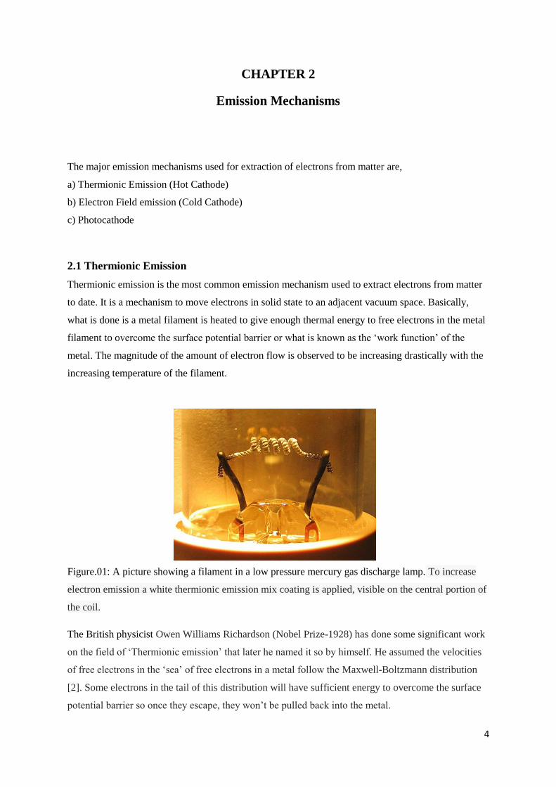
Figure.01: A picture showing a filament in a low pressure mercury gas discharge lamp. To increase
electron emission a white thermionic emission mix coating is applied, visible on the central portion of
the coil.
The British physicist Owen Williams Richardson (Nobel Prize-1928) has done some significant work
on the field of ‘Thermionic emission’ that later he named it so by himself. He assumed the velocities
of free electrons in the ‘sea’ of free electrons in a metal follow the Maxwell-Boltzmann distribution
[2]. Some electrons in the tail of this distribution will have sufficient energy to overcome the surface
potential barrier so once they escape, they won’t be pulled back into the metal.
5
The minimum amount of energy required for an electron to completely escape from the metal surface
is known as its work function which is a characteristic of the metal. For most of the metals this is in
the order of few electron volts. Therefore, thermionic current can be increased by decreasing the work
function. It has been experimentally proven that this can be achieved by applying various oxide layers
on the filament wire. Barium, Calcium and Strontium oxides can be given as some examples.
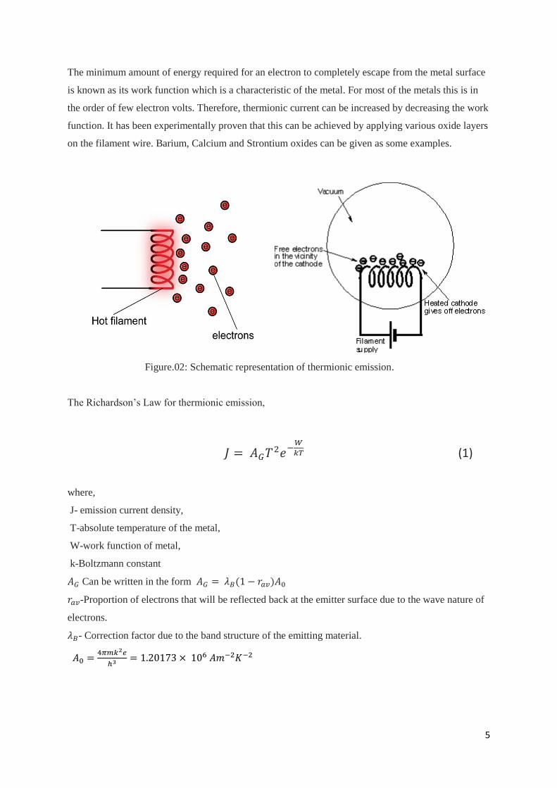
Figure.02: Schematic representation of thermionic emission.
The Richardson’s Law for thermionic emission,
(1)
where,
J- emission current density,
T-absolute temperature of the metal,
W-work function of metal,
k-Boltzmann constant
Can be written in the form
-Proportion of electrons that will be reflected back at the emitter surface due to the wave nature of
electrons.
- Correction factor due to the band structure of the emitting material.
6
Here, m and e arethe mass and the charge of elcetrons and h is Plank’s constant.
In a typical electron emiting device the fillament will be held at a negative potential (cathode.). Let’s
suppose this creates a electic field of magnitude F at the emitter surface.
Without this E-field the surface potential barrier seen by an escaping Fermi level electron be
‘W’,which is the work function.The electric field brings down the surface barrier by an amount ΔW
and thus increases the thermionic current. This is known as the Schottky effect (named after Walter
H.Schottky) or the field enhanced thermionic emission [2]. By simply replacinng W in the
Richardson equation by (W − ΔW) we can model this effect.
√
(2)
wher, ε0 is the electic constant.
This equation is moderately accurate for electric field stength lower than about 108 Vm
−1. For higher
electric field strenghts the so called Fowler-Nordheim (FN) tunneling begins to contribute to the
emission current by a significant amount and in this regime field-enhanced thermionic and field
emission can be modeled by the Murphy-Good equation for thermo-field (T-F) emission. For even
higher electric field strengths FN tunneling becomes the dominant electron emission mechanism and
at here the emitter is in the “cold field electron emission regime”, which is the electon emission
mechanism that will be discussed next.
The following diagram gives a logarithmic plot of some experimental values of anode current versus
filament temperature measurements at three constant anode voltages. Black line represents the
Richardson function for work function W = 4.7 eV.[3]

7
Figure.03: Plot of anode current vs fillament temperature for a termionic emitting fillament.
Thermionic electron emitting sources are used mainly in CRT displays (Televisions, Oscilloscopes),
X-ray generating tubes, transmission electron microscopes and in many and most of the instruments
which requires an electron beam. However, there some drawa bakcs in thermionic emitters which
prevents them from using in certain applications. To name a few,
large amount of energy loss by radiation
inertia of the emitter(a thermionic emitting gun is considerably large and therefore cannot be
fitted into some small electronic instruments)
dimentiona changes due to thermal expansion
the outgassing of species that contribute to vacuum degradation
limited life time from thermal cycling.
2.2 Field Electron Emission (cold emission) Field electron emission is considered as one of the best emission mechanisms among alternative
methods of electron generation. Any place where an electron source is required, we could potentially
use a field electron emitting device. Field electron emitters are particularly important when high
efficiency is necessary, such as in space and portable applications. It’s also effective in producing
high current densities and in applications which requires fast switching or in ultra-high frequency
modulation.
8
Field electron emission (also known as electron field emission and field induced electron emission)
is the emission of electrons from a solid/liquid surface into a dielectric medium which is induced by
an electrostatic field. In contrast with thermionic emission, field electron emission doesn’t require any
heating of electron emitting cathode and therefore it is more generally known as ‘cold emission’.
Field emission can provide bright electron beams with extremely high current density (up to
A. at the emitting site [4]).
However, field emission from pure metals require high strength electrostatic fields with potential
gradient greater than 1 GV/m [5] and depends heavily upon the work function of the metal. Such high
electric fields can only be obtained by the phenomenon known as the local field enhancement. This is
the geometrical enhancement of the electric field caused by the concentration of eclectic field lines
near a conducting solid, shaped as a sharp tip with very low radii of curvature. When very sharp
cathodes are used, the macroscopic electric field needed to induce field emission can be reduced to
about fields with potential gradient of few V/µm are sufficient [4].
The physical mechanism of field emission can be explained by using quantum tunneling. A theory of
field emission from bulk materials has been proposed by Ralph Fowler and Lothar Wolfgang
Nordheim. This is known as Fowler-Nordheim tunneling, which is the wave mechanical tunneling of
electrons through the surface of an electron conductor induced by a high electric field.
A family of approximate equations ‘Fowler-Nodheim equations’ is named after them. Even though,
this model strictly describes field emission from metals at 0 k, it can be used to explain field emission
from some other materials as well.
A very simplified version describing the field emission current from a metallic tip is given below.
[4]
(3)
Where,
I-Emission Current
𝛽 - field enhancement factor
V-Applied voltage
a,b-constants

9
𝛽
d-cathode to anode distance
Figure.04: Schematic diagram of a field emitter, the electric field around the tip is encanced to the
point electrons can tunnel through the surface potential barrier.
2.2.1 Metal cathode field electon emitters
From about 1950 and onwards, extensive effort has been taken for the development of field electron
emitters as electron gun sources. For the generation of a bright and a stable electron beam a ‘large
area field emission source’ is necessary which comprices of a high density of individual field
emission sites created on a subtrate (originally silicon).
One of the early field emitting sources is the ‘Spindt array’ which uses a fabrication technique similar
to the development of silicon-integrated-circuit (IC). These contain very sharp miniature
micromachined metal tips (molybdenum) deposited on small cylindraical voids in an oxide film, with
the void covered by a counterelectrode with a central circular aperture.
Gate(metal) 1 µm Micro tip (metal)
Si substrate
Figure.05: Schematic structure of a Spindt cathode.
V
d

10
2.2.2 Carbon nanotube field electron emitters
Field emission relies heavily on having a very low radius of curvature at the emitting tip. Therefore
it’s essential that the emitting tips’ sharpness remains unaltered during the period of operation.
However, micro machined tips have been shown to be very sensitive and sputtering of cations tends to
dull the tip eventually decreasing the quality of the emission. Hence ultra-high vacuum conditions are
required for this technology which is very expensive and inefficient in industrial scale. Therefore,
researchers initiated looking for other materials that could be grown or deposited as thin films with
required field enhancing properties.
At about 1995, carbon nanotubes rose as a very good potential candidate for a field emitting
material. They showed excellent emission characteristics. Especially because of their shape with high
aspect ratio, they were natural field enhancing objects. Now it’s considered that nanotube films have
the largest potential for technical applications due to their excellent emission characteristic and
relatively ease of fabrication which allows scientists to scale them up for mass production.
Field emission has been observed from Single Wall Nanotubes (SWNT), Multiple Wall Nanotubes
(MWNT) and also nanofibers. However it’s considered that well graphitized nanotubes are superior
field emitters than nanofibers due to their larger dimensions and hence low field enhancement. It’s
unclear whether MWNT or SWNT are better. We might expect single wall nanotubes to have low turn
on voltage due to their higher field enhancing ability, but they exist as bundled ropes which results in
lowering this effect.
MWNT are more mechanical robust than single wall nanotubes due to their multi layered structure.
The choice of nanotube type is often dependent upon the fabrication process selected. MWNTS are
the best choice for in situ chemical vapor deposition process whereas SWNT are used in post
processing emitter fabrication. [4]
11
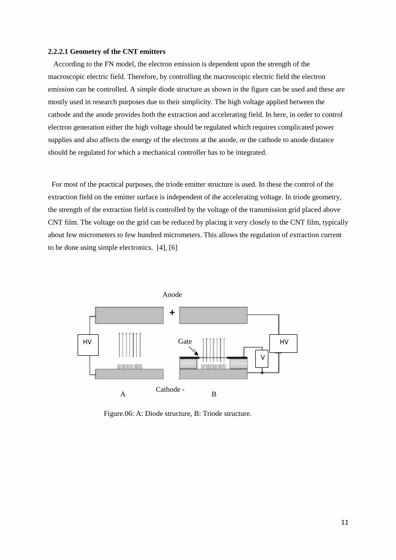
2.2.2.1 Geometry of the CNT emitters
According to the FN model, the electron emission is dependent upon the strength of the
macroscopic electric field. Therefore, by controlling the macroscopic electric field the electron
emission can be controlled. A simple diode structure as shown in the figure can be used and these are
mostly used in research purposes due to their simplicity. The high voltage applied between the
cathode and the anode provides both the extraction and accelerating field. In here, in order to control
electron generation either the high voltage should be regulated which requires complicated power
supplies and also affects the energy of the electrons at the anode, or the cathode to anode distance
should be regulated for which a mechanical controller has to be integrated.
For most of the practical purposes, the triode emitter structure is used. In these the control of the
extraction field on the emitter surface is independent of the accelerating voltage. In triode geometry,
the strength of the extraction field is controlled by the voltage of the transmission grid placed above
CNT film. The voltage on the grid can be reduced by placing it very closely to the CNT film, typically
about few micrometers to few hundred micrometers. This allows the regulation of extraction current
to be done using simple electronics. [4], [6]
A B
Figure.06: A: Diode structure, B: Triode structure.
HV HV
V
Gate
Anode
+
Cathode -
-
12
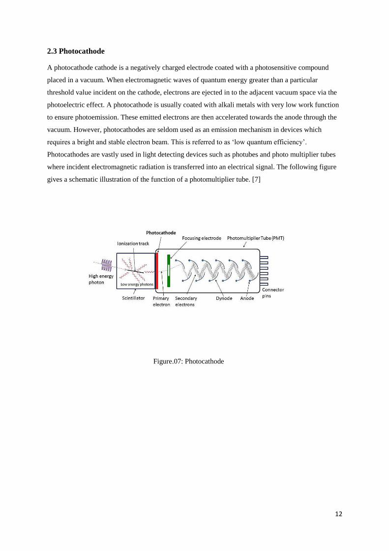
2.3 Photocathode
A photocathode cathode is a negatively charged electrode coated with a photosensitive compound
placed in a vacuum. When electromagnetic waves of quantum energy greater than a particular
threshold value incident on the cathode, electrons are ejected in to the adjacent vacuum space via the
photoelectric effect. A photocathode is usually coated with alkali metals with very low work function
to ensure photoemission. These emitted electrons are then accelerated towards the anode through the
vacuum. However, photocathodes are seldom used as an emission mechanism in devices which
requires a bright and stable electron beam. This is referred to as ‘low quantum efficiency’.
Photocathodes are vastly used in light detecting devices such as photubes and photo multiplier tubes
where incident electromagnetic radiation is transferred into an electrical signal. The following figure
gives a schematic illustration of the function of a photomultiplier tube. [7]
Figure.07: Photocathode
13
CHAPTER 3
Electron Beam Maneuvering
Electrons are negatively charged particles and thus their motion is influenced by electrostatic and
magnetic fields. Depending on the type of application either one or both of these fields are used.
3.1 Force on electrons in an electric field
The relationship between the electric field strength and electric potential is given by;
Ø (4)
which says that electric field strength E(r) at a point r is equivalent to the negative gradient of the
electric potential Ø(r) at that point which is a scalar field at the same point.
Electric potential (Ø) is defined as the electrical potential energy (U) per unit positive test charge.
(5)
The force on a charged particle in an electric field at a point r (x, y, z) is given by
(6)
Here, q is the charge of the particle
for electrons q = -e = -1.60217657 × 10⁻¹⁹
coulombs
Ø(r) (7)
Force on an electron is in opposite direction to the direction of electric field lines in a particular point.
3.1.1 Uniform Electric Fields
In a uniform electric field, both the direction and magnitude of electric field is constant over the space
considered. The electric field formed between two conducting plates with a constant voltage
difference is approximated as a uniform electric field (ignoring the edge effects). The magnitude of
electric field is then given by;
(8)
where, is the potential difference between two plates and d is the plate separation.
Therefore, magnitude of the force on an electron between two parallel conducting plates with a
potential difference of and plate separation of d;
(9)
In the direction of negative plate to positive plate, i.e. towards the opposite direction of electric field
lines.
14
Figure.08: The force on an electron in a uniform electric field between two parallel conducting plates.
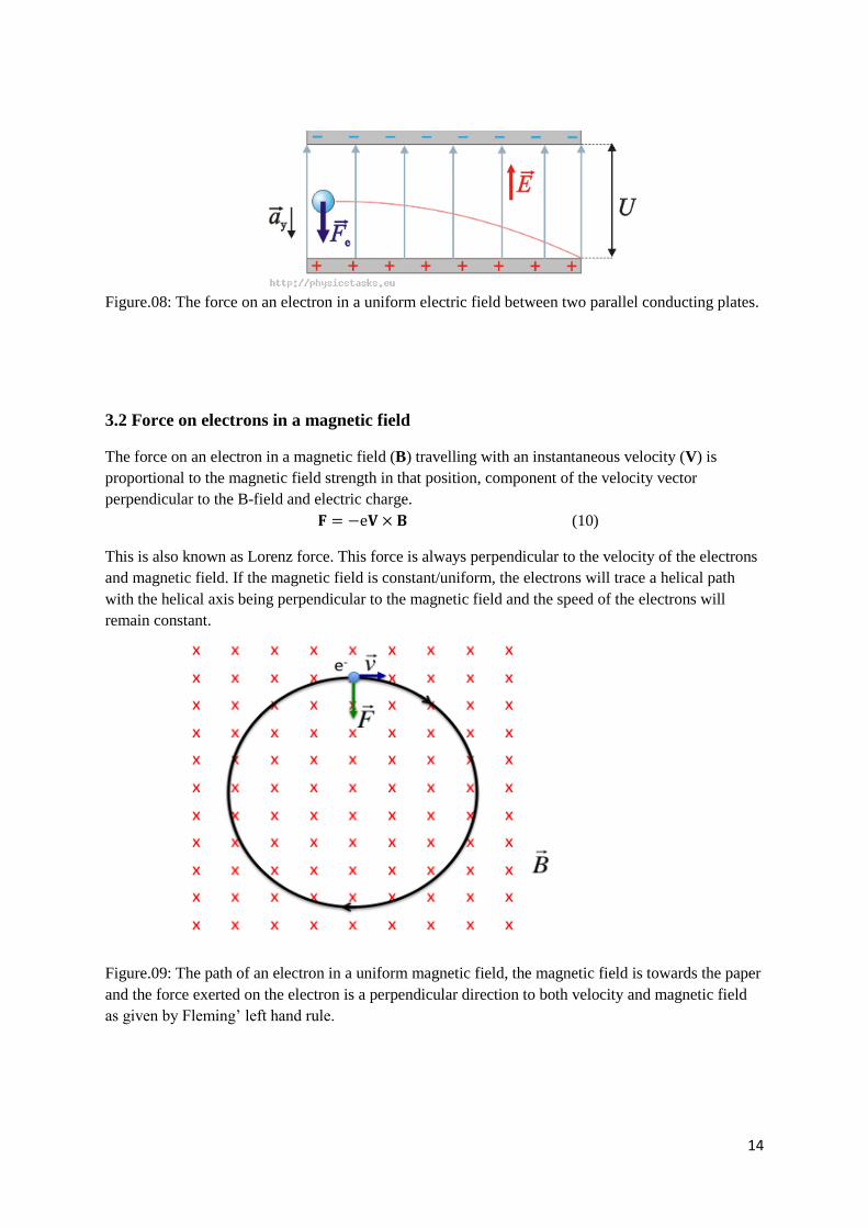
3.2 Force on electrons in a magnetic field
The force on an electron in a magnetic field (B) travelling with an instantaneous velocity (V) is
proportional to the magnetic field strength in that position, component of the velocity vector
perpendicular to the B-field and electric charge.
(10)
This is also known as Lorenz force. This force is always perpendicular to the velocity of the electrons
and magnetic field. If the magnetic field is constant/uniform, the electrons will trace a helical path
with the helical axis being perpendicular to the magnetic field and the speed of the electrons will
remain constant.
Figure.09: The path of an electron in a uniform magnetic field, the magnetic field is towards the paper
and the force exerted on the electron is a perpendicular direction to both velocity and magnetic field
as given by Fleming’ left hand rule.

15
3.3 Usage
3.3.1 Cathode ray tube (CRT)
Electrons generated inside a cathode ray tube (CRT), should be accelerated, focused and deflected to
make the electrons hit the correct phosphor pixel with required intensity and energy.
Typically, a high voltage (about 1 to 20 kV) is used to accelerate electrons to large speeds. Electrons
are focused either by using a focusing anode (electrostatic) or electromagnetic coils (magnetic). Then,
to deflect electrons both the electrostatic deflection plates and electromagnetic coils are used. In large
CRTs where the electron beam has to be deflected by large angles, magnetic deflection coils are used,
like in most televisions. In small CRTs such as is oscilloscopes where the angle of deflection required
is small, electrostatic deflection plates are used. [8]
Figure.10: A CRT which uses electric fields in both focusing and deflecting the electron beam.
Figure.11: A CRT that uses magnetic fields in focusing and deflecting electrons.
16
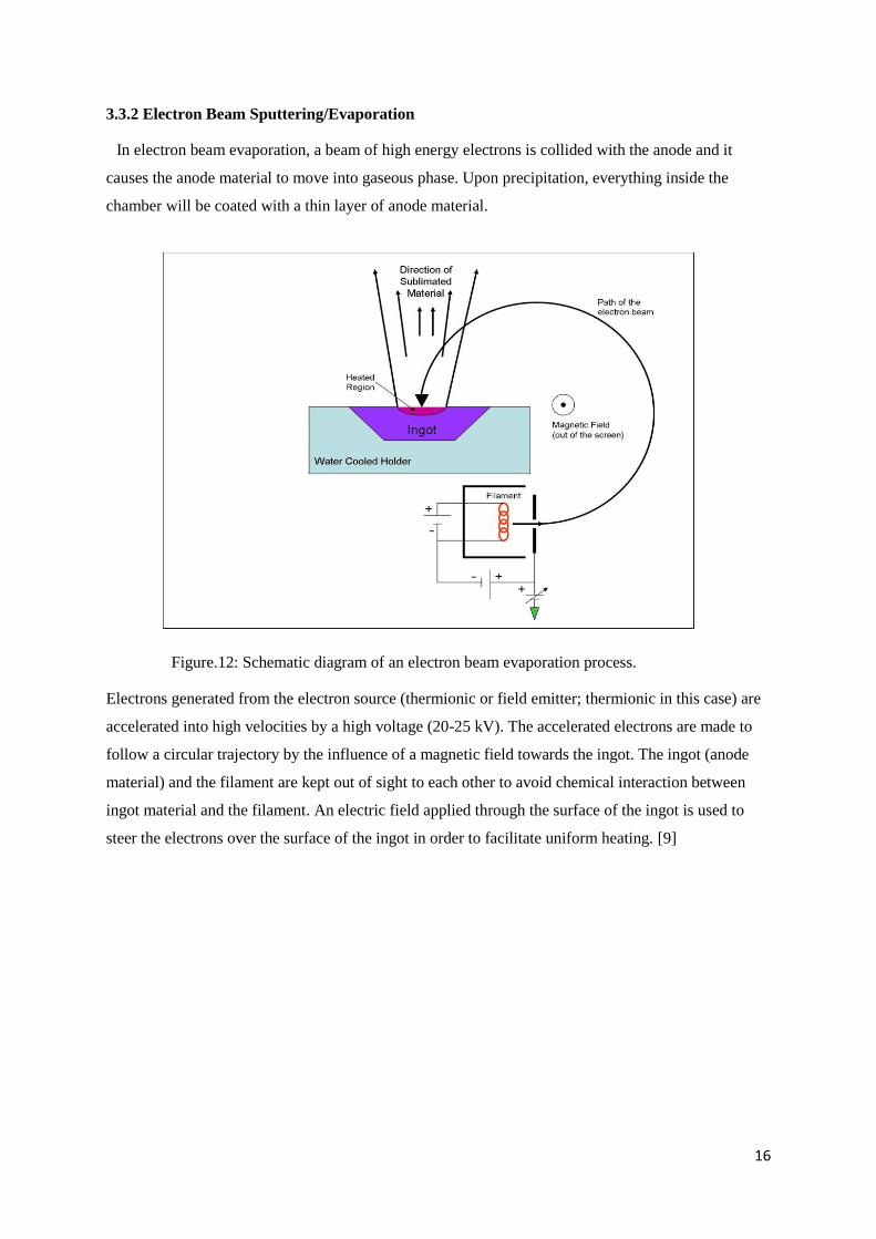
3.3.2 Electron Beam Sputtering/Evaporation
In electron beam evaporation, a beam of high energy electrons is collided with the anode and it
causes the anode material to move into gaseous phase. Upon precipitation, everything inside the
chamber will be coated with a thin layer of anode material.
Figure.12: Schematic diagram of an electron beam evaporation process.
Electrons generated from the electron source (thermionic or field emitter; thermionic in this case) are
accelerated into high velocities by a high voltage (20-25 kV). The accelerated electrons are made to
follow a circular trajectory by the influence of a magnetic field towards the ingot. The ingot (anode
material) and the filament are kept out of sight to each other to avoid chemical interaction between
ingot material and the filament. An electric field applied through the surface of the ingot is used to
steer the electrons over the surface of the ingot in order to facilitate uniform heating. [9]
17
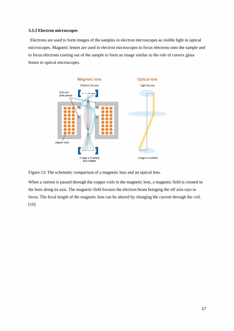
3.3.3 Electron microscopes
Electrons are used to form images of the samples in electron microscopes as visible light in optical
microscopes. Magnetic lenses are used in electron microscopes to focus electrons onto the sample and
to focus electrons coming out of the sample to form an image similar to the role of convex glass
lenses in optical microscopes.
Figure.13: The schematic comparison of a magnetic lens and an optical lens.
When a current is passed through the copper coils in the magnetic lens, a magnetic field is created in
the bore along its axis. The magnetic field focuses the electron beam bringing the off axis rays to
focus. The focal length of the magnetic lens can be altered by changing the current through the coil.
[10]
18
CHAPTER 4
CURRENT DEVELOPMENTS
4.1 Application of carbon nanotube field emitters
As discussed in the section 2.2- ‘Field electron emission’ under Emission Mechanisms, carbon
nanotube field emitters have the largest potential to be used as an electron source in modern
applications. This is due to some attractive qualities accompanied with them such as;
High energy efficiency over thermionic emitters.
Device size can be reduced since a CNT field emitter is in the scale of only a few
micrometers. I.e. can be also used in handheld devices.
Very robust when compared with micro machined metal tip field emitters against destructive
arcing.
Can obtain very high current densities (>1 A/ ) which is essential in instruments like
SEM, TEM.
There are already some instruments which uses CNT field emitting cathodes such as in handheld
XRD machines and some possible applications are under development.
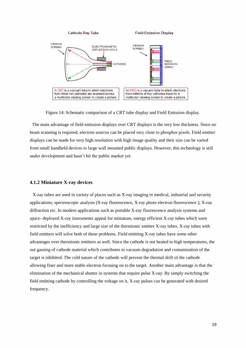
4.1.1 Field emission display
CRT displays has been largely overseen by technologies such as LCD, Plasma displays and OLED
due to its high power requirement and large size. But CRT displays are superior over these by
qualities such as high image contrast, brightness and large field of view. Since CNT field emitters are
very energy efficient and very small in size, attention was drawn to use CNT field emitter arrays in
place of thermionic emitter in CRT displays. In fact, the initial motive behind the developing of
CNT field emitters were to be used in field emitter displays. The idea is to dedicate a separate CNT
field emitter for each phosphor pixel rather than scanning a single beam of electrons throughout all
the pixels to produce an image. This is commonly referred as ‘pixel addressing’. [11]
19
Figure.14: Schematic comparison of a CRT tube display and Field Emission display.
The main advantage of field emission displays over CRT displays is the very low thickness. Since no
beam scanning is required, electron sources can be placed very close to phosphor pixels. Field emitter
displays can be made for very high resolution with high image quality and their size can be varied
from small handheld devices to large wall mounted public displays. However, this technology is still
under development and hasn’t hit the public market yet.
4.1.2 Miniature X-ray devices
X-ray tubes are used in variety of places such as X-ray imaging in medical, industrial and security
applications; spectroscopic analysis (X-ray fluorescence, X-ray photo electron fluorescence ); X-ray
diffraction etc. In modern applications such as portable X-ray fluorescence analysis systems and
space- deployed X-ray instruments appeal for miniature, energy efficient X-ray tubes which were
restricted by the inefficiency and large size of the thermionic emitter X-ray tubes. X-ray tubes with
field emitters will solve both of these problems. Field emitting X-ray tubes have some other
advantages over thermionic emitters as well. Since the cathode is not heated to high temperatures, the
out gassing of cathode material which contributes to vacuum degradation and contamination of the
target is inhibited. The cold nature of the cathode will prevent the thermal drift of the cathode
allowing finer and more stable electron focusing on to the target. Another main advantage is that the
elimination of the mechanical shutter in systems that require pulse X-ray. By simply switching the
field emitting cathode by controlling the voltage on it, X-ray pulses can be generated with desired
frequency.
20
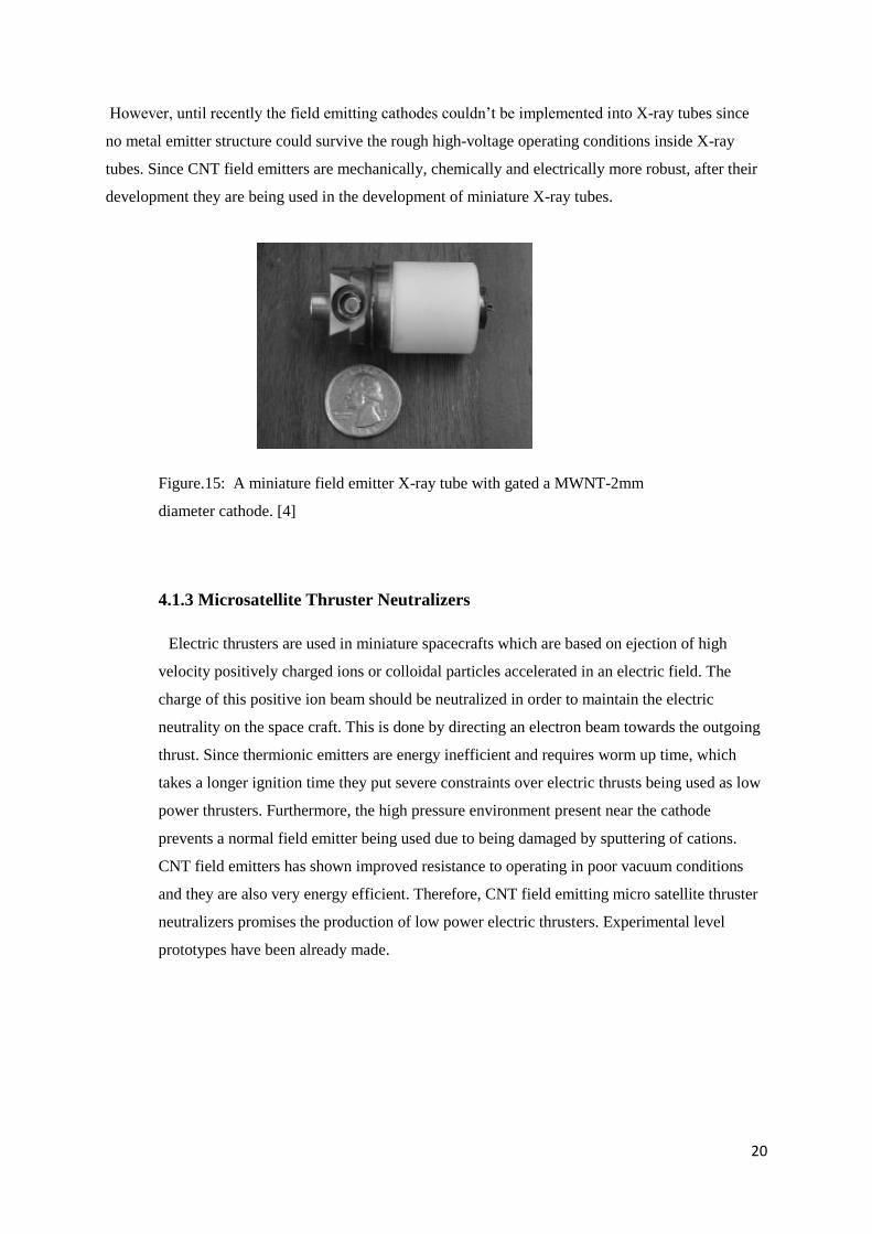
However, until recently the field emitting cathodes couldn’t be implemented into X-ray tubes since
no metal emitter structure could survive the rough high-voltage operating conditions inside X-ray
tubes. Since CNT field emitters are mechanically, chemically and electrically more robust, after their
development they are being used in the development of miniature X-ray tubes.
Figure.15: A miniature field emitter X-ray tube with gated a MWNT-2mm
diameter cathode. [4]
4.1.3 Microsatellite Thruster Neutralizers
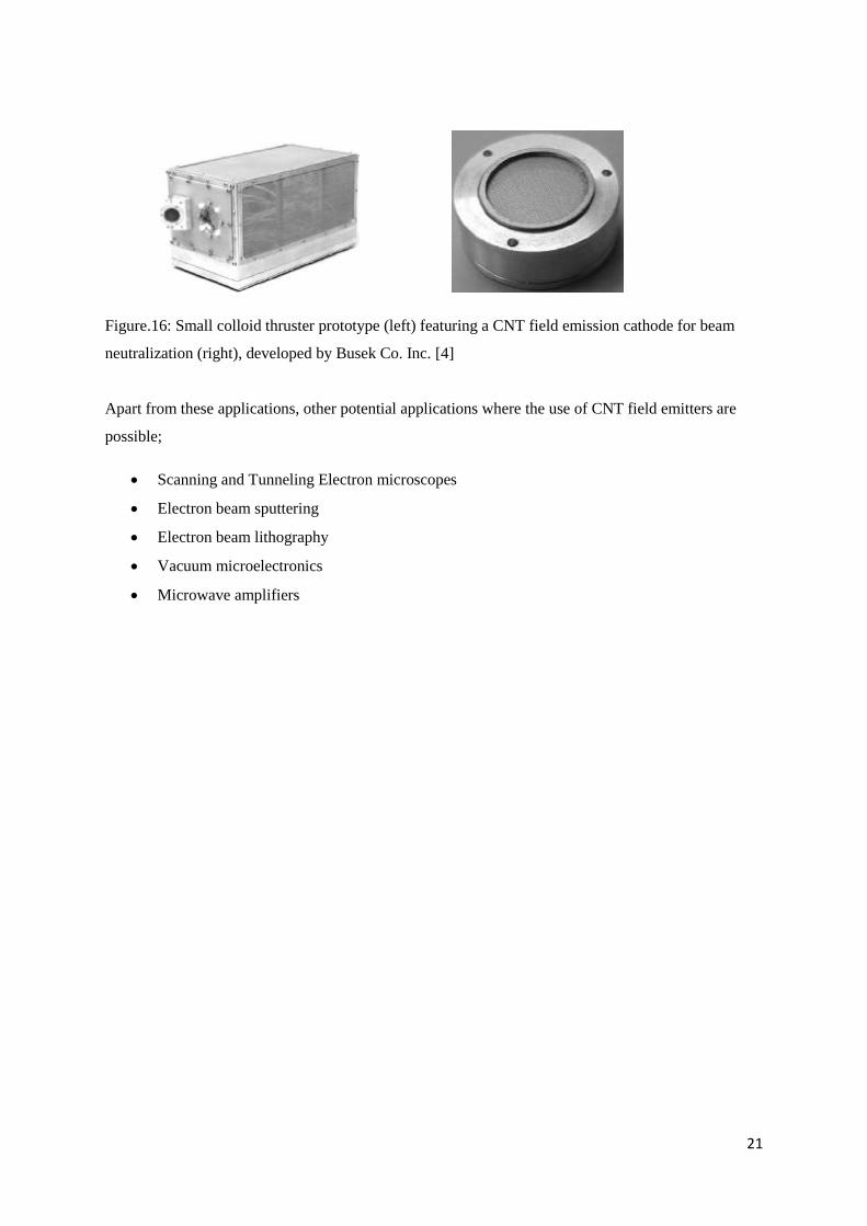
Electric thrusters are used in miniature spacecrafts which are based on ejection of high
velocity positively charged ions or colloidal particles accelerated in an electric field. The
charge of this positive ion beam should be neutralized in order to maintain the electric
neutrality on the space craft. This is done by directing an electron beam towards the outgoing
thrust. Since thermionic emitters are energy inefficient and requires worm up time, which
takes a longer ignition time they put severe constraints over electric thrusts being used as low
power thrusters. Furthermore, the high pressure environment present near the cathode
prevents a normal field emitter being used due to being damaged by sputtering of cations.
CNT field emitters has shown improved resistance to operating in poor vacuum conditions
and they are also very energy efficient. Therefore, CNT field emitting micro satellite thruster
neutralizers promises the production of low power electric thrusters. Experimental level
prototypes have been already made.
21
Figure.16: Small colloid thruster prototype (left) featuring a CNT field emission cathode for beam
neutralization (right), developed by Busek Co. Inc. [4]
Apart from these applications, other potential applications where the use of CNT field emitters are
possible;
Scanning and Tunneling Electron microscopes
Electron beam sputtering
Electron beam lithography
Vacuum microelectronics
Microwave amplifiers
22
REFERENCES
[1]. Wikipedia (26 November 2014).Cathode ray tube. [ONLINE] Available at: .
http://en.wikipedia.org/wiki/Cathode_ray . [Last Accessed 28 th December 2014].
[2]. Wikipedia (23 November 2014). Thermionic emission. [ONLINE] Available at:
http://en.wikipedia.org/wiki/Thermionic_emission. [Last Accessed 28th November 2014]
[3]. Jones & Langmuir , (1927). ''. In: (ed), The Characteristics of Tungsten Filaments as
Functions of Temperature. 1st ed. : . pp.Part I pp. 310–19, Part II pp. 354–61, Part III pp.
408–12.
[4]. Meyyappan M, (2005). 'Field Emission'. CARBON NANOTUBES SCIENCE AND
APPLICATIONS. 1st ed. United States of America: CRC Press LLC. pp.195-211.
[5]. Wikipedia (22 September 2014). Field electron emission. [ONLINE] Available at:
http://en.wikipedia.org/wiki/Field_electron_emission. [Last Accessed 22nd November 2014].
[6]. Tyrrell J (Feb 7, 2008). Stacked nanotubes enhance field emission . [ONLINE] Available at:
http://nanotechweb.org/cws/article/tech/32726#. [Last Accessed 22nd November 2014].
[7]. Wikipedia ( 28 June 2014). Photocathode. [ONLINE] Available at:
http://en.wikipedia.org/wiki/Photocathode. [Last Accessed 28th December 2014].
[8]. Wikipedia (20 December 2014). Cathode ray tube. [ONLINE] Available at:
http://en.wikipedia.org/wiki/Cathode_ray_tube. [Last Accessed 28 th December 2014].
[9]. Wikipedia (7th May 2014). Electron beam physical vapor deposition. [ONLINE] Available
at: http://en.wikipedia.org/wiki/Electron_beam_physical_vapor_deposition. [Last Accessed
23 rd November 2014].
[10]. University of Liverpool (2007). Electromagnetic Lenses. [ONLINE] Available at:
Electromagnetic Lenses. [Last Accessed 22nd November 2014].
[11]. David A. Cathey, Charles Watkins (Jan 9, 2001). Field emission display. [ONLINE]
Available at: http://www.google.com/patents/US6172456. [Last Accessed 28 th December
2014].
Copyright © 2022 FDOKUMEN