
AM Modulation and Demodulation
17
www.cypress.com Document No. 001-62582 Rev. *F 1 AN62582 AM Modulation and Demodulation Author: Pavankumar Vibhute Associated Part Family: All PSoC 3 and PSoC 5LP parts Associated Project: Yes Software Version: PSoC ® Creator™ 3.2 Related Application Notes: None To get the latest version of this application note, or the associated project file, please visit http://www.cypress.com/go/AN62582 . AN62582 explains how to implement amplitude modulation (AM) and demodulation using PSoC ® 3 and PSoC 5LP. AM is achieved by multiplying carrier and message signals. Demodulation is achieved by sampling the AM signal at carrier frequency. Contents 1 Introduction ...............................................................1 2 Mixer Component .....................................................2 2.1 Up Mixer ..........................................................3 2.2 Down Mixer ......................................................4 3 AM Generation .........................................................5 3.1 PSoC 3 and PSoC 5LP Implementation ..........6 3.2 Examples - Modulation ....................................8 4 Demodulation ......................................................... 10 4.1 PSoC 3 and PSoC 5LP Implementation ........ 11 4.2 Example - Demodulation ............................... 14 5 Summary ................................................................ 15 Document History............................................................ 16 Worldwide Sales and Design Support ............................. 17 Products .......................................................................... 17 PSoC ® Solutions ............................................................. 17 Cypress Developer Community....................................... 17 Technical Support ........................................................... 17 1 Introduction Amplitude modulation (AM) is defined as modifying the amplitude of the carrier wave according to the message or information signal. AM generation involves mixing of a carrier and an information signal. There are two methods to generate AM: Low level modulation and High level modulation In low level modulation, the message signal and carrier signal are modulated at low power levels and then amplified. The advantage of this technique is that a small audio amplifier is sufficient to amplify the message signal. The disadvantage is that the linear amplifiers are necessary to amplify the modulated signal to transmitter levels. Nonlinear amplifiers cause distortion of the modulated wave. In this application note, the modulation is inside PSoC 3 and PSoC 5LP at low power levels (not at the transmitting power levels); this is low level modulation technique. In high level modulation, the carrier and message signals are sufficiently amplified to the transmitting levels and modulation is done at high power levels. The advantage of this technique is that nonlinear high-efficiency amplifiers can be used to amplify the signals. The disadvantage is that large audio amplifier needs to be used to amplify the message signal.
-
Upload
khangminh22 -
Category
Documents
-
view
3 -
download
0
Transcript of AM Modulation and Demodulation

www.cypress.com Document No. 001-62582 Rev. *F 1
AN62582
AM Modulation and Demodulation
Author: Pavankumar Vibhute
Associated Part Family: All PSoC 3 and PSoC 5LP parts
Associated Project: Yes
Software Version: PSoC® Creator™ 3.2
Related Application Notes: None
To get the latest version of this application note, or the associated project file, please visit http://www.cypress.com/go/AN62582.
AN62582 explains how to implement amplitude modulation (AM) and demodulation using PSoC® 3 and PSoC 5LP.
AM is achieved by multiplying carrier and message signals. Demodulation is achieved by sampling the AM signal at
carrier frequency.
Contents
1 Introduction ............................................................... 1 2 Mixer Component ..................................................... 2
2.1 Up Mixer .......................................................... 3 2.2 Down Mixer ...................................................... 4
3 AM Generation ......................................................... 5 3.1 PSoC 3 and PSoC 5LP Implementation .......... 6 3.2 Examples - Modulation .................................... 8
4 Demodulation ......................................................... 10 4.1 PSoC 3 and PSoC 5LP Implementation ........ 11
4.2 Example - Demodulation ............................... 14 5 Summary ................................................................ 15 Document History ............................................................ 16 Worldwide Sales and Design Support ............................. 17 Products .......................................................................... 17 PSoC
® Solutions ............................................................. 17
Cypress Developer Community....................................... 17 Technical Support ........................................................... 17
1 Introduction
Amplitude modulation (AM) is defined as modifying the amplitude of the carrier wave according to the message or information signal. AM generation involves mixing of a carrier and an information signal.
There are two methods to generate AM:
Low level modulation and
High level modulation
In low level modulation, the message signal and carrier signal are modulated at low power levels and then amplified. The advantage of this technique is that a small audio amplifier is sufficient to amplify the message signal. The disadvantage is that the linear amplifiers are necessary to amplify the modulated signal to transmitter levels. Nonlinear amplifiers cause distortion of the modulated wave. In this application note, the modulation is inside PSoC 3 and PSoC 5LP at low power levels (not at the transmitting power levels); this is low level modulation technique.
In high level modulation, the carrier and message signals are sufficiently amplified to the transmitting levels and modulation is done at high power levels. The advantage of this technique is that nonlinear high-efficiency amplifiers can be used to amplify the signals. The disadvantage is that large audio amplifier needs to be used to amplify the message signal.

AM Modulation and Demodulation
www.cypress.com Document No. 001-62582 Rev. *F 2
The modulation in PSoC 3 and PSoC 5LP is achieved using the mixer component in “Up Mixer” mode. A square wave with carrier frequency is multiplied with the message signal. The output of the mixer is filtered using a band pass filter to remove harmonics.
The modulation index of AM is the extent of amplitude variation about an unmodulated carrier amplitude level. The higher the message signal amplitude, the larger the variation on the amplitude of the AM wave.
In the section, “Examples - Modulation” on page 8, examples 1, 2, and 3 show the AM for different modulation indices. The message signal power is increased keeping the carrier level constant to get different modulation indices. Example 4 shows the AM waves with different carrier power levels.
In some applications, power is saved by suppressing the carrier from the AM wave. Example 5 shows the double side band suppressed carrier (DSBSC) AM wave.
The “coherent detection” method is used for demodulation. Coherent demodulation involves multiplication of an AM wave by a carrier wave. In this implementation, a square wave with the same frequency as that of carrier wave is generated by passing the input AM wave through a zero crossing detector (ZCD). This square wave and the AM wave are given to the Mixer component in “Down Mixer” mode. The output of the mixer is filtered by a low-pass filter (LPF) to get the message signal.
2 Mixer Component
PSoC Creator provides a “Mixer” component. It can be used for frequency conversion of an input signal using a local oscillator (LO) signal as the sampling clock. Figure 1 shows the mixer component in PSoC Creator.
The Mixer component can be configured in two configurations:
1. Up Mixer
2. Down Mixer
Figure 1. Mixer Component
AM Modulation and Demodulation
www.cypress.com Document No. 001-62582 Rev. *F 3
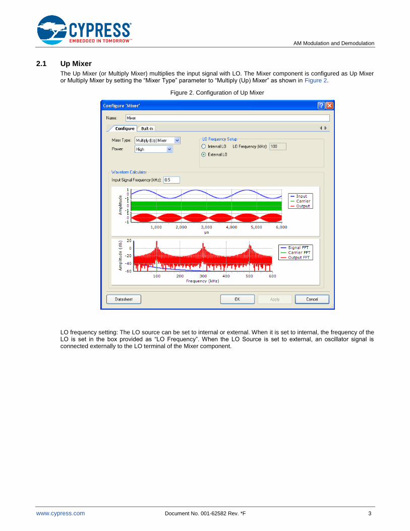
2.1 Up Mixer
The Up Mixer (or Multiply Mixer) multiplies the input signal with LO. The Mixer component is configured as Up Mixer or Multiply Mixer by setting the “Mixer Type” parameter to “Multiply (Up) Mixer” as shown in Figure 2.
Figure 2. Configuration of Up Mixer
LO frequency setting: The LO source can be set to internal or external. When it is set to internal, the frequency of the LO is set in the box provided as “LO Frequency”. When the LO Source is set to external, an oscillator signal is connected externally to the LO terminal of the Mixer component.

AM Modulation and Demodulation
www.cypress.com Document No. 001-62582 Rev. *F 4
2.2 Down Mixer
The Down Mixer (or Sample Mixer) operates as a sample and hold circuit on the input signal. The Mixer component is configured as Down Mixer by setting the “Mixer Type” parameter to “Sample (Down) Mixer” as shown in Figure 3.
Figure 3. Configuration of Down Mixer
LO frequency setting: The LO Source can be set to internal or external. When it is set to internal, the frequency of the LO is set in the box provided as “LO Frequency”. When the LO source is set to external, an oscillator signal is connected externally to the LO terminal of the Mixer component.

AM Modulation and Demodulation
www.cypress.com Document No. 001-62582 Rev. *F 5
3 AM Generation
Figure 4. AM Generation
c(t)
K(offset) +m(t)
AM
( K+m(t) ) * c(t)
Mixer
c(t)= Carrier Signal
m(t)= Message Signal
m(t) is message signal,
m(t) = Am cos (2 Π fmt) Equation 1
where, fm is frequency of message signal and Am is amplitude of message signal.
c(t) is a carrier signal,
c(t) = cos (2 Π fct) Equation 2
where, fc is frequency of carrier signal and Am is amplitude of carrier signal.
Offset of ‘K’ is added to the message signal:
AM = (K + m(t) ) × c(t) = K cos (2 Π fct) + Am cos (2 Π fmt) × cos (2 Π fct) Equation 3
If the message signal is given with zero offset, you get a suppressed carrier AM,
AM = m(t) × c(t) = Am cos (2 Π fmt) × cos (2 Π fct) Equation 4
Figure 5. Suppressed Carrier AM Generation
c(t)
m(t)
AM
m(t) x c(t)
Mixer
c(t)= Carrier Signal
m(t)= Message Signal

AM Modulation and Demodulation
www.cypress.com Document No. 001-62582 Rev. *F 6
3.1 PSoC 3 and PSoC 5LP Implementation
Figure 6. Amplitude Modulation
The Voltage DAC (VDAC) provides offset to the message signal m(t). The message signal and carrier signal are multiplied by mixer; therefore, the carrier component strength in the resulting AM wave is determined by this offset voltage (see Figure 4).
By varying this offset voltage, the carrier level in AM is controlled. The message signal should be biased on top of this DC offset voltage and fed to mixer.
The reference Vdda/2 provides the AGND for all signals and to the mixer. The offset of the message signal should be above AGND. Thus, VDAC voltage value should be VDAC = AGND + offset (K).
As an example, a square wave of 100 kHz is used as a carrier signal. The square wave has odd harmonics such as 300 kHz and 500 kHz in it. When it is multiplied with the message signal with frequency, fM, it produces double sided AM with components ‘fC + fM’ and ‘fC – fM’. However, there are also harmonics ‘3fC + fM’, ‘3fC – fM’, and so on. To remove these higher harmonics the band pass filter with bandwidth 10 kHz and center frequency 100 kHz is put at the mixer output. The mixer component type is set to ‘Up Mixer’ (or ‘Multiply Mixer’). The Up Mixer is used for modulation because it gives a gain of 1 for the up converted frequency; the Down Mixer gives a lesser gain. The band pass filter with cutoff frequency 100 kHz and bandwidth of 10 kHz is built as follows. This is a band pass filter with low Q factor.
Lowest frequency of pass band fL = 90 kHz
Highest frequency of pass band fH = 110 kHz
fL = 1/2 Π R1C1, fH = 1/2 Π R2C2.

AM Modulation and Demodulation
www.cypress.com Document No. 001-62582 Rev. *F 7
3.1.1 Frequency Range
The Up_Mixer maximum frequency ranges are as below:
Max message signal frequency: 500 kHz
Max carrier signal frequency: 1 MHz
Figure 7. Frequency Spectrum for AM
-100
kHz
100
kHz
f
f
Amplitude
500
Hz
-500
Hz
500 Hz Signal
100 kHz carrier
Amplitude
modulated wave
300
kHz
-300
kHz
-100
kHz
100
kHz
f300
kHz
-300
kHz
BPF BPF

AM Modulation and Demodulation
www.cypress.com Document No. 001-62582 Rev. *F 8
3.2 Examples - Modulation
The following examples show AM waveforms for different modulation indices. Modulation index can be defined as the measure of extent of amplitude variation about a unmodulated carrier. The modulation index is an important factor. When a level of modulation is too low, the modulation does not utilize the carrier efficiently and if a level of modulation is too high, the carrier can become over modulated causing sidebands to extend out beyond the allowed bandwidth causing interference to other users. In the following figures, the waveform in cyan color is message signal and waveform in yellow is the AM.
3.2.1 Example 1 : With Modulat ion Index (u) = 50%
Vdda = 5 V
AGND = Vdda/2 = 2.5 V
VDAC = AGND + 1 V (K) = 3.5 V
Message amplitude = Am = 0.5 V
Carrier amplitude = K = 1 V
u = (Max – Min) / (Max + Min); Max and Min are shown in Figure 8.
u = (3 – 1) / (3 + 1) = 0.5
Figure 8. AM with 50% Modulation
3.2.2 Example 2 : With Modulat ion Index (u) = 25%
Message signal strength is reduced keeping the carrier strength same.
Message amplitude = Am = 0.25 V
Vdda = 5 V
AGND = Vdda/2 = 2.5 V
VDAC = AGND + 1 V (K) = 3.5 V
Carrier amplitude = K = 1 V
u = (Max – Min) / (Max + Min); Max and Min are shown in Figure 9.
u = (2.5 – 1.5) / (2.5 + 1.5) = 0.25
Figure 9. AM with 25% Modulation

AM Modulation and Demodulation
www.cypress.com Document No. 001-62582 Rev. *F 9
3.2.3 Example 3 : With Modulat ion Index (u) = 100%
Message signal strength is amplified, keeping the carrier strength same.
Message amplitude = Am = 1 V
Vdda = 5 V
AGND = Vdda/2 = 2.5 V
VDAC = AGND + 1 V (K) = 3.5 V
Carrier amplitude = K = 1 V
u = (Max – Min) / (Max + Min); Max and Min are shown in Figure 10.
u = (4 – 0) / (4 + 0) = 1
Figure 10. AM with 100% Modulation
3.2.4 Example 4 : Showing Di fferent Carr ier Level for 50% Modulat ion
Carrier amplitude = K = 0.5 V
Message amplitude = Am = 0.25 V
Vdda = 5 V
AGND = Vdda/2 = 2.5 V
VDAC= AGND + 0.5 V (K) = 3 V
u = (Max – Min) / (Max + Min)
u = (1.5 – 0.5) / (1.5 + 0.5) = 0.5
Figure 11. AM with 0.5 V Carrier Amplitude
Carrier amplitude = K = 1 V
Message amplitude = Am = 0.5 V
Vdda = 5 V
AGND = Vdda/2 = 2.5 V
VDAC = AGND + 1 V (K) = 3.5 V
u = (Max – Min) / (Max + Min)
u = (3 – 1) / (3 + 1) = 0.5
Figure 12: AM with 1 V Carrier Amplitude
AM Modulation and Demodulation
www.cypress.com Document No. 001-62582 Rev. *F 10
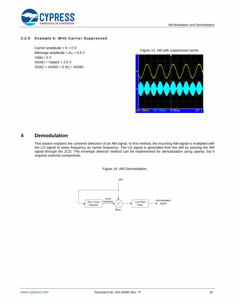
3.2.5 Example 5 : With Carrier Suppressed
Carrier amplitude = K = 0 V
Message amplitude = Am = 0.5 V
Vdda = 5 V
AGND = Vdda/2 = 2.5 V
VDAC = AGND + 0 (K) = AGND
Figure 13. AM with suppressed carrier
4 Demodulation
This section explains the coherent detection of an AM signal. In this method, the incoming AM signal is multiplied with the LO signal of same frequency as carrier frequency. The LO signal is generated from the AM by passing the AM signal through the ZCD. The envelope detector method can be implemented for demodulation using opamp, but it requires external components.
Figure 14. AM Demodulation
Local
Oscillator
AM
Low Pass
Filter
Demodulated
signalZero Cross
Detector
Mixer

AM Modulation and Demodulation
www.cypress.com Document No. 001-62582 Rev. *F 11
4.1 PSoC 3 and PSoC 5LP Implementation
Figure 15. Top Design for AM Demodulation Page 1 - AM_Demodulator

AM Modulation and Demodulation
www.cypress.com Document No. 001-62582 Rev. *F 12
Figure 16. Top Design for AM Demodulation Page 2 - Filter
The Vdda/2 reference voltage is buffered and used as an analog ground (AGND) for the circuit. The incoming AM signal should be biased at this DC voltage.

AM Modulation and Demodulation
www.cypress.com Document No. 001-62582 Rev. *F 13
The AM signal is given to comparator whose reference is AGND. The output of the comparator is square wave with frequency same as the carrier frequency of AM signal. The output of the comparator is used as a LO signal for the mixer. The mixer type is set to Down Mixer (or Sample Mixer).The Down Mixer gives a gain close to ‘1’ (when the signal is sampled at peaks) for the down converted signal. The Down Mixer output has lower harmonic content than up mixer when the input signal and LO signal have near same frequencies. The Mixer samples the input AM signal at the rising edges of the LO as shown in following figure. The LPF is used to filter the demodulated output to remove the sample and hold effect on the output of mixer.
Figure 17. AM Wave Sampled by Mixer Component
The sample and hold gives maximum output when the signal is sampled at peaks. The comparator output delay plays an important role in the demodulation. The ideal delay that gives maximum output is quarter period (90°) of the carrier. See Figure 18. When the delay is 90°, the mixer samples the AM wave at the peaks. A delay lesser than 90° still gives a demodulated output; however, the amplitude level is reduced. The comparator typical delay is 90 ns. This delay makes the mixer sample the AM wave within 45° to 135° from the zero crossing for the frequency range 1.25 MHz to 4 MHz. If the signal frequency is out of this range then, either external delay circuit should be added on the signal before giving it to ZCD or the signal should be brought within the range before demodulating it.
Figure 18. Comparator Delay of 90° Making Sampling at Peak
900
You need a LPF to remove the high frequency components of the mixer output. The Sallen-Key LPF with 1 kHz cutoff is built using opamp as follows.
For Sallen-Key low-pass filter,
Cutoff frequency, fC = 1/2Π(R1 R2 C1 C2)1/2
fC = 1/ 2Π(146.5kΩ × 78.67kΩ × 1nF × 2.2 nF)0.5
= 1 kHz.

AM Modulation and Demodulation
www.cypress.com Document No. 001-62582 Rev. *F 14
4.1.1 Frequency Range
The Down Mixer maximum frequency ranges are as below:
Max AM Carrier Signal Frequency: 4 MHz
Figure 19. Frequency Spectrum for AM and Demodulated Signal
1.2 MHz0 Hz f
Mixer Output
AM Signal
1.2 MHz f–1.2 MHz
Amplitude
1.2 MHz
LPF
Demodulated
Output
4.2 Example - Demodulation
AM wave amplitude = 1 V
Carrier frequency = 1.2 MHz
Message frequency = 500 Hz
Modulation index (u) = 50%
Figure 20. Example of AM Demodulation

AM Modulation and Demodulation
www.cypress.com Document No. 001-62582 Rev. *F 15
5 Summary
Implementing the AM modulation and demodulation using the mixer component in PSoC 3 and PSoC 5LP is discussed in the application note. Also, the AM modulation with different modulation indices, carrier levels, and suppressed carrier is discussed. AM demodulation using the coherent detection method is also demonstrated.
About the Author Name: Pavankumar Vibhute.
Title: Applications Engineer Sr.

AM Modulation and Demodulation
www.cypress.com Document No. 001-62582 Rev. *F 16
Document History
Document Title: AN62582 - AM Modulation and Demodulation
Document Number: 001-62582
Revision ECN Orig. of Change
Submission Date
Description of Change
** 2968090 PVKV 07/02/10 New application note.
*A 3302878 PVKV 07/05/11 Minor text edits.
Added Mixer Component.
Updated Demodulation:
Updated PSoC 3 and PSoC 5LP Implementation:
Added Figure 17.
*B 3444026 PVKV 11/30/11 Updated Software Version as “PSoC® Creator™ 2.0” in page 1.
Updated Abstract.
Updated the figures for PSoC Creator 2.0.
Updated to new template.
*C 3670276 PVKV 07/09/2012 Minor text edits to remove grammatical errors and improve readability.
Updated to new template.
*D 3809511 PVKV 11/09/2012 Updated Associated Part Family as “All PSoC 3 and PSoC 5LP parts” in page 1.
Updated Software Version as “PSoC® Creator™ 2.1 SP1” in page 1.
Updated attached associated project.
*E 4853876 PVKV 07/27/2015 Updated Software Version as “PSoC® Creator™ 3.2” in page 1.
Updated AM Generation:
Updated PSoC 3 and PSoC 5LP Implementation:
Updated Figure 6.
Updated Examples - Modulation:
Updated Example 4: Showing Different Carrier Level for 50% Modulation:
Updated Figure 11 (Updated figure caption only).
Updated Figure 12 (Added figure caption only).
Updated Demodulation:
Updated PSoC 3 and PSoC 5LP Implementation:
Updated Figure 15.
Updated Figure 16.
Updated to new template.
Updated attached associated project.
Completing Sunset Review.
*F 5713104 AESATMP9 04/26/2017 Updated logo and copyright.

AM Modulation and Demodulation
www.cypress.com Document No. 001-62582 Rev. *F 17
Worldwide Sales and Design Support
Cypress maintains a worldwide network of offices, solution centers, manufacturer’s representatives, and distributors. To find the office closest to you, visit us at Cypress Locations.
Products
ARM® Cortex
® Microcontrollers cypress.com/arm
Automotive cypress.com/automotive
Clocks & Buffers cypress.com/clocks
Interface cypress.com/interface
Internet of Things cypress.com/iot
Memory cypress.com/memory
Microcontrollers cypress.com/mcu
PSoC cypress.com/psoc
Power Management ICs cypress.com/pmic
Touch Sensing cypress.com/touch
USB Controllers cypress.com/usb
Wireless Connectivity cypress.com/wireless
PSoC® Solutions
PSoC 1 | PSoC 3 | PSoC 4 | PSoC 5LP | PSoC 6
Cypress Developer Community
Forums | WICED IOT Forums | Projects | Videos | Blogs | Training | Components
Technical Support
cypress.com/support
All other trademarks or registered trademarks referenced herein are the property of their respective owners.
Cypress Semiconductor 198 Champion Court San Jose, CA 95134-1709
©Cypress Semiconductor Corporation, 2010-2017. This document is the property of Cypress Semiconductor Corporation and its subsidiaries, including Spansion LLC (“Cypress”). This document, including any software or firmware included or referenced in this document (“Software”), is owned by Cypress under the intellectual property laws and treaties of the United States and other countries worldwide. Cypress reserves all rights under such laws and treaties and does not, except as specifically stated in this paragraph, grant any license under its patents, copyrights, trademarks, or other intellectual property rights. If the Software is not accompanied by a license agreement and you do not otherwise have a written agreement with Cypress governing the use of the Software, then Cypress hereby grants you a personal, non-exclusive, nontransferable license (without the right to sublicense) (1) under its copyright rights in the Software (a) for Software provided in source code form, to modify and reproduce the Software solely for use with Cypress hardware products, only internally within your organization, and (b) to distribute the Software in binary code form externally to end users (either directly or indirectly through resellers and distributors), solely for use on Cypress hardware product units, and (2) under those claims of Cypress’s patents that are infringed by the Software (as provided by Cypress, unmodified) to make, use, distribute, and import the Software solely for use with Cypress hardware products. Any other use, reproduction, modification, translation, or compilation of the Software is prohibited.
TO THE EXTENT PERMITTED BY APPLICABLE LAW, CYPRESS MAKES NO WARRANTY OF ANY KIND, EXPRESS OR IMPLIED, WITH REGARD TO THIS DOCUMENT OR ANY SOFTWARE OR ACCOMPANYING HARDWARE, INCLUDING, BUT NOT LIMITED TO, THE IMPLIED WARRANTIES OF MERCHANTABILITY AND FITNESS FOR A PARTICULAR PURPOSE. To the extent permitted by applicable law, Cypress reserves the right to make changes to this document without further notice. Cypress does not assume any liability arising out of the application or use of any product or circuit described in this document. Any information provided in this document, including any sample design information or programming code, is provided only for reference purposes. It is the responsibility of the user of this document to properly design, program, and test the functionality and safety of any application made of this information and any resulting product. Cypress products are not designed, intended, or authorized for use as critical components in systems designed or intended for the operation of weapons, weapons systems, nuclear installations, life-support devices or systems, other medical devices or systems (including resuscitation equipment and surgical implants), pollution control or hazardous substances management, or other uses where the failure of the device or system could cause personal injury, death, or property damage (“Unintended Uses”). A critical component is any component of a device or system whose failure to perform can be reasonably expected to cause the failure of the device or system, or to affect its safety or effectiveness. Cypress is not liable, in whole or in part, and you shall and hereby do release Cypress from any claim, damage, or other liability arising from or related to all Unintended Uses of Cypress products. You shall indemnify and hold Cypress harmless from and against all claims, costs, damages, and other liabilities, including claims for personal injury or death, arising from or related to any Unintended Uses of Cypress products.
Cypress, the Cypress logo, Spansion, the Spansion logo, and combinations thereof, WICED, PSoC, CapSense, EZ-USB, F-RAM, and Traveo are trademarks or registered trademarks of Cypress in the United States and other countries. For a more complete list of Cypress trademarks, visit cypress.com. Other names and brands may be claimed as property of their respective owners.