Radio Frequency Switch-mode Power Amplifiers and ...
172
Radio Frequency Switch-mode Power Amplifiers and Synchronous Rectifiers for Wireless Applications by Sadegh Abbasian A THESIS SUBMITTED IN PARTIAL FULFILLMENT OF THE REQUIREMENTS FOR THE DEGREE OF DOCTOR OF PHILOSOPHY in THE COLLEGE OF GRADUATE STUDIES (Electrical Engineering) THE UNIVERSITY OF BRITISH COLUMBIA (Okanagan) October 2015 c Sadegh Abbasian, 2015
-
Upload
khangminh22 -
Category
Documents
-
view
2 -
download
0
Transcript of Radio Frequency Switch-mode Power Amplifiers and ...

Radio Frequency Switch-mode PowerAmplifiers and Synchronous Rectifiers
for Wireless Applicationsby
Sadegh Abbasian
A THESIS SUBMITTED IN PARTIAL FULFILLMENT OFTHE REQUIREMENTS FOR THE DEGREE OF
DOCTOR OF PHILOSOPHY
in
THE COLLEGE OF GRADUATE STUDIES
(Electrical Engineering)
THE UNIVERSITY OF BRITISH COLUMBIA
(Okanagan)
October 2015
c© Sadegh Abbasian, 2015

Abstract
This thesis focuses on identifying and evaluating device, circuit, and system level issuesthat affect the power efficiency of class-D and class-F switch-mode amplifiers, and class-F synchronous rectifiers. The amplifier and rectifier circuits are used to implement pulseencoded switch-mode power amplifier systems.
A detailed power efficiency analysis of current mode class-D amplifiers is presented forvariable duty cycle pulse trains. A device model with current saturation in the switch isintroduced and gives insight into how to select an appropriate load line for variable duty cycleswitching conditions. Other new results include the effect of capacitive switching losses whichare usually neglected in current mode amplifiers. The analytical results are compared withsimulation results and confirm that the model can provide good predictions of power efficiencyfor a more general class of pulse encoded signals.
Class-F amplifiers are also investigated in this work. The work investigates how inputharmonic matching impedances at the gate affect amplifier power efficiency. Second harmonicmatching is very important and desensitizes the circuit to nonlinear capacitances in the device.Third harmonic input terminations are much less significant. A comparison of voltage andcurrent mode circuits is also made and the current mode is better in terms of maximizingpower efficiency. The work is supported by experimental results.
Class-F amplifier circuits are reconfigured into synchronous rectifiers using the theoryof time-reversal duality. Time-reversal duality is usually applied in the context of losslesscircuits and a discussion of how loss impacts the circuit duals is presented. The rectifier dualalways has slightly higher power efficiency and insights into why this occurs are described.Experimental results are shown for voltage and current mode class-F rectifiers as well as awideband current mode class-F rectifier.
The thesis concludes with the analysis and experimental results for an energy recyclingswitch-mode power amplifier. A signal splitting network is implemented at the output of theamplifier and out-of-band power is rectified to enhance the power efficiency of the amplifier.Experimental results confirm that energy recycling can increase power efficiency. Concludingremarks based on this research are summarized in the context of how best to use these circuitsfor implementing high efficiency amplifiers and rectifiers for wireless applications.
ii

Preface
Some of the research results presented in this thesis have been published before in con-ference and journal articles. My co-author for these publications was Dr. Thomas Johnson,my research supervisor, and the relations between the published work and this thesis aresummarized below.
A part of Chapter 2 has been published as a conference paper.
∗ S. Abbasian and T. Johnson, “RF current mode class-D power amplifiers under periodicand non-periodic switching conditions,” in IEEE International Symposium on Circuitsand Systems (ISCAS), May 2013, pp. 610-613.
Part of Chapter 3 has been published as a journal paper.
∗ S. Abbasian and T. Johnson, “Effect of second and third harmonic input impedancesin a class-F amplifier,” Progress In Electromagnetics Research C, vol. 56, pp. 39-53,2015.
Parts of Chapter 4 have been published as a journal paper and a conference paper.
∗ S. Abbasian and T. Johnson, “High efficiency GaN HEMT class-F synchronous rectifierfor wireless applications,” IEICE Electronics Express, vol. 12, no. 1, pp. 1-11, 2015.
∗ S. Abbasian and T. Johnson, “High efficiency and high power GaN HEMT inverseclass-F synchronous rectifier for wireless power applications,” in European MicrowaveConference (EuMC), Paris, France, Sep. 2015, pp. 1-3.
iii

Table of Contents
Abstract . . . . . . . . . . . . . . . . . . . . . . . . . . . . . . . . . . . . . . . . . ii
Preface . . . . . . . . . . . . . . . . . . . . . . . . . . . . . . . . . . . . . . . . . . iii
Table of Contents . . . . . . . . . . . . . . . . . . . . . . . . . . . . . . . . . . . . iv
List of Tables . . . . . . . . . . . . . . . . . . . . . . . . . . . . . . . . . . . . . . vii
List of Figures . . . . . . . . . . . . . . . . . . . . . . . . . . . . . . . . . . . . . . viii
Acknowledgements . . . . . . . . . . . . . . . . . . . . . . . . . . . . . . . . . . . xiv
Dedication . . . . . . . . . . . . . . . . . . . . . . . . . . . . . . . . . . . . . . . . xv
List of Acronyms . . . . . . . . . . . . . . . . . . . . . . . . . . . . . . . . . . . . xvi
Chapter 1: Introduction . . . . . . . . . . . . . . . . . . . . . . . . . . . . . . . . 11.1 Background . . . . . . . . . . . . . . . . . . . . . . . . . . . . . . . . . . . . . . 31.2 Architecture of Switch-Mode Power Amplifier Systems . . . . . . . . . . . . . . 6
1.2.1 Bandpass Sigma-delta Modulation . . . . . . . . . . . . . . . . . . . . . 71.2.2 Pulse Position Modulation . . . . . . . . . . . . . . . . . . . . . . . . . . 8
1.3 Switch-mode Power Amplifier Circuits . . . . . . . . . . . . . . . . . . . . . . . 101.3.1 Class-D Power Amplifiers . . . . . . . . . . . . . . . . . . . . . . . . . . 111.3.2 Class-E Power Amplifiers . . . . . . . . . . . . . . . . . . . . . . . . . . 151.3.3 Class-F Power Amplifiers . . . . . . . . . . . . . . . . . . . . . . . . . . 171.3.4 Summary of Amplifier Classes Based on Harmonic Termination Impedances 20
1.4 Power Efficiency and Device Technology . . . . . . . . . . . . . . . . . . . . . . 211.5 Literature Review . . . . . . . . . . . . . . . . . . . . . . . . . . . . . . . . . . 22
1.5.1 Class-D Power Amplifiers . . . . . . . . . . . . . . . . . . . . . . . . . . 221.5.2 Class-F Power Amplifiers . . . . . . . . . . . . . . . . . . . . . . . . . . 251.5.3 RF Synchronous Rectifiers . . . . . . . . . . . . . . . . . . . . . . . . . . 27
1.6 Research Goals and Objectives . . . . . . . . . . . . . . . . . . . . . . . . . . . 291.6.1 Predicting the Power Efficiency of CMCD Power Amplifiers for Time
Encoded Input Signals . . . . . . . . . . . . . . . . . . . . . . . . . . . . 291.6.2 RF Switch-mode Power Amplifiers with Energy Recycling . . . . . . . . 301.6.3 RF Rectifier Circuits . . . . . . . . . . . . . . . . . . . . . . . . . . . . . 311.6.4 Class-F and Class-F−1 Power Amplifiers . . . . . . . . . . . . . . . . . . 321.6.5 Supporting Publications . . . . . . . . . . . . . . . . . . . . . . . . . . . 32
iv

TABLE OF CONTENTS
1.7 Thesis Outline . . . . . . . . . . . . . . . . . . . . . . . . . . . . . . . . . . . . 33
Chapter 2: Power Efficiency Analysis of RF Current Mode Class-D Amplifiers 342.1 The Current Mode Class-D RF Amplifier . . . . . . . . . . . . . . . . . . . . . 352.2 Device Models . . . . . . . . . . . . . . . . . . . . . . . . . . . . . . . . . . . . 35
2.2.1 Level 1 . . . . . . . . . . . . . . . . . . . . . . . . . . . . . . . . . . . . 362.2.2 Level 2 . . . . . . . . . . . . . . . . . . . . . . . . . . . . . . . . . . . . 402.2.3 Level 3 . . . . . . . . . . . . . . . . . . . . . . . . . . . . . . . . . . . . 41
2.3 Power Efficiency Analysis of a CMCD Amplifier with Periodic Switching . . . . 432.3.1 Selecting the DC Supply Voltage . . . . . . . . . . . . . . . . . . . . . . 432.3.2 Load Power . . . . . . . . . . . . . . . . . . . . . . . . . . . . . . . . . . 442.3.3 Power Loss Mechanisms . . . . . . . . . . . . . . . . . . . . . . . . . . . 442.3.4 Selecting a Device Load Line . . . . . . . . . . . . . . . . . . . . . . . . 472.3.5 Current Saturation Model . . . . . . . . . . . . . . . . . . . . . . . . . . 512.3.6 Analytical versus Simulated Results . . . . . . . . . . . . . . . . . . . . 51
2.4 Predicting CMCD Amplifier Power Efficiency for Pulse Encoded Signals . . . . 542.4.1 Time Encoded Input Signal . . . . . . . . . . . . . . . . . . . . . . . . . 542.4.2 Power Efficiency for 1T Periodic Signals . . . . . . . . . . . . . . . . . . 542.4.3 NT Periodic Signals . . . . . . . . . . . . . . . . . . . . . . . . . . . . . 562.4.4 Power Efficiency Analysis for a 2T Periodic Signal . . . . . . . . . . . . 572.4.5 Power Efficiency for 6T Periodic Signals . . . . . . . . . . . . . . . . . . 58
2.5 Chapter Summary . . . . . . . . . . . . . . . . . . . . . . . . . . . . . . . . . . 60
Chapter 3: Class-F RF Power Amplifiers . . . . . . . . . . . . . . . . . . . . . 613.1 Level 3 Device Model . . . . . . . . . . . . . . . . . . . . . . . . . . . . . . . . . 61
3.1.1 Bare Die Device Model . . . . . . . . . . . . . . . . . . . . . . . . . . . 623.2 Class-F Amplifier Simulation Experiments . . . . . . . . . . . . . . . . . . . . . 70
3.2.1 Class-F Amplifier Design . . . . . . . . . . . . . . . . . . . . . . . . . . 713.2.2 Harmonic Input Impedances and Sensitivity to Device Capacitances . . 73
3.3 Class-F Amplifier Experimental Results . . . . . . . . . . . . . . . . . . . . . . 763.3.1 Physical Circuit Design . . . . . . . . . . . . . . . . . . . . . . . . . . . 763.3.2 Experimental Results . . . . . . . . . . . . . . . . . . . . . . . . . . . . 79
3.4 Inverse Class-F Power Amplifier . . . . . . . . . . . . . . . . . . . . . . . . . . . 843.4.1 Design Methodology . . . . . . . . . . . . . . . . . . . . . . . . . . . . . 843.4.2 Experimental Results . . . . . . . . . . . . . . . . . . . . . . . . . . . . 85
3.5 Wideband Inverse Class-F Power Amplifier . . . . . . . . . . . . . . . . . . . . 863.5.1 Design Methodology . . . . . . . . . . . . . . . . . . . . . . . . . . . . . 883.5.2 Distributed Matching Networks . . . . . . . . . . . . . . . . . . . . . . . 933.5.3 Experimental Results . . . . . . . . . . . . . . . . . . . . . . . . . . . . 97
3.6 Chapter Summary . . . . . . . . . . . . . . . . . . . . . . . . . . . . . . . . . . 98
Chapter 4: Class-F RF Synchronous Rectifiers . . . . . . . . . . . . . . . . . . 994.1 The Principle of Time Reversal Duality . . . . . . . . . . . . . . . . . . . . . . 994.2 Definitions of Equivalence for Amplifier and Rectifier Duals . . . . . . . . . . . 1024.3 High Efficiency GaN HEMT Class-F Synchronous Rectifier . . . . . . . . . . . 105
4.3.1 Rectifier Test Bench and Efficiency Definitions . . . . . . . . . . . . . . 1054.3.2 Experimental Results . . . . . . . . . . . . . . . . . . . . . . . . . . . . 107
v

TABLE OF CONTENTS
4.3.3 Class-F Amplifier and Rectifier Power Efficiency Analysis . . . . . . . . 1114.3.4 Simulation Results . . . . . . . . . . . . . . . . . . . . . . . . . . . . . . 119
4.4 High Efficiency GaN HEMT Inverse Class-F Synchronous Rectifier . . . . . . . 1224.5 High Efficiency GaN HEMT Wideband Inverse Class-F Synchronous Rectifier . 1264.6 Chapter Summary . . . . . . . . . . . . . . . . . . . . . . . . . . . . . . . . . . 128
Chapter 5: Switch-mode Power Amplifier with Energy Recycling . . . . . . . 1295.1 Energy Recycling in Outphasing Power Amplifiers . . . . . . . . . . . . . . . . 1295.2 Energy Recycling in RF Switch-mode Amplifiers . . . . . . . . . . . . . . . . . 1295.3 Spectral Shaping to Enhance Energy Recycling Efficiency . . . . . . . . . . . . 1315.4 Analysis of Power Efficiency Enhancement using Energy Recycling . . . . . . . 1345.5 Experimental Implementation of a Switch-mode Power Amplifier with Energy
Recycling . . . . . . . . . . . . . . . . . . . . . . . . . . . . . . . . . . . . . . . 1365.6 Discussion and Chapter Summary . . . . . . . . . . . . . . . . . . . . . . . . . 140
Chapter 6: Conclusions and Future Work . . . . . . . . . . . . . . . . . . . . . 1416.1 Conclusions . . . . . . . . . . . . . . . . . . . . . . . . . . . . . . . . . . . . . . 1416.2 Future Work . . . . . . . . . . . . . . . . . . . . . . . . . . . . . . . . . . . . . 143
Bibliography . . . . . . . . . . . . . . . . . . . . . . . . . . . . . . . . . . . . . . . 144
Appendix . . . . . . . . . . . . . . . . . . . . . . . . . . . . . . . . . . . . . . . . . 154Appendix A: Measurement Results for Another Class-F PA . . . . . . . . . . . . . . 154
vi

List of Tables
Table 1.1 Coefficient values for the noise shaping filter HRF (s) . . . . . . . . . . . 9Table 1.2 Some recently published results for class-D power amplifiers. . . . . . . . 24Table 1.3 Some recently published results for class-F family PAs . . . . . . . . . . 26Table 1.4 Some recently published results for RF synchronous rectifiers . . . . . . 28
Table 2.1 Summary of level 2 model values for the Cree CGH60015D die. . . . . . 41Table 2.2 CMCD Design Values . . . . . . . . . . . . . . . . . . . . . . . . . . . . 52Table 2.3 Duty cycles for generating signals with a period of 6T. . . . . . . . . . . 59
Table 3.1 Level 3 model values for the Cree GaN HEMT (CGH60015D) in theoff-state bias condition. . . . . . . . . . . . . . . . . . . . . . . . . . . . 66
Table 3.2 Summary of device capacitances for a Cree GaN HEMT (CGH60015D). 66Table 3.3 Class-F amplifier designs with input harmonic termination networks. . . 71Table 3.4 IMN transmission line lengths for a device model with linear capaci-
tances. . . . . . . . . . . . . . . . . . . . . . . . . . . . . . . . . . . . . 75Table 3.5 Summary of simulation results for a device model with nonlinear capac-
itances. . . . . . . . . . . . . . . . . . . . . . . . . . . . . . . . . . . . . 76Table 3.6 Source and load pull harmonic impedances for the class-F amplifier. . . 78Table 3.7 Transmission line lengths for load and source matching networks. . . . . 79Table 3.8 Source and load pull harmonic impedances for the class-F−1 amplifier. . 84Table 3.9 Microstrip transmission line lengths for the class-F−1 amplifier. . . . . . 85Table 3.10 Wideband class-F/family amplifier designs comparison. . . . . . . . . . . 87Table 3.11 Results of the load/source pull simulations for ZLopt and ZSopt . . . . . . 91Table 3.12 Admittance parameters and extracted values for a third order network. . 91Table 3.13 Admittance parameters for low-pass network and extracted values for
the final band-pass structure corresponding to the input matching network. 93Table 3.14 Microstrip transmission line lengths and widths for load and source
matching networks. . . . . . . . . . . . . . . . . . . . . . . . . . . . . . . 95
Table 4.1 Time reversal relations for circuit components. . . . . . . . . . . . . . . 101Table 4.2 Some recently published results for RF synchronous rectifiers . . . . . . 105Table 4.3 Comparison of class-F amplifier and rectifier experimental results. . . . 108Table 4.4 Comparison of class-F amplifier and rectifier circuit duals. . . . . . . . . 120Table 4.5 Comparison of class-F−1 amplifier and rectifier experimental results. . . 123
vii

List of Figures
Figure 1.1 RF switch-mode power amplifier architecture with energy recycling.The figure also serves as a roadmap for this thesis. . . . . . . . . . . . . 2
Figure 1.2 A class-AB power amplifier. . . . . . . . . . . . . . . . . . . . . . . . . 3Figure 1.3 Efficiency as a function of conduction angle for conventional power
amplifiers. . . . . . . . . . . . . . . . . . . . . . . . . . . . . . . . . . . 4Figure 1.4 Efficiency and output power as a function of input power for a class-AB
amplifier with a conduction angle of 244 (θ = 1.36π). . . . . . . . . . . 5Figure 1.5 Block diagram of a SMPA with encoder and reconstruction filter. . . . 6Figure 1.6 Block diagram of a bandpass sigma-delta modulator. . . . . . . . . . . 7Figure 1.7 Power spectrum of a bandpass sigma-delta modulator. . . . . . . . . . . 7Figure 1.8 A bandpass sigma-delta modulator pulse train in the time domain. . . 8Figure 1.9 Block diagram of pulse position modulator. . . . . . . . . . . . . . . . . 9Figure 1.10 A noise shaped PPM pulse train in the time domain. . . . . . . . . . . 9Figure 1.11 A noise shaped PPM pulse train in the frequency domain. . . . . . . . 10Figure 1.12 Schematic of a VMCD power amplifier. . . . . . . . . . . . . . . . . . . 11Figure 1.13 VMCD amplifier voltage and current waveforms for a periodic drive
signal with a duty cycle of 30%. . . . . . . . . . . . . . . . . . . . . . . 12Figure 1.14 Schematic of a CMCD. . . . . . . . . . . . . . . . . . . . . . . . . . . . 13Figure 1.15 CMCD current and voltage waveforms for a periodic input pulse train
with a duty cycle of 30%. . . . . . . . . . . . . . . . . . . . . . . . . . . 14Figure 1.16 Schematic of a class-E power amplifier. . . . . . . . . . . . . . . . . . . 15Figure 1.17 Class-E voltage and current waveforms for a 30% duty cycle pulse train. 16Figure 1.18 Normalized voltage across the switch in a class-E PA for three different
duty cycles: 30% (circle), 50% (star) and 70% (square). . . . . . . . . 17Figure 1.19 A class-F power amplifier circuit. . . . . . . . . . . . . . . . . . . . . . 18Figure 1.20 Class-F power amplifier voltage and current waveforms. . . . . . . . . . 19Figure 1.21 Amplifier classes in terms of harmonic load impedances. . . . . . . . . . 20Figure 1.22 Band gap energy and saturated velocity for Si, GaAs and GaN. . . . . 21Figure 1.23 GaN HEMT technology: packaged device from Cree (left) and MMIC
(right). . . . . . . . . . . . . . . . . . . . . . . . . . . . . . . . . . . . . 22
Figure 2.1 A CMCD circuit. . . . . . . . . . . . . . . . . . . . . . . . . . . . . . . 35Figure 2.2 Typical DC IV characteristics for a GaN device. . . . . . . . . . . . . 36Figure 2.3 Schematic for current mode class-D power amplifier with a level 1 device
model (ADS schematic). . . . . . . . . . . . . . . . . . . . . . . . . . . 37Figure 2.4 Level 1 CMCD current and voltage waveforms for a 30% duty cycle
periodic drive signal. . . . . . . . . . . . . . . . . . . . . . . . . . . . . 39
viii

LIST OF FIGURES
Figure 2.5 Transition time (τ = 0.15T ) for a CMCD with Cree CGH60015D tran-sistors. . . . . . . . . . . . . . . . . . . . . . . . . . . . . . . . . . . . . 41
Figure 2.6 Level 2 device model for a CMCD amplifier. . . . . . . . . . . . . . . . 42Figure 2.7 S-parameters for the on and off state for a Cree CGH60010D device. . 42Figure 2.8 Signal with period T and variable duty cycle (α). . . . . . . . . . . . . 43Figure 2.9 Device current waveforms at the drain terminal of the switching device.
The ADS simulation results are for a Cree large signal device model. . 45Figure 2.10 Overlap of drain current and drain voltage waveforms in a CMCD am-
plifier. . . . . . . . . . . . . . . . . . . . . . . . . . . . . . . . . . . . . . 47Figure 2.11 DC IV operating region for a CMCD amplifier including margin for
duty cycle variation. . . . . . . . . . . . . . . . . . . . . . . . . . . . . . 49Figure 2.12 Efficiency and output power of a CMCD as a function of load resistance
(α = 0.5). . . . . . . . . . . . . . . . . . . . . . . . . . . . . . . . . . . 50Figure 2.13 Efficiency and output power of a CMCD as a function of load resistance
(α = 0.3). . . . . . . . . . . . . . . . . . . . . . . . . . . . . . . . . . . 50Figure 2.14 DC device current as a function of sin(απ) (α is duty cycle). . . . . . 51Figure 2.15 Losses in the CMCD amplifier as a function of duty cycle. The overlap
period τ is 0.1T . . . . . . . . . . . . . . . . . . . . . . . . . . . . . . . 53Figure 2.16 Drain efficiency of CMCD amplifier as a function of duty cycle. . . . . 53Figure 2.17 Signal with period 1T. . . . . . . . . . . . . . . . . . . . . . . . . . . . 54Figure 2.18 Comparison of power efficiency for a CMCD amplifier with a 1T peri-
odic signal and SDM non-periodic signal. . . . . . . . . . . . . . . . . 55Figure 2.19 Drain efficiency as a function of modulator drive level for SDM and
PPM encoders. . . . . . . . . . . . . . . . . . . . . . . . . . . . . . . . . 56Figure 2.20 Signal with period 2T. . . . . . . . . . . . . . . . . . . . . . . . . . . . 56Figure 2.21 A 6T signal with a zero mean DC component. . . . . . . . . . . . . . . 57Figure 2.22 Drain efficiency of CMCD amplifier as a function of duty cycle when
driven with a 2T periodic signal. . . . . . . . . . . . . . . . . . . . . . . 58Figure 2.23 CMCD amplifier power efficiency for periodic (1T , 2T , and 6T ) and
non-periodic pulse trains (SDM and PPM). . . . . . . . . . . . . . . . . 59
Figure 3.1 Level 3 equivalent circuit model for GaN HEMT Cree CGH60015D[reproduced courtesy of The Electromagnetics Academy]. . . . . . . . . 62
Figure 3.2 Equivalent circuit model for off-state bias conditions. . . . . . . . . . . 63Figure 3.3 Z-parameters for the level 3 device model (symbols) and for the large
signal device model (solid lines) for the off-state bias condition. . . . . 64Figure 3.4 Y -parameters for the level 3 device model (symbols) and for the large
signal device model (solid lines) for the off-state bias condition. . . . . 65Figure 3.5 Extracted intrinsic device capacitances for the Cree GaN HEMT (CGH60015D):
(a) drain-source capacitance, (b) gate-source capacitance, (c) gate-drain capacitance, and (d) gate-source capacitance versus gate-sourcevoltage. . . . . . . . . . . . . . . . . . . . . . . . . . . . . . . . . . . . . 67
Figure 3.6 Device model for packaged die [reproduced courtesy of The Electro-magnetics Academy]. . . . . . . . . . . . . . . . . . . . . . . . . . . . . 68
Figure 3.7 Comparison of Y11 parameters for the level 3 model including the pack-age (symbols) and the GaN HEMT Cree large signal model for theCGH40010F (solid line). The device bias conditions are in the off-state. 68
ix

LIST OF FIGURES
Figure 3.8 Comparison of Y12 parameters for the level 3 model including the pack-age (symbols) and the GaN HEMT Cree large signal model for theCGH40010F (solid line). The device bias conditions are in the off-state. 69
Figure 3.9 Comparison of Y22 parameters for the level 3 model including the pack-age (symbols) and the GaN HEMT Cree large signal model for theCGH40010F (solid line). The device bias conditions are in the off-state. 69
Figure 3.10 Schematic for the class-F PA [reproduced courtesy of The Electromag-netics Academy]. . . . . . . . . . . . . . . . . . . . . . . . . . . . . . . . 72
Figure 3.11 Output matching network (OMN) structure [reproduced courtesy ofThe Electromagnetics Academy]. . . . . . . . . . . . . . . . . . . . . . . 73
Figure 3.12 Spectrum for the case where Cgd = 0 pF: drain voltage (left) and gatevoltage (right) [reproduced courtesy of The Electromagnetics Academy]. 73
Figure 3.13 Spectrum for the case where Cgd = 0.36 pF: drain voltage (left) andgate voltage (right) [reproduced courtesy of The Electromagnetics Academy]. 74
Figure 3.14 Input matching network circuits: (a) Design 1, (b) Design 2 and (c)Design 3 [reproduced courtesy of The Electromagnetics Academy]. . . . 74
Figure 3.15 Simulated drain efficiency as a function of second harmonic level fora device model with linear capacitances [reproduced courtesy of TheElectromagnetics Academy]. . . . . . . . . . . . . . . . . . . . . . . . . 77
Figure 3.16 Schematic of the class-F power amplifier with output and input match-ing circuits and bias networks [reproduced courtesy of The Electromag-netics Academy]. . . . . . . . . . . . . . . . . . . . . . . . . . . . . . . . 78
Figure 3.17 Simulated drain voltage and drain current waveforms (left) and gatevoltage and drain current waveforms (right)[reproduced courtesy of TheElectromagnetics Academy]. . . . . . . . . . . . . . . . . . . . . . . . . 79
Figure 3.18 Photograph of the 10 W class-F power amplifier. . . . . . . . . . . . . . 80Figure 3.19 The class-F amplifier test bench. . . . . . . . . . . . . . . . . . . . . . . 80Figure 3.20 Measured and simulated drain efficiency and output power as a func-
tion of input power for a CW test signal [reproduced courtesy of TheElectromagnetics Academy]. . . . . . . . . . . . . . . . . . . . . . . . . 81
Figure 3.21 Measured and simulated drain efficiency and output power as a func-tion of frequency for a CW test signal [reproduced courtesy of TheElectromagnetics Academy]. . . . . . . . . . . . . . . . . . . . . . . . . 82
Figure 3.22 Measured output spectrums for a WCDMA signal at three differentoutput power levels: (a) 35.1 dBm (b) 33.4 dBm and (c) 31.6 dBm[reproduced courtesy of The Electromagnetics Academy]. . . . . . . . . 82
Figure 3.23 Measured drain efficiency and ACLR as a function of output powerfor a WCDMA signal [reproduced courtesy of The ElectromagneticsAcademy]. . . . . . . . . . . . . . . . . . . . . . . . . . . . . . . . . . . 83
Figure 3.24 Schematic of the class-F−1 PA with output and input matching circuitsand bias networks. . . . . . . . . . . . . . . . . . . . . . . . . . . . . . . 85
Figure 3.25 Simulated drain voltage (solid) and drain current (dash) waveforms forthe class-F−1 power amplifier. The waveforms are shown for the drainterminal of the packaged device. . . . . . . . . . . . . . . . . . . . . . . 86
Figure 3.26 Photograph of the class-F−1 power amplifier. . . . . . . . . . . . . . . . 86Figure 3.27 Drain efficiency and output power as a function of input power for the
fabricated class-F−1 PA. . . . . . . . . . . . . . . . . . . . . . . . . . . 87
x

LIST OF FIGURES
Figure 3.28 Different steps for design of a lumped element matching network: (a)low-pass network with normalized admittances gj ; (b) bandpass match-ing network; (c) Norton transformation to increase output impedance. . 90
Figure 3.29 Impedance and frequency scaled lumped element lowpass network forsynthesizing a wideband output match. . . . . . . . . . . . . . . . . . . 91
Figure 3.30 Lumped element output network after applying a lowpass to bandpasstransformation. . . . . . . . . . . . . . . . . . . . . . . . . . . . . . . . 91
Figure 3.31 Impedance transformed output network (top) and the correspondingNorton transformation to create the impedance transformation (bottom). 92
Figure 3.32 Bandpass output matching network with an impedance transformer tomatch the output to 50 Ω. . . . . . . . . . . . . . . . . . . . . . . . . . 92
Figure 3.33 Bandpass input matching network by Norton transformation (nT =1.1079). . . . . . . . . . . . . . . . . . . . . . . . . . . . . . . . . . . . . 93
Figure 3.34 Dividing the capacitance C1 into three parallel capacitances to reformthe output structure as a distributed network. . . . . . . . . . . . . . . 94
Figure 3.35 Equivalent transmission line circuit for a shunt resonator. . . . . . . . . 94Figure 3.36 Distributed output matching network. . . . . . . . . . . . . . . . . . . . 94Figure 3.37 Distributed input matching network. . . . . . . . . . . . . . . . . . . . 94Figure 3.38 The fundamental frequency impedances of the input and output match-
ing networks. . . . . . . . . . . . . . . . . . . . . . . . . . . . . . . . . . 95Figure 3.39 The second harmonic impedances of the input and output matching
networks. . . . . . . . . . . . . . . . . . . . . . . . . . . . . . . . . . . . 96Figure 3.40 Wide frequency range sweep of the impedances of the output matching
network. Fundamental, second harmonic and third harmonic frequencyranges are shown. . . . . . . . . . . . . . . . . . . . . . . . . . . . . . . 96
Figure 3.41 Photograph of the wideband class-F−1 power amplifier. . . . . . . . . . 97Figure 3.42 Measured and simulated drain efficiency of the wideband class-F−1 PA
as a function of frequency for a CW test signal. . . . . . . . . . . . . . 97
Figure 4.1 (a) Network N and its current and voltage, (b) network Nvc, a voltageand current dual of N , and (c) network Ntr, a time reversal dual of N . 100
Figure 4.2 The direction of energy flow in a network and its TR dual. . . . . . . . 101Figure 4.3 Block diagrams of (a) a power amplifier, (b) synchronous rectifier dual,
and (c) synchronous rectifier with feedback to provide gate drive. . . . 103Figure 4.4 Dynamic load lines for: (a) a class-F amplifier (b) a class-F rectifier. . . 104Figure 4.5 The class-F rectifier test bench. . . . . . . . . . . . . . . . . . . . . . . 106Figure 4.6 Measured RF to DC conversion efficiency and output DC power as a
function of load resistance for a class-F rectifier. . . . . . . . . . . . . . 109Figure 4.7 Measured power efficiency and output DC power as a function of RF
input power for a class-F rectifier. . . . . . . . . . . . . . . . . . . . . . 109Figure 4.8 Measured power efficiency and output DC power as a function of fre-
quency for a class-F rectifier. . . . . . . . . . . . . . . . . . . . . . . . . 110Figure 4.9 Class-F rectifier power efficiency with and without mismatch loss. . . . 110Figure 4.10 A class-F power amplifier with a series quarterwave transmission line. . 111Figure 4.11 Drain voltage and drain current waveforms for: (a) a class-F power
amplifier and (b) a class-F rectifier. . . . . . . . . . . . . . . . . . . . . 112
xi

LIST OF FIGURES
Figure 4.12 Drain voltage and drain current waveforms with overlap loss for theclass-F amplifier and rectifier duals. . . . . . . . . . . . . . . . . . . . . 115
Figure 4.13 Estimated drain efficiency of class-F PA and rectifier as a function ofoutput capacitance. Ron for both the amplifier and rectifier are 2.2 Ω. . 119
Figure 4.14 Predicted losses in a class-F power amplifier as a function of outputcapacitance. . . . . . . . . . . . . . . . . . . . . . . . . . . . . . . . . . 121
Figure 4.15 Predicted losses in a class-F rectifier as a function of output capacitance.121Figure 4.16 Test bed for the class-F−1 rectifier. A class-F amplifier is used as a
high power RF input source. . . . . . . . . . . . . . . . . . . . . . . . . 122Figure 4.17 Measured RF to DC conversion efficiency and output DC power versus
load resistance for the rectifier. The measurements conditions are foran input RF source power of 40.76 dBm at a frequency of 910 MHz. . . 124
Figure 4.18 Measured power efficiency and output power as a function of frequencyfor the rectifier. The measurements conditions are for an input RFsource power of 40.76 dBm. . . . . . . . . . . . . . . . . . . . . . . . . . 124
Figure 4.19 Power efficiency comparison of a class-F and class-F−1 synchronousrectifier. Experimental results are shown. . . . . . . . . . . . . . . . . . 125
Figure 4.20 Measured drain efficiency as a function of frequency for the widebandclass-F−1 rectifier. . . . . . . . . . . . . . . . . . . . . . . . . . . . . . . 126
Figure 4.21 Measured drain efficiency as a function of input power for the widebandclass-F−1 rectifier at frequencies of 650 MHz, 850 MHz and 1050 MHz. 127
Figure 4.22 Measured drain efficiency as a function of input power for class-F, class-F−1 and wideband class-F−1 synchronous rectifiers. . . . . . . . . . . . 127
Figure 5.1 Outphasing amplifiers: (a) reactive signal combining and (b) isolatedsignal combining with energy recycling. . . . . . . . . . . . . . . . . . . 130
Figure 5.2 Switch-mode power amplifiers (a) with reactive output filter and (b)with energy recycling. . . . . . . . . . . . . . . . . . . . . . . . . . . . . 131
Figure 5.3 Block diagram of a noise shaped PPM encoder with dither (top) andexample input and output waveforms (bottom). . . . . . . . . . . . . . 132
Figure 5.4 Power spectrum of a noise shaped PPM signal without out-of-bandspectral shaping (top) and with spectral shaping (bottom). . . . . . . . 133
Figure 5.5 Block diagram of a power amplifier with energy recycling. . . . . . . . . 134Figure 5.6 Examples of amplifier power efficiency with energy recycling. . . . . . . 137Figure 5.7 Test bed with a class F amplifier and a class-F−1 rectifier to recover
out-of-band energy. The system implements the block diagram shownin Figure 5.2(b). . . . . . . . . . . . . . . . . . . . . . . . . . . . . . . 138
Figure 5.8 Measured in-band and recovered power as a function of the codingefficiency for encoder of the noise shaped PPM modulator. . . . . . . . 138
Figure 5.9 Measured drain efficiencies with and without energy recycling. . . . . . 139
Figure A.1 Measured drain efficiency as a function of input power for a CW testsignal. . . . . . . . . . . . . . . . . . . . . . . . . . . . . . . . . . . . . . 154
Figure A.2 Measured drain efficiency as a function of frequency for a CW test signal.155Figure A.3 Measured output spectrums for a WCDMA signal at three different
output power levels: (a) 34.2 dBm (b) 32.4 dBm and (c) 30.5 dBm . . 155
xii

LIST OF FIGURES
Figure A.4 Measured drain efficiency and ACLR as a function of output power fora WCDMA signal. . . . . . . . . . . . . . . . . . . . . . . . . . . . . . . 156
xiii

Acknowledgements
First of all, I would like to offer my sincere gratitude to my supervisor, Dr. ThomasJohnson who has inspired me to continue my work in this field, and thanks to him for hispatient guidance and generous support throughout my studies.
I would like to thank Dr. Stephen O’Leary and Dr. Wilson Eberle for their support duringthe past few years as members of my supervisory committee. I would also like to thank all theprofessors in the electrical engineering department who contributed to my learning throughlectures and classes.
I would like to appreciate Dr. Fadhel Ghannouchi from the university of Calgary and Dr.Homayoun Najjaran as members of my examining Committee.
I offer my gratitude to Dr. Andrew Labun with whom I spent a great time doing researchwith in the summer of 2010. I also would like to thank my colleagues especially Dr. AliTirdad and Mr. Saimoom Ferdous for their support throughout the work.
I offer my best and special thanks to my parents and family who have supported me withtheir unconditional love throughout my years of education.
xiv

Dedication
I dedicate this thesis to my parents and family who have supported me throughout myyears of education.
xv

List of Acronyms
ADS Advanced Design System
ACLR Adjacent Channel Leakage Ratio
CMCD Current-Mode Class D
CE Codding Efficiency
CW Continuous Wave
GaN Gallium Nitride
HEMT High Electron Mobility Transistor
HSPA Hard Switched Power Amplifier
JFOM Johnson’s Figure of Merit
MMIC Monolithic Microwave Integrated Circuit
MSE Mean Square Error
PA Power Amplifier
PPM Pulse Position Modulation
PWM Pulse Width Modulation
RF Radio Frequency
SDM Sigma Delta Modulation
SMPA Switch-Mode Power Amplifier
TL Transmission Line
TR Time Reversal
VMCD Voltage-Mode Class D
ZVS Zero Voltage Switching
xvi

Chapter 1
Introduction
This thesis is about the design and implementation of high efficiency amplifiers and rec-tifiers for wireless applications. The work is motivated by interest to improve the powerefficiency of transmit amplifiers in mobile devices like smartphones and basestations. Thetransmit power amplifier (PA) is a large signal stage in the transceiver and the power con-sumption of the amplifier circuit is a significant portion of the total power consumed by theequipment. Reduced energy consumption improves battery utilization in mobile devices anddecreases electric utility costs for operating basestations.
The motivation to improve power efficiency in high power radio frequency (RF) amplifiershas led to a shift from analog modes of amplification to digital modes of amplification. Theallure of the ‘digital’ amplifier is based on the concept that if an amplifying device is operatedas a switch instead of as an analog amplifier, then the power dissipation in the amplifyingdevice is significantly reduced. If device dissipation is reduced, then the overall amplifierpower efficiency is increased because more of the DC supply power is converted to RF power.
An amplifier that is designed to operate the amplifying device as a switch, is called aswitch-mode amplifier. Examples of switch-mode amplifier circuits are class-D and class-E.The term ‘switch-mode’ can also be extended to circuits where the waveforms are designed tominimize overlap losses, and in the limit of no overlap loss, the circuit operation is equivalentto a switch. Class-F is an example of circuits which use waveform shaping to minimize devicedissipation.
In theory, very high power efficiencies are possible in switch-mode amplifiers providinglosses are minimal. Unfortunately, at high frequencies, ideal switching is not realizable withcurrent device technology, and losses can be very significant. Therefore, switch-mode poweramplifier circuits in the GHz frequency range are very challenging to implement. The designeris forced to carefully evaluate circuits and seek to understand what limits performance anddetermine how to overcome these limitations.
The goal of this research is to gain insight into ways to improve the power efficiency ofRF switch-mode amplifiers. The work can be divided into four main topics. The first topicis an analytic study of power losses in class-D amplifiers for arbitrary duty cycle pulse trains.The second topic is related to a study of the relationship between input harmonic impedanceand power efficiency for class-F amplifiers. The class-F work also includes experimental mea-surements for three different types of class-F amplifiers and conclusions are made on the bestcircuit topology for the highest power efficiency. The third topic is the analysis and imple-mentation of a new switch-mode power amplifier system that employs energy recycling as anefficiency enhancement technique. The experimental implementation of the energy recyclingamplifier led to a fourth topic which was the design of high efficiency RF rectifiers requiredto convert RF power into DC power. The rectifier designs are closely linked to the design ofswitch-mode power amplifiers and a design methodology based on the theory of time-reversalduality has been used. An overview of the thesis is given in Figure 1.1.
1

Chapter 1. Introduction
Enco
der
SM
PA
Sig
nal
Sep
arat
orIn
-ban
dP
ower
Out-
of-b
and
Pow
er
Ban
dpas
sP
ower
Sp
ectr
um
Ban
dst
opP
ower
Sp
ectr
um
Pow
erSp
ectr
um
atnode
A
A
RF
toD
CC
onve
rsio
n
RF
Modula
ted
Sig
nal
VDD
Chap
ter
5
PP
M/S
DM
wit
hSp
ectr
alShap
ing
Chap
ter
4
Cla
ss-F
/Fam
ily
Synch
ronou
sR
ecti
fier
s
Chap
ter
5
Ener
gyR
ecov
ery
Syst
em
Chap
ter
2C
lass
-D−1
Chap
ter
3C
lass
-F/F
amily
Fig
ure
1.1:
RF
swit
ch-m
od
ep
ower
amp
lifi
erar
chit
ectu
rew
ith
ener
gyre
cycl
ing.
Th
efi
gure
als
ose
rves
as
aro
ad
map
for
this
thes
is.
2
1.1. Background
1.1 Background
The quest to design power efficient amplifiers has a long history. Two examples are theDoherty amplifier [1] and the Chireix outphasing amplifier [2] both which were patented inthe early 1930’s. As a testament to this early work, the theory remains in widespread usetoday and work continues to improve these types of amplifiers.
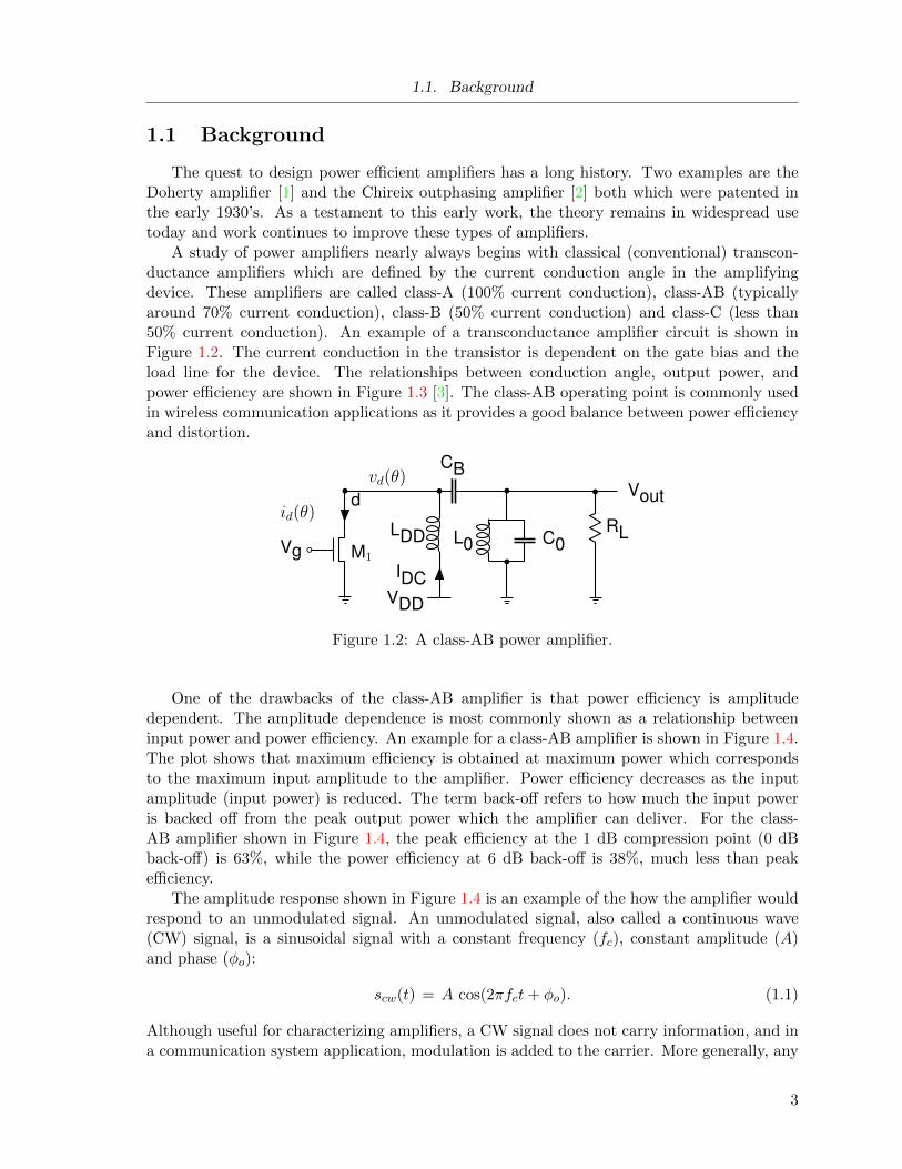
A study of power amplifiers nearly always begins with classical (conventional) transcon-ductance amplifiers which are defined by the current conduction angle in the amplifyingdevice. These amplifiers are called class-A (100% current conduction), class-AB (typicallyaround 70% current conduction), class-B (50% current conduction) and class-C (less than50% current conduction). An example of a transconductance amplifier circuit is shown inFigure 1.2. The current conduction in the transistor is dependent on the gate bias and theload line for the device. The relationships between conduction angle, output power, andpower efficiency are shown in Figure 1.3 [3]. The class-AB operating point is commonly usedin wireless communication applications as it provides a good balance between power efficiencyand distortion.
M1
IDCVDD
LDD
Vout
CB
RLC0L0Vg
vd(θ)
did(θ)
Figure 1.2: A class-AB power amplifier.
One of the drawbacks of the class-AB amplifier is that power efficiency is amplitudedependent. The amplitude dependence is most commonly shown as a relationship betweeninput power and power efficiency. An example for a class-AB amplifier is shown in Figure 1.4.The plot shows that maximum efficiency is obtained at maximum power which correspondsto the maximum input amplitude to the amplifier. Power efficiency decreases as the inputamplitude (input power) is reduced. The term back-off refers to how much the input poweris backed off from the peak output power which the amplifier can deliver. For the class-AB amplifier shown in Figure 1.4, the peak efficiency at the 1 dB compression point (0 dBback-off) is 63%, while the power efficiency at 6 dB back-off is 38%, much less than peakefficiency.
The amplitude response shown in Figure 1.4 is an example of the how the amplifier wouldrespond to an unmodulated signal. An unmodulated signal, also called a continuous wave(CW) signal, is a sinusoidal signal with a constant frequency (fc), constant amplitude (A)and phase (φo):
scw(t) = A cos(2πfct+ φo). (1.1)
Although useful for characterizing amplifiers, a CW signal does not carry information, and ina communication system application, modulation is added to the carrier. More generally, any
3

1.1. Background
Figure 1.3: Efficiency as a function of conduction angle for conventional power amplifiers.
communication signal which can be transmitted through a physical medium can be expressedas
s(t) = r(t) cos[2πfct+ φ(t)] where r(t) ≥ 0. (1.2)
The signal envelope, r(t), adds information to the carrier by amplitude modulation (AM),while the phase term, φ(t), adds information by phase modulation (PM).
Both the AM and PM components in a communication signal can be problematic for poweramplifiers. Since power efficiency in an amplifier is amplitude dependent, the average powerefficiency of the amplifier depends on the statistical distribution of the envelope variationin the signal. Most signals have a peak amplitude that occurs infrequently and the averageenvelope amplitude is typically much smaller than the peak amplitude. The measure mostcommonly used to quantify amplitude variation in the signal is called the peak to averagepower ratio (PAPR):
PAPR (dB) = 10 log10
(peak signal power
average signal power
). (1.3)
Many common wireless communication signals have a PAPR in the range of 6-10 dB.The implication of signals with high PAPR is that, on average, the power amplifier operates
in a back-off state approximately equal to the PAPR of the signal. Therefore, when a class-AB amplifier is used to amplify a signal with a 6 dB PAPR, the average efficiency of theamplifier is approximately equal to the efficiency at 6 dB back-off. For the class-AB amplifierexample shown in Figure 1.4, the average power efficiency of the amplifier for a 6 dB PAPRsignal would therefore be approximately 38%, much less than peak efficiency which is 63%.Although a more accurate estimate of the average efficiency is obtained by integrating theCW response characteristics over the amplitude probability distribution of the input signal,
4

1.1. Background
5 6 7 8 9 10 11 12 13 14 15 1620
30
40
50
60
70
Effi
cien
cy (
%)
Input Power (dBm)
5 6 7 8 9 10 11 12 13 14 15 1634
36
38
40
42
44
Out
put P
ower
(dB
m)
6 dB Back−off Mode
Designed Class−AB PAUsing Cree CGH60015D
Ideal Class−AB PA
1 dB Compression Point
1 dB
Figure 1.4: Efficiency and output power as a function of input power for a class-AB amplifierwith a conduction angle of 244 (θ = 1.36π).
the estimate using PAPR is a very useful approximation. Consequently, the average powerefficiency of a class-AB amplifier is much less than the peak power efficiency when amplifyingtypical communication signals.
Another important characteristic of power amplifiers is distortion. Distortion is created bynonlinear amplitude and phase characteristics in the amplifier. Under large signal conditions,the amplifier saturates leading to amplitude compression. Under small amplitude conditions,the amplifier may enter cut-off depending on the bias point of the amplifying device. Anydeviation from linear amplitude characteristics results in distortion that appears in the outputsignal. Distortion can also be generated from phase distortion that may be both amplitudeand frequency dependent.
Because conventional transconductance amplifiers have amplitude dependent power effi-ciency characteristics, the key to implementing a high efficiency amplifier is to devise circuitswhose power efficiency has reduced sensitivity to amplitude variation. There are differentapproaches to this problem. One method is to implement parallel signal paths which worktogether to reduce amplitude sensitivity. Examples of this method include Doherty [1] andChireix outphasing [2] techniques. Another approach is to create signalling and circuits thatmaintain a saturated operating point in the amplifier. Examples of these methods includeenvelope tracking [4] and switch-mode power amplifier techniques [5]. In this research, thefocus is on the latter method and new analytic and experimental results are presented forswitch-mode power amplifiers (SMPAs).
5

1.2. Architecture of Switch-Mode Power Amplifier Systems
1.2 Architecture of Switch-Mode Power Amplifier Systems
In a switch mode power amplifier (SMPA), the active device is used as a switch insteadof a linearly controlled current source. When the switch is on, the voltage across the switchis low and current is high, and when the switch is open, the voltage is high and the current islow (ideally zero). The switching action theoretically leads to 100% efficiency if the switchesare ideal, because the dissipation in the device, equal to the product of the current timesvoltage, is zero. However, practical devices, especially at high frequencies, have capacitance,inductance, and finite on and off state resistances that all lead to dissipation in the devicewhich degrades power efficiency.
Assuming that a high efficiency switch-mode amplifier can be implemented, the drawbackof switch-mode operation is that a modulated signal with an AM signal envelope cannotbe directly amplified because the amplitude states created by the switching action quantizethe output amplitude. For a switch-mode amplifier with two amplitude states, the outputamplitude is binary, and the only information which can be conveyed to the output signalis the timing of level crossings. Therefore, if the high efficiency operation of a switch-modeamplifier is to be utilized in a wireless communication application, additional circuit blocksmust be added to the amplifier system to map the modulated input signal into a pulse trainand to reconstruct the original modulated source after amplifying the pulse train. A blockdiagram of the amplifier system is shown in Figure 1.5.
Figure 1.5: Block diagram of a SMPA with encoder and reconstruction filter.
Signal reconstruction in a switch-mode power amplifier is constrained by the types ofcircuit elements that can be used in a high power radio frequency output stage. Almostuniversally, signal reconstruction is implemented with a bandpass filter, and this in turnimposes design constraints on the type of signal mapping which can be used to implement thepulse encoder. By quantizing the modulated signal to binary amplitude levels, a large amountof quantization noise is added by the pulse encoder. The quantization noise is spread over avery wide bandwidth and signal encoders implement methods to shape the noise spectrum andcreate a narrow region of high signal to noise ratio (SNR) where the source signal is placed.Examples of compatible source encoding techniques include bandpass sigma-delta modulation(SDM) [6, 7] and noise shaped pulse position modulation (PPM) [7, 8]. More generally, SDMand PPM are examples of a larger signal set called time encoded signals which are a class ofsignals that convey information in the timing of the zero-crossings (amplitude transitions). Inthe following sections, a brief summary of SDM and PPM pulse encoding methods are given.
6

1.2. Architecture of Switch-Mode Power Amplifier Systems
1.2.1 Bandpass Sigma-delta Modulation
Bandpass sigma-delta modulation has been proposed by many researchers as one way ofimplementing a pulse encoder for switch-mode power amplifiers [7, 6]. A block diagram of abandpass SDM is shown in Figure 1.6. The input to the encoder is an RF modulated sourcesignal and the output is a quantized two level pulse train. The quantization process generatessignificant quantization noise that is shaped by a loop filter HRF (s). The noise shaping filtercreates a noise well where the RF input signal spectrum is placed. The noise well is called thein-band spectrum and the broadband noise is called the out-of-band spectrum. An exampleof the output spectrum from a SDM encoder is shown in Figure 1.7 and the correspondingtime domain signal is shown in Figure 1.8.
s(t)HRF (s)
Clock (fs)
p(t)
SamplingQuantizer
NoiseShaping Filter
Figure 1.6: Block diagram of a bandpass sigma-delta modulator.
600 700 800 900 1000 1100 1200 1300 1400-100
-80
-60
-40
-20
0
20
Frequency [MHz]
Pow
er
[dB
m]
Modulator Output Power Spectrum; 0.25Tc
600 700 800 900 1000 1100 1200 1300 1400-100
-80
-60
-40
-20
0
20
Frequency [MHz]
Pow
er
[dB
m]
PA Output Power Spectrum
Figure 1.7: Power spectrum of a bandpass sigma-delta modulator.
The quantizer in a bandpass SDM is triggered by a sampling clock with a frequency fs.The sampling clock is typically selected to be at least above the Nyquist rate of the carrierfrequency, which means the complex envelope is oversampled. For example, a 1 GHz widebandcode division multiple access (WCDMA) modulated input signal with a bandwidth of 10 MHzsampled by a 3.4 GHz clock, has an envelope over sample ratio of 170 and a carrier oversampleratio of 1.7.1 The signal to noise ratio of the reconstructed load signal which is determined by
1In SDM theory, oversample ratio is usually defined relative to the Nyquist sample rate. For example,
7

1.2. Architecture of Switch-Mode Power Amplifier Systems
1000 1001 1002 1003 1004 1005 1006
-1
-0.8
-0.6
-0.4
-0.2
0
0.2
0.4
0.6
0.8
1
Time (ns)
p(t
): S
igm
a-d
elta
pu
lse
tra
ins
Figure 1.8: A bandpass sigma-delta modulator pulse train in the time domain.
the envelope oversample ratio. Therefore, a high envelope oversample ratio is required; thecarrier oversample ratio can also affect the signal to noise ratio but in a less predictable way[6].
Because the timing of the level crossings in a bandpass sigma-delta modulator are triggeredby a clock, the pulse widths in the output are integer multiples of the clock period, Ts, whereTs = 1/fs. Therefore the minimum pulse width is constrained to Ts which is beneficial sincethe current mode class-D power amplifier (CMCD) has a bandwidth limitation and cannotamplify very narrow pulses. On the other hand, long pulses are possible, but occur veryinfrequently. Examples of pulse distributions can be found in the literature [9].
For this research project, a fourth order bandpass SDM is used. The fourth order transferfunction for the noise shaping filter HRF (s) is
HRF (s) =
∑3n=0 bns
n∑4n=0 ans
n(1.4)
and the coefficients are shown in Table 1.1. The carrier oversample ratio for the quantizer isalways 3.4 times the carrier frequency of the input source signal. The quantizer amplitudelevels are normalized to ±1 V and a full scale input amplitude is defined as an amplitude of1 V. The modulator is implemented in Matlab/Simulink and data files are generated for thepulse trains. The data files can be used for both simulation and for experimental work wherethe files are downloaded to an arbitrary waveform generator.
1.2.2 Pulse Position Modulation
Noise shaped pulse position modulation (PPM) [10] is another encoding method thatcan be used for switch-mode power amplifiers. Unlike bandpass SDM which generates leveltransitions that are synchronized with a clock, PPM amplitude changes are asynchronous andcan occur at any time. A block diagram of a noise shaped PPM encoder is shown Figure 1.9.
3.4 GHz/(2 × 1 GHz) = 1.7.
8

1.2. Architecture of Switch-Mode Power Amplifier Systems
Table 1.1: Coefficient values for the noise shaping filter HRF (s)
n bn an
0 7.3874× 1037 1.5584× 1039
1 2.0201× 1027 8.6858× 1026
2 1.8850× 10¹⁸ 7.8962× 10¹⁹
3 2.6147× 10⁷ 2.2× 10⁷
4 - 1
In the noise shaped PPM encoder, the amplitude and width of pulses are constant and theposition (timing) of pulse edges are variable and dependent on the input source signal s(t).Similar to bandpass SDM, the spectrum of PPM is broadband, and the feedback loop shapesthe in-band noise to ensure the source signal is encoded with a high signal to noise ratio.Examples of a noise shaped PPM signal in the time domain and frequency domain are shownin Figures 1.10 and 1.11, respectively.
s(t)HRF (s)
p(t)
Tp
PulseGenerator
NoiseShaping
Figure 1.9: Block diagram of pulse position modulator.
1000 1001 1002 1003 1004 1005 1006
−1
−0.8
−0.6
−0.4
−0.2
0
0.2
0.4
0.6
0.8
1
Time (ns)
p(t)
: Pul
se−
posi
tion
puls
e tr
ains
Figure 1.10: A noise shaped PPM pulse train in the time domain.
The noise shaped PPM encoder is implemented in a Matlab/Simulink model. The noise
9

1.3. Switch-mode Power Amplifier Circuits
600 700 800 900 1000 1100 1200 1300 1400−70
−60
−50
−40
−30
−20
−10
0
10
Frequency [MHz]
Pow
er [d
Bm
]
Figure 1.11: A noise shaped PPM pulse train in the frequency domain.
shaping filter HRF (s) is identical to the bandpass SDM filter whose coefficients were givenin Table 1.1. The pulse width, Tp, is set to be equal to half the period of the input carrierfrequency. This leads to an efficient encoder with high coding efficiency. Data files aregenerated from the Matlab models and used for simulation and the files are downloaded toan arbitrary waveform generator for experimental work.
1.3 Switch-mode Power Amplifier Circuits
The high efficiency amplifier circuit topologies which are relevant to this work are class-D,class-E and class-F. Class-D and class-E are called switch-mode classes because the gate ofthe device is switched by the input signal. Class-F is also frequently lumped into the switch-mode category, although it does not necessary require a two level input signal to switch theamplifying device. Class-F originated from the design of harmonic tuning in the output circuitrather than from a concept where the input signal switches the device. Within class-D andclass-F, the circuit designs can be subdivided into two types of circuits. Circuits which switchvoltage are called voltage mode (VM) circuits and circuits which switch current are calledcurrent mode (CM) circuits. The terms ‘voltage switched’ and ‘current switched’ are mostwidely applied to class-D amplifiers. Within the context of class-F amplifiers, the term inverseclass-F, also written at class-F−1, is more widely used to distinguish current switching fromvoltage switching which is simply written as class-F. A short overview of the basic operationof these circuits is presented next.
10

1.3. Switch-mode Power Amplifier Circuits
1.3.1 Class-D Power Amplifiers
1.3.1.1 Voltage Mode Class-D
A voltage mode class-D power amplifier (VMCD) is shown in Figure 1.12. The circuitconsists of two active devices in a cascade configuration. The common junction between thedevices is connected to a series output filter to reconstruct a sinusoidal load signal from thepulse train. The gate drive signals, Vin1 and Vin2, are two antiphase pulse trains which controlthe state of the switches (devices).
IDC
Vin1
VDD
LDD
RL VL
Vin2
Pout
PDC
Bandpass Filter
Ct
CRF
Lt
M2
M1
VD2
VD1
Figure 1.12: Schematic of a VMCD power amplifier.
Figure 1.13 shows current and voltage waveforms for the VMCD amplifier when the inputpulse train is a periodic pulse train with a duty cycle of 30%. The first row shows the gatedrive waveforms, the second row shows the drain-source voltages across each switch, and thethird row shows the current through each switch. The drain voltage waveforms are similarto the gate voltage waveforms except for distortion arising from switch resistance. Since thevoltage waveform follows the input pulse train, the circuit is called a voltage mode class-Damplifier. The current through the switches are a portion of a sinewave. The two switchcurrents sum to provide a sinusoidal load current.
11

1.3. Switch-mode Power Amplifier Circuits
V D1
V
(V
)
V D2
V
(V
)
Figure 1.13: VMCD amplifier voltage and current waveforms for a periodic drive signal witha duty cycle of 30%.
12

1.3. Switch-mode Power Amplifier Circuits
1.3.1.2 Current Mode Class-D
Figure 1.14 shows a current mode class-D power amplifier. Similar to a VMCD amplifier,the input pulse trains, Vin1 and Vin2, are two antiphase signals that control the state of theswitches. When a device is turned on, the voltage across the switch is zero and all the DCcurrent, IDC , provided by the supply goes through the switch. When the same device isturned off, there is no current through the switch and the voltage across the switch is aportion of a sinusoidal wave. The switch current is similar to a square wave and the voltageacross the device is a portion of a sinusoidal wave. In other words, the CMCD amplifier canbe considered as the voltage-current dual of the VMCD amplifier. The reconstruction filter isa shunt filter in a CMCD circuit which is also the dual of the series resonator in the VMCDcircuit.
Vin2
LDD
RL
Vin1
Ct
Lt
M1 M2
VD1
IDC
VDD
LDD
PDC
VD2
Vg1 Vg2
Figure 1.14: Schematic of a CMCD.
One of the main advantages of the CMCD circuit in Figure 1.14 compared to the VMCDcircuit in Figure 1.12 is that the gate drive signals in CMCD are ground referenced, whilethe gate drive signal for the upper transistor in the VMCD circuit, M1, requires a bootstrapdrive circuit. This feature of CMCD amplifiers makes it more attractive for experimentalwork [11, 12].
Current and voltage waveforms for an example of a CMCD amplifier are shown in Fig-ure 1.15. In the first row, the gate drive waveforms are shown. The input signal is a periodicsquare wave with a duty cycle of 30%. In the second row, the current through the switches isshown. Clearly the current follows the gate waveform and current is switched in the circuit.In the third row, the drain-source voltage across each switch is shown. The drain voltagewaveforms are a gated sinewave and the differential voltage, VD1−VD2, is a sinusoidal signal.The differential drain voltage is the same as the voltage across the load resistor and the shuntresonator circulates harmonic current between the switches.
13

1.3. Switch-mode Power Amplifier Circuits
V D1
V
(V
)
V D2
V
(V
)
Figure 1.15: CMCD current and voltage waveforms for a periodic input pulse train with aduty cycle of 30%.
14

1.3. Switch-mode Power Amplifier Circuits
1.3.2 Class-E Power Amplifiers
Several years after the class-D circuit topology was introduced, Sokal reported the firstclass-E amplifier in 1975 [13]. The novelty in the class-E circuit topology is that, unlikeclass-D which requires two switches, the class-E amplifier requires only one switch. A class-Eamplifier circuit is shown in Figure 1.16. The switch M1 is shunted by a capacitor CP and theload is connected through a series resonator. When the switch is on, current flows throughthe switch and the voltage across the shunt capacitance CP is low. When the switch is open,the capacitor provides current to the load and the voltage across the capacitor changes.
IDC
VDD
LDD
RL VL
Vin
Pout
PDC
SeriesResonator
CtLt
M1
Vdrain
LX
CP
isw ic
Figure 1.16: Schematic of a class-E power amplifier.
Example waveforms for a class-E amplifier are shown in Figure 1.17. The gate drive signalis shown at the top of the figure and the waveform is a square wave pulse train with a dutycycle of 30%. The load current is sinusoidal because the series resonator filters the non-sinusoidal drain voltage waveform, and the sinusoidal current is alternately sourced/sunk bythe switch, M1, or the shunt capacitor, CP . The current into the switch and the current intothe capacitor are shown, and the two currents sum to equal the sinusoidal load current. Thevoltage waveform is more difficult to understand and requires analysis [3]. The key featuresof the voltage waveform are that the voltage is zero when the current is switched betweenthe switch and the capacitor. By proper choice of capacitance CP and inductance LX , thefirst derivative of the voltage waveform can also be zero at the switching instances. In thisway, the voltage waveform smoothly approaches zero at each switching instant and the circuitimplements a zero-voltage switching and zero-derivative switching condition. This is the keyfeature of the class-E amplifier. Therefore, the circuit is attractive because it has a singleswitch and very high efficiency because of the zero-voltage switching condition. The shuntcapacitance CP can also be partitioned between the intrinsic output capacitance of the deviceand an external capacitance such that the sum is equal to CP .
The primary disadvantage of class-E is the peak voltage generated across the switch. Thepeak voltage depends on the duty cycle of the input signal and the variation in peak voltageis illustrated in Figure 1.18. The peak drain voltage is normalized to VDD in this figure andranges from 2.7 for a 50% duty cycle to 4.8 for a 30% duty cycle. The variation in peakvoltage as a function of duty cycle is distinctly different from class-D where peak voltage isindependent of duty cycle. The variation in peak voltage is even more problematic for non-
15

1.3. Switch-mode Power Amplifier Circuits
Figure 1.17: Class-E voltage and current waveforms for a 30% duty cycle pulse train.
16

1.3. Switch-mode Power Amplifier Circuits
periodic pulse trains generated by SDM or PPM pulse encoders where peak voltages can easilybe five times larger than VDD. Therefore, although class-E has attractive features, voltagepeaking limits its application in switch-mode power amplifiers and this amplifier topology willnot be analyzed further in this work. Literature references to class-E amplifiers will be madelater in the context of designing RF rectifiers.
200.5 201.0 201.5200.0 202.0
1
2
3
4
0
5
Time (ns)
Norm
alized d
rain
voltage
200.5 201.0 201.5200.0 202.0
1
2
3
4
0
5
Time (ns)
Norm
alized d
rain
voltage
200.5 201.0 201.5200.0 202.0
1
2
3
4
0
5
Time (ns)
Norm
alized d
rain
voltage
Figure 1.18: Normalized voltage across the switch in a class-E PA for three different dutycycles: 30% (circle), 50% (star) and 70% (square).
1.3.3 Class-F Power Amplifiers
In class-D and class-E amplifier circuits, the device is operated as a switch and the switchedwaveforms at the drain node of the devices are the result of both a switched gate drive signalas well as an output resonator. In class-F, the principle idea is to shape the drain signalwaveforms by controlling the harmonic impedance of the output network such that overlapbetween the current and voltage waveforms are minimized. In practical class-F amplifiers,harmonic impedances up to the third harmonic are commonly controlled and in some designseven higher harmonic order impedance terminations are implemented to maximize powerefficiency. Although output harmonic impedances presented to the drain terminal of the deviceare very important in class-F circuits, harmonic impedances at the gate (input) terminal ofthe device can also significantly affect the power efficiency of the amplifier. The importanceof input harmonic matching is a topic that is investigated further in this work.
A class-F amplifier circuit with harmonic control up to the fifth harmonic is shown in Fig-ure 1.19 and example waveforms are shown in Figure 1.20. The input signal has a fundamentalfrequency fo. The amplifying device is usually biased near a class-B operating point and thecurrent through the device conducts for half a cycle. The device current waveform is ideally ahalf sinusoid and has a fundamental frequency component and even harmonics. The outputmatching circuit is designed to short the even harmonics in the current waveform and presentan open circuit impedance for odd harmonic frequencies. With open circuit impedances at
17

1.3. Switch-mode Power Amplifier Circuits
odd harmonics, the voltage waveform across the switch is shaped to be a rectangular squarewave. Ideally, the overlap of the current and voltage waveforms across the device is smallwhich then leads to low dissipation and high power efficiency. Since the voltage is a squarewave in class-F, the circuit switches voltage.
IDC
VDD
LDD
RL VLVin
Pout
PDC
Third HarmonicC3
L3
M
Vdrain
Fifth HarmonicC5
L5
C0L0
f0
Figure 1.19: A class-F power amplifier circuit.
Class-F amplifier circuits can also be designed to switch current and the current switcheddual is called inverse class-F or class-F−1. In a current switched amplifier, the odd harmonicsare shorted at the drain node and the even harmonics are open. Under these conditions, thecurrent is switched and the voltage is a half sinusoid. Class-F amplifiers are explored muchmore extensively in Chapter 3.
18

1.3. Switch-mode Power Amplifier Circuits
0.2 0.4 0.6 0.8 1.0 1.2 1.4 1.6 1.80.0 2.0
-1
0
1
-2
2
Time (ns)
Vin
put (
V)
0.2 0.4 0.6 0.8 1.0 1.2 1.4 1.6 1.80.0 2.0
0
100
200
300
400
-100
500
Time (ns)
Idra
in (
mA
)
0.2 0.4 0.6 0.8 1.0 1.2 1.4 1.6 1.80.0 2.0
0
10
20
30
40
50
-10
60
Time (ns)
Vdr
ain
(V)
0.2 0.4 0.6 0.8 1.0 1.2 1.4 1.6 1.80.0 2.0
-10
-5
0
5
10
-15
15
Time (ns)
VLo
ad (
V)
Figure 1.20: Class-F power amplifier voltage and current waveforms.
19

1.3. Switch-mode Power Amplifier Circuits
1.3.4 Summary of Amplifier Classes Based on Harmonic TerminationImpedances
The concept of harmonic impedances in class-F can be applied more broadly to otheramplifier classes and this provides a unified way to see the relationships between differentamplifier classes. Every amplifier has an output matching circuit that provides a fundamen-tal frequency match. The output matching circuit also presents the device with harmonicimpedances that may be either explicitly controlled as in class-F, or implicitly controlled as inclass-E. By considering the relative impedance of the odd and even harmonics, the differentamplifier classes can be identified in a diagram as shown in Figure 1.21. This type of visu-alization for the amplifier classes was first presented by Raab in 2001 [14]. In the diagram,the x-axis shows the relative magnitude of the even harmonic impedance (reactance) and they-axis shows the relative magnitude for the odd harmonic impedance presented to the drainterminal of the amplifying device. Mid-scale on each axis is the relative load line resistancepresented to the device at the fundamental frequency.
Starting with class-F, the output matching network should have high impedance at oddharmonics and low impedance for even harmonics. This places class-F in the upper left handcorner of the diagram. Inverse class-F is in the lower righthand corner and requires highimpedance at even harmonics and low impedance at odd harmonics. Voltage switched class-D has an output series resonator that in theory presents an open circuit impedance at allharmonics and therefore class-D is in the upper right. Conversely, inverse class-D has an anti-resonant parallel resonant circuit which shorts all harmonic frequency components placingclass-D−1 in the lower lefthand corner. Class-E has a specially designed output networkimpedance that leads to zero voltage switching and consequently the harmonic impedancesare neither shorted nor open. Class-E harmonic impedances lie within the middle of the figure.
00
R1
R1
|Zn=3,5,...|
|Zk=2,4,...|
E
F D
F−1D−1
Figure 1.21: Amplifier classes in terms of harmonic load impedances.
20

1.4. Power Efficiency and Device Technology
1.4 Power Efficiency and Device Technology
Of the different types of device technologies which are available for wireless communicationapplications, Gallium Nitride (GaN) device technology is now used in many power amplifierdesigns [8, 15, 16, 17, 18, 19, 20, 21]. GaN device technology has the following features:
• A large band-gap energy leads to high electric field breakdown potentials [22]; for in-stance, the breakdown voltage of a Cree CGH40010 transistor is 84 V [23].
• GaN has a higher carrier saturation velocity compared to other technologies [22].
• The thermal dissipation of GaN devices is high. Combined with high breakdown volt-ages, GaN devices have higher power densities (W/mm of gate width) compared toother device technologies such as silicon LDMOS (laterally diffused metal oxide semi-conductor).
Figure 1.22 shows the band-gap energy of three different materials versus saturation veloc-ity. From this figure it shows that GaN offers much better high power and high frequencypossibilities compared to Gallium Arsenide (GaAs) and Silicon (Si) device technologies. Fora better comparison of different semiconductor materials, Johnson’s figure of merit (JFOM)was proposed [24]. It uses the breakdown voltage and saturated electron drift velocity todefine a value for the high-frequency handling capability of a certain semiconductor material.JFOM is expressed as VsatEc/(2π) where Vsat is the saturated electron velocity and Ec is thecritical breakdown field. For example, the JFOM for GaN is 27 times higher than that ofsilicon, about 15 times that of GaAs, and about 1.4 times that of Silicon Carbide (SiC).
0 0.5 1 1.5 2 2.5 3 3.5 4 4.5 5
x 107
0
0.5
1
1.5
2
2.5
3
3.5
4
4.5
5
Vsat (cm/s)
Eg
(e
V)
GaN
GaAs
Si
Figure 1.22: Band gap energy and saturated velocity for Si, GaAs and GaN.
GaN device technology is available in both discrete high power devices as well as mono-lithic microwave integrated circuit (MMIC) processes. A picture of a discrete GaN device anda MMIC GaN circuit are shown in Figure 1.23. In this research project, power amplifiers are
21

1.5. Literature Review
Figure 1.23: GaN HEMT technology: packaged device from Cree (left) and MMIC (right).
built using discrete GaN devices and a 10 W device available from Cree; model CGH40010,is used. For modeling work, the bare die, model CGH60015D, is used along with a packagemodel. Although Cree provides comprehensive large signal device models for these compo-nents, they are black-box models, and equivalent circuit models are developed to providefurther insight into device losses and to predict power efficiency of different amplifier circuits.
1.5 Literature Review
A short summary of relevant published work which provides context for this research isgiven in the next sections.
1.5.1 Class-D Power Amplifiers
Of the three amplifier classes (class-D, class-E and class-F), the class-D circuit topologyis well suited for amplifying pulse encoded signals. Providing the devices are driven with abroadband driver, the amplifier is broadband, and the circuit is fundamentally robust enoughto amplify signals with a range of different duty cycles. The output resonant circuit can alsobe used as a reconstruction filter, although higher order filter structures are usually requiredto sufficiently attenuate out-of-band noise. These features have motivated significant researchinterest in the design of RF class-D power amplifiers for pulse encoded signals.
1.5.1.1 Voltage Mode Class-D Amplifiers
The origin of the class-D amplifier dates back just over fifty years ago, when Baxandallreported the first experimental results in 1959 [25]. The circuit was designed as a way ofgenerating high power sinusoidal signals for RF transmitters. During the next two decades,a number of different high frequency class-D amplifiers were designed and implemented forvarious applications. Variants of the original class-D amplifier which used complementaryswitches then evolved into transformer coupled voltage and current switched configurations[26, 27]. Experimental circuits optimized for high power amplifiers which use periodic signalsource to generate sinusoidal load signals continue to the present day [28, 29].
The first reported work associated with class-D power amplifiers that amplify pulse en-coded signals was described by Raab in 1973 [30]. In his circuit, an RF PWM (pulse width
22

1.5. Literature Review
modulated) signal was amplified by a class-D amplifier in the MHz frequency range. The firstsimulated results for a class-D power amplifier with sigma-delta modulation was published in[31]. In 2008, Johnson et al. [6] published the analysis of a VMCD with bandpass sigma-deltamodulation and he introduced the concept of coding efficiency to generalize the analysis ofpower efficiency to include pulse encoded signals. The loss mechanisms of a voltage modeclass-D amplifier were formulated in [32] and supported by experimental results for a CMOSVMCD amplifier in 2007. Recently, other experimental work with time-encoded signals in-cluding SDM, PPM and PWM for a GaN VMCD amplifier have been reported [8].
1.5.1.2 Current Mode Class-D Amplifiers
In 2001, researchers at USCD published a paper on a CMCD power amplifier circuit thatused a differential tank with two inductors providing DC to the circuit [33]. The circuitwas shown earlier in Figure 1.14 and most CMCD work since 2001 has built on this circuittopology. The analytic work associated with CMCD has focused primarily on conductionlosses and inductive switching losses for period periodic signals with 50% duty cycles [34]. In[35], equations are derived for variable duty cycle switching conditions under the assumptionof independent loss mechanisms; however, the device model is based on a switch and effectsof current saturation are not analyzed.
Different device technologies have been used to implement CMCD circuits with mostwork using either GaN devices for high power amplifiers and CMOS technology of low poweramplifiers. A CMOS design reported in 2011 [12] describes a fully integrated CMOS inverseclass-D amplifier but the experimental results are limited to periodic pulse trains with a fiftypercent duty cycle.
Several research groups in Germany have conducted experimental work to realize CMCDamplifiers and evaluate the amplifier performance with pulse encoded signals [15, 16, 17]. Theyhave also evaluated a derivative of the CMCD amplifier called class-S which includes diodesin series with the switches to prevent an off-state switch from turning on when the duty cycleis not 50%. The experimental work shows that the CMCS amplifier is not any better thanCMCD, and the general consensus is that the additional losses in the diode are offset by gainsin preventing off-state switches from turning on under variable duty cycle switching conditions.Also, their work has primarily focused on designing and implementing experimental circuitsand evaluating the circuit performance with different types of pulse encoders including SDM.The work has not focused as much on detailed analysis and prediction of power efficiency. Asummary of recent work related to CMCD and CMCS amplifiers are shown in Table 1.2.
23

1.5. Literature Review
Tab
le1.
2:S
om
ere
centl
yp
ub
lish
edre
sult
sfo
rcl
ass-
Dp
ower
amp
lifi
ers.
Nu
mb
erT
opol
ogy
Tec
hn
olog
yIn
pu
tsi
gnal
Mod
elY
ear
Auth
or
Ref
.
1∗C
lass
D(C
M)
GaN
Sig
ma-
del
taY
es20
13A
bb
asi
an
etal
[36]
2C
lass
D(C
M)
LD
MO
SR
FP
WM
No
2012
Foad
etal
[37]
3C
lass
D(C
M)
GaN
Per
iod
icN
o20
12P
ark
etal
[38]
4C
lass
D(C
M)
CM
OS
Per
iod
icY
es20
12C
how
dhu
ryet
al
[39]
5C
lass
D(C
M)
GaA
sP
erio
dic
Yes
2011
Kam
per
etal
[40]
6C
lass
D(C
M)
GaN
Per
iod
icN
o20
11A
flaki
etal
[41]
7C
lass
D(C
M)
LD
MO
SP
WM
No
2010
Sch
ub
erth
etal
[42]
8C
lass
D(C
M)
GaN
Per
iod
icN
o20
09A
flaki
etal
[43]
9C
lass
D(C
M)
LD
MO
SP
erio
dic
Yes
2009
Bra
ckle
etal
[35]
10C
lass
D(C
M)
LD
MO
SP
erio
dic
No
2006
Nem
ati
etal
[44]
11C
lass
D(C
M)
LD
MO
SP
erio
dic
No
2005
Kim
etal
[45]
12C
lass
D(V
M)
GaN
Sig
ma-
del
taN
o20
12W
entz
elet
al
[8]
13C
lass
D(V
M)
GaN
Per
iod
icN
o20
11L
inet
al
[29]
14C
lass
D(V
M)
CM
OS
Sig
ma-
del
taY
es20
07H
un
get
al
[32]
15C
lass
D(V
M)
CM
OS
Sig
ma-
del
taY
es20
06Joh
nso
net
al
[6]
16C
lass
SG
aNS
igm
a-d
elta
No
2011
Wen
tzel
etal
[15]
17C
lass
SG
aNS
igm
a-d
elta
No
2010
Wen
tzel
etal
[16]
18C
lass
SG
aNS
igm
a-d
elta
No
2009
Wen
tzel
etal
[17]
19C
lass
SG
aNP
erio
dic
No
2010
Sam
ula
ket
al
[18]
20C
lass
SG
aNP
erio
dic
No
2009
Sam
ula
ket
al
[46]
21C
lass
SG
aNS
igm
a-d
elta
No
2008
Leb
erer
etal
[47]
24

1.5. Literature Review
1.5.2 Class-F Power Amplifiers
The first description of a class-F amplifier was presented by Tyler in 1958 [48]. A fewyears later, the first application of a high efficiency class-F power amplifier was reported bySnider [49] when he constructed and tested a 46 W, 250 MHz power amplifier for generatinghigh power CW signals. The theory of class-F expanded in the mid-90’s by Raab in severalpapers where he systematically evaluated the shape of class-F waveforms related to the outputtermination impedances for a finite number of harmonics [50, 51, 52].
Experimental and theoretical work to optimize class-F amplifier performance has continuedand reports of high power amplifiers with peak efficiencies greater than 80% in the GHzfrequency range are common [19, 53, 54, 55]. Although peak efficiency is high, the powerefficiency of these amplifiers reduces in a similar way to class-AB amplifiers as output poweris backed off from peak power. Also, the class-B bias point that is used in class-F leads to highdistortion levels. On the other hand, if the input signal to the amplifier can be conditionedto maintain operation in a highly saturated state, then class-F amplifiers offer a promisingfuture for wireless applications. The harmonically tuned impedance networks inherent in theclass-F amplifier design methodology are not likely to be optimal for continuous spectrumpulse encoded signals, so methods of implementing broadband class-F amplifiers are of greatinterest. Broadband amplifiers also have applications in multi-band wireless communicationsystems. A summary of recent work in terms of class-F amplifiers is given in Table 1.3.
25

1.5. Literature Review
Tab
le1.
3:S
ome
rece
ntl
yp
ub
lish
edre
sult
sfo
rcl
ass-
Ffa
mil
yP
As
Nu
mb
erT
opol
ogy
Tec
hn
olog
yP
ower
Effi
cien
cyF
requen
cyY
ear
Au
thor
Ref
.
1∗
Cla
ssF
GaN
40.5
dB
m78
.8%
0.99
GH
z20
15A
bb
asi
an
etal
[56]
2C
lass
FG
aN40
.7d
Bm
80.1
%2.
1G
Hz
2014
Hw
an
get
al
[57]
3C
lass
F−1
GaN
42.2
dB
m83
.9%
1.9
GH
z20
14K
imet
al
[58]
4C
lass
FG
aN40
dB
m82
%3.
1G
Hz
2013
Ch
enet
al
[59]
5C
lass
F/F−1
GaN
41d
Bm
73.5
%2.
65G
Hz
2012
Moon
etal
[19]
6C
lass
FG
aN30
.4d
Bm
69%
4G
Hz
2012
Zom
oro
dia
net
al
[20]
7C
lass
FG
aN10
.5W
74%
0.55
-1.1
GH
z20
11C
arr
ub
aet
al
[21]
8C
lass
FG
aAs
20d
Bm
83%
0.9
GH
z20
11C
arr
ub
aet
al
[53]
9C
lass
FG
aN26
.24
dB
m62
.5%
0.9
GH
z20
10O
sori
etal
[60]
10C
lass
FG
aN37
dB
m79
%1
GH
z20
08A
flaki
etal
[61]
11C
lass
FC
MO
S21
.8d
Bm
43.9
%2.
4G
Hz
2006
Hu
an
get
al
[54]
12cl
ass-
F−1
GaN
39.9
dB
m76
.7%
3.5
GH
z20
12D
on
get
al
[62]
13cl
ass-
F−1
GaN
47.2
dB
m69
.4%
3.54
GH
z20
11K
imet
al
[63]
14cl
ass-
F−1
GaN
41.4
dB
m73
.5%
2.5
GH
z20
09W
uet
al
[64]
15cl
ass-
F−1
GaN
46dB
m60
.8%
2.35
GH
z20
09T
an
any
etal
[65]
16cl
ass-
F−1
GaN
22.7
dB
m74
%1
GH
z20
06W
oo
etal
[66]
17cl
ass-
F−1
LD
MO
S41
.2d
Bm
74%
1G
Hz
2006
Ou
yah
iaet
al
[55]
18C
lass
FE
GaN
2.36
W86
.8%
61.4
4M
Hz
2010
You
etal
[67]
26

1.5. Literature Review
1.5.3 RF Synchronous Rectifiers
Interest in RF to DC rectification has grown recently with growing interest in wirelesspower systems. Although wireless power is an active research area, significant contributionsbegan in the early 1960’s with the pioneering work of Brown [68]. He worked on high powermicrowave rectifying antennas, called rectennas, to remotely power a helicopter. Microwavepower was also being considered as a way to distribute power on the moon and to transmitpower from orbiting solar arrays to earth. These systems require very high power microwaveamplifiers and highly directional antenna to collimate high power fields.
Recent work has focused on much lower power level applications with interest to remotelypower or remotely recharge portable devices and sensors. For these applications, the workcan be broadly classified into two categories: 1) diode rectifiers and 2) synchronous rectifiersbased on switching transistors [69]. RF diode rectifier circuits [70, 71, 72] are simpler toimplement and avoid the design issues associated with gate drive circuitry which is requiredin a synchronous rectifier. On the other hand, synchronous rectifiers can also exploit advancesin device technology including high efficiency GaN power devices.
With clever insight, a paper in 2012 was presented by Ruiz et al. [73] where he showed theimplementation of class-E RF rectifier based on reconfiguring a class-E power amplifier circuit.The RF rectifier delivered 50 mW of DC power with an efficiency of 83% at a frequency of 900MHz. The insight for the circuit came from work presented by Hamill [74] in the early 1990’swhere he showed how the theory of time-reversal duality could be applied to relate amplifierand rectifier circuit topologies. The 2012 work has led other researchers to investigate thedesign of synchronous RF rectifiers based on converting switch-mode amplifiers circuits intorectifiers. Other important references related to synchronous rectifiers are shown in Table 1.4.
In this thesis, class-F amplifiers are reconfigured into class-F rectifiers and new contribu-tions have been made in terms of both understanding the impact of loss in applying time-reversal duality as well as the implementation of high power rectifiers and wideband rectifiers.
27

1.5. Literature Review
Tab
le1.
4:S
om
ere
centl
yp
ub
lish
edre
sult
sfo
rR
Fsy
nch
ron
ous
rect
ifier
s
Nu
m.
Typ
eD
evic
ef
(GH
z)PDC
η(%
)Y
ear
Au
thor
Ref
.1∗
clas
s-F
GaN
HE
MT
0.98
58.
7W
81.3
2015
Ab
bas
ian
etal
[75]
syn
ch.
2∗
clas
s-F−1
GaN
HE
MT
0.91
10.1
5W
8520
15A
bb
asia
net
al[7
6]sy
nch
.3∗
clas
s-D
CM
OS
2.45
2.5
mW
31.7
2015
Deh
ghan
iet
al[7
7]sy
nch
.4
clas
s-C
GaN
HE
MT
10.1
1.67
W64
.420
14L
itch
fiel
det
al[7
8]se
lf-s
yn
ch.
MM
IC5
clas
s-C
GaN
HE
MT
10.1
3.18
W63
.920
14L
itch
fiel
det
al[7
8]se
lf-s
yn
ch.
MM
IC6
clas
s-E
E-P
HE
MT
0.9
35m
W88
2014
Ru
izet
al[7
9]se
lf-s
yn
ch.
7cl
ass-
EE
-PH
EM
T2.
4515
mW
7720
14R
uiz
etal
[79]
self
-syn
ch.
8cl
ass-
EG
aAs
PH
EM
T2.
455.
7m
W77
2013
Ish
ikaw
aet
al[8
0]se
lf-s
yn
ch.
9cl
ass-
FG
aAs
PH
EM
T5.
85.
5m
W68
2013
Ish
ikaw
aet
al[8
1]se
lf-s
yn
ch.
10cl
ass-
F−1
GaN
HE
MT
2.14
8.5
W85
2012
Rob
erg
etal
[82]
self
-syn
ch.
11cl
ass-
EE
-PH
EM
T0.
950
mW
8320
12R
uiz
etal
[73]
syn
ch.
12cl
ass-
FE
-PH
EM
T0.
912
.1m
W85
.420
04G
omez
etal
[83]
self
-syn
ch.
28

1.6. Research Goals and Objectives
1.6 Research Goals and Objectives
The goals of this research are:
1. to improve analytic methods to predict the power efficiency of RF switch-mode poweramplifiers under general non-periodic switching conditions;
2. to build experimental prototypes of switch-mode power amplifiers to benchmark andcompare the performance of different circuit topologies;
3. to investigate and evaluate new switch-mode power amplifier circuit topologies that canefficiently amplify pulse encoded signals.
The research goals are derived from the literature survey where the following observationsare made. First, there are many published experimental results that demonstrate high effi-ciency operation for classes D, E and F; however, these results are almost always reportedunder optimal switching conditions which correspond to a square wave drive signal with a50% duty cycle. The power efficiency of switch-mode amplifiers degrades as the duty cycledeviates from 50% and it is very important to understand how power efficiency changes asthe duty cycle (pulse width) changes in order to predict how well an amplifier will work forwireless communication applications. Second, although there are many reports on differentswitch-mode power amplifier circuits, it is not always that easy to compare results becausedifferent devices are used in different circuit topologies and the objectives of the work havenot been to conduct comparative studies. In this work, amplifier circuits are analyzed andevaluated using the same device to improve the consistency of experimental work and to drawconclusions by comparing experimental results. Third, despite the high efficiency potential ofRF switch-mode power amplifier circuits, a competitive digital switch-mode power amplifierhas yet to be reported compared to conventional analog amplifier techniques such as Do-herty [1]. Therefore, it still remains a challenge to realize high efficiency switch-mode poweramplifiers. This suggests that research must continue to evaluate new switch-mode poweramplifier architectures as a way to realize the full potential of high efficiency operation thatcan theoretically be obtained by operating the device as a switch.
In pursuit of these research goals, specific research objectives are defined.
1.6.1 Predicting the Power Efficiency of CMCD Power Amplifiers forTime Encoded Input Signals
As Table 1.2 shows, many publications have been written about CMCD; however, a carefulreview of published work reveals the following limitations:
• Most authors have focused on building and measuring the performance of CMCD am-plifier circuits to present experimental results without providing an analytic model topredict and explain the experimental outcomes.
• Some researchers have presented analytical models; however, the models are usuallyrestricted to periodic input signals with fifty percent duty cycle.
• The peak current which the device can deliver in the saturation region is never consid-ered. The device models are usually simple switches with an on-state resistance thathas no current limitations.
29

1.6. Research Goals and Objectives
• The output capacitance of the device is constant. However, most device capacitancesare nonlinear and capacitance can vary significantly under large signal conditions.
• Inductive switching losses associated with bond wires and the packaging are consideredto be a significant loss mechanisms in CMCD amplifiers, while capacitive switching lossesare usually neglected. Analytical results in Chapter 2 show that capacitive switchinglosses can in fact be very significant under variable duty cycle switching conditions.
• Overlap losses have not been modeled; however, in practice rise time and fall times ofthe voltage and current waveforms for the switches are significant.
Improving analytical models to predict power efficiency in CMCD amplifiers for generalswitching conditions is a research objective. The analysis gives insight into the loss mech-anisms as a function of the duty cycle as well as insight into how to appropriately selectthe device load line considering current saturation in the switch. This work is described inChapter 2.
1.6.2 RF Switch-mode Power Amplifiers with Energy Recycling
As the experimental results of the published work show, it is difficult to obtain high effi-ciency operation when amplifying pulse encoded signals. One of the reasons for this is that thespectrum of the pulse encoded signals is broadband and continuous rather than harmonicallypeaked. Also, the quantization noise is shaped to create a narrow noise well and consequentlya reconstruction filter with sharp attenuation characteristics is required to suppress out-of-band noise. Highly selective filters have multiple resonators and are more complex than asimple resonator. The filters are usually added after the amplifier circuit design and as aresult the out-of-band impedance presented to the device is rarely controlled in a predictableway. If the required out-of-band impedance is violated, then the high efficiency operation ofthe amplifier is compromised. As shown in Figure 1.21, all the amplifier classes can be relatedto specific harmonic impedance conditions. Time encoded signals are challenging signals toamplify because they have continuous power spectrums and are different from periodic signalsthat have discrete harmonic frequency components.
A different approach to implementing RF switch-mode amplifiers was presented in [84]where the output load circuit across the switch is broadband rather than harmonically tuned.The load circuit was implemented by a complementary diplexer which has a matched broad-band input port that splits into two complementary filter branches that separate the amplifiedpulse train into an in-band signal and an out-of-band (quantization noise) signal. After signalseparation, the in-band signal couples to the antenna and the out-of-band signal can be recti-fied. The rectified output power can provide an auxiliary supply which offsets the DC powersupplied to the amplifier. In this way, out-of-band power is recycled to improve the powerefficiency of the amplifier. A diagram of a switch-mode power amplifier with energy recyclingwas shown in Figure 1.1. RF energy recycling has been reported for another power amplifierarchitecture called linear amplification using nonlinear components (LINC), but the conceptis new in terms of its application to RF switch-mode power amplifiers.
Energy recycling is motivated by the observation that when high PAPR signals are encodedinto a pulse train, the coding efficiency of the pulse train is low, and large amounts of powerare generated in the out-of-band frequency spectrum. Therefore, two approaches to the designof an efficient switch-mode power amplifier are: 1) to design a circuit that inherently operates
30

1.6. Research Goals and Objectives
with high efficiency even for pulse trains with broadband spectrums, or 2) design a highefficiency broadband amplifier and use energy recycling to capture out-of-band energy anduse this to offset the DC supply to the amplifier. The second method is investigated in thiswork. The concept of energy recycling is evaluated in detail and supported by experimentalresults. The work is described in Chapter 5.
1.6.3 RF Rectifier Circuits
If energy recycling is to be implemented in a RF switch-mode power amplifier, a funda-mental circuit block that must be designed is the RF rectifier. RF rectification has becomeincreasingly important especially in terms of research related to the development of wirelesspower technology. In wireless power, RF signals are transmitted to a remote device, for ex-ample a sensor, and the remote device rectifies incident RF power to autonomously powerthe device or recharge a battery in the remote device. The research is motivated by the needfor remote systems that never need to be serviced and the devices can be embedded intostructures where access is difficult or impossible to replace batteries. Therefore, althoughthe motivation in this work is to design RF rectifiers for energy recycling in switch-modepower amplifiers, the work contributes to a broader effort focused on implementing efficientRF rectifiers for wireless power applications.
In a very interesting paper presented by Hamill in 1997, he showed how switch-mode poweramplifiers can be time reversed to operate as rectifiers. The work was motivated by the designof power electronics circuits where he showed how time-reversal duality theory can be appliedto unify the design of inverters (amplifiers) and rectifiers. The application of time-reversalduality to the design of RF rectifiers is quite recent with the first reported work in [73]. Sincethis research began with a focus on RF switch-mode power amplifiers, the implementation ofsynchronous RF rectifiers based on time-reversal duality is a natural extension.
Similar to switch-mode power amplifiers, the theory and analytic support for RF syn-chronous rectifiers continues to evolve. This work contributes to the design of RF rectifiersin terms of both analysis and experimental work by investigating the following points.
• When there is significant power loss, there is an ambiguity in how the amplifier and recti-fier circuits should be compared in the context of time-reversal duality. Hamill’s originalwork has been applied to lossless circuits, and the implications of loss are considered.
• The power efficiency of a class-F amplifier and the corresponding rectifier dual areanalyzed and compared experimentally. The results show that the rectifier has slightlyhigher power efficiency and reasons for the difference are given.
• The power efficiency of RF rectifiers is dependent on the DC load impedance. The re-lationship between power efficiency and load resistance is investigated both analyticallyand experimentally.
• The class-F and class-F−1 synchronous rectifiers are compared to clarify which of theseconfigurations is better in terms of power efficiency and dynamic range.
• A wideband class-F−1 synchronous rectifiers is designed and implemented experimen-tally. This is the first report of a wideband RF rectifier design based on time-reversaltheory applied to a wideband class-F−1 synchronous rectifier.
31

1.6. Research Goals and Objectives
The analysis and experimental results of different class-F RF rectifiers is described inChapter 4.
1.6.4 Class-F and Class-F−1 Power Amplifiers
In this research, class-F type amplifiers are used for both switch-mode amplifiers andRF synchronous rectifiers. Therefore, a chapter in this work is dedicated to the design ofclass-F amplifiers. In carrying out the detailed analysis of class-F circuits and reporting onexperimental results, effort has been made to contribute to a deeper understanding of thesecircuits. Two contributions are made. First a detailed study of the importance of inputharmonic matching is made in terms of the relationship between input match and powerefficiency. The work builds on other published contributions and shows that second harmonicinput matching is very important, while third harmonic input matching provides diminishingimprovements in power efficiency. Second, unified experimental work is shown that providesresults for comparing the performance of both class-F and Class-F−1. The conclusion is thatcurrent switched Class-F−1 amplifiers are better than voltage switched class-F amplifiers interms of power efficiency and dynamic range. Chapter 3 describes the details of the class-Famplifier design work and the results are used to compare with class-F rectifier circuits inChapter 4.
1.6.5 Supporting Publications
Some parts of this research work have been previously published in journals and confer-ences as listed below.
1. S. Abbasian and T. Johnson, “RF current mode class-D power amplifiers under periodicand non-periodic switching conditions,” in IEEE International Symposium on Circuitsand Systems (ISCAS), May 2013, pp. 610-613.
2. L. Xiao, S. Abbasian, and T. Johnson, “All-digital encoders for RF switch-mode poweramplifier applications,” in IEEE Wireless and Microwave Tech. Conf. (WAMICON),Jun. 2014, pp. 1-6.
3. S. Dehghani, S. Abbasian and T. Johnson, “Tracking load to optimize power efficiencyin RF to DC rectifier circuits,” IEEE Wireless Power Transfer Conference (WPTC),Boulder, Colorado, U.S.A., pp. 1-3, 2015.
4. S. Abbasian and T. Johnson, “High efficiency and high power GaN HEMT inverseclass-F synchronous rectifier for wireless power applications,” in European MicrowaveConference (EuMC), Paris, France, Sep. 2015.
5. S. Abbasian and T. Johnson, “High efficiency GaN HEMT class-F synchronous rectifierfor wireless applications,” IEICE Electronics Express, vol. 12, no. 1, pp. 1-11, 2015.
6. S. Abbasian and T. Johnson, “Effect of second and third harmonic input impedancesin a class-F amplifier,” Progress In Electromagnetics Research C, Vol. 56, pp. 39-53,2015.
Also another journal article is under review and a second article is in preparation.
32

1.7. Thesis Outline
• S. Dehghani, S. Abbasian and T. Johnson, “Adjustable load with tracking loop toimprove RF rectifier efficiency under variable RF input power conditions” submitted toIEEE Trans. Microwave Theory Tech., Jun. 2015.
• S. Abbasian, L. Xiao, and T. Johnson, “Energy recycling in RF power amplifiers,” inpreparation for IEEE Trans. on Circuits and Systems II.
1.7 Thesis Outline
A roadmap of this thesis was given in Figure 1.1. Chapter 2 describes analysis andmodeling of a CMCD power amplifier circuit with focus on predicting power efficiency for non-periodic pulse trains. Chapter 3 describes the design of class-F and class-F−1 power amplifiers.In Chapter 4, the class-F amplifiers in Chapter 3 are reconfigured as RF synchronous rectifiersusing the theory of time-reversal duality. Chapter 5 presents theory and experimental resultsfor a switch-mode power amplifier with energy recycling. Conclusions and future work arepresented in Chapter 6.
33
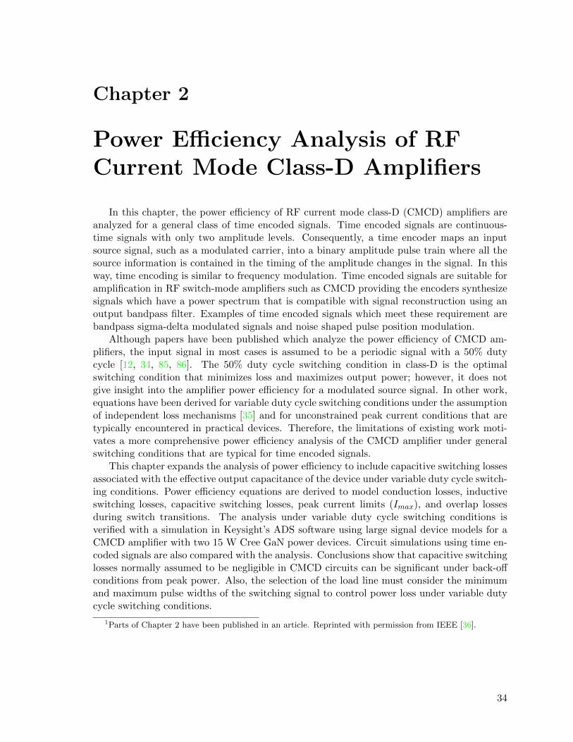
Chapter 2
Power Efficiency Analysis of RFCurrent Mode Class-D Amplifiers
In this chapter, the power efficiency of RF current mode class-D (CMCD) amplifiers areanalyzed for a general class of time encoded signals. Time encoded signals are continuous-time signals with only two amplitude levels. Consequently, a time encoder maps an inputsource signal, such as a modulated carrier, into a binary amplitude pulse train where all thesource information is contained in the timing of the amplitude changes in the signal. In thisway, time encoding is similar to frequency modulation. Time encoded signals are suitable foramplification in RF switch-mode amplifiers such as CMCD providing the encoders synthesizesignals which have a power spectrum that is compatible with signal reconstruction using anoutput bandpass filter. Examples of time encoded signals which meet these requirement arebandpass sigma-delta modulated signals and noise shaped pulse position modulation.
Although papers have been published which analyze the power efficiency of CMCD am-plifiers, the input signal in most cases is assumed to be a periodic signal with a 50% dutycycle [12, 34, 85, 86]. The 50% duty cycle switching condition in class-D is the optimalswitching condition that minimizes loss and maximizes output power; however, it does notgive insight into the amplifier power efficiency for a modulated source signal. In other work,equations have been derived for variable duty cycle switching conditions under the assumptionof independent loss mechanisms [35] and for unconstrained peak current conditions that aretypically encountered in practical devices. Therefore, the limitations of existing work moti-vates a more comprehensive power efficiency analysis of the CMCD amplifier under generalswitching conditions that are typical for time encoded signals.
This chapter expands the analysis of power efficiency to include capacitive switching lossesassociated with the effective output capacitance of the device under variable duty cycle switch-ing conditions. Power efficiency equations are derived to model conduction losses, inductiveswitching losses, capacitive switching losses, peak current limits (Imax), and overlap lossesduring switch transitions. The analysis under variable duty cycle switching conditions isverified with a simulation in Keysight’s ADS software using large signal device models for aCMCD amplifier with two 15 W Cree GaN power devices. Circuit simulations using time en-coded signals are also compared with the analysis. Conclusions show that capacitive switchinglosses normally assumed to be negligible in CMCD circuits can be significant under back-offconditions from peak power. Also, the selection of the load line must consider the minimumand maximum pulse widths of the switching signal to control power loss under variable dutycycle switching conditions.
1Parts of Chapter 2 have been published in an article. Reprinted with permission from IEEE [36].
34

2.1. The Current Mode Class-D RF Amplifier
2.1 The Current Mode Class-D RF Amplifier
A circuit diagram for a CMCD amplifier is shown in Figure 2.1. The circuit consists oftwo devices, M1 and M2, which are switched by a pair of complementary pulse trains, Vs1 andVs2. The pulse trains can be either a periodic signal such as a square wave or more generally anon-periodic pulse train which has an encoded source signal such as a modulated carrier. Thecurrents, isw1 and isw2, form a pair of differential switched current signals. The differentialcurrent is filtered by a parallel tank circuit (LT and CT ) which is anti-resonant at the carrier(fundamental) frequency. Harmonic or out-of-band current components are shorted by thetank and the fundamental frequency component or in-band current components are deliveredto the load.
Rs1
Vs1 VDD
LDC1
IDC
LDC2isw1
CT
LT
RL
isw2
Rs2
Vs2
M1 M2
vL
Node A Node B
Figure 2.1: A CMCD circuit.
In this chapter, a CMCD amplifier design is analyzed for a circuit which uses Cree GaNpower devices for the switches. The devices are 15 W unpackaged die, model CGH60015D.Although Cree provides a comprehensive large signal model for this device, the model isproprietary and the details of the intrinsic devices are not available to the user. The Creemodel is like a black box with terminals for the gate, drain and source, and cannot be usedfor analysis. Therefore, equivalent circuit models which capture the primary behaviour of thedevices are very useful to gain insight into the design of the CMCD amplifier and analyze thecontribution of different loss mechanisms to the overall power efficiency of the amplifier.
2.2 Device Models
Three levels of device models are identified to support analytical and simulation resultsfor CMCD amplifier circuits. The level 3 model described below is also used extensively inlater chapters related to the design of class-F amplifiers. The models are described in thefollowing sections.
35

2.2. Device Models
2.2.1 Level 1
The level 1 model is the most commonly used model in the analysis of CMCD amplifiercircuits. Many literature references can be found for this type of model and the associatedanalysis of the class-D amplifier under periodic switching conditions [87, 41].
In the level 1 model, the device is modeled as a switch with an on-state resistance Ronand an infinite off state resistance Roff . The switch changes states instantaneously in accor-dance with an amplitude transition in the gate drive pulse train. Power loss associated withdissipation in the on-state is modeled and called conduction loss, PRon.
The equivalent on-state resistance for the device model is obtained from an approximationof the DC IV characteristics for the device. In the on-state, the current is constrained tooperate in the linear region of the device at or below the knee point, the point which separatesthe linear and saturation regions of the device IV curve. An example of the knee point andthe on-state resistance approximation are shown in Figure 2.2. As will be shown later, thelinear on-state resistance model can lead to analytic results that are less accurate especiallyfor cases where the input pulse train is periodic and the duty cycle is not 50%. A schematicdiagram of a CMCD amplifier using a level 1 device model is shown in Figure 2.3.
Figure 2.2: Typical DC IV characteristics for a GaN device.
The level 1 model can also include device capacitances and inductances. A fixed outputcapacitance, Cout, models the total effective output capacitance of the device and the capac-itance can be added to shunt the switch. Since device capacitances are nonlinear, the outputcapacitance is the effective output capacitance at the drain node and includes contributionsfrom Cds and Cgd. In Figure 2.3, the effective device capacitances are modeled by C1 and C2.
36

2.2. Device Models
Figure
2.3:Schem
atic
forcu
rrentmodeclass-D
pow
eram
plifier
withalevel1devicemodel
(ADSschem
atic).
37

2.2. Device Models
As is well-known, one of the advantages of the CMCD amplifier is that there is zero-voltageswitching across the devices providing the gate pulse train in a periodic square wave with a50% duty cycle. This means that with a 50% duty cycle there are ideally no switching lossesassociated with the discharge of Cout. Further, the output capacitance of the two switchesshunts the differential tank circuit with an equivalent capacitance of Cout/2 and the tankcapacitance CT can be modified to compensate for the additional shunt capacitance.
When the duty cycle is not 50%, the zero-voltage switching is no longer valid and thereis stored charge in Cout that must be dissipated during the switching transition. An exampleof the current and voltage waveforms at the drain terminals of the devices for a duty cycle of30% is shown in Figure 2.4.2 The analysis of power loss associated with the discharge of Coutfor non-zero voltage switching conditions in CMCD is presented later in Section (2.3). Thepower loss associated with the discharge of Cout is denoted as Pcap.
Another power loss mechanism that is commonly analyzed for CMCD circuits is the powerloss associated with series inductance in the switch, Ls. The inductance is primarily associatedwith the drain inductance on the die and in the package. Because current is hard-switchedin the CMCD circuit, stored energy in the inductor is dissipated each time the switch opens.The inductance also leads to voltage spiking when the switch changes state, because thecurrent cannot instantaneously change through the inductance. For a periodic gate signalwith a fundamental frequency fo, the corresponding power loss from the inductor, called Pind,is Ls I
2DC fo. The equation models the power loss in the two switches where the switched
current has an amplitude of IDC , the total DC current into the CMCD circuit (see Figure 2.1).Typically, inductive switching losses are low because the device and package design minimizeseries inductance. The magnitude of inductive power loss relative to other loss mechanismsis compared later in section (2.3.6).
In summary, the level 1 model is appropriate for independently calculating the powerloss associated with the on-state resistance (PRon), capacitive switching losses (Pcap), andinductive switching losses (Pind). Considering these power loss mechanisms, the overall drainefficiency of the CMCD amplifier is
η =PLPDC
(2.1)
where PL is the power delivered to the load resistor RL and the DC power is
PDC = PL + PRon + Pcap + Pind. (2.2)
2This figure was shown earlier in Figure 1.15 and is repeated for convenience of reference.
38

2.2. Device Models
Figure 2.4: Level 1 CMCD current and voltage waveforms for a 30% duty cycle periodic drivesignal.
39

2.2. Device Models
2.2.2 Level 2
Although the level 1 model is used in many papers for analyzing CMCD circuits, it haslimitations especially under more general switching conditions including arbitrary duty cycleperiodic switching and non-periodic switching. Since the primary application of CMCD am-plifiers in this research is to consider this amplifier as an efficient means of amplifying wirelesssignals, it is necessary to consider how the CMCD works under general switching conditionswhen the input signal is an encoded pulse train.
The level 2 model extends the analysis of the CMCD circuits and includes the followingfeatures.
1. An important loss mechanism in switch-mode power amplifiers is the loss created fromnon-ideal switching waveforms which have finite switching times. During the switchinginterval, of duration τ , the current and voltage waveforms across the device overlapwhich leads to power dissipation in the device. An example of the drain current anddrain voltage waveforms which include overlap loss are shown in Figure 2.5. In the level1 model, switching is assumed to be instantaneous and overlap power loss is zero. Inlevel 2, overlap power loss, denoted as Pτ is included in the calculation of the overallpower efficiency of the amplifier. The overall DC power for the CMCD amplifier withoverlap loss is
PDC = PL + PRon + Pcap + Pind + Pτ . (2.3)
which can then be used in equation (2.1) to calculate the drain efficiency for the amplifier.
2. When the duty cycle for a periodic input signal is not 50%, then the average currentcarried by each switch is no longer equal to IDC/2. This means that one switch carriesmore current than the other. If a CMCD amplifier is designed using the assumptionof a 50% duty cycle condition which is often done, then current saturation in one ofthe switches can appear if the load line is selected for maximum power. Consequently,margin must be allocated in a CMCD design to consider the variation in pulse width(duty cycle) to ensure that current saturation is avoided as this will significantly increasethe dissipation in the amplifier. An analysis with a level 1 model does not include anycurrent saturation limitations as the on-state resistance is an ideal resistor. In level2, current saturation is modeled which constrains the peak current and models thelimitation of a practical device where the peak switch current cannot exceed Imax, themaximum device current at saturation.
3. The effective output capacitance of the device is in general a nonlinear function of thegate and drain voltages. Since often during a switching period the device is either inthe on-state or the off-state, the output capacitance model can be modified to includean on-state capacitance Con and an off-state capacitance Coff . A time averaged capac-itance between the on and off state capacitances can then be used to analyze capacitiveswitching losses under arbitrary duty cycle switching conditions.
The level 2 model is shown in Figure 2.6. The model is partitioned into two states, on-state and off-state, and includes current saturation and different on-state and off-state switchresistances and switch capacitances. The model also assumes that current and voltage overlapfor a state transition interval time of τ .
40

2.2. Device Models
200.6 201.1200.1 201.4
0.0
0.5
1.0
1.5
-0.5
2.0
0102030405060
-10
70
Time (ns)
Drain V
oltage (V)D
rain
Cur
rent
(A)
Figure 2.5: Transition time (τ = 0.15T ) for a CMCD with Cree CGH60015D transistors.
The model values used for the Cree CGH60015D are summarized in Table 2.1. The valueswere extracted from the Cree large signal device model by measuring the S-parameters in theon and off state. The on state corresponds to a gate voltage (Vgs,on) of 0 V, the off statecorresponds to a gate voltage (Vgs,off ) of -4 V, and the DC supply voltage VDD is 25 V.S-parameters for a frequency range of 10 MHz to 2.5 GHz were fitted to the simplified modelto minimize the mean square error. A comparison of the S-parameters for the level 2 modelversus the S-parameters obtained for the Cree large signal model are shown in Figure 2.7. Asshown, the level 2 model matches well with the Cree model.
Table 2.1: Summary of level 2 model values for the Cree CGH60015D die.
Ron Con Coff Ls
2 Ω 1.8 pF 0.5 pF 250 pH
2.2.3 Level 3
Level 3 is a simulation model that is implemented to independently include and controlnonlinear device capacitances. The model includes a current generator that models the DC IVcharacteristics, nonlinear device capacitances for Cgs, Cgd, and Cds, series inductance in thedrain, and gate resistance. The model is implemented in ADS and used for circuit simulationsto compare with analytic results. The simulation model is referenced much more in the nextchapter and additional details are given there.
41

2.2. Device Models
s
d
g
s
d’
d
Con
Ld
Ron
Isat
ON state
Vgs,on
g
s
d’
d
Coff
Ld
Roff
OFF state
Vgs,off
g
τ
Figure 2.6: Level 2 device model for a CMCD amplifier.
0.2
0.5
1.0
2.0
5.0
+j0.2
-j0.2
+j0.5
-j0.5
+j1.0
-j1.0
+j2.0
-j2.0
+j5.0
-j5.0
0.0
S22 ON-State: Model
S22 ON-State: Device
S22 OFF-State: Model
S22 OFF-State: Device
Figure 2.7: S-parameters for the on and off state for a Cree CGH60010D device.
42

2.3. Power Efficiency Analysis of a CMCD Amplifier with Periodic Switching
2.3 Power Efficiency Analysis of a CMCD Amplifier withPeriodic Switching
The level 2 device model is used to analyze the power efficiency of a CMCD amplifier fora periodic switching signal. For the analysis, the periodic signal has a period T and a dutycycle α. An example gate drive waveform is shown in Figure 2.8. The analysis works throughthe following steps. First, equations for the DC supply voltage and supply current are derivedfor an arbitrary duty cycle. The analysis shows that the minimum DC current correspondsto a duty cycle of 50% and increases for non-50% duty cycle conditions. The DC analysisalso provides guidelines on how to select an appropriate load resistance for an arbitrary dutycycle.
The power loss associated with the discharge of the output capacitance is analyzed next.The analysis shows that capacitive switching losses are not negligible for duty cycles whichvary significantly from 50%. Conduction, inductive and overlap loss mechanisms are alsoanalyzed. Finally, a comparison of analytic versus simulated results is made for each of theloss mechanisms.
α
T Time
Amplitude
2T 3T0
Figure 2.8: Signal with period T and variable duty cycle (α).
2.3.1 Selecting the DC Supply Voltage
The constraints on the DC supply voltage VDD for the CMCD amplifier are determined bythe drain-source breakdown voltage of the device, Vds,bd, and the maximum amplitude of theload voltage, Vmax. For a periodic switching signal, the maximum load voltage correspondsto a duty cycle of 50% and the voltage across the device (switch) is a half sinusoid. Theexpected value of the drain voltage is equal to the DC supply voltage. Therefore, for a 50%duty cycle
VDD =Vmaxπ
(2.4)
with the constraint that Vmax must be less than the breakdown voltage. For the CreeCGH60015D, the breakdown voltage is 84 V, and a DC supply voltage of 25 V is selected.From (2.4), the peak amplitude of the load voltage is 78.5 V which leaves a margin of 5.5 Vrelative to the breakdown voltage. The relative values of the DC supply voltage, the maximumswitch voltage, and the breakdown voltage are shown for a typical device in Figure 2.11.
43

2.3. Power Efficiency Analysis of a CMCD Amplifier with Periodic Switching
2.3.2 Load Power
Let’s now consider the relations between the DC current, IDC , supplied to the CMCDcircuit and the peak amplitude of the load current, Iom, to estimate load power, PL. Withreference to the drain current waveforms in Figure 2.4, the amplitude of on-state switchcurrent is equal to IDC . Since the drain current waveforms are periodic square wave signalswith a duty cycle of α, they can be expanded into a Fourier series. The corresponding peakamplitude of the load current is then equal to
Iom =2
πIDC sin(απ). (2.5)
Once the peak output load current is found, an expression for the load power can be writtenas
PL =1
2RL I
2om (2.6)
Equations (2.5) and (2.6) can also be combined to show the relationship between duty cycleand load power:
PL =2
π2RL I
2DC [sin(απ)]2. (2.7)
From the last equation, it is clear that load power is a function of the load resistance, thecurrent switched by the transistors, and the duty cycle of the periodic signal. Load power ismaximized for a 50% duty cycle and power reduces as the duty cycle moves away from 50%.By changing duty cycle, load power changes, and therefore duty cycle can be used to controlthe amplitude of the load signal.
2.3.3 Power Loss Mechanisms
The level 2 device model includes output capacitance, inductance, and finite switchingtime, and the current waveforms at the device terminals are modified compared to the idealclass D switched current waveforms. An example of a typical drain current waveform includingadditional losses is shown in Figure 2.9. When switch 1 (M1) is on, the output capacitance ofthe device is essentially shorted by the low on resistance of the device (see Figure 2.6 for thelevel 2 device model). Therefore, the on-state device capacitance, Con, is negligible and lossis primarily associated with switching current through the series lead inductance Ls. On theother hand, when M1 is on, M2 is in the off-state, and the off-state capacitance, Coff , shuntsthe drain-source terminals of the switch. The voltage across Coff must be charged to trackthe voltage at node B (see Figure 2.1). The energy required to charge Coff must be suppliedby M1 and this leads to an additional current component that is superimposed on the draincurrent flowing into switch 1. The drain current waveform through switch 1 including Coffis given by
isw1(θ) = I1(θ)− IRoff (θ)− ICoff (θ) (2.8)
where θ = ωt and
I1(θ) =
IDC(θ/τ) 0 < θ < τIDC τ < θ < 2πα+ τ
IDC2πα+ 2τ − θ
τ2πα+ τ < θ < 2πα+ 2τ
0 2πα+ 2τ < θ < 2π
(2.9)
44

2.3. Power Efficiency Analysis of a CMCD Amplifier with Periodic Switching
IRoff (θ) =VomRoff
sin(θ) (2.10)
ICoff (θ) ≈ 4
πωCoffRpIDC sin(απ)
sin(τ/2)
τcos(θ). (2.11)
In these equations, Rp = RL||Roff ; however, Roff is usually much greater than RL, thusRp ≈ RL. Also, the current through Coff is calculated from the derivative of the voltageacross the switch with respect to time.
Figure 2.9: Device current waveforms at the drain terminal of the switching device. The ADSsimulation results are for a Cree large signal device model.
The peak amplitude of the load current, Iom, which flows through the load resistance RLis found by calculating the amplitude of the fundamental frequency component of the draincurrent given in (2.8). From a Fourier series analysis of the pulse train, the peak amplitudeof the load current is
Iom =√A2 +B2 (2.12)
where
A =2
π
RpRL
IDC [sin(D)− sin(τ/2)]sin(τ/2)
τ− ICoff (2.13)
B =2
π
RpRL
IDC [cos(τ/2)− cos(D)]sin(τ/2)
τ(2.14)
and D = 2πα + 3τ/2. The current component ICoff associated with charging Coff issmall relative to the amplitude of the load current. Therefore, the expression for Iom can besimplified to
Iom =4
πIDC sin(απ + τ/2)
sin(τ/2)
τ. (2.15)
45

2.3. Power Efficiency Analysis of a CMCD Amplifier with Periodic Switching
As a check on equation (2.15), consider the limit as τ → 0. In the limit, overlap reduces tozero and the current waveform simplifies to the ideal CMCD waveform where
Iom =2
πIDC sin(απ). (2.16)
When overlap loss is not negligible, as in a practical CMCD design, the peak load current isreduced by the finite rise and fall times of the switched current waveform.
The power losses associated with on-state conduction loss and the charging of the off-stateswitch capacitance are
PRon = 2×[
1
2π
∫ π
0Ron (IDC − ICoff (θ))2 dθ
]= RonI
2DC +
1
2Ron max(ICoff )2. (2.17)
There is also power loss associated with non-zero voltage switching for duty cycles whichare not 50%. During an off to on state transition, the output capacitance of the off stateswitch must be discharged. The capacitance is nonlinear, and as an estimate of the power lossduring the transition, the average drain source capacitance is used: Cds = (Coff + Con)/2.The corresponding power loss is given by [35]
Pcap = 2foCds
[πVDD cos(απ)
sin(απ)
1
1 + 4 foCdsRL cos2(απ)
]2. (2.18)
Overlap loss during a switch transition is defined as the power loss associated with thecross-over of the drain current and drain voltage waveforms. Using a linear approximationfor the amplitude transitions as shown in Figure 2.10, the overlap loss is estimated as
Pτ = 2×[
1
2π
∫ 2π
0
(IDC
θ
τ
)(U0τ − θτ
)dθ
]= 2×
[1
π
∫ π
0
(IDC
θ
τ
)(U0τ − θτ
)dθ
]= 2×
[1
π
∫ π
0IDC U0
τθ − θ2τ2
dθ
]=IDC3π
U0 τ. (2.19)
where U0 = Vom cos(απ) τ and Vom is the peak amplitude of the load voltage. The peakamplitude of the load voltage is equal to IomRL, and using the approximation for Iom givenin (2.16), Vom ≈ (2/π)RL IDC sin(απ). Therefore, the overlap power loss can be expressedmore compactly as
Pτ ≈τ
3cot(απ)PL. (2.20)
The last power loss mechanism considered in this analysis is the power loss associated withthe discharge of energy stored in the series inductance, Ls. The fundamental frequency of theswitching waveform is fo and the on-state current is IDC . The stored energy is dischargedtwice per cycle because there are two switches. Therefore, the inductive switching loss is
Pind = Ls I2DC fo. (2.21)
46

2.3. Power Efficiency Analysis of a CMCD Amplifier with Periodic Switching
θ
IdcU0
Vom
τ
2απ + 2τ2απ
Figure 2.10: Overlap of drain current and drain voltage waveforms in a CMCD amplifier.
The sum of all the power losses and the load power must equal the DC power supplied tothe amplifier:
PDC = PL + PRon + Pcap + Pτ + Pind. (2.22)
Analytical expressions have been derived for each term in the preceding analysis, and thereforethe overall drain efficiency of the CMCD under periodic switching conditions can be foundusing
η =PLPDC
=PL
PL + Pon + Pcap + Pτ + Pind. (2.23)
2.3.4 Selecting a Device Load Line
An important design step in any amplifier design is to select the appropriate load line forthe amplifying device. In power amplifier design, this almost always means maximizing loadpower and maximizing power efficiency. The load line for the CMCD amplifier is discussednext. The analysis begins by considering conduction loss, then comments are made abouthow the load line is adjusted for other losses.
The total DC power supplied to the amplifier is equal to the sum of the load power andthe losses in the circuit. The switches in a CMCD amplifier switch a current IDC , and thecorresponding conduction power loss is Ron I
2DC . The DC power supplied to the amplifier is
equal to VDD IDC . Therefore,
PDC = VDD IDC = PL + PRon = PL +Ron I2DC . (2.24)
Using the expression for PL in equation (2.7), (2.24) can be rearranged to solve for IDC :
IDC =VDD
2
π2RL sin2(απ) +Ron
. (2.25)
A few remarks are made about this equation. First, the equation shows that DC poweris a function of duty cycle. The DC current is lowest for a 50% duty cycle (α = 0.5),and DC current increases for non-50% duty cycles. Second, although the equation shows a
47

2.3. Power Efficiency Analysis of a CMCD Amplifier with Periodic Switching
relationship between the load resistance and the DC supply current, the maximum DC currentis constrained by the device characteristics. If the maximum saturation current for the devicein the on-state is Imax, then IDC ≤ Imax. In a level 1 model (see Figure 2.4), the device ismodeled as a simple switch without current saturation. If this circuit is simulated to evaluatepower efficiency as a function of duty cycle, incorrect conclusions can be made because thereis no current saturation function in the model. The level 2 model adds current saturation andensures that unrealistic device currents are not generated in the simulation for arbitrary dutycycles.
An important consequence of the variation of the switch current (IDC) as function ofduty cycle is that a CMCD design must consider the range over which duty cycle will vary.The 50% duty cycle switching condition is a commonly used benchmark in CMCD amplifiersbecause this corresponds to maximum power and maximum efficiency. On the other hand, adesign optimized at 50% duty cycle is not optimal for a design which must amplify signalswith variable duty cycle. Margin must be allocated to ensure that the duty cycle limits do notcreate switch currents that exceeds Imax, otherwise the power efficiency of the amplifier willbe severely reduced because the switch current pushes past the knee and deep saturation canoccur. These points are illustrated in Figure 2.11. In this figure, a DC current (switch current)called Io is defined to correspond to an operating point with 50% duty cycle. Evaluatingequation (2.25) for α = 0.5 gives
Io =VDD
2
π2RL +Ron
. (2.26)
For variable duty cycle switching conditions, the 50% duty cycle switching current Io mustbe less than Imax. As an example, suppose the duty cycle switching range in the input pulsetrain is constrained to a range from 30-70%. To avoid deep saturation at the end points ofthe duty cycle range, the load resistance is selected for the 30% duty cycle, or equivalentlythe 70% duty cycle point, such that IDC is equal to Imax. If the duty cycle exceeds the designrange, then the device becomes deeply saturated. The limiting case for saturation is whenα = 0, or α = 1, which corresponds to one switch closed and one switch open. Under theseconditions, the on-state device is pinned at IDC = Imax and VDS = VDD, and all the DCpower is dissipated in the switch — no power is delivered to the load since the switches arenot switched.
The preceding discussion implicitly links the choice of the load resistance RL to a conditionthat constrains IDC to be less than or equal to Imax for the limits of the duty cycle range inthe pulse train. Another way to visualize the relationship between RL, load power, and powerefficiency is shown in Figure 2.12. With reference to equation (2.7), load power depends onthe load resistance, the DC current supplied to the circuit, and the duty cycle. Additionally,we have equation (2.25) which shows that IDC varies as a function of duty cycle. The twoequations can be combined to rewrite load power as
PL =2
π2RL
[VDD
2π2 RL sin2(απ) +Ron
]2sin2(απ) (2.27)
If conduction losses were zero, then PL would be proportional to V 2DD/RL for a fixed duty
cycle α which is intuitively satisfying. Equation (2.27) is more general and includes conductionlosses, but it still leads to an inverse relation between load power and load resistance, as shown
48

2.3. Power Efficiency Analysis of a CMCD Amplifier with Periodic Switching
VDS
IDS
Imax
I0
Vgs,on
Vgs,off
Vmax00
Vds,bd
LoadLine
α = 0.3
α = 0.5
α = 0
VDD
Figure 2.11: DC IV operating region for a CMCD amplifier including margin for duty cyclevariation.
by the dashed green line in Figure 2.12. Note that the relations in the figure are plotted for aspecific value of duty cycle; in this figure, α = 0.5. The figure also includes the correspondingpower efficiency for the CMCD amplifier as load resistance varies. Using the expression forPL and PDC it is easy to show that the drain efficiency is
η =1
1 +π2
2
RonRL
csc2(απ)
. (2.28)
The solid blue trace in Figure 2.12 shows that power efficiency increases as load resistanceincreases, albeit with diminishing gains in efficiency as RL gets large.
Although equation (2.27) shows how load power varies as function of load resistance, itis derived from a level 1 device model and depends on the on-state resistance, Ron. A directapplication of the equation cannot be used for a practical device without coupling it with aconstraint on the maximum device current, Imax. In order to determine the range of loadresistance that can be used with the device, a second trace is added to the graph to add theImax constraint.
Returning to equation (2.7), the maximum value of IDC that is possible with a physicaldevice is Imax. If IDC = Imax, then PL = (2/π2)I2max sin2(απ)RL which gives a linear boundfor PL as a function of RL for a specific duty cycle. A plot of this bound is shown as thedashed red trace in Figure 2.12. The constrained load resistance range is the segment of thedashed green curve that lies to the right of the intersection of the two lines. The range ishighlighted by a thick black line. The point where the dashed red and dashed green linesintersect is the resistance which maximizes load power, and for the data shown in the figure,the optimum load resistance is 45 Ω. Therefore, the addition of the constraint that IDC ≤ Imaxwith equation (2.27) leads to analytic results which are consistent with the level 2 model thatincludes current saturation in the switch.
Capacitive and inductive switching losses would lead to further adjustment in the finalvalue of load resistance, but equation (2.27) provides a good choice to begin optimizing aCMCD design. As a final note, in a practical design, equation (2.27) should be evaluated
49

2.3. Power Efficiency Analysis of a CMCD Amplifier with Periodic Switching
0
20
40
60
80
100
Effi
cien
cy (
%)
0 20 40 60 80 1000
20
40
60
80
100
Pow
er (
W)
Load Resistance (Ω)
Figure 2.12: Efficiency and output power of a CMCD as a function of load resistance (α = 0.5).
for the endpoints of the duty cycle range which is in the pulse train, since IDC increases fornon-50% duty cycles. An example is given in Figure 2.13 for a 30% duty cycle, and comparedto the 50% duty cycle case, the optimum load resistance is increased to approximately 65 Ω.
0
20
40
60
80
100
Effi
cien
cy (
%)
0 20 40 60 80 1000
20
40
60
80
100
Pow
er (
W)
Load Resistance (Ω)
Figure 2.13: Efficiency and output power of a CMCD as a function of load resistance (α = 0.3).
50

2.3. Power Efficiency Analysis of a CMCD Amplifier with Periodic Switching
2.3.5 Current Saturation Model
As discussed in the previous section, a variable duty cycle periodic pulse train leads toa range of on-state switch currents that fall in the range from Io to Imax. Over this range,the device is transitioning from the linear region to the saturation region and an improvedmodel can be used to predict how IDC changes as duty cycle changes. The transition regionis highlighted in Figure 2.11 and can be modeled by the following equation
IDC ≈ Imax − (Imax − Io) exp(4 [1− csc(απ)]). (2.29)
The exponential function is scaled such that it is consistent with the approximation thate−4 ≈ 0, and the function provides a smooth transition from Io to Imax. An example of howthis function models the change in IDC as a function of duty cycle is shown in Figure 2.14.
Figure 2.14: DC device current as a function of sin(απ) (α is duty cycle).
2.3.6 Analytical versus Simulated Results
The analytical theory which has been developed for the CMCD amplifier is now usedto compare the predicted power efficiency of the amplifier with simulation results. For thecomparison, a CMCD amplifier is designed using the Cree CGH60015D GaN HEMT. Theschematic diagram of the circuit is the same as the circuit shown in Figure 2.1 and thecomponent values are given in Table 2.2.
A summary of the analytical results of different power loss mechanisms versus duty cycleis shown in Figure 2.15. The analytical results are compared with simulation results obtainedusing the Cree large signal device model. For the simulated results, load power and DC sourcepower can be measured but no further details on the breakdown of individual loss mechanismscan be isolated from the simulation results. This is where analytical results provide additionalinsight, and the relative magnitude of different power losses can be compared. Conductionlosses and inductive switching losses are relatively insensitive to changes in duty cycle. On
51

2.3. Power Efficiency Analysis of a CMCD Amplifier with Periodic Switching
Table 2.2: CMCD Design Values
Switches M1 and M2 Cree CGH60015D
Driver resistance Rdrv 5 Ω
Drain supply voltage VDD 25 V
Off-state gate voltage Vgs,off -4 V
On-state gate voltage Vgs,on 0 V
Saturation current Imax 2.3 A
Duty cycle range (α) 30-70%
50% duty cycle switch current Io 1.7 A
Equivalent on-state resistance Ron 2 Ω
Load resistance RL 65 Ω
Fundamental switching frequency fo 1 GHz
Drain bias inductors LDC1 and LDC2 100 nH
Tank Q 5
Tank capacitance CT 12 pF
Tank inductance LT 2 nH
Overlap interval τ 0.1T
the other hand, capacitive switching losses, which are often neglected in CMCD analyses,becomes quite significant particularly as the duty cycle deviates from 50%. As shown, whenall the individual loss mechanisms and the load power are summed together, the predictedDC power is very close to the simulated results. Note that in this figure, all the powers arenormalized to the analytic value for PDC . Some of the simulated values for DC power areslightly higher than the analytic value, therefore, the normalized value for some simulatedvalues are slightly greater than 100%.
Other conclusions from the analytical and simulated results are that the conduction lossis the dominant loss mechanism for duty cycles in the range of 30% to 70%, and for verylow duty cycles (or very high) in the range of 20-30% (70-80%) capacitive switching lossesare significant. From this we can conclude that if it were possible to design a general pulseencoder for CMCD amplifiers, it would be desirable to constrain pulse duty cycles to be inthe range of 30-70% to maintain good power efficiency. This conclusion is supported by thepower efficiency versus duty cycle data shown in Figure 2.16 where we see power efficiencyranges from 55% to 78% for a duty cycle range of 30-70%.
52

2.3. Power Efficiency Analysis of a CMCD Amplifier with Periodic Switching
0.1 0.2 0.3 0.4 0.5 0.60
10
20
30
40
50
60
70
80
90
100
110
Duty Cycle (α)
Nor
mal
ized
to T
otal
Los
ses
(%)
PL
PRon
Pcapacitive
Pinductive
Poverlap
PDC
PL: Simulation
PDC: Simulation
Figure 2.15: Losses in the CMCD amplifier as a function of duty cycle. The overlap period τis 0.1T .
Figure 2.16: Drain efficiency of CMCD amplifier as a function of duty cycle.
53

2.4. Predicting CMCD Amplifier Power Efficiency for Pulse Encoded Signals
2.4 Predicting CMCD Amplifier Power Efficiency for PulseEncoded Signals
2.4.1 Time Encoded Input Signal
When the input pulse train to a CMCD amplifier is a periodic pulse train with a duty cycleα, the load signal is a sinusoid at the fundamental frequency of the pulse train and the peakamplitude is determined by the duty cycle. Although the duty cycle can be adjusted to createan amplitude varying load signal, for a general modulated RF carrier signal, the spectrum ofthe pulse train needs to be shaped to ensure that a modulated load signal with low distortioncan be delivered to the load. Examples of pulse encoders that can generate suitable pulsetrains for amplification by a CMCD amplifier are bandpass sigma-delta modulation (SDM)and noise shaped pulse position modulation (PPM). The time domain and frequency domainproperties of SDM and PPM were briefly reviewed in Chapter 1.
As a way to predict the power efficiency of a CMCD amplifier when the input signal is ageneral pulse encoded signal, CMCD power efficiency is evaluated for more complex periodicsignals. The motivation to use longer periodic sequences is to mimic the type of level crossingsthat would be non-periodic pulse trains such as SDM or PPM. In the following sections, thepower efficiency of a CMCD amplifier is analyzed for periodic signals of different lengths. Theanalytical results are then compared with simulations of a pulse encoded CMCD amplifierwhich has non-periodic switching.
2.4.2 Power Efficiency for 1T Periodic Signals
Analytic results have been developed in earlier sections for predicting the power efficiencyof a CMCD amplifier when the input signal is a periodic signal with duty cycle α. The signalhas a period of T and example pulse train is shown in Figure 2.17. By adjusting the duty,the load power changes and so does the power efficiency. An example of the power efficiencyversus load power characteristic for a signal with period of T is shown in Figure 2.18. Thesame CMCD amplifier design described in section (2.1) is used to obtain these results. Thepeak load power is approximately 30 W and corresponds to a 50% duty cycle. The powerefficiency of the CMCD amplifier is approximately 75% at peak load power. As the duty cycledecreases, load power decreases, there is a corresponding reduction in power efficiency becauseconduction, inductive, and overlap losses are approximately independent of load power, whilecapacitive switching losses increase as load power decreases. At 3 dB back-off the powerefficiency has dropped to 27%.
α1
T Time
Amplitude
Figure 2.17: Signal with period 1T.
54
2.4. Predicting CMCD Amplifier Power Efficiency for Pulse Encoded Signals
0 5 10 15 20 25 30 350
10
20
30
40
50
60
70
80
90
100
Power (W)
Effi
cien
cy (
%)
Periodic SignalSDM Signal
Figure 2.18: Comparison of power efficiency for a CMCD amplifier with a 1T periodic signaland SDM non-periodic signal.
The results for the periodic signal model are now compared with simulated results forbandpass sigma-delta modulator pulse trains. In Figure 2.18, a second response is shownfor the modulator pulse train. The simulation results are obtained using the SDM encoderdescribed in section 1.2.1. The input source signal to the encoder is a sinewave, and theamplitude of the sinewave is swept to change output load power. Three observations aremade when comparing the 1T periodic signal response with the SDM response. First, for thepower range where the two responses overlap (approximately 21 W to 28 W), the two responsesare nearly identical. Second, the 1T response corresponds to a duty cycle range of 20-50%,and clearly this sequence length cannot generate a load power below 21 W. Longer sequencesare required to generate a larger range of load powers. Third, the peak load power with theperiodic signal is higher than SDM. The reason for this is that a square wave with a 50% dutycycle has maximum power at the fundamental frequency and an SDM pulse encoder usuallyoverloads before reaching a periodic limit cycle. Therefore, the peak power with an SDMmodulator is less than the total available peak power which can be obtained with a periodicsignal. This limitation led to the development of the PPM noise shaped encoder described insection 1.2.2 which has higher coding efficiency. A comparison of the SDM and PPM encodersis shown in Figure 2.19. For this figure, the x-axis corresponds to the peak amplitude of thesource signal relative to the quantization amplitude in the encoder. As shown, the PPMencoder can overload to a 50% duty cycle square wave where the fundamental frequencycomponent has an amplitude of 4/π ≈ 1.27, exceeding the quantizer amplitude which isunity.
55

2.4. Predicting CMCD Amplifier Power Efficiency for Pulse Encoded Signals
0 0.2 0.4 0.6 0.8 1 1.20
20
40
60
80
100
Modulator Drive Relative to Full Scale
Eff
icie
ncy
(%
)
SDMPPM
Figure 2.19: Drain efficiency as a function of modulator drive level for SDM and PPM en-coders.
2.4.3 NT Periodic Signals
Up to this point, we have considered periodic signals with a duty cycle of α and period Tas shown in Figure 2.17. If a pulse train with period 2T is considered as shown in Figure 2.20,then it can be described in terms of two duty cycles α1 and α2. The corresponding load signalin a CMCD amplifier is determined by the amplitude of the second harmonic in the 2T pulsetrain. This process can in general be extended to NT where the pulse train is parameterizedin terms of N duty cycles.
α1
T Time
Amplitude
α2
2T
Figure 2.20: Signal with period 2T.
One drawback of the 1T and 2T pulse trains in Figures 2.17 and 2.20 is that there isa variable DC level that depends on the duty cycles. For bandpass source signals, there isno DC component and pulse encoders typically synthesize pulse trains with zero mean DCcomponents. One way to systematically create zero mean pulse trains is to alternate adjacentintervals in the pulse train with a duty cycle of 1−α. In this way, the sequence length doublesfor N duty cycles. An example of a 6T signal with N = 3 is shown in Figure 2.21. For the6T signal, the amplitude of the sixth harmonic determines the amplitude of the load signal
56

2.4. Predicting CMCD Amplifier Power Efficiency for Pulse Encoded Signals
in the CMCD amplifier.
α1
T Time
Amplitude
1− α1
2T
α2
3T
1− α2
4T
α3
5T
1− α3
6T
Figure 2.21: A 6T signal with a zero mean DC component.
2.4.4 Power Efficiency Analysis for a 2T Periodic Signal
Assuming zero-mean pulse trains, we now consider how to predict the power efficiency ofa CMCD amplifier if the input pulse train is a 2T signal. There are two duty cycles, and for azero-mean signal, let α1 = α and α2 = 1−α. The parallel resonant filter in the CMCD outputis tuned to extract the second harmonic of the waveform. From a Fourier series analysis, thesecond harmonic of this pulse can be expressed as
Iom2T =
(2
πIDC2T
)sin2(απ). (2.30)
The output power is then
PL2T=
1
2RLI
2om2T
=2
π2RL I
2DC2T
sin4(απ). (2.31)
Using (2.31) and (2.7), the ratio of the output power of the 2T signal relative to the outputpower of a 1T signal is
PL2T
PL1T
≈ sin2(απ). (2.32)
The equation is written as an approximation because it based on the assumption that theDC current drawn by the amplifier is the same for the 1T and 2T signals. Simulation resultsverify that this is a good assumption as will be shown shortly.
Using equation (2.32), an expression for the relative power efficiency of the CMCD ampli-fier when amplifying 1T and 2T is
η2Tη1T
=(PL2T
/PDC2T)
(PL1T/PDC1T
)≈ sin2(απ). (2.33)
Again, the assumption that the DC currents for the two cases are the same is used to concludethat the DC power for the two cases is the same (recall that VDD is fixed in a CMCD amplifier).
57

2.4. Predicting CMCD Amplifier Power Efficiency for Pulse Encoded Signals
What the power efficiency ratio enables is an extension to lower load power levels, becausethe second harmonic amplitude in a 2T pulse train with duty cycle parameter α is smaller thanthe fundamental frequency amplitude in a 1T pulse train with a duty cycle of α. Equation(2.33) is used to extend the power efficiency analysis of CMCD amplifiers from 1T to 2T . Anexample of analytical and simulated results for 2T signals is shown in Figure 2.22. As theresults show, there is good agreement between the analysis and simulation which confirms theassumption that the DC current in the CMCD amplifier is approximately equal for both the1T and 2T signals.
0 0.2 0.4 0.6 0.8 10
20
40
60
80
100
Duty Cycle
Eff
icie
ncy
(%
)
Calculated resultsSimulated results
Figure 2.22: Drain efficiency of CMCD amplifier as a function of duty cycle when driven witha 2T periodic signal.
2.4.5 Power Efficiency for 6T Periodic Signals
Longer periodic sequences can be generated to increase the amplitude range of the loadsignal. As an example, a zero mean 6T signal is considered next. There are six duty cycleparameters, but after imposing the zero-mean constraint, there are three independent dutycycles. The corresponding duty cycles in the 6T pulse train are α1, 1 − α1, α2, 1 − α2, α3
and 1− α3 as shown in Figure 2.21. Different combinations of duty cycles, lead to differentsixth harmonic amplitude levels and twenty different sequences are tabulated in Table 2.3.
Circuit simulations of a CMCD power amplifier were run with all the different 6T sequencesin Table 2.3 and the corresponding power efficiency is shown Figure 2.23. The simulationresults are compared with SDM and PPM pulse trains as well as with 1T and 2T periodicsequences described earlier. Note that all periodic sequences have been constrained to havepulse widths that are at least 0.2T or greater. From the results, it is clear that simulationsresults with periodic sequences are very consistent with results for more general pulse encodedsignals like SDM and PPM. From these results we conclude that analytic results obtained for1T and 2T periodic signals can lead to good predictions of the performance of a CMCDamplifier for more general pulse trains like SDM and PPM.
58

2.4. Predicting CMCD Amplifier Power Efficiency for Pulse Encoded Signals
Table 2.3: Duty cycles for generating signals with a period of 6T.
Sequence (1) (2) (3) (4) (5) (6) (7) (8) (9) (10)
α1 0.2 0.2 0.2 0.2 0.2 0.2 0.2 0.2 0.2 0.2
α2 0.2 0.2 0.2 0.2 0.3 0.3 0.3 0.4 0.4 0.5
α3 0.2 0.3 0.4 0.5 0.3 0.4 0.5 0.4 0.5 0.5
Input Amplitude 0.44 0.57 0.68 0.72 0.7 0.81 0.85 0.91 0.95 0.98
Sequence (11) (12) (13) (14) (15) (16) (17) (18) (19) (20)
α1 0.3 0.3 0.3 0.3 0.3 0.3 0.4 0.4 0.4 0.5
α2 0.3 0.3 0.3 0.4 0.4 0.5 0.4 0.4 0.5 0.5
α3 0.3 0.4 0.5 0.4 0.5 0.5 0.4 0.5 0.5 0.5
Input Amplitude 0.83 0.94 0.98 1.04 1.08 1.11 1.15 1.17 1.21 1.27
0 5 10 15 20 25 30 350
10
20
30
40
50
60
70
80
90
100
Power (W)
Effi
cien
cy (
%)
Solid: SDM
Dash: PPM
Square: 1T−Signal
Circle: 2T−Signal
Triangular: 6T−Signal
α=0.21T − Signal
2T − Signal 6T − Signalα=0.2
Figure 2.23: CMCD amplifier power efficiency for periodic (1T , 2T , and 6T ) and non-periodicpulse trains (SDM and PPM).
In wireless communication applications, the input signal is a modulated carrier with alarge PAPR. Therefore, the average power point is backed off relative to peak power. Withreference to Figure 2.23, peak load power is approximately 30 W and the power efficiencyis about 75%. At 3 dB back-off, the output power is 15 W and the corresponding powerefficiency is reduced to 28%. This shows that there is a steep reduction in power efficiencyas soon as the output power is backed off. The main reason for the reduction in efficiency isthe range of duty cycles in the pulse train. If the duty cycle variation could be minimized,then higher efficiency could be obtained. For example, with reference to Figure 2.22, a duty
59

2.5. Chapter Summary
cycle range from 35-65% would maintain power efficiency at 50% or higher. Therefore, theseresults show the importance of the signal mapping stage in a RF switch-mode power amplifiersystem.
2.5 Chapter Summary
Three different device model levels were introduced to analyze the power efficiency of aCMCD power amplifier. The level 1 model is a simple switch and a model that is commonlyused in the literature. The level 2 model introduced in this work extends the level 1 modelto include current saturation limitations in the switch as well as overlap losses. The level 3model goes further and includes nonlinear device capacitances, and the model will be usedmore extensively in the next chapter.
The level 2 model was used to analyze the power efficiency of a CMCD amplifier undervariable duty cycle switching conditions. A thorough analysis was presented for 1T periodicsignals. The analytic results were compared with simulations of a CMCD amplifier using aSDM pulse train. The two results are very similar which shows that the analysis models thebehaviour of the amplifier under more general non-periodic switching conditions. The analysiswas extended to 2T periodic signals. Again there is a good match between the predicted andsimulated power efficiency over a large range of duty cycles. Simulation results were thenmade to compare the power efficiency of CMCD amplifiers with longer periodic sequences upto 6T . As with 1T and 2T , the 6T results closely match the performance of SDM and PPMpulse trains.
The power efficiency of the CMCD amplifier is very dependent on the duty cycle variationin the pulse train. As the analytical and simulation results show, power efficiency reducesquickly as the load power is reduced. The results show that signal mapping in the pulseencoder and the design of the switch-mode power amplifier are closely linked. In the nextchapter, class-F amplifiers are designed and later in Chapter 5, the class-F amplifiers aretested with pulse encoded signals.
60

Chapter 3
Class-F RF Power Amplifiers
Class-F amplifiers use harmonically tuned input and output matching networks to shapethe waveforms at the gate and drain of the amplifying device. The goal of harmonic wave-shaping is to reduce the overlap of the drain current and drain voltage waveforms to obtaina high efficiency amplifier. Similar to the class-D amplifier, class-F amplifiers can approach aswitch-mode type of operating condition providing the amplifiers are operated near saturation.
There is a large body of work related to class-F amplifier design and the contributionsto this work are the following. First, a systematic study of the effect of input harmonictermination impedance is made for a class-F amplifier. The study uses a level 3 devicemodel and the relative importance of first, second, and third harmonic input impedances areanalyzed. The comparison includes third harmonic terminations at the input which is new.Experimental results for a class-F amplifier including third harmonic networks for both theinput and the output are also shown. Second, an inverse class-F (class-F−1) amplifier designis implemented using exactly the same device as the class-F amplifier, and the two amplifierdesigns are compared. The comparison is useful as it is more difficult to find reference designsin the literature which provide a direct compare between the voltage switched class-F amplifierand the current switched class-F−1. The experimental results clearly show that the currentswitched class-F−1 circuit has higher power efficiency over a larger dynamic range. The class-F amplifier designs are also very useful benchmarks for Chapter 4, where the amplifier arereconfigured into RF rectifiers. The chapter concludes with the design of a wideband class-F−1. Although experimental results for wideband class-F−1 can be found in the literature, thedesign presented here is reconfigured into a wideband rectifier in Chapter 4, and the widebandrectifier work which builds on the wideband amplifier design is new work.
3.1 Level 3 Device Model
All the experimental circuits in this thesis use a packaged 10 W GaN HEMT (modelCGH40010) available from Cree. Although a comprehensive large signal model for the deviceis available from Cree, it is difficult to use this model to gain insight into the underlyingmechanisms that generate harmonic frequency components at the gate terminal of the device.Also, the black-box Cree model does not enable any way to tune device parameters andevaluate the sensitivity of the circuit with respect to different device parameters. Therefore, alevel 3 device model is first constructed from a large signal device model for a Cree CGH60015Ddie. After building a model of the die, the model is then extended to include package parasiticssince a packaged device is used for all the experimental work. The packaged device (modelCGH40010) uses the CGH60015D die which is wire bonded to the package leads. The methodsused to extract the equivalent circuit values for the level 3 model are reviewed next.
2Parts of Chapter 3 have been published in two articles. Reprinted with permission from PIER and EuMC[56, 76].
61

3.1. Level 3 Device Model
Cgs Cds
Cgd
Intrinsic DeviceModel
I
V
rgLg rd Ld
rs
Ls
G D
S
G’ D’
S’
Figure 3.1: Level 3 equivalent circuit model for GaN HEMT Cree CGH60015D [reproducedcourtesy of The Electromagnetics Academy].
3.1.1 Bare Die Device Model
A level 3 device model is shown in Figure 3.1. The equivalent circuit for the device ispartitioned into an intrinsic device model composed of a current source and nonlinear devicecapacitances (Cgs, Cgd and Cds), and extrinsic inductances and resistances associated withthe interconnect to the intrinsic device. The values for the components in the equivalentcircuit model are obtained from Z and Y -parameters for the large signal device model. Theextraction process is described next.
Let Z ′ be the Z parameters for the intrinsic device. The corresponding Z parameters forthe overall device model are [88][
Z11 Z12
Z21 Z22
]=
[Z ′11 + (rg + rs) + j(Lg + Ls)ω Z ′12 + rs + jLsω
Z ′21 + rs + jLsω Z ′22 + (rd + rs) + j(Ld + Ls)ω
]. (3.1)
Therefore, once the extrinsic interconnect values for the series inductances and resistances areknown, we can find the Z-parameters for the intrinsic device. After Z ′ is obtained, the matrixcan be inverted to find the admittance parameters Y ′. The individual admittance parameterscan be matched to the Π capacitance network and lead to the following equations [89].
Cgd =−Im[Y ′12]
ω(3.2)
Cgs =Im[Y ′11 + Y ′12]
ω(3.3)
Cds =Im[Y ′22 + Y ′12]
ω(3.4)
62

3.1. Level 3 Device Model
3.1.1.1 Extraction of the Parasitic Inductances and Resistances
At this point, we need to find a way to determine the extrinsic circuit component values.An important observation is that the series inductances and resistances are independent ofthe bias point of the device, while the nonlinear device capacitances in the intrinsic model arebias dependent. Therefore, a bias point can be selected that simplifiers the extraction of theextrinsic component values.
A good choice for the extraction, is the off-state bias condition where VGS = VGSOFFand
VDS = 0 V. Under these conditions, the transconductor in the intrinsic model is short circuitedand nodes S′ and D′ are shorted, as shown in Figure 3.2. Under the off-state bias condition,the real part of the Z-parameters is directly related to the resistances in the equivalent circuitand we have the following relations:
Re[Z11] = rg + rsRe[Z22] = rd + rsRe[Z12] = Re[Z21] = rs
(3.5)
From these equations, all the resistances can be uniquely found from Z-parameters for theoff-state. Also note that the real part is frequency independent.
Cgs Cds
Cgd
Intrinsic DeviceModel
rgLg rd Ld
rs
Ls
G D
S
G’ D’
S’
VDS = 0
shorts nodes S’ and D’
Figure 3.2: Equivalent circuit model for off-state bias conditions.
The Z-parameters for the off-state were obtained from the large signal Cree model andthe results are shown in Figure 3.3. The real and imaginary components of the Z-parametersare shown by the solid lines for a frequency range of 0.5 to 10 GHz. The data clearly showthe real component is constant over frequency, consistent with equation (3.5). The equationswere used to calculate the equivalent circuit resistances and the values are optimized in a finalstep after all component values are extracted for the level 3 model.
The imaginary component of the off-state Z-parameters is more entangled and contribu-tions to reactance are made both from the series lead inductances as well as the intrinsicdevices capacitances. The entanglement is simplified by using Z-parameters at very high fre-quencies where the inductance starts to dominate the response and the intrinsic capacitanceshave low reactance. The inductive behaviour of the reactance is evident in the Z-parametermeasurements shown in Figure 3.3 where the slope at high frequencies is related to the in-
63

3.1. Level 3 Device Model
ductance. Clearly, in the limit as ω gets large the Z-parameters are approximated asZ11 ' (rg + rs) + j(Lg + Ls)ωZ22 ' (rd + rs) + j(Ld + Ls)ωZ12 = Z21 ' rs + jLsω
(3.6)
These approximations are used to estimate values for the extrinsic inductances.
Figure 3.3: Z-parameters for the level 3 device model (symbols) and for the large signal devicemodel (solid lines) for the off-state bias condition.
3.1.1.2 Off State Device Model
Once the extrinsic inductances and resistances are found, the Z-parameters of the off-statecan be de-embedded to extract the intrinsic Z ′-parameters. The instrinsic Z ′-parameters arethen inverted to find the admittance matrix Y ′ from which values for the devices capacitancescan be found using equations (3.2), (3.3) and (3.4). After calculating initial values for all themodel components, a final step to optimize the model values is made to provide the best match
64

3.1. Level 3 Device Model
between the level 3 model and the Cree model. The Y -parameters are particularly usefulfor optimizing the final values because they are sensitive to all the device characteristics. Acomparison of the off-state Y -parameters for the level 3 model compared to the Cree model areshown in Figure 3.4. As shown, there is good agreement between the two models. A summaryof model 3 equivalent circuit component values for the off-state is shown in Table 3.1.
Figure 3.4: Y -parameters for the level 3 device model (symbols) and for the large signal devicemodel (solid lines) for the off-state bias condition.
3.1.1.3 Extraction of Nonlinear Device Capacitances
The intrinsic device capacitances are nonlinear, having dependencies on the gate-sourcevoltage and the drain source voltage. Now that the extrinsic inductances and resistances areknown in the level 3 model, parametric sweeps of the de-embedded Y ′-parameters can be usedto extract models of the device capacitances over a wide range of bias conditions. It should benoted, that when VDS is no longer zero, the model includes a voltage controlled current sourcewhich models the transconductance of the device. At low frequencies, the transconductance
65

3.1. Level 3 Device Model
Table 3.1: Level 3 model values for the Cree GaN HEMT (CGH60015D) in the off-state biascondition.
Element rg rd rs Lg Ld Ls Cgs,off Cds,off Cgd,off
(Ω) (Ω) (Ω) (pH) (pH) (pH) (pF) (pF) (pF)
Value 0.62 0.6 0.1 91.8 88.65 1 4.1 0.87 0.6
Table 3.2: Summary of device capacitances for a Cree GaN HEMT (CGH60015D).
Model Model Datasheet
Vgs=-5 V to 0 V , Vds=0 V to 60 V Vgs=-8 V and Vds=28 V Vgs=-8 V and Vds=28 V
Capacitance Min. Max. Linear Value Typical
Cds 0.87 pF 2.4 pF 0.92 pF 0.87 pF 0.9 pF
Cgd 0.1 pF 0.7 pF 0.36 pF 0.19 pF 0.2 pF
Cgs 4.14 pF 7.65 pF 6.17 pF 4.14 pF 4.1 pF
term is associated with the real part of the Y ′-parameters and the imaginary part of the Y ′-parameters can be used to find the intrinsic device capacitance values similar to the procedureused in the off-state.
The bias points which were used to extract the nonlinear device capacitances span a VGSrange from -8 to 0 V (-8, -4, -2, -1, 0 V) and a VDS range from 0 to 80 V (0, 2, 4, 6, 8, 10,20, 28, 40, 50, 60 and 80 V). The best fit values were optimized for a frequency of 1 GHzand the device capacitance characteristics are shown in Figures 3.5 (a)-3.5 (d). Notablecharacteristics include significant variation in Cds for low drain voltages, a significant changein Cgs as the gate voltage swings between on and off states, and nonlinear Cgd characteristicsthat depend on both the gate and drain voltages. The variation in the device capacitancesover the operating range of the device are summarized in Table 3.2. The table also includesthe nominal device capacitances given on the Cree datasheet for the die [90].
In order to implement the level 3 model in a circuit simulator, nonlinear circuit elementsare required for the device capacitances and the transconductance to model the IV curvesof the device. In ADS, nonlinear capacitor models are available that can be linked to lookup tables. In this way, the instantaneous capacitance is dependent on the instantaneousgate-source and drain source voltages in the circuit. The nonlinear transconductance, whichmodels the IV characteristics of the device, is implemented using a special component called asymbolically defined device (SDD). Similar to the capacitors, the SDD block is controlled bya look-up table that models the drain source current dependency on gate-source and drain-source voltages.
3.1.1.4 Level 3 Model for Die and Package
A packaged die is used for experimental work and a level 3 model for the device includinga package is shown in Figure 3.6. It consists of the level 3 bare die model shown earlier in
66

3.1. Level 3 Device Model
0 5 10 15 20 25 300.5
1
1.5
2
2.5
Vds (V)
Dra
in−
Sou
rce
Cap
acita
nce
(pF
)
Decreasing orderVgs=0 to −5
(a)
0 10 20 30 40 50 60 70 804
4.5
5
5.5
6
6.5
7
7.5
8
Vds (V)
Gat
e−S
ourc
e C
apac
itanc
e (p
F)
Vgs= −8 V, −4 V
Vgs= −3 V
Vgs= −2 V, −1 V, 0 V
Vgs= −8 V, −4 V
Vgs= −3 V
Vgs= −2 V, −1 V, 0 V
Vgs= −8 V, −4 V
Vgs= −3 V
Vgs= −2 V, −1 V, 0 V
Vgs= −8 V, −4 V
Vgs= −3 V
Vgs= −2 V, −1 V, 0 V
Vgs= −8 V, −4 V
Vgs= −3 V
Vgs= −2 V, −1 V, 0 V
Vgs= −8 V, −4 V
Vgs= −3 V
Vgs= −2 V, −1 V, 0 V
(b)
0 10 20 30 40 50 60 70 800
0.1
0.2
0.3
0.4
0.5
0.6
0.7
0.8
Vds (V)
Gat
e−D
rain
Cap
acita
nce
(pF
)
Decreasing orderVgs= 0 to −5
(c)
−8 −7 −6 −5 −4 −3 −2 −1 04
4.5
5
5.5
6
6.5
7
7.5
8
Gate−Source Voltage (V)
Gat
e−S
ourc
e C
apac
itanc
e (p
F)
(d)
Figure 3.5: Extracted intrinsic device capacitances for the Cree GaN HEMT (CGH60015D):(a) drain-source capacitance, (b) gate-source capacitance, (c) gate-drain capacitance, and (d)gate-source capacitance versus gate-source voltage.
Figure 3.1 with additional lead inductances (Lpg, Lpd) and capacitances (Cpg, Cpd). Similarto the method used to find extrinsic inductances, the package inductances can be found fromZ-parameters measured at high frequencies where the response is dominated by the packageinductance and the package capacitance approaches a low impedance. After finding estimatesof the package inductances, the package capacitances in the level 3 model are tuned to matchthe Z-parameters of the Cree large signal model for the packaged device (CGH40010F). Theextracted values for the package model are found to be: Lpg = 0.7 nH , Lpd = 0.6 nH,Cpg = 0.41 pF and Cpd = 0.4 pF.
As a confirmation of the level 3 model, the Y -parameters of the model level 3 modelare compared to the Cree model. The results are shown in Figures 3.7 through 3.9. Goodagreement is obtained and the level 3 model is used in the next section to study the effect ofinput harmonic termination impedances in a class-F amplifier.
67

3.1. Level 3 Device Model
Cgs Cds
Cgd
Bare Die
I
V
rgLg rd Ld
rs
Ls
LpdLpg
CpdCpg
Figure 3.6: Device model for packaged die [reproduced courtesy of The ElectromagneticsAcademy].
Figure 3.7: Comparison of Y11 parameters for the level 3 model including the package (sym-bols) and the GaN HEMT Cree large signal model for the CGH40010F (solid line). Thedevice bias conditions are in the off-state.
68

3.1. Level 3 Device Model
Figure 3.8: Comparison of Y12 parameters for the level 3 model including the package (sym-bols) and the GaN HEMT Cree large signal model for the CGH40010F (solid line). Thedevice bias conditions are in the off-state.
Figure 3.9: Comparison of Y22 parameters for the level 3 model including the package (sym-bols) and the GaN HEMT Cree large signal model for the CGH40010F (solid line). Thedevice bias conditions are in the off-state.
69

3.2. Class-F Amplifier Simulation Experiments
3.2 Class-F Amplifier Simulation Experiments
Class-F amplifiers are inherently nonlinear and use harmonic impedance control in theoutput circuit to shape the voltage waveform at the drain. In an ideal class-F design, thedevice is cut-off for half the cycle similar to class B, and harmonics are created in the outputcircuit because the drain current is a half sinusoid. Harmonic termination impedances in theoutput circuit preserve the shape of the current waveform by shorting even harmonics. Thedrain voltage waveform is shaped to reduce overlap with the current waveform by open circuittermination impedances at odd harmonics.
There are however other mechanisms in a class-F amplifier that create additional harmonicfrequency components in the current and voltage waveforms. Examples include deviationsfrom the class-B bias point which means the current waveform is no longer a perfect half-sine waveform, and nonlinear device capacitances [19] and nonlinear device transconductanceswhich create new harmonic frequency terms even for perfectly sinusoidal input signals. Ofthese mechanisms, nonlinear gate-source capacitance Cgs and nonlinear gate-drain capacitanceCgd can directly create harmonic components at the gate. There are also feedback mechanismsincluding Cgd and source inductance which can couple drain harmonics to the gate. Forexample, an imperfect second harmonic termination in the output match creates a secondharmonic voltage component that can be coupled to the gate through Cgd. The effect ofharmonic signal components at the gate is that the gate waveform is no longer sinusoidal evenif the input to the amplifier is a perfect sinusoid. Changes to the gate waveform, affect thedrain current waveform, and consequently the drain current waveform deviates from an idealhalf sinusoidal shape. Therefore harmonic termination impedances at the gate can be usedto shape both the gate waveform and the drain current waveform.
The relationship between power efficiency and input harmonic impedances for class-Famplifiers has been studied by others [91, 92, 93, 94, 95, 96, 97] and a summary is presentedin Table 3.3. Most work listed in the table has focused on evaluating the effect of fundamentaland second harmonic impedance terminations at the input of the device. Also, in these papers,the mechanisms that generate harmonics in the device have been less important, and the workhas focused on investigating harmonic termination impedances using harmonic load pull andtime domain techniques. Although these techniques are general and can be extended to allharmonics, the experimental work presented in these papers has been limited to circuits withinput harmonic terminations for fundamental and second harmonic impedances.
This work extends the investigation of input harmonic impedance to include the effectof third harmonic terminations on the power efficiency of a class-F amplifier. A systematiccomparison of the power efficiency for amplifier designs with fundamental, second harmonic,and third harmonic terminations are made. Simulations with the level 3 device model areused to investigate the relationship between device capacitances and the harmonic levels atthe gate. The impact of the gate to drain capacitance, Cgd, is particularly important asit provides feedback from the output to the input. The feedback, combined with imperfectoutput harmonic termination impedances, can lead to the injection of both odd and evenharmonics to the gate terminal. The model is also used to investigate the sensitivity of thedesign to nonlinear device capacitances. A comparison is made between a model with linearcapacitances and a model with nonlinear capacitances.
70

3.2. Class-F Amplifier Simulation Experiments
Table 3.3: Class-F amplifier designs with input harmonic termination networks.
Ref. Type Device Input Harmonics Approach
[91] class-F GaN fo, 2fo harmonic tuning
class-F−1
[92] class-F PHEMT fo, 2fo device level
class-B
[93] class-F AlGaAs/GaAsN fo, 2fo phase relationship
class-F−1
[98] class-F GaAs MESFET fo, 2fo power balance
class-E
[95] class-F Power MESFET fo, 2fo load/source pull
[96] class-F Power MESFET fo, 2fo, 3fo phase relationship
[97] class-F PHEMT fo, 2fo, 3fo load/source pull
This class-F GaN HEMT fo, 2fo, 3fo device level
work
3.2.1 Class-F Amplifier Design
The complete level 3 simulation model with provisions up to third harmonic terminationimpedances at the gate is shown in Figure 3.10. The amplifier is designed for a fundamentalfrequency of 990 MHz. The drain bias (VDD) is 30 V and the gate bias (VGG) is -2.6 V. Theoptimal load and source impedances at the fundamental frequency were found using sourceand load pull [99] test benches in the simulator.
The transmission line elements TL101 and TL102 in Figure 3.10 implement the fun-damental frequency input match, and transmission lines TL109 and TL110 implement thefundamental frequency output match. The output matching circuit consists of three othertransmission lines, TL106, TL107, and TL108, which create a second harmonic short andthird harmonic open at the drain. The input matching circuit also has three transmissionlines, TL103, TL104 and TL105, which are used to experiment with different input harmonicterminations at the gate.
Further optimization of the third harmonic output stub TL108 can be made to compen-sate for the output reactance of the device at the third harmonic frequency. However, theoptimization of the output matching network with the level 3 device model is not the primaryfocus here and we constrain the output network topology to be the same for all design studiesof the input matching network (see Figure 3.11). Instead, here we adjust the length of theoutput harmonic stubs and vary Cgd to create different harmonic injection levels that arefed back to the gate. In this way, the significance of the input harmonic terminations versuspower efficiency can be swept for different harmonic injection levels at the gate.
71

3.2. Class-F Amplifier Simulation Experiments
gate
gate
drain
drain
VarEqn
Re
f
VarEqn
Re
f
Re
f
DAC
VarEqn
VarEqnHARMONIC BALANCE
VarEqn
Re
f
VarEqn
VarEqn
Re
f
VarEqn
Re
f
Z0=50
ELoutputmatching1=65.1
ELoutputmatching2=54.3
RL=Z0
Lambda0=360
Lambda2=Lambda0/2
Lambda3=Lambda0/3
ELharmonic3=Lambda3/4
ELinputmatching2=47.3
ELinputmatching1=80.25
Z=Z0 Ohm
E=ELharmonic1
F=f GHz
L=Lch nH
R=
vgs=_v1
Vdc=VGG V
L=Ld pH
R=
E=ELharmonic1
F=f GHz
Num=5
F=f GHz
InterpMode=Linear
C=Cb pF
InterpDom=Rectangular
ExtrapMode=Interpolation Mode
Rdamp=5
Z=Z0 Ohm
VGG=-2.6
rd=0.6
Z=50 Ohm
P=dbmtow(Pindbm)
Freq=f GHz
Z=Z0 Ohm
F=f GHz
Freq[1]=f GHz
Order[1]=10
iVal1=vgs
iVar1="VGS"
iVar2="VDS"
E=ELharmonic3
Lg=92
ELharmonic1=Lambda0/4
Pindbm=24.5
Z=Z0 Ohm
E=ELharmonic3
Z=Z0 Ohm
E=ELharmonic2
F=f GHz
Z=Z0 Ohm
E=ELoutputmatching1
Ld=88
E=ELoutputmatching2
F=f GHz
ELharmonic2=Lambda2/4
F=f GHz
R=RL Ohm
R=Rdamp Ohm
vds=_v2
iVal2=vds
R=
L=Lg pH
R=
L=Lch nH
Cport[1]=
I[1,0]=(_v1)*0
R=rd Ohm
ids=fileDAC1, "IDS"
Vdc=VDD V
E=ELinputmatching2
rg=0.6
E=ELinputmatching1
F=f GHz
I[2,0]=ids
F=f GHz
C=Cb pF
C[1]=
Z=Z0 Ohm
Z=Z0 OhmR=rg Ohm
Z=Z0 Ohm
f=0.990
E=ELharmonic2
F=f GHz
Z=Z0 Ohm
VAR
VAR
DataAccessComponent
L
V_DC
VAR
TLIN
VAR
TLOC
P_1Tone
VAR
C
TLOC
TLOC
R
TLINTLIN
R
DC_Block
VAR
TLOC
L
DC_Block
L
L
VAR
TLIN
V_DC
R
NonlinC
RTLOC
SDD2P
C
NonlinC
VAR
NonlinC
HarmonicBalance
TLOCVAR_network2
VAR_wavelengths
VAR_network1
SRC1
L2
DAC1
L3
PORT1
VAR_IDS
TL109
TL105
VAR_bias
TL108
HB1
C1
TL104
TL103
R3
TL106
R4
L1
L4
VAR3
R2
TL102
SRC2
VAR_parameters
SDD2P1
TL101R1
C2
DC_Block2
CdsCgs
Cgd
TL110
DC_Block1
VAR_signal
TL107
Figure 3.10: Schematic for the class-F PA [reproduced courtesy of The ElectromagneticsAcademy].
72

3.2. Class-F Amplifier Simulation Experiments
(λo/12)
(λo/8)
ZOMN 50 Ω
TLout3
TLout2
TLout1 TLout4
TLout5(λo/4)
Figure 3.11: Output matching network (OMN) structure [reproduced courtesy of The Elec-tromagnetics Academy].
3.2.2 Harmonic Input Impedances and Sensitivity to Device Capacitances
For the first simulation experiment, the device model consists of fixed (linear) devicecapacitance values. The fixed capacitance values are selected to be the expected value of thenonlinear capacitances over the operating range of the circuit. The fixed capacitance valuesare: Cgs = 6.17 pF, Cds = 0.92 pF and Cgd = 0.36 pF. When the device capacitances arelinear, the only mechanism for generating harmonics at the gate is feedback from the outputcircuit to the input circuit through Cgd.
The effect of feedback through Cgd is illustrated by comparing the harmonic spectrums atthe drain and gate. In Figure 3.12, the spectrums are shown for the case where Cgd is zero.The drain spectrum for the voltage has DC, fundamental and third harmonic components.The second harmonic is zero because the harmonic is shorted in the output circuit. The cor-responding gate spectrum has only a DC and fundamental frequency component as expectedbecause there is no feedback from the drain to gate. On the other hand, when Cgd is not zero,harmonic components from the drain voltage are fed back to the gate. An example is shownin Figure 3.13 for Cgd = 0.36 pF. The amount of harmonic feedback from the output to theinput of the device depends not only on the size of Cgd but also on the harmonic levels in theoutput circuit.
Figure 3.12: Spectrum for the case where Cgd = 0 pF: drain voltage (left) and gate voltage(right) [reproduced courtesy of The Electromagnetics Academy].
In the next set of simulation experiments, the device model with linear capacitances is usedto compare the power efficiency of three different class-F amplifier designs where each design
73

3.2. Class-F Amplifier Simulation Experiments
Figure 3.13: Spectrum for the case where Cgd = 0.36 pF: drain voltage (left) and gate voltage(right) [reproduced courtesy of The Electromagnetics Academy].
has a different harmonic input matching network. The input matching circuits are shownin Figure 3.14. In the first design (Design 1), the gate is matched only for the fundamentalfrequency. In the second design (Design 2), the input matching circuit provides a fundamentalfrequency match and a short at the second and third harmonics. In the third design (Design 3),the input matching circuit provides a match at the fundamental frequency, a short at the
TLin4(λo/8)
TLin1
TLin2
TLin3(λo/12)
TLin1
TLin2
TLin5(λo/4)
TLin4(λo/8)TLin1
TLin2
TLin3(λo/12)
(a)
(b)
(c)
gate
gate
gate
in
in
in
Figure 3.14: Input matching network circuits: (a) Design 1, (b) Design 2 and (c) Design 3[reproduced courtesy of The Electromagnetics Academy].
74

3.2. Class-F Amplifier Simulation Experiments
Table 3.4: IMN transmission line lengths for a device model with linear capacitances.
DesignHarmonic input impedances
TLin1 TLin2 TLin3 TLin4 TLin5 Γin,2fo Γin,3fofo 2fo 3fo
1 ZS,opt - - 74.8 30.9 - - - 1∠343 1∠58.5
2 ZS,opt Short Short 77.4 26.65 30 45 - 1∠180 1∠180
3 ZS,opt Short Open 80.25 47.3 30 45 90 1∠180 1∠0
second harmonic and an open at the third harmonic. Table 3.4 summarizes the input matchingnetwork (IMN) designs.
As shown in Figure 3.13, odd harmonics in the drain voltage are fed back to the gatethrough Cgd. With linear device capacitances, and an ideal second harmonic short in theoutput, there are no even harmonics at the gate. However, when device capacitances are non-linear or when imperfect second harmonic terminations in the output circuit are considered,there are even harmonic components at the gate as well. In the next simulation experiment,the same device model with linear capacitances is used except the level of second harmonicdistortion at the gate is swept over a large range by tuning the length of TL107 to create animperfect second harmonic short in the output circuit; in other words, the second harmonicphase at the drain is swept from 150 to 180 degrees. An imperfect second harmonic shortis created in practical class-F amplifier designs as soon as the frequency is shifted from thedesign frequency.
The results of the second harmonic sweep for the three different input matching circuitdesigns is summarized in Figure 3.15. It can be seen that the input matching circuit designis significant when the second harmonic level at the drain is high — for example greaterthan -20 dB relative to the fundamental frequency component. For a second harmonic levelof -11 dB, going from Design 1 (fundamental match only) to Design 2 the power efficiencyincreases by 5.5%. A small but measurable improvement in power efficiency is obtained withDesign 3 when a third harmonic open is added to the gate matching network. If the secondharmonic level is low, for example less than -30 dB, the power efficiency of the different designsare similar which is expected. From these results it is clear that incremental improvementsin power efficiency can be obtained with harmonic terminations at the gate and the mostsignificant improvement is gained by a second harmonic short with a smaller improvementgained by adding a third harmonic open. As discussed earlier, the amount of harmonicfeedback from the drain to the gate depends on the size of Cgd. When there is no feedback,the gate signal has only a fundamental frequency component and the performance of the threedesigns are similar. On the other hand, as Cgd is increased, the significance of harmonic inputimpedance becomes increasingly important.
In the next set of simulations, the results for a device model with linear capacitancesare compared with simulation results for a device model with nonlinear capacitances. Withreference to Figure 3.1, a level 3 device model is used with the nonlinear device capacitancecharacteristics shown in Figure 3.5. Similar to the simulations for linear capacitances, theeffect of nonlinear devices capacitances is evaluated for three different amplifier designs, eachwith a different input harmonic matching circuit as shown in Figure 3.14. The output match-
75

3.3. Class-F Amplifier Experimental Results
Table 3.5: Summary of simulation results for a device model with nonlinear capacitances.
DesignHarmonic input impedances
TLin1 TLin2 TLin3 TLin4 TLin5 ηd (%)fo 2fo 3fo
1 ZS,opt - - 79.1 31.9 - - - 77.5
2 ZS,opt Short Short 80.0 21.9 30 45 - 83.2
3 ZS,opt Short Open 81.9 47.4 30 45 90 83.7
ing circuit in these simulations has perfect harmonic terminations at the second and thirdharmonic.
A comparison of the three different designs with nonlinear device capacitances is shownin Table 3.5. The results are consistent with the results shown in Figure 3.15 for linearcapacitances in that the biggest improvement in power efficiency results from adding a secondharmonic short at the gate and a small improvement of less than 1% is obtained by addinga third harmonic open at the gate. Also, the improvement in power efficiency going fromDesign 1 to Design 2 with nonlinear device capacitances is larger than the result with linearcapacitances. For example, for linear device capacitances and a second harmonic level ofapproximately -16.5 dB in Figure 3.15, the power efficiency of Design 1 is about 77.5%, similarto the power efficiency of Design 1 with nonlinear capacitances (Table 3.5). If Design 2 valuesare compared, the result for the linear capacitance model is about 79.5% or an increase of2% compared to Design 1, while the result for the nonlinear capacitance model is 83.2%, anincrease of 5.7% compared to Design 1.
The device level modeling work also shows that the performance of an amplifier with lineardevice capacitances has a power efficiency within a few percent of an amplifier with nonlineardevice capacitances. In other words, the harmonic injection by Cgd is very significant. Also,the simulation experiments show that a second harmonic short at the input is very significantin terms of improving power efficiency in a class-F amplifier. The second harmonic short atthe gate node desensitizes the design to second harmonic injection from both feedback throughCgd as well as second harmonic components created by nonlinear device capacitances. A smallbut slightly higher power efficiency can be obtained with an additional input third harmonictermination.
3.3 Class-F Amplifier Experimental Results
A class-F amplifier with third harmonic input matching and output matching circuits wasbuilt. The design uses a packaged Cree 10 W device and the level 3 model including thepackage model was used for the preliminary design. Final optimization of the design used theCree large signal model.
3.3.1 Physical Circuit Design
The device package introduces parasitic inductance and capacitance that modifies the op-timal harmonic termination impedances at the terminals of the device. The required harmonic
76

3.3. Class-F Amplifier Experimental Results
−45 −40 −35 −30 −25 −20 −15 −1065
70
75
80
85
Effi
cien
cy (
%)
Second / First Harmonic Ratio at Drain (dB)
Design 3
Design 2
Design 1
−45 −40 −35 −30 −25 −20 −15 −10−60
−50
−40
−30
−20
Sec
ond
/ Firs
t Har
mon
ic R
atio
at G
ate
(dB
)
Figure 3.15: Simulated drain efficiency as a function of second harmonic level for a devicemodel with linear capacitances [reproduced courtesy of The Electromagnetics Academy].
impedances at the terminal planes of the device were determined from a load pull test benchin the simulator. The results are shown in Table 3.6 for a fundamental frequency of 990 MHZwith a bias of VDD = 30 V and VGG = −2.6 V.
The harmonic matching networks for the class-F amplifier are shown in Figure 3.16 andare designed using the impedance buffer methodology described in [100]. With referenceto Figure 3.16, the output matching network at reference plane A should provide optimalload impedances of ZL(f0) at f0, ZL(2f0) at 2f0 and ZL(3f0) at 3f0. The correspondingload reflection coefficients at these frequencies are given in Table 3.6. In the design, alltransmission lines have a characteristic impedance of 50 Ω except for TLin5 and TLout3 whichhave a characteristic impedance of 36 Ω.
The synthesis of the output match begins with the second harmonic network. The trans-mission line TLout2 is 90 at the second harmonic frequency and creates a short at plane B.Consequently the reflection coefficient looking to the right of plane B at the second harmonicis 1∠180. The addition of the series transmission line TLout1 modifies the phase to providethe match ΓL(2fo) at plane A. The next step in the synthesis of the output circuit is to addtransmission lines TLout3 and TLout4 to create the third harmonic match. Transmission lineTLout4 is 90 at the third harmonic frequency creates a short at reference plane C. The shortis transformed through transmission line TLout3 to create the required reflection coefficientΓL(3fo) at plane A. Also, the characteristic impedance of TLout3 is reduced from 50 Ω to36 Ω and selected to improve the bandwidth of the fundamental frequency match by trans-forming the lower output impedance at the device terminal plane to a higher impedance closeto 50 Ω. The fundamental frequency output match is implemented with a double stub circuitconsisting of TLout5, TLout6, and TLout7. For this design the double stub circuit results in a
77

3.3. Class-F Amplifier Experimental Results
Table 3.6: Source and load pull harmonic impedances for the class-F amplifier.
Pin(dBm) Pout(dBm) PAE(%)
24.5 40.5 81.6
ΓL(f0) ΓL(2f0) ΓL(3f0)
0.34∠142.67 1.0∠166 1.0∠329.38
ΓS(f0) ΓS(2f0) ΓS(3f0)
0.44∠146.11 1.0∠170.2 1.0∠33.91
M1
VDD
LDD
Rg
IDCCout
Vout
Harmonic Output Matching Network
TLout1
TLout4(λo/12)
TLout2(λo/8)
TLout6
TLout5
VGG
LGGCin
VinTLin4TLin1
TLin2
TLin3(λo/12)
C0
Harmonic Input Matching Network
C0ZA ZB
ZD
ZE
A B
D TLout3TLout7
ZC
C
TLin6(λo/8)
TLin5 TLin7
E
ZF
F
Figure 3.16: Schematic of the class-F power amplifier with output and input matching circuitsand bias networks [reproduced courtesy of The Electromagnetics Academy].
more compact fundamental frequency match than a single stub matching circuit.A similar design methodology is used for the input matching circuit design with the
exception of a series resistor Rg added to improve the stability of the device. The stability ofthe device is evaluated using Rollet’s stability factor [101]
k =2 Re(Z11) Re(Z22)− Re(Z12 Z21)
|Z12 Z21|. (3.7)
A series gate resistance increases the real part of Z11 to improve stability. Since Rg alsoreduces gain, the choice of Rg is a compromise between stability and gain. In this design, avalue of 2 Ω is selected.
The class-F circuit design in Figure 3.16 is transformed into a physical circuit design usingmicrostrip lines for the transmission line structures. The design was fabricated using coppertape transmission lines on a 1.524 mm Rogers 4350 substrate with dielectric constant of 3.70.The final design values for the matching networks are summarized in Table 3.7.
The simulated drain and gate waveforms for the final class-F amplifier design are shownin Figure 3.17. For these simulations, the current and voltage are shown referenced to theterminal planes of the packaged device. The shape of the waveforms are modified relative tothe waveforms at the intrinsic device plane of the device because of the package parasitics.
78

3.3. Class-F Amplifier Experimental Results
Table 3.7: Transmission line lengths for load and source matching networks.
TLout1 TLout2 TLout3 TLout4 TLout5 TLout6 TLout7
in mm 2 22.7 48.9 15.2 21.9 28.8 30.6
in degree 4.1 46.2 102.4 31 44.6 58.6 62.2
TLin1 TLin2 TLin3 TLin4 TLin5 TLin6 TLin7
in mm 29.6 27.5 27 15.7 43.7 21.3 1.3
in degree 60.2 56.1 54.9 32 92.3 43.3 2.7
Figure 3.17: Simulated drain voltage and drain current waveforms (left) and gate voltage anddrain current waveforms (right)[reproduced courtesy of The Electromagnetics Academy].
3.3.2 Experimental Results
The experimental class-F amplifier design is shown in Figure 3.18 and a picture of theexperimental test bed is shown in Figure 3.19. The amplifier design was tested with bothcontinuous wave (CW) and modulated signals. The results for each test signal are describedin the following subsections.
3.3.2.1 CW Performance
The power efficiency of the class-F amplifier for a CW input signal is shown in Figure 3.20.The measured power efficiency reaches a maximum value of 78.8% at an output power of40.5 dBm. At maximum efficiency, the quiescent drain current is 19% of the maximum DCcurrent. The figure also includes simulation results for the same test conditions. Althoughgood agreement between simulation and measurement results are obtained, the discrepancyat high power may be related to the self-heating in the device. At low output power, thedifferences between simulated and measured performance may be related to the switch modeoperation of the model [102, 103, 104].
The power efficiency and output power as function of frequency are shown in Figure 3.21.Power efficiency is greater than 60% over a frequency range of approximately 120 MHz. The
79

3.3. Class-F Amplifier Experimental Results
Figure 3.18: Photograph of the 10 W class-F power amplifier.
Rectified Voltage
RF signalgenerator
Class-F PA
40 dBAttenuator
Cooler
Power Meter
Driver
Figure 3.19: The class-F amplifier test bench.
bandwidth is primarily limited by the impedance variation of the input harmonic stubs nearthe fundamental frequency. Although a double stub input match is added to compensatefor the harmonic stub impedances at the fundamental frequency, the network is inherentlynarrowband. This illustrates the trade-off between bandwidth and power efficiency which canresult by shaping the gate waveform with harmonic terminations at the input.
80

3.3. Class-F Amplifier Experimental Results
3.3.2.2 Modulated Performance
The power efficiency of the class-F amplifier for a CW input signal was shown in Fig-ure 3.20. After characterizing the amplifier with CW test signals, the amplifier was testedwith a 5 MHz WCDMA test signal. The WCDMA signal had a 8.8 dB peak-to-average (PAR)power ratio and was generated using a Tektronix AWG70002A arbitrary waveform generator.Performance of the amplifier was measured without linearization. The measured output spec-trums for the WCDMA signals are shown in Figure 3.22 with a resolution bandwidth (RBW)of 30 KHz. A summary of the adjacent channel leakage ratio (ACLR) and power efficiency asfunction of output power is shown in Figure 3.23.
In the figures, three different output power levels are identified for comparison. At point(a), the average output power is 35.1 dBm. The CW saturated output power is approximately40.5 dBm (see Figure 3.20); therefore the peak power of the modulated signal at point (a)is compressed by about 3.4 dB. The corresponding ACLR is -33.1 dBc (decibels relative tothe carrier) and the power efficiency is 46.1%. With the addition of digital predistortion, im-provements in linearity of 15 dB or more could be expected [105, 106]. The other two points,(b) and (c), are measured under back-off conditions and as expected linearity improves at theexpense of power efficiency.
20 21 22 23 24 2560
70
80
90
Effi
cien
cy (
%)
Input Power (dBm)20 21 22 23 24 25
38
39
40
41
Out
put P
ower
(dB
m)
Solid: MeasurementDash: Simulation
Figure 3.20: Measured and simulated drain efficiency and output power as a function of inputpower for a CW test signal [reproduced courtesy of The Electromagnetics Academy].
81

3.3. Class-F Amplifier Experimental Results
900 950 1000 105040
50
60
70
80
90
Effi
cien
cy (
%)
Frequency (MHz)900 950 1000 1050
36
37
38
39
40
41
Out
put P
ower
(dB
m)
Solid: MeasurementDash: Simulation
Figure 3.21: Measured and simulated drain efficiency and output power as a function offrequency for a CW test signal [reproduced courtesy of The Electromagnetics Academy].
975 980 985 990 995 1000 1005−70
−60
−50
−40
−30
−20
−10
Frequency (MHz)
Pow
er s
pect
rum
den
sity
(dB
/RB
W)
abc
Figure 3.22: Measured output spectrums for a WCDMA signal at three different outputpower levels: (a) 35.1 dBm (b) 33.4 dBm and (c) 31.6 dBm [reproduced courtesy of TheElectromagnetics Academy].
82

3.3. Class-F Amplifier Experimental Results
30 31 32 33 34 35 360
10
20
30
40
50
60
Effi
cien
cy (
%)
Output Power (dBm)30 31 32 33 34 35 36
−42
−40
−38
−36
−34
−32
−30
AC
LR (
dBc)
(c)
(a)
(a)(b)
(b)
(c)
Figure 3.23: Measured drain efficiency and ACLR as a function of output power for a WCDMAsignal [reproduced courtesy of The Electromagnetics Academy].
83

3.4. Inverse Class-F Power Amplifier
Table 3.8: Source and load pull harmonic impedances for the class-F−1 amplifier.
Pin(dBm) Pout(dBm) PAE(%) ΓL(f0)
21.5 41.2 83.6 0.53∠119.67
ΓL(2f0) ΓL(3f0) ΓS(f0) ΓS(2f0)
1.0∠32.85 1.0∠190.51 0.91∠146.41 1.0∠175.73
3.4 Inverse Class-F Power Amplifier
Although a class-F power amplifier has high power efficiency, the current switched class-F−1 amplifier can have even higher power efficiency because capacitive switching losses arereduced. In the class-F amplifier, the waveform shaping creates a switched voltage signal,while in the class-F−1 amplifier, the voltage waveform across the device is a half-sinusoid. Thecurrent switched class-F−1 can also have a larger dynamic range than the voltage switchedclass-F amplifier in terms of maintaining higher power efficiency under back-off conditions.This feature is shown later in Chapter 4 where class-F and class-F−1 rectifiers are compared.The main disadvantage of a class-F−1 amplifier compared to a class-F amplifier is the deviceutilization is slightly lower which means the maximum available power that can be deliveredby a device is slightly higher in the class-F configuration.
3.4.1 Design Methodology
A current switched class-F−1 amplifier is designed for the same 10 W Cree GaN deviceused in the class-F amplifier. Similar to the class-F design, harmonic matching networks areimplemented in the input and output matching circuits to control the gate and drain wave-forms. A second harmonic input match and a third harmonic output match are implementedas shown in Figure 3.24. The required harmonic impedances at the device planes were deter-mined from load pull test benches using the Cree large signal device model. The load pullresults are summarized in Table 3.8 for a bias of VDD = 24 V and VGG = −2.8 V.
The synthesis of the output match begins with the third harmonic network. The trans-mission line TLout2 is 90 at the third harmonic frequency and creates a short at plane B.Consequently the reflection coefficient looking to the right of plane B at the third harmonicis 1∠180. The addition of the series transmission line TLout1 modifies the phase to providethe match ΓL(3fo) at plane A. The next step in the synthesis of the output circuit is to addtransmission lines TLout3 and TLout4 to create the second harmonic match. Transmissionline TLout4 is 90 at the second harmonic frequency which creates a short at reference planeC. The short is transformed through transmission line TLout3 and ideally maps to an opencircuit at the device. However, the line length needs to be modified to compensate for theimpedance contributions of the third harmonic network and to create the required reflectioncoefficient ΓL(2fo) at plane A. The fundamental frequency output match is implemented witha single stub circuit consisting of TLout5 and TLout6.
For the input matching network, a second harmonic termination impedance of ΓS(2fo) isrequired at the gate reference plane (plane D in Figure 3.24). The second harmonic impedanceis created by transmission line TLin3, with a length of 90 at the second harmonic frequency,
84

3.4. Inverse Class-F Power Amplifier
and transmission line TLin4. The fundamental frequency input match is implemented witha single stub circuit consisting of TLin1 and TLin2. Finally, a series resistor (Rg) of 3.5 Ω isadded to improve the stability of the device.
M1
VDD
LDD
Rg
IDCCout
Vout
Harmonic Output Matching Network
TLout1 TLout4(λo/8)
TLout2(λo/12)
TLout5
VGG
Cin
VinTLin1
TLin2
TLin3(λo/4)
C0
Harmonic Input Matching Network
C0
TLout3
TLout6
TLin4
A B CDE
Figure 3.24: Schematic of the class-F−1 PA with output and input matching circuits and biasnetworks.
3.4.2 Experimental Results
An experimental prototype of the class-F−1 amplifier was fabricated on a 0.762 mm Rogers4350 substrate with a dielectric constant of 3.70. The transmission lines were implementedin microstrip and the dimensions were optimized using numerical simulations in ADS. Thefinal design values for the matching networks are summarized in Table 3.9. The simulateddrain voltage and drain current waveforms for the final class-F−1 amplifier design are shownin Figure 3.25.
Table 3.9: Microstrip transmission line lengths for the class-F−1 amplifier.
TLout1 TLout2 TLout3 TLout4 TLout5 TLout6 TLin1 TLin2 TLin3 TLin4
in mm 2 12.65 7.86 21 21.97 28.98 37.37 9.18 44.63 2.8
in degrees 4.1 25.6 15.9 45.5 44.5 58.7 75.7 18.6 90.6 5.6
A photograph of the class-F−1 power amplifier is shown in Figure 3.26. The performanceof the amplifier was measured in a test bed similar to the class-F amplifier test bed shown inFigure 3.19. The power efficiency of the amplifier for a CW input signal is shown in Figure 3.27and reaches a maximum value of 83% at an output power about 40 dBm. These results arecompared with the CW measurements for the class-F amplifier (see Figure 3.21) where thepeak power efficiency is 78.8% at an output power of 40.5 dBm. The results confirm thatthe power efficiency of the class-F−1 is higher than the class-F amplifier. The results alsoshows that the power utilization in the class-F amplifier is slightly higher than class-F−1 anddelivers 0.5 dB more power at peak efficiency.
85

3.5. Wideband Inverse Class-F Power Amplifier
Figure 3.25: Simulated drain voltage (solid) and drain current (dash) waveforms for the class-F−1 power amplifier. The waveforms are shown for the drain terminal of the packaged device.
Inve
rse
Cla
ss-F
Po
we
r A
mp
lifie
r
Output
Input
Figure 3.26: Photograph of the class-F−1 power amplifier.
3.5 Wideband Inverse Class-F Power Amplifier
The class-F and class-F−1 power amplifiers described in the previous sections are inher-ently narrowband. The harmonic impedance matching networks are designed for a specificfrequency and the design process does not consider the synthesis of broadband matchingnetworks.
Interest in wideband power amplifiers is high because most modern wireless communicationsystems such as long term evolution (LTE), wideband code division multiple access (WCDMA)and world wide interoperability for microwave access (WiMax) have services on multiplefrequency bands. For example, the Rogers Communication LTE wireless network in Canada
86

3.5. Wideband Inverse Class-F Power Amplifier
20 21 22 23 24 2560
70
80
90
100
Eff
icie
ncy
(%
)
Input Power (dBm)20 21 22 23 24 25
6
7
8
9
10
Ou
tpu
t P
ow
er (
W)
Figure 3.27: Drain efficiency and output power as a function of input power for the fabricatedclass-F−1 PA.
uses frequency bands spanning a frequency range from 700 MHz to 2600 MHz. Therefore, highefficiency power amplifiers are required to meet multi-band operation requirements. Anotherapplication of wideband power amplifiers is in the design of wideband RF rectifiers for wirelesspower and RF energy recycling circuits [107]. In this work, the RF rectifier application is theprimary motivation for designing a wideband class-F type amplifier.
Different techniques have been proposed to design wideband power amplifiers. Thesetechniques include amplifiers with lossy matching networks[108], feedback amplifiers [109,110], traveling-wave amplifiers (TWA) [111, 112], continuous mode power amplifiers [113, 114]and harmonically tuned methods [104]. Although lossy matching networks and feedbacktechniques are established methods of implementing wideband designs they usually lead to lowpower efficiency. Traveling wave amplifiers use a chain of device in a transmission line structureto create wideband responses but the area, size, and cost and can be high. Continuous modeamplifiers and harmonically tuned methods are more recent and examples of designs usingthese techniques are summarized in Table 3.10. For this work, the harmonically tuned designapproach [104] is selected as it is retains the underlying characteristics of the amplifier topologywith the added goal of synthesizing wideband matching networks. These synthesis of widebandnetworks for switch-mode amplifiers also has other applications such as outphasing amplifierswhere signals with broad bandwidth need to be amplified efficiently.
Table 3.10: Wideband class-F/family amplifier designs comparison.
Ref. BW (GHz), (%) Pout (W) ηd (%) Type2008 [115] 0.8-4, 133 1-2 40-55 Class-F2010 [104] 1.9-4.3, 78 10-15 55-72 Class-F−1
2011 [21] 0.55-0.92, 51 8.5-13 70-80 Class-F2012 [116] 1.45-2.45, 51 11-16.8 70-81 Class-F2014 [114] 1.6-2.8, 54.5 8.1-17.8 67.5-81.9 Class-FThis work 0.6-1.2, 70.7 7-8.83 62.5-79.2 Class-F−1
87

3.5. Wideband Inverse Class-F Power Amplifier
3.5.1 Design Methodology
Fano [117] first presented fundamental design equations for the synthesis of widebandmatching networks in 1950. The equations are transcendental and must be solved numerically.Recently, Dawson [118] has presented analytical closed-form solutions for alternate equationsthat can be used to synthesize wideband networks. Dawson’s method to synthesize widebandlumped element matching circuits is used to design a wideband class-F−1 power amplifier.After the lumped element circuit is designed, it is transformed into a distributed matchingnetwork [104].
The steps in the synthesis of the matching circuits are as follows:
1. The network synthesis begins by specifying the bandwidth of the amplifier. If f1 and f2are the lower and upper band edge frequencies, then the centre frequency is
f0 =√f1f2, (3.8)
the bandwidth is
∆f = f2 − f1, (3.9)
and the fractional bandwidth is
FB =f2 − f1f0
. (3.10)
For this design: f1 is 650 MHz, f2 is 1150 MHz, f0 is 865 MHz, ∆f is 500 MHz, andthe fractional bandwidth is 58%.
2. Use load pull measurements at the fundamental frequency over the operating frequencyrange to construct an equivalent output circuit of the device. The circuit consists of ashunt resistance R0 and shunt capacitance Cout. The resistance is the best fit load lineand the capacitance is the best fit to the output capacitance of the device.
3. Based on the fractional bandwidth and the impedance transformation ratio from thedevice load line to the output load resistance (RL), select a lowpass filter prototype.For this design, the fractional bandwidth is 58% and an odd order prototype withn = 3 is selected. The π network configuration is also selected such that the first shuntcapacitance in the lowpass prototype can be associated with the output capacitance ofthe device. See Figure 3.28(a).
4. Use equations in [118] to calculate the normalized admittance values for the lowpassfilter prototype. The values depend on the terminal resistances of the network, thedevice capacitance, and the relative bandwidth of the network.
5. Frequency and impedance scale the lowpass prototype. After scaling, the input terminalresistance is R0 at the device port and the first shunt element C1 is equivalent to thedevice capacitance Cout. Note that the output port impedance is not 50 Ω because theimpedance scaling is done to match the input port resistance to the device load line. Theoutput port impedance is adjusted by creating in step 7 using a capacitive impedancetransformer.
88

3.5. Wideband Inverse Class-F Power Amplifier
6. The lowpass network is transformed into a bandpass network with a centre frequencyf0. See Figure 3.28(b).
7. Use a Norton transformation in the filter to shift the output terminal impedance to 50 Ω.See Figure 3.28(c). The transformation creates a capacitive impedance transformerwhich can be adjusted to match the output port.
8. Convert lumped element resonators into equivalent transmission line resonators. Thefinal network consists of microstrip lines and one discrete capacitance.
9. Verify that the input port impedance at the second harmonic has high impedance and isnot a short circuit. The current switched class-F−1 amplifier has odd harmonic currentcomponents and even harmonic voltage components. Therefore, the voltage requires anopen impedance at the second harmonic. Since the network is broadband, it is difficultto predict and control the second harmonic impedance. However, based on work bySaad [104], he shows that the power efficiency of the amplifier remains high providingthe second harmonic impedance has a reflection coefficient far away from a short circuit.
10. The same procedure is repeated for the input matching network.
With this design procedure, a wideband F−1 amplifier with fundamental and second har-monic matching is implemented.
3.5.1.1 Lumped Element Output Matching Network
From Dawson’s paper [118], the normalized admittances in the lowpass filter prototypeare found from the following equations:
Q = R0C1ω0 (3.11)
ω0 = 2πf0 (3.12)
g0 = 1 (3.13)
g1 =1
( 1Qω0
) g0(3.14)
gj =1
gj−1(kj−1,j)2for j = 2 to n (3.15)
gn+1 =1
D( 1Qω0
)gn(3.16)
For these equations, n is the order of the lowpass prototype, and ki,j and D are given by(long) equations in [118].
In Equation (3.11), R0 is the load line resistance and C1 is the device output capacitance.Values for R0 and C1 can be found from load and source pull simulations at different fre-quencies. The load pull at the fundamental frequency includes a second harmonic open and a
89

3.5. Wideband Inverse Class-F Power Amplifier
C1 C3
C2
R0
L2
g0
L1
1
(a)
RL
g1 g3g2 g4
2
C1 C3R0
L21
RL
2
L3
Norton
(b)
C ′2
L1C1 C ′3R0
L21 2
L′3
(n2TL3)
(c)
C ′4 R′
L(n2TRL)
Device Model
DeviceCapacitance
LoadLine
Device Model
ImpedanceTransformer
Figure 3.28: Different steps for design of a lumped element matching network: (a) low-pass network with normalized admittances gj ; (b) bandpass matching network; (c) Nortontransformation to increase output impedance.
third harmonic short. Once the load pull data is extracted, mean values for R0 and C1 mustbe found. The real part of the load pull data can be averaged to find R0 and a linear fit tothe imaginary part can be used to find C1 [119]. Another method is to directly use midbandload pull data [104]. The latter method is used here and the input and output impedancesare summarized in Table 3.11.
Focusing on the synthesis of the output match, the conjugate impedance of ZL,opt is usedto estimate the equivalent device model. The equivalent circuit values are R0 = 52.3 Ω andC1 = 4.31 pF. Equations (3.11) through (3.16) are evaluated for n = 3 to give normalizedlowpass prototype filter values in Table 3.12. The normalized lowpass prototype admittancesgk are then impedance and frequency scaled to admittances gFISk. The scaled values andthe corresponding lowpass element values are shown in Table 3.12 and Figure 3.29. In orderto prepare the lumped element network for conversion into a distributed network, the valueof C1 = 5.13 pF is increased to be slightly larger than Cout. Capacitance C1 is partitionedlater into Cout and a second shunt capacitance which is combined into a shunt resonator.
90

3.5. Wideband Inverse Class-F Power Amplifier
Table 3.11: Results of the load/source pull simulations for ZLopt and ZSopt .
Freq. (MHz) Pin(dBm) Pout(dBm) PAE(%) ZLopt(Ω) ZSopt
(Ω)
900 24.5 40.3 81.5 19.9 + j25.4 3.5 + j18
Table 3.12: Admittance parameters and extracted values for a third order network.
g1 (f) g2 (f) g3 (f) g4 (f)
0.8445 0.9593 0.6722 0.9108
gFIS1 gFIS2 gFIS3 gFIS4
5.1383e-12 1.5977e-8 4.0898e-12 47.6534
R0 (Ω) C1 (pF) L2 (nH) C3 (pF)
52.32 5.13 15.97 4.09
C1
5.13C3
4.09R0
52.3
L2
15.97
g01
1
RL
47.6
g10.8445
g30.6722
g20.9593
g40.9108
2
Figure 3.29: Impedance and frequency scaled lumped element lowpass network for synthesiz-ing a wideband output match.
After impedance and frequency scaling, the lowpass network is transformed into a band-pass network using a center frequency of f0 and bandwidth ∆f . The lumped element bandpassnetwork is shown in Figure 3.30.
C2
2.12pF
L1
6.59nHC1
5.13pFC3
4.08pFR0
52.3Ω
L2
15.97nH1
RL
47.6Ω
2
L3
8.28nH
Figure 3.30: Lumped element output network after applying a lowpass to bandpass transfor-mation.
91

3.5. Wideband Inverse Class-F Power Amplifier
As a final step in the lumped element synthesis procedure, the output resistance of 47.6 Ωneeds to be increased to 50 Ω. Through a Norton transformation applied to C2 and C3, animpedance transformer can be constructed with a transformation ratio of nT . With referenceto Figure 3.31(a), after using the capacitive network in Figure 3.31(b), the modified outputload resistance R′L is n2T RL. For the output matching circuit an impedance transformationratio (nT ) of 1.0243 is required. The transformed component values for the output matchingnetwork are shown in Figure 3.32.
RLL3
ZL
n2T RLn2
T L3
n2TZL
Zi
Z1
Zi
nTZ1
Z2 Zo n2TZo
nTZ1Z2
Z1 + (1− nT )Z2
nTZ1
(nT − 1)
(a)
(b)
Figure 3.31: Impedance transformed output network (top) and the corresponding Nortontransformation to create the impedance transformation (bottom).
Norton
C ′2
2.07pF
C ′3
3.85pF
1
R′L
50Ω
2
L′3
8.7nHC ′
4
0.05pFL1
6.59nHC1
5.13pFR0
52.3Ω
L2
15.97nH
Figure 3.32: Bandpass output matching network with an impedance transformer to matchthe output to 50 Ω.
A similar design procedure can be followed to constructed the input matching network.For the input network, the optimal source impedance at the fundamental frequency is ZSopt =3.5 + j18 Ω (see Table 3.11). The corresponding normalized lowpass prototype admittancesand the frequency and impedance scaled admittances are summarized in Table 3.13. The finalinput matching network is shown in Figure 3.33.
92

3.5. Wideband Inverse Class-F Power Amplifier
Table 3.13: Admittance parameters for low-pass network and extracted values for the finalband-pass structure corresponding to the input matching network.
g1 g2 g3 g4 gFIS1 gFIS2 gFIS3 gFIS4
(f) (f) (f) (f)
3.1059 0.5503 2.0157 0.4239 1.0290e-11 1.6829e-8 6.6788e-12 40.7305
R0in C1in C ′2 C ′3 C ′4 L1 L2 L′3(Ω) (pF) (pF) (pF) (pF) (nH) (nH) (nH)
96.071 10.291 0.196 1.817 5.264 3.293 16.830 6.228
C ′2
1.81pF
C ′3
5.26pF
1
R′L
50Ω
2
L′3
6.22nHC ′
4
0.2pFL1
3.29nHC1
10.29pFR0in
96Ω
L2
16.83nH
Figure 3.33: Bandpass input matching network by Norton transformation (nT = 1.1079).
3.5.2 Distributed Matching Networks
At this point, lumped element matching networks have been synthesized for the amplifierand the remaining step is to convert the networks into distributed structures using transmis-sion lines. The first step is to divide capacitance C1 into three parallel capacitances consistingof Cout, C11 and C12 as shown in Figure 3.34. The lumped elements can then be groupedwith adjacent circuit elements to create circuit networks that can be replaced with equivalenttransmission line structures. There are two shunt resonators in the circuit: 1) C11 and L1
and 2) C ′3 and inductor L′3. The LC shunt resonators can be implemented as 90 short circuittransmission lines as shown Figure 3.35 [120]. The π-network consisting of C12, L2 and C ′4is equivalent to a short transmission line with characteristic impedance Zo =
√L2/C ′4 [121].
The only lumped element component which cannot be incorporated into a transmission linestructure is C ′2, but this can serve as a DC blocking capacitor which is required in the circuit.The final output matching network is shown in Figure 3.36.
The same procedure can be used for the input matching circuit and the final transmissionline input matching circuit is shown in Figure 3.37.
Microstrip transmission lines are designed to implement the distributed matching net-works. The substrate is a Rogers RO4350 dielectric with a thickness of 0.762 mm and adielectric constant of 3.70. The final microstrip dimensions for each transmission line areshown in Table 3.14.
Before proceeding to the fabrication of an experimental prototype, it is important to verifythe matching network designs and ensure the networks provide the required impedances atthe fundamental, second and third harmonic frequencies. The matching network designs
93

3.5. Wideband Inverse Class-F Power Amplifier
C ′2
2.07pF
C ′3
3.85pF
1
R′L
50Ω
2
L′3
8.7nHC ′
4
0.05pFL1
6.59nHC11
0.77pFR0
52.3Ω
L2
15.97nH
Cout
4.31pFC12
0.05pF
Transistor TL1 TL2 TL3
Figure 3.34: Dividing the capacitance C1 into three parallel capacitances to reform the outputstructure as a distributed network.
L TLCZ0 = (π/4)ωL
θ = ∠90
Figure 3.35: Equivalent transmission line circuit for a shunt resonator.
C ′2
TL1
TL2
50 Ω
TL3
Drain
Figure 3.36: Distributed output matching network.
C ′S2
TLS3
TLS2
50 Ω
TLS1
Gate
Figure 3.37: Distributed input matching network.
are verified in a simulator and the device plane impedances seen looking into the matchingnetworks are measured. Beginning with the fundamental frequency, a comparison of thenetwork impedances versus the load pull impedances are shown for the input and outputmatching networks in Figure 3.38. The load pull measurements correspond to the pointsand the simulated results correspond to the contours. As shown, the networks synthesizefundamental load impedances that are close to the load pull values.
Next, the second harmonic impedances are simulated. The results are shown in Fig-ure 3.39. Since this is a current switched class F−1 amplifier, the second harmonic is ideally a
94

3.5. Wideband Inverse Class-F Power Amplifier
Table 3.14: Microstrip transmission line lengths and widths for load and source matchingnetworks.
TL1 TL2 TL3 TLS1 TLS2 TLS3
Length (mm) 20.57 21.59 46.17 27.33 21.97 44.57
Width (mm) 0.2 0.2 2.65 6.5 0.2 3.9
Figure 3.38: The fundamental frequency impedances of the input and output matching net-works.
open circuit. Other references on wideband amplifier designs [104] show that power efficiencyis relatively insensitive to an exact second harmonic impedance providing the impedance fallsoutside a region around a short circuit. The simulated results for this design show that thesecond harmonic impedances fall on the open circuit side of the Smith chart well away fromshort circuit impedances and therefore the second harmonic impedance is satisfactory.
As a final check on the matching networks, the third harmonic impedance is evaluated. Theresults for the output matching network are shown in Figure 3.39. Over the third harmonicfrequency range, the network should present a short circuit and the contour lies in the shortcircuit region of the Smith chart. The plot includes a wide frequency sweep range and includesthe fundamental and second harmonic frequency ranges as well. The harmonic impedancedata shown in Figure 3.40 is consistent with the design goal of implementing a widebandclass F−1. A similar result is obtained for the input matching network.
95

3.5. Wideband Inverse Class-F Power Amplifier
Figure 3.39: The second harmonic impedances of the input and output matching networks.
Figure 3.40: Wide frequency range sweep of the impedances of the output matching network.Fundamental, second harmonic and third harmonic frequency ranges are shown.
96
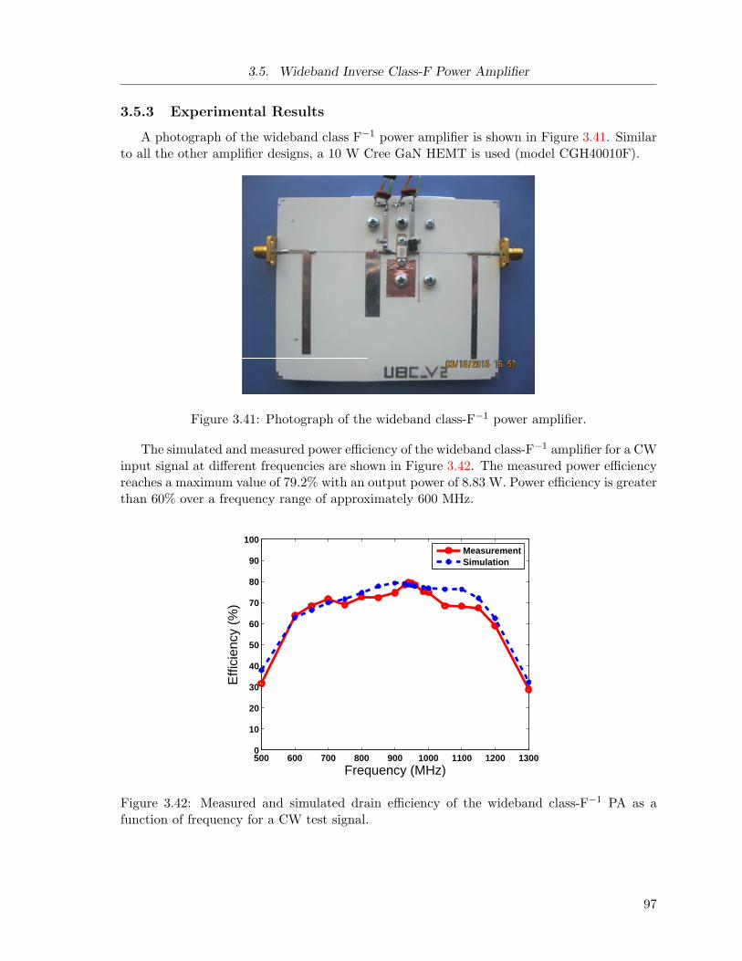
3.5. Wideband Inverse Class-F Power Amplifier
3.5.3 Experimental Results
A photograph of the wideband class F−1 power amplifier is shown in Figure 3.41. Similarto all the other amplifier designs, a 10 W Cree GaN HEMT is used (model CGH40010F).
Figure 3.41: Photograph of the wideband class-F−1 power amplifier.
The simulated and measured power efficiency of the wideband class-F−1 amplifier for a CWinput signal at different frequencies are shown in Figure 3.42. The measured power efficiencyreaches a maximum value of 79.2% with an output power of 8.83 W. Power efficiency is greaterthan 60% over a frequency range of approximately 600 MHz.
500 600 700 800 900 1000 1100 1200 13000
10
20
30
40
50
60
70
80
90
100
Frequency (MHz)
Effi
cien
cy (%
)
MeasurementSimulation
Figure 3.42: Measured and simulated drain efficiency of the wideband class-F−1 PA as afunction of frequency for a CW test signal.
97

3.6. Chapter Summary
3.6 Chapter Summary
In this chapter, the design methodology, simulation results and experimental results wereshown for three different class-F power amplifiers. The designs were for a narrowband switchedvoltage class-F amplifier, a narrowband switched current class-F−1 amplifier, and a widebandclass-F−1 amplifier. All the experimental results use a packaged Cree 10 W GaN HEMTdevice which makes comparison of experimental results insightful.
In the voltage switched class-F amplifier, a comprehensive study of the harmonic inputmatching circuit was made. A level 3 device model was used for this work, and from the study,it is concluded that input matching for the second harmonic is very important while the thirdharmonic has little effect on the overall power efficiency of the amplifier. An experimentalprototype of the amplifier was built which included third harmonic input and output matchingcircuits which is the first work to report third harmonic input matching in a class-F amplifier.
The experimental results of the voltage switched class-F amplifier are compared with asimilar current switched class-F−1 amplifier. The results show that the current switchedamplifier has higher peak power efficiency, which is attributed to lower capacitive switchinglosses compared to the voltage switched amplifier. Conversely, the current switched poweramplifier delivered slightly less power at peak efficiency, about 0.5 dB less, which shows thatthe device utilization is slightly higher in a voltage switched topology. A wideband currentswitched class-F−1 amplifier design was also built using a network synthesis technique thatimplements a wideband fundamental frequency match. It was also shown that the widebandnetwork has a high second harmonic impedance and a low third harmonic impedance over thebandwidth of the design.
In the next chapter, the theory of time-reversal duality is applied to reconfigure theseamplifier designs into RF rectifiers. The experimental results presented in this chapter for theamplifier configuration will be used to compare with experimental results for the RF rectifierconfiguration.
98

Chapter 4
Class-F RF Synchronous Rectifiers
This chapter focuses on the design and implementation of high efficiency and high powerGaN HEMT class-F and class-F−1 synchronous rectifiers. The work provides new benchmarks for high power RF synchronous rectifiers operating at a frequency of 1 GHz and powerlevels of approximately 10 W. The chapter begins with a brief overview of the time reversalduality principle which is used to convert switch-mode power amplifier circuits into equivalentsynchronous rectifier circuits. Time reversal duality concepts have been used for severaldecades in power electronic circuit applications, but the application to RF circuits is muchmore recent. There are also interesting questions raised when applying time reversal dualityto circuits with loss and the implication of loss in terms of constructing circuit duals isinvestigated. The clarification of these subtle points has not been discussed in the literatureand the primary implication is related to the operating point of the device when comparingamplifier and rectifier duals.
Applying the principle of time reversal duality to class-F switch-mode amplifiers, threedifferent RF synchronous rectifiers were designed using a 10 W GaN HEMT device fromCree. These rectifiers are a narrowband class-F rectifier, a narrowband class-F−1 rectifier,and a wideband class-F−1 rectifier. In all cases, the rectifier is compared to the amplifier dualand the work provides new references for comparing circuit duals. Most literature referencesdescribing implementations of RF rectifiers typically use the principle of duality to createrectifiers without providing direct comparisons with the amplifier circuit under equivalentmeasurement conditions.
Other highlights of the research work include a comparison of class-F and class-F−1 recti-fiers under constant load conditions. The optimal load resistance which maximizes RF to DCconversion efficiency is dependent on the RF input power to the rectifier. A comparison of theclass-F and class-F−1 rectifiers shows that the class-F−1 is more robust in terms of operationwith a fixed load compared to a class-F rectifier.
4.1 The Principle of Time Reversal Duality
The concepts of duality are commonly used in circuit theory. Examples include transfor-mations from Thevenin to Norton equivalent circuits and the synthesis of equivalent networkswith series or parallel circuit elements. Another example is the duality between voltage andcurrent waveforms. This is illustrated by comparing (a) and (b) in Figure 4.1; these figures arebased on the work of Hamill [74]. The network N can be transformed into a network dual Nvc
where the current and voltage waveforms are duals. The duality between current and voltagewaveforms is commonly used in switch-mode power amplifiers designs; for example, class-Famplifiers are designed to switch voltage, while class-F
−1 are designed to switch current.
3Parts of Chapter 4 have been published in two articles. Reprinted with permission from ELEX and EuMC[75, 76].
99

4.1. The Principle of Time Reversal Duality
t
(a)
I
t
V
IV
N
(b)
Vvc
t
Ivc
IvcVvc
Nvc
t
t
(c)
Itr
t
Vtr
ItrVtr
Ntr
Figure 4.1: (a) Network N and its current and voltage, (b) network Nvc, a voltage and currentdual of N , and (c) network Ntr, a time reversal dual of N .
Another duality was recognized by Hamill [74, 122] which he called time reversal duality.The time reversal (TR) concept is illustrated by comparing the current-voltage relations fornetwork N in Figure 4.1(a) with the current-voltage relations for the TR dual, network Ntr inFigure 4.1(c). In the TR dual, the voltage across the network is Vtr = V (−t) and the currentinto the network is Itr = −I(−t). As a consequence of the sign change in the current, powerflow is reversed at the terminals of network Ntr relative to the original network N . Moregenerally, for an n-port network, power flow is reversed at all n terminals. An example ofa two port network is shown in Figure 4.2. If network N is an amplifier, the primary inputpower is the DC drain supply P1 and the output is the amplified RF signal P2. The TR dual,network Ntr, is a rectifier circuit where RF input power P ′2 is converted into a DC power P ′1.
A general method of constructing a TR dual can be established [74, 122] and a summaryof the circuit relations is shown in Table 4.1. Capacitor and inductors are assumed to belossless and the circuit elements are unchanged in a TR dual. Resistance on the other hand is
100

4.1. The Principle of Time Reversal Duality
P1 P2N P ′1 P ′
2Ntr
Figure 4.2: The direction of energy flow in a network and its TR dual.
Table 4.1: Time reversal relations for circuit components.
Original Network (N) TR-dual Network (Ntr)
Voltage V (t) Vtr(t) = V (−t)Current I(t) Itr(t) = − I(−t)Power P (t) Ptr(t) = − P (−t)
Inductance L Ltr = L
Capacitance C Ctr = C
Resistance R Rtr = −R
dissipative and because power flow is reversed, the circuit dual must have negative resistance.Obviously negative resistance is not physically realizable except with active circuits, andtherefore the most common application of TR duality is in circuits where dissipative lossesare small. Examples include power electronic circuits which usually operate with very highefficiency. At microwave frequencies, dissipative losses are more significant and power loss canbe substantial. This then motivates the question: how should losses be handled in constructingcircuit duals? More will be said about this later.
The other implication of TR duality is that active devices must be bidirectional andoperate under time reversed conditions. For an active device like a MOSFET or HEMT, thismeans that a device which operates in quadrant I of the IV plane in an amplifier circuit,must operate in quadrant III in a rectifier circuit [73]. The IV symmetry is not perfect inpractical devices, but in theory they have symmetry because the designations of source anddrain nodes are made relative to the polarity of the drain supply. The quadrant I versusquadrant III device operation is discussed in more detail in the next section.
101
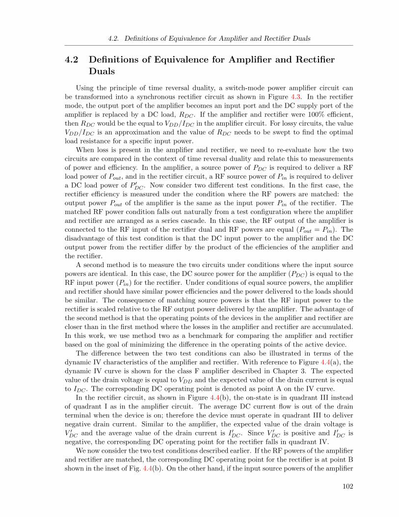
4.2. Definitions of Equivalence for Amplifier and Rectifier Duals
4.2 Definitions of Equivalence for Amplifier and RectifierDuals
Using the principle of time reversal duality, a switch-mode power amplifier circuit canbe transformed into a synchronous rectifier circuit as shown in Figure 4.3. In the rectifiermode, the output port of the amplifier becomes an input port and the DC supply port of theamplifier is replaced by a DC load, RDC . If the amplifier and rectifier were 100% efficient,then RDC would be the equal to VDD/IDC in the amplifier circuit. For lossy circuits, the valueVDD/IDC is an approximation and the value of RDC needs to be swept to find the optimalload resistance for a specific input power.
When loss is present in the amplifier and rectifier, we need to re-evaluate how the twocircuits are compared in the context of time reversal duality and relate this to measurementsof power and efficiency. In the amplifier, a source power of PDC is required to deliver a RFload power of Pout, and in the rectifier circuit, a RF source power of Pin is required to delivera DC load power of P ′DC . Now consider two different test conditions. In the first case, therectifier efficiency is measured under the condition where the RF powers are matched: theoutput power Pout of the amplifier is the same as the input power Pin of the rectifier. Thematched RF power condition falls out naturally from a test configuration where the amplifierand rectifier are arranged as a series cascade. In this case, the RF output of the amplifier isconnected to the RF input of the rectifier dual and RF powers are equal (Pout = Pin). Thedisadvantage of this test condition is that the DC input power to the amplifier and the DCoutput power from the rectifier differ by the product of the efficiencies of the amplifier andthe rectifier.
A second method is to measure the two circuits under conditions where the input sourcepowers are identical. In this case, the DC source power for the amplifier (PDC) is equal to theRF input power (Pin) for the rectifier. Under conditions of equal source powers, the amplifierand rectifier should have similar power efficiencies and the power delivered to the loads shouldbe similar. The consequence of matching source powers is that the RF input power to therectifier is scaled relative to the RF output power delivered by the amplifier. The advantage ofthe second method is that the operating points of the devices in the amplifier and rectifier arecloser than in the first method where the losses in the amplifier and rectifier are accumulated.In this work, we use method two as a benchmark for comparing the amplifier and rectifierbased on the goal of minimizing the difference in the operating points of the active device.
The difference between the two test conditions can also be illustrated in terms of thedynamic IV characteristics of the amplifier and rectifier. With reference to Figure 4.4(a), thedynamic IV curve is shown for the class F amplifier described in Chapter 3. The expectedvalue of the drain voltage is equal to VDD and the expected value of the drain current is equalto IDC . The corresponding DC operating point is denoted as point A on the IV curve.
In the rectifier circuit, as shown in Figure 4.4(b), the on-state is in quadrant III insteadof quadrant I as in the amplifier circuit. The average DC current flow is out of the drainterminal when the device is on; therefore the device must operate in quadrant III to delivernegative drain current. Similar to the amplifier, the expected value of the drain voltage isV ′DC and the average value of the drain current is I ′DC . Since V ′DC is positive and I ′DC isnegative, the corresponding DC operating point for the rectifier falls in quadrant IV.
We now consider the two test conditions described earlier. If the RF powers of the amplifierand rectifier are matched, the corresponding DC operating point for the rectifier is at point Bshown in the inset of Fig. 4.4(b). On the other hand, if the input source powers of the amplifier
102

4.2. Definitions of Equivalence for Amplifier and Rectifier Duals
M1
IDC
VGG
LGG
Vs
VDD
LDD
Rs InputMatching
OutputMatching
RL VL
VGG
Vs
Rs InputMatching
OutputMatching
Pout
M1
VGG
LGG LDDOutput
Matching
VRFin
RL
PhaseShifter
Sampler
(a)
(b)
(c)
InputMatching
PDC
Pin
I′DC R′DC
V′DC
P′DC
P′DC
LGG LDDPin
I′DC R′DC
V′DC
VRFin
RLM1
RDC = VDD/IDC
Figure 4.3: Block diagrams of (a) a power amplifier, (b) synchronous rectifier dual, and (c)synchronous rectifier with feedback to provide gate drive.
and rectifier are equal, then the corresponding rectifier operating point is point C. If circuitlosses were identical for the amplifier and rectifier, the DC operating point for the rectifierwould be point D which mirrors the amplifier DC operating point obtained by changing thesign of IDC . A comparison of the operating points shows that point C is closer to point Dwhich is the operating point dual of the amplifier. Therefore, a comparison of the amplifierand rectifier are made under the condition of equal input source power conditions rather thanequal RF power conditions.
As a final remark on the dynamic IV curves for the amplifier and rectifier, it is noted that
103

4.2. Definitions of Equivalence for Amplifier and Rectifier Duals
0 20 40 60 80
−2
−1
0
1
2
Vds
(V)
I ds (
A)
0 20 40 60 80
−2
−1
0
1
2
Vds
(V)
I ds (
A)
24 26 28−0.5
−0.4
−0.3
DCB
(a) (b)
A A
Figure 4.4: Dynamic load lines for: (a) a class-F amplifier (b) a class-F rectifier.
the effective on resistance of the rectifier is lower than in the amplifier. In quadrant III, thereverse biased drain supply flips the gate control of the device to depend on the drain supply.Therefore, in quadrant III, the device effectively turns on more as the drain swings morenegative. This observation is consistent with measured IV device characteristics reported byother researchers for quadrant III device behaviour [123]. From the DC device characteristicswe therefore conclude that the effective on resistance of the rectifier in quadrant III is expectedto be slightly less than the amplifier on resistance in quadrant I. Also, the loop area under thedynamic IV curve for the amplifier is larger in quadrant I than for the rectifier which meanscurrent/voltage overlap losses are slightly higher in the amplifier than the rectifier. Thesefactors lead to the hypothesis that the rectifier efficiency is expected to be higher than theequivalent amplifier efficiency.
At this point we have established a duality between the amplifier in Figure 4.3(a) and thesynchronous rectifier in Figure 4.3(b). Although a rectifier dual has been constructed fromthe amplifier, the circuit in (b) requires a separate input gate drive similar to the amplifier.The separate gate drive is inconvenient for rectification purposes and instead a feedback pathwhich samples the RF input signal is usually used to generate the gate drive signal. This isshown in circuit (c). Since the gate must be switched with the correct phase relative to thedrain voltage and drain current waveforms, a delay line or phase shift circuit is required. Whenthe gate drive is derived from the RF input signal, the circuit is called a synchronous rectifiercircuit [73]. Another variation of synchronous rectifiers is a self-synchronous rectifier wherethe intrinsic device capacitance Cgd is used in conjunction with a gate termination impedanceto create the required feedback signal for switching the gate [78]. In all the circuits shownin this work, a directional coupler is used to sample the RF input signal and a delay line isused as a phase shift circuit. In this way, any amplifier can be converted into a synchronousrectifier by generating the appropriate gate drive signal from the RF input.
104

4.3. High Efficiency GaN HEMT Class-F Synchronous Rectifier
Table 4.2: Some recently published results for RF synchronous rectifiersRef. Type Device f (GHz) PDC η (%)[73] class-E E-PHEMT 0.9 50 mW 83
synch.[78] class-C GaN HEMT 10.1 1.67 W 64.4
self-synch. MMIC[78] class-C GaN HEMT 10.1 3.18 W 63.9
self-synch. MMIC[82] class-F−1 GaN HEMT 2.14 8.5 W 85
self-synch.[79] class-E E-PHEMT 0.9 35 mW 88
self-synch.[79] class-E E-PHEMT 2.45 15 mW 77
self-synch.[80] class-E GaAs PHEMT 2.45 5.7 mW 77
self-synch.[81] class-F GaAs PHEMT 5.8 5.5 mW 68
self-synch.[83] class-F E-PHEMT 0.9 12.1 mW 85.4
self-synch.[124] class-AB GaN HEMT 9.9 4.11 W 52
self-synch. MMICThis class-F GaN HEMT 0.985 8.7 W 81.3work synch.
4.3 High Efficiency GaN HEMT Class-F SynchronousRectifier
As will be shown, the power efficiency of a rectifier circuit is similar to the power efficiencyof an amplifier circuit providing they are tested under equivalent conditions where the inputpower to the circuits is the same. Therefore, a high efficiency rectifier design begins with ahigh efficiency amplifier design.
In this section we present experimental results for the implementation of a 10 W syn-chronous class-F rectifier. The rectifier design is derived from the class-F amplifier describedearlier in Chapter 3. Other researchers have reported on GaN class-F−1 rectifier designs orlow power class-F rectifiers using pHEMTs, and this appears to be the first work for a highpower class-F design. A comparison of this design with other published results is given inTable 4.2. Experimental results are also shown to compare the performance of the amplifierand the rectifier dual under equivalent input power conditions. In this way, conclusions canbe made about the relative power efficiencies of the dual circuits.
4.3.1 Rectifier Test Bench and Efficiency Definitions
For comparison with the rectifier, the class-F PA in Chapter 3 (and Appendix-A) was firstre-tested. The device was biased with a 27 V drain supply and a gate bias of -2.6 V. At afrequency of 985 MHz and for a sinusoidal input signal of 24.5 dBm (282 mW), the amplifierdelivers 8.3 W to a 50 Ω load. Under these conditions, the drain current is 0.398 A and the
105

4.3. High Efficiency GaN HEMT Class-F Synchronous Rectifier
RF signalgenerator
Class-F PA
Class-F Rectifier
Couplers
Power Meters
Rectified Voltage
AB
Figure 4.5: The class-F rectifier test bench.
corresponding drain efficiency is 77.5%. The equivalent Thevenin source impedance of thedrain supply, RDC , is 67 Ω and the DC supply provides a source power of 10.7 W.
After testing the amplifier circuit, the amplifier was reconfigured as a synchronous class-Frectifier. A photograph of the rectifier test bench is shown in Figure 4.5. An explicit feedbackloop is added to the amplifier to provide a gate drive signal from the RF input port as shownin Figure 4.3(c). A directional coupler (A) samples the RF input signal and a variable delayline is used to adjust the phase of the sampled signal to synchronously switch the GaN powerdevice. The measured sampling level of coupler A is -18.7 dB. The second port of coupler Ais connected to a power meter and calibrated to measure the reflected power at the inputof the rectifier. Since the input RF power is high and cannot be delivered by standard testequipment, another class-F power amplifier is used to generate the RF source signal. A seconddirectional coupler (B) is placed in series between the rectifier and amplifier to measure theavailable RF input power (Pin) delivered to the rectifier. The input power is calibrated tomeasure power at the interface between the two couplers.
Two definitions of RF to DC conversion efficiency which have been used in the literatureto report results for RF rectifiers are [80, 81]
ηr =PDC
Pin − Pref(4.1)
and [82]
ηr =PDCPin
. (4.2)
In these equations, Pin is the incident or available power from the RF input source and Prefis the amount of power reflected back from the input port because of mismatch loss. The
106

4.3. High Efficiency GaN HEMT Class-F Synchronous Rectifier
difference in the power efficiency measures is that in (4.1), the power efficiency accounts formismatch loss at the input of the rectifier, while in (4.2) the power efficiency is burdened byinput mismatch loss. From a system perspective, equation (4.2) is preferred because it includesmismatch loss which is inherently present in the design of the rectifier circuit. If mismatch lossis reduced by improving the design, then the corresponding power efficiency will be improved.On the other hand, the efficiency measure in equation (4.1) accounts for mismatch loss andgives insight into the maximum available power efficiency which can be obtained provided theinput is perfectly matched. Both measures of power efficiency are used in the literature and itis important to identify which power efficiency measure is used for comparing results. Unlessotherwise stated, equation (4.1) which includes mismatch loss is used in this work as it isdeemed to be more appropriate for practical circuits where the terminal interface impedancesare usually specified and circuits must inherently include matching.
4.3.2 Experimental Results
As a starting point for evaluating the rectifier, the initial conditions were configured to bethe dual of the class-F amplifier where the input source powers of the amplifier and rectifierare equal. The RF input power was set to 10.7 W (40.3 dBm) at a frequency of 985 MHz,the same as the DC source power for the amplifier. The DC load resistance, R′DC , and phaseshifter are adjusted to optimize the power efficiency of the rectifier. The corresponding DCload power is 8.7 W and the RF to DC conversion efficiency is 81.3% for an optimal loadresistance of 58 Ω. These numbers are compared to the equivalent class-F amplifier underidentical input source power conditions which showed a slightly lower power efficiency of77.5% with an equivalent DC source resistance (RDC) of 67 Ω, slightly higher than R′DC inthe rectifier dual. This shows that even under equivalent source power conditions where theDC power supplied to an amplifier is equal to the RF power supplied to a rectifier, there aresmall differences attributed to device operation in quadrant I versus quadrant III.
The rectifier power efficiency of 81% was calculated using (4.2) which includes input mis-match loss. The effect of mismatch loss on the overall rectifier power efficiency can be foundby comparing the efficiency without mismatch loss using equation (4.1). Under the statedtest conditions, the reflected RF power at the input port of the rectifier is 28.2 dBm and theinput reflection coefficient is -12.1 dB. The corresponding RF to DC power efficiency withoutmismatch loss is 86.5%, about 5% better. A summary of the class-F amplifier and rectifiercircuit duals tested under identical source power conditions are shown in Table 4.3.
Other test results for the rectifier are shown in Figures 4.6 through 4.8. In Figure 4.6,the measured power efficiency and DC load power are shown as a function of the DC loadresistance R′DC . These measurements are made at a frequency of 985 MHz with a RF inputpower of 10.7 W. As shown, the optimal load resistance (R′DC) is approximately 58 Ω.
Figure 4.7 shows the power efficiency of the rectifier as a function of the RF input power.It shows that power efficiency peaks for an input RF power of 10.7 W (40.3 dBm). Powerefficiency remains above 50% for input power above 34 dBm and the maximum power deliveredby the rectifier is 11.3 W at an efficiency of 78%. Compared to other published work, thisresult appears to be the highest reported DC power which has been measured for a RFsynchronous class-F rectifier circuit.
The rectifier performance as a function of frequency is shown in Figure 4.8. Efficiencyand load power peak at a frequency of 985 MHz. The bandwidth of the rectifier is dependenton the bandwidth of the original amplifier design. In this case, the multiharmonic matching
107

4.3. High Efficiency GaN HEMT Class-F Synchronous Rectifier
Table 4.3: Comparison of class-F amplifier and rectifier experimental results.
Parameter Amplifier Rectifier
Frequency 985 MHz 985 MHz
Gate bias -2.6 V -2.6 V
DC supply/load resistance RDC = 67 Ω R′DC = 58 Ω
Input source power PDC = 10.7 W P ′in = 10.7 W
Load power Pout = 8.3 W P ′DC = 8.7 W
Power efficiency ηa = 77.5% ηr = 81.3%
Power efficiency without mismatch loss - ηr = 86.5%
networks are narrowband and a power efficiency of 50% is maintained over a frequency rangeof about 50 MHz.
The power efficiency measurements shown in Figures 4.7 and 4.8 include mismatch loss.If mismatch loss were reduced by improving the input match, then power efficiency wouldincrease. Measurements of mismatch loss were made over frequency and the results are shownin Figure 4.9. The results show that mismatch loss reduces power efficiency by approximately5% at 985 MHz and the loss increases as the frequency deviates from center frequency of thedesign. The mismatch loss is directly related to the bandwidth of the output match in theamplifier and improvements in the bandwidth of the matching circuit will reduce mismatchloss over frequency. This is not any different than an amplifier which also has reduced efficiencywhen the load match deviates from the optimum match. Later, in Section 4.5, results for awideband class-F amplifier and rectifier are shown.
108

4.3. High Efficiency GaN HEMT Class-F Synchronous Rectifier
10 20 30 40 50 60 70 80 9030
40
50
60
70
80
90
Effic
ien
cy (
%)
Resistance (Ohm)10 20 30 40 50 60 70 80 90
4
5
6
7
8
9
10
Ou
tpu
t D
C P
ow
er
(W)
Figure 4.6: Measured RF to DC conversion efficiency and output DC power as a function ofload resistance for a class-F rectifier.
34 35 36 37 38 39 40 41 4230
40
50
60
70
80
90
Effic
ien
cy (
%)
PRF-in (dBm)34 35 36 37 38 39 40 41 42
0
1
2
3
4
5
6
7
8
9
10
11
12
Ou
tpu
t D
C P
ow
er
(W)
Figure 4.7: Measured power efficiency and output DC power as a function of RF input powerfor a class-F rectifier.
109

4.3. High Efficiency GaN HEMT Class-F Synchronous Rectifier
950 960 970 980 990 100030
40
50
60
70
80
90
Effic
ien
cy (
%)
Frequency (MHz)950 960 970 980 990 1000
4
5
6
7
8
9
10
DC
Po
we
r (W
)
Figure 4.8: Measured power efficiency and output DC power as a function of frequency for aclass-F rectifier.
970 975 980 985 990 99540
50
60
70
80
90
100
Frequency (MHz)
Eff
icie
ncy
(%
)
Without mismatch loss
With mismatch loss
Figure 4.9: Class-F rectifier power efficiency with and without mismatch loss.
110

4.3. High Efficiency GaN HEMT Class-F Synchronous Rectifier
4.3.3 Class-F Amplifier and Rectifier Power Efficiency Analysis
Further insight into the small differences between the power efficiency of the amplifierand rectifier duals can be obtained through analysis. It will be shown that switch losses donot lead to perfect duality and dissipation inherently modifies the voltage waveform in therectifier relative to the amplifier. Also, device operation in quadrant I versus III modifies theoverlap losses in the amplifier and rectifier.
For the analysis, consider the class-F amplifier shown in Figure 4.10 and the waveformsshown in Figure 4.11(a). In class-F, the ideal drain voltage, vd,PA(θ), is a square wave wave-form with a 50% duty cycle. The Fourier series for the waveform consists of a fundamentalfrequency component at f0 and only odd harmonics. The ideal current waveform, id,PA(θ), isa half sinusoidal signal and the Fourier series for the waveform has a fundamental frequencycomponent at f0 and only even harmonics.
M1
IDC
VDD
LDD
VoutTL1
(λo/4)
CB
ZLC0L0
Output Matching Network
Vg
vd,PA(θ)
did,PA(θ)
ZL(f0)
iC(θ)
Cout
Figure 4.10: A class-F power amplifier with a series quarterwave transmission line.
The shape of the voltage and current waveforms in the circuit depends on the harmonicimpedances presented to the switching device at the drain node, d. The tank circuit is anti-resonant at the fundamental frequency f0 which forces the fundamental frequency componentof the drain current to pass through the load, RL. If the Q of the tank circuit is sufficienthigh (Q > 5), then the impedance of the tank is small (ideally a short) at all the harmonicfrequencies. The transmission line is a quarter wavelength long at the fundamental frequency,and the transmission line transforms the harmonic short created by the tank circuit into ashort circuit at the drain node d for even harmonics, and an open circuit at node d for oddharmonics. Together, these conditions create impedance conditions at node d that lead to theclass-F waveforms.
The series transmission line also serves as a matching circuit, and the characteristicimpedance of the line, Zo, can be used to transform the load resistance, RL, to a funda-mental frequency load line resistance, Rf0, where Rf0 = Re[ZL(fo)]. The load line resistanceRf0 is used later in the power efficiency equations and is usually obtained from a load pullsimulation of the device.
The class-F amplifier has three primary loss factors which are analyzed.
1. PRon : conduction losses due to finite switch resistance;
2. Pcap: capacitive switching losses resulting from the discharge of the voltage stored on
111

4.3. High Efficiency GaN HEMT Class-F Synchronous Rectifier
π 2π θ
Id,max Vd,max
0
(a)
i d,PA
v d,PA
and
π 2π θ
−Id,max
Vd,max
0
(b)
i d,Rec
v d,Rec
and
Figure 4.11: Drain voltage and drain current waveforms for: (a) a class-F power amplifier and(b) a class-F rectifier.
the output capacitance of the device, Cout;
3. Poverlap: losses created during switching transitions when the drain voltage and draincurrent waveforms overlap.
Each of these loss mechanisms modifies the ideal drain and current waveforms in the class-F amplifier, and non-ideal waveforms are analyzed from the superposition of the different lossmechanisms. Therefore, each loss mechanism is assumed to be independent and the losses arecombined to estimate the overall power efficiency of the class-F amplifier. The correspond-ing losses in the rectifier dual are also analyzed. In the rectifier dual, it will be shown thatconduction losses are slightly less than the amplifier, and unlike the amplifier, there are nooverlap losses in the rectifier.
112

4.3. High Efficiency GaN HEMT Class-F Synchronous Rectifier
A. Conduction Losses
If the switch has finite on resistance, Ron, then the ideal voltage waveform is modified bythe voltage drop across the device during the on-state. Since the current is a half sine pulse,the corresponding voltage drop is a half sine pulse. The on-state conduction loss is evidentin the voltage waveform shown in Figure 4.11(a). Based on this figure, the class-F amplifiervoltage and current waveforms including conduction losses are
vd,PA(θ) =
Ron Id,max sin(θ) 0 ≤ θ < πVd,max π ≤ θ ≤ 2π
(4.3)
and
id,PA(θ) =
Id,max sin(θ) 0 ≤ θ < π0 π ≤ θ ≤ 2π.
(4.4)
In these equations, Vd,max is the maximum voltage across the device and equal to two timesthat of the DC supply voltage, VDD. The current, Id,max, is the peak amplitude of the currentflowing through the device, and θ is a normalized time variable where θ = 2π f0 t. Using theseequations, it is easy to calculate the conduction loss associated with the half sine voltage drop:
PRon =1
2π
∫ 2π
0Ron i
2d,PA(θ) dθ = Ron
(Id,max
2
)2
(4.5)
The conduction loss is dissipated in the switching device M1.Now consider the time reversal dual of the amplifier circuit to construct an equivalent
rectifier. According to TR theory (see Table 4.1), the rectifier drain voltage waveform vRec(t)is equal to vPA(−t) and the rectifier drain current waveform iRec(t) is equal to −iPA(−t). Thecorresponding waveforms are shown in Figure 4.11(b). The current waveform is time reversedand flipped, while the voltage waveform is only time reversed.
For the on-state in the rectifier, an exact time reversed voltage waveform would include thepositive oriented half sinusoidal pulse shown by the dashed line in Figure 4.11(b). However,positive voltage and negative current during the on-state would imply negative power which isnot physically present in the switch. Therefore, in a dissipative switch, the dual of the voltagewaveform is modified during the on-state and includes a negative sinusoidal pulse as shownby the solid line in Figure 4.11(b). From this, we conclude that the rectifier dual with lossesis not an exact TR dual, and the voltage waveform is modified by considering the dissipationassociated with finite switch resistance.
The drain voltage and drain current waveforms for the class-F rectifier assuming an on-state switch resistance, R′on, are:
vd,Rec(θ) =
Vd,max 0 ≤ θ < πR′on Id,max sin(θ) π ≤ θ ≤ 2π
(4.6)
and
id,Rec(θ) =
0 0 ≤ θ < πId,max sin(θ) π ≤ θ ≤ 2π.
(4.7)
113

4.3. High Efficiency GaN HEMT Class-F Synchronous Rectifier
The corresponding conduction loss in the rectifier is
P ′Ron=
1
2π
∫ 2π
0R′on i
2d,Rec(θ) dθ = R′on
(Id,max
2
)2
(4.8)
where the prime terms denote measures for the rectifier. The conduction loss in the rectifier issimilar to the amplifier except the on-state resistance, R′on, corresponds to device operation inquadrant III instead of quadrant I, as in the amplifier. Since on-state resistances in quadrantI and III are similar, conduction losses in the amplifier and rectifier duals are similar andP ′Ron
≈ PRon .
B. Capacitive Switching Losses
All physical switching devices have output capacitance and this is modeled in the circuitas Cout (see Figure 4.10). When the switch M1 is off, the DC drain inductor LDD chargesCout to Vd,max, and when the switch is on, the capacitor is discharged through M1 and theenergy stored in the capacitor is dissipated in the device creating a capacitive switching loss.Therefore, the power loss is associated with the falling edge of the drain voltage waveform inFigure 4.11(a).
The energy stored in Cout is 12 Cout V
2d,max. The discharge occurs with a frequency f0;
therefore the total power dissipated is
Pcap =1
2Cout V
2d,max fo . (4.9)
We now consider the capacitive switching loss in the rectifier dual. With reference tothe drain voltage waveform in the rectifier circuit shown in Figure 4.11(b), it is clear thatthe capacitor Cout is charged to Vd,max and discharged to zero similar to the amplifier cir-cuit. However, one constraint on the discharge waveform is that it must occur prior to theswitch turning on. During the discharge (falling edge of the voltage waveform), the voltage ispositive, and consequently, the discharge current must also be positive to create positive dis-sipation otherwise negative power would be generated. Therefore, the total power dissipatedby discharging the capacitor Cout is the same as for the amplifier; hence, Pcap = P ′cap.
C. Overlap Power Loss
The third loss mechanism that is important to consider in the class-F amplifier and rectifieris overlap loss. In order to analyze overlap loss, the ideal waveforms shown in Figure 4.11need to be modified to include the rise and fall time of the voltage waveforms. The modifiedwaveforms are shown in Figure 4.12. For analysis, it is assumed that the rise and fall timeschange linearly over a time interval τ .
At this point, before continuing with the analysis, it is insightful to consider a qualitativecomparison of overlap in the amplifier and the rectifier dual. In the amplifier, the draincurrent and drain voltage are always in quadrant I of the IV plane for the device. Thismeans that overlap loss is primarily determined by the harmonic impedances in the matchingnetwork and the gate waveform. The situation for the rectifier dual is different. When thedevice is off, the current and voltage waveforms are in quadrant I, and when the device ison, the current and voltage are in quadrant III. The implication of the on-state in quadrantIII means that the voltage waveform in the off-state has to fully discharge to zero before thecurrent can flow in quadrant III. Another way to describe the current and voltage constraints
114

4.3. High Efficiency GaN HEMT Class-F Synchronous Rectifier
2π θ
−Id,max
Vd,max
0
i d,Rec
v d,Rec
and
π
ττ
(b)
2π θ
Id,maxVd,max
0
i d,PA
v d,PA
and
π
τ τ(a)
Iτ
Figure 4.12: Drain voltage and drain current waveforms with overlap loss for the class-Famplifier and rectifier duals.
is that the dissipation must be positive since negative power cannot be generated in the device.Therefore, the only voltage waveform that can co-exist with the negative on-state drain currentis a negative drain voltage waveform. The quadrant III constraints in the rectifier dual leadto the modified voltage and current waveforms shown in Figure 4.12. The waveforms showthat unlike the amplifier, the rectifier dual does not have overlapping current and voltagewaveforms during the transition intervals. From this observation we conclude that there is nooverlap power loss in the rectifier dual.
In the class-F amplifier, the voltage and current waveforms overlap during the transitionintervals. Overlap loss during a switch transition is defined as the power loss associated withthe cross-over of the current and voltage waveforms as shown in Figure 4.12(a). Using a linear
115

4.3. High Efficiency GaN HEMT Class-F Synchronous Rectifier
approximation over a transition time of τ , the overlap loss is
Poverlap =1
2π
∫ 2π
0vd(θ) id(θ) dθ
= 2× 1
2π
∫ τ
0
(Vd,maxτ
θ
)[−Iττ
(θ − τ)
]dθ
=Vd,max Id,max
6πτ sin(τ).
(4.10)
The overlap power loss is consistent with the condition that the loss is zero when τ is zero.Factors which affect the shape of the current and voltage waveforms will determine the
length of the transition interval and consequently the amount of overlap loss dissipated inthe amplifier. An important factor which affects waveshapes are the harmonic terminationimpedances in the output and input matching networks. The transition time can also be af-fected by the size of the output device capacitance, Cout, because the device has a maximumavailable current to discharge the capacitance. However, it should be noted that the amountof power dissipated to discharge the capacitance is in addition to the overlap loss calculatedabove because the waveforms in Figure 4.12 do not include the current required to dischargethe capacitor. Therefore, the total power loss in a class-F amplifier includes conduction loss,capacitive switching loss and overlap loss, while the total power loss in the rectifier dual onlyincludes conduction and capacitive switching losses. Based on these losses, we expect therectifier dual to have higher power efficiency compared to the amplifier.
D. Power Efficiency
Equations to predict the power efficiency of class-F amplifiers and the corresponding rec-tifier TR dual are derived next using the three loss mechanisms. For the amplifier, the inputsource power is the DC source power, PDC . The DC power source power must equal the sumof the output power delivered to the load, Pout, and the power dissipated in the switchingdevice:
PDC = Pout + Ploss = Pout + PRon + Pcap + Poverlap. (4.11)
For the rectifier, the source power is the input RF power, Pin, and the source power mustequal the sum of the DC power delivered to the load P ′DC plus the power dissipated in therectifying device:
Pin = P ′DC + P ′loss = P ′DC + P ′Ron+ P ′cap. (4.12)
Using these expressions, the drain efficiency of the amplifier is
ηa =PoutPDC
=Pout
Pout + PRon + Pcap + Poverlap(4.13)
and the RF to DC conversion power efficiency of the rectifier is
ηr =P ′DCPin
=P ′DC
P ′DC + P ′Ron+ P ′cap
. (4.14)
Expressions for all the terms in the power efficiency equations have been found except forPout and P ′DC . These terms are found from the Fourier series expansions of the waveforms inFigure 4.11.
116

4.3. High Efficiency GaN HEMT Class-F Synchronous Rectifier
The amplitude of the fundamental frequency component of the drain voltage vd,PA(θ) is
Vf0 =2
πVd,max −Ron
Id,max2
(4.15)
and the amplitude of the fundamental frequency component of the drain current id,PA(θ) is
If0 =Id,max
2. (4.16)
The fundamental frequency components are in-phase across the load and the total load poweris
Pout =Vfo Ifo
2=Vd,max Id,max
2π− Ron
2
(Id,max
2
)2
. (4.17)
The equation can also be written in terms of the fundamental frequency load line impedanceat the drain. Define Rf0 as the ideal load line resistance at the drain assuming a perfectswitch (Ron = 0). Then,
Rf0 =Vf0If0
∣∣∣∣Ron=0
=4
π
Vd,maxId,max
(4.18)
and another expression for Pout is
Pout =1
2(Rf0 −Ron)
(Id,max
2
)2
. (4.19)
Using expressions for Pout, PRon , Pcap, and Poverlap, the power efficiency of the class-F amplifieris
ηa =1
1 +PRon
Pout+PcapPout
+PoverlapPout
=1
1 +2Ron
Rf0 −Ron+π2
4
R2f0Cout fo
Rf0 −Ron+τ sin(τ)
3
Rf0Rf0 −Ron
.(4.20)
For the class-F rectifier, we need an expression for P ′DC to evaluate equation (4.14). Similarto the amplifier, the DC terms of the Fourier series for the rectifier waveforms in Figure 4.11(b)are
V ′DC =Vd,max
2−Ron
Id,maxπ
(4.21)
and
I ′DC =Id,maxπ
. (4.22)
The DC output power of rectifier is therefore
117

4.3. High Efficiency GaN HEMT Class-F Synchronous Rectifier
P ′DC = V ′DC I′DC =
Vd,max Id,max2π
−R′on(Id,maxπ
)2
=
[π2
8Rf0 −R′on
](Id,maxπ
)2
.
(4.23)
Using this expression for P ′DC , the power efficiency of the class-F rectifier can be expressed as
ηr =1
1 +PR′onP ′DC
+Pcap′
P ′DC
=1
1 +2R′on
Rf0 − 8π2R′on
+π2
4
R2f0Cout fo
Rf0 − 8π2R′on
.(4.24)
A comparison of the power efficiency equations for the class-F amplifier and rectifier showsthat the primary difference between the circuit duals is that the rectifier does not have overlaploss. Therefore, we expect the power efficiency of the rectifier to be higher than the amplifier.
E. Expressions for RDC and R′DC
Analytical expressions for the Thevenin equivalent resistance of the DC power supply inthe amplifier, RDC , and the DC load resistance in the rectifier R′DC are derived next. Sincethe power loss is different for the amplifier and rectifier, these two resistances are slightlydifferent.
For the class-F amplifier, the DC components of the Fourier series for the class-F waveformsin Figure 4.11(a) are
VDC =Vd,max
2+Ron
Id,maxπ
(4.25)
and
IDC =Id,maxπ
(4.26)
where the sign of IDC is chosen to be consistent with notation in Figure 4.3. The Theveninresistance of the DC supply is then
RDC =VDCIDC
=π
2
(Vd,maxId,max
)+Ron
=π2
8Rf0 +Ron.
(4.27)
The DC components for the rectifier waveforms were given earlier in equations (4.21) and(4.22). Using these expressions,
R′DC =V ′DCI ′DC
=π
2
Vd,maxId,max
−R′on
=π2
8Rf0 −R′on.
(4.28)
Comparing this equation with the Thevenin equivalent resistance of the amplifier DC supply,we expect that the optimal load resistance for the rectifier to be less than the amplifier.
118

4.3. High Efficiency GaN HEMT Class-F Synchronous Rectifier
4.3.4 Simulation Results
The analytical equations are verified by comparing predicted performance with simulationresults for the class-F power amplifier model in Figure 4.10. For the simulation, a level 2device model is used without device capacitances. Instead, the total effective output devicecapacitance is modelled as Cout in Figure 4.10, the same capacitance used to analyze capacitiveswitching losses. The gate drive for the amplifier consists of a 24.5 dBm sinusoidal source ata frequency fo of 985 MHz and a gate bias of -2.6 V. The drain supply voltage, VDD is 27 Vand the effective on resistance of the device for these bias conditions is estimated to be 2.2 Ω.The resonant tank circuit is chosen to have a Q of 5 for a load resistance of 50 Ω.
0 0.2 0.4 0.6 0.8 1 1.2 1.4 1.650
55
60
65
70
75
80
85
90
95
100
Cout
(pF)
Eff
icie
ncy
(%
)
Analytical model for amplifierAnalytical model for rectifierSimulation model for amplifierSimulation model for rectifier
Figure 4.13: Estimated drain efficiency of class-F PA and rectifier as a function of outputcapacitance. Ron for both the amplifier and rectifier are 2.2 Ω.
Under these conditions, time-domain simulations were run for both a class-F amplifier andthe rectifier dual as Cout is swept over a range of 0 to 1.6 pF. A comparison of the simulatedand analytical results is shown in Figure 4.13. As Cout changes, the switching losses in theamplifier change and the drain current/voltage overlap changes. The overlap interval, τ ,was obtained from the simulated drain voltage and drain current waveforms and varied from0.065π to 0.15π radians, as Cout varied from 0.2 to 1.6 pF, respectively.
Although a simplified device model is used to validate the analytical power efficiency rela-tions, a good reference point for comparison with the experimental results shown in section 4.3is to consider the case of Cout equal to 1 pF. The effective output capacitance of the CreeCGH40010 device used in the experimental work is approximately 1 pF. The correspondingsimulated and analytical results are summarized in Table 4.4 and can be compared with theexperimental results in Table 4.3. Although not an exact match, the analytical results showthat the optimal DC load (R′DC) for the rectifier is expected to be less than the equivalentThevenin resistance (RDC) of the DC supply which is consistent with the experimental results.The analytical and simulated results predict a slightly higher power efficiency for the rectifier
119

4.3. High Efficiency GaN HEMT Class-F Synchronous Rectifier
Table 4.4: Comparison of class-F amplifier and rectifier circuit duals.
Parameter Amplifier Rectifier
Frequency (fo) 985 MHz 985 MHz
Peak drain voltage (Vd,max) 52 V 52 V
Peak drain current (Id,max) 1.3 A 1.3 A
Fundamental frequency load resistance (Rf0) 50.8 50.8
Output device capacitance (Cout) 1 pF 1 pF
Current/voltage overlap (τ) 0.12 π rad 0
Gate bias -2.6 V -2.6 V
DC supply/load resistance RDC = 64.6 Ω R′DC = 60.3 Ω
Input source power PDC = 12 W Pin = 12 W
Load power Pout = 9.5 W P ′DC = 9.8 W
Power efficiency ηa = 79% ηr = 81.7%
Conduction loss (analytic) 0.93 W 0.93 W
Capacitive switching loss (analytic) 1.33 W 1.33 W
Overlap loss (analytic) 0.49 W -
Power Efficiency (analytic) 79.6% 82.1%
(3% in this case) which is similar to the experimental results where the rectifier efficiency was4.8% higher than the amplifier. Also, the analytic, simulation and experimental results forpower efficiency are all within 2% of each other which demonstrates good agreement betweentheory and experiment.
One of the advantages of constructing an analytical model is that it provides a way toexplore the contribution of different loss mechanisms to the overall power efficiency of theamplifier and rectifier duals. A breakdown of losses are shown in Figures 4.14 and 4.15for the class-F amplifier and rectifier, respectively. Conduction losses are independent ofCout and contribute a fixed loss to both the amplifier and rectifier. On the other hand,capacitive switching losses increase as Cout increases for both the amplifier and rectifier. Fora capacitance of 1 pF, conduction losses reduce power efficiency by approximately 8%, whileswitching losses reduce efficiency by about 10%. In the amplifier, there is an additionalpower loss from the overlap of the drain voltage and current waveforms, and for a capacitanceof 1 pF, overlap loss reduces efficiency by approximately 3%. The figures also include thesimulation results which closely follow the analytical results confirming the theory which hasbeen developed to predict power efficiency in the class-F amplifier and rectifier duals.
120

4.3. High Efficiency GaN HEMT Class-F Synchronous Rectifier
0 0.2 0.4 0.6 0.8 1 1.2 1.4 1.670
75
80
85
90
95
100
Cout
(pF)
Eff
icie
ncy
(%
)
PRon
PRon
+ Pcap
PRon
+ Pcap
+ Poverlap
Simulation Results
Figure 4.14: Predicted losses in a class-F power amplifier as a function of output capacitance.
0 0.2 0.4 0.6 0.8 1 1.2 1.4 1.670
75
80
85
90
95
100
Cout
(pF)
Eff
icie
ncy
(%
)
PRon
PRon
+ Pcap
Simulation Results
Figure 4.15: Predicted losses in a class-F rectifier as a function of output capacitance.
121

4.4. High Efficiency GaN HEMT Inverse Class-F Synchronous Rectifier
4.4 High Efficiency GaN HEMT Inverse Class-FSynchronous Rectifier
The class-F synchronous rectifier is a voltage switched rectifier. The class-F rectifier canalso be implemented in an inverse configuration where the current is switched. In this section,experimental results for a class-F−1 synchronous rectifier are presented for the time reverseddual of the class-F−1 amplifier described in Chapter 3. The class-F−1 uses the same Cree10 W GaN device used in the class-F rectifier design, and the performance of these tworectifier designs are compared.
In Section (3.4) of Chapter (3) a 10 W class-F−1 amplifier was designed and implemented.In this section, the amplifier is reconfigured as a high power GaN RF synchronous class-F−1 rectifier by adding feedback from the output to the input. The rectifier is tested underidentical source power condition associated with the dual amplifier. The measurement resultsfor the class-F−1 rectifier are also compared with measurement results for the class-F rectifierdesign presented in Section (4.3) in terms of performance and dynamic range.
The test bench for the class-F−1 rectifier is shown in Figure 4.16. Similar to the class-Frectifier, a -18.7 dB input coupler (coupler A) and a phase shifter are used to create a gatedrive to synchronously switch the device. The other port of coupler A is connected to a powermeter to measure the reflected input power. The high power RF input signal (Pin) from therectifier is generated by a 10 W class-F amplifier, the same amplifier used to implement theclass-F synchronous rectifier. A second coupler, coupler B, is inserted between the rectifierand amplifier to measure the available RF input power (Pin) delivered to the rectifier.
RF signalgenerator
Class-F PA
Inverse Class-FRectifier
Couplers
Power Meters
Rectified Voltage
AB
Figure 4.16: Test bed for the class-F−1 rectifier. A class-F amplifier is used as a high powerRF input source.
As an initial test, the performance of the rectifier is compared with the performance ofthe amplifier under equivalent test conditions. From Chapter 3, the amplifier had a powerefficiency of about 83% for a DC source power of 11.9 W. When the RF input power to therectifier has the same source power as the amplifier (11.9 W), the rectifier has an RF to DC
122
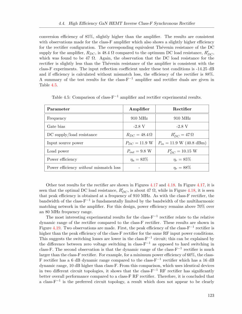
4.4. High Efficiency GaN HEMT Inverse Class-F Synchronous Rectifier
conversion efficiency of 85%, slightly higher than the amplifier. The results are consistentwith observations made for the class-F amplifier which also shows a slightly higher efficiencyfor the rectifier configuration. The corresponding equivalent Thevenin resistance of the DCsupply for the amplifier, RDC , is 48.4 Ω compared to the optimum DC load resistance, R′DC ,which was found to be 47 Ω. Again, the observation that the DC load resistance for therectifier is slightly less than the Thevenin resistance of the amplifier is consistent with theclass-F experiments. The input reflection coefficient under these test conditions is -14.25 dBand if efficiency is calculated without mismatch loss, the efficiency of the rectifier is 88%.A summary of the test results for the class-F−1 amplifier and rectifier duals are given inTable 4.5.
Table 4.5: Comparison of class-F−1 amplifier and rectifier experimental results.
Parameter Amplifier Rectifier
Frequency 910 MHz 910 MHz
Gate bias -2.8 V -2.8 V
DC supply/load resistance RDC = 48.4 Ω R′DC = 47 Ω
Input source power PDC = 11.9 W Pin = 11.9 W (40.8 dBm)
Load power Pout = 9.8 W P ′DC = 10.15 W
Power efficiency ηa = 83% ηr = 85%
Power efficiency without mismatch loss - ηr = 88%
Other test results for the rectifier are shown in Figures 4.17 and 4.18. In Figure 4.17, it isseen that the optimal DC load resistance, R′DC , is about 47 Ω, while in Figure 4.18, it is seenthat peak efficiency is obtained at a frequency of 910 MHz. As with the class-F rectifier, thebandwidth of the class-F−1 is fundamentally limited by the bandwidth of the multiharmonicmatching network in the amplifier. For this design, power efficiency remains above 70% overan 80 MHz frequency range.
The most interesting experimental results for the class-F−1 rectifier relate to the relativedynamic range of the rectifier compared to the class-F rectifier. These results are shown inFigure 4.19. Two observations are made. First, the peak efficiency of the class-F−1 rectifier ishigher than the peak efficiency of the class-F rectifier for the same RF input power conditions.This suggests the switching losses are lower in the class-F−1 circuit; this can be explained bythe difference between zero voltage switching in class-F−1 as opposed to hard switching inclass-F. The second observation is that the dynamic range of the class-F−1 rectifier is muchlarger than the class-F rectifier. For example, for a minimum power efficiency of 60%, the class-F rectifier has a 6 dB dynamic range compared to the class-F−1 rectifier which has a 16 dBdynamic range, 10 dB higher than class-F. From this comparison, which uses identical devicesin two different circuit topologies, it shows that the class-F−1 RF rectifier has significantlybetter overall performance compared to a class-F RF rectifier. Therefore, it is concluded thata class-F−1 is the preferred circuit topology, a result which does not appear to be clearly
123

4.4. High Efficiency GaN HEMT Inverse Class-F Synchronous Rectifier
20 25 30 35 40 45 50 55 60 65 7066
68
70
72
74
76
78
80
82
84
86
Effi
cien
cy (
%)
RDC
(Ω)20 25 30 35 40 45 50 55 60 65 70
8.4
8.6
8.8
9
9.2
9.4
9.6
9.8
10
10.2
10.4
Out
put P
ower
(W
)
Figure 4.17: Measured RF to DC conversion efficiency and output DC power versus loadresistance for the rectifier. The measurements conditions are for an input RF source powerof 40.76 dBm at a frequency of 910 MHz.
860 880 900 920 940 960 980 100010
20
30
40
50
60
70
80
90
Effi
cien
cy (
%)
Frequency (MHz)
3
4
5
6
7
8
9
10
11
Out
put P
ower
(W
)
Figure 4.18: Measured power efficiency and output power as a function of frequency for therectifier. The measurements conditions are for an input RF source power of 40.76 dBm.
presented in the existing literature.
124

4.4. High Efficiency GaN HEMT Inverse Class-F Synchronous Rectifier
20 25 30 35 40 4530
40
50
60
70
80
90
Input Power (dBm)
Effi
cien
cy (
%)
Class−F −1 RectifierClass−F Rectifier
Figure 4.19: Power efficiency comparison of a class-F and class-F−1 synchronous rectifier.Experimental results are shown.
125

4.5. High Efficiency GaN HEMT Wideband Inverse Class-F Synchronous Rectifier
4.5 High Efficiency GaN HEMT Wideband Inverse Class-FSynchronous Rectifier
The class-F and class-F−1 synchronous rectifier designs presented so far are inherentlynarrowband because of the design of the multiharmonic matching networks in the amplifier.In some applications, such as in energy recycling, the spectrum of the RF input signal canbe spread over a large bandwidth and wideband rectifier designs are of interest. In otherapplications, such as wireless power and RF energy harvesting, wideband rectifiers are alsouseful. In this section, experimental results for a wideband class-F−1 are presented.
The same test bench for the narrowband class-F−1 rectifier shown in Figure 4.16 is usedfor measuring the performance of the wideband rectifier. Frequency errors introduced by thebandlimited response of the power amplifier are compensated by measuring the RF inputpower at each frequency using coupler B. The power meter connected to coupler B measuresthe incident RF input power, while the power meter connected to coupler A measures thereflected input power.
The power efficiency of the rectifier as a function of frequency is shown in Figure 4.20.The results show that power efficiency remains above 60% over a bandwidth of approximately500 MHz ranging from 600 MHz to 1150 MHz. The peak efficiency is 80.1% at a frequency of650 MHz. For these measurements, the DC load resistance is 34 Ω and the RF input poweris 10 W. Also, in these measurements, the phase shifter has been tuned at each frequency tomaximize power efficiency.
600 700 800 900 1000 11000
10
20
30
40
50
60
70
80
90
100
Frequency (MHz))
Eff
icie
ncy
(%
)
Figure 4.20: Measured drain efficiency as a function of frequency for the wideband class-F−1
rectifier.
The rectifier performance as a function of the RF input power is shown in Figure 4.21.Results are shown for frequencies of 650 MHz, 850 MHz and 1050 MHz and compared with thenarrowband rectifier measurements in Figure 4.22. The wideband rectifier has good efficiencyand dynamic range over a wide frequency range, while the narrowband designs have good
126

4.5. High Efficiency GaN HEMT Wideband Inverse Class-F Synchronous Rectifier
performance at a specific frequency. Therefore, the bandwidth of the rectifier can be designedto match the bandwidth of the RF input spectrum which is to be rectified.
20 25 30 35 400
10
20
30
40
50
60
70
80
90
100
Input Power (dBm)
Effi
cien
cy (
%)
Wideband: 650 MHz
Wideband: 850 MHz
Wideband: 1050 MHz
Figure 4.21: Measured drain efficiency as a function of input power for the wideband class-F−1
rectifier at frequencies of 650 MHz, 850 MHz and 1050 MHz.
20 25 30 35 400
10
20
30
40
50
60
70
80
90
100
Input Power (dBm)
Effi
cien
cy (
%)
Class F −1 RectifierClass F RectifierWideband: 650 MHzWideband: 850 MHzWideband: 1050 MHz
Figure 4.22: Measured drain efficiency as a function of input power for class-F, class-F−1 andwideband class-F−1 synchronous rectifiers.
127

4.6. Chapter Summary
4.6 Chapter Summary
The design of class-F RF synchronous rectifiers based on the application of time reversalduality has been demonstrated. The implications of loss in the switch-mode amplifier proto-type were considered and a set of equivalent conditions were proposed to evaluate the rectifierdual. A direct comparison was then made between the amplifier and rectifier circuits using theclass-F amplifiers described in Chapter 3. The experimental results provide new benchmarksfor high power class-F synchronous rectifiers including a wideband rectifier design. The RFsynchronous rectifiers described in this chapter are used in an energy recycling switch-modepower amplifier described in the next chapter.
128

Chapter 5
Switch-mode Power Amplifier withEnergy Recycling
5.1 Energy Recycling in Outphasing Power Amplifiers
The concept of energy recycling in power amplifiers was first introduced in 1999 for out-phasing amplifiers [125]. In outphasing amplifiers, the modulated source signal is mapped totwo constant envelope signals, amplified, and after amplification, the signals are combinedto reconstruct the original modulated source signal. The primary motivation behind out-phasing schemes is to exploit the high efficiency operation of amplifiers that can be obtainedwhen amplifying constant envelope signals. The signal mapping commonly used in outphasingamplifiers is called LINC, linear amplification using nonlinear components.
Although the outphasing concept is conceptually attractive as a way to implement highefficiency amplifiers, the practical difficulties of signal combining and reconstruction at theoutput of the amplifier have been difficult to solve. Two approaches have been used inimplementing outphasing amplifiers. The first approach is to reactively combine the outputof the two branches. This method is called Chireix outphasing based on the original inventionof the outphasing amplifier which was described in 1935 [2]. By reactively combining theamplifiers, there is no isolation between the two amplifier branches and the primary designchallenge is to maintain efficient combining over a large dynamic range to accommodate theamplification of signals with high peak to average power ratios. A block diagram of a Chireixoutphasing amplifier is shown in Figure 5.1(a).
The second approach to outphasing that has been proposed uses an isolating signal com-biner [125, 126]. In this method, the interaction between the two amplifier branches is mini-mized and both amplifier branches can operate with very high efficiency. The disadvantage ofisolated combining is that significant power is dissipated in the combiner especially for signalswith high PAPR. Therefore, the overall power efficiency of the amplifier is reduced signifi-cantly by the isolated combiner. As a way to offset the power loss in an isolated combiner,energy recycling has been proposed. Rather than dumping the RF power in the combiner toan internal load, the power is rectified and returned to the DC supply of the amplifier. A blockdiagram of this method is shown in Figure 5.1(b). The published work on energy recyclingin outphasing amplifiers includes simulation work, measurements of RF to DC rectificationefficiency, and some implementations of complete systems [125, 126, 127, 128].
5.2 Energy Recycling in RF Switch-mode Amplifiers
In an analogous way, the two approaches which have been taken in exploring implementa-tions of outphasing amplifiers can also be applied to switch-mode power amplifiers using pulsemodulation techniques. The reactive signal reconstruction approach has been the mainstay
129
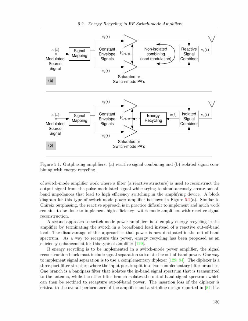
5.2. Energy Recycling in RF Switch-mode Amplifiers
VDD
si(t) SignalMapping
EnergyRecycling
ModulatedSourceSignal
ConstantEnvelopeSignals
a(t) so(t)
Saturated orSwitch-mode PA’s
VDD
si(t) SignalMapping
ModulatedSourceSignal
ConstantEnvelopeSignals
c1(t)
c2(t)
ReactiveSignal
Combiner
so(t)
Saturated orSwitch-mode PA’s
Non-isolatedcombining
(load modulation)
(a)
IsolatedSignal
Combiner
(b)
c1(t)
c2(t)
Figure 5.1: Outphasing amplifiers: (a) reactive signal combining and (b) isolated signal com-bining with energy recycling.
of switch-mode amplifier work where a filter (a reactive structure) is used to reconstruct theoutput signal from the pulse modulated signal while trying to simultaneously create out-of-band impedances that lead to high efficiency switching in the amplifying device. A blockdiagram for this type of switch-mode power amplifier is shown in Figure 5.2(a). Similar toChireix outphasing, the reactive approach is in practice difficult to implement and much workremains to be done to implement high efficiency switch-mode amplifiers with reactive signalreconstruction.
A second approach to switch-mode power amplifiers is to employ energy recycling in theamplifier by terminating the switch in a broadband load instead of a reactive out-of-bandload. The disadvantage of this approach is that power is now dissipated in the out-of-bandspectrum. As a way to recapture this power, energy recycling has been proposed as anefficiency enhancement for this type of amplifier [129].
If energy recycling is to be implemented in a switch-mode power amplifier, the signalreconstruction block must include signal separation to isolate the out-of-band power. One wayto implement signal separation is to use a complementary diplexer [129, 84]. The diplexer is athree port filter structure where the input port is split into two complementary filter branches.One branch is a bandpass filter that isolates the in-band signal spectrum that is transmittedto the antenna, while the other filter branch isolates the out-of-band signal spectrum whichcan then be rectified to recapture out-of-band power. The insertion loss of the diplexer iscritical to the overall performance of the amplifier and a stripline design reported in [84] has
130

5.3. Spectral Shaping to Enhance Energy Recycling Efficiency
a loss of approximately 2 dB in the in-band path and 0.8 dB in the out-of-band path.Another way to implement signal separation is to use a circulator and a bandpass filter.
A block diagram of a switch-mode amplifier with this type of signal separation is shown inFigure 5.2(b). The circulator is a non-reciprocal device and out-of-band power reflected bythe in-band bandpass filter is reflected back to the circulator and coupled to an isolated port.The isolated port, port C in Figure 5.2(b), can then be connected to a RF rectifier to recoverpower from the out-of-band spectrum. As with the complementary diplexer, the insertionloss of the isolator is critical to the overall power efficiency of the architecture. Later, inSection (5.5), experimental results are presented for a switch-mode power amplifier using acirculator for signal separation.
VDD
si(t) PulseEncoder
EnergyRecycling
ModulatedSourceSignal
p(t)
a(t)
so(t)
Switch-modePA
(a)
(b)
SignalMapping
BPFOut-of-band
power
B
In-bandpowerCirculator
A
C
Output SignalReconstruction
Filter
VDD
si(t) PulseEncoder
p(t) so(t)
Switch-modePA
SignalMapping
BPFOut-of-band reactive
termination
In-bandpower Output Signal
ReconstructionFilter
ModulatedSourceSignal
Figure 5.2: Switch-mode power amplifiers (a) with reactive output filter and (b) with energyrecycling.
5.3 Spectral Shaping to Enhance Energy Recycling Efficiency
If energy recycling is employed in a switch-mode amplifier, it is desirable to shape the out-of-band spectrum to improve rectification efficiency. The out-of-band spectrum generatedby the encoding process usually has a very large bandwidth which is created by quantizingthe source signal. Implementing a high efficiency broadband RF rectifier is more challengingthan a narrowband rectifier, therefore spectral shaping to concentrate out-of-band power in areduced frequency range could improve rectification efficiency of out-of-band energy.
131

5.3. Spectral Shaping to Enhance Energy Recycling Efficiency
As an example of out-of-band spectral shaping, a noise shaped pulse position modulatorwith an adaptive sinusoidal dither signal has been implemented. The block diagram of theencoder is shown in Figure 5.3. The encoder consists of a negative feedback loop with a noiseshaping filter H(s) and a pulse generator. The pulse generator creates a pulse width equal tothe half the period of the carrier frequency of the source signal (Tc/2). The zero-crossings ofthe error signal e(t) determine the delay (position) of the pulse and a rising edge triggers thepulse generator. The pulse generator creates an amplitude quantized output pulse train andthe quantization noise is shaped by the noise shaping filter H(s). In this way, the loop is verysimilar to a sigma-delta modulator except that the timing of pulse edges are asynchronousrather than synchronous as in sigma-delta modulation.
H(s)
DitherAmplitude
Control
NoiseShaping Filter
T/2 PulseGenerator
EncodedSignal
ModulatedSource Signal
s(t) p(t)d(t)
e(t)
0
1
0.5-1 t/T
0 0.25 0.75 1 1.51.25 1.75 2
p(t)
s(t)
fdither
Amplitude
Figure 5.3: Block diagram of a noise shaped PPM encoder with dither (top) and exampleinput and output waveforms (bottom).
The noise shaping loop includes a sinusoidal dither signal d(t) which is added to the errorsignal e(t). The amplitude of the dither signal is controlled by the source signal envelope.When the source envelope has a small amplitude, the out-of-band quantization noise has muchhigher power than the signal and the dither amplitude is large. Conversely, when the sourcesignal envelope is at peak envelope power, then the dither amplitude reduces to zero becausemost of the power in the output pulse train is signal power. The exact amplitude mappingfunction used to control the dither amplitude depends on a compromise between signal tonoise ratio (SNR), frequency of the dither signal, and loop stability. Examples of the outputspectrums from the encoder with and without spectral shaping are shown in Figure 5.4.
132

5.3. Spectral Shaping to Enhance Energy Recycling Efficiency
Frequency (MHz)
Rel
ativ
e P
ower
Spe
ctra
l Den
sity
(dB
)
without spectral shaping
850 900 950 1000 1050−60
−50
−40
−30
−20
−10
0
10
Frequency (MHz)
Rel
ativ
e P
ower
Spe
ctra
l Den
sity
(dB
)
with spectral shaping
850 900 950 1000 1050−60
−50
−40
−30
−20
−10
0
10
adaptive ditherto improveout−of−bandrectificationefficiency
signalencoded innoise well
Figure 5.4: Power spectrum of a noise shaped PPM signal without out-of-band spectralshaping (top) and with spectral shaping (bottom).
133

5.4. Analysis of Power Efficiency Enhancement using Energy Recycling
5.4 Analysis of Power Efficiency Enhancement using EnergyRecycling
An RF power amplifier with energy recycling is shown in Figure 5.5. The block diagramis sufficiently general to capture the primary concepts of recycling in both outphasing andswitch-mode power amplifiers. A modulated RF carrier s(t) is mapped to a set of signals ck(t)with reduced amplitude variation; for example, constant envelope signals. The signal mappinggenerates N input signals for the high efficiency amplifier block. For the cases considered here,a switch-mode amplifier has N = 1 and LINC has N = 2.
P ′DC
PDC
Per EnergyRecycling
Psig G21Psig + Padd G31
G21
ηd0
ηer
Pin
PaddG31
3
21N N
High EfficiencyAmplifier(s)
Signal Combiner /Separator
SignalMapping
s(t) ck(t)RL
Figure 5.5: Block diagram of a power amplifier with energy recycling.
The outputs of the amplifier are combined in a signal reconstruction block. The signalreconstruction block also has signal separation and spectral power added by the signal map-ping function can be isolated. An example of a signal combiner/separator in an outphasingamplifier design is a 180 degree hybrid which provides sum and difference output signals.For switch-mode amplifiers, the signal reconstruction and separation can be implemented byeither a complementary diplexer or the combination of a circulator and bandpass filter. Thepower loss associated with signal reconstruction is modeled by the gain term G21 from port1 to port 2, and power loss associated with signal separation to recover dissipated power ismodelled by the gain term G31 from port 1 to port 3. The output path gains are lossy andconsequently the path gains are less than unity: 0 < |G| ≤ 1.
An expression for the overall drain efficiency of the amplifier with energy recycling isderived next. The native drain efficiency of the power amplifier is defined as the powerefficiency of the amplifier block when amplifying the signals ck(t) under a load conditionequivalent to the input impedance of the signal combining network at port 1. The outputpower spectrum from the amplifier can be partitioned into the desired signal power (Psig) andpower added by the signal mapping function (Padd). Therefore, the native drain efficiency ofthe amplifier is
ηd0 =Psig + Padd
PDC(5.1)
where PDC is the DC input power to the amplifier.After signal reconstruction, the total output power delivered to the load at port 2 is equal
to Psig G21. The signal combiner also outputs residual power which is created by the signalreconstruction process. The total residual power available at port 3 is PaddG31. The residual
134

5.4. Analysis of Power Efficiency Enhancement using Energy Recycling
power is rectified to generate an auxiliary DC supply that is summed with the main supply.The return of output RF power back to DC supply power implements an energy recyclingloop.
The DC power provided to the amplifier consists of an external source of power P ′DC andrecycled power Per. The available recycling power depends on both the efficiency of the energyrecycling block (ηer) as well as the loss G31 in the signal reconstruction block. Therefore,
Per = PaddG31 ηer. (5.2)
The overall power efficiency of the amplifier can then be written as
ηd =Psig G21
P ′DC=
Psig G21
PDC − Per. (5.3)
The equation for overall power efficiency can be expanded to write it in terms of the nativepower efficiency ηd0. Using (5.2) in (5.3),
ηd =Psig G21
PDC − PaddG31 ηer× Padd + PsigPadd + Psig
=Padd + Psig
PDC× Psig/(Padd + Psig)G21
1− (Padd/PDC)G31 ηer
= ηd0 ×Psig/(Padd + Psig)G21
1− [(Psig + Padd)/PDC ] [Padd/(Psig + Padd)]G31 ηer
=Psig/(Padd + Psig)G21 ηd0
1− [Padd/(Psig + Padd)]G31 ηer ηd0.
(5.4)
A more concise expression for the overall power efficiency of the energy recycling amplifiercan be obtained by adopting the concept of coding efficiency. Coding efficiency is commonlyused as metric to evaluate how efficient the pulse encoder is in a switch-mode power amplifier.However, coding efficiency can be applied more broadly to any class of signals that adds powerto the original source signal spectrum. The definition of coding efficiency is
CE =in-band signal power
total power=
PsigPsig + Padd
(5.5)
and it gives a measure of how much signal power is added by the signal mapping block tocreate a set of output signals. For LINC, the RF modulated source signal, s(t), is mappedto two constant envelope signals, c1(t) and c2(t), and the signal mapping adds power to thesource signal. Therefore, coding efficiency can be applied to LINC in the same way as it isused as a metric to quantify the efficiency of pulse encoders in switch-mode amplifiers.
Using the definition of coding efficiency and equation (5.5), we also get the relation Psig =(Psig + Padd)CE. Therefore the overall power efficiency of an amplifier with energy recyclingis
ηd =ηd0G21CE
1− ηd0 ηerG31 (1− CE). (5.6)
Equation (5.6) is very useful for exploring the theoretical bounds of power efficiency fordifferent power amplifier scenarios. A number of examples are shown in Figure 5.6. As afirst example, consider the upper bound for a power amplifier with a native power efficiency,
135

5.5. Experimental Implementation of a Switch-mode Power Amplifier with Energy Recycling
ηd0, of 80% and with perfect energy recovery and lossless signal separation.3 Perfect energyrecovery is defined as an RF to DC rectification efficiency, ηer, of 100%, and lossless signalseparation means G21 and G31 are both 0 dB. For this case, if the coding efficiency of theconstant envelope signal were 25%, then the corresponding power efficiency of the amplifier is28% without energy recycling and 50% with energy recycling. Under these conditions, energyrecycling boosts power efficiency by 78% compared to an amplifier without energy recycling:(50% - 28%)/28% x 100% = 78%. For this scenario, energy recycling clearly provides asignificant boost in the power efficiency of the amplifier.
For a second example, consider the same constant envelope power amplifier efficiency of80% with -1 dB loss for the output path, G21, and -0.5 dB for the G31. The losses arepractical values that could be obtained with an optimized output network consisting of eithera circulator and bandpass filter or a complementary diplexer. The third example shown in thefigure corresponds to measured values that model the experimental test-bed described laterin the following section. A comparison of these three examples shows that it is significant tominimize losses in the signal separation block to maximize the efficiency enhancement that isobtained from energy recycling.
5.5 Experimental Implementation of a Switch-mode PowerAmplifier with Energy Recycling
An experimental test-bed was implemented to evaluate energy recycling in a switch-modepower amplifier. A photo of the test-bed is shown in Figure 5.7. The system consists ofan arbitrary waveform generator to generate pulse encoded input signals, a class-F 10 Wamplifier, a circulator and bandpass filter for a signal reconstruction and signal separation,and a wideband class-F−1 rectifier. The class-F 10 W amplifier design and the widebandclass-F−1 rectifier design were described earlier in Chapters 3 and 4, respectively. All thepulse train waveforms were generated in Matlab using the noise shaped PPM pulse encoderwith out-of-band spectral shaping described earlier in section 5.3. The carrier frequency ofthe source signal is centered at 930 MHz and the sinusoidal dither signal has a frequency of986 MHz. The clock rate of the arbitrary generator is 24.25 Gs/sec. A two stage circulatorand a bandpass filter are used for signal separation and signal reconstruction. The bandpassfilter is a cavity filter with a center frequency of 930 MHz and bandwidth of 10 MHz. Thepath gain from the input port (port 1) to the load port (port 2) is -1.12 dB (G21) and thepath gain from the input port (port 1) to the recycling power port (port 3) is -2.1 dB (G31).
The native power efficiencies of the amplifier and rectifier were first measured indepen-dently of other components. For the pulse encoded waveforms the class-F amplifier powerefficiency (ηd0) is approximately 50%. The power efficiency does vary slightly depending onthe amplitude of the source signal and the amplitude of the dither signal. For the rectifier,the peak RF to DC conversion efficiency (ηr) is approximately 80% and the efficiency re-duces as the input power is backed off. Since the amplitude of the dither signal in the pulsetrain spectrum is inversely proportional to the amplitude of the source signal, we expect therectifier will have high power efficiency for low input amplitude source signals and reducedefficiency for high amplitude input source signals. The dependence of rectification efficiencyon power is an important observation and an optimized energy recycling system would adjust
3A saturated or switch-mode power amplifier with a drain efficiency of 80% is considered to be a very goodamplifier and in alignment with the best performance that is obtained from experimental amplifiers.
136

5.5. Experimental Implementation of a Switch-mode Power Amplifier with Energy Recycling
0 20 40 60 80 1000
10
20
30
40
50
60
70
80
Coding Efficiency (%)
Ove
rall
Effi
cien
cy (
%)
ηd0
= 80%; ηER
= 100%; G21
= 0dB; G31
= 0dB
ηd0
= 80%; ηER
= 0%; G21
= 0dB; G31
= 0dB
ηd0
= 80%; ηER
= 80%; G21
= −1dB; G31
= −0.5dB
ηd0
= 80%; ηER
= 0%; G21
= −1dB; G31
= −0.5dB
ηd0
= 50%; ηER
= 80%; G21
= −1.12dB; G31
= −2.1dB
ηd0
= 50%; ηER
= 0%; G21
= −1.12dB; G31
= −2.1dB
Figure 5.6: Examples of amplifier power efficiency with energy recycling.
peak efficiency to coincide with the average amplitude level of the source signal. However, inthis design, peak rectification efficiency is obtained at the lowest source amplitude level.
The test results for the energy recycling switch-mode power amplifier are shown in Fig-ures 5.8 and 5.9. In Figure 5.8, the in-band power measured at the output of the filter isshown as a function of the modulator drive level. The modulator drive level is expressed interms of coding efficiency which gives the ratio of the signal power relative to the total powerin the pulse train spectrum (see equation (5.5)). Therefore, low coding efficiency correspondsto a low amplitude source signal and conversely high coding efficiency corresponds to a highamplitude source signal. Since the encoded pulse train has constant amplitude, the totalpower in the pulse train is constant and the therefore the sum of signal power (Psig) andadded power Padd is equal to a constant. The figure shows the relative distribution of poweras the coding efficiency of the signal changes. From this graph, we expect energy recycling tobe most effective for low amplitude source signals.
In Figure 5.9, the power efficiency of the in-band signal component relative to the totalDC power supplied to the amplifier is shown as function of coding efficiency. Since the en-coded signal is a constant power signal, the power efficiency decreases as the amplitude of
137

5.5. Experimental Implementation of a Switch-mode Power Amplifier with Energy Recycling
RF arbitrary signalgenerator
Class-F PA
Rectifier
Coupler
Powermeter
Driver
CirculatorBPF
VoltmeterAttenuator Phase shifter
Figure 5.7: Test bed with a class F amplifier and a class-F−1 rectifier to recover out-of-bandenergy. The system implements the block diagram shown in Figure 5.2(b).
0 20 40 60 80 1000
1
2
3
4
5
6
7
Coding Efficiency (%)
Pow
er (
W)
In−band PowerRecovered Power
Figure 5.8: Measured in-band and recovered power as a function of the coding efficiency forencoder of the noise shaped PPM modulator.
the source signal decreases. A second trace on the plot shows the in-band power efficiencyof the amplifier with the energy recovery system. At high input levels to the modulator,the energy recovery system does not offer any benefit because the out-of-band dither poweris low. However, as the RF signal level drops, the energy recovery system can significantly
138

5.5. Experimental Implementation of a Switch-mode Power Amplifier with Energy Recycling
improve power efficiency relative to the power efficiency without energy recovery. As can beseen in this figure, for a coding efficiency of 25%, the power efficiency without energy recoveryis 9.2%, while the corresponding power efficiency with energy recovery is 12.5%. From thesemeasurements the efficiency enhancement provided by the energy recovery system is 36%, alarge increase in efficiency. The results in Figure 5.9 include analytical results using the equa-tions in Section 5.4. The analytical results have good agreement with experiment except forhigh input signal levels. As mentioned earlier, the deviation is expected because rectificationefficiency is not constant and decreases as the power available at port 3 decreases. Signalswith high coding efficiency have low out-of-band power levels, and consequently the rectifica-tion efficiency will be lower than pulse trains with low coding efficiency. The measurementsat high coding efficiency also show that power efficiency with and without energy recyclingconverge which is also consistent with the reduction in rectification efficiency.
0 20 40 60 80 1000
10
20
30
40
50
Coding Efficiency (%)
Effi
cien
cy (
%)
In−band (Measured)In−band+Recovered (Measured)Overall efficiency: Analytical
8 10 12 14
34567
Figure 5.9: Measured drain efficiencies with and without energy recycling.
139

5.6. Discussion and Chapter Summary
5.6 Discussion and Chapter Summary
The analytical and experimental results confirm that energy recycling can be used forefficiency enhancement in switch-mode power amplifiers. However, the available hardware inthe test-bed has performance limitations and this is where the analytical results in Figure 5.6are useful to project the overall power efficiency for better designs. For example, a significantlimitation in the experimental test-bed was the insertion loss of the signal separation andreconstruction filters. The reconstruction filter has 2.1 dB loss and the out-of-band filter has1.12 dB loss. An optimized filter design using cavity resonators could be much better andlosses may be as low as 1 dB for the reconstruction filter and 0.5 dB for the out-of-band filter.Also, the class-F amplifier used in the test-bed had a native power efficiency of 50% whenamplifying pulse encoded signals and this could probably be improved.
In Figure 5.6, an example of an improved design with an amplifier efficiency of 80% andreduced losses in the filter paths is shown. Relative to the experiments reported in this work,the power efficiency for a coding efficiency of 25% would increase from 9.2% to 12.5% withthe improved design. Figure 5.6 also includes an upper bound on the power efficiency of anenergy recycling amplifier where filter losses are 0 dB and RF to DC rectification efficiency is100%. This bound is useful to assess the limits of an energy recycling switch-mode amplifier.It should also be noted that the analysis given in Section 5.4 is general and can also beapplied to outphasing amplifiers using LINC. Therefore, the analytical method can be used toevaluate the benefits of energy recycling in any amplifier method that employs signal mappingto reduce amplitude variation as a way of exploiting a high efficiency mode of operation in anamplifier.
140
Chapter 6
Conclusions and Future Work
The research work in this thesis has been motivated by interest to improve the powerefficiency of RF switch-mode power amplifiers for wireless communication applications. Ifpower efficiency is to be improved, then it is essential to understand factors which affectpower efficiency and evaluate new methods to improve the design of RF switch-mode poweramplifiers. Conclusions from this research and recommendations for future work follow.
6.1 Conclusions
In Chapter 2, a detailed power efficiency analysis of CMCD amplifiers was presented. Theanalysis includes a number of new contributions related to the predicting power efficiencyunder variable duty cycle switching conditions. A level 2 device model was introduced to modelcurrent saturation in the switch. Current saturations impose constraints on the maximumswitch current and considers limitations that are not observed when the device is modeled asa simple switch (level 1 model). The implications of current saturation are important whenthe duty cycle deviates significantly from 50% and an appropriate load line must be selectedto avoid deep saturation over the duty cycle operating range. Capacitive switching losseswere also shown to be very significant as the duty cycle deviates significantly from 50%. Inmost literature references on CMCD analysis, capacitive switching losses are usually neglectedbecause the zero-voltage switching condition is assumed; an assumption that is valid only for50% duty cycles. The analysis of power efficiency was extended to 2T signals and, similarto the 1T analysis, there is good agreement between the analytical and simulation results.The CMCD power efficiency analysis for periodic pulse trains was compared to simulationresults using both SDM and PPM pulse encoders. The comparison shows that analyticalresults derived for variable duty cycle conditions provide good insight into predicting thepower efficiency of the CMCD amplifier for more general pulses such as SDM and PPM. Interms of maximizing the power efficiency of CMCD amplifiers, the analysis clearly shows thatit is very important to constrain the range of duty cycle variation in the pulse train. Usingthe circuit models for the Cree CGH60015D GaN HEMT, if duty cycles could be constrainedto a range from 35-65%, then power efficiency greater than 50% could be maintained.
In Chapter 3, class-F power amplifiers were studied. Class-F is another high efficiencymode of operation that has received significant attention in the literature. Despite the largebody of work on class-F amplifiers, it is difficult to find comparative work which benchmarksdifferent circuit topologies. The research work was motivated by three questions: 1) Howsignificant is input harmonic matching in terms of power efficiency?; 2) Is class-F or inverseclass-F the better circuit topology?; and 3) What performance can be expected from using aclass-F amplifier in RF switch-mode power amplifier systems?
A systematic study of the sensitivity of power efficiency with respect to input harmonicimpedance termination was made for class-F amplifier. A device model was used to show howharmonic injection through Cgd from the drain to gate is clearly evident and this also shows
141

6.1. Conclusions
how imperfect output terminations affect input harmonic levels. Second harmonic impedanceterminations were clearly shown to be very important, and further improvements in powerefficiency with a third harmonic match is incremental. An experimental class-F amplifier withharmonic input matching including the third harmonic was designed and tested. A secondclass-F amplifier based on the inverse current switched topology was designed and built tocompare with the voltage switched class-F design. A comparison of the two designs showedthat the inverse class-F amplifier has slightly higher power efficiency at the expense of a smallreduction in output power (0.5 dB). Under backed off power conditions, the inverse class-F amplifier also shows better performance than the class-F amplifier; therefore, the currentswitched inverse class-F design is the preferred choice in terms of power efficiency. A thirdamplifier was designed, which was a wideband inverse class-F amplifier. The design wasbuilt in anticipation of the RF rectifiers required for the energy recycling switch-mode poweramplifier which amplifies wideband pulse encoded signals. Experimental results were shownand the wideband design has a minimum efficiency of 67% over a frequency range of 650 MHzto 1150 MHz.
The class-F switch-mode amplifier designs described in Chapter 3 were reconfigured asRF synchronous rectifiers in Chapter 4. The motivation for designing RF rectifiers is drivenby the need to implement circuits for the energy recycling amplifier described in Chapter 5.In carrying out this work, new contributions were made to the design of RF synchronousrectifiers. Experimental work on RF synchronous rectifiers based on time-reversal concepts isvery recent and began in 2012. After reviewing the design methodology, it was clear that theprinciple of time reversal duality was useful for synthesizing rectifier duals from switch-modeamplifiers, but the supporting analysis of the rectifier dual operating in the time-reversed modewas less well developed. In this work, progress was made to understanding the operating modeof the rectifier particularly in terms of how to interpret the dual when losses are significant.Topologically, prior work has focused on inverting lossless amplifier circuits and the impactof loss has not be studied. In addition to contributions in terms of the analysis of the RFsynchronous rectifier, new experimental benchmarks were established. An inverse class-Frectifier design was recently presented in a conference paper that reports the highest powerefficiency for a high power RF rectifier [76]. The wideband inverse class-F rectifier is also newexperimental work. It should also be noted that RF synchronous rectifiers can be used inother applications including wireless power and RF energy harvesting.
Chapter 5 brings together the work of Chapters 3 and 4 to implement a RF switch-modepower amplifier with energy recycling. An analysis of energy recycling as a means of enhancingthe power efficiency of a switch-mode power amplifier is presented. The analysis is generaland to other amplifier architectures such as outphasing amplifiers using LINC. In switch-modeamplifiers, out-of-band power is extracted in the signal reconstruction filter block and rectifiedto provide DC power which can supplement the main DC supply for the amplifier. The work isthe first report experimental results for energy recycling in RF switch-mode power amplifiers.The work included the implementation of a PPM pulse encoder with out-of-band dither toimprove rectification efficiency of out-of-band energy. Although the overall power efficiencyof the experimental amplifier was low, it does demonstrate how energy recycling can improvepower efficiency. In the experimental test bed power loss in the signal reconstruction filterswas a main source of loss and better designs could significantly improve results.
142

6.2. Future Work
6.2 Future Work
The methodology followed in this work has led to contributions that can benefit the designof class-D amplifiers, class-F amplifiers, RF synchronous rectifiers and energy recycling. Afterexploring different aspects of RF switch-mode power amplifiers, an observation is that theoverall power efficiency is still quite low especially when amplifying modulated source signals.The goal of realizing a competitive high efficiency switch-mode power amplifier still requiresmore innovation and research. So what should be pursued next?
Many of the results in this work illustrate the inter-relationships between signal mappingand the power efficiency performance of the amplifier circuit. For example, if a pulse encodercould be designed that constrains pulse duty cycles to a narrow range, then it may be possibleto get much better efficiency from CMCD amplifiers. Also, integrating the reconstructionfilter and the amplifier are essential to reduce output power losses as well as control outputimpedances at the device plane.
For class-F amplifiers, the design methodology focuses on terminating harmonic impedancesand therefore a better pulse train spectrum for this type of amplifier would probably be aharmonically shaped spectrum rather than the continuous spectrum generated by SDM andnoise shaped PPM. Therefore, an improved pulse encoder could possibly lead to higher ef-ficiency with class-F amplifiers. The other objective in creating a harmonic pulse spectrumwould be to reduce the dissipation of out-of-band power. By shifting out-of-band power toharmonic frequencies, less power should be dissipated in the out-of-band spectrum.
Wideband switch-mode amplifiers are naturally more suited to pulse trains like SDM andPPM; however, they will create out-of-band power that will be dissipated. If wideband ampli-fiers are pursued, then energy recycling would appear to be needed to offset the amplificationof out-of-band power.
The concept of RF switch-mode amplifiers rests on operating a device in a highly saturatedor switching state. When the device is operated with two states, there is a high cost in termsof coding efficiency because signal power must be added to the source signal by the signalmapping block. Is the ‘digital’ amplifier too costly? Perhaps a mixed mode amplifier with asmall range of signal amplitude variation would be better.
LINC and outphasing are close cousins to switch-mode amplifiers. Both amplifier archi-tectures are based on operating the device with constant envelope signals. Recent progressin terms of Chireix outphasing where reactive combining is used instead of isolated combin-ing have been encouraging. For example, a research group in the Netherlands has reporteda drain power efficiency of 53.5% for a Chireix outphasing amplifier amplifying a WCDMAsignal [130]. There are still challenges with Chireix amplifiers such as distortion; however, ithas the advantage that no additional output filter is required for reconstructing the sourcesignal and instead the vector addition of the two branches creates the required cancellationof added source power.
Finally, the work on RF synchronous rectifiers has many new possibilities in terms ofwireless power applications. As shown by results in this thesis, the dependence of rectificationefficiency on the DC load resistance can be significant and therefore the design of the DC loadcircuit needs to be coupled with the design of the rectifier. In this way, the power efficiencyof the rectifier can be maximized over a larger dynamic range. Maintaining high rectificationefficiency over a large dynamic power range is important for both wireless power and energyrecycling applications.
143

Bibliography
[1] W. H. Doherty, “A new high efficiency power amplifier for modulated waves,” Proc.IRE, vol. 24, no. 9, pp. 1163–1182, Sep. 1936. → pages 3, 5, 29
[2] H. Chireix, “High power outphasing modulation,” Proc. IRE, vol. 23, no. 11, pp. 1370–1392, Nov. 1935. → pages 3, 5, 129
[3] S. C. Cripps, RF Power Amplifiers for Wireless Communications. Artech House, Inc.,1999. → pages 3, 15
[4] D. Kimball, J. Jeong, C. Hsia, P. Draxler, S. Lanfranco, W. Nagy, K. Linthicum, L. Lar-son, and P. Asbeck, “High-efficiency envelope-tracking W-CDMA base-station amplifierusing GaN HFETs,” IEEE Trans. Microwave Theory Tech., vol. 54, no. 11, pp. 3848–3856, Nov. 2006. → pages 5
[5] T. Johnson and S. Stapleton, “RF class-D amplification with bandpass sigma-deltamodulator drive signals,” IEEE Trans. Circuits Syst. I, vol. 53, no. 12, pp. 2507–2520,Dec. 2006. → pages 5
[6] ——, “Comparison of bandpass sigma-delta modulator coding efficiency with a periodicsignal model,” IEEE Trans. Circuits Syst. I, vol. 55, no. 11, pp. 3763–3775, Dec. 2008.→ pages 6, 7, 8, 23, 24
[7] A. Wentzel, C. Meliani, and W. Heinrich, “Optimized coding scheme for class-S ampli-fiers,” in Microwave Conference (EuMC), 2011 41st European, Oct. 2011, pp. 329 –332.→ pages 6, 7
[8] A. Wentze1, C. Meliani, G. Fischer, and W. Heinrich, “An 8W GaN-based H-bridgeclass-D PA for the 900 MHz band enabling ternary coding,” in International MicrowaveSymposium (IMS), May 2012. → pages 6, 21, 23, 24
[9] T. Johnson, K. Mekechuk, and D. Kelly, “Noise shaped pulse position modulation for RFswitch-mode power amplifiers,” in European Microwave Conference (EuMC), Manch-ester, UK, Oct. 9–14 2011, pp. 320 – 323. → pages 8
[10] T. Johnson, K. Mekechuk, D. Kelly, and J. Lu, “Asynchronous modulator for lineariza-tion and switch-mode RF power amplifier applications,” in IEEE RFIC Symposium,Boston, MA, Jun. 7–9, 2009, pp. 185–188. → pages 8
[11] H. Kobayashi, J. Hinrichs, and P. M. Asbeck, “Current mode class-D power amplifiersfor high efficiency RF applications,” IEEE Trans. Microwave Theory Tech., vol. 49,no. 12, pp. 2480–2485, Jan. 2001. → pages 13
144

Bibliography
[12] D. Chowdhury, S. V. Thyagarajan, E. A. L. Ye, and A. M. Niknejad, “A fully-integratedefficient CMOS inverse class-D power amplifier for digital polar transmitters,” in IEEERadio Frequency Integrated Circuits Symp., June 2011, pp. 1–4. → pages 13, 23, 34
[13] N. O. Sokal and A. D. Sokal, “Class E - A new class of high-efficiency tuned single-ended switching power amplifiers,” IEEE J. Solid-State Circuits, vol. SC-10, no. 3, pp.168–176, Jun. 1975. → pages 15
[14] F. Raab, “Class-E, class-C, and class-F power ampliers based upon a limite number ofharmonics,” IEEE Trans. Microwave Theory Tech., vol. 49, no. 8, pp. 1462–1468, Jun.2001. → pages 20
[15] A. Wentzel, C. Meliani, and W. Heinrich, “A voltage mode class-S power amplifier forthe 450 MHz band,” Int. Journal of Micro. And Wireless Tech., vol. 3, pp. 311–318,February 2011. → pages 21, 23, 24
[16] ——, “RF class S power amplifiers: State-of-the-art results and potential,” IEEEMTT-S Symp. Dig., pp. 812–815, May 2010. → pages 21, 23, 24
[17] A. Wentzel, C. Meliani, E. Flucke, J.and Ersoy, and W. Heinrich, “Design and realiza-tion of an output network for a GaN-HEMT current-mode class-S power amplifier at450MHz,” in German Microwave Conference, March 2009, pp. 1–4. → pages 21, 23, 24
[18] A. Samulak, G. Fischer, and R. Weigel, “Design and simulation GaN based class-S PAat 900 MHz,” in 18th Int. Conf. on Micro., Radar and Wireless Comm. (MIKON), Jun.14–16 2010, pp. 1–4. → pages 21, 24
[19] J. Moon, S. Jee, J. Kim, J. Kim, and B.Kim, “Behaviors of class-F and class-FI ampli-fiers,” IEEE Trans. Microwave Theory Tech., vol. 60, no. 6, pp. 1937–1951, Jun. 2012.→ pages 21, 25, 26, 70
[20] V. Zomorrodian, U. Mishra, and R. York, “A high-efficiency class F MMIC power am-plifier at 4.0 ghz using AlGaN/GaN HEMT technology,” in Compound SemiconductorIntegrated Circuit Symposium (CSIC), 2012. → pages 21, 26
[21] V. Carrubba, J. Lees, J. Benedikt, P. Tasker, and S. Cripps, “A novel highly efficientbroadband continuous class-F RFPA delivering 74% average efficiency for an octavebandwidth,” in IEEE MTT/S International Microwave Symposium, May 2011, pp. 1–4.→ pages 21, 26, 87
[22] R. J. Trew, “SiC and GaN transistors - Is there one winner for microwave power ap-plications?” in Proceedings of the IEEE, vol. 90, Jun. 2002, p. 1032 1047. → pages21
[23] “CGH40010 GaN HEMT,” Cree, Data Sheet, 2015. [Online]. Available: http://www.cree.com → pages 21
[24] E. Johnson, “Physical limitations on frequency and power parameters of transistors,”RCA Review, vol. 26, pp. 163 – 177, 1965. → pages 21
[25] P. J. Baxandall, “Transistor sinewave oscillators,” Proc. Inst. Elec. Eng., vol. 106, partB, suppl. 16, pp. 748–758, May 1959. → pages 22
145

Bibliography
[26] H. L. Krauss, C. W. Bostian, and F. H. Raab, Solid-State Radio Engineering. JohnWiley & Sons, Inc., 1980. → pages 22
[27] F. H. Raab, “Class-D power amplifier load impedance for maximum efficiency,” in Proc.RF Technology Expo, Anaheim, CA, Jan. 1985, pp. 287–295. → pages 22
[28] S. El-Hamamsy, “Design of high-efficiency RF class-D power amplifier,” IEEE Trans.Power Electron., vol. 9, no. 3, pp. 297–308, May 1994. → pages 22
[29] S. Lin and A. E. Fathy, “Development of a wideband highly efficient GaN VMCDVHF/UHF power amplifier,” Progress In Electromagnetics Research C, vol. 19, pp.135–147, December 2011. → pages 22, 24
[30] F. H. Raab, “Radio frequency pulsewidth modulation,” IEEE Trans. Commun., vol. 21,pp. 958–966, Aug. 1973. → pages 22
[31] A. Jayaraman, P. F. Chen, G. Hanington, L. Larson, and P. Asbeck, “Linear high-efficiency microwave power amplifiers using bandpass delta-sigma modulators,” IEEEMicrow. Guided Wave Lett., vol. 8, no. 3, pp. 121–123, Mar. 1998. → pages 23
[32] Tsai-Pi Hung, J. Rode, L. E. Larson, and P. M. Asbeck, “Design of H-bridge class-Dpower amplifiers for digital pulse modulation transmitters,” IEEE Trans. MicrowaveTheory Tech., vol. 55, no. 12, Part 2, pp. 2845–2855, Dec. 2007. → pages 23, 24
[33] S. D. Kee, I. Aoki, and D. Rutledge, “7-MHz, 1.1-kW Demonstration of thenew E/F2,odd switching amplifier class,” in IEEE MTT/S International MicrowaveSymposium, 2001. → pages 23
[34] Tsai-Pi Hung, A. G. Metzger, P. J. Zampardi, M. Iwamoto, and P. M. Asbeck, “Designof high-efficiency current-mode class-D amplifiers for wireless handsets,” IEEE Trans.Microwave Theory Tech., vol. 53, no. 1, pp. 144–151, Jan. 2005. → pages 23, 34
[35] A. Brackle, S. Heck, M. Berroth, and I. Dettmann, “Efficiency of current-mode Class-Damplifiers with delta-sigma modulated drive signals,” in German Microwave Conf., Mar.16–18, 2009, pp. 1–4. → pages 23, 24, 34, 46
[36] S. Abbasian and T. Johnson, “RF current mode class-D power amplifiers under periodicand non-periodic switching conditions.” in International Symposium on Circuits andSystems (ISCAS), May 2013, pp. 610 –613. → pages 24, 34
[37] F. Malekzadeh, R. Mahmoudi, M. Sarkeshi, and A. Roermund, “Fine tuning of switchingfrequency for minimal distortion in high frequency PWM systems,” in IEEE MTT/SInternational Microwave Symposium, June 2011, pp. 1–4. → pages 24
[38] J.-C. Park, C.-S. Yoo, W. Kang, D. Kim, J.-G. Yook, and W. S. Lee, “GaN HEMTbased high-efficiency current-mode class-D amplifier using chip-on-board technique,”Microwave and Optical Technology Letters, vol. 54, no. 2, pp. 358–362, Feb. 2012. →pages 24
[39] D. Chowdhury, S. V. Thyagarajan, E. A. L. Ye, and A. M. Niknejad, “A fully-integratedefficient CMOS inverse class-D power amplifier for digital polar transmitters,” IEEE J.Solid-State Circuits, vol. 47, no. 5, pp. 1113 – 1122, May 2012. → pages 24
146

Bibliography
[40] M. Kamper, G. Ulbricht, R. Weigel, and G. Fischer, “Comparison of class a and class d rfamplifier operation with focus on reverse intermodulation and efficiency performance,”in Microwave Conference (EuMC), 2011 41st European, Oct. 2011, pp. 272 – 275. →pages 24
[41] P. Aflaki and M. Helaoui, “Effect of the class of switching-mode power amplifiers on theefficiency of band-pass delta-sigma architectures,” in Microwave Conference (EuMC),2011 41st European, Oct. 2011, pp. 312–315. → pages 24, 36
[42] C. Schuberth, P. Singerl, M. E. Gadringer, H. Arthaber, A. Wiesbauer, and G. Magerl,“Highly efficient switched-mode transmitter using a current mode class-D RF amplifier,”International Journal of RF and Microwave Computer-Aided Engineering, vol. 20, no. 4,pp. 446–457, Jul. 2012. → pages 24
[43] P. Aflaki, R. Negra, and F. Ghannouchi, “Highly efficient switched-mode transmitter us-ing a current mode class-D RF amplifier,” IET Microwaves, Antennas and Propagation,vol. 3, no. 6, pp. 997 – 1006, Jul. 2009. → pages 24
[44] H. M. Nemati, C. Fager, and H. Zirath, “High efficiency LDMOS current mode class-Dpower amplifier at 1 GHz,” in Microwave Conference (EuMC), 2011 36st European,Sep. 2006, pp. 176–179. → pages 24
[45] J.-Y. Kim, D.-H. Han, J.-H. Kim, and S. Stapleton, “A 50 W LDMOS current mode 1800MHz class-D power amplifier,” in IEEE MTT/S International Microwave Symposium,June 2005. → pages 24
[46] A. Samulak, G. Fischer, and R. Weigel, “Basic nonlinear analysis of class-S poweramplifiers based on GaN switching transistors,” in German Microwave Conf., Mar. 16–18 2009, pp. 1–4. → pages 24
[47] R. Leberer, R. Reber, and M. Oppermann, “An AIGaN/GaN Class-S amplifier for RF-communication signals,” in IEEE MTT-S International Microwave Symposium, Jun.15–20 2008, pp. 85–88. → pages 24
[48] V. Tyler, “A new high efficiency high power amplifier,” Marconi Rev., vol. 21, pp.96–109, 1958. → pages 25
[49] D. Snider, “A theoretical analysis and experimental confirmation of the optimally loadedand overdriven RF power amplifier,” IEEE Trans. Electron Devices, vol. ED-14, pp.851–857, 1967. → pages 25
[50] F. H. Raab, “Introduction to class-F power amplifiers,” R.F. Design, vol. 19, pp. 79–84,May 1996. → pages 25
[51] F. Raab, “Class-F power amplifiers with maximally flat waveforms,” IEEE Trans.Microwave Theory Tech., vol. 45, no. 11, pp. 2007 – 2012, Jun. 1997. → pages 25
[52] ——, “Maximum efficiency and output of class-F power amplifiers,” IEEE Trans.Microwave Theory Tech., vol. 49, no. 6, pp. 1162 – 1166, May 2001. → pages 25
147

Bibliography
[53] V. Carrubba, A. Clarke, M. Akmal, J. Lees, J. Benedikt, P. Tasker, and S. Cripps, “Onthe extension of the continuous class-F mode power amplifier,” IEEE Trans. MicrowaveTheory Tech., vol. 59, no. 5, pp. 1294 – 1303, May 2011. → pages 25, 26
[54] H. M. Zhe, A. A’ain, and A. Kordesch, “An integrated 2.4GHz CMOS class F poweramplifier,” in IEEE International Conference on Semiconductor Electronics, Oct. 2006,pp. 537 – 540. → pages 25, 26
[55] A. Ouyahia, C. Duperrier, C. Tolant, F. Temcamani, and P. Eudeline, “A 71.9% power-added-efficiency inverse class-F LDMOS,” in IEEE MTT/S International MicrowaveSymposium, June 2006, pp. 1542 – 1545. → pages 25, 26
[56] S. Abbasian and T. Johnson, “Effect of second and third harmonic input impedancesin a class-f amplifier,” Progress In Electromagnetics Research C, vol. 56, pp. 39 – 53,Feb. 2015. → pages 26, 61
[57] T. Hwang, K. Azadet, R. Wilson, and J. Lin, “Characterization of class-f power am-plifier with wide amplitude and phase bandwidth for outphasing architecture,” IEEEMicrowave and Wireless Components Letters, vol. 24, no. 3, pp. 188 – 190, Jun. 2014.→ pages 26
[58] J. Kim and Y. Park, “Design of a compact and broadband inverse class-f−1 poweramplifier,” Progress In Electromagnetics Research C, vol. 46, pp. 75 – 81, Jan. 2014. →pages 26
[59] K. Chen and D. Peroulis, “A 3.1-GHz class-F power amplifier with 82% power-added-efficiency,” IEEE Microwave and wireless components letters, vol. 23, no. 8, pp. 436 –438, Aug. 2013. → pages 26
[60] A. Garcia-Osorio, J. Loo-Yau, and J. Reynoso-Hernandez, “A gan class-F PA with600 MHz bandwidth and 62.5% of PAE suitable for WiMAX frequencies,” in IEEEInternational Microwave Worksho, Feb. 2010, pp. 1 – 4. → pages 26
[61] P. Aflaki, R. Negra, and F. Ghannouchi, “Design and implementation of an inverse class-F power amplifier with 79% efficiency by using a switch-based active device model,” inRadio and Wireless Symposium, Jan. 2008, pp. 423 – 426. → pages 26
[62] L. Dong, S. He, F. You, and Q. Lei, “High-efficiency class-f1 power amplifier designwith input harmonic manipulation,” in IEEE Topical Conference on Power Amplifiersfor Wireless and Radio Applications (PAWR), Jan. 2008, pp. 1–4. → pages 26
[63] J. Kim, G. Jo, J. Hoon Oh, Y. Kim, K. Lee, and J. Jung, “Modeling and designmethodology of high-efficiency class-F and inverse class-F power amplifiers,” IEEETrans. Microwave Theory Tech., vol. 59, no. 1, pp. 153 – 165, Jan. 2011. → pages26
[64] D.-T. Wu and S. Boumaiza, “10W GaN inverse class F PA with input/output har-monic termination for high efficiency WiMAX transmitter,” in Wireless and MicrowaveTechnology Conference (WAMICON), Apr. 2009, pp. 1 – 4. → pages 26
148

Bibliography
[65] A. Al Tanany, A. Sayed, and G. Boeck, “Design of inverse classF power amplifier usingGaN pHEMT for industrial applications,” in German Microwave Conference, Mar. 2009,pp. 1 – 4. → pages 26
[66] Y. Woo, Y. Yang, and B. Kim, “Analysis and experiments for high-efficiency class-Fand inverse class-F power amplifiers,” IEEE Trans. Microwave Theory Tech., vol. 54,no. 5, pp. 1969 – 1974, May 2006. → pages 26
[67] F. You, S. He, X. Tang, and X. Deng, “High-efficiency single-ended class-E/F2 poweramplifier with finite DC feed inductor,” IEEE Trans. Microwave Theory Tech., vol. 58,no. 1, pp. 32 – 40, Jan. 2010. → pages 26
[68] W. Brown, “The history of power transmission by radio waves,” IEEE Trans. MicrowaveTheory Tech., vol. 32, pp. 1230–1242, Sep. 1984. → pages 27
[69] N. Shinohara, “Rectennas for microwave power transmission,” IEICE ElectronicsExpress, vol. 10, no. 21, pp. 1 – 13, Nov. 2013. → pages 27
[70] A. Noda and H. Shinoda, “Compact class-F RF-DC converter with antisymmetric dual-diode configuration,” in IEEE MTT-S Int. Symp., Jun. 2012, pp. 1–3. → pages 27
[71] J. Guo and X. Zhu, “Class F rectifier RF-DC conversion efficiency analysis,” in IEEEMTT-S Int. Symp., Jun. 2013, pp. 1 – 4. → pages 27
[72] E. Falkenstein, M. Roberg, and Z. Popovic, “Low-power wireless power delivery,” IEEETrans. Microwave Theory Tech., vol. 60, no. 7, pp. 2277– 2286, Jul. 2012. → pages 27
[73] M. N. Ruiz, “A class E synchronous rectifier based on an E-pHEMT device for wirelesspowering applications,” in IEEE MTT/S International Microwave Symposium, June2012, pp. 1–3. → pages 27, 28, 31, 101, 104, 105
[74] D. Hamill, “Time reversal duality and the synthesis of a double class-E DC-DC con-verter,” in 21st Power Electronics Specialist Conference (PESC), 1990, pp. 512–521. →pages 27, 99, 100
[75] S. Abbasian and T. Johnson, “High efficiency GaN HEMT class-F synchronous rectifierfor wireless applications,” IEICE Electronics Express, vol. 12, no. 1, pp. 1 – 11, Jan.2015. → pages 28, 99, 154
[76] ——, “High efficiency and high power GaN HEMT inverse class-F synchronous rectifierfor wireless power applications,” in IEEE European Microwave Conference (EuMc),Paris, France, Sep. 2015, pp. 1–4. → pages 28, 61, 99, 142
[77] S. Dehghani, S. Abbasian, and T. Johnson, “Tracking load to optimize power efficiencyin RF to DC rectifier circuits,” in IEEE Wireless Power Transfer Conference(WPTC),May 2015, pp. 1 – 3. → pages 28
[78] M. Litchfield, S. Schafer, T. Reveyrand, and Z. Popovic, “High-efficiency X-band MMICGaN power amplifiers operating as rectifiers,” in IEEE MTT-S Int. Symp., Jun. 2014,pp. 1 – 4. → pages 28, 104, 105
149

Bibliography
[79] M. N. Ruiz and J. A. Garcia, “An E-pHEMT self-biased and self-synchronous class Erectifier,” in IEEE MTT-S Int. Symp., Jun. 2014, pp. 1 – 4. → pages 28, 105
[80] R. Ishikawa and K. Honjo, “Microwave power transfer evaluation at 2.45 GHz usinga high-efficiency GaAs HEMT amplifier and rectifier,” in 43rd European MicrowaveConference (EuMc), Oct. 2013, pp. 916 – 919. → pages 28, 105, 106
[81] ——, “Reversible high efficiency amplifier/rectifier circuit for wireless power transmis-sion system,” in Asia-Pacific Microwave Conference (APMC), 2013, pp. 74 – 76. →pages 28, 105, 106
[82] M. Roberg, T. Reveyrand, I. Ramos, E. Falkenstein, and Z. Popvoic, “High-efficiencyharmonically terminated diode and transistor rectifiers,” IEEE Trans. MicrowaveTheory Tech., vol. 60, no. 12, pp. 4043–4052, Dec. 2012. → pages 28, 105, 106
[83] C. Gomez, J. A. Garcia, A. Mediavilla, and A. Tazon, “A high efficiency rectennaelement using E-pHEMT technology,” in 12th GaAs Symp., 2004, pp. 315 – 318. →pages 28, 105
[84] S. N. Ali and T. E. Johnson, “RF switch-mode power amplifier with an integrateddiplexer for signal reconstruction and energy recovery,” in IEEE MTT-S Symp. Dig.,Montreal, Canada, Jun. 17–22, 2012, pp. 1–3. → pages 30, 130
[85] A. Long, J. Yao, and S. I. Long, “A 13W current mode class D high efficiency 1 GHzpower amplifier,” in Midwest Symposium on Circuits and Systems, vol. 1, Aug. 4–72002, pp. 33–36. → pages 34
[86] H. Kobayashi, J. M. Hinrichs, and P. Asbeck, “Current-mode class-D power amplifiersfor high-efficiency RF applications,” IEEE Trans. Microwave Theory Tech., vol. 49,no. 12, pp. 2480–2485, Dec. 2001. → pages 34
[87] F. Ghannouchi, S. Hatami, P. Aflaki, M. Helaoui, and R. Negra, “Accurate powerefficiency estimation of ghz wireless delta-sigma transmitters for different classes ofswitching mode power amplifiers,” IEEE Trans. Microwave Theory Tech., vol. 58, no. 11,pp. 2812 –2819, Nov. 2010. → pages 36
[88] G. Dambrine, A. Cappy, F. Heliodore, and E. Playez, “A new method for determiningthe FET small-signal equivalent circuit,” IEEE Trans. Microwave Theory, vol. 36, no. 7,pp. 1151–1159, 1998. → pages 62
[89] D. Lovelace, J. Costa, and N. Camilleri, “Extracting small-signal model parameters ofsilicon MOSFET transistors,” in IEEE MTT-S Dig., 1994, pp. 865–868. → pages 62
[90] “CGH60015D GaN HEMT die,” Cree, Data Sheet, Rev. 3.1, 2013. [Online]. Available:http://www.cree.com → pages 66
[91] A. Ramadan, T. Reveyrand, A. Martin, J. Nebus, P. Bouysse, and L. Lapierre, “Exper-imental study on effect of second-harmonic injection at input of classes F and inverse FGaN power amplifiers,” IET Electronics letters, vol. 46, no. 8, pp. 570–572, TBD 2010.→ pages 70, 71
150

Bibliography
[92] P. White, “Effect of input harmonic terminations on high efciency class B and class Foperation of phemt devices,” in IEEE MTT-S Int. Symp., vol. 3, 1998, pp. 1611 – 1614.→ pages 70, 71
[93] S. Goto, T. Kunii, A. Ohta, A. Inoue, Y. Hosokawa, R. Hattori, and Y. Mitsui, “Ef-fect of bias condition and input harmonic termination on high eciency inverse class-Famplifiers,” in 31st IEEE European Microwave Conference (EuMc), 2001, pp. 1–4. →pages 70, 71
[94] P. Colantonio, F. Giannini, G. Leuzzi, and E. Limiti, “Theoretical facet and experimen-tal results of harmonic tuned PAs,” Int. J. RF Microw. Comput.-Aided Eng., vol. 13,no. 6, pp. 459–472, TBD 2003. → pages 70
[95] P. Colantonio, F. Giannini, and E. Limiti, “An approach to harmonic load- and source-pull measurements for high-efficiency PA design,” IEEE Trans. Microwave Theory,vol. 52, no. 1, pp. 191–198, 2004. → pages 70, 71
[96] P. Colantonio, F. Giannini, G. Leuzzi, and E. Limiti, “Multiharmonic manipulation forhighly efficient microwave power amplifiers,” Int. J. RF Microw. Comput.-Aided Eng.,vol. 11, pp. 366–384, 2001. → pages 70, 71
[97] S. Gao, P. Butterworth, S. Ooi, and A. Sambell, “High-efficiency power amplifier designincluding input harmonic termination,” IEEE Microwave And Wireless ComponentsLetters, vol. 16, no. 2, pp. 81–83, 2005. → pages 70, 71
[98] P. Colantonio, F. Giannini, G. Leuzzi, and E. Limiti, “Theoretical facet and experimen-tal results of harmonic tuned PAs,” Int. J. RF Microw. Comput.-Aided Eng., vol. 13,no. 6, pp. 459–472, TBD 2003. → pages 71
[99] V. Vadala, A. Raffo, S. D. Falco, G. Bosi, A. Nalli, and G. Vannini, “A load pullcharacterization technique accounting for harmonic tuning,” IEEE Trans. MicrowaveTheory, vol. 61, no. 7, pp. 2695–2704, 2013. → pages 71
[100] P. Colantonio, F. Giannini, R. Giofre, and L. Piazzon, “A design technique for con-current dual band harmonic tuned power amplifier,” IEEE Trans. Microwave Theory,vol. 56, no. 11, pp. 2545–2555, 2008. → pages 77
[101] J. Rollett, “Stability and power-gain invariants of linear two ports,” IEEE Trans. CircuitTheory, vol. 9, no. 1, pp. 29–32, 1962. → pages 78
[102] H. Nemati, C. Fager, M. Thorsell, and H. Zirath, “High-efficiency LDMOS power-amplifier design at 1 GHz using an optimized transistor model,” IEEE Trans. MicrowaveTheory, vol. 57, no. 7, pp. 1647–1654, 2009. → pages 79
[103] P. Saad, C. Fager, H. Nemati, H. Cao, H. Zirath, and K. Andersson, “A highly efficient3.5 GHz inverse class-F GaN HEMT power amplifier,” Int. J. of Microwave and Wireless,vol. 2, no. 3-4, pp. 317–324, 2010. → pages 79
[104] P. Saad, C. Fager, H. Cao, H. Zirath, and K. Andersson, “Design of a highly efficient 2-4GHz octave bandwidth GaN-HEMT power amplifier,” IEEE Trans. Microwave Theory,vol. 58, no. 7, pp. 1677–1685, 2010. → pages 79, 87, 88, 89, 90, 95
151

Bibliography
[105] S. A. Bassam, M. Helaoui, and F. M. Ghannouchi, “2-D Digital predistortion (2-D-DPD)architecture for concurrent dual-band transmitters,” IEEE Trans. Microwave Theory,vol. 59, no. 10, pp. 2547–2553, 2011. → pages 81
[106] H. Yu, X.and Jiang, “Digital predistortion using adaptive basis functions,” IEEE Trans.Circuits Syst. I, vol. 60, no. 12, pp. 3317–3327, TBD 2013. → pages 81
[107] L. Xiao, S. Abbasian, and T. Johnson, “All-digital encoders for RF switch-mode poweramplifier applications,” in IEEE Wireless and Microwave Tech. Conf. (WAMICON),Jun. 2014, pp. 1 – 6. → pages 87
[108] M. Moazzam and C. Aitchison, “A high gain dual-fed single stage distributed amplifier,”in IEEE MTT-S Int. Microw. Symp. Dig., 1994, pp. 1409–1412. → pages 87
[109] F. Lin, Q.-X. Chu, and Z. Lin, “A novel tri-band branch-line coupler with three con-trollable operating frequencies,” Microw. Wireless Compon. Lett., vol. 20, no. 12, pp.666–668, Dec. 2010. → pages 87
[110] B. S. Virdee, A. S. Virdee, and B. Y. Banyamin, Broadband Microwave Amplifiers.Norwood, MA: Artech House, 2004. → pages 87
[111] E. Saphiro, J. Xu, A. Naga, F. Williams, U. Mishra, and R. York, “A high efficiencytraveling-wave power amplifier topology using improved power-combining technique,”IEEE Microw. Guided Wave Lett., vol. 8, no. 3, pp. 133–135, Mar. 1998. → pages 87
[112] J. Gassmann, P. Watson, L. Kehias, and G. Henry, “Wideband, high efficiency GaNpower amplifiers utilizing a non-uniform distributed topology,” in IEEE MTT-S Int.Microw. Symp. Dig., Jun. 2007, pp. 615–618. → pages 87
[113] V. Carrubba, A. Clarke, M. Akmal, J. Lees, J. Benedikt, P. Tasker, and S. Cripps, “Onthe extension of the continuous class-F mode power amplifier,” IEEE Trans. MicrowaveTheory, vol. 59, no. 5, pp. 1294–1303, May 2011. → pages 87
[114] J. Chen, S. He, F. You, R. Tong, and R. Peng, “Design of broadband high-efficiencypower amplifiers based on a series of continuous modes,” IEEE Microw. WirelessCompon. Lett., vol. 24, no. 9, pp. 631–633, Sep. 2014. → pages 87
[115] P. Colantonio, F. Giannini, R. Giofre, and L. Piazzon, “High-efficiency ultra-widebandpower amplifier in GaN technology,” Electron. Lett., vol. 44, no. 2, pp. 130–131, Jan.2008. → pages 87
[116] N. Tuffy, L. Guan, A. Zhu, and T. J. Brazil, “A simplified broadband design method-ology for linearized high-efficiency continuous class-F power amplifiers,” IEEE Trans.Microwave Theory, vol. 60, no. 6, pp. 1952–1963, Jun. 2012. → pages 87
[117] R. M. Fano, “Theoretical limitations on the broadband matching of arbitraryimpedances,” J. Franklin Inst., vol. 249, no. TBD, p. TBD, TBD 1950. → pages 88
[118] D. E. Dawson, “Closed-form solutions for the design of optimum matching networks,”IEEE Trans. Microwave Theory, vol. 57, no. 1, pp. 121–129, Jan. 2009. → pages 88, 89
152

Bibliography
[119] A. Vatankhahghadim, “Design of high efficiency broadband adjusted class AB poweramplifier,” PhD Dissertation, University of Waterloo, vol. TBD, no. TBD, p. TBD,TBD 2010. → pages 90
[120] R. W. Rhea, HF Filter Design and Computer Simulation. New York: Noble, 1994. →pages 93
[121] D. M. Pozar, Microwave Engineering-4th ed. Reading, Massachusetts: John Wiley &Sons, Inc., 2012. → pages 93
[122] D. C. Hamill, “Time reversal duality in dc-dc converters,” in Power ElectronicsSpecialists Conference (PESC), June 1997, pp. 789–795. → pages 100
[123] G. Callet, J. Faraj, O. Jardel, C. Charbonniaud, J. C. Jacquet, T. Reveyrand, E. Mor-van, S. Piotrowicz, J. P. Teyssier, and R. Quere, “A new nonlinear HEMT model forAlGaN/GaN switch applications,” Int. J. Microw. Wirel. Tech., vol. 2, no. 3-4, pp.283–291, Jul. 2010. → pages 104
[124] M. Coffey, S. Schafer, and Z. Popovic, “Two-stage high-efficiency X-band GaN MMICPA/ rectifier,” in IEEE MTT-S Int. Symp., May 2015, pp. 1 – 3. → pages 105
[125] R. Langridge, T. Thornton, P. Asbeck, and R. Larson, “A power reuse technique forimproved efficiency of outphasing microwave power amplifiers,” IEEE Trans. MicrowaveTheory Tech., vol. 47, no. 8, pp. 1467–1470, Aug. 1999. → pages 129
[126] Z. Zhang, L. Larson, P. Asbeck, and R. Langridge, “Analysis of power recycling tech-niques for RF and microwave outphasing power amplifiers,” IEEE Trans. Circuits Syst.II, vol. 49, no. 5, pp. 312–320, May 2002. → pages 129
[127] P. A. Godoy, D. J. Perreault, and J. L. Dawson, “Outphasing energy recovery amplifierwith resistance compression for improved efficiency,” IEEE Trans. Microwave TheoryTech., vol. 57, no. 12, pp. 2895–2906, Dec. 2009. → pages 129
[128] M. Litchfield and Z. Popovi, “X-band outphasing GaN MMIC PA with power recycling,”in IEEE MTT-S Int. Symp., May 2015, pp. 1–4. → pages 129
[129] S. N. Ali and T. E. Johnson, “A new high efficiency RF switch-mode power amplifierarchitecture for pulse encoded signals,” in IEEE Wireless and Microwave Tech. Conf.(WAMICON), Cocoa Beach FL, USA, Apr. 15–17, 2012, pp. 1–6. → pages 130
[130] D. Calvillo-Cortes, M. van der Heijden, M. Acar, M. Langen, R. Wesson, F. van Rijs,and L. de Vreede, “A package-integrated Chireix outphasing RF switch-mode high-power amplifier,” IEEE Trans. Microwave Theory Tech., vol. 61, no. 10, pp. 3721–3732,Oct. 2013. → pages 143
153

Appendix A
Measurement Results for AnotherClass-F PA
In this appendix, the measurement results for another class-F power amplifier which waspublished in [75] are presented.
20 21 22 23 24 2560
65
70
75
80
Input Power (dBm)
Effi
cien
cy (
%)
Figure A.1: Measured drain efficiency as a function of input power for a CW test signal.
154

Appendix A. Measurement Results for Another Class-F PA
940 960 980 1000 1020 104020
30
40
50
60
70
80
90
Frequency (MHz)
Effi
cien
cy (
%)
Figure A.2: Measured drain efficiency as a function of frequency for a CW test signal.
975 980 985 990 995 1000 1005−70
−60
−50
−40
−30
−20
−10
Frequency (MHz)
Pow
er s
pect
rum
den
sity
(dB
/RB
W)
cab
Figure A.3: Measured output spectrums for a WCDMA signal at three different output powerlevels: (a) 34.2 dBm (b) 32.4 dBm and (c) 30.5 dBm
155

Appendix A. Measurement Results for Another Class-F PA
30 31 32 33 34 350
10
20
30
40
50
60
Effi
cien
cy (
%)
Output Power (dBm)30 31 32 33 34 35
−40
−39
−38
−37
−36
−35
−34
AC
LR (
dBc)
(a)
(a)
(b)
(c)
(c)
(b)
Figure A.4: Measured drain efficiency and ACLR as a function of output power for a WCDMAsignal.
156