Switch-mode High Voltage Drivers for Dielectric Electro Active ...
277
General rights Copyright and moral rights for the publications made accessible in the public portal are retained by the authors and/or other copyright owners and it is a condition of accessing publications that users recognise and abide by the legal requirements associated with these rights. • Users may download and print one copy of any publication from the public portal for the purpose of private study or research. • You may not further distribute the material or use it for any profit-making activity or commercial gain • You may freely distribute the URL identifying the publication in the public portal If you believe that this document breaches copyright please contact us providing details, and we will remove access to the work immediately and investigate your claim. Downloaded from orbit.dtu.dk on: Dec 20, 2017 Switch-mode High Voltage Drivers for Dielectric Electro Active Polymer (DEAP) Incremental Actuators Thummala, Prasanth; Andersen, Michael A. E.; Zhang, Zhe Publication date: 2014 Document Version Publisher's PDF, also known as Version of record Link back to DTU Orbit Citation (APA): Thummala, P., Andersen, M. A. E., & Zhang, Z. (2014). Switch-mode High Voltage Drivers for Dielectric Electro Active Polymer (DEAP) Incremental Actuators. Technical University of Denmark, Department of Electrical Engineering.
-
Upload
khangminh22 -
Category
Documents
-
view
0 -
download
0
Transcript of Switch-mode High Voltage Drivers for Dielectric Electro Active ...
General rights Copyright and moral rights for the publications made accessible in the public portal are retained by the authors and/or other copyright owners and it is a condition of accessing publications that users recognise and abide by the legal requirements associated with these rights.
• Users may download and print one copy of any publication from the public portal for the purpose of private study or research. • You may not further distribute the material or use it for any profit-making activity or commercial gain • You may freely distribute the URL identifying the publication in the public portal
If you believe that this document breaches copyright please contact us providing details, and we will remove access to the work immediately and investigate your claim.
Downloaded from orbit.dtu.dk on: Dec 20, 2017
Switch-mode High Voltage Drivers for Dielectric Electro Active Polymer (DEAP)Incremental Actuators
Thummala, Prasanth; Andersen, Michael A. E.; Zhang, Zhe
Publication date:2014
Document VersionPublisher's PDF, also known as Version of record
Link back to DTU Orbit
Citation (APA):Thummala, P., Andersen, M. A. E., & Zhang, Z. (2014). Switch-mode High Voltage Drivers for Dielectric ElectroActive Polymer (DEAP) Incremental Actuators. Technical University of Denmark, Department of ElectricalEngineering.

Prasanth Thummala
Switch-mode High Voltage Driversfor Dielectric Electro ActivePolymer (DEAP) IncrementalActuators
PhD Thesis, November 2014


Prasanth Thummala
Switch-mode High Voltage Driversfor Dielectric Electro ActivePolymer (DEAP) IncrementalActuators
PhD Thesis, November 2014


Switch-mode High Voltage Drivers for Dielectric Electro Active Polymer (DEAP) Incre-mental Actuators
This PhD Thesis was prepared byPrasanth Thummala
SupervisorsProf. Michael A. E. AndersenAssoc. Prof. Zhe Zhang
Release date: 14th November 2014Category: 1 (public)Edition: FinalComments: This thesis is submitted in partial fulfillment of the requirements
for obtaining the PhD degree at the Technical University ofDenmark.
Rights: ©Prasanth Thummala, 2014
Department of Electrical EngineeringElectronics Group (ELE)Technical University of DenmarkOersteds Plads bygning 349DK-2800 Kgs. LyngbyDenmarkwww.ele.elektro.dtu.dkTel: (+45) 45 25 25 25Fax: (+45) 45 88 01 17


Preface and Acknowledgment
This PhD thesis “Switch-mode high voltage drivers for dielectric electro active poly-mer (DEAP) incremental actuators” has been carried out at the Electronics group,Department of Electrical Engineering, Technical University of Denmark (DTU)during the period November 2011 to November 2014. The PhD work was fundedby the Danish National Advanced Technology Foundation (ATF), and has been apart of the “ATF DEAP Actuator and Generator Project”, managed by DanfossPolyPower A/S. The research work was conducted in close collaboration betweenDTU Electrical Engineering and the industry partner Danfoss PolyPower A/S. Dur-ing the PhD work, a research visit was carried out in “Colorado Power ElectronicsCenter (CoPEC)”, at Department of Electrical, Computer and Energy Engineering,University of Colorado at Boulder, USA.
It is a matter of great pleasure and privilege for me to be able to express my deepsense of gratitude to my PhD supervisors Prof. Michael A. E. Andersen and Assoc.Prof. Zhe Zhang for their unwavering support, insightful suggestions, incessantencouragement, and innumerable fruitful discussions throughout my PhD. Theirtime to time advice was immensely helpful for me in carrying out my research.
I would like to thank all colleagues involved in work packages 6 and 4 (WP6 andWP4) of ATF project, especially Dr. Sarban Rahimullah for his constructive sug-gestions and discussions during my PhD.
I would like to appreciate and thank Henrik Schneider with whom I have had agreat collaboration throughout my PhD. He has always made himself available forany sort of discussion.
I would like to express my sincere gratitude to Prof. Dragan Maksimovic, foraccepting me as a visiting PhD student in his research group, and for his valuablediscussions and suggestions during my 4 months stay in CoPEC. Thanks to allcolleagues in CoPEC, especially, Hua Chen and Hein Nguyen for their help anddiscussions.
Special thanks to Technical University of Denmark for providing me with the re-sources and facilities required to conduct very exciting research.
I am very thankful to many people at DTU Electronics group both former and cur-rent, especially Dr. Ziwei Ouyang, Lina Huang, Riccardo Pittini, Khiem Nguyen-Duy, Milovan Kovacevic, Juan Carlos, and Maria C. Mira who all contributed to
i/xi

a pleasant and great working environment. Special thanks to our group secretaryHenritte D. Wolff and Bertil Morelli, for their care and kind assistance during myPhD.
I am indebted to my father Basaveswara Rao, mother Ratna Kumari, and my elderbrother Sudhakar for their never fading love, support and encouragement fromIndia during my PhD in Denmark. I thank my friend Rama Krishna Challa for hisvaluable suggestions and help during my PhD. Finally, I express my gratitude toall those who helped me directly or indirectly in the successful completion of myPhD.

Abstract
Actuators based on dielectric electro active polymers (DEAPs) have attracted spe-cial attention in the recent years. The unique characteristics of DEAP are largestrain (5-100%), light weight (7 times lighter than steel and copper), high flexibility(100,000 times less stiff than steel), low noise operation, and low power consump-tion. DEAP actuators require very high voltage (2-2.5 kV) to fully elongate them.In general, the elongation or stroke length of a DEAP actuator is of the order of mm.DEAP actuators can be configured to provide incremental motion, thus overcomingthe inherent size-to-stroke implications of conventional linear actuators, where thestroke is limited by their size. In incremental mode, DEAP actuators are severalorders of magnitude shorter in their length compared to the stroke/elongation theyprovide.
The dissertation presents design, control and implementation of switch-mode highvoltage DC-DC converters for driving the DEAP based incremental actuators. TheDEAP incremental actuator technology has the potential to be used in various in-dustries, e.g., automotive, space and medicine. The DEAP incremental actuatorconsists of three electrically isolated and mechanically connected capacitive actua-tors. To accomplish the incremental motion, each capacitive actuator needs to beindependently charged (from 0 V to 2.5 kV, within 40-60 ms) and discharged (from2.5 kV to 0 V, within 40-60 ms) by a high voltage bidirectional DC-DC converter.
This thesis investigates a low input voltage (24 V) and high output voltage (0-2.5kV) bidirectional flyback converter toplology for driving the capacitive actuators.Due to very high step-up ratio requirement, the transformer design becomes verycomplex for charging and discharging the capacitive load at very high voltage.Hence, the thesis particularly focuses on design and optimization of high voltageflyback transformer. The energy efficiency of the bidirectional flyback converter isoptimized using a proposed new automatic winding layout (AWL) technique and acomprehensive loss model. Different transformer winding architectures such as non-interleaved and non-sectioned, interleaved and non-sectioned, non-interleaved andsectioned, and interleaved and sectioned have been investigated and implemented.
A digital control technique to achieve the valley switching (variable frequency con-trol) during both charge and discharge operations in a bidirectional flyback con-verter, has been proposed and implemented. Using the proposed digital controlscheme, the converter achieved good charge and discharge energy efficiencies in theentire output voltage range, and was able to charge and discharge the capacitive
iii/xi

load with in a minimum time period. This digital control scheme is very useful tocontrol and change the charging and discharging profiles of the three high voltagedrivers.
The DEAP incremental actuator concept has been designed, built and tested. It isdemonstrated that the DEAP is feasible for providing incremental motion with vari-able speed and bidirectional motion. The system integration has been performedby driving the three capacitive actuators (each having a capacitance of 400 nF) upto a maximum voltage of 1.8 kV. Each high voltage driver is able to charge anddischarge the 400 nF capacitive actuator within 23 ms and 36 ms, respectively.
Finally, a new bidirectional flyback converter topology with multiple series con-nected outputs is proposed. A theoretical comparison showed that the proposedconverter could improve the overall energy efficiency, lower the cost and reduce thevolume of high voltage driver.
Key words: high voltage, switch-mode power converters, capacitive loads, flyback,transformer design, energy efficiency, dielectric electro active polymer actuators,digital control

Resumé
Aktuatorer baseret på dielektriske elektro aktive polymerer (DEAPs) har tiltrukketsærlig opmærksomhed i de seneste år. De unikke egenskaber ved DEAP er storestamme (5-100%), lette vægt (7 gange lettere end stål og kobber), høj fleksibilitet(100.000 gange mindre stiv end stål), støjsvag drift og lavt strømforbrug. DEAPaktuatorer kræver meget høj spænding (2-2,5 kV) til fuldt ud at forlænge dem.Almindeligvius er forlængelsen eller slaglængden for en DEAP aktuator af stør-relsesordenen mm. DEAP aktuatorer kan konfigureres til at give trinvis bevægelse,og dermed overvinde det iboende størrelse-til-slag forhold for konventionelle lineæreaktuatorer, hvor slaglængden er begrænset af deres størrelse. I trinvis tilstand erDEAP aktuatorer flere størrelsesordener kortere i deres længde i forhold til denslagtilfælde/forlængelse, de leverer.
Afhandlingen præsenterer design, kontrol og gennemførelse af switch-mode høj-spænding DC-DC konvertere til drivning af DEAP baserede trinvise aktuatorer.Den DEAP inkremental aktuator teknologi har potentialet til at blive brugt iforskellige industrier, fx bilindustrien, rumfart og medicin. Den DEAP inkrementalaktuator består af tre elektrisk isolerede og mekanisk forbundne kapacitive aktu-atorer. For at opnå den trinvise bevægelse, behov hver kapacitiv aktuatoren tiluafhængigt opladet (fra 0 V til 2,5 kV, inden 40-60 ms) og afladet (fra 2,5 kV til 0V, inden for 40-60 ms) ved en høj spænding tovejs DC-DC konverter.
Denne afhandling undersøger en lav indgangsspænding (24 V) og høj udgangsspænd-ing (0-2,5 kV) tovejs flybackkonverter topologi til at drive de kapacitive aktuatorer.På grund af meget høj step-up forholdet krav bliver transformerdesignet meget kom-pleks for opladning og afladning af kapacitive belastning til meget høj spænding.Derfor fokusere afhandlingen især på design og optimering af højspændings flyback-transformeren. Energieffektiviteten af tovejs flybackkonverteren er optimeret vedhjælp af en foreslået ny automatisk afvikling layout (AWL) teknik og en omfattendetabsmodel. Forskellige transformerviklingsarkitekturer, såsom ikke-sammenflettetog ikke-sektionaliseret, sammenflettet og ikke-sektionaliseret, ikke-sammenflettetog sektionaliseret, og sammenflettet og sektionaliseret, er blevet undersøgt og im-plementeret.
En digital kontrol teknik, til at opnå minimum skiftetab (med variabel frekvens-styring) under både op- og afladningsoperationer i en tovejs flybackkonverter, erblevet foreslået og implementeret. Ved brug af den foreslåede digitale kontrol harkonverteren opnået gode energieffektiviteter ved både opladning og afladning i hele
v/xi

udgangsspændingsområdet, og var i stand til at oplade og aflade kapacitive belast-ning indenfor kort tidperiode. Denne digitale kontrolmetode er meget nyttigt til atstyre opladnings- og afladningsprofilerne for de tre højspændingskonvertere.
DEAP inkremental aktuatorkonceptet er blevet designet, bygget og testet. Det erpåvist, at DEAP i stand til at give trinvis bevægelser med variabel hastighed og ibegge retninger. Systemintegrationen er blevet udført ved at drive tre kapacitiveaktuatorer (der hver har en kapacitet på 400 nF) op til en maksimal spændingpå 1,8 kV. Hver højspændingskonverter er i stand til at oplade og aflade 400 nFkapacitive aktuator inden for hhv. 23 ms og 36 ms.
Endelig foreslås der en ny tovejs flybackkonvertertopologi med flere serieforbundneudgange. En teoretisk sammenligning viste, at den foreslåede konverteringskonceptkan forbedre den samlede energieffektivitet, sænke omkostningerne og reducere-volumenet af højspændingskonverteren driver.
Nøgleord: højspænding, switch-mode strømforsyninger omformere, kapacitive be-lastninger, flyback, transformer design, energieffektivitet, dielektriske elektro aktivpolymer aktuatorer, digital kontrol
vi/xi

Contents
Preface i
Abstract iii
Resumé v
Contents vii
List of Figures ix
List of Tables xi
1 Introduction 1
1.1 Background and Motivation . . . . . . . . . . . . . . . . . . . . . . . 1
1.2 Thesis Scope . . . . . . . . . . . . . . . . . . . . . . . . . . . . . . . 2
1.3 Thesis Objectives . . . . . . . . . . . . . . . . . . . . . . . . . . . . . 5
1.4 Thesis Structure and Content . . . . . . . . . . . . . . . . . . . . . . 5
2 Overview and State-of-the-art 9
2.1 Linear Actuators . . . . . . . . . . . . . . . . . . . . . . . . . . . . . 9
2.2 Dielectric Electro Active Polymer . . . . . . . . . . . . . . . . . . . . 10
2.3 DEAP Incremental Actuator . . . . . . . . . . . . . . . . . . . . . . 12
2.3.1 Literature on Sliding Dielectric Elastomer Actuators . . . . . 12
2.3.2 Advantages and Figure of Merits of DEAP Incremental Ac-tuator . . . . . . . . . . . . . . . . . . . . . . . . . . . . . . . 14
2.3.3 Conceptual Development of DEAP Incremental Actuator . . 16
2.4 High Voltage Driver Solutions for Incremental Actuator . . . . . . . 18
vii/xi

2.4.1 High Voltage Bidirectional Flyback Converter . . . . . . . . . 18
2.4.2 HV Drivers for DEAP Incremental Actuator . . . . . . . . . 21
2.5 Summary . . . . . . . . . . . . . . . . . . . . . . . . . . . . . . . . . 24
3 High Voltage Bidirectional Flyback Converter 25
3.1 Efficiency Optimization . . . . . . . . . . . . . . . . . . . . . . . . . 25
3.1.1 Automatic Winding Layout (AWL) Technique . . . . . . . . 26
3.1.2 Efficiency Optimization Procedure . . . . . . . . . . . . . . . 28
3.1.3 Results of Optimization . . . . . . . . . . . . . . . . . . . . . 30
3.2 Investigation of Transformer Winding Architectures . . . . . . . . . 31
3.2.1 Investigation using RM8 Core . . . . . . . . . . . . . . . . . . 32
3.2.2 Investigation using EF25 Core . . . . . . . . . . . . . . . . . 34
3.2.3 Discussion . . . . . . . . . . . . . . . . . . . . . . . . . . . . . 35
3.3 Digital Control of High Voltage Bidirectional Flyback Converter . . 37
3.4 Scalability of HV Drivers . . . . . . . . . . . . . . . . . . . . . . . . 40
3.5 Investigation of a New Topology: Bidirectional Flyback Converterwith Multiple Series Connected Outputs . . . . . . . . . . . . . . . . 42
3.6 Implementation of Incremental Pattern on Film Capacitor Loads . . 43
3.7 System Integration with DEAP Incremental Actuator . . . . . . . . 46
3.7.1 Incremental Motion at Different Speeds . . . . . . . . . . . . 46
3.7.2 Bidirectional Motion . . . . . . . . . . . . . . . . . . . . . . . 46
3.7.3 Discussion . . . . . . . . . . . . . . . . . . . . . . . . . . . . . 47
4 Conclusions and Future Works 49
4.1 Conclusions . . . . . . . . . . . . . . . . . . . . . . . . . . . . . . . . 49
4.2 Future Works . . . . . . . . . . . . . . . . . . . . . . . . . . . . . . . 51
Bibliography 53
List of Publications 61
Appendix: Publications 63
A Analysis of Dielectric Electro Active Polymer Actuator and itsHigh Voltage Driving Circuits 63
B A high voltage DC-DC converter driving a Dielectric Electro Ac-
viii/xi
tive Polymer actuator for wind turbine flaps 69
C Battery Powered High Output Voltage Bidirectional Flyback Con-verter for Cylindrical DEAP Actuator 77
D High Voltage Bi-directional Flyback Converter for Capacitive Ac-tuator 83
E Design of a High Voltage Bidirectional DC-DC Converter for Driv-ing Capacitive Incremental Actuators usable in Electric Vehicles(EVs) 95
F Estimation of Transformer Parameters and Loss Analysis for HighVoltage Capacitor Charging Application 105
G Optimization of bi-directional flyback converter for a high voltagecapacitor charging application 113
H Efficiency Optimization by Considering the High Voltage FlybackTransformer Parasitics using an Automatic Winding Layout Tech-nique 123
I Investigation of transformer winding architectures for high voltagecapacitor charging applications 137
J Investigation of Transformer Winding Architectures for High Volt-age (2.5 kV) Capacitor Charging and Discharging Applications 147
K Digital control of a high-voltage (2.5 kV) bidirectional DC-DCconverter for driving a dielectric electro active polymer (DEAP)based capacitive actuator 169
L Digital Control of a High Voltage (2.5 kV) Bidirectional DC-DCConverter for Driving a Capacitive Incremental Actuator 179
M Parallel input parallel output high voltage bi-directional convert-ers for driving dielectric electro active polymer actuators 205
N Bidirectional Flyback Converter with Multiple Series ConnectedOutputs for High Voltage Capacitive Charge and Discharge Ap-plications 221
O Dielectric Electro Active Polymer Incremental Actuator Drivenby Multiple High-Voltage Bi-directional DC-DC Converters 229
ix/xi

P A new Incremental Actuator based on Electro Active Polymer:Conceptual, Control and Driver Design Considerations 239
x/xi

List of Figures
1.1 Incremental actuation schematics. . . . . . . . . . . . . . . . . . . . 2
1.2 Performance roadmap of DEAP material for actuator operation [1]. . 3
1.3 The configuration of DEAP platform project. . . . . . . . . . . . . . 4
1.4 PhD thesis structure. . . . . . . . . . . . . . . . . . . . . . . . . . . . 7
2.1 Linear actuators from different technologies: a) a mechanical linearactuator [3]; b) an electro-mechanical linear actuator [4]; c) a piezolinear actuator [5]; d) a pneumatic linear actuator [6]; e) a hydrauliclinear actuator [7]; . . . . . . . . . . . . . . . . . . . . . . . . . . . . 10
2.2 Basic principle of PolyPower [1] DEAP material. . . . . . . . . . . . 11
2.3 A prototype of linear DEAP actuator. . . . . . . . . . . . . . . . . . 11
2.4 An inchworm robot with a dielectric elastomer body [17]. . . . . . . 12
2.5 A walking robot with MER spring rolls as legs [18]. . . . . . . . . . . 13
2.6 A simple rotary motor based on dielectric elastomers [17]. . . . . . . 13
2.7 An earthworm robot with the actuator module [17]. . . . . . . . . . 13
2.8 A simple rotary motor based on dielectric elastomers [21]. . . . . . . 14
2.9 Typical stress-strain performance ranges for several actuator tech-nologies [1]. . . . . . . . . . . . . . . . . . . . . . . . . . . . . . . . . 14
2.10 An incremental actuator can either be of a pusher type, where an-other object is moved, or of a walker type, where the incrementalactuator itself moves. A walker type can either be guided or un-guided [1]. . . . . . . . . . . . . . . . . . . . . . . . . . . . . . . . . . 15
2.11 Concept 1 of DEAP incremental actuator [1]. . . . . . . . . . . . . . 16
2.12 Concept 2 of DEAP incremental actuator [1]. . . . . . . . . . . . . . 17
2.13 Concept 3 of DEAP incremental actuator [1]. . . . . . . . . . . . . . 17
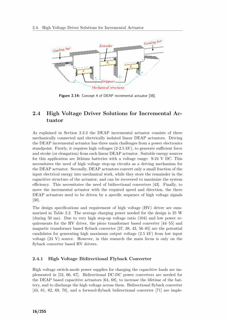
2.14 Concept 4 of DEAP incremental actuator [38]. . . . . . . . . . . . . 18
xi/xi
2.15 Schematic of the conventional bidirectional flyback converter. . . . . 19
2.16 Schematic of the high voltage bidirectional flyback converter for driv-ing a high voltage capacitive load. . . . . . . . . . . . . . . . . . . . 20
2.17 Proposed HV bidirectional flyback converter with 5 transformer stageson the secondary side. . . . . . . . . . . . . . . . . . . . . . . . . . . 20
2.18 Driving multiple actuators in the DEAP incremental actuator withmultiple converters. . . . . . . . . . . . . . . . . . . . . . . . . . . . . 21
2.19 Driving multiple actuators with a single converter. . . . . . . . . . . 22
2.20 Driving multiple actuators with a single converter having multipletransformer windings. . . . . . . . . . . . . . . . . . . . . . . . . . . 22
2.21 Driving multiple actuators with a single converter having a bidirec-tional relay in series with each actuator/capacitive load. . . . . . . . 23
3.1 a) Allocated winding space a) before applying AWL technique; b)after applying AWL technique; c) - e) Different steps involved inAWL technique for primary winding; f) - j) Different steps involvedin AWL technique for secondary winding;. . . . . . . . . . . . . . . . 27
3.2 Variation of transformer parasitics with the diameter of secondarywinding, for PQ 20/20 core (when γs=0.8). . . . . . . . . . . . . . . 28
3.3 Flow chart of the proposed efficiency optimization procedure. . . . . 29
3.4 Optimum secondary winding height allocation factor γs vs. corevolume. . . . . . . . . . . . . . . . . . . . . . . . . . . . . . . . . . . 31
3.5 Calculated optimized energy efficiencies at an output voltage of 2.5kV vs. core volume. The sequence of the 14 cores is: [E 16, EFD20, E 20, RM 8, PQ 20/20, E 25, EFD 25, RM 10, E 30, PQ 26/20,ETD 29, ETD 34, RM 12, ETD 39]. . . . . . . . . . . . . . . . . . . 31
3.6 An overview of different winding schemes. . . . . . . . . . . . . . . . 32
3.7 An overview of different winding buildups (just an example, here thenumber of primary or secondary windings are not the same as thoseshown in Table 3.1 or Table 3.2). . . . . . . . . . . . . . . . . . . . . 32
3.8 Plots from simulation of self-capacitance. a) Energy distribution forwinding scheme B:Z-type. b) Energy distribution for winding schemeD: Bank-type. . . . . . . . . . . . . . . . . . . . . . . . . . . . . . . . 34
3.9 Schematic of the bidirectional flyback converter with the control cir-cuit to achieve valley switching. . . . . . . . . . . . . . . . . . . . . . 38
3.10 Experimental prototype of the HV bidirectional flyback converterwith a 4.5 kV MOSFET on the HV side [94]. . . . . . . . . . . . . . 38
xii/xi
3.11 Experimental charge and discharge cycle of the HV bidirectional fly-back converter with a 4.5 kV MOSFET on the HV side; CH1: 500mA/div, CH2: 500 V/div, CH3: 5 A/div, CH4: 50 V/div, Timescale: 20 ms/div. . . . . . . . . . . . . . . . . . . . . . . . . . . . . . 39
3.12 Experimental results when the converter is operated with valleyswitching during charge process; CH1: 2 A/div, CH2: 20 V/div,CH3: 5 V/div, CH4: 20 V/div, Time scale: 10 µs/div. . . . . . . . . 39
3.13 Experimental results when the converter is operated with valleyswitching during charge process; CH1: 2 A/div, CH2: 20 V/div,CH3: 5 V/div, CH4: 20 V/div, Time scale: 5 µs/div. . . . . . . . . . 39
3.14 Experimental results when the converter is operated with valleyswitching during discharge process; CH1: 200 mA/div, CH2: 500V/div, CH3: 5 V/div, CH4: 20 V/div, Time scale: 5 µs/div. . . . . 40
3.15 Energy efficiency measurements. . . . . . . . . . . . . . . . . . . . . 40
3.16 Circuit diagram of a bi-directional flyback with high voltage semi-conductors connected in parallel on the secondary side to drive acapacitive load. . . . . . . . . . . . . . . . . . . . . . . . . . . . . . . 41
3.17 Circuit diagram of two parallel input parallel output high voltagebidirectional converters to drive a single capacitive load. . . . . . . . 41
3.18 a) Experimental results of a single HV bidirectional converter; CH1:200 mA/div, CH2: 5 A/div, CH3: 10 V/div, CH4: 500 V/div, Timescale: 5 ms/div., and b) 3 parallel connected bidirectional converters;CH1: 200 mA/div, CH2: 200 mA/div, CH3: 200 mA/div, CH4: 500V/div, Time scale: 2 ms/div. . . . . . . . . . . . . . . . . . . . . . . 42
3.19 Moving sequence of the DEAP incremental actuator for incrementalmotion towards the positive x-axis direction. . . . . . . . . . . . . . 44
3.20 Enable signals and driving voltages of all DEAP actuators, to achievethe incremental motion with variable speed, towards the positive x-axis direction [38] (Appendix O). . . . . . . . . . . . . . . . . . . . . 45
3.21 Experimental setup picture. . . . . . . . . . . . . . . . . . . . . . . . 45
3.22 Experimental result with the 3 DC-DC converters with several in-cremental actuation cycles; CH1: 1 kV/div, CH2: 1 kV/div, CH3: 1kV/div, CH4: 5 V/div, Time scale: 200 ms/div. . . . . . . . . . . . . 46
3.23 System integration with DEAP incremental actuator. . . . . . . . . . 47
3.24 Mechanical set-up to demonstrate the incremental motion on a curvedpath with a new DEAP incremental actuator concept. . . . . . . . . 48
xiii/xi

xiv/xi
List of Tables
2.1 Figure of merits of three technologies for two motion types of incre-mental actuators . . . . . . . . . . . . . . . . . . . . . . . . . . . . . 16
2.2 Design specifications and requirements of high voltage converter . . 19
2.3 Comparison of HV driver concepts for the DEAP incremental actuator 23
3.1 Details of the transformer with a turns ratio of 10 for W1-W6 . . . . 33
3.2 Details of the transformer for W7 . . . . . . . . . . . . . . . . . . . . 33
3.3 Self-capacitance of secondary winding . . . . . . . . . . . . . . . . . 34
3.4 Leakage inductance referred to primary . . . . . . . . . . . . . . . . 35
3.5 AC resistance referred to primary at 100 kHz . . . . . . . . . . . . . 35
3.6 Details of the transformer with a turns ratio of 20 . . . . . . . . . . 35
3.7 Parameters for non-interleaved (P/S) and non-sectioned transformer[W2] . . . . . . . . . . . . . . . . . . . . . . . . . . . . . . . . . . . . 36
3.8 Parameters for interleaved (S/P/S) and non-sectioned transformer[W5] . . . . . . . . . . . . . . . . . . . . . . . . . . . . . . . . . . . . 36
3.9 Parameters for non-interleaved (P/S) and sectioned (4 sections) trans-former [W3] . . . . . . . . . . . . . . . . . . . . . . . . . . . . . . . . 36
3.10 Parameters for interleaved (S/P/S) and sectioned (4 sections) trans-former [W8] . . . . . . . . . . . . . . . . . . . . . . . . . . . . . . . . 37
3.11 Specifications of the bidirectional flyback converter . . . . . . . . . . 37
3.12 Experimental data of DEAP incremental actuator moving with dif-ferent speeds to achieve 100 increments/steps . . . . . . . . . . . . . 47
3.13 Experimental data from bidirectional DEAP incremental actuatortests for 100 increments . . . . . . . . . . . . . . . . . . . . . . . . . 48
xv/xi

Chapter 1
Introduction
1.1 Background and Motivation
Actuators providing linear motion are used in a vast variety of applications rangingfrom large size machineries (e.g., cranes) to small scale micro-electro-mechanicalsystem (MEMS) devices used for micro positioning. Linear actuators are typi-cally characterized by their maximum stroke length, force, speed, and precision (orresolution). The stroke of many linear actuators is limited to their initial geomet-rical dimensions. This characteristic of conventional linear actuators limits theiruse in applications where large strokes, and low size and weight of the actuatorsare desired. Incremental linear motors are an alternative to potentially overcomethese limitations by providing an inchworm-like actuation. Dielectric Electro ActivePolymer (DEAP) can act as an artificial muscle and furthermore, DEAP has theability to act as an actuator without using the mechanical parts like bearings or ro-tational joints. DEAP technology, inherently capable of providing novel actuationsneeded for an inchworm-like movement, can potentially provide novel solutions forthe incremental motor design.
The concept of an incremental linear motor based on the DEAP technology isinspired by the inchworm type of actuators. The incremental motor performs theelongation in the direction of the movement by using one or more push/pull linearactuators, in combination with two or more actuators for clamping/holding themotor in position. As shown in Figure 1.1, the incremental actuator with 3 sub-actuators (1 actuator for push/pull operation and 2 actuators for clamping/holding)achieves 1 incremental stroke/movement within 6 steps.
The relative high strain level of DEAP actuator (compared to Piezo actuator) com-bined with its relatively high frequency of operation provides the opportunity todesign a linear positioner capable of moving with relatively high speed. The combi-nation of the relative high speed and the high force density of the DEAP transducercan potentially result in an extremely high power density of the system (densitiesbased on weight). Moreover, combining high efficiency charge and discharge circuitswith the principle of energy recovery during discharge, as a part of the electrical
1/255

1.2. Thesis Scope
driver, can provide low level of electrical energy consumption. The combination ofa highly efficient DEAP motor and an energy efficient electrical driver can resultin a system with extremely high energy efficiency.
The DEAP incremental motor/actuator concept consists of a system of DEAPtransducers mounted in the linear motor structure and electrical drivers. Thedrivers monitor the movement of the motor, charge and discharge the DEAP trans-ducers, and recover the electrical energy from the discharge cycles.
Figure 1.1: Incremental actuation schematics.
1.2 Thesis Scope
Since the early 1990s, a new type of smart material called, dielectric electro activepolymer (DEAP) has gradually attracted the attention of scientists and engineersfrom various disciplines. Danfoss Group perceived the bright prospect of DEAPand started the research within this field since 1995. A separate company withinDanfoss Group, called Danfoss PolyPower A/S, was established in 2008 to designand manufacture the DEAP film and elements for the customers.
A platform project entitled “Highly efficient low cost energy generation and actua-tion using disruptive DEAP technology” was proposed by Danfoss PolyPower A/Sand has gained great financial support from the Danish National Advanced Tech-nology Foundation. 7 companies, 3 universities and 8 PhD students are involved inthis platform project, which is organized with 9 work packages (WPs).
The overall success criterions of this project are, First:
• to mature the DEAP material from version 2 to 5 successively, measured byimproved material properties as shown in Figure 1.2.
• to increase the DEAP material’s dielectric constant to >10, dielectric strengthto >100 V/µm, and tear strength to >25 N/mm.
• to optimize the production processes, to reduce film imperfections, and toenable film width to >1 m and thickness to <20 µm.
2/255

1.2. Thesis Scope
Second, to demonstrate DEAP solutions on four key applications:
• as trailing edge flaps for wind turbine blades (to achieve >10% improved bladeefficiency, and reduced loads and fatigues on blades, turbine and structure).The partner in this project LM Wind Power has withdrawn from the projectdue to some reasons. So, the project has been changed to DEAP basedincremental actuators (to set new standards for weight, energy efficiency,and cost, for replacing the existing conventional linear actuators on mobileapplications).
• in wave energy systems (to achieve an efficiency of 80-85% compared to 25-50% now at grid parity costs).
• as compact in-line heating valves (better and cheaper valves without mechan-ical parts and with battery life of more than 10 years).
• and as flat screen loudspeakers (with a goal of 10 times smaller and 100 timesmore energy efficient compared to current state-of-the-art).
Figure 1.2: Performance roadmap of DEAP material for actuator operation [1].
In WP1, Department of Chemical Engineering at Technical University of Denmark(DTU) and Danfoss PolyPower A/S are cooperating to optimize the characteristicsof DEAP film. In WP2, Polyteknik A/S, ESS Technology A/S, Danfoss PolyPowerA/S and DTU Chemical Engineering are involved to optimize and improve theDEAP production processes. In WP3, DTU Management Engineering and DanfossPolyPower A/S are focusing on investigating DEAP elements with various config-urations and building high-level block diagrams for 4 application work packages.DTU Electrical Engineering, Department of Energy Technology at Aalborg Uni-versity (AAU), and Noliac A/S are working together to provide electrical solutionsinside the platform project. University of Southern Denmark (SDU) Mads ClausenInstitute and Danfoss PolyPower A/S are developing design and simulation toolsfor DEAP film and elements.
The WP6 to WP9 are 4 work packages based on applications, and are led by WP4.In WP6, DTU Electrical Engineering and Danfoss PolyPower A/S are demonstrat-
3/255

1.3. Thesis Objectives
ing a DEAP based incremental motor. In WP7, AAU and Wave Star A/S areinvestigating a wave energy harvester using DEAP technology. In WP8, DTUElectrical Engineering and Danfoss A/S Heating Solutions are investigating a po-tential DEAP based in-line heating valve. In WP9, a flat screen loudspeaker isunder development by DTU Electrical Engineering and Bang & Olufsen A/S. Theplatform project structure with the information of corresponding work packages isillustrated in Figure 1.3.
Figure 1.3: The configuration of DEAP platform project.
This PhD thesis “Switch-mode high voltage drivers for dielectric electro active poly-mer (DEAP) incremental actuators” is based on WP6 and the goal is to develop thenecessary power electronic converters for driving an incremental motor. The DEAPactuators and the incremental actuator mechanical setp-up for system integrationare provided by Danfoss Polypower A/S.
The scope of this thesis is to present the research work carried out during the PhDperiod from November 2011 to November 2014. Most of the scientific results of theresearch have been published or submitted in the form of peer reviewed conferenceand journal papers. The publications form a major part of this thesis and areincluded in Appendix. The thesis supplements already published information andthereby present a more coherent and complete overview of the research work andresults obtained in during the PhD research.
Furthermore, the thesis particularly focuses on the design and optimization of mag-netic transformer for high voltage capacitor charge and discharge application. It isexpected that this thesis will be useful for the power electronics engineers who wantto design, optimize and control the converters for high input and/or high outputvoltage applications.
1.3 Thesis Objectives
The primary objective of this PhD thesis is to develop the necessary power electronicdrivers for WP6 in DEAP platform project, i.e. to investigate energy efficient,
4/255

1.4. Thesis Structure and Content
and highly flexible, high voltage bidirectional DC-DC converters for driving DEAPincremental actuators. To achieve the main objective of the research, the followingsub goals are proposed:
• The DEAP incremental actuator consists of three electrically isolated andmechanically connected capacitive actuators. To accomplish the incrementalmotion, each actuator needs to be independently charged and discharged bya high voltage bidirectional DC-DC converter. A suitable bidirectional powerconverter topology needs to be selected to meet the specifications of the DEAPincremental actuator.
• For battery powered applications, high energy efficiency of the high voltagedriver is extremely important. Hence, another major objective is to optimizethe high voltage bidirectional DC-DC converter, to obtain high charge anddischarge energy efficiencies, using the commercially available high voltageMOSFETs on the secondary high voltage side.
• The low input voltage can be boosted to very high output voltage required bythe actuator, using a high-voltage, high-frequency transformer. The parasiticsof the transformer can significantly affect the performance of the converter.Therefore, the transformer design needs to be optimized, and different trans-former architectures and winding configurations need to be investigated forbetter energy efficiency.
• The parasitics of the high voltage MOSFETs and diodes, on the secondaryhigh voltage side can significantly influence the energy efficiency and perfor-mance of the converter, while charging and discharging the capacitive actuatorat very high output voltage. Hence, new control techniques and new converterconfigurations need to be investigated and implemented to minimize the lossin the high voltage active components.
1.4 Thesis Structure and Content
The structure and contents of this PhD project are visualized in the flow chartas shown in Figure 1.4. The first chapter briefly introduces the background andmotivation, scope as well as the objectives of the project. The overview and state-of-the art are discussed in Chapter 2.
Chapter 3 discusses the research related to the high voltage flyback converter,including the efficiency optimization, investigation of different transformer windingarchitectures (TWAs), digital control implementation, the system level integration,and investigation of a new topology.
The thesis is finalized with conclusions and future works. Furthermore, the pub-lished or submitted conference and journal papers are illustrated in the flow chartas well (Figure 1.4). The purpose of this thesis is to provide a condensed andcoherent overview of the research and results obtained in the thesis.
5/255

1.4. Thesis Structure and Content
Thesis structure
Introduction
High voltage flyback converter
Conclusion and Future Work
Overview andState-of-the-Art
Unidirectional energy flow
Modelling of bidirectional flyback converter
DEAP incremental actuator
Dielectric Electro Active Polymer (DEAP)
Applications
A1 – IEEE IPMHVC 2012:Analysis of DEAP actuator
A2 – IEEE UPEC 2012:High voltage driver for wind turbine flaps
A3– IEEE IPMHVC 2012Unidirectional flyback converter
A4 – IEEE EPE 2013Bidirectional flyback converter
A6 – IEEE ECCE Asia 2013Estimation of Transformer Parameters and Loss Analysis
A15 – IEEE ECCE USA 2013Driving a DEAP incremental actuator
A8 – IEEE Trans. on Power ElectronicsEfficiency optimization using an automatic winding layout technique
A9 – IEEE APEC 2014Investigation of transformer winding architectures
A16 – IEEE Trans. on MechatronicsA new Incremental Actuator based on Electro Active Polymer
A13 – SPIE 2014Parallel input parallel output high voltage bidirectional drivers
A12 – IEEE Trans. on Power Electronics Digital Control of a High Voltage (2.5 kV) Bidirectional DC-DC Converter
A10 – IEEE Trans. on Power Electronics Investigation of Transformer Winding Architectures
A11– IEEE ECCE USA 2014 Digital control of a High voltage bidirectional DC-DC converter
A14 – IEEE APEC 2015Bidirectional Flyback converter with Multiple Series Connected Outputs
A5– IEEE IEVC 2014Design of High Voltage Bidirectional DC-DC Converters
Best student paper award
A7 – IEEE APEC 2014:Optimization of a bi-directional flyback converter
Design of bidirectional flyback converter
Loss analysis of bidirectional flyback converter
Efficiency optimization
Investigation of various transformer structures
Digital control
Investigation of a new efficient high voltage driver topology
Scalability of high voltage drivers
System Integration with DEAP incremental actuator
Figure 1.4: PhD thesis structure.
6/255
Chapter 2
Overview and State-of-the-art
The research topic of the thesis is design and development of high voltage driversfor DEAP incremental actuators. In this chapter, an overview and state-of-the-artfor the DEAP incremental actuators, and the high voltage driving solutions arepresented. The information about some applications of DEAP actuator and itshigh voltage drivers can be obtained from Appendix A and B.
2.1 Linear Actuators
Actuators providing linear motion are used in a vast variety of applications rangingfrom large size machineries (e.g., cranes) to small scale micro-electro-mechanicalsystem (MEMS) devices used for micro positioning. Linear actuators are typicallycharacterized by their maximum stroke length, force, speed, and precision (or res-olution). The typical linear actuators [2] include mechanical, electro-mechanical,hydraulic, pneumatic, and piezo, etc. Several well-known linear actuators are pro-vided in Figure 2.1.
Mechanical linear actuator operates by converting the rotary motion into linearmotion. The advantages of mechanical actuators are low price, precision position-ing, and no need of a power source. The disadvantage is that they have to beoperated manually. The electromechanical linear actuators use DC motors andstepper motors to control a linear-action shaft output. Rotary motion of the motoris converted to linear displacement. These actuators are heavier than their motorcounterparts due to the addition of actuator assembly. Piezoelectric actuators canachieve extremely fine positioning resolution, but have a very short range of motion.The piezo actuators are expensive and fragile. Pneumatic linear actuators operatewith an external source of compressed air. They are efficient, but relatively com-plex to control via pressure valves and compressor manipulation. Hydraulic linearactuators are used in many industrial applications requiring higher levels of forcethan provided through equivalently sized electromechanical systems. Hydraulic lin-ear actuators require an external source for fluid pressurization. Unlike pneumaticactuators, a leak from hydraulic equivalents can foul equipment and require addi-
7/255

2.2. Dielectric Electro Active Polymer
tional clean up procedures depending on the type of fluid used. Control is complex,involving compressor control and hydraulic valves.
a)
b) c)
d) e)
Figure 2.1: Linear actuators from different technologies: a) a mechanical linearactuator [3]; b) an electro-mechanical linear actuator [4]; c) a piezolinear actuator [5]; d) a pneumatic linear actuator [6]; e) a hydraulic
linear actuator [7];
2.2 Dielectric Electro Active Polymer
Smart materials which respond to external stimuli like light, temperature, pressure,pH, magnetic and electric fields by changing their shape or size have been a partic-ular focus in the past decade [8]. The intelligent materials include, shape memoryalloys, piezoelectric materials, etc., and deforming active polymers include, hydrogels, dielectric elastomers, carbon-nano tubes, and liquid crystalline elastomers.
8/255

2.2. Dielectric Electro Active Polymer
The beginning of the Electro Active Polymer (EAP) field can be traced back to an1880 experiment that was conducted out by Roentgen, using a rubber band thatwas charged and discharged with fixed end and a mass attached to the free end [9],[10]. This discovery had been verified by Sacerdote in 1899, who formulated therelationship between strain response and electric field excitation [11].
Electro Active Polymers (EAPs) are categorized into two major classes: Ionic andDielectric (DEAP). An electric field or coulomb forces drive DEAPs, while theactuation mechanism for ionic EAPs is through the diffusion or mobility of ions.The DEAPs generally require high electric fields (>30 V/µm) and the ionic EAPsrequire low driving voltages, nearly equal to 1-5 V. Dielectric electro active polymer(DEAP) is an emerging smart material technology that has experienced substantialdevelopment and has gained increasing attention by scientists and engineers [8], [12],[13].
The DEAP material is a very thin (40 µm) incompressible elastomer film havinga compliant electrode layer on both sides [1], [14], [15]. The unique properties ofDEAP are, light weight, high flexibility, large elastic strain, fast electromechanicalresponse, etc, due to which it can be applied in a wide range of applications [8]. Anactuator is a mechanical device for moving or controlling a mechanism or a system.A laminate of PolyPower DEAP material with corrugated surface and electrode isshown in Figure2.2. The basic operation of the DEAP is the reduction in the poly-mer’s thickness and increase in its area, due to an applied electric field. Figure2.2shows the actuation direction when a high voltage is applied to its electrodes. Theprototye of a linear DEAP actuator is shown in Figure 2.3.
Ao
0applied
V ,maxapplied outV V
Figure 2.2: Basic principle of PolyPower [1] DEAP material.
33 mm
110 mm
Figure 2.3: A prototype of linear DEAP actuator.
DEAPs can be used as actuators in active structures, in particular when large
9/255
2.3. DEAP Incremental Actuator
deformations are required. Such EAP actuators convert electrical energy into me-chanical energy and produce large strains. DEAP actuators have the capability tooutperform the piezo, pneumatic and electromagnetic actuators in many ways, oneof which is presented in Figure 2.9 showing actuation stress vs. strain. The dynam-ical electro mechanical model of DEAs is discussed in [16]. Several applications ofDEAP actuators are discussed in [17], [18], [19], [20], [21], [22].
2.3 DEAP Incremental Actuator
2.3.1 Literature on Sliding Dielectric Elastomer Actuators
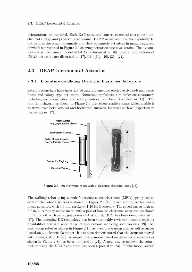
Several researchers have investigated and implemented electro active polymer basedlinear and rotary type actuators. Numerous applications of dielectric elastomersincluding inchworm robot and rotary motors have been described in [17]. Therobotic inchworm as shown in Figure 2.4 uses electrostatic clamps which enable itto travel over both vertical and horizontal surfaces, for tasks such as inspection innarrow pipes [17].
Figure 2.4: An inchworm robot with a dielectric elastomer body [17].
The walking robot using a multifunctional electroelastomer (MER) spring roll aseach of the robot’s six legs is shown in Figure 2.5 [18]. Each spring roll leg was alinear actuator, with 3-6 mm stroke at 1-10 Hz frequency. The speed was as high as2.7 in/s. A rotary motor made with a pair of bow tie elastomer actuators as shownin Figure 2.6, with an output power of 4 W at 100 RPM has been demonstrated in[17]. The emerging DE technology has been thoroughly reviewed presents excitingpossibilities across a wide range of applications including soft robotics [19]. Anearthworm robot as shown in Figure 2.7, has been made using a novel soft actuatorbased on a dielectric elastomer. It has been demonstrated that the actuator movedwith 1 mm/s at 5 Hz [20]. A simple rotary motor based on dielectric elastomers asshown in Figure 2.8, has been proposed in [21]. A new way to achieve the rotarymotion using the DEAP actuators has been reported in [23]. Furthermore, several
10/255

2.3. DEAP Incremental Actuator
researchers have investigated piezo, pneumatic and hydraulic based actuators. Thegain scheduling control of a walking piezo actuator is proposed in [24]. Bipolar piezoelectric actuators are proposed in [25]. High-accuracy tracking control of hydraulicactuators is discussed in [26].
Figure 2.5: A walking robot with MER spring rolls as legs [18].
Figure 2.6: A simple rotary motor based on dielectric elastomers [17].
Figure 2.7: An earthworm robot with the actuator module [17].
11/255

2.3. DEAP Incremental Actuator
Figure 2.8: A simple rotary motor based on dielectric elastomers [21].
2.3.2 Advantages and Figure of Merits of DEAP Incremental Ac-tuator
DEAP actuators exhibit large elastic strains, reasonable actuation pressures, rela-tively high electro-mechanical coupling and actuation speeds as compared to otherknown smart material technologies [8, 12]. DEAP actuators are very silent, can beof relatively light weight. DEAP actuators are potentially capable of outperformingpneumatics and electromagnetics in many ways, one of which is presented in Figure2.9 showing actuation stress versus actuation strain.
Figure 2.9: Typical stress-strain performance ranges for several actuator tech-nologies [1].
The design and implementation of high voltage drivers for the DEAP based capac-itive actuators is a new area of research [27–42]. DEAP, when utilized as linearactuators, has the potential to be an effective replacement for many conventionalactuators.
Replacement of conventional actuators with DEAP actuators is able to provide the
12/255

2.3. DEAP Incremental Actuator
following advantages:
• DEAP is seven times lighter than copper and steel by which the conventionalactuators are made of. Reducing the weight in any application can result inbetter overall efficiency.
• DEAP actuators are capacitive devices, i.e., a large portion of the energy isreactive and can be harvested and reused in cyclic motions. This will requireless energy from the main power source, once again increasing its efficiency.
• DEAP actuators are entirely made of rubbery material which is inherentlytolerant to shock and vibration which exist in some applications (e.g., electricvehicles). Moreover, a DEAP actuator does not incorporate any moving andsliding parts such as bearings, gearing and similar. All these characteristicsresult in improved lifetime, cost, and efficiency.
• DEAP actuators can be configured to provide incremental motion, thus over-coming the inherent size-to-stroke implications of conventional linear actua-tors, where the stroke is limited by their size. In incremental mode, DEAPactuators are several orders of magnitude shorter in their length compared tothe stroke they provide. This will once again reduce the size and weight ofthe actuation mechanism resulting in better system efficiency.
There are two types of operational modes of incremental actuators viz., Pushermode and Walker mode. In Pusher mode an incremental actuator is stationary andit pushes a shaft or rotates a disk. In Walker mode, as the name employs, the incre-mental actuator is mobile and it carry a load on either a guided path or a randompath depending on the applications. For example, in industrial manufacturing thepath is generally guided, while in search and rescue operations the path is random.Figure 2.10 illustrates these fundamental operational modes.
Figure 2.10: An incremental actuator can either be of a pusher type, whereanother object is moved, or of a walker type, where the incremen-tal actuator itself moves. A walker type can either be guided or
unguided [1].
Two existing technologies i.e. Piezo and Pneumatics, with good potentials in pro-
13/255

2.3. DEAP Incremental Actuator
viding incremental motion are being compared with DEAP technology. Table 2.1shows the results of comparison study between the three technologies and the twomotion types. This initial study indicates that DEAP has its value propositionfor mobile applications requiring low weight and form factor (simple and flexibledesign).
Table 2.1: Figure of merits of three technologies for two motion types of incre-mental actuators
FoM Suited for Pusher mode Suited for Walker modeStroke DEAP, Piezo, Pneumatics DEAP, Piezo, PneumaticsForce Piezo, Pneumatics DEAP, Piezo, PneumaticsSpeed (frequency) DEAP, Piezo DEAP, PiezoPrecision Piezo DEAP, PiezoWeight inmobile products DEAP DEAPSimple design DEAP, Piezo DEAPFlexible DEAP, Piezo, Pneumatics DEAPAutonomous DEAP, Piezo, Pneumatics DEAPCompact DEAP, Piezo DEAP, PiezoEnergy efficient DEAP, Piezo, Pneumatics DEAP, Piezo
2.3.3 Conceptual Development of DEAP Incremental Actuator
The conceptual design of electro active polymer based linear DEAP actuators isprovided in Appendix P. The generic concept of an incremental actuator is anassembly of sub-mechanism capable of gripping, releasing and extending. As DEAPshowed most potential in Walker operation (Table 2.1), the incremental actuatorconcepts are developed for this type of motion. The static guiding structures onwhich the actuator performs its motion are chosen to be rods and pipes. Theconcepts used to design DEAP incremental actuator have two grippers and oneextender. A gripper should be able to maintain its position with a certain force,while the extender should be able to displace a gripper at its released state. Theincremental motion is then performed by activating the grippers and extender at acertain pattern. Figures 2.11, 2.12, 2.13 and 2.14 show various conceptual drawingsfor the DEAP incremental actuator.
Figure 2.11: Concept 1 of DEAP incremental actuator [1].
Concept 1 is designed to operate outside a cylindrical rod. It consists of threesub components, namely one extender and two grippers at either end. When inoperation, one gripper holds the bar while the other gripper is in the released
14/255

2.3. DEAP Incremental Actuator
position. The extender either pushes or pulls the released gripper. The grippersand extender are joined by gluing or screwing their mechanical connections together(green plates in Figure 2.11).
Concept 2 is designed to operate inside a cylindrical tube as opposed to Concept1. Concept 2 consists of one extender and two grippers on either end. Both thegrippers and the extender of Concept 2 are realized by using axial DEAP actuators.Additional gripping mechanisms are applied to the grippers (red structures in Figure2.12). The gripping mechanism extends or contracts radially when the grippers are,respectively, contracting or extending axially as illustrated by the arrows in Figure2.12. The three axial actuators are joined together, at their mechanical connections,by gluing or by screws.
Figure 2.12: Concept 2 of DEAP incremental actuator [1].
The concept 3 as shown in Figure 2.13 is based on 3 DEAPs in axial configuration 1extender and 2 blocking DEAPs. When the blocking DEAP is extended the wedgesare driven toward the guide rod thereby create a blocking force.
Figure 2.13: Concept 3 of DEAP incremental actuator [1].
The concept 4 as shown in Figure 2.14 [38] is chosen as the first iteration of thisfeasibility study, due to its transparent motion which can be easily understoodand demonstrated. Here three Axial-1 type transducers are used to facilitate theincremental motion. Auxiliary mechanics are attached to the transducer enablingthem to grip, release and extend on a solid rod.
15/255
2.4. High Voltage Driver Solutions for Incremental Actuator
Figure 2.14: Concept 4 of DEAP incremental actuator [38].
2.4 High Voltage Driver Solutions for Incremental Ac-tuator
As explained in Section 2.3.3 the DEAP incremental actuator consists of threemechanically connected and electrically isolated linear DEAP actuators. Drivingthe DEAP incremental actuator has three main challenges from a power electronicsstandpoint. Firstly, it requires high voltages (2-2.5 kV), to generate sufficient forceand stroke (or elongation) from each linear DEAP actuator. Suitable energy sourcesfor this application are lithium batteries with a voltage range: 9-24 V DC. Thisnecessitates the need of high voltage step-up circuits as a driving mechanism forthe DEAP actuator. Secondly, DEAP actuators convert only a small fraction of theinput electrical energy into mechanical work, while they store the remainder in thecapacitive structure of the actuator, and can be recovered to maximize the systemefficiency. This necessitates the need of bidirectional converters [43]. Finally, tomove the incremental actuator with the required speed and direction, the threeDEAP actuators need to be driven by a specific sequence of high voltage signals[38].
The design specifications and requirement of high voltage (HV) driver are sum-marized in Table 2.2. The average charging power needed for the design is 25 W(during 50 ms). Due to very high step-up voltage ratio (104) and low power re-quirements for the HV driver, the piezo transformer based converter [44–55] andmagnetic transformer based flyback converter [37, 38, 43, 56–65] are the potentialcandidates for generating high maximum output voltage (2.5 kV) from low inputvoltage (24 V) source. However, in this research the main focus is only on theflyback converter based HV drivers.
2.4.1 High Voltage Bidirectional Flyback Converter
High voltage switch-mode power supplies for charging the capacitive loads are im-plemented in [52, 66, 67]. Bidirectional DC-DC power converters are needed forthe DEAP based capacitive actuators [64, 68], to increase the lifetime of the bat-tery, and to discharge the high voltage across them. Bidirectional flyback converter[43, 61, 62, 69, 70], and a forward-flyback bidirectional converter [71] are imple-
16/255

2.4. High Voltage Driver Solutions for Incremental Actuator
Table 2.2: Design specifications and requirements of high voltage converter
Parameters Target SpecificationsInput voltage / Output voltage 24 V / 0-2.5 kVCapacitance of DEAP actuator 400 nFCharging time to reach 2.5 kV from 0 V 50 msAverage charging power 25 WDischarging time to reach 0 V from 2.5 kV 50 msLinear velocity of DEAP incremental actuator 0-5 mm/sCharge energy efficiency to chargethe capacitive actuator from 0 V to 2.5 kV > 90%Discharge energy efficiency to dischargethe capacitive actuator from 2.5 kV to 0 V > 85%
mented for various applications. The schematic of the conventional bidirectionalflyback converter is shown in Figure 2.15. Due to high reverse recovery time (2.6µs) of body diode of high voltage (4 kV) MOSFET, a modified high voltage bidi-rectional flyback converter topology [37] as shown in Figure 2.16, is proposed andimplemented for driving a DEAP actuator.
1:n
Vout
Cin
+
-
Mp Ms
ip is
Energy flow
Vin
Rp Llkp
Lmp Lms
RsLlks
Csiload
+
-
+
-
VMp VMsCossp Cosss
Cload
Dbp Dbs
iin
Flyback transformer
Figure 2.15: Schematic of the conventional bidirectional flyback converter.
The loss analysis of the same converter is performed in [42]. More details about theanalysis of the bidirectional flyback converter can be found in Appendix D. Thedetailed design of the bidirectional flyback converter for driving a capacitive load ispresented in Appendix E. The discharge energy efficiency is limited by the parasiticsof the high voltage components which prevent full utilization of valley switching asdescribed in Appendix K. A new implementation is therefore proposed in AppendixN, where the secondary transformer winding is split into multiple windings whichare connected in series by lower voltage rating MOSFETs driven by a gate drivetransformer which is shown in Figure 2.17. For more details about the new proposedtopology refer to Appendix N.
17/255

2.4. High Voltage Driver Solutions for Incremental Actuator
1:n
Vout
Cin
Db
+
-
Mp Ms
ip is
Energy flow
Vin
Rp Llkp
Lmp Lms
RsLlks
Csiload
High voltage sideLow voltage side
+
-
+
-
VMp VMsCossp Cosss
D2
+
-VDb
+
-VD2
Cload
Dbp Dbs
iin
Flyback transformer
Figure 2.16: Schematic of the high voltage bidirectional flyback converter fordriving a high voltage capacitive load.
Vout
Cin
+
-
Mp
ip is
Energy flow
Vin
Rp Llkp
Lmp Lms1
Rs1Llks1
Cs1iload
High voltage sideLow voltage side
+
-
VMpCossp
Cload
Dbp
iin
Lms2
Rs2Llks2
Cs2
Ms1
+
-
VMs1Dbs1
Ms2
+
-
VMs2Dbs2
Lms3
Rs3Llks3
Cs3
Ms3
+
-
VMs3Dbs3
Lms4
Rs4Llks4
Cs4
Ms4
+
-
VMs4Dbs4
Lms5
Rs5Llks5
Cs5
Ms5
+
-
VMs5Dbs5
1:n2
1:n1
1:n3
1:n4
1:n5
Cosss1
Cosss2
Cosss3
Cosss4
Cosss5
Flyback
Transformer
with multiple
secondary
windings
Figure 2.17: Proposed HV bidirectional flyback converter with 5 transformerstages on the secondary side.
18/255

2.4. High Voltage Driver Solutions for Incremental Actuator
2.4.2 HV Drivers for DEAP Incremental Actuator
The detailed driving voltage waveforms for the DEAP incremental actuator aregiven in Appendix O, from which it is clear that the 3 linear DEAP actuators needto be charged and discharged independently. Different solutions for driving theDEAP incremental actuator are provided in Figures 2.18, 2.19, 2.20. The concept1 is to drive the system of DEAP incremental actuator having 3 linear actuators,with 3 independent HV drivers with the same input power source. Concept 2is to drive the 3 linear actuators, with a single HV driver. For this concept aseries combination of diode and a transistor/IGBT, is connected in series with eachactuator, during both charge and discharge modes. The concept 3 is to drive the3 linear actuators, with a single HV driver with a transformer having multiplesecondary windings. For this concept a transistor/IGBT is connected in series witheach actuator during charge mode, and a diode is connected in series with eachactuator during discharge mode. The concept 4 is to drive the 3 linear actuators,with a single HV driver having a bidirectional relay in series with each actuator.
1:n1Cin
+
-Vin
+
-
M1 M2
1:n2
+
-
M3 M4
1:n3
+
-
M5 M6
DE
AP
in
crem
enta
l act
uato
r
DC-DC converter 1
DC-DC converter 2
1AC
2AC
3AC
1HVD2HVD
3HVD4HVD
5HVD
1bD
3bD
5bD
DC-DC converter 3
1pi 1si
1AV
2pi 2si
2AV
3AV
3pi 3si
6HVD
2bD
4bD
6bD
1mpL1msL
2mpL2msL
3mpL3msL
Figure 2.18: Driving multiple actuators in the DEAP incremental actuator withmultiple converters.
19/255

2.4. High Voltage Driver Solutions for Incremental Actuator
1:nVA1
Cin
D2
CA1
Db
+
-
M1 M2
ip is
Energy flow
Vin
VA2CA2
+
-
VA3CA3
+
-
D3 D4 D5 D6 D7 D8
S1 S2 S3 S4 S5 S6
Figure 2.19: Driving multiple actuators with a single converter.
1:nVA1
Cin
D2
CA1
Db1
+
-
M1M21
ip is1
Energy flow
Vin
VA2
D4
CA2
Db2
+
-
M22
is2
VA3
D6
CA3
Db3
+
-
M23
is3
Flyback
transformer
S1
S2
S3
D3
D5
D7
Figure 2.20: Driving multiple actuators with a single converter having multipletransformer windings.
20/255

2.4. High Voltage Driver Solutions for Incremental Actuator
1:nVA1
CinD2
CA1Db
+
-
M1 M2
ip is
Energy flow
Vin
Rp Llkp
Lmp Lms
RsLlks
Cs
iload1
High voltage sideLow voltage side
Dsn1
VA2
CA2
+
-
iload2
VA3
CA3
+
-
iload3
Relay1 Relay2 Relay3
Figure 2.21: Driving multiple actuators with a single converter having a bidirec-tional relay in series with each actuator/capacitive load.
The comparison among all HV driver concepts is provided in Table 2.3.
Table 2.3: Comparison of HV driver concepts for the DEAP incremental actuator
Comparing item Concept 1 Concept 2 Concept 3 Concept 4Low voltageswitches 1 1 1 1High voltageswitches 3 7 6 1High voltage relays 0 0 0 3High voltage diodes 6 8 9 2Primary low sidegate drivers 1 1 1 1Secondary low sidegate drivers 3 4 6 1Secondary high sidegate drivers 0 3 0 0Control complexity Low Very High High LowCost of HV driver Moderate Very High High LowVolume of HV driver Moderate Moderate High Small
The concept 1 is simple to implement and it is easy to charge and discharge the 3capacitive actuators at very high voltage (2.5 kV). Use of a single magnetic com-ponent (flyback transformer) in Concept 2 has the potential to reduce the systemcost, weight and dimensions while maximizing the system efficiency by recoveringthe unused energy from the capacitive loads. These qualities make the drive circuitattractive for mobile and embedded systems, as well as any weight and power-critical designs. However, Concept 2 is very complex and expensive to implement,since more HV diodes, HV switches, and high-side gate drivers are needed. Concept3 consists of a flyback transformer with multiple secondary windings. This concept
21/255

2.5. Summary
is simple to implement, but, it is expensive. Furthermore, in Concept 3, it is verydifficult to achieve perfect coupling among the 3 secondary windings. The Concept4 has a bidirectional relay in series with each actuator. The commercially availablesolid state bidirectional relay is provided in [72]. But, the maximum rating of therelay is 1.5 kV and 20 mA. Hence, even though the Concept 4 is cheap to implement,it is impossible to drive the capacitive load at very high voltage (2.5 kV).
2.5 Summary
In this chapter, an overview of several linear actuators, literature review on slidingdielectric elastomer actuators, and different conceptual designs for DEAP incremen-tal actuator are presented. The flyback converter is chosen as a suitable topologyfor the HV driver due to its simple structure and a low component count. Severalflyback converter based HV driver solutions are presented for DEAP incrementalactuator to accomplish the incremental motion. Out of the 4 concepts, the concept1 is chosen as a reliable and simple solution.
22/255

Chapter 3High Voltage Bidirectional
Flyback Converter
3.1 Efficiency Optimization
The DEAP incremental actuator technology has the potential to be used in vari-ous industries, e.g. automotive, aeronautics, and medicine. For using the DEAPactuators in such applications, the high voltage drivers should have low volume tofit inside or together with the actuators. The overall energy efficiency of batterypowered high voltage drivers influence, the distance travelled by the incrementalactuator. Hence, for DEAP actuator applications, both the volume and energy ef-ficiency of high voltage drivers are extremely important and need to be optimized.
Transformer design plays a very important role in high voltage DC-DC power con-verters employed in low, medium and high power applications. The design method-ologies for transformers used in conventional switch-mode power supplies are welldocumented [56, 73–75]. Often, a transformer for a given application is designedbased on some assumptions such as, constant switching frequency, maximum tem-perature rise, estimated converter efficiency, winding fill factor, and winding currentdensity. However, those assumptions are not valid or suitable for some applications.Hence, more customized procedures are needed to design efficient transformers, forspecific applications. In a high voltage capacitor charge and discharge application,the high voltage transformer will have a large amount of (> 200) secondary turns.For such application, it is very difficult to select an optimum winding diameter andnumber of winding layers beforehand, which decide the values of the transformerparasitics. To avoid this difficulty, an automatic winding layout (AWL) techniqueis introduced in [41] and Appendix G, for the winding design of a high voltagetransformer. The high voltage flyback converter operation is very sensitive to thetransformer parasitics. The proposed AWL technique, utilizes the entire availablespace in a given transformer bobbin and provides an optimum winding diameterthat minimizes the total loss due to the transformer parasitics.
In the initial design phase, it is difficult to predict which core type is optimal fora given application. In a flyback converter, a long transformer window width is
23/255

3.1. Efficiency Optimization
often preferred, in order to minimize the leakage inductance and AC resistanceby providing a close coupling between windings, and to decrease the number ofwinding layers. For high output or input voltage flyback converters, this couldbe different, since the self-capacitance of the high voltage winding has significantimpact on the performance of the converter. During this research, an efficiencyoptimization algorithm is proposed, which provides an optimum solution for a giventransformer core, by using the proposed AWL technique and the comprehensive lossmodel. Different transformer winding architectures (TWAs) for the high voltagecapacitor charge and discharge application are investigated in [40] and AppendixI. In [39] and Appendix K, a digital control technique is proposed for improvingthe energy efficiency and charge/discharge speed. Control algorithms for optimal-flyback charging of a capacitive load are proposed in [65]. A number of switch-modepower supply design optimization methods have been described in the literature[76–81].
The proposed efficiency optimization technique has the following features:
• an automatic winding layout (AWL) technique, which produces the infor-mation about winding diameters, number of layers, and number of parallelwindings, for both primary and secondary windings.
• an accurate calculation of transformer parasitics using the outputs of AWLtechnique.
• calculation of energy losses during charge and discharge modes using a com-prehensive loss model.
• an objective function that minimizes the sum of energy losses during chargeand discharge modes, over a range of operating points.
More details about the efficiency optimization can be found in Appendix H and G.
3.1.1 Automatic Winding Layout (AWL) Technique
The transformer design using the proposed AWL technique is described in Figure3.1. The inputs to AWL technique are fixed number of primary and secondaryturns, and the dimensions of core/bobbin (window height and width). The outputsof AWL technique are various winding implementations, including specific windingdetails such as, diameters of primary and secondary windings, number of primaryand secondary winding layers, and insulation thicknesses for placing between sec-ondary winding layers.
The outputs of the AWL technique are used to calculate the transformer parasitics[42, 82–87], such as DC resistance, leakage inductance and self-capacitance. In Fig-ure 3.2, one output of AWL technique such as the insulation thickness (dinsulation)for a PQ 20/20 core, and calculated transformer parasitics are shown with re-spect to square width (Wsqs) of secondary winding. As the width of the secondarysquare (or secondary winding) decreases, the insulation spacing dinsulation betweensecondary winding layers increases, DC resistance Rs increases, leakage inductanceLlkp slightly decreases, and the self-capacitance Cs decreases.
24/255

3.1. Efficiency Optimization
1 2 3 4
Winding space allocation for
primary
WW
γpHW
1 2 3 4 5 6
c)
d)
e)
Wsqp Wsqp=γpHW
Wsqp Wsqp<γpHW
HW
WW
γsHW
Top view of the bobbin for horizontal E and ETD, EFD cores
Side view of the bobbin for verticle E cores and PQ, RM cores
Symmetrical line
10 11 12 13 14 15 16 17 18
98721 43 5 6
γpHW
HW
WW
γsHW
Symmetrical line
γpHW
Winding space allocation for
secondary
Winding space allocation for
primary
Transformer
Bobbin
1 2 3 4
Winding space allocation for
secondary
WW
γsHW
1 2 3 4 5 6 7 8 9
10 11 12 13 14 15 16 17 18
f)
g)
h)
i)
Space equally distributed
between secondary layers
Crossed space which is not utilized
by the windings
Wsqs Wsqs=γsHW
Wsqs Wsqs<γsHW
WsqsWsqs<0.5γsHW
Transformer
Bobbin
a) b)
1 2 3 4 16
32
5 6 7 10 128 9 11 14 1513
171819 20 2122 23 26 2824 25 27 30 3129
3334 3536 37 38 39 42 4440 41 43 45
j)
Wsqs
1 2 3 4 5 6
1 2 3 4 5 6
Squares Non-square
Non-square
γpHW
γpHW
γsHW
γsHW
γsHW
γsHW
dinsulation
dinsulation
dinsulation
Figure 3.1: a) Allocated winding space a) before applying AWL technique; b)after applying AWL technique; c) - e) Different steps involved inAWL technique for primary winding; f) - j) Different steps involved
in AWL technique for secondary winding;.
0.15 0.2 0.25 0.3
0.25
0.5
0.75
1
Square width Wsqs
(mm)
din
su
latio
n(m
m)
0.15 0.2 0.25 0.3
5
10
15
20
Square width Wsqs
(mm)
Rs(o
hm
)
0.15 0.2 0.25 0.3
0.820.840.860.880.9
Square width Wsqs
(mm)
Llk
p(u
H)
0.15 0.2 0.25 0.3
5
10
15
Square width Wsqs
(mm)
Cs (
pF
)
Figure 3.2: Variation of transformer parasitics with the diameter of secondarywinding, for PQ 20/20 core (when γs=0.8).
25/255

3.1. Efficiency Optimization
3.1.2 Efficiency Optimization Procedure
The flow chart of the proposed optimization routine is shown in Figure 3.3. Theproposed optimization routine is described in the following steps:
Initialize the design specifications
and constraints
Objective function: Total energy loss
fobj = ElossT (Core, γs, OAWL)
Core data base
Winding height allocation
factor (γs)
Diameters, number of
layers of secondary and
primary windings, etc.
Calculate transformer parasitics
AWL
Technique
Np, Ns
Efficiency maximization or loss
minimization:
Minimize function fobj over Core, γs, OAWL
Optimum design parameters:
Coreopt, γsopt, OAWLopt
Step 1
Step 2
Step 3
Step 4
Step 5
Step 6
Figure 3.3: Flow chart of the proposed efficiency optimization procedure.
• Transformer turns ratio, peak currents (for charge and discharge operations),magnetizing inductance are selected from the design specifications and con-straints. Number of primary and secondary turns are calculated for a giventransformer core.
• The proposed AWL technique is applied to calculate an array of the outputs(diameter, number of layers, turns per layer, number of parallel wires, forboth primary and secondary windings). The condition for the last layer fillfactor (FFLL) is FFLL>0.85, this is to approximately make, equal number of
26/255

3.1. Efficiency Optimization
turns per layer in final secondary layer and remaining secondary layers).
• The transformer parasitics are calculated for each set of outputs resulted fromAWL technique.
• The objective function is defined as sum of the total energy losses in thebidirectional flyback converter over a set of operating points.
• The end results of the optimization routine are the set of parameters whichcontributes to the minimum total energy loss. Finally, the optimum chargeand discharge energy efficiencies are calculated as a function of output voltage.
3.1.3 Results of Optimization
The optimum secondary height allocation factor γs, for each core is provided inFigure 3.4. Figure 3.5 provides the results of the optimum charge, discharge andoverall (product of charge and discharge) energy efficiencies, and an overall energyefficiency of a typical design where 50% space is allocated for primary and secondarywindings, at an output voltage of 2.5 kV, with respect to different core volumes.The most efficient and smallest transformer (or core) designs are two importantoutcomes of the proposed efficiency optimization routine.
The smallest and optimized core designs are described below:
3.1.3.1 Smallest Core Design (SCD)
The smallest core is selected as the core whose temperature rise is less than themaximum temperature limit of 130 C (with an estimated ambient temperatureof 35 C). Several small cores such as, EFD 12, EFD 15, E 16 have been used inthe optimization routine, out of those E 16 is the smallest core with a maximumtemperature rise of 94 C (in a single bidirectional charge and discharge cycle).
3.1.3.2 Optimized Core Design (OCD)
The core which has a lower volume and a better overall energy efficiency comparedto other cores is selected as an optimized core. In Figure 3.5, most of the coreswhose volume is above 2.85 cm3 have an overall energy efficiency between 74% and76%. The EFD 25 core with volume 3.3 cm3 has lower discharge efficiency (hencelower overall efficiency), since its window height HW is less compared with theneighboring cores, such as EF 25 and RM 10. For a better trade-off between thecore volume and overall efficiency, the cores whose volume is between 2.85 and 4 cm3
could be more suitable for the high voltage driver. The cores with volumes 4 cm3 (E30) and 2.85 cm3 (PQ 20/20) have overall efficiencies of 75% and 74%, respectively.However, PQ 20/20 core is selected as an optimized core, as 40% increase in thecore volume provides only 1% increase in the overall energy efficiency. More detailsabout the results of efficiency optimization can be found in Appendix H.
27/255

3.2. Investigation of Transformer Winding Architectures
Figure 3.4: Optimum secondary winding height allocation factor γs vs. corevolume.
0 1 2 3 4 5 6 7 8 9 10 11 12
25
30
35
40
45
50
55
60
65
70
75
80
85
90
95
100
Core volume (cm3)
En
erg
y e
ffic
ien
cy (
%)
charge energy efficiency at 2.5 kV output voltage with proposed AWL method
discharge energy efficiency at 2.5 kV output voltage with proposed AWL method
overall energy efficiency at 2.5 kV output voltage with proposed AWL method
overall energy efficiency at 2.5 kV output voltage when 50% space is allocatedfor both primary and secondary windings
Optimized core PQ 20/20Smallest core E 16
Figure 3.5: Calculated optimized energy efficiencies at an output voltage of 2.5kV vs. core volume. The sequence of the 14 cores is: [E 16, EFD20, E 20, RM 8, PQ 20/20, E 25, EFD 25, RM 10, E 30, PQ 26/20,
ETD 29, ETD 34, RM 12, ETD 39].
3.2 Investigation of TransformerWinding Architectures
Transformer parameters such as leakage inductance and self-capacitance are rarelycalculated in advance during the design phase, because of the complexity and hugeanalytical error margins caused by practical winding implementation issues. Thus,choosing one transformer architecture over another for a given design is usuallybased on experience or a trial and error approach. The leakage inductance, self-capacitance and AC resistance calculations in several transformer winding archi-tectures, ranging from the common non-interleaved primary/secondary windingarchitecture, to an interleaved, sectionalized and bank winded architectures arepresented in [40] and Appendix I.
Four winding schemes (A, B, C and D) are shown in Figure 3.6. Winding scheme
28/255

3.2. Investigation of Transformer Winding Architectures
1 2
3 5 7 8
4 6
1 2 3 4
5 6 7 8
1 2 3 4
5678
1 2 5 6
8743
Winding scheme A – U type Winding scheme B – Z type
Winding scheme D - BankWinding scheme C - Sectioned
Figure 3.6: An overview of different winding schemes.
A is the most simple to implement since the next layer starts where the previouslayer ended. In winding scheme B, the next layer starts just above the startingpoint of the previous layer. Winding scheme C split the winding into a number ofsections that is individually wounded like winding scheme A. In winding schemeD, the turns progress in a vertical back angled way where turns are built on top ofprevious turns. It seems like winding scheme D achieves as many angled sectionsas there are turns in a layer without the penalty of reducing the fill factor due tothe thickness of the section walls. Another advantage is that winding scheme D canbe easily interleaved which is not the case for winding scheme C since it is hard toadd section walls in-between windings. The difference in self-capacitance due to thewinding schemes is severe [82, 86, 87] because of change in the voltage potentialsbetween the turns in the winding.
3.2.1 Investigation using RM8 Core
Several winding buildups (S/P, S/P/S, S/P/S/P/S/P/S; where S and P are thesecondary and primary windings) are investigated - see Figure 3.7.
Symmetrical line
Transformer
Bobbin
P
S
Buildup: S/P
Symmetrical line
Transformer
Bobbin
P
S/2
Buildup: S/P/S
Symmetrical line
Transformer
Bobbin
Buildup: S/P/S/P/S/P/S
S/2P/3
S/4
S/4
P/3
S/4
P/3
S/4
Figure 3.7: An overview of different winding buildups (just an example, here thenumber of primary or secondary windings are not the same as those
shown in Table 3.1 or Table 3.2).
29/255

3.2. Investigation of Transformer Winding Architectures
In order to simplify the implementation of the windings a low turns ratio of 10 isselected. Based on these configurations, seven high voltage transformer windingarchitectures (W1-W7) are derived and the winding information is summarized inTable 3.1. The TWAs W1-W6 are wound with 10 primary turns and 100 secondaryturns. W7 deviates since it is only implemented with 9 primary turns due to thenature of the winding architecture. For more details about the TWAs refer toAppendix I.
Table 3.1: Details of the transformer with a turns ratio of 10 for W1-W6
Parameter ValueNumber of primary / secondary turns 10 / 100Diameter of primary / secondary winding 0.8 mm / 0.32 mmNumber of layers of primary / secondary winding 2 / 4Number of parallel wires of primary / secondary 2 / 1Type of core / material RM8 / N41Space allocation for primary / secondary 50% / 50%
Table 3.2: Details of the transformer for W7
Parameter ValueNumber of primary / secondary turns 9 / 100Diameter of primary / secondary winding 0.5 mm / 0.32 mmNumber of layers of primary / secondary winding 3 / 4Number of parallel wires of primary / secondary 5 / 1Type of core / material RM8 / N41Space allocation for primary / secondary 50% / 50%
The different winding architectures are simulated in Ansoft Maxwell [88] to extractthe values of the leakage inductances, self-capacitances and AC resistances. In Fig-ure 3.8 the electrostatic energy between the windings is shown for winding schemesB and D. It is noted that the energy density is high between layer to layer and lowbetween turn to turn as expected in winding scheme B. In winding scheme D thereis less electrostatic energy and thus it has lower self-capacitance.
The simulated, calculated and measured (using the impedance analyzer PSM1735)values of the self-capacitance, leakage inductance and AC resistance for the 7 trans-former winding architectures (TWAs) are shown in the Tables 3.3, 3.4, 3.5, respec-tively, from which it is clear that the measured, calculated and simulated trans-former parameters for most of the TWAs closely matches. However, the differencesin winding parameters such as an average layer to layer distance and mean lengthturn may cause errors around ±20%. In Appendix I, from the approximate lossmodel it was concluded that W6 has the lowest loss among all TWAs followed byW4, W7 and W3. This analysis is based on calculated parasitics values. However,if measured values are used in the loss calculations, then W4 will have lowest lossdue to transformer parasitics, followed by W3 and W6.
30/255
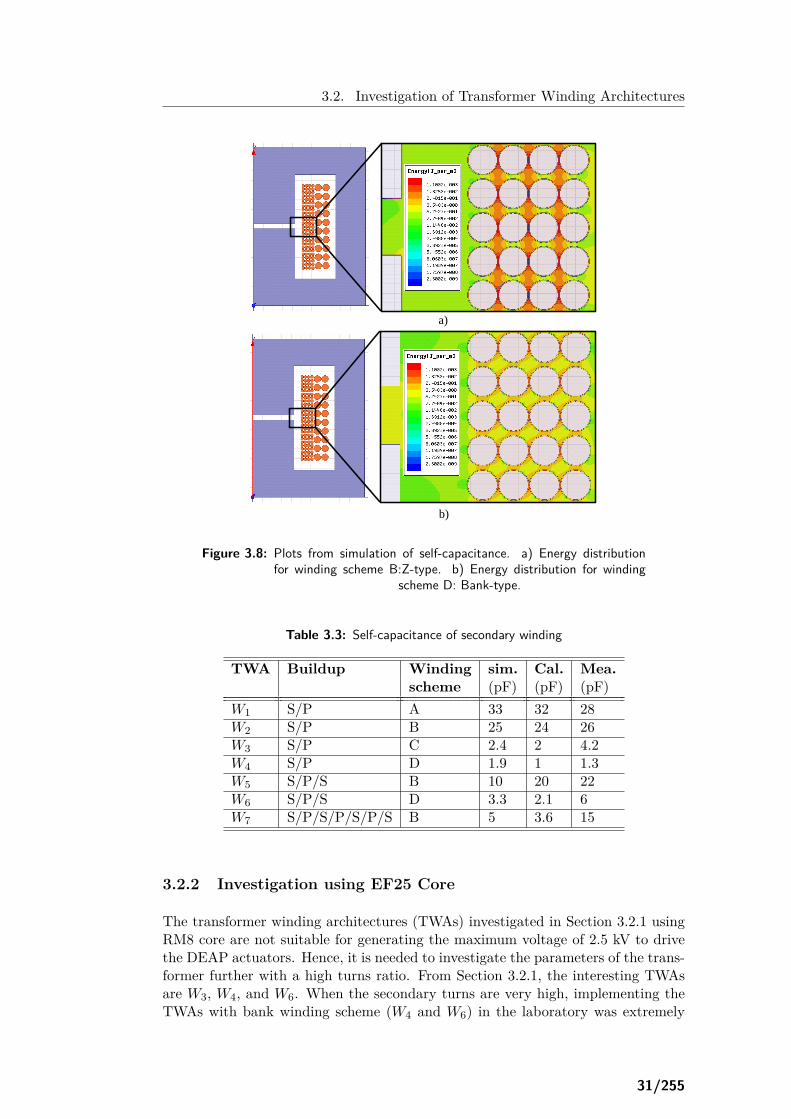
3.2. Investigation of Transformer Winding Architectures
a)
b)
Figure 3.8: Plots from simulation of self-capacitance. a) Energy distributionfor winding scheme B:Z-type. b) Energy distribution for winding
scheme D: Bank-type.
Table 3.3: Self-capacitance of secondary winding
TWA Buildup Winding sim. Cal. Mea.scheme (pF) (pF) (pF)
W1 S/P A 33 32 28W2 S/P B 25 24 26W3 S/P C 2.4 2 4.2W4 S/P D 1.9 1 1.3W5 S/P/S B 10 20 22W6 S/P/S D 3.3 2.1 6W7 S/P/S/P/S/P/S B 5 3.6 15
3.2.2 Investigation using EF25 Core
The transformer winding architectures (TWAs) investigated in Section 3.2.1 usingRM8 core are not suitable for generating the maximum voltage of 2.5 kV to drivethe DEAP actuators. Hence, it is needed to investigate the parameters of the trans-former further with a high turns ratio. From Section 3.2.1, the interesting TWAsare W3, W4, and W6. When the secondary turns are very high, implementing theTWAs with bank winding scheme (W4 and W6) in the laboratory was extremely
31/255

3.2. Investigation of Transformer Winding Architectures
Table 3.4: Leakage inductance referred to primary
TWA Buildup Winding sim. Cal. Mea.scheme (nH) (nH) (nH)
W1 S/P A 550W2 S/P B 520W3 S/P C 526 590 725W4 S/P D 580W5 S/P/S B 181W6 S/P/S D 150 150 208W7 S/P/S/P/S/P/S B 30 22 74
Table 3.5: AC resistance referred to primary at 100 kHz
TWA Buildup Winding sim. Cal. Mea.scheme (mΩ) (mΩ) (mΩ)
W1 S/P A 130W2 S/P B 127W3 S/P C 102 110 135W4 S/P D 84W5 S/P/S B 39W6 S/P/S D 35 37 42W7 S/P/S/P/S/P/S B 23 18 22
difficult, and hence it was not considered. Table 3.6 provides the details of trans-former design using EF20 core. Four different TWAs such as non-interleaved andnon-sectioned (W2), interleaved and non-sectioned (W5), non-interleaved and sec-tioned (W3), and interleaved and sectioned (W8, which is a new TWA) have beenpractically implemented. The measured parameters of the transformer for eachTWA are provided in Tables 3.7, 3.8, 3.9, and 3.10, respectively.
Table 3.6: Details of the transformer with a turns ratio of 20
Parameter ValueNumber of primary / secondary turns 18 / 360Diameter of primary / secondary winding 0.4 mm (TEX [89]) / 0.14 mmNumber of layers of primary / secondary winding 3 / 4Number of parallel wires of primary / secondary 3 / 1Type of core / material EF25 / N87
3.2.3 Discussion
This research work is summarized in Appendix J. By comparing the transformerparasitics of all TWAs for EF25 core, the TWA non-interleaved and sectioned (W3)has lowest self and interwinding capacitances, followed by the interleaved and sec-tioned (W8) TWA. The self-capacitances of TWAs W8 and W3 are comparable.Even though, the leakage inductance of W8 is approximately half of W3, due to
32/255

3.2. Investigation of Transformer Winding Architectures
Table 3.7: Parameters for non-interleaved (P/S) and non-sectioned transformer[W2]
Parameter ValueMagnetizing inductance of primary / secondary 53 µH / 23 mHLeakage inductance referred to primary / secondary 1.2 µH / 490 µHDC resistance of primary / secondary winding 42 mΩ / 16 ΩAC resistance referred to primary / secondary windingat 50 kHz 98 mΩ / 39 ΩAC resistance referred to primary / secondary windingat 100 kHz 130 mΩ / 52 ΩSelf-capacitance of high voltage winding 42 pFInterwinding capacitance 59 pF
Table 3.8: Parameters for interleaved (S/P/S) and non-sectioned transformer[W5]
Parameter ValueMagnetizing inductance of primary / secondary 47 µH / 20 mHLeakage inductance referred to primary / secondary 590 nH / 236 µHDC resistance of primary / secondary winding 43 mΩ / 19 ΩAC resistance referred to primary / secondary windingat 50 kHz 98 mΩ / 38 ΩAC resistance referred to primary / secondary windingat 100 kHz 108 mΩ / 43 ΩSelf-capacitance of high voltage winding 21.5 pFInterwinding capacitance 160 pF
Table 3.9: Parameters for non-interleaved (P/S) and sectioned (4 sections)transformer [W3]
Parameter ValueMagnetizing inductance of primary / secondary 49 µH / 21 mHLeakage inductance referred to primary / secondary 1 µH / 357 µHDC resistance of primary / secondary winding 39 mΩ / 14 ΩAC resistance referred to primary / secondary windingat 50 kHz 91 mΩ / 38 ΩAC resistance referred to primary / secondary windingat 100 kHz 117 mΩ / 43 ΩSelf-capacitance of high voltage winding 4.3 pFInterwinding capacitance 44 pF
very high interwinding capacitance, it might not be recommended for high volt-age capacitor charge and discharge applications, due to conducted and radiatedelectromagnetic interference (EMI) problems.
33/255

3.3. Digital Control of High Voltage Bidirectional Flyback Converter
Table 3.10: Parameters for interleaved (S/P/S) and sectioned (4 sections)transformer [W8]
Parameter ValueMagnetizing inductance of primary / secondary 49 µH / 21.5 mHLeakage inductance referred to primary / secondary 420 nH / 175 µHDC resistance of primary / secondary winding 43 mΩ / 19 ΩAC resistance referred to primary / secondary windingat 50 kHz 90 mΩ / 39 ΩAC resistance referred to primary / secondary windingat 100 kHz 100 mΩ / 43 ΩSelf-capacitance of high voltage winding 6.8 pFInterwinding capacitance 150 pF
3.3 Digital Control of High Voltage Bidirectional Fly-back Converter
Valley switching/quasi resonant (QR) control has been used in [90–93], to improvethe efficiency of the switch mode power supplies by reducing the capacitive turn-on/switching losses, and to reduce EMI. For the high voltage capacitor chargingapplication, the capacitive switching losses [42, 78] due to the equivalent lumpedcapacitance, at the drain node of the primary MOSFET during charge process, andat the drain node of the HV MOSFET during discharge process dominates the totallosses in the converter. Therefore, the capacitive switching losses can be reducedby implementing the valley switching control for charging as well as discharging thecapacitive load. The proposed valley switching technique requires only sensing ofthe low voltage side voltages (supply voltage and drain voltage) without the needto sense any HV side signals. The converter specifications are provided in Table3.11.
Table 3.11: Specifications of the bidirectional flyback converter
Parameter ValueInput / Output voltage 24 V / 0-2.5 kVOn-time of low voltage MOSFETduring charge process 9 µsOn-time of high voltage MOSFET [2 µs, 3 µs, 5 µs,during discharge process 10 µs, 20 µs, 150 µs, 200 µs]
The bidirectional flyback converter with the control circuit to achieve the valleyswitching during charge and discharge processes is shown in Figure 3.9. The inputvoltage and the drain voltage of primary MOSFET M1, each scaled by a resistordivider network H1 (3 kΩ and 90 kΩ), are compared using a high speed compara-tor TLV3501A. The comparator output becomes low (Vcomp = 0), when the drainvoltage of M1 is lower than the input voltage Vin. The output signal of the com-parator Vcomp is sent to the 16-bit microcontroller (PIC18F45K22) which detectsthe comparator output change, and produces a fixed on-time pulse to enable thegate driver 1 to drive the MOSFET M1. The experimental prototype of the HV
34/255

3.3. Digital Control of High Voltage Bidirectional Flyback Converter
bidirectional flyback converter is shown in Figure 3.10. The bidirectional operationof the HV converter at 2.5 kV output voltage is shown in the Figure 3.11. Due toconstant turn on-time tonC forM1 during charge process, the primary current IppkC
is constant. During discharge process, employing variable turn on-time tonD forM2makes the secondary current (hence the primary current) IspkC almost constant.
1:n
Digital Controller
Vout
Cin
D2Cload
Db
+
-
M1M2
ip isEnergy flow
Vin
H1H1
-+Vcc
Vcomp
Gate
driver 2Gate
driver 1
VG1 VG2
iin
Figure 3.9: Schematic of the bidirectional flyback converter with the controlcircuit to achieve valley switching.
Figure 3.10: Experimental prototype of the HV bidirectional flyback converterwith a 4.5 kV MOSFET on the HV side [94].
The experimental results when the converter, tested with a film capacitive load of400 nF, to validate the proposed valley switching technique are shown in Figures3.12, 3.13, 3.14. In Figures 3.12, 3.13, successful valley-switching operation atdifferent output voltages during the charge process is shown. From Figure 3.14,it is clear that the converter operates with zero voltage switching (ZVS) turn-on,and the primary current is negative before the switch is turned-on. The energyefficiency measurements during charge and discharge processes with 4 kV and 4.5kV MOSFETs on the HV side are shown in Figure 3.15. The charge energy efficiencyfor both 4 kV and 4.5 kV MOSFETs is above 90%, for the output voltage range 750V<Vout<2.2 kV, with a maximum efficiency of 92%. The charge energy efficiencyfor the output voltage range 2.2 kV<Vout<2.5 kV is between 88-90%. The discharge
35/255

3.3. Digital Control of High Voltage Bidirectional Flyback Converter
energy efficiency for 4 kV MOSFET is lower than the charge efficiency due to thefact that valley voltage in VM2 is not equal to valley voltage in VD2 during DCM.Some of the reasons for very low discharge energy efficiency for 4.5 kV MOSFETare due to its high on resistance (750 Ω), high gate input resistance (76 Ω). Moredetails about this work can be found in Appendix K.
Drain voltage of M1
VM1
Output voltage Vout
Primary current
ip
Input current
iin
Figure 3.11: Experimental charge and discharge cycle of the HV bidirectionalflyback converter with a 4.5 kV MOSFET on the HV side; CH1:500 mA/div, CH2: 500 V/div, CH3: 5 A/div, CH4: 50 V/div,
Time scale: 20 ms/div.
Drain voltage of M1
VM1
Primary current
ip
Gate drive signal of M1 Input voltage Vin
Vout = 500 V, Vin = 24 V
Figure 3.12: Experimental results when the converter is operated with valleyswitching during charge process; CH1: 2 A/div, CH2: 20 V/div,
CH3: 5 V/div, CH4: 20 V/div, Time scale: 10 µs/div.
Drain voltage of M1
VM1
Primary current
ip
Gate drive signal of M1 Input voltage Vin
Vout = 1700 V, Vin = 24 V
Figure 3.13: Experimental results when the converter is operated with valleyswitching during charge process; CH1: 2 A/div, CH2: 20 V/div,
CH3: 5 V/div, CH4: 20 V/div, Time scale: 5 µs/div.
36/255

3.4. Scalability of HV Drivers
Drain voltage of M1
VM1
Secondary current is
Gate drive signal of M2
Drain voltage of M2
VM2
Vout = 2000 V,
Vin = 24 V
Figure 3.14: Experimental results when the converter is operated with valleyswitching during discharge process; CH1: 200 mA/div, CH2: 500
V/div, CH3: 5 V/div, CH4: 20 V/div, Time scale: 5 µs/div.
Figure 3.15: Energy efficiency measurements.
3.4 Scalability of HV Drivers
Dielectric electroactive polymer (DEAP) actuators are capacitive devices whichprovide mechanical motions when charged electrically. The charging characteris-tics of a DEAP actuator depends on its size, voltage applied to its electrodes, andits operating frequency. The conventional bidirectional flyback DC-DC converterincorporates commercially available high voltage MOSFETs (4 kV [95]) and highvoltage diodes (5 kV [96]). The average current of the aforementioned devices islimited to 300 mA and 150 mA, respectively. Connecting the outputs of multi-ple converters in parallel can provide a scalable design. This enables operating theDEAP actuators in various static and dynamic applications, e.g. positioning, vibra-tion generation or damping, and pumps. The capacitive actuator can be chargedand discharged quickly by employing the converter as shown in Figure 3.16, inwhich the HV semiconductors are connected in parallel on the secondary side. Thesame can be achieved by employing two parallel input parallel output high voltagebidirectional converters as shown in Figure 3.17. More details about this topic canbe found in Appendix M.
37/255

3.4. Scalability of HV Drivers
1:n1
Charge
Controller
Vout
Cin
Dis-charge
Controller
Ds1
CloadDb1
+
-
Mp Ms1
ip is
Energy flow
Vin
Ds2
Db2
Ms2
Lp1 Ls1
Figure 3.16: Circuit diagram of a bi-directional flyback with high voltage semi-conductors connected in parallel on the secondary side to drive a
capacitive load.
1:n
Charge
Controller
Vout
Cin
Dis-charge
Controller
Ds1
CloadDb1
+
Mp1 Ms1
ip1 is1
Energy flow
Vin
1:n
Charge
Controller
Dis-charge
Controller
Ds2
Db2
Mp2 Ms2
ip2 is2
Energy flow
-
iload
Lp Ls
Lp Ls
Figure 3.17: Circuit diagram of two parallel input parallel output high voltagebidirectional converters to drive a single capacitive load.
38/255

3.5. Investigation of a New Topology: Bidirectional Flyback Converter withMultiple Series Connected Outputs
Experimental results of driving a single DEAP actuator/capacitive load with threeparallel connected high voltage converters is shown in Figure 3.18. Practically, asingle converter is able to charge and discharge the actuator to and from 2 kVwithin 15 ms and 18 ms, respectively. The 3 parallel input, parallel output HVmodules are able to charge and discharge the actuator to and from 2 kV within 4.5ms and 6 ms, respectively. This can increase the maximum operating frequency ofthe DEAP actuator from 30 Hz to 90 Hz with an assumption of zero delay timebetween charge and discharge processes.
Tcharge1 = 15 ms Tdischarge1 = 18 ms
Tcharge4 = 4.5 ms Tdischarge4 = 6 ms
Secondary current
a) b)
Output voltage
Low voltage MOSFET gate drive signal
Secondary current of converter 1
Primary current
Output voltage
Secondary current of converter 3
Secondary current of converter 2
Figure 3.18: a) Experimental results of a single HV bidirectional converter; CH1:200 mA/div, CH2: 5 A/div, CH3: 10 V/div, CH4: 500 V/div, Timescale: 5 ms/div., and b) 3 parallel connected bidirectional convert-ers; CH1: 200 mA/div, CH2: 200 mA/div, CH3: 200 mA/div,
CH4: 500 V/div, Time scale: 2 ms/div.
3.5 Investigation of a New Topology: Bidirectional Fly-back Converter with Multiple Series Connected Out-puts
A high voltage MOSFET (4 kV) in series with a blocking diode is added in parallelwith the high voltage output diode of a conventional flyback topology (see Figure2.16) to enable bidirectional operation. Experimental results from a digitally con-trolled bidirectional flyback converter show that the discharge energy efficiency islimited by the parasitics of the high voltage components which prevent full utiliza-tion of valley switching. A new implementation is therefore proposed, where thesecondary transformer winding is split into multiple windings which are connectedin series by lower voltage rating MOSFETs driven by a gate drive transformer.The proposed HV bidirectional flyback converter is shown in Figure 2.17. Usingthis topology, it is possible to series connect several lower voltage (< 4 kV) ratedMOSFETs each having a better body diode (having less reverse recovery time). Formore details about the proposed topology refer to Appendix N.
The advantages of the proposed topology are reduction in the voltage rating andprice of the HV MOSFET, possible to achieve perfect valley switching of HV MOS-FET, unlike the semi-valley switching [39], and improved energy efficiency. How-ever, the difficulties associated with the proposed converter are the need of highside gate drivers, synchronous switching of secondary MOSFETs, and the voltagesharing among the secondary windings and the secondary MOSFETs.
39/255

3.6. Implementation of Incremental Pattern on Film Capacitor Loads
3.6 Implementation of Incremental Pattern on FilmCapacitor Loads
The DEAP incremental actuator consists of three linear DEAP actuators (one ex-tender and two grippers). The incremental actuation steps and the driving voltagewaveforms for the grippers and extender are shown in Figures 3.19, 3.20, respec-tively. Each gripper is connected to mechanical supports on either side. It expandsand clamps to the guiding bar (e.g., a rod) surface when charged (with high volt-age), and unclamps from it, when discharged. The extender expands along theaxis of guiding bar. During the operation, one gripper holds the guiding bar whilethe other gripper is in a released position. The extender either pushes or pulls thereleased gripper. The incremental actuator performs 6 different steps, to achieve asingle incremental actuation stroke ∆x as shown in Figure 3.19.
The moving sequence of steps for the linear incremental motion towards the positivex-axis (right) direction:
• Start: All actuators are in the discharged state.
• Step 0: A1 is charged and clamps to the guiding bar. A2 and A3 are in thedischarged state.
• Step 1: A1 remains in the charged state. A2 is charged and pushes themechanical structure towards right, and A3 remains in the discharged state.
• Step 2: A1 is charged and clamps to the guiding bar. A2 and A3 are in thedischarged state.
• Step 3: A1 is discharged and is in the released position. A2 and A3 stillremain in the charged state.
• Step 4: A1 remains in the discharged state. A2 is discharged, and A3 remainsin the charged state.
• Step 5: A1 is charged. A2 remains in the discharged, and A3 in the chargedstate.
• Step 6: A1 remains in the charged state. A2 remains in the discharged state,and A3 is discharged.
• End: All actuators are discharged at the end. The Step 0 is used only forcharging the actuator A1. The Steps 1-6 repeat for achieving continuousincremental actuations.
40/255

3.6. Implementation of Incremental Pattern on Film Capacitor Loads
Charging
Step 6
Incremental actuator moving
in the direction of the positive x-axis
Step 1
Step 2
A1
Step 3
Step 4
Step 5
A3
A2
A1
A1
A3
A2
A2A3
A2A3
A3A1
A2
A3A1
A2
A1
x
A3
A2A1
Start
Step 0
A1
A2A3
Ste
p 1
– S
tep 6
Discharging
A3
A2A1
End
Distance
(mm)
Loop
repeats
Clamp: A1
Push: A2
Clamp: A3
Release: A1
Pull: A2
Clamp: A1
Release: A3
Figure 3.19: Moving sequence of the DEAP incremental actuator for incremen-tal motion towards the positive x-axis direction.
For more details about the DEAP incremental actuator operation refer to AppendixO and Appendix P. The proposed DEAP incremental actuator control scheme isexperimentally verified on film capacitive loads. The experimental set-up of 3 HVconverters for driving 3 capacitive loads is provided in Figure 3.21. Each capacitiveload is driven by a bidirectional flyback converter. One of the experimental resultis provided in Figure 3.22. The maximum voltage across each load is 2.5 kV, and
41/255

3.6. Implementation of Incremental Pattern on Film Capacitor Loads
the incremental sequence is repeated for several cycles.
0S0
t
0
0
t
t
2.5 kV
2.5 kV
2.5 kV2.5 kV
Start
2AV
1AV
3AV
1chV
3chV
5chV
2chV
4chV
6chV
0
0
0
0
0
0
t
t
t
t
t
t
tD
1increment
increment
Tf
tDS1 S2 tD S3 tD S4 tD S5 tD S6 tD S1
Tch Tdch
5 V 5 V
5 V 5 V
5 V
5 V
5 V
5 V
Figure 3.20: Enable signals and driving voltages of all DEAP actuators, toachieve the incremental motion with variable speed, towards the
positive x-axis direction [38] (Appendix O).
DC-DC converter 1
DC-DC converter 2
DC-DC converter 3
Capacitive load 1
Capacitive load 3
Capacitive load 2
Figure 3.21: Experimental setup picture.
42/255
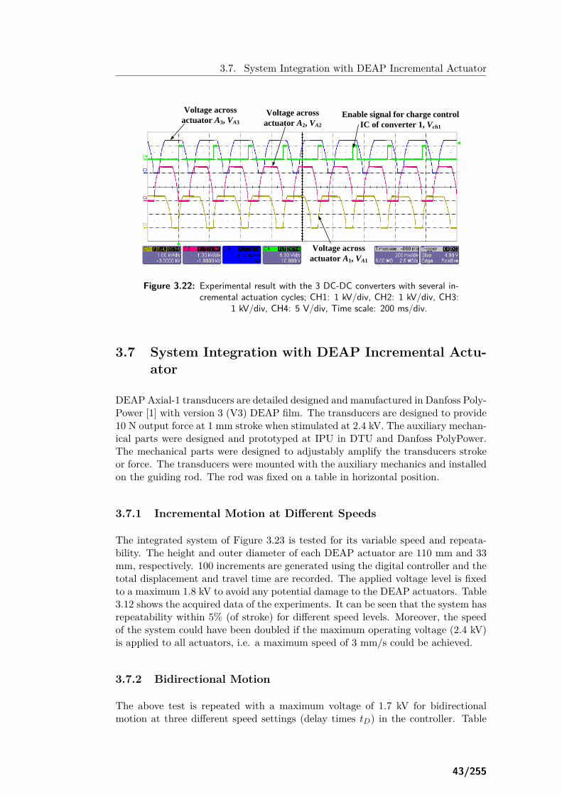
3.7. System Integration with DEAP Incremental Actuator
Voltage across
actuator A1, VA1
Voltage across
actuator A2, VA2
Voltage across
actuator A3, VA3
Enable signal for charge control
IC of converter 1, Vch1
Figure 3.22: Experimental result with the 3 DC-DC converters with several in-cremental actuation cycles; CH1: 1 kV/div, CH2: 1 kV/div, CH3:
1 kV/div, CH4: 5 V/div, Time scale: 200 ms/div.
3.7 System Integration with DEAP Incremental Actu-ator
DEAP Axial-1 transducers are detailed designed and manufactured in Danfoss Poly-Power [1] with version 3 (V3) DEAP film. The transducers are designed to provide10 N output force at 1 mm stroke when stimulated at 2.4 kV. The auxiliary mechan-ical parts were designed and prototyped at IPU in DTU and Danfoss PolyPower.The mechanical parts were designed to adjustably amplify the transducers strokeor force. The transducers were mounted with the auxiliary mechanics and installedon the guiding rod. The rod was fixed on a table in horizontal position.
3.7.1 Incremental Motion at Different Speeds
The integrated system of Figure 3.23 is tested for its variable speed and repeata-bility. The height and outer diameter of each DEAP actuator are 110 mm and 33mm, respectively. 100 increments are generated using the digital controller and thetotal displacement and travel time are recorded. The applied voltage level is fixedto a maximum 1.8 kV to avoid any potential damage to the DEAP actuators. Table3.12 shows the acquired data of the experiments. It can be seen that the system hasrepeatability within 5% (of stroke) for different speed levels. Moreover, the speedof the system could have been doubled if the maximum operating voltage (2.4 kV)is applied to all actuators, i.e. a maximum speed of 3 mm/s could be achieved.
3.7.2 Bidirectional Motion
The above test is repeated with a maximum voltage of 1.7 kV for bidirectionalmotion at three different speed settings (delay times tD) in the controller. Table
43/255

3.7. System Integration with DEAP Incremental Actuator
3.13 shows the results which indicate a larger total displacement in the forwardmotion compared to the reverse motion. In Table 3.13, Forward: positive x-axisdirection, and Reverse: negative x-axis direction.
Guiding rod
A1
A2
A3
Extender
Grippers
Figure 3.23: System integration with DEAP incremental actuator.
Table 3.12: Experimental data of DEAP incremental actuator moving with dif-ferent speeds to achieve 100 increments/steps
Total Actuator Delay Average Increment Incrementstroke total time speed size/ actuation(mm) travel tD (ms) (mm/s) stroke frequency
time (s) per step (mm) (Hz)39 50 50 0.78 0.39 1.5339 45 40 0.86 0.39 1.6839 40 30 0.97 0.39 1.8738 35 20 1.07 0.38 2.1140 30 10 1.33 0.40 2.4140 28 5 1.43 0.40 2.639 25 2 1.56 0.39 2.7339 26 1 1.5 0.39 2.78
3.7.3 Discussion
The DEAP incremental actuator system indicated a non-repeatable motion whenoperated bidirectional, resulting in a drift from the original position. This driftincreased with the number of bidirectional iterations resulting in an even largerdrift from original position. Such drift might be primarily caused by non-identicalgrippers differing in their gripping force. As the extending transducer is activated,it excites both grippers with the same force. The activated gripper should haveenough gripping force to not slip backward due to transient forces generated by theextender. If the two grippers have different gripping forces, the one with smallerforce will exhibit larger backward slipping resulting cumulatively in a drift of thewhole system from the original position.
44/255

3.7. System Integration with DEAP Incremental Actuator
Subsequent iteration of the DEAP incremental actuator will consider improved me-chanical and electronics concepts. Specific attention will be given to the design ofthe grippers to, i) achieve a more identical performance, and ii) have enough gripforce to overcome the inertial effects and as such increased speed and repeatability.The weight and form factor of DEAP are to be exploited and demonstrated. Thisis potentially achieved by reducing the actuator size, redesigning the auxiliary me-chanics, and integrating the electronics on a single PCB print. Moreover, the formfactor can be demonstrated by developing a concept which can travel on curved andinclined paths as shown in Figure 3.24, which is challenging for other technologiesto achieve.
Table 3.13: Experimental data from bidirectional DEAP incremental actuatortests for 100 increments
Total Actuator Delay Average Increment Incrementstroke total time speed size/ actuation(mm) travel tD (ms) (mm/s) stroke frequency
time (s) per step (mm) (Hz)Forward 40 71 100 0.56 1.08Forward 44 35 10 1.26 2.60Forward 43.7 32 1 1.36 3.03Reverse 37 71 100 0.52 1.08Reverse 41 41 10 1.00 2.60Reverse 35 37 1 0.94 3.03
Curved guiding rod
Figure 3.24: Mechanical set-up to demonstrate the incremental motion on acurved path with a new DEAP incremental actuator concept.
45/255

3.7. System Integration with DEAP Incremental Actuator
46/255

Chapter 4
Conclusions and Future Works
4.1 Conclusions
This work has investigated the 24 V input voltage and 0-2.5 kV output voltage, highvoltage, bidirectional DC-DC converters for driving the DEAP based incrementalactuator.
The major parts of this thesis and the associated publications correspond to thefollowing contributions:
• The detailed mathematical analysis of high voltage bidirectional flyback con-verter is presented. The converter operates in boundary conduction mode(BCM) control with variable switching frequency during the charge processand in discontinuous conduction mode (DCM) control with constant switch-ing frequency during the discharge process.
• The power losses in the bidirectional flyback converter for the capacitor charg-ing application has been analyzed in detail. Due to the variable switching fre-quency and non-sinusoidal waveforms, it is very difficult to accurately com-pute the core and winding losses. The core loss was accurately calculatedduring charge and discharge operations, using piecewise linear approximationof the IGSE model. Estimation of the leakage inductance for a non-interleavedstructure and interleaved winding structures has been discussed. Stray ca-pacitance calculation for a typical HV winding structure is discussed.
• The detailed power stage design of the high voltage bidirectional flyback con-verter for driving a dielectric electro active polymer (DEAP) based capacitiveactuator is described. Experimental results are provided to show the bidirec-tional operation (charge and discharge) of the high voltage converter. Eventhough the flyback transformer is designed for a high peak charging fluxdensity of 0.35 T, thermal measurement results show that the maximum tem-perature rise in the transformer is 33 C (with an ambient temperature of 28C). Therefore, for a high voltage capacitor charge and discharge applications
47/255

4.1. Conclusions
it is possible to minimize the number of transformer turns on the secondaryhigh voltage side, by choosing a higher flux density.
• The energy efficiency is optimized using a proposed new automatic windinglayout (AWL) technique and a comprehensive loss model. The proposed op-timization technique is experimentally validated on a 25 W (charging power)high voltage bidirectional flyback converter. The measured charge and dis-charge energy efficiencies of the converter, with PQ 20/20 core at an outputvoltage of 2.5 kV are 88% and 77%, respectively. For both optimized andsmallest core designs, energy efficiency during discharge process is less com-pared to that during charge process, mostly due to the switching loss of outputcapacitance of high voltage MOSFET.
• The proposed automatic winding layout (AWL) technique is highly recom-mended for high input or high output voltage applications which need a trans-former with many turns (primary or secondary). It automatically calculatesand provides the necessary winding design data such as wire sizes, number ofwinding layers, number of turns per layer, and number of parallel wires.
• The analytical equations for calculating the transformer AC resistance, leak-age inductance and self-capacitance for seven different winding architectureshave been presented and evaluated experimentally and with FEA simulationsfor a RM8 core with a turns ratio of 10. The main contribution to the er-rors is due to practical winding issues which are not accounted for in theequations. The transformer loss distribution is based on the calculated val-ues, and it clearly shows that transformer winding architectures where theself-capacitance is lowest are particularly suitable for high voltage chargingapplications. Another investigation has been made for EF25 core with a turnsratio of 25. Non-interleaved and Sectioned transformer could be most suitablefor HV capacitor charge and discharge application as a good balance betweenthe efficiency and EMI.
• The valley switching technique for a bidirectional flyback converter, drivinga capacitive load has been successfully implemented using a 16-bit micro-controller, during charge and discharge processes, respectively. Using theproposed simple valley switching technique, the flyback converter is able tocharge and discharge the capacitor load/actuator within minimum time (orwith maximum speed). To charge and discharge from 2.4 kV output voltageusing a 4 kV MOSFET, the flyback converter has charge and discharge energyefficiencies of 89% and 84%, respectively.
• Parallel-input and parallel-output high voltage bidirectional flyback convert-ers have been implemented, and their operation has been successfully verifiedwith both film capacitive load and the DEAP actuator. The proposed ideaof reducing/scaling the charge and discharge times is verified by connectinga maximum of 3 modules in parallel. With the practical experience, it isexpected that even more modules (> 3) could be easily connected in parallel.Practically, a single converter was able to charge and discharge the actuatorto and from 2 kV within 15 ms and 17.5 ms, respectively. The 3 parallel-
48/255

4.2. Future Works
input and parallel-output HV modules were able to charge and discharge theactuator to and from 2 kV within 4.5 ms and 6 ms, respectively.
• A bidirectional flyback converter with multiple series connected outputs isproposed, for high voltage drive of capacitive DEAP actuators. Simulationresults (output voltages and voltage stresses across the secondary MOSFETs-/diodes) during both charge and discharge processes are provided, to show acomparison between the proposed and the conventional implementation. Atheoretical comparison shows that the proposed converter has the potentialto improve the energy efficiency, lower the cost and reduce the volume of highvoltage driver.
• The DEAP incremental actuator concept has been designed, built and tested.It was demonstrated that the DEAP is feasible for providing incremental mo-tion with variable speed and bidirectional motion. Control and high volt-age electronics demonstrated good performance in providing the appropriatestimuli to the transducers with reasonable efficiency and compactness. Theproposed DEAP incremental actuator moves with a maximum velocity of 1.5mm/s, when all actuators are driven with 1.8 kV. It is possible to achieve aspeed of 3 mm/s, when the actuators are driven by 2.4 kV.
4.2 Future Works
• Driving the three actuators in the DEAP incremental actuator using a singlehigh voltage converter needs to be investigated.
• The proposed automatic winding layout (AWL) technique to design a highvoltage tramsformer, can be further extended for interleaved transformer con-figurations.
• If the future applications demand that the HV drivers should be integratedinside the DEAP incremental actuators, then further research needs to becarried out to accomplish this.
• Special research needs to be carried out to design high side gate drivers forthis challenging high voltage capacitor charge and discharge application.
• The proposed digital control technique can be further extended to improvethe energy efficiency of the converter by optimizing the switching frequencyof the converter. This is possible by switching the converter at other valleypoints in the drain voltage of the MOSFETs.
• Further investigation of proposed digital control technique with 4.5 kV MOS-FET on the secondary HV side needs to be carried out.
• The energy efficiency can be further improved by utilizing the leakage energystored in the transformer by implementing the active clamp circuits both onhigh voltage and low voltage sides.
49/255

4.2. Future Works
• The DEAP incremental actuator should be tested for incremental motionalong the curved path, using the digitally controlled HV drivers.
50/255

Bibliography
[1] “Danfoss polypower.” http://www.polypower.com/, November 2014.
[2] “Linear actuator.” http://en.wikipedia.org/wiki/Linear_actuator,November 2014.
[3] “Ok coil.” http://www.haydonkerk.com/Resources/StepperMotorTheory/tabid/192/Default.aspx, November 2014.
[4] “jenatec.” http://www.jena-tec.co.uk/linear-actuators.php, November2014.
[5] “Pi.” http://www.linear-actuator.net/Vacuum_Linear_Actuators.php,November 2014.
[6] “Local automation.” http://localautomation.com/featured/agi-pneumatic-linear-actuator-agi-american-grippers-inc.html,November 2014.
[7] “Stemulate.” http://www.stemulate.org/2012/07/02/solid-learning-robot-linear-actuators/, November 2014.
[8] Y. Bar-Cohen, Electroactive polymer (EAP) actuators as artificial muscles :reality, potential, and challenges. SPIE Press, 2004.
[9] W. C. Roentgen, “About the changes in shape and volume of dielectrics causedby electricity,” Annual Review of Physical Chemistry, vol. 31, pp. 771–786,1880.
[10] P. Brochu and Q. Pei, “Advances in dielectric elastomers for actuators and arti-ficial muscles,” Macromolecular Rapid Communications, vol. 31, no. 1, pp. 10–36, 2010.
[11] Y. Bar-Cohen, “Electroactive polymers as artificial muscles - reality andchallenges,” Collection of Technical Papers - AIAA/ASME/ASCE/AHS/ASCStructures, Structural Dynamics and Materials Conference, vol. 4, pp. 2313–2321, 2001.
[12] F. Carpi, D. D. Rossi, R. Kornbluh, R. Pelrine, and P. Sommer-Larsen, Di-electric Elastomers as Electromechanical Transducers. Amsterdam: Elsevier,2008.
51/255
Bibliography
[13] R. Pelrine, R. Kornbluh, Q. Pei, and J. Joseph, “High-speed electrically actu-ated elastomers with strain greater than 100%,” SCIENCE, vol. 287, no. 5454,pp. 836–839, 2000.
[14] “Leap technology.” http://leaptechnology.com/, November 2014.
[15] M. Tryson, H.-E. Kiil, and M. Benslimane, “Powerful tubular core free dielec-tric electro activate polymer (DEAP) push actuator,” in Proceedings of SPIE,vol. 7287, pp. 72871F–1 – 72871F–11, March 2009.
[16] R. Sarban, B. Lassen, and M. Willatzen, “Dynamic electromechanical model-ing of dielectric elastomer actuators with metallic electrodes,” Mechatronics,IEEE/ASME Transactions on, vol. 17, pp. 960 –967, October 2012.
[17] R. D. Kornbluh, R. Pelrine, Q. Pei, R. Heydt, S. Stanford, S. Oh, and J. Eck-erle, “Electroelastomers: applications of dielectric elastomer transducers foractuation, generation, and smart structures,” in Proc. SPIE, vol. 4698, pp. 254–270, 2002.
[18] Q. Pei, R. Pelrine, S. Stanford, R. D. Kornbluh, M. S. Rosenthal, K. Meijer,and R. J. Full, “Multifunctional electroelastomer rolls and their applicationfor biomimetic walking robots,” in Proc. SPIE, vol. 4698, pp. 246–253, 2002.
[19] I. A. Anderson, T. A. Gisby, T. G. McKay, B. M. O Brien, and E. P. Cal-ius, “Multi-functional dielectric elastomer artificial muscles for soft and smartmachines,” Journal of Applied Physics, vol. 112, no. 4, pp. –, 2012.
[20] K. Jung, J. C. Koo, J. do Nam, Y. K. Lee, and H. R. Choi, “Artificial annelidrobot driven by soft actuators,” Bioinspiration & Biomimetics, vol. 2, no. 2,p. S42, 2007.
[21] I. A. Anderson, T. C. H. Tse, T. Inamura, B. M. O Brien, T. McKay, andT. Gisby, “A soft and dexterous motor,” Applied Physics Letters, vol. 98, no. 12,pp. –, 2011.
[22] A. T. Conn, A. D. Hinitt, and P. Wang, “Soft segmented inchworm robot withdielectric elastomer muscles,” in Proc. SPIE, vol. 9056, pp. 90562L–90562L–10,2014.
[23] R. Wache, D. McCarthy, S. Risse, and G. Kofod, “Rotary motion achievedby new torsional dielectric elastomer actuators design,” Mechatronics,IEEE/ASME Transactions on, vol. 20, pp. 975–977, April 2015.
[24] R. Merry, J. Holierhoek, M. van de Molengraft, and M. Steinbuch, “Gainscheduling control of a walking piezo actuator,” Mechatronics, IEEE/ASMETransactions on, vol. 19, pp. 954–962, June 2014.
[25] D. Neal and H. Asada, “Bipolar piezoelectric buckling actuators,” Mechatron-ics, IEEE/ASME Transactions on, vol. 19, pp. 9–19, Feb 2014.
[26] J. Yao, Z. Jiao, D. Ma, and L. Yan, “High-accuracy tracking controlof hydraulic rotary actuators with modeling uncertainties,” Mechatronics,IEEE/ASME Transactions on, vol. 19, pp. 633–641, April 2014.
52/255
Bibliography
[27] D. Nielsen, A. Knott, and M. Andersen, “Hysteretic self-oscillating bandpasscurrent mode control for class d audio amplifiers driving capacitive transduc-ers,” in ECCE Asia Downunder (ECCE Asia), 2013 IEEE, pp. 971–975, June2013.
[28] D. Nielsen, A. Knott, and M. Andersen, “A high-voltage class d audio amplifierfor dielectric elastomer transducers,” in Applied Power Electronics Conferenceand Exposition (APEC), 2014 Twenty-Ninth Annual IEEE, pp. 3278–3283,March 2014.
[29] D. Nielsen, A. Knott, and M. A. E. Andersen, “Class d audio amplifier with4th order output filter and self-oscillating full-state hysteresis based feedbackdriving capacitive transducers,” in Proceedings of Epe’14-ecce, 2014.
[30] D. Nielsen, A. Knott, and M. A. E. Andersen, “Multilevel inverter based classd audio amplifier for capacitive transducers,” in Proceedings of Epe’14-ecce,2014.
[31] D. Nielsen, M. B. Moller, R. Sarban, B. Lassen, A. Knott, and M. A. E.Andersen, “Characterization of dielectric electroactive polymer transducers,”in Proc. SPIE, vol. 9056, pp. 90560L–90560L–9, 2014.
[32] L. Huang, Z. Zhang, and M. Andersen, “A review of high voltage drive ampli-fiers for capacitive actuators,” in Universities Power Engineering Conference(UPEC), 2012 47th International, pp. 1–6, Sept 2012.
[33] L. Huang, Z. Zhang, and M. Andersen, “Detailed behavior analysis for highvoltage bidirectional flyback converter driving deap actuator,” in IndustrialElectronics Society, IECON 2013 - 39th Annual Conference of the IEEE,pp. 625–630, Nov 2013.
[34] L. Huang, L. F. Normolle, R. Sarban, E. N. Christiansen, Z. Zhang, andM. A. E. Andersen, “Deap actuator and its high voltage driver for heatingvalve application,” in Proc. SPIE, vol. 9056, pp. 90562U–90562U–13, 2014.
[35] R. Pittini, L. Huang, Z. Zhang, and M. Andersen, “Primary parallel secondaryseries flyback converter (ppssfc) with multiple transformers for very high step-up ratio in capacitive load charging applications,” in Applied Power Electron-ics Conference and Exposition (APEC), 2014 Twenty-Ninth Annual IEEE,pp. 1440–1447, March 2014.
[36] L. Huang, Z. Zhang, and M. Andersen, “Design and development of au-tonomous high voltage driving system for deap actuator in radiator thermo-stat,” in Applied Power Electronics Conference and Exposition (APEC), 2014Twenty-Ninth Annual IEEE, pp. 1633–1640, March 2014.
[37] P. Thummala, Z. Zhang, and M. Andersen, “High voltage bi-directional fly-back converter for capacitive actuator,” in Power Electronics and Applications(EPE), 2013 15th European Conference on, pp. 1–10, Sept 2013.
[38] P. Thummala, Z. Zhang, M. Andersen, and S. Rahimullah, “Dielectric elec-tro active polymer incremental actuator driven by multiple high-voltage bi-directional dc-dc converters,” in Energy Conversion Congress and Exposition(ECCE), 2013 IEEE, pp. 3837–3844, Sept. 2013.
53/255
Bibliography
[39] P. Thummala, D. Maksimovic, Z. Zhang, and M. Andersen, “Digital controlof a high-voltage (2.5 kv) bidirectional dc-dc converter for driving a dielectricelectro active polymer (deap) based capacitive actuator,” in Energy ConversionCongress and Exposition (ECCE), 2014 IEEE, pp. 3435–3442, Sept 2014.
[40] H. Schneider, P. Thummala, L. Huang, Z. Ouyang, A. Knott, Z. Zhang, andM. Andersen, “Investigation of transformer winding architectures for high volt-age capacitor charging applications,” in Applied Power Electronics Confer-ence and Exposition (APEC), 2014 Twenty-Ninth Annual IEEE, pp. 334–341,March 2014.
[41] P. Thummala, H. Schneider, Z. Zhang, A. Knott, and M. Andersen, “Optimiza-tion of bi-directional flyback converter for a high voltage capacitor charging ap-plication,” in Applied Power Electronics Conference and Exposition (APEC),2014 Twenty-Ninth Annual IEEE, pp. 2556–2563, March 2014.
[42] P. Thummala, H. Schneider, Z. Ouyang, Z. Zhang, and M. Andersen, “Esti-mation of transformer parameters and loss analysis for high voltage capacitorcharging application,” in ECCE Asia Downunder (ECCE Asia), 2013 IEEE,pp. 704–710, June 2013.
[43] M. Karpelson, G.-Y. Wei, and R. J. Wood, “Driving high voltage piezoelectricactuators in microrobotic applications,” SENSORS AND ACTUATORS A-PHYSICAL, vol. 176, pp. 78–89, 2012.
[44] E. Horsley, M. Foster, and D. Stone, “State-of-the-art piezoelectric transformertechnology,” in Power Electronics and Applications, 2007 European Conferenceon, pp. 1–10, Sept 2007.
[45] C.-Y. Lin, Design and analysis of piezoelectric transformer converters. PhDthesis, Virginia Polytechnic Institute and State University, 1997.
[46] M. S. Roedgaard, Piezoelectric transformer based power converters; design andcontrol. PhD thesis, Technical University of Denmark, Department of ElectricalEngineering, 2012.
[47] T. Andersen, Piezoelectric transformer based power supply for dielectric electroactive polymers. PhD thesis, Technical University of Denmark, Department ofElectrical Engineering, 2012.
[48] E. Horsley, A. Carazo, M. Foster, and D. Stone, “A lumped equivalent circuitmodel for the radial mode piezoelectric transformer,” in Applied Power Elec-tronics Conference and Exposition, 2009. APEC 2009. Twenty-Fourth AnnualIEEE, pp. 1747–1753, Feb 2009.
[49] Y. Liu, D. Vasic, F. Costa, and D. Schwander, “Improvement of burst-mode controlled piezoelectric transformers,” in Power Electronics and MotionControl Conference (EPE/PEMC), 2012 15th International, pp. DS2c.7–1–DS2c.7–6, September 2012.
[50] M. S. Roedgaard, T. Andersen, K. S. Meyer, and M. A. E. Andersen, “Designof interleaved multi layer rosen type piezoelectric transformer for high volt-age dc/dc applications,” in Power Electronics, Machines and Drives (PEMD2012), 6th IET International Conference on, pp. 1 –6, March 2012.
54/255

Bibliography
[51] E. Baker, W. Huang, D. Chen, and F. Lee, “Radial mode piezoelectric trans-former design for fluorescent lamp ballast applications,” Power Electronics,IEEE Transactions on, vol. 20, pp. 1213–1220, Sept 2005.
[52] T. Andersen, M. S. Roegaard, O. C. Thomsen, and M. A. E. Andersen, “Lowvoltage driven dielectric electro active polymer actuator with integrated piezo-electric transformer based driver,” in Proceedings of SPIE, pp. 79762N–1 –79762N–12, March 2011.
[53] E. Horsley, N. Nguyen-Quang, M. Foster, and D. Stone, “Achieving zvs ininductor-less half-bridge piezoelectric transformer based resonant converters,”in Power Electronics and Drive Systems, 2009. PEDS 2009. International Con-ference on, pp. 446–451, Nov 2009.
[54] K. S. Meyer, M. S. Roedgaard, M. A. E. Andersen, and T. Andersen, “Piezo-electric power converter with bi-directional power transfer,” 2014. PatentWO2013083679.
[55] M. S. Roedgaard, M. A. E. Andersen, and K. S. Meyer, “Self-oscillating loopbased piezoelectric power converter,” 2013. Patent WO2013083678 A3.
[56] R. Erickson and D. Maksimovic, Fundamentals of Power Electronics. Powerelectronics, Springer, 2001.
[57] A. Abramovitz, C.-S. Liao, and K. Smedley, “State-plane analysis of regener-ative snubber for flyback converters,” Power Electronics, IEEE Transactionson, vol. 28, pp. 5323–5332, Nov 2013.
[58] J.-H. Jung and S. Ahmed, “Flyback converter with novel active clamp controland secondary side post regulator for low standby power consumption un-der high-efficiency operation,” Power Electronics, IET, vol. 4, pp. 1058–1067,November 2011.
[59] P. Davari, F. Zare, A. Ghosh, and H. Akiyama, “High-voltage modular powersupply using parallel and series configurations of flyback converter for pulsedpower applications,” Plasma Science, IEEE Transactions on, vol. 40, pp. 2578–2587, Oct 2012.
[60] A. Rahimi, F. Rahimi, and I. Hassanzadeh, “Analysis of high-voltage flybackconverter in color tvs, and its regulation,” in Power Electronics and DriveSystems, 2003. PEDS 2003. The Fifth International Conference on, vol. 1,pp. 353–358 Vol.1, Nov 2003.
[61] G. Chen, Y.-S. Lee, S. Hui, D. Xu, and Y. Wang, “Actively clamped bidi-rectional flyback converter,” Industrial Electronics, IEEE Transactions on,vol. 47, pp. 770–779, Aug 2000.
[62] J. Park, Y.-S. Roh, Y.-J. Moon, and C. Yoo, “A ccm/dcm dual-mode syn-chronous rectification controller for a high-efficiency flyback converter,” PowerElectronics, IEEE Transactions on, vol. 29, pp. 768–774, Feb 2014.
[63] H.-H. Chung, W.-L. Cheung, and K. Tang, “A zcs bidirectional flyback dc/dcconverter,” Power Electronics, IEEE Transactions on, vol. 19, pp. 1426–1434,Nov 2004.
55/255
Bibliography
[64] L. Eitzen, C. Graf, and J. Maas, “Cascaded bidirectional flyback converterdriving deap transducers,” in IECON 2011 - 37th Annual Conference on IEEEIndustrial Electronics Society, pp. 1226–1231, Nov 2011.
[65] N. Sokal and R. Redl, “Control algorithms and circuit designs for optimalflyback-charging of an energy-storage capacitor (e.g., for flash lamp or defib-rillator),” Power Electronics, IEEE Transactions on, vol. 12, pp. 885–894, Sep1997.
[66] J. Elmes, C. Jourdan, O. Abdel-Rahman, and I. Batarseh, “High-voltage, high-power-density dc-dc converter for capacitor charging applications,” in AppliedPower Electronics Conference and Exposition, 2009. APEC 2009. Twenty-Fourth Annual IEEE, pp. 433–439, Feb 2009.
[67] S.-K. Chung and H.-B. Shin, “High-voltage power supply for semi-active sus-pension system with er-fluid damper,” Vehicular Technology, IEEE Transac-tions on, vol. 53, pp. 206–214, Jan 2004.
[68] L. Eitzen, T. Hoffstadt, and J. Maas, “Power electronics concepts for drivingeap actuators,” vol. 8687, pp. 86870D–86870D–13, 2013.
[69] K. Venkatesan, “Current mode controlled bidirectional flyback converter,” inPower Electronics Specialists Conference, 1989. PESC ’89 Record., 20th An-nual IEEE, pp. 835–842 vol.2, Jun 1989.
[70] T. Bhattacharya, V. Giri, K. Mathew, and L. Umanand, “Multiphase bidi-rectional flyback converter topology for hybrid electric vehicles,” IndustrialElectronics, IEEE Transactions on, vol. 56, pp. 78–84, Jan 2009.
[71] F. Zhang and Y. Yan, “Novel forward-flyback hybrid bidirectional dc-dc con-verter,” Industrial Electronics, IEEE Transactions on, vol. 56, pp. 1578–1584,May 2009.
[72] “Solid state relay.” http://www3.panasonic.biz/ac/e_download/control/relay/photomos/catalog/semi_eng_he1a_aqv25.pdf, November 2014.
[73] C. McLyman, Transformer and Inductor Design Handbook, Fourth Edition.Electrical and Computer Engineering, Taylor & Francis, 2011.
[74] W. Hurley and W. Wölfle, Transformers and Inductors for Power Electronics:Theory, Design and Applications. EngineeringPro collection, Wiley, 2013.
[75] M. Kazimierczuk, High-Frequency Magnetic Components. Wiley, 2013.
[76] R. Prieto, J. Cobos, O. Garcia, R. Asensi, and J. Uceda, “Optimizing thewinding strategy of the transformer in a flyback converter,” in Power Elec-tronics Specialists Conference, 1996. PESC ’96 Record., 27th Annual IEEE,vol. 2, pp. 1456–1462 vol.2, Jun 1996.
[77] C. Sullivan, T. Abdallah, and T. Fujiwara, “Optimization of a flyback trans-former winding considering two-dimensional field effects, cost and loss,” inApplied Power Electronics Conference and Exposition, 2001. APEC 2001. Six-teenth Annual IEEE, vol. 1, pp. 116–122 vol.1, 2001.
56/255

Bibliography
[78] S. H. Kang, D. Maksimovic, and I. Cohen, “Efficiency optimization in digi-tally controlled flyback dc-dc converters over wide ranges of operating condi-tions,” IEEE TRANSACTIONS ON POWER ELECTRONICS, vol. 27, no. 8,pp. 3734–3748, 2012.
[79] A. C. Nanakos, E. C. Tatakis, and N. P. Papanikolaou, “A weighted-efficiency-oriented design methodology of flyback inverter for ac photovoltaic mod-ules,” IEEE TRANSACTIONS ON POWER ELECTRONICS, vol. 27, no. 7,pp. 3221–3233, 2012.
[80] X. Zhou, T. Wang, and F. Lee, “Optimizing design for low voltage dc-dcconverters,” in Applied Power Electronics Conference and Exposition, 1997.APEC ’97 Conference Proceedings 1997., Twelfth Annual, vol. 2, pp. 612–616vol.2, Feb 1997.
[81] J. Biela, U. Badstuebner, and J. Kolar, “Impact of power density maximizationon efficiency of dc-dc converter systems,” Power Electronics, IEEE Transac-tions on, vol. 24, pp. 288–300, Jan 2009.
[82] E. Snelling, Soft ferrites : Properties and applications. Butterworths, 1988.
[83] W. Hurley and D. Wilcox, “Calculation of leakage inductance in transformerwindings,” Power Electronics, IEEE Transactions on, vol. 9, pp. 121–126, Jan1994.
[84] F. Blache, J.-P. Keradec, and B. Cogitore, “Stray capacitances of two windingtransformers: equivalent circuit, measurements, calculation and lowering,” inIndustry Applications Society Annual Meeting, 1994., Conference Record of the1994 IEEE, pp. 1211–1217 vol.2, Oct 1994.
[85] A. Massarini and M. Kazimierczuk, “Self-capacitance of inductors,” PowerElectronics, IEEE Transactions on, vol. 12, pp. 671–676, Jul 1997.
[86] J. Biela and J. Kolar, “Using transformer parasitics for resonant converters -a review of the calculation of the stray capacitance of transformers,” in Indus-try Applications Conference, 2005. Fourtieth IAS Annual Meeting. ConferenceRecord of the 2005, vol. 3, pp. 1868–1875, 2005.
[87] L. Dalessandro, F. da Silveira Cavalcante, and J. Kolar, “Self-capacitance ofhigh-voltage transformers,” Power Electronics, IEEE Transactions on, vol. 22,no. 5, pp. 2081–2092, 2007.
[88] “Ansoft maxwell.” http://ansoft-maxwell.narod.ru/english.html,November 2014.
[89] “Furukawa.” http://www.furukawa.co.jp/makisen/eng/product/texe_feature.htm, November 2014.
[90] Y. Panov and M. Jovanovic, “Adaptive off-time control for variable-frequency,soft-switched flyback converter at light loads,” Power Electronics, IEEE Trans-actions on, vol. 17, pp. 596–603, Jul 2002.
57/255

[91] Y. Panov and M. Jovanovic, “Performance evaluation of 70-w two-stageadapters for notebook computers,” in Applied Power Electronics Conferenceand Exposition, 1999. APEC ’99. Fourteenth Annual, vol. 2, pp. 1059–1065vol.2, Mar 1999.
[92] Y.-B. Park and H.-S. Choi, “A efficiency improvement methodology for activemode efficiency regulation,” in Electronics and the Environment, 2008. ISEE2008. IEEE International Symposium on, pp. 1–5, May 2008.
[93] Z.-S. Ling, T.-J. Liang, L.-S. Yang, and T.-H. Li, “Design and implementationof interleaved quasi-resonant dc-dc flyback converter,” in Power Electronicsand Drive Systems, 2009. PEDS 2009. International Conference on, pp. 429–433, Nov 2009.
[94] “Ixys 4.5 kv mosfet.” http://ixapps.ixys.com/DataSheet/DS100498(IXTA-T02N450HV).pdf, November 2014.
[95] “Ixys 4 kv mosfet.” http://ixapps.ixys.com/DataSheet/DS100214A-(IXTH_V03N400_S).pdf, November 2014.
[96] “Vmi 5 kv diode.” http://www.voltagemultipliers.com/pdf/SXF6521_25.pdf, November 2014.
58/255
List of Publications
The overview of publications accomplished during the PhD study are given below.The publications are located in Appendix A-P.
A Prasanth Thummala, Lina Huang, Zhe Zhang and Michael A. E. Andersen,“Analysis of Dielectric Electro Active Polymer Actuator and its High VoltageDriving Circuits,” in Proc. 2012 IEEE International Power Modulator and HighVoltage Conference (IPMHVC 2012), Jun. 2012, pp. 458–461.
B Prasanth Thummala, Zhe Zhang, Michael A. E. Andersen and Ole C. Thom-sen, “A high voltage DC-DC converter driving a Dielectric Electro Active Poly-mer actuator for wind turbine flaps,” in Proc. 47th International Universities’Power Engineering Conference (UPEC 2012), Sept. 2012, pp. 1–7.
C Lina Huang, Prasanth Thummala, Zhe Zhang and Michael A. E. Ander-sen, “Battery Powered High Output Voltage Bidirectional Flyback Converter forCylindrical DEAP Actuator,” in Proc. 2012 IEEE International Power Modu-lator and High Voltage Conference (IPMHVC 2012), Jun. 2012, pp. 454–457.
D Prasanth Thummala, Zhe Zhang and Michael A. E. Andersen, “High VoltageBi-directional Flyback Converter for Capacitive Actuator,” in Proc. 15th Eu-ropean Conference on Power Electronics and Applications (EPE ECCE Europe2013), Sept. 2013, pp. 1–10.
E Prasanth Thummala, Dragan Maksimovic, Zhe Zhang and Michael A. E.Andersen, “Design of a High Voltage Bidirectional DC-DC Converter for DrivingCapacitive Incremental Actuators usable in Electric Vehicles (EVs),” in Proc.2014 IEEE International Electric Vehicle Conference (IEVC 2014), Nov. 2014.
F Prasanth Thummala, Henrik Schneider, Zhe Zhang and Michael A. E. Ander-sen, “Estimation of Transformer Parameters and Loss Analysis for High Volt-age Capacitor Charging Application,” in Proc. 2013 IEEE Energy ConversionCongress and Exposition ASIA (ECCE ASIA 2013), Jun. 2013, pp. 704–710.
G Prasanth Thummala, Henrik Schneider, Zhe Zhang, Arnold Knott and MichaelA. E. Andersen, “Optimization of bi-directional flyback converter for a high volt-age capacitor charging application,” in Proc. 2014 IEEE Applied Power Elec-tronics Conference and Exposition (APEC 2014), Mar. 2014, pp. 2556–2563.
59/255

H Prasanth Thummala, Henrik Schneider, Zhe Zhang, Ziwei Ouyang, ArnoldKnott and Michael A. E. Andersen, “Efficiency Optimization by Considering theHigh Voltage Flyback Transformer Parasitics using an Automatic Winding Lay-out Technique,” IEEE Trans. Power Electronics, DOI: 10.1109/TPEL.2014.2379439,2014.
I Henrik Schneider, Prasanth Thummala, Lina Huang, Ziwei Ouyang, ArnoldKnott, Zhe Zhang and Michael A. E. Andersen, “Investigation of transformerwinding architectures for high voltage capacitor charging applications,” in Proc.2014 IEEE Applied Power Electronics Conference and Exposition (APEC 2014),Mar. 2014, pp. 334–341.
J Prasanth Thummala, Henrik Schneider, Zhe Zhang and Michael A. E. Ander-sen, “Investigation of Transformer Winding Architectures for High Voltage (2.5kV) Capacitor Charging and Discharging Applications,” IEEE Trans. PowerElectronics, about to submit, 2014.
K Prasanth Thummala, Dragan Maksimovic, Zhe Zhang and Michael A. E. An-dersen, “Digital control of a high-voltage (2.5 kV) bidirectional DC-DC converterfor driving a dielectric electro active polymer (DEAP) based capacitive actua-tor,” in Proc. 2014 IEEE Energy Conversion Congress and Exposition USA(ECCE USA 2014), Sept. 2014, pp. 3435–3442.
L Prasanth Thummala, Dragan Maksimovic, Zhe Zhang and Michael A. E.Andersen, “Digital Control of a High Voltage (2.5 kV) Bidirectional DC-DCConverter for Driving a Capacitive Incremental Actuator,” IEEE Trans. PowerElectronics, about to submit, 2014.
M Prasanth Thummala, Zhe Zhang, Michael A. E. Andersen and Sarban Rahimul-lah, “Parallel input parallel output high voltage bi-directional converters fordriving dielectric electro active polymer actuators,” in Proc. SPIE Smart Struc-tures/NDE on Electroactive Polymer Actuators and Devices (EAPAD) 2014,Mar. 2014, pp. 90561N(1–15).
N Prasanth Thummala, Henrik Schneider, Zhe Zhang and Michael A. E. Ander-sen, “Bidirectional Flyback Converter with Multiple Series Connected Outputsfor High Voltage Capacitive Charge and Discharge Applications,” in Proc. 2015IEEE Applied Power Electronics Conference and Exposition (APEC 2015), Mar.2015.
O Prasanth Thummala, Zhe Zhang, Michael A. E. Andersen and Sarban Rahimul-lah, “Dielectric Electro Active Polymer Incremental Actuator Driven by MultipleHigh-Voltage Bi-directional DC-DC Converters,” in 2013 IEEE Energy Conver-sion Congress and Exposition USA (ECCE USA 2013), Sept. 2013, pp. 3837–3844.→ Best Student Paper Award
P Prasanth Thummala, Henrik Schneider, Zhe Zhang, Michael A. E. Andersenand Sarban Rahimullah, “A new Incremental Actuator based on Electro ActivePolymer: Conceptual, Control and Driver Design Considerations,” IEEE Trans.Mechatronics, revision submitted, 2015.
60/255
Appendix AAnalysis of Dielectric Electro
Active Polymer Actuator and itsHigh Voltage Driving Circuits
2012 IEEE International Power Modulator and High Voltage Conference (IPMHVC2012)
61/255

Analysis of Dielectric Electro Active Polymer Actuator and its High Voltage Driving Circuits
Prasanth Thummala, Lina Huang, Zhe Zhang and Michael A. E. Andersen Technical University of Denmark, Department of Electrical Engineering, DK-2800 Kongens Lyngby, Denmark
Email: pthu, huang, zz, [email protected]
ABSTRACT Actuators based on dielectric elastomers have promising
applications in artificial muscles, space robotics, mechatronics, micro-air vehicles, pneumatic and electric automation technology, heating valves, loud speakers, tissue engineering, surgical tools, wind turbine flaps, toys,rotary motors, and grippers for material handling, etc. This paper focuses on the application of Dielectric Electro Active Polymer (DEAP) technology as an actuation mechanism for different applications. The DEAP material requires very high voltage (~2.5 kV DC) to fully utilize it as an actuator. In this paper the DEAP actuator is analyzed in detail and the actuator structures, for the wind turbine flap and the heating valve applications are shown. Different high voltage switch mode power supply topologies for driving the DEAP actuator are discussed. The simulation and experimental results are discussed.
Index Terms — Dielectric electro active polymer (DEAP), actuator, high voltage (HV), dc-dc converter, power electronics, heating valves, wind turbine flaps, PolyPower
1 INTRODUCTION Smart materials which respond to external stimuli like light,
temperature, pressure, pH, magnetic and electric fields by changing their shape or size have been a particular focus in the past decade [1]. The intelligent materials include, shape memory alloys, piezoelectric materials, etc. and deforming active polymers include hydro gels, dielectric elastomers, carbon-nano tubes and liquid crystalline elastomers. Electro Active Polymers (EAPs) that undergoes force and deformation when electrically stimulated were strongly focused in the last years.
An actuator is a mechanical device for moving or controlling a mechanism or a system. EAPs can be used as actuators in active structures, in particular when large deformations are required. Such EAP actuators convert electrical energy into mechanical energy and produce large strains. Several applications of dielectric elastomer actuators were discussed in [2]. From the electrical standpoint, DEAP actuators are capacitive loads. In [3] a low voltage driven DEAP actuator was developed using piezoelectric transformer. A novel activation strategy for dielectric elastomer actuators was proposed in [4]. Section 2 discusses the detailed analysis of the DEAP actuator and its electrical, mechanical, and
electromechanical modeling, and the actuator structures for the heating valves and wind turbine flaps applications. We discuss the high voltage DC-DC converter topologies in Section 3,followed by the conclusion in Section 4.
2 DIELECTRIC ELASTOMERS AS ACTUATORS
Electro Active Polymers (EAPs) are categorized into two major classes: ionic and electronic. An electric field or coulomb forces drive electronic EAPs, while the actuation mechanism for ionic EAPs is through the diffusion or mobility of ions. The electronic EAPs generally require high electric fields (>100 V/µm) and the ionic EAPs requires low driving voltages, nearly equal to 1-5V. Typical driving voltages for dielectric elastomer actuators lie in the range between 2 kVand 4 kV, depending on the polymer breakdown field and thickness of the polymer film. The operating principle of a dielectric elastomer actuator is shown in Figure 1. The DEAP material is a very thin (~40 µm) incompressible elastomer film with a compliant electrode layer on both sides [5]. A dielectric elastomer is basically a compliant capacitor. The electrodes are designed to be able to comply with the deformations of the elastomer. As for any capacitor, when an electric field is applied to the electrodes, positive charges appear on one electrode, and negative charges on the other. This gives rise to coulomb forces between opposite charges, generating a pressure, known as the Maxwell stress. The Maxwell stress forces the electrodes to move closer, thereby squeezing the polymer. As the polymer is thinned, it elongates in the directions perpendicular to the applied force [6]. The electro static pressure (or stress) generated by the actuator is
22DEAP
o r o rv E
x
(1)
where E is the imposed electrical field, x is the final thickness, vDEAP is the voltage across the DEAP material, and εo and εr are the permittivity of the free space (8.85x10⁻¹² F/m) and the relative permittivity of the polymer, respectively. The mechanical strain S of the DE is given by
2
21
1
DEAPo r o rDEAP
o o
v SvSxY Y x
S
(2)
978-1-4673-1225-7/12/$31.00 ©2012 IEEE 458

where Y is the Young’s modulus and do is the initial thickness of the material. Using the capacitive behavior of the polymer, DEAP can be used as an actuator, mechano-electrical sensor, as well as energy harvester to generate electricity. When operated as an actuator DEAP show unique properties, such as very low electrical power consumption, high specific elastic energy density, high speed of response, no noise, flexibility, high power density, large bandwidth, higher performance than competing technologies and light weight, hence it has the potential to be an effective replacement for conventional actuators.
V V
Dielectric elastomer
CompliantElectrodes
Figure 1. Schematic showing the principle of operation of DEAP actuator. Right: Voltage is ON; Left: Voltage is OFF;
1.1 POLYPOWER DEAP ACTUATOR
Figure 2. PolyPower DE tubular actuator
PolyPowerTM dielectric elastomer (DE) is a silicone DE manufactured by Danfoss PolyPower A/S, Denmark. PolyPower DEAP actuator (Figure 2) is produced in thin sheets of 40 μm thickness. Table 1 shows the properties of the Danfoss PolyPower DEAP material. A DE sheet can be modeled as a strain dependent variable plate capacitor (3). For the unidirectional actuation shown in Figure 3, the capacitanceof the DEAP actuator as a function of strain S is
21
11
o oo r o r o r
o o
A S AAC Sx x S x
(3)
Table 1. Material properties of Danfoss PolyPower DEAP material
Film thickness 40 µm
Dielectric field strength 40 V/µm
Dielectric constant 3.1
Ao
1 oxS
ox
ob ob(1 ) oL
SoL
oA (1 ) oA
S
Figure 3. Left: A laminate of PolyPower DE material with corrugated surface and electrode, Right: Actuation direction of the DE material.
1.2 DEAP ELECTRICAL MODELLING
RSRL
+
-
+
-
vDEAPvs C
Figure 4a. Electric-circuit model of DEAP actuator
RSRL
+
-
+
-
vDEAPvs
LS
iC
Figure 4b. Electric-circuit model of DEAP actuator including the inductance of the high voltage cables and the compliant electrodes
Figures 4a and 4b show the circuit representation of the electrical model for the DE system employed in this paper. In the figures, RS is the resistance of the electrodes and the wiring, RL is the resistance of the DE material, C is the capacitance of the DE sheet, LS is the equivalent inductance of the electrodes and the high voltage cables, vs is the voltage of the power source, and vDEAP is the voltage over the DE sheet.
For the circuit shown in Figure 4a, the quasi-electrostatic pressure (1) at the surface of the DE sheet is induced by vDEAP,which is given by
( ) 1( ) ( )L SDEAPDEAP s
L S S
R Rdv t v t v tdt R R C R C
(4)
Similarly for the circuit shown in Figure 4b, the differential equations are given as,
( ) ( )s S S DEAPdiv t R i L v tdt
(5)
( ) ( )DEAP DEAP
L
v t dv ti CR dt
(6)
Figures 5a and 5b are the block diagram representations for the electrical equivalents of the DEAP actuator.
1
SR C
1S
L
RR
1s
-+
vs vDEAP
Figure 5a. Block diagram for the electrical circuit of the EAP actuator shown in Figure 4a
1
sL1s
SR
1C
1
LR
1s
vs i vDEAP+
- - -
+
Figure 5b. State block diagram for the electrical circuit of the EAP actuator shown in Figure 4b
459

1.3 DEAP MECHANICAL MODELLING
EoE1 E2
M( )S t
1 2
Figure 6. Voigt–Kelvin’s viscoelastic model with inertial force.
Dielectric polymers exhibit both elastic solid and viscous fluid characteristics. The viscoelastic behavior of the polymers can be modeled as linear elastic spring (E0, E1 and E2) and dashpot networks (η1 and η2). The viscoelastic behavior of the DE actuators can be predicted by a Voigt–Kelvin five-parameter model (Figure 6) [7]. The strain response S(t) to a step-stress input σ of the five-parameter Voigt–Kelvin model is
2
1
1 1( ) 1 expno n n
tS tE E
(7)
where n n nE are the retardation time constants.
1.4 DEAP ELECTRO-MECHANICAL MODELLING
EoE1 E2
M( )S t
1 2
C
RSRL
+
-
+
-
vs2
DEAPo r
vt
vDEAP
Figure 7. Electro-mechanical modeling of DEAP actuator
Figure 7 shows the electro-mechanical model of DEAP actuator. The input voltage vs generate a voltage across the DEAP capacitor vDEAP, which induces an electrostatic pressure σ. The mechanical part input viz., the electrostatic pressure σ is the input that results in a mechanical strain S. If the actuation strain S is large, it changes the capacitance C, thickness t, and the stiffness of the material
2.5 DIFFERENT STRUCTURES OF DEAP ACTUATORS
In this paper we focus on the application of DEAP actuator technology to two challenging applications, viz., heating valves and wind turbine flaps. The actuator structures for the two applications are discussed below.
2.5.1 WIND TURBINE FLAP APPLICATION
Figure 8. Left: Embedded DEAP actuator into the wing flap; Right: actuated flap structure with DEAP actuators.
Implementing DEAP actuator in the wind turbine flaps will result in improved blade efficiency, reduced loads and fatigues
on the blades and turbine. Figure 8 shows the typical structure of the wind turbine flap with embedded DEAP actuators.
2.5.2 HEATING VALVE APPLICATION
Figure 9. The heating valve containing the DEAP actuator
The current heating valve actuators in the market are thermal actuators, being noiseless but consuming significant power, and electrical gear motors which are relatively energy efficient, but inherently prone to noise issues. The compact in-line heating valves based on DEAP actuator will make better, cheaper and noiseless valves without mechanical parts.
3 HIGH VOLTAGE POWER CONVERTERS TO DRIVE THE DEAP ACTUATOR
To drive the DEAP actuator a high voltage in the range of kilovolts is required [3, 4]. For the systematic control of the DEAP actuators that are implemented in a specific application, special high voltage power electronic (HVPE) converters with advanced control techniques are required. Simulation and experimental results for a unidirectional flyback converter are shown.
3.1 DIFFERENT TOPOLOGIES Flyback and full bridge converters shown in Figures 10a and
10b, are some of the suitable DC-DC converter topologies for high voltage applications. However, the choice of the converter topology depends on the specific requirements of the application, which are shown in Table 2.
Table 2. Specifications of the applications and choice of converter topology
Application Input voltage Charging Time of Actuator
Wind turbineflap
24 V(from battery)400 V
(from wind turbine)50-100 ms
Heating valve 3 V (from battery) 5-10 min
Table 3. Parameters of the flyback converter used in the experiment
Parameters ValuesRated input voltage 24 V
Rated output voltage 2.5 kVMagnetizing inductance Lp 35 µHFlyback transformer core EF20, N87Primary turns/ Turns ratio 10/ 20
Leakage inductance Llk 800 nHCapacitance of DEAP actuator 145 nF
Primary peak current 5.3 A
460

Vin
M1
Lm
1:N
CDEAP
Rs
*
*
RL
D1
Magnetizinginductance
D2
M2
DEAP Actuator
Vout
Figure 10a. Schematic of bi-directional flyback converter
Vin
M1
D1
M3
D3
M4
D4
M2
D2
1:N
M5
D5
M7
D7
M8
D8
M6
D6
CDEAP
Rs
RL
DEAP Actuator
Vout
LFB
* *
Figure 10b. Schematic of isolated bi-directional full bridge converter.
In this paper we focus only on the flyback topology, for both applications. We used LT3751 capacitor charger controller to generate high voltage. However, for wind turbine flap application, if the output power requirement is too high, isolated full bridge converter is the good choice.
3.2 SIMULATION AND EXPERIMENTAL RESULTS The simulation has been done using LTSpice software. The
simulation results for a uni-directional flyback are shown below for different input voltages (Vin = 3V, 24V and 400V).
Figure 11. Simulation results of flyback converter for Vin = 3 V
Figure 12. Simulation results of flyback converter for Vin = 24 V
Figure 13. Simulation results of flyback converter for Vin = 400 V
Figure 14. Experimental waveforms (CH1-Output voltage; CH2-Input current; CH3-Charge signal to the converter; CH4-Mosfet drain voltage)
Figure 15. Experimental waveforms (CH1-Output voltage; CH2-Flyback primary current; CH3-Charge signal to the converter; CH4-Mosfet gate voltage)
Figures 14 and 15 are the experimental results for the uni-directional flyback converter.
4 CONCLUSION The DEAP actuator is analyzed in detail. And the modeling
of the DEAP actuator is presented. Different structures of the DEAP actuators that can be implemented in two different applications are shown. Some high voltage converter topologies for driving the capacitive loads are presented. Finally, simulation and experimental results are shown for a uni-directional flyback converter.
REFERENCES [1] Y. Bar-Cohen, Electroactive Polymer (EAP) Actuators as Artificial
Muscles: Reality, Potential, and Challenges. SPIE Press, Bellingham, Washington, USA, 2001.
[2] R. Pelrine, P. Sommer-Larsen, R. Kornbluh, R. Heydt, G. Kofod, Q. Pei, P. Gravesen, “Applications of dielectric elastomer actuators”, Proc. of SPIE, Smart structures and materials 2001: Electroactive polymer actuators and devices, Vol. 4329, pp. 335-349, 2001.
[3] T. Andersen, M. S. Rødgaard, O. C. Thomsen and M. A. E. Andersen, “Low voltage driven dielectric electro active polymer actuator with integrated piezoelectric transformer based driver,” Proceedings of SPIE,vol. 7976, p. 79762N, 2011.
[4] M. Babič, R. Vertechy, G. Berselli, J. Lenarčič, V. Parenti Castelli, G. Vassura, “An electronic driver for improving the open and closed loop electro-mechanical response of Dielectric Elastomer actuators”,Mechatronics, Vol. 20, pp. 201-212, 2010.
[5] M. Benslimane, P. Gravesen, P. Sommer-Larsen, “Mechanical properties of dielectric elastomers with smart metallic compliant electrodes”, In. Proc. of SPIE Int Soc. Opt. Eng., 4695, pp. 150-157, 2002.
[6] R.E. Pelrine, R.D. Kornbluh, J.P. Joseph, “Electrostriction of polymer dielectrics with compliant electrodes as a means of actuation,” Sensors and Actuators, Vol. A 64, pp. 77-85, 1998.
[7] R. Sarban, B. Lassen, M. Willatzen, "Dynamic Electromechanical Modeling of Dielectric Elastomer Actuators With Metallic Electrodes," IEEE/ASME Transactions on Mechatronics, Vol. PP, no.99, pp.1-8, 2011.
461

66/255
Appendix BA high voltage DC-DC converterdriving a Dielectric Electro ActivePolymer actuator for wind turbine
flaps
47th International Universities’ Power Engineering Conference (UPEC 2012)
67/255

A high voltage DC-DC converter driving a Dielectric Electro Active Polymer actuator for wind
turbine flaps Prasanth Thummala Zhe Zhang Michael A. E. Andersen Ole C. Thomsen Dept. of Electrical Dept. of Electrical Dept. of Electrical Dept. of Electrical Engineering, Technical Engineering, Technical Engineering, Technical Engineering, Technical University of Denmark University of Denmark University of Denmark University of Denmark [email protected] [email protected] [email protected] [email protected]
Abstract-The Dielectric Electro Active Polymer (DEAP) material is a very thin (~80 µm) silicone elastomer film with a compliant metallic electrode layer on both sides. The DEAP is fundamentally a capacitor that is capable of very high strain. The property that the polymer changes its shape, as a result of the electrostatic forces generated by an applied voltage, can be used in actuators, for instance to adapt the trailing edges of wind turbine blades, for maximum efficiency and increased energy output. Conventional actuator technologies have not proven feasible solutions for driving the wind turbine flaps. With the DEAP based high power actuator, it is expected to make a reliable and light solution with superior controllability. The current DEAP technology requires high DC voltage in the range of kV to fully utilize the DEAP material as an actuator. In this paper we propose a flyback converter topology to obtain high voltage at low current, for driving the DEAP actuator. Simulation and experimental results for uni-directional flyback converter topology are shown.
Index Terms--Dielectric Electro Active Polymer (DEAP), high voltage, capacitive load, actuator, wind turbine, flaps, flyback, PolyPower
I. INTRODUCTION
Nowadays the world’s main focus is on how to best utilize the energy from the natural energy resources such as sunlight, wind and tides etc. One of the reasons is due to the fact that the fossil fuels will not last forever. But the energy production from fossil fuel is relatively cheaper when compared to sustainable energy. Engineers are doing extensive research to face the challenge of making the equipment that catches the energy from nature more efficient. Wind turbines and in particular their wings/blades are subject to loads varying greatly because of wind gusts and turbulences occurring at passing the tower. The varying loads on the wings may cause them to oscillate and collide with the tower. So it is very important to control these blade loads along the length of the blade body, to protect the turbine from being damaged. This can be achieved with aerodynamic control devices such as flaps [1].
A flap mounted on the wing can control the lift on certain sections of the wing. A wing flap covering ten percent of the airfoil can change its lift coefficient (Cl) by twenty percent at an angular deflection (δ) of five degrees. The effect of the changing lift coefficient is a change in the force acting on the wing. Being able to control this force makes it feasible to
avoid oscillation of the wing. The flaps may also be used to increase the energy output of a wind turbine. Piezoelectric [2], hydraulic [3]-[6], pneumatic [7]-[10] and electro-mechanical actuators [11]-[12] are the most common types of actuators used in various engineering applications and in existing wind turbines for traditional control purposes. Among the above actuators, piezoelectric and pneumatic actuators had already been implemented for controlling the trailing edge flaps in the wind turbine blades [2], [10].
In this paper, we aim to utilize the DEAP material as an actuation mechanism for the wing flap. The unique properties of the DEAP material such as, very low electrical power consumption, no noise, flexibility, large bandwidth, self sensing ability, higher performance than competing technologies and light weight, allows it to operate as an actuator [13]. The basic behaviour of the DEAP material is the reduction in the polymer’s thickness and increment in its area, due to an applied electric field. The DEAP material can be used for actuation, sensing and energy harvesting [14], [15]. The limited thickness of the polymer film in the range of 20-80 µm, together with the requirement of high operating electric field strength in the range 40-100 V/µm, created the requirement of high voltage power electronics to drive the DEAP actuators.
Prior work in the high voltage DC-DC converters for capacitive load applications is given hereinafter; in [16] a low voltage driven DEAP actuator is developed using a piezoelectric transformer. In [17] a diode converter approach is suggested for harvesting the mechanical energy using DEAP. Cascaded bi-directional flyback topology for generating high voltage is discussed in [18]. A DC-DC converter topology for charging high voltage bulk capacitors for pulsed load applications is given in [19]. Bidirectional power converters for driving dielectric elastomer transducers are given in [20]. A high voltage power supply is developed for ER-fluid application in [21].
The goal of this paper is to discuss, how the high voltage DC-DC converter topology can be used to drive DEAP actuator, which can be as an actuation mechanism for the wind turbine flaps. Section II discusses the advantage of a flap in the wind turbine blade. We discuss the closed loop control of wind turbine flap with DEAP actuator in Section III. In Section IV we discuss about the proposed high voltage power converter topology. In Section V we show the

simulation results and in Section VI we describe the experimental results and choice of high-voltage components. The efficiency analysis is given in Section VII, followed by the conclusion in Section VIII.
II. WIND TURBINE BLADE: REQUIREMENT AND ADVANTAGE OF A FLAP
By providing the wind turbine blade with a movable trailing edge, it is possible to control the loads on the blade and extend the life time of the wind turbine components. This is similar to the technique used on aircrafts, where flaps regulate the lift during the most critical times such as at take-off and landing. The latest wind turbine designs increase the rotor diameter to reduce the cost of energy. Rotor diameters for onshore turbines currently exceed 120 m, and some offshore turbines use rotor diameters of up to 164 m.
Wind turbine blades experience aerodynamically induced fatigue loads from yaw error, wind shear and wind turbulence etc. Extreme operating conditions like strong gusts, emergency shutdown, and parked conditions in high wind further generate large extreme loads on their structure. Both fatigue and extreme loads are also transferred to all major wind turbine components, causing damage and thereby influencing or driving the components design.
The use of smart rotor systems, for future generations of wind turbines is perceived as a promising way to decrease the cost of wind energy [22]. Such systems use distributed sensing and span-wise distributed aerodynamic control surfaces to reduce changes in the aerodynamic loads. This reduction then enables e.g. larger rotor diameters, reduction in the tower bill of material or placement in complex terrain with extreme turbulence levels. The research in the area has amongst others been surveyed in [22], [23].
Fig. 1. Smart rotor concept level: Turbine, Blade and Airfoil [30].
In general, the smart rotor concept can be divided into three different levels (illustrated in Fig. 1): full turbine, full blade and two dimensional airfoil. In the Fig. 1, α is the angle of attack, Cl is the lift coefficient and δ is the flap deflection angle. Fig. 2 shows four popular concepts for active aerodynamic control surfaces. These concepts all change the effective camber of the airfoil by directly modifying the airfoil geometry. The trailing edge flap (TEF) and the nose droop are considered to be the most common ones, with a wide area of applications in aerospace technology. The use of flaps on wind turbines is more similar to aircraft ailerons, which control the aircraft’s roll state.
Fig. 2. Control Surface Concepts [30].
The choice of any aerodynamic control surface directly leads to strict requirements for the choice of actuation. A fundamental distinction arises for nearly all actuator types. Slow actuators can apply large forces and strokes, while fast actuators are limited to small strokes or small forces. A trade-off is usually possible between stroke and force by for instance mechanical levers. Actuators based on pneumatics/hydraulic systems have been applied to wind tunnel experiments in a smart rotor context. Examples are the full rubber structure in [24], or the linear pneumatic artificial muscle (PAM) actuators presented in [25]. Shape memory alloy (SMA) actuators consist of alloy wires that contract when being heated, mostly by an electrical current. They are attributed with being light weight, using less space and operating quietly. The larger the wire diameter the longer it takes the wire to cool down again, before the next motion cycle can be started. This restricts the actuators to low frequencies at reasonable forces. Magnetostrictively actuated flaps for vibration reduction in helicopter rotors are presented in [26]. These actuators produce strain when a magnetic field is applied (e.g. by a surrounding wire coil). Piezo electric benders as actuators have been presented in wind tunnel tests of airfoil sections [27] and rotating turbine models [28].
Fig. 3. Adaptive airfoil structure [13]. Nowadays the challenge for the actuators that are to be
embedded in the trailing edge flaps are: to have a long life span, having no moving parts and being highly robust. The previous actuator configurations that have been implemented so far, in the trailing edge flaps of wind turbine blades or aircraft wings, fails to show the long life span and they contain the moving parts (like rotational joints, and such actuators are expensive due to regular maintenance). The Inslator actuators developed by Danfoss PolyPower have the potential for integration into the airfoil structure as well as performing the above mentioned challenges, due to the unique properties of the polymer material. Fig. 3 shows structure of the typical adaptive airfoil.

δ
Fig. 4. Closed Loop block diagram of the DEAP actuator controlling the wind turbine flap.
III. CLOSED LOOP CONTROL OF WIND TURBINE FLAP WITH DEAP ACTUATOR
If the DEAP material is used as an actuation mechanism for the flap, the actuator has to be supplied with very high voltage. In this paper we present a flyback converter topology, to supply required voltage to the DEAP actuator. Fig. 4 shows the closed loop block diagram of the wind turbine flaps actuated by DEAP actuator.
Fig. 5. Electrical equivalent of DEAP actuator.
Fig. 6. Angular deflections in a typical wind turbine blade with a flap [31].
00
010
1V 3V
010−
2V
Fig. 7. Graph showing flap angular displacement of the flap with respect to actuator voltage.
In Fig. 5 we show the electrical equivalent circuit of DEAP material, C is the capacitance of the DEAP film. SR is the resistance of the electrodes and the wiring, LR is the resistance of the DEAP material and DEAPV is the voltage
across the DEAP actuator. Vs is the voltage of the power source. The electrical time constant of the DEAP actuator is given as
(1)L Se
L S
R R CR R
τ =+
When the DEAP actuator is supplied with a certain voltage, the wing flap should perform a certain angular displacement. Fig. 6 shows the angular deflections in a typical wind turbine blade with the trailing edge flap, and Fig. 7 shows the variation of the actuator voltage with respect to the flap angle. The voltage required by the actuator to achieve a stroke r is given by [32]
2
(2)o r
r x kVA ε ε
× ×=
× ×
The stroke r is a function of the flap angle i.e. ( )r f δ= . In (2) k is the spring constant (assuming DEAP actuator as a spring, with small strain) with ( )k Y A L= × , Y is the Young’s modulus, A is the cross-sectional area and L is the length of the active DEAP material, x is the film thickness and εo and εr are the permittivity of the free space (8.85x10⁻¹²
F/m) and the relative permittivity of the polymer, respectively.
So by sensing the flap angular deflection, the stroke required to deflect the flap to such an angle will be estimated. From the stroke, the voltage required to actuate the flap will be calculated, which acts as a reference voltage for voltage controller. The voltage controller together with peak current controller generates a Pulse Width Modulation (PWM) signal to drive the high voltage DC-DC converter.
The challenge in the wing flap application is, to sense the real time behaviour of the wing. So it is required to develop a system to detect the real time behaviour of the wing to estimate the flap angle. The DEAP actuator has to be charged to a specified voltage, in a specified time, to achieve a certain flap deflection; and it has to be discharged, through a load or by using a bi-directional topology, to achieve another flap deflection. The power rating of the DC-DC converter depends on how fast the actuator has to be charged or discharged and the size of the actuator. Depending on the power rating of the converter, suitable topology has to be chosen.
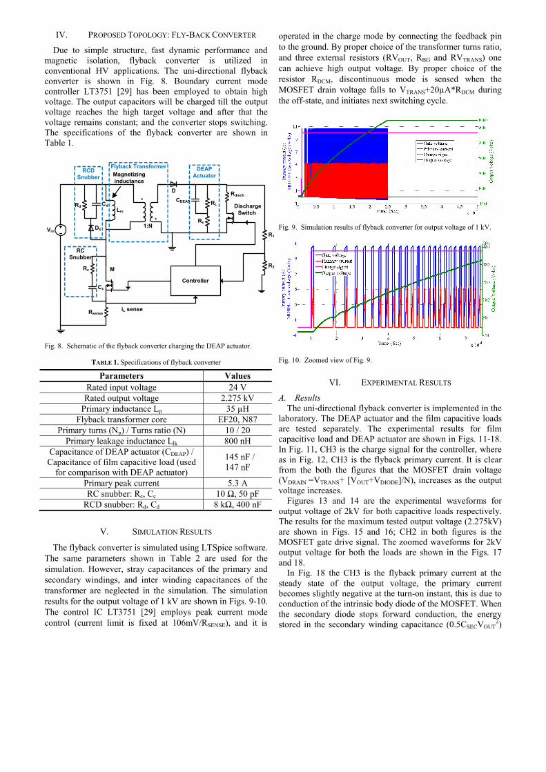
IV. PROPOSED TOPOLOGY: FLY-BACK CONVERTER
Due to simple structure, fast dynamic performance and magnetic isolation, flyback converter is utilized in conventional HV applications. The uni-directional flyback converter is shown in Fig. 8. Boundary current mode controller LT3751 [29] has been employed to obtain high voltage. The output capacitors will be charged till the output voltage reaches the high target voltage and after that the voltage remains constant; and the converter stops switching. The specifications of the flyback converter are shown in Table 1.
Fig. 8. Schematic of the flyback converter charging the DEAP actuator.
TABLE 1. Specifications of flyback converter
Parameters Values Rated input voltage 24 V Rated output voltage 2.275 kV
Primary inductance Lp 35 µH Flyback transformer core EF20, N87
Primary turns (Np) / Turns ratio (N) 10 / 20 Primary leakage inductance Llk 800 nH
Capacitance of DEAP actuator (CDEAP) / Capacitance of film capacitive load (used
for comparison with DEAP actuator)
145 nF / 147 nF
Primary peak current 5.3 A RC snubber: Rc, Cc 10 Ω, 50 pF
RCD snubber: Rd, Cd 8 kΩ, 400 nF
V. SIMULATION RESULTS
The flyback converter is simulated using LTSpice software. The same parameters shown in Table 2 are used for the simulation. However, stray capacitances of the primary and secondary windings, and inter winding capacitances of the transformer are neglected in the simulation. The simulation results for the output voltage of 1 kV are shown in Figs. 9-10. The control IC LT3751 [29] employs peak current mode control (current limit is fixed at 106mV/RSENSE), and it is
operated in the charge mode by connecting the feedback pin to the ground. By proper choice of the transformer turns ratio, and three external resistors (RVOUT, RBG and RVTRANS) one can achieve high output voltage. By proper choice of the resistor RDCM, discontinuous mode is sensed when the MOSFET drain voltage falls to VTRANS+20µA*RDCM during the off-state, and initiates next switching cycle.
Fig. 9. Simulation results of flyback converter for output voltage of 1 kV.
Fig. 10. Zoomed view of Fig. 9.
VI. EXPERIMENTAL RESULTS
A. Results The uni-directional flyback converter is implemented in the
laboratory. The DEAP actuator and the film capacitive loads are tested separately. The experimental results for film capacitive load and DEAP actuator are shown in Figs. 11-18. In Fig. 11, CH3 is the charge signal for the controller, where as in Fig. 12, CH3 is the flyback primary current. It is clear from the both the figures that the MOSFET drain voltage (VDRAIN =VTRANS+ [VOUT+VDIODE]/N), increases as the output voltage increases.
Figures 13 and 14 are the experimental waveforms for output voltage of 2kV for both capacitive loads respectively. The results for the maximum tested output voltage (2.275kV) are shown in Figs. 15 and 16; CH2 in both figures is the MOSFET gate drive signal. The zoomed waveforms for 2kV output voltage for both the loads are shown in the Figs. 17 and 18.
In Fig. 18 the CH3 is the flyback primary current at the steady state of the output voltage, the primary current becomes slightly negative at the turn-on instant, this is due to conduction of the intrinsic body diode of the MOSFET. When the secondary diode stops forward conduction, the energy stored in the secondary winding capacitance (0.5CSECVOUT
2)
iL sense
Vin
M
Lm
1:N
D
R1
R2
CDEAP
Rs
Rsense
*
*
RL
Rdisch
Controller
Discharge Switch
DEAP Actuator
Rc
Cc
CdRd
Ds
Magnetizing inductance
RCD Snubber
RC Snubber
Flyback Transformer

is reflected to the primary. The drain of the MOSFET became negative, when the reflected capacitance was greater than the MOSFET drain capacitance, so the body diode of the MOSFET is conducted. This created a propagation delay, and due to this the charging times in the simulation and in the experiment did not match some times.
Fig. 11. Flyback converter wave forms for output voltage Vout = 1.5kV with Film capacitive load; CH1: Output voltage; CH2: Input current; CH3: Charge signal for the controller; CH4: MOSFET drain voltage.
Fig. 12. Flyback converter wave forms for output voltage Vout = 1.5kV with DEAP actuator as load; CH1: Output voltage; CH2: Input current; CH3: Primary current of flyback transformer; CH4: MOSFET drain voltage.
Fig. 13. Flyback converter wave forms for output voltage Vout = 2kV with Film capacitive load; CH1: Output voltage; CH2: Input current; CH3: Primary current of the flyback transformer; CH4: MOSFET drain voltage.
Fig. 14. Flyback converter wave forms for output voltage Vout = 2kV with DEAP actuator as load; CH1: Output voltage; CH2: Input current; CH3: Primary current of the flyback transformer; CH4: MOSFET drain voltage.
Fig. 15. Flyback converter wave forms for output voltage Vout = 2.275kV with Film capacitive load; CH1: Output voltage; CH2: Input current; CH3: Charge signal for the controller; CH4: MOSFET gate drive signal.
Fig. 16. Flyback converter wave forms for output voltage Vout = 2.275kV with DEAP actuator as load; CH1: Output voltage; CH2: Input current; CH3: Primary current of flyback converter; CH4: MOSFET drain voltage.
Fig. 17. Zoomed wave forms (in the starting) for output voltage Vout = 2kV with Film capacitive load; CH1: Output voltage; CH2: Input current; CH3: Primary current of flyback transformer; CH4: MOSFET drain voltage
Fig. 18. Zoomed wave forms (in the steady state) for output voltage Vout = 2kV with DEAP actuator as load; CH1: Output voltage; CH2: Input current; CH3: Primary current of flyback transformer; CH4: MOSFET drain voltage B. Choice of the high voltage components
We used the high voltage diode VMI SM6525 (5kV and 150 mA) as a secondary diode and the high voltage pulse capacitors RIFA PHE 450 (3000V) as a film capacitive load. The DEAP actuator (PolyPower Push Inslator actuator) rated maximum voltage is 2500V [13].
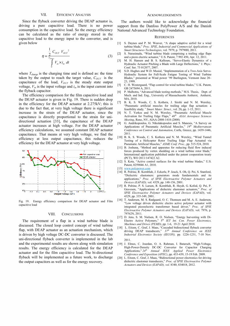
VII. EFFICIENCY ANALYSIS
Since the flyback converter driving the DEAP actuator is, driving a pure capacitive load. There is no power consumption in the capacitive load. So the energy efficiency can be calculated as the ratio of energy stored in the capacitive load to the energy input to the converter, and is given below
where Tcharge is the charging time and is defined as: the time taken by the output to reach the target value, COUT is the capacitance of the load, VOUT is the steady state output voltage, Vin is the input voltage and iin is the input current into the flyback capacitor.
The efficiency comparison for the film capacitive load and the DEAP actuator is given in Fig. 19. There is sudden drop in the efficiency for the DEAP actuator at 2.275kV; this is due to the fact that, at very high voltage there is significant increase in the strain of the DEAP actuator, since the capacitance is directly proportional to the strain for uni-directional actuation [33], the capacitance of the DEAP actuator increases at high voltage. For the DEAP actuator efficiency calculations, we assumed constant DEAP actuator capacitance. That means at very high voltage, we find the efficiency at less output capacitance, this reduces the efficiency for the DEAP actuator at very high voltage.
Fig. 19. Energy efficiency comparison for DEAP actuator and Film capacitive load
VIII. CONCLUSIONS
The requirement of a flap in a wind turbine blade is discussed. The closed loop control concept of wind turbine flap, with DEAP actuator as an actuation mechanism, which is driven by high voltage DC-DC converter is discussed. The uni-directional flyback converter is implemented in the lab and the experimental results are shown along with simulation results. The energy efficiency is calculated for the DEAP actuator and for the film capacitive load. The bi-directional flyback will be implemented as a future work, to discharge the output capacitors as well as for the energy recovery.
ACKNOWLEDGEMENTS
The authors would like to acknowledge the financial support from the Danfoss PolyPower A/S and the Danish National Advanced Technology Foundation.
REFERENCES [1] S. Daynes and P. M. Weaver, “A shape adaptive airfoil for a wind
turbine blade,” Proc. SPIE, Industrial and Commercial Applications of Smart Structures Technologies, vol. 7979, p. 79790H, 2011.
[2] S. Narasimalu, “Wind turbine blade comprising a trailing edge flaps and a piezo electric actuator,” U.S. Patent, 7 992 450, Apr. 12, 2011.
[3] M. H. Hansen and B. S. Kallesøe, “Servo-Elastic Dynamics of a Hydraulic Actuator Pitching a Blade with Large Deflections,” J. Phys.: Conf. Ser. 75 012077, 2007.
[4] S.D. Hughes and W.D. Musial, “Implementation of a Two-Axis Servo- Hydraulic System for Full-Scale Fatigue Testing of Wind Turbine Blades,” presented at Wind power ’99 Burlington, Vermont June 20–23, 1999.
[5] C. H. Westergaard, “Flap control for wind turbine blades,” U.K. Patent, GB 2475694 A, 2011.
[6] P. Malhotra, “Advanced blade testing methods,” M.S. Thesis, Dept. of Mech. and Ind. Eng., University of Massachusetts Amherst, Amherst, MA, 2010.
[7] B. K. S. Woods, C. S. Kothera, J. Sirohi and N. M. Wereley, “Pneumatic artificial muscles for trailing edge flap actuation: a feasibility study,” Smart Mater. Struct., vol. 20, pp. 1-15, 2011.
[8] N. T. Yerkes and N. M. Wereley, “Pneumatic Artificial Muscle Activation for Trailing Edge Flaps,” 46th AIAA Aerospace Sciences Meeting, Reno, NV, AIAA-2008-1418 (2008)
[9] G. Andrikopoulos, G. Nikolakopoulos and S. Manesis, “A Survey on Applications of Pneumatic Artificial Muscles,” 19th Mediterranean Conference on Control and Automation, Corfu, Greece, pp. 1439-1446, 2011.
[10] B. K. S. Woods, C. S. Kothera and N. M. Wereley, “Wind Tunnel Testing of a Helicopter Rotor Trailing Edge Flap Actuated via Pneumatic Artificial Muscles,” ASME Conf. Proc., pp. 515-524, 2010.
[11] B. Joshuna, “Method and apparatus for reducing fluid flow induced forces produced by vortex shedding on a wind turbine rotor blade,” International application published under the patent cooperation treaty (PCT), WO 2011/147422 A2.
[12] S. Kota, “Active control surfaces for the wind turbine blades,” U.S. Patent, 0259046 A1, 2010.
[13] www.polypower.com [14] R. Pelrine, R. Kornbluh, J. Eckerle, P. Jeuck, S. Oh, Q. Pei, S. Stanford,
“Dielectric elastomers: generators mode fundamentals and its applications,” Proc. of SPIE Electroactive Polymer Actuators and Devices (EAPAD), vol. 4329, pp. 148-156, 2001.
[15] R. Pelrine, P. S. Larsen, R. Kornbluh, R. Heydt, G. Kofod, Q. Pei, P. Gravesen, “Applications of dielectric elastomer actuators,” Proc. of SPIE Electroactive Polymer Actuators and Devices (EAPAD), vol. 4329, pp. 335-349, 2001.
[16] T. Andersen, M. S. Rødgaard, O. C. Thomsen and M. A. E. Andersen, “Low voltage driven dielectric electro active polymer actuator with integrated piezoelectric transformer based driver,” Proc. of SPIE Electroactive Polymer Actuators and Devices (EAPAD), vol. 7976, p. 79762N, 2011.
[17] D. Jens, S. M. Nielsen, R. O. Nielsen, “Energy harvesting with Di- Electro Active Polymers,” 5th IET Int. Con. Power Electronics, Machines and Drives (PEMD), pp. 1-6, 19-21 April 2010.
[18] L. Eitzen, C. Graf, J. Maas, “Cascaded bidirectional flyback converter driving DEAP transducers,” 37th Annual Conference on IEEE Industrial Electronics Society (IECON), pp. 1226-1231, 7-10 Nov.
2011. [19] J. Elmes, C. Jourdan, O. A. Rahman, I. Batarseh, “High-Voltage,
High-Power-Density DC-DC Converter for Capacitor Charging Applications,” 24th Annual IEEE Applied Power Electronics Conference and Exposition (APEC), pp. 433-439, 15-19 Feb. 2009.
[20] L. Eitzen, C. Graf, J. Maas, “Bidirectional power electronics for driving dielectric elastomer transducers,” Proc. of SPIE Electroactive Polymer Actuators and Devices (EAPAD), vol. 8340, 834018, 2012.
arg
2
0
1 2 (3)
ch e
OUT OUT
T
in in
C V
V i dt
η =
×∫

[21] S. K. Chung, H. B. Shin, “High-voltage power supply for semi-active suspension system with ER-fluid damper,” IEEE Trans. on Vehi. Tech., vol.53, no.1, pp. 206- 214, Jan. 2004.
[22] T. Barlas and G. V. Kuik, “Review of state of the art in smart rotor control research for wind turbines,” Progress in Aerospace Sciences, vol. 46(1), pp. 1 – 27, 2010.
[23] S. J. Johnson, C. V. Dam, and D. E. Berg. “Active load control techniques for wind turbines,” Technical Report SAND2008-4809, Sandia National Laboratories, 2008.
[24] H. A. Madsen, “The potentials of the controllable rubber trailing edge flap (CRTEF),” in EWEC 2010 proc. online, pp. 1-11, 2010.
[25] C. S. Kothera and N. M. Wereley, “Wind Tunnel Testing of Pneumatic Artificial Muscles for Control Surface Actuation,” in Wind Tunnels InTech, 2011, pp. 105-120.
[26] P. P. Friedmann, G. P. Carman, and T. A. Millott, “Magnetostrictively actuated control flaps for vibration reduction in helicopter rotors–design considerations for implementation,” Int. J. Mathematical and Computer Modelling, vol. 33(10-11), pp. 1203 –1217, 2001.
[27] P. B. Andersen “Advanced Load Alleviation for Wind Turbines using Adaptive Trailing Edge Flaps: Sensoring and Control” PhD thesis, Risø-DTU – National Laboratory for Sustainable Energy, Technical University of Denmark, Denmark, 2010.
[28] J. W. V. Wingerden, A. Hulskamp, T. Barlas, I. Houtzager, H. Bersee, G. V. Kuik, and M. Verhaegen “Two-Degree-of-Freedom Active Vibration Control of a Prototyped Smart Rotor,” IEEE Trans. Contr. Sys. Tech., vol. 19, no. 2, pp. 284-296, March 2011.
[29] “LT3751 High Voltage Capacitor Charger with Regulation Datasheet,” Linear Technology Corporation, USA.
[30] T. Behrens, “Simulation of Moving Trailing Edge Flaps on a Wind Turbine Blade using a Navier-Stokes based Immersed Boundary Method,” Ph.D. thesis, Dept. Mech. Eng., Technical University of Denmark, Denmark, 2011.
[31] http://www.flxsys.com/wind-energy/ [32] A. Bargum, “Adaptive wing flap,” B.S. Thesis, Dept. of Mechatronic
Eng., University of Southern Denmark, Sønderborg, Denmark, 2010. [33] P. Thummala, L. Huang, Z. Zhang and M. A. E. Andersen, “Analysis of
Dielectric Electro Active Polymer Actuator and its High Voltage Driving Circuits,” IEEE International Power Modulator and High Voltage Conference (IPMHVC), San Diego, CA, pp. , Jun. 4-7, 2012.

Appendix CBattery Powered High OutputVoltage Bidirectional Flyback
Converter for Cylindrical DEAPActuator
2012 IEEE International Power Modulator and High Voltage Conference (IPMHVC2012)
75/255

Battery Powered High Output Voltage Bidirectional Flyback Converter for Cylindrical DEAP Actuator
Lina Huang, Prasanth Thummala, Zhe Zhang, Michael A. E. Andersen [email protected], [email protected], [email protected],
Technical University of Denmark, Department of Electrical Engineering, DK-2800 Kgs. Lyngby, Denmark [email protected]
ABSTRACT DEAP (Dielectric Electro Active Polymer) actuator is
essentially a capacitive load and can be applied in various actuation occasions. However, high voltage is needed to actuate it. In this paper, a high voltage bidirectional flyback converter with low input voltage is presented. The fundamental operating principle for both energy transfer process and energy recovery process is analyzed in detail. In order to verify the analysis, critical simulation results are provided. So far, a unidirectional flyback converter, which can realize the energy transfer process, has been implemented in the lab. The design parameters for flyback transformer and snubber circuits are illustrated. Moreover, the experimental waveforms are provided.
Index Terms — DEAP actuator, high voltage, flyback, bidirectional
1 INTRODUCTION
DEAP (Dielectric Electro Active Polymer) is a new type of polymer material, which consists of a soft silicone polymer, sandwiched between two compliant metallic electrodes [1]. The similar structure to a capacitor enables DEAP to be fundamentally considered as a capacitive load. Figure 1 shows the measured impedance of DEAP material at low frequency. The -90 degrees phase angle can sufficiently illustrate the capacitive property of DEAP.
101
102
103
104
105
106
Impe
danc
e (o
hm)
Frequency (Hz)
101
102
103-180
-135
-90
-45
0
45
90
135
180
Pha
se (d
eg)
ImpedancePhase
Figure 1. Impedance measurement of DEAP material
When a voltage is applied to DEAP material, the polymer will
compress in thickness and expand in area due to the electric field [2]; therefore, DEAP can be used as an actuator. Compared to traditional electro-magnetic, pneumatic or hydraulic actuators, capacitive actuator possesses many advantages, such as high power density, low weight, fast and direct actuation, high actuating precision, extremely low steady-state power consumption, low noise, etc.
Because of the simple design and immense applicable occasions, cylindrical DEAP actuator, which only performs linear motion, will be an effective replacement for many conventional actuators. Figure 2 shows a cylindrical DEAP actuator [3].
Figure 2. Cylindrical DEAP actuator
The stroke-voltage response of cylindrical DEAP actuator
shown in Figure 2, is demonstrated in Figure 3 [4]. It is obvious that DEAP actuator needs high voltage to be fully elongated.
0 500 1000 1500 2000 25000
0.2
0.4
0.6
0.8
1
1.2
1.4
Voltage (V)
Stro
ke (m
m)
Figure 3. Stroke-voltage characteristic of cylindrical DEAP actuator
Owing to the low weight of DEAP actuator, it can be used in the
portable or autonomous systems, where the battery will be the only power source. Therefore, for stimulating DEAP, a DC-DC converter which can convert low input voltage to high output voltage will be necessary. Combined with the capacitive property
978-1-4673-1225-7/12/$31.00 ©2012 IEEE 454
of DEAP material and the objective to extend the lifetime of battery, a bidirectional flyback converter can be a good choice, which can not only boost the low voltage to several thousand volts, but also can recover the stored electrical energy when DEAP actuator is released. Furthermore, due to the simple topology of flyback, the converter can be realized in small size, which is vital in the portable or autonomous applications.
This paper analyzes the working principle of bidirectional flyback converter to drive cylindrical DEAP actuator and validates the feasibility through simulation in Section 2. Until now, only the unidirectional flyback converter was realized in the lab, which can boost the output voltage to 2.5kV from a 3V battery and will be addressed in Section 3. And conclusion is drawn in Section 4.
2 BIDIRECTIONAL FLYBACK ANALYSIS For DEAP actuator, only a small portion of stored electrical
energy is converted into mechanical response [5]; therefore, it can approximately be considered as a pure capacitor load in order to simplify the analysis.
2.1 TOPOLOGY AND WORKING PRINCIPLE
The bidirectional flyback converter is shown in Figure 4, consisting of coupled inductors in the middle and active power switches in both primary and secondary side.
-+
*
*
S1 S2
DEAPActuator
+
-
T3V
Battery
LP LS
ILp ILs Vout
VG1 VG2
1:N
Figure 4. The topology of bidirectional flyback converter
a) Energy transfer process analysis
When driving DEAP actuator, the electrical energy is transferred to capacitive load from battery. Actually, the energy transfer process includes a series of switching cycles. For each cycle, the primary inductor LP is magnetized in the on-time of S1 to accumulate magnetic energy. Then in the off-time of S1, through body diode of S2, the stored energy will be transferred to DEAP actuator from coupled secondary inductor LS. Ideally, the magnetic energy of LS is totally transformed into electrical energy in the capacitive actuator. Moreover, based on the basic principle of LC resonant circuit, in every off-time of S1, inductor current of LS and output voltage Vout can be expressed in (1) and (2), respectively.
( ) (0) cos
(0) sin
S SL LS DEAP
DEAPout
S S DEAP
ti t iL C
C tVL L C
(1)
( ) (0) cos
(0) sinS
out outS DEAP
SL
DEAP S DEAP
tV t VL C
L tiC L C
(2)
where LS is the inductance of secondary coupled inductor, CDEAP is the capacitance of DEAP actuator, and iLs(0), Vout(0) are the initial current and voltage for inductor and actuator, respectively.
In order to reduce the charge time of fully elongating DEAP actuator and completely transfer the energy stored in the flyback transformer in each cycle, a boundary mode control strategy can be used [6]. When the current through the body diode of S2 accomplishes freewheeling in the previous cycle, the next cycle immediately starts. In addition, primary peak current control is employed to guarantee the sufficient utilization of magnetic core as well as to avoid its saturation. The fixed input voltage from battery and the application of peak current control make primary conduction time a constant value. However, with the increasing of output voltage, the freewheeling time in secondary side will decrease. That means the switching frequency is variable, and in the early stage of charge, the converter operates in low frequency, whereas at the end, the working frequency becomes high. Although the unfixed operating frequency accelerates the charging process, it also brings some challenges in designing the transformer and analyzing the power loss. The waveforms of first several cycles in charging process are shown in Figure 5.
ILp(t)
ILs(t)
Vout(t)
VG1(t)
t
t
t
t
ON ON ONOFF OFF OFF
Figure 5. Waveforms in the energy transfer process
b) Energy recovery process analysis
For the purpose of increasing the service life of battery, it is pivotal to recover the energy stored in DEAP actuator when it is released. Like the charge process, the energy recovery process also consists of many successive switching cycles. Only S2 and the body diode of S1 work in the discharging process. In each cycle, LS obtains magnetic energy from DEAP actuator in the on-time of S2 and releases the stored energy to primary side in the off-time of S2.
455

Similar to energy transfer stage, boundary mode control scheme and secondary peak current control are also adopted in discharge process. The waveforms of first several cycles in the energy recovery process are shown in Figure 6.
Vout(t)
VG2(t)
t
t
tt
ILp(t)
ILs(t)
ON OFFON ONOFF OFF
Figure 6. Waveforms in energy recovery process
2.2 SIMULATION VERIFICATION
For validating the analysis mentioned above, a bidirectional flyback converter simulation model has been established with PLECS (Piecewise Linear Electrical Circuit Simulation) software. In addition, a boundary operation mode and peak current control module is also built up. The detailed simulations parameters are shown in Table 1.
Table 1. Simulation parameters for bidirectional flyback converter
Simulation Parameters Values LP 9 H LS 21.36 mH
Capacitance of DEAP actuator 142 nF Vin 3 V
Primary peak current 3.9 A Secondary peak current 80 mA
N 48.7
a) Energy transfer process simulation Figure 7 shows the whole charge process, in which the
output voltage increases from 0 to 2.5kV.
0 10 20 30 40 50 60 70 800
500
1000
1500
2000
2500
Time (ms)
Vou
t (V
)
Figure 7. Simulated output voltage waveform in the energy transfer process
In the first several cycles, the current waveforms for both primary and secondary side are shown in Figure 8, which indicates that the boundary mode operation is achieved. Owing to the employment of boundary mode, the charge time is short, only less than 80ms.
0 0.05 0.1 0.15 0.2 0.25 0.30
2
4
Prim
ary
Cur
rent
(A)
Time (ms)0 0.05 0.1 0.15 0.2 0.25 0.3
0
0.05
0.1
Sec
onda
ry C
urre
nt (A
)
Figure 8. Simulated current waveform in the energy transfer process
b) Energy recovery process simulation
The output voltage decreases from 2.5kV to 0 in the energy recovery process, shown in Figure 9. And the current waveforms are provided in Figure 10, which also demonstrates the realization of boundary mode in discharge process.
80 100 120 140 160 180 2000
500
1000
1500
2000
2500
Time (ms)
Vou
t (V
)
Figure 9. Simulated output voltage waveform in the energy recovery process
100.14 100.15 100.16 100.17 100.18 100.19 100.2
-4
-2
0
Prim
ary
Cur
rent
(A)
Time (ms)100.14 100.15 100.16 100.17 100.18 100.19 100.2
-0.1
0S
econ
dary
Cur
rent
(A)
Figure 10. Simulated current waveform in the energy recovery process
456

3 UNIDIRECTIONAL FLYBACK DESIGN AND REALIZATION
A unidirectional flyback converter to drive DEAP actuator,
shown in Figure 11, has been realized in the lab. Because of the voltage stress issue of S1, a RC snubber and a RCD clamp circuits are employed [7].
*
*T1
D1
S1
Cs
Rs
DEAP Actuator
Coss
Llk
Ccp Rcp
Dcp
LP LS
-+3V
BatteryCin
Iin +
-Vout
Figure 11. Unidirectional flyback converter
3.1 DESIGN PARAMETERS
The detailed design parameters are shown in Table 2, including the parameters of transformer, RC and RCD circuit.
Table 2. Design parameters for unidirectional flyback converter
Parameters Values Turns ratio (primary turns : secondary turns) 7:341
Core type (Core material) EF20 (N67) Air gap length 250 m
Lp 9 H Ls 21.36 mH
Leakage inductance Llk 750 nH Capacitance of DEAP actuator 142 nF
Rs of RC snubber circuit 68.1 Cs of RC snubber circuit 220 pF
Rcp of RCD clamp circuit 20 k Ccp of RCD clamp circuit 1 F
3.2 EXPERIMENTAL WAVEFORMS
The experimental waveforms are shown in Figure 12, Figure 13 and Figure 14. From Figure 12, it is clear to see the variable switching frequency which is caused by the boundary mode operation.
Figure 12. Experimental waveforms (CH1-input current Iin; CH2-charge control signal for converter; CH3-gate signal of S1; CH4-output voltage)
The peak current control can be validated in Figure 13 and the whole energy transfer process is shown in Figure 14.
Figure 13. Experimental waveforms (CH1-primary winding current; CH2-charge control signal for converter; CH3-input voltage; CH4-output voltage)
Figure 14. Experimental waveforms (CH1-input current Iin; CH2-charge control signal for converter; CH3-input voltage; CH4-output voltage)
4 CONCLUSION A high voltage bidirectional flyback converter driving
DEAP actuator is presented. The detailed analysis for both the energy transfer and the recovery process is discussed. The simulation results are provided to support analysis. In addition, a unidirectional flyback prototype has been implemented in the lab, which can charge DEAP actuator to 2.5kV.
REFERENCES [1] M. Y. Benslimane, H. E. Kiil and M. J. Tryson, “Electro-mechanical
properties of novel large strain PolyPower film and laminate components for DEAP actuator and sensor applications”, Proceedings of SPIE, Vol. 7642, 2010.
[2] M. Y. Benslimane, H. E. Kiil and M. J. Tryson, “Dielectric electro-active polymer push actuators: performance and challenges”, Polymer International, Vol. 59, No. 3, pp. 415-421, 2010.
[3] T. Andersen, M. S. Rødgaard, O. C. Thomsen and M. A. E. Andersen, “Low voltage driven dielectric electro active polymer actuator with integrated piezoelectric transformer based driver”, Proceedings of SPIE, Vol. 7976, 2011.
[4] R. Sarban, R. W. Jones, B. R. Mace and E. Rustighi, “A tubular dielectric elastomer actuator: Fabrication, characterization and active vibration isolation”, Mechanical Systems and Signal Processing, Vol.25 No. 8. , pp. 2879-2891, 2011.
[5] M. J. Tryson, R. Sarban, K. P. Lorenzen, “The dynamic properties of tubular DEAP actuators”, Proceedings of SPIE, Vol. 7642, 2010.
[6] “LT3750 Capacitor Charger Controller Datasheet”, Linear Technology Corporation, USA.
[7] “Application Note AN-4147 Design Guidelines for RCD Snubber of Flyback Converters”, Fairchild Semiconductor Corporation, USA, 2006.
457

80/255
Appendix DHigh Voltage Bi-directional
Flyback Converter for CapacitiveActuator
15th European Conference on Power Electronics and Applications (EPE ECCE Eu-rope 2013)
81/255
High Voltage Bi-directional Flyback Converter for Capacitive Actuator
Prasanth Thummala, Zhe Zhang and Michael A. E. Andersen TECHNICAL UNIVERSITY OF DENMARK
Oersteds Plads, Building 349 Kongens Lyngby, Denmark
Tel.: +45–45255764. E-Mail: [email protected]
URL: http://www.ele.elektro.dtu.dk
Keywords «High voltage power converters», «Switched-mode power supply », «Energy efficiency», «Actuator», «Electroactive materials».
Abstract This paper presents a high voltage DC-DC converter topology for bi-directional energy transfer between a low voltage DC source and a high voltage capacitive load. The topology is a bi-directional flyback converter with variable switching frequency control during the charge mode, and constant switching frequency control during the discharge mode. The converter is capable of charging the capacitive load from 24 V DC source to 2.5 kV, and discharges it to 0 V. The flyback converter has been analyzed in detail during both charge and discharge modes, by considering all the parasitic elements in the converter, including the most dominating parameters of the high voltage transformer viz., self-capacitance and leakage inductance. The specific capacitive load for this converter is a dielectric electro active polymer (DEAP) actuator, which can be used as an effective replacement for conventional actuators in a number of applications. In this paper, the discharging energy efficiency definition is introduced. The proposed converter has been experimentally tested with the film capacitive load and the DEAP actuator, and the experimental results are shown together with the efficiency measurements.
Introduction High voltage power converters are widely used in medical, airborne and space applications with voltage range from 5 kV to 100 kV and with a power level of few tens of watts to several hundred kilowatts. A number of applications require a capacitive load to be charged to several thousands of volts. Such applications include pulsed lasers, pulsed sonar equipment, photo flash systems, electric fences, and plasma research, which require high voltage DC power supplies to efficiently charge a large capacitive load to high voltage. Design of efficient high voltage power supplies is very vital in terms of selection of converter configuration, switching frequency, and control strategy. All these vital aspects are very closely related to the high voltage transformer used in the power converter.
The focus of our research is to develop high voltage DC power supplies for DEAP actuators, which are a special type of capacitive actuators made with dielectric electro active material, and require high voltage (~2.5 kV) at relatively low current, to fully actuate them. The dielectric electro active polymer is a thin silicon elastomer film (~20-80 µm) sandwiched between two metallic electrodes. Due to requirement of very high electric field strength of >40 V/µm, the material needs high operating voltage to completely elongate the actuator [1]. DEAP technology has a wide potential in actuator, energy harvesting and sensor applications [2], [3] due to the material unique properties such as light weight, very low electrical power consumption, flexible nature, low noise and higher performance than competing technologies. DEAP actuators have some interesting applications in linear incremental motors, loud speakers, in-line heating valves, and wind turbine flaps, etc. [4], [5].
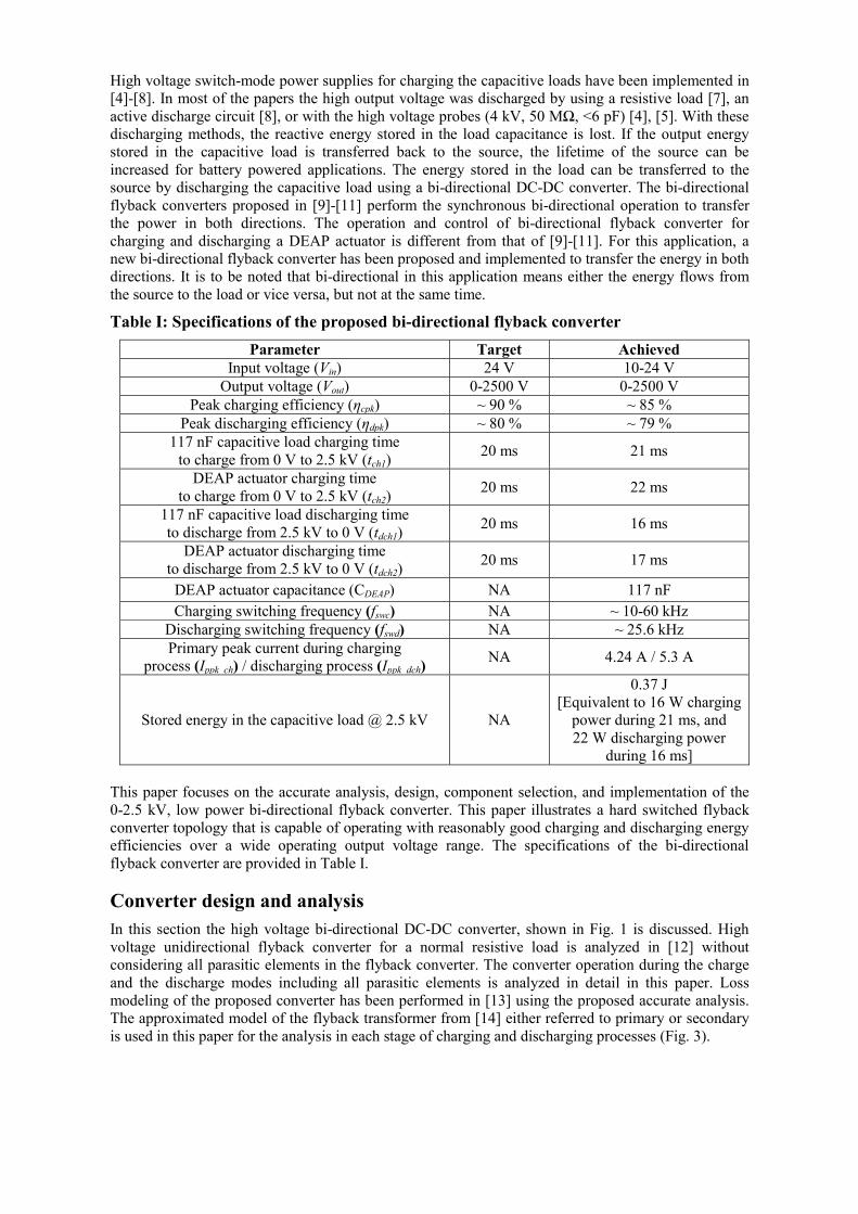
High voltage switch-mode power supplies for charging the capacitive loads have been implemented in [4]-[8]. In most of the papers the high output voltage was discharged by using a resistive load [7], an active discharge circuit [8], or with the high voltage probes (4 kV, 50 MΩ, <6 pF) [4], [5]. With these discharging methods, the reactive energy stored in the load capacitance is lost. If the output energy stored in the capacitive load is transferred back to the source, the lifetime of the source can be increased for battery powered applications. The energy stored in the load can be transferred to the source by discharging the capacitive load using a bi-directional DC-DC converter. The bi-directional flyback converters proposed in [9]-[11] perform the synchronous bi-directional operation to transfer the power in both directions. The operation and control of bi-directional flyback converter for charging and discharging a DEAP actuator is different from that of [9]-[11]. For this application, a new bi-directional flyback converter has been proposed and implemented to transfer the energy in both directions. It is to be noted that bi-directional in this application means either the energy flows from the source to the load or vice versa, but not at the same time.
Table I: Specifications of the proposed bi-directional flyback converter Parameter Target Achieved
Input voltage (Vin) 24 V 10-24 V Output voltage (Vout) 0-2500 V 0-2500 V
Peak charging efficiency (ηcpk) ~ 90 % ~ 85 % Peak discharging efficiency (ηdpk) ~ 80 % ~ 79 %
117 nF capacitive load charging time to charge from 0 V to 2.5 kV (tch1)
20 ms 21 ms
DEAP actuator charging time to charge from 0 V to 2.5 kV (tch2)
20 ms 22 ms
117 nF capacitive load discharging time to discharge from 2.5 kV to 0 V (tdch1)
20 ms 16 ms
DEAP actuator discharging time to discharge from 2.5 kV to 0 V (tdch2)
20 ms 17 ms
DEAP actuator capacitance (CDEAP) NA 117 nF Charging switching frequency (fswc) NA ~ 10-60 kHz
Discharging switching frequency (fswd) NA ~ 25.6 kHz Primary peak current during charging
process (Ippk ch) / discharging process (Ippk dch) NA 4.24 A / 5.3 A
Stored energy in the capacitive load @ 2.5 kV
NA
0.37 J [Equivalent to 16 W charging
power during 21 ms, and 22 W discharging power
during 16 ms] This paper focuses on the accurate analysis, design, component selection, and implementation of the 0-2.5 kV, low power bi-directional flyback converter. This paper illustrates a hard switched flyback converter topology that is capable of operating with reasonably good charging and discharging energy efficiencies over a wide operating output voltage range. The specifications of the bi-directional flyback converter are provided in Table I.
Converter design and analysis In this section the high voltage bi-directional DC-DC converter, shown in Fig. 1 is discussed. High voltage unidirectional flyback converter for a normal resistive load is analyzed in [12] without considering all parasitic elements in the flyback converter. The converter operation during the charge and the discharge modes including all parasitic elements is analyzed in detail in this paper. Loss modeling of the proposed converter has been performed in [13] using the proposed accurate analysis. The approximated model of the flyback transformer from [14] either referred to primary or secondary is used in this paper for the analysis in each stage of charging and discharging processes (Fig. 3).

Topology Flyback converter topology had been widely used because of its relatively simple structure and better performance for single or multiple output applications. It can save the cost and volume compared with the other converters. Flyback converter is a well-suited topology for low power (< 200 W) and high output voltage applications. Some high voltage applications of flyback converter are in cathode ray tube (CRT) for televisions, monitors and in xenon flash lamps for exciting the xenon gas. The power stage of Fig. 1a can be divided into three parts: primary stage, high voltage flyback transformer and secondary stage. The primary stage consists of a DC voltage source, input capacitor Cin, and low voltage MOSFET M1. The flyback transformer with 1: n turns ratio is provided with an air gap, to store the energy in the magnetizing winding when the switch M1 is turned ON. In the transformer model shown in Fig. 1b, Lmp, Cp, Cint, Cs, Llkp, Llks, Rp, and Rs represent the primary magnetizing inductance, primary self-capacitance, interwinding capacitance, secondary self-capacitance, primary and secondary leakage inductances, primary DC resistance, and secondary DC resistances, respectively. The secondary stage consists of high voltage MOSFET M2, high voltage diode D2, which is required as the body diode of M2 has very high reverse recovery time (trr=2.8 µs), another high voltage diode Db added in series with the drain of M2, to block the body diode of M2 during the discharging process, and a high voltage capacitive load Cout.
Fig. 1: Circuit configuration of the high voltage bi-directional flyback converter (a); with equivalent transformer model, and RC snubber on low voltage side and RCD snubber on high voltage side (b). If a snubber circuit is not used in the flyback converter, then the stored energy in the leakage inductance is dissipated in the MOSFET resulting in large voltage spikes across it. In this capacitor charging application, on the primary side only a RC snubber has been used which can damp the high frequency oscillations in the drain voltage waveform, when the switch is OFF. The RCD snubber on the low voltage side can be skipped by either using an overrated low voltage MOSFET M1 or by reducing the transformer leakage inductance. The stray capacitance of the transformer contributes to capacitive switching loss. We are investigating how to reduce both the leakage inductance and stray capacitance of the flyback transformer, and to make a trade-off between them for this high voltage capacitor charging application [13]. On the high voltage side a RCD snubber has been used to protect the high voltage MOSFET M2 from the voltage spikes due to the secondary leakage inductance during discharging. As the maximum drain voltage of M2 used in the converter is 4 kV, and with 24 V as input voltage and n=25 as the turns ratio, the maximum drain voltage of M2 excluding the voltage increase due to secondary leakage inductance, at 2.5 kV output voltage is 3.1 kV. If the leakage inductance of the flyback transformer secondary is considered, the voltage seen by the drain of M2 will be higher
than by a factor of
12
2sec2sec22
sspk
lks lks
C RI CL L
−⎡ ⎤⎛ ⎞⎛ ⎞⎢ ⎥⎜ ⎟⋅ − ⎜ ⎟⎢ ⎥⎜ ⎟⎝ ⎠⎢ ⎥⎝ ⎠⎣ ⎦
(see (12)). Even though a passive snubber (RC
or RCD) protects the MOSFET, it results in high power loss. To eliminate this power loss, active snubber circuits can be used at the cost of extra components. The circuit configuration of the practical
••
•
•

flyback converter with the transformer equivalent model and the low and high voltage snubber circuits is shown in Fig. 1b.
Converter analysis during charging process A soft-switched flyback converter is analyzed in [6] for high voltage capacitor charging application. While charging the capacitive load the proposed converter operates in the boundary mode (boundary between CCM and DCM), with peak current control using LT3751 [15]. The MOSFET M1 is turned OFF when the primary current reaches the peak current Ippk. The waveforms of the converter during the charge operation are shown in Fig. 2a. In general, self-capacitance of the transformer low voltage winding (Cp) is very small compared to that of the high voltage winding, and hence can be neglected. One complete switching period Ts, during the charge mode can be divided into four stages. These stages operate continuously until the desired output voltage is reached. The first stage will begin after the transformer primary has finished storing the energy or when the primary MOSFET is turned OFF.
Stage 1 [t0 < t ≤ t1]
During this stage the MOSFET M1 is OFF and the high voltage diode D2 is blocked. The equivalent parasitic capacitance referred to the primary side (Cpri) when both the switch M1 and the diode D2 are OFF, is the parallel combination of the output capacitance of M1, the transformer secondary self-capacitance referred to the primary side, and the equivalent reflected parasitic capacitance of high voltage diodes (M2 is OFF during the charging process), and is given by
2
1 2
2
2b
b
D Mpri M s D
D M
C CC C C C n
C C
⎡ ⎤⎛ ⎞= + + +⎢ ⎥⎜ ⎟⎜ ⎟+⎢ ⎥⎝ ⎠⎣ ⎦
(1)
The magnetizing current ip charges the equivalent parasitic capacitance Cpri1=Cpri in a resonant manner. The current through the magnetizing inductance mpL is ( ) ( )( )1priC pi t i t= −
( ) ( ) ( ) ( )( ) ( ) ( )( )0 01 0 0 0 0 0 0 0 0 0 0 cos sinC t t
p pri C C in C C C C in C Ci t C e K V t t K V t tα β α β α β β− − ⎡ ⎤= − − − − + −⎣ ⎦ (2)
The voltage across the transformer primary winding is
( ) ( ) ( )( ) ( )( ) ( ) ( ) ( )( )
( ) ( ) ( ) ( )
0 0
1 1 1
1 1
00 0 0 0 0 0 1
20 0 0 0 0 0 1 0 1
1 0 1
cos sin ; ;
1 1; ; ; ; 02
C
pri pri pri
out HVdt tC in C C C C in C
ppkPC C C C in C p p M ppk M
mp mp pri C pri
V t VV t e V t t K t t V t V V t
n
IRK V i t i t i t I i t
L L C C
α β β
α β α αβ
− − − +⎡ ⎤= − + − = =⎣ ⎦
⎛ ⎞ ⎛ ⎞= = − = − = = = =⎜ ⎟ ⎜ ⎟⎜ ⎟ ⎜ ⎟
⎝ ⎠ ⎝ ⎠
(3)
Stage 2 [t1 < t ≤ t2] During this stage the voltage across the primary winding of the transformer is clamped to the reflected voltage of ( )( )0out HVdV t V n− + . The diode in the secondary side is turned-ON and the magnetizing current flows to the secondary side, and delivers the energy stored in Lmp to the output capacitor Cout.
The primary leakage and secondary currents, and voltage across drain of M1, and the output voltage are
( ) ( ) ( )( ) ( )( ) ( ) ( )( ) ( ) ( )( )
( ) ( ) ( )( )( ) ( )( ) ( )( )( ) ( )( )
2 1 2 1
1
1
1 1
122 1 2 1 2 1
2 2
s 1 1 1 1 1 1 1 1 1 1 1 1
cos sin ; sin
( ) cos sin
C C
C
out HVdt t ppk t tClkp ppk C C M in C
C C M
t t lkpout C C out HVd C C C C out HVd C C
o
V t V Ii t I e t t t t V t V e t t
n C
i ti t C e K V t V t t K V t V t t
n
V
α α
α
αβ β ββ β
β α β α β β
− − − −
− −
+⎡ ⎤= − − − = + + −⎢ ⎥
⎣ ⎦
⎡ ⎤= − + − − + + − +⎣ ⎦
( ) ( ) ( )( ) ( )( ) ( )( ) ( ) ( )
( ) ( )( )
1 1
1
1 1 1 1 1 1 1 2
2 21 1 2 2 1 1 1
1
cos sin ; ; 2 2
1 1 1; ;
4C t t ps HVdut out HVd C C C HVd C C
ms lks lkp
spkC C C C C out HVd C
ms lks out lkp M C out
RR rt e V t V t t K t t VL L L
IK V t V
L L C L C C
α β β α α
β α β α αβ
− − +⎡ ⎤= + − + − − = =⎣ ⎦ +
⎛ ⎞⎛ ⎞ ⎛ ⎞= − = − = + +⎜ ⎟⎜ ⎟ ⎜⎜ ⎟ ⎜ ⎟+ ⎝ ⎠⎝ ⎠ ⎝ ⎠
⎟

where HVdV and HVdr are the voltage drop and resistance of the high voltage diode ( )2 or DbD respectively. This stage ends when the secondary current falls to 0 A, and
12 =pri MC C (Fig. 3).
Stage 3 [t2 < t ≤ t3]
This stage occurs after the energy stored in Lmp is completely transferred to the output capacitor Cout. In this stage the output capacitance of M1 resonates with the magnetizing inductance Lmp by bringing the voltage across M1 close to 0 V. In this stage, the equivalent reflected capacitance Cpri3=Cpri1=Cpri
discharges through M1 and ( ) ( )3priC pi t i t= − .
The current through the magnetizing inductance and voltage across the primary winding are
( ) ( ) ( )( ) ( )( )
( ) ( ) ( )( ) ( )( ) ( )( ) ( )
0 2
0 2
3 3
20 2
0
2 00 2 0 2 3
0
1 sin
cos sin ;
C
C
pri pri
out HVdt tp C
mp C
out HVdt t CC C C C in
C
V t Vi t e t t
n L
V t VV t e t t t t V t V
n
α
α
ββ
αβ ββ
− −
− −
⎛ ⎞ ⎡ ⎤− += −⎜ ⎟ ⎢ ⎥⎜ ⎟ ⎢ ⎥⎣ ⎦⎝ ⎠
⎛ ⎞− + ⎡ ⎤= − + − =⎜ ⎟ ⎢ ⎥⎜ ⎟ ⎣ ⎦⎝ ⎠
(5)
The voltage across MOSFET M1 is
( ) ( ) ( )1 3 1 3 0
priM in C MV t V V t ; V t= + = (6)
By solving (5) and (6), and using 0Cα and 0Cβ from (3)
( )( )( )( ) ( )0 3 2
220 0
0 3 2 0 0 02 230 2
1sin ; ; C
C C inC C C Ct t
mp priC out HVd
w V nt t G G w
L Cw G V t V e α
ββ α β− −
⎡ ⎤ ⋅− = ⋅ + − = =⎢ ⎥
+⎢ ⎥⎣ ⎦ (7)
The peak negative amplitude of the equivalent capacitor Cpri3 current at the time t3 is
( )3
23 2 0
3 20 0
12pri
P priin CC
mp C C
R CVi t G
L w wβ⎡ ⎤
= + −⎢ ⎥⎢ ⎥⎣ ⎦
(8)
Stage 4 [t3 < t ≤ Ts ]
Stage 4 begins when M1 is turned-ON by the controller under ZVS conditions. The current through the MOSFET M1 flows in the negative direction (Fig. 2a) through its body diode for a short time, and then it continue to flow through M1. The currents through 4priC , transformer primary and MOSFET M1 are
( ) ( )( )( ) ( )( )( ) ( )( )
( )( )
( )
33 3
4
13
4 1 4
34 3 3 3 3 3 3 3 3
4
31 1
( ) cos sin
( ) ; ( ) ( )
priC
pri pri
p dson
mp lkp
pri pri
Ct tC pri C C C C in C C
pri
R rt t
L L lkpin inp p C M p C
p dson p dson mp
i ti t C e t t K V t V t t
C
LV Vi t i t e i t i t i t i
R r R r L
α β α β β− −
+− −
+
⎡ ⎤= − − + − −⎢ ⎥
⎢ ⎥⎣ ⎦⎡ ⎤⎛ ⎞⎢ ⎥= + − − = +⎜ ⎟⎜ ⎟+ +⎢ ⎥⎝ ⎠⎣ ⎦
( )( ) ( ) ( )3
3 2 2
32 213 3 3 3 3 3 4
4 3 4
( ) (9)
1 1; ; ; 2
pri
pri
CdsonC C C C C in C pri s M D
lkp lkp pri C pri
t
i trK V t V C n C C C
L L C Cα β α α
β⎛ ⎞⎛ ⎞
= = − = − + = ⋅ + +⎜ ⎟⎜ ⎟⎜ ⎟ ⎜ ⎟⎝ ⎠ ⎝ ⎠
Converter analysis during discharging process The same controller LT3751 [15] is used in the proposed bi-directional flyback converter for discharging the capacitive load. During discharging process, the converter operates in the discontinuous conduction mode (DCM) with constant switching frequency. The converter waveforms during the discharging operation are shown in Fig. 2b. The capacitive load is discharged when the high voltage MOSFET M2 is turned ON, and transfer the energy stored in the secondary magnetizing winding Lms to the source, through the body diode of M1, when M2 is OFF. As the output voltage discharges, the ON-

time of the high voltage MOSFET M2 increases, and OFF-time is constant with a value of _dchmp ppk
in
L iV .
At the end of the discharging process M2 is completely turned ON. The switching period Ts during discharging operation can be divided into 5 stages. The Stage 1 begins once the secondary magnetizing inductance Lms of the transformer has finished storing the energy.
Fig. 2: Charging (a) and discharging (b) waveforms of the proposed converter.
Fig. 3: All charging and discharging stages in one respective charging and discharging switching cycle
( )in outV V n+
in outnV V+
in outnV V+
ppkI
spkI
4
12r
lkp pri
fL Cπ
=
1
12
=rlkp M
fL Cπ
ppkI−
spkI−
oin
VV n+
in outnV V V+ + Δ
in onV V+
12r
lks sec
fL Cπ
=
( )1
2r
ms lks sec
fL L Cπ
=+
spkI−
ppkI−
oin
VV n+
in outnV V V+ + Δ
in outnV V+
in outnV V+
spkI
•
•
•
•
•
•
•
•
•
•
•
•
•
••
•
•
•
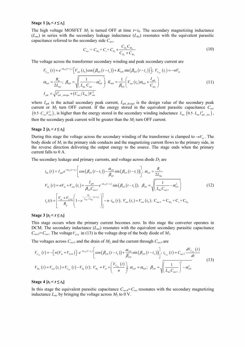
Stage 1 [t0 < t ≤ t1]
The high voltage MOSFET M2 is turned OFF at time t=t0. The secondary magnetizing inductance (Lms) in series with the secondary leakage inductance (Llks) resonates with the equivalent parasitic capacitance referred to the secondary side Csec.
2
2
b
2 2
b
D Msec M s D
D M
C CC = C +C +C
C C+
+ (10)
The voltage across the transformer secondary winding and peak secondary current are
( ) ( ) ( ) ( )( ) ( )( ) ( )
( )
( )
0
sec sec0 0 0 0 1
20 0 0 0 0 0
sec 0 sec
2 2_ sec
cos sin ;
1 1; ; 2 C
D ot tC out D o D D o C in
spkSD D D D out D
ms ms D
spk spk design ms out
V t e V t t t K t t V t nV
IRK V t
L L C
I I C L V
α β β
α β α αβ
− − ⎡ ⎤= − + − = −⎣ ⎦
⎛ ⎞ ⎛ ⎞= = − = +⎜ ⎟ ⎜ ⎟
⎝ ⎠ ⎝ ⎠
= +
(11)
where Ispk is the actual secondary peak current, Ispk_design is the design value of the secondary peak current or M2 turn OFF current. If the energy stored in the equivalent parasitic capacitance Csec
( )20 5 ⋅ sec out. C V , is higher than the energy stored in the secondary winding inductance msL ( )20 5 ⋅ ms spk _ des. L I , then the secondary peak current will be greater than the M2 turn OFF current.
Stage 2 [t1 < t ≤ t2]
During this stage the voltage across the secondary winding of the transformer is clamped to innV− . The body diode of M1 in the primary side conducts and the magnetizing current flows to the primary side, in the reverse direction delivering the output energy to the source. The stage ends when the primary current falls to 0 A.
The secondary leakage and primary currents, and voltage across diode D2 are
( ) ( ) ( )( ) ( )( )
( ) ( ) ( ) ( )( )
( )( )
1 1
1 1
2
1
11 1 1 1 1
1
21 1 1 1 1
1 sec 2 sec 2
cos sin ; 2
1sin ;
( ) 1 ;
D
D
p
mp lkp
t t sDlks spk D D D
D lks
spk t tD in out D D D
D lks
Rt t
L Lin LVdp lks
p
Ri t I e t t t t
L
IV t nV V t e t t
C L C
V Vi t e n i t
R
α
α
αβ β αβ
β β αβ
− −
− −
− −+
⎡ ⎤= − − − =⎢ ⎥
⎣ ⎦
⎛ ⎞= + + − = −⎜ ⎟
⎝ ⎠
⎡ ⎤⎛ ⎞+⎢ ⎥⎜ ⎟= − − ⋅⎢ ⎥⎜ ⎟
⎝ ⎠⎣ ⎦( ) ( )
2 21 0 sec 2 M D; C = C + C + C out out sV t V t=
(12)
Stage 3 [t2 < t ≤ t3]
This stage occurs when the primary current becomes zero. In this stage the converter operates in DCM. The secondary inductance (Lms) resonates with the equivalent secondary parasitic capacitance Csec3=Csec. The voltage LVdV in (13) is the voltage drop of the body diode of M1.
The voltages across Csec3 and the drain of M2, and the current through Csec3 are
( ) ( ) ( ) ( )( ) ( )( ) ( ) ( )
( ) ( ) ( ) ( ) ( )
sec2 2
sec sec
sec
2 sec 1
22 2 2 2 sec3
2
22
1 2 0 2 2sec3
cos sin ;
1; ; ;
D
b
Ct t DC in LVd D D C
D
CM out C D M in D D D D
ms
dV tV t n V V e t t t t i t C
dt
V tV t V t V t V t V V
n L C
α αβ ββ
α α β α
− − ⎡ ⎤= − + ⋅ − + − =⎡ ⎤ ⎢ ⎥⎣ ⎦
⎣ ⎦
⎛ ⎞ ⎛ ⎞= + − = + = = −⎜ ⎟ ⎜ ⎟⎜ ⎟ ⎝ ⎠⎝ ⎠
(13)
Stage 4 [t3 < t ≤ t4]
In this stage the equivalent parasitic capacitance Csec4=Csec resonates with the secondary magnetizing inductance Lms by bringing the voltage across M2 to 0 V.
The current through the equivalent parasitic capacitance Csec4 is given by
( ) ( ) ( ) ( )( )sec0 3
sec
30 3
0
sinD Ct tC D
ms D
V ti t e t t
Lα β
β− − ⎡ ⎤
= − −⎢ ⎥⎢ ⎥⎣ ⎦
(14)
Stage 5 [t4 < t ≤ Ts]
This stage begins when M2 is turned-ON by the controller. The current not only flows through the magnetizing inductance Lms, but also through the equivalent parasitic capacitance
2sec5 s DC C C= + .
The currents through Csec5, Lms and the MOSFET M2, and the output voltage are
( ) ( ) ( )( ) ( )( ) ( )( ) ( )( )( ) ( ) ( )( ) ( )( ) ( )( )
( ) ( )
5 4
sec
4 4
sec 2 sec
5 5 5 1 5 5 4 5 5 1 5 5 4
1 4 4 4 4 4
cos sin
cos sin
( ) ; ( ) ( )
D
D
t tC pri D D out D D D D out D D
t tout out HVd D D D HVd
out lkss out C M s C
ms
i t C e K V t t t K V t t t
V t e V t V t t K t t V
dV t Li t C i t i t i t i
dt L
α
α
β α β α β β
β β
− −
− −
⎡ ⎤= − − − − + −⎣ ⎦⎡ ⎤= − − + − +⎣ ⎦
⎡ ⎤= − − = +⎢ ⎥⎣ ⎦
( ) ( ) ( ) ( )
( ) ( ) ( )( ) ( )
( ) ( )
sec
sec
4 3 2 1
4224 4 4 4 1 4
4
425 1 5 5 5 1 5
sec5 5 s
( );
1 1; ; 2
1 1, ;
out out out out
Cdson S HVdD D D D out HVd D
ms lks ms lks out D out
CD D D D D out D
lks D
t V t V t V t V t
i tr R rK V t V
L L L L C C
i tK V t
L C C
α β α αβ
α α β α αβ
= = =
⎛ ⎞⎛ ⎞+ += = − = − −⎜ ⎟⎜ ⎟⎜ ⎟ ⎜ ⎟+ +⎝ ⎠ ⎝ ⎠
⎛ ⎞= = − = −⎜ ⎟
⎝ ⎠ ec5
⎛ ⎞⎜ ⎟⎜ ⎟⎝ ⎠
(15)
These stages operate continuously until the output voltage is discharged to _ms
spk dchout
LI C , which is the
minimum voltage required to store the energy in Lms during the discharging process. At this point the MOSFET M2 is completely ON, since the secondary current becomes zero, and Lms resonates with Cout.
Controller description, component selection and transformer design Possible control techniques for the capacitor charging flyback converter have been discussed in [16]. For achieving 2.5 kV bi-directional operation, the capacitor charger controller from Linear Technology [15] has been chosen as charge and discharge controllers.
Variable frequency during charging and Constant frequency during discharging The primary inductance store the energy with constant ON-time at low output voltages, and with variable ON-time at high output voltages. The discharging time of M1 decreases with the increase in the output voltage, which increases the switching frequency during the charging process. During discharging process, the control IC needs to sense the output voltage to operate in the boundary mode. But the controller LT3751 is not designed for wide input voltage variations (2.5 kV to 0 V is too wide operating range). So, we operated the IC in the start-up protection mode without giving the output voltage feedback to it, and the IC is operated with a constant switching frequency of ~ 25.6 kHz.
Component selection and Transformer design The components used for the implementation of the bi-directional flyback converter are given Table 2. The flyback transformer is designed with the ETD 29 core and the measured parameters of the transformer are provided in Table 3. The transformer should be designed without saturating the magnetic core during both the charging as well as the discharging processes.
Experimental results The experimental results of the bi-directional flyback converter are shown in Figs. 4 and 5. Fig. 4 shows the zoomed waveforms during charging and discharging operations respectively, and Fig. 5 shows the waveforms of the continuous charging and discharging operation of the flyback converter for

the film capacitive load and the DEAP actuator respectively. The charging energy efficiency is defined as, the ratio of energy stored in the capacitive load, to the energy input to the converter during charging process [17]. The discharging energy efficiency is defined as, the ratio of energy recovered back to the source, to the energy input during the discharging process (which is the energy stored in the capacitive load). The charging argechη and discharging argedischη energy efficiency expressions are given below.
arge
2
arge
_ arge0
0.5
ch
out outch T
in in ch
C V
V i dt
η ⋅=
∫ (17)
arg
arg
_ arg
arg 2
0.5
disch e
ch e delay
T
in in disch eT T
disch eout out
V i dt
C Vη +
=⋅
∫ (18)
where Tcharge and Tdischarge are the charging and discharging times of the capacitive load respectively (Tdelay is a delay between the charging and discharging processes). The input supply current during charging is iin_charge and the recovered input current during discharging is iin_discharge. The energy efficiency curves are given in Fig. 6.
Table II: Components used in the converter
Component Name Low voltage / High voltage MOSFET STB50NF25 [250 V, 45 A, 55 mΩ] /
IXTV03N400S [4 kV, 300 mA, 290 Ω] High voltage diode SXF6525 [5 kV, 150 mA, 70 ns (trr)]
Table III: Flyback transformer parameters Parameter Value
Primary (Lmp) / Secondary magnetizing inductance (Lms) 44 µH / 28 mH Flyback transformer core / Material ETD 29 / N87 Primary turns (Np) / Turns ratio (n) 10 / 25
Leakage inductance of transformer primary (Llkp) / secondary winding (Llks) 930 nH / 647 µH Secondary winding (Cs) / Inter-winding stray capacitance (Cint) 26 pF / 26.2 pF
DC resistance of primary (Rp) / secondary winding (Rs) 60 mΩ / 7.6 Ω
Fig. 4: Zoomed waveforms during charging operation (left)- CH1:VdrainM1 ; CH2: ip ; CH3: VGateM1; CH4: VdrainM2 and discharge operation (right)- CH1:VdrainM1 ; CH2: ip ; CH3: VGateM2; CH4: VD2
Fig. 5: Continuous bi-directional operation of the flyback converter at 2.5 kV output voltage with film capacitive load (left), and with DEAP actuator (right) - CH1: iin ; CH2:ip ; CH3:Vcharge1; CH4: Vout

0 500 1000 1500 2000 250060
65
70
75
80
85
90
Output voltage (Volts)
Cha
rgin
g en
ergy
effi
cien
cy (
%)
Vin=24 V - Film capacitive loadVin=20 V - Film capacitive loadVin=15 V - Film capacitive loadVin=10 V - Film capacitive loadVin=24 V - DEAP actuatorVin=20 V - DEAP actuatorVin=15 V - DEAP actuatorVin=10 V - DEAP actuator
0 500 1000 1500 2000 250020
30
40
50
60
70
80
90
Output voltage (Volts)
Dis
char
ging
ene
rgy
effic
ienc
y (%
)
Vin=24 V - Film capacitive loadVin=20 V - Film capacitive loadVin=15 V - Film capacitive loadVin=10 V - Film capacitive loadVin=24 V - DEAP actuatorVin=20 V - DEAP actuatorVin=15 V - DEAP actuatorVin=10 V - DEAP actuator
Fig. 6: Charging energy efficiency (left) and discharging energy efficiency curves (right)
Conclusion The bi-directional flyback converter was successfully implemented for high voltage capacitor charging application. The converter was operating with 80-85% charging and 70-80% discharging energy efficiencies. Careful design of the flyback transformer is required for successful implementation of high voltage bi-directional flyback converter, without damaging the high voltage 4 kV MOSFET.
References [1] M. Tryson, H. E. Kiil, M. Benslimane, “Powerful tubular core free dielectric electro activate polymer
(DEAP) push actuator,” in Proc. SPIE, vol. 7287, p. 72871F, 2009. [2] R. Pelrine, P. Sommer-Larsen, R. Kornbluh, R. Heydt, G. Kofod, Q. Pei, P. Gravesen, “Applications of
dielectric elastomer actuators,” in Proc. SPIE, vol. 4329, pp. 335-349, 2001. [3] http://www.polypower.com [4] P. Thummala, L. Huang, Z. Zhang, M. A. E. Andersen, “Analysis of Dielectric Electro Active Polymer
Actuator and its High Voltage Driving Circuits,” in Proc. IEEE IPMHVC, pp. 458-461, Jun. 4-7, 2012. [5] P. Thummala, Z. Zhang, M. A. E. Andersen, O. C. Thomsen, “A high voltage DC-DC converter driving a
Dielectric Electro Active Polymer actuator for wind turbine flaps,” in Proc. IEEE UPEC, pp.1-7, 4-7 Sept. 2012.
[6] J. Elmes, C. Jourdan, O. Abdel-Rahman, I. Batarseh, “High-Voltage, High-Power-Density DC-DC Converter for Capacitor Charging Applications,” in Proc. IEEE APEC, pp. 433-439, 2009.
[7] T. Andersen, M. S. Rødgaard, O. C. Thomsen, M. A. E. Andersen, “Low voltage driven dielectric electro active polymer actuator with integrated piezoelectric transformer based driver,” in Proc. SPIE, vol. 7976, p. 79762N, 2011.
[8] S. K. Chung, H. B. Shin, “High-voltage power supply for semi-active suspension system with ER-fluid damper,” in Proc. IEEE Transactions on Vehicular Technology, vol. 53, no. 1, pp. 206- 214, Jan. 2004.
[9] K. Venkatesan, “Current Mode Controlled Bidirectional Flyback Converter,” in Proc. IEEE PESC, pp. 835-842, 1989.
[10] T. Bhattacharya, V. S. Giri, K. Mathew, L. Umanand, “Multiphase Bidirectional Flyback Converter Topology for Hybrid Electric Vehicles,”, in Proc. IEEE Transactions on Industrial Electronics, vol. 56, no.1, pp.78-84, Jan. 2009.
[11] G. Chen, Y.-S. Lee, S.Y.R. Hui, D. Xu, Y. Wang, “Actively clamped bidirectional flyback converter,” in Proc. IEEE Transactions on Industrial Electronics, vol. 47, no. 4, pp. 770-779, Aug. 2000.
[12] S.-S. Hong, S.-K. Ji, Y.-J. Jung, C.-W. Roh, “Analysis and Design of a High Voltage Flyback Converter with Resonant Elements,” in Proc. Journal of Power Electronics, vol. 10, no. 2, pp. 107-114, Mar. 2010.
[13] P. Thummala, H. Schneider, Z. Ouyang, Z. Zhang, M. A. E. Andersen, “Estimation of Transformer Parameters and Loss Analysis for High Voltage Capacitor Charging Application,” in Proc. IEEE ECCE Asia, pp. 704-710, 3-6 Jun. 2013.
[14] S.–K, Chung, “Transient characteristics of high-voltage flyback transformer operating in discontinuous conduction mode,” in IEE Proc. Electric Power Applications, vol.151, no.5, pp.628-634, 9 Sept. 2004.
[15] Linear Technology, “LT3751 High Voltage Capacitor Charger with Regulation”, Linear Technology Corporation, USA. http://cds.linear.com/docs/en/datasheet/3751fc.pdf
[16] N. O. Sokal, R. Redl, “Control algorithms and circuit designs for optimal flyback-charging of an energy-storage capacitor (e.g., for flash lamp or defibrillator),” in Proc. IEEE Transactions on Power Electronics, vol. 12, no. 5, pp. 885-894, Sep. 1997.
[17] T. Andersen, L. Huang, M. A. E. Andersen, O. C. Thomsen, “Efficiency of capacitively loaded converters,” in Proc. IEEE IECON, pp. 367-372, 2012.

92/255

Appendix EDesign of a High Voltage
Bidirectional DC-DC Converter forDriving Capacitive Incremental
Actuators usable in ElectricVehicles (EVs)
2014 IEEE International Electric Vehicle Conference (IEVC 2014)
93/255

Design of a High Voltage Bidirectional DC-DC Converter for Driving Capacitive Incremental Actuators Usable in Electric Vehicles (EVs)
Prasanth Thummala, Zhe Zhang, Michael A. E. Andersen Department of Electrical
Engineering Technical University of Denmark
DK-2800 Kongens Lyngby, Denmark
Dragan Maksimovic Colorado Power Electronics Center Department of Electrical, Computer,
and Energy Engineering University of Colorado at Boulder Boulder, Colorado, USA-80309
Rahimullah Sarban LEAP Technology
Science and Technology Park, Diplomvej 381,
DK-2800 Kongens Lyngby, Denmark
Abstract—This paper presents the design of a low input (24 V) and variable high output voltage (0-2.5 kV) bidirectional dc-dc converter for driving a capacitive actuator. The topology is a digitally controlled bidirectional flyback converter with a variable frequency control. The objective is, to design the converter for efficiently charging and discharging the capacitive actuator from 0 V to 2.5 kV and vice versa, respectively. The converter is used to drive a dielectric electro active polymer (DEAP) based capacitive incremental actuator, which has the potential to be used in automotive (e.g., EVs), space and medical industries. The design of the bidirectional flyback converter to charge and discharge a 400 nF capacitive actuator is presented, when 4 kV and 4.5 kV high voltage MOSFETs are used on the secondary high voltage side. The experimental results and efficiency measurements of the converter with the proposed design are provided.
Keywords—switch mode power converters, electric vehicles, capacitive actuators, high voltage, dc-dc converters
NOMENCLATURE
Ac Cross sectional area of the core BmaxC/BmaxD Maximum flux density during charge/discharge
process Cin/Cload Input capacitance/Load or actuator capacitance D2/Db High voltage (5 kV) diode which conducts
during charge/discharge process Db1/Db2 Body diodes of MOSFET M1/M2 DonC,min Minimum on-duty cycle of M1DoffC,max Maximum off-duty cycle of M1DonD,max Maximum on-duty cycle of M2fswC/fswD Switching frequency during charge/discharge
process iin/ip/is Input/Primary/Secondary current IppkC/IspkD Primary charging peak current/secondary
discharging peak current ID2/IDb Rated average current of diode D2/Db IM2 Rated average current of MOSFET M2 Lmp/Lms Primary/secondary magnetizing inductance
Llkp/Llks Leakage inductance of transformer referred to primary side/secondary side
M1 Low voltage MOSFET M2 High voltage (4 kV/4.5 kV) MOSFET n Turns ratio of the transformer from secondary to
primary Np/Ns Number of primary/secondary turns Rp/Rs Primary/Secondary dc resistance of transformer Tch Charging time to reach the target output voltage tonC/toffC On-time/Off-time of M1 during charge process tonD/toffD On-time/Off-time of M2 during discharge
process Vin/ΔVinD Input voltage/Increment in the input voltage
during discharge process Vo,max Maximum or target output voltage VoutC/VoutD Variable load voltage during charge process (0
V-2.5 kV)/discharge process (2.5 kV-0 V) VM1/VM2 Drain-to-source voltage of MOSFET M1/M2VD2/VDb Reverse voltage across high voltage diode D2/DbVonD2/VonDb Voltage drop of high voltage diode D2/DbVBVM1/VBVM2 Breakdown voltage of MOSFET M1/M2 VBVD2 Breakdown voltage of high voltage diode D2 (or
Db) βM1/βM2/βD2 Margin factor (< 1) for VBVM1/VBVM2/VBVD2 η Power efficiency of the converter
I. INTRODUCTION
Dielectric electro active polymer (DEAP) is an emerging smart material technology that has experienced substantial growth and has gained significant attention over the last decade [1]-[3]. The DEAP material is a very thin (~40 µm) incompressible elastomer film having a compliant electrode layer on both sides [4]-[6]. The basic operation of the DEAP is the reduction in the polymer’s thickness and increase in its area, due to an applied electric field. DEAP, when utilized as linear actuators (Fig. 1), has the potential to be an effective replacement for many conventional actuators. Several applications of DEAP actuators are discussed in [7]-[14].
978-1-4799-6075-0/14/$31.00 ©2014 IEEE

Linear actuators are increasingly used in the automotive industry, for providing various functions. Some of them include, a piezo actuator drive (PAD) to control the door of a car [15], electric actuators to control and move the headlights of vehicles [16], linear motors to replace the conventional shock absorbers in cars [17] (see Fig. 2), digital linear actuators to adjust the air flow in the throttle by pass valve [18], and actuators for the central locking system [19]. However, some of these linear actuators can be very heavy, inefficient, rigid, and can have limited performance (force, stroke, and speed).
Therefore, DEAP actuators have their highest value proposition in automotive and specifically for electric vehicles (EVs) where system efficiency is of highest importance. Replacement of conventional actuators with DEAP actuators is able to provide the following advantages for electric vehicles:
1. DEAP is seven times lighter than copper and steel bywhich the conventional actuators are made of. Reducingthe weight in electric vehicles can result in better overallefficiency.
2. DEAP actuators are capacitive devices, i.e., a largeportion of the energy is reactive and can be harvested andreused in cyclic motions. This will require less energyfrom the main power source of an electric vehicle, onceagain increasing its efficiency.
3. DEAP actuators are entirely made of rubbery materialwhich is inherently tolerant to shock and vibration whichexist in every vehicle. Moreover, a DEAP actuator doesnot incorporate any moving and sliding parts such asbearings, gearing and similar. All these characteristicsresult in improved lifetime, cost, and efficiency.
4. DEAP actuators can be configured to provide incrementalmotion, thus overcoming the inherent size-to-strokeimplications of conventional linear actuators, where thestroke is limited by their size. In incremental mode,DEAP actuators are several orders of magnitude shorter inits length compared to the stroke they provide. This willonce again reduce the size and weight of the actuationmechanism resulting in vehicle efficiency.
The DEAP incremental actuator concept [20] consists of two grippers (to enable gripping operation) and an extender (to move the grippers), see Fig. (3). These grippers connect with the extender using the mechanical structures, so the incremental actuator is equivalent to three independent capacitive actuators with electrical isolation between them.
Due to the requirement of high electric field strength (40-60 V/μm), DEAP actuator needs high voltage (2.5 kV) to fully elongate the actuator. Hence, high voltage dc-dc converters are needed to drive the DEAP actuators. The flyback converter is suitable for high voltage and low power applications due to its simple structure and low component count [21]. Efficiency optimization of the flyback converter for wide range of operating conditions is discussed in [22]. Control algorithms for optimal-flyback charging of a capacitive load have been proposed in [23]. High voltage switch-mode power supplies for charging the capacitive loads have been implemented in [24], [25]. The bidirectional flyback converters are proposed in [26]-[28] to transfer the power in both directions. Prior work on the high voltage drivers for the DEAP actuators demonstrated a low voltage piezoelectric transformer based DEAP solution, and it was inserted inside a coreless DEAP actuator [29], and a bidirectional flyback converter topology to drive the PolyPower Push Inlastor DEAP actuator [30]. In [31] an efficiency optimization technique is proposed for a bidirectional flyback converter used to drive capacitive actuator. Several transformer winding architectures have been investigated in [32] for the high voltage capacitor charge and discharge application. A digital control technique to achieve the valley switching in a bidirectional flyback converter is proposed in [33]. This paper focuses on the power stage design of a bidirectional flyback converter, which is used to drive the incremental DEAP actuator as shown in Fig. 3.
This paper is organized as follows: Section II describes the converter design considerations. Section III provides the experimental results followed by the conclusions in Section IV.
Fig. 1. A prototype of linear DEAP actuator.
Fig. 2. Replacing the shock absorbers in a car with linear motors [17].
Fig. 3. Conceptual diagram of the DEAP incremental actuator.

II. BIDIRECTIONAL DC-DC CONVERTER DESIGN CONSIDERATIONS
The schematic of the bidirectional flyback converter is shown in Fig. 4. Due to very high reverse recovery time of the high voltage (HV) MOSFET M2 (e.g., 2.6 μs for a 4 kV MOSFET), a blocking diode Db is added in series with it. The converter design considerations are discussed in this section. Specifications of the converter and power stage components are provided in Tables I and II, respectively. The main focus of this paper is the design of flyback transformer, as it a critical component in the converter.
A. Choice of turns ratio of the flyback transformer For the capacitor charging application, the turns ratio is
selected based on the maximum charging voltage of the capacitive load Vo,max. The typical voltage stress waveforms across MOSFETs M1, M2, and HV freewheeling diode D2 are shown in Figs. 5a), 5b) and 5c), respectively.
1) Charge process: The minimum and maximum turns ratios, from secondary to primary of the flyback transformer during charge process can be calculated to meet the device breakdown voltage constraints.
The voltage stress across the primary MOSFET M1 when turned off, should be less than its breakdown voltage VBVM1 (Fig. 5a)), so
21 1
o,max onDin leakP BVM
V VV V V
n
⎡ ⎤⎡ ⎤+⎣ ⎦+ + < β⎢ ⎥⎢ ⎥⎣ ⎦
(1)
where leakPV is the increase in the drain voltage of primary MOSFET due to the leakage inductance LlkP.
From (1), the transformer turns ratio
minn n> (2)
where nmin is the minimum turns ratio needed, to charge the capacitive load to Vo,max and is given by
1:nVout
Cin
Db
+
-
M1 M2
ip is
Energy flow
•
•
Vin
Rp Llkp
Lmp Lms
RsLlks
Cs iload
High voltage sideLow voltage side
+
-
+
-VM1 VM2Coss1 Coss2
D2+-VDb
+
-VD2
CloadDb1 Db2
iin
Fig. 4. Schematic of the high voltage bidirectional flyback converter for driving a high voltage capacitive load.
TABLE II. COMPONENTS USED IN THE CONVERTER
Component Value Primary MOSFET M1 250V, 25A, 60 mΩ [IPD600N25N3 G]
HV MOSFET M2
4.5 kV, 200 mA, 750 Ω [IXTA02N450HV] and
4 kV, 300 mA, 290 Ω [IXTV03N400S/ IXTH03N400]
HV diode Db / D2 5 kV, 150 mA [SXF6525]
TABLE I. SPECIFICATIONS OF BIDIRECTIONAL FLYBACK CONVERTER
Parameter Value
Input Vin 24 V Output voltage Vout 0-2.5 kV (Vo,max=2.5 kV)
Capacitance of the load Cload 400 nF On time during charge process tonC 9 µs
Target charging time Tch 50 ms Maximum flux density BmaxC 0.35 T
1BVMV1 1BVMVβ
inV
( )2o,max DV Vn+
a)
M1 ON M1 OFF
2BVDV
2 2BVDVβinnV
o,maxV
b)
M1 ON M1 OFF
2BVMV3 2BVMVβleakSV
o,maxV
innV
c)
M2 ON M2 OFF
t
t
t
VM1
0
VD2
0
VM2
0
leakPV
Fig. 5. Voltage stress when target output voltage (Vo,max) is reached across, a) M1 during charge process (BCM), b) D2 during charge process (BCM),
c) M2 during discharge process (BCM); BCM: Boundary Conduction Mode.
( )2
1 1
o,max onDmin
BVM in leakP
V Vn
V V V
⎡ ⎤+⎣ ⎦=⎡ ⎤β − −⎣ ⎦
(3)
For the given input specifications provided in Table I, by choosing VleakP=70 V (this design value can be changed depending on the possible value of the leakage inductance referred to primary LlkP), and choosing a margin factor of β1=0.9 for a 250 V primary MOSFET (see Table II), with a high voltage diode drop VonD2=7 V, the minimum turns ratio is nmin=20.
The voltage stress across the high voltage freewheeling diode D2 when M1 is turned on must be less than its breakdown voltage VBVD2 (Fig. 5b)), so
2 2o,max in BVDV nV V ⎡ ⎤+ < β⎣ ⎦ (4)
From (4), the transformer turns ratio
maxCn n< (5)
where nmaxC is the maximum turns ratio needed for the charge process, and is given by
2 2BVD o,maxmaxC
in
V Vn
Vβ −⎡ ⎤
= ⎢ ⎥⎣ ⎦
(6)
By choosing a margin factor of β2=0.8 for a 5 kV high voltage diode D2, the maximum turns ratio is nmaxC=62. Since the charge and discharge processes are independent, the turns ratio during the discharge process needs to be calculated separately, and is described below.
2) Discharge process: The turns ratio limit of the flyback transformer during discharge process can be calculated from the breakdown voltage of the secondary HV MOSFET M2. The voltage stress across M2 when turned off should be less than its breakdown voltage VBVM2 (Fig. 5c)), so
3 2o,max in leakS BVMV nV V V ⎡ ⎤+ + < β⎣ ⎦ (7)
where leakSV is an increase in the drain voltage of HV MOSFET due to the leakage inductance LlkS.
From (7), the transformer turns ratio
max Dn n< (8)
where nmaxD is the maximum turns ratio needed for the discharge process, and is given by
3 2BVM o,max leakSmax D
in
V V Vn
Vβ − −⎡ ⎤
= ⎢ ⎥⎣ ⎦
(9)
Since VBVM2<VBVD2 (see Table II), the turns ratio n should satisfy 20<n<48, for 4.5 kV HV MOSFET, and 20<n<30, for 4.5 kV HV MOSFET, respectively. To avoid complexity and difficulty in winding several secondary turns in the transformer, the turns ratio n is selected to be equal to 20. However, it is up to the designer to choose a different turns ratio, different margin factors, and different rating low voltage MOSFET for this application.
B. Design of primary and secondary turns The design methodologies for transformers and coupled
inductors used in conventional switch-mode power supplies are well documented [21], [34]-[36]. For the bidirectional flyback converter, the primary and secondary turns are selected to avoid the saturation of the core during both charge and discharge modes. The converter operates with valley switching/BCM control during both charge and discharge processes [33].
1) Charge process: The number of primary turns needed during charge process is
in onCp
maxC c
V tN
B A=
(10)
The number of secondary turns needed is
sC pN N n= (11)
By choosing an EF25 core (with N87 material) with Ac=52 mm2, and for the specifications shown in Table I, the primary and secondary turns become Np=12 and NsC=240, respectively.
2) Discharge process: The number of secondary turns needed during discharge process is
( )in inD offDoutD onDsD
max D c max D c
n V V tV tN
B A B A+ Δ
= = (12)
The same secondary turns ( s sC sDN N N= = ) should meet both (11) and (12). The input capacitance Cin=30 mF is chosen, such that the voltage increment during the discharge process ΔVinD <2 V.
C. Selection of peak currents during charge and discharge processes 1) Charge process: The expression for primary peak
current to charge the HV capacitive load from 0 V to Vo,max in time Tch is [23], [34]
( )
( )2 in o,max load o,max
ppkCin ch delay
nV V C VI
V T T
+=
η − (13)

For the given input specifications shown in Table I, for a turns ratio of n=20, by choosing a power efficiency η=0.8, and for a delay time Tdelay=5 ms, the approximate primary peak current is IppkC=4 A.
The expression for maximum secondary peak current IspkC,max, to charge the HV capacitive load through HV diode D2, when the converter is operating in a boundary conduction mode (BCM) is
( )2 22 2
1D D
spkC ,maxoffC ,maxonC ,min
I II
DD< <
− (14)
Equation (14) is derived based on the average current expression across HV diode D2 during the charge process. The maximum secondary peak charging current, when a 5 kV HV diode, with a rated current of ID2=150 mA is used, and for a maximum off-duty cycle during charge process DoffC,max=0.9 is IspkC,max=333 mA. This corresponds to a maximum primary peak current of 6.67 A, for a turns ratio of n=20.
2) Discharge process: During the discharge process, since the output voltage decreases in each switching cycle, to discharge the load with constant peak current ispkD, the on-time tonD should increase in each switching cycle. The expression for maximum secondary peak current IspkD,max, to discharge the HV capacitive load, through the series combination of high voltage diode Db and high voltage MOSFET M2 (Fig. 4) is
2 SDspkD,max
onD,max
II
D< (15)
where ISD is the average current in the secondary HV side during discharge process, and is given by:
2
2 2
, if , if
Db Db MSD
M Db M
I I II
I I I<⎧
= ⎨ >⎩ (16)
Since average current of Db is less than that of M2, i.e., IDb<IM2 (see Table II), ISD=IDb. The maximum secondary peak discharging current, for a maximum discharge on-duty cycle DonD,max=0.8 is IspkD,max=375 mA. This corresponds to a maximum primary peak discharging current of 7.5 A, for n=20.
D. Design of primary magnetizing inductance 1) Charge process: When the converter operates in BCM
during charge process, selecting fixed on-time tonC ensures constant peak current. In this case, the duty cycle and the switching frequency are maximum at the final switching cycle (where the output voltage is close to the maximum target output voltage (Vo,max)), and minimum in the first switching cycle (where the output voltage is minimum or 0 V). The expression for the primary magnetizing inductance needed for charge operation is
in onCmpC
ppkC
V tL
I =
(17)
For Vin=24 V, tonC=9 μs, and IppkC=4 A the primary magnetizing inductance LmpC=54 μH.
2) Discharge process: When the converter operates in BCM during discharge process, selecting variable on-time tonD (since the output voltage is decreasing) ensures constant peak current. In this case, the duty cycle and the switching frequency are maximum at the first switching cycle (where the output voltage is close to the maximum target output voltage (Vo,max)) and minimum in the final switching cycle (where the output voltage is close to minimum discharge voltage or 0 V).
When the capacitive load transfers the energy back to the source, the input voltage slightly increases by ΔVinD. The magnitude of ΔVinD depends on the value of the input capacitance Cin used in the converter. The expression for the primary magnetizing inductance for discharge operation is
( )in inD offDmpD
ppkD
V V tL
I
+ Δ= (18)
The same primary magnetizing inductance ( mp mpC mpDL L L= = ) should meet both (17) and (18).
From (10)-(12) and (17), (18), it can be concluded that, if the number of secondary turns s sC sDN N N= = and the magnetizing inductance mp mpC mpDL L L= = then, the flux density during the discharge process is
ppkD spkDmax D maxC maxC
ppkC ppkC
I nIB B B
I I= = (19)
The secondary discharge peak current IspkD in any switching cycle limits the peak flux density BmaxD during the discharge process. Hence, from (19) suppose if a secondary discharge peak current of IspkD=200 mA is chosen, then the flux density during discharge process becomes (for n=20, IppkC=4 A, BmaxC=0.35 T) BmaxD=0.35 T. Hence, the secondary discharge peak current IspkD needs to be selected to avoid the core saturation during discharge operation.
E. Selection of air-gap length lg
1) If the gap is put on the center leg of the core: The expression for the air-gap length is given by [21], [37]
0 p ppkC mg
max C r
N I ll
Bμ⎡ ⎤
= −⎢ ⎥μ⎣ ⎦ (20)
If mg
r
ll
μ, the air-gap length becomes
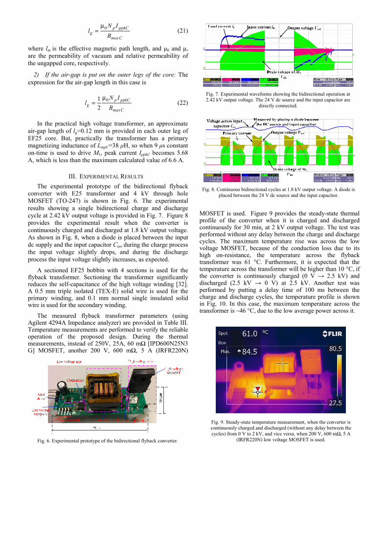
0 p ppkCg
maxC
N Il
Bμ
= (21)
where lm is the effective magnetic path length, and μ0 and μr are the permeability of vacuum and relative permeability of the ungapped core, respectively.
2) If the air-gap is put on the outer legs of the core: The expression for the air-gap length in this case is
012
p ppkCg
maxC
N Il
Bμ
= (22)
In the practical high voltage transformer, an approximate air-gap length of lg=0.12 mm is provided in each outer leg of EF25 core. But, practically the transformer has a primary magnetizing inductance of LmpC=38 μH, so when 9 μs constant on-time is used to drive M1, peak current IppkC becomes 5.68 A, which is less than the maximum calculated value of 6.6 A.
III. EXPERIMENTAL RESULTS The experimental prototype of the bidirectional flyback
converter with E25 transformer and 4 kV through hole MOSFET (TO-247) is shown in Fig. 6. The experimental results showing a single bidirectional charge and discharge cycle at 2.42 kV output voltage is provided in Fig. 7. Figure 8 provides the experimental result when the converter is continuously charged and discharged at 1.8 kV output voltage. As shown in Fig. 8, when a diode is placed between the input dc supply and the input capacitor Cin, during the charge process the input voltage slightly drops, and during the discharge process the input voltage slightly increases, as expected.
A sectioned EF25 bobbin with 4 sections is used for the flyback transformer. Sectioning the transformer significantly reduces the self-capacitance of the high voltage winding [32]. A 0.5 mm triple isolated (TEX-E) solid wire is used for the primary winding, and 0.1 mm normal single insulated solid wire is used for the secondary winding.
The measured flyback transformer parameters (using Agilent 4294A Impedance analyzer) are provided in Table III. Temperature measurements are performed to verify the reliable operation of the proposed design. During the thermal measurements, instead of 250V, 25A, 60 mΩ [IPD600N25N3 G] MOSFET, another 200 V, 600 mΩ, 5 A (IRFR220N)
MOSFET is used. Figure 9 provides the steady-state thermal profile of the converter when it is charged and discharged continuously for 30 min, at 2 kV output voltage. The test was performed without any delay between the charge and discharge cycles. The maximum temperature rise was across the low voltage MOSFET, because of the conduction loss due to its high on-resistance, the temperature across the flyback transformer was 61 °C. Furthermore, it is expected that the temperature across the transformer will be higher than 10 °C, if the converter is continuously charged (0 V → 2.5 kV) and discharged (2.5 kV → 0 V) at 2.5 kV. Another test was performed by putting a delay time of 100 ms between the charge and discharge cycles, the temperature profile is shown in Fig. 10. In this case, the maximum temperature across the transformer is ~46 °C, due to the low average power across it.
Fig. 8. Continuous bidirectional cycles at 1.8 kV output voltage. A diode is
placed between the 24 V dc source and the input capacitor.
Fig. 7. Experimental waveforms showing the bidirectional operation at 2.42 kV output voltage. The 24 V dc source and the input capacitor are
directly connected.
Fig. 6. Experimental prototype of the bidirectional flyback converter.
Fig. 9. Steady-state temperature measurement, when the converter is continuously charged and discharged (without any delay between the cycles) from 0 V to 2 kV, and vice versa, when 200 V, 600 mΩ, 5 A
(IRFR220N) low voltage MOSFET is used.

Since the load is purely capacitive, the converter efficiency is defined as energy efficiency, instead of normal power efficiency. The charge and discharge energy efficiency measurement [30] results are provided in Table IV. During the charge process the output energy is the energy stored in the load capacitor, and the input energy is obtained by integrating the input charge current and multiplying it with the input voltage. During the discharge process, the input energy is the energy stored in the load capacitor, and the output energy is obtained by integrating the input discharge current and multiplying it with the input voltage. All components shown in Table II are used during the energy efficiency measurements. As explained earlier, the converter operates with valley switching control during charge and discharge operations. The charge and discharge efficiencies are 89.2% and 83.4%, respectively. The reasons for the lower discharge energy efficiency are explained in [33].
IV. CONCLUSIONS This paper describes the detailed power stage design of the
high voltage bidirectional flyback converter for driving a dielectric electro active polymer (DEAP) based capacitive actuator. Experimental results are provided to show the bidirectional operation (charge and discharge) of the high voltage converter. Even though the flyback transformer is designed for a high peak charging flux density of 0.35 T, thermal measurement results show that the maximum temperature across the transformer is 61 °C. Therefore, for a high voltage capacitor charge and discharge applications it is possible to minimize the number of transformer turns on the secondary high voltage side, by choosing a high flux density.
Energy efficiency measurements are provided for the charge and discharge modes using the proposed design. For driving the capacitive load at 2.4 kV, the converter attains charge and discharge energy efficiencies of 89.2% and 83.4%, respectively. It is easy to make three similar converters with the same design for driving the DEAP incremental actuator, which has an enormous potential in the automotive industry. By optimizing the flyback transformer design, it is possible to increase the power density of the high voltage driver, so that it can be easily placed in the EVs. The research on the DEAP material is still on-going, and in the future it is expected that the operating voltage ranges of the DEAP actuators may be reduced to 1.5-2 kV from the current range 2-2.5 kV.
REFERENCES [1] Y. Bar-Cohen, ‘‘Electroactive Polymer [EAP] Actuators as Artificial
Muscles: Reality, Potential, and Challenges,’’ 2nd ed. Washington, DC: SPIE, 2004.
[2] F. Carpi, D. DE Rossi, R. Kornbluh, R. Pelrine, P. Sommer-Larsen, Eds, ‘‘Dielectric Elastomer As Electromechanical Transducers,’’ Amsterdam, The Netherlands: Elsevier, 2008.
[3] R. E. Pelrine, R. D. Kornbluh, Q. Pei, J. P. Joseph, “High-speed electrically actuated elastomers with strain greater than 100%,” Science, vol. 287, pp. 836–839, 2000.
[4] Danfoss PolyPower, Denmark, Online available: http://www.polypower.com/ [accessed 20 Oct. 2014].
[5] LEAP Technology, Denmark, Online available: http://leaptechnology.com/ [accessed 20 Oct. 2014].
[6] M. Tryson, H. E. Kiil, M. Benslimane, “Powerful tubular core free dielectric electro active polymer (DEAP) push actuator,” in Proc. SPIE, vol. 7287, 2009.
[7] R. Sarban, B. Lassen, M. Willatzen, “Dynamic Electromechanical Modeling of Dielectric Elastomer Actuators With Metallic Electrodes,” IEEE/ASME Trans. Mechatronics, vol. 17, no. 5, pp. 960-967, Oct. 2012.
[8] R. D. Kornbluh, R. Pelrine, Q. Pei, R. Heydt, S. Stanford, S. Oh, J. Eckerle, “Electroelastomers: applications of dielectric elastomer transducers for actuation, generation, and smart structures,” in Proc. SPIE, vol. 4698, pp. 254-270, 2002.
[9] Q. Pei, R. Pelrine, S. Stanford, R. D. Kornbluh, M. S. Rosenthal, K. Meijer, R. J. Full, “Multifunctional electroelastomer rolls and their application for biomimetic walking robots,” in Proc. SPIE, vol. 4698, 2002.
[10] I. A. Anderson, T. A. Gisby, T. G. McKay, B. M. O’Brien, E. P. Calius, “Multi-functional dielectric elastomer artificial muscles for soft and smart machines,” Journal of Applied Physics, 112, 041101, 2012.
[11] K. Jung, J. C. Koo, J. -do Nam, Y. K. Lee, H. R. Choi, “Artificial annelid robot driven by soft actuators,” Journal of Bioinspiration and Biomimetics, vol. 2, pp. S42-S49, 2007.
Fig. 10. Steady-state temperature measurement, when the converter is continuously charged and discharged (without 100 ms delay between the cycles) from 0 V to 2 kV, and vice versa, when IRFR220N (200 V, 600
mΩ, 5 A) low voltage MOSFET is used.
TABLE III. FLYBACK TRANSFORMER PARAMETERS
Parameter Value Core used / material used EF25 / N87
Type of bobbin (coil former) Sectioned with 4 sections
Number of primary Np / secondary turns Ns 12 / 240 Primary Lmp / secondary magnetizing
inductance Lms 38 μH / 15.2 mH
Leakage inductance referred to primary Llkp / secondary Llks
450 nH / 185 μH
Self-capacitance of secondary winding Cs 5 pF Dc resistance of primary Rp / secondary Rs 50 mΩ / 10.5 Ω
TABLE IV. ENERGY EFFICIENCY AT 2.4 KV OUTPUT VOLTAGE
Type of mode
Input energy (J)
Output energy (J)
Energy efficiency (%)
Charge 1.29 1.15 89.2 (to charge from 0 V to 2.4 kV)
Discharge 1.15 0.96 83.4 (to discharge from 2.4 kV to 0 V)

[12] I. A. Anderson, T. C. H. Tse, T. Inamura, B. M. O’Brien, T. McKay, T. Gisby, “A soft and dexterous motor,” Journal of Applied Physics, 98, 123704, 2011.
[13] A. T. Conn, A. D. Hinitt, P. Wang, “Soft segmented inchworm robot with dielectric elastomer muscles,” in Proc. SPIE, Electroactive Polymer Actuators and Devices (EAPAD), vol. 9056, pp. 90562L, 2014.
[14] F. Carpi, R. Kornbluh, P. Sommer-Larsen, G. Alici, “Electroactive polymer actuators as artificial muscles: are they ready for bioinspired applications?,” Journal of Bioinspiration and Biomimetics, vol. 6 (4), 2011.
[15] Siemens website, online available [accessed 29 Oct. 2014]: http://www.siemens.com/innovation/en/publikationen/publications_pof/pof_spring_2006/motors_articles/future_motors.htm.
[16] Helix Linear Technologies website, online available [accessed 29 Oct. 2014]: http://blog.helixlinear.com/bid/307529/How-a-Small-Electric-Actuator-Operates-Automotive-Headlights.
[17] The University of Sheffield website, online available [accessed 29 Oct. 2014]: http://www.sheffield.ac.uk/research/impact/stories/fce/7.
[18] VDO global website, online available [accessed 29 Oct. 2014]: http://www.vdo.com/generator/www/com/en/vdo/main/products_solutions/cars/replacement_parts/engine_actuators/digital_linear_actuators/digital_linear_actuators_en.html.
[19] VDO global website, online available [accessed 29 Oct. 2014]: http://www.vdo.com/generator/www/com/en/vdo/main/products_solutions/cars/replacement_parts/actuators_for_central_locking_systems/actuators_for_central_locking_systems_en.html.
[20] P. Thummala, Z. Zhang, M. A. E. Andersen, S. Rahimullah, “Dielectric electro active polymer incremental actuator driven by multiple high-voltage bi-directional DC-DC converters,” in Proc. IEEE ECCE USA, pp. 3837-3844, 15-19 Sept. 2013.
[21] R. W. Erickson, D. Maksimovic, “Fundamentals of Power Electronics,” 2nd ed. New York: Springer, 2001.
[22] H. K. Sang, D. Maksimovic, I. Cohen, “Efficiency Optimization in Digitally Controlled Flyback DC–DC Converters Over Wide Ranges of Operating Conditions,” IEEE Trans. Power Electronics, vol. 27, no. 8, pp. 3734-3748, Aug. 2012.
[23] N. O. Sokal, R. Redl, “Control algorithms and circuit designs for optimal flyback-charging of an energy storage capacitor (e.g., for flash lamp or defibrillator),” IEEE Trans. Power Electronics, vol. 12, no. 5, pp. 885-894, Sep. 1997.
[24] J. Elmes, C. Jourdan, O. Abdel-Rahman, I. Batarseh, “High-Voltage, High-Power-Density DC-DC Converter for Capacitor Charging Applications,” in Proc. IEEE APEC, pp. 433-439, 2009.
[25] S. K. Chung, H. B. Shin, “High-voltage power supply for semi-active suspension system with ER-fluid damper,” IEEE Trans. Vehicular Technology, vol. 53, no. 1, pp. 206- 214, Jan. 2004.
[26] T. Bhattacharya, V. S. Giri, K. Mathew, L. Umanand, “Multiphase Bidirectional Flyback Converter Topology for Hybrid Electric Vehicles,” IEEE Trans. Industrial Electronics, vol. 56, no. 1, pp. 78-84, Jan. 2009.
[27] G. Chen, Y.-S. Lee, S. Y. R. Hui, D. Xu, Y. Wang, “Actively clamped bidirectional flyback converter,” IEEE Trans. Industrial Electronics, vol. 47, no. 4, pp. 770-779, Aug. 2000.
[28] F. Zhang, Y. Yan, “Novel Forward–Flyback Hybrid Bidirectional DC-DC Converter,” IEEE Trans. Industrial Electronics, vol. 56, no. 5, pp. 1578-1584, May 2009.
[29] T. Andersen, M. S. Rødgaard, O. C. Thomsen, M. A. E. Andersen, “Low voltage driven dielectric electro active polymer actuator with integrated piezoelectric transformer based driver,” in Proc. SPIE EAPAD, vol. 7976, p. 79762N, 2011.
[30] P. Thummala, Z. Zhang, M. A. E. Andersen, “High Voltage Bi-directional Flyback Converter for Capacitive Actuator,” in Proc. IEEE EPE, pp. 3-6 Sept. 2013.
[31] P. Thummala, H. Schneider, Z. Zhang, A. Knott, M. A. E. Andersen, “Optimization of a bi-directional flyback converter for a high voltage capacitor charging application,” in Proc. IEEE APEC, pp. 2556-2563, 16-20 March 2014.
[32] H. Schneider, P. Thummala, L. Huang, Z. Ouyang, A. Knott, Z. Zhang, M. A. E. Andersen, “Investigation of transformer winding architectures for high voltage capacitor charging applications,” in Proc. IEEE APEC, pp. 334-341, 16-20 March 2014.
[33] P. Thummala, D. Maksimovic, Z. Zhang, M. A. E. Andersen, “Digital control of a high-voltage (2.5 kV) bidirectional DC-DC converter for driving a dielectric electro active polymer (DEAP) based capacitive actuator,” in Proc. IEEE ECCE USA, pp. 3435-3442, 14-18 Sept. 2014.
[34] LT3751 datasheet, “High voltage capacitor charger controller with regulation,” Linear Technology Corporation, USA, Online available: http://cds.linear.com/docs/en/datasheet/3751fc.pdf [accessed 16 Oct. 2014].
[35] C. W. T. McLyman, Transformer and Inductor Design Handbook, 3rd
Ed., New York: Marcel Dekker, 2004. [36] W. G. Hurley, W. H. Wolfle, Transformers and Inductors for Power
Electronics: Theory, Design and Applications, 1st Ed., John Wiley and Sons Ltd., 2013.
[37] M. Kazimierczuk, High-frequency magnetic components, 2nd Ed., John Wiley and Sons Ltd., 2014.

102/255

Appendix FEstimation of Transformer
Parameters and Loss Analysis forHigh Voltage Capacitor Charging
Application
2013 IEEE Energy Conversion Congress and Exposition ASIA (ECCE ASIA 2013)
103/255
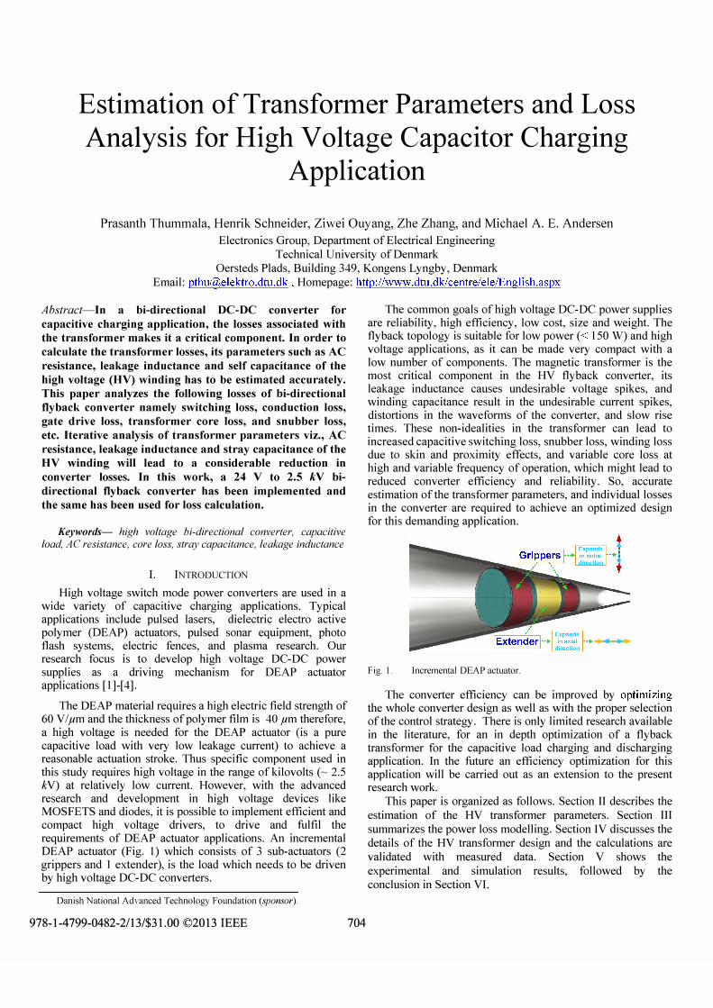
Estimation of Transformer Parameters and Loss Analysis for High Voltage Capacitor Charging
Application
Prasanth Thummala, Henrik Schneider, Ziwei Ouyang, Zhe Zhang, and Michael A. E. Andersen Electronics Group, Department of Electrical Engineering
Technical University of Denmark Oersteds Plads, Building 349, Kongens Lyngby, Denmark
Email: [email protected] , Homepage: http://www.dtu.dk/centre/elelEnglish.aspx
Abstract-In a bi-directional DC-DC converter for
capacitive charging application, the losses associated with
the transformer makes it a critical component. In order to
calculate the transformer losses, its parameters such as AC resistance, leakage inductance and self capacitance of the
high voltage (HV) winding has to be estimated accurately.
This paper analyzes the following losses of bi-directional
flyback converter namely switching loss, conduction loss,
gate drive loss, transformer core loss, and snubber loss,
etc. Iterative analysis of transformer parameters viz., AC resistance, leakage inductance and stray capacitance of the
HV winding will lead to a considerable reduction in
converter losses. In this work, a 24 V to 2.5 kV bi
directional flyback converter has been implemented and
the same has been used for loss calculation.
Keywords- high voltage bi-directional converter, capacitive load, AC resistance, core loss, stray capacitance, leakage inductance
I. INTRODUCTION
High voltage switch mode power converters are used in a wide variety of capacitive charging applications. Typical applications include pulsed lasers, dielectric electro active polymer (DEAP) actuators, pulsed sonar equipment, photo flash systems, electric fences, and plasma research. Our research focus is to develop high voltage DC-DC power supplies as a driving mechanism for DEAP actuator applications [1]-[4].
The DEAP material requires a high electric field strength of 60 VI pm and the thickness of polymer film is 40 pm therefore, a high voltage is needed for the DEAP actuator (is a pure capacitive load with very low leakage current) to achieve a reasonable actuation stroke. Thus specific component used in this study requires high voltage in the range of kilovolts ( 2.5 kV) at relatively low current. However, with the advanced research and development in high voltage devices like MOSFETS and diodes, it is possible to implement efficient and compact high voltage drivers, to drive and fulfil the requirements of DEAP actuator applications. An incremental DEAP actuator (Fig. I) which consists of 3 sub-actuators (2 grippers and 1 extender), is the load which needs to be driven by high voltage DC-DC converters.
Danish National Advanced Technology Foundation (sponsor).
978-1-4799-0482-2/13/$31.00 ©2013 IEEE 704
The common goals of high voltage DC-DC power supplies are reliability, high efficiency, low cost, size and weight. The fly back topology is suitable for low power « 150 W) and high voltage applications, as it can be made very compact with a low number of components. The magnetic transformer is the most critical component in the HV fly back converter, its leakage inductance causes undesirable voltage spikes, and winding capacitance result in the undesirable current spikes, distortions in the waveforms of the converter, and slow rise times. These non-idealities in the transformer can lead to increased capacitive switching loss, snubber loss, winding loss due to skin and proximity effects, and variable core loss at high and variable frequency of operation, which might lead to reduced converter efficiency and reliability. So, accurate estimation of the transformer parameters, and individual losses in the converter are required to achieve an optimized design for this demanding application.
Fig. I. Incremental DEAP actuator.
The converter efficiency can be improved by optImlzmg the whole converter design as well as with the proper selection of the control strategy. There is only limited research available in the literature, for an in depth optimization of a flyback transformer for the capacitive load charging and discharging application. In the future an efficiency optimization for this application will be carried out as an extension to the present research work.
This paper is organized as follows. Section II describes the estimation of the HV transformer parameters. Section III summarizes the power loss modelling. Section IV discusses the details of the HV transformer design and the calculations are validated with measured data. Section V shows the experimental and simulation results, followed by the conclusion in Section VI.

II. HV TRANSFORMER PARAMETERS ESTIMATION
A. DC and AC resistances An increase in the switching frequency of the converter
increases the transformer winding losses due to the skin and proximity effects. Since the converter operates under boundary mode during charging and in discontinuous conduction mode (DCM) during discharging, the AC conduction loss cannot be ignored and may dominate the total winding loss. The AC conduction loss is caused by high frequency skin and proximity effects, as well as the fringing effect. Due to its complexity fringing effect is not considered in this paper.
The DC resistance of the primary winding can be calculated by
pl]p A = trd/ (1) RDep
=A; ' p 4
where, p is the resistivity of copper at room temperature,
N p is the number of primary turns, ITP is the total length of
the primary winding, and d p is the diameter of the primary
winding.
The AC resistance of each harmonic in the current waveform can be calculated as [4], [5],
FH"" = RAe? = F. + F = c I I, ,')'kin ?rox G P 'V n R;x'p
(2)
where, n is the harmonic number, mp is the number of layers
of the primary winding and t: l' is the primary winding
conductor thickness normalized with respect to the conductor skin depth at the switching frequency for a round conductor, 51' is the skin depth at the fundamental frequency, and dj is
Ida the porosity factor of the primary winding.
B. Leakage Inductance
In the tlyback converter the leakage inductance causes voltage spikes on the drain of low voltage and the high voltage MOSFETs, and may cause significant loss if the fly back transformer is not properly designed.
1) Without interleaving: The leakage inductance for the winding structure shown in Fig. 2a referred to primary is calculated using the energy stored in the magnetic field.
I f I 2 E =- B· H ·dv =-L 1 Mag 2 2 1kpk
Vol (3)
The general expression for the leakage inductance referred to the primary winding for a non-interleaving winding structure having nip primary layers and nls secondary layers (with equal
turns per layer) is derived in this work and is given by
705
L - N 2 Ikp - flo b I' If
nlphp +nlsh, + (2n1P -1)(nIP -1)( h,p J 3 6 l nip
+ (2nj, -II ( nj, -1) ( : J + hi
(4)
where flo is the permeability of free air, lw is the mean length
turn (ML T), bw is the width of the bobbin window excluding
the edge isolation tape width, nip / nls IS the number of
primary/secondary layers, and hiP / his IS the insulation
thickness between the primary/secondary layers, and hi is the
insulation thickness between the primary and secondary layers, and Np is the number of primary turns.
The leakage inductance of transformer for the structure shown in Fig. 2 referred to primary is given by [6], [7]
(5)
MMF Distribution "F /' in"s'ulat(5r"
rl!latO'r" fN,I, /' h"S3- /'
i insulator p"""-- - NJ: --i insulato'r"
./ InsulatO'r" N,
rrsS- /' a) b)
Fig. 2. Analytical MMF distribution for non-interleaving structure P-S-S-S-S-S (left) and interleaving S-S-S-P-S-S (right) structure.
2) With interleaving: Practical experience revealed that interleaving the primary and secondary windings reduces the leakage inductance, self capacitance, and increases the interwinding capacitance. A transformer that is used in the HV application will have a lot of secondary windings, the interleaving structure with the secondary windings sandwiched between the primary winding as shown in Fig. 2b is typical for the high voltage DC-DC converter application.
The general expression for the leakage inductance referred to the primary, for an interleaving winding structure where n/,) and nls2 secondary layers are at the top and bottom of a primary winding respectively, having nip primary layers (with equal turns per layer of both, and no insulation between the primary layers) is derived in this work and is given by
flJwN/ L ----'--Ikp - bw
(6)

The leakage inductance of the HV transformer for a simple interleaving structure shown in Fig. 2b is calculated using (7).
J..l o lw. 2 [ 7hp+35h, 6 . 13 . ] L =--N +-h +-h (7) /kp 2 b p 75 25 " 25' w
C. Stray Capacitance
The stray capacitance is another important parameter in the HV transformer because it contributes to capacitive switching loss. The stray capacitance is calculated using the energy stored in the electric field [8]
1 f 1 2 E =- D·E·dv =-c.t.V o.le 2 2 Vol
... ____________ --'?w ____________
(8)
Fig. 3. Voltage distribution in the secondary HV winding with the layers wounded in the same direction
The turn to turn capacitance per unit length of the noninterleaved HV winding with a round conductor is given by
(9)
where S=COS-l l1- :r
In l JJ ' £0 is the aIr permitivity,
lOr is the dielectric constant of the insulation of the winding,
do / dj is the outer/inner diameter of the HV winding
conductor. The layer to layer capacitance is given by
C =0J0,+1)(20,+I) CI ILl 6T 2 "If w /,.\"
(10)
where s is the turns per layer of the HV winding.
The self capacitance of the HV winding for the configuration shown in Fig. 3 is given by
winding
c. = CUI ( n -1/2J2
51 4 Is l nt., For the HV winding structure shown in Fig. 4, the layer to layer capacitance is given by [9], [10]
o -J I==---=------,,=---= _ J - CU2
Fig. 4. A random HV winding arrangement
( I I )
706
distance between the two layers, d, is the spacing between
the centers of adjacent turns. The self capacitance of the HV winding for the winding structure shown in Fig. 4, and with the winding connections as shown in Fig. 3 is given by
(13)
D. Trade-off between AC resistance, leakage inductance and stray capacitance for HV application
301--;==-==r==;:r===:r:::==r==::I===:;-r--j ·.10 times of Leakage Inductance (H) • !'! 25 •• HV winding capacitance (pF) using (11)' l 2 •• HV winding capacitance (pF) using (13) I· 20 '* 1/10 th of AC resistance (ohm) " ro .' 1 \ .. , . i .l .... :I:....::;;t:!. .. -. (; 101 ' ... 11= •• -•• _ .......... -,,·_,,· .. •• . . ......... . 5 ................ ::.: ...... : . .. . .. j(o,ijJ
85 0.55 0.6 , ,
0.65 0.7 0.75 Porosity Factor
0.9
Fig. 5. Trade-o±Ibetween the primary leakage inductance, secondary stray capacitance and the secondary AC resistance with a change in the porosity factor (d/do).
Fig. 5 shows the trade-off between the transformer parameters by changing the porosity factor. To show all the parameters in a single plot, the leakage inductance is multiplied by 10 and the AC resistance is divided by 10. The porosity factor (d; /do) is changed from 0.95 to 0.5 and the calculated parameters are shown in Fig. 5. It is observed that the AC resistance increases, and the self capacitance of the HV winding drops as the porosity factor is decreased.
III. Loss MODELING OF THE CONVERTER
In order to investigate the bi-directional converter efficiency, it is necessary to estimate the losses associated with each one of the circuit components in the converter. The schematic of the bi-directional fly back converter is shown in Fig. 6. The detailed analysis of the same converter is discussed in [13]. Different losses contributed from the transformer of the bi-directional flyback converter are given below.
A. Transformer winding loss
The tlyback converter operates in boundary mode with variable switching frequency, while charging the capacitive load [13]. The primary winding power loss is given by [5]
2 I 2 PWP=RDCpI DCP+ ""2RDCP-;2 FRP,/pn (14)
By applying the Fourier series expansion for the primary current waveform shown in Fig. 7 the following equations are obtained:
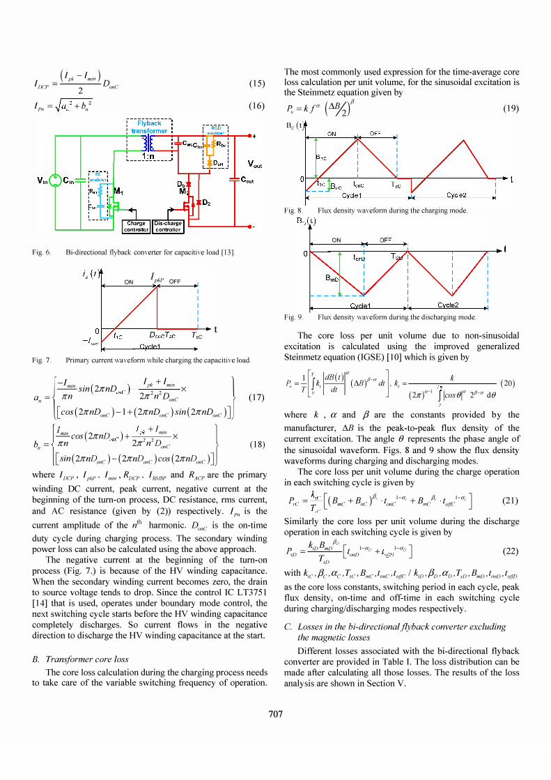
I =(lpk-lrnin)D Dcr 2
onC
Irn = a n2 +bn2
Fig. 6. Bi-directional flyback converter for capacitive load [13] .
ON Ipk1' OFF
r----------- t Tsc
(15)
(16)
Fig. 7. Primary current waveform while charging the capacitive load. . I,+m ----l!2!!2... sin (2JrnD _)+ X one 2 2 an = Jrn 2Jr n DonC [cos (2Jrn Donc ) -1 + (2JrnDonc ) sin (2Jrn Donc ) ] I . ( ) I"k +Imin ---'!"!!..-cos 2JrnD _ + X on! 2 2 2D bn = Jrn Jr none [sin (2JrnDonc ) -(2JrnDonc ) cos (2JrnDonc ) ]
(17)
(18)
where I Dcr' I pkJ" Imin, RDCl" I RMsr and RACT are the primary
winding DC current, peak current, negative current at the beginning of the turn-on process, DC resistance, rms current, and AC resistance (given by (2)) respectively. Irn is the
current amplitude of the nth harmonic. DonC is the on-time
duty cycle during charging process. The secondary winding power loss can also be calculated using the above approach.
The negative current at the beginning of the turn-on process (Fig. 7.) is because of the HV winding capacitance. When the secondary winding current becomes zero, the drain to source voltage tends to drop. Since the control IC L T375 I [14] that is used, operates under boundary mode control, the next switching cycle starts before the HV winding capacitance completely discharges. So current flows in the negative direction to discharge the HV winding capacitance at the start.
B. Transformer core loss
The core loss calculation during the charging process needs to take care of the variable switching frequency of operation.
707
The most commonly used expression for the time-average core loss calculation per unit volume, for the sinusoidal excitation is the Steinmetz equation given by
Pv = kr (%)fi (19)
Bdt
Fig. 8 . Flux density waveform during the charging mode. BD(t)
ON __ -' __ -+ ____ ______ '-____ I't
Cycle2 Fig. 9 . Flux density waveform during the discharging mode.
1 1 1 1 1 1 1
,1
The core loss per unit volume due to non-sinusoidal excitation is calculated using the improved generalized Steinmetz equation (IGSE) [10] which is given by
Pv = fki (Ml-U dt ,k, = 'If k IT I d ( )lrI l T 0 dt (2JZ" )"-' f leos Blu 2fl-u dB
(20)
where k , a and fJ are the constants provided by the
manufacturer, M is the peak-to-peak flux density of the current excitation. The angle e represents the phase angle of the sinusoidal waveform. Figs. 8 and 9 show the flux density waveforms during charging and discharging modes.
The core loss per unit volume during the charge operation in each switching cycle is given by
P.e = ;c [( BrnC + Bne l' . tonel-a, + Bm/' . toJcl-a, ] (21) I" e
Similarly the core loss per unit volume during the discharge operation in each switching cycle is given by
k B fiD P = ID rnD [t I-aD + t I-aD ] vD T onD orfD sD
(22)
with kic, fJc' ac' Tic, Bme, tonc' toiTC / kiD' fJD' aD' T,D' BrnD, tonD' toJjD as the core loss constants, switching period in each cycle, peak flux density, on-time and off-time in each switching cycle during charging/discharging modes respectively.
C. Losses in the bi-directional flyback converter excluding the magnetic losses
Different losses associated with the bi-directional flyback converter are provided in Table I. The loss distribution can be made after calculating all those losses. The results of the loss analysis are shown in Section V.

TABLE I. DIFFERENT LOSSES IN THE BI-DIRECTIONAL FLYBACK CONVERTER DURING CHARGE AND DISCHARGE OPERATIONS
Type of power loss
Low voltage MOSFET
Switching loss
HV MOSFET
Low voltage MOSFET
Sense resistor on the primary side
HVMOSFET Conduction
loss
HV Diode D2
diode Diode Db
Body diode of low voltage MOSFET
Reverse recovery loss ofHV diode
Gate driver loss
RC snubber across primary MOSFET
Snubber loss RCD snubber across secondary winding
Power consumption in the two control Ie's
Power loss expression
P . = fmc l ( Cw" + C""" ) + J .",1' 2 "plp"pc (tif + t,.,. )
J n l(CwS +Co"s )p +] P =---""---,,11 2 I( ) V:t.,,-, pkSD t,r + tlW
P = ,p
J ' . ,Ic (D'"'C-" J +" (JLJ ll,\f;,n
3 T,c 3 T,c P . -sensel'C -
P I!\1sPDr" w""PD - 'wowP
?'s = I ;"",r",
= Ik)/) D 3 UIID
D = + rDflHssc
IJb = Vii) I TX'sn + rnI,\lssTJ
HTJ.\.11 = fTXPTJ
P" e = Q, (V"", + n n ) 1", 1+1"
Q". = f -t, dt ,
PCate = Vcs (QCM 2 fsjjD + QCMl /;WC )
p.\'IIrn"
p -mLV -
= 1.. L [' v"omp 2 lC' pC") V, -nV I",n 'dm." m
PCa,'",,,,, = 2JQ
Abbreviations The subscript 'P' / 'S' or 'C' / 'D' in any variable represents that variable is being referred to primary / secondary side or
that variable during charging and discharging modes
Cw,,/Cws - self capacitance of the transformer
pri mary/secondary - output capacitance of the primary/secondary
MOSFET
;P/Vd,S - primary/secondary MOSFET
voltage
V =V +'i ' d,P In n ' ," = Va., + n v'.
drain to source
Jwc / JW/J - switching frequency during charging/discharging
operation n - turns ratio of the transformer from secondary to primary
t;f / t" - current fall/voltage rise transition times of the
corresponding MOSFETs
,/, - on-resistance of the primary/secondary MOSFET
- primary/secondary rms current during charging
mode
J RMSPD / I RMSSD - primary/secondary rms current during
discharging mode
1m", - negative current at the beginning of the turn-on process
VI" - HV diode forward voltage drop
I DCSC / I RMSSC - average/nns current through the HV diode
D, during charging
IDCSD / I RMSS D - average/nns current through the HV diode Db
during discharging rD - HV diode on resistance
Vi", - forward voltage drop of body diode of M IDCPD - average current through primary during discharging
Done / Donn - on-duty cycle during charging/discharging
Q" /t,, - reverse recovery charge/ti me in the high voltage
diode D2
i, - secondary current, V,,,,, /V;, - outputlinput voltage of flyback converter
v,JS - gate drive voltage of the MOSFET
QGJL/QGM, - gate charge for high voltage/low voltage
MOSFETS
Cm -snubber capacitance in the RC snubber
- clamping voltage of the RCD snubber
V" - 1 C supply voltage
I Q - quiescent current of V,.,
IV. HV TRANSFORMERDESIGN: COMPARISON OF
MEASUREMENTS AND CALCULATIONS
Since the proposed DC-DC converter operates in a wide output voltage range (0-2.5 kV), to charge and discharge the DEAF actuator employed in a specific application, different components of the converter have to be designed for different
operating points. High voltage capacitor charging application requires proper design of the transformer, otherwise significant amount of energy is lost and efficiency will suffer.
708
The parameters that significantly affect the efficiency of the converter for capacitor charging application are the peak current, MOSFET type, transformer type and size, magnetizing
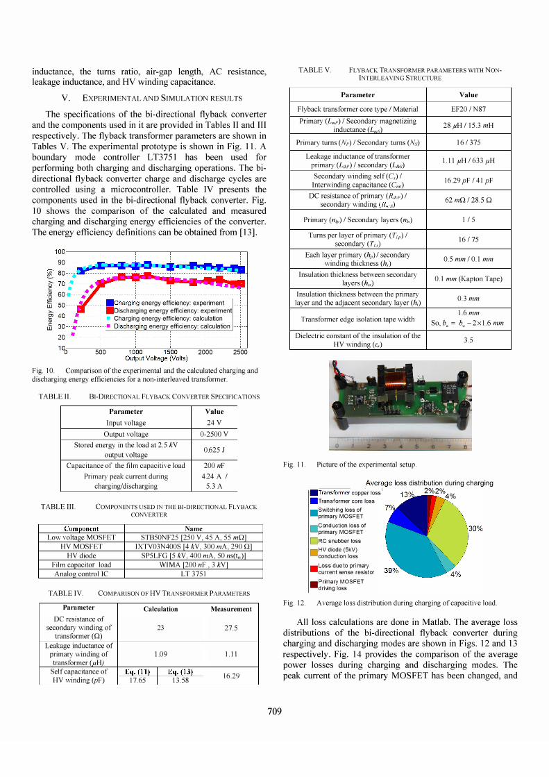
inductance, the turns ratio, air-gap length, AC resistance, leakage inductance, and HV winding capacitance.
V. EXPERIMENTAL AND SIMULATION RESULTS
The specifications of the bi-directional fly back converter and the components used in it are provided in Tables II and III respectively. The fly back transformer parameters are shown in Tables V. The experimental prototype is shown in Fig. 11. A boundary mode controller L T3751 has been used for performing both charging and discharging operations. The bidirectional fly back converter charge and discharge cycles are controlled using a microcontroller. Table IV presents the components used in the bi-directional tlyback converter. Fig. 10 shows the comparison of the calculated and measured charging and discharging energy efficiencies of the converter. The energy efficiency definitions can be obtained from [13].
100,--------------,--------------------"
: - .S'?I:'-';l5I:O:w q::.:JI::fI!'k!rw () 70-c • . 60
IE uu 50 E> Q) c uu
500
ICharging energy efficiency: experiment Discharging energy efficiency: experiment
• Charging energy efficiency: calculation • energy efficiency: calculation
2000 2500
Fig. 10. Comparison of the experimental and the calculated charging and discharging energy e±Iiciencies tor a non-interleaved transformer.
TABLE I! BI-DIRECTIONAL FL YBACK CONVERTER SPECIFICATIONS
Parameter Value Input voltage 24 V
Output voltage 0-2500 V
Stored energy in the load at 2. 5 kV 0.625.1
output voltage
Capacitance of the film capacitive load 200 nF
Primary peak current during 4.24 A / charging/discharging 5. 3 A
TABLE III. COMPONENTS USED IN THE BI-DIRECTIONAL FLYBACK CONVERTER
Component Name Low voltage MOSFET STB50NF25 [250 V, 45 A, 55 mOl
HV MOSFET IXTV03N400S r4 kV, 300 mA, 290 01 HV diode SP5LFG [5 kV, 400 mA, 50 ns(t,,)]
Film capacitor load WIMA [200 nF , 3 kV] Analog control IC LT 3751
TABLE IV. COMPARISON OF HV TRANSFORMER PARAMETERS
Parameter Calculation Measurement DC resistance of
secondary winding of 23 27. 5 trans±onner (0)
Leakage inductance of primary winding of 1.09 1.11
transformer (JlH) Self capacitance of Eq. (11) I Eq. (13) 16.29 HV winding (PF) 17. 65 I 13. 58
709
TABLE V. FLYBACK TRANSFORMER PARAMETERS WITH NONINTERLEAVING STRUCTURE
Parameter Flyback transformer core type / Material
Primary (LmP) / Secondary magnetizing inductance (Lms)
Primary turns (Np) / Secondary turns (Ns) Leakage inductance of transformer
primary (L",r) / secondary (L,kl) Secondary winding self (C,) /
Interwinding capacitance (C,n') DC resistance of primary (Rdcp)/
secondary winding (Rd •• S) Primary (nip) / Secondary layers (n,,)
Turns per layer of primary (Tip) / secondary (h,)
Each layer primary (hI') / secondary winding thickness (h,)
Insulation thickness between secondary layers (h,)
Insulation thickness between the primary layer and the adjacent secondary layer (h)
Trans±ormer edge isolation tape width
Dielectric constant of the insulation of the HV winding (c,.)
Fig. I I. Picture of the experimental setup.
Value EF20 / N87
28 JlH / 15. 3 mH 16/ 375
1.11 JlH / 633 JlH
16.29 pF / 41 pF
62 mO / 28. 5 0
I / 5
16 / 75
0. 5 mm / 0. 1 mm
0. 1 mm (Kapton Tape)
0. 3 mm 1.6 mm
So,bw = bw-2x1.6mm 3. 5
= ___________ A _v _e-,rage loss distribution during charging .Transformer c opper loss 2%2% % .Transformer c ore loss .Switc hing loss of
primary MOSFET .Conduc tion loss of
primary MOSFET ORC snub b er loss
·0Oc51 ·r:et!rir::ior .Primary MOSFET
driving loss
Fig. 12. Average loss distribution during charging of capacitive load.
All loss calculations are done in Matlab. The average loss distributions of the bi-directional flyback converter during charging and discharging modes are shown in Figs. 12 and 13 respectively. Fig. 14 provides the comparison of the average power losses during charging and discharging modes. The peak current of the primary MOSFET has been changed, and
the charging energy efficiency variation has been provided in Fig. 15. In Fig. 16 we show the variation of the energy efficiency with the porosity factor. At high porosity factor the HV winding capacitance is high, so the discharging energy efficiency at 2.5 kV is low compared to that at medium porosity factor. However, at low porosity factor, the AC/DC resistance increases, so both charging and discharging energy efficiencies will drop.
Average loss distribution during discharging iicoppe:r"lo:ss----1 .Transformer core loss .Switching l oss of
high vo ltage (4kV) MOSFET .Conduction loss of
high vo ltage (4kV) MOSFET DHV RCD sn ub be r loss
. dg; c
soe
eusc loss
• conduction loss of body diode of primary MOSFET
.HV(4kV) MOSFET dr iv ing loss
Fig. 13. Average loss distribution during discharging of capacitive load.
'" '" o ...J
o a.
.1. Average Transformer copper loss • 2. Average Transformer core loss D3. Average Conduction loss of 04. Average Switching loss
Snubber Losses
4 Type of Power Loss
Fig. 14. Comparison of the average loss; On Y-axis, 1 and 2-corresponds to power loss during charging and discharging respectively.
"1L- · 80 · , ai 70 ' 60 - ' : . w 50 • . . 40-
' 30 '
w 20 -3
2 . 5 2 - ----____. '.5 ,-output Voltage (kV) .5
Primary Peak Current (A)
80
70
' 60
50
40
Fig. 15. 3D plot showing how the peak current affects the charging energy.
0.9
O.8 " o '" 0.7 (;' 0.6 '" w
°ii":-'---;O"' .2:-----::0"' .3--0;;'"-.4-;-----=0"'=. 5'-----='0 .""6 ---;0"'. 7=----=-';;- Porosity factor
Fig. 16. Variation of energy etliciency at 2. 5 kV with porosity factor (d/d,,)
710
VI. CONCLUS10N
The power losses in the bi-directional flyback converter for the capacitor charging application has been analyzed in detail. Due to the variable switching frequency and nonsinusoidal waveforms, it is very difficult to accurately compute the core and winding losses. The core loss was accurately calculated during charge and discharge operations, using piecewise linear approximation of the IGSE model.
Estimation of the leakage inductance for a non-interleaved structure and an interleaved winding structure has been discussed. Stray capacitance calculation for a typical HV winding structure is discussed. Trade-off between the different transformer parameters has been made with respect to porosity factor. Comparison of the measurement efficiency and the calculated efficiency shows the accuracy of the proposed loss analysis .
The future work involves the optimization of the whole converter with mostly focusing on transformer optimization.
REFERENCES
[I] R Pelrine, P S. Larsen, R. Kornbluh, R Heydt, G. Kofod, Q Pei, P Gravesen, "Applications of dielectric elastomer actuators, " in Proc . SPIE, voL 4329, pp. 335-349, 2001.
[2] M. Tryson, H. E. Kiil, and M. Benslimane, "Powerful tubular core free dielectric electro activate polymer (DEAP) push actuator, " in Proc. SPIE voL 7287, p. 72871 F, 2009.
[3] P. Thummala, L. Huang, Z Zhang and M. A E. Andersen, "Analysis of Dielectric Electro Active Polymer Actuator and its High Voltage Driving Circuits, " in Proc. IPMHVC. pp. , Jun. 4-7, 2012.
[4] P. Thummala, Z Zhang, M. A E. Andersen, 0 C. Thomsen, "A high voltage DC-DC converter driving a Dielectric Electro Active Polymer actuator for wind turbine flaps, " in Proc. UPEC pp.l,7, 4-7 Sept. 2012.
[5] W.G. Hurley, E. Gath, J G. Breslin, "Optimizing the AC resistance of multilayer transformer windings with arbitrary current waveforms, " IEEE Trans. Power Electronics, v01.15, no.2, pp. 369-376, Mar 2000.
[6] D. Murthy-Bellur, M. K. Kazimierczuk, "Winding losses caused by harmonics in high-frequency flyback transformers for pulse-width modulated dc-dc converters in discontinuous conduction mode, " lET Trans. Power ElectroniCS, voU, no. 5, pp.804,817, September 2010.
[7] .I. Zhang, Z. Ouyang, M. Duffy, M. A. E Andersen and W. G. Hurley "Leakage inductance calculation for planar transformer with magnetic shunt ", inProc. ECCE USA 2013 (accepted).
[8] Z. Ouyang, O. C. Thomsen, M. A. E. Andersen, 'The analysis and comparison of leakage inductance in different winding arrangements for planar transformer ", in Proc. IEEE PEDS, pp. 1143-1148, Nov. 2009.
[9] L. Dalessandro, F. da Silveira Cava1cante, .I. W. Kolar, "SelfCapacitance of High-Voltage Transformers, " IEEE Trans. On Power Electronics. Vol. 22, no. 5, pp. 2081-2092, Sept. 2007.
[10] .I. Biela, .I. W. Kolar, "Using Transformer Parasitics for Resonant Converters-A Review of the Calculation of the Stray Capacitance of Transformers, " IEEE Trans. on Industry Applications, , vol. 44, no. I, pp. 223-233, 2008.
[11] E. C. Snelling, Soft Ferrites-Properties and applications. 2nd ed. London, UK, Butterworth, 1988.
[12] K. Venkatachalam, C. R. Sullivan, T. Abdallah, and H. Tacca, "Accurate prediction of ferrite cores loss with nonsinusoidal waveforms using only Steinmetz parameters, " in Proc. IEEE Workshop Comput. Power Electron., pp. 36-41, 2002.
[13] P. Thummala, Z. Zhang and M. A. E. Andersen, "Bi-directional Flyback Converter for Capacitive Actuator ", in Proc. EPE 2013 (accepted).
[14] L T3751, "High voltage capacitor charger controller with regulation, " datasheet.

Appendix GOptimization of bi-directionalflyback converter for a highvoltage capacitor charging
application
2014 IEEE Applied Power Electronics Conference and Exposition (APEC 2014)
111/255

Optimization of bi-directional flyback converter for a high voltage capacitor charging application
Prasanth Thummala, Henrik Schneider, Zhe Zhang, Arnold Knott, Michael A. E. Andersen Electronics Group, Department of Electrical Engineering
Technical University of Denmark 2800 Kongens Lyngby, Denmark
[email protected], [email protected]
Abstract—This paper presents an optimization technique for a flyback converter with a bidirectional energy transfer. The main goal is to optimize the converter for driving an incremental dielectric electro active polymer actuator, which must be charged and discharged from 0 V to 2500 V DC, supplied from a 24 V battery. The proposed optimization routine sweeps through a database of low voltage switching devices, and transformer core types and sizes. For each core, important winding parameters such as, the vertical winding space allocation for primary and secondary windings, and the spacing between the secondary windings layers are also swept. This enables the optimization routine to calculate and optimize the losses caused by transformer parasitics such as leakage inductance, self-capacitance and AC resistance which is crucial in achieving a high energy efficiency and high power density required for this application. The efficiency and loss distribution results provided by the optimization routine provide a deep insight into the transformer design and its impact on total converter efficiency. Finally, experimental work on a prototype of the bi-directional flyback converter is presented. The maximum charging and discharging energy efficiencies of the optimized design, are 96.1% and 85%, respectively.
I. INTRODUCTION Dielectric electro active polymer (DEAP) is an emerging
smart material that has experienced substantial development and has gained increasing attention over the last decade [1]-[4]. The DEAP technology can be used in actuator, sensor and energy harvesting applications. Bidirectional power electronics are of particular interest in DEAP actuator applications since the potential of the material needs to be high (charged) to expand and low (discharged) to retract. In Fig. 1, an illustration of an incremental actuator using two DEAPs as grippers and one DEAP as an extender is shown. DEAP, when used as incremental actuators, has the potential to be an effective replacement for many conventional incremental actuators due to its unique properties, such as large strain, light weight, low power consumption, and high flexibility. The DEAP technology has the potential to be used in various industries, e.g. automotive, aeronautics, space and medicine. In order to take full advantage of the DEAP potential, the drivers for the DEAP’s need to have a low volume to be utilized in small spaces and the weight and
energy efficiency influence the achieved traveling distance when powered from a battery.
The flyback topology is selected for the high voltage driver since it is suitable for low power (< 150 W) and has a low component count. High voltage switch-mode power supplies for charging the capacitive loads have been implemented in [5]-[12]. The design methodologies for transformers used in conventional switch mode power supplies are well documented in the literature. However, the procedures are conservative and are based on some assumptions in order to provide a simple, low risk and fast design phase. Often, the size of a suitable core is calculated based on assumptions such as constant switching frequency, a guess of the total converter efficiency, transformer conduction loss and core loss based on sinusoidal excitation and estimation of the winding current density. Thus, more complex and customized design procedures tailored for specific applications are needed to achieve efficient transformer designs. In this paper, an unconventional optimization routine is developed and tailored for bi-directional flyback converters, for high voltage capacitor charging and discharging applications, since literature regarding for this application is very limited [21]. The transformer optimization procedures for the switch-mode DC-DC converters have been discussed in [13]-[20]. The efficiency optimization method of the digitally controlled flyback converter for wide operating conditions is given in [15]. Analytical optimization of solid round wire conductors is
Figure 1. Incremental DEAP actuator [24].
This work was sponsored by Danish National Advanced Technology Foundation.
978-1-4799-2325-0/14/$31.00 ©2014 IEEE 2556

proposed in [16]. In [17], a weighted efficiency oriented design methodology is proposed for a flyback inverter. The optimization routine is different from most methods since it does not depend on any guess work, estimations or rule of thumb approaches in order to achieve the transformer design. Instead, advanced algorithms for calculating the transformer parasitics are used in combination with a comprehensive loss model in order to evaluate the converter efficiency and other key parameters for a wide range of implementation possibilities. The loss model takes into account that the waveforms in the flyback converter are not sinusoidal in both the conduction and switching loss calculations. The optimization routine provides the designer with the necessary practical details of the chosen design such as core size, core material, wire sizes, number of winding layers, etc. In order to provide a high level of driver design flexibility for different DEAP applications, the driver efficiency and its size/weight can be weighted. The main idea behind the optimization routine can easily be adapted to fit other topologies and applications.
II. OPTIMIZATION ROUTINE The optimization routine is described as follows: first, a
drain to source voltage of the primary MOSFET is selected from a range of voltage levels. Then the turns ratio, magnetizing inductance, peak primary current, and primary and secondary turns are calculated using the converter specifications (input and maximum output voltages, charging time). Next, a primary MOSFET rated for the selected drain to source voltage is selected from a range of MOSFETs with varying parameters such as MOSFET package type, on-resistance and gate charge, etc. Next a transformer core is selected, followed by the choice of winding space allocation
and layer to layer spacing. A dynamic winding function is used to design the transformer enabling the calculation of transformer parameters. Finally, losses in all components of the bi-directional flyback converter [6], in both charging and discharging modes are calculated [12] and added to represent the total estimated loss for that specific design. The optimization routine iterates through all design possibilities and in this case presents two solutions: one for the smallest transformer (limited by a temperature limit), and another for the most efficient solution (limited by an increase in converter efficiency vs. increase in transformer size). In the following sections, the challenges faced in the optimization routine are described, and solutions are presented.
A. Dynamic transformer design Well into the optimization routine when the design
parameters such as the number of turns and the allocated winding space is locked a winding implementation need to be found. In order to simplify that task the huge design space is limited - see Table 1. The core types are limited to 5 types. It is hard to predict which core type is most suitable for any application. In a flyback converter, a long transformer window width is often preferred to minimize the leakage inductance and AC resistance by providing a close coupling between windings and decrease the amount of winding layers. For high voltage converters, this could be different, since the winding self-capacitance on the high voltage side has a significant impact on the performance of the converter. Only the N87 core material and a simple non-interleaved winding structure (S-P) are used to limit complexity of the proposed optimization method. However, the optimization method can be easily adopted for an interleaved winding structure. Single insulated solid wire is used for the secondary winding since a
TABLE I. HIGH VOLTAGE TRANSFORMER STRUCTURES AND WINDING INFORMATION
Description Design decision Advantages
Core type
ETD, EFD, E, RM and
PQ
Round and square center leg ease the analytical complexity.
Core material N87 Suitable for high frequency of
operation. Winding structure P / S Simple implementation and decreases
analytical complexity. Primary winding
type
Solid wire
Flexible in terms of design and different winding structures.
Primary winding
insulation
Triple insulation
Avoid edge tape to achieve a higher fill factor. More flexible in terms of
implementation.
Secondary winding
type
Solid wire
Suitable winding type, for a large number of turns. Flexible in terms of
design, prototyping and different winding structures.
Secondary winding
insulation
Single insulation
Minimum insulation thickness for a large number of turns.
Air gap All legs Simplifies the prototyping. Maximum transformer temperature
140 °C With an estimated ambient temperature
of 40 °C, this enables a transformer temperature rise of 100 °C.
Figure 2. Cases from the dynamic transformer design.
a) Allocated winding area. b) Initial starting point (Square width = area height). c) Unused space above and beside the squares (fill factor < 1).
d) Squares not used (fill factor << 1). e) Close to ideal winding implementation (All squares used for the windings, horizontal space used
as spacing between layers, high fill factor).
2557

lot of turns are needed. The proper insulation between primary and secondary windings are achieved using a triple insulated solid wire for the secondary winding, which has proven to increase the winding fill factor and thus the efficiency and/or size of the transformer. The air gap is provided in all legs of the core, and the maximum air gap length is limited to 20% of the center leg length/window width, to avoid the loss due to the fringing field. A maximum transformer temperature limit of 140 °C is chosen. These limitation values can be altered based on the experience of the designer or the initial design specifications.
In this section, different cases about the dynamic transformer design are explained. The concept is best understood with the help of visualization. In Fig. 2.a, the space allocation for a given winding is shown. The width of the available area is the width of the bobbin window WW and the height of the area is the allocated height for the winding WH,n. The first step is to split the area into squares with a square width (Wsq) equal to the allocated height for the winding. It is αWH,n for secondary and (1- α)WH,n for the primary winding, with being the space allocation factor for secondary. In this case, it results in 4 squares and a non-square area that is considered as an unusable area as shown in Fig 2.b. In each square, a solid round wire could be placed with a diameter equal to the width of the square or a bundle of round wires with an outside bundle diameter equal to the width of the square. In this work, only the first option has been considered since the high number of needed secondary turns result in very thin wire diameter compared to the skin depth. If the number of turns required is 4 or less, this case will be considered as a valid solution and saved for later comparison with other found solutions. If a single turn is needed, then four squares could be utilized by 4 round wires in parallel and only the non-square area would not be used. The wire diameter may not be optimal compared to the skin depth which is why more solutions need to be considered and validated. This is achieved by splitting the winding area into smaller and smaller squares. The width of the squares for the secondary winding is limited by the smallest practical feasible diameter of a solid round wire (0.08 mm). In Fig. 2.c, the square size limits the use of the shaded area above the squares. However, that area can be set free for another winding thus improving the overall fill factor. The case shown in Fig. 2.d, illustrates, how the fill factor of a winding is reduced if not all squares are utilized as a turn. Fig. 2.e, illustrates how an optimum winding solution could look like if 18 turns were needed and the width of the square was optimum in terms of skin depth. Note that non-square horizontal area is utilized as spacing between the layers. The spacing distance is swept in order to balance the transformer parameters and the converter performance.
In Fig. 3, a flowchart of the dynamic transformer winding design is shown. The gray arrows point to a set of variables that are calculated during each iteration viz, squares per column (SqColumn), squares per row (SqRow), total squares (SqTotal), squares in parallel (SqParallel), number of layers (NLayers), total squares used (SqUsed), last or final layer fill factor (FFLastLayer) and spacing between the layers (SpaceLayers). These variables are calculated from the equations (1)-(9). As explained earlier, the design phase starts by defining a square
sized based on the allocated height for a given winding. Then important information about how many squares that can fit into the available area is calculated. The actual number of squares used to construct the winding is then determined based on the number of turns needed. The calculated variables are saved if the fill factor of the final layer is above 85 percent. This limit is implemented since the calculations of the transformer parameters are based on fully occupied layers.
,Sq H nW W i= ⋅ ⋅α (1)
where the variable i varies from 1 to 0 in small steps.
,H nColumn
Sq
WSq floor
W
⎛ ⎞= ⎜ ⎟⎜ ⎟
⎝ ⎠
α (2)
Figure 3. Flowchart of dynamic winding design.
Figure 4. Results of the dynamic winding design for optimized core.
0.2 0.25 0.3 0.350.85
0.9
0.95
1
Square width (mm)
FF
Last
Lay
er
0.2 0.25 0.3 0.350
0.5
1x 10⁻³
Square width (mm)S
pace
Laye
rs
0.2 0.25 0.3 0.354
6
8
10
Square width (mm)
NLa
yers
0.2 0.25 0.3 0.3520
40
60
80
Square width (mm)
Tur
ns p
er la
yer
2558

wRow
Sq
WSq floorW
⎛ ⎞= ⎜ ⎟⎜ ⎟
⎝ ⎠ (3)
Total Column RowSq Sq Sq⋅= (4)
TotalParallel
SqSq floorN
⎛ ⎞= ⎜ ⎟⎝ ⎠
(5)
where N is the number of turns of that particular winding for which the dynamic winding design is applied.
Used ParallelSq N Sq= ⋅ (6)
UsedLayers
Row
SqN ceilSq
⎛ ⎞= ⎜ ⎟
⎝ ⎠ (7)
Last LayerRow Row
N NFF floorSq Sq
⎡ ⎤⎛ ⎞= −⎢ ⎥⎜ ⎟⎢ ⎥⎝ ⎠⎣ ⎦
(8)
( ),
1H n layers sq
Layerslayers
W N WSpace
N
−=
− (9)
In the above equations ceil(x+Δx)=x+1 and floor(x+Δx)=x with 0< Δx<1.
B. Estimation of transformer parasitics and comprehensive loss model The outputs of the dynamic transformer design are used to
calculate the transformer parasitics [12] such as DC and AC resistances, leakage inductance and self-capacitance. The loss model has been verified in [12]. In this paper, the winding loss calculations are calculated accurately, since the primary and secondary currents are 180° out of phase.
1) Flyback transformer winding loss during charge process:
The high voltage bi-directional flyback converter proposed in [6], [12], operates in boundary conduction mode (BCM) with variable switching frequency during the charge process and in discontinuous conduction mode (DCM) during the discharge process. The winding loss in a flyback transformer is calculated using the MMF analysis presented in [22]. For the winding loss modeling, a non-interleaved transformer with 2 layers on the primary side and 5 layers on the secondary side is considered as an example. The MMF distribution in a flyback transformer is different from that of a normal transformer [22]. Fig. 5 shows different MMF distributions during both turn-on (0<t<ton) and turn-off (ton<t<toff) periods in a non-interleaved flyback transformer. The magnetizing current and the time variation of the MMF at the boundary of each layer during the charging process are shown in Figs. 6 and 7, respectively. As the output voltage increases, the magnitude of the minimum negative current -Imin, in Fig. 6
7F
t
p pkPN I
p minN I−
1F
t
1p pkPN I
1p minN I−
2F
t
p pkPN I
p minN I−
4F
t
p pkPN I
p minN I−
6F
t
p pkPN I
p minN I−
3F
t
p pkPN I
p minN I−
5F
t
p pkPN I
p minN I−
0F
t
1pkPI
Nn
3pkPI
Nn2
pkPIN
n
4pkPI
Nn
Figure 7. MMF distribution of the non-interleaved (P-P-S-S-S-S-S)
structure with respect to time during the charge process.
p1
IN
n
p1 pN I
0 0
p pN I
p2
IN
n
p3
IN
n
p4
IN
np
5
IN
n
Figure 5. MMF distribution of the non-interleaved (P-P-S-S-S-S-S) structure with respect to space (secondary winding is wounded on the bobbin first).
( )mpi t
t
pkPI
minI−
Figure 6. Magnetizing current during the charge process.
2559

increases with the switching frequency during the charge process [6], [12].
In Fig. 7, since the negative MMF is presented at the end of each switching cycle for very short time compared to the switching period, it can be neglected in the loss calculation. In Fig. 5, Np1 and Np, are the number turns in the primary layer 1 and the total primary turns. The terms N1, N2, N3, N4, N5 are defined as follows: N1=Ns1, N2=Ns1+Ns2, N3=Ns1+Ns2+Ns3, N4=Ns1+Ns2+Ns3+Ns4, and N5=Ns1+Ns2+Ns3+Ns4+Ns5=Ns where Ns1, Ns2, Ns3, Ns4, Ns5 and Ns are the number of turns in the secondary layers 1, 2, 3, 4, 5, and total secondary turns, respectively.
The magnetizing current and the time variation of the MMFs at the boundary of each layer during the discharging process are shown in Figs. 8 and 9, respectively. Even though the magnetizing current is negative during the discharging process compared to that in the charging process, for the convenience the MMF waveforms are drawn as positive (since the power loss is a function of square of the MMFs, see (10)).
The MMF distribution in each transformer winding layer in the time domain is decomposed into sinusoidal harmonics by Fourier series analysis. The power loss is then computed for each harmonic, and the power loss densities over all harmonics are summed to find the power dissipated in each layer. The corresponding loss model in each layer (Player) is given by [22], [23]
( ) ( )( ) ( )( ) ( ) ( ) ( )
2 21
layer 21
2
0
2 4 0 cos
i i ilayeri
ili i i
F h F GRP
N F h F G
∞
=
⎡ ⎤+⎢ ⎥=⎢ ⎥− Δ⎢ ⎥⎣ ⎦
∑ε
εθ ε
(10)
0i
siif= ρδ
πμ (11)
0.75 1.5
4l
iw i
N dw
⎛ ⎞⎛ ⎞= ⎜ ⎟⎜ ⎟⎝ ⎠ ⎝ ⎠
πεδ
(12)
( ) ( ) ( )( ) ( )1
sinh 2 sin 2cosh 2 cos 2
i ii
i i
G+
=−
ε εε
ε ε (13)
( ) ( ) ( ) ( ) ( )( ) ( )2
sinh cos cosh sincosh 2 cos 2i i i i
ii i
G+
=−
ε ε ε εε
ε ε (14)
Fi(h) and Fi(0) are the MMF amplitudes of the ith harmonic at x=0 and x=h respectively, assuming h as the thickness of each layer, with the suffix i being the harmonic number. For example for layer 1, Fi(h)=F1 and Fi(0)=F0; for layer 2, Fi(h)= F2 and Fi(0)=F1, and so on. Rlayer is the resistance of each layer, Tl is the number of turns in each layer, δi is the skin depth of the conductor material, εi is the ratio of conductor diameter to the effective skin depth, G1 and G2, which are functions of εi, are given by (13) and (14) [22].
The amplitude and phase of ith harmonic of the MMF during the charge process are given by
2 2i i iF a b= + (15)
1
1
tan , if 0
tan , if < 0
ii
ii
ii
i
b aa
b aa
−
−
⎧ ⎛ ⎞− ≥⎪ ⎜ ⎟
⎪ ⎝ ⎠= ⎨⎛ ⎞⎪ + −⎜ ⎟⎪ ⎝ ⎠⎩
θπ
(16)
( ) ( )0i i hΔ = −θ θ θ (17)
The coefficients of the Fourier series of each MMF, during the charging process are given by
( ) ( )( ) ( )1 2 2 1
2 21 2
cos2sin
C C onC sC i C C
isC i i f i onC sC i
D T wa
T w w F F D T w
⎡ − + − +⎤⎢ ⎥=
−⎢ ⎥⎣ ⎦
α α α α (18)
( ) ( )( ) ( )1 2 1
2 22 1 1
sin2cos
C C onC sC i C
isC i i i f onC sC i i i
D T wb
T w w F F D T w w F
⎡ − − + ⎤⎢ ⎥=
− −⎢ ⎥⎣ ⎦
α α α (19)
( )msi t
t
pkSI−
Figure 8. Magnetizing current during the discharge process.
0
7F
tD1TsD TsD
s pkSN I
tON
0
tOFF1F
tD1TsD TsD
1p skSN I n
0
2F
tD1TsD TsD
p skSN I n
0
4F
tTsD
p pkSN I n
0
6F
tD1TsD TsD
p pkSN I n
0
3F
tTsD
p pkSN I n
0
5F
tD1TsD TsD
p pkSN I n
0
0F
t
1 pkSN I
3 pkSN I2 pkSN I
4 pkSN I
tDCM
D2TsD
D2TsD D1TsD D2TsD
D1TsD D2TsD D2TsD
D2TsDD2TsD
Figure 9. MMF distribution of the non-interleaved (P-P-S-S-S-S-S) structure with respect to time during the discharge process.
2560

2iC
sC
iwT
= π (20)
where wiC the frequency of the ith harmonic, TsC is the switching period, and α1C, α2C are the on-time and off-time slopes of the corresponding MMFs, during the charging process, respectively. Fi1, Ff1, Fi2 and Ff2, are the initial and final MMFs of the MMF waveform during the turn-on and turn-off processes, respectively.
The expression for the total winding loss in a flyback transformer during the charge process is
( ), ,
2 2, , , layer
1
ls lp
DC P DC S
n n
winding flyback DC P DC Sk
P I R I R P k+
=
= + + ∑ (21)
where nls, nlp, IDC,P, IDC,S, and RDC,P , RDC,S are the number of primary, secondary layers, primary, secondary DC current, primary, secondary DC resistances, during the charge process, respectively.
2) Flyback transformer winding loss during discharge process:
The winding loss during the discharge process is calculated similar to that of the charge process, hence equations are avoided.
C. Evaluating simulated results Table 2 provides a comparison of the smallest core (D1)
and optimized core (D2) designs. Dynamic winding design discussed in Section 2 has been employed for both designs D1 and D2. All losses in the bi-directional flyback converter have been calculated in Matlab. For the winding loss calculation, 30 harmonics are considered.
The minimum turns ratio is calculated using the following equation
( )( )min
1 2
out HVdiodedropp
s BVpri in
V VNn
N V V
+= >
⎡ ⎤β β −⎣ ⎦ (22)
where Vin, VHVdiodedrop, Np, Ns, β1, and β2 are the input voltage, high voltage diode drop, number of primary and secondary turns, leakage factor for primary, and margin factor for primary MOSFET drain to source voltage, respectively. The constants, β1 and β2 are chosen as 1.75 and 0.8, respectively, which results nmin as 25. In the optimized core, for primary winding TEX-E triple insulated winding has been used. For the smallest core, normal wire with single insulation is used, as the triple isolated wire has an insulation thickness of 0.2 mm, due to which lower diameter wire needs to be used for a
TABLE III. ENERGY LOSS DISTRIBUTION FOR D1 AND D2
Different energy losses in the bi-directional
flyback converter (mJ)
Charging Elossc (mJ)
Discharging Elossd (mJ)
Total (mJ)
During charging: Output energy Eout = 1250 mJ;
ηcharge=Eout/(Eout+Elossc) During discharging:
Input energy Ein= 1250 mJ;
ηdischarge=(Ein-Elossd) /Ein
D1 D2 D1 D2 D1 D2
Energy loss due to transformer paracitics 371.6 105.8 426 96 798 201.8
Winding loss due to resistance 31 12.3 3.75 2.37 34.8 14.67
Loss due to leakage inductance 126 25.7 284 56.4 410 82.1
Capacitive switching loss due to self-
capacitance 207.6 57.1 132 37.3 340 94.4
Core loss (Power loss / switching frequency) 7 10.7 5.96 13.9 13 24.6
Converter energy losses 65.4 58.7 168 154
233 212
Primary MOSFET conduction loss 6.1 6.1 -- --
Secondary MOSFET conduction loss -- -- 6.97 7.4
Primary MOSFET switching loss 44 38.5 -- --
Secondary MOSFET switching loss -- -- 129 115
HV diode conduction loss 2.3 2.5 -- --
Primary body diode loss -- -- 14.3 16
Gate drive loss 1 0.9 0.4 0.3
IC power consumption 9.5 8.2 16.8 15
Loss due to primary current sense resistor 2.5 2.5 -- --
Total energy loss 437 164.5 594 250 1031 413.8
Energy efficiency (%) 74 88.43 52.3 80 39 70.8
TABLE II. DESIGN SPECIFICATIONS FOR D1 AND D2
Design specifications: Vin=24V; Vout=2500V; Cout=400nF;Bsat=0.3T;
Tch=50ms
D1 D2
Primary MOSFET
IPB600N25N3 G 250V, 25A, 60 mΩ
IPB600N25N3 G
250V, 25A, 60 mΩ Core type E16 PQ 20/20
Core volume 750 mm3 2850 mm3 Total turns primary /
secondary 29 / 720 12 / 300
Layers primary / secondary 2 / 8 1 / 4
Turns per layer of primary / secondary 15 / 90 12 / 75
Wire diameter Primary/ secondary
0.4 mm / 0.1 mm
(0.5+0.2) mm / 0.143 mm
Primary magnetizing inductance 40 µH 44 µH
Peak primary current charge / discharge 4.24 A / 5.3 A 4.24 A / 5.3 A
Space allocation secondary (α) 0.6 0.8
Spacing between the secondary layers (mm) 60 µm 0.9 mm
Transformer weight 35 grams 120 grams Transformer maximum temperature rise (°C) 71 30
2561
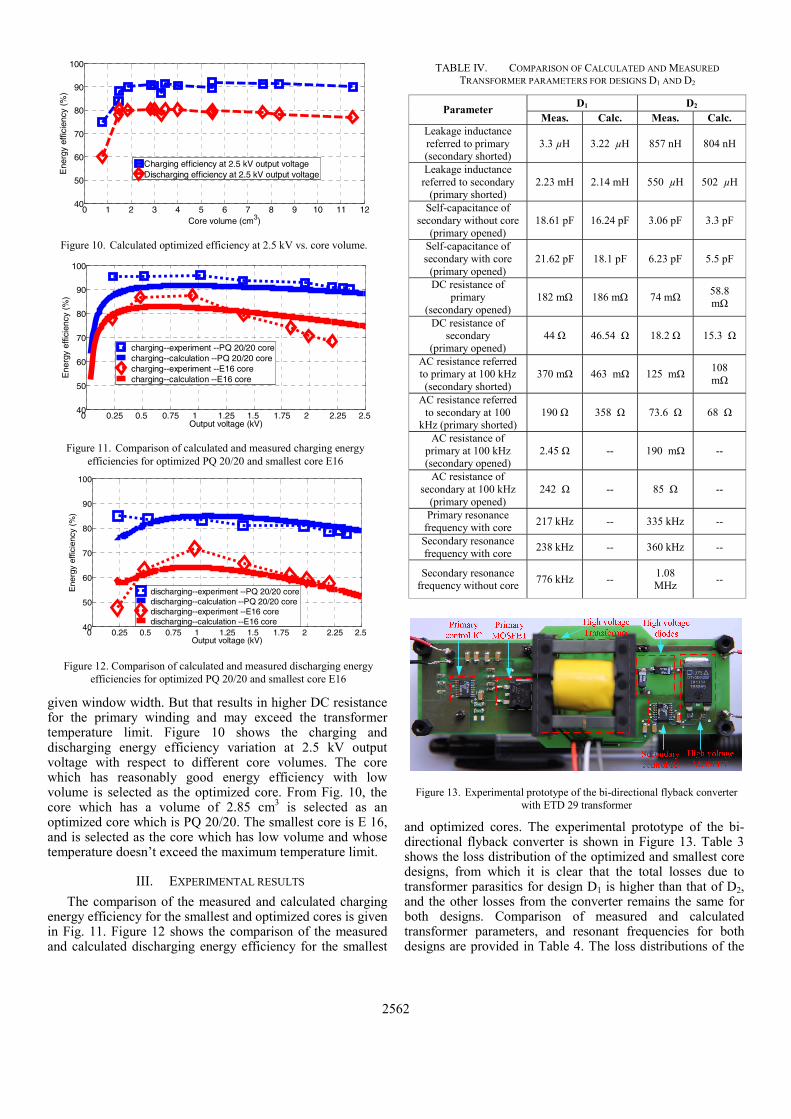
given window width. But that results in higher DC resistance for the primary winding and may exceed the transformer temperature limit. Figure 10 shows the charging and discharging energy efficiency variation at 2.5 kV output voltage with respect to different core volumes. The core which has reasonably good energy efficiency with low volume is selected as the optimized core. From Fig. 10, the core which has a volume of 2.85 cm3 is selected as an optimized core which is PQ 20/20. The smallest core is E 16, and is selected as the core which has low volume and whose temperature doesn’t exceed the maximum temperature limit.
III. EXPERIMENTAL RESULTS The comparison of the measured and calculated charging
energy efficiency for the smallest and optimized cores is given in Fig. 11. Figure 12 shows the comparison of the measured and calculated discharging energy efficiency for the smallest
and optimized cores. The experimental prototype of the bi-directional flyback converter is shown in Figure 13. Table 3 shows the loss distribution of the optimized and smallest core designs, from which it is clear that the total losses due to transformer parasitics for design D1 is higher than that of D2, and the other losses from the converter remains the same for both designs. Comparison of measured and calculated transformer parameters, and resonant frequencies for both designs are provided in Table 4. The loss distributions of the
Figure 11. Comparison of calculated and measured charging energy efficiencies for optimized PQ 20/20 and smallest core E16
TABLE IV. COMPARISON OF CALCULATED AND MEASURED TRANSFORMER PARAMETERS FOR DESIGNS D1 AND D2
Parameter D1 D2 Meas. Calc. Meas. Calc.
Leakage inductance referred to primary (secondary shorted)
3.3 µH 3.22 µH 857 nH 804 nH
Leakage inductance referred to secondary
(primary shorted) 2.23 mH 2.14 mH 550 µH 502 µH
Self-capacitance of secondary without core
(primary opened) 18.61 pF 16.24 pF 3.06 pF 3.3 pF
Self-capacitance of secondary with core
(primary opened) 21.62 pF 18.1 pF 6.23 pF 5.5 pF
DC resistance of primary
(secondary opened) 182 mΩ 186 mΩ 74 mΩ 58.8
mΩ
DC resistance of secondary
(primary opened) 44 Ω 46.54 Ω 18.2 Ω 15.3 Ω
AC resistance referred to primary at 100 kHz (secondary shorted)
370 mΩ 463 mΩ 125 mΩ 108 mΩ
AC resistance referred to secondary at 100
kHz (primary shorted) 190 Ω 358 Ω 73.6 Ω 68 Ω
AC resistance of primary at 100 kHz (secondary opened)
2.45 Ω -- 190 mΩ --
AC resistance of secondary at 100 kHz
(primary opened) 242 Ω -- 85 Ω --
Primary resonance frequency with core 217 kHz -- 335 kHz --
Secondary resonance frequency with core 238 kHz -- 360 kHz --
Secondary resonance frequency without core 776 kHz -- 1.08
MHz
--
Figure 10. Calculated optimized efficiency at 2.5 kV vs. core volume.
Figure 12. Comparison of calculated and measured discharging energy efficiencies for optimized PQ 20/20 and smallest core E16
Figure 13. Experimental prototype of the bi-directional flyback converter with ETD 29 transformer
0 0.25 0.5 0.75 1 1.25 1.5 1.75 2 2.25 2.5 40
50
60
70
80
90
100
Output voltage (kV)
Ene
rgy
effic
ienc
y (%
)
charging--experiment --PQ 20/20 core charging--calculation --PQ 20/20 core charging--experiment --E16 core charging--calculation --E16 core
0 1 2 3 4 5 6 7 8 9 10 11 1240
50
60
70
80
90
100
Core volume (cm3)
Ene
rgy
effic
ienc
y (%
)
Charging efficiency at 2.5 kV output voltageDischarging efficiency at 2.5 kV output voltage
0 0.25 0.5 0.75 1 1.25 1.5 1.75 2 2.25 2.5 40
50
60
70
80
90
100
Output voltage (kV)
Ene
rgy
effic
ienc
y (%
)
discharging--experiment --PQ 20/20 core discharging--calculation --PQ 20/20 core discharging--experiment --E16 core discharging--calculation --E16 core
2562
optimized design during charge and discharge processes are shown in Figs. 14 and 15, respectively.
IV. CONCLUSIONS In this paper, a new dynamic transformer winding design
concept is introduced. An optimization algorithm for minimizing the total energy loss of a bi-directional flyback converter for a high voltage capacitor charging application is presented. Winding loss calculation for a flyback transformer, with a simple non-interleaved structure is discussed. The proposed optimization technique is experimentally validated on a bi-directional flyback converter, and high efficiency (>90%) is achieved during the charge process. The proposed dynamic winding design can be easily extended to other transformer structures and for other applications.
REFERENCES [1] R. E. Pelrine, R. D. Kornbluh, Q. Pei, and J. P. Joseph, “High-speed
electrically actuated elastomers with strain greater than 100%,” in Proc. Science, vol. 287, pp. 836–839, 2000.
[2] R. E. Pelrine, R. D. Kornbluh, and J. P. Joseph, “Electrostriction of polymer dielectric with compliant electrodes as a means of actuation,” in Proc. Sensors and Actuators A, vol. 64, pp. 77–85, 1998.
[3] M. Tryson, H. E. Kiil, M. Benslimane, “Powerful tubular core free dielectric electro active polymer (DEAP) push actuator,” in Proc. SPIE Electroactive Polymer Actuators and Devices (EAPAD), vol. 7287, 2009.
[4] R. Sarban, B. Lassen, M. Willatzen, “Dynamic Electromechanical Modeling of Dielectric Elastomer Actuators With Metallic Electrodes,” in Proc. IEEE/ASME Transactions on Mechatronics, vol. 17, no. 5, pp. 960-967, Oct. 2012.
[5] L. Eitzen, C. Graf, J. Maas, “Cascaded bidirectional flyback converter driving DEAP transducers,” in Proc. IECON, pp. 1226-1231, 7-10 Nov. 2011.
[6] P. Thummala, Z. Zhang, M. A. E. Andersen, “High Voltage Bi-directional Flyback Converter for Capacitive Actuator,” in Proc. European Power Electronics Conference (EPE), pp. 3-6th Sept. 2013.
[7] L. Eitzen, T Hoffstadt, J. Maas, “Power electronics concepts for driving EAP actuators,” in Proc. SPIE Electroactive Polymer Actuators and Devices (EAPAD), pp. 86870D, 2013.
[8] P. Thummala, Z. Zhang, M. A. E. Andersen, O. C. Thomsen, “A high voltage DC-DC converter driving a Dielectric Electro Active Polymer actuator for wind turbine flaps,” in Proc. IEEE UPEC, pp. 1-7, 4-7 Sept. 2012.
[9] J. Elmes, C. Jourdan, O. Abdel-Rahman, I. Batarseh, “High-Voltage, High-Power-Density DC-DC Converter for Capacitor Charging Applications,” in Proc. IEEE APEC, pp. 433-439, 2009.
[10] T. Andersen, M. S. Rødgaard, O. C. Thomsen, M. A. E. Andersen, “Low voltage driven dielectric electro active polymer actuator with integrated piezoelectric transformer based driver,” in Proc. SPIE Electroactive Polymer Actuators and Devices (EAPAD), vol. 7976, pp. 79762N, 2011.
[11] S. K. Chung, H. B. Shin, “High-voltage power supply for semi-active suspension system with ER-fluid damper,” in Proc. IEEE Transactions on Vehicular Technology, vol. 53, no. 1, pp. 206- 214, Jan. 2004.
[12] P. Thummala, H. Schneider, Z. Ouyang, Z. Zhang, M. A. E. Andersen, “Estimation of transformer parameters and loss analysis for high voltage capacitor charging application,” in Proc. IEEE ECCE Asia, pp. 704-710, 3-6 Jun. 2013.
[13] R. Prieto, J.A. Cobos, O. Garcia, R. Asensi and J. Uceda, “Optimizing the winding strategy of the transformer in a flyback converter,” in Proc. IEEE Power Electronics Specialists Conference (PESC), vol. 2, pp. 1456-1462, 1996.
[14] C. R. Sullivan, T. Abdallah, T. Fujiwara, “Optimization of a flyback transformer winding considering two-dimentional field effects, cost and loss,” in Proc. IEEE APEC, vol.1, pp.116-122, 2001.
[15] H. K. Sang, D. Maksimovic, I. Cohen, “Efficiency Optimization in Digitally Controlled Flyback DC–DC Converters Over Wide Ranges of Operating Conditions,” in Proc. IEEE Transactions on Power Electronics, vol. 27, no. 8, pp. 3734-3748, Aug. 2012.
[16] R. P. Wojda, M. K. Kazimierczuk, “Analytical Optimization of Solid–Round-Wire Windings,” in Proc. IEEE Transactions on Industrial Electronics, vol. 60, no. 3, pp. 1033-1041, March 2013.
[17] A.C. Nanakos, E.C. Tatakis, N.P Papanikolaou, “A Weighted-Efficiency-Oriented Design Methodology of Flyback Inverter for AC Photovoltaic Modules,” in Proc. IEEE Transactions on Power Electronics, vol. 27, no. 7, pp. 3221-3233, July 2012.
[18] C. Marxgut, J. Muhlethaler, F. Krism, J.W. Kolar, “Multiobjective Optimization of Ultraflat Magnetic Components With PCB-Integrated Core,” in Proc. IEEE Transactions on Power Electronics, vol. 28, no. 7, pp. 3591-3602, July 2013.
[19] J. Mühlethaler, “Modeling and Multi-Objective Optimization of Inductive Power Components,”, Ph.D. Theis, Dept. Information Technology and Electrical Engineering, ETH Zurich, Switzerland 2012.
[20] Z. Ouyang, “Planar Magnetics for High Grade Converter,” Ph.D. Theis, Dept. Electrical Engineering, Technical University of Denmark, Denmark 2011.
[21] N. O. Sokal, R. Redl, “Control algorithms and circuit designs for optimal flyback-charging of an energy storage capacitor (e.g., for flash lamp or defibrillator),” in Proc. IEEE Transactions on Power Electronics, vol. 12, no. 5, pp. 885-894, Sep. 1997.
[22] J. Vandelac, P. D. Ziogas, “A Novel Approach for Minimizing High-Frequency Transformer Copper Losses,” IEEE Trans. on Power Electronics, vol. 3, no. 3, pp. 266-277, Jul 1988.
[23] S. H. Kang, “Efficiency Optimization in Digitally Controlled Flyback DC-DC Converters Over Wide Ranges of Operating Conditions,” Ph.D. Theis, Dept. Electrical, Computer and Energy Engineering, University of Colorado Boulder, USA 2011.
[24] P. Thummala, Z. Zhang, M. A. E. Andersen, S. Rahimullah, “Dielectric electro active polymer incremental actuator driven by multiple high-voltage bi-directional DC-DC converters,” in Proc. IEEE ECCE USA, pp. 3837-3844, 15-19 Sept. 2013.
Figure 14. Energy loss distribution during charge process with optimized core.
Figure 15. Energy loss distribution during discharge process with optimized core.
7%7%
4%
24%
16%
35%
2%2%<1%5%
Transformer copper lossTransformer core lossConduction loss of primary MOSFETSwitching loss of primary MOSFETLeakage lossSwitching loss due to transformerwinding capacitanceHV diode (5kV) conduction lossLoss due to primarycurrent sense resistorPrimary MOSFET driving lossLoss due to IC power consumption
< 1%5%
3%
43%
21%
14%
< 1%6%
< 1%6%
Transformer copper lossTransformer core lossConduction loss of high voltage(4kV) MOSFETSwitching loss of high voltage(4kV) MOSFETSwitching loss due to transformer winding capacitanceHV RCD snubber lossHV diode (5kV) in series with the HV MOSFET conduction lossConduction loss of body diode of primary MOSFETHV(4kV) MOSFET driving lossLoss due to control IC
2563

120/255
Appendix HEfficiency Optimization by
Considering the High VoltageFlyback Transformer Parasiticsusing an Automatic Winding
Layout Technique
IEEE Transactions on Power Electronics, DOI: 10.1109/TPEL.2014.2379439
121/255

0885-8993 (c) 2013 IEEE. Personal use is permitted, but republication/redistribution requires IEEE permission. Seehttp://www.ieee.org/publications_standards/publications/rights/index.html for more information.
This article has been accepted for publication in a future issue of this journal, but has not been fully edited. Content may change prior to final publication. Citation information: DOI10.1109/TPEL.2014.2379439, IEEE Transactions on Power Electronics
TPEL-Reg-2014-09-1319
Abstract—This paper presents an efficiency optimization
approach for a high voltage bidirectional flyback dc-dc
converter. The main goal is to optimize the converter for driving
a capacitive actuator, which must be charged and discharged
from 0 V to 2.5 kV dc and vice versa, supplied from a 24 V dc
supply. The energy efficiency is optimized using a proposed new
automatic winding layout (AWL) technique and a comprehensive
loss model. The AWL technique generates a large number of
transformer winding layouts. The transformer parasitics such as
dc resistance, leakage inductance and self-capacitance are
calculated for each winding layout. An optimization technique is
formulated to minimize the sum of energy losses during charge
and discharge operations. The efficiency and energy loss
distribution results from the optimization routine provide a deep
insight into the high voltage transformer design and its impact on
the total converter efficiency. The proposed efficiency
optimization approach is experimentally verified on a 25 W
(average charging power) with 100 W (peak power) flyback dc-dc
prototype.
Index Terms—switched-mode power supply, high voltage dc-
dc power converter, transformer design, optimization, energy
efficiency, actuators, dielectric films
NOMENCLATURE
auC, buC Coefficients of Fourier series of the magneto
motive force (MMF) during charge process (AT:
Ampere-turns)
BmC / BmD Maximum flux density during charge / discharge
process (T)
BnC Magnitude of negative flux density at the
beginning of a switching cycle during charge
process (T)
ΔB Peak-to-peak flux density of the current excitation
(T)
Manusctipt received on 8th Sept. 2014, revised on 15th Oct. 2014, and
accepted on 24th Nov. 2014. This paper has been presented at 29th Annual
Applied Power Electronics Conference, Fort Worth, TX, USA, March 2014. All authors are with the Electronics Group, Department of Electrical
Engineering, Technical University of Denmark, Kongens Lyngby, DK-2800
Denmark. E-mail: *[email protected], [email protected], [email protected],
[email protected], [email protected], [email protected]. *Indicates the corresponding author.
Cin / Cload Input capacitance / Capacitance of the load or
actuator (F)
Cs Self-capacitance of secondary winding (F)
Cossp / Cosss Output capacitance of low voltage MOSFET Mp /
high voltage MOSFET Ms (F)
CDb Junction capacitance of high voltage diode Db (F)
dp / ds Diameter of primary / secondary winding of
transformer (mm)
D2 / Db High voltage (5 kV) freewheeling diode /
blocking diode
dinsulation Uniform spacing or thickness of the insulating
tape, between secondary layers (mm)
DonC / DoffC On-time / Off-time duty cycle of low voltage
MOSFET Mp during charge process
DonD / DoffD On-time / Off-time duty cycle of high voltage
MOSFET Ms during discharge process
Eload(Vout) Stored energy in the load at an output voltage Vout
(J)
fswC / fswD Switching frequency during charge / discharge
process (kHz)
FFLL Fill factor of the last layer in the high voltage
winding
FuC(0) / FuC(h) MMF amplitude of uth harmonic at x=0 / x=h, h is
the thickness of layer
G1, G2 Constants used in the power loss expressions and
are functions of εu
HW Window height of transformer bobbin (mm)
iin / ip / is Input current / Primary current / Secondary or
load current (A)
imp / ims Primary / Secondary magnetizing current (A)
IppkC / IppkD Primary peak current during charge process /
discharge process (A)
IspkC / IspkD Secondary peak current during charge process /
discharge process (A)
imin Magnitude of the negative primary current at the
beginning of charge process (A)
IpavgC / IsavgC Primary / Secondary average current during
charge process (A)
kz Core loss constant in the improved generalized
Steinmetz equation (iGSE)
Lmp / Lms Primary / Secondary magnetizing inductance of
transformer (H)
Llkp / Llks Leakage inductance referred to primary /
secondary side of transformer (H)
Mp / Ms Low voltage MOSFET / High voltage (4 kV)
MOSFET
Efficiency Optimization by Considering the
High Voltage Flyback Transformer Parasitics
using an Automatic Winding Layout Technique
Prasanth Thummala*, Student Member IEEE, Henrik Schneider, Student Member IEEE, Zhe Zhang,
Member IEEE, Ziwei Ouyang, Member IEEE, Arnold Knott, Member IEEE, and Michael A. E.
Andersen, Member, IEEE

0885-8993 (c) 2013 IEEE. Personal use is permitted, but republication/redistribution requires IEEE permission. Seehttp://www.ieee.org/publications_standards/publications/rights/index.html for more information.
This article has been accepted for publication in a future issue of this journal, but has not been fully edited. Content may change prior to final publication. Citation information: DOI10.1109/TPEL.2014.2379439, IEEE Transactions on Power Electronics
TPEL-Reg-2014-09-1319
Np / Ns / n Number of primary / secondary turns / Turns ratio
of transformer from secondary to primary
nlp / nls Number of layers in primary / secondary winding
of transformer
nparp / npars Number of parallel wires in primary / secondary
winding of transformer
Nh / Nc Total number of harmonics considered / Total
number of switching cycles during charge process k
layerCP Power loss in kth layer during charge process (W)
PwindC / PTwindC Winding loss at each switching cycle / Total
winding loss during charge process (W)
PswC / PswD Capacitive switching loss due the self-capacitance
during charge / discharge process (W)
PsnC / PsnD Snubber loss due leakage inductance during
charge / discharge process (W)
Rp / Rs dc resistance of primary / secondary winding of
transformer (Ω)
Rpsense / Rssense Primary / Secondary current sense resistance (Ω)
Rlayer dc resistance of a given layer (Ω)
tonC / toffC On-time / Off-time of low voltage MOSFET Mp
during charge process (s)
tonD / toffD On-time / Off-time of high voltage MOSFET Ms
during discharge process (s)
TsC / TsD Switching period during charge / discharge
process (s)
Tch Charging time to reach the target output voltage
from 0 V (s)
Tlayer Number of turns in a given layer (primary or
secondary) of transformer
VleakD Increase in the steady state drain-to-source
voltage of Ms due to leakage inductance Llks (V)
Vin / Vout Input voltage / Output or load or actuator voltage
(V)
WW Window width of bobbin (mm)
Wsqp / Wsqs Width of square for primary / secondary in the
automatic winding layout generator routine (mm)
γs / γp Height allocation factor for secondary / primary
winding with γp=(1-γs)
δu / δ Skin depth of the conductor at uth harmonic
frequency / fundamental (u=0) frequency (mm)
εu Ratio of conductor diameter to the effective skin
depth of uth harmonic
φuC(0) / φuC(h) Phase of uth harmonic of the MMF during charge
process at x=0 / x=h (h is thickness of layer)
ρ / μ0 Resistivity of copper (Ω-m) / Magnetic
permeability of vacuum (H/m)
α, β, k The constants related to core material which are
provided by the core manufacturer
δC Capacitance ratio factor on the high voltage side
I. INTRODUCTION
IELETRC electro active polymer (DEAP) [1]-[3] is an
evolving smart material that can be used in actuation,
sensing and energy harvesting applications [4]. DEAPs, when
used as linear actuators, have the potential to be an effective
replacement for many conventional linear actuators because of
their unique properties, including light weight, low noise
operation, high flexibility, large strain, and autonomous
capability. The axial DEAP actuator as shown in Fig. 1(a) is
ideally equivalent to a capacitive load. When a DEAP actuator
is driven with high voltage (2-2.5 kV), it converts a portion of
the electrical energy into mechanical displacement, which is of
the order of mm (~1-1.5 mm) [5]-[7]. Three of such axial
DEAP actuators are used to create a DEAP incremental
actuator [8] as shown in Fig. 1(b). The DEAP incremental
actuator technology has the potential to be used in various
industries, e.g. automotive, aeronautics, and medicine. For
using the DEAP actuators in such applications, the high
voltage drivers should have low volume to fit inside or above
the actuators. The overall energy efficiency of battery
powered, high voltage driver influences, the distance travelled
by the incremental actuator. Hence, for DEAP actuator
applications, both volume and energy efficiency of high
voltage drivers are extremely important and need to be
optimized.
The flyback converter is suitable for high voltage and low
power applications due to its simple structure and a low
component count [9]. High voltage switch-mode power
supplies for charging the capacitive loads are implemented in
[10]-[12]. Bidirectional dc-dc power converters are needed for
the DEAP based capacitive actuators [13], to increase the
lifetime of the battery, also to discharge the high voltage
across them. Bidirectional flyback converter [14]-[17], and a
forward-flyback bidirectional converter [18] are implemented
for various applications. Due to high reverse recovery time
(~2.6 μs) of high voltage MOSFET, a modified high voltage
bidirectional flyback converter topology [19] as shown in Fig.
2, is proposed and implemented for driving a DEAP actuator.
The loss analysis of the same converter is performed in [20].
Transformer design plays a very important role in high
voltage dc-dc power converters employed in low, medium and
high power applications. The design methodologies for
transformers used in conventional switch-mode power
supplies are well documented [9], [21]-[23]. Often, a
transformer for a given application is designed based on some
assumptions such as, constant switching frequency, maximum
A1
A3
A2
Grippers
Extender
a) b)
33 mm
110 mm
A1
A3
A2
Grippers
Extender
a) b)
33 mm
110 mm
Fig. 1. a) DEAP actuator; b) DEAP incremental actuator.
D
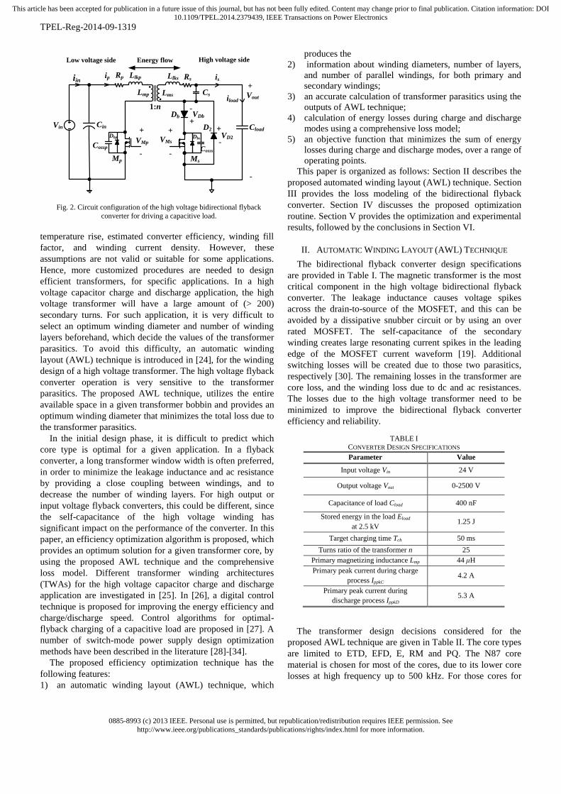
0885-8993 (c) 2013 IEEE. Personal use is permitted, but republication/redistribution requires IEEE permission. Seehttp://www.ieee.org/publications_standards/publications/rights/index.html for more information.
This article has been accepted for publication in a future issue of this journal, but has not been fully edited. Content may change prior to final publication. Citation information: DOI10.1109/TPEL.2014.2379439, IEEE Transactions on Power Electronics
TPEL-Reg-2014-09-1319
temperature rise, estimated converter efficiency, winding fill
factor, and winding current density. However, these
assumptions are not valid or suitable for some applications.
Hence, more customized procedures are needed to design
efficient transformers, for specific applications. In a high
voltage capacitor charge and discharge application, the high
voltage transformer will have a large amount of (> 200)
secondary turns. For such application, it is very difficult to
select an optimum winding diameter and number of winding
layers beforehand, which decide the values of the transformer
parasitics. To avoid this difficulty, an automatic winding
layout (AWL) technique is introduced in [24], for the winding
design of a high voltage transformer. The high voltage flyback
converter operation is very sensitive to the transformer
parasitics. The proposed AWL technique, utilizes the entire
available space in a given transformer bobbin and provides an
optimum winding diameter that minimizes the total loss due to
the transformer parasitics.
In the initial design phase, it is difficult to predict which
core type is optimal for a given application. In a flyback
converter, a long transformer window width is often preferred,
in order to minimize the leakage inductance and ac resistance
by providing a close coupling between windings, and to
decrease the number of winding layers. For high output or
input voltage flyback converters, this could be different, since
the self-capacitance of the high voltage winding has
significant impact on the performance of the converter. In this
paper, an efficiency optimization algorithm is proposed, which
provides an optimum solution for a given transformer core, by
using the proposed AWL technique and the comprehensive
loss model. Different transformer winding architectures
(TWAs) for the high voltage capacitor charge and discharge
application are investigated in [25]. In [26], a digital control
technique is proposed for improving the energy efficiency and
charge/discharge speed. Control algorithms for optimal-
flyback charging of a capacitive load are proposed in [27]. A
number of switch-mode power supply design optimization
methods have been described in the literature [28]-[34].
The proposed efficiency optimization technique has the
following features:
1) an automatic winding layout (AWL) technique, which
produces the
2) information about winding diameters, number of layers,
and number of parallel windings, for both primary and
secondary windings;
3) an accurate calculation of transformer parasitics using the
outputs of AWL technique;
4) calculation of energy losses during charge and discharge
modes using a comprehensive loss model;
5) an objective function that minimizes the sum of energy
losses during charge and discharge modes, over a range of
operating points.
This paper is organized as follows: Section II describes the
proposed automated winding layout (AWL) technique. Section
III provides the loss modeling of the bidirectional flyback
converter. Section IV discusses the proposed optimization
routine. Section V provides the optimization and experimental
results, followed by the conclusions in Section VI.
II. AUTOMATIC WINDING LAYOUT (AWL) TECHNIQUE
The bidirectional flyback converter design specifications
are provided in Table I. The magnetic transformer is the most
critical component in the high voltage bidirectional flyback
converter. The leakage inductance causes voltage spikes
across the drain-to-source of the MOSFET, and this can be
avoided by a dissipative snubber circuit or by using an over
rated MOSFET. The self-capacitance of the secondary
winding creates large resonating current spikes in the leading
edge of the MOSFET current waveform [19]. Additional
switching losses will be created due to those two parasitics,
respectively [30]. The remaining losses in the transformer are
core loss, and the winding loss due to dc and ac resistances.
The losses due to the high voltage transformer need to be
minimized to improve the bidirectional flyback converter
efficiency and reliability.
The transformer design decisions considered for the
proposed AWL technique are given in Table II. The core types
are limited to ETD, EFD, E, RM and PQ. The N87 core
material is chosen for most of the cores, due to its lower core
losses at high frequency up to 500 kHz. For those cores for
1:n
Vout
Cin
Db
+
-
Mp Ms
ip is
Energy flow
Vin
Rp Llkp
Lmp Lms
RsLlks
Csiload
High voltage sideLow voltage side
+
-
+
-
VMp VMsCossp Cosss
D2
+
-VDb
+
-VD2
Cload
Dbp Dbs
iin
Fig. 2. Circuit configuration of the high voltage bidirectional flyback
converter for driving a capacitive load.
TABLE I CONVERTER DESIGN SPECIFICATIONS
Parameter Value
Input voltage Vin 24 V
Output voltage Vout 0-2500 V
Capacitance of load Cload 400 nF
Stored energy in the load Eload
at 2.5 kV 1.25 J
Target charging time Tch 50 ms
Turns ratio of the transformer n 25
Primary magnetizing inductance Lmp 44 μH
Primary peak current during charge
process IppkC 4.2 A
Primary peak current during
discharge process IppkD 5.3 A

0885-8993 (c) 2013 IEEE. Personal use is permitted, but republication/redistribution requires IEEE permission. Seehttp://www.ieee.org/publications_standards/publications/rights/index.html for more information.
This article has been accepted for publication in a future issue of this journal, but has not been fully edited. Content may change prior to final publication. Citation information: DOI10.1109/TPEL.2014.2379439, IEEE Transactions on Power Electronics
TPEL-Reg-2014-09-1319
which N87 material is not available, other core materials
which are suitable for operation up to 500 kHz are considered.
A simple, non-interleaved winding structure (P/S; P: Primary,
S: Secondary), is considered in this paper to limit the
complexity of the proposed AWL technique. Nevertheless, the
proposed AWL technique can be easily extended for the
interleaved transformer structures (P/S/P or S/P/S). The proper
insulation between the low voltage (primary) and high voltage
(secondary) windings is achieved by using a triple insulated
(TEX-E) solid wire for primary winding. To avoid the high
insulation thickness (0.2 mm) of TEX-E wire, single insulated
solid wire is used for a large number of secondary turns. A
maximum transformer temperature limit of 130 °C is chosen.
These limitation values can be altered based on the experience
of the user or the initial design specifications.
The AWL technique is described below:
A. AWL technique:
The space allocated for the primary and secondary
windings for a given transformer bobbin with winding width
WW and window height HW are shown in Fig. 3(a). Different
steps associated with the proposed AWL technique for an
example of Np=6 primary turns and Ns=18 secondary turns, are
explained below:
1) The first step is, to split the available winding space for
primary (see Fig. 3(a)) and secondary (Fig. 3(f)) into a
number of squares, with a square width equal to height
allocated for that winding. As shown in Figs. 3(d) and
3(g), it results into 4 squares and a crossed non-square,
which is considered as an unusable space for both primary
and secondary windings. In each square, a solid round
wire could be placed with a diameter equal to the width of
a square or a bundle of round wires with an outside
bundle diameter equal to the width of a square.
2) Since the number of available squares is 4 in Figs. 3(d) or
3(g), which is less than the required 6 primary and 18
secondary turns, more squares are required to fill the
needed turns. Hence, the width of square for primary or
secondary is decreased from its maximum value of γpHW
or γsHW, respectively.
3) The fill factor of the last layer FFLL for a given winding is
defined as the ratio of the number of squares used in the
final layer to the number of squares available in it. For
example, in Fig. 3(i), 9 squares are available and 9
squares are occupied in the final layer, hence FFLL=1.
Similarly, in Fig. 3(j), 16 squares are available and 13
squares are occupied in the final layer, hence FFLL=0.81.
In the proposed AWL technique a maximum limit of 0.85
is set for FFLL, since the calculation of transformer
parasitics is based on fully occupied layers.
4) When the square width is reduced as shown in Figs. 3(e)
and 3(h), the new square size limits the use of a shaded
space above the squares. For primary winding since only
6 turns are needed, this will be a valid solution. However,
for secondary winding, since 18 turns are needed, the
shaded space can be occupied by the other windings, by
reducing the square width further.
5) When the square width is reduced further as shown in Fig.
3(i), the winding space contains 18 squares in 2 layers,
and a shaded space. The non-square horizontal space is
utilized to provide an insulation tape (with thickness
dinsulation) between the secondary layers. This is the final
step of the AWL technique for 6 primary and 18
secondary turns.
6) If 45 turns are required for the secondary winding, the
square width is decreased again, as shown in Fig. 3(j), the
solution contains 3 layers and 16 squares in each layer.
The last layer fill factor FFLL in this case is 0.81, which is
less than 0.85. Hence, this is not a valid solution and the
square width needs to be decreased further.
7) In Fig. 3(b), a solution from the AWL technique is shown.
The primary and secondary squares are filled with triple
isolated and single isolated solid wires, respectively. The
same steps described above apply for the real high voltage
transformer design which will have more than 200
secondary turns.
8) Finally, the outputs of AWL technique are various
winding implementations, including specific winding
details such as, diameters of primary and secondary
windings, number of primary and secondary winding
layers, and insulation thicknesses for placing between
secondary windings, for which FFLL>0.85, respectively.
TABLE II
TRANSFORMER DESIGN DECISIONS
Description Design decision Comments
Ferrite core and bobbin type ETD, EFD, E, RM and PQ Typically used in switch-mode power supplies.
Core material N87 Suitable for switching frequencies up to 500 kHz.
Winding structure P/S Simple implementation and decreases analytical complexity.
Primary winding type Solid wire Flexible winding type in terms of design and prototyping.
Primary winding insulation Triple insulation (TEX-E) Edge tape can be avoided. No need for interlayer insulation tape between the
primary and secondary windings.
Secondary winding type Solid wire Suitable winding type, for a large number of turns. Flexible winding type in terms
of design, prototyping and different winding structures.
Secondary winding
insulation Single insulation Provides minimum insulation thickness for a large number of turns.
Air gap All legs Simplifies the prototyping.
Maximum transformer
temperature 130 °C
With a predicted ambient temperature of 35 °C, this enables transformer
temperature rise of 95 °C.

0885-8993 (c) 2013 IEEE. Personal use is permitted, but republication/redistribution requires IEEE permission. Seehttp://www.ieee.org/publications_standards/publications/rights/index.html for more information.
This article has been accepted for publication in a future issue of this journal, but has not been fully edited. Content may change prior to final publication. Citation information: DOI10.1109/TPEL.2014.2379439, IEEE Transactions on Power Electronics
TPEL-Reg-2014-09-1319
B. Calculation of transformer parasitics using the results of
AWL technique:
The outputs of the AWL technique are used to calculate the
transformer parasitics [20], [24], [35]-[37] such as dc
resistance, leakage inductance and self-capacitance. In Fig. 4,
one output of AWL technique such as the insulation thickness
(dinsulation) for a PQ 20/20 core, and calculated transformer
parasitics are shown with respect to square width (Wsqs) of
secondary winding. As the width of the secondary square (or
secondary winding) decreases, the insulation spacing dinsulation
between secondary winding layers increases, dc resistance Rs
increases, leakage inductance Llkp slightly decreases, and the
self-capacitance Cs decreases.
1 2 3 4
Winding space allocation for
primary
WW
γpHW
1 2 3 4 5 6
c)
d)
e)
Wsqp Wsqp=γpHW
Wsqp Wsqp<γpHW
HW
WW
γsHW
Top view of the bobbin for horizontal E and ETD, EFD cores
Side view of the bobbin for verticle E cores and PQ, RM cores
Symmetrical line
10 11 12 13 14 15 16 17 18
98721 43 5 6
γpHW
HW
WW
γsHW
Symmetrical line
γpHW
Winding space allocation for
secondary
Winding space allocation for
primary
Transformer
Bobbin
1 2 3 4
Winding space allocation for
secondary
WW
γsHW
1 2 3 4 5 6 7 8 9
10 11 12 13 14 15 16 17 18
f)
g)
h)
i)
Space equally distributed
between secondary layers
Crossed space which is not utilized
by the windings
Wsqs Wsqs=γsHW
Wsqs Wsqs<γsHW
WsqsWsqs<0.5γsHW
Transformer
Bobbin
a) b)
1 2 3 4 16
32
5 6 7 10 128 9 11 14 1513
171819 20 2122 23 26 2824 25 27 30 3129
3334 3536 37 38 39 42 4440 41 43 45
j)
Wsqs
1 2 3 4 5 6
1 2 3 4 5 6
Squares Non-square
Non-square
γpHW
γpHW
γsHW
γsHW
γsHW
γsHW
dinsulation
dinsulation
dinsulation
Fig. 3. a) Allocated winding space a) before applying AWL technique; b) after applying AWL technique; c) - e) Different steps involved in AWL
technique for primary winding; f) - j) Different steps involved in AWL technique for secondary winding;
0.15 0.2 0.25 0.3
0.25
0.5
0.75
1
Square width Wsqs
(mm)
din
su
latio
n(m
m)
0.15 0.2 0.25 0.3
5
10
15
20
Square width Wsqs
(mm)
Rs(o
hm
)
0.15 0.2 0.25 0.3
0.820.840.860.880.9
Square width Wsqs
(mm)
Llk
p(u
F)
0.15 0.2 0.25 0.3
5
10
15
Square width Wsqs
(mm)
Cs (
pF
)
Fig. 4. Variation of transformer parasitics with the diameter of secondary winding, for PQ 20/20 core (when γs=0.8).

0885-8993 (c) 2013 IEEE. Personal use is permitted, but republication/redistribution requires IEEE permission. Seehttp://www.ieee.org/publications_standards/publications/rights/index.html for more information.
This article has been accepted for publication in a future issue of this journal, but has not been fully edited. Content may change prior to final publication. Citation information: DOI10.1109/TPEL.2014.2379439, IEEE Transactions on Power Electronics
TPEL-Reg-2014-09-1319
III. LOSS MODELLING
In order to investigate the bidirectional flyback converter
efficiency, it is necessary to calculate the losses associated
with each circuit component in the converter. The loss model
is a function of transformer parasitics. Different losses in the
bidirectional flyback converter are given below:
A. Transformer winding loss:
In a flyback converter the primary and secondary currents
are 180° out of phase, hence the conventional equations
cannot be used to calculate the ac resistance [38], [39]. The
calculation of the total winding loss in a flyback converter
using the magneto motive force (MMF) analysis [40], [41] is
described below.
1) Winding loss in a flyback transformer during charge
process:
For the winding loss modeling, a non-interleaved
transformer with 2 layers on the primary side (P1 and P2) and
5 layers on the secondary side (S1, S2, S3, S4 and S5), is
considered as an example. The MMF distribution in a flyback
transformer is different from that of a normal transformer [40].
Figure 5 shows different MMF distributions during both turn-
on (0<t<tonC) and turn-off (tonC<t< tonC +toffC) periods in a non-
interleaved flyback transformer. In Fig. 5, Np1 and Np, are the
number of turns in the primary layer 1 and the total primary
turns, respectively, and H0, H1,….H7 are the magnetic field
intensities between the layers. The terms N1, N2, N3, N4, N5 are
defined as follows: N1=Ns1, N2=Ns1+Ns2, N3=Ns1+Ns2+Ns3,
N4=Ns1+Ns2+Ns3+Ns4, and N5=Ns1+Ns2+Ns3+Ns4+Ns5=Ns where
Ns1, Ns2, Ns3, Ns4, Ns5 and Ns are the number of turns in the
secondary layers 1, 2, 3, 4, 5, and the total number of
secondary turns, respectively. The primary imp(t) and
secondary ims(t) magnetizing current waveforms in a given
switching cycle, during charge and discharge processes are
shown in Figs. 6(a) and 6(b), respectively. The MMF
distribution in each transformer winding layer in the time
domain is decomposed into sinusoidal harmonics by Fourier
series analysis [24]. The power loss is then computed for each
harmonic, and the power loss densities over all harmonics are
summed to find the power dissipated in each layer.
The power loss expression in kth
layer klayerCP is given by [24],
[40], [41]
2 2
1
21
2
0
2 4 0 cos
hNuC uC ulayerk
layerC u
ulayeruC uC u
F h F GRP
T F h F G
(1)
0
u
swCuf
(2)
0.75 1.5
4
layer
u
W u
T d
W
(3)
where FuC(0) and FuC(h) are the MMF amplitudes of the uth
harmonic at the beginning (x=0) and end (x=h) of a layer,
respectively, d is the diameter of the given winding, h is the
thickness of a given layer, with the suffix u being the
harmonic number [24].
The magnitude uCF and phase φuC of uth
harmonic of the
MMF during charge process are given by
2 2
uC uC uCF a b (4)
1
1
tan , if 0
tan , if < 0
uC
uC
uC
uC
uC
uC
uC
ba
a
ba
a
(5)
0uC uC h (6)
where auC and buC are the coefficients of the Fourier series of
the MMF during charge process and are provided in [24], and
is the difference between the phase angles of the uth
a)
ON
0
OFF mpi t
t
DonCTsC
TsC
ppkCI
minI DoffC TsC
ON
0
OFF msi t
DCM
DonDTsD DoffDTsD (1-DonD-DoffD )TsD
spkDI
b)
t
Fig. 6. a) Primary magnetizing current in a given switching cycle during
charge process, and b) Secondary magnetizing current discharge process.
Transformer
Core
Symmetrical
line
P2
S1
S2
S3
S4
S5
MMF
Distribution0
P1
MMF
Distribution0
0<t<tonC tonC<t<(toffC +tonC)
H0
H1
H2
H3
H4
H5
H6
H7
x x
1p ppkCN I
p ppkCN I
1ppkCI
Nn
2ppkCI
Nn
3ppkCI
Nn
4ppkCI
Nn
5ppkCI
Nn
Switch is ON Switch is OFF
Fig. 5. MMF distribution of the non-interleaved (P-P-S-S-S-S-S) flyback
transformer with respect to space.

0885-8993 (c) 2013 IEEE. Personal use is permitted, but republication/redistribution requires IEEE permission. Seehttp://www.ieee.org/publications_standards/publications/rights/index.html for more information.
This article has been accepted for publication in a future issue of this journal, but has not been fully edited. Content may change prior to final publication. Citation information: DOI10.1109/TPEL.2014.2379439, IEEE Transactions on Power Electronics
TPEL-Reg-2014-09-1319
harmonic at the beginning (x=0) and end (x=h) of a layer,
respectively.
The expression for the winding loss in a flyback transformer at
each switching frequency (each switching cycle) index j
during charge process is
2 2
1
ls lp
pavgC savgC
n n
k
windC p s layerC
k
P j I j R I j R P j
(7)
The total winding loss during charge process having Nc
switching cycles is
1
cN
TwindC windC
j
P P j
(8)
2) Discussion:
The winding loss during discharge process is calculated
similar to that during charge process. The AC loss due to air-
gap fringing field [28] has not been considered because of
difficulties in interfacing the 2-D/3-D finite element analysis
(FEA) simulation results with the optimization process. The
negative current at the beginning of the turn-on process during
charge process in Fig. 6(a) is due to the high voltage winding
self-capacitance. When the secondary winding current
becomes zero, the drain to source voltage VMp tends to
decrease. Since the control IC, LT3751 [42] operates under
boundary mode control, the next switching cycle starts before
the high voltage winding capacitance completely discharges.
Hence, the current flows in the reverse direction to discharge
the high voltage winding capacitance.
B. Transformer core loss:
The time-average core loss per unit volume Pv due to non-
sinusoidal excitation is calculated using the improved
generalized Steinmetz equation (iGSE) [43] which is given by
0
1 sT
v z
s
dB tP k B dt
T dt
(9)
where dB t
dt is the absolute value of the change rate of the
flux density, ∆B is the peak-to-peak flux density, Ts is the
switching period, and k, α and β are the constants provided by
the core manufacturer. The core loss coefficient kz in (9) is
calculated using the following expression
2
1
0
2 2 cos d
z
kk
(10)
The angle θ in (10) represents the phase angle of the
sinusoidal excitation. For a given values of k, α and β, the
value of coefficient kz in (10) is fixed, irrespective of shape of
the flux density waveform.
The core loss per unit volume using iGSE during charge
operation (where mC nCB B B during the turn-on period
and mCB B during the turn-off period), in each switching
cycle is given by
1 1zvC mC nC onC mC offC
sC
kP B B t B t
T
(11)
Similarly, the core loss per unit volume during discharge
operation (where mDB B ), in each switching cycle is given
by
1 1zvD mD onD offD
sD
kP B t t
T
(12)
C. Switching loss due to transformer self-capacitance
The capacitive turn-on or switching loss due the self-
capacitance when the converter employs valley
switching/boundary conduction mode (BCM) control during
charge process is given by [26], [44], [45]
2
21
2
outswC s in swC
VP n C V f
n
(13)
When the output voltage Vout is greater than nVin, the
capacitive switching loss PswC is 0 W, since the converter
operates with zero voltage switching (ZVS). The capacitive
switching loss due the self-capacitance when the converter
employs DCM control during discharge process is [26]
21
2swD s Ms swDP C V f (14)
In DCM, the drain-to-source voltage VMs at the beginning of
the next switching cycle can be anywhere between
out C in C leakDV nV V and 2 1out C in C leakDV nV V .
The expression for c is given by [26]
osssc
osss Db
C
C C
(15)
The output capacitance Cosss of Ms and junction capacitance
CDb of diode Db are approximately 15 pF and 1 pF,
respectively.
D. Switching loss due to transformer leakage inductance
The loss due to the dissipative RCD snubber during charge
process is given by
21
2
snC
snC lkp ppkC swC
outsnC
VP L I f
VV
n
(16)
The loss due to the dissipative RCD snubber during discharge
process is given by
21
2
snD
snD lks spkD swD
snD in
VP L I f
V nV
(17)
where VsnC and VsnD are the snubber clamp voltages for low
and high voltage MOSFETs, respectively.
E. Remaining losses in the bidirectional flyback converter
The remaining losses in the converter during charge process
are: switching loss of Mp, conduction losses of Mp, D2 and
Rpsense, gate drive loss of Mp, and power consumption of
charge control IC. Similarly, the remaining losses in the
converter during discharge process are: switching loss of Ms,
conduction losses of Ms, Db and Rssense, gate drive loss of Ms,
and power consumption of discharge control IC. Since during
both charge and discharge operations the converter employs
BCM and DCM control, respectively, there are no diode
reverse recovery losses in both modes.
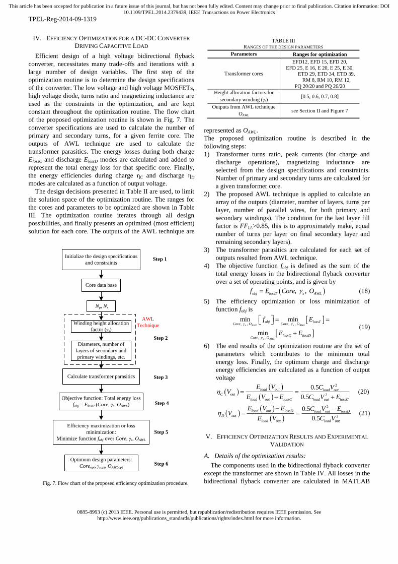
0885-8993 (c) 2013 IEEE. Personal use is permitted, but republication/redistribution requires IEEE permission. Seehttp://www.ieee.org/publications_standards/publications/rights/index.html for more information.
This article has been accepted for publication in a future issue of this journal, but has not been fully edited. Content may change prior to final publication. Citation information: DOI10.1109/TPEL.2014.2379439, IEEE Transactions on Power Electronics
TPEL-Reg-2014-09-1319
IV. EFFICIENCY OPTIMIZATION FOR A DC-DC CONVERTER
DRIVING CAPACITIVE LOAD
Efficient design of a high voltage bidirectional flyback
converter, necessitates many trade-offs and iterations with a
large number of design variables. The first step of the
optimization routine is to determine the design specifications
of the converter. The low voltage and high voltage MOSFETs,
high voltage diode, turns ratio and magnetizing inductance are
used as the constraints in the optimization, and are kept
constant throughout the optimization routine. The flow chart
of the proposed optimization routine is shown in Fig. 7. The
converter specifications are used to calculate the number of
primary and secondary turns, for a given ferrite core. The
outputs of AWL technique are used to calculate the
transformer parasitics. The energy losses during both charge
ElossC and discharge ElossD modes are calculated and added to
represent the total energy loss for that specific core. Finally,
the energy efficiencies during charge ηC and discharge ηD
modes are calculated as a function of output voltage.
The design decisions presented in Table II are used, to limit
the solution space of the optimization routine. The ranges for
the cores and parameters to be optimized are shown in Table
III. The optimization routine iterates through all design
possibilities, and finally presents an optimized (most efficient)
solution for each core. The outputs of the AWL technique are
represented as OAWL.
The proposed optimization routine is described in the
following steps:
1) Transformer turns ratio, peak currents (for charge and
discharge operations), magnetizing inductance are
selected from the design specifications and constraints.
Number of primary and secondary turns are calculated for
a given transformer core.
2) The proposed AWL technique is applied to calculate an
array of the outputs (diameter, number of layers, turns per
layer, number of parallel wires, for both primary and
secondary windings). The condition for the last layer fill
factor is FFLL>0.85, this is to approximately make, equal
number of turns per layer on final secondary layer and
remaining secondary layers).
3) The transformer parasitics are calculated for each set of
outputs resulted from AWL technique.
4) The objective function fobj is defined as the sum of the
total energy losses in the bidirectional flyback converter
over a set of operating points, and is given by
, ,obj lossT s AWLf E Core O (18)
5) The efficiency optimization or loss minimization of
function fobj is
, ,
,
min min
min
s AWL s AWL
s AWL
obj lossTCore , O Core , O
lossC lossDCore , O
f E
E E
(19)
6) The end results of the optimization routine are the set of
parameters which contributes to the minimum total
energy loss. Finally, the optimum charge and discharge
energy efficiencies are calculated as a function of output
voltage
2
2
0.5
0.5
load out load out
C out
load out lossC load out lossC
E V C VV
E V E C V E
(20)
2
2
0.5
0.5
load out lossD load out lossD
D out
load out load out
E V E C V EV
E V C V
(21)
V. EFFICIENCY OPTIMIZATION RESULTS AND EXPERIMENTAL
VALIDATION
A. Details of the optimization results:
The components used in the bidirectional flyback converter
except the transformer are shown in Table IV. All losses in the
bidirectional flyback converter are calculated in MATLAB
TABLE III RANGES OF THE DESIGN PARAMETERS
Parameters Ranges for optimization
Transformer cores
EFD12, EFD 15, EFD 20,
EFD 25, E 16, E 20, E 25, E 30, ETD 29, ETD 34, ETD 39,
RM 8, RM 10, RM 12,
PQ 20/20 and PQ 26/20
Height allocation factors for
secondary winding (γs) [0.5, 0.6, 0.7, 0.8]
Outputs from AWL technique
OAWL see Section II and Figure 7
Initialize the design specifications
and constraints
Objective function: Total energy loss
fobj = ElossT (Core, γs, OAWL)
Core data base
Winding height allocation
factor (γs)
Diameters, number of
layers of secondary and
primary windings, etc.
Calculate transformer parasitics
AWL
Technique
Np, Ns
Efficiency maximization or loss
minimization:
Minimize function fobj over Core, γs, OAWL
Optimum design parameters:
Coreopt, γsopt, OAWLopt
Step 1
Step 2
Step 3
Step 4
Step 5
Step 6
Fig. 7. Flow chart of the proposed efficiency optimization procedure.

0885-8993 (c) 2013 IEEE. Personal use is permitted, but republication/redistribution requires IEEE permission. Seehttp://www.ieee.org/publications_standards/publications/rights/index.html for more information.
This article has been accepted for publication in a future issue of this journal, but has not been fully edited. Content may change prior to final publication. Citation information: DOI10.1109/TPEL.2014.2379439, IEEE Transactions on Power Electronics
TPEL-Reg-2014-09-1319
using the proposed comprehensive loss model. The winding
loss is calculated during both charge and discharge processes,
up to 100th
order harmonics (Nh=100). The optimum
secondary height allocation factor γs, for each core is provided
in Fig. 8. Figure 9 provides the results of the optimum charge,
discharge and overall (product of charge and discharge)
energy efficiencies, and an overall energy efficiency of a
typical design where 50% space is allocated for primary and
secondary windings, at an output voltage of 2.5 kV, with
respect to different core volumes.
The total energy loss ElossC at an output voltage of 2.5 kV is
the loss occurred in all components of the converter, for
charging the capacitive load from 0 V to 2.5 kV. Similarly, the
total energy loss ElossD at an output voltage of 2.5 kV is the
loss occurred in all components of the converter, for
discharging the capacitive load from 2.5 kV to 0 V. The most
efficient and smallest transformer (or core) designs are two
important outcomes of the proposed efficiency optimization
routine. Table V shows a comparison of smallest core (SCD)
and optimized core (OCD) designs.
The smallest and optimized core designs are described below:
1) Smallest core design (SCD)
The smallest core is selected as the core whose temperature
rise is less than the maximum temperature limit (130 °C).
Several small cores such as, EFD 12, EFD 15, E 16 have been
used in the optimization routine, out of those E 16 is the
smallest core with a maximum temperature rise of 94 °C (in a
single bidirectional charge and discharge cycle). In the
optimization routine, for all small cores (EFD 12, EFD 15, E
16), a maximum flux density of 0.33 T is chosen, hence for E
16, Np becomes 29. As shown in Fig. 8, the optimum
secondary height allocation factor for E 16 core is 0.6, this is
for accommodating the 29 primary turns on the small core.
The spacing between the secondary winding layers for SCD is
66 μm.
2) Optimized core design (OCD)
The core, which has a lower volume and a better overall
energy efficiency compared with other cores, is selected as an
optimized core. In Fig. 9, most of the cores whose volumes are
above 2.85 cm3 have an overall energy efficiency between
74% and 76%. The EFD 25 core with volume 3.3 cm3
has a
lower discharge efficiency (hence lower overall efficiency),
since its window height HW has been less compared with the
neighboring cores, such as the EF 25 and RM 10 (see Fig. 9).
For a better trade-off between the core volume and overall
efficiency, the cores whose volume is between 2.85 and 4 cm3
could be more suitable for the high voltage driver (with
specifications shown in Table I). The cores with volumes 4
cm3 (E 30)
and 2.85 cm
3 (PQ 20/20)
have overall efficiencies
of 75% and 74%, respectively. However, PQ 20/20 core is
selected as an optimized core, as a 40% increase in the core
volume provides only 1% increase in the overall energy
efficiency. In the optimization routine, a maximum flux
density of 0.26 T is chosen for all cores whose volumes are
greater than equal to 1.46 cm3 (EFD 20). As shown in Fig. 8,
for all cores except the smallest core, the optimum secondary
winding height allocation factor varies between 0.7 and 0.8.
For PQ 20/20 core, the secondary height allocation factor is
0.8. The spacing between the secondary winding layers for
OCD is 0.9 mm.
The energy loss distributions for PQ 20/20 core during
charge and discharge processes are shown in Figs. 10(a) and
10(b), respectively. During charge process, the converter
operates with boundary conduction mode (BCM) control;
hence the capacitive switching loss due to the self-capacitance
is very low compared with other losses. The significant losses
during charge process are: switching loss of low voltage
MOSFET Mp, switching loss/snubber loss due to the
transformer leakage inductance and transformer winding loss.
During discharge process, the converter operates with
discontinuous conduction mode (DCM) control; hence the
capacitive switching loss due to the self-capacitance cannot be
0 1 2 3 4 5 6 7 8 9 10 11 12
0.5
0.6
0.7
0.8
0.9
Core volume (cm3)
Optim
um
secondary
win
din
g h
eig
ht allo
cation facto
r
Proposed optimization
Typical design rule
Fig. 8. Optimum secondary winding height allocation factor γs vs. core
volume.
TABLE IV COMPONENTS USED IN THE BIDIRECTIONAL FLYBACK CONVERTER
Component Name / Manufacturer
Low voltage MOSFET Mp IPB600N25N3 G
[250 V, 25 A, 60 mΩ]
High voltage MOSFET Ms IXTV03N400S
[4 kV, 300 mA, 290 Ω]
High voltage diode D2 or
Db
SP5LFG
[5 kV, 400 mA, 50 ns (trr)]
Film capacitive load Cload WIMA [400 nF, 3 kV]
Analog control IC LT3751
0 1 2 3 4 5 6 7 8 9 10 11 12
25
35
45
55
65
75
85
95
Core volume (cm3)
Energ
y e
ffic
iency (
%)
charge energy efficiency at 2.5 kV output voltagewith proposed AWL method.
discharge energy efficiency at 2.5 kV output voltagewith proposed AWL method.
overall energy efficiency at 2.5 kV output voltagewith proposed AWL method.
overall energy efficiency at 2.5 kV output voltagewhen 50% space is allocated for both primary andsecondary windings.
Fig. 9. Calculated optimized energy efficiencies at an output voltage of 2.5 kV vs. core volume. The sequence of the 14 cores is:
[E 16, EFD 20, E 20, RM 8, PQ 20/20, E 25, EFD 25, RM 10, E 30, PQ
26/20, ETD 29, ETD 34, RM 12, ETD 39].

0885-8993 (c) 2013 IEEE. Personal use is permitted, but republication/redistribution requires IEEE permission. Seehttp://www.ieee.org/publications_standards/publications/rights/index.html for more information.
This article has been accepted for publication in a future issue of this journal, but has not been fully edited. Content may change prior to final publication. Citation information: DOI10.1109/TPEL.2014.2379439, IEEE Transactions on Power Electronics
TPEL-Reg-2014-09-1319
neglected. The significant losses during discharge process are:
switching loss of high voltage MOSFET Ms, switching loss
due to the transformer leakage inductance, and capacitive
switching loss due to the transformer self-capacitance.
B. Experimental Results
The experimental prototype of the bidirectional flyback
converter is shown in Fig. 11(a). The prototypes of optimized
and smallest transformers are shown in Fig. 11(b). The
comparison of measured [19] and calculated charge and
discharge energy efficiencies for the smallest and optimized
cores is provided in Figs. 12(a) and 12(b), respectively. In
Figs. 12(a) and 12(b), the maximum difference between the
calculated and measured energy efficiencies during charge and
discharge modes is less than ±5%, except for the smallest core
design at very high output voltage (>2.2 kV). The total loss
due to the transformer parasitics for SCD is higher than that of
OCD by 5 times, and the remaining losses in the converter, are
the same for both designs.
In the bidirectional flyback converter an input capacitance
Cin of 1800 µF (100 V) is used. The primary Rpsense and
secondary Rssense sense resistors used in the converter are 25
mΩ and 0.5 Ω, respectively. The Z-type winding scheme [25]
is implemented in the secondary winding of the flyback
transformer, to reduce the self-capacitance. To remove the
interlayer insulation tape between primary and secondary
windings, triple insulated wire (TEX-E) from Furukawa [46]
13%
10%
6%
36%
22%
< 1%
2%< 1%
8%2%
Transformer copper loss
Transformer core loss
Conduction loss of low voltage MOSFET
Switching loss of low voltage MOSFET
Switching loss due to transformer
leakage inductance
Swithing loss due to transformer
self-capacitance
Conduction loss of high voltage (5 kV)
freewheeling diode
Low voltage MOSFET driving loss
Energy consumption due to charge
control IC
Conduction loss due to low voltage side
current sense resistor
a)
4%6%
3%
48%
15%
14%
< 1%< 1%
5%6%
Transformer copper loss
Transformer core loss
Conduction loss of high voltage
(4 kV) MOSFET
Switching loss of high voltage
(4 kV) MOSFET
Switching loss due to transformer
leakage inductance
Switching loss due to transformer
self-capacitance
Conduction loss of high voltage (5 kV)
blocking diode
High voltage (4 kV) MOSFETdriving loss
Energy consumption due to discharge
control IC
Conduction loss of body diode of
low voltage MOSFET b)
Fig. 10. Energy loss distribution of the optimized core (PQ 20/20), a)
during charge and b) during discharge process.
Charge
control IC
Discharge
control IC
High voltage (5 kV)
diodes
High voltage (4 kV)
MOSFET
High voltage
transformer
a)
Transformer with
PQ 20/20 core
Transformer with
E 16 core
5 m
m
17 m
m
15 mm
22 mm
28 m
m
13 m
m
b)
Fig. 11. a) Experimental prototype of the bidirectional flyback
converter with PQ 20/20 core; b) Optimized (PQ 20/20) and smallest
(E 16) transformers.
TABLE V RESULTS OF THE OPTIMIZATION FOR SMALLEST CORE DESIGN (SCD) AND OPTIMIZED CORE DESIGN (OCD)
Parameter SCD OCD
Core name E 16 PQ 20/20
Core volume 0.75 cm3 2.85 cm3
Maximum flux density BmC 0.33 T 0.26 T
Total number of turns of primary Np / secondary Ns winding 29 / 720 12 / 300
Number of layers of primary nlp / secondary nls 2 / 8 1 / 4
Number of parallel wires (or squares) of primary nparp / secondary npars 1 / 1 1 / 1
Number of turns (or squares) per layer of primary / secondary 15 / 90 12 / 75
Diameter of primary dp / secondary winding ds 0.4 mm / 0.1 mm (0.5+0.2) mm / 0.143 mm
Primary magnetizing inductance Lmp 40 µH 44 µH
Height allocation for secondary winding γs 0.6 0.8
Spacing (or insulation) between secondary layers dinsulation 66 µm 0.9 mm
Transformer maximum temperature rise in a single bidirectional charge and
discharge cycle 94 °C 30 °C

0885-8993 (c) 2013 IEEE. Personal use is permitted, but republication/redistribution requires IEEE permission. Seehttp://www.ieee.org/publications_standards/publications/rights/index.html for more information.
This article has been accepted for publication in a future issue of this journal, but has not been fully edited. Content may change prior to final publication. Citation information: DOI10.1109/TPEL.2014.2379439, IEEE Transactions on Power Electronics
TPEL-Reg-2014-09-1319
is used for the primary winding, and it has an insulation
thickness of 0.2 mm. As shown in Table VI, 0.7 mm overall
diameter wire (0.5 mm TEX-E wire) is used in the primary
winding of PQ 20/20 core, and 0.4 mm overall diameter
normal single insulated wire is used in the primary winding of
E 16 core, due to non-availability of 0.2 mm TEX-E wire
during practical implementation.
For PQ 20/20 core, no snubber is used in either low voltage
or high voltage side. Since the leakage inductance of E 16 core
is very high, RCD snubbers are used in both primary and
secondary sides and the loss model is updated accordingly.
The loss model automatically considers RCD snubbers, when
the leakage inductance Llkp in the optimization is higher than
1.2 μH. The low voltage VsnC and high voltage VsnD RCD
snubber clamp voltages are chosen as 2 out ,maxV
n and 2 innV ,
respectively, with a maximum output voltage Vout,max of 2.5
kV. The insulation between the secondary layers of
transformer is provided by the Kapton tape which has a single
layer thickness of 66 μm. The calculated and measured
transformer parasitics for both SCD and OCD are provided in
Table VI. The comparison shows that the model used for
calculating the parasitics, for multiple solutions in the
optimization routine is accurate enough.
VI. CONCLUSIONS
This paper presents an efficiency optimization approach
for a high voltage bidirectional flyback dc–dc converter. The
energy efficiency is optimized using a proposed new
automatic winding layout generator technique and a
comprehensive loss model. The proposed optimization
technique is experimentally validated on a 25 W (charging
power) high voltage bidirectional flyback converter. The
measured charge and discharge energy efficiencies of the
converter, with PQ 20/20 core at an output voltage of 2.5 kV
are 89% and 77.1%, respectively. For both optimized and
smallest core designs, energy efficiency during discharge
process is less compared to that during charge process, mostly
due to the switching loss of the output capacitance of high
voltage MOSFET.
The important conclusions of this paper are as follows:
1) The proposed AWL technique is highly recommended for
high input or high output voltage applications which need
a transformer with many turns (primary or secondary). It
automatically calculates and provides the necessary
winding design data such as wire sizes, number of
winding layers, number of turns per layer, and the number
of parallel wires.
2) The AWL technique can be easily extended to interleaved
and/or sectioned transformer structures.
3) Transformer parasitics are calculated for each set of
outputs from AWL technique, which are needed to
estimate the energy efficiency. By iteratively changing the
spacing between secondary winding layers, the loss due to
self-capacitance, leakage inductance and dc resistance of
the transformer are balanced.
4) Providing a very thick insulating tape between the
secondary winding layers reduces the self-capacitance.
The self-capacitance can be reduced significantly by
allocating more space (or height) for the secondary
winding.
5) Non-sectioned bobbins with larger window height are
suitable for minimizing the self-capacitance, hence are
recommended for high voltage capacitor charge and
discharge application.
6) The output of the proposed efficiency optimization
(overall energy efficiency vs. core volume curve) gives
the flexibility for the designer to choose the necessary
core and winding configurations.
REFERENCES
[1] Y. Bar-Cohen, Electroactive Polymer [EAP] Actuators as Artificial
Muscles: Reality, Potential, and Challenges, 2nd Ed. Washington, DC: SPIE, 2004.
TABLE VI
COMPARISON OF CALCULATED AND MEASURED TRANSFORMER
PARAMETERS FOR SMALLEST AND OPTIMIZED CORE DESIGNS
Parameter of
Transformer
SCD OCD
Calculati
on
Measure
ment
Calculati
on
Measur
ement
Leakage inductance
referred to primary Llkp
3.22 µH 3.3 µH 818 nH 857 nH
Self-capacitance of
secondary (high
voltage) winding Cs
18.1 pF 21.62 pF 4.5 pF 6.23 pF
Dc resistance of
secondary (high
voltage) winding Rs
46.54 Ω 44 Ω 15.3 Ω 18.2 Ω
0 0.25 0.5 0.75 1 1.25 1.5 1.75 2 2.25 2.5
50
60
70
80
90
100
Output voltage (kV)
Energ
y e
ffic
iency (
%)
charge process--experiment --E16 core
charge process--calculation --E16 core
charge process--calculation --PQ 20/20 core
charge process--experiment --PQ 20/20 core
a)
0 0.25 0.5 0.75 1 1.25 1.5 1.75 2 2.25 2.5
50
60
70
80
90
100
Output voltage (kV)
Energ
y e
ffic
iency (
%)
discharge--experiment --PQ 20/20 core
discharge--experiment --E16 core
discharge--calculation --E16 core
discharge--calculation --PQ 20/20 core
b)
Fig. 12. Comparison of calculated and measured a) charge and b)
discharge energy efficiencies for the optimized (PQ 20/20) and smallest
(E 16) cores.
7)
8)
9)
0885-8993 (c) 2013 IEEE. Personal use is permitted, but republication/redistribution requires IEEE permission. Seehttp://www.ieee.org/publications_standards/publications/rights/index.html for more information.
This article has been accepted for publication in a future issue of this journal, but has not been fully edited. Content may change prior to final publication. Citation information: DOI10.1109/TPEL.2014.2379439, IEEE Transactions on Power Electronics
TPEL-Reg-2014-09-1319
[2] R. E. Pelrine, R. D. Kornbluh, Q. Pei, J. P. Joseph, “High-speed
electrically actuated elastomers with strain greater than 100%,” Science, vol. 287, pp. 836–839, 2000.
[3] F. Carpi, D. DE Rossi, R. Kornbluh, R. Pelrine, P. Sommer-Larsen, Eds,
“Dielectric Elastomer As Electromechanical Transducers,” Amsterdam, The Netherlands: Elsevier, 2008.
[4] Danfoss PolyPower, Denmark, Online avilable:
http://www.polypower.com/ [accessed 16 Oct. 2014]. [5] M. Tryson, H. E. Kiil, M. Benslimane, “Powerful tubular core free
dielectric electro active polymer (DEAP) push actuator,” in Proc. SPIE,
vol. 7287, 2009. [6] R. Sarban, B. Lassen, M. Willatzen, “Dynamic Electromechanical
Modeling of Dielectric Elastomer Actuators With Metallic
Electrodes,” IEEE/ASME Tran. Mechatronics, vol. 17, no. 5, pp. 960-967, Oct. 2012.
[7] P. Thummala, H. Schneider, Z. Zhang, M. A. E. Andersen, R. Sarban,
“A new Incremental Actuator based on Electro Active Polymer: Conceptual, Control and Driver Design Considerations,” IEEE/ASME
Trans. Mechatronics (under review process).
[8] P. Thummala, Z. Zhang, M. A. E. Andersen, S. Rahimullah, “Dielectric electro active polymer incremental actuator driven by multiple high-
voltage bi-directional DC-DC converters,” in Proc. IEEE ECCE USA,
pp. 3837-3844, 2013. [9] R. W. Erickson, D. Maksimovic, Fundamentals of Power Electronics,
2nd Ed., New York: Springer, 2001.
[10] J. Elmes, C. Jourdan, O. Abdel-Rahman, I. Batarseh, “High-Voltage, High-Power-Density DC-DC Converter for Capacitor Charging
Applications,” in Proc. IEEE APEC, pp. 433-439, 2009. [11] T. Andersen, M. S. Rødgaard, O. C. Thomsen, M. A. E. Andersen, “Low
voltage driven dielectric electro active polymer actuator with integrated
piezoelectric transformer based driver,” in Proc. SPIE, vol. 7976, p. 79762N, 2011.
[12] S. K. Chung, H. B. Shin, “High-voltage power supply for semi-active
suspension system with ER-fluid damper,” IEEE Trans. Vehicular Technology, vol. 53, no. 1, pp. 206- 214, Jan. 2004.
[13] L. Eitzen, T Hoffstadt, J. Maas, “Power electronics concepts for driving
EAP actuators,” in Proc. SPIE, Electroactive Polymer Actuators and Devices (EAPAD), pp. 86870D, 2013.
[14] K. Venkatesan, “Current Mode Controlled Bidirectional Flyback
Converter,” in Proc. IEEE PESC, pp. 835-842, 1989. [15] G. Chen, Y.-S. Lee, S.Y.R. Hui, D. Xu, Y. Wang, “Actively clamped
bidirectional flyback converter,” IEEE Trans. on Industrial Electronics,
vol. 47, no. 4, pp. 770-779, Aug. 2000. [16] T. Bhattacharya, V. S. Giri, K. Mathew, L. Umanand, “Multiphase
Bidirectional Flyback Converter Topology for Hybrid Electric
Vehicles,” IEEE Trans. Industrial Electronics, vol. 56, no. 1, pp. 78-84, Jan. 2009.
[17] M. Karpelson, G. Y. Wei, R. J. Wood, “Driving high voltage
piezoelectric actuators in microrobotic applications,” Sensors and Actuators A, vol. 176, pp. 78– 89, 2012.
[18] F. Zhang, Y. Yan, “Novel Forward–Flyback Hybrid Bidirectional DC–
DC Converter,” IEEE Trans. Industrial Electronics, vol. 56, no. 5, pp. 1578-1584, May 2009.
[19] P. Thummala, Z. Zhang, M. A. E. Andersen, “High Voltage Bi-
directional Flyback Converter for Capacitive Actuator”, in Proc. IEEE EPE, pp. 1-10, 2013.
[20] P. Thummala, H. Schneider, Z. Ouyang, Z. Zhang, M. A. E. Andersen,
“Estimation of transformer parameters and loss analysis for high voltage capacitor charging application,” in Proc. IEEE ECCE Asia, pp. 704-710,
2013.
[21] C. W. T. McLyman, Transformer and Inductor Design Handbook, 3rd Ed., New York: Marcel Dekker, 2004.
[22] W. G. Hurley, W. H. Wolfle, Transformers and Inductors for Power
Electronics: Theory, Design and Applications, 1st Ed., John Wiley and Sons Ltd., 2013.
[23] M. Kazimierczuk, High-frequency magnetic components, 2nd Ed., John
Wiley and Sons Ltd., 2014. [24] P. Thummala, H. Schneider, Z. Zhang, A. Knott, M. A. E. Andersen,
“Optimization of a bi-directional flyback converter for a high voltage
capacitor charging application,” in Proc. IEEE APEC, pp. 2556-2563, 2014.
[25] H. Schneider, P. Thummala, L. Huang, A. Knott, Z. Zhang, M. A. E.
Andersen, “Investigation of Transformer Winding Architectures for High Voltage Capacitor Charging Applications,” in Proc. IEEE APEC,
pp. 334-341, 2014.
[26] P. Thummala, D. Maksimovic, Z. Zhang, M. A. E. Andersen, “Digital
control of a high-voltage (2.5 kV) bidirectional DC-DC converter for driving a dielectric electro active polymer (DEAP) based capacitive
actuator,” in Proc. IEEE ECCE USA, 14-18th Sept. 2014.
[27] N. O. Sokal, R. Redl, “Control algorithms and circuit designs for optimal flyback-charging of an energy storage capacitor (e.g., for flash
lamp or defibrillator),” IEEE Trans. Power Electronics, vol. 12, no. 5,
pp. 885-894, Sep. 1997. [28] R. Prieto, J.A. Cobos, O. Garcia, R. Asensi, J. Uceda, “Optimizing the
winding strategy of the transformer in a flyback converter,” in Proc.
IEEE PESC, pp. 1456-1462, 1996. [29] C. R. Sullivan, T. Abdallah, T. Fujiwara, “Optimization of a flyback
transformer winding considering two-dimensional field effects, cost and
loss,” in Proc. IEEE APEC, pp.116-122, 2001. [30] H. K. Sang, D. Maksimovic, I. Cohen, “Efficiency Optimization in
Digitally Controlled Flyback DC–DC Converters Over Wide Ranges of
Operating Conditions,” IEEE Trans. Power Electronics, vol. 27, no. 8, pp. 3734-3748, Aug. 2012.
[31] A. C. Nanakos, E.C. Tatakis, N. P Papanikolaou, “A Weighted-
Efficiency-Oriented Design Methodology of Flyback Inverter for AC Photovoltaic Modules,” IEEE Trans. Power Electronics, vol. 27, no. 7,
pp. 3221-3233, July 2012.
[32] X. Zhou, T. G. Wang, F. C. Lee, “Optimizing Design for Low Voltage DC-DC Converters,” in Proc. IEEE APEC, pp. 612-616, 2007.
[33] U. Badstuebner, J. Biela, J. W. Kolar, “An optimized, 99% efficient, 5
kW, phase-shift PWM DC-DC converter for data centers and telecom applications,” in Proc. IEEE IPEC, pp.626,634, 21-24 June 2010.
[34] J. Biela, U. Badstuebner, J. W. Kolar, “Impact of Power Density Maximization on Efficiency of DC-DC Converter Systems,” IEEE
Trans. Power Electronics, vol. 24, no. 1, pp. 288-300, Jan 2009.
[35] E. C. Snelling, Soft Ferrites-Properties and applications, 2nd Ed. London, UK, Butterworth, 1988.
[36] L. Dalessandro, F. da Silveira Cavalcante, J. W. Kolar, “Self-
Capacitance of High-Voltage Transformers,” IEEE Trans. Power Electronics, vol. 22, no.5, pp. 2081-2092, Sept. 2007.
[37] J. Biela, J. W. Kolar, “Using Transformer Parasitics for Resonant
Converters—A Review of the Calculation of the Stray Capacitance of Transformers,” IEEE Trans. Industry Applications, vol. 44, no.1, pp.
223-233, 2008.
[38] W.G. Hurley, E. Gath, J. G. Breslin, “Optimizing the AC resistance of multilayer transformer windings with arbitrary current
waveforms,” IEEE Trans. Power Electronics, vol. 15, no. 2, pp. 369-
376, Mar 2000. [39] J. A. Ferreira, “Improved analytical modeling of conductive losses in
magnetic components,” IEEE Trans. Power Electronics, vol. 9, no. 1,
pp. 127,131, Jan 1994. [40] J. Vandelac, P. D. Ziogas, “A Novel Approach for Minimizing High-
Frequency Transformer Copper Losses,” IEEE Trans. Power
Electronics, vol. 3, no. 3, pp. 266-277, Jul. 1988. [41] S. H. Kang, “Efficiency Optimization in Digitally Controlled Flyback
DC-DC Converters Over Wide Ranges of Operating Conditions,” Ph.D.
Thesis, Dept. Electrical, Computer and Energy Engineering, University of Colorado Boulder, USA 2011.
[42] LT3751 datasheet, “High voltage capacitor charger controller with
regulation,” Linear Technology Corporation, USA, Online available: http://cds.linear.com/docs/en/datasheet/3751fc.pdf [accessed 16 Oct.
2014].
[43] K. Venkatachalam, C. R. Sullivan, T. Abdallah, H. Tacca, “Accurate prediction of ferrite cores loss with nonsinusoidal waveforms using only
Steinmetz parameters,” in Proc. IEEE Workshop Comput. Power
Electron., pp. 36–41, 2002. [44] M. T. Zhang, M. M. Jovanovic, F. C. Lee, “Design considerations and
performance evaluations of synchronous rectification in flyback
converters,” in Proc. IEEE APEC, pp. 623-630, Feb 1997. [45] C. P. Basso, Switch-mode power supplies-spice simulations and
practical designs, 2nd Ed., McGraw Hill, 2008.
[46] Furukawa webpage, “Triple Insulated Wire: Standard Type TEX-E,” Furukawa Electric, Japan, Online available:
http://www.furukawa.co.jp/makisen/eng/product/texe_series.htm
[accessed 16 Oct. 2014].

0885-8993 (c) 2013 IEEE. Personal use is permitted, but republication/redistribution requires IEEE permission. Seehttp://www.ieee.org/publications_standards/publications/rights/index.html for more information.
This article has been accepted for publication in a future issue of this journal, but has not been fully edited. Content may change prior to final publication. Citation information: DOI10.1109/TPEL.2014.2379439, IEEE Transactions on Power Electronics
TPEL-Reg-2014-09-1319
Prasanth Thummala (S’11) was born in
India in 1987. He received the B.Tech.
degree in electrical and electronics
engineering from Acharya Nagarjuna
University, Guntur, India, in 2008, and the
M.Tech degree in control systems
engineering, at the department of electrical
engineering, from the Indian Institute of
Technology Kharagpur, Kharagpur, India, in 2010. He was a
Ph.D. student in the electronics group, department of electrical
engineering, Technical University of Denmark (DTU),
Denmark, from Nov. 2011 to Nov. 2014.
From Sept. 2013 to Jan. 2014, he was a Visiting PhD
student in Colorado Power Electronics Center (CoPEC), at the
University of Colorado Boulder, Boulder, CO, USA. He
received the first prize UTRC best student paper award at the
IEEE ECCE USA conference held in Denver, CO, USA, 2013.
His research interests include modeling and control of power
electronic converters, high-voltage switch-mode power
converters for driving capacitive loads, magnetic design,
digital control and system identification.
Henrik Schneider (S’11) was born in
Denmark and received a master’s degree
in electrical engineering from the
Technical University of Denmark in
2009. The following two years he
worked as an R&D engineer within
power electronics.
In 2011 he was enrolled as a Ph.D. at
the Technical University of Denmark
with a focus on switch mode power supplies and audio
amplifiers. He received the best paper award at the IEEE
ECCE Asia conference held in Melbourne, Australia, 2013
and a best presentation award at the IEEE APEC conference in
Dallas, USA, 2014. His research interests include, efficiency
and power density optimization of power electronics, audio
system integration, magnetic design and finite element
modeling.
Zhe Zhang (S’07, M’11) received the
B.Sc. and M.Sc. degrees in power
electronics from Yanshan University,
Qinhuangdao, China, in 2002 and 2005,
respectively, and the Ph.D. degree from
the Technical University of Denmark,
Kgs. Lyngby, Denmark, in 2010.
He is currently an Associate Professor
with the Department of Electrical
Engineering, at the Technical University of Denmark. From
2005 to 2007, he was an Assistant Professor with Yanshan
University. From June 2010 to August 2010, he was with the
University of California, Irvine, CA, USA, as a visiting
scholar. He was a Postdoctoral Researcher and Assistant
Professor at the Technical University of Denmark between
2011 and 2014. He has authored or co-authored more than 70
transactions and conference papers. His current research
interests include DC/DC converters, multiple-input converters,
and multi-level inverters for renewable energy systems (RES),
hybrid electric vehicles (HEV) and uninterruptable power
supplies (UPS).
Ziwei Ouyang (S’07, M’11) received the
B.S degree in electrical engineering from
the Naval University of Engineering,
Wuhan, China, in 2004, the M.S degree
from the Tianjin University of
Technology, Tianjin, China, in 2007, and
the Ph.D. degree from the Technical
University of Denmark (DTU), Denmark,
in 2011. He worked as a Postdoctoral
Researcher at DTU from 2011 to 2013 and is currently
assistant professor in the Department of Electrical Engineering
at DTU.
His current research interests include advanced magnetics
design, modeling and integration in switch mode power
supplies, dc/dc converters, and digital control in high-power
reversible converters. He has over 30 peer-reviewed journal
and conference publications and currently he is the holder of
three US/EP/PCT patents. He received the Young Engineer
Award at PCIM Asia 2014 and Best Paper Awards in ECCE-
Asia conferences in 2010 and 2012, respectively. He is a
member of the IEEE PELS, IES and Magnetics societies.
Arnold Knott (M’10) received the Diplom-
Ingenieur (FH) degree from the University
of Applied Sciences in Deggendorf,
Germany, in 2004. From 2004 until 2009 he
has been working with Harman/Becker
Automotive Systems GmbH in Germany
and USA, designing switch-mode audio
power amplifiers and power supplies for
automotive applications. In 2010 he earned the Ph.D. degree from the Technical
University of Denmark, Kongens Lyngby, Denmark working
on a research project under the title “Improvement of out-of-
band Behaviour in Switch-Mode Amplifiers and Power
Supplies by their Modulation Topology”. From 2010 to 2013
he was Assistant Professor and since 2013 Associate Professor
at the Technical University of Denmark. His interests include
switch-mode audio power amplifiers, power supplies, active
and passive components, integrated circuit design, acoustics,
radio frequency electronics, electromagnetic compatibility and
communication systems.
Michael A. E. Andersen (M’88) received
the M.Sc.E.E. and Ph.D. degrees in power
electronics from the Technical University
of Denmark, Kgs. Lyngby, Denmark, in
1987 and 1990, respectively. He is
currently a Professor in power electronics
and head of the Electronics group at the
Technical University of Denmark (DTU).
Since 2009 he has been the Deputy Head
of the Department at the Department of Electrical
Engineering, Technical University of Denmark.
He received the best poster prize in UPEC 1991 conference.
He has authored and co-authored more than 280 publications.
From 2010, he is serving as an Associate Editor of IEEE
Transactions on Power Electronics. His research areas include
switch mode power supplies, piezoelectric transformers,
power factor correction, and switch mode audio power
amplifiers.

Appendix IInvestigation of transformer
winding architectures for highvoltage capacitor charging
applications
2014 IEEE Applied Power Electronics Conference and Exposition (APEC 2014)
135/255

Investigation of transformer winding architectures for high voltage capacitor charging applications
Henrik Schneider, Prasanth Thummala, Lina Huang, Ziwei Ouyang, Arnold Knott, Zhe Zhang, Michael A. E. Andersen Electronics Group, Department of Electrical Engineering
Technical University of Denmark 2800 Kongens Lyngby, Denmark
[email protected], [email protected], [email protected]
Abstract—Transformer parameters such as leakage inductance and self-capacitance are rarely calculated in advance during the design phase, because of the complexity and huge analytical error margins caused by practical winding implementation issues. Thus, choosing one transformer architecture over another for a given design is usually based on experience or a trial and error approach. This work presents equations regarding calculation of leakage inductance, self-capacitance and AC resistance in transformer winding architectures, ranging from the common non-interleaved primary/secondary winding architecture, to an interleaved, sectionalized and bank winded architecture. The analytical results are evaluated experimentally and through FEM simulations. Different transformer winding architectures are investigated in terms of the losses caused by the transformer parasitics for a bi-directional high-voltage (~1500 V) flyback converter used to drive a dielectric electro active polymer based incremental actuator. The total losses due to the transformer parasitics for the best transformer architectures is reduced by more than a factor of ten compared to the worst case transformer architectures.
I. INTRODUCTION Dielectric electro active polymer (DEAP) is an emerging
smart material that has experienced significant development and has gained increasing attention over the last decade [1], [2]. DEAP, when used as actuators, has the potential to be an effective replacement for many conventional actuators due to its unique properties such as high strain, light weight, low noise operation, low power consumption. However, a compact high voltage driver is required to charge and discharge the DEAP from 0 V to 2500 V DC supplied from a 24 V battery. The DEAP actuator applications require a bi-directional energy transfer capability, to increase the life time of the battery. The flyback converter topology is suitable for low power (< 150 W), and high voltage capacitor charging applications, as it can be made very compact with a low number of components.
The flyback transformer is the most critical component in terms of driver performance. The high voltage requirement
demands a high turns ratio which calls for a large number of secondary turns. This may lead to a high winding self-capacitance resulting in severe capacitive switching loss and undesirable, resonating current spikes in the leading edge of the current waveform, which could lead to false triggering of the current limit during the turn-on process.
The leakage inductance of the transformer may cause undesirable voltage spikes on the drains of the primary and secondary MOSFETs during the charge and the discharge processes, respectively, which lead to use of active or passive snubber circuits in the converter. With active snubbers high energy efficiency can be achieved, at the expense of a higher cost and added control complexity whereas the passive snubbers result in switching loss due to the leakage inductance. The AC resistance is also an important parameter to consider, since the AC conduction loss is caused by high frequency skin and proximity effects in a flyback converter operating in boundary conduction mode (BCM) or in discontinuous conduction mode (DCM).
Thus, accurate estimation of the transformer parameters and their associated losses are required, to evaluate different transformer winding architectures (TWAs) from which the best TWA is selected to achieve high energy efficiency. Extensive research has been done on calculating the leakage inductance in conventional transformers [3]-[6], [17], and in [7]-[17], the capacitance calculation methods have been proposed for inductors, power, planar, and high voltage transformers. The influence of transformer parasitics for the low power flyback converter has been discussed in [24]. This paper investigates a number of TWAs providing a deep insight into transformer design and its impact on the total loss contribution of a bi-directional high-voltage flyback converter.
The paper is organized as follows: the TWAs are described and then calculations of self-capacitance, leakage inductance and AC resistance for different TWAs are provided. The calculated transformer parameters are evaluated via FEA simulation using ANSOFT Maxwell and
This work was sponsored by Danish National Advanced Technology Foundation.
978-1-4799-2325-0/14/$31.00 ©2014 IEEE 334

the transformer paracitics for all TWAs are presented, followed by the conclusion.
II. TRANSFORMER WINDING ARCHITECTURES This paper investigates the four known winding schemes
(A, B, C and D) as shown in Fig. 1 [14], [16], [26], [27]. Winding scheme A is the most simple to implement since the next layer starts where the previous layer ended. In winding scheme B, the next layer starts just above the starting point of the previous layer. Winding scheme C split the winding into a number of sections that is individually wounded like winding scheme A. In winding scheme D, the turns progress in a vertical back angled way where turns are built on top of previous turns. It seems like winding scheme D achieves as many angled sections as there are turns in a layer without the penalty of reducing the fill factor due to the thickness of the section walls. Another advantage is that winding scheme D can be easily interleaved which is not the case for winding scheme C since it is hard to add section walls in-between windings. The difference in self-capacitance due to the winding schemes is severe because the voltage potentials between the turns in the winding are changed.
Several winding buildups (S/P, S/P/S, S/P/S/P/S/P/S; where S and P are is the secondary and primary windings, respectively) are investigated - see Fig. 2. Based on these configurations, seven high voltage transformer winding architectures (W1-W7) are derived and the winding information is summarized in Table 1. In order to simplify the implementation of the windings a low turns ratio of 10 is selected. The TWAs W1-W6 are wound with 10 primary turns
and 100 secondary turns. W7 deviates since it is only implemented with 9 primary turns due to the nature of the winding architecture.
Winding scheme A is employed for the primary winding of all architectures. Moreover, all winding space of the bobbin is utilized to improve the fill factor and to reduce the winding resistance. Equal space allocation for primary and secondary winding is adopted for this investigation, thus the primary winding is wounded with a number of parallel wires.
III. SELF-CAPACITANCE High voltage transformers tend to have a large number of
turns in the high voltage side, which introduces a non-negligible parasitic self-capacitance. It is important to predict the self-capacitance in the design phase in order to avoid severe switching loss. In fact, the winding self-capacitance is a parameter representing the electric field energy stored in the winding and is considered as a shunt lumped element in most cases [14]. Due to a large number of turns per layer, the effect of the turn-to-turn capacitance can be neglected and the main
P
S
h [mm]
w [mm]
n...
Buildup: S/P
P
S/2
h [mm]
w [mm]
n...
Buildup: S/P/S
P/3
h [mm]
w [mm]
n...
Buildup: S/P/S/P/S/P/S
S/2 S/4
S/4P/3S/4P/3S/4
Figure 2. An overview of different winding buildups.
Figure 1. An overview of different winding schemes.
TABLE I. HIGH VOLTAGE TRANSFORMER ARCHITECTURES
Design Winding buildup
Secondary winding Primary winding
Scheme Parameters Parameters W1 S/P A Ns = 100
dis = 0.3 mm dos = 0.32 mm pTT = 0.355 mm pLL = 0.34 mm nls = 4 npars = 1 Core / Material used: RM8 / N41
Np = 10 *dip = 0.7 mm *dop =0.8 mm nlp = 2 nparp = 2
W2 S/P B W3 S/P C W4 S/P D W5 S/P/S B W6 S/P/S D
W7 S/P/S/P/S/P/S B
Np = 9 *dip = 0.48 mm *dop = 0.5 mm nlp = 3 nparp = 5
Parameters interpretation Ns / Np - number of secondary / primary turns; nls / nlp - number of secondary / primary winding layers; npars / nparp - number of secondary / primary parallel windings; dis / dos - inner / outer diameter of secondary winding; dip / dop - inner / outer diameter of primary winding; pTT / pLL - turn-to-turn / layer-to-layer pitch of secondary winding; *In the practical transformer implementation triple insulated (TEX) windings are not used for the primary due to the unavailability of the wires;
335

contribution to the self-capacitance comes from the layer-to-layer capacitance, which can be calculated based on the simple parallel-plate or cylindrical capacitor model [14]-[16].
The self-capacitance in the transformer windings can be calculated using the electro static energy stored in the volume between the conductors [14], [16] and is given by
2 21 1 2 2Electric S W
Vol
E E dv C U= ε =∫∫∫ (1)
where ε is the equivalent dielectric constant of the winding, E is the electric field strength, CS is the self-capacitance, and UW is the total voltage across the winding.
The energy stored in two adjacent conductive layers with a linear potential distribution, shown in Fig. 3a, can be calculated by (2), which is derived in [16]. The total stored energy is
( )2 2
6l
Stored S S T TCE U U U U= + + (2)
where US and UT are the potential difference between the two surfaces at the bottom and top respectively, and Cl is the capacitance between the two surfaces and is considered as a parallel plate capacitance and can be calculated using (3)
0l reff
hwCd
= ε ε (3)
where ε0 is the vacuum permittivity and is 8.854×10⁻¹² F/m, εr is the relative permittivity of the dielectric material. The parameters h, w represents the dimensions of the plate and deff is the effective distance between two layers (which needs to be calculated for each TWA) and is given by
1.15 0.26eff LL is TTd p d p= − + (4)
where pLL, dis and pTT are the layer to layer pitch, inner diameter, and turn to turn pitch, of the secondary winding, respectively. According to the methods given in [16], the expressions for calculating the self-capacitance for all above mentioned TWAs have been derived and are summarized in Table 2. Normally, the cylindrical shape, shown in Fig. 3b, is desired for most winding layers due to the simple winding
technique as well as the short mean turn length [14]. If the distance between two layers is much less than the mean diameter for the two layers, the cylindrical capacitor can be considered to be a parallel plate capacitor and (3) can be employed to calculate the capacitance by replacing w with π D (see Fig. 3b).
IV. LEAKAGE INDUCTANCE The leakage inductance in a transformer is calculated
using the energy stored in the magnetic field [16]. The total leakage energy stored in the magnetic field is given by
2 20
1 12 2Magnetic lk p
Vol
E H dv L I= μ =∫∫∫ (5)
where H is the magnetic field strength which is proportional to the number of ampere turns linked by the flux path, Llk is the leakage inductance, and Ip is the peak current in the winding. The fundamental principles used to calculate the leakage inductance are thoroughly investigated in [3], [4],
Figure 3. a) Two parallel plates with a linear potential distribution,
b) Cylindrical capacitor model
TABLE II. SELF-CAPACITANCE EXPRESSIONS FOR DIFFERENT TWAS
TWA Self-capacitance expression
W1 ( ) ( )( )1
0 121
14 ; C ; 1
3ls l w w
l r w i ls is ls isls eff
n C b l l D n d n hn d
−= ε ε = π + + −
W2 ( ) ( )1
021
14 ; C ; 1
4ls l w w
l r w ls TT osls eff
n C b l b T p dn d
−= ε ε = − +
W3 ( )2
11
021 1
4 1;
3
ww
ls ll r
ls eff
b ln C qCq n d
−= ε ε
W4 ( )10
2
; 1TT wr ls LL os
eff w
p l L L n p dd b
ε ε = − + [7]
W5 ( )0 2 3 42
3 3 3 1r w w w w
ls eff eff eff lp p lp ip
b l l ln d d d n d n h
⎡ ⎤ε ε⎢ ⎥+ +
+ + −⎢ ⎥⎣ ⎦
W6
( )( )
( )
2 3 2 41 20
4 4
1 2
2 2
; 1
1 ; 1 ;2
TT w w TT wr
eff w weff lp p lp ip
lsLL os TT lp p lp ip os
TT os
p l l p lL Ld b bd n d n h
nL p d p n h n h d
L p d
⎡ ⎤+⎢ ⎥ε ε +
+ + −⎢ ⎥⎣ ⎦⎛ ⎞= − + = + − +⎜ ⎟⎝ ⎠
= +
W7 0 5 6 72
5
r w w w w
ls eff
b l l ln d
⎡ ⎤ε ε + +⎢ ⎥⎢ ⎥⎣ ⎦
Parameters interpretation ε0 / εr - relative permittivity of vacuum / dielectric material; εr = 4; bw - the width of the layer; Tls is turns per layer of secondary winding; Di - inner diameter of the bobbin; deff1,2,3,4,5 - effective thickness of dielectric between two layers [14] [16] for different TWAs; lw1 - mean length turn for the TWAs W1, W2 , W3 and W4; lw2 / lw3 / lw4 - mean length turn between most inner two secondary (S1, S2) / most outer two secondary (S3, S4) / most outer secondary and the most inner secondary (S2, S3), layers for W5 and W6; lw5 / lw6 / lw7 / lw8 / lw9 / lw10 - mean length turn between most inner two secondary (S1, S2) / middle two secondary (S2, S3) / most outer two secondary (S3, S4) layers for W7 q1 - number of sections for structure W3 and q1 = 4; For remaining abbreviations refer Tables 1 and 3;
336
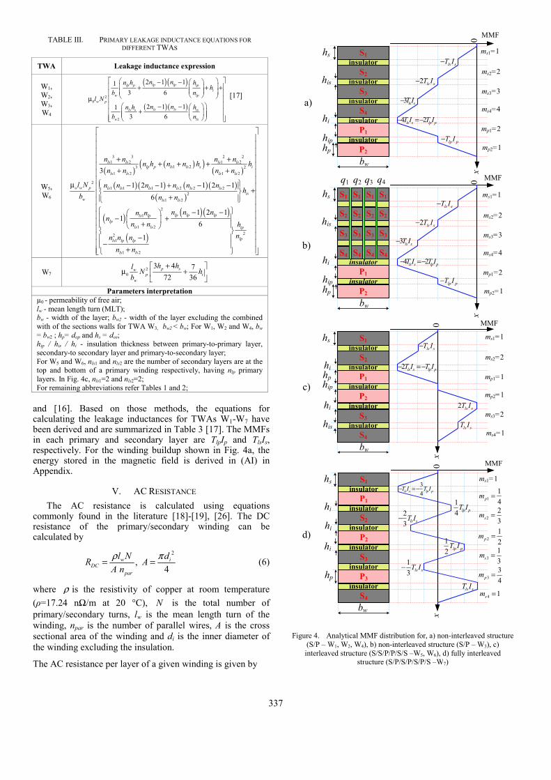
and [16]. Based on those methods, the equations for calculating the leakage inductances for TWAs W1-W7 have been derived and are summarized in Table 3 [17]. The MMFs in each primary and secondary layer are TlpIp and TlsIs, respectively. For the winding buildup shown in Fig. 4a, the energy stored in the magnetic field is derived in (AI) in Appendix.
V. AC RESISTANCE The AC resistance is calculated using equations
commonly found in the literature [18]-[19], [26]. The DC resistance of the primary/secondary winding can be calculated by
2
, 4
w iDC
par
l N dR AA n
= =ρ π (6)
where ρ is the resistivity of copper at room temperature (ρ=17.24 nΩ/m at 20 °C), N is the total number of primary/secondary turns, lw is the mean length turn of the winding, npar is the number of parallel wires, A is the cross sectional area of the winding and di is the inner diameter of the winding excluding the insulation.
The AC resistance per layer of a given winding is given by
TABLE III. PRIMARY LEAKAGE INDUCTANCE EQUATIONS FOR DIFFERENT TWAS
TWA Leakage inductance expression
W1, W2, W3, W4
( ) ( )
( )( )2
0
2
2 1 113 6
2 1 113 6
lp lplp p ipi
w lpw p
ls lsls s is
w ls
n nn h hh
b nl N
n nn h hb n
⎡ ⎤⎛ ⎞− − ⎛ ⎞⎢ ⎥⎜ ⎟+ + +⎜ ⎟⎜ ⎟⎜ ⎟⎢ ⎥⎝ ⎠⎝ ⎠μ ⎢ ⎥⎢ ⎥⎛ ⎞− − ⎛ ⎞
+⎢ ⎜ ⎟ ⎥⎜ ⎟⎜ ⎟⎢ ⎥⎝ ⎠⎝ ⎠⎣ ⎦
[17]
W5, W6
( )( )( )
( )( )( ) ( )( )
( )
( ) ( ) ( )
( )
3 3 2 21 2 1 2
1 23 21 2 1 2
21 1 1 2 2 2
21 2
21
1 2
21
1 2
3
1 2 1 1 2 16
1 2 11
6
1
ls ls ls lslp p ls ls s i
ls ls ls ls
o w p ls ls ls ls ls lsis
w ls ls
lp lp lpls lplp
ls ls
ls lp lp
ls ls
n n n nn h n n h hn n n n
l N n n n n n nh
b n n
n n nn nn
n n
n n nn n
+ ++ + ++ +
⎧ ⎫μ − − + − −⎪ ⎪ +⎨ ⎬+⎪ ⎪⎩ ⎭
⎧ − −⎛ ⎞− +⎜ ⎟+⎝ ⎠
−−
+
2ip
lp
hn
⎡ ⎤⎢ ⎥⎢ ⎥⎢ ⎥⎢ ⎥⎢ ⎥⎢ ⎥⎢ ⎥⎢ ⎥⎢ ⎥⎢ ⎥⎢ ⎥⎫⎢ ⎥⎪ ⎪⎢ ⎥⎪ ⎪⎢ ⎥⎨ ⎬⎢ ⎥⎪ ⎪⎢ ⎥⎪ ⎪⎢ ⎥⎩ ⎭⎣ ⎦
W7 20
3 4 772 36
p swp i
w
h hl N hb
+⎡ ⎤μ +⎢ ⎥
⎣ ⎦
Parameters interpretation µ0 - permeability of free air; lw - mean length turn (MLT); bw - width of the layer; bw2 - width of the layer excluding the combined with of the sections walls for TWA W3, bw2 < bw; For W1, W2 and W4, bw = bw2 ; hp= dop and hs = dos; hip / his / hi - insulation thickness between primary-to-primary layer, secondary-to secondary layer and primary-to-secondary layer; For W5 and W6, nls1 and nls2 are the number of secondary layers are at the top and bottom of a primary winding respectively, having nlp primary layers. In Fig. 4c, nls1=2 and nls2=2; For remaining abbreviations refer Tables 1 and 2;
S2S2S2S2
S3S3S3
S4
S3
S4S4S4
S1 S1S1
S1insulator
P1
P2
MMF
his
hp
hs
lp pT I−
0
bw
2 ls sT I−
ls sT I−
x
4 2ls s lp pT I T I− =−
3 ls sT I−
S2
S3
S4
insulator
insulator
insulator
insulator
hi
hip
S1insulator
P1
P2
MMF
hihp
hs
0
bw
2 ls s lp pT I T I− =−
ls sT I−
x
S2
S3
S4
insulator
insulator
insulator
insulator
his
hip
S1
P1
P2
MMF
his
hp
hs
lp pT I−
0
bw
2 ls sT I−
ls sT I−
x
4 2ls s lp pT I T I− =−
3 ls sT I−
insulator
insulator
hi
hip
ls sT I
2 ls sT I
q1 q2 q3 q4
hi
S1insulator
P1
P2
MMF
hi
hp
hs
0
bw
23 ls sT I−
34ls s lp pT I T I− =−
x
S2
S3
insulator
insulator
insulator
insulatorhi
hi
S4
insulatorP3
a)
b)
c)
d)
14 lp pT I
13 ls sT I−
12 lp pT I
ls sT I
ms1=1
ms2=2
ms3=3
mp2=1
mp1=2
ms4=4
ms1=1
ms2=2
ms3=3
mp2=1
mp1=2
ms4=4
ms1=1
ms2=2
mp1=1
ms4=1
ms3=2
mp2=1
ms1=1
114pm =
223sm =
212pm =
313sm =
334pm =
4 1sm =
Figure 4. Analytical MMF distribution for, a) non-interleaved structure (S/P – W1, W2, W4), b) non-interleaved structure (S/P – W3), c) interleaved structure (S/S/P/P/S/S –W5, W6), d) fully interleaved
structure (S/P/S/P/S/P/S –W7)
337

( ) ( ) ( )( ) ( )
( ) ( ) ( ) ( ) ( )( ) ( )
2
,layer ,2
sinh 2 sin 22 2 1
cosh 2 cos 2
cos sinh sin cosh4
cosh 2 cos 2
AC DC layer
Q Qm m
Q QR R Q
Q Q Q Qm m
Q Q
+⎧ ⎫− + −⎪ ⎪−⎪ ⎪= ⎨ ⎬
−⎪ ⎪−⎪ ⎪+⎩ ⎭
(7)
Assume the variables Δl, Δ2, Δ3, and Δ4 are assigned as in (8)
( ) ( )( ) ( )
( ) ( ) ( ) ( )( ) ( )
( ) ( )( ) ( )
( ) ( )( ) ( )
1 2
3 4
sinh 2 sin 2 cos sinh sin cosh,
cosh 2 cos 2 cosh 2 cos 2
sinh sin sinh sin,
cosh cos cosh cos
Q Q Q Q Q Q
Q Q Q Q
Q Q Q Q
Q Q Q Q
+ −Δ = Δ =
− +
+ −Δ = Δ =
− +
(8)
The variable Δ1 in terms of Δ3 and Δ4, and Δ2 and Δ4 is given by [19]
( ) ( )1 3 4 1 2 41 , 22
Δ = Δ + Δ Δ = Δ + Δ (9)
Using (8), (9) in (7), the simplified AC resistance per layer is
( ) 2,layer , 1 42AC DC layerR R Q m m= Δ + − Δ (10)
( ) 2,layer , 3 42 1
2AC DC layerQR R m= Δ + − Δ (11)
The total AC resistance of M layers for the non-interleaved TWAs W1-W4 is given by
( ) ( ) ( )
( )
2,total , 1 4
1
2, 1 4
2,total 1 4
2
2 13
2 13
M
AC DC layerm
DC layer
DC
R R Q m m
= R M Q M
= R Q M
== Δ + − Δ
⎧ ⎫Δ + − Δ⎨ ⎬⎩ ⎭
⎧ ⎫Δ + − Δ⎨ ⎬⎩ ⎭
∑
(12)
where RDC,layer and RDC,total are the DC resistance per layer and total DC resistance, respectively. The variable m represents the effective number of layers and is given by
( )( ) (0)
F hmF h F
=−
(13)
where F(0) and F(h) are the magneto motive forces (MMFs) at the start and end of each layer, respectively. The variable Q is the effective layer thickness normalized with the skin depth and is given by
3.5
0
4o l
iw
d Tdblayer thicknessQ =
penetration depthf
π
=ρ
πμ
(14)
where di is the bare wire diameter, do is the overall wire diameter including insulation, Tl is the turns per layer of the given winding and f is the switching frequency.
To calculate the AC resistance per layer for the interleaved TWAs W5-W7, (10) or (11) needs to be used with the corresponding value of m for each layer. The total AC resistance is the sum of all AC resistances in each layer.
The total AC resistance referred to the primary is given by
,total, S, total, P 2
AC AC AC
RR R
n= + (15)
where n is the transformer turns ratio RAC,total,P and RAC,total,S are the total AC resistance of primary and secondary windings, respectively.
TABLE IV. ENERGY LOSS EXPRESSIONS OF TRANSFORMER PARACITICS
Name of energy loss
Loss expressions Charge process (J) Discharge process (J)
Switching loss due to self-capacitance
21 0 5C P dsPE . C V= 2
2 0 5C S dsSE . C V=
Snubber loss due to leakage
inductance
2
1
0 5 lkP pkP snLVL
outsnLV
. L i VE VV
n
=−
2
2
0 5 lkS pkS snHVL
snHV in
. L i VE
V V n=
−
Winding loss due to AC and DC resistances
2
2
1 2
2
DCP DCPonC
RMSP ACPR
DCS DCSoffC
RMSS ACS
I Rt
I RE
I Rt
I R
⎛ ⎞⎡ ⎤+⎜ ⎟+⎢ ⎥⎜ ⎟⎢ ⎥⎣ ⎦= ⎜ ⎟⎡ ⎤+⎜ ⎟⎢ ⎥⎜ ⎟⎜ ⎟⎢ ⎥⎣ ⎦⎝ ⎠
2
2
2 2
2
DCP DCPoffD
RMSP ACPR
DCS DCSonD
RMSS ACS
I Rt
I RE
I Rt
I R
⎛ ⎞⎡ ⎤+⎜ ⎟+⎢ ⎥⎜ ⎟⎢ ⎥⎣ ⎦= ⎜ ⎟⎡ ⎤+⎜ ⎟⎢ ⎥⎜ ⎟⎜ ⎟⎢ ⎥⎣ ⎦⎝ ⎠
Parameters interpretation CP / CS – self capacitance referred to primary / secondary; VdsP / VdsS – drain to source voltage of primary / secondary MOSFET; LlkP / LlkS – leakage inductance referred to primary / secondary; ipkP / ipkS – primary / secondary peak current; VsnLV / VsnHV – RCD snubber capacitor voltage of primary / secondary; Vout / Vin – output / input voltage of the converter; IDCP / IDCS – DC current of primary / secondary; RDCP / RDCS – DC resistance of primary / secondary; IRMSP / IRMSS – RMS current of primary / secondary; RACP / RACS – AC resistance of primary / secondary; tonC / toffC – on / off time of the primary MOSFET during the charge process; tonD/ toffD – on / off time of the HV MOSFET during the discharge process;
VI. FINITE ELEMENT ANALYSES The different winding architectures are simulated in
Ansoft Maxwell to extract the value of the leakage inductance, self-capacitance and AC resistance. In Fig. 5 the electrostatic energy between the windings is shown for winding schemes B and D. It is noted that the energy density is high between layer to layer and low between turn to turn as expected in winding scheme B. In winding scheme D there is less electrostatic energy and thus it has lower self-capacitance.
Fig. 6 shows a close-up of the magneto static energy of the three investigated winding buildups. The leakage flux runs approximately vertically through the windings and the magneto static energy is highest in the space between the primary and secondary windings. The heavy interleaved buildup (S/P/S/P/S/P/S) has very low magneto static energy and thus it will have a very low leakage inductance.
The AC resistance at 100 kHz is also simulated for the three winding buildups. A standard mesh which is very fine compared to the skin depth is used to simulate the eddy effects in the winding. A close up plot of the mesh is shown in Fig. 7.a. The diameter of the secondary winding is 0.3 mm and the skin depth at 100 kHz is approximately 0.2 mm. It is
338

noted that the dimensions of the mesh is much lower than the diameter of the winding and the skin depth at 100 kHz. In Fig. 7. b-d, a close up of the current density for the three winding buildups is shown. It is noted that the current density in the non-interleaved buildup is much higher compared to the others and thus the AC resistance will also be higher.
VII. EXPERIMENTAL RESULTS The simulated, calculated and measured values of the self-
capacitance, leakage inductance (measured at 10 kHz frequency using the impedance analyzer PSM1735) and AC resistance for the 7 TWA’s are shown in the Tables 5, 6 and 7, respectively, from which it is clear that the measured, calculated and simulated transformer parameters for most of the TWAs closely matches. However, the differences in winding parameters such as an average layer to layer distance and mean length turn may cause errors around ±20 %. The measurement setup with 5 of the transformer prototypes is shown in Fig. 8. The energy loss expressions due to the transformer parasitics are summarized in Table 4. A plot of the loss distribution of the energy losses caused by the transformer parasitics), in a bi-directional flyback converter, used for charging and discharging an incremental DEAP actuator is shown in Fig. 9. The winding loss calculation for the flyback transformer is different from that of normal
transformer since the primary and secondary currents are out of phase, in [20] the winding loss is calculated for a flyback transformer with a non-interleaved structure. The same method can be used for the interleaved structures as well. However, due to limited space that is not included in this paper.
The calculated transformer parasitic values are used for calculating all losses, in order to provide a fair and useful comparison of the losses. The following specifications are used to calculate the losses in the bi-directional flyback converter [17], [20]-[23]: input voltage: 24V, output voltage: 1500 V, load capacitance: 200 nF, switching frequency during the charging and discharging process: 20-200 kHz, and 26 kHz, and primary peak current during charge and discharge processes: 2.12 A. The primary magnetizing inductance: 35 µH. From Fig. 9, it is clear that W6 has the lowest loss among all TWAs followed by W4, W7 and W3.
a)
b)
c)
Figure 5. Plots from simulation of self-capacitance. a) Energy distribution for winding scheme B. b) Energy distribution for
winding scheme D. c) Density color bar
a)
b)
c)
d)
Figure 6. Plots from simulation of leakage inductance. a) P/S. b) S/P/S. c) S/P/S/P/S/P/S. d) Density color bar.
339

Thus the structure W6 is highly recommended for high voltage capacitor charging application.
VIII. CONCLUSIONS The analytical equations for calculating the transformer
AC resistance, lekage inductance and self-capacitance for seven different winding architectures have been presented and evaluated experimentally and with FEA simulation. The main contribution to the errors is due to practical winding issues which are not accounted for in the equations. The transformer loss distribution is based on the calculated values, and it clearly shows that transformer winding architectures
where the self-capacitance is lowest are particularly suitable for high voltage charging applications. Future work involves the experimental validation of the proposed TWAs in the high voltage bi-directional dc-dc converter.
TABLE V. SELF-CAPACITANCE OF SECONDARY WINDING AT RESONANCE FREQUENCY
TWA Buildup Winding scheme Sim. (pF)
Calc. (pF)
Meas. (pF)
W1 S/P A 33 32 28 W2 S/P B 25 24 26 W3 S/P C 2.4 2 4.2 W4 S/P D 1.9 1 1.3 W5 S/P/S B 10 20 22 W6 S/P/S D 3.3 2.1 6W7 S/P/S/P/S/P/S B 5 3.6 15
TABLE VI. LEAKAGE INDUCTANCE REFERRED TO PRIMARY
TWA Buildup Winding scheme Sim. (nH)
Calc. (nH)
Meas. (nH)
W1 S/P A
526 590
550 W2 S/P B 520 W3 S/P C 725 W4 S/P D 580 W5 S/P/S B 150 152 181 W6 S/P/S D 208W7 S/P/S/P/S/P/S B 30 22 74
W1 W2 W3 W4 W5 W6 W710
-1
100
101
102
103
Type of transformer winding architecture (TWA)
Ene
rgy
loss
(m
J)
Transformer total winding lossPrimary RCD snubber lossSecondary RCD snubber lossPrimary swithcing loss due to winding capacitanceSecondary swithcing loss due to winding capacitanceTotal loss due to transformer parasitics
Figure 9. Energy loss distribution of the losses caused by transformer
parasitics in the high voltage capacitor charging application.
a)
b)
c)
d)
HIGHLOW
e)
Figure 7. Plots from the simulations of AC resistance. a) Default mesh, b) Current density of W1-W4, c) Current density of W5-
W6, d) Current density of W7, e) Density color bar
Figure 8. Measurement setup and five transformer prototypes with RM8
core
340

TABLE VII. AC RESISTANCE REFERRED TO PRIMARY AT 100 KHZ
TWA Buildup Winding scheme
Sim. (mΩ)
Calc. (mΩ)
Meas. (mΩ)
W1 S/P A
102
110
130 W2 S/P B 127 W3 S/P C 135 W4 S/P D 84W5 S/P/S B 35 37 39 W6 S/P/S D 42W7 S/P/S/P/S/P/S B 23 18 22
REFERENCES [1] R. E. Pelrine, R. D. Kornbluh, Q. Pei, and J. P. Joseph, “High-speed
electrically actuated elastomers with strain greater than 100%,” in Proc. Science, vol. 287, pp. 836–839, 2000.
[2] R. E. Pelrine, R. D. Kornbluh, and J. P. Joseph, “Electrostriction of polymer dielectric with compliant electrodes as a means of actuation,” in Proc. Sens. Actuators A, vol. 64, pp. 77–85, 1998.
[3] W. G. Hurley and D. J. Wilcox, “Calculation of leakage inductance in transformer windings,” in Proc. IEEE Trans. Power Electronics, vol. 9, pp. 121-126, 1994.
[4] Z. Ouyang, Z. Zhang, O. C. Thomsen and M. A. E. Andersen, “Planar-integrated magnetics (PIM) module in hybrid bidirectional DC-DC converter for fuel cell application,” in Proc. IEEE Trans. Power Electronics, vol.26, pp. 3254-3264, 2011.
[5] S. R. Cove, M. Ordonez, F. Luchino, and J. E. Quaicoe, “Applying Response Surface Methodology to Small Planar Transformer Winding Design,” in Proc. IEEE Trans. Industrial Electronics, vol. 60, pp. 483- 493, 2013.
[6] J. Zhang, Z. Ouyang, M. Duffy, M. A. E Andersen and W. G. Hurley “Leakage inductance calculation for planar transformer with magnetic shunt”, in Proc. ECCE USA 2013.
[7] F. Blache, J-P. Keradec, B. Cogitore, “Stray capacitances of two winding transformers: equivalent circuit, measurements, calculation and lowering,” in Proc. IEEE Industry Applications Society Annual Meeting, pp. 1211-1217 vol. 2, 2-6 Oct. 1994.
[8] W. T. Duerdoth, “Equivalent capacitance of transformer windings,” in Proc. Wireless Eng., vol. 23, pp. 161–167, Jun. 1946.
[9] A. Massarini and M. K. Kazimierczuk, “Self-capacitance of inductors,” in Proc. IEEE Trans. Power Electron., vol. 12, no. 4, pp. 671–676, Jul. 1997.
[10] T. Duerbaum and G. Sauerlander, “Energy based capacitance model for magnetic devices,” in Proc. APEC, vol. 1, pp. 109–115, 2001.
[11] W. T. Duerdoth, “Equivalent capacitance of transformer windings,” in Proc. Wireless Eng., vol. 23, pp. 161–167, Jun. 1946.
[12] T. Duerbaum, “Capacitance model for magnetic devices,” in Proc. Power Electron. Spec. Conf., vol. 3, pp. 1651–1656, 2000.H. Y. Lu, J. Zhu, S. Y. R. Hui, and V. S. Ramseden, “Measurement and Modeling
of stray capacitances in high frequency transformers,” in Proc. Power Electron. Spec. Conf., pp. 763–769, 1999.
[13] H. Y. Lu, J. G. Zhu, and S. Y. R. Hui, “Experimental determination of stray capacitances in high-frequency transformers,” in Proc. IEEE Trans. Power Electron., vol. 18, no. 5, pp. 1105–1112, Sep. 2003.
[14] L. Dalessandro, F. da Silveira Cavalcante, J. W. Kolar, “Self-Capacitance of High-Voltage Transformers,” in Proc. IEEE Trans. Power Electronics, vol. 22, no. 5, pp. 2081-2092, Sept. 2007.
[15] J. Biela, J. W. Kolar, “Using Transformer Parasitics for Resonant Converters—A Review of the Calculation of the Stray Capacitance of Transformers,” in Proc. IEEE Trans. Industry Applications, vol. 44, no. 1, pp. 223-233, 2008.
[16] E. C. Snelling, Soft Ferrites-Properties and applications, 2nd ed. London, UK, Butterworth, 1988.
[17] P. Thummala, H. Schneider, Z. Ouyang, Z. Zhang, M. A. E. Andersen, “Estimation of transformer parameters and loss analysis for high voltage capacitor charging application,” in Proc. IEEE ECCE Asia, pp. 704-710, 3-6 Jun. 2013.
[18] W.G. Hurley, E. Gath, J. G. Breslin, “Optimizing the AC resistance of multilayer transformer windings with arbitrary current waveforms,” in Proc. IEEE Trans. Power Electronics, vol. 15, no. 2, pp. 369-376, Mar 2000.
[19] J. A. Ferreira, “Improved analytical modeling of conductive losses in magnetic components,” in Proc. IEEE Transactions on Power Electronics, vol. 9, no. 1, pp.127,131, Jan 1994.
[20] P. Thummala, H. Schneider, Z. Zhang, A. Knott, M. A. E. Andersen, “Optimization of a Bi-Directional Flyback Converter for a High Voltage Capacitor Charging Application,” in Proc. IEEE APEC, pp., 16-20 Mar. 2014.
[21] K. Venkatesan, “Current Mode Controlled Bidirectional Flyback Converter,” in Proc. IEEE PESC, pp. 835-842, 1989.
[22] T. Bhattacharya, V. S. Giri, K. Mathew, L. Umanand, “Multiphase Bidirectional Flyback Converter Topology for Hybrid Electric Vehicles,”, in Proc. IEEE Transactions on Industrial Electronics, vol. 56, no.1, pp.78-84, Jan. 2009.
[23] P. Thummala, Z. Zhang, M. A. E. Andersen, “High Voltage Bi-directional Flyback Converter for Capacitive Actuator,” in Proc. European Power Electronics Conference (EPE), pp. 3-6th Sept. 2013.
[24] G. Chen, Y.-S. Lee, S.Y.R. Hui, D. Xu, Y. Wang, “Actively clamped bidirectional flyback converter,” in Proc. IEEE Trans. Industrial Electronics, vol. 47, no. 4, pp. 770-779, Aug. 2000.
[25] M. J. Prieto, A. Fernandez, J. M. Diaz, J. M. Lopera, J. Sebastian, “Influence of transformer parasitics in low-power applications,” in Proc. IEEE APEC, vol. 2, pp. 1175-1180, 14-18th Mar. 1999.
[26] R. W. Erickson and D. Maksimovic, “Fundamentals of Power Electronics,” 2nd ed. New York: Springer, 2001.
[27] John R. Barnes, “Robust electronic design reference book,” Volume 1, Springer, 2004.
APPENDIX
( )
( ) ( )
112 2 2 2 2 20 0
1 11 1 1,b 1 1,d 10 0
;2 2
11;
ps lp lpls lshh n nn n
Mag w w w w su pv sab is pcd ip sp iu v a a c c
lp lp p lp pls s ls ssu pv
w w s w w p
E l b H x dx l b K K H dx H dx H h H h H h
n v T I T Iu T I T I x xH Hb b h b b h
−−
= = = = + = = +
⎡ ⎤μ μ= = = + + + +⎢ ⎥⎢ ⎥⎣ ⎦
− +⎡ − ⎤= − − = − +⎢ ⎥⎣ ⎦
∑ ∑ ∑ ∑∫ ∫ ∫
2 2 2 2 2
0 0 0 0
1
; ; ; ;
2 3s s s
lp pls s ls ls ssab pcd sp
w w w
h h h hlp pls s ls s ls s ls s ls s ls s ls s
ipw s w w s w w s w w s w
vT IuT I n T IH H Hb b b
T IT I x T I T I x T I T I x T I T I xdx dx dx dx hb h b b h b b h b b h b
K
⎡ ⎤⎢ ⎥ = − = − = −⎢ ⎥⎣ ⎦
⎛ ⎞ ⎛ ⎞ ⎛ ⎞ ⎛ ⎞ ⎛ ⎞− + − − + − − + − − + −⎜ ⎟ ⎜ ⎟ ⎜ ⎟ ⎜ ⎟ ⎜ ⎟⎝ ⎠ ⎝ ⎠ ⎝ ⎠ ⎝ ⎠ ⎝ ⎠
=∫ ∫ ∫
2 22 2 2 2
0 0
23
2 22 3
4 143
s
p ph hlp p lp p lp p lp p lp pls s ls s ls s
is iw w w w w p w w p w
ls s s
w
T I T I T I T I T IT I T I T I x xh dx dx hb b b b b h b b h b
T I h = hb
⎡ ⎤⎢ ⎥⎢ ⎥⎢ ⎥
⎡ ⎤ ⎛ ⎞ ⎛ ⎞⎢ ⎥⎛ ⎞ ⎛ ⎞ ⎛ ⎞ ⎛ ⎞⎢ ⎥+ − + − + − + − + + − + + −⎜ ⎟ ⎜ ⎟⎢ ⎥⎜ ⎟ ⎜ ⎟ ⎜ ⎟ ⎜ ⎟⎜ ⎟ ⎜ ⎟⎢ ⎥⎢ ⎥⎝ ⎠ ⎝ ⎠ ⎝ ⎠ ⎝ ⎠⎝ ⎠ ⎝ ⎠⎣ ⎦⎣ ⎦
⎛ ⎞+⎜ ⎟
⎝ ⎠
∫
∫ ∫2 2
3 2 4 72 4 ; ;3 3 8 4
lp lp p ls ls slp p p p p p s ipisis ip i i
p p s sw w
n T I n T IT I h N I h h hhh h = h N I N Ib b
=+⎛ ⎞ ⎛ ⎞⎡ ⎤ ⎡ ⎤⎡ ⎤ + + + + + +⎜ ⎟ ⎜ ⎟⎢ ⎥ ⎢ ⎥⎢ ⎥ =⎣ ⎦ ⎣ ⎦ ⎣ ⎦⎝ ⎠ ⎝ ⎠
(AI)
341

144/255

Appendix JInvestigation of Transformer
Winding Architectures for HighVoltage (2.5 kV) CapacitorCharging and Discharging
Applications
About to Submit to IEEE Transactions on Power Electronics
145/255

Investigation of Transformer Winding Architectures for High
Voltage (2.5 kV) Capacitor Charging and Discharging
Applications
Prasanth Thummala, Member, IEEE, Henrik Schneider, Student Member, IEEE, Zhe Zhang, Member, IEEE,
Michael A. E. Andersen, Member, IEEE
Electronics Group, Department of Electrical Engineering,
Technical University of Denmark, 2800 Kongens Lyngby, Denmark
Email: [email protected], [email protected], [email protected], [email protected]
Abstract—Transformer parameters such as leakage inductance and self-capacitance are rarely calculated in advance
during the design phase, because of the complexity and huge analytical error margins caused by practical winding
implementation issues. Thus, choosing one transformer architecture over another for a given design is usually based on
experience or a trial and error approach. This paper presents equations regarding calculation of leakage inductance,
self-capacitance and ac resistance in transformer winding architectures, ranging from the common non-interleaved
primary/secondary winding architecture, to an interleaved, sectionalized and bank winded architecture. The analytical
results are evaluated experimentally and through FEM simulations. Different transformer winding architectures for
two different cores RM8 and EF25, are investigated in terms of the losses caused by the transformer parasitics for a
bidirectional high-voltage flyback converter used to drive a electro active polymer based incremental actuator. The
total losses due to the transformer parasitics for the best transformer architectures are reduced by more than a factor
of ten compared to the worst case transformer architectures.
Index Term —switch-mode power converters, high voltage dc-dc converters, digital control, energy efficiency, actuator
The statement: A part of this paper was presented and selected as an outstanding presentation at IEEE APEC 2014 (March
16–20th
, 2014, Fort Worth, TX, USA). It is not currently under review for publication in any other journal.

I. INTRODUCTION
Dielectric electro active polymer (DEAP) is an emerging smart material that has experienced significant development and
has gained increasing attention over the last decade [1], [2]. DEAP, when used as actuators, has the potential to be an effective
replacement for many conventional actuators due to its unique properties such as high strain, light weight, low noise operation,
low power consumption. However, a compact high voltage driver is required to charge and discharge the DEAP from 0 V to
2500 V DC supplied from a 24 V battery. The DEAP actuator applications require a bi-directional energy transfer capability,
to increase the life time of the battery. The flyback converter topology is suitable for low power (< 150 W), and high voltage
capacitor charging applications, as it can be made very compact with a low number of components. The flyback transformer is
the most critical component in terms of driver performance. The high voltage requirement demands a high turns ratio which
calls for a large number of secondary turns. This may lead to a high winding self-capacitance resulting in the severe capacitive
switching loss and undesirable, resonating current spikes in the leading edge of the current waveform, which could lead to
false triggering of the current limit during the turn-on process.
The leakage inductance of the transformer may cause undesirable voltage spikes on the drains of the primary and secondary
MOSFETs during the charge and the discharge processes, respectively, which lead to the use of active or passive snubber
circuits in the converter. With active snubbers high energy efficiency can be achieved, at the expense of a higher cost and
added control complexity, whereas the passive snubbers result in switching loss due to the leakage inductance. The AC
resistance is also an important parameter to consider, since the AC conduction loss is caused by high frequency skin and
proximity effects in a flyback converter operating in boundary conduction mode (BCM) or in discontinuous conduction mode
(DCM).
Thus, accurate estimation of the transformer parameters and their associated losses are required, to evaluate different
transformer winding architectures (TWAs) from which the best TWA is selected to achieve high energy efficiency. Extensive
research has been done on calculating the leakage inductance in conventional transformers [3]-[6], [17], and in [7]-[17], the
capacitance calculation methods have been proposed for inductors, power, planar, and high voltage transformers. The
influence of transformer parasitics for the low power flyback converter has been discussed in [24]. This paper investigates a
number of TWAs providing a deep insight into transformer design and its impact on the total loss contribution of a bi-
directional high-voltage flyback converter. The paper is organized as follows: the TWAs are described and then the
calculations of self-capacitance, leakage inductance and AC resistance for different TWAs are provided. The calculated

transformer parameters are evaluated via FEA simulation using ANSOFT Maxwell and the transformer parasitics for all TWAs
are presented, followed by the conclusion.
II. TRANSFORMER WINDING ARCHITECTURES
This paper investigates the four known winding schemes (A, B, C and D) as shown in Fig. 1 [14], [16], [26], [27].
Winding scheme A is the most simple to implement since the next layer starts where the previous layer ended. In winding
scheme B, the next layer starts just above the starting point of the previous layer. Winding scheme C split the winding into a
number of sections that is individually wounded like winding scheme A. In winding scheme D, the turns progress in a vertical
back angled way where turns are built on top of previous turns. It seems like winding scheme D achieves as many angled
sections as there are turns in a layer without the penalty of reducing the fill factor due to the thickness of the section walls.
Another advantage is that winding scheme D can be easily interleaved, which is not the case for winding scheme C since it is
hard to add section walls in-between windings. The difference in self-capacitance due to the winding schemes is severe
because the voltage potentials between the turns in the winding are changed.
1 2
3 5 7 8
4 6
1 2 3 4
5 6 7 8
1 2 3 4
5678
1 2 5 6
8743
Winding scheme A – U type Winding scheme B – Z type
Winding scheme D - BankWinding scheme C - Sectioned
Figure 1. An overview of different winding schemes.

Several winding buildups (S/P, S/P/S, S/P/S/P/S/P/S; where S and P are is the secondary and primary windings,
respectively) are investigated - see Fig. 2. Based on these configurations, seven high voltage transformer winding architectures
(W1-W7) are derived and the winding information is summarized in Table 1. In order to simplify the implementation of the
windings a low turns ratio of 10 is selected. The TWAs W1-W6 are wound with 10 primary turns and 100 secondary turns. W7
deviates since it is only implemented with 9 primary turns due to the nature of the winding architecture.
Winding scheme A is employed for the primary winding of all architectures. Moreover, all winding space of the bobbin is
utilized to improve the fill factor and to reduce the winding resistance. Equal space allocation for primary and secondary
P
S
h [mm]
w [mm]
n...
Buildup: S/P
P
S/2
h [mm]
w [mm]
n...
Buildup: S/P/S
P/3
h [mm]
w [mm]
n...
Buildup: S/P/S/P/S/P/S
S/2S/4
S/4
P/3
S/4
P/3
S/4
Figure 2. An overview of different winding buildups.
TABLE I. HIGH VOLTAGE TRANSFORMER ARCHITECTURES
Design Winding
buildup
Secondary winding Primary winding
Scheme Parameters Parameters
W1 S/P A
Ns = 100
dis = 0.3 mm
dos = 0.32 mm pTT = 0.355 mm pLL = 0.34 mm
nls = 4
npars = 1
Core / Material used:
RM8 / N41
Np = 10
*dip = 0.7 mm *dop =0.8 mm
nlp = 2 nparp = 2
W2 S/P B
W3 S/P C
W4 S/P D
W5 S/P/S B
W6 S/P/S D
W7 S/P/S/P/S/P/S B
Np = 9
*dip = 0.48 mm
*dop = 0.5 mm
nlp = 3
nparp = 5
Parameters interpretation
Ns / Np - number of secondary / primary turns;
nls / nlp - number of secondary / primary winding layers; npars / nparp - number of secondary / primary parallel windings;
dis / dos - inner / outer diameter of secondary winding;
dip / dop - inner / outer diameter of primary winding; pTT / pLL - turn-to-turn / layer-to-layer pitch of secondary winding;
*In the practical transformer implementation triple insulated (TEX) windings are not used for the primary due to the unavailability of the wires;

winding is adopted for this investigation, thus the primary winding is wounded with a number of parallel wires.
III. SELF-CAPACITANCE
High voltage transformers tend to have a large number of turns in the high voltage side, which introduces a non-negligible
parasitic self-capacitance. It is important to predict the self-capacitance in the design phase in order to avoid severe switching
loss. In fact, the winding self-capacitance is a parameter representing the electric field energy stored in the winding and is
considered as a shunt lumped element in most cases [14]. Due to a large number of turns per layer, the effect of the turn-to-turn
capacitance can be neglected and the main contribution to the self-capacitance comes from the layer-to-layer capacitance,
which can be calculated based on the simple parallel-plate or cylindrical capacitor model [14]-[16].
The self-capacitance in the transformer windings can be calculated using the electro static energy stored in the volume
between the conductors [14], [16] and is given by
2 21 1
2 2Electric S W
Vol
E E dv C U (1)
where ε is the equivalent dielectric constant of the winding, E is the electric field strength, CS is the self-capacitance, and UW is
the total voltage across the winding.
The energy stored in two adjacent conductive layers with a linear potential distribution, shown in Fig. 3a, can be calculated
by (2), which is derived in [16]. The total stored energy is
A B
deff
h
w
UAS UBS
UAT UBT
US=UBS-UAS
UT=UBT-UAT
h
D
a) b)deff
Figure 3. a) Two parallel plates with a linear potential distribution, b) Cylindrical capacitor model

2 2
6
lStored S S T T
CE U U U U (2)
where US and UT are the potential difference between the two surfaces at the bottom and top respectively, and Cl is the
capacitance between the two surfaces and is considered as a parallel plate capacitance and can be calculated using (3)
0l r
eff
hwC
d (3)
where ε0 is the vacuum permittivity and is 8.854×10⁻¹²
F/m, εr is the relative permittivity of the dielectric material. The
parameters h, w represents the dimensions of the plate and deff is the effective distance between two layers (which needs to be
calculated for each TWA) and is given by
1.15 0.26eff LL is TTd p d p (4)
TABLE II. SELF-CAPACITANCE EXPRESSIONS FOR DIFFERENT TWAS
TWA Self-capacitance expression
W1
10 12
1
14 ; C ; 1
3
ls l w wl r w i ls is ls is
ls eff
n C b ll D n d n h
n d
W2
102
1
14 ; C ; 1
4
ls l w wl r w ls TT os
ls eff
n C b lb T p d
n d
W3 2
1
102
1 1
4 1;
3
ww
ls ll r
ls eff
bl
n C qC
q n d
W4 10
2
; 1TT wr ls LL os
eff w
p l LL n p d
d b [7]
W5
0 2 3 4
2
3 3 3 1
r w w w w
ls eff eff eff lp p lp ip
b l l l
n d d d n d n h
W6
2 3 2 41 20
4 4
1 2
2 2
; 1
1 ; 1 ;2
TT w w TT wr
eff w weff lp p lp ip
lsLL os TT lp p lp ip os
TT os
p l l p lL L
d b bd n d n h
nL p d p n h n h d
L p d
W7 0 5 6 7
2
5
r w w w w
ls eff
b l l l
n d
Parameters interpretation
ε0 / εr - relative permittivity of vacuum / dielectric material; εr = 4;
bw - the width of the layer; Tls is turns per layer of secondary winding; Di - inner diameter of the bobbin;
deff1,2,3,4,5 - effective thickness of dielectric between two layers [14] [16] for different TWAs;
lw1 - mean length turn for the TWAs W1, W2 , W3 and W4; lw2 / lw3 / lw4 - mean length turn between most inner two secondary (S1, S2) / most outer two secondary (S3, S4) / most outer secondary and the
most inner secondary (S2, S3), layers for W5 and W6;
lw5 / lw6 / lw7 / lw8 / lw9 / lw10 - mean length turn between most inner two secondary (S1, S2) / middle two secondary (S2, S3) / most outer two secondary (S3, S4) layers for W7
q1 - number of sections for structure W3 and q1 = 4;
For remaining abbreviations refer Tables 1 and 3;

where pLL, dis and pTT are the layer to layer pitch, inner diameter, and turn to turn pitch, of the secondary winding, respectively.
According to the methods given in [16], the expressions for calculating the self-capacitance for all above mentioned TWAs
have been derived and are summarized in Table 2. Normally, the cylindrical shape, shown in Fig. 3b, is desired for most
winding layers due to the simple winding technique as well as the short mean turn length [14]. If the distance between two
layers is much less than the mean diameter for the two layers, the cylindrical capacitor can be considered to be a parallel plate
capacitor and (3) can be employed to calculate the capacitance by replacing w with π D (see Fig. 3b).
IV. LEAKAGE INDUCTANCE
The leakage inductance in a transformer is calculated using the energy stored in the magnetic field [16]. The total leakage
energy stored in the magnetic field is given by
2 2
0
1 1
2 2Magnetic lk p
Vol
E H dv L I (5)
where H is the magnetic field strength which is proportional to the number of ampere turns linked by the flux path, Llk is the
leakage inductance, and Ip is the peak current in the winding. The fundamental principles used to calculate the leakage
inductance are thoroughly investigated in [3], [4], and [16]. Based on those methods, the equations for calculating the leakage
inductances for TWAs W1-W7 have been derived and are summarized in Table 3 [17]. The MMFs in each primary and
TABLE III. PRIMARY LEAKAGE INDUCTANCE EQUATIONS FOR DIFFERENT TWAS
TWA Leakage inductance expression
W1, W2,
W3, W4
2
0
2
2 1 1 2 1 11 1
3 6 3 6
lp lplp p ip ls lsls s isw p i
w lp w ls
n nn h h n nn h hl N h
b n b n
[17]
W5, W6
3 3 2 2
1 2 1 21 23 2
1 2 1 2
22
1
1 21 1 1 2 2 2
2 21 2 1
1 2
3
1 2 11
61 2 1 1 2 1
6 1
ls ls ls lslp p ls ls s i
ls ls ls ls
lp lp lpo w p ls lp
lp
w ls lsls ls ls ls ls ls
is
ls ls ls lp lp
ls ls
n n n nn h n n h h
n n n n
n n nl N n nn
b n nn n n n n nh
n n n n n
n n
2
ip
lp
h
n
W7 2
0
3 4 7
72 36
p swp i
w
h hlN h
b
Parameters interpretation
µ0 - permeability of free air;
lw - mean length turn (MLT);
bw - width of the layer; bw2 - width of the layer excluding the combined with of the sections walls for TWA W3, bw2 < bw; For W1, W2 and W4, bw = bw2 ; hp= dop and hs = dos;
hip / his / hi - insulation thickness between primary-to-primary layer, secondary-to secondary layer and primary-to-secondary layer;
For W5 and W6, nls1 and nls2 are the number of secondary layers are at the top and bottom of a primary winding respectively, having nlp primary layers. In Fig. 4c, nls1=2 and nls2=2;
For remaining abbreviations refer Tables 1 and 2;
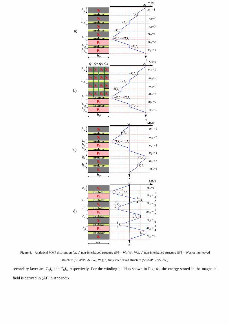
secondary layer are TlpIp and TlsIs, respectively. For the winding buildup shown in Fig. 4a, the energy stored in the magnetic
field is derived in (AI) in Appendix.
S2S2S2S2
S3S3S3
S4
S3
S4S4S4
S1 S1S1
S1
insulator
P1
P2
MMF
his
hp
hs
lp pT I
0
bw
2 ls sT I
ls sT I
x
4 2ls s lp pT I T I
3 ls sT I
S2
S3
S4
insulator
insulator
insulator
insulator
hi
hip
S1
insulator
P1
P2
MMF
hi
hp
hs
0
bw
2 ls s lp pT I T I
ls sT I
x
S2
S3
S4
insulator
insulator
insulator
insulator
his
hip
S1
P1
P2
MMF
his
hp
hs
lp pT I
0
bw
2 ls sT I
ls sT I
x
4 2ls s lp pT I T I
3 ls sT I
insulator
insulator
hi
hip
ls sT I
2 ls sT I
q1 q2 q3 q4
hi
S1
insulator
P1
P2
MMF
hi
hp
hs
0
bw
2
3ls sT I
3
4ls s lp pT I T I
x
S2
S3
insulator
insulator
insulator
insulatorhi
hi
S4
insulator
P3
a)
b)
c)
d)
1
4lp pT I
1
3ls sT I
1
2lp pT I
ls sT I
ms1=1
ms2=2
ms3=3
mp2=1
mp1=2
ms4=4
ms1=1
ms2=2
ms3=3
mp2=1
mp1=2
ms4=4
ms1=1
ms2=2
mp1=1
ms4=1
ms3=2
mp2=1
ms1=1
1
1
4pm
2
2
3sm
2
1
2pm
3
1
3sm
3
3
4pm
4 1sm
Figure 4. Analytical MMF distribution for, a) non-interleaved structure (S/P – W1, W2, W4), b) non-interleaved structure (S/P – W3), c) interleaved
structure (S/S/P/P/S/S –W5, W6), d) fully interleaved structure (S/P/S/P/S/P/S –W7)

V. AC RESISTANCE
The AC resistance is calculated using equations commonly found in the literature [18]-[19], [26]. The DC resistance of the
primary/secondary winding can be calculated by
2
, 4
w iDC
par
l N dR A
A n
(6)
where is the resistivity of copper at room temperature (ρ=17.24 nΩ/m at 20 °C), N is the total number of
primary/secondary turns, lw is the mean length turn of the winding, npar is the number of parallel wires, A is the cross sectional
area of the winding and di is the inner diameter of the winding excluding the insulation.
The AC resistance per layer of a given winding is given by
2 2
,layer ,
sinh 2 sin 2 cos sinh sin cosh2 2 1 4
cosh 2 cos 2 cosh 2 cos 2AC DC layer
Q Q Q Q Q QR R Q m m m m
Q Q Q Q
(7)
Assume the variables Δl, Δ2, Δ3, and Δ4 are assigned as in (8)
1 2
3 4
sinh 2 sin 2 cos sinh sin cosh,
cosh 2 cos 2 cosh 2 cos 2
sinh sin sinh sin,
cosh cos cosh cos
Q Q Q Q Q Q
Q Q Q Q
Q Q Q Q
Q Q Q Q
(8)
The variable Δ1 in terms of Δ3 and Δ4, and Δ2 and Δ4 is given by [19]
1 3 4 1 2 4
1, 2
2 (9)
Using (8), (9) in (7), the simplified AC resistance per layer is
2
,layer , 1 42AC DC layerR R Q m m (10)
2
,layer , 3 42 12
AC DC layer
QR R m (11)
The total AC resistance of M layers for the non-interleaved TWAs W1-W4 is given by

2
,total , 1 4
1
2
, 1 4
2
,total 1 4
2
21
3
21
3
M
AC DC layer
m
DC layer
DC
R R Q m m
= R M Q M
= R Q M
(12)
where RDC,layer and RDC,total are the DC resistance per layer and total DC resistance, respectively. The variable m represents the
effective number of layers and is given by
( )
( ) (0)
F hm
F h F
(13)
where F(0) and F(h) are the magneto motive forces (MMFs) at the start and end of each layer, respectively. The variable Q is
the effective layer thickness normalized with the skin depth and is given by
3.5
0
4
o li
w
d Td
blayer thicknessQ =
penetration depth
f
(14)
TABLE IV. ENERGY LOSS EXPRESSIONS OF TRANSFORMER PARASITICS
Name of energy loss Loss expressions
Charge process (J) Discharge process (J)
Switching loss due to self-
capacitance 2
1 0 5C P dsPE . C V 2
2 0 5C S dsSE . C V
Snubber loss due to leakage
inductance
2
1
0 5 lkP pkP snLV
Lout
snLV
. L i VE
VV
n
2
2
0 5 lkS pkS snHV
L
snHV in
. L i VE
V V n
Winding loss due to AC and
DC resistances
2 2
1 2 2
DCP DCP DCS DCS
R onC offC
RMSP ACP RMSS ACS
I R I RE t t
I R I R
2 2
2 2 2
DCP DCP DCS DCS
R offD onD
RMSP ACP RMSS ACS
I R I RE t t
I R I R
Parameters interpretation CP / CS – self capacitance referred to primary / secondary;
VdsP / VdsS – drain to source voltage of primary / secondary MOSFET;
LlkP / LlkS – leakage inductance referred to primary / secondary; ipkP / ipkS – primary / secondary peak current;
VsnLV / VsnHV – RCD snubber capacitor voltage of primary / secondary;
Vout / Vin – output / input voltage of the converter; IDCP / IDCS – DC current of primary / secondary;
RDCP / RDCS – DC resistance of primary / secondary;
IRMSP / IRMSS – RMS current of primary / secondary; RACP / RACS – AC resistance of primary / secondary;
tonC / toffC – on / off time of the primary MOSFET during the charge process;
tonD/ toffD – on / off time of the HV MOSFET during the discharge process;

where di is the bare wire diameter, do is the overall wire diameter including insulation, Tl is the turns per layer of the given
winding and f is the switching frequency.
To calculate the AC resistance per layer for the interleaved TWAs W5-W7, (10) or (11) needs to be used with the
corresponding value of m for each layer. The total AC resistance is the sum of all AC resistances in each layer.
The total AC resistance referred to the primary is given by
,total, S
,total, P 2
AC
AC AC
RR R
n (15)
where n is the transformer turns ratio RAC,total,P and RAC,total,S are the total AC resistance of primary and secondary windings,
respectively.
VI. FINITE ELEMENT ANALYSES
The different winding architectures are simulated in Ansoft Maxwell to extract the value of the leakage inductance, self-
capacitance and AC resistance. In Fig. 5 the electrostatic energy between the windings is shown for winding schemes B and D.
It is noted that the energy density is high between layer to layer and low between turn to turn as expected in winding scheme
B. In winding scheme D there is a less electrostatic energy and thus it has lower self-capacitance.
Fig. 6 shows a close-up of the magneto static energy of the three investigated winding buildups. The leakage flux runs
approximately vertically through the windings and the magneto static energy is highest in the space between the primary and
secondary windings. The heavy interleaved buildup (S/P/S/P/S/P/S) has a very low magneto static energy and thus it will have
a very low leakage inductance.
The AC resistance at 100 kHz is also simulated for the three winding buildups. A standard mesh which is very fine
compared to the skin depth is used to simulate the eddy effects in the winding. A close up plot of the mesh is shown in Fig. 7.a.
The diameter of the secondary winding is 0.3 mm and the skin depth at 100 kHz is approximately 0.2 mm. It is noted that the
dimensions of the mesh is much lower than the diameter of the winding and the skin depth at 100 kHz. In Fig. 7. b-d, a close
up of the current density for the three winding buildups is shown. It is noted that the current density in the non-interleaved
buildup is much higher compared to the others and thus the AC resistance will also be higher.

a)
b)
HIGHLOW
c)
Figure 5. Plots from simulation of self-capacitance.
a) Energy distribution for winding scheme B. b) Energy distribution for winding scheme D. c) Density color bar

a)
b)
c)
HIGHLOW
d)
Figure 6. Plots from simulation of leakage inductance.
a) P/S. b) S/P/S. c) S/P/S/P/S/P/S. d) Density color bar.

a)
b)
c)
d)
HIGHLOW
e)
Figure 7. Plots from the simulations of AC resistance.
a) Default mesh, b) Current density of W1-W4, c) Current density of W5-W6, d) Current density of W7, e) Density color bar
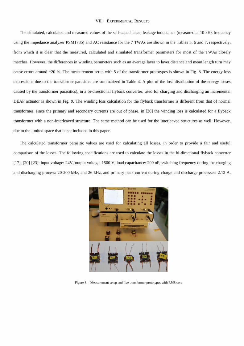
VII. EXPERIMENTAL RESULTS
The simulated, calculated and measured values of the self-capacitance, leakage inductance (measured at 10 kHz frequency
using the impedance analyzer PSM1735) and AC resistance for the 7 TWAs are shown in the Tables 5, 6 and 7, respectively,
from which it is clear that the measured, calculated and simulated transformer parameters for most of the TWAs closely
matches. However, the differences in winding parameters such as an average layer to layer distance and mean length turn may
cause errors around ±20 %. The measurement setup with 5 of the transformer prototypes is shown in Fig. 8. The energy loss
expressions due to the transformer parasitics are summarized in Table 4. A plot of the loss distribution of the energy losses
caused by the transformer parasitics), in a bi-directional flyback converter, used for charging and discharging an incremental
DEAP actuator is shown in Fig. 9. The winding loss calculation for the flyback transformer is different from that of normal
transformer, since the primary and secondary currents are out of phase, in [20] the winding loss is calculated for a flyback
transformer with a non-interleaved structure. The same method can be used for the interleaved structures as well. However,
due to the limited space that is not included in this paper.
The calculated transformer parasitic values are used for calculating all losses, in order to provide a fair and useful
comparison of the losses. The following specifications are used to calculate the losses in the bi-directional flyback converter
[17], [20]-[23]: input voltage: 24V, output voltage: 1500 V, load capacitance: 200 nF, switching frequency during the charging
and discharging process: 20-200 kHz, and 26 kHz, and primary peak current during charge and discharge processes: 2.12 A.
Figure 8. Measurement setup and five transformer prototypes with RM8 core

The primary magnetizing inductance: 35 µH. From Fig. 9, it is clear that W6 has the lowest loss among all TWAs followed by
W4, W7 and W3. Thus the structure W6 is highly recommended for high voltage capacitor charging application.
TABLE V. SELF-CAPACITANCE OF SECONDARY WINDING AT RESONANCE FREQUENCY
TWA Buildup Winding scheme
Sim.
(pF)
Calc.
(pF)
Meas.
(pF)
W1 S/P A 33 32 28
W2 S/P B 25 24 26
W3 S/P C 2.4 2 4.2
W4 S/P D 1.9 1 1.3
W5 S/P/S B 10 20 22
W6 S/P/S D 3.3 2.1 6
W7 S/P/S/P/S/P/S B 5 3.6 15
TABLE VI. LEAKAGE INDUCTANCE REFERRED TO PRIMARY
TWA Buildup Winding scheme
Sim.
(nH)
Calc.
(nH)
Meas.
(nH)
W1 S/P A
526 590
550
W2 S/P B 520
W3 S/P C 725
W4 S/P D 580
W5 S/P/S B
150 152
181
W6 S/P/S D 208
W7 S/P/S/P/S/P/S B 30 22 74
W1 W2 W3 W4 W5 W6 W710
-1
100
101
102
103
Type of transformer winding architecture (TWA)
Energ
y loss (
mJ)
Transformer total winding loss
Primary RCD snubber loss
Secondary RCD snubber loss
Primary swithcing loss due to winding capacitance
Secondary swithcing loss due to winding capacitance
Total loss due to transformer parasitics
Figure 9. Energy loss distribution of the losses caused by transformer parasitics in the high voltage capacitor charging application.

TABLE VII. AC RESISTANCE REFERRED TO PRIMARY AT 100 KHZ
TWA Buildup
Winding
scheme
Sim.
(mΩ)
Calc.
(mΩ)
Meas.
(mΩ)
W1 S/P A
102
110
130
W2 S/P B 127
W3 S/P C 135
W4 S/P D 84
W5 S/P/S B
35 37
39
W6 S/P/S D 42
W7 S/P/S/P/S/P/S B 23 18 22
VIII. INVESTIGATION USING EF 25 CORE
The transformer winding architectures (TWAs) investigated in the above sections using RM8 core are not suitable for
generating the maximum voltage of 2.5 kV to drive the DEAP actuators. Hence, it is needed to investigate the parameters of
the transformer further with a high turns ratio. From Section VII, the interesting TWAs are W3, W4, and W6. When the
secondary turns are very high, implementing the TWAs with bank winding scheme (W4 and W6) in the laboratory was
extremely difficult, and hence it was not considered. Table VIII provides the details of transformer design using EF20 core.
Four different TWAs such as non-interleaved and non-sectioned (W2), interleaved and non-sectioned (W5), non-interleaved
and sectioned (W3), and interleaved and sectioned (W8, which is a new TWA) have been practically implemented. The
measured parameters of the transformer for each TWA are provided in Tables IX, X, XI, and XII, respectively.
By comparing the transformer parasitics of all TWAs for EF25 core, the TWA non-interleaved and sectioned (W3) has the
lowest self and interwinding capacitances, followed by the interleaved and sectioned (W8) TWA. The self-capacitances of
TWAs W8 and W3 are comparable. Even though, the leakage inductance of W8 is approximately half of W3, due to very high
interwinding capacitance, it might not be recommended for high voltage capacitor charge and discharge applications, due to
conducted and radiated electromagnetic interference (EMI) problems.
TABLE VIII. DETAILS OF THE TRANSFORMER WITH A TURNS RATIO OF 20
Parameter Value
Number of primary / secondary turns 18 / 360
Diameter of primary / secondary winding 0.4 mm (TEX [89]) / 0.14 mm
Number of layers of primary / secondary winding 3 / 4
Number of parallel wires of primary / secondary 3 / 1
Type of core / material EF25 / N87

TABLE IX. PARAMETERS FOR NON-INTERLEAVED (P/S) AND NON-SECTIONED TRANSFORMER [W2]
Parameter Value
Magnetizing inductance of primary / secondary 53 μH / 23 mH
Leakage inductance referred to primary / secondary 1.2 μH / 490 μH
DC resistance of primary / secondary winding 42 mΩ / 16 Ω
AC resistance referred to primary / secondary winding at 50 kHz 98 mΩ / 39 Ω
AC resistance referred to primary / secondary winding at 100 kHz 130 mΩ / 52 Ω
Self-capacitance of the high voltage winding 42 pF
Interwinding capacitance 59 pF
TABLE X. PARAMETERS FOR INTERLEAVED (S/P/S) AND NON-SECTIONED TRANSFORMER [W5]
Parameter Value
Magnetizing inductance of primary / secondary 47 μH / 20 mH
Leakage inductance referred to primary / secondary 590 nH / 236 μH
DC resistance of primary / secondary winding 43 mΩ / 19 Ω
AC resistance referred to primary / secondary winding at 50 kHz 98 mΩ / 38 Ω
AC resistance referred to primary / secondary winding at 100 kHz 108 mΩ / 43 Ω
Self-capacitance of the high voltage winding 21.5 pF
Interwinding capacitance 160 pF
TABLE XI. PARAMETERS FOR NON-INTERLEAVED (P/S) AND SECTIONED (4 SECTIONS) TRANSFORMER [W3]
Parameter Value
Magnetizing inductance of primary / secondary 49 μH / 21 mH
Leakage inductance referred to primary / secondary 1 μH / 357 μH
DC resistance of primary / secondary winding 39 mΩ / 14 Ω
AC resistance referred to primary / secondary winding at 50 kHz 91 mΩ / 38 Ω
AC resistance referred to primary / secondary winding at 100 kHz 117 mΩ / 43 Ω
Self-capacitance of the high voltage winding 4.3 pF
Interwinding capacitance 44 pF
TABLE XII. PARAMETERS FOR INTERLEAVED (S/P/S) AND SECTIONED (4 SECTIONS) TRANSFORMER [W8]
Parameter Value
Magnetizing inductance of primary / secondary 49 μH / 21.5 mH
Leakage inductance referred to primary / secondary 420 nH / 175 μH
DC resistance of primary / secondary winding 43 mΩ / 19 Ω
AC resistance referred to primary / secondary winding at 50 kHz 90 mΩ / 39 Ω
AC resistance referred to primary / secondary winding at 100 kHz 100 mΩ / 43 Ω
Self-capacitance of the high voltage winding 6.8 pF
Interwinding capacitance 150 pF
IX. CONCLUSIONS
The analytical equations for calculating the transformer AC resistance, leakage inductance and self-capacitance for seven
different winding architectures have been presented and evaluated experimentally and with FEA simulation. The main

contribution to the errors is due to practical winding issues which are not accounted for in the equations. The transformer loss
distribution is based on the calculated values, and it clearly shows that transformer winding architectures where the self-
capacitance is lowest are particularly suitable for high voltage charging applications. Another investigation has been made for
EF25 core with a turns ratio of 25. Non-interleaved and Sectioned transformer could be most suitable for HV capacitor charge
and discharge application as a good balance between the efficiency and EMI.
REFERENCES
[1] R. E. Pelrine, R. D. Kornbluh, Q. Pei, and J. P. Joseph, “High-speed electrically actuated elastomers with strain greater
than 100%,” in Proc. Science, vol. 287, pp. 836–839, 2000.
[2] R. E. Pelrine, R. D. Kornbluh, and J. P. Joseph, “Electrostriction of polymer dielectric with compliant electrodes as a
means of actuation,” in Proc. Sens. Actuators A, vol. 64, pp. 77–85, 1998.
[3] W. G. Hurley and D. J. Wilcox, “Calculation of leakage inductance in transformer windings,” in Proc. IEEE Trans. Power
Electronics, vol. 9, pp. 121-126, 1994.
[4] Z. Ouyang, Z. Zhang, O. C. Thomsen and M. A. E. Andersen, “Planar-integrated magnetics (PIM) module in hybrid
bidirectional DC-DC converter for fuel cell application,” in Proc. IEEE Trans. Power Electronics, vol.26, pp. 3254-3264,
2011.
[5] S. R. Cove, M. Ordonez, F. Luchino, and J. E. Quaicoe, “Applying Response Surface Methodology to Small Planar
Transformer Winding Design,” in Proc. IEEE Trans. Industrial Electronics, vol. 60, pp. 483- 493, 2013.
[6] J. Zhang, Z. Ouyang, M. Duffy, M. A. E Andersen and W. G. Hurley “Leakage inductance calculation for planar
transformer with magnetic shunt”, in Proc. ECCE USA 2013.
[7] F. Blache, J-P. Keradec, B. Cogitore, “Stray capacitances of two winding transformers: equivalent circuit, measurements,
calculation and lowering,” in Proc. IEEE Industry Applications Society Annual Meeting, pp. 1211-1217 vol. 2, 2-6 Oct.
1994.
[8] W. T. Duerdoth, “Equivalent capacitance of transformer windings,” in Proc. Wireless Eng., vol. 23, pp. 161–167, Jun.
1946.
[9] A. Massarini and M. K. Kazimierczuk, “Self-capacitance of inductors,” in Proc. IEEE Trans. Power Electron., vol. 12, no.
4, pp. 671–676, Jul. 1997.

[10] T. Duerbaum and G. Sauerlander, “Energy based capacitance model for magnetic devices,” in Proc. APEC, vol. 1, pp.
109–115, 2001.
[11] W. T. Duerdoth, “Equivalent capacitance of transformer windings,” in Proc. Wireless Eng., vol. 23, pp. 161–167, Jun.
1946.
[12] T. Duerbaum, “Capacitance model for magnetic devices,” in Proc. Power Electron. Spec. Conf., vol. 3, pp. 1651–1656,
2000.H. Y. Lu, J. Zhu, S. Y. R. Hui, and V. S. Ramseden, “Measurement and Modeling of stray capacitances in high
frequency transformers,” in Proc. Power Electron. Spec. Conf., pp. 763–769, 1999.
[13] H. Y. Lu, J. G. Zhu, and S. Y. R. Hui, “Experimental determination of stray capacitances in high-frequency transformers,”
in Proc. IEEE Trans. Power Electron., vol. 18, no. 5, pp. 1105–1112, Sep. 2003.
[14] L. Dalessandro, F. da Silveira Cavalcante, J. W. Kolar, “Self-Capacitance of High-Voltage Transformers,” in Proc. IEEE
Trans. Power Electronics, vol. 22, no. 5, pp. 2081-2092, Sept. 2007.
[15] J. Biela, J. W. Kolar, “Using Transformer Parasitics for Resonant Converters—A Review of the Calculation of the Stray
Capacitance of Transformers,” in Proc. IEEE Trans. Industry Applications, vol. 44, no. 1, pp. 223-233, 2008.
[16] E. C. Snelling, Soft Ferrites-Properties and applications, 2nd
ed. London, UK, Butterworth, 1988.
[17] P. Thummala, H. Schneider, Z. Ouyang, Z. Zhang, M. A. E. Andersen, “Estimation of transformer parameters and loss
analysis for high voltage capacitor charging application,” in Proc. IEEE ECCE Asia, pp. 704-710, 3-6 Jun. 2013.
[18] W.G. Hurley, E. Gath, J. G. Breslin, “Optimizing the AC resistance of multilayer transformer windings with arbitrary
current waveforms,” in Proc. IEEE Trans. Power Electronics, vol. 15, no. 2, pp. 369-376, Mar 2000.
[19] J. A. Ferreira, “Improved analytical modeling of conductive losses in magnetic components,” in Proc. IEEE Transactions
on Power Electronics, vol. 9, no. 1, pp.127,131, Jan 1994.
[20] P. Thummala, H. Schneider, Z. Zhang, A. Knott, M. A. E. Andersen, “Optimization of a Bi-Directional Flyback Converter
for a High Voltage Capacitor Charging Application,” in Proc. IEEE APEC, pp., 16-20 Mar. 2014.
[21] K. Venkatesan, “Current Mode Controlled Bidirectional Flyback Converter,” in Proc. IEEE PESC, pp. 835-842, 1989.
[22] T. Bhattacharya, V. S. Giri, K. Mathew, L. Umanand, “Multiphase Bidirectional Flyback Converter Topology for Hybrid
Electric Vehicles,”, in Proc. IEEE Transactions on Industrial Electronics, vol. 56, no.1, pp.78-84, Jan. 2009.
[23] P. Thummala, Z. Zhang, M. A. E. Andersen, “High Voltage Bi-directional Flyback Converter for Capacitive Actuator,” in
Proc. European Power Electronics Conference (EPE), pp. 3-6th
Sept. 2013.

[24] G. Chen, Y.-S. Lee, S.Y.R. Hui, D. Xu, Y. Wang, “Actively clamped bidirectional flyback converter,” in Proc. IEEE
Trans. Industrial Electronics, vol. 47, no. 4, pp. 770-779, Aug. 2000.
[25] M. J. Prieto, A. Fernandez, J. M. Diaz, J. M. Lopera, J. Sebastian, “Influence of transformer parasitics in low-power
applications,” in Proc. IEEE APEC, vol. 2, pp. 1175-1180, 14-18th
Mar. 1999.
[26] R. W. Erickson and D. Maksimovic, “Fundamentals of Power Electronics,” 2nd ed. New York: Springer, 2001.
[27] John R. Barnes, “Robust electronic design reference book,” Volume 1, Springer, 2004.
APPENDIX
112 2 2 2 2 20 0
1 1
1 1 1,b 1 1,d 10 0
;2 2
11;
ps lp lpls lshh n nn n
Mag w w w w su pv sab is pcd ip sp i
u v a a c c
lp lp p lp pls s ls ssu pv
w w s w w p
E l b H x dx l b K K H dx H dx H h H h H h
n v T I T Iu T I T I x xH H
b b h b b h
2 2 2 2 2
0 0 0 0
1
; ; ; ;
2 3s s s
lp pls s ls ls ssab pcd sp
w w w
h h h h
lp pls s ls s ls s ls s ls s ls s ls sip
w s w w s w w s w w s w
vT IuT I n T IH H H
b b b
T IT I x T I T I x T I T I x T I T I xdx dx dx dx h
b h b b h b b h b b h bK
2 22 2 2 2
0 0
2
3
2 22 3
4 143
s
p ph h
lp p lp p lp p lp p lp pls s ls s ls sis i
w w w w w p w w p w
ls s s
w
T I T I T I T I T IT I T I T I x x
h dx dx hb b b b b h b b h b
T I h = h
b
2 2
32 4 7
2 4 ; ;3 3 8 4
lp lp p ls ls slp p p p p p s ipisis ip i i
p p s sw w
n T I n T IT I h N I h h hhh h = h
N I N Ib b
(AI)

Appendix KDigital control of a high-voltage
(2.5 kV) bidirectional DC-DCconverter for driving a dielectricelectro active polymer (DEAP)
based capacitive actuator
2014 IEEE Energy Conversion Congress and Exposition USA (ECCE USA 2014)
167/255

Digital control of a high-voltage (2.5 kV) bidirectional DC-DC converter for driving a dielectric electro active
polymer (DEAP) based capacitive actuator
Prasanth Thummala, Zhe Zhang, Michael A.E. Andersen Electronics Group
Department of Electrical Engineering Technical University of Denmark
DK-2800, Kongens Lyngby, Denmark [email protected]
Dragan Maksimovic Colorado Power Electronics Center
Department of Electrical, Computer, and Energy Engineering University of Colorado Boulder Boulder, Colorado, USA-80309
Abstract—This paper presents a digital control technique to achieve valley switching in a bidirectional flyback converter used to drive a dielectric electro active polymer based incremental actuator. The incremental actuator consists of three electrically isolated, mechanically connected capacitive actuators. The incremental actuator requires three high voltage (~2.5 kV) bidirectional DC-DC converters, to accomplish the incremental motion by charging and discharging the capacitive actuators. The bidirectional flyback converter employs a digital controller to improve efficiency and charge/discharge speed using the valley switching technique during both charge and discharge processes, without the need to sense signals on the output high-voltage side. Experimental results verifying the bidirectional operation of a single high voltage flyback converter are presented, using a film capacitor as the load. Energy efficiency measurements are provided.
NOMENCLATURE Cin/Cload Input/load capacitance Cs Self-capacitance of the high voltage winding
of transformer Coss1/Coss2 Output capacitance of MOSFET M1/M2 CD2 /CDb Junction capacitance of diode D2/Db ClumpP/ClumpS Equivalent lumped capacitance referred at the
drain node of MOSFET M1/M2 D2/Db High voltage (5 kV) diode which conducts
during charge/discharge process D b1/Db2 Body diodes of MOSFET M1 /M2 fswC/fswD Switching frequency during charge/discharge
process fr1/fr2 Charge/discharge process ringing frequency
in discontinuous conduction mode (DCM) iin/ ip /is Input /primary/secondary current IppkC/IspkD Primary charging peak current / secondary
discharging peak current Lmp/Lms Primary/secondary magnetizing inductance
Llkp /Llks Leakage inductance of transformer referred to primary side/secondary side
M1 Low voltage MOSFET M2 High voltage (4 kV/4.5 kV) MOSFET n Turns ratio of the transformer from secondary
to primary Np/Ns Number of primary/secondary turns Rp /Rs Primary/secondary DC resistance of
transformer tonC/toffC On-time/off-time of M1 during charge process tonD/toffD On-time/off-time of M2 during discharge
process Toss1/Toss2 Charge/discharge process oscillation period in
DCM tdcmC/tdcmD Total DCM time duration during
charge/discharge process tvC/tvD Time to reach the valley point during
charge/discharge process tdC/tdD Delay time needed to reach the valley point
during charge/discharge process after the comparator output becomes low/high
tdleak Delay time introduced to avoid the leakage inductance Llkp effect during charge process
Vin /ΔVinD Input voltage/ increment in the input voltage during discharge process
VoutC/VoutD Variable load voltage during charge (0 V-2.5 kV) /discharge process (2.5 kV- 0 V)
VM1/ VM2 Drain-to-source voltage of MOSFET M1/M2 VD2/VDb Reverse voltage across diode D2/Db VonD2 /VonDb Voltage drop of diode D2/Db VleakD Voltage increment in M2 due to leakage
inductance Llks Vcomp Output of the comparator δ Capacitance ratio factor on the HV side
This work was sponsored by Danish National Advanced Technology Foundation.
978-1-4799-5776-7/14/$31.00 ©2014 IEEE 3435

I. INTRODUCTION Dielectric electro active polymer (DEAP) is an evolving
smart material that has experienced substantial development and has gained growing attention over the last decade [1]-[3]. DEAPs, when used as linear actuators, have the potential to be an effective replacement for many conventional linear actuators because of their unique properties, including light weight, low noise operation, high flexibility, low cost, large strain, and autonomous capability. The DEAP actuator, shown in Fig. 1(a), is ideally equivalent to a pure capacitive load [4]. The DEAP incremental actuator concept, recently proposed in [5], consists of two grippers at both ends (to enable gripping operation) and an extender (to move the grippers), as shown in Fig. 1(b). These grippers connect with the extender mechanically. The grippers A1 and A3, and the extender A2 are similar to the DEAP actuator shown in Fig. 1(a). For moving the incremental actuator, the three DEAP actuators (which behave as electrically isolated capacitive loads) needs to be controlled. Details of the DEAP incremental actuator operation can be found in [5].
To drive a DEAP incremental actuator, high voltage (~ 2.5 kV) bidirectional DC-DC converters are required, to generate sufficient force and displacement for the three sub-actuators [5]. Prior work on high voltage (HV) drivers for the DEAP actuators demonstrated a low voltage piezoelectric transformer based DEAP solution which was incorporated into a coreless DEAP actuator [6], and a bidirectional flyback converter topology to drive the PolyPower Push Inlastor DEAP actuator [7], which utilized the control IC LT3751 [8] to achieve the charge and discharge operations, with boundary conduction mode (BCM) control and discontinuous conduction mode control (DCM), respectively. The objectives of this paper are to implement the valley switching technique using a digital controller, during both charge and discharge operations, in order to improve efficiency and charge/discharge speed, as well as to reduce electromagnetic interference (EMI). Furthermore, another objective is to eliminate the need to sense any signal (voltage or current) on the HV side.
The flyback converter is suitable for high voltage and low power applications due to its simple structure and low component count [11]. Control algorithms for optimal-flyback charging of a capacitive load have been proposed in [9]. In [12] an efficiency optimization technique is proposed for a bidirectional flyback converter [7] for a high voltage capacitor charging application. In [13] an efficiency optimization technique has been proposed for a flyback converter which employs the valley switching control. Valley switching/QR control has also been used in [14]-[17], to improve the efficiency of the switch mode power supplies by reducing the capacitive turn-on/switching losses, and to reduce EMI.
For the high voltage capacitor charging application, the capacitive switching losses [13], [19] due to the equivalent lumped capacitance, at the drain node of the primary MOSFET during charge process, and at the drain node of
Figure 1. a) DEAP actuator; b) Incremental DEAP actuator.
the HV MOSFET during discharge process dominates the total losses in the converter. Therefore, the approach followed in this paper is to reduce the capacitive switching losses by implementing the valley switching control for charging as well as discharging the capacitive load. The proposed valley switching technique requires only sensing of the low voltage side voltages (supply voltage and drain voltage) without the need to sense any HV side signals.
This paper is organized as follows: Section II presents the theoretical analysis of the HV flyback converter in DCM, for achieving the valley switching during both charge and discharge modes. Section III discusses the proposed valley switching control technique. Section IV provides the experimental results followed by the conclusions in Section V.
II. QUASI RESONANT (QR) / VALLEY SWITCHING CONTROL IN BIDIRECTIONAL HV FLYBACK CONVERTER The schematic of the HV bidirectional flyback converter
for charging and discharging a capacitive actuator/load is shown in Fig. 2 [7]. This section provides the theoretical analysis, to detect the valley points in the drain voltage of the MOSFETs M1 and M2, respectively, with the assumption of Cload>>Cs or CD2.
A. Analysis during charge process Figure 3 shows the drain-to-source voltage of the
primary MOSFET M1 during charge process, when the converter operates in DCM. The drain to source voltage VM1 when VoutC<nVin in DCM is [17]
( ) ( ) ( )221 1cos
p
mp lkp
Rt
L LoutC onDM in r
V VV t V e w tn
⎡ ⎤−⎢ ⎥
+⎢ ⎥⎣ ⎦+⎡ ⎤= + ⎢ ⎥⎣ ⎦ (1)
a)
33 mm
110 mm
A1
A3
A2
Grippers
Extender
b)
3436
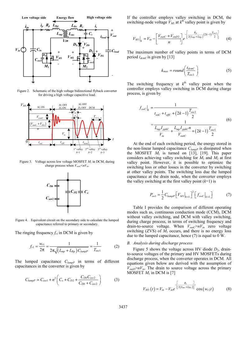
Figure 2. Schematic of the high voltage bidirectional flyback converter for driving a high voltage capacitive load.
Figure 3. Voltage across low voltage MOSFET M1 in DCM, during charge process when VoutC<nVin.
Figure 4. Equivalent circuit on the secondary side to calculate the lumped capacitance referred to primary or secondary.
The ringing frequency fr1 in DCM is given by
( )1
11
1 12 2
rr
oscmp lkp lumpP
wfTL L C
= = =π π +
(2)
The lumped capacitance ClumpP in terms of different capacitances in the converter is given by
221 2
2
Db osslumpP oss s D
Db oss
C CC C n C CC C
⎛ ⎞+ + +⎜ ⎟+⎝ ⎠ (3)
If the controller employs valley switching in DCM, the switching-node voltage VM1 at kth valley point is given by
( ) ( ) 12 12 22
1
p osc
mp lkp
R TkL LoutC onD
M inkV VV V e
n
⎡ ⎤− −⎢ ⎥
+⎢ ⎥⎣ ⎦+⎡ ⎤= − ⎢ ⎥⎣ ⎦ (4)
The maximum number of valley points in terms of DCM period tdcmC is given by [13]
1
dcmCmax
osc
tk roundT
⎛ ⎞= ⎜ ⎟⎝ ⎠
(5)
The switching frequency at kth valley point when the controller employs valley switching in DCM during charge process, is given by
( )
( )
1
1
1
2 12
1 =2 1
2
swC kosc
onC offC
mp ppkC mp ppkC osc
in outC
fTt t k
L I L I n TkV V
=+ + −
+ + −
(6)
At the end of each switching period, the energy stored in the non-linear lumped capacitance ClumpP is dissipated when the MOSFET M1 is turned on [13], [19]. This paper considers achieving valley switching for M1 and M2 at first valley point. However, it is possible to optimize the switching loss or other losses in the converter by switching at other valley points. The switching loss due the lumped capacitance at the drain node, when the converter employs the valley switching at the first valley point (k=1) is
21 1 1 1
12sw lumpP M swCk kP C V f= =
⎡ ⎤⎡ ⎤= ⎣ ⎦ ⎣ ⎦ (7)
Table I provides the comparison of different operating modes such as, continuous conduction mode (CCM), DCM without valley switching, and DCM with valley switching, during charge process, in terms of switching frequency and drain-to-source voltage. When VoutC>nVin zero voltage switching (ZVS) of M1 occurs, and there is no energy loss due to the lumped capacitance, hence (7) is equal to 0 W.
B. Analysis during discharge process Figure 5 shows the voltage across HV diode D2, drain-
to-source voltages of the primary and HV MOSFETs during discharge process, when the converter operates in DCM. All equations given below are derived with the assumption of VoutD>nVin. The drain to source voltage across the primary MOSFET M1 in DCM is [7]
( ) ( ) ( )21 2cos
s
ms lks
R tL L
M in in rV t V V e w t⎡ ⎤
−⎢ ⎥+⎢ ⎥⎣ ⎦= − (8)
1:nVout
Cin
Db
+
-
M1 M2
ip is
Energy flow
•
•
Vin
Rp Llkp
Lmp Lms
RsLlks
Cs iload
High voltage sideLow voltage side
+
-
+
-VM1 VM2Coss1 Coss2
D2+-VDb
+
-VD2
CloadDb1 Db2
iin
inV
( )2outC DV Vn+
M1 ONM1 OFF
t
VM1
0
leakPV
D2 ONM1 OFFD2 OFF DCM
1oscT
1st valleyk=1
2nd valleyk=2
3rd valleyk=3
onCt offCt dcmCt
vCtdCt
3437

TABLE I. COMPARISON OF DIFFERENT OPERATING MODES IN A FLYBACK CONVERTER DURING CHARGE PROCESS
Operating Mode
Switching frequency during
charge process fswC
Drain-to-source voltage of M1 (VM1) at the beginning of next switching cycle during charge
process
CCM 1
onC offCt t+
2
TCin
TC outC onD
VVn
V V V
+
= +
DCM (without valley
switching)
1onC offC
dcmC
t t
t
+ +⎡ ⎤⎢ ⎥⎢ ⎥⎣ ⎦
( )1 1
1
cos
when
2
TCin o dcmC
outC in
pdcmC
Tp
Tp mp lkp
VV e w tn
V nV
Rt
L
L L L
−Δ+
<
⎡ ⎤Δ = ⎢ ⎥
⎣ ⎦= +
DCM (with valley switching at
kth valley point)
( ) 1
1
2 12
onC offC
osc
t t
Tk
+ +⎡ ⎤⎢ ⎥⎢ ⎥−⎢ ⎥⎣ ⎦
( )
2
12
, if
0 ZVS , if
2 12 2
TCin outC in
outC in
p osc
Tp
VV e V nVn
V nV
R TkL
−Δ⎧ − <⎪⎨⎪ ⇒ >⎩
⎡ ⎤Δ = −⎢ ⎥
⎣ ⎦
The voltage across HV diode D2 in DCM is [7]
( ) ( ) ( ) ( )22 2cos
s
ms lks
R tL L
D outD onDb in rV t V V nV e w t⎡ ⎤
−⎢ ⎥+⎢ ⎥⎣ ⎦= − + (9)
The voltage across HV diode Db in DCM is
( ) ( ) ( )221 cos
s
ms lks
R tL L
Db leakD in rV t V nV e w t⎡ ⎤
−⎢ ⎥+⎢ ⎥⎣ ⎦
⎡ ⎤⎧ ⎫⎪ ⎪⎢ ⎥= δ + δ −⎨ ⎬⎢ ⎥⎪ ⎪⎢ ⎥⎩ ⎭⎣ ⎦
(10)
where lksleakD spkD
lumpS
LV IC
= and 2
2
oss
oss Db
CC C
δ =+
The voltage across HV MOSFET M2 in DCM is
( )( )
( ) ( ) ( )2
221 cos
s
ms lks
outD onDb leakD in
RM tL L
in r
V V V nVV t
nV e w t⎡ ⎤
−⎢ ⎥+⎢ ⎥⎣ ⎦
⎡ − + δ + δ + ⎤⎢ ⎥= ⎢ ⎥⎢ ⎥− δ⎣ ⎦
(11)
The ringing frequency fr2 in DCM is given by
( )2
22
1 12 2
rr
oscms lks lumpS
wfTL L C
= = =π π +
(12)
The lumped capacitance ClumpS in terms of different capacitances in the converter is given by
Figure 5. Voltages across D2, M2 and M1 in DCM, during discharge process when VoutD>nVin.
22
2
Db osslumpS s D
Db oss
C CC C CC C
⎛ ⎞+ +⎜ ⎟+⎝ ⎠ (13)
If the controller employs valley switching in DCM during discharge process, the switching-node voltage VM2 at kth valley point is given by
( )
( ) ( )( ) 22 2 12 2
+
1s osc
ms lks
outD onDb leakD in
R TM k kL L
in
V V V nVV
nV e⎡ ⎤
− −⎢ ⎥+⎢ ⎥⎣ ⎦
⎡ − + δ δ +⎤⎢ ⎥= ⎢ ⎥⎢ ⎥− δ⎣ ⎦
(14)
The switching frequency at kth valley point when the controller employs valley switching in DCM during discharge process, is given by
( )
( ) ( )
2
2
1
2 12
1 =2 1
2
swD k osconD offD
ms spkD mp spkD osc
outD in in
fTt t k
L I L I n TkV V V
=+ + −
+ + −+ Δ
(15)
At the end of each switching period, the energy stored in the non-linear lumped capacitance ClumpS is dissipated when
innV
( )outD DbV V−
leakSV 2oscT
onDt offDt dcmDt
vDtdDt
innVδ
( )outD DbV V−
leakSVδ
inV
( )outD DbV Vn−
2oscTvDt
dDt
3438

the switch M2 is turned-on. Valley switching at the first valley point is employed during the discharge process, to reduce the discharging time or to increase the discharge speed. The switching loss due the lumped capacitance at the drain node, when the converter employs the valley switching at the first valley point (k=1) is
22 2 1 1
12
sw lumpS M swDk kP C V f= =⎡ ⎤ ⎡ ⎤= ⎣ ⎦ ⎣ ⎦ (16)
Table II provides the comparison of different operating modes during discharge process, in terms of switching frequency and drain-to-source voltage.
TABLE II. COMPARISON OF DIFFERENT OPERATING MODES IN A FLYBACK CONVERTER DURING DISCHARGE PROCESS
Operating Mode
Switching frequency
during charge process fswD
Drain-to-source voltage of M2 (VM2) at the beginning of the next
switching cycle during the discharge process
CCM 1
onD offDt t+ TD leakD in
TD outD onDb
V V nVV V V
+ δ + δ= −
DCM (without valley
switching)
1onD offD
dcmD
t tt
+ +⎡ ⎤⎢ ⎥⎣ ⎦
( ) ( )3 2
3
1 cos
;2
TD leakD in
in o dcmD
sdcmD Ts ms lks
Ts
V V nV
nV e w t
R t L L LL
−Δ
+ δ + δ⎡ ⎤⎢ ⎥
− δ⎢ ⎥⎣ ⎦⎡ ⎤Δ = = +⎢ ⎥⎣ ⎦
DCM (with valley switching at
kth valley point)
( ) 2
1
2 12
onD offD
osc
t tTk
+ +⎡ ⎤⎢ ⎥⎢ ⎥−⎢ ⎥⎣ ⎦
( )
( )
4
1 2
1 2
24
1 2
, if 1
~ , if
2 12 2
;
TDoutD in
in
TD outD in
s osc
Ts
leakD in
VV nV
nV e
V V nV
R TkL
V nV
−Δ
⎧ + γ + γ −⎡ ⎤⎪ >⎢ ⎥
− δ⎨ ⎢ ⎥⎣ ⎦⎪
δ + γ + γ <⎩⎡ ⎤Δ = −⎢ ⎥⎣ ⎦
γ = δ γ = δ
III. PROPOSED VALLEY SWITCHING CONTROL
A. Charge process The bidirectional flyback converter with the control
circuit to achieve the valley switching during charge and discharge processes is shown in Fig. 6. The input voltage and the drain voltage of primary MOSFET M1, each scaled by a resistor divider network H1 (3 kΩ and 90 kΩ), are compared using a high speed comparator TLV3501A. The comparator output becomes low (Vcomp=0), when the drain voltage of M1 is lower than the input voltage Vin. The output signal of the comparator Vcomp is sent to the 16-bit microcontroller (PIC18F45K22) which detects the comparator output change, and produces a fixed on-time pulse to enable the gate driver 1 to drive the MOSFET M1.
To introduce the control approach, Figs. 7-9 provide experimental results in the flyback converter during charge process, in the case when the converter is driven at a fixed frequency without valley switching. From Fig. 7, it can be observed that there is a delay time tdC (~1.04 μs) between the time when the comparator output goes low and the first valley point (at which the next switching cycle should start
to achieve valley switching), in the drain voltage of M1 (VM1). The microcontroller provides the delay time tdC such that the next turn-on cycle of M1 starts at the first valley point. The delay time tdC can be calculated from the ringing frequency of VM1 in DCM. The delay time tdC is half of the time to reach first valley point tvC (k=1) when VoutC<nVin (see Fig. 3). The expression for tdC in terms of DCM ringing frequency fr1 is given by
( )1
12 4 2vC
dC mp lkp lumpPr
tt L L Cf
π= = = + (17)
Figure 6. Schematic of the bidirectional flyback converter with the
control circuit to achieve valley switching.
As mentioned before, M1 is turned-on whenever the comparator output becomes low (Vcomp=0), but the operation can be corrupted by ringing due to the leakage inductance Llkp, which can also make the comparator output low (see Fig. 8). So, another delay time tdleak (~1.5-2 μs) is provided by the microcontroller to disable the switching of M1 during this interval. When VoutC>nVin the drain voltage VM1 reaches 0 V (with in 500 ns) before the delay time tdC, which ensures zero voltage turn-on, as shown in Fig. 9. Hence, there is no capacitive switching loss during charge process when the output voltage VoutC>nVin (see Table I).
B. Discharge process To achieve valley switching of HV MOSFET M2 during
discharge process, only the information of the comparator output Vcomp is used. The comparator output becomes high (Vcomp=5 V), when the drain voltage of M1 is higher than the input voltage Vin. Similar to the charge process, the output signal of the comparator is sent to the microcontroller which produces a fixed or variable on-time pulse to enable the gate driver 2, to drive the MOSFET M2. During the discharge process, since the output voltage decreases, the on-time tonD of M2 should be increased with the discharge time, to make the secondary discharge peak current IspkD constant. Figures 10-12 provide experimental results in the flyback converter during discharge process, in the case when the converter is driven at a fixed frequency without valley switching. From Fig. 10, it can be observed that there is a delay time tdD (~1.04 μs) between the time when the comparator output goes high and the first valley point (at which the next switching cycle should start to achieve valley switching), in the drain voltage of M2 (VM2). The microcontroller provides
1:n
Digital Controller
Vout
CinD2 Cload
Db
+
-
M1M2
ip is
Energy flow
•
•
Vin
H1H1
-+Vcc
Vcomp
Gate driver 2
Gate driver 1
VG1 VG2
iin
3439

the delay time tdD such that the next turn-on cycle of M2 starts at the first valley point, and it can be calculated from the ringing frequency of VM2 in DCM. The delay time tdD is half of the time to reach first valley point tvD (k=1) when VoutD>nVin (see Fig. 5). The expression for tdD in terms of DCM ringing frequency fr2 is given by
( )2
12 4 2vD
dD ms lks lumpSr
tt L L Cf
π= = = + (18)
When the HV probe is placed across D2, the equivalent lumped capacitance ClumpS is increased by ~9-10 pF due to the capacitance CHVprobe of the HV probe Lecroy PPE 4 kV. Due to this ringing frequency fr2 shown in Figs. 10 and 11 are different. When the HV probe is placed across M2, ClumpS remains unchanged, due to the series combination of Db and M2. When VoutD<nVin the drain voltage VM2 reaches
1 2~ TDVδ + γ + γ , whereas the voltage across D2 becomes 0 V (see Table II) before the delay time tdD, as shown Figs. 12 and 13, respectively.
Figure 7. Experimental results when M1 is driven with fixed frequency (Vout<600V) during charge process; CH2: Vin; CH3: Vcomp; CH4: VM1.
Figure 8. A zoomed view of Fig. 7 immediately after M1 is turned-off.
Figure 9. Experimental results when M1 is driven with fixed frequency (Vout>600V) during charge process; CH2: Vin; CH3: Vcomp; CH4: VM1.
Figure 10. Experimental results when M2 is driven with fixed frequency (Vout>600V) during discharge process; CH1: VM2; CH2: Vin; CH3: Vcomp;
CH4: VM1.
Figure 11. Experimental results when M2 is driven with fixed frequency (Vout>600V) during discharge process; CH1: VD2; CH2: Vin; CH3: Vcomp;
CH4: VM1.
Figure 12. Experimental results when M2 is driven with fixed frequency (Vout<600V) during discharge process; CH1: VM2; CH2: Vin; CH3: Vcomp;
CH4: VM1.
Figure 13. Experimental results when M2 is driven with fixed frequency (Vout<600V) during discharge process; CH1: VD2; CH2: Vin; CH3: Vcomp;
CH4: VM1.
IV. VALLEY SWITCHING EXPERIMENTAL RESULTS Tables II, III and IV provide the converter
specifications, components used in the converter, and
Tdleak=1.4 μs
Drain voltage of M1VM1
Comparator outputVcomp
Input voltageVin
3440

flyback transformer parameters, respectively. The experimental prototype of the HV bidirectional flyback converter is shown in Fig. 14. The experimental results in the converter, tested with a film capacitive load of 400 nF, to validate the proposed valley switching technique are shown in Figs. 15-18. In Figs. 15 and 16, successful valley-switching operation at different output voltages during the charge process is shown. From Fig. 16, it is clear that the converter operates with zero voltage switching (ZVS) turn-on, and the primary current is negative before the switch is turned-on. In Fig. 17, successful valley-switching operation during discharge process is shown. As explained in Section III, the first valley voltage in the drain to-source voltage of M2 is not very low, compared to the first valley voltage in HV diode voltage VD2 (due to the series combination of Db and M2). The capacitive switching loss is directly proportional to the voltage across the HV MOSFET when it is turned-on (7), (16). This is one of the reasons for the low energy efficiency during the discharge process.
TABLE III. SPECIFICATIONS OF THE BIDIRECTIONAL FLYBACK CONVERTER
Parameter Value
Input voltage Vin 24 V Output voltage Vout 0-2.5 kV
Capacitance of the load Cload 400 nF On time of M1 during charge process
tonC 9 µs
On times of M2 during discharge process tonD
[2 µs, 3 µs, 5 µs, 10 µs, 20 µs, 150 µs, 200 µs]
TABLE IV. COMPONENTS USED IN THE HV CONVERTER
Component Value Primary MOSFET M1 250V, 16A [FQD16N25CTM]
HV MOSFET M2 4.5 kV, 200 mA, 750 Ω
[IXTA02N450HV] / 4 kV, 300 mA, 290 Ω [IXTV03N400S]
HV diode Db / D2 5 kV, 150 mA [SXF6525] Gate driver EL7104 Comparator 4.5 ns Rail-to-Rail, TLV3501A
Film capacitive load 400 nF, 3 kV [WIMA]
TABLE V. FLYBACK TRANSFORMER PARAMETERS
Parameter Value Core used / material used PQ 20/20 / P type
Primary Np / secondary turns Ns 12 / 300 Primary Lmp / secondary magnetizing
inductance Lms 47.5 μH / 30 mH
Leakage inductance referred to primary Llkp / secondary Llks
990 nH / 620 μH
Self-capacitance of secondary winding Cs
(from the Impedance analyzer) 6 pF
Self-capacitance Cs from frequencies fr1, fr2 12.5 pF
Diameter of primary/secondary winding 0.5 mm (TEX-E)/ 0.11 mm
DC resistance of primary Rp /secondary Rs 62 mΩ / 14 Ω Number of layers of primary/secondary 1 / 4
Figure 14. Experimental prototype of the HV bidirectional flyback
converter with a 4.5 kV MOSFET on the HV side.
Figure 15. Experimental results when the converter is operated with valley switching during charge process; CH1: ip; CH2: Vin; CH3: VG1; CH4: VM1.
Figure 16. Experimental results with valley switching operation during the charge process; CH1: IP; CH2: Vin; CH3: VG1; CH4: VM1.
Figure 17. Experimental results with valley switching operation during
discharge process; CH1: is; CH2: VM2; CH3: VG2; CH4: VM1.
The bidirectional operation of the HV converter at 2.5 kV output voltage is shown in the Fig. 18. As provided in Table III, due to constant turn on-time tonC for M1 during charge process, the primary current IppkC is constant. During discharge process, employing variable turn on-time tonD for M2 makes the secondary current (hence the primary current) IspkC almost constant. The energy efficiency measurements
30 m
m
3441
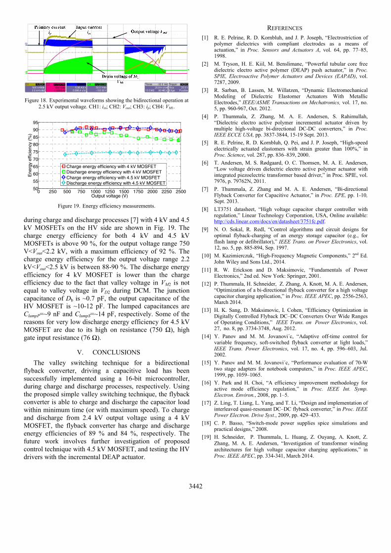
Figure 18. Experimental waveforms showing the bidirectional operation at
2.5 kV output voltage. CH1: iin; CH2: Vout; CH3: ip; CH4: VM1.
0 250 500 750 1000 1250 1500 1750 2000 2250 250050
55
60
65
70
75
80
85
90
95
Output voltage (V)
Ene
rgy
effic
ienc
y (%
)
Charge energy efficiency with 4 kV MOSFETDischarge energy efficiency with 4 kV MOSFETCharge energy efficiency with 4.5 kV MOSFETDischarge energy efficiency with 4.5 kV MOSFET
Figure 19. Energy efficiency measurements.
during charge and discharge processes [7] with 4 kV and 4.5 kV MOSFETs on the HV side are shown in Fig. 19. The charge energy efficiency for both 4 kV and 4.5 kV MOSFETs is above 90 %, for the output voltage range 750 V<Vout<2.2 kV, with a maximum efficiency of 92 %. The charge energy efficiency for the output voltage range 2.2 kV<Vout<2.5 kV is between 88-90 %. The discharge energy efficiency for 4 kV MOSFET is lower than the charge efficiency due to the fact that valley voltage in VM2 is not equal to valley voltage in VD2 during DCM. The junction capacitance of Db is ~0.7 pF, the output capacitance of the HV MOSFET is ~10-12 pF. The lumped capacitances are ClumpP=~9 nF and ClumpS=~14 pF, respectively. Some of the reasons for very low discharge energy efficiency for 4.5 kV MOSFET are due to its high on resistance (750 Ω), high gate input resistance (76 Ω).
V. CONCLUSIONS The valley switching technique for a bidirectional
flyback converter, driving a capacitive load has been successfully implemented using a 16-bit microcontroller, during charge and discharge processes, respectively. Using the proposed simple valley switching technique, the flyback converter is able to charge and discharge the capacitor load within minimum time (or with maximum speed). To charge and discharge from 2.4 kV output voltage using a 4 kV MOSFET, the flyback converter has charge and discharge energy efficiencies of 89 % and 84 %, respectively. The future work involves further investigation of proposed control technique with 4.5 kV MOSFET, and testing the HV drivers with the incremental DEAP actuator.
REFERENCES [1] R. E. Pelrine, R. D. Kornbluh, and J. P. Joseph, “Electrostriction of
polymer dielectrics with compliant electrodes as a means of actuation,” in Proc. Sensors and Actuators A, vol. 64, pp. 77–85, 1998.
[2] M. Tryson, H. E. Kiil, M. Benslimane, “Powerful tubular core free dielectric electro active polymer (DEAP) push actuator,” in Proc. SPIE, Electroactive Polymer Actuators and Devices (EAPAD), vol. 7287, 2009.
[3] R. Sarban, B. Lassen, M. Willatzen, “Dynamic Electromechanical Modeling of Dielectric Elastomer Actuators With Metallic Electrodes,” IEEE/ASME Transactions on Mechatronics, vol. 17, no. 5, pp. 960-967, Oct. 2012.
[4] P. Thummala, Z. Zhang, M. A. E. Andersen, S. Rahimullah, “Dielectric electro active polymer incremental actuator driven by multiple high-voltage bi-directional DC-DC converters,” in Proc. IEEE ECCE USA, pp. 3837-3844, 15-19 Sept. 2013.
[5] R. E. Pelrine, R. D. Kornbluh, Q. Pei, and J. P. Joseph, “High-speed electrically actuated elastomers with strain greater than 100%,” in Proc. Science, vol. 287, pp. 836–839, 2000.
[6] T. Andersen, M. S. Rødgaard, O. C. Thomsen, M. A. E. Andersen, “Low voltage driven dielectric electro active polymer actuator with integrated piezoelectric transformer based driver,” in Proc. SPIE, vol. 7976, p. 79762N, 2011.
[7] P. Thummala, Z. Zhang and M. A. E. Andersen, “Bi-directional Flyback Converter for Capacitive Actuator,” in Proc. EPE, pp. 1-10, Sept. 2013.
[8] LT3751 datasheet, “High voltage capacitor charger controller with regulation,” Linear Technology Corporation, USA, Online available: http://cds.linear.com/docs/en/datasheet/3751fc.pdf.
[9] N. O. Sokal, R. Redl, “Control algorithms and circuit designs for optimal flyback-charging of an energy storage capacitor (e.g., for flash lamp or defibrillator),” IEEE Trans. on Power Electronics, vol. 12, no. 5, pp. 885-894, Sep. 1997.
[10] M. Kazimierczuk, “High-Frequency Magnetic Components,” 2nd Ed. John Wiley and Sons Ltd., 2014.
[11] R. W. Erickson and D. Maksimovic, “Fundamentals of Power Electronics,” 2nd ed. New York: Springer, 2001.
[12] P. Thummala, H. Schneider, Z. Zhang, A. Knott, M. A. E. Andersen, “Optimization of a bi-directional flyback converter for a high voltage capacitor charging application,” in Proc. IEEE APEC, pp. 2556-2563, March 2014.
[13] H. K. Sang, D. Maksimovic, I. Cohen, “Efficiency Optimization in Digitally Controlled Flyback DC–DC Converters Over Wide Ranges of Operating Conditions,” IEEE Trans. on Power Electronics, vol. 27, no. 8, pp. 3734-3748, Aug. 2012.
[14] Y. Panov and M. M. Jovanovi´c, “Adaptive off-time control for variable frequency, soft-switched flyback converter at light loads,” IEEE Trans. Power Electronics, vol. 17, no. 4, pp. 596–603, Jul. 2002.
[15] Y. Panov and M. M. Jovanovi´c, “Performance evaluation of 70-W two stage adapters for notebook computers,” in Proc. IEEE APEC, 1999, pp. 1059–1065.
[16] Y. Park and H. Choi, “A efficiency improvement methodology for active mode efficiency regulation,” in Proc. IEEE Int. Symp. Electron. Environ., 2008, pp. 1–5.
[17] Z. Ling, T. Liang, L. Yang, and T. Li, “Design and implementation of interleaved quasi-resonant DC–DC flyback converter,” in Proc. IEEE Power Electron. Drive Syst., 2009, pp. 429–433.
[18] C. P. Basso, “Switch-mode power supplies spice simulations and practical designs,” 2008.
[19] H. Schneider, P. Thummala, L. Huang, Z. Ouyang, A. Knott, Z. Zhang, M. A. E. Andersen, “Investigation of transformer winding architectures for high voltage capacitor charging applications,” in Proc. IEEE APEC, pp. 334-341, March 2014.
3442

176/255
Appendix LDigital Control of a High Voltage
(2.5 kV) Bidirectional DC-DCConverter for Driving a Capacitive
Incremental Actuator
About to Submit to IEEE Transactions on Power Electronics
177/255

Digital Control of a High Voltage (2.5 kV) Bidirectional DC-
DC Converter for Driving a Capacitive Incremental Actuator
Prasanth Thummala*, Student Member, IEEE, Dragan Maksimovic
#, Senior Member, IEEE, Zhe Zhang
*, Member, IEEE, and
Michael A. E. Andersen*, Member, IEEE
*Electronics group, Department of Electrical Engineering, Technical University of Denmark, 2800 Kongens Lyngby,
Denmark.
#Colorado Power Electronics Center, Department of Electrical, Computer, and Energy Engineering, University of Colorado
Boulder, Boulder, 80309 Colorado, USA.
Email: [email protected], [email protected]
Abstract — This paper presents a digital control technique to achieve valley switching in a bidirectional flyback
converter used to drive a dielectric electro active polymer based incremental actuator. The incremental actuator
consists of three electrically isolated, mechanically connected capacitive actuators. The incremental actuator requires
three high voltage (2-2.5 kV) bidirectional dc-dc converters, to accomplish the incremental motion by charging and
discharging the capacitive actuators. The bidirectional flyback converter employs a digital controller to improve
efficiency and charge/discharge speed using the valley switching technique during both charge and discharge processes,
without the need to sense signals on the output high-voltage side. The design of a low input (24 V) and variable high
output voltage (0-2.5 kV) bidirectional dc-dc converter for driving a capacitive actuator is presented. Experimental
results verifying the bidirectional operation of a single high voltage flyback converter are presented, using a film
capacitor as the load. Energy efficiency measurements are provided.
Index Terms — switch-mode power converters, high voltage dc-dc converters, digital control, energy efficiency,
actuator
Statement: A part of this manuscript is presented at the IEEE ECCE USA 2014 conference. It is not currently under review
for publication in any other journal. Compared with the conference paper, the detailed bidirectional flyback converter design
and loss analysis results are included. Furthermore, the experimental results are updated.

NOMENCLATURE
Cin / Cload Input / load or actuator capacitance (F)
Cs Self-capacitance of high voltage winding of transformer (F)
Cossp / Cosss Output capacitance of low voltage MOSFET Mp / high voltage MOSFET Ms (F)
CD2 / CDb Junction capacitance of high voltage freewheeling diode D2 / blocking diode Db (F)
ClumpP / ClumpS Equivalent lumped capacitance referred at the drain node of MOSFET Mp / Ms (F)
D2 / Db High voltage (5 kV) freewheeling diode / blocking diode
Dbp / Dbs Body diode of MOSFET Mp / Ms
DonC,min Minimum on-duty cycle of Mp
DoffC,max Maximum off-duty cycle of Mp
DonD,max Maximum on-duty cycle of Ms
fswC / fswD Switching frequency during charge / discharge process (Hz)
fr1 / fr2 Charge / discharge process ringing frequency in discontinuous conduction mode (DCM) (Hz)
iin / ip / is Input / primary / secondary current (A)
IppkC / IspkD Primary peak charging current / Secondary peak discharging current (A)
ID2/IDb Rated average current of diode D2/Db
IM2 Rated average current of MOSFET Ms
Lmp / Lms Primary/secondary magnetizing inductance (H)
Llkp / Llks Leakage inductance of transformer referred to primary / secondary side (H)
Mp Low voltage MOSFET
Ms High voltage (4 kV / 4.5 kV) MOSFET
n Turns ratio of transformer from secondary to primary
Np / Ns Number of primary / secondary turns
Rp / Rs Primary / Secondary dc resistance of transformer (Ω)
tonC / toffC On-time / off-time of Mp during charge process (s)
tonD / toffD On-time / off-time of Ms during discharge process (s)
Toss1 / Toss2 Charge / discharge process oscillation period in DCM (s)
tdcmC / tdcmD Total DCM time duration during charge / discharge process (s)
tvC / tvD Time to reach the valley point in the drain voltage during charge / discharge process (s)

tdC / tdD Delay time needed to reach the valley point during charge / discharge process after the comparator output
changes (s)
tdleak Delay time introduced to avoid the leakage inductance Llkp effect during charge process (s)
Vin / ΔVinD Input voltage / Increment in the input voltage during discharge process (V)
VoutC / VoutD Variable load voltage during charge (0 V-2.5 kV) / discharge process (2.5 kV-0 V)
VMp / VMs Drain-to-source voltage of MOSFET Mp / Ms (V)
VD2 / VDb Reverse voltage across diode D2 / Db (V)
VonD2 / VonDb Voltage drop of diode D2 / Db (V)
VBVM1 / VBVM2 Breakdown voltage of MOSFET Mp / Ms
VBVD2 Breakdown voltage of high voltage diode D2 (or Db)
βM1 / βM2 / βD2 Margin factor (< 1) for VBVM1 / VBVM2 / VBVD2
η Power efficiency of the converter
VleakD Voltage increment in drain-to-source voltage of Ms due to leakage inductance Llks (V)
Vcomp Output of the comparator (V)
δ Capacitance ratio factor on the high voltage (HV) side
I. INTRODUCTION
Dielectric electro active polymer (DEAP) is an evolving smart material that has experienced substantial development and
has gained growing attention over the last decade [1]-[3]. DEAPs, when used as linear actuators, have the potential to be an
effective replacement for many conventional linear actuators because of their unique properties, including light weight, low
noise operation, high flexibility, low cost, large strain, and autonomous capability. The DEAP actuator, shown in Fig. 1(a), is
ideally equivalent to a pure capacitive load [4]. The DEAP incremental actuator concept, recently proposed in [5], consists of
A1
A3
A2
Grippers
Extender
a) b)
33 mm
110 mm
A1
A3
A2
Grippers
Extender
a) b)
33 mm
110 mm
Fig. 1. a) DEAP actuator; b) DEAP incremental actuator.

two grippers at both ends (to enable gripping operation) and an extender (to move the grippers), as shown in Fig. 1(b). These
grippers connect with the extender mechanically. The grippers A1 and A3 and the extender A2 are similar to the DEAP actuator
shown in Fig. 1(a). For moving the incremental actuator, the three DEAP actuators (which behave as electrically isolated
capacitive loads) needs to be controlled. Details of the DEAP incremental actuator operation can be found in [5].
To drive a DEAP incremental actuator, high voltage (~ 2.5 kV) bidirectional DC-DC converters are required, to generate
sufficient force and displacement for the three sub-actuators [5]. Prior work on high voltage (HV) drivers for the DEAP
actuators demonstrated a low voltage piezoelectric transformer based DEAP solution which was incorporated into a coreless
DEAP actuator [6], and a bidirectional flyback converter topology to drive the PolyPower Push Inlastor DEAP actuator [7],
which utilized the control IC LT3751 [8] to achieve the charge and discharge operations, with boundary conduction mode
(BCM) control and discontinuous conduction mode control (DCM), respectively. The objectives of this paper are to implement
the valley switching technique using a digital controller, during both charge and discharge operations, in order to improve
efficiency and charge/discharge speed, as well as to reduce electromagnetic interference (EMI). Furthermore, another objective
is to eliminate the need to sense any signal (voltage or current) on the HV side.
The flyback converter is suitable for high voltage and low power applications due to its simple structure and low
component count [11]. Control algorithms for optimal-flyback charging of a capacitive load have been proposed in [9]. In [12]
an efficiency optimization technique is proposed for a bidirectional flyback converter [7] for a high voltage capacitor charging
application. In [13] an efficiency optimization technique has been proposed for a flyback converter which employs the valley
switching control. Valley switching/QR control has also been used in [14]-[17], to improve the efficiency of the switch mode
power supplies by reducing the capacitive turn-on/switching losses, and to reduce electro magnetic interference (EMI).
For the high voltage capacitor charging application, the capacitive switching losses [13], [19] due to the equivalent lumped
capacitance, at the drain node of the primary MOSFET during charge process, and at the drain node of the HV MOSFET
during discharge process dominates the total losses in the converter. Therefore, the approach followed in this paper is to reduce
the capacitive switching losses by implementing the valley switching control for charging as well as discharging the capacitive
load. The proposed valley switching technique requires only sensing of the low voltage side voltages (supply voltage and drain
voltage) without the need to sense any HV side signals.
This paper is organized as follows: Section II describes the converter design considerations. Section III presents the
theoretical analysis of the HV flyback converter in DCM, for achieving the valley switching during both charge and discharge

modes. Section IV discusses the proposed valley switching control technique. Section V provides the experimental results
followed by the conclusions in Section VI.
II. BIDIRECTIONAL DC-DC FLYBACK CONVERTER DESIGN CONSIDERATIONS
The schematic of the bidirectional flyback converter is shown in Fig. 2. The converter design considerations are discussed
in this section. Specifications of the converter and power stage components are provided in Tables I and II, respectively.
A. Choice of turns ratio of the flyback transformer
For the capacitor charging application, the turns ratio is selected based on the maximum charging voltage of the capacitive
load Vo,max. The typical voltage stress waveforms across MOSFETs Mp, Ms, and HV diode D2 are shown in Figs. 3(a), 3(b) and
3(c), respectively.
1:n
Vout
Cin
Db
+
-
Mp Ms
ip is
Energy flow
Vin
Rp Llkp
Lmp Lms
RsLlks
Csiload
High voltage sideLow voltage side
+
-
+
-
VMp VMsCossp Cosss
D2
+
-VDb
+
-VD2
Cload
Dbp Dbs
iin
Fig. 2. Circuit configuration of the high voltage bidirectional flyback converter for driving a capacitive load.
TABLE I. SPECIFICATIONS OF BIDIRECTIONAL FLYBACK CONVERTER
Parameter Value
Input Vin 24 V
Output voltage Vout 0-2.5 kV (Vout,max=2.5 kV)
Capacitance of the load Cload 400 nF
On time during charge process tonC 9 µs
Target charging time Tch 50 ms
Maximum flux density BmaxC 0.3 T
TABLE II. POWER STAGE COMPONENTS USED IN THE CONVERTER
Component Value
Primary MOSFET Mp 250V, 25A [IPD600N25N3 G]
HV MOSFET Ms 4.5 kV, 200 mA, 750 Ω [IXTA02N450HV] /
4 kV, 300 mA, 290 Ω [IXTV03N400S]
HV diode Db / D2 5 kV, 150 mA [SXF6525]

1) Charge process: The maximum and minimum turns ratios, from secondary to primary of the flyback transformer during
charge process can be calculated to meet the device breakdown voltage constraints.
The voltage stress across the primary MOSFET Mp when turned off, should be less than its breakdown voltage VBVM1 (Fig.
3(a)), so
2
1 1
o,max onD
in leakP BVM
V VV V V
n
(1)
where leakPV is the increase in the drain voltage of primary MOSFET due to the leakage inductance LlkP.
From (1), the transformer turns ratio
minn n (2)
where nmin is the minimum turns ratio needed, to charge the capacitive load to Vo,max and is given by
1BVMV
1 1BVMV
inV
2o,max DV V
n
a)
Mp ON Mp OFF
2BVDV
2 2BVDVinnV
o,maxV
b)
Mp ON Mp OFF
2BVMV3 2BVMVleakSV
o,maxV
innV
c)
Ms ON Ms OFF
t
t
t
VMp
0
VD2
0
VMs
0
leakPV
Fig. 3: Voltage stress when target output voltage (Vo,max) is reached across, a) Mp during charge process (BCM), b) D2 during
charge process (BCM), c) Ms during discharge process (BCM); BCM: Boundary Conduction Mode.
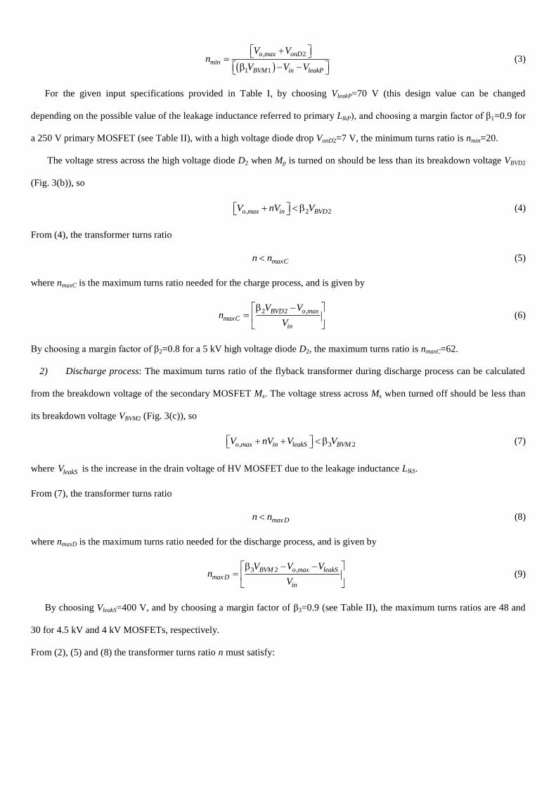
2
1 1
o,max onD
min
BVM in leakP
V Vn
V V V
(3)
For the given input specifications provided in Table I, by choosing VleakP=70 V (this design value can be changed
depending on the possible value of the leakage inductance referred to primary LlkP), and choosing a margin factor of β1=0.9 for
a 250 V primary MOSFET (see Table II), with a high voltage diode drop VonD2=7 V, the minimum turns ratio is nmin=20.
The voltage stress across the high voltage diode D2 when Mp is turned on should be less than its breakdown voltage VBVD2
(Fig. 3(b)), so
2 2o,max in BVDV nV V (4)
From (4), the transformer turns ratio
maxCn n (5)
where nmaxC is the maximum turns ratio needed for the charge process, and is given by
2 2BVD o,max
maxCin
V Vn
V
(6)
By choosing a margin factor of β2=0.8 for a 5 kV high voltage diode D2, the maximum turns ratio is nmaxC=62.
2) Discharge process: The maximum turns ratio of the flyback transformer during discharge process can be calculated
from the breakdown voltage of the secondary MOSFET Ms. The voltage stress across Ms when turned off should be less than
its breakdown voltage VBVM2 (Fig. 3(c)), so
3 2o,max in leakS BVMV nV V V (7)
where leakSV is the increase in the drain voltage of HV MOSFET due to the leakage inductance LlkS.
From (7), the transformer turns ratio
maxDn n (8)
where nmaxD is the maximum turns ratio needed for the discharge process, and is given by
3 2BVM o,max leakSmax D
in
V V Vn
V
(9)
By choosing VleakS=400 V, and by choosing a margin factor of β3=0.9 (see Table II), the maximum turns ratios are 48 and
30 for 4.5 kV and 4 kV MOSFETs, respectively.
From (2), (5) and (8) the transformer turns ratio n must satisfy:

2 2
2 2
, if
, if
min maxC BVD BVM
min max D BVD BVM
n n n V Vn
n n n V V
(10)
Since VBVM2<VBVD2 (Table II), the turns ratio n should satisfy 20<n<48, for 4.5 kV HV MOSFET, and 20<n<30, for 4.5 kV
HV MOSFET, respectively. To avoid complexity and difficulty in winding several secondary turns in the transformer, the
turns ratio n is selected to be equal to 25. However, it is up to the designer to choose a different turns ratio, different margin
factors, and different rating low voltage MOSFET for this application.
B. Selection of peak currents during charge and discharge processes
1) Charge process: The expression for primary peak current to charge the HV capacitive load from 0 V to Vo,max in time
Tch is [8], [9]
2 in o,max load o,max
ppkC
in ch delay
nV V C VI
V T T
(11)
For the given input specifications, for a turns ratio of n=25, by choosing a power efficiency η=0.8, and for a delay time
Tdelay=5 ms, the approximate primary peak current is IppkC=4.28 A.
The expression for maximum secondary peak current IspkC,max, to charge the HV capacitive load through HV diode D2, when
the converter is operating in BCM is
2 22 2
1
D DspkC,max
offC,maxonC,min
I II
DD
(12)
Equation (12) is derived based on the average current expression across HV diode D2 during the charge process. The maximum
secondary peak charging current, when a 5 kV HV diode, with a rated current of ID2=150 mA is used, and for a maximum off-
duty cycle during charge process DoffC,max=0.9 is IspkC,max=333 mA. This corresponds to a maximum primary peak current of 8.3
A, for n=25.
2) Discharge process: During the discharge process, since the output voltage decreases in each switching cycle, to
discharge the load with constant peak current ispkD, the on-time tonD should increase in each switching cycle. The expression for
maximum secondary peak current IspkD,max, to discharge the HV capacitive load, through the series combination of high voltage
diode Db and high voltage MOSFET Ms (Fig. 2) is
2 SDspkD,max
onD,max
II
D (13)
where ISD is the average current in the secondary side during discharge process, and is given by:

2
2 2
, if
, if
Db Db MSD
M Db M
I I II
I I I
(14)
Since average current of Db is less than that of M2, i.e., IDb<IM2 (see Table II), ISD=IDb. The maximum secondary peak
discharging current, for a maximum discharge on-duty cycle DonD,max=0.8 is IspkD,max=375 mA. This corresponds to a maximum
primary peak discharging current of 9.37 A, for n=25.
C. Design of primary and secondary turns
1) Charge process: The number of primary turns needed during charge process is
in onCp
maxC c
V tN
B A
(15)
The number of secondary turns needed is
sC pN N n (16)
By choosing a PQ 20/20 core with Ac=62 mm2, and for the specifications shown in Table I, Np=12 and NsC=300.
2) Discharge process: The number of secondary turns needed during discharge process is
in inD offDoutD onDsD
max D c max D c
n V V tV tN
B A B A
(17)
The same secondary turns ( s sC sDN N N ) should meet both (15) and (16). The input capacitance of Cin=30 mF is chosen,
such that the voltage increment during the discharge process ΔVinD <2 V.
D. Design of primary magnetizing inductance
1) Charge process: When the converter operates in BCM during charge process, selecting fixed on-time tonC ensures
constant peak current. In this case, the duty cycle and the switching frequency are maximum at the final switching cycle
(where the output voltage is close to the maximum target output voltage (Vo,max)), and minimum in the first switching cycle
(where the output voltage is minimum or 0 V). The expression for the primary magnetizing inductance needed during charge
process is
in onCmpC
ppkC
V tL
I
(18)
For Vin=24 V, tonC=9 μs, and IppkC=4.28 A the primary magnetizing inductance LmpC=50.5 μH.
2) Discharge process: When the converter operates in BCM during discharge process, selecting variable on-time tonD
ensures constant peak current. In this case, the duty cycle and the switching frequency are maximum at the first switching

cycle (where the output voltage is close to the maximum target output voltage (Vo,max)), and minimum in the final switching
cycle (where the output voltage is close to minimum discharge voltage or 0 V). When the capacitive load transfers the energy
back to the source, the input voltage slightly increases by ΔVinD. The magnitude of ΔVinD depends on the value of the input
capacitance Cin. The expression for the primary magnetizing inductance during discharge process is
in inD offD
mpD
ppkD
V V tL
I
(19)
The same primary magnetizing inductance ( mp mpC mpDL L L ) should meet both (18) and (19).
From (15)-(19), it can be concluded that, if the number of secondary turns s sC sDN N N and the magnetizing
inductance mp mpC mpDL L L then,
ppkD spkD
max D maxC maxCppkC ppkC
I nIB B B
I I (20)
The secondary discharge peak current IspkD in any switching cycle limits the peak flux density BmaxD during the discharge
process. Hence, from (20) suppose if a secondary discharge peak current of IspkD=200 mA is chosen, then the flux density
during discharge process becomes (for n=25, IppkC=4.26 A, BmaxC=0.3 T) BmaxD=0.35 T. The secondary discharge peak current
ispkD should be selected to avoid the core saturation.
III. QUASI RESONANT (QR) / VALLEY SWITCHING CONTROL
The schematic of the HV bidirectional flyback converter for charging and discharging a capacitive actuator/load is shown
in Fig. 2 [7]. This section provides the theoretical analysis, to detect the valley points in the drain voltage of the MOSFETs Mp
and Ms, respectively, with the assumption of Cload>>Cs or CD2.
A. Analysis during charge process
Figure 4 shows the drain-to-source voltage of the primary MOSFET Mp during charge process, when the converter operates
in DCM. The drain to source voltage VMp when VoutC<nVin in DCM is [17]
22
1cos
p
mp lkp
Rt
L LoutC onDMp in r
V VV t V e w t
n
(21)

The ringing frequency fr1 in DCM is given by
11
1
1 1
2 2
rr
oscmp lkp lumpP
wf
TL L C
(22)
The lumped capacitance ClumpP in terms of different capacitances in the converter is given by
22
Db ossslumpP ossp s D
Db osss
C CC C n C C
C C
(23)
If the controller employs valley switching in DCM, the switching-node voltage VMp at kth
valley point is given by
12 1
2 22
p osc
mp lkp
R Tk
L LoutC onDMp in
k
V VV V e
n
(24)
The maximum number of valley points in terms of DCM period tdcmC is given by [13]
1
dcmCmax
osc
tk round
T
(25)
The switching frequency at kth
valley point when the controller employs valley switching in DCM during charge process, is
given by
inV
2outC DV V
n
Mp ONMp OFF
t
VMp
0
leakPV
D2 ON
Mp OFF
D2 OFF DCM
1oscT
1st valley
k=1
2nd valley
k=2
3rd valley
k=3
onCt offCtdcmCt
vCt
dCt
Fig. 4. Voltage across low voltage MOSFET Mp in DCM, during charge process when VoutC<nVin.
CDb
Cossp
CD2 Cs
Fig. 5. Equivalent circuit on the secondary side to calculate the lumped capacitance referred to primary or secondary.

1
1
1
2 12
1 =
2 12
swC kosc
onC offC
mp ppkC mp ppkC osc
in outC
fT
t t k
L I L I n Tk
V V
(26)
At the end of each switching period, the energy stored in the non-linear lumped capacitance ClumpP is dissipated when the
MOSFET Mp is turned on [13], [19]. This paper considers achieving valley switching for Mp and Ms at first valley point.
However, it is possible to optimize the switching loss or other losses in the converter by switching at other valley points. The
switching loss due the lumped capacitance at the drain node, when the converter employs the valley switching at the first
valley point (k=1) is
2
1 11
1
2sw lumpP Mp swC kk
P C V f
(27)
Table III provides the comparison of different operating modes such as, continuous conduction mode (CCM), DCM
without valley switching, and DCM with valley switching, during charge process, in terms of switching frequency and drain-
to-source voltage. When VoutC>nVin zero voltage switching (ZVS) of Mp occurs, and there is no energy loss due to the lumped
capacitance, hence (27) is equal to 0 W.
TABLE III. COMPARISON OF DIFFERENT OPERATING MODES IN A FLYBACK CONVERTER DURING CHARGE PROCESS
Operating Mode Switching frequency during
charge process fswC
Drain-to-source voltage of Mp (VMp) at the beginning
of next switching cycle during charge process
CCM 1
onC offCt t
2
TCin
TC outC onD
VV
n
V V V
DCM
(without valley switching)
1
onC offC dcmCt t t
11
1
cos
when
2
TCin o dcmC
outC in
pdcmC
Tp
Tp mp lkp
VV e w t
n
V nV
Rt
L
L L L
DCM
(with valley switching at
kth valley point) 1
1
2 12
osconC offC
Tt t k
2
12
, if
0 ZVS , if
2 12 2
TCin outC in
outC in
p osc
Tp
VV e V nV
n
V nV
R Tk
L

B. Analysis during discharge proces
Figure 6 shows the voltage across HV diode D2, drain-to-source voltages of the primary and HV MOSFETs during
discharge process, when the converter operates in DCM. All equations given below are derived with the assumption of
VoutD>nVin. The drain to source voltage across the primary MOSFET Mp in DCM is [7]
2
2cos
s
ms lks
Rt
L LMp in in rV t V V e w t
(28)
The voltage across HV diode D2 in DCM is [7]
2
2 2cos
s
ms lks
Rt
L LD outD onDb in rV t V V nV e w t
(29)
The voltage across HV diode Db in DCM is
2
21 cos
s
ms lks
Rt
L LDb leakD in rV t V nV e w t
(30)
where lks
leakD spkD
lumpS
LV I
C and
2
2
oss
oss Db
C
C C
The voltage across HV MOSFET Ms in DCM is
2
21 cos
s
ms lks
Rt
L LMs outD onDb leakD in in rV t V V V nV nV e w t
(31)
The ringing frequency fr2 in DCM is given by
22
2
1 1
2 2
rr
oscms lks lumpS
wf
TL L C
(32)
The lumped capacitance ClumpS in terms of different capacitances in the converter is given by

2Db osss
lumpS s D
Db osss
C CC C C
C C
(33)
If the controller employs valley switching in DCM during discharge process, the switching-node voltage VMs at kth
valley point
is given by
22 1
2 2+ 1
s osc
ms lks
R Tk
L LMs outD onDb leakD in in
kV V V V nV nV e
(34)
The switching frequency at kth
valley point when the controller employs valley switching in DCM during discharge process, is
given by
2
2
1
2 12
1 =
2 12
swDk
osconD offD
ms spkD mp spkD osc
outD in in
fT
t t k
L I L I n Tk
V V V
(35)
innV
outD DbV V
Ms ONMs OFF
t
VD2
0
leakSV
Ms OFF
Dbp OFF DCM
2oscT
onDt offDtdcmDt
vDt
dDt
Dbp ON
innV
outD DbV V
t
VMs
0
leakSV
1st valley
k=1 2nd valley
k=2
3rd valley
k=3
inV
outD DbV V
n
t
VMp
0
2oscT
vDt
dDt
Fig. 6. Voltages across D2, Ms and Mp in DCM, during discharge process when VoutD>nVin.

At the end of each switching period, the energy stored in the non-linear lumped capacitance ClumpS is dissipated when the
switch M2 is turned-on. Valley switching at the first valley point is employed during the discharge process, to reduce the
discharging time or to increase the discharge speed. The switching loss due the lumped capacitance at the drain node, when the
converter employs the valley switching at the first valley point (k=1) is
2
2 21 1
1
2sw lumpS M swD
k kP C V f
(36)
Table IV provides the comparison of different operating modes during discharge process, in terms of switching frequency
and drain-to-source voltage.
IV. PROPOSED VALLEY SWITCHING CONTROL
A. Charge process
The bidirectional flyback converter with the control circuit to achieve the valley switching during charge and discharge
processes is shown in Fig. 7. The input voltage and the drain voltage of primary MOSFET Mp, each scaled by a resistor divider
network H1 (3 kΩ and 90 kΩ), are compared using a high speed comparator TLV3501A. The comparator output becomes low
(Vcomp=0), when the drain voltage of Mp is lower than the input voltage Vin. The output signal of the comparator Vcomp is sent to
the 16-bit microcontroller (PIC18F45K22) which detects the comparator output change, and produces a fixed on-time pulse to
enable the gate driver 1 to drive the MOSFET Mp.
TABLE IV. COMPARISON OF DIFFERENT OPERATING MODES IN A FLYBACK CONVERTER DURING DISCHARGE PROCESS
Operating Mode Switching frequency during
charge process fswD
Drain-to-source voltage of Ms (VMs) at the beginning of the
next switching cycle during the discharge process
CCM 1
onD offDt t TD leakD in
TD outD onDb
V V nV
V V V
DCM (without valley
switching) 1
onD offD dcmDt t t 3
2
3
1 cos
;2
TD leakD in
in o dcmD
sdcmD Ts ms lks
Ts
V V nV
nV e w t
Rt L L L
L
DCM
(with valley switching
at kth valley point) 2
1
2 12
osconD offD
Tt t k
4
1 2
1 2
24
1 2
, if 1
~ , if
2 12 2
;
TD
outD inin
TD outD in
s osc
Ts
leakD in
VV nV
nV e
V V nV
R Tk
L
V nV

To introduce the control approach, Figs. 8-10 provide experimental results in the flyback converter during charge process,
in the case when the converter is driven at a fixed frequency without valley switching. From Fig. 8, it can be observed that
there is a delay time tdC (~1.04 μs) between the time when the comparator output goes low and the first valley point (at which
the next switching cycle should start to achieve valley switching), in the drain voltage of Mp (VMp). The microcontroller
provides the delay time tdC such that the next turn-on cycle of Mp starts at the first valley point. The delay time tdC can be
calculated from the ringing frequency of VMp in DCM. The delay time tdC is half of the time to reach first valley point tvC (k=1)
when VoutC<nVin (see Fig. 4). The expression for tdC in terms of DCM ringing frequency fr1 is given by
1
1
2 4 2
vCdC mp lkp lumpP
r
tt L L C
f
(37)
As mentioned before, Mp is turned-on whenever the comparator output becomes low (Vcomp=0), but the operation can be
corrupted by ringing due to the leakage inductance Llkp, which can also make the comparator output low (see Fig. 9). So,
another delay time tdleak (~1.5-2 μs) is provided by the microcontroller to disable the switching of Mp during this interval. When
VoutC>nVin the drain voltage VMp reaches 0 V (with in 500 ns) before the delay time tdC, which ensures zero voltage turn-on, as
shown in Fig. 10. Hence, there is no capacitive switching loss during charge process when the output voltage VoutC>nVin (see
Table III).
B. Discharge process
To achieve valley switching of HV MOSFET Ms during discharge process, only the information of the comparator output
Vcomp is used. The comparator output becomes high (Vcomp=5 V), when the drain voltage of Mp is higher than the input voltage
Vin. Similar to the charge process, the output signal of the comparator is sent to the microcontroller which produces a fixed or
variable on-time pulse to enable the gate driver 2, to drive the MOSFET Ms. During the discharge process, since the output
1:n
Digital Controller
Vout
Cin
D2 Cload
Db
+
-
MpMs
ip is
Energy flow
Vin
H1H1
-+Vcc
Vcomp
Gate
driver 2Gate
driver 1
VG1 VG2
iin
Fig. 7. Schematic of the bidirectional flyback converter with the control circuit to achieve valley switching.

voltage decreases, the on-time tonD of Ms should be increased with the discharge time, to make the secondary discharge peak
current IspkD constant. Figures 11-14 provide experimental results in the flyback converter during discharge process, in the case
when the converter is driven at a fixed frequency without valley switching. From Fig. 11, it can be observed that there is a
delay time tdD (~1.04 μs) between the time when the comparator output goes high and the first valley point (at which the next
switching cycle should start to achieve valley switching), in the drain voltage of M2 (VM2). The microcontroller provides the
delay time tdD such that the next turn-on cycle of M2 starts at the first valley point, and it can be calculated from the ringing
Tdleak=1.4 μs
Drain voltage of Mp
VMp
Comparator output
Vcomp
Input voltage
Vin
Figure 1. A zoomed view of Fig. 8 immediately after Mp is turned-off.
Input voltage Vin
Drain voltage of Mp
VMp
Comparator output
Vcomp
fr1=240 kHz
Tosc1=4.175 μs
Tosc1
tvC=2.08 μs
tdC=1.04 μs
Vout = 500 V, Vin = 24 V
Fig. 8. Experimental results when Mp is driven with fixed frequency (Vout<600V) during charge process; CH2: Vin; CH3: Vcomp; CH4: VMp.
Drain voltage of Mp
VMp
Input voltage Vin
Comparator output Vcomp
Vout = 933 V, Vin = 24 V
500 ns
tdC=1.04 μs
Fig. 10. Experimental results when Mp is driven with fixed frequency (Vout>600V) during charge process; CH2: Vin; CH3: Vcomp; CH4: VMp.
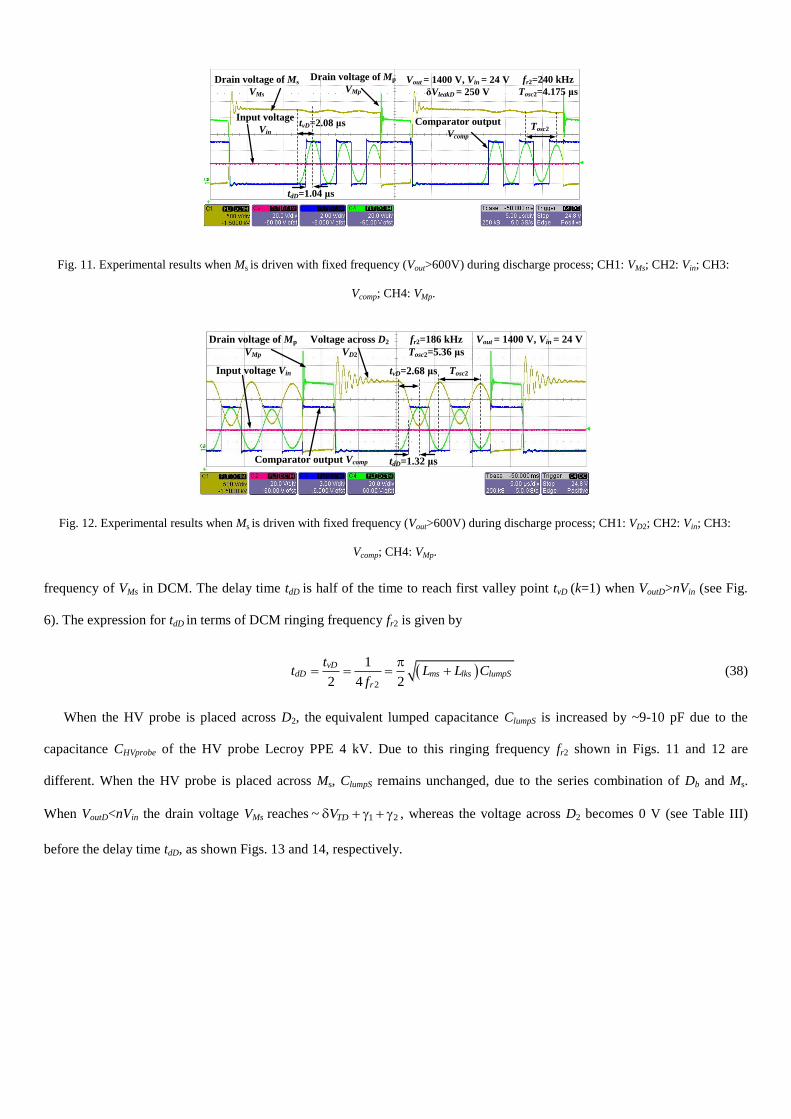
frequency of VMs in DCM. The delay time tdD is half of the time to reach first valley point tvD (k=1) when VoutD>nVin (see Fig.
6). The expression for tdD in terms of DCM ringing frequency fr2 is given by
2
1
2 4 2
vDdD ms lks lumpS
r
tt L L C
f
(38)
When the HV probe is placed across D2, the equivalent lumped capacitance ClumpS is increased by ~9-10 pF due to the
capacitance CHVprobe of the HV probe Lecroy PPE 4 kV. Due to this ringing frequency fr2 shown in Figs. 11 and 12 are
different. When the HV probe is placed across Ms, ClumpS remains unchanged, due to the series combination of Db and Ms.
When VoutD<nVin the drain voltage VMs reaches 1 2~ TDV , whereas the voltage across D2 becomes 0 V (see Table III)
before the delay time tdD, as shown Figs. 13 and 14, respectively.
Input voltage Vin
Voltage across D2
VD2
Drain voltage of Mp
VMp
Comparator output Vcomp
tvD=2.68 μs
tdD=1.32 μs
fr2=186 kHz
Tosc2=5.36 μs
Tosc2
Vout = 1400 V, Vin = 24 V
Fig. 12. Experimental results when Ms is driven with fixed frequency (Vout>600V) during discharge process; CH1: VD2; CH2: Vin; CH3:
Vcomp; CH4: VMp.
Input voltage
Vin
Drain voltage of Ms
VMs
Drain voltage of Mp
VMp
Comparator output
Vcomp
Vout = 1400 V, Vin = 24 V
δVleakD = 250 V
tvD=2.08 μs
tdD=1.04 μs
fr2=240 kHz
Tosc2=4.175 μs
Tosc2
Fig. 11. Experimental results when Ms is driven with fixed frequency (Vout>600V) during discharge process; CH1: VMs; CH2: Vin; CH3:
Vcomp; CH4: VMp.

V. VALLEY SWITCHING EXPERIMENTAL RESULTS
Tables V, VI and VII provide the converter specifications, components used in the converter, and flyback transformer
parameters, respectively. The experimental prototype of the HV bidirectional flyback converter is shown in Fig. 15. The
experimental results in the converter, tested with a film capacitive load of 400 nF, to validate the proposed valley switching
technique are shown in Figs. 16-19. In Figs. 16 and 17, successful valley-switching operation at different output voltages
during the charge process is shown. From Fig. 17, it is clear that the converter operates with zero voltage switching (ZVS)
turn-on, and the primary current is negative before the switch is turned-on. In Fig. 18, successful valley-switching operation
during discharge process is shown. As explained in Section III, the first valley voltage in the drain to-source voltage of Ms is
not very low, compared to the first valley voltage in HV diode voltage VD2 (due to the series combination of Db and Ms). The
capacitive switching loss is directly proportional to the voltage across the HV MOSFET when it is turned-on. This is one of the
reasons for the low energy efficiency during the discharge process.
Input voltage Vin
Drain voltage of Mp
VMp
Comparator output Vcomp
Drain voltage of Ms
VMs
Vout = 400 V, Vin = 24 V
δVleakD = 250 V
400 ns
tdD=1.04 μs
Fig. 13. Experimental results when Ms is driven with fixed frequency (Vout<600V) during discharge process; CH1: VMs; CH2: Vin; CH3:
Vcomp; CH4: VMp.
Drain voltage of Mp
VMp
Voltage across D2,VD2
Input voltage Vin Comparator output Vcomp
Vout = 400 V, Vin = 24 VtdD=1.32 μs
750 ns
Fig. 14. Experimental results when Ms is driven with fixed frequency (Vout<600V) during discharge process; CH1: VD2; CH2: Vin; CH3:
Vcomp; CH4: VMp.

TABLE V. SPECIFICATIONS OF THE BIDIRECTIONAL FLYBACK CONVERTER
Parameter Value
Input voltage Vin 24 V
Output voltage Vout 0-2.5 kV
Capacitance of the load Cload 400 nF
On time of M1 during charge process tonC 9 µs
On times of M2 during discharge process tonD [2 µs, 3 µs, 5 µs, 10 µs, 20 µs, 150 µs, 200 µs]
TABLE VI. COMPONENTS USED IN THE HV CONVERTER
Component Value
Primary MOSFET M1 250V, 16A [FQD16N25CTM]
HV MOSFET M2
4.5 kV, 200 mA, 750 Ω 250V, 16A [FQD16N25CTM]
[IXTA02N450HV] /
4 kV, 300 mA, 290 Ω [IXTV03N400S]
HV diode Db / D2 5 kV, 150 mA [SXF6525]
Gate driver EL7104
Comparator 4.5 ns Rail-to-Rail, TLV3501A
Film capacitive load 400 nF, 3 kV [WIMA]
TABLE VII. FLYBACK TRANSFORMER PARAMETERS
Parameter Value
Core used / material used PQ 20/20 / P type
Primary Np / secondary turns Ns 12 / 300
Primary Lmp / secondary magnetizing inductance Lms 47.5 μH / 30 mH
Leakage inductance referred to primary Llkp / secondary Llks 990 nH / 620 μH
Self-capacitance of secondary winding Cs
(from the Impedance analyzer) 6 pF
Self-capacitance Cs from frequencies fr1, fr2 12.5 pF
Diameter of primary/secondary winding 0.5 mm (TEX-E)/ 0.11 mm
DC resistance of primary Rp /secondary Rs 62 mΩ / 14 Ω
Number of layers of primary/secondary 1 / 4
Flyback transformer
High voltage sideLow voltage side
High voltage
MOSFET
Low voltage
MOSFETHigh voltage
Diodes
z
To
Microcontroller
Gate
driver
Comparator
90 mm
30
mm
Fig. 15. Experimental prototype of the HV bidirectional flyback converter with a 4.5 kV MOSFET on the HV side.

Drain voltage of Mp
VMp
Primary current
ip
Gate drive signal of Mp Input voltage Vin
Vout = 500 V, Vin = 24 V
Fig. 16. Experimental results when the converter is operated with valley switching during charge process; CH1: ip; CH2: Vin; CH3: VG1;
CH4: VMp.
Drain voltage of Mp
VMp
Primary current
ip
Gate drive signal of Mp Input voltage Vin
Vout = 1700 V, Vin = 24 V
Fig. 17. Experimental results with valley switching operation during the charge process; CH1: ip; CH2: Vin; CH3: VG1; CH4: VMp.
Drain voltage of Mp
VMp
Secondary current is
Gate drive signal of Ms
Drain voltage of Ms
VMs
Vout = 2000 V,
Vin = 24 V
Fig. 18. Experimental results with valley switching operation during discharge process; CH1: is; CH2: VMs; CH3: VG2; CH4: VMp.
The bidirectional operation of the HV converter at 2.5 kV output voltage is shown in the Fig. 19. As provided in Table V,
due to constant turn on-time tonC for Mp during charge process, the primary current IppkC is constant. During discharge process,
employing variable turn on-time tonD for Ms makes the secondary current (hence the primary current) IspkC almost constant. The
energy efficiency measurements

Drain voltage of Mp
VMp
Output voltage Vout
Primary current
ip
Input current
iin
Fig. 19. Experimental waveforms showing the bidirectional operation at 2.5 kV output voltage. CH1: iin; CH2: Vout; CH3: ip; CH4: VM1.
during charge and discharge processes [7] with 4 kV and 4.5 kV MOSFETs on the HV side are shown in Fig. 20. The charge
energy efficiency for both 4 kV and 4.5 kV MOSFETs is above 90 %, for the output voltage range 750 V<Vout<2.2 kV, with a
maximum efficiency of 92 %. The charge energy efficiency for the output voltage range 2.2 kV<Vout<2.5 kV is between 88-90
%. The discharge energy efficiency for 4 kV MOSFET is lower than the charge efficiency due to the fact that valley voltage in
VM2 is not equal to valley voltage in VD2 during DCM. The junction capacitance of Db is ~0.7 pF, the output capacitance of the
HV MOSFET is ~10-12 pF. The lumped capacitances are ClumpP=~9 nF and ClumpS=~14 pF, respectively. Some of the reasons
for very low discharge energy efficiency for 4.5 kV MOSFET are due to its high on resistance (750 Ω), high gate input
resistance (76 Ω).
0 250 500 750 1000 1250 1500 1750 2000 2250 250050
55
60
65
70
75
80
85
90
95
Output voltage (V)
Energ
y e
ffic
iency (
%)
Charge energy efficiency with 4 kV MOSFET
Discharge energy efficiency with 4 kV MOSFET
Charge energy efficiency with 4.5 kV MOSFET
Discharge energy efficiency with 4.5 kV MOSFET
Fig. 20. Energy efficiency measurements.
VI. CONCLUSIONS
The valley switching technique for a bidirectional flyback converter, driving a capacitive load has been successfully
implemented using a 16-bit microcontroller, during charge and discharge processes, respectively. Using the proposed simple
valley switching technique, the flyback converter is able to charge and discharge the capacitor load within minimum time (or
with maximum speed). To charge and discharge from 2.4 kV output voltage using a 4 kV MOSFET, the flyback converter has

charge and discharge energy efficiencies of 89% and 84%, respectively. The future work involves further investigation of
proposed control technique with 4.5 kV MOSFET, and testing the HV drivers with the incremental DEAP actuator.
REFERENCES
[1] R. E. Pelrine, R. D. Kornbluh, and J. P. Joseph, “Electrostriction of polymer dielectrics with compliant electrodes as a
means of actuation,” in Proc. Sensors and Actuators A, vol. 64, pp. 77–85, 1998.
[2] M. Tryson, H. E. Kiil, M. Benslimane, “Powerful tubular core free dielectric electro active polymer (DEAP) push
actuator,” in Proc. SPIE, Electroactive Polymer Actuators and Devices (EAPAD), vol. 7287, 2009.
[3] R. Sarban, B. Lassen, M. Willatzen, “Dynamic Electromechanical Modeling of Dielectric Elastomer Actuators With
Metallic Electrodes,” IEEE/ASME Transactions on Mechatronics, vol. 17, no. 5, pp. 960-967, Oct. 2012.
[4] P. Thummala, Z. Zhang, M. A. E. Andersen, S. Rahimullah, “Dielectric electro active polymer incremental actuator driven
by multiple high-voltage bi-directional DC-DC converters,” in Proc. IEEE ECCE USA, pp. 3837-3844, 15-19 Sept. 2013.
[5] R. E. Pelrine, R. D. Kornbluh, Q. Pei, and J. P. Joseph, “High-speed electrically actuated elastomers with strain greater
than 100%,” in Proc. Science, vol. 287, pp. 836–839, 2000.
[6] T. Andersen, M. S. Rødgaard, O. C. Thomsen, M. A. E. Andersen, “Low voltage driven dielectric electro active polymer
actuator with integrated piezoelectric transformer based driver,” in Proc. SPIE, vol. 7976, p. 79762N, 2011.
[7] P. Thummala, Z. Zhang and M. A. E. Andersen, “Bi-directional Flyback Converter for Capacitive Actuator,” in Proc.
EPE, pp. 1-10, Sept. 2013.
[8] LT3751 datasheet, “High voltage capacitor charger controller with regulation,” Linear Technology Corporation, USA,
Online available: http://cds.linear.com/docs/en/datasheet/3751fc.pdf.
[9] N. O. Sokal, R. Redl, “Control algorithms and circuit designs for optimal flyback-charging of an energy storage capacitor
(e.g., for flash lamp or defibrillator),” IEEE Trans. on Power Electronics, vol. 12, no. 5, pp. 885-894, Sep. 1997.
[10] M. Kazimierczuk, “High-Frequency Magnetic Components,” 2nd
Ed. John Wiley and Sons Ltd., 2014.
[11] R. W. Erickson and D. Maksimovic, “Fundamentals of Power Electronics,” 2nd ed. New York: Springer, 2001.
[12] P. Thummala, H. Schneider, Z. Zhang, A. Knott, M. A. E. Andersen, “Optimization of a bi-directional flyback converter
for a high voltage capacitor charging application,” in Proc. IEEE APEC, pp. 2556-2563, March 2014.
[13] H. K. Sang, D. Maksimovic, I. Cohen, “Efficiency Optimization in Digitally Controlled Flyback DC–DC Converters Over
Wide Ranges of Operating Conditions,” IEEE Trans. on Power Electronics, vol. 27, no. 8, pp. 3734-3748, Aug. 2012.

[14] Y. Panov and M. M. Jovanovi´c, “Adaptive off-time control for variable frequency, soft-switched flyback converter at
light loads,” IEEE Trans. Power Electronics, vol. 17, no. 4, pp. 596–603, Jul. 2002.
[15] Y. Panov and M. M. Jovanovi´c, “Performance evaluation of 70-W two stage adapters for notebook computers,” in Proc.
IEEE APEC, 1999, pp. 1059–1065.
[16] Y. Park and H. Choi, “A efficiency improvement methodology for active mode efficiency regulation,” in Proc. IEEE Int.
Symp. Electron. Environ., 2008, pp. 1–5.
[17] Z. Ling, T. Liang, L. Yang, and T. Li, “Design and implementation of interleaved quasi-resonant DC–DC flyback
converter,” in Proc. IEEE Power Electron. Drive Syst., 2009, pp. 429–433.
[18] C. P. Basso, “Switch-mode power supplies spice simulations and practical designs,” 2008.
[19] H. Schneider, P. Thummala, L. Huang, Z. Ouyang, A. Knott, Z. Zhang, M. A. E. Andersen, “Investigation of transformer
winding architectures for high voltage capacitor charging applications,” in Proc. IEEE APEC, pp. 334-341, March 2014.

202/255
Appendix MParallel input parallel output highvoltage bi-directional converters
for driving dielectric electro activepolymer actuators
SPIE Smart Structures/NDE on Electroactive Polymer Actuators and Devices (EA-PAD) 2014
203/255
Parallel input parallel output high voltage bi-directional converters for
driving dielectric electro active polymer actuators P. Thummala*
a, Z. Zhang*
a, M. A. E. Andersen*
a, S. Rahimullah**
b
aTechnical University of Denmark, Electronics group, Dept. of Electrical Eng., Oersteds Plads,
Building 349, Kgs. Lyngby, 2800 DENMARK; bDanfoss PolyPower A/S, Nordborg, 6430 DENMARK;
ABSTRACT
Dielectric electroactive polymer (DEAP) actuators are capacitive devices which provide mechanical motions when
charged electrically. The charging characteristics of a DEAP actuator depends on its size, voltage applied to its
electrodes, and its operating frequency. The main idea of this paper is to design and implement driving circuits for the
DEAP actuators for their use in various applications. This paper presents implementation of parallel input, parallel
output, high voltage (~2.5 kV) bi-directional DC-DC converters for driving the DEAP actuators. The topology is a bi-
directional flyback DC-DC converter incorporating commercially available high voltage MOSFETs (4 kV) and high
voltage diodes (5 kV). Although the average current of the aforementioned devices is limited to 300 mA and 150 mA,
respectively, connecting the outputs of multiple converters in parallel can provide a scalable design. This enables
operating the DEAP actuators in various static and dynamic applications e.g. positioning, vibration generation or
damping, and pumps. The proposed idea is experimentally verified by connecting three high voltage converters in
parallel to operate a single DEAP actuator. The experimental results with both film capacitive load and the DEAP
actuator are shown for a maximum charging voltage of 2 kV.
Keywords: dielectric electro active polymer, high voltage power converters, capacitive actuator, energy efficiency,
flyback converter
1. INTRODUCTION
Dielectric electro active polymer (DEAP) is a very thin incompressible silicone elastomer film sandwiched between two
metallic electrodes [1], [2]. The polymer film expands in area and contracts in thickness, as a result of the electrostatic
pressure generated by the applied voltage to the electrodes [3]. The thickness of the polymer film is ~40 µm and the
DEAP material requires high electric field strength of ~60 V/µm [4], [5], hence the DEAP actuator requires high DC
voltage (~2.5 kV) to generate sufficient force and displacement. DEAP can be considered as a pure capacitive load with
very low leakage current (~0.2-1 nA/nF). DEAP when actuated, changes its capacitance which is proportional to the
strain. DEAP actuators have the potential to be an effective replacement for many conventional actuators for example piezo,
hydraulic, and pneumatic actuators, because of their unique characteristics such as large strain, light weight, low noise
operation, and high flexibility [6]. Some of the prospective applications for the DEAP actuator are in line heating valves,
loudspeakers, and wind turbine flaps, etc. Moreover, the DEAP actuator technology has the potential to be used in
several industries such as automotive, aeronautics, space and medicine.
While the focus has been given to establish the electromechanical characteristics [7] and application-based designs of the
actuators, less research has been done in implementing the necessary electrical drivers for different DEAP actuator
applications. Commercially available laboratory equipment such as high voltage (HV) power supplies [8] and/or HV
amplifiers are often used to operate the DEAP actuators. Although such HV equipment provides the necessary signals
for laboratory experiments, they are quite inadequate in real applications as they are expensive and bulky. Furthermore, a
new incremental DEAP actuator proposed in [9] requires HV bi-directional DC-DC converters to discharge the actuators
besides transferring some of the energy stored in the capacitive actuators to the source [10], [11]. Consequently, HV
drivers specifically designed to operate the DEAP actuators while being compatible with the real applications are
needed. Scalability of such HV drivers is of outmost importance for their use in various applications with different
operational requirements.
*pthu, zz, [email protected]; http://www.ele.elektro.dtu.dk/; **[email protected]; http://www.polypower.com/;
Electroactive Polymer Actuators and Devices (EAPAD) 2014, edited by Yoseph Bar-Cohen, Proc. of SPIE Vol. 9056, 90561N · © 2014 SPIE · CCC code: 0277-786X/14/$18 · doi: 10.1117/12.2044887
Proc. of SPIE Vol. 9056 90561N-1
Downloaded From: http://spiedigitallibrary.org/ on 03/09/2014 Terms of Use: http://spiedl.org/terms
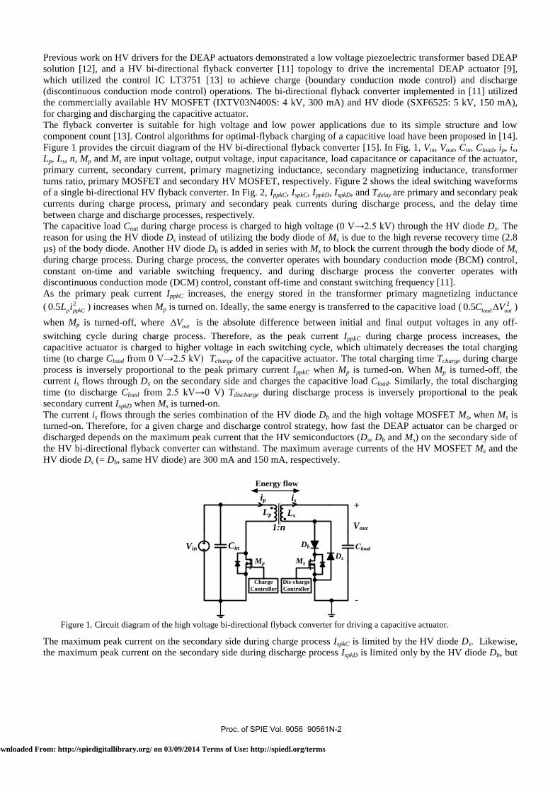
Previous work on HV drivers for the DEAP actuators demonstrated a low voltage piezoelectric transformer based DEAP
solution [12], and a HV bi-directional flyback converter [11] topology to drive the incremental DEAP actuator [9],
which utilized the control IC LT3751 [13] to achieve charge (boundary conduction mode control) and discharge
(discontinuous conduction mode control) operations. The bi-directional flyback converter implemented in [11] utilized
the commercially available HV MOSFET (IXTV03N400S: 4 kV, 300 mA) and HV diode (SXF6525: 5 kV, 150 mA),
for charging and discharging the capacitive actuator.
The flyback converter is suitable for high voltage and low power applications due to its simple structure and low
component count [13]. Control algorithms for optimal-flyback charging of a capacitive load have been proposed in [14]. Figure 1 provides the circuit diagram of the HV bi-directional flyback converter [15]. In Fig. 1, Vin, Vout, Cin, Cload, ip, is,
Lp, Ls, n, Mp and Ms are input voltage, output voltage, input capacitance, load capacitance or capacitance of the actuator,
primary current, secondary current, primary magnetizing inductance, secondary magnetizing inductance, transformer
turns ratio, primary MOSFET and secondary HV MOSFET, respectively. Figure 2 shows the ideal switching waveforms
of a single bi-directional HV flyback converter. In Fig. 2, IppkC, IspkC, IppkD, IspkD, and Tdelay are primary and secondary peak
currents during charge process, primary and secondary peak currents during discharge process, and the delay time
between charge and discharge processes, respectively.
The capacitive load Cout during charge process is charged to high voltage (0 V→2.5 kV) through the HV diode Ds. The
reason for using the HV diode Ds instead of utilizing the body diode of Ms is due to the high reverse recovery time (2.8
µs) of the body diode. Another HV diode Db is added in series with Ms to block the current through the body diode of Ms
during charge process. During charge process, the converter operates with boundary conduction mode (BCM) control,
constant on-time and variable switching frequency, and during discharge process the converter operates with
discontinuous conduction mode (DCM) control, constant off-time and constant switching frequency [11].
As the primary peak current IppkC increases, the energy stored in the transformer primary magnetizing inductance
( 20.5 p ppkCL i ) increases when Mp is turned on. Ideally, the same energy is transferred to the capacitive load ( 20.5 load outC V )
when Mp is turned-off, where outV is the absolute difference between initial and final output voltages in any off-
switching cycle during charge process. Therefore, as the peak current IppkC during charge process increases, the
capacitive actuator is charged to higher voltage in each switching cycle, which ultimately decreases the total charging
time (to charge Cload from 0 V→2.5 kV) Tcharge of the capacitive actuator. The total charging time Tcharge during charge
process is inversely proportional to the peak primary current IppkC when Mp is turned-on. When Mp is turned-off, the
current is flows through Ds on the secondary side and charges the capacitive load Cload. Similarly, the total discharging
time (to discharge Cload from 2.5 kV→0 V) Tdischarge during discharge process is inversely proportional to the peak
secondary current IspkD when Ms is turned-on.
The current is flows through the series combination of the HV diode Db and the high voltage MOSFET Ms, when Ms is
turned-on. Therefore, for a given charge and discharge control strategy, how fast the DEAP actuator can be charged or
discharged depends on the maximum peak current that the HV semiconductors (Ds, Db and Ms) on the secondary side of
the HV bi-directional flyback converter can withstand. The maximum average currents of the HV MOSFET Ms and the
HV diode Ds (= Db, same HV diode) are 300 mA and 150 mA, respectively.
1:n
Charge
Controller
Vout
Cin
Dis-charge
Controller
Ds
CloadDb
+
-
Mp Ms
ip is
Energy flow
Vin
Lp Ls
Figure 1. Circuit diagram of the high voltage bi-directional flyback converter for driving a capacitive actuator.
The maximum peak current on the secondary side during charge process IspkC is limited by the HV diode Ds. Likewise,
the maximum peak current on the secondary side during discharge process IspkD is limited only by the HV diode Db, but
Proc. of SPIE Vol. 9056 90561N-2
Downloaded From: http://spiedigitallibrary.org/ on 03/09/2014 Terms of Use: http://spiedl.org/terms
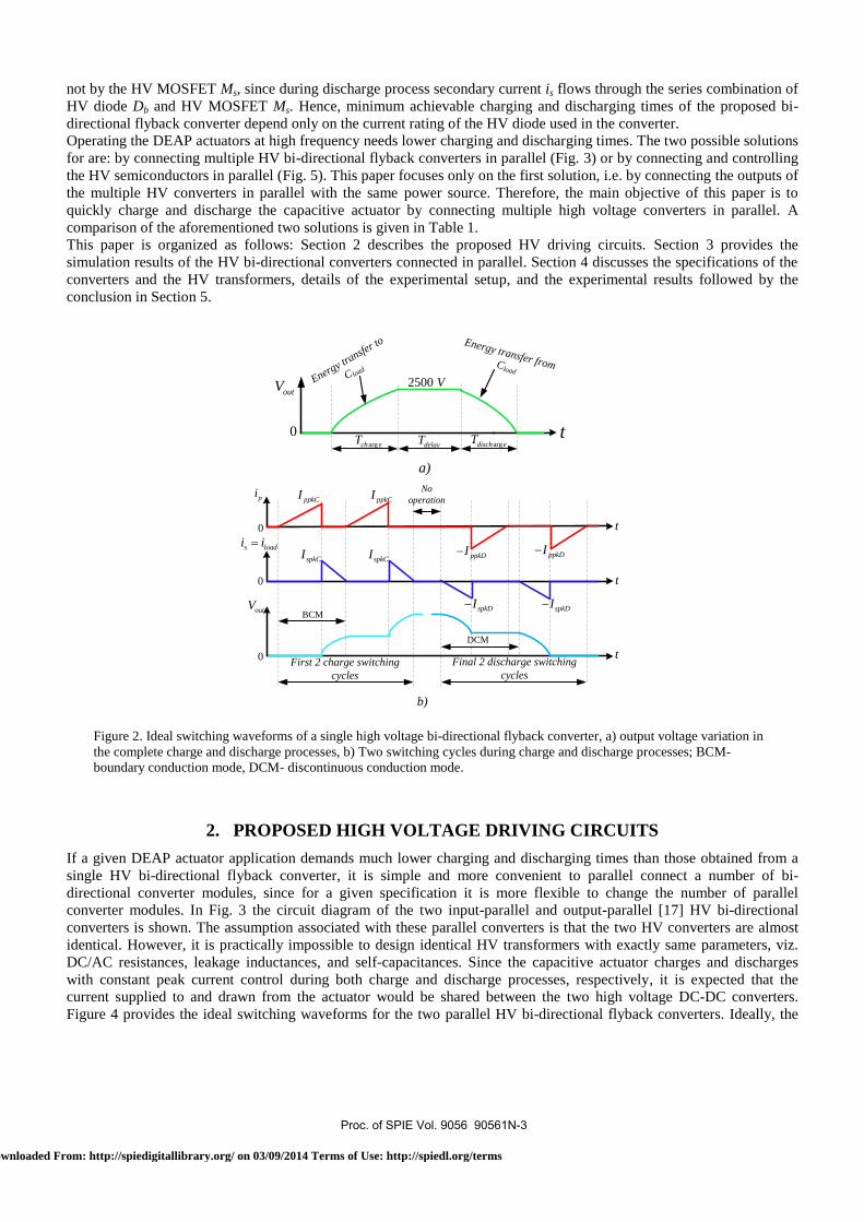
not by the HV MOSFET Ms, since during discharge process secondary current is flows through the series combination of
HV diode Db and HV MOSFET Ms. Hence, minimum achievable charging and discharging times of the proposed bi-
directional flyback converter depend only on the current rating of the HV diode used in the converter.
Operating the DEAP actuators at high frequency needs lower charging and discharging times. The two possible solutions
for are: by connecting multiple HV bi-directional flyback converters in parallel (Fig. 3) or by connecting and controlling
the HV semiconductors in parallel (Fig. 5). This paper focuses only on the first solution, i.e. by connecting the outputs of
the multiple HV converters in parallel with the same power source. Therefore, the main objective of this paper is to
quickly charge and discharge the capacitive actuator by connecting multiple high voltage converters in parallel. A
comparison of the aforementioned two solutions is given in Table 1.
This paper is organized as follows: Section 2 describes the proposed HV driving circuits. Section 3 provides the
simulation results of the HV bi-directional converters connected in parallel. Section 4 discusses the specifications of the
converters and the HV transformers, details of the experimental setup, and the experimental results followed by the
conclusion in Section 5.
0 t
Energy transfer from Cload
outV 2500 VEnergy transfe
r to
C load
t0
ppkCI
t
ppkDIspkCI
0
0
outV
s loadi i
pi
argch eT argdisch eTdelayT
ppkCI
a)
b)
t
No
operation
ppkDIspkCI
spkDI spkDI
First 2 charge switching
cycles
Final 2 discharge switching
cycles
BCM
DCM
Figure 2. Ideal switching waveforms of a single high voltage bi-directional flyback converter, a) output voltage variation in
the complete charge and discharge processes, b) Two switching cycles during charge and discharge processes; BCM-
boundary conduction mode, DCM- discontinuous conduction mode.
2. PROPOSED HIGH VOLTAGE DRIVING CIRCUITS
If a given DEAP actuator application demands much lower charging and discharging times than those obtained from a
single HV bi-directional flyback converter, it is simple and more convenient to parallel connect a number of bi-
directional converter modules, since for a given specification it is more flexible to change the number of parallel
converter modules. In Fig. 3 the circuit diagram of the two input-parallel and output-parallel [17] HV bi-directional
converters is shown. The assumption associated with these parallel converters is that the two HV converters are almost
identical. However, it is practically impossible to design identical HV transformers with exactly same parameters, viz.
DC/AC resistances, leakage inductances, and self-capacitances. Since the capacitive actuator charges and discharges
with constant peak current control during both charge and discharge processes, respectively, it is expected that the
current supplied to and drawn from the actuator would be shared between the two high voltage DC-DC converters.
Figure 4 provides the ideal switching waveforms for the two parallel HV bi-directional flyback converters. Ideally, the
Proc. of SPIE Vol. 9056 90561N-3
Downloaded From: http://spiedigitallibrary.org/ on 03/09/2014 Terms of Use: http://spiedl.org/terms

current supplied to the load during charge process and the current drawn from it during discharge process are doubled,
but practical HV transformers will have a small difference in their parameters, hence, the secondary currents are not
represented in phase as shown in Fig. 4 b) (see Figs. 25 and 26). The total charging and discharging times with two
parallel converters become half of those with a single converter, due to increase in the output voltage for each secondary
current pulse.
1:n
Charge
Controller
Vout
Cin
Dis-charge
Controller
Ds1
CloadDb1
+
Mp1 Ms1
ip1 is1
Energy flow
Vin
1:n
Charge
Controller
Dis-charge
Controller
Ds2
Db2
Mp2 Ms2
ip2 is2
Energy flow
-
iload
Lp Ls
Lp Ls
Figure 3. Circuit diagram of two parallel input parallel output high voltage bi-directional converters to drive a single
capacitive load.
0 t
Energy transfer from Cload
outV 2500 VEnergy tr
ansfer t
o
C load
t0
spkCI
0
First 2 charge switching
cycles
Final 2 discharge switching
cycles
outV
loadi
arg
2
ch eTdelayT
a)
b)
t
spkCI
spkDI spkDI
arg
2
disch eT
No
operation
Figure 4. Ideal switching waveforms of two parallel input parallel output high voltage bi-directional flyback converters, a)
output voltage variation in the complete charge and discharge processes, b) Two switching cycles during charge and
discharge processes.
Proc. of SPIE Vol. 9056 90561N-4
Downloaded From: http://spiedigitallibrary.org/ on 03/09/2014 Terms of Use: http://spiedl.org/terms

The capacitive actuator can also be charged and discharged quickly by employing the converter as shown in Fig. 5, in
which the HV semiconductors are connected in parallel on the secondary side. The assumptions associated with this
topology is that the secondary current is equally shared between the HV diodes Ds1 and Ds2 during charge process, also
the secondary current is equally shared between the series combination of the HV diodes Db1 and Db2 with the HV
MOSFETS Ms1 and Ms2, respectively during discharge process, finally the HV MOSFETs Ms1 and Ms2 are synchronously
controlled during discharge process. The HV transformer in the converter shown in Fig. 5 needs to be designed to handle
twice the peak current of the converter shown in Fig. 3 is designed for. In Fig. 5, the new primary and secondary
inductances, and the turns ratio of the HV transformer are Lp1, Ls1, and n1 respectively. Even though the topology
mentioned in Fig. 5 requires less number of components compared to the topology shown in Fig. 3, achieving
synchronizing control of Ms1 and Ms2 and current sharing through HV diodes is very complex. Figure 6 provides the ideal
switching waveforms of the topology mentioned in Fig. 5.
1:n1
Charge
Controller
Vout
Cin
Dis-charge
Controller
Ds1
CloadDb1
+
-
Mp Ms1
ip is
Energy flow
Vin
Ds2
Db2
Ms2
Lp1 Ls1
Figure 5. Circuit diagram of a bi-directional flyback with high voltage semiconductors connected in parallel on the
secondary side to drive a capacitive load (n1>n).
0 t
Energy transfer from Cload
outV 2500 VEnergy tr
ansfer t
o
C load
t0
2 spkCI
0
First 2 charge switching
cycles
Final 2 discharge switching
cycles
outV
loadi
arg
2
ch eTdelayT
a)
b)
t
2 spkCI
2 spkDI 2 spkDI
arg
2
disch eT
No
operation
Figure 6. Ideal switching waveforms of two high voltage bi-directional flyback converters connected in parallel, a) output
voltage variation in the complete charge and discharge process, b) Two switching cycles during charge and discharge
processes (iDs1C=iDs2C=IspkC ; iDs1D=iDs2D=IspkD ; C, D-stands for charge and discharge processes, respectively).
Proc. of SPIE Vol. 9056 90561N-5
Downloaded From: http://spiedigitallibrary.org/ on 03/09/2014 Terms of Use: http://spiedl.org/terms

An input parallel connected and outputs series connected modular converter system is proposed in [18] for energy
harvesting application. Figure 7 provides a modular parallel input parallel output HV bi-directional flyback converter
circuit, in which p modules are connected in parallel to charge the DEAP actuator. In the Fig. 8, the ideal switching
waveforms are shown. Due to the non-identical HV transformers, the load current with the p converters is drawn as
shown in Fig. 8 b).
Module 1
Module 2
Module 3
Module p
Energy flow
Vin Cin
+
-Vout
Cload
Figure 7. Proposed conceptual block diagram with p parallel input parallel output, high voltage bi-directional converters to
drive a single capacitive load.
0 t
Energy transfer from Cload
outV 2500 VEnergy tr
ansfer t
o
C load
argch eT
pdelayT
a)
argdisch eT
p
t0
spkCI
0
First charge
switching cycle
Final discharge
switching cycle
outV
loadi
b)
t
spkDI
2 spkDI
No operation
2 spkCIp pulses
Figure 8. Ideal switching waveforms of p high voltage bi-directional flyback converters connected in parallel: a) output
voltage variation in the complete charge and discharge process, b) Two switching cycles during charge and discharge
processes.
Proc. of SPIE Vol. 9056 90561N-6
Downloaded From: http://spiedigitallibrary.org/ on 03/09/2014 Terms of Use: http://spiedl.org/terms

110V80V50V20V
-10V3.0KV
1.4KV
-0.3KV3.0KV
1.4KV
-0.3KV5A
lA-3A
-7A2.2KV1.6KV1.0KV0.4KV
-0.2KVOms
V(vdrain_lv)
V(vhv_diode)
V(vdrain_hv)
Id(M1)
V(vout)
4ms 8ms 12ms 16ms 20ms 24ms 28ms 32ms 36ms
Table 1. Comparison of the p parallel input parallel output bi-directional flyback converters (solution 1) and the bi-
directional flyback with q high voltage semiconductors combinations (parallel connection of Ds, with series connection of
Db and Ms) connected in parallel on the secondary side (solution 2), for the same power level
Comparing parameters Solution 1 Solution 2
Number of low voltage MOSFETs p 1
Number of high voltage MOSFETs p q
Number of high voltage diodes 2p 2q
Number of transformers p 1
Cost of implementation High High
Complexity with winding high voltage transformers Very high Low
Control complexity Low Very high
Filter size requirement Low High
Electromagnetic interference (EMI) Low High
3. SIMULATION RESULTS
The bi-directional flyback converter is simulated in the LTSpice software. In the simulation a maximum number of p=3
HV converter modules are used. The specifications of the converter, the simulation and experimental parameters of the
high voltage transformers, and the components used in each converter are shown in Tables 2, 3 and 4, respectively. The
simulations are performed without adding any leakage inductance and self-capacitances. In the simulations, the Spice-
models of HV diode and HV MOSFET models are used. Figure 9 provides the simulation results for a single HV bi-
directional flyback converter, for a maximum output voltage of ~ 2 kV. In Fig. 10, the simulation results of the three
parallel input parallel output bi-directional high voltage converters are shown.
The zoomed simulation results of three parallel input parallel output HV bi-directional flyback converters are shown in
Fig. 11. Since the high voltage transformers are slightly different (see Table 2), the currents and the voltages of three HV
converters are not synchronized and have a small phase-shift among them as shown in Figs. 11 a) and b).
Figure 9. Simulation results of a single HV bi-directional flyback converter. V(vout) – Output voltage; Id(M1) – current
through primary MOSFET; V(vdrain_hv) – drain voltage across high voltage MOSFET; V(vhv_diode) – voltage across
high voltage diode Ds; V(vdrain_lv) – drain voltage across low voltage MOSFET;
Proc. of SPIE Vol. 9056 90561N-7
Downloaded From: http://spiedigitallibrary.org/ on 03/09/2014 Terms of Use: http://spiedl.org/terms

110V80V50V20V
-10V2.7KV
1.2KV
-0.3KV2.7KV
1.2KV
-0.3KV5A2A
-1A-4A-7A
2.2KV1.6KV1.0KV0.4KV
-0.2KVOms
N'(vdrain_lv1)
V(vhv_diodel)
'. (vd lain h \ )
Id(N11)
s c i rain
iJ
V(vhv_dinde2)
drakin_IIN 2)
V(vdrain_1v3)
.
\ hs diotle3 )
V(vdrain_hy3)
Id(N 3 Id(M5)
lms 2ms anis 4ms
V(vout)
Sms Ems 7rns 8ms 9ms 10ms llms 12ms
110V80V50V20V
-10V
2.81CV
laK%.
-0.3KV
2.6KV
2.3KV4.5A
2.0A
-0.5A2.023KV
2.018KV
V(vdrain_h 1)
V(vhv_diodel)
J II\ (vihain_hv l )
JVO di4 .1c2)
[(vdr:tin 1,2)
V(vdnio_h5)
V(vhv_diode3)JV(vdrain c,i)
immt.ria"111111111/ amour
r2.012KV
3.068ms 3.070ms 3.072ms 3.074ms 3.076ms 3.078ms 3.080ms 3.082ms 3.084ms 3.086ms 3.088ms 3.090ms 3.092ms 3.094ms
V(vout)
110 \'V(vdnin_WII
80V50V20V
-IOVV(vhv_diodel)
2.4KV1.8KV1.2KV0.6KV0.0KV2.7KV
1.2KV
-0JKV0.7A
3.2A
-7.0A2.028KV
Vo drain_hv1)
1d(1111)
."1
HINIWAYMiNMNMwv
-11110#64A,)rrrrrwri.
Al Woo\'(sh _diode3)
\t..lrain_hr2) \1 71-ain 11.3)
Id(1113) I1 r\ I,/ IVO/o80
2.008KV .1.988K\'
5.51ms 5.52ms 5.53sm 5.54ms 5.55ms 5.56ms 5.57ms 5.58ms 5.59ms 5.60ms 5.61ms 5.62ms 5.63ms 5.64ms 5.65m.
Figure 10. Simulation results of three parallel input parallel output high voltage bi-directional flyback converters. V(vout) –
Output voltage; Id(M1), Id(M3) , Id(M5) – currents through primary MOSFET 1, 2 and 3 respectively; V(vdrain_hv) –
drain voltage across high voltage MOSFET; V(vhv_diode) – voltage across high voltage diode Ds; V(vdrain_lv) – drain
voltage across low voltage MOSFET; The numbers 1, 2 and 3 in the above three voltages stands for HV converter 1, 2 and
3, respectively;
(a) (b)
Figure 11. Zoomed simulation results of three parallel input parallel output high voltage bi-directional flyback converters, a)
during charge process and b) during discharge process.
4. EXPERIMENTAL RESULTS
The proposed idea to quickly charge and discharge the capacitive load using the parallel input parallel output high
voltage bi-directional DC-DC converters is experimentally verified. Both film capacitive load and the DEAP actuator
have been tested with the high voltage parallel input parallel output drivers. The experimental setup of the three parallel
input parallel output HV converters to charge the film capacitive load is shown in Fig. 12. In Fig. 13, the experimental
setup of the three parallel input parallel output HV converters to drive the DEAP actuator is shown. As discussed earlier
in Section 1, charge and discharge processes of each converter will be performed by the control IC LT3751, which needs
an enable signal to initiate charge or discharge process. The enable signals for each HV bi-directional converter are
provided by the microcontroller PIC18F2550.
The high voltage film capacitors with a capacitance of ~133 nF (four 33 nF in parallel) from KEMET have been used as
a film capacitive load. The DEAP actuator which has a capacitance of ~133 nF is a PolyPower Inlaster PUSH type
Proc. of SPIE Vol. 9056 90561N-8
Downloaded From: http://spiedigitallibrary.org/ on 03/09/2014 Terms of Use: http://spiedl.org/terms

I......I
actuator manufactured by Danfoss PolyPower. The high voltage transformer parameters provided in Table 3 have been
measured by the Impedance analyzer PSM1735. The high voltage (4 kV) MOSFET IXTV03N400S used in each
converter is manufactured by IXYS and is currently out of production. At present, IXYS is producing 4.5 kV MOSFETs
(IXTA02N450HV). The 5 kV high voltage (SXF6525) diode manufactured by VMI has been used in all converters.
Figure 12. Experimental setup with film capacitive load.
Figure 13. Experimental setup with DEAP actuator.
Table 2. Specifications of the bidirectional flyback converter
Parameter Value
Input voltage 24 V
Output voltage 0 – 2500 V
Capacitance of the DEAP actuator / film capacitive load 133 nF
Stored energy in the load at 2.5 kV 0.416 J
Primary peak current during charge / discharge process 4.2 A / 5.3 A
Proc. of SPIE Vol. 9056 90561N-9
Downloaded From: http://spiedigitallibrary.org/ on 03/09/2014 Terms of Use: http://spiedl.org/terms

Stop 3 00Edge Pos !be
Table 3. Parameters of the high voltage transformers
Parameter Transformer1 Transformer2 Transformer3
Core / Material used EF 20 / N 87 EF 20 / N 87 EF 20 / N 87
Primary / Secondary turns 15 / 375 16 / 400 16 / 400
Primary / Secondary inductance 30 µH / 19 mH 33 µH / 21 mH 28 µH / 18 mH
Leakage inductance referred to primary 1.1 µH 1.2 µH 1.25 µH
Self-capacitance of secondary 17 pF 19 pF 22 pF
DC resistance of primary / secondary 62 mΩ / 28 Ω 85 mΩ / 41 Ω 84 mΩ / 40 Ω
Diameter of primary / secondary 0.5 mm / 0.1 mm 0.65 mm / 0.1 mm 0.65 mm / 0.1 mm
Number of layers of primary / secondary 1 / 5 2 / 5 2 / 5
Table 4. Components used in the bi-directional flyback converter
Component Value
Primary / High voltage MOSFET 250V, 25A [IPB600N25N3G] / 4 kV, 300 mA [IXTV03N400S]
High voltage diode (Db or Ds) 5 kV, 150 mA [SXF6525]
Microcontroller PIC18F2550
Film capacitor 33 nF (3 kV), 4 of them in parallel
The experimental test results are provided in Figs. 14-26. In each of Figs. 14-26, all sub figures a) corresponds to film
capacitive load and sub figures b) corresponds to the DEAP actuator. The experimental results of a single HV bi-
directional converter are shown in Figs. 14-19, and the experimental results of three parallel input parallel output HV bi-
directional converters are shown in Figs. 20-26. As shown in Fig. 14, during charge process the output voltage increases,
and primary and secondary currents are positive, and during discharge process the output voltage decreases, and primary
and secondary currents are negative. The zoomed waveforms of Fig. 14, during charge and discharge processes are
shown in Figs. 15 and 16, respectively. Figure 17 provides the drain voltages across primary and secondary MOSFETs,
voltage across the HV diode which conducts during charge process. The zoomed waveforms of Fig. 17, during charge
and discharge processes are shown in Figs. 18 and 19, respectively.
In Fig. 20, primary currents of the parallel input parallel output HV converters are shown together with the output
voltage. The zoomed waveforms of Fig. 20, during charge and discharge processes are shown in Figs. 21 and 22,
respectively. In Fig. 23, secondary currents of the parallel input parallel output HV converters are shown together with
the output voltage. The zoomed waveforms of Fig. 23, during charge and discharge processes are shown in Figs. 24, 25
and 26, respectively.
Tcharge1 = 15 ms Tdischarge1 = 18 msTcharge1 = 15 ms Tdischarge1 = 18 ms
(a) (b)
Figure 14. Experimental results of a single HV bi-directional converter, a) with film capacitive load, b) with DEAP actuator;
CH1: Secondary current in the converter; CH2: Primary current in the converter; CH3: primary MOSFET gate drive signal;
CH4: Output voltage across the load; Vout,max = 2 kV.
Proc. of SPIE Vol. 9056 90561N-10
Downloaded From: http://spiedigitallibrary.org/ on 03/09/2014 Terms of Use: http://spiedl.org/terms
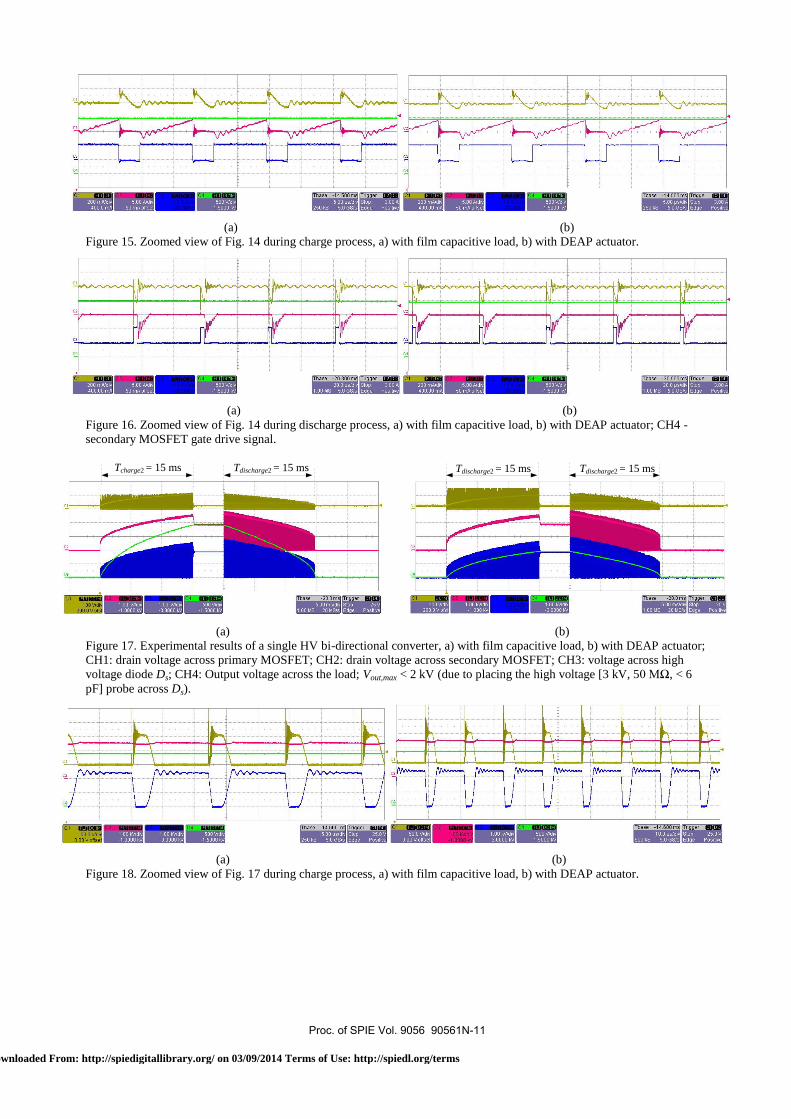
00A
00 mw40000 TIN
00umnonzat
I i'MI11111111111i W11 iiiwrw®w00 Nd
50 m10 t
.
20 .990OomeM
OOMS .20 WeemeEEee PoeNe
(a) (b)
Figure 15. Zoomed view of Fig. 14 during charge process, a) with film capacitive load, b) with DEAP actuator.
(a) (b)
Figure 16. Zoomed view of Fig. 14 during discharge process, a) with film capacitive load, b) with DEAP actuator; CH4 -
secondary MOSFET gate drive signal.
Tcharge2 = 15 ms Tdischarge2 = 15 ms Tdischarge2 = 15 ms Tdischarge2 = 15 ms
(a) (b)
Figure 17. Experimental results of a single HV bi-directional converter, a) with film capacitive load, b) with DEAP actuator;
CH1: drain voltage across primary MOSFET; CH2: drain voltage across secondary MOSFET; CH3: voltage across high
voltage diode Ds; CH4: Output voltage across the load; Vout,max < 2 kV (due to placing the high voltage [3 kV, 50 MΩ, < 6
pF] probe across Ds).
(a) (b)
Figure 18. Zoomed view of Fig. 17 during charge process, a) with film capacitive load, b) with DEAP actuator.
Proc. of SPIE Vol. 9056 90561N-11
Downloaded From: http://spiedigitallibrary.org/ on 03/09/2014 Terms of Use: http://spiedl.org/terms

.® r,,,
-wV Vw...wn.w®.,,.fr*rsnrnor
500 pua!500kß 50051$
1.11111Mop
Edge Po
00&
III i no5.-...
iluuulmiidhmluuiumli
ll
5.00 Nd
0 ml Greet
00 NdO mA. aRee1
00 Nd0ml oll al
iSyo 'nu O00000
500NE0m9oRee1
00 Nd0m1 ails e1
(a) (b)
Figure 19. Zoomed view of Fig. 17 during discharge process, a) with film capacitive load, b) with DEAP actuator.
Tcharge3 = 4.5 ms Tdischarge3 = 6 ms Tcharge3 = 4.5 ms Tdischarge3 = 6 ms
(a) (b)
Figure 20. Experimental results of three parallel input parallel output HV bi-directional converters, a) with film capacitive
load, b) with DEAP actuator; CH1: Primary current in converter 1; CH2: Primary current in converter 2; CH3: Primary
current in converter 3; CH4: Output voltage across the load; Vout,max = 2 kV.
(a) (b)
Figure 21. Zoomed view of Fig. 20 during charge process, a) with film capacitive load, b) with DEAP actuator.
(a) (b)
Figure 22. Zoomed view of Fig. 20 during discharge process, a) with film capacitive load, b) with DEAP actuator.
Proc. of SPIE Vol. 9056 90561N-12
Downloaded From: http://spiedigitallibrary.org/ on 03/09/2014 Terms of Use: http://spiedl.org/terms

®I,lull lllll i lllli d,llli i
Ply I,
00 MID
0001 kw 00
uN os swoo
\ \ -44111 7 -"NN 1
env 000Z-Pbw 001
IYPVW00NPMP00
Tcharge4 = 4.5 ms Tdischarge4 = 6 ms Tcharge4 = 4.5 ms Tdischarge4 = 6 ms
(a) (b) Figure 23. Experimental results of three parallel input parallel output HV bi-directional converters, a) with film capacitive
load, b) with DEAP actuator; CH1: Secondary current in converter 1; CH2: Secondary current in converter 2; CH3:
Secondary current in converter 3; CH4: Output voltage across the load; Vout,max = 2 kV.
(a) (b) Figure 24. Zoomed view of Fig. 23 during charge process at low output voltage, a) with film capacitive load, b) with DEAP
actuator.
(a) (b)
Figure 25. Zoomed view of Fig. 23 during charge process at high output voltage, a) with film capacitive load, b) with DEAP
actuator.
(a) (b)
Figure 26. Zoomed view of Fig. 23 during discharge process, a) with film capacitive load, b) with DEAP actuator.
Proc. of SPIE Vol. 9056 90561N-13
Downloaded From: http://spiedigitallibrary.org/ on 03/09/2014 Terms of Use: http://spiedl.org/terms
5. CONCLUSION
Parallel input parallel output high voltage bi-directional flyback converters have been designed and implemented, and
their operation has been successfully verified with both film capacitive load and the DEAP actuator. Even though, the
DEAP actuator could able to withstand 2.4 kV output voltage, only a maximum voltage of 2 kV is applied to the actuator
to avoid any potential damage to it. Similarly, all simulation results are shown for a maximum output voltage of 2 kV.
The proposed idea of reducing the charge and discharge times is verified by connecting a maximum of 3 modules in
parallel. With the practical experience, it is expected that even more modules (> 3) could be easily connected in parallel.
Practically, a single converter is able to charge and discharge the actuator to and from 2 kV within 15 ms and 17.5 ms,
respectively. The 3 parallel input parallel output HV modules are able to charge and discharge the actuator to and from 2
kV within 4.5 ms and 6 ms, respectively. This can increase the maximum operating frequency of the DEAP actuator
from 30 Hz to 90 Hz by assuming the delay time between charge and discharge processes Tdelay equal to 0 ms.
REFERENCES
[1] Pelrine, R. E., Kornbluh, R. D., Pei, Q. and Joseph, J. P., “High-speed electrically actuated elastomers with strain
greater than 100%,” Proc. Science, 287, 836–839 (2000).
[2] Pelrine, R. E., Kornbluh, R. D. and Joseph, J. P., “Electrostriction of polymer dielectric with compliant electrodes as
a means of actuation,” Proc. Sens. Actuators A, 64, 77–85 (1998).
[3] Danfoss PolyPower website, http://www.polypower.com/Technology/Overview/DEAP+in+General/.
[4] Tryson, M., Kiil, H. E., Benslimane, M., “Powerful tubular core free dielectric electro activate polymer (DEAP)
push actuator,” Proc. SPIE, 7287, 72871F1-11(2009).
[5] Benslimane, M. Y., Kiil H. E. and Tryson, M. J., “Dielectric electro-active polymer push actuators: performance and
challenges,” Proc. Polymer International, 59 (3), 415-421 (2010).
[6] Technical document from Danfoss PolyPower, http://www.polypower.com/NR/rdonlyres/8C3F4F8B-3F60-417B-
94B6-378042EF169B/0/094F5002WhitepaperDEAPActuatorElements.pdf.
[7] Sarban, R., Lassen, B., Willatzen, M., “Dynamic Electromechanical Modeling of Dielectric Elastomer Actuators
with Metallic Electrodes,” IEEE/ASME Transactions on Mechatronics, 17(5), 960-967 (2012).
[8] Technical document from Danfoss PolyPower, http://www.polypower.com/NR/rdonlyres/DA0AC752-6FE7-40F0-
B973-6A2C264F7AEF/0/094F0439_Charger_Engineering_sheet.pdf.
[9] Thummala, P., Zhang, Z., Andersen, M. A. E. and Rahimullah, S. “Dielectric electro active polymer incremental
actuator driven by multiple high-voltage bi-directional DC-DC converters,” Proc. IEEE Energy Conversion
Congress and Exposition (ECCE) USA, 3837-3844 (2013).
[10] Eitzen, L., Graf, C. and Maas, J., “Bidirectional power electronics for driving dielectric elastomer transducers,”
Proc. SPIE, 8340, (2012).
[11] Thummala, P., Zhang Z. and Andersen, M. A. E., “Bi-directional Flyback Converter for Capacitive Actuator,” Proc.
European Power Electronics (EPE) conference, 1-10 (2013).
[12] Andersen, T., Rødgaard, M. S., Thomsen, O. C. and Andersen, M. A. E., “Low voltage driven dielectric electro
active polymer actuator with integrated piezoelectric transformer based driver,” Proc. SPIE, 7976, 79762N1-12
(2011).
Proc. of SPIE Vol. 9056 90561N-14
Downloaded From: http://spiedigitallibrary.org/ on 03/09/2014 Terms of Use: http://spiedl.org/terms

[13] LT3751 datasheet, “High voltage capacitor charger controller with regulation,” Linear Technology Corporation,
USA, http://cds.linear.com/docs/en/datasheet/3751fc.pdf.
[14] Erickson, R. W. and Maksimovic, D., [Fundamentals of Power Electronics], 2nd ed. Springer, New York (2001).
[15] Sokal, N. O. and Redl. R., “Control Algorithms and Circuit Designs for Optimal Flyback-Charging of and Energy-
Storage Capacitor (e.g. for Flash Lamp or Defibrillator),” IEEE Transactions on Power Electronics, 885-894 (1997).
[16] Venkatesan, K., “Current Mode Controlled Bidirectional Flyback Converter,” Proc. 20
th Annual IEEE Power
Electronics Specialists Conference, 835-842 (1989).
[17] Cheng, P., Shi, J. and He, X., “A Novel Input-Parallel Output-Parallel Connected DC-DC Converter Modules with
Automatic Sharing of Currents,” Proc. IEEE 7th International Power Electronics and Motion Control Conference -
ECCE Asia, 1871-1876 (2012).
[18] Eitzen, L., Graf, C., Maas, J., “Modular DC-DC converter system for energy harvesting with EAPs,” Proc. SPIE
8687, 86870P 1-14 (2013).
Proc. of SPIE Vol. 9056 90561N-15
Downloaded From: http://spiedigitallibrary.org/ on 03/09/2014 Terms of Use: http://spiedl.org/terms

Appendix NBidirectional Flyback Converterwith Multiple Series Connected
Outputs for High VoltageCapacitive Charge and Discharge
Applications
2015 IEEE Applied Power Electronics Conference and Exposition(APEC 2015)
219/255

Bidirectional Flyback Converter with Multiple SeriesConnected Outputs for High Voltage Capacitive
Charge and Discharge Applications
Prasanth Thummala, Henrik Schneider, Zhe Zhang and Michael A. E. AndersenElectronics Group, Department of Electrical Engineering
Technical University of DenmarkKongens Lyngby, DK-2800 DenmarkWeb: http://www.ele.elektro.dtu.dk/
Email: [email protected], [email protected]
Abstract—This paper evaluates two different implementationsof a bidirectional flyback converter for driving a capacitiveelectro active actuator, which must be charged and dischargedfrom 0 V to 2.5 kV DC and vice versa, supplied from a 24V battery. In one implementation, a high voltage MOSFET (4kV) in series with a high voltage blocking diode is added, inparallel with a high voltage freewheeling diode of a conventionalflyback topology, to enable bidirectional operation. Experimentalresult from a digitally controlled bidirectional flyback convertershows that the discharge energy efficiency is limited by theparasitics of the high voltage active components, which alsoprevent full utilization of valley switching during dischargeprocess. A second implementation is therefore proposed, wherethe secondary of flyback transformer winding is split into multiplewindings which are connected in series by lower voltage ratingMOSFETs driven by a gate drive transformer. Simulation resultsto compare the operation of conventional and proposed convertersare provided. The advantages of proposed implementation areimproved energy efficiency and lower cost. Experimental resultswith two series connected secondary windings are provided tovalidate the proposed implementation.
NOMENCLATURE
Cin/Cload Input capacitance / Load capacitance.Cout1 Balancing capacitor across a series combina-
tion of one of the splitted secondary windingand a secondary MOSFET.
Cossp Output capacitance of the low voltage MOS-FET Mp.
Cosss Output capacitance of the high voltage MOS-FET Ms.
Cosss1 Output capacitance of one of the several seriesconnected MOSFETs (Ms1) on the secondaryhigh voltage side.
Cj Junction capacitance of the high voltagediodes D2 or Db.
Cs Self capacitance of secondary high voltagewinding of the flyback transformer.
Cs1 Self capacitance of one of the secondary highvoltage splitted windings of the flyback trans-former.
D2 High voltage (5 kV) freewheeling diode whichconducts while charging the capacitive load.
Db High voltage (5 kV) blocking diode whichconducts while discharging the capacitive
load.Dbp/Dbs Body diode of the MOSFET Mp/Ms.Dbs1 Body diode of one of the several series con-
nected MOSFETs (Ms1) on the secondaryhigh voltage side.
iin/ip/is Input / Primary / Secondary current.iload Current through the load.Lmp/Lms Primary / Secondary magnetizing inductance
of a non-splitted flyback transformer.Lms1 Secondary magnetizing inductance of one of
the splitted winding of the flyback trans-former.
Llkp/Llks Leakage inductance referred to primary / sec-ondary of a non-splitted flyback transformer.
Llks1 Leakage inductance referred to secondary ofone of the splitted winding of the flybacktransformer.
Mp/Ms Low voltage / High voltage (4 kV) MOSFET.Ms1 One of the several series connected MOSFETs
on the secondary high voltage side.n Turns ratio from secondary to primary of the
non-splitted flyback transformer.n1 Turns ratio from one of the splitted secondary
to primary of the splitted flyback transformer.Np/Ns Number of primary / secondary turns of the
non-splitted flyback transformer.Ns1 Number of secondary turns on one of the split-
ted secondary winding of the flyback trans-former.
Rp/Rs DC resistance of low voltage / high voltagewinding of the transformer.
Rs1 DC resistance of one of the splitted secondaryhigh voltage winding of the flyback trans-former.
VDb/VD2 Voltage across the high voltage (5 kV) block-ing / freewheeling diode.
VMp/VMs Voltage across the low voltage / high voltage(4 kV) MOSFET.
VMs1 Voltage across one of the several series con-nected MOSFETs (Ms1) on the secondaryhigh voltage side.
Vin/Vout Input voltage / Output or load voltage.

I. INTRODUCTION
Dielectric electro active polymer (DEAP) is an emergingsmart material that has experienced substantial improvementand has gained increasing attention over the last decade fromthe researchers [1]–[3]. The DEAP material is a very thin (40μm) incompressible silicone elastomer film with a compliantelectrode layer on both sides [5], [7]. DEAP can be consideredas a pure capacitive load from an electrical perspective [6].The basic behaviour of the DEAP actuator is the reductionin the polymer thickness and the increment in its area, dueto an applied electric field (40-60 V/μm) [7], [8]. The axialDEAP actuator as shown in Fig. 1 is ideally equivalent toa capacitive load. When a DEAP actuator is driven with highvoltage (2-2.5 kV), it converts a portion of the electrical energyinto mechanical displacement, which is of the order of mm (1-1.5 mm) [4], [5]. Three of such axial DEAP actuators are usedto create a DEAP incremental actuator [9] as shown in Fig.2. DEAP, when used as linear incremental actuators, has thepotential to be an effective replacement for many conventional(e.g., piezo, pneumatic and hydraulic) linear actuators due toits unique properties such as large strain, light weight, andhigh flexibility.
33 mm
110 mm
Fig. 1. A linear DEAP actuator manufactured by Danfoss PolyPower A/S.
The DEAP actuator applications [10], [11] require highvoltage (HV) bidirectional power electronic converters, tocharge and discharge the actuator, and to transfer part of theenergy stored in it to the source. Switch-mode power suppliesfor charging the capacitive loads have been implemented in[12]–[15]. The flyback converter is suitable for low power(< 150 W) and high voltage (2.5 kV) applications, due toits simple structure and low component count [16]. In [17],[30], [32]–[36], [44], [45] bidirectional flyback converters withvarious power stages and control techniques, for chargingand discharging DEAP actuators have been proposed andimplemented. The proposed converter with multiple series con-
Fig. 2. A DEAP incremental actuator.
nected secondary windings is different from aforementionedconverters, since it is aimed for bidirectional operation, byreplacing the diode with a MOSFET on the secondary HVside. This paper is organized as follows: Section II describesthe conventional and proposed HV drivers. Section III providesthe simulation results. Section IV discusses the gate driver forthe secondary HV side. Section V provides the experimentalresults and efficiency measurements. Section VI concludes thepaper followed by the futur work in Section VII.
II. HIGH VOLTAGE DRIVERS: CONVENTIONAL ANDPROPOSED
High efficient flyback based converters have been widelyinvestigated and implemented by researchers [18]–[24]. Sev-eral bidirectional flyback converter topologies have been pro-posed and implemented in [25]–[29]. The conventional highvoltage bidirectional flyback converter [30], [31], for driving(charging and discharging) a DEAP actuator with a certainactuation frequency, is shown in Fig. 3.
Vout
CinDb
+
-
Mp Ms
ip is
Energy flow
Vin
Rp Llkp
Lmp Lms
RsLlks
Cs iload
High voltage sideLow voltage side
+
-
+
-VMp VMsCossp Cosss
D2+-VDb
+-VD2
CloadDbp Dbs
iin
Flyback transformer1:n
Fig. 3. Conventional HV bidirectional flyback converter.
An efficiency optimization technique has been proposed in[32], [33] to improve the energy efficiency of the converter.Investigation of different transformer winding architectures(TWAs) for the same topology is proposed in [34]. A newdigital control technique to achieve the valley switching duringboth charge and discharge processes in a bidirectional flybackconverter is proposed in [35], for better energy efficiencyand improved charge and discharge speed. Primary parallel,secondary series flyback converter with multiple transformersis proposed in [36], to reduce the equivalent self-capacitanceon the secondary HV side. The HV converter used in [9], [30],[32], [35], requires a HV (4 or 4.5 kV) MOSFET Ms and twoHV (5 kV) diodes D2 and Db as shown in Fig. 3.
The 4 kV, 300 mA high voltage IXYS MOSFET [37] hasthe following features:
• high on-resistance of 290 Ω.
• high output capacitance of 19 pF.
• high reverse recovery time of 2.8 μs.
The 5 kV, 150 mA VMI high voltage diode [38] has thefollowing features:

• on-state voltage drop of 7 V.
• junction capacitance of 3 pF.
• reverse recovery time of 70 ns.
Therefore, using a HV MOSFET Ms and two HV diodesD2 and Db on the secondary side of the HV bidirectional DC-DC converter, make it very expensive and inefficient.
To reduce the voltage rating of the high voltage MOSFETs,series input and parallel output DC-DC converters have beenproposed and implemented in [39]–[43]. The proposed HVbidirectional flyback converter is shown in Fig. 4. Using thistopology, it is possible to series connect several lower voltage(< 4 kV) rated MOSFETs each having a better body diode(with less reverse recovery time).
Vout
Cin
+
-
Mp
ip is
Energy flow
Vin
Rp Llkp
Lmp Lms1
Rs1Llks1
Cs1 iload
High voltage sideLow voltage side
+
-VMpCossp
Cload
Dbp
iin
Lms2
Rs2Llks2
Cs2
Ms1
+
-VMs1 Dbs1
Ms2
+
-VMs2 Dbs2
Lms3
Rs3Llks3
Cs3
Ms3
+
-VMs3 Dbs3
Lms4
Rs4Llks4
Cs4
Ms4
+
-VMs4 Dbs4
Lms5
Rs5Llks5
Cs5
Ms5
+
-VMs5 Dbs5
1:n2
1:n1
1:n3
1:n4
1:n5
Cosss1
Cosss2
Cosss3
Cosss4
Cosss5
Flybacktransformerwith multiplesecondarywindings
Cout1
Cout2
Cout3
Cout4
Cout5
Fig. 4. Proposed HV bidirectional flyback converter with 5 series connectedsecondary transformer windings and MOSFETs on the secondary HV side.
The advantages of the proposed topology are:
• reduction in the voltage rating and price of the HVMOSFET.
• elimination of blocking and freewheeling HV diodes.
• possibility to achieve perfect valley switching of HVMOSFET, unlike the semi-valley switching [35] (dueto series connection of HV diode Db and HV MOS-FET Ms during the discharge process).
• improved overall (charge and/or discharge) energyefficiency.
However, the difficulties associated with the proposedconverter are:
• the need of high side gate drivers for driving some ofthe secondary MOSFETs.
• synchronous switching of secondary MOSFETs.
• voltage sharing among the secondary windings and thesecondary MOSFETs.
III. SIMULATION RESULTS
Simulations have been performed in PSpice software tovalidate the proposed method, and the results are provided inFigs. 5 and 6.
2500 out ,maxV V
2 2500 25 24 3100 D .maxV V
12500 5 24 620
5Dbs .maxV V
Fig. 5. Simulation results during charge process for p = 5 stages.
2500 25 24 3100 Ms,maxV V
2500 out ,maxV V
12500 5 24 620
5Ms ,maxV V
Fig. 6. Simulation results during discharge process for p = 5 stages.
The simulation parameters used for the conventional fly-back converter (Fig. 3) are: Vin=24 V, Cload=400 nF, Lmp=48μH, Lms=30 mH, Rp=60 mΩ, n=25, Rs=13 Ω. Peak cur-rent control has been implemented during both charge (withcurrent limit 5 A) and discharge (with current limit 200mA) processes with a fixed time period of 22 μs (switchingfrequency fsw=45.54 kHz). The simulation parameters usedfor the proposed flyback converter (Fig. 4) are the sameas above, except the turns ratio (n1=5) and the secondarymagnetizing inductance (Lms1=1.2 mH). In the simulations,the leakage inductance and self-capacitance are ignored andideal switches and diodes are being used. Figure 5, providesthe comparison between the output voltages, and the voltageacross the secondary HV free wheeling diode VD2, and bodydiode VMs1, for the conventional and proposed converters,

during charge process. Figure 6, provides the comparison ofthe output voltages and the drain-to-source voltage acrossthe secondary MOSFET, for the conventional and proposedconverters, during discharge process.
When p series connected transformer and MOSFET stagesare used in the secondary HV side of the proposed converter:
• the turns ratio n1 is reduced by p.
• the magnetizing inductance Lms1 is reduced by p2.
• the drain-to-source voltage across the body diode ofthe secondary MOSFETs during the charge process isreduced by p.
• the drain-to-source voltage across the secondary MOS-FETs during the discharge process is reduced by p.
Hence, to charge and discharge the capacitive load to andfrom 2.5 kV output voltage, the 4 kV or 4.5 kV MOSFET onthe secondary HV side, could be easily replaced by a 800 VMOSFET, when p = 5 stages are used in the secondary side.
Table I provides the comparison between the conventionaland proposed converters in terms of losses due to the HVactive components (at the maximum output voltage during bothcharge and discharge modes). Table II provides the comparisonbetween the conventional and proposed converters in termscost and the volume occupied, when the real MOSFETs andHV diodes are used in the converter.
TABLE I. LOSS COMPARISON BETWEEN THE CONVENTIONAL ANDPROPOSED CONVERTERS
Converter Loss during Loss during TotalType charge process (W) discharge process (W) loss (W)Conventional Ploss1 = 0.168 Ploss3 = 0.133 5.201
Ploss4 = 4.9Proposed Ploss2 = 0.192 Ploss5 = 0.61 0.8
TABLE II. COST AND VOLUME COMPARISON BETWEEN THECONVENTIONAL AND PROPOSED CONVERTERS
Converter Cost ($) Volume Total TotalType ∗low quantity occupied cost volume
prices (mm3) ($) (mm3)Conventional 20 (∗10 for each 128 (64 each 50 1162
HV diode) diode)∗30 (HV MOSFET) 1034 (MOSFET)
Proposed 5 (1 for each 440 (88 each 8 1000MOSFET), 3 (for gate MOSFET),driver) 560 (gate driver)
In Table I the loss expressions are given by:Ploss1 = iavgCVonD2 (for HV diode D2);Ploss2 = piavgCVonDbs (for p = 5 HV body diodes);Ploss3 = iavgDVonDb (for HV diode Db);Ploss4 = i2rmsDRdsons + 0.5CosssV
2Ms,maxfsw + VgsfswQgs
(for 4 kV MOSFET Ms);Ploss5 = p(i2rmsDRdsons1 + 0.5Cosss1V
2Ms1,maxfsw +
VgsfswQgs1) (for p series connected MOSFETs Msi,i = 1, 2...p);
The parameters used are: iavgC= 24 mA, iavgD =19 mA,irmsD=52 mA, VonD2=VonDb=7 V, VonDbs=1.6 V, Rdsons =290 Ω (4 kV MOSFET), Rdsons1 = 13 Ω (800 V MOSFET),
Cosss=19 pF, Cosss1 = 9.5 pF, VMs=3100 V, VMs1=620 V,Vgs=12 V, Qgs=16.3 nC, Qgs1=7.7 nC;
In the above iavgC , iavgD, irmsD are the average currentduring charge and discharge modes, and RMS current duringdischarge mode, respectively. Those values are extracted fromthe PSpice simulations. Also VonD2, VonDb, and VonDbs are theon-state diode drops of diodes D2, Db and Dbs1, respectively.
IV. DRIVING THE SECONDARY SERIES CONNECTEDMOSFETS USING A GATE DRIVE TRANSFORMER (GDT)
In the proposed topology as shown in Fig. 4, the secondaryHV side MOSFETs, need to be driven with p−1 high side gatedrivers, for p series connected stages. It is possible to drive allsecondary MOSFETs using a gate drive transformer (GDT).Figure 7a) provides the full schematic of the gate driver for 2series connected stages (p = 2). The microcontroller generatesenable signals for the dual low-side gate driver, whose outputsare fed to the GDT. The GDT as shown in Fig. 7a) has a singleprimary and two secondary windings with 1:1 turns ratio.
To Gate 11:1
1:1Gate drivetransformer
To Source 1
To Gate 2
To Source 2
RM 6 core15 turns
Micro-controller
Dual low-sidegate driver
A
B
C
D
AV
BV
CV
DV
1 1G SV
0
0
0
0
0
t
t
5 V 5 V
5 V 5 V
t
t12 V 12 V
12 V 12 V
G1
S1
G2
S2
2 2G SV12 V 12 V
t
12 V 12 V
a)
b)
12 V
12 V
Secondarygate driver
Fig. 7. a) Schematic of the gate driver for driving two secondary seriesconnected MOSFETs; b) Driving signals at different nodes in the gate driverschematic.
The GDT is made using a RM 6 core, each winding has15 turns with 0.2 mm diameter. The two isolated outputs ofthe GDT are used to drive the 2 secondary series connectedMOSFETs. To protect the secondary MOSFETs from thevoltage spikes, a 12 V Zener diode is placed across the gateto source terminals of the two MOSFETs. Driving signalsat different nodes in the secondary gate driver are shown inFig. 7b). The two primary winding terminals of gate drivetransformer (nodes C and D) are driven with two out-of-phasesignals. Positive signal at the primary dot terminal of GDT(node C), produces positive gate-to-source driving signals,and positive signal at the primary non-dot terminal of GDT(node D), produces negative gate-to-source driving signals,for the two MOSFETs, respectively. In Fig. 7b), G1, G2, S1
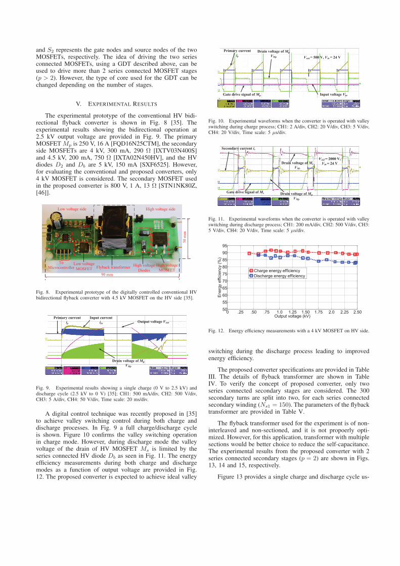
and S2 represents the gate nodes and source nodes of the twoMOSFETs, respectively. The idea of driving the two seriesconnected MOSFETs, using a GDT described above, can beused to drive more than 2 series connected MOSFET stages(p > 2). However, the type of core used for the GDT can bechanged depending on the number of stages.
V. EXPERIMENTAL RESULTS
The experimental prototype of the conventional HV bidi-rectional flyback converter is shown in Fig. 8 [35]. Theexperimental results showing the bidirectional operation at2.5 kV output voltage are provided in Fig. 9. The primaryMOSFET Mp is 250 V, 16 A [FQD16N25CTM], the secondaryside MOSFETs are 4 kV, 300 mA, 290 Ω [IXTV03N400S]and 4.5 kV, 200 mA, 750 Ω [IXTA02N450HV], and the HVdiodes D2 and Db are 5 kV, 150 mA [SXF6525]. However,for evaluating the conventional and proposed converters, only4 kV MOSFET is considered. The secondary MOSFET usedin the proposed converter is 800 V, 1 A, 13 Ω [STN1NK80Z,[46]].
Flyback transformer
High voltage sideLow voltage side
High voltageMOSFET
Low voltageMOSFET
High voltageDiodes
z
ToMicrocontroller
Gatedriver
Comparator
90 mm
30m
m
Fig. 8. Experimental prototype of the digitally controlled conventional HVbidirectional flyback converter with 4.5 kV MOSFET on the HV side [35].
Drain voltage ofMpVMp
Output voltage VoutPrimary current
ipInput current
iin
Fig. 9. Experimental results showing a single charge (0 V to 2.5 kV) anddischarge cycle (2.5 kV to 0 V) [35]; CH1: 500 mA/div, CH2: 500 V/div,CH3: 5 A/div, CH4: 50 V/div, Time scale: 20 ms/div.
A digital control technique was recently proposed in [35]to achieve valley switching control during both charge anddischarge processes. In Fig. 9 a full charge/discharge cycleis shown. Figure 10 confirms the valley switching operationin charge mode. However, during discharge mode the valleyvoltage of the drain of HV MOSFET Ms is limited by theseries connected HV diode Db as seen in Fig. 11. The energyefficiency measurements during both charge and dischargemodes as a function of output voltage are provided in Fig.12. The proposed converter is expected to achieve ideal valley
Drain voltage ofMpVMp
Primary currentip
Gate drive signal ofMp Input voltage Vin
Vout= 500 V, Vin= 24 V
Fig. 10. Experimental waveforms when the converter is operated with valleyswitching during charge process; CH1: 2 A/div, CH2: 20 V/div, CH3: 5 V/div,CH4: 20 V/div, Time scale: 5 μs/div.
Drain voltage ofMpVMp
Secondary current is
Gate drive signal ofMs
Drain voltage ofMsVMs
Vout= 2000 V,Vin= 24 V
Fig. 11. Experimental waveforms when the converter is operated with valleyswitching during discharge process; CH1: 200 mA/div, CH2: 500 V/div, CH3:5 V/div, CH4: 20 V/div, Time scale: 5 μs/div.
0 .25 .50 .75 1.0 1.25 1.50 1.75 2.0 2.25 2.5050
5560
6570
7580
859095
Output voltage (kV)
Ene
rgy
effic
ienc
y (%
)
Charge energy efficiency Discharge energy efficiency
Fig. 12. Energy efficiency measurements with a 4 kV MOSFET on HV side.
switching during the discharge process leading to improvedenergy efficiency.
The proposed converter specifications are provided in TableIII. The details of flyback transformer are shown in TableIV. To verify the concept of proposed converter, only twoseries connected secondary stages are considered. The 300secondary turns are split into two, for each series connectedsecondary winding (Ns1 = 150). The parameters of the flybacktransformer are provided in Table V.
The flyback transformer used for the experiment is of non-interleaved and non-sectioned, and it is not propoerly opti-mized. However, for this application, transformer with multiplesections would be better choice to reduce the self-capacitance.The experimental results from the proposed converter with 2series connected secondary stages (p = 2) are shown in Figs.13, 14 and 15, respectively.
Figure 13 provides a single charge and discharge cycle us-

ing the proposed topology, when the capacitor load is chargedand discharged from 0 V to 200 V, and vice versa. To verify theproposed concept, during both charge and discharge processes,the converter is driven with fixed switching frequency. Duringthe charge process the switching time period is 59 μs, andduring the discharge process, the switching time period is100 μs. In Figs. 14 and 15, a comparison of drain-to-sourcevoltage across the two secondary MOSFETs during a chargeand discharge switching cycle are provided.
TABLE III. CONVERTER SPECIFICATIONS
Parameter ValueInput voltage 24 VCapacitance of load 400 nFOn-time of primary MOSFET during the charge process 9 μs
TABLE IV. DETAILS OF THE SPLITTED FLYBACK TRANSFORMER WITHA TURNS RATIO OF 25
Parameter ValueNumber of primary / secondary turns 12 / 300Diameter of primary / secondary winding 0.5 mm / 0.12 mmNumber of layers of primary / secondary winding 1 / 4Type of core / material EF25 / N87
TABLE V. PARAMETERS OF THE SPLITTED FLYBACK TRANSFORMER
Parameter ValuePrimary / Each splitted secondary magnetizing inductance 42 μH / 6.3 mHSecondary non-splitted magnetizing inductance 25 mHLeakage inductance referred to primary / splitted secondary 1.1 μH / 53 μHLeakage inductance referred to non-splitted secondary 721 μHPrimary / Secondary splitted winding DC resistance 64 mΩ / 6.3 ΩSecondary non-splitted winding DC resistance 12.4 ΩSelf-capacitance of each splitted secondary winding 78.2 pFSelf-capacitance of non-splitted secondary winding 37 pF
Output voltage
Gate drive signal ofMp
Vout,max= 200 V,Vin= 24 V
Gate drive signal ofMs1 andMs2
Fig. 13. A charge and discharge cycle with the proposed topology; CH1: 10V/div, CH2: 100 V/div, CH3: 10 V/div, Time scale: 500 μs/div.
Drain to ground voltage of high sidesecondary MOSFET
Source to ground voltage of highside secondary MOSFET
Drain to source voltage of lowside secondary MOSFET
Drain to source voltage of highside secondary MOSFET
Fig. 14. Comparison of the voltage stress across the two secondary MOSFETsduring the charge process using the proposed topology; CH1: 200 V/div, CH2:200 V/div, CH4: 100 V/div,F3=C2-C4: 200 V/div, Time scale: 10 μs/div.
Drain to ground voltage of high sidesecondary MOSFET Source to ground voltage of high
side secondary MOSFET
Drain to source voltage of low side secondary MOSFET
Drain to source voltage of high side secondary MOSFET
Fig. 15. Comparison of the voltage stress across the two secondary MOSFETsduring the discharge process using the proposed topology; CH1: 200 V/div,CH2: 200 V/div, CH4: 100 V/div,F3=C2-C4: 200 V/div, Time scale: 10 μs/div.
VI. CONCLUSION
In this paper, a bidirectional flyback converter with multipleseries connected outputs is proposed, for high voltage drive ofcapacitive DEAP actuators. Simulation results (output voltagesand voltage stresses across the secondary MOSFETs/diodes)during both charge and discharge processes are provided, toshow a comparison between the proposed and conventionalimplementations. A theoretical comparison shows that theproposed converter has the potential to improve efficiency andlower the cost. The detailed implementation of secondary gatedriver, using a gate drive transformer is provided. Experimentalresults from the conventional (for full operating voltage range0-2.5 kV) and the proposed (0-200 V) bidirectional convertersare provided. The experimental waveforms of the drain-to-source voltages of the two secondary MOSFETs confirm thevoltage sharing across the two secondary MOSFETs.
VII. FUTURE WORK
Due to lack of time the converter operation for full operat-ing voltage range (0-2.5 kV), and with p = 5 series connectedsecondary stages are not verified. However, the future workregarding the proposed converter involves:
• implementing the valley switching control during bothcharge and discharge processes.
• design and implementation of the gate drive trans-former for p = 5 stages.
• design of the efficient flyback trasformer with verylow self-capacitance.
• investigating the coupling factor of different windingstrategies interms of voltage sharing.
REFERENCES
[1] Y. Bar-Cohen, Electroactive Polymer [EAP] Actuators as ArtificialMuscles: Reality, Potential, and Challenges, 2nd ed. Washington, DC:SPIE, 2004.
[2] R. E. Pelrine, R. D. Kornbluh, Q. Pei, and J. P. Joseph, “High-speedelectrically actuated elastomers with strain greater than 100%,” Science,vol. 287, pp. 836–839, 2000.
[3] F. Carpi, D. DE Rossi, R. Kornbluh, R. Pelrine, and P. Sommer-Larsen,Dielectric Elastomer As Electromechanical Transducers, Amsterdam,Netherlands: Elsevier, 2008.
[4] M. Tryson, H. E. Kiil, M. Benslimane, “Powerful tubular core freedielectric electro active polymer (DEAP) push actuator,” in Proc. SPIE,vol. 7287, 2009.
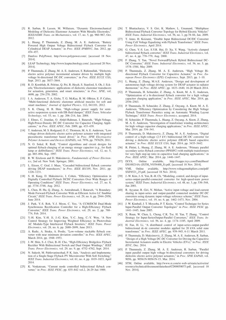
[5] R. Sarban, B. Lassen, M. Willatzen, “Dynamic ElectromechanicalModeling of Dielectric Elastomer Actuators With Metallic Electrodes,”IEEE/ASME Trans. on Mechatronics, vol. 17, no. 5, pp. 960–967, Oct.2012.
[6] L. Huang, P. Thummala, Z. Zhang, M. A. E. Andersen, “BatteryPowered High Output Voltage Bidirectional Flyback Converter forCylindrical DEAP Actuator,” in Proc. IEEE IPMHVC, Jun. 2012, pp.454–457.
[7] Danfoss PolyPower, http://www.polypower.com/, [accessed 18 Nov.2014].
[8] LEAP Technology, http://www.leaptechnology.com/, [accessed 20 Nov.2014].
[9] P. Thummala, Z. Zhang, M. A. E. Andersen, S. Rahimullah, “Dielectricelectro active polymer incremental actuator driven by multiple high-voltage bi-directional DC-DC converters,” in Proc. IEEE ECCE USA,Sept. 2013, pp. 3837–3844.
[10] R. D. Kornbluh, R. Pelrine, Q. Pei, R. Heydt, S. Stanford, S. Oh, J. Eck-erle,“Electroelastomers: applications of dielectric elastomer transducersfor actuation, generation, and smart structures,” in Proc. SPIE, vol.4698, pp. 254-270, 2002.
[11] I. A. Anderson, T. A. Gisby, T. G. McKay, B. M. OBrien, E. P. Calius,“Multi-functional dielectric elastomer artificial muscles for soft andsmart machines,” Journal of Applied Physics, 112, 041101, 2012.
[12] S. K. Chung, H. B. Shin, “High-voltage power supply for semi-active suspension system with ER-fluid damper,” IEEE Trans. VehicularTechnology, vol. 53, no. 1, pp. 206–214, Jan. 2004.
[13] J. Elmes, C. Jourdan, O. Abdel-Rahman, I. Batarseh, “High-Voltage,High-Power-Density DC-DC Converter for Capacitor Charging Appli-cations,” in Proc. IEEE APEC, Feb. 2009, pp. 433–439.
[14] T. Andersen, M. S. Rodgaard, O. C. Thomsen, M. A. E. Andersen, “Lowvoltage driven dielectric electro active polymer actuator with integratedpiezoelectric transformer based driver,” in Proc. SPIE ElectroactivePolymer Actuators and Devices (EAPAD), vol. 7976, pp. 79762N, 2011.
[15] N. O. Sokal, R. Redl, “Control algorithms and circuit designs foroptimal flyback-charging of an energy storage capacitor (e.g., for flashlamp or defibrillator),” IEEE Trans. Power Electronics, vol. 12, no. 5,pp. 885–894, Sep. 1997.
[16] R. W. Erickson and D. Maksimovic, Fundamentals of Power Electron-ics, 2nd ed. New York: Springer, 2001.
[17] L. Eitzen, C. Graf, J. Maas, “Cascaded bidirectional flyback converterdriving DEAP transducers,” in Proc. IEEE IECON, Nov. 2011, pp.1226–1231.
[18] S. H. Kang, D. Maksimovic, I. Cohen, “Efficiency Optimization inDigitally Controlled Flyback DCDC Converters Over Wide Ranges ofOperating Conditions” IEEE Trans. Power Electronics, vol. 27, no. 8,pp. 3734–3748, Aug. 2012.
[19] L. Chen, H. Hu, Q. Zhang, A. Amirahmadi, I. Batarseh, “A Boundary-Mode Forward-Flyback Converter With an Efficient Active LC SnubberCircuit,” IEEE Trans. Power Electronics, vol. 29, no. 6, pp. 2944–2958,June 2014.
[20] J. Park, Y.-S. Roh, Y.-J. Moon, C. Yoo, “A CCM/DCM Dual-ModeSynchronous Rectification Controller for a High-Efficiency FlybackConverter,” IEEE Trans. Power Electronics, vol. 29, no. 2, pp. 768–774, Feb. 2014.
[21] Y.-H. Kim, Y.-H. Ji, J.-G. Kim, Y.-C. Jung, C.-Y. Won, “A NewControl Strategy for Improving Weighted Efficiency in PhotovoltaicAC Module-Type Interleaved Flyback Inverters,” IEEE Trans. PowerElectronics, vol. 28, no. 6, pp. 2688–2699, June 2013.
[22] A. Radic, A. Straka, A. Prodic, “Low-volume stackable flyback con-verter with near minimum deviation controller,” in Proc. IEEE APEC,March 2014, pp. 1948–1953.
[23] J.-W. Shin, S.-J. Choi, B.-H. Cho, “High-Efficiency Bridgeless FlybackRectifier With Bidirectional Switch and Dual Output Windings,” IEEETrans. Power Electronics, vol. 29, no. 9, pp. 4752–4762, Sept. 2014.
[24] N. Sukesh, M. Pahlevaninezhad, P. K. Jain, “Analysis and Implementa-tion of a Single-Stage Flyback PV Microinverter With Soft Switching,”IEEE Trans. Industrial Electronics, vol. 61, no. 4, pp. 1819–1833, April2014.
[25] K. Venkatesan, “Current mode controlled bidirectional flyback con-verter,” in Proc. IEEE PESC, pp. 835–842 vol.2, 26-29 Jun 1989.
[26] T. Bhattacharya, V. S. Giri, K. Mathew, L. Umanand, “MultiphaseBidirectional Flyback Converter Topology for Hybrid Electric Vehicles”IEEE Trans. Industrial Electronics, vol. 56, no. 1, pp.78–84, Jan. 2009.
[27] T. Anno, H. Koizumi, “Double Input Bidirectional DC/DC ConverterUsing Cell Voltage Equalizing with Flyback Transformer,” IEEE Trans.Power Electronics, April 2014.
[28] G. Chen, Y.-S. Lee, S.Y.R. Hui, D. Xu, Y. Wang, “Actively clampedbidirectional flyback converter,” IEEE Trans. Industrial Electronics, vol.47, no. 4, pp. 770–779, Aug. 2000.
[29] F. Zhang, Y. Yan, “Novel ForwardFlyback Hybrid Bidirectional DC-DC Converter,” IEEE Trans. Industrial Electronics, vol. 56, no. 5, pp.1578–1584, May 2009.
[30] P. Thummala, Z. Zhang, M. A. E. Andersen, “High Voltage Bi-directional Flyback Converter for Capacitive Actuator,” in Proc. Eu-ropean Power Electronics (EPE) Conference, Sept. 2013, pp. 1–10.
[31] L. Huang, Z. Zhang, M.A.E. Andersen, “Design and development ofautonomous high voltage driving system for DEAP actuator in radiatorthermostat,” in Proc. IEEE APEC, pp. 1633–1640, 16-20 March 2014.
[32] P. Thummala, H. Schneider, Z. Zhang, A. Knott, M. A. E. Andersen,“Optimization of a bi-directional flyback converter for a high voltagecapacitor charging application,” in Proc. IEEE APEC, Mar. 2014, pp.2556–2563.
[33] P. Thummala, H. Schneider, Z. Zhang, Z. Ouyang, A. Knott, M. A. E.Andersen, “Efficiency Optimization by Considering the High VoltageFlyback Transformer Parasitics using an Automatic Winding LayoutTechnique,” IEEE Trans. Power Electronics, accepted, 2014.
[34] H. Schneider, P. Thummala, L. Huang, Z. Ouyang, A. Knott, Z. Zhang,M. A. E. Andersen, “Investigation of transformer winding architecturesfor high voltage capacitor charging applications,” in Proc. IEEE APEC,Mar. 2014, pp. 334–341.
[35] P. Thummala, D. Maksimovic, Z. Zhang, M. A. E. Andersen, “Digitalcontrol of a high-voltage (2.5 kV) bidirectional DC-DC converter fordriving a dielectric electro active polymer (DEAP) based capacitiveactuator,” in Proc. IEEE ECCE USA, Sept. 2014, pp. 3435–3442.
[36] R. Pittini, L. Huang, Z. Zhang, M. A. E. Andersen, “Primary parallelsecondary series flyback converter (PPSSFC) with multiple transformersfor very high step-up ratio in capacitive load charging applications,” inProc. IEEE APEC, Mar. 2014, pp. 1440–1447.
[37] IXYS, Online available, http://ixapps.ixys.com/DataSheet/DS100214A-(IXTH V03N400 S).pdf, [accessed 18 Nov. 2014].
[38] VMI, Online available, http://www.voltagemultipliers.com/pdf/SXF6521 25.pdf, [accessed 18 Nov. 2014].
[39] J.-W. Kim, J.-S. Yon, B.-H. Ch, “Modeling, control, and design of input-series-output-parallel-connected converter for high-speed-train powersystem,” IEEE Trans. Industrial Electronics, vol. 48, no. 3, pp. 536–544,Jun 2001.
[40] R. Ayyanar, R. Giri, N. Mohan, “Active input-voltage and load-currentsharing in input-series and output-parallel connected modular DC-DCconverters using dynamic input-voltage reference scheme,” IEEE Trans.Power Electronics, vol. 19, no. 6, pp. 1462–1473, Nov. 2004.
[41] J. W. Kimball, J. T. Mossoba, P. T. Krein, “Control Technique for SeriesInput-Parallel Output Converter Topologies” in Proc. IEEE PESC pp.1441–1445, June 2005.
[42] X. Ruan, W. Chen, L. Cheng, C.K. Tse, H. Yan, T. Zhang, “ControlStrategy for Input-SeriesOutput-Parallel Converters,” IEEE Trans. In-dustrial Electronics, vol. 56, no. 4, pp. 1174–1185, April 2009.
[43] H. Fan, H. Li, “A distributed control of input-series-output-parallelbidirectional dc-dc converter modules applied for 20 kVA solid statetransformer,” in Proc. IEEE APEC, pp. 939–945, 6-11 March 2011.
[44] P. Thummala, D. Maksimovic, Z. Zhang, M. A. E. Andersen, R. Sarban,“Design of a High Voltage DC-DC Converter for Driving the CapacitiveIncremental Actuators usable in Electric Vehicles (EVs),” in Proc. IEEEIEVC, Dec. 2014.
[45] P. Thummala, Z. Zhang, M. A. E. Andersen, R. Sarban, “Parallelinput parallel output high voltage bi-directional converters for drivingdielectric electro active polymer actuators,” in Proc. SPIE EAPAD, vol.9056, pp. 90561N-90561N-15, Mar. 2014.
[46] STM, Online available, http://www.st.com/st-web-ui/static/active/en/resource/technical/document/datasheet/CD00058073.pdf, [accessed 18Nov. 2014].

Appendix ODielectric Electro Active PolymerIncremental Actuator Driven by
Multiple High-VoltageBi-directional DC-DC Converters
2013 IEEE Energy Conversion Congress and Exposition USA (ECCE USA 2013)→ Best Student Paper Award
227/255

Dielectric Electro Active Polymer Incremental Actuator Driven by Multiple High-Voltage Bi-directional
DC-DC Converters Prasanth Thummala, Zhe Zhang, Michael A.E. Andersen
Department of Electrical Engineering Technical University of Denmark
DK-2800 Kongens Lyngby, Denmark [email protected]
Sarban Rahimullah Danfoss PolyPower A/S
DK-6430 Nordborg, Denmark [email protected]
Abstract— This paper presents driving circuit for a recently invented dielectric electro active polymer (DEAP) incremental actuator. The basic operation of such an actuator is bio-inspired from the movement of an inchworm. The actuator consists of three electrically isolated, and mechanically connected capacitive sub-actuators. It needs to be driven by three high voltage (~2.5 kV) DC-DC converters, to achieve the linear incremental motion. The topology used for this application is a bi-directional flyback DC-DC converter. The control of the incremental actuator involves, implementation of digital controller used for controlling charge and discharge sequences of the individual sub-actuators, and monitoring and adjustment of the output voltages of three high voltage DC-DC converters to provide over-voltage protection capability. Three power stages of the proposed converter were experimentally tested. The experimental results and efficiency measurements are shown.
NOMENCLATURE
inV Input voltage inC Input capacitance
1 2 3, , A A AC C C Capacitances of the actuators A1, A2, and A3
1 2 3, , p p pi i i Primary currents of converters 1, 2 and 3
1 2 3, , s s si i i Secondary currents of converters 1, 2 and 3
1 2 3, , n n n Turns ratios of converters 1, 2 and 3 1, 2, 3, 4, 5, 6 AC Analog controllers 1, 2, 3, 4, 5 and 6
1, 2, 3, 4, 5, 6 chV Enable signals for the analog controllers 1, 2, 3, 4, 5 and 6
1 3 5, ,M M M Low voltage MOSFETS of converters 1, 2 and 3
2 4 6, ,M M M High voltage MOSFETS of converters 1, 2 and 3
1, 2, 3, 4, 5, 6HVD High voltage diodes of converters 1,2 and 3
1 2 3, , A A AV V V Output voltages of the actuators A1, A2 and
A3 / capacitive loads 1 2 3, , FB FB FBV V V Feedback voltages of the actuators A1, A2
and A3 / capacitive loads
INTRODUCTION Dielectric electro active polymer (DEAP) is an emerging
smart material that has experienced substantial development and has gained increasing attention over the last decade [1], [2]. The DEAP material is a very thin (~40 µm) incompressible elastomer film with a compliant electrode layer on both sides [3]. The basic behavior of the DEAP material is the reduction in the polymer’s thickness and increment in its area, due to an applied electric field (~60 V/µm). DEAP, when used as actuators, has the potential to be an effective replacement for many conventional actuators due to its unique properties, such as large strain, light weight, noiseless operation, low power consumption, high flexibility, and power density. Actuators providing linear motion are used in a vast range of applications ranging from large size machineries (e.g. cranes), to small scale MEMS devices used for micro positioning. Linear actuators are typically characterized by their maximum stroke, force, speed, and precision. The strokes of many linear actuators are limited to their initial geometrical dimensions. This characteristic of conventional linear actuators limits their use in applications where large strokes, and low size and weight of the actuators are desired. DEAP incremental actuators are an alternative design to overcome these limitations by providing an inchworm-like actuation.
The DEAP incremental actuator concept is the latest invention from Danfoss PolyPower [4] that consists of two grippers (to enable gripping operation) and an extender (to move the grippers). These grippers connect with the extender using the mechanical structures, so the incremental actuator is equivalent to three independent capacitive actuators with electrical isolation between them. Fast and precise adjustment, low noise operation, and high energy efficiency are the key advantages of the DEAP incremental actuator. Some potential applications for the DEAP incremental actuator are transportation of equipment at industrial production facilities, pipe monitoring and cleaning, and search and rescue robots. In addition to the above, the DEAP incremental actuator technology has the
Danish National Advanced Technology Foundation
3837978-1-4799-0336-8/13/$31.00 ©2013 IEEE

Figure 1: PolyPower axial DEAP actuator.
Figure 2: Conceptual diagram of the DEAP incremental actuator.
potential to be used in various industries, e.g. automotive, aeronautics, space and medicine. Table I provides a short comparison of the DEAP and Piezo incremental actuator technologies.
TABLE I. COMPARISON OF DEAP AND PIEZO INCREMENTAL ACTUATOR TECHNOLOGIES
Parameter Piezo Technology DEAP Technology Strain Small (~0.02-0.1 %) Large (~5-100 %)
Force density High (~20 N/mm2 ) Medium (~0.5 N/mm2 ) Structural flexibility
Low (Young’s Modulus
Y=~40-60 GPa)
High (Young’s Modulus
Y=~1.1 MPa) Linear velocity per
unit length = Strain×actuation
frequency
Medium (~20-100 Hz)
High (~100-1500 Hz)
Driving the DEAP incremental actuator has three main challenges from a power electronics standpoint. Firstly, it requires high voltages of approximately 2.5 kV at relatively low currents [5], to generate sufficient force and displacement for the sub-actuators. Suitable energy sources for the incremental actuator application are lithium batteries with voltage range 9-24 V; this necessitates the need of high voltage step-up circuits as a driving mechanism for the DEAP actuator. Secondly, DEAP actuators convert only a small fraction of the input electrical energy into mechanical work, while they store the remainder in the capacitive structure of the actuator and must be recovered to maximize the system efficiency; this necessitates the need of bi-directional converters [6]-[8], [11]. Finally, control of charge and discharge cycles of three sub-actuators to achieve the required incremental motion.
Prior work on the high voltage drivers for the DEAP actuators demonstrated a world’s first low voltage piezoelectric transformer based DEAP solution, and it was
integrated into a core less DEAP actuator [9], and a flyback converter topology to drive the PolyPower Push Inlastor DEAP actuator for wind turbine flaps application [10], without energy recovery circuits in both topologies. Bi-directional, high voltage DC-DC converter topology for capacitive charging application has been recently proposed and implemented in [13], and the detailed loss analysis of the same converter has been discussed in [14]. The overall goal of this paper is the design, control and implementation of the three high voltage DC-DC converters.
The paper is organized as follows. Section II describes the basic idea and operational diagrams of the DEAP incremental actuator concept. Section III presents high voltage driving circuits for the incremental actuator. Section IV discusses the experimental results, and the implementation issues, followed by the conclusion in Section V.
INCREMENTAL DEAP ACTUATOR The PolyPower axial DEAP actuator and the DEAP
incremental actuator conceptual diagrams are shown in Figs. 1 and 2, respectively. The DEAP incremental actuator consists of three axial DEAP actuators viz., one extender (A2) and two grippers (A1 and A3) at either end. Each gripper that is connected to mechanical supports on either side, expands and clamps to the guiding bar surface when charged, and unclamp from it, when discharged. The extender expands axially along the axis of the guiding bar. When in operation, one gripper holds the guiding bar while the other gripper is in the released position. The extender either pushes or pulls the released gripper. The incremental actuation sequence of steps, and the driving voltage waveforms of the grippers and the extender are shown in Figs. 3-5, respectively. The incremental actuator undergoes 6 steps of different operations (Fig. 3), to achieve a single incremental actuation stroke.
A. The moving sequence of steps for the linear incremental motion towards the positive x-axis (right) direction • Start: All actuators are in the discharged state.
• Step 0: A1 is charged and clamps to the guiding bar. A2 and A3 are in the discharged state.
• Step 1: A1 remains in the charged state. A2 is charged and pushes the mechanical structure towards right, and A3 remains in the discharged state.
• Step 2: A1 and A2 still remain in the charged state. A3 is charged.
• Step 3: A1 is discharged and is in the released position. A2 and A3 still remain in the charged state.
• Step 4: A1 remains in the discharged state. A2 is discharged, and A3 remains in the charged state.
• Step 5: A1 is charged. A2 remains in the discharged state, and A3 remains in the charged state.
3838
• Step 6: A1 remains in the charged state. A2 remains in the discharged state, and A3 is discharged.
• End: All actuators are discharged at the end.
The Step 0 is used only for charging the actuator A1. The Steps 1-6 repeat for achieving continuous incremental actuations.
xΔ
Figure 3: Moving sequence of the incremental actuator for moving towards the positive x-axis direction.
2500 V 2500 V
2500 V 2500 V
2500 V2500 V
2AV
1AV
3AV
1chV
3chV
5chV
2chV
4chV
6chV
increment_max
1fΔ
Figure 4: Driving voltages of the sub-actuators for moving towards the positive x-axis direction with maximum speed.
2500 V
2500 V
2500 V2500 V
2AV
1AV
3AV
1chV
3chV
5chV
2chV
4chV
6chV
1
incrementfΔ
Figure 5: Driving voltages of the sub-actuators for moving towards the positive x-axis direction with variable speed.
The moving sequence of steps for the linear incremental motion towards the negative x-axis (left) direction can be easily drawn similar to Fig. 3. In Fig. 4, xΔ is the stroke of the incremental actuator for one incremental actuation movement. The driving voltages for moving with the maximum frequency (speed) are shown in Fig. 4, where no delay is provided between the actuator charge and discharge cycles. The incremental actuator speed can be changed, by proving delay between the actuator charge and discharge
3839

cycles as shown in Fig. 5. However, when the incremental actuator is loaded when in operation, the delay between the Steps 1 and 2 can be skipped, to prevent the actuator being led the load. This can prevent the pulling of the incremental actuator by the load when actuator A2 is charged. In Figs. 4 and 5 increment_maxfΔ and incrementfΔ are the maximum and variable incremental actuation frequencies, respectively.
III. HIGH VOLTAGE DRIVERS FOR INCREMENTAL DEAP ACTUATOR
The basic block diagram of the high voltage driving circuits to drive the DEAP incremental actuator is shown in Fig. 6. The complete circuit schematic of the DEAP incremental actuator driven by multiple bi-directional high voltage DC-DC converters is shown in Fig. 7. The topology is a peak current controlled bi-directional flyback converter. Three bi-directional flyback converters are powered by the same source. Each converter independently controls the charge and discharge operations of the three axial sub- actuators (two grippers and an extender) in the incremental actuator. The basic theory of operation of the proposed circuit is described below.
B. Bi-directional flyback converter 1) Charge process: To transfer the energy from the
source to the actuator A1, M1 is turned ON by the analog controller 1 (AC1) [12], which is enabled by the enable signal
1chV , provided by the digital controller, causing the current in the primary winding
1mpL of the flyback transformer to increase to the peak value 1ppkI . When M1 is turned OFF, the energy stored in the transformer core is transferred to the capacitive actuator
1AC via secondary winding
1msL and diode 1HVD , causing the output voltage
1AV to increase. 2AC and
3AC are charged independently, in a similar fashion through the DC-DC converters 2 and 3, respectively.
The energy balance equation for the converter 1, during the charging process is:
( )1 1 1
1 1 1
22 2
A _ A _2 2mp ppk A
loss final initial
L I CE V V− = − (1)
where 1lossE is the dissipated energy in the flyback converter,
1 _A initialV and 2 _A finalV are the values of output voltage
1AV at the beginning and end of a switching cycle.
2) Discharge process: To transfer the energy back to the source from the actuator A1, M2 (is turned ON by the analog controller 2 (AC2), which is enabled by the enable signal
2chV , provided by the digital controller, causing the current in the secondary winding
1msL of the flyback transformer to increase to the peak value 1spkI− . When M2 is turned OFF, the energy stored in the transformer core is transferred to the
DE
AP
Incr
emen
tal A
ctua
tor
1AC
2AC
3AC
Figure 6: Block diagrams of multiple high voltage bi-directional DC-DC
converters and digital controller.
•
•
•
•
•
•
DE
AP
incr
emen
tal a
ctua
tor
1AC
2AC
3AC
1HVD2HVD
3HVD4HVD
1chV2chV
5HVD
1bD
3bD
5bD
1pi
1si
1AV
2pi2s
i
3chV4chV
2AV
3AV
3pi3s
i
6HVD
2bD
4bD
6bD
5chV6chV
1mpL1msL
2mpL2msL
3mpL3msL
Figure 7: Circuit schematic of the DEAP incremental actuator driven by
multiple high voltage bi-directional DC-DC converters.
source via primary winding 1mpL and the body diode of M1,
i.e.,1bD , causing the output voltage
1AV to decrease. 2AC
and3AC are discharged independently, in a similar fashion
through the DC-DC converters 2 and 3, respectively.
The energy balance equation for the converter 1, during the discharging process is:
3840
1
1
Ain
VV n⎛ ⎞+ ⎜ ⎟⎝ ⎠
11 in AnV V+
1ppkI
11 spkn I−
1AV
1
1
ppkIn
1spkI−
1onMt1offMt
1gsMV
02gsMV
1dsMV
2DV−
1AV
2onMt2offMt
2dcmMt
Energy transfer
to A1
1gsMV
2gsMV
1chV
2chV
1AV 2500 V 2500 V
Figure 8a): Ideal switching waveform of the bi-directional flyback converter 1; 8b): Driving signal for the sub-actuator A1
( )1 1 1
2 1 1
22 2
_ _2 2ms spk A
loss A initial A final
L I CE V V− = − (2)
where 2lossE is the dissipated energy in the flyback converter
during a discharging switching cycle. The same principles apply for the converters 2 and 3. The ideal bi-directional flyback converter waveforms during energy transfer and energy recovery processes are shown in Fig. 8. In any DC-DC converter of Fig. 7, the low voltage MOSFET is used during energy transfer from source to load, while high voltage MOSFET is used during energy recovery from load
to source. More details about the bi-directional flyback converter topology and analysis can be obtained from [13].
C. Digital controller For controlling the incremental actuator, the 16-bit
microcontroller PIC18F2550 has been used. The block diagram of the digital controller is shown in Fig. 9.
The main functions of the microcontroller are:
• To control the charge and discharge sequences of the individual sub-actuators
• Monitoring the high voltage to provide the over voltage protection for all converters
• To change the direction of movement of incremental actuator
• To change the speed of movement of the incremental actuator
Analog inputs
Digital outputs
1chV
2chV
3chV
4chV
5chV
6chV
inV
1FBV
2FBV
3FBV
Direction
Speed
Figure 9: Block diagram of the digital controller to control the 3 high
voltage DC-DC converters.
D. High voltage measurement
1AC1HVC
1LVC
1HVR
1LVR OPA 336
1FBV1AV
Figure 10: High voltage measurement circuit of converter 1 with resistive
and capacitive voltage divider.
The high voltage measurement circuit for DC-DC converter 1, with resistive and capacitive voltage dividers is shown in Fig. 10. The feedback voltage is buffered by an operational amplifier having a very high input impedance (>10 TΩ), and the outputs of the buffer is used as the feedback signal to the digital controller which provides the over voltage protection.
The low frequency or steady state relationship between the feedback signals and the output voltages are given by
3841

; =1, 2 and 3i
i i
i i
LVFB A
HV LV
RV V i
R R⎡ ⎤
= ⎢ ⎥+⎢ ⎥⎣ ⎦
(3)
To eliminate the impact of the parasitic capacitors, without increasing the static discharge of the DEAP actuator, a capacitive voltage divider is added. By using relatively large capacitors in the divider the impact from the parasitic capacitors is neglected.
The frequency dependent feedback voltages for the combined resistive and capacitive voltage dividers is given in (4).
1
1 1
1, 2 and 3
i
i i
i ii i
i i i i
LV
LV LVFB A
HV LV
HV HV LV LV
Rj R C
V V R Rj R C j R C
i
ω
ω ω
⎡ ⎤⎢ ⎥+⎢ ⎥= ⎢ ⎥
+⎢ ⎥+ +⎢ ⎥⎣ ⎦=
(4)
The frequency dependent feedback voltages can become frequency independent, if
; 1, 2 and 3i i i iLV LV HV HVR C R C i= = (5)
The frequency independent feedback voltages are
1, 2 and 3
i i
i i i
i i i i
LV HVFB A A
HV LV LV HV
R CV V V
R R C C
i
⎡ ⎤ ⎡ ⎤= =⎢ ⎥ ⎢ ⎥
+ +⎢ ⎥ ⎢ ⎥⎣ ⎦ ⎣ ⎦=
(6)
whereiHVR ,
iLVR , iHVC and
iLVC are the high voltage (3 kV), low voltage resistors, high voltage (3 kV, C0G/NP0 type) and low voltage capacitors used in the high voltage sensing network, respectively. For each converter, 5 HVR G= Ω ,
5.1 MLVR = Ω , 33 pFHVC = , and 33 nFHVC = .
IV. EXPERIMENTAL RESULTS Three high voltage bi-directional flyback converters were
experimentally tested. The experimental results are shown in Figs. 11 and 14. The maximum energy efficiency of the converters during charging operation (transferring the input energy to the actuator) was 87 %, and during discharging operation (transferring the actuator energy back to the source) it was 80 %, for an output energy of 0.62 J. The converter specifications are provided Table II. The parameters of the flyback transformers 1, 2 and 3 are given in Tables III, IV and V respectively. The measurement of transformer parameters is described below.
E. Measurement of Transformer parameters using the Impedance Analyser
1) Magnetizing inductance (Lm): Magnetizing inductance of the primary/secondary side can be obtained by
opening the secondary/primary winding and measuring the inductance across the primary/secondary winding at the frequency of interest.
2) Leakage inductance (Llk): Leakage inductance referred to the primary/secondary side can be obtained by shorting the secondary/primary winding and measuring the inductance across the primary/secondary winding.
3) Self capacitance (Cs): Self capacitance of the secondary winding can be obtained by measuring the resonant frequency (frs) of the secondary winding from its impedance plot. Then, self-capacitance Cs is given by
( )21
2srs ms
Cf Lπ
= (7)
where msL is the secondary winding magnetizing inductance.
4) Interwinding capacitance: Interwinding capacitance can be obtained, by shorting both primary and secondary windings, and measuring the capacitance across the shorted primary and secondary windings.
F. Discussion During charging process the converter operates in the
boundary mode, and during discharging it operates in the discontinuous conduction mode. The energy loss is mainly contributed as the capacitive switching loss caused by the transformer parasitic winding capacitance, and the leakage loss due to the transformer’s leakage inductance. Research is still ongoing to optimize the flyback converter to obtain very high energy efficiency in the entire operating range.
Practical experience reveals that careful design of the flyback transformer with low leakage inductance and low stray capacitance is required for achieving continuous high voltage bi-directional operation. In the current market the available high voltage MOSFETs for this application are 4 kV, IXTV400NS (used in the current research) and 4.5 kV, IXTA02N450HV MOSFETs. Improper flyback transformer designs may lead to failure of the converter during the discharging operation. The experimental prototype is shown in Fig. 15. The charging and discharging energy efficiency [13] measurement results are provided in Figs. 16 and 17.
TABLE II. CONVERTER SPECIFICATIONS
Parameter Value Input voltage 24 V
Output voltage 0-2500 V
Stored energy at 2.5 kV output voltage 0.62 J
Capacitance of each sub-actuator/film capacitor load
200 nF
Incremental actuation frequency ~ 1-5 Hz Primary peak current during charging/discharging process
4.2 A / 5.3 A
Input filter capacitor 3900 µF
3842

TABLE III. FLYBACK TRANSFORMER 1 PARAMETERS
Parameter Value
Flyback transformer core type / Material EF20 / N87 Primary (LmP) / Secondary magnetizing
inductance (LmS) 29.5 µH / 16 mH
Primary turns (NP) / Secondary turns (NS) 16 / 375
Leakage inductance of transformer primary (LlkP) / secondary (LlkS)
1.11 µH / 633 µH
Secondary winding self (Cs) / Interwinding capacitance (Cint)
17 pF / 41 pF
DC resistance of primary (RdcP) / secondary winding (RdcS)
62 mΩ / 28.5 Ω
Primary (nlp) / Secondary layers (nls) 1 / 5
Each layer primary (hp) / secondary winding thickness (hs)
0.5 mm / 0.1 mm
TABLE IV. FLYBACK TRANSFORMERS 2 PARAMETERS
Parameter Value Flyback transformer core type / Material EF20 / N87 Primary (LmP) / Secondary magnetizing
inductance (LmS) 33.5 µH / 20.8 mH
Primary turns (NP) / Secondary turns (NS) 16 / 400
Leakage inductance of transformer primary (LlkP) / secondary (LlkS)
1.2 µH / 728 µH
Secondary winding self (Cs) / Interwinding capacitance (Cint)
19.4 pF / 33.5 pF
DC resistance of primary (RdcP) / secondary winding (RdcS)
85 mΩ / 41 Ω
Primary (nlp) / Secondary layers (nls) 2 / 5
Each layer primary (hp) / secondary winding thickness (hs)
0.65 mm / 0.1 mm
TABLE V. FLYBACK TRANSFORMERS 3 PARAMETERS
Parameter Value
Flyback transformer core type / Material EF20 / N87 Primary (LmP) / Secondary magnetizing
inductance (LmS) 28 µH / 17 mH
Primary turns (NP) / Secondary turns (NS) 16 / 400
Leakage inductance of transformer primary (LlkP) / secondary (LlkS)
1.25 µH / 710 µH
Secondary winding self (Cs) / interwinding capacitance (Cint)
22.6 pF / 35 pF
DC resistance of primary (RdcP) / secondary winding (RdcS)
84 mΩ / 41 Ω
Number of primary (nlp) / secondary layers (nls) 2 / 5
Each layer primary (hp) / secondary winding thickness (hs)
0.65 mm / 0.1 mm
Figure 11: Experimental result with the 3 dc-dc converters with 1
incremental actuation cycle; CH1: 1AV ; CH2:
2AV ; CH3: 3AV ; CH4:
1chV ; Δfincrement_max = 4.3 Hz
Figure 12: Experimental result with the 3 dc-dc converters with several incremental actuation cycles; CH1:
1AV ; CH2: 2AV ; CH3:
3AV ; CH4: 1chV ;
Δfincrement_max = 4.3 Hz
Figure 13: Experimental result with the 3 dc-dc converters; CH1: 1HVDV− ;
CH2: 2HVDV− ; CH3:
3HVDV− ; CH4: 1chV ;
Figure 14: Experimental result with the 3 dc-dc converters with several
incremental actuation cycles; CH1: 1AV ; CH2:
2AV ; CH3: 3AV ; CH4:
1chV ; Δfincrement = 1.5 Hz.
3843
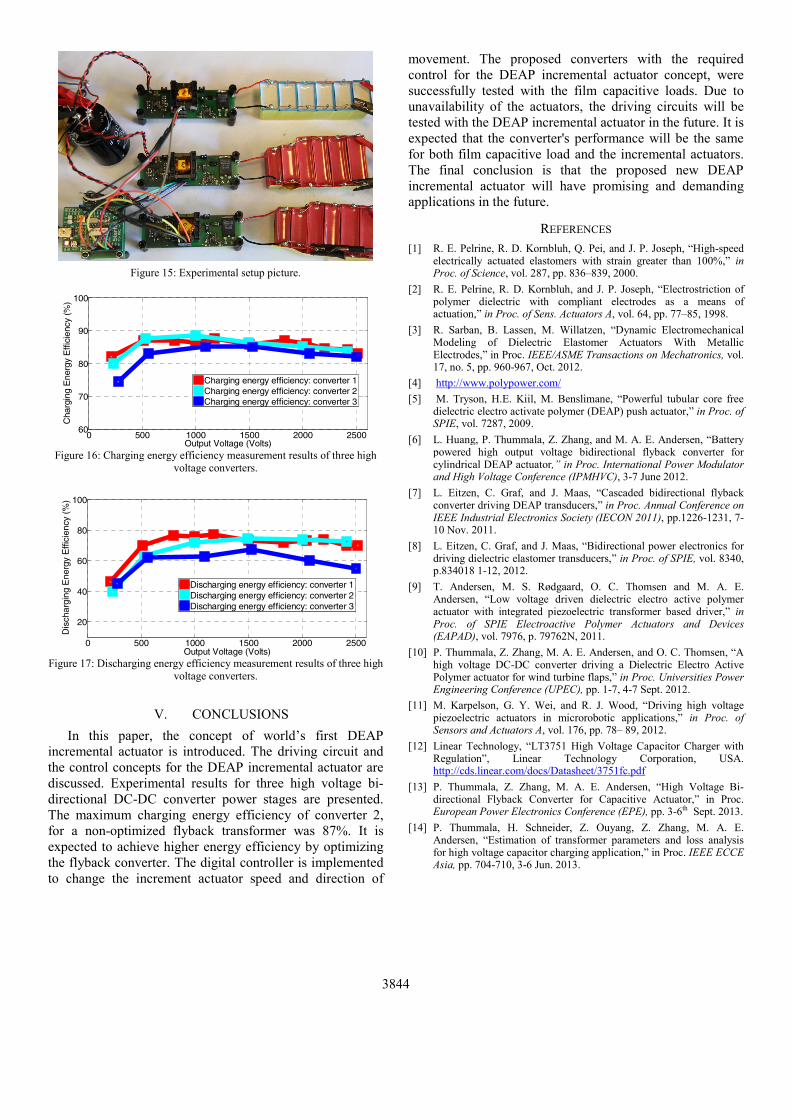
Figure 15: Experimental setup picture.
0 500 1000 1500 2000 250060
70
80
90
100
Output Voltage (Volts)
Cha
rgin
g E
nerg
y E
ffici
ency
(%
)
Charging energy efficiency: converter 1Charging energy efficiency: converter 2Charging energy efficiency: converter 3
Figure 16: Charging energy efficiency measurement results of three high
voltage converters.
0 500 1000 1500 2000 2500
20
40
60
80
100
Output Voltage (Volts)
Dis
char
ging
Ene
rgy
Effi
cien
cy (
%)
Discharging energy efficiency: converter 1Discharging energy efficiency: converter 2Discharging energy efficiency: converter 3
Figure 17: Discharging energy efficiency measurement results of three high
voltage converters.
V. CONCLUSIONS In this paper, the concept of world’s first DEAP
incremental actuator is introduced. The driving circuit and the control concepts for the DEAP incremental actuator are discussed. Experimental results for three high voltage bi-directional DC-DC converter power stages are presented. The maximum charging energy efficiency of converter 2, for a non-optimized flyback transformer was 87%. It is expected to achieve higher energy efficiency by optimizing the flyback converter. The digital controller is implemented to change the increment actuator speed and direction of
movement. The proposed converters with the required control for the DEAP incremental actuator concept, were successfully tested with the film capacitive loads. Due to unavailability of the actuators, the driving circuits will be tested with the DEAP incremental actuator in the future. It is expected that the converter's performance will be the same for both film capacitive load and the incremental actuators. The final conclusion is that the proposed new DEAP incremental actuator will have promising and demanding applications in the future.
REFERENCES [1] R. E. Pelrine, R. D. Kornbluh, Q. Pei, and J. P. Joseph, “High-speed
electrically actuated elastomers with strain greater than 100%,” in Proc. of Science, vol. 287, pp. 836–839, 2000.
[2] R. E. Pelrine, R. D. Kornbluh, and J. P. Joseph, “Electrostriction of polymer dielectric with compliant electrodes as a means of actuation,” in Proc. of Sens. Actuators A, vol. 64, pp. 77–85, 1998.
[3] R. Sarban, B. Lassen, M. Willatzen, “Dynamic Electromechanical Modeling of Dielectric Elastomer Actuators With Metallic Electrodes,” in Proc. IEEE/ASME Transactions on Mechatronics, vol. 17, no. 5, pp. 960-967, Oct. 2012.
[4] http://www.polypower.com/ [5] M. Tryson, H.E. Kiil, M. Benslimane, “Powerful tubular core free
dielectric electro activate polymer (DEAP) push actuator,” in Proc. of SPIE, vol. 7287, 2009.
[6] L. Huang, P. Thummala, Z. Zhang, and M. A. E. Andersen, “Battery powered high output voltage bidirectional flyback converter for cylindrical DEAP actuator,” in Proc. International Power Modulator and High Voltage Conference (IPMHVC), 3-7 June 2012.
[7] L. Eitzen, C. Graf, and J. Maas, “Cascaded bidirectional flyback converter driving DEAP transducers,” in Proc. Annual Conference on IEEE Industrial Electronics Society (IECON 2011), pp.1226-1231, 7-10 Nov. 2011.
[8] L. Eitzen, C. Graf, and J. Maas, “Bidirectional power electronics for driving dielectric elastomer transducers,” in Proc. of SPIE, vol. 8340, p.834018 1-12, 2012.
[9] T. Andersen, M. S. Rødgaard, O. C. Thomsen and M. A. E. Andersen, “Low voltage driven dielectric electro active polymer actuator with integrated piezoelectric transformer based driver,” in Proc. of SPIE Electroactive Polymer Actuators and Devices (EAPAD), vol. 7976, p. 79762N, 2011.
[10] P. Thummala, Z. Zhang, M. A. E. Andersen, and O. C. Thomsen, “A high voltage DC-DC converter driving a Dielectric Electro Active Polymer actuator for wind turbine flaps,” in Proc. Universities Power Engineering Conference (UPEC), pp. 1-7, 4-7 Sept. 2012.
[11] M. Karpelson, G. Y. Wei, and R. J. Wood, “Driving high voltage piezoelectric actuators in microrobotic applications,” in Proc. of Sensors and Actuators A, vol. 176, pp. 78– 89, 2012.
[12] Linear Technology, “LT3751 High Voltage Capacitor Charger with Regulation”, Linear Technology Corporation, USA. http://cds.linear.com/docs/Datasheet/3751fc.pdf
[13] P. Thummala, Z. Zhang, M. A. E. Andersen, “High Voltage Bi-directional Flyback Converter for Capacitive Actuator,” in Proc. European Power Electronics Conference (EPE), pp. 3-6th Sept. 2013.
[14] P. Thummala, H. Schneider, Z. Ouyang, Z. Zhang, M. A. E. Andersen, “Estimation of transformer parameters and loss analysis for high voltage capacitor charging application,” in Proc. IEEE ECCE Asia, pp. 704-710, 3-6 Jun. 2013.
3844

236/255

Appendix PA new Incremental Actuator
based on Electro Active Polymer:Conceptual, Control and Driver
Design Considerations
Revision Submitted to IEEE Transactions on Mechatronics
237/255

Abstract—This paper presents an overview of the widely used
conventional linear actuator technologies and existing electro
active polymer based linear and rotary actuators. It also provides
conceptual, control and driver design considerations for a new
dielectric electro active polymer (DEAP) based incremental
actuator. The proposed actuator consists of three independent
DEAP actuators with a unique cylindrical design that potentially
simplifies mass production and scalability compared to existing
DEAP actuators. To accomplish the incremental motion, each
actuator is independently charged and discharged by a high
voltage bidirectional DC-DC converter. The topology used for the
high voltage driver is a peak-current controlled bidirectional
flyback converter. The scalability of the proposed incremental
actuator is discussed and the estimated speed and force of various
designs are provided. The high voltage drivers are
experimentally tested with both capacitive loads and a prototype
of the DEAP incremental actuator. The prototype moves with a
maximum velocity of 1.5 mm/s, at 2.87 Hz incremental driving
frequency, when all actuators are driven with 1.8 kV.
Index Terms—linear actuators, switch-mode power supplies, DC-
DC power converters, actuators, energy efficiency, dielectric
electro active polymer (DEAP)
I. INTRODUCTION
CTUATORS providing linear motion are used in a vast
variety of applications ranging from large size
machineries (e.g., cranes) to small scale micro-electro-
mechanical system (MEMS) devices used for micro
positioning. Linear actuators are typically characterized by
their maximum stroke length, force, speed, and precision (or
resolution). The typical linear actuators include electro-
mechanical, hydraulic, pneumatic, piezo, and electro active
polymer, etc.
This work was supported by the Danish National Advanced Technology
Foundation under the “Highly efficient low cost energy generation and
actuation using disruptive DEAP technology” project, managed by Danfoss
PolyPower A/S, Denmark. Part of this paper was presented and selected as a best student paper award
at IEEE Energy Conversion Congress and Exposition (ECCE) USA’13
conference (Sept. 15-19th, 2013, Denver, CO, USA). *The authors are with the Department of Electrical Engineering, Technical
University of Denmark, DK-2800 Kongens Lyngby, Denmark (e-mail:
[email protected], [email protected], [email protected], [email protected]).
#The author is with LEAP Technology, Science and Technology Park, DK-
2800 Kongens Lyngby, Denmark (e-mail: [email protected]).
An electromechanical linear actuator uses a DC motor or a
stepper motor to control a linear-action shaft output, as shown
in Fig. 1. The rotary motion of the motor is converted to linear
displacement through a belt drive, a gearing, a threaded rod
and a nut connected to a shaft. The advantages are high force,
high speed and high precision which all can be tailored via
high design flexibility. The disadvantages are mechanical
complexity, weight, size and cost. Pneumatic linear actuators
as shown in Fig. 2 operate with an external source of
compressed air. They are efficient, but relatively complex to
control via pressure valves and compressor manipulation.
Hydraulic linear actuators are used in many industrial
applications requiring higher levels of force than provided
through equivalently sized electromechanical systems.
Hydraulic actuators not only allow the generation of large
forces, but also capable of closed-loop velocity controlling or
highly precise positioning of heavy loads. A hydraulic linear
A new Incremental Actuator based on Electro
Active Polymer: Conceptual, Control and Driver
Design Considerations
Prasanth Thummala*, Student Member, IEEE, Henrik Schneider
*, Student Member, IEEE, Zhe Zhang
*, Member,
IEEE, Michael A. E. Andersen*, Member, IEEE, Sarban Rahimullah
#, Member, IEEE
A
Fig. 1. An electro-mechanical linear actuator [1].
Fig. 2. A pneumatic linear actuator [2].

actuator as shown in Fig. 3 requires an external source for
fluid pressurization. Unlike pneumatic actuators, a leak from
hydraulic equivalents can foul equipment and require
additional clean up procedures depending on the type of fluid
used. Control is complex, involving compressor control and
hydraulic valves. All the aforementioned standard linear
actuators are mechanically complex systems, hence are not
suitable for some applications.
Piezo actuators convert electrical energy directly into
mechanical energy and vice versa. The actuators typically
operate in a clamp and push configuration and allow for
motions in the sub-nanometer range. Besides a high resolution
the piezo actuator as shown in Fig. 4 has other advantages
such as small size, light weight, operation under magnetic
fields, and low wear and tear. The disadvantages are low
force, low speed, high cost, low shock robustness and high
driving voltage (~100-200 Vac) [4].
Dielectric electro active polymer (DEAP) is an emerging
smart material that has experienced substantial development
and has gained increasing attention by the researchers from
academia and industry [6]-[8]. The DEAP material consists of
a very thin (35-55 µm) incompressible silicone elastomer film
with a compliant electrode layer on both sides [9]-[12]. DEAP
can be used in actuation, sensing and energy harvesting
applications. The basic behavior of the DEAP is the reduction
in the polymer’s thickness and increase in its area, due to an
applied electric field to its electrodes. The unique properties of
DEAP are large strain (5-100%), light weight (7 times lighter
than steel), high flexibility (100,000 times less stiff than steel),
low noise operation, and low power consumption. DEAP,
when used as actuators, have the potential to be an effective
replacement for many conventional actuators viz. electro-
mechanical, pneumatic, hydraulic, piezo etc. The linear DEAP
actuator shown in Fig. 5 is ideally equivalent to a pure
capacitive load [12], [13].
Several researchers have investigated and implemented
electro active polymer based linear and rotary type actuators.
Numerous applications of dielectric elastomers including an
inchworm robot and rotary motors have been described in
[14]. The robotic inchworm as shown in Fig. 6 uses
electrostatic clamps which enable it to travel over both vertical
and horizontal surfaces, for tasks such as inspection in narrow
pipes [14]. A segmented DE-driven inchworm concept has
been described in [15], and each segment consists of a single
tube, two DE membranes and a coupling fluid. The walking
robot using a multi-functional electro elastomer (MER) spring
roll as each of the robot’s six legs is shown in Fig. 7 [16].
Each spring roll leg was a linear actuator, with 3-6 mm stroke
at 1-10 Hz frequency. The speed was as high as 2.7 in/s. A
rotary motor made with a pair of bow tie elastomer actuators
as shown in Fig. 8, with an output power of 4 W at 100 RPM
has been demonstrated in [14]. The emerging DE technology
has been thoroughly reviewed and presented exciting
possibilities across a wide range of applications including soft
robotics [17]. An earthworm robot as shown in Fig. 9 has been
made using a novel soft actuator based on a dielectric
elastomer. It has been demonstrated that the actuator moved
with 1 mm/s at 5 Hz [18]. A simple rotary motor based on
dielectric elastomers as shown in Fig. 10, has been proposed
in [19]. A new way to achieve the rotary motion using the
DEAP actuators has been reported in [20]. Furthermore,
Fig. 4. A piezo linear actuator [5].
Fig. 3. A hydraulic linear actuator [3].
Fig. 6. An inchworm robot with a dielectric elastomer body [14].
Fig. 5. A prototype of linear DEAP actuator.
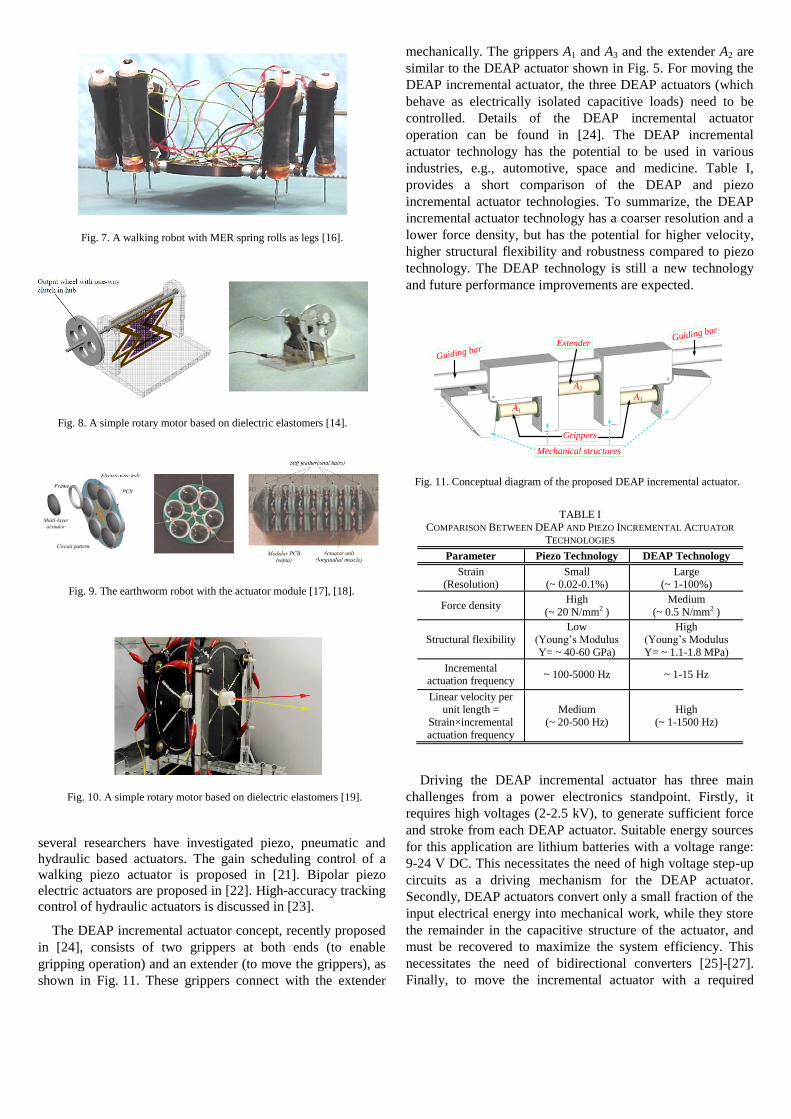
several researchers have investigated piezo, pneumatic and
hydraulic based actuators. The gain scheduling control of a
walking piezo actuator is proposed in [21]. Bipolar piezo
electric actuators are proposed in [22]. High-accuracy tracking
control of hydraulic actuators is discussed in [23].
The DEAP incremental actuator concept, recently proposed
in [24], consists of two grippers at both ends (to enable
gripping operation) and an extender (to move the grippers), as
shown in Fig. 11. These grippers connect with the extender
mechanically. The grippers A1 and A3 and the extender A2 are
similar to the DEAP actuator shown in Fig. 5. For moving the
DEAP incremental actuator, the three DEAP actuators (which
behave as electrically isolated capacitive loads) need to be
controlled. Details of the DEAP incremental actuator
operation can be found in [24]. The DEAP incremental
actuator technology has the potential to be used in various
industries, e.g., automotive, space and medicine. Table I,
provides a short comparison of the DEAP and piezo
incremental actuator technologies. To summarize, the DEAP
incremental actuator technology has a coarser resolution and a
lower force density, but has the potential for higher velocity,
higher structural flexibility and robustness compared to piezo
technology. The DEAP technology is still a new technology
and future performance improvements are expected.
Driving the DEAP incremental actuator has three main
challenges from a power electronics standpoint. Firstly, it
requires high voltages (2-2.5 kV), to generate sufficient force
and stroke from each DEAP actuator. Suitable energy sources
for this application are lithium batteries with a voltage range:
9-24 V DC. This necessitates the need of high voltage step-up
circuits as a driving mechanism for the DEAP actuator.
Secondly, DEAP actuators convert only a small fraction of the
input electrical energy into mechanical work, while they store
the remainder in the capacitive structure of the actuator, and
must be recovered to maximize the system efficiency. This
necessitates the need of bidirectional converters [25]-[27].
Finally, to move the incremental actuator with a required
Fig. 9. The earthworm robot with the actuator module [17], [18].
A1
A3
A2
Grippers
Extender
Guiding bar
Guiding bar
Mechanical structures
Fig. 11. Conceptual diagram of the proposed DEAP incremental actuator.
Fig. 10. A simple rotary motor based on dielectric elastomers [19].
Fig. 8. A simple rotary motor based on dielectric elastomers [14].
Fig. 7. A walking robot with MER spring rolls as legs [16].
TABLE I
COMPARISON BETWEEN DEAP AND PIEZO INCREMENTAL ACTUATOR
TECHNOLOGIES
Parameter Piezo Technology DEAP Technology
Strain (Resolution)
Small (~ 0.02-0.1%)
Large (~ 1-100%)
Force density High
(~ 20 N/mm2 )
Medium
(~ 0.5 N/mm2 )
Structural flexibility
Low
(Young’s Modulus
Y= ~ 40-60 GPa)
High
(Young’s Modulus
Y= ~ 1.1-1.8 MPa)
Incremental actuation frequency
~ 100-5000 Hz ~ 1-15 Hz
Linear velocity per unit length =
Strain×incremental
actuation frequency
Medium
(~ 20-500 Hz)
High
(~ 1-1500 Hz)
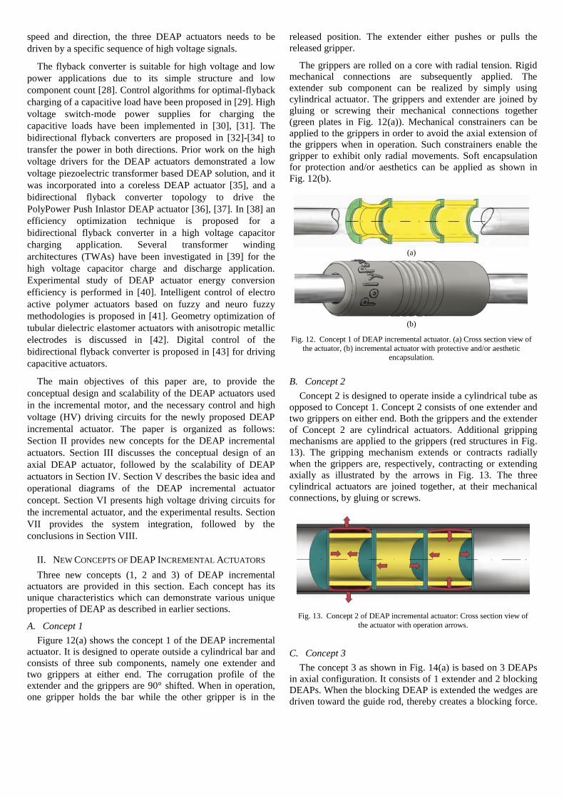
speed and direction, the three DEAP actuators needs to be
driven by a specific sequence of high voltage signals.
The flyback converter is suitable for high voltage and low
power applications due to its simple structure and low
component count [28]. Control algorithms for optimal-flyback
charging of a capacitive load have been proposed in [29]. High
voltage switch-mode power supplies for charging the
capacitive loads have been implemented in [30], [31]. The
bidirectional flyback converters are proposed in [32]-[34] to
transfer the power in both directions. Prior work on the high
voltage drivers for the DEAP actuators demonstrated a low
voltage piezoelectric transformer based DEAP solution, and it
was incorporated into a coreless DEAP actuator [35], and a
bidirectional flyback converter topology to drive the
PolyPower Push Inlastor DEAP actuator [36], [37]. In [38] an
efficiency optimization technique is proposed for a
bidirectional flyback converter in a high voltage capacitor
charging application. Several transformer winding
architectures (TWAs) have been investigated in [39] for the
high voltage capacitor charge and discharge application.
Experimental study of DEAP actuator energy conversion
efficiency is performed in [40]. Intelligent control of electro
active polymer actuators based on fuzzy and neuro fuzzy
methodologies is proposed in [41]. Geometry optimization of
tubular dielectric elastomer actuators with anisotropic metallic
electrodes is discussed in [42]. Digital control of the
bidirectional flyback converter is proposed in [43] for driving
capacitive actuators.
The main objectives of this paper are, to provide the
conceptual design and scalability of the DEAP actuators used
in the incremental motor, and the necessary control and high
voltage (HV) driving circuits for the newly proposed DEAP
incremental actuator. The paper is organized as follows:
Section II provides new concepts for the DEAP incremental
actuators. Section III discusses the conceptual design of an
axial DEAP actuator, followed by the scalability of DEAP
actuators in Section IV. Section V describes the basic idea and
operational diagrams of the DEAP incremental actuator
concept. Section VI presents high voltage driving circuits for
the incremental actuator, and the experimental results. Section
VII provides the system integration, followed by the
conclusions in Section VIII.
II. NEW CONCEPTS OF DEAP INCREMENTAL ACTUATORS
Three new concepts (1, 2 and 3) of DEAP incremental
actuators are provided in this section. Each concept has its
unique characteristics which can demonstrate various unique
properties of DEAP as described in earlier sections.
A. Concept 1
Figure 12(a) shows the concept 1 of the DEAP incremental
actuator. It is designed to operate outside a cylindrical bar and
consists of three sub components, namely one extender and
two grippers at either end. The corrugation profile of the
extender and the grippers are 90° shifted. When in operation,
one gripper holds the bar while the other gripper is in the
released position. The extender either pushes or pulls the
released gripper.
The grippers are rolled on a core with radial tension. Rigid
mechanical connections are subsequently applied. The
extender sub component can be realized by simply using
cylindrical actuator. The grippers and extender are joined by
gluing or screwing their mechanical connections together
(green plates in Fig. 12(a)). Mechanical constrainers can be
applied to the grippers in order to avoid the axial extension of
the grippers when in operation. Such constrainers enable the
gripper to exhibit only radial movements. Soft encapsulation
for protection and/or aesthetics can be applied as shown in
Fig. 12(b).
B. Concept 2
Concept 2 is designed to operate inside a cylindrical tube as
opposed to Concept 1. Concept 2 consists of one extender and
two grippers on either end. Both the grippers and the extender
of Concept 2 are cylindrical actuators. Additional gripping
mechanisms are applied to the grippers (red structures in Fig.
13). The gripping mechanism extends or contracts radially
when the grippers are, respectively, contracting or extending
axially as illustrated by the arrows in Fig. 13. The three
cylindrical actuators are joined together, at their mechanical
connections, by gluing or screws.
C. Concept 3
The concept 3 as shown in Fig. 14(a) is based on 3 DEAPs
in axial configuration. It consists of 1 extender and 2 blocking
DEAPs. When the blocking DEAP is extended the wedges are
driven toward the guide rod, thereby creates a blocking force.
Fig. 13. Concept 2 of DEAP incremental actuator: Cross section view of
the actuator with operation arrows.
(a)
(b)
Fig. 12. Concept 1 of DEAP incremental actuator. (a) Cross section view of
the actuator, (b) incremental actuator with protective and/or aesthetic encapsulation.
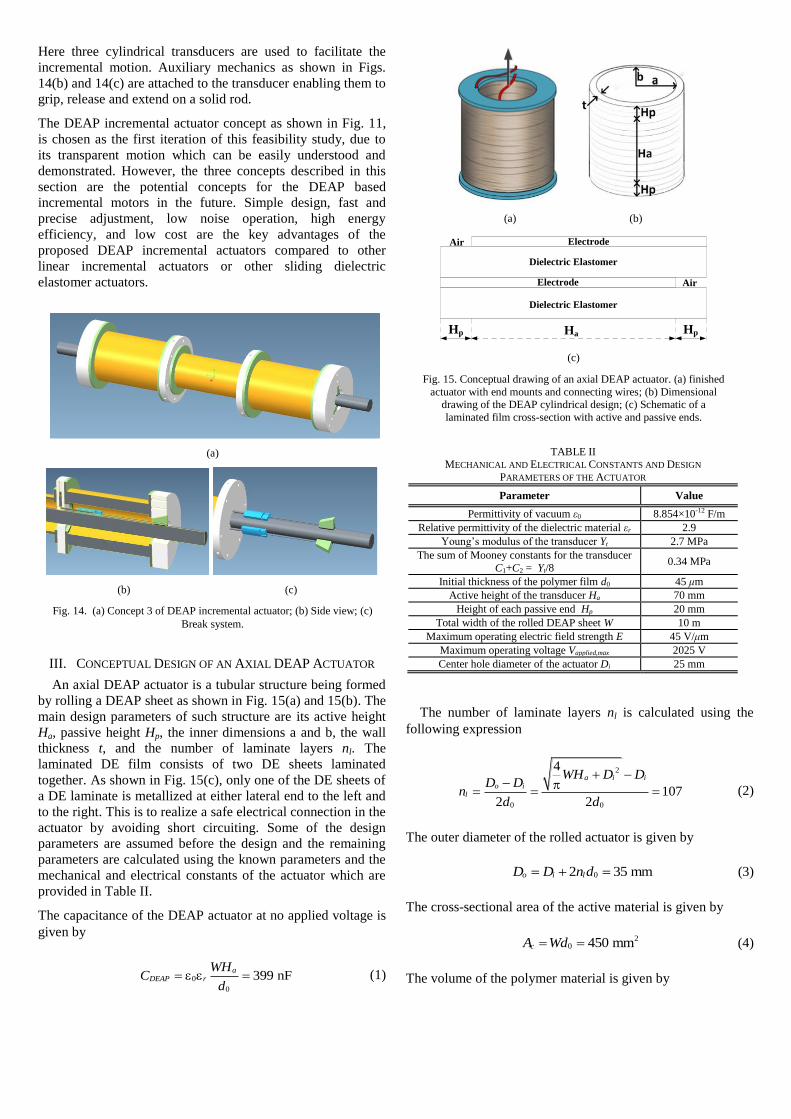
Here three cylindrical transducers are used to facilitate the
incremental motion. Auxiliary mechanics as shown in Figs.
14(b) and 14(c) are attached to the transducer enabling them to
grip, release and extend on a solid rod.
The DEAP incremental actuator concept as shown in Fig. 11,
is chosen as the first iteration of this feasibility study, due to
its transparent motion which can be easily understood and
demonstrated. However, the three concepts described in this
section are the potential concepts for the DEAP based
incremental motors in the future. Simple design, fast and
precise adjustment, low noise operation, high energy
efficiency, and low cost are the key advantages of the
proposed DEAP incremental actuators compared to other
linear incremental actuators or other sliding dielectric
elastomer actuators.
III. CONCEPTUAL DESIGN OF AN AXIAL DEAP ACTUATOR
An axial DEAP actuator is a tubular structure being formed
by rolling a DEAP sheet as shown in Fig. 15(a) and 15(b). The
main design parameters of such structure are its active height
Ha, passive height Hp, the inner dimensions a and b, the wall
thickness t, and the number of laminate layers nl. The
laminated DE film consists of two DE sheets laminated
together. As shown in Fig. 15(c), only one of the DE sheets of
a DE laminate is metallized at either lateral end to the left and
to the right. This is to realize a safe electrical connection in the
actuator by avoiding short circuiting. Some of the design
parameters are assumed before the design and the remaining
parameters are calculated using the known parameters and the
mechanical and electrical constants of the actuator which are
provided in Table II.
The capacitance of the DEAP actuator at no applied voltage is
given by
0
0
399 nFa
DEAP r
WHC
d (1)
The number of laminate layers nl is calculated using the
following expression
2
0 0
4
1072 2
a i io i
l
WH D DD D
nd d
(2)
The outer diameter of the rolled actuator is given by
02 35 mmo i lD D n d (3)
The cross-sectional area of the active material is given by
20 450 mmcA Wd (4)
The volume of the polymer material is given by
TABLE II MECHANICAL AND ELECTRICAL CONSTANTS AND DESIGN
PARAMETERS OF THE ACTUATOR
Parameter Value
Permittivity of vacuum ε0 8.854×10⁻¹² F/m
Relative permittivity of the dielectric material εr 2.9
Young’s modulus of the transducer Yt 2.7 MPa
The sum of Mooney constants for the transducer
C1+C2 = Yt/8 0.34 MPa
Initial thickness of the polymer film d0 45 μm
Active height of the transducer Ha 70 mm
Height of each passive end Hp 20 mm
Total width of the rolled DEAP sheet W 10 m
Maximum operating electric field strength E 45 V/μm
Maximum operating voltage Vapplied,max 2025 V
Center hole diameter of the actuator Di 25 mm
(a)
(b) (c)
Fig. 14. (a) Concept 3 of DEAP incremental actuator; (b) Side view; (c)
Break system.
(a) (b)
Dielectric Elastomer
Dielectric Elastomer
Electrode
Electrode
Air
Air
Hp Ha Hp
(c)
Fig. 15. Conceptual drawing of an axial DEAP actuator. (a) finished
actuator with end mounts and connecting wires; (b) Dimensional drawing of the DEAP cylindrical design; (c) Schematic of a
laminated film cross-section with active and passive ends.

20 49.5 cmc a pV Wd H H (5)
The equation governing the electrostatic ElectrostaticF , elastic
ElasticF and load forces loadF in a DEAP actuator system as
shown in Fig. 16, during static operation is given by
Electrostatic Elastic loadF F F (6)
Equation (6) can be simplified as [6], [44], [45]
2
2 2 20 1 2
0
2( )DEAP
r c c load
VA C C A F
d
(7)
VDEAP is the applied voltage to the DEAP actuator, α
represents the stretch (elongation) ratio and is defined as,
α=1+s, where s is the strain in the compliant direction. In this
case, the influence of passive ends has been ignored, as the
displacement between passive ends and active area is much
smaller than the stroke of the transducer.
2
2 2 20 1 2
0
2( )DEAP load
r
c
V FC C
d A
(8)
The output force of the actuator is given by
2
2 2 20 1 2
0
2( )DEAP load c
output r
c
V F AF C C
d A
(9)
Since the displacement between the active area and passive
area is limited, so we could assume that they are linear
material, and passive area has the same modulus of elasticity
as that of active area. In the equilibrium position, the stress on
the passive area should be equal to the stress of the active
area:
2
0
0
2DEAPt r t
p a
L V LY Y
H d H
(10)
The displacement L between the active area and the passive
end is
2
0
0
1 2
DEAPr
t
p a
V
dL
YH H
(11)
Blocking force can be reduced by passive ends of the
transducer, due to the displacement between the passive area
and the active area. The blocking force is given by the
following expression,
2
0 0 0
0
2DEAPblocking r t t
a p
V L LF Y Wh Y Wh
d H H
(12)
The operating region of a DEAP actuator can be
represented by the relationship between its force, stroke and
applied voltage (or electric field strength). The force-stroke,
stroke-voltage and force-electric field strength characteristics
of the axial DEAP actuator which is designed above, are
shown in Figs. 17, 18 and 19, respectively. As shown in Fig.
17, to achieve a certain stroke, the output force of the actuator
decreases with the applied voltage. Also, for a given applied
voltage, the output force drops as the actuator elongates. The
variation of the stroke and strain of the DEAP actuator as a
function of the applied voltage are shown in Fig. 18. The
FElectrostatic
FElastic FLoad
Fig. 16. Force balance of DEAP actuator element in static operation.
200 400 600 800 1000 1200 1400 1600 1800 2000
0.25
0.5
0.75
1
1.25
1.5
1.75
2
VDEAP
(V)
Str
ok
e (m
m)
200 400 600 800 1000 1200 1400 1600 1800 2000 2200
0.25
0.5
0.75
1
1.25
1.5
1.75
2
Str
ain
(%
)
Stroke
Strain
Fig. 18. Modelled actuator stroke and strain as a function of applied
voltage.
0.2 0.4 0.6 0.8 1 1.2 1.4
5
10
15
20
25
Stroke (mm)
Fo
utp
ut (
N)
VDEAP
=2025 V
VDEAP
=1800 V
VDEAP
=1500 V
VDEAP
=1000 V
Fig. 17. Modelled actuator output force as a function of stroke for
different maximum applied voltages (Fload=0 N).

blocking forces of the actuator with and without passive ends
in the design of actuator are shown in Fig. 19. From Fig. 19, it
is clear that the blocking force is lower for the actuator which
has passive ends, compared to the actuator without passive
ends.
IV. SCALABILITY OF DEAP ACTUATORS
One of the unique features of DEAP actuator elements is
their ease of scaling. DEAP actuator elements can be scaled up
to provide larger actuation forces by increasing the cross
section areas as shown in Figs. 20(a) and 20(b), i.e. rolling
more DEAP material. Similarly, DEAP actuator elements can
be scaled up easily to provide larger actuation stroke by
increasing the length of the DEAP actuator element (Fig. 20).
The up scaling can also be achieved by connecting multiple
actuator elements in series or parallel resulting in larger stroke
or force, respectively.
To investigate the scalability of the DEAP incremental
actuator, 3 designs as shown in Table III, are considered. The
reference design parameters are provided in Section III. In the
design 1, the actuator’s height is reduced by 10 times, by
keeping the area of cross-section same as the reference design.
In the design 2, the area of cross-section of the actuator is
reduced by 10 times, by keeping its length the same as the
reference. The design 3 is made by reducing both the
actuator’s length and its area of cross-section by 10 times. The
characteristics of designs 1 and 2 are shown in Figs. 21, 22,
and 23, 24, respectively. Similarly, the characteristics of
design 3 are provided in Fig. 25.
For the design 1, since the actuator’s length is reduced by
10 times, the stroke as shown in Fig. 21 is very low, even at 2
kV. Since the area of cross-section is not changed the output
force is not reduced as shown in Fig. 22. For the design 2,
since the area of cross-section is reduced by 10 times, the
output force is reduced as shown in Fig. 23, but the stroke
remains the same as the reference design. The blocking force
is also reduced for the design 2, as shown in Fig. 24.
Similarly, for the design 3, the force-stroke characteristics are
shown in Fig. 25, in which the stroke and force both are
reduced. In Fig. 25, the actuator when driven with 1.8 kV can
only produce 1 N output force for a stroke of 0.05 mm.
5 10 15 20 25 30 35 40 45
2.5
5
7.5
10
12.5
15
17.5
20
22.5
25
Applied electric field strength(V/um)
Fb
lock
(N)
with passive ends
without passive ends
Fig. 19. Modelled blocking force as a function of applied electric field
strength.
a)
b)
Fig. 20. Rolled structure construction, a) Electrode elasticity allows axial
actuation. b) Electrode elasticity allows radial actuation.
TABLE III DESIGN PARAMETERS OF THE SCALED DEAP ACTUATOR
Parameter Scaled
design 1
Scaled
design 2
Scaled
design 3
Active height of the
transducer Ha 7 mm 70 mm 7 mm
Height of each passive
end Hp 2 mm 20 mm 2 mm
Total width of the
rolled DEAP sheet W 10 m 1 m 1 m
Center hole diameter of the actuator Di
25 mm 4 mm 4 mm
The outer diameter of
the actuator Do 35 mm 9 mm 9 mm
Capacitance of the actuator CDEAP
39.9 nF 39.9 nF 3.99 nF
Number of layers of
laminate nl 107 51 51
Area of cross section
of active DEAP Ac 450 mm2 45 mm2 45 mm2

V. CONTROL OF INCREMENTAL MOTOR
The DEAP incremental actuator consists of three axial DEAP
actuators (one extender and two grippers). The incremental
actuation sequence and the driving voltage waveforms for the
grippers and the extender are shown in Figs. 26 and 27,
respectively [24]. Each gripper is connected to mechanical
supports on either side. It expands and clamps to the guiding
bar (e.g., a rod) surface when charged (with high voltage), and
unfastens from it, when discharged. The extender expands
axially along the guiding bar. During the operation, one
gripper holds the guiding bar while the other gripper is in a
released position. The extender either pushes or pulls the
released gripper. The incremental actuator performs 6
different steps, to achieve a single incremental actuation stroke
Δx as shown in Fig. 26.
A. Moving sequence of the linear incremental motion
towards the positive x-axis direction
1. Start: All actuators are in the discharged state.
2. Step 0 (S0): A1 is charged and clamps to the guiding
bar. A2 and A3 are in the discharged state.
3. Step 1 (S1): A1 remains in the charged state. A2 is
charged and pushes the mechanical structure towards
right, and A3 remains in the discharged state.
4. Step 2 (S2): A1 and A2 still remain in the charged state.
A3 is charged.
5. Step 3 (S3): A1 is discharged and is in the released
position. A2 and A3 still remain in the charged state.
6. Step 4 (S4): A1 remains in the discharged state. A2 is
discharged, and A3 remains in the charged state.
7. Step 5 (S5): A1 is charged. A2 remains in the discharged
state, and A3 remains in the charged state.
8. Step 6 (S6): A1 remains in the charged state. A2 remains
in the discharged state, and A3 is discharged.
9. End: All actuators are discharged at the end.
The Step 0 is only used for charging the actuator A1. The
Steps 1-6 (S1-S6) repeat for achieving continuous incremental
0 0.02 0.04 0.06 0.08 0.1 0.12 0.140
5
10
15
20
25
Stroke (mm)
Fo
utp
ut (
N)
VDEAP
=2025 V
VDEAP
=1800 V
VDEAP
=1500 V
VDEAP
=1000 V
Fig. 22. Actuator output force as a function of stroke for different
maximum applied voltages for the scaled design 1.
0 0.02 0.04 0.06 0.08 0.1 0.12 0.140
0.5
1
1.5
2
2.5
Stroke (mm)
Fo
utp
ut (
N)
VDEAP
=2025 V
VDEAP
=1800 V
VDEAP
=1500 V
VDEAP
=1000 V
Fig. 25. Actuator output force as a function of stroke for different
maximum applied voltages for the scaled design 3.
0.1 0.2 0.3 0.4 0.5 0.6 0.7 0.8 0.9 1 1.1 1.2 1.3 1.4
0.25
0.5
0.75
1
1.25
1.5
1.75
2
2.25
2.5
Stroke (mm)
Fo
utp
ut (
N)
VDEAP
=2025 V
VDEAP
=1800 V
VDEAP
=1500 V
VDEAP
=1000 V
Fig. 23. Actuator output force as a function of stroke for different maximum
applied voltages for the scaled design 2.
200 400 600 800 1000 1200 1400 1600 1800 2000
0.025
0.05
0.075
0.1
0.125
0.15
0.175
0.2
Applied voltage (V)
Str
oke
(mm
)
200 400 600 800 1000 1200 1400 1600 1800 2000
0.25
0.5
0.75
1
1.25
1.5
1.75
2
Str
ain (
%)
Stroke
Strain
Fig. 21. Actuator stroke and strain as a function of applied voltage for the
scaled design 1.
5 10 15 20 25 30 35 40 45
0.25
0.5
0.75
1
1.25
1.5
1.75
2
2.25
2.5
Applied electric field strength (V/um)
Fb
lock
(N
)
with passive ends
without passive ends
Fig. 24. Blocking force as a function of applied electric field strength for
the scaled design 2.

actuation cycles. The End step is used to discharge all
actuators. The moving sequence for the reverse linear
incremental motion towards the negative x-axis direction can
be easily drawn similar to Fig. 26. For moving towards the
negative x-axis (reverse) direction, the driving voltages of
actuators A1 and A3 need to be reversed, without changing the
driving voltage of actuator A2. The driving voltages for
moving with the certain incremental driving frequency are
shown in Fig. 27. To move the actuator with maximum
incremental frequency, zero delay (tD=0) needs to be provided
between the charge and discharge cycles of actuators A1, A2
and A3.
B. Incremental driving frequency
Assuming the same charging Tch and discharging Tdch times
for all DEAP actuators, the maximum incremental driving
frequency increment_maxf or minimum incremental period
increment _ minT is given by
1 1
6increment _ max
ch dch increment _ min
fT T T
(13)
The incremental actuator speed can be changed, by proving a
delay tD between the charge and discharge cycles of actuators
A1, A2, and A3. The expression for the variable incremental
driving frequency incrementf or variable incremental period
incrementT is given by
1 1
6 6increment
ch dch D increment
fT T t T
(14)
When the DEAP incremental actuator is loaded during the
operation, the delay between the steps S1 and S2 can be
skipped. This can prevent pulling of the incremental actuator
by the load when actuator A2 is charged.
It is very interesting to estimate the velocity of the DEAP
incremental actuator for the scaled axial DEAP actuators.
Figure 28 provides the estimated velocity as a function of the
incremental drive frequency (see Eq. (14)) for all designs
discussed in Sections III and IV. The viscous effects of the
polymer material have been neglected. The speed of the
incremental motor for the reference design and each scaled
design is estimated when all actuators are driven with 1.8 kV.
Furthermore, the speed is estimated at a given output force and
0S0
t
0
0
t
t
2.5 kV
2.5 kV
2.5 kV2.5 kV
Start
2AV
1AV
3AV
1chV
3chV
5chV
2chV
4chV
6chV
0
0
0
0
0
0
t
t
t
t
t
t
tD
1increment
increment
Tf
tDS1 S2 tD S3 tD S4 tD S5 tD S6 tD S1
Tch Tdch
5 V 5 V
5 V 5 V
5 V
5 V
5 V
5 V
Fig. 27. Enable signals and driving voltages of all DEAP actuators, to
achieve the incremental motion with variable speed, towards the positive x-axis direction.
Charging
Step 6
Incremental actuator moving
in the direction of the positive x-axis
Step 1
Step 2
A1
Step 3
Step 4
Step 5
A3
A2
A1
A1
A3
A2
A2A3
A2A3
A3A1
A2
A3A1
A2
A1
x
A3
A2A1
Start
Step 0
A1
A2A3
Ste
p 1
– S
tep
6
Discharging
A3
A2A1
End
Distance
(mm)
Loop
repeats
Clamp: A1
Push: A2
Clamp: A3
Release: A1
Pull: A2
Clamp: A1
Release: A3
Fig. 26. Moving sequence of the DEAP incremental actuator for incremental motion towards the positive x-axis direction.
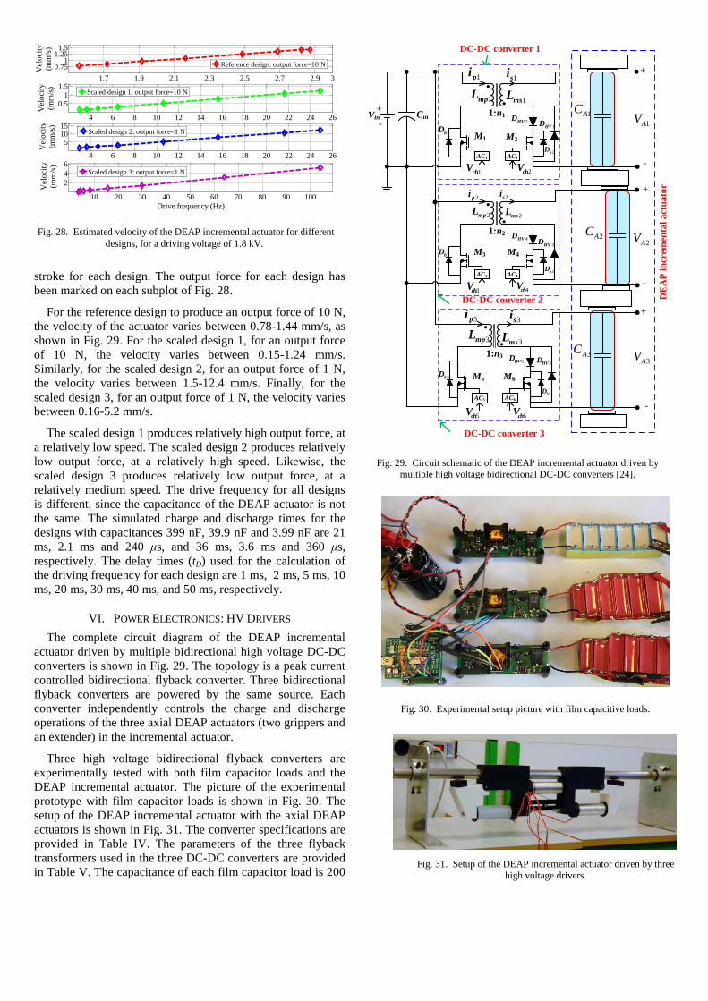
stroke for each design. The output force for each design has
been marked on each subplot of Fig. 28.
For the reference design to produce an output force of 10 N,
the velocity of the actuator varies between 0.78-1.44 mm/s, as
shown in Fig. 29. For the scaled design 1, for an output force
of 10 N, the velocity varies between 0.15-1.24 mm/s.
Similarly, for the scaled design 2, for an output force of 1 N,
the velocity varies between 1.5-12.4 mm/s. Finally, for the
scaled design 3, for an output force of 1 N, the velocity varies
between 0.16-5.2 mm/s.
The scaled design 1 produces relatively high output force, at
a relatively low speed. The scaled design 2 produces relatively
low output force, at a relatively high speed. Likewise, the
scaled design 3 produces relatively low output force, at a
relatively medium speed. The drive frequency for all designs
is different, since the capacitance of the DEAP actuator is not
the same. The simulated charge and discharge times for the
designs with capacitances 399 nF, 39.9 nF and 3.99 nF are 21
ms, 2.1 ms and 240 μs, and 36 ms, 3.6 ms and 360 μs,
respectively. The delay times (tD) used for the calculation of
the driving frequency for each design are 1 ms, 2 ms, 5 ms, 10
ms, 20 ms, 30 ms, 40 ms, and 50 ms, respectively.
VI. POWER ELECTRONICS: HV DRIVERS
The complete circuit diagram of the DEAP incremental
actuator driven by multiple bidirectional high voltage DC-DC
converters is shown in Fig. 29. The topology is a peak current
controlled bidirectional flyback converter. Three bidirectional
flyback converters are powered by the same source. Each
converter independently controls the charge and discharge
operations of the three axial DEAP actuators (two grippers and
an extender) in the incremental actuator.
Three high voltage bidirectional flyback converters are
experimentally tested with both film capacitor loads and the
DEAP incremental actuator. The picture of the experimental
prototype with film capacitor loads is shown in Fig. 30. The
setup of the DEAP incremental actuator with the axial DEAP
actuators is shown in Fig. 31. The converter specifications are
provided in Table IV. The parameters of the three flyback
transformers used in the three DC-DC converters are provided
in Table V. The capacitance of each film capacitor load is 200
1:n1Cin
+
-Vin
+
-
M1 M2
1:n2
+
-
M3 M4
1:n3
+
-
M5 M6
DE
AP
in
crem
enta
l act
uato
r
AC1 AC2
AC3 AC4
AC5 AC6
DC-DC converter 1
DC-DC converter 2
1AC
2AC
3AC
1HVD2HV
D
3HVD
4HVD
1chV 2ch
V
5HVD
1bD
3bD
5bD
DC-DC converter 3
1pi
1si
1AV
2pi 2s
i
3chV 4ch
V
2AV
3AV
3pi
3si
6HVD
2bD
4bD
6bD
5chV 6ch
V
1mpL
1msL
2mpL
2msL
3mpL
3msL
Fig. 29. Circuit schematic of the DEAP incremental actuator driven by
multiple high voltage bidirectional DC-DC converters [24].
Fig. 30. Experimental setup picture with film capacitive loads.
1.
1.7 1.9 2.1 2.3 2.5 2.7 2.9 3
0.751
1.251.5
Vel
oci
ty
(mm
/s)
4 6 8 10 12 14 16 18 20 22 24 26
0.51
1.5
Vel
oci
ty
(mm
/s)
4 6 8 10 12 14 16 18 20 22 24 26
51015
Vel
oci
ty
(mm
/s)
10 20 30 40 50 60 70 80 90 100
2
4
6
Drive frequency (Hz)
Vel
oci
ty
(mm
/s)
Scaled design 3: output force=1 N
Scaled design 2: output force=1 N
Scaled design 1: output force=10 N
Reference design: output force=10 N
Fig. 28. Estimated velocity of the DEAP incremental actuator for different
designs, for a driving voltage of 1.8 kV.
Fig. 31. Setup of the DEAP incremental actuator driven by three
high voltage drivers.
2.
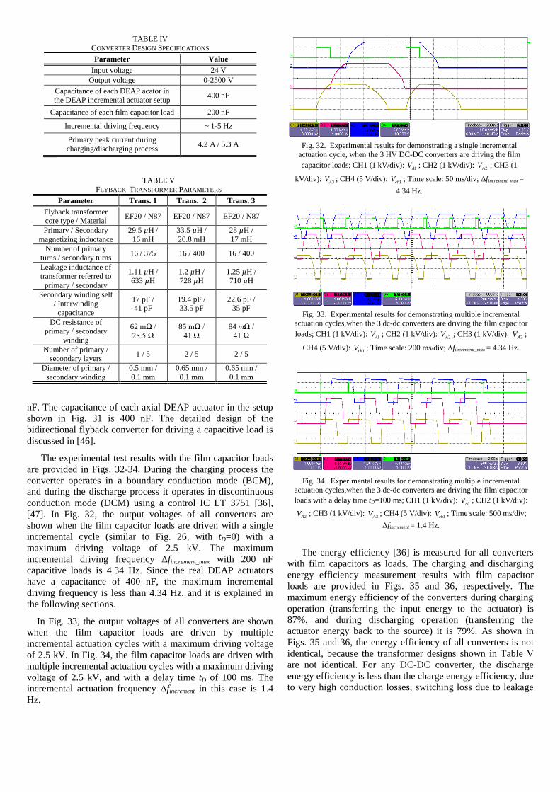
nF. The capacitance of each axial DEAP actuator in the setup
shown in Fig. 31 is 400 nF. The detailed design of the
bidirectional flyback converter for driving a capacitive load is
discussed in [46].
The experimental test results with the film capacitor loads
are provided in Figs. 32-34. During the charging process the
converter operates in a boundary conduction mode (BCM),
and during the discharge process it operates in discontinuous
conduction mode (DCM) using a control IC LT 3751 [36],
[47]. In Fig. 32, the output voltages of all converters are
shown when the film capacitor loads are driven with a single
incremental cycle (similar to Fig. 26, with tD=0) with a
maximum driving voltage of 2.5 kV. The maximum
incremental driving frequency Δfincrement_max with 200 nF
capacitive loads is 4.34 Hz. Since the real DEAP actuators
have a capacitance of 400 nF, the maximum incremental
driving frequency is less than 4.34 Hz, and it is explained in
the following sections.
In Fig. 33, the output voltages of all converters are shown
when the film capacitor loads are driven by multiple
incremental actuation cycles with a maximum driving voltage
of 2.5 kV. In Fig. 34, the film capacitor loads are driven with
multiple incremental actuation cycles with a maximum driving
voltage of 2.5 kV, and with a delay time tD of 100 ms. The
incremental actuation frequency Δfincrement in this case is 1.4
Hz.
The energy efficiency [36] is measured for all converters
with film capacitors as loads. The charging and discharging
energy efficiency measurement results with film capacitor
loads are provided in Figs. 35 and 36, respectively. The
maximum energy efficiency of the converters during charging
operation (transferring the input energy to the actuator) is
87%, and during discharging operation (transferring the
actuator energy back to the source) it is 79%. As shown in
Figs. 35 and 36, the energy efficiency of all converters is not
identical, because the transformer designs shown in Table V
are not identical. For any DC-DC converter, the discharge
energy efficiency is less than the charge energy efficiency, due
to very high conduction losses, switching loss due to leakage
TABLE IV
CONVERTER DESIGN SPECIFICATIONS
Parameter Value
Input voltage 24 V
Output voltage 0-2500 V
Capacitance of each DEAP acator in the DEAP incremental actuator setup
400 nF
Capacitance of each film capacitor load 200 nF
Incremental driving frequency ~ 1-5 Hz
Primary peak current during
charging/discharging process 4.2 A / 5.3 A
3. TABLE V
FLYBACK TRANSFORMER PARAMETERS
Parameter Trans. 1 Trans. 2 Trans. 3
Flyback transformer core type / Material
EF20 / N87 EF20 / N87 EF20 / N87
Primary / Secondary
magnetizing inductance
29.5 µH /
16 mH
33.5 µH /
20.8 mH
28 µH /
17 mH
Number of primary turns / secondary turns
16 / 375 16 / 400 16 / 400
Leakage inductance of
transformer referred to
primary / secondary
1.11 µH / 633 µH
1.2 µH / 728 µH
1.25 µH / 710 µH
Secondary winding self
/ Interwinding
capacitance
17 pF / 41 pF
19.4 pF / 33.5 pF
22.6 pF / 35 pF
DC resistance of primary / secondary
winding
62 mΩ /
28.5 Ω
85 mΩ /
41 Ω
84 mΩ /
41 Ω
Number of primary / secondary layers
1 / 5 2 / 5 2 / 5
Diameter of primary /
secondary winding
0.5 mm /
0.1 mm
0.65 mm /
0.1 mm
0.65 mm /
0.1 mm
Fig. 32. Experimental results for demonstrating a single incremental
actuation cycle, when the 3 HV DC-DC converters are driving the film
capacitor loads; CH1 (1 kV/div): 1AV ; CH2 (1 kV/div):
2AV ; CH3 (1
kV/div): 3AV ; CH4 (5 V/div):
1chV ; Time scale: 50 ms/div; Δfincrement_max =
4.34 Hz.
Fig. 33. Experimental results for demonstrating multiple incremental
actuation cycles,when the 3 dc-dc converters are driving the film capacitor
loads; CH1 (1 kV/div): 1AV ; CH2 (1 kV/div):
2AV ; CH3 (1 kV/div): 3AV ;
CH4 (5 V/div): 1chV ; Time scale: 200 ms/div; Δfincrement_max = 4.34 Hz.
Fig. 34. Experimental results for demonstrating multiple incremental
actuation cycles,when the 3 dc-dc converters are driving the film capacitor
loads with a delay time tD=100 ms; CH1 (1 kV/div): 1AV ; CH2 (1 kV/div):
2AV ; CH3 (1 kV/div): 3AV ; CH4 (5 V/div):
1chV ; Time scale: 500 ms/div;
Δfincrement = 1.4 Hz.

inductance and capacitive switching losses of the HV
MOSFET.
Practical experience reveals that careful design of the
flyback transformer with low leakage inductance and low self-
capacitance is required for achieving high energy efficiency in
high voltage bidirectional operation. The HV MOSFET used
for this research is IXTV03N400S (4 kV, 300 mA, 290 Ω)
[48]. The available high voltage MOSFET for this application,
in the current market is IXTA02N450HV (4.5 kV, 200 mA,
750 Ω) [49]. The HV diode used in the converter is SXF 6525
(5 kV, 150 mA, 70 ns (trr)) [50]. The improper HV flyback
transformer designs may lead to failure of the HV MOSFET
during the discharging operation.
VII. SYSTEM INTEGRATION
A. Incremental motion with different speeds
The integrated system as shown in Fig. 31 is tested for its
variable speed and repeatability. 100 increments are generated
using the digital controller, and the total displacement and
travel time are recorded. The applied voltage level is fixed to a
maximum of 1.8 kV to avoid any potential damage to the
transducers. Table VI provides the acquired data of the
experiments. It can be seen that the system has a repeatability
within 5% (of stroke) for different speeds.
B. Bidirectional motion:
The above test is repeated with a maximum voltage of 1.7
kV for bidirectional motion at three different speed settings
(delay times tD) in the controller. Table VII provides the
results which indicate a larger total displacement in the
forward motion compared to the reverse motion.
C. Discussion
In Fig. 37 the sequential DEAP incremental actuator images
are provided when it moved with a maximum speed of 1.5
mm/s. The DEAP incremental actuator system indicated a
non-repeatable motion when operated bidirectional resulting
in a drift from original position. This drift increased with the
number of bidirectional iterations resulting in an even larger
drift from original position. Such drift might be primarily
caused by non-identical grippers differing in their gripping
force. As the extending transducer is activated, it excites both
grippers with the same force. The activated gripper should
have enough gripping force, to not slip backward due to
transient forces generated by the extender. If the two grippers
have different gripping force, the one with smaller force will
exhibit larger backward slipping resulting cumulatively in a
drift of the whole system from the original position. The
performance specifications of the several designed
incremental motors are summarized in Table VIII. The
reference design has the highest volume, maximum output
force, and the scaled design 3 has the lowest volume and
minimum output force. The scaled design 2 has maximum
0 250 500 750 1000 1250 1500 1750 2000 2250 2500
20
40
60
80
100
Output Voltage (Volts)
Dis
charg
ing E
nerg
y E
ffic
iency (
%)
Discharging energy efficiency: converter 1
Discharging energy efficiency: converter 2
Discharging energy efficiency: converter 3
Fig. 36. Discharging energy efficiency measurement results of three
high voltage converters.
0 250 500 750 1000 1250 1500 1750 2000 2250 250060
70
80
90
100
Output Voltage (Volts)
Charg
ing E
nerg
y E
ffic
iency (
%)
Charging energy efficiency: converter 1
Charging energy efficiency: converter 2
Charging energy efficiency: converter 3
Fig. 35. Charging energy efficiency measurement results of three high
voltage converters.
TABLE VI EXPERIMENTAL DATA OF DEAP INCREMENTAL ACTUATOR MOVING
WITH DIFFERENT SPEEDS TO ACHIEVE 100 INCREMENTS/STEPS
Total travel*
(mm)
Total travel
time (s)
Delay time tD
(ms)
Average Speed
(mm/s)
Increment
size /
stroke per step (mm)
Incremental
driving
frequency Δfincrement (Hz)
39 50 50 0.78 0.39 1.55
39 45 40 0.86 0.39 1.72
39 40 30 0.97 0.39 1.91
38 35 20 1.07 0.38 2.16
40 30 10 1.33 0.40 2.49
40 28 5 1.43 0.40 2.68
39 25 2 1.56 0.39 2.82
39 26 1 1.50 0.39 2.87
*All 3 DEAP actuators are driven with a maximum voltage of 1.8 kV.
Charging time Tch=22 ms, discharging time Tdch=36 ms.
TABLE VII
EXPERIMENTAL DATA FROM BIDIRECTIONAL DEAP INCREMENTAL
ACTUATOR TESTS FOR 100 INCREMENTS
Direction
of movement
Total
travel* (mm)
Total travel
time (s)
Delay
time tD
(ms)
Average
Speed (mm/s)
Incremental
driving
frequency Δfincrement
(Hz)
Forward 40 71 100 0.56 1.08
Forward 44 35 10 1.26 2.60
Forward 43.7 32 1 1.36 3.03
Reverse 37 71 100 0.52 1.08
Reverse 41 41 10 1.00 2.60
Reverse 35 37 1 0.94 3.03
*All 3 DEAP actuators are driven with a maximum voltage of 1.7 kV.
Charing time Tch=21 ms, discharging time Tdch=33 ms.
Forward: positive x-axis direction.
Reverse: negative x-axis direction.
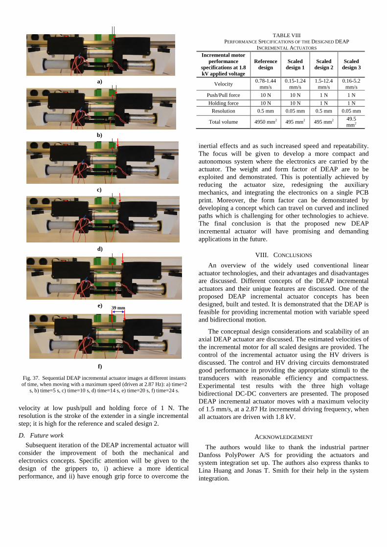
velocity at low push/pull and holding force of 1 N. The
resolution is the stroke of the extender in a single incremental
step; it is high for the reference and scaled design 2.
D. Future work
Subsequent iteration of the DEAP incremental actuator will
consider the improvement of both the mechanical and
electronics concepts. Specific attention will be given to the
design of the grippers to, i) achieve a more identical
performance, and ii) have enough grip force to overcome the
inertial effects and as such increased speed and repeatability.
The focus will be given to develop a more compact and
autonomous system where the electronics are carried by the
actuator. The weight and form factor of DEAP are to be
exploited and demonstrated. This is potentially achieved by
reducing the actuator size, redesigning the auxiliary
mechanics, and integrating the electronics on a single PCB
print. Moreover, the form factor can be demonstrated by
developing a concept which can travel on curved and inclined
paths which is challenging for other technologies to achieve.
The final conclusion is that the proposed new DEAP
incremental actuator will have promising and demanding
applications in the future.
VIII. CONCLUSIONS
An overview of the widely used conventional linear
actuator technologies, and their advantages and disadvantages
are discussed. Different concepts of the DEAP incremental
actuators and their unique features are discussed. One of the
proposed DEAP incremental actuator concepts has been
designed, built and tested. It is demonstrated that the DEAP is
feasible for providing incremental motion with variable speed
and bidirectional motion.
The conceptual design considerations and scalability of an
axial DEAP actuator are discussed. The estimated velocities of
the incremental motor for all scaled designs are provided. The
control of the incremental actuator using the HV drivers is
discussed. The control and HV driving circuits demonstrated
good performance in providing the appropriate stimuli to the
transducers with reasonable efficiency and compactness.
Experimental test results with the three high voltage
bidirectional DC-DC converters are presented. The proposed
DEAP incremental actuator moves with a maximum velocity
of 1.5 mm/s, at a 2.87 Hz incremental driving frequency, when
all actuators are driven with 1.8 kV.
ACKNOWLEDGEMENT
The authors would like to thank the industrial partner
Danfoss PolyPower A/S for providing the actuators and
system integration set up. The authors also express thanks to
Lina Huang and Jonas T. Smith for their help in the system
integration.
a)
b)
c)
d)
e)
f)
39 mm
Fig. 37. Sequential DEAP incremental actuator images at different instants
of time, when moving with a maximum speed (driven at 2.87 Hz): a) time=2
s, b) time=5 s, c) time=10 s, d) time=14 s, e) time=20 s, f) time=24 s.
TABLE VIII PERFORMANCE SPECIFICATIONS OF THE DESIGNED DEAP
INCREMENTAL ACTUATORS
Incremental motor
performance
specifications at 1.8
kV applied voltage
Reference
design
Scaled
design 1
Scaled
design 2
Scaled
design 3
Velocity 0.78-1.44
mm/s 0.15-1.24
mm/s
1.5-12.4
mm/s
0.16-5.2
mm/s
Push/Pull force 10 N 10 N 1 N 1 N
Holding force 10 N 10 N 1 N 1 N
Resolution 0.5 mm 0.05 mm 0.5 mm 0.05 mm
Total volume 4950 mm2 495 mm2 495 mm2 49.5 mm2

REFERENCES
[1] JenaTec, Online available: http://www.jena-tec.co.uk/linear-actuators.php [accessed 14 Nov. 2014].
[2] AGI American Grippers, Online available: http://localautomation.com/featured/agi-pneumatic-linear-actuator-agi-american-grippers-inc.html [accessed 14 Nov. 2014].
[3] Stemulate, Online available: http://www.stemulate.org/2012/07/02/solid-learning-robot-linear-actuators/ [accessed 14 Nov. 2014].
[4] Piezodrive, Online available: http://www.piezodrive.com/products.html [accessed 06 Jan. 2015].
[5] PI, Online available: http://www.linear-actuator.net/Vacuum_Linear_Actuators.php [accessed 14 Nov. 2014].
[6] Y. Bar-Cohen, “Electroactive Polymer [EAP] Actuators as Artificial
Muscles: Reality, Potential, and Challenges,” 2nd ed. Washington, DC:
SPIE, 2004. [7] R. E. Pelrine, R. D. Kornbluh, Q. Pei, J. P. Joseph, “High-speed
electrically actuated elastomers with strain greater than 100%,” Science,
vol. 287, pp. 836–839, 2000. [8] F. Carpi, D. DE Rossi, R. Kornbluh, R. Pelrine, P. Sommer-Larsen, Eds,
“Dielectric Elastomer As Electromechanical Transducers,” Amsterdam,
The Netherlands: Elsevier, 2008. [9] Danfoss PolyPower, Denmark, Online available:
http://www.polypower.com/ [accessed 20 Oct. 2014].
[10] LEAP Technology, Denmark, Online available:
http://leaptechnology.com/ [accessed 20 Oct. 2014].
[11] M. Tryson, H. E. Kiil, M. Benslimane, “Powerful tubular core free dielectric electro active polymer (DEAP) push actuator,” in Proc. SPIE,
vol. 7287, 2009. [12] R. Sarban, B. Lassen, M. Willatzen, “Dynamic Electromechanical
Modeling of Dielectric Elastomer Actuators With Metallic Electrodes,” IEEE/ASME Trans. Mechatronics, vol. 17, no. 5, pp. 960-967, Oct. 2012.
[13] L. Huang, P. Thummala, Z. Zhang, M. A. E. Andersen, “Battery powered high output voltage bidirectional flyback converter for
cylindrical DEAP actuator,” in Proc. IEEE IPMHVC, pp. 454-457, 3-7
June 2012.
[14] R. D. Kornbluh, R. Pelrine, Q. Pei, R. Heydt, S. Stanford, S. Oh, J. Eckerle, “Electroelastomers: applications of dielectric elastomer transducers for actuation, generation, and smart structures,” in Proc. SPIE, vol. 4698, pp. 254-270, 2002.
[15] A. T. Conn, A. D. Hinitt, P. Wang, “Soft segmented inchworm robot with dielectric elastomer muscles,” in Proc. SPIE, Electroactive Polymer Actuators and Devices (EAPAD), vol. 9056, pp. 90562L, 2014.
[16] Q. Pei, R. Pelrine, S. Stanford, R. D. Kornbluh, M. S. Rosenthal, K. Meijer, R. J. Full, “Multifunctional electroelastomer rolls and their application for biomimetic walking robots,” in Proc. SPIE, vol. 4698, 2002.
[17] I. A. Anderson, T. A. Gisby, T. G. McKay, B. M. O’Brien, E. P. Calius, “Multi-functional dielectric elastomer artificial muscles for soft and smart machines,” Journal of Applied Physics, 112, 041101, 2012.
[18] K. Jung, J. C. Koo, J. -do Nam, Y. K. Lee, H. R. Choi, “Artificial annelid robot driven by soft actuators,” Journal of Bioinspiration and Biomimetics, vol. 2, pp. S42-S49, 2007.
[19] I. A. Anderson, T. C. H. Tse, T. Inamura, B. M. O’Brien, T. McKay, T. Gisby, “A soft and dexterous motor,” Journal of Applied Physics, 98, 123704, 2011.
[20] R. Wache, D. N. McCarthy, S. Risse, G. Kofod, “Rotary Motion Achieved by New Torsional Dielectric Elastomer Actuators Design,” IEEE/ASME Trans. Mechatronics, vol. 99, pp. 1-3, Feb. 2014.
[21] R. J. E. Merry, J. L. Holierhoek, M. J. G. van de Molengraft, M. Steinbuch, “Gain Scheduling Control of a Walking Piezo Actuator,” IEEE/ASME Trans. Mechatronics, vol. 19, no. 3, pp. 954-962, June 2014.
[22] D. M. Neal, H. H. Asada, “Bipolar Piezoelectric Buckling Actuators,” IEEE/ASME Trans. Mechatronics, vol. 19, no. 1, pp. 9-19, Feb. 2014.
[23] Y. Jianyong, J. Zongxia, M. Dawei, Y. Liang, “High-Accuracy Tracking Control of Hydraulic Rotary Actuators With Modeling Uncertainties,” IEEE/ASME Trans. Mechatronics, vol. 19, no. 2, pp. 633-641, April 2014.
[24] P. Thummala, Z. Zhang, M. A. E. Andersen, S. Rahimullah, “Dielectric electro active polymer incremental actuator driven by multiple high-voltage bi-directional DC-DC converters,” in Proc. IEEE ECCE USA, pp. 3837-3844, 15-19 Sept. 2013.
[25] M. Karpelson, G. Y. Wei, R. J. Wood, “Driving high voltage piezoelectric actuators in microrobotic applications,” Sensors and
Actuators A, vol. 176, pp. 78– 89, 2012.
[26] L. Eitzen, C. Graf, J. Maas, “Cascaded bidirectional flyback converter driving DEAP transducers,” in Proc. IEEE IECON, pp. 1226-1231, 7-10
Nov. 2011.
[27] L. Eitzen, C. Graf, J. Maas, “Bidirectional power electronics for driving
dielectric elastomer transducers,” in Proc. SPIE, vol. 8340, p. 834018 1-
12, 2012.
[28] R. W. Erickson, D. Maksimovic, “Fundamentals of Power Electronics,” 2nd ed. New York: Springer, 2001.
[29] N. O. Sokal, R. Redl, “Control algorithms and circuit designs for optimal flyback-charging of an energy storage capacitor (e.g., for flash lamp or defibrillator),” IEEE Trans. Power Electronics, vol. 12, no. 5, pp. 885-894, Sep. 1997.
[30] J. Elmes, C. Jourdan, O. Abdel-Rahman, I. Batarseh, “High-Voltage, High-Power-Density DC-DC Converter for Capacitor Charging Applications,” in Proc. IEEE APEC, pp. 433-439, 2009.
[31] S. K. Chung, H. B. Shin, “High-voltage power supply for semi-active suspension system with ER-fluid damper,” IEEE Trans. Vehicular Technology, vol. 53, no. 1, pp. 206- 214, Jan. 2004.
[32] T. Bhattacharya, V. S. Giri, K. Mathew, L. Umanand, “Multiphase Bidirectional Flyback Converter Topology for Hybrid Electric Vehicles,” IEEE Trans. Industrial Electronics, vol. 56, no. 1, pp. 78-84, Jan. 2009.
[33] G. Chen, Y.-S. Lee, S.Y.R. Hui, D. Xu, Y. Wang, “Actively clamped bidirectional flyback converter,” IEEE Trans. Industrial Electronics, vol. 47, no. 4, pp. 770-779, Aug. 2000.
[34] F. Zhang, Y. Yan, “Novel Forward–Flyback Hybrid Bidirectional DC-
DC Converter,” IEEE Trans. Industrial Electronics, vol. 56, no. 5, pp.
1578-1584, May 2009.
[35] T. Andersen, M. S. Rødgaard, O. C. Thomsen, M. A. E. Andersen, “Low
voltage driven dielectric electro active polymer actuator with integrated
piezoelectric transformer based driver,” in Proc. SPIE EAPAD, vol.
7976, p. 79762N, 2011.
[36] P. Thummala, Z. Zhang, M. A. E. Andersen, “High Voltage Bi-directional Flyback Converter for Capacitive Actuator,” in Proc. IEEE
European Power Electronics conference, pp. 3-6 Sept. 2013.
[37] L. Huang, Z. Zhang, M. A. E Andersen, “Design and development of
autonomous high voltage driving system for DEAP actuator in radiator
thermostat,” in Proc. IEEE Applied Power Electronics Conference and Exposition (APEC), pp. 1633-1640, 16-20 March 2014.
[38] P. Thummala, H. Schneider, Z. Zhang, Z. Ouyang, A. Knott, M. A. E. Andersen, “Efficiency Optimization by Considering the High Voltage Flyback Transformer Parasitics using an Automatic Winding Layout Technique,” IEEE Trans. Power Electronics.
[39] H. Schneider, P. Thummala, L. Huang, Z. Ouyang, A. Knott, Z. Zhang, M. A. E. Andersen, “Investigation of transformer winding architectures for high voltage capacitor charging applications,” in Proc. IEEE APEC, pp. 334-341, 16-20 March 2014.
[40] J. P. L. Bigue, J. S. Plante, “Experimental Study of Dielectric Elastomer Actuator Energy Conversion Efficiency,” IEEE/ASME Trans. Mechatronics, vol. 18, no. 1, pp. 169-177, Feb. 2013.
[41] C. M. Druitt, G. Alici, “Intelligent Control of Electroactive Polymer Actuators Based on Fuzzy and Neurofuzzy Methodologies,” IEEE/ASME Trans. Mechatronics, vol. 19, no. 6, pp. 1951-1962, Dec. 2014.
[42] B. Rechenbach, M. Willatzen, R. Sarban, C. Liang, B. Lassen, “Geometry optimization of tubular dielectric elastomer actuators with anisotropic metallic electrodes,” in Proc. SPIE Electroactive Polymer Actuators and Devices (EAPAD), vol. 9056, pp. 905606-905606-13, Mar. 2014.
[43] P. Thummala, D. Maksimovic, Z. Zhang, M. A. E. Andersen, “Digital control of a high-voltage (2.5 kV) bidirectional DC-DC converter for driving a dielectric electro active polymer (DEAP) based capacitive actuator,” in Proc. IEEE ECCE USA, pp. 3435-3442, 14-18 Sept. 2014.

[44] Y. H. Iskandarani, R. W. Jones, E. Villumsen, “Modeling and experimental verification of a dielectric polymer energy scavenging cycle”, in Proc. SPIE EAPAD, vol. 7287, pp. 72871Y-1–72871Y-12, 2009.
[45] M. Tryson, H. -E. Kiil, M. Benslimane, “Powerful tubular core free dielectric electro activate polymer (DEAP) push actuator,” in Proc. SPIE EAPAD, vol. 7287, pp. 72871F-72871F-11, April, 2009.
[46] P. Thummala, D. Maksimovic, Z. Zhang, M. A. E. Andersen, S. Rahimullah, “Design of a High Voltage Bidirectional DC-DC Converter for Driving Capacitive Incremental Actuators Usable in Electric Vehicles (EVs),” in Proc. IEEE IEVC, 14-18 Dec. 2014.
[47] Linear Technology, “LT3751 High Voltage Capacitor Charger with Regulation,” Linear Technology Corporation, USA. http://cds.linear.com/docs/en/datasheet/3751fc.pdf [accessed 20 Oct. 2014].
[48] IXYS, IXTV03N400S, 4 kV MOSFET, Online available: http://ixapps.ixys.com/DataSheet/DS100214A-(IXTH_V03N400_S).pdf [accessed 20 Oct. 2014].
[49] IXYS, IXTA02N450HV, 4.5 kV MOSFET, Online available: http://ixapps.ixys.com/DataSheet/DS100498(IXTA-T02N450HV).pdf [accessed 20 Oct. 2014].
[50] VMI, SXF 6525, 5 kV diode, Online available: http://www.voltagemultipliers.com/pdf/SXF6521_25.pdf [accessed 20 Oct. 2014].


www.elektro.dtu.dkDepartment of Electrical EngineeringElectronics Group (ELE)Technical University of DenmarkOersteds Plads bygning 349DK-2800 Kgs. LyngbyDenmarkTel: (+45) 45 25 25 25Fax: (+45) 45 88 01 17Email: [email protected]