
Digital and Mixed-Signal Implementation of Fast Transient Response Digital Controllers for...
99
DIGITAL AND MIXED-SIGNAL IMPLEMENTATION OF FAST TRANSIENT RESPONSE DIGITAL CONTROLLERS FOR HIGH FREQUENCY SWITCH-MODE POWER SUPPLIES by Andrija Stupar A thesis submitted in conformity with the requirements for the degree of Master of Applied Science Graduate Department of Electrical and Computer Engineering University of Toronto © Copyright by Andrija Stupar, 2008
-
Upload
independent -
Category
Documents
-
view
0 -
download
0
Transcript of Digital and Mixed-Signal Implementation of Fast Transient Response Digital Controllers for...
DIGITAL AND MIXED-SIGNAL IMPLEMENTATION OF FAST TRANSIENT
RESPONSE DIGITAL CONTROLLERS FOR HIGH FREQUENCY SWITCH-MODE
POWER SUPPLIES
by
Andrija Stupar
A thesis submitted in conformity with the requirements for the degree of
Master of Applied Science
Graduate Department of Electrical and Computer Engineering
University of Toronto
© Copyright by Andrija Stupar, 2008
ii
ABSTRACT
Digital and Mixed-Signal Implementation of Fast Transient Response Digital Controllers
for High-Frequency Switch-Mode Power Supplies
by
Andrija Stupar
Master of Applied Science
Graduate Department of Electrical and Computer Engineering
University of Toronto
2008
The purpose of this thesis is to develop implementations of digital controllers for switch
mode power supplies providing fast transient response, superior to that of existing
solutions, both analog and digital. The targeted applications are Point-of-Load converters
supplying modern digital circuits. An on-chip implementation of a previously described
continuous-time algorithm is presented. The operation of this continuous-time digital
controller (CT-DC) is verified through simulations and also through experimental testing
of the fabricated integrated circuit. The CT-DC is then extended to include a novel auto-
tuning algorithm, which is capable of extracting power stage parameters simply by
observing the CT-DC’s transient performance. The operation of this algorithm is verified
through simulations. Finally, a novel modified converter topology for improving heavy-
to-light load transient performance, where the CT-DC offers only marginal improvement
compared to existing solutions, is presented and verified experimentally.

iii
TABLE OF CONTENTS
1. Introduction 1
1.1 DC-DC Converters in Point-of-Load Applications …………………………… 1
1.2 Digital Control of DC-DC SMPS ……………………………………………... 2
1.3 Transient Response of Digital SMPS Controllers ……………………………... 4
1.4 Thesis Objectives ……………………………………………………………… 5
1.5 Thesis Overview ………………………………………………………………. 5
2. Previous Art & Research Motivation 6
2.1 Analog Controllers …………………………………………………………….. 6
2.2 Digital Controllers ……………………………………………………………... 8
2.3 CT-DSP Optimal Response Controller ………………………………………... 9
2.4 Auto-Tuning …………………………………………………………………… 13
2.5 Dynamic Response in the Case of a Heavy-to-Light Load Change …………… 14
2.6 Summary ………………………………………………………………………. 16
3. On-Chip Implementation of the Continuous-Time Digital Controller 17
3.1 Targeted Application …………………………………………………………... 17
3.2 Theory Overview ……………………………………………………………… 17
3.3 System Architecture …………………………………………………………… 18
3.4 Functional Blocks ……………………………………………………………... 21
3.4.1 Comparators ……………………………………………………………... 21
3.4.2 Duty Ratio Extractor …………………………………………………….. 23
3.4.3 Dynamic Mode Detector ………………………………………………… 25
3.4.4 Time Calculator ………………………………………………………….. 27
A. DD −1/ LUT ………………………………………………………. 28
B. D−1 LUT …………………………………………………………... 31
C. outVv /∆ LUT ………………………………………………………... 31
D. LC2 Register and the Scaling of ton and toff ………………………... 32
3.4.5 Time Adjustment ………………………………………………………… 33
3.4.6 Switching Logic …………………………………………………………. 35
3.5 Simulation Results …………………………………………………………….. 36
3.6 Experimental Results ………………………………………………………….. 40
3.6.1 Light-to-Heavy Load Transient …………………………………………. 41
3.6.2 Heavy-to-Light Load Transient …………………………………………. 45
3.7 System Limitations and Issues ………………………………………………… 47
3.7.1 Peak and Valley Point Detection Lag …………………………………… 47
3.7.2 The Value of D …………………………………………………………... 48
3.7.3 The CT-DC to PID Transition …………………………………………... 50
3.7.4 The Effect of Switch On-Resistance ……………………………………. 51

iv
4. Auto-Tuning Extension to the Continuous-Time Digital Controller 54
4.1 One-Shot Auto-Tuning through the Observation of Transient Performance ….. 54
4.2 System Architecture …………………………………………………………… 57
4.2.1 One-Shot Tuning ………………………………………………………… 60
4.2.2 Iterative Tuning ………………………………………………………….. 60
4.3 Simulation Results …………………………………………………………….. 61
5. Current-Steered Buck Converter for Improving Heavy-to-Light Load
Transient Response 65
5.1 The Problem of the Heavy-to-Light Load Transient …………………………... 65
5.2 Modified Buck Topology ……………………………………………………… 66
5.3 Principle of Operation – Current Steering …………………………………….. 68
5.4 Simulation Results …………………………………………………………….. 69
5.5 System Architecture …………………………………………………………… 71
5.5.1 Mode Control ……………………………………………………………. 72
A. Steady-State Operation ……………………………………………….. 72
B. Heavy-to-Light Load Transient Operation …………………………… 74
5.5.2 Determining the Magnitude of the Load Current Change ………………. 76
5.6 Experimental Results …………………………………………………………... 78
5.7 Drawbacks and Possible Improvements ……………………………………….. 82
5.7.1 Current Sensing ………………………………………………………….. 82
5.7.2 The Differentiator ………………………………………………………... 83
5.7.3 The Effect of Additional Switches ……………………………………….. 84
6. Conclusions and Future Work 85
6.1 Continuous-Time Digital Controller …………………………………………... 85
6.2 Auto-Tuning Extension ………………………………………………………... 85
6.3 Current-Steered Buck Converter ………………………………………………. 86
6.4 Future Work …………………………………………………………………… 86
References 87

v
LIST OF TABLES
Table 3.1 Comparator thresholds at Vout = 1.5 V ………………………………….. 22
Table 3.2 Transient voltage deviation ∆v at different valleys/peaks at
Vout = 1.5 V …………………………………………………………….... 23
Table 3.3 Estimated silicon area and critical path of CT-DC functional blocks …... 40
Table 3.4 Iterative tuning procedure ………………………………………………. 61
vi
LIST OF FIGURES
Fig. 2.1 A buck converter with a typical analog controller ……………………… 7
Fig. 2.2 A buck converter with a typical digital controller ……………………… 8
Fig. 2.3 The CT-DSP controller …………………………………………………. 10
Fig. 2.4 Waveforms showing optimal one switching action response to light-to-
heavy load transient ……………………………………………………... 11
Fig. 3.1 Block diagram of the full system including controller chip and power
stage ……………………………………………………………………... 19
Fig. 3.2 Block diagram of the continuous-time digital controller (CT-DC) ……... 20
Fig. 3.3 The synchronous comparators used for analog to digital conversion …... 21
Fig. 3.4 Duty ratio extractor schematic ………………………………………….. 24
Fig. 3.5 State transition diagram of the dynamic mode detector ………………… 26
Fig. 3.6 Look-up table structure – the DD −1/ LUT ………………………….. 30
Fig. 3.7 The CT-DC’s switching logic …………………………………………... 35
Fig. 3.8 Simulation results. Output voltage, inductor current, and internal system
signals. Comparison of transients – first two load step changes
compensated by the PID loop, next two by the CT-DC ………………… 37
Fig. 3.9 Response to a 10 A to 40 A load step increase: (left) PID compensator
(right) CT-DC …………………………………………………………… 38
Fig. 3.10 Response to a 40 A to 10 A load step decrease: (left) PID compensator
(right) CT-DC …………………………………………………………… 39
Fig. 3.11 Response of the on-chip PID compensator to a 20 A load step increase... 41
Fig. 3.12 Oscillations caused by the CT-DC in response to a 20 A load step
increase ………………………………………………………………….. 42
Fig. 3.13 Response of the on-chip CT-DC to a 20 A load step increase with ∆t1
set to 4 …………………………………………………………………... 44
Fig. 3.14 CT-DC response to a 20 A load step change (increase followed by
decrease) ………………………………………………………………… 46
Fig. 3.15 Buck converter with non-idealities included in the schematic ………….. 49
Fig. 3.16 CT-DC response to 30 A load step changes with a converter with high
MOSFET on-resistance …………………………………………………. 52
Fig. 3.17 CT-DC response to 30 A load step changes with a converter with high
MOSFET on-resistance, enlarged ………………………………………. 53
Fig. 4.1 Transient response of the CT-DC when the on and off times are correct
(optimal, top), too short (undershoot, middle), and too long (overshoot,
bottom) ………………………………………………………………….. 55
Fig. 4.2 Block diagram of the auto-tuner ………………………………………… 58
Fig. 4.3 Transient response of the CT-DC with an overly high K ……………….. 62
Fig. 4.4 Auto-tuner’s response to the overshoot of Fig. 4.3, showing one-shot
auto-tuning ……………………………………………………………… 62
Fig. 4.5 Transient response of the CT-DC after auto-tuning …………………….. 63
Fig. 4.6 Auto-tuner’s response to the overshoot of Figure 4.5, showing iterative
tuning …………………………………………….……………………… 63

vii
Fig. 5.1 Modified current-steered buck converter topology for improving heavy-
to-light load transient response …………………………………………. 67
Fig. 5.2 Converter states: a) during steady-state and light-to-heavy transients
b) during heavy-to-light transients ……………………………………… 68
Fig. 5.3 Simulation results, transient response to a 10 A to 2 A load step change
(∆I = 8 A): a) (above) with PID only b) (below) with inductor current
steering ………………………………………………………………….. 70
Fig. 5.4 Digitally-controlled current-steered Buck converter system …………… 71
Fig. 5.5 State transition diagram illustrating operation of the mode control logic
state machine ……………………………………………………………. 73
Fig. 5.6 The spike in capacitor current ic(t) during heavy-to-light transient (with
current steering) …………………………………………………………. 76
Fig. 5.7 Operational-amplifier-based inverting differentiator circuit used to
detect the magnitude of the load change ………………………………... 77
Fig. 5.8 Flash ADC used to determine ∆I ……………………………………….. 77
Fig. 5.9 Transient response to an 8 A load step change: (top) with PID only;
(bottom) with inductor current steering ………………………………… 79
Fig. 5.10 Transient response to an 8 A load step increase ………………………… 80
Fig. 5.11 Transient response to an 8 A load step decrease: (top) with PID only;
(bottom) with inductor current steering ………………………………… 81
Fig. 5.12 Transient response with current steering to an 8 A load step decrease,
showing the output of the inverting differentiator ……………………… 82
1
Chapter 1
Introduction
The subject of this thesis is the design and detailed on-chip implementation of digital
controllers for Point-of-Load (PoL) DC-DC Switch-mode power supplies (SMPS) which
improve and provide near time-optimal dynamic response to load transients. The
improvement of dynamic response increases power supply efficiency, allows for the
minimization of passive components, and reduces the risk of system failures and damage.
The work begins with the detailed on-chip implementation of a previously described [1]-
[3] continuous-time digital controller, and continues with the extension of that controller
to create an auto-tuning system that can identify power supply parameters based on
dynamic response. Subsequently, a novel method to further improve specifically the
dynamic response to heavy-to-light load transient is introduced.
1.1 DC-DC Converters in Point-of-Load Applications
Switch-mode power supplies (SMPS) are found in many electronic devices today,
wherever conversion from one voltage level to another is required. In comparison to their
predecessors, linear power supplies, they have lesser cost, smaller dimensions, and higher
operating efficiency, often exceeding 90% [4]. Applications in which SMPS are found
range from portable electronics such as mobile phones, digital still cameras, and laptop
computers where it is necessary to power many different components requiring different
supply voltages from the same source (battery), through computers, consumer electronics
and home appliances, to lighting equipment, automotive devices, and so on.

2
The focus of this thesis is on Point-of-Load converters (PoL), called so because
they are small and near to their load, that is, they are close to their point of use. PoL
supplies are most commonly used to convert the voltage of a common DC bus into a
particular supply voltage needed for a specific electronic component. They are often used
to supply devices such as digital signal processors (DSPs), field-programmable gate
arrays (FPGAs) and general purpose computer processors [5]-[7]. An SMPS typically
consists of a dc-dc converter, with the focus of this work being specifically on step-down
Buck converters [4], and a controller. The converter, or power stage, consists of
switching elements (Power MOSFETs and diodes) and passive components (inductors
and capacitors) for filtering. The controller can be implemented as an analog, digital, or
mixed-signal circuit.
One of the most common designs is a voltage-mode controller employing pulse-
width modulation (PWM) [4], in which the output voltage of the power stage is
compared to a set reference voltage. The error of the output relative to the reference is
then used by the controller to determine the pulse-width or duty cycle of the waveform
applied to the switching elements, which operate at a set constant frequency.
1.2 Digital Control of DC-DC SMPS
Analog controllers predominate in the market today. A voltage-mode controller
consisting of a subtractor, proportional–integral–derivative (PID) regulator, and an
analog pulse-width modulator (PWM) can be constructed using a few operational
amplifiers and passive components [4], without exceeding 20 to 30 transistors in size.
Such a device has low power consumption, low silicon area and is relatively simple to
design. It provides tight output voltage regulation and for some applications, relatively

3
good dynamic response. However, analog controllers have several drawbacks, especially
when used to supply digital loads such as processors or FPGAs. They often cannot be
integrated on the same die as the load, due to different implementation technologies or
process differences. Furthermore, they have poor design portability: when transferring a
design to a new implementation technology, for example from 0.35 µm process to a 0.18
µm process, the analog circuit basically must be redesigned from the beginning. In
contrast, a digital circuit described in a hardware-description language (HDL) such as
Verilog or VHDL can simply be re-synthesized using digital design tools. Such
controllers also have poor flexibility: an analog controller designed for one application
cannot be easily used in another. For that reason commercial analog controllers use
external passive components, which is undesirable from an integration point of view, in
order to allow their use in a wide range of applications. Digital circuits, on the other
hand, can be easily created as to contain programmable parameters. For these reasons,
digital controllers for SMPS have been receiving a great deal of attention in the past few
years [8]-[12], and it has been demonstrated that they can act as feasible substitutes for
their analog counterparts. Besides not suffering from any of the drawbacks listed above,
they can also be used to implement advanced control algorithms [3], [13]-[17], which can
be very difficult if not impossible to implement through an analog approach.

4
1.3 Transient Response of Digital SMPS Controllers
The dynamic response of an SMPS, or the response to load transients, that is fast changes
in the output load current, is of crucial importance. Any sudden load change will cause a
deviation of the converter output voltage. The controller must react quickly so that this
deviation is small and so that the output voltage returns to its required level as soon as
possible. A fast transient response by the controller minimizes the chance of damage to
the load, ensures the load’s proper operation, and minimizes converter passive
components that would otherwise need to be larger in order to suppress the output
voltage deviation.
The first generations of digital controllers for SMPS were built as functional
replicas of analog solutions. They eventually achieved performance characteristics
comparable to most analog controllers, but nonetheless lagged slightly behind top of the
line analog solutions, when transient response was considered. This made them
unsuitable for certain applications, such as voltage regulator modules (VRMs) for
computer processors, which have very tight requirements concerning dynamic response
[18]. This has resulted in research into various non-linear control schemes [3], [19]-[20]
designed specifically for improving transient response and overcoming digital PID
controller bandwidth limitations. Such controllers achieve a time-optimal transient
response limited only by the physical characteristics of the power stage.
While the aforementioned controllers achieve near-optimal response for the case
of a light-to-heavy load transient, that is, an increase of the load current, they still suffer
from a relatively large output voltage spike in the case of a heavy-to-light load transient,
5
that is, a decrease in the load current. This is due to a physical limitation of the buck
converter in this case, as will be shown later.
1.4 Thesis Objectives
The objectives of this thesis are three-fold. The first is to design and demonstrate a
detailed on-chip implementation of a previously described [1]-[3] continuous-time digital
controller that achieves near time-optimal transient response and to discuss its advantages
and limitations. The second is to extend this controller to create an auto-tuning system
that can detect a non-optimal transient, and, based on a given dynamic response, improve
its performance. The final goal is to achieve equal performance during both heavy-to-
light and light-to-heavy load transients by overcoming the physical limitations imposed
by a converter through novel modified buck topology.
1.5 Thesis Overview
The thesis is organized as follows: Chapter 2 gives an overview of existing art and
discusses the motivation for the research presented in this work. The continuous-time
controller the implementation of which is the subject of this thesis is also presented here.
Chapter 3 gives in the detail the on-chip implementation of the controller, as well as
simulation and experimental results, and also discusses certain implementation issues and
limitations encountered in the subsequent testing of the controller. Chapter 4 presents the
auto-tuning extension to the controller and gives simulation results for it. Chapter 5
presents the novel topology for improving heavy-to-light transient response, with
experimental results. Chapter 6 contains conclusions and suggestions for future work. All
HDL code and similar materials related to this thesis are given in the Appendices.
6
Chapter 2
Previous Art & Research Motivation
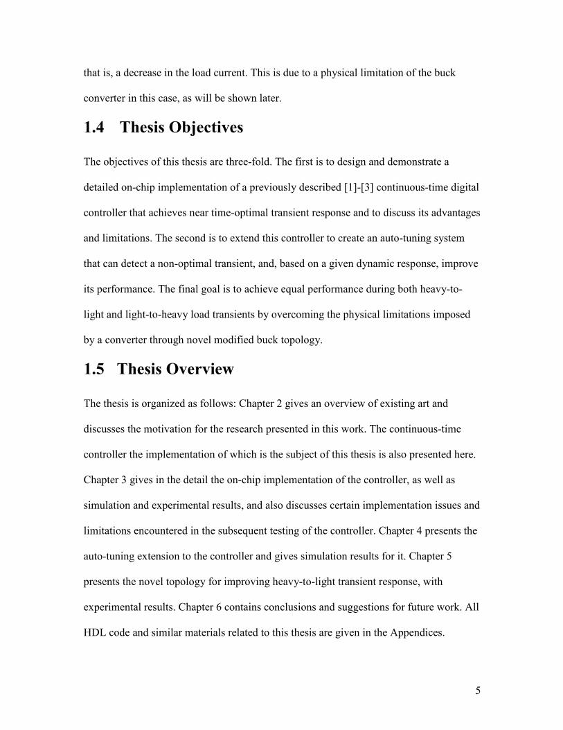
2.1 Analog Controllers
Commercial PoL SMPS are predominantly controlled by analog circuits. A typical
voltage mode analog-controlled buck converter [4] is given in Figure 2.1. Analog
controllers are a well-known and time-tested technology with which engineers are
familiar and comfortable with. Examples of current commercial analog-controlled PoL
include [21]-[23]. For PoL applications, voltage-mode control is preferred to other
control methods, because it avoids costly current sensing and amplification circuits [25],
required for methods such current-mode control [4], and the issues of noise and
interference caused by variable switching frequency, which is a characteristic of
approaches such as hysteretic control [26]. Buck converters are the preferred topology for
the power stage in these applications, since, as noted in Chapter 1, PoL SMPS usually
have the task of stepping down the voltage coming from an external power supply or DC
bus to a lower level required by the load, often a digital integrated circuit.
As seen in Figure 2.1, the control loop consists of a subtractor which compares
the converter output voltage to a reference value, and then forwards the result, the error
signal e(t), to a compensator, which is usually of the PID type. The compensator
generates a control voltage for the pulse-width modulator (PWM), which generates a
switching waveform for the converter switches of constant frequency but of varying
width, or duty ratio.

7
By modeling the buck converter [4], it is known that the dc value of the output voltage,
Vout, depends on the input voltage Vg, and the value of the duty ratio, D:
gout DVV = (2.1)
The advantages and disadvantages of analog compared to digital controllers have been
mentioned already in Chapter 1, and have been discussed at length in the literature [1],
[8], [9], [27]-[29].
Figure 2.1: A buck converter with a typical analog
controller
8
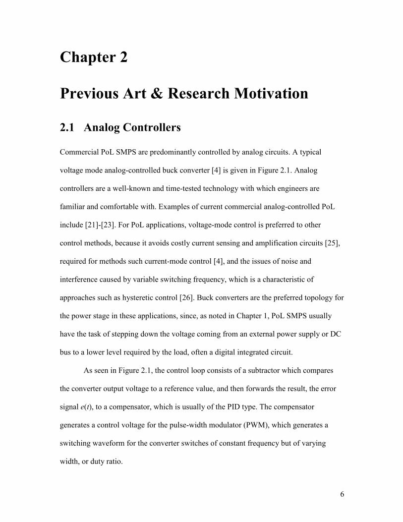
2.2 Digital Controllers
Digital controllers have been applied in the past few years to many different control
methods: voltage mode control [8], [12], [29], current mode control [30]-[31], and
hysteretic control [32]. However, for the same reasons as with analog controllers,
voltage-mode control is generally preferred.
A typical voltage-mode digitally-controlled Buck converter is given in Figure 2.2.
The loop consists of an analog-to-digital converter (ADC) which converts the analog
output voltage signal vout(t) to a multi-bit digital value, vout[n]. This value is compared to
a digital reference Vref[n] by the error generator circuit which outputs a digital error value
e[n], taken by the digital PID compensator as input. The digital PID compensator [33] is
Figure 2.2: A buck converter with a typical digital
controller

9
constructed according to the control law
]2[]1[][]1[][ −⋅+−⋅+⋅+−= necnebneandnd (2.2)
Where a, b, and c are PID coefficients, e[n], e[n – 1], and e[n – 2] the error values from
the current and previous two switching cycles, respectively, d[n – 1] the value of the duty
ratio control signal from the previous switching cycle, while d[n] is the output of the
compensator, and represents the value of the duty ratio control variable which is
forwarded to the digital pulse width modulator (DPWM) [8], [12] which creates the
switching signal for the power stage. Such a system is a functional replica of a voltage-
mode analog controller, whose dynamic response characteristics generally lag behind
those of analog solutions, unless non-linear control methods are added to this
combination [1], [34]. This has led to various attempts to augment PID-based voltage-
mode control with non-linear methods to be used during load transients to improve
dynamic performance [3], [19], [20], [35]-[37].
2.3 CT-DSP Optimal Response Controller
Of particular interest is the controller presented in [1]-[3] and developed at the University
of Toronto. It uses the concepts of continuous-time digital signal processing (CT-DSP)
[38]-[40] and capacitor charge balance [19], [41]-[43] to perform compensation of a load
change within one switching action. A block diagram of the system is given in Figure
2.3. During steady state, that is, when the output load is not changing significantly, the
voltage is regulated by a PID compensator, as in the standard digital set-up described in
the previous section. The CT-DSP controller is active during load transients only.
Instead of a traditional ADC, a set of asynchronous comparators is used, followed
by delay lines made up of delay cells with a very short propagation time. This allows the

10
controller to react almost instantly to output voltage deviations and quickly detect a load
transient, effectively processing information in continuous time. When a load transient is
detected, that is when the output deviates far enough from the reference, the controller
detects a load change. The CT-DSP controller then suspends the PID compensator and
responds to the transient by generating an optimal-time switching sequence. In the case
of a light-to-heavy transient, that is, a load current increase, the CT-DSP controller turns
on the main switch of the converter and waits for the output voltage to reach its valley
point, that is, to start increasing again after the dip caused by the load change. At that
point, the optimal times for the switching action are calculated. This is shown in Figure
2.4.
The algorithm used to calculate the time intervals for which the main switch and
synchronous rectifier of the converter should be on during a load transient is based on
Figure 2.3: The CT-DSP Controller

11
capacitor charge balance. In a Buck converter, the average inductor current is equal to the
average load current, and the average capacitor current is equal to zero [4]. When a
sudden load current increase occurs, triggering a light-to-heavy load transient, the
inductor current cannot instantaneously follow, and as a result this extra current must
flow from the capacitor, with a corresponding drop in the capacitor voltage, which is also
the output voltage of the converter. Charge has been lost in the capacitor, and this lost
charge must be recovered for steady state to be restored. It is known that the amount of
Figure 2.4: Waveforms showing optimal one switching action response to
light-to-heavy load transient: output voltage vout(t), load current iload(t),
inductor current iL(t), main switch control signal c(t)
12
charge in a capacitor is defined by its capacitance and the voltage across it. Therefore,
looking at Figure 2.4, the amount of charge, Q, which must be recovered is defined as
vCQ ∆= (2.3)
where C is the capacitance and ∆v the change in voltage across the capacitor. Since this
must be compensated by an increase in the inductor current, it follows that it is not
merely enough for the inductor current to reach the new load current value, but also to go
above it for a certain period of time, in order to recover the lost charge Q, as shown in
Figure 2.4. As can be seen, the voltage continues to drop, that is, charge continues to be
lost, until the inductor current reaches the new load current value – this is the voltage
valley point, and at this point it begins to rise, that is charge begins to be recovered.
Then, the main switch must continue to be on for a while longer – this is the calculated
on-time, ton – in order for the charge to continue to be recovered. At some point the
switch must be turned off so that the inductor current returns to the new steady-state
value – this is the calculated off-time, toff . The charge Q can be broken up into two
values, Qon, the charge recovered after the valley point while the main switch is on, and
Qoff, the charge recovered while the main switch is off but before the inductor current
drops back to its new steady-state level. As shown in [1]-[3], these values can be
calculated by integrating the inductor current over these intervals, namely
2
002
on
outgt
outg
t
on tL
VVdtd
L
VVQ
on −=
−= ∫∫ τ (2.4)
2
002
off
out
t
out
t
off tL
Vdtd
L
VQ
off
== ∫∫ τ (2.5)

13
Rearranging equations 2.4 and 2.5 to solve for the on and off times, and substituting in
equation 2.3 for charge, and then 2.1 for the relationship between the input voltage,
output voltage, and duty ratio, the following equations for ton and toff are derived:
vD
Dk
VVV
vVLCt
outgg
outon ∆
−=
−
∆=
1)(
2 (2.6)
vDkVV
VVvLCt
outg
outg
off ∆−=−∆
= 1)(
)(2 (2.7)
where outVLCk /2= .
The operation of this controller, as demonstrated in [1], [3], has been verified via
an experimental prototype built out of off the shelf components and with the digital parts
of the controller implemented on an FPGA. The controller’s performance has been
shown to be superior to that of a digital PID compensator and comparable with or better
than existing analog solutions. However, in order to truly demonstrate that this is a viable
alternative to existing commercial power management solutions, it must be implemented
as a dedicated on-chip controller and tested on a commercial power stage. This is one of
the objectives of this thesis, and is the subject of Chapter 3.
2.4 Auto-Tuning
As can be seen from previous sections, both the design of PID compensator coefficients
and the continuous-time method for optimal response requires the knowledge of the
values of power stage passive components, L and C. These values are assumed to be
known beforehand and are programmed as parameters into the digital circuitry of the
controllers. However, due to component tolerances, aging, or differing operating
conditions, such as changes in temperature, the values of the inductance and capacitance

14
of the converter may not be identical to those originally input into the controller. Any
significant variation of the L and C values used for the calculation of on and off times
from the actual values in the converter will cause a non-optimal response. Therefore it is
useful to have some method of extracting the actual L and C, directly or indirectly, during
SMPS operation, and changing controller parameters accordingly to adapt. This is known
as auto-tuning or self-calibration. Numerous methods of auto-tuning exist [1], [13], [44]-
[49]. Characteristic for these methods is either the need for complicated and powerful
microprocessors, or the need for a large number of sample points (that is, switching
cycles) in order to arrive at a result, or the need to purposefully inject some sort of
disturbance into the output voltage so that it can be observed for tuning purposes. As it
will be shown in Chapter 4, a side benefit of using the CT-DSP algorithm presented in
the previous section is that auto-tuning, that is, extraction of L and C values, can be
performed after just one load transient with a minimum of added hardware.
2.5 Dynamic Response in the Case of a Heavy-to-Light
Load Change
Two basic cases of load transients exist: a light-to-heavy load change, that is, an increase
in the load current, and a heavy-to-light load change, that is, a decrease in the load
current. All mentioned methods of improving dynamic response hold for both cases; for
example, with the CT-DSP controller, the switching sequence is simply reversed [1], [3].
However, the response in the two cases, regardless of the method, is usually not
symmetric. The heavy-to-light load transient is more problematic, due to a basic physical
limitation of the Buck converter. PoL SMPS often supply digital loads with very low
15
supply voltages. In modern digital systems, this can be as low as 0.9 V, and according to
[50], supply voltages of digital systems are expected to decrease to 0.7 V soon, and to
drop to 0.5 V in the long term.
During a heavy-to-light load transient response, since the load current has
dropped, there is an excess of current in the inductor, and it must be discharged. This
discharge is limited by the slew rate Vout/L [4], which, if the load is a modern digital
system, tends therefore to be quite low. This causes significant output voltage overshoots,
in turn requiring a large output capacitance for their suppression. Keeping in mind trends
in supply voltages, this means that in conventional PoL, the size of the output capacitor
suppressing voltage spikes is likely to increase, negatively affecting the system size and
cost.
Several solutions have been proposed for augmenting the buck topology to
improve transient response. In [51], parallel resistors are added to the inductor and the
capacitor to bypass the energy storage elements during transients. Such a solution
significantly improves the response but at the same time adds new losses. During heavy-
to-light transients, excess energy is essentially “burned” through the resistors. The
addition of extra conduction paths during transient [52], [53], though also effective,
suffers from similar problems. Different inductances used in steady state and during
transient [54]-[56] improve the response but often require specialized and costly
inductors.
In Chapter 5, a novel topological modification is presented which solves the
problem of heavy-to-light transient response, without the problems noted in existing
solutions.

16
2.6 Summary
A previously described and FPGA-tested digital controller which achieves dynamic
response better than or comparable to existing analog solutions was reviewed. However,
that implementation is not suitable for on-chip fabrication, which is necessary if the
controller is ever to be considered for a commercial product. Therefore a viable on-chip
implementation of it must be devised and demonstrated. Furthermore, since the values of
L and C are required for the proper operation of this controller, a method of auto-tuning,
or extraction of these values during converter operation, is desirable, but without the
addition of complicated extra hardware or procedures. Finally, the problem of heavy-to-
light transient remains as a fundamental physical limitation in modern PoL SMPS.
17
Chapter 3
On-Chip Implementation of the
Continuous-Time Digital Controller
3.1 Targeted Application
The targeted application for this on-chip implementation of the Continuous-time digital
controller (CT-DC) is the PIP-212 PoL demonstrator board [24] manufactured by
Philips/NXP Semiconductors. This project is an on-going collaboration with NXP
Semiconductors of the Netherlands who are interested in replacing their analog controller
for the PIP-212 with a digital one.
The PIP-212 comprises a 12 V to 1.5 V buck converter with inductance
L = 0.38 µH and output capacitance C = 600 µF. Its maximum output power is 60 W
giving a maximum output current of 40 A at an output of 1.5 V. The switching frequency
of the converter is fsw = 500 kHz.
3.2 Theory Overview
As noted in Chapter 2, the equations for calculating optimal on and off times, ton and toff
respectively, for a load transient are as follows
vD
Dkton ∆
−=
1 (3.1)
vDktoff ∆−= 1 (3.2)

18
where outVLCk /2= . For the purpose of this implementation however, Equations 3.1
and 3.2 are slightly rearranged to give
out
onV
v
D
DLCt
∆
−=
12 (3.3)
out
offV
vDLCt
∆−= 12 (3.4)
This is done as to simplify the use of the look-up tables used to calculate each of the three
square-rooted terms in equations 3.3 and 3.4, as will be shown below. These equations
are derived for the low-to-high transient; as noted earlier, the equations for the heavy-to-
light transient are the same just with the ton, toff sequence being reversed.
3.3 System Architecture
A high-level block diagram of the system is given in Figure 3.1. The power stage
comprises the PIP-212 demonstrator board with its analog controller removed; into the
feedback loop the digital controller chip is inserted. The converter’s output voltage,
vout(t), is fed into the chip, while the chip supplies the converter with the control signal
c(t). On-chip are the comparators, that is the flash analog-to-digital converter (ADC), that
digitize vout(t), the digital PID loop used for steady-state control and small transients, and
the dynamic mode continuous-time controller, as well as a higher-level processor, used to
program the PID and CT-DC look-up tables and to communicate with the outside world
(a laptop or desktop computer), along with other circuitry (clock generators, etc.). The
comparators and the higher-level processor were designed and implemented by NXP
Semiconductors. As noted, the continuous-time digital controller is the subject of this
thesis and is described here. The PID loop was also designed at the University of Toronto

19
as an adaptation of previous work done by the research group [12], [29]. The whole chip
was fabricated by NXP Semiconductors in their 0.14 µm process.
To speed up development time and save silicon area, the original approach
described in [1] using asynchronous comparators followed by delay cells and
asynchronous circuitry was abandoned. More precisely, it was decided that the delay
cells be removed. Instead, synchronous comparators with oversampling are used. The
output voltage vout(t) is sampled at a frequency 32 times higher than the switching
frequency, yielding performance similar to that of asynchronous comparators followed
by delay cells. It then follows that the whole system is synchronous – the CT-DC
Figure 3.1: Block diagram of the full system
including controller chip and power stage
20
operates at the sampling frequency, clk_32, making it fast enough to react quickly to
disturbances in the output voltage.
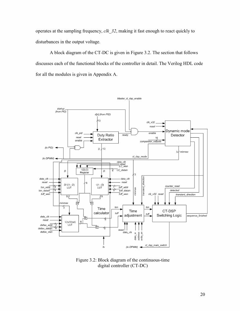
A block diagram of the CT-DC is given in Figure 3.2. The section that follows
discusses each of the functional blocks of the controller in detail. The Verilog HDL code
for all the modules is given in Appendix A.
Figure 3.2: Block diagram of the continuous-time
digital controller (CT-DC)
21
3.4 Functional Blocks
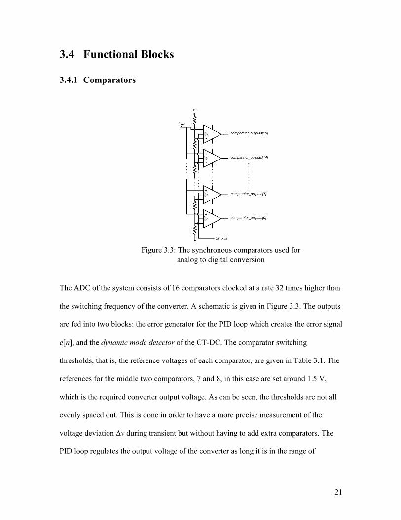
3.4.1 Comparators
The ADC of the system consists of 16 comparators clocked at a rate 32 times higher than
the switching frequency of the converter. A schematic is given in Figure 3.3. The outputs
are fed into two blocks: the error generator for the PID loop which creates the error signal
e[n], and the dynamic mode detector of the CT-DC. The comparator switching
thresholds, that is, the reference voltages of each comparator, are given in Table 3.1. The
references for the middle two comparators, 7 and 8, in this case are set around 1.5 V,
which is the required converter output voltage. As can be seen, the thresholds are not all
evenly spaced out. This is done in order to have a more precise measurement of the
voltage deviation ∆v during transient but without having to add extra comparators. The
PID loop regulates the output voltage of the converter as long it is in the range of
Figure 3.3: The synchronous comparators used for
analog to digital conversion
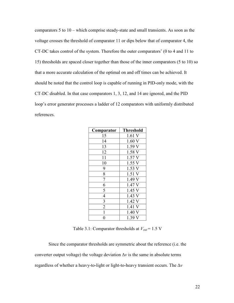
22
comparators 5 to 10 – which comprise steady-state and small transients. As soon as the
voltage crosses the threshold of comparator 11 or dips below that of comparator 4, the
CT-DC takes control of the system. Therefore the outer comparators’ (0 to 4 and 11 to
15) thresholds are spaced closer together than those of the inner comparators (5 to 10) so
that a more accurate calculation of the optimal on and off times can be achieved. It
should be noted that the control loop is capable of running in PID-only mode, with the
CT-DC disabled. In that case comparators 1, 3, 12, and 14 are ignored, and the PID
loop’s error generator processes a ladder of 12 comparators with uniformly distributed
references.
Since the comparator thresholds are symmetric about the reference (i.e. the
converter output voltage) the voltage deviation ∆v is the same in absolute terms
regardless of whether a heavy-to-light or light-to-heavy transient occurs. The ∆v
Comparator Threshold
15 1.61 V
14 1.60 V
13 1.59 V
12 1.58 V
11 1.57 V
10 1.55 V
9 1.53 V
8 1.51 V
7 1.49 V
6 1.47 V
5 1.45 V
4 1.43 V
3 1.42 V
2 1.41 V
1 1.40 V
0 1.39 V
Table 3.1: Comparator thresholds at Vout = 1.5 V

23
corresponding to each comparator that may be the peak or valley point during transient is
given in Table 3.2. The system was designed with the assumption that the comparator
thresholds scale with the controller reference, that is, if the required Vout changes, so do
the thresholds, proportionally, so that ideally the ∆v/Vout ratio used in equations 3.3 and
3.4 always remains constant. However, even this not being the case does not present a
problem, since the look-up table storing these ratios can be easily reprogrammed.
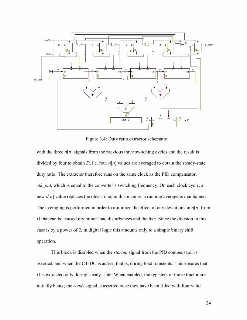
3.4.2 Duty Ratio Extractor
As noted in Chapter 2, information about the input voltage of the converter is not
available to the controller, and therefore it is necessary to use the steady-state duty ratio
D in the equations for calculating ton and toff. This is facilitated by the fact that the
instantaneous duty ratio, d[n], for the present switching cycle is available as an output
from the PID compensator that fed into the DPWM. Since the PID loop operates more or
less only in steady-state in this system, the value of d[n] is close to the value needed for
the equations, D.
The duty ratio extractor consists of adders and a four-entry shift register. A
schematic is given in Figure 3.4. The 13-bit d[n] signal from the PID compensator is
taken as input and stored in the register each switching cycle. That input is then added
Peak point comparator Valley point comparator ∆v minmax
11 4 0.07 V 000
12 3 0.08 V 001
13 2 0.09 V 010
14 1 0.10 V 011
15 0 0.11 V 100
Table 3.2: Transient voltage deviation ∆v at different valleys/peaks at Vout = 1.5 V
24
with the three d[n] signals from the previous three switching cycles and the result is
divided by four to obtain D, i.e. four d[n] values are averaged to obtain the steady-state
duty ratio. The extractor therefore runs on the same clock as the PID compensator,
clk_pid, which is equal to the converter’s switching frequency. On each clock cycle, a
new d[n] value replaces the oldest one; in this manner, a running average is maintained.
The averaging is performed in order to minimize the effect of any deviations in d[n] from
D that can be caused my minor load disturbances and the like. Since the division in this
case is by a power of 2, in digital logic this amounts only to a simple binary shift
operation.
This block is disabled when the startup signal from the PID compensator is
asserted, and when the CT-DC is active, that is, during load transients. This ensures that
D is extracted only during steady-state. When enabled, the registers of the extractor are
initially blank; the ready signal is asserted once they have been filled with four valid
Figure 3.4: Duty ratio extractor schematic
25
values of d[n], that is, once a valid value of D has been produced. If ready is low, the CT-
DC is disabled.
3.4.3 Dynamic Mode Detector
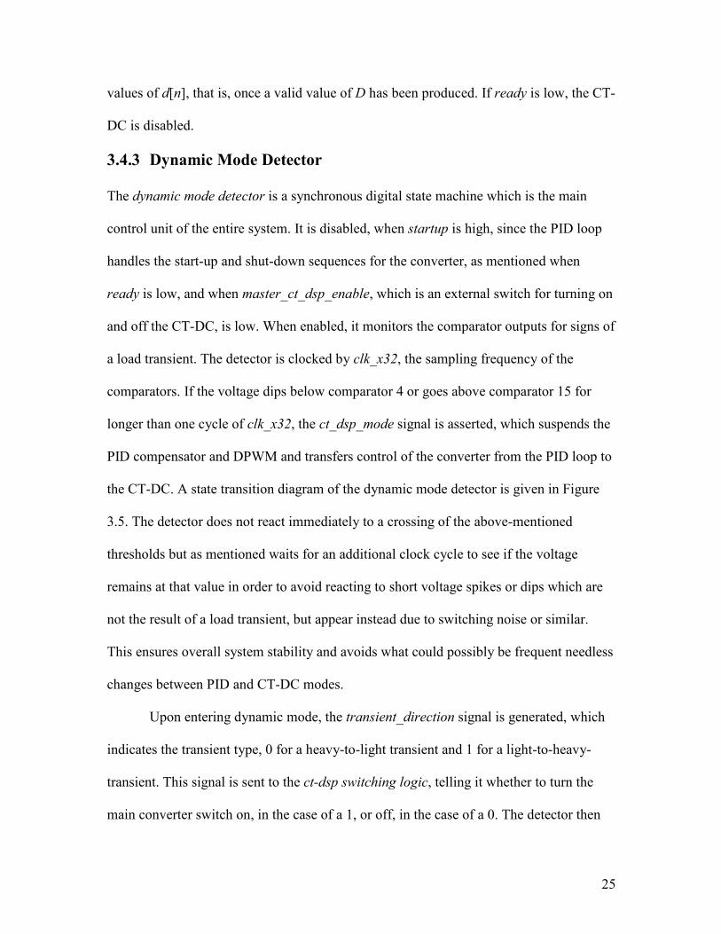
The dynamic mode detector is a synchronous digital state machine which is the main
control unit of the entire system. It is disabled, when startup is high, since the PID loop
handles the start-up and shut-down sequences for the converter, as mentioned when
ready is low, and when master_ct_dsp_enable, which is an external switch for turning on
and off the CT-DC, is low. When enabled, it monitors the comparator outputs for signs of
a load transient. The detector is clocked by clk_x32, the sampling frequency of the
comparators. If the voltage dips below comparator 4 or goes above comparator 15 for
longer than one cycle of clk_x32, the ct_dsp_mode signal is asserted, which suspends the
PID compensator and DPWM and transfers control of the converter from the PID loop to
the CT-DC. A state transition diagram of the dynamic mode detector is given in Figure
3.5. The detector does not react immediately to a crossing of the above-mentioned
thresholds but as mentioned waits for an additional clock cycle to see if the voltage
remains at that value in order to avoid reacting to short voltage spikes or dips which are
not the result of a load transient, but appear instead due to switching noise or similar.
This ensures overall system stability and avoids what could possibly be frequent needless
changes between PID and CT-DC modes.
Upon entering dynamic mode, the transient_direction signal is generated, which
indicates the transient type, 0 for a heavy-to-light transient and 1 for a light-to-heavy-
transient. This signal is sent to the ct-dsp switching logic, telling it whether to turn the
main converter switch on, in the case of a 1, or off, in the case of a 0. The detector then

26
continues to monitor comparators, keeping track of which comparator thresholds have
been crossed. Once the output voltage waveform changes direction, that is once a valley
or peak point has been detected, the minmax signal, indicating which comparator is the
peak or valley, is generated. The minmax value corresponding to each of the possible
values of ∆v is shown in Table 3.2. This value is fed into the time calculator block and is
Figure 3.2: Block diagram of the continuous-time
digital controller (CT-DC)
Figure 3.5: State transition diagram of the
dynamic mode detector
27
used to calculate ton and toff which are then forwarded to the switching logic. Also at this
point the dynamic mode detector enables, by asserting the detected signal, the counter in
the switching logic which uses the time values to generate the optimal switching
sequence. The state machine then waits for the sequence to finish, which is indicated by
the sequence_finished signal from the switching logic going high. It then enters a
blocking state for two converter switching cycles, or 64 cycles of clk_x32. During this
time the CT-DC is inactive, and only the PID loop controls the power stage. This is done
to ensure system stability, to avoid the CT-DC from needlessly reacting to voltage
deviations that may result as due to the transition from the CT-DC back to the PID loop.
The ct_dsp_mode signal is lowered, and the DPWM and PID resume operation as the
system returns to steady state. After the blocking time is up, the dynamic mode detector
reenters its initial state, monitoring the comparators, waiting for another load transient to
occur.
3.4.4 Time Calculator
The time calculator block produces the ton and toff values using the minmax signal and the
output of the duty ratio extractor, D. It consists of multipliers and look-up tables (LUTs).
The LUTs produce the terms in equations 3.3 and 3.4 that contain square roots and
fractions. In this manner the use of more complicated division and square root circuits
that would require more costly multi-cycle operation is avoided. All of the LUTs are
programmable. Upon reset, they default to preset values custom-tailored for the targeted
application, the PIP-212. However, all LUT entries can be rewritten using a very simple
protocol consisting of address (addr), write enable (wen), and datain signals
synchronized to the programming clock signal, data_clk. These signals are connected to

28
the previously mentioned higher level processor on the chip, allowing for the change of
controller parameters. The LUTs generate the LC2 , outVv /∆ , D−1 , and
DD −1/ terms needed by equations 3.3 and 3.4. Each is described in more detail
below.
A. DD −1/ LUT
This look-up table takes the 13-bit output D of the duty ratio extractor as input to produce
as an output the DD −1/ term used in equation 3.3. In order to save silicon area and
provide easy addressing in binary code, this table is limited to 256 entries. However, the
number of values of D is much higher. Mapping each 13-bit value of D to a unique LUT
entry would require 8192 entries in total, resulting in a circuit which would be too large.
For that reason, only the 10 most significant bits of D are used for addressing the LUT.
Even this would still create a table of 1024 entries, still too large. However, it is not
strictly necessary to take into account all values of D. In this specific application, the
input voltage for the converter is 12 V and the output 1.5 V, giving, ideally, a steady state
duty ratio of 0.125 or 12.5%. Taking into account non-idealities that produce different
steady-state duty ratios at different conditions, and the fact that PoL converters generally
supply digital loads with voltages in the range from 1.8 to 0.9 V, while having an input
voltage in the range from 6 to 12 V, it is clear that it is not necessary to take into
consideration the full range of D, from 0 to 100%. Therefore both LUTs in this system
which take D as their input are designed to provide the finest accuracy for a given range
of D most likely to be encountered during operation. To provide good performance, this
range was chosen to be 0.04 < D < 0.45, that is a duty ratio between 4% and 45%.
29
The DD −1/ value produced by the LUT is a 9-bit number. The values stored in
the LUT were arrived at by taking the actual value of a DD −1/ term (with 0 < D < 1)
for a given value of D and multiplying it by 511 and rounding the result to the nearest
integer. This provided a number that could be represented as a binary 9-bit integer. This
process by itself resulted in a degree of approximation, yielding a situation where almost
every 2 or 3 adjacent values of D would map to the same LUT value. Yet, keeping all the
unique values in the range from 4% to 45% would still require 291 entries, larger than the
256 set as the goal. Therefore further reduction of accuracy was performed. Most of the
table entries, 250 of them, were reserved for the targeted range from 4% to 45% where
highest accuracy was required. The remaining six entries were left for values outside of
this range. This was done by averaging the values outside the accurate range at equal
intervals as to produce six equally spaced-out entries all other D values would map to.
This now left the problem of “fitting” 291 separate values into 250 table entries. In the
range of D from 8% to 30%, full accuracy was preserved. In the range from 4% to 8%,
and 30% to 45%, entries were “merged” by averaging together groups of 2 or 3 adjacent
values at equal distances from one another, to produce one the given values of D would
map to. In this way there is a periodic loss in accuracy, but far enough away from the
ideal steady-state value of D in the targeted application. This finally reduced the LUT to
256 entries. Tables showing exact input-to-output mappings for all look up tables are
given in Appendix B1.
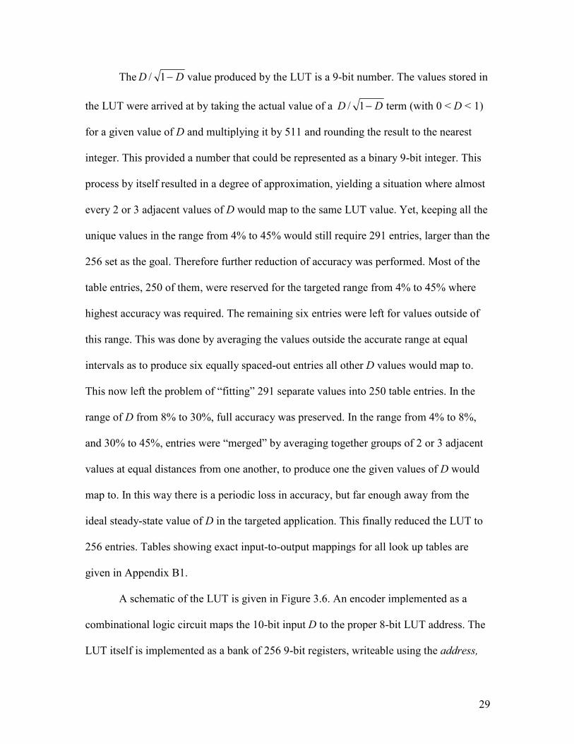
A schematic of the LUT is given in Figure 3.6. An encoder implemented as a
combinational logic circuit maps the 10-bit input D to the proper 8-bit LUT address. The
LUT itself is implemented as a bank of 256 9-bit registers, writeable using the address,

30
write_enable, and data_in signals. A multiplexer is used to select among the registers
using the output of the encoder, producing the required output value for a given D. The
overall structure of the D−1 LUT, described next, is the same, with the difference that
it has half as many entries. The five-entry outVv /∆ LUT has a similar structure, but
without the encoder, which is not necessary in its case.
To create the values for the LUTs and the mappings from D to the LUT entries a
program was written in C++. This same program was then used to generate Verilog HDL
Figure 3.6: Look-up table structure – the DD −1/ LUT

31
code for these modules based on the mappings. The code for this program is given in
Appendix B2.
B. D−1 LUT
This look-up table also takes in the most significant 10 bits of D as input, and produces as
output the D−1 term used in equation 3.4. Similar to the previous case, this is also a 9-
bit integer, arrived at by multiplying the actual value of D−1 by 511 and rounding to
the nearest integer. This produces 123 entries in the range of duty ratio from 4% to 45%,
allowing for full preservation of accuracy of those values. Another 5 entries are left for
values of D outside that range, the mappings for which are produced by the same manner
as above. This results in a LUT of 128 entries. The encoder in this case therefore maps a
10-bit value of D to a 7-bit table address.
C. outVv /∆ LUT
This look up table takes the 3-bit minmax signal, which is produced by the dynamic mode
detector and which indicates which comparator was the peak or valley point, as input,
and produces as output the outVv /∆ term used in both equations 3.3 and 3.4. The
number stored in the LUT is 8-bit, representing the actual value of outVv /∆ multiplied
by 600 and rounded to the nearest integer. This LUT is also reprogrammable, but as
mentioned earlier, ideally the ∆v/Vout ratio should always remain the same, meaning that
this LUT can ideally be used with its default values for all operating conditions. This was
one of the reasons why equations 3.1 and 3.2 were rearranged into 3.3 and 3.4. Using the
original equations, it would be necessary to change to contents of two look up tables (one
for k and one for v∆ ) every time either the power stage components (L and/or C) or
32
the output voltage change. With the arrangement that is used in this implementation and
that follows from equations 3.3 and 3.4, a change of required the output voltage for the
converter ideally requires no reprogramming of LUTs, and at worst requires changing the
contents of one, while similarly a change in L or C requires only the register storing the
LC product to be rewritten, and no other.
D. LC2 Register and the Scaling of ton and toff
The final LUT of the time calculator is a simple writeable register which holds the LC
product of the power stage. The LC2 value is stored as a 6-bit binary integer. Of
particular importance is the manner in which it is scaled. The CT-DC, including the
counter which produces the optimal time switching sequence during transient, runs on
clk_x32. Therefore the final ton and toff values must be binary integers denoting numbers
of clock cycles of clk_x32. Since the switching frequency of the converter is 500 kHz, the
CT-DC system clock, being 32 times higher, is 16 MHz. The produced ton and toff values
are 8-bit, which is sufficient to cover a maximum length transient switching sequence
that can be produced by the default values in the LUTs for the targeted application with
the converter running at either a 500 kHz or 1 MHz switching frequency.
The time calculator block contains four multipliers. First the contents of the
LC2 register (6-bit) are multiplied with the outputs of the D−1 and DD −1/ LUTs
(9-bit), yielding a 15-bit result, of which the 8 most significant bits are taken for further
calculation. Then these two results are multiplied by the output of the outVv /∆ LUT (8-
bit) of which the 8 most significant bits again are taken as the final values of ton and toff.
Equations 3.3 and 3.4 produce ton and toff values in seconds; to convert them to clock
cycles it is necessary to multiply those equations by the frequency of clk_x32. However,
33
through the process of scaling the values for the LUTs and truncating results of
multiplications, the equations have already been multiplied 511, then 600, and then
divided by 128 and again by 256. Therefore the scaling factor for the LC2 term must
be such that when figured into the calculations, the overall scaling factor of equations 3.3
and 3.4 is 16 MHz, the clock frequency. This number is therefore 16 000 000 · 128 · 256
÷ (511 · 600) = 1710006.523. Multiplying LC2 by this value also allows it, a very small
number, to be stored as a 6-bit binary number rounded to the nearest integer. In this
manner all the numbers used in the calculations are binary integers, avoiding the use of
more complicated floating of fixed point arithmetic.
Finally, the option of easily adapting the CT-DC for the control of a converter
operating at 1 MHz also exists. This is done by the means of the frequency select (fs)
input. By default this input should be set to zero, for a switching frequency of 500 kHz
and a system clock of 16 MHz. In the case of a switching frequency of 1 MHz, it is
assumed that the system clock doubles to 32 MHz. In this case, fs is set to one, which
tells the time calculator to double all calculated on and off times, giving a final value in
clock cycles of a 32 MHz clock. The LUT entries described here are as mentioned default
values designed for the targeted application. The look up tables can be reprogrammed
with different values, therefore adapting the controller for different operating conditions.
3.4.5 Time Adjustment
Equations 3.3 and 3.4 assume an ideal converter. However, in a real system, non-
idealities are always present. The time adjustment block is therefore added to correct the
calculated on and off times by a programmable constant amount, so somewhat correcting
for the non-idealities present. The time adjustment block stores in three writeable

34
registers three time increments, ∆t1, ∆t2, and ∆t3. The effect of equivalent-series
resistance (ESR) of the output capacitor C is of main concern here. As explained in [1],
the presence of non-negligible ESR adds a certain lag time to valley point detection
during a light-to-heavy transient, causing undershoot, and therefore non-ideal response.
The solution, as noted in [1], is to delay the switching sequence, or, extend ton by a
certain amount of time corresponding to C·ESR.
During light-to-heavy load transient, the time adjustment block adds ∆t1 to the ton
outputted by the time calculator, while toff is left unmodified. The ton + ∆t1 value is then
forwarded to the switching logic. During a heavy-to-light transient, it is toff that should
modified, while ton is left untouched. However, in this case there is another variable to be
taken into account. If comparator 15 was the peak point, it is possible that the voltage
peak in fact exceeded the maximum known ∆v of 0.11 V (see Table 3.2) by a significant
amount, and therefore the calculated off time is too long. So to correct for the limited
range of the comparators in this case, a constant increment ∆t2 is subtracted from toff. The
toff - ∆t2 value is then forwarded to the switching logic. In the case that comparator 15 is
not the peak, the limited range of the ADC is not a problem and it is ESR once again that
must be corrected for. As before the switching sequence is extended, only this it is on the
side of toff, so that value toff + ∆t3 is forwarded on.
By default, the values of ∆t1, ∆t2, and ∆t3 are set to zero. There is no pre-
calculation of these values in this implementation; rather, they are left out to be
determined experimentally.
35
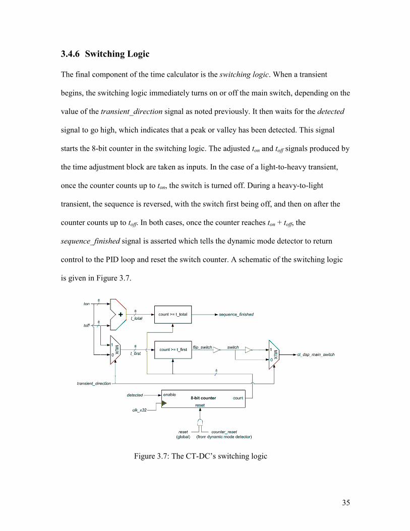
3.4.6 Switching Logic
The final component of the time calculator is the switching logic. When a transient
begins, the switching logic immediately turns on or off the main switch, depending on the
value of the transient_direction signal as noted previously. It then waits for the detected
signal to go high, which indicates that a peak or valley has been detected. This signal
starts the 8-bit counter in the switching logic. The adjusted ton and toff signals produced by
the time adjustment block are taken as inputs. In the case of a light-to-heavy transient,
once the counter counts up to ton, the switch is turned off. During a heavy-to-light
transient, the sequence is reversed, with the switch first being off, and then on after the
counter counts up to toff. In both cases, once the counter reaches ton + toff, the
sequence_finished signal is asserted which tells the dynamic mode detector to return
control to the PID loop and reset the switch counter. A schematic of the switching logic
is given in Figure 3.7.
Figure 3.7: The CT-DC’s switching logic

36
3.5 Simulation Results
The system was simulated using a Verilog-AMS simulator in the Cadence IC design
software suite. The simulated system consisted of the power stage, comparators, PID
loop and CT-DC. The digital components were simulated directly as Verilog blocks
while the analog parts of the loop were modeled in Verilog-A. Figures 3.8 to 3.10 show
simulation results. Shown is the system response to period 30 A load step changes, 10 A
to 40 A, and then 40 A to 10 A.
Figure 3.8 shows the startup sequence of the system (up to 140,000,000 ps), and
two pairs of heavy-to-light and light-to-heavy load transients. The transients occur on the
edges of the load_step signal visible in the figure. As can be seen, the master_ct_dsp_en
signal is held low until about half-way through the simulation, and therefore the first pair
of transients is reacted to by the PID compensator. The second pair of transients is
compensated by the CT-DC, allowing for the comparison of responses. The CT-DC
produces a much better response than the PID compensator in the case of the light-to-
heavy transient, and a slightly better response in the case of the heavy-to-light transient.
Visible here also is the inductor current, and the manner in which it settles much more
quickly to the new steady-state value with the CT-DC active. Visible in this figure are
other signals within the system, such as the ct_dsp_mode signal which goes high during
transients and freezes the PID loop’s operation, and the output of the DPWM (dpwm_out)
which is frozen during a CT-DC transient. It can also be seen that the waveform for the
main switch of the converter is the same as the output of the DPWM during steady-state,
but then follows the value of the ct_dsp_main_switch signal during transients, as

37
Fig
ure
3.8
: S
imula
tion r
esult
s. O
utp
ut
volt
age,
induct
or
curr
ent,
and i
nte
rnal
syst
em s
ign
als.
Com
par
ison o
f tr
ansi
ents
– f
irst
tw
o
load
ste
p c
han
ges
com
pen
sate
d b
y t
he
PID
loop, n
ext
two b
y t
he
CT
-DC
. A
ll t
ransi
ents
are
30 A
load
ste
p c
han
ges
.

38
intended. Visible also is the optimal switching sequence calculated by the CT-DC, in
contrast to that of the PID compensator.
Figure 3.9 shows a comparison of the light-to-heavy load transients of the PID
compensator and the CT-DC. Noticeable is the smaller voltage deviation and faster
settling time of the CT-DC’s response compared to the PID compensator’s. The
maximum voltage drop in the case of the PID is 20 mV, while with the CT-DC it is 10
mV, an improvement of 50%. The settling time of the PID loop’s response is about 30 µs,
while the CT-DC settles the output voltage in about 16 µs. Other signals, including the
main switch with the optimal switching sequence, are also visible.
Figure 3.9: Response to a 10 A to 40 A load step increase: (left) PID
compensator (right) CT-DC
39
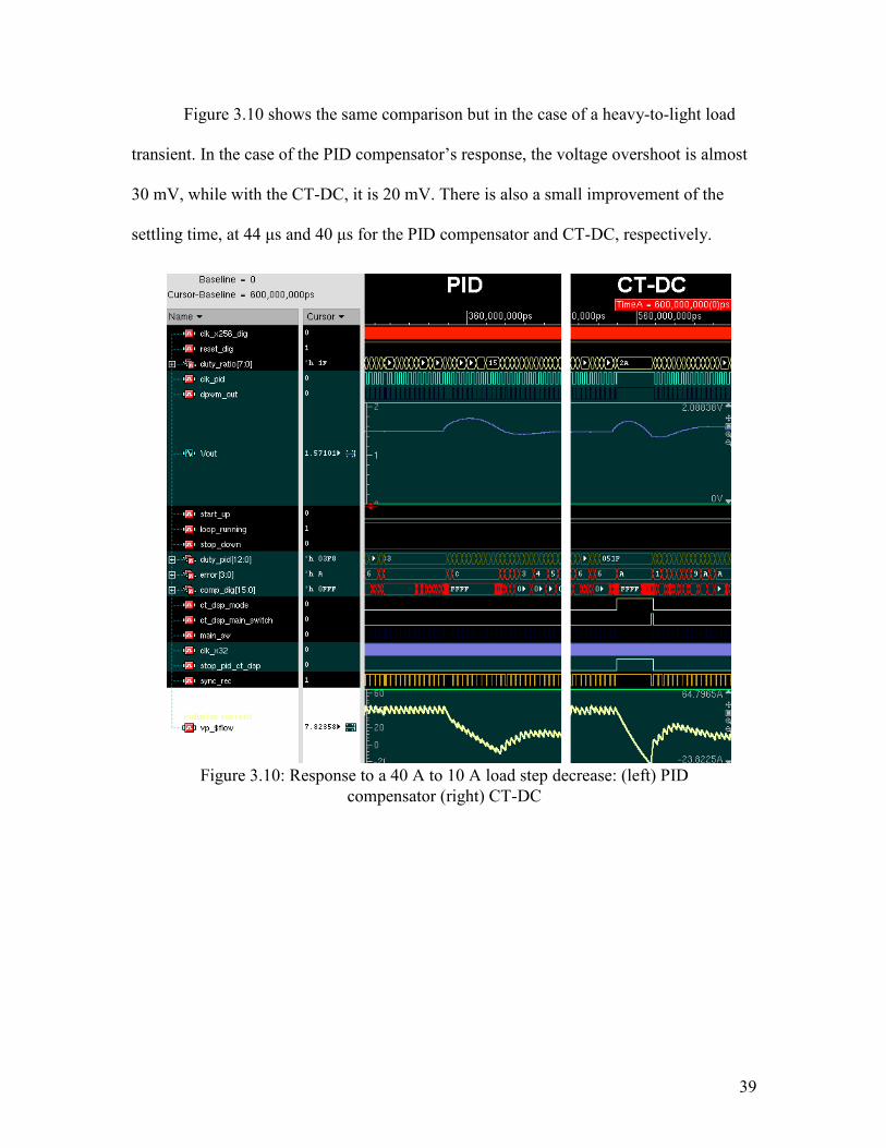
Figure 3.10 shows the same comparison but in the case of a heavy-to-light load
transient. In the case of the PID compensator’s response, the voltage overshoot is almost
30 mV, while with the CT-DC, it is 20 mV. There is also a small improvement of the
settling time, at 44 µs and 40 µs for the PID compensator and CT-DC, respectively.
Figure 3.10: Response to a 40 A to 10 A load step decrease: (left) PID
compensator (right) CT-DC
40
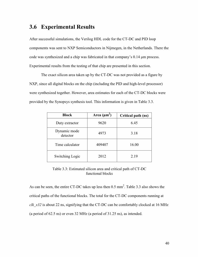
Block Area (µm2) Critical path (ns)
Duty extractor 9620 6.45
Dynamic mode
detector 4973 3.18
Time calculator 409407 16.00
Switching Logic 2012 2.19
Table 3.3: Estimated silicon area and critical path of CT-DC
functional blocks
3.6 Experimental Results
After successful simulations, the Verilog HDL code for the CT-DC and PID loop
components was sent to NXP Semiconductors in Nijmegen, in the Netherlands. There the
code was synthesized and a chip was fabricated in that company’s 0.14 µm process.
Experimental results from the testing of that chip are presented in this section.
The exact silicon area taken up by the CT-DC was not provided as a figure by
NXP, since all digital blocks on the chip (including the PID and high-level processor)
were synthesized together. However, area estimates for each of the CT-DC blocks were
provided by the Synopsys synthesis tool. This information is given in Table 3.3.
As can be seen, the entire CT-DC takes up less then 0.5 mm2. Table 3.3 also shows the
critical paths of the functional blocks. The total for the CT-DC components running at
clk_x32 is about 22 ns, signifying that the CT-DC can be comfortably clocked at 16 MHz
(a period of 62.5 ns) or even 32 MHz (a period of 31.25 ns), as intended.

41
The figures that follow show experimental waveforms provided by NXP collected
during the testing of the CT-DC chip.
3.6.1 Light-to-Heavy Load Transient
The PID loop of the system performed as expected. Figure 3.11 shows the response of
the PID compensator to a 20 A load step increase. As can be seen, the maximum voltage
deviation (dip) is 140 mV. The recovery time is 18 µs.
Figure 3.11: Response of the on-chip PID compensator to a 20 A load step
increase. Time scale: 2 µs/div; CH1: vout, AC coupled, 50 mV/div; CH2: PWM
output (main switch), 5 V/div; CH3: Voltage across load resistor, 0.5 V/div;
CH4: Vg, 2 V/div; CH5: Vref, 0.5 V/div; CH6: vout, DC coupled, 0.5 V/div;
CH7: detected signal; CH8: load step drive signal

42
The CT-DC when enabled, however, did not perform exactly as expected from the
simulation results. When used first with all default settings, the CT-DC would produce
oscillations of the output voltage. This is shown in Figure 3.12. The on and off times
calculated by the CT-DC were in this case not sufficient to compensate for the load
change; the PID compensator would then continue to compensate, but could not do so
quickly enough, and this would then cause the CT-DC to detect another “transient” since
Figure 3.12: Oscillations caused by the CT-DC in response to a 20 A load step
increase. Time scale: 10 µs/div; CH1: vout, 0.5 V/div; CH2: PWM output (main
switch), 5 V/div; CH3: Vg, 2 V/div, 0.5 V/div; CH4: detected signal, 2 V/div;
CH5: Vref, 0.5 V/div. Digital channels, top to bottom: dmd_enable,
counter_reset, detected, sequence_finished, transient_direction, minmax[2],
minmax[1]
43
the voltage would at one point cross the CT-DC thresholds. The CT-DC does block for a
while after each transient, but in this case the blocking time was not long enough to allow
the PID loop to correct that which the CT-DC could not. Since the blocking time was
hardcoded, it was not possible to change it after fabrication. The oscillations caused the
CT-DC to detect a series of “transients”, light-to-heavy and heavy-to-light, and being
unable to compensate, the CT-DC actions just further increased them, and so on.
However, this behaviour was corrected by the use of the time adjustment block described
in section 3.4.5. Since by default the time increment values in the adjustment block are
set to zero, the CT-DC does not compensate for ESR. While this was not an issue during
simulation, it clearly showed its impact during experimental testing. This is probably a
result of the ESR not being sufficiently modeled in simulation. Therefore, different
values of ∆t1 were tried until a good response was achieved. Best results were given by
setting ∆t1 to a value of 2 to 4 cycles. Large ∆t1 values produced considerable overshoot.
A response of the CT-DC to a 20 A load step increase with ∆t1 tuned to produce the best
possible result is shown in Figure 3.13. It can be seen that the maximum voltage dip is 75
mV, which is almost half of that of the PID compensator. However, even though this was
the best response that was observed during experimental testing, it is still not ideal. An
overshoot of 50 mV exists, lengthening the settling time since this overshoot must be
corrected by the PID after the CT-DC finishes. Still, at 10 µs, the settling time of the CT-
DC is still better than that of the PID alone.

44
In conclusion, after experimental tuning of the ∆t1 parameter, the CT-DC
produced a light-to-heavy load transient response superior to that of the PID
compensator. However, this response was not ideal. There are several reasons why this
was the case and why the experimental results did not match the simulations. The first is
the discrepancy between the Verilog-A models of the analog components of the loop and
their actual counterparts. While converter non-idealities were modeled to an extent, the
comparators for example were modeled as being completely ideal; things such as
Figure 3.13: Response of the on-chip CT-DC to a 20 A load step increase with
∆t1 set to 4. Time scale: 2 µs/div; CH1: vout, AC coupled, 50 mV/div; CH2:
PWM output (main switch), 5 V/div; CH3: Voltage across load resistor, 0.5
V/div; CH4: Vg, 2 V/div; CH5: Vref, 0.5 V/div; CH6: vout, DC coupled, 0.5
V/div; CH7: detected signal; CH8: load step drive signal. Digital channels, top
to bottom: dmd_enable, counter_reset, detected, sequence_finished,
transient_direction, minmax[2], minmax[1]
45
switching noise, crosstalk, or delay were not taken into account. The second is that the
digital components of the loop were simulated only as Verilog code, not as synthesized
transistor-level circuits. This was done because development time was short and
Verilog/Verilog-A simulation is much faster than transistor level Spice or Spectre
simulation, and because at the University of Toronto the design files for NXP’s
implementation technology were not available. There are further reasons for incorrect
calculations of the on and off times, and they are considered in detail in section 3.7.
3.6.2 Heavy-to-Light Load Transient
While it was possible to achieve a response superior to that of the PID compensator in the
light-to-heavy load change case by tuning ∆t1, the situation with the heavy-to-light
transient was more difficult. A CT-DC response to a heavy-to-light load change, a 20 A
load current decrease, is shown in Figure 3.14 (in this figure both transients are shown,
the heavy-to-light is to the right). The problem here is with the limited range of the
comparators. The voltage peak during transient (first peak on the figure in the heavy-to-
light transient, to the right) is 140 mV above the reference; the comparators only detect
deviations as large as 110 mV. This causes the ton and toff produced by the CT-DC in this
case to be inadequate, since the wrong value of ∆v = 110 mV is used in the calculations.
The times are too short to return the output voltage to its reference level; again, since the
blocking time is too short for the PID to do so afterwards, the CT-DC detects another
heavy-to-light transient since the output voltage is still above that threshold, and this
causes further overshoots. Unlike with the heavy-to-light case, tweaking the ∆t2, and ∆t3
parameters in the time adjustment block did not produce a notable improvement. The
problem here is further aggravated by peak point detection lag, which will be discussed

46
in the next section. The solution to this problem lies in modifying the dynamic mode
detector: first, extending the length of time it is in the blocking state, and, second, adding
additional checks so that during a heavy-to-light load transient, it monitors the output
voltage at the end of the switching sequence, and then, if it is too high, keeps the main
switch off until it drops to a value closer to the reference, and only then returns the
control of the converter to the PID loop. Also, the comparators could be redesigned to be
asymmetric about the reference, that is, to have a higher range of above the reference
Figure 3.14: CT-DC response to a 20 A load step change (increase followed by
decrease). Time scale: 10 µs/div; CH1: vout, 0.5 V/div; CH2: PWM output
(main switch), 5 V/div; CH3: Vg, 2 V/div, 0.5 V/div; CH4: detected signal, 2
V/div; CH5: Vref, 0.5 V/div; CH8: load step drive signal. Digital channels, top
to bottom: dmd_enable, counter_reset, detected, sequence_finished,
transient_direction, minmax[2], minmax[1]

47
than below it, so that the proper value of ∆v can be recorded. Both of these approaches
require redesign and re-fabrication of the circuitry.
Even with such fixes implemented, the performance of the CT-DC would
probably be only comparable to that of the PID compensator, and not substantially better:
this is the result visible in the simulations, in Figures 3.8 and 3.10. As noted earlier in
Chapter 2, the heavy-to-light transient problem suffers from a particular physical
limitation in the Buck topology. An approach for solving this problem specifically and
achieving a heavy-to-light transient response comparable to that of the CT-DC in the
light-to-heavy case is the subject of Chapter 5.
3.7 System Limitations and Issues
During experimental testing, several issues causing non-ideal response that were not
apparent during simulations were discovered. They are the subject of this section.
3.7.1 Peak and Valley Point Detection Lag
A key issue that influences CT-DC performance is the size of the ADC bins, that is, the
distance between comparator thresholds. The production of an optimal switching
sequence depends on accurate detection of peak and valley points of the output voltage.
A problem arises when a peak or valley occurs in between two comparator thresholds.
The output voltage dips below, for example, the threshold of comparator 3, but does not
go low enough to trigger a change of the state of comparator 2. Rather, the valley point
occurs somewhere half-way in between. When the voltage rises back above comparator
3, that comparator is detected as the valley point while the point in time at which the
voltage rises above its threshold is taken as the moment at which the valley point
occurred. The valley point, however, occurred earlier in fact, and the produced on and off

48
times are too long, causing the overshoot seen in Figure 3.12. No compensation for this
effect was included in the fabricated implementation of the CT-DC, and modification of
the circuit is required. The problem is solved by adding extra counters to the dynamic
mode detector; whenever the system enters one of the transient states (C to H or N to W)
a counter is started; therefore the system keeps track of how long the voltage is at each
level. When the peak or valley is detected, the value for the correct voltage level is
selected via the minmax signal, and half of this value is then subtracted from ton. The
assumption here is that the peak or valley occurred at the half-way point of the time the
voltage spent past the highest/lowest comparator threshold.
3.7.2 The Value of D
For an ideal Buck converter, as noted earlier, the steady state duty ratio is defined as
gout VVD = [4]. As can be seen from the derivation of Equations 3.1 and 3.2 shown in
Chapter 2, it is this relation which is used to remove the input voltage Vg as a term from
the original equations for ton and toff. D is used because no direct information about Vg is
available to the controller, while the duty ratio can be extracted from the PID
compensator.
One problem that was not apparent during simulation but would sometimes cause
incorrect calculation of ton and toff was the fact that, due to delays in the circuit and
depending on which point of the switching cycle a load change occurs, the PID
compensator would sometimes start reacting to a load transient before the CT-DC would
freeze it. This would then cause the duty extractor to take as input a value of d[n] that
was a steady-state duty ratio, creating an incorrect value of D for equations 3.3 and 3.4.
The solution to this problem is fairly simple, namely, that the duty extractor should

49
monitor the PID error and take in values of d[n] for averaging only when the error is
zero, that is, the system is in steady-state.
Another issue are converter non-idealities. Figure 3.15 shows a circuit of a Buck
converter with non-idealities, such as ESR, inductor resistance RL, and MOSFET on-
resistance modeled. Even ignoring ESR, the following equation is derived for the ratio
between the output and input voltage:
SRonMSonLg
out
RDDRRR
RD
V
V
−− +++⋅=
' (3.5)
From equation 3.5 it is clear that the value of D now depends on the value of the load as
well (R), and is no longer the simple relation used to produce equations 3.1 and 3.2. Since
the value D for the purpose of equations 3.3 and 3.4 is extracted from the PID
compensator, which always works in feedback to maintain the same input to output
voltage ratio, it is influenced by non-idealities and changes with the load conditions, it
can cause incorrect calculation of ton and toff. With high-efficiency power stages such as
the PIP-212 and with the converter operating in its optimal efficiency range, this is not a
significant problem, since the value of D remains close to the ideal value of gout VV .
However, with a converter outside of its optimal efficiency range, or with a low-
Figure 3.15: Buck converter with non-idealities
included in the schematic

50
efficiency power stage where non-idealities are noticeable large, the value of D can differ
by as much as 10% to 30% between one load condition and the next. In this case the
values of ton and toff produced by 3.3 and 3.4 are seriously compromised. To have the CT-
DC operate in such conditions, it would be necessary to implement sampling of the input
voltage Vg and the use of that information for the calculation of on and off times, rather
then rely on information from the PID loop.
3.7.3 The CT-DC to PID Transition
After a load transient is completed, the control of the system passes back to the PID
compensator. In simulation, where the PID loop was frozen by the CT-DC almost
instantly upon a transient, the transition back was not seen as an issue. However in
experimental testing it became apparent that careful attention must be paid to exactly this
transition from the CT-DC back to the PID loop. As noted in the previous section, the
PID sometimes starts compensating for the transient itself before control passes to the
CT-DC. As noted in Chapter 2, the PID compensator operates on the following control
law, producing the duty ratio value for the DPWM d[n] using the error values e[n],
]2[]1[][]1[][ −⋅+−⋅+⋅+−= necnebneandnd (3.6)
If the PID is simply restarted in the same state it was disabled in prior to the load
transient, the values of d[n – 1], e[n], e[n – 1], and e[n – 2] that are stored in the
compensator’s registers can be those not corresponding to steady-state, and this can cause
further deviations in the output voltage. Since the CT-DC should ideally produce a
perfect response and return the output voltage to steady-state, that is, error zero, the
easiest approach to handling the CT-DC to PID transition is to simply reset all the error
registers to zero, and load the duty ratio register d[n – 1] with the steady-state duty ratio
51
value present in the duty ratio extractor. However, as can be seen, the CT-DC is not
always ideal, and overshoot and undershoot can occur. Therefore, it is better to capture
the actual error at the point the CT-DC finishes its switching sequence, and then load that
value into the error registers. This will allow the PID to react more quickly when it is
enabled and allow for a smoother transition.
The problem of which duty ratio to store into d[n – 1] becomes an issue when
non-idealities become significant, causing noticeably different values of D for different
load conditions, as discussed in the previous section. In this case it is no longer
appropriate to load the d[n – 1] register with the steady state value from a previous, that
is different, load condition. If the new value of D is significantly larger or smaller than
the previous, doing this can throw the system into another transient. Therefore it is
necessary to calculate, at least approximately, the new value of D. This can be done using
the techniques described in [57], [58].
3.7.4 The Effect of Switch On-Resistance
The non-ideality with the most dramatic effect on CT-DC operation is the MOSFET on-
resistance. The PIP-212 has on-resistance of below 10 mΩ for both switches [21]. This
was modeled in simulation, and did not have a significant effect on system operation,
either in simulation or later during testing of the fabricated controller. However, as the
on-resistance, Ron, increases beyond 10 mΩ, serious problems arise in CT-DC operation.
Recall from Chapter 2 the integrals for charge, Q, used to derive equations 3.1 and 3.2:
dtdL
VVQ
toutg
t
on
on
τ∫∫−
=00
(3.7)
dtdL
VQ
t
out
t
off
off
τ∫∫−
=00
(3.8)

52
These integrals are constructed without taking into account converter non-idealities.
Consider now the effect of the on-resistance of the main switch and the synchronous
rectifier, Ron-MS and Ron-SR, respectively. The integrals now become
dtdL
iRVVQ
tLMSonoutg
t
on
on
τ∫∫⋅−−
=−
00
(3.9)
dtdL
iRVQ
t
LSRonout
t
off
off
τ∫∫⋅−−
= −
00
(3.10)
It is important to note that now, the value of the inductor current, iL, is now a term in the
equations. If the resistances are large enough, Equations 3.7 and 3.8 are no longer good
approximations of the system, and Equations 3.1 and 3.2 are incorrect for producing an
optimal switching sequence. This can be seen from the simulation results shown in
Figures 3.16 and 3.17. Here Ron-MS = 50 mΩ and Ron-SR = 70 mΩ, while the load step
changes are the same in simulations shown previously. As can be seen, in this case the ton
and toff values produced by the CT-DC are completely off the mark. The inductor current
Figure 3.16: CT-DC response to 30 A load step changes with a converter
with high MOSFET on-resistance

53
does not reach the new steady-state level as in previous simulations with low on-
resistances, but instead drops back almost to the old steady-state level at the end of the
switching sequence, making it as if no transient compensation occurred at all. As a result,
the output voltage dips again as now the PID must compensate. Equations 3.1 and 3.2
cannot be easily augmented (as was the case with ESR) to correct for the influence of on-
resistance because of the dependence on the inductor current iL.
While this did not surface as a problem with the targeted application for this
implementation, the PIP-212, the on-resistances of which are low enough to be neglected,
there are power switches which have on-resistances as high as those used in the
simulations in this section. Therefore, when seeking to use the CT-DC for a particular
application, caeful attention must be paid to the selection of Power MOSFETs.
Figure 3.17: CT-DC response to 30 A load step changes with a converter
with high MOSFET on-resistance, enlarged

54
Chapter 4
Auto-Tuning Extension to the
Continuous-Time Digital Controller
4.1 One-Shot Auto-Tuning through the Observation of
Transient Performance
Auto-tuning is the ability of a controller to, during system operation, extract parameters
of the power stage and thereby improve its performance. The continuous-time digital
controller (CT-DC) described in Chapter 3 is constructed so that it is programmable, with
its main parameters used for calculations alterable, and this makes it ideal for adaptation
with an auto-tuner. The main target of the auto-tuner are the inductance and capacitance
values of the power stage, which differ from one particular power stage to the next due to
tolerances, and which may change over time in a particular converter due to aging effects
or differing operating conditions, such as temperature variations. The LC product is
stored as a parameter in the CT-DC in a reprogrammable register. Among the several
auto-tuning techniques mentioned in Chapter 2, the one presented in [1], [13], extracts the
LC product by deliberately inducing disturbances in the output voltage and then
observing their characteristics. However, if the CT-DC is already available and running,
this is not necessary to perform auto-tuning. Disturbances in the output voltage occur
“naturally” – they are caused by load changes. The theory from which the CT-DC

55
equations are derived then allow for the extraction of the LC product simply by observing
the controller’s transient performance.
Consider again equations 3.3 and 3.4., but now with the LC2 term replaced with
the parameter K:
out
onV
v
D
DKt
∆
−
=
1 (4.1)
out
offV
vDKt
∆−= 1 (4.2)
Figure 4.1: Transient response of the CT-DC when the
on and off times are correct (optimal, top), too short
(undershoot, middle), and too long (overshoot, bottom)

56
K is a reprogrammable parameter of the CT-DC, stored in its LC2 register, as
described in Chapter 3. Ideally, LCK 2= , where L and C are the inductor and capacitor
values of the power stage, respectively. However, the value of K may be off, due to the
reasons mentioned above. Consider now Figure 4.1. The term ∆v is the voltage drop
which occurs during transient. It is this voltage drop which must be compensated. As a
result of the CT-DC’s actions, the voltage goes up from the valley point by an amount
∆v’. For an ideal response, ∆v = ∆v’. However, due an incorrect value of K, ∆v’ may be
higher or lower than ∆v.
Recall from Chapter 2 that equations 4.1 and 4.2 are derived using the principle of
capacitor charge balance, where the lost charge in the capacitor is denoted Q and is
defined as Q = C∆v. The charge put back into the capacitor during transient resulting
from the switching sequence consisting of ton and toff is denoted Qon and Qoff. Ideally,
Qon + Qoff = Q, but if K is incorrect, this may not be the case. Using the definition for
capacitor charge, the total charge put into the capacitor during the transient switching
sequence is
vCQQ offon′∆⋅=+ (4.3)
Recalling equations 2.4 and 2.5 for Qon and Qoff, and rearranging equation 4.3 to solve for
∆v’, the following equation is derived:
LC
tVtVVv
offoutonoutg
2
)(22
+−=′∆ (4.4)
Substituting in equations 4.1 and 4.2 for the on and off times, and factoring out K:
LC
V
vDV
V
v
D
DVV
Kv out
out
out
outg
2
)1()1
)((2
2
∆−+
∆
−−
=′∆ (4.5)

57
Note again the distinction between ∆v, the voltage drop from the reference value to the
valley point, and ∆v’, the difference between the valley point and the voltage level at
which the transient finishes. Note also the difference between K, the parameter of the CT-
DC, and LC, which is the product of the actual inductance and capacitance values. Now,
substituting into equation 4.5 the Buck converter conversion ratio Vout = DVg [4] and
consolidating terms,
LC
vKv
2
2 ∆=′∆ (4.6)
Equation 4.6 can be rearranged so that the following ratio for K is obtained:
v
v
LC
K
∆
′∆=
2 (4.7)
As noted earlier, ideally both sides of equation 4.7 should be equal to 1. However, if this
is not the case, equation 4.7 allows for the extraction of the power stage’s LC product
after just one non-ideal transient:
v
vKLC
′∆
∆=2 (4.8)
After this value is calculated, K can be set to LC2 , ensuring ideal transients from that
point on. This is one-shot auto-tuning.
4.2 System Architecture
The auto-tuner is implemented as simply an additional block of the CT-DC presented in
Chapter 3. The task of the auto-tuner is to monitor the performance of the CT-DC.
Initially, it is programmed with the same value of K as the LC2 register of the CT-DC.
Upon a transient, the auto-tuner captures the value of ∆v; when the transient is over, it

58
captures the value of ∆v’, and then calculates the new K, that is, it extracts the
LC2 value based on equation 4.8. This value is then programmed into the
LC2 register of the CT-DC. A block diagram of the auto-tuner is given in Figure 4.2.
There are three main parts of the tuner. The first is a finite-state machine, the
monitor/programmer. It waits until the detected signal from the dynamic mode detector
of the CT-DC is raised, and on this positive edge it captures the minmax signal which
indicates which comparator is the valley point, thereby recording ∆v. It then waits for the
ct_finished signal to go high. When this happens, indicating the end of the CT-DC
switching action, it records the value of the comparator outputs at that point and stores
Figure 4.2: Block diagram of the auto-tuner

59
them in the ct_dsp_error register, thereby recording the value of the output voltage at the
end of the CT-DC’s transient compensation, in other words, ∆v’. Following this, the
calculated value of LC2 becomes available. The monitor/programmer then places this
value of the LC_datain bus, raises the LC_wen signal and creates a data_clk pulse. This
reprograms the CT-DC’s LC2 register. This new value is then stored internally to the
auto-tuner as well, for future calculations.
The second part is the one-shot tuner. It calculates the correct value of
LC2 based on equation 4.8. Since the output voltage is quantized by the sixteen
comparators, the number of combinations of ∆v and ∆v’ values is finite, and this block
can therefore be implemented with look-up tables. Ideally, after one load transient, the
correct LC2 value should be extracted by the one-shot tuner. However, due to converter
non-idealities, measurement error, and rounding error in the number representation and
calculations, this may not be the case. This is why there is a third main block in the
system, the iterative tuner. It is used for fine adjustment of the K value after the tuning
based on equation 4.8 has been performed. The monitor/programmer maintains a counter,
so that after each use of the one-shot tuner, the next three adjustments, if necessary, are
iterative fine tunings. Based on that state of this counter, either the output of the one-shot
or iterative tuner is selected to be placed on the LC_datain bus. Verilog code for the auto-
tuner module, and the CT-DC modules containing some of the improvements noted in
section 3.7, is given in Appendix C.
Due to the problems experienced with the heavy-to-light transient described in
Chapter 3, and noting the general difficulties regarding heavy-to-light load changes

60
mentioned earlier, only the light-to-heavy load transient case is treated here. The problem
of heavy-to-light transient response is the subject of the next chapter.
4.2.1 One-Shot Tuning
The look-up tables of the one-shot tuner are constructed in a similar manner to those
described in Chapter 3. There is one LUT for each possible value of ∆v, that is, each
possible value of minmax in the system, giving a total of five. They each take the
ct_dsp_error value, which represents ∆v’, as input. For each comparator that is the valley
point, ∆v’ may only be one of the comparators above it; therefore the LUTs have from
eleven (for minmax = 0, or comparator 4 being the valley) to fifteen (for minmax = 4, or
comparator 0 being the valley) entries. Each entry is the corresponding value of
'/ vv ∆∆ multiplied by 64, and stored as an 8-bit binary integer. Scaling is utilized again
as in Chapter 3 in order to avoid the use of floating-point arithmetic. The minmax signal
is used to select among the outputs of the LUTs, thereby generating the correct
'/ vv ∆∆ value for the transient in question. This value is then multiplied by K (old_LC
in Figure 4.2) and then divided (by means of a bit shift) to get rid of the scaling factor and
create a 6-bit value (newLC) that can be written into the CT-DC’s register. If comparator
7 or 8 is the peak of the output voltage waveform after transient, then no tuning needs to
be performed, as this indicates an optimal response has been achieved. For that reason, in
this case the LUTs output 1, so that K remains unchanged.
4.2.2 Iterative Tuning
Iterative tuning is a simple process whereby K is increased (in the case of undershoot) or
decreased (in the case of overshoot) by a fixed amount depending on ∆v’, that is, the
value of the ct_dsp_error signal. If comparators 6, 7, or 8 are the peak after transient, K is
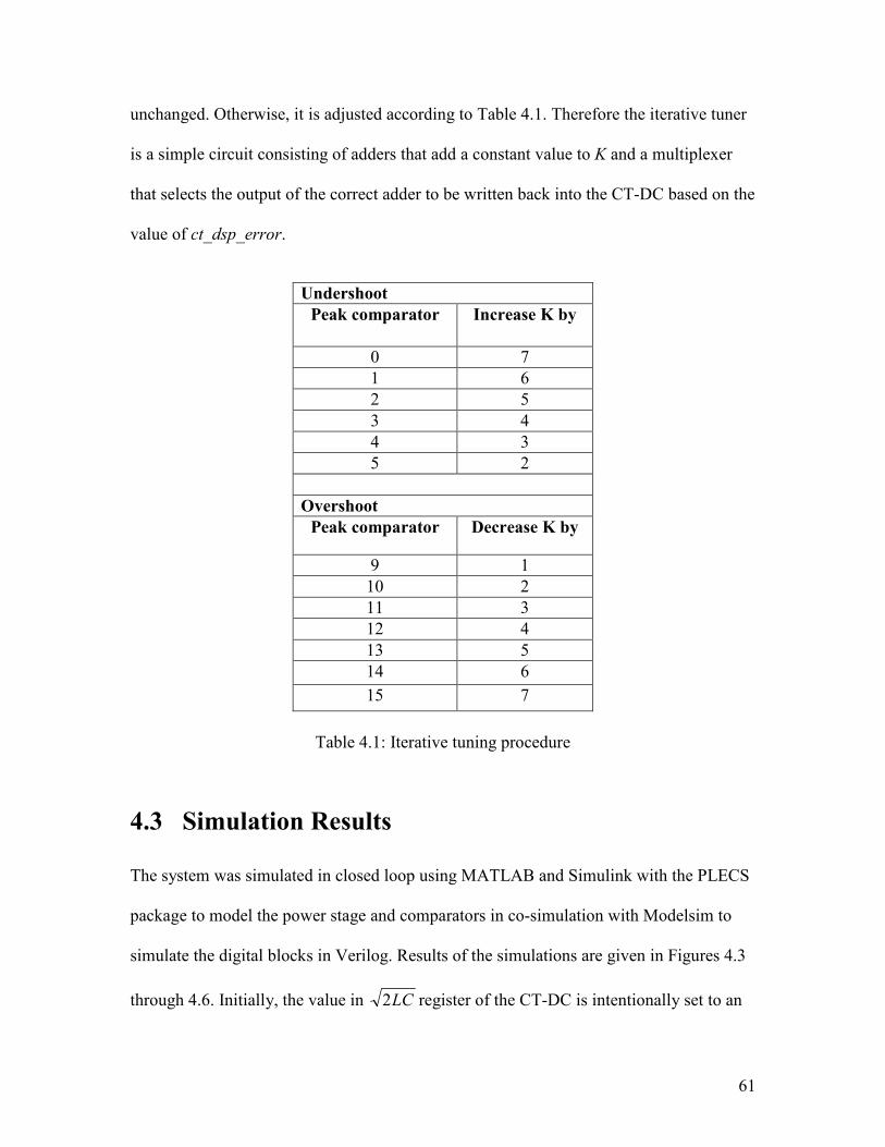
61
unchanged. Otherwise, it is adjusted according to Table 4.1. Therefore the iterative tuner
is a simple circuit consisting of adders that add a constant value to K and a multiplexer
that selects the output of the correct adder to be written back into the CT-DC based on the
value of ct_dsp_error.
4.3 Simulation Results
The system was simulated in closed loop using MATLAB and Simulink with the PLECS
package to model the power stage and comparators in co-simulation with Modelsim to
simulate the digital blocks in Verilog. Results of the simulations are given in Figures 4.3
through 4.6. Initially, the value in LC2 register of the CT-DC is intentionally set to an
Undershoot
Peak comparator Increase K by
0 7
1 6
2 5
3 4
4 3
5 2
Overshoot
Peak comparator Decrease K by
9 1
10 2
11 3
12 4
13 5
14 6
15 7
Table 4.1: Iterative tuning procedure
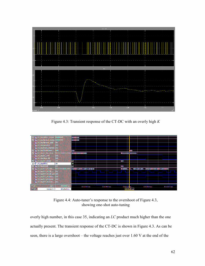
62
overly high number, in this case 35, indicating an LC product much higher than the one
actually present. The transient response of the CT-DC is shown in Figure 4.3. As can be
seen, there is a large overshoot – the voltage reaches just over 1.60 V at the end of the
Figure 4.4: Auto-tuner’s response to the overshoot of Figure 4.3,
showing one-shot auto-tuning
Figure 4.3: Transient response of the CT-DC with an overly high K

63
CT-DC switching action. The corresponding digital signals are given in Figure 4.4.
Visible is in the initial value of K (oldLC), which is 35. The minmax signal is 010,
indicating that comparator 2 is the valley point, i.e. ∆v = 0.09 V. The ct_dsp_error signal
Figure 4.6: Auto-tuner’s response to the overshoot of Figure 4.5,
showing iterative tuning
Figure 4.5: Transient response of the CT-DC after auto-tuning

64
indicates that the voltage topped out at comparator 14, the threshold of which is 1.60 V,
and therefore ∆v’ = 0.19 V. This gives 68825.0'/ =∆∆ vv , which when multiplied by K,
gives 24.1. As can be seen in Figure 4.3, the LC_datain bus becomes 24, which is the
calculated value, and data_clk and LC_wen are raised to write this number into the CT-
DC’s register. Therefore the correct operation of the one-shot tuner is verified.
Figure 4.5 shows the next transient. The overshoot, reduced by about 50 mV, is
now much lower but it still exists, as the result of the calculation performed previously
does not give ideal results due to the inaccuracies mentioned earlier. Figure 4.6 shows the
corresponding digital signals. Since one-shot tuning was performed just one transient ago,
now iterative tuning is done. The ct_dsp_error signal shows that the voltage topped at out
comparator 9, and therefore, as set out in Table 4.1, K is reduced by one, to 23, and this
value is written into the LC2 register.

65
Chapter 5
Current-Steered Buck Converter for
Improving Heavy-to-Light Load
Transient Response
5.1 The Problem of the Heavy-to-Light Load Transient
When it comes to examining the heavy-to-light load transient response of a buck
converter, comparing a controller’s performance during a heavy-to-light transient to that
of light-to-heavy transient, and improving upon it, there is a particular physical limitation
which becomes apparent when modern PoL supplying digital loads are concerned. The
CT-DC considered earlier in this work was demonstrated on a 12 V to 1.5 V converter.
Many digital loads for PoL today use supply voltages that are even lower, down to 0.9 V,
and this is expected to decrease further, to 0.7 V in short term and to go as low as 0.5 V
in the long term [50]. During a heavy-to-light load transient, the load current goes down,
and there is an excess of current in the inductor which needs to be dissipated. With
controllers such as a PID compensator and the CT-DC, this current is essentially
discharged into the load, causing a spike in the output voltage. Such spikes can be
harmful to the load, and therefore large output capacitors are required for their
suppression. The limiting factor in how quickly this excess current can be discharged is

66
the inductor slew rate, which, in a buck converter, is defined [4] to be
L
v
dt
di outL −= (5.1)
Therefore, with the output voltage vout as low as it is, this rate is quite slow, and is to
become even slower in the future, signifying that as output voltages decrease, while, at
the same time, output currents increase [50], possible output spikes during heavy-to-light
transients become larger, necessitating ever larger, bulkier and costlier output capacitors.
In the simulation results shown in Chapter 3 the CT-DC only marginally
improved the heavy-to-light transient response as compared to a standard PID
compensator, whereas in experimental testing it could not perform properly during such a
transient at all. Moreover, due to this basic physical limitation of slew rate, whichever
method is used for improving transient response in a Buck converter will result in a
disproportionate situation between the two responses: the heavy-to-light transient
response will almost always not be as good as the reverse, light-to-heavy case. Therefore
a new approach, dealing with a modification of the Buck topology itself to overcome this
limitation, is presented in this chapter.
5.2 Modified Buck Topology
As discussed in Chapter 2, various attempts at modifying the buck converter topology to
improve heavy-to-light load transient response have been made. These generally fall into
two broad categories. One general approach is the addition of extra conduction paths
[52], [53], through which the excess inductor current can be dissipated. This is generally
done by adding extra resistors connected to ground which are connected to the converter
output by means of a switch during a transient. While this method is successful in

67
providing a faster transient and a smaller output voltage spike, it reduces the efficiency of
the converter. The excess current in the inductor is simply “burned” through these
resistive paths, rather than being used for load operation, and is essentially wasted. The
second approach [54]-[56] is to use stepped inductors, essentially two inductors in
parallel, so that different inductances are present in the converter during steady-state and
transient. A smaller inductance value is used during transient than during steady-state,
therefore increasing the slew rate. However, the construction of such circuits can be
costly and complicated.
Here a novel approach is presented, whereby a buck converter is modified solely
by the addition of two extra switches. As shown in Figure 5.1, besides the existing
converter main switch and synchronous rectifier, denoted Q1 and Q2, respectively, an
extra switch, Q3, is added between the inductor on one side and the output capacitor and
load on the other, and another, Q4, is added to crate a breakable path in between the
positive terminal of the input voltage and negative terminal of the inductor.
Figure 5.1: Modified current-steered buck converter topology for
improving heavy-to-light load transient response

68
5.3 Principle of Operation – Current Steering
During steady-state and while undergoing light-to-heavy transients, the modified
converter of Figure 5.1 operates as an ordinary buck converter: switch Q3 is left always
on, while Q4 is always off. This state of the converter is shown in Figure 5.2(a).
However, during heavy-to-light transients, the configuration changes: Q1 and Q3 are left
off, while Q2 and Q4 are turned on. This is shown in Figure 5.2(b). At this point the
connection between the inductor and the output is broken; there is a new circuit made
between the inductor and the input voltage. The inductor current, iL, is now “steered”
back into the source. In most power supplies, there is an input capacitor that serves to
minimize the effect of switching noise [4], in parallel with the source. Therefore the
Figure 5.2: Converter states: a) during steady-state and light-to-
heavy transients b) during heavy-to-light transients
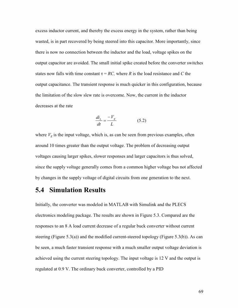
69
excess inductor current, and thereby the excess energy in the system, rather than being
wasted, is in part recovered by being steered into this capacitor. More importantly, since
there is now no connection between the inductor and the load, voltage spikes on the
output capacitor are avoided. The small initial spike created before the converter switches
states now falls with time constant τ = RC, where R is the load resistance and C the
output capacitance. The transient response is much quicker in this configuration, because
the limitation of the slow slew rate is overcome. Now, the current in the inductor
decreases at the rate
L
V
dt
di gL−
= (5.2)
where Vg is the input voltage, which is, as can be seen from previous examples, often
around 10 times greater than the output voltage. The problem of decreasing output
voltages causing larger spikes, slower responses and larger capacitors is thus solved,
since the supply voltage generally comes from a common higher voltage bus not affected
by changes in the supply voltage of digital circuits from one generation to the next.
5.4 Simulation Results
Initially, the converter was modeled in MATLAB with Simulink and the PLECS
electronics modeling package. The results are shown in Figure 5.3. Compared are the
responses to an 8 A load current decrease of a regular buck converter without current
steering (Figure 5.3(a)) and the modified current-steered topology (Figure 5.3(b)). As can
be seen, a much faster transient response with a much smaller output voltage deviation is
achieved using the current steering topology. The input voltage is 12 V and the output is
regulated at 0.9 V. The ordinary buck converter, controlled by a PID

70
compensator, produces a maximum voltage deviation (spike) of 200 mV, while in the
case of the current-steered topology the spike is a much smaller 75 mV, which is 2.7
times less. Similarly, the settling time of the output voltage waveform in the ordinary
Figure 5.3: Simulation results, transient response to a 10 A to 2 A
load step change (∆I = 8 A):
a) (above) with PID only b) (below) with inductor current
steering
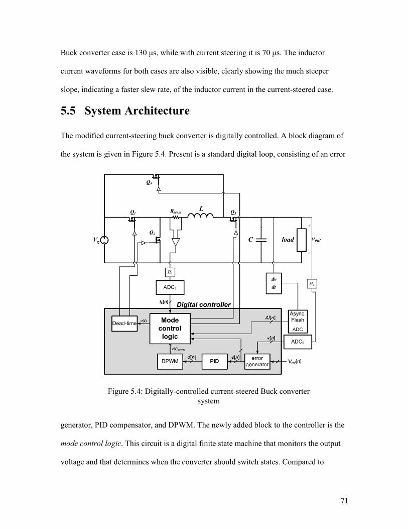
71
Buck converter case is 130 µs, while with current steering it is 70 µs. The inductor
current waveforms for both cases are also visible, clearly showing the much steeper
slope, indicating a faster slew rate, of the inductor current in the current-steered case.
5.5 System Architecture
The modified current-steering buck converter is digitally controlled. A block diagram of
the system is given in Figure 5.4. Present is a standard digital loop, consisting of an error
generator, PID compensator, and DPWM. The newly added block to the controller is the
mode control logic. This circuit is a digital finite state machine that monitors the output
voltage and that determines when the converter should switch states. Compared to
Figure 5.4: Digitally-controlled current-steered Buck converter
system

72
digitally-controlled converters previously presented in this work, other additions here are
a sense resistor Rsense connected to another analog-to-digital converter, denoted ADC1, for
sampling the inductor current, and an inverting differentiator circuit the output of which
is fed into a flash ADC, for determining the magnitude of a load step change.
5.5.1 Mode Control
The mode control logic is the main decision-making circuit in the system. It ultimately
controls all the switches of the converter. A state transition diagram illustrating the
operation of the mode control logic is given in Figure 5.5. Like in a standard digitally-
controlled Buck, the error generator outputs a digital signal e[n] based on digital
reference Vref[n] and the sampled output voltage, which is in this case v[n], the output of
ADC2. Positive error indicates that the output voltage is below the reference, while
negative error indicates that it is above, and in this particular implementation e[n] ranges
from -6 to +6. An error threshold, etransient, is set to indicate at which error level the
converter should switch into the heavy-to-light transient mode. In this particular case,
etransient = -5, although this is a parameter than can be easily changed in the code.
A. Steady-State Operation
As long as e[n] > etransient, the converter is either in steady-state or going through a light-
to-heavy load transient. Therefore, during this time the mode control logic forwards the
output of the DPWM, c(t)dpwm, as the control signal c(t) to the dead-time circuit, which
produces non-overlapping signals for Q1 and Q2. At the same time the mode control logic
keeps Q3 on and Q4. The converter is, in this state, controlled by the PID loop and
operates as the regular buck of Figure 5.2(a).
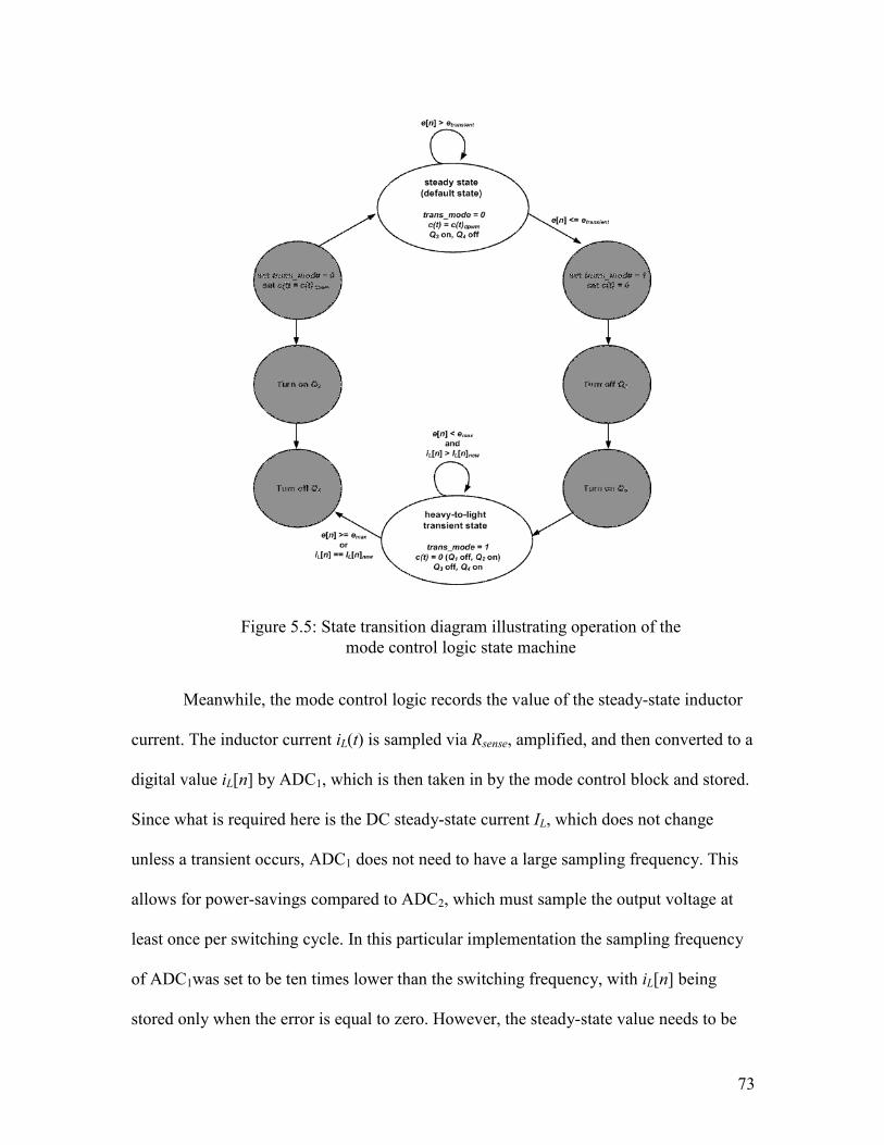
73
Meanwhile, the mode control logic records the value of the steady-state inductor
current. The inductor current iL(t) is sampled via Rsense, amplified, and then converted to a
digital value iL[n] by ADC1, which is then taken in by the mode control block and stored.
Since what is required here is the DC steady-state current IL, which does not change
unless a transient occurs, ADC1 does not need to have a large sampling frequency. This
allows for power-savings compared to ADC2, which must sample the output voltage at
least once per switching cycle. In this particular implementation the sampling frequency
of ADC1was set to be ten times lower than the switching frequency, with iL[n] being
stored only when the error is equal to zero. However, the steady-state value needs to be
Figure 5.5: State transition diagram illustrating operation of the
mode control logic state machine
74
captured essentially only once after a transient occurs, and this value is valid until the
next load change. A small modification to the described system to make this possible
would be to monitor e[n], and, whenever it would go above or below zero (or other
threshold deemed to be a criterion for a load transient), wait for it to return to zero for a
few cycles, and then sample the inductor current. No sampling would occur until the next
disturbance in the error value. In this way the power consumption of ADC1 would be
even further reduced.
B. Heavy-to-Light Load Transient Operation
When e[n] < etransient, the system goes into transient mode. The mode control logic asserts
the trans_mode signal which freezes the PID compensator and DPWM. The last
previously recorded value of iL[n] is then stored into a separate register as IL[n]old,
denoting that it is the steady-state value of the inductor current which existed prior to the
transient. Upon the positive edge of the trans_mode signal the output of the asynchronous
flash ADC is captured. This output, ∆I[n], is the change in load current which has just
occurred and which is the cause of the transient. The control signal c(t) is set by the mode
control logic to zero, which causes the dead-time circuit to turn off Q1 and turn on Q2.
Then, Q3 is turned off followed by the turning on of Q4. The converter is now in the
configuration of Figure 5.2(b). This configuration must be maintained until the load
transient finishes, that is, until the inductor current reaches its new steady state value,
which is equal to the new output current value [4]. The new steady-state value, IL[n]new, is
then logically the old steady-state value, which has been recorded, less the output current
change, which has also been, or
][][][ nInInI oldLnewL ∆−= (5.3)
75
During transient, the sampling frequency of ADC1 is greatly increased (in this case to 10
MHz) in order to provide as accurate as possible a measurement of the inductor current.
The mode control logic maintains the transient configuration of Figure 5.2(b) until the
condition in equation 5.3 is satisfied, that is, until the sampled value iL[n] equals IL[n]new.
At that point Q4 is turned off, Q3 is turned on, and control of the converter is returned to
the PID loop.
Since the output of the converter and the inductor are decoupled during a heavy-
to-light load transient, it is possible, depending on the values of the load R, and converter
filtering components L and C, for the output voltage to fall to an unacceptably low level
before the inductor current reaches IL[n]new. To guard against this possibility, another
error threshold, emax, in this case set to +4, is introduced. The mode control logic
continues to monitor e[n] during transient. If at any point e[n] > emax, the system exits the
transient configuration and returns to conventional buck operation regardless of the value
of iL(t). Although the resulting transient response in this case is not ideal, it is still better
than the PID-only case. Even though the inductor current in such a situation has not
reached the level defined by equation 5.3, it has nevertheless decreased by some amount
at a much faster rate than in a regular buck. Despite the fact that the conventional
controller then completes the response to transient, transient performance is still
significantly better. Now the PID compensator is correcting a load-step that is much
smaller than the one that initially occurred.
The Verilog HDL code for all the modules in the system is given in Appendix D.

76
5.5.2 Determining the Magnitude of the Load Current Change
It was mentioned previously that the output of the asynchronous flash ADC, ∆I[n], is the
magnitude of the load step change. This value is arrived at by estimating the capacitor
current ic(t). In steady-state, the average value of ic(t) is zero, i.e. the inductor and load
currents are the same [4]. During a heavy-to-light transient, in the first instant, the load
current suddenly drops while the inductor current iL(t) remains practically unchanged,
causing a spike in the capacitor current. This deviation of the capacitor current, ∆I, is
equal to the change in load current. The transient current waveforms are shown in
simulation in Figure 5.6. In order to determine ic(t), and by extension ∆I, a capacitor
current sensor is not necessary, since capacitor current is defined as
dt
dvCti C
C =)( (5.4)
Figure 5.6: The spike in capacitor current ic(t) during heavy-to-
light transient (with current steering). The delay between the load
step and the trans_mode signal is due to delay of the ADC
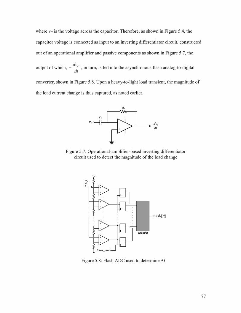
77
where vC is the voltage across the capacitor. Therefore, as shown in Figure 5.4, the
capacitor voltage is connected as input to an inverting differentiator circuit, constructed
out of an operational amplifier and passive components as shown in Figure 5.7, the
output of which, dt
dvC− , in turn, is fed into the asynchronous flash analog-to-digital
converter, shown in Figure 5.8. Upon a heavy-to-light load transient, the magnitude of
the load current change is thus captured, as noted earlier.
Figure 5.8: Flash ADC used to determine ∆I
Figure 5.7: Operational-amplifier-based inverting differentiator
circuit used to detect the magnitude of the load change
78
5.6 Experimental Results
The converter of Figure 5.4 was implemented as a custom printed-circuit board (PCB)
using off-the-shelf components while the digital controller was implemented on an Altera
FPGA. The 12 V-to-0.9 V, 10 W, power stage operates at a switching frequency of
fsw = 500 kHz, where L = 0.9 µH and C = 400 µF. This particular system was designed
with the minimum necessary capacitance to always maintain 0.75 V < vout < 1.05 V. This
is inside the limits of modern digital loads. Figure 5.9 shows a comparison of the PID
compensator response and the current steered configuration’s response. In all
experimental results presented, the light-to-heavy transient is handled by the PID loop
only. The load change shown is an 8 A load step. The top part of Figure 5.9 shows the
PID loop’s response for both transients. As can be seen, the voltage overshoot during the
heavy-to-light transient is 425 mV. The lower part of Figure 5.9 shows the transient
response when current steering is used. The voltage overshoot during heavy-to-light
transient is 150 mV in this case – 2.8 times smaller than with the PID. Figures 5.10 and
5.11 show enlarged versions of the experimental results in Figure 5.9. Figure 5.10 shows
the light-to-heavy load transient, which is compensated by the PID loop in both cases. It
can be seen that with current steering, a “symmetric” response is now achieved – the
heavy-to-light load transient is no longer much worse than the light-to-heavy. Rather, the
performance in both cases is now almost the same (the voltage drop during the light-to-
heavy transient is 150 mV, same as the overshoot in the opposite case). Figure 5.11
shows the heavy-to-light load transient only, with the PID compensator’s response at the
top, and the current steered configuration’s response below. Note that the settling time is
1.5 times faster with the current steering configuration. Visible in the lower part of Figure

79
5.11 is also the transient mode switching sequence with switches Q3 and Q4. It can be
seen that, when the transient is detected, the inductor current rapidly decreases to the new
steady state value, and the converter returns into regular operating mode. After the action
Figure 5.9: Transient response to an 8 A load step change: (top)
with PID only; (bottom) with inductor current steering. Ch1: vout,
500 mV/div; Ch2: iL, 8 A/V, 8 V/div; Ch3: Q3, 5 V/div; Ch4: Q4,
5V/div; Time scale: 50 µs/div

80
is completed a small remaining deviation of the output voltage is compensated with the
PID. This small deviation is caused by a loss of the capacitor charge, which can be taken
into account and compensated with a more advanced control algorithm requiring more
powerful hardware for implementation. Finally, in Figure 5.12, the operation of the
inverting differentiator that is used to determine the magnitude of the load step change is
shown.
Figure 5.10: Transient response to an 8 A load step increase. Ch1:
vout, 500 mV/div; Ch2: iL, 8 A/V, 8 V/div; Ch3: Q3, 5 V/div; Ch4:
Q4, 5V/div; Time scale: 20 µs/div

81
Figure 5.11: Transient response to an 8 A load step decrease: (top)
with PID only; (bottom) with inductor current steering. Ch1: vout,
500 mV/div; Ch2: iL, 8 A/V, 8 V/div; Ch3: Q3, 5 V/div; Ch4: Q4,
5V/div; Time scale: 20 µs/div

82
5.7 Drawbacks and Possible Improvements
5.7.1 Current Sensing
The main drawback of the system shown in Figure 5.4 is that it has two additional
analog-to-digital controllers as compared to a standard digital voltage-controlled loop,
namely ADC1 and the flash. This adds complexity and increases power consumption.
Furthermore, for current sensing, the sense resistor Rsense and accompanying amplifier are
required, and this represents a further drop in efficiency and more power consumption,
respectively. However, recent publications [57], [58] present methods for digital sensor-
less current measurement in a buck converter that could possibly be applied here to
completely remove the analog sensing circuit.
Figure 5.12: Transient response with current steering to an 8 A
load step decrease, showing the output of the inverting
differentiator. Ch1: vout, 500 mV/div; Ch2: iL, 8 A/V, 8 V/div;
Ch3: -iC, 1 V/div; Time scale: 20 µs/div
83
It is also possible to operate the system while being in essence blind to the actual
steady-state values of the current, and looking only at slew rate and load step changes. If
L is input into the controller as a parameter (similarly as the LC product is in the CT-DC),
and if ADC1 is used to sample the input voltage Vg rather than the inductor current, then
the slew rate of the inductor current during transient, defined in equation 5.2, is known.
Using that information and ∆I[n], the time needed to have the current in the inductor
decrease by ∆I at a given slew rate can be calculated. Information about the old or new
steady-state current is not necessary. Since Vg changes very slowly (ideally not at all), a
slow and constant sampling rate is sufficient, and the fast sampling of the inductor
current during transient is avoided. Furthermore, since only occasional sampling is
necessary, ADC2, which is used here to sample the output voltage, can be multiplexed,
and, occasionally, in between samples of the output voltage, sample Vg. In this way
ADC1 can be completely removed from the system.
5.7.2 The Differentiator
The system of Figure 5.4 was constructed out of off-the-shelf components. The need to
determine ∆I necessitated the use of the differentiator and flash ADC, as described
previously. Eliminating these two blocks, while maintaining the ability to determine the
magnitude of the load step change, would be of great benefit. This can potentially be
done by using an approach with comparators as is done with the CT-DC described in
Chapter 3. As seen in the simulations and experimental waveforms, a small voltage peak
is created before the converter switches configurations when a transient occurs. If the
output voltage is measured precisely at two or more points during this initial overshoot,
the slope, that is, the rate of change, of the output voltage just after a load transient occurs

84
can be calculated. Since the output voltage is ideally equal to the capacitor voltage, this
rate of change is basically the same as the output given by the differentiator circuit.
Implementing such a solution would by no means be trivial, but it would render the
differentiator and accompanying ADC redundant, greatly reducing complexity on the
analog side of the loop and having a beneficial impact on power consumption.
5.7.3 The Effect of Additional Switches
The one addition in the current-steered buck converter system that cannot be avoided are
of course the two extra switches. They add additional cost, take up additional area, and
reduce converter efficiency through the addition of more on-resistances. The main drag
on efficiency comes from Q3 which is turned on most of the time and, because of that,
must be designed to handle the full load current. Q4 on the other hand, is only on for a
small amount of time overall, and does not need to be able to handle as large an average
current, nor does it have a large effect on converter efficiency. On the other hand, as
demonstrated, better performance is achieved and the increase in output capacitance that
would otherwise be necessary is avoided. This is simply a tradeoff which is made in this
case.

85
Chapter 6
Conclusions and Future Work
6.1 Continuous-Time Digital Controller
A viable on-chip implementation of the CT-DC, described previously but only tested on
an FPGA, was presented. Simulations yielded expected results but did not match the
experimental results observed when the chip was fabricated. A favourable, yet still not
ideal, response, better than that of a PID compensator, was achieved in the light-to-heavy
load transient case. It was tested successfully with a commercial power stage. The CT-
DC, however, only provided marginal improvement in the heavy-to-light load transient
case in simulations, and did not function properly for that condition in experimental
testing. Additional issues concerning CT-DC operation, such as susceptibility to non-
idealities, were discovered, and the solutions were some of these problems were
suggested. This work has brought the CT-DC closer to a market-ready commercial on-
chip implementation.
6.2 Auto-tuning Extension
A novel algorithm for extracting the L and C values of a buck converter was presented,
and its operation was verified through closed-loop simulations. The algorithm adds
minimal hardware to the CT-DC and exploits the theory upon which the CT-DC is based
to perform auto-tuning simply by observing the CT-DC’s performance, without any
added actions needed.
86
6.3 Current-Steered Buck Converter
A modified Buck topology was presented to solve the problem of the heavy-to-light load
transient response which appeared during work on the first part of this thesis. It was
demonstrated that with a small modification of the popular Buck converter and a digital
controller the physical limitation hampering performance during heavy-to-light load
transients can be overcome. The operation of this novel system was verified in simulation
and experimentally using an FPGA setup. A superior transient response to that of a PID
compensator using a standard buck was demonstrated.
6.4 Future Work
The improvements required for the CT-DC discussed in Section 3.7 have been verified
only in simulation and need to be tested experimentally on-chip. Also, fabrication and
experimental testing of the auto-tuner is required. Further research needs to be put into
the possibilities lined out in Section 5.7, in order to reduce the hardware requirements
and power consumption of the steered-current Buck converter system. A final goal would
be an on-chip implementation of the controller. Since a novel topology is in question, for
which commercial power stages do not exist, it would be of great benefit it this on-chip
solution could be integrated with all four power MOSFETs as well. Finally, it remains for
the CT-DC system, with auto-tuning, to be combined with the current-steered buck
converter, therefore achieving optimal response in both transient cases.
87
References
[1] Zhenyu Zhao, Design and Practical Implementation of Digital Auto-Tuning and
Fast-Response Controllers for Low-Power Switch-Mode Power Supplies, Ph.D.
Thesis, University of Toronto, 2008.
[2] Z. Zhao, V. Smolyakov, and A. Prodić , "Continuous-Time Digital Signal Processing
Based Controller for High-Frequency DC-DC," in Proc. IEEE Applied Power
Electronics Conference (APEC), 2007, pp. 882-886.
[3] Z. Zhao and A. Prodić, “Continuous-Time Digital Controller for High-Frequency DC-
DC Converters,” IEEE Transactions on Power Electronics, Volume 23, Issue 2,
March 2008, pp. 564-573.
[4] Robert W. Erickson and Dragan Maksimović, Fundamentals of Power Electronics,
Second Edition, New York: Springer Science+Business Media, 2001.
[5] S. Abe, M. Hirokawa, T. Zaitsu, and T, Ninomiya, “Study of Stabilization Design for
On-Board Distributed Power Architecture,” in Proc. of the 12th
International
Power Electronics and Motion Control Conference (EPE-PEMC), 2006, August
2006, pp. 636 – 640.
[6] Electrical Engineering Glossary Definition for Point-of-Load, Maxim Corp.,
available online at
http://www.maxim-ic.com/glossary/index.cfm/Ac/V/ID/1016/Tm/point-of-load-POL
[7] Demand Increasing for Non-Isolated Point-of-Load DC-DC Converters, Press
Release, Venture Development Corporation, Massachusetts, July 2004, available
online at http://www.vdc-corp.com/_Documents/pressrelease/04_dcdc_pr1.pdf
[8] B. J. Patella, A. Prodić, A. Zirger, and D. Maksimović, “High-Frequency Digital
PWM Controller IC for DC–DC Converters,” IEEE Transactions on Power
Electronics, Volume 18, Issue 1, part 2, January 2003, pp. 438-446.
[9] J. Xiao, A. Peterchev, J. Zhang, and S. Sanders, “An Ultra-Low-Power Digitally-
Controlled Buck Converter IC for Cellular Phone Applications,” in Proc. IEEE
Applied Power Electronics Conference and Exposition, 2004, vol. 1, pp. 383-391.
[10] E. O’Malley and K. Rinne, “A 16-bit Fixed-Point Digital Signal Processor for
Digital Power Converter Control,” in Proc. IEEE Applied Power Electronics
Conference and Exposition, 2005, vol. 1, pp. 50-56.

88
[11] D. Trevisan, P. Mattavelli, S. Saggini, G. Garcea, and M. Ghioni, “High-
Performance Synchronous-Asynchronous Digital Voltage-Mode Control for dc-dc
Converters,” in Proc. IEEE Applied Power Electronics Conference and Exposition,
2006, pp. 1121-1126.
[12] Z. Lukić, N. Rahman, and A. Prodić, “Multibit Σ–∆ PWM Digital Controller IC for
DC–DC Converters Operating at Switching Frequencies Beyond 10 MHz,” IEEE
Transactions on Power Electronics, Volume 22, Issue 5, September 2007, pp. 1693-
1707.
[13] Z. Zhao and A. Prodić, “ Limit-Cycle Oscillations Based Auto-Tuning System for
Digitally Controlled DC–DC Power Supplies,” IEEE Transactions on Power
Electronics, Volume 22, Issue 5, November 2007, pp. 2211-2222.
[14] A. Prodić and D. Maksimović, “Digital PWM controller and current estimator
for a low-power switching converter,” in Proc. IEEE Workshop on Computers in
Power Electronics, 2000, pp. 123–128.
[15] O. Trescases, W. Ng, H. Nishio, M. Edo, and T. Kawashima, “A digitally controlled
DC-DC converter module with a segmented output stage for optimized
efficiency,” in Proc. IEEE ISPSD Conference, 2006, pp. 1–4.
[16] Z. Lukić, Z. Zhao, A. Prodić, and D. Goder "Digital Controller for Multi-Phase DC-
DC Converters with Logarithmic Current Sharing ," in Proc. IEEE Power
Electronics Specialists Conference (PESC), 2007, pp. 119-123.
[17] O. Trescases, G. Wei, A. Prodić, and W. Ng, “Predictive Efficiency Optimization
for DC–DC Converters With Highly Dynamic Digital Loads,” IEEE Transactions
on Power Electronics, Volume 23, Issue 4, July 2008, pp. 1859-1869.
[18] R. Redl, B. P. Erisman, and Z. Zansky, “Optimizing the load transient response
of the buck converter,” in Proc. IEEE Applied Power Electronics Conference,
1998, pp. 30–36.
[19] V. Yousefzadeh, A. Babazadeh, B. Ramachandran, E. Alarcon, L. Pao, D.
Maksimović, “Proximate Time-Optimal Digital Control for Synchronous Buck DC–
DC Converters,” IEEE Transactions on Power Electronics, Volume 23, Issue 4, July
2008, pp. 2018-2026.
[20] A. Costabeber, L. Corradini, P. Mattavelli, S. Saggini, “Time Optimal, Parameters-
insensitive Digital Controller for DC-DC Buck Converters,” in Proc. IEEE Power
Electronics Specialists Conference (PESC), 2008, pp. 1243-1249.
[21] PIP212-12M datasheet, NXP Semiconductors, available online at
http://www.nxp.com/acrobat_download/datasheets/PIP212-12M_4.pdf

89
[22] PTH12040W datasheet, Texas Instruments, available online at
http://focus.ti.com/lit/ds/symlink/pth12040w.pdf
[23] MAX8655 datasheet, Maxim Corp., available online at
http://datasheets.maxim-ic.com/en/ds/MAX8655.pdf
[24] UM10117 PIP212-12M demonstration board datasheet, NXP Semiconductors,
available online at
http://www.nxp.com/acrobat_download/usermanuals/UM10117_3.pdf
[25] H. P. Forghani-zadeh and G. A. Rincon-Mora, “Current-sensing techniques for
DC-DC converters,” in Proc. IEEE Midwest Symposium on Circuits and Systems
(MWSCAS), 2002, vol. 2, pp. 577–580.
[26] S. Banerjee and G. Verghese, Eds., Nonlinear Phenomena in Power Electronics:
Attractors, Bifurcation, Chaos, and Nonlinear Control, New York: Wiley-
IEEE Press, 2001.
[27] T.W. Martin and S.S. Ang, "Digital Control of Switching Converters” in Proc. IEEE
Symposium on Industrial Electronics, 1995 (ISIE ’95), vol. 2, pp. 480-484.
[28] Y. Duan and H. Jin, "Digital Controller Design for Switch Mode Power Converters”
in Proc. IEEE Applied Power Electronics Conference, 1999, vol. 2, pp. 480-484.
[29] Zdravko Lukić, Sigma-delta DPWM controllers for 12MHz DC-DC switch-mode
power supplies, M.A.Sc. thesis, University of Toronto, 2006.
[30] O. Trescases, Z. Lukić, W. Ng, and A. Prodic, “A low power mixed-signal
current-mode DC-DC converter using a one-bit delta sigma DAC,” in Proc. IEEE
Applied Power Electronics Conference and Exposition, 2006, pp. 700–704.
[31] O. Trescases, A. Parayandeh, A.Prodić, and W.T. Ng, "Sensorless Digital Peak
Current Controller for Low-Power DC-DC SMPS Based on a Bi-directional Delay
Line," in Proc. IEEE Power Electronics Specialists Conference (PESC), 2007, pp.
1670-1676.
[32] S. Saggini, E. Orietti, P. Mattavelli, A. Pizzutelli, A. Bianco, “Fully-Digital
Hysteretic Voltage-Mode Control for dc-dc Converters based on Asynchronous
Sampling” in Proc. IEEE Applied Power Electronics Conference and Exposition,
2008, pp. 503–509.
[33] A. Prodić and D. Maksimović, “Design of a digital PID regulator based on look-up
tables for control of high-frequency DC-DC converters” in Proc. IEEE Workshop on
Computers and Power Electronics (COMPEL), 2002, pp. 18-22.

90
[34] L.T. Jakobsen, H. Schneider, and M. Andersen, “Comparison of state-of-the-art
digital control and analogue control for high bandwidth point of load converters” in
Proc. IEEE Applied Power Electronics Conference and Exposition, 2008, pp. 1440–
1445.
[35] G. Feng, W. Eberle, and Y. Liu, “A new digital control algorithm to
achieve optimal dynamic performance in DC-DC converters,” IEEE Transactions
on Power Electronics, Volume 22, Issue 4, July 2007, pp. 1489-1498.
[36] A. Soto, A. P. Alou, and J. A. Cobos, “Nonlinear digital control breaks
bandwidth limitations,” in Proc. IEEE Applied Power Electronics Conference and
Exposition, 2006, pp. 42–47.
[37] P. T. Krein, “Feasibility of geometric digital controls and augmentation for ultrafast
Dc-Dc converter response” in Proc. IEEE Workshop Computers in Power
Electronics, 2006, pp. 48–56.
[38] Y. Tsividis, “Continuous-time digital signal processing,” Electronics Letters, vol.
39, pp. 1551–1552, October 2003.
[39] Y. Tsividis, G. Cowan, Y. W. Li, and K. Shepard, “Continuous-Time DSPs,
analog/digital computers and other mixed-domain circuits,” in Proc. ESSCIRC
Conference, 2005, pp. 113–116.
[40] Y. Tsividis, “Digital signal processing in continuous time: A possibility
for avoiding aliasing and reducing quantization error,” in Proc. IEEE
ICASSP Conference, 2004, vol. 2, pp. 589–92.
[41] K. S. Leung and H. S. Chung, “Derivation of a second-order switching
surface in the boundary control of buck converters,” IEEE Power Electronics
Letters, vol. 2, issue 2, June 2004, pp. 63–67.
[42] K. S. Leung and H. S. Chung, “A comparative study of the boundary
control of buck converters using first- and second-order switching surfaces–Part I:
Continuous conduction mode,” in Proc. IEEE Power Electronics Specialists
Conference (PESC), 2005, pp. 2133–2139.
[43] K. S. Leung and H. S. Chung, “Dynamic hysteresis band control of
the buck converter with fast transient response,” IEEE Transactions on Circuits and
Systems II: Express Briefs, vol. 52, issue 7, July 2005, pp. 398-402.
[44] I. Kaya and D. P. Atherton, “Exact parameter estimation from relay autotuning
under static load disturbances” in Proc. American Control Conference, 2001,
pp. 3274–3279.

91
[45] W. Stefanutti, P. Mattavelli, S. Saggini, and M. Ghioni, “Autotuning of digitally
controlled buck converters based on relay feedback,” in Proc. IEEE Power
Electronics Specialist Conference, 2005, pp. 2140–2145.
[46] B. Miao, R. Zane, and D. Maksimović, “Automated digital controller design for
switching converters,” in Proc. IEEE Power Electronics Specialist Conference,
2005, pp. 2729–2735.
[47] B. Miao, R. Zane, and D. Maksimović, “System identification of power converters
with digital control through cross-correlation methods,” IEEE Transactions on
Power Electronics, vol. 20, issue 5, pp. 1093–1099, Sept. 2005.
[48] A. Kelly and K. Rinne, “A self-compensating adaptive digital regulator for
switching converters based on linear prediction” in Proc. IEEE Applied Power
Electronics Conference, 2006, pp. 712–718.
[49] M. Shirazi, R. Zane, D. Maksimović, L. Corradini, and P. Mattavelli, “Autotuning
techniques for digitally-controlled point-of-load converters with wide range
of capacitive loads,” in Proc. IEEE Applied Power Electronics Conference, 2007,
pp. 14–20.
[50] International Technology Roadmap for Semiconductors 2005 Edition Executive
Summary, pp. 81-82. Available online at
http://www.itrs.net/Links/2005ITRS/ExecSum2005.pdf
[51] G. E. Pitel and P. T. Krein, “Transient reduction of Dc-Dc converters via
augmentation and geometric control,” in Proc. IEEE Power Electronics Specialists
Conference and Exposition, 2007, pp. 1652–1657.
[52] L. Amoroso, M. Donati, X. Zhou, and F. C. Lee, “Single shot transient suppressor
(SSTS) for high current slew rate microprocessor,” in Proc. IEEE Applied Power
Electronics Conference and Exposition, 1999, vol. 1, pp. 284-288.
[53] A. M. Wu and S. R. Sanders, "An active clamp circuit for voltage regulation module
(VRM) applications," IEEE Transactions on Power Electronics, Volume 16, Issue 5,
September 2001, pp. 623-634.
[54] N. K. Poon, C. P. Li, and M. H. Pong, “A low cost DC-DC stepping inductance
voltage regulator with fast transient loading response,” in Proc. IEEE Applied
Power Electronics Conference and Exposition, 2001, vol. 1, pp. 268-272.
[55] X. Cao, and R. Oruganti, “Fast Response Control of Stepping Inductance Voltage
Regulator Module,” in Proc. IEEE Power Electronics Specialists Conference, 2005,
pp. 382–388.

92
[56] Dylan Dah-Chuan Lu, J. C. P. Liu, F. N. K. Poon, and Bryan Man Hay Pong, “A
Single Phase Voltage Regulator Module (VRM) With Stepping Inductance for Fast
Transient Response,” in IEEE Transactions on Power Electronics, Volume 22,
Issue 2, March 2007, pp. 417-424.
[57] Z. Lukić, Z. Zhao, S. M. Ahsanuzzaman, and A. Prodić, “Self-Tuning Digital
Current Estimator for Low-Power Switching Converters,” in Proc. IEEE Applied
Power Electronics Conference and Exposition, 2008, pp. 529-534.
[58] Z. Lukić, A. Stupar, A. Prodić, D. Goder, “Current Estimation and Remote
Temperature Monitoring System for Low Power Digitally Controlled DC-DC
SMPS,” in Proc. IEEE Power Electronics Specialists Conference (PESC), 2008,
pp. 1139-1143.
[59] A. Stupar, Z. Lukić, and A. Prodić, “Digitally-Controlled Steered-Inductor Buck
Converter for Improving Heavy-to-Light Load Transient Response,” in Proc. IEEE
Power Electronics Specialists Conference (PESC), 2008, pp. 3950-3954.