quasi z-source-based multilevel inverter for single phase
77
QUASI Z-SOURCE-BASED MULTILEVEL INVERTER FOR SINGLE PHASE PHOTO VOLTAIC APPLICATIONS A Thesis Presented to The Graduate Faculty of the University of Akron In Partial Fulfillment of the Requirements for the Degree Master of Science Aida Gorgani August, 2016
-
Upload
khangminh22 -
Category
Documents
-
view
2 -
download
0
Transcript of quasi z-source-based multilevel inverter for single phase
QUASI Z-SOURCE-BASED MULTILEVEL INVERTER FOR SINGLE PHASE
PHOTO VOLTAIC APPLICATIONS
A Thesis
Presented to
The Graduate Faculty of the University of Akron
In Partial Fulfillment
of the Requirements for the Degree
Master of Science
Aida Gorgani
August, 2016
ii
QUASI Z-SOURCE-BASED MULTILEVEL INVERTER FOR SINGLE PHASE
PHOTO VOLTAIC APPLICATIONS
Aida Gorgani
M.S. Thesis
Approved:
Accepted:
Advisor
Dr. Malik E. Elbuluk
Interim Department Chair
Dr. Joan Carletta
Co-Advisor
Dr. Yilmaz Sozer
Interim Dean of College
Dr. Donald P. Visco
Committee Member
Dr. Robert Veillette
Interim Dean of the Graduate School
Dr. Chand Midha
Date
iii
ABSTRACT
This thesis presents a PV system for single-phase applications. A multilevel DC
link (MLDCL) structure and a single-phase H-bridge are used. To regulate the PV voltage,
a quasi Z-Source converter is used in each unit of the MLDCL. Several quasi Z-source
half-bridge converters are connected in series to produce the required discrete voltage
output levels of the MLDCL.
A detailed design and analysis are applied to a 180 W single phase stand-alone PV
system using three cascaded half-bridge quasi Z-source converters and a 60 Hz H-bridge
single-phase inverter. Each quasi Z-source module in the proposed structure has the
advantage of having an independent control scheme, so that each unit can effectively
achieve maximum power point (MPP) from the individual PV panels. The complete system
is simulated using MATLAB/Simulink to verify the proposed concept and the theoretical
analysis. In the simulations, the incremental conductance method is used as the Maximum
Power Point Tracking (MPPT) scheme. The feasibility of the proposed topology is also
confirmed through a 60-W experimental setup. The simulation and experimental results
are discussed to verify the analysis. The simulations and experiments also confirm that the
quasi Z-source structures allow the use of fewer switches and the use of capacitors with
lower voltage ratings than traditional buck/boost or Z-source implementations.

iv
ACKNOWLEDGEMENTS
I wish to express my deepest gratitude to my academic advisors, Drs. Malik Elbuluk and
Yilmaz Sozer for all the advising, guidance and support that I received from them during
the course of my research. Also, I would like to thank Dr. Yilmaz Sozer for his help during
the implementation of the experimental setup. I also would like to express my sincere
appreciation to Dr. Robert Veillette for being in my thesis committee and for his help with
discussion and editing the thesis.
Thanks are also extended to my colleagues in the Alternative Energy and Advanced
Electric Machines Laboratory at The University of Akron for their sincere friendship,
especially Mohamed Badawy for his technical help.
Last but not least, I would also like to thank my parents and my sister for their love, support
and continuous encouragements over the years.
v
TABLE OF CONTENTS
Page
LIST OF TABLES ........................................................................................................... viii
LIST OF FIGURES ........................................................................................................... ix
CHAPTER I: INTRODUCTION .........................................................................................1
1.1 Research motivation .................................................................................................. 1
1.2 Literature review ....................................................................................................... 2
1.3 Problem definition ..................................................................................................... 5
1.4 Thesis contribution .................................................................................................... 6
1.5 Thesis organization ................................................................................................... 6
CHAPTER II: POWER ELECTRONICS IN PV APPLICATIONS ...................................9
2.1 Introduction ............................................................................................................... 9
2.2 PV-connected basic DC/DC converter topologies .................................................. 11
2.2.1 Buck converter .................................................................................................. 12
2.2.2 Boost converter ................................................................................................. 13
2.2.3 Buck/boost converter ........................................................................................ 14
2.3 The Z-source converter ........................................................................................... 16
2.4 The quasi-Z-source converter.................................................................................. 20
2.5 Conclusion ............................................................................................................... 22
vi
CHAPTER III: PV-CONNECTED Z/QUASI Z-SOURCE MULTILEVEL
INVERTER ........................................................................................................................24
3.1 Introduction ............................................................................................................. 24
3.2 Cascaded half-bridge based Multilevel DC Link (MLDCL) inverter ..................... 25
3.3 Voltage-fed MLDCL H-bridge inverter .................................................................. 26
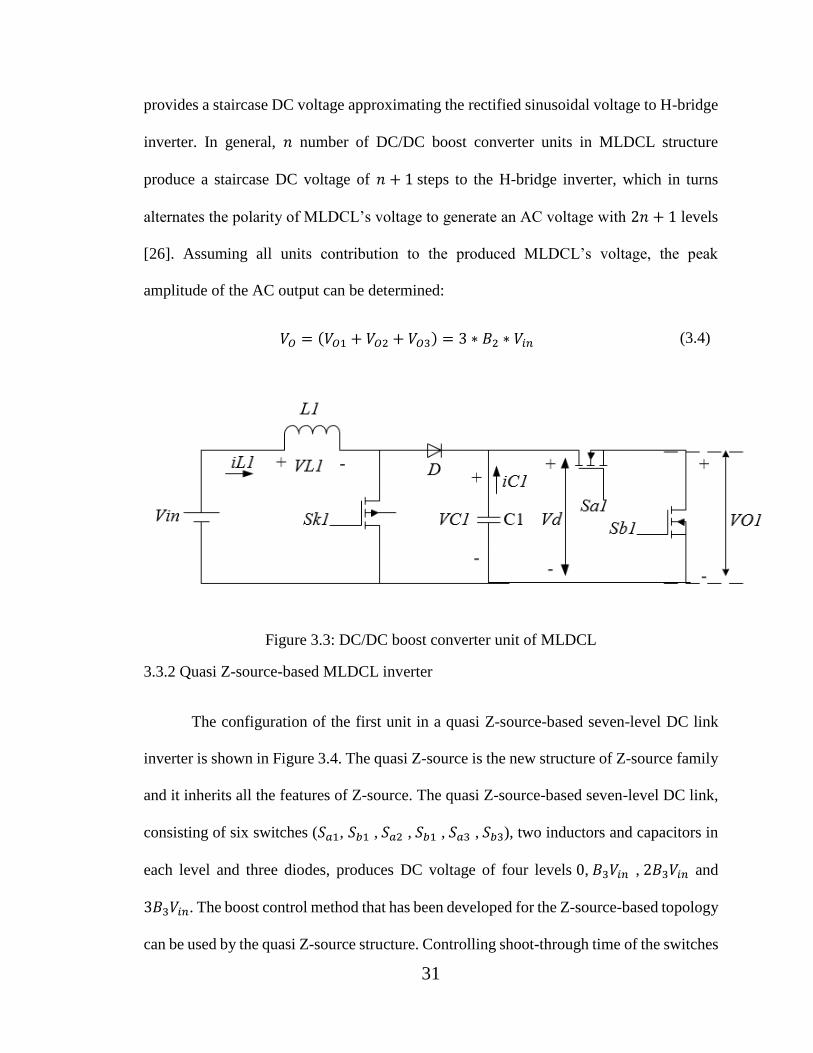
3.3.1 DC/DC boost converter-based MLDCL H-bridge inverter .............................. 30
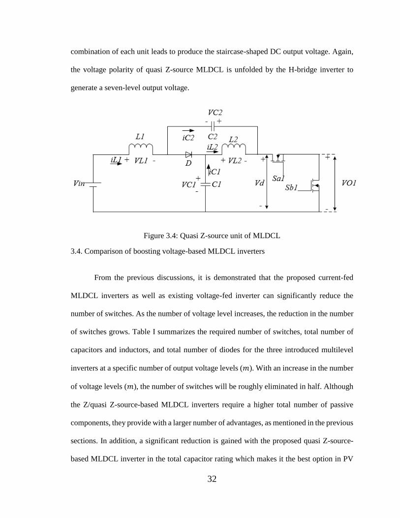
3.3.2 Quasi Z-source-based MLDCL inverter ........................................................... 31
3.4 Comparison of boosting voltage-based MLDCL inverters ..................................... 32
3.5 Description of stand-alone based MLDCL inverter topology for PV application .. 33
3.5.1 Comparison between the proposed topology and the traditional structure ...... 35
3.6 Conclusion ............................................................................................................... 35
CHAPTER IV: SIMULATION AND EXPERIMENTAL RESULTS .............................37
4.1 Simulation results .................................................................................................... 37
4.1.1 Multilevel inverter simulation .......................................................................... 37
4.1.2 Mathematical model of solar module ............................................................... 38
4.1.3 Maximum power point tracking ....................................................................... 39
4.2 Experimental results ................................................................................................ 48
CHAPTER V: SUMMARY, CONCLUSION AND SUGGESTED FUTURE WORK ...60
REFERENCES ..................................................................................................................62

vii
APPENDICES ...................................................................................................................66
viii
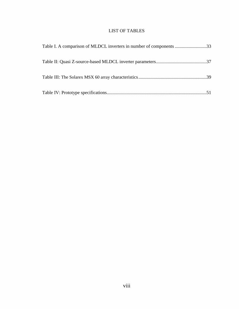
LIST OF TABLES
Table I. A comparison of MLDCL inverters in number of components ...........................33
Table II: Quasi Z-source-based MLDCL inverter parameters ...........................................37
Table III: The Solarex MSX 60 array characteristics ..........................................................39
Table IV: Prototype specifications.....................................................................................51
ix
LIST OF FIGURES
Figure 1.1: General block diagram of PV conversion system ............................................ 2
Figure 2.1: A simple DC/DC converter ............................................................................ 10
Figure 2.2: Buck converter ............................................................................................... 12
Figure 2.3: Boost converter .............................................................................................. 13
Figure 2.4: Buck/boost converter ...................................................................................... 14
Figure 2.5: Z-source general structure in power electronics applications ........................ 17
Figure 2.6: The Z-source control scheme ......................................................................... 18
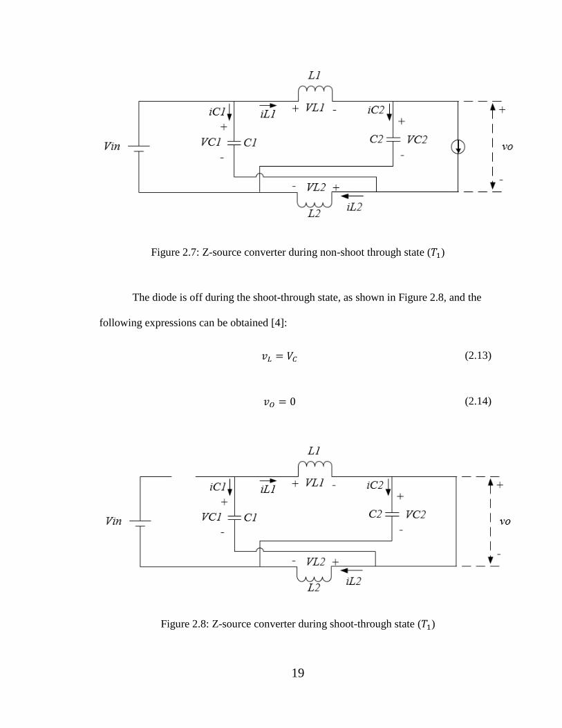
Figure 2.7: Z-source converter during non-shoot-through state (𝑇1) ............................... 19
Figure 2.8: Z-source converter during shoot-through state (𝑇1) ...................................... 19
Figure 2.9: Quasi Z-source converter in non-shoot-through state .................................... 21
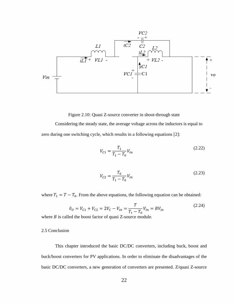
Figure 2.10: Quasi Z-source converter in shoot-through state ......................................... 22
Figure 3.1: n-level DC link H-bridge inverter .................................................................. 26
Figure 3.2: Z-source unit and waveforms ......................................................................... 29
Figure 3.3: DC/DC boost converter unit of MLDCL ....................................................... 31
Figure 3.4: Quasi Z-source unit of MLDCL ..................................................................... 32
Figure 3.5: Cascaded n-level MLDCL H-bridge inverter ................................................. 34
Figure 4.1: Incremental conductance algorithm ............................................................... 41
Figure 4.2: Photovoltaic characteristics at different insolation level ............................... 42
Figure 4.3: Photovoltaic characteristics at different temperature level ............................ 43
Figure 4.4: Output voltage of PV-1 .................................................................................. 44
Figure 4.5: Output current of PV-1 ................................................................................... 45
Figure 4.6: Maximum power tracking for PV-1 ............................................................... 45
x
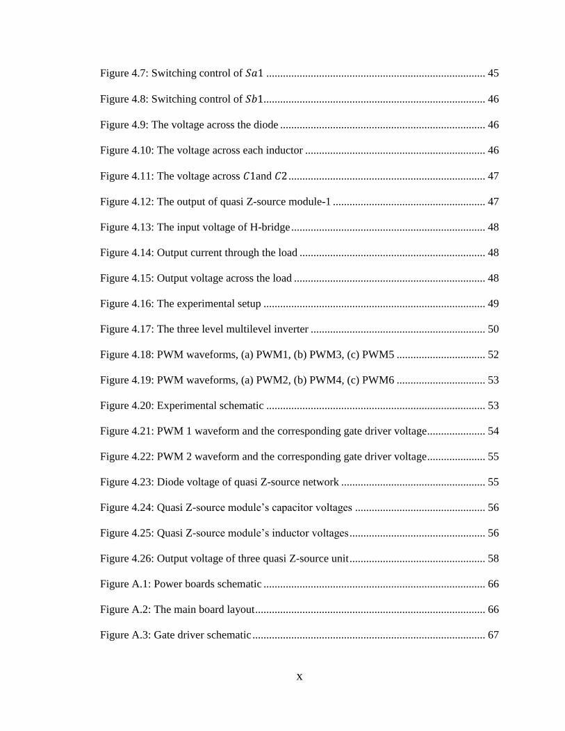
Figure 4.7: Switching control of 𝑆𝑎1 ............................................................................... 45
Figure 4.8: Switching control of 𝑆𝑏1................................................................................ 46
Figure 4.9: The voltage across the diode .......................................................................... 46
Figure 4.10: The voltage across each inductor ................................................................. 46
Figure 4.11: The voltage across 𝐶1and 𝐶2 ....................................................................... 47
Figure 4.12: The output of quasi Z-source module-1 ....................................................... 47
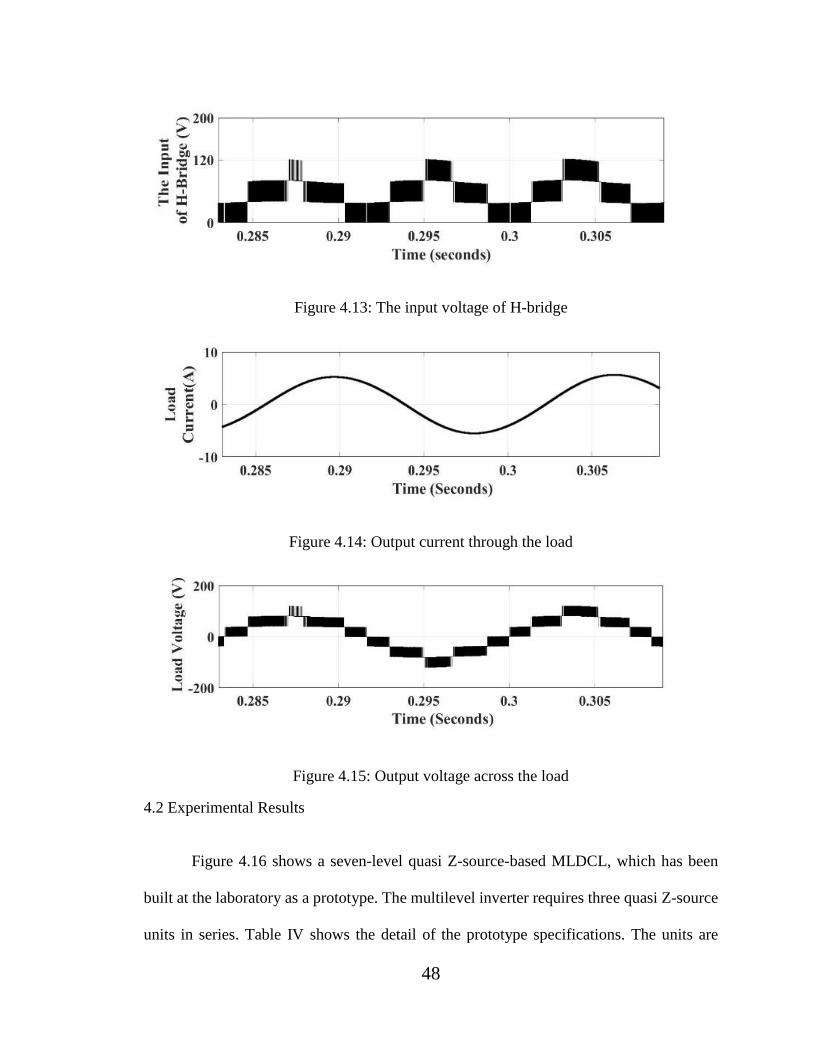
Figure 4.13: The input voltage of H-bridge ...................................................................... 48
Figure 4.14: Output current through the load ................................................................... 48
Figure 4.15: Output voltage across the load ..................................................................... 48
Figure 4.16: The experimental setup ................................................................................ 49
Figure 4.17: The three level multilevel inverter ............................................................... 50
Figure 4.18: PWM waveforms, (a) PWM1, (b) PWM3, (c) PWM5 ................................ 52
Figure 4.19: PWM waveforms, (a) PWM2, (b) PWM4, (c) PWM6 ................................ 53
Figure 4.20: Experimental schematic ............................................................................... 53
Figure 4.21: PWM 1 waveform and the corresponding gate driver voltage ..................... 54
Figure 4.22: PWM 2 waveform and the corresponding gate driver voltage ..................... 55
Figure 4.23: Diode voltage of quasi Z-source network .................................................... 55
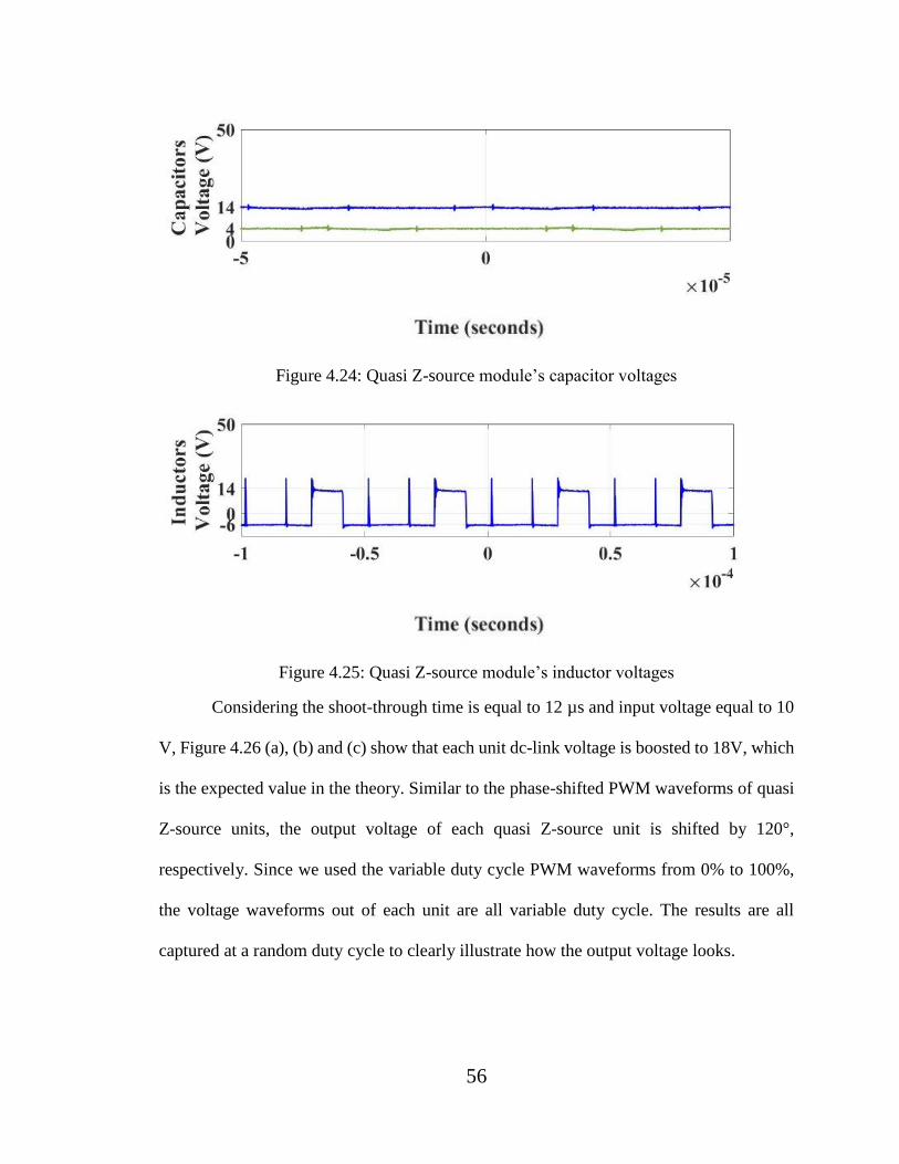
Figure 4.24: Quasi Z-source module’s capacitor voltages ............................................... 56
Figure 4.25: Quasi Z-source module’s inductor voltages ................................................. 56
Figure 4.26: Output voltage of three quasi Z-source unit ................................................. 58
Figure A.1: Power boards schematic ................................................................................ 66
Figure A.2: The main board layout ................................................................................... 66
Figure A.3: Gate driver schematic .................................................................................... 67
1
CHAPTER I
INTRODUCTION
1.1 Research motivation
Recently, renewable energy sources have been considered as a promising
replacement for fossil fuels. Using renewable energy not only leads to the reduction of the
greenhouse gas production, but also provides more flexibility in energy usage. Among the
renewable energy sources, photovoltaic (PV) systems provide a great potential in power
generation because of their modularity, low cost, and ease of installation. Using an
arrangement of solar panels, the PV energy can be absorbed and converted into a direct
usable electricity. In general, PV-based systems are operated in stand-alone mode, grid-
connected mode or in a hybrid mode. In stand-alone mode, PV systems can be considered
as an effective source of electricity to deliver power to isolated or remote areas and can be
operated in AC or DC form. Because of its simple control scheme and reliable structure,
stand-alone PV system can be used at various scale applications from household
application to large scale application.
Recently, a new class of Z/quasi Z-source power converters/inverters are
introduced for PV application. Overcoming the common problems in the traditional power
converters, Z/quasi Z-source converters could become a great alternative to the traditional
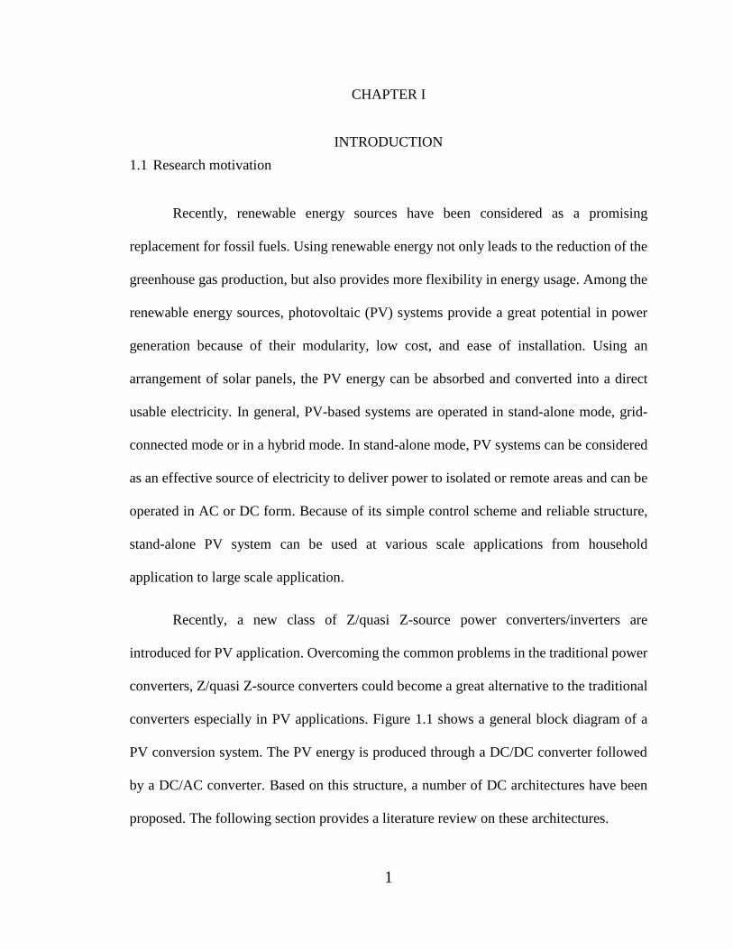
converters especially in PV applications. Figure 1.1 shows a general block diagram of a
PV conversion system. The PV energy is produced through a DC/DC converter followed
by a DC/AC converter. Based on this structure, a number of DC architectures have been
proposed. The following section provides a literature review on these architectures.
2
Figure 1.1: General block diagram of PV conversion system
1.2 Literature review
A photovoltaic cell’s voltage varies over a wide range due to the fact that it is
dependent on temperature and irradiation of the solar energy. In order to compensate for
PV system’s variations and generate the desired voltage to the utility, a DC/DC converter
is used to interface the PV system to the DC/AC converter [1], [2]. Control of the DC/DC
and the DC/AC converters is coordinated to obtain the maximum power from the PV
system. Several DC/DC converters such as buck, boost and buck-boost type converters are
widely used for photovoltaic applications. However, some of these converters are restricted
to the low power applications [3]. New converters such as Z-source converter are
introduced for high power PV application. The Z-source voltage source converter is
capable of overcoming the barriers of the traditional DC/DC converters and provides
unique features and a novel power conversion such as directly generating an output voltage
greater or less than the connected PV voltage [4]. Moreover, the Z-source passive
3
components are designed to result in a maximum boost voltage capability and fewer
switches. Hence, it has a compact and reliable structure that results in more low cost and a
more efficient system [1].
The quasi Z-source network is a derived structure from the Z-source network,
which inherits all the advantages of the Z-source. Besides being a reliable single stage
power conversion, Z-source structure provides the system with a buck/boost capability and
a wide range of voltage gain. The quasi Z-source inverter provides a few additional unique
features of lower capacitance rating and continuous DC current from the PV array [1], [2],
[5]. Also, a coupled inductor can be used in quasi Z-source structure, which results in
reducing of the size and weight of the overall system. The quasi Z-source network has been
used to feed a Voltage Source Inverter (VSI), which leads to have a buck/boost structure
between the source and the H-bridge, something that was lacked in conventional VSI [6].
Also, the shoot-through state is supported in the overall combination of quasi Z-source
VSI, which has led to a more reliable system [7].
Because of their proper structures for modularization, better harmonic output
voltage and the voltage stress reduction on the switches, multilevel inverters have gained
wide attention in high and medium power applications especially in PV applications [8].
Using multiple lower DC voltage level and semiconductor switches, the main objective of
multilevel inverters is to produce a higher output voltage with comparatively low voltage
rated switches. In addition, multilevel inverter has led to a better harmonic output voltage
and the voltage stress reduction on the switches [9]. There are three main categories for
multilevel inverter structures that have been reported in the literature. There are the Diode-
Clamped Structure (DMS), Capacitor-Clamped Structure (CCS) and Cascaded Multilevel
4
Inverter (CMI) [9]-[11]. Among the introduced structures, the CMI is the most useful
topology due to the simple control of it and the lower number of components needed to
produce the similar number of voltage levels at the same power level [12], [13].
Significant researches have been conducted in the area of Z/quasi Z-source inverter
for either grid-connected or stand-alone system. The analysis and simulation of both grid-
connected and off-grid PV system based on Z/quasi Z-source inverter have been studied in
[14], [15], [16], [17], [18], [19], [20], [21]. A stand-alone PV system based on a quasi Z-
source inverter is investigated for water pumping system in [18].
More studies have been done on the Z/quasi Z-source multilevel inverters due to
the large number of this structures’ benefits. A cascaded Z-source multilevel inverter is
designed for a grid-connected PV source. Each level of this inverter consists of a PV
source, a quasi Z-source network and an H-bridge [22], [23], [24], [25]. A new cascaded
Z-source inverter with reduction of switches is presented and analyzed in [26]. With the
objective of lowering the voltage stress on the switches, a single-phase neutral-point-
clamped quasi Z-source inverter is proposed in [8]. A review of recent proposed multilevel
inverter structures with reduced number of power switches is given in [21].
The optimized switching control for the multilevel inverter has been also recently
investigated in paper [27]. A maximum boost control method is presented to generate the
maximum voltage gain at a specific modulation index.
Extracting maximum power from a stand-alone PV system depends mainly on the
system’s load, temperature and insolation or irradiation. The PV output voltage can be
significantly affected by ambient temperature, while the change in irradiation leads to
change in the PV output power. Besides controlling the temperature and insolation in a PV
5
system, an impedance load control method is required for a stand-alone system to result in
a maximum output power at any temperature and insolation level. Assuming a constant
level for temperature and irradiation, the PV system works at the intersection of load line
and PV voltage-current (V-I) curve. Based on the function and control strategies of the
overall PV system, the direct or indirect Maximum Power Point Tracking (MPPT) method
is used. The conductance incremental approach has been employed in this thesis, which is
based on the derivative of the PV output power with respect to the voltage [14].
The relative MPPT control strategy is also applied to the quasi Z-source-based
multilevel inverter to optimize its performance. Considering the insolation and ambient
temperature, a simple MPPT has been presented in [28]. Using a current source based
converter, both perturb and observe and incremental conductance method are implemented
and compared in [29]. An accurate and fast dynamic response Adaptive Neuro-Fuzzy
Inference System (ANFIS)-based MPPT is proposed to deliver the maximum power from
the PV generator [30]. In [31], a unified MPPT method along with a capacitor voltage
control are presented to achieve a maximum power point in the PV system.
1.3 Problem definition
Despite all of the aforementioned advantages of multilevel inverters, there is still a
high switching loss. The excessive number of semiconductor switches has been considered
as the main cause of the switching loss. Several researches have worked to improve this
issue and reduce the number of power switches [32]-[34]. The performance and topology
of several multilevel inverters with reduced number of devices are presented in [8]. Among
these structures, a new structure which is based on multilevel dc link (MLDCL) and H-
bridge inverter is considered as an excellent choice for PV applications. The MLDCL
6
consists of multiple cascaded units, each of which includes a DC source, voltage boosting
stage and two switches. MLDCL H-bridge inverter has resulted in a more efficient PV
system because of its simple and modular structure as well as reduced number of switches
[26], [35]. Also, the new system can deliver the balanced power to the load, and at the same
time each module ensures separate MPPT to collect maximum solar power. A Z-source-
based MLDCL H-bridge inverter and its advantages are studied in paper [26]. However,
MLDCL inverters based on quasi Z-source converters have not been reported in the
literature. Due to the aforementioned great advantages of quasi Z-source rather than Z-
source and DC/DC boost converter, a quasi Z-source MLDCL H-bridge inverter is the best
choice in PV application.
1.4 Thesis contribution
This thesis proposes a multilevel inverter, which consists of a quasi Z-source-based
MLDCL and an H-bridge inverter. The quasi Z-source structure is used as an efficient
interface between a PV generator and a half-bridge unit. The proposed MLDCL inverter
uses three series-connected quasi Z-source-based units connecting to an H-bridge inverter.
In the following sections, the multilevel inverter structure analysis, the PV modeling, and
the incremental conductance method are discussed in details. Simulation and experimental
results are presented to verify the analysis.
1.5 Thesis Organization
Chapter I of this thesis focuses on the research trends in the area of Z/quasi Z-source
converters for PV systems. This section is followed by a study of the PV systems, Z/quasi
Z-source converter, Z/quasi Z-source inverter and finally a discussion of Z/quasi Z-source
multilevel inverters. The multilevel inverters and their advantages over the traditional
7
inverters are the major part of this section. Indicating the switching loss as the common
problem in multilevel inverter, a quasi Z-source-based MLDCL inverter is introduced for
PV applications.
Chapter II describes the basic topologies of the power converters and classification
of different power converter structures. The voltage and current conversion ratios and
switching control scheme of basic boost, buck and boost/buck converters are studied for
PV application in this chapter. The main disadvantages of the basic power converters are
discussed. Ways to overcome the disadvantages of the traditional power converters and the
introduction of the Z/quasi Z-source converters are presented. A literature review of the
existing Z/quasi Z-source source power converters as well as a comparison between
Z/quasi Z-source source power converters and the traditional voltage-fed and current-fed
inverters are also given.
In Chapter III, the proposed topology of a multilevel inverter based on Z/quasi Z-
source inverter is discussed. A literature review discusses the main advantages of the
proposed structure with the existing ones. A comparison is also considered between the
Z/quasi Z-source-based structure and boost converter-based topology. In addition, a
mathematical model of a PV generator is presented and the proposed Z/quasi Z-source
structure is studied for PV applications. In order to achieve the maximum power point from
each PV, a MPPT method is also introduced in this chapter. The PV characteristics are
shown at different insolation and temperature levels.
Chapter IV studies the simulation and experimental results of the quasi Z-source-
based multilevel inverter. The simulation results verify the analysis of the proposed design
process and control strategy. The experimental results are provided to confirm the

8
simulation results. The design procedure of the system including the Printed Circuit Board
(PCB), the schematic, layout, and conducting the experimental results are presented and
discussed.
Chapter V presents the summary, conclusion and future work of the thesis.
9
CHAPTER II
POWER ELECTRONICS IN PV APPLICATIONS
2.1 Introduction
Since the output voltage and current of a PV module vary, they are not always fit
for a specific application. A DC/DC converter is usually used to interface the PV module
and the rest of the power conversion system. The main traditional generation of DC/DC
converters and their pros and cons in conjunction with the use in PV applications are
discussed in this Chapter.
Power electronics applications in renewable energy are rapidly growing during the
recent years. Power converter devices cover a wide range of applications including motor
drives and power supplies for stand-alone and grid-connected loads.
Power converters must be designed in a way to result in an efficient, reliable, low
size, weight and cost system. The aforementioned factors need to be considered in a power
converter design to lead to a high system efficiency. The energy efficiency (𝜂) is defined
as:
𝜂 =𝑃𝑜𝑢𝑡
𝑃𝑖𝑛
(2.1)
Power electronic converters need to be controlled in a way to convert the power
between DC to DC, AC to AC, AC to DC and DC to AC systems. To achieve high
efficiency in power converters, the semiconductor devices such as diode and transistors are
the main components that provide the needed functionality. Figure 2.1 shows a very simple
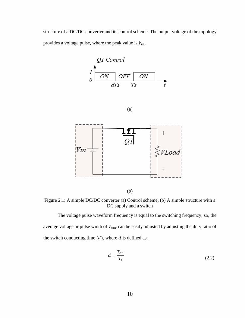
10
structure of a DC/DC converter and its control scheme. The output voltage of the topology
provides a voltage pulse, where the peak value is 𝑉𝑖𝑛.
(a)
(b)
Figure 2.1: A simple DC/DC converter (a) Control scheme, (b) A simple structure with a
DC supply and a switch
The voltage pulse waveform frequency is equal to the switching frequency; so, the
average voltage or pulse width of 𝑉𝑜𝑢𝑡 can be easily adjusted by adjusting the duty ratio of
the switch conducting time (𝑑), where 𝑑 is defined as.
𝑑 =𝑇𝑜𝑛
𝑇𝑠
(2.2)
11
where 𝑇𝑜𝑛 is the on-time period of the switch and 𝑇𝑠 is the switching period. The introduced
structure is called a switch mode converter. Depending on what is required in an
application, this topology can be used at a low-frequency or high-frequency applications.
Having a constant switching frequency, the switching time period is shown in the following
[36]:
𝑇𝑆 =1
𝑓𝑠
(2.3)
Considering one period for the switching, the average voltage can be obtained:
=< 𝑣 >=1
𝑇∫ 𝑣(𝑡)𝑑𝑡 =
𝑇
0
𝑇𝑜𝑛
𝑇𝑠𝑉𝑖𝑛 = 𝑑𝑉𝑖𝑛
(2.4)
where 𝑇𝑜𝑛
𝑇𝑠 is described as duty ratio (𝑑) of the switching, as shown in Figure 2.1 (a). In this
chapter, our main focus is to introduce PV power conversion using DC/DC converters.
2.2 PV-connected basic DC/DC converter topologies
The requirements for a PV system, such as a DC/DC converter, have been already
discussed in the previous section. The input and output of a DC/DC converter are assumed
constant during the steady state condition. In any DC/DC power converter, the inductor
associated with the main switch is considered as the main energy transfer element from
input to the output. It is assumed that the inductor energy increases, while the switch is on.
Then, the saved energy into the inductor is transferred to the output during off-time
switching cycle. There might be additional energy transfer elements such as capacitors in
the circuit, which can be considered into the analysis as well.
12
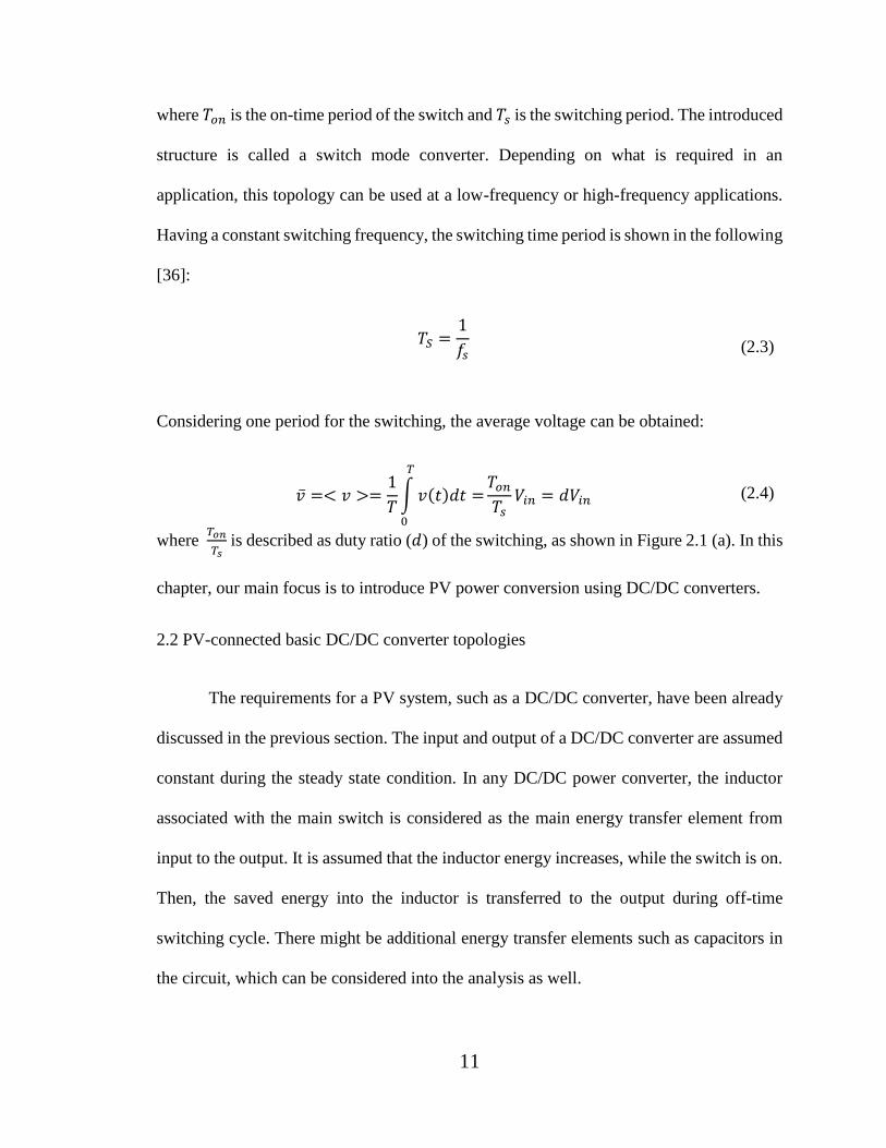
2.2.1 Buck converter
Figure 2.2 shows the basic non-isolated buck converter, with the diode and switch
as the main components. The inductor current increases during the transistor on-time (𝑑𝑇),
as shown in Figure 2.1 (a). During the transistor off-time (1 − 𝑑)𝑇, the inductor current
flows through the diode to transfer energy to the output. Considering the inductor as an
ideal component, the average voltage across the inductor would be equal to zero. This leads
to the relationship between the input and output voltage as [36]:
𝑉𝑜𝑢𝑡 = 𝑑𝑉𝑝𝑣 (2.5)
Considering the power balance, the current relationship can be derived as [36]
𝐼𝑖𝑛 = 𝑑𝐼𝑜𝑢𝑡 (2.6)
The voltage conversion ratio depends on the switching duty ratio (𝑑), which is
always between 0 and 1. The buck or step down converter can be used in the applications,
which require a lower voltage at the output compared to the input [36].
Figure 2.2: Buck converter
13
2.2.2 Boost converter
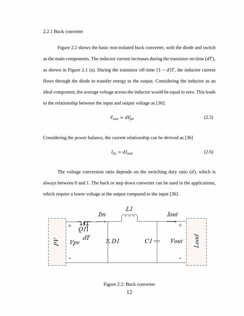
A PV-connected boost converter is shown in Figure 2.3. This topology helps us to
convert a lower DC voltage level to a higher value. Turning on the switch, the voltage
across the inductor would be equal to the PV voltage (𝑉𝑝𝑣). While the switch is off, the
inductor current is forced to flow through the diode and transfer the stored energy to the
output. Again, considering the average voltage across the inductor equal to zero, the
relationship between the input and output voltage can be written as [36]
𝑉𝑜𝑢𝑡
𝑉𝑝𝑣=
1
1 − 𝑑
(2.7)
Figure 2.3: Boost converter
The boost converter or a step up converter provides a higher voltage rather than the
input voltage. Considering the conservation of power from the input to the output, the
current relationship can be as [36]
𝐼𝑖𝑛
𝐼𝑜𝑢𝑡=
1
1 − 𝑑
(2.8)
14
2.2.3 Buck/boost converter
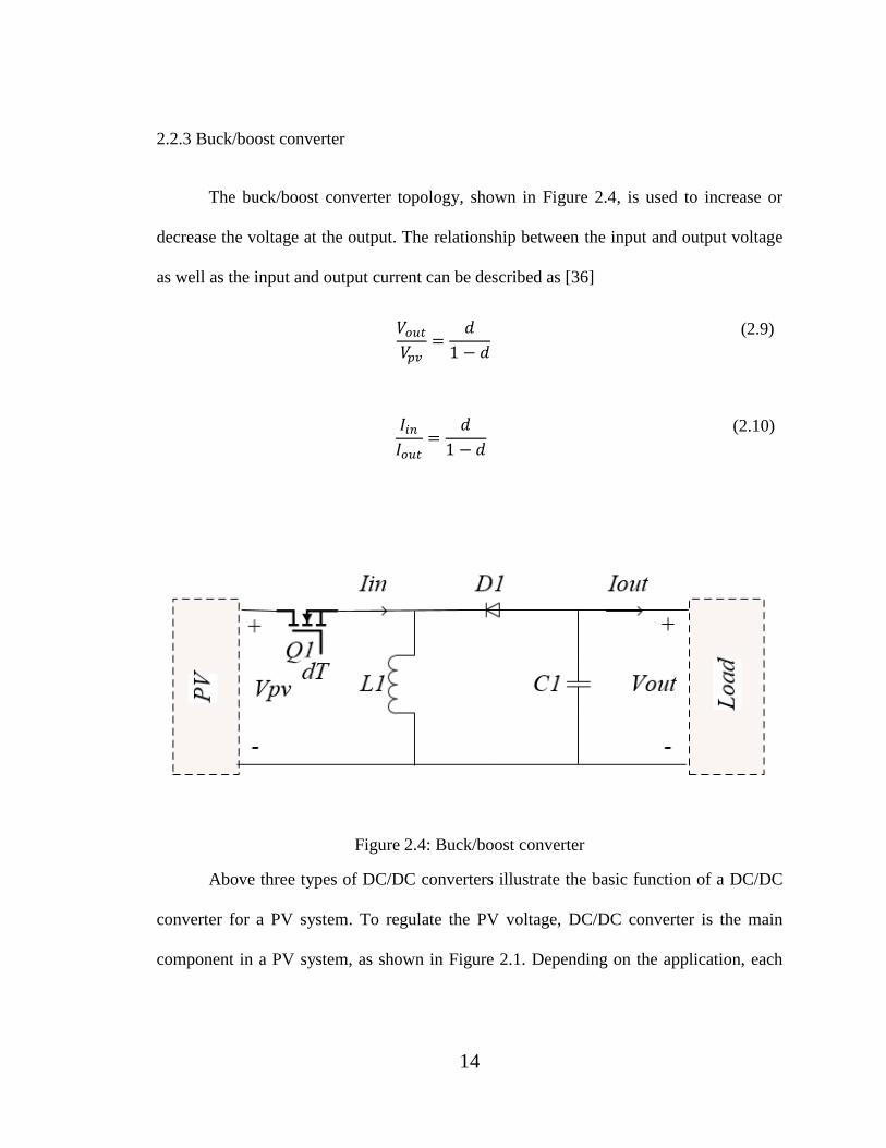
The buck/boost converter topology, shown in Figure 2.4, is used to increase or
decrease the voltage at the output. The relationship between the input and output voltage
as well as the input and output current can be described as [36]
𝑉𝑜𝑢𝑡
𝑉𝑝𝑣=
𝑑
1 − 𝑑
(2.9)
𝐼𝑖𝑛
𝐼𝑜𝑢𝑡=
𝑑
1 − 𝑑
(2.10)
Figure 2.4: Buck/boost converter
Above three types of DC/DC converters illustrate the basic function of a DC/DC
converter for a PV system. To regulate the PV voltage, DC/DC converter is the main
component in a PV system, as shown in Figure 2.1. Depending on the application, each
15
one of the introduced DC/DC converters in this chapter can act as a voltage regulator in
the system.
Supplying an AC load or grid by a PV module, a DC/AC converter (inverter) is
also required in the system, as shown in Figure 2.1. The basic power inverters can be
categorized into two big groups: current-fed inverters and voltage-fed inverters. The
voltage-fed inverter is the most common type of inverter. The buck converter of Figure 2.2
is a simple example of a voltage-fed converter. Besides all the advantages of voltage-fed
inverter, it has several intrinsic limitations. The AC voltage out of the regular voltage-fed
inverter cannot exceed the input DC voltage. So, an extra DC/DC power converter is
always required to adjust the input DC voltage. However, the mentioned basic DC/DC
converter topologies have limitations in terms of switching losses and operation range,
which could be considered as drawbacks in PV applications. In addition, a shoot-through
would happen if the upper and lower switches of each inverter’s leg are on simultaneously.
The shoot-through issue is the biggest problem in the voltage-fed inverter and it can affect
the reliability of the overall structure. A reasonable amount of dead time needs to be
considered for both upper and lower switches. Moreover, power loss and complicated
control scheme are other disadvantages of voltage-fed inverter, which can be solved using
an LC filter.
Current-fed inverter can be an alternative to the voltage-fed inverter in industrial
applications, still it has its own limitations and barriers. Using current-fed inverter, the AC
voltage out of the inverter has to be higher than the input DC voltage and it functions like
a boost converter of Figure 2.3. In order to avoid the open circuit in current-fed inverter, at
least one of the leg’s switch has be maintained on during the switching cycle which results
16
in a complicated control procedure. Therefore, both voltage-fed and current-fed inverter
have their own disadvantages. The most important cons of these two topologies are that
they are at risk of unreliability due to the EMI noise.
To overcome the disadvantages of the traditional voltage-fed and current-fed
converters, a Z-source structure can be implemented to the power converters, including AC
to DC, DC to AC, DC to DC, and AC to AC. In other words, the Z-source inverter can be
generally implemented between the PV generator and the load or grid in any types of the
converter. Z-source structure provides a unique power conversion, which eliminates the
limitations of the traditional voltage-fed and current-fed inverter [4].
2.3 The Z-source converter
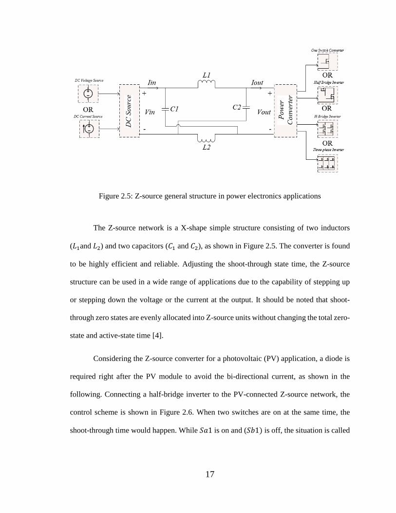
Figure 2.5 shows the general use of Z-source network in power electronic
application. Z-source converter is a new type of power converter, which can overcome the
disadvantages of the basic DC/DC power converters. It operates as a buck/boost converter
without using the DC/DC converter bridge. The Z-source converter provides a wide range
of power conversion using a simple switching control scheme.
17
Figure 2.5: Z-source general structure in power electronics applications
The Z-source network is a X-shape simple structure consisting of two inductors
(𝐿1and 𝐿2) and two capacitors (𝐶1 and 𝐶2), as shown in Figure 2.5. The converter is found
to be highly efficient and reliable. Adjusting the shoot-through state time, the Z-source
structure can be used in a wide range of applications due to the capability of stepping up
or stepping down the voltage or the current at the output. It should be noted that shoot-
through zero states are evenly allocated into Z-source units without changing the total zero-
state and active-state time [4].
Considering the Z-source converter for a photovoltaic (PV) application, a diode is
required right after the PV module to avoid the bi-directional current, as shown in the
following. Connecting a half-bridge inverter to the PV-connected Z-source network, the
control scheme is shown in Figure 2.6. When two switches are on at the same time, the
shoot-through time would happen. While 𝑆𝑎1 is on and (𝑆𝑏1) is off, the situation is called
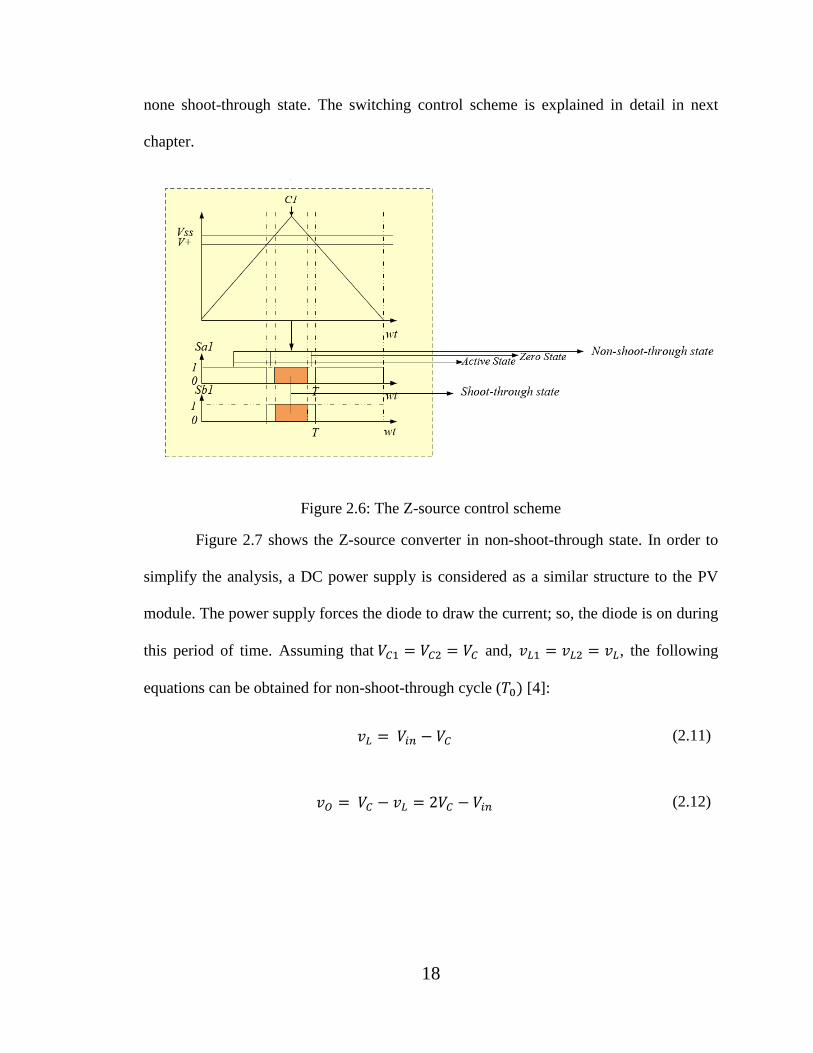
18
none shoot-through state. The switching control scheme is explained in detail in next
chapter.
Figure 2.6: The Z-source control scheme
Figure 2.7 shows the Z-source converter in non-shoot-through state. In order to
simplify the analysis, a DC power supply is considered as a similar structure to the PV
module. The power supply forces the diode to draw the current; so, the diode is on during
this period of time. Assuming that 𝑉𝐶1 = 𝑉𝐶2 = 𝑉𝐶 and, 𝑣𝐿1 = 𝑣𝐿2 = 𝑣𝐿, the following
equations can be obtained for non-shoot-through cycle (𝑇0) [4]:
𝑣𝐿 = 𝑉𝑖𝑛 − 𝑉𝐶 (2.11)
𝑣𝑂 = 𝑉𝐶 − 𝑣𝐿 = 2𝑉𝐶 − 𝑉𝑖𝑛 (2.12)
19
Figure 2.7: Z-source converter during non-shoot through state (𝑇1)
The diode is off during the shoot-through state, as shown in Figure 2.8, and the
following expressions can be obtained [4]:
𝑣𝐿 = 𝑉𝐶 (2.13)
𝑣𝑂 = 0 (2.14)
Figure 2.8: Z-source converter during shoot-through state (𝑇1)
20
Assuming that the inductors and capacitors of each Z-source unit have the same
inductance (𝐿) and capacitance (𝐶) respectively, the average voltage of inductor is equal
to zero over one switching period [4].
𝐿 =𝑇0𝑉𝐶 + 𝑇1(𝑉𝑖𝑛 − 𝑉𝐶)
𝑇= 0
(2.15)
where 𝑇0 is the shoot-through time, 𝑇1is the non-shoot-through time, 𝑇 is the period of
each unit switching, 𝑉𝐶 is the voltage across each capacitor and 𝑉𝑖𝑛 is the input voltage (a
DC voltage source is considered as a PV cell of each unit to simplify the analysis). So, the
following equation can be derived based on the equation (2.15).
𝑉𝐶
𝑉𝑖𝑛=
𝑇1
𝑇1 − 𝑇0
(2.16)
Controlling the Z-source module, the peak value of the produced output voltage
across the Z-source unit can be expressed as follows [4].
𝑣𝑂 = 𝑉𝐶 − 𝑣𝐿 = 2𝑉𝐶 − 𝑉𝑖𝑛 =𝑇
𝑇1 − 𝑇0𝑉𝑖𝑛 = 𝐵𝑉𝑖𝑛
(2.17)
𝐵 =𝑇
𝑇1 − 𝑇0
(2.18)
where 𝐵 is the boosting factor of Z-source structure and 𝑉𝑂 is the output voltage of Z-
source unit.
2.4 The quasi Z-source converter
The quasi Z-source structure is a reliable buck/boost converter which has all the
advantages of the traditional Z-source structure. Using the quasi Z-source topology, the
21
additional advantages of continuous DC current and lower components rating can be
obtained, which can be greatly beneficial in PV applications. The same control scheme of
Z-source topology is used for quasi Z-source structure [2].
The similar analysis can be done during the shoot through and non-shoot-through
states. The equivalent circuits of quasi Z-source topology during these two states are shown
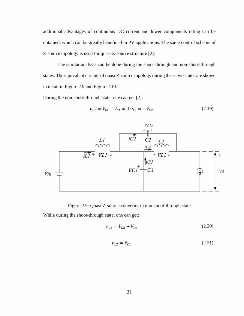
in detail in Figure 2.9 and Figure 2.10.
During the non-shoot-through state, one can get [2]:
𝑣𝐿1 = 𝑉𝑖𝑛 − 𝑉𝐶1 and 𝑣𝐿2 = −𝑉𝐶2 (2.19)
Figure 2.9: Quasi Z-source converter in non-shoot-through state
While during the shoot-through state, one can get:
𝑣𝐿1 = 𝑉𝐶2 + 𝑉𝑖𝑛 (2.20)
𝑣𝐿2 = 𝑉𝐶1 (2.21)
22
Figure 2.10: Quasi Z-source converter in shoot-through state
Considering the steady state, the average voltage across the inductors is equal to
zero during one switching cycle, which results in a following equations [2]:
𝑉𝐶1 =𝑇1
𝑇1 − 𝑇0𝑉𝑖𝑛
(2.22)
𝑉𝐶2 =𝑇0
𝑇1 − 𝑇0𝑉𝑖𝑛
(2.23)
where 𝑇1 = 𝑇 − 𝑇0. From the above equations, the following equation can be obtained:
𝑣𝑂 = 𝑉𝐶1 + 𝑉𝐶2 = 2𝑉𝐶 − 𝑉𝑖𝑛 =𝑇
𝑇1 − 𝑇0𝑉𝑖𝑛 = 𝐵𝑉𝑖𝑛
(2.24)
where 𝐵 is called the boost factor of quasi Z-source module.
2.5 Conclusion
This chapter introduced the basic DC/DC converters, including buck, boost and
buck/boost converters for PV applications. In order to eliminate the disadvantages of the
basic DC/DC converters, a new generation of converters are presented. Z/quasi Z-source

23
structure can be a great alternative to the basic structures in terms of the reliability and
simplicity. Adjusting the shoot-through state time, the Z/quasi Z-source converters can be
used in a wide ranges of PV applications. In order to supply the AC load or grid, Z/quasi
Z-source inverters are highly beneficial in PV systems. A brief literature review on the
existing Z/quasi Z-source inverters and their advantages and disadvantages is given in the
next chapter.
24
CHAPTER III
PV-CONNECTED Z/QUASI Z-SOURCE MULTILEVEL INVERTER
3.1 Introduction
DC to AC power converters play an important role in the power electronics science
and industry including the motor drives, adjustable power supply, PV applications,
transmission system and so on. In PV systems, the DC power is the power that is produced
by solar panel and AC power is what is required by the electrical equipment. Depending
on the application, the inverters come in several types, sizes and capacities. There are two
main categories for power inverters: voltage-fed inverters and current-fed inverters, which
can be used in a wide range of applications. However, they can only function as a buck or
boost inverter, which is considered as a limitation in the applications. Also, the shoot-
through state is banned in these type of inverters, which makes the control scheme
complicated [4].
The Z/quasi Z-source inverters have recently attracted many attention due to the
fact that they can overcome the disadvantages of the existing traditional voltage-fed and
current-fed inverters. The simple structure and control scheme, wide range of operation
and less switching losses make the Z/quasi Z-source inverter a great topology for PV
applications [15]-[18].
The multilevel inverter has been introduced as one of the beneficial inverter during
the recent decade for medium and high power applications. Using multiple lower DC
power supplies, multilevel inverter results in high power with the help of semiconductor
switches [8]. The renewable energy voltage sources can be a good alternative of the DC
25
voltage sources, required for a multilevel inverter. A control scheme is also provided to
control the switches in a way to result in a high output voltage. Having a low voltage input
for each level to achieve the high voltage at the output results in a lower rating components
for each level of the multilevel inverter. Using multilevel inverters in power electronics
applications, the filtering requirement can be greatly reduced. Also, less voltage stress
would be exist on the semiconductor components in comparison with the traditional types
of the inverter. In addition, multilevel inverters can bring large number of benefits such as
low distorted input current and programmable fault tolerant operation to the renewable
energy source applications including wind, photovoltaic and fuel cell applications.
Moreover, the switching loss has been always an issue in all the multilevel inverters
structures.
A PV-connected multilevel inverter structure is introduced in this chapter, which
leads to a less overall switching loss. This topology is based on the series connected units
or MLDCL. Each unit consists of a PV generator to supply the circuit, a DC/DC converter
to achieve the maximum power of the PV and a half-bridge. Having a separate control for
each unit and decreasing the number of switches, this structure could be a highly beneficial
multilevel inverter for PV application.
3.2 Cascaded half-bridge based Multilevel DC Link (MLDCL) inverter
The general schematic illustration of an 𝑛-level DC link inverter structure,
consisting of cascaded MLDCL units and single phase H-bridge inverter, is shown in
Figure 3.1. The H-bridge inverter is connected to a cascaded string of several units, with
each unit having a PV, a voltage boosting stage and two switches as the main components
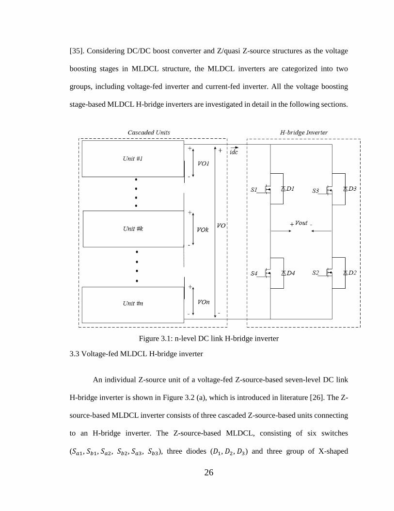
26
[35]. Considering DC/DC boost converter and Z/quasi Z-source structures as the voltage
boosting stages in MLDCL structure, the MLDCL inverters are categorized into two
groups, including voltage-fed inverter and current-fed inverter. All the voltage boosting
stage-based MLDCL H-bridge inverters are investigated in detail in the following sections.
Figure 3.1: n-level DC link H-bridge inverter
3.3 Voltage-fed MLDCL H-bridge inverter
An individual Z-source unit of a voltage-fed Z-source-based seven-level DC link
H-bridge inverter is shown in Figure 3.2 (a), which is introduced in literature [26]. The Z-
source-based MLDCL inverter consists of three cascaded Z-source-based units connecting
to an H-bridge inverter. The Z-source-based MLDCL, consisting of six switches
(𝑆𝑎1, 𝑆𝑏1, 𝑆𝑎2, 𝑆𝑏2, 𝑆𝑎3, 𝑆𝑏3), three diodes (𝐷1, 𝐷2, 𝐷3) and three group of X-shaped
27
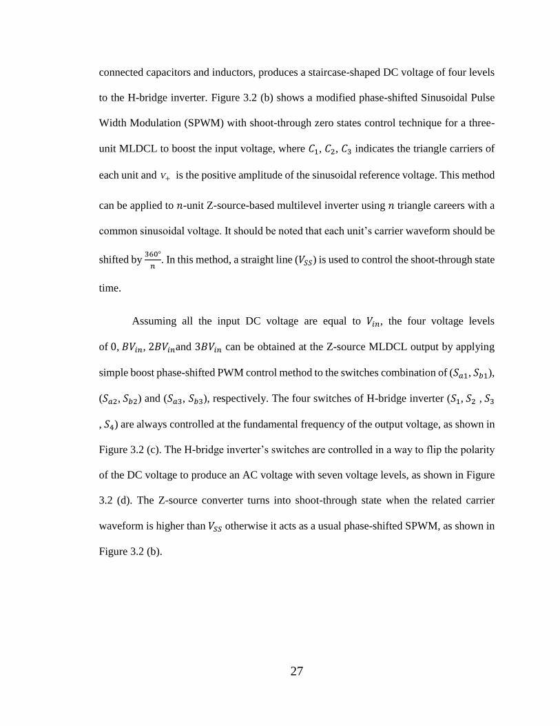
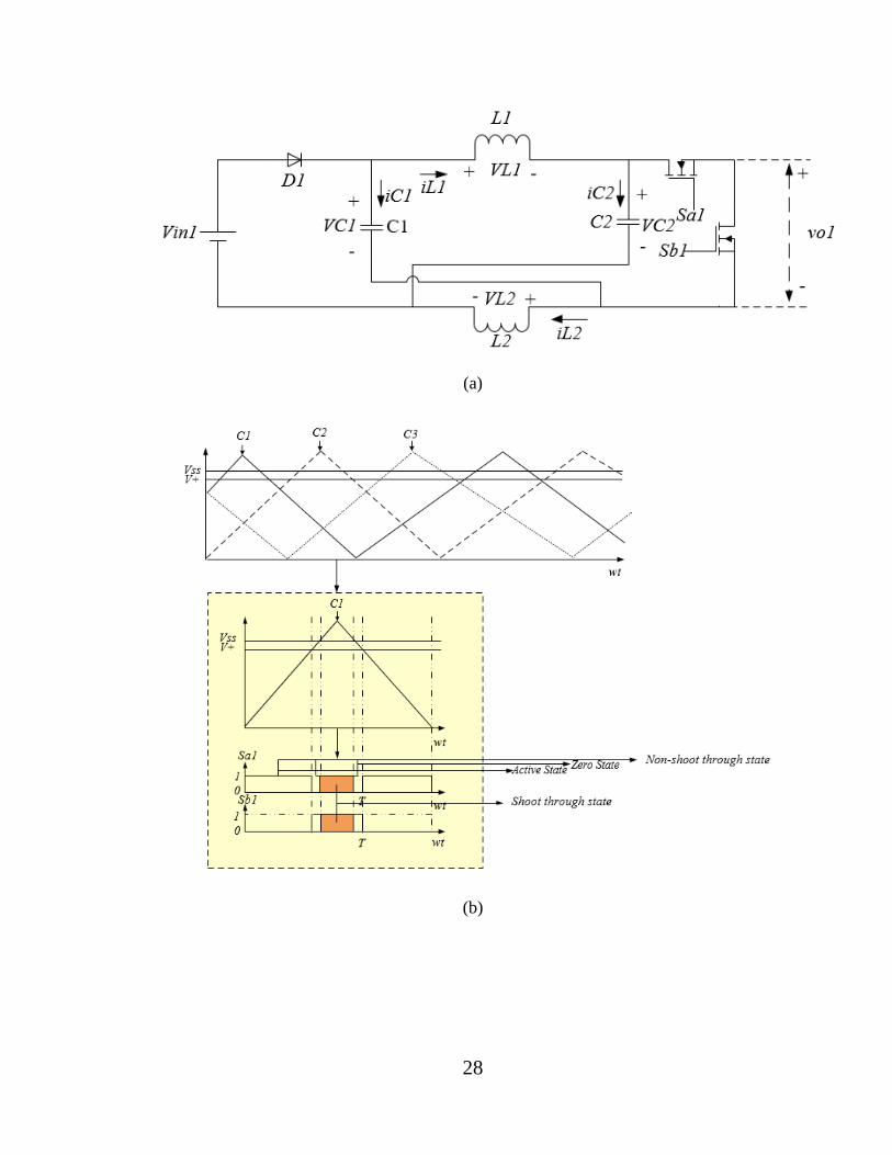
connected capacitors and inductors, produces a staircase-shaped DC voltage of four levels
to the H-bridge inverter. Figure 3.2 (b) shows a modified phase-shifted Sinusoidal Pulse
Width Modulation (SPWM) with shoot-through zero states control technique for a three-
unit MLDCL to boost the input voltage, where 𝐶1, 𝐶2, 𝐶3 indicates the triangle carriers of
each unit and V is the positive amplitude of the sinusoidal reference voltage. This method
can be applied to 𝑛-unit Z-source-based multilevel inverter using 𝑛 triangle careers with a
common sinusoidal voltage. It should be noted that each unit’s carrier waveform should be
shifted by 360°
𝑛. In this method, a straight line (𝑉𝑆𝑆) is used to control the shoot-through state
time.
Assuming all the input DC voltage are equal to 𝑉𝑖𝑛, the four voltage levels
of 0, 𝐵𝑉𝑖𝑛, 2𝐵𝑉𝑖𝑛and 3𝐵𝑉𝑖𝑛 can be obtained at the Z-source MLDCL output by applying
simple boost phase-shifted PWM control method to the switches combination of (𝑆𝑎1, 𝑆𝑏1),
(𝑆𝑎2, 𝑆𝑏2) and (𝑆𝑎3, 𝑆𝑏3), respectively. The four switches of H-bridge inverter (𝑆1, 𝑆2 , 𝑆3
, 𝑆4) are always controlled at the fundamental frequency of the output voltage, as shown in
Figure 3.2 (c). The H-bridge inverter’s switches are controlled in a way to flip the polarity
of the DC voltage to produce an AC voltage with seven voltage levels, as shown in Figure
3.2 (d). The Z-source converter turns into shoot-through state when the related carrier
waveform is higher than 𝑉𝑆𝑆 otherwise it acts as a usual phase-shifted SPWM, as shown in
Figure 3.2 (b).
28
(a)
(b)
29
(c)
(d)
Figure 3.2: Z-source unit and waveforms (a) Z-source-based unit of MLDCL, (b)
Modified phase-shifted SPWM technique, (c) The control of H-bridge switches, (d) Z-
source-based MLDCL’s voltage to H-bridge
Based on the proposed voltage-fed Z-source-based MLDCL H-bridge inverter, two
current-fed seven-level DC link inverter topologies are proposed using DC/DC boost
converter and quasi Z-source. The new structures are studied in detail in the following
sections.
30
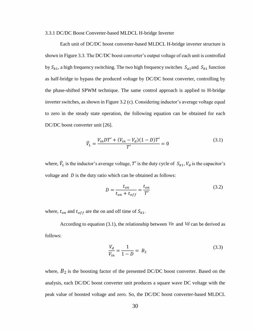
3.3.1 DC/DC Boost Converter-based MLDCL H-bridge Inverter
Each unit of DC/DC boost converter-based MLDCL H-bridge inverter structure is
shown in Figure 3.3. The DC/DC boost converter’s output voltage of each unit is controlled
by 𝑆𝑘1, a high frequency switching. The two high frequency switches 𝑆𝑎1and 𝑆𝑏1 function
as half-bridge to bypass the produced voltage by DC/DC boost converter, controlling by
the phase-shifted SPWM technique. The same control approach is applied to H-bridge
inverter switches, as shown in Figure 3.2 (c). Considering inductor’s average voltage equal
to zero in the steady state operation, the following equation can be obtained for each
DC/DC boost converter unit [26].
𝐿 =𝑉𝑖𝑛𝐷𝑇′ + (𝑉𝑖𝑛 − 𝑉𝑑)(1 − 𝐷)𝑇′
𝑇′= 0
(3.1)
where, 𝐿 is the inductor’s average voltage, 𝑇′ is the duty cycle of 𝑆𝑘1, 𝑉𝑑 is the capacitor’s
voltage and 𝐷 is the duty ratio which can be obtained as follows:
𝐷 =𝑡𝑜𝑛
𝑡𝑜𝑛 + 𝑡𝑜𝑓𝑓=
𝑡𝑜𝑛
𝑇′
(3.2)
where, 𝑡𝑜𝑛 and 𝑡𝑜𝑓𝑓 are the on and off time of 𝑆𝑘1.
According to equation (3.1), the relationship between Vin and Vd can be derived as
follows:
𝑉𝑑
𝑉𝑖𝑛=
1
1 − 𝐷= 𝐵2
(3.3)
where, 𝐵2 is the boosting factor of the presented DC/DC boost converter. Based on the
analysis, each DC/DC boost converter unit produces a square wave DC voltage with the
peak value of boosted voltage and zero. So, the DC/DC boost converter-based MLDCL
31
provides a staircase DC voltage approximating the rectified sinusoidal voltage to H-bridge
inverter. In general, 𝑛 number of DC/DC boost converter units in MLDCL structure
produce a staircase DC voltage of 𝑛 + 1 steps to the H-bridge inverter, which in turns
alternates the polarity of MLDCL’s voltage to generate an AC voltage with 2𝑛 + 1 levels
[26]. Assuming all units contribution to the produced MLDCL’s voltage, the peak
amplitude of the AC output can be determined:
𝑉𝑂 = (𝑉𝑂1 + 𝑉𝑂2 + 𝑉𝑂3) = 3 ∗ 𝐵2 ∗ 𝑉𝑖𝑛 (3.4)
Figure 3.3: DC/DC boost converter unit of MLDCL
3.3.2 Quasi Z-source-based MLDCL inverter
The configuration of the first unit in a quasi Z-source-based seven-level DC link
inverter is shown in Figure 3.4. The quasi Z-source is the new structure of Z-source family
and it inherits all the features of Z-source. The quasi Z-source-based seven-level DC link,
consisting of six switches (𝑆𝑎1, 𝑆𝑏1 , 𝑆𝑎2 , 𝑆𝑏1 , 𝑆𝑎3 , 𝑆𝑏3), two inductors and capacitors in
each level and three diodes, produces DC voltage of four levels 0, 𝐵3𝑉𝑖𝑛 , 2𝐵3𝑉𝑖𝑛 and
3𝐵3𝑉𝑖𝑛. The boost control method that has been developed for the Z-source-based topology
can be used by the quasi Z-source structure. Controlling shoot-through time of the switches
32
combination of each unit leads to produce the staircase-shaped DC output voltage. Again,
the voltage polarity of quasi Z-source MLDCL is unfolded by the H-bridge inverter to
generate a seven-level output voltage.
Figure 3.4: Quasi Z-source unit of MLDCL
3.4. Comparison of boosting voltage-based MLDCL inverters
From the previous discussions, it is demonstrated that the proposed current-fed
MLDCL inverters as well as existing voltage-fed inverter can significantly reduce the
number of switches. As the number of voltage level increases, the reduction in the number
of switches grows. Table I summarizes the required number of switches, total number of
capacitors and inductors, and total number of diodes for the three introduced multilevel
inverters at a specific number of output voltage levels (𝑚). With an increase in the number
of voltage levels (𝑚), the number of switches will be roughly eliminated in half. Although
the Z/quasi Z-source-based MLDCL inverters require a higher total number of passive
components, they provide with a larger number of advantages, as mentioned in the previous
sections. In addition, a significant reduction is gained with the proposed quasi Z-source-
based MLDCL inverter in the total capacitor rating which makes it the best option in PV
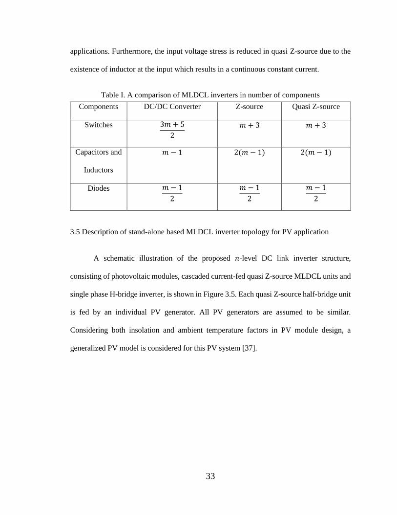
33
applications. Furthermore, the input voltage stress is reduced in quasi Z-source due to the
existence of inductor at the input which results in a continuous constant current.
Table I. A comparison of MLDCL inverters in number of components
Components DC/DC Converter Z-source Quasi Z-source
Switches 3𝑚 + 5
2
𝑚 + 3 𝑚 + 3
Capacitors and
Inductors
𝑚 − 1 2(𝑚 − 1) 2(𝑚 − 1)
Diodes 𝑚 − 1
2
𝑚 − 1
2
𝑚 − 1
2
3.5 Description of stand-alone based MLDCL inverter topology for PV application
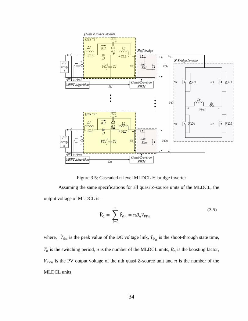
A schematic illustration of the proposed 𝑛-level DC link inverter structure,
consisting of photovoltaic modules, cascaded current-fed quasi Z-source MLDCL units and
single phase H-bridge inverter, is shown in Figure 3.5. Each quasi Z-source half-bridge unit
is fed by an individual PV generator. All PV generators are assumed to be similar.
Considering both insolation and ambient temperature factors in PV module design, a
generalized PV model is considered for this PV system [37].
34
Figure 3.5: Cascaded n-level MLDCL H-bridge inverter
Assuming the same specifications for all quasi Z-source units of the MLDCL, the
output voltage of MLDCL is:
𝑂 = ∑ 𝑂𝑛
𝑛
𝑖=0
= 𝑛𝐵𝑛𝑉𝑃𝑉𝑛 (3.5)
where, 𝑂𝑛 is the peak value of the DC voltage link, 𝑇0𝑛 is the shoot-through state time,
𝑇𝑛 is the switching period, 𝑛 is the number of the MLDCL units, 𝐵𝑛 is the boosting factor,
𝑉𝑃𝑉𝑛 is the PV output voltage of the nth quasi Z-source unit and 𝑛 is the number of the
MLDCL units.
35
3.5.1 Comparison between the proposed topology and the traditional structure
By the use of quasi Z-source converters in the MLDCL, the proposed structure can
overcome some disadvantages of the traditional buck or boost converters. [37]. The
proposed MLDCL inverter can significantly reduce the number of switches. The H-bridge
in each unit of traditional cascaded MLDCL has been replaced with a half-bridge in each
level. A common H-bridge is considered for the whole MLDCL system to change the
polarity of the voltage. As the number of voltage levels increases, the reduction in number
of switches grows. For a MLDCL producing a large number of voltage levels, the proposed
structure will use roughly half the number of switches.
Compared to Z-Source-based MLDCL inverter, a significant reduction is gained
with the proposed quasi Z-source-based MLDCL inverter in the total capacitor rating
which makes it the best option in PV applications [14]. Also, the input voltage stress is
reduced in quasi Z-source converter due to the existence of inductor at the input, which
results in a continuous constant current.
3.6 Conclusion
A very efficient type of multilevel inverter is introduced based on MLDCL
structure in this Chapter. This topology consists of a series of connected DC/DC converters
with a half-bridge at each level and an H-bridge for the overall structure. Three different
types of MLDCL structures, including Z-source, quasi Z-source and a DC/DC boost
converter MLDCL-based inverters are introduced and compared in this Chapter. Then, a
three level quasi Z-source MLDCL inverter is presented for a PV application. Each level
consists of a PV module, a quasi Z-source converter and an half-bridge converter. The

36
advantages of quasi Z-source MLDCL inverter over the traditional ones are investigated in
details.
37
CHAPTER IV
SIMULATION AND EXPERIMENTAL RESULTS
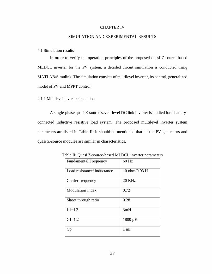
4.1 Simulation results
In order to verify the operation principles of the proposed quasi Z-source-based
MLDCL inverter for the PV system, a detailed circuit simulation is conducted using
MATLAB/Simulink. The simulation consists of multilevel inverter, its control, generalized
model of PV and MPPT control.
4.1.1 Multilevel inverter simulation
A single-phase quasi Z-source seven-level DC link inverter is studied for a battery-
connected inductive resistive load system. The proposed multilevel inverter system
parameters are listed in Table II. It should be mentioned that all the PV generators and
quasi Z-source modules are similar in characteristics.
Table II: Quasi Z-source-based MLDCL inverter parameters
Fundamental Frequency 60 Hz
Load resistance/ inductance 10 ohm/0.03 H
Carrier frequency 20 KHz
Modulation Index 0.72
Shoot through ratio 0.28
L1=L2 3mH
C1=C2 1800 µF
Cp 1 mF
38
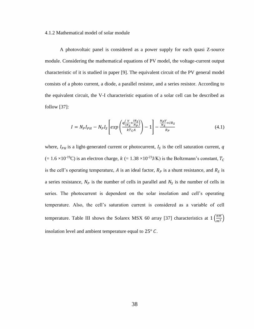
4.1.2 Mathematical model of solar module
A photovoltaic panel is considered as a power supply for each quasi Z-source
module. Considering the mathematical equations of PV model, the voltage-current output
characteristic of it is studied in paper [9]. The equivalent circuit of the PV general model
consists of a photo current, a diode, a parallel resistor, and a series resistor. According to
the equivalent circuit, the V-I characteristic equation of a solar cell can be described as
follow [37]:
𝐼 = 𝑁𝑃𝐼𝑃𝐻 − 𝑁𝑃𝐼𝑆 [𝑒𝑥𝑝 (𝑞(
𝑉
𝑁𝑆+
𝐼𝑅𝑆𝑁𝑃
)
𝑘𝑇𝐶𝐴) − 1] −
𝑁𝑃𝑉
𝑁𝑆+𝐼𝑅𝑆
𝑅𝑃 (4.1)
where, 𝐼𝑃𝐻 is a light-generated current or photocurrent, 𝐼𝑆 is the cell saturation current, 𝑞
(= 1.6 ×10⁻¹⁹C) is an electron charge, 𝑘 (= 1.38 ×10⁻²³J/K) is the Boltzmann’s constant, 𝑇𝐶
is the cell’s operating temperature, 𝐴 is an ideal factor, 𝑅𝑃 is a shunt resistance, and 𝑅𝑆 is
a series resistance, 𝑁𝑃 is the number of cells in parallel and 𝑁𝑆 is the number of cells in
series. The photocurrent is dependent on the solar insolation and cell’s operating
temperature. Also, the cell’s saturation current is considered as a variable of cell
temperature. Table III shows the Solarex MSX 60 array [37] characteristics at 1 (𝑘𝑊
𝑚2 )
insolation level and ambient temperature equal to 25° 𝐶.
39
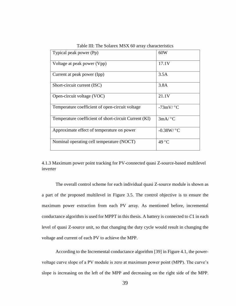
Table III: The Solarex MSX 60 array characteristics
Typical peak power (Pp) 60W
Voltage at peak power (Vpp) 17.1V
Current at peak power (Ipp) 3.5A
Short-circuit current (ISC) 3.8A
Open-circuit voltage (VOC) 21.1V
Temperature coefficient of open-circuit voltage -73mV/ C
Temperature coefficient of short-circuit Current (KI) 3mA/ C
Approximate effect of temperature on power -0.38W/ C
Nominal operating cell temperature (NOCT) 49 C
4.1.3 Maximum power point tracking for PV-connected quasi Z-source-based multilevel
inverter
The overall control scheme for each individual quasi Z-source module is shown as
a part of the proposed multilevel in Figure 3.5. The control objective is to ensure the
maximum power extraction from each PV array. As mentioned before, incremental
conductance algorithm is used for MPPT in this thesis. A battery is connected to 𝐶1 in each
level of quasi Z-source unit, so that changing the duty cycle would result in changing the
voltage and current of each PV to achieve the MPP.
According to the Incremental conductance algorithm [39] in Figure 4.1, the power-
voltage curve slope of a PV module is zero at maximum power point (MPP). The curve’s
slope is increasing on the left of the MPP and decreasing on the right side of the MPP.
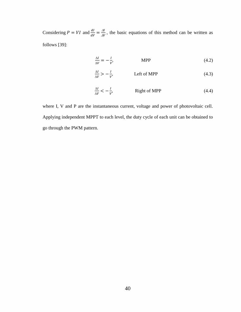
40
Considering 𝑃 = 𝑉𝐼 and 𝑑𝐼
𝑑𝑉=
𝐼
𝑉 , the basic equations of this method can be written as
follows [39]:
𝐼
𝑉= −
𝐼
𝑉, MPP (4.2)
𝐼
𝑉> −
𝐼
𝑉, Left of MPP (4.3)
𝐼
𝑉< −
𝐼
𝑉, Right of MPP (4.4)
where I, V and P are the instantaneous current, voltage and power of photovoltaic cell.
Applying independent MPPT to each level, the duty cycle of each unit can be obtained to
go through the PWM pattern.
41
Figure 4.1: Incremental conductance algorithm
(a)
1 kW/m2
0.8 kW/m2
0.6 kW/m2 0.4 kW/m2
0.2 kW/m2
42
(b)
Figure 4.2: Photovoltaic characteristics at different insolation level (a) I-V characteristic,
(b) P-V characteristic
(a)
0.2 kW/m2
1 kW/m2
0.4 kW/m2
0.6 kW/m2
0.8 kW/m2
100 C° 75 C° 50 C°
25 C°
0 C°
43
(b)
Figure 4.3: Photovoltaic characteristics at different temperature level (a) I-V
characteristic, (b) P-V characteristic
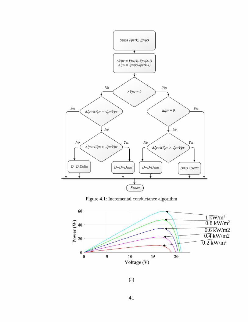
Besides the incremental conductance approach, the effect of insolation and
temperature can also be considered. Considering a range of temperature and insolation
levels, the MPP can be obtained for each PV module. The effect of changing the insolation
has been studied for each PV module. Figure 4.2 (a), (b) show the P-V and I-V
characteristics of each PV module while there is an increase in insolation level. An increase
in the insolation leads to an increase in the maximum power of each PV module. With an
increase at insolation level, the short circuit current increases, which results in an increase
in the maximum power point.
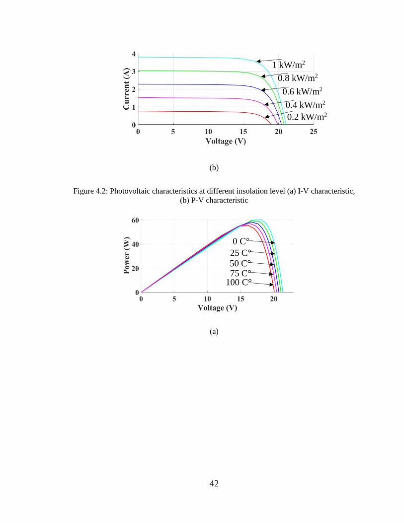
Increasing in the level of operation temperature, each PV module’s short circuit
current increases, while the maximum power point drops. The reason is that the decrease
in the open-circuit voltage is higher than the increase in the short circuit current. Figure 4.3
(a) and (b) show the P-V and I-V curves of each PV module at various temperatures. The
reason behind this change is that there is a direct relationship between the short-circuit
100 C° 75 C°
50 C°
25 C°
0 C°
44
current and insolation, while the open circuit voltage is logarithmically proportional to the
insolation [37].
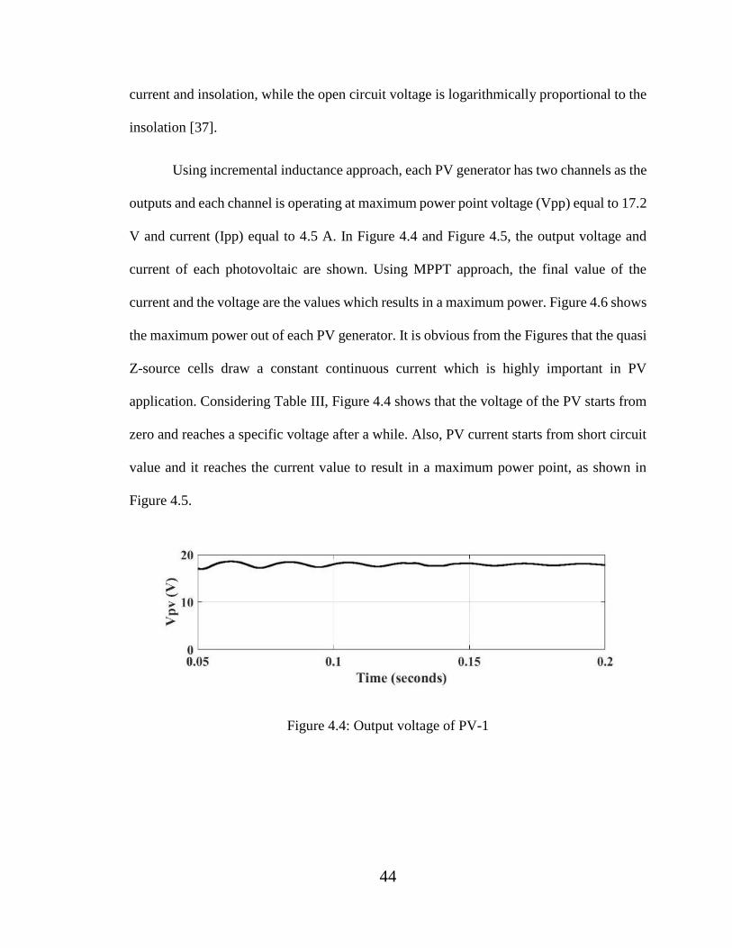
Using incremental inductance approach, each PV generator has two channels as the
outputs and each channel is operating at maximum power point voltage (Vpp) equal to 17.2
V and current (Ipp) equal to 4.5 A. In Figure 4.4 and Figure 4.5, the output voltage and
current of each photovoltaic are shown. Using MPPT approach, the final value of the
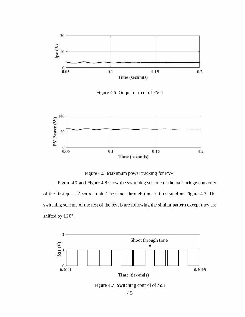
current and the voltage are the values which results in a maximum power. Figure 4.6 shows
the maximum power out of each PV generator. It is obvious from the Figures that the quasi
Z-source cells draw a constant continuous current which is highly important in PV
application. Considering Table III, Figure 4.4 shows that the voltage of the PV starts from
zero and reaches a specific voltage after a while. Also, PV current starts from short circuit
value and it reaches the current value to result in a maximum power point, as shown in
Figure 4.5.
Figure 4.4: Output voltage of PV-1
45
Figure 4.5: Output current of PV-1
Figure 4.6: Maximum power tracking for PV-1
Figure 4.7 and Figure 4.8 show the switching scheme of the half-bridge converter
of the first quasi Z-source unit. The shoot-through time is illustrated on Figure 4.7. The
switching scheme of the rest of the levels are following the similar pattern except they are
shifted by 120°.
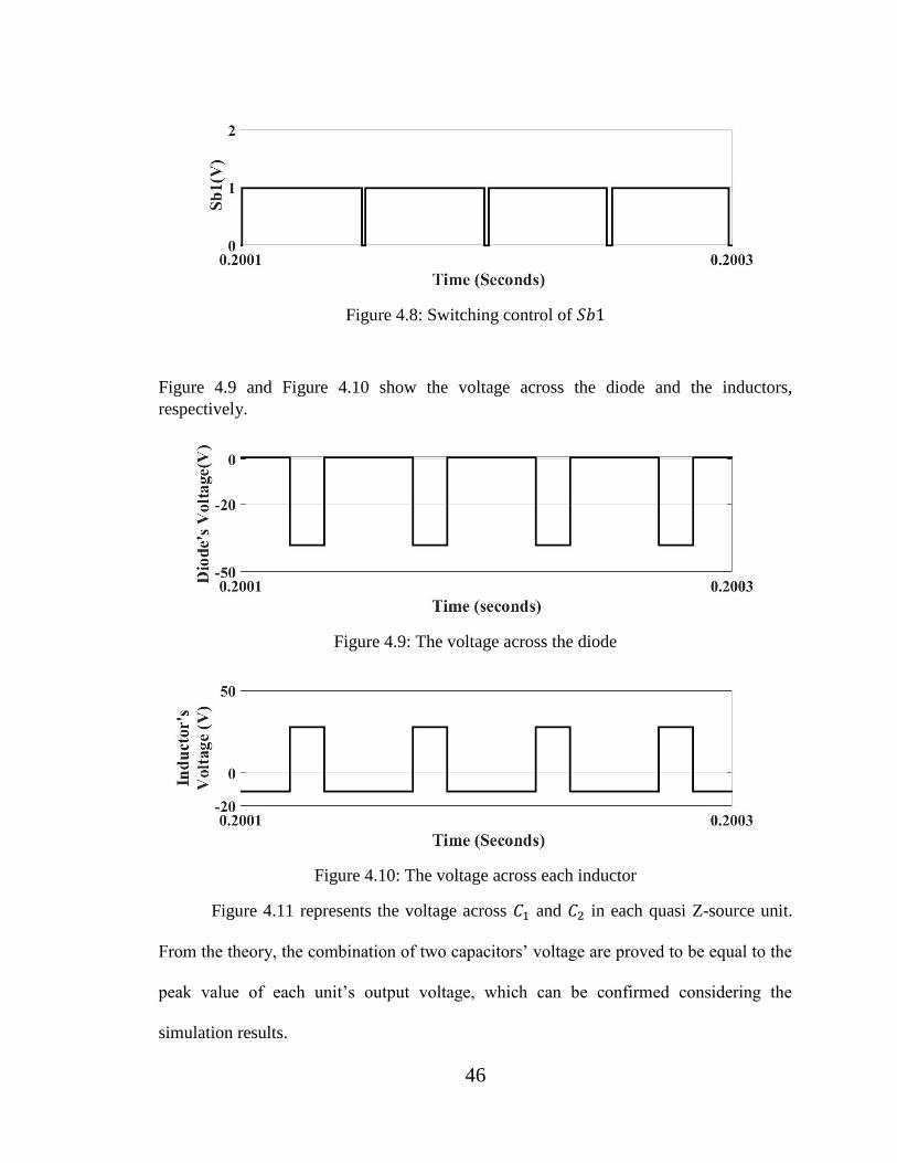
Figure 4.7: Switching control of 𝑆𝑎1
Shoot through time
46
Figure 4.8: Switching control of 𝑆𝑏1
Figure 4.9 and Figure 4.10 show the voltage across the diode and the inductors,
respectively.
Figure 4.9: The voltage across the diode
Figure 4.10: The voltage across each inductor
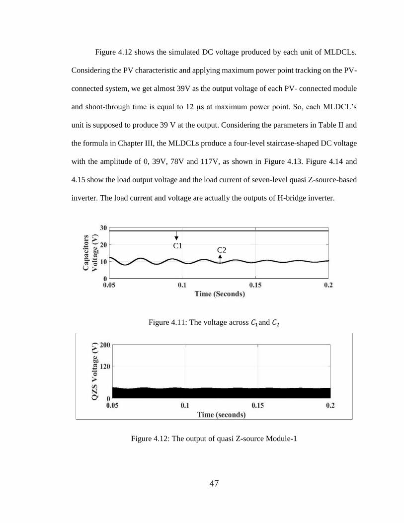
Figure 4.11 represents the voltage across 𝐶1 and 𝐶2 in each quasi Z-source unit.
From the theory, the combination of two capacitors’ voltage are proved to be equal to the
peak value of each unit’s output voltage, which can be confirmed considering the
simulation results.
47
Figure 4.12 shows the simulated DC voltage produced by each unit of MLDCLs.
Considering the PV characteristic and applying maximum power point tracking on the PV-
connected system, we get almost 39V as the output voltage of each PV- connected module
and shoot-through time is equal to 12 µs at maximum power point. So, each MLDCL’s
unit is supposed to produce 39 V at the output. Considering the parameters in Table II and
the formula in Chapter III, the MLDCLs produce a four-level staircase-shaped DC voltage
with the amplitude of 0, 39V, 78V and 117V, as shown in Figure 4.13. Figure 4.14 and
4.15 show the load output voltage and the load current of seven-level quasi Z-source-based
inverter. The load current and voltage are actually the outputs of H-bridge inverter.
Figure 4.11: The voltage across 𝐶1and 𝐶2
Figure 4.12: The output of quasi Z-source Module-1
C1 C2
48
Figure 4.13: The input voltage of H-bridge
Figure 4.14: Output current through the load
Figure 4.15: Output voltage across the load
4.2 Experimental Results
Figure 4.16 shows a seven-level quasi Z-source-based MLDCL, which has been
built at the laboratory as a prototype. The multilevel inverter requires three quasi Z-source
units in series. Table IV shows the detail of the prototype specifications. The units are
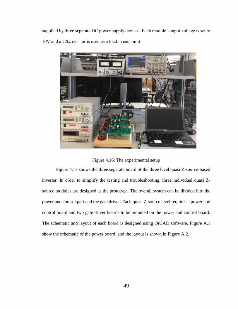
49
supplied by three separate DC power supply devices. Each module’s input voltage is set to
10V and a 72Ω resistor is used as a load in each unit.
Figure 4.16: The experimental setup
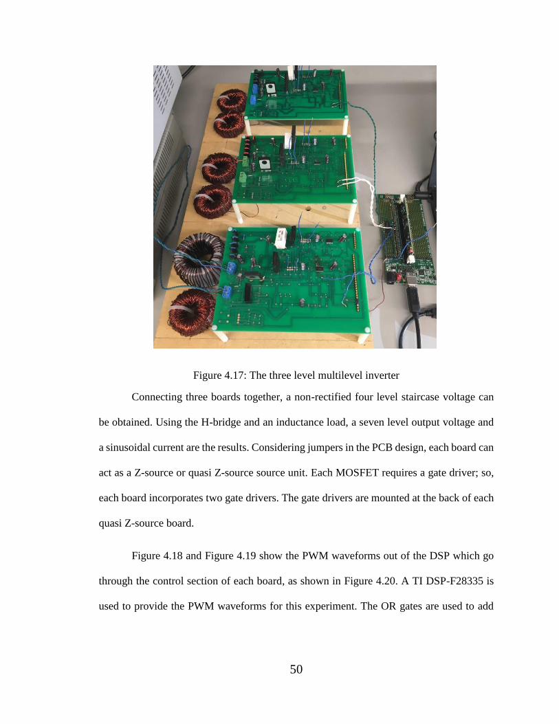
Figure 4.17 shows the three separate board of the three level quasi Z-source-based
inverter. In order to simplify the testing and troubleshooting, three individual quasi Z-
source modules are designed as the prototype. The overall system can be divided into the
power and control part and the gate driver. Each quasi Z-source level requires a power and
control board and two gate driver boards to be mounted on the power and control board.
The schematic and layout of each board is designed using OrCAD software. Figure A.1
show the schematic of the power board, and the layout is shown in Figure A.2.
50
Figure 4.17: The three level multilevel inverter
Connecting three boards together, a non-rectified four level staircase voltage can
be obtained. Using the H-bridge and an inductance load, a seven level output voltage and
a sinusoidal current are the results. Considering jumpers in the PCB design, each board can
act as a Z-source or quasi Z-source source unit. Each MOSFET requires a gate driver; so,
each board incorporates two gate drivers. The gate drivers are mounted at the back of each
quasi Z-source board.
Figure 4.18 and Figure 4.19 show the PWM waveforms out of the DSP which go
through the control section of each board, as shown in Figure 4.20. A TI DSP-F28335 is
used to provide the PWM waveforms for this experiment. The OR gates are used to add
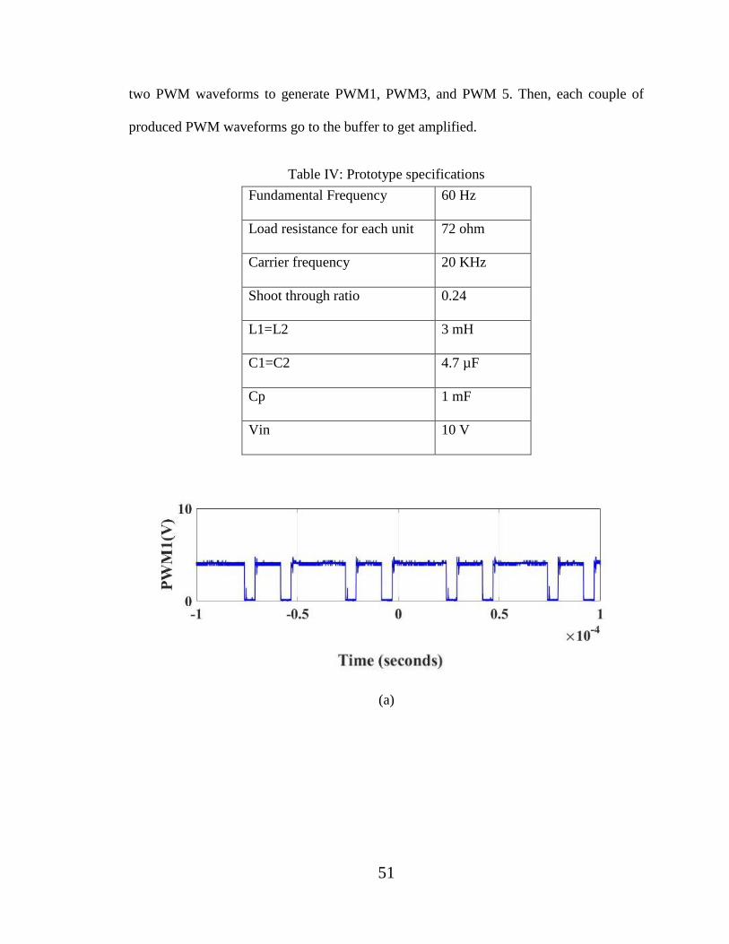
51
two PWM waveforms to generate PWM1, PWM3, and PWM 5. Then, each couple of
produced PWM waveforms go to the buffer to get amplified.
Table IV: Prototype specifications
Fundamental Frequency 60 Hz
Load resistance for each unit 72 ohm
Carrier frequency 20 KHz
Shoot through ratio 0.24
L1=L2 3 mH
C1=C2 4.7 µF
Cp 1 mF
Vin 10 V
(a)
52
(b)
(c)
Figure 4.18: PWM waveforms, (a) PWM1, (b) PWM3, (c) PWM5
(a)
53
(b)
(c)
Figure 4.19: PWM waveforms, (a) PWM2, (b) PWM4, (c) PWM6
Figure 4.20: Experimental schematic
54
A Fairchild gate driver (FOD8318) is designed to be placed next to the buffer on
the control part. Figure A.3 shows each gate driver schematic. Each gate driver consists of
the IGBT drive optocoupler (FOD8318) and a DC/DC converter as the main components.
The objective of using DC/DC converter on the gate driver board is to supply the
optocoupler.
The main objective of using the gate driver is to provide the required output current
to drive the switches. Figure 4.21 and Figure 4.22 show the PWM waveforms and the
corresponding gate driver voltage for one quasi Z-source unit. It can be seen that the gate
drivers work between -15 and +15 to drive the gate of each MOSFET.
Figure 4.21: PWM 1 waveform and the corresponding gate driver voltage
55
Figure 4.22: PWM 2 waveform and the corresponding gate driver voltage
In Figure 4.23, the voltage across the diode in each quasi Z-source network is
shown. The diode is on during the non-shoot-through time and it is open, while it is off
during the shoot-through time. Figure 4.24 verifies the voltage across 𝐶1 and 𝐶2
respectively. It is better to mention that similar components are considered for each quasi
Z-source network. Figure 4.25 represents the voltage across any inductor in the quasi Z-
source MLDCL. The voltage across the inductor would be a positive value during non-
shoot-through time while, it is negative during the shoot-through time. Also, the average
voltage of the inductor is considered equal to zero during one period.
Figure 4.23: Diode voltage of quasi Z-source network
56
Figure 4.24: Quasi Z-source module’s capacitor voltages
Figure 4.25: Quasi Z-source module’s inductor voltages
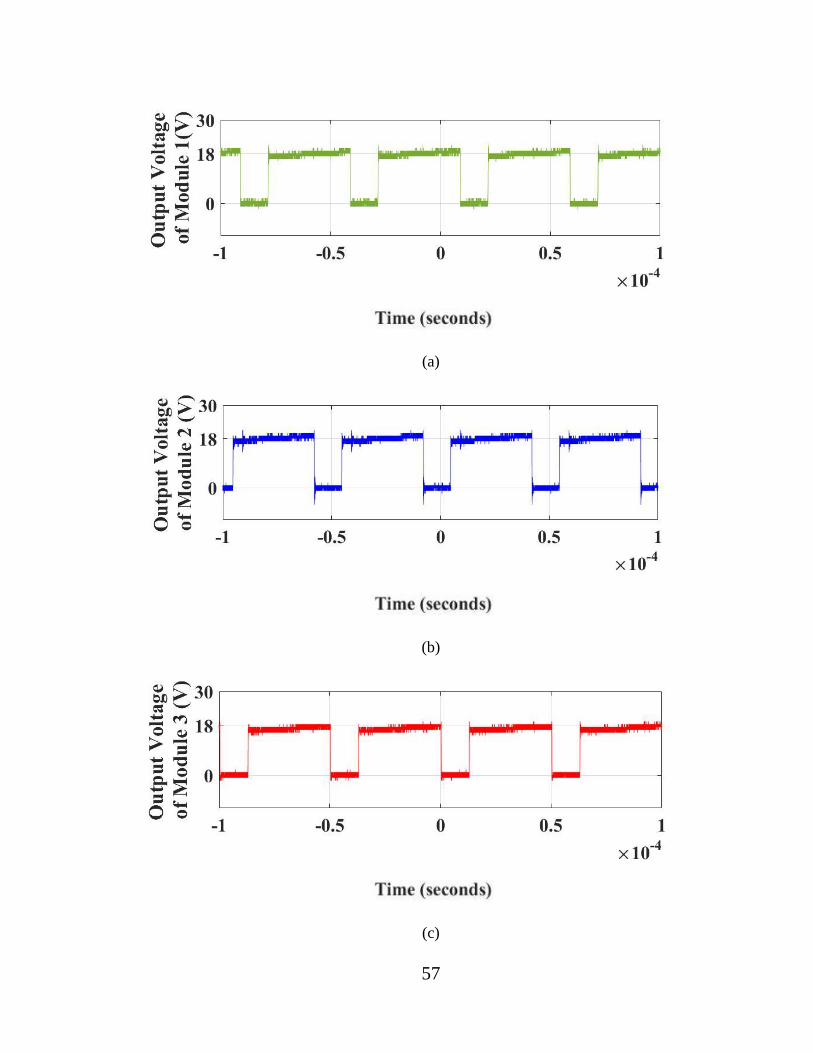
Considering the shoot-through time is equal to 12 µs and input voltage equal to 10
V, Figure 4.26 (a), (b) and (c) show that each unit dc-link voltage is boosted to 18V, which
is the expected value in the theory. Similar to the phase-shifted PWM waveforms of quasi
Z-source units, the output voltage of each quasi Z-source unit is shifted by 120°,
respectively. Since we used the variable duty cycle PWM waveforms from 0% to 100%,
the voltage waveforms out of each unit are all variable duty cycle. The results are all
captured at a random duty cycle to clearly illustrate how the output voltage looks.
57
(a)
(b)
(c)
58
(d)
(e)
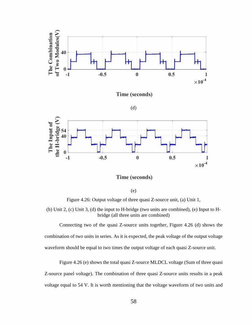
Figure 4.26: Output voltage of three quasi Z-source unit, (a) Unit 1,
(b) Unit 2, (c) Unit 3, (d) the input to H-bridge (two units are combined), (e) Input to H-
bridge (all three units are combined)
Connecting two of the quasi Z-source units together, Figure 4.26 (d) shows the
combination of two units in series. As it is expected, the peak voltage of the output voltage
waveform should be equal to two times the output voltage of each quasi Z-source unit.
Figure 4.26 (e) shows the total quasi Z-source MLDCL voltage (Sum of three quasi
Z-source panel voltage). The combination of three quasi Z-source units results in a peak
voltage equal to 54 V. It is worth mentioning that the voltage waveform of two units and

59
three units’ combination are not captured at the same duty cycle as the voltage output of
the three individual quasi Z-source units. They are captured at duty cycles chosen to clearly
show a variety of output voltage levels as examples of how the combinations of the outputs
of two or three units may look.
60
CHAPTER V
SUMMARY, CONCLUSION AND SUGGESTED FUTURE WORK
The modeling and simulation of a new quasi Z-source-based MLDCL inverter is
presented in this thesis. Compared to the traditional type of multilevel inverters such as
CMI and CCS, the proposed structure shows a few unique features which make it practical
and efficient in PV applications. The proposed MLDCL-based multilevel inverter has
fewer switches, which leads to the less switching loss. Also, the topology provides a simple
structure compared to the existing ones, which makes the whole system more flexible.
Moreover, the shoot-through time is allowed in quasi-Z-source-based MLDCL inverter,
which results in a simple control scheme and reliable system.
The quasi Z-source-based MLDCL inverter has several advantages over existing
Z-source-based MLDCL inverters that make it a better choice in PV systems. It draws a
constant current from the source, results in reduced voltage stress, and requires capacitors
with lower voltage ratings.
Considering an individual PV generator for each unit of quasi Z-source-based
MLDCL inverter, the incremental conductance is applied to achieve the maximum power
point of each PV. The proposed structure provides an independent control scheme for each
quasi Z-source unit. Applying separate MPPT to every single module of the quasi Z-
source-based multilevel inverter, comprehensive simulation and experimental results are
presented.
For future work, the Z/quasi Z-source source multilevel inverter could be
completed by adding an H-bridge to it. Three separate PV simulators could be added to

61
each quasi Z-source unit as the input voltage. Connecting three quasi Z-source modules
together, the MPPT control with grid connection would be implemented using voltage and
current sensors, which are already considered in the PCB design. Using jumpers in the PCB
design schematic, each quasi Z-source module would be able to function as a Z-source
module as well. Depending on the application, the set up can be used as a Z-source-based
MLDCL inverter or quasi Z-source based MLDCL inverter.
The number of quasi Z-source units could be increased to provide more flexibility
for various applications. A comprehensive small signal analysis and closed loop control
would be presented for the PV-connected quasi Z-source-based MLDCL inverter using
analysis, simulation and experiments.
62
REFRENCES
[1] Kalaiarasi, N., Paramasivam, S., & Kuntu, S. “Comparison of Z-source inverter with
DC/DC boost converter fed VSI for PV applications,” In IEEE 2th International Conference
on Electrical Energy Systems (ICEES), 2014, pp. 87-91.
[2] Li, Y., Anderson, J., Peng, F. Z., & Liu, D. “Quasi-Z-source inverter for photovoltaic
power generation systems,” In IEEE 24th Annual Applied Power Electronics Conference
and Exposition (APEC), 2009, pp. 918-924.
[3] Ramya, K., & Reddy, S. R. “Design and simulation of a photovoltaic induction motor
coupled water pumping system,” In IEEE International Computing, Electronics and
Electrical Technologies (ICCEET) Conference, 2012, pp. 32 - 39.
[4] Peng, F. Z. “Z-source inverter,” In IEEE Transactions on Industry Applications, vol.
39, Issue 2, March/April 2003, pp. 504-510.
[5] Anderson, J., & Peng, F. Z. “Four quasi Z-source inverters,” In 39th Power Electronics
Specialists Conference (PESC), 2008, pp. 2743–2749.
[6] Liu, Y., Ge, B., & Abu-Rub, H. “Modelling and controller design of quasi Z-source
cascaded multilevel inverter-based three-phase grid-tie photovoltaic power system,” In
IET Renewable Power Generation, vol.8, Issue 8, 2014, pp. 925-936.
[7] Xue, Y., Ge, B., & Peng, F. Z. “Reliability, efficiency and cost comparisons of MW-
scale photovoltaic inverters,” In IEEE Energy Conversion Congress and Exposition
(ECCE), September 2012, pp. 1627–1634.
[8] Gupta, K. K., Ranjan, A., Bhatnagar, P., Sahu, L. K., & Jain, S. “Multilevel inverter
topologies with reduced device count: a review,” In IEEE Transactions on Power
Electronics, vol. 31, Issue 1, 2016, pp.135-151.
[9] Kavidha, B., & Rajambal, K. “Transformer less cascaded inverter topology for
photovoltaic applications,” In India International Conference on Power Electronics, 2006,
pp. 328-3312006.
[10] Rodriguez, J., Lai, J. S., & Peng, F. Z. “Multilevel inverters: a survey of topologies,
controls, and applications,” In IEEE Transactions on Industrial Electronics, vol. 49, Issue
4, 2002, pp. 724-738.
[11] Selvaraj, J., & Rahim, N. A. “Multilevel inverter for gird – connected PV system
employing digital PI controller,” In IEEE Transactions on Industrial Electronics, vol. 56,
Issue 1, 2009, pp.149-158.
[12] Rahim, N. A., & Selvaraj, J. “Multistring five-level inverter with novel PWM control
scheme for PV application,” In IEEE Transactions on Industrial Electronics, vol.57, Issue
6, June 2010, pp.2111, 2123.
63
[13] Park, S. J., Kang, F. S., Cho, S. E., Moon, C. J., & Nam, H. K. “A novel switching
strategy for improving modularity and manufacturability of cascaded-transformer-based
multilevel inverters,” In Electric Power Systems Research, vol. 74, Issue 3, 2005, pp. 409-
416.
[14] Shahparasti, M., Larijani, A. S., Fatemi, A., Varjani, A. Y., & Mohammadian, M.
“Quasi Z-source inverter for photovoltaic system connected to single phase AC grid,” In
Power Electronic & Drive Systems & Technologies Conference (PEDSTC), 2010, pp. 456-
460.
[15] Zope, P. H., Patil, A. J., & Somkuwar, A. “Performance and simulation analysis of
single-phase grid connected PV system based on Z-source inverter,” In IEEE Power
Electronics, Drives and Energy Systems (PEDES) & Power India, 2010, pp.1-6.
[16] Chen, X., Fu, Q., & Infield, D. G. “PV grid-connected power conditioning system
with Z-source network,” In International Conference on Sustainable Power Generation and
Supply, 2009, pp. 1-6.
[17] Park, J. H., Kim, H. G., Nho, E. C., Chun, T. W., & Choi, J. “Grid-connected PV
system using a quasi-Z-source inverter,” In IEEE 24th Annual Applied Power Electronics
Conference and Exposition Conference (APEC), 2009, pp. 925-929.
[18] Li, Y., Jiang, S., Cintron-Rivera, J. G., & Peng, F. Z. “Modeling and control of quasi-
Z-source inverter for distributed generation applications,” In IEEE Transactions on
Industrial Electronics, vol. 60, Issue 4, 2013, pp. 1532-1541.
[19] Xu, P., Zhang, X., Zhang, C. W., Cao, R. X., & Chang, L. “Study of Z-source inverter
for grid-connected PV systems,” In IEEE 37th Power Electronics Specialists Conference,
2006, pp.1-5.
[20] Park, J. H., Kim, H. G., Chun, T. W., Nho, E. C., Shin, H. J., & Chi, M. H. “A control
strategy for the grid-connected PV system using a Z-source inverter,” In 2th International
Power and Energy (PE) Conference, 2008, pp. 948-951.
[21] Yu, Y., Zhang, Q., Liang, B., Liu, X., & Cui, S. “Analysis of a single-phase Z-source
inverter for battery discharging in vehicle to grid applications,” In Energies, vol. 4, Issue
12, 2011, pp. 2224-2235.
[22] Liu, L., Li, H., Zhao, Y., He, X., & Shen, Z. J. “1 MHz cascaded Z-source inverters
for scalable grid-interactive photovoltaic (PV) applications using GaN device,” In IEEE
Energy Conversion Congress and Exposition, 2011, pp. 2738-2745.
[23] Sun, D., Ge, B., Yan, X., Bi, D., Zhang, H., Liu, Y., Abu-Rub, H., Ben-Brahim, L. &
Peng, F.Z. “Modeling, impedance design, and efficiency analysis of quasi-source module
in cascaded multilevel photovoltaic power system,” In IEEE Transactions on Industrial
Electronics, vol. 61, Issue 11, 2014, pp. 6108-6117.
64
[24] Sun, D., Ge, B., Liang, W., Abu-Rub, H., & Peng, F. Z. “An energy stored quasi Z-
source cascade multilevel inverter-based photovoltaic power generation system,” In IEEE
Transactions on Industrial Electronics, vol. 62, Issue 9, 2015, pp. 5458-5467.
[25] Liu, Y., Ge, B., & Abu-Rub, H. “Modelling and controller design of quasi Z-source
cascaded multilevel inverter-based three-phase grid-tie photovoltaic power system,” In IET
Renewable Power Generation, vol. 8, Issue 8, 2014, pp. 925-936.
[26] Banaei, M. R., Dehghanzadeh, A. R., Salary, E., Khounjahan, H., & Alizadeh, R. “Z-
source-based multilevel inverter with reduction of switches,” In IET Power Electronics,
vol. 5, Issue 3, 2012, pp. 385-392.
[27] Shen, M., Wang, J., Joseph, A., Peng, F. Z., Tolbert, L. M., & Adams, D.
J. “Maximum constant boost control of the Z-source inverter,” In IEEE 39th IAS Annual
Meeting on Industry Applications, vol. 1, 2004.
[28] Revankar, P. S., Thosar, A. G., & Gandhare, W. Z. “Maximum power point tracking
for PV systems using MATALAB/SIMULINK,” In IEEE 2th International Conference on
Machine Learning and Computing (ICMLC), 2010, pp. 8-11.
[29] Naik, Y. R., & Thorat, A. R. “A control topology for maximum peak power tracking
of grid tied photovoltaic system,” In IEEE International Conference on Energy Efficient
Technologies for Sustainability (ICEETS), 2013, pp. 482-48.
[30] Abu-Rub, H., Iqbal, A., Ahmed, S. M., Peng, F. Z., Li, Y., & Baoming, G. “Quasi Z-
source inverter-based photovoltaic generation system with maximum power tracking
control using ANFIS,” In IEEE Transactions on Sustainable Energy, vol. 4, Issue 1, 2013,
pp. 11-20.
[31] Thangaprakash, S. “Unified MPPT control strategy for Z-source inverter based
photovoltaic power conversion systems,” In Journal of Power Electronics, vol.12, Issue 1,
2012, pp.172-180.
[32] Banaei, M. R., & Dehghanzadeh, A. R. “A novel Z-source based multilevel inverter
for renewable sources fed DVR,” In IEEE 1th Power Quality Conference, 2010, pp. 1-6.
[33] Babaei, E., & Hosseini, S. H. “New cascaded multilevel inverter topology with
minimum number of switches,” In Energy Conversion and Management, vol. 50, Issue 11,
2009, pp. 2761-2767.
[34] Banaei, M. R., & Salary, E. “New multilevel inverter with reduction of switches and
gate driver,” In Energy Conversion and Management, vol. 52, Issue 2, 2011, pp. 1129–
1136
[35] Su, G. J. “Multilevel DC-link inverter,” In IEEE Transaction on Industry Applications,
vol. 41, Issue 3, May/June 2005, pp. 848-854.
65
[36] Mohan, N., & Undeland, T. M. “Power electronics: converters, applications, and
design,” John Wiley & Sons, 2007.
[37] Tsai, H. L., Tu, C. S., & Su, Y. J. “Development of generalized photovoltaic model
using MATLAB/SIMULINK,” In Proceedings of the World Congress on Engineering and
Computer Science, 2008, pp. 1-6.
[38] Rivera, E. I. O., & Rodríguez, L. A. “The Z-source converter as an introduction to
power electronics and undergraduate research,” In IEEE 37th Annual Frontiers in
Education Conference-Global Engineering: Knowledge Without Borders, Opportunities
Without Passports, 2007, pp. T2C-5 – T2C-10.
[39] Joshi, L., & Shah, K. “Incremental conductance based maximum power point tracking
for PV multi-string power conditioning system,” In International Journal of Emerging
Technology and Advanced Engineering, vol. 3, Issue 5, May 2013, pp. 254-259.
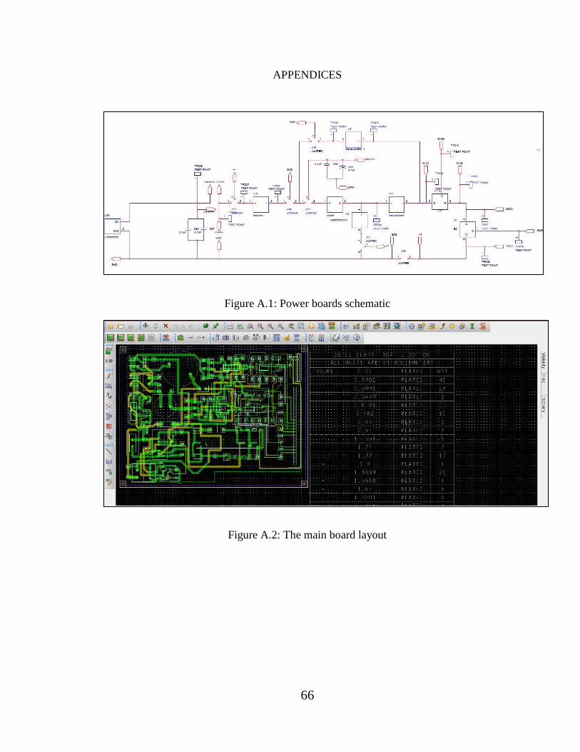
66
APPENDICES
Figure A.1: Power boards schematic
Figure A.2: The main board layout
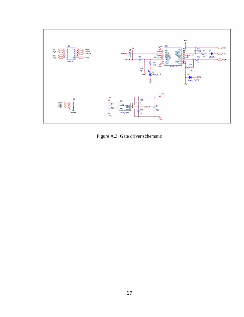
67
Figure A.3: Gate driver schematic