Simulation and Comparison of Newly Designed Mutistring Multilevel Inverter with High Level Inverter
10
SIMULATION AND COMPARISON OF NEWLY DESIGNED MUTISTRING MULTILEVEL INVERTER WITH HIGH LEVEL INVERTER CH. GANESH 1 , P. SARATH 2 , K. NAGESH 3 & J. V. G. RAMARAO 4 1,2 Assistant Professor, Department of EEE, BVC College Engineering, Palacharla, Andhra Pradesh, India 3 Associate Professor, Department of EEE, BVC College Engineering, Palacharla, Andhra Pradesh, India 4 Professor, Department of EEE, BVC Engineering College, Odalarevu, Andhra Pradesh, India ABSTRACT This paper presents a single-phase multi-string multilevel inverter for micro grid applications. The multilevel topology consists of few H-bridges connected in series, each one connected to a string. The proposed multistring multilevel inverter needs only six switches whereas conventional cascaded H-bridge multilevel inverter need eight switches. The multi-string inverter topology offers advantages like quality output waveform, small LC filter size, lower total harmonics distortion (THD) and less electromagnetic interference (EMI). The multilevel converters achieve high-voltage switching by means of a series of voltage steps, each of which lies within the ratings of the individual power devices. This paper presents comparison of single-phase Multistring multilevel inverter with single phase high level inverters. A micro grid has larger power capacity and is able to provide a coordinated integration of the increasing share of distributed generation units in the network. The unique feature of the multilevel inverters is to provide high switching frequencies with low switching losses. The studied multistring inverter topology offers strong advantages such as improved output waveforms, smaller filter size, and lower electromagnetic interference and total harmonics distortion. The simulation results are verified by Matlab/Simulink software. KEYWORDS: Multistring Multilevel Inverter, Micro Grid, H-Bridges, Total Harmonics Distortion (THD) INTRODUCTION Micro grid is a small scale power supply network that is designed to provide power for a small community. Both renewable and non renewable energy sources can be used in micro grid. Multistring multilevel inverters are used to obtain the sinusoidal output voltage and to reduce the total harmonic distortion by employing less number of switches. In the present scenario the distributed energy resource (DER) based single-phase inverter is usually adopted in the micro grid systems. In order to reduce conversion losses, the key is to save costs and size by removing any kind of transformer as well as reducing the power devices. A single-phase multistring five-level, seven, nine and eleven level inverter integrated with an auxiliary circuit was recently proposed for DC/AC power conversion. This report presents comparison of newly designed multistring multilevel inverter topology with high level inverters. The new topology produces a significant reduction in the number of power devices and capacitors required to implement a multilevel output. The new topology achieves a 37.5% reduction in the number of main power switches. Multilevel converters were used only in some high power applications such as high power motor drivers in marine, mining, or chemical industries applications, high power transmission, power line conditioners. Multilevel converters offer high power capability, International Journal of Electrical and Electronics Engineering Research (IJEEER) ISSN(P): 2250-155X; ISSN(E): 2278-943X Vol. 3, Issue 5, Dec 2013, 207-218 © TJPRC Pvt. Ltd.
-
Upload
independent -
Category
Documents
-
view
3 -
download
0
Transcript of Simulation and Comparison of Newly Designed Mutistring Multilevel Inverter with High Level Inverter
SIMULATION AND COMPARISON OF NEWLY DESIGNED MUTISTRING MULTILEVEL
INVERTER WITH HIGH LEVEL INVERTER
CH. GANESH1, P. SARATH
2, K. NAGESH
3 & J. V. G. RAMARAO
4
1,2Assistant Professor, Department of EEE, BVC College Engineering, Palacharla, Andhra Pradesh, India
3Associate Professor, Department of EEE, BVC College Engineering, Palacharla, Andhra Pradesh, India
4Professor, Department of EEE, BVC Engineering College, Odalarevu, Andhra Pradesh, India
ABSTRACT
This paper presents a single-phase multi-string multilevel inverter for micro grid applications. The multilevel
topology consists of few H-bridges connected in series, each one connected to a string. The proposed multistring multilevel
inverter needs only six switches whereas conventional cascaded H-bridge multilevel inverter need eight switches.
The multi-string inverter topology offers advantages like quality output waveform, small LC filter size, lower total
harmonics distortion (THD) and less electromagnetic interference (EMI). The multilevel converters achieve high-voltage
switching by means of a series of voltage steps, each of which lies within the ratings of the individual power devices.
This paper presents comparison of single-phase Multistring multilevel inverter with single phase high level inverters.
A micro grid has larger power capacity and is able to provide a coordinated integration of the increasing share of
distributed generation units in the network. The unique feature of the multilevel inverters is to provide high switching
frequencies with low switching losses.
The studied multistring inverter topology offers strong advantages such as improved output waveforms, smaller
filter size, and lower electromagnetic interference and total harmonics distortion. The simulation results are verified by
Matlab/Simulink software.
KEYWORDS: Multistring Multilevel Inverter, Micro Grid, H-Bridges, Total Harmonics Distortion (THD)
INTRODUCTION
Micro grid is a small scale power supply network that is designed to provide power for a small community. Both
renewable and non renewable energy sources can be used in micro grid. Multistring multilevel inverters are used to obtain
the sinusoidal output voltage and to reduce the total harmonic distortion by employing less number of switches. In the
present scenario the distributed energy resource (DER) based single-phase inverter is usually adopted in the micro grid
systems. In order to reduce conversion losses, the key is to save costs and size by removing any kind of transformer as well
as reducing the power devices.
A single-phase multistring five-level, seven, nine and eleven level inverter integrated with an auxiliary circuit was
recently proposed for DC/AC power conversion. This report presents comparison of newly designed multistring multilevel
inverter topology with high level inverters. The new topology produces a significant reduction in the number of power
devices and capacitors required to implement a multilevel output.
The new topology achieves a 37.5% reduction in the number of main power switches. Multilevel converters were
used only in some high power applications such as high power motor drivers in marine, mining, or chemical industries
applications, high power transmission, power line conditioners. Multilevel converters offer high power capability,
International Journal of Electrical and Electronics
Engineering Research (IJEEER)
ISSN(P): 2250-155X; ISSN(E): 2278-943X
Vol. 3, Issue 5, Dec 2013, 207-218
© TJPRC Pvt. Ltd.

208 CH. Ganesh, P. Sarath, K. Nagesh & J. V. G. Ramarao
associated with lower output harmonics and lower commutation losses.
Figure 1: Basic Structure of Multistring Multilevel Inverter
Various topologies for multilevel inverters have been proposed in the literature. Common ones are diode-clamped,
flying capacitor or multi-cell, cascaded H-bridge, and modified H-bridge multilevel. Cascaded multilevel inverters
synthesize a medium-voltage output by a series connection of power cells which use standard low-voltage component
configurations. This feature gives benefit of high-quality output voltages and input currents and also outstanding
availability due to their intrinsic component redundancy.
SYSTEM CONFIGURATION OF OPERATION PRINCIPLES
A Full H-Bridge
Vout
S3
S2S4
S1
Vdc
Figure 2: Full H-Bridge
Figure 2 shows the Full H-Bridge Configuration. By using single H-Bridge we can get 3 voltage levels.
The number output voltage levels of cascaded Full H-Bridge are given by 2n+1 and voltage step of each level is given by
Vdc/n. Where n is number of H-bridges connected in cascaded. The switching table is given in Table 1.
Table 1: Switching Table for Full H-Bridge
Switches Turn ON Voltage Level
S1,S2 Vdc
S3,S4 -Vdc
S4,D2 0
Simulation and Comparison of Newly Designed Mutistring Multilevel Inverter with High Level Inverter 209
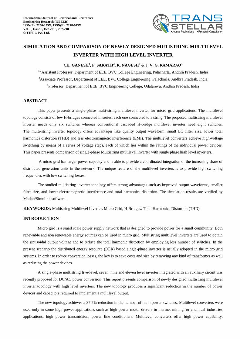
Simplified Multilevel Inverter Stage
A new single-phase multi string topology, presented as a new basic circuitry in Figure 3. Referring to Figure 2,
it should be assumed that, in this configuration, the two capacitors in the capacitive voltage divider are connected directly
across the dc bus, and all switching combinations are activated in an output cycle. The dynamic voltage balance between
the two capacitors is automatically controlled by the preceding high step-up converter stage. Then, we can
Assume Vs1 = Vs2 = Vs
This topology includes six power switches—two fewer than the CCHB inverter with eight power
switches—which drastically reduces the power circuit complexity and simplifies modulator circuit design and
implementation. . The phase disposition (PD) PWM control scheme is introduced to generate switching signals and to
produce five output-voltage levels: 0, VS, 2VS ,−VS , and −2VS .
This inverter topology uses two carrier signals and one reference to generate PWM signals for the switches.
The modulation strategy and its implemented logic scheme is widely used alternative for PD modulation. With the
exception of an offset value equivalent to the carrier signal amplitude, two comparators are used in this scheme with
identical carrier signals Vtri1 and Vtri2 to provide high-frequency switching signals for switches Sa1 , Sb1 , Sa3 , and Sb3 .
Another comparator is used for zero-crossing detection to provide line-frequency switching signals for switches Sa2 and
Sb2.
The required five output levels and the corresponding operation modes of the multi level inverter stage are
described clearly as follows.
Maximum positive output, 2VS: Active switches Sa 2, Sb 1, and Sb 3 are ON; the voltage applied to the LC output
filter is 2VS .
Half-level positive output, +Vs: This output condition can be induced by two different switching combinations.
One switching combination is such that active switches Sa 2, Sb 1, and Sa 3 are ON; the other is such that active
switches Sa 2, Sa 1, and Sb 3 are ON. During this operating stage, the voltage applied to the LC output filter is
+Vs .
Zero output, 0: This output condition can be formed by either of the two switching structures. Once the left orright
switching leg is ON, the load will be short-circuited, and the voltage applied to the load terminals.
Half-level negative output,−Vs : This output condition can be induced by either of the two different switching
combinations. One switching combination is such that active switches Sa 1 , Sb 2 , and Sb 3 are ON; the other is
such that active switches Sa 3 , Sb 1 , and Sb 2 are ON.
Maximum negative output,−2Vs : During this stage, active switches Sa 1 ,Sa 3 , and Sb 2 are ON, and the voltage
applied to the LC output filter is −2Vs
210 CH. Ganesh, P. Sarath, K. Nagesh & J. V. G. Ramarao
Figure 3: Basic Five-Level Inverter Circuitry
Figure 4: Modulation Logic
MATLAB/SIMULINK MODEL & SIMULATION RESULTS
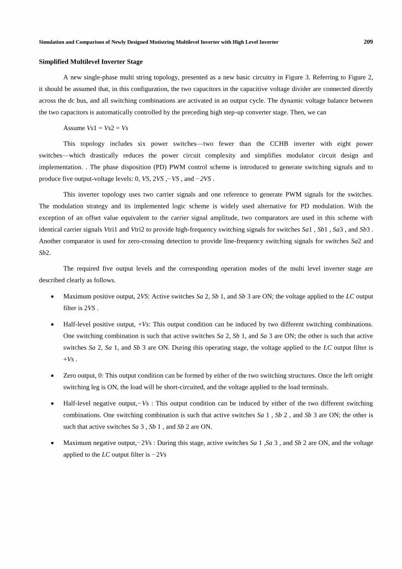
Diode Clamped Multilevel Inverter
Figure 5: Diode Clamped Multilevel Inverter
The basic simulation circuit shown in Figure 5 is a Eleven level Diode clamped Multilevel inverter with
combination of twenty switches in the circuit output voltage are obtained.
v+-
Voltage Measurement1 Scope1
gm
ak
SA8
gm
ak
SA7
gm
ak
SA6
gm
ak
SA5
gm
ak
SA4'1
gm
ak
SA4'
gm
ak
SA4
gm
ak
SA3'1
gm
ak
SA3'
gm
ak
SA3
gm
ak
SA2'1
gm
ak
SA2'
gm
ak
SA2
gm
ak
SA1'1
gm
ak
SA1'
gm
ak
SA1
Pulse
Generator9
Pulse
Generator8
Pulse
Generator7
Pulse
Generator6
Pulse
Generator5
Pulse
Generator4
Pulse
Generator3
Pulse
Generator2
Pulse
Generator15
Pulse
Generator14
Pulse
Generator13
Pulse
Generator12
Pulse
Generator11
Pulse
Generator10
Pulse
Generator1
Pulse
Generator
PG8
PG7
PG6
PG5
PG4
PG3
PG2
PG1
Diode9
Diode8
Diode7
Diode6
Diode5
Diode4
Diode3
Diode25
Diode24
Diode23
Diode22
Diode21
Diode20
Diode2
Diode19
Diode18
Diode17
Diode16Diode15
Diode14
Diode13
Diode12
Diode11Diode10
Diode1
Diode
DCSource
D8
D7
D4
D3
D2
D1
C4
C3
C2
C1
Add7
Add6
Add5
Add4
Add3
Add2
Add1
Add
7
6
5
4
3
2
1
Simulation and Comparison of Newly Designed Mutistring Multilevel Inverter with High Level Inverter 211
Figure 6: Diode Clamped Multilevel Inverter Output Waveform
Figure 6 shows the output voltage wave form which are obtained by Diode Clamped Multilevel Inverter Output
waveform.
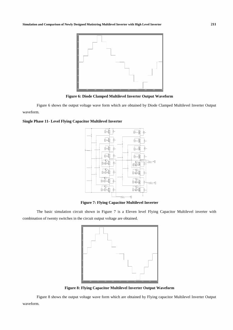
Single Phase 11- Level Flying Capacitor Multilevel Inverter
Figure 7: Flying Capacitor Multilevel Inverter
The basic simulation circuit shown in Figure 7 is a Eleven level Flying Capacitor Multilevel inverter with
combination of twenty switches in the circuit output voltage are obtained.
Figure 8: Flying Capacitor Multilevel Inverter Output Waveform
Figure 8 shows the output voltage wave form which are obtained by Flying capacitor Multilevel Inverter Output
waveform.
v+-
Voltage Measurement2
v+-
Voltage Measurement1
v+-
Voltage Measurement
Series RLC Branch9
Series RLC Branch8
Series RLC Branch7
Series RLC Branch6
Series RLC Branch5
Series RLC Branch4
Series RLC Branch3
Series RLC Branch2
Series RLC Branch17
Series RLC Branch15
Series RLC Branch14
Series RLC Branch12
Series RLC Branch11
Series RLC Branch10
Series RLC Branch1
Series RLC Branch
Scope2
Scope1
Scope
Pulse
Generator9
Pulse
Generator8
Pulse
Generator7
Pulse
Generator6
Pulse
Generator5
Pulse
Generator4
Pulse
Generator3
Pulse
Generator23
Pulse
Generator22
Pulse
Generator21
Pulse
Generator20
Pulse
Generator2
Pulse
Generator19
Pulse
Generator18
Pulse
Generator17
Pulse
Generator16
Pulse
Generator15
Pulse
Generator14
Pulse
Generator13
Pulse
Generator12
Pulse
Generator11
Pulse
Generator10
Pulse
Generator1
Pulse
Generator
gm
ak
Gto9
gm
ak
Gto8
gm
ak
Gto7
gm
ak
Gto6
gm
ak
Gto5
gm
ak
Gto4
gm
ak
Gto3
gm
ak
Gto2
gm
ak
Gto15
gm
ak
Gto14
gm
ak
Gto13
gm
ak
Gto12
gm
ak
Gto11
gm
ak
Gto10
gm
ak
Gto1
gm
ak
Gto
Diode9
Diode8
Diode7
Diode6
Diode5
Diode4
Diode3
Diode2
Diode15
Diode14
Diode13
Diode12
Diode11
Diode10
Diode1
Diode
DC Voltage Source
Add7
Add6
Add5
Add4
Add3
Add2
Add1
Add
212 CH. Ganesh, P. Sarath, K. Nagesh & J. V. G. Ramarao
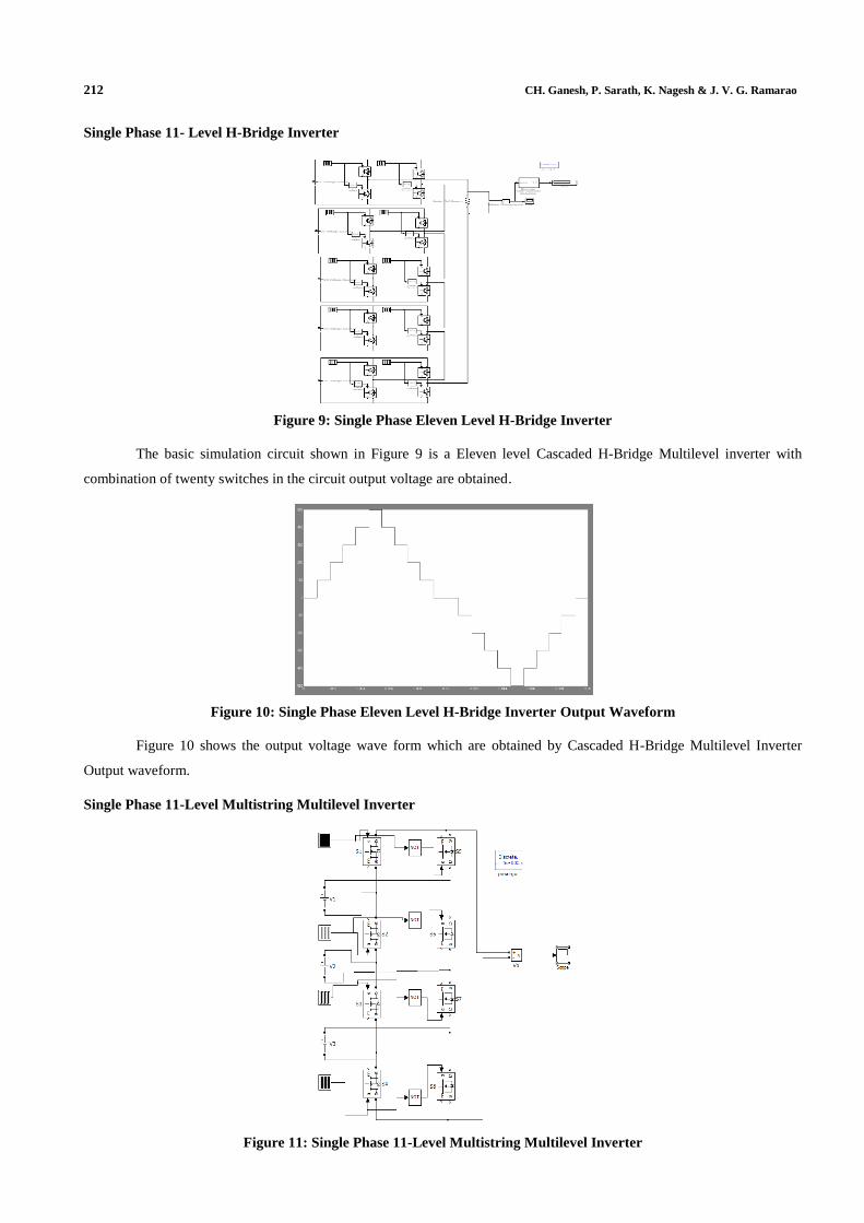
Single Phase 11- Level H-Bridge Inverter
Figure 9: Single Phase Eleven Level H-Bridge Inverter
The basic simulation circuit shown in Figure 9 is a Eleven level Cascaded H-Bridge Multilevel inverter with
combination of twenty switches in the circuit output voltage are obtained.
Figure 10: Single Phase Eleven Level H-Bridge Inverter Output Waveform
Figure 10 shows the output voltage wave form which are obtained by Cascaded H-Bridge Multilevel Inverter
Output waveform.
Single Phase 11-Level Multistring Multilevel Inverter
Figure 11: Single Phase 11-Level Multistring Multilevel Inverter
Simulation and Comparison of Newly Designed Mutistring Multilevel Inverter with High Level Inverter 213
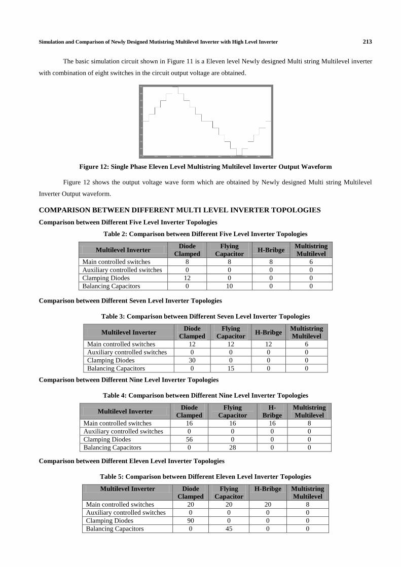
The basic simulation circuit shown in Figure 11 is a Eleven level Newly designed Multi string Multilevel inverter
with combination of eight switches in the circuit output voltage are obtained.
Figure 12: Single Phase Eleven Level Multistring Multilevel Inverter Output Waveform
Figure 12 shows the output voltage wave form which are obtained by Newly designed Multi string Multilevel
Inverter Output waveform.
COMPARISON BETWEEN DIFFERENT MULTI LEVEL INVERTER TOPOLOGIES
Comparison between Different Five Level Inverter Topologies
Table 2: Comparison between Different Five Level Inverter Topologies
Multilevel Inverter Diode
Clamped
Flying
Capacitor H-Bribge
Multistring
Multilevel
Main controlled switches 8 8 8 6
Auxiliary controlled switches 0 0 0 0
Clamping Diodes 12 0 0 0
Balancing Capacitors 0 10 0 0
Comparison between Different Seven Level Inverter Topologies
Table 3: Comparison between Different Seven Level Inverter Topologies
Multilevel Inverter Diode
Clamped
Flying
Capacitor H-Bribge
Multistring
Multilevel
Main controlled switches 12 12 12 6
Auxiliary controlled switches 0 0 0 0
Clamping Diodes 30 0 0 0
Balancing Capacitors 0 15 0 0
Comparison between Different Nine Level Inverter Topologies
Table 4: Comparison between Different Nine Level Inverter Topologies
Multilevel Inverter Diode
Clamped
Flying
Capacitor
H-
Bribge
Multistring
Multilevel
Main controlled switches 16 16 16 8
Auxiliary controlled switches 0 0 0 0
Clamping Diodes 56 0 0 0
Balancing Capacitors 0 28 0 0
Comparison between Different Eleven Level Inverter Topologies
Table 5: Comparison between Different Eleven Level Inverter Topologies
Multilevel Inverter Diode
Clamped
Flying
Capacitor
H-Bribge Multistring
Multilevel
Main controlled switches 20 20 20 8
Auxiliary controlled switches 0 0 0 0
Clamping Diodes 90 0 0 0
Balancing Capacitors 0 45 0 0

214 CH. Ganesh, P. Sarath, K. Nagesh & J. V. G. Ramarao
From the above tables 2,3,4,5 the numbers of switching devices are reduced greater in Multistring Multilevel
inverter using auxiliary controlled switch. When the switching devices are reduced the switching losses also reduced then
the efficiency of the inverter is improved. In this papet, we proposed model simulated different levels of inverters and
compared to other level inverters.
COMPARISON BETWEEN DIFFERENT MULTI LEVEL INVERTER TOPOLOGIES FOR
DIFFERENT LOADS
In this project different topologies of multilevel inverters like Diode clamped, flying capacitor and cascaded
H-bridge and Multi string Multilevel inverter analysis (for 50HZ) is carried out for various levels along with their
corresponding circuit diagrams and waveforms. The total THD of different multi level inverters are tabulated below:
Table 6: Comparison between Different Levels Inverter Topologies for Different Loads
INVERTER R-Load RL-Load
For 50Hz For 50Hz
1-Ø PWM Inverter 1.478 1.6669
1-Ø Half bridge Inverter 0.4803 0.4817
1-Ø Full Bridge Inverter (3-level) 0.4803 0.4821
1-Ø Diode Clamped Inverter (5-level) 0.2673 --
1-Ø Flying capacitor Inverter (5-level) 0.2637 --
1-Ø H-Bridge Inverter (5-level) 0.5695 0.5721
1-Ø H-Bridge Inverter (7-level) 0.3105 0.3189
1-Ø H-Bridge Inverter (9-level) 0.2576 0.2568
1-Ø H-Bridge Inverter (11-level) 0.2230 0.2223
1-Ø Multistring Multilevel Inverter (5-level) 0.5595 0.5618
1-Ø Multistring Multilevel Inverter (7-level) 0.2439 0.2459
1-Ø Multistring Multilevel Inverter (9-level) 0.1813 0.1832
1-Ø Multistring Multilevel Inverter (11-level) 0.1383 0.1395
From the above results the Total Harmonic Distortion of different multilevel inverters are are compared for
different loads. From the above table the total harmonic distortion is reduced, when the level of the inverter is increased.
CONCLUSIONS
In this project the advantages and applications of multilevel inverters are mentioned and a detailed description of
different multilevel inverter topologies are presented., and also concluded that controlling of voltage magnitude of inverter
by PWM technique is most efficient when compared with other techniques. All these inverter topologies are virtually
simulated using MATLAB SIMULINK and the gating signals of different inverter topologies have been analyzed and
respective output voltage waveforms are given. From the simulation results, concluded that the non linear loads have
reduced total harmonic distortion (THD) in multi level inverters as compared to other conventional inverters. Then the
reduced harmonic distortion reduces the switching losses for higher frequency applications. Then the power transfer
capability is increased for non linear loads. The conventional inverter eliminates the 3rd
harmonic and 5th
harmonics in the
output voltage.
A brief Comparison of different multilevel inverter topologies are given and we observe that the THD of the
output voltage wave is reduced with level improvement of inverter. The Multistring Multilevel inverter gives good
performance as compared to other high voltage inverter. We hereby conclude that multilevel inverter is a very promising
technology in the power industry.

Simulation and Comparison of Newly Designed Mutistring Multilevel Inverter with High Level Inverter 215
REFERENCES
1. Y. Li, D.M. Vilathgamuwa, and P.C. Loh, “Design, analysis, and realtime testing of a controller for multibus
microgrid system,” IEEE Trans Electron., vol. 19, no. 5, pp. 1195-1204, Sep. 2004.
2. N. Hatziargyriou, H. Asano, R. Iravani, and C. Marnay, “Microgrids,” IEEE power Energy Mag., vol. 5,no. 4,
pp.78-94, Jul/Aug.2007.
3. F. Katiraei, R. Iravani, N. Hatziargyriou, and A. Dimeas, “Microgrids management,” IEEE Power Energy Mag.,
vol. 6, no. 3, pp. 54-65, May/Jun. 2008.
4. C. L. Chen, Y.Wang, J.S.Lai, Y.S..Lee, and D. Martin, “Design of parallel inverters for smooth mode transfer
microgrid applications,” IEEE trans. Power Eletron., vol. 25, no.1 pp. 6-15, Jan.2010.
5. C.T. Pan, C.M. Lai, and M. C. Cheng, “ A novel high step-up ratio inverters for distributed energy
resources(DERs),” in proc. IEEE Int. Power Electron Conf., 2010, pp. 1433-1437.
6. C. T. Pan, C. M. Lai, and M.C. Cheng, “A novel integrated single phase inverter with an auxilary step-up circuit
for low-voltage alternative energy source application,” IEEE Trans. Power Electron., vol.25. no.9, pp.2234-2241,
Sep.2010.
7. D.G. Infield, P.Onions, A.D.Simmons, and G.A.smith, “Power quality from multiple grid-connected single-phase
inverters,” IEEE Trans. Power Del., vol 19, no.4,pp.1983-1989, oct.2004
8. S.B.Kjaer, J.K.Pedersen, and F.Blaabjerg,”A review of single-phase grid-connected inverters for photovoltaic
modules,” IEEE Trans. Ind. Appl., vol. 41, no. 5, pp. 1292-1306, Sep/Oct.2005.
9. O.Lopez, R.Teodoresuc, and J. Doval-Gandoy, “Multilevel transformerless topologies for single-phase
grid-connected converters,”in proc. IEEE Ind. Electron. Conf., 2006,pp.5191-5196.
10. T. Kerekes, R.Teodorescu, and U. Borup, “Transformerless photovoltaic inverters connected to the grid,” in Proc.
IEEE Appl. Power Electrons. Conf., 2007, p.1733-1737
11. F. Blaabjerg, Z. Chen, and S. B. Kjaer, “Power electonics as efficiency interface in dispersed power generation
systems,” IEEE Trans. Power Electronl., vol 19, no.5,pp.1184-1194, oct.2004.
12. Yi-Hung Liao and Ching-Ming Lai, “ Newly constructed simplified single phase multistring multilevel inverter
topology for distributed energy resources,” in IEEE Trans. Power Electrons, vol.26, no.9, Sep. 2011.
13. CH.Ganesh, andJ.V.G>Ramarao, “Symmetrical Five Level and Asymmetrical Seven Level Inverter for PV
application,’’Recent Science Publications vol. 43, no. 2, ISSN:0306-6190, SAug. 2012.
AUTHOR’S DETAILS
CH. GANESH received his B.Tech Degree in EEE from Godavari Institute of Engineering and Technology

216 CH. Ganesh, P. Sarath, K. Nagesh & J. V. G. Ramarao
Rajahmundry East Godavari (Dt) in 2009, the M.Tech. Degree in Power Electronics from B.V.C. Engineering College,
Odalarevu, in 2012. At present he is also working as an Asst. Prof in the department of Electrical and Electronics
Engineering, B.V.C. College of Engineering, Palacharla.
POTHULA SARATH received his B.Tech Degree in EEE from B.V.C. Engineering College, Odalarevu, East
Godavari (Dt) in 2005, the M.Tech. Degree in Power Electronics from B.V.C. Engineering College, Odalarevu, in 2012.
At present he is also working as an Asst. Prof in the department of Electrical and Electronics Engineering, B.V.C. College
of Engineering, Palacharla.
K. NAGESH received his B.Tech degree in EEE from A.S.R College of Engineering Tadepalligudem, West
Godavari (Dt) in 2002, the M.Tech. Degree in power electronics from Vardhaman College of Engineering in 2010.
At present he is also working as an Assoc.Prof in the Department of Electrical and Electronics Engineering, B.V.C.
College of Engineering, Palacharla.
Dr. J.V.G. RAMARAO was born in Kakinada, India in 1972. He received the B.E degree from Karnataka
University, India in 1995, the M.Tech (High Voltage Engineering) degree from the department of Electrical Engineering,
Jawaharlal Nehru Technological University, Kakinada in 2001.He completed his Doctral degree from Jawaharlal Nehru
technological university, Hyderabad. He is also working as Professor in the Department of Electrical Engineering,
B.V.C.Engineering College, Odalarevu .His research interests include Gas insulated substations, High voltage testing,
Electromagnetic field computations, HVDC Transmission systems, Power converters, Wavelets. He has published research
papers in national and international conferences.