
Prototyping the TI TMS320C40 to the Cypress VIC068 ...
41
Prototyping the TI TMS320C40 to the Cypress VIC068/VAC068 Interface Application Report Peter F. Siy and David L. Merriman The MITRE Corporation Timothy V. Blanchard Cypress Semiconductor SPRA105 February 1994 Printed on Recycled Paper
-
Upload
khangminh22 -
Category
Documents
-
view
0 -
download
0
Transcript of Prototyping the TI TMS320C40 to the Cypress VIC068 ...

Prototyping the TI TMS320C40 to theCypress VIC068/VAC068 Interface
Application Report
Peter F. Siy and David L. MerrimanThe MITRE CorporationTimothy V. Blanchard
Cypress Semiconductor
SPRA105February 1994
Printed on Recycled Paper

IMPORTANT NOTICE
Texas Instruments (TI) reserves the right to make changes to its products or to discontinue anysemiconductor product or service without notice, and advises its customers to obtain the latestversion of relevant information to verify, before placing orders, that the information being reliedon is current.
TI warrants performance of its semiconductor products and related software to the specificationsapplicable at the time of sale in accordance with TI’s standard warranty. Testing and other qualitycontrol techniques are utilized to the extent TI deems necessary to support this warranty.Specific testing of all parameters of each device is not necessarily performed, except thosemandated by government requirements.
Certain applications using semiconductor products may involve potential risks of death,personal injury, or severe property or environmental damage (“Critical Applications”).
TI SEMICONDUCTOR PRODUCTS ARE NOT DESIGNED, INTENDED, AUTHORIZED, ORWARRANTED TO BE SUITABLE FOR USE IN LIFE-SUPPORT APPLICATIONS, DEVICESOR SYSTEMS OR OTHER CRITICAL APPLICATIONS.
Inclusion of TI products in such applications is understood to be fully at the risk of the customer.Use of TI products in such applications requires the written approval of an appropriate TI officer.Questions concerning potential risk applications should be directed to TI through a local SCsales office.
In order to minimize risks associated with the customer’s applications, adequate design andoperating safeguards should be provided by the customer to minimize inherent or proceduralhazards.
TI assumes no liability for applications assistance, customer product design, softwareperformance, or infringement of patents or services described herein. Nor does TI warrant orrepresent that any license, either express or implied, is granted under any patent right, copyright,mask work right, or other intellectual property right of TI covering or relating to any combination,machine, or process in which such semiconductor products or services might be or are used.
Copyright 1996, Texas Instruments Incorporated

1
Introduction
The Texas Instruments TMS320C40 digital signal processor (DSP) represents a state-of-the-art solutionto many signal processing problems via its high-speed central processor unit (CPU), unique parallelprocessing I/O capability, and robust interface to other system components [1]. Likewise, the CypressSemiconductor VIC068 VMEbus Interface Controller and its companion VAC068 VMEbus AddressController provide a complete VMEbus interface, including master and slave capability [2,3]. Since thesecomponents are effective in a wide variety of applications and since the VIC068/VAC068 is a single- ormultiple-TMS320C40 VMEbus card design, we developed a single TMS320C40 VMEbus card for use ina satellite modem application [4].
The VIC068/VAC068 is designed to interface with the Motorola 68000 family of microprocessors, so itwas determined that the interfacing to a TMS320C40 required a logic simulation or some form ofprogrammable, configurable prototype. When this design was initiated, only preliminary documentationexisted for the VMEbus chip set, and no simulation models were available for either the chip set or theTMS320C40 DSP. Therefore, we first prototyped the interface of these components in a wire-wrapenvironment before proceeding to a printed circuit board design. This paper provides the high-level as wellas low-level details of the prototyping effort so that others may examine our approach and techniques tominimize design time for subsequent efforts. Note that this design has not been optimized for either sizeor speed. Section 2 outlines the design goals established before design began and gives relevant backgroundregarding the devices involved. The paper focuses on the hardware details, programmable logic sourcecode, and schematics that follow. In addition, the software initialization of the chip set by the ’C40 isdescribed. Throughout this paper, we assume that you are familiar with the ’C40 architecture as well as withthe VMEbus and its protocol(s). You can refer to [5,6] for more details on the VMEbus. Figure 1 showsthe VIC068/VAC068 prototype block diagram.

2
Figure 1. TMS320 – VIC/VAC Prototype Block Diagram
Comm Port 3Comm Port 4Comm Port 5
JTAG Scan Path
TMS320C40
Comm Port 0Comm Port 1Comm Port 2
Clock In
Data BusBuffers
HighData
VIC068 VMEBusController
LowAddress/Dat
aC40-VIC/VACPLD Interface
C40 BusControl
Master CycleGenerationSlave CycleGeneration
VAC068VMEBusAddressInterface
HighAddress
Pseudo-68000Signals
128K WordsProgramEPROM
128K WordsProgram SRAM
Serial ParallelI/O
VMEBus(A24 D32)

3
Prototype Design
Design Goals
We began by developing a set of design goals for the VME interface that were based on our particular needs.We were interested in a ’C40 card that provided both (VMEbus) master and slave capability for reads,writes, read-modify-writes, write posting, and slave block transfers. We designed the address/datacapability according to the most prevalent configuration (for other cards available commercially): 24-bitaddress and 32-bit data (i.e., A24/D32); however, the design presented here does not preclude 32-bitaddressing with minor modifications. Via the VIC068, this design also features system controllercapability. We did not incorporate VMEbus interrupt support, because we provided application-specificinterrupt inputs directly to the ’C40. We utilized the VAC068 for address control/mapping of the twoUniversal Asynchronous Receiver/Transmitters (UARTs) that were required for our application, and forgeneral-purpose parallel I/O. The new Cypress CY6C964 Bus Interface Logic Circuit can be used insteadof the VAC068. In addition to the VMEbus functionality, we required the interface to be compatible withboth the existing ’C40-40 (50-nanosecond cycle time) and the faster ’C40 (40-nanosecond).
Design Considerations
First, we thoroughly examined the VIC068 and VAC068 and reviewed the 680x0 family bus signals andcycles. In particular, we referred to the 68020 user’s manual [7] extensively. The VIC068 and VAC068interface directly to the Motorola 680x0 family data, address, and control signals and are driven with thefamiliar 680x0 address and data strobes (PAS, DS). An asynchronous transfer protocol is implemented viadata transfer and size acknowledgment signals DSACK0 and DSACK1. In addition to these signals, thetransfer size signals SIZ0 and SIZ1 are essential elements in the 680x0’s dynamic bus sizing capability and,with the lower address lines, encode the size of the transfer in progress. Also, during the transfer, thefunction code signals (FC0–FC2) provide information of importance in multiuser environments. Busarbitration is an integral part of the 680x0 via the bus request (BR), bus grant (BG), and bus grantacknowledge (BGACK) signals and is used directly by the VIC068. Finally, as in many othergeneral-purpose microprocessors, bus cycles for the 680x0 are several clock cycles long.
While the VIC068 and VAC068 are driven by (and can drive) the familiar 680x0 bus signals, the ’C40 bussignals show little similarity to those of the 680x0 family. The ’C40’s bus protocol is common to theTMS320 floating- point DSP product line. An external ready signal allows for wait-state generation andcontrols the rate of transfer in a synchronous fashion (i.e., cycles can be extended an integer number ofclock cycles). As described in [1], the ’C40 has two identical external interfaces: the global memoryinterface and the local memory interface. Each consists of a 32-bit data bus, a 31-bit address bus, and twosets of control signals. The benchmark of all DSP technology, the ’C40 executes single-cycle instructions(see the ’C4x user’s guide for complete details) and relies on a multistage pipeline for execution speed.Detailed bus status, including type of instruction and type of access, is given for each cycle via the STATlines. Individual control lines can put the address, data, and control bus(es) in the high-impedance state.There is no read-modify-write signal (as on the 680x0); however, an instruction-driven LOCK signal isavailable. Each cycle is controlled by a strobe (STRBx) signal in conjunction with the correspondingread/write (R/Wx) strobe. One of the ’C40’s notable features is its range of configuration options. The ’C40has evolved from its earlier floating-point counterparts into a truly flexible interface via the local and globalbus configuration control registers.

4
Figure 2. TMS320C40 – VIC/VAC Prototype ’C40 Global Bus
C17
STRB0
R/W0
PAGE0
RDY0
CE0
A5
A6
A7
A8
A9
A10
A11
A12
A13
A14
A15
A16
A17
A18
A19
A20
A21
A22
A23
A24
A25
A26
A27
A28
A29
A30A
0
A1
A2
A3
A4
D32
B32
D30
C29
B30
F28
F24
C27
D28
B28
F26
C25
E27
B26
D26
C23
B24
E25
C21
D24
B22
E23
C19
D22
B20
E21
B18
D20
B16
GA0–GA30
RESETLOC1
RESETLOC0
RESET
ROMEN
X1
X2/CLKIN
H1
H3
AH34
AF30
AJ33
AK4
W1
AA1
AC3
AC5
C33
D5
D6
D7
D8
D9
D10
D11
D12
D13
D14
D15
D16
D17
D18
D19
D20
D21
D22
D23
D24
D25
D26
D27
D28
D29
D30
D0
D1
D2
D3
D4
U33
V32
T34
U31
A33
P34
T32
N33
M34
P32 L3
3
N31
K34
M32 J33
L31
M30
K32
H34 J3
1
G33
K30
F34
H32
E33
D34
G31
H30
E31
D31
F32
GD0–GD31
ResetVector
Location
RN1 RN1
+5 V +5 V
2 31 16
2 15
RESET
RN1
+5 V
43 14
ROMEnabled
H1CLK
H3CLK
AD30
AF32
AG33
Y32
AA32
AC33
AC31
AB32
W31
V34
AA31
AG31
AD32
AE33
AF34
AE31
W33
OUT
OUT
A Y1
Y2
G1 Y3
G2 Y4
8 19
1 18
17
20
1
2
3
U16 U17A
OSC40 MHz
74ACT11208
OUT
OUT
GSTRB0
GR/W0
GBE
GSTRB1
GRDY1
GSTAT0–GSTAT3
GLOCK
TMS320C40GFL
R31
E29
SW1
SW1
SW1
STRB1
R/W1
PAGE1
RDY1
CE1
DE
AE
STAT0
STAT1
STAT2
STAT3
LOCK
5
High-Level Architecture
The high-level architecture for the card places fast 20-ns high-density 4-megabit (128K × 32) CypressCMOS SRAM modules on both local and global buses of the ’C40 (the size of the memory array does notimpact the ’C40-to-VIC068/VAC068 interface design). We designated the global side as program memoryand the local side as data memory for our application. In our environment, it is anticipated that the localmemory will be fully occupied by DMA coprocessor activity coupled with data fetches duringcommunications-oriented DSP operations. Given this, we chose to place the A24 VME spectrum on theglobal (program) side, segmenting the local side I/O activity (the critical path for our application) from allVMEbus activity. (However, the interface documented herein can be used on either side because the globaland local buses are symmetric.) On the global side, in addition to program SRAM, we also placed two 128K× 16 EPROMs for embedded program store, using the boot load feature of the ’C40.
Because we limited our design to VMEbus A24 addressing, this range fits nicely anywhere in the ’C40global side address spectrum, from 08000 0000h to 0FFFF FFFFh. Therefore, VMEbus master access ismemory mapped into the ’C40 global side address range. When an access occurs in this predefined A24range, the ’C40 bus signals are transformed into 680x0 bus signals, which drive the VIC068/VAC068 pairand initiate a VMEbus transfer. Global side accesses outside of this range do not generate such signals andoccur at full speed (i.e., the speed appropriate for that memory or peripheral). Regarding the “endianess”[8,9] of the interface, we know that the 680x0 family maintains big-endian byte ordering (byte-addressablememory organization) with little-endian bit ordering in each addressable unit. In contrast, the ’C40 is flatin its byte endianess (32-bit word addressable only) and little-endian bit ordered. Therefore, no swappingis done on the interface, because 32-bit word transfers (between processors) maintain D0 as the leastsignificant bit. This forces a tradeoff of transfer speed for a wider range of transfers (byte, word, and threebyte) than the ’C40 offers. We chose to limit our transfers to D32. To make transfers of all sizes available,you must preform additional setup and/or decoding before/during the transfer in progress.

6
Figure 3. TMS320C40 – VIC/VAC Prototype Program SRAM
I/O0
I/O1
I/O2
I/O3
I/O4
I/O5
I/O6
I/O7
I/O8
I/O9
I/O10
I/O11
I/O12
I/O13
I/O14
I/O15
I/O16
I/O17
I/O18
I/O19
I/O20
I/O21
I/O22
I/O23
I/O24
I/O25
I/O26
I/O27
I/O28
I/O29
I/O30
I/O31
4
6
8
10
20
22
24
26
5
7
9
11
19
21
23
25
40
42
44
46
56
58
60
62
39
41
43
45
57
59
61
63
13
15
17
47
49
51
55
14
16
18
48
50
52
54
30
29
36
32
31
34
33
37
28
A0
A1
A2
A3
A4
A5
A6
A7
A8
A9
A10
A11
A12
A13
A14
A15
A16
CS1
CS2
CS3
CS4
OE
WE
+5 V
GA0–GA16 GD0–GD31
RN1
6GSTRB0
GR/W0
128K-Word SRAM Module
CYM1836
Hardware Description
After examining the VIC068/VAC068 interface and capabilities and comparing them with the ’C40, weinitiated a prototype design. Based on the preceding discussion, the strategy is to map from the given setof ’C40 bus signals to a set of 680x0-like signals, driving their counterparts on the VIC068 and VAC068for master cycles (the ’C40 is reading from or writing to the VMEbus). Not only can the ’C40 initiateVMEbus cycles as a bus master, but also the card should respond to slave cycles. Most often, slave accessis gained through shared memory on the (slave) card. On the ’C40-based VME card, one set of signals isrequired to respond to bus requests from the VIC068/VAC068, and an additional set is required to “holdoff” the ’C40 global side during such transfers.
To accomplish this transformation of signals, programmable logic is applied. We wanted to keep the designtime to a minimum while maintaining the most flexible (i.e., programmable) design. Based on this, we usedthe Texas Instruments TIB82S105BC programmable logic sequencer. This device is a field-programmableMealy-type state machine with 16 inputs, 8 outputs, 48 product terms, and 14 pairs of sum terms; it operatesat a maximum frequency of 50 MHz [10]. Development tools for these sequencers are plentiful andinexpensive — we used Data I/O’s ABEL version 4.0 for all programmable logic device (PLD)development.

7
Figure 4. TMS320C40 – VIC/VAC Prototype Programmable Logic
FPLS
CLK
PR/DE
I0
I1
I2
I3
I4 F0∇
I5 F1∇
I6 F2∇
I7 F3∇
I8 F4∇
I9 F5∇
I10 F6∇
I11 F7∇
I12
I13
I14
I15
1
19
9
8
7
6
5
4
3
2
27
26
25
24
23
22
21
20
H3CLK
RESET
MRD
MWR
RRD
RWR
GPROM
MWB
LBR
DEDLK
DSACK0
DSACK1
LBERR
GLOCK
U13
Bus Control
18
17
16
15
13
12
11
10
LBG
GBE
MOE
SOE
GRDY1
16R6
CLK
OE
R18∇
I2 R17∇
R16∇
R15∇
I3 R14∇
I4 R13∇
I5
I6
I7
I8 IO19∇
I9 IO12∇
1
11
2
3
4
5
6
7
8
9
H1CLK
RESET
GA28
GA29
GA30
GSTRB1
U12
Bus Decode
18
17
16
15
14
13
19
12
GPROM
RWR
RRD
MWR
MRD
GSTAT0–GSTAT3
FPLS
CLK
PR/OE
I0
I1
I2
I3
I4 F0∇
I5 F1∇
I6 F2∇
I7 F3∇
I8 F4∇
I9 F5∇
I10 F6∇
I11 F7∇
I12
I13
I14
I15
1
19
9
8
7
6
5
4
3
2
27
26
25
24
23
22
21
20
MOE
RESET
MRD
MWR
RRD
RWR
GPROM
MWB
LBR
DEDLK
DSACK0
DSACK1
LBERR
GLOCK
U14
Master BusCycle Generation
18
17
16
15
13
12
11
10
PAS
DS
R/W
RMC
SIZ0
SIZ1
FC1
FC2
FPLS
CLK
PR/DE
I0
I1
I2
I3
I4 F0∇
I5 F1∇
I6 F2∇
I7 F3∇
I8 F4∇
I9 F5∇
I10 F6∇
I11 F7∇
I12
I13
I14
I15
1
19
9
8
7
6
5
4
3
2
27
26
25
24
23
22
21
20
SOE
RESET
PAS
DS
R/W
RMC
SIZ0
SIZ1
FC0
FC1
FC2
LBG
U15
Slave BusCycle Generation
18
17
16
15
13
12
11
10
DSACK0
DSACK1
LBERR
GSTRBO
GR/WO
Reset Circuitry
We found that the VIC068/VAC068 required a “global” reset to operate correctly. In particular, the VIC068IRESET signal should be driven with the incoming reset request. This signal can be buffered as shown toprovide the delayed signal to the IPL0 input —thereby providing the required stimulus for a VIC068 globalreset. Given these inputs, the VIC068, in turn, drives the RESET line (and the SYSRESET line if theVIC068 is configured as a system controller) for 200 milliseconds. We used the RESET output on theVIC068 to reset both the ’C40 and the VAC068, as well as programmable logic on-board.

8
Figure 5. TMS320C40 – VIC/VAC Prototype VICO68 VMEbus Interface
IAC
KO
UT
IAC
KIN
IAC
K
IRQ
7
IRQ
6
IRQ
5
IRQ
4
IRQ
3
IRQ
2
IRQ
1M
3
N3
P2
R1
N4
P3
R2
P6
N6
R4
N5
P5
P15
SY
SC
LK
SY
SR
ES
ET
AC
FAIL
SY
SFA
ILS
YS
FAIL
AC
FAIL
SY
SR
ES
ET
SY
SC
LK
7
RN1+5 V
IRQ
1
IRQ
2
IRQ
3
IRQ
4
IRQ
5
IRQ
6
IRQ
7
IAC
K
IAC
KIN
IAC
KO
UT
AO1AO2AO3AO4AO5AO6AO7AM0AM1AM2AM3AM4AM5DO0DO1DO2DO3DO4DO5DO6DO7ASDS0DS1DIACKBERRWRITELWORD
A1K2
A2L1
A3L2
A4M1
A5M2
A6L3
A7N2
AM0R6
AM1R7
AM2P8
AM3R8
AM4R9
AM5R10
D0K13
D1K14
D2L15
D3J14
D4K15
D5J15
A1–A7
AM0–AM5
D0–D7
ASDS0DS1
DTACKBERR
WRITELWORD
R14N12
R12P12N11P13
M14L13N15M15
N13P14M13N14
BCLRBBSY
BR0BR1BR2BR3
BG0OUTBG1OUTBG2OUTBG3OUT
BG0INBG1INBG2INBG3IN
BCLRBBSY
BR0BR1BR2BR3
BG0OUTBG1OUTBG2OUTBG3OUT
BG0INBG1INBG2INBG3IN
U3AVICO68_VME
R3

9
Address Bus DecodingThe VIC068/VAC068 interface (and consequently the VMEbus itself) is mapped into the ’C40 global sideat 0D000 0000h. In our application, we divided the global side into two halves via the STRB ACTIVE fieldin the ’C40 global memory control register. We placed zero-wait-state devices (fast SRAM) in the lowerhalf and placed slower memory (EPROM) and peripherals (the VIC068/VAC068 pair) in the upper half.Therefore, the ’C40 addresses program memory via STRB0 and addresses the VMEbus via STRB1. Asshown in the accompanying schematics, U12 is a 16R6 programmable device (in particular, a TexasInstruments TIBAL16R6-5C was used). It decodes each global ’C40 STRB1 bus cycle by using the ’C40H1 clock. Cycle type decoding is performed fully via the STAT lines (instead of using the R/W strobe) andallows for future expansion/reconfiguration if required. As shown, the STRB1 range is divided into eightdistinct segments by using GA28—GA30 (GA31 is implicitly a logic 1). Outputs of the decoding operationare VMEbus master write (MWR), master read (MRD), VIC068/VAC068 register write (RWR), registerread (RRD) and EPROM read (GPROM). The VIC068/VAC068 documentation shows that the VAC068is hard-wired, starting at address 0FFFD 0000h, and designates VIC068 selection, starting at address0FFFC 0000h. A memory map for the global side, as decoded by the 16R6 logic device, is shown in Table 1.The ABEL source code is provided in the appendix.
Table 1. Global Side Memory Map
Address Unit Addressed
08000 0000h SRAM
0C000 0000h EPROM
0D000 0000h VMEbus A24
Address 00 0000h
0FFFC 0000h VIC068 Register Set
0FFFD 0000h VAC068 Register Set
Bus ControlOnce a cycle in the VMEbus address range is detected by the address-decoding programmable logic, thesequencers provide the signals required for both master and slave cycles. U13 is the first of three sequencersand facilitates overall bus control, providing these enable signals: ’C40 global bus (GBE), master cyclesequencer output (MOE), slave cycle sequencer output (SOE), VMEbus slave local bus grant (LBG), anda ’C40 ready signal (GRDY1). Notice that a full complement of inputs is presented to the bus controlsequencer. This was done to accommodate all possible cycles and allow reconfiguration without hardwarechanges. While the ’C40 H3 clock (20 MHz) was used here, this is not an absolute requirement, becausethe array of sequencers operates asynchronously, once a master or slave cycle begins. However, using H3simplifies the sequencer code because the H3 clock serves as a convenient reference to the ’C40 cycle inprogress.
A master cycle begins with U12 generating a master read or write signal or a register read or write. Thisenables the output of the master bus cycle signal generation sequencer U14 (in fact, this signal is assertedduring all bus activity other than slave cycles). A master cycle ends with the assertion of the acknowledgesignals DSACK0 and DSACK1 and/or the local bus error signal LBERR, all generated by the VIC068 inresponse to acknowledge signals received over the VMEbus. The sequencer responds to these signals byasserting GRDY to supply the ready signal RDY1 for this ’C40 STRB1 access. In this design, externalready signals are used exclusively (versus ANDing or ORing with internal ready), and the generation ofthe ready signal conforms to the second of two methods described in [1]: high between accesses.

10
Slave cycles are initiated by the assertion of the VIC068 local bus request (LBR) input signal. Then, U13provides bus control by first disabling the ’C40 global bus (deasserting GBE) and the master cyclesequencer output (MOE) and then by enabling the outputs on the slave cycle sequencer (SOE), U15. Whenthe bus has been successfully “seized”, the local bus grant signal (LBG) is asserted. Slave cycles areterminated by the deassertion of the local bus request input signal.
Figure 6. TMS320C40 – VIC/VAC Prototype VICO68 Local Bus Interface
LA0
LA1
LA2
LA3
LA4
LA5
LA6
LA7
LD0
LD1
LD2
LD3
LD4
LD5
LD6
LD7
PAS
DS
DSACK0
DSACK1
LBERR
R/W
RMC
SIZ0
SIZ1
FC1
FC2
LBR
LBG
GA0 B6
GA1 A8
GA2 A7
GA3 A6
GA4 B7
GA5 B6
GA6 C6
GA7 A5
GD0 B5
GD1 A4
GD2 A3
GD3 B4
GD4 C5
GD5 B3
GD6 A2
GD7 C4
A10
C9
A11
B9
B10
B11
B12
B13
A14
C11
A13
C12
A15
PAS
DS
DSACK0
DSACK1
LBERR
R/W
RMC
SIZ0
SIZ1
FC1
FC2
LBR
LBG
E2
D1
F3
F2
E1
G2
G3
C1
D3
C2
B1
LIR
Q1
LIR
Q2
LIR
Q3
LIR
Q4
LIR
Q5
LIR
Q6
LIR
Q7
LIA
CK
0
IPL0
IPL1
IPL2
74LS14
U6D
8 9 6 5
74LS14
U6CIRESET
DE
DLK
CS
MW
B
FC
IAC
K
WO
RD
SLS
EL0
SLS
EL1
ICF
SE
L
AS
IZ0
AS
IZ1
DE
DLK
VIC
SE
L
MW
B
FC
IAC
K
WO
RD
SLS
EL0
SLS
EL1
ICF
SE
L
AS
IZ0
AS
IZ1
C3
A9
B2 J2 K1 J1 J3 H1
H2
G1
F1
SC
ON
C13
IRE
SE
TIR
ES
ET
B14
RE
SE
TR
ES
ET
C10
HA
LTA
12
CLK
64M
D13
RN1
BLT8
+5 V
RN22
+5 V
134
SW1
74LS14
U6B
4 3 2 1
74LS14
U6A
RN23+5 V
GA
0–G
A7
GD
0–G
D7
LA0
LA1
LA2
LA3
LA4
LA5
LA6
LA7
LD0
LD1
LD2
LD3
LD4
LD5
LD6
LD7
PAS
DS
DSACK0
DSACK1
LBERR
R/W
RMC
SIZ0
SIZ1
FC1
FC2
LBR
LBG
GA0 B8
GA1 A8
GA2 A7
GA3 A6
GA4 B7
GA5 B6
GA6 C6
GA7 A5
GD0 B5
GD1 A4
GD2 A3
GD3 B4
GD4 C5
GD5 B3
GD6 A2
GD7 C4
A10
C9
A11
B9
B10
B11
B12
B13
A14
C11
A13
C12
A15
ABEN
LADO
LADI
LEDO
LEDI
DDIR
UWDENIN
LWDENIN
SWDEN
DENO
ISOBE
LAEN
B15
C14
E13
D15
D14
E14
E15
F14
F15
G14
G15
E3
ABEN
LADO
LADI
LEDO
LEDI
DDIR
UWDENIN
LWDENIN
DENO
LAEN
A Y1
Y2
G1 Y3
G2 Y4
8
1
OUT
OUT
20
1
2
3
19
18
17OSC 64 MHz
74ACT11208
U4 U5A
+5 V
R1
2
C1SW2
BLT
BLT
VIC068

11
Master Bus Cycle Generation
The master bus cycle generation sequencer U14 runs in tandem with the bus control sequencer U13, andthe sequencer code found in U13 and U14 results from one common state diagram. It was necessary to splitthese functions because of the number of outputs per sequencer. Therefore, the inputs to U14 are identicalto those on U13. Master bus cycles proceed according to the appropriate cycle (read or write) definitionin [7]. The function code lines are driven to indicate the widest possible audience, supervisory data.Termination of a master cycle ends with the assertion of the acknowledge signals DSACK0 and DSACK1and/or the local bus error signal LBERR as described above. Note that VIC068/VAC068 register accessesare also master accesses in the ’C40 global side address range. While the sequencer code does not initiateread-modify-write cycles, you could use the ’C40 GLOCK input to do this.
Figure 7. TMS320C40 – VIC/VAC Prototype VACO68 VME Interface

12
A8A8
A9B8
A10A7
A11B7
A12A6
A13B6
A14A5
A15B5
A16A4
A17A3
A18B4
A19B3
A20A2
A21C3
A22B2
A23A1
A24B9
A8A9A10A11A12A13A14A15A16A17A18A19A20A21A22A23A24A25A26A27A28A29A30A31VAS
C2
C1
D3
E1
P3
E2
SW
DE
N
DD
IR
LAD
I
LAE
N
AB
EN
K1K2J2L1L2M1N1L3
C11B12A14B13F2C12B14C13D13B15C14D1D15B1
ID8ID9
ID10ID11ID12ID13ID14ID15
PIO0PIO1PIO2PIO3PIO4PIO5PIO6PIO7PIO8PIO9
PIO10PIO11PIO12PIO13
PU
LLU
P
LAD
O
LAD
I
LAE
N
AB
EN
A8–A31
AS
U7A
VAC068_VME
LAD
O
DD
IR

13
Slave Bus Cycle Generation
Slave cycles are initiated by the VAC068 in response to a request over the VMEbus in the selected rangeas determined in the appropriate VAC068 register (discussed in VIC068/VAC068 Software Initialization,page 15). Inputs to the sequencer are the common 680x0 bus signals driven by the VIC068 for slave cycles(and alternately driven by the master sequencers for master cycles). Assertion of the local bus grant signalLBG by U13 indicates the absence of the ’C40 on the global bus, thereby allowing access of shared globalSRAM by the VIC068/VAC068 pair. Assuming the correct transfer size, the memory strobe signalsGSTRB0 and GR/W0 are driven, providing access to the shared global SRAM. After this,acknowledgement is provided via DSACK0 and DSACK1, ending the slave cycle. Note that whileVAC068 documentation states that its DSACK signals can be put in the high-impedance state on theassertion of LAEN, we found this not to be the case with our configuration. Therefore, U8A was requiredto artificially put those signals in the high-impedance state so that the slave sequencer could control the dataacknowledgement.

14
Figure 8. TMS320C40 – VIC/VAC Prototype VACO68 Local Interface
GA8P14GA9M13
GA10P15
GA11N13
GA12N14GA13L13
GA14M14
GA15L14
GA16N15
GA17K14
GA18M15
GA19K15GA20L15
GA21J15
GA22H14
GA23
LA8LA9LA10LA11LA12LA13LA14LA15LA16LA17LA18LA19LA20LA21LA22LA23LA24LA25LA26LA27LA28LA29LA30LA31PAS
E3
P13
R13
G1
G3
F1
LDM
AC
K
CA
CH
INH
FP
UC
S
HE
FG
I
VIC
LBR
BLT
P6GD0R6GD1P7GD2R4GD3R7GD4R5GD5P8GD6N7GD7N8GD8R8GD9R9GD10P9GD11R10GD12P10GD13R11GD14P11GD15
LD16LD17LD18LD19LD20LD21LD22LS23LD24LD25LD26LD27LD28LD29LD30LD31
LBR
PULLUPPAS
U7B
VAC068_LOC
G2
VS
BS
EL
N3
CP
UC
LKH
1CLK
H2
SLS
EL0
SLS
EL0
J1S
LSE
L1S
LSE
L1H
1IC
FS
EL
ICF
SE
LR
15IO
SE
L0J1
4IO
SE
L1 GD
0–
GD
15
R/W
DS
AC
K0
DS
AC
K1
RE
SE
T
DR
AM
CS
EP
RO
MC
S
VIC
SE
L
AS
IZ0
WO
RD
MW
B
FC
IAC
K
P4
P5
R3
R14
N11
P12
D14 P1
M3
M2
R12 N2
P2
R1
N4
FC
1
FC
2
R/W
RE
SE
T
VIC
SE
L
AS
IZ0
WO
RD
MW
B
FC
IAC
K
FC
1
FC
2
G
Y4A4
Y3A3
8642
12141618
LAEN
74F2441
DSACK1DSACK0
U8A
BLT
GA
8 –
GA
30
AS
IZ1
AS
IZ1
FC
0F
C0

15
VIC068/VAC068 Software Initialization
While the VIC068/VAC068 pair register set is, at first glance, overwhelming, we found that very fewregisters require attention before the pair can be used for either master or slave operations. The VAC068should be initialized first because it controls both master and slave address mapping. When initializationis complete, the VIC068 is programmed. You can fine-tune the interface by using the programmable delayregisters for the interface after initial capability is verified. As we programmed the VIC068/VAC068 usingC, we developed vic.h and vac.h header files, which give base and offset definitions for the completeregister set of each device.
Before programming the VIC068/VAC068 pair, you must bring the VAC068 out of its initial ForceEPROM mode (which asserts EPROMCS for all accesses) by reading from the EPROM space beginningat 0FF00 0000h. While the address-decoding programmable logic device U12 does not provide for accessto this range, we can initiate a dummy access to this region by manipulating the ’C40 global memoryinterface control register. We first set the SWW and WTCNT fields so that the register will providezero-wait-state, internal ready dependent (only) accesses to the appropriate strobe (STRB1 for our case).We then perform a read from address 0FF00 0000h, reset the SWW field to external ready accesses, andperform a second read to the VAC068 — this time at the VAC068 register base 0FFFD 0000h. This secondread provides the required access to snap the sequencers back to their default states.
After the Force EPROM mode is exited, we first verify that the VAC068 can be addressed by reading thedevice ID via the VAC068 ID register. Then, we program the slave SLSEL0 base address register, theSLSEL0 mask register, and the master A24 base address register. To enable the VAC068 decode andcompare functions, the last step is to write to the VAC068 ID register. The VIC068 ID register is similarlypolled; following the successful read of that register, we set the address modifier source register and theslave select 0 control 0 register. This completes the initial programming of the pair. Now, we can extinguishthe SYSFAIL LED (if applicable) by writing to the interprocessor communication 7 register. The initialregister settings for our application are provided in Table 2.
Table 2. VIC068/VAC068 Initial Register Settings
Address Register Size (Bits) Setting
0FFFD 0200h VAC SLSEL0 Base 16 0010h
0FFFD 0300h VAC SLSEL0 Mask 16 00F0h
0FFFD 0800h VAC A24 Base 13 0D10h
0FFFD 2900h VAC ID 16 Write to Enable VAC
0FFFC 00B4h VIC Address Modifier 8 03Dh
0FFFC 00C0h VIC Slave Select 0 Control 0 8 014h

16 Figure 9. TMS320C40 – VIC/VAC Prototype VMEbus Data Bus Interface
XCVRGBA
CEBA
LEBA
GAB
CEAB
LEAB
∇ A1 B1∇
∇ A2 B2∇
∇ A3 B3∇
∇ A4 B4∇
∇ A5 B5∇
∇ A6 B6∇
∇ A7 B7∇
∇ A8 B8∇
223
1131114
GD8 3
GD9 4
GD10 5
GD11 6
GD12 7
GD13 8
GD14 9
GD15 10
22D8
21D9
20D10
19D11
18D12
17D13
16D14
15D15
LWDENINLEDI
DENOLEDO
UWDENIN
GD8–GD31
U9
74F543
XCVRGBA
CEBA
LEBA
GAB
CEAB
LEAB
∇ A1 B1∇
∇ A2 B2∇
∇ A3 B3∇
∇ A4 B4∇
∇ A5 B5∇
∇ A6 B6∇
∇ A7 B7∇
∇ A8 B8∇
223
1131114
GD16 3
GD17 4
GD18 5
GD19 6
GD20 7
GD21 8
GD22 9
GD23 10
22D16
21D17
20D18
19D19
18D20
17D21
16D22
15D23
U10
74F543
XCVRGBA
CEBA
LEBA
GAB
CEAB
LEAB
∇ A1 B1∇
∇ A2 B2∇
∇ A3 B3∇
∇ A4 B4∇
∇ A5 B5∇
∇ A6 B6∇
∇ A7 B7∇
∇ A8 B8∇
223
1131114
GD24 3
GD25 4
GD26 5
GD27 6
GD28 7
GD19 8
GD30 9
GD31 10
22D24
21D25
20D26
19D27
18D28
17D29
16D30
15D31
U11
74F543
D8–D31

17
Conclusion
We have developed a prototype interface between the ’C40 DSP and the Cypress VIC068/VAC068 witha minimum amount of programmable logic in the form of simple PLDs and sequencers. The result is areconfigurable, programmable interface for A24/D32 VMEbus master/slave capability. While the initialtransfer speed is low, you can improve it by increasing the sequencer’s clock rate and eliminatingunnecessary states in the prototype sequencer code. You can initiate read-modify-write cycles with theexisting hardware by using the ’C40 LOCK instruction group. Ultimately, the knowledge gained from thiseffort could be used to develop an FPGA interface that improves both speed and size. In the future,simulation models for state-of-the-art devices such as the ’C40 and VIC068/VAC068 should precede theactual hardware release, allowing early proof-of-concept with in-place CAE tools.
Acknowledgements
The authors would like to thank James E. S. Wilkins of The MITRE Corporation for his essentialcontributions to the prototype effort and also to David Fuchs, Texas Instruments, Waltham, Massachusetts,for his timely support and encouragement. A special note of thanks go to the staff at Data I/O for theirsupport of the ABEL programming language.
References
1. TMS320C4x User’s Guide, Texas Instruments, 1991.
2. VIC068 VMEbus Interface Controller Specification, Cypress Semiconductor, 1991.
3. VAC068 VMEbus Address Controller Specification, Cypress Semiconductor, 1991.
4. Siy, P. F., and W. T. Ralston, “Application of the TI ’C40 in Satellite Modem Technology,” presentedat the Third Annual International Conference on Signal Processing Applications and Technology,Boston, MA, November, 1992.
5. IEEE Standard for a Versatile Backplane Bus: VMEbus. New York: Wiley-Interscience, 1987.
6. W.D. Peterson. The VMEbus Handbook, VFEA International Trade Association, Scottsdale, AZ, 1990.
7. MC68020 32-Bit Microprocessor User’s Manual, Motorola, Inc., 1984.
8. Henessey, J. L., and D. A. Patterson. Computer Architecture: A Quantitative Approach.San Mateo: Morgan Kaufmann Publishers, Inc., 1990.
9. Dewar, R. B. K., and M. Smosna. Microprocessors: A Programmer’s View.New York: McGraw-Hill, Inc., 1990.
10. Programmable Logic Data Book, Texas Instruments, 1990.

18
Appendix A: Address Bus Decoder — ABEL Source
Module Decode
Title Global Bus Decode
Date 24 March 1992
Revision 1.0
Part TIBPAL16R6-5C
Abel Version 4.00
Designer Peter F. Siy
Company MITRE Corp.
Location Bedford, MA
Project C40 I/O Board
U12 device ’P16R6’;
”Inputs”clk, reset pin 1,2; ”clock, reset”gstat0,gstat1,gstat2,gstat3 pin 3,4,5,6; ”C40 status”ga28,ga29,ga30 pin 7,8,9; ”C40 address”gstrb1 pin 12; ”C40 strobe 1”oute pin 11; ”output enable”
”Outputs”mrd,mwr pin 13,14; ”master read & write”rrd,rwr pin 15,16; ”register read & write”gprom pin 17; ”PROM select”
”Misc”ga31 = 1; ”dummy var”
”Sets”stat = [gstat3,gstat2,gstat1,gstat0]; ”status”addr = [ga31,ga30,ga29,ga28]; ”ms nibble”output = [gprom,rwr,rrd,mwr,mrd]; ”output”
H,L,X,C,Z = 1,0,.X.,.C.,.Z.;
equationsoutput.c = clk;output.oe = !oute;
”Master Read”!mrd := reset & (addr == ^hd) & (stat == [1,0,X,X]) & !gstrb1;
”Master Write”!mwr := reset & (addr == ^hd) & ((stat == [1,1,0,1]) # (stat == [1,1,1,0])) & !gstrb1;
”Register Read”!rrd := reset & (addr == ^hf) & (stat == [1,0,X,X]) & !gstrb1;
”Register Write”!rwr := reset & (addr == ^hf) & ((stat == [1,1,0,1]) # (stat == [1,1,1,0])) & !gstrb1;
”PROM Read”!gprom := reset & (addr == ^hc) & (stat == [1,0,X,X]) & !gstrb1;

19
Appendix A (Continued)
test_vectors
([clk,reset,gstat3,gstat2,gstat1,gstat0,ga30,ga29,ga28,gstrb1,oute] –> output)
[C,X,X,X,X,X,X,X,X,X,1] –> Z; ”1 test for high–z”[C,0,X,X,X,X,X,X,X,X,0] –> ^b11111;”2 test for reset”[C,1,1,0,X,X,1,0,1,0,0] –> ^b11110;”3 test for master read”[C,1,1,1,0,1,1,0,1,0,0] –> ^b11101;”4 test for master write”[C,1,1,1,1,0,1,0,1,0,0] –> ^b11101;”5 test for master write”[C,1,1,0,X,X,1,1,1,0,0] –> ^b11011;”6 test for register read”[C,1,1,1,0,1,1,1,1,0,0] –> ^b10111;”7 test for register write”[C,1,1,1,1,0,1,1,1,0,0] –> ^b10111;”8 test for register write”[C,1,1,0,X,X,1,0,0,0,0] –> ^b01111;”9 test for PROM read”[C,1,1,0,X,X,0,0,0,0,0] –> ^b11111;”10 test bad address”[C,1,0,0,0,0,1,1,1,0,0] –> ^b11111;”11 test bad status”
end decode
Appendix B: Bus Control Sequencer — ABEL Source
module bus_controltitle ’C40 Bus ControlDate 30 March 1992Revision 1.0Part TIB82S105BCAbel Version 4.00Designer Peter F. SiyCompany MITRE Corp.Location Bedford, MAProject ’C40 I/O Card ’
U13 device ’F105’;
”Inputs”clk, reset pin 1,9; ”clock, reset”mrd,mwr,rrd,rwr,gprom pin 8,7,6,5,4; ”decoded cycle”mwb,lbr pin 3,2; ”master/slave requests”dedlk pin 27; ”m/s deadlock”dsack0,dsack1,lberr pin 26,25,24; ”cycle responses”glock pin 23; ”C40 lock”oe pin 19; ”output enable”
”Outputs”lbg pin 18 istype ’buffer,reg_RS’; ”slave grant”gbe pin 17 istype ’buffer,reg_RS’; ”C40 g bus enable”soe,moe pin 15,16 istype ’buffer,reg_RS’; ”pls oe(s)”grdy1 pin 13 istype ’buffer,reg_RS’; ”C40 ready 1”
”Sets”cycle = [gprom,rwr,rrd,mwr,mrd]; ”cycle request”ack = [dsack1,dsack0]; ”acknowledge”output = [grdy1,soe,moe,gbe,lbg]; ”output”
”State Description”P4,P3,P2,P1,P0node 41,40,39,38,37 istype ’reg_RS’;sreg = [P4,P3,P2,P1,P0];

20
Appendix B (Continued)
S0 = [0,0,0,0,0]; S1 = [0,0,0,0,1]; S2 = [0,0,0,1,0]; S3 = [0,0,0,1,1]; S4 = [0,0,1,0,0]; S5 = [0,0,1,0,1]; S6 = [0,0,1,1,0]; S7 = [0,0,1,1,1]; S8 = [0,1,0,0,0]; S9 = [0,1,0,0,1]; S10 = [0,1,0,1,0]; S11 = [0,1,0,1,1]; S12 = [0,1,1,0,0]; S13 = [0,1,1,0,1]; S14 = [0,1,1,1,0]; S15 = [0,1,1,1,1]; S16 = [1,0,0,0,0]; S17 = [1,0,0,0,1]; S18 = [1,0,0,1,0]; S19 = [1,0,0,1,1]; S20 = [1,0,1,0,0]; S31 = [1,1,1,1,1];
”Misc”H,L,X,C,Z = 1,0,.X.,.C.,.Z.;
equationsoutput.OE = !oe; ”set output enable”output.CLK = clk; ”clock the output regs”sreg.CLK = clk; ”and state regs”
@pagestate_diagram sregstate S0:
if !reset then S0 WITH lbg.S = 1; ”slave disable” gbe.R = 1; ”enable C40 global side” soe.S = 1; ”slave disable” moe.R = 1; ”enable master pls” grdy1.S = 1; ”not ready” ENDWITH;
else if (!mrd # !mwr & lbr) then S1; ”master read/write”else if (!rrd # !rwr & lbr) then S4; ”reg read/write”else if (!gprom & lbr) then S8; ”EPROM read”else if (!lbr # !dedlk) then S16 WITH ”slave request” gbe.S = 1; ”disable global side” moe.S = 1; ”and master pls” ENDWITH;
else S0 WITH lbg.S = 1; ”slave disable” gbe.R = 1; ”enable C40 global side” soe.S = 1; ”slave disable” moe.R = 1; ”enable master pls” grdy1.S = 1; ”not ready” ENDWITH;
@page”Master Read/Write”

21
Appendix B (Continued)
state S1:if !reset then S0 WITH lbg.S = 1; ”slave disable” gbe.R = 1; ”enable C40 global side” soe.S = 1; ”disable slave pls” moe.R = 1; ”enable master pls” grdy1.S = 1; ”not ready” ENDWITH;
else if !dedlk & ((!mwb) # (mwb)) then S16 WITH moe.S = 1; gbe.S = 1; ENDWITH;
else if !mwb then S2;”wait for !mwb”
else S1;
state S2:if !reset then S0 WITH lbg.S = 1; ”slave disable” gbe.R = 1; ”enable C40 global side” soe.S = 1; ”disable slave pls” moe.R = 1; ”enable master pls” grdy1.S = 1; ”not ready” ENDWITH;
else if !dedlk & ((!mwb) # (mwb)) then S16 WITH; moe.S = 1; gbe.S = 1; ENDWITH;
else if ((!dsack1 & !dsack0) # !lberr) then S3 WITH grdy1.R = 1; ENDWITH; else S2;
state S3:goto S0 WITH grdy1.S = 1; ENDWITH;
@page”Register Read/Write”
state S4:if !reset then S0 WITH lbg.S = 1; ”slave disable” gbe.R = 1; ”enable C40 global side” soe.S = 1; ”disable slave pls” moe.R = 1; ”enable master pls” grdy1.S = 1; ”not ready” ENDWITH;
else if !dsack1 then S5 WITH grdy1.R = 1; ENDWITH;
else S4;
state S5:goto S0 WITH grdy1.S = 1; ENDWITH;
@page”EPROM Read, 150ns EPROMs”

22
Appendix B (Continued)
state S8:if !reset then S0 WITH lbg.S = 1; ”slave disable” gbe.R = 1; ”enable C40 global side” soe.S = 1; ”disable slave pls” moe.R = 1; ”enable master pls” grdy1.S = 1; ”not ready” ENDWITH; else goto S9;
state S9:if !reset then S0 WITH lbg.S = 1; ”slave disable” gbe.R = 1; ”enable C40 global side” soe.S = 1; ”disable slave pls” moe.R = 1; ”enable master pls” grdy1.S = 1; ”not ready” ENDWITH;
else goto S10;
state S10:if !reset then S0 WITH lbg.S = 1; ”slave disable” gbe.R = 1; ”enable C40 global side” soe.S = 1; ”disable slave pls” moe.R = 1; ”enable master pls” grdy1.S = 1;d ”not ready” ENDWITH;
else goto S11;
state S11:if !reset then S0 WITH lbg.S = 1; ”slave disable” gbe.R = 1; ”enable C40 global side” soe.S = 1; ”disable slave pls” moe.R = 1; ”enable master pls” grdy1.S = 1; ”not ready” ENDWITH;
else goto S12 WITH grdy1.R = 1; ENDWITH;
state S12:if !reset then S0 WITH lbg.S = 1; ”slave disable” gbe.R = 1; ”enable C40 global side” soe.S = 1; ”disable slave pls” moe.R = 1; ”enable master pls” grdy1.S = 1;d ”not ready” ENDWITH;
else goto S0 WITH grdy1.S = 1; ENDWITH;
@page”Local Bus Request”

23
Appendix B (Continued)
state S16: if !reset then S0 WITH lbg.S = 1; ”slave disable” gbe.R = 1; ”enable C40 global side” soe.S = 1; ”disable slave pls” moe.R = 1; ”enable master pls” grdy1.S = 1; ”not ready” ENDWITH;
else goto S17 WITH soe.R = 1; ”enable slave PLS” ENDWITH;
state S17:if !reset then S0 WITH lbg.S = 1; ”slave disable” gbe.R = 1; ”enable C40 global side” soe.S = 1; ”disable slave pls” moe.R = 1; ”enable master pls” grdy1.S = 1; ”not ready” ENDWITH;
else goto S18 WITH lbg.R = 1; ”finally allow slave access” ENDWITH;
state S18:if !reset then S0 WITH lbg.S = 1; ”slave disable” gbe.R = 1; ”enable C40 global side” soe.S = 1; ”disable slave pls” moe.R = 1; ”enable master pls” grdy1.S = 1; ”not ready” ENDWITH;
else if lbr then goto S19 WITH lbg.S = 1; ”slave disable” ENDWITH;
else S18;
state S19:if !reset then S0 WITH lbg.S = 1; ”slave disable” gbe.R = 1; ”enable C40 global side” soe.S = 1; ”disable slave pls” moe.R = 1; ”enable master pls” grdy1.S = 1; ”not ready” ENDWITH;
else goto S20 WITH soe.S =1; ”disable slave pls” ENDWITH;
state S20:if !reset then S0 WITH lbg.S = 1; ”slave disable” gbe.R = 1; ”enable C40 global side” soe.S = 1; ”disable slave pls” moe.R = 1; ”enable master pls” grdy1.S = 1; ”not ready” ENDWITH;
else goto S0 WITH moe.R = 1; gbe.R = 1; ENDWITH;

24
Appendix B (Continued)
@page”Power–Up”
state S31:goto S0 WITH lbg.S = 1; ”slave disable” lbg.R = 0; ”dummy err 6099” gbe.R = 1; ”enable C40 global side” gbe.S = 0; ”dummy err 6099” soe.S = 1; ”disable slave PLS” soe.R = 0; ”dummy err 6099” moe.R = 1; ”enable master pls” moe.S = 0; ”dummy err 6099” grdy1.S = 1; ”not ready” grdy1.R = 0; ”dummy err 6099” ENDWITH;
@pagetest_vectors
([clk,reset,gprom,rwr,rrd,mwr,mrd,lbr,mwb, dsack1,dsack0,dedlk,lberr,glock,oe] –> [sreg,grdy1,soe,moe,gbe,lbg])
[1,X,X,X,X,X,X,X,X,X,X,X,X,X,0] –> [S31,X,X,X,X,X]; ”1 power up”[0,X,X,X,X,X,X,X,X,X,X,X,X,X,0] –> [S31,X,X,X,X,X]; ”2 power up”[C,0,X,X,X,X,X,X,X,X,X,X,X,X,0] –> [S0,1,1,0,0,1]; ”3 reset state”[C,1,1,1,1,1,0,1,1,1,1,1,1,1,0] –> [S1,1,1,0,0,1]; ”4 master read”[C,1,1,1,1,1,0,1,0,1,1,1,1,1,0] –> [S2,1,1,0,0,1]; ”5 mwb asserted”[C,1,1,1,1,1,0,1,0,0,0,1,1,1,0] –> [S3,0,1,0,0,1]; ”6 data acked”[C,1,1,1,1,1,1,1,1,1,1,1,1,1,0] –> [S0,1,1,0,0,1]; ”7 ready for nxt”[C,1,1,1,1,0,1,1,1,1,1,1,1,1,0] –> [S1,1,1,0,0,1]; ”8 master write”[C,1,1,1,1,1,0,1,0,1,1,1,1,1,0] –> [S2,1,1,0,0,1]; ”9 mwb asserted”[C,1,1,1,1,1,0,1,0,0,0,1,1,1,0] –> [S3,0,1,0,0,1]; ”10 data acked”[C,1,1,1,1,1,1,1,1,1,1,1,1,1,0] –> [S0,1,1,0,0,1]; ”11 ready for nxt”[C,1,1,1,0,1,1,1,1,1,1,1,1,1,0] –> [S4,1,1,0,0,1]; ”12 reg read”[C,1,1,1,0,1,1,1,1,0,1,1,1,1,0] –> [S5,0,1,0,0,1]; ”13 data ackd”[C,1,1,1,1,1,1,1,1,1,1,1,1,1,0] –> [S0,1,1,0,0,1]; ”14 ready for nxt”[C,1,0,1,1,1,1,1,1,1,1,1,1,1,0] –> [S8,1,1,0,0,1]; ”15 prom read”[C,1,0,1,1,1,1,1,1,1,1,1,1,1,0] –> [S9,1,1,0,0,1]; ”16 prom read”[C,1,0,1,1,1,1,1,1,1,1,1,1,1,0] –> [S10,1,1,0,0,1]; ”17 wait”[C,1,0,1,1,1,1,1,1,1,1,1,1,1,0] –> [S11,1,1,0,0,1]; ”18 wait”[C,1,0,1,1,1,1,1,1,1,1,1,1,1,0] –> [S12,0,1,0,0,1]; ”19 wait”[C,1,1,1,1,1,1,1,1,1,1,1,1,1,0] –> [S0, 1,1,0,0,1]; ”20 ready for nxt”[C,1,1,1,1,1,1,0,1,1,1,1,1,1,0] –> [S16,1,1,1,1,1]; ”21 slave request’[C,1,1,1,1,1,1,0,1,1,1,1,1,1,0] –> [S17,1,0,1,1,1]; ”22 en slve pls”[C,1,1,1,1,1,1,0,1,1,1,1,1,1,0] –> [S18,1,0,1,1,0]; ”23 slave grant”[C,1,1,1,1,1,1,0,1,1,1,1,1,1,0] –> [S18,1,0,1,1,0]; ”24 slave aces”[C,1,1,1,1,1,1,1,1,1,1,1,1,1,0] –> [S19,1,0,1,1,1]; ”25 rescend grant” [C,1,1,1,1,1,1,1,1,1,1,1,1,1,0] –> [S20,1,1,1,1,1]; ”26 disable sl pls”[C,1,1,1,1,1,1,1,1,1,1,1,1,1,0] –> [S0, 1,1,0,0,1]; ”27 end sl access”[C,1,1,1,1,1,1,1,1,1,1,0,1,1,0] –> [S16,1,1,1,1,1]; ”29 deadlock”[C,1,1,1,1,1,1,0,1,1,1,1,1,1,0] –> [S17,1,0,1,1,1]; ”30 en slve pls”[C,1,1,1,1,1,1,0,1,1,1,1,1,1,0] –> [S18,1,0,1,1,0]; ”31 slave grant”[C,1,1,1,1,1,1,0,1,1,1,1,1,1,0] –> [S18,1,0,1,1,0]; ”32 slave aces”[C,1,1,1,1,1,1,1,1,1,1,1,1,1,0] –> [S19,1,0,1,1,1]; ”33 rescend grant” [C,1,1,1,1,1,1,1,1,1,1,1,1,1,0] –> [S20,1,1,1,1,1]; ”34 disable sl pls”[C,1,1,1,1,1,1,1,1,1,1,1,1,1,0] –> [S0, 1,1,0,0,1]; ”35 end sl access”
end bus_control

25
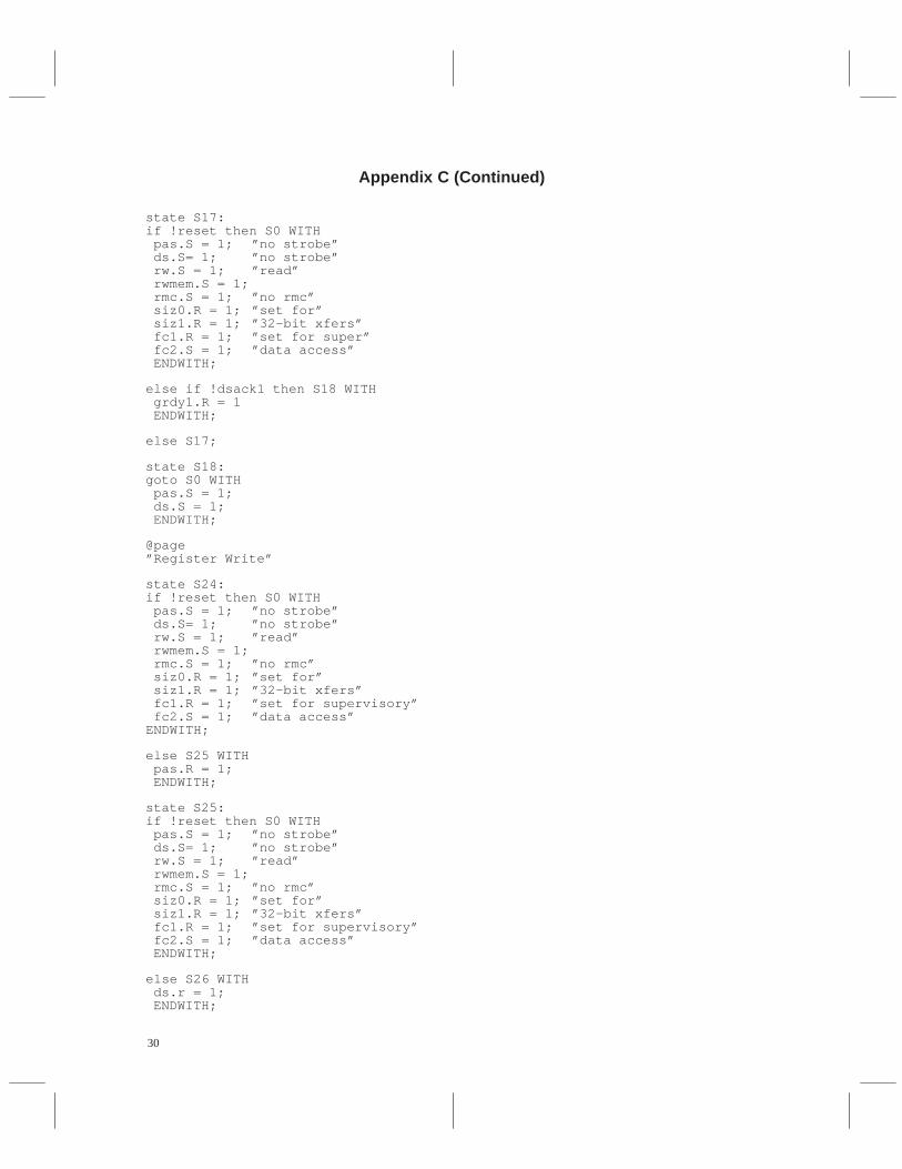
Appendix C: Master Cycle Generation Sequencer — ABEL Source
module mastertitle ’C40 Bus ControlDate 31 March 1992Revision 1.0Part TIB82S105BCAbel Version 4.00Designer Peter F. SiyCompany MITRE Corp.Location Bedford, MAProject ’C40 I/O Card ’
U14 device ’F105’;
”Inputs”clk, reset pin 1,9; ”clock, reset”mrd,mwr,rrd,rwr,gprom pin 8,7,6,5,4; ”decoded cycle”mwb,lbr pin 3,2; ”master/slave requests”dedlk pin 27; ”m/s deadlock”dsack0,dsack1,lberr pin 26,25,24; ”cycle responses”glock pin 23; ”C40 lock”oe pin 19; ”output enable”
”Outputs”pas pin 18 istype ’buffer,reg_RS’; ”68K address strobe”ds pin 17 istype ’buffer,reg_RS’; ”68K data strobe”rw pin 16 istype ’buffer,reg_RS’; ”68K read/write bar”rmc pin 15 istype ’buffer,reg_RS’; ”68K read–mod–write”siz0 pin 13 istype ’buffer,reg_RS’; ”68K size 0”siz1 pin 12 istype ’buffer,reg_RS’; ”68K size 1”fc1 pin 11 istype ’buffer,reg_RS’; ”68K function 1” fc2 pin 10 istype ’buffer,reg_RS’; ”68K function 0”
”Sets”cycle = [gprom,rwr,rrd,mwr,mrd]; ”cycle request”ack = [dsack1,dsack0]; ”acknowledge”output = [pas,ds,rw,rmc,siz0,siz1,fc1,fc2]; ”68K ouputs”
”State Description”P4,P3,P2,P1,P0node 41,40,39,38,37 istype ’reg_RS’;sreg = [P4,P3,P2,P1,P0]; S0 = [0,0,0,0,0]; S1 = [0,0,0,0,1]; S2 = [0,0,0,1,0]; S3 = [0,0,0,1,1]; S4 = [0,0,1,0,0]; S5 = [0,0,1,0,1]; S6 = [0,0,1,1,0]; S7 = [0,0,1,1,1]; S8 = [0,1,0,0,0]; S9 = [0,1,0,0,1]; S10 = [0,1,0,1,0]; S11 = [0,1,0,1,1]; S12 = [0,1,1,0,0]; S13 = [0,1,1,0,1]; S14 = [0,1,1,1,0]; S15 = [0,1,1,1,1]; S16 = [1,0,0,0,0]; S17 = [1,0,0,0,1]; S18 = [1,0,0,1,0]; S19 = [1,0,0,1,1];

26
Appendix C (Continued)
S20 = [1,0,1,0,0]; S21 = [1,0,1,0,1]; S22 = [1,0,1,1,0]; S23 = [1,0,1,1,1]; S24 = [1,1,0,0,0]; S25 = [1,1,0,0,1]; S26 = [1,1,0,1,0]; S27 = [1,1,0,1,1]; S28 = [1,1,1,0,0]; S29 = [1,1,1,0,1]; S30 = [1,1,1,1,0]; S31 = [1,1,1,1,1];
”Misc”rwmemnode 42 istype ’reg_RS’; ”r/w flag”H,L,X,C,Z = 1,0,.X.,.C.,.Z.;
equationsoutput.OE = !oe; ”set output enable”output.CLK = clk; ”clock the output regs”sreg.CLK = clk; ”and state regs”rwmem.CLK = clk; ”and r/w store”
@page
state_diagram sregstate S0:if (!reset # !dedlk) then S0 WITH pas.S = 1; ”no strobe” ds.S= 1; ”no strobe” rw.S = 1; ”read” rwmem.S = 1; ”flag for mem” rmc.S = 1; ”no rmc siz0.R = 1; ”set for” siz1.R = 1; ”32–bit xfers” fc1.R = 1; ”set for supervisory” fc2.S = 1; ”data access” ENDWITH;
else if (!mrd & !rwmem & lbr) then S1 WITH ”master read” rw.S = 1; ”assert read/write” rwmem.S =1; ENDWITH;
else if (!mrd & rwmem & lbr) then S2 WITH ”master read” pas.R = 1; ”assert pas” ds.R = 1; ”and ds” ENDWITH;
else if (!mwr & rwmem & lbr) then S8 WITH ”master write” rw.R = 1; ”assert r/w” rwmem.R = 1; ENDWITH;
else if (!mwr & !rwmem & lbr) then S9 WITH ”master write” pas.R = 1; ”assert pas only” ENDWITH;
else if (!rrd & !rwmem & lbr) then S16 WITH ”reg read” rw.S = 1; ”assert r/w” rwmem.S = 1; ENDWITH;
else if (!rrd & rwmem & lbr) then S17 WITH ”reg read” pas.R = 1; ”assert pas” ds.R = 1; ”and ds” ENDWITH;

27
Appendix C (Continued)
else if (!rwr & rwmem & lbr) then S24 WITH ”reg write” rw.R = 1; rwmem.R = 1; ENDWITH;
else if (!rwr & !rwmem & lbr) then S25 WITH pas.R = 1; ”assert pas only” ENDWITH;
else S0 WITH pas.S = 1; ”no strobe” ds.S= 1; ”no strobe” rw.S = 1; ”read” rwmem.S = 1; ”flag for mem” rmc.S = 1; ”no rmc” siz0.R = 1; ”set for” siz1.R = 1; ”32–bit xfers” fc1.R = 1; ”set for supervisory” fc2.S = 1; ”data access” ENDWITH;
@page”Master Read”
state S1:if (!reset # !dedlk) then S0 WITH pas.S = 1; ”no strobe” ds.S= 1; ”no strobe” rw.S = 1; ”read” rwmem.S = 1; ”flag for mem” rmc.S = 1; ”no rmc” siz0.R = 1; ”set for” siz1.R = 1; ”32–bit xfers” fc1.R = 1; ”set for super” fc2.S = 1; ”data access” ENDWITH;
else S2 WITH pas.R = 1; ds.R = 1; ENDWITH;
state S2:if (!reset # !dedlk) then S0 WITH pas.S = 1; ”no strobe” ds.S= 1; ”no strobe” rw.S = 1; ”read” rwmem.S = 1; ”flag for mem” rmc.S = 1; ”no rmc” siz0.R = 1; ”set for” siz1.R = 1; ”32–bit xfers” fc1.R = 1; ”set for super” fc2.S = 1; ”data access” ENDWITH;
else if !mwb then S3; ”wait for !mwb”
else S2;
state S3:if (!reset # !dedlk) then S0 WITH pas.S = 1; ”no strobe” ds.S= 1; ”no strobe” rw.S = 1; ”read” rwmem.S = 1; ”flag for mem”

28
Appendix C (Continued)
rmc.S = 1; ”no rmc” siz0.R = 1; ”set for” siz1.R = 1; ”32–bit xfers” fc1.R = 1; ”set for supervisory” fc2.S = 1; ”data access” ENDWITH;
else if ((!dsack1 & !dsack0) # !lberr) then S4 WITH grdy1.R = 1 ENDWITH;
else S3;
state S4:goto S0 WITH pas.S = 1; ds.S = 1; ENDWITH;
@page”Master Write”
state S8:if (!reset # !dedlk) then S0 WITH pas.S = 1; ”no strobe” ds.S= 1; ”no strobe” rw.S = 1; ”read” rwmem.S = 1; rmc.S = 1; ”no rmc” siz0.R = 1; ”set for” siz1.R = 1; ”32–bit xfers” fc1.R = 1; ”set for supervisory” fc2.S = 1; ”data access” ENDWITH;
else S9 WITH pas.R = 1; ENDWITH;
state S9:if (!reset # !dedlk) then S0 WITH pas.S = 1; ”no strobe” ds.S= 1; ”no strobe” rw.S = 1; ”read” rwmem.S = 1; rmc.S = 1; ”no rmc” siz0.R = 1; ”set for” siz1.R = 1; ”32–bit xfers” fc1.R = 1; ”set for supervisory” fc2.S = 1; ”data access” ENDWITH;
else S10 WITH ds.r = 1; ENDWITH;

29
Appendix C (Continued)
state S10:if (!reset # !dedlk) then S0 WITH pas.S = 1; ”no strobe” ds.S= 1; ”no strobe” rw.S = 1; ”read” rwmem.S = 1; rmc.S = 1; ”no rmc” siz0.R = 1; ”set for” siz1.R = 1; ”32–bit xfers” fc1.R = 1; ”set for super” fc2.S = 1; ”data access” ENDWITH;
else if !mwb then S11;
else S10;
state S11:if (!reset # !dedlk) then S0 WITH pas.S = 1; ”no strobe” ds.S= 1; ”no strobe” rw.S = 1; ”read” rwmem.S = 1; rmc.S = 1; ”no rmc” siz0.R = 1; ”set for” siz1.R = 1; ”32–bit xfers” fc1.R = 1; ”set for supervisory” fc2.S = 1; ”data access” ENDWITH;
else if ((!dsack1 & !dsack0) # !lberr) then S12; else S11;
state S12:goto S0 WITH pas.S = 1; ds.S = 1; ENDWITH;
@page”Register Read”
state S16:if !reset then S0 WITH pas.S = 1; ”no strobe” ds.S= 1; ”no strobe” rw.S = 1; ”read” rwmem.S = 1; rmc.S = 1; ”no rmc” siz0.R = 1; ”set for” siz1.R = 1; ”32–bit xfers” fc1.R = 1; ”set for super” fc2.S = 1; ”data access” ENDWITH;
else S17 WITH pas.R = 1; ds.R =1; ENDWITH;
30
Appendix C (Continued)
state S17:if !reset then S0 WITH pas.S = 1; ”no strobe” ds.S= 1; ”no strobe” rw.S = 1; ”read” rwmem.S = 1; rmc.S = 1; ”no rmc” siz0.R = 1; ”set for” siz1.R = 1; ”32–bit xfers” fc1.R = 1; ”set for super” fc2.S = 1; ”data access” ENDWITH;
else if !dsack1 then S18 WITH grdy1.R = 1 ENDWITH;
else S17;
state S18:goto S0 WITH pas.S = 1; ds.S = 1; ENDWITH;
@page”Register Write”
state S24:if !reset then S0 WITH pas.S = 1; ”no strobe” ds.S= 1; ”no strobe” rw.S = 1; ”read” rwmem.S = 1; rmc.S = 1; ”no rmc” siz0.R = 1; ”set for” siz1.R = 1; ”32–bit xfers” fc1.R = 1; ”set for supervisory” fc2.S = 1; ”data access”ENDWITH;
else S25 WITH pas.R = 1; ENDWITH;
state S25:if !reset then S0 WITH pas.S = 1; ”no strobe” ds.S= 1; ”no strobe” rw.S = 1; ”read” rwmem.S = 1; rmc.S = 1; ”no rmc” siz0.R = 1; ”set for” siz1.R = 1; ”32–bit xfers” fc1.R = 1; ”set for supervisory” fc2.S = 1; ”data access” ENDWITH;
else S26 WITH ds.r = 1; ENDWITH;

31
Appendix C (Continued)
state S26:if !reset then S0 WITH pas.S = 1; ”no strobe” ds.S= 1; ”no strobe” rw.S = 1; ”read” rwmem.S = 1; rmc.S = 1; ”no rmc” siz0.R = 1; ”set for” siz1.R = 1; ”32–bit xfers” fc1.R = 1; ”set for supervisory” fc2.S = 1; ”data access” ENDWITH;
else if !dsack1 then S27; else S26;
state S27:goto S0 WITH pas.S = 1; ds.S = 1; ENDWITH;
@page”Power–Up”
state S31:goto S0 WITH pas.S = 1; ”no strobe” pas.R = 0; ”error 6099 fix” ds.S= 1; ”no strobe” ds.R= 0; ”error 6099 fix” rw.S = 1; ”read” rwmem.S = 1; rw.R = 0; ”error 6099 fix” rmc.S = 1; ”no rmc” rmc.R = 0; ”error 6099 fix” siz0.R = 1; ”set for” siz0.S = 0; ”error 6099 fix” siz1.R = 1; ”32–bit xfers” siz1.S = 0; ”error 6099 fix” fc1.R = 1; ”set for supervisory” fc1.S = 0; ”error 6099 fix” fc2.S = 1; ”data access” fc2.R = 0; ”error 6099 fix”ENDWITH;
@pagetest_vectors
([clk,reset,gprom,rwr,rrd,mwr,mrd,lbr,mwb, dsack1,dsack0,dedlk,lberr,glock,oe] –> [sreg,rwmem,fc2,fc1,siz1,siz0,rmc,rw,ds,pas])
[1,X,X,X,X,X,X,X,X,X,X,X,X,X,0] –> [S31,X,X,X,X,X,X,X,X,X]; ”1 power up”[0,X,X,X,X,X,X,X,X,X,X,X,X,X,0] –> [S31,X,X,X,X,X,X,X,X,X]; ”2 power up”[C,0,X,X,X,X,X,X,X,X,X,X,X,X,0] –> [S0, 1,1,0,0,0,1,1,1,1]; ”3 reset state”[C,1,1,1,1,1,0,1,1,1,1,1,1,1,0] –> [S2, 1,1,0,0,0,1,1,0,0]; ”4 master read”[C,1,1,1,1,1,0,1,0,1,1,1,1,1,0] –> [S3, 1,1,0,0,0,1,1,0,0]; ”5 mwb asserted”[C,1,1,1,1,1,0,1,0,0,0,1,1,1,0] –> [S4, 1,1,0,0,0,1,1,0,0]; ”6 data acked”[C,1,1,1,1,1,1,1,1,1,1,1,1,1,0] –> [S0, 1,1,0,0,0,1,1,1,1]; ”7 ready for nxt”[C,1,1,1,1,0,1,1,1,1,1,1,1,1,0] –> [S8, 0,1,0,0,0,1,0,1,1]; ”8 master

32
Appendix C (Continued)
write”[C,1,1,1,1,0,1,1,1,1,1,1,1,1,0] –> [S9, 0,1,0,0,0,1,0,1,0]; ”9 assert pas”[C,1,1,1,1,0,1,1,1,1,1,1,1,1,0] –> [S10,0,1,0,0,0,1,0,0,0]; ”10 assert ds”[C,1,1,1,1,0,1,1,0,1,1,1,1,1,0] –> [S11,0,1,0,0,0,1,0,0,0]; ”11 mwb”[C,1,1,1,1,0,1,1,0,0,0,1,1,1,0] –> [S12,0,1,0,0,0,1,0,0,0]; ”12 data ackd”[C,1,1,1,1,1,1,1,1,1,1,1,1,1,0] –> [S0, 0,1,0,0,0,1,0,1,1]; ”13 ready for next”[C,1,1,1,0,1,1,1,1,1,1,1,1,1,0] –> [S16,1,1,0,0,0,1,1,1,1]; ”14 reg read”[C,1,1,1,0,1,1,1,1,1,1,1,1,1,0] –> [S17,1,1,0,0,0,1,1,0,0]; ”15 assert strobes”[C,1,1,1,0,1,1,1,1,0,1,1,1,1,0] –> [S18,1,1,0,0,0,1,1,0,0]; ”16 data ackd”[C,1,1,1,1,1,1,1,1,1,1,1,1,1,0] –> [S0, 1,1,0,0,0,1,1,1,1]; ”17 ready for nxt”[C,1,1,0,1,1,1,1,1,1,1,1,1,1,0] –> [S24,0,1,0,0,0,1,0,1,1]; ”18 reg write”[C,1,1,0,1,1,1,1,1,1,1,1,1,1,0] –> [S25,0,1,0,0,0,1,0,1,0]; ”19 assert pas”[C,1,1,0,1,1,1,1,1,1,1,1,1,1,0] –> [S26,0,1,0,0,0,1,0,0,0]; ”20 assert ds”[C,1,1,0,1,1,1,1,1,0,1,1,1,1,0] –> [S27,0,1,0,0,0,1,0,0,0]; ”21 data ackd”[C,1,1,1,1,1,1,1,1,1,1,1,1,1,0] –> [S0, 0,1,0,0,0,1,0,1,1]; ”22 ready for next”end master
APPENDIX D
SLAVE CYCLE GENERATION SEQUENCER – ABEL SOURCE
module slavetitle ’C40 Bus ControlDate 2 April 1992Revision 1.0Part TIB82S105BCAbel Version 4.00Designer Peter F. SiyCompany MITRE Corp.Location Bedford, MAProject ’C40 I/O Card ’
U15 device ’F105’;
”Inputs”clk, reset pin 1,9; ”clock, reset”pas,ds pin 8,7; ”address,data strobe”rw,rmc pin 6,5; ”read/write strobes”siz0,siz1 pin 4,3; ”bus sizing”fc0,fc1,fc2 pin 2,27,26; ”function codes”lbg pin 25; ”local bus grant”oe pin 19; ”output enable”
”Outputs”dsack0 pin 18 istype ’buffer,reg_RS’; ”data ack 0”dsack1 pin 17 istype ’buffer,reg_RS’; ”data ack 1”lberr pin 16 istype ’buffer,reg_RS’; ”bus error”gstrb0 pin 15 istype ’buffer,reg_RS’; ”C40 mem strobe”grw0 pin 13 istype ’buffer,reg_RS’; ”C40 read/write”
”Sets”size = [siz1,siz0]; ”size”func = [fc2,fc1,fc0]; ”function”output = [grw0,gstrb0,lberr,dsack1,dsack0];
”State Description”P3,P2,P1,P0 node 40,39,38,37 istype ’reg_RS’;sreg = [P3,P2,P1,P0]; S0 = [0,0,0,0]; S1 = [0,0,0,1]; S2 = [0,0,1,0];

33
Appendix C (Continued)
S3 = [0,0,1,1]; S4 = [0,1,0,0]; S5 = [0,1,0,1]; S6 = [0,1,1,0]; S7 = [0,1,1,1]; S8 = [1,0,0,0]; S9 = [1,0,0,1]; S10 = [1,0,1,0]; S11 = [1,0,1,1]; S12 = [1,1,0,0]; S13 = [1,1,0,1]; S14 = [1,1,1,0]; S15 = [1,1,1,1];
”Misc”rwmemnode 42 istype ’reg_RS’; ”r/w flag”H,L,X,C,Z = 1,0,.X.,.C.,.Z.;
equationsoutput.OE = !oe; ”set output enable”output.CLK = clk; ”clock the output regs”sreg.CLK = clk; ”and state regs”rwmem.CLK = clk; ”and r/w store”
@pagestate_diagram sregstate S0:
if (!reset) then S0 WITH dsack0.S = 1; ”deassert” dsack1.S = 1; ”all” lberr.S = 1; ”strobes” gstrb0.S = 1; ”deassert C40” grw0.R = 1; ”strobe, read” rwmem.S = 1; ”set to read” ENDWITH;
else if (!lbg) then S1;
else S0 WITH dsack0.S = 1; ”deassert” dsack1.S = 1; ”all” lberr.S = 1; ”strobes” gstrb0.S = 1; ”deassert C40” grw0.R = 1; ”strobe, read” rwmem.S = 1; ”set to read” ENDWITH;
@page”Sort Slave Request”state S1:
”Reset” if (!reset) then S0 WITH dsack0.S = 1; ”deassert” dsack1.S = 1; ”all” lberr.S = 1; ”strobes” gstrb0.S = 1; ”deassert C40” grw0.R = 1; ”strobe, read” rwmem.S = 1; ”set to read” ENDWITH;
”32–Bit Read”else if (!pas & !ds & rw & !rwmem & !siz0 & !siz1) then S2 WITH grw0.S = 1; rwmem.S = 1; ENDWITH;

34
Appendix C (Continued)
else if (!pas & !ds & rw & rwmem & !siz0 & !siz1) then S3 WITH gstrb0.R = 1; ENDWITH;
”32–Bit Write”else if (!pas & !ds & !rw & rwmem & !siz0 & !siz1) then S2 WITH grw0.R = 1; rwmem.R = 1; ENDWITH;
else if (!pas & !ds & !rw & !rwmem & !siz0 & !siz1) then S3 WITH gstrb0.R = 1; ENDWITH;
”Illegal Access (non–32 bit access)” else if (!pas & !ds & (rw # !rw) & (siz0 # siz1)) then S9 WITH lberr.R = 1; ENDWITH;
else S1;
@page”32–Bit Read/Write”
state S2:goto S3 WITH gstrb0.R = 1; ENDWITH;
state S3:goto S4 WITH dsack0.R = 1; dsack1.R = 1; ENDWITH;
state S4:if pas then S0 WITH dsack0.S = 1; dsack1.S = 1; gstrb0.S = 1; ENDWITH;
else S4;
@page”Illegal Access”
state S9:if pas then S0 WITH lberr.S = 1; ENDWITH
@page”Power–Up”
state S15:goto S0 WITH dsack0.S = 1; ”no ack” dsack0.R = 0; ”error 6099 fix” dsack1.S = 1; ”no ack” dsack1.R = 0; ”error 6099 fix” rwmem.S = 1; ”r/w mem” rwmem.R = 0; ”error 6099 fix” lberr.S = 1; ”no bus error” lberr.R = 0; ”error 6099 fix” gstrb0.S = 1; ”no strobe” grw0.S = 1; ”read” ENDWITH;

35
Appendix C (Continued)
@pagetest_vectors
([clk,reset,pas,ds,rw,rmc,siz0,siz1,fc0,fc1,fc2,lbg,oe] –> [sreg,rwmem,dsack0,dsack1,lberr,gstrb0,grw0])
[1,X,X,X,X,X,X,X,X,X,X,X,0] –> [S15,X,X,X,X,X,X]; ”1 power up”[0,X,X,X,X,X,X,X,X,X,X,X,0] –> [S15,X,X,X,X,X,X]; ”2 power up”[C,0,X,X,X,X,X,X,X,X,X,X,0] –> [S0, 1,1,1,1,1,1]; ”3 reset state”[C,1,1,1,1,1,1,1,X,X,X,0,0] –> [S1, 1,1,1,1,1,1]; ”4 slave read,lbg”[C,1,0,1,1,1,0,0,X,X,X,0,0] –> [S1, 1,1,1,1,1,1]; ”5 pas asserted”[C,1,0,0,1,1,0,0,X,X,X,0,0] –> [S3, 1,1,1,1,0,1]; ”6 and ds, strobe”[C,1,0,0,1,1,0,0,X,X,X,0,0] –> [S4, 1,0,0,1,0,1]; ”7 ack”[C,1,0,0,1,1,0,0,X,X,X,0,0] –> [S4, 1,0,0,1,0,1]; ”8 wait for pas release”[C,1,1,1,1,1,1,1,X,X,X,1,0] –> [S0, 1,1,1,1,1,1]; ”9 done, release gstrb”[C,1,1,1,0,1,1,1,X,X,X,0,0] –> [S1, 1,1,1,1,1,1]; ”10 slave write,lbg”[C,1,0,1,0,1,0,0,X,X,X,0,0] –> [S1, 1,1,1,1,1,1]; ”11 pas asserted”[C,1,0,0,0,1,0,0,X,X,X,0,0] –> [S2, 0,1,1,1,1,0]; ”12 and ds”[C,1,0,0,0,1,0,0,X,X,X,0,0] –> [S3, 0,1,1,1,0,0]; ”13 assert strobe”[C,1,0,0,0,1,0,0,X,X,X,0,0] –> [S4, 0,0,0,1,0,0]; ”14 ack”[C,1,0,0,0,1,0,0,X,X,X,0,0] –> [S4, 0,0,0,1,0,0]; ”15 wait for pas release”[C,1,1,1,1,1,1,1,X,X,X,1,0] –> [S0, 0,1,1,1,1,0]; ”16 done,relase gstrb”[C,1,1,1,1,1,1,1,X,X,X,0,0] –> [S1, 0,1,1,1,1,0]; ”17 slave read,lbg”[C,1,0,1,1,1,0,0,X,X,X,0,0] –> [S1, 0,1,1,1,1,0]; ”18 pas asserted”[C,1,0,0,1,1,0,0,X,X,X,0,0] –> [S2, 1,1,1,1,1,1]; ”19 and ds, r/w asserted”[C,1,0,0,1,1,0,0,X,X,X,0,0] –> [S3, 1,1,1,1,0,1]; ”20 and strobe”[C,1,0,0,1,1,0,0,X,X,X,0,0] –> [S4, 1,0,0,1,0,1]; ”21 ack”[C,1,0,0,1,1,0,0,X,X,X,0,0] –> [S4, 1,0,0,1,0,1]; ”22 wait for pas release”[C,1,1,1,1,1,1,1,X,X,X,1,0] –> [S0, 1,1,1,1,1,1]; ”23 done,relase gstrb”[C,1,1,1,1,1,1,1,X,X,X,0,0] –> [S1, 1,1,1,1,1,1]; ”24 bad access,lbg”[C,1,0,1,1,1,0,1,X,X,X,0,0] –> [S1, 1,1,1,1,1,1]; ”25 pas asserted”[C,1,0,0,1,1,0,1,X,X,X,0,0] –> [S9, 1,1,1,0,1,1]; ”26 and ds, error”[C,1,0,0,1,1,0,1,X,X,X,0,0] –> [S9, 1,1,1,0,1,1]; ”27 wait for pas release”[C,1,1,1,1,1,1,1,X,X,X,1,0] –> [S0, 1,1,1,1,1,1]; ”28 done, release lberr”[C,1,1,1,0,1,1,1,X,X,X,0,0] –> [S1, 1,1,1,1,1,1]; ”29 slave write,lbg”[C,1,0,1,0,1,0,0,X,X,X,0,0] –> [S1, 1,1,1,1,1,1]; ”30 pas asserted”[C,1,0,0,0,1,0,0,X,X,X,0,0] –> [S2, 0,1,1,1,1,0]; ”31 and ds”[C,1,0,0,0,1,0,0,X,X,X,0,0] –> [S3, 0,1,1,1,0,0]; ”32 assert strobe”[C,1,0,0,0,1,0,0,X,X,X,0,0] –> [S4, 0,0,0,1,0,0]; ”33 ack”[C,1,0,0,0,1,0,0,X,X,X,0,0] –> [S4, 0,0,0,1,0,0]; ”34 wait for pas release”[C,1,1,1,1,1,1,1,X,X,X,1,0] –> [S0, 0,1,1,1,1,0]; ”35 done,relase gstrb”[C,1,1,1,0,1,1,1,X,X,X,0,0] –> [S1, 0,1,1,1,1,0]; ”36 slave write,lbg”[C,1,0,1,0,1,0,0,X,X,X,0,0] –> [S1, 0,1,1,1,1,0]; ”37 pas asserted”[C,1,0,0,0,1,0,0,X,X,X,0,0] –> [S3, 0,1,1,1,0,0]; ”38 and ds,assert strobe”[C,1,0,0,0,1,0,0,X,X,X,0,0] –> [S4, 0,0,0,1,0,0]; ”39 ack”[C,1,0,0,0,1,0,0,X,X,X,0,0] –> [S4, 0,0,0,1,0,0]; ”40 wait for pas release”[C,1,1,1,1,1,1,1,X,X,X,1,0] –> [S0, 0,1,1,1,1,0]; ”41 done,relase gstrb”
end slave

36
Appendix D: Schematics
Figure 10. TMS320C40 – VIC/VAC Protototype VMEbus P1 Connector

37
A1D0
A2D1
A3D2
A4D3
A5D4
A6D5
A7D6
A8D7
A9GND
A10SYSCLK
A11GND
A12DS1
A13DS0
A14WRITE
A15GND
A16DIACK
A17GND
A18AS
A19
D0–D7
A1–A7
P1
B1BBSY
B2BCLR
B3ACFAIL
B4BGOIN
B5BGOOUT
B6BG1IN
B7BG1OUT
B8BG2IN
B9BG2OUT
B10BG3IN
B11BG3OUT
B12BR0
B13BR1
B14BR2B15BR3B16AM0B17AM1B18AM2
B19AM3B20GND
P1
C1D8
C2D9
C3D10
C4D11
C5D12
C6D13
C7D14
C8D15
C9GND
C10SYSFAIL
C11BERR
C12SYSRESET
C13LWORD
C14AM5
C15A23
C16A22
C17A21
C18A20
C19
D8–D15
A8–A23
P1

38
Appendix D: Schematics (Continued)
Figure 11. TMS320C40 – VIC/VAC Protototype VMEbus P2 Connector

39
A1
A2
A3
A4
A5
A6
A7
A8
A9
A10
A11
A12
A13
A14
A15
A16
A17
A18
A19
A20
A21
A22
A23
A24
A25
A26
A27
A28
A24–A31
D24–D31
P2
B1+5 V
B2GND
B3
B4A24
B5A25
B6A26
B7A27
B8A28
B9A29
B10A30
B11A31
B12GND
B13+5 V
B14D16B15D17B16D18B17D19B18D20
B19D21B20D22
B21D23
P2
C1
C2
C3
C4
C5
C6
C7
C8
C9
C10
C11
C12
C13
C14
C15
C16
C17
C18
C19
C20
C21
C22
C23
C24
C25
C26
C27
C28
P2
D16–D23