
Project Report - OpenCores
26
73 CHAPTER 6 HDL DESIGN S TRATEGY 6-1. HDL Design 6.1-1. HDL STRATEGY In order to develop Verilog or HDL description of a device, it is necessary to imagine all the external inputs and outputs of the device. For example, the digital Tristate buffer has one input, one output and an enable line. In this case, if there is a 16-bit input and output and a one-bit enable. The Verilog realization for this is as follows: module Tristate (in, out, enable) input[15:0] in; output[15:0] out; input enable; Verilog syntax is similar to C. Each input and output must be referenced in the functioned prototype and then declared as inputs or outputs in the first few lines of the module. Once the basic I/O is established the compiler needs to know which I/O needs to hold its value during operation. In addition, there are often some internal connections that are needed to be made. This is accomplished in Verilog with the use of the wire and reg commands. The wire command is generally used for inputs and the reg command used for outputs. This is because it is often desirable in digital
-
Upload
khangminh22 -
Category
Documents
-
view
0 -
download
0
Transcript of Project Report - OpenCores
73
CHAPTER 6
HDL DESIGN STRATEGY
6-1. HDL Design
6.1-1. HDL STRATEGY
In order to develop Verilog or HDL description of a device, it is necessary to
imagine all the external inputs and outputs of the device. For example, the digital
Tristate buffer has one input, one output and an enable line. In this case, if there is a
16-bit input and output and a one-bit enable. The Verilog realization for this is as
follows:
module Tristate (in, out, enable)
input[15:0] in;
output[15:0] out;
input enable;
Verilog syntax is similar to C. Each input and output must be referenced in the
functioned prototype and then declared as inputs or outputs in the first few lines of the
module. Once the basic I/O is established the compiler needs to know which I/O
needs to hold its value during operation. In addition, there are often some internal
connections that are needed to be made. This is accomplished in Verilog with the use
of the wire and reg commands. The wire command is generally used for inputs and
the reg command used for outputs. This is because it is often desirable in digital
74
circuits for outputs to hold their value after being driven. The next few lines of code
for the Tristate module will use these commands to configure their respective inputs
and outputs.
wire [15:0] in;
wire enable;
reg [15:0] out;
Therefore, if data arrived at the input and the enable line was toggled the input
data would appear at the output.
The initialization of the variables for the Tris tate Buffers are completed. The
internal operation of the Tristate buffer and many other hardware modules are
achieved using the case statement. Unlike the Case statement in C, the first <Value>
that matches the value of the <expression> is selected and the associated statement is
executed.
case (<expression>)
<value1>: <statement>
<value2>: <statement>
default: <statement>
endcase
Using this syntax, the internal operation of the Tristate buffer is achieved from
the following code:
always @ (enable)
begin
case (enable)
1: out = in;
0: out = 16'bz; // high impedance
endcase
end
75
The always command is used to create a hardware description that
continuously monitors the enable line of the Tri-State buffer for an active high level.
The Tri-State Buffer is a simple digital device but it clearly demonstrates the method
used in most of the Modules throughout this design.
6.1-2. INSTANTIATION
Verilog uses a technique called instantiation to group entities into one
encompassing module called the top- level design block. The top- level design block
for this design is called the Micro Module i.e. proc module in our designed core. The
Micro Module instantiates each hardware component including the Tristate Buffer,
several Latches, ALU, RAM, Register, Decoders, Program Counter, Machine Cycle
Counter and the Display Unit to create the final realization of a microprocessor. When
the micro module instantiates each hardware module, it can be viewed as each
hardware device is being placed internally into the processor block.
The Micro Module initializes all the I/O similar to the Tristate buffer. The
Micro Module also contains many internal connections implemented using the wire
command. For example, to connect the output of the register to the ALU internally,
there is a wire between them. Once all the modules are instantiated and all wires
connected, the Micro Module functions like a stand alone processor.
6.1-3. TIMING
In order to avoid the Timing problems the Verilog constructs should be
according to the IEEE standards as shown in the appendix and we must take full
advantage of the extra circuitry provided by the target FPGA. The Control Unit has
many inputs and outputs that enable the unit to perform various operations
synchronously by coordinating its activities with rest of the processor circuitry.
Upon power up of the processor, different components of the processor are
reset to their default values. Thus PC start counting from zero and the RAM module
fetch 16-Bits of instruction from memory and incrementing the PC by one. Then the
fetched instruction is decoded by the Control Unit and an appropriate action is taken
according to the operator. The instruction result is then assigned to the Display

76
module, which is displayed on the seven segment display. For the whole process
above, the maximum number of clock cycle consumed for a single instruction is four
machine cycle.
6-2. HDL Design of Microprocessor Components
6.2-1. CONTROL LINES
In Verilog HDL the control lines are implemented by defining them as the input
ports of the top code module as shown below.
module proc(Resetp, Holdp, Clockp, led1h, led2h); //Port Decleration
input Clockp;
input Resetp;
input Holdp;
In the above code Clockp, Resetp and Holdp are the externally generated signal to
control the operation of the processor.
6.2-2. CONTROL UNIT
The Verilog HDL module for the Control Unit mainly consists of two main
blocks. The first block is used to decode the instruction fetched from RAM and the
second block performs the required action according to the operator. The Verilog
HDL code for the instruction decoding block for the Control Unit is given below.
//Control Unit
always @(catch or pcoutput) begin F = pcoutput[15:12]; Rx = pcoutput[11:10]; Ry = pcoutput[9:8]; Data = pcoutput[7:0]; end
77
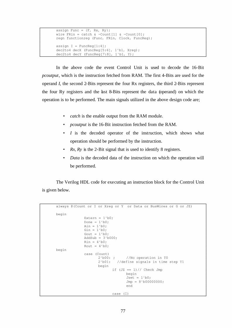
assign Func = {F, Rx, Ry}; wire FRin = catch & ~Count[1] & ~Count[0]; regn functionreg (Func, FRin, Clock, FuncReg); assign I = FuncReg[1:4]; dec2to4 decX (FuncReg[5:6], 1'b1, Xreg); dec2to4 decY (FuncReg[7:8], 1'b1, Y);
In the above code the event Control Unit is used to decode the 16-Bit
pcoutput, which is the instruction fetched from RAM. The first 4-Bits are used for the
operand I, the second 2-Bits represent the four Rx registers, the third 2-Bits represent
the four Ry registers and the last 8-Bits represent the data (operand) on which the
operation is to be performed. The main signals utilized in the above design code are;
• catch is the enable output from the RAM module.
• pcoutput is the 16-Bit instruction fetched from the RAM.
• I is the decoded operator of the instruction, which shows what
operation should be performed by the instruction.
• Rx, Ry is the 2-Bit signal that is used to identify 8 registers.
• Data is the decoded data of the instruction on which the operation will
be performed.
The Verilog HDL code for executing an instruction block for the Control Unit
is given below.
always @(Count or I or Xreg or Y or Data or BusWires or G or JZ) begin Extern = 1'b0; Done = 1'b0; Ain = 1'b0; Gin = 1'b0; Gout = 1'b0; AddSub = 3'b000; Rin = 4'b0; Rout = 4'b0; begin case (Count) 2'b00: ; //No operation in T0 2'b01: //define signals in time step T1 begin if (JZ == 1)// Check Jmp begin Jset = 1'b0; Jmp = 8'b00000000; end case (I)
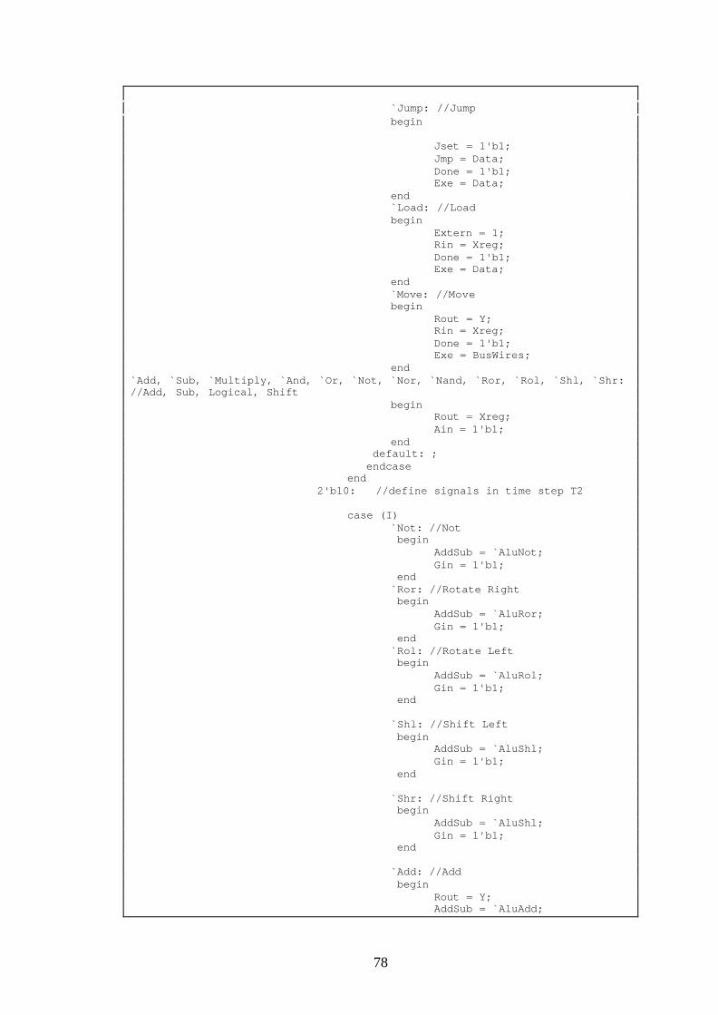
78
`Jump: //Jump begin Jset = 1'b1; Jmp = Data; Done = 1'b1; Exe = Data; end `Load: //Load begin Extern = 1; Rin = Xreg; Done = 1'b1; Exe = Data; end `Move: //Move begin Rout = Y; Rin = Xreg; Done = 1'b1; Exe = BusWires; end `Add, `Sub, `Multiply, `And, `Or, `Not, `Nor, `Nand, `Ror, `Rol, `Shl, `Shr: //Add, Sub, Logical, Shift begin Rout = Xreg; Ain = 1'b1; end default: ; endcase end 2'b10: //define signals in time step T2 case (I) `Not: //Not begin AddSub = `AluNot; Gin = 1'b1; end `Ror: //Rotate Right begin AddSub = `AluRor; Gin = 1'b1; end `Rol: //Rotate Left begin AddSub = `AluRol; Gin = 1'b1; end `Shl: //Shift Left begin AddSub = `AluShl; Gin = 1'b1; end `Shr: //Shift Right begin AddSub = `AluShl; Gin = 1'b1; end `Add: //Add begin Rout = Y; AddSub = `AluAdd;
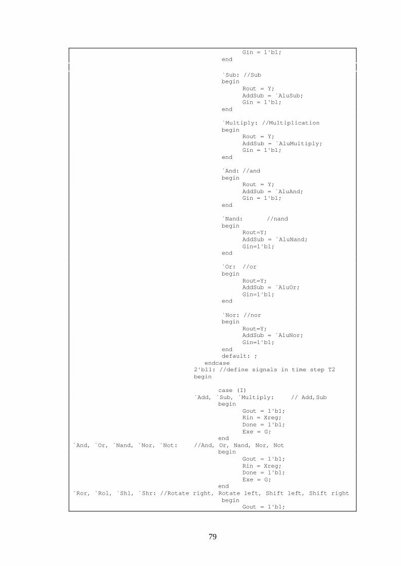
79
Gin = 1'b1; end `Sub: //Sub begin Rout = Y; AddSub = `AluSub; Gin = 1'b1; end `Multiply: //Multiplication begin Rout = Y; AddSub = `AluMultiply; Gin = 1'b1; end `And: //and begin Rout = Y; AddSub = `AluAnd; Gin = 1'b1; end `Nand: //nand begin Rout=Y; AddSub = `AluNand; Gin=1'b1; end `Or: //or begin Rout=Y; AddSub = `AluOr; Gin=1'b1; end `Nor: //nor begin Rout=Y; AddSub = `AluNor; Gin=1'b1; end default: ; endcase 2'b11: //define signals in time step T2 begin case (I) `Add, `Sub, `Multiply: // Add,Sub begin Gout = 1'b1; Rin = Xreg; Done = 1'b1; Exe = G; end `And, `Or, `Nand, `Nor, `Not: //And, Or, Nand, Nor, Not begin Gout = 1'b1; Rin = Xreg; Done = 1'b1; Exe = G; end `Ror, `Rol, `Shl, `Shr: //Rotate right, Rotate left, Shift left, Shift right begin Gout = 1'b1;

80
Rin = Xreg; Done = 1'b1; Exe = G; end default: ; endcase end endcase end end
In the above code there are two nested Conditional Case-Select statements,
where the outer conditional case is based on the Count parameter to controls and
tracks the number of machine cycles consumed by a given instruction and the inner
conditional case is based on I parameter for performing the required steps according
to the decoded operator. The most important signals utilized in the above Control Unit
design code are defined as;
• Count is the output from the Machine Cycle Counter.
• AddSub is the 4-Bit signal used by the ALU module to identify the operation
to perform.
• Extern is a signal used to put the contents of data on the buswires.
• Rin is the 2-Bit signal used to put the contents of buswires into the register.
• Rout is the 2-Bit signal used to put the contents of register on the buswires.
• Done signal show the execution of an instruction.
• Exe signal value is displayed on an output device.
• Gin and Gout signals are used to put the value into and out of the temporary
register G.
6.2-3. ALU
ALU is used to perform arithmetic logic operations. The below Verilog HDL
design code demonstrates the working structure of an ALU. In the given code an
event control unit (always block) is used to continuously monitor the value of Inst (an
ALU instruction), A register, Result and the buswires. If any change in the value of
the above mentioned signals occurs then the conditional case-select structure becomes
active. The next step is to perform an action according to the changed value of Inst on
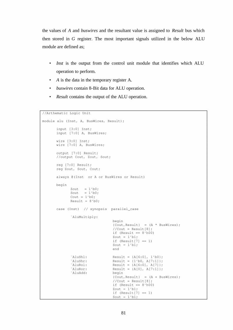
81
the values of A and buswires and the resultant value is assigned to Result bus which
then stored in G register. The most important signals utilized in the below ALU
module are defined as;
• Inst is the output from the control unit module that identifies which ALU
operation to perform.
• A is the data in the temporary register A.
• buswires contain 8-Bit data for ALU operation.
• Result contains the output of the ALU operation.
//Arthematic Logic Unit module alu (Inst, A, BusWires, Result); input [3:0] Inst; input [7:0] A, BusWires; wire [3:0] Inst; wire [7:0] A, BusWires; output [7:0] Result; //output Cout, Zout, Sout; reg [7:0] Result; reg Zout, Sout, Cout; always @(Inst or A or BusWires or Result) begin Zout = 1'b0; Sout = 1'b0; Cout = 1'b0; Result = 8'b0; case (Inst) // synopsis parallel_case `AluMultiply: begin {Cout,Result} = (A * BusWires); //Cout = Result[8]; if (Result == 8'h00) Zout = 1'b1; if (Result[7] == 1) Sout = 1'b1; end `AluShl: Result = {A[6:0], 1'b0}; `AluShr: Result = {1'b0, A[7:1]}; `AluRol: Result = {A[6:0], A[7]}; `AluRor: Result = {A[0], A[7:1]}; `AluAdd: begin {Cout,Result} = (A + BusWires); //Cout = Result[8]; if (Result == 8'h00) Zout = 1'b1; if (Result[7] == 1) Sout = 1'b1;

82
end `AluSub: begin {Cout,Result} = (A - BusWires) ; //Cout = Result[8]; if (Result == 8'h00) Zout = 1'b1; if (Result[7] == 1) Sout = 1'b1; end `AluAnd: Result = A & BusWires; `AluNand: Result = ~(A & BusWires); `AluOr: Result = A | BusWires; `AluNor: Result = ~(A | BusWires); `AluNot: Result = ~(A); default: begin Zout = 1'b0; Sout = 1'b0; Cout = 1'b0; Result = 8'b0; end endcase end endmodule
6.2-4. DECODER
The Decoder is used for decoding the 4-Bits of the instruction field by which
we can select any of the eight registers. The Verilog HDL design code for the
Decoder Unit is given below. In the code an event control block (always block) is
active whenever the 2-Bits input W or enable input En value changes, as a result the
case-select block use the 2-Bits input W to assign the selected register value to the
decoder output Y. The most important signals utilized in the below Decoder moduel
are described as;
• W is the externa l input to the decoder module from the control unit.
• En is the enable signal for the decoder working.
• Y is the output of the decoder.
//2-4 Decoder module dec2to4(W, En, Y); input [1:0] W; input En; wire [1:0] W; wire En;
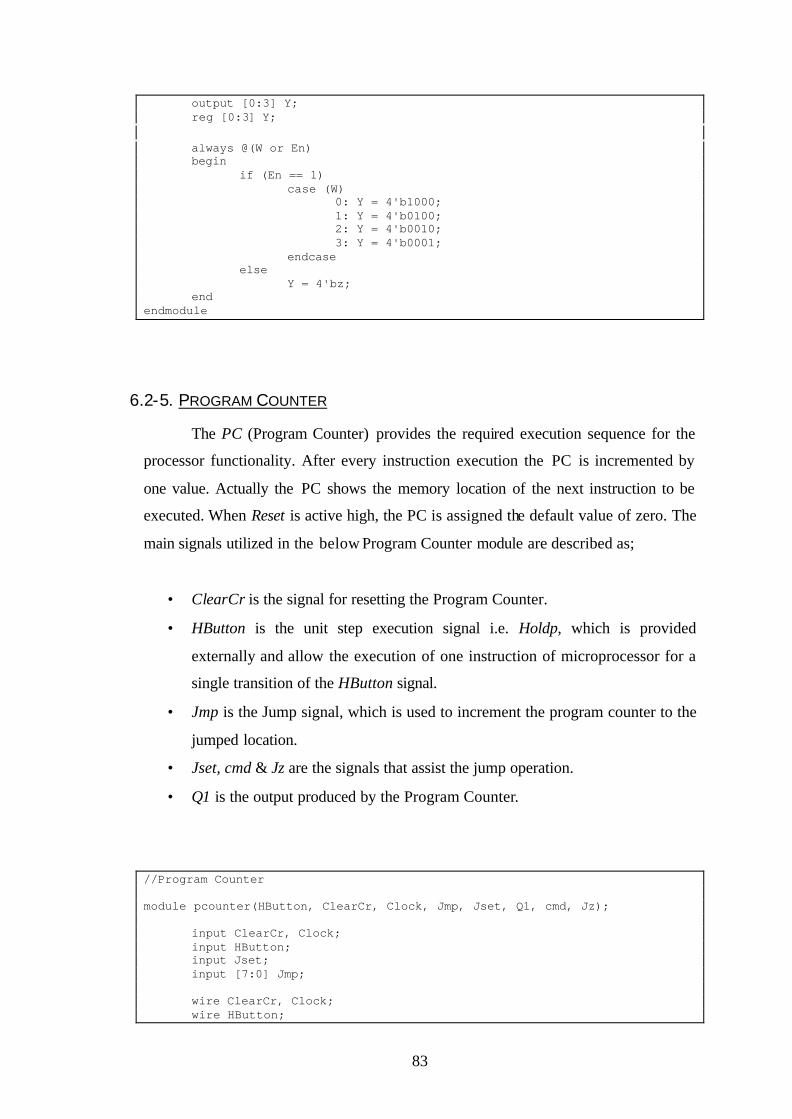
83
output [0:3] Y; reg [0:3] Y; always @(W or En) begin if (En == 1) case (W) 0: Y = 4'b1000; 1: Y = 4'b0100; 2: Y = 4'b0010; 3: Y = 4'b0001; endcase else Y = 4'bz; end endmodule
6.2-5. PROGRAM COUNTER
The PC (Program Counter) provides the required execution sequence for the
processor functionality. After every instruction execution the PC is incremented by
one value. Actually the PC shows the memory location of the next instruction to be
executed. When Reset is active high, the PC is assigned the default value of zero. The
main signals utilized in the below Program Counter module are described as;
• ClearCr is the signal for resetting the Program Counter.
• HButton is the unit step execution signal i.e. Holdp, which is provided
externally and allow the execution of one instruction of microprocessor for a
single transition of the HButton signal.
• Jmp is the Jump signal, which is used to increment the program counter to the
jumped location.
• Jset, cmd & Jz are the signals that assist the jump operation.
• Q1 is the output produced by the Program Counter.
//Program Counter module pcounter(HButton, ClearCr, Clock, Jmp, Jset, Q1, cmd, Jz); input ClearCr, Clock; input HButton; input Jset; input [7:0] Jmp; wire ClearCr, Clock; wire HButton;
84
wire Jset; wire [7:0] Jmp; output [7:0] Q1; output cmd; output Jz; reg [7:0] Q1; reg work, cmd, Jz; always @(posedge Clock) begin if (ClearCr == 1) begin Q1 <= 0; work = 1'b0; end else if (HButton == 0) begin if (work != 1'b1) begin cmd = 1'b1; work = 1'b1; begin if (Jset == 1) begin Q1 <= Jmp; Jz = 1'b1; end else Q1 <= Q1 + 1 ; end end end else begin cmd = 1'b0; work = 1'b0; Jz = 1'b0; end end endmodule
6.2-6. MACHINE CYCLE COUNTER
MMC (Machine Cycle Counter) is used for providing the required timing and
flow control for the instruction execution in the Control Unit. Most of the instruction
requires four machine cycles for its execution, while few require one machine cycle.
The signals utilized in the below MMC module are briefly explained as follows;
• Clear signal is used for resetting the counter.
• Clock signal is used for clocking purpose.
85
• Q is the output of the counter.
• Cmd is the enable signal from Program Counter.
• Catch is the enable signal from RAM.
//Machine Cycle (T) Counter module upcount(Clear, Clock, Q, cmd, catch); input Clear, Clock, cmd, catch; output [1:0] Q; wire Clear, Clock, cmd, catch; reg [1:0] Q; reg [3:0] RT1; always @(posedge Clock) begin if (Clear == 1) begin Q <= 2'b00; RT1 <= 4'b0000; end else if (cmd == 0) begin Q <= 2'b00; RT1 <= 4'b0000; end else begin if (catch == 1'b1) begin if (RT1 < 8'b0100) begin RT1 <= RT1 + 1; Q <= Q + 1 ; end else if (RT1 == 8'b1111) begin RT1 <= 4'b0100; end else RT1 <= RT1 + 1; end else begin Q <= 2'b0; RT1 <= 4'b0000; end end end endmodule
86
6.2-7. REGISTER
The Register module provides the creation of 8-Bit registers. The important
signals utilized in the below Register module are as following.
• R is the external data input to the Register.
• Rin is the enable input for the data storage in the Register.
• Clock signal provide the required clocking to the Register functionality.
• Q is the 8 bit output from the Register.
//8-Bit Register module regn(R, Rin, Clock, Q); parameter n = 8; input [n-1:0] R; input Rin, Clock; wire [n-1:0] R; wire Rin, Clock; output [n-1:0] Q; reg [n-1:0] Q; always @(posedge Clock) if (Rin) Q <= R; endmodule
6.2-8. DELAY LOCKED LOOP
The DLL (Delay Locked Loop) is the special feature of the Spartan 2E FPGA.
DLL provide a synchronize signal to all circuitry in the processor. DLL can be used to
increase or decrease the frequency of input clock or it can also be used change the
duty cycle of the input clock. There are four DLL circuit available in the Spartan 2E
FPGA. DLL can be instantiated by calling them and assigning valid values to it as
shown in the below code. The most important signals utilized in the below DLL
module are;
• CLKIN is the external clock input to the DLL block.
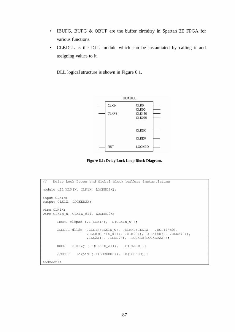
87
• IBUFG, BUFG & OBUF are the buffer circuitry in Spartan 2E FPGA for
various functions.
• CLKDLL is the DLL module which can be instantiated by calling it and
assigning values to it.
DLL logical structure is shown in Figure 6.1.
Figure 6.1: Delay Lock Loop Block Diagram.
// Delay Lock Loops and Global clock buffers instantiation module dll(CLKIN, CLK1X, LOCKED2X); input CLKIN; output CLK1X, LOCKED2X; wire CLK1X; wire CLKIN_w, CLK1X_dll, LOCKED2X; IBUFG clkpad (.I(CLKIN), .O(CLKIN_w)); CLKDLL dll2x (.CLKIN(CLKIN_w), .CLKFB(CLK1X), .RST(1'b0), .CLK0(CLK1X_dll), .CLK90(), .CLK180(), .CLK270(), .CLK2X(), .CLKDV(), .LOCKED(LOCKED2X)); BUFG clk2xg (.I(CLK1X_dll), .O(CLK1X)); //OBUF lckpad (.I(LOCKED2X), .O(LOCKED)); endmodule
88
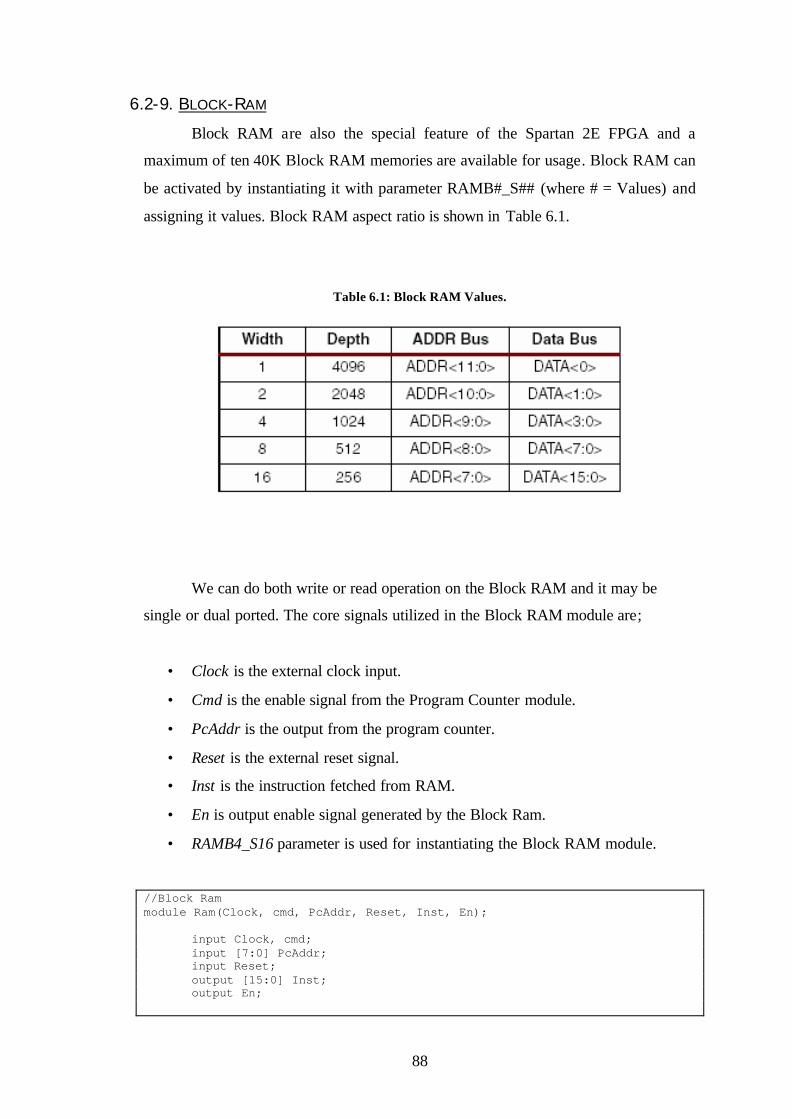
6.2-9. BLOCK-RAM
Block RAM are also the special feature of the Spartan 2E FPGA and a
maximum of ten 40K Block RAM memories are available for usage. Block RAM can
be activated by instantiating it with parameter RAMB#_S## (where # = Values) and
assigning it values. Block RAM aspect ratio is shown in Table 6.1.
Table 6.1: Block RAM Values.
We can do both write or read operation on the Block RAM and it may be
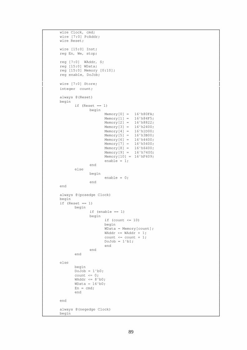
single or dual ported. The core signals utilized in the Block RAM module are;
• Clock is the external clock input.
• Cmd is the enable signal from the Program Counter module.
• PcAddr is the output from the program counter.
• Reset is the external reset signal.
• Inst is the instruction fetched from RAM.
• En is output enable signal generated by the Block Ram.
• RAMB4_S16 parameter is used for instantiating the Block RAM module.
//Block Ram module Ram(Clock, cmd, PcAddr, Reset, Inst, En); input Clock, cmd; input [7:0] PcAddr; input Reset; output [15:0] Inst; output En;
89
wire Clock, cmd; wire [7:0] PcAddr; wire Reset; wire [15:0] Inst; reg En, We, stop; reg [7:0] WAddr, S; reg [15:0] WData; reg [15:0] Memory [0:10]; reg enable, DoJob; wire [7:0] Store; integer count; always @(Reset) begin if (Reset == 1) begin Memory[0] = 16'h80FA; Memory[1] = 16'h84F5; Memory[2] = 16'h8822; Memory[3] = 16'h2400; Memory[4] = 16'h1D00; Memory[5] = 16'h3B00; Memory[6] = 16'h4400; Memory[7] = 16'h5400; Memory[8] = 16'h6400; Memory[9] = 16'h7400; Memory[10] = 16'hF409; enable = 1; end else begin enable = 0; end end always @(posedge Clock) begin if (Reset == 1) begin if (enable == 1) begin if (count <= 10) begin WData = Memory[count]; WAddr <= WAddr + 1; count <= count + 1; DoJob = 1'b1; end end end else begin DoJob = 1'b0; count <= 0; WAddr <= 8'b0; WData = 16'b0; En = cmd; end end always @(negedge Clock) begin
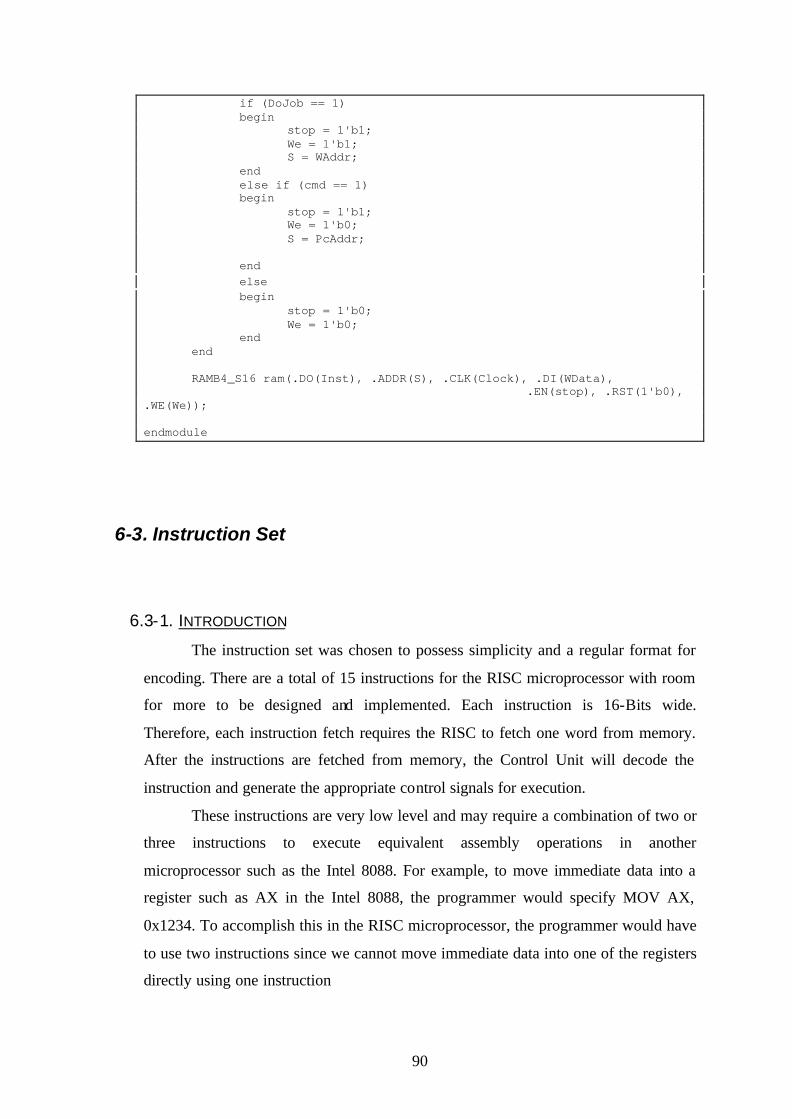
90
if (DoJob == 1) begin stop = 1'b1; We = 1'b1; S = WAddr; end else if (cmd == 1) begin stop = 1'b1; We = 1'b0; S = PcAddr; end else begin stop = 1'b0; We = 1'b0; end end RAMB4_S16 ram(.DO(Inst), .ADDR(S), .CLK(Clock), .DI(WData), .EN(stop), .RST(1'b0), .WE(We)); endmodule
6-3. Instruction Set
6.3-1. INTRODUCTION
The instruction set was chosen to possess simplicity and a regular format for
encoding. There are a total of 15 instructions for the RISC microprocessor with room
for more to be designed and implemented. Each instruction is 16-Bits wide.
Therefore, each instruction fetch requires the RISC to fetch one word from memory.
After the instructions are fetched from memory, the Control Unit will decode the
instruction and generate the appropriate control signals for execution.
These instructions are very low level and may require a combination of two or
three instructions to execute equivalent assembly operations in another
microprocessor such as the Intel 8088. For example, to move immediate data into a
register such as AX in the Intel 8088, the programmer would specify MOV AX,
0x1234. To accomplish this in the RISC microprocessor, the programmer would have
to use two instructions since we cannot move immediate data into one of the registers
directly using one instruction
91
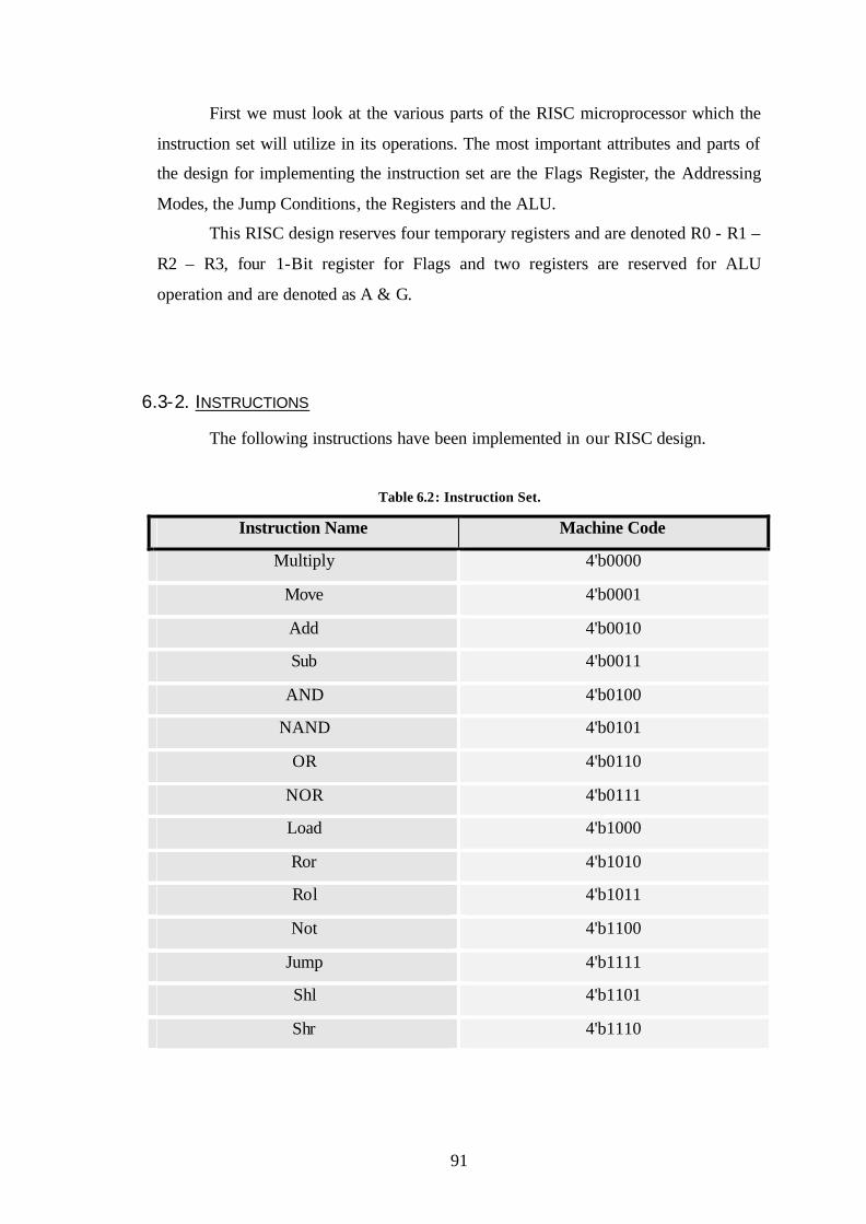
First we must look at the various parts of the RISC microprocessor which the
instruction set will utilize in its operations. The most important attributes and parts of
the design for implementing the instruction set are the Flags Register, the Addressing
Modes, the Jump Conditions, the Registers and the ALU.
This RISC design reserves four temporary registers and are denoted R0 - R1 –
R2 – R3, four 1-Bit register for Flags and two registers are reserved for ALU
operation and are denoted as A & G.
6.3-2. INSTRUCTIONS
The following instructions have been implemented in our RISC design.
Table 6.2: Instruction Set.
Instruction Name Machine Code
Multiply 4'b0000
Move 4'b0001
Add 4'b0010
Sub 4'b0011
AND 4'b0100
NAND 4'b0101
OR 4'b0110
NOR 4'b0111
Load 4'b1000
Ror 4'b1010
Rol 4'b1011
Not 4'b1100
Jump 4'b1111
Shl 4'b1101
Shr 4'b1110

92
6-4. Testing and Verification
6.4-1. STAGES
There were three stages in verifying the RISC design. Each time a module or
piece of the design was written in Verilog HDL, it was first simulated using the
ModelSim simulator. The simulation file can be either Verilog HDL text based or
graphical wave file. After the design was realized in a netlist using XST, the
regenerated Verilog description was re-simulated using the ModelSim behavioral
simulator and later simulated using the ModelSim Post-Place & Route simulator as
shown in figures below. The same Verilog stimulus file was used in both simulations
to verify that both simulations produce identical results. Finally, the FPGA was
configured, a sample assembler program was burned into the EPROM and the RISC
operation was tested using single step debugging.
The Figure 6.2 illustrates the execution of Reset instruction, due to which the
instruction set is reloaded into the RAM.
Figure 6.2: Simulation of Reset Instruction.
The Figure 6.3 illustrates the execution of Load instruction from RAM i.e.
80FA instruction, due to which FA is loaded into R0.
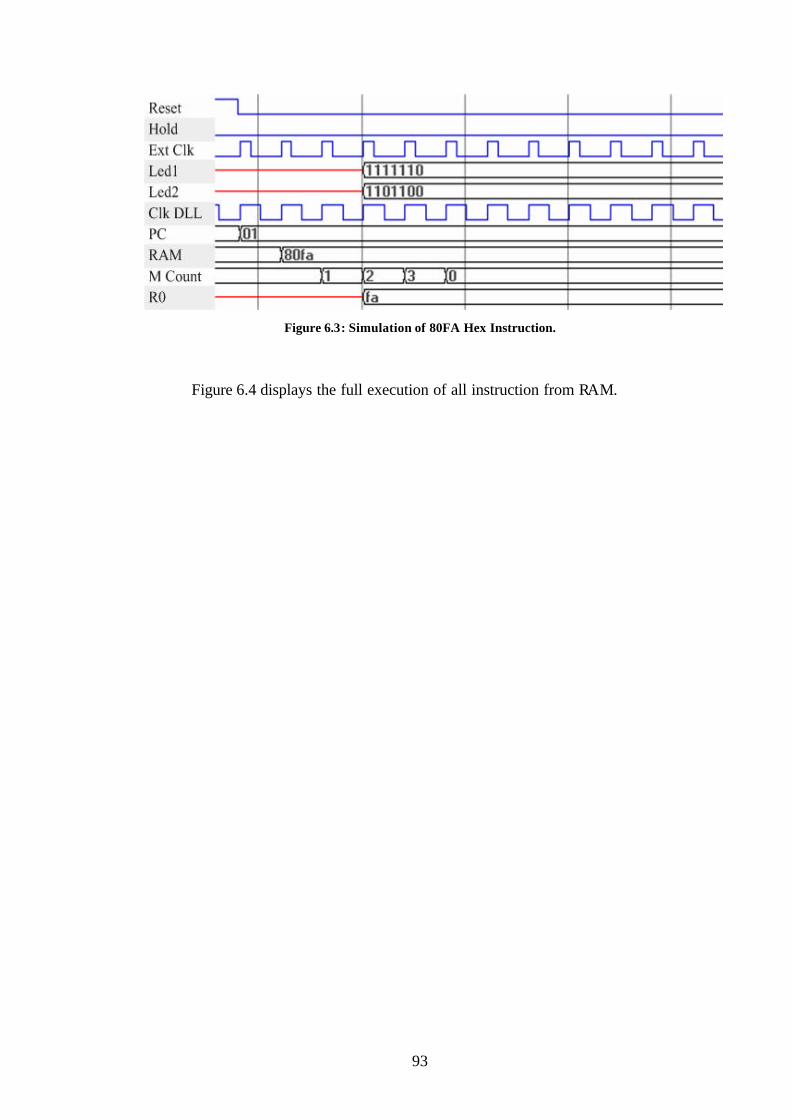
93
Figure 6.3: Simulation of 80FA Hex Instruction.
Figure 6.4 displays the full execution of all instruction from RAM.
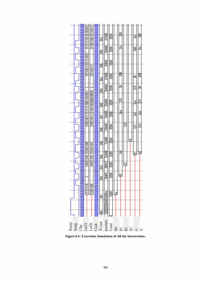
94
Figure 6.4: Execution Simulation of All the Instructions.
95
6.4-2. VERILOG SOURCE
The Verilog HDL module(s) were tested using various stimulus modules as
the design progressed. Once all hardware modules were verified, each module was
instantiated into a top- level design block to be tested.
Before the Control Unit was to be incorporated all input lines were defined at
the highest level. In the stimulus file, all inputs to the microprocessor were declared as
registers in order to set the inputs to various values at different points in time during
the simulation. During the two months of verification, there were several stimulus
files developed. Initially, a file was developed to verify the functionality of the 8-Bit
design without the Control Unit. This was accomplished by applying stimulus to all
the control lines at different points in time, moving data throughout the design. Once
the control unit was implemented, it was no longer possible to apply stimulus to
several control lines because they were now governed by the Control Unit.
In order to test any instructions at the Verilog level an 'EEPROM' and 'SRAM'
behavioral modules were developed (see Appendix F). They functioned very similar
to the actual EPROM and SRAM on the board like the signals WE, RD, Address and
Data. The assembled/linked HEX code for an instruction(s) was then coded in the
'EEPROM' behavioral module as if the code was burned into the external EEPROM
on the board. Eventually, a program that tested each instruction was developed and
coded into the behavioral EEPROM and verified.
6.4-3. XILINX SYNTHESIS TECHNOLOGY
The XST verification stage was almost exactly the same as the pre-Synopsys,
Verilog stage. In this stage the RISC design syntax is first checked and then its
application in targeted device hardware is verified. Each program that was verified at
the Verilog level was also verified at this level.
6.4-4. HARDWARE LEVEL
The final stage of testing consisted of downloading the design into the Xilinx
FPGA, single stepping the clock of the RISC and verifying that it functionally
behaved as in the previous two simulations. The difficultly at this stage is the ability
96
to monitor the internal functionality of the processor. Therefore, a Display module
was created as explained in the design sections. The Display Units on the board are
driven by the FPGA and display the contents of the Address Bus, Data Bus and the
ALU results. This ability was vital to the success of this project.
The Display Unit requires one clock cycle to completely display the contents
of the busses. Therefore, in order to execute one instruction, it was necessary to single
step the processor clock while the display clock operated at full frequency. Once
proper functionality was verified the processor clock could run at full frequency. It is
important to note that the Display Unit was developed for testing purposes only.
During final operation of the RISC machine, the Display Unit will be discarded.
When the instructions were tested using the RISC Control Unit, each state or
clock was stepped through using a manual Hold signal on the Xilinx board. Each state
of the Control Unit state machine was verified using the two Display Units. The data
incoming/outgoing from the Data Bus, Address Bus and the output from the ALU
were viewed using the Display Units.
6-5. Conclusions
6.5-1. CONCLUDING REMARKS
The purpose of this thesis project was to study and implement a RISC
(Reduced Instruction Set Computer) in an FPGA. A final 8-Bit design was achieved
with 15 instructions, 6 registers in the Register Unit, Display Unit logic for debugging
using the Xilinx XC2S100 FPGA. This design has partially fit the RISC criteria
because it has a simplified architecture and instruction set.
The bottom up design methodology proved to be successful for this project. It
was important to test and verify the behavioral modeling of each of the internal RISC
microprocessor components such as the Decoder, Register Unit, ALU and so on.
Once all lower level modules were verified one could then easily integrate all into a
higher level module. The Control Unit proved to be the hardware device that was
most prolonged to design, test and verify. As each instruction encoding was included

97
in the Control Unit design more testing and verification had to be done at the
synthesis and board level. The board level testing of the instructions was lengthy due
to the single stepping/clocking of the FPGA. Pieces of this design can be easily
exported and used in another digital FPGA design such as the behavioral model of the
Tristate Buffer.
Problems were encountered in this project but modifications were made to
overcome these minor setbacks. As the design approached completion the target
FPGA became nearly fully utilized. Problems such as Place & Routing of the design
in the FPGA and running out of CLBs on the FPGA had to be overcome. The solution
to the Place and Routing problem was to select a high effort level and multi-pass
cycle in the Xilinx Design Manager tool.
The design of the RISC microprocessor in an FPGA has shown how a
microprocessor can be simplified, which can be useful in specific applications. The
RISC design is fairly simplified for a microprocessor so it could be a useful teaching
aid in a university undergraduate course.
6.5-2. FUTURE WORK
A number of additional modifications could be made to the current RISC
microprocessor to improve efficiency and flow. Looking back, one could take a
variety of different approaches in accomplishing the design once attaining valuable
experience in using the HDL languages and various tools. Familiarization with the
specific tools and the target technology devices can help in attaining a fitting design.
Since the design was aimed more toward functionality rather than speed on the
Xilinx FPGA chip, improvements can be made. However, implementing memory
devices in an FPGA can be very inefficient. The current RISC design can be
interfaced with an SDRAM device for memory storage. Various speed grades of
FPGAs can be purchased from vendors which can affect the performance of the
design. Often, the ability of the chosen synthesis tool can govern the amount of the
FPGA utilized. Therefore, a more efficient synthesis tool could be chosen to create a
smaller netlist.
There are a few design decision that were made throughout this project that
could be altered to produce a more efficient and structured processor. For example,
98
the method used for monitoring the status of the flags in the control unit could be
improved. Instead of having an extra muxer for the ALU flags, one could implement a
Latch for the flags to drive onto the Transfer bus. Moreover, interrupts can also be
easily integrated into the design. Initially, the goal of this project was to accomplish
full operation of each instruction. Therefore, the number of clock cycles to execute
each instruction in this RISC is slightly greater than the expected number of clock
cycles. When the state machine was developed there were extra clock cycles
implemented to ensure ample set up and hold times for correct operation. Now that
full operation is achieved, one could reduce the number of clock cycles to produce a
more efficient state machine.