FINAL YEAR PROJECT REPORT
11
i FINAL YEAR PROJECT REPORT (Implementation of MIPS on FPGA) Project Advisor (Sir Muhammad Bilal) Submitted by (Syed Rehan Tariq - 081120064) (Taimoor Nafees - 081120067) (Abdullah Mehmood - 081120071) (Waseem Abbas - 081120073) Department of Electrical Engineering School of Science and Technology University of Management and Technology
-
Upload
khangminh22 -
Category
Documents
-
view
2 -
download
0
Transcript of FINAL YEAR PROJECT REPORT

i
FINAL YEAR PROJECT REPORT (Implementation of MIPS on FPGA)
Project Advisor
(Sir Muhammad Bilal)
Submitted by
(Syed Rehan Tariq - 081120064)
(Taimoor Nafees - 081120067)
(Abdullah Mehmood - 081120071)
(Waseem Abbas - 081120073)
Department of Electrical Engineering
School of Science and Technology
University of Management and Technology
ii
(Implementation of MIPS on FPGA)
Project Report submitted to the
Department of Electrical Engineering, University of Management and Technology
in partial fulfillment of the requirements for the degree of
Bachelor of Science
in
Electrical Engineering
(Syed Rehan Tariq - 081120064)
(Taimoor Nafees - 081120067)
(Abdullah Mehmood - 081120071)
(Waseem Abbas - 081120073)
(09-03-12)

iii
Abstract
Computer organization and design is a common engineering course where students learn concepts of modern computer architecture. Students often learn computer design by implementing individual sections of a computer microprocessor using a simulation only approach that limits a student’s experience to software design.
This project targets the computer architecture courses and presents an FPGA (Field Programmable Gate Array) implementation of a MIPS (Microprocessor without Interlocked Pipeline Stages) RISC (Reduced Instruction Set Computer) Processor via verilog design.
The goal of this project is to enhance the simulator based approach by integrating some hardware design to help the computer architecture students gain a hands-on experience in hardware-software integration and achieve a better understanding of both the MIPS single-cycle and pipelined processors as described in the widely used book.

iv
Acknowledgements
First of all we would like to thank Almighty Allah
Secondly we would like to thank my project advisor Sir Muhammad Bilal, as he helped us in making programming modules. He guided us in a very informative and descriptive way by assigning us different task step by step. We are very thankful to him for his support and guidance.
Finally we would like to thank our family and friends for putting up with our constant moaning about the project and supporting us through the difficult Times!
v
Table of contents Chapter I Introduction
Introduction..................................................................................... 1
Basic Processor Architecture…………………………………………………………... 1
List of components……………………….……………………………………………..... 3
ALU……………………………………………………………………………………………… 3
Memory (RAM)……………………………………………………………................... 3
Multiplexer (MUX)…………………………………………………………………………. 4
Register……………………………………………………………………………………….. 4
Full Adder…………………………………………………………………………………….. 5
Chapter II Programming Modules And Their Results
ALU………………………………………………………………………………………………. 6
ALU_TB………………………………………………………………………………………….. 7
Result………………………………………………………………………………………….. 10
MUX………………………………………………………………………........................ 11
MUX_TB………………………………………………………………………………………… 12
Result………………………………………………………………………………………….. 14
Full Adder…………………………………………………………………..................... 15
Full Adder_TB………………………………………………………………………………… 16
Result………………………………………………………………………………………….. 18
Registers………………………………………………………………………………………. 19
Registers_TB………………………………………………………………..................... 21
Result…………………………………………………………………………………………… 23

vi
Memory (RAM)……………………………………………………………………………….. 23
Memory (RAM)_TB…………………………………………………………………………… 25
Result……………………………………………………………………………………………. 28
Data to Memory…………………………………………………………………………….. 30
Data to Memory_TB…...…………………………………………………………………… 36
Result……………………………………………………………………………………………. 37
ALU control…………………………………………………………………….……………… 37
Control………………………………………………………………………..................... 38
Program Counter………………………………………………………….................... 39
Add_4……………………………………………………………………………………………. 40
Sign Extend……………………………………………………………………………………. 40
Connection of All components………………………………………………............. 41
Total Program with Test bench………………………………………………............ 44
Serial Communication………………………………………………………………………. 45
Memory Mapped I/O………………………………………………………………………… 46
Chapter III Summary and Conclusion UART……………………………………………………………………………………………… 47
VGA…………………………………………………………………………........................ 48
Keyboard……………………………………………………………………...................... 49
Conclusion………………………………………………………………………………………. 50
Chapter IV References
References…………………………………………………………………….................... 51

1
Chapter I. Introduction
1 Introduction
MIPS stands for (Microprocessor without Interlocked Pipeline Stages).The MIPS processor, designed in 1984 by researchers at Stanford University, is a RISC (Reduced Instruction Set Computer) processor. Compared with their CISC (Complex Instruction Set Computer) counterparts (such as the Intel Pentium processors), RISC processors typically support fewer and much simpler instructions.
The premise is, however, that a RISC processor can be made much faster than a CISC processor because of its simpler design. These days, it is generally accepted that RISC processors are more efficient than CISC processors; and even the only popular CISC processor that is still around (Intel Pentium) internally translates the CISC instructions into RISC instructions before they are executed
RISC processors typically have “load-store architecture”. This means there are two instructions for accessing memory: A load instruction to load data from memory and a store instruction to write data to memory. It also means that none of the other instructions can access memory directly.
Basic Processor Architecture The execution of an instruction in a processor can be split up into a number of stages. How many stages there are, and the purpose of each stage is different for each processor design. Examples include 2 stages (Instruction Fetch / Instruction Execute) and 3 stages (Instruction Fetch, Instruction Decode, and Instruction Execute). The MIPS processor has 5 stages:
IF The Instruction Fetch stage fetches the next instruction from memory using the address in the PC (Program Counter) register and stores this instruction in the IR (Instruction Register)
ID The Instruction Decode stage decodes the instruction in the IR, calculates the next PC, and reads any operands required from the register file.

EX Tdone in such as
MA Tinstructistore an
WB Fthis resunops (a
The Executethis stage.addition, su
The Memoryon, so for
n operand in
or instructiult back to nop, no-op
e stage "ex. (The ALU ubtraction,
y Access stloads, it w
nto memory
ons that hathe registe
p or no-ope
xecutes" this the Aritshifts left a
age performwould load ay. For all ot
ave a resulr file. Note ration instr
2
he instructhmetic andand right, e
ms any mean operandther instruc
t (a destinathat this in
ruction simp
Figure 1.1
ion. In facd Logic Unitetc.)
emory accesd from memctions, it wo
ation registncludes neaply does no
1
ct, all ALU t and perfo
ss requiredmory. For sould do noth
ter), the Warly all instrothing) and
operationsorms opera
d by the custores, it whing.
rite Back wructions, exs (stores).
s are tions
rrent would
writes xcept
3
1.2 List of Components used in MIPS:
1. ALU 2. Memory 3. Multiplexer (MUX) 4. Registers 5. Adder
ALU:
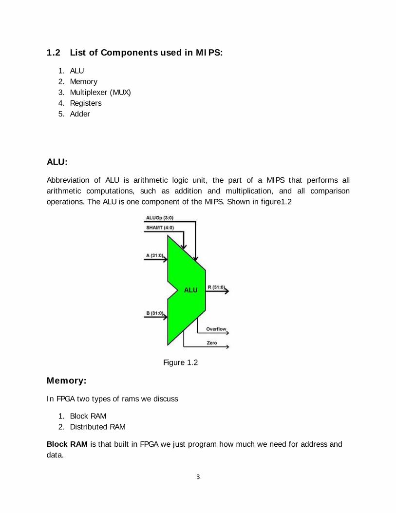
Abbreviation of ALU is arithmetic logic unit, the part of a MIPS that performs all arithmetic computations, such as addition and multiplication, and all comparison operations. The ALU is one component of the MIPS. Shown in figure1.2
Figure 1.2
Memory:
In FPGA two types of rams we discuss
1. Block RAM 2. Distributed RAM
Block RAM is that built in FPGA we just program how much we need for address and data.
4
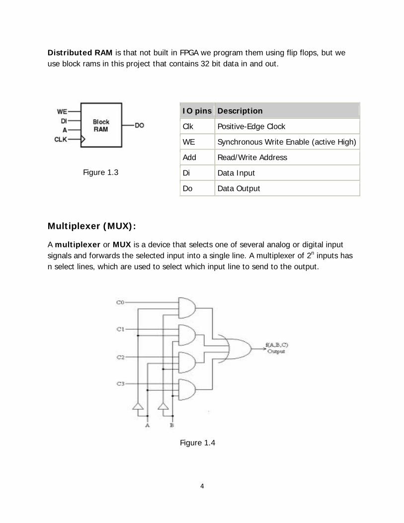
Distributed RAM is that not built in FPGA we program them using flip flops, but we use block rams in this project that contains 32 bit data in and out.
Figure 1.3
Multiplexer (MUX):
A multiplexer or MUX is a device that selects one of several analog or digital input signals and forwards the selected input into a single line. A multiplexer of 2n inputs has n select lines, which are used to select which input line to send to the output.
Figure 1.4
IO pins Description
Clk Positive-Edge Clock
WE Synchronous Write Enable (active High)
Add Read/Write Address
Di Data Input
Do Data Output

5
Register:
Registers are special high-speed storage area within the CPU. All data must be represented in a register before it can be processed. For example, if two numbers are to be multiplied, both numbers must be in registers, and the result is also placed in a register.
FULL ADDER:
The full-adder circuit adds three one-bit binary numbers (C A B) and outputs two one-bit binary numbers, a sum (S) and a carry (C1)
Figure 1.5