
6th Generation Intel® Processor Families for S-Platforms - Icecat

Programming the Intel 80-core network-on-a-chip Terascale Processor
Timothy G. Mattson, Intel Corp., DuPont, WA, USA
Rob Van der Wijngaart, Intel Corp., Santa Clara, CA USA Michael Frumkin, Google Inc., Mountain View, CA USA
Intel’s 80-core Terascale Processor was the first generally programmable microprocessor to break the Teraflops barrier. The primary goal for the chip was to study power management and on-die communication technologies. When announced in 2007, it received a great deal of attention for running a stencil kernel at 1.0 single precision TFLOPS while using only 97 Watts. The literature about the chip, however, focused on the hardware, saying little about the software environment or the kernels used to evaluate the chip. This paper completes the literature on the 80-core Terascale Processor by fully defining the chip’s software environment. We describe the instruction set, the programming environment, the kernels written for the chip, and our experiences programming this microprocessor. We close by discussing the lessons learned from this project and what it implies for future message passing, network-on-a-chip processors.
1 Introduction The trends in the semiconductor industry are clear; microprocessors with large complex cores that emphasize high frequencies are being displaced by microprocessors composed of multiple simpler cores. The multi-core microprocessors deliver increasing performance through on-chip parallelism, but within a reduced power envelope. Currently, microprocessors with two and four cores are common, but in the future, as transistor densities increase following Moore’s law, designs with dozens if not hundreds of cores can be expected. This is a big change for the computing industry with serious implications for every facet of the hardware platform and the supporting software. Intel has embarked on a research program to understand the implications of dozens of small simple cores on a single chip. An early result from this research program is the 80-core Terascale Processor [Vangal2008].
The primary goal for the 80-core Terascale Processor was to study power management methods and to explore different approaches for the on-die interconnection network between cores. A secondary goal, however, was to demonstrate that high performance could be delivered with these many-core chips. And on this count, the project was successful. The 80-core Terascale Processor was the first generally programmable microprocessor to run an application kernel at over one trillion (single precision) floating point operations per second (TFLOPS). Previous papers described the overall design of the microprocessor, the performance results, the on-die network, and the cores ([Vangal2008], [Hoskote2007], [Vangal2006]). The application kernels, instruction set, and software environment were not included in these papers, leaving the scientific literature concerning this chip in an incomplete state. An important goal of this paper is to describe the 80-core Terascale chip from the point of view of a software developer. We begin with a high level overview of the architecture of the processor and its programming model. We then describe each of the four kernels used to evaluate the chip Stencil, SGEMM, Spreadsheet, and FFT and the challenges encountered in mapping these kernels onto the chip. We close with a discussion of the insights gained from this project.
2 The 80-core Terascale Processor
The 80-core Terascale Processor [Vangal2008] is a tiled architecture, consisting of an 8 by 10 two-dimensional mesh of tiles implemented with 65 nm process technology. The chip holds a total of 100 million transistors on a 275mm2 die. Each tile defines a core and consists of:
Permission to make digital or hard copies of all or part of this work for personal or classroom use is granted without fee provided that copies are not made or distributedfor profit or commercial advantage and that copies bear this notice and the full citation on the first page. To copy otherwise, to republish, to post on servers or to redistribute to lists, requires prior specific permission and/or a fee. SC2008 November 2008, Austin, Texas, USA 978-1-4244-2835-9/08 $25.00 ©2008 IEEE
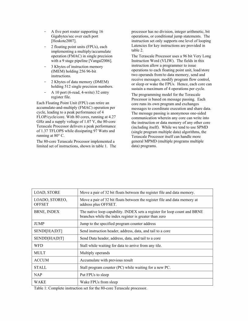
LOAD, STORE Move a pair of 32 bit floats between the register file and data memory.
LOADO, STOREO, OFFSET
Move a pair of 32 bit floats between the register file and data memory at address plus OFFSET.
BRNE, INDEX The native loop capability. INDEX sets a register for loop count and BRNE branches while the index register is greater than zero
JUMP Jump to the specified program counter address
SENDI[H|A|D|T] Send instruction header, address, data, and tail to a core
SENDD[H|A|D|T] Send Data header, address, data, and tail to a core
WFD Stall while waiting for data to arrive from any tile.
MULT Multiply operands
ACCUM Accumulate with previous result
STALL Stall program counter (PC) while waiting for a new PC.
NAP Put FPUs to sleep
WAKE Wake FPUs from sleep Table 1: Complete instruction set for the 80-core Terascale processor.
- A five port router supporting 16 Gigabytes/sec over each port [Hoskote2007].
- 2 floating point units (FPUs), each implementing a multiply/accumulate operation (FMAC) in single precision with a 9 stage pipeline [Vangal2006].
- 3 Kbytes of instruction memory (IMEM) holding 256 96-bit instructions.
- 2 Kbytes of data memory (DMEM) holding 512 single precision numbers.
- A 10 port (6-read, 4-write) 32 entry register file.
Each Floating Point Unit (FPU) can retire an accumulate-and-multiply (FMAC) operation per cycle, leading to a peak performance of 4 FLOP/cycle/core. With 80 cores, running at 4.27 GHz and a supply voltage of 1.07 V, the 80-core Terascale Processor delivers a peak performance of 1.37 TFLOPS while dissipating 97 Watts and running at 80° C. The 80-core Terascale Processor implemented a limited set of instructions, shown in table 1. The
processor has no division, integer arithmetic, bit operations, or conditional jump statements. The instruction set only supports one level of looping Latencies for key instructions are provided in table 2. The Terascale Processor uses a 96 bit Very Long Instruction Word (VLIW). The fields in this instruction allow a programmer to issue operations to each floating point unit, load/store two operands from/to data memory, send and receive messages, modify program flow control, or sleep or wake the FPUs. Hence, each core can sustain a maximum of 4 operations per cycle. The programming model for the Terascale Processor is based on message passing. Each core runs its own program and exchanges messages to coordinate execution and share data. The message passing is anonymous one-sided communication wherein any core can write into the instruction or data memory of any other core (including itself). While we tend to use SPMD (single program multiple data) algorithms, the Terascale Processor itself can handle more general MPMD (multiple programs multiple data) programs.
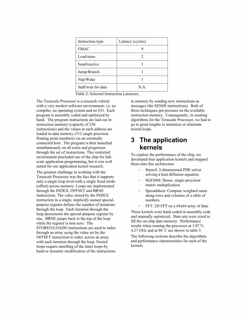
Instruction type Latency (cycles)
FMAC 9
Load/store 2
Send/receive 1
Jump/Branch 1
Nap/Wake 1
Stall/wait for data N.A.
Table 2: Selected Instruction Latencies.
The Terascale Processor is a research vehicle with a very modest software environment; i.e. no compiler, no operating system and no I/O. Each program is assembly coded and optimized by hand. The program instructions are laid out in instruction memory (capacity of 256 instructions) and the values at each address are loaded in data memory (512 single precision floating point numbers) via an externally connected host. The program is then launched simultaneously on all cores and progresses through the set of instructions. This restricted environment precluded use of the chip for full-scale application programming, but it was well suited for our application kernel research. The greatest challenge in working with the Terascale Processor was the fact that it supports only a single loop level with a single fixed stride (offset) across memory. Loops are implemented through the INDEX, OFFSET and BRNE instructions. The value stored by the INDEX instruction in a single, implicitly named special-purpose register defines the number of iterations through the loop. Each iteration through the loop decrements the special-purpose register by one. BRNE jumps back to the top of the loop while the register is non-zero. The STOREO/LOADO instructions are used to index through an array using the value set by the OFFSET instruction to index across an array with each iteration through the loop. Nested loops require unrolling of the inner loops by hand or dynamic modification of the instructions
in memory by sending new instructions as messages (the SENDI instructions). Both of these techniques put pressure on the available instruction memory. Consequently, in creating algorithms for the Terascale Processor, we had to go to great lengths to minimize or eliminate nested loops.
3 The application kernels
To explore the performance of the chip, we developed four application kernels and mapped them onto this architecture
- Stencil: 2-dimensional PDE solver solving a heat diffusion equation.
- SGEMM: Dense, single-precision matrix multiplication.
- Spreadsheet: Compute weighted sums along rows and columns of a table of numbers.
- FFT: 2D FFT on a 64x64 array of data. These kernels were hand coded in assembly code and manually optimized. Data sets were sized to fill the on-chip data memory. Performance results when running the processor at 1.07 V, 4.27 GHz and at 80 C are shown in table 3. The following sections describe the algorithms and performance characteristics for each of the kernels.

Kernel Single Precision TFLOPS @ 4.27 GHz
Stencil 1.00
SGEMM 0.51
Spreadsheet 0.45
2D FFT 0.02 Table 3: Single precision TFLOPS for the four application kernels.
3.1 Stencil Stencil kernels apply regular operations on rectangular arrays of data. They are common in scientific computing and graphics. We used a five-point star-shaped stencil to implement a two-dimensional relaxation method for solving the steady state, homogeneous, anisotropic heat equation with Dirichlet/semi-periodic boundary conditions on a rectangular, structured grid. The method chosen is far from optimal and should not be considered an example of good numerics. It merely serves as a demonstration of the Terascale processor’s computational potential. The mathematical definition of a single iteration of the Stencil operation is given in terms of updates to the interior points and the boundary conditions:
Interior point updates: Bi,j:= w1*Ai-1,j+w2*Ai,j+w3*Ai+1,j+ w4*Ai,j-1+w5*Ai,j+1 Boundary conditions: B0,j = Bni,j, Bi,0=1, Bi,nj=2
Implementation of the interior point scheme would ordinarily require a two-dimensional loop, which is not possible on the chip. So we linearized the array and loop indices: for (ij=ni;ij<=ni*(nj-1);ij++) B[ij] = w1*A[ij-1] + w2*A[ij] + w3*A[ij+1] + w4*A[ij-ni] + w5*A[ij+ni];
This introduces a complication for the periodic boundary conditions at j=0 and j=nj. They formally require a conditional statement within the single loop, which is not possible with the chip’s instruction set. However, note that A0,j = A0,j+1 + O(h), where h is the mesh spacing. So by substituting A0,j for A0,j+1, we introduce only an O(h) error, formally reducing the accuracy of the approximation and potentially slowing the rate of convergence for the relaxation computation. The resulting method, however, remains numerically consistent. Hence, we can safely use the above
loop to completely define the semi-periodic stencil computation. Note that the right hand side contains multiple accesses to the array A, all with unit stride but with different initial offsets. These offsets are part of the program; they are precomputed and stored, so that no integer arithmetic (other than the fixed-stride access to A) is required while running the code. To reduce the amount of memory required, we replaced the point-Jacobi scheme with Gauss-Seidel, i.e.
A[ij] += w1*A[ij-1] + (w2-1)*A[ij] + w3*A[ij+1] + w4*A[ij-ni] + w5*A[ij+ni],
where the latest available values of A are used to update the value at each target grid point. Parallelizing this algorithm was relatively straightforward. We used a one-dimensional strip-wise domain decomposition, in which the second (j) non-periodic array dimension was distributed among the 80 cores of the chip. We used the common method of defining ghost cells to hold the A values exchanged with the northern and southern neighbors of the target strip of the grid. Hence, each core (except the two cores on the northernmost and southernmost boundaries of the grid) sends two messages to its nearest neighbors and receives two messages back. Optimization and performance analysis: To reduce delays due to the pipeline depth of the FPUs, we relaxed the requirement that the latest information always be used in the Gauss-Seidel update scheme. In addition, we implemented the message passing without a handshake. That is, we did not stall a core until all incoming data had been received. Both optimization strategies may introduce small errors and reduce the convergence rate, but they are legitimate optimizations that do not affect the overall consistency of the method. The method is well-balanced in terms of instructions. Each point update requires the loading of three new operands (two can stay in registers), and involves

5 FMAC operations. The chip can load two operands per cycle per core. Hence, two updates take 5 cycles for the FPUs and require only three cycles to load the operands, so the FPUs can operate at peak speed. Unrolling by a factor of eight assures that no FPU pipeline stalls are incurred. For a tall and narrow grid 16 points wide (ni=16) and 28 points tall per core, the asynchronous communications are completely overlapped with computations. Performance of the Stencil code, which includes cycles spent on register moves and loop branching, is shown in Table 3.
3.2 SGEMM SGEMM is the BLAS 3 subroutine used to multiply two single precision general dense matrices. It is the key building block for many dense linear algebra algorithms. The BLAS 3 routine includes many variations (e.g. scaling, transposition, etc), but we consider only the simplest case: C = A x B, where A, B, and C are NxP, PxM, and NxM matrices, respectively. The SGEMM routine can be defined by the following C code fragment: for (i=0; i<N;i++) for (j=0;j<M;j++) C[i][j] = 0.0; for(k=0;k<P;k++) C[i][j] += A[i][k] * B[k][j];
Modern algorithms for SGEMM are block-based and decompose the problem into smaller SGEMM problems. For matrices of order N these algorithms have read/write operations that scale as O(N2) while computational effort is O(N3). By selecting large blocks that fit in cache, the read/write operations can be overlapped with computations, allowing SGEMM to execute near the peak floating point capacity of a chip. The 80-core Terascale processor does not have a cache, but blocking could still be useful for overlapping communication and computation as well as register blocking. However, block-structured algorithms require triple loops over the blocks of the matrices. Since the Terascale Processor does not support nested loops, we have to use a different and less efficient algorithm based on dot products. We mapped the cores onto a ring topology. The A and C matrices were decomposed into rows with one row per core. B was decomposed by columns with one
column per core. The algorithm proceeded as follows: On core number i Loop over j = 1, M { C[i][j] = dot_product (row Ai * column Bj) Circular shift column Bj to neighboring core }
Optimization and Performance Analysis: Additional optimizations used in the final algorithm
- Used diagonal wrapped storage where the array holding each row of C started with the diagonal element and wraped around, thereby letting us use a single indexing scheme into C for each core.
- Unrolled the dot product loop, so we could use a single loop to run over a column of C.
- Organized code so elements of B were shifted immediately after they were used; thereby overlapping computation and communication
We selected the matrix dimensions N, M and P to fill the available memory: N=P=80 and M=206. Each element of C required a dot product of length M, resulting in M multiplies, M-1 adds, and 2M loads. Each FPU can retire one FMAC per cycle. The FPU is a 9-stage pipeline. So to load registers to feed the pipelines for a dot product required 2*9 registers for the operands and 1 register for the accumulator; or 38 registers for both FMAC units. Obviously, there were not enough registers to keep both FPUs running at 100% for a dot product. The fundamental performance bottleneck, however, was the fact that one can only load 2 operands from data memory per cycle. Since the FMACs need 2 operands from memory each, the loads limited peak dot product performance to 50% of the total available floating point performance.
3.3 Spreadsheet This is a synthetic kernel meant to capture computations common when working with spreadsheets. In particular, we computed weighted sums across rows and columns of data.
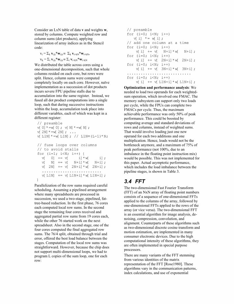
Consider an LxN table of data v and weights w, stored by columns. Compute weighted row and column sums (dot products), applying linearization of array indices as in the Stencil code:
vi = k vi,k*wi,k k vi+kN*wi+kN, vk = i vi,k*wi,k i vi+kN*wi+kN
We distributed the table across cores using a one-dimensional decomposition, such that whole columns resided on each core, but rows were split. Hence, column sums were computed completely locally on each core. However, naïve implementation as a succession of dot products incurs severe FPU pipeline stalls due to accumulation into the same register. Instead, we fused all dot product computations into a single loop, such that during successive instructions within the loop, accumulation took place into different variables, each of which was kept in a different register: // preamble v[0]*=w[0]; v[N]*=w[N]; v[2N]*=w[2N]; ... v[L1N]*=w[L1N]; // L1N (L-1)*N; // fuse loops over columns // to avoid stalls for (i=1; i<N; i++) { v[ 0] += v[ i]*w[ i]; v[ N] += v[ N+i]*w[ N+i]; v[ 2N] += v[ 2N+i]*w[ 2N+i]; .......................... v[L1N] += v[L1N+i]*w[L1N+i]; }
Parallelization of the row sums required careful scheduling. Assuming a pipelined arrangement where many spreadsheets are processed in succession, we used a two-stage, pipelined, fat-tree-based reduction. In the first phase, 76 cores each computed local row sums. In the second stage the remaining four cores received and aggregated partial row sums from 19 cores each, while the other 76 started work on the next spreadsheet. Also in the second stage, one of the four cores computed the final aggregated row sums. The 76/4 split, obtained through trial and error, offered the best load balance between the stages. Computation of the local row sums was straightforward. However, because the chip does not support multi-dimensional loops, we had to program L copies of the sum loop, one for each row:
// preamble for (i=0; i<N; i++) v[i] *= w[i]; // add one column at a time for (i=0; i<N; i++) v[i] += v[ N+i]*w[ N+i]; for (i=0; i<N; i++) v[i] += v[ 2N+i]*w[ 2N+i]; for (i=0; i<N; i++) v[i] += v[ 3N+i]*w[ 3N+i]; ............................ for (i=0; i<N; i++) v[i] += v[L1N+i]*w[L1N+i];
Optimization and performance analysis: We needed to load two operands for each weighted-sum operation, which involved one FMAC. The memory subsystem can support only two loads per cycle, while the FPUs can complete two FMACs per cycle. Thus, the maximum achievable performance was only 50% of peak performance. This could be boosted by computing average and standard deviations of rows and columns, instead of weighted sums. That would involve loading just one new operand for each two additions and one multiplication. Hence, loads would not be the bottleneck anymore, and a maximum of 75% of peak performance (not 100%, due to an imbalance in the floating point instruction mix) would be possible. This was not implemented for this paper. Actual asymptotic performance, which includes the load imbalance between the pipeline stages, is shown in Table 3.
3.4 FFT The two-dimensional Fast Fourier Transform (FFT) of an NxN array of floating point numbers consists of a sequence of one-dimensional FFTs applied to the columns of the array, followed by one-dimensional FFTs applied to the rows of the array (or vice versa). The two-dimensional FFT is an essential algorithm for image analysis, de-noising, compression, convolution, and alignment. Counterparts of these algorithms such as two-dimensional discrete cosine transform and motion estimation, are implemented in many consumer electronic devices. Due to the high computational intensity of these algorithms, they are often implemented in special purpose processors. There are many variants of the FFT stemming from various identities of the matrix representation of the FFT [Rose1980]. These algorithms vary in the communication patterns, index calculations, and use of exponential

factors. The best known algorithms are the Cooley-Tukey and Singleton algorithms. The limited ability of the Terascale Processor to support index and branch operations, limited size of the instruction memory, the mesh interconnection network (as opposed to a shuffle network), and lack of I/O capabilities constrained our choice of algorithm. In particular, our algorithm had to address the following constraints. First, the algorithm had to be blocked so each core performed a large number of operations with local data before it was exchanged with other cores. Second, the number of exchange patterns with other tiles had to be minimized to accommodate the single level of loop nesting in the core. Third, the algorithm had to be “in-core”, i.e. all data has to be stored in the data memory of the tiles. Fourth, the code size had to be small enough to fit into the limited instruction memory on each core. The Pease FFT ([Pease1968]) algorithm effectively addresses most of these constraints. It has a fixed communication pattern and is known to work well on systolic array processors: for(int i=log_n;i>0;i--){ for(int j=0;j<n/2;j++){ angle=2*PI*floor(j/(1<<(i-1)))/(1<<(log_n-i+1)); er[j]=cos(angle); ei[j]=sin(angle); ar=er[j]*ur[2*j+1]- ei[j]*ui[2*j+1]; ai=er[j]*ui[2*j+1]+ei[j]* ur[2*j+1]; wr[j]=ur[2*j]+ar; wi[j]=ui[2*j]+ai; wr[j+n/2]=ur[2*j]-ar; wi[j+n/2]=ui[2*j]-ai; } for(int j=0;j<n/2;j++){ ur[j]=wr[j]; ui[j]=wi[j]; ur[j+n/2]=wr[j+n/2]; ui[j+n/2]=wi[j+n/2]; }
}
A disadvantage of this algorithm is that different exponential terms (array elements er[] and ei[]) are needed for each iteration. This vector of exponents, however, can be pre-computed and stored on each core if there is enough memory for the data.
The data and instruction memory sizes allowed us to compute a 2D FFT over a 64x64 array. We used an 8x8 mesh of cores, with each core storing an 8x8 block of the matrix and a 64-element complex vector of exponents. Due to the symmetries in the exponents the actual number of floats needed to be stored is 32, which is small enough to fit in the remaining 128 locations of data memory. These exponents can be pre-computed. Compressed storage of the exponents, however, would excessively complicate the code, so we actually used 64 memory locations to store the exponents. We blocked the Pease algorithm, so it performed operations over 8 vectors of 8 elements each, with index operations explicitly coded for the 8 point kernel (shown below). After finishing computations with a block, a core interchanged the intermediate results with cores along the column of the mesh. After three such iterations the 64-point FFT of 8 vectors was completed in each column of the mesh. Then similar computations were performed along the rows of the mesh. The following code shows an 8 point FFT kernel with (xr, xi) and (yr, yi) as input/output vectors for(int j=0;j<n/2;j++){ ulr[j]=xr[2*j]; uli[j]=xi[2*j]; uhr[j]=xr[2*j+1]; uhi[j]=xi[2*j+1]; } peaseFFTx4(ulr,uli,wlr,wli,4); peaseFFTx4(uhr,uhi,whr,whi,4); er[0]=1.0; ei[0]=0.0; er[1]=0.707107; ei[1]=0.707107; er[2]=0.0; ei[2]=1.0; er[3]=-0.707107; ei[3]=0.707107; for(int j=0;j<4;j++){ uhr[j]=er[j]*whr[j]- ei[j]*whi[j]; uhi[j]= er[j]*whi[j]+ ei[j]*whr[j]; yr[j]=wlr[j]+uhr[j]; yi[j]=wli[j]+uhi[j]; yr[j+4]=wlr[j]-uhr[j]; yi[j+4]=wli[j]-uhi[j]; }
The function peaseFFTx4() is 4 point Pease FFT, which performs 16 accumulations and subtractions, and no multiplications.
Our main coding effort was spent on unrolling the 8 by 8-point FFTs within a core so that the instructions would fit in the 256 locations of the tile’s memory. Only single-level loops were used. Addressing into the compressed vector of the exponents, and reading/writing of the data received/sent to other tiles were carefully synchronized. Optimization and performance analysis: After verifying that the initial program worked correctly, we rearranged the computations to increase the overlap of computations and communications between cores. This was accomplished by sending completed columns of the local 8x8 matrix block in the first phase to all receiving tiles the moment they became available, instead of postponing communications to the end of the first phase. Total FLOP count of the Pease algorithm (excluding computations of the exponents and multiplications by 1) is 4*N*log N. The 2D FFT algorithm is composed of 2*N Pease algorithms and has a number of flops equal to 4*N2*log2N = 196608 (for N = 64). The overall balance of floating point multiplication and accumulation operations limited peak performance of the kernel to 17.5%.
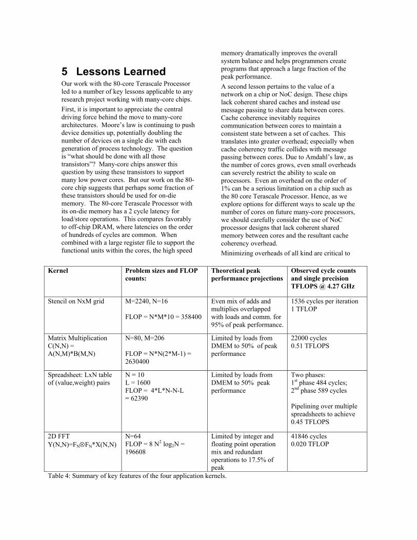
4 Discussion We summarize the kernels and their key characteristics in Table 4. In each case, we project the ideal performance (based purely on instruction mix and load/store limitations, disregarding load imbalance, communication overhead, pipeline stalls, etc.) so we can evaluate the effectiveness of a kernel’s implementation. The stencil kernel ran at 76% of peak performance, compared to an ideal performance projection of 95%. With the focus on power efficiency in this project, however, the more important results are the power efficiency
metrics expressed as single precision GFLOPS per Watt:
- 19.4 GFLOP/W for Stencil running at 0.394 TFLOPS
- 10.5 GFLOP/W for Stencil running at 1.00 TFLOPS
- 5.8 GFLOP/W for Stencil running at 1.33 TFLOPS
These are the highest GFLOP/W numbers we are aware of for processors in the teraflop range. The SGEMM and Spreadsheet kernels were observed to run at 37% and 33% of peak performance, respectively. This compares to an ideal performance of 50%. The gap between maximum achievable and actually realized performance of the above three kernels is relatively small, compared with the large gaps commonly seen with modern microprocessors. This is due to the fact that because of the absence of cache, locality plays no role, except with respect to register reuse. The performance of the 2D FFT, observed at around 2% of peak performance, was low. This was due almost entirely to communication overhead. The high performance attained with the Terascale Processor is a result of several factors. First, the processor is well-balanced for dense floating point kernels. With the 10 port register file and latencies well balanced for floating point data movement operations, the kernels are able to reasonably approach their projected theoretical performance levels. Second, all memory accessed by the Terascale Processor was on chip, so we did not need to deal with high latencies to off-chip DRAM. A third factor was that the high on-chip network bandwidth and low contention due to the mesh architecture allowed us to overlap computation and communication effectively for most of the kernels.
5 Lessons Learned Our work with the 80-core Terascale Processor led to a number of key lessons applicable to any research project working with many-core chips. First, it is important to appreciate the central driving force behind the move to many-core architectures. Moore’s law is continuing to push device densities up, potentially doubling the number of devices on a single die with each generation of process technology. The question is “what should be done with all those transistors”? Many-core chips answer this question by using these transistors to support many low power cores. But our work on the 80-core chip suggests that perhaps some fraction of these transistors should be used for on-die memory. The 80-core Terascale Processor with its on-die memory has a 2 cycle latency for load/store operations. This compares favorably to off-chip DRAM, where latencies on the order of hundreds of cycles are common. When combined with a large register file to support the functional units within the cores, the high speed
memory dramatically improves the overall system balance and helps programmers create programs that approach a large fraction of the peak performance. A second lesson pertains to the value of a network on a chip or NoC design. These chips lack coherent shared caches and instead use message passing to share data between cores. Cache coherence inevitably requires communication between cores to maintain a consistent state between a set of caches. This translates into greater overhead; especially when cache coherency traffic collides with message passing between cores. Due to Amdahl’s law, as the number of cores grows, even small overheads can severely restrict the ability to scale on processors. Even an overhead on the order of 1% can be a serious limitation on a chip such as the 80 core Terascale Processor. Hence, as we explore options for different ways to scale up the number of cores on future many-core processors, we should carefully consider the use of NoC processor designs that lack coherent shared memory between cores and the resultant cache coherency overhead. Minimizing overheads of all kind are critical to
Kernel Problem sizes and FLOP counts:
Theoretical peak performance projections
Observed cycle counts and single precision TFLOPS @ 4.27 GHz
Stencil on NxM grid M=2240, N=16 FLOP = N*M*10 = 358400
Even mix of adds and multiplies overlapped with loads and comm. for 95% of peak performance.
1536 cycles per iteration 1 TFLOP
Matrix Multiplication C(N,N) = A(N,M)*B(M,N)
N=80, M=206 FLOP = N*N(2*M-1) = 2630400
Limited by loads from DMEM to 50% of peak performance
22000 cycles 0.51 TFLOPS
Spreadsheet: LxN table of (value,weight) pairs
N = 10 L = 1600 FLOP = 4*L*N-N-L = 62390
Limited by loads from DMEM to 50% peak performance
Two phases: 1st phase 484 cycles; 2nd phase 589 cycles Pipelining over multiple spreadsheets to achieve 0.45 TFLOPS
2D FFT Y(N,N)=FN FN*X(N,N)
N=64 FLOP = 8 N2 log2N = 196608
Limited by integer and floating point operation mix and redundant operations to 17.5% of peak
41846 cycles 0.020 TFLOP
Table 4: Summary of key features of the four application kernels.

achieving a highly scalable design. One source of overhead arises when a core must stop useful work in order to deal with an incoming message. We avoided this problem on the 80-core Terascale Processor. Any core could write directly into the memory of any other core. These transactions were managed by the router on each tile and hence did not interrupt the receiving core. We acknowledge that undisciplined use of this feature could cause serious correctness problems, but performance benefits are so high that this is a productive area of study for future many-core chips. The 80-core Terascale Processor is an extremely efficient processor in terms of the performance per Watt. This was a primary design goal for the chip [Vangal2008]. A particularly effective technique for managing power on the chip came from the WAKE and NAP instructions. These instructions exposed power management to the programmer allowing the programmer to turn floating point units on or off depending on the needs of the application. Cooperation between hardware and software was critical to achieving these high levels of power efficiency. Finally, we point out the hazards of designing a many core chip without direct involvement by applications programmers. This chip was presented to us a completed package; in essence we were given the chip and challenged to do the best we could with it. While we achieved impressive results, small changes to the instruction set could have had a large impact on the programmability of the chip. For example, a simple computed jump statement would have allowed us to add nested loops. A second offset parameter would have allowed us to program general 2D array computations. These small changes would have been easy to implement if caught early in the design phase of the project, but the hardware team developed the chip without the help of applications programmers and hence missed these enhancements.
6 Conclusion The Intel 80 core Terascale Processor demonstrates that many low power cores can be used in a single processor to achieve TFLOPS scale performance. The individual cores were simple consuming a small fraction of the power needed with a more traditional CPU. With on-chip parallelism, these cores worked together to deliver high sustained performance of 1.0 single precision TFLOPS at 97W for the Stencil kernel.
Sustained performance is important, but to fully appreciate the 80-core Terascale processor, the performance per Watt is most important. Finding a consistent set of performance/watt results to compare against is difficult. We provide two points of comparison. First, consider the Tilera 64-core mesh-connected chip [Tilera 2007] with 0.192 TFLOPS/s at 35W. Our value of 1.37 TFLOPS at 97 Watts is a 2.5 fold advantage in performance per Watt. As a second point of comparison, consider Intel® Core™ 2 Quad processor CPU running at 2.66 GHz with a thermal design power of 95W (model number Q6700) [Intel2008]. This CPU was manufactured using the same 65 nm process technology as was used for the 80-core Terascale processor. A Core™ 2 core includes two 128 bit wide SIMD FPU that support the SSE3 instructions each of which can retire up to 4 single precision floating point operations per cycle. Hence, the peak performance of this quad core CPU is:
4 core*8flop/core*2.66 GHZ = 85.12 single precision GFLOPS
This translates to 0.9 GFLOP/Watt making the 80-core Terascale processors (19.4 GFLOP/W at 0.394 TFLOP) over 20 times more power efficient than a more traditional “big core” multi-core CPU. We acknowledge that these comparisons are somewhat unfair. The 80-core Terascale processor is a research chip suitable for kernel studies while the Tilera and Intel® Core™ 2 Quad processors are products that run full applications. But these comparisons are still useful as points of comparison to validate the approaches we’ve taken with the 80-core Terascale processor. The instruction set on the Terascale Processor was limited. While this made the chip unsuitable for full applications development, it is important to note that application programming was not the goal of this project. As reported in [Vangal2008] and [Hoskote2007], the primary purpose of this project was to study tiled architectures and a family of techniques to support high performance, power efficient many-core chips. The applications studies were secondary. In this light, the performance attained by our kernels was high, and it was remarkable that a complex kernel such as the 2D FFT could be implemented at all. The 80-core Terascale Processor is the first member of what should be a family of research

chips. Future processors in this family will include NoC chips but using cores with more fully featured cores to support general purpose application programming. We are directly working with the processor architects to make sure these follow-on chips are useful for application programmers. The larger questions driving our work pertain to the software implications of many core processors based on message passing. While there is a considerable body of legacy software dependent on cache coherent processors, we believe the advantages of a message passing software are too great to ignore. Our future work will highlight three major advantages of message passing architectures for many core chips. First, managing messages and explicitly distributing data structures adds considerable complexity to the software development process. This complexity, however, is balanced by the greater ease of avoiding race conditions when all sharing of data is through explicit messages rather than through a shared address space. Second, while a programmer can block data to fit into a cache or use prefetching to prepare a cache in advance of a computation, programmers have little or no control over eviction of data from a cache. It is difficult to write software with predictable performance when the state of the cache is so difficult to control. A NoC chip without cache coherence between cores avoids this problem altogether. Third, there are software engineering advantages to message passing architectures. Well engineered software is often constructed as modules that can be composed into the final application. Composition is based on isolation of concerns; computing occurs inside a “black box” module while sharing of information occurs only through the interfaces to the modules. A shared address space makes it difficult to assure that no unintended sharing is taking place. A message passing architecture, however, naturally supports a discipline of isolation between modules since sharing can only occur through the exchange of messages. We believe it is important to fully explore these and other
software engineering advantages of message passing architectures as we move to NoC processors with more complete instruction sets.
7 Acknowledgments This was a team effort. Yatin Hoskote, Jason Howard, and Saurabh Dighe of Intel’s Microprocessor Technology Laboratory worked closely with us to design these algorithms and served as the “optimizing compiler” for this project, creating optimized assembly code by hand from our algorithms.
8 References [Vangal2008] Sriram Vangal, et al. "An 80-Tile Sub-100-W TeraFLOPS Processor in 65-nm CMOS," l. IEEE Journal of Solid-State Circuits, Vol. 43, No. 1, Jan 2008.
[Vangal2006] S. Vangal, et al. IEEE JSSC, Oct. 2006.
[Hoskote2007] Yatin Hoskote, Sriram Vangal, Arvind Singh, Nitin Borkar and Shekhar Borkar, “A 5GHz Mesh Interconnect for a Teraflops Processor”, IEEE Micro, Vol 27, pp. 51-61, 2007.
[Pease1968] M. C. Pease. An adaptation of the fast Fourier transform for parallel processing. J. ACM, 15(2), pp. 252-264, April 1968.
[Rose1980] D. J. Rose. Matrix Identities of The Fast Fourier Transform. Linear Algebra and its Applications, v. 29, pp. 423-443, 1980.
[Tilera 2007] Tilera Processor Family: http://www.tilera.com/products/processors.php
[Intel2008] Intel(R) 64 and IA-32 Architectures Software developerr’s manual volume 1: Basic Architecture, April 2008.
Copyright © 2022 FDOKUMEN