34 .80 - Octopart
111
IMPORTANT NOTICE Dear customer, As from August 2 nd 2008, the wireless operations of NXP have moved to a new company, ST-NXP Wireless. As a result, the following changes are applicable to the attached document. ● Company name - NXP B.V. is replaced with ST-NXP Wireless. ● Copyright - the copyright notice at the bottom of each page “© NXP B.V. 200x. All rights reserved”, shall now read: “© ST-NXP Wireless 200x - All rights reserved”. ● Web site - http://www.nxp.com is replaced with http://www.stnwireless.com ● Contact information - the list of sales offices previously obtained by sending an email to [email protected] , is now found at http://www.stnwireless.com under Contacts. If you have any questions related to the document, please contact our nearest sales office. Thank you for your cooperation and understanding. ST-NXP Wireless www.stnwireless.com
-
Upload
khangminh22 -
Category
Documents
-
view
0 -
download
0
Transcript of 34 .80 - Octopart

IMPORTANT NOTICE
Dear customer,
As from August 2nd 2008, the wireless operations of NXP have moved to a new company,ST-NXP Wireless.
As a result, the following changes are applicable to the attached document.
Company name - NXP B.V. is replaced with ST-NXP Wireless.
Copyright - the copyright notice at the bottom of each page “© NXP B.V. 200x. All rights reserved”, shall now read: “© ST-NXP Wireless 200x - All rights reserved”.
Web site - http://www.nxp.com is replaced with http://www.stnwireless.com
Contact information - the list of sales offices previously obtained by sending an email to [email protected] , is now found at http://www.stnwireless.com under Contacts.
If you have any questions related to the document, please contact our nearest sales office.Thank you for your cooperation and understanding.
ST-NXP Wireless
www.stnwireless.com

1. General description
The ISP1760 is a Hi-Speed Universal Serial Bus (USB) host controller with a genericprocessor interface. It integrates one Enhanced Host Controller Interface (EHCI), oneTransaction Translator (TT) and three transceivers. The host controller portion of theISP1760 and the three transceivers comply to Ref. 1 “Universal Serial Bus SpecificationRev. 2.0”. The EHCI portion of the ISP1760 is adapted from Ref. 2 “Enhanced HostController Interface Specification for Universal Serial Bus Rev. 1.0”.
The integrated high-performance Hi-Speed USB transceivers enable the ISP1760 tohandle all Hi-Speed USB transfer speed modes: high-speed (480 Mbit/s), full-speed(12 Mbit/s) and low-speed (1.5 Mbit/s). The three downstream ports allow simultaneousconnection of three devices at different speeds (high-speed, full-speed and low-speed).
The generic processor interface allows the ISP1760 to be connected to variousprocessors as a memory-mapped resource. The ISP1760 is a slave host: it does notrequire ‘bus-mastering’ capabilities of the host system bus. The interface can beconfigured, ensuring compatibility with a variety of processors. Data transfer can beperformed on 16 bits or 32 bits, using Programmed Input/Output (PIO) or Direct MemoryAccess (DMA) with major control signals configurable as active LOW or active HIGH.
Integration of the TT allows connection to full-speed and low-speed devices, without theneed of integrating Open Host Controller Interface (OHCI) or Universal Host ControllerInterface (UHCI). Instead of dealing with two sets of software drivers, EHCI and OHCI orUHCI, you need to deal with only one set, EHCI, that dramatically reduces softwarecomplexity and IC cost.
2. Features
n The host controller portion of the ISP1760 complies with Ref. 1 “Universal Serial BusSpecification Rev. 2.0”
n The EHCI portion of the ISP1760 is adapted from Ref. 2 “Enhanced Host ControllerInterface Specification for Universal Serial Bus Rev. 1.0”
n Contains three integrated Hi-Speed USB transceivers that support high-speed,full-speed and low-speed modes
n Integrates a TT for Original USB (full-speed and low-speed) device support
n Up to 64 kB internal memory (8 k × 64 bits) accessible through a generic processorinterface; operation in multitasking environments is made possible by theimplementation of virtual segmentation mechanism with bank switching on taskrequest
ISP1760Hi-Speed Universal Serial Bus host controller for embeddedapplicationsRev. 04 — 4 February 2008 Product data sheet

NXP Semiconductors ISP1760Embedded Hi-Speed USB host controller
n Generic processor interface, non-multiplexed and variable latency, with a configurable32-bit or 16-bit external data bus; the processor interface can be defined asvariable-latency or SRAM type (memory mapping)
n Slave DMA support to reduce the load of the host system CPU during the data transferto or from the memory
n Integrated Phase-Locked Loop (PLL) with a 12 MHz crystal or an external clock input
n Integrated multi-configuration FIFO
n Optimized ‘msec-based’ or ‘multi-msec-based’ Philips Transfer Descriptor (PTD)interrupt
n Tolerant I/O for low voltage CPU interface (1.65 V to 3.6 V)
n 3.3 V-to-5.0 V external power supply input
n Integrated 5.0 V-to-1.8 V or 3.3 V-to-1.8 V voltage regulator (internal 1.8 V forlow-power core)
n Internal power-on reset and low-voltage reset
n Supports suspend and remote wake-up
n Target current consumption:
u Normal operation; one port in high-speed active: ICC < 100 mA
u Suspend mode: ICC(susp) < 150 µA at room temperature
n Built-in configurable overcurrent circuitry (digital or analog overcurrent protection)
n Available in LQFP128 and TFBGA128 packages
3. Applications
The ISP1760 can be used to implement a Hi-Speed USB compliant host controllerconnected to most of the CPUs present in the market today, having a generic processorinterface with de-multiplexed address and data bus. This is because of the efficientslave-type interface of the ISP1760.
The internal architecture of the ISP1760 is such that it can be used in a large spectrum ofapplications requiring a high-performance internal host controller.
3.1 Examples of a multitude of possible applicationsn Set-top box: for connecting external high-performance mass storage devices
n Mobile phone: for connecting various USB devices
n Personal Digital Assistant (PDA): for connecting a large variety of USB devices
n Printer: for connecting external memory card readers, allowing direct printing
n Digital Still Camera (DSC): for printing to an external USB printer, for direct printing
n Mass storage: for connecting external memory card readers or other mass storagedevices, for direct back-up
The low power consumption and deep power management modes of the ISP1760make it particularly suitable for use in portable devices.
ISP1760_4 © NXP B.V. 2008. All rights reserved.
Product data sheet Rev. 04 — 4 February 2008 2 of 110

NXP Semiconductors ISP1760Embedded Hi-Speed USB host controller
4. Ordering information
Table 1. Ordering information
Type number Package
Name Description Version
ISP1760BE LQFP128 plastic low profile quad flat package; 128 leads; body 14 × 20 × 1.4 mm SOT425-1
ISP1760ET TFBGA128 plastic thin fine-pitch ball grid array package; 128 balls; body 9 × 9 × 0.8 mm SOT857-1
ISP1760_4 © NXP B.V. 2008. All rights reserved.
Product data sheet Rev. 04 — 4 February 2008 3 of 110

NXP Semiconductors ISP1760Embedded Hi-Speed USB host controller
5. Block diagram
The figure shows the LQFP pinout. For the TFBGA ballout, see Table 2.
All ground pins should normally be connected to a common ground plane.
Fig 1. Block diagram
RISC PROCESSORINTERFACE:
MEMORYMANAGEMENT
UNIT+
SLAVE DMACONTROLLER
+
INTERRUPT CONTROL
MEMORY ARBITERAND FIFO
EHCI AND OPERATIONAL
REGISTERS
PIE
TRANSACTIONTRANSLATOR
AND RAM
PORT ROUTING OR CONTROL LOGIC + HOST AND HUB PORT STATUS
HI-SPEEDUSB ATX1
DP1 DM1
PSW1_N
OC1_N
PSW3_N
OC3_N
004aaa435
PLL
30 MHz
60 MHz
XTAL1
GLOBAL CONTROLAND POWER
MANAGEMENT
POWER-ON RESETAND VBAT ON
DIGITALAND ANALOG
OVERCURRENTDETECTION
RESET_N
SUSPEND/WAKEUP_N
REF5V
A[17:1]
GE
NE
RIC
PR
OC
ES
SO
R B
US
HC PAYLOAD MEMORY (60 kB)
5 V-TO-1.8 V VOLTAGE
REGULATOR
16-bit or
32-bit
HC PTD MEMORY (3 kB)
+
HARDWARECONFIGURATION
REGISTERS
VCC(5V0)
USB FULL-SPEED AND LOW-SPEED DATA PATH USB HIGH-SPEED DATA PATH
HI-SPEEDUSB ATX2
HI-SPEEDUSB ATX3
DP2 DM2 DP3 DM3
37 to 39, 41 to 43,45 to 47, 49, 51, 52, 54, 56 to 58, 60 to 62, 64 to 66,68 to 70, 72 to 74,76 to 78, 80
82, 84, 86, 87,89, 91 to 93,95 to 98, 100 to 103, 105
106CS_N
107RD_N
108WR_N
114DREQ
116DACK
112IRQ
10, 40, 48, 59, 67, 75, 83, 94, 104, 115
XTAL2
11
12
CLKIN13
2
20 18 27 2521 12719
GNDA
26
GNDA
28 128 34 33
GNDA
35 1
RREF1
16
GND(RREF1)
15
RREF2
23
GND(RREF2)
22
RREF3
30
GND(RREF3)
29
122
119
BAT_ON_N110
5 V-TO-3.3 V VOLTAGE
REGULATOR REG3V3
REG1V8
5, 50,85, 118
9
6, 7
GNDD
4, 17, 24,31, 123
DATA[15:0]/DATA[31:0]
ISP1760BE
PSW2_N
OC2_N
VCC(I/O)
17
32
8GND(OSC)
14, 36, 44, 55, 63,71, 79, 90, 99, 109
GNDA
53, 88, 121 GNDC
ISP1760_4 © NXP B.V. 2008. All rights reserved.
Product data sheet Rev. 04 — 4 February 2008 4 of 110
NXP Semiconductors ISP1760Embedded Hi-Speed USB host controller
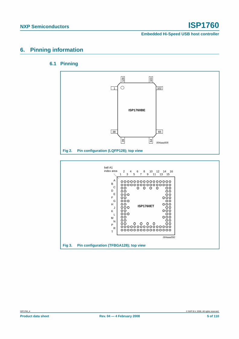
6. Pinning information
6.1 Pinning
Fig 2. Pin configuration (LQFP128); top view
Fig 3. Pin configuration (TFBGA128); top view
ISP1760BE
102
39 64
128
103
65
1
38
004aaa505
004aaa550
ISP1760ET
TR
PN
ML
J
G
K
H
FE
DC
BA
2 4 6 8 10 1213
1415
161 3 5 7 9 11
ball A1index area
ISP1760_4 © NXP B.V. 2008. All rights reserved.
Product data sheet Rev. 04 — 4 February 2008 5 of 110

NXP Semiconductors ISP1760Embedded Hi-Speed USB host controller
6.2 Pin description
Table 2. Pin description
Symbol [1] [2] Pin Type[3] Description
LQFP128 TFBGA128
OC3_N 1 C2 AI port 3 analog (5 V input) and digital overcurrent input; if not used,connect to VCC(I/O) through a 10 kΩ resistor
input, 5 V tolerant
REF5V 2 A2 AI 5 V reference input for analog OC detector; connect a 100 nFdecoupling capacitor
TEST1 3 B2 - connect to ground
GNDA 4 A1 - analog ground
REG1V8 5 B1 P core power output (1.8 V); internal 1.8 V for the digital core; used fordecoupling; connect a 100 nF capacitor; for details on additionalcapacitor placement, see Section 7.8
VCC(5V0) 6 C1 P input to internal regulators (3.0 V to 5.5 V); connect a 100 nFdecoupling capacitor; see Section 7.8
VCC(5V0) 7 D2 P input to internal regulators (3.0 V to 5.5 V); connect a 100 nFdecoupling capacitor; see Section 7.8
GND(OSC) 8 E3 - oscillator ground
REG3V3 9 D1 P regulator output (3.3 V); for decoupling only; connect a 100 nFcapacitor and a 4.7 µF-to-10 µF capacitor; see Section 7.8
VCC(I/O) 10 E2 P digital supply voltage; 1.65 V to 3.6 V; connect a 100 nF decouplingcapacitor; see Section 7.8
XTAL1 11 E1 AI 12 MHz crystal connection input; connect to ground if an externalclock is used; see Table 88
XTAL2 12 F2 AO 12 MHz crystal connection output
CLKIN 13 F1 I 12 MHz oscillator or clock input; when not in use, connect to VCC(I/O)
GNDD 14 G3 - digital ground
GND(RREF1) 15 G2 - RREF1 ground
RREF1 16 G1 AI reference resistor connection; connect a 12 kΩ ± 1 % resistorbetween this pin and the RREF1 ground
GNDA[4] 17 H2 - analog ground
DM1 18 H1 AI/O downstream data minus port 1
GNDA 19 J3 - analog ground
DP1 20 J2 AI/O downstream data plus port 1
PSW1_N 21 J1 OD power switch port 1, active LOW
output pad, push-pull open-drain, 8 mA output drive, 5 V tolerant
GND(RREF2) 22 K2 - RREF2 ground
RREF2 23 K1 AI reference resistor connection; connect a 12 kΩ ± 1 % resistorbetween this pin and the RREF2 ground
GNDA[5] 24 L3 - analog ground
DM2 25 L1 AI/O downstream data minus port 2
GNDA 26 L2 - analog ground
DP2 27 M2 AI/O downstream data plus port 2
ISP1760_4 © NXP B.V. 2008. All rights reserved.
Product data sheet Rev. 04 — 4 February 2008 6 of 110

NXP Semiconductors ISP1760Embedded Hi-Speed USB host controller
PSW2_N 28 M1 OD power switch port 2, active LOW
output pad, push-pull open-drain, 8 mA output drive, 5 V tolerant
GND(RREF3) 29 N2 - RREF3 ground
RREF3 30 N1 AI reference resistor connection; connect a 12 kΩ ± 1 % resistorbetween this pin and the RREF3 ground
GNDA[6] 31 P2 - analog ground
DM3 32 P1 AI/O downstream data minus port 3
GNDA 33 R2 - analog ground
DP3 34 R1 AI/O downstream data plus port 3
PSW3_N 35 T1 OD power switch port 3, active LOW
output pad, push-pull open-drain, 8 mA output drive, 5 V tolerant
GNDD 36 T2 - digital ground
DATA0 37 R3 I/O data bit 0 input and output
bidirectional pad, push-pull input, 3-state output, 4 mA output drive,3.3 V tolerant
DATA1 38 T3 I/O data bit 1 input and output
bidirectional pad, push-pull input, 3-state output, 4 mA output drive,3.3 V tolerant
DATA2 39 R4 I/O data bit 2 input and output
bidirectional pad, push-pull input, 3-state output, 4 mA output drive,3.3 V tolerant
VCC(I/O) 40 T4 P digital supply voltage; 1.65 V to 3.6 V; connect a 100 nF decouplingcapacitor; see Section 7.8
DATA3 41 P5 I/O data bit 3 input and output
bidirectional pad, push-pull input, 3-state output, 4 mA output drive,3.3 V tolerant
DATA4 42 T5 I/O data bit 4 input and output
bidirectional pad, push-pull input, 3-state output, 4 mA output drive,3.3 V tolerant
DATA5 43 R5 I/O data bit 5 input and output
bidirectional pad, push-pull input, 3-state output, 4 mA output drive,3.3 V tolerant
GNDD 44 T6 - digital ground
DATA6 45 R6 I/O data bit 6 input and output
bidirectional pad, push-pull input, 3-state output, 4 mA output drive,3.3 V tolerant
DATA7 46 P7 I/O data bit 7 input and output
bidirectional pad, push-pull input, 3-state output, 4 mA output drive,3.3 V tolerant
DATA8 47 T7 I/O data bit 8 input and output
bidirectional pad, push-pull input, 3-state output, 4 mA output drive,3.3 V tolerant
VCC(I/O) 48 R7 P digital supply voltage; 1.65 V to 3.6 V; connect a 100 nF decouplingcapacitor; see Section 7.8
Table 2. Pin description …continued
Symbol [1] [2] Pin Type[3] Description
LQFP128 TFBGA128
ISP1760_4 © NXP B.V. 2008. All rights reserved.
Product data sheet Rev. 04 — 4 February 2008 7 of 110

NXP Semiconductors ISP1760Embedded Hi-Speed USB host controller
DATA9 49 T8 I/O data bit 9 input and output
bidirectional pad, push-pull input, 3-state output, 4 mA output drive,3.3 V tolerant
REG1V8 50 R8 P core power output (1.8 V); internal 1.8 V for the digital core; used fordecoupling; connect a 100 nF capacitor; for details on additionalcapacitor placement, see Section 7.8
DATA10 51 P9 I/O data bit 10 input and output
bidirectional pad, push-pull input, 3-state output, 4 mA output drive,3.3 V tolerant
DATA11 52 T9 I/O data bit 11 input and output
bidirectional pad, push-pull input, 3-state output, 4 mA output drive,3.3 V tolerant
GNDC 53 R9 - core ground
DATA12 54 T10 I/O data bit 12 input and output
bidirectional pad, push-pull input, 3-state output, 4 mA output drive,3.3 V tolerant
GNDD 55 R10 - digital ground
DATA13 56 P11 I/O data bit 13 input and output
bidirectional pad, push-pull input, 3-state output, 4 mA output drive,3.3 V tolerant
DATA14 57 T11 I/O data bit 14 input and output
bidirectional pad, push-pull input, 3-state output, 4 mA output drive,3.3 V tolerant
DATA15 58 R11 I/O data bit 15 input and output
bidirectional pad, push-pull input, 3-state output, 4 mA output drive,3.3 V tolerant
VCC(I/O) 59 T12 P digital supply voltage; 1.65 V to 3.6 V; connect a 100 nF decouplingcapacitor; see Section 7.8
DATA16 60 R12 I/O data bit 16 input and output
bidirectional pad, push-pull input, 3-state output, 4 mA output drive,3.3 V tolerant
DATA17 61 T13 I/O data bit 17 input and output
bidirectional pad, push-pull input, 3-state output, 4 mA output drive,3.3 V tolerant
DATA18 62 R13 I/O data bit 18 input and output
bidirectional pad, push-pull input, 3-state output, 4 mA output drive,3.3 V tolerant
GNDD 63 R14 - digital ground
DATA19 64 T14 I/O data bit 19 input and output
bidirectional pad, push-pull input, 3-state output, 4 mA output drive,3.3 V tolerant
DATA20 65 T15 I/O data bit 20 input and output
bidirectional pad, push-pull input, 3-state output, 4 mA output drive,3.3 V tolerant
Table 2. Pin description …continued
Symbol [1] [2] Pin Type[3] Description
LQFP128 TFBGA128
ISP1760_4 © NXP B.V. 2008. All rights reserved.
Product data sheet Rev. 04 — 4 February 2008 8 of 110

NXP Semiconductors ISP1760Embedded Hi-Speed USB host controller
DATA21 66 R15 I/O data bit 21 input and output
bidirectional pad, push-pull input, 3-state output, 4 mA output drive,3.3 V tolerant
VCC(I/O) 67 P15 P digital supply voltage; 1.65 V to 3.6 V; connect a 100 nF decouplingcapacitor; see Section 7.8
DATA22 68 T16 I/O data bit 22 input and output
bidirectional pad, push-pull input, 3-state output, 4 mA output drive,3.3 V tolerant
DATA23 69 R16 I/O data bit 23 input and output
bidirectional pad, push-pull input, 3-state output, 4 mA output drive,3.3 V tolerant
DATA24 70 P16 I/O data bit 24 input and output
bidirectional pad, push-pull input, 3-state output, 4 mA output drive,3.3 V tolerant
GNDD 71 N16 - digital ground
DATA25 72 N15 I/O data bit 25 input and output
bidirectional pad, push-pull input, 3-state output, 4 mA output drive,3.3 V tolerant
DATA26 73 M15 I/O data bit 26 input and output
bidirectional pad, push-pull input, 3-state output, 4 mA output drive,3.3 V tolerant
DATA27 74 M16 I/O data bit 27 input and output
bidirectional pad, push-pull input, 3-state output, 4 mA output drive,3.3 V tolerant
VCC(I/O) 75 M14 P digital supply voltage; 1.65 V to 3.6 V; connect a 100 nF decouplingcapacitor; see Section 7.8
DATA28 76 L16 I/O data bit 28 input and output
bidirectional pad, push-pull input, 3-state output, 4 mA output drive,3.3 V tolerant
DATA29 77 L15 I/O data bit 29 input and output
bidirectional pad, push-pull input, 3-state output, 4 mA output drive,3.3 V tolerant
DATA30 78 K16 I/O data bit 30 input and output
bidirectional pad, push-pull input, 3-state output, 4 mA output drive,3.3 V tolerant
GNDD 79 K15 - digital ground
DATA31 80 K14 I/O data bit 31 input and output
bidirectional pad, push-pull input, 3-state output, 4 mA output drive,3.3 V tolerant
TEST2 81 J16 - connect to ground
A1 82 H16 I address pin 1
input, 3.3 V tolerant
VCC(I/O) 83 J15 P digital supply voltage; 1.65 V to 3.6 V; connect a 100 nF decouplingcapacitor; see Section 7.8
Table 2. Pin description …continued
Symbol [1] [2] Pin Type[3] Description
LQFP128 TFBGA128
ISP1760_4 © NXP B.V. 2008. All rights reserved.
Product data sheet Rev. 04 — 4 February 2008 9 of 110

NXP Semiconductors ISP1760Embedded Hi-Speed USB host controller
A2 84 H15 I address pin 2
input, 3.3 V tolerant
REG1V8 85 G16 P core power output (1.8 V); internal 1.8 V for the digital core; used fordecoupling; connect a 100 nF capacitor and a 4.7 µF-to-10 µFcapacitor; see Section 7.8
A3 86 H14 I address pin 3
input, 3.3 V tolerant
A4 87 F16 I address pin 4
input, 3.3 V tolerant
GNDC 88 G15 - core ground
A5 89 F15 I address pin 5
input, 3.3 V tolerant
GNDD 90 E16 - digital ground
A6 91 F14 I address pin 6
input, 3.3 V tolerant
A7 92 E15 I address pin 7
input, 3.3 V tolerant
A8 93 D16 I address pin 8
input, 3.3 V tolerant
VCC(I/O) 94 D15 P digital supply voltage; 1.65 V to 3.6 V; connect a 100 nF decouplingcapacitor; see Section 7.8
A9 95 C16 I address pin 9
input, 3.3 V tolerant
A10 96 C15 I address pin 10
input, 3.3 V tolerant
A11 97 B16 I address pin 11
input, 3.3 V tolerant
A12 98 B15 I address pin 12
input, 3.3 V tolerant
GNDD 99 A16 - digital ground
A13 100 A15 I address pin 13
input, 3.3 V tolerant
A14 101 B14 I address pin 14
input, 3.3 V tolerant
A15 102 A14 I address pin 15
input, 3.3 V tolerant
A16 103 A13 I address pin 16
input, 3.3 V tolerant
VCC(I/O) 104 B13 P digital supply voltage; 1.65 V to 3.6 V; connect a 100 nF decouplingcapacitor; see Section 7.8
A17 105 C12 I address pin 17
input, 3.3 V tolerant
Table 2. Pin description …continued
Symbol [1] [2] Pin Type[3] Description
LQFP128 TFBGA128
ISP1760_4 © NXP B.V. 2008. All rights reserved.
Product data sheet Rev. 04 — 4 February 2008 10 of 110

NXP Semiconductors ISP1760Embedded Hi-Speed USB host controller
CS_N 106 A12 I chip select signal assertion indicates the ISP1760 being accessed;active LOW
input, 3.3 V tolerant
RD_N 107 B12 I read enable; active LOW
input, 3.3 V tolerant
WR_N 108 B11 I write enable; active LOW
input, 3.3 V tolerant
GNDD 109 A11 - digital ground
BAT_ON_N 110 C10 OD to indicate the presence of a minimum 3.3 V on pins 6 and 7(open-drain); connect to VCC(I/O) through a 10 kΩ pull-up resistor
output pad, push-pull open-drain, 8 mA output drive, 5 V tolerant
n.c. 111 A10 - not connected
IRQ 112 B10 O host controller interrupt signal
output pad, 4 mA drive, 3.3 V tolerant
n.c. 113 A9 - not connected
DREQ 114 B9 O DMA controller request for the host controller
output pad, 4 mA drive, 3.3 V tolerant
VCC(I/O) 115 C8 P digital supply voltage; 1.65 V to 3.6 V; connect a 100 nF decouplingcapacitor; see Section 7.8
DACK 116 A8 I host controller DMA request acknowledgment; when not in use,connect to VCC(I/O) through a 10 kΩ pull-up resistor
input, 3.3 V tolerant
TEST3 117 B8 - connect to VCC(I/O) through a 10 kΩ pull-up resistor
REG1V8 118 B7 P core power output (1.8 V); internal 1.8 V for the digital core; used fordecoupling; connect a 100 nF capacitor; for details on additionalcapacitor placement, see Section 7.8
SUSPEND/WAKEUP_N
119 A7 I/OD host controller suspend and wake-up; 3-state suspend output (activeLOW) and wake-up input circuits are connected together
• HIGH = output is 3-state; ISP1760 is in suspend mode
• LOW = output is LOW; ISP1760 is not in suspend mode
connect to VCC(I/O) through an external 10 kΩ pull-up resistor
output pad, open-drain, 4 mA output drive, 3.3 V tolerant
TEST4 120 C6 - pull up to VCC(I/O)
GNDC 121 A6 - core ground
RESET_N 122 B6 I external power-up reset; active LOW; when reset is asserted, it isexpected that bus signals are idle, that is, not toggling
input, 3.3 V tolerant
Remark: During reset, ensure that all the input pins to the ISP1760are not toggling and are in their inactive states.
GNDA 123 B5 - analog ground
TEST5 124 A5 - connect a 220 nF capacitor between this pin and pin 125
TEST6 125 B4 - connect a 220 nF capacitor between this pin and pin 124
Table 2. Pin description …continued
Symbol [1] [2] Pin Type[3] Description
LQFP128 TFBGA128
ISP1760_4 © NXP B.V. 2008. All rights reserved.
Product data sheet Rev. 04 — 4 February 2008 11 of 110

NXP Semiconductors ISP1760Embedded Hi-Speed USB host controller
[1] Symbol names ending with underscore N, for example, NAME_N, represent active LOW signals.
[2] All ground pins should normally be connected to a common ground plane.
[3] I = input only; O = output only; I/O = digital input/output; OD = open-drain output; AI/O = analog input/output; AI = analog input; P =power.
[4] For port 1.
[5] For port 2.
[6] For port 3.
TEST7 126 A4 - connect to 3.3 V
OC1_N 127 B3 AI port 1 analog (5 V input) and digital overcurrent input; if not used,connect to VCC(I/O) through a 10 kΩ resistor
input, 5 V tolerant
OC2_N 128 A3 AI port 2 analog (5 V input) and digital overcurrent input; if not used,connect to VCC(I/O) through a 10 kΩ resistor
input, 5 V tolerant
Table 2. Pin description …continued
Symbol [1] [2] Pin Type[3] Description
LQFP128 TFBGA128
ISP1760_4 © NXP B.V. 2008. All rights reserved.
Product data sheet Rev. 04 — 4 February 2008 12 of 110

NXP Semiconductors ISP1760Embedded Hi-Speed USB host controller
7. Functional description
7.1 ISP1760 internal architecture: advanced NXP slave host controllerand hubThe EHCI block and the Hi-Speed USB hub block are the main components of theadvanced NXP slave host controller.
The EHCI is the latest generation design, with improved data bandwidth. The EHCI in theISP1760 is adapted from Ref. 2 “Enhanced Host Controller Interface Specification forUniversal Serial Bus Rev. 1.0”.
The internal Hi-Speed USB hub block replaces the companion host controller block usedin the original PCI Hi-Speed USB host controllers to handle full-speed and low-speedmodes. The hardware architecture in the ISP1760 is simplified to help reduce cost anddevelopment time, by eliminating the additional work involved in implementing the OHCIsoftware required to support full-speed and low-speed modes.
Figure 4 shows the internal architecture of the ISP1760. The ISP1760 implements theEHCI that has an internal port, the root hub port (not available externally), on which theinternal hub is connected. The three external ports are always routed to the internal hub.The internal hub is a Hi-Speed USB (USB 2.0) hub, including the TT.
Remark: The root hub must be enabled and the internal hub must be enumerated.Enumerate the internal hub as if it is externally connected. For details, refer to Ref. 5“Interfacing the ISP176x to the Intel PXA25x processor (AN10037)”.
At the host controller reset and initialization, the internal root hub port will be polled until anew connection is detected, showing the connection of the internal hub.
The internal Hi-Speed USB hub is enumerated using a sequence similar to a standardHi-Speed USB hub enumeration sequence, and the polling on the root hub is stoppedbecause the internal Hi-Speed USB hub will never be disconnected. When enumerated,the internal hub will report the three externally available ports.
ISP1760_4 © NXP B.V. 2008. All rights reserved.
Product data sheet Rev. 04 — 4 February 2008 13 of 110

NXP Semiconductors ISP1760Embedded Hi-Speed USB host controller
7.1.1 Internal clock scheme and port selection
The ISP1760 has three ports. Figure 5 shows the internal clock scheme of the ISP1760.
Figure 5 shows that the host clock is derived from port 2. Port 2 does not need to beenabled by software, if only port 1 or port 3 is used. No port needs to be disabled byexternal pull-up resistors, if not used. The DP and DM of the unused ports need not beexternally pulled HIGH because there are internal pull-down resistors on each port thatare enabled by default.
Table 3 lists the various port connection scenarios.
Fig 4. Internal hub
004aaa513
EHCI
ROOT HUB
INTERNAL HUB (TT)
EXTERNAL PORTS
ENUMERATION AND POLLING USING
ACTUAL PTDs
PORTSC1
PORT3PORT1 PORT2
Fig 5. ISP1760 clock scheme
004aaa535
HOSTCORE
DIGITAL CORE
PORT 2ATX
PORT 1ATX
PORT 3ATX
XOSC
host clock:48 MHz,30 MHz,60 MHz
PLL 12 MHz IN
ISP1760_4 © NXP B.V. 2008. All rights reserved.
Product data sheet Rev. 04 — 4 February 2008 14 of 110

NXP Semiconductors ISP1760Embedded Hi-Speed USB host controller
7.2 Host controller buffer memory block
7.2.1 General considerations
The internal addressable host controller buffer memory is 63 kB. The 63 kB effectivememory size is the result of subtracting the size of the registers (1 kB) from the totaladdressable memory space defined in the ISP1760 (64 kB). This is the optimized value toachieve the highest performance with minimal cost.
The ISP1760 is a slave host controller. This means that it does not need access to thelocal bus of the system to transfer data from the system memory to the ISP1760 internalmemory, unlike the case of the original PCI Hi-Speed USB host controllers. Therefore,correct data must be transferred to both the PTD area and the payload area by PIO (usingCPU access) or programmed DMA.
The ‘slave-host’ architecture ensures better compatibility with most of the processorspresent in the market today because not all processors allow a ‘bus-master’ on the localbus. It also allows better load balancing of the processor’s local bus because only theinternal bus arbiter of the processor controls the transfer of data dedicated to USB. Thisprevents the local bus from being busy when other more important transfers may be in thequeue; and therefore achieving a ‘linear’ system data flow that has less impact on otherprocesses running at the same time.
The considerations mentioned are also the main reason for implementing the pre-fetchingtechnique, instead of using a READY signal. The resulting architecture avoids ‘freezing’ ofthe local bus, by asserting READY, enhancing the ISP1760 memory access time, andavoiding introduction of programmed additional wait states. For details, see Section 7.3and Section 8.3.8.
The total amount of memory allocated to the payload determines the maximum transfersize specified by a PTD, a larger internal memory size results in less CPU interruption fortransfer programming. This means less time spent in context switching, resulting in betterCPU usage.
Table 3. Port connection scenarios
Port configuration Port 1 Port 2 Port 3
One port (port 1) DP and DM are routed to USBconnector
DP and DM are not connected(left open)
DP and DM are not connected(left open)
One port (port 2) DP and DM are not connected(left open)
DP and DM are routed to USBconnector
DP and DM are not connected(left open)
One port (port 3) DP and DM are not connected(left open)
DP and DM are not connected(left open)
DP and DM are routed to USBconnector
Two ports (ports 1and 2)
DP and DM are routed to USBconnector
DP and DM are routed to USBconnector
DP and DM are not connected(left open)
Two ports (ports 2and 3)
DP and DM are not connected(left open)
DP and DM are routed to USBconnector
DP and DM are routed to USBconnector
Two ports (ports 1and 3)
DP and DM are routed to USBconnector
DP and DM are not connected(left open)
DP and DM are routed to USBconnector
Three ports (ports 1,2 and 3)
DP and DM are routed to USBconnector
DP and DM are routed to USBconnector
DP and DM are routed to USBconnector
ISP1760_4 © NXP B.V. 2008. All rights reserved.
Product data sheet Rev. 04 — 4 February 2008 15 of 110

NXP Semiconductors ISP1760Embedded Hi-Speed USB host controller
A larger buffer also implies a larger amount of data can be transferred. The transfer,however, can be done over a longer period of time, to maintain the overall systemperformance. Each transfer of the USB data on the USB bus can span for up to a fewmilliseconds before requiring further CPU intervention for data movement.
The internal architecture of the ISP1760 allows a flexible definition of the memory bufferfor optimization of the data transfer on the CPU extension bus and the USB. It is possibleto implement various data transfer schemes, depending on the number and type of USBdevices present. For example: push-pull; data can be written to half of the memory whiledata in the other half is being accessed by the host controller and sent on the USB bus.This is useful especially when a high-bandwidth ‘continuous or periodic’ data flow isrequired.
Through an analysis of the hardware and software environment regarding the usual dataflow and performance requirements of most embedded systems, NXP has determined theoptimal size for the internal buffer as approximately 64 kB.
7.2.2 Structure of the ISP1760 host controller memory
The 63 kB internal memory consists of the PTD area and the payload area.
PTD memory zone is divided into three dedicated areas for each main type of USBtransfer: Isochronous (ISO), Interrupt (INT) and Asynchronous Transfer List (ATL). Asshown in Table 4, the PTD areas for ISO, INT and ATL are grouped at the beginning of thememory, occupying the address range 0400h to 0FFFh, following the register addressspace. The payload or data area occupies the next memory address range 1000h toFFFFh, meaning that 60 kB of memory are allocated for the payload data.
A maximum of 32 PTD areas and their allocated payload areas can be defined for eachtype of transfer. The structure of a PTD is similar for every transfer type and consists ofeight Double Words (DWs) that must be correctly programmed for a correct USB datatransfer. The reserved bits of a PTD must be set to logic 0. A detailed description of thePTD structure can be found in Section 9.
The transfer size specified by the PTD determines the contiguous USB data transfer thatcan be performed without any CPU intervention. The respective payload memory areamust be equal to the transfer size defined. The maximum transfer size is flexible and canbe optimized, depending on the number and nature of USB devices or PTDs defined andtheir respective MaxPacketSize.
The CPU will program the DMA to transfer the necessary data in the payload memory.The next CPU intervention will be required only when the current transfer is completedand DMA programming is necessary to transfer the next data payload. This is normallysignaled by the IRQ that is generated by the ISP1760 on completing the current PTD,meaning all the data in the payload area was sent on the USB bus. The external IRQsignal is asserted according to the settings in the IRQ Mask OR or IRQ Mask ANDregisters, see Section 8.4.
The RAM is structured in blocks of PTDs and payloads so that while the USB is executingon an active transfer-based PTD, the processor can simultaneously fill up another blockarea in the RAM. A PTD and its payload can then be updated on-the-fly without stoppingor delaying any other USB transaction or corrupting the RAM data.
Some of the design features are:
ISP1760_4 © NXP B.V. 2008. All rights reserved.
Product data sheet Rev. 04 — 4 February 2008 16 of 110

NXP Semiconductors ISP1760Embedded Hi-Speed USB host controller
• The address range of the internal RAM buffer is from 0400h to FFFFh.
• The internal memory contains isochronous, interrupt and asynchronous PTDs, andrespective defined payloads.
• All accesses to the internal memory are double word aligned.
• Internal memory address range calculation:
Memory address = (CPU address − 0400h) (shift right >> 3). Base address is 0400h.
Table 4. Memory address
Memory map CPU address Memory address
ISO 0400h to 07FFh 0000h to 007Fh
INT 0800h to 0BFFh 0080h to 00FFh
ATL 0C00h to 0FFFh 0100h to 017Fh
Payload 1000h to FFFFh 0180h to 1FFFh
Fig 6. Memory segmentation and access block diagram
004aaa436
PTD1
PTD2
PTD32
PTD1
PTD2
. .. .
PTD32
PAYLOAD
PAYLOAD
63 kB
USB BUS USB HIGH-SPEEDHOST AND
TRANSACTIONTRANSLATOR(FULL-SPEED
AND LOW-SPEED)
INTERRUPT
ASYNC
PAYLOAD
PTD32
. .
PTD1
PTD2ISOCHRONOUS
MEMORY MAPPEDINPUT/OUTPUT,
MEMORYMANAGEMENT
UNIT,SLAVE DMA
CONTROLLERAND
INTERRUPT CONTROL
REGISTERS
ARBITER
control signals
240 MB/saddress data (64 bits)
D[15:0]/D[31:0]
A[17:1]
. . .
. . .
. .
CS_N
RD_N
WR_N
DREQ
DACK
IRQ
MICRO-PROCESSOR
ISP1760_4 © NXP B.V. 2008. All rights reserved.
Product data sheet Rev. 04 — 4 February 2008 17 of 110

NXP Semiconductors ISP1760Embedded Hi-Speed USB host controller
Both the CPU interface logic and the USB host controller require access to the internalISP1760 RAM at the same time. The internal arbiter controls these accesses to theinternal memory, organized internally on a 64-bit data bus width, allowing a maximumbandwidth of 240 MB/s. This bandwidth avoids any bottleneck on accesses both from theCPU interface and the internal USB host controller.
7.3 Accessing the ISP1760 host controller memory: PIO and DMAThe CPU interface of the ISP1760 can be configured for a 16-bit or 32-bit data bus width.
When the ISP1760 is configured for a 16-bit data bus width, the upper unused 16 datalines must be pulled up to VCC(I/O). This can be achieved by connecting DATA[31:16] linestogether to a single 10 kΩ pull-up resistor. The 16-bit or 32-bit data bus widthconfiguration is done by programming bit 8 of the HW Mode Control register. This willdetermine the register and memory access types in both PIO and DMA modes. Allaccesses must be word-aligned for 16-bit mode and double word aligned for 32-bit mode,where one word = 16 bits. When accessing the host controller registers in 16-bit mode,the register access must always be completed using two subsequent accesses. In thecase of a DMA transfer, the 16-bit or 32-bit data bus width configuration will determine thenumber of bursts that will complete a certain transfer length.
In PIO mode, CS_N, WR_N and RD_N are used to access registers and memory. In DMAmode, the data validation is performed by DACK, instead of CS_N, together with theWR_N and RD_N signals. The DREQ signal will always be asserted as soon as theISP1760 DMA is enabled.
7.3.1 PIO mode access, memory read cycle
The following method has been implemented to reduce the read access timing in the caseof a memory read:
• The Memory register contains the starting address and the bank selection to readfrom the memory. Before every new read cycle of the same or different banks, anappropriate value is written to this register.
• Once a value is written to this register, the address is stored in the FIFO of that bankand is then used to pre-fetch data for the memory read of that bank.
For every subsequent read operation executed at a contiguous address, the addresspointer corresponding to that bank is automatically incremented to pre-fetch the nextdata to be sent to the CPU.
Memory read accesses for multiple banks can be interleaved. The FIFO blockhandles the multiplexing of appropriate data to the CPU.
• The address written to the Memory register is incremented and used to successivelypre-fetch data from the memory irrespective of the value on the address bus for eachbank, until a new value for a bank is written to the Memory register. This is valid onlywhen the address refers to the memory space (400h to FFFFh).
For example, consider the following sequence of operations:
– Write the starting (read) address 4000h and bank1 = 01 to the Memory register.When RD_N is asserted for three cycles with A[17:16] = 01, the returned datacorresponds to addresses 4000h, 4004h and 4008h.
ISP1760_4 © NXP B.V. 2008. All rights reserved.
Product data sheet Rev. 04 — 4 February 2008 18 of 110

NXP Semiconductors ISP1760Embedded Hi-Speed USB host controller
Remark: Once 4000h is written to the Memory register for bank1, the bank selectvalue determines the successive incremental addresses used to fetch data. Thatis, the fetching of data is independent of the address on A[15:0] lines.
– Write the starting (read) address 4100h and bank2 = 10 to the Memory register.When RD_N is asserted for four cycles with A[17:16] = 10, the returned datacorresponds to addresses 4100h, 4104h, 4108h and 410Ch.
Consequently, the RD_N assertion with A[17:16] = 01 will return data from 400Chbecause the bank1 read stopped there in the previous cycle. Also, RD_Nassertions with A[17:16] = 10 will now return data from 4110h because the bank2read stopped there in the previous cycle.
7.3.2 PIO mode access, memory write cycle
The PIO memory write access is similar to a normal memory access. It is not necessaryto set the pre-fetching address before a write cycle to the memory.
The ISP1760 internal write address will not be automatically incremented duringconsecutive write accesses, unlike in a series of ISP1760 memory read cycles. Thememory write address must be incremented before every access.
7.3.3 PIO mode access, register read cycle
The PIO register read access is similar to a general register access. It is not necessary toset a pre-fetching address before a register read.
The ISP1760 register read address will not be automatically incremented duringconsecutive read accesses, unlike in a series of ISP1760 memory read cycles. TheISP1760 register read address must be correctly specified before every access.
7.3.4 PIO mode access, register write cycle
The PIO register write access is similar to a general register access. It is not necessary toset a pre-fetching address before a register write.
The ISP1760 register write address will not be automatically incremented duringconsecutive write accesses, unlike in a series of ISP1760 memory read cycles. TheISP1760 register write address must be correctly specified before every access.
7.3.5 DMA mode, read and write operations
The internal ISP1760 host controller DMA is a slave DMA. The host system processor orDMA must ensure the data transfer to or from the ISP1760 memory.
The ISP1760 DMA supports a DMA burst length of 1, 4, 8 and 16 cycles for both the 16-bitand 32-bit data bus width. DREQ will be asserted at the beginning of the first burst of aDMA transfer and will be de-asserted on the last cycle, RD_N or WR_N active pulse, ofthat burst. It will be reasserted shortly after the DACK de-assertion, as long as the DMAtransfer counter was not reached. DREQ will be de-asserted on the last cycle when theDMA transfer counter is reached and will not be reasserted until the DMA reprogrammingis performed. Both the DREQ and DACK signals are programmable as active LOW oractive HIGH, according to the system requirements.
ISP1760_4 © NXP B.V. 2008. All rights reserved.
Product data sheet Rev. 04 — 4 February 2008 19 of 110

NXP Semiconductors ISP1760Embedded Hi-Speed USB host controller
The DMA start address must be initialized in the respective register, and the subsequenttransfers will automatically increment the internal ISP1760 memory address. A register ormemory access or access to other system memory can occur in between DMA bursts,whenever the bus is released because DACK is de-asserted, without affecting the DMAtransfer counter or the current address.
Any memory area can be accessed by the system’s DMA at any starting address becausethere are no predefined memory blocks. The DMA transfer must start on a word or doubleword address, depending on whether the data bus width is set to 16 bit or 32 bit. DMA isthe most efficient method to initialize the payload area, to reduce the CPU usage andoverall system loading.
The ISP1760 does not implement EOT to signal the end of a DMA transfer. Ifprogrammed, an interrupt may be generated by the ISP1760 at the end of the DMAtransfer.
The slave DMA of the ISP1760 will issue a DREQ to the DMA controller of the system toindicate that it is programmed for transfer and data is ready. The system DMA controllermay also start a transfer without the need of the DREQ, if the ISP1760 memory isavailable for the data transfer and the ISP1760 DMA programming is completed.
It is also possible that the system’s DMA will perform a memory-to-memory type oftransfer between the system memory and the ISP1760 memory. The ISP1760 will beaccessed in PIO mode. Consequently, memory read operations must be preceded byinitializing the Memory register (address 033Ch), as described in Section 7.3.1. No IRQwill be generated by the ISP1760 on completing the DMA transfer but an internalprocessor interrupt may be generated to signal that the DMA transfer is completed. This ismainly useful in implementing the double-buffering scheme for data transfer to optimizethe USB bandwidth.
The ISP1760 DMA programming involves:
• Set the active levels of signals DREQ and DACK in the HW Mode Control register.
• The DMA Start Address register contains the first memory address at which the datatransfer will start. It must be word-aligned in 16-bit data bus mode and double wordaligned in 32-bit data bus mode.
• The programming of the DMA Configuration register specifies:
– The type of transfer that will be performed: read or write.
– The burst size, expressed in bytes, is specified, regardless of the data bus width.For the same burst size, a double number of cycles will be generated in 16-bitmode data bus width as compared to 32-bit mode.
– The transfer length, expressed in number of bytes, defines the number of bursts.The DREQ will be de-asserted and asserted to generate the next burst, as long asthere are bytes to be transferred. At the end of a transfer, the DREQ will bede-asserted and an IRQ can be generated if DMAEOTINT (bit 3 in the Interruptregister) is set. The maximum DMA transfer size is equal to the maximum memorysize. The transfer size can be an odd or even number of bytes, as required. If thetransfer size is an odd number of bytes, the number of bytes transferred by thesystem’s DMA is equal to the next multiple of two for the 16-bit data bus width orfour for the 32-bit data bus width. For a write operation, however, only the specifiedodd number of bytes in the ISP1760 memory will be affected.
ISP1760_4 © NXP B.V. 2008. All rights reserved.
Product data sheet Rev. 04 — 4 February 2008 20 of 110

NXP Semiconductors ISP1760Embedded Hi-Speed USB host controller
– Enable ENABLE_DMA (bit 1) of the DMA Configuration register to determine theassertion of DREQ immediately after setting the bit.
After programming the preceding parameters, the system’s DMA may be enabled, waitingfor the DREQ to start the transfer or immediate transfer may be started.
The programming of the system’s DMA must match the programming of the ISP1760DMA parameters. Only one DMA transfer may take place at a time. PIO mode datatransfer may occur simultaneously with a DMA data transfer, in the same or a differentmemory area.
7.4 InterruptsThe ISP1760 will assert an IRQ according to the source or event in the Interrupt register.The main steps to enable the IRQ assertion are:
1. Set GLOBAL_INTR_EN (bit 0) in the HW Mode Control register.
2. Define the IRQ active as level or edge in INTR_LEVEL (bit 1) of the HW Mode Controlregister.
3. Define the IRQ polarity as active LOW or active HIGH in INTR_POL (bit 2) of the HWMode Control register. These settings must match the IRQ settings of the hostprocessor.
By default, interrupt is level-triggered and active LOW.
4. Program the individual interrupt enable bits in the Interrupt Enable register. Thesoftware will need to clear the interrupt status bits in the Interrupt register beforeenabling individual interrupt enable bits.
Additional IRQ characteristics can be adjusted in the Edge Interrupt Count register, asnecessary, applicable only when IRQ is set to be edge-active; a pulse of a defined width isgenerated every time IRQ is active.
Bits 15 to 0 of the Edge Interrupt Count register define the IRQ pulse width. The maximumpulse width that can be programmed is FFFFh, corresponding to a 1 ms pulse width. Thissetting is necessary for certain processors that may require a different minimum IRQpulse width from the default value. The default IRQ pulse width set at power-on isapproximately 500 ns.
Bits 31 to 24 of the Edge Interrupt Count register define the minimum interval between twointerrupts to avoid frequent interrupts to the CPU. The default value of 00h attributed tothese bits determines the normal IRQ generation, without any delay. When a delay isprogrammed and the IRQ becomes active after the respective delay, several IRQ eventsmay have already occurred.
All the interrupt events are represented by the respective bits allocated in the Interruptregister. There is no mechanism to show the order or the moment of occurrence of aninterrupt.
The asserted bits in the Interrupt register can be cleared by writing back the same value tothe Interrupt register. This means that writing logic 1 to each of the set bits will reset thecorresponding bits to the initial inactive state.
The IRQ generation rules that apply according to the preceding settings are:
ISP1760_4 © NXP B.V. 2008. All rights reserved.
Product data sheet Rev. 04 — 4 February 2008 21 of 110

NXP Semiconductors ISP1760Embedded Hi-Speed USB host controller
• If an event of interrupt occurs but the respective bit in the Interrupt Enable register isnot set, then the respective Interrupt register bit is set but the interrupt signal is notasserted.
An interrupt will be generated when interrupt is enabled and the respective bit in theInterrupt Enable register is set.
• For a level trigger, an interrupt signal remains asserted until the processor clears theInterrupt register by writing logic 1 to clear the Interrupt register bits that are set.
• If an interrupt is made edge-sensitive and is asserted, writing to clear the Interruptregister will not have any effect because the interrupt will be asserted for a prescribedamount of clock cycles.
• The clock stopping mechanism does not affect the generation of an interrupt. This isuseful during the suspend and resume cycles, when an interrupt is generated tosignal a wake-up event.
The IRQ generation can also be conditioned by programming the IRQ Mask OR and IRQMask AND registers.
With the help of the IRQ Mask AND and IRQ Mask OR registers for each type of transfer(ISO, INT and bulk), software can determine which PTDs get priority and an interrupt willbe generated when the AND or OR conditions are met. The PTDs that are set will waituntil the respective bits of the remaining PTDs are set and then all PTDs generate aninterrupt request to the CPU together.
The registers definition shows that the AND or OR conditions are applicable to the samecategory of PTDs: ISO, INT, ATL.
When an IRQ is generated, the PTD Done Map registers and the respective V bits willshow which PTDs were completed.
The rules that apply to the IRQ Mask AND or IRQ Mask OR settings are:
• The OR mask has a higher priority over the AND mask. An IRQ is generated if bit n ofthe done map is set and the corresponding bit n of the OR Mask register is set.
• If the OR mask for any done bit is not set, then the AND mask comes into picture. AnIRQ is generated if all the corresponding done bits of the AND Mask register are set.For example: If bits 2, 4 and 10 are set in the AND Mask register, an IRQ is generatedonly if bits 2, 4, 10 of the done map are set.
• If using the IRQ interval setting for the bulk PTD, an interrupt will only occur at theregular time interval as programmed in the ATL Done Timeout register. Even if aninterrupt event occurs before the time-out of the register, no IRQ will be generateduntil the time is up.
For an example on using the IRQ Mask AND or IRQ Mask OR registers without the ATLDone Timeout register, see Table 5.
The AND function: Activate the IRQ only if PTDs 1, 2 and 4 are done.
The OR function: If any of the PTDs 7, 8 or 9 are done, an IRQ for each of the PTD will beraised.
ISP1760_4 © NXP B.V. 2008. All rights reserved.
Product data sheet Rev. 04 — 4 February 2008 22 of 110

NXP Semiconductors ISP1760Embedded Hi-Speed USB host controller
7.5 Phase-Locked Loop (PLL) clock multiplierThe internal PLL requires a 12 MHz input, which can be a 12 MHz crystal or a 12 MHzclock already existing in the system with a precision better than 50 ppm. This allows theuse of a low-cost 12 MHz crystal that also minimizes ElectroMagnetic Interference (EMI).When an external crystal is used, make sure the CLKIN pin is connected to VCC(I/O).
The PLL block generates all the main internal clocks required for normal functionality ofvarious blocks: 30 MHz, 48 MHz and 60 MHz.
No external components are required for the PLL operation.
7.6 Power managementThe ISP1760 implements a flexible power management scheme, allowing various powersaving stages.
The usual powering scheme implies programming EHCI registers and the internalHi-Speed USB (USB 2.0) hub in the same way it is done in the case of a PCI Hi-SpeedUSB host controller with a Hi-Speed USB hub attached.
When the ISP1760 is in suspend mode, the main internal clocks will be stopped to ensureminimum power consumption. An internal LazyClock of 100 kHz ± 40 % will continuerunning. This allows initiating a resume on one of these events:
• External USB device connect or disconnect
• CS_N signal asserted when the ISP1760 is accessed
• Driving the SUSPEND/WAKEUP_N pin to a LOW level
The SUSPEND/WAKEUP_N pin is a bidirectional pin. This pin must be connected to oneof the GPIO pins of a processor.
The awake state can be verified by reading the LOW level of this pin. If the level is HIGH,it means that the ISP1760 is in the suspend state.
The SUSPEND/WAKEUP_N pin requires a pull-up because in the ISP1760 suspendedstate the pin becomes 3-state and can be pulled down, driving it externally by switchingthe processor’s GPIO line to output mode to generate the ISP1760 wake-up.
Table 5. Using the IRQ Mask AND or IRQ Mask OR registers
PTD AND register OR register Time PTD done IRQ
1 1 0 1 ms 1 -
2 1 0 - 1 -
3 0 0 - - -
4 1 0 3 ms 1 active because of AND
5 0 0 - - -
6 0 0 - - -
7 0 1 5 ms 1 active because of OR
8 0 1 6 ms 1 active because of OR
9 0 1 7 ms 1 active because of OR
ISP1760_4 © NXP B.V. 2008. All rights reserved.
Product data sheet Rev. 04 — 4 February 2008 23 of 110

NXP Semiconductors ISP1760Embedded Hi-Speed USB host controller
The SUSPEND/WAKEUP_N pin is a 3-state output. It is also an input to the internalwake-up logic.
When in suspend mode, the ISP1760 internal wake-up circuitry will sense the status ofthe SUSPEND/WAKEUP_N pin:
• If it remains pulled-up, no wake-up is generated because a HIGH is sensed by theinternal wake-up circuit.
• If the pin is externally pulled LOW, for example, by the GPIO line or just as a test byjumper, the input to the wake-up circuitry becomes LOW and the wake-up is internallyinitiated.
The resume state has a clock-off count timer defined by bits 31 to 16 of the Power DownControl register. The default value of this timer is 10 ms, meaning that the resume statewill be maintained for 10 ms. If during this time, the RUN/STOP bit in the USBCMDregister is set to logic 1, the host controller will go into a permanent resume; the normalfunctional state. If the RUN/STOP bit is not set during the time determined by the clock-offcount, the ISP1760 will switch back to suspend mode after the specified time. Themaximum delay that can be programmed in the clock-off count field is approximately500 ms.
Additionally, the Power Down Control register allows the ISP1760 internal blocks to bedisabled for lower power consumption as defined in Table 51.
The lowest suspend current, ICC(susp), that can be achieved is approximately 150 µA atroom temperature. The suspend current will increase with the increase in temperature,with approximately 300 µA at 40 °C and up to a typical 1 mA at 85 °C. The system is not insuspend mode when its temperature increases above 40 °C. Therefore, even a 1 mAcurrent consumption by the ISP1760 in suspend mode can be considered negligible. Innormal environmental conditions, when the system is in suspend mode, the maximumISP1760 temperature will be approximately 40 °C determined by the ambient temperatureso the ISP1760 maximum suspend current will be below 300 µA. An alternative solution toachieve a very low suspend current is to completely switch off the VCC(5V0) power input byusing an external PMOS transistor, controlled by one of the GPIO pins of the processor.This is possible because the ISP1760 can be used in hybrid mode, which allows only theVCC(I/O) powered on to avoid loading of the system bus.
When the ISP1760 power is always on, the time from wake-up to suspend will beapproximately 100 ms.
It is necessary to wait for the CLKREADY interrupt assertion before programming theISP1760 because internal clocks are stopped during deep-sleep suspend and restartedafter the first wake-up event. The occurrence of the CLKREADY interrupt means thatinternal clocks are running and the normal functionality is achieved.
It is estimated that the CLKREADY interrupt will be generated less than 100 µs after thewake-up event, if the power to the ISP1760 was on during suspend.
If the ISP1760 is used in hybrid mode and VCC(5V0) is off during suspend, a 2 ms resetpulse is required when the power is switched back on, before the resume programmingsequence starts. This will ensure that internal clocks are running and all logics reach astable initial state.
ISP1760_4 © NXP B.V. 2008. All rights reserved.
Product data sheet Rev. 04 — 4 February 2008 24 of 110
NXP Semiconductors ISP1760Embedded Hi-Speed USB host controller
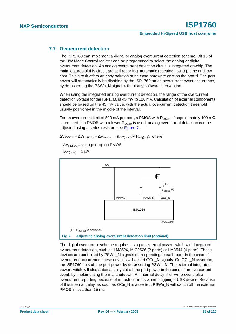
7.7 Overcurrent detectionThe ISP1760 can implement a digital or analog overcurrent detection scheme. Bit 15 ofthe HW Mode Control register can be programmed to select the analog or digitalovercurrent detection. An analog overcurrent detection circuit is integrated on-chip. Themain features of this circuit are self reporting, automatic resetting, low-trip time and lowcost. This circuit offers an easy solution at no extra hardware cost on the board. The portpower will automatically be disabled by the ISP1760 on an overcurrent event occurrence,by de-asserting the PSWn_N signal without any software intervention.
When using the integrated analog overcurrent detection, the range of the overcurrentdetection voltage for the ISP1760 is 45 mV to 100 mV. Calculation of external componentsshould be based on the 45 mV value, with the actual overcurrent detection thresholdusually positioned in the middle of the interval.
For an overcurrent limit of 500 mA per port, a PMOS with RDSon of approximately 100 mΩis required. If a PMOS with a lower RDSon is used, analog overcurrent detection can beadjusted using a series resistor; see Figure 7.
∆VPMOS = ∆Vtrip(OC) = ∆Vtrip(int) − (IOC(nom) × Radj(oc)), where:
∆VPMOS = voltage drop on PMOS
IOC(nom) = 1 µA
The digital overcurrent scheme requires using an external power switch with integratedovercurrent detection, such as LM3526, MIC2526 (2 ports) or LM3544 (4 ports). Thesedevices are controlled by PSWn_N signals corresponding to each port. In the case ofovercurrent occurrence, these devices will assert OCn_N signals. On OCn_N assertion,the ISP1760 cuts off the port power by de-asserting PSWn_N. The external integratedpower switch will also automatically cut off the port power in the case of an overcurrentevent, by implementing thermal shutdown. An internal delay filter will prevent falseovercurrent reporting because of in-rush currents when plugging a USB device. Becauseof this internal delay, as soon as OCn_N is asserted, PSWn_N will switch off the externalPMOS in less than 15 ms.
(1) Radj(oc) is optional.
Fig 7. Adjusting analog overcurrent detection limit (optional)
004aaa662
REF5V
Radj(oc)(1)
5 V
ISP1760
OCn_NPSWn_N
IOC
ISP1760_4 © NXP B.V. 2008. All rights reserved.
Product data sheet Rev. 04 — 4 February 2008 25 of 110

NXP Semiconductors ISP1760Embedded Hi-Speed USB host controller
7.8 Power supplyFigure 8 shows the ISP1760 power supply connection.
Figure 9 shows the most commonly used power supply connection.
7.8.1 Hybrid mode
Table 6 shows the description of hybrid mode.
The figure shows the LQFP pinout. For the TFBGA ballout, see Table 2.
A 4.7 µF-to-10 µF electrolytic or tantalum capacitor is required on any one of the pins 5, 50 or 118.All the electrolytic or tantalum capacitors must be of LOW ESR type (0.2 Ω to 2 Ω).
Fig 8. ISP1760 power supply connection
The figure shows the LQFP pinout. For the TFBGA ballout, see Table 2.
A 4.7 µF-to-10 µF electrolytic or tantalum capacitor is required on any one of the pins 5, 50 or 118.All the electrolytic or tantalum capacitors must be of LOW ESR type (0.2 Ω to 2 Ω).
Fig 9. Most commonly used power supply connection
004aaa533
6, 7
VCC(I/O)
ISP1760BE
3.3 V to 5 VVCC(5V0)
10, 40, 48,59, 67, 75,
83, 94,104, 115
REG1V885
10 µF 100 nF
100 nF
100 nF
1.65 V to 3.6 V
REG1V85, 50, 118
100 nF
REG3V39
10 µF 100 nF
004aaa534
VCC(5V0), VCC(I/O)
ISP1760BE
6, 7, 10,40, 48, 59,67, 75, 83,
94, 104, 115
REG1V885
10 µF 100 nF
100 nF
3.3 V
REG1V85, 50, 118
100 nF
REG3V39
10 µF 100 nF
ISP1760_4 © NXP B.V. 2008. All rights reserved.
Product data sheet Rev. 04 — 4 February 2008 26 of 110

NXP Semiconductors ISP1760Embedded Hi-Speed USB host controller
In hybrid mode (see Figure 10), VCC(5V0) can be switched off using an external PMOStransistor, controlled using one of the GPIO pins of the processor. This helps to reduce thesuspend current, ICC(I/O), below 100 µA. If the ISP1760 is used in hybrid mode andVCC(5V0) is off during suspend, a 2 ms reset pulse is required when power is switchedback on, before the resume programming sequence starts.
Table 7 shows the status of output pins during hybrid mode.
7.9 Power-On Reset (POR)When VCC(I/O) is directly connected to the RESET_N pin, the internal POR pulse width,tPORP, will typically be 800 ns. The pulse is started when VCC(5V0) rises above VTRIP of1.2 V.
Table 6. Hybrid mode
Voltage Status
VCC(5V0) off
VCC(I/O) on
The figure shows the LQFP pinout. For the TFBGA ballout, see Table 2.
A 4.7 µF-to-10 µF electrolytic or tantalum capacitor is required on any one of the pins 5, 50 or 118.All the electrolytic or tantalum capacitors must be of LOW ESR type (0.2 Ω to 2 Ω).
Fig 10. Hybrid mode
Table 7. Pin status in hybrid mode
Pins VCC(I/O) VCC(5V0) Status
DATA[31:0], A[17:1], TEST1, TEST2, TEST3,TEST4, TEST5, TEST6, TEST7, DREQ,DACK, IRQ, SUSPEND/WAKEUP_N
on on normal
on off high-Z
off X undefined
CS_N, RESET_N, RD_N, WR_N on X input
off X undefined
004aaa677
6, 7
VCC(I/O)
ISP1760BE
3.3 V to 5 VVCC(5V0)
10, 40, 48,59, 67, 75,
83, 94,104, 115
REG1V885
10 µF 100 nF
100 nF
100 nF
1.65 V to 3.6 V
REG1V85, 50, 118
100 nF
REG3V39
10 µF 100 nF
controlled by the CPU
ISP1760_4 © NXP B.V. 2008. All rights reserved.
Product data sheet Rev. 04 — 4 February 2008 27 of 110

NXP Semiconductors ISP1760Embedded Hi-Speed USB host controller
To give a better view of the functionality, Figure 11 shows a possible curve of VCC(5V0) withdips at t2 to t3 and t4 to t5. If the dip at t4 to t5 is too short, that is, < 11 µs, the internalPOR pulse will not react and will remain LOW. The internal POR starts with a 1 at t0. At t1,the detector will see the passing of the trip level and a delay element will add anothertPORP before it drops to 0.
The internal POR pulse will be generated whenever VCC(5V0) drops below VTRIP for morethan 11 µs.
The recommended RESET input pulse length at power-on must be at least 2 ms to ensurethat internal clocks are stable.
The RESET_N pin can be either connected to VCC(I/O) using the internal POR circuit orexternally controlled by the microcontroller, ASIC, and so on. Figure 12 shows theavailability of the clock with respect to the external POR.
(1) PORP = Power-On Reset Pulse.
Fig 11. Internal power-on reset timing
Stable external clock is available at A.
Fig 12. Clock with respect to the external power-on reset
004aaa584
VCC(5V0)
t0 t1 t2 t3 t4 t5
VTRIP
tPORPPORP(1)
tPORP
RESET_N
EXTERNAL CLOCK
A
004aaa583
ISP1760_4 © NXP B.V. 2008. All rights reserved.
Product data sheet Rev. 04 — 4 February 2008 28 of 110

NXP Semiconductors ISP1760Embedded Hi-Speed USB host controller
8. Registers
Table 8 shows the bit description of the registers.
• All registers range from 0000h to 03FFh. These registers can be read or written asdouble word, that is 32-bit data. In the case of a 16-bit data bus width, two subsequentaccesses are necessary to complete the register read or write cycle.
• Operational registers range from 0000h to 01FFh. Configuration registers range from0300h to 03FFh.
Table 8. Register overview
Address Register Reset value References
EHCI capability registers
0000h CAPLENGTH 20h Section 8.1.1 on page 30
0002h HCIVERSION 0100h Section 8.1.2 on page 30
0004h HCSPARAMS 0000 0011h Section 8.1.3 on page 30
0008h HCCPARAMS 0000 0086h Section 8.1.4 on page 31
EHCI operational registers
0020h USBCMD 0008 0B00h Section 8.2.1 on page 32
0024h USBSTS 0000 0000h Section 8.2.2 on page 33
0028h USBINTR 0000 0000h Section 8.2.3 on page 34
002Ch FRINDEX 0000 0000h Section 8.2.4 on page 34
0060h CONFIGFLAG 0000 0000h Section 8.2.5 on page 35
0064h PORTSC1 0000 2000h Section 8.2.6 on page 36
0130h ISO PTD Done Map 0000 0000h Section 8.2.7 on page 37
0134h ISO PTD Skip Map FFFF FFFFh Section 8.2.8 on page 37
0138h ISO PTD Last PTD 0000 0000h Section 8.2.9 on page 38
0140h INT PTD Done Map 0000 0000h Section 8.2.10 on page 38
0144h INT PTD Skip Map FFFF FFFFh Section 8.2.11 on page 38
0148h INT PTD Last PTD 0000 0000h Section 8.2.12 on page 39
0150h ATL PTD Done Map 0000 0000h Section 8.2.13 on page 39
0154h ATL PTD Skip Map FFFF FFFFh Section 8.2.14 on page 39
0158h ATL PTD Last PTD 0000 0000h Section 8.2.15 on page 40
0200h to 02FFh reserved - -
Configuration registers
0300h HW Mode Control 0000 0100h Section 8.3.1 on page 40
0304h Chip ID 0001 1761h Section 8.3.2 on page 41
0308h Scratch 0000 0000h Section 8.3.3 on page 42
030Ch SW Reset 0000 0000h Section 8.3.4 on page 42
0330h DMA Configuration 0000 0000h Section 8.3.5 on page 43
0334h Buffer Status 0000 0000h Section 8.3.6 on page 44
0338h ATL Done Timeout 0000 0000h Section 8.3.7 on page 45
033Ch Memory 0000 0000h Section 8.3.8 on page 45
0340h Edge Interrupt Count 0000 000Fh Section 8.3.9 on page 46
ISP1760_4 © NXP B.V. 2008. All rights reserved.
Product data sheet Rev. 04 — 4 February 2008 29 of 110

NXP Semiconductors ISP1760Embedded Hi-Speed USB host controller
8.1 EHCI capability registers
8.1.1 CAPLENGTH register
The bit description of the Capability Length (CAPLENGTH) register is given in Table 9.
8.1.2 HCIVERSION register
Table 10 shows the bit description of the Host Controller Interface Version Number(HCIVERSION) register.
8.1.3 HCSPARAMS register
The Host Controller Structural Parameters (HCSPARAMS) register is a set of fields thatare structural parameters. The bit allocation is given in Table 11.
0344h DMA Start Address 0000 0000h Section 8.3.10 on page 47
0354h Power Down Control 03E8 1BA0h Section 8.3.11 on page 48
0374h Port 1 Control 0086 0086h Section 8.3.12 on page 50
Interrupt registers
0310h Interrupt 0000 0000h Section 8.4.1 on page 51
0314h Interrupt Enable 0000 0000h Section 8.4.2 on page 53
0318h ISO IRQ Mask OR 0000 0000h Section 8.4.3 on page 54
031Ch INT IRQ Mask OR 0000 0000h Section 8.4.4 on page 55
0320h ATL IRQ Mask OR 0000 0000h Section 8.4.5 on page 55
0324h ISO IRQ Mask AND 0000 0000h Section 8.4.6 on page 55
0328h INT IRQ Mask AND 0000 0000h Section 8.4.7 on page 55
032Ch ATL IRQ Mask AND 0000 0000h Section 8.4.8 on page 56
Table 8. Register overview …continued
Address Register Reset value References
Table 9. CAPLENGTH - Capability Length register (address 0000h) bit description
Bit Symbol Access Value Description
7 to 0 CAPLENGTH[7:0] R 20h Capability Length : This is used as an offset. It is added to the registerbase to find the beginning of the operational register space.
Table 10. HCIVERSION - Host Controller Interface Version Number register (address 0002h) bit description
Bit Symbol Access Value Description
15 to 0 HCIVERSION[15:0] R 0100h Host Controller Interface Version Number : It contains a BCDencoding of the version number of the interface to which the hostcontroller interface conforms.
Table 11. HCSPARAMS - Host Controller Structural Parameters register (address 0004h) bit allocation
Bit 31 30 29 28 27 26 25 24
Symbol reserved
Reset 0 0 0 0 0 0 0 0
Access R R R R R R R R
ISP1760_4 © NXP B.V. 2008. All rights reserved.
Product data sheet Rev. 04 — 4 February 2008 30 of 110

NXP Semiconductors ISP1760Embedded Hi-Speed USB host controller
[1] For details on register bit description, refer to Ref. 2 “Enhanced Host Controller Interface Specification forUniversal Serial Bus Rev. 1.0”.
8.1.4 HCCPARAMS register
The Host Controller Capability Parameters (HCCPARAMS) register is a four-byte register,and the bit allocation is given in Table 13.
Bit 23 22 21 20 19 18 17 16
Symbol DPN[3:0] reserved P_INDICATOR
Reset 0 0 0 0 0 0 0 0
Access R R R R R R R R
Bit 15 14 13 12 11 10 9 8
Symbol N_CC[3:0] N_PCC[3:0]
Reset 0 0 0 0 0 0 0 0
Access R R R R R R R R
Bit 7 6 5 4 3 2 1 0
Symbol PRR reserved PPC N_PORTS[3:0]
Reset 0 0 0 1 0 0 0 1
Access R R R R R R R R
Table 12. HCSPARAMS - Host Controller Structural Parameters register (address 0004h) bitdescription
Bit Symbol Description [1]
31 to 24 - reserved; write logic 0
23 to 20 DPN[3:0] Debug Port Number : This field identifies which of the host controllerports is the debug port.
19 to 17 - reserved; write logic 0
16 P_INDICATOR Port Indicators : This bit indicates whether the ports support portindicator control.
15 to 12 N_CC[3:0] Number of Companion Controller : This field indicates the numberof companion controllers associated with this Hi-Speed USB hostcontroller.
11 to 8 N_PCC[3:0] Number of Ports per Companion Controller : This field indicatesthe number of ports supported per companion host controller.
7 PRR Port Routing Rules : This field indicates the method used to mapports to companion controllers.
6 to 5 - reserved; write logic 0
4 PPC Port Power Control : This field indicates whether the host controllerimplementation includes port power control.
3 to 0 N_PORTS[3:0] N_Ports : This field specifies the number of physical downstreamports implemented on this host controller.
Table 13. HCCPARAMS - Host Controller Capability Parameters register (address 0008h) bit allocation
Bit 31 30 29 28 27 26 25 24
Symbol reserved
Reset 0 0 0 0 0 0 0 0
Access R R R R R R R R
ISP1760_4 © NXP B.V. 2008. All rights reserved.
Product data sheet Rev. 04 — 4 February 2008 31 of 110

NXP Semiconductors ISP1760Embedded Hi-Speed USB host controller
[1] For details on register bit description, refer to Ref. 2 “Enhanced Host Controller Interface Specification forUniversal Serial Bus Rev. 1.0”.
8.2 EHCI operational registers
8.2.1 USBCMD register
The USB Command (USBCMD) register indicates the command to be executed by theserial host controller. Writing to this register causes a command to be executed. Table 15shows the USBCMD register bit allocation.
Bit 23 22 21 20 19 18 17 16
Symbol reserved
Reset 0 0 0 0 0 0 0 0
Access R R R R R R R R
Bit 15 14 13 12 11 10 9 8
Symbol EECP[7:0]
Reset 0 0 0 0 0 0 0 0
Access R R R R R R R R
Bit 7 6 5 4 3 2 1 0
Symbol IST[3:0] reserved ASPC PFLF reserved
Reset 1 0 0 0 0 1 1 0
Access R R R R R R R R
Table 14. HCCPARAMS - Host Controller Capability Parameters register (address 0008h) bitdescription
Bit Symbol Description [1]
31 to 16 - reserved; write logic 0
15 to 8 EECP[7:0] EHCI Extended Capabilities Pointer : Default = implementationdependent. This optional field indicates the existence of a capabilities list.
7 to 4 IST[3:0] Isochronous Scheduling Threshold : Default = implementationdependent. This field indicates, relative to the current position of theexecuting host controller, where software can reliably update theisochronous schedule.
3 - reserved; write logic 0
2 ASPC Asynchronous Schedule Park Capability : Default = implementationdependent. If this bit is set to logic 1, the host controller supports the parkfeature for high-speed Transfer Descriptors in the AsynchronousSchedule.
1 PFLF Programmable Frame List Flag : Default = implementation dependent. Ifthis bit is cleared, the system software must use a frame list length of1024 elements with this host controller.
If PFLF is set, the system software can specify and use a smaller framelist and configure the host through the Frame List Size (FLS) field of theUSBCMD register.
0 - reserved; write logic 0
ISP1760_4 © NXP B.V. 2008. All rights reserved.
Product data sheet Rev. 04 — 4 February 2008 32 of 110

NXP Semiconductors ISP1760Embedded Hi-Speed USB host controller
[1] The reserved bits should always be written with the reset value.
[1] For details on register bit description, refer to Ref. 2 “Enhanced Host Controller Interface Specification forUniversal Serial Bus Rev. 1.0”.
8.2.2 USBSTS register
The USB Status (USBSTS) register indicates pending interrupts and various states of thehost controller. The status resulting from a transaction on the serial bus is not indicated inthis register. Software clears register bits by writing ones to them. The bit allocation isgiven in Table 17.
Table 15. USBCMD - USB Command register (address 0020h) bit allocation
Bit 31 30 29 28 27 26 25 24
Symbol reserved[1]
Reset 0 0 0 0 0 0 0 0
Access R/W R/W R/W R/W R/W R/W R/W R/W
Bit 23 22 21 20 19 18 17 16
Symbol reserved[1]
Reset 0 0 0 0 1 0 0 0
Access R/W R/W R/W R/W R/W R/W R/W R/W
Bit 15 14 13 12 11 10 9 8
Symbol reserved[1]
Reset 0 0 0 0 1 0 1 1
Access R/W R/W R/W R/W R/W R/W R/W R/W
Bit 7 6 5 4 3 2 1 0
Symbol LHCR reserved[1] HCRESET RS
Reset 0 0 0 0 0 0 0 0
Access R/W R/W R/W R/W R/W R/W R/W R/W
Table 16. USBCMD - USB Command register (address 0020h) bit description
Bit Symbol Description [1]
31 to 8 - reserved
7 LHCR Light Host Controller Reset (optional): If implemented, it allows thedriver software to reset the EHCI controller without affecting the state ofthe ports or the relationship to the companion host controllers. If notimplemented, a read of this field will always return logic 0.
6 to 2 - reserved
1 HCRESET Host Controller Reset : This control bit is used by the software to resetthe host controller.
0 RS Run/Stop : 1 = Run, 0 = Stop. When set, the host controller executes theschedule.
Table 17. USBSTS - USB Status register (address 0024h) bit allocation
Bit 31 30 29 28 27 26 25 24
Symbol reserved[1]
Reset 0 0 0 0 0 0 0 0
Access R/W R/W R/W R/W R/W R/W R/W R/W
ISP1760_4 © NXP B.V. 2008. All rights reserved.
Product data sheet Rev. 04 — 4 February 2008 33 of 110
NXP Semiconductors ISP1760Embedded Hi-Speed USB host controller
[1] The reserved bits should always be written with the reset value.
[1] For details on register bit description, refer to Ref. 2 “Enhanced Host Controller Interface Specification forUniversal Serial Bus Rev. 1.0”.
8.2.3 USBINTR register
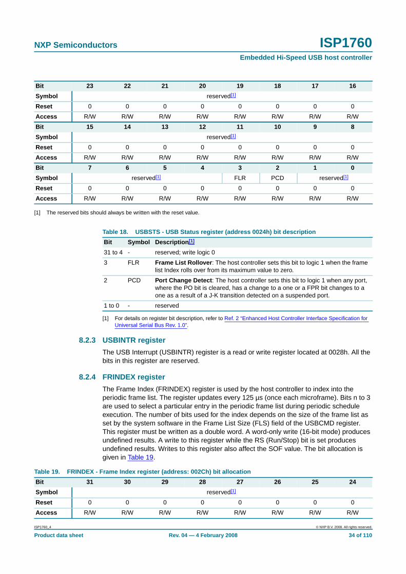
The USB Interrupt (USBINTR) register is a read or write register located at 0028h. All thebits in this register are reserved.
8.2.4 FRINDEX register
The Frame Index (FRINDEX) register is used by the host controller to index into theperiodic frame list. The register updates every 125 µs (once each microframe). Bits n to 3are used to select a particular entry in the periodic frame list during periodic scheduleexecution. The number of bits used for the index depends on the size of the frame list asset by the system software in the Frame List Size (FLS) field of the USBCMD register.This register must be written as a double word. A word-only write (16-bit mode) producesundefined results. A write to this register while the RS (Run/Stop) bit is set producesundefined results. Writes to this register also affect the SOF value. The bit allocation isgiven in Table 19.
Bit 23 22 21 20 19 18 17 16
Symbol reserved[1]
Reset 0 0 0 0 0 0 0 0
Access R/W R/W R/W R/W R/W R/W R/W R/W
Bit 15 14 13 12 11 10 9 8
Symbol reserved[1]
Reset 0 0 0 0 0 0 0 0
Access R/W R/W R/W R/W R/W R/W R/W R/W
Bit 7 6 5 4 3 2 1 0
Symbol reserved[1] FLR PCD reserved[1]
Reset 0 0 0 0 0 0 0 0
Access R/W R/W R/W R/W R/W R/W R/W R/W
Table 18. USBSTS - USB Status register (address 0024h) bit description
Bit Symbol Description [1]
31 to 4 - reserved; write logic 0
3 FLR Frame List Rollover : The host controller sets this bit to logic 1 when the framelist Index rolls over from its maximum value to zero.
2 PCD Port Change Detect : The host controller sets this bit to logic 1 when any port,where the PO bit is cleared, has a change to a one or a FPR bit changes to aone as a result of a J-K transition detected on a suspended port.
1 to 0 - reserved
Table 19. FRINDEX - Frame Index register (address: 002Ch) bit allocation
Bit 31 30 29 28 27 26 25 24
Symbol reserved[1]
Reset 0 0 0 0 0 0 0 0
Access R/W R/W R/W R/W R/W R/W R/W R/W
ISP1760_4 © NXP B.V. 2008. All rights reserved.
Product data sheet Rev. 04 — 4 February 2008 34 of 110

NXP Semiconductors ISP1760Embedded Hi-Speed USB host controller
[1] The reserved bits should always be written with the reset value.
[1] For details on register bit description, refer to Ref. 2 “Enhanced Host Controller Interface Specification forUniversal Serial Bus Rev. 1.0”.
8.2.5 CONFIGFLAG register
The bit allocation of the Configure Flag (CONFIGFLAG) register is given in Table 21.
[1] The reserved bits should always be written with the reset value.
Bit 23 22 21 20 19 18 17 16
Symbol reserved[1]
Reset 0 0 0 0 0 0 0 0
Access R/W R/W R/W R/W R/W R/W R/W R/W
Bit 15 14 13 12 11 10 9 8
Symbol reserved[1] FRINDEX[13:8]
Reset 0 0 0 0 0 0 0 0
Access R/W R/W R/W R/W R/W R/W R/W R/W
Bit 7 6 5 4 3 2 1 0
Symbol FRINDEX[7:0]
Reset 0 0 0 0 0 0 0 0
Access R/W R/W R/W R/W R/W R/W R/W R/W
Table 20. FRINDEX - Frame Index register (address: 002Ch) bit description
Bit Symbol Description [1]
31 to 14 - reserved
13 to 0 FRINDEX[13:0]
Frame Index : Bits in this register are used for the frame number in the SOFpacket and as the index into the frame list. The value in this registerincrements at the end of each time frame. For example, microframe.
Table 21. CONFIGFLAG - Configure Flag register (address 0060h) bit allocation
Bit 31 30 29 28 27 26 25 24
Symbol reserved[1]
Reset 0 0 0 0 0 0 0 0
Access R/W R/W R/W R/W R/W R/W R/W R/W
Bit 23 22 21 20 19 18 17 16
Symbol reserved[1]
Reset 0 0 0 0 0 0 0 0
Access R/W R/W R/W R/W R/W R/W R/W R/W
Bit 15 14 13 12 11 10 9 8
Symbol reserved[1]
Reset 0 0 0 0 0 0 0 0
Access R/W R/W R/W R/W R/W R/W R/W R/W
Bit 7 6 5 4 3 2 1 0
Symbol reserved[1] CF
Reset 0 0 0 0 0 0 0 0
Access R/W R/W R/W R/W R/W R/W R/W R/W
ISP1760_4 © NXP B.V. 2008. All rights reserved.
Product data sheet Rev. 04 — 4 February 2008 35 of 110

NXP Semiconductors ISP1760Embedded Hi-Speed USB host controller
[1] For details on register bit description, refer to Ref. 2 “Enhanced Host Controller Interface Specification forUniversal Serial Bus Rev. 1.0”.
8.2.6 PORTSC1 register
The Port Status and Control (PORTSC) register (bit allocation: Table 23) is in the powerwell. It is reset by hardware only when the auxiliary power is initially applied or in responseto a host controller reset. The initial conditions of a port are:
• No peripheral connected
• Port disabled
If the port has power control, software cannot change the state of the port until it sets portpower bits. Software must not attempt to change the state of the port until the power isstable on the port (maximum delay is 20 ms from the transition).
[1] The reserved bits should always be written with the reset value.
Table 22. CONFIGFLAG - Configure Flag register (address 0060h) bit description
Bit Symbol Description [1]
31 to 1 - reserved
0 CF Configure Flag : The host software sets this bit as the last action when it isconfiguring the host controller. This bit controls the default port-routingcontrol logic.
Table 23. PORTSC1 - Port Status and Control 1 register (address 0064h) bit allocation
Bit 31 30 29 28 27 26 25 24
Symbol reserved[1]
Reset 0 0 0 0 0 0 0 0
Access R/W R/W R/W R/W R/W R/W R/W R/W
Bit 23 22 21 20 19 18 17 16
Symbol reserved[1] PTC[3:0]
Reset 0 0 0 0 0 0 0 0
Access R/W R/W R/W R/W R/W R/W R/W R/W
Bit 15 14 13 12 11 10 9 8
Symbol PIC[1:0] PO PP LS[1:0] reserved[1] PR
Reset 0 0 1 0 0 0 0 0
Access R R R/W R/W R/W R/W R/W R
Bit 7 6 5 4 3 2 1 0
Symbol SUSP FPR reserved[1] PED ECSC ECCS
Reset 0 0 0 0 0 0 0 0
Access R/W R/W R/W R/W R/W R/W R/W R
ISP1760_4 © NXP B.V. 2008. All rights reserved.
Product data sheet Rev. 04 — 4 February 2008 36 of 110

NXP Semiconductors ISP1760Embedded Hi-Speed USB host controller
[1] For details on register bit description, refer to Ref. 2 “Enhanced Host Controller Interface Specification forUniversal Serial Bus Rev. 1.0”.
[2] These fields read logic 0, if the PP (Port Power) bit in register PORTSC1 is logic 0.
8.2.7 ISO PTD Done Map register
The bit description of the register is given in Table 25.
This register represents a direct map of the done status of the 32 PTDs. The bitcorresponding to a certain PTD will be set to logic 1 as soon as that PTD execution iscompleted. Reading the Done Map register will clear all the bits that are set to logic 1, andthe next reading will reflect the updated status of new executed PTDs.
8.2.8 ISO PTD Skip Map register
Table 26 shows the bit description of the register.
Table 24. PORTSC1 - Port Status and Control 1 register (address 0064h) bit description
Bit Symbol Description [1]
31 to 20 - reserved
19 to 16 PTC[3:0] Port Test Control : When this field is zero, the port is not operating in testmode. A nonzero value indicates that it is operating in test mode indicatedby the value.
15 to 14 PIC[1:0] Port Indicator Control : Writing to this field has no effect if theP_INDICATOR bit in the HCSPARAMS register is logic 0.
For a description on how these bits are implemented, refer to Ref. 1“Universal Serial Bus Specification Rev. 2.0”.[2]
13 PO Port Owner : This bit unconditionally goes to logic 0 when the configuredbit in the CONFIGFLAG register makes a logic 0 to logic 1 transition. Thisbit unconditionally goes to logic 1 whenever the configured bit is logic 0.
12 PP Port Power : The function of this bit depends on the value of the PPC (PortPower Control) field in the HCSPARAMS register.
11 to 10 LS[1:0] Line Status : This field reflects the current logical levels of the DP (bit 11)and DM (bit 10) signal lines.
9 - reserved
8 PR Port Reset : Logic 1 means the port is in the reset state. Logic 0 meansthe port is not in reset.[2]
7 SUSP Suspend : Logic 1 means the port is in the suspend state. Logic 0 meansthe port is not suspended.[2]
6 FPR Force Port Resume : Logic 1 means resume detected or driven on theport. Logic 0 means no resume (K-state) detected or driven on the port.[2]
5 to 3 - reserved
2 PED Port Enabled/Disabled : Logic 1 means enable. Logic 0 means disable.[2]
1 ECSC Connect Status Change : Logic 1 means change in ECCS. Logic 0means no change.[2]
0 ECCS Current Connect Status : Logic 1 indicates a device is present on theport. Logic 0 indicates no device is present.[2]
Table 25. ISO PTD Done Map register (address 0130h) bit description
Bit Symbol Access Value Description
31 to 0 ISO_PTD_DONE_MAP[31:0]
R 0000 0000h ISO PTD Done Map : Done map for each of the 32 PTDs forthe ISO transfer
ISP1760_4 © NXP B.V. 2008. All rights reserved.
Product data sheet Rev. 04 — 4 February 2008 37 of 110

NXP Semiconductors ISP1760Embedded Hi-Speed USB host controller
When a bit in the PTD Skip Map is set to logic 1 that PTD will be skipped although its V bitmay be set. The information in that PTD is not processed. For example, NextPTDPointerwill not affect the order of processing of PTDs. The Skip bit should not normally be set onthe position indicated by NextPTDPointer.
8.2.9 ISO PTD Last PTD register
Table 27 shows the bit description of the ISO PTD Last PTD register.
Once the LastPTD bit corresponding to a PTD is set, this will be the last PTD processed(checking V = 1) in that PTD category. Subsequently, the process will restart with the firstPTD of that group. This is useful to reduce the time in which all the PTDs, the respectivememory space, would be checked, especially if only a few PTDs are defined. TheLastPTD bit must be normally set to a higher position than any other position indicated bythe NextPTDPointer from an active PTD.
8.2.10 INT PTD Done Map register
The bit description of the register is given in Table 28.
This register represents a direct map of the done status of the 32 PTDs. The bitcorresponding to a certain PTD will be set to logic 1 as soon as that PTD execution iscompleted. Reading the Done Map register will clear all the bits that are set to logic 1, andthe next reading will reflect the updated status of new executed PTDs.
8.2.11 INT PTD Skip Map register
Table 29 shows the bit description of the INT PTD Skip Map register.
Table 26. ISO PTD Skip Map register (address 0134h) bit description
Bit Symbol Access Value Description
31 to 0 ISO_PTD_SKIP_MAP[31:0]
R/W FFFF FFFFh ISO PTD Skip Map : Skip map for each of the 32 PTDs for theISO transfer.
Table 27. ISO PTD Last PTD register (address 0138h) bit description
Bit Symbol Access Value Description
31 to 0 ISO_PTD_LAST_PTD[31:0]
R/W 0000 0000h ISO PTD last PTD : Last PTD of the 32 PTDs is indicated by the 32bitmap.
1h — One PTD in ISO
2h — Two PTDs in ISO
4h — Three PTDs in ISO
Table 28. INT PTD Done Map register (address 0140h) bit description
Bit Symbol Access Value Description
31 to 0 INT_PTD_DONE_MAP[31:0]
R 0000 0000h INT PTD Done Map : Done map for each of the 32 PTDs for theINT transfer
Table 29. INT PTD Skip Map register (address 0144h) bit description
Bit Symbol Access Value Description
31 to 0 INT_PTD_SKIP_MAP[31:0]
R/W FFFF FFFFh INT PTD Skip Map : Skip map for each of the 32 PTDs for the INTtransfer
ISP1760_4 © NXP B.V. 2008. All rights reserved.
Product data sheet Rev. 04 — 4 February 2008 38 of 110

NXP Semiconductors ISP1760Embedded Hi-Speed USB host controller
When a bit in the PTD Skip Map is set to logic 1 that PTD will be skipped although its V bitmay be set. The information in that PTD is not processed. For example, NextPTDPointerwill not affect the order of processing of PTDs. The Skip bit must not be normally set onthe position indicated by NextPTDPointer.
8.2.12 INT PTD Last PTD register
The bit description of the register is given in Table 30.
Once the LastPTD bit corresponding to a PTD is set, this will be the last PTD processed(checking V = 1) in that PTD category. Subsequently, the process will restart with the firstPTD of that group. This is useful to reduce the time in which all the PTDs, the respectivememory space, would be checked, especially if only a few PTDs are defined. TheLastPTD bit must be normally set to a higher position than any other position indicated bythe NextPTDPointer from an active PTD.
8.2.13 ATL PTD Done Map register
Table 31 shows the bit description of the ATL PTD Done Map register.
This register represents a direct map of the done status of the 32 PTDs. The bitcorresponding to a certain PTD will be set to logic 1 as soon as that PTD execution iscompleted. Reading the Done Map register will clear all the bits that are set to logic 1, andthe next reading will reflect the updated status of new executed PTDs.
8.2.14 ATL PTD Skip Map register
The bit description of the register is given in Table 32.
When a bit in the PTD Skip Map is set to logic 1 that PTD will be skipped although its V bitmay be set. The information in that PTD is not processed. For example, NextPTDPointerwill not affect the order of processing of PTDs. The Skip bit must not normally be set onthe position indicated by NextPTDPointer.
Table 30. INT PTD Last PTD register (address 0148h) bit description
Bit Symbol Access Value Description
31 to 0 INT_PTD_LAST_PTD[31:0]
R/W 0000 0000h INT PTD Last PTD : Last PTD of the 32 PTDs as indicated by the 32bitmap.
1h — One PTD in INT
2h — Two PTDs in INT
3h — Three PTDs in INT
Table 31. ATL PTD Done Map register (address 0150h) bit description
Bit Symbol Access Value Description
31 to 0 ATL_PTD_DONE_MAP[31:0]
R 0000 0000h ATL PTD Done Map : Done map for each of the 32 PTDs forthe ATL transfer
Table 32. ATL PTD Skip Map register (address 0154h) bit description
Bit Symbol Access Value Description
31 to 0 ATL_PTD_SKIP_MAP[31:0]
R/W FFFF FFFFh ATL PTD Skip Map : Skip map for each of the 32 PTDs for theATL transfer
ISP1760_4 © NXP B.V. 2008. All rights reserved.
Product data sheet Rev. 04 — 4 February 2008 39 of 110

NXP Semiconductors ISP1760Embedded Hi-Speed USB host controller
8.2.15 ATL PTD Last PTD register
The bit description of the ATL PTD Last PTD register is given in Table 33.
Once the LastPTD bit corresponding to a PTD is set, this will be the last PTD processed(checking V = 1) in that PTD category. Subsequently, the process will restart with the firstPTD of that group. This is useful to reduce the time in which all the PTDs, the respectivememory space, would be checked, especially if only a few PTDs are defined. TheLastPTD bit must normally be set to a higher position than any other position indicated bythe NextPTDPointer from an active PTD.
8.3 Configuration registers
8.3.1 HW Mode Control register
Table 34 shows the bit allocation of the register.
[1] The reserved bits should always be written with the reset value.
Table 33. ATL PTD Last PTD register (address 0158h) bit description
Bit Symbol Access Value Description
31 to 0 ATL_PTD_LAST_PTD[31:0]
R/W 0000 0000h ATL PTD Last PTD : Last PTD of the 32 PTDs as indicated by the 32bitmap.
1h — One PTD in ATL
2h — Two PTDs in ATL
4h — Three PTDs in ATL
Table 34. HW Mode Control - Hardware Mode Control register (address 0300h) bit allocation
Bit 31 30 29 28 27 26 25 24
Symbol ALL_ATX_RESET
reserved[1]
Reset 0 0 0 0 0 0 0 0
Access R/W R/W R/W R/W R/W R/W R/W R/W
Bit 23 22 21 20 19 18 17 16
Symbol reserved[1]
Reset 0 0 0 0 0 0 0 0
Access R/W R/W R/W R/W R/W R/W R/W R/W
Bit 15 14 13 12 11 10 9 8
Symbol ANA_DIGI_OC
reserved[1] DATA_BUS_WIDTH
Reset 0 0 0 0 0 0 0 1
Access R/W R/W R/W R/W R/W R/W R/W R/W
Bit 7 6 5 4 3 2 1 0
Symbol reserved DACK_POL
DREQ_POL
reserved[1] INTR_POL INTR_LEVEL
GLOBAL_INTR_EN
Reset 0 0 0 0 0 0 0 0
Access R/W R/W R/W R/W R/W R/W R/W R/W
ISP1760_4 © NXP B.V. 2008. All rights reserved.
Product data sheet Rev. 04 — 4 February 2008 40 of 110

NXP Semiconductors ISP1760Embedded Hi-Speed USB host controller
8.3.2 Chip ID register
Read this register to get the ID of the ISP1760. The upper word of the register containsthe hardware version number and the lower word contains the chip ID. Table 36 shows thebit description of the register.
Table 35. HW Mode Control - Hardware Mode Control register (address 0300h) bitdescription
Bit Symbol Description
31 ALL_ATX_RESET All ATX Reset : For debugging purposes (not used normally).
1 — Enable reset, then write back logic 0
0 — No reset
30 to 16 - reserved; write logic 0
15 ANA_DIGI_OC Analog Digital Overcurrent : This bit selects analog or digitalovercurrent detection on pins OC1_N, OC2_N and OC3_N.
0 — Digital overcurrent
1 — Analog overcurrent
14 to 9 - reserved; write logic 0
8 DATA_BUS_WIDTH Data Bus Width :
0 — Defines a 16-bit data bus width
1 — Sets a 32-bit data bus width
7 - reserved; write logic 0
6 DACK_POL DACK Polarity :
1 — Indicates that the DACK input is active HIGH
0 — Indicates active LOW
5 DREQ_POL DREQ Polarity :
1 — Indicates that the DREQ output is active HIGH
0 — Indicates active LOW
4 to 3 - reserved; write logic 0
2 INTR_POL Interrupt Polarity :
0 — Active LOW
1 — Active HIGH
1 INTR_LEVEL Interrupt Level :
0 — INT is level triggered.
1 — INT is edge triggered. A pulse of certain width is generated.
0 GLOBAL_INTR_EN Global Interrupt Enable : This bit must be set to logic 1 toenable the IRQ signal assertion.
0 — IRQ assertion is disabled. IRQ will never be asserted,regardless of other settings or IRQ events.
1 — IRQ assertion is enabled. IRQ will be asserted according tothe Interrupt Enable register, and events setting and occurrence.
ISP1760_4 © NXP B.V. 2008. All rights reserved.
Product data sheet Rev. 04 — 4 February 2008 41 of 110
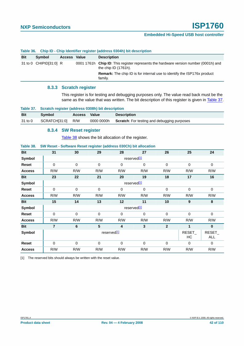
NXP Semiconductors ISP1760Embedded Hi-Speed USB host controller
8.3.3 Scratch register
This register is for testing and debugging purposes only. The value read back must be thesame as the value that was written. The bit description of this register is given in Table 37.
8.3.4 SW Reset register
Table 38 shows the bit allocation of the register.
[1] The reserved bits should always be written with the reset value.
Table 36. Chip ID - Chip Identifier register (address 0304h) bit description
Bit Symbol Access Value Description
31 to 0 CHIPID[31:0] R 0001 1761h Chip ID : This register represents the hardware version number (0001h) andthe chip ID (1761h).
Remark: The chip ID is for internal use to identify the ISP176x productfamily.
Table 37. Scratch register (address 0308h) bit description
Bit Symbol Access Value Description
31 to 0 SCRATCH[31:0] R/W 0000 0000h Scratch : For testing and debugging purposes
Table 38. SW Reset - Software Reset register (address 030Ch) bit allocation
Bit 31 30 29 28 27 26 25 24
Symbol reserved[1]
Reset 0 0 0 0 0 0 0 0
Access R/W R/W R/W R/W R/W R/W R/W R/W
Bit 23 22 21 20 19 18 17 16
Symbol reserved[1]
Reset 0 0 0 0 0 0 0 0
Access R/W R/W R/W R/W R/W R/W R/W R/W
Bit 15 14 13 12 11 10 9 8
Symbol reserved[1]
Reset 0 0 0 0 0 0 0 0
Access R/W R/W R/W R/W R/W R/W R/W R/W
Bit 7 6 5 4 3 2 1 0
Symbol reserved[1] RESET_HC
RESET_ALL
Reset 0 0 0 0 0 0 0 0
Access R/W R/W R/W R/W R/W R/W R/W R/W
ISP1760_4 © NXP B.V. 2008. All rights reserved.
Product data sheet Rev. 04 — 4 February 2008 42 of 110

NXP Semiconductors ISP1760Embedded Hi-Speed USB host controller
8.3.5 DMA Configuration register
The bit allocation of the DMA Configuration register is given in Table 40.
[1] The reserved bits should always be written with the reset value.
Table 39. SW Reset - Software Reset register (address 030Ch) bit description
Bit Symbol Description
31 to 2 - reserved; write logic 0
1 RESET_HC Reset Host Controller : Reset only the host controller-specific registers(only registers with address below 300h).
0 — No reset
1 — Enable reset
0 RESET_ALL Reset All : Reset all the host controller and CPU interface registers.
0 — No reset
1 — Enable reset
Table 40. DMA Configuration register (address 0330h) bit allocation
Bit 31 30 29 28 27 26 25 24
Symbol DMA_COUNTER[23:16]
Reset 0 0 0 0 0 0 0 0
Access R/W R/W R/W R/W R/W R/W R/W R/W
Bit 23 22 21 20 19 18 17 16
Symbol DMA_COUNTER[15:8]
Reset 0 0 0 0 0 0 0 0
Access R/W R/W R/W R/W R/W R/W R/W R/W
Bit 15 14 13 12 11 10 9 8
Symbol DMA_COUNTER[7:0]
Reset 0 0 0 0 0 0 0 0
Access R/W R/W R/W R/W R/W R/W R/W R/W
Bit 7 6 5 4 3 2 1 0
Symbol reserved[1] BURST_LEN[1:0] ENABLE_DMA
DMA_READ_WRITE_
SEL
Reset 0 0 0 0 0 0 0 0
Access R/W R/W R/W R/W R/W R/W R/W R/W
ISP1760_4 © NXP B.V. 2008. All rights reserved.
Product data sheet Rev. 04 — 4 February 2008 43 of 110

NXP Semiconductors ISP1760Embedded Hi-Speed USB host controller
8.3.6 Buffer Status register
The Buffer Status register is used to indicate the HC that a particular PTD buffer (that is,ATL, INT and ISO) contains at least one PTD that must be scheduled. Once software setsthe Buffer Filled bit of a particular transfer in the Buffer Status register, the HC will starttraversing through PTD headers that are not marked for skipping and are valid PTDs.
Remark: Software can set these bits during the initialization.
Table 42 shows the bit allocation of the Buffer Status register.
Table 41. DMA Configuration register (address 0330h) bit description
Bit Symbol Description
31 to 8 DMA_COUNTER[23:0] DMA Counter : The number of bytes to be transferred (read orwrite).
Remark: Different number of bursts will be generated for thesame transfer length programmed in 16-bit and 32-bit modesbecause DMA_COUNTER is in number of bytes.
7 to 4 - reserved
3 to 2 BURST_LEN[1:0] DMA Burst Length :
00 — Single DMA burst
01 — 4-cycle DMA burst
10 — 8-cycle DMA burst
11 — 16-cycle DMA burst
1 ENABLE_DMA Enable DMA :
0 — Terminate DMA
1 — Enable DMA
0 DMA_READ_WRITE_SEL
DMA Read/Write Select : Indicates if the DMA operation is awrite or read to or from the ISP1760.
0 — DMA write to the ISP1760 internal RAM is set
1 — DMA read from the ISP1760 internal RAM
Table 42. Buffer Status register (address 0334h) bit allocation
Bit 31 30 29 28 27 26 25 24
Symbol reserved[1]
Reset 0 0 0 0 0 0 0 0
Access R/W R/W R/W R/W R/W R/W R/W R/W
Bit 23 22 21 20 19 18 17 16
Symbol reserved[1]
Reset 0 0 0 0 0 0 0 0
Access R/W R/W R/W R/W R/W R/W R/W R/W
Bit 15 14 13 12 11 10 9 8
Symbol reserved[1]
Reset 0 0 0 0 0 0 0 0
Access R/W R/W R/W R/W R/W R/W R/W R/W
ISP1760_4 © NXP B.V. 2008. All rights reserved.
Product data sheet Rev. 04 — 4 February 2008 44 of 110

NXP Semiconductors ISP1760Embedded Hi-Speed USB host controller
[1] The reserved bits should always be written with the reset value.
8.3.7 ATL Done Timeout register
The bit description of the ATL Done Timeout register is given in Table 44.
8.3.8 Memory register
The Memory register contains the base memory read address and the respective bank.This register needs to be set only before a first memory read cycle. Once written, theaddress will be latched for the bank and will be incremented for every read of that bank,until a new address for that bank is written to change the address pointer.
The bit description of the register is given in Table 45.
Bit 7 6 5 4 3 2 1 0
Symbol reserved[1] ISO_BUF_FILL
INT_BUF_FILL
ATL_BUF_FILL
Reset 0 0 0 0 0 0 0 0
Access R/W R/W R/W R/W R/W R/W R/W R/W
Table 43. Buffer Status register (address 0334h) bit description
Bit Symbol Description
31 to 3 - reserved
2 ISO_BUF_FILL
ISO Buffer Filled :
1 — Indicates one of the ISO PTDs is filled, and the ISO PTD area will beprocessed.
0 — Indicates there is no PTD in this area. Therefore, processing of the ISOPTDs will completely be skipped.
1 INT_BUF_FILL
INT Buffer Filled :
1 — Indicates one of the INT PTDs is filled, and the INT PTD area will beprocessed.
0 — Indicates there is no PTD in this area. Therefore, processing of the INTPTDs will completely be skipped.
0 ATL_BUF_FILL
ATL Buffer Filled :
1 — Indicates one of the ATL PTDs is filled, and the ATL PTD area will beprocessed.
0 — Indicates there is no PTD in this area. Therefore, processing of the ATLPTDs will completely be skipped.
Table 44. ATL Done Timeout register (address 0338h) bit description
Bit Symbol Access Value Description
31 to 0 ATL_DONE_TIMEOUT[31:0]
R/W 0000 0000h ATL Done Timeout : This register determines the ATL donetime-out interrupt. This register defines the time-out inmilliseconds after which the ISP1760 asserts the INT line, ifenabled. It is applicable to ATL done PTDs only.
ISP1760_4 © NXP B.V. 2008. All rights reserved.
Product data sheet Rev. 04 — 4 February 2008 45 of 110

NXP Semiconductors ISP1760Embedded Hi-Speed USB host controller
[1] The reserved bits should always be written with the reset value.
8.3.9 Edge Interrupt Count register
Table 47 shows the bit allocation of the register.
Table 45. Memory register (address 033Ch) bit allocation
Bit 31 30 29 28 27 26 25 24
Symbol reserved[1]
Reset 0 0 0 0 0 0 0 0
Access R/W R/W R/W R/W R/W R/W R/W R/W
Bit 23 22 21 20 19 18 17 16
Symbol reserved[1] MEM_BANK_SEL[1:0]
Reset 0 0 0 0 0 0 0 0
Access R/W R/W R/W R/W R/W R/W R/W R/W
Bit 15 14 13 12 11 10 9 8
Symbol START_ADDR_MEM_READ[15:8]
Reset 0 0 0 0 0 0 0 0
Access R/W R/W R/W R/W R/W R/W R/W R/W
Bit 7 6 5 4 3 2 1 0
Symbol START_ADDR_MEM_READ[7:0]
Reset 0 0 0 0 0 0 0 0
Access R/W R/W R/W R/W R/W R/W R/W R/W
Table 46. Memory register (address 033Ch) bit description
Bit Symbol Description
31 to 18 - reserved
17 to 16 MEM_BANK_SEL[1:0]
Memory Bank Select : Up to four memory banks can be selected.For details on internal memory read description, see Section 7.3.1.Applicable to PIO mode memory read or write data transfers only.
15 to 0 START_ADDR_MEM_READ[15:0]
Start Address for Memory Read Cycles : The start address for aseries of memory read cycles at incremental addresses in acontiguous space. Applicable to PIO mode memory read datatransfers only.
Table 47. Edge Interrupt Count register (address 0340h) bit allocation
Bit 31 30 29 28 27 26 25 24
Symbol MIN_WIDTH[7:0]
Reset 0 0 0 0 0 0 0 0
Access R/W R/W R/W R/W R/W R/W R/W R/W
Bit 23 22 21 20 19 18 17 16
Symbol reserved[1]
Reset 0 0 0 0 0 0 0 0
Access R/W R/W R/W R/W R/W R/W R/W R/W
ISP1760_4 © NXP B.V. 2008. All rights reserved.
Product data sheet Rev. 04 — 4 February 2008 46 of 110

NXP Semiconductors ISP1760Embedded Hi-Speed USB host controller
[1] The reserved bits should always be written with the reset value.
8.3.10 DMA Start Address register
This register defines the start address select for the DMA read and write operations. SeeTable 49 for the bit allocation.
[1] The reserved bits should always be written with the reset value.
Bit 15 14 13 12 11 10 9 8
Symbol NO_OF_CLK[15:8]
Reset 0 0 0 0 0 0 0 0
Access R/W R/W R/W R/W R/W R/W R/W R/W
Bit 7 6 5 4 3 2 1 0
Symbol NO_OF_CLK[7:0]
Reset 0 0 0 0 1 1 1 1
Access R/W R/W R/W R/W R/W R/W R/W R/W
Table 48. Edge Interrupt Count register (address 0340h) bit description
Bit Symbol Description
31 to 24 MIN_WIDTH[7:0] Minimum Width : Indicates the minimum width between two edgeinterrupts in µSOFs (1 µSOF = 125 µs). This is not valid for levelinterrupts. A count of zero means that interrupts occur as andwhen an event occurs.
23 to 16 - reserved
15 to 0 NO_OF_CLK[15:0] Number of Clocks : Count in number of clocks that the edgeinterrupt must be kept asserted on the interface. The default IRQpulse width is approximately 500 ns.
Table 49. DMA Start Address register (address 0344h) bit allocation
Bit 31 30 29 28 27 26 25 24
Symbol reserved[1]
Reset 0 0 0 0 0 0 0 0
Access W W W W W W W W
Bit 23 22 21 20 19 18 17 16
Symbol reserved[1]
Reset 0 0 0 0 0 0 0 0
Access W W W W W W W W
Bit 15 14 13 12 11 10 9 8
Symbol START_ADDR_DMA[15:8]
Reset 0 0 0 0 0 0 0 0
Access W W W W W W W W
Bit 7 6 5 4 3 2 1 0
Symbol START_ADDR_DMA[7:0]
Reset 0 0 0 0 0 0 0 0
Access W W W W W W W W
ISP1760_4 © NXP B.V. 2008. All rights reserved.
Product data sheet Rev. 04 — 4 February 2008 47 of 110

NXP Semiconductors ISP1760Embedded Hi-Speed USB host controller
8.3.11 Power Down Control register
This register is used to turn off power to the internal blocks of the ISP1760 to obtainmaximum power savings. Table 51 shows the bit allocation of the register.
[1] The reserved bits should always be written with the reset value.
Table 50. DMA Start Address register (address 0344h) bit description
Bit Symbol Description
31 to 16 - reserved
15 to 0 START_ADDR_DMA[15:0]
Start Address for DMA : The start address for DMA read or writecycles.
Table 51. Power Down Control register (address 0354h) bit allocation
Bit 31 30 29 28 27 26 25 24
Symbol CLK_OFF_COUNTER[15:8]
Reset 0 0 0 0 0 0 1 1
Access R/W R/W R/W R/W R/W R/W R/W R/W
Bit 23 22 21 20 19 18 17 16
Symbol CLK_OFF_COUNTER[7:0]
Reset 1 1 1 0 1 0 0 0
Access R/W R/W R/W R/W R/W R/W R/W R/W
Bit 15 14 13 12 11 10 9 8
Symbol reserved[1] PORT3_PD
PORT2_PD
VBATDET_PWR
reserved[1]
Reset 0 0 0 1 1 0 1 1
Access R/W R/W R/W R/W R/W R/W R/W R/W
Bit 7 6 5 4 3 2 1 0
Symbol reserved[1] BIASEN VREG_ON OC3_PWR OC2_PWR OC1_PWR HC_CLK_EN
Reset 1 0 1 0 0 0 0 0
Access R/W R/W R/W R/W R/W R/W R/W R/W
ISP1760_4 © NXP B.V. 2008. All rights reserved.
Product data sheet Rev. 04 — 4 February 2008 48 of 110

NXP Semiconductors ISP1760Embedded Hi-Speed USB host controller
Table 52. Power Down Control register (address 0354h) bit description
Bit [1] Symbol Description
31 to 16 CLK_OFF_COUNTER[15:0]
Clock Off Counter : Determines the wake-up status duration after anywake-up event before the ISP1760 goes back into suspend mode. Thistime-out is applicable only if, during the given interval, the host controller isnot programmed back to the normal functionality.
03E8h — The default value. It determines the default wake-up interval of10 ms. A value of zero implies that the host controller never wakes up onany of the events. This may be useful when using the ISP1760 as aperipheral to save power by permanently programming the host controllerin suspend.
FFFFh — The maximum value. It determines a maximum wake-up time of500 ms.
The setting of this register is based on the 100 kHz ± 40 % LazyClockfrequency. It is a multiple of 10 µs period.
Remark: In 16-bit mode, the default value is 17E8h. A write operation tothese bits with any value fixes the clock off counter at 1400h. This value isequivalent to a fixed wake-up time of 50 ms.
15 to 13 - reserved
12 PORT3_PD Port 3 Pull-Down : Controls port 3 pull-down resistors.
0 — Port 3 internal pull-down resistors are not connected.
1 — Port 3 internal pull-down resistors are connected.
11 PORT2_PD Port 2 Pull-Down : Controls port 2 pull-down resistors.
0 — Port 2 internal pull-down resistors are not connected.
1 — Port 2 internal pull-down resistors are connected.
10 VBATDET_PWR
VBAT Detector Powered : Controls the power to the VBAT detector.
0 — VBAT detector is powered or enabled in suspend.
1 — VBAT detector is not powered or disabled in suspend.
9 to 6 - reserved; write reset value
5 BIASEN Bias Circuits Powered : Controls the power to internal bias circuits.
0 — Internal bias circuits are not powered in suspend.
1 — Internal bias circuits are powered in suspend.
4 VREG_ON VREG Powered : Enables or disables the internal 3.3 V and 1.8 Vregulators when the ISP1760 is in suspend.
0 — Internal regulators are normally powered in suspend.
1 — Internal regulators switch to low power mode (in suspend mode).
3 OC3_PWR OC3_N Powered : Controls the powering of the overcurrent detectioncircuitry for port 3.
0 — Overcurrent detection is powered on or enabled during suspend.
1 — Overcurrent detection is powered off or disabled during suspend.
This may be useful when connecting a faulty device while the system is instandby.
ISP1760_4 © NXP B.V. 2008. All rights reserved.
Product data sheet Rev. 04 — 4 February 2008 49 of 110

NXP Semiconductors ISP1760Embedded Hi-Speed USB host controller
[1] For a 32-bit operation, the default wake-up counter value is 10 µs. For a 16-bit operation, the wake-upcounter value is 50 ms. In the 16-bit operation, read and write back the same value on initialization.
8.3.12 Port 1 Control register
The values read from the lower 16 bits and the upper 16 bits of this register are always thesame. Table 53 shows the bit allocation of the register.
2 OC2_PWR OC2_N Powered : Controls the powering of the overcurrent detectioncircuitry for port 2.
0 — Overcurrent detection is powered-on or enabled during suspend.
1 — Overcurrent detection is powered-off or disabled during suspend.
This may be useful when connecting a faulty device while the system is instandby.
1 OC1_PWR OC1_N Powered : Controls the powering of the overcurrent detectioncircuitry for port 1.
0 — Overcurrent detection is powered-on or enabled during suspend.
1 — Overcurrent detection is powered-off or disabled during suspend.
This may be useful when connecting a faulty device while the system is instandby.
0 HC_CLK_EN
Host Controller Clock Enabled : Controls internal clocks during suspend.
0 — Clocks are disabled during suspend. This is the default value. Onlythe LazyClock of 100 kHz ± 40 % will be left running in suspend if this bitis logic 0. If clocks are stopped during suspend, CLKREADY IRQ will begenerated when all clocks are running stable.
1 — All clocks are enabled even in suspend.
Table 52. Power Down Control register (address 0354h) bit description …continued
Bit [1] Symbol Description
Table 53. Port 1 Control register (address 0374h) bit allocation
Bit 31 30 29 28 27 26 25 24
Symbol reserved
Reset 0 0 0 0 0 0 0 0
Access R/W R/W R/W R/W R/W R/W R/W R/W
Bit 23 22 21 20 19 18 17 16
Symbol PORT1_INIT2
reserved
Reset 1 0 0 0 0 1 1 0
Access R/W R/W R/W R/W R/W R/W R/W R/W
Bit 15 14 13 12 11 10 9 8
Symbol reserved
Reset 0 0 0 0 0 0 0 0
Access R/W R/W R/W R/W R/W R/W R/W R/W
Bit 7 6 5 4 3 2 1 0
Symbol PORT1_INIT1
reserved PORT1_POWER[1:0] reserved
Reset 0 0 0 1 0 1 1 0
Access R/W R/W R/W R/W R/W R/W R/W R/W
ISP1760_4 © NXP B.V. 2008. All rights reserved.
Product data sheet Rev. 04 — 4 February 2008 50 of 110

NXP Semiconductors ISP1760Embedded Hi-Speed USB host controller
[1] For correct port 1 initialization, write 0080 0018h to this register after power-on.
8.4 Interrupt registers
8.4.1 Interrupt register
The bits of this register indicate the interrupt source, defining the events that determinedthe INT generation. Clearing the bits that were set because of the events listed is done bywriting back logic 1 to the respective position. All bits must be reset before enabling newinterrupt events. These bits will be set, regardless of the setting of bit GLOBAL_INTR_ENin the HW Mode Control register. Table 55 shows the bit allocation of the Interrupt register.
[1] The reserved bits should always be written with the reset value.
Table 54. Port 1 Control register (address 0374h) bit description
Bit [1] Symbol Description
31 to 24 - reserved; write reset value
23 PORT1_INIT2 Port 1 Initialization 2 : Write logic 1 at the ISP1760 initialization. Itwill clear both this bit and bit 7. Affects only port 1.
22 to 8 - reserved
7 PORT1_INIT1 Port 1 Initialization 1 : Must be reset to logic 0 at power-upinitialization for correct operation of port 1. Correct host controllerfunctionality is not ensured if set to logic 1 (affects only port 1). Toclear this bit, logic 1 must be written to bit 23 during the ISP1760initialization.
This is not required for the normal functionality of port 2 and port 3.
6 to 5 - reserved
4 to 3 PORT1_POWER[1:0]
Port 1 Power : Set these bits to 11b. These bits must be set to enableport 1 power.
2 to 0 - reserved; write reset value
Table 55. Interrupt register (address 0310h) bit allocation
Bit 31 30 29 28 27 26 25 24
Symbol reserved[1]
Reset 0 0 0 0 0 0 0 0
Access R/W R/W R/W R/W R/W R/W R/W R/W
Bit 23 22 21 20 19 18 17 16
Symbol reserved[1]
Reset 0 0 0 0 0 0 0 0
Access R/W R/W R/W R/W R/W R/W R/W R/W
Bit 15 14 13 12 11 10 9 8
Symbol reserved[1] ISO_IRQ ATL_IRQ
Reset 0 0 0 0 0 0 0 0
Access R/W R/W R/W R/W R/W R/W R/W R/W
Bit 7 6 5 4 3 2 1 0
Symbol INT_IRQ CLKREADY
HC_SUSP reserved[1] DMAEOTINT
reserved[1] SOFITLINT reserved[1]
Reset 0 0 0 0 0 0 0 0
Access R/W R/W R/W R/W R/W R/W R/W R/W
ISP1760_4 © NXP B.V. 2008. All rights reserved.
Product data sheet Rev. 04 — 4 February 2008 51 of 110

NXP Semiconductors ISP1760Embedded Hi-Speed USB host controller
Table 56. Interrupt register (address 0310h) bit description
Bit Symbol Description
31 to 10 - reserved; write reset value
9 ISO_IRQ ISO IRQ: Indicates that an ISO PTD was completed, or the PTDscorresponding to the bits set in the ISO IRQ Mask AND or ISO IRQ MaskOR register bits combination were completed. The IRQ line will beasserted if the respective enable bit in the HCInterruptEnable register isset.
0 — No ISO PTD event occurred.
1 — ISO PTD event occurred.
For details, see Section 7.4.
8 ATL_IRQ ATL IRQ : Indicates that an ATL PTD was completed, or the PTDscorresponding to the bits set in the ATL IRQ Mask AND or ATL IRQ MaskOR register bits combination were completed. The IRQ line will beasserted if the respective enable bit in the HCInterruptEnable register isset.
0 — No ATL PTD event occurred.
1 — ATL PTD event occurred.
For details, see Section 7.4.
7 INT_IRQ INT IRQ: Indicates that an INT PTD was completed, or the PTDscorresponding to the bits set in the INT IRQ Mask AND or INT IRQ MaskOR register bits combination were completed. The IRQ line will beasserted if the respective enable bit in the HCInterruptEnable register isset.
0 — No INT PTD event occurred.
1 — INT PTD event occurred.
For details, see Section 7.4.
6 CLKREADY Clock Ready : Indicates that internal clock signals are running stable. TheIRQ line will be asserted if the respective enable bit in theHCInterruptEnable register is set.
0 — No CLKREADY event has occurred.
1 — CLKREADY event occurred.
5 HC_SUSP Host Controller Suspend : Indicates that the host controller has enteredsuspend mode. The IRQ line will be asserted if the respective enable bitin the HCInterruptEnable register is set.
0 — The host controller did not enter suspend mode.
1 — The host controller entered suspend mode.
If the ISR accesses the ISP1760, it will wake up for the time specified inbits 31 to 16 of the Power Down Control register.
4 - reserved; write reset value
3 DMAEOTINT
DMA EOT Interrupt : Indicates the DMA transfer completion. The IRQ linewill be asserted if the respective enable bit in the HCInterruptEnableregister is set.
0 — No DMA transfer is completed.
1 — DMA transfer is complete.
ISP1760_4 © NXP B.V. 2008. All rights reserved.
Product data sheet Rev. 04 — 4 February 2008 52 of 110

NXP Semiconductors ISP1760Embedded Hi-Speed USB host controller
8.4.2 Interrupt Enable register
This register allows enabling or disabling of the IRQ generation because of various eventsas described in Table 57.
[1] The reserved bits should always be written with the reset value.
2 - reserved; write reset value; value is zero just after reset and changes toone after a short while
1 SOFITLINT SOT ITL Interrupt : The IRQ line will be asserted if the respective enablebit in the HCInterruptEnable register is set.
0 — No SOF event has occurred.
1 — An SOF event has occurred.
0 - reserved; write reset value; value is zero just after reset and changes toone after a short while
Table 56. Interrupt register (address 0310h) bit description …continued
Bit Symbol Description
Table 57. Interrupt Enable register (address 0314h) bit allocation
Bit 31 30 29 28 27 26 25 24
Symbol reserved[1]
Reset 0 0 0 0 0 0 0 0
Access R/W R/W R/W R/W R/W R/W R/W R/W
Bit 23 22 21 20 19 18 17 16
Symbol reserved[1]
Reset 0 0 0 0 0 0 0 0
Access R/W R/W R/W R/W R/W R/W R/W R/W
Bit 15 14 13 12 11 10 9 8
Symbol reserved[1] ISO_IRQ_E ATL_IRQ_E
Reset 0 0 0 0 0 0 0 0
Access R/W R/W R/W R/W R/W R/W R/W R/W
Bit 7 6 5 4 3 2 1 0
Symbol INT_IRQ_E CLKREADY_E
HCSUSP_E reserved[1] DMAEOTINT_E
reserved[1] SOFITLINT_E
reserved[1]
Reset 0 0 0 0 0 0 0 0
Access R/W R/W R/W R/W R/W R/W R/W R/W
ISP1760_4 © NXP B.V. 2008. All rights reserved.
Product data sheet Rev. 04 — 4 February 2008 53 of 110

NXP Semiconductors ISP1760Embedded Hi-Speed USB host controller
8.4.3 ISO IRQ Mask OR register
Each bit of this register corresponds to one of the 32 ISO PTDs defined, and is ahardware IRQ mask for each PTD done map. See Table 59 for bit description. For details,see Section 7.4.
Table 58. Interrupt Enable register (address 0314h) bit description
Bit Symbol Description
31 to 10 - reserved; write logic 0
9 ISO_IRQ_E ISO IRQ Enable : Controls the IRQ assertion when one or more ISOPTDs matching the ISO IRQ Mask AND or ISO IRQ Mask ORregister bits combination are completed.
0 — No IRQ will be asserted when ISO PTDs are completed.
1 — IRQ will be asserted.
For details, see Section 7.4.
8 ATL_IRQ_E ATL IRQ Enable : Controls the IRQ assertion when one or more ATLPTDs matching the ATL IRQ Mask AND or ATL IRQ Mask ORregister bits combination are completed.
0 — No IRQ will be asserted when ATL PTDs are completed.
1 — IRQ will be asserted.
For details, see Section 7.4.
7 INT_IRQ_E INT IRQ Enable : Controls the IRQ assertion when one or more INTPTDs matching the INT IRQ Mask AND or INT IRQ Mask OR registerbits combination are completed.
0 — No IRQ will be asserted when INT PTDs are completed.
1 — IRQ will be asserted.
For details, see Section 7.4.
6 CLKREADY_E
Clock Ready Enable : Enables the IRQ assertion when internal clocksignals are running stable. Useful after wake-up.
0 — No IRQ will be generated after a CLKREADY_E event.
1 — IRQ will be generated after a CLKREADY_E event.
5 HCSUSP_E Host Controller Suspend Enable : Enables the IRQ generationwhen the host controller enters suspend mode.
0 — No IRQ will be generated when the host controller enterssuspend mode.
1 — IRQ will be generated when the host controller enters suspendmode.
4 - reserved; write logic 0
3 DMAEOTINT_E
DMA EOT Interrupt Enable : Controls assertion of IRQ on the DMAtransfer completion.
0 — No IRQ will be generated when a DMA transfer is completed.
1 — IRQ will be asserted when a DMA transfer is completed.
2 - reserved; must be written with logic 0
1 SOFITLINT_E
SOT ITL Interrupt Enable : Controls the IRQ generation at everySOF occurrence.
0 — No IRQ will be generated on an SOF occurrence.
1 — IRQ will be asserted at every SOF.
0 - reserved; must be written with logic 0
ISP1760_4 © NXP B.V. 2008. All rights reserved.
Product data sheet Rev. 04 — 4 February 2008 54 of 110

NXP Semiconductors ISP1760Embedded Hi-Speed USB host controller
8.4.4 INT IRQ Mask OR register
Each bit of this register (see Table 60) corresponds to one of the 32 INT PTDs defined,and is a hardware IRQ mask for each PTD done map. For details, see Section 7.4.
8.4.5 ATL IRQ Mask OR register
Each bit of this register corresponds to one of the 32 ATL PTDs defined, and is ahardware IRQ mask for each PTD done map. See Table 61 for bit description. For details,see Section 7.4.
8.4.6 ISO IRQ Mask AND register
Each bit of this register corresponds to one of the 32 ISO PTDs defined, and is ahardware IRQ mask for each PTD done map. For details, see Section 7.4.
Table 62 provides the bit description of the register.
8.4.7 INT IRQ Mask AND register
Each bit of this register (see Table 63) corresponds to one of the 32 INT PTDs defined,and is a hardware IRQ mask for each PTD done map. For details, see Section 7.4.
Table 59. ISO IRQ Mask OR register (address 0318h) bit description
Bit Symbol Access Value Description
31 to 0 ISO_IRQ_MASK_OR[31:0]
R/W 0000 0000h ISO IRQ Mask OR : Represents a direct map for ISO PTDs 31 to 0.
0 — No OR condition defined between ISO PTDs.
1 — The bits corresponding to certain PTDs are set to logic 1 todefine a certain OR condition.
Table 60. INT IRQ Mask OR register (address 031Ch) bit description
Bit Symbol Access Value Description
31 to 0 INT_IRQ_MASK_OR[31:0]
R/W 0000 0000h INT IRQ Mask OR : Represents a direct map for INT PTDs 31 to 0.
0 — No OR condition defined between INT PTDs 31 to 0.
1 — The bits corresponding to certain PTDs are set to logic 1 todefine a certain OR condition.
Table 61. ATL IRQ Mask OR register (address 0320h) bit description
Bit Symbol Access Value Description
31 to 0 ATL_IRQ_MASK_OR[31:0]
R/W 0000 0000h ATL IRQ Mask OR : Represents a direct map for ATL PTDs 31 to 0.
0 — No OR condition defined between the ATL PTDs.
1 — The bits corresponding to certain PTDs are set to logic 1 todefine a certain OR condition.
Table 62. ISO IRQ Mask AND register (address 0324h) bit description
Bit Symbol Access Value Description
31 to 0 ISO_IRQ_MASK_AND[31:0]
R/W 0000 0000h ISO IRQ Mask AND : Represents a direct map for ISO PTDs 31 to 0.
0 — No AND condition defined between ISO PTDs.
1 — The bits corresponding to certain PTDs are set to logic 1 todefine a certain AND condition between the 32 INT PTDs.
ISP1760_4 © NXP B.V. 2008. All rights reserved.
Product data sheet Rev. 04 — 4 February 2008 55 of 110

NXP Semiconductors ISP1760Embedded Hi-Speed USB host controller
8.4.8 ATL IRQ Mask AND register
Each bit of this register corresponds to one of the 32 ATL PTDs defined, and is ahardware IRQ mask for each PTD done map. For details, see Section 7.4.
Table 64 shows the bit description of the register.
9. Philips Transfer Descriptor (PTD)
The standard EHCI data structures as described in Ref. 2 “Enhanced Host ControllerInterface Specification for Universal Serial Bus Rev. 1.0” are optimized for the bus masteroperation that is managed by the hardware state machine.
The PTD structures of the ISP1760 are translations of the EHCI data structures that areoptimized for the ISP1760. It, however, still follows the basic EHCI architecture. Thisoptimized form of EHCI data structures is necessary because the ISP1760 is a slave hostcontroller and has no bus master capability.
EHCI manages schedules in two lists: periodic and asynchronous. The data structuresare designed to provide the maximum flexibility required by USB, minimize memory traffic,and reduce hardware and software complexity. The ISP1760 controller executestransactions for devices by using a simple shared-memory schedule. This scheduleconsists of data structures organized into three lists.
qISO — Isochronous transfer
qINTL — Interrupt transfer
qATL — Asynchronous transfer; for the control and bulk transfers
The system software maintains two lists for the host controller: periodic andasynchronous.
The ISP1760 has a maximum of 32 ISO, 32 INTL and 32 ATL PTDs. These PTDs areused as channels to transfer data from the shared memory to the USB bus. Thesechannels are allocated and de-allocated on receiving the transfer from the core USBdriver.
Table 63. INT IRQ Mask AND register (address 0328h) bit description
Bit Symbol Access Value Description
31 to 0 INT_IRQ_MASK_AND[31:0]
R/W 0000 0000h INT IRQ Mask AND : Represents a direct map for INT PTDs 31 to 0.
0 — No OR condition defined between INT PTDs.
1 — The bits corresponding to certain PTDs are set to logic 1 todefine a certain AND condition between the 32 INT PTDs.
Table 64. ATL IRQ Mask AND register (address 032Ch) bit description
Bit Symbol Access Value Description
31 to 0 ATL_IRQ_MASK_AND[31:0]
R/W 0000 0000h ATL IRQ Mask AND : Represents a direct map for ATL PTDs 31 to 0.
0 — No OR condition defined between ATL PTDs.
1 — The bits corresponding to certain PTDs are set to logic 1 todefine a certain AND condition between the 32 ATL PTDs.
ISP1760_4 © NXP B.V. 2008. All rights reserved.
Product data sheet Rev. 04 — 4 February 2008 56 of 110

NXP Semiconductors ISP1760Embedded Hi-Speed USB host controller
Multiple transfers are scheduled to the shared memory for various endpoints by traversingthe next link pointer provided by endpoint data structures, until it reaches the end of theendpoint list. There are three endpoint lists: one for ISO endpoints, and the other for INTLand ATL endpoints. If the schedule is enabled, the host controller executes the ISOschedule, followed by the INTL schedule, and then the ATL schedule.
These lists are traversed and scheduled by the software according to the EHCI traversalrule. The host controller executes the scheduled ISO, INTL and ATL PTDs. Thecompletion of a transfer is indicated to the software by the interrupt that can be groupedunder various PTDs by using the AND or OR registers that are available for each scheduletype: ISO, INTL and ATL. These registers are simple logic registers to decide thecompletion status of group and individual PTDs. When the logical conditions of the Donebit is true in the shared memory, it means that PTD has completed.
There are four types of interrupts in the ISP1760: ISO, INTL, ATL and SOF. The latencycan be programmed in multiples of µSOF (125 µs).
The NextPTD pointer is a feature that allows the ISP1760 to jump unused and skip PTDs.This will improve the PTD transversal latency time. The NextPTD pointer is not meant forsame or single endpoint. The NextPTD works only in forward direction.
The NextPTD traversal rules defined by the ISP1760 hardware are:
1. Start the PTD memory vertical traversal, considering the skip and LastPTDinformation, as follows.
2. If the current PTD is active and not done, perform the transaction.
3. Follow the NextPTD pointer as specified in bits 4 to 0 of DW4.
4. If combined with LastPTD, the LastPTD setting must be at a higher address than theNextPTD specified. So both are set in a logical manner.
5. If combined with skip, the skip must not be set (logically) on the same positioncorresponding to NextPTD, pointed by the NextPTD pointer.
6. If PTD is set for skip, it will be neglected and the next vertical PTD will be considered.
7. If the skipped PTD already has a setting including a NextPTD pointer that will not betaken into consideration, the behavior will be just as described in the preceding step.
ISP1760_4 © NXP B.V. 2008. All rights reserved.
Product data sheet Rev. 04 — 4 February 2008 57 of 110

NXP Semiconductors ISP1760Embedded Hi-Speed USB host controller
Fig 13. NextPTD traversal rule
PTD SKIPPED?
START PTD SCHEDULE
no yes
CHECK FOR VALID AND ACTIVE BIT
SET?
FOLLOW NEXT PTD POINTED BY NEXTPTD
POINTER
no
yes
START PTDEXECUTION
IS PTDPOINTER
NULL?
GO TO NEXTPTDVERTICAL
yes
no
004aaa883
ISP1760_4 © NXP B.V. 2008. All rights reserved.
Product data sheet Rev. 04 — 4 February 2008 58 of 110

xxxxxxxxxxxxxxxxxxxxx xxxxxxxxxxxxxxxxxxxxxxxxxx xxxxxxx x x x xxxxxxxxxxxxxxxxxxxxxxxxxxxxxx xxxxxxxxxxxxxxxxxxx xx xxxxxxx xxxxxxxxxxxxxxxxxxxxxxxxxxx xxxxxxxxxxxxxxxxxxx xxxxxx xxxxxxxxxxxxxxxxxxxxxxxxxxxxxxxxxxx xxxxxxxxxxxx x xxxxxxxxxxxxxxxxxxxxxx xxxxxxxxxxxxxxxxxxxxxxxxxxxxxx xxxxx xxxxxxxxxxxxxxxxxxxxxxxxxxxxxxxxxxxxxxxxxxxxxxxxxx xxxxxxxxxxxxxxxxxxxxxxxxxxxxxxxxx xxxxxxxxxxxxxxxxxxxx xxx
ISP
1760_4
Product data shee
NX
P S
emiconductors
ISP
1760E
mbedded H
i-Speed U
SB
host controller
9.1 High-speed bulk IN and OUTTable 65 shows the bit allocation of the high-speed bulk IN and OUT, bulk Transfer Descriptor.
Table 65. High-speed bulk IN and OUT: bit allocation
0 39 38 37 36 35 34 33 32
4:0] (32 kB − 1 B for high-speed)
DeviceAddress[6:0] EndPt[3:1]
8 7 6 5 4 3 2 1 0
J NextPTDPointer[4:0]
reserved
:0] [1] V
© N
XP
B.V. 2008. A
ll rights reserved.
tR
ev. 04 — 4 F
ebruary 200859 of 110
[1] Reserved.
[2] EndPt[0].
Bit 63 62 61 60 59 58 57 56 55 54 53 52 51 50 49 48 47 46 45 44 43 42 41 4
DW7 reserved
DW5 reserved
DW3 A H B X [1] P DT Cerr[1:0]
NakCnt[3:0] reserved NrBytesTransferred[1
DW1 reserved S EPType[1:0]
Token[1:0]
Bit 31 30 29 28 27 26 25 24 23 22 21 20 19 18 17 16 15 14 13 12 11 10 9
DW6 reserved
DW4 reserved
DW2 reserved RL[3:0] [1] DataStartAddress[15:0]
DW0 [2] Mult[1:0]
MaxPacketLength[10:0] NrBytesToTransfer[14

NXP Semiconductors ISP1760Embedded Hi-Speed USB host controller
Table 66. High-speed bulk IN and OUT: bit description
Bit Symbol Access Value Description
DW7
63 to 32 reserved - - -
DW6
31 to 0 reserved - - -
DW5
63 to 32 reserved - - -
DW4
31 to 6 reserved - 0 not applicable
5 J SW — writes - Jump :
0 — To increment the PTD pointer.
1 — To enable the next PTD branching.
4 to 0 NextPTDPointer[4:0]
SW — writes - Next PTD Counter : Next PTD branching assigned by the PTDpointer.
DW3
63 A SW — sets
HW — resets
- Active : Write the same value as that in V.
62 H HW — writes - Halt : This bit corresponds to the Halt bit of the Status field of TD.
61 B HW — writes - Babble : This bit corresponds to the Babble Detected bit in theStatus field of iTD, siTD or TD.
1 — When babbling is detected, A and V are set to 0.
60 X HW — writes - Error : This bit corresponds to the Transaction Error bit in the Statusfield of iTD, siTD or TD (Exec_Trans, the signal name is xacterr).
0 — No PID error.
1 — If there are PID errors, this bit is set active. The A and V bits arealso set to inactive. This transaction is retried three times.
SW — writes - 0 — Before scheduling.
59 reserved - - -
58 P SW — writes
HW — updates
- Ping : For high-speed transactions, this bit corresponds to the Pingstate bit in the Status field of a TD.
0 — Ping is not set.
1 — Ping is set.
For the first time, software sets the Ping bit to 0. For the successiveasynchronous TD, software sets the bit in asynchronous TD basedon the state of the bit for the previous asynchronous TD of the sametransfer, that is:
• The current asynchronous TD is completed with the Ping bitset.
• The next asynchronous TD will have its Ping bit set by thesoftware.
57 DT HW — updates
SW — writes
- Data Toggle : This bit is filled by software to start a PTD. IfNrBytesToTransfer[14:0] is not complete, software needs to read thisvalue and then write back the same value to continue.
ISP1760_4 © NXP B.V. 2008. All rights reserved.
Product data sheet Rev. 04 — 4 February 2008 60 of 110

NXP Semiconductors ISP1760Embedded Hi-Speed USB host controller
56 to 55 Cerr[1:0] HW — writes
SW — writes
- Error Counter : This field corresponds to the Cerr[1:0] field in TD.The default value of this field is zero for isochronous transactions.
00 — The transaction will not retry.
11 — The transaction will retry three times. Hardware willdecrement these values.
54 to 51 NakCnt[3:0] HW — writes
SW — writes
- NAK Counter : This field corresponds to the NakCnt field in TD.Software writes for the initial PTD launch. The V bit is reset ifNakCnt decrements to zero and RL is a nonzero value. It reloadsfrom RL if transaction is ACK-ed.
50 to 47 reserved - - -
46 to 32 NrBytesTransferred[14:0]
HW — writes
SW — writes0000
- Number of Bytes Transferred : This field indicates the number ofbytes sent or received for this transaction. If Mult[1:0] is greater thanone, it is possible to store intermediate results in this field.
DW2
31 to 29 reserved - - Set to 0 for asynchronous TD.
28 to 25 RL[3:0] SW — writes - Reload : If RL is set to 0h, hardware ignores the NakCnt value. RLand NakCnt are set to the same value before a transaction.
24 reserved - - Always 0 for asynchronous TD.
23 to 8 DataStartAddress[15:0]
SW — writes - Data Start Address : This is the start address for data that will besent or received on or from the USB bus. This is the internalmemory address and not the direct CPU address.
RAM address = (CPU address − 400h) / 8
7 to 0 reserved - - -
DW1
63 to 47 reserved - - Always 0 for asynchronous TD.
46 S SW — writes - This bit indicates whether a split transaction has to be executed:
0 — High-speed transaction
1 — Split transaction
45 to 44 EPType[1:0] SW — writes - Transaction type:
00 — Control
10 — Bulk
43 to 42 Token[1:0] SW — writes - Token : Identifies the token Packet Identifier (PID) for thistransaction:
00 — OUT
01 — IN
10 — SETUP
11 — PING (written by hardware only)
41 to 35 DeviceAddress[6:0]
SW — writes - Device Address : This is the USB address of the function containingthe endpoint that is referred to by this buffer.
34 to 32 EndPt[3:1] SW — writes - Endpoint : This is the USB address of the endpoint within thefunction.
Table 66. High-speed bulk IN and OUT: bit description …continued
Bit Symbol Access Value Description
ISP1760_4 © NXP B.V. 2008. All rights reserved.
Product data sheet Rev. 04 — 4 February 2008 61 of 110
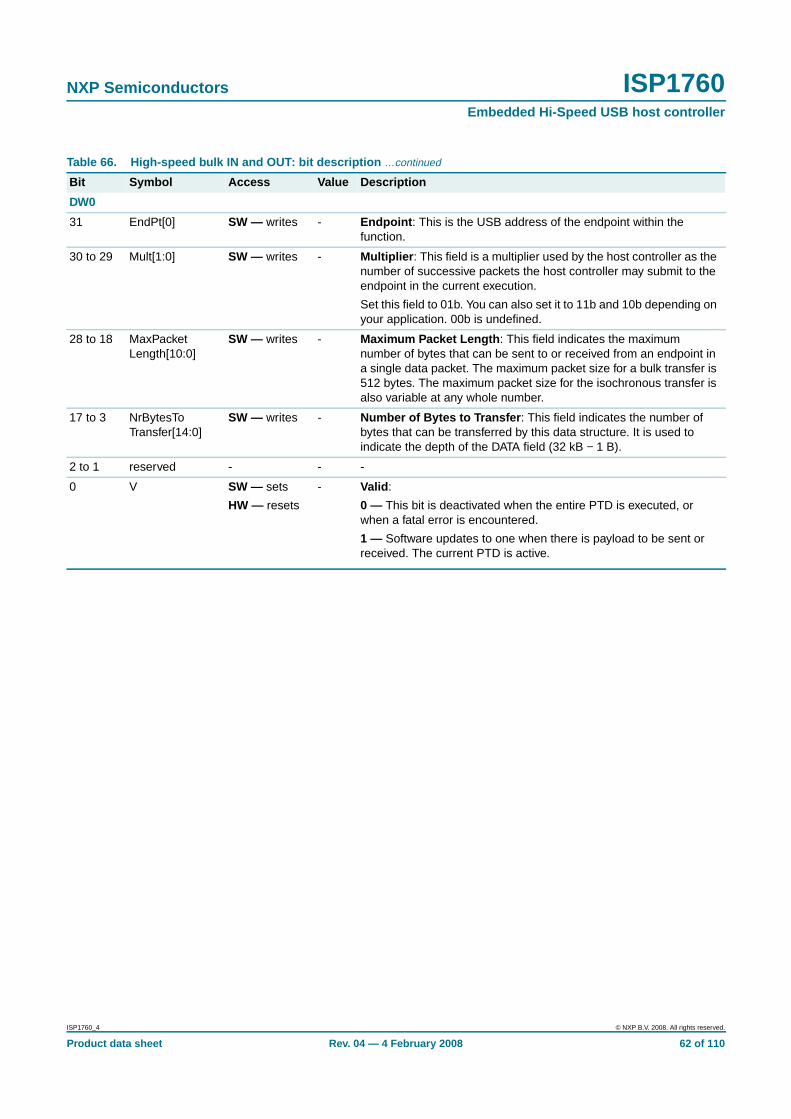
NXP Semiconductors ISP1760Embedded Hi-Speed USB host controller
DW0
31 EndPt[0] SW — writes - Endpoint : This is the USB address of the endpoint within thefunction.
30 to 29 Mult[1:0] SW — writes - Multiplier : This field is a multiplier used by the host controller as thenumber of successive packets the host controller may submit to theendpoint in the current execution.
Set this field to 01b. You can also set it to 11b and 10b depending onyour application. 00b is undefined.
28 to 18 MaxPacketLength[10:0]
SW — writes - Maximum Packet Length : This field indicates the maximumnumber of bytes that can be sent to or received from an endpoint ina single data packet. The maximum packet size for a bulk transfer is512 bytes. The maximum packet size for the isochronous transfer isalso variable at any whole number.
17 to 3 NrBytesToTransfer[14:0]
SW — writes - Number of Bytes to Transfer : This field indicates the number ofbytes that can be transferred by this data structure. It is used toindicate the depth of the DATA field (32 kB − 1 B).
2 to 1 reserved - - -
0 V SW — sets
HW — resets
- Valid :
0 — This bit is deactivated when the entire PTD is executed, orwhen a fatal error is encountered.
1 — Software updates to one when there is payload to be sent orreceived. The current PTD is active.
Table 66. High-speed bulk IN and OUT: bit description …continued
Bit Symbol Access Value Description
ISP1760_4 © NXP B.V. 2008. All rights reserved.
Product data sheet Rev. 04 — 4 February 2008 62 of 110

xxxxxxxxxxxxxxxxxxxxx xxxxxxxxxxxxxxxxxxxxxxxxxx xxxxxxx x x x xxxxxxxxxxxxxxxxxxxxxxxxxxxxxx xxxxxxxxxxxxxxxxxxx xx xxxxxxx xxxxxxxxxxxxxxxxxxxxxxxxxxx xxxxxxxxxxxxxxxxxxx xxxxxx xxxxxxxxxxxxxxxxxxxxxxxxxxxxxxxxxxx xxxxxxxxxxxx x xxxxxxxxxxxxxxxxxxxxxx xxxxxxxxxxxxxxxxxxxxxxxxxxxxxx xxxxx xxxxxxxxxxxxxxxxxxxxxxxxxxxxxxxxxxxxxxxxxxxxxxxxxx xxxxxxxxxxxxxxxxxxxxxxxxxxxxxxxxx xxxxxxxxxxxxxxxxxxxx xxx
ISP
1760_4
Product data shee
NX
P S
emiconductors
ISP
1760E
mbedded H
i-Speed U
SB
host controller
9.2 High-speed isochronous IN and OUTTable 67 shows the bit allocation of the high-speed isochronous IN and OUT, isochronous Transfer Descriptor (iTD).
Table 67. High-speed isochronous IN and OUT: bit allocation
0 39 38 37 36 35 34 33 32
ISOIN_5[11:4]
ISOIN_0[11:0]
4:0] (32 kB − 1 B for high-speed)
DeviceAddress[6:0] EndPt[3:1]
8 7 6 5 4 3 2 1 0
] ISOIN_2[11:8]
0] µSA[7:0]
µFrame[7:0]
:0] [1] V
© N
XP
B.V. 2008. A
ll rights reserved.
tR
ev. 04 — 4 F
ebruary 200863 of 110
[1] Reserved.
[2] EndPt[0].
Bit 63 62 61 60 59 58 57 56 55 54 53 52 51 50 49 48 47 46 45 44 43 42 41 4
DW7 ISOIN_7[11:0] ISOIN_6[11:0]
DW5 ISOIN_2[7:0] ISOIN_1[11:0]
DW3 A H B reserved NrBytesTransferred[1
DW1 reserved S EPType[1:0]
Token[1:0]
Bit 31 30 29 28 27 26 25 24 23 22 21 20 19 18 17 16 15 14 13 12 11 10 9
DW6 ISOIN_5[3:0] ISOIN_4[11:0] ISOIN_3[11:0
DW4 Status7[2:0] Status6[2:0] Status5[2:0] Status4[2:0] Status3[2:0] Status2[2:0] Status1[2:0] Status0[2:
DW2 reserved DataStartAddress[15:0]
DW0 [2] Mult[1:0]
MaxPacketLength[10:0] NrBytesToTransfer[14

NXP Semiconductors ISP1760Embedded Hi-Speed USB host controller
Table 68. High-speed isochronous IN and OUT: bit description
Bit Symbol Access Value Description
DW7
63 to 52 ISOIN_7[11:0] HW — writes - Bytes received during µSOF7, if µSA[7] is set to 1 and frame number iscorrect.
51 to 40 ISOIN_6[11:0] HW — writes - Bytes received during µSOF6, if µSA[6] is set to 1 and frame number iscorrect.
39 to 32 ISOIN_5[11:4] HW — writes - Bytes received during µSOF5 (bits 11 to 4), if µSA[5] is set to 1 andframe number is correct.
DW6
31 to 28 ISOIN_5[3:0] HW — writes - Bytes received during µSOF5 (bits 3 to 0), if µSA[5] is set to 1 andframe number is correct.
27 to 16 ISOIN_4[11:0] HW — writes - Bytes received during µSOF4, if µSA[4] is set to 1 and frame number iscorrect.
15 to 4 ISOIN_3[11:0] HW — writes - Bytes received during µSOF3, if µSA[3] is set to 1 and frame number iscorrect.
3 to 0 ISOIN_2[11:8] HW — writes - Bytes received during µSOF2 (bits 11 to 8), if µSA[2] is set to 1 andframe number is correct.
DW5
63 to 56 ISOIN_2[7:0] HW — writes - Bytes received during µSOF2 (bits 7 to 0), if µSA[2] is set to 1 andframe number is correct.
55 to 44 ISOIN_1[11:0] HW — writes - Bytes received during µSOF1, if µSA[1] is set to 1 and frame number iscorrect.
43 to 32 ISOIN_0[11:0] HW — writes - Bytes received during µSOF0, if µSA[0] is set to 1 and frame number iscorrect.
DW4
31 to 29 Status7[2:0] HW — writes - ISO IN or OUT status at µSOF7
28 to 26 Status6[2:0] HW — writes - ISO IN or OUT status at µSOF6
25 to 23 Status5[2:0] HW — writes - ISO IN or OUT status at µSOF5
22 to 20 Status4[2:0] HW — writes - ISO IN or OUT status at µSOF4
19 to 17 Status3[2:0] HW — writes - ISO IN or OUT status at µSOF3
16 to 14 Status2[2:0] HW — writes - ISO IN or OUT status at µSOF2
13 to 11 Status1[2:0] HW — writes - ISO IN or OUT status at µSOF1
10 to 8 Status0[2:0] HW — writes - Status of the payload on the USB bus for this µSOF after ISO has beendelivered.
Bit 0 — Transaction error (IN and OUT)
Bit 1 — Babble (IN token only)
Bit 2 — Underrun (OUT token only)
7 to 0 µSA[7:0] SW — writes(0 → 1)
HW — writes(1 → 0)
Afterprocessing
- µSOF Active : When the frame number of bits DW1[7:3] match theframe number of USB bus, these bits are checked for 1 before they aresent for µSOF. For example: If µSA[7:0] = 1, 1, 1, 1, 1, 1, 1, 1: sendISO every µSOF of the entire millisecond. If µSA[7:0] = 0, 1, 0, 1, 0, 1,0, 1: send ISO only on µSOF0, µSOF2, µSOF4 and µSOF6.
DW3
ISP1760_4 © NXP B.V. 2008. All rights reserved.
Product data sheet Rev. 04 — 4 February 2008 64 of 110

NXP Semiconductors ISP1760Embedded Hi-Speed USB host controller
63 A SW — sets - Active : This bit is the same as the Valid bit.
62 H HW — writes - Halt : Only one bit for the entire millisecond. When this bit is set, theValid bit is reset. The device decides to stall an endpoint.
61 B HW — writes - Babble : Not applicable here.
60 to 47 reserved - 0 Set to 0 for isochronous.
46 to 32 NrBytesTransferred[14:0]
HW — writes - Number of Bytes Transferred : This field indicates the number ofbytes sent or received for this transaction. If Mult[1:0] is greater thanone, it is possible to store intermediate results in this field.NrBytesTransferred[14:0] is 32 kB − 1 B per PTD.
DW2
31 to 24 reserved - 0 Set to 0 for isochronous.
23 to 8 DataStartAddress[15:0]
SW — writes - Data Start Address : This is the start address for data that will be sentor received on or from the USB bus. This is the internal memoryaddress and not the direct CPU address.
RAM address = (CPU address − 400h) / 8
7 to 0 µFrame[7:0] SW — writes - Bits 2 to 0 — Don’t care
Bits 7 to 3 — Frame number that this PTD will be sent for ISO OUT orIN
DW1
63 to 47 reserved - - -
46 S SW — writes - This bit indicates whether a split transaction has to be executed.
0 — High-speed transaction
1 — Split transaction
45 to 44 EPType[1:0] SW — writes - Endpoint type :
01 — Isochronous
43 to 42 Token[1:0] SW — writes - Token : This field indicates the token PID for this transaction:
00 — OUT
01 — IN
41 to 35 DeviceAddress[6:0]
SW — writes - Device Address : This is the USB address of the function containingthe endpoint that is referred to by this buffer.
34 to 32 EndPt[3:1] SW — writes - Endpoint : This is the USB address of the endpoint within the function.
DW0
31 EndPt[0] SW — writes - Endpoint : This is the USB address of the endpoint within the function.
30 to 29 Mult[1:0] SW — writes - This field is a multiplier counter used by the host controller as thenumber of successive packets the host controller may submit to theendpoint in the current execution.
For details, refer to Appendix D of Ref. 2 “Enhanced Host ControllerInterface Specification for Universal Serial Bus Rev. 1.0”.
28 to 18 MaxPacketLength[10:0]
SW — writes - Maximum Packet Length : This field indicates the maximum numberof bytes that can be sent to or received from the endpoint in a singledata packet. The maximum packet size for an isochronous transfer is1024 bytes. The maximum packet size for the isochronous transfer isalso variable at any whole number.
Table 68. High-speed isochronous IN and OUT: bit description …continued
Bit Symbol Access Value Description
ISP1760_4 © NXP B.V. 2008. All rights reserved.
Product data sheet Rev. 04 — 4 February 2008 65 of 110

NXP Semiconductors ISP1760Embedded Hi-Speed USB host controller
17 to 3 NrBytesToTransfer[14:0]
SW — writes - Number of Bytes Transferred : This field indicates the number ofbytes that can be transferred by this data structure. It is used toindicate the depth of the DATA field (32 kB − 1 B).
2 to 1 reserved - - -
0 V HW — resets
SW — sets
- 0 — This bit is deactivated when the entire PTD is executed, or when afatal error is encountered.
1 — Software updates to one when there is payload to be sent orreceived. The current PTD is active.
Table 68. High-speed isochronous IN and OUT: bit description …continued
Bit Symbol Access Value Description
ISP1760_4 © NXP B.V. 2008. All rights reserved.
Product data sheet Rev. 04 — 4 February 2008 66 of 110

xxxxxxxxxxxxxxxxxxxxx xxxxxxxxxxxxxxxxxxxxxxxxxx xxxxxxx x x x xxxxxxxxxxxxxxxxxxxxxxxxxxxxxx xxxxxxxxxxxxxxxxxxx xx xxxxxxx xxxxxxxxxxxxxxxxxxxxxxxxxxx xxxxxxxxxxxxxxxxxxx xxxxxx xxxxxxxxxxxxxxxxxxxxxxxxxxxxxxxxxxx xxxxxxxxxxxx x xxxxxxxxxxxxxxxxxxxxxx xxxxxxxxxxxxxxxxxxxxxxxxxxxxxx xxxxx xxxxxxxxxxxxxxxxxxxxxxxxxxxxxxxxxxxxxxxxxxxxxxxxxx xxxxxxxxxxxxxxxxxxxxxxxxxxxxxxxxx xxxxxxxxxxxxxxxxxxxx xxx
ISP
1760_4
Product data shee
NX
P S
emiconductors
ISP
1760E
mbedded H
i-Speed U
SB
host controller
9.3 High-speed interrupt IN and OUTTable 69 shows the bit allocation of the high-speed interrupt IN and OUT, periodic Transfer Descriptor (pTD).
Table 69. High-speed interrupt IN and OUT: bit allocation
0 39 38 37 36 35 34 33 32
INT_IN_5[11:4]
INT_IN_0[11:0]
4:0] (32 kB − 1 B for high-speed)
DeviceAddress[6:0] EndPt[3:1]
8 7 6 5 4 3 2 1 0
] INT_IN_2[11:8]
0] µSA[7:0]
µFrame[7:0]
:0] [1] V
© N
XP
B.V. 2008. A
ll rights reserved.
tR
ev. 04 — 4 F
ebruary 200867 of 110
[1] Reserved.
[2] EndPt[0].
Bit 63 62 61 60 59 58 57 56 55 54 53 52 51 50 49 48 47 46 45 44 43 42 41 4
DW7 INT_IN_7[11:0] INT_IN_6[11:0]
DW5 INT_IN_2[7:0] INT_IN_1[11:0]
DW3 A H reserved DT Cerr[1:0]
reserved NrBytesTransferred[1
DW1 reserved S EPType[1:0]
Token[1:0]
Bit 31 30 29 28 27 26 25 24 23 22 21 20 19 18 17 16 15 14 13 12 11 10 9
DW6 INT_IN_5[3:0] INT_IN_4[11:0] INT_IN_3[11:0
DW4 Status7[2:0] Status6[2:0] Status5[2:0] Status4[2:0] Status3[2:0] Status2[2:0] Status1[2:0] Status0[2:
DW2 reserved DataStartAddress[15:0]
DW0 [2] Mult[1:0]
MaxPacketLength[10:0] NrBytesToTransfer[14

NXP Semiconductors ISP1760Embedded Hi-Speed USB host controller
Table 70. High-speed interrupt IN and OUT: bit description
Bit Symbol Access Value Description
DW7
63 to 52 INT_IN_7[11:0] HW — writes - Bytes received during µSOF7, if µSA[7] is set to 1 and frame numberis correct.
51 to 40 INT_IN_6[11:0] HW — writes - Bytes received during µSOF6, if µSA[6] is set to 1 and frame numberis correct.
39 to 32 INT_IN_5[11:4] HW — writes - Bytes received during µSOF5 (bits 11 to 4), if µSA[5] is set to 1 andframe number is correct.
DW6
31 to 28 INT_IN_5[3:0] HW — writes - Bytes received during µSOF5 (bits 3 to 0), if µSA[5] is set to 1 andframe number is correct.
27 to 16 INT_IN_4[11:0] HW — writes - Bytes received during µSOF4, if µSA[4] is set to 1 and frame numberis correct.
15 to 4 INT_IN_3[11:0] HW — writes - Bytes received during µSOF3, if µSA[3] is set to 1 and frame numberis correct.
3 to 0 INT_IN_2[11:8] HW — writes - Bytes received during µSOF2 (bits 11 to 8), if µSA[2] is set to 1 andframe number is correct.
DW5
63 to 56 INT_IN_2[7:0] HW — writes - Bytes received during µSOF2 (bits 7 to 0), if µSA[2] is set to 1 andframe number is correct.
55 to 44 INT_IN_1[11:0] HW — writes - Bytes received during µSOF1, if µSA[1] is set to 1 and frame numberis correct.
43 to 32 INT_IN_0[11:0] HW — writes - Bytes received during µSOF0, if µSA[0] is set to 1 and frame numberis correct.
DW4
31 to 29 Status7[2:0] HW — writes - INT IN or OUT status of µSOF7
28 to 26 Status6[2:0] HW — writes - INT IN or OUT status of µSOF6
25 to 23 Status5[2:0] HW — writes - INT IN or OUT status of µSOF5
22 to 20 Status4[2:0] HW — writes - INT IN or OUT status of µSOF4
19 to 17 Status3[2:0] HW — writes - INT IN or OUT status of µSOF3
16 to 14 Status2[2:0] HW — writes - INT IN or OUT status of µSOF2
13 to 11 Status1[2:0] HW — writes - INT IN or OUT status of µSOF1
10 to 8 Status0[2:0] HW — writes - Status of the payload on the USB bus for this µSOF after INT hasbeen delivered.
Bit 0 — Transaction error (IN and OUT)
Bit 1 — Babble (IN token only)
Bit 2 — Underrun (OUT token only)
7 to 0 µSA[7:0] SW — writes(0 → 1)
HW — writes(1 → 0)
Afterprocessing
- When the frame number of bits DW2[7:3] match the frame number ofthe USB bus, these bits are checked for 1 before they are sent forµSOF. For example: When µSA[7:0] = 1, 1, 1, 1, 1, 1, 1, 1: send INTfor every µSOF of the entire millisecond. When µSA[7:0] = 0, 1, 0, 1,0, 1, 0, 1: send INT for µSOF0, µSOF2, µSOF4 and µSOF6. WhenµSA[7:0] = 1, 0, 0, 0, 1, 0, 0, 0: send INT for every fourth µSOF.
ISP1760_4 © NXP B.V. 2008. All rights reserved.
Product data sheet Rev. 04 — 4 February 2008 68 of 110

NXP Semiconductors ISP1760Embedded Hi-Speed USB host controller
DW3
63 A HW — writes
SW — writes
- Active : Write the same value as that in V.
62 H HW — writes - Halt : Transaction is halted.
61 to 58 reserved - - -
57 DT HW — writes
SW — writes
- Data Toggle : Set the Data Toggle bit to start the PTD. Softwarewrites the current transaction toggle value. Hardware writes the nexttransaction toggle value.
56 to 55 Cerr[1:0] HW — writes
SW — writes
- Error Counter . This field corresponds to the Cerr[1:0] field in the TD.The default value of this field is zero for isochronous transactions.
54 to 47 reserved - - -
46 to 32 NrBytesTransferred[14:0]
HW — writes - Number of Bytes Transferred : This field indicates the number ofbytes sent or received for this transaction. If Mult[1:0] is greater thanone, it is possible to store intermediate results in this field.
DW2
31 to 24 reserved - - -
23 to 8 DataStartAddress[15:0]
SW — writes - Data Start Address : This is the start address for data that will besent or received on or from the USB bus. This is the internal memoryaddress and not the direct CPU address.
RAM address = (CPU address − 400h) / 8
7 to 0 µFrame[7:0] SW — writes - Bits 7 to 3 represent the polling rate in milliseconds.
The INT polling rate is defined as 2(b − 1) µSOF, where b is 1 to 9.
When b is 1, 2, 3 or 4, use µSA to define polling because the rate isequal to or less than 1 ms. Bits 7 to 3 are set to 0. Polling checks µSAbits for µSOF rates. See Table 71.
DW1
63 to 47 reserved - - -
46 S SW — writes - This bit indicates if a split transaction has to be executed:
0 — High-speed transaction
1 — Split transaction
45 to 44 EPType[1:0] SW — writes - Endpoint type :
11 — Interrupt
43 to 42 Token[1:0] SW — writes - Token : This field indicates the token PID for this transaction:
00 — OUT
01 — IN
41 to 35 DeviceAddress[6:0]
SW — writes - Device Address : This is the USB address of the function containingthe endpoint that is referred to by the buffer.
34 to 32 EndPt[3:1] SW — writes - Endpoint : This is the USB address of the endpoint within thefunction.
DW0
31 EndPt[0] SW — writes - Endpoint : This is the USB address of the endpoint within thefunction.
Table 70. High-speed interrupt IN and OUT: bit description …continued
Bit Symbol Access Value Description
ISP1760_4 © NXP B.V. 2008. All rights reserved.
Product data sheet Rev. 04 — 4 February 2008 69 of 110

NXP Semiconductors ISP1760Embedded Hi-Speed USB host controller
30 to 29 Mult[1:0] SW — writes - Multiplier : This field is a multiplier counter used by the host controlleras the number of successive packets the host controller may submitto the endpoint in the current execution.
Set this field to 01b. You can also set it to 11b and 10b, depending onyour application. 00b is undefined.
28 to 18 MaxPacketLength[10:0]
SW — writes - Maximum Packet Length : This field indicates the maximum numberof bytes that can be sent to or received from the endpoint in a singledata packet.
17 to 3 NrBytesToTransfer[14:0]
SW — writes - Number of Bytes to Transfer : This field indicates the number ofbytes that can be transferred by this data structure. It is used toindicate the depth of the DATA field (32 kB − 1 B).
2 to 1 reserved - - -
0 V SW — sets
HW — resets
- Valid :
0 — This bit is deactivated when the entire PTD is executed, or whena fatal error is encountered.
1 — Software updates to one when there is payload to be sent orreceived. The current PTD is active.
Table 70. High-speed interrupt IN and OUT: bit description …continued
Bit Symbol Access Value Description
Table 71. Microframe description
b Rate µFrame[7:3] µSA[7:0]
1 1 µSOF 0 0000 1111 1111
2 2 µSOF 0 0000 1010 1010 or 0101 0101
3 4 µSOF 0 0000 any 2 bits set
4 1 ms 0 0000 any 1 bit set
5 2 ms 0 0001 any 1 bit set
6 4 ms 0 0010 to 0 0011 any 1 bit set
7 8 ms 0 0100 to 0 0111 any 1 bit set
8 16 ms 0 1000 to 0 1111 any 1 bit set
9 32 ms 1 0000 to 1 1111 any 1 bit set
ISP1760_4 © NXP B.V. 2008. All rights reserved.
Product data sheet Rev. 04 — 4 February 2008 70 of 110

xxxxxxxxxxxxxxxxxxxxx xxxxxxxxxxxxxxxxxxxxxxxxxx xxxxxxx x x x xxxxxxxxxxxxxxxxxxxxxxxxxxxxxx xxxxxxxxxxxxxxxxxxx xx xxxxxxx xxxxxxxxxxxxxxxxxxxxxxxxxxx xxxxxxxxxxxxxxxxxxx xxxxxx xxxxxxxxxxxxxxxxxxxxxxxxxxxxxxxxxxx xxxxxxxxxxxx x xxxxxxxxxxxxxxxxxxxxxx xxxxxxxxxxxxxxxxxxxxxxxxxxxxxx xxxxx xxxxxxxxxxxxxxxxxxxxxxxxxxxxxxxxxxxxxxxxxxxxxxxxxx xxxxxxxxxxxxxxxxxxxxxxxxxxxxxxxxx xxxxxxxxxxxxxxxxxxxx xxx
ISP
1760_4
Product data shee
NX
P S
emiconductors
ISP
1760E
mbedded H
i-Speed U
SB
host controller
9.4 Start and complete split for bulkTable 72 shows the bit allocation of Start Split (SS) and Complete Split (CS) for bulk, asynchronous Start Split and CompleteSplit (SS/CS) Transfer Descriptor (TD).
Table 72. Start and complete split for bulk: bit allocation
0 39 38 37 36 35 34 33 32
sTransferred[14:0]
DeviceAddress[6:0] EndPt[3:1]
8 7 6 5 4 3 2 1 0
J NextPTDAddress[4:0]
reserved
:0] [1] V
© N
XP
B.V. 2008. A
ll rights reserved.
tR
ev. 04 — 4 F
ebruary 200871 of 110
[1] Reserved.
[2] EndPt[0].
Bit 63 62 61 60 59 58 57 56 55 54 53 52 51 50 49 48 47 46 45 44 43 42 41 4
DW7 reserved
DW5 reserved
DW3 A H B X SC [1] DT Cerr[1:0]
NakCnt[3:0] reserved NrByte
DW1 HubAddress[6:0] PortNumber[6:0] SE[1:0] [1] S EPType[1:0]
Token[1:0]
Bit 31 30 29 28 27 26 25 24 23 22 21 20 19 18 17 16 15 14 13 12 11 10 9
DW6 reserved
DW4 reserved
DW2 reserved RL[3:0] [1] DataStartAddress[15:0]
DW0 [2] [1] MaxPacketLength[10:0] NrBytesToTransfer[14

NXP Semiconductors ISP1760Embedded Hi-Speed USB host controller
Table 73. Start and complete split for bulk: bit description
Bit Symbol Access Value Description
DW7
63 to 32 reserved - - -
DW6
31 to 0 reserved - - -
DW5
63 to 32 reserved - - -
DW4
31 to 6 reserved - - -
5 J SW — writes - 0 — To increment the PTD pointer.
1 — To enable the next PTD branching.
4 to 0 NextPTDPointer[4:0]
SW — writes - Next PTD branching assigned by the PTD pointer.
DW3
63 A SW — sets
HW — resets
- Active : Write the same value as that in V.
62 H HW — writes - Halt : This bit corresponds to the Halt bit of the Status field of TD.
61 B HW — writes - Babble : This bit corresponds to the Babble Detected bit in theStatus field of iTD, siTD or TD.
1 — When babbling is detected, A and V are set to 0.
60 X HW — writes - Transaction Error : This bit corresponds to the Transaction Errorbit in the status field.
SW — writes - 0 — Before scheduling
59 SC SW — writes 0
HW — updates
- Start/Complete :
0 — Start split
1 — Complete split
58 reserved - - -
57 DT HW — writes
SW — writes
- Data Toggle : Set the Data Toggle bit to start for the PTD.
56 to 55 Cerr[1:0] HW — updates
SW — writes
- Error Counter : This field contains the error count forasynchronous start and complete split (SS/CS) TD. When an errorhas no response or bad response, Cerr[1:0] will be decrementedto zero and then Valid will be set to zero. A NAK or NYET will resetCerr[1:0]. For details, refer to Section 4.12.1.2 of Ref. 2 “EnhancedHost Controller Interface Specification for Universal Serial BusRev. 1.0”.
If retry has insufficient time at the beginning of a new SOF, the firstPTD must be this retry. This can be accomplished if aperiodic PTDis not advanced.
54 to 51 NakCnt[3:0] HW — writes
SW — writes
- NAK Counter : The V bit is reset if NakCnt decrements to zero andRL is a nonzero value. Not applicable to isochronous splittransactions.
50 to 47 reserved - - -
ISP1760_4 © NXP B.V. 2008. All rights reserved.
Product data sheet Rev. 04 — 4 February 2008 72 of 110

NXP Semiconductors ISP1760Embedded Hi-Speed USB host controller
46 to 32 NrBytesTransferred[14:0]
HW — writes - Number of Bytes Transferred : This field indicates the number ofbytes sent or received for this transaction.
DW2
31 to 29 reserved - - -
28 to 25 RL[3:0] SW — writes - Reload : If RL is set to 0h, hardware ignores the NakCnt value. SetRL and NakCnt to the same value before a transaction. Forfull-speed and low-speed transactions, set this field to 0000b. Notapplicable to isochronous start split and complete split.
24 reserved - - -
23 to 8 DataStartAddress[15:0]
SW — writes - Data Start Address : This is the start address for data that will besent or received on or from the USB bus. This is the internalmemory address and not the direct CPU address.
RAM address = (CPU address − 400h) / 8
7 to 0 reserved - - -
DW1
63 to 57 HubAddress[6:0] SW — writes - Hub Address : This indicates the hub address.
56 to 50 PortNumber[6:0] SW — writes - Port Number : This indicates the port number of the hub orembedded TT.
49 to 48 SE[1:0] SW — writes - This depends on the endpoint type and direction. It is valid only forsplit transactions. Table 74 applies to start split and complete splitonly.
47 reserved - - -
46 S SW — writes - This bit indicates whether a split transaction has to be executed:
0 — High-speed transaction
1 — Split transaction
45 to 44 EPType[1:0] SW — writes - Endpoint Type :
00 — Control
10 — Bulk
43 to 42 Token[1:0] SW — writes - Token : This field indicates the PID for this transaction.
00 — OUT
01 — IN
10 — SETUP
41 to 35 DeviceAddress[6:0] SW — writes - Device Address : This is the USB address of the functioncontaining the endpoint that is referred to by this buffer.
34 to 32 EndPt[3:1] SW — writes - Endpoint : This is the USB address of the endpoint within thefunction.
DW0
31 EndPt[0] SW — writes - Endpoint : This is the USB address of the endpoint within thefunction.
30 to 29 reserved - - -
28 to 18 MaximumPacketLength[10:0]
SW — writes - Maximum Packet Length : This field indicates the maximumnumber of bytes that can be sent to or received from an endpointin a single data packet. The maximum packet size for full-speed is64 bytes as defined in the Ref. 1 “Universal Serial BusSpecification Rev. 2.0”.
Table 73. Start and complete split for bulk: bit description …continued
Bit Symbol Access Value Description
ISP1760_4 © NXP B.V. 2008. All rights reserved.
Product data sheet Rev. 04 — 4 February 2008 73 of 110

NXP Semiconductors ISP1760Embedded Hi-Speed USB host controller
17 to 3 NrBytesToTransfer[14:0]
SW — writes - Number of Bytes to Transfer : This field indicates the number ofbytes that can be transferred by this data structure. It is used toindicate the depth of the DATA field.
2 to 1 reserved - - -
0 V SW — sets
HW — resets
- Valid :
0 — This bit is deactivated when the entire PTD is executed, orwhen a fatal error is encountered.
1 — Software updates to one when there is payload to be sent orreceived. The current PTD is active.
Table 73. Start and complete split for bulk: bit description …continued
Bit Symbol Access Value Description
Table 74. SE description
Bulk Control S E Remarks
I/O I/O 1 0 low-speed
I/O I/O 0 0 full-speed
ISP1760_4 © NXP B.V. 2008. All rights reserved.
Product data sheet Rev. 04 — 4 February 2008 74 of 110

xxxxxxxxxxxxxxxxxxxxx xxxxxxxxxxxxxxxxxxxxxxxxxx xxxxxxx x x x xxxxxxxxxxxxxxxxxxxxxxxxxxxxxx xxxxxxxxxxxxxxxxxxx xx xxxxxxx xxxxxxxxxxxxxxxxxxxxxxxxxxx xxxxxxxxxxxxxxxxxxx xxxxxx xxxxxxxxxxxxxxxxxxxxxxxxxxxxxxxxxxx xxxxxxxxxxxx x xxxxxxxxxxxxxxxxxxxxxx xxxxxxxxxxxxxxxxxxxxxxxxxxxxxx xxxxx xxxxxxxxxxxxxxxxxxxxxxxxxxxxxxxxxxxxxxxxxxxxxxxxxx xxxxxxxxxxxxxxxxxxxxxxxxxxxxxxxxx xxxxxxxxxxxxxxxxxxxx xxx
ISP
1760_4
Product data shee
NX
P S
emiconductors
ISP
1760E
mbedded H
i-Speed U
SB
host controller
9.5 Start and complete split for isochronousTable 75 shows the bit allocation for start and complete split for isochronous, split isochronous Transfer Descriptor (siTD).
Table 75. Start and complete split for isochronous: bit allocation
0 39 38 37 36 35 34 33 32
ISO_IN_7[7:0]
µSCS[7:0][2]
NrBytesTransferred[11:0]
DeviceAddress[6:0] EndPt[3:1]
8 7 6 5 4 3 2 1 0
ISO_IN_3[7:0]
0] µSA[7:0]
µFrame[7:0] (full-speed)
or full-speed) [1] V
© N
XP
B.V. 2008. A
ll rights reserved.
tR
ev. 04 — 4 F
ebruary 200875 of 110
[1] Reserved.
[2] EndPt[0].
Bit 63 62 61 60 59 58 57 56 55 54 53 52 51 50 49 48 47 46 45 44 43 42 41 4
DW7 reserved
DW5 ISO_IN_2[7:0] ISO_IN_1[7:0] ISO_IN_0[7:0]
DW3 A H B X SC [1] DT reserved
DW1 HubAddress[6:0] PortNumber[6:0] reserved S EPType[1:0]
Token[1:0]
Bit 31 30 29 28 27 26 25 24 23 22 21 20 19 18 17 16 15 14 13 12 11 10 9
DW6 ISO_IN_6[7:0] ISO_IN_5[7:0] ISO_IN_4[7:0]
DW4 Status7[2:0] Status6[2:0] Status5[2:0] Status4[2:0] Status3[2:0] Status2[2:0] Status1[2:0] Status0[2:
DW2 reserved DataStartAddress[15:0]
DW0 [2] [1] TT_MPS_Len[10:0] NrBytesToTransfer[14:0] (1 kB f

NXP Semiconductors ISP1760Embedded Hi-Speed USB host controller
Table 76. Start and complete split for isochronous: bit description
Bit Symbol Access Value Description
DW7
63 to 40 reserved - - -
39 to 32 ISO_IN_7[7:0] HW — writes - Bytes received during µSOF7, if µSA[7] is set to 1 and framenumber is correct.
DW6
31 to 24 ISO_IN_6[7:0] HW — writes - Bytes received during µSOF6, if µSA[6] is set to 1 and framenumber is correct.
23 to 16 ISO_IN_5[7:0] HW — writes - Bytes received during µSOF5, if µSA[5] is set to 1 and framenumber is correct.
15 to 8 ISO_IN_4[7:0] HW — writes - Bytes received during µSOF4, if µSA[4] is set to 1 and framenumber is correct.
7 to 0 ISO_IN_3[7:0] HW — writes - Bytes received during µSOF3, if µSA[3] is set to 1 and framenumber is correct.
DW5
63 to 56 ISO_IN_2[7:0] HW — writes - Bytes received during µSOF2 (bits 7 to 0), if µSA[2] is set to 1 andframe number is correct.
55 to 48 ISO_IN_1[7:0] HW — writes - Bytes received during µSOF1, if µSA[1] is set to 1 and framenumber is correct.
47 to 40 ISO_IN_0[7:0] HW — writes - Bytes received during µSOF0 if µSA[0] is set to 1 and framenumber is correct.
39 to 32 µSCS[7:0] SW — writes(0 → 1)
HW — writes(1 → 0)
After processing
- All bits can be set to one for every transfer. It specifies which µSOFthe complete split needs to be sent. Valid only for IN. Start split andcomplete split active bits, µSA = 0000 0001, µSCS = 0000 0100,will cause SS to execute in µFrame0 and CS in µFrame2.
DW4
31 to 29 Status7[2:0] HW — writes - Isochronous IN or OUT status of µSOF7
28 to 26 Status6[2:0] HW — writes - Isochronous IN or OUT status of µSOF6
25 to 23 Status5[2:0] HW — writes - Isochronous IN or OUT status of µSOF5
22 to 20 Status4[2:0] HW — writes - Isochronous IN or OUT status of µSOF4
19 to 17 Status3[2:0] HW — writes - Isochronous IN or OUT status of µSOF3
16 to 14 Status2[2:0] HW — writes - Isochronous IN or OUT status of µSOF2
13 to 11 Status1[2:0] HW — writes - Isochronous IN or OUT status of µSOF1
10 to 8 Status0[2:0] HW — writes - Isochronous IN or OUT status of µSOF0
Bit 0 — Transaction error (IN and OUT)
Bit 1 — Babble (IN token only)
Bit 2 — Underrun (OUT token only)
ISP1760_4 © NXP B.V. 2008. All rights reserved.
Product data sheet Rev. 04 — 4 February 2008 76 of 110

NXP Semiconductors ISP1760Embedded Hi-Speed USB host controller
7 to 0 µSA[7:0] SW — writes(0 → 1)
HW — writes(1 → 0)
After processing
- Specifies which µSOF the start split needs to be placed.
For OUT token : When the frame number of bits DW2[7:3] matchesthe frame number of the USB bus, these bits are checked for onebefore they are sent for the µSOF.
For IN token : Only µSOF0, µSOF1, µSOF2 or µSOF3 can be setto 1. Nothing can be set for µSOF4 and above.
DW3
63 A SW — sets
HW — resets
- Active : Write the same value as that in V.
62 H HW — writes - Halt : The Halt bit is set when any microframe transfer status has astalled or halted condition.
61 B HW — writes - Babble : This bit corresponds to bit 1 of Status0 to Status7 for everymicroframe transfer status.
60 X HW — writes - Transaction Error : This bit corresponds to bit 0 of Status0 toStatus7 for every microframe transfer status.
59 SC SW — writes 0
HW — updates
- Start/Complete :
0 — Start split
1 — Complete split
58 reserved - - -
57 DT HW — writes
SW — writes
- Data Toggle : Set the Data Toggle bit to start for the PTD.
56 to 44 reserved - - -
43 to 32 NrBytesTransferred[11:0]
HW — writes - Number of Bytes Transferred : This field indicates the number ofbytes sent or received for this transaction.
DW2
31 to 24 reserved - - -
23 to 8 DataStartAddress[15:0]
SW — writes - Data Start Address : This is the start address for data that will besent or received on or from the USB bus. This is the internalmemory address and not the CPU address.
7 to 0 µFrame[7:0] SW — writes - Bits 7 to 3 determine which frame to execute.
DW1
63 to 57 HubAddress[6:0]
SW — writes - Hub Address : This indicates the hub address.
56 to 50 PortNumber[6:0]
SW — writes - Port Number : This indicates the port number of the hub orembedded TT.
49 to 47 reserved - - -
46 S SW — writes - This bit indicates whether a split transaction has to be executed:
0 — High-speed transaction
1 — Split transaction
45 to 44 EPType[1:0] SW — writes - Transaction type:
01 — Isochronous
Table 76. Start and complete split for isochronous: bit description …continued
Bit Symbol Access Value Description
ISP1760_4 © NXP B.V. 2008. All rights reserved.
Product data sheet Rev. 04 — 4 February 2008 77 of 110

NXP Semiconductors ISP1760Embedded Hi-Speed USB host controller
43 to 42 Token[1:0] SW — writes - Token PID for this transaction:
00 — OUT
01 — IN
41 to 35 DeviceAddress[6:0]
SW — writes - Device Address : This is the USB address of the functioncontaining the endpoint that is referred to by this buffer.
34 to 32 EndPt[3:1] SW — writes - Endpoint : This is the USB address of the endpoint within thefunction.
DW0
31 EndPt[0] SW — writes - Endpoint : This is the USB address of the endpoint within thefunction.
30 to 29 reserved - - -
28 to 18 TT_MPS_Len[10:0]
SW — writes - Transaction Translator Maximum Packet Size Length : This fieldindicates the maximum number of bytes that can be sent per startsplit, depending on the number of total bytes needed. If the totalbytes to be sent for the entire millisecond is greater than 188 bytes,this field should be set to 188 bytes for an OUT token and192 bytes for an IN token. Otherwise, this field should be equal tothe total bytes sent.
17 to 3 NrBytesToTransfer[14:0]
SW — writes - Number of Bytes to Transfer : This field indicates the number ofbytes that can be transferred by this data structure. It is used toindicate the depth of the DATA field. This field is restricted to1023 bytes because in siTD the maximum allowable payload for afull-speed device is 1023 bytes. This field indirectly becomes themaximum packet size of the downstream device.
2 to 1 reserved - - -
0 V SW — sets
HW — resets
- 0 — This bit is deactivated when the entire PTD is executed, orwhen a fatal error is encountered.
1 — Software updates to one when there is payload to be sent orreceived. The current PTD is active.
Table 76. Start and complete split for isochronous: bit description …continued
Bit Symbol Access Value Description
ISP1760_4 © NXP B.V. 2008. All rights reserved.
Product data sheet Rev. 04 — 4 February 2008 78 of 110

xxxxxxxxxxxxxxxxxxxxx xxxxxxxxxxxxxxxxxxxxxxxxxx xxxxxxx x x x xxxxxxxxxxxxxxxxxxxxxxxxxxxxxx xxxxxxxxxxxxxxxxxxx xx xxxxxxx xxxxxxxxxxxxxxxxxxxxxxxxxxx xxxxxxxxxxxxxxxxxxx xxxxxx xxxxxxxxxxxxxxxxxxxxxxxxxxxxxxxxxxx xxxxxxxxxxxx x xxxxxxxxxxxxxxxxxxxxxx xxxxxxxxxxxxxxxxxxxxxxxxxxxxxx xxxxx xxxxxxxxxxxxxxxxxxxxxxxxxxxxxxxxxxxxxxxxxxxxxxxxxx xxxxxxxxxxxxxxxxxxxxxxxxxxxxxxxxx xxxxxxxxxxxxxxxxxxxx xxx
ISP
1760_4
Product data shee
NX
P S
emiconductors
ISP
1760E
mbedded H
i-Speed U
SB
host controller
9.6 Start and complete split for interruptTable 77 shows the bit allocation of start and complete split for interrupt.
Table 77. Start and complete split for interrupt: bit allocation
0 39 38 37 36 35 34 33 32
INT_IN_7[7:0]
µSCS[7:0]
sferred[11:0] (4 kB for full-speed andlow-speed)
DeviceAddress[6:0] EndPt[3:1]
8 7 6 5 4 3 2 1 0
INT_IN_3[7:0]
0] µSA[7:0]
µFrame[7:0] (full-speed andlow-speed)
peed and low-speed) [1] V
© N
XP
B.V. 2008. A
ll rights reserved.
tR
ev. 04 — 4 F
ebruary 200879 of 110
[1] Reserved.
[2] EndPt[0].
Bit 63 62 61 60 59 58 57 56 55 54 53 52 51 50 49 48 47 46 45 44 43 42 41 4
DW7 reserved
DW5 INT_IN_2[7:0] INT_IN_1[7:0] INT_IN_0[7:0]
DW3 A H B X SC [1] DT Cerr[1:0]
reserved NrBytesTran
DW1 HubAddress[6:0] PortNumber[6:0] SE[1:0] [1] S EPType[1:0]
Token[1:0]
Bit 31 30 29 28 27 26 25 24 23 22 21 20 19 18 17 16 15 14 13 12 11 10 9
DW6 INT_IN_6[7:0] INT_IN_5[7:0] INT_IN_4[7:0]
DW4 Status7[2:0] Status6[2:0] Status5[2:0] Status4[2:0] Status3[2:0] Status2[2:0] Status1[2:0] Status0[2:
DW2 reserved DataStartAddress[15:0]
DW0 [2] [1] MaxPacketLength[10:0] NrBytesToTransfer[14:0] (4 kB for full-s
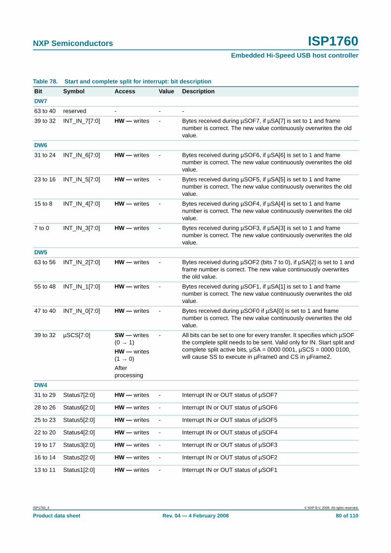
NXP Semiconductors ISP1760Embedded Hi-Speed USB host controller
Table 78. Start and complete split for interrupt: bit description
Bit Symbol Access Value Description
DW7
63 to 40 reserved - - -
39 to 32 INT_IN_7[7:0] HW — writes - Bytes received during µSOF7, if µSA[7] is set to 1 and framenumber is correct. The new value continuously overwrites the oldvalue.
DW6
31 to 24 INT_IN_6[7:0] HW — writes - Bytes received during µSOF6, if µSA[6] is set to 1 and framenumber is correct. The new value continuously overwrites the oldvalue.
23 to 16 INT_IN_5[7:0] HW — writes - Bytes received during µSOF5, if µSA[5] is set to 1 and framenumber is correct. The new value continuously overwrites the oldvalue.
15 to 8 INT_IN_4[7:0] HW — writes - Bytes received during µSOF4, if µSA[4] is set to 1 and framenumber is correct. The new value continuously overwrites the oldvalue.
7 to 0 INT_IN_3[7:0] HW — writes - Bytes received during µSOF3, if µSA[3] is set to 1 and framenumber is correct. The new value continuously overwrites the oldvalue.
DW5
63 to 56 INT_IN_2[7:0] HW — writes - Bytes received during µSOF2 (bits 7 to 0), if µSA[2] is set to 1 andframe number is correct. The new value continuously overwritesthe old value.
55 to 48 INT_IN_1[7:0] HW — writes - Bytes received during µSOF1, if µSA[1] is set to 1 and framenumber is correct. The new value continuously overwrites the oldvalue.
47 to 40 INT_IN_0[7:0] HW — writes - Bytes received during µSOF0 if µSA[0] is set to 1 and framenumber is correct. The new value continuously overwrites the oldvalue.
39 to 32 µSCS[7:0] SW — writes(0 → 1)
HW — writes(1 → 0)
Afterprocessing
- All bits can be set to one for every transfer. It specifies which µSOFthe complete split needs to be sent. Valid only for IN. Start split andcomplete split active bits, µSA = 0000 0001, µSCS = 0000 0100,will cause SS to execute in µFrame0 and CS in µFrame2.
DW4
31 to 29 Status7[2:0] HW — writes - Interrupt IN or OUT status of µSOF7
28 to 26 Status6[2:0] HW — writes - Interrupt IN or OUT status of µSOF6
25 to 23 Status5[2:0] HW — writes - Interrupt IN or OUT status of µSOF5
22 to 20 Status4[2:0] HW — writes - Interrupt IN or OUT status of µSOF4
19 to 17 Status3[2:0] HW — writes - Interrupt IN or OUT status of µSOF3
16 to 14 Status2[2:0] HW — writes - Interrupt IN or OUT status of µSOF2
13 to 11 Status1[2:0] HW — writes - Interrupt IN or OUT status of µSOF1
ISP1760_4 © NXP B.V. 2008. All rights reserved.
Product data sheet Rev. 04 — 4 February 2008 80 of 110

NXP Semiconductors ISP1760Embedded Hi-Speed USB host controller
10 to 8 Status0[2:0] HW — writes - Interrupt IN or OUT status of µSOF0
Bit 0 — Transaction error (IN and OUT)
Bit 1 — Babble (IN token only)
Bit 2 — Underrun (OUT token only)
7 to 0 µSA[7:0] SW — writes(0 → 1)
HW — writes(1 → 0)
Afterprocessing
- Specifies which µSOF the start split needs to be placed.
For OUT token : When the frame number of bits DW1[7:3]matches the frame number of the USB bus, these bits are checkedfor one before they are sent for the µSOF.
For IN token : Only µSOF0, µSOF1, µSOF2 or µSOF3 can be setto 1. Nothing can be set for µSOF4 and above.
DW3
63 A SW — sets
HW — resets
- Active : Write the same value as that in V.
62 H HW — writes - Halt : The Halt bit is set when any microframe transfer status has astalled or halted condition.
61 B HW — writes - Babble : This bit corresponds to bit 1 of Status0 to Status7 forevery microframe transfer status.
60 X HW — writes - Transaction Error : This bit corresponds to bit 0 of Status0 toStatus7 for every microframe transfer status.
59 SC SW — writes 0
HW — updates
- Start/Complete :
0 — Start split
1 — Complete split
58 reserved - - -
57 DT HW — writes
SW — writes
- Data Toggle : For an interrupt transfer, set correct bit to start thePTD.
56 to 55 Cerr[1:0] HW — writes
SW — writes
- Error Counter : This field corresponds to the Cerr[1:0] field in TD.
00 — The transaction will not retry.
11 — The transaction will retry three times. Hardware willdecrement these values.
54 to 44 reserved - - -
43 to 32 NrBytesTransferred[11:0]
HW — writes - Number of Bytes Transferred : This field indicates the number ofbytes sent or received for this transaction.
DW2
31 to 24 reserved - - -
23 to 8 DataStartAddress[15:0]
SW — writes - Data Start Address : This is the start address for data that will besent or received on or from the USB bus. This is the internalmemory address and not the CPU address.
7 to 0 µFrame[7:0] SW — writes - Bits 7 to 3 is the polling rate in milliseconds. Polling rate is definedas 2(b − 1) µSOF; where b = 4 to 16. When b is 4, executed everymillisecond. See Table 79.
DW1
63 to 57 HubAddress[6:0]
SW — writes - Hub Address : This indicates the hub address.
Table 78. Start and complete split for interrupt: bit description …continued
Bit Symbol Access Value Description
ISP1760_4 © NXP B.V. 2008. All rights reserved.
Product data sheet Rev. 04 — 4 February 2008 81 of 110

NXP Semiconductors ISP1760Embedded Hi-Speed USB host controller
56 to 50 PortNumber[6:0] SW — writes - Port Number : This indicates the port number of the hub orembedded TT.
49 to 48 SE[1:0] SW — writes - This depends on the endpoint type and direction. It is valid only forsplit transactions. Table 80 applies to start split and complete splitonly.
47 reserved - - -
46 S SW — writes - This bit indicates whether a split transaction has to be executed:
0 — High-speed transaction
1 — Split transaction
45 to 44 EPType[1:0] SW — writes - Transaction type:
11 — Interrupt
43 to 42 Token[1:0] SW — writes - Token PID for this transaction:
00 — OUT
01 — IN
41 to 35 DeviceAddress[6:0]
SW — writes - Device Address : This is the USB address of the functioncontaining the endpoint that is referred to by this buffer.
34 to 32 EndPt[3:1] SW — writes - Endpoint : This is the USB address of the endpoint within thefunction.
DW0
31 EndPt[0] SW — writes - Endpoint : This is the USB address of the endpoint within thefunction.
30 to 29 reserved - - -
28 to 18 MaxPacketLength[10:0]
SW — writes - Maximum Packet Length : This field indicates the maximumnumber of bytes that can be sent to or received from an endpoint ina single data packet. The maximum packet size for the full-speedand low-speed devices is 64 bytes as defined in Ref. 1 “UniversalSerial Bus Specification Rev. 2.0”.
17 to 3 NrBytesToTransfer[14:0]
SW — writes - Number of Bytes to Transfer : This field indicates the number ofbytes that can be transferred by this data structure. It is used toindicate the depth of the DATA field. The maximum total number ofbytes for this transaction is 4 kB.
2 to 1 reserved - - -
0 V SW — sets
HW — resets
- 0 — This bit is deactivated when the entire PTD is executed, orwhen a fatal error is encountered.
1 — Software updates to one when there is payload to be sent orreceived. The current PTD is active.
Table 78. Start and complete split for interrupt: bit description …continued
Bit Symbol Access Value Description
Table 79. Microframe description
b Rate µFrame[7:3]
5 2 ms 0 0001
6 4 ms 0 0010 or 0 0011
7 8 ms 0 0100 or 0 0111
8 16 ms 0 1000 or 0 1111
9 32 ms 1 0000 or 1 1111
ISP1760_4 © NXP B.V. 2008. All rights reserved.
Product data sheet Rev. 04 — 4 February 2008 82 of 110
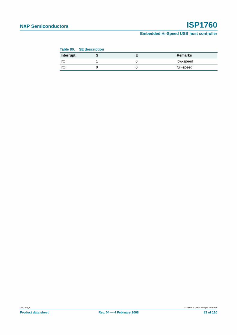
NXP Semiconductors ISP1760Embedded Hi-Speed USB host controller
Table 80. SE description
Interrupt S E Remarks
I/O 1 0 low-speed
I/O 0 0 full-speed
ISP1760_4 © NXP B.V. 2008. All rights reserved.
Product data sheet Rev. 04 — 4 February 2008 83 of 110

NXP Semiconductors ISP1760Embedded Hi-Speed USB host controller
10. Power consumption
The idle operating current, ICC, that is, when the ISP1760 is in operational mode,initialized and without any devices connected, is 70 mA. The additional currentconsumption on ICC is below 1 mA per port in the case of full-speed and low-speeddevices.
Deep-sleep suspend mode ensures the lowest power consumption when VCC is alwayssupplied to the ISP1760. The suspend current ICC(susp) is typically about 150 µA at roomtemperature. The suspend current may increase if the ambient temperature increases. Fordetails, see Section 7.6.
In hybrid mode, when VCC is disconnected, ICC(I/O) will generally be below 100 µA. Theaverage value is 60 µA to 70 µA.
Under the condition of constant read and write accesses occurring on the 32-bit data bus,the maximum ICC(I/O) drawn from VCC(I/O) is measured as 25 mA when the NXP ISP1760evaluation board is connected to a BSQUARE PXA255 development platform. Thiscurrent will vary depending on the platform because of the different access timing, thetype of data patterns written on the data bus, and loading on the data bus.
Table 81. Power consumption
Number of ports working ICC
One port working (high-speed)
VCC = 5.0 V, VCC(I/O) = 3.3 V 90 mA
VCC = 3.3 V, VCC(I/O) = 3.3 V 77 mA
VCC = 5.0 V, VCC(I/O) = 1.8 V 82 mA
VCC = 3.3 V, VCC(I/O) = 1.8 V 77 mA
Two ports working (high-speed)
VCC = 5.0 V, VCC(I/O) = 3.3 V 110 mA
VCC = 3.3 V, VCC(I/O) = 3.3 V 97 mA
VCC = 5.0 V, VCC(I/O) = 1.8 V 102 mA
VCC = 3.3 V, VCC(I/O) = 1.8 V 97 mA
Three ports working (high-speed)
VCC = 5.0 V, VCC(I/O) = 3.3 V 130 mA
VCC = 3.3 V, VCC(I/O) = 3.3 V 117 mA
VCC = 5.0 V, VCC(I/O) = 1.8 V 122 mA
VCC = 3.3 V, VCC(I/O) = 1.8 V 117 mA
ISP1760_4 © NXP B.V. 2008. All rights reserved.
Product data sheet Rev. 04 — 4 February 2008 84 of 110

NXP Semiconductors ISP1760Embedded Hi-Speed USB host controller
11. Limiting values
12. Recommended operating conditions
[1] Deep-sleep suspend mode.
Table 82. Limiting valuesIn accordance with the Absolute Maximum Rating System (IEC 60134).
Symbol Parameter Conditions Min Max Unit
VCC(I/O) input/output supply voltage −0.5 +4.6 V
VCC(5V0) supply voltage (5.0 V) −0.5 +5.6 V
Ilu latch-up current VI < 0 V or VI > VCC - 100 mA
Vesd electrostatic discharge voltage ILI < 1 µA (all pins) −4000 +4000 V
Tstg storage temperature −40 +125 °C
Table 83. Recommended operating conditions
Symbol Parameter Conditions Min Typ Max Unit
VCC(I/O) input/output supply voltage VCC(I/O) = 3.3 V 3.0 3.3 3.6 V
VCC(I/O) = 1.8 V 1.65 1.8 1.95 V
VCC(5V0) supply voltage (5.0 V) 3.0 - 5.5 V
Tamb ambient temperature −40 - +85 °C
ICC(susp) suspend supply current Tamb = 25 °C;VCC(5V0) = 3.3 V
[1] - 150 - µA
ISP1760_4 © NXP B.V. 2008. All rights reserved.
Product data sheet Rev. 04 — 4 February 2008 85 of 110
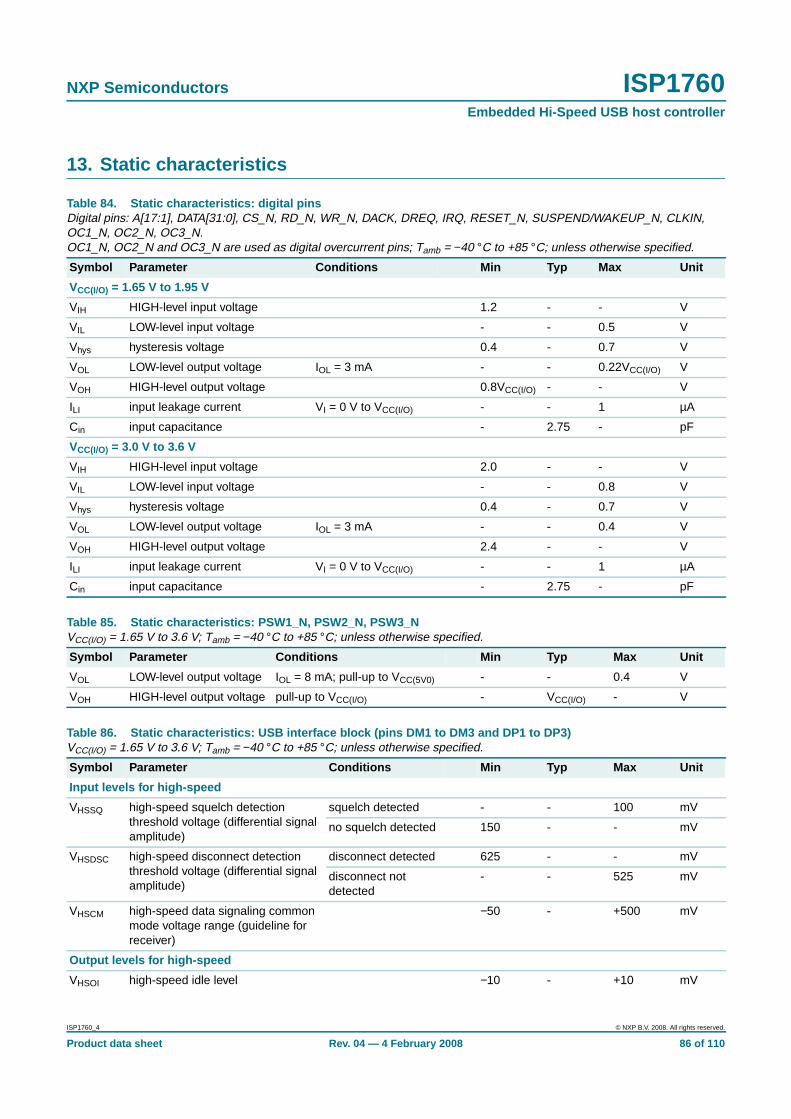
NXP Semiconductors ISP1760Embedded Hi-Speed USB host controller
13. Static characteristics
Table 84. Static characteristics: digital pinsDigital pins: A[17:1], DATA[31:0], CS_N, RD_N, WR_N, DACK, DREQ, IRQ, RESET_N, SUSPEND/WAKEUP_N, CLKIN,OC1_N, OC2_N, OC3_N.OC1_N, OC2_N and OC3_N are used as digital overcurrent pins; Tamb = −40 °C to +85 °C; unless otherwise specified.
Symbol Parameter Conditions Min Typ Max Unit
VCC(I/O) = 1.65 V to 1.95 V
VIH HIGH-level input voltage 1.2 - - V
VIL LOW-level input voltage - - 0.5 V
Vhys hysteresis voltage 0.4 - 0.7 V
VOL LOW-level output voltage IOL = 3 mA - - 0.22VCC(I/O) V
VOH HIGH-level output voltage 0.8VCC(I/O) - - V
ILI input leakage current VI = 0 V to VCC(I/O) - - 1 µA
Cin input capacitance - 2.75 - pF
VCC(I/O) = 3.0 V to 3.6 V
VIH HIGH-level input voltage 2.0 - - V
VIL LOW-level input voltage - - 0.8 V
Vhys hysteresis voltage 0.4 - 0.7 V
VOL LOW-level output voltage IOL = 3 mA - - 0.4 V
VOH HIGH-level output voltage 2.4 - - V
ILI input leakage current VI = 0 V to VCC(I/O) - - 1 µA
Cin input capacitance - 2.75 - pF
Table 85. Static characteristics: PSW1_N, PSW2_N, PSW3_NVCC(I/O) = 1.65 V to 3.6 V; Tamb = −40 °C to +85 °C; unless otherwise specified.
Symbol Parameter Conditions Min Typ Max Unit
VOL LOW-level output voltage IOL = 8 mA; pull-up to VCC(5V0) - - 0.4 V
VOH HIGH-level output voltage pull-up to VCC(I/O) - VCC(I/O) - V
Table 86. Static characteristics: USB interface block (pins DM1 to DM3 and DP1 to DP3)VCC(I/O) = 1.65 V to 3.6 V; Tamb = −40 °C to +85 °C; unless otherwise specified.
Symbol Parameter Conditions Min Typ Max Unit
Input levels for high-speed
VHSSQ high-speed squelch detectionthreshold voltage (differential signalamplitude)
squelch detected - - 100 mV
no squelch detected 150 - - mV
VHSDSC high-speed disconnect detectionthreshold voltage (differential signalamplitude)
disconnect detected 625 - - mV
disconnect notdetected
- - 525 mV
VHSCM high-speed data signaling commonmode voltage range (guideline forreceiver)
−50 - +500 mV
Output levels for high-speed
VHSOI high-speed idle level −10 - +10 mV
ISP1760_4 © NXP B.V. 2008. All rights reserved.
Product data sheet Rev. 04 — 4 February 2008 86 of 110

NXP Semiconductors ISP1760Embedded Hi-Speed USB host controller
[1] The HS termination resistor is disabled, and the pull-up resistor is connected. Only during reset, when both the hub and the device arecapable of the high-speed operation.
VHSOH high-speed data signalingHIGH-level voltage
360 - 440 mV
VHSOL high-speed data signalingLOW-level voltage
−10 - +10 mV
VCHIRPJ Chirp J level (differential voltage) 700[1] - 1100 mV
VCHIRPK Chirp K level (differential voltage) −900[1] - −500 mV
Input levels for full-speed and low-speed
VIH HIGH-level input voltage 2.0 - - V
VIHZ HIGH-level input voltage (floating) 2.7 - 3.6 V
VIL LOW-level input voltage - - 0.8 V
VDI differential input sensitivity |VDP − VDM| 0.2 - - V
VCM differential common mode voltagerange
0.8 - 2.5 V
Output levels for full-speed and low-speed
VOH HIGH-level output voltage 2.8 - 3.6 V
VOL LOW-level output voltage 0 - 0.3 V
VOSE1 SE1 output voltage 0.8 - - V
VCRS output signal crossover voltage 1.3 - 2.0 V
Table 86. Static characteristics: USB interface block (pins DM1 to DM3 and DP1 to DP3) …continuedVCC(I/O) = 1.65 V to 3.6 V; Tamb = −40 °C to +85 °C; unless otherwise specified.
Symbol Parameter Conditions Min Typ Max Unit
Table 87. Static characteristics: REF5VVCC(I/O) = 1.65 V to 3.6 V; Tamb = −40 °C to +85 °C; unless otherwise specified.
Symbol Parameter Conditions Min Typ Max Unit
VIH HIGH-level input voltage - 5 - V
ISP1760_4 © NXP B.V. 2008. All rights reserved.
Product data sheet Rev. 04 — 4 February 2008 87 of 110

NXP Semiconductors ISP1760Embedded Hi-Speed USB host controller
14. Dynamic characteristics
[1] Recommended values for external capacitors when using a crystal are 22 pF to 27 pF.
[2] Recommended accuracy of the clock frequency is 50 ppm for the crystal and oscillator. The oscillator used depends on VCC(I/O).
[1] This also serves as a high-speed termination.
Table 88. Dynamic characteristics: system clock timingVCC(I/O) = 1.65 V to 3.6 V; Tamb = −40 °C to +85 °C; unless otherwise specified.
Symbol Parameter Conditions Min Typ Max Unit
Crystal oscillator
fclk clock frequency crystal[1] [2] - 12 - MHz
oscillator - 12 - MHz
External clock input
tJ external clock jitter - - 500 ps
δ clock duty cycle - 50 - %
Vi(XTAL1) input voltage on pin XTAL1 - VCC(I/O) - V
tr rise time - - 3 ns
tf fall time - - 3 ns
Table 89. Dynamic characteristics: CPU interface blockVCC(I/O) = 1.65 V to 3.6 V; Tamb = −40 °C to +85 °C; unless otherwise specified.
Symbol Parameter Conditions Min Typ Max Unit
SR slew rate standard load 1 - 4 V/ns
Table 90. Dynamic characteristics: high-speed source electrical characteristicsVCC(I/O) = 1.65 V to 3.6 V; Tamb = −40 °C to +85 °C; unless otherwise specified.
Symbol Parameter Conditions Min Typ Max Unit
Driver characteristics
tHSR rise time (10 % to 90 %) 500 - - ps
tHSF fall time (10 % to 90 %) 500 - - ps
ZHSDRV driver output impedance (whichalso serves as high-speedtermination)
includes the RS resistor [1] 40.5 45 49.5 Ω
Clock timing
tHSDRAT high-speed data rate 479.76 - 480.24 Mbit/s
tHSFRAM microframe interval 124.9375 - 125.0625 µs
tHSRFI consecutive microframe intervaldifference
1 - fourhigh-speedbit times
ns
ISP1760_4 © NXP B.V. 2008. All rights reserved.
Product data sheet Rev. 04 — 4 February 2008 88 of 110

NXP Semiconductors ISP1760Embedded Hi-Speed USB host controller
Table 91. Dynamic characteristics: full-speed source electrical characteristicsVCC(I/O) = 1.65 V to 3.6 V; Tamb = −40 °C to +85 °C; unless otherwise specified.
Symbol Parameter Conditions Min Typ Max Unit
Driver characteristics
tFR rise time CL = 50 pF; 10 % to 90 %of |VOH − VOL|
4 - 20 ns
tFF fall time CL = 50 pF; 90 % to 10 %of |VOH − VOL|
4 - 20 ns
tFRFM differential rise and fall timematching
90 - 111.1 %
ZDRV driver output impedance for driver that is nothigh-speed capable
28 - 44 Ω
Data timing: see Figure 14
tFDEOP source jitter for differentialtransition to SE0 transition
full-speed timing −2 - +5 ns
tFEOPT source SE0 interval of EOP 160 - 175 ns
tFEOPR receiver SE0 interval of EOP 82 - - ns
tLDEOP upstream facing port sourcejitter for differential transition toSE0 transition
low-speed timing −40 - +100 ns
tLEOPT source SE0 interval of EOP 1.25 - 1.5 µs
tLEOPR receiver SE0 interval of EOP 670 - - ns
tFST width of SE0 interval duringdifferential transition
- - 14 ns
Table 92. Dynamic characteristics: low-speed source electrical characteristicsVCC(I/O) = 1.65 V to 3.6 V; Tamb = −40 °C to +85 °C; unless otherwise specified.
Symbol Parameter Conditions Min Typ Max Unit
Driver characteristics
tLR transition time: rise time 75 - 300 ns
tLF transition time: fall time 75 - 300 ns
tLRFM rise and fall time matching 90 - 125 %
TPERIOD is the bit duration corresponding with the USB data rate.
Fig 14. USB source differential data-to-EOP transition skew and EOP width
004aaa929
TPERIOD
differentialdata lines
crossover point
differential data toSE0/EOP skew
N × TPERIOD + tFDEOPN × TPERIOD + tLDEOP
source EOP width: tFEOPT, tLEOPT
receiver EOP width: tFEOPR, tLEOPR
crossover pointextended
+3.3 V
0 V
ISP1760_4 © NXP B.V. 2008. All rights reserved.
Product data sheet Rev. 04 — 4 February 2008 89 of 110
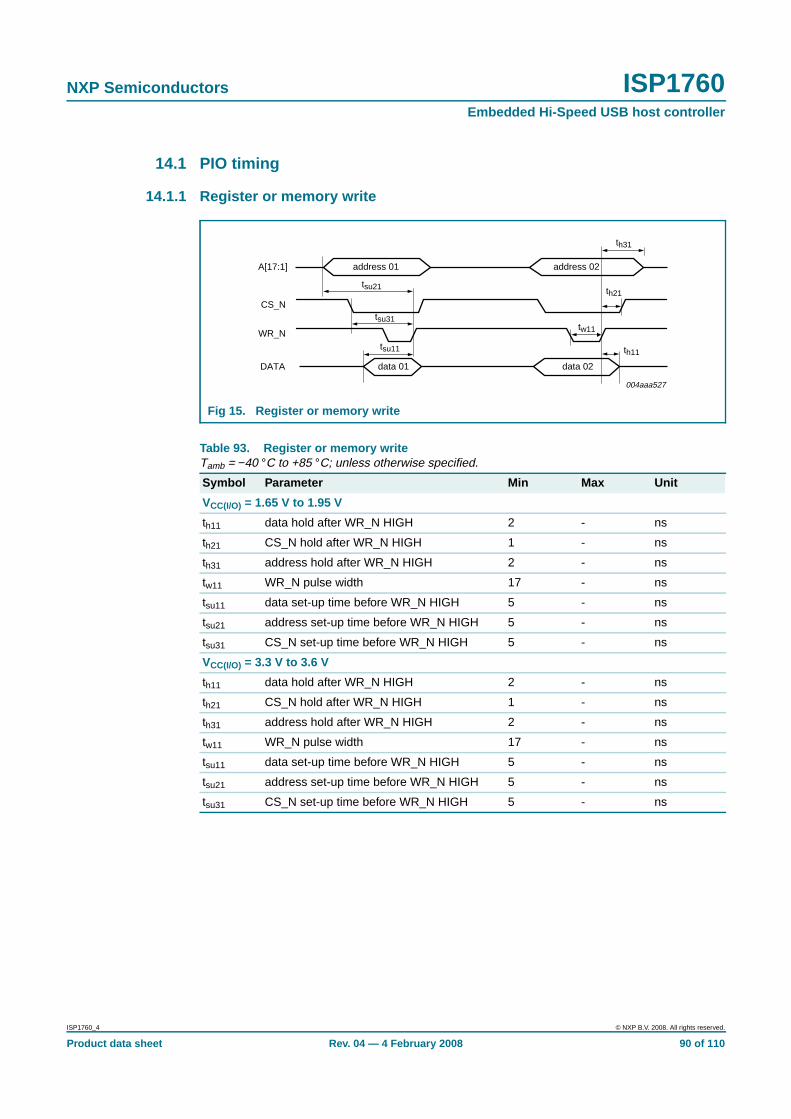
NXP Semiconductors ISP1760Embedded Hi-Speed USB host controller
14.1 PIO timing
14.1.1 Register or memory write
Fig 15. Register or memory write
Table 93. Register or memory writeTamb = −40 °C to +85 °C; unless otherwise specified.
Symbol Parameter Min Max Unit
VCC(I/O) = 1.65 V to 1.95 V
th11 data hold after WR_N HIGH 2 - ns
th21 CS_N hold after WR_N HIGH 1 - ns
th31 address hold after WR_N HIGH 2 - ns
tw11 WR_N pulse width 17 - ns
tsu11 data set-up time before WR_N HIGH 5 - ns
tsu21 address set-up time before WR_N HIGH 5 - ns
tsu31 CS_N set-up time before WR_N HIGH 5 - ns
VCC(I/O) = 3.3 V to 3.6 V
th11 data hold after WR_N HIGH 2 - ns
th21 CS_N hold after WR_N HIGH 1 - ns
th31 address hold after WR_N HIGH 2 - ns
tw11 WR_N pulse width 17 - ns
tsu11 data set-up time before WR_N HIGH 5 - ns
tsu21 address set-up time before WR_N HIGH 5 - ns
tsu31 CS_N set-up time before WR_N HIGH 5 - ns
004aaa527
address 01A[17:1] address 02
CS_N
data 01DATA data 02
WR_N
th11
th21
th31
tw11
tsu11
tsu21
tsu31
ISP1760_4 © NXP B.V. 2008. All rights reserved.
Product data sheet Rev. 04 — 4 February 2008 90 of 110

NXP Semiconductors ISP1760Embedded Hi-Speed USB host controller
14.1.2 Register read
14.1.3 Register access
Fig 16. Register read
Table 94. Register readTamb = −40 °C to +85 °C; unless otherwise specified.
Symbol Parameter Min Max Unit
VCC(I/O) = 1.65 V to 1.95 V
tsu12 address set-up time before RD_N LOW 0 - ns
tsu22 CS_N set-up time before RD_N LOW 0 - ns
tw12 RD_N pulse width > td12 - ns
td12 data valid time after RD_N LOW - 35 ns
td22 data valid time after RD_N HIGH - 1 ns
VCC(I/O) = 3.3 V to 3.6 V
tsu12 address set-up time before RD_N LOW 0 - ns
tsu22 CS_N set-up time before RD_N LOW 0 - ns
tw12 RD_N pulse width > td12 - ns
td12 data valid time after RD_N LOW - 22 ns
td22 data valid time after RD_N HIGH - 1 ns
004aaa524
address 01A[17:1] address 02
DATA
CS_N
RD_N
tsu12
tsu22
tw12
td12
td22
Fig 17. Register access
004aaa983
WR_N
RD_N
CS_N
tWHRL tRHWLtRHRL
tWHWL
ISP1760_4 © NXP B.V. 2008. All rights reserved.
Product data sheet Rev. 04 — 4 February 2008 91 of 110

NXP Semiconductors ISP1760Embedded Hi-Speed USB host controller
[1] For EHCI operational registers, minimum value is 195 ns.
14.1.4 Memory read
Table 95. Register accessTamb = −40 °C to +85 °C; unless otherwise specified.
Symbol Parameter Min Max Unit
tWHRL WR_N HIGH to RD_N LOW time 25[1] - ns
tRHRL RD_N HIGH to RD_N LOW time 25[1] - ns
tRHWL RD_N HIGH to WR_N LOW time 25 - ns
tWHWL WR_N HIGH to WR_N LOW time 25[1] - ns
Fig 18. Memory read
Table 96. Memory readTamb = −40 °C to +85 °C; unless otherwise specified.
Symbol Parameter Min Max Unit
VCC(I/O) = 1.65 V to 1.95 V
tp13 initial pre-fetch time 90 - ns
Tcy13 memory RD_N cycle time 40 - ns
td13 data valid time after RD_N LOW - 31 ns
td23 data available time after RD_N HIGH - 1 ns
tw13 RD_N pulse width 32 - ns
tsu13 CS_N set-up time before RD_N LOW 0 - ns
tsu23 address set-up time before RD_N LOW 0 - ns
VCC(I/O) = 3.3 V to 3.6 V
tp13 initial pre-fetch time 90 - ns
Tcy13 memory RD_N cycle time 36 - ns
td13 data valid time after RD_N LOW - 20 ns
004aaa523
address = 33CA[17:1] address 2address 1 address 3
dataDATA data 2data 1 data 3
CS_N
WR_N
RD_N
tp13
td13
tw13
tsu23
tsu13
Tcy13
td23
ISP1760_4 © NXP B.V. 2008. All rights reserved.
Product data sheet Rev. 04 — 4 February 2008 92 of 110

NXP Semiconductors ISP1760Embedded Hi-Speed USB host controller
14.2 DMA timingIn the following sections:
• Polarity of DACK is active HIGH
• Polarity of DREQ is active HIGH.
14.2.1 Single cycle: DMA read
td23 data available time after RD_N HIGH - 1 ns
tw13 RD_N pulse width 21 - ns
tsu13 CS_N set-up time before RD_N LOW 0 - ns
tsu23 address set-up time before RD_N LOW 0 - ns
Table 96. Memory read …continuedTamb = −40 °C to +85 °C; unless otherwise specified.
Symbol Parameter Min Max Unit
Fig 19. DMA read (single cycle)
Table 97. DMA read (single cycle)Tamb = −40 °C to +85 °C; unless otherwise specified.
Symbol Parameter Min Max Unit
VCC(I/O) = 1.65 V to 1.95 V
ta14 DACK assertion time after DREQ assertion 0 - ns
ta24 RD_N assertion time after DACK assertion 0 - ns
td14 data valid time after RD_N assertion - 24 ns
tw14 RD_N pulse width > td14 - ns
ta34 DREQ de-assertion time after RD_N assertion - 29 ns
ta44 DACK de-assertion to next DREQ assertion time - 56 ns
th14 data hold time after RD_N de-asserts - 5 ns
VCC(I/O) = 3.3 V to 3.6 V
ta14 DACK assertion time after DREQ assertion 0 - ns
ta24 RD_N assertion time after DACK assertion 0 - ns
td14 data valid time after RD_N assertion - 20 ns
004aaa530
DATA
DREQ
DACK
RD_N
ta14
ta24td14
tw14
ta44
ta34
th14
ISP1760_4 © NXP B.V. 2008. All rights reserved.
Product data sheet Rev. 04 — 4 February 2008 93 of 110

NXP Semiconductors ISP1760Embedded Hi-Speed USB host controller
14.2.2 Single cycle: DMA write
tw14 RD_N pulse width > td14 - ns
ta34 DREQ de-assertion time after RD_N assertion - 18 ns
ta44 DACK de-assertion to next DREQ assertion time - 56 ns
th14 data hold time after RD_N de-asserts - 5 ns
Table 97. DMA read (single cycle) …continuedTamb = −40 °C to +85 °C; unless otherwise specified.
Symbol Parameter Min Max Unit
DREQ and DACK are active HIGH.
Fig 20. DMA write (single cycle)
Table 98. DMA write (single cycle)Tamb = −40 °C to +85 °C; unless otherwise specified.
Symbol Parameter Min Max Unit
VCC(I/O) = 1.65 V to 1.95 V
ta15 DACK assertion time after DREQ assertion 0 - ns
ta25 WR_N assertion time after DACK assertion 1 - ns
th15 data hold time after WR_N de-assertion 3 - ns
th25 DACK hold time after WR_N de-assertion 0 - ns
tsu15 data set-up time before WR_N de-assertion 5.5 - ns
ta35 DREQ de-assertion time after WR_N assertion - 28 ns
tcy15 last DACK strobe de-assertion to next DREQassertion time
- 82 ns
tw15 WR_N pulse width 22 - ns
VCC(I/O) = 3.3 V to 3.6 V
ta15 DACK assertion time after DREQ assertion 0 - ns
ta25 WR_N assertion time after DACK assertion 1 - ns
th15 data hold time after WR_N de-assertion 2 - ns
th25 DACK hold time after WR_N de-assertion 0 - ns
tsu15 data set-up time before WR_N de-assertion 5.5 - ns
ta35 DREQ de-assertion time after WR_N assertion - 16 ns
tcy15 last DACK strobe de-assertion to next DREQassertion time
- 82 ns
tw15 WR_N pulse width 22 - ns
004aaa525dataDATA data 1
DREQ
WR_N
DACK
ta15
ta25
th15
th25
tsu15
ta35
tcy15
tw15
ISP1760_4 © NXP B.V. 2008. All rights reserved.
Product data sheet Rev. 04 — 4 February 2008 94 of 110

NXP Semiconductors ISP1760Embedded Hi-Speed USB host controller
14.2.3 Multi-cycle: DMA read
DREQ and DACK are active HIGH.
Fig 21. DMA read (multi-cycle burst)
Table 99. DMA read (multi-cycle burst)Tamb = −40 °C to +85 °C; unless otherwise specified.
Symbol Parameter Min Max Unit
VCC(I/O) = 1.65 V to 1.95 V
ta16 DACK assertion after DREQ assertion time 0 - ns
ta26 RD_N assertion after DACK assertion time 0 - ns
td16 data valid time after RD_N assertion - 31 ns
tw16 RD_N pulse width 38 - ns
Tcy16 read-to-read cycle time 46 - ns
ta36 DREQ de-assertion time after last burst RD_Nde-assertion
- 30 ns
ta46 DACK de-assertion to next DREQ assertiontime
- 82 ns
th16 data hold time after RD_N de-asserts - 5 ns
VCC(I/O) = 3.3 V to 3.6 V
ta16 DACK assertion after DREQ assertion time 0 - ns
ta26 RD_N assertion after DACK assertion time 0 - ns
td16 data valid time after RD_N assertion - 16 ns
tw16 RD_N pulse width 17 - ns
Tcy16 read-to-read cycle time 38 - ns
ta36 DREQ de-assertion time after last burst RD_Nde-assertion
- 20 ns
ta46 DACK de-assertion to next DREQ assertiontime
- 82 ns
th16 data hold time after RD_N de-asserts - 5 ns
DREQ
ta36
DACK
RD_N
004aaa531data 0
DATA
data n-1data 1 data n
ta16
ta26
td16
tw16
Tcy16
ta46
th16
ISP1760_4 © NXP B.V. 2008. All rights reserved.
Product data sheet Rev. 04 — 4 February 2008 95 of 110

NXP Semiconductors ISP1760Embedded Hi-Speed USB host controller
14.2.4 Multi-cycle: DMA write
Fig 22. DMA write (multi-cycle burst)
Table 100. DMA write (multi-cycle burst)Tamb = −40 °C to +85 °C; unless otherwise specified.
Symbol Parameter Min Max Unit
VCC(I/O) = 1.65 V to 1.95 V
Tcy17 DMA write cycle time 51 - ns
tsu17 data set-up time before WR_N de-assertion 5 - ns
th17 data hold time after WR_N de-assertion 2 - ns
ta17 DACK assertion time after DREQ assertion 0 - ns
ta27 WR_N assertion time after DACK assertion 2 - ns
ta37 DREQ de-assertion time at last strobe (WR_N)assertion
- 28 ns
th27 DACK hold time after WR_N de-assertion 0 - ns
ta47 strobe de-assertion to next strobe assertion time 34 - ns
tw17 WR_N pulse width 17 - ns
ta57 DACK de-assertion to next DREQ assertion time - 82 ns
VCC(I/O) = 3.3 V to 3.6 V
Tcy17 DMA write cycle time 51 - ns
tsu17 data set-up time before WR_N de-assertion 5 - ns
th17 data hold time after WR_N de-assertion 2 - ns
ta17 DACK assertion time after DREQ assertion 0 - ns
ta27 WR_N assertion time after DACK assertion 1 - ns
ta37 DREQ de-assertion time at last strobe (WR_N)assertion
- 16 ns
th27 DACK hold time after WR_N de-assertion 0 - ns
ta47 strobe de-assertion to next strobe assertion time 34 - ns
tw17 WR_N pulse width 17 - ns
ta57 DACK de-assertion to next DREQ assertion time - 82 ns
004aaa526data 1
DATA
data n-1data 2 data n
WR_N
DREQ
DACKTcy17tsu17
th17
ta17
ta27
ta37
th27
ta47
tw17
ta57
ISP1760_4 © NXP B.V. 2008. All rights reserved.
Product data sheet Rev. 04 — 4 February 2008 96 of 110

NXP Semiconductors ISP1760Embedded Hi-Speed USB host controller
15. Package outline
Fig 23. Package outline SOT425-1 (LQFP128)
UNIT A1 A2 A3 bp c E(1) e HE L L p Zywv θ
REFERENCESOUTLINEVERSION
EUROPEANPROJECTION ISSUE DATE
IEC JEDEC JEITA
mm 0.150.05
1.451.35
0.250.270.17
0.200.09
14.113.9 0.5
16.1515.85
0.810.59
70
o
o0.120.2 0.11
DIMENSIONS (mm are the original dimensions)
Note
1. Plastic or metal protrusions of 0.25 mm maximum per side are not included.
0.750.45
SOT425-1 136E28 MS-02600-01-1903-02-20
D(1) (1)(1)
20.119.9
HD
22.1521.85
EZ
0.810.59
D
0 5 10 mm
scale
bpe
θ
E A1A
Lp
detail X
L
(A )3
B
c
bp
EH A2
DH v M B
D
ZD
A
ZE
e
v M A
X
102
103
y
w M
w M
Amax.
1.6
LQFP128: plastic low profile quad flat package; 128 leads; body 14 x 20 x 1.4 mm SOT425-1
6564
38
39
1128
pin 1 index
ISP1760_4 © NXP B.V. 2008. All rights reserved.
Product data sheet Rev. 04 — 4 February 2008 97 of 110

NXP Semiconductors ISP1760Embedded Hi-Speed USB host controller
Fig 24. Package outline SOT857-1 (TFBGA128)
REFERENCESOUTLINEVERSION
EUROPEANPROJECTION
ISSUE DATEIEC JEDEC JEITA
SOT857-1 MO-195
SOT857-1
04-05-0504-06-22
DIMENSIONS (mm are the original dimensions)
TFBGA128: plastic thin fine-pitch ball grid array package; 128 balls; body 9 x 9 x 0.8 mm
A
detail X
A2
A1
b
ball A1index area
ball A1index area
D
E
B
C
A
AB
CD
EF
H
K
G
L
J
MN
PR
T
2 4 6 8 10 12 14 161 3 5 7 9 11 13 15
e2
e1
e
e
1/2 e
1/2 e
AC B∅ v M
C∅ w M
yCy1
X
0 2.5 5 mm
scale
UNIT
mm 0.250.15
0.850.75
0.350.25
9.18.9
A1 A2 b E
9.18.9
D e e1 v
0.157.5
e2
7.50.5
w
0.05
y
0.08
y1
0.1
Amax
1.1
ISP1760_4 © NXP B.V. 2008. All rights reserved.
Product data sheet Rev. 04 — 4 February 2008 98 of 110

NXP Semiconductors ISP1760Embedded Hi-Speed USB host controller
16. Soldering of SMD packages
This text provides a very brief insight into a complex technology. A more in-depth accountof soldering ICs can be found in Application Note AN10365 “Surface mount reflowsoldering description”.
16.1 Introduction to solderingSoldering is one of the most common methods through which packages are attached toPrinted Circuit Boards (PCBs), to form electrical circuits. The soldered joint provides boththe mechanical and the electrical connection. There is no single soldering method that isideal for all IC packages. Wave soldering is often preferred when through-hole andSurface Mount Devices (SMDs) are mixed on one printed wiring board; however, it is notsuitable for fine pitch SMDs. Reflow soldering is ideal for the small pitches and highdensities that come with increased miniaturization.
16.2 Wave and reflow solderingWave soldering is a joining technology in which the joints are made by solder coming froma standing wave of liquid solder. The wave soldering process is suitable for the following:
• Through-hole components
• Leaded or leadless SMDs, which are glued to the surface of the printed circuit board
Not all SMDs can be wave soldered. Packages with solder balls, and some leadlesspackages which have solder lands underneath the body, cannot be wave soldered. Also,leaded SMDs with leads having a pitch smaller than ~0.6 mm cannot be wave soldered,due to an increased probability of bridging.
The reflow soldering process involves applying solder paste to a board, followed bycomponent placement and exposure to a temperature profile. Leaded packages,packages with solder balls, and leadless packages are all reflow solderable.
Key characteristics in both wave and reflow soldering are:
• Board specifications, including the board finish, solder masks and vias
• Package footprints, including solder thieves and orientation
• The moisture sensitivity level of the packages
• Package placement
• Inspection and repair
• Lead-free soldering versus SnPb soldering
16.3 Wave solderingKey characteristics in wave soldering are:
• Process issues, such as application of adhesive and flux, clinching of leads, boardtransport, the solder wave parameters, and the time during which components areexposed to the wave
• Solder bath specifications, including temperature and impurities
ISP1760_4 © NXP B.V. 2008. All rights reserved.
Product data sheet Rev. 04 — 4 February 2008 99 of 110

NXP Semiconductors ISP1760Embedded Hi-Speed USB host controller
16.4 Reflow solderingKey characteristics in reflow soldering are:
• Lead-free versus SnPb soldering; note that a lead-free reflow process usually leads tohigher minimum peak temperatures (see Figure 25) than a SnPb process, thusreducing the process window
• Solder paste printing issues including smearing, release, and adjusting the processwindow for a mix of large and small components on one board
• Reflow temperature profile; this profile includes preheat, reflow (in which the board isheated to the peak temperature) and cooling down. It is imperative that the peaktemperature is high enough for the solder to make reliable solder joints (a solder pastecharacteristic). In addition, the peak temperature must be low enough that thepackages and/or boards are not damaged. The peak temperature of the packagedepends on package thickness and volume and is classified in accordance withTable 101 and 102
Moisture sensitivity precautions, as indicated on the packing, must be respected at alltimes.
Studies have shown that small packages reach higher temperatures during reflowsoldering, see Figure 25.
Table 101. SnPb eutectic process (from J-STD-020C)
Package thickness (mm) Package reflow temperature ( °C)
Volume (mm 3)
< 350 ≥ 350
< 2.5 235 220
≥ 2.5 220 220
Table 102. Lead-free process (from J-STD-020C)
Package thickness (mm) Package reflow temperature ( °C)
Volume (mm 3)
< 350 350 to 2000 > 2000
< 1.6 260 260 260
1.6 to 2.5 260 250 245
> 2.5 250 245 245
ISP1760_4 © NXP B.V. 2008. All rights reserved.
Product data sheet Rev. 04 — 4 February 2008 100 of 110

NXP Semiconductors ISP1760Embedded Hi-Speed USB host controller
For further information on temperature profiles, refer to Application Note AN10365“Surface mount reflow soldering description”.
17. Soldering of through-hole mount packages
17.1 Introduction to soldering through-hole mount packagesThis text gives a very brief insight into wave, dip and manual soldering.
Wave soldering is the preferred method for mounting of through-hole mount IC packageson a printed-circuit board.
17.2 Soldering by dipping or by solder waveDriven by legislation and environmental forces the worldwide use of lead-free solderpastes is increasing. Typical dwell time of the leads in the wave ranges from3 seconds to 4 seconds at 250 °C or 265 °C, depending on solder material applied, SnPbor Pb-free respectively.
The total contact time of successive solder waves must not exceed 5 seconds.
The device may be mounted up to the seating plane, but the temperature of the plasticbody must not exceed the specified maximum storage temperature (Tstg(max)). If theprinted-circuit board has been pre-heated, forced cooling may be necessary immediatelyafter soldering to keep the temperature within the permissible limit.
17.3 Manual solderingApply the soldering iron (24 V or less) to the lead(s) of the package, either below theseating plane or not more than 2 mm above it. If the temperature of the soldering iron bit isless than 300 °C it may remain in contact for up to 10 seconds. If the bit temperature isbetween 300 °C and 400 °C, contact may be up to 5 seconds.
MSL: Moisture Sensitivity Level
Fig 25. Temperature profiles for large and small components
001aac844
temperature
time
minimum peak temperature= minimum soldering temperature
maximum peak temperature= MSL limit, damage level
peak temperature
ISP1760_4 © NXP B.V. 2008. All rights reserved.
Product data sheet Rev. 04 — 4 February 2008 101 of 110

NXP Semiconductors ISP1760Embedded Hi-Speed USB host controller
17.4 Package related soldering information
[1] For SDIP packages, the longitudinal axis must be parallel to the transport direction of the printed-circuitboard.
[2] For PMFP packages hot bar soldering or manual soldering is suitable.
18. Abbreviations
Table 103. Suitability of through-hole mount IC packages for dipping and wave soldering
Package Soldering method
Dipping Wave
CPGA, HCPGA - suitable
DBS, DIP, HDIP, RDBS, SDIP, SIL suitable suitable[1]
PMFP[2] - not suitable
Table 104. Abbreviations
Acronym Description
ACK Acknowledgment
ASIC Application-Specific Integrated Circuit
ATL Asynchronous Transfer List
ATX Analog Transceiver
CS Complete Split
DMA Direct Memory Access
DW Double Word
EHCI Enhanced Host Controller Interface
EMI ElectroMagnetic Interference
EOP End-Of-Packet
EOT End-Of-Transfer
ESD ElectroStatic Discharge
ESR Effective Series Resistance
FIFO First In, First Out
FLS Frame List Size
FS Full-Speed
GPIO General-Purpose Input/Output
HC Host Controller
HNP Host Negotiation Protocol
HS High-Speed
iTD isochronous Transfer Descriptor
INT Interrupt
ISO Isochronous
ISR Interrupt Service Routine
ITL Isochronous (ISO) Transfer List
LS Low-Speed
NAK Not Acknowledged
NYET Not Yet
ISP1760_4 © NXP B.V. 2008. All rights reserved.
Product data sheet Rev. 04 — 4 February 2008 102 of 110

NXP Semiconductors ISP1760Embedded Hi-Speed USB host controller
19. References
[1] Universal Serial Bus Specification Rev. 2.0
[2] Enhanced Host Controller Interface Specification for Universal Serial Bus Rev. 1.0
[3] Embedded Systems Design with the ISP176x (AN10043)
[4] ISP176x Linux Programming Gui13de (AN10042)
[5] Interfacing the ISP176x to the Intel PXA25x processor (AN10037)
OC Overcurrent
OHCI Open Host Controller Interface
PCI Peripheral Component Interconnect
PDA Personal Digital Assistant
PID Packer Identifier
PIO Programmed Input/Output
PLL Phase-Locked Loop
PMOS Positive-channel Metal-Oxide Semiconductor
POR Power-On Reset
PORP Power-On Reset Pulse
PTD Philips Transfer Descriptor
RISC Reduced Instruction Set Computer
SE0 Single Ended 0
SE1 Single Ended 1
siTD split isochronous Transfer Descriptor
SOF Start-Of-Frame
SRP Session Request Protocol
SS Start Split
TT Transaction Translator
UHCI Universal Host Controller Interface
USB Universal Serial Bus
Table 104. Abbreviations …continued
Acronym Description
ISP1760_4 © NXP B.V. 2008. All rights reserved.
Product data sheet Rev. 04 — 4 February 2008 103 of 110

NXP Semiconductors ISP1760Embedded Hi-Speed USB host controller
20. Revision history
Table 105. Revision history
Document ID Release date Data sheet status Change notice Supersedes
ISP1760_4 20080204 Product data sheet - ISP1760_3
Modifications: • Section 7.3 “Accessing the ISP1760 host controller memory: PIO and DMA”: updated the secondparagraph.
• Table 52 “Power Down Control register (address 0354h) bit description”: updated description forbits 12 and 11.
• Table 82 “Limiting values”: updated the conditions column of Vesd.
• Section 19 “References”: Removed On-The-Go Supplement to the USB Specification Rev. 1.2.
ISP1760_3 20070302 Product data sheet - ISP1760_2
ISP1760_2(9397 750 15189)
20051025 Product data sheet - ISP1760_1
ISP1760_1(9397 750 13257)
20041108 Product data sheet - -
ISP1760_4 © NXP B.V. 2008. All rights reserved.
Product data sheet Rev. 04 — 4 February 2008 104 of 110

NXP Semiconductors ISP1760Embedded Hi-Speed USB host controller
21. Legal information
21.1 Data sheet status
[1] Please consult the most recently issued document before initiating or completing a design.
[2] The term ‘short data sheet’ is explained in section “Definitions”.
[3] The product status of device(s) described in this document may have changed since this document was published and may differ in case of multiple devices. The latest product statusinformation is available on the Internet at URL http://www.nxp.com.
21.2 Definitions
Draft — The document is a draft version only. The content is still underinternal review and subject to formal approval, which may result inmodifications or additions. NXP Semiconductors does not give anyrepresentations or warranties as to the accuracy or completeness ofinformation included herein and shall have no liability for the consequences ofuse of such information.
Short data sheet — A short data sheet is an extract from a full data sheetwith the same product type number(s) and title. A short data sheet is intendedfor quick reference only and should not be relied upon to contain detailed andfull information. For detailed and full information see the relevant full datasheet, which is available on request via the local NXP Semiconductors salesoffice. In case of any inconsistency or conflict with the short data sheet, thefull data sheet shall prevail.
21.3 Disclaimers
General — Information in this document is believed to be accurate andreliable. However, NXP Semiconductors does not give any representations orwarranties, expressed or implied, as to the accuracy or completeness of suchinformation and shall have no liability for the consequences of use of suchinformation.
Right to make changes — NXP Semiconductors reserves the right to makechanges to information published in this document, including withoutlimitation specifications and product descriptions, at any time and withoutnotice. This document supersedes and replaces all information supplied priorto the publication hereof.
Suitability for use — NXP Semiconductors products are not designed,authorized or warranted to be suitable for use in medical, military, aircraft,space or life support equipment, nor in applications where failure or
malfunction of an NXP Semiconductors product can reasonably be expectedto result in personal injury, death or severe property or environmentaldamage. NXP Semiconductors accepts no liability for inclusion and/or use ofNXP Semiconductors products in such equipment or applications andtherefore such inclusion and/or use is at the customer’s own risk.
Applications — Applications that are described herein for any of theseproducts are for illustrative purposes only. NXP Semiconductors makes norepresentation or warranty that such applications will be suitable for thespecified use without further testing or modification.
Limiting values — Stress above one or more limiting values (as defined inthe Absolute Maximum Ratings System of IEC 60134) may cause permanentdamage to the device. Limiting values are stress ratings only and operation ofthe device at these or any other conditions above those given in theCharacteristics sections of this document is not implied. Exposure to limitingvalues for extended periods may affect device reliability.
Terms and conditions of sale — NXP Semiconductors products are soldsubject to the general terms and conditions of commercial sale, as publishedat http://www.nxp.com/profile/terms, including those pertaining to warranty,intellectual property rights infringement and limitation of liability, unlessexplicitly otherwise agreed to in writing by NXP Semiconductors. In case ofany inconsistency or conflict between information in this document and suchterms and conditions, the latter will prevail.
No offer to sell or license — Nothing in this document may be interpretedor construed as an offer to sell products that is open for acceptance or thegrant, conveyance or implication of any license under any copyrights, patentsor other industrial or intellectual property rights.
21.4 TrademarksNotice: All referenced brands, product names, service names and trademarksare the property of their respective owners.
22. Contact information
For more information, please visit: http://www .nxp.com
For sales office addresses, please send an email to: salesad [email protected]
Document status [1] [2] Product status [3] Definition
Objective [short] data sheet Development This document contains data from the objective specification for product development.
Preliminary [short] data sheet Qualification This document contains data from the preliminary specification.
Product [short] data sheet Production This document contains the product specification.
ISP1760_4 © NXP B.V. 2008. All rights reserved.
Product data sheet Rev. 04 — 4 February 2008 105 of 110

NXP Semiconductors ISP1760Embedded Hi-Speed USB host controller
23. Tables
Table 1. Ordering information . . . . . . . . . . . . . . . . . . . . .3Table 2. Pin description . . . . . . . . . . . . . . . . . . . . . . . . . .6Table 3. Port connection scenarios . . . . . . . . . . . . . . . .15Table 4. Memory address . . . . . . . . . . . . . . . . . . . . . . .17Table 5. Using the IRQ Mask AND or IRQ Mask OR
registers . . . . . . . . . . . . . . . . . . . . . . . . . . . . . .23Table 6. Hybrid mode . . . . . . . . . . . . . . . . . . . . . . . . . .27Table 7. Pin status in hybrid mode . . . . . . . . . . . . . . . .27Table 8. Register overview . . . . . . . . . . . . . . . . . . . . . .29Table 9. CAPLENGTH - Capability Length register
(address 0000h) bit description . . . . . . . . . . . .30Table 10. HCIVERSION - Host Controller Interface
Version Number register (address 0002h)bit description . . . . . . . . . . . . . . . . . . . . . . . . .30
Table 11. HCSPARAMS - Host Controller StructuralParameters register (address 0004h) bitallocation . . . . . . . . . . . . . . . . . . . . . . . . . . . . .30
Table 12. HCSPARAMS - Host Controller StructuralParameters register (address 0004h) bitdescription . . . . . . . . . . . . . . . . . . . . . . . . . . . .31
Table 13. HCCPARAMS - Host Controller CapabilityParameters register (address 0008h) bitallocation . . . . . . . . . . . . . . . . . . . . . . . . . . . . .31
Table 14. HCCPARAMS - Host Controller CapabilityParameters register (address 0008h) bitdescription . . . . . . . . . . . . . . . . . . . . . . . . . . . .32
Table 15. USBCMD - USB Command register(address 0020h) bit allocation . . . . . . . . . . . . .33
Table 16. USBCMD - USB Command register(address 0020h) bit description . . . . . . . . . . . .33
Table 17. USBSTS - USB Status register(address 0024h) bit allocation . . . . . . . . . . . . .33
Table 18. USBSTS - USB Status register(address 0024h) bit description . . . . . . . . . . . .34
Table 19. FRINDEX - Frame Index register(address: 002Ch) bit allocation . . . . . . . . . . . .34
Table 20. FRINDEX - Frame Index register(address: 002Ch) bit description . . . . . . . . . . .35
Table 21. CONFIGFLAG - Configure Flag register(address 0060h) bit allocation . . . . . . . . . . . . .35
Table 22. CONFIGFLAG - Configure Flag register(address 0060h) bit description . . . . . . . . . . . .36
Table 23. PORTSC1 - Port Status and Control 1register (address 0064h) bit allocation . . . . . . .36
Table 24. PORTSC1 - Port Status and Control 1register (address 0064h) bit description . . . . .37
Table 25. ISO PTD Done Map register(address 0130h) bit description . . . . . . . . . . . .37
Table 26. ISO PTD Skip Map register(address 0134h) bit description . . . . . . . . . . . .38
Table 27. ISO PTD Last PTD register(address 0138h) bit description . . . . . . . . . . . .38
Table 28. INT PTD Done Map register(address 0140h) bit description . . . . . . . . . . . .38
Table 29. INT PTD Skip Map register(address 0144h) bit description . . . . . . . . . . . .38
Table 30. INT PTD Last PTD register(address 0148h) bit description . . . . . . . . . . . . 39
Table 31. ATL PTD Done Map register(address 0150h) bit description . . . . . . . . . . . . 39
Table 32. ATL PTD Skip Map register(address 0154h) bit description . . . . . . . . . . . . 39
Table 33. ATL PTD Last PTD register(address 0158h) bit description . . . . . . . . . . . . 40
Table 34. HW Mode Control - Hardware ModeControl register (address 0300h)bit allocation . . . . . . . . . . . . . . . . . . . . . . . . . . 40
Table 35. HW Mode Control - Hardware ModeControl register (address 0300h) bitdescription . . . . . . . . . . . . . . . . . . . . . . . . . . . . 41
Table 36. Chip ID - Chip Identifier register(address 0304h) bit description . . . . . . . . . . . . 42
Table 37. Scratch register (address 0308h) bitdescription . . . . . . . . . . . . . . . . . . . . . . . . . . . . 42
Table 38. SW Reset - Software Reset register(address 030Ch) bit allocation . . . . . . . . . . . . 42
Table 39. SW Reset - Software Reset register(address 030Ch) bit description . . . . . . . . . . . 43
Table 40. DMA Configuration register(address 0330h) bit allocation . . . . . . . . . . . . . 43
Table 41. DMA Configuration register(address 0330h) bit description . . . . . . . . . . . . 44
Table 42. Buffer Status register (address 0334h)bit allocation . . . . . . . . . . . . . . . . . . . . . . . . . . 44
Table 43. Buffer Status register (address 0334h)bit description . . . . . . . . . . . . . . . . . . . . . . . . . 45
Table 44. ATL Done Timeout register (address 0338h)bit description . . . . . . . . . . . . . . . . . . . . . . . . . 45
Table 45. Memory register (address 033Ch) bitallocation . . . . . . . . . . . . . . . . . . . . . . . . . . . . . 46
Table 46. Memory register (address 033Ch) bitdescription . . . . . . . . . . . . . . . . . . . . . . . . . . . . 46
Table 47. Edge Interrupt Count register(address 0340h) bit allocation . . . . . . . . . . . . . 46
Table 48. Edge Interrupt Count register(address 0340h) bit description . . . . . . . . . . . . 47
Table 49. DMA Start Address register(address 0344h) bit allocation . . . . . . . . . . . . . 47
Table 50. DMA Start Address register(address 0344h) bit description . . . . . . . . . . . . 48
Table 51. Power Down Control register(address 0354h) bit allocation . . . . . . . . . . . . . 48
Table 52. Power Down Control register(address 0354h) bit description . . . . . . . . . . . . 49
Table 53. Port 1 Control register (address 0374h)bit allocation . . . . . . . . . . . . . . . . . . . . . . . . . . 50
Table 54. Port 1 Control register (address 0374h)bit description . . . . . . . . . . . . . . . . . . . . . . . . . 51
Table 55. Interrupt register (address 0310h)bit allocation . . . . . . . . . . . . . . . . . . . . . . . . . . 51
Table 56. Interrupt register (address 0310h)bit description . . . . . . . . . . . . . . . . . . . . . . . . . 52
ISP1760_4 © NXP B.V. 2008. All rights reserved.
Product data sheet Rev. 04 — 4 February 2008 106 of 110

NXP Semiconductors ISP1760Embedded Hi-Speed USB host controller
Table 57. Interrupt Enable register (address 0314h) bitallocation . . . . . . . . . . . . . . . . . . . . . . . . . . . . .53
Table 58. Interrupt Enable register (address 0314h)bit description . . . . . . . . . . . . . . . . . . . . . . . . .54
Table 59. ISO IRQ Mask OR register (address 0318h)bit description . . . . . . . . . . . . . . . . . . . . . . . . .55
Table 60. INT IRQ Mask OR register (address 031Ch)bit description . . . . . . . . . . . . . . . . . . . . . . . . .55
Table 61. ATL IRQ Mask OR register (address 0320h)bit description . . . . . . . . . . . . . . . . . . . . . . . . .55
Table 62. ISO IRQ Mask AND register (address 0324h)bit description . . . . . . . . . . . . . . . . . . . . . . . . .55
Table 63. INT IRQ Mask AND register (address 0328h)bit description . . . . . . . . . . . . . . . . . . . . . . . . .56
Table 64. ATL IRQ Mask AND register (address 032Ch)bit description . . . . . . . . . . . . . . . . . . . . . . . . .56
Table 65. High-speed bulk IN and OUT:bit allocation . . . . . . . . . . . . . . . . . . . . . . . . . . .59
Table 66. High-speed bulk IN and OUT:bit description . . . . . . . . . . . . . . . . . . . . . . . . .60
Table 67. High-speed isochronous IN and OUT:bit allocation . . . . . . . . . . . . . . . . . . . . . . . . . . .63
Table 68. High-speed isochronous IN and OUT:bit description . . . . . . . . . . . . . . . . . . . . . . . . .64
Table 69. High-speed interrupt IN and OUT:bit allocation . . . . . . . . . . . . . . . . . . . . . . . . . . .67
Table 70. High-speed interrupt IN and OUT:bit description . . . . . . . . . . . . . . . . . . . . . . . . .68
Table 71. Microframe description . . . . . . . . . . . . . . . . . .70Table 72. Start and complete split for bulk:
bit allocation . . . . . . . . . . . . . . . . . . . . . . . . . . .71Table 73. Start and complete split for bulk:
bit description . . . . . . . . . . . . . . . . . . . . . . . . .72Table 74. SE description . . . . . . . . . . . . . . . . . . . . . . . . .74Table 75. Start and complete split for isochronous:
bit allocation . . . . . . . . . . . . . . . . . . . . . . . . . . .75Table 76. Start and complete split for isochronous:
bit description . . . . . . . . . . . . . . . . . . . . . . . . .76Table 77. Start and complete split for interrupt:
bit allocation . . . . . . . . . . . . . . . . . . . . . . . . . . .79Table 78. Start and complete split for interrupt:
bit description . . . . . . . . . . . . . . . . . . . . . . . . .80Table 79. Microframe description . . . . . . . . . . . . . . . . . .82Table 80. SE description . . . . . . . . . . . . . . . . . . . . . . . . .83Table 81. Power consumption . . . . . . . . . . . . . . . . . . . . .84Table 82. Limiting values . . . . . . . . . . . . . . . . . . . . . . . . .85Table 83. Recommended operating conditions . . . . . . . .85Table 84. Static characteristics: digital pins . . . . . . . . . . .86Table 85. Static characteristics:
PSW1_N, PSW2_N, PSW3_N . . . . . . . . . . . .86Table 86. Static characteristics: USB interface block
(pins DM1 to DM3 and DP1 to DP3) . . . . . . . .86Table 87. Static characteristics: REF5V . . . . . . . . . . . . .87Table 88. Dynamic characteristics: system clock
timing . . . . . . . . . . . . . . . . . . . . . . . . . . . . . . . .88Table 89. Dynamic characteristics: CPU interface
block . . . . . . . . . . . . . . . . . . . . . . . . . . . . . . . .88Table 90. Dynamic characteristics: high-speed
source electrical characteristics . . . . . . . . . . . 88Table 91. Dynamic characteristics: full-speed source
electrical characteristics . . . . . . . . . . . . . . . . . 89Table 92. Dynamic characteristics: low-speed
source electrical characteristics . . . . . . . . . . . 89Table 93. Register or memory write . . . . . . . . . . . . . . . . 90Table 94. Register read . . . . . . . . . . . . . . . . . . . . . . . . . . 91Table 95. Register access . . . . . . . . . . . . . . . . . . . . . . . . 92Table 96. Memory read . . . . . . . . . . . . . . . . . . . . . . . . . . 92Table 97. DMA read (single cycle) . . . . . . . . . . . . . . . . . 93Table 98. DMA write (single cycle) . . . . . . . . . . . . . . . . . 94Table 99. DMA read (multi-cycle burst) . . . . . . . . . . . . . . 95Table 100.DMA write (multi-cycle burst) . . . . . . . . . . . . . 96Table 101.SnPb eutectic process (from J-STD-020C) . . 100Table 102.Lead-free process (from J-STD-020C) . . . . . 100Table 103.Suitability of through-hole mount
IC packages for dipping and wave soldering . 102Table 104.Abbreviations . . . . . . . . . . . . . . . . . . . . . . . . . 102Table 105.Revision history . . . . . . . . . . . . . . . . . . . . . . . 104
ISP1760_4 © NXP B.V. 2008. All rights reserved.
Product data sheet Rev. 04 — 4 February 2008 107 of 110

NXP Semiconductors ISP1760Embedded Hi-Speed USB host controller
24. Figures
Fig 1. Block diagram . . . . . . . . . . . . . . . . . . . . . . . . . . . .4Fig 2. Pin configuration (LQFP128); top view . . . . . . . . .5Fig 3. Pin configuration (TFBGA128); top view . . . . . . . .5Fig 4. Internal hub . . . . . . . . . . . . . . . . . . . . . . . . . . . . .14Fig 5. ISP1760 clock scheme . . . . . . . . . . . . . . . . . . . .14Fig 6. Memory segmentation and access block
diagram . . . . . . . . . . . . . . . . . . . . . . . . . . . . . . . .17Fig 7. Adjusting analog overcurrent detection limit
(optional) . . . . . . . . . . . . . . . . . . . . . . . . . . . . . . .25Fig 8. ISP1760 power supply connection. . . . . . . . . . . .26Fig 9. Most commonly used power supply connection .26Fig 10. Hybrid mode . . . . . . . . . . . . . . . . . . . . . . . . . . . .27Fig 11. Internal power-on reset timing . . . . . . . . . . . . . . .28Fig 12. Clock with respect to the external
power-on reset . . . . . . . . . . . . . . . . . . . . . . . . . . .28Fig 13. NextPTD traversal rule. . . . . . . . . . . . . . . . . . . . .58Fig 14. USB source differential data-to-EOP
transition skew and EOP width . . . . . . . . . . . . . .89Fig 15. Register or memory write. . . . . . . . . . . . . . . . . . .90Fig 16. Register read . . . . . . . . . . . . . . . . . . . . . . . . . . . .91Fig 17. Register access . . . . . . . . . . . . . . . . . . . . . . . . . .91Fig 18. Memory read . . . . . . . . . . . . . . . . . . . . . . . . . . . .92Fig 19. DMA read (single cycle). . . . . . . . . . . . . . . . . . . .93Fig 20. DMA write (single cycle) . . . . . . . . . . . . . . . . . . .94Fig 21. DMA read (multi-cycle burst) . . . . . . . . . . . . . . . .95Fig 22. DMA write (multi-cycle burst) . . . . . . . . . . . . . . . .96Fig 23. Package outline SOT425-1 (LQFP128) . . . . . . . .97Fig 24. Package outline SOT857-1 (TFBGA128). . . . . . .98Fig 25. Temperature profiles for large and small
components . . . . . . . . . . . . . . . . . . . . . . . . . . . .101
ISP1760_4 © NXP B.V. 2008. All rights reserved.
Product data sheet Rev. 04 — 4 February 2008 108 of 110

NXP Semiconductors ISP1760Embedded Hi-Speed USB host controller
25. Contents
1 General description . . . . . . . . . . . . . . . . . . . . . . 12 Features . . . . . . . . . . . . . . . . . . . . . . . . . . . . . . . 13 Applications . . . . . . . . . . . . . . . . . . . . . . . . . . . . 23.1 Examples of a multitude of possible
applications. . . . . . . . . . . . . . . . . . . . . . . . . . . . 24 Ordering information . . . . . . . . . . . . . . . . . . . . . 35 Block diagram . . . . . . . . . . . . . . . . . . . . . . . . . . 46 Pinning information . . . . . . . . . . . . . . . . . . . . . . 56.1 Pinning . . . . . . . . . . . . . . . . . . . . . . . . . . . . . . . 56.2 Pin description . . . . . . . . . . . . . . . . . . . . . . . . . 67 Functional description . . . . . . . . . . . . . . . . . . 137.1 ISP1760 internal architecture: advanced
NXP slave host controller and hub . . . . . . . . . 137.1.1 Internal clock scheme and port selection . . . . 147.2 Host controller buffer memory block . . . . . . . . 157.2.1 General considerations. . . . . . . . . . . . . . . . . . 157.2.2 Structure of the ISP1760 host controller
memory. . . . . . . . . . . . . . . . . . . . . . . . . . . . . . 167.3 Accessing the ISP1760 host controller
memory: PIO and DMA . . . . . . . . . . . . . . . . . 187.3.1 PIO mode access, memory read cycle . . . . . . 187.3.2 PIO mode access, memory write cycle . . . . . 197.3.3 PIO mode access, register read cycle . . . . . . 197.3.4 PIO mode access, register write cycle . . . . . . 197.3.5 DMA mode, read and write operations . . . . . . 197.4 Interrupts . . . . . . . . . . . . . . . . . . . . . . . . . . . . 217.5 Phase-Locked Loop (PLL) clock multiplier . . . 237.6 Power management . . . . . . . . . . . . . . . . . . . . 237.7 Overcurrent detection . . . . . . . . . . . . . . . . . . . 257.8 Power supply . . . . . . . . . . . . . . . . . . . . . . . . . 267.8.1 Hybrid mode . . . . . . . . . . . . . . . . . . . . . . . . . . 267.9 Power-On Reset (POR) . . . . . . . . . . . . . . . . . 278 Registers. . . . . . . . . . . . . . . . . . . . . . . . . . . . . . 298.1 EHCI capability registers . . . . . . . . . . . . . . . . 308.1.1 CAPLENGTH register. . . . . . . . . . . . . . . . . . . 308.1.2 HCIVERSION register . . . . . . . . . . . . . . . . . . 308.1.3 HCSPARAMS register . . . . . . . . . . . . . . . . . . 308.1.4 HCCPARAMS register . . . . . . . . . . . . . . . . . . 318.2 EHCI operational registers . . . . . . . . . . . . . . . 328.2.1 USBCMD register . . . . . . . . . . . . . . . . . . . . . . 328.2.2 USBSTS register . . . . . . . . . . . . . . . . . . . . . . 338.2.3 USBINTR register . . . . . . . . . . . . . . . . . . . . . . 348.2.4 FRINDEX register . . . . . . . . . . . . . . . . . . . . . . 348.2.5 CONFIGFLAG register . . . . . . . . . . . . . . . . . . 358.2.6 PORTSC1 register . . . . . . . . . . . . . . . . . . . . . 368.2.7 ISO PTD Done Map register. . . . . . . . . . . . . . 378.2.8 ISO PTD Skip Map register . . . . . . . . . . . . . . 378.2.9 ISO PTD Last PTD register . . . . . . . . . . . . . . 388.2.10 INT PTD Done Map register . . . . . . . . . . . . . . 388.2.11 INT PTD Skip Map register. . . . . . . . . . . . . . . 388.2.12 INT PTD Last PTD register. . . . . . . . . . . . . . . 398.2.13 ATL PTD Done Map register. . . . . . . . . . . . . . 398.2.14 ATL PTD Skip Map register . . . . . . . . . . . . . . 398.2.15 ATL PTD Last PTD register . . . . . . . . . . . . . . 40
8.3 Configuration registers . . . . . . . . . . . . . . . . . . 408.3.1 HW Mode Control register . . . . . . . . . . . . . . . 408.3.2 Chip ID register . . . . . . . . . . . . . . . . . . . . . . . 418.3.3 Scratch register . . . . . . . . . . . . . . . . . . . . . . . 428.3.4 SW Reset register . . . . . . . . . . . . . . . . . . . . . 428.3.5 DMA Configuration register . . . . . . . . . . . . . . 438.3.6 Buffer Status register . . . . . . . . . . . . . . . . . . . 448.3.7 ATL Done Timeout register . . . . . . . . . . . . . . 458.3.8 Memory register . . . . . . . . . . . . . . . . . . . . . . . 458.3.9 Edge Interrupt Count register. . . . . . . . . . . . . 468.3.10 DMA Start Address register . . . . . . . . . . . . . . 478.3.11 Power Down Control register . . . . . . . . . . . . . 488.3.12 Port 1 Control register . . . . . . . . . . . . . . . . . . 508.4 Interrupt registers . . . . . . . . . . . . . . . . . . . . . . 518.4.1 Interrupt register. . . . . . . . . . . . . . . . . . . . . . . 518.4.2 Interrupt Enable register. . . . . . . . . . . . . . . . . 538.4.3 ISO IRQ Mask OR register. . . . . . . . . . . . . . . 548.4.4 INT IRQ Mask OR register . . . . . . . . . . . . . . . 558.4.5 ATL IRQ Mask OR register. . . . . . . . . . . . . . . 558.4.6 ISO IRQ Mask AND register . . . . . . . . . . . . . 558.4.7 INT IRQ Mask AND register. . . . . . . . . . . . . . 558.4.8 ATL IRQ Mask AND register . . . . . . . . . . . . . 569 Philips Transfer Descriptor (PTD) . . . . . . . . . 569.1 High-speed bulk IN and OUT . . . . . . . . . . . . . 599.2 High-speed isochronous IN and OUT . . . . . . 639.3 High-speed interrupt IN and OUT . . . . . . . . . 679.4 Start and complete split for bulk. . . . . . . . . . . 719.5 Start and complete split for isochronous . . . . 759.6 Start and complete split for interrupt . . . . . . . 7910 Power consumption . . . . . . . . . . . . . . . . . . . . 8411 Limiting values . . . . . . . . . . . . . . . . . . . . . . . . 8512 Recommended operating conditions . . . . . . 8513 Static characteristics . . . . . . . . . . . . . . . . . . . 8614 Dynamic characteristics . . . . . . . . . . . . . . . . . 8814.1 PIO timing . . . . . . . . . . . . . . . . . . . . . . . . . . . 9014.1.1 Register or memory write. . . . . . . . . . . . . . . . 9014.1.2 Register read . . . . . . . . . . . . . . . . . . . . . . . . . 9114.1.3 Register access . . . . . . . . . . . . . . . . . . . . . . . 9114.1.4 Memory read . . . . . . . . . . . . . . . . . . . . . . . . . 9214.2 DMA timing. . . . . . . . . . . . . . . . . . . . . . . . . . . 9314.2.1 Single cycle: DMA read . . . . . . . . . . . . . . . . . 9314.2.2 Single cycle: DMA write . . . . . . . . . . . . . . . . . 9414.2.3 Multi-cycle: DMA read . . . . . . . . . . . . . . . . . . 9514.2.4 Multi-cycle: DMA write . . . . . . . . . . . . . . . . . . 9615 Package outline . . . . . . . . . . . . . . . . . . . . . . . . 9716 Soldering of SMD packages . . . . . . . . . . . . . . 9916.1 Introduction to soldering. . . . . . . . . . . . . . . . . 9916.2 Wave and reflow soldering . . . . . . . . . . . . . . . 9916.3 Wave soldering. . . . . . . . . . . . . . . . . . . . . . . . 9916.4 Reflow soldering. . . . . . . . . . . . . . . . . . . . . . 10017 Soldering of through-hole mount packages 10117.1 Introduction to soldering through-hole
mount packages. . . . . . . . . . . . . . . . . . . . . . 10117.2 Soldering by dipping or by solder wave . . . . 101
ISP1760_4 © NXP B.V. 2008. All rights reserved.
Product data sheet Rev. 04 — 4 February 2008 109 of 110

NXP Semiconductors ISP1760Embedded Hi-Speed USB host controller
17.3 Manual soldering . . . . . . . . . . . . . . . . . . . . . 10117.4 Package related soldering information . . . . . 10218 Abbreviations . . . . . . . . . . . . . . . . . . . . . . . . . 10219 References . . . . . . . . . . . . . . . . . . . . . . . . . . . 10320 Revision history . . . . . . . . . . . . . . . . . . . . . . . 10421 Legal information. . . . . . . . . . . . . . . . . . . . . . 10521.1 Data sheet status . . . . . . . . . . . . . . . . . . . . . 10521.2 Definitions . . . . . . . . . . . . . . . . . . . . . . . . . . . 10521.3 Disclaimers . . . . . . . . . . . . . . . . . . . . . . . . . . 10521.4 Trademarks . . . . . . . . . . . . . . . . . . . . . . . . . . 10522 Contact information. . . . . . . . . . . . . . . . . . . . 10523 Tables . . . . . . . . . . . . . . . . . . . . . . . . . . . . . . . 10624 Figures . . . . . . . . . . . . . . . . . . . . . . . . . . . . . . 10825 Contents . . . . . . . . . . . . . . . . . . . . . . . . . . . . . 109
© NXP B.V. 2008. All rights reserved.For more information, please visit: http://www.nxp.comFor sales office addresses, please send an email to: [email protected]
Date of release: 4 February 2008
Document identifier: ISP1760_4
Please be aware that important notices concerning this document and the product(s)described herein, have been included in section ‘Legal information’.