Product Technical Specification - Maritex
68
Product Technical Specification AirPrime HL8548 and HL8548-G 4114663 12.0 August 28, 2018
-
Upload
khangminh22 -
Category
Documents
-
view
1 -
download
0
Transcript of Product Technical Specification - Maritex
Product Technical Specification
AirPrime HL8548 and HL8548-G
4114663 12.0
August 28, 2018
4114663 Rev 12.0 August 28, 2018 2
Product Technical Specification
Important Notice Due to the nature of wireless communications, transmission and reception of data can never be guaranteed. Data may be delayed, corrupted (i.e., have errors) or be totally lost. Although significant delays or losses of data are rare when wireless devices such as the Sierra Wireless modem are used in a normal manner with a well-constructed network, the Sierra Wireless modem should not be used in situations where failure to transmit or receive data could result in damage of any kind to the user or any other party, including but not limited to personal injury, death, or loss of property. Sierra Wireless accepts no responsibility for damages of any kind resulting from delays or errors in data transmitted or received using the Sierra Wireless modem, or for failure of the Sierra Wireless modem to transmit or receive such data.
Safety and Hazards Do not operate the Sierra Wireless modem in areas where cellular modems are not advised without proper device certifications. These areas include environments where cellular radio can interfere such as explosive atmospheres, medical equipment, or any other equipment which may be susceptible to any form of radio interference. The Sierra Wireless modem can transmit signals that could interfere with this equipment. Do not operate the Sierra Wireless modem in any aircraft, whether the aircraft is on the ground or in flight. In aircraft, the Sierra Wireless modem MUST BE POWERED OFF. When operating, the Sierra Wireless modem can transmit signals that could interfere with various onboard systems.
Note: Some airlines may permit the use of cellular phones while the aircraft is on the ground and the door is open. Sierra Wireless modems may be used at this time.
The driver or operator of any vehicle should not operate the Sierra Wireless modem while in control of a vehicle. Doing so will detract from the driver or operator’s control and operation of that vehicle. In some states and provinces, operating such communications devices while in control of a vehicle is an offence.
Limitations of Liability This manual is provided “as is”. Sierra Wireless makes no warranties of any kind, either expressed or implied, including any implied warranties of merchantability, fitness for a particular purpose, or noninfringement. The recipient of the manual shall endorse all risks arising from its use.
The information in this manual is subject to change without notice and does not represent a commitment on the part of Sierra Wireless. SIERRA WIRELESS AND ITS AFFILIATES SPECIFICALLY DISCLAIM LIABILITY FOR ANY AND ALL DIRECT, INDIRECT, SPECIAL, GENERAL, INCIDENTAL, CONSEQUENTIAL, PUNITIVE OR EXEMPLARY DAMAGES INCLUDING, BUT NOT LIMITED TO, LOSS OF PROFITS OR REVENUE OR ANTICIPATED PROFITS OR REVENUE ARISING OUT OF THE USE OR INABILITY TO USE ANY SIERRA WIRELESS PRODUCT, EVEN IF SIERRA WIRELESS AND/OR ITS AFFILIATES HAS BEEN ADVISED OF THE POSSIBILITY OF SUCH DAMAGES OR THEY ARE FORESEEABLE OR FOR CLAIMS BY ANY THIRD PARTY.
Notwithstanding the foregoing, in no event shall Sierra Wireless and/or its affiliates aggregate liability arising under or in connection with the Sierra Wireless product, regardless of the number of events, occurrences, or claims giving rise to liability, be in excess of the price paid by the purchaser for the Sierra Wireless product.
4114663 Rev 12.0 August 28, 2018 3
Product Technical Specification
Patents This product may contain technology developed by or for Sierra Wireless Inc.
This product includes technology licensed from QUALCOMM®.
This product is manufactured or sold by Sierra Wireless Inc. or its affiliates under one or more patents licensed from MMP Portfolio Licensing.
Copyright © 2018 Sierra Wireless. All rights reserved.
Trademarks Sierra Wireless®, AirPrime®, AirLink®, AirVantage®, WISMO®, ALEOS® and the Sierra Wireless and Open AT logos are registered trademarks of Sierra Wireless, Inc. or one of its subsidiaries.
Watcher® is a registered trademark of NETGEAR, Inc., used under license.
Windows® and Windows Vista® are registered trademarks of Microsoft Corporation.
Macintosh® and Mac OS X® are registered trademarks of Apple Inc., registered in the U.S. and other countries.
QUALCOMM® is a registered trademark of QUALCOMM Incorporated. Used under license.
Other trademarks are the property of their respective owners.
Contact Information Sales information and technical support, including warranty and returns
Web: sierrawireless.com/company/contact-us/ Global toll-free number: 1-877-687-7795 6:00 am to 5:00 pm PST
Corporate and product information Web: sierrawireless.com
4114663 Rev 12.0 August 28, 2018 4
Product Technical Specification
Document History Version Date Updates
1.0
September 19, 2013 Creation October 16, 2013 Updated based on initial internal review
January 08, 2014
Added: • 2.1 Pin Configuration (Top View, Through Module) • 4 Mechanical Drawings
Updated: • 1.1 Common Flexible Form Factor (CF3) • 2 Pad Definition • TBC/TBD information throughout the document
1.1 February 10, 2014
Updated: • Figure 1 Architecture Overview • Table 8 Pad Definition • Table 9 Power Supply • Table 18 GPIO Pin Description • 3.15 PCM • 5.3 Emergency Power OFF
Added: • 5.8 ESD Guidelines for USB • 5.9 Dual SIM Application
1.2 February 11, 2014
Added load capacitance for VBATT and VBATT_PA after Table 9 Power Supply Updated:
• Figure 1 Architecture Overview • 1.7 Interfaces • Table 8 Pad Definition • Table 18 GPIO Pin Description
1.3 February 14, 2014
Updated: • Weight in 1.2 Physical Dimensions • 3.10 POWER ON Signal (PWR_ON_N) • 3.11 Reset Signal (RESET_IN_N) • 3.14 Clock Interface • Table 31 PPS Electrical Characteristics • Table 32 RF Connection • Table 36 GNSS Interface Specifications • 5.3 Emergency Power OFF • 5.7 ESD Guidelines for SIM Card • 5.10 Radio Integration
Added: • 3.5.1 UIM1_DET • 3.21.2 GNSS Antenna Interface • 3.21.3 GNSS Antenna Recommendations • Figure 19 Power OFF Sequence for PWR_ON_N, VGPIO • 8 Ordering Information

4114663 Rev 12.0 August 28, 2018 5
Product Technical Specification
Version Date Updates
2.0 May 27, 2014
Updated: • Table 2 General Features • Table 8 Pad Definition • Table 29 SW Trace Pin Description
2.1 July 02, 2014
Updated: • Table 6 Regulation Compliance • Table 10 Current Consumption • Table 12 VGPIO Electrical Characteristics • 3.10 POWER ON Signal (PWR_ON_N) • 3.11 Reset Signal (RESET_IN_N) • Table 22 ADC Electrical Characteristics • Table 33 RF Performance • 5.1 Power-Up Sequence • 5.2 Module Switch-Off • 7 FCC/IC Legal Information
Added: • Band 19 support • Table 11 Current Consumption per Power Supply (VBATT_PA
and VBATT; typical values) • 5.3 Emergency Power OFF
2.2 July 04, 2014
Updated: • Table 18 GPIO Pin Description • 3.10 POWER ON Signal (PWR_ON_N) • Table 23 PWM Electrical Characteristics • 3.15 PCM • 3.18 PPS (HL8548-G Only) • 5.1 Power-Up Sequence
Added 5.5 Power Supply Design
3.0
October 20, 2014
• Fixed typo in section 3.6 USB • Added cautionary note in section 5.2 Module Switch-Off • Updated:
Table 3 GNSS Capabilities 3.18 PPS (HL8548-G Only) 3.21 GNSS Interface 7 FCC/IC Legal Information
February 09, 2015
Added Table 16 USB_VBUS Electrical Characteristics Updated:
• Table 10 Current Consumption (at nominal voltage, 3.7V; typical values)
• 3.6 USB • 3.8 General Purpose Input/Output (GPIO)
Deleted X-Ray Exposure February 16, 2015 Updated 3.21.1 GNSS Performances
March 10, 2015 Added:
• 1.5 Encryption Support • 6 Reliability Specification
4114663 Rev 12.0 August 28, 2018 6
Product Technical Specification
Version Date Updates
3.0 March 10, 2015
Updated: • Table 2 General Features• Figure 2 Mechanical Overview• 2 Pad Definition• 3.2 Current Consumption• 3.9 Main Serial Link (UART1)• 3.15 PCM• 3.20.1 RF Connection• Table 36 GNSS Interface Specifications
4.0 June 03, 2015
Updated: • 1.2 Physical Dimensions• Table 4 ESD Specifications• Table 10 Current Consumption (at nominal voltage, 3.7V; typical
values)• Table 13 BAT_RTC Electrical Characteristics• Table 45 Handling Resistance Stress Tests• Table 46 Ordering Information
4.1 August 11, 2015 Updated Table 8 Pad Definition
5.0 October 14, 2015
Updated: • 1.9 ESD• Table 8 Pad Definition• 3.16 I2C Interface• 6 Reliability Specification
5.1 October 26, 2015 Updated 6 Reliability Specification
6.0 March 01, 2016 Updated:
• Table 2 General Features• 3.9 Main Serial Link (UART1)
7.0 June 06, 2016
Added 1.11 Conformance with ATEX 94/9/CE Directive Updated:
• Table 6 Regulation Compliance• 3.21.3 GNSS Antenna Recommendations
7.1 June 07, 2016 Updated Figure 24 GSM Antenna Connection with Antenna Detection
8.0 February 14, 2017 Updated:
• Figure 19 Power OFF Sequence for PWR_ON_N, VGPIO• Table 46 Ordering Information
9.0 July 24, 2017 Deleted HSIC 10.0 January 29, 2018 Added 5.6 Power Cycle
11.0 July 04, 2018
Updated: • 1.10.2 Regulatory• 1.10.3 RoHS Directive Compliance• 3.20 RF Interface
12.0 August 28, 2018 Updated section 2 Pad Definition for HL series signal name consistency
4114663 Rev 12.0 August 28, 2018 7
Contents 1. INTRODUCTION ................................................................................................ 13
1.1. Common Flexible Form Factor (CF3) ................................................................................ 13 1.2. Physical Dimensions ......................................................................................................... 14
1.3. General Features ............................................................................................................... 14
1.4. GNSS Features ................................................................................................................. 17
1.5. Encryption Support ............................................................................................................ 17
1.6. Architecture........................................................................................................................ 18
1.7. Interfaces ........................................................................................................................... 18 1.8. Connection Interface ......................................................................................................... 19
1.9. ESD ................................................................................................................................... 19
1.10. Environmental and Certifications ....................................................................................... 20 1.10.1. Environmental Specifications ................................................................................... 20 1.10.2. Regulatory ................................................................................................................ 20 1.10.3. RoHS Directive Compliance .................................................................................... 22 1.10.4. Disposing of the Product .......................................................................................... 22
1.11. Conformance with ATEX 94/9/CE Directive ...................................................................... 22
1.12. References ........................................................................................................................ 22
2. PAD DEFINITION ............................................................................................... 23
2.1. Pin Configuration (Top View, Through Module) ................................................................ 28
3. DETAILED INTERFACE SPECIFICATIONS ..................................................... 29
3.1. Power Supply..................................................................................................................... 29 3.2. Current Consumption ........................................................................................................ 29
3.3. VGPIO ............................................................................................................................... 31
3.4. BAT_RTC .......................................................................................................................... 32
3.5. SIM Interface ..................................................................................................................... 32 3.5.1. UIM1_DET ............................................................................................................... 33
3.6. USB ................................................................................................................................... 33 3.7. Electrical Information for Digital I/O ................................................................................... 33
3.8. General Purpose Input/Output (GPIO) .............................................................................. 34
3.9. Main Serial Link (UART1) .................................................................................................. 35 3.9.1. 8-wire Application .................................................................................................... 36 3.9.2. 4-wire Application .................................................................................................... 36 3.9.3. 2-wire Application .................................................................................................... 37
3.10. POWER ON Signal (PWR_ON_N) .................................................................................... 37
3.11. Reset Signal (RESET_IN_N) ............................................................................................. 38
3.12. ADC ................................................................................................................................... 38
4114663 Rev 12.0 August 28, 2018 8
Product Technical Specification
3.13. PWM .................................................................................................................................. 39 3.13.1. Electrical Characteristics ......................................................................................... 39 3.13.2. Pin Description ......................................................................................................... 39 3.13.3. Application ............................................................................................................... 40
3.14. Clock Interface ................................................................................................................... 40
3.15. PCM ................................................................................................................................... 41
3.16. I2C Interface ....................................................................................................................... 42 3.16.1. I2C Waveforms ......................................................................................................... 42 3.16.2. I2C Electrical Characteristics ................................................................................... 42 3.16.3. I2C Pin Description ................................................................................................... 43
3.17. Debug Interfaces ............................................................................................................... 43 3.17.1. Debug Port ............................................................................................................... 43 3.17.2. JTAG ........................................................................................................................ 44
3.18. PPS (HL8548-G Only) ....................................................................................................... 44 3.19. EXT_LNA_GPS_EN (HL8548-G only) .............................................................................. 45
3.20. RF Interface ....................................................................................................................... 45 3.20.1. RF Connection ......................................................................................................... 45 3.20.2. RF Performances ..................................................................................................... 45 3.20.3. TX Burst Indicator (2G_TX_ON) .............................................................................. 45
3.21. GNSS Interface ................................................................................................................. 46 3.21.1. GNSS Performances ............................................................................................... 47 3.21.2. GNSS Antenna Interface ......................................................................................... 48 3.21.3. GNSS Antenna Recommendations ......................................................................... 48
4. MECHANICAL DRAWINGS ............................................................................... 49
5. DESIGN GUIDELINES ....................................................................................... 52
5.1. Power-Up Sequence ......................................................................................................... 52
5.2. Module Switch-Off ............................................................................................................. 52 5.3. Emergency Power OFF ..................................................................................................... 53
5.4. Sleep Mode Management ................................................................................................. 53 5.4.1. Using UART ............................................................................................................. 53 5.4.2. Using USB ............................................................................................................... 54
5.5. Power Supply Design ........................................................................................................ 54
5.6. Power Cycle....................................................................................................................... 54 5.7. ESD Guidelines for SIM Card ............................................................................................ 54
5.8. ESD Guidelines for USB .................................................................................................... 55
5.9. Dual SIM Application ......................................................................................................... 56
5.10. Radio Integration ............................................................................................................... 56 5.10.1. GSM Antenna Integration with Antenna Detection Circuitry .................................... 56 5.10.2. GNSS Active Antenna Integration ........................................................................... 57
6. RELIABILITY SPECIFICATION ......................................................................... 58
6.1. Reliability Compliance ....................................................................................................... 58
4114663 Rev 12.0 August 28, 2018 9
Product Technical Specification
6.2. Reliability Prediction Model ............................................................................................... 58 6.2.1. Life Stress Test ........................................................................................................ 58 6.2.2. Environmental Resistance Stress Tests .................................................................. 59 6.2.3. Corrosive Resistance Stress Tests ......................................................................... 59 6.2.4. Thermal Resistance Cycle Stress Tests .................................................................. 60 6.2.5. Mechanical Resistance Stress Tests ....................................................................... 61 6.2.6. Handling Resistance Stress Tests ........................................................................... 62
7. FCC/IC LEGAL INFORMATION......................................................................... 63
7.1. FCC Regulations ............................................................................................................... 63 7.2. IC Regulations ................................................................................................................... 64
8. ORDERING INFORMATION .............................................................................. 66
9. TERMS AND ABBREVIATIONS ........................................................................ 67
4114663 Rev 12.0 August 28, 2018 10
List of Figures Figure 1. Architecture Overview ..................................................................................................... 18
Figure 2. Mechanical Overview ...................................................................................................... 19 Figure 3. Pin Configuration ............................................................................................................. 28
Figure 4. 8-wire UART Application Example .................................................................................. 36
Figure 5. 4-wire UART Application Example .................................................................................. 36
Figure 6. 2-wire UART Application Example .................................................................................. 37
Figure 7. PWR_ON_N Assertion Time ........................................................................................... 37
Figure 8. Relative Timing for the PWM Output ............................................................................... 39 Figure 9. Example of an LED Driven by either the PWM1 or PWM2 Output ................................. 40
Figure 10. PCM Timing Waveform ................................................................................................... 42
Figure 11. I2C Timing Diagram (Master Mode) ................................................................................. 42
Figure 12. PPS Signal ...................................................................................................................... 44
Figure 13. 2G_TX_ON State during TX Burst .................................................................................. 46
Figure 14. Mechanical Drawing ........................................................................................................ 49 Figure 15. Dimensions Drawing ....................................................................................................... 50
Figure 16. Footprint .......................................................................................................................... 51
Figure 17. PWR_ON_N Sequence with VGPIO Information ............................................................ 52
Figure 18. PWR_ON_N Sequence with Trampup ................................................................................ 52
Figure 19. Power OFF Sequence for PWR_ON_N, VGPIO ............................................................. 53 Figure 20. Voltage Limiter Example ................................................................................................. 54
Figure 21. EMC and ESD Components Close to the SIM ................................................................ 55
Figure 22. ESD Protection for USB .................................................................................................. 55
Figure 23. Reference Design for Dual SIM Application .................................................................... 56
Figure 24. GSM Antenna Connection with Antenna Detection ........................................................ 57
Figure 25. GNSS Application with Active Antenna ........................................................................... 57
4114663 Rev 12.0 August 28, 2018 11
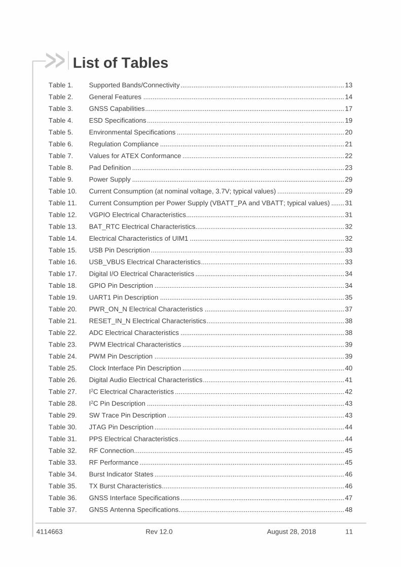
List of Tables Table 1. Supported Bands/Connectivity ........................................................................................ 13
Table 2. General Features ............................................................................................................ 14 Table 3. GNSS Capabilities ........................................................................................................... 17
Table 4. ESD Specifications .......................................................................................................... 19
Table 5. Environmental Specifications .......................................................................................... 20
Table 6. Regulation Compliance ................................................................................................... 21
Table 7. Values for ATEX Conformance ....................................................................................... 22
Table 8. Pad Definition .................................................................................................................. 23 Table 9. Power Supply .................................................................................................................. 29
Table 10. Current Consumption (at nominal voltage, 3.7V; typical values) .................................... 29
Table 11. Current Consumption per Power Supply (VBATT_PA and VBATT; typical values) ....... 31
Table 12. VGPIO Electrical Characteristics ..................................................................................... 31
Table 13. BAT_RTC Electrical Characteristics................................................................................ 32
Table 14. Electrical Characteristics of UIM1 ................................................................................... 32 Table 15. USB Pin Description ........................................................................................................ 33
Table 16. USB_VBUS Electrical Characteristics ............................................................................. 33
Table 17. Digital I/O Electrical Characteristics ................................................................................ 34
Table 18. GPIO Pin Description ...................................................................................................... 34
Table 19. UART1 Pin Description ................................................................................................... 35 Table 20. PWR_ON_N Electrical Characteristics ........................................................................... 37
Table 21. RESET_IN_N Electrical Characteristics .......................................................................... 38
Table 22. ADC Electrical Characteristics ........................................................................................ 38
Table 23. PWM Electrical Characteristics ....................................................................................... 39
Table 24. PWM Pin Description ...................................................................................................... 39
Table 25. Clock Interface Pin Description ....................................................................................... 40 Table 26. Digital Audio Electrical Characteristics ............................................................................ 41
Table 27. I2C Electrical Characteristics ........................................................................................... 42
Table 28. I2C Pin Description .......................................................................................................... 43
Table 29. SW Trace Pin Description ............................................................................................... 43
Table 30. JTAG Pin Description ...................................................................................................... 44
Table 31. PPS Electrical Characteristics ......................................................................................... 44 Table 32. RF Connection................................................................................................................. 45
Table 33. RF Performance .............................................................................................................. 45
Table 34. Burst Indicator States ...................................................................................................... 46
Table 35. TX Burst Characteristics .................................................................................................. 46
Table 36. GNSS Interface Specifications ........................................................................................ 47
Table 37. GNSS Antenna Specifications ......................................................................................... 48

4114663 Rev 12.0 August 28, 2018 12
Product Technical Specification
Table 38. GNSS Antenna Recommendations ................................................................................. 48
Table 39. Standards Conformity ...................................................................................................... 58
Table 40. Life Stress Test................................................................................................................ 58 Table 41. Environmental Resistance Stress Tests ......................................................................... 59
Table 42. Corrosive Resistance Stress Tests ................................................................................. 59
Table 43. Thermal Resistance Cycle Stress Tests ......................................................................... 60
Table 44. Mechanical Resistance Stress Tests .............................................................................. 61
Table 45. Handling Resistance Stress Tests .................................................................................. 62
Table 46. Ordering Information ....................................................................................................... 66
4114663 Rev 12.0 August 28, 2018 13
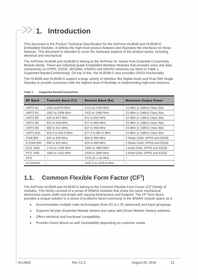
1. IntroductionThis document is the Product Technical Specification for the AirPrime HL8548 and HL8548-G Embedded Modules. It defines the high-level product features and illustrates the interfaces for these features. This document is intended to cover the hardware aspects of the product series, including electrical and mechanical.
The AirPrime HL8548 and HL8548-G belong to the AirPrime HL Series from Essential Connectivity Module family. These are industrial grade Embedded Wireless Modules that provides voice and data connectivity on GPRS, EDGE, WCDMA, HSDPA and HSUPA networks (as listed in Table 1 Supported Bands/Connectivity). On top of this, the HL8548-G also provides GNSS functionality.
The HL8548 and HL8548-G support a large variety of interface like Digital Audio and Dual SIM Single Standby to provide customers with the highest level of flexibility in implementing high-end solutions.
Table 1. Supported Bands/Connectivity
RF Band Transmit Band (Tx) Receive Band (Rx) Maximum Output Power
UMTS B1 1922 to1978 MHz 2112 to 2168 MHz 23 dBm (± 2dBm) Class 3bis UMTS B2 1852 to 1908 MHz 1932 to 1988 MHz 23 dBm (± 2dBm) Class 3bis UMTS B5 826 to 847 MHz 871 to 892 MHz 23 dBm (± 2dBm) Class 3bis UMTS B6 832 to 838 MHz 877 to 883 MHz 23 dBm (± 2dBm) Class 3bis UMTS B8 882 to 913 MHz 927 to 958 MHz 23 dBm (± 2dBm) Class 3bis UMTS B19 832.4 to 842.6 MHz 877.4 to 887.6 MHz 23 dBm (± 2dBm) Class 3bis GSM 850 824 to 849 MHz 869 to 894 MHz 2 Watts GSM, GPRS and EDGE E-GSM 900 880 to 915 MHz 925 to 960 MHz 2 Watts GSM, GPRS and EDGE DCS 1800 1710 to 1785 MHz 1805 to 1880 MHz 1-Watt GSM, GPRS and EDGE PCS 1900 1850 to 1910 MHz 1930 to 1990 MHz 1-Watt GSM, GPRS and EDGE GPS -- 1575.42 ± 20 MHz -- GLONASS -- 1597.5 to 1605.8 MHz --
1.1. Common Flexible Form Factor (CF3) The AirPrime HL8548 and HL8548-G belong to the Common Flexible Form Factor (CF3) family of modules. This family consists of a series of WWAN modules that share the same mechanical dimensions (same width and length with varying thicknesses) and footprint. The CF3 form factor provides a unique solution to a series of problems faced commonly in the WWAN module space as it:
• Accommodates multiple radio technologies (from 2G to LTE advanced) and band groupings
• Supports bit-pipe (Essential Module Series) and value add (Smart Module Series) solutions
• Offers electrical and functional compatibility
• Provides Direct Mount as well Socketability depending on customer needs
4114663 Rev 12.0 August 28, 2018 14
Product Technical Specification Introduction
1.2. Physical Dimensions The AirPrime HL8548 and HL8548-G modules are compact, robust, fully shielded modules with the following dimensions:
• Length: 23 mm
• Width: 22 mm
• Thickness: 2.5 mm
• Weight: 3.1 g
Note: Dimensions specified above are typical values.
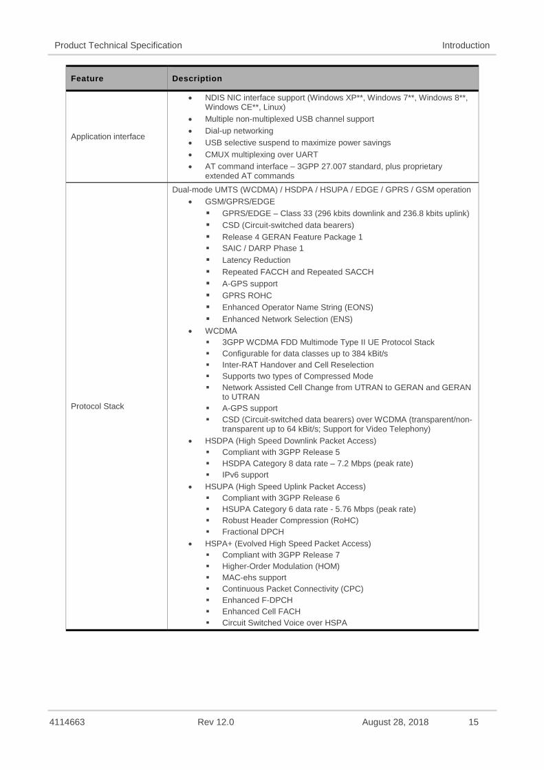
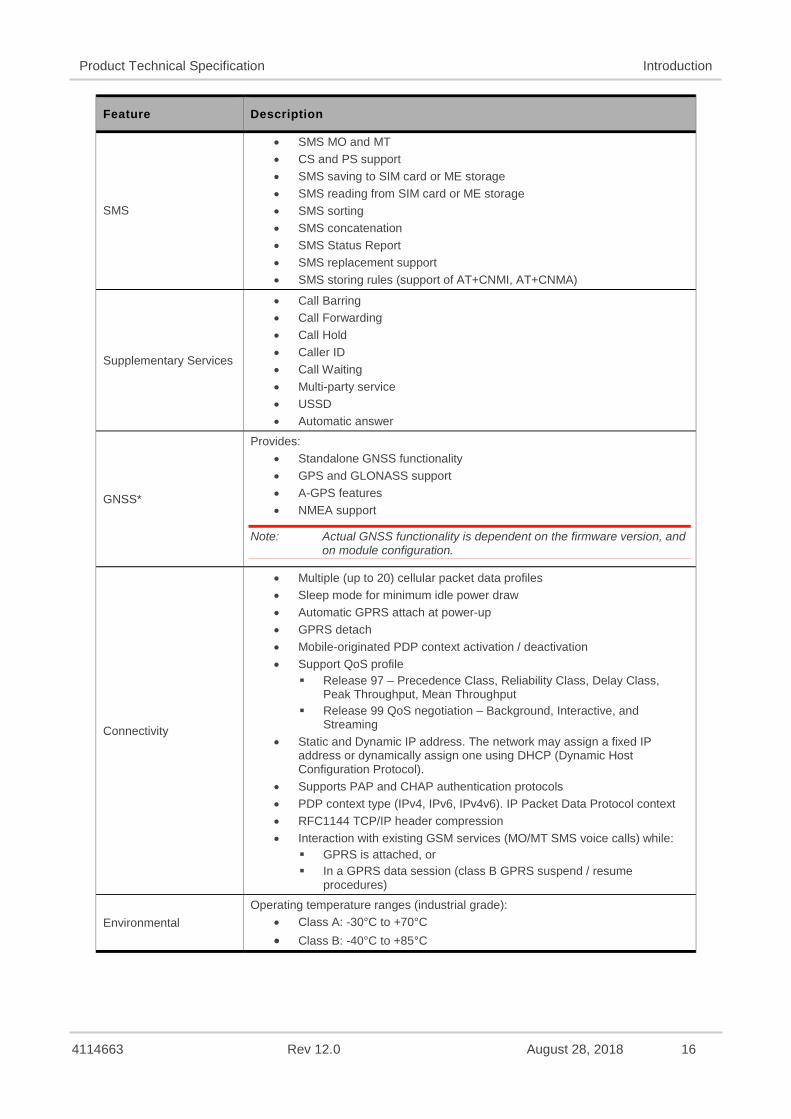
1.3. General Features The table below summarizes the AirPrime HL8548 and HL8548-G features.
Table 2. General Features
Feature Description
Physical
• Small form factor (146-pin solderable LGA pad) – 23mm x 22mm x 2.5mm (nominal)
• Complete body shielding • RF connection pads – RF primary and GNSS interface • Baseband signals connection
Electrical Single or double supply voltage (VBATT and VBATT_PA) – 3.2V – 4.5V
RF
• Quad-band GSM / GPRS / EDGE (850 MHz, 900 MHz, 1800 MHz, 1900 MHz)
• Hexa-band UMTS WCDMA FDD (800 MHz (B19), 850 MHz(B5/B6), 900MHz(B8), 1900 MHz(B2), 2100MHz(B1))
• GPS (1575.42 MHz), GLONASS (1602MHz)
Audio interface
• Digital interface (ONLY) • Supports Enhanced Full Rate (EFR), Full Rate (FR), Half Rate (HR), and
both Narrow-Band and Wide-band Adaptive Multirate (AMR-NB and AMR-WB) vocoders
• MO and MT calling • Echo cancellation and noise reduction • Emergency calls (112, 110, 911, etc.) • Incoming call notification • DTMF generation
SIM interface
• Dual SIM Single Standby with fast network switching capability • 1.8V/3V support • SIM extraction / hot plug detection • SIM/USIM support • Conforms with ETSI UICC Specifications. • Supports SIM application tool kit with proactive SIM commands
4114663 Rev 12.0 August 28, 2018 15
Product Technical Specification Introduction
Feature Description
Application interface
• NDIS NIC interface support (Windows XP**, Windows 7**, Windows 8**, Windows CE**, Linux)
• Multiple non-multiplexed USB channel support • Dial-up networking • USB selective suspend to maximize power savings • CMUX multiplexing over UART • AT command interface – 3GPP 27.007 standard, plus proprietary
extended AT commands
Protocol Stack
Dual-mode UMTS (WCDMA) / HSDPA / HSUPA / EDGE / GPRS / GSM operation • GSM/GPRS/EDGE
GPRS/EDGE – Class 33 (296 kbits downlink and 236.8 kbits uplink) CSD (Circuit-switched data bearers) Release 4 GERAN Feature Package 1 SAIC / DARP Phase 1 Latency Reduction Repeated FACCH and Repeated SACCH A-GPS support GPRS ROHC Enhanced Operator Name String (EONS) Enhanced Network Selection (ENS)
• WCDMA 3GPP WCDMA FDD Multimode Type II UE Protocol Stack Configurable for data classes up to 384 kBit/s Inter-RAT Handover and Cell Reselection Supports two types of Compressed Mode Network Assisted Cell Change from UTRAN to GERAN and GERAN
to UTRAN A-GPS support CSD (Circuit-switched data bearers) over WCDMA (transparent/non-
transparent up to 64 kBit/s; Support for Video Telephony) • HSDPA (High Speed Downlink Packet Access)
Compliant with 3GPP Release 5 HSDPA Category 8 data rate – 7.2 Mbps (peak rate) IPv6 support
• HSUPA (High Speed Uplink Packet Access) Compliant with 3GPP Release 6 HSUPA Category 6 data rate - 5.76 Mbps (peak rate) Robust Header Compression (RoHC) Fractional DPCH
• HSPA+ (Evolved High Speed Packet Access) Compliant with 3GPP Release 7 Higher-Order Modulation (HOM) MAC-ehs support Continuous Packet Connectivity (CPC) Enhanced F-DPCH Enhanced Cell FACH Circuit Switched Voice over HSPA
4114663 Rev 12.0 August 28, 2018 16
Product Technical Specification Introduction
Feature Description
SMS
• SMS MO and MT • CS and PS support • SMS saving to SIM card or ME storage • SMS reading from SIM card or ME storage • SMS sorting • SMS concatenation • SMS Status Report • SMS replacement support • SMS storing rules (support of AT+CNMI, AT+CNMA)
Supplementary Services
• Call Barring • Call Forwarding • Call Hold • Caller ID • Call Waiting • Multi-party service • USSD • Automatic answer
GNSS*
Provides: • Standalone GNSS functionality • GPS and GLONASS support • A-GPS features • NMEA support
Note: Actual GNSS functionality is dependent on the firmware version, and on module configuration.
Connectivity
• Multiple (up to 20) cellular packet data profiles • Sleep mode for minimum idle power draw • Automatic GPRS attach at power-up • GPRS detach • Mobile-originated PDP context activation / deactivation • Support QoS profile
Release 97 – Precedence Class, Reliability Class, Delay Class, Peak Throughput, Mean Throughput
Release 99 QoS negotiation – Background, Interactive, and Streaming
• Static and Dynamic IP address. The network may assign a fixed IP address or dynamically assign one using DHCP (Dynamic Host Configuration Protocol).
• Supports PAP and CHAP authentication protocols • PDP context type (IPv4, IPv6, IPv4v6). IP Packet Data Protocol context • RFC1144 TCP/IP header compression • Interaction with existing GSM services (MO/MT SMS voice calls) while:
GPRS is attached, or In a GPRS data session (class B GPRS suspend / resume
procedures)
Environmental Operating temperature ranges (industrial grade):
• Class A: -30°C to +70°C • Class B: -40°C to +85°C
4114663 Rev 12.0 August 28, 2018 17
Product Technical Specification Introduction
Feature Description
RTC Real Time Clock (RTC) with calendar and alarm
Temperature Sensor • Temperature monitoring • Alarms
* Only available on the AirPrime HL8548-G.
** USB drivers have not been certified by Microsoft and should only be used for test purposes.
1.4. GNSS Features The table below summarizes the AirPrime HL8548-G GNSS capabilities.
Table 3. GNSS Capabilities
Feature Description
GPS L1 band (CDMA 1575.42 MHz) GLONASS L1 Band (FDMA 1602MHz) Channels 52 Antenna Passive or active antenna support Assistance data Server-generated Extended Ephemeris
1.5. Encryption Support The AirPrime HL8548 and HL8548-G supports the following encryption algorithms:
• Ciphering algorithms A51, A52 and A53
• GEA1/GEA2 and GEA3 algorithm for GPRS encryption
• Cyclic Redundancy Check (CRC) with programmable polynomial
• UMTS confidentiality algorithm f8 for message ciphering (Kasumi based UEA1)
• UMTS integrity algorithm f9 for message authentication (Kasumi based UIA1 and SNOW 3G based UIA2)
4114663 Rev 12.0 August 28, 2018 18
Product Technical Specification Introduction
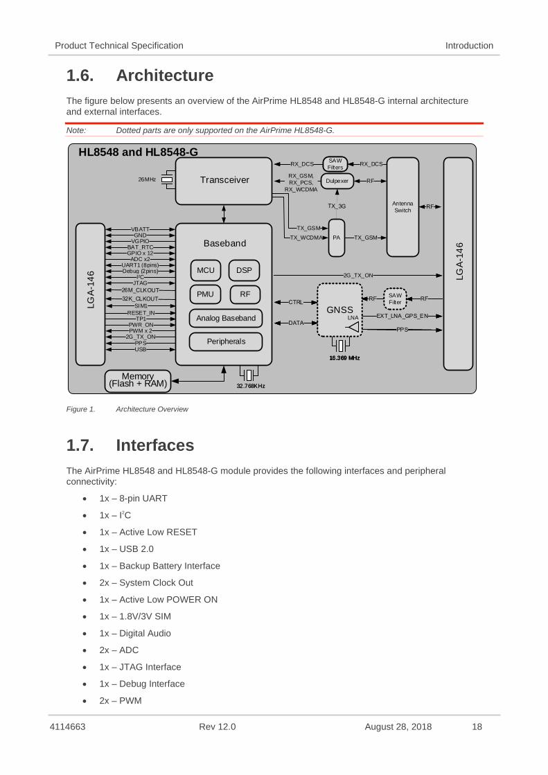
1.6. Architecture The figure below presents an overview of the AirPrime HL8548 and HL8548-G internal architecture and external interfaces.
Note: Dotted parts are only supported on the AirPrime HL8548-G.
32.768KHz32.768KHz
HL8548 and HL8548-G
AntennaSwitch
26MHz
LGA-
146
Baseband
MCU DSP
PMU RF
Analog Baseband
Peripherals
RX_GSM, RX_PCS,
RX_WCDMARF
TX_GSMTX_WCDMA
LGA-
146
Dulpexer
PATX_GSM
Memory(Flash + RAM)
2G_TX_ON
16.369 MHz16.369 MHz
GNSSSAWFilter
GNSSSAWFilter
16.369 MHz
GNSSSAWFilter
2G_TX_ON
16.369 MHz
GNSSSAWFilter
LNA
UART1 (8pins)Debug (2pins)
VBATTGND
VGPIOBAT_RTCGPIO x 12
ADC x2
I²C
RESET_IN
JTAG
SIM1
TP1PWR_ON
2G_TX_ONPWM x 2
PPSUSB
Transceiver
SAWFiltersRX_DCS RX_DCSSAWFiltersRX_DCS RX_DCS
Figure 1. Architecture Overview
1.7. Interfaces The AirPrime HL8548 and HL8548-G module provides the following interfaces and peripheral connectivity:
• 1x – 8-pin UART
• 1x – I2C
• 1x – Active Low RESET
• 1x – USB 2.0
• 1x – Backup Battery Interface
• 2x – System Clock Out
• 1x – Active Low POWER ON
• 1x – 1.8V/3V SIM
• 1x – Digital Audio
• 2x – ADC
• 1x – JTAG Interface
• 1x – Debug Interface
• 2x – PWM
4114663 Rev 12.0 August 28, 2018 19
Product Technical Specification Introduction
• 12x – GPIOs with 4 multiplexes
• 1x – 2G TX Burst Indicator
• 1x – GSM Antenna
In addition, the AirPrime HL8548-G module provides the following additional interfaces and peripheral connectivity:
• GNSS Antenna
• External GNSS LNA Enable/Disable
• Pulse Per Second
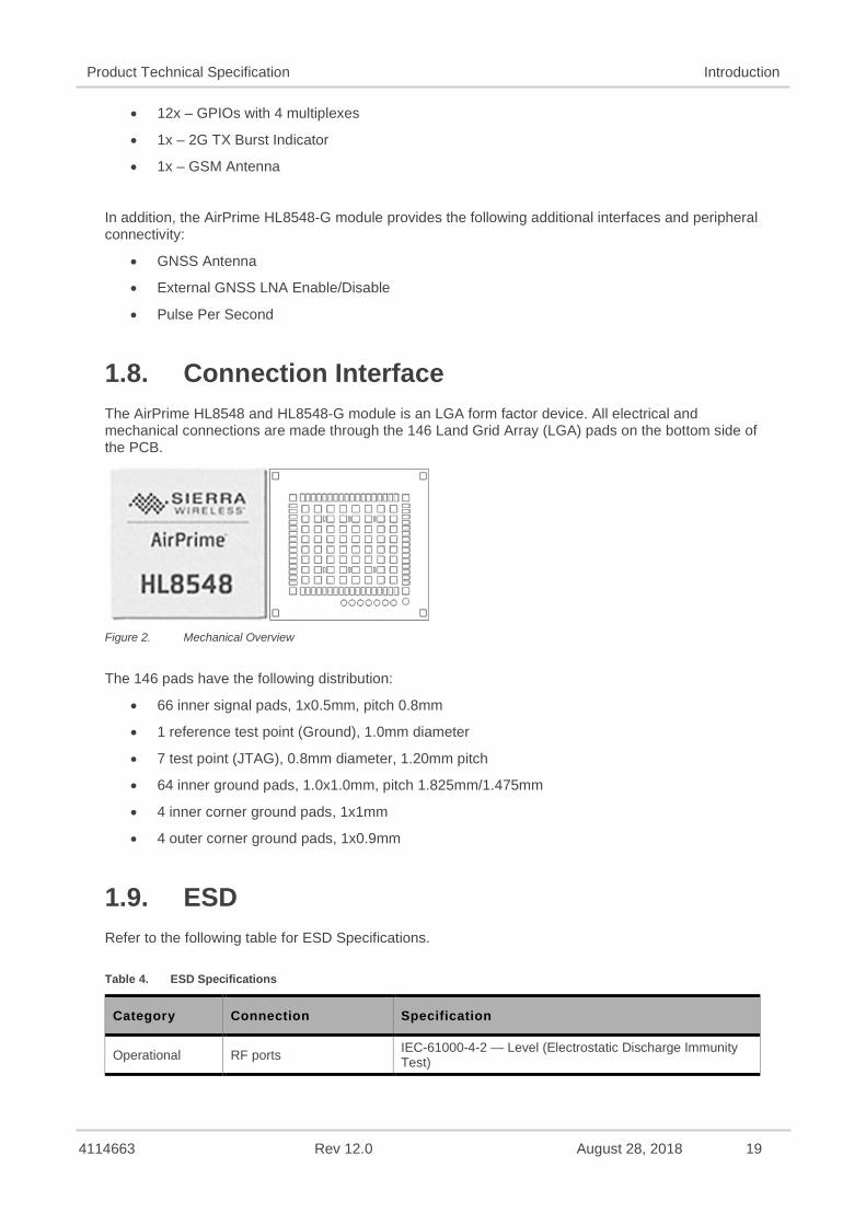
1.8. Connection Interface The AirPrime HL8548 and HL8548-G module is an LGA form factor device. All electrical and mechanical connections are made through the 146 Land Grid Array (LGA) pads on the bottom side of the PCB.
Figure 2. Mechanical Overview
The 146 pads have the following distribution:
• 66 inner signal pads, 1x0.5mm, pitch 0.8mm
• 1 reference test point (Ground), 1.0mm diameter
• 7 test point (JTAG), 0.8mm diameter, 1.20mm pitch
• 64 inner ground pads, 1.0x1.0mm, pitch 1.825mm/1.475mm
• 4 inner corner ground pads, 1x1mm
• 4 outer corner ground pads, 1x0.9mm
1.9. ESD Refer to the following table for ESD Specifications.
Table 4. ESD Specifications
Category Connection Specification
Operational RF ports IEC-61000-4-2 — Level (Electrostatic Discharge Immunity Test)
4114663 Rev 12.0 August 28, 2018 20
Product Technical Specification Introduction
Category Connection Specification
Non-operational Host connector interface
Unless otherwise specified: • JESD22-A114 ± 1kV Human Body Model • JESD22-A115 ± 200V Machine Model • JESD22-C101 ± 250V Charged Device Model
Signals SIM connector ESD protection is highly recommended at the point where
the USIM contacts are exposed, and for any other signals that would be subjected to ESD by the user. Other host signals
1.10. Environmental and Certifications
1.10.1. Environmental Specifications The environmental specification for both operating and storage conditions are defined in the table below.
Table 5. Environmental Specifications
Conditions Range
Operating Class A -30°C to +70°C Operating Class B -40°C to +85°C Storage -40°C to +85°C
Class A is defined as the operating temperature ranges that the device:
• Shall exhibit normal function during and after environmental exposure.
• Shall meet the minimum requirements of 3GPP or appropriate wireless standards.
Class B is defined as the operating temperature ranges that the device:
• Shall remain fully functional during and after environmental exposure
• Shall exhibit the ability to establish a voice, SMS or DATA call (emergency call) at all times even when one or more environmental constraint exceeds the specified tolerance.
• Unless otherwise stated, full performance should return to normal after the excessive constraint(s) have been removed.
1.10.2. Regulatory The AirPrime HL8548 and HL8548-G are both compliant with the following regulations:
• Japan JRF/JPA
• FCC
• IC
These compliances will be reflected on the AirPrime HL8548 and HL8548-G labels when applicable.
4114663 Rev 12.0 August 28, 2018 21
Product Technical Specification Introduction
Table 6. Regulation Compliance
Document Current Version Title
NAPRD.03 v5.18 or later Overview of PCS Type certification review board (PTCRB) Mobile Equipment Type Certification and IMEI control
GCF-CC v3.51.1 or later GCF Conformance Certification Criteria
TS 51.010-1 V10.0.0 (2012-03)
3rd Generation Partnership Project; Technical Specification Group GSM/EDGE Radio Access Network; Digital cellular telecommunications system (Phase 2+); Mobile Station (MS) conformance specification; Part 1: Conformance specification
TS 51.010-2 V10.0.0 (2012-03)
3rd Generation Partnership Project; Technical Specification Group GSM/EDGE Radio Access Network; Mobile Station (MS) conformance specification; Part 2: Protocol Implementation Conformance Statement (PICS) proforma specification
EN 301489-1 V1.9.2 (2011-09) Electromagnetic compatibility and Radio spectrum Matters (ERM); ElectroMagnetic Compatibility (EMC) standard for radio equipment and services; Part 1: Common technical requirements
EN 301489-3 V1.4.1 (2002-08)
Electromagnetic compatibility and Radio spectrum Matters (ERM); ElectroMagnetic Compatibility (EMC) standard for radio equipment and services; Part 3: Specific conditions for Short-Range Devices (SRD) operating on frequencies between 9 kHz and 40 GHz
EN 301489-7 V1.3.1 (2005-11)
Electromagnetic Compatibility and Radio Spectrum Matters (ERM); ElectroMagnetic Compatibility (EMC) Standard for Radio Equipment and Services; Part 7: Specific Conditions for Mobile and Portable Radio and Ancillary Equipment of Digital Cellular Radio Telecommunications Systems (GSM and DCS)
EN 60950-1 NA
IEC 60950-1:2005/A1:2009 EN 60950-1:2006/A11:2009/A1:2010/A12:2011/AC :2011 Information technology equipment – safety- and general requirements
EN 300440-1 v1.6.1 (2012-08)
Electromagnetic compatibility and Radio spectrum Matters (ERM); Short range devices; Radio equipment to be used in the 1 GHz to 40 GHz frequency range; Part 1: Technical characteristics and test methods
FCC Part 22H NA Cellular Radiotelephone Service; Subpart H: Cellular Radiotelephone Service
FCC Part 24E NA Personal Communications Service; Subpart E: Broadband PCS.
RSS-132 Issue 2:2005 Cellular telephones employing new technologies operating in the 824-849 MHz and 869-894 MHz bands.
RSS-133 Issue 5:2009 2 GHz personal communications services
AS/ACIF S042.1 2008 Requirements for connection to an air interface of a telecommunications network Part 1; General
AS/ACIF S042.3 2005 Requirements for connection to an air interface of a Telecommunications Network - Part 3: GSM Customer Equipment
AS/NZS 60950.1 2011 Safety of information technology equipment (IEC 60950-1, Ed.2.0: 2005, MOD)
CCC NA China Compulsory Certification
4114663 Rev 12.0 August 28, 2018 22
Product Technical Specification Introduction
1.10.3. RoHS Directive Compliance AirPrime HL8548 and HL8548-G modules are compliant with RoHS Directive 2011/65/EU, including directive 2015/863 amending annex II, which sets limits for the use of certain restricted hazardous substances. This directive states that electrical and electronic equipment put on the market does not contain lead, mercury, cadmium, hexavalent chromium, polybrominated biphenyls (PBB), polybrominated diphenyl ethers (PBDE), Bis (2-ethylhexyl) phthalate (DEHP), Butyl benzyl phthalate (BBP), Dibutyl phthalate (DBP) or Diisobutyl phthalate (DIBP) above threshold limits.
1.10.4. Disposing of the Product
This electronic product is subject to the EU Directive 2012/19/EU for Waste Electrical and Electronic Equipment (WEEE). As such, this product must not be disposed of at a municipal waste collection point. Please refer to local regulations for directions on how to dispose of this product in an environmental friendly manner.
1.11. Conformance with ATEX 94/9/CE Directive To evaluate the conformity of a product using the AirPrime HL8548 or HL8548-G with ATEX 94/9/CE directive, the integrator must take into account the following data from the AirPrime HL8548 and HL8548-G.
Table 7. Values for ATEX Conformance
Variant Sum of all Capacitors
Sum of all Inductors
Biggest Single Capacitor
Biggest Single Inductor
HL8548 200 µF 10 µH 22 µF ± 20% 3.3 µH ± 20% HL8548-G 230 µF 12 µH 22 µF ± 20% 3.3 µH ± 20%
1.12. References [1] AirPrime HL Series Customer Process Guidelines
Reference Number: 4114330
[2] AirPrime HL6 and HL8 Series AT Commands Interface Guide
Reference Number: 4114680
[3] AirPrime HL Series Development Kit User Guide
Reference Number: 4114877
[4] “I2C Bus Specification”, Version 2.0, Philips Semiconductor 1998
4114663 Rev 12.0 August 28, 2018 23
2. Pad DefinitionAirPrime HL8548 and HL8548-G pins are divided into 2 functional categories.
• Core functions and associated pins cover all the mandatory features for M2M connectivity and will be available by default across all CF3 family ofmodules. These Core functions are always available and always at the same physical pin locations. A customer platform using only these functionsand associated pins is guaranteed to be forward and/or backward compatible with the next generation of CF3 modules.
• Extension functions and associated pins bring additional capabilities to the customer. Whenever an Extension function is available on a module, itis always at the same pin location.
Other pins marked as “not connected” or “reserved” should not be used.
Table 8. Pad Definition
Pin # Signal Name Function I/O Active Low/High
Reset State*
Power Supply Domain
Recommendation for Unused Pins Type
1 GPIO1 / I2C_CLK General purpose input/output / I2C Clock I/O I, T/PU 1.8V Left Open Extension
2 UART1_RI UART1 Ring indicator O I, T/PD 1.8V Left Open Core
3 UART1_RTS UART1 Request to send I L I, T/PD 1.8V Connect to UART1_CTS if using a 2-wire UART; otherwise, leave open
Core
4 UART1_CTS UART1 Clear to send O L I, T/PD 1.8V Connect to UART1_RTS if using a 2-wire UART; otherwise, leave open
Core
5 UART1_TX UART1 Transmit data I I, T/PD 1.8V Mandatory connection if using a 2-wire UART; otherwise, leave open
Core
6 UART1_RX UART1 Receive data O I, T/PD 1.8V Mandatory connection if using a 2-wire UART; otherwise, leave open
Core
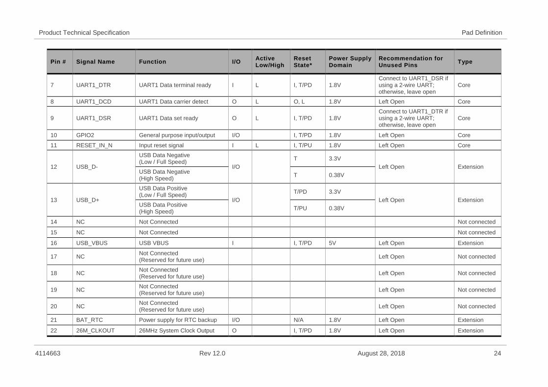
4114663 Rev 12.0 August 28, 2018 24
Product Technical Specification Pad Definition
Pin # Signal Name Function I/O Active Low/High
Reset State*
Power Supply Domain
Recommendation for Unused Pins Type
7 UART1_DTR UART1 Data terminal ready I L I, T/PD 1.8V Connect to UART1_DSR if using a 2-wire UART; otherwise, leave open
Core
8 UART1_DCD UART1 Data carrier detect O L O, L 1.8V Left Open Core
9 UART1_DSR UART1 Data set ready O L I, T/PD 1.8V Connect to UART1_DTR if using a 2-wire UART; otherwise, leave open
Core
10 GPIO2 General purpose input/output I/O I, T/PD 1.8V Left Open Core
11 RESET_IN_N Input reset signal I L I, T/PU 1.8V Left Open Core
12 USB_D-
USB Data Negative (Low / Full Speed)
I/O T 3.3V
Left Open Extension USB Data Negative (High Speed) T 0.38V
13 USB_D+
USB Data Positive (Low / Full Speed)
I/O T/PD 3.3V
Left Open Extension USB Data Positive (High Speed) T/PU 0.38V
14 NC Not Connected Not connected
15 NC Not Connected Not connected
16 USB_VBUS USB VBUS I I, T/PD 5V Left Open Extension
17 NC Not Connected (Reserved for future use) Left Open Not connected
18 NC Not Connected (Reserved for future use) Left Open Not connected
19 NC Not Connected (Reserved for future use) Left Open Not connected
20 NC Not Connected (Reserved for future use) Left Open Not connected
21 BAT_RTC Power supply for RTC backup I/O N/A 1.8V Left Open Extension
22 26M_CLKOUT 26MHz System Clock Output O I, T/PD 1.8V Left Open Extension
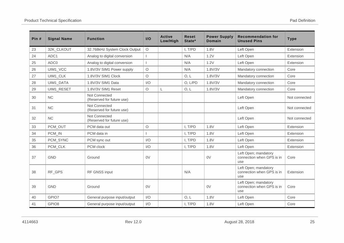
4114663 Rev 12.0 August 28, 2018 25
Product Technical Specification Pad Definition
Pin # Signal Name Function I/O Active Low/High
Reset State*
Power Supply Domain
Recommendation for Unused Pins Type
23 32K_CLKOUT 32.768kHz System Clock Output O I, T/PD 1.8V Left Open Extension
24 ADC1 Analog to digital conversion I N/A 1.2V Left Open Extension
25 ADC0 Analog to digital conversion I N/A 1.2V Left Open Extension
26 UIM1_VCC 1.8V/3V SIM1 Power supply O N/A 1.8V/3V Mandatory connection Core
27 UIM1_CLK 1.8V/3V SIM1 Clock O O, L 1.8V/3V Mandatory connection Core
28 UIM1_DATA 1.8V/3V SIM1 Data I/O O, L/PD 1.8V/3V Mandatory connection Core
29 UIM1_RESET 1.8V/3V SIM1 Reset O L O, L 1.8V/3V Mandatory connection Core
30 NC Not Connected (Reserved for future use) Left Open Not connected
31 NC Not Connected (Reserved for future use) Left Open Not connected
32 NC Not Connected (Reserved for future use) Left Open Not connected
33 PCM_OUT PCM data out O I, T/PD 1.8V Left Open Extension
34 PCM_IN PCM data in I I, T/PD 1.8V Left Open Extension
35 PCM_SYNC PCM sync out I/O I, T/PD 1.8V Left Open Extension
36 PCM_CLK PCM clock I/O I, T/PD 1.8V Left Open Extension
37 GND Ground 0V 0V Left Open; mandatory connection when GPS is in use
Core
38 RF_GPS RF GNSS input N/A Left Open; mandatory connection when GPS is in use
Extension
39 GND Ground 0V 0V Left Open; mandatory connection when GPS is in use
Core
40 GPIO7 General purpose input/output I/O O, L 1.8V Left Open Core
41 GPIO8 General purpose input/output I/O I, T/PD 1.8V Left Open Core
4114663 Rev 12.0 August 28, 2018 26
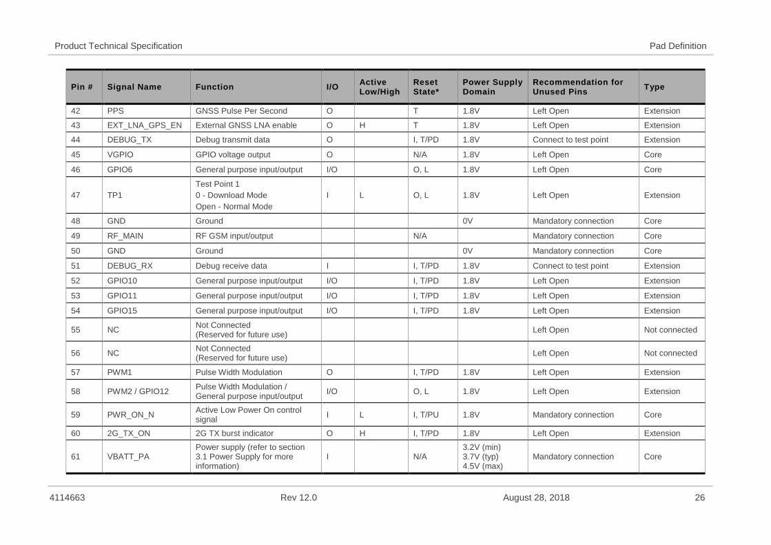
Product Technical Specification Pad Definition
Pin # Signal Name Function I/O Active Low/High
Reset State*
Power Supply Domain
Recommendation for Unused Pins Type
42 PPS GNSS Pulse Per Second O T 1.8V Left Open Extension
43 EXT_LNA_GPS_EN External GNSS LNA enable O H T 1.8V Left Open Extension
44 DEBUG_TX Debug transmit data O I, T/PD 1.8V Connect to test point Extension
45 VGPIO GPIO voltage output O N/A 1.8V Left Open Core
46 GPIO6 General purpose input/output I/O O, L 1.8V Left Open Core
47 TP1 Test Point 1 0 - Download Mode Open - Normal Mode
I L O, L 1.8V Left Open Extension
48 GND Ground 0V Mandatory connection Core
49 RF_MAIN RF GSM input/output N/A Mandatory connection Core
50 GND Ground 0V Mandatory connection Core
51 DEBUG_RX Debug receive data I I, T/PD 1.8V Connect to test point Extension
52 GPIO10 General purpose input/output I/O I, T/PD 1.8V Left Open Extension
53 GPIO11 General purpose input/output I/O I, T/PD 1.8V Left Open Extension
54 GPIO15 General purpose input/output I/O I, T/PD 1.8V Left Open Extension
55 NC Not Connected (Reserved for future use) Left Open Not connected
56 NC Not Connected (Reserved for future use) Left Open Not connected
57 PWM1 Pulse Width Modulation O I, T/PD 1.8V Left Open Extension
58 PWM2 / GPIO12 Pulse Width Modulation / General purpose input/output I/O O, L 1.8V Left Open Extension
59 PWR_ON_N Active Low Power On control signal I L I, T/PU 1.8V Mandatory connection Core
60 2G_TX_ON 2G TX burst indicator O H I, T/PD 1.8V Left Open Extension
61 VBATT_PA Power supply (refer to section 3.1 Power Supply for more information)
I N/A 3.2V (min) 3.7V (typ) 4.5V (max)
Mandatory connection Core
4114663 Rev 12.0 August 28, 2018 27
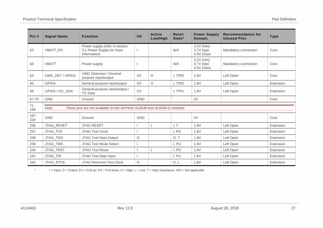
Product Technical Specification Pad Definition
Pin # Signal Name Function I/O Active Low/High
Reset State*
Power Supply Domain
Recommendation for Unused Pins Type
62 VBATT_PA Power supply (refer to section 3.1 Power Supply for more information)
I N/A 3.2V (min) 3.7V (typ) 4.5V (max)
Mandatory connection Core
63 VBATT Power supply I N/A 3.2V (min) 3.7V (typ) 4.5V (max)
Mandatory connection Core
64 UIM1_DET / GPIO3 UIM1 Detection / General purpose input/output I/O H I, T/PD 1.8V Left Open Core
65 GPIO4 General purpose input/output I/O H I, T/PD 1.8V Left Open Extension
66 GPIO5 / I2C_SDA General purpose input/output / I2C Data I/O I, T/PU 1.8V Left Open Extension
67-70 GND Ground GND 0V Core 71 - 166 Note: These pins are not available on the AirPrime HL8548 and HL8548-G modules.
167-234 GND Ground GND 0V Core
236 JTAG_RESET JTAG RESET I L I, T 1.8V Left Open Extension
237 JTAG_TCK JTAG Test Clock I I, PD 1.8V Left Open Extension
238 JTAG_TDO JTAG Test Data Output O O, T 1.8V Left Open Extension
239 JTAG_TMS JTAG Test Mode Select I I, PU 1.8V Left Open Extension
240 JTAG_TRST JTAG Test Reset I L I, PD 1.8V Left Open Extension
241 JTAG_TDI JTAG Test Data Input I I, PU 1.8V Left Open Extension
242 JTAG_RTCK JTAG Returned Test Clock O O, L 1.8V Left Open Extension
* I = Input, O = Output, PU = Pull up, PD = Pull down, H = High, L = Low, T = High impedance, N/A = Not applicable
4114663 Rev 12.0 August 28, 2018 28
Product Technical Specification Pad Definition
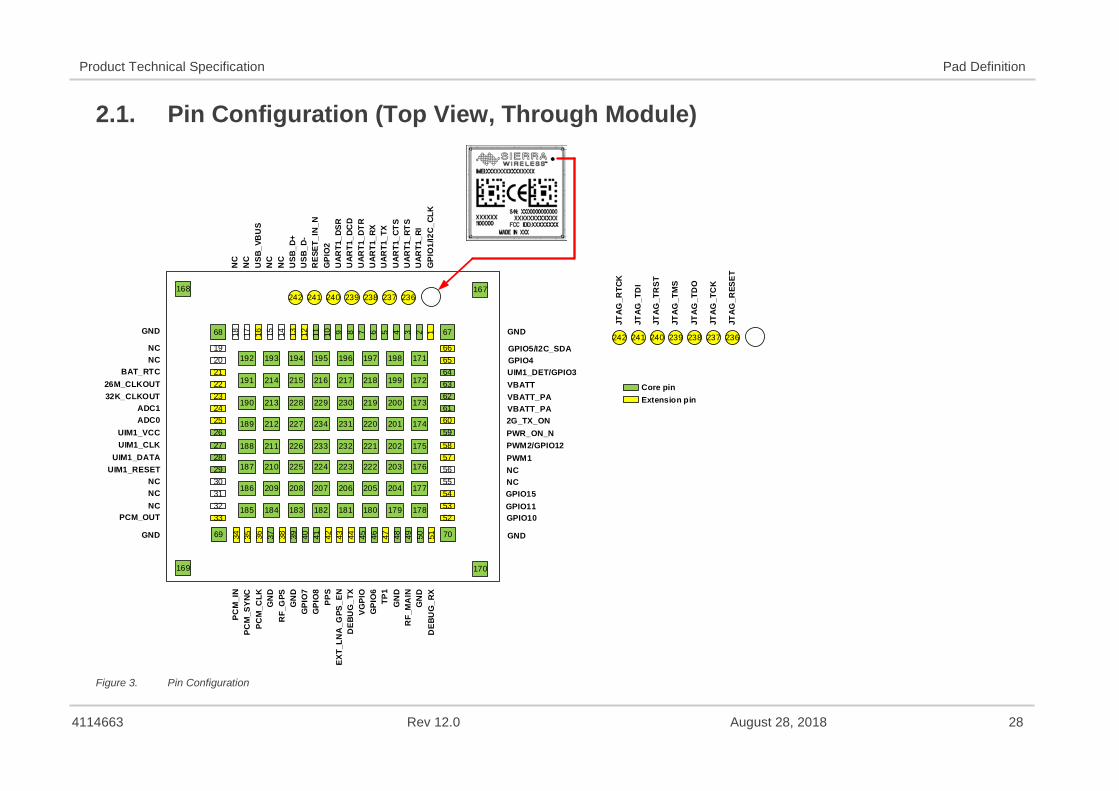
2.1. Pin Configuration (Top View, Through Module)
168
169
167
170
18 17 16 15 14 13 12 11 10 9 8 7 6 4 3 2 15
6665646362616059
34 35 36 37 38 39 40 41 42 43 44 45 46 48 49 50 5147
58575655
5352
54
70
67
192021222324252627282930
3233
31
69
68
192 193 194 195 196 197 198 171
191 214 215 216 217 218 199 172
190 213 228 229 230 219 200 173
189 212 227 234 231 220 201 174
188 211 226 233 232 221 202 175
187 210 225 224 223 222 203 176
186 209 208 207 206 205 204 177
185 184 183 182 181 180 179 178
236237238239240241242GND
GPIO5/I2C_SDAGPIO4UIM1_DET/GPIO3VBATTVBATT_PAVBATT_PA2G_TX_ONPWR_ON_NPWM2/GPIO12PWM1NCNCGPIO15GPIO11GPIO10
GND
GND
NCNC
BAT_RTC26M_CLKOUT32K_CLKOUT
ADC1ADC0
UIM1_VCCUIM1_CLK
UIM1_DATAUIM1_RESET
NCNCNC
PCM_OUT
GND
PCM
_IN
PCM
_SYN
CPC
M_C
LKG
ND
RF_
GPS
GN
DG
PIO
7G
PIO
8PP
SEX
T_LN
A_G
PS_E
ND
EBU
G_T
XVG
PIO
GPI
O6
TP1
GN
DR
F_M
AIN
GN
DD
EBU
G_R
X
NC
NC
USB
_VB
US
NC
NC
USB
_D+
USB
_D-
RES
ET_I
N_N
GPI
O2
UAR
T1_D
SRU
ART1
_DC
DU
ART1
_DTR
UAR
T1_R
XU
ART1
_TX
UAR
T1_C
TSU
ART1
_RTS
UAR
T1_R
IG
PIO
1/I2
C_CL
K
JTAG
_RTC
K
JTAG
_TD
I
JTAG
_TR
ST
JTAG
_TM
S
JTAG
_TD
O
JTAG
_TC
K
JTAG
_RES
ET
Core pinExtension pin
236237238239240241242
Figure 3. Pin Configuration
4114663 Rev 12.0 August 28, 2018 29
3. Detailed Interface SpecificationsNote: If not specified, all electrical values are given for VBATT=3.7V and an operating temperature of
25°C.
For standard applications, VBATT and VBATT_PA must be tied externally to the same power supply. For some specific applications, AirPrime HL8548 and HL8548-G module supports separate VBATT and VBATT_PA connection if requirements below are fulfilled.
3.1. Power Supply The AirPrime HL8548 and HL8548-G module is supplied through the VBATT signal with the following characteristics.
Table 9. Power Supply
Supply Minimum Typical Maximum
VBATT voltage (V) 3.21 3.7 4.5 VBATT_PA voltage (V) Full Specification 3.21 3.7 4.5 VBATT_PA voltage (V) Extended Range2 2.82 3.7 4.5
1 This value must be guaranteed during the burst
2 No guarantee of 3GPP performances over extended range
Note: Load capacitance for VBATT is around 30µF ± 20% embedded inside the module. Load capacitance for VBATT_PA is around 20µF ± 20% embedded inside the module.
3.2. Current Consumption The following table lists the current consumption of the AirPrime HL8548 and HL8548-G at different conditions.
Note: The following data is under the setup as recommended in 5.5 Power Supply Design section. The USB is disconnected for the lowest current consumption; additional 0.4mA will be consumed with the USB enabled.
Typical values are defined for VBATT/VBATT_PA at 3.7V and 25°C, for 50Ω impedance at all RF ports. Maximum values are provided for VSWR 3:1 with worst conditions among supported ranges of voltage and temperature.
Table 10. Current Consumption (at nominal voltage, 3.7V; typical values)
Parameter Typical Maximum
Off mode 40 µA 70 µA
Sleep mode - GSM DRX2 (registered to the network)
GSM900 1.9 mA 2.1 mA DCS1800 1.7 mA 2.0 mA GSM850 1.7 mA 2.0 mA PCS1900 1.7 mA 2.0 mA

4114663 Rev 12.0 August 28, 2018 30
Product Technical Specification Detailed Interface Specifications
Parameter Typical Maximum
Sleep mode - GSM DRX9 (registered to the network)
GSM900 1.3 mA 1.6 mA DCS1800 1.2 mA 1.4 mA GSM850 1.2 mA 1.4 mA PCS1900 1.1 mA 1.4 mA
Sleep mode - WCDMA DRX8 (registered to the network)
Band 1 1.4 mA 1.5 mA Band 2 1.4 mA 1.5 mA Band 5 / 6 1.4 mA 1.5 mA Band 8 1.4 mA 1.5 mA
WCDMA in communication mode (Voice Call)
Band 1 670 mA 756 mA Band 2 579 mA 766 mA Band 5 / 6 540 mA 686 mA
Band 8 594 mA 694 mA
WCDMA in communication mode (HSDPA)
Band 1 716 mA 814 mA
Band 2 639 mA 817 mA
Band 5 / 6 630 mA 784 mA
Band 8 680 mA 798 mA
WCDMA in communication mode (HSUPA)
Band 1 626 mA 877 mA
Band 2 547 mA 861 mA
Band 5 / 6 658 mA 818 mA
Band 8 683 mA 842mA
GSM in communication mode
GSM900 / GSM850 (PCL=5) 245 mA 301 mA
DCS / PCS (PCL=0) 170 mA 255 mA
GPRS (2 TX,3 RX) GSM900 / GSM850 (PCL=5) 452 mA 475 mA
DCS / PCS (PCL=0) 298 mA 387 mA
Peak current consumption GSM900 / GSM850 1.9 A 2.0 A
DCS / PCS 1.8 A 1.8 A
GNSS Acquisition1 (average, mA) GSM registered on network; RF in Idle Mode 42 mA 46 mA
GNSS Acquisition1 (average, mA) GSM in Flight mode; RF in Idle Mode 42 mA 46 mA
GNSS Navigation (1Hz)1 (average, mA) GSM registered on network; RF in Idle Mode 35 mA 38 mA
GNSS Navigation (1Hz)1 (average, mA) GSM in Flight mode; RF in Idle Mode 34 mA 38 mA
GNSS Hibernate mode2 (average, mA) GSM registered on network; RF in Idle Mode
15 mA 17 mA
GNSS Hibernate mode2 (average, mA) GSM in Flight mode, Baseband in sleep mode 1.1 mA 1.2 mA
GNSS Hibernate mode2 (average, mA) GSM900 Paging 9 1.4 mA 1.5 mA
1 Maximum SVs in view, signal level @-130dBm, high gain configuration
2 Hot start conditions are maintained in Hibernate mode; HL8548x baseband is in Idle mode
4114663 Rev 12.0 August 28, 2018 31
Product Technical Specification Detailed Interface Specifications
Table 11. Current Consumption per Power Supply (VBATT_PA and VBATT; typical values)
Parameters Typical
VBATT_PA
Average current GSM in communication mode
E-GSM 900 / GSM 850 (PCL=5) 194 mA DCS 1800/ PCS 1900 (PCL=0) 126 mA
Average current GPRS (2 TX,3 RX)
E-GSM 900 / GSM 850 (PCL=5) 380 mA DCS 1800/ PCS 1900 (PCL=0) 236 mA
Average current WCDMA in communication mode (Voice Call)
Band 1 475 mA Band 2 421 mA Band 5 / 6 390 mA Band 8 416 mA
VBATT
Average current GSM in communication mode
E-GSM 900 / GSM 850 (PCL=5) 41 mA DCS 1800/ PCS 1900 (PCL=0) 39 mA
Average current GPRS (2 TX,3 RX)
E-GSM 900 / GSM 850 (PCL=5) 60 mA DCS 1800/ PCS 1900 (PCL=0) 58 mA
Average current WCDMA in communication mode (Voice Call)
Band 1 128 mA Band 2 127 mA Band 5 / 6 118 mA Band 8 119 mA
3.3. VGPIO The VGPIO output can be used to:
• Pull-up signals such as I/Os
• Supply the digital transistors driving LEDs
• Act as a voltage reference for the ADC interfaces, ADC0 and ADC1
The VGPIO output is available when the AirPrime HL8548 AND HL8548-G module is switched ON.
Table 12. VGPIO Electrical Characteristics
Parameter Minimum Typical Maximum Remarks
Voltage level (V) 1.7 1.8 1.9 Both active mode and sleep mode
Current capability (mA) - - 50 Power Management support up to 50mA output.
Rise Time(ms) - - 1.5 Start-Up time from 0V
4114663 Rev 12.0 August 28, 2018 32
Product Technical Specification Detailed Interface Specifications
3.4. BAT_RTC The AirPrime HL8548 and HL8548-G module provides an input/output to connect a Real Time Clock power supply.
This pin is used as a back-up power supply for the internal Real Time Clock. The RTC is supported when VBATT is available but a back-up power supply is needed to save date and hour when VBATT is switched off.
If VBATT is available, the back-up battery can be charged by the internal 1.8V power supply regulator.
Table 13. BAT_RTC Electrical Characteristics
Parameter Minimum Typical Maximum Unit
Input voltage 1.0 1.8 1.9 V Input current consumption - 1 - µA Output voltage -5% 1.8 +5% V Max charging current (@VBATT=3.7V) - 25 - mA
Note: When used with the HL Series snap-in socket, or when compatibility with HL6528x is needed, Sierra Wireless recommends adding a 10µF capacitor to the BAT_RTC pin.
3.5. SIM Interface The AirPrime HL8548 and HL8548-G has one physical SIM interface, UIM1, which has optional support for dual SIM application with an external SIM switch. Refer to Section 5.9 Dual SIM Application for more information regarding dual SIM.
The UIM1 interface allows control of a 1.8V/3V SIM and is fully compliant with GSM 11.11 recommendations concerning SIM functions.
The five signals used by this interface are as follows:
• UIM1_VCC: power supply
• UIM1_CLK: clock
• UIM1_DATA: I/O port
• UIM1_RST: reset
• UIM1_DET: SIM detection
Table 14. Electrical Characteristics of UIM1
Parameter Minimum Typical Maximum Remarks
UIM1 Interface Voltage (V) (VCC, CLK, IO, RST)
2.7 3.0 3.15 The appropriate output voltage is auto detected and selected by software. 1.65 1.80 1.95
UIM1 Detect 1.33 1.80 2.1 High active
UIM1_VCC Current (mA) - - 10 Max output current in sleep mode = 3 mA
UIM1_VCC Line Regulation (mV/V) - - 50 At Iout_Max
UIM1_VCC Power-up Setting Time (µs) from power down - 10 -
4114663 Rev 12.0 August 28, 2018 33
Product Technical Specification Detailed Interface Specifications
3.5.1. UIM1_DET UIM1_DET is used to detect and notify the application about the insertion and removal of a SIM device in the SIM socket connected to the main SIM interface (UIM1). When a SIM is inserted, the state of UIM1_DET transitions from logic 0 to logic 1. Inversely, when a SIM is removed, the state of UIM1_DET transitions from logic 1 to logic 0.
Enabling or disabling this SIM detect feature can be done using the AT+KSIMDET command. For more information about this command, refer to document [2] AirPrime HL6 and HL8 Series AT Commands Interface Guide.
3.6. USB The AirPrime HL8548 and HL8548-G have one USB interface.
Table 15. USB Pin Description
Pin Number Signal Name I/O Function
12 USB_D- I/O USB Data Negative 13 USB_D+ I/O USB Data Positive 16 USB_VBUS I USB VBUS
Note: When the 5V USB supply is not available, connect USB_VBUS to VBATT to supply the USB interface. For details, refer to document [2] AirPrime HL6 and HL8 Series AT Commands Interface Guide.
Table 16. USB_VBUS Electrical Characteristics
Parameter Minimum Typical Maximum Unit
Input voltage 4.75 5.0 5.25 V Input current consumption - 1 - µA
Note: USB_VBUS is used for USB connection detection purposes. Values can be changed using AT commands when USB_VBUS is connected to VBATT. For details, refer to document [2] AirPrime HL6 and HL8 Series AT Commands Interface Guide.
3.7. Electrical Information for Digital I/O The AirPrime HL8548 and HL8548-G supports three groups of digital interfaces with varying current drain limits. The following list enumerates these interface groupings and Table 17 Digital I/O Electrical Characteristics enumerates the electrical characteristics of each digital interface.
• Group 1 (8mA current drain limit)
UART
GPIOs
JTAG
RESET
PWM
4114663 Rev 12.0 August 28, 2018 34
Product Technical Specification Detailed Interface Specifications
• Group 2 (5mA current drain limit)
PCM
• Group 3 (1mA current drain limit)
I²C
Table 17. Digital I/O Electrical Characteristics
Parameter Minimum Typical Maximum
Input Current-High(µA) - - 125
Input Current-Low(µA) - - 125
Group 1 DC Output Current-High (mA) - - 8
DC Output Current-Low (mA) -8 - -
Group 2 DC Output Current-High (mA) - - 5
DC Output Current-Low (mA) -5 - -
Group 3 DC Output Current-High (mA) - - 1
DC Output Current-Low (mA) -1 - -
Input Voltage-High(V) 1.33 2.1
Input Voltage-Low(V) - - 0.34
Output Voltage-High(V) 1.5 - 1.9
Output Voltage-Low(V) - - 0.2
3.8. General Purpose Input/Output (GPIO) The AirPrime HL8548 and HL8548-G modules provide 12 GPIOs, 4 of which have multiplexes.
Table 18. GPIO Pin Description
Pin Number Signal Name Multiplex I/O Power Supply Domain
1 GPIO1 I2C_CLK I/O 1.8V 10 GPIO2 I/O 1.8V 40 GPIO7 I/O 1.8V 41 GPIO8 I/O 1.8V 46 GPIO6 I/O 1.8V 52 GPIO10 I/O 1.8V 53 GPIO11 I/O 1.8V 54 GPIO15 I/O 1.8V 58 GPIO12 PWM2 I/O 1.8V 64 GPIO3 UIM1_DET I/O 1.8V 65 GPIO4 I/O 1.8V 66 GPIO5 I2C_SDA I/O 1.8V
4114663 Rev 12.0 August 28, 2018 35
Product Technical Specification Detailed Interface Specifications
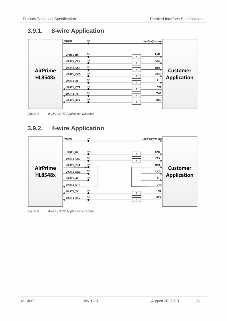
3.9. Main Serial Link (UART1) The main serial link (UART1) is used for communication between the AirPrime HL8548 and HL8548-G module and a PC or host processor. It consists of a flexible 8-wire serial interface that complies with RS-232 interface.
The supported baud rates of the UART1 are 300, 1200, 2400, 4800, 9600, 19200, 38400, 57600, 115200, 230400, 460800, 500000, 750000, 921600, 1843200, 3000000, 3250000 and 6000000 bit/s.
The signals used by UART1 are as follows:
• TX data (UART1_TX)
• RX data (UART1_RX)
• Request To Send (UART1_RTS)
• Clear To Send (UART1_CTS)
• Data Terminal Ready (UART1_DTR)
• Data Set Ready (UART1_DSR)
• Data Carrier Detect (UART1_DCD)
• Ring Indicator (UART1_RI)
Note: Signal names are according to PC view.
UART1 pin description is summarized in the table below.
Table 19. UART1 Pin Description
Pin # Signal Name* I/O* Description
2 UART1_RI O Signal incoming calls (voice and data), SMS, etc. 3 UART1_RTS I Wakes the module up when KSLEEP=1 is used
4 UART1_CTS O AirPrime HL8548 and HL8548-G is ready to receive AT commands
5 UART1_TX I Transmit data 6 UART1_RX O Receive data
7 UART1_DTR I (active low) Prevents the AirPrime HL8548 and HL8548-G from entering sleep mode, switches between data mode and command mode, and wakes the module up.
8 UART1_DCD O Signal data connection in progress 9 UART1_DSR O Signal UART interface is ON
* According to PC view.
Note: UART1 input signal pins (UART1_RTS, UART1_TX and UART1_DTR) are internally pulled up by an 8kΩ resistor when the module is ON.
4114663 Rev 12.0 August 28, 2018 36
Product Technical Specification Detailed Interface Specifications
3.9.1. 8-wire Application
AirPrime HL8548x
Customer Application
R
R
R
R
R
R
R
R
Level shifter use
RXD
CTS
DSR
DCD
RI
DTR
TXD
RTS
VGPIO
UART1_TX
UART1_DSR
UART1_CTS
UART1_DCD
UART1_RI
UART1_RX
UART1_RTS
UART1_DTR
TP
TP
TP
TP
TP
TP
TP
TP
TP
Figure 4. 8-wire UART Application Example
3.9.2. 4-wire Application
AirPrime HL8548x
Customer Application
R
R
R
R
Level shifter use
RXD
CTS
DSR
DCD
RI
DTR
TXD
RTS
VGPIO
UART1_TX
UART1_DSR
UART1_CTS
UART1_DCD
UART1_RI
UART1_RX
UART1_RTS
UART1_DTR
TP
TP
TP
TP
TP
TP
TP
TP
Figure 5. 4-wire UART Application Example
4114663 Rev 12.0 August 28, 2018 37
Product Technical Specification Detailed Interface Specifications
3.9.3. 2-wire Application
AirPrime HL8548x
Customer Application
R
R
Level shifter use
RXD
CTS
DSR
DCD
RI
DTR
RTS
TXD
VGPIO
UART1_RTS
UART1_DSR
UART1_CTS
UART1_DCD
UART1_RI
UART1_RX
UART1_TX
UART1_DTR
TP
TP
TP
TP
TP
TP
TP
Figure 6. 2-wire UART Application Example
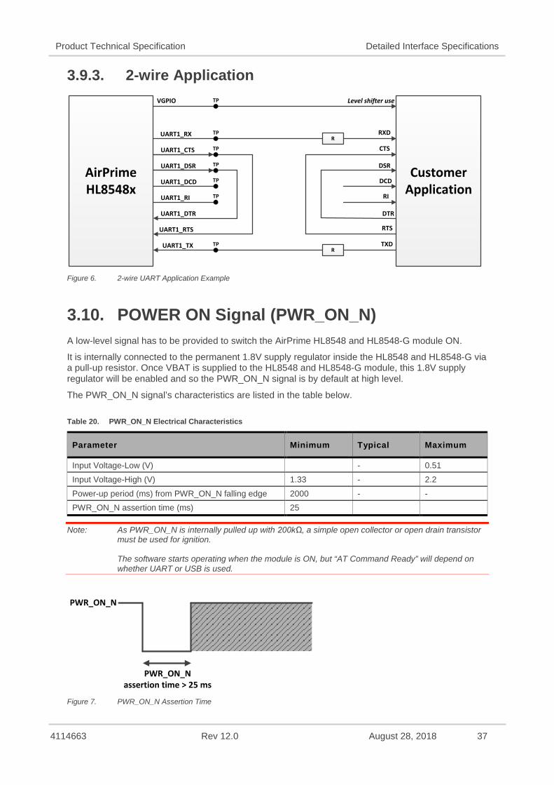
3.10. POWER ON Signal (PWR_ON_N) A low-level signal has to be provided to switch the AirPrime HL8548 and HL8548-G module ON.
It is internally connected to the permanent 1.8V supply regulator inside the HL8548 and HL8548-G via a pull-up resistor. Once VBAT is supplied to the HL8548 and HL8548-G module, this 1.8V supply regulator will be enabled and so the PWR_ON_N signal is by default at high level.
The PWR_ON_N signal’s characteristics are listed in the table below.
Table 20. PWR_ON_N Electrical Characteristics
Parameter Minimum Typical Maximum
Input Voltage-Low (V) - 0.51 Input Voltage-High (V) 1.33 - 2.2 Power-up period (ms) from PWR_ON_N falling edge 2000 - - PWR_ON_N assertion time (ms) 25
Note: As PWR_ON_N is internally pulled up with 200kΩ, a simple open collector or open drain transistor must be used for ignition. The software starts operating when the module is ON, but “AT Command Ready” will depend on whether UART or USB is used.
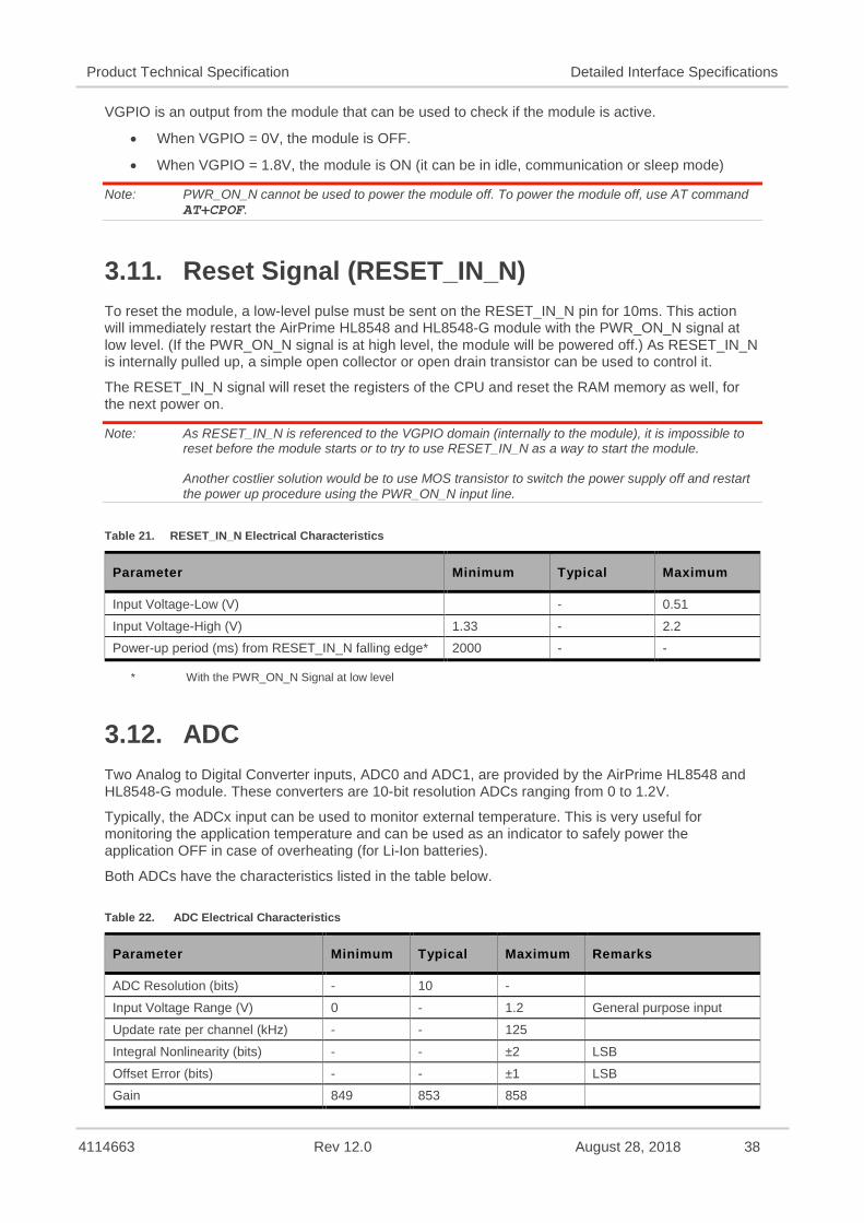
PWR_ON_Nassertion time > 25 ms
PWR_ON_N
Figure 7. PWR_ON_N Assertion Time
4114663 Rev 12.0 August 28, 2018 38
Product Technical Specification Detailed Interface Specifications
VGPIO is an output from the module that can be used to check if the module is active.
• When VGPIO = 0V, the module is OFF.
• When VGPIO = 1.8V, the module is ON (it can be in idle, communication or sleep mode)
Note: PWR_ON_N cannot be used to power the module off. To power the module off, use AT command AT+CPOF.
3.11. Reset Signal (RESET_IN_N) To reset the module, a low-level pulse must be sent on the RESET_IN_N pin for 10ms. This action will immediately restart the AirPrime HL8548 and HL8548-G module with the PWR_ON_N signal at low level. (If the PWR_ON_N signal is at high level, the module will be powered off.) As RESET_IN_N is internally pulled up, a simple open collector or open drain transistor can be used to control it.
The RESET_IN_N signal will reset the registers of the CPU and reset the RAM memory as well, for the next power on.
Note: As RESET_IN_N is referenced to the VGPIO domain (internally to the module), it is impossible to reset before the module starts or to try to use RESET_IN_N as a way to start the module. Another costlier solution would be to use MOS transistor to switch the power supply off and restart the power up procedure using the PWR_ON_N input line.
Table 21. RESET_IN_N Electrical Characteristics
Parameter Minimum Typical Maximum
Input Voltage-Low (V) - 0.51 Input Voltage-High (V) 1.33 - 2.2 Power-up period (ms) from RESET_IN_N falling edge* 2000 - -
* With the PWR_ON_N Signal at low level
3.12. ADC Two Analog to Digital Converter inputs, ADC0 and ADC1, are provided by the AirPrime HL8548 and HL8548-G module. These converters are 10-bit resolution ADCs ranging from 0 to 1.2V.
Typically, the ADCx input can be used to monitor external temperature. This is very useful for monitoring the application temperature and can be used as an indicator to safely power the application OFF in case of overheating (for Li-Ion batteries).
Both ADCs have the characteristics listed in the table below.
Table 22. ADC Electrical Characteristics
Parameter Minimum Typical Maximum Remarks
ADC Resolution (bits) - 10 - Input Voltage Range (V) 0 - 1.2 General purpose input Update rate per channel (kHz) - - 125 Integral Nonlinearity (bits) - - ±2 LSB Offset Error (bits) - - ±1 LSB Gain 849 853 858
4114663 Rev 12.0 August 28, 2018 39
Product Technical Specification Detailed Interface Specifications
Parameter Minimum Typical Maximum Remarks
Input Resistance (MΩ) 1 - - Input Capacitance (pF) - 1 -
3.13. PWM The AirPrime HL8548 and HL8548-G modules provide two PWM signals that can be used in conjunction with an external transistor for driving a vibrator, or a backlight LED.
Each PWM uses two 7-bit unsigned binary numbers: one for the output period and one for the pulse width or the duty cycle.
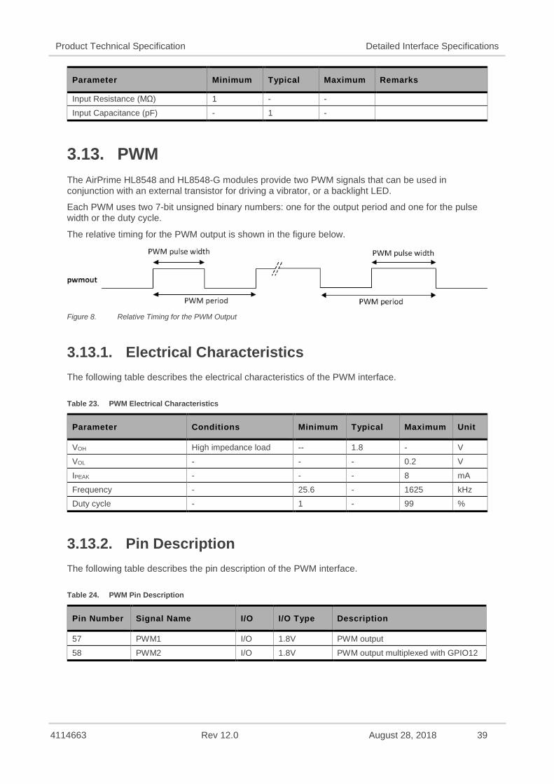
The relative timing for the PWM output is shown in the figure below.
Figure 8. Relative Timing for the PWM Output
3.13.1. Electrical Characteristics The following table describes the electrical characteristics of the PWM interface.
Table 23. PWM Electrical Characteristics
Parameter Conditions Minimum Typical Maximum Unit
VOH High impedance load -- 1.8 - V VOL - - - 0.2 V IPEAK - - - 8 mA Frequency - 25.6 - 1625 kHz Duty cycle - 1 - 99 %
3.13.2. Pin Description The following table describes the pin description of the PWM interface.
Table 24. PWM Pin Description
Pin Number Signal Name I/O I/O Type Description
57 PWM1 I/O 1.8V PWM output 58 PWM2 I/O 1.8V PWM output multiplexed with GPIO12
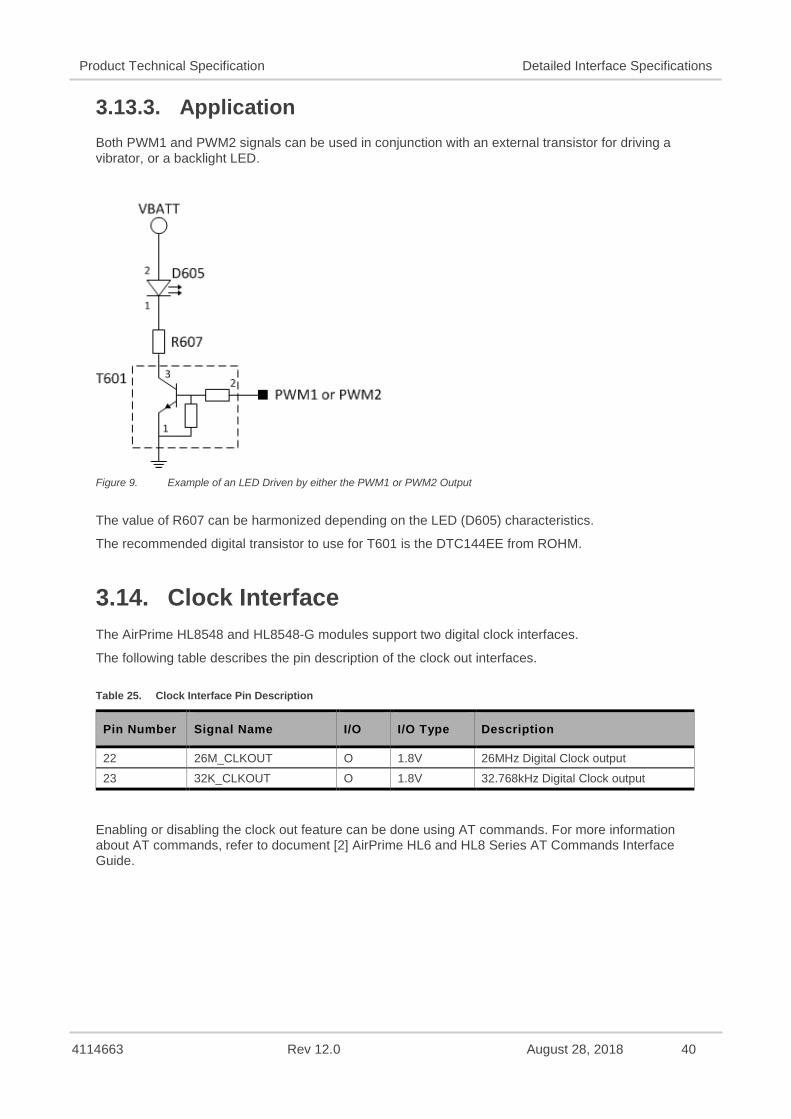
4114663 Rev 12.0 August 28, 2018 40
Product Technical Specification Detailed Interface Specifications
3.13.3. Application Both PWM1 and PWM2 signals can be used in conjunction with an external transistor for driving a vibrator, or a backlight LED.
Figure 9. Example of an LED Driven by either the PWM1 or PWM2 Output
The value of R607 can be harmonized depending on the LED (D605) characteristics.
The recommended digital transistor to use for T601 is the DTC144EE from ROHM.
3.14. Clock Interface The AirPrime HL8548 and HL8548-G modules support two digital clock interfaces.
The following table describes the pin description of the clock out interfaces.
Table 25. Clock Interface Pin Description
Pin Number Signal Name I/O I/O Type Description
22 26M_CLKOUT O 1.8V 26MHz Digital Clock output 23 32K_CLKOUT O 1.8V 32.768kHz Digital Clock output
Enabling or disabling the clock out feature can be done using AT commands. For more information about AT commands, refer to document [2] AirPrime HL6 and HL8 Series AT Commands Interface Guide.
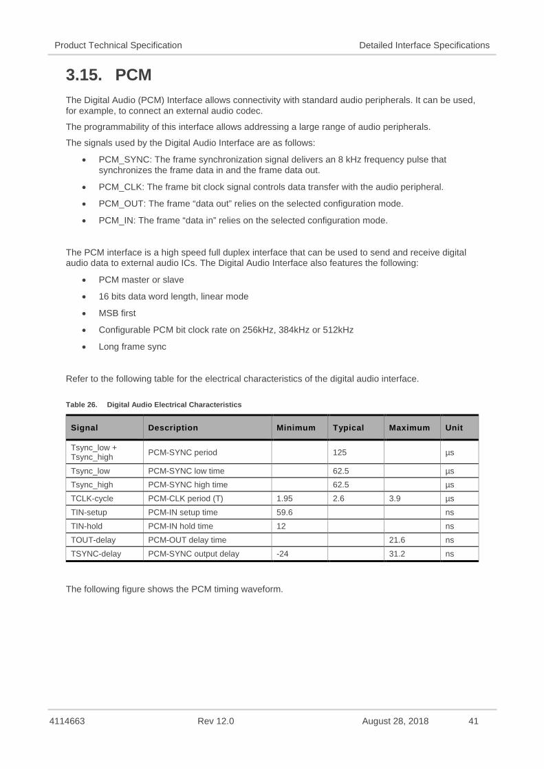
4114663 Rev 12.0 August 28, 2018 41
Product Technical Specification Detailed Interface Specifications
3.15. PCM The Digital Audio (PCM) Interface allows connectivity with standard audio peripherals. It can be used, for example, to connect an external audio codec.
The programmability of this interface allows addressing a large range of audio peripherals.
The signals used by the Digital Audio Interface are as follows:
• PCM_SYNC: The frame synchronization signal delivers an 8 kHz frequency pulse that synchronizes the frame data in and the frame data out.
• PCM_CLK: The frame bit clock signal controls data transfer with the audio peripheral.
• PCM_OUT: The frame “data out” relies on the selected configuration mode.
• PCM_IN: The frame “data in” relies on the selected configuration mode.
The PCM interface is a high speed full duplex interface that can be used to send and receive digital audio data to external audio ICs. The Digital Audio Interface also features the following:
• PCM master or slave
• 16 bits data word length, linear mode
• MSB first
• Configurable PCM bit clock rate on 256kHz, 384kHz or 512kHz
• Long frame sync
Refer to the following table for the electrical characteristics of the digital audio interface.
Table 26. Digital Audio Electrical Characteristics
Signal Description Minimum Typical Maximum Unit
Tsync_low + Tsync_high PCM-SYNC period 125 µs
Tsync_low PCM-SYNC low time 62.5 µs Tsync_high PCM-SYNC high time 62.5 µs TCLK-cycle PCM-CLK period (T) 1.95 2.6 3.9 µs TIN-setup PCM-IN setup time 59.6 ns TIN-hold PCM-IN hold time 12 ns TOUT-delay PCM-OUT delay time 21.6 ns TSYNC-delay PCM-SYNC output delay -24 31.2 ns
The following figure shows the PCM timing waveform.
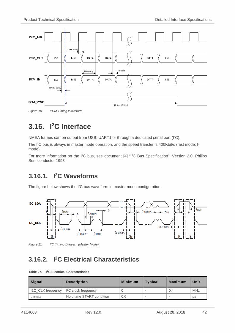
4114663 Rev 12.0 August 28, 2018 42
Product Technical Specification Detailed Interface Specifications
Figure 10. PCM Timing Waveform
3.16. I2C Interface NMEA frames can be output from USB, UART1 or through a dedicated serial port (I2C).
The I2C bus is always in master mode operation, and the speed transfer is 400Kbit/s (fast mode: f-mode).
For more information on the I2C bus, see document [4] “I2C Bus Specification”, Version 2.0, Philips Semiconductor 1998.
3.16.1. I2C Waveforms The figure below shows the I2C bus waveform in master mode configuration.
Figure 11. I2C Timing Diagram (Master Mode)
3.16.2. I2C Electrical Characteristics
Table 27. I2C Electrical Characteristics
Signal Description Minimum Typical Maximum Unit
I2C_CLK frequency I²C clock frequency 0 - 0.4 MHz tHD; STA Hold time START condition 0.6 - - µs
4114663 Rev 12.0 August 28, 2018 43
Product Technical Specification Detailed Interface Specifications
Signal Description Minimum Typical Maximum Unit
tLOW Low period for clock 1.3 - - µs tHD; DAT Data hold time 0 - 0.9 µs tSU; DAT Data setup time 100 - - ns tHIGH High period for clock 0.6 - - µs
tSU; STA Setup time repeated START condition 0.6 - - µs
tHD; STA Hold time START condition 0.6 - - µs tSU; STO Setup time STOP condition 0.6 - - µs tBUF Bus free time, STOP to START 1.3 - - µs
3.16.3. I2C Pin Description
Table 28. I2C Pin Description
Pin Number Signal Name Function
1 I2C_CLK I2C Clock 66 I2C_SDA I2C Data
Note: I2C pins are multiplexed with GPIO features and are internally pulled to VGPIO with 4.7kΩ.
3.17. Debug Interfaces The AirPrime HL8548 and HL8548-G module provides 2 interfaces for a powerful debug system.
3.17.1. Debug Port The AirPrime HL8548 and HL8548-G provides a 2-wire debug port interface, providing real-time instruction and data trace of the Modem Core.
Table 29. SW Trace Pin Description
Pin Number Signal Name* I/O* Function
44 DEBUG_TX O Debug Transmit Data 51 DEBUG_RX I Debug Receive Data
* According to module view.
Note: It is strongly recommended to provide access through Test Points to this interface.
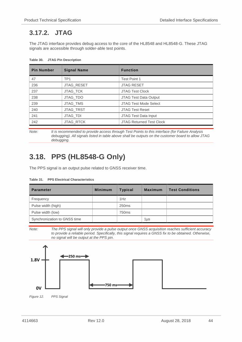
4114663 Rev 12.0 August 28, 2018 44
Product Technical Specification Detailed Interface Specifications
3.17.2. JTAG The JTAG interface provides debug access to the core of the HL8548 and HL8548-G. These JTAG signals are accessible through solder-able test points.
Table 30. JTAG Pin Description
Pin Number Signal Name Function
47 TP1 Test Point 1 236 JTAG_RESET JTAG RESET 237 JTAG_TCK JTAG Test Clock 238 JTAG_TDO JTAG Test Data Output 239 JTAG_TMS JTAG Test Mode Select 240 JTAG_TRST JTAG Test Reset 241 JTAG_TDI JTAG Test Data Input 242 JTAG_RTCK JTAG Returned Test Clock
Note: It is recommended to provide access through Test Points to this interface (for Failure Analysis debugging). All signals listed in table above shall be outputs on the customer board to allow JTAG debugging.
3.18. PPS (HL8548-G Only) The PPS signal is an output pulse related to GNSS receiver time.
Table 31. PPS Electrical Characteristics
Parameter Minimum Typical Maximum Test Conditions
Frequency 1Hz
Pulse width (high) 250ms
Pulse width (low) 750ms
Synchronization to GNSS time 1µs
Note: The PPS signal will only provide a pulse output once GNSS acquisition reaches sufficient accuracy to provide a reliable period. Specifically, this signal requires a GNSS fix to be obtained. Otherwise, no signal will be output at the PPS pin.
250 ms1.8V
750 ms0V
Figure 12. PPS Signal
4114663 Rev 12.0 August 28, 2018 45
Product Technical Specification Detailed Interface Specifications
3.19. EXT_LNA_GPS_EN (HL8548-G only) EXT_LNA_GPS_EN ON indicates whether the GNSS receiver is active and can be used to enable an external LNA (or active antenna), especially during GNSS low power mode.
3.20. RF Interface The GSM RF interface of the HL8548 and HL8548-G module allows the transmission of RF signals. This interface has a 50Ω nominal impedance.
Contact Sierra Wireless technical support for assistance in integrating the AirPrime HL8548 or HL8548-G on applications with embedded antennas.
3.20.1. RF Connection A 50Ω (with maximum VSWR 1.1:1, and 0.5dB loss) RF track is recommended to be connected to standard RF connectors such as SMA, UFL, etc. for antenna connection.
Table 32. RF Connection
RF Signal Impedance VSWR Rx (max) VSWR Tx (max)
RF_MAIN 50Ω 3:1 3:1
3.20.2. RF Performances RF performances are compliant with the ETSI recommendation GSM 05.05.
Table 33. RF Performance
Frequency Band Typical Sensitivity (dBm)
GSM850/EGSM -109 DCS/PCS -108 UMTS B1 -110 UMTS B2 -110 UMTS B5/6 -110 UMTS B8 -110
3.20.3. TX Burst Indicator (2G_TX_ON) The AirPrime HL8548 and HL8548-G module provides a signal, 2G_TX_ON, for TX Burst indication. The 2G_TX_ON is a 1.8V signal and its status signal depends on the module transmitter state.
Refer to the following table for the status of the 2G_TX_ON signal depending on the embedded module’s state.
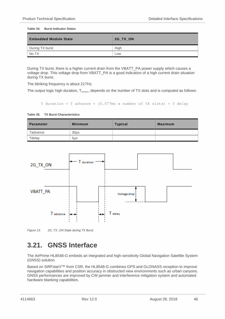
4114663 Rev 12.0 August 28, 2018 46
Product Technical Specification Detailed Interface Specifications
Table 34. Burst Indicator States
Embedded Module State 2G_TX_ON
During TX burst High No TX Low
During TX burst, there is a higher current drain from the VBATT_PA power supply which causes a voltage drop. This voltage drop from VBATT_PA is a good indication of a high current drain situation during TX burst.
The blinking frequency is about 217Hz.
The output logic high duration, Tduration, depends on the number of TX slots and is computed as follows:
T duration = T advance + (0.577ms x number of TX slots) + T delay
Table 35. TX Burst Characteristics
Parameter Minimum Typical Maximum
Tadvance 30µs Tdelay 5µs
Figure 13. 2G_TX_ON State during TX Burst
3.21. GNSS Interface The AirPrime HL8548-G embeds an integrated and high-sensitivity Global Navigation Satellite System (GNSS) solution.
Based on SiRFstarV™ from CSR, the HL8548-G combines GPS and GLONASS reception to improve navigation capabilities and position accuracy in obstructed view environments such as urban canyons. GNSS performances are improved by CW jammer and interference mitigation system and automated hardware blanking capabilities.
4114663 Rev 12.0 August 28, 2018 47
Product Technical Specification Detailed Interface Specifications
In addition, it supports Control Plane Assisted GPS and Secure User Plane Location (SUPL) protocol to reduce the time to first fix in the presence of assistance information from wireless networks.
The operation of GNSS is offloaded to a GNSS standalone solution to guaranty the modem resources availability for the best performances.
The GNSS implementation supports GPS L1 signal (1575.42 ± 20 MHz) and GLONASS L1 FDMA signals for frequency -7 to 6 (1597.5 – 1605.8 MHz), with 50Ω connection on RF_GPS pad.
3.21.1. GNSS Performances
Table 36. GNSS Interface Specifications
Test Parameters Typical Value
Sensitivity
GPS Autonomous Acquisition without LNA (dBm); Cold start conditions -146 GPS Autonomous Acquisition without LNA (dBm); Warm start conditions -146 GPS Autonomous Acquisition without LNA (dBm); Hot start conditions -160 GPS Navigation without LNA (dBm) -160 GLONASS Navigation (dBm) -156 GNSS Navigation (dBm) -158 GPS Tracking (dBm) -164 GLONASS Tracking (dBm) -164
Autonomous Cold Start
Time To First Fix (s) 50% 28 95% 40
2D Position Error (m) 50% 1 95% 2
Autonomous Warm Start
Time To First Fix (s) 50% 20 95% 35
2D Position Error (m) 50% 3.6 95% 8
Autonomous Hot Start
Time To First Fix (s) 50% 0.7 95% 1
2D Position Error (m) 50% 5.5 95% 10
Aiding Warm Start
Time To First Fix (s) 50% TBD 95% TBD
2D Position Error (m) 50% TBD 95% TBD
Note: Values in the table above are based on static conditions, RF GNSS level @-130dBm. Cold start does not include internal GNSS firmware download on first GNSS start.
4114663 Rev 12.0 August 28, 2018 48
Product Technical Specification Detailed Interface Specifications
3.21.2. GNSS Antenna Interface Specifications for the GNSS antenna interface are defined in the table below.
Table 37. GNSS Antenna Specifications
Characteristics GNSS
Frequency (MHz) GPS L1 1575.42 ± 20 GLONASS L1 FDMA 1597.5-1605.8
RF Impedance (Ω) 50 VSWR max 2:1
The minimum isolation between GNSS and GSM antennas should be 20dB.
3.21.3. GNSS Antenna Recommendations Both passive and active antennas are supported by the AirPrime HL8548-G module.
The table below describes the expected performance function as input signal power.
Table 38. GNSS Antenna Recommendations
GNSS Signal Level Description Input Signal Power (dBm) Expected Performances
Absolute maximum -110 Maximum to input level
Good >-134 Best performance in TTFF and position accuracy, allow to enter low power modes
Acceptable >-147 Minimum input level to allow initial acquisition without aiding
Poor <-147 No signal acquisition without aiding Minimum usable signal -161 Below this level, no fix with reasonable error
Minimum tracking level -165 Minimum level to lock the signal for fast recovery when the signal returns to the minimum usable level
For passive antennas, the internal LNA should be set to high gain mode. When configured in high gain mode, the noise figure of the HL8548-G’s GNSS input is 3 dB.
For active antennas, the configuration of the internal LNA gain is dependent on external RF chain implementation, especially for the external net gain (i.e. gain from the antenna input to the module input including LNA gain minus cable losses).
The internal LNA gain should be set to low gain if the external net gain is higher than 8 dB. When configured in low gain mode, the noise figure of the HL8548-G’s GNSS input is 7 dB.
The external net gain should never exceed 22 dB.
If the external net gain is lower than 8 dB, it is recommended that the internal LNA gain be set to high gain mode.
These limits have been determined for active antennas with noise figures lower than 3 dB.
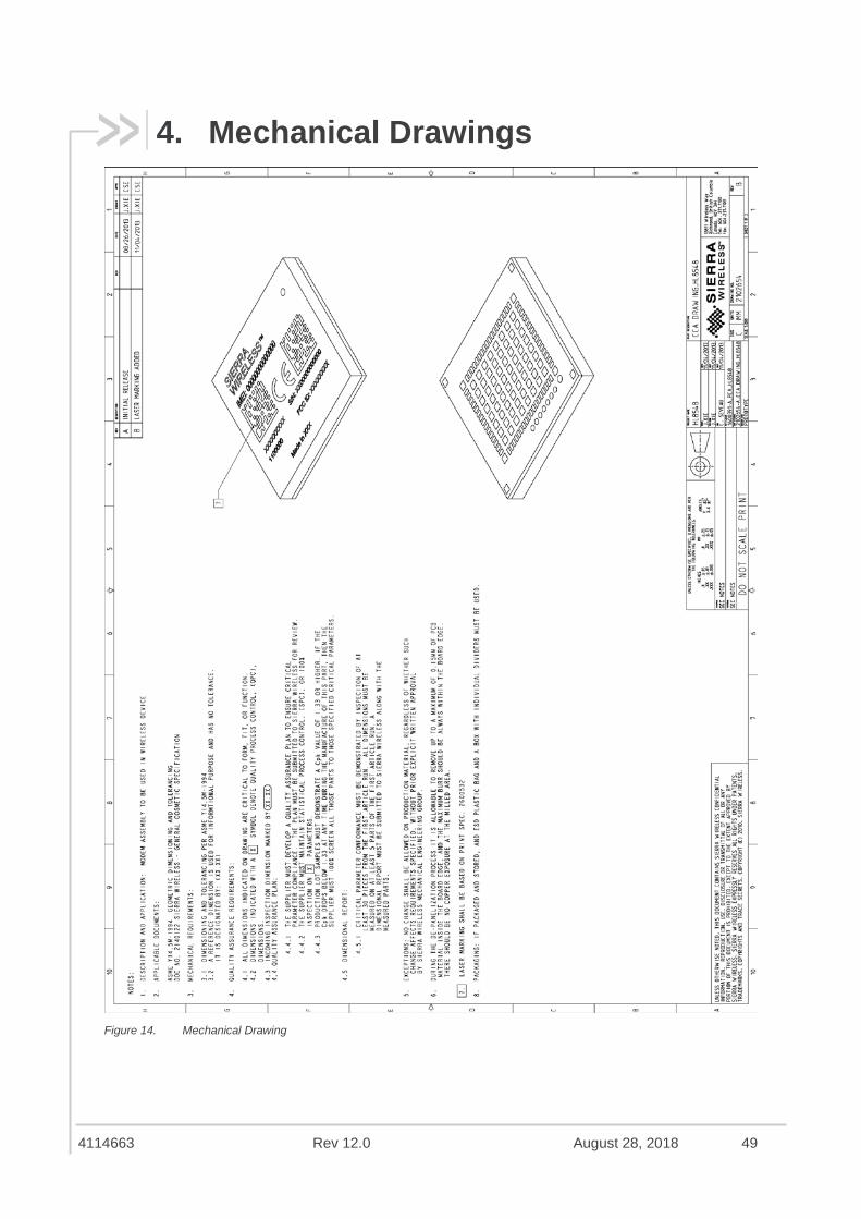
4114663 Rev 12.0 August 28, 2018 49
4. Mechanical Drawings
Figure 14. Mechanical Drawing
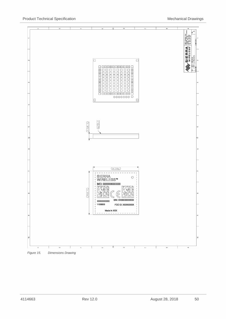
4114663 Rev 12.0 August 28, 2018 50
Product Technical Specification Mechanical Drawings
Figure 15. Dimensions Drawing
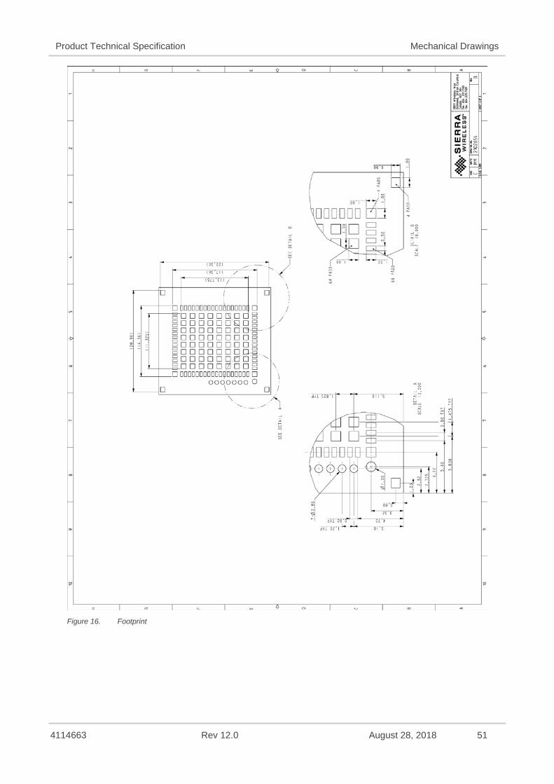
4114663 Rev 12.0 August 28, 2018 51
Product Technical Specification Mechanical Drawings
Figure 16. Footprint
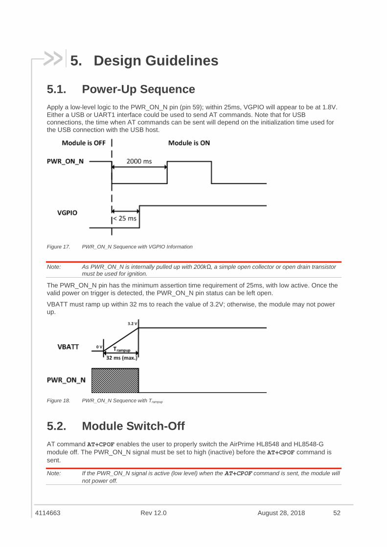
4114663 Rev 12.0 August 28, 2018 52
5. Design Guidelines
5.1. Power-Up Sequence Apply a low-level logic to the PWR_ON_N pin (pin 59); within 25ms, VGPIO will appear to be at 1.8V. Either a USB or UART1 interface could be used to send AT commands. Note that for USB connections, the time when AT commands can be sent will depend on the initialization time used for the USB connection with the USB host.
Figure 17. PWR_ON_N Sequence with VGPIO Information
Note: As PWR_ON_N is internally pulled up with 200kΩ, a simple open collector or open drain transistor must be used for ignition.
The PWR_ON_N pin has the minimum assertion time requirement of 25ms, with low active. Once the valid power on trigger is detected, the PWR_ON_N pin status can be left open.
VBATT must ramp up within 32 ms to reach the value of 3.2V; otherwise, the module may not power up.
Figure 18. PWR_ON_N Sequence with Trampup
5.2. Module Switch-Off AT command AT+CPOF enables the user to properly switch the AirPrime HL8548 and HL8548-Gmodule off. The PWR_ON_N signal must be set to high (inactive) before the AT+CPOF command issent.
Note: If the PWR_ON_N signal is active (low level) when the AT+CPOF command is sent, the module will not power off.
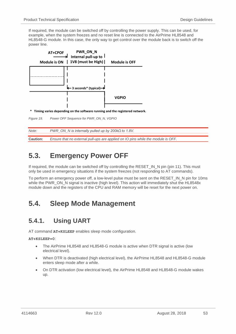
4114663 Rev 12.0 August 28, 2018 53
Product Technical Specification Design Guidelines
If required, the module can be switched off by controlling the power supply. This can be used, for example, when the system freezes and no reset line is connected to the AirPrime HL8548 and HL8548-G module. In this case, the only way to get control over the module back is to switch off the power line.
3 seconds* (typical)
AT+CPOF
Module is ON
PWR_ON_N Internal pull-up to 1V8 (must be High) Module is OFF
VGPIO
* Timing varies depending on the software running and the registered network. Figure 19. Power OFF Sequence for PWR_ON_N, VGPIO
Note: PWR_ON_N is internally pulled up by 200kΩ to 1.8V.
Caution: Ensure that no external pull-ups are applied on IO pins while the module is OFF.
5.3. Emergency Power OFF If required, the module can be switched off by controlling the RESET_IN_N pin (pin 11). This must only be used in emergency situations if the system freezes (not responding to AT commands).
To perform an emergency power off, a low-level pulse must be sent on the RESET_IN_N pin for 10ms while the PWR_ON_N signal is inactive (high level). This action will immediately shut the HL8548x module down and the registers of the CPU and RAM memory will be reset for the next power on.
5.4. Sleep Mode Management
5.4.1. Using UART AT command AT+KSLEEP enables sleep mode configuration.
AT+KSLEEP=0:
• The AirPrime HL8548 and HL8548-G module is active when DTR signal is active (low electrical level).
• When DTR is deactivated (high electrical level), the AirPrime HL8548 and HL8548-G module enters sleep mode after a while.
• On DTR activation (low electrical level), the AirPrime HL8548 and HL8548-G module wakes up.
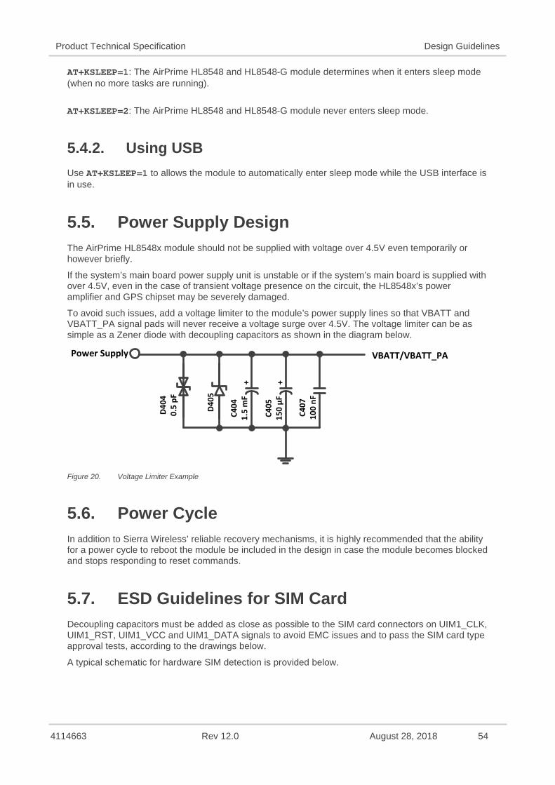
4114663 Rev 12.0 August 28, 2018 54
Product Technical Specification Design Guidelines
AT+KSLEEP=1: The AirPrime HL8548 and HL8548-G module determines when it enters sleep mode (when no more tasks are running).
AT+KSLEEP=2: The AirPrime HL8548 and HL8548-G module never enters sleep mode.
5.4.2. Using USB Use AT+KSLEEP=1 to allows the module to automatically enter sleep mode while the USB interface is in use.
5.5. Power Supply Design The AirPrime HL8548x module should not be supplied with voltage over 4.5V even temporarily or however briefly.
If the system’s main board power supply unit is unstable or if the system’s main board is supplied with over 4.5V, even in the case of transient voltage presence on the circuit, the HL8548x’s power amplifier and GPS chipset may be severely damaged.
To avoid such issues, add a voltage limiter to the module’s power supply lines so that VBATT and VBATT_PA signal pads will never receive a voltage surge over 4.5V. The voltage limiter can be as simple as a Zener diode with decoupling capacitors as shown in the diagram below.
Power Supply VBATT/VBATT_PA
D404
0.5
pF
D405
C404
1.5
mF
+ +C4
0515
0 µF
C407
100
nF
Figure 20. Voltage Limiter Example
5.6. Power Cycle In addition to Sierra Wireless’ reliable recovery mechanisms, it is highly recommended that the ability for a power cycle to reboot the module be included in the design in case the module becomes blocked and stops responding to reset commands.
5.7. ESD Guidelines for SIM Card Decoupling capacitors must be added as close as possible to the SIM card connectors on UIM1_CLK, UIM1_RST, UIM1_VCC and UIM1_DATA signals to avoid EMC issues and to pass the SIM card type approval tests, according to the drawings below.
A typical schematic for hardware SIM detection is provided below.
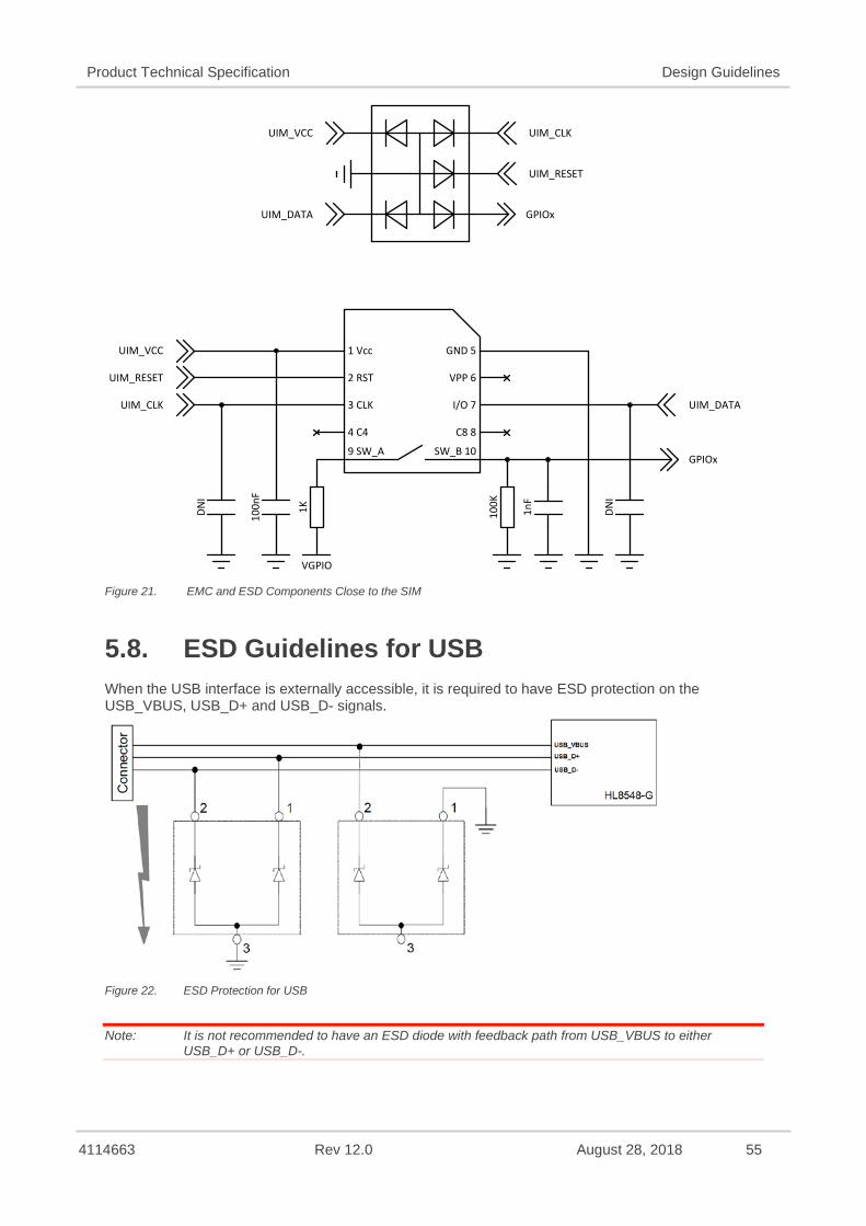
4114663 Rev 12.0 August 28, 2018 55
Product Technical Specification Design Guidelines
Figure 21. EMC and ESD Components Close to the SIM
5.8. ESD Guidelines for USB When the USB interface is externally accessible, it is required to have ESD protection on the USB_VBUS, USB_D+ and USB_D- signals.
Figure 22. ESD Protection for USB
Note: It is not recommended to have an ESD diode with feedback path from USB_VBUS to either USB_D+ or USB_D-.
1 Vcc
2 RST
3 CLK
4 C4
I/O 7
VPP 6
GND 5
C8 8
9 SW_A
UIM_DATA
UIM_VCC
UIM_RESET
UIM_CLK
100n
F
DNI
DNI
UIM_VCC
UIM_DATA
UIM_RESET
UIM_CLK
GPIOx
1K
SW_B 10GPIOx
100K
1nF
VGPIO
4114663 Rev 12.0 August 28, 2018 56
Product Technical Specification Design Guidelines
5.9. Dual SIM Application Using an external switch and GPIOs, the HL8548 and HL8548-G can support Dual SIM Single Standby with fast network switching. Refer to document [2] AirPrime HL6 and HL8 Series AT Commands Interface Guide for related AT commands.
Figure 23. Reference Design for Dual SIM Application
5.10. Radio Integration
5.10.1. GSM Antenna Integration with Antenna Detection Circuitry
The AirPrime HL8548 and HL8548-G is equipped with external antennas. A 50Ω line matching circuit between the module, the customer’s board and the RF antennas is required, for GSM and GPS feed path, as shown in the example below.
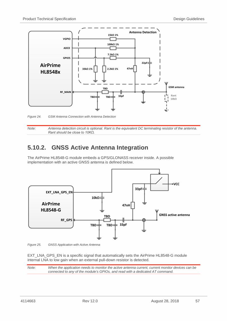
4114663 Rev 12.0 August 28, 2018 57
Product Technical Specification Design Guidelines
AirPrime HL8548x
22pF
33kΩ 1% 2.2kΩ 1%
7.5kΩ 1%
100kΩ 1%
15kΩ 1%
47nH
TBD TBD 33pF
GSM antennaTBD
Rant10kΩ
Antenna Detection
VGPIO
ADC0
GPIO5
RF_MAIN
Figure 24. GSM Antenna Connection with Antenna Detection
Note: Antenna detection circuit is optional. Rant is the equivalent DC terminating resistor of the antenna. Rant should be close to 10KΩ.
5.10.2. GNSS Active Antenna Integration The AirPrime HL8548-G module embeds a GPS/GLONASS receiver inside. A possible implementation with an active GNSS antenna is defined below.
AirPrimeHL8548-G
33pF
47nH
TBD TBD 33pF
GNSS active antennaTBD
EXT_LNA_GPS_EN
RF_GPS
VCC
10kΩ
Figure 25. GNSS Application with Active Antenna
EXT_LNA_GPS_EN is a specific signal that automatically sets the AirPrime HL8548-G module internal LNA to low gain when an external pull-down resistor is detected.
Note: When the application needs to monitor the active antenna current, current monitor devices can be connected to any of the module’s GPIOs, and read with a dedicated AT command.
4114663 Rev 12.0 August 28, 2018 58
6. Reliability SpecificationThe AirPrime HL8548x module is tested against the Sierra Wireless Industrial Reliability Specification defined below.
6.1. Reliability Compliance The AirPrime HL8548x module connected on a development kit board application is compliant with the following requirements.
Table 39. Standards Conformity
Abbreviation Definition
IEC International Electro technical Commission ISO International Organization for Standardization
6.2. Reliability Prediction Model
6.2.1. Life Stress Test The following tests the AirPrime HL8548x module product performances.
Table 40. Life Stress Test
Designation Condition
Performance Test PT3T & PTRT
Standard: N/A Special conditions:
• Temperature: Class A: -30°C to +70°C Class B: -40°C to +85°C Rate of temperature change: ± 3°C/min
• Recovery time: 3 hoursOperating conditions: Powered Duration: 14 days
4114663 Rev 12.0 August 28, 2018 59
Product Technical Specification Reliability Specification
6.2.2. Environmental Resistance Stress Tests The following tests the AirPrime HL8548x module resistance to extreme temperature.
Table 41. Environmental Resistance Stress Tests
Designation Condition
Cold Test Active COTA
Standard: IEC 680068-2-1, Test Ad Special conditions:
• Temperature: -40°C • Temperature variation: 1°C/min
Operating conditions: Powered ON with a power cycle of 1 minute ON and 2 minutes OFF Duration: 3 days
Resistance to Heat Test RH
Standard: IEC 680068-2-2, Test Bb Special conditions:
• Temperature: +85°C • Temperature variation: 1°C/min
Operating conditions: Powered ON with a power cycle of 15 minutes ON and 15 minutes OFF
Duration: 50 days
6.2.3. Corrosive Resistance Stress Tests The following tests the AirPrime HL8548x module resistance to corrosive atmosphere.
Table 42. Corrosive Resistance Stress Tests
Designation Condition
Humidity Test HUT
Standard: IEC 60068-2-3, Test Ca Special conditions:
• Temperature: +65°C • RH: 95% • Temperature variation: 3 ± 0.6°C/min
Operating conditions: Powered on, DUT is powered up for 15 minutes and OFF for 15 minutes
Duration: 10 days
Component Solder Wettability CSW
Standard: JESD22 – B102, Method 1/Condition C, Solderability Test Method Special conditions:
• Test method: Dip and Look Test with Steam preconditioning 8 h ±15min. dip for 5 +0/-0.5 seconds
Operating conditions: Un-powered
Duration: 1 day
4114663 Rev 12.0 August 28, 2018 60
Product Technical Specification Reliability Specification
Designation Condition
Moist Heat Cyclic Test MHCT
Standard: IEC 60068-2-30, Test Db Special conditions:
• Upper temperature: +40 ± 2°C • Lower temperature: +23 ± 5°C • RH:
Upper temperature: 93% Lower temperature: 95%
• Number of cycles: 21 (1 cycle/24 hours) Operating conditions: Powered ON for 15 minutes during each 3 hours ramp up and 3 hours ramp down (in middle) for every cycle
Duration: 21 days
6.2.4. Thermal Resistance Cycle Stress Tests The following tests the AirPrime HL8548x module resistance to extreme temperature cycling.
Table 43. Thermal Resistance Cycle Stress Tests
Designation Condition
Thermal Shock Test TSKT
Standard: IEC 60068-2-14, Test Na Special conditions:
• Temperature: -30°C to +80°C • Temperature Variation: less than 30s • Number of cycles: 600 • Dwell Time: 10 minutes
Operating conditions: Un-powered Duration: 9 days
Temperature Change TCH
Standard: IEC 60068-2-14, Test Nb Special conditions:
• Temperature: -40°C to +90°C • Temperature Variation: 3 ± 0.6°C/min • Number of cycles: 400 • Dwell Time: 10 minutes
Operating conditions: Un-powered Duration: 29 days
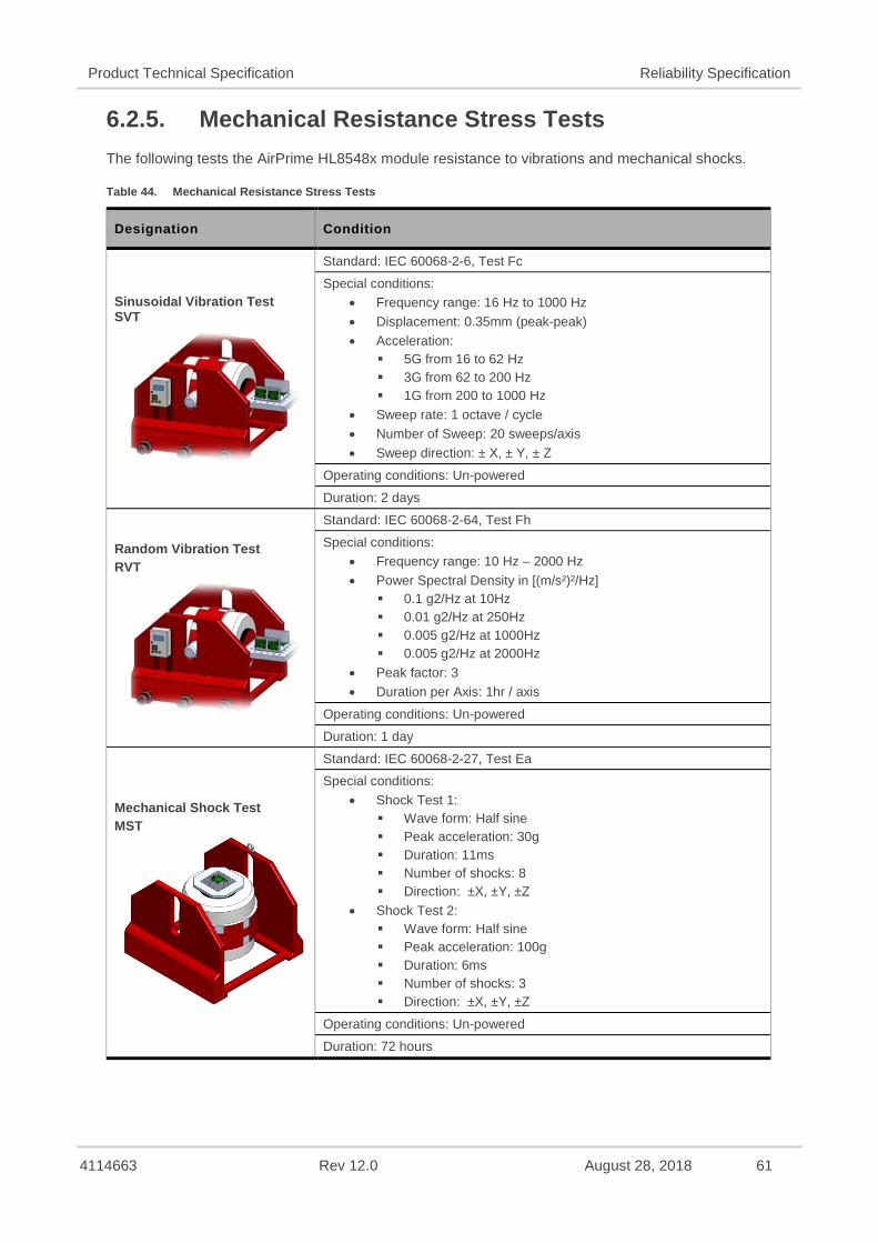
4114663 Rev 12.0 August 28, 2018 61
Product Technical Specification Reliability Specification
6.2.5. Mechanical Resistance Stress Tests The following tests the AirPrime HL8548x module resistance to vibrations and mechanical shocks.
Table 44. Mechanical Resistance Stress Tests
Designation Condition
Sinusoidal Vibration Test SVT
Standard: IEC 60068-2-6, Test Fc Special conditions:
• Frequency range: 16 Hz to 1000 Hz • Displacement: 0.35mm (peak-peak) • Acceleration:
5G from 16 to 62 Hz 3G from 62 to 200 Hz 1G from 200 to 1000 Hz
• Sweep rate: 1 octave / cycle • Number of Sweep: 20 sweeps/axis • Sweep direction: ± X, ± Y, ± Z
Operating conditions: Un-powered Duration: 2 days
Random Vibration Test RVT
Standard: IEC 60068-2-64, Test Fh Special conditions:
• Frequency range: 10 Hz – 2000 Hz • Power Spectral Density in [(m/s²)²/Hz]
0.1 g2/Hz at 10Hz 0.01 g2/Hz at 250Hz 0.005 g2/Hz at 1000Hz 0.005 g2/Hz at 2000Hz
• Peak factor: 3 • Duration per Axis: 1hr / axis
Operating conditions: Un-powered Duration: 1 day
Mechanical Shock Test MST
Standard: IEC 60068-2-27, Test Ea Special conditions:
• Shock Test 1: Wave form: Half sine Peak acceleration: 30g Duration: 11ms Number of shocks: 8 Direction: ±X, ±Y, ±Z
• Shock Test 2: Wave form: Half sine Peak acceleration: 100g Duration: 6ms Number of shocks: 3 Direction: ±X, ±Y, ±Z
Operating conditions: Un-powered Duration: 72 hours

4114663 Rev 12.0 August 28, 2018 62
Product Technical Specification Reliability Specification
6.2.6. Handling Resistance Stress Tests The following tests the AirPrime HL8548x module resistance to handling malfunctions and damage.
Table 45. Handling Resistance Stress Tests
Designation Condition
ESDC Test
Standard: JESD22-A114, JESD22-A115, JESD22-C101 Special conditions:
• HBM (Human Body Model): 1000V (Class 1C) • MM (Machine Model): 200V • CDM (Charged Device Model): 250V (Class II)
Operating conditions: Powered Duration: 3 days
ESD Test
Standard: IEC 61000-4-2 Special conditions:
• Contact Voltage: ±2kV, ±4kV, ±6kV • Air Voltage: ±2kV, ±4kV, ±8kV
Operating conditions: Powered
Duration: 3 days
Free Fall Test FFT 1
Standard: IEC 60068-2-32, Test Ed Special conditions:
• Number of drops: 2 drops per unit • Height: 1m
Operating conditions: Un-powered
Duration: 6 hours

4114663 Rev 12.0 August 28, 2018 63
7. FCC/IC Legal Information
7.1. FCC Regulations The HL8548x module has been granted modular approval for mobile applications. Integrators may use the HL8548x module in their final products without additional FCC certification if they meet the following conditions. Otherwise, additional FCC approvals must be obtained.
1. At least 20 cm separation distance between the antenna and the user’s body must bemaintained at all times.
2. To comply with FCC regulations limiting both maximum RF output power and humanexposure to RF radiation, the maximum antenna gain including cable loss in a mobile-onlyexposure condition must not exceed:
6.43 dBi in the cellular band
3.0 dBi in the PCS band
3. The HL8548x module must not transmit simultaneously with other collocated radiotransmitters within a host device.
4. The RF signal must be routed on the application board using tracks with a 50Ω characteristicimpedance. Basically, the characteristic impedance depends on the dielectric, the track widthand the ground plane spacing. In order to respect this constraint, Sierra Wirelessrecommends using MicroStrip or StripLine structure and computing the Tracks width with asimulation tool (like AppCad shown in the figure below and that is available free of charge athttp://www.agilent.com).
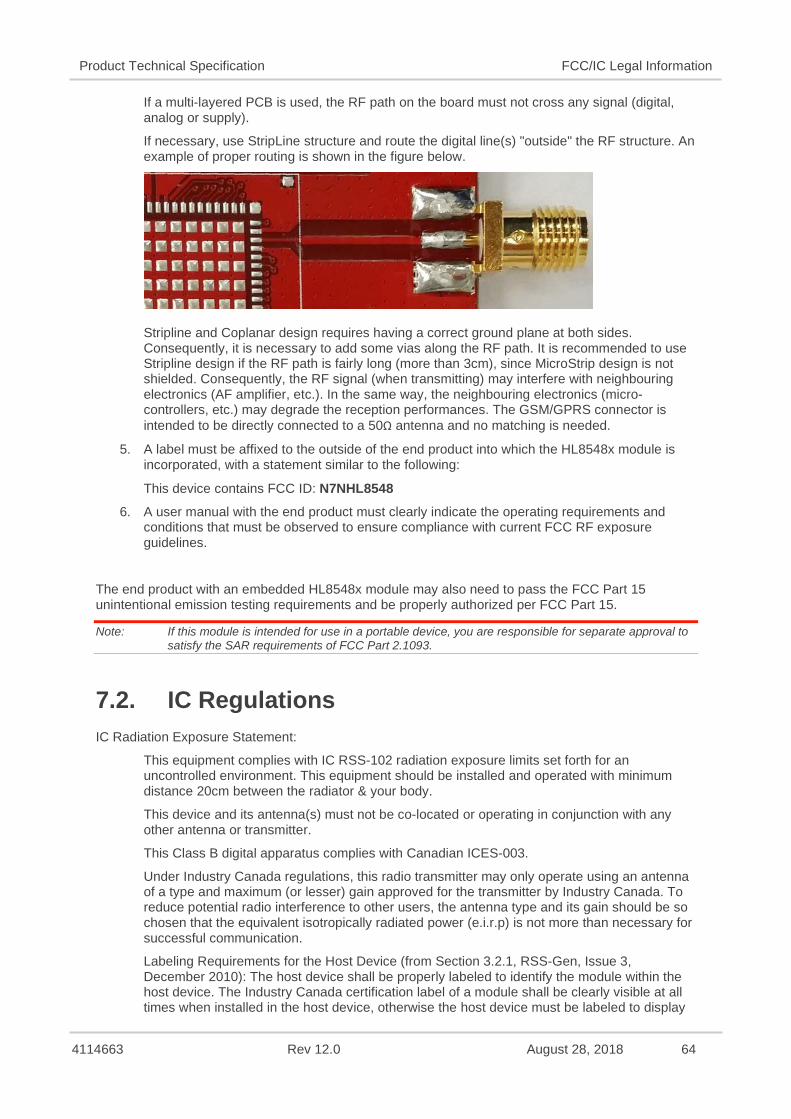
4114663 Rev 12.0 August 28, 2018 64
Product Technical Specification FCC/IC Legal Information
If a multi-layered PCB is used, the RF path on the board must not cross any signal (digital, analog or supply).
If necessary, use StripLine structure and route the digital line(s) "outside" the RF structure. An example of proper routing is shown in the figure below.
Stripline and Coplanar design requires having a correct ground plane at both sides. Consequently, it is necessary to add some vias along the RF path. It is recommended to use Stripline design if the RF path is fairly long (more than 3cm), since MicroStrip design is not shielded. Consequently, the RF signal (when transmitting) may interfere with neighbouring electronics (AF amplifier, etc.). In the same way, the neighbouring electronics (micro-controllers, etc.) may degrade the reception performances. The GSM/GPRS connector is intended to be directly connected to a 50Ω antenna and no matching is needed.
5. A label must be affixed to the outside of the end product into which the HL8548x module is incorporated, with a statement similar to the following:
This device contains FCC ID: N7NHL8548
6. A user manual with the end product must clearly indicate the operating requirements and conditions that must be observed to ensure compliance with current FCC RF exposure guidelines.
The end product with an embedded HL8548x module may also need to pass the FCC Part 15 unintentional emission testing requirements and be properly authorized per FCC Part 15.
Note: If this module is intended for use in a portable device, you are responsible for separate approval to satisfy the SAR requirements of FCC Part 2.1093.
7.2. IC Regulations IC Radiation Exposure Statement:
This equipment complies with IC RSS-102 radiation exposure limits set forth for an uncontrolled environment. This equipment should be installed and operated with minimum distance 20cm between the radiator & your body.
This device and its antenna(s) must not be co-located or operating in conjunction with any other antenna or transmitter.
This Class B digital apparatus complies with Canadian ICES-003.
Under Industry Canada regulations, this radio transmitter may only operate using an antenna of a type and maximum (or lesser) gain approved for the transmitter by Industry Canada. To reduce potential radio interference to other users, the antenna type and its gain should be so chosen that the equivalent isotropically radiated power (e.i.r.p) is not more than necessary for successful communication.
Labeling Requirements for the Host Device (from Section 3.2.1, RSS-Gen, Issue 3, December 2010): The host device shall be properly labeled to identify the module within the host device. The Industry Canada certification label of a module shall be clearly visible at all times when installed in the host device, otherwise the host device must be labeled to display

4114663 Rev 12.0 August 28, 2018 65
Product Technical Specification FCC/IC Legal Information
the Industry Canada certification number of the module, preceded by the words – Contains transmitter module‖, or the word – Contains‖, or similar wording expressing the same meaning, as follows: Contains transmitter module IC: 2417C-HL8548.
This device complies with Industry Canada license-exempt RSS standard(s). Operation is subject to the following two conditions: (1) this device may not cause interference, and (2) this device must accept any interference, including interference that may cause undesired operation of the device. Le présent appareil est conforme aux CNR d'Industrie Canada applicables aux appareils radio exempts de licence.
This radio transmitter (identify the device by certification number, or model number if Category II) has been approved by Industry Canada to operate with the antenna types listed below with the maximum permissible gain and required antenna impedance for each antenna type indicated. Antenna types not included in this list, having a gain greater than the maximum gain indicated for that type, are strictly prohibited for use with this device.

4114663 Rev 12.0 August 28, 2018 66
8. Ordering Information Table 46. Ordering Information
Model Name Description Part Number
HL8548 HL8548 embedded module Contact Sierra Wireless for the latest SKU HL8548-G HL8548-G embedded module Contact Sierra Wireless for the latest SKU DEV-KIT HL Series Development Kit 6000620
4114663 Rev 12.0 August 28, 2018 67
9. Terms and Abbreviations Abbreviation Definition
ADC Analog to Digital Converter AGC Automatic Gain Control AT Attention (prefix for modem commands) CDMA Code Division Multiple Access CF3 Common Flexible Form Factor CLK Clock CODEC Coder Decoder CPU Central Processing Unit DAC Digital to Analog Converter DTR Data Terminal Ready EGNOS European Geostationary Navigation Overlay Service EMC Electromagnetic Compatibility EMI Electromagnetic Interference EN Enable ESD Electrostatic Discharges ETSI European Telecommunications Standards Institute FDMA Frequency-division multiple access GAGAN GPS aided geo augmented navigation GLONASS Global Navigation Satellite System GND Ground GNSS Global Navigation Satellite System GPIO General Purpose Input Output GPRS General Packet Radio Service GSM Global System for Mobile communications Hi Z High impedance (Z) IC Integrated Circuit IMEI International Mobile Equipment Identification I/O Input / Output LED Light Emitting Diode LNA Low Noise Amplifier MAX Maximum MIN Minimum MSAS Multi-functional Satellite Augmentation System N/A Not Applicable PA Power Amplifier PC Personal Computer PCB Printed Circuit Board PCL Power Control Level PLL Phase Lock Loop PWM Pulse Width Modulation QZSS Quasi-Zenith Satellite System
4114663 Rev 12.0 August 28, 2018 68
Product Technical Specification Terms and Abbreviations
Abbreviation Definition
RF Radio Frequency RFI Radio Frequency Interference RMS Root Mean Square RST Reset RTC Real Time Clock RX Receive SCL Serial Clock SDA Serial Data SIM Subscriber Identification Module SMD Surface Mounted Device/Design SPI Serial Peripheral Interface SW Software PSRAM Pseudo Static RAM TBC To Be Confirmed TBD To Be Defined TP Test Point TX Transmit TYP Typical UART Universal Asynchronous Receiver-Transmitter UICC Universal Integrated Circuit Card USB Universal Serial Bus UIM User Identity Module VBATT Main Supply Voltage from Battery or DC adapter VSWR Voltage Standing Wave Ratio WAAS Wide Area Augmentation System