Preliminary User's Manual V850ES/Fx3 Starter Board - Renesas
40
User’s Manual AB-050-FX3-U V850ES/Fx3 Starter Board Hardware Document No. EASE-UM-0019-2.1 Date Published February 2007 © NEC Electronics 2007
-
Upload
khangminh22 -
Category
Documents
-
view
1 -
download
0
Transcript of Preliminary User's Manual V850ES/Fx3 Starter Board - Renesas

User’s Manual AB-050-FX3-U V850ES/Fx3 Starter Board Hardware Document No. EASE-UM-0019-2.1 Date Published February 2007 © NEC Electronics 2007

NEC Electronics (Europe) GmbH
- 2 -
DISCLAIMER
• The information in this document is current as of April 2006. The information is subject to change without notice. For actual design-in, refer to the latest publications of NEC Electronics data sheets or data books, etc., for the most up-to-date specifications of NEC Electronics products. Not all products and/or types are available in every country. Please check with an NEC sales representative for availability and additional information.
• No part of this document may be copied or reproduced in any form or by any means without prior written consent of NEC Electronics. NEC Electronics assumes no responsibility for any errors that may appear in this document.
• NEC Electronics does not assume any liability for infringement of patents, copyrights or other intellectual property rights of third parties by or arising from the use of NEC Electronics products listed in this document or any other liability arising from the use of such NEC Electronics products. No license, express, implied or otherwise, is granted under any patents, copyrights or other intellectual property rights of NEC Electronics or others.
• Descriptions of circuits, software and other related information in this document are provided for illustrative purposes in semiconductor product operation and application examples. The incorporation of these circuits, software and information in the design of customer's equipment shall be done under the full responsibility of customer. NEC Electronics assumes no responsibility for any losses incurred by customers or third parties arising from the use of these circuits, software and information.
• While NEC Electronics endeavours to enhance the quality, reliability and safety of NEC Electronics products, customers agree and acknowledge that the possibility of defects thereof cannot be eliminated entirely. To minimize risks of damage to property or injury (including death) to persons arising from defects in NEC Electronics products, customers must incorporate sufficient safety measures in their design, such as redundancy, fire containment and anti-failure features.
• NEC Electronics products are classified into the following three quality grades: “Standard”, “Special” and “Specific”. The "Specific" quality grade applies only to NEC Electronics products developed based on a customer-designated “quality assurance program” for a specific application. The recommended applications of NEC Electronics product depend on its quality grade, as indicated below. Customers must check the quality grade of each NEC Electronics product before using it in a particular application. "Standard": Computers, office equipment, communications equipment, test and
measurement equipment, audio and visual equipment, home electronic appliances, machine tools, personal electronic equipment and industrial robots.
"Special": "Special": Transportation equipment (automobiles, trains, ships, etc.), traffic control systems, anti-disaster systems, anti-crime systems, safety equipment and medical equipment (not specifically designed for life support).
"Specific": "Specific": Aircraft, aerospace equipment, submersible repeaters, nuclear reactor control systems, life support systems and medical equipment for life support, etc.
The quality grade of NEC Electronics products is “Standard” unless otherwise expressly specified in NEC Electronics data sheets or data books, etc. If customers wish to use NEC Electronics products in applications not intended by NEC Electronics, they must contact NEC Electronics sales representative in advance to determine NEC Electronics 's willingness to support a given application.
Note: 1. "NEC Electronics" as used in this statement means NEC Electronics Corporation
and also includes its majority-owned subsidiaries. 2. "NEC Electronics products" means any product developed or
manufactured by or for NEC Electronics (as defined above).

NEC Electronics (Europe) GmbH
- 3 -
Table of Contents 1 Introduction............................................................................................................................................................6 2 Board description...................................................................................................................................................7
2.1 Overview..........................................................................................................................................................7 2.1.1 Electrical Area .........................................................................................................................................7 2.1.2 Functional Area .......................................................................................................................................8 2.1.3 Connecting both areas............................................................................................................................8
2.2 Reset................................................................................................................................................................9 2.3 NWire connection ............................................................................................................................................9 2.4 PG-FP4 connection .........................................................................................................................................9 2.5 RS-232 / LIN ..................................................................................................................................................10 2.6 CAN ...............................................................................................................................................................13
3 Mounting the FK3 device on the board ...............................................................................................................14 4 Connecting the Power Supply .............................................................................................................................15 5 UART / LIN CAN DSUB connectors....................................................................................................................16
5.1 UART / LIN connectors..................................................................................................................................16 5.2 CAN connectors.............................................................................................................................................17
6 Mounting other Fx3 devices on the board ...........................................................................................................18 6.1 Mounting devices...........................................................................................................................................18
6.1.1 Mounting a FE3 device .........................................................................................................................18 6.1.2 Mounting a FF3 device..........................................................................................................................19 6.1.3 Mounting a FG3 device.........................................................................................................................19 6.1.4 Mounting a FJ3 device..........................................................................................................................20
6.2 Pin connection ...............................................................................................................................................21 6.2.1 Power supply pins .................................................................................................................................21 6.2.2 REGC pin ..............................................................................................................................................22 6.2.3 X1, X2 pins............................................................................................................................................23 6.2.4 XT1, FLMD0..........................................................................................................................................24
6.3 Functional pin connection ..............................................................................................................................25 6.3.1 Jumper overview ...................................................................................................................................25 6.3.2 Testpoints..............................................................................................................................................26 6.3.3 Reset signal ..........................................................................................................................................26 6.3.4 NWIRE signals ......................................................................................................................................27 6.3.5 Flash Programming interface................................................................................................................27 6.3.6 CAN interface........................................................................................................................................28 6.3.7 UARTD interface ...................................................................................................................................29
7 Revision History...................................................................................................................................................30 8 Appendix A – Pin Number templates ..................................................................................................................31 9 Appendix B - Schematic ......................................................................................................................................32

NEC Electronics (Europe) GmbH
- 4 -
List of Figures Figure 1 AB-050-FX3-U with FK3 Device.....................................................................................................................6 Figure 2-1 Board overview .......................................................................................................................................7 Figure 2-2 Pin Patch Area ........................................................................................................................................8 Figure 3-1 FK3 device mounting (1).......................................................................................................................14 Figure 3-2 FK3 device mounting (2).......................................................................................................................14 Figure 5-1 UART / LIN DSUB connectors ..............................................................................................................16 Figure 5-2 CAN DSUB connector...........................................................................................................................17 Figure 6-1 Mounting a FE3 device .........................................................................................................................18 Figure 6-2 Mounting a FF3 device..........................................................................................................................19 Figure 6-3 Mounting a FG3 device.........................................................................................................................19 Figure 6-4 Mounting a FJ3 device..........................................................................................................................20 Figure 6-5 Device power supply .............................................................................................................................21 Figure 6-6 REGC pin components .........................................................................................................................22 Figure 6-7 X1, X2 pin components.........................................................................................................................23 Figure 6-8 Pins with Pull-Down ..............................................................................................................................24 Figure 6-9 Jumpers location ...................................................................................................................................25 Figure 6-10 Test Point location ............................................................................................................................26

NEC Electronics (Europe) GmbH
- 5 -
List of Tables
Table 2-1 Overview of functional signals ................................................................................................................8 Table 2-2 CN48 – Nwire..........................................................................................................................................9 Table 2-3 FP4 (CSI) Jumpers .................................................................................................................................9 Table 2-4 FP4 (UART) Jumpers............................................................................................................................10 Table 2-5 UARTDn signal jumpers .......................................................................................................................10 Table 2-6 RS-232 signal jumpers..........................................................................................................................11 Table 2-7 LIN bus signal jumpers..........................................................................................................................12 Table 2-8 CAN signal jumpers ..............................................................................................................................13 Table 5-1 UART / LIN DSUB connectors ..............................................................................................................16 Table 5-2 CAN DSUB connectors.........................................................................................................................17 Table 6-1 VSS signal connection ..........................................................................................................................21 Table 6-2 VDD signal connection..........................................................................................................................22 Table 6-3 REGC signal connection.......................................................................................................................22 Table 6-4 X1, X2 signal connection ......................................................................................................................23 Table 6-5 XT1, FLMD0 signal connection.............................................................................................................24 Table 6-6 Colours of Jumper functionality.............................................................................................................26 Table 6-7 Reset signal connection........................................................................................................................26 Table 6-8 NWire interface signals .........................................................................................................................27 Table 6-9 Flash programming jumper settings......................................................................................................27 Table 6-10 CAN jumper settings .............................................................................................................................28 Table 6-11 UARTD jumper settings ........................................................................................................................29

NEC Electronics (Europe) GmbH
- 6 -
1 Introduction
The AB-050-FX3-U is designed as a simple and easy to use Starter Board to support users with the first steps when starting with the Fx3-Series family. The Starter Board is prepared to hold a V850ES/FK3 device (uPD70F3385). As the largest device of the Fx3-Series the FK3 offers the complete range of all Fx3 peripherals. Therefore software development for all other Fx3-Series devices is possible as well. Due to the software compatibility between the different family members porting of SW from FK3 to smaller devices is possible with only minimum efforts. Mounting other members of the Fx3-Series on the board also is possible, at the cost of manual replacement of components and rewiring of signals. With the NWire Debug interface and the Flash Programming interface for the NEC PG-FP4 Flash Programmer the standard NEC programming interfaces are directly available. To enable further application development the board features drivers for five high speed CAN interfaces, eight RS-232 interfaces and eight LIN bus interfaces. With on-board voltage regulator and reset generator a simple external DC power supply is sufficient to operate the board.
Figure 1 AB-050-FX3-U with FK3 Device

NEC Electronics (Europe) GmbH
- 7 -
2 Board description
2.1 Overview
Pin Patch Area
Pin Patch Area
Pin
Patc
h A
rea
Pin
Patc
h A
rea
CN0
CN63
CN2
CN28
CN1
CN
6
CN
7
CN
8
CN
10
CN
5
CN
4
CN
3
CN
11
CN
12
CN
13
CN
15
CN
14
CN31
CN29
CN
30
CN
32
JP11
JP15
CN49
JP1CN52
JP2
12
JP26
JP27
JP28
JP29
JP7
CN47
CN46
CN45
CN4421
21
21
21
CN53
TP1
TP15
TP50
TP11
TP12
TP48
TP54
TP56
TP58
TP62
TP60
TP7
TP6
CN18CN17CN37
CN20 CN19CN22 CN21CN34 CN33CN36 CN35
JP12
JP10JP
13JP16
JP14JP
17JP20
JP18JP
21JP24
JP22JP
25JP36
JP33JP
37JP40
JP38JP
41
CN
38C
N39
CN
40
CN23
CN
48
12
2 1
CN
24
21
CN
9
21
JP22
CN
16JP
3
JP3
JP5JP
4JP8
JP6JP
9
TP5 TP4
CN54
CN55 CN56
CN
59C
N60
CN
57C
N58
Figure 2-1 Board overview
Basically the board is divided into two areas, an ‘Electrical Area’ and a ‘Functional Area’. In Figure 2-1 the Electrical Area is surrounded in by a red line and the Functional Area is surrounded by a blue line.
2.1.1 Electrical Area
In the center of the Electrical Area a 180 pin SMD pad field is located that any of the F-Series devices can be assembled to. On each side of the Device Pad Field a Pin Patch Area is located. In this patch area access is given to
- each pin of the device - VDD - VSS
Further more SMD and through hole components can directly be soldered onto the Pin Patch Area to allow simple networks to be easily built up. The circuitry available at each pin inside the Pin Patch Area is described in the figure below:

NEC Electronics (Europe) GmbH
- 8 -
VDD
VSS
SMD1
SMD2
Device signal
Figure 2-2 Pin Patch Area
A component assembled to the SMD1 field will therefore be connected between the device pin and VSS. A component assembled to the SMD2 field will be connected between the device pin and VCC.
2.1.2 Functional Area
The Functional Area holds the drivers for RS-232, LIN bus and CAN. Additionally other patch areas are available as well to directly assemble LEDs, PowerDrivers and connectors to the board. Note: For detailed information about the operation of the used RS-232, LIN bus and CAN drivers refer to the related datasheets of those devices.
2.1.3 Connecting both areas
The Electrical and Functional Areas are not connected to one another except by a common VSS plane. Nevertheless by use of Jumpers a signal connection between the Electrical Area and the Functional Area is possible. The following signals are available on the related jumper fields:
Signal Jumper _Reset CN52 VDD CN49
Flash programming (PG-FP4) CN48 JP2
NWIRE CN48 UARTDn (n=0..7) CN9 CANn (n=0..4) CN24
Table 2-1 Overview of functional signals

NEC Electronics (Europe) GmbH
- 9 -
2.2 Reset
A simple Reset Generator using analog circuitry is available. To connect the on-board Reset generator to the FK3 device close CN52 3-4. If an external Reset signal shall be connected to the board the following setup must be used:
a) Use TP15 to physically connect the external reset signal. b) Close CN52 1-2 to connect the external reset signal to the FK3 device. c) Open CN52 3-4 to disconnect the onboard Reset circuitry from the device.
2.3 NWire connection
The NWire debug cable from a NEC Debug Tool (e.g. MiniCube) can be connected to CN2. Additionally a KEL connector (CN23) is available to connect third party NWire Debug Tools. The following jumpers on CN48 must be closed in order to physically connect the NWire signals from CN2 to the corresponding pins of the FK3 device:
Signal CN48 Pin number SCK 9 – 10 DCK 11 – 12 DMS 13 – 14 DDI 15 – 16
DRST 17 – 18 RES 19 – 20
FLMD0 21 – 22 DDO 23 – 24
Table 2-2 CN48 – Nwire
Additionally JP2 must be closed.
2.4 PG-FP4 connection
The programming cable of the PG-FP4 Flash programmer can be connected to CN28. To program the device via the CSI interface the following jumpers must be closed:
Connector Pin number JP15 2 – 3 JP11 2 – 3
CN48 5 – 6 7 – 8
Table 2-3 FP4 (CSI) Jumpers

NEC Electronics (Europe) GmbH
- 10 -
To program the device via the UART interface the following jumpers must be closed:
Connector Pin number JP15 1 – 2 JP11 1 – 2
CN48 1 – 2 3 – 4
Table 2-4 FP4 (UART) Jumpers
For Flash programming using the PG-FP4 device power can either be supplied by the PG-FP4 or by the AB-050-FX3.
a) For PG-FP4 power supply open JP2. b) For AB-050-FJ3 power supply close JP2.
If the clock supply for PG-FP4 programming is not on board, close CN48 Pins 25-26 to supply the clock from PG-FP4.
2.5 RS-232 / LIN
Close CN49 1 – 2 and 3 – 4 to supply power to RS-232 / LIN bus drivers. For the LIN bus drivers additionally a VBAT voltage must be supplied. This voltage must be in a range of 5V to 12V. For the exact specification refer to the Datasheet of the LIN Drivers. To supply VBAT to the board use either of the two connections:
- Use TP1 - Close JP19 and use Cn16
Close the following jumpers on CN9 to physically connect the UARTD signals from the Electrical Area to the Functional Area.
Signal CN9 Pin # TXD0 1 – 2 UARTD0 RXD0 3 – 4 TXD1 5 – 6 UARTD1 RXD1 7 – 8 TXD2 9 – 10 UARTD2 RXD2 11 – 12 TXD3 13 – 14 UARTD3 RXD3 15 – 16 TXD4 17 – 18 UARTD4 RXD4 19 – 20 TXD5 21 – 22 UARTD5 RXD5 23 – 24 TXD6 25 – 26 UARTD7 RXD6 27 – 28 TXD7 29 – 30 UARTD6 RXD7 31 – 32
Table 2-5 UARTDn signal jumpers
NEC Electronics (Europe) GmbH
- 11 -
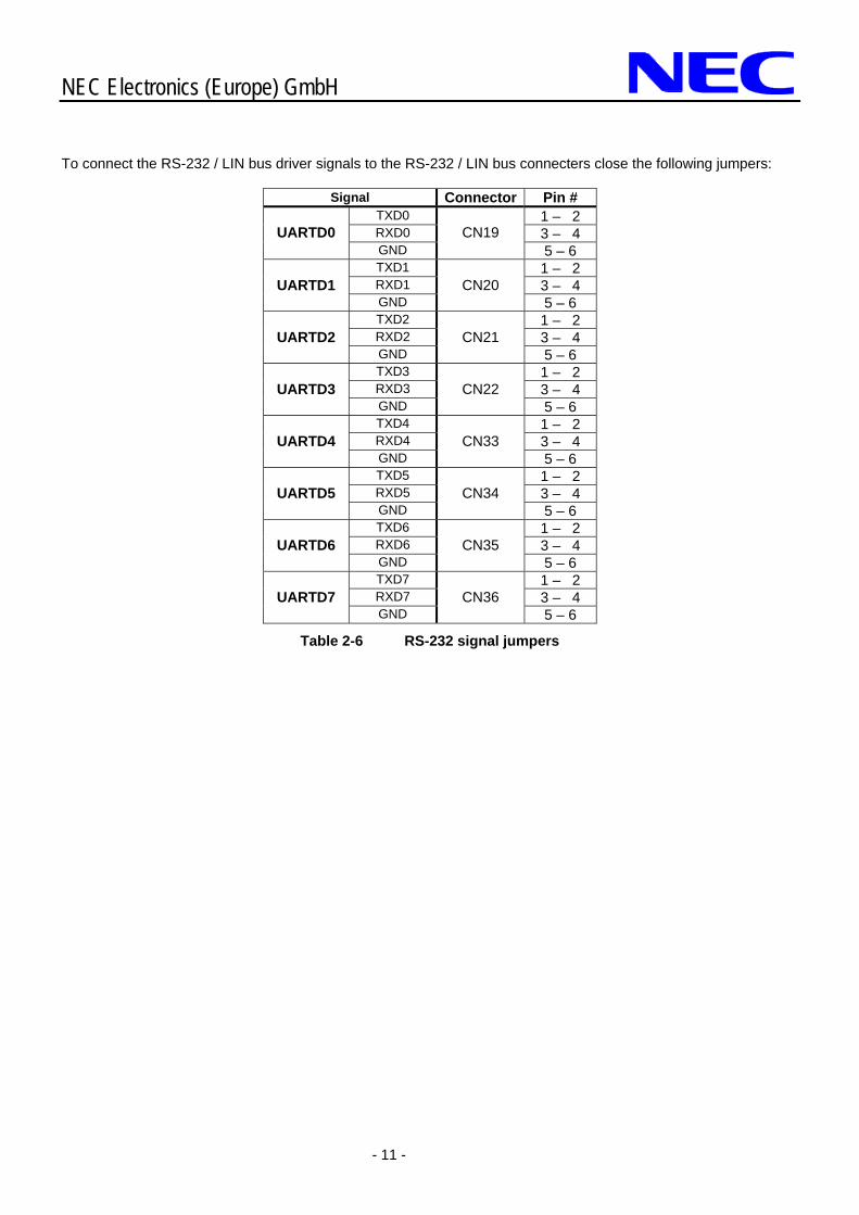
To connect the RS-232 / LIN bus driver signals to the RS-232 / LIN bus connecters close the following jumpers:
Signal Connector Pin # TXD0 1 – 2 RXD0 3 – 4 UARTD0 GND
CN19 5 – 6
TXD1 1 – 2 RXD1 3 – 4 UARTD1 GND
CN20 5 – 6
TXD2 1 – 2 RXD2 3 – 4 UARTD2 GND
CN21 5 – 6
TXD3 1 – 2 RXD3 3 – 4 UARTD3 GND
CN22 5 – 6
TXD4 1 – 2 RXD4 3 – 4 UARTD4 GND
CN33 5 – 6
TXD5 1 – 2 RXD5 3 – 4 UARTD5 GND
CN34 5 – 6
TXD6 1 – 2 RXD6 3 – 4 UARTD6 GND
CN35 5 – 6
TXD7 1 – 2 RXD7 3 – 4 UARTD7 GND
CN36 5 – 6
Table 2-6 RS-232 signal jumpers

NEC Electronics (Europe) GmbH
- 12 -
To connect the LIN bus driver signals to the related RS-232/LIN bus connector close the following jumpers:
Signal Connector Pin # 12V 7 – 8 LIN 9 – 10 LIN0
GND CN19
11 – 12 12V 7 – 8 LIN 9 – 10 LIN1
GND
CN20 11 – 12
12V 7 – 8 LIN 9 – 10 LIN2
GND CN21
11 – 12 12V 7 – 8 LIN 9 – 10 LIN3
GND CN22
11 – 12 12V 7 – 8 LIN 9 – 10 LIN4
GND CN33
11 – 12 12V 7 – 8 LIN 9 – 10 LIN5
GND
CN34
11 – 12 12V 7 – 8 LIN 9 – 10 LIN6
GND CN35
11 – 12 12V 7 – 8 LIN 9 – 10 LIN7
GND CN36
11 – 12
Table 2-7 LIN bus signal jumpers
To enable the LIN drivers (IC218, IC219, IC172, IC221, IC217, IC223, IC228, IC229) the NSLP pin of the drivers must be pulled high. To do so a Jumper is available to connect the pin to VDD.
LIN channel NSLP Jumper 0 JP3 1 JP8 2 JP12 3 JP16 4 JP20 5 JP24 6 JP40 7 JP36
NEC Electronics (Europe) GmbH
- 13 -
The RxD pin of the LIN driver (pin #1) is an open drain output. The necessary pull-up resistor in order to interface to the Fx3 device is not assembled on the board. To enable operation of the RxD signal
- either connect an appropriate pull up resister to the related RxD input pin of the LIN channel, or - enable the internal Pull-Up resistors available in the Fx3 devices for each LIN input pin.
The corresponding input pin for each RxD pin can be found in Table 6-11. For additional information on the LIN driver refer to its User’s Manual / Datasheet. Caution: The RXD reception output pin of the LIN driver (e.g. IC218 pin1) and the RxD reception output pin of
the UART driver (e.g. IC173 pin 12) are physically connected to the same pin on connector CN9 (e.g. CN9 pin 4). Therefore
- when using the LIN driver lift the connected UART driver RxD output pin from the PCB. - when using the UART driver place the connected LIN driver in standby mode or lift the LIN
driver RxD output pin from the board.
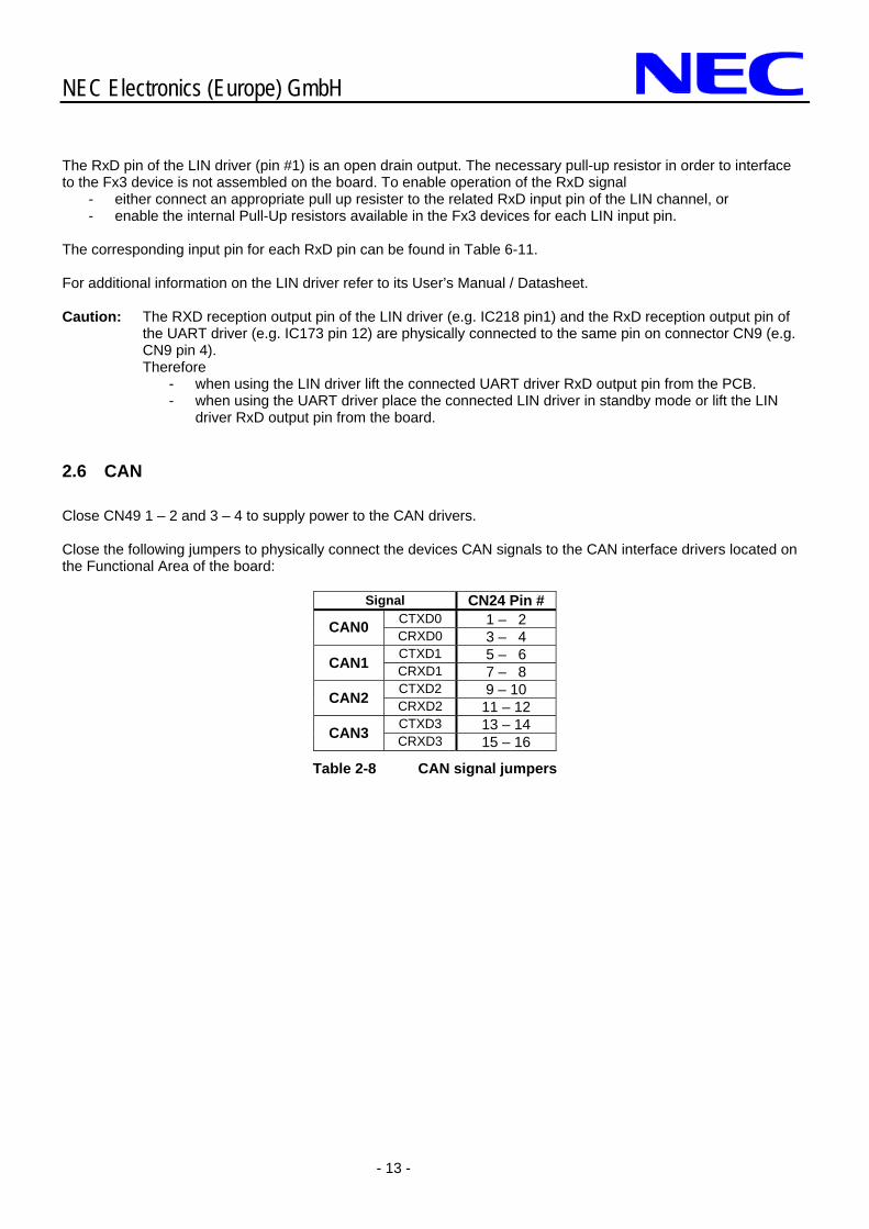
2.6 CAN
Close CN49 1 – 2 and 3 – 4 to supply power to the CAN drivers. Close the following jumpers to physically connect the devices CAN signals to the CAN interface drivers located on the Functional Area of the board:
Signal CN24 Pin # CTXD0 1 – 2 CAN0 CRXD0 3 – 4 CTXD1 5 – 6 CAN1 CRXD1 7 – 8 CTXD2 9 – 10 CAN2 CRXD2 11 – 12 CTXD3 13 – 14 CAN3 CRXD3 15 – 16
Table 2-8 CAN signal jumpers

NEC Electronics (Europe) GmbH
- 14 -
3 Mounting the FK3 device on the board
The AB-050-FX3-U boards is shipped with a mounted V850ES/FK3 device. Nevertheless, if mounting of another V850ES/FK3 device is required at a later time the following guideline is supplied: To mount a FK3 device on the AB-050-FX3-U place the package in the top right corner of the SMD area. As the FK3 with 176 pins is placed on an SMD area with 180 pins 4 pads will not be used. Due to the alignment of the device in the top right corner two pads in the lowest line and two pads in the left most line remain empty. Therefore align pin 1 of the device with pin 2 of the SMD pad area. For details see Figure 3-1 and Figure 3-2.
Figure 3-1 FK3 device mounting (1)
CN0
CN31
CN29
CN
30
CN
32 FK3
1
Figure 3-2 FK3 device mounting (2)

NEC Electronics (Europe) GmbH
- 15 -
4 Connecting the Power Supply
Power can be supplied to the board either a) by directly supplying the device operating voltage, or b) via the onboard 7805 type voltage regulator.
Direct voltage supply: A direct supply of the device operating voltage can either be implied by using CN7 to connect VCC (typical +5V for Fx3 devices) and CN8 to connect VSS (0V), or by using CN1. As the supplied voltage is directly connected to the device the input voltage must not exceed the specified power supply voltage range of the assembled device. Close JP1 1-2 when directly supplying the devices voltage. Voltage regulator supply: Use CN1 to supply a stabilized voltage of 6V - 12V to the board. The on board 7805 type regulator will generate the 5V supply of the board. Close JP1 2-3 when using the on board voltage regulator. Caution: On CN1 the inner pin connects to VSS and the outer pin connects to VCC. Applying a voltage to the device outside the specified device operating voltage range may damage
the device!

NEC Electronics (Europe) GmbH
- 16 -
5 UART / LIN CAN DSUB connectors
To physically connect the Starter Board to other UART / LIN / CAN devices DSUB type connectors are available..
5.1 UART / LIN connectors
To interface the AB-050-FX3-U board to external to UART / LIN devices a 9 pin male D-SUB connector is supplied for each of the eight available UART / LIN interfaces. The signal layout of the UART/LIN DSUB connector can be seen in Table 5-1.
Male D-SUB, 9pin Function
1 n/c 6 n/c 2 RS-232 TxD 7 LIN 3 RS-232 Rxd or GND 8 n/c 4 n/c 9 +12V 5 GND
Table 5-1 UART / LIN DSUB connectors
Figure 5-1 displays the assignment of each DSUB connector to its related peripheral:
UART0
UART1
UART2
UART3
UART4
UART5
UART6
UART7
Figure 5-1 UART / LIN DSUB connectors

NEC Electronics (Europe) GmbH
- 17 -
5.2 CAN connectors
To interface the AB-050-FX3-U board to external CAN devices a 9 pin female D-SUB connector is supplied for each of the five available CAN interfaces. The pin functions of the CAN DSUB connectors can be seen in Table 5-2.
Female D-SUB, 9pin Function
1 n/c 6 GND 2 CANL 7 CANH 3 GND (if jumpered) 8 n/c 4 n/c 9 n/c 5 n/c
Table 5-2 CAN DSUB connectors
Figure 5-2 displays the assignment of each DSUB connector to its related peripheral:
CAN0
CAN1
CAN2
CAN3
CAN4
Figure 5-2 CAN DSUB connector

NEC Electronics (Europe) GmbH
- 18 -
6 Mounting other Fx3 devices on the board
Even though the AB-050-FX3-U is prepared for operation of the FK3 device also other devices of the Fx3-Line can be mounted on the board. Besides mounting the new device to the board
- the components in the Pin Patch Area must be replaced according to the pin layout of the new device and - the signals between the device pins and the jumpers connecting the Electrical Area and the Functional
Area must wired manually. Therefore the following changes must be applied:
6.1 Mounting devices
First the device must be mounted to the PCB. The alignment of the different Fx3-family devices is explained below.
6.1.1 Mounting a FE3 device
To mount a FE3 device on the AB-050-FX3-U place the package in the lower left corner of the SMD area but do not use the two pins most in the corner. Place pin 1 of the device on pin 2 of the SMD area.
CN31
CN29
CN
30
CN
32
FE31
Figure 6-1 Mounting a FE3 device

NEC Electronics (Europe) GmbH
- 19 -
6.1.2 Mounting a FF3 device
To mount a FF3 device on the AB-050-FX3-U place the package in the lower left corner of the SMD area but do not use the two pins most in the corner. Place pin 1 of the device on pin 2 of the SMD area.
CN31
CN29C
N30
CN
32
FF31
Figure 6-2 Mounting a FF3 device
6.1.3 Mounting a FG3 device
To mount a FF3 device on the AB-050-FX3-U place the package in the lower left corner of the SMD area. Place pin 1 of the device on pin 1 of the SMD area.
CN31
CN29
CN
30
CN
32
FG31
Figure 6-3 Mounting a FG3 device

NEC Electronics (Europe) GmbH
- 20 -
6.1.4 Mounting a FJ3 device
To mount a FJ3 device on the AB-050-FX3-U place the package in the lower left corner of the SMD area. Place pin 1 of the device on pin 1 of the SMD area.
CN31
CN29
CN
30
CN
32
FJ3
1
Figure 6-4 Mounting a FJ3 device

NEC Electronics (Europe) GmbH
- 21 -
6.2 Pin connection
6.2.1 Power supply pins
Connect the devices power supply pins to the related power lines using the available SMD pads in the Pin Patch Areas. Refer to the Fx3 User’s Manual and Table 6-1 for the location of the VDD and VSS pins on the different devices. Connect the VDD and VSS pins in the Pin Patch Areas like this:
VDD
VSS
R = 0
leave open
Device VSS pin
VDD
VSS
C = 100 nF
R = 0
Device VDD pin
Figure 6-5 Device power supply
To connect the devices VSS pins to the VSS lane of the board place a 0 Ohm resistor on the SMD1 pad.
Fx3 pinning Signal FE3 FF3 FG3 FJ3 FK3 VSS 6 11 11 11 11 VSS1 n/a n/a n/a n/a 124 AVSS 2 2 2 2 2 AVSS1 n/a n/a n/a n/a 46
32 30 33 33 28 EVSS n/a n/a n/a n/a 76 BVSS n/a n/a 69 103 127
Table 6-1 VSS signal connection

NEC Electronics (Europe) GmbH
- 22 -
To connect the devices VDD pins to the VDD lane of the board place a 0 Ohm resistor on the SMD2 pad and place a 100 nF buffering capacitor on the SMD1 pad.
Fx3 pinning Signal FE3 FF3 FG3 FJ3 FK3 VDD 4 9 9 9 9 VDD1 n/a n/a n/a n/a 126 AVREF0 1 1 1 1 1 AVREF1 n/a n/a n/a n/a 45
33 31 34 34 47 n/a n/a 5 5 5 EVDD n/a n/a n/a n/a 77
BVDD n/a n/a 70 104 128
Table 6-2 VDD signal connection
6.2.2 REGC pin
A buffering capacitor between the devices REGC pin(s) and VSS should be placed. Assemble the capacitor to the SMD1 pad field.
VDD
VSS
C
Device signal
Figure 6-6 REGC pin components
Refer to the Fx3 User’s Manual and Table 6-3 for the location of the RECC pin on the different devices.
Fx3 pinning Signal FE3 FF3 FG3 FJ3 FK3 REGC 5 10 10 10 10 REGC1 n/a n/a n/a n/a 125
Table 6-3 REGC signal connection

NEC Electronics (Europe) GmbH
- 23 -
6.2.3 X1, X2 pins
An external oscillator can be connected to the X1 and X2 pins of the device. Connect the oscillator between the X1 and X2 pins and place a small capacitor on the SMD1 areas of those pins. For size of the capacitor refer to the oscillator manufacturer specification / recommendation.
VDD
VSS
C
Device VDD pin
Figure 6-7 X1, X2 pin components
Refer to the Fx3 User’s Manual and Table 6-4 for the location of the X1 and X2 pins on the different devices.
Fx3 pinning Signal FE3 FF3 FG3 FJ3 FK3 X1 7 12 12 12 12 X2 8 13 13 13 13
Table 6-4 X1, X2 signal connection

NEC Electronics (Europe) GmbH
- 24 -
6.2.4 XT1, FLMD0
A pull-down resistor should be connected to input pins XT1 and FLMD0.
VDD
VSS
R
Device signal
Figure 6-8 Pins with Pull-Down
Refer to the Fx3 User’s Manual and Table 6-5 for the location of the XT1 and FLMD0 pins on the different devices.
Fx3 pinning Signal FE3 FF3 FG3 FJ3 FK3 XT1 10 15 15 15 15 FLMD0 3 8 8 8 8
Table 6-5 XT1, FLMD0 signal connection

NEC Electronics (Europe) GmbH
- 25 -
6.3 Functional pin connection
As the routing of the functional signals (Reset, UARTDn, CANn, NWIRE and FP4) between the device SMD pad area and the Jumpers connecting the Electrical Area and Functional Area is based on the FK3 device, the routing of those signals for other Fx3 devices must be place manually. To do so, connect a wire between the device pin (e.g. from one of the through holes in the Pin Patch areas) and the functional side of the related signal jumper. Caution: Do not close the related Jumpers of any of the newly routed signals as this can lead to a direct
connection between different device pins. Be aware that no further disconnection by the use of jumpers between the Electrical Area and
Functional Area is possible after wiring the signals for other than FK3 devices.
6.3.1 Jumper overview
The location of all jumpers located on the board can be seen in the Figure 6-9. Pin 1 of each Jumper field is marked with a black square.
JP11
JP15
CN49
JP1CN52
JP2
12
JP26
JP27
JP28
JP29
JP7
CN47
CN46
CN45
CN4421
21
21
21
CN20 CN19CN22 CN21CN34 CN33CN36 CN35
JP12
JP10JP
13JP16
JP14JP
17JP20
JP18JP
21JP24
JP22JP
25JP36
JP33JP
37JP40
JP38JP
41C
N48
12
2 1
CN
24
21
CN
9
21
JP22
JP3
JP3
JP5JP
4JP8
JP6JP
9
Figure 6-9 Jumpers location

NEC Electronics (Europe) GmbH
- 26 -
The different jumper groups are highlighted in different colours according to their related functionality:
Jumper colour Related functionality
Yellow NWire Debug interface and Flash programming interface
Green CAN interface signals Blue RS-232 interface signals Red LIN bus interface signals
Magenta Power supply and Reset
Table 6-6 Colours of Jumper functionality
6.3.2 Testpoints
The available Test Points can be seen in
TP1
TP15
TP50
TP11
TP12
TP48
TP54
TP56
TP58
TP62
TP60
TP7
TP6
TP5 TP4
Figure 6-10 Test Point location
6.3.3 Reset signal
To connect the RESET signal place a wire according to the table below:
Fx3 pin number Signal FE3 FF3 FG3 FJ3 FK3 CN52
pin number Reset 9 14 14 14 14 4
Table 6-7 Reset signal connection

NEC Electronics (Europe) GmbH
- 27 -
6.3.4 NWIRE signals
To connect the NWIRE signals place wires according to the table below:
Fx3 pin number Signal FE3 FF3 FG3 FJ3 FK3 CN48
pin number DCK 34 36 41 41 60 11 DMS 35 37 42 42 61 13 DDI 30 34 39 39 58 15 DRSTZ 17 17 20 20 21 17 RESET 9 14 14 14 14 19 FLMD0 3 8 8 8 8 21 DDO 31 35 40 40 59 23
Table 6-8 NWire interface signals
6.3.5 Flash Programming interface
To connect the Flash Programming signals place wires according to the table below:
Fx3 pin number Signal FE3 FF3 FG3 FJ3 FK3 CN48 Pin number
TxD 22 22 25 25 26 1 RxD 23 23 26 26 47 3 SIB 19 19 22 22 23 5 SOB 20 20 23 23 24 7 SCK 21 21 24 24 25 9
Table 6-9 Flash programming jumper settings

NEC Electronics (Europe) GmbH
- 28 -
6.3.6 CAN interface
To connect the CAN interface signals place wires according to the table below:
Fx3 pin number Signal FE3 FF3 FG3 FJ3 FK3 CN24 Pin number
25 (*) 25 (*) 28 (*) 28 (*) 49 (*) CTXD0 18 18 21 21 22
2
26 (*) 26 (*) 29 (*) 29 (*) 50 (*) CRXD0 16 7 19 19 20 4
CTXD1 n/a n/a 31 31 52 6 CRXD1 n/a n/a 32 32 53 8
n/a n/a n/a 67 (*) 48 (*) CTXD2 n/a n/a n/a 71 92 10
n/a n/a n/a 68 (*) 49 (*) CRXD2 n/a n/a n/a 72 93 12
CTXD3 n/a n/a n/a 50 69 14 CRXD3 n/a n/a n/a 51 70 16 CTXD4 n/a n/a n/a n/a 104 18 CRXD4 n/a n/a n/a n/a 105 20
Table 6-10 CAN jumper settings
(*) Compatible pinning to the corresponding Fx2 device.
NEC Electronics (Europe) GmbH
- 29 -
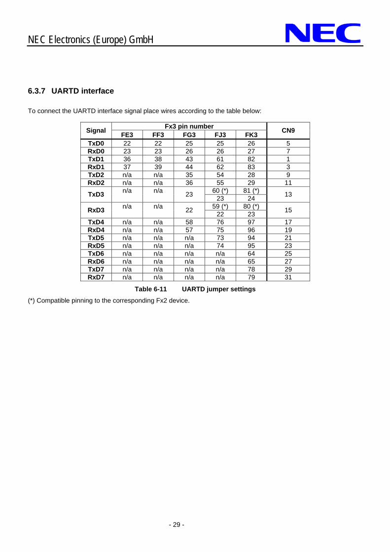
6.3.7 UARTD interface
To connect the UARTD interface signal place wires according to the table below:
Fx3 pin number Signal FE3 FF3 FG3 FJ3 FK3 CN9
TxD0 22 22 25 25 26 5 RxD0 23 23 26 26 27 7 TxD1 36 38 43 61 82 1 RxD1 37 39 44 62 83 3 TxD2 n/a n/a 35 54 28 9 RxD2 n/a n/a 36 55 29 11
60 (*) 81 (*) TxD3 n/a n/a 23 23 24 13
59 (*) 80 (*) RxD3 n/a n/a 22 22 23 15
TxD4 n/a n/a 58 76 97 17 RxD4 n/a n/a 57 75 96 19 TxD5 n/a n/a n/a 73 94 21 RxD5 n/a n/a n/a 74 95 23 TxD6 n/a n/a n/a n/a 64 25 RxD6 n/a n/a n/a n/a 65 27 TxD7 n/a n/a n/a n/a 78 29 RxD7 n/a n/a n/a n/a 79 31
Table 6-11 UARTD jumper settings
(*) Compatible pinning to the corresponding Fx2 device.

NEC Electronics (Europe) GmbH
- 30 -
7 Revision History
Version Chapter Comment
1.0 Initial release 6.2.1 - 6.2.4 6.3.3 - 6.3.7 Added pin tables for the different devices
All Modified / expanded text Error!
Reference source not
found. Added chapter ‘Cautions’
1.1
7 Added chapter ‘Revision History’ Error!
Reference source not
found. Added chapter for cable description 1.2
2.5 Added information on LIN operation 2.0 Update for V2.0 revision of the AB-050-FX3 board.
Updated naming of board to AB-050-FX3-U 2.1 2.5 Added Caution on UART / LIN driver usage

NEC Electronics (Europe) GmbH
- 31 -
8 Appendix A – Pin Number templates
If wanted the tables below can be printed and the pin numbers for the device placed on the AB-050-FX3-U glued to board. This allows for an easer handling of the devices pins.
FE3 FF3 FG3 FJ3 FK3
1 17 33 49 1 21 41 61 1 26 51 76 1 37 73 109 1 45 89 1332 18 34 50 2 22 42 62 2 27 52 77 2 38 74 110 2 46 90 1343 19 35 51 3 23 43 63 3 28 53 78 3 39 75 111 3 47 91 1354 20 36 52 4 24 44 64 4 29 54 79 4 40 76 112 4 48 92 1365 21 37 53 5 25 45 65 5 30 55 80 5 41 77 113 5 49 93 1376 22 38 54 6 26 46 66 6 31 56 81 6 42 78 114 6 50 94 1387 23 39 55 7 27 47 67 7 32 57 82 7 43 79 115 7 51 95 1398 24 40 56 8 28 48 68 8 33 58 83 8 44 80 116 8 52 96 1409 25 41 57 9 29 49 69 9 34 59 84 9 45 81 117 9 53 97 141
10 26 42 58 10 30 50 70 10 35 60 85 10 46 82 118 10 54 98 14211 27 43 59 11 31 51 71 11 36 61 86 11 47 83 119 11 55 99 14312 28 44 60 12 32 52 72 12 37 62 87 12 48 84 120 12 56 100 14413 29 45 61 13 33 53 73 13 38 63 88 13 49 85 121 13 57 101 14514 30 46 62 14 34 54 74 14 39 64 89 14 50 86 122 14 58 102 14615 31 47 63 15 35 55 75 15 40 65 90 15 51 87 123 15 59 103 14716 32 48 64 16 36 56 76 16 41 66 91 16 52 88 124 16 60 104 148
17 37 57 77 17 42 67 92 17 53 89 125 17 61 105 149 18 38 58 78 18 43 68 93 18 54 90 126 18 62 106 150 19 39 59 79 19 44 69 94 19 55 91 127 19 63 107 151 20 40 60 80 20 45 70 95 20 56 92 128 20 64 108 152 21 46 71 96 21 57 93 129 21 65 109 153 22 47 72 97 22 58 94 130 22 66 110 154 23 48 73 98 23 59 95 131 23 67 111 155 24 49 74 99 24 60 96 132 24 68 112 156 25 50 75 100 25 61 97 133 25 69 113 157 26 62 98 134 26 70 114 158 27 63 99 135 27 71 115 159 28 64 100 136 28 72 116 160 29 65 101 137 29 73 117 161 30 66 102 138 30 74 118 162 31 67 103 139 31 75 119 163 32 68 104 140 32 76 120 164 33 69 105 141 33 77 121 165 34 70 106 142 34 78 122 166 35 71 107 143 35 79 123 167 36 72 108 144 36 80 124 168 37 81 125 169 38 82 126 170 39 83 127 171 40 84 128 172 41 85 129 173 42 86 130 174 43 87 131 175 44 88 132 176

NEC Electronics (Europe) GmbH
- 32 -
9 Appendix B - Schematic

C
D
E
Assemblydrawing
Distribution:
NEC EE ETC DT
Approved
Scale
Approved
Version Item
321 4 5
Designed Checked
Spec.
Issue
Date
6
NEC Corporation
1 2 3 4 5 7
C
D
E
6
5
4
3
2
1
Version
A
B
4 GND
1LVDD
3PIN
2VCC
Sheet1
K.Hesse S.Gupta
Page 4/8
EESS-0400-034-02
1
AB-050-FK3
VCC
notass
KH
IC76
connector
4pinsGND4
LVDD1
PIN3
VCC2
notass
KH
connector
IC26
4pins
4pinsGND4
LVDD1
PIN3
VCC2
notass
KH
connector
IC63
4pins4 GND
1LVDD
3PIN
2
VCC2
notass
KH
connector
IC77
4pins4 GND
1LVDD
3PIN
2VCC
notass
KH
IC34
connector
4pins4 GND
1LVDD
3PIN
2VCC
notass
KH
IC11
connector
4pinsGND4
LVDD1
PIN3
3VCC
2
notass
KH
connector
IC37
4pins4 GND
1LVDD
3PIN
2VCC
notass
KH
connector
IC46
4pins4 GND
1LVDD
3PIN
2VCC
notass
KH
IC74
connector
4pinsGND4
LVDD1
PIN
PIN2
VCC
notass
KH
connector
IC56
4pins4 GND
1LVDD
3PIN
2VCC
notass
KH
connector
IC87
IC4
4pins4 GND
1LVDD
3PIN
2VCC
notass
KH
connector
IC22
4pins4 GND
1LVDD
3
PIN3
VCC2 notass
KH
IC36
connector
4pinsGND4
LVDD1
PIN3
VCC2
notass
KH
connector
connector
IC35
4pins4 GND
1LVDD
3PIN
2VCC
notass
KH
IC17
connector
4pinsGND4
LVDD1
1
PIN3
VCC2
notass
KH
IC84
connector
4pinsGND4
LVDD1
PIN3
VCC2
notass
KH
IC25
connector
4pinsGND4
LVDD1
PIN3
VCC2
notass
KH
IC5
connector
4pinsGND4
LVDD
1
PIN3
VCC2
notass
KH
connector
IC69
4pins4 GND
1LVDD
3PIN
2VCC
notass
KH
KH
IC23
connector
4pinsGND4
LVDD1
PIN3
VCC2
notass
KH
IC38
connector
4pinsGND4
LVDD
LVDD1
PIN3
VCC2
notass
KH
IC62
connector
4pinsGND4
LVDD1
PIN3
VCC2
notass
notass
KH
connector
IC65
4pins4 GND
1LVDD
3PIN
2VCC
notass
KH
IC3
connector
4pinsGND4
GND
1LVDD
3PIN
2VCC
notass
KH
connector
IC83
4pins4 GND
1LVDD
3PIN
2VCC
notass
KH
connector
IC59
4pins4 GND
1LVDD
3PIN
2VCC
notass
KH
connector
IC24
4pins4
1
PIN3
VCC2 notass
KH
IC32
connector
4pinsGND4
LVDD1
PIN3
VCC2
5V
KH
IC43
connector
4pinsGND4
LVDD1
PIN3
VCC2
notass
KH
IC13
connector
4pinsGND4
LVDD
LVDD1
PIN3
VCC2
notass
KH
IC15
connector
4pinsGND4
LVDD1
PIN3
VCC2
notass
notass
KH
connector
IC14
4pins4 GND
1LVDD
3PIN
2VCC
notass
KH
IC30
connector
4pinsGND4
4
LVDD1
PIN3
VCC2
notass
KH
IC64
connector
4pinsGND4
LVDD1
PIN3
VCC2
notass
KH
connector
IC71
4pins4 GND
1LVDD
3PIN
2VCC
notass
KH
IC27
connector
4pinsGND
GND
1LVDD
3PIN
2VCC
notass
KH
connector
IC97
4pins4 GND
1LVDD
3PIN
2VCC
2
notass
KH
connector
IC93
4pins4 GND
1LVDD
3PIN
2VCC
notass
KH
connector
IC20
4pins4
4 GND
1LVDD
3PIN
2VCC
notass
KH
IC57
connector
4pinsGND4
LVDD1
PIN3
VCC
VCC
notass
KH
IC47
connector
4pinsGND4
LVDD1
PIN3
VCC2
notass
KH
connector
IC48
4pins
4pinsGND4
LVDD1
PIN3
VCC2
notass
KH
connector
IC44
4pins4 GND
1LVDD
3PIN
2
VCC2
notass
KH
IC92
connector
4pinsGND4
LVDD1
PIN3
VCC2
notass
KH
IC51
connector
4pins4 GND
1LVDD
3PIN
2VCC
notass
KH
IC80
connector
4pinsGND4
LVDD1
PIN3
PIN2
VCC
notass
KH
connector
IC2
4pins4 GND
1LVDD
3PIN
2VCC
notass
KH
connector
IC79
4pins4 GND
1LVDD
3PIN
2VCC
notass
KH
connector
IC8
4pins4 GND
1LVDD
3
3VCC
2
notass
KH
connector
IC10
4pins4 GND
1LVDD
3PIN
2VCC
notass
KH
connector
IC100
IC31
4pins4 GND
1LVDD
3PIN
2VCC
notass
KH
IC45
connector
4pinsGND4
LVDD1
PIN
3PIN
2VCC
notass
KH
connector
IC98
4pins4 GND
1LVDD
3PIN
2VCC
notass
KH
connector
connector
4pinsGND4
LVDD1
PIN3
VCC2
notass
KH
connector
IC81
4pins4 GND
1LVDD
1
PIN3
VCC2
notass
KH
IC49
connector
4pinsGND4
LVDD1
PIN3
VCC2
notass
KH
IC42
connector
IC67
4pins4 GND
1LVDD
3PIN
2VCC
notass
KH
IC21
connector
4pinsGND4
LVDD1
PIN3
VCC2
notass
KH
IC68
connector
4pinsGND4
LVDD1
PIN3
VCC2
notass
KH
KH
IC96
connector
4pinsGND4
LVDD1
PIN3
VCC2
notass
KH
IC72
connector
4pinsGND4
LVDD
LVDD1
PIN3
VCC2
notass
KH
connector
IC75
4pins4 GND
1LVDD
3PIN
2VCC
notass
notass
KH
IC1
connector
4pinsGND4
LVDD1
PIN3
VCC2
notass
KH
IC9
connector
4pinsGND4
GND
1LVDD
3PIN
2VCC
notass
KH
IC88
connector
4pinsGND4
LVDD1
PIN3
VCC2
notass
KH
connector
IC95
4pins4 GND
1LVDD
3PIN
2VCC
notass
KH
connector
IC58
4pins4
4
LVDD1
PIN3
VCC2
notass
KH
IC86
connector
4pinsGND4
LVDD1
PIN3
VCC2
2
notass
KH
IC28
connector
4pinsGND4
LVDD1
PIN3
VCC2
notass
KH
IC53
connector
4pinsGND
4 GND
1LVDD
3PIN
2VCC
notass
KH
IC78
connector
4pinsGND4
LVDD1
PIN3
VCC
notass
KH
IC19
connector
4pinsGND4
LVDD1
PIN3
VCC2
notass
KH
connector
IC39
4pins
GND
1LVDD
3PIN
2VCC
notass
KH
connector
IC29
4pins4 GND
1LVDD
3PIN
2VCC
notass
KH
connector
IC85
4pins4 GND
1LVDD
3PIN
2VCC
notass
KH
connector
IC6
4pins4
GND
1LVDD
3PIN
2VCC
notass
KH
connector
IC41
4pins4 GND
1LVDD
3PIN
2VCC
VCC
notass
KH
IC40
connector
4pinsGND4
LVDD1
PIN3
VCC2
notass
KH
connector
IC18
4pins4
4 GND
1LVDD
3PIN
2VCC
notass
KH
connector
IC50
4pins4 GND
1LVDD
3PIN
2
2
notass
KH
IC94
connector
4pinsGND4
LVDD1
PIN3
VCC2
notass
KH
connector
IC16
4pins
4pins4 GND
1LVDD
3PIN
2VCC
notass
KH
IC99
connector
4pinsGND4
LVDD1
PIN3
VCC
2VCC
notass
KH
IC60
connector
4pinsGND4
LVDD1
PIN3
VCC2
notass
KH
connector
IC73
4pins4 GND
1LVDD
3PIN
2VCCnotass
KH
connector
IC12
4pins4 GND
1LVDD
3PIN
PIN2
VCC
notass
KH
connector
IC54
4pins4 GND
1LVDD
3PIN
2VCC
notass
KH
connector
IC33
4pinsGND4
LVDD1
PIN3
VCC2
notass
KH
connector
IC91
4pins4 GND
1LVDD
3PIN
2VCC
notass
KH
connector
IC61
4pins4 GND
1LVDD
3PIN
2VCC
notass
KH
IC70
connector
IC89
4pins4 GND
1LVDD
3PIN
2VCC
notass
KH
connector
IC52
4pins4 GND
1LVDD
3
PIN3
VCC2
notass
KH
IC82
connector
4pinsGND4
LVDD1
PIN3
VCC2
notass
KH
connector
connector
4pinsGND4
LVDD1
PIN3
VCC2
notass
KH
IC55
connector
4pinsGND4
LVDD1
1
PIN3
VCC2
notass
KH
IC66
connector
4pinsGND4
LVDD1
PIN3
VCC2
notass
KH
IC7
PIN96
PIN97
PIN98
PIN99
PIN100
5.0
notass
KH
IC90
connector
4pinsGND4
LVDD
PIN82
PIN83
PIN84
PIN85
PIN86
PIN87
PIN88
PIN89
PIN90
PIN91
PIN92
PIN93
PIN94
PIN95
PIN68
PIN69
PIN70
PIN71
PIN72
PIN73
PIN74
PIN75
PIN76
PIN77
PIN78
PIN79
PIN80
PIN81
PIN53
PIN54
PIN55
PIN56
PIN57
PIN58
PIN59
PIN60
PIN61
PIN62
PIN63
PIN64
PIN65
PIN66
PIN67
PIN37
PIN38
PIN39
PIN40
PIN41
PIN42
PIN43
PIN44
PIN45
PIN46
PIN47
PIN48
PIN49
PIN50
PIN51
PIN52
PIN18
PIN19
PIN20
PIN21
PIN22
PIN23
PIN24
PIN25
PIN26
PIN27
PIN28
PIN29
PIN30
PIN31
PIN32
PIN33
PIN34
PIN35
PIN36
PIN1
PIN2
PIN3
PIN4
PIN5
PIN6
PIN7
PIN8
PIN9
PIN10
PIN11
PIN12
PIN13
PIN14
PIN15
PIN16
PIN17

3 4 5 6 7
C
D
E
NEC EE ETC DT
1
2
3
4
5
A
B
C
D
E
1 2
Issue
DateVersion
1 2 3 4 5 6
NEC Corporation
Spec.
Assemblydrawing
Distribution:
Scale
Designed Checked Approved
Version Item Approved
AB-050-FK3
Page /
EESS-0400-034-02
1
PIN3
VCC2
4pins
KH
notass
connector
IC202
4 GND
1LVDD
3PIN
2VCC
1 8Sheet2
nc1
1pin
notass
KH
connector
IC102
nc1
4pins
KH
notass
IC133
connector
GND4
LVDD
1pin
notass
KH
connector
IC121
nc1
1pin
notass
KH
IC120
connector
nc1
1pin
notass
KH
connector
IC119
notass
connector
IC196
4 GND
1LVDD
3PIN
2VCC
1pin
notass
KH
IC122
connector
nc1
LVDD
3PIN
2VCC
4pins
KH
notass
IC195
connector
GND4
LVDD1
PIN3
VCC2
4pins
KH
nc1
1pin
notass
KH
IC101
connector
nc1
4pins
KH
notass
connector
IC194
4 GND
1
GND4
LVDD1
PIN3
VCC2
1pin
notass
KH
connector
IC123
nc1
1pin
notass
KH
IC124
connector
2
connector
IC205
notass
KH
4pins4 GND
1LVDD
3PIN
2VCC
IC206
connector
notass
KH
4pins
4 GND
1LVDD
3PIN
2VCC
IC204
connector
notass
KH
4pinsGND4
LVDD1
PIN3
VCC
VCC2
connector
IC212
notass
KH
4pins4 GND
1LVDD
3PIN
2VCC
connector
IC203
notass
KH
4pins
4pins4 GND
1LVDD
3PIN
2VCC
IC211
connector
notass
KH
4pinsGND4
LVDD1
PIN3
PIN2
VCC
4pins
KH
notass
IC135
connector
GND4
LVDD1
PIN3
VCC2
connector
IC136
notass
KH
GND4
LVDD1
PIN3
VCC2
connector
IC134
notass
KH
4pins4 GND
1LVDD
3
3VCC
2
connector
IC132
notass
KH
4pins4 GND
1LVDD
3PIN
2VCC
4pins
KH
notass
IC201
connector
notass
KH
4pins4 GND
1LVDD
3PIN
2VCC
4pins
KH
notass
IC131
connector
GND4
LVDD1
PIN
3PIN
2VCC
4pins
KH
notass
IC129
connector
GND4
LVDD1
PIN3
VCC2
connector
IC130
IC127
connector
GND4
LVDD1
PIN3
VCC2
connector
IC128
notass
KH
4pins4 GND
1LVDD
1
PIN3
VCC2
4pins
KH
notass
connector
IC167
4 GND
1LVDD
3PIN
2VCC
4pins
KH
notass
notass
connector
IC165
4 GND
1LVDD
3PIN
2VCC
4pins
KH
notass
IC166
connector
GND4
LVDD
1
PIN3
VCC2
connector
IC214
notass
KH
4pins4 GND
1LVDD
3PIN
2VCC
4pins
KH
connector
IC138
notass
KH
4pins4 GND
1LVDD
3PIN
2VCC
IC213
connector
notass
KH
4pinsGND4
LVDD
1LVDD
3PIN
2VCC
4pins
KH
notass
IC137
connector
GND4
LVDD1
PIN3
VCC2
connector
IC210
notass
KH
4pins4 GND
1LVDD
3PIN
2VCC
4pins
KH
notass
connector
IC171
4 GND
KH
IC118
connector
nc1
4pins
KH
notass
IC197
connector
GND4
LVDD1
PIN3
VCC2
connector
GND4
LVDD1
PIN3
VCC2
1pin
notass
KH
connector
IC117
nc1
1pin
notass
PIN3
VCC2
4pins
KH
notass
connector
IC186
4 GND
1LVDD
3PIN
2VCC
4pins
KH
notass
IC187
IC183
connector
GND4
LVDD1
PIN3
VCC2
4pins
KH
notass
IC185
connector
GND4
LVDD1
1
PIN3
VCC2
4pins
KH
notass
connector
IC182
4 GND
1LVDD
3PIN
2VCC
4pins
KH
notass
notass
connector
IC180
4 GND
1LVDD
3PIN
2VCC
4pins
KH
notass
IC181
connector
GND4
LVDD
1
PIN3
VCC2
4pins
KH
notass
IC179
connector
GND4
LVDD1
PIN3
VCC2
4pins
KH
KH
notass
connector
IC163
4 GND
1LVDD
3PIN
2VCC
4pins
KH
notass
IC164
connector
GND4
LVDD
PIN2
VCC
1pin
notass
KH
connector
IC104
nc1
1pin
notass
KH
IC116
connector
nc1
4pins
GND4
LVDD1
PIN3
VCC2
4pins
KH
notass
connector
IC188
4 GND
1LVDD
3
GND4
LVDD1
PIN3
VCC2
1pin
notass
KH
connector
IC106
nc1
4pins
KH
notass
IC156
connector
VCC2
4pins
KH
notass
connector
IC169
4 GND
1LVDD
3PIN
2VCC
4pins
KH
notass
IC170
connector
4 GND
1LVDD
3PIN
2VCC
4pins
KH
notass
IC168
connector
GND4
LVDD1
PIN3
PIN2
VCC
4pins
KH
notass
IC160
connector
GND4
LVDD1
PIN3
VCC2
4pins
KH
notass
connector
IC161
GND4
LVDD1
PIN3
VCC2
4pins
KH
notass
connector
IC159
4 GND
1LVDD
3
nc1
4pins
KH
notass
connector
IC157
4 GND
1LVDD
3PIN
2VCC
4pins
KH
notass
IC158
connector
VCC2
IC139
connector
notass
KH
4pinsGND4
LVDD1
PIN3
VCC2
1pin
notass
KH
connector
IC125
4 GND
1LVDD
3PIN
2VCC
4pins
KH
notass
IC162
connector
GND4
LVDD1
PIN3
4 GND
1LVDD
3PIN
2VCC
1pin
notass
KH
connector
IC110
nc1
4pins
KH
notass
connector
IC184
2
connector
IC208
notass
KH
4pins4 GND
1LVDD
3PIN
2VCC
4pins
KH
notass
connector
IC155
4 GND
1LVDD
3PIN
2VCC
IC150
connector
notass
KH
4pinsGND4
LVDD1
PIN3
VCC
2VCC
IC148
connector
notass
KH
4pinsGND4
LVDD1
PIN3
VCC2
connector
IC149
notass
KH
4pins
4pinsGND4
LVDD1
PIN3
VCC2
connector
IC147
notass
KH
4pins4 GND
1LVDD
3PIN
PIN2
VCC
4pins
KH
notass
IC193
connector
GND4
LVDD1
PIN3
VCC2
IC146
connector
notass
KH
GND4
LVDD1
PIN3
VCC2
4pins
KH
notass
connector
IC192
4 GND
1LVDD
3
5
6 6
4pins
KH
notass
connector
IC190
4 GND
1LVDD
3PIN
2VCC
4pins
KH
notass
IC191
connector
4 4
5 5
6 6
6pin
KH
notass
IC175
connector
11
22
33
4 4
5
1pin
notass
KH
connector
IC115
nc1
6pin
KH
notass
IC174
connector
11
22
33
nc1
1pin
notass
KH
IC113
connector
nc1
1pin
notass
KH
connector
IC114
nc1
4 GND
1LVDD
3PIN
2VCC
1pin
notass
KH
IC111
connector
nc1
1pin
notass
KH
connector
IC112
VCC
IC144
connector
notass
KH
4pinsGND4
LVDD1
PIN3
VCC2
connector
IC145
notass
KH
4pins
GND4
LVDD1
PIN3
VCC2
connector
IC143
notass
KH
4pins4 GND
1LVDD
3PIN
2
VCC2
connector
IC141
notass
KH
4pins4 GND
1LVDD
3PIN
2VCC
IC142
connector
notass
KH
4pins
2
1pin
notass
KH
IC103
connector
nc1
IC140
connector
notass
KH
4pinsGND4
LVDD1
PIN3
GND4
LVDD1
PIN3
VCC2
IC209
connector
notass
KH
4pinsGND4
LVDD1
PIN3
VCC
2
4pins
KH
notass
connector
IC200
4 GND
1LVDD
3PIN
2VCC
4pins
KH
notass
IC189
connector
IC109
connector
nc1
5V
3.3
4pins
KH
notass
IC199
connector
GND4
LVDD1
PIN3
VCC
3VCC
2
4pins
KH
notass
connector
IC198
4 GND
1LVDD
3PIN
2VCC
1pin
notass
KH
IC153
4 GND
1LVDD
3PIN
2VCC
4pins
KH
notass
IC154
connector
GND4
LVDD1
PIN
PIN2
VCC
4pins
KH
notass
IC152
connector
GND4
LVDD1
PIN3
VCC2
4pins
KH
notass
connector
nc1
1pin
notass
KH
IC107
connector
nc1
4pins
KH
notass
connector
IC151
4 GND
1LVDD
3
5.0
PIN180
1pin
notass
KH
IC105
connector
nc1
1pin
notass
KH
connector
IC108
PIN176
PIN175
PIN174
PIN173
PIN172
PIN171
PIN170
PIN169
PIN168
PIN167
PIN166
PIN165
PIN164
PIN163
PIN162
PIN161
PIN145
PIN149
PIN150
PIN151
PIN152
PIN153
PIN154
PIN155
PIN156
PIN157
PIN158
PIN159
PIN160
PIN179
PIN178
PIN177
PIN112
PIN113
PIN114
PIN115
PIN116
PIN117
PIN118
PIN119
PIN120
PIN141
PIN142
PIN143
PIN144
PIN148
PIN147
PIN146
PIN137
PIN138
PIN139
PIN140
PIN101
PIN102
PIN103
PIN104
PIN105
PIN106
PIN107
PIN108
PIN109
PIN110
PIN111
PIN121
PIN122
PIN123
PIN124
PIN125
PIN126
PIN127
PIN128
PIN129
PIN130
PIN131
PIN132
PIN133
PIN134
PIN135
PIN136

3 4 5 6 7
C
D
E
NEC EE ETC DT
1
2
3
4
5
A
B
C
D
E
1 2
Issue
DateVersion
1 2 3 4 5 6
NEC Corporation
Spec.
Assemblydrawing
Distribution:
Scale
Designed Checked Approved
Version Item Approved
99
2 8
AB-050-FK3
Page /
EESS-0400-034-02
Multi QFP176 Footprint
99
9090
9191
9292
9393
9494
9595
9696
9797
9898
99
88
8080
81
81
82
82
83
83
84
84
85
85
86
86
87
87
88
88
8989
7
70
70
71
71
72
72
73
73
74
74
75
75
76
76
77
77
78
78
79
79
6
60
60
61
61 62
62
63
63
64
64
65
65
66
66
67
67
68
68
69
69
7
50
50
51
51
52
52
53
53
54
54
55
55
56
56
57
57
58
58
59
59
6
4040
41
41
42
42
43
43
4444
45
45
46
46
47
47
48
48
49
49
55
30
3131
3232
3333
3434
3535
3636
37
37
38
38
39
39
44
2121
2222
2323
2424
2525
2626
2727
2828
2929
33
30
174
175
175
176
176
177
177
178
178
179
179
1818
180
180
1919
22
2020
164
165
165
166
166
167
167
168
168
169
169
1717
170
170
171
171
172
172
173
173
174
155
155
156
156
157
157
158
158
159
159
1616
160
160
161
161
162
162
163
163
164
145
146
146
147
147
148
148
149
149
1515
150
150
151
151
152
152
153
153
154
154
136
136
137
137
138
138
139
139
1414
140
140
141
141
142
142
143
143
144
144
145
126126
127127
128128
129129
1313
130130
131131
132132
133
133
134
134
135
135
116116
117117
118118
119119
1212
120120
121121
122122
123123
124124
125125
106
107107
108108
109109
1111
110110
111111
112112
113113
114114
115115
11
1010
100100
101101
102102
103103
104104
105105
106
PIN164
PIN163
PIN162
PIN161
PIN160
PIN159
PIN171
PIN175
PIN174
PIN173
PIN172
PIN176
PIN180
multi176qfp_05
SO2
PIN155
PIN154
PIN153
PIN152
PIN151
PIN150
PIN149
PIN148
PIN147
PIN146
PIN158
PIN170
PIN169
PIN168
PIN167
PIN166
PIN165
PIN115
PIN116
PIN117
PIN112
PIN113
PIN114
PIN109
PIN110
PIN111
PIN142
PIN143
PIN144
PIN145
PIN157
PIN156
PIN135
PIN130
PIN131
PIN132
PIN127
PIN128
PIN129
PIN124
PIN125
PIN126
PIN121
PIN122
PIN123
PIN118
PIN119
PIN120
PIN59
PIN66
PIN67
PIN68
PIN72
PIN71
PIN70
PIN69
PIN139
PIN140
PIN141
PIN136
PIN137
PIN138
PIN133
PIN134
PIN44
PIN39
PIN40
PIN41
PIN178
PIN37
PIN38
PIN63
PIN64
PIN65
PIN60
PIN61
PIN62
PIN57
PIN58
PIN54
PIN55
PIN56
PIN51
PIN52
PIN53
PIN48
PIN49
PIN50
PIN45
PIN46
PIN47
PIN42
PIN43
PIN80
PIN79
PIN78
PIN77
PIN76
PIN75
PIN74
PIN73
PIN108
PIN179PIN177
PIN1
PIN2
PIN3
PIN84
PIN26
PIN27
PIN28
PIN29
PIN30
PIN31
PIN32
PIN33
PIN34
PIN35
PIN36
PIN83
PIN82
PIN81
PIN98
PIN97
PIN96
PIN95
PIN94
PIN93
PIN92
PIN91
PIN90
PIN89
PIN88
PIN87
PIN86
PIN85
PIN20
PIN21
PIN22
PIN23
PIN24
PIN25
PIN107
PIN106
PIN105
PIN104
PIN103
PIN102
PIN101
PIN100
PIN99
PIN4
PIN5
PIN6
PIN7
PIN8
PIN9
PIN10
PIN11
PIN12
PIN13
PIN14
PIN15
PIN16
PIN17
PIN18
PIN19

C
D
6
NEC Electron Devices
Spec.
Assemblydrawing
Distribution:
Scale
Designed Checked Approved
E
NEC EE ETC DT
1
2
3
4
5
543
Date
Issue
Version
21
A
B
C
D
E
1 2
Item
3 6
Approved
4 7
Version
5
5 8Page /
AB-050-FK3
.
Board VER. 1.00
QFP180 Footprint
EESS-0400-034-02
99
9090
9191
9292
9393
9494
9595
9696
9797
9898
9999
8
8080
81
81 82
82
83
83
84
84
85
85
86
86
87
87
88
88
8989
70
70
71
71
72
72
73
73
74
74
75
75
76
76
77
77
78
78
79
79
8
60
60
61
61 62
62
63
63
64
64
65
65
66
66
67
67
68
68
69
69
77
50
51
51 52
52
53
53
54
54
55
55
56
56
57
57
58
58
59
59
66
40
41
41
42
42
43
43
4444
45
45
46
46
47
47
48
48
49
49
55
50
3131
3232
3333
3434
3535
3636
37
37
38
38
39
39
44
40
2121
2222
2323
2424
2525
2626
2727
2828
2929
33
3030
174
175
175
176
176
177177
178
178
179
179
1818
180
180
1919
22
2020
165
165
166
166
167
167
168
168
169
169
1717
170
170
171
171
172
172
173
173
174
155
155
156
156
157
157
158
158
159
159
1616
160
160
161
161
162
162
163
163
164
164
146
146
147
147
148
148
149
149
1515
150
150
151
151
152
152
153
153
154
154
136
136
137
137
138
138
139
139
1414
140
140
141
141
142
142
143
143
144
144
145
145
126
127127
128128
129129
1313
130130
131131
132132
133
133
134
134
135
135
116
117117
118118
119119
1212
120120
121121
122122
123123
124124
125125
126
107107
108108
109109
1111
110110
111111
112112
113113
114114
115115
116
11
1010
100100
101101
102102
103103
104104
105105
106106
PIN110
PIN109
PIN108
PIN107
PIN106
PIN105
PIN104
PIN103
PIN102
PIN101
PIN100
PIN180
qfp180_05
SO1
PIN126
PIN125
PIN124
PIN123
PIN122
PIN121
PIN120
PIN119
PIN118
PIN117
PIN116
PIN115
PIN114
PIN113
PIN112
PIN111
PIN142
PIN141
PIN140
PIN139
PIN138
PIN137
PIN136
PIN135
PIN134
PIN133
PIN132
PIN131
PIN130
PIN129
PIN128
PIN127
PIN158
PIN157
PIN156
PIN155
PIN154
PIN153
PIN152
PIN151
PIN150
PIN149
PIN148
PIN147
PIN146
PIN145
PIN144
PIN143
PIN175
PIN174
PIN173
PIN172
PIN171
PIN170
PIN169
PIN168
PIN167
PIN166
PIN165
PIN164
PIN163
PIN162
PIN161
PIN160
PIN159
PIN54
PIN53
PIN52
PIN51
PIN50
PIN49
PIN48
PIN47
PIN46
PIN45
PIN179
PIN178
PIN176
PIN69
PIN68
PIN67
PIN66
PIN65
PIN64
PIN63
PIN62
PIN61
PIN60
PIN59
PIN58
PIN57
PIN56
PIN55
PIN82
PIN81
PIN80
PIN79
PIN78
PIN77
PIN76
PIN75
PIN74
PIN73
PIN72
PIN71
PIN70
PIN96
PIN95
PIN94
PIN93
PIN92
PIN91
PIN90
PIN89
PIN88
PIN87
PIN86
PIN85
PIN84
PIN83
PIN32
PIN33
PIN34
PIN35
PIN36
PIN37
PIN38
PIN39
PIN40
PIN41
PIN42
PIN43
PIN44
PIN99
PIN98
PIN97
PIN16
PIN17
PIN18
PIN19
PIN20
PIN21
PIN22
PIN23
PIN24
PIN25
PIN26
PIN27
PIN28
PIN29
PIN30
PIN31
PIN177
PIN1
PIN2
PIN3
PIN4
PIN5
PIN6
PIN7
PIN8
PIN9
PIN10
PIN11
PIN12
PIN13
PIN14
PIN15

5
543
Date
Issue
Version
21
A
B
C
D
E
1 2
Item
3 6
Approved
4 7
Version
5
C
D
6
NEC Electronics Corporation
Spec.
Assemblydrawing
Distribution:
Scale
Designed Checked Approved
E
NEC EE ETC DT
1
2
3
4
EESS-0400-034-02.
AB-050-FK3Board VER. 1.00
4748
49
5
50
6
78
9
87PiggyPack Connectors Page /
3738
39
4
40
4142
4344
4546
2728
29
3
30
3132
3334
3536
18
19
2
20
2122
2324
2526
1
10
1112
1314
1516
17
49
5
50
6
78
9
CN56
50pins/54722/Socket
39
4
40
4142
4344
4546
4748
29
3
30
3132
3334
3536
3738
19
2
20
2122
2324
2526
2728
1
10
1112
1314
1516
1718
5
50
6
7 8
9
CN55
50pins/54722/Socket
4
40
41 42
43 44
45 46
47 48
49
30
31 32
33 34
35 36
37 38
39
2
20
21 22
23 24
25 26
27 28
29
3
10
11 12
13 14
15 16
17 18
19
50pins/54722/Socket
CN54
1
90
9192
9394
9596
9798
99
8
80
8182
8384
8586
8788
89
9
70
7172
7374
7576
7778
79
60
6162
6364
6566
6768
69
7
50
5152
5354
5556
5758
59
6
4142
4344
4546
4748
49
5
32
3334
3536
3738
39
4
40
22
2324
2526
2728
29
3
30
31
12
1314
1516
1718
19
2
20
21
NAIS/AXN300130S
100pins/AXN/Socket
CN291
10
100
11 90
91 92
93 94
95 96
97 98
99
8
80
81 82
83 84
85 86
87 88
89
9
70
71 72
73 74
75 76
77 78
79
60
61 62
63 64
65 66
67 68
69
7
50
51 52
53 54
55 56
57 58
59
6
41 42
43 44
45 46
47 48
49
5
32
33 34
35 36
37 38
39
4
40
22
23 24
25 26
27 28
29
3
30
31
12
13 14
15 16
17 18
19
2
20
21
99
NAIS/AXN300130S
100pins/AXN/Socket
CN311
10
100
11
9
90
91
92
93
94
95
96
97
988
80
81
82
83
84
85
86
87
88
89
7
70
71
72
73
74
75
76
77
78
79
60
61
62
63
64
65
66
67
68
69
5
50
51
52
53
54
55
56
57
58
59
6
40
41
42
43
44
45
46
47
48
49
31
32
33
34
35
36
37
38
39
4
21
22
23
24
25
26
27
28
29
3
30
11
12
13
14
15
16
17
18
19
2
20
8
9
CN32
100pins/AXN/Socket
NAIS/AXN300130S
1
10 100
44
45 46
47 48
49
5
50
6
7
34
35 36
37 38
39
4
40
41 42
43
24
25 26
27 28
29
3
30
31 32
33
14
15 16
17 18
19
2
20
21 22
23
50pins/54722/Socket
CN531
10
11 12
13
9
90
91
92
93
94
95
96
97
98
99
8
80
81
82
83
84
85
86
87
88
89
7
70
71
72
73
74
75
76
77
78
79
60
61
62
63
64
65
66
67
68
69
50
51
52
53
54
55
56
57
58
59
6
41
42
43
44
45
46
47
48
49
5 31
32
33
34
35
36
37
38
39
4
40
21
22
23
24
25
26
27
28
29
3
30
11
12
13
14
15
16
17
18
19
2
20
CN30
100pins/AXN/Socket
NAIS/AXN300130S
1
10 100
46
47
48
49
5
506
78
9
36
37
38
39
4
40
41
42
43
44
45
27
28
29
3
30
31
32
33
34
35
17
18
19
2
20
21
22
23
24
25
2650pins/54722/Socket
CN57
1
10
11
12
13
14
15
16
47
48
49
5
506
78
9
38
39
4
40
41
42
43
44
45
46
28
29
3
30
31
32
33
34
35
36
37
18
19
2
20
21
22
23
24
25
26
27
50pins/54722/Socket
CN58
1
10
11
12
13
14
15
16
17
78
9 41
42
43
44
45
46
47
48
49
5
506
32
33
34
35
36
37
38
39
4
40
23
24
25
26
27
28
29
3
30
31
13
14
15
16
17
18
19
2
20
21
22
78
9
CN60
50pins/54722/Socket
1
10
11
12
43
44
45
46
47
48
49
5
506
33
34
35
36
37
38
39
4
40
41
42
23
24
25
26
27
28
29
3
30
31
32
14
15
16
17
18
19
2
20
21
22
PIN178
CN59
50pins/54722/Socket 1
10
11
12
13
PIN78
PIN79
PIN80
PIN81
PIN82
PIN83
PIN84
PIN85
PIN86
PIN87
PIN88
PIN66
PIN67
PIN68
PIN69
PIN70
PIN71
PIN72
PIN73
PIN74
PIN75
PIN76
PIN77
PIN54
PIN55
PIN56
PIN57
PIN58
PIN59
PIN60
PIN61
PIN62
PIN63
PIN64
PIN65
PIN88
PIN178
PIN45
PIN46
PIN47
PIN48
PIN49
PIN50
PIN51
PIN52
PIN53
PIN75
PIN76
PIN77
PIN78
PIN79
PIN80
PIN81
PIN82
PIN83
PIN84
PIN85
PIN86
PIN87
PIN63
PIN64
PIN65
PIN66
PIN67
PIN68
PIN69
PIN70
PIN71
PIN72
PIN73
PIN74
PIN50
PIN51
PIN52
PIN53
PIN54
PIN55
PIN56
PIN57
PIN58
PIN59
PIN60
PIN61
PIN62
PIN172
PIN173
PIN174
PIN134
PIN175
PIN176
PIN180
PIN45
PIN46
PIN47
PIN48
PIN49
PIN160
PIN161
PIN162
PIN163
PIN164
PIN133
PIN165
PIN166
PIN167
PIN168
PIN169
PIN170
PIN171
PIN147
PIN148
PIN149
PIN150
PIN151
PIN152
PIN153
PIN154
PIN155
PIN156
PIN157
PIN158
PIN159
PIN135
PIN136
PIN137
PIN138
PIN139
PIN140
PIN141
PIN142
PIN143
PIN144
PIN145
PIN146
PIN166
PIN167
PIN168
PIN169
PIN170
PIN171
PIN172
PIN173
PIN174
PIN134
PIN175
PIN176
PIN180
PIN154
PIN155
PIN156
PIN157
PIN158
PIN159
PIN160
PIN161
PIN162
PIN163
PIN164
PIN133
PIN165
PIN142
PIN143
PIN144
PIN145
PIN146
PIN147
PIN148
PIN149
PIN150
PIN151
PIN152
PIN153
PIN138
PIN137
PIN136
PIN135
PIN134
PIN133
PIN135
PIN136
PIN137
PIN138
PIN139
PIN140
PIN141
PIN154
PIN153
PIN152
PIN151
PIN150
PIN149
PIN148
PIN147
PIN146
PIN145
PIN144
PIN143
PIN142
PIN141
PIN140
PIN139
PIN170
PIN169
PIN168
PIN167
PIN166
PIN165
PIN164
PIN163
PIN162
PIN161
PIN160
PIN159
PIN158
PIN157
PIN156
PIN155
PIN6
PIN5
PIN4
PIN3
PIN2
PIN1
PIN177
PIN180
PIN176
PIN175
PIN174
PIN173
PIN172
PIN171
PIN19
PIN18
PIN17
PIN16
PIN15
PIN14
PIN13
PIN12
PIN11
PIN10
PIN9
PIN8
PIN7
PIN31
PIN30
PIN29
PIN28
PIN27
PIN26
PIN25
PIN24
PIN23
PIN22
PIN21
PIN20
PIN44
PIN43
PIN42
PIN41
PIN40
PIN39
PIN38
PIN37
PIN36
PIN35
PIN34
PIN33
PIN32
PIN34
PIN35
PIN36
PIN37
PIN38
PIN39
PIN40
PIN41
PIN42
PIN43
PIN44
PIN177
PIN21
PIN22
PIN23
PIN24
PIN25
PIN26
PIN27
PIN28
PIN29
PIN30
PIN31
PIN32
PIN33
PIN8
PIN9
PIN10
PIN11
PIN12
PIN13
PIN14
PIN15
PIN16
PIN17
PIN18
PIN19
PIN20
PIN129
PIN130
PIN90
PIN131
PIN132
PIN179
PIN1
PIN2
PIN3
PIN4
PIN5
PIN6
PIN7
PIN114
PIN115
PIN116
PIN117
PIN118
PIN119
PIN120
PIN89
PIN121
PIN122
PIN123
PIN124
PIN125
PIN126
PIN127
PIN128
PIN99
PIN100
PIN101
PIN102
PIN103
PIN104
PIN105
PIN106
PIN107
PIN108
PIN109
PIN110
PIN111
PIN112
PIN113
PIN130
PIN90
PIN131
PIN132
PIN179
PIN91
PIN92
PIN93
PIN94
PIN95
PIN96
PIN97
PIN98
PIN115
PIN116
PIN117
PIN118
PIN119
PIN120
PIN89
PIN121
PIN122
PIN123
PIN124
PIN125
PIN126
PIN127
PIN128
PIN129
PIN99
PIN100
PIN101
PIN102
PIN103
PIN104
PIN105
PIN106
PIN107
PIN108
PIN109
PIN110
PIN111
PIN112
PIN113
PIN114
PIN40
PIN41
PIN42
PIN43
PIN44
PIN177
PIN180
PIN91
PIN92
PIN93
PIN94
PIN95
PIN96
PIN97
PIN98
PIN24
PIN25
PIN26
PIN27
PIN28
PIN29
PIN30
PIN31
PIN32
PIN33
PIN34
PIN35
PIN36
PIN37
PIN38
PIN39
PIN8
PIN9
PIN10
PIN11
PIN12
PIN13
PIN14
PIN15
PIN16
PIN17
PIN18
PIN19
PIN20
PIN21
PIN22
PIN23
PIN82
PIN83
PIN84
PIN85
PIN86
PIN87
PIN88
PIN178
PIN1
PIN2
PIN3
PIN4
PIN5
PIN6
PIN7
PIN68
PIN69
PIN70
PIN71
PIN72
PIN73
PIN74
PIN75
PIN76
PIN77
PIN78
PIN79
PIN80
PIN81
PIN54
PIN55
PIN56
PIN57
PIN58
PIN59
PIN60
PIN61
PIN62
PIN63
PIN64
PIN65
PIN66
PIN67
PIN130
PIN90
PIN131
PIN132
PIN179
PIN45
PIN46
PIN47
PIN48
PIN49
PIN50
PIN51
PIN52
PIN53
PIN115
PIN116
PIN117
PIN118
PIN119
PIN120
PIN89
PIN121
PIN122
PIN123
PIN124
PIN125
PIN126
PIN127
PIN128
PIN129
PIN100
PIN101
PIN102
PIN103
PIN104
PIN105
PIN106
PIN107
PIN108
PIN109
PIN110
PIN111
PIN112
PIN113
PIN114
PIN172
PIN173
PIN174
PIN175
PIN176
PIN91
PIN92
PIN93
PIN94
PIN95
PIN96
PIN97
PIN98
PIN99PIN156
PIN157
PIN158
PIN159
PIN160
PIN161
PIN162
PIN163
PIN164
PIN165
PIN166
PIN167
PIN168
PIN169
PIN170
PIN171
PIN140
PIN141
PIN142
PIN143
PIN144
PIN145
PIN146
PIN147
PIN148
PIN149
PIN150
PIN151
PIN152
PIN153
PIN154
PIN155
PIN53
PIN52
PIN51
PIN50
PIN49
PIN48
PIN47
PIN46
PIN133
PIN134
PIN135
PIN136
PIN137
PIN138
PIN139
PIN69
PIN68
PIN67
PIN66
PIN65
PIN64
PIN63
PIN62
PIN61
PIN60
PIN59
PIN58
PIN57
PIN56
PIN55
PIN54
PIN83
PIN82
PIN81
PIN45
PIN80
PIN79
PIN78
PIN77
PIN76
PIN75
PIN74
PIN73
PIN72
PIN71
PIN178
PIN70
PIN123
PIN124
PIN125
PIN126
PIN127
PIN128
PIN129
PIN130
PIN131
PIN132
PIN179
PIN88
PIN87
PIN86
PIN85
PIN84
PIN107
PIN108
PIN109
PIN110
PIN111
PIN112
PIN113
PIN114
PIN115
PIN116
PIN117
PIN118
PIN119
PIN120
PIN121
PIN122
PIN91
PIN92
PIN93
PIN94
PIN95
PIN96
PIN97
PIN98
PIN99
PIN100
PIN101
PIN102
PIN103
PIN104
PIN105
PIN106
PIN33
PIN34
PIN35
PIN36
PIN37
PIN38
PIN39
PIN40
PIN41
PIN42
PIN43
PIN44
PIN177
PIN89
PIN90
PIN17
PIN18
PIN19
PIN20
PIN21
PIN22
PIN23
PIN24
PIN25
PIN26
PIN27
PIN28
PIN29
PIN30
PIN31
PIN32
PIN1
PIN2
PIN3
PIN4
PIN5
PIN6
PIN7
PIN8
PIN9
PIN10
PIN11
PIN12
PIN13
PIN14
PIN15
PIN16
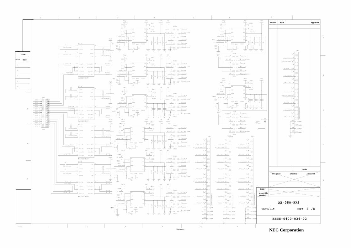
3 4 5 6 7
C
D
E
NEC EE ETC DT
1
2
3
4
5
A
B
C
D
E
1 2
Issue
DateVersion
1 2 3 4 5 6
NEC Corporation
Spec.
Assemblydrawing
Distribution:
Scale
Designed Checked Approved
Version Item Approved
Slave
Master
Slave
Master
Slave
Master
Slave
Master
Slave
Master
TP1
3 8
Slave
Master
TXD7
RXD7
TXD2
RXD2
TXD3
RXD3
TXD4
RXD4
TXD5
RXD5
TXD6
RXD6
RXD0
TXD0
Page /
EESS-0400-034-02
UART/LIN
AB-050-FK3
TXD1
RXD1
Slave
Master
Slave
Master
C35
100nf/63V/eia0805
TP/LC-3-G/black
IC229 TJA1020
BAT 7
GND 5
INH 8
LIN 6
NSLP2
NWAKE3
RXD1
TXD4
7BAT
5GND
8INH
6LIN
2 NSLP
3 NWAKE
1 RXD
4 TXD
1uf/16V/eia0805
C47
IC228 TJA1020
C23
1nf/63V/eia0805
100nf/63V/eia0805
C24
9
T1in_TTL11
T1out_RS23214
T2in_TTL10
T2out_RS2327
VCC16
Vminus6
Vplus2
MAX232ECSE/5V
IC177
C1minus3
C1plus1
C2minus5
C2plus4
GND15
13R1in_RS232R1out_TTL
12
R2in_RS2328
R2out_TTL
8R2out_TTL
9
T1in_TTL11
T1out_RS23214
T2in_TTL10
T2out_RS2327
VCC16
Vminus6
Vplus2
MAX232ECSE/5V
IC176
C1minus3
C1plus1
C2minus5
C2plus4
GND15
13R1in_RS232R1out_TTL
12
R2in_RS232
JP24
1
2
2pins
JP3
1
2
JP25
2pins
1
2
2pins
C17
1uf/16V/eia0805
C32
NOT ASS
7BAT
5GND
8INH
6LIN
NSLP2
3 NWAKE
1 RXD
4 TXD
C4
1uf/16V/eia0805
IC219 TJA1020
C30
1nf/63V/eia0805
1uf/16V/eia0805
C13
1nf/63V/eia0805
C18
2pins
1
2
C12
1uf/16V/eia0805
9
T1in_TTL11
T1out_RS23214
T2in_TTL10
T2out_RS2327
VCC16
Vminus6
Vplus2
JP13
IC178
C1minus3
C1plus1
C2minus5
C2plus4
GND15
13R1in_RS232R1out_TTL
12
R2in_RS2328
R2out_TTL
12gnd3
gnd413
JP17
2pins
1
2
MAX232ECSE/5V
2_2
2_3
2_4
2_5
2_6
2_7
2_8
2_9
gnd110
11gnd2
1_1
1_2
1_3
1_4
1_5
1_6
1_7
1_8
1_9
2_12
2pins
JP16
1
2
2x9pins/rectangle/male
CN17
JP371
2
JP21
2pins
1
NOT ASS
JP33
1
2
2pins
R28
100
10k
R29
R27
10k2pins
JP9
1
2
12V
100
100
R36
10k
R33
R34
R32
100
C46
1uf/16V/eia0805
1uf/16V/eia0805
C45
C6
1uf/16V/eia0805
1uf/16V/eia0805
C5
7
GND 5
INH 8
LIN 6
NSLP2
3 NWAKE
RXD1
TXD4
12V
5V_2
IC218 TJA1020
BAT
100
R26
5V_2
C33
10k
R25
R24
100
NOT ASS
6
2 NSLP
NWAKE3
RXD1
TXD4
JP18
NOT ASS
1
2
TJA1020IC172
BAT 7
GND 5
INH 8
LIN
NOT ASS
C20
C10
1uf/16V/eia0805
12gnd3
gnd413
C28
100nf/63V/eia0805
2_2
2_3
2_4
2_5
2_6
2_7
2_8
2_9
gnd110
11gnd2
1_1
1_2
1_3
1_4
1_5
1_6
1_7
1_8
1_9
2_1
9
100nf/63V/eia0805
C25
2x9pins/rectangle/male
CN18
29
3
30
31 32
4
5 6
7 8
19
2
20
21 22
23 24
25 26
27 28
1
10
11 12
13 14
15 16
17 18
C19
100nf/63V/eia0805
CN9
32pins
JP23
1
2
C15
1uf/16V/eia0805
12V
12V
12V
NOT ASS
2
2pins
JP8
1
2
12V
JP36
1
2
JP12
2pins
1
7BAT
5GND
8INH
6LIN
2 NSLP
3 NWAKE
1 RXD
4 TXD
2pins
NOT ASS
C26
IC221 TJA1020
C22
NOT ASS
C52
1nf/63V/eia0805
100nf/63V/eia0805
C53
10gnd1
gnd211
gnd312
13gnd4
1uf/16V/eia0805
C3
1_8
1_9
2_1
2_2
2_3
2_4
2_5
2_6
2_7
2_8
2_9
2x9pins/rectangle/male
1_1
1_2
1_3
1_4
1_5
1_6
1_7
R31
10k
CN63
100
R30
C44
1uf/16V/eia0805
1
2
JP4
2pins
1
2
5V_2
12V
12V
JP5
NOT ASS
R37
10k
12V
5V_2
5V_2
10k
R35
NSLP
3 NWAKE
1 RXD
4 TXD
12V
12V
12V
12V
12V
IC223 TJA1020
7BAT
GND 5
8INH
6LIN
2
8
LIN 6
NSLP2
NWAKE3
RXD1
TXD4
NOT ASS
C48
5V_2
5V_2
IC217 TJA1020
BAT 7
GND 5
INH
2pins
JP40
1
2
12V
2pins
1
2
C51
NOT ASS
NOT ASS
JP38
1
2
JP41
JP20
1
2
100nf/63V/eia0805
C31
NOT ASS
JP14
1
2
2pins
9
T1in_TTL11
T1out_RS23214
T2in_TTL10
T2out_RS2327
VCC16
Vminus6
Vplus2
1uf/16V/eia0805
C14
IC173
C1minus3
C1plus1
C2minus5
C2plus4
GND15
13R1in_RS232R1out_TTL
12
R2in_RS2328
R2out_TTL
1uf/16V/eia0805
C11
MAX232ECSE/5V
12V
12V
2
1nf/63V/eia0805
C27
12V
NOT ASS
JP10
1
JP6
NOT ASS
1
2
1uf/16V/eia0805
C16
12V
12V
12V12V
12V
5V_2
2_3
2_4
2_5
2_6
2_7
2_8
2_9
10gnd1
gnd211
gnd312
13gnd4
1_2
1_3
1_4
1_5
1_6
1_7
1_8
1_9
2_1
2_2
1nf/63V/eia0805
C34
CN37
2x9pins/rectangle/male
1_1
10k
R39
8
9
12V
R38
100
1
10
11 12
2
3 4
5 6
7
4
5 6
7 8
9
CN36
12pins
CN35
12pins
1
10
11 12
2
3
10
11 12
2
3 4
5 6
7 8
9
5 6
7 8
9
CN34
12pins
1
CN33
12pins
1
10
11 12
2
3 4
10
11 12
2
3 4
5 6
7 8
9
5 6
7 8
9
CN22
12pins
1
CN21
12pins
1
10
11 12
2
3 4
11 12
2
3 4
5 6
7 8
9
6
7 8
9
CN20
12pins
1
10
1
10
11 12
2
3 4
5
C21
1nf/63V/eia0805
12V
CN19
12pins
5V_2
NOT ASS
C29
5V_2
5V_2
12V
12V
5V_2
12V
12V
12V
12V
12V
12V
C50
100nf/63V/eia0805
R2_4_IN_CN_LINGND
12.0
TTL_R2_4_OUT
TTL_T2_4_IN
TTL_R1_4_OUT
TTL_T1_4_IN
TTL_R2_3_OUT
TTL_T2_3_IN
TTL_R1_3_OUT
TTL_T1_3_IN
TTL_R2_2_OUT
TTL_T2_2_IN
TTL_R1_2_OUT
TTL_T1_2_IN
TTL_R2_1_OUT
TTL_T2_1_IN
TTL_R1_1_OUT
TTL_T1_1_IN
1nf/63V/eia0805
C49
R2_4_IN_CN_LINGND
TR1_2_GND
LIN_1_2_LIN
LIN_1_2_12V
T1_2_OUT_CN
R1_2_IN_CN_LINGND
TR2_2_GND
LIN_2_2_LIN
LIN_2_2_12V
T2_2_OUT_CN
R2_2_IN_CN_LINGND
TR1_3_GND
LIN_1_3_LIN
LIN_1_3_12V
T1_3_OUT_CN
R1_3_IN_CN_LINGND
TR2_3_GND
LIN_2_3_LIN
LIN_2_3_12V
T2_3_OUT_CN
R2_3_IN_CN_LINGND
TR1_4_GND
LIN_1_4_LIN
LIN_1_4_12V
T1_4_OUT_CN
R1_4_IN_CN_LINGND
TR2_4_GND
LIN_2_4_LIN
LIN_2_4_12V
T2_4_OUT_CN
T2_4_OUT_CN
R2_4_IN_CN_LINGND
TR2_4_GND
LIN_2_4_12V
LIN_2_4_LIN
T1_1_OUT_CN
R1_1_IN_CN_LINGND
TR1_1_GND
LIN_1_1_12V
LIN_1_1_LIN
12.0
12.0
12.0
R1_1_IN_CN_LINGND
R2_1_IN_CN_LINGND
R1_2_IN_CN_LINGND
R2_2_IN_CN_LINGND
R1_3_IN_CN_LINGND
R2_3_IN_CN_LINGND
TR2_1_GND
LIN_2_1_LIN
LIN_2_1_12V
T2_1_OUT_CN
R2_1_IN_CN_LINGND
R1_4_IN_CN_LINGND
T2_1_OUT_CN
R2_1_IN_CN_LINGND
TR2_1_GND
LIN_2_1_12V
LIN_2_1_LIN
T1_2_OUT_CN
R1_2_IN_CN_LINGND
TR1_2_GND
LIN_1_2_12V
LIN_1_2_LIN
T2_2_OUT_CN
R2_2_IN_CN_LINGND
TR2_2_GND
LIN_2_2_12V
LIN_2_2_LIN
T1_3_OUT_CN
R1_3_IN_CN_LINGND
TR1_3_GND
LIN_1_3_12V
LIN_1_3_LIN
T2_3_OUT_CN
R2_3_IN_CN_LINGND
TR2_3_GND
LIN_2_3_12V
LIN_2_3_LIN
T1_4_OUT_CN
R1_4_IN_CN_LINGND
TR1_4_GND
LIN_1_4_12V
LIN_1_4_LIN
12.0
PIN65
PIN64
PIN55
PIN54
PIN27
PIN26
T1_1_OUT_CN
R1_1_IN_CN_LINGND
TR1_1_GND
LIN_1_1_12V
LIN_1_1_LIN
PIN95
PIN94
PIN83
PIN82
PIN81
PIN80
PIN79
PIN78
TTL_R1_3_OUT
TTL_R1_1_OUT TTL_R1_4_OUT
PIN97
PIN96
12.0
12.0 12.0
12.0
12.0
12.0
12.0
12.0
12.0
12.0
12.0
12.0
12.0
12.0
3.3
TTL_R1_2_OUT
12.0
12.0
12.0
12.0
12.0
12.0
12.0
12.0
12.0
12.0
12.0
12.0
12.0
12.0
T1_4_OUT
R1_4_IN
3.3
R2_1_IN
T2_1_OUT
TTL_T2_4_IN
T2_4_OUT
R2_4_IN
T2_2_OUT
T1_3_OUT
T2_3_OUT
TTL_R2_4_OUT
3.3
T1_2_OUT
R1_2_IN
R2_2_IN
R1_3_IN
R2_3_IN
3.3
3.3
3.3
R1_4_IN
R2_4_IN
T1_4_OUT
T2_4_OUT
3.3
TTL_T1_4_IN
R1_1_IN
T1_1_OUT
3.3
3.3
3.3
3.3
3.3
T2_1_OUT
R2_1_IN
R1_1_IN
R2_2_IN
T1_2_OUT
R1_2_IN
T1_1_OUT
R2_3_IN
T2_3_OUT
T1_3_OUT
R1_3_IN
T2_2_OUT
TTL_T1_1_IN
TTL_R2_1_OUT
TTL_T2_1_IN
TTL_R2_2_OUT
TTL_T1_2_IN
TTL_T2_2_IN
TTL_R2_3_OUT
TTL_T1_3_IN
TTL_T2_3_IN

Driver
Switch closed
without connection
Driver
Driver
Driver
Driver
5
543
Date
Issue
Version
21
A
B
C
D
E
1 2
Item
3 6
Approved
4 7
Version
5
C
D
6
NEC Electronics Corporation
Spec.
Assemblydrawing
Distribution:
Scale
Designed Checked Approved
E
NEC EE ETC DT
1
2
3
4
86CAN/POWER/RESET Page /
EESS-0400-034-02
CTXD0
CRXD0
CTXD1
CRXD1
CTXD2
CRXD2
CTXD3
CRXD3
CTXD4
CRXD4
.
AB-050-FK3Board VER. 1.00
TP7
4pins
CN51
12
34
TP6
4
TP9TP8
TP50
4pins
CN50
12
3
2
R59
0
2pins
1
2
JP29
2pins
1
NOT ass
C2
TP56
JP27
CN1
socket_round
1F
M1 3
4M2
S 2
R3
10k
RX04 SPLIT 11
STB 14TX01
VBAT 10
VCC3
5 VIO
9WAKE
TP54
IC230 TJA1041
CANH 13
CANL 12
6 EN
8ERR
GND2
INH7
2
34
10k
R12
R48
4pins
CN49
1
5V_25V_2
0
1
2
R61
0
JP19
2pins
12
CN15
C40
100nf/63V/eia0805
C39
12V
2
TP12
100nf/63V/eia0805
TP48
CN10
1
2_8
2_9
gnd110
11gnd2
12gnd3
gnd413
TP11
1_6
1_7
1_8
1_9
2_1
2_2
2_3
2_4
2_5
2_6
2_7
2x9pins/rectangle/female
CN38
1_1
1_2
1_3
1_4
1_5
10
VCC3
5 VIO
9WAKE
R23
NOT ass
CANH 13
CANL 12
6 EN
8ERR
2 GND
INH7
RX04 SPLIT 11
STB 14TX01
VBAT
C1
1u/16V/taj_a
IC222 TJA1041
5V_2
R21k
R7
10k
R9
10k
2
34
CN12
1
2
STB1 TX0
10VBAT
3 VCC
VIO5
WAKE 9
CN47
4pins
1
TJA1041
13CANH
12CANL
EN6
8ERR
2 GND
7 INH
4 RX0 11SPLIT
14
4pins
CN46
12
34
IC226
8
2 GND
7 INH
4 RX0 11SPLIT
14STB1 TX0
10VBAT
3 VCC
VIO5
WAKE 9
IC224 TJA1041
13CANH
12CANL
EN6
ERR
0.1u/35V/taj_a
10k
R5
0R60
C7
R21
10k
R10
4pins
CN52
12
34
NOT ass
std_lab_socket_black
CN8
1
2
2pins
JP26 1
2
NOT ass
CN13
1
2
TP/LC-3-G/yellowTP15
R22
CN11
1
2
CN3
1
2
R4
10k
NOT ass
R13
SW1
OMRON/B3F1000
12
34
C38
100nf/63V/eia0805
100V/150mA
D1
R14
NOT ass
SMD-LED/green/If=10mA
D4
LED
R6
10k
SMD-LED/green/If=10mA
LED
D5
LED
LED
D3
SMD-LED/green/If=10mA
VIO
9WAKE
R16
NOT ass
SMD-LED/green/If=10mA
D2
6 EN
8ERR
GND2
INH7
RX04 SPLIT 11
STB 14TX01
VBAT 10
3 VCC
5
R8
IC225 TJA1041
CANH 13
CANL 12
34
TP60
10k
12
34
CN45
4pins
12
10k
R11
CN44
4pins
100nf/63V/eia0805
2pins
JP7 1
2
C36
100nf/63V/eia0805
C37
0.22u/35V/taj_a
5V_2
5V_2
5V_2
5V_2
IC126
7805/5V/1A
GND
2
VIN1 3
VOUT
C8
2_4
2_5
2_6
2_7
2_8
2_9
gnd110
11gnd2
12gnd3
gnd413
1_1
1_2
1_3
1_4
1_5
1_6
1_7
1_8
1_9
2_1
2_2
2_3
2_9
10gnd1
gnd211
gnd312
13gnd4
2x9pins/rectangle/female
CN40
1_7
1_8
1_9
2_1
2_2
2_3
2_4
2_5
2_6
2_7
2_8
CN39
2x9pins/rectangle/female
1_1
1_2
1_3
1_4
1_5
1_6
CN4
1
2
5V_2
5V
5V_2
CN5
1
2
5V_2
5V_2
5V_2 5V_2 5V_2
5V_2
5V_2
0R62
5V_2
5V_2
CN14
1
2
3pins
1
2
3
5V_2
5V
TP62
std_lab_socket_black
CN16
1
2
JP1
10
R1
10
11 12
13 14
15 16
17 18
19 20
1 2
3 4
5 6
87
9
1
2
TP58
CN24
20pins
2
CN6
std_lab_socket_black
1
2
CN7
std_lab_socket_red
5V_2
5V_2
2pins
JP28 1
CANL_4
CANH_0
CANL_0
GND_1
CANH_1
CANL_1
CANL_2
GND_2
CANH_2
CANL_3
GND_3
CANH_3
CANL_4
GND_4
CANH_4
12.0
5V 5V_2
PIN50
PIN49
PIN14
CANH_0
CANH_4
GND_0
GND_0
CANH_1
CANL_1
CANH_2
CANL_2
CANH_3
CANL_3
PIN104
5.0
5.0
5.0
5.0
PIN70
PIN69
PIN68
PIN67
PIN53
PIN52
3.3
3.3
3.3
3.3
3.3
3.3
3.3
3.3
3.3
PIN105
3.3 3.3
3.3 3.3
3.3 3.3
GND_4
3.3 3.3
3.3
CANL_0
3.3
GND_1
GND_2
GND_3
3.3
3.3 3.3

5
543
Date
Issue
Version
21
A
B
C
D
E
1 2
Item
3 6
Approved
4 7
Version
5
C
D
6
NEC Electronics Corporation
Spec.
Assemblydrawing
Distribution:
Scale
Designed Checked Approved
E
NEC EE ETC DT
1
2
3
4
FK3 Device
.
AB-050-FK3Board VER. 1.00
Nwire/FP4 Page /
EESS-0400-034-02
5V
3pins
JP15
1
2
3
Components for Power/Ground connection.
17 18
19 2021 22
23 24
25 26
87
9 10
11 12
13 14
15 16
3
26pins
CN48
1 2
3 4
5 6
TP5
JP11
3pins
1
2
TP3TP/Ground-Testpoint TP/Ground-Testpoint
10k
R51
10k
R52
b13
b2
b3
b4
b5
b6
b7
b8
b9
a3
a4
a5
a6
a7
a8
a9
b1
b10
b11
b12
26pins
CN23a1
a10
a11
a12
a13
a2
R49
TP4TP/Ground-Testpoint
R47
0
0
0
R46
0
R44
0
R45
0
R43
100nf/63V/eia0805
C61
0
R42
100nf/63V/eia0805
C60
100nf/63V/eia0805
C58
100nf/63V/eia0805
C59
C56
100nf/63V/eia0805
C55
C57
100nf/63V/eia0805
C54
100nf/63V/eia0805
100nf/63V/eia0805
10pf/63V/eia0805
C9
10pf/63V/eia0805
C41
NC210
RESET12
TVDD20
10k
R53
1
19GND10
GND23
GND35
GND47
GND59
11GND6
GND713
15GND8
GND917
NC116
20pins/straight/male/housing/NWIRE Debug
CN2
DCK2
DDI6
18DDO
DMS4
DRSTZ8
14FLMD0
GND1
87
9 10
11 12
13 14
15 16
16pins
CN28
1 2
3 4
5 6
10pf/63V/eia0805
10pf/63V/eia0805
C43
10k
R58
C42
10k
R57
TP2TP/Ground-Testpoint
10k
R56
2pins
1
2
R55
10k
R54
10k
JP2
JP22
1
2
5V
0
R50
R41
2pins
0
R40
0
R19
0
R20
0
R18
0
0
R17
TVDO
FLMD0
FLMD0
X1
DDO
DDO
DRSTZ
RESET
RESET
DDi
DCK
DMS
5.0
PIN12
0
R15
SO_TxD
SI_RxD
SCK
SCK
TxD0
RxD0
SIB0
SOB0
5.0
PIN61
PIN60
PIN59
PIN58
PIN47
PIN26
PIN25
PIN24
PIN23
PIN21
PIN14PIN8
TVDO