Plasma-enhanced chemical vapour deposition growth of carbon nanotubes on different metal underlayers
7
IOP PUBLISHING NANOTECHNOLOGY Nanotechnology 18 (2007) 505307 (7pp) doi:10.1088/0957-4484/18/50/505307 Plasma-enhanced chemical vapour deposition growth of Si nanowires with low melting point metal catalysts: an effective alternative to Au-mediated growth F Iacopi 1,5 , P M Vereecken 1 , M Schaekers 1 , M Caymax 1 , N Moelans 2 , B Blanpain 2 , O Richard 1 , C Detavernier 3 and H Griffiths 4 1 IMEC, Kapeldreef 75, B-3001 Leuven, Belgium 2 Metallurgy and Materials Engineering Department, Katholieke Universiteit Leuven, Kasteelpark Arenberg 44 bus 2450, B-3001 Leuven, Belgium 3 Solid State Physics Department, Universiteit Gent, Krijgslaan 281 S1, B-9000 Gent, Belgium 4 Oxford Instruments, Plasma Technology Ltd, North End, Yatton, Bristol, BS49 4AP, UK E-mail: [email protected] Received 14 June 2007, in final form 13 August 2007 Published 23 November 2007 Online at stacks.iop.org/Nano/18/505307 Abstract Au nanoparticles are efficient catalysts for the vapour–solid–liquid (VLS) growth of semiconductor nanowires, but Au poses fundamental reliability concerns for applications in Si semiconductor technology. In this work we show that the choice of catalysts for Si nanowire growth can be broadened when the need for catalytic precursor dissociation is eliminated through the use of plasma enhancement. However, in this regime the incubation time for the activation of VLS growth must be minimized to avoid burying the catalyst particles underneath an amorphous Si layer. We show that the combined use of plasma enhancement and the use of a catalyst such as In, already in a liquid form at the growth temperature, is a powerful method for obtaining Si nanowire growth with high yield. Si nanowires grown by this method are monocrystalline and generally oriented in the 111 direction. (Some figures in this article are in colour only in the electronic version) 1. Introduction Catalyst-assisted 1D crystal growth through the vapour–liquid– solid (VLS [1–3]) mechanism is a widely known mechanism for growing semiconductor nanowires. The possibility for nanowire growth with control over wire positioning, dimensions and directionality opens up the possibility for a wide range of applications with bottom-up manufacturing at the nanoscale [4], such as sensors [5], photonics [6] and microelectronics [7] devices. Nevertheless, the feasibility of such applications depends on a complete understanding and control of all the mechanisms governing reproducible whisker growth with defined characteristics. A large part of this 5 Author to whom any correspondence should be addressed. understanding is still lacking. For example, the vast majority of the work reported in literature until now makes use of Au as the metal catalyst, which appears to be a sort of ‘universal’ choice for growing the most diverse types of semiconductor nanowhiskers (e.g. Si, SiGe [8], Ge [9] and III–V [10]). To our knowledge, only a few studies have shown the feasibility for VLS growth of Si nanowhiskers mediated by Ga [11], Cu [12], and vapour–solid–solid (VSS) growth with Al [13] and Ti [14]. All these studies invariably reported a lower efficiency as compared to Au-catalysed VLS growth. The availability of alternative catalysts to Au may be enabling for some specific applications, such as the use of nanowires for Si-based devices. Au is an undesired metal for Si-based technology. Au diffusion into Si leads to the creation of deep traps in the Si bandgap, a killer phenomenon for the minority carrier lifetime [15]. Given 0957-4484/07/505307+07$30.00 1 © 2007 IOP Publishing Ltd Printed in the UK
Transcript of Plasma-enhanced chemical vapour deposition growth of carbon nanotubes on different metal underlayers
IOP PUBLISHING NANOTECHNOLOGY
Nanotechnology 18 (2007) 505307 (7pp) doi:10.1088/0957-4484/18/50/505307
Plasma-enhanced chemical vapourdeposition growth of Si nanowires with lowmelting point metal catalysts: an effectivealternative to Au-mediated growthF Iacopi1,5, P M Vereecken1, M Schaekers1, M Caymax1,N Moelans2, B Blanpain2, O Richard1, C Detavernier3 andH Griffiths4
1 IMEC, Kapeldreef 75, B-3001 Leuven, Belgium2 Metallurgy and Materials Engineering Department, Katholieke Universiteit Leuven,Kasteelpark Arenberg 44 bus 2450, B-3001 Leuven, Belgium3 Solid State Physics Department, Universiteit Gent, Krijgslaan 281 S1, B-9000 Gent, Belgium4 Oxford Instruments, Plasma Technology Ltd, North End, Yatton, Bristol, BS49 4AP, UK
E-mail: [email protected]
Received 14 June 2007, in final form 13 August 2007Published 23 November 2007Online at stacks.iop.org/Nano/18/505307
AbstractAu nanoparticles are efficient catalysts for the vapour–solid–liquid (VLS)growth of semiconductor nanowires, but Au poses fundamental reliabilityconcerns for applications in Si semiconductor technology. In this work weshow that the choice of catalysts for Si nanowire growth can be broadenedwhen the need for catalytic precursor dissociation is eliminated through theuse of plasma enhancement. However, in this regime the incubation time forthe activation of VLS growth must be minimized to avoid burying thecatalyst particles underneath an amorphous Si layer. We show that thecombined use of plasma enhancement and the use of a catalyst such as In,already in a liquid form at the growth temperature, is a powerful method forobtaining Si nanowire growth with high yield. Si nanowires grown by thismethod are monocrystalline and generally oriented in the 〈111〉 direction.
(Some figures in this article are in colour only in the electronic version)
1. Introduction
Catalyst-assisted 1D crystal growth through the vapour–liquid–solid (VLS [1–3]) mechanism is a widely known mechanismfor growing semiconductor nanowires. The possibilityfor nanowire growth with control over wire positioning,dimensions and directionality opens up the possibility for awide range of applications with bottom-up manufacturing atthe nanoscale [4], such as sensors [5], photonics [6] andmicroelectronics [7] devices. Nevertheless, the feasibility ofsuch applications depends on a complete understanding andcontrol of all the mechanisms governing reproducible whiskergrowth with defined characteristics. A large part of this
5 Author to whom any correspondence should be addressed.
understanding is still lacking. For example, the vast majorityof the work reported in literature until now makes use of Auas the metal catalyst, which appears to be a sort of ‘universal’choice for growing the most diverse types of semiconductornanowhiskers (e.g. Si, SiGe [8], Ge [9] and III–V [10]). To ourknowledge, only a few studies have shown the feasibility forVLS growth of Si nanowhiskers mediated by Ga [11], Cu [12],and vapour–solid–solid (VSS) growth with Al [13] and Ti [14].All these studies invariably reported a lower efficiency ascompared to Au-catalysed VLS growth. The availability ofalternative catalysts to Au may be enabling for some specificapplications, such as the use of nanowires for Si-based devices.Au is an undesired metal for Si-based technology. Au diffusioninto Si leads to the creation of deep traps in the Si bandgap, akiller phenomenon for the minority carrier lifetime [15]. Given
0957-4484/07/505307+07$30.00 1 © 2007 IOP Publishing Ltd Printed in the UK
Nanotechnology 18 (2007) 505307 F Iacopi et al
the small volume of the Si nanowires (roughly in the order of10−16–10−18 cm3), even a few Au atoms could compromisethe performance of the device. It has already been shownthat diffusion of Au atoms from the catalyst particle onto thewire surface is a rather favourable process [16]. Therefore,in this study we want to indicate possible alternative metalscompatible with Si technology, which can also be efficientcatalysts for VLS growth of Si nanowires [17].
The key principle behind the VLS mechanism is thetransformation of the solid metal catalyst nanoparticle into aliquid alloy of the catalyst and the semiconductor compound.The liquid particle acts as a privileged site for Si deposition,thanks to the higher sticking coefficient of liquid as comparedto solid surfaces [18]. The supersaturation of the droplet,induced by the continuous gas phase supply of Si species, leadsto the precipitation of Si nanowhiskers at the interface betweenthe particle and the substrate. Growth is obtained when asteady-state condition is reached between the flux of the siliconthrough the particle and the precipitation of Si on the substrate.
We will refer here to the time span needed to reachthis stage as the ‘incubation time’ for VLS [19, 20]. Oncegrowth is initiated, the process at the steady state can bebroken down into several steps: precursor gas transport to thecatalyst particle, gas dissociation at the particle site, stickingand diffusion in the liquid alloy of Si with the metal particle,alloy supersaturation and (1D) precipitation of the Si crystal.The rate limiting step is dependent on the catalyst type andthe growth conditions. In conventional CVD growth processesof Si nanowires using silane as gas precursor, the dissociationof the precursor molecule is often reported as the rate limitingstep [3].
Au nanoparticles play a key catalyst role in all theabove mentioned steps of VLS growth by chemical vapourdeposition, thanks to the favourable chemical and physicalproperties of this noble metal. In particular, Au is an efficientchemical catalyst for silane dehydrogenation/dissociation [21].Only few metals show this property [22], which poses stringentrestrictions on the spectrum of possible catalysts. With theuse of plasma enhancement upon CVD growth, pre-dissociatedSi species are transported to the substrate and the catalyst.Therefore, the catalytic dissociation of the precursor moleculeis not required and the catalyst choice can be broadened beyondthe class of chemical catalysts. This way, the process balanceis shifted away from a source-limited regime and the sloweststep of the VLS mechanism (either the Si diffusion into thecatalyst particle or the precipitation from the supersaturatedalloy) will become the rate limiting step. A first example ofSi nanowire growth assisted by plasma enhancement has beenshown by Hofmann et al [23] with Au particles. This was in2003, but this avenue has been given only minor attention in themeantime. One reason could be the fact that nanowire growthin the plasma-enhanced regime suffers from the competitionwith parasitic deposition of amorphous silicon (a-Si). Later on,Sharma and Sunkara showed Si nanowire growth with plasmaenhancement from Ga molten pools [24]. Growth from largepools may not sound technologically appealing, as it requirespost-growth manipulation and placement of the single wires.Nevertheless, continuing on the same research line, we willshow that the combined use of plasma enhancement with alow melting point metal catalyst is an effective alternative
route to Au-mediated growth of Si nanowires. We will alsopoint out the importance of a prompt activation of the catalystparticles (i.e. a short incubation time for the VLS mechanism)for obtaining Si nanowire growth with high yield.
2. Experimental details
In this work we compare Al and In nanoparticles as catalystmaterials, both shallow impurities and thus possible dopingelements for Si. Early growth trials using In as catalyst withconventional chemical vapour deposition technique were notsuccessful [3].
Indium nanoparticles with a diameter range of 40–80 nmwere electrodeposited on (001) Si from an aqueous solution ofInCl3 (0.05 M), KCl (0.2 M) and HCl (0.005 M) at a constantcurrent density of 10 mA cm−2 [25]. Prior to In deposition,the Si surface was cleaned in 2 wt% hydrofluoric acid. Alnanoparticles were formed through ex situ physical vapourdeposition of 10 nm thin films, and subsequent agglomerationinduced by exposure to H2 plasma. The plasma exposure wasperformed in situ with growth, at the same temperatures chosenfor the growth processes. The final Al particles size was ina similar range as for the In particles. Al nanoparticles wereformed either directly on (001) Si substrates or on top of 50 nmthick SiO2 and Si3N4 layers on Si.
Nanowires were grown in a cold-wall plasma-enhancedchemical vapour deposition (PE CVD) system (PlasmaLab100by Oxford Instruments). The top electrode of the systemis provided with a shower head through which the gasesflow before reaching the chamber and is coupled to a radio-frequency (RF) power generator (13.56 MHz). The Sisubstrates are placed on the bottom electrode, which isgrounded and placed at a 20 mm gap distance from the topelectrode. All growth processes were carried out for 10 minsimultaneously on samples with different catalysts placed onthe same carrier substrate, for direct comparison. H2 plasmatreatments (200 W RF power for 20 min) were performedin situ prior to the growth process on all samples, with atwofold purpose: (1) particle formation through agglomerationof the Al film and (2) surface cleaning by chemical reductionof the surface oxides present on the substrate and the metalparticles. SiH4 was used as source gas for Si nanowire growth,mixed with Ar and/or H2. Conditions of low plasma power(5 W) and low chamber pressure (500 mTorr) are used fornanowire growth. Gas flow ratios and process temperaturesare variable parameters. Low silane partial pressures (0.12–0.25 Torr) were used for the experiments. The processtemperature is controlled through a thermocouple connectedto the bottom electrode. The substrate temperature can be10–30 ◦C lower than the set point, depending on the processconditions.
The Al–Si phase diagram is a eutectic type, as for Au–Si. The bulk Al–Si system has a eutectic temperature of577 ◦C, roughly 100 ◦C lower than the melting point of Al [26].On the other hand, In is a low melting point metal, and theeutectic temperature of the In–Si binary system coincides withthe melting temperature of indium, around 157 ◦C [26]. Alsonote that the In–Si eutectic alloy exhibits an extremely lowSi solubility (∼10−4 at.% Si) and a steep liquidus line, suchthat the liquid alloy is promptly supersaturated with Si in a
2
Nanotechnology 18 (2007) 505307 F Iacopi et al
a b
c d
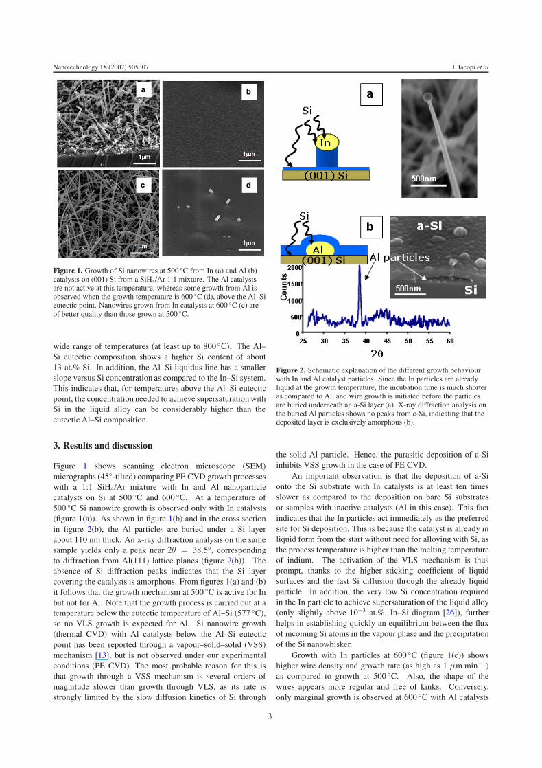
Figure 1. Growth of Si nanowires at 500 ◦C from In (a) and Al (b)catalysts on (001) Si from a SiH4/Ar 1:1 mixture. The Al catalystsare not active at this temperature, whereas some growth from Al isobserved when the growth temperature is 600 ◦C (d), above the Al–Sieutectic point. Nanowires grown from In catalysts at 600 ◦C (c) areof better quality than those grown at 500 ◦C.
wide range of temperatures (at least up to 800 ◦C). The Al–Si eutectic composition shows a higher Si content of about13 at.% Si. In addition, the Al–Si liquidus line has a smallerslope versus Si concentration as compared to the In–Si system.This indicates that, for temperatures above the Al–Si eutecticpoint, the concentration needed to achieve supersaturation withSi in the liquid alloy can be considerably higher than theeutectic Al–Si composition.
3. Results and discussion
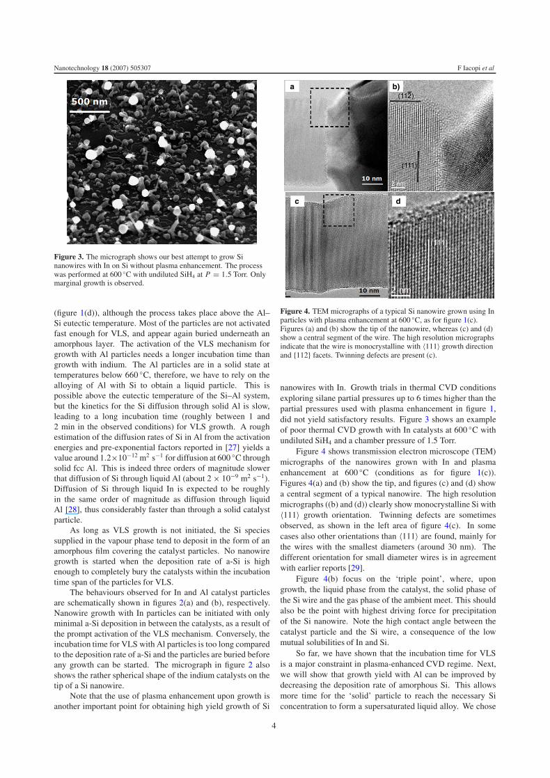
Figure 1 shows scanning electron microscope (SEM)micrographs (45◦-tilted) comparing PE CVD growth processeswith a 1:1 SiH4/Ar mixture with In and Al nanoparticlecatalysts on Si at 500 ◦C and 600 ◦C. At a temperature of500 ◦C Si nanowire growth is observed only with In catalysts(figure 1(a)). As shown in figure 1(b) and in the cross sectionin figure 2(b), the Al particles are buried under a Si layerabout 110 nm thick. An x-ray diffraction analysis on the samesample yields only a peak near 2θ = 38.5◦, correspondingto diffraction from Al(111) lattice planes (figure 2(b)). Theabsence of Si diffraction peaks indicates that the Si layercovering the catalysts is amorphous. From figures 1(a) and (b)it follows that the growth mechanism at 500 ◦C is active for Inbut not for Al. Note that the growth process is carried out at atemperature below the eutectic temperature of Al–Si (577 ◦C),so no VLS growth is expected for Al. Si nanowire growth(thermal CVD) with Al catalysts below the Al–Si eutecticpoint has been reported through a vapour–solid–solid (VSS)mechanism [13], but is not observed under our experimentalconditions (PE CVD). The most probable reason for this isthat growth through a VSS mechanism is several orders ofmagnitude slower than growth through VLS, as its rate isstrongly limited by the slow diffusion kinetics of Si through
Figure 2. Schematic explanation of the different growth behaviourwith In and Al catalyst particles. Since the In particles are alreadyliquid at the growth temperature, the incubation time is much shorteras compared to Al, and wire growth is initiated before the particlesare buried underneath an a-Si layer (a). X-ray diffraction analysis onthe buried Al particles shows no peaks from c-Si, indicating that thedeposited layer is exclusively amorphous (b).
the solid Al particle. Hence, the parasitic deposition of a-Siinhibits VSS growth in the case of PE CVD.
An important observation is that the deposition of a-Sionto the Si substrate with In catalysts is at least ten timesslower as compared to the deposition on bare Si substratesor samples with inactive catalysts (Al in this case). This factindicates that the In particles act immediately as the preferredsite for Si deposition. This is because the catalyst is already inliquid form from the start without need for alloying with Si, asthe process temperature is higher than the melting temperatureof indium. The activation of the VLS mechanism is thusprompt, thanks to the higher sticking coefficient of liquidsurfaces and the fast Si diffusion through the already liquidparticle. In addition, the very low Si concentration requiredin the In particle to achieve supersaturation of the liquid alloy(only slightly above 10−3 at.%, In–Si diagram [26]), furtherhelps in establishing quickly an equilibrium between the fluxof incoming Si atoms in the vapour phase and the precipitationof the Si nanowhisker.
Growth with In particles at 600 ◦C (figure 1(c)) showshigher wire density and growth rate (as high as 1 μm min−1)as compared to growth at 500 ◦C. Also, the shape of thewires appears more regular and free of kinks. Conversely,only marginal growth is observed at 600 ◦C with Al catalysts
3
Nanotechnology 18 (2007) 505307 F Iacopi et al
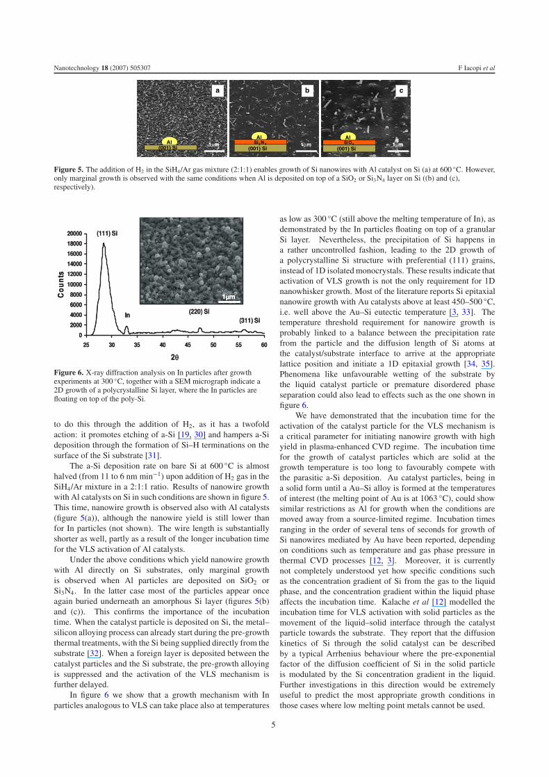
Figure 3. The micrograph shows our best attempt to grow Sinanowires with In on Si without plasma enhancement. The processwas performed at 600 ◦C with undiluted SiH4 at P = 1.5 Torr. Onlymarginal growth is observed.
(figure 1(d)), although the process takes place above the Al–Si eutectic temperature. Most of the particles are not activatedfast enough for VLS, and appear again buried underneath anamorphous layer. The activation of the VLS mechanism forgrowth with Al particles needs a longer incubation time thangrowth with indium. The Al particles are in a solid state attemperatures below 660 ◦C, therefore, we have to rely on thealloying of Al with Si to obtain a liquid particle. This ispossible above the eutectic temperature of the Si–Al system,but the kinetics for the Si diffusion through solid Al is slow,leading to a long incubation time (roughly between 1 and2 min in the observed conditions) for VLS growth. A roughestimation of the diffusion rates of Si in Al from the activationenergies and pre-exponential factors reported in [27] yields avalue around 1.2×10⁻¹² m2 s−1 for diffusion at 600 ◦C throughsolid fcc Al. This is indeed three orders of magnitude slowerthat diffusion of Si through liquid Al (about 2 × 10⁻⁹ m2 s−1).Diffusion of Si through liquid In is expected to be roughlyin the same order of magnitude as diffusion through liquidAl [28], thus considerably faster than through a solid catalystparticle.
As long as VLS growth is not initiated, the Si speciessupplied in the vapour phase tend to deposit in the form of anamorphous film covering the catalyst particles. No nanowiregrowth is started when the deposition rate of a-Si is highenough to completely bury the catalysts within the incubationtime span of the particles for VLS.
The behaviours observed for In and Al catalyst particlesare schematically shown in figures 2(a) and (b), respectively.Nanowire growth with In particles can be initiated with onlyminimal a-Si deposition in between the catalysts, as a result ofthe prompt activation of the VLS mechanism. Conversely, theincubation time for VLS with Al particles is too long comparedto the deposition rate of a-Si and the particles are buried beforeany growth can be started. The micrograph in figure 2 alsoshows the rather spherical shape of the indium catalysts on thetip of a Si nanowire.
Note that the use of plasma enhancement upon growth isanother important point for obtaining high yield growth of Si
a b)
c d
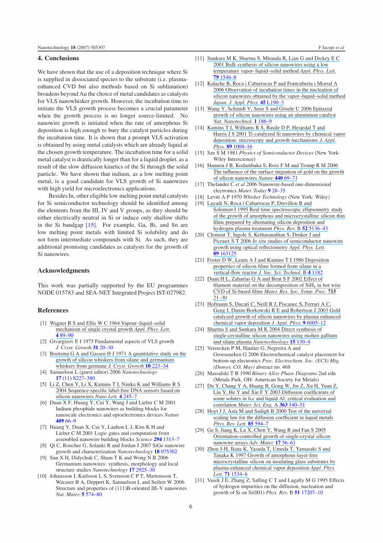
Figure 4. TEM micrographs of a typical Si nanowire grown using Inparticles with plasma enhancement at 600 ◦C, as for figure 1(c).Figures (a) and (b) show the tip of the nanowire, whereas (c) and (d)show a central segment of the wire. The high resolution micrographsindicate that the wire is monocrystalline with 〈111〉 growth directionand {112} facets. Twinning defects are present (c).
nanowires with In. Growth trials in thermal CVD conditionsexploring silane partial pressures up to 6 times higher than thepartial pressures used with plasma enhancement in figure 1,did not yield satisfactory results. Figure 3 shows an exampleof poor thermal CVD growth with In catalysts at 600 ◦C withundiluted SiH4 and a chamber pressure of 1.5 Torr.
Figure 4 shows transmission electron microscope (TEM)micrographs of the nanowires grown with In and plasmaenhancement at 600 ◦C (conditions as for figure 1(c)).Figures 4(a) and (b) show the tip, and figures (c) and (d) showa central segment of a typical nanowire. The high resolutionmicrographs ((b) and (d)) clearly show monocrystalline Si with〈111〉 growth orientation. Twinning defects are sometimesobserved, as shown in the left area of figure 4(c). In somecases also other orientations than 〈111〉 are found, mainly forthe wires with the smallest diameters (around 30 nm). Thedifferent orientation for small diameter wires is in agreementwith earlier reports [29].
Figure 4(b) focus on the ‘triple point’, where, upongrowth, the liquid phase from the catalyst, the solid phase ofthe Si wire and the gas phase of the ambient meet. This shouldalso be the point with highest driving force for precipitationof the Si nanowire. Note the high contact angle between thecatalyst particle and the Si wire, a consequence of the lowmutual solubilities of In and Si.
So far, we have shown that the incubation time for VLSis a major constraint in plasma-enhanced CVD regime. Next,we will show that growth yield with Al can be improved bydecreasing the deposition rate of amorphous Si. This allowsmore time for the ‘solid’ particle to reach the necessary Siconcentration to form a supersaturated liquid alloy. We chose
4
Nanotechnology 18 (2007) 505307 F Iacopi et al
Al(001) Si
1οmAl
(001) SiSi3 N 4 1οm
a b
Al
(001) SiSiO2 1οm
c
Al(001) Si
Al(001) Si
1 m1 mAl
(001) SiSi3 N 4
Al
(001) SiSi3 N 4 1μm
a b
Al
(001) SiSiO2
Al
(001) SiSiO2 1 m1 m
c
μ μ
Figure 5. The addition of H2 in the SiH4/Ar gas mixture (2:1:1) enables growth of Si nanowires with Al catalyst on Si (a) at 600 ◦C. However,only marginal growth is observed with the same conditions when Al is deposited on top of a SiO2 or Si3N4 layer on Si ((b) and (c),respectively).
Figure 6. X-ray diffraction analysis on In particles after growthexperiments at 300 ◦C, together with a SEM micrograph indicate a2D growth of a polycrystalline Si layer, where the In particles arefloating on top of the poly-Si.
to do this through the addition of H2, as it has a twofoldaction: it promotes etching of a-Si [19, 30] and hampers a-Sideposition through the formation of Si–H terminations on thesurface of the Si substrate [31].
The a-Si deposition rate on bare Si at 600 ◦C is almosthalved (from 11 to 6 nm min−1) upon addition of H2 gas in theSiH4/Ar mixture in a 2:1:1 ratio. Results of nanowire growthwith Al catalysts on Si in such conditions are shown in figure 5.This time, nanowire growth is observed also with Al catalysts(figure 5(a)), although the nanowire yield is still lower thanfor In particles (not shown). The wire length is substantiallyshorter as well, partly as a result of the longer incubation timefor the VLS activation of Al catalysts.
Under the above conditions which yield nanowire growthwith Al directly on Si substrates, only marginal growthis observed when Al particles are deposited on SiO2 orSi3N4. In the latter case most of the particles appear onceagain buried underneath an amorphous Si layer (figures 5(b)and (c)). This confirms the importance of the incubationtime. When the catalyst particle is deposited on Si, the metal–silicon alloying process can already start during the pre-growththermal treatments, with the Si being supplied directly from thesubstrate [32]. When a foreign layer is deposited between thecatalyst particles and the Si substrate, the pre-growth alloyingis suppressed and the activation of the VLS mechanism isfurther delayed.
In figure 6 we show that a growth mechanism with Inparticles analogous to VLS can take place also at temperatures
as low as 300 ◦C (still above the melting temperature of In), asdemonstrated by the In particles floating on top of a granularSi layer. Nevertheless, the precipitation of Si happens ina rather uncontrolled fashion, leading to the 2D growth ofa polycrystalline Si structure with preferential (111) grains,instead of 1D isolated monocrystals. These results indicate thatactivation of VLS growth is not the only requirement for 1Dnanowhisker growth. Most of the literature reports Si epitaxialnanowire growth with Au catalysts above at least 450–500 ◦C,i.e. well above the Au–Si eutectic temperature [3, 33]. Thetemperature threshold requirement for nanowire growth isprobably linked to a balance between the precipitation ratefrom the particle and the diffusion length of Si atoms atthe catalyst/substrate interface to arrive at the appropriatelattice position and initiate a 1D epitaxial growth [34, 35].Phenomena like unfavourable wetting of the substrate bythe liquid catalyst particle or premature disordered phaseseparation could also lead to effects such as the one shown infigure 6.
We have demonstrated that the incubation time for theactivation of the catalyst particle for the VLS mechanism isa critical parameter for initiating nanowire growth with highyield in plasma-enhanced CVD regime. The incubation timefor the growth of catalyst particles which are solid at thegrowth temperature is too long to favourably compete withthe parasitic a-Si deposition. Au catalyst particles, being ina solid form until a Au–Si alloy is formed at the temperaturesof interest (the melting point of Au is at 1063 ◦C), could showsimilar restrictions as Al for growth when the conditions aremoved away from a source-limited regime. Incubation timesranging in the order of several tens of seconds for growth ofSi nanowires mediated by Au have been reported, dependingon conditions such as temperature and gas phase pressure inthermal CVD processes [12, 3]. Moreover, it is currentlynot completely understood yet how specific conditions suchas the concentration gradient of Si from the gas to the liquidphase, and the concentration gradient within the liquid phaseaffects the incubation time. Kalache et al [12] modelled theincubation time for VLS activation with solid particles as themovement of the liquid–solid interface through the catalystparticle towards the substrate. They report that the diffusionkinetics of Si through the solid catalyst can be describedby a typical Arrhenius behaviour where the pre-exponentialfactor of the diffusion coefficient of Si in the solid particleis modulated by the Si concentration gradient in the liquid.Further investigations in this direction would be extremelyuseful to predict the most appropriate growth conditions inthose cases where low melting point metals cannot be used.
5
Nanotechnology 18 (2007) 505307 F Iacopi et al
4. Conclusions
We have shown that the use of a deposition technique where Siis supplied in dissociated species to the substrate (i.e. plasma-enhanced CVD but also methods based on Si sublimation)broadens beyond Au the choice of metal candidates as catalystsfor VLS nanowhisker growth. However, the incubation time toinitiate the VLS growth process becomes a crucial parameterwhen the growth process is no longer source-limited. Nonanowire growth is initiated when the rate of amorphous Sideposition is high enough to bury the catalyst particles duringthe incubation time. It is shown that a prompt VLS activationis obtained by using metal catalysts which are already liquid atthe chosen growth temperature. The incubation time for a solidmetal catalyst is drastically longer than for a liquid droplet, as aresult of the slow diffusion kinetics of the Si through the solidparticle. We have shown that indium, as a low melting pointmetal, is a good candidate for VLS growth of Si nanowireswith high yield for microelectronics applications.
Besides In, other eligible low melting point metal catalystsfor Si semiconductor technology should be identified amongthe elements from the III, IV and V groups, as they should beeither electrically neutral in Si or induce only shallow shiftsin the Si bandgap [15]. For example, Ga, Bi, and Sn arelow melting point metals with limited Si solubility and donot form intermediate compounds with Si. As such, they areadditional promising candidates as catalysts for the growth ofSi nanowires.
Acknowledgments
This work was partially supported by the EU programmesNODE 015783 and SEA-NET Integrated Project IST-027982.
References
[1] Wagner R S and Ellis W C 1964 Vapour–liquid–solidmechanism of single crystal growth Appl. Phys. Lett.4 89–90
[2] Givargizov E I 1975 Fundamental aspects of VLS growthJ. Cryst. Growth 31 20–30
[3] Bootsma G A and Gassen H J 1971 A quantitative study on thegrowth of silicon whiskers from silane and germaniumwhiskers from germane J. Cryst. Growth 10 223–34
[4] Samuelson L (guest editor) 2006 Nanotechnology17 (11) S227–380
[5] Li Z, Chen Y, Li X, Kamins T I, Nauka K and Williams R S2004 Sequence-specific label-free DNA sensors based onsilicon nanowires Nano Lett. 4 245–7
[6] Duan X F, Huang Y, Cui Y, Wang J and Lieber C M 2001Indium phosphide nanowires as building blocks fornanoscale electronics and optoelectronics devices Nature409 66–9
[7] Huang Y, Duan X, Cui Y, Lauhon L J, Kim K H andLieber C M 2001 Logic gates and computation fromassembled nanowire building blocks Science 294 1313–7
[8] Qi C, Roncher G, Solanki R and Jordan J 2007 SiGe nanowiregrowth and characterization Nanotechnology 18 075302
[9] Sun X H, Didychuk C, Sham T K and Wong N B 2006Germanium nanowires: synthesis, morphology and localstructure studies Nanotechnology 17 2925–30
[10] Johansson J, Karlsson L S, Svensson C P T, Martensson T,Wacaser B A, Deppert K, Samuelson L and Seifert W 2006Structure and properties of (111)B-oriented III–V nanowiresNat. Mater. 5 574–80
[11] Sunkara M K, Sharma S, Miranda R, Lian G and Dickey E C2001 Bulk synthesis of silicon nanowires using a lowtemperature vapor–liquid–solid method Appl. Phys. Lett.79 1546–8
[12] Kalache B, Roca i Cabarrocas P and Fontcuberta i Morral A2006 Observation of incubation times in the nucleation ofsilicon nanowires obtained by the vapor–liquid–solid methodJapan. J. Appl. Phys. 45 L190–3
[13] Wang Y, Schmidt V, Senz S and Gosele U 2006 Epitaxialgrowth of silicon nanowires using an aluminium catalystNat. Nanotechnol. 1 186–9
[14] Kamins T I, Williams R S, Basile D P, Hesjedal T andHarris J S 2001 Ti-catalyzed Si nanowires by chemical vapordeposition: microscopy and growth mechanisms J. Appl.Phys. 89 1008–16
[15] Sze S M 1981 Physics of Semiconductor Devices (New York:Wiley Interscience)
[16] Hannon J B, Kodambaka S, Ross F M and Tromp R M 2006The influence of the surface migration of gold on the growthof silicon nanowires Nature 440 69–71
[17] Thelander C et al 2006 Nanowire-based one-dimensionalelectronics Mater. Today 9 28–35
[18] Levitt A P 1970 Whisker Technology (New York: Wiley)[19] Layadi N, Roca i Cabarrocas P, Drevillon B and
Solomon I 1995 Real time spectroscopic ellipsometry studyof the growth of amorphous and microcrystalline silicon thinfilms prepared by alternating silicon deposition andhydrogen plasma treatment Phys. Rev. B 52 5136–43
[20] Clement T, Ingole S, Ketharanathan S, Druker J andPicraux S T 2006 In situ studies of semiconductor nanowiregrowth using optical reflectometry Appl. Phys. Lett.89 163125
[21] Foster D W, Learn A J and Kamins T I 1986 Depositionproperties of silicon films formed from silane in avertical-flow reactor J. Vac. Sci. Technol. B 4 1182
[22] Duan H L, Zaharias G A and Bent S F 2002 Effect offilament material on the decomposition of SiH4 in hot wireCVD of Si-based films Mater. Res. Soc. Symp. Proc. 71521–30
[23] Hofmann S, Ducati C, Neill R J, Piscanec S, Ferrari A C,Geng J, Dunin-Borkowski R E and Robertson J 2003 Goldcatalyzed growth of silicon nanowires by plasma enhancedchemical vapor deposition J. Appl. Phys. 9 6005–12
[24] Sharma S and Sunkara M K 2004 Direct synthesis ofsingle-crystalline silicon nanowires using molten galliumand silane plasma Nanotechnology 15 130–4
[25] Vereecken P M, Hautier G, Negreira A andGroeseneken G 2006 Electrochemical catalyst placement forbottom-up electronics Proc. Electrochem. Soc. (ECS) Mtg.(Denver, CO, May) abstract no. 468
[26] Massalski T B 1990 Binary Alloy Phase Diagrams 2nd edn(Metals Park, OH: American Society for Metals)
[27] Du Y, Chang Y A, Huang B, Gong W, Jin Z, Xu H, Yuan Z,Liu Y, He Y and Xie F Y 2003 Diffusion coefficients ofsome solutes in fcc and liquid Al: critical evaluation andcorrelation Mater. Sci. Eng. A 363 140–51
[28] Hoyt J J, Asta M and Sadigh B 2000 Test of the universalscaling law for the diffusion coefficient in liquid metalsPhys. Rev. Lett. 85 594–7
[29] Ge S, Jiang K, Lu X, Chen Y, Wang R and Fan S 2005Orientation-controlled growth of single-crystal siliconnanowire arrays Adv. Mater. 17 56–61
[30] Zhou J-H, Ikuta K, Yasuda T, Umeda T, Yamasaki S andTanaka K 1997 Growth of amorphous-layer-freemicrocrystalline silicon on insulating glass substrates byplasma-enhanced chemical vapor deposition Appl. Phys.Lett. 71 1534–6
[31] Vasek J E, Zhang Z, Salling C T and Lagally M G 1995 Effectsof hydrogen impurities on the diffusion, nucleation andgrowth of Si on Si(001) Phys. Rev. B 51 17207–10
6

Nanotechnology 18 (2007) 505307 F Iacopi et al
[32] Dai L, You L P, Duan X F, Lian W C and Qin G G 2005Growth of silica nanowire arrays by reaction of Si substratewith oxygen using Ga as catalyst Phys. Lett. A 335 304–9
[33] Weber W M et al 2006 Silicon-nanowire transistors withintruded nickel-silicide contacts Nano Lett. 6 2660–6
[34] Baliga J 1986 Epitaxial Silicon Technology (London:Academic)
[35] Dubrovskii V G and Sibirev N V 2004 Growth rate of a crystalfacet of arbitrary size and growth kinetics of verticalnanowires Phys. Rev. E 70 031604
7