
Lukas Kinner BSc Inkjet Printed Metal Grid-Based ITO-free ...
Upload
independentCategory
view
2download
0
Inkjet Printing of Catalyst-Inks on Si Wafers and the Subsequent Synthesis of Carbon Nanotubes by Chemical Vapour Deposition
M. Mansoor1,a, I. Kinloch2,b and B. Derby2,c 1Institute of Industrial Control System, P.O Box 1398, Rawalpindi, Pakistan
2Materials Science Centre, University of Manchester, UK [email protected], [email protected] , [email protected]
Keywords: Catalytic ink formulation, inkjet printing, CCVD SEM, TEM, and Raman spectroscopy.
Abstract. The production of substrates coated with carbon nanotubes (CNTs) in well-defined patterns is desirable for sensor applications. In the present work, nickel based catalytic inks were prepared and printed on silicon substrates using inkjet delivery. Subsequently, the substrates were subjected to calcination and chemical vapour deposition for the growth of aligned CNTs. Scanning electron microscopy, transmission electron microscopy and Raman spectroscopy were used to characterize the CNTs. Various concentrations and formulations of ink preparations were studied to investigate the effect of these parameters on the growth and structure of the CNTs.
Introduction
Carbon nanotubes (CNTs) are thin rolled-up graphene-film structures which have demonstrated remarkable physical, chemical and mechanical properties. The intrinsic characteristics of CNTs, for example, excellent thermal conductivity [1-3], superior mechanical strength [4-6], tailor-able electrical conduction [7-13] and enhanced field-emission [14, 15], have been successfully realised in numerous applications [16-19]. The electronic or electrochemical applications have shown particular promise, with example applications including field emission displays [20], nano-devices [21], Li-ion batteries [22], sensors [23], electro-active composites [24] and fuel cells [25]. The optimal performance of these applications can require the selective placement and aligned assembly of CNTs [26]. CNTs can be produced by a variety of techniques, including laser ablation process, electric arc discharge technique, flame synthesis, solar energy route and catalytic chemical vapour deposition [27-30]. Most of these processes have certain limitations which restrict their application to mass production. Catalytic chemical vapour deposition (CCVD) technique, though, has been reported periodically for large scale production of CNTs at low temperatures with relatively better process control and sensitivity [31-34]. In the CCVD method, a carbonaceous source, usually a hydrocarbon gas is decomposed in the presence of a transition metal catalyst to produce CNTs. The catalyst and hence nanotubes produced can be supported on a substrate or free standing. Generally, the catalyst is made either by impregnating a catalyst precursor into a powdered catalyst support, such as silica powder and alumina powder[35,36] or by decomposing the precursor in the gas phase together with a carbon source at elevated temperature [37,38]. Inkjet printing of electrically conductive patterns of CNT by preparing inks through sonication and acid refluxing of CNT ink functionalisation has been reported earlier [39]. The process has generic wetting limitations to hydrophobic substrates, which subsequently could result in possible reduction in CNT to substrate adhesion. The area-selective synthesis of well-organized CNTs on pre-patterned templates using CCVD method opens up further novel fields for advanced future applications. The key issue for the applications is patterning of the catalyst. For the purpose, two primary techniques have been reported so far: the first one is based on lithography, which uses an electron-beam to pattern nickel thin film and obtained patterned arrays of nanotubes by subsequent CVD process [40]. The other is based on micro-contact printing. Kind et al. [41] has shown aligned CNT arrays patterned by
Key Engineering Materials Vol. 442 (2010) pp 7-14Online available since 2010/Jun/02 at www.scientific.net© (2010) Trans Tech Publications, Switzerlanddoi:10.4028/www.scientific.net/KEM.442.7
All rights reserved. No part of contents of this paper may be reproduced or transmitted in any form or by any means without the written permission of TTP,www.ttp.net. (ID: 141.213.236.110, University of Michigan Library, Media Union Library, Ann Arbor, United States of America-25/06/13,10:15:30)
stamping of iron catalyst on the substrate. The patterning process consisted of a poly-dimethylsiloxane stamp whose surface was wetted with ethanolic solution of iron nitrate. The technique has difficulties of patterning position; moreover, stamps are fabricated by lithography. Direct printing of the catalysts using ink-jet printing (IJP) techniques is the latest approach to grow desired patterns of CNTs on a variety of substrates. The IJP technique has flexibility to the catalysts and their patterning, it is possible to mark the position, patterns can be controlled by nozzles movement adjustment, and precise delivery of the catalyst to ensure controlled CNT distribution. Some researchers reported successful experimentation of IJP of catalysts and subsequent CNT growth for various electronic applications [42,43]. In present work we investigated the influence of ink formulation on its physical properties which may affect subsequent IJP process, and catalyst distribution in the printed patterns on silicon (Si) wafers. The printed patterns of catalyst were further grown to CNTs by CCVD method.
Experimental
The experimental consists of catalytic ink formulation, characterization, and printing on Si substrates which followed by CVD growth of CNTs out of the printed substrates. For ink formulation ultrasonic stirring and refluxing was used. These inks were characterized by viscosity meter and liquid-solid contact angle analysers. A DMP 2831 inkjet printer (Fujifilm Dimatix, Santa Clara, CA, USA) was used to print catalytic inks on the Si wafer substrates. A horizontal CVD reactor was used to grow CNTs, which were subsequently characterized by SEM, TEM, and Raman spectroscopy.
Preparation of Inks. Ink formulation (Table-1) was based upon three constituents; catalyst, carrier, and dispersant. Function of catalyst was to support subsequent CVD process for CNT growth, whereas carrier or solvent was used to facilitate suspension of catalytic particles to be uniformly distributed by the dispersant.
Table 1 The ink formulations used for IJP.
Formulation Nomenclature
IJP-1 IJP-2 IJP-3 IJP-4
Ethanol (ml) 60 37 37 60
Water(ml) 40 - - 10
Nickel Nitrite (M) 0.1 to 0.9 0.1 to 0.9 0.4 0.4
Ethylene Glycol (ml) - 63 63 40
Tetraethyl Orthosilicate (M) - - 0.1 to 0.9 0.4
Characterization of the Inks. The formulated inks were characterized by viscosity and contact angle measurements. It was a prerequisite for the inks to have a viscosity range between 10-20 mPas for reproducible and successive inkjet printing. The contact angle measurements yielded the wetting property of the inks on a silicon surface. The contact angle controls the size of the deposit by defining the equilibrium spread drop diameter.
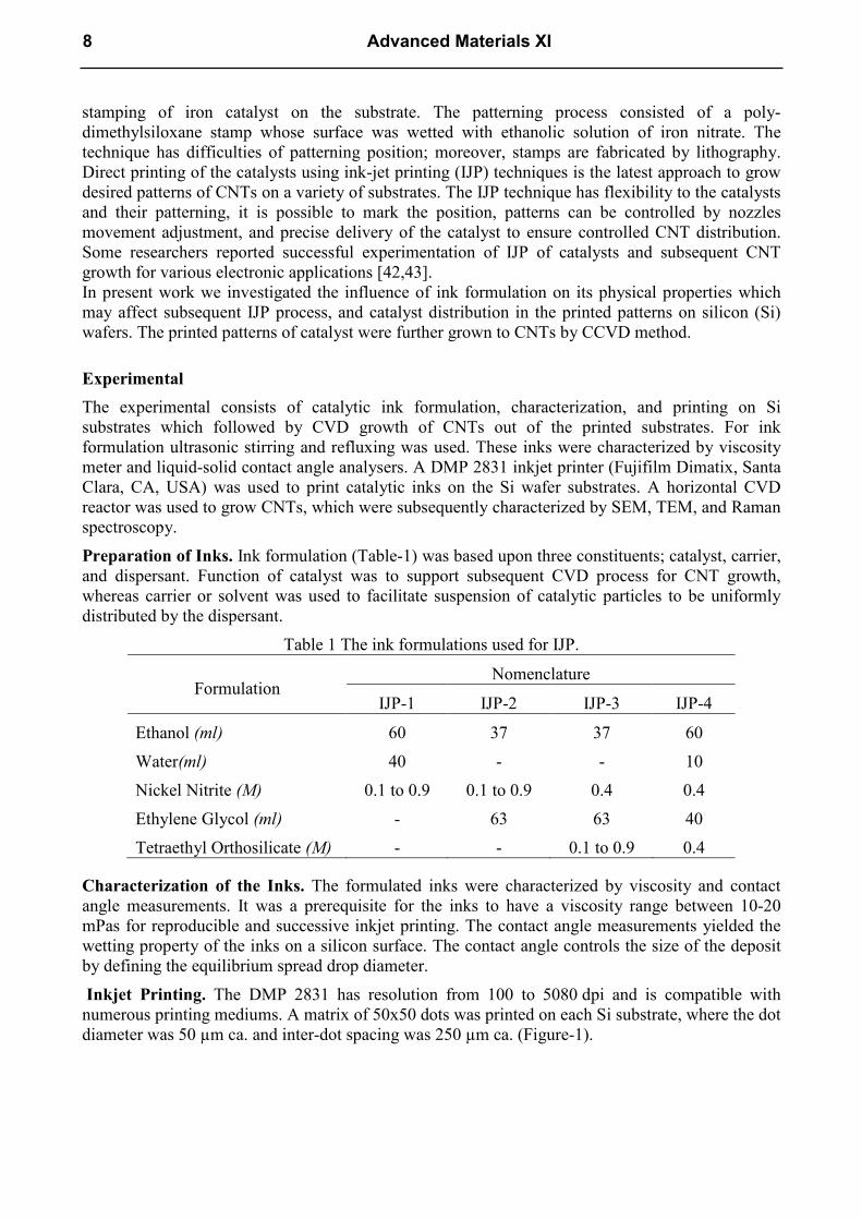
Inkjet Printing. The DMP 2831 has resolution from 100 to 5080 dpi and is compatible with numerous printing mediums. A matrix of 50x50 dots was printed on each Si substrate, where the dot diameter was 50 µm ca. and inter-dot spacing was 250 µm ca. (Figure-1).
8 Advanced Materials XI

Chemical Vapour Deposition. A horizontal CVD reactor was used to grow CNT on the printed Si substrates. The reactor consisted of a horizontal tube furnace with a quartz glass reaction tube through which mixtures of nitrogen, argon, hydrogen, methane and/or acetylene gases could be passed. The reactor environment was computer controlled. Flow rates of inert and reactive gases could be as high as 100 sccm and 10 sccm, respectively. The flu gases were passed through a water-trap bubbler, which served two purposes; first it absorbed water soluble hazardous fumes and second it indicated regular flow of gases through the reactor. A schematic view of the CVD reactor is shown in Figure-2.
Characterisation of the C Ts. A scanning electron microscope equipped with field emission gun (FEG-SEM), transmission electron microscope (TEM) and Raman spectroscope (excitation wavelength of 633 nm) was used to evaluate CNTs.
Results and discussion
The formulation of the inks had a significant effect on the viscosity and liquid solid contact angle of the inks (Table-2). The addition of ethylene glycol and tetraethyl orthosilicate (TEOS) increased the viscosity and decreased the liquid to metal contact angle, respectively (Figure-3). As described earlier, the inkjet printer used was limited to printing inks which had viscosities ranging from 10 to 20mPas. Moreover, the inks having higher contact angles with the substrate (Si) caused a concentration gradient of catalytic particles within droplet when printed. The criteria indicated that IJP-1 was not suitable for printing.
Fig. 1 Printed dot matrix pattern of experimental inks using the MPS.
PC Controlled Gases Inlet
Gases Outlet
Tube Furnace
Quartz Tube Printed Substrate
Fig. 2 Schematic diagram of the CVD reactor
150µm
Key Engineering Materials Vol. 442 9

a. b.
Fig. 3 The effect of TEOS on the contact angle inks with the silicon wafer a) Formulation with no TEOS (IJP-2) and b) Formulation with TEOS (IJP-3).
Table 2 Results of viscosity and contact angle measurement
Inks Viscosity (mPas) Contact angle
IJP-1 1.9 - 7.8 60°- 80 °
IJP-2 12.4 - 14.5 35°- 40 °
IJP-3 15.5 - 18.4 3.5°- 5.5 °
IJP-4 19.1 - 22.3 3.8°- 4.9°
After printing, the substrates were placed in CVD reactor for calcination and subsequent CNT growth. Firgure-5a shows the calcination cycle, where the printed substrates were heated to 400°C in air to reduce nickel nitrate to nickel oxide. During calcination splashing of catalyst occurred and caused dispersion of catalysis on unprinted regions. This problem was rectified by slow heating, see Figure-4. Inks calcination was followed by CNT synthesis. A typical growth cycle is shown in Figure-5b.
During SEM studies it was observed that after printing, ink dots have a uniform catalytic distribution which was affected by calcination treatment because volatile hydrocarbons left the printed dots at high temperature causing fissures and cracks. These cracks could be minimised by controlling heating rate and/or oxidation rate during calcination, see Figure-6.
Droplet
Si Substrate
a. b.
Fig. 4 (a) splashes of catalyst on the un-printed regions; eliminated by controlled heating rate during calcination (b).
a. b.
10 Advanced Materials XI

Subsequent studies by SEM, TEM and Raman spectroscopy indicated that the addition of ethylene glycol and TEOS has decreased the defect ration in the CNTs. Figures 7 and 8 shows the CNTs synthesized by inks IJP-2 and IJP-4. Figure-9 shows the Raman spectra of the CNTs produced as a
Fig. 5 Thermal cycles of the CVD process
Fig. 6 SEM images of the catalytic ink dots before (a) and after (b) calcination. Inset is a high magnification image of the selected area showing nickel oxide particles.
a. b.
Key Engineering Materials Vol. 442 11

function of ink formulation. The degree of crystallinity in the samples is related to the relative intensities of the G and D peaks. It can be seen that IJP-4 produced the high quality nanotubes.
Fig. 7 SEM images of a) IJP-2 and b). IJP-4 inks after CVD treatment – insets are respective micrographs at higher magnifications.
Fig. 8 TEM micrographs of the CNTs grown on a) IJP-2 and b) IJP-4 inks.
a.
65nm
b.
65nm
a.
b.
12 Advanced Materials XI

Fig. 9 Raman spectroscopy of the CNTs. Respective D and G bands indicate the lowering of defect densities in the CNTs from IJP-1 to IJP-4 inks.
Conclusion Catalytic inks were successfully prepared and used for the printing by a DMP. These printed patterns were used as catalytic templates for CNT synthesis by CVD. It was observed that ethylene glycol and TEOS not only improved the viscosity and wetting of the inks but also decreased the structural imperfections of the subsequently grown CNTs.
References
[1] R. S. Ruoff, D. C. Lorents, Carbon (1995), 33, p-925 [2] J.W. Che, T. Cagin, W. A. Goddard, Nanotechnology (2000), 11, p-65 [3] S. Berber, Y. K. Kwon, D. Tomanek, Phys. Rev. Lett. (2000), 84, p-4613 [4] A. Y. Cao, V. P. Veedu, X. S. Li, Z. L. Yao, M. N. Ghasemi- Nejhad, P. M. Ajayan, Nat.
Mater. (2005), 4, p-540 [5] H. E. Troiani, M. Miki-Yoshida, G. A. Camacho-Bragado, M. A. L. Marques, A. Rubio, J.
A. Ascencio, M. Jose-Yacaman, Nano Lett. 3, (2003), p-751 [6] M. Sammalkorpi, A. Krasheninnikov, A. Kuronen, K. Nordlund, K. Kaski, Phys. Rev. B 70,
(2004), p-416 [7] S. Li, Z. Yu, C. Rutherglen, P. J. Burke, Nano Lett. (2004), 4, p-2003 [8] G. Gruner, Proc. SPIE Int. Soc. Opt. Eng. 5592, (2005), p-175 [9] W. Hoenlein, F. Kreupl, G. S. Duesberg, A. P. Graham, M. Liebau, R. Seidel, E. Unger, AIP
Conf. Proc. 723, (2004), p-565
IJP-1
IJP-2
IJP-3
IJP-4
Key Engineering Materials Vol. 442 13

[10] L. B. Kish, P. M. Ajayan, Appl. Phys. Lett. 86, (2005), p-106 [11] J. E. Fischer, H. Dai, A. Thess, R. Lee, N. M. Hanjani, D. L.Dehaas, R. E. Smalley, Phys.
Rev. B 55, (1997), R4921 [12] B.Xiang, Y. Zhang, T. H. Wang, J. Xu, D. P. Yu, Mater. Lett. 60, (2006), p-754 [13] A. P. Graham, G. S. Duesberg, R. V. Seidel, M. Liebau, E.Unger, W. Pamler, F. Kreupl, W.
Hoenlein, Small 1,(2005), p-382 [14] W. A. Deheer, A. Chatelain, D. Ugarte, Science 270, (1995), p-1179 [15] J. T. H. Tsai, H. C. Ko, Appl. Phys. Lett. 88, 13, (2006), p-104 [16] A. Modi, N. Koratkar, E. Lass, B. Q. Wei, P. M. Ajayan, Nature, 424, (2003), p-171 [17] H. Dai, Acc. Chem. Res. 35, (2002), p-1035 [18] S. Chopra, K. McGuire, N. Gothard, A. M. Rao, A. Pham, Appl.Phys. Lett. 83, (2003), p-
2280 [19] M. Terrones, A. Jorio, M. Endo, A. M. Rao, Y. A. Kim, T. Hayashi, H. Terrones, J.-C.
Charlier, G.Dresselhaus, M. S. Dresselhaus, Mater Today 7, (2004), p-30 [20] Y. Saito, K. Hamaguchi, K. Hata, K. Uchida, Y. Tasaka, F., Ikazaki, M. Yumura, A.
Kasuya, I. Nishina, Nature 389 (1997), p-554 [21] K. Tsukagoshi, B.W. Alphenaar, H. Ago, Nature 401 (1999), p-572 [22] G. Maurtin, C. Bousquet, F. Henn, P. Bernier, R. Almairac, B. Simon, Chem. Phys. Lett.
312 (1999), p-14 [23] J. Kong, N.R. Franklin, C. Zhou, M.G. Chapline, S. Peng, K. Cho, H. Dai, Science 287
(2000), p-622 [24] H. Ago, K. Petritsch, M.S.P. Shaffer, A.H. Windle, Adv. Mater. 11 (1999), p-1281 [25] A.C. Dillon, K.M. Jones, T.A. Bekkedahl, C.H. Kiang, D.S. Bethune, M.J. Heben, Nature
386 (1997), p-377 [26] T. Rueckes, K. Kim, E. Joselevich, G.Y. Tseng, C.L. Cheung, Science 289 (2000), p-94 [27] Journet C., W.K. Maser, P. Bernier, A. Loiseau, M.L. dela Chapelle & S. Lefrant, Nature,
388, (1997), p-756 [28] Guo T., C.M. Jin & R.E. Smalley, Chem. Phys. Lett. 243, (1995), p-49 [29] Vander Wal R.L., T.M. Ticlch & V.E. Curtis, Chem. Phys., Lett. 323, (2000), p-217 [30] Laplaze D., P. Berinier, W.K. Maser, G. Flamant, & A. Loiseau, Carbon, 36, (1998), p-685 [31] Colomer J.F., C. Stephan, S. Lefrant, G. Van Tendeloo, I. Willems & Z. Konya, Chem.
Phys. Lett. 317, (2000), p-83 [32] Andrews R., D. Jacques & A.M. Rao, Chem. Phys. Lett. 303, (1999), p-467 [33] Nguyen V.Q, Nguyen D.H, Myungchan A, Yousuk C and Dojin K, Nanotechnology 18
(2007) 345201 (6pp) [34] Yao W, Fei W, Guangsheng G, Hao Y, Physica B 323 (2002) p-327 [35] Cassell A.M., J.A. Raymakers, J. Kong & H. Dai, J. Phys. Chem. B 103, (1999), p-6484 [36] Kitiyanan B., W.E. Alvarez, & D.E. Resasco, Chem. Phys. Lett. 317, (2000), p-493 [37] Cheng H.M., F. Li, G. Su, H.Y. Pan, L.L. He, X. Sun & M.S. Dresselhaus, Appl. Phys. Lett.
72, (1998), 3282–3284 [38] Nilolaev P., M.J. Bronikowski, R.K. Bradley, F. Rohmund, D.T. Colbert, K.A. Smith &
R.E. Smalley, Chem. Phys. Lett. 313, (1999),p-91 [39] Krisztian K, Tero M, Geza T, Heli J, Marja L, Caterina S, Saikat T, Swastik K, Robert V
and Pulickel M. A, Small, 2, No. 8-9, (2006), p-1021 [40] Z. F. Ren, Z. P. Huang, D. Z. Wang, J. G. Wen, J. W. Xu, J. H. Wang, L. E. Calvet, J. Chen,
J. F. Klemic, and M. A. Reed, Appl. Phys. Lett. 75, (2004), p-1086 [41] H. Kind, J. M. Bonard, L. Forro´, K. Kern, K. Hernadi, L. O. Nilsson, and L. Schlapbach,
Langmuir 16, (2001), p-6877 [42] T. R. Hebner, C. C. Wu, D. Marcy, and J. C. Sturm, Appl. Phys.Lett. 72, 519 (1998), p-104 [43] H. Sirringhaus, T. Kawase, R. H. Friend, T. Shimoda, M. Inbasekaran, W. Wu, and E. P.
Woo, Science 290, (2002), p-21238
14 Advanced Materials XI

Advanced Materials XI 10.4028/www.scientific.net/KEM.442 Inkjet Printing of Catalyst-Inks on Si Wafers and the Subsequent Synthesis of Carbon Nanotubes by
Chemical Vapour Deposition 10.4028/www.scientific.net/KEM.442.7
DOI References
[11] J. E. Fischer, H. Dai, A. Thess, R. Lee, N. M. Hanjani, D. L.Dehaas, R. E. Smalley, Phys. Rev. B 55,
(1997), R4921
doi:10.1103/PhysRevB.55.R4921 [37] Cheng H.M., F. Li, G. Su, H.Y. Pan, L.L. He, X. Sun & M.S. Dresselhaus, Appl. Phys. Lett. 72, (1998),
3282–3284
doi:10.1063/1.121624
Copyright © 2022 FDOKUMEN