Mechanical properties of thin silicon wafers for photovoltaic ...
241
HAL Id: tel-03127335 https://tel.archives-ouvertes.fr/tel-03127335 Submitted on 1 Feb 2021 HAL is a multi-disciplinary open access archive for the deposit and dissemination of sci- entific research documents, whether they are pub- lished or not. The documents may come from teaching and research institutions in France or abroad, or from public or private research centers. L’archive ouverte pluridisciplinaire HAL, est destinée au dépôt et à la diffusion de documents scientifiques de niveau recherche, publiés ou non, émanant des établissements d’enseignement et de recherche français ou étrangers, des laboratoires publics ou privés. Mechanical properties of thin silicon wafers for photovoltaic applications : Influence of material quality and sawing process Louise Carton To cite this version: Louise Carton. Mechanical properties of thin silicon wafers for photovoltaic applications : Influence of material quality and sawing process. Mechanics [physics.med-ph]. Université de Lyon, 2020. English. NNT : 2020LYSEI107. tel-03127335
-
Upload
khangminh22 -
Category
Documents
-
view
0 -
download
0
Transcript of Mechanical properties of thin silicon wafers for photovoltaic ...

HAL Id: tel-03127335https://tel.archives-ouvertes.fr/tel-03127335
Submitted on 1 Feb 2021
HAL is a multi-disciplinary open accessarchive for the deposit and dissemination of sci-entific research documents, whether they are pub-lished or not. The documents may come fromteaching and research institutions in France orabroad, or from public or private research centers.
L’archive ouverte pluridisciplinaire HAL, estdestinée au dépôt et à la diffusion de documentsscientifiques de niveau recherche, publiés ou non,émanant des établissements d’enseignement et derecherche français ou étrangers, des laboratoirespublics ou privés.
Mechanical properties of thin silicon wafers forphotovoltaic applications : Influence of material quality
and sawing processLouise Carton
To cite this version:Louise Carton. Mechanical properties of thin silicon wafers for photovoltaic applications : Influence ofmaterial quality and sawing process. Mechanics [physics.med-ph]. Université de Lyon, 2020. English.�NNT : 2020LYSEI107�. �tel-03127335�

N°d’ordre NNT : 2020LYSEI107
THÈSE de DOCTORAT DE L’UNIVERSITÉ DE LYON opérée au sein de
l’Institut National des Sciences Appliquées de Lyon
École Doctorale N° ED162
MÉCANIQUE, ÉNERGÉTIQUE, GÉNIE CIVIL, ACOUSTIQUE
Spécialité de doctorat : Génie Mécanique
Soutenue publiquement le 01/12/2020 par :
Louise CARTON
Mechanical properties of thin silicon
wafers for photovoltaic applications: influence of material quality and sawing
process
Devant le jury composé de :
SCHOENFELDER Stephan Professeur des universités HTWK Leipzig Rapporteur
PAGGI Marco Professeur des universités IMT Lucca Rapporteur
GUILLEMOLES Jean-François Directeur de recherche CNRS Président
NELIAS Daniel Professeur des universités INSA Lyon Directeur de thèse
RIVA Roland Ingénieur chercheur CEA-INES Co-directeur
FOURMEAU Marion Maître de conférences INSA Lyon Co-encadrante
MEHL Céline Ingénieure ADEME Invitée
Cette thèse est accessible à l'adresse : http://theses.insa-lyon.fr/publication/2020LYSEI107/these.pdf © [L. Carton], [2020], INSA Lyon, tous droits réservés

Département FEDORA – INSA Lyon - Ecoles Doctorales – Quinquennal 2016-2020
SIGLE ECOLE DOCTORALE NOM ET COORDONNEES DU RESPONSABLE
CHIMIE CHIMIE DE LYO N
http://www.edchimie-lyon.fr Sec. : Renée EL MELHEM Bât. Blaise PASCAL, 3e étage
[email protected] INSA : R. GOURDON
M. Stéphane DANIELE Institut de recherches sur la catalyse et l’environnement de Lyon IRCELYON-UMR 5256 Équipe CDFA 2 Avenue Albert EINSTEIN
69 626 Villeurbanne CEDEX
E.E.A. ÉLECTRO NIQ UE,
ÉLECTRO TECHNIQ UE,
AUTO MATIQ UE
http://edeea.ec-lyon.fr Sec. : M.C. HAVGOUDOUKIAN
M. Gérard SCO RLETTI École Centrale de Lyon 36 Avenue Guy DE COLLONGUE 69 134 Écully Tél : 04.72.18.60.97 Fax 04.78.43.37.17
E2M2 ÉVO LUTIO N, ÉCO SYSTÈME,
MICRO BIO LO GIE, MO DÉLISATIO N
http://e2m2.universite-lyon.fr Sec. : Sylvie ROBERJOT Bât. Atrium, UCB Lyon 1 Tél : 04.72.44.83.62
INSA : H. CHARLES
M. Philippe NO RMAND UMR 5557 Lab. d’Ecologie Microbienne Université Claude Bernard Lyon 1 Bâtiment Mendel 43, boulevard du 11 Novembre 1918
69 622 Villeurbanne CEDEX
EDISS INTERDISCIPLINAIRE
SCIENCES-SANTÉ
http://www.ediss-lyon.fr Sec. : Sylvie ROBERJOT Bât. Atrium, UCB Lyon 1 Tél : 04.72.44.83.62 INSA : M. LAGARDE
Mme Sylvie RICARD-BLUM Institut de Chimie et Biochimie Moléculaires et Supramoléculaires (ICBMS) - UMR 5246 CNRS - Université Lyon 1 Bâtiment Curien - 3ème étage Nord 43 Boulevard du 11 novembre 1918 69622 Villeurbanne Cedex Tel : +33(0)4 72 44 82 32
sylvie [email protected]
INFOMATHS INFO RMATIQ UE ET
MATHÉMATIQ UES
http://edinfomaths.universite-lyon.fr Sec. : Renée EL MELHEM Bât. Blaise PASCAL, 3e étage Tél : 04.72.43.80.46
M. Hamamache KHEDDO UCI Bât. Nautibus 43, Boulevard du 11 novembre 1918 69 622 Villeurbanne Cedex France Tel : 04.72.44.83.69
Matériaux MATÉRIAUX DE LYO N
http://ed34.universite-lyon.fr Sec. : Stéphanie CAUVIN Tél : 04.72.43.71.70
Bât. Direction
M. Jean-Yves BUFFIÈRE INSA de Lyon MATEIS - Bât. Saint-Exupéry 7 Avenue Jean CAPELLE 69 621 Villeurbanne CEDEX Tél : 04.72.43.71.70 Fax : 04.72.43.85.28
MEGA MÉCANIQ UE, ÉNERGÉTIQ UE,
GÉNIE CIVIL, ACO USTIQ UE
http://edmega.universite-lyon.fr Sec. : Stéphanie CAUVIN
Tél : 04.72.43.71.70
Bât. Direction
M. Jocelyn BONJOUR INSA de Lyon Laboratoire CETHIL Bâtiment Sadi-Carnot 9, rue de la Physique 69 621 Villeurbanne CEDEX
ScSo ScSo*
http://ed483.univ-lyon2.fr Sec. : Véronique GUICHARD INSA : J.Y. TOUSSAINT Tél : 04.78.69.72.76
M. Christian MO NTES Université Lyon 2 86 Rue Pasteur 69 365 Lyon CEDEX 07
*ScSo : Histoire, Géographie, Aménagement, Urbanisme, Archéologie, Science politique, Sociologie, Anthropologie
Cette thèse est accessible à l'adresse : http://theses.insa-lyon.fr/publication/2020LYSEI107/these.pdf © [L. Carton], [2020], INSA Lyon, tous droits réservés

- i -
Abstract
Crystalline silicon is the key material of photovoltaic technology: over 95 % of solar cells use thin silicon slices
as base substrates. These so-called wafers are obtained by wire sawing of the solid bricks, a step which
accounts for a significant portion of the total photovoltaic module cost. A better use of silicon material is
therefore a privileged pathway towards significant reduction of the solar energy production costs, thereby
enabling a sustainable and rapid growth. In practice, enhancing material yield implies reducing wafer as-cut
thickness as well as the diameter of the cutting wires. Nevertheless, silicon remains a brittle crack-sensitive
material and the increase in breakage rates when handling these thin wafers is a major obstacle to the
economic benefit. In this context, it is essential to improve our understanding of the mechanisms responsible
for wafer embrittlement and failure. Only in this way will we be able to establish recommendations for the
manufacturing of silicon wafers, as well as to propose adjusted handling technologies.
This work investigates the mechanical properties of silicon wafers obtained using diamond wire sawing. We
developed a mechanical characterization methodology suited for these thin, brittle samples, combining
destructive 4-line and biaxial bending tests with dynamic impacts. This methodology was applied on more
than 7 000 wafers sawn in our laboratory equipment using known and controlled parameters. Jointly, finite
element simulations were implemented to better understand the underlying phenomena. In parallel, we
characterized the properties of the as-cut wafer surface using topology and microscopy (optical, confocal,
scanning electron) techniques, as well as through evaluation of microcracks depth.
With the ambition to understand which of the typical defects present in a silicon wafer are the most critical
regarding mechanical failure, we implemented an original procedure to isolate their respective influence.
The results obtained disprove the commonly accepted fact that edge defects are the main origin of failure,
and show that the most dangerous mechanical damage is located in a thin subsurface layer (< 3 µm), which
is generated during the sawing step. By coupling 4-line bending and dynamic tests on wafers of different
as-cut thicknesses (from 180 to 100 µm), we demonstrated that thinner wafers exhibit an increased bending
flexibility without alteration of their intrinsic mechanical strength (failure stress), accompanied however by a
higher risk of failure following an edge impact. Through 4-line bending tests on samples obtained from
bricks of different crystallinity sawn using identical conditions, we highlighted that the presence of structural
defects in multicrystalline and mono-like silicon is indirectly responsible for the lower fracture strength of the
wafers. The increased suffering of the diamond wire when cutting through these defects generated indeed
deeper microcracks than on the monocrystalline samples. Finally, through a design of experiment approach,
we show that the characteristics of the diamond wire play a more important role on the mechanical
properties of the resulting wafers than the parameters of the sawing process.
KEYWORDS: photovoltaic solar cell, silicon wafer, diamond wire sawing, mechanical strength, fracture,
subsurface damage, TTV, 4-line bending, Ring on Ring, impact tests
Cette thèse est accessible à l'adresse : http://theses.insa-lyon.fr/publication/2020LYSEI107/these.pdf © [L. Carton], [2020], INSA Lyon, tous droits réservés

- ii -
Résumé
Le silicium cristallin est le matériau clé de la technologie photovoltaïque : plus de 95 % des cellules solaires
sont élaborées à partir de tranches fines de silicium. Ces wafers sont obtenus par découpe au fil diamanté
de briques, étape qui représente une part significative du coût final du module photovoltaïque. Une meilleure
utilisation du matériau silicium constitue alors une piste privilégiée pour diminuer significativement les coûts
de production d’électricité photovoltaïque, et permettre ainsi de maintenir une croissance élevée et durable.
En pratique, l’amélioration de ce rendement matière passe par une diminution de l’épaisseur des wafers et
du diamètre des fils de découpe. Néanmoins, le silicium reste un matériau fragile sensible à la fissuration, et
l’augmentation des taux de casse de ces substrats fins durant les étapes de manipulation constitue un
obstacle majeur au gain économique potentiel. Dans ce contexte, il est primordial d’améliorer notre
compréhension des mécanismes de rupture et de fragilisation des wafers. C’est à cette condition que nous
pourrons établir des recommandations sur la fabrication et la mise en forme du silicium, ainsi que proposer
des techniques de manipulation adéquates.
Ce travail de thèse étudie les propriétés mécaniques des wafers de silicium obtenus par découpe au fil
diamanté. Nous avons développé une méthodologie de caractérisation mécanique adaptée à la fragilité de
ces échantillons, en combinant des essais de rupture de flexion 4-lignes et biaxiale, ainsi que des sollicitations
dynamiques par chocs. Cette méthodologie a pu être appliquée à plus de 7 000 wafers découpés dans notre
scie de laboratoire avec des conditions et paramètres connus. Conjointement, des simulations numériques
par la méthode des éléments finis ont permis de mieux comprendre les phénomènes mis en jeux. En
parallèle, nous avons caractérisé les propriétés de la surface brute de découpe des wafers au moyen de
techniques de topologie, de microscopie (optique, confocale, électronique à balayage) et d’évaluation de la
profondeur de microfissures.
Avec l’ambition de comprendre quels défauts typiques d’un wafer de silicium sont les plus critiques pour sa
défaillance mécanique, nous avons mis en place une procédure originale consistant à isoler leur influence
respective. Les résultats obtenus infirment l’hypothèse communément admise selon laquelle les défauts de
bords sont la principale source de rupture, et démontrent que l’endommagement le plus dangereux se situe
dans une couche de faible épaisseur (< 3 µm) sous la surface, générée lors de l’étape de découpe. En
couplant des tests de flexion avec des essais dynamiques sur des wafers de différentes épaisseurs (de 180 à
100 µm), nous avons montré que l’amincissement des plaquettes permet un gain de flexibilité sans
diminution de la résistance mécanique intrinsèque (contrainte à rupture), mais qui s’accompagne d’un risque
plus élevé de ruine suite à un impact sur la tranche. Au travers d’essais de flexion 4 lignes sur des échantillons
issus de briques de cristallinité différentes mais découpés dans les mêmes conditions, nous avons mis en
évidence que l’existence de défauts structurels dans le s ilicium multicristallin et mono-like est indirectement
responsables de la diminution de la résistance à rupture des wafers. En effet, la difficulté accrue du fil à
traverser ces défauts se traduit par des microfissures plus profondes que dans les échantillons
monocristallins. Enfin, une approche par plans d’expérience nous permet de comprendre que les
caractéristiques du fil diamanté utilisé jouent un rôle plus important sur les propriétés mécaniques des wafers
obtenus que les paramètres du procédé de découpe.
MOTS-CLÉS : cellule solaire photovoltaïque, wafer de silicium, découpe au fil diamanté, résistance
mécanique, rupture, endommagement de subsurface, TTV, flexion 4-lignes, flexion Ring on Ring, essais de
chocs
Cette thèse est accessible à l'adresse : http://theses.insa-lyon.fr/publication/2020LYSEI107/these.pdf © [L. Carton], [2020], INSA Lyon, tous droits réservés

- iii -
Dedication
A ma famille
Maman et papa,
pour n’avoir jamais douté de ce dont j’étais capable
Violette et Jules,
pour votre rageuse et contagieuse envie d’un monde plus juste
‘‘ Pour ce qui est de l’avenir, il ne s’agit pas de le prévoir, mais de le rendre possible ’’
Antoine de Saint Exupéry
Citadelle, 1948
Cette thèse est accessible à l'adresse : http://theses.insa-lyon.fr/publication/2020LYSEI107/these.pdf © [L. Carton], [2020], INSA Lyon, tous droits réservés

- iv -
Acknowledgments
Ce travail de thèse n’aurait jamais pu aboutir sans le soutien quotidien ou ponctuel de nombreuses
personnes qui m’ont entourées pendant ces trois années. Au terme de cette aventure, je souhaite leur
exprimer ma plus profonde et sincère reconnaissance.
J’aimerais commencer par remercier l’ADEME, pour son financement sans lequel cette thèse n’aurait
probablement pas vu le jour, bien sûr, mais pas uniquement. Je suis avant tout très reconnaissante d’avoir
pu rejoindre une communauté incroyable de doctorants issus de domaines très différents, mais partageant
l’envie de contribuer à un meilleur futur au travers de leur travail de recherche. Je garde un souvenir
enrichissant de tous les moments d’échange partagés avec eux, notamment au cours de deux éditions de
JDD, échanges qui constituent selon moi un point fort d’une thèse ADEME. J’adresse également un
remerciement tout particulier à Céline Mehl, pour son suivi bienveillant au cours de ces trois années.
I would like to express my deepest gratitude to Stephan Schoenfelder, Marco Paggi and Jean-François
Guillemoles for agreeing to be part of my PhD committee. Thank you for the time spent reading my
manuscript and for your constructive feedback. It has been a pleasure and honor to discuss my work with
you during the defense.
Cette thèse ne serait jamais arrivée au bout sans une équipe d’encadrement aux petits oignons. Merci à
Daniel Nélias, Roland Riva, et Marion Fourmeau, trio complémentaire qui a guidé mon travail du premier au
dernier jour de thèse. Vous avez su m’accorder la liberté et l’autonomie nécessaires pour explorer ce sujet à
fond et à ma manière, mais aussi être rassurants dans les moments où je ne savais plus trop où j’en étais ni
où j’allais. J’ai beaucoup appris à vos côtés, et je garderai un souvenir précieux de notre collaboration.
Il me faut aussi adresser un immense remerciement à toute l’équipe de découpe du laboratoire LMPS :
Fabrice Coustier, pour ton expertise sans limite du sciage diamant et tes idées pour des découpes toujours
plus farfelues. Nicolas Velet, pour des heures passées à soigneusement nettoyer et trier des wafers, tout ça
pour que je les casse après. Amal Chabli, pour la tornade d’énergie que tu ramènes dans toutes les
discussions auxquelles tu participes.
Je souhaite aussi remercier tous les autres membres du LMPS ayant participé à ce travail. Merci à Sylvain
Rousseau pour les nombreuses attaques chimiques à Restaure, surtout les plus exotiques (on n’oubliera
jamais ce scotch se dissolvant doucement dans le bac de solution ...). Merci à Virginie Brizé pour la tâche
ingrate et minutieuse de polissage des bords des wafers. Merci à Nelly Plassat pour les découpes laser sur
mes plaquettes.
Plus généralement, j’adresse toute ma gratitude à la bonne ambiance du laboratoire LMPS dans son
ensemble. Merci pour votre bonne humeur, pour tous les événements off, du repas de Noël aux examens
de meilleur ouvrier de France en restauration - vous avez fait de ces trois ans une aventure humaine, malgré
les circonstances particulières sur la fin de cette thèse. Je ne peux m’empêcher d’être émue en songeant que
très bientôt, le LMPS tel que je l’ai connu disparaîtra : n’oubliez surtout pas d’emmener un peu de vous
partout où vous atterrirez.
Ce travail a aussi trouvé de l’aide en dehors de notre laboratoire. Je tiens à remercier Nicolas Enjalbert pour
toujours plus d’attaques chimiques, Jean-Marc Fabbri de la plateforme PFNC de Grenoble pour sa patience
avec la polisseuse, et Olivier Sicardy pour les mesures de diffraction aux rayons X.
Cette thèse est accessible à l'adresse : http://theses.insa-lyon.fr/publication/2020LYSEI107/these.pdf © [L. Carton], [2020], INSA Lyon, tous droits réservés

- v -
J’aimerais aussi remercier tous les « non-permanents » (cette si jolie désignation !) de l’INES. Stagiaires,
thésards, alternants et CDD avec qui j’ai partagé une discussion professionnelle ou personnelle, derrière un
bureau ou une bière: Marc, Alisson, Younes, Mylène, Maxim, Elise, Audrey, Antoine, Florent, José, Apolline,
Tatiana, Ramzi, et tant d’autres.
Cette aventure de trois ans est absolument indissociable de la découverte de Chambéry et de sa région, et
surtout de l’accueil qui nous y a été fait. Débarqués en 2017 sans connaître personne, nous voilà en 2020
munis d’une bande de copains unie comme les doigts de la main, en dépit de la dure épreuve que nous
avons dû affronter cette dernière année. Caro et Clem, un merci pour les soirées coinche arrosées. Adrien,
Natan, Margot, Jules, Caro, Alex, Noémie, Pacôme, Solenn, Ju, Laurène, Clément, et tous les autres : merci
pour les nocturnes du mardi à la Féclaz, les bières du jeudi soir (ou de n’importe quel autre soir), les weekends
chalet en Haute Maurienne, les sorties ski de randonnée au coucher du soleil … Merci tout simplement de
nous avoir adoptés et transformés en vrais savoyards.
Si l’on remonte plus loin, je souhaite aussi remercier les copains de l’INSA. Un merci spécial à mes deux
co-docteures, qui ont navigué à travers l’aventure thèse en même temps que moi : à Alice, qui nous avait
rendus si fiers en premier il y a un an à Bordeaux, et à Lidia, qui, joli signe du hasard, a brillamment soutenu
sa thèse quelques heures avant moi à quelques milliers de kilomètres de là. Merci à toutes les deux pour vos
petits messages d’encouragements, vos attentions. Mais aussi merci à tous les autres anciens, pour votre
soutien, votre humour, votre amour : Jeanne, Agathe, Armelle, Lucas, Paul, Yoann, Mike, Henri, Josh, où que
vous soyez, vous restez les vrais, les essentiels.
Toute mon affection va à ma famille, qui m’a toujours soutenue, poussée, fait grandir. Vous êtes ma
fondation, et j’emmène un morceau de vous dans tout ce que j’entreprends. Une petite graine féministe
plantée par toi, maman, et arrosée par la suite tous les jours par notre Violette, et que j’essaie de faire
pousser autant que possible dans ma vie de tous les jours. Une envie d’aller toujours plus loin, de faire mieux,
plus grand, parce mon premier coach personnel, mon papa, a toujours pensé qu’il n’y avait rien que je ne
pouvais accomplir. Et bien sûr, un soupçon de combat social, subtilement insufflé par mon indigné préféré,
mon Jules. J’ai une pensée émue pour nos grands-parents, Zouzou l’institutrice, Jojo le bricoleur, Grand-
Père l’ingénieur, qui auraient je crois été très fiers.
Enfin, merci à mon pilier, ma force tranquille, mon phare contre lequel s’écrasent mes régulières vagues de
stress et de panique, Paul. Merci d’avoir accepté de me suivre jusque dans ces montagnes il y a trois ans.
Merci d’avoir relu articles et chapitres, avec un regard critique, posé, pertinent, admiratif. Merci de n’avoir
jamais douté une seule seconde que cette aventure serait une réussite, merci de croire en moi.
Cette thèse est accessible à l'adresse : http://theses.insa-lyon.fr/publication/2020LYSEI107/these.pdf © [L. Carton], [2020], INSA Lyon, tous droits réservés
- vi -
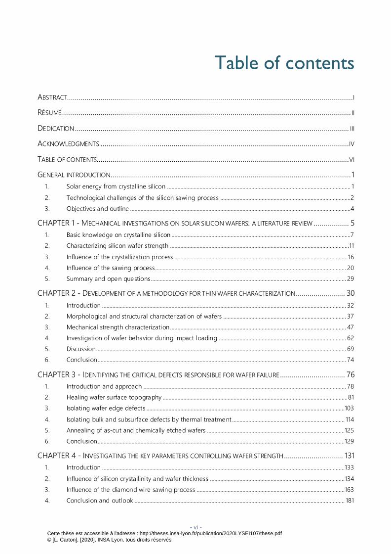
Table of contents
ABSTRACT.................................................................................................................................................I
RÉSUMÉ................................................................................................................................................... II
DEDICATION ........................................................................................................................................... III
ACKNOWLEDGMENTS ..............................................................................................................................IV
TABLE OF CONTENTS................................................................................................................................VI
GENERAL INTRODUCTION .......................................................................................................................... 1
1. Solar energy from crystalline silicon ............................................................................................................................ 1
2. Technological challenges of the silicon sawing process ........................................................................................2
3. Objectives and outline .....................................................................................................................................................4
CHAPTER 1 - MECHANICAL INVESTIGATIONS ON SOLAR SILICON WAFERS: A LITERATURE REVIEW .................. 5
1. Basic knowledge on crystalline silicon .........................................................................................................................7
2. Characterizing silicon wafer strength .........................................................................................................................11
3. Influence of the crystallization process ..................................................................................................................... 16
4. Influence of the sawing process................................................................................................................................. 20
5. Summary and open questions.................................................................................................................................... 29
CHAPTER 2 - DEVELOPMENT OF A METHODOLOGY FOR THIN WAFER CHARACTERIZATION ......................... 30
1. Introduction ..................................................................................................................................................................... 32
2. Morphological and structural characterization of wafers ................................................................................... 37
3. Mechanical strength characterization ....................................................................................................................... 47
4. Investigation of wafer behavior during impact loading ...................................................................................... 62
5. Discussion......................................................................................................................................................................... 69
6. Conclusion........................................................................................................................................................................ 74
CHAPTER 3 - IDENTIFYING THE CRITICAL DEFECTS RESPONSIBLE FOR WAFER FAILURE ................................. 76
1. Introduction and approach ......................................................................................................................................... 78
2. Healing wafer surface topography ............................................................................................................................. 81
3. Isolating wafer edge defects ......................................................................................................................................103
4. Isolating bulk and subsurface defects by thermal treatment ............................................................................ 114
5. Annealing of as-cut and chemically etched wafers .............................................................................................125
6. Conclusion.......................................................................................................................................................................129
CHAPTER 4 - INVESTIGATING THE KEY PARAMETERS CONTROLLING WAFER STRENGTH .............................. 131
1. Introduction ....................................................................................................................................................................133
2. Influence of silicon crystallinity and wafer thickness ...........................................................................................134
3. Influence of the diamond wire sawing process ....................................................................................................163
4. Conclusion and outlook .............................................................................................................................................. 181
Cette thèse est accessible à l'adresse : http://theses.insa-lyon.fr/publication/2020LYSEI107/these.pdf © [L. Carton], [2020], INSA Lyon, tous droits réservés

- vii -
GENERAL CONCLUSIONS AND PROSPECTS ............................................................................................... 185
1. Conclusions .....................................................................................................................................................................185
2. Perspectives ....................................................................................................................................................................187
3. Epilogue ...........................................................................................................................................................................190
APPENDIX A - WEIBULL STRENGTH SIZE EFFECT ON DIAMOND WIRE SAWN SILICON WAFERS..................... 191
1. Introduction .................................................................................................................................................................... 191
2. Applying weibull size effect theory to silicon wafers ........................................................................................... 191
3. Experimental approach................................................................................................................................................194
4. Results ..............................................................................................................................................................................195
5. Conclusions and perspectives....................................................................................................................................196
APPENDIX B - INFLUENCE OF NUMBER OF TESTED SAMPLES ON ESTIMATION OF WEIBULL PARAMETERS ..... 197
1. Introduction ....................................................................................................................................................................197
2. Methodology ..................................................................................................................................................................198
3. Results for the 4-line bending setup .......................................................................................................................199
4. Results for the RoR setup............................................................................................................................................201
APPENDIX C - X-RAY DIFFRACTION TECHNIQUE TO MEASURE RESIDUAL STRESSES .................................. 203
APPENDIX D - INFLUENCE OF ANNEALING ATMOSPHERE ON THE STRENGTH OF AS-CUT WAFERS ............. 206
1. Experimental procedure ............................................................................................................................................. 206
2. Strength results ............................................................................................................................................................. 207
APPENDIX E - STRENGTH RESULTS OF ALL MONO-SI WAFERS TESTED WITH THE 4-LINE BENDING SETUP ... 208
1. Recall of sawing parameters and designation ..................................................................................................... 208
2. Results ............................................................................................................................................................................. 209
REFERENCES......................................................................................................................................... 213
Cette thèse est accessible à l'adresse : http://theses.insa-lyon.fr/publication/2020LYSEI107/these.pdf © [L. Carton], [2020], INSA Lyon, tous droits réservés

- 1 -
General introduction
1. SOLAR ENERGY FROM CRYSTALLINE SILICON
Solar energy, growing and expanding
Solar photovoltaic (PV) energy is becoming one of the most competitive options for electricity generation,
both for residential and commercial applications. It possesses the highest learning rate of all renewable
power technologies - for every doubling of PV shipment volume, module price decreases by 24 % [1] - and
is as such now cheaper than fossil fuels in an increasing number of countries [2,3]. In this context, we
witnessed a tremendous increase of the worldwide installed PV capacity over the past decade, reaching
627 GW in 2019 - a value to compare to the 23 GW from 2009 (Figure 1).
Figure 1. Evolution of worldwide solar capacity and annual additions [4]
Silicon as the key material
A solar cell can be manufactured according to multiple technologies and involving different semiconductor
materials. To this day, crystalline silicon remains however the most widely used material: more than 95 % of
the PV cells produced worldwide in 2019 use thin silicon slices – wafers - as base substrate [5]. This market
domination has numerous causes: silicon is the second most earth-abundant element and possesses
excellent electrical properties, the corresponding manufacturing techniques are well-mastered, and the
cost-to-efficiency ratio of the silicon solar cell is very favourable when compared to other materials.
From raw polysilicon to PV module
The polysilicon material for the PV chain is obtained by purifying metallurgical grade silicon to a 99.9999 %
(six nines or 6N) purity [6]. This so-called solar grade silicon is then melted and solidified into ingots
(Figure 2). Depending on the desired cost and material quality, different crystallization techniques can be
implemented. For the PV industry, the two main techniques are directional solidification systems (DSS), which
allows to obtain multicrystalline silicon, and the Czochralski (Cz) method which yields monocrystalline silicon.
After the crystallization process, the ingots are cut into bricks whose lateral dimensions determine the size
of the wafers. Each brick is then sliced at once into several hundreds of wafers with a wire saw. The resulting
wafers then undergo several processing steps to become solar cells. Chemical processes allow to clean the
Cette thèse est accessible à l'adresse : http://theses.insa-lyon.fr/publication/2020LYSEI107/these.pdf © [L. Carton], [2020], INSA Lyon, tous droits réservés

General Introduction
- 2 -
wafer and to generate a textured surface that minimizes light reflection. Doping diffusion steps create the
electrical junction required to allow the photo current to flow in one single direction. In addition to surface
texturing, anti-reflective coating is applied on the surface to further increase the amount of light absorbed.
Finally, metal contacts are printed on the wafer to collect the charges carrying the electrical current produced.
Several cell architectures exist, which are characterized by their efficiency conversion ratio. The record lab
efficiency in 2019 is 26.7 % and 23.2 % for monocrystalline and multicrystalline silicon respectively [7]. The
final solar cells are connected in series to increase the tension, and the obtained series are connected in
parallel to increase the current. The obtained cell assembly after encapsulation results in a PV module, with
average area efficiency (module power / module area) reaching 210 W/m2 [5].
Figure 2. Manufacturing process of a silicon-based PV module
Accelerating PV growth
Despite the important achievements in efficiency improvements and cost reduction, the share of solar energy
remains marginal (2.8 % of global electricity production [4] in 2019) and above all too low to meet the climate
change targets defined by the Intergovernmental Panel on Climate Change (IPCC) through PV deployment.
Needleman et al. estimated in 2016 that to ensure a higher probability of limiting global temperature rise
below 1.5-2 °C, a cumulative PV installed capacity of 7-10 TW by 2030 would be required [8] – in other words,
more than ten times the capacity installed in 2019. As pointed out by numerous studies [9–11] , such a growth
trajectory can only be sustained with drastic reductions of costs and capital expenditure (capex). The latest
International Technology Roadmap for PV (ITRPV [5]) emphasizes three strategies to address this challenge:
Improve module area efficiency
Introduce specialized module products for different market applications
Continue cost optimization per piece, by using silicon material more efficiently
This work focuses on the third strategy - in others words, the need to enhance silicon material yield at every
stage of the PV manufacturing chain. As discussed in the following section, a very large share of this yield is
attributable to the sawing step.
2. TECHNOLOGICAL CHALLENGES OF THE SILICON SAWING PROCESS
A crucial step for material and cost savings
Although some alternative processes are under study [12,13], more than 95 % of silicon wafers for PV
applications are obtained by wire sawing. The basic working principle is illustrated in Figure 3: the cutting
wire, which moves at a few tens of meters per second, is wound multiple times around two cylinders to form
a web. The silicon brick is moved down through this moving web, allowing several hundreds of wafers to be
generated in once. This manufacturing step is of significant economic importance, as it still accounts for 15 %
Cette thèse est accessible à l'adresse : http://theses.insa-lyon.fr/publication/2020LYSEI107/these.pdf © [L. Carton], [2020], INSA Lyon, tous droits réservés

General Introduction
- 3 -
of the final PV module cost [5]. More specifically, the major inherent drawback of the wire sawing process is
the material waste: for each wafer obtained, a thin layer of material corresponding to the cutting line, called
the kerf, is lost. Therefore, with a standard wafer thickness of 170 µm for a kerf width of 75 µm in 2019 [5],
about 30 % of the material available in a brick gets lost in the form of a silicon powder. While promising
recycling applications for this kerf are being developed [14], optimizing material yield during the sawing step
remains a crucial objective. In practice, this implies reducing both wafer as-cut thickness (i.e., thickness right
after the sawing step) and kerf width.
Figure 3. Schematic layout of the wire sawing process
Towards thinner wafers
Decreasing as-cut thickness is indeed a way to generate more wafers per silicon brick. As a demonstration,
Liu et al. [11] calculated that decreasing wafer thickness from 160 to 50 µm can potentially get a capex
reduction of ~ 0.14 $/(W/year) and a cost reduction of ~ 0.07 $/W of the current PV module 1, which in 2019
had an average price of 0.26 $/W [5]. Even though decreasing wafer thickness can deteriorate the final solar
cell efficiency due to an incomplete absorption of photons, recent studies all estimate the threshold value to
be between 50 µm and 100 µm depending on the cell architecture [11,15,16] – i.e., well below the industry
standards. There is therefore still much room for improvement regarding wafer thickness.
Diamond wire sawing as dominant technology
In the context of a need for kerf reduction and increased productivity, we witnessed an abrupt change in the
past ten years, with diamond wire sawing (DWS) technology completely replacing the historical loose
abrasive slurry (LAS) sawing technique. The market share of DWS officially reached 100 % in 2018, while in
2016 it was only 45 % and 5 % for monocrystalline and multicrystalline silicon, respectively [5,17]. Thinner
wire core, lower cutting time and lower capex are among the unquestionable advantages of DWS that
justified this extremely fast shift in technology [18,19]. However, the mechanical damage generated by this
new abrasion process has proven to be complex, anisotropic and above all fundamentally different from that
of the LAS technique [20,21]. Ever since the appearance of DWS, characterizing this damage has been the
subject of extensive work [22–24], but its exact nature and influencing parameters are to this day not entirely
known or understood.
1 In comparison, they show that increasing cell efficiency from 19 % to 24 % by implementing advanced technologies only
decreases capex by ~ 0.08 $/(W/year) and cost by ~ 0.07 $/W.
Cette thèse est accessible à l'adresse : http://theses.insa-lyon.fr/publication/2020LYSEI107/these.pdf © [L. Carton], [2020], INSA Lyon, tous droits réservés

General Introduction
- 4 -
What about the wafer breakage rates?
Common to both the as-cut thickness reduction and the extremely fast development of DWS is their
potential influence on the mechanical behaviour and properties of the resulting wafers. On the one hand,
several studies measured indeed higher breakage rates when processing thinner wafers [25]. On the other
hand, it has been repeatedly demonstrated that as-cut DWS samples exhibit anisotropic mechanical
properties, with a critically lower measured fracture strength depending on the orientation of the applied
load [26–28]. This dual influence is precisely where the scientific and economic challenge lies: lower thickness
and DWS technology were both introduced as a pathway towards a better use of silicon material. However,
if they induce higher breakage rates of the wafers during solar cell processing, we may question their actual
benefits.
Therefore, enhancing silicon material yield during the sawing process will lead to cost savings only if
the resulting wafers exhibit reliable and controlled mechanical strength.
3. OBJECTIVES AND OUTLINE
In this work, we aim to improve our understanding of the mechanical properties of silicon wafers and to
identify the most influencing mechanisms. We concentrate on the behaviour of as-cut samples, i.e. which
were collected directly after sawing, because all subsequent solar cell processing steps (chemical cleaning,
texturing, etc.) will help enhance their fracture strength. In other words, the time when a wafer is the more
likely to break is following the sawing process, which is where our focus lies. The main ambition of our study
is to be able to establish recommendations for the manufacturing parameters of thin silicon wafers – from
crystallization to sawing - as well as to propose adjustments of the handling and processing technologies to
limit breakage rates. The present work is based on mechanical fracture tests performed on more than seven
thousands of samples, in combination with finite element modelling methods. In our methodology, we
particularly benefited from using wafers that were cut in our lab using controlled parameters. The manuscript
develops in four main chapters:
Chapter 1 provides a state of the art overview of the mechanical investigations performed on PV silicon
wafers. We present the theoretical properties related to the crystallographic structure of silicon, as well
as the existing experimental characterization methods. The two main processing steps of silicon wafer
manufacturing - crystallization and sawing - and their known influence on sample strength are
discussed in detail. This literature review allows us to highlight the yet unanswered questions that
guided our work.
In Chapter 2, we develop the different methods implemented to characterize a typical as-cut wafer as
comprehensively as possible. We introduce the non-destructive techniques chosen to analyse the
structural and morphological defects of the samples, as well as the destructive fracture tests. This
thorough methodology allows us to define characterization guidelines for the rest of our work.
Chapter 3 aims at determining which of the defects present in a typical as-cut DWS wafer are the most
critical for mechanical failure. To this end, we propose an original systematic procedure to isolate their
respective influence on the fracture properties of the samples.
In Chapter 4, we conduct an extensive mechanical characterization of silicon wafers from different
crystalline nature, different as-cut thicknesses and sawn using different slicing parameters. Our goal is
to determine whether we can find a combination of crystallization and sawing parameters to obtain the
most mechanically reliable thin wafer.
We finally draw the General conclusions of our work and propose some prospects.
Cette thèse est accessible à l'adresse : http://theses.insa-lyon.fr/publication/2020LYSEI107/these.pdf © [L. Carton], [2020], INSA Lyon, tous droits réservés

- 5 -
CHAPTER 1
- Mechanical investigations on solar
silicon wafers: a literature review
Studying the mechanical properties of silicon wafers has always been a subject of interest for the PV
research and industry, as they often dictate the fundamental limits on the handling and processing
steps of the future solar cells. This chapter aims at giving a state of the art overview of mechanical
investigations on solar silicon wafers. The first part deals with basic crystallographic knowledge of
silicon and the resulting elastic and fracture properties of the crystal. The second part introduces the
experimental and statistical approaches to characterize silicon fracture strength and behavior. The
third and fourth parts present the two main processing steps needed to manufacture a typical solar
wafer: crystallization of silicon raw material into a solid ingot and wire sawing of the brick. The defects
associated with each process and their influence on the mechanical properties of the resulting wafers
are discussed. We finally put forward some open questions.
Cette thèse est accessible à l'adresse : http://theses.insa-lyon.fr/publication/2020LYSEI107/these.pdf © [L. Carton], [2020], INSA Lyon, tous droits réservés

Chapter 1 – Mechanical investigations on solar silicon wafers: a literature review
- 6 -
Contents
1. BASIC KNOWLEDGE ON CRYSTALLINE SILICON ..................................................................................... 7
1.1. Elastic properties ...............................................................................................................................................................8
1.2. Fracture properties ...........................................................................................................................................................9
2. CHARACTERIZING SILICON WAFER STRENGTH ..................................................................................... 11
2.1. Destructive mechanical testing.....................................................................................................................................11
2.2. Statistical description of brittle fracture: Weibull theory ...................................................................................... 13
3. INFLUENCE OF THE CRYSTALLIZATION PROCESS .................................................................................. 16
3.1. Silicon crystallization techniques................................................................................................................................. 16
3.1.1. Czochralski process .................................................................................................................................................... 16
3.1.2. Directional solidification process............................................................................................................................ 17
3.2. Link between crystallization defects and wafer mechanical properties ........................................................... 19
4. INFLUENCE OF THE SAWING PROCESS ............................................................................................... 20
4.1. Wire sawing cutting processes ................................................................................................................................... 20
4.2. Damage and defects generated during sawing .................................................................................................... 22
4.2.1. Origin of defects: brittle and ductile mode machining ................................................................................... 23
4.2.2. Damage layer concept ........................................................................................................................................ 25
4.3. Link between sawing induced damage and wafer mechanical properties .................................................... 26
5. SUMMARY AND OPEN QUESTIONS ................................................................................................... 29
Cette thèse est accessible à l'adresse : http://theses.insa-lyon.fr/publication/2020LYSEI107/these.pdf © [L. Carton], [2020], INSA Lyon, tous droits réservés

Chapter 1 – Mechanical investigations on solar silicon wafers: a literature review
- 7 -
1. BASIC KNOWLEDGE ON CRYSTALLINE SILICON
Crystalline silicon owns a diamond crystalline structure, which can be described as a pair of intersecting face-
centered cubic lattices, each of them being separated by one fourth of the width of the unit cell in each
dimension. Each atom connects with four neighbor atoms via covalent bonds. A unit cell is composed, as
shown in Figure 1.1, of eight atoms at the corners (in grey), six atoms at the center of faces (in red) and four
extra atoms resting inside the lattice (in green) at the centroid of 4 tetrahedrons [29].
Figure 1.1. Face-centered cubic crystal structure of silicon
The crystal planes and crystallographic directions are commonly defined by the Miller indices ℎ, 𝑘 and 𝑙 as
indicated Table 1.1 [30]. The cubic symmetry of the structure implies that there are 24 equivalent possibilities
to position the single crystal in a Cartesian coordinate system [31]. This means that a single direction
(or plane 2) associated with ℎ, 𝑘 and 𝑙 for any sign of each and in any order belongs to the same direction
(or plane) family defined by positive ℎ, 𝑘 and 𝑙. Figure 1.2 shows the {100}, {110} and {111} family of planes,
which are the most studied ones in silicon. The crystal planes in each family are identical.
Table 1.1 Miller Indices
Notation Interpretation
(ℎ𝑘𝑙) Single crystal plane
{ℎ𝑘𝑙} Equivalent planes (family)
⟨ℎ𝑘𝑙⟩ Single crystal direction
[ℎ𝑘𝑙] Equivalent directions (family)
Since the atom density differs from one crystallographic direction to another, the physical properties of single
crystal silicon exhibit anisotropic characteristics, such as thermal expansion coefficients, surface energies, and
electrical resistivity. In particular, this anisotropy dominates the elastic and fracture behavior of silicon.
Crystalline silicon can exist in its monocrystalline form as a single, continuous and unbroken crystal, or in
multicrystalline form. In this case, the material consists of multiple small silicon crystals (grains) separated by
grain boundaries. In the solid state, silicon can also exhibit a non-crystalline amorphous form, in which the
long-range order of the tetrahedral structure is not present anymore: atoms form a continuous random
network and some of them exhibit dangling bonds 3, which can cause degradation of the electrical properties.
2 According to the Miller indices, a crystallographic plane is defined with its normal direction. 3 In chemistry, a dangling bond is an unsatisfied valence on an immobilized atom.
Cette thèse est accessible à l'adresse : http://theses.insa-lyon.fr/publication/2020LYSEI107/these.pdf © [L. Carton], [2020], INSA Lyon, tous droits réservés

Chapter 1 – Mechanical investigations on solar silicon wafers: a literature review
- 8 -
Figure 1.2. Crystallographic planes in single cystal silicon
1.1. Elastic properties
The anisotropic elastic behavior of single-crystal silicon can be described by the fourth-order stiffness tensor
𝑪 owning three independent parameters 𝐶11, 𝐶12 and 𝐶44 in the crystallographic coordinate system of
principal axes [100], [010] and [001]. At room temperature and ambient pressure, the measurements
considered as the most accurate in the literature were reported by Hall [32] with acoustic wave propagation
in the solid and are recalled below:
𝑪 =
(
165.7 63.9 63.9
63.9 165.7 63.963.9 63.9 165.7
79.679.6
79.6
)
𝐺𝑃𝑎 (1.1)
The orthotropic nature of this tensor allows to determine the usual elasticity constants of a material, such as
the Young’s modulus E, Poisson’s ratio ν and shear modulus G in any direction of interest [33]. In particular,
the Young’s modulus of monocrystalline silicon is minimal (130 GPa) in the [100] direction and maximal
(188 GPa) in the [111] direction. It is important to understand that the stiffness tensor from equation (1.1) is
valid for a monocrystalline silicon sample owning the default 𝑋𝑌𝑍-axes, i.e. 𝑋 is <100>, 𝑌 is <010> and 𝑍 is
<001>, as shown in Figure 1.2. In order to obtain the elasticity constants in any arbitrary direction, the stiffness
tensor 𝑪 must be rotated so that one of the axes is aligned with the direction of interest [34]. The expression
for the rotated 𝑪′ can be found in literature [35,36] and is more easily calculated using algebraic notations:
𝑪′𝒊𝒋𝒌𝒍 = ∑∑∑∑𝑄𝑝𝑖𝑄𝑞𝑗𝑄𝑟𝑘𝑄𝑠𝑙𝐶𝑝𝑞𝑟𝑠
3
𝑠=1
3
𝑟=1
3
𝑞=1
3
𝑝=1
(1.2)
where 𝑸 is the rotation matrix. This tensor rotation requires tedious calculations that can however easily be
performed numerically with a computer program.
As an aggregate of multiple single crystals separated by grain boundaries, multicrystalline silicon theoretically
owns an intermediate value of Young's modulus between 130 GPa and 188 GPa. If the aggregate contains a
sufficiently large number of grains and is macroscopically homogeneous [37], the sample can be seen as an
elastically isotropic material described by two parameters, the Young's modulus and the Poisson's ratio. This
so-called aggregate theory has been widely applied to microelectromechanical systems (MEMS) [38], which
have grains of nanometric or micrometric size. However, depending on the growth process parameters, the
grain size of a PV silicon multicrystalline wafer can vary between some hundreds of micrometers to a few
Cette thèse est accessible à l'adresse : http://theses.insa-lyon.fr/publication/2020LYSEI107/these.pdf © [L. Carton], [2020], INSA Lyon, tous droits réservés

Chapter 1 – Mechanical investigations on solar silicon wafers: a literature review
- 9 -
centimeters. In the latter case, the grain size is almost the same order of magnitude as the sample
dimensions, as illustrated in Figure 1.3.a. Funke et al. [39] performed an analytical calculation considering a
uniform orientation distribution of the grains in a representative volume element and obtained E = 162.5 GPa
and ν = 0.223. Zhao et al. [40] proposed a different approach based on a numerical model, in which the
grain structure of the wafer is generated by a Voronoi tessellation 4 as illustrated in Figure 1.3.b. The resulting
wafer is thereafter introduced in a finite element (FE) model reproducing a 4-line bending test, and the
equivalent Young's modulus, calculated from the slope of the load-deflection curve, is assessed as
163 ± 2 GPa. The negligible difference in value between the two methods seems to validate the
homogenization hypothesis made by Funke et al.
(a)
(b)
Figure 1.3. Example of a (a) PV multicrystalline silicon wafer and (b) Voronoi tesselation
1.2. Fracture properties
At room temperature, silicon is a purely brittle material: when solicited, it deforms elastically until fracture,
with no movement of dislocations and therefore no plastic deformation. If considered as a perfect
single-crystal with no structural defects, silicon actually owns a very high intrinsic strength: ab initio theory
allowed to calculate the ideal tensile strength of silicon to be 22 GPa [41], while notch-free fracture
experiments performed on high-quality mirror polished monocrystalline silicon samples provided tensile
strength values between 3-7 GPa [42].
However, as soon as a microscopic defect exists in the wafer, the fracture strength is significantly reduced
and even a moderate stress value may initiate failure. The linear elastic fracture mechanics (LEFM) theory
explains this phenomenon by a dramatic increase of the local stress in the region of the defect. LEFM theory
shows that, regardless of the loading and the sample geometry, the solution of the stresses in polar
coordinates (𝑟, 𝜃) with the origin at the crack tip is:
𝜎(𝑟, 𝜃) =𝐾𝛼
√2𝜋𝑟∙ 𝑓𝛼(𝜃) (1.3)
where 𝛼 = 𝐼, 𝐼𝐼 or 𝐼𝐼𝐼 are known as the cracking modes used to classify the fracture problems depending
on the loads applied to the crack (Figure 1.4). 𝐾𝛼 is the stress intensity factor that depends on the sample
and crack geometry and 𝑓𝛼 is a dimensionless function of the coordinate angle 𝜃. For example, in the case
of a straight crack of length 2𝑎 subjected to a uniform tensile stress 𝜎, the concentration factor 𝐾𝐼 is
expressed as:
𝐾𝐼 = 𝜎 ∙ √𝜋𝑎 (1.4)
4 A Voronoi diagram (or tessellation) is a partition of a plane into regions close to each of a given set of objects.
Cette thèse est accessible à l'adresse : http://theses.insa-lyon.fr/publication/2020LYSEI107/these.pdf © [L. Carton], [2020], INSA Lyon, tous droits réservés

Chapter 1 – Mechanical investigations on solar silicon wafers: a literature review
- 10 -
Figure 1.4. Elementary fracture modes. Mode I: opening - Mode II: in-plane shear - Mode III: out-of-plane shear
The resistance of the material against crack growth determines whether an existing crack remains stationary
or starts to propagate. LEFM states that crack growth initiates as soon as the stress intensity factor reaches
a critical value 𝐾𝐼𝐶 , called the fracture toughness. In the same way as for the elastic properties, fracture
toughness of single crystalline silicon depends on the crystallographic orientation [33]. This anisotropic
toughness is commonly measured by Knoop or Vickers micro-hardness indentation sometimes associated
with bending tests [43,44] or with double-cantilever beam tests [45,46]. Toughness can also be calculated
by molecular dynamics [47] or density functional theory [48]. The values reported in literature are either
expressed in terms of fracture toughness 𝐾𝐼𝐶 or surface energy 5, and may vary strongly depending on the
testing method, specimen surface preparation and crack length. It is however agreed upon that silicon has
two principal cleavage planes: the {111} and {110} planes, which exhibit lower toughness than other planes
and are therefore preferential fracture paths. Fracture of single crystalline silicon is moreover a dynamic
process, with crack propagation velocities reaching up to 3700 m/s [49].
Above a certain temperature, a brittle to ductile transition is observable, a phenomenon which was first
revealed in the 1950s [50,51]. Investigations on single crystal silicon were widely conducted via fracture tests
on pre-cleaved specimens, in order to capture and model the transition from pure cleavage to general
plasticity [52–54]. As temperature increases, transition is dictated by the emission and motion of dislocations
near the crack tip, which blunt the crack front and increase the material toughness compared to room
temperature [55].
The transition temperature value is a function of the silicon type, the strain rate, the crystallographic
orientation and the doping level. It has been measured around 600 °C, which is much higher than most of
the operating temperatures of silicon-based systems – temperature at the surface of a solar module rarely
exceeds 100 °C. In service, silicon remains therefore brittle and plasticity is far from nucleation. However,
depending on the solar cell architecture, a silicon wafer may undergo a certain number of high temperature
steps, such as the diffusion of the dopant material-containing coating, which takes place at temperatures
around 850 [56], or the deposition of the metallic contacts on the wafer, which involves a peak firing
temperature of up to 1000 °C [57]. If initial microcracks are present in the wafer during these high
temperature steps, crack plasticity may occur, although its effect on the mechanical properties of the solar
cells is rarely considered [58].
5 The toughness 𝐾𝐼𝐶 equals twice the surface energy of the fracture plane 𝛾 in the case of quasi-static crack propagation in
a brittle material, and becomes larger than 2𝛾 when plastic deformation occurs at the crack tip.
Cette thèse est accessible à l'adresse : http://theses.insa-lyon.fr/publication/2020LYSEI107/these.pdf © [L. Carton], [2020], INSA Lyon, tous droits réservés

Chapter 1 – Mechanical investigations on solar silicon wafers: a literature review
- 11 -
2. CHARACTERIZING SILICON WAFER STRENGTH
2.1. Destructive mechanical testing
Silicon wafers for PV applications are square or pseudo-square thin plates with an extremely high
length-to-thickness ratio: they have a typical size of 156 × 156 mm2 with thickness ranging from 100 to
180 µm. The length-to-thickness ratio is moreover expected to become more important, as wafer format is
quickly shifting towards higher lateral dimensions (166 × 166 mm2 wafers are already in production, while
210 × 210 mm2 are being introduced in the market) and lower thicknesses (for certain cell architectures,
160 µm is already mainstream [5]). It is worth noting that up to recently, no standard test method existed to
evaluate the mechanical strength of silicon wafers. The test setup and sample geometry are therefore chosen
based on existing literature as well as on practical criteria – it is for instance very difficult to perform tensile
tests on thin brittle specimens such as silicon wafers.
At the wafer scale, the most widely used methods are uniaxial bending setups, in which the loading devices
are in the form of cylindrical bars, thus creating a linear contact with the sample surface. The 4-line bending
configuration is usually preferred over 3-line bending, as it enables to have a large area of the tested sample
submitted to a uniform mechanical state [31] (Figure 1.5). Silicon is indeed a crack-sensitive material and
fracture mechanics predicts that the failure will initiate on the tensile lower surface of the sample, where the
largest crack is located. Imposing a uniform tensile load on a significant sample area thus improves the
representativeness of the test procedure in terms of wafer defect population [59].
(a)
(b)
Figure 1.5. Schematic setup and theoretical maximum tensile stress distribution in (a) 3-line (b) 4-line bending test
Based on the similarities in brittle fracture behavior, several studies choose to design their 4-line bending
setup according to the guideline of ASTM standards for technical ceramics [40,60,61]. However, their
recommendations are often not suited to the high length-to-thickness ratio of PV silicon wafers. In order to
overcome this issue, a standard test method for strength testing of PV wafers was recently developed, which
provides requirements to design a 4-line bending setup suited for full-size silicon wafers and lookup tables
to compute fracture stresses [62]. However, given the recentness of this contribution, there are yet only very
few studies relying on it [27]. The uniform stress distribution over the whole wafer area implies that different
types of defects are loaded, mainly surface and edge defects, and to a lesser extent volume defects. The
4-line bending method therefore has the advantage of being more sensitive to the overall wafer damage,
but may be limiting if there is a need to focus on a specific defect population.
This is the reason why some studies implement biaxial bending methods, mostly in the form of Ring on
Ring (RoR) [63–65] or Ball on Ring (BoR) setups [66]. In these configurations, the wafer is supported by an
annular support and loaded either by a ring of smaller diameter for the RoR setup or by a sphere for the
BoR configuration. The main advantage of this test geometry is that the stress is theoretically zero at the
Cette thèse est accessible à l'adresse : http://theses.insa-lyon.fr/publication/2020LYSEI107/these.pdf © [L. Carton], [2020], INSA Lyon, tous droits réservés

Chapter 1 – Mechanical investigations on solar silicon wafers: a literature review
- 12 -
wafer edges and maximum at the center of the sample, and in particular in the case of the RoR setup, uniform
over the whole area below the loading ring (Figure 1.6). This method thus allows to eliminate the influence
of defects located at the edges of the wafer and to concentrate on the study of surface or volume defects.
(a)
(b)
Figure 1.6. Schematic setup and theoretical maximal tensile stress distribution (a) RoR and (b) BoR test
However, the analytical formula for the stress distribution as depicted in Figure 1.6, introduced by Vitman
and Pukh [67], is only valid under strict and restrictive conditions. In particular, the maximum wafer deflection
should not exceed half the thickness. In order to meet these requirements, the setup can be designed based
on the ASTM standard for equibiaxial flexural strength of advanced ceramics [68], as done in several
studies [64,65]. Complying with this standard requires, however, to work with extremely small samples (in
the order of 1 × 1 cm2) and therefore to evaluate a very restricted area of the wafer (4 % of the surface). This
not only reduces the representativeness of the results, but it also calls for an extra dicing step that could,
very much itself, modify the results. Some studies alternatively choose to design a RoR setup with dimensions
suitable to test an entire wafer [63], thus requiring specific care when analyzing the stress results as the
analytical formulae are no longer valid.
A few limited works combine the previous bending methods with twist tests [69,70], but the highly
inhomogeneous stress field generated in the wafer makes the interpretation of the results difficult and
explains the little interest raised by this technique.
The aforementioned tests are quasi-static methods, i.e. the force or displacement is applied at a sufficiently
low speed (usually adjusted to have a strain rate between 10-5 and 10-1 s-1 on universal testing machines) so
that inertia effects can be neglected. While these methods are of high practical interest, they are not entirely
representative of the “real” stresses experienced by a wafer during handling and transporting. A more suited
alternative is to apply dynamic loads to the wafer in the form of impact tests. Such methods are however
rarely implemented, mainly because the required energy levels are very low (in the order of a few mJ) and
therefore difficult to control. Notable exceptions either involve a setup with a wafer falling on a collision
body [71,72] or a pendulum-like system allowing to introduce a controlled amount of impact energy on the
wafer edge [73]. Strength evaluation of silicon wafers can even be taken a step further by designing specific
setups that reproduce as closely as possible the actual handling conditions (wafer singulation and placement
in carriers, gripping, carrying, and turning actions) [74]. The main advantage is that the results could be
directly transformed into design recommendations for industrial equipment or processes. Conceiving such
systems is however complex and costly and the number of applications remains very limited.
Within a more local approach, indentation tests are also often employed to characterize the facture behavior
of silicon wafers. These methods can indeed be used to measure local mechanical properties such as
hardness or toughness [44,75], but also to create artificial cracks in silicon wafers, with the aim to mimic the
damage existing in a PV wafer [76]. Inserting these artificial defects can help comprehend the mechanisms
Cette thèse est accessible à l'adresse : http://theses.insa-lyon.fr/publication/2020LYSEI107/these.pdf © [L. Carton], [2020], INSA Lyon, tous droits réservés

Chapter 1 – Mechanical investigations on solar silicon wafers: a literature review
- 13 -
of crack propagation, for example by determining which cracks will more likely propagate and lead to failure
under a given loading configuration [77], or how different cracks can interact with one another [78].
It should be mentioned that there has been evidence of fatigue behavior in micro- or nanoscale silicon
samples [79,80] and the topic has recently gained some interest for MEMS applications [81,82]. While several
hypotheses were proposed to explain this fatigue behavior, none of the mentioned mechanisms were ever
observed at the PV silicon wafer scale. Moreover, the level of stresses at stake in the existing experimental
studies, in the order of a few GPa, is about two to three orders of magnitude higher that the strength values
usually measured in PV silicon wafers. This explains why in the PV industry, subcritical crack growth (fatigue)
problem is not taken into account when evaluating the mechanical reliability of silicon wafers.
The study of mechanical integrity in the PV field also recently extended to the solar cell and module scale.
Blakers and Armour [83] showed that under repeated non-destructive bending, solar cells either broke on
the first flexure or did not break at all. Mechanical studies on solar cells and modules usually focus on the
formation of microcracks during mechanical loading and their impact on module performance.
Kajari-Schröder et al. provided a statistical analysis of the spatial distribution of cracks with the
electroluminescence method [84]. Sander et al. studied crack patterns in solar cells based on 4-line bending
tests and highlighted that the cell strength varies with the orientation of the busbars [85]. Kaule et al.
obtained the same result and coupled their experimental values with a FE model taking into account all the
components of the solar cell [86]. More recent studies showed that at the module scale, cell cracking was
also related to a fatigue degradation phenomenon during cycling bending, which is caused by the
encapsulation of the cells in a polymer generating residual thermo-elastic stresses [87]. Borri et al. showed
moreover that this fatigue crack growth originates from the soldering point between the busbar and the
solar cell [88].
2.2. Statistical description of brittle fracture: Weibull theory
Some elements of the literature review described in the following paragraph were quoted verbatim from an
article published by Carton et al. [89].
Breakage stress values obtained for silicon wafers that are deemed identical will exhibit large scattering. This
dispersion results from the brittle nature of silicon: the strength of a silicon wafer is ultimately controlled by
the density, size and geometry of its defects, which can vary strongly even within a series of samples from
the same ingot. These characteristics are random variables, and the failure stress of the wafer under a given
applied load becomes a statistical data. Failure is then a random event with a certain probability or likelihood
of coming true under given circumstances. The mean stress value is therefore not sufficient to represent the
strength of a set of wafers and the data require statistical treatment.
There exist different statistical approaches to model brittle failure, which all aim at linking the characteristics
of the defect population and the characteristics of the stress field to the material failure probability. Because
of its ability to evaluate both the level and the scattering of strength values, Weibull probability function [90]
is the most widely used one to describe the fracture behavior of silicon wafers. In the specific case of wafers
for PV applications, Weibull is, to the best of our knowledge, the only implemented model. The fundamental
assumption for Weibull’s statistical theory of fracture [91] is the weakest link hypothesis: the survival
probability of a specimen is the product of survival probabilities of each volume element within the
specimen [92]. The mechanical strength of the entire specimen is therefore defined by its weakest defect .
For a uniaxial homogeneous tensile stress state, Weibull theory assumes that each volume element possesses
the same probability of failure and the general 3-parameter distribution gives the probability 𝑃 for a
specimen of volume 𝑉 to fail when subjected to a uniaxial tensile stress 𝜎 :
Cette thèse est accessible à l'adresse : http://theses.insa-lyon.fr/publication/2020LYSEI107/these.pdf © [L. Carton], [2020], INSA Lyon, tous droits réservés
Chapter 1 – Mechanical investigations on solar silicon wafers: a literature review
- 14 -
𝑃(𝜎, 𝑉) = 1 − exp (−𝑉
𝑉0(𝜎 − 𝜎𝑢𝜎0
)𝑚
) (1.5)
where 𝑚 is the Weibull modulus (known as the shape parameter), 𝜎0 is the characteristic strength value (scale
parameter), and 𝜎𝑢 the threshold stress below which the specimen will not fail (location parameter). The
Weibull modulus describes the scattering of the results (a higher value of 𝑚 means a small variation in
strength) while 𝜎0 represents the level of stress at which 63.2 % of the samples will fail. This distribution thus
depends on the volume of the loaded sample, a phenomenon known as the “size effect”: for a given volume,
a sample with more defects is more likely to fail than a sample with less defects. Conversely, a sample of
greater volume has a greater chance of having a critical defect than a smaller sample. 𝑉0 is the chosen
normalizing volume, which allows to adjust the dimension of the shape parameter. In most cases, for the
sake of simplicity, the threshold stress is assumed to be zero, and the distribution can be reduced to a
simplified 2-parameter form:
𝑃(𝜎, 𝑉) = 1 − exp (−𝑉
𝑉0(𝜎
𝜎0)𝑚
) (1.6)
This simplification allows to obtain a conservative prediction, and the remaining two parameters are much
simpler to estimate [93]. Several studies discussed the effect of assuming 𝜎𝑢 = 0 on the estimation of the
Weibull parameters [94,95]. Lu et al. [94] proposed a quantitative procedure to highlight the effects of the
threshold stress and concluded that a compromise should be made between simplicity of the 2-parameter
distribution and applicability of the 3-parameter distribution as the threshold stress of the considered
samples increases. Malzbender et al. [96] demonstrated that for fracture characterization of thin ceramic
components, the 3-parameter Weibull distribution is more appropriate. More recently, Deng et al. [95]
conducted an extensive examination based on Monte Carlo simulations and showed that the 2-parameter
Weibull function is sufficiently suitable for the description of the statistical variation of the measured strength
sample, regardless of whether the strength follows a 2-parameter of 3-parameter Weibull distribution.
When working with silicon wafers, almost all studies choose to restrict the strength distribution to a
2-parameter function. A first notable exception can be found in the work of Saleh et al. [97], who used a
3-parameter function to describe the strength of polycrystalline wafers. However, their investigations were
performed on MEMS samples (i.e. for electronic and not PV applications) with extremely high strength values
(in the order of 2-5 GPa), thus justifying the use of a threshold stress value, while failure stresses for solar
silicon wafers rarely exceed a few hundreds of MPa. There exist, to the best of our knowledge, only two
studies applying 3-parameter Weibull distribution to silicon wafers for PV applications: Cereceda et al. [98]
performed RoR tests on wafers with drilled holes for back contact cell application, while Barredo et al. [99]
carried out 4-line bending tests on wafers of different silicon crystallinity.
In the case where a non-uniform stress state is applied on the specimen, as it is the case for most of the
bending tests 6 chosen for silicon wafers and described above, each volume element has a different failure
probability. The formulation of equation (1.6) becomes an integral over the entire specimen volume:
𝑃(𝜎, 𝑉) = 1 − exp [−1
𝑉0∫ (
𝜎(𝑥, 𝑦, 𝑧) − 𝜎𝑢𝜎0
)
𝑚
𝑑𝑉𝑉
] (1.7)
The three parameters (𝑚, 𝜎0 , 𝜎𝑢 ) are associated with the material and are independent of size or stress
distribution within the sample. However, taking into account the size effect requires a complex iterative
6 In the bending tests described in the previous section, there exists a stress gradient along the thickness of the sample, wit h
a maximal compression stress on the upper surface and a maximum tensile stress on the lower surface.
Cette thèse est accessible à l'adresse : http://theses.insa-lyon.fr/publication/2020LYSEI107/these.pdf © [L. Carton], [2020], INSA Lyon, tous droits réservés

Chapter 1 – Mechanical investigations on solar silicon wafers: a literature review
- 15 -
procedure that involves the calculation of an equivalent volume (or area) submitted to a uniaxial constant
load [100], thus ensuring that equation (1.7) is valid. This is the reason why nearly all existing studies choose
to neglect this effect, which is justified by the use of a given sample geometry (for example a 156 × 156 mm2
wafer of thickness 180 µm) and identical test dimensions, so that the loaded volume can be considered
similar throughout their work. Since the important data is usually the strength comparison between different
sets of wafers rather than the actual strength value, the equivalent volume (or area) is considered as
unity [98]. This assumption yields a much simpler expression for the probability of failure:
𝑃(𝜎, 𝑉) = 1 − exp [− (𝜎 −𝜎𝑢𝜎𝜃
)𝑚
] (1.8)
It is however very important to mention here the change in parameter designation for the characteristic
strength, from 𝜎0 to 𝜎𝜃 : while 𝜎0 is independent of the tested size, 𝜎𝜃 depends on the stress distribution and
size of the tested sample, i.e. on the type and geometry of setup used. This essentially means that the stress
distribution values obtained by neglecting the size effect from different setups (for example, between a RoR
and a 4-line bending setup, but also between two 4-line bending setups with different dimensions) are in
theory not comparable. This effect had however never been verified experimentally for solar silicon wafers.
We conducted a specific experimental study to explore this problem, which compares the Weibull strength
parameters obtained from wafers tested with three different bending setups. The results were published in
a separate article [89] and are synthesized in Appendix A.
Despite its wide applicability, Weibull’s theory has been called into question since its first introduction. The
main criticism is the macroscopic nature of the approach: it acknowledges the existence of defects within
the material but does not take into account their characteristics such as size, orientation or density. A
significant amount of research has therefore been made in the last fifty years to implement models with a
more physical basis. Batdorf considers the defects as longitudinal cracks and introduces a distribution
function which expresses the density of cracks with a strength exceeding a critical defined stress value [101].
Several other models were developed based on this concept of defect density function, which is determined
either a priori via a mathematical distribution as in Batdorf’s model or a posteriori by analyzing the defects
in the material. For example, Poloniecki proposes an expression for the defect density function based on
fracture data [102]. Todinov expands this approach by accounting for the defects’ orientation with respect to
the uniaxial stress direction [103].
These non-exhaustive examples add a physical meaning to Weibull’s probabilistic model, by trying to
characterize the physical reality of the material microstructure. However, they introduce additional
parameters that are difficult to quantify experimentally. For a silicon wafer typically, it would imply creating
a distribution function that accurately describes the size, density and orientation of all-existing defects within
the material. Yet, as we will understand in the following sections, a silicon wafer possesses of a multitude of
defects of different natures, sizes, shapes and densities generated during its manufacturing process, from
crystallization to sawing.
Cette thèse est accessible à l'adresse : http://theses.insa-lyon.fr/publication/2020LYSEI107/these.pdf © [L. Carton], [2020], INSA Lyon, tous droits réservés

Chapter 1 – Mechanical investigations on solar silicon wafers: a literature review
- 16 -
3. INFLUENCE OF THE CRYSTALLIZATION PROCESS
The crystallization process of a silicon ingot not only determines the structural quality of the material but
also the chemical contamination, two parameters that can strongly influence the mechanical properties of
the obtained silicon. Crystalline silicon for PV applications exists in three forms:
monocrystalline silicon, which is grown by the Czochralski process
multicrystalline silicon, which is grown by directional solidification processes
quasi-monocrystalline or mono-like silicon, which results from a specific application of the
directional solidification process
In order to modulate the electrical and optical properties of the material, doping impurities are added to the
silicon feedstock during the crystallization step. When the doping element possesses five valence electrons,
such as phosphorus (P), the fifth electron is free to move within the crystal when a voltage is applied. The
majority charge carriers are electrons and the resulting silicon is an n-type (for negative charge) semi-
conductor. Conversely, if the doping impurity only has three electrons such as boron (B), it leaves a vacant
location called a hole, which can accept an electron. The majority charge carriers are holes and p-type silicon
has a positive charge. It should be noted that Gallium (Ga) has been very recently gaining significant interest
as replacement of boron for doping of p-type silicon [104].
The different crystallization techniques and associated silicon properties and defects are detailed in the
following sections.
3.1. Silicon crystallization techniques
3.1.1. Czochralski process
Silicon crystal growth by the Czochralksi (Cz) technique begins with melting electronic grade (9N) polysilicon
chunks or grains together with possible doping elements in a high purity quartz crucible. A small crystal seed
with a specific crystallographic orientation 7 attached at the end of a cable is dipped into the melt, and slowly
drawn upwards (Figure 1.7) while rotating the crucible in the opposite direction. The liquid silicon thus
solidifies into a continuous crystal extending from the initial seed. At the beginning of the process,
temperature and pulling speed are adjusted to “neck” the crystal diameter to 5 mm, in order to eliminate
the dislocations generated by the seed/melt contact shock.
Once this neck reaches a few centimeters in height, the crystal diameter is enlarged to form a cone until it
reaches the target diameter value. Typical diameter for PV samples is 210 mm, although it is rapidly
increasing towards higher values to meet the requirements for larger wafers. The cylindrical part of the body
with constant diameter is then grown by controlling the pulling rate and the melt temperature. Near the end
of the growth process, the diameter is again gradually reduced to form an end-cone and minimize thermal
shock. The single crystal can then be separated from the melt without generation of dislocations [105].
7 For PV applications, orientation is {100} to facilitate the surface texturing (detailed in Chapter 3) of the wafers.
Cette thèse est accessible à l'adresse : http://theses.insa-lyon.fr/publication/2020LYSEI107/these.pdf © [L. Carton], [2020], INSA Lyon, tous droits réservés

Chapter 1 – Mechanical investigations on solar silicon wafers: a literature review
- 17 -
Figure 1.7. Schematic description of the Czochralski pulling process
The cylindrical ingots need to be reshaped into square or pseudo-square bricks in order to be compatible
with the solar cell shape. Although this “lost material“ can be re-used as raw material for other processes, it
remains one of the main disadvantages of the Cz process, together with its relatively high cost.
Impurities in Cz silicon can be classified into two categories: dopants and contaminants. Doping elements
are voluntarily introduced to improve the properties (mainly electrical) of the silicon crystal, while
contaminants are unintentionally incorporated during the growth. The most abundant non-doping impurity
in Cz silicon is unquestionably oxygen, which is incorporated in the melt from the corrosion of the quartz
crucible walls during the growth [106]. Its inherent presence, with concentrations in the order
of 1018 atoms/cm3, can generate numerous types of defects: oxide precipitates [107,108], thermal donors
(small chains formed by aggregation of a few atoms of Si and Oi [109,110]) and so-called light-induced
degradation (LID) defects which are activated after crystallization under carrier injection, either provided by
illumination or by current [111]. These degradation mechanisms are mainly related to Boron-Oxygen (B-O)
complexes [112] or interstitial copper contamination [113]. To a lesser extent, carbon impurities coming from
the graphite elements of the furnace can also deteriorate ingot quality, for example by entering into reaction
with SiO vapor to form SiC precipitates and carbon monoxide gas.
3.1.2. Directional solidification process
The directional solidification method is a lower cost alternative for the growth of solar silicon, as it allows to
manufacture square ingots of more than 1.25 meter wide (so called G8 ingot) from which 8 × 8 bricks
of 156 mm in section can be obtained. This process uses solar grade polysilicon (6N), which is placed together
with the doping material in a square-shaped and Si3N4-coated fused silica crucible [114]. Once the feedstock
is completely melted, a vertical temperature gradient is applied and crystallization occurs as the solid / liquid
interface moves from the bottom to the top of the crucible with a growth rate of 1 to 2 cm/h. This procedure
allows purifying the silicon material, because the impurities from the releasing coating and crucible (mainly
metallic) are more soluble in the liquid phase and segregate towards the top of the ingot [115]. A standard
directional solidification system is illustrated in Figure 1.8.
There are many variants regarding the furnace design and the cooling system [116], but the system is usually
composed of an insulating chamber with heaters on the sides and top. Crystallization is carried out by
extracting the heat through the crucible bottom with the help of a liquid-cooled heat exchanger.
Cette thèse est accessible à l'adresse : http://theses.insa-lyon.fr/publication/2020LYSEI107/these.pdf © [L. Carton], [2020], INSA Lyon, tous droits réservés

Chapter 1 – Mechanical investigations on solar silicon wafers: a literature review
- 18 -
Figure 1.8. Schematic description of a directional solidification system
The typical material obtained by directional solidification is multicrystalline silicon, for which crystallization is
achieved without initial seeds. Nucleation of crystals takes place at the bottom of the crucible on the Si3N4
particles. The obtained ingot possesses however a relatively poor structural quality. Among structural defects,
dislocations assembled in low angle grain boundary or dense clusters are the most deleterious ones for
electrical properties. It is currently not known to what degree the observed dislocation density is a result of
dislocation generation at stress concentrators such as secondary phases formed by reaction with impurities,
multiplication of dislocations during growth, or recovery during solidification and cooling down [117]. In order
to improve the material quality, two main alternative directional solidification systems have been developed:
high performance (HP) multicrystalline silicon or quasi-monocrystalline silicon (mono-like).
In order to obtain HP multicrystalline silicon, a layer of small randomly oriented silicon crystals is initially
placed at the bottom of the crucible. This layer, often called the incubation layer, acts as a nucleation center
and results in a uniform crystal structure with many small grains (Figure 1.9.a). The grains developed from
such structures significantly relax thermal stresses and suppress the massive generation and propagation of
dislocation clusters [118].
Quasi-monocrystalline silicon was introduced about ten years ago as a disruptive technology for PV solar
cells [119,120] with the ambition of combining the most favorable features of Cz mono-Si ({100} orientation,
high material quality and thus high cell efficiency) with the lower cost and higher productivity of mc-Si.
Mono-like silicon is obtained by positioning a pavement of closely packed monocrystalline seeds at the
bottom of the crucible. The polysilicon feedstock is then melted at the top part of the crucible while the
monocrystalline seeds remain solid at the bottom. After partially melting the seeds, silicon solidifies from
bottom to top while keeping the same crystallographic orientation as the initial seeds, thus creating a pseudo
single crystal (Figure 1.9.b), with known and controlled orientation. In opposition to the Cz pulling process,
quasi-monocrystalline silicon is sometimes referred to as “cast mono”.
The crystallographic orientation of the mono-like ingot can be controlled by the initial orientation of the
monocrystalline seeds used for the pavement and by the controlled process used to position them at the
bottom of the crucible [121]. Depending on the desired properties, the resulting mono-like ingot can
therefore either be aligned with the orientation of a typical Cz-grown ingot (i.e. with sides oriented along
the [100] crystallographic directions) or deliberately disoriented by a known angle 𝜃. Considering the highly
anisotropic characteristics of crystalline silicon, this disorientation needs to be taken into account when
evaluating the crystallographic-dependent elastic properties of the resulting wafers, as will be done
in Chapter 2.
Cette thèse est accessible à l'adresse : http://theses.insa-lyon.fr/publication/2020LYSEI107/these.pdf © [L. Carton], [2020], INSA Lyon, tous droits réservés

Chapter 1 – Mechanical investigations on solar silicon wafers: a literature review
- 19 -
(a)
(b)
Figure 1.9. Directional solidification techniques to obtain (a) HP multicrystalline and (b) mono-like silicon
Similarly to the Cz process, contaminants can be unintentionally integrated in the melt during solidification.
The most common impurities are either metallic (mainly iron, aluminum or copper incorporated from the
crucible [122]) or lighter elements such as carbon, oxygen and nitrogen [123,124]. Depending on their
concentration with respect to the silicon solubility limit, they may form chemical complexes or precipitates .
The source of these impurities is multiple: they may come from the crucible, from the furnace atmosphere,
heating elements or even from contaminations during handling.
The discriminating difference of quality between Cz silicon and silicon obtained by directional solidification
remains however the structural defects such as dislocation clusters, grain boundaries and grain twinning.
There is considerable research focusing on the parameters that control the appearance and evolution of
these defects, such as the shape of the solid / liquid front during crystallization [125–127], interaction
between crucible and silicon material [128] or the incorporation of specific doping elements such as
germanium [129].
3.2. Link between crystallization defects and wafer mechanical properties
While the influence of crystallization defects on the electrical properties of silicon wafers has been the subject
of intensive studies [130,131], there is little work reporting a direct correlation between structural growth
defects and mechanical properties of wafers. A few notable exceptions are discussed hereafter.
Studies have shown that silicon mechanical properties can be enhanced by adding elements that interact
with the structural defects. The three principal doping elements having a positive influence on the mechanical
strength of silicon are oxygen, nitrogen and germanium. More precisely, their atoms have the ability to
congregate on dislocations and lock them effectively. The resulting material behaves like a crystal of very
low density of dislocations and shows a high yield stress [132,133]. It should however be mentioned here that
this phenomenon of dislocation locking is only observed at high temperatures: in the previous studies,
mechanical strength of the crystals was evaluated by tensile tests at temperatures between 800 °C
and 900 °C.
More recently with germanium as a doping element, the mechanical strength of the resulting wafers was
also investigated via bending tests at room temperature: Chen et al. showed that wafers coming from
Ge-doped Cz silicon ingots exhibit a higher fracture bending strength than wafers coming from a
conventional Cz silicon ingot [134]. The influence of Ge doping was also studied on multicrystalline silicon by
Wang et al. [135]: they highlighted that for as-sawn wafers, the characteristic fracture strength was very
similar for all wafers, while after chemical etching of the samples, the Ge-doped multicrystalline wafers
showed significantly improved fracture bending strength compared to conventional multicrystalline wafers
(+15 % in average). Popovich’s work [59,65,136] has been focusing for several years on the influence of
crystallinity on the mechanical strength of multicrystalline wafers, mainly by sorting out the samples
depending on their grain morphology prior to destructive testing with biaxial of uniaxial bending. They found
Cette thèse est accessible à l'adresse : http://theses.insa-lyon.fr/publication/2020LYSEI107/these.pdf © [L. Carton], [2020], INSA Lyon, tous droits réservés

Chapter 1 – Mechanical investigations on solar silicon wafers: a literature review
- 20 -
that samples with bigger grains (and therefore fewer grain boundaries) exhibited a higher mechanical
strength. They also showed that wafers taken from the bottom of the multicrystalline ingot are up to 30 %
more resistant than wafers taken from the top. The authors propose two mains hypotheses to explain this
effect: a higher concentration in carbon impurities at the bottom of the ingot, which can affect crack
propagation in the wafer, and a higher oxygen concentration at the top of the ingot, which promotes the
formation of SiO2 precipitates and thus facilitates dislocation nucleation. A relatively unique study from
Barredo et al. [99] compares the mechanical strength of four different series of wafers: monocrystalline,
multicrystalline, mono-like with low defect density and mono-like with a higher defect density. The qualitative
evaluation of high or low defect density is performed via a full-surface photoluminescence analysis of the
mono-like wafers: the high defect density wafers are described as having a large quantity of sub-grain
boundaries over the surface. The authors highlighted that monocrystalline, multicrystalline and mono-like
wafers with low defect density wafers showed similar fracture stress, while the mono-like wafers with high
density of defects exhibited the lowest mechanical strength (-15 %). Beyond the foregoing exceptions, there
is usually little mention of the silicon quality in studies focusing on the mechanical behavior of wafers, without
any actual analysis of the internal defects and their consequences.
It is worth noting here that historically, multicrystalline silicon-based cells dominated the solar market with a
typical 80 %-20 % share with respect to monocrystalline silicon, mainly because of the lower crystallization
costs. However, as a single crystal with almost no structural defects, monocrystalline silicon possesses better
electronic properties and the solar cells have a higher PV efficiency. Over the past four to five years,
significant advances in Cz production technologies therefore allowed for a quick increase of the proportion
monocrystalline silicon [137,138]. In 2019, silicon wafers for PV applications are 65 % monocrystalline and
35 % multicrystalline, while mono-like wafers are present but at a negligible market share [5].
4. INFLUENCE OF THE SAWING PROCESS
After silicon crystallization, the wafers need to be extracted from the ingots. As discussed in the Introduction,
while PV wafers are almost exclusively manufactured using wire sawing. This technological sawing step raises
many challenges, such as limiting material waste, increasing productivity and reducing silicon wafer thickness.
As an alternative, several studies focused on developing so-called kerfless wafering techniques, where no
material is lost. These processes include for example ribbon growth of the silicon on a temporary substrate
[139], epitaxial growth on a porous surface [140], or thermally-induced spalling of thin silicon layers using a
bi-layered interface [141,142]. However, these alternative techniques still fail to find industrial applications,
and are not expected to contribute significantly to the future PV wafer market [5].
In this context, DWS technology has made outstanding progress in the PV industry and has completely
replaced the historical LAS sawing technique over a very short time period. The cutting mechanisms involved
in the two techniques are however fundamentally different and this quick change in landscape technology
required intensive study of the sawing process.
4.1. Wire sawing cutting processes
Up until 10 years ago, wafers were traditionally obtained by the LAS technique, which is schematically
illustrated in Figure 1.10. A steel wire of diameter around 120 µm is wound multiple times around
polyurethane wire-guides. The wire moves at a few tens of meters per second while carrying a slurry
composed of a mixture of micrometer size abrasive SiC grains (about 10 µm in diameter) and lubricant fluid
(usually polyethylene glycol), while the silicon bricks is fed downwards into the moving wire web. The relative
Cette thèse est accessible à l'adresse : http://theses.insa-lyon.fr/publication/2020LYSEI107/these.pdf © [L. Carton], [2020], INSA Lyon, tous droits réservés

Chapter 1 – Mechanical investigations on solar silicon wafers: a literature review
- 21 -
movement between the wire and the silicon ingot induces the rotation of the abrasive particles, thus
removing material through different wear mechanisms. The pitch between grooves used to form the wire
web determines the thickness of the few hundreds of wafers obtained, and the quantity of material lost
during the process, the kerf, is a function of the wire diameter (wire diameter + slurry layer).
Figure 1.10. Schematic representation of loose abrasive slurry sawing technique
Although LAS technology had proved its worth for 40 years, its potential improvements were too limited to
meet the objectives of further cost reduction of wafering for solar applications. DWS technique offered an
attractive alternative. The technology is very similar to LAS but uses diamond grits attached to the steel wire
with an electroplated or a resin layer, while a water-based cutting fluid replaces the slurry. The typical
abrasive grain size is between 5 and 15 µm, with average values in the order of 8 to 9 µm. As opposed to
the slurry process, a back-and-forth movement is imposed on the wire in order to reduce its consumption,
with a small amount of fresh wire introduced at the entry side of the web during each back and forth
movement. The two main process-defining parameters of DWS are the wire speed (in the order of 30 m/s)
and the feed rate, i.e. the rate at which the silicon brick moves through the wire web (in the order of one
millimeter per minute).
DWS technology provides many advantages over LAS, such as the ability to cut at least twice faster [18,19].
Moreover, the wire core, which is already much thinner than for slurry sawing (between 60 and 70 µm
diameter nowadays), still has great potential for further diameter decrease and hence material loss reduction.
DWS also facilitates the recycling of the kerf, as it is only composed of silicon powder - as opposed to the
slurry waste, which requires sorting out the SiC particles with similar densities. A few years ago, DWS still
faced some challenges when it came to cutting multicrystalline silicon, mainly because the presence of
crystallographic defects makes it more difficult to cut than monocrystalline silicon [143], and because the
surface structure of DWS multicrystalline wafers requires specific texturing processes [144]. However, a
significant amount of research allowed overcoming these hurdles, mainly through the development of new
texturing techniques such as wet chemical etching [145] or plasma etching [27] and by specifically adjusting
some sawing parameters (typically increasing the wire consumption) when cutting multicrystalline
silicon [146,147].
In spite of the relative similarities between the two processes, the interaction mechanisms between wire and
silicon are fundamentally different, as illustrated in Figure 1.11. Slurry technique involves free abrasive particles
capable of having movements distinct from those of either the wire or the silicon. In this so-called three-
body abrasion mode, material removal is achieved by the multiple indentations of the silicon carbide grains
rolling on the surface of silicon [148]. In the case of DWS, the diamond particles are fixed on the wire and
their movement is thus dictated by the one of the wire. In this two-body abrasion mode, material removal
Cette thèse est accessible à l'adresse : http://theses.insa-lyon.fr/publication/2020LYSEI107/these.pdf © [L. Carton], [2020], INSA Lyon, tous droits réservés

Chapter 1 – Mechanical investigations on solar silicon wafers: a literature review
- 22 -
occurs via the combined scratching and indenting actions of the diamond abrasives on the silicon
surface [22].
(a)
(b)
Figure 1.11. Illustration of the cutting mechanisms involved in (a) slurry and (b) DWS technique
This mechanical difference between free and fixed abrasive particles has an impact on the sliced surface. The
first difference is observed on the shape of the wafer. During the slurry process, the wire moves in a single
direction and the thickness of the slurry layer around the core decreases as the wire crosses the silicon brick.
This results in tapered wafers that are thinner on the side where the wire entered the brick [26]. This
‘squishing’ effect does not exist with DWS technique. Abrasion mechanisms also have an influence on the
surface quality of the wafers, as illustrated in Figure 1.12.
Slurry sawn wafers exhibit a homogeneous, rough surface characterized by several indentations created by
the SiC particles and with no indication of the wire direction during sawing. The surface of a DWS wafer is
on the contrary more heterogeneous: some long parallel grooves oriented in the direction of the wire are
observable, as well as randomly distributed indentation pits [22]. In both processes, the quality of the surface
is influenced by the sawing parameters. Since the work presented here focuses on DWS, only the damage
and defects generated by this technique will be discussed in the following.
(a)
(b)
Figure 1.12. Scanning electron microscopy (SEM) images of (a) LAS and (b) DWS monocrystalline wafers
4.2. Damage and defects generated during sawing
While the productivity benefits of DWS are unquestionable, the technique raises new challenges regarding
the silicon surface damage created during sawing. There has been some considerable effort to characterize
the morphological, structural and chemical properties of the surface obtained by DWS, as well as the
parameters that can influence its quality. These studies are based either on analytical [149] and
numerical [150] modelling of the cutting mechanism, or through experiments using a single diamond
indenter [151], a small section of the diamond wire [152] or even industrial equipment [153].
Cette thèse est accessible à l'adresse : http://theses.insa-lyon.fr/publication/2020LYSEI107/these.pdf © [L. Carton], [2020], INSA Lyon, tous droits réservés

Chapter 1 – Mechanical investigations on solar silicon wafers: a literature review
- 23 -
4.2.1. Origin of defects: brittle and ductile mode machining
The theoretical background for the cutting mechanism involved in DWS is that material removal occurs as a
mixture of ductile and brittle machining. The possibility to machine brittle materials such as semiconductors,
ceramics or glass in a ductile mode regime is not new. It was first introduced by King and Tabor in 1954 [154]
and has been widely investigated ever since as a way to significantly improve surface quality and machining
accuracy [121–123]. Ductile cutting occurs via a plastic deformation of a thin layer of the material, which is
scrapped off without cracking, as opposed to brittle fracture, which creates smaller cutting chips and tends
to damage the underlying layers due to crack propagation [158]. Figure 1.13 emphasizes this difference in
material removal.
(a)
(b)
Figure 1.13. Schemes of cutting brittle materials in (a) ductile mode and (b) brittle fracture, from [158]
The mechanism of crack formation during brittle mode machining was explained more precisely by Sreejith
and Ngoi [159] and is illustrated in Figure 1.14. The area under the indenter undergoes an inelastic / plastic
deformation, until at some point a flaw develops into a median crack, which grows as the load increases.
During removal of the indenter, lateral cracks begin to initiate at the base of the plastic deformation and
spread out laterally. Once the indenter is removed completely, these cracks continue to extend towards the
surface and finally lead to removal by chipping.
Figure 1.14. Crack formation mechanisms in brittle material removal mode, from [159]
The transition from brittle to ductile mode occurs when the volume of material stressed by the indenter is
small enough to yield in ductile removal rather than to exhibit brittle fracture [155]. This implies that there
exists a critical depth of cut, defined as the cutting depth, below which ductile mode is obtained. For silicon
more specifically, the physical basis for plastic deformation is the transformation of the diamond cubic phase
of silicon to a metallic phase, and upon release of the pressure, a transition to an amorphous phase [151,160].
Scribing experiments and molecular dynamics simulations showed that the success of ductile mode cutting
of silicon depends not only on the geometry of the cutting tool [161,162] but also on optimizing many
Cette thèse est accessible à l'adresse : http://theses.insa-lyon.fr/publication/2020LYSEI107/these.pdf © [L. Carton], [2020], INSA Lyon, tous droits réservés

Chapter 1 – Mechanical investigations on solar silicon wafers: a literature review
- 24 -
machining parameters and characteristics of the silicon crystal being cut. A non-exhaustive review of the
most influencing factors identified in literature to achieve ductile mode cutting of silicon is given in Table 1.2.
Table 1.2 Literature review of some important factors influencing the ductile mode cutting of silicon
Category Studied parameter Factors prone to ductile mode cutting Reference
Cutting tool
geometry
Edge radius Radius should not exceed a certain upper limit (nanoscale)
Chip thickness should be less than radius [161,163,164]
Rake angle Rake angle should be negative [163,165]
Machining
parameters
Cutting speed Higher cutting speed (increasing the cutting temperature) [166]
Feed rate Low feed rate [163]
Cutting liquid Use of coolant results in longer ductile mode cutting
distances [167]
Material Crystallographic
orientation
For a (111) wafer, avoid the directions ⟨2̅11⟩, ⟨112̅⟩ and ⟨12̅1⟩
For a (001) wafer, prefer the ⟨100⟩ than ⟨110⟩ direction [168,169]
Nevertheless, as pointed out in the remarkable study from Kovalchenko and Milman [170], even with an
optimal choice for the diamond tool design and cutting parameters, some microcracks can inevitably form
under the amorphous layer. Several experimental studies [171,172] yet observed by transmission electron
microscopy that these microcracks are filled by the ductile metallic or amorphous silicon phase immediately
after their occurrence. Kovalchenko and Milman classify this phenomenon as a mechanism of “self-healing”
cracks. Self-healing materials have been previously defined in literature as having the ability to close a
mechanically induced crack via the generation of a “mobile phase” [173]. Kovalchenko and Milman propose
that in the case of silicon ductile cutting, the “mobile phase” role is played by the soft transformed metallic
phase. This model is one of the key elements of Kovalchenko and Milman’s model of “partial ductile cutting”
of single-crystalline silicon by a diamond tool and is illustrated in Figure 1.15. This model also takes into
account the fact that dislocations can form under the amorphous layer, as previously observed
experimentally [151].
Figure 1.15. Ductile cutting of silicon with the formation of cracks (“partial ductile mode”) by Kovalchenko [170]
Moreover, the majority of the aforementioned investigations were performed using scratching or scribing
experiments. The wire used to slice silicon wafers for PV applications is actually covered by hundreds of
diamond particles per linear millimeter with irregular shapes and sizes, and with an uneven distribution of
the grits along the wire. It is then highly improbable, if not impossible, to provide conditions for a full ductile
mode cutting along the entire wire, as the local contact pressure changes from one particle to the other.
There is therefore unavoidably always a mixture of ductile cutting and brittle fracture during DWS of silicon.
Cette thèse est accessible à l'adresse : http://theses.insa-lyon.fr/publication/2020LYSEI107/these.pdf © [L. Carton], [2020], INSA Lyon, tous droits réservés

Chapter 1 – Mechanical investigations on solar silicon wafers: a literature review
- 25 -
4.2.2. Damage layer concept
The previous studies and the ductile cutting model presented in Figure 1.15 show that the abrasion
mechanism disrupts the material properties at the surface, but also within a subsurface area deeper under
the surface. In the existing literature, this effect is often described by the existence of a subsurface damage
(SSD) layer containing the transformed silicon phases (amorphous or metallic), microcracks, residual stresses,
dislocations and other possible sawing-induced damage. A silicon wafer taken directly after the sawing
process is thus often represented as the superposition of three layers (Figure 1.16): a bulk silicon layer
unaffected by the sawing mechanism and one SSD layer on each side.
Figure 1.16. Schematic cross section view of an as-cut DWS silicon wafer
Determining the nature and thickness of this SSD layer is the subject of intensive studies, as it affects
simultaneously the mechanical, optical and electronic properties of the as-cut silicon wafers. In the solar cell
manufacturing chain, one of the very first steps after wafer sawing is a chemical etching whose sole purpose
is precisely to remove this SSD layer. The SSD depth can be measured by direct methods such as bevel
polishing of the as-cut wafers. This technique enables to amplify the spatial extent of the microcracks 8 and
to extract statistical parameters regarding their length and density [174]. The SSD layer can also be
characterized indirectly. These methods involve progressively removing the SSD layer by chemical etching
until the unaffected bulk material is reached, and by measuring some specific properties at each step. The
two main studied properties in the case of silicon wafers are the etch rate [175] and the minority carrier
lifetime 9 [176]. The evolution of these indicators as a function of material removal theoretically allows
determining the thickness of the SSD layer. Depending on the studies, cutting parameters and
characterization techniques, the values reported in literature for the SSD layer depth of silicon wafers vary
between 2 µm [24], 6 µm [177] or 30 µm [178]. This wide range of values highlights that the SSD depth
depends strongly on the measurement techniques, which makes the quantitative comparison between
studies highly questionable.
The thickness of SSD layer is directly related to the cutting modes: favoring ductile material removal over
brittle chipping reduces the SSD layer. The influence of sawing process and material parameters on the SSD
depth of DWS silicon wafers has been widely studied. Sopori et al. [177] studied the properties of wafers
sawn with different diamond wires with particle size ranging from 6 to 25 µm and showed that the damage
depth increases with the effective size of the abrasive. Similar observations were obtained by Kumar et
al. [152], who performed scribing experiments with diamond grits with average diameter of 8.5 µm and found
that the SSD depth depends strongly on the grit shape. Kovalchenko et al. [179] studied this effect more
precisely and proved that using spherical abrasives instead of sharp particles significantly increases the
proportion of ductile mode cutting. Würzner et al. [180] showed that the maximum crack length decreases
8 Microcracks account for the main part of the SSD layer and are its most investigated aspect – when studies mention the
thickness of the SSD layer it is generally understood that they refer to the length of the subsurface microcracks. 9 Minority carrier lifetime τ measures how long a carrier is likely to remain in a semiconductor material before recombining.
Its value depends on several recombination mechanisms occurring in the bulk material and on the wafer surface.
Cette thèse est accessible à l'adresse : http://theses.insa-lyon.fr/publication/2020LYSEI107/these.pdf © [L. Carton], [2020], INSA Lyon, tous droits réservés

Chapter 1 – Mechanical investigations on solar silicon wafers: a literature review
- 26 -
with increasing wire speed. Liu et al. [178] confirmed and completed this result, by developing an analytical
model to predict SSD crack depth and compared to experimental results. They found that the SSD diminishes
when decreasing the feed rate and increasing the wire speed, whereas keeping the feed rate to wire speed
ratio constant led to a constant SSD. Very recently, Wang et al. [181] proposed a new numerical model to
predict the SSD of a silicon wafer and obtained additional results. They found that there exis ts a critical ratio
of feed rate to wire speed below which the theoretical calculation of the SSD is zero, which implies that a
pure ductile removal of the slice surface could be achieved (Figure 1.17).
Figure 1.17. Critical feed rate to wire speed ratio to achieve pure ductile removal of silicon, according to model from [181]
In addition to the aforementioned surface and subsurface defects of DWS silicon wafers, it has been shown
that the slicing process can induce some micrometer scale chipping at the wafer sides [182] and generate
edge defects such as the ones illustrated in Figure 1.18. Although these defects are believed to play a
significant role in the fracture of silicon PV wafers, there exist, to this day, very few characterization techniques
enabling to precisely quantify them, and least of all to compare their size and density depending on sawing
parameters.
(a)
(b)
Figure 1.18. Optical microscopic images of defects observable on the edges of DWS wafers
4.3. Link between sawing induced damage and wafer mechanical properties
It is generally agreed upon that the most critical damage regarding wafer failure is generated during the
sawing process. This explains the large amount of studies aiming at directly linking the damage induced by
sawing with the mechanical properties of silicon wafers. In particular, several works highlighted that the saw
marks left at the surface of DWS wafers by the back and forth movement of the wire cause an anisotropy in
fracture strength depending on the loading direction. Uniaxial bending setups therefore always need to
distinguish two configurations: either the resulting tensile stress is applied perpendicular to the saw marks
(i.e. the loading devices are parallel to the saw marks), or parallel to the saw marks (i.e. the loading devices
Cette thèse est accessible à l'adresse : http://theses.insa-lyon.fr/publication/2020LYSEI107/these.pdf © [L. Carton], [2020], INSA Lyon, tous droits réservés

Chapter 1 – Mechanical investigations on solar silicon wafers: a literature review
- 27 -
are perpendicular to the saw marks). In the rest of this work, these configurations will be referred to
depending on the orientation of the rollers with respect to the sawing parameters: either in wire direction
(Figure 1.19.a) or in cut direction (Figure 1.19.b). Studies show that the strength in cut direction can be up to
twice as high as in wire direction, with typical bending strength values around 100 MPa and 200 MPa,
respectively [183]. This phenomenon was observed both on monocrystalline, mono-like and multicrystalline
DWS wafers [183,184]. Wafers sawn by the slurry technique do not exhibit this anisotropy in mechanical
properties and their facture strength usually ranges between the values obtained in wire and cut direction
of DWS wafers, i.e. in the order of 150 MPa [26].
(a) wire direction
(b) cut direction
Figure 1.19. Testing configurations for a 4-line bending setup for DWS wafers with the rollers oriented in the (a) wire direction
and (b) cut direction
Although the strength anisotropy observed in DWS wafers might seem straightforward considering the
unidirectional aspect of the surface, there have been little attempts to give a physical explanation for this
phenomenon. Yang et al. proposed an interesting approach, by considering that the characteristic defects
of DWS wafers, mainly the scratching grooves and microcracks, are unidirectional and therefore their size 𝑐
varies depending on the viewing orientation [183]. When bent perpendicular to the saw marks, the defects
can be considered as small round defects, whereas when bent parallel to the saw marks, they form a large
sharp defect (Figure 1.20). Using LFEM theory, they explained that this difference in characteristic defect size
depending on loading orientation is the reason for the fracture strength anisotropy. Sekhar et al. [28]
proposed a similar explanation: they consider the defects as elongated pits with cracks at the tips. When
bending the wafer perpendicular to the saw marks, the load applied is more likely to open the pits and
propagate the accompanying cracks.
(a)
(b)
Figure 1.20. Characteristic defects viewed from (a) perpendicular and (b) parallel directions according to Yang et al. [183]
Some studies showed that this anisotropy in strength could be significantly reduced, or even suppressed, by
removing the surface damage layer via chemical etching. Yang et al. showed that fracture strength measured
with a 4-line bending setup for multicrystalline and mono-like DWS wafers increased after removing 5 µm
of silicon material at the surface [183]. Popovich et al. also observed an increase in strength (~ 50 %) for
multicrystalline wafers following a chemical etching. According to the authors, the reason for this
improvement is a decrease in microcracks length as well as the disappearance of the amorphous silicon layer
due to the chemical etching [59].
Cette thèse est accessible à l'adresse : http://theses.insa-lyon.fr/publication/2020LYSEI107/these.pdf © [L. Carton], [2020], INSA Lyon, tous droits réservés

Chapter 1 – Mechanical investigations on solar silicon wafers: a literature review
- 28 -
There have also been some interesting attempts to correlate the length of the microcracks to the wafer
fracture strength. Saffar et al. developed a FE model of multicrystalline wafers with a pre-existing crack and
loaded either with a 4-line bending or twist setup [185]. They varied the length, depth and orientation of the
crack and compared their simulations with the failure probability plots obtained from experimental data.
They thus managed to identify which crack geometries are the most common in their investigated wafers.
Demant et al. showed that it would be possible to define sorting criteria for wafers in an industrial production
line, by correlating different crack morphologies measured at the wafer surface with their fracture
strength [186]. More recently, Azar et al. performed a FE study to determine the most critical crack length
and angle for a wafer loaded in a 4-line bending setup [61].
As introduced in the previous section, the influence of the DWS process parameters (wire speed, feed
rate, etc.) on the subsurface damage generated has been widely investigated, but mainly at a local scale
through scribing experiments, or via numerical and analytical studies. Very few studies focused on extending
these results at the scale of the wafer, i.e. determining the influence of the sawing parameters on the resulting
fracture strength. The multiple works of Sekhar et al., which study the fracture strength of DWS silicon wafers
via 3-line bending tests, are a notable yet very recent exception [28]. Their methodology has the particularity
to compare the stress values depending on whether the wafers were taken from the “fresh wire” side, i.e.
where the wire is the least worn, or from the “worn wire” side (see section 4.1). They thus show that wafers
taken from the worn-out wire side are usually stronger. They also highlighted that a wire with lower density
and higher dispersion of smaller diamond particles (diameter range 6-12 µm compared to 8-16 µm) will yield
wafers with higher mechanical strength [187].
The vast majority of the previous studies focus on wafers with standard thickness for PV applications, i.e.
between 160 and 180 µm. Some do focus on the mechanical properties of “thin” (< 150 µm) wafers, but the
samples are usually thinned through texturing or chemical etching [63,74], or they were obtained by
alternative manufacturing processes [188]. To the best of our knowledge, the only exception regarding “thin”
as-cut DWS silicon wafers is an article from Sekhar et al., which compared the mechanical properties of
wafers of 210 and 140 µm thickness coming from the same brick and showed that the 140 µm wafers
exhibited lower strength [189]. Therefore, although PV roadmaps predict a quick decrease of thickness,
literature studies focusing on the fracture strength of thin as-cut wafers are nearly non-existent.
Cette thèse est accessible à l'adresse : http://theses.insa-lyon.fr/publication/2020LYSEI107/these.pdf © [L. Carton], [2020], INSA Lyon, tous droits réservés

Chapter 1 – Mechanical investigations on solar silicon wafers: a literature review
- 29 -
5. SUMMARY AND OPEN QUESTIONS
A typical PV silicon wafer is a thin and large plate resulting from two main processing steps: the crystallization
of the silicon raw material into a solid ingot and the subsequent sawing of the brick. Both operations generate
damage of different nature (chemical, structural, mechanical) and at different locations on the wafer (bulk,
surface, edges). Silicon being a highly brittle material, these defects ultimately control wafer fracture behavior
and strength.
The sawing process is considered as the step that generates the most critical mechanical damage. The
extremely quick shift of wafering technology from slurry (LAS) to diamond wire (DWS) sawing in the industry
has increased the amount of researches studying the nature of this damage, commonly described as a
disrupted surface silicon layer containing all sawing-induced defects. This so-called subsurface damage (SSD)
layer is conditioned by the proportion of ductile to fragile areas, which strongly influences the mechanical
integrity of the wafer: the fracture strength is significantly increased upon removal of the SSD layer.
The anisotropic nature of the damage induced by DWS is moreover particularly critical from a mechanical
point of view: the fracture behavior of the resulting wafers strongly depends on the loading orientation with
respect to the direction of the wire.
Studying the mechanical properties of PV silicon wafers is not a new subject and has been widely reported.
Among the multiple defects present in a wafer, it remains unclear to this day which ones are responsible for
wafer failure. Following the SSD layer model, it is often agreed upon that the sawing-induced defects are the
most critical regarding fracture. However, we presented results from a few studies in section 3 indicating that
intrinsic defects also influence the mechanical strength of wafers after the sawing process. Even within the
SSD layer, the nature of the defects is multiple and complex: how can we identify the ones that control wafer
fracture behavior? We will address these questions in Chapter 3.
The representation of an as-cut silicon wafer composed of an undamaged bulk layer and two SSD layers
(Figure 1.16) should imply that under similar sawing conditions, reducing the overall thickness would increase
the impact of the SSD layer on wafer strength. Yet this effect has barely been investigated. We know that a
wafer is most likely to break directly after the sawing process: is there a critical as-cut thickness for which the
sawing induced damage becomes too important and decreases wafer strength? We will focus on this topic
on the first part of Chapter 4.
Moreover, while we are beginning to better understand which sawing and material parameters control the
sawing-induced damage, the existing investigations were mainly performed at a local scale, through scribing
experiments. There is almost no data relating these observations to the full-scale wafer strength. Which
sawing parameters are the most important for the mechanical properties of silicon wafers? Could we
optimize the sawing recipe (wire speed, feed rate) and the characteristics of the wire (core diameter, abrasive
shape and size) to obtain as-cut wafers that are as mechanically reliable as possible? This will be discussed
in the second part of Chapter 4.
Cette thèse est accessible à l'adresse : http://theses.insa-lyon.fr/publication/2020LYSEI107/these.pdf © [L. Carton], [2020], INSA Lyon, tous droits réservés

- 30 -
CHAPTER 2
- Development of a methodology for
thin wafer characterization
Diamond wire sawn silicon wafers for PV applications are very thin and large brittle samples with
specific morphological features. This chapter develops the methodology implemented in this work to
characterize a typical wafer as comprehensively as possible. The first part details the sawing process
used to obtain the wafers to help understanding what an as cut silicon wafer is. The second part
presents the experimental techniques chosen to characterize the morphological and structural defects
of the wafers. The third and fourth parts describe in more details the destructive testing methods
implemented to characterize the wafer behavior under different mechanical loading types. The
advantages and limitations of each technique for the scope of this work are finally discussed in
part five.
Cette thèse est accessible à l'adresse : http://theses.insa-lyon.fr/publication/2020LYSEI107/these.pdf © [L. Carton], [2020], INSA Lyon, tous droits réservés

Chapter 2 - Development of a methodology for thin wafer characterization
- 31 -
Contents
1. INTRODUCTION.............................................................................................................................. 32
1.1. From brick to wafer: the practical sawing process ................................................................................................ 32
1.2. The as-cut wafer in question....................................................................................................................................... 34
1.3. Goal and approach ........................................................................................................................................................ 37
2. MORPHOLOGICAL AND STRUCTURAL CHARACTERIZATION OF WAFERS................................................. 37
2.1. Surface topology ............................................................................................................................................................ 37
2.2. Surface morphology ...................................................................................................................................................... 38
2.2.1. Image acquisition ...................................................................................................................................................... 38
2.2.2. Image processing ................................................................................................................................................. 39
2.2.3. Extracting roughness parameters .................................................................................................................... 40
2.3. Subsurface damage depth measurement ................................................................................................................ 41
2.3.1. Sample preparation ................................................................................................................................................... 41
2.3.2. Bevel sample characterization........................................................................................................................... 43
2.3.3. Image processing to extract SSD parameters ............................................................................................... 44
2.4. Photoluminescence imaging....................................................................................................................................... 45
3. MECHANICAL STRENGTH CHARACTERIZATION ................................................................................... 47
3.1. 4-line bending method ................................................................................................................................................ 47
3.1.1. Experimental setup.................................................................................................................................................... 47
3.1.2. Finite element modeling.......................................................................................................................................... 50
3.2. Ring on Ring bending method ................................................................................................................................... 53
3.2.1. Experimental setup.................................................................................................................................................... 53
3.2.2. Finite element modeling..................................................................................................................................... 55
3.3. Estimating Weibull parameters................................................................................................................................... 58
3.3.1. The choice of a 2-parameter Weibull distribution ........................................................................................... 58
3.3.2. Determining the probability index ................................................................................................................... 59
3.3.3. Estimating Weibull parameters ......................................................................................................................... 59
3.4. Fracture pattern investigation...................................................................................................................................... 61
4. INVESTIGATION OF WAFER BEHAVIOR DURING IMPACT LOADING ......................................................... 62
4.1. Drop tower experimental setup and optimization ................................................................................................ 63
4.2. Impact loading tests on wafer edge ......................................................................................................................... 65
5. DISCUSSION .................................................................................................................................. 69
5.1. On the relevance of the RoR setup versus 4-line bending................................................................................. 69
5.2. Impact loading on wafer edge: applicability of the test ...................................................................................... 73
6. CONCLUSION ................................................................................................................................ 74
Cette thèse est accessible à l'adresse : http://theses.insa-lyon.fr/publication/2020LYSEI107/these.pdf © [L. Carton], [2020], INSA Lyon, tous droits réservés

Chapter 2 - Development of a methodology for thin wafer characterization
- 32 -
1. INTRODUCTION
1.1. From brick to wafer: the practical sawing process
Characterization and optimization of the DWS process for PV silicon wafers is one of the main research topics
of our laboratory (Laboratoire Matériau et Procédés pour le Solaire – LMPS). To carry out this activity, it is
equipped with a state-of-the-art industrial Meyer-Burger DW 288P6-03 sawing machine (Figure 2.1), which
is suited to cut silicon bricks with diamond wires of core diameter between 100 and 50 µm. At the date of
this manuscript, more than 140 cuts were performed with this equipment over a period of four years. The
laboratory has thus developed a thorough know-how and characterization techniques on the DWS process,
starting from the silicon brick and ending with close to one thousand wafers ready to be processed into cells.
Figure 2.1. Picture of the Meyer-Burger sawing equipment used in this work
The bricks used in this work can come from monocrystalline, multicrystalline or mono-like silicon that was
either grown industrially (i.e. bought from manufacturers) or in-house in the Cz-puller or one of the
directional solidification furnaces of the laboratory. Regardless of their crystallinity, the ready-to-slice bricks
have a typical cross section of 156 × 156 mm2 and length varying between 200 and 500 mm 10. The first step
of the process consists in bonding the brick to a holding device called beam, which ensures the wafers
remain in place after the wire has passed through the brick and half the beam thickness. The beams used in
our process are resin-based. The brick is then placed in the sawing chamber above the prepared wire web
(Figure 2.2).
Figure 2.2. Silicon brick mounted in the sawing chamber
10 The industrial equipment is originally designed to handle 600 mm long bricks. However for practical reasons, we usually
choose to handle so-called “half-load” bricks in order to reduce the number of samples to handle.
Cette thèse est accessible à l'adresse : http://theses.insa-lyon.fr/publication/2020LYSEI107/these.pdf © [L. Carton], [2020], INSA Lyon, tous droits réservés

Chapter 2 - Development of a methodology for thin wafer characterization
- 33 -
The diamond wires used in this study come from two main manufacturers and can have different core
diameters, abrasive sizes and densities. The nominal thickness ℎ of the future wafers is controlled by the
pitch of the wire guiding system 𝑝 and by the thickness of material removed by the wire, which is called the
kerf 𝑘:
ℎ = 𝑝 − 𝑘 (2.1)
For a wire with 80 µm core thickness and abrasive particles with size between 8 and 16 µm, the kerf is around
100 µm. The sawing of the brick then proceeds following a so-called sawing recipe, which consists of a certain
number of successive steps, typically twelve. For each step, the values of the most important processing
parameters are fixed, mainly wire speed and the feed rate (i.e. the downward speed of the brick).
The sawing recipe begins with a relatively high feed rate and low wire speed to facilitate the initial penetration
of the wire web through the bottom of the brick. The feed rate is then gradually decreased (and wire speed
increased) to reach a stable cutting regime. Towards the end of the cut, feed rate and wire speed are usually
decreased to allow for a smoother end of cut. Moreover, as introduced in Chapter 1, the wire runs back and
forth from one working spool to another, with a small amount of fresh wire feeding on the entry side of the
web during each movement. As the silicon brick moves downwards, the wire deforms to take the shape of a
circular arc, or bow (Figure 2.3). This deflection is measured in situ during the process via inductive sensors
positioned along the web, a specific in-house development [190]. In a standard sawing recipe using a fresh
wire, the bow increases very quickly at the beginning of the cut as the wire enters the brick (Figure 2.3.a),
and then more steadily until (depending on the wear of the wire) it eventually reaches a stabilized state [146].
Towards the end of the cut, the bow decreases again as the wire starts to exit the brick (Figure 2.3.c) and as
feed rate slows down. The process is stopped when the last portion of the wire has transitioned from the
silicon brick into the beam.
(a)
(b)
(c)
Figure 2.3. Schematic of the wire bow at the (a) beginning (b) middle and (c) end of the sawing process
Figure 2.4 shows the evolution of the wire bow as a function of percentage of cut for a typical sawing process.
The time required to slice the entire brick is directly related to the feed rate and usually varies between 120
and 180 minutes. Upon completion of this process, the sliced wafers are still glued to the beam (Figure 2.5).
In order to separate them from their support, they are dipped in a so-called “pre-clean” bath composed of
a mixture of tap water and 1 to 2 % of detergent, heated between 50 and 60 °C for about one to two hours.
Cette thèse est accessible à l'adresse : http://theses.insa-lyon.fr/publication/2020LYSEI107/these.pdf © [L. Carton], [2020], INSA Lyon, tous droits réservés

Chapter 2 - Development of a methodology for thin wafer characterization
- 34 -
Figure 2.4. Evolution of wire bow during a typical sawing process
Figure 2.5. Wafers still attached to the beam after the sawing process (wafers stick to one another by capillarity)
Following the pre-clean step, the several hundreds of wafers are then manually singled and positioned into
carriers of 30 positions each, in order to go through an automatic cleaning procedure, consisting of three
steps described in Table 2.1. As they come out of the cleaning equipment, the dried wafers are once again
manually handled to be stored in boxes.
Table 2.1. Description of the cleaning steps applied on the wafers following the sawing process
Step Cleaning Rinsing Drying
Type Tap water + detergent Tap water Warm air
Temperature 80 °C Room temperature 90 °C
Ultrasonic frequency 27 kHz 27 kHz None
Time 500 s 500 s 500 s
A typical lab-scaled sawing process takes usually about seven to eight hours to complete, from the start of
the wire sawing device until the last wafer is put in his storage box. For a brick length of 200 mm and nominal
thickness of 180 µm, a total of 800 wafers are obtained.
1.2. The as-cut wafer in question
The wafers obtained with the slicing and cleaning procedure described above are referred to as “as-cut” or
“as-sawn”. These terms essentially mean that the samples were collected directly after the sawing process,
without application of any chemical or thermal treatment, and that they thus exhibit the characteristic
sawing-induced features. As mentioned in our Introduction, the time when a wafer is the more likely to break
is directly after the sawing process, which is why we focus on the structural and mechanical properties of
Cette thèse est accessible à l'adresse : http://theses.insa-lyon.fr/publication/2020LYSEI107/these.pdf © [L. Carton], [2020], INSA Lyon, tous droits réservés

Chapter 2 - Development of a methodology for thin wafer characterization
- 35 -
as-cut wafers. It is important to realize that most PV cell manufacturers buy as-cut wafers in order to apply
their own process. This means that these samples travel from one factory to another, from one country to
another in boxes.
A typical PV as-cut silicon wafer is a square 156 × 156 mm2 plate with thickness ranging from 100 to 180 µm.
Its surface displays the saw marks caused by the movement of the wire, which are well visible to the naked
eye (Figure 2.6). More precisely, because of the aforementioned deflection of the wire during the sawing
process, these marks have a curved shape. In the particular case of Cz-grown monocrystalline wafers for PV
applications, the edges are always aligned with the [100] crystallographic axes, as indicated in Figure 2.6.
Therefore, the privileged [110] cleavage directions are oriented at 45° with respect to the wafer edges (and
saw marks). This implies that when manually cleaving a monocrystalline silicon wafer, it will always break
along this privileged direction.
Figure 2.6. Scanning image of a DWS monocrystalline PV wafer and usual orientation of crystallographic axes
The characteristics of the DWS process lead to a strong heterogeneity of the sawing-induced defects, which
reflects on different levels. This heterogeneity is observed at the wafer scale: indeed, the bottom part of the
brick is cut with a completely fresh, unused wire web, while the upper part (closer to the beam) is cut with a
more worn wire. Yet the morphology of both the wire and the abrasive particles is affected by the various
wear mechanisms, as illustrated on the SEM images from Figure 2.7.
(a) Unused wire
(b) Worn wire
Figure 2.7. SEM images of portions and abrasive particles of (a) a fresh unused wire and (b) the same wire after performing
an entire cut
Cette thèse est accessible à l'adresse : http://theses.insa-lyon.fr/publication/2020LYSEI107/these.pdf © [L. Carton], [2020], INSA Lyon, tous droits réservés

Chapter 2 - Development of a methodology for thin wafer characterization
- 36 -
As it can be seen on the bottom images, the abrasive coating is removed during contact and thus exposes
the diamond grits. This leads to blunting of the abrasive edges and thus an overall decrease in protrusion
height along the wire. If the grit force is high enough, some particles can even be dislodged [153], thus
decreasing the overall abrasive areal density (i.e. the number of particles per mm2).
Moreover, as introduced in the previous section, the values of feed rate and wire speed vary throughout the
steps of the sawing process. As a result, the sawing conditions (and subsequent induced damage) differ
between the bottom and top area of a wafer, which are referred to as the “brick entry” and “brick exit” areas
in Figure 2.8. Due to the back and forth movement of the wire, we assume that the sawing induced damage
is symmetric and should not change along the wire direction. It is however worth noting that there can be a
strong difference in edge defects between the lateral edges (wire entry and exit) and the top and bottom
edges.
Figure 2.8. Heterogeneity of the sawing conditions at the wafer scale
The damage heterogeneity also exists at the brick scale: since a new portion of fresh wire is introduced at
each back and forth movement, wafers located close to the supply spool are cut with a larger amount of
fresh unworn wire compared to wafers located close to the output spool (Figure 2.9). This heterogeneity is
often taken into account by differentiating three areas along the brick:
Wafers coming from the Machine Side (MS) of the brick, i.e. where the wire is the least worn
Wafers coming from the Middle (MID) of the brick
Wafers coming from the Operator Side (OS) of the brick, i.e. where the wire is the most worn
Figure 2.9. Heterogeneity of sawing conditions at the brick scale
Cette thèse est accessible à l'adresse : http://theses.insa-lyon.fr/publication/2020LYSEI107/these.pdf © [L. Carton], [2020], INSA Lyon, tous droits réservés

Chapter 2 - Development of a methodology for thin wafer characterization
- 37 -
1.3. Goal and approach
The DWS process implemented at the LMPS laboratory allows slicing monocrystalline, multicrystalline or
mono-like silicon bricks into a few hundreds of wafers, with the ability to control the sawing parameters and
to monitor the behavior of the wire during the cut. The resulting as-cut wafers are thin, brittle, and may
exhibit strong differences in damage depending on i) the position along the brick and ii) the position on the
wafer surface. The goal of our work is to understand which defects are critical for wafer failure, and whether
the sawing parameters can be adjusted to limit those defects. To this end, we want to be able to statistically
compare wafers coming from different silicon qualities, as well as coming from the same material but cut
using different sawing parameters. We therefore developed a specific methodology that allows to
characterize on the one hand the morphological and structural defects of the as-cut wafers, and on the other
hand their mechanical properties, with the ambition of correlating both aspects.
2. MORPHOLOGICAL AND STRUCTURAL CHARACTERIZATION OF WAFERS
The section describes the methods chosen to characterize the morphological features of the as-cut wafers,
as well as their structural properties. With the exception of the subsurface damage depth measurement
technique, which inherently requires to create a cross sectional view of the damaged layer, we focused on
nondestructive characterization techniques, which allow performing measurements on the wafers prior to
mechanical testing, without any preparation or dicing step. This however reduces the number of available
methods, as it requires devices that can handle a full-scale 156 × 156 mm2 wafer.
2.1. Surface topology
Thickness and geometrical control is the first characterization step of an as-cut wafer. The device used is
based on a capacitive measurement of the distance between two sensors A and B, as illustrated on
Figure 2.10. The wafer is placed between the two sensors and its thickness is deduced from the capacitive
measurement of distances dA and dB between the sensor surfaces and the upper and lower surfaces of the
sample.
Figure 2.10. Capacitive distance measurement of the thickness h of a wafer
The E+H Metrology’s model “MX-204-8-49-q” used in this work offers a multi-sensor configuration, which
allows to measure the local thickness at 45 or 49 points (for pseudo-square or full-square wafers
respectively), distributed on the wafer surface (Figure 2.11). The mean thickness of an entire wafer is then
calculated as the average of the 45 or 49 points. This multi-point thickness measurement technique also
characterizes the geometrical imperfections exhibited by the wafers after the sawing process. These are
mainly described by three parameters represented on Figure 2.12: the total thickness variation (TTV), defined
as the difference between the largest and smallest thickness value measured, the bow and the warp. In the
PV industry, the TTV parameter is the most important specification used to assess the quality of an as-cut
wafer.
Cette thèse est accessible à l'adresse : http://theses.insa-lyon.fr/publication/2020LYSEI107/these.pdf © [L. Carton], [2020], INSA Lyon, tous droits réservés

Chapter 2 - Development of a methodology for thin wafer characterization
- 38 -
(a)
(b)
Figure 2.11. Distribution of the capacitive sensors on a (a) square and (b) pseudo square wafer
Figure 2.12. Parameters defining the geometrical defects of as-cut wafers: the TTV, the bow and the warp
2.2. Surface morphology
In addition to the geometrical defects, the DWS process generates micrometric morphological defects at the
surface of the wafers, as introduced in Chapter 1. The method chosen in this work to analyze the surface
topography of the samples is the confocal scanning microscopy (CSM). This quantitative and qualitative
characterization technique allows to build a three-dimensional (3D) image of the surface with
sub-micrometer spatial resolution and nanometer height resolution. In comparison with scanning electron
microscopy (SEM), which has a higher spatial resolution and accuracy, CSM has the advantage of not
requiring any specific surface preparation and being able to handle an entire 156 × 156 mm2 wafer.
Moreover, the data from each image is stored as a 3D height function 𝑍 = 𝑓(𝑥, 𝑦), which can be processed
by any scanning probe microscopy software. We took advantage of this functionality to standardize the
analysis of the CSM images, which were systematically analyzed by Gwyddion, a free microscopy data
software, in order to extract statistical 2D and 3D roughness parameters. The acquisition and analysis
procedure implemented for the topographic analysis of our wafers is described below.
2.2.1. Image acquisition
The device used is a “Plu Neox 3D Optical profiler” from Sensofar, composed of three confocal objectives
with magnifications ×5, ×20 and ×100. To obtain information at different scales, we systematically combine
the use of the ×20 and ×100 objectives to characterize a series of wafers. The characteristics of each objective
are given in Table 2.2. In order to account for the double-scale heterogeneity of surface topography
mentioned in section 1.2, several images per series of wafers are needed to obtain statistically reliable results.
This means acquiring several images per wafer, performed on several wafers per series. The acquisition and
reconstruction of a full 3D image is however a time-consuming process and a compromise needs to be
made between the number of images needed and the measurement time. Depending on the goal of the
Cette thèse est accessible à l'adresse : http://theses.insa-lyon.fr/publication/2020LYSEI107/these.pdf © [L. Carton], [2020], INSA Lyon, tous droits réservés

Chapter 2 - Development of a methodology for thin wafer characterization
- 39 -
study, we choose to acquire between two and five images per wafer and to analyze between five and ten
wafers per series. This ensures that the average roughness parameters are based on a minimum of 10
measurements (2 images × 5 wafers).
Table 2.2. Characteristics of the confocal objectives of the “Plu Neox 3D Optical profiler”
Objective (magnification) ×20 ×100
Spot size [µm × µm] 636 × 477 127 × 95
Spatial resolution x and y [µm] 0.31 0.15
Height resolution z [nm] 8 2
Measuring range z [µm] 48 10
Minimal scanning step z [µm] 1 0.1
Depending on surface and measuring parameters (light, scanning depth), the microscope succeeds in
measuring a given percentage of the total surface points. For our application, we automatically reject images
with less than 95 % of measured points. The unmeasured data can be later interpolated upon processing.
2.2.2. Image processing
The goal of the processing step is to obtain comparable, reliable 𝑍(𝑥, 𝑦) data from which the statistical
roughness parameters can be extracted. Image analysis is divided into three phases:
i. The image is leveled by subtracting a 6th order polynomial background: this allows to correct a potential
tilt of the sample surface, see Figure 2.13.b [191].
ii. The missing unmeasured data is interpolated by solving the Laplace’s equation. This creates a smooth
transition converging to the mean value of the boundary conditions around the missing values [192].
iii. An opening 11 filter with a 5-pixel circular structuring element is applied: this step removes any unwanted
positive bumps that may come from dust particles present on the wafer when performing the measure,
such as the ones depicted by the arrows on Figure 2.13.b [193].
(a) Raw image obtained from
microscope
(b) After leveling by plane subtraction
(c) After missing data interpolation
and opening filter
Figure 2.13. Processing steps performed with Gwyddion software on × 100 CSM images of a monocrystalline DWS wafer
11 In mathematical morphology, opening is the dilation of the erosion of a set A by a structuring element B. In image
processing, it serves as a morphological noise removal to remove small objects from the foreground.
Cette thèse est accessible à l'adresse : http://theses.insa-lyon.fr/publication/2020LYSEI107/these.pdf © [L. Carton], [2020], INSA Lyon, tous droits réservés

Chapter 2 - Development of a methodology for thin wafer characterization
- 40 -
2.2.3. Extracting roughness parameters
Once the images have been processed and filtered, the surface topography can be quantified with the help
of statistical roughness parameters. In the case of DWS silicon wafers, the parameters of interest are either
unidimensional or two-dimensional (2D). unidimensional parameters are integrated along a profile 𝑍(𝑥) or
𝑍(𝑦) while 2D quantities are integrated over the surface 𝑍(𝑥, 𝑦).
The most usual unidimensional roughness parameters are defined by the ISO 4287 standard, as recalled in
Figure 2.14. While the first five parameters are easy to represent on a profile line, the skewness and kurtosis
are more complicated to visualize. Skewness is a measure of the symmetry of the profile with respect to the
mean line: if 𝑅𝑠𝑘 > 0, the profile is skewed beneath the mean line and if 𝑅𝑠𝑘 < 0 the profile is skewed above
the mean line. Kurtosis relates to the sharpness of the profile: if 𝑅𝑘𝑢 > 3, the height distribution is spiked and
if 𝑅𝑘𝑢 < 3 the distribution is even.
Maximum profile peak height 𝑅𝑝 = max (𝑍)
Minimum profile valley depth 𝑅𝑣 = |min (𝑍)|
Maximum profile height 𝑅𝑧 = 𝑅𝑝+ 𝑅𝑣
Roughness average 𝑅𝑎 =1
𝐿∫ |𝑍(𝑥)|𝑑𝑥𝐿
0
Root mean square roughness 𝑅𝑞= √1
𝐿∫ 𝑍2(𝑥)𝑑𝑥𝐿
0
Skewness 𝑅𝑠𝑘 =1
𝑅𝑞3 [1
𝐿∫ 𝑍3(𝑥)𝑑𝑥𝐿
0]
Kurtosis 𝑅𝑘𝑢 =1
𝑅𝑞4 [1
𝐿∫ 𝑍4(𝑥)𝑑𝑥𝐿
0]
Figure 2.14. Unidimensional roughness parameters according to ISO 4287 standard
The point of using one-dimensional parameters roughness to characterize DWS wafers is to highlight
differences in defects depending on the profile orientation: perpendicular or parallel to the saw marks, as
illustrated in Figure 2.15. For a given image, three profiles are extracted in each direction.
Figure 2.15. Line profiles extracted from a 3D image taken with the ×100 magnification objective in the direction parallel or
perpendicular to the saw marks
The 2D roughness parameters, also called areal parameters, are simply an extension of the one-dimensional
parameters whereby the quantities are integrated over the surface. For example, the areal roughness average
𝑆𝑎 is defined as:
𝑆𝑎 =1
𝐴∬|𝑍(𝑥, 𝑦)|𝑑𝑥𝑑𝑦 (2.2)
Cette thèse est accessible à l'adresse : http://theses.insa-lyon.fr/publication/2020LYSEI107/these.pdf © [L. Carton], [2020], INSA Lyon, tous droits réservés

Chapter 2 - Development of a methodology for thin wafer characterization
- 41 -
The same extension can be performed on the other quantities to obtain the surface parameters 𝑆𝑝, 𝑆𝑣, 𝑆𝑧,
𝑆𝑞 , 𝑆𝑠𝑘 and 𝑆𝑘𝑢. These parameters can be extracted for the images taken with the ×20 or ×100 objective.
Figure 2.16 shows the 3D images obtained for an as-cut monocrystalline wafer at the two different
magnifications, as well as the corresponding areal roughness parameters 𝑆𝑎 and 𝑆𝑧. These images show that
the two magnifications provide different information on the surface morphology. At the ×20 magnification,
the as-cut surface appears as relatively rough with parallel lines oriented in the direction of the wire. At the
×100 magnification, the parallel long grooves resulting from the scratching of the diamond particles are well
observable, as well as some chipping areas where silicon chunks were broken off from the surface.
(a) Magnification ×20
𝑆𝑎 = 0.37 µm - 𝑆𝑧 = 4.55 µm
(b) Magnification ×100
𝑆𝑎 = 0.13 µm - 𝑆𝑧 = 2.46 µm
Figure 2.16. Topographical maps of an as-cut monocrystalline wafer surface obtained with CSM at magnification (a) ×20 (b)
×100 and corresponding areal surface roughness parameters 𝑆𝑎 and 𝑆𝑧
The roughness parameters are in average twice higher when measured with the ×20 magnification, which
can easily be understood since we are analyzing a much larger area of the sample. After some preliminary
measurements, we showed that the scale of the ×20 objective is too large to highlight detailed morphological
differences between samples. It was decided that for the rest of this work, the images from the ×20
magnification will rather therefore be used to compare quantitative roughness parameters rather than
qualitative differences. The images obtained with the ×100 magnification will however provide valuable
information on the qualitative evolution of the surface morphology.
2.3. Subsurface damage depth measurement
As introduced in Chapter 1, the sawing-induced damage on a silicon wafer is usually described by the
existence of a subsurface damage (SSD) layer. For this work, we chose to implement a characterization
technique allowing to quantitatively measure the depth of the SSD layer of as-cut DWS wafers, which is
assimilated here to the length of the microcracks. The methodology, based on the bevel polishing of wafers,
is the result of several works from the LMPS laboratory. The experimental basis and interpretation technique
have been developed and optimized prior to this work [175,194] and are presented below.
2.3.1. Sample preparation
The available bevel polishing device cannot handle full size wafers: they have to be cut into smaller coupons
of 10 × 10 mm2. This dicing step is performed with the help of an engraving laser 12 and subsequent manual
cleavage to obtain square samples as indicated in Figure 2.17.a. The intensity of the laser was adjusted so
12 The use of the laser is required to achieve cleavage along directions parallel to the wafer edges rather than
along the privileged [110] directions, which are aligned at 45° with respect to the edges (see section 1.2).
Cette thèse est accessible à l'adresse : http://theses.insa-lyon.fr/publication/2020LYSEI107/these.pdf © [L. Carton], [2020], INSA Lyon, tous droits réservés

Chapter 2 - Development of a methodology for thin wafer characterization
- 42 -
that the penetration depth would not exceed half the wafer thickness. The coupons are then glued on a
thicker mirror polished silicon support in order to avoid breakage during polishing. The side of the sample
that was in contact with the laser is purposely oriented towards the glue side (as shown in Figure 2.17.b), so
that the top surface analyzed is free of laser damage.
(a)
(b)
Figure 2.17. Sample preparation for polishing: (a) Pattern used for the laser-assisted cleavage of the wafer to obtain square
10 × 10 mm2 coupons (b) Gluing of sample on support
The principle of the bevel polishing technique is to spatially extend the damaged area, so that it can more
easily be observed with standard microscopy, in particular to measure its depth. Figure 2.18 illustrates this
idea: if 𝛼 is the bevel angle, the depth of the SSD layer 𝑆𝑆𝐷𝑑𝑒𝑝𝑡ℎ and the horizontal dimension 𝐿 of the
damaged area follow the relation:
𝑆𝑆𝐷𝑑𝑒𝑝𝑡ℎ = 𝐿 × tan (𝛼) (2.3)
So the lower the bevel angle, the larger the analysis area. For our application, we use an angle of 2°, which
means that for microcracks with length in the order of 5 µm, the analyzed area is about 143 µm, which is
compatible with characterization with an optical microscope. The bevel polishing is performed perpendicular
to the saw marks, as shown in Figure 2.18.
Figure 2.18. Illustration of the SSD depth measurement principle on a bevel polished sample
This step is performed on an automatic polisher (Centar model from “Sagitta Ltd”) which has an angle
precision of ± 0.1°. The samples undergo three successive steps on different polishing pads:
Pre-polishing on a diamond pad with 3 µm abrasive size for 100 seconds
Polishing on a diamond pad with 1 µm abrasive size for 200 seconds
Surface finish on a SiO2 pad with 0.25 µm abrasive size for 200 seconds
After polishing, the samples are etched in a chemical solution to reveal the microcracks. For this work we
used a WRIGHT solution composed of water, chromium oxide, copper nitrate, acetic acid, nitric acid and
hydrofluoric acid [195]. The revelation etch is based on the oxidation of the silicon and subsequent
dissolution of the oxides. The rate of the chemical reaction (etch rate) increases at sites where atomics bonds
are weakened, i.e. at defects. In the studied bevel samples, these defects are the microcracks, which are
therefore preferentially etched and revealed.
Cette thèse est accessible à l'adresse : http://theses.insa-lyon.fr/publication/2020LYSEI107/these.pdf © [L. Carton], [2020], INSA Lyon, tous droits réservés

Chapter 2 - Development of a methodology for thin wafer characterization
- 43 -
2.3.2. Bevel sample characterization
As previously explained, the crack depth is obtained from equation (2.3) as a function of the bevel angle.
The value 𝛼 therefore conditions the accuracy of the crack depth evaluation and must be determined a
posteriori. The measurement is performed with a mechanical surface stylus profiler (Dektak XTL model from
Bruker). The sample to be measured is composed of the bevel polished coupon glued on its silicon support
as illustrated in Figure 2.17.b, and is placed on the horizontal table of the profiler, resting on the face of the
support. The stylus moves from right to left and scans both the polished and as-cut surface. This allows to
obtain a profile 𝑧 = 𝑓(𝑥) (Figure 2.19) from which we can extract the bevel angle:
𝛼 = 𝑎𝑟𝑐𝑡𝑎𝑛(Δ𝑧
Δ𝑥) (2.4)
Figure 2.19. Profile of the bevel sample measured with the mechanical stylus profiler
Once the bevel angle of each sample has been measured, the images of the surfaces can be acquired. The
quality of the images is of great importance as they will be the basis for the statistical analysis of the cracks.
This step is performed with a Zeiss Axio Imager microscope via a multidimensional acquisition: several
images are assembled to cover the whole surface of the sample, and each of these images is acquired by
stacking different focus planes. This allows to obtain images with large dimensions and a high depth of field.
By assembling about ten images obtained with the ×20 objective lens, an area of about 8 mm length can be
analyzed. Figure 2.20 shows the optical image obtained over the total length of the sample and a zoom
where the microcracks are observable.
Figure 2.20. Optical image of a bevel sample over the total length of the sample and over an enlarged area
Cette thèse est accessible à l'adresse : http://theses.insa-lyon.fr/publication/2020LYSEI107/these.pdf © [L. Carton], [2020], INSA Lyon, tous droits réservés

Chapter 2 - Development of a methodology for thin wafer characterization
- 44 -
2.3.3. Image processing to extract SSD parameters
The last step to characterize the SSD layer of the bevel samples is a processing of the raw images obtained
with the microscope. The goal is to obtain statistical data on the SSD layer, such as maximum and average
depth, density, etc. The image processing chain is performed with the software Igor Pro and can be divided
into four main steps:
(i) To simplify the analysis, the image is binarized. The raw images from the microscope are indeed
composed of pixels with light intensity varying from 0 to 255 (0 corresponding to black and 255 to
white). The binarization step transforms the initial image into an image composed solely of white or
black pixels. The original pixels are transformed according to their level of gray. The gray value below
which pixels become black is called the binarization threshold – the other pixels become white. Image
artefacts coming from polishing step, such as scratches, are removed by selective particle analysis.
(ii) The binary image is then sampled into vertical slices of 𝑛 pixels for which the light intensity profile is
analyzed. This provides, for a given pixel slice (as indicated by the rectangle in Figure 2.21.b), the level
of gray depending on the image coordinate.
(iii) The length 𝐿 of the SSD damage in pixels is extracted from each intensity profile. This parameter
corresponds to the distance between the last black pixel and the first white pixels (Figure 2.21.c). This
allows to obtain the SSD depth as defined in equation (2.3) by converting pixels into micrometers 13.
(iv) The SSD depths obtained for all the profiles are combined and formatted to obtain statistical data.
Figure 2.21.d shows for example the histograms of SSD depth for three samples which were extracted
from the same wafer.
(a)
(b)
(c)
(d)
Figure 2.21. Illustration of the image processing steps (a) Raw image (b) Binary image (c) Intensity profile analyzed over a
pixel slice (d) SSD depth histogram obtained on three different samples coming from the same wafer
13 For the images obtained with ×20 objectives length with 150 dpi quality 1 µm = 1.935 pixels.
Cette thèse est accessible à l'adresse : http://theses.insa-lyon.fr/publication/2020LYSEI107/these.pdf © [L. Carton], [2020], INSA Lyon, tous droits réservés

Chapter 2 - Development of a methodology for thin wafer characterization
- 45 -
For the characterization of our samples, we will mainly focus on the following statistical parameters:
The number of cracks depending on their depth (presented on the histogram from Figure 2.21.d)
The crack density (cracks per cm)
The maximum crack depth of a sample 𝑆𝑆𝐷𝑚𝑎𝑥
The weighted mean crack depth 𝑆𝑆𝐷𝑤𝑒𝑖𝑔ℎ𝑡𝑒𝑑 _𝑚𝑒𝑎𝑛
The definition of the last parameter is based on the distribution of crack depth into different classes:
𝑆𝑆𝐷𝑤𝑒𝑖𝑔ℎ𝑡𝑒𝑑 _𝑚𝑒𝑎𝑛 =∑ 𝑛𝑖𝑖 𝛼𝑖∑ 𝑛𝑖𝑖
(2.5)
where 𝑖 is the index of the class, 𝛼𝑖 the average crack depth within the class and 𝑛𝑖 the number of cracks
within this class. This methodology provides comparable statistical data on the SSD layer of as-cut wafers. It
however requires a very important number of preparation steps (laser dicing, polishing, chemical etching,
microscopic images acquisition, image processing) and is therefore extremely time consuming. It was
therefore only implemented on a limited number of samples. In particular, it provides interesting insight to
understand the differences in mechanical behavior between monocrystalline, multicrystalline and mono-like
silicon, as it will be presented in Chapter 4.
2.4. Photoluminescence imaging
Topological measurement and CSM techniques help characterize the morphological sawing-induced defects
at the wafer surface, at a micrometer scale for the topological analysis and at a sub-micrometer or even
nanometer scale for the CSM, while SSD measurement gives statistical information about the depth of the
cracks underneath the wafer surface. Photoluminescence provides a method to highlight areas of structural
defects within the wafers, which are linked to the intrinsic quality of the material.
Photoluminescence (PL) is the process of silicon absorbing photons and re-emitting them under different
wavelengths. The sample is excited with a light source in the form of a laser beam and generates a
photoluminescent signal in return. In the case of PL imaging, a camera is used to capture this signal and
create a luminescence intensity mapping of the sample surface [196]. In the resulting image, areas with high
luminescence appear lighter. Conversely, areas with lower intensity exhibit darker pixels.
Interpretation of the image is based on the fact that luminescence intensity depends on the concentration
and lifetime of the charge carriers in the material. More specifically, when considering as-cut wafers, areas
with low luminescence indicate the presence of local defects that act as recombination sites and reduce the
charge carrier lifetime. These local defects can be impurities, dislocations, or even grain boundaries in the
case of multicrystalline silicon. PL imaging can also help detect cracks that are invisible to the naked eye. The
measurement technique was moreover implemented on broken wafers in order to visualize the fracture
pattern, as it will be presented in section 3.4.
Cette thèse est accessible à l'adresse : http://theses.insa-lyon.fr/publication/2020LYSEI107/these.pdf © [L. Carton], [2020], INSA Lyon, tous droits réservés

Chapter 2 - Development of a methodology for thin wafer characterization
- 46 -
(a)
(b)
(c)
(d)
Figure 2.22. PL images (arbitrary scale) of DWS wafers: (a) monocrystalline silicon (b) mono-like silicon with low dislocation
density (c) mono-like silicon with high dislocation density (d) multicrystalline silicon
When analyzing monocrystalline wafers, which exhibit almost no structural defects, the resulting PL images
are very similar from one wafer to another. Depending on growth conditions and bulk properties, ring-like
patterns are occasionally observed for as-cut Cz wafers, such as the ones present in Figure 2.22.a. The precise
mechanisms responsible for these oxidation-induced stacking fault (OSF) rings remain an open question.
Their formation is usually related to oxygen precipitation, especially in the interstitial or vacancy-rich regions
that can form depending on the pulling speed [197–199].
For mono-like and multicrystalline wafers, PL images highlight the presence of dislocations (Figure 2.22.b
and c) or grains boundaries (Figure 2.22.d). The device used for PL imaging in this work is a “LIS-R2” from
“BT Imaging”, which is suited to analyze silicon bricks, wafers and cells. The system can either be used with
a standard lens that generates a ×1 magnification image of the sample and a field of view of 165 × 165 mm2,
or with a so-called high magnification lens which enables to take images with magnification ×7 and a field
of view of approximately 35 × 35 mm2. For the purposes of this work, where we mainly want to image the
entire wafer, we exclusively used the standard lens.
Cette thèse est accessible à l'adresse : http://theses.insa-lyon.fr/publication/2020LYSEI107/these.pdf © [L. Carton], [2020], INSA Lyon, tous droits réservés

Chapter 2 - Development of a methodology for thin wafer characterization
- 47 -
3. MECHANICAL STRENGTH CHARACTERIZATION
As discussed in Chapter 1, quasi-static bending methods are particularly suited for the strength
characterization of thin brittle specimens such as silicon wafers. In this work, we implemented two different
techniques: a uniaxial 4-line bending and a biaxial Ring on Ring (RoR) bending setup. The experimental
setups and corresponding experimental protocols are detailed below. FE models were developed to provide
knowledge on the stress distribution in the wafer during the test. The method chosen to estimate the Weibull
parameters from the failure stress data is also discussed. We finally present an original experimental
technique allowing to study the fracture patterns of wafers after failure.
Both bending setups are mounted on the same “INSTRON 5965” dual column universal testing machine,
composed of a fixed frame and a mobile crosshead with adjustable displacement speed. The device is
equipped with two load cells of maximum measuring ranges of 50 N and 500 N with respective accuracies
of ± 0.5 N and ± 2.5 N.
3.1. 4-line bending method
3.1.1. Experimental setup
Upon designing a 4-line bending setup for thin silicon wafers, several options are possible. One can either
choose to follow the recommendations of the standard test method for flexural strength of advanced
ceramics [60], but it requires modifications on the sample geometry to reduce the plate deflection, such as
dicing smaller rectangular samples from the full-scale wafer [183,200]. Some of the design instructions of the
norm are moreover simply impossible to follow for silicon wafers, such as the radius of the cylinders, which
needs to be approximately 1.5 times the sample thickness. Another option is to apply the recently developed
standard for strength testing of silicon wafers [62], which provides design requirements and lookup tables
that are suited to the geometry of PV silicon wafers. However, the distance between support and loading
cylinders recommended for wafers with thickness less than 150 µm (80-40 mm) was found to be unsuitable
for our samples. Mainly, it did not enable to reach the breaking point for some of the wafers with thickness
less than 140 µm.
We therefore chose to follow a third option to design our 4-line bending setup: determining an optimal
distance between the support and loading rollers experimentally, with the aim of reaching failure for all full
scale (156 × 156 mm2) wafers while maintaining an inner span as large as possible to evaluate the greatest
area (or volume) possible. The dimensions and important measured data of the setup are shown in
Figure 2.23, where 𝐹 represents the load force, 𝐿 and 𝑙 indicate the inner and outer spans and 𝛿 stands for
the crosshead displacement, which is also the plate deflection under the punch rollers. Since the wafers
studied in this work have thicknesses ranging from 180 to 100 µm, we chose to design two different span
configurations, suited for different ranges of thickness, as indicated in Table 2.3. The pictures of the
corresponding configurations can be seen in Figure 2.24.
Cette thèse est accessible à l'adresse : http://theses.insa-lyon.fr/publication/2020LYSEI107/these.pdf © [L. Carton], [2020], INSA Lyon, tous droits réservés

Chapter 2 - Development of a methodology for thin wafer characterization
- 48 -
Figure 2.23. Important dimensions and measured data of the 4-line bending setup
Table 2.3. Parameters of the two experimental setup configurations chosen
Configuration name Outer span Inner span Range of nominal wafer thickness
80-48 mm 𝐿 = 80 mm 𝑙 = 48 mm 140 to 180 µm
60-32 mm 𝐿 = 60 mm 𝑙 = 32 mm 100 to 140 µm
The support and loading devices are steel cylindrical rollers with a diameter of 8 mm. A constant crosshead
speed of 10 mm/min is imposed for the displacement of the loading rollers (in agreement with [62]), which
implies a strain rate in the order of 10-5 s-1 and thus a quasi-static loading condition 14.
(a) 80-48 mm configuration
(b) 60-32 mm configuration
Figure 2.24. Picture of the two 4-line bending setup configurations used to test the silicon wafers
In order to relieve frictional constrains and according to the recommendations of [60], the loading and
support rollers are free to rotate about their axis. Moreover, the upper loading rollers can independently
articulate to match the wafer top surface, and only one of the two support rollers can articulate while the
other is fixed (Figure 2.25). An initial preload is imposed in order to remove slack from the loading string
while the rollers articulate. The value for this preload varies between 0.25 and 1 N depending on the
maximum load reached during the test (and therefore the thickness of the samples).
14 휀̇ =6×ℎ×𝑣𝑐𝑟𝑜𝑠𝑠ℎ𝑒𝑎𝑑
(𝐿−𝑙)×(𝐿+2𝑙), where 𝑣𝑐𝑟𝑜𝑠𝑠ℎ𝑒𝑎𝑑 is the crosshead speed.
Cette thèse est accessible à l'adresse : http://theses.insa-lyon.fr/publication/2020LYSEI107/these.pdf © [L. Carton], [2020], INSA Lyon, tous droits réservés

Chapter 2 - Development of a methodology for thin wafer characterization
- 49 -
Figure 2.25. Schematic figure of a fully articulated bending fixture according to [60]
In order to obtain statistically representative results, an ideal minimum of 80 twin wafers (i.e. wafers that are
adjacent following the sawing process) is needed to test a given series of wafers. This number corresponds
to a compromise between the number of samples needed to obtain sufficiently reliable statistical data (in
terms of Weibull distribution) and the time required to test a given series, as well as the available number of
samples. It has been the object of a specific experimental and numerical study, the details of which can be
found in Appendix B 15.
To account for the surface anisotropy of DWS wafers, each set of 80 wafers is further divided into two subsets
to be tested either with the saw marks parallel or perpendicular to the rollers (referred to as wire direction
and cut direction, as introduced in Chapter 1). In order to avoid the risk of having one series with different
properties (either crystalline or due to the sawing process), the two subsets are alternately sampled, as
illustrated in Figure 2.26. With the exception of some specific studies, a series a wafer is systematically tested
in both directions in order to fully characterize the anisotropic strength properties 16.
Figure 2.26. Sampling methodology applied to each set of wafers to be tested with the 4-line bending setup
During the test, the displacement 𝛿 is recorded in real time with an integrated sensor, while the reaction
force 𝐹 is measured with the 50 N load cell. The raw results are therefore obtained as load-deflection curves
(Figure 2.27), and the values of fracture displacement 𝛿𝑏𝑟𝑒𝑎𝑘 and fracture force 𝐹𝑏𝑟𝑒𝑎𝑘 are stored as output
data for each wafer.
15 This number is an ideal recommendation. In some cases where the number of available wafers was too limited, a lower
number of samples had to be tested. 16 For the sake of clarity, every graphic presenting results from 4-line bending tests is accompanied with the pictograms from
Figure 2.26 to explicit which testing direction is considered.
Cette thèse est accessible à l'adresse : http://theses.insa-lyon.fr/publication/2020LYSEI107/these.pdf © [L. Carton], [2020], INSA Lyon, tous droits réservés

Chapter 2 - Development of a methodology for thin wafer characterization
- 50 -
(a) wire direction
(b) cut direction
Figure 2.27. Experimental load-displacement curves obtained for two twin monocrystalline 160 µm wafers tested with the
80-48 mm configuration in (a) wire direction and (b) cut direction
3.1.2. Finite element modeling
The non-linearity of the load-deflection curves implies that the analytical formulae expressing stress as a
function of load are not valid. FE models of the two configurations (80-48 mm and 60-32 mm) were therefore
developed on ANSYS software to evaluate the stress field in the wafer. The FE analysis is purely elastic and
does not include fracture mechanics simulation. For both models, the double symmetry of the setup was
considered and only a quarter of the geometry was modeled in 3D. The silicon wafer is meshed with
quadratic cubic elements with four layers along the thickness (Figure 2.28). Because the mesh was refined in
the contact areas, whose dimensions slightly differ between the two configurations, the total number of
elements for the wafer is not the same (Table 2.4). The wafer meshing elements have aspect ratios ranging
from 70:1 in areas where the mesh is least refined to 10:1 where the mesh is most refined.
Figure 2.28. Global mesh used for the FE model of the 80-48 mm configuration
The rollers are modeled as semi-cylindrical rigid surfaces. The supporting rollers are fixed in all degrees of
freedom and a displacement is imposed on the loading rollers. The analysis performed is static, i.e. inertia
and damping effects are not considered. In order to account for the changes in stiffness during the
deformation process of the wafer, the large deflection formulation is implemented. The frictional contact
between the rollers and the wafer surface is computed using the Augmented Lagrange algorithm.
Table 2.4. Number of mesh elements depending on the configuration
Configuration Number of elements in wafer mesh
80-48 mm 25 200
60-32 mm 29 760
Cette thèse est accessible à l'adresse : http://theses.insa-lyon.fr/publication/2020LYSEI107/these.pdf © [L. Carton], [2020], INSA Lyon, tous droits réservés

Chapter 2 - Development of a methodology for thin wafer characterization
- 51 -
Depending on the crystallinity of the tested silicon samples, different behaviors are considered for the wafer
material. For the monocrystalline and mono-like wafers, the anisotropic elasticity is defined by a stiffness
tensor. As monocrystalline wafers have their edges aligned with the [100] crystallographic directions, their
stiffness tensor 𝐶 has the three independent parameters 𝐶11 = 165.7 GPa, 𝐶12 = 63.9 GPa and
𝐶44 = 79.6 GPa. For the mono-like wafers however, the potential initial disorientation of the silicon ingot
needs to be taken into account (see Chapter 1). If no disorientation of the pavement seeds was introduced
during crystallization, then the samples also have their edges aligned with the [100] directions and the same
stiffness tensor is used. However, if an initial disorientation angle 𝜃 exists, then the stiffness tensor must be
rotated of 𝜃 about the [001] axis, using the algebraic notation introduced in Chapter 1. For the multicrystalline
wafers, the material is considered as isotropic with a Young's modulus of 162.5 GPa and a Poisson's ratio of
𝜈 = 0.223. Based on the maximum failure deflection values 𝛿𝑚𝑎𝑥 reached experimentally, a different total
displacement is imposed for the simulation.
Given that the only unknown parameter in the experimental setup is the friction coefficient of the contact
between rollers and wafers, its value is varied empirically for each experimentally tested series until the
numerical and experimental load-deflection curves show good agreement. Within the frame of this work,
coefficient values ranging from 0.1 to 0.2 were used. The accuracy of the models is validated by simulating
the minimal and maximal thickness of a given set of wafers and comparing them with the experimental
curves. Figure 2.29 shows an example of the experimental and numerical curves obtained for monocrystalline
wafers of nominal thickness 120 µm tested in cut direction with the 60-32 mm bending configuration, for
which a friction coefficient of 0.1 was used. This validation step is performed for every series of wafers tested.
It is worth specifying here that for the FE model, we consider a uniform thickness throughout the wafer.
Experimentally, this value corresponds to the average thickness measured with the topology technique
introduced in section 2.1.
Figure 2.29. Comparison of numerical and experimental load-deflection curves for monocrystalline wafers of nominal
thickness 120 µm tested with the 60-32 mm configuration
The results obtained on various types of wafers throughout this work show that the FE model is reliable for
monocrystalline, multicrystalline and mono-like silicon wafers of thickness ranging from 180 to 95 µm 17.
The analysis of the calculated stress field confirms that the wafer is subjected to a uniaxial uniform stress
between the loading rollers, and that the stress outside the supporting rollers is zero (Figure 2.30). Because
17 For informational purpose, the calculation time for the configuration 80-48 mm for an imposed displacement of 15 mm is
of approximately four hours on a personal computer.
Cette thèse est accessible à l'adresse : http://theses.insa-lyon.fr/publication/2020LYSEI107/these.pdf © [L. Carton], [2020], INSA Lyon, tous droits réservés

Chapter 2 - Development of a methodology for thin wafer characterization
- 52 -
silicon is a brittle material, the failure criterion used to determine the stress at the time of breakage is the
maximum principal stress. The calculation of the breakage stresses from the experimental results is then
done as follows: for each set of wafers of a given nominal thickness and material, five thicknesses within the
measured range of the series are simulated to obtain the corresponding stress-displacement curves 𝜎 =
𝑓(𝛿). The charts of the other thicknesses are then interpolated based upon the calculated results. These
curves are then used to compute the maximal breakage stress of each sample, knowing its thickness and the
value of the fracture displacement: 𝜎𝑏𝑟𝑒𝑎𝑘 = 𝑓(𝛿𝑏𝑟𝑒𝑎𝑘).
Figure 2.30. Calculated maximum principal stress distribution at the bottom surface of a 160 µm monocrystalline wafer for an
imposed displacement of 15 mm in the 80-48 mm bending configuration
In spite of its many advantages, it is important to understand that the 4-line bending setup possesses some
inherent geometrical limits. For a given span configuration, the maximum stress value that can be reached
during a test is limited. Indeed, as the displacement 𝛿 of the loading rollers increases, the bending radius
decreases until it reaches a geometrical limit. If we assume that the plate undergoes pure bending, this
maximum geometric bending position is reached when its sides are vertical and parallel to one another. This
is illustrated in Figure 2.30 for a wafer with thickness 161.8 µm: the maximum principal stress in the sample
stops increasing for deflection values higher than 20 mm. If further displacement is applied, the sample will
continue to “slide” downwards while keeping the same bending radius, and the stress remains constant.
Reaching the maximum bending position during a test should of course be avoided: it would indeed mean
that the maximum wafer fracture stress has not been reached and either the wafer will not break at all, or it
will break when it comes into contact with the lower part of the setup. In either case, the stress results will
be biased. However, due to their high length-to-thickness ratio, the wafers used in this work are extremely
flexible and the deflection values reached before failure can be very high. Therefore, especially in cut
direction, some thin wafers may reach their maximum bending position during testing. Whenever this
particular case is encountered in the rest of this work, special care will be required to analyze the results:
mainly, the displacement 𝛿𝑙𝑖𝑚𝑖𝑡 for which the critical bending position and maximum achievable stress 𝜎𝑙𝑖𝑚𝑖𝑡
are reached will be determined, as well as the number of tested samples per series that failed over this limit.
Cette thèse est accessible à l'adresse : http://theses.insa-lyon.fr/publication/2020LYSEI107/these.pdf © [L. Carton], [2020], INSA Lyon, tous droits réservés

Chapter 2 - Development of a methodology for thin wafer characterization
- 53 -
Figure 2.31. Maximum principal stress calculated by the FE model for a wafer of thickness 161.8 µm in 4-line bending with
80-48 mm configuration and maximum bending position for displacement > 20-25 mm
3.2. Ring on Ring bending method
As discussed in Chapter 1, RoR bending tests have been often used for PV silicon wafers as a way to suppress
the influence of the edge defects in the fracture mechanism of the samples. The standard test method for
monotonic equibiaxial flexural strength of advanced ceramics ASTM 1499 [68] is the closest to the material
characteristics of silicon and setup geometry that we want to achieve. This test method covers the
determination of ceramic strength via a setup composed of two concentric rings: an upper loading ring and
a lower support one. However, given the geometry of our samples, complying with this standard is very
complicated, if not impossible. Indeed, considering a wafer of thickness 160 µm with Young’s modulus
E = 130 GPa and an expected flexural strength of 𝜎𝑓 = 400 MPa, the norm indicates that the diameters of
the lower and upper ring should be less than 12 mm and 6 mm respectively, and the side length of the
square tested sample should be less than 13.4 mm. This hardly seems an appropriate choice for our study,
mainly for three reasons:
(i) It requires dicing the 156 × 156 mm2 wafers into smaller samples. This step is not only time consuming,
it also raises questions regarding the experimental protocol to follow: how many samples per wafer
should we collect, and from which area?
(ii) The effective tested area of the wafer becomes very small, which reduces the representativeness of
the test, by not soliciting the defects at the full wafer scale.
(iii) Designing the millimeter scale rings would require high accuracy machining, and more importantly,
they would need to be mounted on a testing machine with a much higher precision than the
“INSTRON” device available in our lab. Such modifications were considered to be beyond the scope
of this work.
We therefore chose to implement a RoR setup suitable for the dimensions of an entire wafer, with the
knowledge that analytical formulae for stress calculation are not valid and that specific interpretation tools
are required.
3.2.1. Experimental setup
The geometry of the RoR setup used in this work is shown in Figure 2.32. The device is composed of two
aluminum alloy rings of 6 mm thickness. The lower ring, with 100 mm diameter, is fixed to the frame while
the upper ring of 60 mm diameter is connected to the crosshead via a ball joint. The role of this joint is to
ensure a perfectly planar contact between the supporting surfaces and the wafer. Before each test, the
Cette thèse est accessible à l'adresse : http://theses.insa-lyon.fr/publication/2020LYSEI107/these.pdf © [L. Carton], [2020], INSA Lyon, tous droits réservés

Chapter 2 - Development of a methodology for thin wafer characterization
- 54 -
concentricity of the two rings is controlled and adjusted with an aligning tube, which was specifically
machined for the setup.
During the test, both the displacement of the upper ring and the reaction force are recorded. Since the loads
reached before failure are higher than with the 4-line bending setup, the load cell with 500 N range is used.
The crosshead speed is fixed at 1 mm/min and an initial 4 N preload is imposed. For a given series of wafers,
50 samples are tested until failure 18. Due to the axisymmetric nature of the setup, there is in this case no
need to differentiate configurations according to the direction of the saw marks.
(a)
(b)
Figure 2.32. (a) Picture and (b) schematic of the RoR setup
As it can be seen from the characteristic load-displacement curves obtained for monocrystalline wafers in
Figure 2.33, the wafers exhibit a strong nonlinear behavior from the beginning of the test. Moreover, the
curves consistently display sudden drops in the measured value of the reaction force. These drops, which
are marked with circles in Figure 2.33, correspond to changes of the wafer deformation mode. Above a
certain load value, the wafer undergoes buckling and changes its form to better distribute the stress applied.
Depending on the samples, the wafer may experience one to three buckling modes before failure.
(a)
(b)
Figure 2.33. Characteristic load-deflection curves for a monocrystalline wafer of nominal thickness 180 µm tested until failure
with the RoR setup with (a) one (b) two changes in deformation mode
18 This number was determined with the same procedure as for the 4-line bending setup and can be found in Appendix B.
Cette thèse est accessible à l'adresse : http://theses.insa-lyon.fr/publication/2020LYSEI107/these.pdf © [L. Carton], [2020], INSA Lyon, tous droits réservés

Chapter 2 - Development of a methodology for thin wafer characterization
- 55 -
For a given sample, these buckling modes are highly repeatable. Figure 2.34 shows two consecutive load-
displacement curves of the same wafer: in the first case, the test was stopped right after the first buckling
mode and the wafer was unloaded. In the second case, the test was repeated until failure. For both trials, the
change in deformation mode occurs at the same displacement and load value.
Figure 2.34. Load-displacement curves obtained for a monocrystalline wafer of nominal thickness 180 µm tested with the RoR
setup a first time by stopping the test after buckling, and a second time until failure
3.2.2. Finite element modeling
The load-displacement curves and the buckling phenomenon observed confirm that the test conditions
differ from the analytical case. In order to better understand the stress distribution in the wafer during the
test, a FE model of the experimental setup was implemented on ANSYS. The double symmetry of the RoR
configuration was used to model one quarter of the geometry in three dimensions. The wafer is meshed
with 9 200 eight-node shell elements (Figure 2.35).
Figure 2.35. Mesh used for the FE element model of the RoR bending setup
The other parameters of the model are very similar to the ones developed for the 4-line bending setup: the
loading and support rings are considered as rigid semi-cylinders, with the lower ring fixed in all degrees of
freedom and the lower ring assigned with an imposed displacement. The analysis takes into account the
changes in stiffness of the wafer as well as the frictional contact between wafer surfaces and rings. Silicon
material behavior is modeled as presented in section 3.1.2. Figure 2.36 compares the load-displacement
curves obtained with the FE model for a monocrystalline wafer of 179.5 µm thickness with the corresponding
experimental curve. Regarding the general shape of the curve, the agreement between numerical and
experimental results is very acceptable.
Cette thèse est accessible à l'adresse : http://theses.insa-lyon.fr/publication/2020LYSEI107/these.pdf © [L. Carton], [2020], INSA Lyon, tous droits réservés

Chapter 2 - Development of a methodology for thin wafer characterization
- 56 -
Figure 2.36. Comparison between experimental and numerical load-displacement curve obtained for a 179.5 µm thick
monocrystalline wafer in RoR
Furthermore, the drop in force reaction value detected experimentally is also observable numerically. The
study of the numerical wafer deflection before and after this drop in load confirms that it corresponds to a
change in plate deformation mode, or buckling (Figure 2.37).
Figure 2.37. Calculated total deflection of a 179.5 µm thick monocrystalline wafer before after buckling
Nevertheless, upon comparing the numerical and experimental curves from Figure 2.36, it appears that the
buckling modes do not happen exactly at the same load. Experimentally, the wafer changes its deformation
mode one first time around 𝛿 = 0.6 mm and then a second time when 𝛿 = 0.8 mm, while the simulated wafer
only experiences buckling once, for an imposed displacement value of 0.75 mm. For all simulations
performed on wafers of different thicknesses, only one buckling mode is systematically observed. Moreover,
while the wafer deformation shape after buckling obtained numerically is of course always perfectly
symmetric, this is not always the case experimentally, as illustrated in Figure 2.38.
All these differences can be explained by the fact that buckling is a highly unstable phenomenon, and that
any misalignment of the experimental setup or geometrical imperfection of the wafer (such as topology
defects mentioned in section 2.1) will have a strong influence on the mechanism. In particular, our
experimental setup is not perfectly symmetrical, and the double symmetry used in the FE model prohibits
from reproducing all existing buckling modes. In order to obtain numerically all deflections observable
experimentally, we would need to model the entire wafer and introduce small misalignments and
geometrical defects in the simulation. Since the general shape of the curves are very similar, we can however
consider that the FE model describes the experimental elastic behavior of the wafer satisfactorily, and that it
can thus be used to study the stress field.
Cette thèse est accessible à l'adresse : http://theses.insa-lyon.fr/publication/2020LYSEI107/these.pdf © [L. Carton], [2020], INSA Lyon, tous droits réservés

Chapter 2 - Development of a methodology for thin wafer characterization
- 57 -
(a)
(b)
Figure 2.38. Pictures of monocrystalline wafers after buckling (a) Deformed shape is symmetrical and consistent with
simulation (b) Deformed shape is asymmetric. The images are willingly distorted for a better visualization.
Figure 2.39 illustrates that the stress distribution in the wafer calculated with the FE model is fairly complex.
Firstly, the stress at the center of the wafer, in the area located under the loading ring, is uniform during the
test. Areas where the stress is maximum are located at the contact circle with the wider ring, but they vary
according to the deformation mode of the wafer. Indeed, when looking at the deformed shape of the wafer
before or after buckling, it is clear that the stress field between the two modes can be very different. In
particular, in areas of the wafer that reverse their direction of deformation, the face of the wafer that was
under tensile stress becomes suddenly under compressive stress, and vice versa.
Figure 2.39. Calculated maximum principal stress on the lower face of a 179.5 µm wafer before and after buckling
The RoR bending setup therefore exhibits a complex and multiaxial stress field, which mainly depends on
the deformed shape of the wafer during buckling. Using the FE model as an appropriate tool to compute
the failure stresses would require replicating the exact experimental deformation of each wafer tested
experimentally via the simulation. Yet it is on the one hand very difficult to observe the actual deformed
shape of the wafer with the naked eye, and on the other hand, the FE model does not allow to reproduce all
existing buckling modes, as previously explained. For all these reasons, we conclude that it is not relevant to
interpret the results from the RoR bending setup in terms of failure stress values without introducing
unacceptable uncertainties. We therefore propose to use one or several of the following parameters to
describe the behavior of the wafers:
The measured force at the time of failure 𝐹𝑏𝑟𝑒𝑎𝑘
The measured displacement at the time of failure 𝛿𝑏𝑟𝑒𝑎𝑘
The number of buckling modes experienced by the wafer before failure 𝑁𝑏𝑢𝑐𝑘𝑙𝑖𝑛𝑔
Cette thèse est accessible à l'adresse : http://theses.insa-lyon.fr/publication/2020LYSEI107/these.pdf © [L. Carton], [2020], INSA Lyon, tous droits réservés

Chapter 2 - Development of a methodology for thin wafer characterization
- 58 -
The strict comparison of these parameters between different series requires however to investigate wafers
of equivalent thicknesses. For the analysis in terms of Weibull distribution, we will mainly focus on the
breakage force values, as is presented in the following section.
3.3. Estimating Weibull parameters
Depending on the bending method used, the test results are obtained under two different forms:
For the 4-line bending setup, two series of 𝑁 failure stress values 𝜎𝑖,𝑤𝑖𝑟𝑒 and 𝜎𝑖,𝑐𝑢𝑡 corresponding to each
loading direction (ideally 𝑁 = 40)
For the RoR setup, one series of 𝑁 failure load values 𝐹𝑖 (ideally 𝑁=50)
Due to the highly brittle nature of silicon, these values will exhibit large scattering within a single series of
adjacent wafers, and regardless of their form, they require statistical treatment.
3.3.1. The choice of a 2-parameter Weibull distribution
While several alternative models have been implemented since the 1950s (see Chapter 1), we choose to use
Weibull’s distribution function to characterize the statistical fracture behavior of our samples. Indeed,
alternative models aim at characterizing precisely the microstructure of the material, typically by introducing
a mathematical defect density function depending on a certain number of parameters. We showed in
Chapter 1 that a wafer is however composed of multiple defects of different natures, sizes, shapes and
densities generated during its manufacturing process – and it remains to this day unclear which of these
defects is primary responsible for mechanical failure. It therefore seems extremely complicated to define (let
alone determine experimentally) a distribution function that would accurately describe this variety of defects.
The macroscopic approach of Weibull’s theory is therefore considered the most suited for our study. It can
help predict the failure of a wafer and study the influence of different processing parameters (crystallization,
sawing …) at the macroscopic scale.
More specifically, we choose to use the simplest 2-parameter form of Weibull’s distribution and assume that
a zero failure probability does not exist for a silicon wafer. While this hypothesis may alienate the model
from the physical reality, the studies introduced in Chapter 1 showed that as long as the threshold stress is
not too large (𝜎𝑢𝜎0⁄ < 2) and the tested samples are limited in number (𝑁 < 100) [94,95], the more flexible
2-parameter distribution is accurate enough to describe the statistical variation of strength for a brittle
material. The expression for the probability of failure 𝑃𝑓 at an applied stress 𝜎 used in the following for the
4-line bending method is recalled below:
𝑃𝑓(𝜎) = 1 − 𝑒𝑥𝑝 [− (𝜎
𝜎𝜃)𝑚
] (2.6)
where 𝜎𝜃 is the characteristic fracture strength at which 63.2 % of the samples will fail, and 𝑚 is the Weibull
modulus. This expression can also be written for the failure probability 𝑃𝑓 at an applied load 𝐹 in the case of
the RoR setup:
𝑃𝑓(𝐹) = 1 − 𝑒𝑥𝑝 [−(𝐹
𝐹𝜃)𝑚
] (2.7)
where 𝐹𝜃 is defined to be the characteristic fracture load. In both cases, the parameters (𝜎𝜃, 𝑚) or (𝐹𝜃,𝑚)
need to be estimated from the experimental data 19.
19 The reader is reminded here that 𝜎𝜃 and 𝐹𝜃 depend on the sample size and setup geometry.
Cette thèse est accessible à l'adresse : http://theses.insa-lyon.fr/publication/2020LYSEI107/these.pdf © [L. Carton], [2020], INSA Lyon, tous droits réservés

Chapter 2 - Development of a methodology for thin wafer characterization
- 59 -
3.3.2. Determining the probability index
After performing the mechanical tests, the obtained strength values 𝜎𝑖 (or force values 𝐹𝑖) are rearranged in
ascending order so as to be displayed graphically. Since it is impossible to know the true value of the
corresponding probability 𝑃𝑖 for each measured 𝜎𝑖 (or 𝐹𝑖) from the experiments, a prescribed function called
the probability index is employed to calculate the 𝑃𝑖-value. Different forms of probability indexes have been
proposed, which usually start from the following general form:
𝑃𝑖 =𝑖 − 𝛼
𝑁 + 𝛽 (2.8)
where 𝑁 is he total number of samples per series. Several studies aimed to find suitable values for the
parameters 𝛼 and 𝛽 that minimize the bias of the estimated Weibull modulus 𝑚 [201–203]. This bias is
however only an issue if the Weibull modulus is estimated via the least square regression method [204]. In
this study, we choose a method (see following section 3.3.3) that does not require the use of probability
indexes to estimate the Weibull parameters. The probability index is therefore only used for graphical
representation (experimental scatterplot of 𝑃𝑖 vs 𝜎𝑖 ). We choose to compute the failure probability 𝑃𝑖 via
Bénard’s approximation for median ranks:
𝑃𝑖 =𝑖− 0.3
𝑁+ 0.4 (2.9)
3.3.3. Estimating Weibull parameters
The most commonly used methods in literature to determine Weibull parameters are the least square
regression (LSR) and the maximum-likelihood estimation (MLE) methods. The calculation procedure for the
LSR method involves transforming equation (2.6) into a linear expression:
𝑙𝑛 [𝑙𝑛 (1
1 −𝑃𝑓)] = 𝑚 ∙ [𝑙𝑛(𝜎) − 𝑙𝑛(𝜎𝜃)] (2.10)
The estimated values (𝜎𝜃,𝑚) can then be directly obtained by a LSR performed on the scatterplot of the
experimental data 𝑃𝑖 vs 𝜎𝑖 . However, as mentioned in the previous section, while the calculation procedure
is relatively simple, the estimated Weibull modulus changes depending on the method chosen to compute
the probability index 𝑃𝑖 .
In the MLE method, which was first introduced by Fischer [205], the two parameters (𝜎𝜃,𝑚) are optimized
to yield a Weibull function describing most likely the experimental data. The likelihood function 𝐿 is defined
as the product of the probability densities at each experimental point: i.e., the derivative of the distribution
with respect to its random variable. For a 2-parameter Weibull distribution function with experimental data
𝜎𝑖 the likelihood function yields:
𝐿 =∏𝑚
𝜎𝜃(𝜎𝑖𝜎𝜃)𝑚−1
𝑒𝑥𝑝 [− (𝜎𝑖𝜎𝜃)𝑚
]
𝑁
𝑖=1
(2.11)
The MLE method consists in finding (𝜎𝜃 ,𝑚) so that equation (2.11) is maximum. The derivation is performed
by taking the logarithm of 𝐿, since it is easier to derive a sum rather than a product. The detailed calculation
can be found in the work of many authors, e.g. [206]. The resulting equations to solve are:
𝑁
𝑚+∑ln(𝜎𝑖)− 𝑁
𝑁
𝑖=1
∑ 𝜎𝑖𝑚ln (𝜎𝑖)
𝑁𝑖=1
∑ 𝜎𝑖𝑚𝑁𝑖=1
= 0 (2.12)
Cette thèse est accessible à l'adresse : http://theses.insa-lyon.fr/publication/2020LYSEI107/these.pdf © [L. Carton], [2020], INSA Lyon, tous droits réservés

Chapter 2 - Development of a methodology for thin wafer characterization
- 60 -
𝜎𝜃 = (1
𝑁∑(𝜎𝑖)
𝑚
𝑁
𝑖=1
)
1𝑚
(2.13)
Although equation (2.12) is nonlinear and must be solved using standard iterative procedures, it has a unique
positive solution for 𝑚 [207]. Once 𝑚 has been determined, the characteristic strength 𝜎𝜃 can be calculated
using equation (2.13). The MLE method is asymptotically consistent, which means that as the sample size
gets larger, the estimates converge to the right values. Moreover, the distribution of the estimates themselves
is normal, which is the basis hypothesis to compute the confidence bounds using the Fisher Matrix method,
as discussed below. Finally, while MLE method is known to overestimate rather than underestimate the
Weibull modulus value, it has been shown that it still leads to the best reproducibility when estimating the
parameters [206].
For all the above reasons, the MLE method was chosen to estimate the Weibull parameters in the rest of this
work and a specific Matlab® code was developed to implement it. For a given set of failure data 𝜎𝑖 (or 𝐹𝑖),
equation (2.12) is solved using the Newton-Raphson algorithm to obtain the Weibull modulus 𝑚. The
characteristic strength 𝜎𝜃 is deduced from equation (2.13). Figure 2.40 illustrates the MLE method by showing
a 3D plot of the logarithm of the likelihood as a function of Weibull parameters. The optimal set of
parameters (𝜎𝜃,𝑚) corresponds to the peak, where the surface exhibits a maximum (in this example
𝜎𝜃 = 292.4 MPa and 𝑚 = 14.6). The Matlab® code also computes the confidence bounds of the estimated
parameters for a confidence level of 90 % based on the Fisher Matrix method. This technique relies on the
fact that the estimated Weibull parameters follow a normal distribution. We can therefore calculate the
probability that they lie within a certain interval, knowing the quantiles of the normal distribution and the
standard deviation of the Weibull parameters [208].
Figure 2.40. 3D plot representing the logarithm of the likelihood as a function of the two parameters to be estimated : the
optimal set (𝜎𝜃 ,𝑚) corresponds to the surface peak
Moreover, in order to check the validity of the estimated parameters, a chi-square goodness-of-fit test is
systematically performed on the data sample 𝜎𝑖 according to equation (2.14). This test compares the
theoretical stress values obtained with the estimated Weibull parameters to the experimental values. The
𝜒2-value obtained is compared with critical values available in lookup tables. If the 𝜒2-value is lower than
the critical value for a given confidence level, it confirms that the strength data follows the estimated Weibull
distribution correctly.
𝜒2 =∑(𝜎𝑖,𝑡ℎ𝑒𝑜𝑟𝑒𝑡𝑖𝑐𝑎𝑙 − 𝜎𝑖,𝑒𝑥𝑝𝑒𝑟𝑖𝑚𝑒𝑛𝑡𝑎𝑙)
2
𝜎𝑖,𝑡ℎ𝑒𝑜𝑟𝑒𝑡𝑖𝑐𝑎𝑙
𝑁
𝑖=1
(2.14)
Cette thèse est accessible à l'adresse : http://theses.insa-lyon.fr/publication/2020LYSEI107/these.pdf © [L. Carton], [2020], INSA Lyon, tous droits réservés

Chapter 2 - Development of a methodology for thin wafer characterization
- 61 -
Weibull strength results are usually presented graphically on a so-called probability plot. This graph shows
the experimental points (𝜎𝑖 ,𝑃𝑖) obtained with equation (2.9), together with the theoretical curve drawn with
parameters estimated using the MLE method. This is illustrated on Figure 2.41 for the same failure data
sample than the one used in Figure 2.40. The failure probability plot can either be directly plotted as
𝑃 = 𝑓(𝜎), and the curve will then have the typical exponential shape of the cumulative distribution function,
or on a logarithmic scale to obtain straight lines (Figure 2.41.a and b, respectively). The straight line displays
the 63.2 % failure probability of the characteristic fracture strength parameter 𝜎𝜃.
However, it is worth noting here that the graphical comparison between theoretical curve and experimental
points is not strictly representative. Indeed, as can be seen from the equations above, the MLE method is
independent from the ranking method used to plot the experimental points (𝜎𝑖 ,𝑃𝑖). For this reason, it is
possible that the Weibull curve obtained by MLE method does not track the data on the probability plot.
This is acceptable because the two methods are independent of each other and it does not suggest that the
solution is wrong.
(a)
(b)
Figure 2.41. Example of a Weibull probability plot graph comparing the experimental failure points with the fitted theoretical
curve (a) normal scale (b) logarithmic scale– the failure data is the same than the one from Figure 2.40
3.4. Fracture pattern investigation
Some elements of the methodology described in the following paragraph were quoted verbatim from an article
published by Carton et al. [209].
Destructive bending tests such as the 4-line bending or RoR setup enable to assess the strength or maximal
load and deflection applicable to a wafer. However, it does not provide information regarding the way wafers
are cracking, nor the origin of the crack that led to the failure of the sample. Indeed, the wafers usually break
abruptly and shatter into many small fragments, thus making a visual analysis impossible. An experimental
technique allowing to maintain the silicon fragments after failure was therefore implemented. Prior to testing,
some wafers are prepared as illustrated in Figure 2.42: a plastic film is positioned on one side of the sample
and held to the surface by capillarity with a few drops of water (1). The wafer is then turned upside down and
another plastic film is placed similarly on the opposite side (2). When the wafer thus prepared (3) is tested
until failure (with the 4-line bending or RoR setup), the fragments remain between the plastic films.
Cette thèse est accessible à l'adresse : http://theses.insa-lyon.fr/publication/2020LYSEI107/these.pdf © [L. Carton], [2020], INSA Lyon, tous droits réservés

Chapter 2 - Development of a methodology for thin wafer characterization
- 62 -
Figure 2.42. Schematic of the preparation procedure implemented to maintain fragments after wafer failure
The samples can then be observed with the previously described PL imaging technique in order to visualize
the fracture pattern (Figure 2.43). As this preparation step is however time-consuming, it is only applied on
a few samples of each tested series. The obtained images can then be analyzed to better understand the
crack propagation mechanisms, as will be discussed in Chapter 4.
(a)
(b)
Figure 2.43. PL images of mono-Si wafers broken in (a) 4-line bending and (b) RoR
4. INVESTIGATION OF WAFER BEHAVIOR DURING IMPACT LOADING
Some of the results presented in the following sections were quoted verbatim from a conference paper published
by Carton et al. [210].
Quasi-static bending methods are an essential and practical tool for the mechanical characterization of
silicon wafers, as they allow to describe sample strength with statistical quantities (mainly, the Weibull
parameters) that are comparable from one series of wafers to another. However, they fail to characterize an
important part of the stresses experienced by a wafer in “real life”: the ones induced by dynamic loading.
More specifically, one of the most critical type of shocks during handling is impact on wafer edge, which can
occur during operations where edges are in contact with processing equipment such as carriers or boats.
For as-cut wafers, this type of loading arises as early as the wafers are placed in their carriers for the automatic
clean-up step (see section 1.1). The forces applied are generally very low and therefore considered as non-
destructive. However, when dealing with very thin wafers, even small impact energies can generate defects
that may lead to wafer failure if sufficient tensile stress is applied during the following operations.
We therefore developed a third testing setup, in the form of a drop test able to generate a controlled impact
on the edge of thin silicon wafers. This optimization work was jointly carried out within the scope of a
Cette thèse est accessible à l'adresse : http://theses.insa-lyon.fr/publication/2020LYSEI107/these.pdf © [L. Carton], [2020], INSA Lyon, tous droits réservés

Chapter 2 - Development of a methodology for thin wafer characterization
- 63 -
6-months internship, which took place during the second half of this thesis [211]. In this method, impact is
achieved by dropping a falling known mass from a given height. It is worth noting that this setup is the first
of its kind for PV silicon wafers. Indeed, as discussed in Chapter 1, previously implemented dynamic impact
setups either involved a wafer falling on a plate, which has the advantage of more easily controlling the
impact energy but can induce experimental inaccuracies such as tilting or shifting [71,72], or pendulum-like
systems [73]. The drop test method and experimental protocol were optimized to either cause failure of the
entire wafer or induce local reproducible damage. The ambition of our setup was to characterize wafer
behavior under dynamic loading with two main goals:
i) Determining the minimum breakage energy of a given series of wafers
ii) Evaluating the damage potential caused by a non-destructive local impact
4.1. Drop tower experimental setup and optimization
The setup was developed by modifying and adapting a commercial INSTRON CEAST 9310 drop tester initially
designed to perform impact tests with energies in the order of a few tens of Joules, which are far too high
for our samples. In order to reduce the impact energy, a braking system was added to the initial equipment.
It consists of a counterweight attached to the impactor via a cable guided by pulleys (Figure 2.44.a). The
falling mass 𝑚2 and the mass of the counterweight 𝑚1 can both be adjusted by adding or removing unit
balance weights (Figure 2.44.b).
(a)
(b)
Figure 2.44. (a) Schematic diagram and (b) Picture of the drop tower setup with counterweight system
The impactor was initially instrumented with a strain gauge force sensor and an acquisition unit to record
the load exerted during impact and potentially derive the energy absorbed by the wafer. However,
preliminary tests showed that its characteristics were unsuited for our applications. Indeed, the load range
(3 kN) and associated resolution (± 30 N) of the sensor are an order of magnitude higher than the quantities
that we wish to measure. Consequently, we showed that the signal recorded when impacting a wafer
corresponds mainly to noise coming from the vibrations of the test structure and that it is impossible to
extract or filter the response of the wafer itself. An alternative, more suited sensor could not be acquired in
the timeframe of this study and the reaction force during impact was not analyzed in this work.
Cette thèse est accessible à l'adresse : http://theses.insa-lyon.fr/publication/2020LYSEI107/these.pdf © [L. Carton], [2020], INSA Lyon, tous droits réservés

Chapter 2 - Development of a methodology for thin wafer characterization
- 64 -
The only measurable physical quantity during the test is therefore the velocity 𝑉 at the time of impact, which
in turn gives us the kinetic impact energy:
𝐸𝑘 =1
2𝑚2𝑉
2 (2.15)
This velocity is measured with an optical sensor system illustrated on Figure 2.45. A flag fixed on the impactor
temporarily blocks the light beam emitted by a photocell as it falls down. The impact speed is deduced by
knowing the distance between the two edges of the flag 𝑑 and the time during which the light was stopped.
Theoretically, the impact velocity should depend strictly on the masses 𝑚2 and 𝑚1 and on the drop height
ℎ, which are the only input data of the test, according to the following relation:
𝑉 = √2𝑔ℎ𝑚2 − 𝑚1𝑚2 + 𝑚1
(2.16)
where 𝑔 is the acceleration of gravity. In practice however, a certain percentage of the energy is dissipated
due to the friction in the guiding system, mainly in the cable and the pulleys. As a result, the measured
velocity is lower than its theoretical value. These energy losses are an important advantage for our
application, since they contribute to further reducing the effective impact energy. However, it also implies
that the knowledge of the kinetic impact energy is conditioned by an accurate measurement of the velocity,
which required optimization.
Figure 2.45. Optical detector system used to measure the impact velocity
In the initial configuration, the velocity measurement was limited by the photocell characteristics to values
higher than 0.5 m/s. This corresponds to a minimum kinetic energy of approximately 90 mJ, which is higher
than the expected breakage energies for wafers (in the order of a few tens of mJ). In order to extend the
measuring range, a new flag with reduced opening length 𝑑 = 2 mm (instead of the initial 10 mm) was
machined. Thanks to this modification and by optimizing the values of 𝑚2, 𝑚1 and ℎ, the drop test can now
operate a minimum impact energy of 3.1 mJ with an associated uncertainty of ± 0.6 mJ 20. The range of
kinetic energies as a function of the drop height is given in Figure 2.46 for a mass 𝑚2 = 592 g and
𝑚1 = 481.4 g 21.
20 The relative uncertainty on the kinetic energy is equal to twice the uncertainty on the velocity measurement, which depends
only on the flag length uncertainty: ∆𝐸
𝐸= 2×
∆𝑥
𝑥= 2×
0.2𝑚𝑚
2𝑚𝑚= 20 %.
21 These mass values were kept constant for all following presented test results.
Cette thèse est accessible à l'adresse : http://theses.insa-lyon.fr/publication/2020LYSEI107/these.pdf © [L. Carton], [2020], INSA Lyon, tous droits réservés
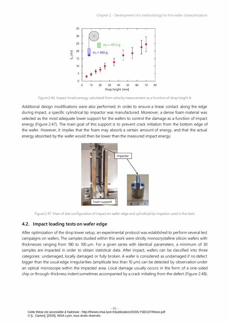
Chapter 2 - Development of a methodology for thin wafer characterization
- 65 -
Figure 2.46. Impact kinetic energy calculated from velocity measurement as a function of drop height ℎ
Additional design modifications were also performed. In order to ensure a linear contact along the edge
during impact, a specific cylindrical tip impactor was manufactured. Moreover, a dense foam material was
selected as the most adequate lower support for the wafers to control the damage as a function of impact
energy (Figure 2.47). The main goal of this support is to prevent crack initiation from the bottom edge of
the wafer. However, it implies that the foam may absorb a certain amount of energy, and that the actual
energy absorbed by the wafer would then be lower than the measured impact energy.
Figure 2.47. View of test configuration of impact on wafer edge and cylindrical tip impactor used in the tests
4.2. Impact loading tests on wafer edge
After optimization of the drop tower setup, an experimental protocol was established to perform several test
campaigns on wafers. The samples studied within this work were strictly monocrystalline silicon wafers with
thicknesses ranging from 180 to 100 µm. For a given series with identical parameters, a minimum of 30
samples are impacted in order to obtain statistical data. After impact, wafers can be classified into three
categories: undamaged, locally damaged or fully broken. A wafer is considered as undamaged if no defect
bigger than the usual edge irregularities (amplitude less than 10 µm) can be detected by observation under
an optical microscope within the impacted area. Local damage usually occurs in the form of a one-sided
chip or through-thickness indent sometimes accompanied by a crack initiating from the defect (Figure 2.48).
Cette thèse est accessible à l'adresse : http://theses.insa-lyon.fr/publication/2020LYSEI107/these.pdf © [L. Carton], [2020], INSA Lyon, tous droits réservés

Chapter 2 - Development of a methodology for thin wafer characterization
- 66 -
Figure 2.48. Microscope images of locally damaged wafers after impact on the edge
In order to meet the two objectives of the setup previously defined, we implemented two testing procedures
to characterize a series of wafers:
i) In order to determine the minimum breakage energy, the wafers are alternately sampled and impacted
at different levels of energy.
ii) In order to evaluate the damage potential caused by a non-destructive local impact, the wafers are
impacted at a given energy value, and the samples that were not fully broken are then tested in the
4-line bending setup. The stress distribution obtained is compared to a reference batch.
We applied the first testing procedure (i) on 300 monocrystalline samples of nominal thickness 160 µm. The
wafers were divided into ten subsets and impacted at ten different levels of energy, from Ek-min = 3.0 ± 0.6 mJ
(corresponding to a drop height of 5 mm) to Ek-max = 25.3 ± 5.1 mJ (drop height of 70 mm). Impact was
performed on the middle of the lateral edges where the wire enters and exits the bricks, defined in section 1.2
and presented in blue on Figure 2.9 22. The results are displayed in Figure 2.49 by showing the evolution of
the three curves (undamaged, locally damaged, fully broken) as a function of impact energy. Due to the
relatively high measurement uncertainty, most of the error bars for two consecutive levels of energy overlap.
This explains some unexpected values such as the decrease in breakage rate between 8 and 10 mJ
(Figure 2.49.c).
Results firstly show that the percentage of undamaged wafers decrease with impact energy, while the
breakage rate increases. This confirms the relevance of our setup despite the relatively high measuring
uncertainties. We observe that until a breakage rate of ~ 70 % is reached, the increase in broken wafers is
exponential. The curve then slightly flattens and the 100 % breakage rate is not reached as fast as expected.
In other words, after a certain level of energy, there still remain 3 to 4 wafers able to withstand the impact
without fully breaking. An extremely sharp evolution of the curves can be observed at very low levels of
energy, with a combined drop in number of undamaged wafers (from 93 % to 43 %) and a jump in number
of locally damaged wafers (from 7 % to 57 %) between 3 and 4 mJ. This quick transition illustrates that the
local damage is actually a way for the wafer to dissipate the impact energy without fully breaking: above a
certain value, the level of energy is too high to be elastically absorbed by the wafer, and needs to be
evacuated. After this fast raise, the number of locally damaged wafers slowly decreases as the number of
broken wafers increases.
22 Preliminary tests showed no statistically significant differences in breakage/damage rates when impacting the wafers on
different edges. As explained below, there is however a significant effect on wafer strength.
Cette thèse est accessible à l'adresse : http://theses.insa-lyon.fr/publication/2020LYSEI107/these.pdf © [L. Carton], [2020], INSA Lyon, tous droits réservés

Chapter 2 - Development of a methodology for thin wafer characterization
- 67 -
(a) Undamaged
(b) Local damage
(c) Fully broken
Figure 2.49. Percentage of (a) undamaged, (b) locally
damaged and (c) fully broken monocrystalline wafers of
thickness 160 µm as a function of impact energy
The initial goal of this study was to be able to determine precisely the minimum breakage energy, i.e. the
highest value of Ek for which the breakage rate is equal to zero. One way to achieve this is to find a
mathematical function that fits the experimental points from the fully broken wafers. The shape of the curve
from Figure 2.49.c leads us to propose an exponential function of the form:
𝑃𝑏𝑟𝑜𝑘𝑒𝑛(𝐸𝑘) = {0 𝑖𝑓 𝐸𝑘 ≤ 𝐸𝑘−𝑚𝑖𝑛1 − 𝑒𝑥𝑝[−𝑎(𝐸𝑘 − 𝐸𝑘−𝑚𝑖𝑛)
𝑏] 𝑖𝑓 𝐸𝑘 > 𝐸𝑘−𝑚𝑖𝑛 (2.17)
where 𝑃𝑏𝑟𝑜𝑘𝑒𝑛 (𝐸𝑘) is the percentage of fully broken wafers at an impact kinetic energy 𝐸𝑘 . This function is
actually a 3-parameter Weibull distribution with shape parameter 𝑏, scale parameter 1 𝑎⁄ and threshold
parameter 𝐸𝑘−𝑚𝑖𝑛, i.e. the minimum breakage energy that we are trying to determine. The optimal
parameters 𝑎, 𝑏 and 𝐸𝑘−𝑚𝑖𝑛 were estimated by the least squares method on the 10 measured data. As
illustrated in Figure 2.50, the fitted curve allows us to estimate the minimum breakage energy for this series
of wafers to 𝐸𝑘−𝑚𝑖𝑛 = 6.5 ± 1.3 mJ.
Cette thèse est accessible à l'adresse : http://theses.insa-lyon.fr/publication/2020LYSEI107/these.pdf © [L. Carton], [2020], INSA Lyon, tous droits réservés

Chapter 2 - Development of a methodology for thin wafer characterization
- 68 -
Figure 2.50. Exponential curve fitting of the percentage of fully broken wafers as a function of impact energy
Ideally, the complete characterization of a series of wafers under impact loading should be performed
following this previous procedure, i.e. using at least ten levels of kinetic energies in order to fully describe
the dynamic response of the samples over a wide range of energies. However, this would require 300
samples to characterize an entire series of wafers, which seems unreasonable. In the rest of this work, we will
therefore assume that all monocrystalline wafers follow a behavior similar to the one observed for the
reference series of 300 wafers. This hypothesis will allow us to test only three to five levels of energies for a
given series of wafers, and use the evolution of the curves obtained presented in Figure 2.49 to comment
on possible missing transition values. In particular, the 3-parameter exponential law derived to express the
percentage of broken wafers as a function of energy may be used to determine the minimum breakage
energy. The use of this fitting function requires however to have at least four experimental points to build a
relevant model, and at least one point with a measured breakage rate higher than 50 %. Indeed, if only
points with extremely low breakage rates are available, the exponential increase of the curve will not be
correctly modeled.
The second testing procedure (ii) was implemented by performing impact tests at 12 mJ energy on two series
of 50 monocrystalline 180 µm thick wafers. In order to account for the strength anisotropy of DWS wafers,
the first series was impacted on the lateral edge of the wafers, where the wire enters and exits the brick,
while the other series was impacted on the edge of the wafer which is parallel to the wire web. These
configurations correspond respectively to the wire and cut direction orientations of the 4-line bending setup.
More specifically for the second series, the impact was performed on the edge glued to the beam during
cutting (see section 1.1), which is known to exhibit more chipping [182]. The wafers that were not fully broken
after impact where then tested in the 4-line bending setup and compared with a reference batch. Figure 2.51
illustrates the results as histograms of the fracture stress values for the two loading directions. It appears
quite clearly that wafers impacted on the lateral edge (Figure 2.51.a) have the same strength as the reference
wafers. On the contrary, the influence of an impact on the top edge is remarkable: the scattering of the stress
values increases, and the strength is in average 20 % lower. More specifically, a new wafer population with
much lower strength than the reference batch, corresponding to the wafers that were damaged during
impact, can clearly be identified.
Cette thèse est accessible à l'adresse : http://theses.insa-lyon.fr/publication/2020LYSEI107/these.pdf © [L. Carton], [2020], INSA Lyon, tous droits réservés

Chapter 2 - Development of a methodology for thin wafer characterization
- 69 -
(a)
(b)
Figure 2.51. Histograms of wafer strength in 4-line bending before and after 12 mJ impact on the edge (a) wire direction and
(b) cut direction
The new drop test methodology for impact loading on wafer edge was thus validated with both its testing
procedures. It is however important to mention here that this characterization technique still presents some
important limitations:
The uncertainty on the velocity measurement, and therefore the calculated impact energy, is relatively
high. Indeed, an impact energy of 20 mJ is measured with an uncertainty ± 4 mJ, which makes it difficult
to compare results obtained for different impact energies relatively close to one another. This high
uncertainty is however inherent to the optical detecting system and could only be reduced introducing
an alternate, more precise speed measuring system such as a high frequency camera.
In the absence of an exploitable load signal, we have no information regarding which percentage of the
impacting kinetic energy is actually absorbed by the wafer and by the support foam material. The
evaluated minimum breakage values could therefore be underestimated. They should therefore be used
with caution, and rather for comparison between series than as empirical values.
5. DISCUSSION
In the scope of this work, we developed different destructive testing techniques, in the form of two
quasi-static bending methods and a dynamic impact test. The ambition behind this approach was to have
at our disposal a wide range of characterization tools, which would allow to describe, study and compare
different aspects of the mechanical behavior of a PV silicon wafer. Yet for obvious reasons related to the
limited time and number of samples available, we did not systematically implement all three methods to
each studied set of wafers. In the following section, we discuss and compare the advantages, applicability
and limits of each characterization technique in order to define for which purposes each of them can be
preferentially used.
5.1. On the relevance of the RoR setup versus 4-line bending
Both quasi-static bending tests implemented, i.e. the classic uniaxial 4-line bending setup and a biaxial RoR
method, are designed to test an entire 156 × 156 mm2 wafer without requiring a preparation or dicing step.
On the one hand, we showed in section 3.1 that provided an appropriate span configuration is chosen as a
function of sample thickness, the stress distribution in the wafer under 4-line bending is uniform and
homogeneous. The failure stresses can easily be computed via the FE models and statistically analyzed to be
Cette thèse est accessible à l'adresse : http://theses.insa-lyon.fr/publication/2020LYSEI107/these.pdf © [L. Carton], [2020], INSA Lyon, tous droits réservés

Chapter 2 - Development of a methodology for thin wafer characterization
- 70 -
compared between different series of wafers. On the other hand, results from section 3.2 highlight that the
behavior of the wafer when tested with the RoR setup is nonlinear and experiences buckling before failure.
FE analysis reveals a complex and multiaxial stress distribution, which strongly depends on the deformed
shape of the plate after buckling. We concluded that it was not relevant to interpret the results from the RoR
setup in terms of stress values, and alternatively proposed to describe wafer strength via the statistical
distribution of the fracture load values 𝐹𝑖, which however requires to compare samples of similar thickness.
When compared with the simplicity of application and interpretation of the 4-line bending setup, it is
legitimate to question the relevance of the RoR setup for wafer strength evaluation. In existing literature, the
main argument put forward when applying this method on PV silicon wafers is that it allows to exclude the
influence of edge defects, which are believed to be the main origin of failure in uniaxial bending tests. The
underlying second argument is that the RoR method is more efficient than the 4-line bending method to
detect differences in mechanical behavior caused by differences in wafer surface defects. Given our
experience, we however consider that these arguments require further investigation. More specifically, in
order to justify the relevance of the RoR setup with respect to 4-line bending, we performed specific
experimental studies to address the two following questions:
(i) Compared to the 4-line bending test, is the RoR test unaffected by the presence of edge defects?
(ii) Compared to the 4-line bending test, is the RoR test more sensitive to differences in surface defects?
In order to answer the first question (i), we deliberately introduced defects on the edges of monocrystalline
wafers of thickness 180 µm. The defects were created with using a laser and had the shape of 5 mm through-
thickness cracks starting from the edge, with different angles (Figure 2.52).
Figure 2.52. Microscopic images of laser defects created at the wafer edges
According to the required number of samples per test method, 50 identically damaged samples were
prepared for the RoR setup, and two series of 40 identically damaged samples were prepared for the 4-line
bending setup to be tested in both loading directions. The position and number of defects per wafer was
adjusted depending on the geometry of the setup, as indicated in Figure 2.53. For each damaged series, a
reference series with an identical number of wafers was kept as a reference. The wafers from the damaged
and undamaged series were then tested with the 4-line bending and RoR setups according to the
experimental procedures described in sections 3.1 and 3.2.
Cette thèse est accessible à l'adresse : http://theses.insa-lyon.fr/publication/2020LYSEI107/these.pdf © [L. Carton], [2020], INSA Lyon, tous droits réservés

Chapter 2 - Development of a methodology for thin wafer characterization
- 71 -
(a)
(b)
(c)
Figure 2.53. Relative position of the edge defects on the wafers with respect to the test geometry (a) RoR setup (b) 4 -line
bending in wire direction (c) 4-line bending in cut direction
For the 4-line bending setup, the failure stresses 𝜎𝑖 are computed via the FE model and adjusted to a Weibull
distribution with parameters (𝜎𝜃,𝑚), while results from the RoR test are presented as a Weibull distribution
of failure loads with parameters (𝐹𝜃,𝑚). Figure 2.54 thus compares the characteristic strength and load
parameters 𝜎𝜃 and 𝐹𝜃 obtained for both testing setups. The vertical error bars represent the 90 % confidence
bounds of the estimated parameters.
The results obtained for the RoR setup highlight that contrary to what was expected, the existence of edge
defects did influence the mechanical strength of the wafers. Indeed, as it is indicated on Figure 2.54, the
estimated characteristic load 𝐹𝜃 is about 23 % lower for the wafers with damaged edges. More specifically,
it appears that the vast majority (>80 %) of the wafers with damaged edges does not survive the first buckling
mode, i.e. failure occurs as soon as the plate tries to change its deformation mode. Therefore, although the
stress levels at the wafer edges remain relatively low during the RoR test, the sudden change in value during
buckling can lead to failure at the edge defects, which act as stress concentration areas.
(a)
(b)
Figure 2.54. Comparison of Weibull scale parameter obtained when testing wafers with damaged or undamaged edges: (a)
Characteristic strength 𝜎𝜃 for the 4-line bending setup (b) Characteristic load 𝐹𝜃 for the RoR setup
The presence of edge defects also has an influence on the mechanical strength of the wafers in 4-line
bending setup, which depends on the loading direction: in wire direction, the decrease in characteristic
strength is of the same order of magnitude as for the RoR test. In cut direction however, the edge defects
lead to a decrease of more than 65 % of the mechanical strength, with stress values falling below the ones
from the reference batch in wire direction. In other words, the introduction of edge defects lowers the
mechanical strength of the wafers to the same level, regardless of the loading direction. When taking into
account the impact on both loading directions, one could conclude that while the RoR setup is not immune
to the presence of edge defects on the wafers, their influence on the mechanical properties is somewhat less
Cette thèse est accessible à l'adresse : http://theses.insa-lyon.fr/publication/2020LYSEI107/these.pdf © [L. Carton], [2020], INSA Lyon, tous droits réservés

Chapter 2 - Development of a methodology for thin wafer characterization
- 72 -
critical than in the 4-line bending setup. One should also mention here that the size of these “fake” defects
is about 300 times bigger than the usual edge defects observable on as-cut wafers (in the order of a few
tens of micrometers). There might exist a critical size below which their influence in the RoR setup would be
negligible.
In order to answer the second question (ii), we tested wafers that were cut using different sawing recipes
(which therefore potentially exhibit different surface characteristics) with both bending methods. The aim
was to see whether one of the setups was more efficient in detecting differences in mechanical behavior.
More specifically, we sampled wafers coming from four recipes R1, R2, R3 and R4. As indicated on Table 2.5,
the recipes differ in wire speed and feed rate 23. Recipes R1 and R2 were performed with the same wire on
two identical monocrystalline bricks and recipes R3 and R4 with another wire on two other bricks. The
mechanical properties of the obtained wafers are therefore compared two by two, i.e. recipe R1 vs recipe R2
and recipe R3 vs recipe R4. The average thicknesses of the compared wafers are similar (Table 2.5), so that
the failure load values 𝐹𝑖 obtained with the RoR setup are comparable.
Table 2.5. Sawing recipes and average wafer thicknesses
Sawing
recipe Characteristics Wire used Brick used
Average thickness ±
STD [µm]
R1 High wire speed – high feed rate Diamond 80 HT Cz mono, set 1 179.9 ± 0.4
R2 High wire speed – low feed rate Diamond 80 HT Cz mono, set 1 179.1 ± 0.6
R3 Low wire speed – low feed rate Diamond 70 HT Cz mono, set 2 179.5 ± 0.8
R4 High wire speed – high feed rate Diamond 70 HT Cz mono, set 2 179.4 ± 0.8
Figure 2.55 shows, in the same format as previously, the characteristic strength and load parameters 𝜎𝜃 and
𝐹𝜃 obtained with both testing setups for wafers from sawing recipes R1 and R2. It appears that regardless of
the bending method used, wafers sawn with recipe R2 exhibit higher mechanical strength than wafers sawn
with recipe R1. For both setups, there is a statistically significant increase in parameters 𝜎𝜃 and 𝐹𝜃. Although
the relative increase measured is slightly higher for the RoR (+13 %) than for the 4-line bending setup (+11 %
in cut direction), the difference is not large enough to conclude that the RoR method is a more appropriate
tool to highlight distinctions in mechanical properties between wafers.
When looking at the results obtained for the wafers sawn with recipes R3 and R4 (Figure 2.56), it comes out
that the mechanical properties of the samples are equivalent. In other words, there is no statistically
significant difference between the estimated parameters 𝜎𝜃 and 𝐹𝜃, regardless of the setup used. The RoR
test did not allow to detect any additional differences in mechanical behavior when compared to the 4-line
bending setup. These findings lead us to reconsider the relevance of the RoR setup for strength evaluation
of silicon wafers. Indeed, the main theoretical advantage of this method with respect to the 4-line bending
setup was its ability to suppress the influence of edge defects and to emphasize the influence of surface
defects. Yet the above presented results show that (i) large edge defects do have an influence on the
mechanical strength of wafers when tested with the RoR setup and that (ii) when comparing two sets of
wafers, the RoR method does not necessarily provide more information than the 4-line bending method.
23 The specific parameter values of each recipe are not detailed here as the purpose is to compare the differences in
mechanical behavior between the two setups. The influence of sawing parameters will be investigated in Chapter 4.
Cette thèse est accessible à l'adresse : http://theses.insa-lyon.fr/publication/2020LYSEI107/these.pdf © [L. Carton], [2020], INSA Lyon, tous droits réservés

Chapter 2 - Development of a methodology for thin wafer characterization
- 73 -
(a)
(b)
Figure 2.55. Comparison of Weibull scale parameter obtained when testing wafers sawn with recipes R1 and R2:
(a) Characteristic strength 𝜎𝜃 for the 4-line bending setup (b) Characteristic load 𝐹𝜃 for the RoR setup
(a)
(b)
Figure 2.56. Comparison of Weibull scale parameter obtained when testing wafers sawn with recipes R3 and R4:
(a) Characteristic strength 𝜎𝜃 for the 4-line bending setup (b) Characteristic load 𝐹𝜃 for the RoR setup
The RoR setup still benefits from one significant practical advantage when compared to the 4-line bending
method, namely the fact that there is no need to differentiate the loading direction, and less samples are
thus required to characterize a given series – which allows saving time. However, given on the one hand that
the RoR setup requires a more rigorous experimental protocol, and on the other hand that the results are
more difficult to interpret and limited to comparing wafers of similar thicknesses, this advantage was
considered too limited to justify the systematic use of the RoR over the 4-line bending method.
5.2. Impact loading on wafer edge: applicability of the test
The drop test methodology developed is the first of its kind for PV silicon wafers and is therefore the least
standardized of the strength characterization techniques presented in this work. The initial commercial
equipment underwent numerous design modifications and the experimental protocol was gradually
improved through extensive preliminary testing. The method helps to gain understanding on the behavior
of silicon wafers when subjected to impact loading on their edge. However, due to the relatively high
uncertainty of kinetic energy calculation and the inability to measure the reaction load from the wafer, a
Cette thèse est accessible à l'adresse : http://theses.insa-lyon.fr/publication/2020LYSEI107/these.pdf © [L. Carton], [2020], INSA Lyon, tous droits réservés

Chapter 2 - Development of a methodology for thin wafer characterization
- 74 -
quantitative comparison between wafers coming from different sawing recipes or different crystal growth
techniques is not yet possible.
Nevertheless, as it will be shown in Chapter 4, the impact loading test method provides some insightful
information to study the influence of wafer thickness on their dynamic behavior. Moreover, the results
presented in section 4.2 of the present chapter when submitting impacted wafers to 4-line bending tests are
a first step towards more practical handling recommendations: they show that it is more desirable for wafers
to experience impact loading on the lateral edges, as it does not have a negative impact on their bending
strength. Wafers should therefore as much as possible be handled so that contact occurs preferably on their
lateral edges. This aspect is not taken into account in the industry today. Within the scope of this work, the
drop test method was therefore rather used as a tool to provide handling recommendations for the
processing of PV silicon wafers in general, rather than as a characterization technique to strictly compare the
influence of sawing parameters of the mechanical strength of wafers.
6. CONCLUSION
The objectives of this chapter were to develop appropriate tools to characterize the morphological, structural
and mechanical properties of diamond-wire sawn silicon wafers for PV applications. We developed different
characterization techniques and corresponding experimental protocols. When necessary, design
modifications were performed to adjust the methodology to the characteristics of the wafers. In the last
section, we more specifically confronted the advantages and limitations of the mechanical testing setups.
This chapter allowed to define the following characterization guidelines for the rest of our study:
(i) Prior to any destructive mechanical testing, the topology of each investigated wafer is systematically
measured with the capacitive distance system (see section 2.1). This step provides the important
geometrical parameters that classically define the quality of an as-cut wafer: average thickness and TTV.
(ii) If the available number allows it, about ten to twenty wafers from each series to be characterized are
randomly sampled and set aside as control or witness samples. They will not undergo mechanical testing
and will remain intact if further characterization is needed.
(iii) The 4-line bending setup is the preferred characterization technique to study and compare the influence
of different silicon crystallinities and surface properties on the mechanical properties of the wafers, as
well as the impact of decreasing as-cut thickness on the bending strength of the plates. Indeed the
method is easily implemented on wafers of thicknesses ranging from 100 to 180 µm and provides
statistical quantities to describe and compare the strength properties of different series of wafers. The
methodology implemented for this setup is schematically reminded in Figure 2.57.
(iv) The RoR setup is implemented on wafers as a way of completing results obtained with the 4-line bending
setup. This is done in particular when further investigation on the influence of different surface properties
is required, or to provide specific information on the buckling phenomenon, which can be related to the
flexibility of the wafers. The implemented methodology for this setup is recalled on Figure 2.58.
(v) Finally, the drop tower setup is implemented on reference series of DWS monocrystalline wafers with
the aim of better understanding their behavior when subject to impact loading on their edge. The
method does not yet allow comparison between different sets of wafers but helps providing practical
handling recommendations regarding the processing of the wafers into solar cells, in particular as the
as-cut thickness decreases. The drop tower test can be used on its own or in combination with 4-line
bending tests performed on pre-impacted wafers, as schematically shown in Figure 2.59.
Cette thèse est accessible à l'adresse : http://theses.insa-lyon.fr/publication/2020LYSEI107/these.pdf © [L. Carton], [2020], INSA Lyon, tous droits réservés

Chapter 2 - Development of a methodology for thin wafer characterization
- 75 -
Figure 2.57. Methodology implemented to characterize the wafers with the 4-line bending setup
Figure 2.58. Methodology implemented to characterize the wafers with the RoR setup
Figure 2.59. Methodology implemented to characterize the wafers with the drop tower test
These characterization techniques provide the necessary tools to study the mechanical behavior of as-cut
diamond wire sawn silicon wafers as comprehensively as possible. In the following chapters, we will use these
tools, with a preference given to the 4-line bending setup, to try to identify which defects are the most critical
for wafer failure, and whether the sawing recipe can be optimized to limit those defects and obtain wafers
that are as mechanically reliable as possible.
Cette thèse est accessible à l'adresse : http://theses.insa-lyon.fr/publication/2020LYSEI107/these.pdf © [L. Carton], [2020], INSA Lyon, tous droits réservés

- 76 -
CHAPTER 3
- Identifying the critical defects
responsible for wafer failure
The as-cut silicon wafer can be seen as an assembly of defects of different size, nature, density and
shape, which ultimately control the resulting fracture strength of the brittle material. The aim of this
chapter is to determine which of these flaws are the most critical for the mechanical failure of the
samples. We first recall which different defects are generated during wafer manufacturing and
develop the approach implemented to isolate their influence on fracture strength. In the second part,
we compare the behavior of samples that were chemically etched and show that the morphology of
the initial sawing-induced surface defects plays a significant role on the mechanical properties of the
wafers. In the third part, we use selective chemical and mechanical polishing processes to demonstrate
that edge defects are not responsible for the mechanical failure of as-cut wafers. Annealing processes
performed on as-cut samples in the fourth part highlight that without any modification of the surface
features, wafer strength can be doubled using a thermal treatment. Finally, by combining the action
of chemical etching and annealing processes, we show in part five that all critical damage regarding
wafer mechanical failure is located within a thin subsurface layer, which is less than 3 µm deep.
Cette thèse est accessible à l'adresse : http://theses.insa-lyon.fr/publication/2020LYSEI107/these.pdf © [L. Carton], [2020], INSA Lyon, tous droits réservés

Chapter 3 - Identifying the critical defects responsible for wafer failure
- 77 -
Contents
1. INTRODUCTION AND APPROACH ..................................................................................................... 78
2. HEALING WAFER SURFACE TOPOGRAPHY ........................................................................................... 81
2.1. Evolution of wafer strength with surface chemical polishing and texturing ................................................... 81
2.1.1. Samples preparation.................................................................................................................................................. 81
2.1.2. Surface characterization .......................................................................................................................................... 85
2.1.3. Strength results .......................................................................................................................................................... 87
2.2. Evolution of wafer strength as a function of chemical etch removal ............................................................... 94
2.2.1. Sample preparation .................................................................................................................................................. 94
2.2.2. Surface characterization ..................................................................................................................................... 96
2.2.3. Mechanical strength ............................................................................................................................................ 99
3. ISOLATING WAFER EDGE DEFECTS.................................................................................................... 103
3.1. Differentiating DWS wafer edges .............................................................................................................................103
3.2. Chemical polishing of wafer edges ..........................................................................................................................104
3.2.1. Experimental procedure .........................................................................................................................................105
3.2.2. Sample characterization ....................................................................................................................................106
3.2.3. Strength results ....................................................................................................................................................108
3.3. Mechanical polishing of wafer edges ......................................................................................................................109
3.3.1. Experimental procedure .........................................................................................................................................109
3.3.2. Sample characterization ..................................................................................................................................... 111
3.3.3. Strength results .................................................................................................................................................... 112
3.4. Discussion........................................................................................................................................................................ 113
4. ISOLATING BULK AND SUBSURFACE DEFECTS BY THERMAL TREATMENT ................................................ 114
4.1. Introduction .................................................................................................................................................................... 114
4.2. Influence of thermal treatment on as-cut wafer strength.................................................................................. 115
4.2.1. Experimental procedure ......................................................................................................................................... 115
4.2.2. Strength results .................................................................................................................................................... 116
4.3. Structural and chemical characterization of the annealed wafers ................................................................... 118
4.3.1. Measuring residual stresses in as-cut and annealed wafers......................................................................... 119
4.3.2. Measuring surface oxidation of as-cut and annealed wafers..................................................................122
4.3.3. Discussion ..............................................................................................................................................................124
5. ANNEALING OF AS-CUT AND CHEMICALLY ETCHED WAFERS .............................................................. 125
5.1.1. Experimental procedure .........................................................................................................................................125
5.1.2. Sample characterization .........................................................................................................................................126
5.1.3. Strength results .........................................................................................................................................................127
6. CONCLUSION ............................................................................................................................... 129
Cette thèse est accessible à l'adresse : http://theses.insa-lyon.fr/publication/2020LYSEI107/these.pdf © [L. Carton], [2020], INSA Lyon, tous droits réservés

Chapter 3 - Identifying the critical defects responsible for wafer failure
- 78 -
1. INTRODUCTION AND APPROACH
While the fracture strength of defect-free single crystalline silicon has been reported to range between
5 and 7 GPa [42,212], a typical solar grade silicon wafer will usually fail at applied stresses well below
1 GPa [27,213]. This phenomenon is a result of the numerous defects generated during the manufacturing
process of the wafer, from crystallization to sawing. As in any inherently brittle mater ial with low fracture
toughness [214], failure in silicon initiates indeed from existing flaws that act as local stress risers. The strength
of a silicon wafer is conditioned by the size, nature, density and shape of these defects.
Optimizing the parameters of this manufacturing process to reduce the number of generated defects and
to obtain mechanically reliable wafers is an important objective for the PV industry, as it would allow to
significantly lower the breakage rates during the handling steps. However, before determining which of the
processing steps are the most important to improve wafer strength and how the corresponding parameters
should be adjusted, it seems legitimate to wonder which of these defects are indeed the most critical for
mechanical failure of the wafer.
As presented in Chapter 1, the manufacturing process of silicon wafer can be divided into two main steps:
the crystallization of the raw material into a solid ingot and the sawing of the brick. Both steps generate
defects of different nature, location and size. Defects generated during the solidification process are usually
referred to as bulk defects or intrinsic defects. From a mechanical point of view, the bulk defects that have
been identified in previous work as possible fracture origins in wafers are mainly residual stresses generated
during solidification [215] and inclusions in the form of doping elements [135] or impurities [65]. It was also
suggested that areas with high dislocation density act as barriers to crack propagation and give rise to higher
toughness and overall wafer fracture strength [216]. In the particular case of multicrystalline or mono-like
silicon, the role of grain boundaries has also often been called into question: Popovich et al. observed cracks
propagating along the boundaries and assumed they reduced the wafer strength [59,136], while Barredo et
al. found that mono-like wafers with larger quantity of sub-grain boundaries exhibited lower fracture
strength [99].
The sawing process is considered as the step that generates the most critical defects regarding wafer failure.
As discussed in Chapter 1, the abrasion mechanisms involved in DWS generate long parallel grooves oriented
in the direction of the wire, as well as randomly distributed indention pits [22]. These features can be
considered as morphological surface defects, and their unidirectional nature is believed to play an important
role in the mechanical strength of the wafers [28]. We also explained that the sawing process damages the
material properties within a subsurface volume up to a few micrometers below the surface, the so-called
SSD layer, containing flaws of different nature and size. The most commonly recognized fracture cause
among these subsurface defects are microcracks, with reported lengths varying from a few tenths up to
several tens of microns [24,153,178]. Yet a few studies also question the role of other subsurface defects:
Sekhar et al. thus justify the lower fracture strength measured on some DWS wafers by an increased
proportion of transformed silicon phase in the SSD layer [187]. Some works also highlighted the existence of
sawing-process related residual stresses in the SSD layer, caused by a high local contact pressure [183].
Finally, as shortly introduced in Chapter 1, the sawing process can also induce some micrometer scale
chipping at the wafer edges, thus generating what we refer to as edge defects.
All above described defects may play a role on the fracture strength of the as-cut wafer, and are summarized
in Table 3.1. It is worth recalling here that bulk defects refer to damage generated during crystallization, while
surface, subsurface and edge defects were induced by the sawing process.
Cette thèse est accessible à l'adresse : http://theses.insa-lyon.fr/publication/2020LYSEI107/these.pdf © [L. Carton], [2020], INSA Lyon, tous droits réservés

Chapter 3 - Identifying the critical defects responsible for wafer failure
- 79 -
Table 3.1. Summary of the type of potential defects influencing the strength of as-cut DWS wafers
Location of defect in wafer Nature
Bulk Inclusions (doping or impurities) - Dislocations clusters - Grain
boundaries - Residual stresses
Surface Scratching grooves - Indentation pits
Subsurface Microcracks - Crystalline phases - Residual stresses
Edge Chipping or cracks
Before analyzing these defect populations more in detail, it seems worthwhile to discuss the most important
mechanical feature of DWS wafers: their strong anisotropy in strength properties. This characteristic was
rapidly discovered when the first DWS samples were introduced and studied as a potential replacement
substrate for the slurry sawn wafers in standard solar cell production lines [21], and has been widely
documented since [26,28,153,184,217]. As introduced in the previous chapter, we indeed know that the
unidirectional nature of the sawing-induced damage on DWS wafers causes an anisotropy in fracture
strength depending on the loading direction. In order to get a practical understanding of the extent of this
property, we present in Figure 3.1 the Weibull failure probability plots obtained for monocrystalline DWS
wafers that were sawn in our lab in 2020 and tested with the 4-line bending setup presented in Chapter 2.
On the same graph are also depicted the plots for monocrystalline slurry sawn wafers, which were
manufactured in 2015 and tested in 2020 using the exact same bending setup. Both types of wafers can be
considered as state-of-the-art representative samples of each sawing technology. According to the
experimental procedure, the as-cut wafers were tested by positioning the saw marks either parallel or
perpendicular to the loading devices 24, which we refer to as wire direction and cut direction.
Figure 3.1. Weibull failure probability plots obtained for monocrystalline DWS and slurry sawn wafers when tested in 4-line
bending in cut and wire direction
24 For the slurry sawn wafers, the saw marks are not visible to the naked eye. Their orientation was then determined by
spotting the differences in local thicknesses. As introduced in Chapter 1, slurry sawn wafers are indeed tapered and thinner
on the side where the wire enters the brick.
Cette thèse est accessible à l'adresse : http://theses.insa-lyon.fr/publication/2020LYSEI107/these.pdf © [L. Carton], [2020], INSA Lyon, tous droits réservés

Chapter 3 - Identifying the critical defects responsible for wafer failure
- 80 -
The difference in strength distribution between the two loading directions is unquestionable for the DWS
wafers, with a characteristic strength parameter 𝜎𝜃, which is 2.4 times higher in cut direction. In comparison,
the slight anisotropy exhibited by the slurry sawn wafers can be considered negligible, with a ratio in
characteristic strength lower than 1.1. More specifically, these plots confirm that while in cut direction, the
strength of DWS wafers is higher than that of slurry sawn wafers, the opposite is observable in wire direction:
the fracture strength of the DWS is critically lower. It is worth noting that for a given loading direction, the
slopes of the probability plots are almost identical regardless of the sawing technique. More specifically, the
slope of the curves in wire direction are in average twice as steep as in cut direction. In other words, for both
types of samples, the Weibull modulus is twice higher in wire direction, i.e. failure stress values are less
scattered, which implies a more homogeneous defect density. Therefore, although no difference in
characteristic strength is detectable for the slurry-sawn wafers, the movement of the wire does create a form
of anisotropy similar to that of the DWS samples, which reflects in the scattering of the stress values.
It is important to understand that the lower strength in wire direction is precisely the critical weak point of
DWS wafers. Ultimately, the goal of any work aiming at improving the mechanical properties of DWS wafers
is actually to shift the failure stresses measured in wire direction (i.e., the left pink curve) towards the values
obtained in cut direction (i.e., the right pink curve). With this goal in mind, one could theoretically only
evaluate the mechanical properties of DWS wafers in wire direction. However, the results obtained in cut
direction can provide valuable additional information on the type of defects responsible for changes in
strength.
The goal of this chapter is to determine the most critical defects regarding wafer failure among the ones
listed in in Table 3.1. We identified two possible approaches to address this issue. The first option would be
to perform mechanical tests on different series of as-cut wafers, and in parallel, to implement numerous
defects characterization techniques, and attempt to correlate the differences in mechanical behavior
measured with possible differences in defect shape, concentration or size. The main issue of this approach
is that it is relatively time-consuming, especially since we do not know a priori which type of defects should
be analyzed in priority. The second option, which was retained for this work, is to try to selectively isolate or
remove some of the defects presented in Table 3.1 from the as-cut wafers. By performing mechanical tests
on the samples before and after removing these defects, our ambition is to understand which of these
defects most influence the mechanical strength of the wafers.
In this chapter, we therefore conduct an extensive systematic procedure to isolate different areas of the
as-cut wafers and their corresponding defects. All investigations are performed on monocrystalline DWS
samples, and their mechanical strength is evaluated with the help of 4-line bending or RoR tests. In the
second part, we focus on the influence of the morphological surface defects generated by the sawing process
by performing chemical processing on the as cut samples. In a third part, we try to remove efficiently the
edge defects from the samples, both chemically and mechanically. The fourth part of the chapter is dedicated
to the influence of an annealing process on the mechanical properties of the as cut wafers. Finally, the last
part combines chemical etching with thermal processes to try to understand which areas of the wafers are
affected and how this effectively heals some of the most critical wafers’defects.
It should be noted that the wafers used throughout this chapter are strictly monocrystalline and were sawn
using diamond wires with either 80 or 70 µm core diameter and abrasive grain size [8-16] µm.
Cette thèse est accessible à l'adresse : http://theses.insa-lyon.fr/publication/2020LYSEI107/these.pdf © [L. Carton], [2020], INSA Lyon, tous droits réservés

Chapter 3 - Identifying the critical defects responsible for wafer failure
- 81 -
2. HEALING WAFER SURFACE TOPOGRAPHY
The strong anisotropy in strength properties displayed by DWS as-cut wafers indicates that the surface
features play a significant role on their mechanical behavior. It therefore seems relevant to start our study
by investigating the influence of modification in surface topography.
2.1. Evolution of wafer strength with surface chemical polishing and texturing
In this section, we compare the mechanical behavior of monocrystalline wafers with three fundamentally
different surface features, which are characteristic of the PV industry: as-cut wafers taken directly after the
sawing process, chemically-polished and textured wafers. The polishing and texturing processes applied to
the samples are detailed in the following section. Since the aim of this study is to highlight differences in
behavior related to surface properties, the mechanical behavior of the resulting wafers is evaluated by 4-line
bending tests coupled with RoR tests. It should however be mentioned that on the one hand, the wafers
used for the 4-line bending and RoR tests came from different batches, and on the other hand that the tests
and corresponding wafer treatments were performed two years apart. Within this lapse of time, there have
been changes in the chemistry benches from the clean room and in the texturing processes, which can lead
to differences in surface topography between the two series.
2.1.1. Samples preparation
a) Chemical etching
The chemical etching process is one of the first steps performed on as-cut wafers. It consists in removing a
certain thickness of silicon layer at the wafer surface via a chemical reaction. The solution used is composed
of hydrofluoric acid (HF), nitric acid (HNO3) and acetic acid (CH3COOH). The material removal mechanism is
ensured by the oxidation of silicon by the HNO3 (3.1) and the subsequent removal of the resulting oxide by
the HF (3.2) [218]. The balanced chemical equation for the reaction is given in (3.3).
3𝑆𝑖 + 4𝐻𝑁𝑂3 → 3𝑆𝑖𝑂2 + 4𝑁𝑂 +2𝐻2𝑂 (3.1)
𝑆𝑖𝑂2 + 6𝐻𝐹 = 𝐻2𝑆𝑖𝐹6 +2𝐻2𝑂 (3.2)
3𝑆𝑖 + 4𝐻𝑁𝑂3 + 18𝐻𝐹 = 3𝐻2𝑆𝑖𝐹6 +4𝑁𝑂 + 8𝐻2𝑂 (3.3)
The chemical reaction (3.3) is highly exothermic. The chemical reaction rate of the HF:HNO3 mixture is
isotropic with respect to the crystallographic orientation of silicon [219]. CH3COOH acts as a diluent of the
solution and provides control over the reaction rate [220]. In other words, increasing the proportion of
CH3COOH decreases the material removal rate. For the chemical etching of our as-cut wafers, we chose to
have a relatively low reaction rate, for which the material removal rate on typical as-cut DWS wafers had
been determined in a previous work [175]. The solution used, with volume proportions given in Table 3.2,
yields a material removal rate of approximately 0.2 µm/min.
Table 3.2. Composition of the solution used for the chemical etching of the as-cut wafers
Component HF HNO3 CH3COOH
Volume proportion 1 25 25
Volume (L) 0.343 8.575 8.575
Cette thèse est accessible à l'adresse : http://theses.insa-lyon.fr/publication/2020LYSEI107/these.pdf © [L. Carton], [2020], INSA Lyon, tous droits réservés

Chapter 3 - Identifying the critical defects responsible for wafer failure
- 82 -
The etching process is performed in a clean room on a specific bench composed of a chemical solution tank
and two rinsing tanks with 20 L volume capacity each. These tanks are suited to accommodate a carrier
containing 25 wafers (Figure 3.2). The carrier is immersed in the chemical solution for 20 minutes, thus
ensuring that approximately 4 µm of silicon per wafer face are removed. The chemical reaction is effectively
stopped by introducing the carrier in a rinsing tank filled with deionized water for about 15 minutes. The
wafers are then finally dried in an oven at 80 °C.
Figure 3.2. TeflonTM carrier containing the 25 as-cut wafers to be chemically etched
b) Surface texturing
In the solar cell manufacturing chain, the goal of the texturing process is to reduce the reflectivity of the
wafers by “roughening” their surface. This increases the chances of reflected light bouncing back onto the
surface, rather than to the surrounding air. Monocrystalline wafers are most commonly textured with an
alkaline solution such as potassium hydroxide (KOH), which has the specificity of etching the {100}
crystallographic planes of silicon much quicker than the {111} planes [221,222]. This anisotropic etch drives
the formation of random upright pyramidal structures (Figure 3.3) [223] with typically 7 to 10 µm in size [224].
This step usually removes between 5 and 15 µm of silicon from each wafer face and is also performed in a
clean room. The as-cut wafers are first cleaned with a Caro’s etch or piranha etch (sulfuric acid + hydrogen
peroxide) at 90 °C to remove any remaining organic residues at their surface 25. The texturing step is then
performed by immersing the as-cut wafers in a diluted KOH solution (weight fraction 20 %) for 14 minutes.
This process is fully automated and can handle carriers of 50 wafers at a time.
Figure 3.3. Plane and angular-view SEM images of alkaline textured monocrystalline wafers, from [223]
25 This cleaning step is required before introducing the as-cut wafers in the texturing equipment to avoid contamination.
Cette thèse est accessible à l'adresse : http://theses.insa-lyon.fr/publication/2020LYSEI107/these.pdf © [L. Carton], [2020], INSA Lyon, tous droits réservés

Chapter 3 - Identifying the critical defects responsible for wafer failure
- 83 -
c) Number of wafers and sampling methodology
The chemical etching and texturing process can only be performed in a clean-room by authorized operators.
Each processed carrier of wafers requires an important time of preparation and consumes valuable chemical
solution. We therefore had to make concessions on the number of prepared wafers per series, and could
not always comply with the ideal required number of wafers for statistical strength evaluation as defined in
Chapter 2. We recall that for the 4-line bending setup, two series of 40 wafers are ideally required, while for
the RoR setup one series of 50 wafers is required. One should also consider that as explained previously, the
chemical etching and texturing processes respectively handle 25 and 50 wafers at a time.
With these information in mind, we therefore chose to sample 150 initial wafers for each setup. The wafers
used for the RoR setup were taken from the middle of a monocrystalline brick and had a nominal thickness
of 180 µm. They were alternately sampled into three series of 50 wafers: the first as-cut series was kept as
reference, and the two others were respectively chemically polished and textured following the procedures
described above. The chemical polishing was performed by the successive immersion of two carriers of
25 wafers. For the 4-line bending setup, the 150 wafers were sampled from another monocrystalline brick
and had a nominal thickness of 160 µm. Similarly as for the RoR setup, they were separated into three series:
as-cut, chemical polishing and texturing. In addition, each of these series was further divided into two series
of 25 wafers to be tested in wire or cut direction.
The thickness and TTV of each wafer were evaluated before and after the chemical etching and texturing, in
order to determine the average silicon material removal per side. These data are given for the chemical
polishing step in Table 3.3 and for the texturing in Table 3.4.
Table 3.3. Topology of the monocrystalline wafers before and after chemical polishing
(a) RoR (b) 4-line bending
Thickness [µm] TTV [µm] Thickness [µm] TTV [µm]
Before 180.4 8.4 Before 158.8 4.9
After 172.5 10.5 After 153.2 7.7
Silicon removed per side = 4.0 µm Silicon removed per side = 2.8 µm
Due to the specific hydrodynamics of the chemical solution as it circulates through the carrier, the material
removal during chemical polishing is heterogeneous, both at the carrier and wafer scale. This explains that
the TTV of the wafers increases following the chemical polishing. Table 3.3 also highlights that although the
wafers used for the RoR and 4-line bending setup were immersed for 20 minutes in the chemical solution,
the thickness of silicon removed per face is not similar. There are two possible explanations for this difference:
(i) the two chemical treatments were performed in two different tanks with distinct recirculation flow paths,
which can influence the hydrodynamics of the solution and therefore the material removal; (ii) the wafers
sampled for the RoR setup and 4-line bending setup, although both coming from monocrystalline samples,
came from fundamentally different batches and may react differently to the chemical solution. It is indeed a
known fact that when etching silicon, the reaction rate depends on the quality of the initial material [175,225].
If the differences in surface topography and/or bulk quality between the two batches are important enough,
they may explain the differences in total material removal for similar chemical solution composition and
reaction time.
Cette thèse est accessible à l'adresse : http://theses.insa-lyon.fr/publication/2020LYSEI107/these.pdf © [L. Carton], [2020], INSA Lyon, tous droits réservés

Chapter 3 - Identifying the critical defects responsible for wafer failure
- 84 -
Table 3.4. Topology of the monocrystalline wafers before and after texturing
(a) RoR (b) 4-line bending
Thickness [µm] TTV [µm] Thickness [µm] TTV [µm]
Before 180.6 8.3 Before 158.7 5.0
After 166.9 6.6 After 134.6 8.5
Silicon removed per side = 6.8 µm Silicon removed per side = 12.1 µm
Table 3.4 shows, as expected, that the thickness of silicon removed by the texturing process is higher than
for the chemical etching. Moreover, the differences in material removal between the two batches are again
significant, with a quantity of silicon removed per side almost twice higher for the wafers used for the 4-line
bending tests. In this case, the main explanation for this difference is that the wafers sampled for the RoR
setup were part of a first run of a texturing series, while the wafers sampled for the 4-line bending setup
were part of a second run. Yet it is a known process issue in our clean room that the etching kinetic of the
first run is always very low compared to the following ones. The privileged hypothesis to explain this
phenomenon is that the silicate density varies strongly between the first run and the following ones.
The heterogeneity of material removal at the wafer scale can be further investigated by looking at the local
thickness values measured by the capacitive system before and after the chemical treatments. This allows
obtaining a spatial distribution of the material removed at the wafer surface, as illustrated on Figure 3.4 for
a chemically etched and a textured wafer. The numbers under the circles correspond to the thickness
removed per side, while the color of the circle indicates the relative deviation with respect to the average
material removed. This mean value is indicated in the legend of each map.
(a) Chemical polishing – average 2.7 µm/face
(b) Texturing – average 12.1 µm/face
Figure 3.4. Distribution of material removal per face measured with the capacitive sensors for monocrystalline wafers that
were (a) chemically polished (b) textured
Great care is taken to keep track of each wafer before and after etching and to always position the samples
with the same orientation in the capacitive measurement system (in Figure 3.4, the saw marks are horizontal).
However, another operator handles the wafers during etching and it is possible that some were turned
upside down through the process. We can therefore not guaranty that each capacitive sensor was indeed
positioned at the same spot on the wafer before and after etching or texturing. The absolute values in the
maps from Figure 3.4 should be analyzed with caution.
Figure 3.4.a confirms that the material removal during chemical etching is inhomogeneous on the wafer
surface, with differences between average and local removal values reaching ± 80 %. More specifically, the
thickness of silicon removed is higher along the edge and corner of the sample. These areas correspond to
parts of the wafer that were at either the bottom or the top of the solution tank, where the chemical kinetic
Cette thèse est accessible à l'adresse : http://theses.insa-lyon.fr/publication/2020LYSEI107/these.pdf © [L. Carton], [2020], INSA Lyon, tous droits réservés

Chapter 3 - Identifying the critical defects responsible for wafer failure
- 85 -
can be different due to insufficient recirculation of the solution. Material removal during the texturing process
is much more homogeneous (Figure 3.4.b) at the wafer scale, with relative deviation not exceeding 20 %.
However, we do observe that the material removal is lower on the bottom edge of the wafer in Figure 3.4.b,
and higher on the three other edges. These differences in effective thickness will require attention during
the interpretation of the bending strength results, as will be detailed in section 2.1.3.
2.1.2. Surface characterization
After preparation of the samples, five wafers were sampled from each of the as-cut, chemically polished and
textured series to characterize their surface topography with CSM. Five images per wafer were acquired at
the ×20 and ×100 magnification and processed with software Gwyddion according to the methodology
described in Chapter 2. Hence for a given surface type, 25 images were obtained (5 wafers × 5 images) thus
allowing a statistical treatment of the data, which were used to extract both the one-dimensional roughness
parameters (parallel and perpendicular to the saw marks) and the 2D surface parameters.
As explained in Chapter 2, the images acquired with the ×20 objective are used for quantitative comparison
of roughness parameters, while the ×100 images help us further investigate the qualitative evolution of
surface morphology. Figure 3.5 thus shows some typical examples of 3D profiles obtained for an as-cut
wafer, chemically polished and textured wafer at the ×100 magnification.
(a) As-cut
(b) Chemically polished
(c) Textured
Figure 3.5. Topographical maps of wafer surfaces at
magnification ×100 (a) as-cut (b) chemically polished (c)
textured
The as-cut wafer exhibits the characteristic topographic defects previously discussed: on the one hand, the
parallel long grooves resulting from the scratching of the abrasive particles, and on the other hand some
unevenly scattered chipping areas corresponding to pieces of silicon that were indented and broken off from
the surface. On the chemically polished wafer, the grooves are still visible, but the pits appear wider, as if
they had been enlarged or opened by the chemical etching. This effect can again be explained by the fact
that the material removal rate is higher at the defects areas [226]. At the beginning of the chemical reaction,
the pits and cracks are preferentially etched than the rest of the surface, which results in an opening
phenomenon of these defects. This mechanism has been widely investigated in a previous work from our
Cette thèse est accessible à l'adresse : http://theses.insa-lyon.fr/publication/2020LYSEI107/these.pdf © [L. Carton], [2020], INSA Lyon, tous droits réservés

Chapter 3 - Identifying the critical defects responsible for wafer failure
- 86 -
lab [175] and will be addressed in more details in section 2.2 when comparing the surface topographies of
silicon wafers etched for different durations. Surprisingly, the expected pyramids are not discernible on the
textured wafers, even at the ×100 magnification (Figure 3.5.c). Instead, we observe an extremely rough and
heterogeneous surface, with large pits up to 10 µm deep. It is interesting to notice that this relatively
disrupted surface exhibits little remaining evidence of anisotropy: it is indeed harder to guess the orientation
of the saw marks by simply looking at the CSM images. One can however still distinguish that some of the
pits have an oblong shape, i.e. they are more elongated in one direction, which corresponds to the direction
of the wire.
The increased roughness of the textured wafers is confirmed when looking at the parameters extracted from
the CSM images, as shown in Table 3.5. Whether at the ×20 or ×100 magnification, the textured wafers
exhibit indeed a much higher areal surface roughness 𝑆𝑎 and maximum height 𝑆𝑧. No significant differences
in roughness parameters are observable between the as-cut and chemically polished wafers at the ×20
magnification, while at the ×100 magnification, the chemically polished wafers seem to exhibit a rougher
surface. The mean 𝑆𝑎 and 𝑆𝑧 is in average twice that of the as-cut wafers. This increase can be explained by
the fact that as the defects are etched, their depth and width increases.
Table 3.5. Areal surface roughness 𝑆𝑎 and maximum peak-to-valley 𝑆𝑧 measured with CSM on the as-cut, chemically
polished and textured wafers (mean values and standard deviation based on 25 measurements)
Magnification Series Mean 𝑆𝑎 ± STD [µm] Mean 𝑆𝑧 ± STD [µm]
×20
As-cut 0.37 ± 0.04 5.3 ± 1.3
Chemically polished 0.35 ± 0.04 5.4 ± 1.6
Textured 1.83 ± 0.54 16.9 ± 4.2
×100
As-cut 0.11 ± 0.03 1.9 ± 0.5
Chemically polished 0.20 ± 0.05 2.9 ± 0.6
Textured 1.18 ± 0.27 11.9 ± 2.4
In order to complete the 3D surface profiles obtained with CSM, we also acquired SEM images of an as-cut,
a chemically polished and a textured wafer (Figure 3.6). The images obtained for the as-cut and chemically
polished wafers confirm the previous observations, i.e. the chemical etching process tends to widen and
deepen the initial morphological defects present on the as-cut surface.
More interestingly, we observe that the pyramidal texture, which was too small to be detected on the CSM
images, is now well observable on the SEM images. The pattern is however far from being homogeneous,
with pyramids of very different width and in height, and exhibiting relatively rounded edges and tips. The
non-uniformity of the texturing process on as-cut DWS wafers is a known literature problem. It is attributed
to the initial heterogeneity of the sawing induced damage, which causes a faster etching at the defects
areas [227] and to the existence of an amorphous silicon layer, which is more resistant to KOH etching and
thus slows down the reaction [228]. Ever since the introduction of DWS technology, several studies focused
on solving this problem and allow to create a more uniform pyramidal surface, either by implementing a
pretreatment process on the as-cut wafers to remove the saw damage before texturing [229] or by
proposing adjusted texturing chemical solutions [230].
Cette thèse est accessible à l'adresse : http://theses.insa-lyon.fr/publication/2020LYSEI107/these.pdf © [L. Carton], [2020], INSA Lyon, tous droits réservés

Chapter 3 - Identifying the critical defects responsible for wafer failure
- 87 -
(a) As-cut
(b) Chemically polished
(c) Textured
Figure 3.6. SEM images of monocrystalline wafers (a) as cut
(b) chemically polished (c) textured
2.1.3. Strength results
The as-cut, chemically polished and textured wafers thus prepared were then tested with the 4-line bending
and the RoR setup. We first present the test results from each testing configuration, and then discuss the
differences and similarities highlighted by the changes in surface topography.
a) RoR test results
According to the experimental procedure described in Chapter 2, the 50 samples of each series were tested
until failure. It is worth reminding here that due to their preparation process, the average thickness of the
chemically polished and textured wafers is lower than the one of the as cut wafers (Table 3.6). These
differences in thicknesses will however lead to limitations when comparing the Weibull load parameters
obtained between the different series.
Table 3.6. Average wafer thicknesses of the three series of monocrystalline wafers tested with the RoR setup
Average thickness [µm] Standard deviation [µm]
As cut 180.3 0.8
Chemically polished 172.5 1.3
Textured 166.9 0.8
In order to visualize more easily the differences in behavior between the wafers, Figure 3.7 displays the
characteristic load-displacement curves of each series on the same graph. To ease viewing, the curves are
offset along the horizontal axis. For displacement values lower than 0.6 mm, the shape of the curves is
relatively similar regardless of the series considered. For higher displacements however, strong differences
between the series arise. On the one hand, the load-displacement curves from the as-cut series exhibit the
Cette thèse est accessible à l'adresse : http://theses.insa-lyon.fr/publication/2020LYSEI107/these.pdf © [L. Carton], [2020], INSA Lyon, tous droits réservés

Chapter 3 - Identifying the critical defects responsible for wafer failure
- 88 -
characteristic profile presented in Chapter 2: the wafers undergo buckling once or twice before failure, which
occurs for an average applied load of 64 N. On the other hand, the chemically polished and textured wafers
reach much higher loads before failure, thus showing that the properties of the surface and subsurface layer
have a great influence on the fracture behavior of the wafers.
A more detailed analysis of the curves highlights moreover that it does not only modify the maximum load
that the wafers can withstand before breaking, but also their behavior under buckling. Indeed, some of the
curves from the polished and textured wafers exhibit very particular shapes when the measured force drops
due to buckling. The load-displacement curves from the chemically polished wafers can be classified into
two categories, and the curves from the textured wafers into three categories, all of which are represented
on Figure 3.7.
Figure 3.7. Load-displacement curves characteristic of each series of wafers tested with the RoR setup
Most of the chemically polished wafers change deformation mode twice of thrice before failure, while
maintaining a relatively continuous increase of the load (characteristic curve 1). A few wafers exhibit however
a completely different behavior, with a much higher drop in measured load for the second buckling mode
(-20 %) and a slight decrease of the slope of the curve afterwards (characteristic curve 2). The differences in
buckling behavior are even more complex for the textured wafers, which exhibit three different types of
characteristic curves. The two first types are similar to the ones described for the chemically polished wafers,
but the third one is again fundamentally different: at the third buckling mode, the load drastically falls (-50 %)
until it increases again with a much lower slope. Visually, steeper and asymmetrical deformed shapes of the
wafer following buckling characterize these more abrupt modes. It is worth noting that following this sudden
buckling modes, the wafers still hold a long time before breaking.
It would therefore seem that the modification in surface morphology gives the wafers the ability to
redistribute better the stress during buckling, in order to support the applied load as long as possible.
The study of the load-displacement curves gives us information about the buckling behavior of the wafers.
In order to obtain a statistical representation of the wafers’ strength, the failure load values 𝐹𝑖 of the 50
wafers of each series are fitted to a 2-parameter Weibull distribution following the procedure described in
Chapter 2. Figure 3.8 shows the probability plots for the three series of wafers and Table 3.7 gives the
corresponding estimated Weibull parameters 𝐹𝜃 and 𝑚 with their 90 % confidence bounds.
The gain in mechanical strength when modifying the as-cut surface topography is remarkable for both the
chemically polished and textured wafers, with a respective increase of the characteristic load 𝐹𝜃 of 83 % and
64 %. This increase is even more significant when considering that their average thickness is lower. In
Cette thèse est accessible à l'adresse : http://theses.insa-lyon.fr/publication/2020LYSEI107/these.pdf © [L. Carton], [2020], INSA Lyon, tous droits réservés

Chapter 3 - Identifying the critical defects responsible for wafer failure
- 89 -
addition, we observe that chemical polishing process increased the Weibull modulus of the wafers, i.e. it
decreased the scattering of the failure loads within the series. This confirms the selective etching effect of
the reaction: initially, the largest and most critical defects are preferentially etched and polished. As the
reaction continues, all defects start to converge towards similar sizes and shapes. The resulting polished
wafers exhibit a more homogeneous defect distribution and therefore a lower scattering of failure loads.
Figure 3.8. Weibull probability plots obtained for the three series of wafers tested with the RoR setup
This effect is not observable for the textured wafers, which exhibit nearly the same Weibull modulus as the
as-cut wafers. One would however expect an even stronger homogenization effect of the surface defects,
when considering the isotropic pyramidal texture generated by the process. One hypothesis to explain this
surprising result is the existence of the three different characteristic buckling curves exhibited in Figure 3.7.
Indeed, depending on whether the wafer buckles according to the characteristic curve 1, 2 or 3, the values
of fracture load and fracture displacement will be significantly different. For example, a wafer following the
characteristic curve 1 can reach loads as high as 120 N but will very likely break before the displacement
reaches 1 mm. On the contrary, a wafer which buckles according to the characteristic curve 3 will hold for
displacement values over 1.3 mm but never reach loads higher than 80 N. About one third of the wafers
buckles according to each of the identified characteristic curves, thus resulting in a high dispersion of the
failure load values 𝐹𝑖, which can explain the low Weibull modulus.
Table 3.7. Weibull parameters and 90 % confidence bounds obtained for the wafers tested with the RoR setup
Characteristic load 𝐹𝜃 [N] Weibull modulus 𝑚 [-]
As cut 69 (66 … 71) 6.3 (5.3 … 7.6)
Chemically polished 126 (124 … 128) 13.5 (11.4 … 16.1)
Textured 113 (107 … 119) 4.9 (4.1 … 5.7)
However, the limitations of using load-related Weibull parameters (𝐹𝜃;𝑚) rather than stress-related
parameters (𝜎𝜃; 𝑚) are highlighted upon comparing the behavior of the chemically polished and textured
wafers. It is indeed not straightforward to determine which of both surface topographies generates wafers
with the highest mechanical strength. The textured wafers are indeed thinner than the chemically polished
wafers, which logically explains that their failure loads and displacement are respectively lower and higher.
The 4-line bending tests should provide more reliable information on the comparison of the two surface
topographies.
Cette thèse est accessible à l'adresse : http://theses.insa-lyon.fr/publication/2020LYSEI107/these.pdf © [L. Carton], [2020], INSA Lyon, tous droits réservés

Chapter 3 - Identifying the critical defects responsible for wafer failure
- 90 -
b) 4-line bending results
According to the experimental procedure described in Chapter 2, the 50 samples of each series were each
divided into two subsets to be tested until failure with the 4-line bending setup with the 80-48 mm
configuration in cut and wire direction. The average thicknesses of each series of wafers is indicated in
Table 3.8.
Table 3.8. Average wafer thicknesses of the three series of wafers tested with the 4-line bending setup
Average thickness (µm) Standard deviation (µm)
As cut 158.9 0.5
Chemically polished 153.2 0.6
Textured 134.6 0.8
The strong heterogeneity in material removal at the wafer scale highlighted previously raised questions
regarding the thickness to take into account for failure stress evaluation with the FE model. While we usually
consider the effective wafer thickness to be the average of the 45 local values measured by the capacitive
sensors, the distribution of these values for the etched and textured wafers (see Figure 3.4) challenges this
approach. Indeed, we showed that the material removal was different at the wafer edges and corner. Yet
some of these areas are not mechanically loaded during the bending tests since they are located outside of
the rollers, as illustrated in Figure 3.9. Technically, these local thickness values should therefore not be taken
into account when computing the stress. This problem is usually not considered for as-cut wafers, since the
TTV values lie within 5 to 8 µm, so that it does not make any difference (less than 0.1 %) to either include or
exclude these values when computing the average thickness. For this special study however, it seems
legitimate to evaluate the impact of calculating the average thickness based on all sensors values or only the
21 ones located between the 4-line bending rollers, as indicated in Figure 3.9 by the red circles.
Figure 3.9. Illustration of the position of the local thicknesses measured by the capacitive sensors with respect to the position
of the 4-line bending support rollers
For the chemically polished and textured wafers used in this study, the difference between average
thicknesses based on the 21 central values or on the 45 complete values never exceeds 0.6 % and 0.9 %
respectively. This deviation leads to an error of the similar order of magnitude on the failure stress calculated
via the FE model, which is therefore considered very negligible. For simplicity reasons, we chose to compute
the average wafer thickness based on the 45 local values. The relevance of this choice was confirmed when
comparing the experimental and numerical load-displacement curves, which showed very good agreement,
as illustrated in Figure 3.10.
Cette thèse est accessible à l'adresse : http://theses.insa-lyon.fr/publication/2020LYSEI107/these.pdf © [L. Carton], [2020], INSA Lyon, tous droits réservés

Chapter 3 - Identifying the critical defects responsible for wafer failure
- 91 -
(a) Chemical polishing
(b) Texturing
Figure 3.10. Comparison of numerical and experimental load-deflection curves obtained in 4-line bending in cut direction for
monocrystalline wafers that were (a) chemically polished (b) textured
Figure 3.10 also highlights that the deflection values reached by the chemically polished and textured wafers
in cut direction are extremely high, which is an indicator that we reached the geometrical limits of the 4-line
bending setup, as discussed in Chapter 2. Indeed, with the 80-48 mm configuration, we can determine with
the help of the FE model that the maximum bending position of the chemically polished wafers, which have
an average thickness of 153 µm, is reached at a displacement value 𝛿𝑙𝑖𝑚𝑖𝑡 ≈ 22 mm, corresponding to a
highest achievable stress 𝜎𝑙𝑖𝑚𝑖𝑡 ≈ 355 MPa. For the textured wafers with lower average thickness
(e = 134.6 µm), this critical bending position is reached at 𝛿𝑙𝑖𝑚𝑖𝑡 ≈ 22.5 mm for a corresponding
𝜎𝑙𝑖𝑚𝑖𝑡 ≈ 312 MPa. In wire direction, none of the chemically polished or textured wafers reached these
geometrical limits. When tested in cut direction however, eight chemically polished wafers reached deflection
values higher than 22 mm, i.e. more than 30 % of the 25 tested samples. The right-tail strength distribution
for these series in cut direction is therefore strongly underestimated and the Weibull parameters should be
analyzed with great care. For the textured wafers, only one sample tested in cut direction failed at a deflection
higher than 22.5 mm, and we therefore consider that the strength distribution is not significantly biased for
these series.
The failure stress values calculated for each series were then fitted to a 2-parameter Weibull distribution
following the procedure described in Chapter 2. The results are depicted as probability plots for both testing
directions in Figure 3.11.
The graphs from Figure 3.11 highlight that in wire direction, the influence of the chemical etching and
texturing process is remarkable: in comparison with the as-cut wafers, the failure plots are shifted towards
much higher values, with a slightly stronger increase for the textured wafers. In cut direction, we observe
that the probability plot of the chemically polished samples is further shifted towards the right, while the
plots from the as-cut and textured wafers almost overlap. One can even notice that the two minimum failure
stress values obtained for the textured wafers (~ 200 and 220 MPa, observable on the left of the plot from
Figure 3.11.b) are actually lower than those of the as-cut samples. Therefore, the chemical etching process
allows to increase the strength of the wafers in both loading directions, while the texturing process only plays
a role when the wafers are loaded in wire direction. This finding reflects the observations made on the surface
of wafers (section 2.1.2): the chemical polishing process tends to accentuate the initial surface morphology
by widening the defects in both directions while retaining strong anisotropic properties. The failure stresses
therefore increase in both directions. On the opposite, the texturing process fundamentally modifies the
as-cut morphology, in particular by creating new surface “defects” with a completely different shape (i.e. the
Cette thèse est accessible à l'adresse : http://theses.insa-lyon.fr/publication/2020LYSEI107/these.pdf © [L. Carton], [2020], INSA Lyon, tous droits réservés

Chapter 3 - Identifying the critical defects responsible for wafer failure
- 92 -
pyramids). In cut direction, these new defects do not exhibit higher strength than the initial ones and the
failure stresses remain more or less the same. This new structure is however highly beneficial for the strength
in wire direction, and the failure stress values increase. More generally, as expected, the texturing process
almost completely suppresses the initial anisotropy, and the differences in stress values between both
loading directions are significantly reduced.
(a) Wire direction
(b) Cut direction
Figure 3.11. Weibull probability plots obtained for the as-cut, chemically polished and textured wafers tested in 4-line
bending in (a) wire direction (b) cut direction
Figure 3.12 compares the values of the estimated Weibull parameters for the three series of wafers in both
testing directions. The error bars correspond to the 90 % confidence bounds. Moreover, in order to better
visualize the statistical significance of the obtained values, Figure 3.13 shows the 90 % confidence contour
plots for the estimated parameters. The values obtained in wire direction confirm that the influence of the
texturing process on the as-cut wafers is indeed more important than the chemical etching process, with a
respective increase of the characteristic strength 𝜎𝜃 of 97 % and 82 %, a statistically significant difference
when considering the confidence bounds. In cut direction, the chemically etched samples exhibit a
characteristic strength about 15 % higher than the as-cut wafers. This increase is moreover very likely
underestimated, since more than 30 % of the tested wafers did not reach their maximum bending strength
due to the geometric limitations of the setup and some high failure stress values of the distribution are
therefore missing. Although the estimated characteristic strength of the textured wafers in cut direction is
slightly lower than for the as-cut wafers, this difference cannot be considered significant with respect to the
90 % confidence bounds: this can clearly be seen in Figure 3.13, where the contour plots of the as-cut and
textured wafers intersect. This therefore confirms that contrary to the chemical etching, the texturing process
does not allow to further increase the strength of the as-cut wafers when loaded in cut direction.
It is moreover interesting to notice that in terms of strength, the initial anisotropy of the as-cut wafers is
more reduced by the texturing process than by the chemical etching: the ratio in characteristic strength
between both directions indeed evolves from 2.4 for the as-cut wafers to 1.5 and 1.2 for the chemically
polished and textured wafers respectively. This finding could be expected from the CSM analysis of surface
morphology performed in section 2.1.2, where we showed that the textured wafers exhibited almost no traces
of sawing-induced anisotropic features.
Cette thèse est accessible à l'adresse : http://theses.insa-lyon.fr/publication/2020LYSEI107/these.pdf © [L. Carton], [2020], INSA Lyon, tous droits réservés

Chapter 3 - Identifying the critical defects responsible for wafer failure
- 93 -
(a) Characteristic strength 𝜎𝜃
(b) Weibull modulus 𝑚
Figure 3.12. Comparison of Weibull parameters obtained when testing as-cut, chemically polished and textured wafers in
4-line bending (a) Characteristic strength 𝜎𝜃 (b) Weibull modulus 𝑚
Analysis of the evolution of the Weibull modulus helps provide further information on the scattering of the
failure stress values and by extension, on the scattering of existing defects. However, due to the limited
number of samples per series, the 90 % confidence bounds are extremely wide and there is therefore in
theory no statistically significant difference between the estimated values when looking at Figure 3.12.b. With
the help of Figure 3.13, it is nevertheless possible to acknowledge that in wire direction, both the chemical
etching and texturing process tend to decrease the value of the Weibull modulus, i.e. increase the scattering
of the failure stress values. This finding would imply that in wire direction, the effect of the chemical etching
and texturing process on the critical defects is not homogeneous, i.e. some defects are effectively removed
while some still cause premature failure, and the overall stress distribution is more scattered. This observation
should however be nuanced by the fact that the initial Weibull modulus of the as-cut wafers is unusually
high (generally 𝑚𝑤𝑖𝑟𝑒 ≈ 20).
Figure 3.13. Weibull 90 % confidence contour plots for the as-cut, chemically polished and textured wafers tested in 4-line
bending in wire and cut direction
c) Discussion
The RoR and 4-line bending tests performed on as-cut, chemically polished and textured wafers showed
that the surface morphology has a very significant influence on the mechanical properties, which reflects
mainly on the level of stress (or load) applicable on the wafers before failure, and to a lesser extent on the
scattering of these values. The mechanisms behind this influence remain however unclear and these findings
Cette thèse est accessible à l'adresse : http://theses.insa-lyon.fr/publication/2020LYSEI107/these.pdf © [L. Carton], [2020], INSA Lyon, tous droits réservés

Chapter 3 - Identifying the critical defects responsible for wafer failure
- 94 -
raise an important question: what causes the increase in mechanical strength observed for the chemically
polished and textured wafers? At this stage, we may formulate two hypotheses:
(i) Mechanical strength increases because a significant layer of silicon was removed. This hypothesis implies
that the critical defects are located in a subsurface layer, which was efficiently suppressed during the
chemical etching and texturing process. This hypothesis is supported by Yang et al. [183], who justify the
increase in mechanical strength observed after etching 5 µm of silicon from as-cut DWS wafers by saying
that it removed the layer containing residual stresses. The results obtained with the 4-line bending setup
in wire direction would tend to confirm this hypothesis: more silicon material was removed with the
texturing process than with chemical etching (12.1 µm vs. 2.8 µm per wafer side respectively), thus
explaining why mechanical strength of textured wafers is higher. It does however not explain why in cut
direction, the texturing process has no influence on the stress distribution.
(ii) Mechanical strength increases because the morphology of the critical defects was modified during the
chemical etching process. In other words, the defects were not necessarily suppressed, but rather
passivated, so that they would not be activated, and would not lead to wafer failure. Such an explanation
can be found in the work from Popovich et al. [59], who explain that as a result of the etching process,
the depth of surface microcracks is reduced, while some crack tips become more blunted, thus
decreasing the probability of failure initiation and increasing wafer strength.
The goal of the following section is therefore to shed some light on these hypotheses, by studying the
gradual evolution of mechanical strength as a function of silicon material removed and subsequent
modification of surface morphology.
2.2. Evolution of wafer strength as a function of chemical etch removal
In this section, we compare the mechanical behavior of samples that were chemically polished for different
durations. This allows following the increase in strength as the surface morphology is modified by the etching
process. As detailed in the previous section, the chemical etching of one carrier of 25 wafers is a long and
tedious process, which requires a certain amount of chemical products. We therefore had to make a
compromise between the number of tested wafers, and the number of different etching durations. We
therefore chose to restrict ourselves to tests in 4-line bending in wire direction. Since the influence of the
etching process on strength is indeed more spectacular in this direction, it should yield a more detailed a
systematic evolution. This way, each etch duration only requires one carrier of 25 wafers and we can afford
to study five time increments.
2.2.1. Sample preparation
The samples used for this study were monocrystalline wafers of nominal thickness 160 µm. We collected
150 adjacent wafers coming from the middle of the brick and alternately sampled them into six series of 25.
One of these series was kept as an as-cut reference, and the other five were chemically etched with the
diluted acid solution (HF:CH3COOH:HNO3) in the same volume proportions as the ones used in the previous
section (Table 3.2).
For the design of this experimental campaign, we had to consider the fact that this type of etchant wears
out with time: the chemical reaction is initially very quick, but as silicon material is consumed, the
concentrations of reactants change and reaction significantly slows down [231]. This essentially means that
the efficiency of a given volume of solution is limited in terms of number of wafers (and by extension, number
of carriers) to be etched. The maximum number of wafers that can be efficiently etched with a solution tank
Cette thèse est accessible à l'adresse : http://theses.insa-lyon.fr/publication/2020LYSEI107/these.pdf © [L. Carton], [2020], INSA Lyon, tous droits réservés

Chapter 3 - Identifying the critical defects responsible for wafer failure
- 95 -
of 20 L (such as the one used in the clean room) is not precisely determined, as it depends on many
uncontrollable factors such as the initial wafer topography, the recirculation of solution, etc.
The ideal strategy would of course be to renew the bath for each new carrier to be introduced. Given the
important volumes of chemical products involved for one tank, this option should however be ruled out.
From experience of the chemists in charge of this experiment, they usually consider that a solution is “worn
out” once it has consumed about 100 wafers. With this information in mind, we implemented the preparation
procedure illustrated in Figure 3.14: the first four carriers were successively immersed in the same solution
tank for respective durations of 5, 15, 30 and 60 minutes. For the last series, a new solution bath was prepared
and the wafers were etched again for 60 minutes.
Figure 3.14. Procedure implemented to successively etch 5 series of 25 wafers for different durations
The topology of the wafers was characterized before and after etching in order to evaluate the quantity of
silicon removed during each etching step. Figure 3.15.a shows the thickness removed per wafer side as a
function of etching time, for the two solution baths used, while Figure 3.15.b displays the evolution of the
mean TTV of the samples. The error bars correspond to the standard deviation obtained for the 25 wafers.
The aging mechanism of the solution is clearly observed in the graph: for the first two carriers of wafers, the
material removal increases almost linearly with etching time, but after the third carrier the solution is less
and less able to efficiently etch the silicon. One could also notice that even with a completely new bath, the
total material removal for an etch time of 60 min is only slightly higher (+0.9 µm per face) than the one
obtained for the same etching time with an “old solution”. If we were to remove more than 5 µm of silicon
per side, we would need to consider using a more concentrated solution.
(a) Material removed
(b) TTV
Figure 3.15. (a) Silicon material thickness removed and (b) wafer mean TTV as a function of etching time with the first and
second bath
An important observation is the very small standard deviation obtained for the wafers etched for 15 minutes.
This indicates that for this particular series, the material removal was more homogeneous at the carrier scale.
After a discussion with the chemists in charge of the experiment, we could not find a clear and definite
Cette thèse est accessible à l'adresse : http://theses.insa-lyon.fr/publication/2020LYSEI107/these.pdf © [L. Carton], [2020], INSA Lyon, tous droits réservés

Chapter 3 - Identifying the critical defects responsible for wafer failure
- 96 -
explanation to justify this phenomenon, although it is possible that the carrier was positioned differently by
the operator in the tank for this particular series, which resulted in a better solution recirculation and more
homogeneous material removal.
Figure 3.15.b then demonstrates an almost perfectly linear increase of the TTV with etching time. It is worth
noting that this mechanism seems to be insensitive to the ageing of the chemical solution: the TTV values of
the wafers etched for 60 minutes in the old and new bath are almost identical. The increase in TTV value
reflects the highly inhomogeneous material removal mechanism at the wafer scale. Similarly as in
section 2.1.1, we can analyze this effect more in detail by looking at the spatial distribution of the material
removed at the wafer surface. This is illustrated in Figure 3.16 for three wafers that were polished for 5, 30
and 60 minutes (with the new solution bath).
Figure 3.16 highlights that the material removal heterogeneity is reduced with etch duration. For small
etching times, the relative differences between average and local removal values can reach ± 200 %.
Figure 3.16.a even exhibits some negative values, which are of course physically inconsistent as the chemical
reaction does not “add” material. They can be explained either by the fact that the value of thickness removed
was so low that it lied within the accuracy of the capacitive sensors, or by an operator error in wafer
orientation with respect to the sensors, as mentioned previously. Figure 3.16.b and c also show that similarly
as what we observed in section 2.1.1, the material removal is always higher along an edge of the wafer and
even more at the respective corners. These areas correspond here again to the part of the wafers which are
either on the top or bottom of the solution tank and may experience different reaction kinetics if solution
recirculation is not optimal. Wafers that were etched for 60 minutes therefore have areas where the thickness
removed was as high as 10 µm/face, while it only reached 2 µm/face on other areas. This explains why wafers
exhibit TTV values of 25 µm. These heterogeneities are known to be inherent to the chemical etching
process [175] and could only be avoided by introducing the wafers one at a time in the solution bath while
avoiding contact with supporting equipment, which is unrealistic.
(a) 5 min etch – average
1 µm/face
(b) 30 min etch – average
2.3 µm/face
(c) 60 min etch (new) – average
4.4 µm/face
Figure 3.16. Distribution of material removal per face measured with the capacitive sensors for monocrystalline wafers that
were etched for (a) 5 min (b) 30 min (c) 60 min with a new solution bath
2.2.2. Surface characterization
After the chemical etching process, 10 wafers were sampled from each series to be analyzed with CSM. Two
images per wafer were acquired at the ×20 and ×100 magnification and processed with software Gwyddion
to obtain a total of 20 images per etching duration. A selection of some typical 2D images of the surface of
the wafers for the different etch durations is shown in Figure 3.17 for the ×100 magnification objective. These
images are depicted with the same range of colors and height scale (from - 2 µm to 1 µm).
Cette thèse est accessible à l'adresse : http://theses.insa-lyon.fr/publication/2020LYSEI107/these.pdf © [L. Carton], [2020], INSA Lyon, tous droits réservés

Chapter 3 - Identifying the critical defects responsible for wafer failure
- 97 -
Figure 3.17. 2D CSM images (magnification ×100) of monocrystalline wafers for different etch durations
We observe that the initial as-cut surface actually appears relatively smooth, with regularly spaced grooves
and some random pits and holes. As from the first five minutes of etching, some of the grooves and pits are
slightly enlarged, and this effect increases with etching time (white rectangles on the images). After 15 to
30 minutes, new defect morphologies emerge, in the form of small pits oriented along the grooves (white
ellipse). These correspond to microcracks that are not visible at the as-cut wafer surface and are being
revealed by the chemical etching. For the highest etching time of 60 minutes, all defects appear much wider
and rounder (white circle), and the overall surface does not seem “polished” at all.
In order to quantify the evolution of surface topography as a function of the chemical etching process, we
calculated the average roughness parameters for each series. Figure 3.18 shows the evolution of the areal
surface roughness 𝑆𝑎 and the maximum peak-to-valley height 𝑆𝑧 as a function of the average material
removal per face, for both magnifications. The error bars correspond to the standard deviation of the 20
values of each series.
Figure 3.18 shows that the effect of the chemical etching process on the surface morphology is different
depending on the magnification considered. On the one hand, at the ×20 scale we observe a decrease of
the roughness parameters after the five first minutes of etching and a subsequent stabilization. This evolution
is, strictly speaking, the definition of a polishing effect. On the other hand, when estimated at the ×100 scale,
these parameters increase steadily as a function of etching time. An interpretation for this increase in
parameters has been proposed in a previous work [175] and can be linked to the evolution of defect
morphology discussed from the images in Figure 3.17. At the very beginning of the chemical reaction, the
thin surface layer of amorphous silicon is consumed and the cracks are revealed. These defects are then
preferentially etched, i.e. the chemical reaction is faster at the bottom of the cracks and their depth increases.
After some time, this effect leads to a flattening of the crack tip and eventually an enlargement of the crack
width. This evolution is illustrated on the graphs in Figure 3.18.b and d by pictograms showing the schematic
evolution of the defects morphology. This evolution implies that after some time, the roughness parameters
should reach a plateau, i.e. when all cracks have been etched and exhibit a square form.
Cette thèse est accessible à l'adresse : http://theses.insa-lyon.fr/publication/2020LYSEI107/these.pdf © [L. Carton], [2020], INSA Lyon, tous droits réservés

Chapter 3 - Identifying the critical defects responsible for wafer failure
- 98 -
(a) Surface roughness 𝑆𝑎 – mag. ×20
(b) Surface roughness 𝑆𝑎 – mag. ×100
(c) Peak-to-valley height 𝑆𝑧 – mag. ×20
(d) Peak-to-valley height 𝑆𝑧 – mag. ×100
Figure 3.18. Evolution of areal surface roughness 𝑆𝑎 and peak to valley height 𝑆𝑧 as a function of material removed per
etching measured with the ×20 and ×100 objectives
In order to evaluate the evolution of the anisotropic surface properties of the wafers with the chemical
etching process, we also plotted the values of the one-dimensional roughness parameters 𝑅𝑎 and 𝑅𝑧 in both
directions, parallel and perpendicular to the wire marks. According to the methodology described in
Chapter 2, these values are obtained by extracting three line profiles from each image acquired. The results
are shown in Figure 3.19 for both magnifications.
At the ×20 magnification, we observe a slight decrease in roughness in the direction perpendicular to the
wire, while in the other direction the parameters stay mainly constant: as a result, the surface anisotropy is
somewhat reduced but still very pronounced. At the ×100 magnification, the line roughness parameters
roughly follow the same evolution pattern as the 2D parameters, i.e. they reflect the revealing and enlarging
mechanism of the defects. The gap between the roughness values in both directions remains almost constant
as the etching time increases.
Cette thèse est accessible à l'adresse : http://theses.insa-lyon.fr/publication/2020LYSEI107/these.pdf © [L. Carton], [2020], INSA Lyon, tous droits réservés

Chapter 3 - Identifying the critical defects responsible for wafer failure
- 99 -
(a) Line roughness Ra – mag. ×20
(b) Line roughness Ra – mag. ×100
(c) Peak-to-valley height Rz – mag. ×20
(d) Peak-to-valley height Rz – mag. ×100
Figure 3.19. Evolution of line roughness 𝑅𝑎 and peak to valley height 𝑅𝑧 as a function of material removed measured with the
×20 and ×100 objectives in the directions parallel and perpendicular to the wire
The main conclusion of this characterization step is that the effect of the chemical etching mechanism differs
depending on the considered scale. When considering the wafer at a millimeter scale (dimensions of the
spot size with the ×20 objective are around 0.5 mm), the action of chemical etching on the surface can be
considered as a polishing mechanism in the sense that it homogenizes the surface by removing the spikes
and decreasing average roughness values. However, at a micrometer scale, the chemical etching has a
function of revealing and widening the morphological defects, which increases the roughness. Moreover,
regardless of the considered scale, the surface morphology still exhibits strong anisotropic properties.
2.2.3. Mechanical strength
After the comprehensive surface characterization steps, the samples from each series were tested with the
4-line bending setup using the the 80-48 mm configuration in wire direction. Similarly as in the previous
section, given the heterogeneity in material removal at the wafer scale (Figure 3.16), it seems legitimate to
check which average effective thickness should be taken into account for stress calculation with the FE model,
i.e. based on the 21 central or the 45 values. We show that the differences between these two methods never
exceed 1.5 % for all series, and therefore choose to compute the average wafer thickness based on the 45
local values. The relevance of this choice is confirmed when comparing the experimental and numerical
curves, which show very good agreement, as illustrated in Figure 3.20 for the 30 minutes and 60 minutes
etched wafers.
Cette thèse est accessible à l'adresse : http://theses.insa-lyon.fr/publication/2020LYSEI107/these.pdf © [L. Carton], [2020], INSA Lyon, tous droits réservés

Chapter 3 - Identifying the critical defects responsible for wafer failure
- 100 -
(a) 30 min etch
(b) 60 min etch (old solution)
Figure 3.20. Comparison of numerical and experimental load-deflection curves for monocrystalline wafers etched for (a)
30 min and (b) 60 min with the old solution and tested with the 4-line bending setup
The strength results are presented as Weibull probability plots for all etching durations in Figure 3.21. These
plots show that the mechanical properties of the wafers are strongly affected by the chemical etching
process, with a remarkable shift towards higher values after 5 and 15 minutes of etching. For higher durations,
the failure stresses still increase but less rapidly.
Figure 3.21. Weibull probability plots of monocrystalline wafers etched for different durations in 4-line bending
This observation is confirmed when plotting both Weibull parameters, the characteristic strength 𝜎𝜃 and
modulus 𝑚, as a function of the material removed per wafer side for each etch duration, as illustrated in
Figure 3.22. The increase of the characteristic strength is extremely quick and almost linear up to 2 µm
removed per side (15 minutes etch) and then slows down. It is worth mentioning that removing only 0.8 µm
of silicon per wafer side allows to increase the characteristic strength of 25 %. It therefore seems that the
most critical morphological defects or cracks are located within the first 2 µm of surface layer, which are
either removed or modified by the etching process.
Cette thèse est accessible à l'adresse : http://theses.insa-lyon.fr/publication/2020LYSEI107/these.pdf © [L. Carton], [2020], INSA Lyon, tous droits réservés

Chapter 3 - Identifying the critical defects responsible for wafer failure
- 101 -
(a) Characteristic strength 𝜎𝜃
(b) Weibull modulus 𝑚
Figure 3.22. Evolution of Weibull parameters as a function of silicon thickness removed per chemical etching (a)
Characteristic strength 𝜎𝜃 (b) Weibull modulus 𝑚
When investigating the evolution of the Weibull modulus with respect to material removed, we notice that
a relatively high value is obtained for a material removal of 2 µm, i.e. an etching time of 15 minutes, which
corresponds to the series that exhibited the lowest standard deviation in material removal between the
wafers (Figure 3.15). The material removal was more homogeneous between the different wafers of the
series, which resulted in a smaller scatter of the failure stress values. With the exception of this series, the
chemical etching process has little influence on the Weibull modulus. The modification of surface topography
therefore seems to decrease the number of critical defects (and hence increase the mechanical strength) but
it does not reduce nor increase their density.
These results show that the as-cut surface properties are a significant weak point for wafer failure, as even a
small modification of morphology results in a considerable increase of the mechanical strength. In order to
understand more specifically how wafer strength is connected to the surface topography, we performed
correlation tests between the roughness parameters extracted from the CSM images and the characteristic
strength parameter 𝜎𝜃. This analysis is performed by computing the Pearson coefficient of correlation, which
measures linear dependence between two variables 𝑥 and 𝑦 [232]. Its value is between +1 and −1, where +1
is total positive linear correlation, 0 is no linear correlation, and −1 is total negative linear correlation. Its
expression is:
𝑟 =∑(𝑥 − �̅�)(𝑦 − 𝑦)
√∑(𝑥 − �̅�)2 −∑(𝑦 − 𝑦)2 (3.4)
where �̅� and 𝑦 are the mean values of the 𝑥 and 𝑦 respectively. The question to whether the correlation
obtained is indeed statistically significant is described by the 𝑝-value, which represents the probability that
the identified correlation is due to chance. The lower the 𝑝-value, the more meaningful the correlation is.
The 𝑝-value is determined using Student’s 𝑡-test for a degree of freedom 𝑑𝑓 = 𝑛 − 2, where 𝑛 represents
the number of observations (in our case 𝑛 = 6) and where the 𝑡-value is expressed as [233]:
𝑡 =𝑟
√1 − 𝑟2∙ √𝑛 − 2 (3.5)
This correlation analysis is performed with the software Ellistat [234]. In our case, the 𝑦 data is the set of
characteristic strength parameter 𝜎𝜃 obtained for each series, and the 𝑥 data is successively defined as each
of the roughness parameters evaluated in section 2.2.2 (either one-dimensional 𝑅𝑎, 𝑅𝑧, 𝑅𝑠𝑘, 𝑅𝑘𝑢 in both
directions, or 2D 𝑆𝑎, 𝑆𝑧, 𝑆𝑘𝑢, 𝑆𝑠𝑘 , etc. estimated for both magnifications, i.e. ×20 or ×100). The goal is to
determine which of these parameters correlates the most significantly with the mechanical strength.
Cette thèse est accessible à l'adresse : http://theses.insa-lyon.fr/publication/2020LYSEI107/these.pdf © [L. Carton], [2020], INSA Lyon, tous droits réservés

Chapter 3 - Identifying the critical defects responsible for wafer failure
- 102 -
Although a significance level of 0.05 is usually the conventional choice for correlation testing, in our case the
number of data is extremely low. In order to avoid detecting false correlations, we choose a confidence level
of 0.01, i.e. we consider the correlation as significant if the 𝑝-value is less than 0.01.
By applying this methodology to all estimated roughness parameters, we show that the most significant
correlation is obtained for the one-dimensional roughness parameter Ra (or Rq) and peak-to-valley height
Rz measured in the direction perpendicular to the wire saw marks with the ×100 magnification. This
correlation is illustrated by the scatterplots in Figure 3.23 showing the characteristic strength 𝜎𝜃 versus both
parameters, together with the corresponding 𝑝-values. We observe that the characteristic strength increases
indeed almost linearly with the one-dimensional roughness parameters.
(a) Line roughness Ra
(b) Peak-to-valley height Rz
Figure 3.23. Scatterplots of the characteristic strength parameter 𝜎𝜃 versus the one-dimensional roughness parameters Ra (a)
and Rz (b) measured in the direction perpendicular to the wire with the ×100 magnification
The fact that the most significant roughness parameters for wafer strength are unidimensional is justified by
the highly anisotropic nature of the surface properties. It more specifically makes sense that the critical
direction is the one perpendicular to saw marks, as it corresponds to the orientation of the applied tensile
stress when the wafer is tested in the 4-line bending setup in wire direction. This is illustrated in Figure 3.24:
when bent in wire direction, the bottom surface of the wafer is submitted to a tensile stress perpendicular to
the saw marks. This tensile stress acts as a mode I crack-opening mechanism (see Chapter 1) for the defects
measured in the direction perpendicular to the saw marks, as indicated on the graph from Figure 3.24.
Figure 3.24. Orientation of the stress applied on the wafer when tested in 4-line bending setup in wire direction with respect
to the measured roughness profile (etch time of 30 minutes)
Now, we showed in section 2.2.2 that at the micrometer scale, the chemical etching process changes the
shape and morphology of these defects, mainly by flattening their tip and widening them. This effect was
illustrated in the graphs from Figure 3.18 by pictograms showing the schematic evolution of defect
morphology. From a mechanical point of view, a narrow crack with a sharp tip is more likely to open and
propagate than a wide crack with a flat blunt tip. Before chemical etching, defects are mainly narrow and
sharp and therefore easily activated, which explains the low mechanical strength. With the chemical etching
Cette thèse est accessible à l'adresse : http://theses.insa-lyon.fr/publication/2020LYSEI107/these.pdf © [L. Carton], [2020], INSA Lyon, tous droits réservés

Chapter 3 - Identifying the critical defects responsible for wafer failure
- 103 -
of the surface, they become blunter and wider and a higher stress is needed to propagate them: the
mechanical strength increases.
We showed in this section that the surface sawing-induced defects, and more specifically their morphology,
plays a critical role in the fracture strength of the wafers. A chemical etching process removing only 0.8 µm
of silicon per wafer face allows to increase the wafer strength by more than 25 %. The as-cut surface
morphology should therefore be one of the most important parameters to control when optimizing the DWS
process.
In the following section, we consider another type of sawing induced damage: defects located at the edges
of the wafers.
3. ISOLATING WAFER EDGE DEFECTS
There exists a general consensus in literature that edge defects are among the most critical for silicon wafer
failure. This is largely what motivates studies to develop test methods that do not load the wafer edges. It
has for example been shown in previous work focusing on silicon dies that a 4-line bending test did not
enable to detect differences in mechanical strength between wafers with fundamentally different surface
conditions, because failure systematically initiated from edge defects [235]. Wasmer et al. showed that by
chemically etching the edges of slurry sawn multicrystalline 125 × 125 mm2 wafers, the mechanical strength
measured with a 4-line bending setup was 20 % higher [236]. In another study from Wasmer et al., the silicon
bricks themselves were chemically etched or mechanically polished prior to the wafer sawing process, and
an increase of 33 % in mechanical strength was measured for the resulting wafers in comparison with an
unpolished brick [237]. Much more recently, Sekhar et al. applied a similar methodology on DWS wafers:
they compared the mechanical strength of wafers obtained from a typical ground brick and from a mirror-
polished brick and showed that the wafers obtained from the polished brick exhibited a higher mechanical
strength [238]. It should however be mentioned that their tests were performed with a 3-line bending setup
in cut direction, i.e. the strongest direction of DWS wafers, when one would expect the efforts to focus on
the weak direction.
It can be seen from the examples above that the link between edge defects and fracture was mainly studied
when wafers were still sawn with the slurry technique, and only scarcely on DWS wafers. Keeping in mind
that the two processes are fundamentally different in terms of generated damage, we concluded that the
role of edge defects in the failure of DWS wafers required further attention.
3.1. Differentiating DWS wafer edges
It should firstly be reminded that there are three edges to be differentiated in a typical DWS silicon wafer,
which are illustrated in Figure 3.25:
The web entry edge of the wafer, corresponding to the bottom of the brick that first entered in contact
with the wire web at the beginning of the cut.
The web exit edge of the wafer, corresponding to where the brick was glued to the beam.
The symmetrical lateral edges of the wafer, corresponding to where the wire enters and exists the brick
during its back-and-forth movement.
Cette thèse est accessible à l'adresse : http://theses.insa-lyon.fr/publication/2020LYSEI107/these.pdf © [L. Carton], [2020], INSA Lyon, tous droits réservés

Chapter 3 - Identifying the critical defects responsible for wafer failure
- 104 -
Figure 3.25. Illustration of three characteristic edges of an as-cut DWS silicon wafer
Figure 3.26 shows some optical microscopy images of each of these edges. The web exit edge (a) usually
exhibits a lot of chipping generated by the rapid exit of the wire from silicon to glue and beam. Indeed, at
the very end of the sawing process, there remains only an extremely thin layer of silicon to be cut, which can
easily break before the wire completely exits the brick. A very recent contribution of Koepge et al. studied
more precisely the influence of this mechanism: they developed a tool to automatically analyze wafer edge
chipping of a few hundreds of wafers at a time [182]. They showed that by using a hot melt glue instead of
a resin-based glue, edge chipping at the bonding edge was significantly increased (respectively 40‰ and
29‰ average chipping density along the edge of a stack of 100 wafers). However, they demonstrated that
this increase did not have any influence on the mechanical strength of the resulting wafers. The web entry
edge (b) may also display some chipping but to a much lesser extent. The lateral edges exhibit a somewhat
hatched profile, as if the abrasive particles ripped off some material when entering the brick from the side.
(a) Web exit edge
(b) Web entry edge
(c) Lateral edge
Figure 3.26. Optical microscopy images of the three types of edges
In order to study the influence of these defects on wafer strength, we naturally focused on the 4-line bending
setup, as it allows loading uniformly both the surface and the edges of the wafer. Since the stress outside of
the support rollers is zero during the bending test, only two parallel edges are solicited during bending. If
the wafers are tested in cut direction, then the brick bonding and leading edge are mechanically stressed. If
the wafers are tested in wire direction, then the lateral edges are being loaded.
3.2. Chemical polishing of wafer edges
We showed in the previous section that chemical etching was a very efficient way to modify the morphology
of surface defects in order to increase the mechanical strength of the wafers. We therefore implemented a
methodology that allows to selectively etch only the edges of the wafers, with the ambition of isolating their
influence.
Cette thèse est accessible à l'adresse : http://theses.insa-lyon.fr/publication/2020LYSEI107/these.pdf © [L. Carton], [2020], INSA Lyon, tous droits réservés

Chapter 3 - Identifying the critical defects responsible for wafer failure
- 105 -
3.2.1. Experimental procedure
We sampled 120 adjacent monocrystalline wafers of nominal thickness 180 µm and divided them into two
series: one reference as-cut series and another whose edges were to be chemically etched. Each of these
series was further divided into two subseries to be tested either in cut or wire direction. The chemical
polishing procedure implemented to etch only the edges of the wafers is illustrated in Figure 3.27. The wafers
are positioned into a carrier of 30 samples each, which is introduced in a tank containing about 600 mL of
chemical solution, so that only the lower edge of the wafer is dipped into the solution (~ 5 mm in length
from the border). The solution used is an acidic HF:CH3COOH:HNO3 mixture but in a less diluted proportion
than the one used for the previous experiments (1:5:5 versus 1:25:25). The corresponding solution volumes
are given in Table 3.9. The main reason for using a more concentrated etching solution is that it allows to
decrease the etch duration and therefore save some time. This aspect is crucial because this series of
experiments were not implemented in a clean room but in our smaller chemical lab, where the processes
are less automated.
Table 3.9. Volume proportions of the (1:5:5) chemical solution used to etch only the edges of the wafers
Component HF HNO3 CH3COOH
Volume proportion 1 5 5
Volume (mL) 50 250 250
As illustrated in Figure 3.27, only two edges of the wafers from each subset were etched, depending on the
bending testing direction. Indeed, as mentioned previously, the edges of the wafers that remain parallel to
the loading rollers are not solicited and do not contribute to failure. The wafer edges are dipped in the
solution for 3 minutes. After this period of time, they are taken out of the tank, fully rinsed and dried. The
samples are then turned upside down and the opposite edge is similarly etched. During the whole
experiment, the solution tank remained unchanged, i.e. the same solution was used to etch the four borders
without being renewed.
Figure 3.27. Chemical etching procedure implemented to etch only the edges of the wafers
In parallel, to ensure that the more concentrated (1:5:5) solution has the same effect on wafer mechanical
behavior as the one used in the previous section (1:25:25), we also sampled 100 monocrystalline wafers
coming from the same cut. Half of these wafers were etched entirely in the clean room using the same
procedure as the one described in section 2.1.1: two carriers of 25 samples 26 were dipped one after the other
26 Carriers available in the clean room for chemical etching can only contain 25 wafers each .
Cette thèse est accessible à l'adresse : http://theses.insa-lyon.fr/publication/2020LYSEI107/these.pdf © [L. Carton], [2020], INSA Lyon, tous droits réservés

Chapter 3 - Identifying the critical defects responsible for wafer failure
- 106 -
in the solution tank for a duration of 3 minutes each. The volume proportions of the solution used are given
in Table 3.10.
Table 3.10. Volume proportions of the (1:5:5) chemical solution used to etch the wafers entirely
Component HF HNO3 CH3COOH
Volume proportion 1 5 5
Volume (L) 1.6 8 9
3.2.2. Sample characterization
Prior to mechanical testing, the edges of the chemically etched wafers were observed with optical microscopy
and compared with as-cut edges. Figure 3.28 shows images of the four different edges in the order in which
they were etched: the leading edge (a) was the first to be dipped into the tank (when the chemical solution
was new) and the lateral edge left edge (d) was the last to be dipped into the tank (when the chemical
solution was the most used up).
(a) Web entry edge (first)
(b) Right lateral edge (second)
(c) Web exit edge (third)
(d) Left lateral edge (fourth)
Figure 3.28. Optical images of the chemically etched edges in the order in which they were dipped into the sol ution (a) 1st:
web entry edge (b) 2nd: right lateral edge (c) 3rd: web exit edge (d) 4th: left lateral edge
These images highlight that the polishing effect is more or less important depending on the edge considered.
Indeed, in comparison with an as-cut edge (Figure 3.26), the first etched edge exhibits much more rounded
corners. The polishing effect is still remarkable for the second edge, but it diminishes for the third and fourth
edge. This mechanism was predictable, since as discussed before, the type of chemical solution wears out as
silicon is consumed.
Cette thèse est accessible à l'adresse : http://theses.insa-lyon.fr/publication/2020LYSEI107/these.pdf © [L. Carton], [2020], INSA Lyon, tous droits réservés

Chapter 3 - Identifying the critical defects responsible for wafer failure
- 107 -
With the Dektak stylus profiler introduced in Chapter 2, we also performed some profile measurements of
the samples, in order to evaluate the difference in thickness between the etched edges and the rest of the
as-cut surface of the wafer. Results show that for the edge that was first etched, material removal reached
20 µm per side, while for the last edge it was around 4 µm per wafer side. In spite of these high
heterogeneities, we showed in the previous section that when etching the entire wafer, a material removal
of 4 µm per side was more than enough to significantly modify the surface morphology and strongly increase
the wafer strength. It therefore seems reasonable to assume that this is also the case for the edges, and that
if there exist a significant difference in edge morphology between as-cut and etched wafers, it should reflect
on their mechanical strength. In parallel, the thickness of the wafers that were entirely etched in the clean
room was measured before and after and showed that the 3 minutes etching process in the (1:5:5) solution
allowed to remove 5.0 µm of silicon per wafer side in average (Table 3.11).
Table 3.11. Average thickness before and after chemical etching of the wafers in acid solution in proportions (1:5:5)
Thickness [µm] TTV [µm]
Before 178.3 4.8
After 168.4 9.2
Silicon removed per face = 5.0 µm
Moreover, the edges of the wafers that were entirely etched were also analyzed with optical microscopy, in
order to check whether there were some noticeable differences in morphology with the samples for which
only the edges were etched. This comparison is illustrated in Figure 3.29 by showing the web entry edge and
lateral edge of two wafers: in the first case (a and c), the wafer has been entirely etched, while in the second
case (b and d) the wafer was only dipped into the solution tank to selectively polish the edges.
(a) Complete wafer etching
(b) Selective edge etching
(c) Complete wafer etching
(d) Selective edge etching
Figure 3.29. Microscopic images of the edge of a monocrystalline wafer which was entirely chemically etched (a and c) and
for which only the edges were chemically etched (b and d)
Cette thèse est accessible à l'adresse : http://theses.insa-lyon.fr/publication/2020LYSEI107/these.pdf © [L. Carton], [2020], INSA Lyon, tous droits réservés

Chapter 3 - Identifying the critical defects responsible for wafer failure
- 108 -
Based on the analysis of these images, it appears that the morphological modifications of the wafer edges
due to chemical etching are fairly similar regardless of whether the wafer was entirely immersed or if only
the edges were dipped in the chemical solution.
3.2.3. Strength results
The wafers with etched edges and the totally etched wafers were tested until fracture with the 4-line bending
setup in the 80-48 mm configuration. Failure stresses were computed with the help of the FE model and the
values were fitted to a 2-parameter Weibull distribution. Figure 3.30 thus compares the Weibull strength
parameter 𝜎𝜃 obtained for the tested series. The error bars represent the 90 % confidence bounds. We notice
that in cut direction, the references series (in grey) exhibit different characteristic strength values (286 MPa
and 237 MPa), which is surprising since the wafers were sampled from the same cut. After further analysis,
we found that a dozen of samples from the second series exhibited an unusually long (>500 µm) microcrack
defect on the web exit edge, which is shown in Figure 3.30.c. This defect led to premature failure of these
samples in cut direction and therefore to both a decrease of the estimated characteristic s trength and a
higher scattering. This defect also had an influence on the Weibull modulus. In wire direction, the estimated
𝑚 values show no statistically significant differences for the four series (in average 𝑚𝑤𝑖𝑟𝑒 = 18.3). In cut
direction however, the estimated 𝑚 values of the series with the microcrack defect (𝑚𝑐𝑢𝑡 = 3.2 and
𝑚𝑐𝑢𝑡 = 2.9 for the as-cut and totally etched samples respectively) is much lower than for the series without
defect (𝑚𝑐𝑢𝑡 = 10.5 and 𝑚𝑐𝑢𝑡 = 9.8 for the as-cut samples and samples with edges etched). It is however
worth noting that regardless of whether Weibull modulus is high or low, the etching process, either on the
edges or on the total wafer, has no effect on its value.
(a) As-cut versus edges etched
(b) As-cut versus total wafer etch
(c) Microcrack
Figure 3.30. Comparison of Weibull characteristic strength parameter 𝜎𝜃 obtained when testing monocrystalline wafers (a)
As-cut versus edges chemically etched (b) As-cut versus total wafer chemical etch (c) Microcrack defect present on the web
exit edge of a dozen of as-cut samples
The graphs highlight that contrary to what might have been expected, the chemical polishing of the wafer
edges has no significant influence on their mechanical strength. The stress distribution is exactly the
same whether the edges are etched or not, i.e. in both cases the origin of failure is similar. This would imply
that during bending, wafer fracture initiates mainly from the surface or subsurface defects and not from the
edges. One might argue that the chemical solution may not have the expected defect polishing effect: yet
the graph from Figure 3.30.b shows that when immersing wafers coming from the exact same batch in the
same acid solution and for the same amount of time, their mechanical strength is significantly improved in
Cette thèse est accessible à l'adresse : http://theses.insa-lyon.fr/publication/2020LYSEI107/these.pdf © [L. Carton], [2020], INSA Lyon, tous droits réservés

Chapter 3 - Identifying the critical defects responsible for wafer failure
- 109 -
both directions. More importantly, even with the existence of the unusually long microcrack edge defect, the
chemical etching allowed to increase the strength in cut direction by more than 30 %.
This first series of experiments thus questions the role of edge defects in the mechanical strength of wafers.
There remains however an uncertainty regarding the chemical etching process that prevents us from drawing
a definite conclusion. Although the optical images from Figure 3.29 seem to show a similar morphology
modification due to etching, the comparison is only qualitative and it is possible that the chemical reaction
behaves differently depending on whether the whole wafer surface is immersed or only the edges. The ratio
of liquid chemical solution to solid silicon material to be etched is indeed different between the two
procedures and may therefore modify the reaction kinetics. In order to go beyond this uncertainty, we
implemented another methodology allowing smoothing the edges without the use of a chemical solution,
i.e. via mechanical polishing.
3.3. Mechanical polishing of wafer edges
In the semiconductor industry, mechanical polishing of silicon wafers is usually referred to as planarization
or chemical-mechanical polishing (CMP), because it consists in smoothing surfaces via the combined action
of chemical and mechanical forces [239]. The process uses an abrasive and corrosive chemical slurry together
with a polishing pad. The wafer is pressed on the rotating pad, thus allowing removing material and even
out the surface topography. This process is widely used for MEMS systems, which require an extremely fine
surface finish [240]. In our implemented methodology however, we do not use any slurry material, rather
only water as a lubricant. The material removal occurs only via the mechanical abrasive action of the pad,
and we therefore refer to our process as mechanical polishing.
3.3.1. Experimental procedure
The equipment used for this study is a TegraPol manual polishing system from Struers. It is composed of a
rotating plate on which a polishing pad is mounted. A feeding nozzle supplies water onto the polishing pad
to lubricate the contact, and the sample to be polished has to be held manually. For obvious reasons, it was
impossible to maintain the wafer vertical to the polishing pad without breaking it. As illustrated in Figure 3.31,
we chose instead to position the wafer tilted with respect to the horizontal, in order to bevel polish the edge
and generate a chamfer.
(a) Side view
(b) Top view
Figure 3.31. Schematic figure of the mechanical polishing equipment used to polish the edges of the wafers – the angle
between the wafer and the horizontal plane is approximately 60-70°
These chamfers are generated on both opposite edges of a wafer, as indicated in Figure 3.32.a. The chamfers
are moreover only created on one side of the wafer, i.e. the side that will be submitted to tensile loading
when positioning the sample in the 4-line bending setup. Indeed, as previously discussed, silicon is a brittle
Cette thèse est accessible à l'adresse : http://theses.insa-lyon.fr/publication/2020LYSEI107/these.pdf © [L. Carton], [2020], INSA Lyon, tous droits réservés

Chapter 3 - Identifying the critical defects responsible for wafer failure
- 110 -
crack-sensitive material. If failure initiates from the edges, it will initiate from the side loaded by a positive
tensile stress. The positioning of the wafer and its chamfered edges in the 4-line bending setup is illustrated
in Figure 3.32.b.
(a) Geometrical shape of chamfered
edges
(b) Orientation of polished wafer in
4-line bending setup
Figure 3.32. (a) Geometrical shape of the wafer edges after the mechanical polishing step (b) Orientation of the bevel
polished edges in the 4-line bending setup
The successful mechanical polishing of a surface with such a device depends on the abrasive grain size of
the pads used, as well as on the polishing time. Typically, the process starts by using a pad with a relatively
large grain size for a small amount of polishing time. The grain size of the next pad is then reduced, while
the polishing time is increased. Depending on the required surface finish, the process can be composed of
up to a dozen of successive polishing steps. It is however essential to remind the reader that the machine
used in this study is not automated and the process is entirely done by hand: the operator must maintain
the wafer in its tilted position for the required polishing time, and manually replace the successive polishing
pads. We therefore had to compromise on the number of samples, as well as on the number of pads and
polishing time. After some preliminary tests, we decided to work with two types of polishing pads:
A silicon carbide (SiC) pad P2500 27, corresponding to an average grain size of 8.4 µm
A SiC pad with grit P4000, corresponding to an average grain size of 5 µm
It is worth noticing that the average grain size of the polishing pads is relatively close to that of the smallest
diamond particles on the wire, which are defined by the manufacturer to range from 6 to 12 µm. One should
therefore consider the possibility that this polishing process generates some defects similar to those created
by the diamond wire. However, unlike the diamond grits from the wire, the abrasives from the polishing pads
are perfectly homogeneous in size and density. The overall polished surface quality should therefore be
significantly different that the as-cut DWS surface. For this study, we focused on polishing the lateral edges
(see Figure 3.25) of the samples, because they correspond to the ones that are loaded when testing the
wafers in wire direction, i.e. their weakest orientation. The goal of our study is indeed ultimately to understand
which defects cause a decrease in mechanical strength of the wafers. Therefore, if the available number of
samples is limited, it seems logical to focus on the weakest loading configuration. For this experiment, we
sampled 40 adjacent monocrystalline wafers of nominal thickness 160 µm, which were divided into three
series. The first 20 wafers were kept as reference, and we polished the lateral edges of the others series
following two different procedures, which are detailed in Table 3.12 and thereafter referred to as “coarse
edge polish” and “fine edge polish”.
27 The standards for the polishing pads and their corresponding average grit size are defined by the FEPA (Federation of
European Producers of Abrasives).
Cette thèse est accessible à l'adresse : http://theses.insa-lyon.fr/publication/2020LYSEI107/these.pdf © [L. Carton], [2020], INSA Lyon, tous droits réservés

Chapter 3 - Identifying the critical defects responsible for wafer failure
- 111 -
Table 3.12. Polishing procedures used for the tested wafers
Designation As-cut Coarse edge polish Fine edge polish
Polishing procedure None 2 minutes with P2500 pad 2 minutes with P2500 pad
4 minutes with P4000 pad
Number of samples 20 10 10
Total polishing time per wafer - 4 minutes 12 minutes
3.3.2. Sample characterization
The ability of a mechanical polishing procedure to suppress effectively the morphological defects depends
mainly on two parameters: how much material was removed and how rough the remaining surface is. In
order to evaluate qualitatively and quantitatively both of these parameters, we acquired images of the
polished edges by assembling different focus planes to capture the total depth of field. From this stack
acquisition, we then used a module software of the microscope to extract the roughness profile along the
edge in order to determine the chamfer depth and angle. Figure 3.33 shows some images of the chamfered
edges obtained with the two different polishing procedures, and Figure 3.34 displays the corresponding
extracted roughness profiles. The measuring direction of the profile is indicated in the optical images.
(a) Coarse edge polish
(b) Fine edge polish
Figure 3.33. Images of the mechanically chamfered edges (a) coarse polish (b) fine polish
As could be expected, the aspect of the final surface appears much smoother with the finer polishing
procedure. When only the P2500 pad is used to polish the edges, the resulting surface exhibits more or less
the same properties as the as-sawn wafer surface. The deep scratches of the abrasive grits are still visible
and some unevenly scattered holes are still present. When an extra polishing step is applied with the finer
P4000 pad, most of these irregular holes are removed, and the remaining polishing traces are regularly
spaced.
Cette thèse est accessible à l'adresse : http://theses.insa-lyon.fr/publication/2020LYSEI107/these.pdf © [L. Carton], [2020], INSA Lyon, tous droits réservés

Chapter 3 - Identifying the critical defects responsible for wafer failure
- 112 -
(a) Coarse edge polish
(b) Fine edge polish
Figure 3.34. Profile measured along the chamfered edges obtained with (a) coarse polish and (b) fine polish
It is important to notice that in both cases, the quantity of material removed by the process is relatively high:
over the ten analyzed profiles, we measured an average of 49 µm and 64 µm for the coarse and fine
polishing procedure respectively, corresponding to average bevel angles of 21° and 25°. Therefore, if the
sawing process does generate some microcracks or chips starting from the edges, most of them should have
been removed by the bevel polishing process.
3.3.3. Strength results
The as-cut, coarse edge polish and fine edge polish wafers were tested in the 4-line bending setup with
configuration 80-48 mm in wire direction until failure. Given the very low number of samples per series
(𝑁=10), it is irrelevant to adjust the failure stress values to a Weibull distribution. We indeed demonstrated
in Appendix B that for less than 20 samples, especially in wire direction, the modulus tends to be
overestimated and cannot be trusted. We would therefore only be able to compare the characteristic
strength parameter 𝜎𝜃, which for of number of samples of 𝑁=10 can only be estimated with 90 % confidence
intervals of ±10 %. It therefore seems more relevant to compare directly the average failure stress obtained
for the 10 values and to use the standard deviation as a measure for scattering. Knowing that in wire direction
the failure stress values exhibit very little scattering, this analysis should be fine enough to detect an influence
of the polishing process. These results are illustrated in Figure 3.35 by showing the average breakage stress
obtained for each of the series. The error bars represent the standard deviation.
This graph illustrates that regardless of the edge polishing procedure implemented, no statistically significant
influence on the mechanical strength of the wafers is observable. In other words, regardless of whether or
how the edges were polished, failure occurred at the same level of stress for all series. This results therefore
seems to confirm what we observed with the chemically etched edges: wafer failure driven by bending does
not initiate from its edges.
It is worth specifying here that the above presented experiments and results are not isolated cases. We
implemented numerous different edge polishing procedures, either by combining other pads with different
grit sizes, or by using a manual polishing wheel mounted on a rotary tool, which we slid along the wafer
edges to polish them one by one. These procedures are not detailed in this manuscript for length reasons,
and because none of them enabled to increase the mechanical strength of the resulting wafers. It would
have been ideal to perform the same mechanical polishing procedure on the entire surface of the wafer, in
order to evaluate the gain in mechanical strength with respect to an as-cut wafer, as was done for the
chemical etching process. This can however only be performed on a more specific and automated
Cette thèse est accessible à l'adresse : http://theses.insa-lyon.fr/publication/2020LYSEI107/these.pdf © [L. Carton], [2020], INSA Lyon, tous droits réservés

Chapter 3 - Identifying the critical defects responsible for wafer failure
- 113 -
equipment, which allows to maintain the wafer horizontally pressed against the polishing pad. The
equipment available in our lab was initially designed for thicker wafers (>300 µm), and the risk of breaking
our thinner samples and damaging the device was considered too high to pursue this experiment.
Nevertheless, there exists proof in literature that mechanically grinding or polishing the surface of silicon
dies or wafers significantly influences their resulting fracture strength [241,242]. Yet when applying such a
mechanical process exclusively to the edges, we observe no changes in fracture stress, thus implying that
failure does not initiate from the edges.
Figure 3.35. Average failure stress obtained for the as-cut wafers and wafers with edges mechanically polished when tested
with the 4-line bending setup in wire direction
3.4. Discussion
In the previous sections, we developed two main methodologies to try to reduce or even suppress the
morphological defects located at the edges of the wafers: chemical etching and mechanical polishing. Visual
analysis and comparison of the as-cut and etched/polished edges highlights that their morphology was
indeed modified. However, when testing the resulting wafers in a 4-line bending setup, we showed that this
alteration of edge topography did not modify their mechanical properties. This result is even more surprising
considering that we did not observe any influence, positive or negative. Indeed, one might question the
chemical etching or mechanical polishing procedures applied on the edges regarding their ability to suppress
effectively the defects. However, if it were the case, we would have witnessed a decrease of the mechanical
strength. The fact that in spite of a modification of the edges topography the fracture strength remains
constant indicates that wafer failure does not initiate from its borders. While sawing-induced edge defects
may appear impressive under microscope analysis (Figure 3.26), they are not critical for wafer fracture.
This finding goes against several previous works, such as the ones from Wasmer et al. [236,237]. However,
as we pointed out in our introduction, these studies were carried before 2010 and used silicon wafers that
were sawn with the slurry technique, which generates fundamentally different damage than DWS. More
specifically, we showed in section 2 that for DWS, one of the most critical damage are the anisotropic sawing-
induced surface and subsurface defects. It is highly probable that compared to these features, edge
defects are in fact negligible and do not contribute significantly to wafer failure.
To the best of our knowledge, there exist only two additional works studying the influence of edge defects
on the mechanical properties of DWS silicon wafers, which were both mentioned in the introduction. The
results from the paper from Sekhar et al. [238] conflicts with our own work: they showed that when mirror-
polishing the silicon brick before the sawing process, the mechanical strength of the resulting wafers could
be significantly improved. It should however be noted that the sawing parameters used in their experimental
Cette thèse est accessible à l'adresse : http://theses.insa-lyon.fr/publication/2020LYSEI107/these.pdf © [L. Carton], [2020], INSA Lyon, tous droits réservés

Chapter 3 - Identifying the critical defects responsible for wafer failure
- 114 -
study are well below the standards from the PV industry. They used a 16.7 m/s wire speed that is usually
around 30 m/s in production, a 0.53 mm/min feed rate that is usually over 1 mm/min and a 2-4 m/wafer
wire consumption, which normally does not exceed 1 m/wafer for monocrystalline silicon. Moreover, when
considering the picture of their mirror-polished brick (Figure 3.36.a) it seems to be extremely close to the
usual standard surface finish used for any silicon bricks for PV applications. As a comparison, a picture of a
typical silicon brick used for our process is shown in Figure 3.36.b. Therefore, their results should be analyzed
with caution.
(a)
(b)
Figure 3.36. Picture of (a) the "mirror-polished" brick used in the work from Sekhar et al. [238] (b) a typical brick used for our
sawing process
The other recent study focusing on edge defects from DWS wafers is from Koepge et al. [182] and their
conclusions are more nuanced. On the one hand, they show that a difference in chipping percentage along
the brick bonding edge does not influence the mechanical strength of the resulting wafers. On the other
hand, they find that if the brick bonding edge is “removed” by laser etching, the wafer strength is increased.
However, since the Weibull modulus value remains unchanged, i.e. defect distribution is the same, they
conclude that this increase is caused by surface defects located close to the edges, and not by edge defects
themselves. Their overall conclusion is that chipping does not damage the wafer nor reduce the wafer
strength, which tends to confirm our finding that edge defects are not critical for DWS wafer failure.
4. ISOLATING BULK AND SUBSURFACE DEFECTS BY THERMAL TREATMENT
4.1. Introduction
In the previous sections 2 and 3, we introduced processes that acted either mechanically or chemically on
the morphology of the sawing-induced defects. This allowed highlighting, or not, correlations between these
topographic defects and the resulting wafer strength.
In order to expand our analysis beyond this morphological aspect, we tried to implement a process that
would be able to heal or treat defects without contact, i.e. without direct modification of the topographic
features. The ambition was to be able to act, amongst others, on the bulk defects of the wafer. After some
preliminary tests, we found that a thermal treatment of the as-cut wafers, or in other words, an annealing
process, had the ability to modify their mechanical properties to a significant extent, as we will show in the
following.
In literature, thermal processing of PV silicon wafers is usually studied regarding its influence on oxygen
precipitation and subsequent bulk lifetime [243–245] rather than on mechanical properties. A worthy
exception is a patent from Bagdahn et al. in 2010 [246], which explains that an annealing process of PV silicon
wafers can increase their mechanical strength. They indicate that their process can be applied at any moment
Cette thèse est accessible à l'adresse : http://theses.insa-lyon.fr/publication/2020LYSEI107/these.pdf © [L. Carton], [2020], INSA Lyon, tous droits réservés

Chapter 3 - Identifying the critical defects responsible for wafer failure
- 115 -
along the solar cell manufacturing chain, with a temperature range between 100 and 1000 °C. It should again
be pointed out that this patent relies on slurry-sawn wafers. The same authors presented a paper a year
later [247] to investigate the reason for this increase in strength. To this end, they use microelectronic grade
silicon wafers of thickness 527 µm, which have been mechanically and chemically polished and pre-cracked
with a Vickers indenter. They show that after annealing at 600 °C, a crack-healing phenomenon is observable,
with an increase of strength and effective fracture toughness of the wafers.
It is worth reminding here that silicon exhibits a brittle to ductile thermal transition, which has been measured
around 600 °C. Above this temperature, plastic deformation and dislocation motion can occur. However, as
mentioned above, the goal of this section is to focus on a process that does not modify the morphological
features of the wafers: we therefore purposely used annealing temperatures no higher than 500 °C, in order
to ensure that we remain in the elastic domain of silicon and that no plastic deformation of the material can
arise.
4.2. Influence of thermal treatment on as-cut wafer strength
4.2.1. Experimental procedure
The thermal treatments implemented in this study are performed in a LH60/13 Nabertherm chamber furnace
(Figure 3.37). The heating chamber is isolated through alumina fire bricks, and the four lateral faces are
equipped with heating elements. An air inlet is positioned under the SiC floor plate. The technical
specifications of the furnace are given in Table 3.13. The wafers to be heated are positioned in a metallic
carrier capable of containing 50 samples. The carrier is placed on the bottom plate of the furnace, in the
middle of the chamber (Figure 3.37).
Figure 3.37. Nabertherm chamber furnace with the wafer carrier positioned inside
A complete thermal cycle in the furnace is defined by the gradient of temperature rise (expressed
in °C per hour), the target temperature 𝑇𝑡𝑎𝑟𝑔𝑒𝑡 and the time-at-temperature 𝑡, as illustrated in Figure 3.38.
Once the time-at-temperature is elapsed, the furnace cools down. Temperature drops quickly below 300 °C,
and then takes about 6 to 7 hours to reach 100 °C, the limit temperature at which the furnace door can be
safely opened. The process therefore allows annealing 50 wafers at a time and requires a full day to complete.
Cette thèse est accessible à l'adresse : http://theses.insa-lyon.fr/publication/2020LYSEI107/these.pdf © [L. Carton], [2020], INSA Lyon, tous droits réservés

Chapter 3 - Identifying the critical defects responsible for wafer failure
- 116 -
Table 3.13. Technical specifications of the Nabertherm furnace used for the thermal treatment of the wafers
Maximum temperature Inner dimensions Volume
Tmax [°C] W [mm] D [mm] H [mm] V [L]
1300 400 400 400 60
It was then again necessary to compromise on the number of samples to be tested. We chose to use the
4-line bending setup to evaluate the mechanical strength of the annealed wafers, as we wanted to investigate
how the thermal treatment influences the anisotropic properties of the as-cut wafers. We therefore decided
that for a given thermal cycle, 50 wafers are annealed: 25 to be tested in cut direction and 25 in wire direction.
Figure 3.38. Example of a temperature evolution during a thermal cycle in the chamber furnace
The samples used for this study are monocrystalline wafers of nominal thickness 160 µm. 300 adjacent wafers
were taken from the middle of the brick and sampled into 6 series of 50 wafers. One series was kept as
reference, and the other five series were annealed in the furnace at respectively 100, 200, 300, 400 and 500 °C
target temperature. In all cases, the rise gradient was 300 °C per hour and the time-at-temperature was set
at 2 hours. The average thickness and TTV of the 300 samples is given in Table 3.14.
Table 3.14. Average thickness and TTV of the 300 monocrystalline wafers used for the annealing experiments
Average thickness [µm] Average TTV [µm]
159.7 9.1
In the previously described experiments from sections 2 and 3, the standard procedure was to perform
various characterizations on the prepared samples prior to mechanical testing. However, this approach did
not seem relevant in this case, mainly because we are unsure about which features of the wafers the
annealing process affects. We would therefore need to try out numerous characterization methods of
different nature to determine which one allows to highlight differences between the series. We rather chose
to keep two wafers from each annealed series and to test the others. According to the obtained strength
results, we will be able to select some adequate characterization methods to perform on the two reference
wafers.
4.2.2. Strength results
The as-cut series and the five annealed series were each subdivided into two subsets to be tested until failure
in wire or cut direction with the 80-48 mm configuration of the 4-line bending setup. Fracture stress values
were evaluated with the FE model and fitted to a 2-parameter Weibull distribution. The evolution of
characteristic strength parameter 𝜎𝜃 and Weibull modulus 𝑚 as a function of annealing temperature is
Cette thèse est accessible à l'adresse : http://theses.insa-lyon.fr/publication/2020LYSEI107/these.pdf © [L. Carton], [2020], INSA Lyon, tous droits réservés

Chapter 3 - Identifying the critical defects responsible for wafer failure
- 117 -
displayed for both testing directions in Figure 3.39. The error bars represent the 90 % confidence bounds
for the estimated parameters.
(a) 𝜎𝜃 wire direction
(b) 𝜎𝜃 cut direction
(c) 𝑚 wire direction
(d) 𝑚 cut direction
Figure 3.39. Evolution of Weibull strength parameters 𝜎𝜃 and 𝑚 as a function of annealing temperature for the
monocrystalline wafers tested in 4-line bending in wire direction and cut direction
In wire direction, the positive impact of the annealing process on the mechanical strength of the wafers is
remarkable, and it is statistically significant as of 200 °C. For an annealing temperature of 500 °C, the
characteristic strength parameter is nearly doubled compared to the reference wafers (Figure 3.39.a). In cut
direction, the increase in strength is not exponential, and the results are more complicated to interpret,
mainly because due to the low number of samples, the 90 % confidence bounds are very wide and it is
therefore difficult to highlight a significant increase between two series (Figure 3.39.b). The increase in
fracture strength with respect to as-cut wafers can however be considered significant from 300 °C. Moreover,
for the highest annealing temperatures, we reach the geometrical limits of the 4-line bending setup. Indeed,
with the 80-48 mm configuration and for wafers of nominal thickness 160 µm, the maximum bending
position is reached at 𝛿 = 22.5 mm, corresponding to a highest achievable stress 𝜎𝑙𝑖𝑚𝑖𝑡 = 373 MPa. For the
wafers that were annealed at 400 °C and 500 °C, there are respectively 4 and 3 samples that reached
deflection values higher than 22.5 mm: the characteristic strength parameter for these series is therefore
underestimated.
When considering the width of the 90 % confidence bounds, it appears that the annealing process did not
have any influence on the Weibull modulus, i.e. the defect density remains unchanged. This is true for both
Cette thèse est accessible à l'adresse : http://theses.insa-lyon.fr/publication/2020LYSEI107/these.pdf © [L. Carton], [2020], INSA Lyon, tous droits réservés

Chapter 3 - Identifying the critical defects responsible for wafer failure
- 118 -
directions (Figure 3.39.c and d). In order to better visualize the evolution of stress distribution caused by the
thermal treatment, we represented in Figure 3.40 the histograms of the failure stresses in both directions.
(a) Wire
direction
(b) Cut
direction
Figure 3.40. Histograms of failure stresses distribution obtained when testing the as-cut and annealed monocrystalline wafers
with the 4-line bending setup in (a) wire direction (b) cut direction
In wire direction, we observe very well that the breakage stress values are laterally displaced towards higher
values, while keeping a similar distribution shape. The annealing process therefore seems to act equally on
the critical defect population. In cut direction, the above mentioned phenomenon of underestimated failure
stress can also be highlighted from the histograms in Figure 3.40.b: for the 400 °C and 500 °C annealed
wafers, there appear to be values “missing” from the right tail of the stress distribution, as illustrated by the
dashed box. The values could be the ones from the 4 and 3 wafers which failed at deflection values higher
than 20 mm.
4.3. Structural and chemical characterization of the annealed wafers
The increase of as-cut wafer strength with annealing seems remarkable when considering that the
morphology of the samples is unchanged. Their surface indeed still exhibits the characteristic sawing-
induced defects, which we showed in section 2 are critical for wafer failure. When comparing results obtained
from sections 2.2.3 and 4.2.2, it appears that a thermal treatment at 500 °C allows to increase the mechanical
strength of the wafers almost as much as a chemical etching process of one hour which removes about 4 µm
of silicon per face. Yet obviously, both processes do not act on the same type of wafer defects.
The underlying question is to understand what caused the increase in strength of the wafers following the
annealing process, i.e. which type of defects were modified. Since the maximum temperature reached during
Cette thèse est accessible à l'adresse : http://theses.insa-lyon.fr/publication/2020LYSEI107/these.pdf © [L. Carton], [2020], INSA Lyon, tous droits réservés

Chapter 3 - Identifying the critical defects responsible for wafer failure
- 119 -
the process was of 500 °C, this increase cannot be explained by a phenomenon of crack healing, as was
proposed by Klute et al. in their paper [247]. The brittle-to-ductile transition of silicon is indeed above 650 °C
and it is therefore impossible that plastic deformation occurred during the annealing process. We identified
two main hypotheses that could explain the increase in wafer strength:
(i) The thermal treatment relaxes residual stresses in the wafers, which can either be generated during
ingot crystallization via the thermal stresses in the crystal or during the sawing process through the
pressure of the abrasives on the surface.
(ii) Since the annealing process takes place under air atmosphere, some oxide may form at the wafer
surface. In particular, if enough is deposited at the tip of microcracks, it could play a binding role which
would have the effect of passivating the cracks from a mechanical point of view.
It is worth noting that the second hypothesis would be in contradiction with the work from Klute et al [18],
which stated that the increase in mechanical strength was observed following a thermal treatment under
inert atmosphere. Nevertheless, we implemented methodologies to try to verify both of these hypothesis.
4.3.1. Measuring residual stresses in as-cut and annealed wafers
The verification of the first hypothesis requires performing residual stress measurement on the wafers, which
is not straightforward. Indeed, most of stress-measurement techniques such as hole-drilling [248],
micro-indentation [249] or micro-Raman [250] are either too local or unsuited for the geometry of thin
crystalline wafers. There have been several attempts in literature to generate residual stress maps on silicon
wafers via photoelasticity measurements [183,251,252]. This technique measures the phase retardation when
a polarized light propagates in the material, which depends on the internal stresses in the crystal. For a silicon
wafer, the relation between principal stresses and phase retardation needs to be expressed as a tensor due
to the anisotropic elasticity of monocrystalline silicon [251]. However, the accuracy of the measurement relies
on the correct definition of light polarization as it enters the samples: yet for an as-cut silicon wafer, the
roughness of the surface is too high and induces a depolarization, which prevents from correctly using this
technique.
The best nondestructive alternative to measure residual stresses inside thin silicon wafers is the X-ray
diffraction (XRD) technique. This method is based on the variation of the diffraction angle 𝜃 created by
changes in spacing of the atomic planes in the crystal. The result of this characterization is a diffraction
pattern, which displays the intensity of the X-Ray diffracted by the material along a 2𝜃 sweep. By comparing
the obtained pattern with that of reference crystal, it is possible to determine whether the crystal lattice is
deformed, and whether residual stresses are present. A more detailed description of this measurement
technique and of the influence of deformations on the XRD peaks can be found in Appendix C.
The device used is a D8 Discover diffractometer from Bruker with which uses the classical 𝜃 − 2𝜃
measurement mode, in which the beam is fixed, the sample rotates with an angle 𝜃 and the detector rotates
with an angle 2𝜃. In order to determine whether differences in the crystal lattice could be observed following
a thermal treatment, we analyzed an as-cut wafer and a 500 °C annealed wafer. The samples were taken
from the two wafers of each series that were kept for investigation. In order to fit into the diffractometer,
coupons of 30 × 30 mm2 had to be manually cleaved from the full wafers.
The first analysis of the samples was performed by diffracting on the (400) crystallographic planes of silicon,
which are parallel to the as-cut surface. Under these conditions, 95 % of the diffracted signal comes from
the first 46 micrometer of the wafer surface, while 48 % comes from the first 10 micrometers. The formula
used to obtain these percentages can be found in Appendix C. Figure 3.41 shows the diffraction patterns
Cette thèse est accessible à l'adresse : http://theses.insa-lyon.fr/publication/2020LYSEI107/these.pdf © [L. Carton], [2020], INSA Lyon, tous droits réservés

Chapter 3 - Identifying the critical defects responsible for wafer failure
- 120 -
obtained for the as-cut sample and for the sample that was annealed at 500 °C, and compares two
quantitative parameters: the angular position of the peak and its full width at half maximum (FWHM). Both
parameters, expressed in degrees, are obtained by fitting the experimental peaks with a pseudo-Voigt
function. As detailed in Appendix C, a shift of the angular position of the XRD peak reflects the existence of
macro-stresses in the sample, while a broadening of the peak implies that micro-deformations are generated
in the crystal lattice.
Macro-stresses are first order residual stresses, they result from a uniform deformation and are
homogeneous over a large scale of the crystal (several grains in the case of multicrystalline materials).
Micro-deformations are second and third order residual stresses, which are homogeneous over small
domains of the crystal (single grain) [253,254].
(a) Diffraction pattern
(b) Fitting parameters
Figure 3.41. XRD results obtained on the (400) crystallographic planes for an as-cut reference wafer and for a wafer that was
annealed at 500 °C (a) diffraction pattern (b) fitting parameters for the kα1 peak
We notice that the profiles of the diffraction patterns obtained for both samples do exhibit some small
variations. More precisely, comparison of the quantitative fitting parameters shows that the angular positions
of the diffraction peak from the as-cut and annealed samples are very close to one another. The small
differences measured between the two samples are indeed within the measurement uncertainty (± 0.01°).
However, the FWHM of the peak is slightly smaller for the 500 °C annealed sample. This implies that there
exist some micro-deformations within a thin damaged layer of the as-cut surface and that the annealing
process allows slightly reducing these deformations.
This previous configuration enables to study a relatively large depth of material. In order to complete this
analysis, we also used a configuration where the incident beam has a more grazing angle with the surface
and therefore investigated the diffraction on the (531) crystallographic planes. In this case, the depth of
analysis is smaller than for the (400) planes (59 % of the diffracted signal comes from the first 10 micrometers)
but since the diffraction angles are higher, the sensitivity of the planes to lattice deformation is greater [175].
Figure 3.42 shows the corresponding diffraction patterns, for the same samples as the ones presented
previously, along with the quantitative parameters.
Cette thèse est accessible à l'adresse : http://theses.insa-lyon.fr/publication/2020LYSEI107/these.pdf © [L. Carton], [2020], INSA Lyon, tous droits réservés

Chapter 3 - Identifying the critical defects responsible for wafer failure
- 121 -
(a) Diffraction pattern
(b) Fitting parameters
Figure 3.42. XRD results obtained on the (531) crystallographic planes for an as-cut reference wafer and for a wafer that was
annealed at 500 °C (a) diffraction pattern (b) fitting parameters for the kα1 peak
The diffraction patterns obtained for both samples show very little variations, yet when comparing the fitting
parameters, we observe that in the same way as for the (400) crystallographic planes, the diffraction peak of
the 500 °C annealed sample is slightly narrower than that of the as-cut sample, for a similar angular position.
In other words, some micro-deformations that were initially present in a thin surface layer of the as-cut
sample were partially removed by the thermal treatment.
Because the difference in FWHM between the as-cut and annealed was considered relatively small, additional
measurements were performed on another diffractometer with higher resolution. For this new analysis, an
XPERT tool from Panalytical was used to investigate diffraction on the (400) and the (422) crystallographic
planes. In addition to the as-cut and the 500 °C annealed sample, a mirror-polished MEMS silicon wafer,
which is considered as defect-free reference, was also examined for this series of measurements. The
obtained fitting parameters (position and FWHM of the peak) are displayed for the (400) and (422) planes
in Figure 3.43.
These new measurements first highlight that the angular position of the peaks from the as-cut and annealed
samples are very close to that of the mirror-polished wafer. This implies that the sawing process does not
generate significant macro-stresses in the subsurface layer. However, we observe a large broadening of the
XRD peaks (higher FWHM) of the as-cut sample when compared to the mirror-polished wafer. The width is
then slightly reduced for the annealed sample. These observations demonstrate that the DWS process
generates some micro-deformations of the crystal lattice in a subsurface layer, which can be partially
suppressed when annealing the sample. We remind the reader here that micro-deformations are related to
second or third order stresses involving small-scale variations of the lattice, which vary from point to point
within the crystal.
Cette thèse est accessible à l'adresse : http://theses.insa-lyon.fr/publication/2020LYSEI107/these.pdf © [L. Carton], [2020], INSA Lyon, tous droits réservés

Chapter 3 - Identifying the critical defects responsible for wafer failure
- 122 -
Figure 3.43. Position and FWHM of the peaks measured on the (400) and (422) planes of a mirror-polished, an as-cut and a
500 °C annealed silicon wafer (results from high resolution diffractometer)
It is interesting to notice that the generation of second and third order stresses in a surface layer has been
previously highlighted for austenitic and ferritic steels following a mechanical surface treatment such as shot
peening [255]. These induced surface micro-stresses can then be relaxed using a thermal treatment [256].
It is also worth noting that similar observations were reported in previous work from Souidi [175], who
performed measurements with the D8 Discover device on an as-cut DWS wafer, a chemically polished sample
for which 10 µm were removed per side, and a mirror polished MEMS silicon wafer. He similarly demonstrated
that while the angular position of the peaks was unchanged for the three samples, the FWHM was much
higher for the as-cut wafer compared to the mirror-polished and chemically etched wafers. He concluded
that chemically etching 10 µm of silicon could almost entirely remove the micro-deformations induced during
the sawing step. Our XRD measurements therefore indicate that the annealing process has the same effect,
which would confirm our first hypothesis, i.e. that the thermal treatment allows to relax sawing-induced
residual stresses. It should however be pointed out that the differences in peak width measured in this work
(-3 % and -4 % for the (400) and (531) planes with the D8 Discover device) are very small compared to the
ones measured by Souidi (-17 % and -23 % between the as-cut and chemically polished wafer).
4.3.2. Measuring surface oxidation of as-cut and annealed wafers
The verification of the second hypothesis requires to measure the oxide thickness at the surface of the as-cut
and annealed silicon wafers or at least to make a qualitative comparison. To this end, we implemented two
characterization techniques: energy dispersive X-ray (EDX) spectroscopy and Fourier transformed infrared
spectroscopy in the attenuated total reflection mode (FTIR-ATR). For each technique, an as-cut wafer and a
wafer annealed at 400 °C were analyzed.
EDX is used to analyze the elemental composition of solid surfaces. The EDX technique used for this study
is coupled with our SEM: when the electron beam hits the sample, the excitation of the structure produces
an X-Ray emission, which has an energy signature characteristic of each element. The result of an EDX
analysis is thus presented in the form of an energy spectrum measured at a given spot of the acquired image.
Each energy peak corresponds to a given element. For both the as-cut and the 400 °C annealed wafer,
spectra were acquired at 15 points on the sample surface. Figure 3.44 shows, as an example, the image of
the as-cut surface and a corresponding spectrum.
Cette thèse est accessible à l'adresse : http://theses.insa-lyon.fr/publication/2020LYSEI107/these.pdf © [L. Carton], [2020], INSA Lyon, tous droits réservés

Chapter 3 - Identifying the critical defects responsible for wafer failure
- 123 -
Figure 3.44. EDX analysis of an as-cut wafer: SEM image and characteristic energy spectrum taken at a point
Results highlight that for all spectra acquired for both the as-cut and the annealed wafer, the only
characteristic peak that can be identified is the silicon one, as illustrated in Figure 3.44. This would therefore
imply that the surface oxidation is not significantly higher for the annealed wafer than for the as-cut wafer.
IR spectroscopy is used to identify compounds or investigate sample composition. A beam of IR light passes
through the sample, and examination of the transmitted light shows how much energy was absorbed for
each wavelength. In the particular case of FTIR spectroscopy, the beam uses a Fourier transform instrument,
which allows measuring all wavelengths at once. The results are obtained in the form of a transmittance or
absorbance spectrum depending on the wavelength, which gives information about the molecular structure
of the sample [257]. In FTIR-ATR, the beam of IR passes through a so-called ATR crystal and reflects on the
internal surface in contact with the sample. This reflection forms an evanescent wave which penetrates into
the sample at a depth between 0.5 and 2 µm. The IR beam can either reflect once (Single Reflection ATR, as
illustrated in Figure 3.45) or multiple times.
Figure 3.45. Schematic principle of a single reflection FTIR ATR measurement system
For our analysis, the spectra were obtained using a VERTEX 70 FT-IR spectrometer from Bruker equipped
with an MKII Golden GateTM Single Reflection ATR system and a diamond crystal prism pressed on the
samples. For each as-cut and 400 °C annealed sample, between three and four spectra were recorded in the
400 cm-1 – 4000 cm-1 spectral range at room temperature. The results highlight that all acquired spectra
almost perfectly overlap, as illustrated in Figure 3.46. The differences between the as-cut and annealed
wafers spectra are in the same order of magnitude as the differences between two spectra coming from the
same sample.
Cette thèse est accessible à l'adresse : http://theses.insa-lyon.fr/publication/2020LYSEI107/these.pdf © [L. Carton], [2020], INSA Lyon, tous droits réservés

Chapter 3 - Identifying the critical defects responsible for wafer failure
- 124 -
Figure 3.46. Examples of FTIR-ATR spectra obtained for an as-cut and a 400 °C annealed wafer
Both the EDX and FTIR-ATR measurements seem to indicate that there is no difference in surface oxidation
between an as-cut and a thermally processed wafer. This can either mean that surface oxidation during
annealing is negligible in comparison to the oxides that are already present on the as-cut wafers (for example
deposited during the cleaning steps), or that the characterization techniques implemented are not precise
enough to detect the differences in oxidation levels at the required scale. The implementation of more
techniques could not be achieved within the scope of this work, and this issue had to be addressed via
additional experiments rather than additional characterizations, as discussed below.
4.3.3. Discussion
The goal of the characterization techniques implemented in the previous sections was to verify our
hypothesis to explain the increase in fracture strength of the wafers following a thermal treatment. On the
one hand, XRD analysis highlights that a 500 °C annealed wafer exhibits slightly less micro-deformations of
the crystal lattice than an as-cut wafers, which would indicate that the thermal treatment has the ability to
relax some sawing-induced deformations. However, the measured difference in peak width seems very small
to be sufficient to justify the extremely high increase in fracture strength (+86 % in wire direction for a 500 °C
annealing), especially when compared with previous work. On the other hand, EDX and FTIR-ATR
measurements show that there is no significant difference in surface oxidation between an as-cut and an
annealed sample. We can however not be sure that the precision of both techniques is high enough to
detect existing differences.
These results seem to favor the first hypothesis over the second, i.e. that the increase in fracture strength
arises from a relaxing effect of subsurface sawing-induced damage in the form of micro-deformations. In
order to investigate this effect more precisely, we decided to conduct two supplementary experiments to try
to isolate the action mechanism of the thermal treatment.
The first experiment, which is only briefly discussed here and detailed in Appendix D, consists in performing
a new annealing process but under an inert atmosphere. The design of such an experiment requires
performing the two processes in the same furnace, in order to have strictly identical thermal conditions and
to be able to compare rigorously the influence of the annealing atmosphere. The Nabertherm chamber
furnace used in the previous experiments is not originally designed to operate under inert atmosphere.
However, no other furnace was available for both operating under air and inert atmosphere and handling
the metal carrier containing the 50 wafers. We therefore chose to modify manually the Nabertherm furnace
to connect the air inlet to an argon bottle. The main problem is however that the furnace is not strictly
airtight, since the door closes with a brick-on-brick seal. We could therefore not guaranty that the
atmosphere in the furnace was strictly argon, but rather than it was far less rich in oxygen. The main result
Cette thèse est accessible à l'adresse : http://theses.insa-lyon.fr/publication/2020LYSEI107/these.pdf © [L. Carton], [2020], INSA Lyon, tous droits réservés

Chapter 3 - Identifying the critical defects responsible for wafer failure
- 125 -
of this experiment is that in comparison with as-cut samples, wafers that were annealed at 400 °C for one
hour 28 under air or argon atmosphere exhibit the exact same gain in mechanical strength. This would
therefore reject the second hypothesis stating that the increase in strength of the wafers is caused by a
mechanism of surface oxidation. One might of course argue that some oxygen did enter the furnace and
deposit on the wafer surface. However, it is interesting to note that the increase in characteristic wafer
strength caused by an annealing process at 400 °C of one hour (+65 % and +12 % in wire and cut direction
respectively) is the same as for the previous process at 400 °C for two hours (+67 % and +14 % in wire and
cut direction respectively). This seems to support that the annealing temperature is responsible for the
modification of the mechanical properties of the samples rather than the furnace atmosphere. It is worth
reminding here that this result is comforted by the work from Klute et al. [247] and their previously deposited
patent [246], which indicate that the increase in wafer strength following a thermal treatment is observed
regardless of the atmosphere used.
The second experiment involves performing an annealing process on chemically polished wafers, i.e. for
which the sawing-induced surface and subsurface defects have been modified. Similarly, a chemical etching
process is performed on annealed wafers. The ambition is to be able to understand on which area of the
wafer the thermal process acts and thus help us identify the type of defects that are impacted. This procedure
is presented in section 5.
5. ANNEALING OF AS-CUT AND CHEMICALLY ETCHED WAFERS
The goal of the following experimental study is to try to locate the area of the wafer on which the thermal
process acts. To this end, we compared the mechanical strength of the five following series of
monocrystalline wafers:
As-cut wafers;
Wafers chemically polished (~ 3 µm of material removed per face);
Wafers annealed at 400 °C;
Wafers chemically polished and then annealed at 400 °C;
Wafers annealed at 400 °C and then chemically polished.
On the one hand, if the action of the thermal treatment is global, i.e. if it affects bulk defects of the wafers,
then a subsequent annealing process should affect the mechanical strength of chemically polished wafers.
On the other hand, if the annealing process rather affects the damaged subsurface layer, then it should have
no influence on polished wafers.
5.1.1. Experimental procedure
For this experimental study, we decided to focus on studying the mechanical strength of the wafers in wire
direction. As we explained in section 2.1.1, the chemical etching process can indeed only be performed on
25 wafers at a time, so testing the wafers in both wire and cut direction would require twice more preparation
time. Therefore, it makes sense to focus on the weak direction of the wafers, i.e. wire direction. We sampled
125 adjacent monocrystalline wafers of nominal thickness 160 µm and divided them into five series. The first
one was kept as reference, and the four others were prepared with chemical etching and annealing processes
according to the procedure described in Table 3.15. The three chemical etching processes (on series 2, 4 and
28 In comparison with the previous experiments, the time-at-temperature was reduced in order to ensure that the argon
bottle would not be empty before the end of the thermal cycle.
Cette thèse est accessible à l'adresse : http://theses.insa-lyon.fr/publication/2020LYSEI107/these.pdf © [L. Carton], [2020], INSA Lyon, tous droits réservés

Chapter 3 - Identifying the critical defects responsible for wafer failure
- 126 -
5) were performed in the clean room using the same diluted acid solution (HF:CH3COOH:HNO3) in volume
proportions (1:25:25) given in Table 3.2. The solution bath was renewed systematically before introducing
the carrier of 25 wafers in order to ensure that the etching action would be comparable.
Table 3.15. Annealing and etching procedures applied to the monocrystalline wafers
Number Designation Preparation procedure
1 As-cut -
2 Etching Chemical etch for 20 minutes in (1:25:25) unused acid solution
3 Annealing Thermal annealing for 2 hours annealing at 400 °C
4 Etching then annealing Chemical etch for 20 minutes in (1:25:25) unused acid solution
Thermal annealing for 2 hours annealing at 400 °C
5 Annealing then etching Thermal annealing for 2 hours annealing at 400 °C
Chemical etch for 20 minutes in (1:25:25) unused acid solution
Similarly, the three annealing processes (series 3, 4 and 5) were performed with an identical thermal cycle
under air atmosphere: the rise gradient was 300 °C per hour, target temperature was 400 °C and
time-at-temperature was 2 hours.
5.1.2. Sample characterization
The topology of all wafers was investigated prior to testing. For all chemically polished samples,
characterization was performed before and after etching to determine the average material removal.
Table 3.16 gives the average thickness and TTV of each series, differentiating before and after for the etched
wafers.
Table 3.16. Average thickness and TTV of the five series of wafers depending on their preparation procedure
Designation Thickness before [µm] Thickness after [µm] TTV before [µm] TTV after [µm]
As-cut 159.1 - 5.6 -
Etching 159.3 153.0 5.3 7.3
Annealing 158.8 - 5.4 -
Etching then annealing 159.2 152.7 5.1 6.5
Annealing then etching 159.0 152.5 5.9 7.4
These values allow determining that for the three etched series, the average material removal was of 3.1, 3.3
and 3.3 µm per wafer side, and that the increase in TTV values was relatively similar. This confirms that since
we used a new solution for each etching process, the material removal process was identical for the three
series. We also investigated the surface of one wafer of each series with CSM. Figure 3.47 shows typical
examples of 2D images taken with the ×100 objective depending on the preparation procedure, depicted
with the same range of colors and height scale (from - 2 µm to 1 µm). These images show that the reference
and annealed series (top) exhibit the same features characteristic of a DWS as-cut surface. On the contrary,
the three other series (bottom) which all experienced the same etching process display the typical properties
of a chemically polished surface, i.e. much wider and rounder defects.
Cette thèse est accessible à l'adresse : http://theses.insa-lyon.fr/publication/2020LYSEI107/these.pdf © [L. Carton], [2020], INSA Lyon, tous droits réservés

Chapter 3 - Identifying the critical defects responsible for wafer failure
- 127 -
Figure 3.47. 2D CSM images (mag. ×100) of monocrystalline wafers depending on their preparation procedure
5.1.3. Strength results
The prepared wafers were then tested with the 4-line bending setup in configuration 80-48 mm, in wire
direction. Table 3.17 gives the estimated Weibull strength parameters 𝜎𝜃 and 𝑚 obtained for the five series.
Table 3.17. Weibull parameters with 90 % confidence bounds obtained for the five series of monocrystalline wafers tested
with the 4-line bending setup in wire direction
Characteristic strength 𝜎𝜃 [MPa] Weibull modulus 𝑚 [-]
As cut 120 (118 … 122) 17.4 (13.5 … 22.5)
Etching 216 (211 … 220) 17.3 (13.4 … 22.3)
Annealing 208 (204 … 212) 18.0 (13.9 … 23.3)
Etching then annealing 218 (214 … 223) 17.4 (13.5 … 22.4)
Annealing then etching 222 (217 … 227) 16.0 (12.3 … 20.8)
The first striking result observable when looking at the Table 3.17 is that the etching and annealing processes
have almost the same effect on the as-cut wafer mechanical properties: the characteristic strength is
increased by more than 70 % and the Weibull modulus remains unchanged. Strictly speaking, this would
imply that both processes allow suppressing the most critical defects for wafer failure, which sounds
surprising considering that etching and heating are two fundamentally different actions. Then on the one
hand, we notice that the annealing process has no influence on the mechanical properties of chemically
polished wafers: characteristic strength shifts from 216 MPa to 218 MPa, which cannot be considered as
significant when taking into account the 90 % confidence bounds, and the Weibull modulus remains, once
again, unchanged. On the other hand, the chemical etching performed on the annealed wafers does allow
increasing the characteristic strength compared to the annealed wafers (+7%). This difference can be
considered as statistically significant with respect to the 90 % confidence bounds, but the increase
percentage is very small compared to what is observable on as-cut wafers.
Cette thèse est accessible à l'adresse : http://theses.insa-lyon.fr/publication/2020LYSEI107/these.pdf © [L. Carton], [2020], INSA Lyon, tous droits réservés

Chapter 3 - Identifying the critical defects responsible for wafer failure
- 128 -
In order to understand more precisely how the stress distribution evolves as a function of the etching and
annealing processes, we present in Figure 3.48 the histograms of failure stresses on two different graphs.
Figure 3.48.a shows the successive evolution of the as-cut stress distribution with the etching process and
subsequent annealing process. In Figure 3.48.b, we display the evolution of the as-cut distribution with the
annealing process, followed by a chemical etching.
(a)
(b)
Figure 3.48. Histograms of failure stresses distribution obtained when testing the as-cut, annealed and chemically etched (a)
influence of successive etching and annealing (b) influence of successive annealing and etching
When looking at Figure 3.48.a, we observe very clearly that the annealing process on the chemically etched
wafers does not further modify their mechanical behavior, as both stress distributions almost perfectly
overlap. The contrary is however not entirely true, as can be seen from Figure 3.48.b: indeed, even though
the characteristic strength parameter 𝜎𝜃 only slightly increases, the stress distribution shows that the
chemical etching allows to suppress some defects on which the annealing process did not have enough
action. The two dashed arrows on the graph illustrate this : for the annealed wafers, there still exists a “weak”
wafer which displays a relatively low fracture strength even after the thermal treatment, and which is shifted
towards higher values with the subsequent chemical etching. Similarly, there is a strong peak of stress
population of the annealed wafer located around 200 MPa, as if some of the thermal treatment could not
further improve their mechanical strength. Following the chemical etching, this population is spread over
higher stress values, implying that this process allowed healing some defects that the thermal treatment
could not.
Most importantly, these findings confirm that the annealing process does not act on the bulk defects of
the wafer, but rather in a thin layer located just below the surface, which corresponds of course to the
Cette thèse est accessible à l'adresse : http://theses.insa-lyon.fr/publication/2020LYSEI107/these.pdf © [L. Carton], [2020], INSA Lyon, tous droits réservés

Chapter 3 - Identifying the critical defects responsible for wafer failure
- 129 -
SSD layer generated during the sawing process. Since the annealing process performed on samples for
which about 3 µm of silicon were removed per face has no effect on their fracture strength , we can estimate
the depth of this SSD layer to be less or equal to 3 µm. This value is worth comparing with the model
proposed by Souidi [175], who describes the distribution of the DWS induced damage in three areas along
the surface of the wafer. First, within the first 500 nm, we observe a layer of amorphous silicon followed by
a hardened layer. Then, an area with high density of cracks propagating into the sub-surface extends over 2
to 3 µm. Finally, the deeper area displays isolated cracks with higher depth. Our results would hence indicate
that the second area of high density is the one responsible for wafer mechanical failure.
Although the specific action of the thermal treatment on the defects remains somewhat unclear, our findings
confirm that the most critical damage is contained within this extremely thin subsurface layer, the properties
of which are conditioned by the sawing process. We remind the reader that the samples used throughout
this chapter were sawn using wires with diamond grain size between 8 and 16 µm. It would be interesting to
investigate whether smaller particles would yield a thinner SSD layer.
6. CONCLUSION
The goal of this chapter was to identify which defects of a typical DWS as-cut wafer are the most critical for
mechanical failure. To pursue this objective, we implemented an original experimental approach, whereby
we tried to selectively isolate or remove some specific defects from the as-cut wafers, and investigated the
impact of these operations on the mechanical strength of the samples.
The first part focused on the influence of the morphological surface defects, which were modified by applying
chemical treatments on the as-cut wafers. We showed that this influence varied depending on the type of
chemical operation. On the one hand, the texturing process, which generates small random pyramids at the
surface while removing around 10 µm of silicon on each side of the wafer, allows to significantly reduce the
initial anisotropy in strength properties. More specifically, failure stress values increase in the weakest loading
direction while remaining the same in the strongest loading direction. On the other hand, the acidic chemical
etching process allows to increase the failure stress values in both loading directions and therefore retains a
significant anisotropic feature. By investigating the evolution of fracture strength as a function of etching
time, we demonstrated that the mechanism behind this influence was an effect of widening and blunting of
the surface defects during the etching process, which thus require higher stress to propagate. This analysis
demonstrated that the morphology of the initial sawing-induced surface defects plays a significant
role on the mechanical properties of the wafers.
The second part addresses another important type of sawing-induced damage: edge defects. These
characteristic features take the form of chipping areas which could act as stress concentrators, and are
therefore often believed to be one of the main origin of failure for as-cut wafers. We implemented two
different methodologies to try to remove these flaws: a chemical etching and a mechanical polishing process,
both performed selectively on the edges of the wafers. The 4-line bending tests showed that regardless of
the treatment applied on the edges, the mechanical properties were exactly the same as untreated reference
wafers, i.e. that the modification of edge morphology had no influence on the fracture strength of the
samples, either positive or negative. We thus demonstrated that edge defects are not responsible for the
mechanical failure of as-cut DWS wafers. This observation goes against some previous results obtained
on slurry sawn wafers, thereby confirming that the weak point of diamond-wire sawing technology regarding
mechanical failure is rather the anisotropic near surface damage, which becomes so critical that it outweighs
the influence of edge defects.
Cette thèse est accessible à l'adresse : http://theses.insa-lyon.fr/publication/2020LYSEI107/these.pdf © [L. Carton], [2020], INSA Lyon, tous droits réservés

Chapter 3 - Identifying the critical defects responsible for wafer failure
- 130 -
The third part of this chapter is an attempt to extend our analysis to defects of non-morphological nature,
by applying a thermal treatment on the as-cut wafers. 4-line bending tests performed on more than 300
wafers heated at temperatures between 100 °C and 500 °C during two hours demonstrated that their
mechanical strength increases considerably upon annealing. This positive influence is significant starting
from 200°C in wire direction, and from 300 °C in cut direction. This finding represents one of the most
innovative results of this chapter: without any modification of as-cut surface morphology, wafer fracture
strength can be doubled following a thermal treatment. The proposed interpretation for the mechanism
behind this influence is that the thermal treatment allows to partially relaxing some micro-deformations of
the crystal lattice, which were generated during the sawing process. This explanation is supported by XRD
measurements performed on an as-cut wafer and a 500 °C annealed sample compared with a mirror-
polished MEMS wafer.
By noticing that a chemical etching and a thermal treatment are both capable of significantly increasing
as-cut wafer fracture strength but via completely different mechanisms, we proposed a last experimental
study, where we combined the action of both processes. The results presented in section 5 thus show that a
chemical etching process removing approximately 3 µm of silicon per side and a thermal treatment at 400 °C
have the same effect on the measured fracture strength in wire direction, i.e. an increase of more than 70 %.
However, performing an annealing process on wafers that were chemically etched does not allow to further
increase their fracture strength. This constitutes a further proof that the thermal treatment acts on a thin
localized subsurface area, which is the main origin of fracture in DWS wafers.
The latter observation is the primary finding of this chapter: all critical damage regarding wafer mechanical
failure is located within a thin subsurface layer, which, for the size of the diamond abrasives used
(8-16 µm) is less than 3 µm deep. Wafer fracture strength can be increased by modifying the nature of this
SSD layer, either morphologically with the help of a chemical etching process, or structurally by a thermal
treatment. If we want to obtain as-cut wafers with higher fracture strength, we need to determine which
parameters of the wafer manufacturing process can significantly influence this SSD layer. This is the objective
pursued in the following chapter, where we investigate the impact of the crystallization and sawing
parameters on the strength properties of the wafers.
Cette thèse est accessible à l'adresse : http://theses.insa-lyon.fr/publication/2020LYSEI107/these.pdf © [L. Carton], [2020], INSA Lyon, tous droits réservés

- 131 -
CHAPTER 4
- Investigating the key parameters
controlling wafer strength
This chapter investigates the influence of the crystallization and sawing parameters, as well as initial
as-cut thickness, on the mechanical properties of the silicon wafers, with the goal to understand which
factor plays the most important role on fracture strength. By performing both quasi-static bending
and impact tests on as-cut samples with nominal thicknesses ranging from 180 to 100 µm, we
demonstrate that thinner wafers exhibit increased bending flexibility, without alteration of their
intrinsic mechanical strength, but with a higher vulnerability to edge impact compared to thicker
samples. Results of 4-line bending tests on monocrystalline, multicrystalline and mono like silicon
samples sawn using identical conditions highlight that the influence of material quality on wafer
strength is indirect, because the diamond wire has more difficulty to cut through structural defects
such as grain boundaries or precipitates. This results in an increased subsurface damage of mono like
and multicrystalline wafers, which thus exhibit lower fracture strength. Finally, we present the most
significant results of fracture tests performed on close to 4 000 monocrystalline samples coming from
different cutting processes. This analysis allows us to understand that the characteristics of the
diamond wire play a more important role on the mechanical properties of the resulting wafers than
the process parameters such as feed rate or wire speed.
Cette thèse est accessible à l'adresse : http://theses.insa-lyon.fr/publication/2020LYSEI107/these.pdf © [L. Carton], [2020], INSA Lyon, tous droits réservés

Chapter 4 - Investigating the key parameters controlling wafer strength
- 132 -
Contents
1. INTRODUCTION............................................................................................................................. 133
2. INFLUENCE OF SILICON CRYSTALLINITY AND WAFER THICKNESS ..........................................................134
2.1. Experimental procedure for wafer sawing..............................................................................................................134
2.2. Morphological and structural characterization .....................................................................................................137
2.2.1. Surface topology ......................................................................................................................................................137
2.2.2. Surface morphology ...........................................................................................................................................138
2.2.3. Structural defects .................................................................................................................................................140
2.3. 4-line bending test results .......................................................................................................................................... 141
2.3.1. Influence of wafer thickness ..................................................................................................................................142
2.3.2. Influence of silicon crystallinity ........................................................................................................................146
2.3.3. Fracture pattern investigation ..........................................................................................................................148
2.4. Subsurface damage characterization ...................................................................................................................... 151
2.5. RoR test results ..............................................................................................................................................................153
2.5.1. Tests on the 180-160-140 µm wafers ...................................................................................................................153
2.5.2. Tests on 140-120-100 µm wafers .....................................................................................................................155
2.6. Drop tower test results ................................................................................................................................................159
2.6.1. Impact loading on 180-160-140 µm wafers .......................................................................................................159
2.6.2. Impact loading on 140-120-100 µm wafers .................................................................................................. 161
3. INFLUENCE OF THE DIAMOND WIRE SAWING PROCESS ...................................................................... 163
3.1. Sawing parameters: definition and characterization ...........................................................................................163
3.2. Experimental approach................................................................................................................................................165
3.3. Influence of wire morphology and wear.................................................................................................................166
3.3.1. DoE approach and characterization methods ..................................................................................................166
3.3.2. Morphology and wear behavior of the wires ..............................................................................................168
3.3.3. Wafer topology and morphology ...................................................................................................................170
3.3.4. Wafer strength results and DoE analysis .......................................................................................................172
3.4. Towards ductile mode cutting: influence of feed rate ........................................................................................175
3.4.1. Introduction................................................................................................................................................................175
3.4.2. Experimental procedure ....................................................................................................................................176
3.4.3. Results.....................................................................................................................................................................177
4. CONCLUSION AND OUTLOOK ......................................................................................................... 181
4.1. On wafer as-cut thickness...........................................................................................................................................182
4.2. On wafer crystallinity ....................................................................................................................................................182
4.3. On sawing parameters.................................................................................................................................................183
4.4. Outlook ............................................................................................................................................................................184
Cette thèse est accessible à l'adresse : http://theses.insa-lyon.fr/publication/2020LYSEI107/these.pdf © [L. Carton], [2020], INSA Lyon, tous droits réservés

Chapter 4 - Investigating the key parameters controlling wafer strength
- 133 -
1. INTRODUCTION
Ever since the as-cut nominal thickness of PV silicon wafers fell below 200 µm in the early 2000s, studies
focusing on their mechanical properties multiplied [39,63,70]. Unwanted cracking or failure is indeed
problematic both during the processing steps as it results to losses in production yields, and in the final solar
cell by limiting the performance and lifetime. A better understanding of which parameters influence the
fracture of silicon wafers was then a prerequisite to optimize their manufacturing and maintain low breakage
rates.
Since multicrystalline-based silicon wafers initially dominated the solar market, several studies focused on
determining the influence of wafer crystallinity on fracture strength. Grain boundaries were for example
identified as weak points where cracks can initiate [136] and wafers with less grains therefore exhibited higher
fracture strength. However, there always existed a general consensus that the dominant mechanism in wafer
breakage was caused by surface defects generated during the sawing process [258]. Most of existing works
then concentrated their efforts on investigating the impact of surface damage, for example by correlating
wafer strength to the density and length of surface cracks [61,185,259]. There lacked however information on
which of the sawing process parameters affected these cracks, and therefore on how they could be optimized
to increase wafer strength.
With the extremely fast development of DWS technology, there was an increased and urgent need to
investigate the abrasion mechanisms and their influence on the properties of the resulting as-cut surfaces.
Tremendous effort was put into determining which parameters of the DWS process mostly influence the
surface and subsurface damage of the wafers. The most recent works showed that the abrasive shape [152],
the wire speed [180] and the feed rate [24] were among the critical factors for sawing-induced defects.
Nevertheless, a clear correlation between optimization of these factors and the fracture strength of the
wafers is still missing. Moreover, with most of the recent researches concentrated on the influence of DWS,
very little attention is still given to the initial crystallinity of the silicon material and the role it may play in
fracture behavior. Finally, despite the predictions of significant decrease of PV wafer as-cut thickness [5],
there is, apart from few very recent exceptions [189,238] almost no existing work investigating the influence
of such a reduction on the behavior of the silicon wafers.
More generally, we notice that existing studies usually lack a systematic and rigorous approach to isolate the
influence of each of the crystallization and sawing parameters. This can be explained by the fact that such a
procedure requires to investigate a very large number of wafers for which both the crystallization and sawing
process were carefully monitored, which is far from straightforward.
In this fourth chapter, we try to implement such an approach, based on a rigorous mechanical
characterization of silicon wafers from different crystalline nature, different as-cut thicknesses and sawn using
different sawing parameters. The ambition is to understand which of these parameters is the most critical for
wafer mechanical failure, and to try answering the following questions:
Can we find a combination of crystallization and sawing parameters that allow having the most
mechanically reliable as-cut silicon wafer?
Which aspects of wafer manufacturing should we focus on to significantly increase fracture strength?
The results of this chapter are divided into two sections. Section 2 is dedicated to studying the influence of
the crystalline nature of the wafers and their initial as-cut thickness, while section 3 focuses on the parameters
of the DWS process.
Cette thèse est accessible à l'adresse : http://theses.insa-lyon.fr/publication/2020LYSEI107/these.pdf © [L. Carton], [2020], INSA Lyon, tous droits réservés

Chapter 4 - Investigating the key parameters controlling wafer strength
- 134 -
2. INFLUENCE OF SILICON CRYSTALLINITY AND WAFER THICKNESS
Some elements of the results presented in sections 2.2 and 2.3 were quoted verbatim from an article published
by Carton et al. [209].
2.1. Experimental procedure for wafer sawing
Our laboratory is equipped with two sets of special wire-guides with a variable pitch, which enable the slicing
of wafers of three different thicknesses along a single brick length. As illustrated in Figure 4.1, the first
wire-guide allows obtaining wafers of successive thicknesses 180, 160 and 140 µm, which correspond to pitch
values of 280, 260 and 240 µm respectively. The second wire-guide enables to slice wafers of thickness 140,
120 and 100 µm, corresponding to pitch values of 240, 220 and 200 µm. These values are valid when using
a diamond wire of core diameter 80 µm with a corresponding kerf of 100 µm.
(a)
(b)
Figure 4.1. Nominal wafer thickness for a wire diameter of 80 µm along a brick cut with the special wire-guide with variable
pitch: (a) thickness 180-160-140 µm (b) thickness 140-120-100 µm
The advantage of this sawing procedure is that it enables to obtain wafers of different thicknesses that are
cut out of the same silicon brick using identical sawing parameters: the material characteristics and sawing-
induced damage are therefore similar for all samples, thus allowing to isolate the influence of thickness. Both
wire–guides were successively installed in our sawing machine to obtain wafers of different silicon
crystallinities and thicknesses. We recall in Figure 4.1 that depending on the position of the wafers along the
brick, we refer to them as MS (Machine Side, where the wire is the least worn), MID (middle of the brick) or
OS (Operator Side, where the wire is the most worn).
The 180-160-140 µm wire–guide was used to cut three different bricks: a Cz-grown monocrystalline brick, a
mono-like brick and a high-performance multicrystalline one. The initial mono-like ingot from which the
brick was taken was solidified with a voluntary disorientation: the sides of the bricks are offset by an angle
of 𝜃=15° with respect to the [100] crystallographic direction.
As indicated in Table 4.1, the three bricks were cut using the exact same operating conditions and with the
same wire (80 µm core diameter and 8-16 µm diamonds), with the exception of the wire consumption
(1 m/wafer, 1.5 m/wafer and 2 m/wafer for the mono, mono-like and multicrystalline brick, respectively).
Introducing more new wire when sawing mono-like or multicrystalline silicon is indeed necessary to ensure
the cutting effectiveness, because the diamond wire wears more quickly cutting those materials than with
monocrystalline silicon. Kumar et al. [147] recently demonstrated with scribing experiments that the localized
Cette thèse est accessible à l'adresse : http://theses.insa-lyon.fr/publication/2020LYSEI107/these.pdf © [L. Carton], [2020], INSA Lyon, tous droits réservés

Chapter 4 - Investigating the key parameters controlling wafer strength
- 135 -
defects in multicrystalline silicon such as grains and twin boundaries were responsible for higher scribing
forces and therefore greater wear of the diamond particles. In the case of mono-like, the multiple cuts
performed with our sawing machine on different qualities of brick have shown that the wear and bowing of
the wire is directly related to the density and size of precipitates in the brick [190]. Increasing the wire
consumption allows to compensate for this faster wear.
Table 4.1. Sawing parameters used to slice the silicon bricks of different thicknesses
Guiding system Silicon brick Web width
[mm]
Maximum wire
speed [m/s]
Cut duration
[min]
Wire tension
[N]
Wire consumption
[m/wafer]
“180-160-140”
mono 1 495 30 160 15 1
mono-like 260 30 160 15 1.5
HP multi 185 30 160 15 2
“140-120-100” mono 2 273 25 180 16 1.5
The 140-120-100 µm wire-guide was used to perform a single cut on a monocrystalline Cz brick. However, in
order to successfully complete the cut with the same wire as previously, the parameters of the sawing recipe
had to be adjusted. Indeed, cutting wafers of 100 µm or 180 µm thickness with a diamond wire of 80 µm core
diameter generates a fundamentally different slicing geometries, as illustrated in Figure 4.2 where 𝑘
represents the kerf, i.e. the thickness of material removed during the cut, and ℎ is the nominal wafer thickness.
(a)
(b)
Figure 4.2. Schematic illustration of kerf versus wafer thickness when cutting a silicon brick with a wire of core diameter
80 µm (a) Nominal thickness 180 µm (b) Nominal thickness 100 µm
Regardless of ℎ, the value of the kerf is the same, and is known to be around 100 µm for a wire with core
diameter 80 µm. Therefore, in the case where the nominal thickness is 180 µm, the thickness of material
removed is much smaller than the uncut thickness, and two adjacent wires are far away from one another
(Figure 4.2.a). However, when cutting 100 µm thin wafers, the kerf and nominal thickness are equal, i.e. there
is almost as much material removed as uncut material (Figure 4.2.b). This geometry can cause unwanted
contact between two adjacent wires. Moreover, the wire groove opening angle is adjusted for the wire
diameter and remains the same regardless of the pitch chosen. Therefore, as illustrated Figure 4.3, for a
given wire diameter (or kerf), the depth of the groove 𝑔 decreases with the pitch 𝑝. When sawing 100 µm
thick wafers, the groove depth is only 133 µm, which increases the risk of the wire jumping out of the groove.
The stability and vibration of the wire must therefore be more carefully controlled when sawing thinner
wafers, in order to avoid any incidents.
Cette thèse est accessible à l'adresse : http://theses.insa-lyon.fr/publication/2020LYSEI107/these.pdf © [L. Carton], [2020], INSA Lyon, tous droits réservés

Chapter 4 - Investigating the key parameters controlling wafer strength
- 136 -
(a)
(b)
Figure 4.3. Depth of wire groove for a wafer with thickness (a) 180 µm (pitch 280 µm) (b) 100 µm (pitch 200 µm)
The parameters of the sawing recipe were therefore adjusted to perform a cut in smoother conditions
(Table 4.1): the wire speed was reduced, while the cut duration 29, wire tension and wire consumption were
increased. The wire employed is however exactly the same for the four cuts described. It should moreover
be noted that the width of the web was different for each cut, which results in a different number of sliced
wafers.
As listed in Table 4.2, these cuts provided a certain number of adjacent wafers, which form the sample basis
to study the influence of both crystallinity and wafer thickness throughout this entire section. They were
tested mechanically using the different techniques presented in Chapter 2. The type of mechanical tests
implemented for each series is indicated in the last column of Table 4.2. The choice for each test was made
following the characterization guidelines presented at the end of Chapter 2, i.e. depending on the number
of available samples, the parameter to be studied (crystallinity or thickness) as well as the time required per
method.
Table 4.2. Number of available samples per silicon type and thickness and mechanical tests implemented
Silicon brick Thicknesses [µm] Number of adjacent samples
available per thickness Mechanical tests implemented
mono 1 180-160-140 3 × 80 from MS
3 × 80 from OS
4-line bending 80-48 mm
RoR
Drop tower
mono-like 180-160-140 3 × 80 from MS-MID-OS 4-line bending 80-48 mm
HP multi 180-160-140 3 × 80 from MS-MID-OS 4-line bending 80-48 mm
mono 2 140-120-100 3 × 90 from MS-MID-OS
4-line bending 60-32 mm
RoR
Drop tower
Moreover, prior to mechanical testing, the samples were analyzed using topology measurement, confocal
scanning microscopy (CSM) as well as photoluminescence for wafers of different crystallinities. In addition,
when possible, a certain number of wafers from each series was randomly sampled and set aside as “witness
samples” to allow for further characterization.
29 As will be discussed in the introduction of section 3, the cut duration is directly related to the feed rate.
Cette thèse est accessible à l'adresse : http://theses.insa-lyon.fr/publication/2020LYSEI107/these.pdf © [L. Carton], [2020], INSA Lyon, tous droits réservés

Chapter 4 - Investigating the key parameters controlling wafer strength
- 137 -
2.2. Morphological and structural characterization
2.2.1. Surface topology
Topology characterization was performed on the adjacent wafers from the first three thickness levels of each
cut (MS of brick). For a given silicon brick and thickness level, between 80 and 90 wafers were sampled.
Figure 4.4 compares the mean thickness and TTV measured on the wafers from the mono, mono-like and
multicrystalline brick that were cut using the 180-160-140 µm wire-guide in similar sawing conditions. The
error bars correspond to the standard deviation. We first observe that the actual measured thickness is lower
than the nominal expected one: average values are around 178 µm, 158 µm and 138 µm. This means that the
kerf of the wire used for these cuts is approximately 102 µm, i.e. slightly higher than the expected 100 µm.
While the average thickness of a series is relatively similar regardless of silicon crystallinity, there are some
noticeable differences in topology features. First, for the 140 µm wafers the standard thickness deviation is
twice higher for mono-like and multicrystalline wafers than for mono (1.5 µm versus 0.7 µm respectively).
Second, for a given nominal thickness, TTV of the series is higher for mono-like wafers, and even more for
multi. Finally, for mono-like and multi wafers, TTV and corresponding standard deviation increases with
decreasing thickness, while this is not observable for monocrystalline wafers. This effect is very significant for
thin multicrystalline wafers, with maximum measured TTV values above 20 µm. Although this remains within
the specifications for 180 µm solar wafers, it could be considered as critical for 140 µm wafers, as it represents
more than 10 % of their average thickness.
All previous observations are preliminary evidence of the differences in the behavior of wire when cutting
mono, mono-like or multicrystalline silicon. The increase in TTV and standard deviation values indicates
indeed that the wire experienced significant lateral motion, i.e. vibrations during the cut. Therefore, even
though we adjusted the consumption, the wire still has more difficulties to cut through the structural defects
from mono-like and multicrystalline silicon, and suffers more than when cutting monocrystalline silicon.
(a)
(b)
Figure 4.4. Mean thickness (a) and mean TTV (b) measured on 80 wafers sampled from MS side of the mono, mono-like and
multi brick cut with the 180-160-140 µm wire guiding system
Figure 4.5 shows the mean thickness and TTV of the monocrystalline wafers obtained with the
140-120-100 µm wire guiding system. We notice that the difference between measured and nominal
thickness is slightly higher than for the previous wire guides, which indicates an increased wire kerf. This can
be a result of a lateral displacement of the wire due to an unsuitable guiding groove (see Figure 4.3). We
also observe an increase in TTV with decreasing thickness, even though the brick is therefore theoretically
Cette thèse est accessible à l'adresse : http://theses.insa-lyon.fr/publication/2020LYSEI107/these.pdf © [L. Carton], [2020], INSA Lyon, tous droits réservés

Chapter 4 - Investigating the key parameters controlling wafer strength
- 138 -
free from structural defects and the sawing recipe was adjusted. This illustrates the difficulty of cutting
extremely thin wafers while maintaining a controlled behavior of the wire during the process.
(a)
(b)
Figure 4.5. Mean thickness (a) and mean TTV (b) measured on 90 wafers sampled from MS side of the mono-Si brick cut with
the 140-120-100 µm wire guiding system
The final topological quality of the 100 µm wafers can however be considered as relatively high, particularly
when taking into account that the sawing equipment is not designed to process such thin wafers. It is worth
mentioning here that to the best of our knowledge, no existing study on DWS solar wafers uses 100 µm
as-cut samples. The lowest as-cut thickness achieved in literature is 120 µm, with no mention of the resulting
TTV [28,238].
2.2.2. Surface morphology
For each silicon brick, we sampled five MS wafers to analyze their surface topography with CSM. For each
single wafer, images were taken at five different areas of the sample (center, top left, top right, bottom right
and bottom left). Each image was moreover taken with the lowest (× 20) and highest (× 100) magnification.
Therefore, for a given silicon brick and magnification level, the average roughness parameters are obtained
based on 25 measurements. Typical examples of topographical maps obtained at magnification ×100 for the
four different bricks are shown in Figure 4.6.
It can be seen that all surfaces exhibit the characteristic features from as-cut DWS wafers and that we cannot
distinguish any qualitative differences between the type of wafers observed. The same observation can be
done on all images obtained: regardless of silicon type, CSM magnification or sawing recipe, surface
characteristics are comparable. The similarity in surface topography is confirmed Table 4.3, which
summarizes the 2D surface roughness parameters 𝑆𝑎 (arithmetic mean) and 𝑆𝑧 (maximum peak-to-valley
height) obtained from the 25 measurements for the four types of wafers. In comparison with the scattering
of the parameters values, it can be observed that there is no statistically significant difference in roughness
parameters between the different types of wafers, for both magnifications used.
Cette thèse est accessible à l'adresse : http://theses.insa-lyon.fr/publication/2020LYSEI107/these.pdf © [L. Carton], [2020], INSA Lyon, tous droits réservés

Chapter 4 - Investigating the key parameters controlling wafer strength
- 139 -
(a) mono 1
(b) mono-like
(c) multi
(d) mono 2
Figure 4.6. Topographical maps of MS as-cut wafers obtained with CSM at magnification ×100
The similar roughness parameters obtained for all wafers imply that for a given wire and sawing recipe,
silicon crystallinity does not influence surface morphology. These observations agree with the recent findings
of Kumar et al., who showed that for a given abrasive shape, the scribed surface morphologies of mono and
multicrystalline wafers were very similar [152]. More precisely, they found that the morphology was more
dependent on the grit shape than on crystallographic orientation. Both our results seem to indicate that
as-cut wafer surface morphology is mainly defined by the characteristics of the wire, particularly the shape
and size of the abrasive used, rather than by the crystallinity of the silicon brick or sawing parameters.
Table 4.3. Areal surface roughness 𝑆𝑎 and maximum peak-to-valley 𝑆𝑧 measured with CSM at magnification ×20 and ×100
for the MS wafers from the four different cuts
Magnification Silicon brick Mean 𝑆𝑎 ± STD [nm] Mean 𝑆𝑧 ± STD [µm]
× 20
mono 1 357 ± 31 4.6 ± 1.3
mono-like 367 ± 25 5.1 ± 1.7
multi 333 ± 39 4.9 ± 1.5
mono 2 384 ± 24 4.7 ± 0.8
× 100
mono 85 ± 18 1.7 ± 0.4
mono-like 111 ± 25 2.0 ± 0.5
multi 88 ± 28 1.8 ± 0.5
mono 2 113 ± 27 2.0 ± 0.5
Cette thèse est accessible à l'adresse : http://theses.insa-lyon.fr/publication/2020LYSEI107/these.pdf © [L. Carton], [2020], INSA Lyon, tous droits réservés

Chapter 4 - Investigating the key parameters controlling wafer strength
- 140 -
2.2.3. Structural defects
Prior to mechanical testing, we sampled a total of ten MS wafers from each silicon brick to perform
photoluminescence (PL) images. Figure 4.7 shows typical images obtained for wafers of thickness 180 µm
taken from the mono, mono-like and multicrystalline brick. As introduced in Chapter 2, since the Cz grown
ingots exhibit no structural defects, the PL images obtained from the two different monocrystalline bricks
are very much alike. It is however worth noting that the wafers from the second monocrystalline brick
(Figure 4.7.d) exhibits a denser pattern of concentric rings. Such ring-like structures have been previously
observed on as-cut wafers [197,260] and have been shown to lead to losses in solar cell efficiency [261].
Although their formation is believed to be influenced by oxygen-precipitation and crystallization parameters
such as the pulling speed, the exact nature of the defects responsible for these patterns remains unclear and
is beyond the scope of this work. This observation is however an indication that the material qualities of the
two monocrystalline bricks are different.
Figure 4.7.b shows that the mono-like wafers exhibit an area with relatively high dislocation density on the
upper part, and to a lesser extent on the lateral edges. The rest of the wafer surface is comparable to that of
the monocrystalline wafers, with no structural defects. The multicrystalline wafers present the characteristic
structure from a high-performance cast ingot, with relatively small grains of equivalent sizes [118]. For a better
visualization, we draw the outline of two grains in red on the image. The multicrystalline wafers also exhibit
unevenly scattered dislocations clusters of different sizes, as marked by the dashed blue rectangles.
(a) mono 1
(b) mono-like
(c) multi
(d) mono 2
Figure 4.7. Typical PL images of MS wafers from the four different cuts
Cette thèse est accessible à l'adresse : http://theses.insa-lyon.fr/publication/2020LYSEI107/these.pdf © [L. Carton], [2020], INSA Lyon, tous droits réservés

Chapter 4 - Investigating the key parameters controlling wafer strength
- 141 -
Usually, differences in structural defects from one wafer to another should depend purely on the
crystallization process, and not on the thickness of the sample. However, depending on the solidification
parameters, the size and density of the defects may vary along the position from where the wafers were
taken with respect to the length of the brick. This is typically the case for the mono-like wafers in this study,
as illustrated by Figure 4.8 comparing PL images from a 180 µm, a 160 µm and a 140 µm mono-like wafer.
These three wafers are spaced approximately 20 mm apart along the brick (see Figure 4.1.a). We observe
that the area with high dislocation density, depicted in green in Figure 4.8, increases along the brick length,
and as a result, the 140 µm wafers exhibit a higher dislocated area than the 160 µm and 180 µm wafers.
(a) 180 µm
(b) 160 µm
(c) 140 µm
Figure 4.8. PL images of mono-like wafers taken with different thicknesses depending on position along brick
2.3. 4-line bending test results
The first mechanical test chosen to characterize the samples is the 4-line bending setup, as it is easily applied
to wafers of different thicknesses. The methodology described in Chapter 2 was successively
implemented on:
The mono, mono-like and multicrystalline wafers of thickness 180, 160 and 140 µm with the
80-48 mm configuration span of the setup
The monocrystalline wafers of thickness 140, 120 and 100 µm with the 60-32 mm configuration of
the setup 30
For each set of wafers of a given thickness and silicon type, we sampled 80 adjacent MS samples. The mean
thickness and TTV of each series of a given thickness and brick was given in the previous section in Figure
4.4 and Figure 4.5. Each series was then further divided into two subsets to be tested until failure either in
wire or cut direction. The two FE models for the 80-48 mm and 60-32 mm configuration presented in
Chapter 2 were used to compute the failure stresses as a function of breakage displacement values. The
elastic behavior of the mono and mono-like wafers in the FE model was defined as anisotropic with the
corresponding stiffness tensors. For the monocrystalline wafers owning axes in <100>, <010> and <001>
directions, the tensor is defined by the previously introduced three independent parameters 𝐶11 = 165.7 GPa,
𝐶12 = 63.9 GPa and 𝐶44 = 79.6 GPa. For the disoriented mono-like wafers, the tensor must be rotated by an
angle 𝜃=15° about the [001] axis, which yields:
30 As explained in Chapter 2, reducing the span of the bending setup allows to reach failure of the thinner flexible wafers.
Cette thèse est accessible à l'adresse : http://theses.insa-lyon.fr/publication/2020LYSEI107/these.pdf © [L. Carton], [2020], INSA Lyon, tous droits réservés

Chapter 4 - Investigating the key parameters controlling wafer strength
- 142 -
𝑪𝒎𝒐𝒏𝒐−𝒍𝒊𝒌𝒆, 𝜽=𝟏𝟓° =
(
172.9 56.7 63.9
56.7 172.9 63.963.9 63.9 165.7
-12.4 -12.4
-12.4 -12.4
79.679.6
72.4
)
𝐺𝑃𝑎 (4.1)
For the multicrystalline samples, the elasticity of the wafer was modeled as isotropic with Young's modulus
162.5 GPa and a Poisson's ratio of ν = 0.223. The failure stress values obtained for silicon type, thickness and
testing direction were then adjusted to a 2-parameter Weibull distribution with parameters (𝜎𝜃,𝑚). In
addition, according to the preparation procedure described in Chapter 2, two wafers from each silicon brick
were positioned between to plastic films prior to testing, in order to visualize the fracture pattern post-
mortem. In the following sections, we successively study the influence of as-cut wafer thickness and silicon
crystallinity on their bending strength.
2.3.1. Influence of wafer thickness
The experimental and sampling methods used in this study allow to investigate the influence of as-cut wafer
thickness from 180 to 140 µm for mono, mono-like and multicrystalline wafers, and down to 100 µm for the
second monocrystalline brick. It should however be mentioned that the strength results obtained for the
monocrystalline wafers of thickness 180-160-140 µm cannot be compared with the ones obtained with the
wafers of thickness 140-120-100 µm. Indeed, on the one hand, the sawing recipe used for the two bricks was
different, which can influence their mechanical strength. On the other hand, the wafers are tested with setups
of different span configurations, and as we demonstrated in a separate article [89] and summarized in
Appendix A, identical wafers tested with the 80-48 mm and 60-32 mm bending setup yield different strength
results.
a) From 180 to 140 µm
The mono, mono-like and multicrystalline wafers of thickness 180 to 140 µm were tested until failure with the
80-48 mm configuration of the 4-line bending setup. The Weibull strength parameters estimated are
presented in Table 4.4 as a function of silicon crystallinity, thickness and testing direction, and are depicted
as Weibull probability plots in Figure 4.9.
The results firstly show that the anisotropy of bending strength with respect to the orientation of the saw
marks, which has been demonstrated several times on monocrystalline wafers in Chapter 3, is even more
significant for mono-like and multicrystalline wafers. The characteristic strength 𝜎𝜃 estimated for the
mono-like and multicrystalline wafers is indeed respectively 2.5 and 3 times weaker when in wire direction
than in cut direction, compared to only twice weaker for monocrystalline wafers. The influence of loading
direction on the Weibull modulus is however similar for the three bricks, with a calculated value for wafers
loaded in wire direction on average twice the one from wafers loaded in cut direction.
Cette thèse est accessible à l'adresse : http://theses.insa-lyon.fr/publication/2020LYSEI107/these.pdf © [L. Carton], [2020], INSA Lyon, tous droits réservés

Chapter 4 - Investigating the key parameters controlling wafer strength
- 143 -
(a) mono
(b) mono-like
(c) multi
Figure 4.9. Weibull probability plots for (a) mono (b)
mono-like (c) multicrystalline wafers tested in 4-line
bending setup in wire and cut direction (left and right
curves from graph respectively)
The major observation that can be made from Figure 4.9 is that for a given loading direction and silicon
type, the failure probability plots of different thicknesses almost overlay, i.e. both the Weibull modulus 𝑚
and the characteristic fracture strength 𝜎𝜃 do not seem to significantly vary with thickness. This is verified
when looking at the values from Table 4.4: for both estimated parameters, the 90 % confidence intervals
obtained for the 180, 160 and 140 µm wafers of a given silicon type and loading direction systematically
overlap. A constant Weibull modulus implies that the defect distribution is the same for all thicknesses, and
hence that cutting thinner wafers does not modify the density of the defects. Observing similar characteristic
strength values means that the maximum stress value that a wafer can hold before failure is the same for
thicknesses 180, 160 and 140 µm.
It is however worth specifying that when decreasing wafer thickness, the breakage load decreases, while the
breakage displacement increases, as illustrated as an example by the load-displacement curves of the
monocrystalline wafers in Figure 4.10. The deflection value required to reach a certain stress level is higher
for thinner wafers. As thickness decreases, wafers are more flexible, but they can hold lower loads.
Cette thèse est accessible à l'adresse : http://theses.insa-lyon.fr/publication/2020LYSEI107/these.pdf © [L. Carton], [2020], INSA Lyon, tous droits réservés

Chapter 4 - Investigating the key parameters controlling wafer strength
- 144 -
Figure 4.10. Measured load-deflection curves obtained for the monocrystalline wafers of thickness 180, 160 and 140 µm
tested in 4-line bending in cut direction (40 samples each)
Table 4.4. Weibull strength parameters with 90 % confidence bounds for mono, mono-like and multicrystalline wafers of
different thicknesses tested in 4-line bending in wire and cut direction
Silicon type Testing direction Nominal thickness 𝜎𝜃 [MPa] 𝑚 [-]
mono
wire direction
180 µm 113 (111 … 115) 14.4 (11.5 … 18.1)
160 µm 119 (117 … 121) 15.8 (12.7 … 9.8)
140 µm 119 (117 … 121) 18.0 (14.3 … 22.7)
cut direction
180 µm 251 (238 … 265) 5.3 (4.2 … 6.7)
160 µm 246 (236 … 256) 7.2 (6.7 … 9.1)
140 µm 248 (239 … 258) 7.9 (6.4 … 9.9)
mono-like
wire direction
180 µm 97 (95 … 98) 17.0 (14.0 … 20.6)
160 µm 95 (93 … 96) 17.8 (14.6 … 21.7)
140 µm 95 (93 … 97) 11.6 (9.5 … 14.1)
cut direction
180 µm 232 (224 … 240) 8.0 (6.5 … 9.8)
160 µm 239 (233 … 245) 11.2 (9.0 … 14.0)
140 µm 250 (245 … 255) 13.1 (10.7 … 16.1)
multi
wire direction
180 µm 90 (89 … 91) 21.5 (17.5 … 26.4)
160 µm 88 (86 … 90) 15.2 (12 … 19.3)
140 µm 84 (82 … 86) 15.2 (12.1 … 18.9)
cut direction
180 µm 243 ( 234 … 253) 7.6 (6.1 … 9.5)
160 µm 257 (250 … 265) 11.0 (8.7 … 13.9)
140 µm 250 (241 … 259) 7.9 (6.4 … 9.8)
b) From 140 to 100 µm
The monocrystalline wafers of thickness 140, 120 and 100 µm were tested with the 4-line bending setup using
the 60-32 mm configuration. However, even with this adjusted span ratio, most of the 100 µm wafers reached
deflection values higher than 20 mm. Moreover, two of the 40 wafers tested in cut direction broke only when
entering in contact with the lower part of the setup, at displacement values around 35-40 mm. This implies
that, similarly as we observed previously for the chemically polished and annealed wafers tested in Chapter 3,
we are reaching the geometrical limits of the 4-line bending setup. FE analysis shows indeed that for a
Cette thèse est accessible à l'adresse : http://theses.insa-lyon.fr/publication/2020LYSEI107/these.pdf © [L. Carton], [2020], INSA Lyon, tous droits réservés

Chapter 4 - Investigating the key parameters controlling wafer strength
- 145 -
100 µm wafer, the maximum achievable stress is 𝜎𝑙𝑖𝑚𝑖𝑡 ≈ 340 MPa, corresponding to a displacement of
30 mm. Since the maximum failure stress reached by the 120 and 140 µm wafers does not significantly exceed
this value (≈ 324 MPa and 342 MPa respectively), we however assume that the results obtained for the
100 µm wafers are not significantly biased and can still be compared. The Weibull strength parameters
obtained are given in Table 4.5 as a function of thickness and testing direction and depicted in a probability
plots in Figure 4.11
Table 4.5. Weibull strength parameters with 90 % confidence bounds for monocrystalline wafers of thickness 140, 120 and
100 µm tested in 4-line bending in wire and cut direction
Testing direction Nominal thickness 𝜎𝜃 [MPa] 𝑚 [-]
wire direction
140 µm 134 (132 … 136) 20.2 (16.5 … 24.7)
120 µm 131 (130 … 133) 21.3 (17.4 … 26.1)
100 µm 136 (134 … 139) 17.3 (14.3 … 20.8)
cut direction
140 µm 306 (300 … 312) 13.2 (10.7 … 16.3)
120 µm 295 (289 … 300) 14.2 (11.5 … 17.6)
100 µm 297 (288 … 306) 9.0 (7.4 … 10.9)
We observe that the strength parameters values and corresponding curves are very similar to the ones
obtained for the previous wafers: the ratio between wire and cut direction is in the order of 2.2 for
characteristic strength and 1.6 for Weibull modulus. It is worth noting that the Weibull moduli obtained in
both directions are higher than for the previous series, thus implying a lower scattering of breakage stress
values and therefore samples with a more homogeneous defect distribution.
When looking at the parameters obtained in Table 4.5, it appears that while the characteristic strength 𝜎𝜃 is
once again independent of thickness for both testing directions, the existence of some variations is however
arguable for the Weibull modulus in cut direction. Mainly, the confidence intervals obtained for the 120 and
100 µm wafers do not exactly overlap with one another, although they do overlap with the ones of the
140 µm wafers. More precisely, the Weibull modulus estimated for the 100 µm wafers is lower than for the
other thicknesses, i.e. the thinner samples exhibit a higher scattering of the breakage stress values in cut
direction. One possible hypothesis is that the 100 µm wafers exhibit a more inhomogeneous defect
population. This phenomenon could also be explained by the geometrical limitation of the 4-line bending
setup for these series. Indeed, although we assumed that the maximum achievable stress 𝜎𝑙𝑖𝑚𝑖𝑡 ≈ 340 MPa
was high enough not to significantly alter the breakage stress values, we may assume that some wafers
would have had a different fracture behaviors with a more suited setup, and that the scattering of the values
was influenced by this biased phenomenon. Nevertheless, when looking at Figure 4.11, we notice that the
curves in both directions almost overlap, i.e. the difference in Weibull modulus in cut direction is not high
enough to create a significantly different slope in the failure probability plots, and that the wafers of different
thicknesses exhibit a fairly similar strength behavior.
Cette thèse est accessible à l'adresse : http://theses.insa-lyon.fr/publication/2020LYSEI107/these.pdf © [L. Carton], [2020], INSA Lyon, tous droits réservés

Chapter 4 - Investigating the key parameters controlling wafer strength
- 146 -
Figure 4.11. Weibull probability plots obtained for monocrystalline wafers of different thicknesses tested in 4-line bending
setup in wire and cut direction (left and right curves from graph respectively
These findings prove that increasing the ratio of the sawing-induced damage layer to the total wafer
thickness does not alter the overall mechanical strength of the wafer, at least down to 100 µm. The
characteristic fracture strength 𝜎𝜃 and Weibull modulus 𝑚 of a series of wafers are parameters that are thus
representative of the material quality and existing defects (intrinsic and sawing-induced) and depend on the
loading direction, but are independent of the thickness. It is worth noting that this finding goes against the
observations from Sekhar et al. [189], who tested as-cut DWS wafers of 210 and 140 µm thickness coming
from the same brick with a 3-line bending setup and found that the 140 µm wafers exhibited lower failure
stresses. However, their methodology seems highly questionable: they indeed use the classic analytical
formula expressing stress as a function of load to evaluate fracture strength, without justifying its validity
(e.g. by showing the load-displacement curves). Yet we demonstrated throughout our work that as thickness
decreases, wafers become extremely flexible and linear stress formula cannot be easily implemented. The
use of such a formula is all the more arguable considering that they are testing the wafers with the saw marks
perpendicular to the loading devices, i.e. in cut direction, where the deflections reached are the highest.
2.3.2. Influence of silicon crystallinity
The advantage of the sawing procedure used to obtain the 180-160-140 µm wafers is that the mono,
mono-like and multicrystalline bricks were cut using the same processing parameters, with the exception of
wire consumption: we are therefore in a position to isolate the influence of silicon crystallinity. Figure 4.12
thus compares the characteristic fracture strength 𝜎𝜃 obtained for the three types of silicon in both loading
directions, with the error bars corresponding to the 90 % confidence intervals.
Figure 4.12 first shows that when bent in cut direction, the wafers exhibit a similar mechanical resistance,
regardless of the initial crystallinity of the brick. In wire direction however, characteristic fracture strength of
mono-like and multicrystalline wafers is respectively 18 % and 25 % lower than for monocrystalline wafers.
It is worth noting that to the best of our knowledge, this study is the first that directly compares the strength
behavior from as-cut DWS wafers originating from the three existing types of silicon for PV applications - so
that only little comparison with existing literature can be performed. An extensive study on mono, mono-like
and multicrystalline wafers has been reported previously [99], which showed that when considering
mono-like wafers with low defect density, the three types of silicon exhibit similar fracture stress. However,
Cette thèse est accessible à l'adresse : http://theses.insa-lyon.fr/publication/2020LYSEI107/these.pdf © [L. Carton], [2020], INSA Lyon, tous droits réservés

Chapter 4 - Investigating the key parameters controlling wafer strength
- 147 -
while the authors do not specify which sawing technology was used to obtain their wafers, one can guess
from the date of the article (2013) that they were slurry sawn. Moreover, a chemical etching removing 25 µm
thickness of material was applied on the wafers prior to testing, which may explain why the level of stresses
measured are equivalent for all samples. We could only find two other existing works comparing the
mechanical strength of as-cut DWS wafers of different silicon crystallinities. In 2013, Yang et al. measured the
strength of as-cut DWS mono-like and multicrystalline wafers with a 4-line bending setup. Although the
authors are not focusing on the differences between mono-like and multi in their discussion, we notice that
they measured a slightly higher fracture strength for the as-cut mono-like wafers in wire direction than for
the multicrystalline wafers. In 2014, Meng and Zhou compared the behavior of as-cut DWS monocrystalline
and multicrystalline wafers tested with a 3-line bending setup [184]. They highlighted that when bent in wire
direction, DWS multicrystalline wafers exhibited a much lower critical strain than monocrystalline wafers. The
observations from both studies agree with our findings, although they do not propose any interpretation to
justify the differences in strength between the types of silicon.
(a)
(b)
Figure 4.12. Characteristic fracture strength and 90 % confidence bounds obtained for mono, mono-like and multicrystalline
wafers of different thicknesses when tested in 4-line bending in (a) wire (b) cut direction
The comparable strength values obtained for the three types of silicon in cut direction indicate that when
loading the wafers perpendicular to the saw marks, the crystallinity does not play a role in their bending
strength. More specifically, intrinsic bulk defects such as grains boundaries, twin boundaries or dislocations
that are present in mono-like and multicrystalline wafers do not lower their mechanical fracture strength.
Therefore, the critical defects responsible for wafer fracture are not volume defects, but rather surface
defects. Since the mono, mono-like and multicrystalline wafers used in this study were cut using the same
processing parameters, their surface defects are similar and the strength value at which they are activated is
the same. This is in agreement with the CSM analysis presented in section 2.2.2, which revealed that the
surface morphologies were the same regardless of the wafer crystallinity, i.e. the average depth and density
of the microscopic surface defects were similar for mono, mono-like and multicrystalline wafers.
However, if only the surface defects were responsible for fracture, there should be no difference in
mechanical resistance in wire direction between the three types of silicon wafers. The proposed explanation
is that the lower strength of mono-like and multicrystalline wafers comes from a difference in damage that
is more likely to be found on subsurface regions of the wafers, which are not revealed by CSM analysis. This
hypothesis is supported by a few previous studies regarding multicrystalline wafers. Buchwald et al. studied
beveled samples from DWS mono and multicrystalline wafers and showed that the subsurface cracks were
15 % deeper for the multicrystalline samples [217]. More recently, Kumar et al. compared the subsurface
Cette thèse est accessible à l'adresse : http://theses.insa-lyon.fr/publication/2020LYSEI107/these.pdf © [L. Carton], [2020], INSA Lyon, tous droits réservés

Chapter 4 - Investigating the key parameters controlling wafer strength
- 148 -
damage induced by diamond wire scribing on the surface of mono and multicrystalline silicon [152]. They
found that when using the same abrasive, the scribed surface morphologies of mono and multicrystalline
silicon were similar, but the subsurface damage was different: no subsurface cracks were observed in
monocrystalline silicon, whereas several complex median and lateral cracks formed in multicrystalline silicon.
These subsurface cracks could be the origin of fracture when multicrystalline wafers are loaded in wire
direction, thus explaining the lower mechanical strength. To the best of our knowledge, there exist no study
focusing on the subsurface damage of DWS mono-like silicon wafers. However, since cast mono-like and
multicrystalline silicon share some common structural defects, it is highly probable that the subsurface
damage in mono-like wafers may also be increased in comparison with monocrystalline wafers.
In order to verify this hypothesis, we performed subsurface damage measurement on the mono, mono-like
and multicrystalline silicon wafers, which are presented in section 2.4.
2.3.3. Fracture pattern investigation
In order to gain a better understanding of the fracture mode of the wafers in 4-line bending, several samples
were prepared according to the procedure described in Chapter 2 prior to testing. Because the differences
in maximum deflection between wire and cut direction are all the more pronounced for thin wafers, we have
chosen to prepare four wafers of thickness 140 µm from each silicon brick (mono, mono-like and
multicrystalline). Half of these wafers were tested until fracture in wire direction and the other half in cut
direction. The obtained samples were then observed with integrated photoluminescence imaging.
The typical fracture patterns obtained for each silicon type and loading direction are shown in Figure 4.13.
For a better interpretation of the results, the position of the loading rollers (48 mm span) is schematically
represented. It is important to specify that this experimental technique does not provide information as to
where fracture started. It helps visualize the number of cracks and their main orientations, but it cannot
determine which crack appeared first.
The first observation that can be made when looking at all fracture patterns is that a vast majority of the
cracks are located in between the loading rollers, i.e. in the area where the stress is maximum. In
monocrystalline wafers, it sometimes appears that secondary cracks initiate from the main cracks, as
illustrated in Figure 4.13.b. Another feature that is common to the three types of silicon is the extremely
dense and branching network of cracks between the loading rollers observable in cut direction, which seems
to indicate that the sample stored a lot of energy as it deformed, and suddenly broke into hundreds of pieces
with multiple cracks initiating almost simultaneously.
In wire direction, some noticeable differences between the types of silicon are observable. Mainly, the
particularity of monocrystalline wafers is that their cracks are always oriented in a preferred direction, with
an angle of approximately 54° (or 36°) with respect to the sides of the wafer, as illustrated on Figure 4.13..a.
These angle values are unexpected, as silicon is reported to have two privileged cleavage planes: the {110}
and {111} planes [48], both of which are oriented at 45° with respect to the sides of the wafers. So a crack
propagating in {110} or {111} planes should also be oriented at 45° to the sides of the wafers. The
measurements performed on all images of broken mono-Si wafers confirm that for the test configuration
considered in this study, crack propagation does not take place in {110} - or {111} - planes, and that the crack
direction is instead systematically oriented at about 10° with respect to the <110> direction.
Cette thèse est accessible à l'adresse : http://theses.insa-lyon.fr/publication/2020LYSEI107/these.pdf © [L. Carton], [2020], INSA Lyon, tous droits réservés

Chapter 4 - Investigating the key parameters controlling wafer strength
- 149 -
(a) mono wire direction
(b) mono cut direction
(b) mono-like wire direction
(c) mono-like cut direction
(d) multi wire direction
(d) multi cut direction
Figure 4.13. PL images of mono, mono-like and multicrystalline 140 µm wafers broken in 4-line bending in wire and cut
direction – the position of the loading rollers is schematically represented
Cette thèse est accessible à l'adresse : http://theses.insa-lyon.fr/publication/2020LYSEI107/these.pdf © [L. Carton], [2020], INSA Lyon, tous droits réservés

Chapter 4 - Investigating the key parameters controlling wafer strength
- 150 -
The reason for this specific crack orientation can be understood when considering the direction of the
applied tensile stress with respect to the cleavage planes of the silicon wafer. Indeed, most of the works
studying crack propagation in mono-Si via bending tests [262–264] use samples with sides oriented along
the [110] direction, which can easily be obtained without laser cutting, by natural cleavage of the plates. When
testing such samples in 4-line bending, the {110} cleavage planes are oriented perpendicular to the tensile
stress direction (Figure 4.14.a). The crack (or more often the introduced pre-crack) can therefore easily
propagate in the [110] direction, as it is loaded in mode I (opening mode) along the wafer length. However,
the wafers used in this study have their sides oriented along the [100] directions and the {110} cleavage planes
thus form an angle of 45° with the stress direction (Figure 4.14.b). Therefore, while the crack should preferably
propagate at 45°, the orientation of the tensile stress creates a mixed-mode fracture (I + II + III) and the
crack is deviated from the {110} planes.
(a) 4-line bending of monocrystalline wafers
with [110] sides
(b) 4-line bending of monocrystalline wafers
with [100] sides
Figure 4.14. Crack propagation mode in 4-line bending setup with respect to the privileged cleavage directions for (a) a
monocrystalline wafer with [110] sides (b) a monocrystalline wafers with [100] sides
When analyzing the fracture patterns of mono-like wafers, we observe that their cracks also exhibit a
preferred direction, with an angle of 64° (or 26°) with respect to the sides of the wafers, as illustrated in
Figure 4.13.c. This privileged direction for crack propagation is therefore shifted by 10° more with respect to
the monocrystalline wafers. This angular offset is justified by the initial disorientation of the mono-like wafers
with respect to the monocrystalline samples: we remind here indeed that the edges of the mono-like wafers
are shifted by an angle 𝜃=15° with respect to the [100] crystallographic direction. Under pure mode I loading,
a crack in mono-like wafers would therefore preferably propagate at an angle of 35° with respect to the
wafers sides. Under 4-line bending, the orientation of stress deviates the crack from this privileged direction,
similarly as for the monocrystalline wafers.
In contrast with the mono and mono-like samples, the cracks in multicrystalline wafers follow more random
orientations, and they regularly change direction as they propagate. This can be explained by the fact that
the fracture path in multicrystalline silicon is mainly transgranular, i.e. the cracks propagate straightly in each
grain and then change direction when crossing a grain boundary [265].
Cette thèse est accessible à l'adresse : http://theses.insa-lyon.fr/publication/2020LYSEI107/these.pdf © [L. Carton], [2020], INSA Lyon, tous droits réservés

Chapter 4 - Investigating the key parameters controlling wafer strength
- 151 -
2.4. Subsurface damage characterization
The results from the 4-line bending tests presented in section 2.3.2 showed that multicrystalline and
mono-like wafers were weaker than monocrystalline wafers when bent in wire direction, although the as-cut
surface morphologies are similar regardless of silicon crystallinity. In order to check whether this lower
mechanical strength could be explained by a difference in subsurface damage between the samples, we
performed SSD depth measurements on the mono, mono-like and multicrystalline as-cut wafers.
For each silicon brick, we sampled one MS wafer of nominal thickness 180 µm, which was diced it into smaller
coupons of 10 × 10 mm2. For each wafer, four coupons were prepared according to the procedure described
in Chapter 2: glued on a mirror-polished support, bevel polished at an angle of 2° and chemically etched in
a WRIGHT solution to reveal the microcracks. The bevel angle of each sample was then precisely measured
with a mechanical stylus profiler (Table 4.6 31).
Table 4.6. Bevel angles measured on each sample with the mechanical stylus profiler
Silicon type Sample 1 Sample 2 Sample 3 Sample 4
mono 1.95 2.00 1.99 -
mono-like 2.01 1.97 2.00 2.05
multi 1.94 2.01 1.89 1.99
Finally, as thoroughly described in Chapter 2, the beveled surfaces were analyzed with optical microscopy
and the acquired images were processed to extract the depth of the cracks along the sample length.
Figure 4.15 shows the crack histograms as a function of depth obtained for the three or four samples of each
silicon wafer. Because the total scanning length can vary between 6 and 9 mm depending on the analyzed
coupon, the results are given as a function of crack percentage rather than the total number of cracks in
order to facilitate comparison. It is worth noting that for an analyzed length of 9 mm, the total number of
detected cracks is in the order of 600.
Figure 4.15 first highlights that for a given wafer, the SSD depth histograms obtained from the different
samples are relatively similar, i.e. the curves almost overlap. When comparing the three types of silicon
wafers, it appears that the crack distribution of the monocrystalline samples is shifted towards smaller depths
and appears narrower than for the mono-like and multicrystalline ones. Most of the identified microcracks
(>85 %) of the monocrystalline samples have depths lower than 1 µm, while the mono-like and
multicrystalline wafers exhibit a significant percentage of cracks (around 30 %) with lengths between 1 and
2 µm.
31 One monocrystalline sample coupon was broken during the polishing step, thus explaining why only three monocrystalline
samples are presented.
Cette thèse est accessible à l'adresse : http://theses.insa-lyon.fr/publication/2020LYSEI107/these.pdf © [L. Carton], [2020], INSA Lyon, tous droits réservés

Chapter 4 - Investigating the key parameters controlling wafer strength
- 152 -
(a) mono
(b) mono-like
(c) multi
Figure 4.15. Crack depth histograms obtained on three or
four samples coming from the same (a) mono (b)
mono-like (c) multicrystalline wafer
In order to obtain statistically comparable data, we used the average of the three or four samples per wafer
to compute the following parameters defined in Chapter 2:
The crack density (cracks per cm)
The maximum crack depth of a sample 𝑆𝑆𝐷𝑚𝑎𝑥
The weighted mean crack depth 𝑆𝑆𝐷𝑤𝑒𝑖𝑔ℎ𝑡𝑒𝑑 _𝑚𝑒𝑎𝑛
These parameters are shown in Figure 4.16 whereby the error bars represent the standard deviation obtained
on the three or four values. It appears on the one hand when looking at these graphs that the crack density
is not the significant parameter for wafer strength: the measured number of cracks per centimeter is indeed
slightly higher for the mono-like samples, which does not correlate with the fracture stress results.
On the other hand, both the maximum and weighted mean crack depth are significantly higher for the
mono-like and multicrystalline wafers. This increase reflects what we observed on the crack histograms: the
mono-like and multicrystalline samples exhibit a greater number of deeper cracks. Although the mean
measured values for 𝑆𝑆𝐷𝑚𝑎𝑥 and 𝑆𝑆𝐷𝑤𝑒𝑖𝑔ℎ𝑡𝑒𝑑 _𝑚𝑒𝑎𝑛 are slightly higher for multicrystalline than for mono-like
silicon, which would correlate well with the measured fracture strength, the standard deviation is too high to
be able to draw firm conclusions as to whether the subsurface damage really is more important for
multicrystalline wafers.
Cette thèse est accessible à l'adresse : http://theses.insa-lyon.fr/publication/2020LYSEI107/these.pdf © [L. Carton], [2020], INSA Lyon, tous droits réservés

Chapter 4 - Investigating the key parameters controlling wafer strength
- 153 -
(a) Crack density
(b) 𝑆𝑆𝐷𝑚𝑎𝑥
(c) 𝑆𝑆𝐷𝑤𝑒𝑖𝑔ℎ𝑡𝑒𝑑_𝑚𝑒𝑎𝑛
Figure 4.16. Comparison of average SSD parameters measured for mono, mono-like and multicrystalline wafers (a) crack
density (b) maximum SSD depth (c) weighted mean SSD depth
These findings confirm the hypothesis that the lower strength of the mono-like and multicrystalline wafers
is related to an increased subsurface damage, as was supported by several studies [152,217]. Although the
three types of silicon were cut using the same process parameters, the sawing induced subsurface cracks
measured are higher in mono-like and multicrystalline silicon. This increased subsurface damage reflects that
even though the wire consumption was adjusted to slice the different silicon materials as homogeneously as
possible, the diamond wire still faces some difficulties when cutting through structural defects, which can be
of different nature. For the multicrystalline wafers, the crossing of grain/twin boundaries increases the
scribing force of the diamond abrasive [143,147]. In both mono-like and multicrystalline silicon, the presence
of inclusions such as silicon carbide and silicon nitride can also be responsible for an increased subsurface
damage. Both SiC and Si3N4 have indeed a much higher hardness (between 20 and 35 GPa [266,267]) than
silicon, which varies between 12 and 13 GPa [33,172]. As the wire cuts through theses precipitates, the cutting
force increases and causes localized brittle fracture in the material [268], which can thereby increase the
length of the subsurface microcracks.
2.5. RoR test results
In order to further instigate the effect of decreasing wafer thickness on their flexibility, we performed RoR
tests on the two sets of monocrystalline wafers of different thicknesses, i.e. the samples that were cut using
the 180-160-140 µm and the 140-120-100 µm wire-guide, respectively.
2.5.1. Tests on the 180-160-140 µm wafers
A total of 50 MS wafers per thickness level were sampled for this study, directly adjacent to the samples used
for the 4-line bending tests. Table 4.7 gives the average thickness and TTV measured for the three nominal
thicknesses. The 50 samples of each series were tested until failure following the procedure described in
Chapter 2.
Cette thèse est accessible à l'adresse : http://theses.insa-lyon.fr/publication/2020LYSEI107/these.pdf © [L. Carton], [2020], INSA Lyon, tous droits réservés

Chapter 4 - Investigating the key parameters controlling wafer strength
- 154 -
Table 4.7. Mean thickness and TTV measured for the monocrystalline wafers tested with the RoR setup (50 samples per
series)
Nominal thickness [µm] Mean thickness ± STD [µm] Mean TTV ± STD [µm]
180 178.4 ± 0.7 5.1 ± 1.3
160 158.7 ± 0.9 5.6 ± 1.5
140 138.8 ± 0.9 5.8 ± 1.8
Figure 4.17 shows the load-displacement curves obtained for the three different thicknesses. We notice that
compared to the experimental curves obtained in 4-line bending (Figure 4.10), the difference in slope
between the wafers of different thicknesses is much less significant. Moreover, it appears that both the
fracture load 𝐹𝑏𝑟𝑒𝑎𝑘 and maximum deflection 𝛿𝑏𝑟𝑒𝑎𝑘 decrease with decreasing thickness. This effect is
contrary to the results obtained with the 4-line bending tests: we indeed observed that as thickness
decreased, the wafers were more flexible and reached higher displacements but could withstand lower
fracture loads. We would have therefore expected a similar evolution with the RoR setup.
Figure 4.17. RoR load-displacement curves obtained when testing monocrystalline wafers of different thicknesses (50 samples
per series)
The failure load values 𝐹𝑖 of the 50 wafers of each thickness were fitted to a 2-parameter Weibull distribution.
Table 4.8 gives the corresponding estimated Weibull parameters 𝐹𝜃 and 𝑚 with their 90% confidence
bounds. The results confirm that the characteristic fracture load decreases with decreasing thickness. The
estimated Weibull modulus remains however constant regardless of wafer thickness, which is consistent with
the 4-line bending tests results: the defect distribution is the same for all thicknesses, i.e. cutting thinner
wafers does not modify the density of the defects.
Table 4.8. Weibull parameters with 90 % confidence bounds obtained for the monocrystalline wafers of different thicknesses
tested with the RoR setup
Nominal thickness Characteristic load 𝐹𝜃 [N] Weibull modulus 𝑚 [-]
180 µm 67 (65 … 69) 8.9 (7.4 … 10.7)
160 µm 57 (55 … 58) 7.6 (6.4 … 9.1)
140 µm 49 (48 … 51) 9.8 (8.1 … 11.9)
The fact that the maximum deflection values do not increase with decreasing thickness would imply that
thinner wafers did not gain in flexibility. We know however that wafers experience buckling when tested in
the RoR setup, a characteristic behavior which may also be related to their flexibility and which, as we
Cette thèse est accessible à l'adresse : http://theses.insa-lyon.fr/publication/2020LYSEI107/these.pdf © [L. Carton], [2020], INSA Lyon, tous droits réservés

Chapter 4 - Investigating the key parameters controlling wafer strength
- 155 -
observed in Chapter 3, can strongly differ depending on the tested sample. We therefore studied the
evolution of the number of buckling modes as a function of nominal thickness: Figure 4.18 thus shows the
percentage of wafers having experienced zero, one or two buckling modes before failure.
Figure 4.18. Percentage of monocrystalline wafers of different thicknesses having experienced zero, one or two buckling
modes before failure when tested with RoR setup
We observe very clearly that the percentage of wafers who experience zero or one buckling mode before
breaking decreases with thickness, while the number of sample buckling twice increases. In other words,
wafers of higher thickness are less likely to buckle and redistribute the applied stress and will fail rapidly if
the load keeps increasing. On the contrary, thin wafers are able to find one or two deformation modes that
allow distributing the load better.
2.5.2. Tests on 140-120-100 µm wafers
The similar testing procedure was applied on 50 OS wafers per thickness level sampled from the
monocrystalline brick that was cut using the 140-120-100 µm wire-guide. The mean thickness and TTV of the
samples from each series is given in Table 4.9
Table 4.9. Thickness and TTV measured the monocrystalline wafers tested with the RoR setup
Nominal thickness [µm] Mean thickness ± STD [µm] Mean TTV ± STD [µm]
140 137.2 ± 0.8 7.2 ± 2.3
120 117.0 ± 1.0 7.6 ± 2.1
100 97.2 ± 0.9 7.3 ± 2.0
In order to facilitate the comparison in behavior between the different wafers, Figure 4.19 displays the
characteristic load-displacement curves obtained for each thickness. For the sake of clarity, the curves are
offset along the horizontal axis. We notice that, in the same way as for the previously tested samples, the
differences in slope between the curves of different thicknesses are not extremely significant when compared
to the behavior in 4-line bending. Moreover, while it appears clearly that the fracture load values 𝐹𝑏𝑟𝑒𝑎𝑘
reached before failure decrease with decreasing thickness, the subsequent evolution of the fracture
displacements is not straightforward. This is mainly because, as it is clearly observable in Figure 4.19, some
very particular buckling modes appear, which resemble those observed on the chemically polished and
textured samples investigated in Chapter 3. The vast majority of the 140 µm curves have the same shape as
the ones from the previous series (Figure 4.17), yet some wafers exhibit a higher drop in measured load when
experiencing their second buckling, and a slight decrease of the slope of the curves afterwards. The 120 and
Cette thèse est accessible à l'adresse : http://theses.insa-lyon.fr/publication/2020LYSEI107/these.pdf © [L. Carton], [2020], INSA Lyon, tous droits réservés
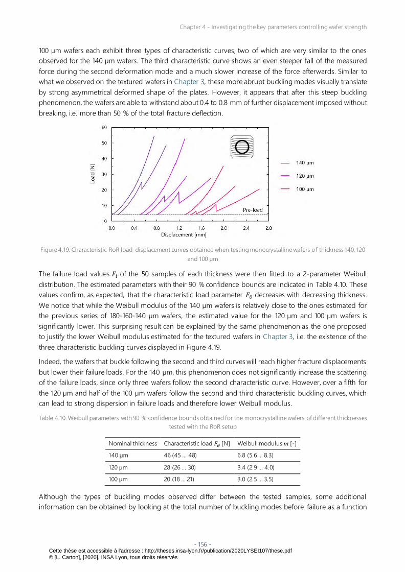
Chapter 4 - Investigating the key parameters controlling wafer strength
- 156 -
100 µm wafers each exhibit three types of characteristic curves, two of which are very similar to the ones
observed for the 140 µm wafers. The third characteristic curve shows an even steeper fall of the measured
force during the second deformation mode and a much slower increase of the force afterwards. Similar to
what we observed on the textured wafers in Chapter 3, these more abrupt buckling modes visually translate
by strong asymmetrical deformed shape of the plates. However, it appears that after this steep buckling
phenomenon, the wafers are able to withstand about 0.4 to 0.8 mm of further displacement imposed without
breaking, i.e. more than 50 % of the total fracture deflection.
Figure 4.19. Characteristic RoR load-displacement curves obtained when testing monocrystalline wafers of thickness 140, 120
and 100 µm
The failure load values 𝐹𝑖 of the 50 samples of each thickness were then fitted to a 2-parameter Weibull
distribution. The estimated parameters with their 90 % confidence bounds are indicated in Table 4.10. These
values confirm, as expected, that the characteristic load parameter 𝐹𝜃 decreases with decreasing thickness.
We notice that while the Weibull modulus of the 140 µm wafers is relatively close to the ones estimated for
the previous series of 180-160-140 µm wafers, the estimated value for the 120 µm and 100 µm wafers is
significantly lower. This surprising result can be explained by the same phenomenon as the one proposed
to justify the lower Weibull modulus estimated for the textured wafers in Chapter 3, i.e. the existence of the
three characteristic buckling curves displayed in Figure 4.19.
Indeed, the wafers that buckle following the second and third curves will reach higher fracture displacements
but lower their failure loads. For the 140 µm, this phenomenon does not significantly increase the scattering
of the failure loads, since only three wafers follow the second characteristic curve. However, over a fifth for
the 120 µm and half of the 100 µm wafers follow the second and third characteristic buckling curves, which
can lead to strong dispersion in failure loads and therefore lower Weibull modulus.
Table 4.10. Weibull parameters with 90 % confidence bounds obtained for the monocrystalline wafers of different thicknesses
tested with the RoR setup
Nominal thickness Characteristic load 𝐹𝜃 [N] Weibull modulus 𝑚 [-]
140 µm 46 (45 … 48) 6.8 (5.6 … 8.3)
120 µm 28 (26 … 30) 3.4 (2.9 … 4.0)
100 µm 20 (18 … 21) 3.0 (2.5 … 3.5)
Although the types of buckling modes observed differ between the tested samples, some additional
information can be obtained by looking at the total number of buckling modes before failure as a function
Cette thèse est accessible à l'adresse : http://theses.insa-lyon.fr/publication/2020LYSEI107/these.pdf © [L. Carton], [2020], INSA Lyon, tous droits réservés

Chapter 4 - Investigating the key parameters controlling wafer strength
- 157 -
of nominal thickness. In the same way as previously, we displayed the percentage of wafers having
experienced zero to five buckling modes in Figure 4.20.
Figure 4.20. Percentage of monocrystalline wafers of different thicknesses having experienced zero to five buckling modes
before failure when tested with RoR setup
We notice that to the exception of one 120 µm sample, all tested wafers change their deformation mode at
least once before failure. However, compared to the 180-160-140 µm wafers, it is less straightforward to
identify clear trends for the increase or decrease in percentage of wafers depending on thickness. We do
observe that the percentage of wafers experiencing two buckling modes decreases with thickness, in favor
of an increase in percentage of either one or three buckling modes. To a lesser extent, some 120 and 100 µm
even experience four to five changes in deformation. Therefore, while we noticed an increase of the number
of buckling modes with decreasing thickness for the 180-160-140 µm wafers, the evolution is more subtle for
thinner wafers. Instead of simply increasing the number of times they change their deformation, the plates
exhibit more complex deformation shapes, accompanied by stronger drops in measured force. The effect is
however the same, i.e. it allows them to hold longer before fracture. Indeed, following a steep buckling
mode, the slope of the curve is strongly decreased afterwards. In other words, for the same value of imposed
displacement, the applied load is lower and the plate can withstand in this position longer before failure.
Unfortunately, due to the highly reflective aspect of the wafers’ surface and to the geometric constraints of
our equipment (Plexiglas® frame protection around the setup), we were not able to capture accurate
pictures of the five deformation modes. However, it is worth noting that precise analytical solutions for ten
different buckling modes of a plate with free edges under biaxial compression were recently obtained in a
study [269].
Also interesting to notice is that even though the monocrystalline samples from both tested series (the
180-160-140 µm and the 140-120-100 µm wafers) came from different brick manufacturers and were obtained
using different sawing recipes, the characteristic load parameters 𝐹𝜃 obtained for the thickness common to
both series, i.e. 140 µm, have confidence intervals that almost overlap. We indeed measure 𝐹𝜃 = 49 (48 … 51)
for the first series and 𝐹𝜃 = 46 (45 … 48) for the second. This similarity led us to display on the same graph
the evolution of characteristic load parameter as a function of average thickness, as presented in Figure 4.21.
We observe that, as presented in Figure 4.21, we could propose two fitting functions to describe the evolution
of 𝐹𝜃 with respect to thickness 𝑒: either quadratic or linear.
Cette thèse est accessible à l'adresse : http://theses.insa-lyon.fr/publication/2020LYSEI107/these.pdf © [L. Carton], [2020], INSA Lyon, tous droits réservés

Chapter 4 - Investigating the key parameters controlling wafer strength
- 158 -
Figure 4.21. Characteristic fracture load 𝐹𝜃 as a function of wafer mean thickness (error bars represent the 90 % confidence
bounds)
The first quadratic model 𝐹𝜃 = 𝑎 × 𝑒2 would be in agreement with the analytical stress formula developed
by Vitman and Pukh [67]:
𝜎 =3
4𝜋[2(1+ 𝜈)𝑙𝑛
𝑎
𝑏+(1− 𝜈)(𝑎2 − 𝑏2)
𝐿(1 +√2)4
]×𝐹
𝑒2 (4.2)
where 𝐹 is the applied force, 𝑒 is the wafer thickness, 𝜈 is the Poisson’s ratio, 𝑎 and 𝑏 are the outer and inner
ring diameter and 𝐿 is the wafer length. Indeed, if we assume that, following the results obtained with the
4-line bending setup, the characteristic fracture strength 𝜎𝜃 of the wafers does not depend on wafer
thickness, and then the fracture load 𝐹𝑏𝑟𝑒𝑎𝑘 is proportional to the wafer thickness squared:
𝜎 ∝𝐹
𝑒2 (4.3)
This model implies that the characteristic fracture load 𝐹𝜃 decreases gradually with wafer thickness, and that
𝐹𝜃 = 0 will only be reached for the limit case of a null thickness. This assumption can however be called into
question: we could indeed imagine the existence of a threshold thickness, below which the wafer will fail as
soon as the applied loads exceeds zero. In this case, the experimental points may be described a by a second
linear fit 𝐹𝜃 = 𝑎 × 𝑒 + 𝑏. A similar linear relation between breakage load and thickness has been highlighted
by Coletti et al. [63], who performed RoR tests on textured wafers with thickness ranging from 120 and
320 µm. In their study however, the linear fit was forced through the origin. Determining which of these
models is accurate would require testing either much thinner (<50 µm) or much thicker (>300 µm) samples,
which could not be performed within the frame of this study.
This analysis shows nevertheless that thinner wafers have indeed an increased bending flexibility, but that
the effect on wafer strength differs between the 4-line bending and RoR setup. In 4-line bending, the
increased flexibility enables the wafers to reach extremely high deflection values without breaking. In RoR, it
allows them to change their deformation mode easily in order to redistribute the applied stress. For the
180-160-140 µm wafers, this redistribution translates into an increase in the total number of buckling modes.
For even lower thickness, it translates into more complex deformation shapes of the wafers during buckling,
which allow them to hold longer before catastrophic failure.
Cette thèse est accessible à l'adresse : http://theses.insa-lyon.fr/publication/2020LYSEI107/these.pdf © [L. Carton], [2020], INSA Lyon, tous droits réservés

Chapter 4 - Investigating the key parameters controlling wafer strength
- 159 -
2.6. Drop tower test results
Results obtained with the bending setups in sections 2.3 and 2.5 showed that wafers with lower thickness
exhibit an increased flexibility: they support lower breakage loads but can reach extremely high deflection
values in uniaxial bending, and modify their deformation shape up to five times before breaking in biaxial
bending. Strength results obtained with the 4-line bending setup showed moreover that reducing the as-cut
thickness did not modify the intrinsic fracture strength of the wafers.
The following section aims at further investigating the influence of decreasing wafer thickness on their
mechanical properties, by characterizing monocrystalline wafer behavior under dynamic loading as a
function of thickness. The results are first presented for the wafers that were cut at 180-160-140 µm
thicknesses, and then for the samples of thickness 140, 120 and 100 µm.
2.6.1. Impact loading on 180-160-140 µm wafers
For this study, 160 monocrystalline OS wafers per thickness level were sampled. Table 4.11 indicates the mean
thickness and TTV of the samples. Each series of a given thickness was then further divided into four
equivalent subsets to perform impact tests at the following kinetic energies: 10, 13.25, 14.5 and 16.5 mJ. The
samples were impacted on their lateral edges, where the wire enters and exits the bricks.
Table 4.11. Thickness and TTV measured for the monocrystalline wafers impacted with the drop tower setup
Nominal thickness [µm] Mean thickness ± STD [µm] Mean TTV ± STD [µm]
180 178.3 ± 1.1 5.6 ± 1.6
160 158.4 ± 0.8 5.9 ± 1.8
140 138.4 ± 0.7 5.6 ± 1.6
As described in the experimental procedure in Chapter 2, impact occurs on the middle of the wafer edge.
After impact, samples are classified into three categories: undamaged, locally damaged or fully broken.
Results are presented as histograms in Figure 4.22 for the three thicknesses and four impact energies.
Figure 4.22 shows that as-cut thickness has a strong influence on the response of wafers to an impact
loading: indeed, for a given energy, the breakage rate increases with decreasing thickness. Moreover, it
appears that thinner wafers exhibit very low percentages of locally damaged wafers. In other words, with
decreasing thickness, the dynamic response of the wafer is either fully broken or undamaged. This implies
that thicker wafers have the ability to dissipate the impact energy through the formation of a chip. On the
contrary, when impact energy is concentrated on an area with low thickness, full breakage of the wafer
through crack initiation is more likely.
Cette thèse est accessible à l'adresse : http://theses.insa-lyon.fr/publication/2020LYSEI107/these.pdf © [L. Carton], [2020], INSA Lyon, tous droits réservés

Chapter 4 - Investigating the key parameters controlling wafer strength
- 160 -
(a) 180µm
(b) 160 µm
(c) 140 µm
Figure 4.22. Results of impact tests performed on
monocrystalline wafers of three different thicknesses as a
function of energy
It can be pointed out that the minimum breakage energy (i.e. the energy for which the breakage rate is zero)
could not be reached in this series of tests for the 160 and 140 µm wafers. However, we showed in Chapter 2
with preliminary tests on 300 monocrystalline wafers that the percentage of broken wafers follows an
exponential increase. If we assume that the tested wafers follow the same evolution, we may estimate the
missing minimum breakage energies by adjusting the experimental points to the 3-parameter distribution
introduced in Chapter 2:
𝑃𝑏𝑟𝑜𝑘𝑒𝑛(𝐸𝑘) = {0 𝑖𝑓 𝐸𝑘 ≤ 𝐸𝑘−𝑚𝑖𝑛1 − 𝑒𝑥𝑝[−𝑎(𝐸𝑘 − 𝐸𝑘−𝑚𝑖𝑛)
𝑏] 𝑖𝑓 𝐸𝑘 > 𝐸𝑘−𝑚𝑖𝑛 (4.4)
where 𝐸𝑘−𝑚𝑖𝑛 corresponds to the minimum breakage energy. Figure 4.23 thus displays the experimental
points obtained for the percentage of broken wafers for the 140 and 160 µm wafers, together with the fitted
distribution curves.
Cette thèse est accessible à l'adresse : http://theses.insa-lyon.fr/publication/2020LYSEI107/these.pdf © [L. Carton], [2020], INSA Lyon, tous droits réservés

Chapter 4 - Investigating the key parameters controlling wafer strength
- 161 -
Figure 4.23. Curve fitting for the evolution of the percentage of fully broken wafers as a function of impact energy for wafers
of thickness 160 and 140 µm
This allows us to estimate the minimum breakage energy to be 𝐸𝑘−𝑚𝑖𝑛 = 6.7 ± 1.3 mJ and
𝐸𝑘−𝑚𝑖𝑛 = 2.7 ± 0.5 mJ for the 160 and 140 µm wafers, respectively. These values illustrate the higher
sensitivity of as-cut thickness on the ability of silicon wafers to absorb shocks: decreasing their thickness from
160 to 140 µm divides by two the minimum impact energy that the samples can hold without breaking.
2.6.2. Impact loading on 140-120-100 µm wafers
In order to further investigate the effect of decreasing as-cut thickness on wafer behavior under impact
loading, we completed the previous study by sampling a total of 270 adjacent wafers from the
monocrystalline brick that was cut using the 140-120-100 µm wire guiding system. The 90 wafers from each
thickness level came from the middle of the brick. The average thickness and TTV of each series is given in
Table 4.12.
Table 4.12. Thickness and TTV measured for the monocrystalline wafers impacted with the drop tower setup
Nominal thickness [µm] Mean thickness ± STD [µm] Mean TTV ± STD [µm]
140 136.1 ± 1.3 6.2 ± 1.9
120 116.5 ± 1.4 6.6 ± 1.9
100 96.5 ± 1.5 8.0 ± 2.1
Each series of a given thickness was divided into three subsets to be tested at three different impact energies:
3.5 mJ, 5 mJ and 7 mJ 32. As for the previous study, the wafers were impacted on their lateral edge. The
results are presented as percentage of undamaged, locally damaged or fully broken wafers in Figure 4.24. It
is worth noting that 3.5 mJ is the smallest impact energy achievable with the setup, as it corresponds to a
measured velocity of 0.1 m/s, which is the lowest value measurable by the photocell with the 2 mm flag.
32 These values were chosen based on preliminary tests, with the goal to achieve 0 % breakage rate for the 140 µm wafers at
the lowest energy.
Cette thèse est accessible à l'adresse : http://theses.insa-lyon.fr/publication/2020LYSEI107/these.pdf © [L. Carton], [2020], INSA Lyon, tous droits réservés

Chapter 4 - Investigating the key parameters controlling wafer strength
- 162 -
(a) 140 µm
(b) 120 µm
(c) 100 µm
Figure 4.24. Results of impact tests performed on
monocrystalline wafers of three different thicknesses as a
function of energy
Similarly as for the previous impact tests, we observe that for a given impact energy, the breakage rate
increases with decreasing thickness. We also notice that the percentage of locally damaged wafers is
extremely low for the 120 µm samples, and almost zero for the 100 µm. This confirms the previous
observation: wafers with low as-cut thicknesses do not have the ability to absorb the kinetic energy through
local damage, and impact will more likely lead to complete failure of the sample.
We observe that the behavior of the 100 µm wafers under impact loading is particularly critical: the breakage
rates are extremely high considering the low levels of energy, and they increase very fast with increasing
impact energy: between 3.5 and 5 mJ, the percentage of fully broken wafers increases from 10 to 90 % and
reaches 100 % at 7 mJ. Given that there are only three experimental points per thickness available, it seems
unreasonable to adjust the data to an exponential curve, as it was done for the previous samples.
Nevertheless, we notice that we did not reach a zero percentage of broken 100 µm wafers, i.e. some samples
will still fail at levels of energy lower than 3.5 mJ.
These findings highlight that as-cut thickness therefore plays a critical role in the dynamic mechanical
behavior of the wafers: thin samples are less likely to absorb the impact energy coming from a shock on
their edge and can fail even at very low levels of energy.
Cette thèse est accessible à l'adresse : http://theses.insa-lyon.fr/publication/2020LYSEI107/these.pdf © [L. Carton], [2020], INSA Lyon, tous droits réservés

Chapter 4 - Investigating the key parameters controlling wafer strength
- 163 -
3. INFLUENCE OF THE DIAMOND WIRE SAWING PROCESS
The extremely fast development of DWS technology for PV silicon wafering has been accompanied by
extensive work aiming to characterize the properties of the surface obtained and more specifically to
understand which parameters most influence the sawing-induced damage. Yet as introduced in Chapter 1,
these numerous investigations are almost exclusively carried out on a very small scale, mainly through
scribing experiments and subsequent characterization of the obtained surface via local techniques (SEM
images observation [152], Raman spectroscopy [180], cross-sectional TEM analysis [23]). These experimental
studies have been complemented by analytical calculations which model either a 2D cross-section [149,270]
or 3Ddimensional portion length of the diamond wire [181] to predict the depth of the sawing-induced
damage. The application of these models requires however some significant simplifications, the most
important of all being that they consider only one section of a diamond wire cutting through a single silicon
substrate.
While these studies provide some crucial information on which parameters influence the local
sawing-induced damage, it is not straightforward to correlate their observations to the mechanical properties
of the full-scale silicon wafer. The actual DWS process indeed involves about 1 km of wire running back and
forth through a 500 mm long brick for two to three hours, with process parameters that vary throughout the
cut. The action of the wire on the silicon material may then evolve both spatially (along the wafer cross-
section and along the brick length) and temporally (from the beginning until the end of the cut).
It is of course impossible to develop analytical models that accurately describe such a complex, dynamic
process. Similarly, it seems difficult to implement characterization techniques that allow evaluating the
damage at the entire wafer scale, i.e. over the whole 156 × 156 mm2 surface. We may however use the
mechanical characterization techniques developed in Chapter 2 to understand how wafer strength evolves
when changing the sawing parameters, with the ambition to determine an optimal sawing process. This
approach is described through this section: we first recall the important sawing parameters and discuss the
ones we can (or cannot) control and measure, and then discuss the experimental approaches implemented
to isolate their influence. We finally present our results in two different sections: the first one focuses on the
influence of the characteristics of the diamond wire and its wear, and the second one explores the possibilities
of approaching ductile mode cutting of silicon during the experimental sawing process.
For the rest of our study, we choose to focus on monocrystalline silicon. This choice is justified by the fact
that the crystalline quality of a mono-like or multicrystalline material varies from one brick to another. Yet as
we demonstrated in the previous section, the presence of structural defects can have a strong impact on the
resulting mechanical behavior of the wafers, and this effect would make it impossible to isolate the influence
of the sawing process alone. In addition, when possible, we try to focus on strictly comparing Cz-grown
bricks that came from the same manufacturer, in order to exclude a potential influence of defects in
monocrystalline silicon.
3.1. Sawing parameters: definition and characterization
As it was presented in Chapter 2, the DWS process proceeds by following a so-called recipe, which is divided
into a certain number of successive steps (in our equipment, either 12 or 60). Each of these steps is defined
by setting the value of five parameters, which are listed in Table 4.13. The brick position represents the vertical
downwards displacement of the brick, which is performed at a certain feed rate. The wire runs back and forth
at given speed, with a slightly higher forward length, so that a small amount of fresh wire is introduced at
each cycle.
Cette thèse est accessible à l'adresse : http://theses.insa-lyon.fr/publication/2020LYSEI107/these.pdf © [L. Carton], [2020], INSA Lyon, tous droits réservés

Chapter 4 - Investigating the key parameters controlling wafer strength
- 164 -
Table 4.13. Process parameters used to define each step of a the sawing recipe
Parameter Brick position
[mm]
Feed rate
[mm/min]
Wire speed
[m/s]
Length of wire
forwards [m]
Length of wire
backwards [m]
Typical value or range [+2.5 to -165] [0.35 – 2] [15 – 30] 800 795
The value of the above-described parameters therefore vary during the process, according to the defined
recipe. We however describe a single cut by introducing more general parameter values, which are constant
for a given process:
The total cut duration 𝒕𝒄𝒖𝒕, i.e. the elapsed time between the beginning and end of the process.
The maximum wire speed 𝒗𝒔 , i.e. which corresponds to the speed value used for more than 90 % of the
cut, during the stable cutting regime.
The number of back-and forth movements of the wire 𝑵𝑩&𝑭 achieved during a cut. Using the values
from Table 4.13, a complete back-and-forth movement is achieved in approximately one minute, and
the total number of back and forth movements for a cut duration of 160 minutes is therefore
approximately 160. It is important to note that this means that during an entire cut, the wire stops
approximately 320 times to change direction.
The wire consumption 𝑾𝒄, which is defined as the length of new wire consumed per wafer to perform
the cut, i.e.:
𝑊𝑐 =(𝐿𝑓𝑜𝑟𝑤𝑎𝑟𝑑𝑠 − 𝐿𝑏𝑎𝑐𝑘𝑤𝑎𝑟𝑑𝑠 )𝑁𝐵&𝐹
𝑁𝑤𝑎𝑓𝑒𝑟𝑠 (4.5)
where 𝐿𝑓𝑜𝑟𝑤𝑎𝑟𝑑 and 𝐿𝑏𝑎𝑐𝑘𝑤𝑎𝑟𝑑𝑠 are the respective forward and backward lengths run by the wire during a
movement, and 𝑁𝑤𝑎𝑓𝑒𝑟𝑠 is the total number of wafers generated during a cut, which is defined by the width
of the wire web 𝐿𝑤𝑒𝑏 and the pitch 𝑝:
𝑁𝑤𝑎𝑓𝑒𝑟𝑠 =𝐿𝑤𝑒𝑏𝑝
(4.6)
In the rest of this work, a given cut will therefore be defined by the values of the four previous parameters.
Unless otherwise stated, all other possible influencing factors, such as the nature or temperature of the
cooling liquid, are identical between the cuts that are being compared.
In addition to these process related parameters, the other determinant factors are the features of the
diamond wire itself, such as the core diameter or the size, shape, and density of the abrasive particles. It is
important to understand that unlike the process parameters from Table 4.13, we cannot modify the
characteristic values of a wire: they are indeed defined by the manufacturer. We can however measure some
of these properties using a certain number of characterization techniques summarized in Table 4.14. For
qualitative analysis, the most widely used method within the scope of this work is SEM analysis of either a
cross-section or longitudinal portion of the wire, or even of the diamond particles alone extracted from their
core. The quantitative properties, such as abrasive bump height or density, are almost exclusively evaluated
using a Keyence optical micrometer LS-9006D that can measure the wire apparent diameter using two
perpendicular light beams. It can record 400 000 data points with a maximum frequency of 16 kHz. The
statistical quantities given in Table 4.14 are then extracted from these measures [271].
Cette thèse est accessible à l'adresse : http://theses.insa-lyon.fr/publication/2020LYSEI107/these.pdf © [L. Carton], [2020], INSA Lyon, tous droits réservés

Chapter 4 - Investigating the key parameters controlling wafer strength
- 165 -
Table 4.14. Typical parameters defining a diamond wire and association characterization means
Parameter Studied value or range Characterization technique
Core diameter [µm] [70 – 80] Manufacturer data
Apparent diameter [µm] [75 – 95] Optical micrometer
Abrasive size [µm] [8 – 16]
[6 – 12]
Manufacturer data
Particle size distribution (PSD)
Maximum bump height [µm] [3 – 7] Optical micrometer
Abrasive density [mm-1] [80 – 120] Optical micrometer
Abrasive shape Qualitative SEM
The SEM images and optical micrometer analysis can be implemented on a new or used wire (i.e. after
performing a cut), and therefore allow to evaluate the wear both qualitatively, for example by observing a
blunting of the particles edges, and quantitatively, for example by measuring the decrease in apparent
diameter and/or abrasive density.
Apart from the process and wire-related parameters previously defined, the sawing process may be
influenced by non-controllable parameters such as undetected defects along the wire. Moreover, some
parameters of the process are evolving over time, in particular for the needs of parallel researches , or to stay
in line with industrial evolutions. Typically, the material of the beam on which the silicon brick is glued before
the process has been regularly changed and investigated. The tension of the wire is also adjusted to meet
the evolution of the diameter (15 N and 12 N for an 80 µm and 70 µm core diameter, respectively). Finally,
although as stated before, we tried to compare only Cz-grown bricks coming from the same manufacturer,
there may still exist some differences in material quality between two apparently identical bricks, which could
in turn influence the behavior of the wire. It should therefore be kept in mind that the DWS process can
never be completely reproducible, and that isolating the influence of the parameters can have some
limitations.
3.2. Experimental approach
During this work and over a period of more than two years, we sampled monocrystalline silicon wafers
coming from more than 30 different cuts, for which one or several of the above mentioned parameters were
varied. Seven different wires were used, which were bought from two different manufacturers (a technical
world reference and an alternative supplier) and with two different core diameters (70 and 80 µm). In the
following, each wire is designated by a letter from A to G. The detailed characteristics of the wires and the
parameters of each process from which the wafers were sampled can be found in Appendix E. The
monocrystalline bricks were purchased from three different manufacturers, thereafter referred to as Cz-1,
Cz-2 and Cz-3.
Unlike the previously presented results studying the mechanical properties as a function of silicon crystallin ity
and thickness, the strength of the samples cut using different sawing parameters is strictly investigated via
4-line bending tests, more specifically using the 80-48 mm configuration. This characterization method is
indeed the most reproducible among the ones developed in Chapter 2. Moreover, we proved in the previous
section that as-cut thickness had no influence on the measured bending fracture strength. This implies that
we are able to compare samples that were cut using different wire-guides and thus having different nominal
thicknesses.
Cette thèse est accessible à l'adresse : http://theses.insa-lyon.fr/publication/2020LYSEI107/these.pdf © [L. Carton], [2020], INSA Lyon, tous droits réservés

Chapter 4 - Investigating the key parameters controlling wafer strength
- 166 -
For every studied cut with given sawing parameters, the same procedure is applied. Mainly, 100 adjacent
samples are collected and measured with the topology equipment to obtain their average thickness and
TTV. Unless otherwise specified such as in section 3.3, the wafers are systematically collected from the MS
area of the brick, i.e. where the wire is the least worn. Out of these 100 wafers, 20 are randomly set aside as
witness samples for further characterization such as CSM. The remaining 80 samples are then alternately
divided into two series to be tested in wire and cut direction. Failure stresses are determined via the FE model
(with systematic control and comparison of the experimental and numerical load-displacement curves) and
adjusted to a 2-parameter Weibull distribution. The results are then always presented either in the form of
Weibull probability plots, or by directly comparing the values of the parameters. The 90 % confidence
bounds are used as indicators to determine whether a difference in strength, and therefore the influence of
a sawing parameter, is actually significant or not.
Throughout this sampling and testing procedure, we pursued two different approaches. The first was to test
a large number of samples, coming from cuts with sawing parameters as different as possible. By performing
a design of experiment (DoE) analysis on a certain number of selected factors, the goal was to be able to
determine which of these sawing parameters was the most critical for wafer fracture strength. This approach
is presented in section 3.3 by focusing on the characteristics of the wire and its behavior during the cut. This
methodology however faced some important limitations. On the one hand, we could chose to compare cuts
with strictly identical secondary parameters such as brick origin or coolant type. However, to the exception
of the results presented in section 3.3, this choice necessarily implied having a very incomplete design of
experiment. On the other hand, in order to have a more complete DoE, we could chose to assume that some
parameters had no influence on the mechanical properties of the wafers, and consider for example all
monocrystalline bricks to be equivalent. Yet when applying these simplifications, the results were so scattered
that it was impossible to find a significant correlation between one factor and the measured fracture strength
of the wafers. The reader is referred to Appendix E to get an overview of the strength results obtained for
each sawing process.
We therefore implemented a second approach, in which we specifically adjusted some of the sawing
parameters to target an increase in the resulting wafers’ strength, by focusing on one of the most discussed
aspects in literature, i.e. achieving ductile mode cutting of silicon. This approach is detailed in section 3.4.
3.3. Influence of wire morphology and wear
3.3.1. DoE approach and characterization methods
To illustrate the first approach implemented to study the influence the sawing parameters on the mechanical
properties of the resulting wafers, we chose to focus on the main consumable of the process, the diamond
wire itself. Our goal was to investigate how wires of different types behave when used with similar process
conditions, with a special focus on their wear behavior, and how it influences the mechanical properties of
the obtained wafers. To this end, we conducted an extensive experimental study, for which three different
wires were used to each perform two consecutive cuts. A DoE was then constructed based on the three
following factors:
The type of wire, a qualitative parameter consisting of three levels: wires D, E and F
The number of cuts performed per wire, a quantitative parameter with two levels : one or two
The position of the wafers along the brick, a qualitative parameter with two levels: MS or OS
The last two factors are representative of wire wear, but at a different scale. A full factorial DoE was
performed, resulting in 12 configurations. All other possible influencing parameters were kept constant: an
Cette thèse est accessible à l'adresse : http://theses.insa-lyon.fr/publication/2020LYSEI107/these.pdf © [L. Carton], [2020], INSA Lyon, tous droits réservés

Chapter 4 - Investigating the key parameters controlling wafer strength
- 167 -
identical sawing recipe (Table 4.15) was used to slice six monocrystalline half-bricks (220 mm web width)
coming from the same manufacturer batch. According to the experimental testing procedure, 100 adjacent
wafers were collected from each configuration. The three wires were described to have identical core
diameter (70 µm) and similar kerf (≈ 90 µm) but abrasives of different nature and densities. The pitch of the
wire-guiding system used was 250 µm, which results in a nominal wafer thickness of 160 µm. The six cuts
were performed using the sawing recipe given in Table 4.15 and in the following order: first and second cut
with wire D, followed by the two consecutive cuts with wire F, and finally with wire E.
Table 4.15. Sawing parameters used to perform the six cuts of the DoE
Cut duration 𝑡𝑐𝑢𝑡
[min]
Maximum wire speed
𝑣𝑠 [m/s]
Number of B&F movements
of wire 𝑁𝐵&𝐹
Wire consumption 𝑊𝑐
[m/wafer]
160 30 160 1
In order to evaluate the differences in wear and cutting behavior both qualitatively and quantitatively, several
characterizations were carried out on the wires and on the wafers. The morphology of the new and used
wires (after performing the two consecutive cuts) was analyzed by SEM. The optical micrometer mentioned
in section 3.1 was used to inspect the wires before and after each cut and thus quantify the wear of the wire
by studying the evolution of the characteristic values introduced in Table 4.14. An example of the type of
results obtained from this analysis, in the form of histograms of the apparent diameter of wire D before and
after cutting is shown in Figure 4.25.
Figure 4.25. Histograms of apparent diameter of wire D before and after cutting
In parallel, the cutting behavior of the wire was evaluated in situ by measuring the bow along the wire web
during each cut. As mentioned in Chapter 2, this measurement system is the result of an in-house
development using multiple inductive sensors positioned along the web [190]. More precisely for the six cuts
performed for this study, the bow was measured at five different positions. The evolution of bow for the five
sensors as a function of the percentage of cut is illustrated in Figure 4.26 for the first cut performed with wire
D. The sensors are numbered depending on their position with respect to the wire entry (sensor 1) and wire
exit (sensor 5). For the rest of this analysis, we will focus on comparing the evolution of the maximum bowing
profile. In the case of Figure 4.26, this corresponds to the bow measured by sensor 4, which reaches a
maximum value of 5.7 mm at approximately 80 % of the cut.
Cette thèse est accessible à l'adresse : http://theses.insa-lyon.fr/publication/2020LYSEI107/these.pdf © [L. Carton], [2020], INSA Lyon, tous droits réservés

Chapter 4 - Investigating the key parameters controlling wafer strength
- 168 -
Figure 4.26. Evolution of wire bow measured by five sensors during the first cut performed with wire D
Information on the sawing process and the wires can also be extracted from the wafers themselves: the mean
thickness and TTV were measured on the 100 samples from each DoE configuration. Differences in as-cut
thickness between wafers sawn with a new or used wire are an additional indicator of wire wear, while TTV
measurements provide further information on the cutting behavior, in particular the vibrations of the wire.
In addition to topology characterization, five MS samples from the first cut performed with each wire were
analyzed with CSM. For each single wafer, images were taken at five different areas of the sample with the
lowest (×20) and highest (×100) magnification. Therefore, for a given wire and magnification level, the
average roughness parameters are obtained based on 25 measurements.
Finally, 80 wafers per configuration were divided into two series and tested with the 80-48 mm configuration
of the 4-line bending setup in cut and wire direction. The corresponding Weibull strength parameters 𝜎𝜃
and 𝑚 were estimated for each DoE configuration and testing direction.
3.3.2. Morphology and wear behavior of the wires
Figure 4.27 shows the SEM images of the three new wires, i.e. before performing any cuts. We notice that
although according to the manufacturers’ data the abrasives are supposed to be of different sizes and exhibit
different densities, no significant differences can be detected from these images. It should be noted that due
to the very small portions of wire analyzed, it is not possible to extract quantities from the SEM images.
Wire D
(b) Wire E
(c) Wire F
Figure 4.27. SEM images of the three unused wires
Similar observations can be done when looking at their quantitative characteristics, which are given in
Table 4.16. Apart from a lower apparent diameter measured for wires E and F (77.2 and 77.0 µm versus
78.5 µm respectively), both the maximum bump height and abrasive density appear very similar.
Cette thèse est accessible à l'adresse : http://theses.insa-lyon.fr/publication/2020LYSEI107/these.pdf © [L. Carton], [2020], INSA Lyon, tous droits réservés

Chapter 4 - Investigating the key parameters controlling wafer strength
- 169 -
Table 4.16. Initial characteristics of the three wires before cutting – *abrasive size is given by manufacturer
Wire Wire D Wire E Wire F
Abrasive size* [µm] [8 – 16] [6 – 12] [6 – 12]
Apparent diameter [µm] 78.5 77.2 77.0
Max bump height [µm] 6.5 6.4 5.8
Abrasive density [mm-1] 100 114 103
However, significant differences in wire behavior did rapidly emerge when using the wires in the sawing
equipment. Figure 4.28 thus displays the maximum measured wire bow during the first and second cut
performed with each wire. On the one hand, we notice that during the first cut, wires D and F exhibit a
relatively similar behavior, with a steady increase of the bow until maximum values reach 5.7 and 5.2 mm
respectively. The bow of wire E on the other hand increases much faster and up to 9.7 mm, which from
comparison with usual measured values is an indicator of increased wire breakage risk. During the second
cut, since the wires are already partially worn, their behavior should reach a more stabilized wear
regime [146]. This seems to be the case for wires D and F, for which the bow slowly reaches maximum values
of 7.7 and 7.3 mm. In the case of wire E however, we observe once again an abrupt rise, with maximum
values that were quickly considered as too critical to complete the cut without wire breakage, and the feed
rate had thus to be decreased twice during the process (at 50 % and 62 %).
(a) First cut
(b) Second cut
Figure 4.28. Maximum wire bow measured during (a) the first and (b) second cut performed with each wire
Therefore, although the three wires seemed to share very similar morphological characteristics, they exhibit
strong differences in cutting behavior. The impact of these differences on the wire wear can be analyzed by
measuring the same quantitative properties on the used wires, i.e. after performing the two cuts, and
comparing them with the initial values. This is displayed in Table 4.17 for the three wires. We observe that in
addition to being the wire for which the higher bow was measured, wire E also exhibits the highest wire wear
(-1.9 µm in diameter). In comparison, wires D and F only lost 1.5 and 1.3 µm in apparent diameter. The same
differences are observable when comparing the evolution of the maximum bump heights, with a maximum
50.9 % decrease for wire E. Surprisingly however, the decrease in abrasive density is maximum for wire F: this
would imply that less particles were pulled out for wires D and E.
Cette thèse est accessible à l'adresse : http://theses.insa-lyon.fr/publication/2020LYSEI107/these.pdf © [L. Carton], [2020], INSA Lyon, tous droits réservés

Chapter 4 - Investigating the key parameters controlling wafer strength
- 170 -
Table 4.17. Comparison of wire characteristics before and after performing the cuts
Wire D Wire E Wire F
new used difference new used difference new used difference
Apparent diameter [µm] 78.5 77.0 -1.5 µm 77.2 75.3 -1.9 µm 77.0 75.7 -1.3 µm
Max bump height [µm] 6.5 3.7 -43.4 % 6.4 3.1 -50.9 % 5.8 3.5 -40.4 %
Abrasive density [mm-1] 100 89 -11.6 % 114 95 -16.3 % 103 84 -19.2 %
More generally, this analysis shows us that the characteristics of the wire strongly influence its wear and
behavior. When used under identical process conditions, wire E suffers from an increased wear compared to
wire D and F, and experiences more difficulties to cut through an equivalent monocrystalline brick.
3.3.3. Wafer topology and morphology
As previously mentioned, topology analysis of the obtained as-cut wafers provides additional information
on the behavior and wear of the wire. Figure 4.29 and Figure 4.30 respectively show the mean thickness and
mean TTV obtained for the three wires on 100 adjacent MS and OS samples collected from each cut. For
each of these graphs, wire wear increases from left to right. One first observation is that the as-cut thicknesses
of the wafers cut with wire D are in average 2.4 µm lower than for wires E and F. This can be explained by
the difference in apparent wire diameter (Table 4.17): wire D possesses a higher initial diameter and therefore
higher kerf, which in turn generates thinner wafers. In terms of silicon material loss, wires E and F are therefore
more efficient.
(a) Wire D
(b) Wire E
(c) Wire F
Figure 4.29. Mean thickness measured on 100 MS and OS wafers as a function of wire and number of cuts
Regardless of the wire used, we observe an increase in wafer thickness between the MS wafers of the first
cut and the OS wafers of the second cut, which can be directly correlated to the decrease in apparent
diameter as the wire wears. As could be expected, this increase is more pronounced for wire E, which
experienced the higher wear. We also notice the extremely high standard deviation of the OS wafers from
the second cut performed with wire E, which is very likely caused by the increased lateral vibration of the
wire resulting from the high bow (Figure 4.28.b).
We also observe an increase in TTV from the MS wafers of the first cut and the OS wafers of the second cut,
which is an indicator of the increased difficulty and vibration of the wire as it travels through the brick. Wafers
cut with wire E exhibits the highest TTV values, which is consistent with the measured wire bow. Especially
for the second cut, the extremely high bow values resulted in OS wafers with average TTV of 18.3 µm and
maximum values on single wafers as high as 28 µm. These values are still within the specifications for solar
Cette thèse est accessible à l'adresse : http://theses.insa-lyon.fr/publication/2020LYSEI107/these.pdf © [L. Carton], [2020], INSA Lyon, tous droits réservés

Chapter 4 - Investigating the key parameters controlling wafer strength
- 171 -
wafers (< 30 µm), but are considered quite high compared to standard DWS values (between 5 and 10 µm).
This confirms that wire E did experience more difficulties to cut through the material, which translated into
a higher bow, higher lateral vibrations and an increased TTV of the wafers.
(a) Wire D
(b) Wire E
(c) Wire F
Figure 4.30. Mean TTV measured on 100 MS and OS wafers as a function of wire and number of cuts
In contrast, we observe that in terms of topological quality, wafers cut with wire F show the best results, with
a very reasonable increase in TTV from 3.9 µm to 7.7 µm between the MS wafers from the first cut and OS
wafers from second cut, while wire D exhibits intermediate values. Therefore, while the measured bow was
extremely similar for wires D and F, there still exists some differences in cutting behavior between the two
wires.
The as-cut surface morphology generated by the three types of wire is finally investigated by comparing the
roughness parameters measured with CSM on MS wafers coming from the first cuts. Although no significant
difference could be extracted from the ×20 magnification images, small deviations in surface roughness
parameters 𝑆𝑎 and 𝑆𝑧 extracted from the ×100 magnification can be observed. Figure 4.31 thus displays the
measured parameters as box plots for the three types of wire. We notice that wires E and F exhibit slightly
lower average roughness. This could be explained by the supposed higher abrasive particle size declared by
the manufacturer (Table 4.16) for the diamonds from wire D (8-16 µm) compared to that of wires E and
F (6-12 µm). Another interesting observation is the lowest range of values measured for wire F, and to a
lesser extent for wire D. This would imply that both these wires have abrasives that generate a more
homogeneous as-cut surface.
One should however note that compared to the very high differences observed in both wire behavior and
topology of the as-cut wafers, the deviations in surface morphology can be considered as relatively low. It
would therefore seems that the influence of different wire morphologies on the as-cut wafer properties is
rather observable at a larger scale than on the micrometer surface properties.
Cette thèse est accessible à l'adresse : http://theses.insa-lyon.fr/publication/2020LYSEI107/these.pdf © [L. Carton], [2020], INSA Lyon, tous droits réservés

Chapter 4 - Investigating the key parameters controlling wafer strength
- 172 -
(a) 𝑆𝑎
(b) 𝑆𝑧
Figure 4.31. (a) Areal surface roughness 𝑆𝑎 and (b) peak-to-valley height 𝑆𝑧 measured by CSM at magnification ×100 on MS
wafers from the first cut performed with each wire (25 measurements per wire)
3.3.4. Wafer strength results and DoE analysis
We tested 960 wafers (i.e. 80 × 12) with the 4-line bending setup to evaluate the influence of wire type and
behavior on their mechanical properties. For the sake of clarity, the results will only be presented in terms of
characteristic strength parameter 𝜎𝜃 for both testing directions, thereafter referred to as 𝜎𝜃−𝑤𝑖𝑟𝑒 and 𝜎𝜃−𝑐𝑢𝑡,
respectively. Indeed, with the exceptions of a few unexplained outliers, the estimated Weibull modulus varies
very little depending on the tested configuration. More precisely, this parameter is rather characteristic of
the loading direction, with values between 5 and 14 in cut direction and between 14 and 23 in wire direction.
Following the same color codes as the one used for the thickness and TTV values, Figure 4.32 and Figure 4.33
display the characteristic strength parameters estimated in cut and wire direction for all tested configurations.
The error-bars represent the 90 % confidence bounds.
(a) Wire D
(b) Wire E
(c) Wire F
Figure 4.32. Characteristic strength parameter and 90 % confidence bounds obtained in cut direction for monocrystalline
wafers as a function of wire, number of cuts and sampling position
When looking at the results in cut direction, it appears that the estimated characteristic strength parameter
𝜎𝜃−𝑐𝑢𝑡 only takes two limit values, i.e. either a lower value between 210 and 220 MPa (MS wafers from first
cut of wire D and second cut of wire E, OS wafers from wire F) or a higher value between 260 and 280 MPa.
There are surprisingly no intermediate values measured between these two levels, and it is therefore not
straightforward to understand how the strength in cut direction evolves as a function of the wire and wear
behavior. On the one hand, if only looking at the values from wire D, it seems that the wear of the wire is
Cette thèse est accessible à l'adresse : http://theses.insa-lyon.fr/publication/2020LYSEI107/these.pdf © [L. Carton], [2020], INSA Lyon, tous droits réservés

Chapter 4 - Investigating the key parameters controlling wafer strength
- 173 -
beneficial for wafer strength, which increases and stabilizes from the OS position of the first cut. On the other
hand, for the two other wires, the lower characteristic strength values are measured at unexplained positions
within the brick, such as the OS wafers from the second cut performed with wire E and MS wafers from the
second cut performed using wire F.
(a) Wire D
(b) Wire E
(c) Wire F
Figure 4.33. Characteristic strength parameter and 90 % confidence bounds obtained in wire direction for monocrystalline
wafers as a function of wire, number of cuts and sampling position
The evolution of strength in wire direction follows a more graduate evolution and allows us to identify some
trends depending on the wires. First, for a given cut number and wafer position, we notice that wafers cut
with wire F exhibit the highest fracture strength. It is worth noting that the value obtained for the MS wafers
from the first cut (131 MPa) is the highest ever measured on as-cut monocrystalline wafers sawn with the
standard recipe (Table 4.15). Second, the wear of wire D seems to have absolutely no influence on the wafer
fracture strength, with estimated confidence bounds that systematically overlap regardless of the position
along the brick or the cut number. For wires E and F however, we observe a decrease in characteristic strength
from left to right, i.e. with wire wear. This is particularly significant for wire E, for which the strength measured
on OS wafers from the second cut is 10 % lower than that of the MS wafers from the first cut.
As expected, the combined influence of wire morphology and wear behavior makes it difficult to precisely
analyze their effects on wafer strength, which justifies the relevance of using a DoE approach and associated
tools. To this end, we conducted an analysis of variance (ANOVA) [272] with Ellistat software to estimate the
relative contributions of the three factors (wire, number of cuts, position) and possible interactions between
them. This analysis is performed on the evolution of both strength parameters, i.e. 𝜎𝜃−𝑐𝑢𝑡 and 𝜎𝜃−𝑤𝑖𝑟𝑒. The
level of significance of each contribution is assessed by the 𝑝-value of the ANOVA test, which represents the
probability that a given contribution results from a random event. An effect is considered significant if
𝑝 < 0.05. Figure 4.34 illustrates the results of ANOVA analysis by showing the four most important
contributions of factors to the two parameters 𝜎𝜃−𝑐𝑢𝑡 and 𝜎𝜃−𝑤𝑖𝑟𝑒, as well as the corresponding 𝑝-values.
Cette thèse est accessible à l'adresse : http://theses.insa-lyon.fr/publication/2020LYSEI107/these.pdf © [L. Carton], [2020], INSA Lyon, tous droits réservés

Chapter 4 - Investigating the key parameters controlling wafer strength
- 174 -
(a) 𝜎𝜃−𝑐𝑢𝑡
(b) 𝜎𝜃−𝑤𝑖𝑟𝑒
Figure 4.34. Four most important contributions of factors to strength parameters (a) 𝜎𝜃−𝑐𝑢𝑡 and (b) 𝜎𝜃−𝑤𝑖𝑟𝑒 according to
ANOVA analysis
The results highlight that in cut direction, the two most important contributions to changes in strength are
combined interactions of the wire with the two others factors. However, the 𝑝-values obtained are too high
to allow considering the contributions as statistically significant. This conclusion was to be expected from
our previous observations, as it reflects the existence of anomalous data (outliers), mainly the four low
fracture strength values measured, which cannot be explained by a change in the factors. A possible
hypothesis to interpret these values is that the bending strength in cut direction of DWS wafers is more
sensitive to non-controllable parameters, such as a series of chipping defects present along a few centimeters
on the side of the brick, which might influence the strength of a few neighboring hundreds of wafers. These
local effects would not be observable in wire direction because the stress values are so low (we remind here
that 𝜎𝜃−𝑤𝑖𝑟𝑒 is in average half of 𝜎𝜃−𝑐𝑢𝑡) that random parameters have very little influence on their value.
In wire direction however, ANOVA analysis shows that the wire is the most influencing parameter, with a
significance level low enough (𝑝=0.04) that we can consider this contribution as significant. In other words,
the mechanical strength in wire direction is mainly controlled by the characteristics of the wire. More
precisely, the wafers with highest fracture strength in wire direction were obtained with wire F, i.e. the wire
that showed the smoothest behavior during the cut and experienced the lower wear. On the opposite, wire E,
which suffered the most during cutting, yielded the wafers with the lowest fracture stresses.
There therefore seems to exist a correlation between the morphology of the wires and subsequent wear
behavior and the resulting mechanical strength of the as-cut wafers. It is however not straightforward to
determine which specific features of the studied wires were responsible for their differences in behavior.
Previous scribing experiments or simulations showed indeed that using spherical particles rather than sharp
grits [152,179], decreasing the size of the abrasive [23,177] or increasing their density along the wire [181]
were all possibilities to decrease the sawing-induced damage. Yet from our means of characterizations, there
does not seem to exist significant differences in either shape, size or density between the abrasives from
wires D, E and F. This is confirmed when looking at SEM images of the particles from each wire, as displayed
in Figure 4.35: the general morphology and size of the grits seems very similar from one wire to another.
Moreover, while several studies agree that the progressive wear of a diamond wire causes rounding and
blunting of the particles and results in less brittle fractures at the silicon surface [23,153], this effect was not
observed for the wires used in our study. On the contrary, wafers cut with wire E and F showed decreased
fracture strength with wire wear.
Cette thèse est accessible à l'adresse : http://theses.insa-lyon.fr/publication/2020LYSEI107/these.pdf © [L. Carton], [2020], INSA Lyon, tous droits réservés

Chapter 4 - Investigating the key parameters controlling wafer strength
- 175 -
(a) Wire D
(b) Wire E
(c) Wire F
Figure 4.35. SEM images of abrasive particles from wires D, E and F
While this experimental study confirms the significant role played by the morphology of the wire on the
mechanical strength of the wafers, the origin of this influence cannot be justified by the shape, the size or
the distribution of the diamond abrasives. It is worth noting that although the exact composition of the core
material of the wires is unknown, tensile and fatigue tests performed on new and used portions of the wires
demonstrated that their mechanical behavior was very similar. A possible effect of the core material should
therefore very likely be ruled out.
The last undetermined factor that may play a role in the cutting behavior of the wire and therefore the
sawing-induced damage on silicon is the crystalline nature of the diamond particles. Indeed, just as silicon,
single-crystal diamond is known to have a strong anisotropy of mechanical and physical properties
depending on the crystallographic orientation [273]. There is evidence in previous work that when machining
silicon, the wear characteristics of a diamond tool depend on the crystallographic orientation of the rake and
flank face [274–276]. The reason for this dependence, as explained in [276], is that the Young modulus of
diamond changes depending on crystallographic orientation. It is therefore a plausible hypothesis that the
abrasive particles from wires D, E and F are of different crystalline nature (mono or multicrystalline, typically)
and thus exhibit different elastic and toughness properties, which can modify their behavior when cutting
silicon, and in turn affect the sawing-induced damage of the resulting wafers.
3.4. Towards ductile mode cutting: influence of feed rate
3.4.1. Introduction
As discussed in Chapter 1, ductile mode cutting of silicon via a diamond tool has been widely investigated
as a way to improve the integrity of the machined substrate [150,157]. By removing the silicon material via
plastic deformation rather than brittle fracture, a smooth surface with low density of defects in the thin
subsurface layer can be generated [170]. The modification in depth and structure of this near-surface layer
can in turn influence the mechanical, optical and electronic properties of the resulting silicon substrates.
Adjusting the parameters of the DWS process in order to achieve ductile mode cutting of the silicon material
can therefore be a way to increase the fracture strength of the as-cut wafers. It should however be reminded
here that a full pure ductile mode cutting of a silicon brick with an industrial DWS process is very likely
impossible. Indeed, we explained in Chapter 1 that the contact pressure changes along the wire due to
differences in shape, protrusion and distribution of the abrasive particles: brittle fracture will therefore
inevitably occur locally, so that there is always a mixture of ductile and brittle material removal. Our ambition
is therefore to try to come as close as possible to a so-called partial ductile mode removal.
Cette thèse est accessible à l'adresse : http://theses.insa-lyon.fr/publication/2020LYSEI107/these.pdf © [L. Carton], [2020], INSA Lyon, tous droits réservés

Chapter 4 - Investigating the key parameters controlling wafer strength
- 176 -
Among the large number of possible influencing parameters, we isolated the ones for which both
experimental and numerical studies widely agree that they play a critical role in ductile mode cutting of
silicon, and discussed if and how we could adjust them in our process:
The characteristics of the abrasive particles [152,179]: their strong influence on the mechanical properties
of the wafers was confirmed in the previous section. However, it was impossible within the scope of this
work to modify these parameters. Adjusting the particle shape, size or density would indeed require to
manufacture our own wires.
The speed of the wire: all existing works agree that increasing wire speed allows to decrease the
maximum crack length [24,178,180,277]. Unfortunately, the maximum speed used in our standard sawing
recipe (30 m/s) already corresponds to the upper limit of the equipment.
The feed rate: similarly as for the wire speed, both experiments and simulations show that ductile mode
cutting of silicon could be improved by reducing the feed rate [24,178,181,277].
For our study, we chose to focus on this last parameter, which we can modify most easily and widely. As
previously explained, adjusting the average feed rate of our sawing process will affect the total cutting time.
The only existing lower limit value for this parameter is therefore that it still allows completing the cut within
a day.
3.4.2. Experimental procedure
For this study, we performed four different cuts whose corresponding brick, wire and sawing parameters are
given in Table 4.18. Throughout the rest of this section, these cuts will be referred to by their total cutting
time. It should be noted that because different wires were used throughout these cuts, only two-by-two
comparisons of the obtained wafers are possible.
The first two cuts were performed using the same wire B with core diameter 80 µm and 8-16 µm diamonds
on identically monocrystalline bricks from manufacturer Cz-2 and will therefore be compared with one
another. The nominal thickness of the resulting wafers is 180 µm. The processes were completed using a
total cutting time of 140 and 180 minutes, which correspond to average feed rates of 1.2 mm/min and
0.9 mm/min respectively 33.
The third cut is the result of a more assertive approach, whereby we decreased the feed rate with the aim to
come closer to a criterion proposed by Wang et al. in a very recent contribution [181]. They developed an
analytical model to predict the depth of the SSD layer in DWS of silicon depending on several process
parameters. Their models considers a cross section of a single wire scribing along a feed distance
𝑥 = 250 µm. They proved that there exists a theoretical critical ratio of feed rate to wire speed, below which
material removal is supposed to occur in a pure ductile mode and the SSD depth is zero. We plotted in
Figure 4.36 their five experimental points giving the critical feed rate to achieve ductile mode cutting as a
function of wire speed. By noticing that the evolution of the curve from Figure 4.36 is substantially linear and
using a suited fitting equation, we are able to determine that in order to achieve a cutting process for which
the SSD depth is zero using our maximum wire speed 𝑣𝑠 = 30 m/s, we need to use a feed rate
𝑣𝑓 ≤ 430 µm/min.
33 It is worth mentioning that these ranges of values would be industrially acceptable.
Cette thèse est accessible à l'adresse : http://theses.insa-lyon.fr/publication/2020LYSEI107/these.pdf © [L. Carton], [2020], INSA Lyon, tous droits réservés

Chapter 4 - Investigating the key parameters controlling wafer strength
- 177 -
Figure 4.36. Critical feed rate for ductile mode cutting as a function of wire speed according to [181]
In order to be certain to be far below this limit, we chose to perform the cut with a total time of 470 minutes,
i.e. about eight hours, which ensures an average feed rate 𝑣𝑓 = 350 µm/min. This very long cut is compared
with a reference 160 minutes cut (last line of Table 4.18) which was performed using the same wire F with
core diameter 70 µm. Although due to practical issues the monocrystalline bricks used for the two cuts came
from different manufacturers, we assume that we can compare them with one another given the extremely
high difference in process parameter. The nominal thickness of the wafers obtained with the 160 min and
470 min cuts is 160 µm. The wire speed was kept constant for all four cuts.
Table 4.18. References and sawing parameters used to perform the four cuts with different feed rates
Brick Wire [core diameter] Cut duration
𝑡𝑐𝑢𝑡 [min]
Maximum wire
speed 𝑣𝑠 [m/s]
Number of B&F
movements of wire 𝑁𝐵&𝐹
Wire consumption
𝑊𝑐 [m/wafer]
Cz-2
Wire B [80 µm] 180 30 180 1
Wire B [80 µm] 140 30 140 1
Cz-1 Wire F
[70 µm] 470 30 470 1
Cz-3 Wire F
[70 µm] 160 30 160 1
We notice when looking at Table 4.18 that the number of back-and-forth movements evolves with the
duration of the cut. This is because throughout these four cuts, the length of wire forward and backwards
was kept constant (about 800 m), i.e. a back-and-forth movement requires the same distance of wire and is
always performed at the same wire speed of 30 m/s. Therefore, if we decrease the feed rate, the wire has
the time to perform more back-and-forth movements during the cut.
3.4.3. Results
According to the sampling and testing procedure defined earlier, 100 adjacent MS wafers were sampled from
each cut. Their average thickness and TTV is given in Table 4.19. We can notice that increasing or decreasing
the feed rate seems to have no influence on the topology of the resulting wafers. The samples were then
divided into two series of 40 and tested with the 4-line bending setup with span configuration 80-48 mm.
The results are presented in terms of estimated Weibull parameters, firstly for the cuts performed in 180 and
140 minutes, and secondly for the 470 and 160 minutes cuts.
Cette thèse est accessible à l'adresse : http://theses.insa-lyon.fr/publication/2020LYSEI107/these.pdf © [L. Carton], [2020], INSA Lyon, tous droits réservés

Chapter 4 - Investigating the key parameters controlling wafer strength
- 178 -
Table 4.19. Thickness and TTV measured on 100 MS wafers from the cuts performed at different durations
Wire [core diameter] Cut duration Mean thickness ± STD Mean TTV ± STD
Wire B [80 µm] 180 min 179.9 ± 0.5 4.8 ± 1.3
Wire B [80 µm] 140 min 179.1 ± 0.7 3.7 ± 1.0
Wire F [70 µm] 160 min 160.8 ± 0.4 3.9 ± 1.0
Wire F [70 µm] 470 min 160.0 ± 0.5 3.6 ± 1.1
Figure 4.37 shows the Weibull probability plots obtained for the monocrystalline wafers sawn in 180 and
140 minutes and Table 4.20 displays the estimated Weibull parameters and corresponding 90 % confidence
bounds in both testing directions.
Figure 4.37. Weibull probability plots obtained for the monocrystalline wafers sawn in 180 and 140 min with wire B and tested
in 4-line bending setup in wire and cut direction
We observe that contrary to what was expected, the wafers that were cut using a higher total cutting time
and therefore a lower feed rate exhibit lower fracture strength. Indeed, while the influence on Weibull
modulus is negligible when considering the width of the confidence intervals, there is a statistically significant
difference in characteristic strength parameter, with a respective decrease of 5 % and 10 % in wire and cut
direction for the wafers that were sawn in 180 minutes.
Table 4.20. Weibull parameters and 90 % confidence bounds for wafers sawn in 180 and 140 min with wire B
Testing direction Cut duration 𝜎𝜃 [MPa] 𝑚 [-]
wire 180 min 112 (110 … 113) 18.4 (15.0 … 22.6)
140 min 117 (115 … 119) 13.0 (10.5 … 16)
cut 180 min 234 (225 … 243) 7.2 (6.0 … 8.6)
140 min 260 (252 … 268) 9.4 (7.7 … 11.5)
This surprising result goes against the conclusions of experimental and analytical studies, which all measured
or predicted a decrease in SSD depth when decreasing the feed rate. One possible explanation to justify our
results is that the difference in feed rate between the two cuts (+ 33 % increase from 0.9 mm/min to
1.2 mm/min) was not high enough to generate a significant difference in subsurface damage. Even more
Cette thèse est accessible à l'adresse : http://theses.insa-lyon.fr/publication/2020LYSEI107/these.pdf © [L. Carton], [2020], INSA Lyon, tous droits réservés

Chapter 4 - Investigating the key parameters controlling wafer strength
- 179 -
likely, it is possible that the range of values chosen for our experimental study is unsuited to observe any
influence. Indeed, when compared with the majority of experimental and numerical studies, the values
chosen for our process parameters are relatively high. For example, Liu et al. [178] compare wire speeds
between 0.8 and 1.5 m/s and feed rate values no higher than 0.75 mm/min. Wang et al. [181] use the values
that come the closest to our experimental parameters, with a maximum tested wire speed of 20 m/s and
highest feed rate 1.8 mm/min. Upon comparing our results, we however notice that according to their model,
the influence of feed rate on SSD becomes less significant for higher wire speeds and higher feed rates. This
is illustrated in Figure 4.38, where we reproduced their evolution of theoretical SSD with feed rate, and
emphasized where the SSD values from the wafers obtained with cuts 180 and 140 minutes should lie (green
dashed rectangle). If we indeed assume that the curves would keep following the same trend, then the curve
corresponding to a wire speed of 30 m/s should lie just below the one for 20 m/s. We realize that according
to the analytical model, the two feed rate values chosen for our study (900 and 1200 µm/min) would yield
wafers with SSD values very close to one another. If this is indeed the case, it is probable that the differences
in characteristic strength measured between the samples from the two cuts were caused by the influence of
other parameters, such as unwanted brick and/or wire defects.
Figure 4.38. Evolution of theoretical SSD as a function of feed rate according to [181] and comparison with the experimental
values used for the cuts performed in 180, 140 and 470 minutes
More generally when looking at Figure 4.38, we realize that according to Wang et al.’s analytical model,
nearly all cuts performed within the scope of this work (wire speed between 25 and 30 m/s and feed rate
between 900 and 1200 µm/min) would yield wafers with SSD values located within the green rectangle, and
hence very similar to each other. Following this reasoning, the cut performed in 470 min, i.e. at a feed rate
of 350 µm/min, should however generate wafers with significantly lower SSD, as is emphasized by the purple
circle in Figure 4.38, showing the theoretical position of their SSD values according to Wang et al.’s model.
The results obtained for the wafers from this cut should therefore display significantly improved fracture
strength. The Weibull probability plots obtained for the monocrystalline wafers sawn in 470 and 160 minutes
are shown in Figure 4.39 and the corresponding Weibull parameters are given in Table 4.21.
It appears quite clearly from Figure 4.39 and Table 4.21 that the drastic decrease in feed rate did not have
the desired effect on wafer fracture strength. More specifically, we notice that in cut direction, the
characteristic strength is 15 % lower for the wafers sawn in 470 minutes. This effect could be attributed to
the presence of non-controllable defects such as differences between the brick quality, which came from
Cette thèse est accessible à l'adresse : http://theses.insa-lyon.fr/publication/2020LYSEI107/these.pdf © [L. Carton], [2020], INSA Lyon, tous droits réservés

Chapter 4 - Investigating the key parameters controlling wafer strength
- 180 -
different manufacturers. In wire direction however, the failure stress distribution in almost perfectly overlap,
regardless of the cut duration.
Figure 4.39. Weibull probability plots obtained for the monocrystal line wafers sawn in 160 and 470 min with wire F and tested
in 4-line bending setup in wire and cut direction
Therefore, even though we divided the average feed rate by a third (from 1000 µm/min to 350 µm/min),
the mechanical failure of the wafers is still controlled by the same defect population . More precisely,
these cuts tend to confirm the conclusions from the previous section, i.e. that wafer fracture strength in wire
direction is mainly controlled by the characteristics of the wire: samples cut with wire F, regardless of the cut
duration, exhibit higher mechanical strength.
Table 4.21. Weibull parameters with 90 % confidence bounds for wafers sawn in 160 and 470 min with wire F
Testing direction Cut duration 𝜎𝜃 [MPa] 𝑚 [-]
wire 160 min 130 (127 … 133) 12.7 (10.3 … 15.6)
470 min 127 (124 … 130) 12.6 (10.6 … 15.1)
cut 160 min 266 (257 … 276) 7.7 (6.3 … 9.4)
470 min 228 (221 … 235) 8.7 (7.1 … 10.5)
How can we explain that such a drastic change in process parameters had no influence on wafer fracture?
The first proposed hypothesis assumes that decreasing the feed rate did allow to create a more ductile
material removal mode, but that it did not result in an improved fracture strength of the wafers. In other
words, the proportion of ductile mode cutting is not correlated with the mechanical strength of the wafers.
However, numerous studies demonstrated that ductile mode cutting of silicon significantly modifies the
properties of the SSD layer, mainly by reducing microcrack length [24,152], transforming the crystalline
phases at the surface of machined silicon [278] and even by generating dislocations [170]. Yet we showed in
Chapter 3 that the SSD layer contains the most critical damage for wafer failure. If the cut performed in
470 minutes did achieve a higher proportion of silicon surface machined by ductile mode cutting, then some
influence on the mechanical properties of the wafer should have been detected.
The privileged second hypothesis is that even with a drastic decrease in feed rate, we could not even come
close to achieving ductile mode cutting in our sawing equipment. The main reason would be that, as
Cette thèse est accessible à l'adresse : http://theses.insa-lyon.fr/publication/2020LYSEI107/these.pdf © [L. Carton], [2020], INSA Lyon, tous droits réservés

Chapter 4 - Investigating the key parameters controlling wafer strength
- 181 -
previously discussed, the DWS process performed on an entire silicon brick and with multiple wires involves
complex and dynamic mechanisms that cannot be taken into account by the analytical models and scribing
experiments presented in previous literature. Among the possible influencing factors, one can mention the
longitudinal and radial inhomogeneity of the size, shape and density of the abrasive particles on the wire. In
addition, a critical phenomenon to consider for the full-scale DWS process are the back-and-forth
movements of the wire. Indeed, every time the wire changes direction, it briefly slows down, stops, and
accelerates again, while the brick keeps moving down at a constant rate. These oscillations are illustrated in
Figure 4.40 for the cut performed in 160 min with wire F. During the transition between positive or negative
speed value transitions, the local ratio of wire speed to feed rate is therefore fundamentally different.
(a)
(b)
Figure 4.40. Actual speed of wire F during the 160 min cut (a) Total time (b) Zoom over 5 min
Moreover, since the length of wire forward and backward is constant throughout the cuts, this effect
becomes more important if the total cutting time increases. Indeed, since a back-and-forth motion lasts
around one minute (Figure 4.40.b), for the cut performed in 470 min, the wire stopped about
2 × 470 = 940 times, compared with 320 times for the cut performed in 160 min. Maintaining a constant
ratio throughout the entire cut would require to use a one-way motion of the wire, which could not be
performed on our sawing equipment due to insufficient wire storage capacity.
This experimental study thus confirmed that achieving even partial ductile mode cutting of an entire silicon
brick is therefore far from straightforward, at least not without fundamentally modifying some aspects of the
sawing process. More generally, one should be very careful when applying the conclusions obtained from
single-indentor or single-wire scribing experiments to a full-scale sawing process.
4. CONCLUSION AND OUTLOOK
The goal of this chapter was to investigate the influence of several processing parameters on the mechanical
properties of a DWS as-cut silicon wafer, with the ambition to understand which factors were the most critical
for wafer failure. The work was divided into two main sections, which focused on the parameters related to
the two main processing steps of a typical PV silicon wafer: the solidification of the raw material, which
creates a silicon substrate of a certain crystalline nature, and the wire sawing process, which generates a thin
wafer with specific surface and subsurface damage.
The first section compared the strength properties of more than 1 500 silicon wafers of three different
crystalline origins (monocrystalline, mono-like and multicrystalline) and with nominal thicknesses ranging
Cette thèse est accessible à l'adresse : http://theses.insa-lyon.fr/publication/2020LYSEI107/these.pdf © [L. Carton], [2020], INSA Lyon, tous droits réservés

Chapter 4 - Investigating the key parameters controlling wafer strength
- 182 -
from 180 to 100 µm. These wafers were obtained using an original slicing and sampling method which allows
to isolate the influence of both the crystallinity and the as-cut thickness. The mechanical properties of the
samples were investigated via both quasi-static bending methods and impact tests. The second section
presented the most significant strength results extracted from an extensive experimental work involving
more than 30 cuts performed using different process parameters and a total of close to 4 000 tested
monocrystalline samples. The fracture strength of the obtained wafers was strictly evaluated via the 4-line
bending setup in order to obtain reproducible and comparable results. The main results and observations
that were drawn from this chapter are summarized below.
4.1. On wafer as-cut thickness
The 4-line bending tests highlighted that the intrinsic mechanical strength of the wafers does not depend
on their as-cut thickness. The maximum stress that a wafer can withstand before failure depends on the
crystal quality, slicing process and loading direction, but is independent of its thickness, at least down
to 100 µm. More precisely, we showed that while thinner wafers fail at lower applied forces, they exhibit an
increased bending flexibility and can reach deflections values as high as 40 mm without breaking. The
additional RoR tests showed that this higher flexibility manifests itself differently under biaxial loading: the
samples undergo a buckling phenomenon that allows them to change their deformation mode and
redistribute the applied load, in order to hold longer before failure.
As demonstrated by the impact tests, this gain in bending flexibility comes however with an increased
vulnerability to edge impact. For a given impact energy, wafers with lower as-cut thickness reached higher
breakage rates. More specifically, we showed that with decreasing thickness, the wafers are less likely to
absorb the kinetic energy through local damage, which increases the probability of catastrophic failure.
We were able to determine that the minimum breakage energies could vary between more than 10 mJ for
wafers of thickness 180 µm and less than 3 mJ for wafers of thickness 100 µm. It seems interesting to compare
these values with the actual loads experienced by a wafer during the handling and processing steps. Using
experimental data from previous internal work [279], we were able to estimate that in a typical automated
wafer transportation equipment, the shock between the edge of a wafer and a static equipment can imply
levels of energies between 0.5 and 5 mJ. In other words, while the minimum breakage energy of a 180 µm
will very likely not be reached during handling, it is highly probable that wafers with thickness from 140 to
100 µm will suffer from impacts that will cause catastrophic failure. This explains the higher breaking
percentages observed by previous studies when handling and processing thin wafers into solar cells using
standard production lines [25].
4.2. On wafer crystallinity
The 4-line bending tests performed on monocrystalline, multicrystalline and mono-like wafers showed that
the crystal quality is determinant for the mechanical properties of the resulting as-cut wafers, but that
this influence is not direct. Indeed, we highlighted that when sawn under similar conditions, mono-like and
multicrystalline wafers exhibit a significantly lower mechanical strength when loaded in wire direction. We
showed that the microscopic surface defects were not the cause of this difference, as the observed
morphologies and roughness parameters of the three types of silicon wafers were similar. The crystallinity of
the brick thus has no influence on the as-cut surface morphology of the wafers. The reason for the lower
strength of the mono-like and multicrystalline wafers was instead found to be due to a difference in
subsurface damage. More precisely, mono-like and multicrystalline wafers exhibit microcracks approximately
25 % deeper than monocrystalline wafers.
Cette thèse est accessible à l'adresse : http://theses.insa-lyon.fr/publication/2020LYSEI107/these.pdf © [L. Carton], [2020], INSA Lyon, tous droits réservés

Chapter 4 - Investigating the key parameters controlling wafer strength
- 183 -
The typical material defects from mono-like and multicrystalline silicon, such as grain boundaries,
dislocations or precipitates, are not directly responsible for the decrease in wafer strength, i.e. they cannot
be identified to be the origin of failure. However, it has been reported prev iously that when crossing such
structural defects, the scribing force of the diamond wire increases, which can result in localized brittle failure
and deeper microcracks [143,147,268]. This increased subsurface damage may be interpreted as an indirect
indicator of the greater suffering of the wire when cutting through non homogeneous material such as
mono-like or multicrystalline silicon.
4.3. On sawing parameters
The DoE approach and mechanical tests performed on monocrystalline wafers obtained from six different
cuts with three different wires demonstrated that the wire itself was the most determinant parameter for
wafer fracture behavior. When using exactly identical process parameters, wafers obtained with two different
wires showed differences in bending strength in wire direction in the order of 16 %. The features of the wire
also have a strong impact on its cutting behavior and wear performances, which will reflect on the mechanical
properties of the resulting wafers: the wire which suffered the most during a cut and which experienced the
most wear yielded the wafers with the lowest failure stresses. It remains however unclear which of the wire
features is responsible for modification in behavior and resulting properties of the wafers. As we could not
detect significant differences in size, shape or density between the abrasives nor in the core material
behavior, our privileged hypothesis is that the diamond particles are of different crystalline nature. Using
particles with multi or monocrystalline diamond as well as having different crystallographic orientations on
the edges and faces of the particles in contact with the silicon surface can influence the abrasion and wear
mechanisms and generate different subsurface damage.
The second part of the study focused on adjusting one specific process parameter, the feed rate, with the
ambition to come as close as possible to a ductile mode cutting of the silicon material by the diamond wire.
This approach was driven by numerous previous literature studies, which demonstrated that the sawing-
induced damage could be significantly reduced when using lower feed rates. We evaluated the fracture
strength of wafers sawn using a total process time of 140, 160, 180 and 470 minutes which correspond to
respective average feed rates of 1200, 1000, 900 and 350 µm/min. Our results highlight that even with a
drastic decrease of the feed rate, the fracture strength of the resulting wafers remains unchanged. Our
privileged hypothesis to explain this contradictory result is that given the complex, inhomogeneous and
dynamic nature of the DWS process, achieving even a partial ductile mode cutting along the entire wafer
surface is very unlikely, if not impossible. More specifically, the back-and-forth movement of the wire implies
that approximately every 30 seconds, the wire slows down and steps through an intermediate null speed.
Even though these transitions are performed relatively fast, they still represent a significant proportion of the
total cutting time, during which the ratio between feed rate and wire speed changes drastically. The
necessary back-and-forth motion, specific to DWS process, could therefore be an obstacle to achieve ductile
mode cutting.
It therefore seems that the characteristics of the diamond wire play a more important role on the
mechanical properties of the resulting wafers than the parameters of the sawing process. Indeed, the
results obtained in the second part of the study showed that even when comparing cuts with significantly
different feed rates, the wafers with the highest fracture strength were always the ones cut using wire F. In
other words, even when changing the process parameters, the mechanical properties of the wafers are still
mainly controlled by the type of wire.
Cette thèse est accessible à l'adresse : http://theses.insa-lyon.fr/publication/2020LYSEI107/these.pdf © [L. Carton], [2020], INSA Lyon, tous droits réservés

Chapter 4 - Investigating the key parameters controlling wafer strength
- 184 -
4.4. Outlook
Since we gathered strength results from wafers coming from all crystalline natures, thicknesses and
numerous combinations of sawing parameters, it seems appropriate to try answering the two questions
raised at the beginning of this chapter.
Can we find a combination of crystallization and sawing parameters that allow having the most
mechanically reliable as-cut silicon wafers?
If we focus on the fracture strength measured in wire direction, i.e. the weakest critical loading orientation,
we would recommend using wire F with a standard sawing recipe (𝑣𝑠 = 30 m/s, 160 minutes cut duration,
1 m/wafer consumption) to obtain the most mechanically reliable wafer with thickness 160 µm. Indeed the
4-line bending tests performed on 40 MS wafers yielded a characteristic strength parameter
𝜎𝜃−𝑤𝑖𝑟𝑒 = 130 ± 3 MPa. It is worth mentioning that a similarly high strength value (𝜎𝜃−𝑤𝑖𝑟𝑒 = 134 ± 3 MPa)
was also obtained for monocrystalline wafers of nominal thickness 180 µm cut with wire A but using an
adjusted sawing recipe (𝑣𝑠 = 25 m/s, 180 minutes cut duration, 1.5 m/wafer consumption – cut #79 from
Appendix E). However, if we take into account the productivity and cost issues of the PV industry, it seems
more relevant to propose parameters that limit the wire consumption, and even more importantly the cutting
time.
Which aspects of wafer manufacturing should we focus on to significantly increase fracture strength?
In the light of the abundant results obtained from the two sections of these chapters, it appears that two
parameters play a particularly important role on wafer strength: the initial crystallinity of the silicon, with
monocrystalline samples exhibiting higher fracture stress, and the nature of the wire.
The required research focus would therefore strongly depend on the studied silicon material. Regarding
multicrystalline and mono-like silicon wafers, there is a need to deepen our understanding of the scribing
mechanisms involved between the wire and the structural defects present within the material. More precisely,
it is necessary to determine which of these defects (precipitates, grain boundaries, and dislocations) are
responsible for the higher wear and suffering of the wire, as this phenomenon results in higher subsurface
damage and lower fracture strength of the resulting wafers. The crystallization parameters of multicrystalline
and mono-like silicon could then be adjusted to minimize the most critical defects for DWS and aim to bring
wafer fracture strength closer to that of monocrystalline wafers. When cutting through monocrystalline
silicon, the morphology and nature of the wire seems to be the parameters that require the most attention.
It would be particularly interesting to compare the properties of wafers obtained using wires with completely
different abrasive shapes, following for example the work from Kumar [152] of Kovalchenko [179]. Valuable
information could also be obtained by comparing the scribing behavior of multicrystalline or monocrystalline
diamonds.
These suggestions call however for some nuance: even when choosing the most optimal crystallization and
sawing parameters discussed above, we were never able to obtain as-cut wafers with failure stress values
exceeding 140 MPa in wire direction – which is still very low compared to their strength in cut direction. This
value should moreover be put into perspective with the results obtained in Chapter 3: we remind the reader
that a 5 minutes chemical etch of the as-cut wafers and a 300 °C thermal treatment allow to reach
characteristic strength values in wire direction of respectively 150 and 160 MPa. In comparison, the gain in
strength resulting from the crystalline quality or from drastic adjustments of the sawing parameters seems
fairly limited.
Cette thèse est accessible à l'adresse : http://theses.insa-lyon.fr/publication/2020LYSEI107/these.pdf © [L. Carton], [2020], INSA Lyon, tous droits réservés

- 185 -
General conclusions and prospects
This PhD work strived to fit into one of the strategies emphasized by the International Technology Roadmap
for Photovoltaics [5] to achieve significant reductions of solar energy production costs: enhancing silicon
material yield throughout every stage of the manufacturing chain. More specifically, we focused on
optimizing silicon use during the brick wire sawing step, which implies reducing both wafer thickness and
wire diameter.
We demonstrated in our Introduction that the pursuit of this objective could however only lead to costs
savings if the resulting wafers exhibited reliable and controlled mechanical strength. Throughout this
dissertation, we therefore attempted to improve our understanding of the mechanical properties of silicon
wafers, and to identify the most influencing mechanisms. This issue has mainly been approached through
experimental studies on samples sawn in our laboratory using controlled process parameters, while auxiliary
numerical simulations provided additional insight. In this conclusion, we summarize the major achievements
of our work and suggest future research topics that would be worth investigating.
1. CONCLUSIONS
A methodology for wafer mechanical characterization
The first underlying objective of this work was to enable an accurate comparison of the mechanical properties
of wafers of different thicknesses, crystalline nature, and sawn using various process parameters. To this end,
we developed a thorough methodology to characterize the mechanical behavior of as-cut DWS wafers as
comprehensively as possible (Chapter 2). We specifically implemented three destructive characterization
techniques, for which the setup designs and experimental protocols were adapted to the characteristics of
the wafers. We confronted the advantages, applicability and limits of each technique to define guidelines for
the mechanical characterization of silicon wafers:
The 4-line bending setup is the privileged technique to obtain statistical and comparable strength data
between wafers of different thickness, crystallinity and surface properties. This technique takes into
account the anisotropic wafer characteristics and uses suited FE models to calculate the failure stress
values. The results are provided in the form of two Weibull parameters: the characteristic fracture
strength 𝜎𝜃 and Weibull modulus 𝑚.
The RoR setup provides specific information on wafer flexibility, by bringing to light a buckling
phenomenon of the samples, which evolves depending on surface properties and as-cut thickness.
Results are obtained as the characteristic fracture load 𝐹𝜃 and Weibull modulus 𝑚. This technique can
either be implemented on its own if wafers of identical thickness are being compared, or as a
complement to 4-line bending results.
The drop tower setup contributes to understanding the dynamic behavior of the wafers, by analyzing
their response when submitted to an impact on their edge at different kinetic energies. The method
does not yet allow comparison between different sets of wafers but it helps making recommendations
for their handling that are easier to implement. Either this technique can be used on its own or in
combination with 4-line bending tests performed on pre-impacted wafers.
Cette thèse est accessible à l'adresse : http://theses.insa-lyon.fr/publication/2020LYSEI107/these.pdf © [L. Carton], [2020], INSA Lyon, tous droits réservés

General conclusions and prospects
- 186 -
These techniques provide the necessary tools to evaluate the mechanical behavior of as-cut DWS silicon
wafers with thicknesses ranging from 180 to 100 µm. As such, they may be regarded as a step further towards
a standardized evaluation of wafer strength in the PV community, as will be detailed in the perspectives.
Identification of critical defects for wafer mechanical failure
Based on the facts that (i) failure in brittle silicon initiates from existing flaws and that (ii) a wafer is composed
of a multitude of defects of different nature, our first approach towards understanding the breakage
mechanisms in PV wafers was to try to identify which of these defects were the most critical for mechanical
failure. To pursue this objective, we developed an original procedure, whereby we attempted to selectively
isolate or remove some specific defects of as-cut DWS wafers, and investigate the influence on the resulting
strength properties (Chapter 3).
The main findings of this study are reported as follows:
The morphology of the surface sawing-induced defects plays a critical role in the fracture properties of
the wafers. Through a correlation analysis between strength and roughness parameters of chemically
polished samples, we show that this influence results from a widening and blunting of the surface
defects during the etching process, which thus require higher stress to propagate.
By modifying the morphology of wafer edges through selective chemical and mechanical polishing
processes, we demonstrate that mechanical failure in PV wafers does not initiate from edge defects.
Their contribution to wafer strength is essentially overshadowed by the DWS-induced surface damage.
Without any modification of as-cut surface morphology, wafer fracture strength can be doubled by
applying a thermal annealing. As supported by XRD measurements, the proposed mechanism to explain
this influence is that the thermal process allows partially relaxing some micro-deformations of the crystal
lattice, which were generated during the sawing process.
While a chemical etching process removing approximately 3 µm of silicon material and a thermal
treatment at 400°C can both increase as-cut wafer strength by more than 70 %, the annealing of
chemically etched samples does not allow to further improve their mechanical properties. This
observation constitutes proof that the thermal treatment acts on a localized thin subsurface area.
These results highlight that all critical damage regarding wafer mechanical failure is located within a less than
3 µm deep subsurface damage (SSD) layer, and that improving fracture strength of as-cut wafers requires
controlling the nature of this layer.
Optimization of crystallization and sawing parameters
In a second approach, we conducted an extensive mechanical characterization of silicon wafers from different
crystalline nature, different as-cut thicknesses and sawn using different sawing parameters (Chapter 4). Our
goal was to understand which of these parameters most influence wafer strength, and, by extension, to
determine whether we can optimize them to obtain the most mechanically reliable wafers. The main results
are listed below:
The maximum stress that a wafer can withstand before failure is independent of its thickness, at least
down to 100 µm. More precisely, thinner wafers exhibit an increased bending flexibility, which manifests
itself either by reaching extremely high deflections values (in uniaxial 4-line bending) or by increasing
the number of buckling modes (in biaxial RoR bending). However, thinner wafers have a higher risk of
failure following an edge impact, mainly because they are less likely to absorb the kinetic energy
Cette thèse est accessible à l'adresse : http://theses.insa-lyon.fr/publication/2020LYSEI107/these.pdf © [L. Carton], [2020], INSA Lyon, tous droits réservés

General conclusions and prospects
- 187 -
through local damage. This increased sensitivity to shocks explains the higher breakage rates
encountered when handling thin samples in production lines.
When sawn using identical conditions, wafers coming from bricks of different crystallinity exhibit
differences in mechanical properties. By measuring the depth of the SSD layer, we demonstrate that
that the structural defects such as grain boundaries or precipitates present in mono-like or
multicrystalline silicon are indirectly responsible for the lower fracture strength of the wafers . When
cutting through these flaws, the scribing force of the diamond wire increases and results in localized
brittle failure and therefore deeper microcracks (+25 %) than on the monocrystalline wafers.
Through a design of experiment approach, we show that the diamond wire itself is the most
determinant sawing parameter for wafer fracture behavior. More specifically, there seems to exist a
correlation between the cutting behavior of the wire and the resulting mechanical properties of the
wafers: the strongest samples were obtained with the wire that experienced the least bowing and wear
during two consecutive cuts.
We find that monocrystalline wafers cut using fundamentally different feed rates (350 and 1000 µm/min)
exhibit almost identical fracture strength. This finding goes against multiple numerical and scribing
studies [178,181], which determined that decreasing the feed rate could lead to an almost full ductile
cutting mode of silicon, and therefore a much lower SSD. Our results prove however, that at the scale
of the complete DWS process, achieving even a partial ductile material removal is far from
straightforward, even with drastic modifications of process parameters.
In the light of the above, we conclude that two parameters are of significant importance for wafer strength:
the initial crystallinity of the silicon, and the nature of the wire – which actually plays a more important role
than the process parameters.
2. PERSPECTIVES
Towards standardization of wafer strength evaluation
We mentioned in our literature review from Chapter 1 that up to very recently, there existed no standard test
method for the strength evaluation of PV silicon wafers. Yet, in the same way as standardized characterization
techniques allow to compare the efficiency of solar cells manufactured at different companies or laboratories,
the PV community would benefit from having universal testing methods to compare the mechanical
properties of as-cut silicon wafers.
The development of the DIN SPEC 91351 [62] in 2017 by the Fraunhofer CSP, the Leipzig University and
industrial partners was an important first step in that direction. This standard defines requirements for
strength testing of PV wafers by use of 4-line bending tests, and provides lookup tables to compute the
fracture stresses. However, as discussed in Chapter 2, the recommended distance between support and
loading cylinders was found to be inadequate for samples with thickness less than 140 µm. This existing
standard could therefore be improved by offering additional testing options suited for thinner samples, such
as the 60-32 mm span configuration we implemented for wafers with thickness between 100 and 140 µm.
More generally, we believe that the methodology developed throughout Chapter 2 could be further
optimized to propose a more complete and comprehensive standard to evaluate the mechanical properties
of PV silicon wafers. The latter would typically include the three destructive techniques detailed in our work,
i.e. the uniaxial 4-line and biaxial RoR bending methods, as well as the edge impact tests. Built on the same
Cette thèse est accessible à l'adresse : http://theses.insa-lyon.fr/publication/2020LYSEI107/these.pdf © [L. Carton], [2020], INSA Lyon, tous droits réservés

General conclusions and prospects
- 188 -
model as the DIN SPEC 91351, the standard would provide recommendations on the number of samples
required per series, the experimental protocols and analysis to perform for each method.
Within this objective, the auxiliary results obtained in appendices A and B could be a particularly valuable
addition. Indeed, we demonstrated in Appendix A that in order to allow a strict comparison of strength
measured with different 4-line bending setups, the wafers need to be tested with the rollers parallel to the
saw marks. In Appendix B, we proposed a procedure that evaluates the mean error on the estimated Weibull
parameters as a function of the number of tested samples. These studies can translate into direct practical
recommendations for the testing procedure of the 4-line bending setup.
Adding the RoR and drop tower techniques to the standard would help characterize different mechanical
properties of the wafers. RoR results give on the one hand information about the biaxial flexibility of the
as-cut samples, which could be helpful for certain applications where the resulting solar modules require to
withstand a high bending radius – for example on vehicle integrated photovoltaics [280]. On the other hand,
results from the drop tower method provide key data on the minimum impact energies, speeds or
accelerations that wafers can experience without breaking.
The elaboration of such a standard, which would of course require further work and optimization of the RoR
and drop tower methods, could provide a useful tool for wafer manufacturers. Validation through a
mechanical standard could indeed be a warranty that their as-cut samples will never exceed a certain
percentage of breakage rate during handling. This could become a major asset as wafers evolve towards
lower as-cut thicknesses and larger dimensions.
Investigations on diamond abrasives
Results from Chapter 4 showed that the morphology of the wire was one of the most significant influencing
parameters for wafer fracture strength. When using identical process parameters, wafers obtained with wires
of similar core diameter but with abrasives of different natures showed differences in bending strength in
wire direction in the order of 16 %. In future work, it would be very interesting to investigate this influence
more in details. The ideal strategy would be to have the possibility to manufacture customized wires using
the same basis core but covered with different types of abrasive particles. Their behavior and wear during a
cut of a monocrystalline brick with a standard recipe could be characterized by the techniques introduced
in Chapter 4, and the mechanical properties of the resulting wafers compared. Among the most promising
parameters to investigate, we can list the following:
Abrasive shape: scribing experiments showed that using diamonds with more rounded contours [152]
or tungsten carbide particles with completely spherical shape [179] can lead to lower damage. Although
they are difficult to manufacture, round diamond particles would be worth testing.
Crystalline nature of abrasives: our results show that wires with abrasives of apparent similar shape
behave very differently when cutting silicon. As suggested by former studies [274,276], an explanation
for this difference could be the crystalline nature of the diamond particles. This effect would deserve
further study, for example by comparing the behavior of multicrystalline or monocrystalline diamonds.
Abrasive distribution: more recent contributions suggest that optimizing the angular spacing of the
particles [281] or using exotic helical distribution of the particles along the wire [282] can influence the
microcrack depth. This aspect could be further investigated by testing different distribution patterns.
These suggestions should nevertheless be put into perspective with the fact that the prices of diamond wires
are sinking, and that the cost of such an optimized wire would probably be much higher than the standard
Cette thèse est accessible à l'adresse : http://theses.insa-lyon.fr/publication/2020LYSEI107/these.pdf © [L. Carton], [2020], INSA Lyon, tous droits réservés

General conclusions and prospects
- 189 -
ones. In order to raise interest in the PV community, the gain in wafer strength properties would therefore
have to be extremely significant.
Accepting and dealing with low as-cut wafer strength
Finally, we mentioned in the conclusion of Chapter 4 that the observations on the influence of wire
morphology called for some nuance: indeed, compared to the impact of 5 min chemical etch or a 300 °C
annealing treatment, the gain in characteristic strength that could be obtained by using our best wire seems
limited. It would therefore seem that there is not as much room for improvement of as-cut wafer strength
as we initially thought, at least not from the crystallization or sawing parameters. An as-cut DWS wafer will
always exhibit a strong anisotropy in strength parameters, with a significantly weak loading direction.
Moreover, as thickness decreases, its sensitivity to edge impact will inevitably increase.
If we acknowledge the fact that as-cut DWS wafers unavoidably display these mechanical weaknesses, future
investigations could be oriented according to two lines of research:
The first would be to focus on adjusting the current processing equipment to the properties of thin,
as-cut wafers in order to maintain low breakage rates. The minimum breakage values obtained via the
drop tower tests could be used as design recommendations, for example by defining a threshold
conveying speed or acceleration. One could more generally recommend to avoid as much as possible
contact with the wafer edges, as it seems to be the most critical type of load for thin as-cut wafers. It
would be preferable to take advantage of the higher flexibility of the thin samples to improve handling
technologies, as was suggested by a recent study [11]. Non-contact Bernoulli grippers are for example
an ideal candidate [283].
The second would be to implement “healing treatments” on the as-cut wafers. These would have to be
performed as soon as possible following the sawing process, in order to increase their mechanical
strength before handling and processing into solar cells. One could for example imagine an extremely
fast chemical etching or annealing process, which would occur directly after the slicing of the wafers.
These processes could easily be integrated to the typical cleaning steps of the samples (see Chapter 2).
One could indeed replace the tap water and detergent mixture by an acidic solution to simultaneously
clean and etch the surface for about 10 to 20 minutes, or increase the usual 80 °C drying temperature
to 300 °C or 400 °C to allow for a thermal treatment of the wafers. In both options, strength of wafers
after cleaning would be increased, without any significant loss of processing time. While both processes
have comparable positive influence on wafer mechanical properties, it seems important to mention that
in terms of costs, a chemical treatment would be preferable, as the wafers will require etching at some
point in the manufacturing chain. However, if considering the environmental impact, the relatively low
temperatures required would favor the use of a thermal treatment.
Cette thèse est accessible à l'adresse : http://theses.insa-lyon.fr/publication/2020LYSEI107/these.pdf © [L. Carton], [2020], INSA Lyon, tous droits réservés

General conclusions and prospects
- 190 -
3. EPILOGUE
The sustainability of the research and development activity in the crystallization and wafering steps of the
PV chain is being challenged more than ever before in Europe. As technology continues to mature, the
relentless competition puts indeed enormous pressures on manufacturers to lower their prices. This
encourages the aggressive expansion of giant companies, predominantly from China [284]. Of the top ten
worldwide suppliers for solar cells and modules, nine are Chinese companies [4], which benefit from
record-low prices of polysilicon and wafers. In this context, it is becoming increasingly difficult for European
manufacturers and research institutes to develop competitive, innovative crystallization and wire sawing
processes.
Preserving a European know-how of these key process steps may however be crucial to meet the future fast
evolutions of PV technologies. In order to overcome the theoretical efficiency limits of silicon-based devices,
new cell architectures emerge indeed very quickly. The perovskite / silicon tandem cell is among the
promising options, with an established record at 28 % [7]. This technology raises several challenges for the
bottom silicon substrate tandem partner, mainly regarding surface properties and subsequent texturing
process [285,286], as well as optimal thickness to minimize optical losses [287]. As for any new emerging PV
technology, the requirements on these parameters may evolve very rapidly and radically. If the future
mainstream as-cut silicon wafer needs to have completely different morphology, the wire sawing process
may need to be entirely readjusted, and a deep understanding of the mechanisms involved will prove
extremely valuable.
Cette thèse est accessible à l'adresse : http://theses.insa-lyon.fr/publication/2020LYSEI107/these.pdf © [L. Carton], [2020], INSA Lyon, tous droits réservés

- 191 -
APPENDIX A
- Weibull strength size effect on
diamond wire sawn silicon wafers
This appendix is a summarized extract of an article published by Carton et al. [89], from which some parts were
quoted verbatim.
1. INTRODUCTION
As a brittle material with low fracture toughness [288], silicon is theoretically subject to a strength size effect,
i.e. a silicon wafer with greater volume should be more likely to fail than a smaller sample. Yet, with a very
few rare exceptions [99], the possible influence of a strength size effect is almost never considered for PV
silicon wafers, although it is known to be a major concern in the field of technical ceramics [289,290]. This
omission is usually justified by the fact that each study uses a unique sample geometry (typically a
156 × 156 mm2 wafer of thickness 180 µm) and identical fixed test dimensions, so that the effective volume
can be considered similar. While this holds true when comparing results within each study, we showed in
Chapter 1 that there exists a large variety of setups (uniaxial or biaxial, with various span configurations) and
wafer dimensions (square or rectangular, 156 and 125 mm long). It is then legitimate to question whether
the strength results obtained from different studies can be directly compared.
The present study therefore aims at determining if solar silicon wafers do present a significant size effect and
how it should be taken into account when comparing strength results from different works. The investigation
focuses on diamond wire sawn samples, which happen to be an ideal case study, due to their anisotropy in
strength properties. Indeed, while usually the influence of Weibull parameters on the size effect has to be
studied numerically, typically via the use of Monte Carlo simulations [291,292], DWS wafers offer the
possibility to experimentally verify the contribution of the size effect with changing Weibull parameters.
2. APPLYING WEIBULL SIZE EFFECT THEORY TO SILICON WAFERS
As explained in Chapter 1, while there exist different statistical approaches to model brittle failure, Weibull’s
probability function [90] remains the most widely used to describe the fracture behavior of silicon wafers.
We remind here that in the most general case where a non-uniform stress state is applied on a specimen of
volume 𝑉, the 2-parameter form of Weibull’s distribution 34 yields:
𝑃(𝜎, 𝑉) = 1 − 𝑒𝑥𝑝 [−1
𝑉0∫ (
𝜎(𝑥, 𝑦, 𝑧)
𝜎0)𝑚
𝑑𝑉𝑉
] (A.1)
where 𝑚 is the Weibull modulus, 𝜎0 is the characteristic strength value and 𝑉0 is the chosen normalizing
volume. Introducing the maximum stress 𝜎𝑚𝑎𝑥 and rearranging the terms of equation (A.1) yields:
34 The relevance of using the 2 or 3-parameter Weibull distribution function for silicon wafers is discussed in Chapter 2.
Cette thèse est accessible à l'adresse : http://theses.insa-lyon.fr/publication/2020LYSEI107/these.pdf © [L. Carton], [2020], INSA Lyon, tous droits réservés

Appendix A - Weibull strength size effect on diamond wire sawn silicon wafers
- 192 -
𝑃(𝜎, 𝑉) = 1 − 𝑒𝑥𝑝 [−1
𝑉0(𝜎𝑚𝑎𝑥𝜎0
)𝑚
∫ (𝜎(𝑥, 𝑦, 𝑧)
𝜎𝑚𝑎𝑥)𝑚
𝑑𝑉𝑉
] (A.2)
The formulation of equation (A.2) enables to reveal the effective volume parameter 𝑉eff, which is defined as
the integral over the specimen volume of the ratio between the local stress value 𝜎(𝑥, 𝑦, 𝑧) and the maximum
stress value 𝜎𝑚𝑎𝑥 :
𝑉eff = ∫ (𝜎(𝑥, 𝑦, 𝑧)
𝜎𝑚𝑎𝑥)𝑚
𝑑𝑉𝑉
(A.3)
The effective volume can be interpreted as the size of an equivalent uniaxial tensile specimen that has the
same failure probability as the specimen subjected to a non-uniform stress state. It accounts for the specimen
geometry and the stress gradient, and can be used to compare the failure probabilities of specimens of
different sizes and subjected to different stress fields. Let indeed to samples consisting of the material and
of different effective volumes such that 𝑉eff,1 > 𝑉eff,2. The ratio of the stresses to apply on each of the samples
for them to have the same failure probability can be expressed by combining the two probabilities:
𝜎1𝜎2= (
𝑉eff,2𝑉eff,1
)
1𝑚
(A.4)
With a positive Weibull modulus and 𝑉eff,1 > 𝑉eff,2, equation (A.4) leads to 𝜎1 < 𝜎2, i.e. the specimen with
smaller effective volume has higher mechanical strength. It is worth noting that 𝑉eff depends on the Weibull
modulus of the sample considered. Specifically, the size effect increases with decreasing Weibull modulus.
This means that materials with high defect dispersion are more sensitive to the size effect.
The previous approach is based on the assumption that the critical defects are located in the volume of the
material considered. However, if failure initiates mainly from surface micro-defects, it is more relevant to
consider the effective surface 𝑆eff [100,293]. The integration in equation (A.3) is then performed over the
sample surface instead of the volume and the previously 3D stress function 𝜎(𝑥, 𝑦, 𝑧) becomes 2D.
Fischer [293] alternatively proposed an effective shell model 𝑆𝐻eff, which is derived under the assumption
that the critical defects are located in a thin shell layer. The thickness of the layer 𝛿 is determined by
minimizing the scatter in strength values obtained experimentally. All models are valid and are usually chosen
according to the specific defect population in order to improve the reliability of experimental results.
For silicon wafers, depending on which type of defect population is assumed to be the most critical regarding
mechanical failure, one could theoretically derive four different types of models to study the strength size
effect:
A model based on an effective volume 𝑉eff which assumes that the critical defects are equally distributed
throughout the entire wafer volume
A model based on an effective surface 𝑆eff , which assumes that the critical defects are located at the
surface of the wafer
A model based on an effective shell layer 𝑆𝐻eff which assumes the critical defects are located close under
the surface in a thin layer of thickness e
A model based on an effective length 𝐿eff which assumes that the critical defects are located on the edges
of the wafer
However, we show that deriving these models for silicon wafers submitted to a 4-line bending setup will lead
to the same strength scaling law. In other words, regardless of the assumption made on defect population,
the expressions for strength ratio from one flexure configuration to another will be identical. This scaling
equivalence has already been highlighted by several studies over the past: Quinn showed that the ratio of
Cette thèse est accessible à l'adresse : http://theses.insa-lyon.fr/publication/2020LYSEI107/these.pdf © [L. Carton], [2020], INSA Lyon, tous droits réservés

Appendix A - Weibull strength size effect on diamond wire sawn silicon wafers
- 193 -
strength from any two flexure configurations (3 or 4-point bending for example) is identical for volume or
surface scaling, provided the beam geometries have constant cross-sectional size and shape [290]. More
recently, Bhushan demonstrated that this independence holds for bi-modular cylindrical ceramic
specimens [294].
We derived the size effect equations of the four listed models for a typical silicon wafer with 156 × 156 mm2
square shape and thickness ranging from 100 to 200 µm, tested in a 4-line bending setup. The geometry
and parameters used for the equations are shown in Figure A.1. The expressions obtained for the four models
are given in Table A.1. For the detailed development of the formulae, the reader is referred to the
corresponding article [89].
Figure A.1. Geometry and coordinate system used to derived the size effect equations
Table A.1. Size effect equations for the four models considered
Size effect model Equation
Effective volume 𝑉eff 𝑏ℎ𝐿
2×𝑚 +1 −2𝑛𝑚
(𝑚 + 1)2
Effective surface 𝑆eff 𝑏𝐿 ×𝑚 + 1− 2𝑛𝑚
𝑚 + 1
Effective shell 𝑆𝐻eff 𝐿𝑏 ×ℎ𝑚+1 −(ℎ −2𝑒)𝑚+1
ℎ𝑚(𝑚 + 1)2× (𝑚 + 1− 2𝑛𝑚)
Effective length 𝐿eff 2𝐿 ×𝑚 + 1− 2𝑛𝑚
𝑚 + 1
Considering two different 4-line bending setups with parameters (𝐿1 ,𝑛1) and (𝐿2 ,𝑛2), the strength scaling
equation (A.4) can be applied to the expressions in Table A.1 to compare the strengths 𝜎1 and 𝜎2 measured
with the two configurations. We consider here that the subsurface damage layer is the same for all samples
( 𝑒1 = 𝑒2). In the special case where the cross-sectional size of the bending bars is the same, i.e. 𝑏1 = 𝑏2 and
ℎ1 = ℎ2, the following equation holds true:
𝜎2𝜎1= (
𝑉eff,1𝑉eff,2
)
1𝑚
= (𝑆eff,1𝑆eff,2
)
1𝑚
= (𝑆𝐻eff,1𝑆𝐻eff,2
)
1𝑚
= (𝐿eff,1𝐿eff,2
)
1𝑚
=𝐿1𝐿2×𝑚 +1 − 2𝑛1𝑚
𝑚+ 1 −2𝑛2𝑚 (A.5)
Equation (A.5) demonstrates that all models are equivalent and that the ratio of stresses is therefore
independent of the assumption made for flaw distribution. The strength size effect depends only on the
4-line bending setup parameters (𝐿, 𝑛) and the Weibull modulus 𝑚. For simplicity’s sake, in the following
experimental part, we will therefore only consider the expression for the effective length 𝐿eff .
Cette thèse est accessible à l'adresse : http://theses.insa-lyon.fr/publication/2020LYSEI107/these.pdf © [L. Carton], [2020], INSA Lyon, tous droits réservés

Appendix A - Weibull strength size effect on diamond wire sawn silicon wafers
- 194 -
3. EXPERIMENTAL APPROACH
For the experimental part of this study, a total of 240 monocrystalline DWS adjacent wafers of nominal
thickness 180 µm were collected directly after the sawing process. The as-cut thickness and TTV of the
samples is given in Table A.2.
Table A.2. Mean thickness and TTV of the tested wafers
Mean thickness ± standard deviation [µm] Mean TTV ± standard deviation [µm]
179.0 ± 0.9 6.9 ± 2.0
The 4-line bending setup used in this investigation is the same as the one introduced in Chapter 2. The
distance between the rollers, which is manually adjustable, is the parameter that allows to modify the
effective volumes (or surface and lengths) and therefore to create a size effect. We chose to evaluate the
size effect of the silicon wafers by using three different span configurations, thereafter referred to by their
outer and inner span: 60-32 mm, 80-48 mm and 100-700 mm (Figure A.2). The 240 wafers were alternately
sampled into three series of 80 wafers for each configurations. Each set was then divided into two subsets
to be tested until failure in wire or cut direction.
(a) 60-32 mm configuration
(b) 80-48 mm configuration
(c) 100-70 mm configuration
Figure A.2. The three configurations used for the 4-line bending tests
FE models of the experimental setups were used to obtain the stress distribution in the samples at the time
of fracture. One model was built for each configuration. The mesh characteristics and boundary conditions
used for the numerical model of the 80-48 mm and 60-32 mm configuration were thoroughly discussed in
Chapter 2 and can be found back in the corresponding article. The model for the 100-70 mm configuration
was built using the same conditions. These models were used to compute the stress values 𝜎𝑖 for each
bending configuration and testing directions. These values were then fitted to a 2-parameter distribution, in
which the failure probability 𝑃𝑓 at an applied stress 𝜎 is defined as:
𝑃𝑓(𝜎) = 1 − 𝑒𝑥𝑝 [− (𝜎
𝜎𝜃)𝑚
] (A.6)
where 𝜎𝜃 is the characteristic fracture strength, which is dependent on the size of the sample and 𝑚 is the
Weibull modulus, which is a material constant and should therefore remain constant whatever the
configuration used. The Weibull parameters were estimated by the maximum likelihood method with their
corresponding 90 % confidence bounds.
Cette thèse est accessible à l'adresse : http://theses.insa-lyon.fr/publication/2020LYSEI107/these.pdf © [L. Carton], [2020], INSA Lyon, tous droits réservés

Appendix A - Weibull strength size effect on diamond wire sawn silicon wafers
- 195 -
4. RESULTS
The Weibull parameters estimated for the three configurations in both testing directions are given in
Table A.3 and depicted as probability plots in Figure A.3. Several observations can be drawn from the values
and corresponding graphs obtained. We first notice that as expected, for a given configuration and testing
direction, silicon wafers exhibit characteristic strength values that are in average two times higher in cut
direction than in wire direction. This observation, which is valid for all three configurations, is a characteristic
property of DWS wafers that is widely discussed in this manuscript and will not be further detailed here. An
important finding is however that regardless of the inner and outer span of the 4-line bending setup, the
Weibull modulus estimated stays constant for a given testing direction. This implies that this parameter is
indeed a constant representative of the critical defect distribution in the wafer, which only depends on the
testing direction and not on the size of the tested sample.
Table A.3. Weibull strength parameters with 90 % confidence bounds for the three configurations
Configuration Testing direction Characteristic fracture strength 𝜎𝜃 [MPa] Weibull modulus 𝑚 [-]
60-32 mm Wire 123 (121 … 125) 16.5 (13.3 … 20.0)
Cut 285 (276 … 294) 8.6 (6.9 … 10.6)
80-48 mm Wire 122 (120 … 124) 16.5 (13.2 … 20.2)
Cut 267 (258 … 275) 8.6 (6.9 … 10.6)
100-70 mm Wire 119 (117 … 121) 16.1 (13.0 … 19.4)
Cut 242 (231 … 253) 6.2 (4.9 … 7.6)
The strength values then confirm that DWS wafers do exhibit a significant size effect. Indeed, when testing
the wafers perpendicular in cut direction, the estimated characteristic strength σθ is respectively 10 % and
18 % higher for the 80-48 mm and 60-32 mm configurations than for the 100-70 mm configuration. In the
wire direction however, the observed size effect is much weaker or even nonexistent when considering the
90 % confidence bounds. The reason for this is a direct consequence of the anisotropy in Weibull modulus
depending on the testing direction. Indeed, as recalled by the strength scaling equation developed in the
previous part, size effect depends on the effective length of the setup and on Weibull modulus value 𝑚:
𝜎𝜃2𝜎𝜃1
= (𝐿eff,1𝐿eff,2
)
1𝑚
(A.7)
The strength size effect is thus much stronger in cut direction because the Weibull modulus is lower, i.e.
because the characteristic defects in this direction have a stronger dispersion. Reducing the size of the tested
sample decreases the probability of finding a highly critical defect and thus increases the characteristic
strength.
Cette thèse est accessible à l'adresse : http://theses.insa-lyon.fr/publication/2020LYSEI107/these.pdf © [L. Carton], [2020], INSA Lyon, tous droits réservés

Appendix A - Weibull strength size effect on diamond wire sawn silicon wafers
- 196 -
Figure A.3. Weibull probability failure plots for the three setup configurations in wire and cut direction
5. CONCLUSIONS AND PERSPECTIVES
The main finding of this experimental study is that DWS wafers exhibit an anisotropic behavior with respect
to Weibull strength size effect: when bent in cut direction, the fracture strength values increase with
decreasing effective length. When bent in wire direction however, the stress distribution remains the same
regardless of the setup configuration. This result is an experimental validation that the strength size effect
depends on the scattering of the defect population, i.e. on the Weibull modulus. The theoretical scaling law
developed was found to accurately describe the strength size effect for two of the setup configurations but
was inadequate for the configuration with span configuration 100-70 mm, mainly because of the highly
inhomogeneous stress field generated in the wafer at high deflection values.
These findings open up prospects for further standardization of wafer strength evaluation for the PV industry,
more specifically for diamond-wire sawn wafers, which now account for all of the monocrystalline-based
solar cells. Indeed, we highlighted that it is inaccurate to directly compare strength parameters obtained
from different setup dimensions when testing wafers perpendicular to the diamond saw marks.
The best recommendation to obtain directly comparable wafer strength values would therefore be to limit
the results to bending tests performed parallel to the wire saw marks. Indeed, results show that failure stress
values obtained when bending wafers in the wire direction should not vary with the setup dimensions. This
recommendation is also of practical value, since this loading direction is precisely the most critical one for
DWS wafers. This points to the possibility of developing a standard for strength testing of DWS wafers, which
would recommend testing the samples only in the direction of the saw marks.
Cette thèse est accessible à l'adresse : http://theses.insa-lyon.fr/publication/2020LYSEI107/these.pdf © [L. Carton], [2020], INSA Lyon, tous droits réservés

- 197 -
APPENDIX B
- Influence of number of tested samples
on estimation of Weibull parameters
1. INTRODUCTION
The probabilistic nature of silicon wafer failure raises the question of how many samples need to be tested
in order to obtain reliable data. Indeed, if we select and test five random wafers from a given batch, the five
failure stress values obtained can all be higher or lower than the mean stress distribution from the parent
batch. This will result in an incorrect determination of both the mean and the width of the stress distribution.
It is however important to realize that the properties of a random sample of 𝑁 wafers will never be exactly
the same as the parent distribution. However, by increasing this number 𝑁, we can reduce the likelihood
that all selected samples exhibit stress values higher or lower than the mean parent distribution.
In the specific case of estimating the parameters of Weibull distribution for strength data, this issue has been
addressed by several studies in the past, mostly via Monte Carlo simulations. A very large set of data points
(a few hundreds) is generated following a Weibull distribution of known parameters (𝜎𝜃,𝑡ℎ, 𝑚𝑡ℎ), and smaller
subsets of 𝑁 = 10, 20, 30 … samples are then randomly drawn from the large set. The Weibull parameters
are estimated for each subset of 𝑁 samples (𝜎𝜃,𝑚) and compared with the true values (𝜎𝜃,𝑡ℎ,𝑚𝑡ℎ). Following
this procedure, the works of Bergmann [295] and Khalili et al. [206] were among the first to demonstrate
how the number of samples influences the estimation of Weibull parameters. Wu et al. [296] later claimed
that at least 30 specimens are required to obtain a reasonable estimation precision of the Weibull
parameters, while an ideal of 60 is preferred. More recently, Nohut [297] declared that at least 150-200
strength data should be used to determine the best fitting distribution function.
For strength characterization of usual brittle technical materials such as ceramics or glass, a general
rule-of-thumb is that 30 samples is a satisfying compromise to determine Weibull statistics with enough
precision and reasonable experimental effort [214,298]. This value is also recommended as a minimum in
most test standards [60,68].
For strength testing of PV silicon wafers however, the lack of a testing standard gave the existing studies a
certain freedom to choose their number of samples. As a result, the number of silicon wafers used to
characterize the strength of a given series varies between 20 [299], 30 [72], 40 [185] or 50 samples at the
most [70]. Some works do not give any indication regarding this parameter, although by counting the
number of experimental points presented on the probability plots one can observe that sometimes less than
10 samples are used [242]. The recently developed standard for strength testing of PV silicon wafers [62]
requires a minimum of 30 samples per series but recommends the use of at least 50.
Given these numerous different data and information, we decided to conduct a specific numerical and
experimental study to help us determine an appropriate number of samples to be tested for our setups.
Rather than performing Monte Carlo simulations, we decided to test experimentally a very large set of
adjacent wafers and to select random subsets from this large parent batch. This method ensures that the
conclusions drawn from the analysis are indeed suited for the stress distribution of our wafers.
Cette thèse est accessible à l'adresse : http://theses.insa-lyon.fr/publication/2020LYSEI107/these.pdf © [L. Carton], [2020], INSA Lyon, tous droits réservés

Appendix B - Influence of the number of tested samples on estimation of Weibull parameters
- 198 -
2. METHODOLOGY
The procedure implemented to study the influence of the number of tested wafers on the estimation of
Weibull strength parameters is illustrated on Figure B.1. We performed destructive tests on 110 twin
monocrystalline wafers of nominal thickness 180 µm, i.e. the samples are adjacent following the sawing
process. Depending on whether the tests were performed with the 4-line bending or RoR setup, we therefore
have 110 𝜎𝑖 or 𝐹𝑖 values. Using the maximum-likelihood method, the Weibull parameters for this series are
estimated, together with their 90 % confidence bounds, and will be considered in the following as the “true”
values (𝜎𝜃𝑡𝑟𝑢𝑒 ,𝑚𝑡𝑟𝑢𝑒) or (𝐹𝜃𝑡𝑟𝑢𝑒, 𝑚𝑡𝑟𝑢𝑒).
Figure B.1. Flow diagram for the experimental and numerical procedure implemented
With the help of a Matlab® script, we randomly sample 1000 subsets of 𝑁 values from the original batch.
This random sampling is performed for 𝑁 = 10, 15, 20, … , 100 and the Weibull parameters of each subset
are estimated. Consequently, for a given value of 𝑁, 1000 sets of parameters (𝜎𝜃𝑁 ,𝑚𝑁) or (𝐹𝜃𝑁 ,𝑚𝑁) are
obtained. These values are then statistically compared with the “true” Weibull parameters. In particular, we
focused on the following statistical quantities: the mean value of the estimated parameters and of their
respective 90 % confidence lower and upper bounds for the 1000 values, which is illustrated on equation (B.1)
below for the case of Weibull modulus, and average relative deviation (or error) of the estimated parameters
from their “true” value, as illustrated in equation (B.2) below in the case of the characteristic strength
parameter:
𝑚𝑛̅̅ ̅̅ = ∑𝑚𝑛𝑗
1000
1000
𝑗=1
(B.1)
𝜂 = ∑|𝜎𝜃𝑡𝑟𝑢𝑒 − 𝜎𝜃𝑛,𝑗|
𝜎𝜃𝑡𝑟𝑢𝑒×
1
1000
1000
𝑗=1
(B.2)
The evolution of these statistical quantities is studied as a function of the tested number of samples 𝑁. This
procedure was implemented for three testing configurations, mainly, the 4-line bending setup in cut
direction and in wire direction and the RoR setup. The results and the choice for an optimal number 𝑁 are
discussed below.
Cette thèse est accessible à l'adresse : http://theses.insa-lyon.fr/publication/2020LYSEI107/these.pdf © [L. Carton], [2020], INSA Lyon, tous droits réservés

Appendix B - Influence of the number of tested samples on estimation of Weibull parameters
- 199 -
3. RESULTS FOR THE 4-LINE BENDING SETUP
Two series of 110 wafers were therefore sampled to be tested in the two loading configurations of the 4-line
bending setup: cut direction and wire direction. It is worth reminding the reader here that the strong
anisotropic strength properties of DWS wafers reflects on both the value of the characteristic strength 𝜎𝜃
(which is in average twice higher in cut direction) and on the Weibull modulus 𝑚 (which is in average two to
three times higher in wire direction).
(a)
(b)
(c)
(d)
Figure B.2. Influence of sample size on estimated Weibull parameters and 90 % confidence bounds in 4-line bending setup:
(a) Mean 𝜎𝜃 in cut direction and (b) wire direction (c) Mean 𝑚 in cut direction and (d) wire direction
Figure B.2 shows the influence of the number of samples per series on both estimated Weibull parameters
and in both directions. It can be seen that for the characteristic strength parameter, the average estimated
value is almost equal to the true value, regardless of the number of tested samples. For the Weibull modulus
parameter however, the mean value is overestimated for small sample sizes and gets closer to the true value
as the number of samples increases. This overestimation of Weibull modulus value is a known characteristic
of the maximum likelihood method [206] and the reason why this method is usually not recommended when
the number of samples is too small (𝑁 < 30). It can be observed that this effect is more critical in wire
direction, for which the true Weibull modulus value is higher (𝑚𝑡𝑟𝑢𝑒 = 15.6 in wire direction and 𝑚𝑡𝑟𝑢𝑒 = 5.2
in cut direction). Indeed, 50 samples are needed to reach the true value in wire direction, while 30 are enough
in cut direction.
Cette thèse est accessible à l'adresse : http://theses.insa-lyon.fr/publication/2020LYSEI107/these.pdf © [L. Carton], [2020], INSA Lyon, tous droits réservés

Appendix B - Influence of the number of tested samples on estimation of Weibull parameters
- 200 -
For both parameters, the width of the confidence intervals for the estimated parameters decreases rapidly
with increasing sample size, especially for 𝑁<30. Between 30 and 60 samples, the interval keeps getting
narrower but more slowly. For more than 60 samples, the gain in interval width becomes less important as
the sample size increases. Figure B.2 shows the absolute estimated values for Weibull parameters in both
directions. However, since the estimated values differ strongly depending on the loading direction, it is also
interesting to study relative quantities, such as the relative deviation (or error) on the true value, which was
defined in equation (B.2). Figure B.3 illustrates the mean error on each of the parameters in both loading
directions.
(a)
(b)
Figure B.3. Mean relative error 𝜂 of the estimated parameters with respect to the true values (a) Characteristic strength (b)
Weibull modulus
We can observe that for a given number of samples, the relative error on the estimation of Weibull
parameters is not the same depending on the loading direction. Mainly, the error on the estimation of 𝜎𝜃 is
higher in cut direction, while the error on the estimation of 𝑚 is higher in wire direction. This can be
understood by the differences in the true values of Weibull parameters in both directions: in wire direction,
the Weibull modulus is high, which means that the scatter in stress values is relatively low. Therefore, even
by collecting only a small number of samples, there is a high probability that the stress values will be close
to the parent stress distribution and that no significant error will be made on the true value of 𝜎𝜃. Yet,
precisely because the stress values are very close to one another, there is a high risk that the Weibull modulus
will be overestimated. In the cut direction, there is higher risk of making an error on the true value of 𝜎𝜃,
because the stress values exhibit larger scattering. There is, however, a lower risk of overestimating the
Weibull modulus.
Figure B.3 moreover highlights that in terms of relative error, the Weibull modulus is the most critical
parameter. Indeed, even for sample sizes smaller than 30 samples, the relative error on the characteristic
strength 𝜎𝜃 never exceeds 5 % in cut direction and 2 % in wire direction. For the Weibull modulus however,
more than 60 samples are required to reach a mean relative error lower than 5 %. In addition to these
observations, there are also two main practical requirements that need to be considered to choose an
appropriate number of testing samples:
The required number of samples must be the same for wire direction and cut direction. Indeed, as is
described in Chapter 2, a series of wafers is always systematically tested in both directions to characterize
the anisotropic feature of fracture behavior. It would therefore make no sense to test a larger number of
samples in one direction.
Cette thèse est accessible à l'adresse : http://theses.insa-lyon.fr/publication/2020LYSEI107/these.pdf © [L. Carton], [2020], INSA Lyon, tous droits réservés

Appendix B - Influence of the number of tested samples on estimation of Weibull parameters
- 201 -
The time required to characterize a complete series of wafers in both directions needs to be taken into
account. After some preliminary tests, we estimated that for a wafer of nominal thickness 180 µm,
approximately 4 minutes per wafer are needed (topology + destructive testing). It should be noted
however that this value is a lower limit, because for wafers of lower thicknesses, which reach higher
deflections before failure, the testing time will increase.
With the available data, we choose that 𝑁 = 40 samples per direction is a satisfying choice. On the one hand,
it ensures that the relative error on the true value of Weibull modulus is less than 10 %, and no more than
2 % on the characteristic strength. On the other hand, it implies a total testing time of
4 × (40 + 40) = 320 minutes, i.e. a little more than five hours to characterize one series, which is still
reasonable. As an indication, Table B.1 gives the corresponding relative widths of the 90 % confidence
bounds associated with the parameters estimated for 𝑁 = 40. These values essentially define the limits for
comparison between two different series of wafers: e.g. two series can be considered statistically different in
terms of strength in cut direction only if their estimated characteristic strength deviate from more than 5 %.
One might argue that the width for the confidence intervals of Weibull modulus is still quite high, but it is
worth noting that testing 50 samples instead of 40 would require seven hours to characterize one series,
while only decreasing the confidence interval width from 21 % to 18 %.
Table B.1. Approximate relative width of the 90% confidence intervals for Weibull parameters of 𝑁=40 wafers tested in each
direction with the 4-line bending setup
Testing direction Relative width of 90 % interval on 𝜎𝜃 Relative width of 90 % interval on m
Wire direction ± 2 % ± 21 %
Cut direction ± 5 % ± 21 %
4. RESULTS FOR THE ROR SETUP
The same procedure was applied on 110 monocrystalline 180 µm twin wafers (i.e. adjacent following the
sawing process) tested with the RoR bending setup. Figure B.4 illustrates the evolution of the mean estimated
Weibull parameters and corresponding 90 % confidence bounds as a function of the number of samples.
The observations are quite similar to the ones made for the 4-line bending setup: the average estimated
value for the characteristic load parameter 𝐹𝜃 is equal to the true value as soon as 𝑁>20, but the Weibull
modulus is overestimated for sample sizes 𝑁<40. Similarly, upon studying the relative error between the
estimated parameter and the true value (Figure B.5), it appears that here again the most critical parameter
is the Weibull modulus. While for 𝑁>30 the mean error on the estimation of 𝐹𝜃 falls below 1.5 %, the error
on Weibull modulus is still over 15 %.
Cette thèse est accessible à l'adresse : http://theses.insa-lyon.fr/publication/2020LYSEI107/these.pdf © [L. Carton], [2020], INSA Lyon, tous droits réservés

Appendix B - Influence of the number of tested samples on estimation of Weibull parameters
- 202 -
(a)
(b)
Figure B.4. Influence of sample size on the estimated Weibull parameters and 90 % confidence bounds in RoR setup: (a)
Mean 𝐹𝜃 (b) Mean 𝑚
(a)
(b)
Figure B.5. Mean relative error 𝜂 of the estimated parameters with respect to the true values (a) Characteristic load (b)
Weibull modulus
The choice of an optimal number of samples was made on the same criteria as for the 4-line bending setup
i.e. a compromise between accuracy and experimental time. Now since the RoR setup does not require to
differentiate the testing direction, the time needed to fully characterize a series of wafers is lower and we
can afford to increase the sample size. Considering the data from Figure B.4 and Figure B.5, we choose that
𝑁 = 50 samples per series for the RoR setup is a satisfying choice. It ensures that the relative error on the
true value of Weibull modulus is less than 10 %, and no more than 1 % on the characteristic load. The total
time needed to test an entire series is around three and a half hours for wafers of nominal thickness 180 µm.
Table B.2 indicates the corresponding relative widths of the 90 % confidence bounds associated with the
parameters estimated for 𝑁 = 50.
Table B.2. Approximate relative width of the 90 % confidence intervals for Weibull parameters of 𝑁=50 wafers tested with
the RoR setup
Relative width of 90 % interval on 𝐹𝜃 Relative width of 90 % interval on m
± 3 % ± 18 %
Cette thèse est accessible à l'adresse : http://theses.insa-lyon.fr/publication/2020LYSEI107/these.pdf © [L. Carton], [2020], INSA Lyon, tous droits réservés

- 203 -
APPENDIX C
- X-ray diffraction technique to
measure residual stresses
The best nondestructive alternative to measure residual stresses inside thin silicon wafers is the X-ray
diffraction (XRD) technique. This method exploits the fact that when a crystalline material is under stress
(applied or residual), the resulting elastic strain will cause changes in spacing of the atomic planes in the
crystal. As illustrated in Figure C.1, monochromatic X-rays irradiated over the surface of a crystalline material
can be diffracted only if they are in agreement with Bragg’s law:
2𝑑𝑠𝑖𝑛(𝜃) = 𝑛𝜆 (C.1)
where 𝑑 is the characteristic spacing between the crystal planes, 𝜃 is the incident angle, 𝑛 is an integer called
the order of diffraction and 𝜆 is the wavelength. Therefore, by varying the incident angle 𝜃, we obtain a
diffraction pattern, which is composed of localized peaks at the angles for which Bragg’s law is satisfied.
Figure C.2 shows an XRD pattern for a perfect crystalline structure, and for a crystal with deformations.
(a)
(b)
Figure C.1. Schematic representation of X-ray diffraction method (a) Two incident X-rays A and B on a crystal lattice (b) the
diffraction geometry according to Bragg’s law
(a)
(b)
Figure C.2. X-Ray diffraction patterns for (a) a perfect crystal (b) a crystal with deformations
The presence of defects induces a deformation of the crystal lattice, which results in a widening and
displacement of the diffraction peaks, as highlighted in Figure C.2.b. The lattice deformation will however
produce different effects on the XRD peak depending on whether the deformation is uniform or non-
Cette thèse est accessible à l'adresse : http://theses.insa-lyon.fr/publication/2020LYSEI107/these.pdf © [L. Carton], [2020], INSA Lyon, tous droits réservés

Appendix C - X-ray diffraction technique to measure residual stresses
- 204 -
uniform. A uniform deformation (휀 < 0.2 %) will result in macro-stresses which are homogeneous over a
large scale, i.e. a few hundreds of microns [253]. This will lead to a shift of the angular position of the XRD
peak, as illustrated in Figure C.3.a. In the case of non-uniform deformation, several micro-deformations are
generated, which may vary from point to point within the crystal [300]. In this case, a broadening of the XRD
peak is observed (Figure C.3.b).
(a)
(b)
Figure C.3. Effects of lattice deformation on XRD peaks (a) uniform deformation (macro-stresses) and (b) non-uniform
deformation (micro-deformation) according to [253]
For our study, two different types of diffractometers were used. The first one is a D8 Discover from Bruker
with a cobalt cathode as generating source for the X-rays, with two available wavelength 𝑘𝛼1 = 0.178897 nm
and 𝑘𝛼2 = 0.179285 nm. The second one, which possesses a higher resolution, is an XPERT from Panalytical,
which uses a copper source. Both devices possess a 4 circles goniometer allowing to vary four angles defining
the diffraction geometry (𝜃, 2𝜃,𝜓,𝜑). They are equipped with a scintillation detector and use the classical
𝜃 − 2𝜃 measurement mode, in which the beam is fixed, the sample rotates with an angle 𝜃 and the detector
rotates with an angle 2𝜃. In this work, we analyzed the diffraction patterns on the (400) and (531)
crystallographic planes of silicon with the D8 Discover diffractometer, and on the (400) and (422) planes with
the XPERT diffractometer. This allows obtaining different information: indeed, for a given studied
crystallographic plane and incident X-Ray, we can define the intensity diffracted by the layer of thickness
𝐼(𝑧) with respect to the total diffracted intensity 𝐼∞:
𝐼(𝑧)
𝐼∞= 1 − 𝑒
−2𝜇𝑧
cos(𝜓)sin (𝜃) (C.2)
where 𝜇 is the coefficient of absorption of the X-rays in the material, and the angles 𝜃 and 𝜓 are defined in
Figure C.4 and Figure C.5. Depending on the studied crystallographic plane, the penetration depth of the
signal avries.
Diffraction on the (400) planes
In this first configuration, the (400) diffraction planes are parallel to the wafer as-cut surface, as illustrated in
Figure C.4, which makes them the most easy to identify as a first step. Under these conditions, 95 % of the
diffracted signal comes from the first 46 micrometers of the wafer surface, while 48 % comes from the first
10 micrometers.
Cette thèse est accessible à l'adresse : http://theses.insa-lyon.fr/publication/2020LYSEI107/these.pdf © [L. Carton], [2020], INSA Lyon, tous droits réservés

Appendix C - X-ray diffraction technique to measure residual stresses
- 205 -
(a)
(b)
Figure C.4. Schematic representation in 2D (a) and 3D (b) of the diffraction on the (400) planes of silicon
Diffraction on the (531) planes
In this previous configuration where the diffraction planes are parallel to the as-cut surface, the penetration
depth is relatively high. In order to complete this analysis, it is possible to explore other levels of depth by
using a configuration with a grazing incidence. In this case, the penetration depth of the X-rays is lower.
About 95 % of the diffracted signal comes from the first 34 micrometers, while 59 % comes from the first
10 micrometers. In this configuration, we are investigating the diffraction on the (531) planes of silicon, which
form an angle of 60° with respect to the (400) planes (i.e. the as-cut surface). The configuration of the setup
for is illustrated in Figure C.5. In silicon, for a radiation 𝑘𝛼1 = 0.178897 nm, the (531) planes diffract the
incident beam at an angle 2𝜃 = 154.007°. Given the important diffraction angle, these planes have a greater
sensitivity to lattice deformation, as can be deduced from Bragg’s law introduced in equation (C.1). The depth
analysis is lower than for the diffraction on the (400) planes, because on the one hand the diffraction angle
is high, and on other hand because the sample is tilted with respect to the normal plane (variation of the
angle 𝜓).
(a)
(b)
Figure C.5. Schematic representation in 2D (a) and 3D (b) of the diffraction on the (531) planes of silicon
Diffraction on the (422) planes
With the XPERT diffractometer of higher resolution, we could perform an additional analysis by investigating
diffraction on the (422) planes. These planes form an angle of approximately 35° with respect to the (400)
planes, i.e. the as-cut surface. In this configuration, the incident beam is diffracted at an angle 2𝜃 = 88.02°.
About 95 % of the diffracted signal comes from the first 57 micrometers, while 41 % comes from the first
10 micrometer.
Cette thèse est accessible à l'adresse : http://theses.insa-lyon.fr/publication/2020LYSEI107/these.pdf © [L. Carton], [2020], INSA Lyon, tous droits réservés

- 206 -
APPENDIX D
- Influence of annealing atmosphere on
the strength of as-cut wafers
1. EXPERIMENTAL PROCEDURE
For this study, we sampled 150 adjacent monocrystalline wafers with nominal thickness 160 µm, which were
divided into three series. The first series was kept as reference, as the two others were annealed at 400 °C
under air and argon atmosphere, respectively. For both annealing processes, the thermal cycle is identical:
the rise gradient is set at 400 °C per hour and the time-at-temperature at one hour. The average thickness
and TTV of the 150 monocrystalline wafers is given in
Table D.1. Average thickness and TTV measured for the 150 monocrystalline wafers used for the air and inert annealing
processes
Average thickness [µm] Average TTV [µm]
160.4 12.1
For the air annealing process, the Nabertherm furnace is left unchanged, as for the experiments described
in Chapter 3. For the inert annealing process, we connected a bottle of hydrogenated argon (2 %) to the air
inlet located under the floor plate of the chamber furnace. Argon was injected as soon as the temperature
reached 150 °C and the flow rate was kept a constant at 20 L/min throughout the process. Gas pressure was
regularly monitored and the bottle was finally closed after 8 hours when temperature had cooled down to
168 °C (Figure D.1).
Figure D.1. Evolution of temperature and argon pressure in the furnace during the inert annealing process
It is important to specify here that the Nabertherm furnace is not strictly airtight since the door closes with
a brick-on-brick seal. It is therefore not accurate to say that the atmosphere in the furnace is strictly argon,
Cette thèse est accessible à l'adresse : http://theses.insa-lyon.fr/publication/2020LYSEI107/these.pdf © [L. Carton], [2020], INSA Lyon, tous droits réservés

Appendix D - Influence of annealing atmosphere on the mechanical strength of as-cut wafers
- 207 -
but rather than it is far less rich in oxygen than when the annealing process is performed without the argon
bottle.
Prior to mechanical testing, one wafer from each of the as-cut, air annealed and argon annealed series were
sampled and investigated with EDX and FTIR-ATR techniques detailed in Chapter 3, in order to verify whether
differences in surface oxidation could be detected. EDX results highlight that all investigated spectra only
exhibit the characteristic silicon peak, regardless of whether the wafer was annealed or under which
atmosphere. Similar observations can be made with the FTIR-ATR absorption spectra, which almost perfectly
overlap for the as-cut, air annealed and argon annealed wafers. This would confirm that the formation of
oxides during the annealing process at the surface of the wafers is negligible in comparison with what is
already present on the as-cut samples.
2. STRENGTH RESULTS
The three series of as-cut, air annealed and argon annealed wafers were each subdivided into two series to
be tested with the 4-line bending setup in configuration 80-48 mm in cut and wire direction. Figure D.2
displays the Weibull strength parameters 𝜎𝜃 and 𝑚 and their corresponding 90 % confidence intervals
estimated for the three series in both directions.
(a) Characteristic strength
(b) Weibull modulus
Figure D.2. Characteristic strength 𝜎𝜃 and Weibull modulus 𝑚 estimated for the as-cut, air annealed and argon annealed
monocrystalline silicon wafers tested with the 4-line bending setup
When comparing the parameters in Figure D.2, it appears quite clearly that the annealing atmosphere has
absolutely no influence on the increase in mechanical strength. Both air and argon annealing processes allow
to increase the characteristic strength 𝜎𝜃 by approximately 65 % in wire direction and 12 % in cut direction.
As previously observed, the thermal treatment of the wafers does not modify significantly the Weibull
modulus, thus implying that the defect density remains unchanged.
Cette thèse est accessible à l'adresse : http://theses.insa-lyon.fr/publication/2020LYSEI107/these.pdf © [L. Carton], [2020], INSA Lyon, tous droits réservés

- 208 -
APPENDIX E
- Strength results of all mono-Si wafers
tested with the 4-line bending setup
This appendix provides the reader the 4-line bending tests results of all monocrystalline wafers tested within
the period of this work, together with the corresponding process sawing parameters.
1. RECALL OF SAWING PARAMETERS AND DESIGNATION
#cut stands for the reference number of the cut, whereby #61 is the 61st cut performed with the Meyer
Burger sawing equipment.
Brick (Si-type) stands from the manufacturer of the brick. Within the scope of this work, the
monocrystalline bricks came from three different manufacturers, referred in the tables as Cz-1, Cz-2 and
Cz-3, and from the in-house Cz-puller, referred to as In-house. The indicator in brackets gives the type
of silicon, i.e. n- or p-type.
Wire [Ø µm] designates the wire by a letter and by its core diameter in brackets. For the cuts presented
in this work, we used a total of seven different wires, which came either from a technical world reference
manufacturer, or from an alternative supplier. The core diameter were either 70 or 80 µm. The
characteristics of each wire are given in Table E.1.
Wire speed indicates the maximum speed of the wire reached during the sawing recipe, in m/s.
Cut duration represents the total elapsed time between the beginning and the end of the cut.
Wire cons. gives the consumption of wire per wafer, which is deduced from the length of wire forward
and backwards, the number of back and forth movements and the total number of wafers.
Special features are indications of whether something particular was performed during the cut, in
particular if it was not defined within the previous parameters.
Wafers position refers to the position from which the tested wafers were sampled (MS, MID or OS).
Cette thèse est accessible à l'adresse : http://theses.insa-lyon.fr/publication/2020LYSEI107/these.pdf © [L. Carton], [2020], INSA Lyon, tous droits réservés

Appendix E – Strength results of all mono-Si wafers tested with 4-line bending setup
- 209 -
Table E.1. Characteristics of the wires used to perform the cuts presented in this work
Wire
designation Manufacturer
Core diameter
[µm] Abrasive size [µm]
Batch
number Used for cuts
A Technical World
Reference 80 [8-16] 1 #60 to #85
B Technical World
Reference 80 [8-16] 2 #86 to #92
C Technical World
Reference 70 [8-16] 1 #97 to #110
D Technical World
Reference 70 [8-16] 2
#111 to #118
#124 to #130
E Alternative Supplier 70 [6-12] 1 #119 and #120
F Alternative Supplier 70 [6-12] 2 #121 to #123
#134 and #135
G Technical World
Reference 70 [8-16] 3 #136
2. RESULTS
The following tables display the results in terms of characteristic strength parameter 𝜎𝜃 estimated in both
testing directions. These parameters were estimated based on 40 tested samples per direction. The 90%
confidence bounds are given in parenthesis. Some particularly high and low measured characteristic strength
values appear in bold and in green and red respectively. In wire direction, a value is considered as particular
low if 𝜎𝜃 ≤ 110 MPa and particularly high if 𝜎𝜃 ≥ 130 MPa. In cut direction, a value is considered as particular
low if 𝜎𝜃 ≤ 210 MPa and particularly high if 𝜎𝜃 ≥ 290 MPa.
To the exception of cut #79 (indicated in italics in the results), for which the wafers obtained had thicknesses
ranging from 140 to 100 µm, all samples were tested with the 80-48 mm configuration of the bending setup.
Cette thèse est accessible à l'adresse : http://theses.insa-lyon.fr/publication/2020LYSEI107/these.pdf © [L. Carton], [2020], INSA Lyon, tous droits réservés

Appendix E – Strength results of all mono-Si wafers tested with 4-line bending setup
- 210 -
#cut Brick origin
(Si-type)
Wire
[Ø µm]
Wire speed
[m/s]
Cut duration
[min]
Wire cons.
[m/wafer] Special features
Wafer
position
𝜎𝜃 cut direction
[MPa]
𝜎𝜃 wire direction
[MPa]
#61 Cz-1 (n-type) A [80] 30 160 1 Wire-guide with variable pitch MS 248 (239 … 258) 119 (117 … 121)
#79 Cz-2 (n-type) A [80] 25 180 1.5 Wire-guide with variable pitch MS 306 (300 … 312) 134 (132 … 136)
#80 Cz-2 (n-type) A [80] 30 160 1 Centrifugation 2.5 L/min MS 286 (281 … 291) 113 (111 … 115)
#82 Cz-1 (n-type) A [80] 30 160 1 Centrifugation 4 L/min MS 199 (190 … 208) 113 (111 … 116)
#84 Cz-1 (n-type) A [80] 30 160 1 Centrifugation 6 L/min MS 248 (240 … 256) 120 (118 … 122)
#85 Cz-1 (n-type) A [80] 30 160 1 Centrifugation 4 L/min MS 269 (261 … 278) 119 (117 … 121)
#89 Cz-2 (n-type) B [80] 30 180 1 Low feed rate MS 234 (225 … 243) 112 (110 … 113)
#90 Cz-2 (n-type) B [80] 30 140 1 High feed rate MS 260 (252 … 268) 117 (115 … 119)
#91 Cz-2 (n-type) B [80] 30 160 1 27 back-and-forth movements of wire MS 211 (206 … 217) 106 (104 … 108)
#98 Cz-1 (p-type) C [70] 30 160 1 Proportional feed rate MS 273 (268 … 277) 113 (111 … 115)
#99 Cz-1 (p-type) C [70] 30 160 1 - MS 273 (267 … 279) 116 (114 … 118)
#100 Cz-1 (p-type) C [70] 30 160 1 Alternated feed rate MS 310 (305 … 315) 126 (124 … 128)
#101 Cz-1 (p-type) C [70] 25 180 1 Low feed rate & high wire speed MS 279 (271 … 288) 121 (119 … 123)
#102 Cz-1 (p-type) C [70] 30 140 1 High feed rate and high wire speed MS 273 (265 … 280) 119 (115 … 122)
#103 Cz-1 (p-type) C [70] 30 160 1 27 back-and-forth movements of wire MS 216 (205 … 228) 114 (112 … 116)
#111 Cz-1 (p-type) D [70] 30 160 1 - MS 215 (206 … 225) 120 (118 … 121)
Cette thèse est accessible à l'adresse : http://theses.insa-lyon.fr/publication/2020LYSEI107/these.pdf © [L. Carton], [2020], INSA Lyon, tous droits réservés

Appendix E – Strength results of all mono-Si wafers tested with 4-line bending setup
- 211 -
#cut Brick origin
(Si-type)
Wire
[Ø µm]
Wire speed
[m/s]
Cut duration
[min]
Wire cons.
[m/wafer] Special features
Wafer
position
𝜎𝜃 cut direction
[MPa]
𝜎𝜃 wire direction
[MPa]
#112 In-house
(n-type) D [70] 30 160 1
Wafer edges aligned with [110]
directions MS 255 (249 … 263) 80 (79 … 82)
#117 Cz-3 (p-type) D [70] 30 160 1 Cut 1/2 MS 220 (211 … 228) 118 (116 … 120)
#117 Cz-3 (p-type) D [70] 30 160 1 Cut 1/2 OS 281 (275 … 287) 118 (116 … 119)
#118 Cz-3 (p-type) D [70] 30 160 1 Cut 2/2 MS 275 (266 … 283) 122 (119 … 125)
#118 Cz-3 (p-type) D [70] 30 160 1 Cut 2/2 OS 286 (279 … 293) 117 (115 … 119)
#119 Cz-3 (p-type) E [70] 30 160 1 Cut 1/2 MS 276 (266 … 287) 112 (110 … 114)
#119 Cz-3 (p-type) E [70] 30 160 1 Cut 1/2 OS 277 (265 … 290) 117 (115 … 119)
#120 Cz-3 (p-type) E [70] 30 160 1 Cut 2/2 MS 211 (199 … 223) 108 (106 … 110)
#120 Cz-3 (p-type) E [70] 30 160 1 Cut 2/2 OS 274 (266 … 284) 101 (99 … 103)
#121 Cz-3 (p-type) F [70] 30 160 1 Cut 1/2 MS 266 (257 … 276) 130 (127 … 133)
#121 Cz-3 (p-type) F [70] 30 160 1 Cut 1/2 OS 213 (206 … 220) 131 (128 … 133)
#122 Cz-3 (p-type) F [70] 30 160 1 Cut 2/2 MS 264 (254 … 275) 123 (122 … 125)
#122 Cz-3 (p-type) F [70] 30 160 1 Cut 2/2 OS 205 (198 … 212) 126 (124 … 128)
#123 Cz-1 (p-type) F [70] 30 160 2 - MS 273 (265 … 280) 121 (119 … 124)
#123 Cz-1 (p-type) F [70] 30 160 2 - OS 290 (283 … 298) 122 (120 … 124)
#125 Cz-1 (p-type) D [70] 30 160 2 - MS 292 (287 … 298) 119 (117 … 122)
Cette thèse est accessible à l'adresse : http://theses.insa-lyon.fr/publication/2020LYSEI107/these.pdf © [L. Carton], [2020], INSA Lyon, tous droits réservés

Appendix E – Strength results of all mono-Si wafers tested with 4-line bending setup
- 212 -
#cut Brick origin
(Si-type)
Wire
[Ø µm]
Wire speed
[m/s]
Cut duration
[min]
Wire cons.
[m/wafer] Special features
Wafer
position
𝜎𝜃 cut direction
[MPa]
𝜎𝜃 wire direction
[MPa]
#125 Cz-1 (p-type) D [70] 30 160 2 - MID Not tested 116 (114 … 118)
#125 Cz-1 (p-type) D [70] 30 160 2 - OS Not tested 120 (119 … 122)
#126 Cz-1 (p-type) D [70] 30 160 0.7 Cut 1/2 MS 289 (281 … 297) 122 (120 … 124)
#126 Cz-1 (p-type) D [70] 30 160 0.7 Cut 1/2 MID Not tested 118 (117 … 120)
#126 Cz-1 (p-type) D [70] 30 160 0.7 Cut 1/2 OS Not tested 118 (116 … 120)
#127 Cz-1 (p-type) D [70] 30 160 0.7 Cut 2/2 MS 285 (277 … 294) 116 (115 … 118)
#128 Cz-1 (p-type) D [70] 30 160 1 Voluntary 0.5 mm lateral tilt in wire
web MS 284 (273 … 294) 117 (115 … 118)
#129 Cz-1 (p-type) D [70] 30 160 1 Voluntary 1 mm lateral tilt in wire web MS 281 (271 … 289) 118 (116 … 120)
#134 Cz-1 (p-type) F [70] 30 470 1 8 hours cut MS 228 (221 … 235) 127 (124 … 130)
#134 Cz-1 (p-type) F [70] 30 470 1 8 hours cut OS 269 (260 … 279) 125 (124 … 127)
#135 Cz-1 (p-type) F [70] 30 160 1 Alternated feed rate MS 258 (248 … 269) 117 (115 … 119)
#136 Cz-1 (p-type) G [70] 30 160 1 Alternated feed rate MS 226 (215 … 238) 120 (118 … 122)
Cette thèse est accessible à l'adresse : http://theses.insa-lyon.fr/publication/2020LYSEI107/these.pdf © [L. Carton], [2020], INSA Lyon, tous droits réservés

- 213 -
References
[1] Fraunhofer ISE, Photovoltaics Report, 2020.
[2] B. Eckhouse, Solar and Wind Cheapest Sources of Power in Most of the World, Bloomberg (2020).
[3] International Renewable Energy Agency, Renewable Power Generation Costs in 2019, 2020.
[4] REN21, Renewables 2020 Global Status Report, 2020.
[5] International Technology Roadmap for Photovoltaic (ITRPV), 11th edition, 2020.
[6] F. Chigondo, From Metallurgical-Grade to Solar-Grade Silicon: An Overview, Silicon 10 (2018) 789–798.
[7] Solar cell efficiency tables (Version 55), Progress in Photovoltaics 28 (2020) 3–15.
[8] D.B. Needleman, J.R. Poindexter, R.C. Kurchin, I.M. Peters, G. Wilson, T. Buonassisi, Economically
sustainable scaling of photovoltaics to meet climate targets, Energy & Environmental Science 9 (2016) 2122–
2129.
[9] N.M. Haegel, R. Margolis, T. Buonassisi, D. Feldman, A. Froitzheim, R. Garabedian, M. Green, S. Glunz, H.-
M. Henning, B. Holder, I. Kaizuka, B. Kroposki, K. Matsubara, S. Niki, K. Sakurai, R.A. Schindler, W. Tumas, E.R.
Weber, G. Wilson, M. Woodhouse, S. Kurtz, Terawatt-scale photovoltaics: Trajectories and challenges,
Science 356 (2017) 141–143.
[10] D.M. Powell, R. Fu, K. Horowitz, P.A. Basore, M. Woodhouse, T. Buonassisi, The capital intensity of
photovoltaics manufacturing: barrier to scale and opportunity for innovation, Energy & Environmental
Science 8 (2015) 3395–3408.
[11] Z. Liu, S.E. Sofia, H.S. Laine, M. Woodhouse, S. Wieghold, I.M. Peters, T. Buonassisi, Revisiting thin silicon
for photovoltaics: a technoeconomic perspective, Energy & Environmental Science 13 (2020) 12–23.
[12] P. Bellanger, A. Slaoui, S. Roques, A.G. Ulyashin, M. Debucquoy, A. Straboni, A. Sow, Y. Salinesi, I. Costa,
J.M. Serra, Silicon foil solar cells on low cost supports, Journal of Renewable and Sustainable Energy 10 (2018)
023502.
[13] L. Wang, A. Lochtefeld, J. Han, A.P. Gerger, M. Carroll, J. Ji, A. Lennon, H. Li, R. Opila, A. Barnett,
Development of a 16.8% Efficient 18-μm Silicon Solar Cell on Steel, IEEE Journal of Photovoltaics 4 (2014)
1397–1404.
[14] A. Benayad, H. Hajjaji, F. Coustier, M. Benmansour, A. Chabli, Surface chemical-bonds analysis of silicon
particles from diamond-wire cutting of crystalline silicon, Journal of Applied Physics 120 (2016) 235308.
[15] P. Kowalczewski, L.C. Andreani, Towards the efficiency limits of silicon solar cells: How thin is too thin?,
Solar Energy Materials and Solar Cells 143 (2015) 260–268.
[16] D.B. Needleman, A. Augusto, A. Peral, S. Bowden, C. del Cañizo, T. Buonassisi, Thin absorbers for
defect-tolerant solar cell design, in: IEEE 43rd Photovoltaic Specialists Conference (PVSC), 2016, pp. 0606–
0610.
[17] International Technology Roadmap for Photovoltaic (ITRPV), 2017.
Cette thèse est accessible à l'adresse : http://theses.insa-lyon.fr/publication/2020LYSEI107/these.pdf © [L. Carton], [2020], INSA Lyon, tous droits réservés

References
- 214 -
[18] F. Coustier, J.-D. Penot, G. Sanchez, M. Ly, Diamond wire sawing - State of the art and perspectives,
Photovoltaics International 15 (2012) 40–45.
[19] A. Kumar, S. Melkote, Diamond wire sawing of solar silicon wafers: a sustainable manufacturing
alternative to loose abrasive slurry sawing, in: Proceedings of the 15th Global Conference on Sustainable
Manufacturing, 2018, pp. 549–566.
[20] B. Sopori, S. Devayajanam, S. Shet, D. Guhabiswas, P. Basnyat, H. Moutinho, L. Gedvilas, K. Jones, J.
Binns, J. Appel, Characterizing damage on Si wafer surfaces cut by slurry and diamond wire sawing, in:
Proceedings of the 39th IEEE Photovoltaic Specialists Conference (PVSC), 2013, pp. 0945–0950.
[21] A. Bidiville, J. Heiber, K. Wasmer, S. Habegger, F. Assi, Diamond wire wafering: wafer morphology in
comparison to slurry sawn wafers, in: Proceedings of the 25th European Photovoltaic Solar Energy
Conference EU PVSEC, 2010, pp. 1673–1676.
[22] A. Bidiville, K. Wasmer, R. Kraft, C. Ballif, Diamond wire-sawn silicon wafers-from the lab to the cell
production, in: Proceedings of the 24th European Photovoltaic Solar Energy Conference EU PVSEC, 2009,
pp. 1400–1405.
[23] T. Suzuki, Y. Nishino, J. Yan, Mechanisms of material removal and subsurface damage in fixed-abrasive
diamond wire slicing of single-crystalline silicon, Precision Engineering 50 (2017) 32–43.
[24] H. Xiao, H. Wang, N. Yu, R. Liang, Z. Tong, Z. Chen, J. Wang, Evaluation of fixed abrasive diamond wire
sawing induced subsurface damage of solar silicon wafers, Journal of Materials Processing Technology 273
(2019) 116267.
[25] S. Harrison, O. Nos, A. Danel, J. Rakotoniana, J. Gaume, C. Roux, P.-J. Ribeyron, How to deal with thin
wafers in a heterojunction solar cells industrial pilot line: first analysis of the integration of cells down to 70µm
thick in production mode, in: Proceedings of the 32nd European Photovoltaic Solar Energy Conference EU
PVSEC, 2016.
[26] C. Yang, H. Wu, S. Melkote, S. Danyluk, Comparative Analysis of Fracture Strength of Slurry and
Diamond Wire Sawn Multicrystalline Silicon Solar Wafers, Advanced Engineering Materials 15 (2013) 358–
365.
[27] F. Kaule, B. Köhler, J. Hirsch, S. Schoenfelder, D. Lausch, Improved mechanical strength and reflectance
of diamond wire sawn multi-crystalline silicon wafers by inductively coupled plasma (ICP) etching, Solar
Energy Materials and Solar Cells 185 (2018) 511–516.
[28] H. Sekhar, T. Fukuda, K. Tanahashi, K. Shirasawa, H. Takato, K. Ohkubo, H. Ono, Y. Sampei, T. Kobayashi,
The impact of saw mark direction on the fracture strength of thin (120 µm) monocrystalline silicon wafers for
photovoltaic cells, Japanese Journal of Applied Physics 57 (2018) 095501.
[29] M. Tilli, A. Haapalinna, Chapter 1 - Properties of Silicon, in: M. Tilli, T. Motooka, V.-M. Airaksinen, S.
Franssila, M. Paulasto-Kröckel, V. Lindroos (Eds.), Handbook of Silicon Based MEMS Materials and
Technologies (Second Edition), 2015, pp. 3–17.
[30] N.W. Ashcroft, N.D. Mermin, Solid state physics, Brooks Cole, New York, 1976.
[31] L. Zhao, On the fracture of solar grade crystalline silicon wafer, Thèse, Université de Lyon, 2016.
[32] J.J. Hall, Electronic effects in the elastic constants of n-type silicon, Physical Review 161 (1967) 756.
[33] A. Masolin, P.-O. Bouchard, R. Martini, M. Bernacki, Thermo-mechanical and fracture properties in
single-crystal silicon, Journal of Materials Science 48 (2013) 979–988.
Cette thèse est accessible à l'adresse : http://theses.insa-lyon.fr/publication/2020LYSEI107/these.pdf © [L. Carton], [2020], INSA Lyon, tous droits réservés

References
- 215 -
[34] M.A. Hopcroft, W.D. Nix, T.W. Kenny, What is the Young’s Modulus of Silicon?, Journal of
Microelectromechanical Systems 19 (2010) 229–238.
[35] J.J. Wortman, R.A. Evans, Young’s Modulus, Shear Modulus, and Poisson’s Ratio in Silicon and
Germanium, Journal of Applied Physics 36 (1965) 153–156.
[36] J. Turley, G. Sines, The anisotropy of Young’s modulus, shear modulus and Poisson’s ratio in cubic
materials, Journal of Physics D: Applied Physics 4 (1971) 264–271.
[37] R. Hill, The Elastic Behaviour of a Crystalline Aggregate, Proceedings of the Physical Society Section A
65 (1952).
[38] W.N. Sharpe, Mechanical properties of MEMS materials, in: Proceedings of the International
Semiconductor Device Research Symposium, 2001, pp. 416–417.
[39] C. Funke, E. Kullig, M. Kuna, H.J. Möller, Biaxial Fracture Test of Silicon Wafers, Advanced Engineering
Materials 6 (2004) 594–598.
[40] L. Zhao, A. Maynadier, D. Nelias, Stiffness and fracture analysis of photovoltaic grade silicon plates,
International Journal of Solids and Structures 97–98 (2016) 355–369.
[41] D. Roundy, M.L. Cohen, Ideal strength of diamond, Si, and Ge, Physical Review B 64 (2001).
[42] V.V. Kozhushko, P. Hess, Comparison of mode-resolved fracture strength of silicon with mixed-mode
failure of diamond crystals, Engineering Fracture Mechanics 77 (2010) 193–200.
[43] C.P. Chen, M.H. Leipold, Fracture toughness of silicon, American Ceramic Society Bulletin 59 (1980)
469–472.
[44] J. Tan, S.X. Li, Y. Wan, F. Li, K. Lu, Crystallographic cracking behavior in silicon single crystal wafer,
Materials Science and Engineering: B 103 (2003) 49–56.
[45] J.J. Gilman, Direct Measurements of the Surface Energies of Crystals, Journal of Applied Physics 31
(1960) 2208–2218.
[46] R.J. Jaccodine, Surface Energy of Germanium and Silicon, Journal of The Electrochemical Society 110
(1963) 524.
[47] M. Tanaka, K. Higashida, H. Nakashima, H. Takagi, M. Fujiwara, Orientation dependence of fracture
toughness measured by indentation methods and its relation to surface energy in single crystal s ilicon,
International Journal of Fracture 139 (2006) 383.
[48] R. Pérez, P. Gumbsch, Directional anisotropy in the cleavage fracture of silicon, Physical Review Letters
84 (2000) 5347.
[49] L. Zhao, D. Bardel, A. Maynadier, D. Nelias, Velocity correlated crack front and surface marks in single
crystalline silicon, Nature Communications 9 (2018).
[50] C.J. Gallagher, Plastic Deformation of Germanium and Silicon, Physical Review 88 (1952) 721–722.
[51] G.L. Pearson, W.T. Read, W.L. Feldmann, Deformation and fracture of small silicon crystals, Acta
Metallurgica 5 (1957) 181–191.
[52] C.S. John, The brittle-to-ductile transition in pre-cleaved silicon single crystals, Philosophical Magazine
32 (1975) 1193–1212.
Cette thèse est accessible à l'adresse : http://theses.insa-lyon.fr/publication/2020LYSEI107/these.pdf © [L. Carton], [2020], INSA Lyon, tous droits réservés

References
- 216 -
[53] J. Samuels, S.G. Roberts, P.B. Hirsch, The brittle-to-ductile transition in silicon, Materials Science and
Engineering: A 105–106 (1988) 39–46.
[54] M. Brede, The brittle-to-ductile transition in silicon, Acta Metallurgica et Materialia 41 (1993) 211–228.
[55] P.B. Hirsch, S.G. Roberts, J. Samuels, P.D. Warren, The Brittle-To-Ductile Transition in Silicon, in: A.C.F.
Cocks, A.R.S. Ponter (Eds.), Mechanics of Creep Brittle Materials 1, 1989, pp. 1–12.
[56] N. Chen, E.-C. Wang, X. Yan, V. Shanmugam, B. Nagarajan, L. Zhang, X. Gong, X. Zhang, Q. Wang, H.
Jin, S. Duttagupta, Development of Bifacial n-Type Front-and-Back Contact Cells with Phosphorus Back
Surface Field via Mask-Free Approaches, Physica Status Solidi (A) 216 (2019) 1900238.
[57] W. Oh, J. Park, S. Dimitrijev, E.K. Kim, Y.S. Park, J. Lee, Metallization of crystalline silicon solar cells for
shingled photovoltaic module application, Solar Energy 195 (2020) 527–535.
[58] V.A. Popovich, M. Janssen, I.J. Benett, I.M. Richardson, Breakage issues in silicon solar wafers and cells,
Photovoltaics International 12 (2011) 49–57.
[59] V.A. Popovich, A.C. Riemslag, M. Janssen, I.J. Bennett, I.M. Richardson, Characterization of
multicrystalline silicon solar wafers fracture strength and influencing factors, International Journal of Material
Science 3 (2013).
[60] ASTM International, Standard Test Method for Flexural Strength of Advanced Ceramics at Ambient
Temperature, ASTM C 1161, (2018).
[61] A.S. Azar, B. Holme, Ø. Nielsen, Effect of sawing induced micro-crack orientations on fracture
properties of silicon wafers, Engineering Fracture Mechanics 154 (2016) 262–271.
[62] DIN SPEC 91351: Strength testing for photovoltaic wafers, (2017).
[63] G. Coletti, N. Van Der Borg, S. De Iuliis, C.J.J. Tool, L.J. Geerligs, Mechanical strength of silicon wafers
depending on wafer thickness and surface treatment, in: Proceedings of the 21st European Photovoltaic Solar
Energy Conference and Exhibition EU PVSEC, 2006.
[64] S. Gouttebroze, H.I. Lange, X. Ma, R. Gløckner, B. Emamifard, M. Syvertsen, M. Vardavoulias, A.
Ulyashin, Comparative analysis of mechanical properties of Si substrates processed by different routes,
Physica Status Solidi (A) 210 (2013) 777–784.
[65] V.A. Popovich, W. Geerstma, M. Janssen, I.J. Bennett, I.M. Richardson, Mechanical Strength of Silicon
Solar Wafers Characterized by Ring-On-Ring Test in Combination with Digital Image Correlation, in:
Proceedings of the EPD Congress 2015, 2015, pp. 241–248.
[66] N. Watanabe, T. Miyazaki, K. Yoshikawa, M. Aoyagi, Damage Evaluation of Wet-Chemical Si-Wafer
Thinning/Backside Via Exposure Process, IEEE Transactions on Components, Packaging and Manufacturing
Technology 4 (2014) 741–747.
[67] F.F. Vitman, G.M. Bartenev, V.P. Pukh, L.P. Tsepkov, A method for measuring the strength of sheet
glass, Steklo i Keramika 19 (1962) 9–11.
[68] ASTM International, Standard Test Method for Monotonic Equibiaxial Flexural Strength of Advanced
Ceramics at Ambient Temperature (C1499-05), 2005.
[69] O. Borrero-López, T. Vodenitcharova, M. Hoffman, A.J. Leo, Fracture Strength of Polycrystalline Silicon
Wafers for the Photovoltaic Industry, Journal of the American Ceramic Society 92 (2009) 2713–2717.
Cette thèse est accessible à l'adresse : http://theses.insa-lyon.fr/publication/2020LYSEI107/these.pdf © [L. Carton], [2020], INSA Lyon, tous droits réservés

References
- 217 -
[70] S. Schoenfelder, A. Bohne, J. Bagdahn, Comparison of test methods for strength characterization of
thin solar wafer, in: Proceedings of the 22nd European Photovoltaic Solar Energy Conference EU PVSEC,
2007, pp. 1636–1640.
[71] F. Kraemer, S. Wiese, Development of a drop test methodology for solar cells with FEM simulations,
in: 12th Intl. Conf. on Thermal, Mechanical&Multi-Physics Simulation and Experiments in Microelectronics
and Microsystems, 2011.
[72] F. Kaule, R. Koepge, S. Schoenfelder, Damage and breakage of silicon wafers during impact loading of
wafer edge, in: Proceedings of the 27th European Photovoltaic Solar Energy Conference and Exhibition EU
PVSEC, 2012.
[73] F. Atrash, I. Meshi, A. Krokhmal, P. Ryan, M. Wormington, D. Sherman, Crystalline damage in silicon
wafers and “rare event” failure introduced by low-energy mechanical impact, Materials Science in
Semiconductor Processing 63 (2017) 40–44.
[74] X.F. Brun, S.N. Melkote, Analysis of stresses and breakage of crystalline silicon wafers during handling
and transport, Solar Energy Materials and Solar Cells 93 (2009) 1238–1247.
[75] B. Bhushan, V.N. Koinkar, Nanoindentation hardness measurements using atomic force microscopy,
Applied Physics Letters 64 (1994) 1653–1655.
[76] P.K. Kulshreshtha, K.M. Youssef, G. Rozgonyi, Nano-indentation: A tool to investigate crack
propagation related phase transitions in PV silicon, Solar Energy Materials and Solar Cells 96 (2012) 166–172.
[77] F. Wallburg, Influence of Microcracks on Strength of Diamond Wire Sawn Silicon Substrates, (2020).
[78] M. Paggi, I. Berardone, M. Martire, An Electric Model of Cracked Solar Cells Accounting for Distributed
Damage Caused by Crack Interaction, Energy Procedia 92 (2016) 576–584.
[79] J.A. Connally, S.B. Brown, Slow Crack Growth in Single-Crystal Silicon, Science 256 (1992) 1537–1539.
[80] C.L. Muhlstein, E.A. Stach, R.O. Ritchie, A reaction-layer mechanism for the delayed failure of micron-
scale polycrystalline silicon structural films subjected to high-cycle fatigue loading, Acta Materialia 50 (2002)
3579–3595.
[81] S. Kamiya, A. Kongo, H. Sugiyama, H. Izumi, Electronic imaging of subcritical defect accumulation in
single crystal silicon under fatigue loading, Sensors and Actuators A: Physical 279 (2018) 705–711.
[82] V. Le Huy, S. Kamiya, J. Gaspar, O. Paul, Fatigue lifetime prediction of arbitrarily -shaped MEMS
structures made of polysilicon thin films, Microsystem Technologies 25 (2019) 2713–2726.
[83] A.W. Blakers, T. Armour, Flexible silicon solar cells, Solar Energy Materials and Solar Cells 93 (2009)
1440–1443.
[84] S. Kajari-Schröder, I. Kunze, U. Eitner, M. Köntges, Spatial and orientational distribution of cracks in
crystalline photovoltaic modules generated by mechanical load tests, Solar Energy Materials and Solar Cells
95 (2011) 3054–3059.
[85] M. Sander, S. Dietrich, M. Pander, M. Ebert, J. Bagdahn, Systematic investigation of cracks in
encapsulated solar cells after mechanical loading, Solar Energy Materials and Solar Cells 111 (2013) 82–89.
[86] F. Kaule, W. Wang, S. Schoenfelder, Modeling and testing the mechanical strength of solar cells, Solar
Energy Materials and Solar Cells 120 (2014) 441–447.
Cette thèse est accessible à l'adresse : http://theses.insa-lyon.fr/publication/2020LYSEI107/these.pdf © [L. Carton], [2020], INSA Lyon, tous droits réservés

References
- 218 -
[87] M. Paggi, I. Berardone, A. Infuso, M. Corrado, Fatigue degradation and electric recovery in Silicon solar
cells embedded in photovoltaic modules, Scientific Reports 4 (2014) 1–7.
[88] C. Borri, M. Gagliardi, M. Paggi, Fatigue crack growth in Silicon solar cells and hysteretic behaviour of
busbars, Solar Energy Materials and Solar Cells 181 (2018) 21–29.
[89] L. Carton, R. Riva, D. Nélias, M. Fourmeau, Weibull strength size effect of diamond wire sawn
photovoltaic silicon wafers, Journal of the European Ceramic Society (2020).
[90] W. Weibull, A statistical distribution function of wide applicability, Journal of Applied Physics 18 (1951)
293–297.
[91] W. Weibull, A statistical theory of the strength of materials, Royal Swedish Institute for Engineering
Research (1939) 1–45.
[92] F.W. Zok, On weakest link theory and Weibull statistics, Journal of the American Ceramic Society 100
(2017) 1265–1267.
[93] K. Trustrum, A.D.S. Jayatilaka, On estimating the Weibull modulus for a brittle material, Journal of
Materials Science 14 (1979) 1080–1084.
[94] C. Lu, R. Danzer, F.D. Fischer, Influence of Threshold Stress on the Estimation of the Weibull Statistics,
Journal of the American Ceramic Society 85 (2002) 1640–1642.
[95] B. Deng, D. Jiang, J. Gong, Is a three-parameter Weibull function really necessary for the
characterization of the statistical variation of the strength of brittle ceramics?, Journal of the European
Ceramic Society 38 (2018) 2234–2242.
[96] J. Malzbender, R.W. Steinbrech, Threshold fracture stress of thin ceramic components, Journal of the
European Ceramic Society 28 (2008) 247–252.
[97] M.E. Saleh, J.L. Beuth, M.P. Boer, Validated Prediction of the Strength Size Effect in Polycrystalline
Silicon Using the Three-Parameter Weibull Function, Journal of the American Ceramic Society 97 (2014)
3982–3990.
[98] E. Cereceda, J. Barredo, J.R. Gutiérrez, J.C. Jimeno, A. Fraile, L. Hermanns, Study of the effect of different
hole sizes on mechanical strength of wafers for back contact solar cells, in: Proceedings of the 38th IEEE
Photovoltaic Specialists Conference (PVSC), 2012.
[99] J. Barredo, V. Parra, I. Guerrero, A. Fraile, L. Hermanns, On the mechanical strength of monocrystalline,
multicrystalline and quasi-monocrystalline silicon wafers: a four-line bending test study, Progress in
Photovoltaics: Research and Applications (2013) 1204–1212.
[100] C. Przybilla, A. Fernández-Canteli, E. Castillo, Deriving the primary cumulative distribution function of
fracture stress for brittle materials from 3- and 4-point bending tests, Journal of the European Ceramic
Society 31 (2011) 451–460.
[101] S.B. Batdorf, H.L. Heinisch, Weakest Link Theory Reformulated for Arbitrary Fracture Criterion, Journal
of the American Ceramic Society 61 (1978) 355–358.
[102] J.D. Poloniecki, T.R. Wilshaw, Determination of Surface Crack Size Densities in Glass, Nature Physical
Science 229 (1971) 226–227.
[103] M.T. Todinov, The cumulative stress hazard density as an alternative to the Weibull model,
International Journal of Solids and Structures 47 (2010) 3286–3296.
Cette thèse est accessible à l'adresse : http://theses.insa-lyon.fr/publication/2020LYSEI107/these.pdf © [L. Carton], [2020], INSA Lyon, tous droits réservés

References
- 219 -
[104] F. Hongbin, Gallium-doped monocrystalline silicon – Best solution for LeTID and LID in PERC cells, PV
Tech (accessed in 2020). Retrieved from https://www.pv-tech.org/industry-updates/gallium-doped-
monocrystalline-silicon-best-solution-for-letid-and-lid-in-pe.
[105] F. Shimura, Single-Crystal Silicon: Growth and Properties, in: S. Kasap, P. Capper (Eds.), Springer
Handbook of Electronic and Photonic Materials, 2017, pp. 293–306.
[106] K. Mukai, T. Sako, Z. Yuan, Z. Su, Local Corrosion of Solid Silica at the Surface of Molten Silicon,
Materials Transactions 41 (2000) 639–645.
[107] A. Borghesi, B. Pivac, A. Sassella, A. Stella, Oxygen precipitation in silicon, Journal of Applied Physics
77 (1995) 4169–4244.
[108] D. Kot, G. Kissinger, M.A. Schubert, A. Sattler, Current Stage of the Investigation of the Composition
of Oxygen Precipitates in Czochralski Silicon Wafers, ECS Journal of Solid State Science and Technology 6
(2017) N17–N24.
[109] P. Wagner, J. Hage, Thermal double donors in silicon, Applied Physics A 49 (1989) 123–138.
[110] M. Pesola, J. von Boehm, T. Mattila, R.M. Nieminen, Computational study of interstitial oxygen and
vacancy-oxygen complexes in silicon, Physical Review B 60 (1999) 11449–11463.
[111] E. Letty, Identification and neutralization of lifetime-limiting defects in Czochralski silicon for high
efficiency photovoltaic applications, Thèse, Institut National des Sciences Appliquées de Lyon, 2017.
[112] T. Niewelt, J. Schon, W. Warta, S.W. Glunz, M.C. Schubert, Degradation of Crystalline Silicon Due to
Boron–Oxygen Defects, IEEE Journal of Photovoltaics 7 (2017) 383–398.
[113] J. Lindroos, H. Savin, Review of light-induced degradation in crystalline silicon solar cells, Solar Energy
Materials and Solar Cells 147 (2016) 115–126.
[114] S. Pizzini, Current status of growth processes for solar grade silicon, Materials Chemistry 4 (1979) 335–
375.
[115] J. Kraiem, R. Einhaus, F. Lissalde, S. Dubois, N. Enjalbert, B. Drevet, F. Servant, D. Camel, Innovative
Crystallisation of Multi-Crystalline Silicon Ingots from different types of Silicon Feedstock, in: Proceedings of
the 23rd European Photovoltaic Solar Energy Conference and Exhibition EU PVSEC, 2008, pp. 1071–1074.
[116] C. Lan, C. Hsu, K. Nakajima, 10 - Multicrystalline Silicon Crystal Growth for Photovoltaic Applications,
in: P. Rudolph (Ed.), Handbook of Crystal Growth (Second Edition), 2015, pp. 373–411.
[117] M.D. Sabatino, G. Stokkan, Defect generation, advanced crystallization, and characterization methods
for high-quality solar-cell silicon, Physica Status Solidi (A) 210 (2013) 641–648.
[118] C.W. Lan, A. Lan, C.F. Yang, H.P. Hsu, M. Yang, A. Yu, B. Hsu, W.C. Hsu, A. Yang, The emergence of
high-performance multi-crystalline silicon in photovoltaics, Journal of Crystal Growth 468 (2017) 17–23.
[119] N. Stoddard, B. Wu, I. Witting, M.C. Wagener, Y. Park, G.A. Rozgonyi, R. Clark, Casting Single Crystal
Silicon: Novel Defect Profiles from BP Solar’s Mono2 TM Wafers, Solid State Phenomena 131–133 (2007) 1–8.
[120] A. Jouini, D. Ponthenier, H. Lignier, N. Enjalbert, B. Marie, B. Drevet, E. Pihan, C. Cayron, T. Lafford, D.
Camel, Improved multicrystalline silicon ingot crystal quality through seed growth for high efficiency solar
cells: Improved mc-Si ingot crystal quality through seed growth, Progress in Photovoltaics: Research and
Applications 20 (2012) 735–746.
Cette thèse est accessible à l'adresse : http://theses.insa-lyon.fr/publication/2020LYSEI107/these.pdf © [L. Carton], [2020], INSA Lyon, tous droits réservés

References
- 220 -
[121] V. De Oliveira, Influence of processing parameters on the generation and propagation of electrically
active crystalline defects in monolike silicon, Thèse, Université Grenoble Alpes, 2016.
[122] G. Zhong, Q. Yu, X. Huang, L. Liu, Influencing factors on the formation of the low minority carrier
lifetime zone at the bottom of seed-assisted cast ingots, Journal of Crystal Growth 402 (2014) 65–70.
[123] H.J. Möller, L. Long, M. Werner, D. Yang, Oxygen and carbon precipitation in multicrystalline solar
silicon, Physica Status Solidi (A) 171 (1999) 175–190.
[124] J. Li, R.R. Prakash, K. Jiptner, J. Chen, Y. Miyamura, H. Harada, K. Kakimoto, A. Ogura, T. Sekiguchi,
Butterfly-shaped distribution of SiNx precipitates in multi-crystalline Si for solar cells, Journal of Crystal
Growth 377 (2013) 37–42.
[125] K.M. Yeh, C.K. Hseih, W.C. Hsu, C.W. Lan, High-quality multi-crystalline silicon growth for solar cells by
grain-controlled directional solidification, Progress in Photovoltaics: Research and Applications 18 (2010)
265–271.
[126] B. Gao, S. Nakano, H. Harada, Y. Miyamura, T. Sekiguchi, K. Kakimoto, Anisotropic Thermal Stress
Simulation with Complex Crystal–Melt Interface Evolution for Seeded Growth of Monocrystalline Silicon,
Crystal Growth & Design 12 (2012) 5708–5714.
[127] M.G. Tsoutsouva, T. Riberi-Béridot, G. Regula, G. Reinhart, J. Baruchel, N. Mangelinck-Noël, In Situ
Imaging of Dislocation Expansion in FZ-Si Seeds During Temperature Ramp Heating Process, Physica Status
Solidi (A) 215 (2018) 1700758.
[128] C.C. Hsieh, A. Lan, C. Hsu, C.W. Lan, Improvement of multi-crystalline silicon ingot growth by using
diffusion barriers, Journal of Crystal Growth 401 (2014) 727–731.
[129] V.A. Oliveira, M. Rocha, A. Lantreibecq, M.G. Tsoutsouva, T.N. Tran-Thi, J. Baruchel, D. Camel, Cellular
dislocations patterns in monolike silicon: Influence of stress, time under stress and impurity doping, Journal
of Crystal Growth 489 (2018) 42–50.
[130] K. Kutsukake, N. Usami, T. Ohtaniuchi, K. Fujiwara, K. Nakajima, Quantitative analysis of subgrain
boundaries in Si multicrystals and their impact on electrical properties and solar cell performance, Journal of
Applied Physics 105 (2009).
[131] L. Gong, F. Wang, Q. Cai, D. You, B. Dai, Characterization of defects in mono-like silicon wafers and
their effects on solar cell efficiency, Solar Energy Materials and Solar Cells 120 (2014) 289–294.
[132] I. Yonenaga, K. Sumino, K. Hoshi, Mechanical strength of silicon crystals as a function of the oxygen
concentration, Journal of Applied Physics 56 (1984) 2346–2350.
[133] K. Sumino, I. Yonenaga, M. Imai, T. Abe, Effects of nitrogen on dislocation behavior and mechanical
strength in silicon crystals, Journal of Applied Physics 54 (1983) 5016–5020.
[134] J. Chen, D. Yang, X. Ma, Z. Zeng, D. Tian, L. Li, D. Que, L. Gong, Influence of germanium doping on the
mechanical strength of Czochralski silicon wafers, Journal of Applied Physics 103 (2008) 123521.
[135] P. Wang, X. Yu, Z. Li, D. Yang, Improved fracture strength of multicrystalline silicon by germanium
doping, Journal of Crystal Growth 318 (2011) 230–233.
[136] V.A. Popovich, A. Yunus, M. Janssen, I.M. Richardson, I.J. Bennett, Effect of silicon solar cell processing
parameters and crystallinity on mechanical strength, Solar Energy Materials and Solar Cells 95 (2011) 97–100.
[137] S. Price, A. Barrows, The mainstreaming of mono, PV Magazine International (2019).
Cette thèse est accessible à l'adresse : http://theses.insa-lyon.fr/publication/2020LYSEI107/these.pdf © [L. Carton], [2020], INSA Lyon, tous droits réservés

References
- 221 -
[138] F. Mosel, A.V. Denisov, B. Klipp, B. Spill, R. Sharma, P. Dold, Cost effective growth of silicon mono
ingots by the application of a mobile recharge system in Cz-puller, in: Proceedings of the 32nd European
Photovoltaic Solar Energy Conference EU PVSEC, 2016.
[139] P. Bellanger, A. Sow, M. Grau, A. Augusto, J.M. Serra, A. Kaminski, S. Dubois, A. Straboni, New method
of fabricating silicon wafer for the photovoltaic application based on sintering and recrystallization steps,
Journal of Crystal Growth 359 (2012) 92–98.
[140] H.S. Radhakrishnan, R. Martini, V. Depauw, K. Van Nieuwenhuysen, M. Debucquoy, J. Govaerts, I.
Gordon, R. Mertens, J. Poortmans, Improving the Quality of Epitaxial Foils Produced Using a Porous Silicon-
based Layer Transfer Process for High-Efficiency Thin-Film Crystalline Silicon Solar Cells, IEEE Journal of
Photovoltaics 4 (2014) 70–77.
[141] I. Berardone, J. Hensen, V. Steckenreiter, S. Kajari-Schröder, M. Paggi, Simulation of Spalling with a
Non-planar Bi-layered Interface Due to the Reuse of the Substrate, Energy Procedia 92 (2016) 764–772.
[142] P. Bellanger, M.C. Brito, D.M. Pera, I. Costa, G. Gaspar, R. Martini, M. Debucquoy, J.M. Serra, New Stress
Activation Method for Kerfless Silicon Wafering Using Ag/Al and Epoxy Stress-Inducing Layers, IEEE Journal
of Photovoltaics 4 (2014) 1228–1234.
[143] H. Wu, S.N. Melkote, Effect of crystal defects on mechanical properties relevant to cutting of
multicrystalline solar silicon, Materials Science in Semiconductor Processing 16 (2013) 1416–1421.
[144] B. Meinel, T. Koschwitz, J. Acker, Textural development of SiC and diamond wire sawed sc-silicon wafer,
Energy Procedia 27 (2012) 330–336.
[145] A. Kumagai, Texturization using metal catalyst wet chemical etching for multicrystalline diamond wire
sawn wafer, Solar Energy Materials and Solar Cells 133 (2015) 216–222.
[146] F. Coustier, R. Riva, M. Debourdeau, N. Velet, J. Bounan, A. Chabli, Diamond wire process monitoring,
Photovoltaics International 39 (2018) 34–40.
[147] A. Kumar, S.N. Melkote, Wear of diamond in scribing of multi-crystalline silicon, Journal of Applied
Physics 124 (2018) 065101.
[148] H.J. Möller, Basic Mechanisms and Models of Multi-Wire Sawing, Advanced Engineering Materials 6
(2004) 501–513.
[149] C. Chung, G.D. Tsay, M.-H. Tsai, Distribution of diamond grains in fixed abrasive wire sawing process,
The International Journal of Advanced Manufacturing Technology 73 (2014) 1485–1494.
[150] S. Goel, X. Luo, A. Agrawal, R.L. Reuben, Diamond machining of silicon: A review of advances in
molecular dynamics simulation, International Journal of Machine Tools and Manufacture 88 (2015) 131–164.
[151] J. Yan, T. Asami, H. Harada, T. Kuriyagawa, Fundamental investigation of subsurface damage in single
crystalline silicon caused by diamond machining, Precision Engineering 33 (2009) 378–386.
[152] A. Kumar, S.N. Melkote, S. Kaminski, C. Arcona, Effect of grit shape and crystal structure on damage in
diamond wire scribing of silicon, Journal of the American Ceramic Society 100 (2017) 1350–1359.
[153] A. Kumar, S. Kaminski, S.N. Melkote, C. Arcona, Effect of wear of diamond wire on surface morphology,
roughness and subsurface damage of silicon wafers, Wear 364–365 (2016) 163–168.
[154] D. Tabor, R.F. King, The strength properties and frictional behaviour of brittle solids, Proceedings of
the Royal Society of London. Series A. Mathematical and Physical Sciences 223 (1954) 225–238.
Cette thèse est accessible à l'adresse : http://theses.insa-lyon.fr/publication/2020LYSEI107/these.pdf © [L. Carton], [2020], INSA Lyon, tous droits réservés

References
- 222 -
[155] B.K.A. Ngoi, P.S. Sreejith, Ductile Regime Finish Machining - A Review, The International Journal of
Advanced Manufacturing Technology 16 (2000) 547–550.
[156] Z.W. Zhong, Ductile or Partial Ductile Mode Machining of Brittle Materials, The International Journal
of Advanced Manufacturing Technology 21 (2003) 579–585.
[157] A.M. Kovalchenko, Studies of the ductile mode of cutting brittle materials (A review), Journal of
Superhard Materials 35 (2013) 259–276.
[158] V. Domnich, Y. Gogotsi, Phase transformations in silicon under contact loading, Reviews on Advanced
Materials Science(Russia) 3 (2002) 1–36.
[159] P.S. Sreejith, B.K.A. Ngoi, Material removal mechanisms in precision machining of new materials,
International Journal of Machine Tools and Manufacture 41 (2001) 1831–1843.
[160] H. Wu, S.N. Melkote, Effect of crystallographic orientation on ductile scribing of crystalline silicon: Role
of phase transformation and slip, Materials Science and Engineering: A 549 (2012) 200–205.
[161] S. Arefin, X.P. Li, M. Rahman, K. Liu, The upper bound of tool edge radius for nanoscale ductile mode
cutting of silicon wafer, The International Journal of Advanced Manufacturing Technology 31 (2006) 655–
662.
[162] M.B. Cai, X.P. Li, M. Rahman, A.A.O. Tay, Crack initiation in relation to the tool edge radius and cutting
conditions in nanoscale cutting of silicon, International Journal of Machine Tools and Manufacture 47 (2007)
562–569.
[163] T.P. Leung, W.B. Lee, X.M. Lu, Diamond turning of silicon substrates in ductile-regime, Journal of
Materials Processing Technology 73 (1998) 42–48.
[164] M.B. Cai, X.P. Li, M. Rahman, Study of the mechanism of nanoscale ductile mode cutting of silicon
using molecular dynamics simulation, International Journal of Machine Tools and Manufacture 47 (2007) 75–
80.
[165] R. Komanduri, N. Ch and rasekaran, L.M. Raff, Molecular dynamics simulation of the nanometric cutting
of silicon, Philosophical Magazine B 81 (2001) 1989–2019.
[166] J. Yan, H. Zhao, T. Kuriyagawa, Effects of tool edge radius on ductile machining of silicon: an
investigation by FEM, Semiconductor Science and Technology 24 (2009) 075018.
[167] J. Yan, K. Syoji, J. Tamaki, Some observations on the wear of diamond tools in ultra-precision cutting
of single-crystal silicon, Wear 255 (2003) 1380–1387.
[168] J. Yan, K. Syoji, T. Kuriyagawa, H. Suzuki, Ductile regime turning at large tool feed, Journal of Materials
Processing Technology 121 (2002) 363–372.
[169] B.P. O’Connor, E.R. Marsh, J.A. Couey, On the effect of crystallographic orientation on ductile material
removal in silicon, Precision Engineering 29 (2005) 124–132.
[170] A.M. Kovalchenko, Y.V. Milman, On the cracks self-healing mechanism at ductile mode cutting of
silicon, Tribology International 80 (2014) 166–171.
[171] S.J. Lloyd, J.M. Molina-Aldareguia, W.J. Clegg, Deformation under nanoindents in Si, Ge, and GaAs
examined through transmission electron microscopy, Journal of Materials Research 16 (2001) 3347–3350.
[172] L.J. Vandeperre, F. Giuliani, S.J. Lloyd, W.J. Clegg, The hardness of silicon and germanium, Acta
Materialia 55 (2007) 6307–6315.
Cette thèse est accessible à l'adresse : http://theses.insa-lyon.fr/publication/2020LYSEI107/these.pdf © [L. Carton], [2020], INSA Lyon, tous droits réservés

References
- 223 -
[173] M.D. Hager, P. Greil, C. Leyens, S. van der Zwaag, U.S. Schubert, Self-Healing Materials, Advanced
Materials 22 (2010) 5424–5430.
[174] A. Grün, K. Lauer, R. Porytskyy, Methods for investigating the subsurface damage at bevel polished
wafer samples, in: Proceedings of the 27th European Photovoltaic Solar Energy Conference and Exhibition
EU PVSEC, 2012, pp. 1014–1017.
[175] R. Souidi, Etude des propriétés physiques et chimiques de la surfaces des tranches de silicium après
découpe au fil diamanté pour les applications aux cellules solaires photovoltaïques, Thèse, Université
Grenoble Alpes, 2018.
[176] B. Sopori, S. Devayajanam, P. Basnyat, A method for determining average damage depth of sawn
crystalline silicon wafers, Review of Scientific Instruments 87 (2016) 045104.
[177] B. Sopori, P. Basnyat, S. Devayajanam, R. Schnepf, S. Sahoo, J. Gee, F. Severico, A. Manens, H. Seigneur,
W.V. Schoenfeld, Analyses of diamond wire sawn wafers: Effect of various cutting parameters, in: Proceedings
of the 42nd IEEE Photovoltaic Specialist Conference (PVSC), 2015, pp. 1–6.
[178] T. Liu, P. Ge, W. Bi, Y. Gao, Subsurface crack damage in silicon wafers induced by resin bonded
diamond wire sawing, Materials Science in Semiconductor Processing 57 (2017) 147–156.
[179] A.M. Kovalchenko, S. Goel, I.M. Zakiev, E.A. Pashchenko, R. Al-Sayegh, Suppressing scratch-induced
brittle fracture in silicon by geometric design modification of the abrasive grits, Journal of Materials Research
and Technology (2018).
[180] S. Würzner, A. Falke, R. Buchwald, H.J. Möller, Determination of the impact of the wire velocity on the
surface damage of diamond wire sawn silicon wafers, Energy Procedia 77 (2015) 881–890.
[181] L. Wang, Y. Gao, X. Li, T. Pu, Y. Yin, Analytical prediction of subsurface microcrack damage depth in
diamond wire sawing silicon crystal, Materials Science in Semiconductor Processing 112 (2020) 105015.
[182] R. Koepge, K. Buehler, A. Langhans, F. Kaule, E. Velispahic, Variation of silicon wafer strength and edge
chipping induced by residual stresses at the brick bonding interface, in: Proceedings of the 36th European
Photovoltaic Solar Energy Conference EU PVSEC, 2019.
[183] C. Yang, F. Mess, K. Skenes, S. Melkote, S. Danyluk, On the residual stress and fracture strength of
crystalline silicon wafers, Applied Physics Letters 102 (2013) 021909.
[184] H. Meng, L. Zhou, Mechanical Behavior of Diamond-Sawn Multi-Crystalline Silicon Wafers and its
Improvement, Silicon 6 (2014) 129–135.
[185] S. Saffar, S. Gouttebroze, Z.L. Zhang, Fracture Analysis and Distribution of Surface Cracks in
Multicrystalline Silicon Wafers, Journal of Solar Energy Engineering 136 (2014) 021024.
[186] M. Demant, M. Oswald, T. Welschehold, S. Nold, S. Bartsch, S. Schoenfelder, S. Rein, Micro-cracks in
silicon wafers and solar cells: Detection and rating of mechanical strength and electrical quality, in:
Proceedings of the 29th European Photovoltaic Solar Energy Conference and Exhibition EU PVSEC, 2014, pp.
390–396.
[187] H. Sekhar, T. Fukuda, K. Tanahashi, K. Shirasawa, H. Takato, K. Ohkubo, H. Ono, Y. Sampei, T. Kobayashi,
The impact of subsurface damage on the fracture strength of diamond-wire-sawn monocrystalline silicon
wafers, Japanese Journal of Applied Physics 57 (2018).
Cette thèse est accessible à l'adresse : http://theses.insa-lyon.fr/publication/2020LYSEI107/these.pdf © [L. Carton], [2020], INSA Lyon, tous droits réservés

References
- 224 -
[188] J. Choi, H. Lee, B. Jung, J.-H. Woo, J.-Y. Kim, K.-S. Lee, J. Jeong, J.-Y. Choi, W.M. Kim, W.S. Lee, D.S.
Jeong, T.-S. Lee, D.J. Choi, I. Kim, Co-diffusion of boron and phosphorus for ultra-thin crystalline silicon solar
cells, Journal of Physics D: Applied Physics 51 (2018) 275101.
[189] H. Sekhar, T. Fukuda, K. Tanahashi, H. Takato, The impact of wafer thickness (210 and 140 μm) for
photovoltaic use on the fracture strength, in: Proceedings of the 35th European Photovoltaic Solar Energy
Conference EU PVSEC, 2018.
[190] F. Coustier, R. Riva, L. Carton, A. Chabli, Study of the wire bow for a powerful control of performance
of the diamond-wire wafer sawing, 2020, (Unpublished manuscript).
[191] P. Klapetek, D. Nečas, C. Anderson, Gwyddion user guide - Data Leveling and Background Subtraction,
(accessed in 2020). Retrieved from http://gwyddion.net/documentation/user-guide-en/leveling-and-
background.html.
[192] P. Klapetek, D. Nečas, C. Anderson, Gwyddion user guide - Local Defects, (accessed in 2020). Retrieved
from http://gwyddion.net/documentation/user-guide-en/editing-correction.html#remove-data-under-
mask.
[193] P. Klapetek, D. Nečas, C. Anderson, Gwyddion user guide - Filters, (accessed in 2020). Retrieved from
http://gwyddion.net/documentation/user-guide-en/filters.html.
[194] L. Debay, Impact de l’endommagement de surface des conditions de découpe au fil diamanté du
silicium cristallin pour les applications photovoltaïques, CEA-LITEN, Mémoire de soutenance de diplôme
d’ingénieur, 2017.
[195] M.W. Jenkins, A New Preferential Etch for Defects in Silicon Crystals, Journal of The Electrochemical
Society 124 (1977) 757.
[196] T. Trupke, R.A. Bardos, M.C. Schubert, W. Warta, Photoluminescence imaging of silicon wafers, Applied
Physics Letters 89 (2006) 044107.
[197] J. Haunschild, I.E. Reis, J. Geilker, S. Rein, Detecting efficiency-limiting defects in Czochralski-grown
silicon wafers in solar cell production using photoluminescence imaging, Physica Status Solidi – Rapid
Research Letters 5 (2011) 199–201.
[198] H. Angelskår, R. Søndenå, M.S. Wiig, E.S. Marstein, Characterization of Oxidation-Induced Stacking
Fault Rings in Cz Silicon: Photoluminescence Imaging and Visual Inspection After Wright etch, Energy
Procedia 27 (2012) 160–166.
[199] J. Veirman, B. Martel, E. Letty, R. Peyronnet, G. Raymond, M. Cascant, N. Enjalbert, A. Danel, T. Desrues,
S. Dubois, C. Picoulet, X. Brun, P. Bonnard, Thermal History Index as a bulk quality indicator for Czochralski
solar wafers, Solar Energy Materials and Solar Cells 158 (2016) 55–59.
[200] D. Echizenya, K. Sasaki, Effect of surface damage on strength of silicon wafer for solar cells , in:
Proceedings of the International Conference on Electronics Packaging (ICEP), 2014, pp. 14–18.
[201] B. Bergman, On the estimation of the Weibull modulus, Journal of Materials Science Letters 3 (1984)
689–692.
[202] J.A. Griggs, Y. Zhang, Determining the confidence intervals of Weibull parameters estimated using a
more precise probability estimator, Journal of Materials Science Letters 22 (2003) 1771–1773.
[203] L. Song, D. Wu, Y. Li, Optimal probability estimators for determining Weibull parameters, Journal of
Materials Science Letters 22 (2003) 1651–1653.
Cette thèse est accessible à l'adresse : http://theses.insa-lyon.fr/publication/2020LYSEI107/these.pdf © [L. Carton], [2020], INSA Lyon, tous droits réservés

References
- 225 -
[204] I.J. Davies, Unbiased estimation of Weibull modulus using linear least squares analysis—A systematic
approach, Journal of the European Ceramic Society 37 (2017) 369–380.
[205] R.A. Fisher, On the mathematical foundations of theoretical statistics, Philosophical Transactions of the
Royal Society of London. Series A, Containing Papers of a Mathematical or Physical Character 222 (1922)
309–368.
[206] A. Khalili, K. Kromp, Statistical properties of Weibull estimators, Journal of Materials Science 26 (1991)
6741–6752.
[207] J.I. McCool, Inference on Weibull Percentiles and Shape Parameter from Maximum Likelihood
Estimates, IEEE Transactions on Reliability R-19 (1970) 2–9.
[208] Parameter Estimation, ReliaWiki® (accessed in 2016). Retrieved from
http://reliawiki.org/index.php/Parameter_Estimation.
[209] L. Carton, R. Riva, D. Nelias, M. Fourmeau, F. Coustier, A. Chabli, Comparative analysis of mechanical
strength of diamond-sawn silicon wafers depending on saw mark orientation, crystalline nature and
thickness, Solar Energy Materials and Solar Cells 201 (2019).
[210] L. Carton, R. Riva, Y. Abidate, F. Coustier, D. Nélias, Drop test method for impact loading on silicon
wafer edge: damage and breakage, in: Proceedings of the 37th European Photovoltaic Solar Energy
Conference EU PVSEC, 2020.
[211] Y. Abidate, Etude des propriétés mécaniques de tranches de silicium soumises à des chocs, CEA LITEN,
Rapport de stage de fin d’études, 2019.
[212] V.V. Kozhushko, A.M. Lomonosov, P. Hess, Intrinsic Strength of Silicon Crystals in Pure- and Combined-
Mode Fracture without Precrack, Physical Review Letters 98 (2007).
[213] H. Sekhar, T. Fukuda, K. Tanahashi, H. Takato, H. Ono, Y. Sampei, T. Kobayashi, Mechanical strength
problem of thin silicon wafers (120 and 140 μm) cut with thinner diamond wires (Si kerf 120 → 100 μm) for
photovoltaic use, Materials Science in Semiconductor Processing 119 (2020) 105209.
[214] R. Danzer, T. Lube, P. Supancic, R. Damani, Fracture of Ceramics, in: Ceramics Science and Technology,
2010, pp. 529–575.
[215] A. Kumar, R.G.R. Prasath, V. Pogue, K. Skenes, C. Yang, S.N. Melkote, S. Danyluk, Effect of Growth Rate
and Wafering on Residual Stress of Diamond Wire Sawn Silicon Wafers, Procedia Manufacturing 5 (2016)
1382–1393.
[216] A. Kumar, C. Yang, S. Melkote, S. Danyluk, Relationship between Macro- scale and Micro- scale
Mechanical Properties of Photovoltaic Silicon wafers, in: Proceedings of the 29th European Photovoltaic Solar
Energy Conference and Exhibition EU PVSEC, 2014, pp. 769–772.
[217] R. Buchwald, K. Fröhlich, S. Würzner, T. Lehmann, K. Sunder, H.J. Möller, Analysis of the Sub-surface
Damage of mc- and cz-Si Wafers Sawn with Diamond-plated Wire, Energy Procedia 38 (2013) 901–909.
[218] K. Kaneko, A. Tamenori, N. Alleborn, F. Durst, Numerical and Experimental Investigation of Wet
Chemical Etching of Silicon Wafers, ECS Transactions 2 (2007) 295.
[219] B. Schwartz, H. Robbins, Chemical Etching of Silicon: IV . Etching Technology, Journal of The
Electrochemical Society 123 (1976) 1903.
Cette thèse est accessible à l'adresse : http://theses.insa-lyon.fr/publication/2020LYSEI107/these.pdf © [L. Carton], [2020], INSA Lyon, tous droits réservés

References
- 226 -
[220] H. Robbins, B. Schwartz, Chemical Etching of Silicon: II . The System HF, HNO3, H2O and HC2H3O2,
Journal of The Electrochemical Society 107 (1960) 108.
[221] H. Seidel, L. Csepregi, A. Heuberger, H. Baumgärtel, Anisotropic Etching of Crystalline Silicon in Alkaline
Solutions: I . Orientation Dependence and Behavior of Passivation Layers, Journal of The Electrochemical
Society 137 (1990) 3612.
[222] S.C. Baker-Finch, K.R. McIntosh, Reflection distributions of textured monocrystalline silicon:
implications for silicon solar cells, Progress in Photovoltaics: Research and Applications 21 (2013) 960–971.
[223] P.K. Basu, A. Khanna, Z. Hameiri, The effect of front pyramid heights on the efficiency of
homogeneously textured inline-diffused screen-printed monocrystalline silicon wafer solar cells, Renewable
Energy 78 (2015) 590–598.
[224] H. Park, S. Kwon, J.S. Lee, H.J. Lim, S. Yoon, D. Kim, Improvement on surface texturing of single
crystalline silicon for solar cells by saw-damage etching using an acidic solution, Solar Energy Materials and
Solar Cells 93 (2009) 1773–1778.
[225] J. Acker, T. Koschwitz, B. Meinel, R. Heinemann, C. Blocks, HF/HNO3 Etching of the Saw Damage,
Energy Procedia 38 (2013) 223–233.
[226] M.S. Kulkarni, A Review and Unifying Analysis of Defect Decoration and Surface Polishing by Chemical
Etching in Silicon Processing, Industrial & Engineering Chemistry Research 42 (2003) 2558–2588.
[227] K. Chen, Y. Liu, X. Wang, L. Zhang, X. Su, Novel texturing process for diamond-wire-sawn single-
crystalline silicon solar cell, Solar Energy Materials and Solar Cells 133 (2015) 148–155.
[228] N. Kawasegi, N. Morita, S. Yamada, N. Takano, T. Oyama, K. Ashida, Etch stop of silicon surface induced
by tribo-nanolithography, Nanotechnology 16 (2005) 1411–1414.
[229] P.K. Basu, K. Sreejith, T.S. Yadav, A. Kottanthariyil, A.K. Sharma, Novel low-cost alkaline texturing
process for diamond-wire-sawn industrial monocrystalline silicon wafers, Solar Energy Materials and Solar
Cells 185 (2018) 406–414.
[230] A. Stapf, F. Honeit, C. Gondek, E. Kroke, Texturing of monocrystalline silicon wafers by HF-HCl-H2O2
mixtures: Generation of random inverted pyramids and simulation of light trapping in PERC solar cells, Solar
Energy Materials and Solar Cells 159 (2017) 112–120.
[231] M. Steinert, J. Acker, S. Oswald, K. Wetzig, Study on the Mechanism of Silicon Etching in HNO3-Rich
HF/HNO3 Mixtures, The Journal of Physical Chemistry C 111 (2007) 2133–2140.
[232] K. Pearson, F. Galton, VII. Note on regression and inheritance in the case of two parents, in:
Proceedings of the Royal Society of London, 1895, pp. 240–242.
[233] Zach, How to Find the P-value for a Correlation Coefficient in Excel, Statology (2020).
[234] Ellistat user guide - Statistical tests, Ellistat - Statistical Software and Data Analysis (accessed in 2020).
Retrieved from https://ellistat.com/user-guide/statistical-tests.
[235] M.Y. Tsai, C.H. Chen, Evaluation of test methods for silicon die strength, Microelectronics Reliability 48
(2008) 933–941.
[236] K. Wasmer, A. Bidiville, J. Michler, C. Ballif, M.P. van der Meer, P.M. Nasch, Effect of strength test
methods on silicon wafer strength measurements, in: Proceedings of the 22nd European Photovoltaic Solar
Energy Conference EU PVSEC, 2007.
Cette thèse est accessible à l'adresse : http://theses.insa-lyon.fr/publication/2020LYSEI107/these.pdf © [L. Carton], [2020], INSA Lyon, tous droits réservés

References
- 227 -
[237] K. Wasmer, A. Bidiville, F. Jeanneret, J. Michler, C. Ballif, M.P. van der Meer, P.M. Nasch, Effects of edge
defects induced by multi-wire sawing on the wafer strength, in: Proceedings of the 23rd European
Photovoltaic Solar Energy Conference EU PVSEC, 2008, pp. 1305–1310.
[238] H. Sekhar, T. Fukuda, K. Tanahashi, H. Takato, The impact of silicon brick polishing on thin (120 μm)
silicon wafer sawing yields and fracture strengths in diamond-wire sawing, Materials Science in
Semiconductor Processing 105 (2020) 104751.
[239] K.C. Cadien, L. Nolan, Chapter 10 - Chemical Mechanical Polishing Method and Practice, in: K. Seshan,
D. Schepis (Eds.), Handbook of Thin Film Deposition (Fourth Edition), 2018, pp. 317–357.
[240] X.-L. Shi, G. Chen, L. Xu, C. Kang, G. Luo, H. Luo, Y. Zhou, M.S. Dargusch, G. Pan, Achieving ultralow
surface roughness and high material removal rate in fused silica via a novel acid SiO2 slurry and its chemical-
mechanical polishing mechanism, Applied Surface Science 500 (2020) 144041.
[241] X. Bie, F. Qin, L. Zhou, J. Sun, P. Chen, Z. Wang, Impacts of back-grinding process parameters on the
strength of thinned silicon wafer, in: Proceedings of the 17th International Conference on Electronic
Packaging Technology (ICEPT), 2016, pp. 1197–1200.
[242] D. Echizenya, H. Sakamoto, K. Sasaki, Effect of mechanical surface damage on Silicon wafer strength,
Procedia Engineering 10 (2011) 1440–1445.
[243] D. Lee, T. Kim, S. Park, T. Kim, Y. Lee, E. Park, H. Yeo, R. Falster, Precipitation Behaviors of Rapid Thermal
Annealing Treated Silicon Wafers under Various Thermal Cycles, ECS Transactions 64 (2014) 55–69.
[244] D. Kot, G. Kissinger, M.A. Schubert, A. Sattler, Morphology of oxygen precipitates in silicon wafers pre-
treated by rapid thermal annealing, Applied Physics Letters 104 (2014) 182101.
[245] K. Tanahashi, T. Fukuda, K. Shirasawa, H. Takato, A novel approach for suppression of oxygen
precipitation in CZ silicon wafers of solar cells by pre-thermal treatment, AIP Conference Proceedings 1999
(2018) 130018.
[246] J. Bagdahn, A. Bohne, S. Schoenfelder, C. Fischer, Method of enhancing the strength of semiconductor
wafers or chips, WO 2010083995 A3, 2010.
[247] C. Klute, L. Lam, S. Schoenfelder, J. Bagdahn, Crack investigation in monocrystalline silicon before and
after annealing, in: 21st Workshop on Crystalline Silicon Solar Cells & Modules: Materials and Processes, 2011.
[248] A.G. Olabi, M.S.J. Hashmi, Stress relief procedures for low carbon steel (1020) welded components,
Journal of Materials Processing Technology 56 (1996) 552–562.
[249] M. Nishikawa, H. Soyama, Two-step method to evaluate equibiaxial residual stress of metal surface
based on micro-indentation tests, Materials & Design 32 (2011) 3240–3247.
[250] T. Kunz, M.T. Hessmann, B. Meidel, C.J. Brabec, Micro-Raman mapping on layers for crystalline silicon
thin-film solar cells, Journal of Crystal Growth 314 (2011) 53–57.
[251] F. Jagailloux, V. Valle, J.-C. Dupré, J.-D. Penot, A. Chabli, Applied Photoelasticity for Residual Stress
Measurement inside Crystal Silicon Wafers for Solar Applications, Strain 52 (2016) 355–368.
[252] M. Stoehr, G. Gerlach, T. Härtling, S. Schoenfelder, Analysis of photoelastic properties of
monocrystalline silicon, Journal of Sensors and Sensor Systems 9 (2020) 209–217.
[253] B. De Carvalho Pinheiro, Etude par diffraction des rayons X des modifications microstructurales en
cours de fatigue, Thèse, Université Lille 1, 2011.
Cette thèse est accessible à l'adresse : http://theses.insa-lyon.fr/publication/2020LYSEI107/these.pdf © [L. Carton], [2020], INSA Lyon, tous droits réservés

References
- 228 -
[254] G. Maeder, J.L. Lebrun, J.M. Sprauel, Present possibilities for the X-ray diffraction method of stress
measurement, NDT International 14 (1981) 235–247.
[255] M. Chen, C. Jiang, Z. Xu, K. Zhan, V. Ji, Experimental study on macro- and microstress state,
microstructural evolution of austenitic and ferritic steel processed by shot peening, Surface and Coatings
Technology 359 (2019) 511–519.
[256] R. Wawszczak, A. Baczmański, M. Marciszko, M. Wróbel, T. Czeppe, K. Sztwiertnia, C. Braham, K. Berent,
Evolution of microstructure and residual stress during annealing of austenitic and ferritic steels, Materials
Characterization 112 (2016) 238–251.
[257] A.F. Ismail, K.C. Khulbe, T. Matsuura, Chapter 3 - RO Membrane Characterization, in: A.F. Ismail, K.C.
Khulbe, T. Matsuura (Eds.), Reverse Osmosis, 2019, pp. 57–90.
[258] P. Rupnowski, B. Sopori, Strength of silicon wafers: fracture mechanics approach, International Journal
of Fracture 155 (2009) 67–74.
[259] C. Funke, S. Wolf, D. Stoyan, Modeling the Tensile Strength and Crack Length of Wire-Sawn Silicon
Wafers, Journal of Solar Energy Engineering 131 (2009) 011012.
[260] Z.-Y. Shih, F.-S. Chen, J. Chang, W.-C. Hsieh, M.-Y. Chen, Quality estimation of n-mono wafers in silicon
heterojunction solar cells using photoluminescence imaging, in: Proceedings of the 31st European
Photovoltaic Solar Energy Conference and Exhibition EUPVSEC, 2015.
[261] J. Haunschild, J. Broisch, I. Reis, S. Rein, Cz-Si wafers in solar cell production: Efficiency-limiting defects
and material quality control, Photovoltaics International 15 (2012) 40–46.
[262] D. Sherman, I. Be’ery, Velocity dependent crack deflection in single crystal silicon, Scripta Materialia 49
(2003) 551–555.
[263] L. Zhao, D. Bardel, A. Maynadier, D. Nelias, Crack initiation behavior in single crystalline silicon, Scripta
Materialia 130 (2017) 83–86.
[264] M. Wang, L. Zhao, M. Fourmeau, D. Nelias, Crack plane deflection and shear wave effects in the
dynamic fracture of silicon single crystal, Journal of the Mechanics and Physics of Solids 122 (2019) 472–488.
[265] L. Zhao, D. Nelias, D. Bardel, A. Maynadier, P. Chaudet, B. Marie, On the fracture of multi-crystalline
silicon wafer, Journal of Physics D: Applied Physics 49 (2016) 475601.
[266] P.T.B. Shafffer, Effect of Crystal Orientation on Hardness of Silicon Carbide, Journal of the American
Ceramic Society 47 (1964) 466.
[267] A. Zerr, M. Kempf, M. Schwarz, E. Kroke, M. Göken, R. Riedel, Elastic Moduli and Hardness of Cubic
Silicon Nitride, Journal of the American Ceramic Society 85 (2002) 86–90.
[268] H. Wu, S.N. Melkote, S. Danyluk, Effects of carbide and nitride inclusions on diamond scribing of
multicrystalline silicon for solar cells, Precision Engineering 37 (2013) 500–504.
[269] R. Li, X. Zheng, H. Wang, S. Xiong, K. Yan, P. Li, New analytic buckling solutions of rectangular thin
plates with all edges free, International Journal of Mechanical Sciences 144 (2018) 67–73.
[270] C. Chung, L.V. Nhat, Generation of diamond wire sliced wafer surface based on the distribution of
diamond grits, International Journal of Precision Engineering and Manufacturing 15 (2014) 789–796.
[271] J.-D. Penot, A. Faujour, R. Riva, Method and device for monitoring a cutting wire with bonded
abrasives, WO201736888, 2017.
Cette thèse est accessible à l'adresse : http://theses.insa-lyon.fr/publication/2020LYSEI107/these.pdf © [L. Carton], [2020], INSA Lyon, tous droits réservés

References
- 229 -
[272] N.R. Smalheiser, Chapter 11 - ANOVA, in: N.R. Smalheiser (Ed.), Data Literacy, 2017, pp. 149–155.
[273] R.H. Telling, C.J. Pickard, M.C. Payne, J.E. Field, Theoretical Strength and Cleavage of Diamond, Physical
Review Letters 84 (2000) 5160–5163.
[274] M.S. Uddin, K.H.W. Seah, X.P. Li, M. Rahman, K. Liu, Effect of crystallographic orientation on wear of
diamond tools in nanoscale ductile cutting of silicon, Wear 257 (2004) 751–759.
[275] M.S. Uddin, K.H.W. Seah, M. Rahman, X.P. Li, K. Liu, Performance of single crystal diamond tools in
ductile mode cutting of silicon, Journal of Materials Processing Technology 185 (2007) 24–30.
[276] X.P. Li, M.B. Cai, W.C.L. Neo, K.H.W. Seah, Effect of crystalline orientation of a diamond tool on the
machined surface in ductile mode cutting of silicon, Proceedings of the Institution of Mechanical Engineers,
Part B: Journal of Engineering Manufacture 222 (2008) 1597–1603.
[277] C. Chung, V.-N. Le, Depth of cut per abrasive in fixed diamond wire sawing, The International Journal
of Advanced Manufacturing Technology 80 (2015) 1337–1346.
[278] E.C. Costa, F.A. Xavier, R. Knoblauch, C. Binder, W.L. Weingaertner, Effect of cutting parameters on
surface integrity of monocrystalline silicon sawn with an endless diamond wire saw, Solar Energy 207 (2020)
640–650.
[279] L. Isabel, Etude des sollicitations subies par les wafers de silicium dans l’industrie photovoltaïque, CEA
LITEN, Rapport de stage de Master 2, 2012.
[280] O. Ganz, B. Lim, Vehicle-Integrated Photovoltaics (VIPV) as a core source for electricity in road
transport, VIPV Position Paper, 2019.
[281] A. Kumar, S.N. Melkote, A fracture mechanics approach to enhance product and process sustainability
in diamond wire sawing of silicon wafers for solar cells through improved wire design, International Journal
of Sustainable Manufacturing 4 (2020) 186–200.
[282] Y. Yin, Y. Gao, X. Li, T. Pu, L. Wang, Study on cutting PV polysilicon with a new type of diamond
abrasives-helix-distribution saw wire based on controlling the subsurface microcrack damage depth, The
International Journal of Advanced Manufacturing Technology 110 (2020) 2389–2406.
[283] D. Liu, W. Liang, H. Zhu, C.S. Teo, K.K. Tan, Development of a distributed Bernoulli gripper for ultra-
thin wafer handling, in: Proceedings of the 2017 IEEE International Conference on Advanced Intelligent
Mechatronics (AIM), 2017, pp. 265–270.
[284] China Solar Giants Get Bigger as Glut Ignites Battle for Share, Bloomberg News (2020).
[285] F.E. Subhan, A.D. Khan, A.D. Khan, N. Ullah, M. Imran, M. Noman, Optical optimization of double-side-
textured monolithic perovskite–silicon tandem solar cells for improved light management, RSC Advances 10
(2020) 26631–26638.
[286] F. Hou, C. Han, O. Isabella, L. Yan, B. Shi, J. Chen, S. An, Z. Zhou, W. Huang, H. Ren, Q. Huang, G. Hou,
X. Chen, Y. Li, Y. Ding, G. Wang, C. Wei, D. Zhang, M. Zeman, Y. Zhao, X. Zhang, Inverted pyramidally-textured
PDMS antireflective foils for perovskite/silicon tandem solar cells with flat top cell, Nano Energy 56 (2019)
234–240.
[287] Afrasiab, A.D. Khan, F.E. Subhan, A.D. Khan, S.D. Khan, M.S. Ahmad, M.S. Rehan, M. Noman,
Optimization of efficient monolithic perovskite/silicon tandem solar cell, Optik 208 (2020) 164573.
Cette thèse est accessible à l'adresse : http://theses.insa-lyon.fr/publication/2020LYSEI107/these.pdf © [L. Carton], [2020], INSA Lyon, tous droits réservés

References
- 230 -
[288] X. Li, T. Kasai, S. Nakao, T. Ando, M. Shikida, K. Sato, H. Tanaka, Anisotropy in fracture of single crystal
silicon film characterized under uniaxial tensile condition, Sensors and Actuators A: Physical 117 (2005) 143–
150.
[289] S.F. Duffy, E.H. Baker, A.A. Wereszczak, J.J. Swab, Weibull Analysis Effective Volume and Effective Area
for a Ceramic C-Ring Test Specimen, Journal of Testing and Evaluation 33 (2005) 233–238.
[290] G.D. Quinn, Weibull strength scaling for standardized rectangular flexure specimens, Journal of the
American Ceramic Society 86 (2003) 508–510.
[291] R. Danzer, P. Supancic, J. Pascual, T. Lube, Fracture statistics of ceramics - Weibull statistics and
deviations from Weibull statistics, Engineering Fracture Mechanics 74 (2006) 2919–2932.
[292] M. Ambroži, R.A. Bermejo, P.H. Supancic, T. Kosma, Monte Carlo simulation of Weibull distribution of
ceramic strength values, in: 2008.
[293] H. Fischer, W. Rentzsch, R. Marx, A modified size effect model for brittle nonmetallic materials,
Engineering Fracture Mechanics 69 (2002) 781–791.
[294] A. Bhushan, S.K. Panda, D. Khan, A. Ojha, K. Chattopadhyay, H.S. Kushwaha, I.A. Khan, Weibull Effective
Volumes, Surfaces, and Strength Scaling for Cylindrical Flexure Specimens Having Bi-Modularity, Journal of
Testing and Evaluation 44 (2016) 1978–1997.
[295] B. Bergman, On the variability of the fracture stress of brittle materials, Journal of Materials Science
Letters 4 (1985) 1143–1146.
[296] D. Wu, Y. Li, J. Zhang, L. Chang, D. Wu, Z. Fang, Y. Shi, Effects of the number of testing specimens and
the estimation methods on the Weibull parameters of solid catalysts, Chemical Engineering Science 56 (2001)
7035–7044.
[297] S. Nohut, Influence of sample size on strength distribution of advanced ceramics, Ceramics
International 40 (2014) 4285–4295.
[298] J.B. Quinn, G.D. Quinn, A pratical and systematic review of Weibull statistics for reporting s trength of
dental materials, Dental Materials 26 (2010) 135–147.
[299] H. Sekhar, T. Fukuda, Y. Kida, K. Tanahashi, H. Takato, The impact of damage etching on fracture
strength of diamond wire sawn monocrystalline silicon wafers for photovoltaics use, Japanese Journal of
Applied Physics 57 (2018) 126501.
[300] N. Broll, Caractérisation de solides cristallisés par diffraction X, Ed. Techniques Ingénieur, 1996.
Cette thèse est accessible à l'adresse : http://theses.insa-lyon.fr/publication/2020LYSEI107/these.pdf © [L. Carton], [2020], INSA Lyon, tous droits réservés

FOLIO ADMINISTRATIF
THESE DE L’UNIVERSITE DE LYON OPEREE AU SEIN DE L’INSA LYON
NOM : CARTON DATE de SOUTENANCE : 01/12/2020
Prénoms : Louise
TITRE : Comportement mécanique des tranches fines de silicium pour applications photovoltaïques : influence de la qualité du matériau et de sa découpe en tranches / Mechanical properies of thin silicon wafers for photovoltaic applications : influence of material quality and sawing process
NATURE : Doctorat Numéro d'ordre : 2020LYSEI107
Ecole doctorale : ED162 MEGA
Spécialité : Génie Mécanique
RESUME : Le wafer de silicium cristallin est le composant clé de la cellule solaire et représente une part significative du prix du module photovoltaïque. La réduction de l’épaisseur des wafers offre donc une voie privilégiée pour diminuer les coûts de production de l’énergie solaire. Le maintien de faibles taux de casse lors de la manipulation de ces fines plaquettes reste cependant un obstacle majeur. Dans ce contexte, il est primordial d’améliorer notre compréhension des mécanismes de fragilisation et de rupture des wafers. Ce travail étudie les propriétés mécaniques des wafers de silicium obtenus par découpe au fil diamanté. Nous avons développé une méthodologie de caractérisation mécanique adaptée à l’extrême fragilité de ces échantillons, en combinant des essais de rupture en flexion 4-lignes, biaxiale ainsi que des sollicitations dynamiques par chocs. En parallèle, des simulations par la méthode des éléments finis ont été implémentées afin de mieux comprendre les phénomènes en jeu. Des essais réalisés sur des échantillons bruts de découpe, attaqués chimiquement et recuits thermiquement ont révélé que l’endommagement le plus critique pour la défaillance mécanique se situe dans une couche de faible épaisseur < 3 µm) sous la surface, dont les propriétés sont contrôlées par l’é tape de découpe. Au travers d’une vaste campagne de caractérisation sur des wafers de différentes épaisseurs (de 180 à 100 µm), nous avons montré que l’amincissement des plaquettes permet un gain de flexibilité sans diminution de la résistance mécanique intrinsèque, mais qui s’accompagne d’un risque plus élevé de rupture suite à un impact sur la tranche. Enfin, nous avons mis en évidence que les défauts structurels dans le silicium multicristallin et mono -like sont indirectement responsables de la diminution de la résistance à rupture des wafers : la difficulté accrue du fil à traverser ces défauts se traduit par des microfissures plus profondes.
The crystalline silicon wafer is the key component of the solar cell and accounts for a significant portion of the total photovoltaic (PV) module cost. Reducing wafer thickness is therefore a privileged pathway to decrease solar energy production costs. Maintaining low breakage rates when processing such thin samples remains however challenging. In this context, it is essential to improve our understanding of the mechanisms responsible for wafer embrittlement and failure. This work investigates the mechanical properties of silicon wafers obtained using diamond wire sawing. We developed a mechanical characterization methodology suited for these thin, brittle samples, combining destructive tests with 4 -line bending, biaxial bending and dynamic impacts. In parallel, finite element simulations were implemented to better understand the underlying phenomena. Tests performed on as-cut, chemically etched and annealed samples revealed that the most critical damage regarding mechanical failure is located within a thin subsurface layer (< 3 µm), which properties are controlled by the sawing step. Through an extensive characterization campaign on wafers with different thicknesses (from 180 to 100 µm), we demonstrated that thinner samples exhibit an increased bending flexibility without alteration of their intrinsic mechanical strength, accompanied however by a higher risk of failu re following an impact. Finally, we highlighted that the presence of structural defects in multicrystalline and mono -like silicon is indirectly responsible for the lower fracture strength of the wafers: the increased suffering of the diamond wire when cutt ing through these defects generates indeed deeper microcracks.
MOTS-CLÉS : cellule solaire photovoltaïque, wafer de silicium, découpe au fil diamanté, résistance mécanique, rupture, endommagement de subsurface, TTV, flexion 4-lignes, flexion Ring on Ring, essais de chocs
Laboratoires de recherche :
Laboratoire de Mécanique des Contacts et des Structures CEA LITEN/DTS (Département des Technologies Solaires) UMR CNRS 5259 - INSA de Lyon Laboratoire Matériau et Procédé pour le Solaire (LMPS) 20, avenue Albert Einstein 50 avenue du Lac Léman 69621 Villeurbanne Cedex France 73375 Le Bourget-du-Lac
Directeur de thèse: Professeur Daniel NELIAS
Président de jury : Jean-François GUILLEMOLES
Composition du jury: Stephan SCHOENFELDER Daniel NELIAS Marion FOURMEAU Marco PAGGI Jean-François GUILLEMOLES Roland RIVA
Cette thèse est accessible à l'adresse : http://theses.insa-lyon.fr/publication/2020LYSEI107/these.pdf © [L. Carton], [2020], INSA Lyon, tous droits réservés