Characterization of 300 mm silicon-polished and EPI wafers
14
Microelectronic Engineering 45 (1999) 169–182 Characterization of 300 mm silicon-polished and EPI wafers a, a a a a * Steven Shih , Chi Au , Zach Yang , Troy Messina , Randal K. Goodall , b Howard R. Huff a International 300 mm Initiate, 2706 Montopolis Drive, Austin, TX 78741, USA b SEMATECH, 2706 Montopolis Drive, Austin, TX 78741, USA Abstract Maturity of 300 mm polished wafers and early epi wafers were evaluated in respects of particles, flatness, metal contamination, and epitaxy thickness. Data of 300 mm polished wafers showed encouraging characteristics comparable to state-of-the-art 200 mm prime wafers. Preliminary characterization of 300 mm epi wafers revealed that dominant localized light scatterers (LLS) with sizes more than 1 mm were epitaxy growth-related surface or bulk imperfections. 1999 Elsevier Science B.V. All rights reserved. Keywords: Evaluation of wafer maturity; 300 mm silicon wafers; Characterization of silicon wafers 1. Introduction The mission of International 300 mm Initiative (I300I) is to ensure 300 mm wafer processing capability available to the silicon industry at the right time. The focus is to make ready of 300 mm 0.25 mm process equipment in 1997 and initiate the demonstration of 0.18 mm capable equipment in 1998–99. Since the cost of 300 mm silicon wafers is projected to be as much as 30% of the total wafer processing cost [1], it is essential to align all the silicon wafer suppliers to be more cost effective in order to meet the forecasted 300 mm production ramp-up in 1999–2000. LLS, metal contents and flatness of incoming wafers have been studied at I300I to evaluate the quality of potential silicon suppliers [2]. The preliminary characterization of developmental epi wafers, which are sampled in the first half of 1998, provides a snapshot of the performance of these early available 300 mm epi wafers. 2. Particles and crystal-originated pits (COPs) separation 1997 National Technology Roadmap for Semiconductors (NTRS) [3] modeled the killer defect size as half of critical dimension (CD) for a given technology. LLS can be reliably monitored by modern *Corresponding author. Tel.: 1 1-5122-356-7044; 1 1-512-356-7848. 0167-9317 / 99 / $ – see front matter 1999 Elsevier Science B.V. All rights reserved. PII: S0167-9317(99)00134-3
Transcript of Characterization of 300 mm silicon-polished and EPI wafers

Microelectronic Engineering 45 (1999) 169–182
Characterization of 300 mm silicon-polished and EPI wafersa , a a a a*Steven Shih , Chi Au , Zach Yang , Troy Messina , Randal K. Goodall ,
bHoward R. HuffaInternational 300 mm Initiate, 2706 Montopolis Drive, Austin, TX 78741, USA
bSEMATECH, 2706 Montopolis Drive, Austin, TX 78741, USA
Abstract
Maturity of 300 mm polished wafers and early epi wafers were evaluated in respects of particles, flatness, metalcontamination, and epitaxy thickness. Data of 300 mm polished wafers showed encouraging characteristics comparable tostate-of-the-art 200 mm prime wafers. Preliminary characterization of 300 mm epi wafers revealed that dominant localizedlight scatterers (LLS) with sizes more than 1 mm were epitaxy growth-related surface or bulk imperfections. 1999Elsevier Science B.V. All rights reserved.
Keywords: Evaluation of wafer maturity; 300 mm silicon wafers; Characterization of silicon wafers
1. Introduction
The mission of International 300 mm Initiative (I300I) is to ensure 300 mm wafer processingcapability available to the silicon industry at the right time. The focus is to make ready of 300 mm0.25 mm process equipment in 1997 and initiate the demonstration of 0.18 mm capable equipment in1998–99. Since the cost of 300 mm silicon wafers is projected to be as much as 30% of the totalwafer processing cost [1], it is essential to align all the silicon wafer suppliers to be more costeffective in order to meet the forecasted 300 mm production ramp-up in 1999–2000. LLS, metalcontents and flatness of incoming wafers have been studied at I300I to evaluate the quality of potentialsilicon suppliers [2]. The preliminary characterization of developmental epi wafers, which aresampled in the first half of 1998, provides a snapshot of the performance of these early available 300mm epi wafers.
2. Particles and crystal-originated pits (COPs) separation
1997 National Technology Roadmap for Semiconductors (NTRS) [3] modeled the killer defect sizeas half of critical dimension (CD) for a given technology. LLS can be reliably monitored by modern
*Corresponding author. Tel.: 1 1-5122-356-7044; 1 1-512-356-7848.
0167-9317/99/$ – see front matter 1999 Elsevier Science B.V. All rights reserved.PI I : S0167-9317( 99 )00134-3
170 S. Shih et al. / Microelectronic Engineering 45 (1999) 169 –182
surface inspection systems (such as equipment P1 used at I300I) to as low as 0.08 mm on bare siliconwafers. Large LLS with sizes $ 0.2 mm were regularly found in early developmental polished wafersfrom silicon suppliers. The presence of excessive COPs in early 300 mm wafers accounts for asignificant portion of observed LLS smaller than 0.14 mm. Presently defects inspection industry facesat least three primary road blocks: (1) separation of real particles from COPs, (2) reduction of smallparticles and COPs by optimized control or /and novel processes and (3) global size standardization ofpolystyrene latex (PSL) spheres among different suppliers.
Based on the methodology originally developed by Wacker [4], real particles and COPs can bereadily separated from each other. Experiments performed by Wacker applied a series of scan/cleaning/scan to distinguish stationary COPs from removable particles. The capability of separatingreal particles from COPs is critical to applications in wafer cleaning, defects reduction as well asadvanced cleanroom technology.
Surfscans were performed with both wide and narrow channels of P1 turned on to collect LLSevents between 110 nm and 1000 nm. The data were stored as ‘‘.tff’’ files and converted to text filesusing ‘‘Textout’’ software. Interactive Data Language (IDL version 5.0.2) was then used to separatedouble-counted events, which were logged by both wide and narrow channels, from individual events.The resulting double-counted events were further analyzed to extract the size delta between channels.
There is a strong belief that due to the physical shape and dimensional difference, reflected lightfrom COPs is preferentially scattered into narrow channel detector of P1 and are frequently reportedas a larger LLS compared to the size appeared in wide channel. By gaussian fitting the histogram ofsize delta, as shown in Fig. 1, two distinguished groups of events with one group’s peak close to zero
Fig. 1. Event size on as-received 300 mm wafers $ 100 nm.
S. Shih et al. / Microelectronic Engineering 45 (1999) 169 –182 171
delta and the other group’s peak at | 25 nm delta can be obtained. The group with the peak close tozero delta is presumably composed of real particles. On the other hand, the group which shows a clearsize delta between wide and narrow channels is attributed to COPs.
Several limitations apply to the approach described above. First of all, only LLS detected in bothwide and narrow channels can be separated by the guassian fitting. Individual events which are onlydetected by either one of the channels can not be classified by size delta approach. Secondly, thesuccess rate of catching COPs and flawlessly distinguishing COPs from particles is still unknow. Thedevelopment of the size delta approach is still in ‘‘belief’’ or model simulation phase and lack ofdirect support from systematic experiments. Third, for a fine particle-grade wafer the total LLS countfor sizes $ 0.12 mm would be likely less than 100. For these superior particle wafers, how well thegussian distribution can fit into the histogram needs to be addressed. More background works need tobe done before the size delta approach can be widely accepted.
3. 300 mm polished wafers characterization
3.1. Polished wafers LLS
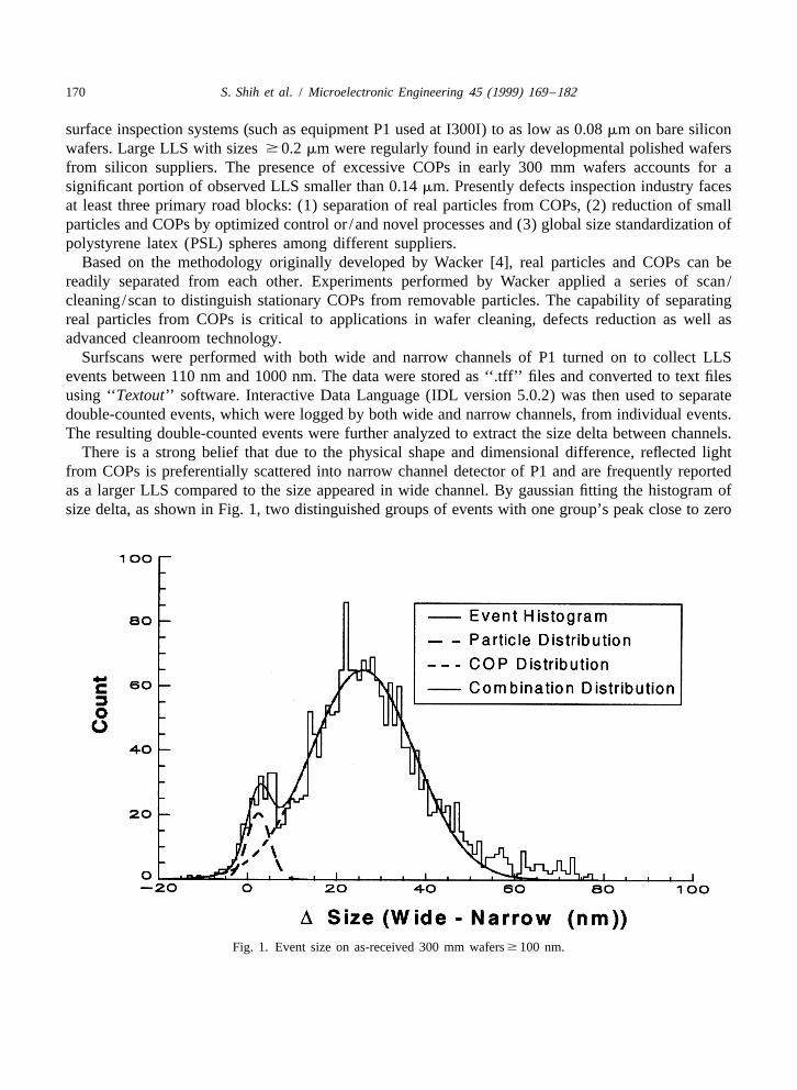
The LLS results of five silicon suppliers are listed in Table 1. The minimum LLS size has beenpushed from 0.12 mm in 1997 toward 0.09 mm in 1998 as dictated by 0.18 mm process requirement.Compared to data collected in 1997, information in Table 1 shows remarkable improvement [email protected] mm from originally more than 100 to close to 50 this year. Supplier C even shows a recordlot average of 14 [email protected] mm, which is well below the average | 50 of the rest of suppliers. This
Table 1LLS summary of 300 mm as received polished wafers
Q1-Q2 of 1998 Composite DFW 0.09–0.20,
bin size (mm) DFN 0.2–1.0
Supplier (wafer type)
A(furnace) F(furnace) A(particle) C(particle) D(particle) E(particle) A(litho)
0.090–0.100 282 1367 278 47 280 117 329
0.100–0.120 209 1726 190 51 85 67 184
0.120–0.140 21 694 24 5 6 10 18
0.140–0.160 12 571 8 2 4 7 6
0.160–0.180 8 282 4 1 2 4 3
0.180–0.200 2 45 2 0 1 2 1
0.200–0.300 32 85 9 3 17 10 15
0.300–0.500 12 23 4 2 9 5 5
0.500–1.000 8 35 4 1 4 6 11
Total . 0.090 586 4827 522 111 408 228 573
Total . 0.120 95 1735 55 14 44 44 60
Total . 0.160 63 470 23 7 34 27 35
. 0.090/ . 0.160 33.9 10.4 29.0 24.6 19.0 9.9 20.8
DFW avg haze (ppb) 248 83 254 26 59 23 234
172 S. Shih et al. / Microelectronic Engineering 45 (1999) 169 –182
great enhancement indicates excellent progress made in ingot pulling control for COPs suppressionsince last year.
Most of silicon suppliers used either slow crystal pulling ( , 0.1 mm/min) or heavily doped p-typesubstrate last year for COPs reduction. The average observed LLS $ 0.09 mm in the first half of 1998shown in Table 1 is | 300. The desired target of allowed LLS is originally set to [email protected] mm atI300I, however, for cost control reason the target was relaxed to 200/wafer. Even so, most of thesupplier today would still fall out of the I300I’s specifications. Down to 0.09 mm LLS, a moreaggressive approach is needed to further reduce the COPs amount. H anneal was previously proposed2
to be one of the options for this purpose.Control of haze level is another subject critical to the reduction of [email protected] mm and below. Due
to the promoted sensitivity of current metrology tools, high haze level wafers occasionally can causefalse counts of small LLS as well as mediocre data repeatibility. | 50 ppb level of haze isrecommended as maximum level haze to prevent above issues based on I300I’s past experience. Somesuppliers, such as supplier A, have an elevated haze level and therefore more liable to thenoise-related issues.
3.2. Trace Metal Contamination and Wet Bench Capability
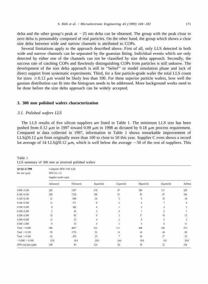
Trace metals of incoming 300mm wafers was monitored by vapor phase decomposition (VPD)inductively coupled plasma mass spectrometry (ICP/MS). Surface contaminants and native oxidewere dissolved by HF vapor and then collected by the VPD system. The HF droplet was diluted in 1%
3HNO to about 1 cm before it was fed into the ICP/MS system for analysis. NTRS’s trace metals3
recommendations are adopted as guidelines for metal contamination at I300I. Some metals such ascalcium and sodium are relatively evironmental-rich and therefore highly sensitive to ambient controlduring the data collection.
Both as-received wafers and the wafers cleaned by in-house wet benches at I300I were evaluated(see Tables 2 and 3). The sodium and calcium levels are artificially high primarily due to manualoperation during experiments. Both suppliers B and D demonstrate acceptable levels of metalcontents, while the rest of supplier are not far from the tolerance limits.
Table 210 2Silicon suppliers incoming wafer metal capability ( 3 10 /cm ) (supplier / test date)
Element NTRS Spec B (11/97) D (12/97) C (12/97) E (12/97) F (12/97)
Na # 2.5 2.9 16 64 450 2800Al # 10 5.4 5.3 7.9 16 88K – 1.1 0.8 5.7 18 190Ca # 2.5 17 37 17000 9400 86000Cr # 2.5 0.013 0.075 0.65 0.32 0.39Fe # 2.5 1.4 1.8 15 9 71Ni # 2.5 0.046 0.047 7.9 3.6 39Cu # 2.5 0.092 1.6 10 1.9 6.3Zn # 10 9.2 3.3 53 120 560

S. Shih et al. / Microelectronic Engineering 45 (1999) 169 –182 173
Table 310 2Trace metal level of wet cleaned wafers ( 3 10 /cm ) (wet Bench/ test date)
SIA Spec W1 (5/98) W2 (2/98) W4 (12/97) W5 (12/97) W3 (11/97)
Na , 2.5E 10 6.08E 1 10 5.73E 1 10 2.28E 1 10 7.50E 1 09 2.77E 1 11K – 1.61E 1 10 1.06E 1 10 6.76E 1 10 , 7.2 E 1 08 2.11E 1 10Ca , 2.5E 10 7.97E 1 11 3.68E 1 11 6.10E 1 11 2.25E 1 11 4.38E 1 11Al , 1.0E 11 6.03E 1 10 3.73E 1 10 3.01E 1 10 3.00E 1 10 5.10E 1 10Cr , 2.5E 10 , 3.3 E 1 07 2.29E 1 09 2.70E 1 09 4.80E 1 07 4.84E 1 08Fe , 2.5E 10 8.3 E 1 09 1.98E 1 10 1.62E 1 10 1.46E 1 10 1.31E 1 10Ni , 2.5E 10 1.12E 1 10 5.8 E 1 08 1.03E 1 10 1.75E 1 10 3.43E 1 09Cu , 2.5E 10 7.08E 1 09 1.73E 1 10 2.13E 1 10 1.80E 1 10 1.27E 1 09Zn , 1.0E 11 3.37E 1 10 4.88E 1 10 2.55E 1 10 1.30E 1 10 2.17E 1 10
Out of SIA Spec is shadedLowest in each kind is inverted in color
Wet benches W1 to W4 are equipped with conventional batch-type cleaning stations, whereas W3 issingle-wafer spin-on type compact cleaning tool. As indicated in Table 3, the conventional wet benchW5 has the lowest alkaline level detected, while the single wafer tool W3 shows almost comparablecleaning capability to the conventional ones.
3.3. Polished wafers flatness
As photolithography evolves, wafer surface flatness measured by GBIR, GFLR, and SFQR [6] havebecome more important than ever. The newly introduced scanning steppers will even require themeasurement of scanning site flatness parameter, SFSR [7,8] in the near future.
SFQR was measured for polished wafers of four suppliers by equipment F1, as shown in Fig. 2.Equipment F1 employs capacitative probe to detect the surface topography change with a relativelylarge probe size of 4 mm 3 4 mm. All the silicon suppliers except supplier D can reach a pretty highstandard of more than 90% of measured sites having a SFQR smaller than 0.18 mm. From the pasthistory on supplier D we learn that the F1 data on supplier D could be impacted by a so-called ‘‘donorkill’’ issue [5], which is associated with the relative insensitivity of some areas on the highly dopedp-type substrate to the capacitative probe. Fig. 3 further shows a typical cumulative SFQR histogramof five wafers from supplier D. The majority of the sites on the surface are peaked at 0.04 mm, leavinga wide process margin for future lithography improvement.
Equipment F2 applies a much smaller optical probe size 12 mm 3 12 mm for flatness measurement,which enables 1 mm edge exclusion as opposed to 3 mm exclusion for equipment F1. The initialcorrelation between these two techniques was studied for SFQR and wafer thickness. As expectedfrom their different working principles and probe sizes, SFQR data did not correlate well between F1and F2, as shown in Fig. 4(a). However, the wafer thickness and other parameters such as SBIR areshown in Fig. 4(b) and (c) to have good agreement between these two different measurement methods.
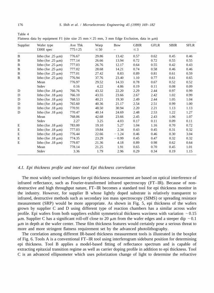
Table 4 summarizes three suppliers’ flatness data except SFQR. Two suppliers have pretty goodcontrol margin to current I300I’s thickness, warpage, and GBIR specifications. Only supplier Dexhibits marginal warp and GBIR data, which might require some improvement in the future.

174 S. Shih et al. / Microelectronic Engineering 45 (1999) 169 –182
Fig. 2. Summary of SFQR of incoming polished wafers.
Fig. 3. Cumulative SFQR histogram from supplier D.

S. Shih et al. / Microelectronic Engineering 45 (1999) 169 –182 175
Fig. 4. Correlation results between flatness measurement tools (Equipment F1 and F2).
4. 300 mm Epi wafers characterization
Two types of 300 mm epi wafers from supplier B, C, and D are available and checked out by I300Ifor early process development. The major difference between them is the concentration of substrate
1doping, namely heavily doped p substrate with resistivity | 10 mV-cm from supplier C, D and2lightly doped p substrate with resistivity | 10 V-cm from supplier B. Supplier B, D use epi growth
chamber manufactured by AMAT, whereas supplier C uses reactors made by ASM. Preliminary datacollected by I300I silicon team provide insights into the maturity of these developmental epi wafers.
176 S. Shih et al. / Microelectronic Engineering 45 (1999) 169 –182
Table 4Flatness data by equipment F1 (site size 25 mm 3 25 mm, 3 mm Edge Exclusion, data in mm)
Supplier Wafer type Ave Thk Warp Bow GBIR GFLR SBIR SFLRI300I spec 775625 # 50 – # 3
B litho (for .25 mm) 776.67 29.86 13.42 0.57 0.62 0.45 0.46B litho (for .25 mm) 777.14 26.66 13.94 0.72 0.72 0.55 0.55B litho (for .25 mm) 777.03 26.76 12.17 0.64 0.55 0.42 0.43B litho (for .25 mm) 777.02 28.68 14.21 0.74 0.58 0.46 0.46B litho (for .25 mm) 777.01 27.42 8.83 0.89 0.81 0.61 0.59B litho (for .25 mm) 776.94 37.76 23.40 1.10 0.77 0.61 0.65
Mean 776.97 29.52 14.33 0.78 0.67 0.52 0.52Stdev 0.16 4.22 4.86 0.19 0.11 0.08 0.09
D litho (for .18 mm) 766.76 43.32 22.20 2.29 2.44 0.97 0.99D litho (for .18 mm) 766.10 43.55 23.66 2.67 2.42 1.02 0.99D litho (for .18 mm) 768.53 40.21 19.30 2.49 2.44 1.05 1.04D litho (for .18 mm) 765.60 40.36 21.17 2.54 2.51 0.99 1.00D litho (for .18 mm) 770.91 48.50 30.94 2.20 2.21 1.13 1.13D litho (for .18 mm) 770.47 40.14 24.69 2.48 2.53 1.22 1.27
Mean 768.06 42.68 23.66 2.45 2.43 1.06 1.07Stdev 2.27 3.25 4.03 0.17 0.11 0.09 0.11
E litho (for .18 mm) 783.00 19.10 5.27 1.04 1.16 0.70 0.72E litho (for .18 mm) 777.03 19.84 2.34 0.43 0.45 0.31 0.32E litho (for .18 mm) 776.44 22.66 2 1.24 0.46 0.46 0.30 3.04E litho (for .18 mm) 774.35 23.29 2 0.99 0.45 0.47 0.32 0.32E litho (for .18 mm) 779.87 21.36 4.18 0.89 0.98 0.62 0.64
Mean 778.14 21.25 1.91 0.65 0.70 0.45 1.01Stdev 3.36 1.79 2.96 0.29 0.34 0.19 1.15
4.1. Epi thickness profile and inter-tool Epi thickness correlation
The most widely used techniques for epi thickness measurement are based on optical interference ofinfrared reflectance, such as Fourier-transformed infrared spectroscopy (FT–IR). Because of non-destructive and high throughput nature, FT–IR becomes a standard tool for epi thickness monitor inthe industry. However, for supplier B whose lightly doped substrate is relatively transparent toinfrared, destructive methods such as secondary ion mass spectroscopy (SIMS) or spreading resistacemeasurement (SRP) would be more appropriate. As shown in Fig. 5, epi thickness of the wafersgrown by supplier C and D using different type of reaction chambers has a similar across waferprofile. Epi wafers from both suppliers exhibit symmetrical thickness waviness with variation | 0.15mm. Supplier C has a significant roll-off close to 20 mm from the wafer edges and a steeper dip | 0.1mm in depth at the wafer center. These film thickness features would certainly pose a serious threat tomore and more stringent flatness requirement set by the advanced photolithography.
The correlation among different IR-based thickness measurement tools is illustrated in the boxplotof Fig. 6. Tools A is a conventional FT–IR tool using interferogram sideburst position for determiningepi thickness. Tool B applies a model-based fitting of reflectance spectrum and is capable ofextracting epitaxial transition regime as well as carrier doping profile in addition to epi thickness. ToolC is an advanced ellipsometer which uses polorization change of light to determine the refractive

S. Shih et al. / Microelectronic Engineering 45 (1999) 169 –182 177
Fig. 5. Epi thickness profiles by conventional FT–IR for suppliers C and D.
index and the film thickness. As observed in Fig. 6(a) and (b), reading of tool A is consistently higherthan tool B by | 0.02 mm, while reading of tool C is slightly lower than tool B and the differencedepends on the wafer characteristics. These observed thickness differences are most likely determined

178 S. Shih et al. / Microelectronic Engineering 45 (1999) 169 –182
Fig. 6. Epi thickness comparison between tools.
by how the tools respond to the epitaxial transition zone. By model-based fitting, tool B theoreticallyhas a chance to resolve the transition regions better than other tools. SIMS and SRP are currently inprogress to confirm the above argument.
4.2. Epi flatness
SFQR site flatness of epi wafers was shown in Fig. 7. In spite of epi thickness waviness, the siteflatness of supplier C is well controlled to be within the current 0.18 mm specification, consistent withthe measurement made on their polished wafers. In addition, for the first time we observe that partialsites flatness has better control than full site flatness. The rest of suppliers has the flatness datacomparable to their polished wafers.
Table 5 summaries the rest of flatness-related parameters for epi wafers. Notice that the warpageand GBIR of epi wafers from supplier D fall out of current I300I specifications, which is consistentwith marginal data shown in their polished wafers.
4.3. Epi LLS
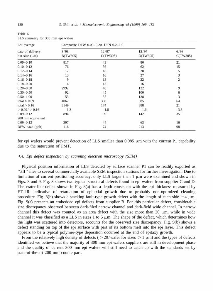
Table 6 listed the LLS performance measured by equipment P1 at I300I. In addition todevelopmental epi wafers, supplier C provides their early production epi wafers for the initialcharacterization. The impressed result of less than 65 LLS @0.09 mm from these production epiwafers signal the rapid learning of some silicon suppliers over the past 6 months. For majority of

S. Shih et al. / Microelectronic Engineering 45 (1999) 169 –182 179
Fig. 7. SFQR site flatness for epi wafers.
suppliers, growth of epitaxy layer significantly reduce small LLS with sizes # 0.18 mm. This LLSreduction was primarily attributed to the coverage of COPs by the grown silicon film. Oppositely,LLS with sizes $ 0.18 mm remarkably increases beyond the level of normal polished wafers in theseearly epi wafers. Additionally, increase of haze level from | 30 ppb in polished wafers to | 100 ppb
Table 5Flatness data summary for epi wafers
Supplier Wafer type Ave Thk Warp Bow GBIR GFLR SBIR SFLRI300I spec # 50 – # 3
B TW305 780.92 12.63 2 0.52 0.74 0.63 0.40 0.39B TW305 781.03 14.24 2 0.17 0.68 0.56 0.38 0.40B TW305 780.86 11.40 1.62 0.57 0.50 0.38 0.38
Mean 780.94 12.76 0.31 0.66 0.56 0.39 0.39Stdev 0.09 1.42 1.15 0.09 0.07 0.01 0.01
C TW305 774.79 35.36 8.52 2.82 2.71 1.40 1.37C TW305 774.71 36.47 7.10 2.72 2.69 1.16 1.17C TW305 774.06 35.74 7.22 2.70 2.65 1.39 1.40
Mean 774.52 35.86 7.61 2.75 2.68 1.32 1.31Stdev 0.40 0.57 0.79 0.06 0.03 0.13 0.13
D TW305 771.43 60.91 2 50.89 3.28 3.24 1.57 1.57D TW305 776.17 91.20 2 80.11 3.35 3.30 1.61 1.63D TW305 771.57 69.06 2 57.45 3.26 3.18 1.60 1.59
Mean 773.06 73.72 2 62.81 3.30 3.24 1.59 1.60Stdev 2.70 15.67 15.33 0.05 0.06 0.02 0.03
180 S. Shih et al. / Microelectronic Engineering 45 (1999) 169 –182
Table 6LLS summary for 300 mm epi wafers
Lot average Composite DFW 0.09–0.20, DFN 0.2–1.0
date of delivery 3/98 12/97 12/97 6/98bin size (mm) B(TW305) C(TW305) D(TW305) C(TW305)
0.09–0.10 817 43 80 210.10–0.12 76 56 62 150.12–0.14 12 18 28 50.14–0.16 13 16 27 30.16–0.18 9 13 22 20.18–0.20 4 13 16 10.20–0.30 2992 48 122 90.30–0.50 92 45 100 60.50–1.00 53 57 128 3total . 0.09 4067 308 585 64total . 0.16 3149 174 388 21. 0.09/ . 0.16 1.3 1.8 1.6 3.50.09–0.12 894 99 142 35200 mm equivalent0.09–0.12 397 44 63 16DFW haze (ppb) 116 74 213 98
for epi wafers would prevent detection of LLS smaller than 0.085 mm with the current P1 capabilitydue to the saturation of PMT.
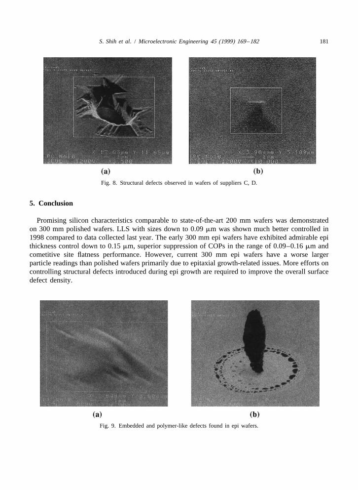
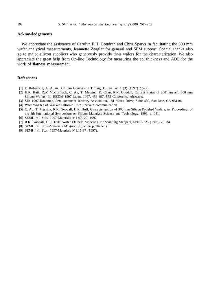
4.4. Epi defect inspection by scanning electron microscopy (SEM)
Physical position information of LLS detected by surface scanner P1 can be readily exported as‘‘.tff’’ files to several commercially available SEM inspection stations for further investigation. Due tolimitation of current positioning accuracy, only LLS larger than 1 mm were examined and shown inFigs. 8 and 9. Fig. 8 shows two typical structural defects found in epi wafers from supplier C and D.The crater-like defect shown in Fig. 8(a) has a depth consistent with the epi thickness measured byFT–IR, indicative of retardation of epitaxial growth due to probably non-optimized cleaningprocedure. Fig. 8(b) shows a stacking fault-type growth defect with the length of each side | 4 mm.Fig. 9(a) presents an embedded epi defects from supplier B. For this particular defect, considerablesize discrepancy observed between dark-filed narrow channel and dark-field wide channel. In narrowchannel this defect was counted as an area defect with the size more than 20 mm, while in widechannel it was classified as a LLS in sizes 1 to 5 mm. The shape of the defect, which determines howthe light was scattered into detectors, accounts for the observed size discrepancy. Fig. 9(b) shows adefect standing on top of the epi surface with part of its bottom melt into the epi layer. This defectappears to be a typical polymer-type deposition occurred at the end of epitaxy growth.
From the relatively high density of defects ( . 20/wafer for sizes . 1 mm) and the types of defectsidentified we believe that the majority of 300 mm epi wafers suppliers are still in development phaseand the quality of current 300 mm epi wafers will still need to catch up with the standards set bystate-of-the-art 200 mm counterpart.
S. Shih et al. / Microelectronic Engineering 45 (1999) 169 –182 181
Fig. 8. Structural defects observed in wafers of suppliers C, D.
5. Conclusion
Promising silicon characteristics comparable to state-of-the-art 200 mm wafers was demonstratedon 300 mm polished wafers. LLS with sizes down to 0.09 mm was shown much better controlled in1998 compared to data collected last year. The early 300 mm epi wafers have exhibited admirable epithickness control down to 0.15 mm, superior suppression of COPs in the range of 0.09–0.16 mm andcometitive site flatness performance. However, current 300 mm epi wafers have a worse largerparticle readings than polished wafers primarily due to epitaxial growth-related issues. More efforts oncontrolling structural defects introduced during epi growth are required to improve the overall surfacedefect density.
Fig. 9. Embedded and polymer-like defects found in epi wafers.
182 S. Shih et al. / Microelectronic Engineering 45 (1999) 169 –182
Acknowledgements
We appreciate the assistance of Carolyn F.H. Gondran and Chris Sparks in facilitating the 300 mmwafer analytical measurements, Jeannette Zeagler for general and SEM support. Special thanks alsogo to major silicon suppliers who generously provide their wafers for the characterization. We alsoappreciate the great help from On-line Technology for measuring the epi thickness and ADE for thework of flatness measurement.
References
[1] F. Robertson, A. Allan, 300 mm Conversion Timing, Future Fab 1 (3) (1997) 27–33.[2] H.R. Huff, D.W. McCormack, C. Au, T. Messina, K. Chan, R.K. Goodall, Current Status of 200 mm and 300 mm
Silicon Wafers, in: ISSDM 1997 Japan, 1997, 456-457, 575 Conference Abstracts.[3] SIA 1997 Roadmap, Semiconductor Industry Association, 181 Metro Drive, Suite 450, San Jose, CA 95110.[4] Peter Wagner of Wacker Siltronic Corp., private communication.[5] C. Au, T. Messina, R.K. Goodall, H.R. Huff, Characterization of 300 mm Silicon Polished Wafers, in: Proceedings of
the 8th International Symposium on Silicon Materials Science and Technology, 1998, p. 641.[6] SEMI Int’l Stds. 1997-Materials M1-97, 20, 1997.[7] R.K. Goodall, H.R. Huff, Wafer Flatness Modeling for Scanning Steppers, SPIE 2725 (1996) 76–84.[8] SEMI Int’l Stds.-Materials M1-(rev. 98, to be published).[9] SEMI Int’l Stds. 1997-Materials M1.15-97 (1997).