
Estimation and Control in Semiconductor Etch: Practice and Possibilities
Upload
independentCategory
view
4download
0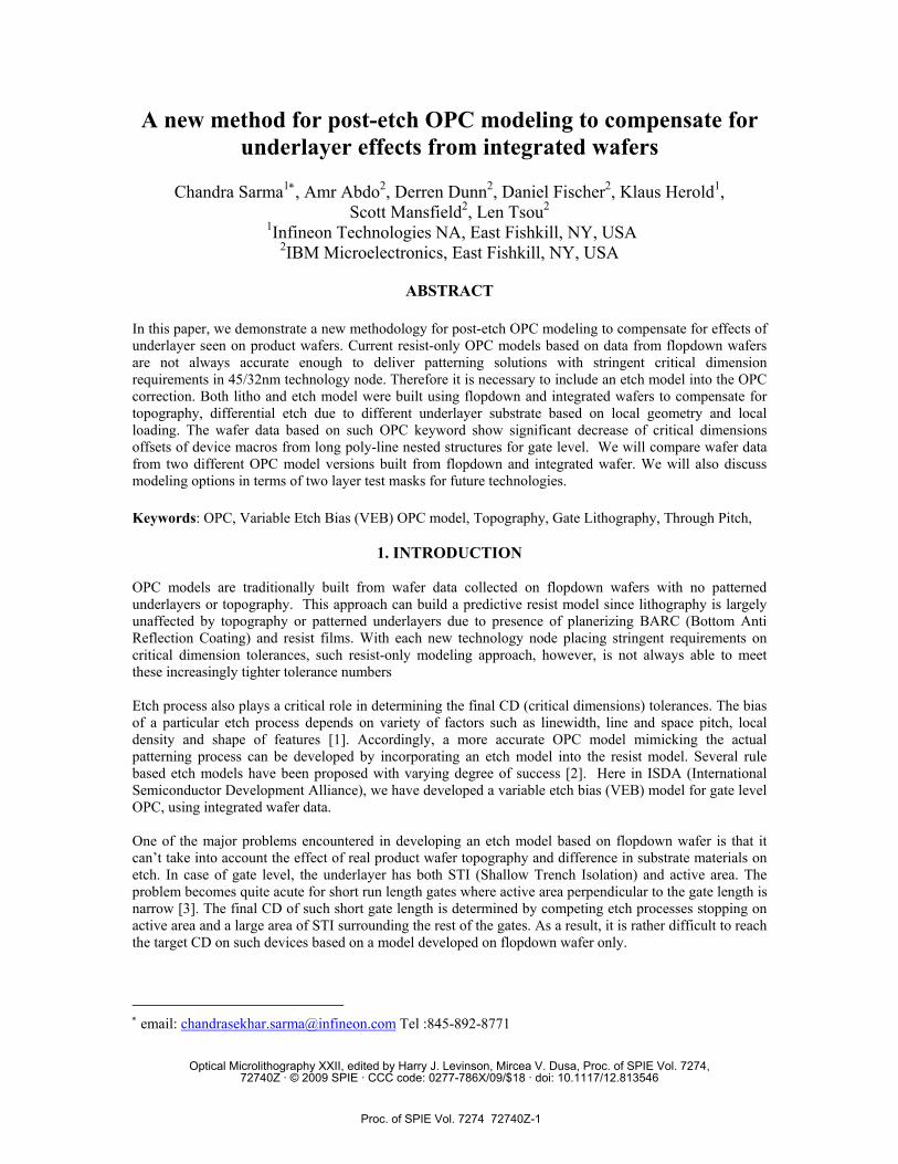
A new method for post-etch OPC modeling to compensate for underlayer effects from integrated wafers
Chandra Sarma1∗, Amr Abdo2, Derren Dunn2, Daniel Fischer2, Klaus Herold1,
Scott Mansfield2, Len Tsou2 1Infineon Technologies NA, East Fishkill, NY, USA
2IBM Microelectronics, East Fishkill, NY, USA
ABSTRACT In this paper, we demonstrate a new methodology for post-etch OPC modeling to compensate for effects of underlayer seen on product wafers. Current resist-only OPC models based on data from flopdown wafers are not always accurate enough to deliver patterning solutions with stringent critical dimension requirements in 45/32nm technology node. Therefore it is necessary to include an etch model into the OPC correction. Both litho and etch model were built using flopdown and integrated wafers to compensate for topography, differential etch due to different underlayer substrate based on local geometry and local loading. The wafer data based on such OPC keyword show significant decrease of critical dimensions offsets of device macros from long poly-line nested structures for gate level. We will compare wafer data from two different OPC model versions built from flopdown and integrated wafer. We will also discuss modeling options in terms of two layer test masks for future technologies. Keywords: OPC, Variable Etch Bias (VEB) OPC model, Topography, Gate Lithography, Through Pitch,
1. INTRODUCTION OPC models are traditionally built from wafer data collected on flopdown wafers with no patterned underlayers or topography. This approach can build a predictive resist model since lithography is largely unaffected by topography or patterned underlayers due to presence of planerizing BARC (Bottom Anti Reflection Coating) and resist films. With each new technology node placing stringent requirements on critical dimension tolerances, such resist-only modeling approach, however, is not always able to meet these increasingly tighter tolerance numbers Etch process also plays a critical role in determining the final CD (critical dimensions) tolerances. The bias of a particular etch process depends on variety of factors such as linewidth, line and space pitch, local density and shape of features [1]. Accordingly, a more accurate OPC model mimicking the actual patterning process can be developed by incorporating an etch model into the resist model. Several rule based etch models have been proposed with varying degree of success [2]. Here in ISDA (International Semiconductor Development Alliance), we have developed a variable etch bias (VEB) model for gate level OPC, using integrated wafer data. One of the major problems encountered in developing an etch model based on flopdown wafer is that it can’t take into account the effect of real product wafer topography and difference in substrate materials on etch. In case of gate level, the underlayer has both STI (Shallow Trench Isolation) and active area. The problem becomes quite acute for short run length gates where active area perpendicular to the gate length is narrow [3]. The final CD of such short gate length is determined by competing etch processes stopping on active area and a large area of STI surrounding the rest of the gates. As a result, it is rather difficult to reach the target CD on such devices based on a model developed on flopdown wafer only.
∗ email: [email protected] Tel :845-892-8771
Optical Microlithography XXII, edited by Harry J. Levinson, Mircea V. Dusa, Proc. of SPIE Vol. 7274,72740Z · © 2009 SPIE · CCC code: 0277-786X/09/$18 · doi: 10.1117/12.813546
Proc. of SPIE Vol. 7274 72740Z-1

We will demonstrate a methodology where we can incorporate such effects seen on product wafers into our OPC models. It includes collecting resist CD data from flopdown wafers using an OPC test mask, collecting etch data from flopdown wafer exposed with an OPC test mask to account for etch dependence on structure pitch and shape and finally collecting additional data from integrated wafers using a product mask with special macros and then retargeting the resist model output at every stage. The wafer data based on such OPC keyword show significant decrease of CD offsets of devices macros from long Poly-line nested structures. Such an OPC model can also minimize macro-to-macro offsets for short run length gates, which is not possible using standard OPC methodology. We will present wafer data from 2 different OPC model versions: OPC VEB model without integrated wafer data and the VEB model with integrated wafer data. We will also discuss modeling options in terms of two layer test masks for future technologies.
2. RESULTS AND DISCUSSIONS The wafer data we present below are based on 3 different types of OPC modeling 1) Litho-only OPC model, 2) OPC model based on both litho and etch process on flopdown wafers, and finally 3) OPC model derived from both etch and litho processes on integrated wafers with patterned underlayers. All the data pertain to gate level in 45 nm technology. The model improvement is quantified in terms of through pitch variations and also in terms of CD variations among different devices for same target CD and pitch. Figure 1 summarizes the through pitch 3-sigma (on product wafers) for all three OPC models.
Testsite Keyword
Thrupitch CD Range
(normalized)
Thrupitch 3sigma
(normalized) Model1 KW1 0.57 0.5 VEB+new test mask+integrated wafer2 KW2 1.41 1.0 VEB+old testmask+ constant bias based on limited integrated data3 KW3 2.02 1.6 VEB model+ flodown data4 KW4 1.00 1.0 resist model
Figure 1. Summary of post etch through pitch 3-sigma and range (normalized to resist-only model) for product wafers using different OPC models (built with resist process only, resist & etch process and resist & etch process on integrated wafers) 2.1 Litho only OPC model: This is a traditional OPC model approach. The model was built taking into account optical/resist/litho process on flopdown wafers, i.e. wafers with an unpatterned gate stack underlayer. No underlayer effect or subsequent etch process was taken into account while building the model. The assumption was that etch process is constant across all features/pitches and therefore optimizing litho process only will optimize the final CDs). Till 65nm node such model worked fairly well for gate level but critical dimension tolerances have become progressively much tighter in successive technology nodes In 45nm/32nm nodes, ignoring etch process in the modeling would not meet the target CD tolerances. The resist-only OPC model enables a 3sigma of 5.3nm for through pitch on actual product wafers (Figure 1). In addition, such models have not been able to meet the CD tolerance between various devices for the same pitch and linewidth.
Proc. of SPIE Vol. 7274 72740Z-2

Figure 2 Device macro with 1X, 2X and 3X gate pitches: The device run length (vertical gate line) and active area (perpendicular dark areas) are relatively smaller than traditional Poly-line macros (see Figure 3) One reason for such behavior is the change of etch characteristics based on local pattern loading, topography and run length of devices which are not taken into account in a litho only model. One case in point is a device such as the one shown in Figure 2. The run length of the device ( smaller than traditional thru pitch macro) and the size of patterned underlayer (in this case active device) probably complicates the etch process and thus shows a dramatically different post RIE CD deltas than was expected from longer poly lines (similar to traditional through pitch macros). 2.2 Litho and Etch model from flopdown wafer: The inability of resist only model to meet critical dimension requirements (thru pitch and site to site component) prompted the development of an OPC model based on both etch and litho process. The process involves collecting post litho and post etch data on a flopdown wafer (with unpatterned gate stack underneath) using an OPC test mask. A dense OPC model, similar to the one in ref [4], was used for resist model and a variable etch bias model was used to model the etch process bias. The resultant thru pitch number is shown in Figure 1.The 3-sigma for the through pitch for nested/ semi-nested and isolated pitches, increased by almost 100% compared to the resist only model. The reason for such deterioration of thrupitch behavior is mainly two-fold: 1) Etch only model was not adequate enough, 2) The etch process on product wafers (integrated wafers with patterned underlayer) and modeling wafers (flopdown) are very different due to local loading effects and the dependence of etch process on local geometry (the relative size of active layer and gate run length). The clue to such local geometry dependence was pointed out by the measurements of poly-length for the same pitch for two different structures. In one case the run length of the gate line was much shorter than the Poly lines and the active area underneath was also much smaller compared to traditional Poly-line through pitch macro (Figure 2 and Figure 3).
Proc. of SPIE Vol. 7274 72740Z-3

Figure 3: Traditional through pitch macro (longer PC run length, vertical nested line, and larger active area underneath, designated by a light square box around it). While the thrupitch macro of Figure 3 show a delta of less than 1nm CD between 1x and 2x pitches, the device in Figure 2 shows a delta CD of 5-7nm. Figure 4 summarizes the CD delta between 1X, 2X and 3x pitches for the devices shown in Figure 2.
Post RIE CD offset for etch model from flopdown wafer
01234567
2X-1X 2X-1X 3X-1X 3X-1Xmacro
CD
del
ta b
etw
een
mac
ros(
nm)
nFET nFETpFET pFET
Figure 4: CD delta between 1x/2x and 1x/3x pitches for the device shown in Figure2. The behavior does not follow the thru pitch behavior measured on large Poly-line devices (less than 1nm). The etch OPC was built from flopdown wafer data. 2.3 Litho and etch model from integrated wafer
Proc. of SPIE Vol. 7274 72740Z-4
The analysis of the data from flopdown model essentially showed an inherent weakness of etch model on flopdown wafers, when the underlayer substrate characteristics change over a short distance as in the case of the devices in Figure 2. We have collected extensive data to determine what cause such deviation between integrated wafer measurements and OPC prediction based on flopdown wafers: CD data from both flopdown and integrated wafers were collected on post litho and post RIE wafers for both small devices and large Poly lines. Figure 5 shows a CD delta between 1X and 2X and 3X and 5X pitches for the device in Figure 2. Figure 5: Post litho and post etch CD delta between 1X and 2X and 1X-3X pitches for device macro in Figure2: Data on flopdown wafers are designed as FD and those from integrated wafers are designated as STI It can be clearly observed that while post resist data are similar with 0-2nm variation for both flopdown and integrated wafers, the post etch data are different. The post-etch data for integrated wafers show much larger CD deviation than those from flopdown wafers. The resist CD data collected from the OPC through pitch macro (longer Poly line as in Figure 3) show no significant difference between flopdown and integrated wafers (Figure 5).
Orch2 Resist Data (RELCHIP)
-10
-8
-6
-4
-2
0
2
4
6
140180220260300340380420460500540580620660700740780820860900940980
Pitch
Del
ta fr
om 1
80nm
pitc
h
FD ResistSTI ResistResist TargetPredicted
Post resist CD on long L-poly lines
Device Macro - Delta's
-3-2-1012345678
CD
Del
ta (n
m) FD - Resist
FD - EtchSTI - ResistSTI - EtchResist Target
CD(2x-1x) CD(3x-1x)
nFET pFET pFETnFET
Proc. of SPIE Vol. 7274 72740Z-5

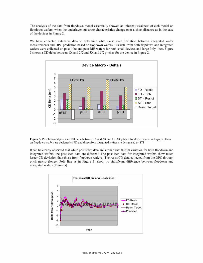
Figure 6. Delta-to-target CD as a function of pitch for post litho process (on both flopdown and integrated wafers): At and above 1X pitch, a maximum delta of 2nm is observed between model prediction and measurements on integrated wafers. The etch CD data (Figure 7) measured on longer Poly lines show a general offsets between flopdown and integrated wafers above a certain pitch. However the offsets get much worse when the Poly length and underlayer size (in this case it is the active area) become smaller. Figure 7: post etch data from long Poly-line macro showing an offset of about 2nm between flopdown (FD) and integrated (STI) wafers. It is not clearly understood what drives such differences between flopdown and STI wafers and how such differences get worse for short length devices. The possible reasons are the differential etches between active area and STI in case of integrated wafers and local loading. However these data enable us to go for an OPC model that can incorporate such effects. 2.3.1 Litho and Etch Model built using new test mask and integrated wafers: A new improved resist model was built using a new test mask with extended coverage that includes very short run length macros. A VEB etch model was built using integrated wafers data. A dense OPC engine was used. The resultant CD thru pitch and macro to macro offsets are dramatically improved. Figure 8 shows thrupitch curves for different types of OPC models. The model based on both litho and etch process on integrated wafers yields a 3sigma of 2.9nm, an improvement of about 50% compared to all previous models (based on resist only or etch on flopdown wafers).
Orch2 Etch Data (RELCHIP)
-10
-8
-6
-4
-2
0
2
4
6
140180220260300340380420460500540580620660700740780820860900940980
Pitch
Del
ta fr
om 1
80nm
pitc
h
FD EtchSTI EtchEtch TargetPredictedCorrected
Post Etch CD on Long L-poly lines
Proc. of SPIE Vol. 7274 72740Z-6
0.0
0.5
1.0
1.5
2.0
2.5
Res
ist
Mod
el
Res
ist+
etch
mod
el(F
lopd
own)
Res
ist+
etch
mod
el(In
tegr
ated
)
nm3sigma normalizedRange normalized
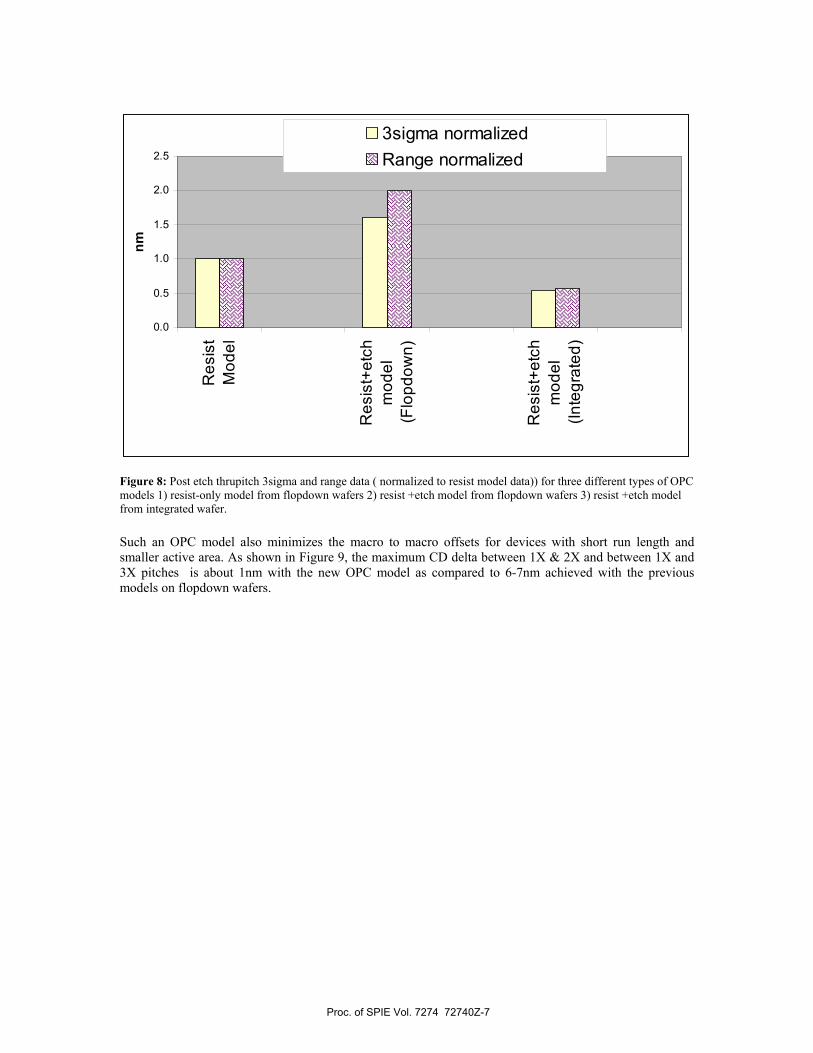
Figure 8: Post etch thrupitch 3sigma and range data ( normalized to resist model data)) for three different types of OPC models 1) resist-only model from flopdown wafers 2) resist +etch model from flopdown wafers 3) resist +etch model from integrated wafer. Such an OPC model also minimizes the macro to macro offsets for devices with short run length and smaller active area. As shown in Figure 9, the maximum CD delta between 1X & 2X and between 1X and 3X pitches is about 1nm with the new OPC model as compared to 6-7nm achieved with the previous models on flopdown wafers.
Proc. of SPIE Vol. 7274 72740Z-7
Post RIE CD offset for etch model from flopdown wafer
01234567
2X-1X 2X-1X 3X-1X 3X-1Xmacro
CD
del
ta b
etw
een
mac
ros(
nm)
Ffopdown wafer etch model Integrated wafer etch model
nFETnFETpFET pFET
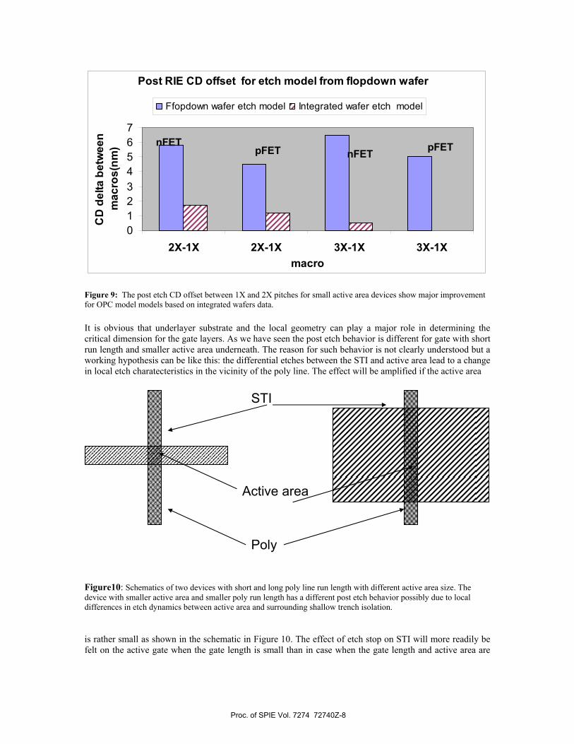
Figure 9: The post etch CD offset between 1X and 2X pitches for small active area devices show major improvement for OPC model models based on integrated wafers data. It is obvious that underlayer substrate and the local geometry can play a major role in determining the critical dimension for the gate layers. As we have seen the post etch behavior is different for gate with short run length and smaller active area underneath. The reason for such behavior is not clearly understood but a working hypothesis can be like this: the differential etches between the STI and active area lead to a change in local etch charatecteristics in the vicinity of the poly line. The effect will be amplified if the active area Figure10: Schematics of two devices with short and long poly line run length with different active area size. The device with smaller active area and smaller poly run length has a different post etch behavior possibly due to local differences in etch dynamics between active area and surrounding shallow trench isolation. is rather small as shown in the schematic in Figure 10. The effect of etch stop on STI will more readily be felt on the active gate when the gate length is small than in case when the gate length and active area are
Poly
Active area
STI
Proc. of SPIE Vol. 7274 72740Z-8

both large. It is important, therefore, to incorporate such ‘underlayer’ effects in an OPC model in order to accurately predict critical dimensions of the variety of devices with different active area sizes. 2.3.2 OPC model on integrated wafers with 2 OPC masks. One of the major findings from this methodology is that patterned underlayers (in this case the active area and STI) play a major role in determine post etch CD of the current layer. This necessitates a careful isolation of such effects while building OPC model for a critical layer. In the current work, we have developed the model based on one layer gate test mask, designed in a way to ensure enough overlap with existing product mask of the STI layer. However, a more robust methodology proposal will have two layer OPC test masks, one for example, STI and one for gate level and they have extensive coverage of various configuration of active area as seen on a typical product mask. This part of the work is currently undergoing.
3 SUMMARY AND CONCLUSIONS We have shown a new methodology for OPC modeling which takes into account the topography of the underlayer normally found on product wafer. A combination of resist and a variable etch model was developed based on data collected on integrated wafers. This shows a dramatic improvement in thru pitch behavior on product wafers. This also reduced CD offsets from device to device by as much as 7 times. The difference between the etch behavior on flopdown and integrated wafers is not clearly understood but differential etch characteristics on different substrate and micro-loading based on local geometry of the pattern is believed to have contributed to such observed offsets. For comparison wafer data based on OPC using resist-only model on flopdown wafer, resist and etch modeling on flopdown wafers are also collected. The proposed methodology for OPC development is able to deliver stringent critical dimension requirements in 45/32nm technology. For future a two test mask solution is being offered for further robustness of the model.
4 ACKNOWLDEGEMNT The authors are responsible for the content of the paper. We would like to thank Dongbing Shao, Narender Rana and Eric Lehner of IBM for their help with CDSEM /AFM data collection and George Hefferon, Arpan Mahorowala of IBM and Paul Schroeder of Infineon for useful discussions and suggestions. This work was performed at the IBM Microelectronics Div. Semiconductor Research & Development Center, Hopewell Junction, and NY 12533.
5. REFERENCES 1. Shunichiro Sato et al., “Dry-etch function for model-based OPC beyond 65-nm node”, Optical Microlithography, Proc. Of SPIE 6155 615504-1(2006) 2. Chin T Lim et al.., “Consideration of VT5 etch based OPC modeling”, Proc. Of SPIE 6924 69243D-1, (2008) 3. Manuel Tagliavini et al., “Impact of Medium and Long range Effects on Poly Gate Patterning”, Proc SPIE, Vol. 6924, 69243Y, (2008) 4. Amr Abdo et al., “The Comparison of OPC performance and run time for dense versus sparse solution", Proc. SPIE vol. 6924, 69243G (2008)
Proc. of SPIE Vol. 7274 72740Z-9
Copyright © 2022 FDOKUMEN


![Increased [CO 2] does not compensate for negative effects on yield caused by higher temperature and [O 3] in Brassica napus L](https://static.fdokumen.com/doc/165x107/631794e7831644824d038e8a/increased-co-2-does-not-compensate-for-negative-effects-on-yield-caused-by-higher.jpg)