Double exposure double etch for dense SRAM: a designer's dream
9
Double Exposure Double Etch for Dense SRAM: A Designer’s Dream Chandra Sarma ∗ , Allen Gabor 1 , Scott Halle 1 , Henning Haffner, Klaus Herold, Len Tsou 1 , Helen Wang 1 , Haoren Zhuang Infineon Technologies NA, East Fishkill, NY, USA 1 IBM Microelectronics, East Fishkill, NY, USA ABSTRACT As SRAM arrays become lithographically more aggressive than random logic, they are more and more determining the lithography processes used. High yielding, low leakage, dense SRAM cells demand fairly aggressive lithographic process conditions. This leads to a borderline process window for logic devices. The tradeoff obtained between process window optimization for random logic gates and dense SRAM is not always straightforward, and sometimes necessitates design rule and layout modifications. By delinking patterning of the logic devices from SRAM, one can optimize the patterning processes for these devices independently. This can be achieved by a special double patterning technique that employs a combination of double exposure and double etch (DE2). In this paper we show how a DE2 patterning process can be employed to pattern dense SRAM cells in the 45nm node on fully integrated wafers, with more than adequate overlap of gate line-end onto active area. We have demonstrated that this process has adequate process window for sustainable manufacturing. For comparison purpose we also demonstrate a single exposure single etch solution to treat such dense SRAM cells. In 45nm node, the dense SRAM cell can also be printed with adequate tolerances and process window with single expose (SE) with optimized OPC. This is confirmed by electrical results on wafer. We conclude that DE2 offers an attractive alternative solution to pattern dense SRAM in 45nm and show such a scheme can be extended to 32nm and beyond. Employing DE2 lets designers migrate to very small tip-to-tip distance in SRAM. The selection of DE2 or SE depends on layout, device performance requirements, integration schemes and cost of ownership. Keywords: Double Patterning, DE2, SRAM, Printed Assist Feature, SRAF, Gate Process Window 1. INTRODUCTION With Extreme Ultra Violet (EUV) lithography still several years away from being a viable manufacturing process, the roadmap for next few nodes in logic device will necessarily include optical lithography as a run path for manufacturing. With the current tool sets, the optimal patterning solution of logic devices is not always optimum for specific devices like SRAMs where the criterion of success is mainly driven by line-end shortening of polysilicon lines and its final coverage on active area and therefore, there is always a tradeoff between SRAM and random logic patterning 1 Thus, for each technology node, the device shrinkage is posing even more challenges to optical lithography solution. For example in 45 technology node, in some specific design, the shrinkage of gate level is more than the STI (shallow trench isolation) design. This leads to a greater demand on gate level (PC) SRAM patterning in order to ensure there is adequate coverage of PC over the active area to minimize electrical leakage. The problem is more acute in 32nm node where, due to restriction of SRAF (Sub Resolution Assist Features) size and limited numerical aperture (NA) settings, the process windows are even significantly smaller for logic devices. ∗ Chandra Sarma, Tel: 845-892-8771, [email protected] Optical Microlithography XXI, edited by Harry J. Levinson, Mircea V. Dusa, Proc. of SPIE Vol. 6924, 692429, (2008) · 0277-786X/08/$18 · doi: 10.1117/12.772985 Proc. of SPIE Vol. 6924 692429-1 2008 SPIE Digital Library -- Subscriber Archive Copy
-
Upload
independent -
Category
Documents
-
view
0 -
download
0
Transcript of Double exposure double etch for dense SRAM: a designer's dream

Double Exposure Double Etch for Dense SRAM: A Designer’s Dream
Chandra Sarma∗, Allen Gabor1, Scott Halle1, Henning Haffner, Klaus Herold, Len Tsou1,
Helen Wang1, Haoren Zhuang Infineon Technologies NA, East Fishkill, NY, USA
1IBM Microelectronics, East Fishkill, NY, USA
ABSTRACT As SRAM arrays become lithographically more aggressive than random logic, they are more and more determining the lithography processes used. High yielding, low leakage, dense SRAM cells demand fairly aggressive lithographic process conditions. This leads to a borderline process window for logic devices. The tradeoff obtained between process window optimization for random logic gates and dense SRAM is not always straightforward, and sometimes necessitates design rule and layout modifications. By delinking patterning of the logic devices from SRAM, one can optimize the patterning processes for these devices independently. This can be achieved by a special double patterning technique that employs a combination of double exposure and double etch (DE2). In this paper we show how a DE2 patterning process can be employed to pattern dense SRAM cells in the 45nm node on fully integrated wafers, with more than adequate overlap of gate line-end onto active area. We have demonstrated that this process has adequate process window for sustainable manufacturing. For comparison purpose we also demonstrate a single exposure single etch solution to treat such dense SRAM cells. In 45nm node, the dense SRAM cell can also be printed with adequate tolerances and process window with single expose (SE) with optimized OPC. This is confirmed by electrical results on wafer. We conclude that DE2 offers an attractive alternative solution to pattern dense SRAM in 45nm and show such a scheme can be extended to 32nm and beyond. Employing DE2 lets designers migrate to very small tip-to-tip distance in SRAM. The selection of DE2 or SE depends on layout, device performance requirements, integration schemes and cost of ownership. Keywords: Double Patterning, DE2, SRAM, Printed Assist Feature, SRAF, Gate Process Window
1. INTRODUCTION
With Extreme Ultra Violet (EUV) lithography still several years away from being a viable manufacturing process, the roadmap for next few nodes in logic device will necessarily include optical lithography as a run path for manufacturing. With the current tool sets, the optimal patterning solution of logic devices is not always optimum for specific devices like SRAMs where the criterion of success is mainly driven by line-end shortening of polysilicon lines and its final coverage on active area and therefore, there is always a tradeoff between SRAM and random logic patterning 1 Thus, for each technology node, the device shrinkage is posing even more challenges to optical lithography solution. For example in 45 technology node, in some specific design, the shrinkage of gate level is more than the STI (shallow trench isolation) design. This leads to a greater demand on gate level (PC) SRAM patterning in order to ensure there is adequate coverage of PC over the active area to minimize electrical leakage. The problem is more acute in 32nm node where, due to restriction of SRAF (Sub Resolution Assist Features) size and limited numerical aperture (NA) settings, the process windows are even significantly smaller for logic devices.
∗ Chandra Sarma, Tel: 845-892-8771, [email protected]
Optical Microlithography XXI, edited by Harry J. Levinson, Mircea V. Dusa, Proc. of SPIE Vol. 6924, 692429, (2008) · 0277-786X/08/$18 · doi: 10.1117/12.772985
Proc. of SPIE Vol. 6924 692429-12008 SPIE Digital Library -- Subscriber Archive Copy

One way to optimize the patterning process for gate level is to separate the process for random logic devices from that of ultra dense SRAM devices. This can be achieved by a specific double patterning technique, where one lithography-one etch step is followed by another lithography another etch step (Double Exposure Double Etch, or DE2). This has several advantages: 1) it allows one to design even more aggressive SRAM with extremely tight gate tip-to-tip variation, 2) eliminates corner rounding of gate line ends, 3)allows one to find the best possible illumination conditions for best process window for random logic. The absence of corner rounding and line-end shortening in this case allows excellent control of PC (gate) over active area. This opens up the opportunity to enlarge the active area and to realize device and integration benefits. The ability to tightly control line-ends by PC double patterning has been previously suggested2. The seemingly straightforward process, in manufacturing reality, involves consideration of many factors such as topography of gate stack post first etch, the use of multilayer schemes for litho and etch, and novel etch methodology. Even rework in such a scheme can be fairly involved and it needs careful process optimization. In a more general case, DE2 enables doubling of pitch frequency and it allows insertion of printed assists for process window boost and consequent reduction of ACLV (Across Chip Linewidth Variation). This can be very effective where insertion SRAF is not possible due to space restrictions and possible assist printing However, double patterning, where each exposure is followed by a subsequent etch has the biggest drawback of cost addition. Thus, there is always a tradeoff between single exposure single etch (SE) solution and Double Exposure Double Etch(DE2) in terms of cost and functionality.
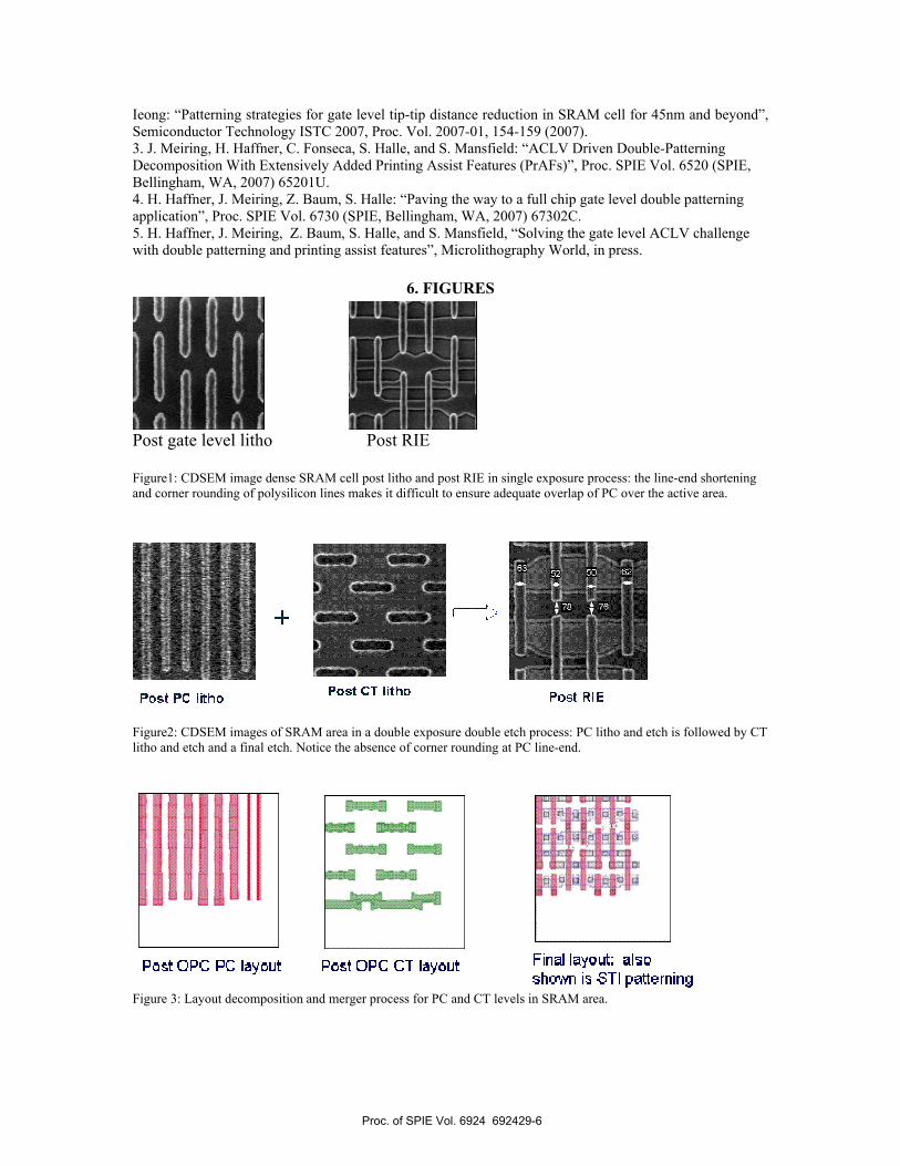
2. RESULTS AND DISCUSSIONS 2.1 Single Exposure vs. DE2: Comparison of the conventional single expose to double patterning PC lithographic process illustrates the tradeoffs between improved process capability and added process complexity. In a single expose process, shown in Figure [1] both lines and line-ends are simultaneously exposed, while only the lines are exposed in a double patterning process. Both single and double patterning approaches will typically employ an etch-trim to reduce the printed linewidth for device length tailoring. However, only the single expose patterning approach suffers from the unwanted effect of etching back the printed line-ends. While the overall patterning of line-ends, especially in an SRAM, has always been important, it becomes critical at the <45nm device generation. The reduction of the SRAM cell size, at the <45nm node, is directly limited by PC line-end tolerance control, including both the PC line-ends extensions over active area, and the PC line-end tip to line-end tip distances. The line-end control of a single exposure process is limited by several factors: a) the fore-shortening of the line-ends and non-vertical resist profile control, limited by the aerial image b) high mask error factor at the line-ends c) the etch trim pullback of the line-end, which typically exceeds the line trim bias with by a factor of two. A double patterning PC lithographic process does not suffer these limitations and is uniquely suited to enable tight line-end control, sub 80nm line-end tip to line-end tip distances, while adequately maintaining technology compliant linewidth tolerance. Double patterning techniques in which the PC lines are imaged with one reticle and where a second reticle is used to achieve a “cut” of the line-end, have the advantage of improving the overall PC tolerance control by de-coupling the pattern formation of PC lines from the PC line-ends. Figure [2] shows a wafer patterning example of a double patterning process; double exposure double etch (DE2) for which the PC lines are printed and then etch trimmed, a “cut” (CT) shape is printed, and then the combined patterns are translated to the substrate. By splitting up the line and cut masks, optimized independent illumination and optical proximity correction methods can be employed to imaged lines and cut shapes, separately. Additionally, by decoupling the etch/trim patterning of lines from the etch of the cut shapes with near zero etch bias, approximately straight patterned line-ends and extremely narrow line-end tip to line-end tip distances can be achieved.
Proc. of SPIE Vol. 6924 692429-2

2.2. Design Decomposition in DE2: The decomposition of the PC design intent which has been split into the line (PC) and cut (CT) mask, shown in Figure [3], has been previously described by Haffner et al.3-5. For this first step of this automated decomposition method, all critical dimension line-ends are extended by an amount consistent with linewidth and process overlay tolerances between gate PC and active area. The line-end extensions have the advantage that OPC induced necking or bulging regions are shifted to regions outside the active area thus reducing possible across-device-length degradation. Next, clean-up code can then be used to compensate for any pitch differences between adjoining layouts. In the third step of decomposition, cut mask shapes are formed on all shapes added in the first two steps of the decomposition. 2.3. DE2 Process Flow In this section of the paper, we will describe the process flow used for DE2, while restricting the discussion to SRAM only patterning and point out the process complexities for each step. While double patterning techniques, such as double exposure double etch (DE2) may sound relatively straightforward to the lithographer, the application of this patterning technique on a given film stack presents some unique challenges especially for the PC level. The challenge of transferring both the PC and CT layers while maintaining process tolerances and without damaging a thin gate oxide layer is complicated by several factors including a variety of etch selectivity, topography, doping of the polysilicon, and need for vertical profiles for the polysilicon gate. 2.3.1. Embedded DE2 process In this section we describe the overall embedded DE2 process sequence, shown in Figure [4], for a polysilicon gate stack. In this case there is a dielectric film stack above the polysilicon gate material, which will serve a critical role in the overall process. Typically for a PC stack substrate at this point in the overall flow, the thin doped layer is on top of the undoped layer, since thermal processes have not yet diffused the n-type or p-type doping. The following process sequence shows patterning the polysilicon lines first (PC) and then patterning cut mask second (CT). In principle, the process could be practiced in reverse order (i.e. CT -> PC). In the first step, PC lithography is exposed and developed. Since the decomposed PC line structure looks purely like a grating for the SRAM; the resist selection, illumination, and OPC implementation can all be optimized without taking into consideration line end behaviors typically found in SRAM. The post develop photoresist of the PC line is then patterned by etch/trim through the ARC and dielectric layer and partially transferred into the doped polysilicon layer. Again, tailoring the polysilicon device length is done by etch/trim is done, independent of cutting the line-ends. At this point the PC lines patterns are already embedded into the hardmask / dielectric layer. Since there is a degree of topography on the stack post PC processing, a highly planarizing ARC or trilayer resist stack is coated and exposed with the CT photo-process. An optimized reticle-illumination-OPC and photoresist is used to obtain the best fidelity of the CT pattern. In the second etch patterning step, the CT pattern is etch transferred into only the dielectric stack with an optimized near-zero etch bias process for minimizing any line-end loss. Post etch, a strip/removal of the residual resist/ARC is performed to reveal the PC and CT patterns which are embedded in the remaining dielectric/hardmask over the polysilicon stack. In the third and last etch patterning step, a convention polysilicon PC etch is performed which is highly selective to the thin gate oxide layer. 2.3.2: Parameters Effecting DE2 Pattern Transfer There are a variety of parameters that impact the pattern transfer during the DE2 process. For the initial polysilicon gate stack with dielectric/hardmask, there are three factors (Figure[5]) that result in variability to this process; 1) the depth of the shallow trench isolation controlled by RIE etch in a prior step; 2) the height and overall range of the active area relative to the dielectric-filled shallow trench isolation, which in this case is assumed to be higher than the active area; 3) step height variation of the dielectric material over polysilicon from prior processing. To minimize these effects, an ARC is used to planarize any step height variation induced from these three parameters.
Proc. of SPIE Vol. 6924 692429-3

During the partial etch of the PC lines into the dielectric and the part of the doped polysilicon layer, two important patterning issues are experimentally found. Even though under-etching this partial etch provides more margin for gate-oxide punch-through, in general a tapered and sometime notched final polysilicon profile is observed. At the other limit, while over-etching the partial etch would provide less margin for gate oxide punch through, it is found to preserve more dielectric hardmask and results in a straighter final polysilicon profile as shown in Figure [6]. The etch selectively and control of the doped polysilicon layer plays a critical role in the PC line patterning transfer. For the CT patterning process, as previously noted, planarization of the ARC layer is critical to any double patterning process. In addition, depending on the size and the shape of the CT pattern, the overlay of CT pattern from over an area of shallow trench isolation to an active area may have a impact on the patterning process, if the etch selectivity of the CT is marginal. During the partial etch of the CT process into the dielectric/hardmask material, we find two key process balance issues. If the CT partial etch is slightly under-etched, it results both more polysilicon remaining after the partial etch and in a tighter final line-end tip to tip; however, too much under-etching results in an incomplete removal of polysilicon under the CT shape. In contrast, over-etching the partial CT etch, reduces the remaining polysilicon over the shallow trench isolation and in general results in more loss in the line-ends and larger line-end tip to tip distances. It should be emphasized that the margin of remaining polysilicon after this step, provides a process margin for topography induced by active to shallow trench oxide height variation, as seen in Figure [7]. If a small margin of polysilicon remains and there is poor CT to PC overlay, this may result in gate oxide punch through during the final step. Much of the patterning process complexity as described above, results from selective areas of the pattern which are etch transferred in all three patterning etches, both partial PC and CT etches, plus the final etch. The overwhelming lithographic preference for the CT shape favors a slotted contact rather then a rounded contact to cut the line-ends, due to superior aerial image contrast and lower sensitivity to PC to CT overlay variation. When the CT pattern does not fall on top of the polysilicon lines, variable etch rates may occur in this area. By breaking up the process into three discrete etch patterning steps, we have found that the DE2 process has more process margin to control the overall double patterning process. They key metrics for success of the DE2 process are to achieve narrow line-end tip to tip distance for enable high density SRAMs, while having large margin for gate oxide punch-through and vertical polysilicon profiles for both nFET and pFET gate devices. 2.4. Litho process window The process window for both PC and CT shapes are obtained on fully integrated device wafers. For ultra dense SRAM cell CT shapes, the DOF is about 0.2um as shown in Figure [8] and is more than what the DOF for the line-end-to-line-end distance in single expose. The PC DOF is same as in single expose since in this case only the SRAM line ends were created by DE2. Once the process was established, wafers were processed in the standard manufacturing routes using standard tolerance specs. Figure [2] shows a CDSEM top down image of one of the SRAM cells post CT and PC/CT RIE. The straight line-end shape and a significant reduction of tip-to-tip can be seen, compared to the single expose (see Fig 1 for comparison). No gate oxide punch-through was observed with the etch process employed. The significant overlap of PC line over active area in SRAM gives much lesser leakage even in the case of marginal overlay and is confirmed by electrical data. 2.5: Future outlook, extending into 32nm and beyond: With the use of immersion lithography in the hyper NA region, the resultant loss of depth of focus (DOF) has a significant impact on the utility of SRAF to meet extremely challenging linewidth tolerances at DOF challenged pitches. Figure [9] shows the falloff of the DOF as a function of assist width for a forbidden pitch region at double the contacted pitch. The DOF dramatically increases with the assist width from the non-printed to the printed assist width region. Meiring et al.3 have termed these features, Printed Assist Features (or PrAFs) which are populated alongside nested and semi-isolated lines to make the PC line
Proc. of SPIE Vol. 6924 692429-4

layout appear as a dense grating (in a manner similar to SRAFs). Since the PrAF features are unwanted, the DE2 scheme can be employed to remove these features with the second CT patterning. The successful PrAF placement and clean-up is followed by the decomposition of the PrAF enhanced layout into two mask levels. As a general rule, all newly generated features on the poly-conductor mask must be covered by a cut mask shape to ensure their removal in the second step of the double patterning process. To accomplish a clean removal, the edges of shapes on the final cut mask layout need to overlap the boundaries of the poly-conductor shapes underneath except where line-ends are cut 4. Figure [10] pictures a 45nm logic layout with critical lines at 180nm pitch. The original poly-conductor and active area layout and its decomposition into two mask levels are shown on the left and in the center, respectively. The figure in the center also depicts a superpositioned, simulated process-variation band print image contour using realistic 45nm logic process tolerance assumptions (excluding overlay errors). On the right, a SEM image of the same layout using the described double patterning process. The rectangular line-end corners are proof of the double patterning process as seen in the SEM image.
Because of the added expenses of such a double patterning process scheme, it becomes crucial to gain more than a minimized SRAM tip-to-tip patterning. The most important advantages made possible by the additionally added enhancement features and their subsequent removal can be summarized as follows:
Corner rounding free line-ends everywhere such that the design rule for poly-conductor line-ends past active area boundary overlap can be greatly reduced, thus realizing major real estate savings;
ACLV and ADLV improvements due to increased regularity and uniformity of the poly-conductor exposure and etch processes being always dense like a single contacted pitch (utilizing PrAFs equal to the critical size).
However, simulations also show that it will be of utmost importance to ensure optimum performance with regard to CD tolerances for the most critical single contacted pitch, even for a one-dimensional layout configuration, taking into account all major CD tolerance contributors such as focus, dose, and mask CD variations.
3. SUMMARY AND CONCLUSIONS We have demonstrated a double patterning technique on fully integrated device wafers for gate level patterning in 45 nm node. Such a technique can significantly decrease the space between two polysilicon line-end compared to single expose method in dense SRAM cells. DE2 ensures adequate coverage of polysilicon line over active areas due to absence of line-end foreshortening and corner rounding. A number of parameters such as topography, alignment and etch control can impact pattern transfer in DE2. We have discussed how to optimize these parameters to deliver a consistent production process. Finally we have shown how this technique can be extended to 32nm or beyond, to gain additional benefits of process window advancement and reduced ACLV.
4. ACKNOWLEDGEMENT
The authors are responsible for the content of the paper. This work was performed at the IBM Microelectronics Div. Semiconductor Research & Development Center, Hopewell Junction, NY 12533.
5. REFERENCES
1. C. Sarma et al., “Finding the right way: DFM vs. area efficiency for 65nm gate layer lithography”, Optical Microlithography XIX, Proc. Of SPIE Vol. 6154 61541L-1, 2006 2. H. Zhuang, H. Wang, C. Yap, A. Gutmann, J. Lian, C. Sarma, L. Tsou, A. Gabor, U. Schroeder, S. Halle, K. Herold, H. Haffner, H. Lee, N. Rovedo, C. Chang, H. Ng, D. Shum, R. Wise, M. Hierlemann, and M.
Proc. of SPIE Vol. 6924 692429-5
Ieong: “Patterning strategies for gate level tip-tip distance reduction in SRAM cell for 45nm and beyond”, Semiconductor Technology ISTC 2007, Proc. Vol. 2007-01, 154-159 (2007). 3. J. Meiring, H. Haffner, C. Fonseca, S. Halle, and S. Mansfield: “ACLV Driven Double-Patterning Decomposition With Extensively Added Printing Assist Features (PrAFs)”, Proc. SPIE Vol. 6520 (SPIE, Bellingham, WA, 2007) 65201U. 4. H. Haffner, J. Meiring, Z. Baum, S. Halle: “Paving the way to a full chip gate level double patterning application”, Proc. SPIE Vol. 6730 (SPIE, Bellingham, WA, 2007) 67302C. 5. H. Haffner, J. Meiring, Z. Baum, S. Halle, and S. Mansfield, “Solving the gate level ACLV challenge with double patterning and printing assist features”, Microlithography World, in press.
6. FIGURES
Post gate level litho Post RIE Figure1: CDSEM image dense SRAM cell post litho and post RIE in single exposure process: the line-end shortening and corner rounding of polysilicon lines makes it difficult to ensure adequate overlap of PC over the active area.
Figure2: CDSEM images of SRAM area in a double exposure double etch process: PC litho and etch is followed by CT litho and etch and a final etch. Notice the absence of corner rounding at PC line-end.
Figure 3: Layout decomposition and merger process for PC and CT levels in SRAM area.
Proc. of SPIE Vol. 6924 692429-6

PC litho PC partial etch
CT litho CT partial etch
Final etch Figure 4: Sequence of DE2 patterning process is shown for gate level patterning.
Proc. of SPIE Vol. 6924 692429-7

Figure 5: Parameters impacting patterning process: under-etch / over-etch in D gives tapered final etch and less gate oxide punch through/straight profile but risk of punch through.respectively.
Figure 6: Cross section image of poly line (top) and topdown CDSEM image of SRAM area showing punch through as a function of etch. Increasing PC partial etch results in straighter profile but leads to more gate punch through in the final step.
Figure 7: Schematic showing CT patterning process: CT etch into polysilicon is shown as F; for under-etch F, remaining poly (G) is not removed, and tip-to-tip is small. For over-etch F, remaining poly is removed but T2T increases.
Proc. of SPIE Vol. 6924 692429-8

SnI-
40Annint Sizn (nfl)
0A
-juj 035nn
03@5
025
02
OiS
0-I20 so so
Figure 8: Bossung plot for CT shapes. The process window for CT shapes is about 200nm, greater than that for PC tip-to-tip in dense SRAM in single exposure.
Fig 9: Depth of focus at 2x the pitch (in the forbidden pitch region), as a function of the assist width size. DOF increases non-linearly with the assist width, matching the DOF at the 1x pitch feature
Figure 10: Various stages from design layout to patterning results on wafer using the described PrAF enhanced double patterning technique.
-0.2 -0.1 0 0.1
20
40
60
80
100
120
Focus (µm)
Prin
ted
CD
(nm
)
0 0.05 0.1 0.15 0.2
0
5
10
15
20
DOF (µm)
Exp
osur
e La
titud
e (%
)
DOF: 0.193 µmExp Lat: 3.868 %Center Dose: 4.521 E0Center Focus: -0.048 µm
Proc. of SPIE Vol. 6924 692429-9