Estimation and Control in Semiconductor Etch: Practice and Possibilities
12
IEEE TRANSACTIONS ON SEMICONDUCTOR MANUFACTURING, VOL. 23, NO. 1, FEBRUARY 2010 87 Estimation and Control in Semiconductor Etch: Practice and Possibilities John V. Ringwood, Senior Member, IEEE, Shane Lynn, Student Member, IEEE, Giorgio Bacelli, Beibei Ma, Emanuele Ragnoli, and Sean McLoone, Senior Member, IEEE Abstract—Semiconductor wafer etching is, to a large extent, an open-loop process with little direct feedback control. Most silicon chip manufacturers rely on the rigorous adherence to a “recipe” for the various etch processes, which have been built up based on con- siderable historical experience. However, residue buildup and dif- ficulties in achieving consistent preventative maintenance opera- tions lead to drifts and step changes in process characteristics. This paper examines the particular technical difficulties encountered in achieving consistency in the etching of semiconductor wafers and documents the range of estimation and control techniques cur- rently available to address these difficulties. An important feature of such an assessment is the range of measurement options avail- able if closed-loop control is to be achieved. Index Terms—Closed-loop control, plasma etch, run-to-run con- trol, semiconductor wafer, state estimation, virtual metrology. I. INTRODUCTION W ITH the continuing drive towards smaller feature sizes [1], there are increased pressures on tolerances in semi- conductor wafer processing. As the unit value of wafers in- creases with these dimension decreases, it is imperative that better quality control be achieved if yield rates are to be main- tained. Closed-loop control, and related technologies, are tradi- tionally employed to reduce process variance, with the ability to tightly regulate around process setpoints directly relating to yield. Many of the control issues in semiconductor manufac- turing are covered in [2]–[6]. Semiconductor manufacturing processes, such as plasma etch, are highly complex processes, and the minute feature sizes also make etch variable measurement difficult, with measure- ment feedback a prerequisite for control. In addition, attempts to perform in-situ measurement can disturb the etch process, which is largely run according to a very specific open-loop recipe. Optical and electrical measurement of the wafer pro- vide downstream measurement, which, though not usable for real-time control, could be used in a run-to-run control strategy. In addition to measurement and control, two associated (and related) areas that can assist in quality improvement are mathe- matical modelling and virtual metrology. Mathematical model- ling involves the determination of a set of mathematical equa- Manuscript received March 05, 2008; revised August 09, 2009. First pub- lished December 22, 2009; current version published February 03, 2010. This work was supported by Intel (Ireland) Ltd., Enterprise Ireland, and the Irish Re- search Council for Science, Engineering and Technology. The authors are with the Department of Electronic Engineering, National Uni- versity of Ireland, Maynooth, Ireland (e-mail: [email protected]). Digital Object Identifier 10.1109/TSM.2009.2039250 tions to describe the behavior of a process. Such mathematical models are usually embedded in virtual metrology algorithms and also form the basis for model-based control strategies. Vir- tual metrology (VM) models the relationship between desired unmeasurable variables and other measurable quantities. The model is then employed to “reconstruct” the variables, which are not directly measurable. This paper is focused on the state-of-the-art in the control and measurement sciences as applied to the semiconductor etch process. It follows the excellent review of Edgar et al. [7] (in 2000) and the November 2007 issue of this TRANSACTIONS, which has a Special Section on Advanced Process Control [8]. This paper attempts to present a broad picture of the possibili- ties in etch control and estimation and presents a sample of the recent literature for illustration. More comprehensive literature listings are contained in [9]–[11]. II. MATHEMATICAL MODELS The etch process is a multivariable (interacting), nonlinear, distributed parameter process with a significant spread of dy- namical time constants. As such, some level of simplification is inevitable if models are to be tractable and computable. Plasma/ etch models can be considered at various levels. • Particle-in-cell (PIC) models [12] model the spatial varia- tion in the plasma and, in general, respect the very fastest process dynamics. They are computationally intensive due to the need to compute electric/magnetic fields at mesh points in three dimensions, integration of the equations of motion, and interpolation of the fields to the particle loca- tions. • Bulk plasma models, e.g., [13]–[15], ignore the spatial di- mension and focus on the representation of the physical process as a lumped parameter system. While these models are computationally simpler than PIC models, they have no ability to resolve spatial variations, but single point mod- elled outputs usually focus on specific areas of interest, e.g., ion flux at the wafer surface. • Black-box models, e.g., [16] and [17], largely ignore the underlying physical process and are parameterized from a process behavioral point of view. Measured process inputs and outputs are used to produce a mathematical formula relating outputs to inputs. While black-box models can be used to derive relationships between spatially distributed measurements, they are normally used for bulk or single- point measurements. Due to an incomplete understanding of plasma physics, it is un- likely that a complete physical plasma model will be achieved. In addition, for some applications, such as model-based control 0894-6507/$26.00 © 2010 IEEE Authorized licensed use limited to: The Library NUI Maynooth. Downloaded on February 5, 2010 at 10:31 from IEEE Xplore. Restrictions apply.
Transcript of Estimation and Control in Semiconductor Etch: Practice and Possibilities
IEEE TRANSACTIONS ON SEMICONDUCTOR MANUFACTURING, VOL. 23, NO. 1, FEBRUARY 2010 87
Estimation and Control in Semiconductor Etch:Practice and Possibilities
John V. Ringwood, Senior Member, IEEE, Shane Lynn, Student Member, IEEE, Giorgio Bacelli, Beibei Ma,Emanuele Ragnoli, and Sean McLoone, Senior Member, IEEE
Abstract—Semiconductor wafer etching is, to a large extent, anopen-loop process with little direct feedback control. Most siliconchip manufacturers rely on the rigorous adherence to a “recipe” forthe various etch processes, which have been built up based on con-siderable historical experience. However, residue buildup and dif-ficulties in achieving consistent preventative maintenance opera-tions lead to drifts and step changes in process characteristics. Thispaper examines the particular technical difficulties encounteredin achieving consistency in the etching of semiconductor wafersand documents the range of estimation and control techniques cur-rently available to address these difficulties. An important featureof such an assessment is the range of measurement options avail-able if closed-loop control is to be achieved.
Index Terms—Closed-loop control, plasma etch, run-to-run con-trol, semiconductor wafer, state estimation, virtual metrology.
I. INTRODUCTION
W ITH the continuing drive towards smaller feature sizes[1], there are increased pressures on tolerances in semi-
conductor wafer processing. As the unit value of wafers in-creases with these dimension decreases, it is imperative thatbetter quality control be achieved if yield rates are to be main-tained. Closed-loop control, and related technologies, are tradi-tionally employed to reduce process variance, with the abilityto tightly regulate around process setpoints directly relating toyield. Many of the control issues in semiconductor manufac-turing are covered in [2]–[6].
Semiconductor manufacturing processes, such as plasmaetch, are highly complex processes, and the minute feature sizesalso make etch variable measurement difficult, with measure-ment feedback a prerequisite for control. In addition, attemptsto perform in-situ measurement can disturb the etch process,which is largely run according to a very specific open-looprecipe. Optical and electrical measurement of the wafer pro-vide downstream measurement, which, though not usable forreal-time control, could be used in a run-to-run control strategy.
In addition to measurement and control, two associated (andrelated) areas that can assist in quality improvement are mathe-matical modelling and virtual metrology. Mathematical model-ling involves the determination of a set of mathematical equa-
Manuscript received March 05, 2008; revised August 09, 2009. First pub-lished December 22, 2009; current version published February 03, 2010. Thiswork was supported by Intel (Ireland) Ltd., Enterprise Ireland, and the Irish Re-search Council for Science, Engineering and Technology.
The authors are with the Department of Electronic Engineering, National Uni-versity of Ireland, Maynooth, Ireland (e-mail: [email protected]).
Digital Object Identifier 10.1109/TSM.2009.2039250
tions to describe the behavior of a process. Such mathematicalmodels are usually embedded in virtual metrology algorithmsand also form the basis for model-based control strategies. Vir-tual metrology (VM) models the relationship between desiredunmeasurable variables and other measurable quantities. Themodel is then employed to “reconstruct” the variables, whichare not directly measurable.
This paper is focused on the state-of-the-art in the controland measurement sciences as applied to the semiconductor etchprocess. It follows the excellent review of Edgar et al. [7] (in2000) and the November 2007 issue of this TRANSACTIONS,which has a Special Section on Advanced Process Control [8].This paper attempts to present a broad picture of the possibili-ties in etch control and estimation and presents a sample of therecent literature for illustration. More comprehensive literaturelistings are contained in [9]–[11].
II. MATHEMATICAL MODELS
The etch process is a multivariable (interacting), nonlinear,distributed parameter process with a significant spread of dy-namical time constants. As such, some level of simplification isinevitable if models are to be tractable and computable. Plasma/etch models can be considered at various levels.
• Particle-in-cell (PIC) models [12] model the spatial varia-tion in the plasma and, in general, respect the very fastestprocess dynamics. They are computationally intensive dueto the need to compute electric/magnetic fields at meshpoints in three dimensions, integration of the equations ofmotion, and interpolation of the fields to the particle loca-tions.
• Bulk plasma models, e.g., [13]–[15], ignore the spatial di-mension and focus on the representation of the physicalprocess as a lumped parameter system. While these modelsare computationally simpler than PIC models, they have noability to resolve spatial variations, but single point mod-elled outputs usually focus on specific areas of interest,e.g., ion flux at the wafer surface.
• Black-box models, e.g., [16] and [17], largely ignore theunderlying physical process and are parameterized from aprocess behavioral point of view. Measured process inputsand outputs are used to produce a mathematical formularelating outputs to inputs. While black-box models can beused to derive relationships between spatially distributedmeasurements, they are normally used for bulk or single-point measurements.
Due to an incomplete understanding of plasma physics, it is un-likely that a complete physical plasma model will be achieved.In addition, for some applications, such as model-based control
0894-6507/$26.00 © 2010 IEEE
Authorized licensed use limited to: The Library NUI Maynooth. Downloaded on February 5, 2010 at 10:31 from IEEE Xplore. Restrictions apply.
88 IEEE TRANSACTIONS ON SEMICONDUCTOR MANUFACTURING, VOL. 23, NO. 1, FEBRUARY 2010
and state estimation, models must have the facility to be interro-gated in real time. For run-to-run control, computational speedis not so crucial. In general, PIC models [18] are less usefulfor control due to their computational complexity and the pro-vision of information not crucial to the control problem. In ad-dition, the dynamics of the kinetic reactions, which are accu-rately modelled by the PIC models, are very fast compared tothe dominant (slow dynamics) in etch control loops, which ariseprimarily from actuator (e.g., throttle valve, gas flow) and sensordynamics.
At the other end of the spectrum, black-box models [19], in-cluding artificial neural networks (ANNs) [17], require the min-imum of process knowledge but are only valid for the range ofdata used to train the models and care needs to be taken in thespecification of a parsimonious model structure. Bulk plasmamodels, based on physical principles, are frequently employedin etch control and can be tuned using process data. For example,a control-oriented plasma model is developed in [20], where astatic, multivariable nonlinearity is used to model the plasma,with the (largely scalar) dynamics resulting from sensors andactuators.
Equivalent circuit models are also useful in plasma/etchmodelling, particularly where virtual instrumentation relies onimpedance measurements [21], and can also be useful in pro-viding corrections to raw radio-frequency (RF) measurements[22].
The challenges and progress in modelling the spatial variationin plasma etch processes are articulated well in Yang et al. [23].
III. MEASUREMENT AND VIRTUAL METROLOGY
Measurement is vital for process monitoring, diagnosis, andcontrol. Various measurement regimes are possible, includingreal-time local measurement (e.g., Langmuir probe, opticalemission spectra (OES), plasma impedance monitor (PIM),etc.), virtual metrology (to synthesize, in real time, importantvariables that are not directly measurable), and downstream(delayed) metrology (electrical and optical). The availabilityof key process variable measurements in real time is crucial toaccurate diagnosis and control of plasma etch processes.
A. Diagnostic Measurements
Some measurement devices can provide actual measurementof plasma or etch variables, e.g., the Langmuir probe providesdirect measurement of ion flux, while laser inferometry directlymeasures etch depth. However, the in-situ use of such measure-ment devices in a production environment can be problematic.Other devices, such as OES and PIMs [24], provide a more in-direct measurement of the process variables and can, at least, beused to diagnose the “health” of the process if normal workingmeasurement profiles are known. However, they can also be in-corporated in VM strategies to give an indirect measurement ofthe process variables, e.g., [25].
B. Virtual Metrology
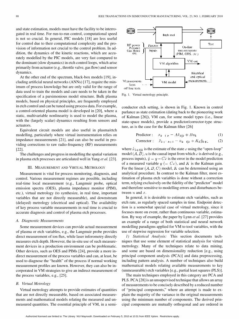
Virtual metrology attempts to provide estimates of quantitiesthat are not directly measurable, based on associated measure-ments and mathematical models relating the measured and un-measured quantities. The essential principle of VM, in a semi-
Fig. 1. Virtual metrology principle.
conductor etch setting, is shown in Fig. 1. Known in controlparlance as state estimation (dating back to the pioneering workof Kalman [26]), VM can, for some model types (i.e., linearstate-space models), provide a predictor/corrector-type struc-ture, as is the case for the Kalman filter [26]
Predictor (1)
Corrector (2)
where is the estimate of the state using the “open-loop”model , is the causal input from which is derived (e.g.,process inputs), is the error in the model predictionof a measured variable , and is the Kalman gain.For the linear model, can be determined using ananalytical procedure. In contrast to the Kalman filter, most es-timation of plasma etch variables is done without a correctionterm, relying exclusively on the fidelity of the “predictor” modeland therefore sensitive to modelling errors and disturbances be-tween and .
In general, it is desirable to estimate etch variables, such asetch rate, as regularly spaced samples in time. Endpoint detec-tion is a somewhat special case of virtual metrology, since itfocuses more on event, rather than continuous variable, estima-tion. By way of example, the paper by Lynn et al. [27] providesan example of a range of both statistical and neural networkmodelling paradigms applied for VM to tool variables, with theuse of stepwise regression for variable selection.
1) Statistical Analysis: This section documents tech-niques that use some element of statistical analysis for virtualmetrology. Many of the techniques relate to data mining,and some are based on dimensionality reduction [e.g., usingprincipal component analysis (PCA)] and data preprocessing,including pattern analysis. A number of techniques also buildmathematical models relating available measurements to key(unmeasurable) etch variables [e.g., partial least squares (PLS)].
The main techniques employed in this category are PCA andPLS. PCA [28] is an unsupervised technique that allows an arrayof measurements to be concisely described by a reduced numberof “principal components,” where an attempt is made to ex-plain the majority of the variance in the original measurementsusing the minimum number of components. The derived prin-cipal components are mutually orthogonal and are ordered in
Authorized licensed use limited to: The Library NUI Maynooth. Downloaded on February 5, 2010 at 10:31 from IEEE Xplore. Restrictions apply.

RINGWOOD et al.: ESTIMATION AND CONTROL IN SEMICONDUCTOR ETCH 89
terms of amount of variance explained in the original data. Typ-ically, PCA is used to distill information distributed across anumber of (potentially correlated) measurements into a smallernumber of independent components.
An alternative to PCA, independent component analysis(ICA) [29], can also be used to separate independent signalstreams, where the new data basis is formed by a set of inde-pendent vectors, rather than orthogonal vectors, as in the caseof PCA. Though ICA has found considerable application inareas such as blind source separation [30], the application tosemiconductor etch has been limited [31].
Supervised statistical techniques such as PLS and a super-vised derivative of PCA, principal component regression (PCR),attempt to derive concise multidimensional relationships be-tween vectors of inputs and outputs. By directing the infor-mation distillation activity onto a set of target outputs, PCRand PLS can form the basis of modelling or virtual metrologymethodologies. A useful exposure of PCA, PCR, and PLS in asemiconductor etch setting is given in [32].
A variety of measurements have been used to drive VMmodels. Chen et al. [33], for example, developed chamber statemodels of plasma etch using compressed OES data related toetch variables using least squares (LS) on a reactive ion etcher(RIE) with . Data were compressed by manual selectionof OES lines, PCA, and partial least squares (PLS) analysis,with model outputs of etch rate uniformity and aspect ratio. Incontrast, Tsunami et al. [34] used PIM data in a dual-frequencysystem to estimate etch rate using a simple linear regressionmodel. However, the model has no drift component and losesaccuracy over time. Lee and Spanos [35], on the other hand, useprocess inputs (pressure, power gas flows, etc.) to build a modelfor RIE process outputs of etch rate, uniformity, selectivity,and anisotropy. Both PCA and PLS returned prediction errorsof 7–10%. May et al. [36] also used process inputs to estimateetch variables, using response surface modelling. Ragnoli etal. [37] compare VM schemes for etch rate using a variety oftechniques, including PCR, PLS, forward selection componentanalysis (FSCA), and forward selection regression (FSR), basedon OES data. FSR and FSCA are found to be more effective forfeature selection in OES datasets due to the selection of fewerOES lines to summarize key variations in the process data.
Statistical techniques find wide application in fault detectionand classification, typically using a data reduction mechanismsuch as PCA, and sometimes augmented by a modelling toolsuch as PLS or neural networks. For example, Shadmehr et al.[38] found OES to be superior for residual gas analysis (usingmass spectrometry) and reported success in predicting thin-filmcontamination levels. Yue et al. [39] also used PCA to detectan etch stop condition in high-density plasma etch. Wise et al.[40] compared PCA with other multivariate methods, includingparallel factor analysis and trilinear decomposition, for a metaletch fault detection application. Both local and global modelswere trained with a variety of sensor data, with local modelsproviding the best performance, using machine state signals andRF information. ICA has, in some cases [31], been shown tooutperform PCA in fault detection and classification applica-tions, including semiconductor etch. Using a more traditional
time-series approach, Guo et al. [41] use an ARIMA modelto filter real-time signals into identically independent and nor-mally distributed components, followed by the application ofHotelling’s statistic to obtain single scores. The techniquewas shown to be successful in detecting internal machine varia-tions before wafer product was affected. Forward and reflectedpowers, in an electron cyclotron resonance (ECR) plasma etchsystem, were used [42] to aid visualization and fault detection.In particular, forward/reflected power ratios were found to be ef-fective in fault detection and diagnosis. The nonstationarity ofetch processes has been directly addressed in [43], where modelmean and covariances are adapted during processing, using aversion of the exponentially weighted moving average (EWMA)controller. This gave valid operation over six months, includingmaintenance, cleaning, and new equipment interventions. Sum-mary statistics were also adapted in [44], with a satisfactoryQ-statistic over 3000 wafers. Weighted PCA has also been eval-uated for use in etch fault detection applications [45].
Endpoint detection is the most popular application of VM,typically using OES measurements, where settings such as inte-gration time can be adapted to optimize signal-to-noise (S/N)ratio and response times [46]. Early applications [47] used asingle OES wavelength, but with decreases in open etch area(down to 1%), multiple wavelengths are now employed, usu-ally with PCA processing [48]. For example, Rangan et al. [49]used PCA-reduced OES data to form a linear dynamical model,which was shown to be capable of detecting endpoints and tran-sition times in plasma etch. White et al. [50], also using PCAwith OES data, used the statistic as a measure of model ac-curacy (i.e., endpoint detection) and the statistic to indicatea need to recompute the PCA basis. Yue et al. [51] proposemethods to remove uninformative wavelengths from the PCAmodel by analyzing variance and thresholding PCA loadings.Fifty wavelengths were retained and gave good endpoint detec-tion. More recent work on sparse PCA [52] holds further possi-bilities for selecting key wavelengths from OES data. Goodlin’sPh.D. dissertation [53] provides a good overview of statisticalmethods for OES in endpoint detection and devises a methodfor weighting OES according to S/N ratio.
PIM data can also be useful in endpoint detection, with anumber of authors simply using change patterns to indicate thearrival of endpoint [21], [54]. Koh et al. [55] applied PCA tothe RF harmonics and demonstrated how the loadings changedas the endpoint is reached. Dewan et al. [25] developed a PIMphase model, the output of which was compared to measuredphase for endpoint detection. PIM-based techniques have alsobeen used to optimize cleaning cycles for chemical vapor depo-sition processes [56]. In Ragnoli et al. [57], nonnegative matrixfactorization is employed as a data reduction and variable se-lection method, where it is applied to OES data for endpointdetection. Results similar to those achieved with PCA were re-ported.
Imai et al. [58] apply PLS-based VM to detect harmfulspecies using dc bias voltage, while a paper by Khan et al.[59] uses PLS-based virtual metrology to estimate metrologyoutputs on a run-to-run, rather then a time-series, basis. Actualmetrology values are used to update the PLS model recursively,
Authorized licensed use limited to: The Library NUI Maynooth. Downloaded on February 5, 2010 at 10:31 from IEEE Xplore. Restrictions apply.
90 IEEE TRANSACTIONS ON SEMICONDUCTOR MANUFACTURING, VOL. 23, NO. 1, FEBRUARY 2010
and the VM scheme and an associated run-to-run controller areapplied to a simulated process, with good results.
Some nonlinear derivatives of linear statistical techniques,such as PCA and PLS, have also been employed in VM for etchprocesses. In [60], a PCA-based support vector machine (SVM)algorithm, which could loosely be described as a kernel PCAmethod [61], has been employed for endpoint detection, basedon OES measurement. The use of an SVM to facilitate nonlinearPLS in a classification/fault detection setting has also been con-sidered [62], though no applications in plasma etch have yetbeen reported.
2) Neural Networks: Due to their ability to synthesize non-linear relationships from process data, ANNs have been widelyused in virtual metrology for etch processes, finding applica-tion in the prediction of etch variables (etch rate, selectivity,anisotropy, etc), fault classification, and endpoint detection.
The work of Kim [17], [63], [64] is representative in demon-strating how etch rate may be determined from manipulated in-puts, such as gas flows, power, pressure, and bias, using ANNs.Typically, a static (nondynamical) map between process inputsand actual (offline) measurements is built up and them subse-quently used in a real-time way, with typical prediction errorsof 5–7% reported [17], [63], [65], [66]. A radial basis functionnetwork, as opposed to a multilayer perceptron (MLP), was em-ployed by Kim and Park [67] to model etch rate, based on ma-nipulated inputs. They reported a 40% improvement over somestatistical techniques, though Lee and Spanos [35], who com-pare ANNs to a variety of statistical techniques (LS, PCA, andPLS) could distinguish no improvement, using a wide variety oftraining signals. Polynomial ANNs were shown by Kim et al. tooutperform MLPs for etch rate prediction, using chuck gap, RFpower, bias, and fraction as network inputs. ANNs have alsobeen used to produce inverse models for etch rate (i.e., etch rate
manipulated inputs), which can be used for real-time control[68]. A paper by Su et al. [69] looks at a variety of ANN archi-tectures against the accuracy and real-time requirements of R2Rprocess control. They conclude that recurrent ANNs can satisfyrequirements and show application to chemical-mechanical pol-ishing (CMP) and etch processes. The issue of input variableselection for ANN-based VM models is dealt with by Lin et al.[70], who use stepwise regression for variable selection froma range of tool variables in an etch process. A similar scheme,using stepwise regression for variable selection with both MLPand radial-basis ANN models, is described in [71] for a chem-ical vapor deposition process.
ANNs have been employed with OES data, frequently usingPCA (or something similar) as a data preprocessing technique.Hong et al. [72] compared the use of PCA and ANNs for featureextraction from OES data, with a further ANN used to modelthe reduced data. However, 226 “relevant” wavelengths are ini-tially chosen from the 2048, prior to compression. The com-pression ANN returned seven features while PCA returned five,with comparable results for both, giving prediction errors aslow as 0.2%. Kim and Kim [73], however, reported a drasticperformance improvement with partial OES models (110 wave-lengths) compared to conventional PCA-OES reduction.
Selectivity, the ability to etch one material (e.g., Si) at a dif-ferent rate to another (e.g., photoresist), has also been modelledby ANNs. Himmel and May [65] found ANNs to be superiorto quadratic response surfaces, which might be expected sincecomplexity is more limited in the quadratic case. Hong et al.[72] compared ANNs and PCA for data reduction in selectivityprediction, concluding that the ANN reduction was significantlybetter.
Uniformity, a measure of the spatial variation in etch acrossthe wafer, has also been modelled using ANNs, requiring spa-tial measurements for model building. Lee and Spanos [35] re-ported little success in modelling uniformity using manipulatedvariables (gas flows, power, pressure, and gap) as inputs, whileKim and Kim [73] found that the addition of dc bias (as an input)only served to reduce the accuracy and increase the complexity,of the model. However, Kim et al. [63] reported a predictionerror of just 0.4% using pressure, gas flows, and power as inputs.In the case where OES was used to model nonuniformity alone,PCA was reported [72] to significantly outperform ANN-baseddata reduction.
ANNs have also been employed to model surface characteris-tics, such as anisotropy and surface roughness. Hong et al. [72]built an ANN model that modelled anisotropy with an error ofless then 2%, with Kim et al. [63] predicting etch profile anglewith an error of less than 4 . However, anisotropy was shownto have a high dependency on RF power. Kim and Kim [73]achieved similar levels of accuracy for etch profile angle, usinga reduced set of OES lines, in preference to manipulated in-puts, with PCA-OES models also performing poorly. Kim etal. [74] successfully produced an ANN model that predictedthe discrepancy in sidewall bottom etch rate compared to centeretch rate, using genetic algorithms to optimize the spread values.Surface roughness was modelled, using ANNs, in [75] and [67]using generalized regression and radial basis function networks,respectively. Reference [75] also employed GAs for ANN op-timization, while statistical models, for the same application,were found to be significantly inferior in [67].
The classification properties of ANNs have been well doc-umented (e.g., [76]), and fault detection and classification forplasma etch is a significant application area. In one of the fewapplications of a dynamical ANN for semiconductor manu-facturing applications, Hong and May [77] apply a time-seriesANN for fault identification. The ANN predicts the manipu-lated inputs (RF power, pressure, and two gas flows) based onthe variations in seven OES lines, six atomic mass signals froma residual gas analyzer, and the sample time index. The sampletime index gives a measure of the chamber “age” or usageand should help to account for drift due to chamber residuebuildup. The system demonstrated a sensitivity to performancedeviations down to 10%. In a similar way, though using astatic ANN, Shadmehr et al. [38] used mass spectometry andOES measurements to predict power and gas flows. The ANNwas also able to model thin-film contamination levels on thechamber walls. A dynamical radial-basis function ANN wasutilized in [78] to predict manipulated inputs, given a windowof previous values. The ANN was trained to incorporate normal
Authorized licensed use limited to: The Library NUI Maynooth. Downloaded on February 5, 2010 at 10:31 from IEEE Xplore. Restrictions apply.
RINGWOOD et al.: ESTIMATION AND CONTROL IN SEMICONDUCTOR ETCH 91
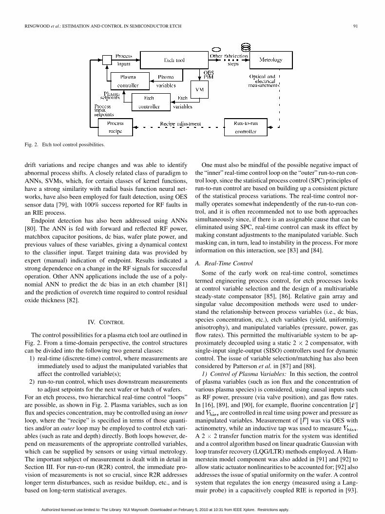
Fig. 2. Etch tool control possibilities.
drift variations and recipe changes and was able to identifyabnormal process shifts. A closely related class of paradigm toANNs, SVMs, which, for certain classes of kernel functions,have a strong similarity with radial basis function neural net-works, have also been employed for fault detection, using OESsensor data [79], with 100% success reported for RF faults inan RIE process.
Endpoint detection has also been addressed using ANNs[80]. The ANN is fed with forward and reflected RF power,matchbox capacitor positions, dc bias, wafer plate power, andprevious values of these variables, giving a dynamical contextto the classifier input. Target training data was provided byexpert (manual) indication of endpoint. Results indicated astrong dependence on a change in the RF signals for successfuloperation. Other ANN applications include the use of a poly-nomial ANN to predict the dc bias in an etch chamber [81]and the prediction of overetch time required to control residualoxide thickness [82].
IV. CONTROL
The control possibilities for a plasma etch tool are outlined inFig. 2. From a time-domain perspective, the control structurescan be divided into the following two general classes:
1) real-time (discrete-time) control, where measurements areimmediately used to adjust the manipulated variables thataffect the controlled variable(s);
2) run-to-run control, which uses downstream measurementsto adjust setpoints for the next wafer or batch of wafers.
For an etch process, two hierarchical real-time control “loops”are possible, as shown in Fig. 2. Plasma variables, such as ionflux and species concentration, may be controlled using an innerloop, where the “recipe” is specified in terms of those quanti-ties and/or an outer loop may be employed to control etch vari-ables (such as rate and depth) directly. Both loops however, de-pend on measurements of the appropriate controlled variables,which can be supplied by sensors or using virtual metrology.The important subject of measurement is dealt with in detail inSection III. For run-ro-run (R2R) control, the immediate pro-vision of measurements is not so crucial, since R2R addresseslonger term disturbances, such as residue buildup, etc., and isbased on long-term statistical averages.
One must also be mindful of the possible negative impact ofthe “inner” real-time control loop on the “outer” run-to-run con-trol loop, since the statistical process control (SPC) principles ofrun-to-run control are based on building up a consistent pictureof the statistical process variations. The real-time control nor-mally operates somewhat independently of the run-to-run con-trol, and it is often recommended not to use both approachessimultaneously since, if there is an assignable cause that can beeliminated using SPC, real-time control can mask its effect bymaking constant adjustments to the manipulated variable. Suchmasking can, in turn, lead to instability in the process. For moreinformation on this interaction, see [83] and [84].
A. Real-Time Control
Some of the early work on real-time control, sometimestermed engineering process control, for etch processes looksat control variable selection and the design of a multivariablesteady-state compensator [85], [86]. Relative gain array andsingular value decomposition methods were used to under-stand the relationship between process variables (i.e., dc bias,species concentration, etc.), etch variables (yield, uniformity,anisotrophy), and manipulated variables (pressure, power, gasflow rates). This permitted the multivariable system to be ap-proximately decoupled using a static 2 2 compensator, withsingle-input single-output (SISO) controllers used for dynamiccontrol. The issue of variable selection/matching has also beenconsidered by Patterson et al. in [87] and [88].
1) Control of Plasma Variables: In this section, the controlof plasma variables (such as ion flux and the concentration ofvarious plasma species) is considered, using causal inputs suchas RF power, pressure (via valve position), and gas flow rates.In [16], [89], and [90], for example, fluorine concentrationand are controlled in real time using power and pressure asmanipulated variables. Measurement of was via OES withactinometry, while an inductive tap was used to measure .A 2 2 transfer function matrix for the system was identifiedand a control algorithm based on linear quadratic Gaussian withloop transfer recovery (LQG/LTR) methods employed. A Ham-merstein model component was also added in [91] and [92] toallow static actuator nonlinearities to be accounted for; [92] alsoaddresses the issue of spatial uniformity on the wafer. A controlsystem that regulates the ion energy (measured using a Lang-muir probe) in a capacitively coupled RIE is reported in [93].
Authorized licensed use limited to: The Library NUI Maynooth. Downloaded on February 5, 2010 at 10:31 from IEEE Xplore. Restrictions apply.

92 IEEE TRANSACTIONS ON SEMICONDUCTOR MANUFACTURING, VOL. 23, NO. 1, FEBRUARY 2010
was adjusted using a resistor in parallel with the blockingcapacitor. It was deliberately chosen not to use RF power andgas concentrations as control variables, since these affect otheraspects of the etch. Two applications, selectivity enhancementand ion-enhanced plasma cleaning, were shown to benefit fromthe control, though a reduction in plasma stability was noted. Aslightly different approach is presented in [94], where ion cur-rent and ion energy are controlled via RF power and bias powerusing two SISO PI controllers. Ion current is estimated from an-tenna impedance, while ion energy is inferred from root meansquare RF voltage. A decoupling compensator, controlling ionflux and species concentration in a variety ofplasmas, is presented in [95]. In particular, the multivariableinteraction between the manipulated variables (RF power, gasflows) is addressed. More recently, Lin et al. [96] describe ascheme where RF power is manipulated to control electron den-sity and ion energy, where a transmission line microstrip mi-crowave inferometer is used to measure electron density. Thisscheme is shown to achieve good consistency in etch character-istics and can counteract the “first wafer” effect. A fuzzy logiccontroller was shown to outperform a traditional PI controller.
Hanish et al. [97] demonstrate one of the few applications ofan asymptotic observer, an extended Kalman filter (EKF), whichis used to estimate from OES with actinometry. Two SISOPID controllers are used to control and pressure, using therate constant of dissociation and “gas loss” (essentially outletflow plus gas loss to chamber walls) as manipulated variables. APID controller is also employed by Klimecky et al. [98] to con-trol plasma density, using RF power as a manipulated variable.One of the significant features is the claim that the controller cancompensate for transient chamber wall conditions and thereforeprovide better consistency in the face of residue buildup.
2) Control of Etch Variables: In this section, the control ofetch variables, either directly or indirectly, is considered. Aninteresting paper by Vincent et al. [99] employs an EKF tomeasure etch rate, using dual-frequency reflectometry as a cor-recting output. The focus is on the use of power, as a manipu-lated variable, to control etch rate, using a PI controller, thoughother control structures could be considered. The authors re-port an 83% improvement in etch depth results compared toa purely timed etch. A model-based feedback controller is re-ported in [68] and [100], controlling etch rate, which is mea-sured using laser inferometry and a profilometer. Manipulatedvariables are pressure, RF power, and gas flow, and a linearLQG/LTR controller is compared to a nonlinear adaptive con-troller based on a neural network model. The nonlinear adap-tive controller is shown to be superior under parameter varia-tion and disturbance conditions. Armaou et al. [101] describe aPI-based control scheme that manipulates gas flows to controlthree spatially distributed measurements of etch rate. Results arepresented for a simulation and demonstrate a potential reductionin etch-rate nonuniformity from 30.2% to 3.8%.
In [102], the control system is extended to include the controlof . Etch rate of GaAs, measured using spectroscopic ellip-sometry, is also controlled in [103]. A model-based LQG con-troller is used to manipulate pressure, where the model is deter-mined by fitting experimental data to a first-principles structure.This paper also presents a robust adaptive controller for a Si N
etch application based on an empirical model. The use of phasedifference between upper and lower RF signals as a manipu-lated input acting on etch characteristics has been demonstratedby Sung et al. [104] and could provide the basis for real-timecontrol.
B. Run-to-Run Control
In contrast to real-time control, R2R control works with de-layed measurements and is driven by the availability of wafermeasurements. It therefore falls into the class of discrete-eventrather then discrete-time (as is the case of real-time control) sys-tems. An excellent overview of the application of R2R control inthe semiconductor industry is given in the book by Moyne et al.[105]. R2R control has its origins in SPC, which provides toolsfor the detection of process faults using statistical techniques.R2R extends these ideas to provide active control via feedback.
1) Algorithms: Since there are a small number of R2R al-gorithms, mostly based around the EWMA controller [84], wegive the SISO double EWMA controller (which can cater forboth slow drifts and fast shocks) [106] as
(3)
(4)
(5)
(6)
where (3) defines the process model, (4) and (5) are estimatorsfor the model parameter and drift, respectively, with (6) calcu-lating the manipulated value. is the controlled variable (e.g.,etch depth), is the setpoint for , is the manipulated vari-able, and (which is determined a priori) are model parame-ters, and is a disturbance. The “ ” notation is used to denotean estimate, and and are tuning parameters used to specifythe sensitivity to variations in and , respectively. The choiceof and is discussed in [84]. Note that the double EWMAcontroller assumes a linear drift in the process, of the form ,and implements a form of deadbeat control [107], which at-tempts to regulate the process output in minimum time (sam-ples).
Since EWMA controllers are based on statistical measures ofprocess behavior, their use with mixed products needs to be con-sidered carefully. One solution to the mixed product probleminclude the employment of a disturbance model for foreach product type , with the appropriate used in the dead-beat control calculation in [108], [109]. EWMA controllerscan also be used across different tools, via the use of multipleprocess models [108], by employing different and parame-ters for each tool. Zheng et al. [108] also consider the stabilityand performance implications of using multiple process and dis-turbance models.
2) Model Identification: While (4) provides an estimate for, Wang et al. [110] prefer a Bayesian statistic for the detec-
tion and classification of disturbances in order to obtain betterparameter estimation and illustrate its use on a film depositionprocess. An additional common method for parameter estima-tion of linear models is least squares (LS), frequently used also
Authorized licensed use limited to: The Library NUI Maynooth. Downloaded on February 5, 2010 at 10:31 from IEEE Xplore. Restrictions apply.
RINGWOOD et al.: ESTIMATION AND CONTROL IN SEMICONDUCTOR ETCH 93
in R2R control [111]–[115] (simulated CMP process). In thiscase, (3) is replaced by a recursive LS estimator for the onlineestimation of the intercept , while a weighted LS algorithm[116] allows the assignment of preference to current measure-ments versus past measurements. Palmer et al. [117] employa Kalman filter to estimate both the gain and the intercept andapply it to a photoresist deposition process. The “age-based”double EWMA controller presented in [118] introduces a terminto the model to represent a drift due to the tools’ wearing,which is proportional to the number of runs since the last main-tenance operation.
3) Weight Determination: The performances of EWMA-typecontrollers are strongly affected by the choice of the weights
and (also called “forgetting factors”) [84], [119]. Discus-sion and methods concerning the optimal choice of weights canbe found in [120] (CMP application), [121], and [114], whilein [122], the choice of the weights is studied with respect tothe performance tradeoff between the short-term and long-termresponses of the system. In [123], weight optimization tradesoff controlled variable regulation against manipulated variableeffort, using a heuristic algorithm. A similar strategy has beenadopted in [124], where the minimization focuses on the reg-ulated outputs, using dynamic programming theory. In [125],a neural network is used to map the relation between the dis-turbance state (drift and noise) and the optimal weight of anEWMA estimator.
4) Multivariable Models: Modifications to the basic EWMAcontroller, with etch applications, include extensions to allowmultivariable models [84], nonsquare models [105], and non-linear models [114]. With regard to nonsquare systems, thereare two possibilities:
a) more output (controlled) variables than available manip-ulated variables (underactuated);
b) more manipulated variables than outputs (overactuated).In the case of a), a “best compromise” solution can be achievedusing least squares type solutions (see [105]). One possibility isalso to attach a greater importance to the regulation of one ormore controlled variables, as exemplified for the chemical-me-chanical polishing (CMP) case in [126]. In the overactuatedcase, some additional freedom is available to the control de-signer, over and above regulating the controlled variables. Oneway to exploit this freedom, seen in a variety of control appli-cations, is to minimize the energy or variance of the control ac-tion. This is vital in some applications, such as aerospace, wherelimited energy to power actuators is available, but could also en-courage less actuator wear and material usage in semiconductoretch. Examples of how overactuated systems are dealt with in-clude:
• weight assignment to minimize the variance of specific ma-nipulated variables (for a CMP process) [120];
• the use of Lagrange multipliers for new recipe calculation(silicon epitaxy and CMP applications) [121];
• the use of a nonsquare matrix pseudoinverse (which canbe related to least squares minimization of the manipulatedvariables) [119];
• the use of PLS to determine a diagonalizing (nonsquare)precompensator, followed by application of multiple
single-loop double EWMA controllers [127] (also for aCMP application);
• ridge regression [128], where a bound is put on manipu-lated signal values.
The paper by Khan et al. [59] uses a multivariable EWMAcontroller based on a PLS model in both wafer-to-wafer andlot-to-lot control, where an advantage in wafer-to-wafer controlis highlighted.
Bounding the manipulated input signal, in addition to poten-tially reducing actuator wear and energy use, also has the advan-tage of respecting actuator constraints (both amplitude and rate),reducing the incidence of nonlinear behavior. In addition to theinput bounding method of Rajagopal and del Castillo [128],Boning et al. proposed the recursive bound pinning technique[120] (demonstrated on a CMP application).
5) Nonlinear Models: Nonlinear models give the possibilityof obtaining a better description of the process, which can sub-sequently improve the R2R control performance. Using static(nondynamical) polynomial elements, it is possible to intro-duce nonlinearity in the model while retaining the ability toemploy recursive LS estimation techniques, as in [115], [114],and [111], since the model is still linear in the parameters. Asecond-order polynomial is employed in [106] and [112], wherethe estimation technique is based on a steady-state design of ex-periments (DOE). A different approach has been taken in [129],where a bounding ellipsoid algorithm is employed to estimateparameters of a second-order polynomial model. At each iter-ation, the algorithm returns an outer bounding ellipsoid of thelikely process parameter set. Ramaswamy et al. [130] designed avariable gain controller for the compensation of nonlinearities,which solves a min-max problem to find the input adjustmentthat minimizes the worst case predicted error using a doubleEWMA controller.
Neural networks are also widely used due to their abilityto model nonlinear systems; however, a large number of sam-ples are generally required for training. This is not a substan-tial issue in high-volume manufacturing, such as semiconductoretch, since most production plants are equipped with extensivedatabases for the recording of large numbers of process vari-ables. Such data have been used in [82], [123], and [131]–[133]to train a neural network for the mapping of etch process input/output relationships. A neural network model, predicting etchrate, is combined with a real-time optimizer in [131] to provideprocess setpoints to alleviate long-term process drift and sensi-tivity to PM interventions. The ANN model is trained with ex-tensive historical process data prior to use. By comparison, in[91] and [134], the data for the training of the neural networkare collected by performing a specific experiment using DOEtechniques.
6) Other R2R Control Structures: Though EWMA con-trollers are among the most popular in semiconductor processcontrol, a number of other structures have been investigated.Controllers based on disturbance feedforward adjust the recipein accordance with the outcome of upstream processes, withetch applications reported in [135] and [136]. Another typeof “lookup” controller interrogates historical data to lookfor a similar previous situation or interpolates to find the
Authorized licensed use limited to: The Library NUI Maynooth. Downloaded on February 5, 2010 at 10:31 from IEEE Xplore. Restrictions apply.
94 IEEE TRANSACTIONS ON SEMICONDUCTOR MANUFACTURING, VOL. 23, NO. 1, FEBRUARY 2010
closest match [137]. Both of these controller types providemore conservative options than R2R algorithms, which allowbatch-to-batch adjustment and are common in many productionenvironments.
Using intelligent systems methods, fuzzy logic and databaselearning have been incorporated into a generic R2R etch con-troller in [138], while genetic algorithms for recipe generationand low variance control have been used in [139] and [140]. Amultiresolution reinforcement learning approach to R2R controlwas also examined in [141].
Model predictive control, which has found widespread ap-plication in real-time process control, has also been extendedto R2R control in [142] and [143], while Hamby et al. [144]adopted a probabilistic approach to R2R control.
A number of other issues relating to R2R control, such asstability, robustness, and measurement delay, are also importantand have received some attention in the published literature butare omitted here for brevity. The interested reader is directed to[10] for an overview.
V. CONCLUSION
Since plasma etch in semiconductor processing is sucha high-value process, it has attracted significant attentionin attempts to improve the process quality and consistency.However, in most production environments, such processes areeffectively run in “open-loop” mode, with reliance on consis-tency in recipe and etch chamber state. In some instances, someschedule-based correction to the recipe is applied to accountfor process drift due to residue deposition on the chamberwalls. While a number of run-to-run applications are reported,particularly in experimental setups, there is a paucity of doc-umented application of real-time control of process variables.The principal reason for this is that direct measurement ofkey etch variables is difficult (Langmuir probes are invasive,while reflectometry is notoriously difficult in a productionenvironment), with virtual metrology providing a promisingalternative, using indirect measurements (such as OES andPIM) as a basis. However, most current VM strategies useonly a forward model, unlike the predictor-corrector structure,which is characteristic of linear state estimators. This couldprovide a possibility for improvement of VM algorithms. Withthe availability of reliable measurements, there is an enormousrange of control algorithms that could be brought to bear [145],[146]. Predictive control, for example, has many desirable char-acteristics and has been widely applied in industrial processcontrol settings [147].
One real-time control possibility is to attempt to directlycontrol plasma variables, such as ion flux and species density,and to base a “recipe” on these variables, which may help toachieve consistency in etch, in an environment experiencingdrift (residue buildup) and step changes (PM steps). Run-to-runcontrol for etch still has a number of important challenges,some of which arise from the delay and others related to theuncertainty associated with the effect of other processing stepsbetween actuation and measurement. The delay may result insignificant product wastage before corrective action is taken andprovides a stability challenge for the control engineer, while
the presence of intermediate process steps between actuationand measurement creates a difficulty in relating effect to cause.However, run-to-run control algorithms appear to have mainlyconverged to variants of the EWMA type.
The selection of key variables is an important issue. Indirectmeasurements, such as PIM and OES signals, are high in dimen-sion, and appropriate dimension reduction is vital if etch vari-ables (such as etch rate) are to be reconstructed using virtualmetrology. Likewise, selection of key manipulated variables isimportant since the plasma etch process is a highly interactivemultivariable nonlinear system and care must be taken that onlythe desired controlled variables will be affected by feedbackcontrol action.
ACKNOWLEDGMENT
The authors are grateful for the contribution to this work byN. MacGearailt of Intel (Ireland) Ltd.
REFERENCES
[1] P. Otellini, Intel Corp., Intel developer forum Sep. 18, 2007 [Online].Available: www.intel.com, Tech. Rep.
[2] S. Limanond, J. Si, and K. Tsakalis, “Monitoring and control of semi-conductor manufacturing processes,” IEEE Control Syst. Mag., vol. 18,no. 6, pp. 46–58, 1998.
[3] A. Emami-Naeini, J. Ebert, R. Kosut, D. de Roover, and S. Ghosal,“Model-based control for semiconductor and advanced materials pro-cessing: An overview,” in Proc. Amer. Contr. Conf., Boston, MA, Jun.2004, vol. 5, pp. 3902–3909.
[4] A.-J. Su, J.-C. Jeng, H.-P. Huang, C.-C. Yu, S.-Y. Hung, and C.-K.Chao, “Control relevant issues in semiconductor manufacturing:Overview with some new results,” Contr. Eng. Practice, vol. 15, no.10, pp. 1268–1279, 2007.
[5] G. S. May and C. J. Spanos, Fundamentals of Semiconductor Manu-facturing and Process Control. New York: Wiley-IEEE Press, 2006.
[6] S. J. Qin, G. Cherry, R. Good, J. Wang, and C. A. Harrison, “Semi-conductor manufacturing process control and monitoring: A fab-wideframework,” J. Process Contr., vol. 16, no. 3, pp. 179–191, 2006.
[7] T. Edgar, S. Butler, W. Campbell, C. Pfeiffer, C. Bode, S. Hwang,K. Balakrishnan, and J. Hahn, “Automatic control in microelectronicsmanufacturing: Practices, challenges, and possibilities,” Automatica,vol. 36, no. 11, pp. 1567–1603, 2000.
[8] J. Moyne and N. Patel, “Special section on advanced process control,”IEEE Trans. Semicond. Manuf., vol. 20, no. 4, pp. 343–344, Nov. 2007.
[9] S. Lynn, Virtual metrology for plasma etching: A literature reviewDept. of Electrical Engineering, NUI Maynooth, Ireland, Res. Rep.EE/JVR/4/2007, 2007.
[10] G. Bacelli, Control in semiconductor manufacturing: A literature re-view Dept. of Electrical Engineering, NUI Maynooth, Ireland, Res.Rep. EE/JVR/3/2007, 2007, Tech. Rep..
[11] M. Beibei, Literature review: Endpoint detection in plasma etchingDept. of Elect. Eng., NUI Maynooth, Ireland, Res. Rep. EE/SMcL/1/2007, 2007.
[12] J. P. Verboncoeur, “Particle simulation of plasmas: Review and ad-vances,” Plasma Phys. Contr. Fusion, vol. 47, no. 5A, pp. A231–A260,2005.
[13] M. J. Kushner, “A kinetic study of the plasma-etching process—I: Amodel for the etching of �� and ��� in � � �� and � � ��plasmas,” J. Appl. Phys., vol. 4, pp. 2923–2938, 1982.
[14] E. Gogolides, M. Stathakopoulos, and A. Boudouvis, “Modelling ofradio frequency plasmas in tetrafluoromethane ��� �: The gas phasephysics and the role of negative ion detachment,” J. Phys. D, Appl.Phys., vol. 27, no. 9, pp. 1878–1886, 1994.
[15] M. A. Sobolewski, “Real-time, noninvasive monitoring of ion energyand ion current at a wafer surface during plasma etching,” J. Vac. Sci.Technol., vol. 24, no. 5, pp. 1892–1905, 2006.
[16] B. Rashap, P. Khargonekar, J. Grizzle, M. Elta, J. Freudenberg, and F.Terry, “Real-time control of reactive ion etching: Identification and dis-turbance rejection,” in Proc. 32nd IEEE Conf. Decision Contr., 1993,pp. 3379–3385.
[17] B. Kim and B. T. Lee, “Prediction of silicon oxynitride plasma etchingusing a generalized regression neural network,” J. Appl. Phys., vol. 98,no. 3, p. 034912, 2005.
Authorized licensed use limited to: The Library NUI Maynooth. Downloaded on February 5, 2010 at 10:31 from IEEE Xplore. Restrictions apply.
RINGWOOD et al.: ESTIMATION AND CONTROL IN SEMICONDUCTOR ETCH 95
[18] S. H. Lee, F. Iza, and J. K. Lee, “Particle-in-cell monte carlo and fluidsimulations of argon-oxygen plasma: Comparisons with experimentsand validations,” Phys. Plasmas, vol. 13, no. 5, p. 057102, 2006.
[19] L. Ljung, System Identification: Theory for the User. EnglewoodCliffs, NJ: Prentice-Hall, 1999.
[20] P. Iordanov and J. Ringwood, “Control-oriented modelling of an ex-perimental Ar-O plasma process,” in Proc. IEEE-ICIT Intl. Conf. Ind.Tech., Valparaiso, Chile, Mar. 2010.
[21] M. Kanoh, M. Yamage, and H. Takada, “End-point detection of reactiveion etching by plasma impedance monitoring,” Jpn. J. Appl. Phys., vol.40, no. 3A, pp. 1457–1462, 2001.
[22] M. A. Sobolewski, “Noninvasive monitoring of ion energy drift in aninductively coupled plasma reactor,” J. Appl. Phys., vol. 97, no. 3, pp.033 301-1–033 301-12, 2005.
[23] Y. Yang, M. Wang, and M. J. Kushner, “Progress, opportunities andchallenges in modeling of plasma etching,” in Proc. Int. InterconnectTechnol. Conf. (IITC), Sapporo, Japan, Jun. 2008, pp. 90–92.
[24] Straatum, Scientific Systems Ltd., Knowledge based process control2002 [Online]. Available: http://www.straatum.com/
[25] M. N. A. Dewan, P. J. McNally, T. Perova, and P. A. F. Herbert, “Useof plasma impedance monitoring for determination of sf6 reactive ionetching end point of the sio2/si system,” Microelectron. Eng., vol. 65,no. 1–2, pp. 25–46, 2003.
[26] R. Kalman and R. Bucy, “New results in linear filtering and predictiontheory,” ASME J. Basic Eng. D, vol. 83, pp. 95–108, 1961.
[27] S. Lynn, J. Ringwood, E. Ragnoli, S. McLoone, and N. MacGearailt,“Virtual metrology for plasma etch using tool variables,” in Proc. IEEE/SEMI Adv. Semicond. Manuf. Conf. (ASMC), Berlin, May 2009, pp.143–148.
[28] I. Jolliffe, Principal Component Analysis. New York: Springer-Verlag, 1986.
[29] P. Comon, “Independent component analysis—A new concept?,”Signal Process., vol. 36, pp. 287–314, 1994.
[30] J.-F. Cardoso, “Blind signal separation: Statistical principles,” Proc.IEEE, vol. 86, pp. 2009–2025, Oct. 1998.
[31] J.-M. Lee, S. J. Qin, and I.-B. Lee, “Fault detection and diagnosis basedon modified independent component analysis,” AIChE J., vol. 52, no.10, pp. 3501–3514, 2006.
[32] D. White, D. Boning, S. Watts Butler, and G. Barna, “Spatial charac-terization of wafer state using principal component analysis of opticalemission spectra in plasma etch,” IEEE Trans. Semicond. Manuf., vol.10, no. 1, pp. 52–61, Feb. 1997.
[33] R. Chen, H. Huang, C. J. Spanos, and M. Gatto, “Plasma etch modelingusing optical emission spectroscopy,” J. Vac. Sci. Technol. A, Vac. Surf.Films, vol. 14, no. 3, pp. 1901–1906, 1996.
[34] D. Tsunami, J. McNames, B. Whitefield, P. Rudolph, and J. Zola,“Oxide etch rate estimation using plasma impedance monitoring,” inProc. SPIE, 2005, vol. 5755, pp. 59–68.
[35] S. Lee and C. Spanos, “Prediction of wafer state after plasma pro-cessing using real-time tool data,” IEEE Trans. Semicond. Manuf., vol.8, no. 3, pp. 252–261, Aug. 1995.
[36] G. May, J. Huang, and C. Spanos, “Statistical experimental design inplasma etch modeling,” IEEE Trans. Semicond. Manuf., vol. 4, no. 4,pp. 83–98, Nov. 1991.
[37] E. Ragnoli, S. McLoone, J. Ringwood, and N. Macgerailt, “Identifyingkey process characteristics and predicting etch rate from high-dimen-sional datasets,” in Proc. IEEE/SEMI Adv. Semicond. Manuf. Conf.(ASMC), Berlin, 2009, pp. 106–111.
[38] R. Shadmehr, D. Angell, P. B. Chou, G. S. Oehrlein, and R. S. Jaffe,“Principal component analysis of optical emission spectroscopy andmass spectrometry: Application to reactive ion etch process parameterestimation using neural networks,” J. Electrochem. Soc., vol. 139, no.3, pp. 907–914, 1992.
[39] H. Yue, S. Qin, R. Markle, C. Nauert, and M. Gatto, “Fault detection ofplasma etchers using optical emission spectra,” IEEE Trans. Semicond.Manufact., vol. 13, no. 3, pp. 374–385, Aug. 2000.
[40] B. M. Wise, N. B. Gallagher, D. D. Butler, S. W. White, and G. G.Barna, “A comparison of principal component analysis, multiway prin-cipal component analysis, trilinear decomposition and parallel factoranalysis for fault detection in a semiconductor etch process,” J. Chemo-metrics, vol. 13, no. 3–4, pp. 379–396, 1999.
[41] H.-F. Guo, C. Spanos, and A. Miller, “Real time statistical process con-trol for plasma etching,” in Proc. IEEE/SEMI Semicond. Manuf. Sci.Symp., 1991, pp. 113–118.
[42] V. J. Law and N. Macgearailt, “Visualization of a dual-frequencyplasma etch process,” Meas. Sci. Technol., vol. 18, no. 3, pp. 645–649,2007.
[43] N. Gallagher and B. Wise, Eigenvector Research Inc., Developmentand benchmarking of multivariate statistical process control tools for asemiconductor etch process: Improving robustness through model up-dating Tech. Rep., 1997.
[44] K. A. Chamness and T. Edgar, “Diagnostics of plasma etch: PCA withadaptive centering and scaling,” in Proc. AEC/APC XV Symp., 2003.
[45] H. Yue and M. Tomoyasu, “Weighted principal component analysisand its applications to improve fdc performance,” in Proc. IEEE Conf.Decision Contr., 2004, pp. 4262–4267.
[46] S. Thomas, III, H. H. Chen, C. K. Hanish, J. W. Grizzle, and S. W.Pang, “Minimized response time of optical emission and mass spectro-metric signals for optimized endpoint detection,” J. Vac. Sci. Technol.B, vol. 14, no. 4, pp. 2531–2536, 1996.
[47] S. Dolins, A. Srivastava, and B. Flinchbaugh, “Monitoring and diag-nosis of plasma etch processes,” IEEE Trans. Semicond. Manuf., vol.1, no. 1, pp. 23–27, Feb. 1988.
[48] K. Han, E. S. Yoon, J. Lee, H. Chae, K. H. Han, and K. J. Park, “Real-time end-point detection using modified principal component analysisfor small open area sio2 plasma etching,” Ind. Eng. Chem. Res., vol.47, no. 11, pp. 3907–3911, 2008.
[49] S. Rangan, C. Spanos, and K. Poolla, “Modeling and filtering of opticalemission spectroscopy data for plasma etching systems,” in Proc. IEEEInt. Symp. Semicond. Manuf., 1997, pp. B41–B44.
[50] D. White, B. Goodlin, A. Gower, D. Boning, H. Chen, H. Sawin, andT. Dalton, “Low open-area endpoint detection using a PCA-based �statistic and Q statistic on optical emission spectroscopy measure-ments,” IEEE Trans. Semicond. Manuf., vol. 13, no. 2, pp. 193–207,2000.
[51] H. H. Yue, S. J. Qin, J. Wiseman, and A. Toprac, “Plasma etchingendpoint detection using multiple wavelengths for small open-areawafers,” J. Vac. Sci. Technol. A, vol. 19, no. 1, pp. 66–75, 2001.
[52] A. d’Aspremont, L. E. Ghaoui, M. Jordan, and G. R. G. Lanckriet, “Adirect formulation for sparse PCA using semidefinite programming,”SIAM Rev., vol. 49, no. 3, pp. 434–448, 2007.
[53] B. E. Goodlin, “Multivariate endpoint detection of plasma etching pro-cesses,” Ph.D. dissertation, Univ. of Texas, Austin, Apr. 2002.
[54] V. Patel, B. Singh, and J. H. Thomas, “Reactive ion etching end-pointdetermination by plasma impedance monitoring,” Appl. Phys. Lett.,vol. 61, no. 16, pp. 1912–1914, 1992.
[55] A. Koh, N. Thornhill, and V. Law, “Principal component analysis ofplasma harmonics in end-point detection of photoresist stripping,”Electron. Lett., vol. 35, no. 16, pp. 1383–1385, 1999.
[56] M. Bonner and R. Clark, “RF-based sensor technology improvescleaning efficiency on pecvd tools,” Semicond. Fabtech, vol. 19, pp.1–4, 2003.
[57] E. Ragnoli, S. McLoone, J. Ringwood, and N. Macgerailt, “Matrix fac-torisation techniques for endpoint detection in plasma etching,” in Proc.IEEE/SEMI Advanced Semicond. Manuf. Conf. (ASMC), Cambridge,MA, 2008, pp. 156–161.
[58] S. Imai, “Virtual metrology for plasma particle in plasma etching equip-ment,” in Proc. Int. Symp. Semicond. Manuf. (ISSM), Tokyo, Japan,2007 [Online]. Available: http://ieeexplore.ieee.org/stamp/stamp.jsp?arnumber=04446835, Paper PC-O-186
[59] A. A. Khan, J. Moyne, and D. Tilbury, “Virtual metrology andfeedback control for semiconductor manufacturing processes usingrecursive partial least squares,” J. Process Contr., vol. 18, no. 10, pp.961–974, 2008.
[60] K. Han, S. Kim, K. J. Park, E. S. Yoon, and H. Chae, “Principal compo-nent analysis based support vector machine for the end point detectionof the metal etch process,” in Proc. IFAC World Congr., Seoul, Korea.
[61] J.-M. Lee, C. Yoo, and I.-B. Lee, “Fault detection of batch processesusing multiway kernel principal component analysis,” Comput. Chem.Eng., vol. 28, no. 9, pp. 1837–1847, 2004.
[62] R. Rosipal, L. Trejo, and B. Matthews, “Kernel pls-svc for linearand nonlinear classification,” in Proc. 20th Int. Conf. Machine Learn.(ICML), Washington, DC, 2003, pp. 218–223.
[63] B. Kim, K. Kwon, S. Kwon, J. Park, S. Yoo, K. Park, I. You, and B.Kim, “Modeling etch rate and uniformity of oxide via etching in a��� ��� plasma using neural networks,” Thin Solid Films, vol. 426,no. 1–2, pp. 8–15, 2003.
[64] B. Kim and B.-T. Lee, “Effect of plasma and control parameters on sicetching in a � � plasma,” Plasma Chem. Plasma Process., vol. 23, no.3, pp. 489–499, 2003.
[65] C. Himmel and G. May, “Advantages of plasma etch modeling usingneural networks over statistical techniques,” IEEE Trans. Semicond.Manuf., vol. 6, no. 2, pp. 103–111, May 1993.
[66] B. Kim, W. Choi, and H. Kim, “Using neural networks with a linearoutput neuron to model plasma etch processes,” in Proc. IEEE Int.Symp. Ind. Electron., 2001, vol. 1, pp. 441–445.
[67] B. Kim and K. Park, “Modeling plasma etching process using a ra-dial basis function network,” Microelectron. Eng., vol. 77, no. 2, pp.150–157, 2005.
[68] D. Stokes and G. May, “Real-time control of reactive ion etching usingneural networks,” IEEE Trans. Semicond. Manuf., vol. 13, no. 4, pp.469–480, Dec. 2000.
Authorized licensed use limited to: The Library NUI Maynooth. Downloaded on February 5, 2010 at 10:31 from IEEE Xplore. Restrictions apply.
96 IEEE TRANSACTIONS ON SEMICONDUCTOR MANUFACTURING, VOL. 23, NO. 1, FEBRUARY 2010
[69] Y.-C. Su, T.-H. Lin, F.-T. Cheng, and W.-M. Wu, “Accuracy and real-time considerations for implementing various virtual metrology algo-rithms,” IEEE Trans. Semicond. Manuf., vol. 21, no. 3, pp. 426–434,Aug. 2008.
[70] T.-H. Lin, F.-T. Cheng, W.-M. Wu, C.-A. Kao, A.-J. Ye, and F.-C.Chang, “Nn-based key-variable selection method for enhancing virtualmetrology accuracy,” IEEE Trans. Semicond. Manuf., vol. 22, no. 1,pp. 204–211, Feb. 2009.
[71] A. Ferreira, A. Roussy, and L. Conde, “Virtual metrology models forpredicting physical measurement in semiconductor manufacturing,”in Proc. IEEE/SEMI Adv. Semicond. Manuf. Conf., Berlin, 2009, pp.149–154.
[72] S. Hong, G. May, and D.-C. Park, “Neural network modeling of reac-tive ion etching using optical emission spectroscopy data,” IEEE Trans.Semicond. Manuf., vol. 16, no. 4, pp. 598–608, Nov. 2003.
[73] B. Kim and S. Kim, “Partial diagnostic data to plasma etch modelingusing neural network,” Microelectron. Eng., vol. 75, no. 4, pp. 397–404,2004.
[74] B. Kim, D. Han, S. Moon, and K. K. Lee, “Modeling of sidewall bottometching using a neural network,” J. Korean Phys. Soc., vol. 46, no. 6,pp. 1365–1370, 2005.
[75] B. Kim and K. Kim, “Prediction of profile surface roughness inchf3/cf4 plasma using neural network,” Appl. Surface Sci., vol. 222,no. 1–4, pp. 17–22, 2004.
[76] S. Huang and K. K. Tan, “Fault detection and diagnosis based on mod-eling and estimation methods,” IEEE Trans. Neural Netw., vol. 20, no.3, pp. 872–881, May 2009.
[77] S. Hong and G. May, “Neural-network-based sensor fusion of opticalemission and mass spectroscopy data for real-time fault detection inreactive ion etching,” IEEE Trans. Ind. Electron., vol. 52, no. 4, pp.1063–1072, Jul./Aug. 2005.
[78] Y.-J. Chang, “Fault detection for plasma etching processes using RBFneural networks.,” in Proc. ISNN, 2005, pp. 538–543.
[79] T. Sarmiento, S. Hong, and G. May, “Fault detection in reactive ionetching systems using one-class support vector machines,” in IEEE/SEMI Adv. Semicond. Manuf. Conf. Workshop, 2005, pp. 139–142.
[80] H. L. Maynard, E. A. Rietman, J. T. C. Lee, and D. E. Ibbotson,“Plasma etching endpointing by monitoring radio-frequency powersystems with an artificial neural network,” J. Electrochem. Soc., vol.143, no. 6, pp. 2029–2035, 1996.
[81] B. Kim, D. W. Kim, and G. T. Park, “Prediction of plasma etchingusing a polynomial neural network,” IEEE Trans. Plasma Sci., vol. 31,no. 6, pp. 1330–1336, Dec. 2003.
[82] E. Rietman and S. Patel, “A production demonstration of wafer-to-wafer plasma gate etch control by adaptive real-time computation ofthe over-etch time from in situ process signals,” IEEE Trans. Semicond.Manuf., vol. 8, no. 3, pp. 304–308, Aug. 1995.
[83] G. Box, A. Luceno, and M. Paniagua-Quinones, Statistical Control byMonitoring and Adjustment, 2nd ed. New York: Wiley, 2009.
[84] E. del Castillo, Statistical Process Adjustment for Quality Control.New York: Wiley, 2002.
[85] S. W. Butler, K. J. McLaughlin, T. F. Edgar, and I. Trachtenberg, “De-velopment of techniques for real-time monitoring and control in plasmaetching,” J. Electrochem. Soc., vol. 138, no. 9, pp. 2727–2735, 1991.
[86] K. McLaughlin, T. Edgar, and I. Trachtenberg, “Real-time monitoringand control in plasma etching,” IEEE Contr. Syst. Mag., vol. 11, no. 3,pp. 3–10, 1991.
[87] O. Patterson, X. Dong, P. Khargonekar, and V. Nair, “Methodologyfor feedback variable selection for control of semiconductor manu-facturing processes—Part 1: Analytical and simulation results,” IEEETrans. Semicond. Manuf., vol. 16, no. 4, pp. 575–587, Nov. 2003.
[88] O. Patterson, X. Dong, P. Khargonekar, V. Nair, and D. Grimard,“Methodology for feedback variable selection for control of semicon-ductor manufacturing processes—Part 2: Application to reactive ionetching,” IEEE Trans. Semicond. Manuf., vol. 16, no. 4, pp. 588–597,Nov. 2003.
[89] O. D. Patterson and P. P. Khargonekar, “Reduction of loading effectin reactive ion etching using real-time closed-loop control,” J. Elec-trochem. Soc., vol. 144, no. 8, pp. 2865–2871, 1997.
[90] B. Rashap, M. Elta, H. Etemad, J. Fournier, J. Freudenberg, M. Giles,J. Grizzle, P. Kabamba, P. Khargonekar, S. Lafortune, J. Moyne, D.Teneketzis, and F. Terry, “Control of semiconductor manufacturingequipment: Real-time feedback control of a reactive ion etcher,” IEEETrans. Semicond. Manuf., vol. 8, no. 3, pp. 286–297, Aug. 1995.
[91] M. Hankinson, T. Vincent, K. Irani, and P. Khargonekar, “Integratedreal-time and run-to-run control of etch depth in reactive ion etching,”IEEE Trans. Semicond. Manuf., vol. 10, no. 1, pp. 121–130, Feb. 1997.
[92] M. Hankinson, T. L. Vincent, K. Irani, and P. P. Khargonekar, “Com-bined real-time and run-to-run control of etch depth and spatial uni-formity in plasma etching,” J. Electrochem. Soc., vol. 144, no. 7, pp.2473–2479, 1997.
[93] H. M. Park, C. Garvin, D. S. Grimard, and J. W. Grizzle, “Control of ionenergy in a capacitively coupled reactive ion etcher,” J. Electrochem.Soc., vol. 145, no. 12, pp. 4247–4252, 1998.
[94] C. Lin, K.-C. Leou, and K.-M. Shiao, “Feedback control of chlorineinductively coupled plasma etch processing,” J. Vac. Sci. Technol., vol.23, pp. 281–287, 2005.
[95] V. Milosavljevic, A. Ellingboe, C. Gaman, and J. Ringwood, “Realtime plasma control in a dual frequency confined plasma etcher,” J.Appl. Phys., 2008, vol. Accepted.
[96] C. Lin, K.-C. Leou, H.-M. Huang, and C.-H. Hsieh, “Feedback controlof plasma electron density and ion energy in an inductively coupledplasma etcher,” J. Vac. Sci. Technol. A, Vac. Surf. Films, vol. 27, no. 1,pp. 157–164, 2009.
[97] C. Hanish, J. Grizzle, J. Teny, and F. L. , “Estimating and controllingatomic chlorine concentration via actinometry,” IEEE Trans. Semicond.Manuf., vol. 12, no. 3, pp. 323–331, Aug. 1999.
[98] P. I. Klimecky, J. W. Grizzle, and F. L. Terry, “Compensation for tran-sient chamber wall condition using real-time plasma density feedbackcontrol in an inductively coupled plasma etcher,” J. Vac. Sci. Technol.A, vol. 21, no. 3, pp. 706–717, 2003.
[99] T. L. Vincent, P. P. Khargonekar, and F. L. Terry, Jr., “End point andetch rate control using dual-wavelength laser reflectometry with a non-linear estimator,” J. Electrochem. Soc., vol. 144, no. 7, pp. 2467–2472,1997.
[100] D. Stokes and G. May, “Real-time plasma etch control using in-situsensors and neural networks,” in Proc. IEEE Int. Conf. Contr. App.,1999, vol. 1, pp. 779–783.
[101] A. Armaou, J. Baker, and P. D. Christofides, “Feedback control ofplasma etching reactors for improved etching uniformity,” Chem. Eng.Sci., vol. 56, no. 4, pp. 1467–1475, 2001.
[102] D. Stokes and G. May, “Indirect adaptive control of reactive ion etchingusing neural networks,” IEEE Trans. Robot. Autom., vol. 17, no. 5, pp.650–657, Oct. 2001.
[103] I. Rosen, T. Parent, B. Fidan, C. Wang, and A. Madhukar, “Design,development, and testing of real-time feedback controllers for semi-conductor etching processes using in situ spectroscopic ellipsometrysensing,” IEEE Trans. Contr. Syst. Technol., vol. 10, no. 1, pp. 64–75,Jan. 2002.
[104] D. Sung, S. Jeong, Y. Park, V. N. Volynets, A. G. Ushakov, and G.-H.Kim, “Effect on plasma and etch-rate uniformity of controlled phaseshift between rf voltages applied to powered electrodes in a triode ca-pacitively coupled plasma reactor,” J. Vac. Sci. Technol. A, Vac. Surf.Films, vol. 27, no. 1, pp. 13–19, 2009.
[105] J. Moyne, E. D. Castillo, and A. M. Hurwitz, Run-to-Run Control inSemiconductor Manufacturing. Boca Raton, FL: CRC Press, 2001.
[106] S. Butler and J. Stefani, “Supervisory run-to-run control of polysilicongate etch using in situ ellipsometry,” IEEE Trans. Semicond. Manuf.,vol. 7, no. 2, pp. 193–201, May 1994.
[107] A. dePaor, “Some new thoughts on dead-beat control in sampled-datasystems,” IEEE Trans. Instrum. Meas., vol. 12, no. 2, pp. 91–96, Feb.1990.
[108] Y. Zheng, Q.-H. Lin, D. S.-H. Wang, S.-S. Jang, and K. Hui, “Sta-bility and performance analysis of mixed product run-to-run control,”J. Process Contr., vol. 16, no. 5, pp. 431–443, 2006.
[109] M.-D. Ma, C.-C. Chang, S.-S. Jang, and D. S.-H. Wong, “Mixedproduct run-to-run process control—An ANOVA model with ARIMAdisturbance approach,” J. Process Contr., vol. 19, no. 4, pp. 604–614,2009.
[110] J. Wang and Q. P. He, “A bayesian approach for disturbance detectionand classification and its application to state estimation in run-to-runcontrol,” IEEE Trans. Semicond. Manuf., vol. 20, no. 2, pp. 126–136,May 2007.
[111] E. Del Castillo and J.-Y. Yeh, “An adaptive run-to-run optimizing con-troller for linear and nonlinear semiconductor processes,” IEEE Trans.Semicond. Manuf., vol. 11, no. 2, pp. 285–295, May 1998.
[112] C. H. Jen, B. C. Jiang, and S. K. S. Fan, “General run-to-run (R2R)control framework using self-tuning control for multiple-input mul-tiple-output (MIMO) processes,” Int. J. Prod. Res., vol. 42, no. 20, pp.4249–4270, 2004.
[113] S.-T. Tseng, W. Song, and Y.-C. Chang, “An Initial Intercept Itera-tively Adjusted (IIIA) controller: An enhanced double EWMA feed-back control scheme,” IEEE Trans. Semicond. Manuf., vol. 18, no. 3,pp. 448–457, Aug. 2005.
[114] J. Wang, Q. He, S. Qin, C. Bode, and M. Purdy, “Recursive leastsquares estimation for run-to-run control with metrology delay and itsapplication to STI etch process,” IEEE Trans. Semicond. Manuf., vol.18, no. 2, pp. 309–319, May 2005.
[115] S.-K. S. Fan and Y. Lin, “Multiple-input dual-output adjustmentscheme for semiconductor manufacturing processes using a dynamicdual-response approach,” Eur. J. Oper. Res., vol. 180, no. 2, pp.868–884, 2007.
Authorized licensed use limited to: The Library NUI Maynooth. Downloaded on February 5, 2010 at 10:31 from IEEE Xplore. Restrictions apply.
RINGWOOD et al.: ESTIMATION AND CONTROL IN SEMICONDUCTOR ETCH 97
[116] S. Firth, W. Campbell, A. Toprac, and T. Edgar, “Just-in-time adaptivedisturbance estimation for run-to-run control of semiconductor pro-cesses,” IEEE Trans. Semicond. Manuf., vol. 19, no. 3, pp. 298–315,Aug. 2006.
[117] E. Palmer, W. Ren, and C. J. Spanos, “Control of photoresist properties:A Kalman filter based approach,” IEEE Trans. Semicond. Manuf., vol.9, no. 2, pp. 208–214, May 1996.
[118] A. Chen and R.-S. Guo, “Age-based double EWMA controller and itsapplication to cmp processes,” IEEE Trans. Semicond. Manuf., vol. 14,no. 1, pp. 11–19, Feb. 2001.
[119] E. Del Castillo and R. Rajagopal, “A multivariate double EWMAprocess adjustment scheme for drifting processes,” IIE Trans., vol. 34,no. 12, pp. 1055–1068, 2002.
[120] D. Boning, W. Moyne, T. Smith, J. Moyne, and A. Hurwitz, “Practicalissues in run by run process control,” in Proc. IEEE/SEMI Adv. Semi-cond. Manuf. Conf., 1995, pp. 201–208.
[121] S.-T. Tseng, R.-J. Chou, and S.-P. Lee, “A study on a multivariateEWMA controller,” IIE Trans., vol. 34, no. 6, pp. 541–549, 2002.
[122] E. D. Castillo, “Long run and transient analysis of a double EWMAfeedback controller,” IIE Trans., vol. 31, no. 12, pp. 1157–1169, 1999.
[123] J. Card, “A study in dynamic neural control of semiconductor fabri-cation processes,” IEEE Trans. Semicond. Manuf., vol. 13, no. 3, pp.359–365, May 2000.
[124] J. Baras and N. Patel, “A framework for robust run by run control withlot delayed measurements,” IEEE Trans. Semicond. Manuf., vol. 10,no. 1, pp. 75–83, Feb. 1997.
[125] T. Smith and D. Boning, “A self-tuning EWMA controller utilizingartificial neural network function approximation techniques,” IEEETrans. Comp., Packag., Manuf. Technol., vol. 20, no. 2, pp. 121–132,Jun. 1997.
[126] D. Boning, W. Moyne, T. Smith, J. Moyne, R. Telfeyan, A. Hurwitz, S.Shellman, and J. Tayor, “Run by run control of chemical-mechanicalpolishing,” IEEE Trans. Compon., Packag., Manuf. Technol., vol. 19,no. 4, pp. 307–314, Dec. 1996.
[127] J. Chen and F. Wang, “PLS based dEWMA run-to-run controller forMIMO non-square semiconductor processes,” J. Process Contr., vol.17, no. 4, pp. 309–319, 2007.
[128] R. Rajagopal and E. Del Castillo, “An analysis and MIMO extension ofa double EWMA run-to-run controller for non-squared systems,” Int.J. Reliab., Quality Safety Eng. (IJRQSE), vol. 10, no. 4, pp. 417–428,2003.
[129] C. Zhang, H. Deng, and J. S. Baras, “Run-to-run control methods basedon the DHOBE algorithm,” Automatica, vol. 39, no. 1, pp. 35–45, 2003.
[130] S. Ramaswamy and J. Lee, “Robust forecasts and run-to-run controlfor processes with linear drifts,” in Proc. Amer. Contr. Conf., Denver,CO, Jun. 2003, vol. 5, pp. 3986–3991.
[131] J. Card, D. Sniderman, and C. Klimasauskas, “Dynamic neural controlfor a plasma etch process,” IEEE Trans. Neural Netw., vol. 8, no. 4, pp.883–901, Jul. 1997.
[132] J. Card, M. Naimo, and W. Ziminsky, “Run-to-run process control ofa plasma etch process with neural network modelling,” Quality Reliab.Eng. Int., vol. 14, pp. 247–260, 1998.
[133] S. Limanond, J. Si, and Y.-L. Tseng, “Production data based optimaletch time control design for a reactive ion etching process,” IEEE Trans.Semicond. Manuf., vol. 12, no. 1, pp. 139–147, Feb. 1999.
[134] X. Wang and R. Mahajan, “Artificial neural network model-basedrun-to-run process controller,” IEEE Trans. Compon., Packag., Manuf.Technol., vol. 19, no. 1, pp. 19–26, Jan. 1996.
[135] M. Nagase and K. Tokashiki, “Advanced gate etching for accurate CDcontrol for 130-nm node ASIC manufacturing,” IEEE Trans. Semicond.Manuf., vol. 17, no. 3, pp. 281–285, Aug. 2004.
[136] K. Miwa, T. Inokuchi, T. Takahashi, A. Oikawa, and K. Imaoka, “Re-duction of depth variation in an Si etching process by applying an opti-mized run-to-run control system,” IEEE Trans. Semicond. Manuf., vol.18, no. 4, pp. 517–521, Nov. 2005.
[137] J. Davis, P. Mozumder, R. Burch, C. Fernando, P. Apte, S. Saxena, S.Rao, and K. Vasanth, “Automatic synthesis of equipment recipes fromspecified wafer-state transitions,” IEEE Trans. Semicond. Manuf., vol.11, no. 4, pp. 527–536, Nov. 1998.
[138] J. R. Moyne, N. Chaudhry, and R. Telfeyan, “Adaptive extensions toa multibranch run-to-run controller for plasma etching,” in Proc. 41stNat. Symp. Amer. Vac. Soc., 1995, vol. 13, pp. 1787–1791.
[139] T.-B. Koh, S.-Y. Cha, K. B. Woo, D.-S. Moon, K. H. Kwak, and H. S.Chang, “Development of integrated process control system utilizingneural network for plasma etching,” in Proc. 17th IEEE/CPMT Int.Electron. Manuf. Technol. Symp., 1995, pp. 218–223.
[140] E. Rietman and R. Frye, “A genetic algorithm for low variance con-trol in semiconductor device manufacturing: Some early results,” IEEETrans. Semicond. Manuf., vol. 9, no. 2, pp. 223–229, May 1996.
[141] R. Ganesan, T. Das, and K. Ramachandran, “A multiresolution anal-ysis-assisted reinforcement learning approach to run-by-run control,”IEEE Trans. Robot. Autom., vol. 4, no. 2, pp. 182–193, Apr. 2007.
[142] T. Edgar, W. Campbell, and C. Bode, “Model-based control in micro-electronics manufacturing,” in Proc. 38th IEEE Conf. Decision Contr.,1999, vol. 4, pp. 4185–4191.
[143] W. Campbell, S. Firth, A. Toprac, and T. Edgar, “A comparison ofrun-to-run control algorithms,” in Proc. Amer. Contr. Conf., 2002, vol.3, pp. 2150–2155.
[144] E. Hamby, P. Kabamba, and P. Khargonekar, “A probabilistic approachto run-to-run control,” IEEE Trans. Semicond. Manuf., vol. 11, no. 4,pp. 654–669, Nov. 1998.
[145] L. Westphal, Handbook of Control Systems Engineering. New York:Springer, 2001.
[146] W. E. Levine, The Control Handbook. Boca Raton, FL: CRC Press,2009.
[147] S. Qin and T. Badgewell, “An overview of industrial model predictivecontrol technology,” in AIChe Symp. Chem. Process Contr. V, 1997,vol. 93, no. 316, pp. 232–256.
John V. Ringwood (M’87–SM’97) received theDiploma in electrical engineering from DublinInstitute of Technology, Ireland, in 1981 and thePh.D. degree in control systems from StrathclydeUniversity, Scotland, U.K., in 1985.
He was with the School of Electronic Engineering,Dublin City University, Ireland, from 1985 to 2000.During that time, he held visiting positions withMassey University and the University of Auckland,New Zealand. He is currently a Professor of elec-tronic engineering with the National University of
Ireland (NUI), Maynooth, and Associate Dean for Engineering in the Facultyof Science and Engineering. He was Head of the Electronic EngineeringDepartment at NUI Maynooth from 2000 to 2005, developing the departmentfrom a greenfield site. His research interests cover a number of areas, includingtime-series modelling, wave energy, control of plasma processes, and biomed-ical engineering.
Prof. Ringwood is a Fellow the Institution of Engineers of Ireland. He is aChartered Engineer.
Shane Lynn (S’09) received the bachelor’s degreein electrical engineering with computers from theNational University of Ireland, Maynooth, in 2006,where he is currently pursuing the Ph.D.
His dissertation is entitled, “Virtual Metrologyfor Plasma Etch Processes.” He has completedinternships with the Ad Astra Rocket Company,Costa Rica, where he worked on virtual metrologyfor a plasma-propelled rocket engine; and IntelIreland, where he was a Process Engineer. His prin-cipal research interests are data analysis, statistical
modelling, and control engineering.
Giorgio Bacelli received the Laurea Magistrale de-gree in electronic engineering from the Universita’Politecnica delle Marche, Italy, in 2006. He is cur-rently pursuing the Ph.D. degree in the Dynamics andControl Research Group, Electronic Engineering De-partment, National University of Ireland, Maynooth.
Between 2006 and 2007, he worked on the con-trol of impedance matching for an inductively cou-pled plasma chamber and on the control of plasmaetch processes. Since 2007, he has been working onthe modelling and control of ocean wave energy con-
verters for the production of potable water and electricity.
Authorized licensed use limited to: The Library NUI Maynooth. Downloaded on February 5, 2010 at 10:31 from IEEE Xplore. Restrictions apply.
98 IEEE TRANSACTIONS ON SEMICONDUCTOR MANUFACTURING, VOL. 23, NO. 1, FEBRUARY 2010
Beibei Ma received the B.Sc. degree from DalianUniversity of Technology, China, in 2003 and theM.Sc. degree from Dalian Maritime University,China, in 2006. She is currently pursuing the Ph.D.degree in the Electronic Engineering Department,National University of Ireland, Maynooth.
Her research interests include feature extraction,data mining, semiconductor plasma process control,and image processing.
Emanuele Ragnoli received the master’s degree inmathematics from Universitá degli Studi di Milano,Italy, in 2002 and the Ph.D. degree in electronic en-gineering from the Hamilton Institute, National Uni-versity of Ireland (NUI), Maynooth, in 2006.
He has been with the Electronic Engineering De-partment, NUI Maynooth, since 2007. His interestscover machine learning, system identification, andcontrol theory applied to semiconductor manufac-turing.
Sean McLoone (S’94–M’96–SM’02) received theM.Eng. degree (with distinction) in electrical andelectronic engineering and the Ph.D. degree in con-trol engineering from Queen’s University Belfast,Ireland, in 1992 and 1996, respectively.
He is a Senior Lecturer and Head of the Depart-ment of Electronic Engineering, National Universityof Ireland, Maynooth. His research interests lie in thegeneral area of data-based modelling and analysisof dynamical systems. This encompasses techniquesranging from classical system identification, fault
diagnosis, and statistical process control to modern artificial intelligence in-spired adaptive learning algorithms and optimization techniques. His researchhas a strong application focus, with many projects undertaken in collaborationwith industry in areas such as process monitoring, control and optimization,time-series prediction, and inline sensor characterization.
Dr. McLoone is a member of Engineers Ireland and the Institution of Engi-neering and Technology. He is the current Chairman of the UK and Republic ofIreland Section of the IEEE. He is a Chartered Engineer.
Authorized licensed use limited to: The Library NUI Maynooth. Downloaded on February 5, 2010 at 10:31 from IEEE Xplore. Restrictions apply.