Lukas Kinner BSc Inkjet Printed Metal Grid-Based ITO-free ...
90
Lukas Kinner BSc Inkjet Printed Metal Grid-Based ITO-free Electrodes for Organic Light Emitting Diodes MASTER’S THESIS to achieve the university degree of Diplom-Ingenieur Master’s degree programme: Technical Physics submitted to Graz University of Technology Supervisor Ao.Univ.-Prof. Dipl.-Ing. Dr. techn. Emil J.W. List-Kratochvil in cooperation with the NanoTecCenter Weiz Forschungsgesellschaft mbH Graz, October 2015
-
Upload
khangminh22 -
Category
Documents
-
view
3 -
download
0
Transcript of Lukas Kinner BSc Inkjet Printed Metal Grid-Based ITO-free ...

Lukas Kinner BSc
Inkjet Printed Metal Grid-Based ITO-free Electrodes for Organic Light Emitting Diodes
MASTER’S THESIS
to achieve the university degree of
Diplom-Ingenieur
Master’s degree programme: Technical Physics
submitted to
Graz University of Technology
Supervisor
Ao.Univ.-Prof. Dipl.-Ing. Dr. techn. Emil J.W. List-Kratochvil
in cooperation with the NanoTecCenter Weiz Forschungsgesellschaft mbH
Graz, October 2015

I
I AcknowledgementFrom thebeginningofmy studies thedayonwhich Iwouldhand inmydiploma thesis felt so far
away,Ineverthoughtthatitwouldcome.Nowasthisthesisendsit istimetothankallthepeople
whomadethispossible.
FirstIwanttothankmysupervisorEmilJ.W.List-Kratochvilwhobroughtmeincontactwithorganic
semiconductors and arousedmy curiosity inOLEDs. Furthermore he supportedmywork from the
firstdayandgavemetheopportunitytoworkinanoutstandingteam,forwhichIamgrateful.
Abig “thankyou”goes toSebastianNau.Heguidedme through thisworkas if itwashisown. In
experimentalleanperiodshegavemethenecessaryimpulsestogoon.Besidesexperimentaldetails,
he taught me what really matters in physics (or life as physicist? ;) ). With his gentle but still
professionalmannerhebecamemoreafriendthanasupervisortome.
Florian “theMountainman” Kolb, took all the AFMpictures for this thesis. Although always in a
hurryhealwayslentmehishelpinghandinthelaboratoryandcheeredmeupifnecessary.Thanksa
lotforthat!
ManualAuer-Berger thankyou for thebasic introduction inOLEDprocessingand for the “painful”
guidanceincuttingglass.
For this thesis a lotof inkjetprintedmetal gridswereneeded formyexperiments.All this studies
would have been impossible without Karl Popovic and Alex Wheeldon. No matter how full their
timetablewas,theyalwaysmanagedtosupplymewithsufficientgrids.
I also want to mention the enlightening and helpful discussions with Stefan Sax about OLEDs,
especiallybecauseI learnedmoreaboutfishingthenOLEDs.FurtherIwanttothankyouStefanfor
providingmewiththeprofessionaldrawingsoftheembeddingprocessandanOLEDstackitself.
WithoutGerburgSchider,IwouldlackofSEMimagesofsilvernanowires,sothankyouGerburg.
Further I want to thank the whole team of the NanoTecCenter Weiz. The whole administration
division,whowerealwayspatientwithneverendingrequestsaboutcompanyprocesses.Lastbutnot
least:Thankstoallthepeoplewhowereresponsibleforthelabs,whichmademyexperimentalwork
mucheasierandtomycolleges,whowerealwayshelpful.ThankYou!
For the last 9months I haven’tbeenonly at theNTC-Weiz. In theory, I spentmoreofmy timeat
homewithmygirlfriendLena.AsIsaidintheory,thetruthisthatIwokeupwenttoWeizandcame
homelate.IwanttothankyouLenathatyousupportedmeduringthistoughtime.Youneverletme
downnorcomplainedalthoughitwasastressfultime.ThankYou!

II
Iwouldn’tbeherewritingthisthesiswithoutmyfamily.Mymotherwhowasathometogivemea
wonderfulchildhood,myfatherforgivingmehisfascinationfornatureanditswonders,thankyou
myparents.
Ialsowanttothankmysistersandmybrotherforinspiringmetostudyandgetanacademicdegree.
Furtherthatyoualwaystookcareaboutyour“small”brother.
ThankYou!

III
II AbstractThis diploma thesis focuses on the investigation of transparent conductive electrodes for organic
lightemittingdiodes(OLEDs)inordertoreplacethenowadaysmostcommonlyusedindiumtinoxide
(ITO) electrode.[1] Such a novel setup is to be benchmarked against ITO by two key parameters,
namely its transparency and its conductivity.[2] Furthermore, the raw material costs as well as
processing costs have to be taken into account. Flexibility of the electrode material is also an
important factor toconsider,as future lightingapplications shouldbeapplicableoncurvedshapes
andbendablesubstrates.
Inthiscontext,inkjetprintedsilverelectrodesareinvestigated.Inordertoreducecoverageandthus
shadowingduring light out coupling, honeycomb structures are chosen.[3] It is demonstrated that
alreadyat high coverage values (around25%), the transmission in theopticalwavelength range is
comparableorbetterthanconventionalITO.
In a first step, the functional layers of an OLED are deposited straightforwardly onto these grids.
Highly conducive PEDOT:PSS is used to minimize voltage drop towards the center of a single
honeycomb.Toovercomethetypicallyobtainedfeatureheightsaswellasroughsurfaces,anovel,
commercially available high-viscosity and high-conductive PEDOT:PSS formulation was used.
Although the IV-characteristics of these devices reveal significant parasitic shunt currents, they
alreadyshowcomparableperformancevaluestoITOelectrodes.
To reduce remaining shunt pathways through the device, a planarization/embedding process is
applied in a second step.[4] This process is demonstrated for the first time for OLEDs and inkjet
printed silverelectrodes.ThenewembeddedOLEDconfiguration showsignificantly reduced shunt
current compared the previous overcoated devices. Due to this optimized electrode structure,
efficiencies of up to 9.4 cd/A and luminancemaxima of 47000 cd/Awere found for selected grid
geometries.Thisrepresentsanincreaseof250%inefficiencycomparedtoITO.
Besides silver, also copper inks are evaluated with respect to their performance in OLEDs. Here,
differentsinteringmethods(formicacidsinteringandlasersintering)areapplied.Forbothprocesses,
reasonablyworkingOLEDswerefabricatedshowingthatalsocoppergridscanbeusedastransparent
conductiveelectrodes.Theefficiencies/luminancevaluesof ITObasedOLEDsarenotfullyreached,
howevertheresultscanbeconsideredashighlypromisingforfuturedevelopments.

IV
III KurzfassungDiese Diplomarbeit beschäftigt sich mit der Entwicklung und Untersuchung von transparenten,
leitfähigen Elektroden für organische Leuchtdioden (OLEDs), um die heutzutage typischerweise
verwendete Indium-Zinnoxid Elektrode zu ersetzen. Eine solche neuartige Elektrode wird an
verschiedenenParametern,beispielsweisederenTransparenzundLeitfähigkeit,qualifiziert.Weiters
sind auch die Kosten für das Rohmaterial und die Prozessierung wichtige Punkte. Für spezielle
Anwendungen, wie etwa flexible oder gekrümmte Beleuchtungsmittel, wird zusätzlich auch die
mechanischeVerformbarkeitderElektrodegefordert.
IndiesemZusammenhangwerdemittelsderTintenstrahldruckTechnikhergestellteGitterstrukturen
aus Silber untersucht. Um die flächige Bedeckung und die daraus resultierende Abschattung des
LichtsbeiderEmissionzuminimierenwähltemanalsGitterstruktureineBienenwabenform.Eswird
gezeigt, dass ab einer Bedeckung von etwa 25%, die Transmission im sichtbaren
Wellenlängenbereich,dieTransmissionvonITOerreichtoderübersteigt.
AufsolchenStrukturenwerdeninweitererFolgeOLEDsprozessiert.ImerstenSchrittwirdderOLED-
SchichtaufbaudirektaufdasGitteraufgebracht.DabeiwirdhochleitfähigesPEDOT:PSSverwendet,
umden Spannungsabfall zum Zentrumder einzelnenHexagonstrukturen so geringwiemöglich zu
halten. Tintenstrahl gedruckte Strukturen sind in der Regel relativ hoch und rau. Um diese
ausreichend zu bedecken wird eine neueartige, kommerziell erhältliche hoch viskose und hoch
leitende PEDOT:PSS-Formulierung verwendet.Obwohl die IV-Charakteristiken dieser Bauteile hohe
Leckströmeaufwiesen, kannbereitsmitOLEDsbasierend auf einem solchen Elektrodensystemdie
EffizenzvonITO-basierendenOLEDsreproduziertwerden.
Um solche ungewünschten parasitären Leckströme durch das Bauteil zu verkleinern, werden die
Gitter in einem zweiten Schritt eingebettet unddadurchplanarisiert. Ein solcher Prozesswirdhier
erstmals für OLEDs und tintenstrahl-gedruckte Silberwaben präsentiert. Verglichenmit den ersten
Bauteilserien, zeigen die eingebetteten Bauteile deutlich reduzierte Leckströme. Dank dieser
optimierten Bauweise können Effizienzen bis 9.4 cd/A und Lumineszenzen bis 47000 cd/m2 an
ausgewählten Gitterstrukturen erreicht werden. Dies entspricht einer Steigerung der Effizienz um
250%imVergleichzukonventionellenITO-basierendenOLEDs.
Neben Silbertintewerden auch Kupfertinten in Bezug auf ihre Tauglichkeit als Elektrode in OLEDs
erforscht. Dabei kommen verschiedene Sinterprozesse (Ameisensäure- und Lasersintern) zum
Einsatz.MitbeidenProzessenwerdenerfolgreichfunktionstüchtigeOLEDsaufdenGitterstrukturen
demonstriert. Die Effizienz/Lumineszenz von ITO-basierenden OLEDs werden hier nicht erreicht,
allerdings könnendie Ergebnisse als sehr vielversprechend, für künftige Entwicklungen auf diesem
Gebieteingestuftwerden.

V
IV Tableofcontents
I Acknowledgement........................................................................................................I
II Abstract.....................................................................................................................III
III Kurzfassung................................................................................................................IV
IVTableofcontents.........................................................................................................V
V Listofabbreviations..................................................................................................VII
1 Introductionandmotivation........................................................................................1
2 Organicsemiconductors..............................................................................................3
2.1 Carbonbonds...................................................................................................................3
2.2 Conjugationandmolecularorbitals..................................................................................62.2.1 Polarons.............................................................................................................................................72.2.2 Excitons.............................................................................................................................................82.2.3 Opticalprocessesinorganicsemiconductors...................................................................................9
3 WorkingprincipleofOLEDs.......................................................................................11
3.1 Lightgeneration.............................................................................................................13
3.2 FunctionallayersofOLEDsanddegradiationproblems..................................................16
3.2.1 Transparentconductiveelectrodes(TCE).......................................................................................183.2.2 Inkjetprinting..................................................................................................................................20
3.3 DegradationeffectsoffunctionalgroupsinPLEDs..........................................................22
4 Experimentalmethodology.......................................................................................24
4.1 Gridfabrication..............................................................................................................24
4.2 Embeddingprocess........................................................................................................26
4.3 OLEDfabrication............................................................................................................29
4.3.1 SolutionprocessedPLEDs................................................................................................................304.3.2 ThermalevaporationofOLEDs........................................................................................................31
4.4 Characterisationmethods..............................................................................................32
5 SolutionprocessedreferencePLEDsonITO................................................................36

VI
6 OLEDsbasedoninkjetprintedsilvergrids..................................................................38
6.1 Opticalcharacterizationofgrids.....................................................................................38
6.2 PLEDsmanufacturedoninkjetprintedsilvergrids..........................................................39
6.2.1 Devicecharacteristicsofovercoatedgrids.....................................................................................40
6.3 InkjetprintedembeddedAggridswithsolutionprocessedHILandLEP..........................42
6.3.1 Devicecharacteristicsofembeddedgrids.......................................................................................43
6.4 Inkjet printed embedded silver grids with vacuum evaporated HIL and active layer
systems.....................................................................................................................................48
6.5 Discussiononsilvergrids................................................................................................49
7 Copperink.................................................................................................................51
7.1 InkjetprintedovercoatedcoppergridswithsolutionprocessedHILandLEP..................51
7.1.1 Coppergridssinteredat180°Cinformicacid.................................................................................517.1.2 Coppergridssinteredat200°Cinformicacid................................................................................527.1.3 Coppergridssinteredat250°Cinformicacid................................................................................59
7.2 InkjetprintedembeddedcoppergridswithsolutionprocessedHILandLEP...................60
7.3 Discussiononcoppergrids.............................................................................................63
8 Agnanowiresastransparentconductiveelectrodes..................................................64
8.1 CharacterizationofAgnanowires...................................................................................64
8.2 Deviceperformance.......................................................................................................66
8.3 Discussiononsilvernanowires.......................................................................................68
9 Conclusion.................................................................................................................69
10 Bibliography..........................................................................................................72
11 Listoffigures.........................................................................................................78

VII
V Listofabbreviations
ITO IndiumTinOxide
PEDOT Poly(3,4-ethylenedioxytiophene)
PSS Polysterenesulfunate
OLED Organiclightemittingdiode
PLED Polymerlightemittingdiode
AgNW Silvernanowires
IV-characteristics Voltage-currentcharacteristics
Alq3 Aluminium-tris(8-hydroxychinolin)
NPB N,Nʹ-Di(1-naphthyl)-N,Nʹ-diphenyl-(1,1ʹ-
biphenyl)-4,4ʹ-diamine
HIL Holeinjectionlayer
LEP Lightemittingpolymer
CP Copolymer

1
1 Introduction and motivation
Organic light emitting diodes (OLEDs) are getting more and more a part of our everyday live.[5] Many
providers of consumer electronics feature OLEDs in displays and lighting applications.[6] OLEDs
comprise many positive features, e.g. their potential low production costs, light weight and the
possibility of processing them from solution at low temperatures, are few to mention.[7]
Furthermore, they are energy efficient in operation and achieve high contrast ratios. The opportunity
to process OLEDs on virtually every substrate, even flexible ones, offers further possibilities for
lighting applications and new design options.[8] Inkjet printing offers the possibility to include this
features and to process solution processed OLEDs on various substrates cheap and fast.[9] Summing
up, OLEDs offer promising features for future lighting applications.
As a matter of fact it requires at least one (semi-) transparent electrode to allow out coupling of
generated light. Until now, in most commercial applications indium tin oxide (ITO) is used as a
transparent electrode due to its positive properties, including a low sheet resistance (around 6 Ω/)
in thin films combined with a high transmission of about 85% over the whole visible spectrum. [10]
However, ITO films are rigid and brittle.[11] Further on, an energy consuming high vacuum sputtering
process is needed to deposit the films. This is one of the reasons that OLEDs are still too expensive
for lighting applications. Therefor OLEDs are only applied in niche lighting applications so far. The
scope of this work is to investigate an alternative transparent conductive electrode (TCE) to ITO. To
satisfy the demands on easy and cheap process ability inkjet printed metal grids were used as TCEs,
applied in OLEDs and evaluated by the OLED performance.
Chapter 2 comprises the theoretical background of organic semiconductors.
In chapter 3 the basic working principle of an OLED is explained. Details of light generation and basic
material topics are discussed. Chapter 4 comprises all experimental details. All applied processes and
measurments techniques are explained. Chapter 5 shows a multilayer light emitting diode (PLED)
processed on ITO, which was further used as a reference device. Chapter 6 presents OLEDs using a
metal grid layout as an alternative to ITO. The grids have been fabricated by a high volume industrial
scale print head. This first set of grids was made of Ag nano particle ink and were overcoated with
PEDOT:PSS. These first grids already showed a comparable performance to ITO.
In a second step, the same grid structures were embedded in an UV-curable hybrid polymer layer, in
order to planarize the electrode and further increase the efficiency.

2
Chapter 7 deals with the properties of two different copper inks for inkjet printing. These inks were
used to print the same grid structures as with silver ink. To compare the performance of these two
inks the same experiments were carried out as before. Finally in chapter 8 an alternative approach is
shown. This chapter deals with silver nanowires as transparent conductive electrodes. Nanowires can
be seen as highly disordered micro grids. Applied in thin films, nanowires could be used as
transparent electrodes. Further details are presented in this chapter. Chapter 9 presents a conclusion
of the performed experiments.

3
2 Organic semiconductors
This chapter deals with the basics of organic semiconductors. A short explanation on carbon atoms
and its binding ability to form molecules and polymers is given. Further the details of organic
conduction and light generation are discussed.
2.1 Carbon bonds
Organic by common sense means a compound of carbon atoms. The basis of organic bonds is
hybridization of atomic orbitals.[12] Carbon has 5 atomic orbitals. Its electron configuration is
1s22s22px2py. The s orbital has a spherical shape and the p orbital a dumbbell shape. The 2pz orbital
remains empty in the neutral atom and only the 4 outer electrons in the 2s2, 2px and 2py orbitals
contribute to chemical bonding. Hybridization means, that these orbitals can form an intermediate
orbital state with an intermediate energy level to form a chemical bond. Hybridization is favourable
as it lowers the overall energy of the orbitals. The three types of hybridization will be explained in the
following.
Figure 1 shows the ethene molecule as an example. The left sketch shows the atomic sp2 and s
orbitals which overlap to covalent bonds. Figure 1 (right) shows the molecular bonds, bonds for the
overlap of the p orbitals and bonds for the overlapping sp2 orbitals.
Figure 1: Ethene molecule with its bonds taken from [13]. Left: 2 carbon and 4 hydrogen atoms form a molecule by hybridization. The yellow dumbbell shaped orbitals represent sp
2-hybridized orbitals. Right: The formation of all bonds by
overlap are shown. Two sp2 orbitals form a bond, overlap of two p orbitals form a bond.

4
sp3 hybridization
Two s orbitals can hybridize with two p orbitals. This gives 4 energetic identically sp3 orbitals which
are lower in energy than the sum of the ground state orbitals. Caused by electrostatic forces those 4
orbitals try to be as far apart as possible. They form an imaginary tetraeder around one carbon atom.
Four hybridized orbitals can overlap with those of a neighbouring carbon atom, leading to strong
covalent bonds. sp3 orbitals form 3 dimensional structures. Figure 2 shows the energetic relationship
between hybridized and ground state orbitals. Overlap of sp3 orbitals form bonds as shown in
Figure 2.
Figure 2: Schematic representation of sp3 hybridization. Right: 2s and 2p orbitals hybridize to form 4 energetically identically
orbitals which are lower in energy then the ground state. Left: Ethane molecule with according bonds taken from [14].
sp2 hybridization
This type of hybridization consists of two s orbitals but only one p orbital. 3 hybridized sp2 orbitals
spread out in one plane and the remaining p orbital stands out of plane. The not hybridized p-orbitals
overlap additionally to the sp2 hybridized orbitals. This leads to a double bond formed by 2
energetically different orbitals. This energy discrepancy in orbitals forms the prerequisite
requirements for organic semiconductors. Figure 3 displays the energies of the orbitals, the three
lower lying orbitals have lower energy then the sp3 orbitals in Figure 2. The overlap of sp hybridized
orbitals is denoted as bonds and the overlap of p orbitals as bonds. bonds are found in all
organic semiconductors.

5
Figure 3: Right: Schematic representation of sp2 hybridization, 3 energetically identical and one energetically higher lying
orbital are formed. Left: Ethene molecule with according bonds, taken from [14].
sp1 hybridization
In this type of hybridization, one s orbital hybridizes with one p orbital. The remaining two p orbitals
build-up 2 more bonds, which lead to a triple bond. Triple bonds form one-dimensional chains. Figure
4 displays again the energy relations, the 2 lower lying orbitals are energetically even below the sp2
orbitals. This leads to a high reaction potential of triple bonds.
Figure 4: Schematic representation of sp hybridization. Right: One s and one p orbital hybridize to two sp orbitals, which are lower in energy then other hybrid orbitals of carbon molecules. The two remaining 2p orbitals are energitcally higher. Right: Ethyne molecule with according bonds taken from [14].

6
2.2 Conjugation and molecular orbitals
According to molecular orbital theory, molecular orbitals are described as a linear combination of
atomic orbitals. [15] This is equivalent to the description of overlapping hybridized carbon orbitals
and the resulting chemical bonds ( and ). orbitals are formed by the pz orbitals of the carbon
atom. pz orbitals stand out of the imaginary plane formed by bonds and the carbon atoms.
Therefore electrons (electrons in orbitals) are not as strong bound to one atom as the electrons
in the bonds formed by sp2 overlap.[16][17] The alternation of single and double bonds in organic
molecules is called conjugation. Conjugation leads to a delocalisation of the electrons over the
molecule, polymer. [18] Conjugation causes the semiconducting properties of organic molecules.
Concerning electron energy orbitals form the highest occupied- (HOMO ()) and lowest unoccupied
molecular orbital (LUMO (*)). * denotes the antibonding orbitals. The antibonding * orbitals are
higher in energy than the orbitals causing a band gap between HOMO and LUMO.[19]
HOMO and LUMO can be compared to the valence and the conduction band, of an inorganic
semiconductor.
However, the conduction properties of an inorganic and organic semiconductor differ.
Figure 5: Schematic representation of energy levels (bands) in an organic semiconductor (left) and an inorganic semiconductor (right); on the left is the energy scale; EF denotes the Fermi energy.
Figure 5 compares an organic (left) and an inorganic (right) semiconductor. The broad variation of
energy levels in the HOMO and the LUMO is caused by disorder, vacancies and inhomogenities.
These effects are more prominent in organic materials then in crystallite solids. The various possible
energy levels are represented by the short black lines. Consequently in an organic semiconductor the
charge transport is hopping dominated which was originally described by the Marcus theory. [20]
This leads to very low charge carrier mobilities compared to an inorganic semiconductor.

7
HOMO and LUMO are filled with charge carriers according to a Gaussian distribution. Figure 5 (right)
shows an inorganic semiconductor. Due to its crystal structure the inorganic semiconductor has
sharp defined valence and conduction bands. The difference in energy distribution on microscopic
scale leads to different properties in lighting applications. Inorganic LEDs have sharp-defined
emission spectra, while OLEDs have broad spectra.
Conductivity is the product of mobility, number of charge carriers and elemental charge, as shown in
Equation 1. Therefor conductivity can be increased either by increasing the number of charge carriers
or by increasing the mobility. Hopping is a thermally driven process, therefor organic semiconductors
conduct better at higher temperatures. The number of charge carriers can be increased by doping
(e.g Iodine or Nitrogen in Polyacethylene) in the organic compound. [21]
𝜎 = 𝑛 ∗ 𝑞 ∗ 𝜇
Equation 1: σ…conductivity; n...mobility; q...elemental charge; μ...Mobility
2.2.1 Polarons
Charge carrier, which are moving through an organic solid are attracting the positively charged cores
atomic cores and reject negative electron clouds or vice versa.[22] This polarisation cloud moves with
the particle through the organic solid and increases the effective mass of the charge carrier. Due to
the increased effective mass the charge carriers loose total energy and occupy energetic lower lying
intra band states. One can think of a charge carrier deaccelerated by the surrounding charges. The
resulting quasi particle is called polaron. Figure 6 shows the energy shift of polarons. Further the
different types of polarons are displayed. A positive polaron can be seen as a missing electron (hole)
in the HOMO, while a negative polaron can be seen as an additional electron in the LUMO. The term
bipolaron describes a combination of two positive or negative polarons.

8
Figure 6: Energetic relations of various polarons are shown. The term positive polaron describes a missing electron in the HOMO (hole), negative polaron describes an additional electron in the LUMO, the term bipolaron refers to 2 polarons.
2.2.2 Excitons
An exciton is a bound pair of a neagitve and a positive polaron. [23] Depending on the distance
between the 2 charge carriers, one can distinguish between Frenkel and Mott Wanier excitons.
Frenkel excitons are localised on one molecule and feature a distance in the range of 1 nm. Mott
Wanier excitons are spread further over the solid. Only Frenkel excitons are found in organic
semiconductors due to strong inhomogeneities compared to inorganic crystals.[24]
An exciton is a neutral quasi particle hence it can carry energy without carrying charge, nevertheless
the bounded charge carriers have a spin. Hence, an exciton does not have a netto charge but a netto
spin. Due to the linear combination of up and down spin, singlet and triplet excitons can form.
Equation 2 describes the wave function of a singlet exciton with total spin zero while Equation 3
describes the possible wave functions of a triplet exciton with total spin one. Due to the 3 possible
triplet and one possible singlet formation of excitons, excitons obey a 25% to 75% ratio in OLEDs. [25]
𝛹𝑠 =1
√2(| ↑ ↓⟩ − | ↑ ↓⟩)
Equation 2 : Wave equation for a singlet exciton.
𝛹𝑡 = | ↓ ↓⟩
𝛹𝑡 = | ↑ ↑⟩
𝛹𝑡 =1
√2(| ↑ ↓⟩ + | ↑ ↓⟩)
Equation 3: Wave equations for triplet excitons.

9
2.2.3 Optical processes in organic semiconductors
Figure 7 shows the schematic representation of the ground state and the first excited state of a 2
atomic molecule. All considerations can be applied for larger molecules with more atoms because of
the Born Oppenheimer approximation. According to the Born-Oppenheimer approximation the wave
function of a molecule can be described as product of its electronic and nuclear wave functions. [26]
In Figure 7 the ground state of the molecule is stated with S0. In a two atomic molecule the ground
state wavefunction can be calculated by solving the Schrödinger equation. The potential term in the
equation can be estimated with a parabolic form.
Figure 7: Two electronic states with various vibronic states, S0 labels the singlet ground state while S1 is the singlet excited state. The straight lines stand for stimulation and decay under radiation while the wiggled lines mark radiationless decay. Taken from [27].
The index n in Figure 7 is called quantum number and denotes to the increasing vibrational modes of
the molecule.[28] S1 is the first excited singlet state of the molecule with according vibrational
modes. A transition can occur if a photon with sufficient energy is absorbed by the molecule (blue
arrows in Figure 7). According to the Frank Condon principle the probability of a transition is higher if
the wave functions in the S0 and S1 state have the same probability density.[29-31]
The offset in configurational coordinates of the 2 potential wells is further noticeable. This is caused
by the reason that transitions between HOMO-LUMO always change the bond lengths of the
molecule. As a consequence the potential energy curves for ground and excited state show a
displacement.
Vibronic relaxations take place in about 10-18 s and electronic transitions take place in 10-15 s.[32] This
results in the fact that internal conversion to the lowest lying vibrational mode in the excited

10
electron state happens before an electronic relaxation takes place. Internal conversion for vibronic
states refers to thermalisation. From this fact derives usually absorption spectra are mirrored
emission spectra. This phenomena is called Stokes shift and shown in Figure 7.
Jablonski diagram
The Jablonski diagram shows all possible light induced molecule transitions. In a jablonski diagram
the excited states and transition rates are drawn.[33] Starting with a molecule in singlet ground state
(S0) absorption of a photon excites the molecule to an excited vibrational state. The dashed lines in
Figure 8 symbolise vibrational modes. From the vibrational mode the molecule relaxes to the first
excited state S1 in approximately 10-18 s. The molecule remains in the S1 state for approximately 10-15
s. Fluorescence (kFL), the radiative recombination of an electron hole pair, can only take place for
singlet excitons as the total spin needs to be conserved. knr denotes the non-radiative decay rate
from the S1 to the S0 state. If the molecule is in the excited state (S1) it can undergo an inter system
crossing (kISC) to a triplet state (T1). The radiative recombination of triplet excitons is quantum
mechanically forbidden due to spin-orbit coupling. Nevertheless quantum mechanically forbidden
means that this transitions are rare but can happen after a certain period of time. (Denoted as
lifetime of the excited state.) The lifetimes of the T1 states are in the range of micro seconds up to
milliseconds and in rare cases up to hours for phosphorescence (kph). Phosophorence is the radiative
decay from the T1 to the S0 state and knr ph denotes the non-radiative rate from T1 to S0. To weaken
the spin orbit coupling and make the transition possible for a triplet exciton (kPH) heavy elements
(e.g. Ir) can be added to the compound.
Figure 8: Jablonski diagram of an arbitrary organic semiconductor where S0 and S1 denote the singlet ground and excited state. T1 represents the triplet state. The dashed lines stand for vibronic states. knr denotes the non-radiative recombination rate of an exciton. kfl is the rate for fluorescent recombined excitons. kisc describes the rate of inter system crossing. kPH is the rate of phosphoresecent recombined excitons. The rate of non-radiative decay of phosphorescent transitions is denoted by knr ph.

11
3 Working principle of OLEDs
The following chapters explain the basic working principles of an OLED. Further the different layers
and the according materials are explained. As organic materials are prone to degradation, in oxygen
and humid atmosphere, degradation effects are also explained briefly.
Electroluminescence
The basic set up of an OLED includes at least one organic semiconductor between two electrodes. If
an electric field is applied charge carrier can be injected into the organic semiconductor. This
electrons and holes recombine under the radiation of light. This principle is called
electroluminescence. [34] Figure 9 shows the schematic set up of the OLEDs presented in this thesis.
At the bottom is usually a transparent substrate. This can be glass or a flexible, transparent material.
In state of the art OLEDs a structured layer of ITO is sputtered on this substrate. On top of the ITO
layer follows a layer of PEDOT:PSS for smoothening and hole-injection reasons.
Figure 9: Standard OLED/PLED device stack; from bottom to top: transparent substrate; structured ITO layer; PEDOT:PSS layer; light emitting layer; Calcium layer; Aluminium layer; the black arrows represent holes respectively electrons which are injected; the red wave line represents the generated photon.
The core of the OLED is the light emitting layer, which consists of an organic semiconductor. Here the
injected electrons and holes form excitons and recombine under the generation of light. To achieve a
low injection barrier for electrons at the interface, a thin layer of a low work function material (e.g.
Ca, Ba, LiF) is evaporated on the stack of organic layers.[35] More details are explained in 3.2 metal-
organic interfaces. To avoid degradation from Oxygen and humidity and to get a better conductivity
the final layer consists of Aluminium.

12
Metal-Organic Interfaces
As shown above, an OLED device consists of several layers of organic and inorganic materials. As
charge carrier injection is crucial for electroluminescence a closer look on the interfaces is given. Due
to different Fermi energiey of the participating materials, energy barriers at the interfaces are
formed. Starting point of the discussion are metal-organic interfaces, which are the main interfaces
for charge carrier injection from the metal electrode into the organic semiconductor. These barriers
should be kept low to achieve increase the number of injected charge carriers. The basic
considerations for interfaces are band bending and energy level alignment. If separated in spcace
metal and organic layer share a common vacuum level (Figure 10 left). Figure 10 additionally shows
the work function (m) of the metal, the Fermi energies of the materials (Ef), the work function of the
organic layer (org), the electron affinty (A), the ionisaiton potential (I) and the LUMO and HOMO. If
brought into direct physical contact, a dipole layer is formed at the interface (Figure 10 right).
Electrons have a finite space distribution probability outside the bulk. This electrons attract positive
charges in the organic layer and a dipole is formed. This dipole layer leads to a change in the form of
the barrier between the materials as shown on the right side of Figure 10. The shift of energy can
increase or decrease, depending on the work function of the metal and the organic semiconductor.
Figure 10: Left: Metal and organic semiconductor are far apart and share a common vacuum level. Right: Metal and organic
semiconductor form an interface and a dipole layer. Further shown are the metal work function (m), the Fermi energies of
the materials (Ef), the work function of the organic layer (org), the electron affinity (A), the ionisation potential (I), LUMO and HOMO.
Additionally to the ID (interface dipole) barrier, band bending of the HOMO and the LUMO take place
(not in figure). The fermi levels of the materials which are brought into contact have usually different
work functions. In Figure 10 Ef of the metal is lower as for the organic semiconductor. Electrons move
to the metal side, creating a built in potential. This potential leads to a bended Ef at the interface.
Band bending can only occur if sufficient mobile charge carriers are present.[36-37]

13
Organic-Organic Interfaces
Besides metal-organic interfaces OLEDs also feature organic-organic interafaces. Dipole layer like in
the previous described metal-organic interfaces also occur if two organic materials are brought in
contact. The vacuum level shift is not as high as in metal-organic interlayers and hence do not lead to
strong band bandings. Band bending effects are generally small at organic-organic interfaces.[37]
3.1 Light generation
Figure 11 shows the active layer, the PEDOT:PSS cathode and the Calcium anode in the so called flat
band regime. The flat band regime represents the OLED under a small enough forward bias to flatten
the LUMO and the HOMO. Further, in figure shows the work function of PEDOT:PSS (5.0 eV) [38] and
Ca (2.9 eV) [38], the electron affinity (Ea), the band gap (Bg), the ionisation potential (Ip) and the
vacuum level.
Figure 11 (right) shows the same relations under an applied forward bias. Caused by the forward bias
an increase of the potential at the cathode side and a subsequent alignment of the energy levels in
the device is observed. The work functions of the different materials remain constant. The lowest
unoccupied molecular (LUMO) and the highest occupied molecular orbital (HOMO) also align
according to this circumstances.
Figure 11: Left: Flat band regime of an OLED device, Ea electron affinity, Bg band gap, Ip ionisation potential are shown. Further the energy relations are shown of PEDOT:PSS anode, active layer and cathode. Right: OLED under forward bias, the blue arrows symbolize charge carrier injection via tunnelling, yellow arrows denote injection due to thermal emission. e
- h
+
denote electrons and holes, the red wave line symbolizes emitted light.
This leads to the formation of triangular shaped energy levels (Figure 11 right, right top and left
bottom). Through this triangular shaped energy barrier electrons and respectively holes can be
injected via tunnelling (blue arrows).
14
Injected holes and electrons move along the active layer under the influence of the electric field,
until Coulomb interactions become dominant and form an exciton[32]. From the exciton state the
electron and hole can recombine under the emission of light. The wavelength of the light is
determined by the size of the bandgap.
𝐽 =𝐴∗𝑇2
ɸ(
𝑞𝐸
𝑘𝑇𝑚 ∗ 𝜅)
2
𝑒𝑥𝑝 (−2𝜅ɸ
23⁄
3𝑞𝐸)
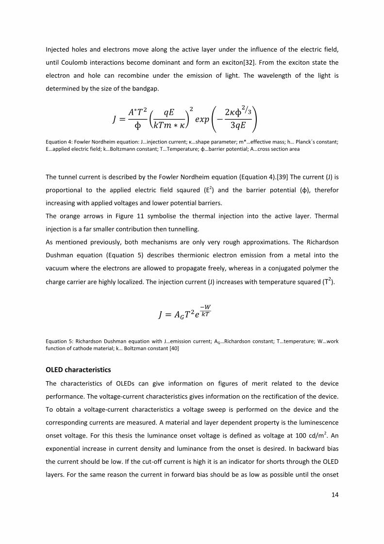
Equation 4: Fowler Nordheim equation: J…injection current; κ…shape parameter; m*…effective mass; h… Planck´s constant; E…applied electric field; k…Boltzmann constant; T…Temperature; ɸ…barrier potential; A…cross section area
The tunnel current is described by the Fowler Nordheim equation (Equation 4).[39] The current (J) is
proportional to the applied electric field sqaured (E2) and the barrier potential (ɸ), therefor
increasing with applied voltages and lower potential barriers.
The orange arrows in Figure 11 symbolise the thermal injection into the active layer. Thermal
injection is a far smaller contribution then tunnelling.
As mentioned previously, both mechanisms are only very rough approximations. The Richardson
Dushman equation (Equation 5) describes thermionic electron emission from a metal into the
vacuum where the electrons are allowed to propagate freely, whereas in a conjugated polymer the
charge carrier are highly localized. The injection current (J) increases with temperature squared (T2).
𝐽 = 𝐴𝐺𝑇2𝑒−𝑊𝑘𝑇
Equation 5: Richardson Dushman equation with J…emission current; AG…Richardson constant; T…temperature; W…work function of cathode material; k… Boltzman constant [40]
OLED characteristics
The characteristics of OLEDs can give information on figures of merit related to the device
performance. The voltage-current characteristics gives information on the rectification of the device.
To obtain a voltage-current characteristics a voltage sweep is performed on the device and the
corresponding currents are measured. A material and layer dependent property is the luminescence
onset voltage. For this thesis the luminance onset voltage is defined as voltage at 100 cd/m2. An
exponential increase in current density and luminance from the onset is desired. In backward bias
the current should be low. If the cut-off current is high it is an indicator for shorts through the OLED
layers. For the same reason the current in forward bias should be as low as possible until the onset

15
voltage. From the voltage-current-luminance characteristic the efficiency of the device can be
calculated.
Photoluminescence quantum yield (PLQY)
With photoluminescence measurements information on the electronic and vibrational transitions in
a molecule can be gathered. The photoluminescence quantum yield (ɸ, Equation 6) is described as
the number of photons emitted, divided by number of photons absorbed and builds the basis for the
electroluminescence quantum yield which is an efficiency parameter of an OLED.
ɸ𝑃𝐿 =number of photons emitted
number 𝑜𝑓 𝑝ℎ𝑜𝑡𝑜𝑛𝑠 𝑎𝑏𝑠𝑜𝑟𝑏𝑒𝑑=
𝑘𝑟
𝑘𝑟 + 𝑘𝑛𝑟
Equation 6: ɸPL…PLQY; kr denotes the rate of radiative decay, whilst knr represents the opposite, non-radiative decay.
Electroluminescence quantum yield
Equation 7 describes the quantum efficiency (ƞ) of a PLED. ƞ is basically defined as the number of
charge carriers injected divided by the number of photons emitted by an electroluminescent device.
Equation 7 shows further factors influencing ƞ.
ƞ = ɸ𝑃𝐿 ∗ 𝑟𝑠𝑡 ∗ 𝛾 ∗ 𝑋
Equation 7: ƞ…Electroluminescence quantum yield; ɸPL…PLQY; rst…singlet triplet ratio; γ…ratio of injected charge carriers and formed excitons; X…quenching factor
Besides radiative recombination, there are other ways for an excited state to release its energy, as
described in detail in the Jablonski diagram.
rst takes the singlet-triplet ratio into account. In contrast to ɸPL, rst is the number of excitons which
are able to recombine under radiation divided by the total number of excitons generated.
The number of excitons formed over the total number of charge carriers injected is described by the
factor ɣ. To improve ɣ and therefor get a higher efficiency charge blocking layers can be placed
between the electrodes and the organic layers. This helps to balance charge currents in the layers
and get an increased efficiency.
X represents all factors which further decrease light out-coupling, for example self-absorption in the
active layer, also interference and total reflection at interfaces. Further X also includes all types of
quenching.
16
3.2 Functional layers of OLEDs and degradiation problems
State of the art OLEDs feature many functional layers. An increasing number of functional layers are
added for different reasons in an OLED stack. Also different materials and methods for processing are
applied in nowadays OLEDs. The following is a list of the basic principles, materials and processes for
manufacturing an OLED.
Basically there are two different types of organic light emitting materials, small molecules and
polymers which are further explained in detail.
Small molecules
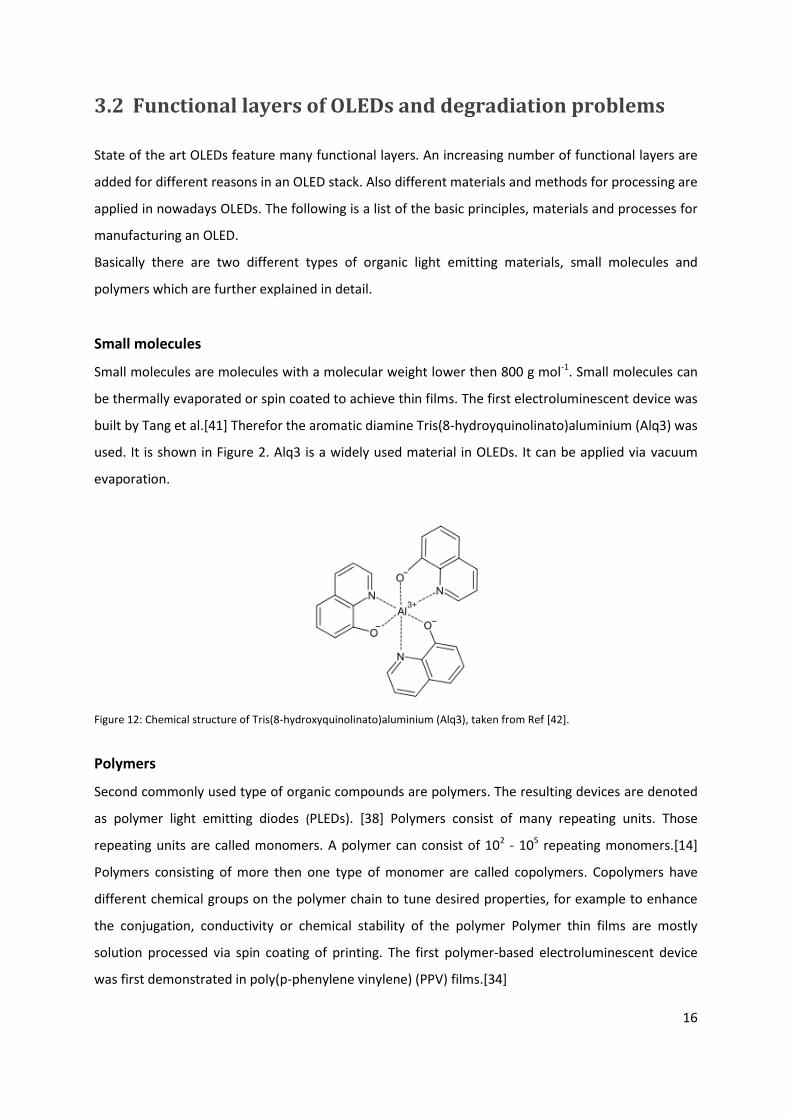
Small molecules are molecules with a molecular weight lower then 800 g mol-1. Small molecules can
be thermally evaporated or spin coated to achieve thin films. The first electroluminescent device was
built by Tang et al.[41] Therefor the aromatic diamine Tris(8-hydroyquinolinato)aluminium (Alq3) was
used. It is shown in Figure 2. Alq3 is a widely used material in OLEDs. It can be applied via vacuum
evaporation.
Figure 12: Chemical structure of Tris(8-hydroxyquinolinato)aluminium (Alq3), taken from Ref [42].
Polymers
Second commonly used type of organic compounds are polymers. The resulting devices are denoted
as polymer light emitting diodes (PLEDs). [38] Polymers consist of many repeating units. Those
repeating units are called monomers. A polymer can consist of 102 - 105 repeating monomers.[14]
Polymers consisting of more then one type of monomer are called copolymers. Copolymers have
different chemical groups on the polymer chain to tune desired properties, for example to enhance
the conjugation, conductivity or chemical stability of the polymer Polymer thin films are mostly
solution processed via spin coating of printing. The first polymer-based electroluminescent device
was first demonstrated in poly(p-phenylene vinylene) (PPV) films.[34]

17
Figure 13: Chemical structure of Poly(p-phenylene vinylene), a semi conducting polymer showing electroluminescence taken from [34].
Hole injection layer (HIL)
As mentioned in previous chapters, additional layers can enhance the efficiency of OLEDs. The main
steps of light generation (charge injection, conduction, recombination) demand different material
properties. [34]. First to mention, because of their use in this thesis, are hole injection layers (HIL). As
shown in Figure 11 between the PEDOT:PSS layer and the organic semiconductor there is a step in
energy. To reduce this step height and hence allow for an increased charge carrier injection a HIL is
introduced. It should have an intermediate HOMO between anode and light emitting layer (LEM).
Further, a HIL should have hole blocking abilities to hinder holes from leaving the active layer without
recombining.
PEDOT:PSS and its variations
Figure 14 shows the chemical structure of PEDOT (Poly(3,4-ethylenedioxythiophene)) and PSS
(polystyrene sulfonate). PEDOT:PSS is a mixture of PEDOT and PSS. PEDOT:PSS is an electrical
conducting polymer.[43] It is used in the previously mentioned devices as smoothening and hole
injection layer. The layer thickness of PEDOT:PSS is controlled by the according process parameters.
(e.g.: here spincoating parameters) Subsequently to layer deposition PEDOT:PSS needs to be
thermally treated, to remove residual solvents. PEDOT is a conjugated polymer on thiophene basis,
whereas PSS is an isolator. When mixed, PSS acts as dopant for PEDOT to achieve the electrical
conductivity in thin films. PSS is acidic with a pH value of approximately 1.5-2.5. Depending on the
physical demands of the PEDOT:PSS layer, various formulations of the solutions are available on the
market.
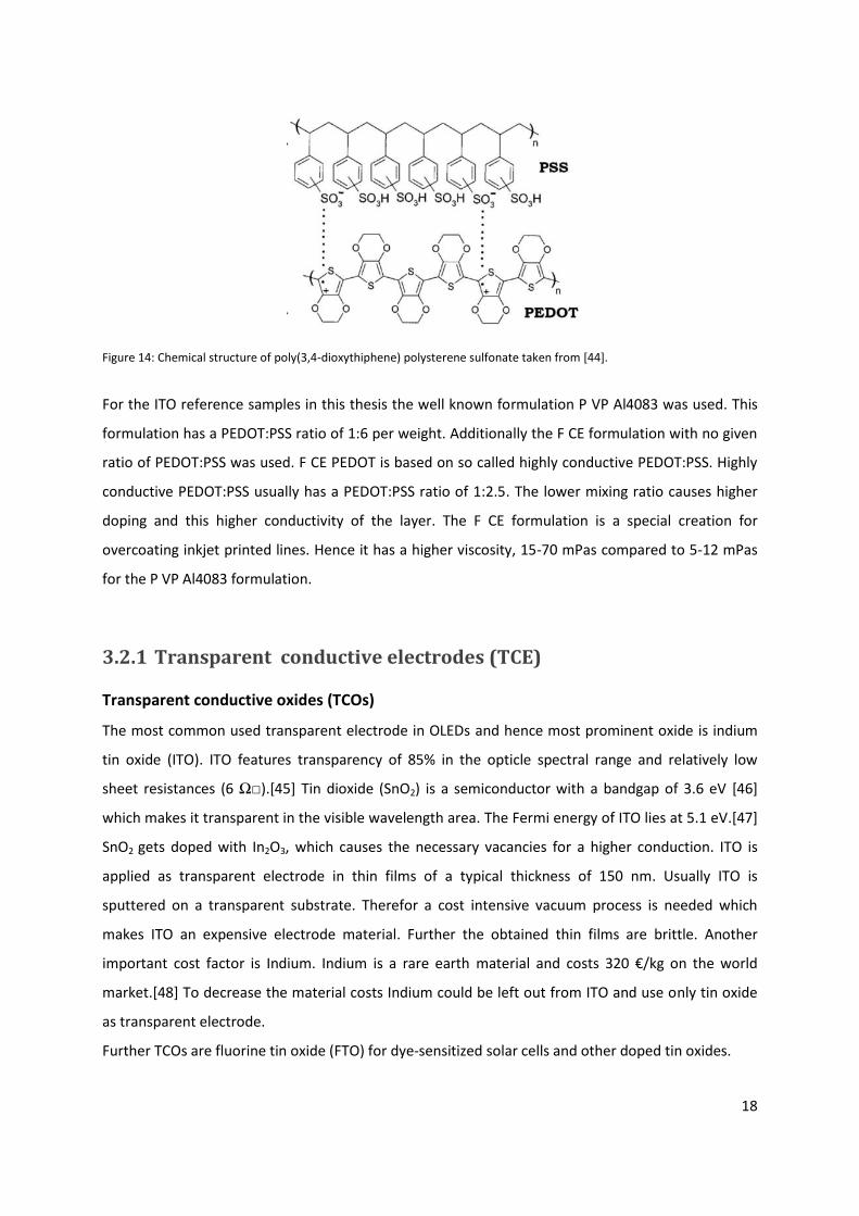
18
Figure 14: Chemical structure of poly(3,4-dioxythiphene) polysterene sulfonate taken from [44].
For the ITO reference samples in this thesis the well known formulation P VP Al4083 was used. This
formulation has a PEDOT:PSS ratio of 1:6 per weight. Additionally the F CE formulation with no given
ratio of PEDOT:PSS was used. F CE PEDOT is based on so called highly conductive PEDOT:PSS. Highly
conductive PEDOT:PSS usually has a PEDOT:PSS ratio of 1:2.5. The lower mixing ratio causes higher
doping and this higher conductivity of the layer. The F CE formulation is a special creation for
overcoating inkjet printed lines. Hence it has a higher viscosity, 15-70 mPas compared to 5-12 mPas
for the P VP Al4083 formulation.
3.2.1 Transparent conductive electrodes (TCE)
Transparent conductive oxides (TCOs)
The most common used transparent electrode in OLEDs and hence most prominent oxide is indium
tin oxide (ITO). ITO features transparency of 85% in the opticle spectral range and relatively low
sheet resistances (6 Ω).[45] Tin dioxide (SnO2) is a semiconductor with a bandgap of 3.6 eV [46]
which makes it transparent in the visible wavelength area. The Fermi energy of ITO lies at 5.1 eV.[47]
SnO2 gets doped with In2O3, which causes the necessary vacancies for a higher conduction. ITO is
applied as transparent electrode in thin films of a typical thickness of 150 nm. Usually ITO is
sputtered on a transparent substrate. Therefor a cost intensive vacuum process is needed which
makes ITO an expensive electrode material. Further the obtained thin films are brittle. Another
important cost factor is Indium. Indium is a rare earth material and costs 320 €/kg on the world
market.[48] To decrease the material costs Indium could be left out from ITO and use only tin oxide
as transparent electrode.
Further TCOs are fluorine tin oxide (FTO) for dye-sensitized solar cells and other doped tin oxides.
19
Grids
As alternative to metal oxide thin films metal grids are studied. Grids can be fabricated
photolithographically [50], inkjet printed and electro plated.[52] Depending on the type of deposition
grid strucutres can vary from 2 µm line width and grid spacings of 10 µm for photolithographic grids
[52] up to 150 µm line width and 8 mm spacing for inkjet printed grids presented in this work.
Carbon nano tubes (CNTs)
Carbon nano tubes have already been successfully applied in displays and photovoltaic devices as
transparent electrodes. [53-55] Important for the application of CNTs as TCEs is that the
concentration of CNTs needs to be high enough to build a percolation network.[56] To get
comparable conductivity properties to ITO the single CNT needs to be more than 100 nm long,
leading to high losses in transparency.[57]
Nanowires (NW)
Additionaly various optoelctric devices were made with metal nanowires as transparent electrodes.
[58]–[62] NW feature properties similar to CNTs, including threshold concentration for conductivity
and related losses in transparency. Although NW feature high conductivities in the wire the wire to
wire junction decreases significantly the conductivity. [61] So far the performances of NW thin films
rival already those of ITO.[57]
Graphene
As a zero band gap semiconductor graphene comprises electrons delocalized over the whole
molecule, offering the possibility to conduct electrons without scattering.[63] Combined with the
possible doping of graphene, this leads to high in plane conductivities.[64] In contrast to the high in
plane conductivity of graphene stand sheet resistances of up to 800 Ω. The high sheet resistances
are caused by the fact that so far solution processed graphene films consist of thousands of graphene
flakes, building up grain boundaries and showing many defects. Nevertheless Wu et al. already
showed that solution processed graphene films deliver OLED performances comparable to ITO.[65]
20
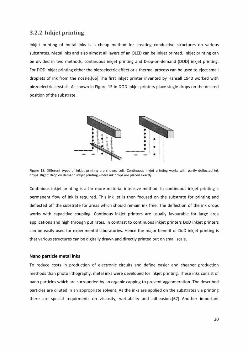
3.2.2 Inkjet printing
Inkjet printing of metal inks is a cheap method for creating conductive structures on various
substrates. Metal inks and also almost all layers of an OLED can be inkjet printed. Inkjet printing can
be divided in two methods, continuous inkjet printing and Drop-on-demand (DOD) inkjet printing.
For DOD inkjet printing either the piezoelectric effect or a thermal process can be used to eject small
droplets of ink from the nozzle.[66] The first inkjet printer invented by Hansell 1940 worked with
piezoelectric crystals. As shown in Figure 15 in DOD inkjet printers place single drops on the desired
position of the substrate.
Figure 15: Different types of inkjet printing are shown. Left: Continuous inkjet printing works with partly deflected ink drops. Right: Drop on demand inkjet printing where ink drops are placed exactly.
Continious inkjet printing is a far more material intensive method. In continuous inkjet printing a
permanent flow of ink is required. This ink jet is then focused on the substrate for printing and
deflected off the substrate for areas which should remain ink free. The deflection of the ink drops
works with capacitive coupling. Continous inkjet printers are usually favourable for large area
applications and high through put rates. In contrast to continuous inkjet printers DoD inkjet printers
can be easily used for experimental laboratories. Hence the major benefit of DoD inkjet printing is
that various structures can be digitally drawn and directly printed out on small scale.
Nano particle metal inks
To reduce costs in production of electronic circuits and define easier and cheaper production
methods than photo lithography, metal inks were developed for inkjet printing. These inks consist of
nano particles which are surrounded by an organic capping to prevent agglomeration. The described
particles are diluted in an appropriate solvent. As the inks are applied on the substrates via printing
there are special requirments on viscosity, wettability and adheasion.[67] Another important

21
property of an ink is its dry rate. Fast drying enables fast printing but enhances the risk of nozzle
blocking.
To get a conductive structure the printed lines have to be sintered. Sintering can be done in various
ways, but all sintering processes aim for the removing of the capping of the nano particles and for
linking the nanoparticles to get a bulk like structure. So far nano particle inks do not reach bulk
conductivity of the original material.[68]
Piezo electric inkjet single nozzle printhead set up
Figure 16 explains the main parts of a single nozzle printhead, driven by a piezo electric crystal. The
nozzle consists of a glass capillary which contains the ink. This glass capillary is surrounded by the
piezo electric crystal. On the end are the voltage supply for the piezo crystal and the further ink
supply.
Figure 16: Basic set up of a sinlge nozzle piezo electric inkjet printhead, the ink is in the glass capillary from which it is ejected via the piezo crystal [69].
For printing one drop of ink a voltage is applied on the piezocrystal. The piezocrystal subsequently
expands. This causes a shock wave through the glass capillary causing the ejection of an ink droplet.
Figure 17 shows an industrial scale printhead based on 128 individually addressable nozzles, each
one similar to the described above. The voltage and control plug is on top. The nozzles are at the
bottom of the picture. Drop volume of this printhead is 90 pico liter. A print speed of 200 mm/s can
be achieved.

22
Figure 17: Pix Dro LP50 piezoelectric printhead with 128 nozzles at the NTC Weiz used for this thesis.
3.3 Degradation effects of functional groups in PLEDs
As PLEDs should contribute to future lighting applications a long life time is desired. Especially blue
emitters are sensible to degradation, because of their large bandgap and therefor low electron
affinity. Some of the known reasons for spectral shift in PLEDs are described in the following.
First to mention are Keto-defects in Polyfluorene type materials. Keto defects lead to a strong green
shift caused by an Oxygen atom which is added to the polyfluorene chain.[70]
Figure 18: Explaination of the proposed mechanism of the keto defect. 9-monoalkylated fluorine building blocks get (I) get reduced to fluorenyl anions while hydrogen forms. Hydroperoxide (III) anions are formed by the hydrogen and atmospheric oxygen. (IV) finally the hydroperoxide anions rearrange and form fluorenone moieties. This whole process takes place during the synthesis of fluorene type polymers.[70]
As described in the chapter about charge carrier injection, cathode materials with low work function
are necessary for a good electron injection. Materials like Calcium (work function ɸc=2.9 eV), Barium
(work function ɸc=2.6 eV) and caesium fluoride (work function ɸc=2.2 eV) show low enough work
functions, but they also show strong reactivity to Oxygen and humidity. The Aluminium barrier of 150
nm cannot exclude these reactions and interactions sufficiently.[71] For poly(fluorene) type polymers

23
one possible degradation is explained as a deprotonation reaction of hydroxyl end chain units by
diffused Calcium (Equation 8).[72]
2 Ar–OH + Ca → 2 Ar–O- + Ca2+ + H2
Equation 8: Deprotonation reaction of hydroxyl units by diffused Calcium.
Another problem related to moisture are so called dark spots. Dark spots are non emissive areas,
caused by delamination of the electrodes. This delamination occurs due to electrochemical
dissociation of water according to Equation 9. Driven by the applied voltage water molecules in the
device can dissociate causing H and O gas.[73]
2 H2O + 2e- →H2 + 2OH-
Equation 9: Dissociation of water under electric fields.
PEDOT:PSS is used in almost all organic light emitting and photovoltaic devices as smoothening layer.
Additionally to its smoothing ability the work function of PEDOT:PSS makes it an optimal hole
injector, which is desired for high efficient devices. However the drawback of PEDOT:PSS is its acidity.
Most times PEDOT:PSS is applied to any surface via spincoating. This leads to a formation of a PSS
rich layer on top of the fresh spincasted PEDOT:PSS layer. [36][74] Different studies [75-77] show
that PSS causes trap states at the emissive layer, which derives from the acidity of PSS. Another shift
in the electroluminescence spectrum is caused by protonation of nitrogen containing polymers.[38]
Last to mention are electrophilic addition reactions with unsaturated electron-rich carbon double
bonds (e.g. in PPV).[75][78]

24
4 Experimental methodology
This chapter describes the most important methods used in this thesis. Details of inkjet printing and
the used grids are discussed at the beginning. The embedding process for the inkjet printed grids is
explained. Further the general OLED fabrication process, for solution processed PLEDs and for
vacuum evaporated small molecules is shown. Finally, the used characterisation process and
appropriate equipment is described.
4.1 Grid fabrication
All experimental work, except for the sintering of copper grids in formic acid, was done at NTC Weiz
Forschungsgesellschaft mbH. Inkjet pringting took place in a chemistry lab under a fume hood. All
further preparation steps were carried out in a state of the art ISO-Class 6 clean room facility.
Silver Ink
Here, Cabot CCl – 300 Ag nano particle ink was used. To remove the capping of the nano
particparticles and achieve a bulk like grid all inkjet printed silver grids were sintered. The sintering
took place in a sinter oven manufactured by Heraeus. In this oven a vacuum can be applied. The
printed silver grids were sintered for 2 h at 150°C.
Copper Ink
Two types of copper ink were used in this work. The ink for the embedded copper grids was Intrinsiq
Cl-003G. This ink had a lower adheasion on glass and was suitable for embedding. For the over
coated grids the ink Cl-005G from Intrinsiq Materials was used. As it was optimized for adhesion,
embedding became impossible and it was used for overcoating.
Inkjet printing
Substrates for inkjet printing were cleaned with acetone and mechanically using tissue. This intensive
cleaning procedure turned out to be crucial for the later lift off during the embedding process.
Further intensive cleaning reduces the possibilities of defects caused by contamination and non
emissive areas in the OLED. Printing of the hexagonal grid structures was performed using a PixDro
LP50 printer equipped with a FujiFilm Dimatix (Spectra) S-Class 128 nozzle piezoelectric print head.
Here, the three previously explained inks were used. Subsequent to printing, the silver grids were
annealed for 2h at 150°C in vacuum. Sintering of the silver grids was necessary to stabilise the grid
25
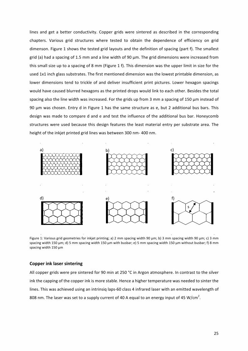
lines and get a better conductivity. Copper gridswere sintered as described in the corresponding
chapters. Various grid structures where tested to obtain the dependence of efficiency on grid
dimenson.Figure1showsthetestedgridlayoutsandthedefinitionofspacing(partf).Thesmallest
grid(a)hadaspacingof1.5mmandalinewidthof90µm.Thegriddimensionswereincreasedfrom
thissmallsizeuptoaspacingof8mm(Figure1f).Thisdimensionwastheupperlimitinsizeforthe
used1x1inchglasssubstrates.Thefirstmentioneddimensionwasthelowestprintabledimension,as
lowerdimensions tend to trickleof anddeliver insufficientprintpictures. Lowerhexagon spacings
wouldhavecausedblurredhexagonsastheprinteddropswouldlinktoeachother.Besidesthetotal
spacingalsothelinewidthwasincreased.Forthegridsupfrom3mmaspacingof150µminsteadof
90µmwaschosen.Entryd inFigure1hasthesamestructurease,but2additionalbusbars.This
designwasmadetocomparedandeandtestthe influenceoftheadditionalbusbar.Honeycomb
structureswereusedbecause thisdesign features the leastmaterialentryper substratearea.The
heightoftheinkjetprintedgridlineswasbetween300nm-400nm.
Figure1:Variousgridgeometriesforinkjetprinting;a)2mmspacingwidth90µm;b)3mmspacingwidth90µm;c)3mmspacingwidth150µm;d)5mmspacingwidth150µmwithbusbar;e)5mmspacingwidth150µmwithoutbusbar;f)8mmspacingwidth150µm
Copperinklasersintering
Allcoppergridswerepresinteredfor90minat250°CinArgonatmosphere.Incontrasttothesilver
inkthecappingofthecopperinkismorestable.Henceahighertemperaturewasneededtosinterthe
lines.Thiswasachievedusinganintrinsiqlaps-60class4infraredlaserwithanemittedwavelengthof
808nm.Thelaserwassettoasupplycurrentof40Aequaltoanenergyinputof45W/cm2.
a) b) c)
e) f)d)
s

26
Copper ink sintered in formic acid enviornment
Alternativeley to the previously described laser sintering some copper grids were sintered in a formic
acid atmosphere. Therefor the samples were put in a custom-made sinter oven with the possibility to
apply a formic acid atmosphere in the heating chamber. Three identical sets of grids were sintered
with 180°C, 200°C and 250°C. Then formic acid was bubbled in the chamber. The formic acid
concentration was 3.4% for all samples and the sintering time was 60 min.
4.2 Embedding process
As described in 4.1, inkjet printed lines have a typical height between 300 nm – 400 nm. A typical
OLED has a total height of 300 nm – 400 nm. Further feature inkjet printed lines a rough surface. As
the mobilities of the charge carriers are strongly field dependent, should the electric field in the OLED
be as homogenious as possible for homogenious light emission. [79][80][81][52] From this fact, it is
clear that inkjet printed grids offer some problems in the application as TCO. However the grid is
fabricated, (photolithographic or inkjet printed) grid lines always tower above the glass substrate and
lead to defects in the OLED stacks. These defects can lead to short cuts. To overcome the defects
caused by grid lines an embedment can be applied. Here, an embedding process is described, first
used by Burgeos et al. [4]. In Ormocomp® embedded inkjet printed silver grids used as TCEs for
organic photovoltaic cells (OPVs), showed an increased efficiency of 149% compared to convential
OPVs.
UV curable and hybrid Polymers
For the embedding process a UV curable hybrid polymer called Ormocomp® was used. Ormocomp is
an Ormocer. Ormocers® were developed by the Frauenhofer Institut für Silicatforschung and are
manufactured and distributed by micro resist technology GmbH. [82] These Ormocers ® harden
under UV radiation and show glass like properties. UV curable polymers are polymers which change
their chemical structure or cross link with neighbouring molecules under UV radiation. Hybrid
polymers are polymers with added inorganic elements, for example silicon.

27
Process
Two substrates are needed for this process, a sacrificial one, on which the grid is printed and a final
one, on which the grid is embedded. Figure 20 a displays the first step of the process, inkjet printing
of the grids on the sacrificial substrate. Figure 20 b shows the final substrate over coated with the
adheasion promoter Ormoprime 08. Ormoprime 08 is the according adheasion promoter for
Ormocomp also sustained by micro resist technology GmbH. This adhesion promoter ensures that
the cured Ormoprime layer sticks to the final substrate. Before overcoating the substrate needs to be
plasma etched to increase the adheasion of Ormoprime08. A drop of Ormocomp is then put on the
grid structure (Figure 20 c). At this step it is important to cover the whole grid with Ormocomp to
ensure a lift off of the whole grid.

28
Figure 20: Manufacturing process of inkjet printed embedded grids: a) Inkjet printing of the grid. b) Coating the final substrate with Ormoprime. (blue glass/plastic; beige Ormoprime) c) Covering the grid with Ormocomp. d) Place Ormoprime layer on covered grid. d) Final substrate after lift-off. e) Final stack with finished OLED and structured cathodes.
Afterwards the sample has to be heated on a hotplate to reduce air bubbles in the layer and to
promote a better adhesion of the inkjet lines in the Ormocomp. The final substrate is placed on the
over coated grid (d). UV radiation (1=280 nm, 2=230 nm) was applied to the stack to cure the
Ormocomp layer. Finally a lift off is performed and a reverse embedded grid structure was obtained
(e). Figure 20 f shows the finished OLED device. The inkjet printed grid is fully embedded in
Ormocomp (grey semi-transparent layer). The subsequent layers face a less inhomogeneous surface
then on over coated grids. Figure 20 f further shows the active layer (pink) and the finishing Calcium,
Aluminium cathode.
a)
a)
b)
c) d)
f) e)
sacrificial substrate
printer
final substrate
Ormoprime 08
sacrificial substrate grid
Ormocomp
sacrificial substrate grid
Ormocomp
final substrate Ormoprime 08
final substrate grid
Ormocomp Ormoprime 08

29
4.3 OLED fabrication
The following steps describe the basic fabrication procedure of an OLED, starting with cleaning and
plasma etching. Subsequent are the processes for different types of OLEDs are described (solution
processed PLED respectively evaporated small molecules).
Cleaning
All sacrificial substrates for inkjet printing had to be cleaned with acetone and mechanically rubbed
tissue. The final substrates (quarz glass) were cleaned with acetone and mechanically applied tissue.
Subsequentley the glass substrates were sonicated 10 minutes in Isopropanol. The ITO samples were
10 minutes sonicated in Hellmanex, subsequently in Isopropanol. Between each cleaning step the
substrates were dry blown with N2.
O2 plasma etching
All final substrates were O2 plasma etched before spin coating with Ormoprime. Plasma etching
enhances the wettability of the surface and hence an increased adhesion of the subsequently
deposited material is achieved. O2 plasma etching leads to the formation of OH groups on the surface
of the treated sample. The substrates were etched in a femto plasma tool from diener at 200 Watt
for 5 Minutes. Grid structures had to be etched shorter (6 s) because the lines showed indications for
strong oxidation after a longer etch process. Embedded lines seemed to withstand the etch process
better as fewer oxidized areas occurred during the etch process compared to the normal grids.
Also all ITO samples were plasma etched for 5 minutes at 200 W. The sacrificial substrates were
excluded from plasma etching, since due to enhanced wettability the applied inks would trickle off.
Hence the digital drawn grid structures would not be printed properly.
PEDOT deposition
The grids maintained as described in the sample preparation section where first O2 plasma etched for
5 minutes at 200 W. A layer of FCE PEDOT:PSS from Clevious was spin coated on the embedded grids.
The layer was spun with 2000 rpm for 40 seconds. Subsequently the samples with the FCE layer were
baked on a hotplate for 15 minutes under ambient atmosphere. The whole spin coating and drying
process was carried out in a laminar flow box. This resulted in an approximately 150 nm thick PEDOT
layer.

30
4.3.1 Solution processed PLEDs
Solution processed HIL
For the solution processed PLEDs, copolymers with various functional units were used. This HIL/LEP
systems were first investigated by Nau et al. [38] Figure 21 displays the various chemical groups of
the Copolymers. The different groups were added with different focus on hole injection, hole
transport, recombination and groups to prevent the copolymers from degradation in the acidic
environment of PEDOT. The HIL had on its polymer chains the functional groups A (indenofluorene) E
(triphenylamine) in a ratio of 50:50.
Figure 21: Chemical structures of the individual copolymer building blocks: A) 9,9,12,12-tetraorganyl-6,12-dihydroindeno[1,2-b]fluorene; B) (E)-4-organyl-N-phenyl-N-(4-styrylphenyl)aniline; C) 9,10-diorganyl-phenanthrene; D) N
1N
4-bis(4-organphenyl)-N
1,N
4-diphenylbenzene-1,4-diamine E) 4-organyl-N,N-diphenylaniline
Solution processed LEP
The LEP consisted of ABCD. In detail the emissive units are indenofluorene (A), (E)-4-organyl-N-
phenyl-N-(4-styrylphenyl)aniline as an emissive unit (B), electron-transport-supporting phenanthrene
(C), and hole-transport-supporting amine (D) units at an A:B:C:D ratio of 46:2:50:2.
Preparing solutions
For the solution processed PLEDs also a solution processed HIL was applied. The hole injection layer
(HIL) and the light emitting polymer (LEP) were dissolved in Toluene. For the HIL a concentration of 2
g/L and for the LEP a concentration of 4 g/L was chosen.

31
Layer Deposition
Layer deposition of the solution processed HIL and LEP were carried out in an Argon filled glovebox. A
20 nm thick HIL and a 60 nm thick LEP layer were spin coated on the FCE layer. This was achieved by
spinning the HIL solution with 1000 rpm for 15 seconds and subsequent with 3000 rpm for 40
seconds. The LEP was spin coated with 1500 rpm for 15 and subsequent with 3000 rpm for 40
seconds.
The HIL was baked under Argon atmosphere on a hotplate at 200°C for one hour. The LEP layer was
baked under high vacuum at 120°C for one hour.
4.3.2 Thermal evaporation of OLEDs
The steps here describe the materials, methods and hardware for thermal evaporated OLEDs. First
are the used materials explained.
Evaporated HIL
For the experiments with the thermal evaporated OLEDs on embedded grids the standard HIL N,N-
Di(1-naphthyl)-N,N-diphenyl-(1,1-biphenyl)-4,4-diamine (NPB) from sigma Aldrich was used. A 30 nm
thick film of NPB was evaporated on the PEDOT:PSS layer with the embedded grid underneath.
Figure 22 shows the molecular structure of NPB.
Figure 22: NPB molecular structure taken from [10].
Evaporated LEM
Tris-(8-hydroxyquinoline)aluminum (Alq3) is a commonly used thermal evaporated LEM. It is easy to
handle in thermal evaporation and well studied, therefore it is perfectly suited for studying TCEs. For
the molecular formula see Figure 12. 300 nm of Alq3 were applied on the previous NPB layer with
the vacuum evaporation chamber described in 4.3.2.
Thermal evaporation
For the evaporated hole injection layer (HIL) and the evaporated light emitting layer (LEM) a vacuum
deposition chamber in an argon filled glovebox was used. This same chamber was also used for the

32
deposition of the Calcium and Aluminium layers, which have been evaporated through a mask. The
chamber consists of 5 different evaporation units. To realize a fully evaporated OLED the chamber
was built with a rotatable sample holder wheel and a rotatable mask wheel, hence it is possible to
evaporate different material layers with different masks without breaking the vacuum. The whole
process is software controlled. The devices for thesis were fabricated according to the following
steps:
The inkjet printed grids were embedded according to the process in 4.2. Then they were spin coated
with F CE PEDOT as explained in 4.3. Then the samples were transferred into a glovebox with the
vacuum evaporation chamber. The chamber was vented and opened. The evaporation units for the
organic materials had a crucible in a heating set up. The crucible were filled with Alq3 and NBP,
respectively and then brought in two different units. Calcium and aluminium were evaporated from
tungsten boats in two further units. When all the materials were located the samples were put in the
substrate holder wheel with the mask wheel underneath. Finally the chamber was closed and
evacuated to 10-6 mbar. NPB and Alq3 were evaporated over the whole substrate area. To define the
OLED size calcium and aluminium were evaporated through masks.
Cathode
To enhance electron injection 10 nm of Calcium were evaporated through a mask on the Alq3 layer.
To cover up the OLED and get a good conductivity 100 nm of Al were evaporated through the same
mask with the vacuum chamber described in 4.3.2. The final cathode consisted of 10 nm evaporated
Calcium and subsequently 150 nm evaporated Aluminum, as described.
4.4 Characterisation methods
In the following the various methods for characterising grids and OLEDs are explained. It is important
to gather information about the grids themselves to understand the influences on the later
processed OLED on the grid. Microscopy was performed to check the grids for cracks. Optical
transmission measurements of the grids were necessary to compare the different geometries in
transmission and with ITO. With SEM, AFM and profilomter measurements the microscopic influence
of the embedding process was revealed. Finally the OLEDs were electro-optically characterised, to
compare the different influence on different geometries on the performance.

33
Optical microscope measurements
As the grids were printed with line widths in the µm range and spacings up to the mm range optical
microscope pictures were taken with an Olympus 2000 microscope. Distances in the microscope
pictures were measured with the cellD scan software. An optical microscope can be used in various
modes. For this thesis most pictures were taken in reflective mode. To increase the contrast of
obstacles and planar inhomogeneity pictures were also taken in dark mode.
Optical transmission measurements
First it is necessary to mention that a grid has no exact transmission. The grid lines block almost all
the light. In between the grid lines all the light is passing through. Therefor a so called “coverage” in
percent was introduced. It is the ratio of grid line area divided by the whole area covered by the grid.
The calculation is described in Equation 10.
𝐴𝑔
𝐴𝑤= 𝑐 (%)
Equation 10: Ag…area covered by grid lines; Aw…total grid area
For grid spacings up to 5 mm spacing transmission measurements were performed according to
Equation 11.
𝑇(𝜆) =
𝐼(𝜆)
𝐼0(𝜆)
Equation 11: T…transmission; I…intensity; I0…incident intensity
Transmission is defined as transmitted intensity (I(λ)) divided by incident intensity (I0(λ)). I is a
function of the wave length λ. Hence transmission depends on the wavelength of the incident light.
To measure the wavelength dependent transmissions the spectrometer needs to have a tuneable
light source. Most spectrometer consist therefore of a broad band light source which emits all
wavelengths. To tune the wavelength a spectrometer uses either a prism or a grating. To characterize
the grids a perkin elmer lambda 900 UV/VIS spectrometer was used. It consists of a Deuterium and
Halogen lamb as a light source and holographic gratings for tuning the wavelength. The whole
measurement system is fully software controlled.
34
Profilometer measurments
A profilometer measures the surface topology of a material. Main parts are a cantilever with a needle
and a coil for vertical measurements and a moveable sample stage. The measurement is done by a
needle which is scratching over the surface while the sample stage is moved underneath. The vertical
displacements of the needle are measured inductive with a coil attached to the cantilever. The lateral
position and the vertical amplitude are mapped and a surface profile can be determined. For this
thesis a Bruker XT profilometer was used. It can achieve a vertical resolution down to 1 nm up to 1
mm depending on the needle. Lateral it can measure up to an area of 55 mm times 55 mm.
Device Characterisation
The completed OLED/PLED deviceses were characterized with following tools. Voltage-current
characteristics were recorded with a KEITHLEY 2612 sourcemeter (computer assisted). Simultaneous
measurement of the emitted light intensity was performed using a silicon-diode and a KEITHLEY
6417A electrometer. Photocurrent – luminance calibration was done with a MINOLTA LS-100
luminance meter.
With the calibrated photocurrent luminance ratio the luminance was calculated according to
Equation 12. The luminance was measured at a constant photocurrent Ac for this calibration.
𝑙𝑢𝑚[𝑐𝑑 𝑚2⁄ ] = 𝑝ℎ𝑜𝑡𝑜𝑐𝑢𝑟𝑟. [𝐴] ∗
𝑙𝑢𝑚𝑖(𝐴𝑐)[𝑐𝑑 𝑚2⁄ ]
𝑝ℎ𝑜𝑡𝑜𝑐𝑢𝑟𝑟. (𝐴𝑐)[𝐴]
Equation 12: lum...luminescence; photocurr...photocurrent; lumi(Ac)...luminescence at calibration photocurrent; photocurr.(Ac)…photocurrent during calibration
According to Equation 13 the current density through the device was calculated. A is the active area
of the OLED.
𝑐𝑢𝑟𝑟. 𝑑𝑒𝑛𝑠𝑖𝑡𝑦 [𝐴 𝑚2⁄ ] =𝑐𝑢𝑟𝑟[𝐴]
𝐴[𝑚2]
Equation 13: curr. density…current density, curr…current, A…active area

35
The luminance in combination with the current density can reveal the efficiency of the OLED
according to Equation 14.
𝑒𝑓𝑓 [𝑐𝑑 𝐴⁄ ] =
𝑙𝑢𝑚𝑖𝑛𝑎𝑛𝑐𝑒[𝑐𝑑 𝑚2⁄ ]
𝑐𝑢𝑟𝑟𝑒𝑛𝑡 𝑑𝑒𝑛𝑠𝑖𝑡𝑦 [𝐴 𝑚2⁄ ]
Equation 14: eff…efficiency
Another important property of a light emitting device is the emission spectra. Measurement of the
electroluminescence emission spectrum was done using a LOT-ORIEL CCD-spectrometer.

36
5 Solution processed reference PLEDs on ITO
This chapter introduces basic PLEDs on ITO. The PLED was fabricated according to the process given
in chapter 4. The characterisation comprises the voltage-current-luminescence characteristics and
electroluminescence spectra. Figure 23 displays the voltage-current-luminance characteristics and
the electroluminescence spectra of the devices. The current density and luminance increase
exponentially from the onset. The characteristics also displays a low current density in reverse bias.
The graph of the current density (circles) shows a smooth increase without spikes. This leads to the
conclusion that there are few shorts in the device.
-4 -2 0 2 4 6 8 10 120
10000
20000
30000
curr
ent
density (
A/m
2)
bias (V)
current density
0
20000
40000
60000
lum
ina
nce (
cd/m
2)
luminance
5 6 7 8 9 10 11 121.6
2.4
3.2
4.0
eff
icie
ncy (
cd
/A)
bias (V)
400 450 500 550 600 6500.00
0.25
0.50
0.75
1.00
4 V
11 V
norm
. ele
ctr
olu
min
escence
wavelength (nm)
Figure 23: Right: Voltage-current-luminance characteristics of PLEDs (ITO/PEDOT:PSS/HIL/LEP/Ca/Al) on ITO. Right: Normalized electroluminescence spectrum of PLEDs at 4 V operating voltage (circles) and 11V (squares).
The onset is at 3.6 V as typical for this material with this layer thickness. The efficiency reached a
value of 3.7 cd/A. The efficiency at 1000 cd/m2 was 3.2 cd/A. A maximum luminance of 64000 cd/m2
was reached. The current density at this voltage reached a maximum of over 30000 A/m2. The
electroluminescence spectra are stable at low voltages and corresponding low current densities.
With increasing current density a peak shift to the red take place. An increasing of the peak at 480
nm is visible. Compared to the spectra in chapter 6,7 and 8 the current density at 11 V for the ITO
devices is more than 3 times higher. This results in a higher stress on the material. Caused by this
stress is a far higher spectral shift in the electroluminescence spectrum.

37
Figure 24: Image of a PLED processed on an ITO substrates.
Figure 24 shows an image of the described PLED under operation. Also visible are the not operating
neighbouring cathodes in different sizes.
The here presented devices are used as references for the grid devices.
Figure 25 shows the outcome of ultraviolet photoelectron spectroscopy (UPS) performed by Nau et
al. [38] Here the reasons for the high efficiencies of the PLED consisting of the used copolymers (CP)
become clear. PEDOT:PSS has a work function of 5.0 eV and the HIL an ionisation energy of 5.5 eV.
Therefore easy hole injection and electron blocking is possible. The HOMO of the HIL is further only
0.3 eV away from the HOMO of the LEP leading to a low hole injection barrier. Additionally the
LUMOs show an energy barrier of 0.2 eV for electrons. The energy barrier for electrons at the
PEDOT:PSS HIL interface is with 2.4 eV high enough for sufficient electron blocking.
Figure 25: Band diagramme of PEDOT:PSS/HIL/LEP of the presented PLED. Taken from [38].

38
6 OLEDs based on inkjet printed silver grids
The following chapter comprises grids printed with the silver grid described in 4.1. In the beginning
optical characterization of the grids, ITO and Ormocomp® are presented. Further PLEDs on
overcoated and embedded grids are shown.
6.1 Optical characterization of grids
As explained in 4.4 it is impossible to measure an exact transmission or absorbance of a metal grid.
Nevertheless, as long as the measuring spot size exceeds the grid spacing, an approximated average
transmission value can be estimated. The here presented transmissions are measured on grids with
sufficient small spacing. These data was measured with a PerkinElmer Lambda 900 UV/VIS –
spectrometer. According to Equation 11 I0 was obtained by measuring the transmission of an empty
glass sample. Subsequently the grid structures were put in the sample holder and measured.
400 500 600 700 800
80
100
ITO transmission
2 mm grid spacing
5 mm grid spacing
FCE PEDOT transmission
Ormocomp film transmission thickness=0.7 mm
tra
nsm
issio
n (
%)
wavelength (nm)
Figure 26: Optical transmission of: 2 mm spacing grid, 5 mm spacing grid, ITO, FCE PEDOT:PSS and an Ormocomp thin film.
Figure 26 shows the transmission of the used materials and grid spacings. A grid with a spacing of 2
mm (empty squares) is already fine enough meshed to be comparable to ITO (empty triangulars). The
wider the grid spacing gets the higher gets the transmission. This stems from the fact that a higher
spacing leads to a lower coverage and thus lower shadowing. With a spacing of 5 mm (empty circles)
one can achieve an average transmission of almost 92%. This lies also above the transmission of ITO
(empty triangulars) with 88% on average. Also important for later OLED performances is the
transmission of Ormocomp (circles with cross). It has an average transmission of 97% which is
comparable to glass. Further the graph displays the transmission of a 150 nm thick F CE PEDOT layer.

39
Transmission is between 98% blue wavelength range and 92% in the red range. From Figure 26 it is
furthermore evident that the transmission of grids is constant over the visible wavelength region.
The transmission of ITO varies strongly depending on the wavelength.
6.2 PLEDs manufactured on inkjet printed silver grids
Grids with a line width of 150 µm and a spacing of 3 mm were investigated in this part. The first ink
used was silver nano particle ink (chapter 4.1). Before processing the OLED layers on the grid the grid
lines were investigated with a Dektatak Stylus profilometer. Subsequent to the profilometer
measurments the OLEDs were processed on the grids and characterised. The results are following. To
compensate the grid line height and reduce subsequent defects a special formulation of PEDOT:PSS
was used for this grids. F CE PEDOT:PSS produced and delivered by Clevious is a special formulation
of PEDOT:PSS, designed to make thick layers and hence overcoat inkjet printed structures.
Profilometer measurments
Figure 27 shows one of the profilometer measurements, it is a cross-section through a grid line on a
glass substrate. This figure is representative for all the silver grid lines as no modifications in the
printing set up or adjustment have been made.
0 100 200 3000.0
0.2
0.4
heig
ht (µ
m)
x-direction (µm)
Figure 27: Profilometer measurement of Ag grid line on glass.

40
The grid line height is between 300 nm and 400 nm, which exceeds the total stack height of the
fabricated PLED (150 nm PEDOT, 20 nm HIL, 60 nm LEP, 10 nm Ca, 150 nm Al). As mentioned in
chapter 4 the lines also show a rough surface.
6.2.1 Device characteristics of over coated grids
Figure 28 shows the voltage-current-luminance characteristics of the OLED devices with overcoated
grid lines. The onset is at 3.6 V typical for this material with this layer thickness. A maximum
luminance of 16000 cd/m2 was achieved. The current density reaches a value of 10000 A/m2. From
this data a maximum efficiency of 3.4 cd/A was calculated. The current density graph does not show
significant spikes due to overcoating. This device has already a comparable performance to the
previously measured ITO device. The second picture in the graph shows the normalized
electroluminescence spectrum. The spectrum is sufficient stable over the whole operating voltage
area. Peak broadening is smaller for the ITO device in chapter 5 because the current density for this
device at 7 V is 30 times smaller than for ITO, which results in a lower stress of the material.
-4 -2 0 2 4 6 8 10 120
2000
4000
6000
8000
10000
cu
rre
nt
den
sity (
A/m
2)
bias (V)
current density
0
4000
8000
12000
16000
lum
inan
ce
(cd
/m2)
luminance
5 6 7 8 9 10 11 121.6
2.4
3.2
4.0
eff
icie
ncy (
cd/A
)
bias (V)
400 450 500 550 600 6500.00
0.25
0.50
0.75
1.00
5 V
13 V
no
rm.
ele
ctr
olu
min
esce
nce
wavelength (nm)
Figure 28: Left: Voltage-current-luminance characteristics of over coated grid with 150 µm line width and 3 mm line spacing. Right: Electroluminescence spectra at 5 V (open circles) and 13 V (open squares).
Figure 29 displays the cut-off current of two PLED devices. One has ITO (open triangles) as bottom
electrode and the other an over coated grid (open aquares with cross). A significant discrepancy of
the cut-off current is visible. The cut-off current is 3 orders of magnitude higher, either under reverse
or forward bias. It is suggested that this behaviour derives from shorts caused by the high grid lines.
To flatten and planarize the electrode an embedding process was applied in the following.

41
-4 -2 0 2 4 6
1E-3
0.1
10
1000
100000 ITO/Al4083
over coated 3 mm 150 µm
ab
s. cu
rr.
de
n. (A
/m2)
voltage (V)
Figure 29: Logarithmic plotted cut-off current of a PLED fabricated on an over coated grid (square with cross) and on ITO (open triangles)

42
6.3 Inkjet printed embedded Ag grids with solution
processed HIL and LEP
As shown in the previous chapter inkjet printed grids as transparent conductive electrodes already
showed a sufficient performance. Still, compared with the ITO device from chapter 5, the high
maximum luminance values of ITO were not reached. Further was the device yield of the so far
tested structures low. Many devices showed an ohmic behaviour in the I-V characteristics. As shown
in Figure 29 the cut-off current is 3 orders of magnitude higher in the grid based devices compared to
the ITO based devices. To improve the overall performance of the grid lines the previously described
embedding process was applied. This part presents embedded inkjet printed silver grids with various
dimensions. Grids with a line width of 90 µm and 1.5 mm, 2 mm and 3 mm spacing were tested.
Further grids with 150 µm line width and 3 mm, 5 mm and 8 mm were investigated. Additionally to
the normally used 5 mm grid, a 5 mm grid with an extra busbar on each side was tested. To get
comparable results the same solution processed PLEDs as in the previous chapters were
manufactured in the same way. Subsequently to printing the grids were embedded as described in
chapter 4 and the embedded lines were investigated with a Profilometer. Figure 30 displays a cross-
section of an inkjet printed line embedded in Oromocomp. The height levels of Ormocomp and grid
almost match. Important to notice is that the grid line may lay under the Ormocomp level (about 40
nm). A ditch between Ormocomp and grid line, which occurred in all measurments can be found. This
ditch derives from shrinking. Ormocomp shrinks up to 10% under UV radiation. The surface of the
grid line becomes even rougher after the lift off.
0 20 40 60 80 100 120
-0.12
-0.08
-0.04
0.00
he
igh
t (µ
m)
x-direction (µm)
Figure 30: Profilometer measurement of embedded silver line after lift off, left and right is Ormocomp, in the middle is the silver line with spikes.
Figure 31 shows that these spikes smooth under a layer of PEDOT:PSS. Still the ditches between the
Ormocomp and the grid line remain, but smaller. The high peak to the right is related to PEDOT spin

43
coating. As the ditch lies next to the peak it is assumed that the ditch builds an obstacle for drops of
PEDOT:PSS caused by the small surface gap and according surface energy differences.
0 100 200 300
-0.05
0.00
0.05
0.10
he
igh
t (µ
m)
x-direction (µm) Figure 31: Profilometer measurement of embedded and PEDOT:PSS overcoated grid line.
6.3.1 Device characteristics of embedded grids
The over coated grids already showed a comparable performance to ITO based devices. To further
increase the performance the next series of grids were embedded. Further the grid structures were
varied to test for an optimal grid dimension. Figure 32 shows the voltage-current-luminance
characteristics of the first device. It has a grid with a spacing of 1.5 mm and a line width of 90 µm.
-4 -2 0 2 4 60
1000
2000
3000
4000
5000
6000
7000
curr
ent
density (
A/m
2)
bias (V)
current density
0
3000
6000
9000
12000
lum
inance (
cd/m
2)
luminance
5 6 71.6
2.4
3.2
4.0
eff
icie
ncy (
cd
/A)
bias (V)
400 450 500 550 600 6500.00
0.25
0.50
0.75
1.00 4V
7V
norm
. ele
ctr
olu
min
escence
wavelength (nm)
Figure 32: Left: Voltage-current-luminance characteristics of a PLED on an embedded silver grid with 1.5 mm grid spacing and 90 µm line width. Right: According normalised electroluminescence spectrum.
The onset is at 3.6 V. The current density and luminance graph show a smooth line. Further the
current density under backward bias is low. The inset presents the efficiency of the OLED. The
maximum efficiency is approximately 3.8 cd/A. The efficiency at 1000 cd/m2 is 3.7 cd/A which is close
to the maximum efficiency.
Figure 33 presents the data of a grid with 2 mm spacing and a line width of 90 µm. This grid shows
the same onset at 3.6 V. This grid structure delivered a slightly higher maximum luminance at even

44
lower voltages then the previous grid. The increase of luminance and current density in the voltage
range from 4 V to 6 V is steeper than for the grid with 1.5 mm spacing.
-4 -2 0 2 4 60
1000
2000
3000
4000
5000
6000
7000
cu
rre
nt
de
nsity (
A/m
2)
bias (V)
current density
0
5000
10000
15000
lu
min
an
ce
(cd
/m2)
luminance
4.8 5.4 6.01.6
2.4
3.2
4.0
eff
icie
ncy (
cd
/A)
bias (V)
400 450 500 550 600 6500.0
0.2
0.4
0.6
0.8
1.0 3 V
5 V
no
rm. ele
ctr
olu
min
escen
ce
wavelength (nm) Figure 33: Left: Voltage-current-luminance characteristics of a PLED on an embedded silver grid with 2 mm grid spacing and 90 µm line width. Right: According normalised electroluminescence spectrum.
The maximum current density is 6500 A/m2. The maximum luminance reached a value of 14500
cd/m2 at an operating voltage of 6 V. Maximum efficiency was 3.5 cd/A and efficiency at 1000 cd/m2
was 3.0 cd/A. The electroluminescence spectra are colour stable. For the operating voltages of 4 V
and 5 V no peak shift occurs. This might derive from the low current density of 2000 A/m2 at 5 V.
-4 -2 0 2 4 6
5000
10000
15000
20000
curr
ent
density (
A/m
2)
bias (V)
current density 1000
2000
3000
4000
5000
lum
inance (
cd/m
2)
luminance
4.5 5.4 6.3
0.8
1.6
2.4
effic
ien
cy (
cd
/A)
bias (V)
400 450 500 550 600 6500.00
0.25
0.50
0.75
1.00 4V
7V
norm
. ele
ctr
olu
min
escence
wavelength (nm)
Figure 34: Left: Voltage-current-luminance characteristics of a PLED on an embedded silver grid with 3 mm grid spacing and 90 µm line width. Right: According normalised electroluminescence spectrum.
Figure 34 shows the characteristics of a grid with a spacing of 3 mm and a line width of 90 µm. The
spacing is bigger compared to the previous grids. Line width stays the same at 90 µm. This leads to a
lower maximum luminance of 5000 cd/m2. Further, the current density increases in the small voltage
range from 4 V to 7.5 V to a maximum value of 19000 A/m2 which leads to a worse current efficiency
of 2.3 cd/m2. The maximum current efficiency is equal to the efficiency at 1000 cd/m2. The turn on
voltage stays the same at 3.6 V indicating the approximately same layer thicknesses. At
approximately -2 V a small outburst of the luminance is visible. This can be a measured artefact or a
defect break down. On the right of Figure 34 the corresponding electroluminescence spectrum is

45
visible. According to the high current densities a peak broadening into the blue occurs due to
degradation because of the PSS interaction with the vinylene unite of the light emitting copolymer
(CP). [38]
-4 -2 0 2 4 6 80
2000
4000
6000
8000
cu
rre
nt
de
nsity (
A/m
2)
bias (V)
current density
0
10000
20000
30000
40000
50000
lum
ina
nce
(cd
/m2)
luminance
4 5 6 7 82
4
6
8
eff
icie
ncy (
cd/A
)
Bias (V)
400 450 500 550 600 6500.00.10.20.30.40.50.60.70.80.91.01.1
5.5V
8V
no
rm. ele
ctr
olu
min
sce
nce
wavelength (nm)
Figure 35: Right: Voltage-current-luminance characteristics of a PLED on an embedded silver grid with 3 mm grid spacing and 150 µm line width. Right: According normalised electroluminescence spectrum.
Figure 35 shows voltage-current-luminance characteristics of a grid with the same spacing (3 mm) as
the previous one, but here the line width is broadened to 150 µm. Luminescence values up to 45000
cd/m2 for embedded inkjet printed silver grids were achieved. The maximum current density reached
a value of 6700 A/m2. Maximum efficiency was calculated to 7 cd/A and efficiency at 1000 cd was 5.2
cd/A. At approximately 7 V is kink in the current density and the fast rise in current density stops.
Saturation occurs and charge carrier limited current flow is reached. Shortly after the saturation in
current density is reached, the luminance saturates also. Electroluminescence spectra remain
sufficient stable from 5.5 V to 8 V.
-4 -2 0 2 4 6 80
1000
2000
3000
4000
5000
cu
rre
nt d
en
sity (
A/m
2)
bias (V)
current density
0
10000
20000
30000
40000
lu
min
an
ce
(cd
/m2)
luminance
5 6 7 82
4
6
8
eff
icie
ncy (
cd
/A)
bias (V)
400 450 500 550 600 6500.00
0.25
0.50
0.75
1.00 4 V
7.5 V
10 V
no
rm.
ele
ctr
olu
min
esce
nce
wavelength (nm)
Figure 36: Left: Voltage-current-luminance characteristics of a PLED on an embedded silver grid with 5 mm grid spacing and 150 µm line width, additionally this grid has 2 extra bus bars on each side. Right: According normalised electroluminescence spectrum.
Figure 36 shows the characteristics of a device with the same line width of 150 µm but now with a
spacing of 5 mm and an additional busbar around the grid (compare Figure 19, d). A maximum
current density of 5000 A/m2 and a maximum luminance of almost 40000 cd/m2 were achieved.

46
Efficiency at 1000 cd/m2 was calculated to 3.5 cd/A while the maximum efficiency was determined to
6 cd/A. Saturation in current density is again present at app. 6 V. In Figure 36 (right) are plotted the
electroluminescence spectra at 4 V, 7.5V, and 10 V. A peak broadening to the blue occurs. This peak
broadening is related to a shift of the recombination zone towards the HIL.[38]
-4 -2 0 2 4 6 8 100
2000
4000
6000
8000
10000
12000
curr
ent
density (
A/m
2)
bias (V)
current density
0
10000
20000
30000
40000
50000
lum
inance (
cd/m
2)
luminance
5 6 7 8 9 103
4
5
6
eff
icie
ncy (
cd
/A)
bias (V)
400 450 500 550 600 6500.00
0.25
0.50
0.75
1.00 4 V
8 V
13 V
no
rm.
ele
ctr
olu
min
esce
nce
wavelength (nm)
Figure 37: Left: voltage-current-luminance characteristics of a PLED on an embedded silver grid with 5 mm grid spacing and 150 µm line width. Right: According normalised electroluminescence spectrum.
Figure 37 shows the voltage-current-luminance characteristics of the same line structure as the
previous grid, except this grid had no extra bus bar. This grid structure exhibits a higher maximum
current density of 11000 A/m2 compared to the previous one although two conducting lines are
missing. With this grid dimensions of 5 mm hexagon spacing and 150 µm line width the highest
luminescence values for inkjet printed silver grids were achieved with 47000 cd. The maximum
efficiency was calculated to 5.5 cd/A and the efficiency at 1000 cd/m2 was 4.2 cd/A. The
electroluminescence spectra are on the right in Figure 37. One spectrum was taken at the so far
highest operating voltage for spectra, at 13 V. The peak broadening can be again realted to a shift of
the recombination zone.[38]

47
-4 -2 0 2 4 6 80
1000
2000
3000
4000
5000curr
ent
density (
A/m
2)
bias (V)
current density
0
5000
10000
15000
20000
25000
lum
inance (
cd/m
2)
luminance
5 6 7 82
4
6
8
10
effic
ien
cy (
cd
/A)
bias (V)
400 450 500 550 600 6500.00
0.25
0.50
0.75
1.00 4 V
8 V
13 V
no
rm.
ele
ctr
olu
min
esce
nce
wavelength (nm)
Figure 38: Left: Voltage-current-luminance characteristics of an embedded silver grid with 8 mm grid spacing and 150 µm line width. Right: According normalised electroluminescence spectrum.
Figure 38 shows voltage-current-luminance characteristics of the biggest tested grid structure with a
spacing of 8 mm and a line width of 150 µm. This grid structure displays the best efficiencies of more
than 9 cd/A. The maximum current density was measured 4500 A/m2. The efficiency at 1000 cd/m2
was calculated 7 cd/A. Maximum luminance was determined to be 26000 cd/m2. The
electroluminescence spectrum reveals again the influence of PSS. The peak broadening is clearly
visible.
Figure 39: Working PLED on embedded grid with 5 mm spacing and 150 µm line width.
Figure 39 displays a PLED under operation. The grid had 5 mm spacing and 150 µm line width. This
grid disposes the additional bus bars on the sides.

48
6.4 Inkjet printed embedded silver grids with vacuum
evaporated HIL and active layer systems
As the experiments with solutions processed PLEDs on embedded inkjet printed silver grids were
promising an alternative OLED manufacturing process should be tested. This part of chapter 6 deals
with thermal evaporated materials as HIL and active layer as small molecules are industry state of the
art materials. As described in 4.3.2 NPB was used as HIL. 30 nm of NPB were deposited with the
process described in 4.3.2. 150 nm of Alq3 were deposited on the HIL without breaking the vacuum
of the evaporation chamber. Subsequent to processing the OLEDs were characterised as explained in
4.4. Here the characteristics are presented.
Device characteristics
Figure 40 shows the current-voltage-luminance characteristics of the described device. The ohmic
behaviour is significant over the shown voltage range. This behaviour might result from shorts. Due
to the thermal evaporation process small molecules reconstruct surface topologies of under laying
substrates leading to shorts.[83] Due to this behaviour current densities vary from 3700 A/m2 at -9 V
and 5000 A/m2 at 13 V. The luminance was almost impossible to measure as the maximum value is
only 180 cd /m2. Due to the low luminance, it was impossible to record reliable spectra of this device.
-8 -4 0 4 8 12-4000
-2000
0
2000
4000
6000
cu
rre
nt
de
nsity (
A/m
2)
bias (V)
current density
0
100
200
300
lum
ina
nce
(cd
/m2) luminance
Figure 40: Voltage-current-luminance characteristics of OLED on embedded Ag grid with evaporated HIL/EML system.
The characteristics of different grid geometries showed all the same behaviour as in Figure 40. In
conclusion thermal evaporated OLED materials seem to perform worse on embedded silver grids
then solution processed PLEDs. During a thermal evaporation process the evaporated material sticks
immediately to free surface spots. A further movement and migration of the molecuels can be
excluded. Therefore small molecules build perfectly conform layers of the substrate underneath,

49
including spikes. The spikes in the layers can lead to shorts. These shorts here result from the vertical
conform layer formation of Alq3.[83]
6.5 Discussion on silver grids
The proof of concept that inkjet printed grids can replace ITO as transparent electrode was shown in
this chapter. Different grid dimensions were tested to check the influence on an OLED device. Table 1
shows the figure of merit of the presented devices and sums up the important data. Overall the
coverage decreases with increasing spacing size, except for identical spacings with different line
thicknesses. The onset for this material and this layer thickness is independent of the grid dimension
as all devices showed the same onset voltage of approximately 3.6 V. All devices suffer a comparable
degradation related to PSS. The devices displayed a low current density in reverse bias down to 5 V.
The devices with the grid spacing of 3 mm and a line width of 150 µm and the spacing of 5 mm and
width 150 µm showed the most promising performances.
Table 1: Summary of structure and performance of PLEDs; the coverage is the area covered by grid lines divided by the total area of the grid times one hundred
Grid dimensions: s
[mm] x w [µm]
Max. Efficency
[cd/A]
Efficencya) at
[cd/A] luminance [cd/m2] Coverage [%]
1.5 x 90 3.8 3.7 12000 21.4
2 x 90 3.5 3.0 14500 26.9
3 x 90 2.3 2.3 5000 21.7
3 x 150 7.0 5.2 45000 24.5
5 x 150
extra busbar 6.0 3.5 40000 16.3
5 x 150 5.5 4.2 47000 16.3
8 x 150 9.4 7.0 26000 11.7
a) At 1000 cd/m2

50
-4 -2 0 2 4 6
1E-3
0.1
10
1000
100000 ITO/Al4083
8 mm 150 µm
3 mm 150 µm
overcoated 3 mm 150 µm
3 mm 90 µm
ab
s. cu
rr.
de
n. (A
/m2)
voltage (V)
2000 4000 6000 8000 100000
2
4
6
8
10
ITO
3 mm 150 µm embedded
8 mm 150 µm embedded
3 mm 150 µm overcoated
effic
en
cy (
cd
/A)
luminance (cd/m2)
Figure 41: Left: Logarithmic plot of current density versus voltage of various embedded grid structures, over coated grids and ITO devices. Right: Efficiency plotted over luminance of embedded and overcoated grids, further devices with ITO anode.
On the left of Figure 41 the absolute current density of 3 different embedded and an overcoated grid
structures and further an ITO device are plotted. For a good working OLED the values under
backward bias should as low as possible to state few shorts and enhance the possibility of a high
efficency. Lowest cut-off current is achieved by the ITO device. Embedded grids show, depending on
the dimension higher cut-off currents from 0.1 – 8.0 A/m2. The overcoated grid exhibit the highest
cut-off current of 10 A/m2. Under forward bias the ITO device keeps the lowest cut-off current up to
3.6 V. At 3.6 V all devices switch on. In the forward bias regime the difference between embedded
and overcoated grids becomes significant. The cut-off current is almost 3 magnitudes higher.
Figure 41 to the right comprise the efficiency plotted over the luminance. Again PLEDs on embedded
and over coated grids and ITO are plotted. While the ITO device features low turn-off currents it has
the lowest efficiency in the range from 0 to 10000 cd/m2 operating emission. The over coated grid
although exhibiting a high turn-off current have an average efficiency of approximately 3.8 cd/A. The
embedded grid structures reach depending on the dimension up to 9.4 cd/A.

51
7 Copper ink
Additionally to silver ink, copper ink was used to print grids. In general inkjet printed copper grids are
favourable to silver ink due to the lower material costs. The here presented data is in the same order
as in chapter 6. At the beginning over coated grids and their performances are presented, followed
by embedded grids. For the two parts of the experiments the two different inks as described in 4.1
were used.
7.1 Inkjet printed overcoated copper grids with solution
processed HIL and LEP
For the first overcoated experiments the Intrinsiq 005G ink was used. It turned out to be a adheasion
optimized ink. Hence it was impossible to perform the embedding and lift-off process. Further these
grids were sintered in a special reactor under formic acid atmosphere. It was expected that this kind
of sintering leads to a homogeneous and less rough surface compared to usually laser sintered inkjet
printed lines further these lines should exhibit a better conductivity. This benefits should make the
embedding process unnecessary for a good performance. As explained in 4.1. Following are
described the difference influences of different sintering temperatures and the devices with the most
promising copper grids.
7.1.1 Copper grids sintered at 180°C in formic acid
The grid dimensions were equal as for the Ag grids. Figure 42 comprises 3 microscope pictures of a
copper grid sintered in formic acid at 180°C. Grid parameters are 1.5 mm hexagon spacing and 90 µm
line width. Figure 42 a shows the hexagons in a closer look. The ink is trickled during the printing
process and no exact hexagons are left. Figure 42 b displays one grid line with a larger magnification.
From the center of the line to the edge (left to right) the line height seems to increase and peak at
the edge. Figure 42 c confirms this increase in height as it is a dark mode picture. In dark mode
obstacles which are out of plane are enlightened. The increase in height at the edge of the inkjet
printed line is due to the coffee ring effect. [84]

52
Figure 42: a) Optical microscope picture of the a copper grid with 1.5 mm spacing and 90 µm line width. b) Shows the same
grid with bigger magnification at the edege. c) Displays the same grid with a magnification (100 x) in dark mode.
7.1.2 Copper grids sintered at 200 °C in formic acid
These grids were sintered at 200 °C and had the lowest resistivity of only 5 Ohm measured from bus
bar to bus bar. As the ink was the same as the previous one we again see the ink has trickled away
during printing and the hexagons transformed to circle like structures (Figure 43 a). According to this
fact, it is for sure an ink property and no sintering issue. The difference in sintering temperature
becomes clear with a closer look on the microscope pictures. Figure 43 b show dark spots in the
normal mode microscope picture. Dark mode picture (Figure 43 c) confirm that these are not holes,
but structures standing out of the plane.

53
Figure 43: Copper grid with 1.5 mm spacing and 90 µm line wideth sintered at 200°C; a) Microscope picture of the grid. b) Line in more detail, the line height is clearly visible at the edges of the line. c) Dark mode picture of b to compare the dark spots.
These grids showed the highest conductivity hence they were choosen for OLED processing. The
various dimensions and performance details are presented in the following parts. Due to
comparability the same solutions were processed PLEDs were processed on the grids as in chapter 6.
The same processes and materials were applied here.
Grids with 2 mm spacing and 90 µm width
The first investigated grid sintered at 200°C had 2 mm spacing and 90 µm line width. The PLED stack
is the same as in chapter 6. Figure 44 shows the current-photocurrent characteristics. Due to low
device yield and fast failure it was impossible to calibrate the photo diode properly. The
photocurrent is an approximate indicator for brightness. The photocurrent is increasing similar to
luminance in former devices. The cut-off current at -5 V is 0.4 mA indicating a low shunt resistance.
As visible in Figure 45 the not the same area as the cathode was emitting light therefor it was
impossible to calculate a current density.

54
-4 -2 0 2 4 6 8 10
0.000
0.002
0.004
0.006
0.008
ph
oto
cu
rre
nt (A
)
current
cu
rre
nt (A
)
voltage (V)
0.0
4.0x10⁻¹⁰
8.0x10⁻¹⁰
1.2x10⁻⁹
photocurrent
Figure 44: Current-photocurrent characteristics of solution processed PLEDs on copper grids sintered in formic acid at 200°C.
Figure 45 shows a picture of the described PLED on the copper grid. Strong inohomogenities in light
emission are visible.
Figure 45: Working PLED on over coated copper grid, the luminescent area shows many failures.
Grids with 3 mm spacing and 150 µm line width
These grids were made as the previous except the F CE PEDOT:PSS layer was approximately 200 nm
instead of 150 nm. The thicker PEDOT:PSS layer was choosen to reduce shorts which occurred in the
previous experiment. Figure 46 (left) shows the voltage-current-luminance characteristics of this
device. The cut-off current density of 890 A/m2 indicates a again many shorts through the layers. A
maximum current density of 15000 A/m2 was reached. The current density characteristics are very
noisy compared to other devices. Also the luminance characteristics are noisy and reaches a
maximum value of 4800 cd/m2. The onset is at 3.6 V.

55
-4 -2 0 2 4 6 8 10 12
0
4000
8000
12000
16000
20000curr
ent
density (
A/m
2)
bias (V)
current density
0
1000
2000
3000
4000
5000
lum
inance (
cd/m
2)
luminance
6 7 8 9 1011120.00.10.20.30.40.50.6
effic
ien
cy (
cd
/A)
bias (V)
400 450 500 550 600 6500.00
0.25
0.50
0.75
1.00
no
rm.
ele
ctr
olu
min
esce
nce
wavelength (nm)
5 V
25 V
50 V
Figure 46: Left: Current-voltage-luminance characteristics of a PLED on a overcoated copper grid with 3 mm spacing and 150 µm line width. Right: Electroluminescence spectra of PLEDs on overcoated copper grids.
Figure 46 (right) are the electroluminescence spectra at various voltages. This device seems to be
more stable as almost no peak shift is visible. Figure 47 shows a PLED on an over coated copper grid
with increasing driving voltage from a to c. At low operating voltages (a) the inohmogenity in the
electric field and subsequent the luminance becomes clearly visible. The closer to the grid line the
higher the luminance. Even at higher operating voltages (b) the inhomogeneity is visible. The
inhomogeneity seems to vanish at operating voltages above 12 V (c). Figure 46 (c) also shows the
bright and blue emission of the material. Further the grid structure seems to vanish for the naked eye
because of the high brightness. Because of the thermal curing of the HIL and the LEP layer cracks
occurred in some Ormocomp layers.
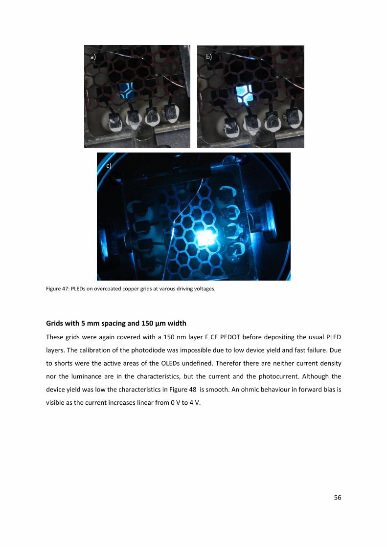
56
Figure 47: PLEDs on overcoated copper grids at varous driving voltages.
Grids with 5 mm spacing and 150 µm width
These grids were again covered with a 150 nm layer F CE PEDOT before depositing the usual PLED
layers. The calibration of the photodiode was impossible due to low device yield and fast failure. Due
to shorts were the active areas of the OLEDs undefined. Therefor there are neither current density
nor the luminance are in the characteristics, but the current and the photocurrent. Although the
device yield was low the characteristics in Figure 48 is smooth. An ohmic behaviour in forward bias is
visible as the current increases linear from 0 V to 4 V.
a) b)
c)

57
-4 -2 0 2 4 6 8 10 120.0000
0.0008
0.0016
0.0024
0.0032
0.0040
ph
oto
cu
rren
t (A
)
curr
ent (A
)
voltage (V)
current
0.00E+000
8.00E-010
1.60E-009
2.40E-009
photocurrent
Figure 48: Current photocurrent characteristics of PLED on over coated copper grids with 5 mm spacing and 150 µm line width.
Figure 49 shows on PLED of this device under operation. Inhomogeneity of the emissive area is visible
causing an undefined active area of the device. Additionally the device is split in electroluminescence
because of the grid line.
Figure 49: PLED on over coated copper grid with 5 mm grid spacing and 150 µm line width during operation.
Grids with 8 mm spacing and 150 µm line width
For this grid the PEDOT:PSS F CE layer was increased to 200 nm as previous experiments showed that
a thicker layer of PEDOT:PSS is necessary for a better overcoating and thus a higher device yield.
Further PLED layers were deposited equally to the previous.
Figure 50 displays the results of the PLEDs on overcoated copper grids with a spacing of 8 mm and a
line width of 150 µm. Due to the thicker PEDOT:PSS layer a fully characterisation with calibration of
the photodiode was possible. Current density reached its maximum at 3000 A/m2. Luminance peaked
at 2800 cd/m2. From this values a maximum efficiency of 1.0 cd/A and an efficiency at 1000 cd/m2 of
1.0 cd/A was calculated (see inset Figure 50). The thicker PEDOT:PSS layer may have increased device
yield and made a full characterisation possible. However the drawback is an increased serial
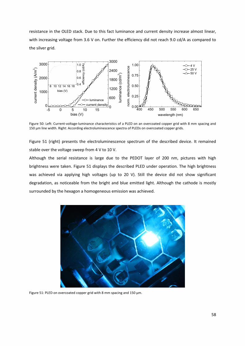
58
resistance in the OLED stack. Due to this fact luminance and current density increase almost linear,
with increasing voltage from 3.6 V on. Further the efficiency did not reach 9.0 cd/A as compared to
the silver grid.
-5 0 5 10 150
1000
2000
3000
lum
ina
nce
(cd
/m2)
cu
rre
nt d
en
sity (
A/m
2)
bias (V)
current density0
600
1200
1800
2400
3000
luminance
8 10 12 14 16 180.4
0.6
0.8
1.0
eff
icie
ncy (
cd
/A)
bias (V)
400 450 500 550 600 6500.00
0.25
0.50
0.75
1.00
4 V
25 V
50 V
norm
. ele
ctr
olu
min
escence
wavelength (nm)
Figure 50: Left: Current-voltage-luminance characteristics of a PLED on an overcoated copper grid with 8 mm spacing and 150 µm line width. Right: According electroluminescence spectra of PLEDs on overcoated copper grids.
Figure 51 (right) presents the electroluminescence spectrum of the described device. It remained
stable over the voltage sweep from 4 V to 10 V.
Although the serial resistance is large due to the PEDOT layer of 200 nm, pictures with high
brightness were taken. Figure 51 displays the described PLED under operation. The high brightness
was achieved via applying high voltages (up to 20 V). Still the device did not show significant
degradation, as noticeable from the bright and blue emitted light. Although the cathode is mostly
surrounded by the hexagon a homogeneous emission was achieved.
Figure 51: PLED on overcoated copper grid with 8 mm spacing and 150 µm.

59
7.1.3 Copper grids sintered at 250 °C in formic acid
These grids were sintered at 250 °C and showed a resistivity of 266 Ω measured from bus bar to bus
bar. The serial resistance would have been too high to process efficient OLEDs on them. Figure 52
shows microscope pictures of a grid with 1.5 mm line spacing and a line width of 90 µm. Figure 52 a
shows an overview in dark mode over the hexagons with the same magnification as in Figure 42 a
and Figure 43 a. The hexagons are circle like structures due to trickling of the ink while printing.
Cracks are at this magnification. In dark mode, a different surface structure visible compared to
Figure 42 a and Figure 43 a was found. Figure 52 b gives a closer look on the line. Compared with
Figure 43 b crystallite like structures are visible. Additionally to the crystallites large black areas occur
which seem to be destroyed and missing ink parts. Figure 52 gives a closer look on one of the
crystallites. With the highest magnification (100 x) cracks in the crystallite are already visible.
Figure 52: microscope pictures of copper grids sintered in formic acid a-c increasing magnification.
a) b)
c)

60
7.2 Inkjet printed embedded copper grids with solution
processed HIL and LEP
First experiments with the copper ink 005G showed that embedding and lift off was impossible with
this ink due to improved adhesion. For embedding experiments the intrinsiq 003G ink was used. With
this ink the embedding process was applicable the same way as for silver inks. For the here
presented devices the same materials and methods as in chapter 6 were used. The following parts
describe the performances of embedded copper grids with various dimensions as transparent
conductive electrodes for PLEDs.
Embedded copper grid with 1.5 mm spacing and 90 µm line width
Figure 53 presents the current density – luminance characteristics of the smallest grid with 1.5 mm
spacing and 90 µm line width. Although the grid was embedded the characteristics show ohmic
behaviour. From -5 V to 9 V the current density increases linear. A maximum current density of 900
A/m2 was reached. The maximum luminance was 120 cd/m2. The electroluminscence spectrum is
stable up to 14 V operating voltage.
-3 0 3 6 9 12 15
0
300
600
900
cu
rre
nt d
en
sity (
A/m
2)
bias (V)
current density
0
40
80
120
lu
min
an
ce
(cd
/m2) luminance
400 450 500 550 600 6500.00
0.25
0.50
0.75
1.00
4 V
11 V
norm
. ele
ctr
olu
min
escence
wavelength (nm)
Figure 53: Left: Current density and luminance of PLEDs on embedded copper grids with 1.5 mm spacing and 90 µm line width. Right: According electroluminescence specrtrum.
Figure 54 shows the described PLED under operation. Bright and blue light emission was achieved,
although the shorts. Although an operating voltage of 17 V and a line width of 90 µm the grid lines
are still visible.

61
Figure 54: PLED on embedded inkjet printed copper grid with 1.5 mm line spacing and 90 µm line width.
Embedded copper grid with 2 mm line spacing and 90 µm line width
No I-V-luminance data were measured as the device failed too fast. Figure 55 displays the
electroluminescence spectrum. The spectrum confirms the fast degradation. At 9 V the first spectrum
was measured and it shows already a peak shift to the red from 451 nm to 488 nm.
400 450 500 550 600 6500.00
0.25
0.50
0.75
1.00
10 V
12 V
norm
. ele
ctr
olu
min
escence
wavelength (nm)
Figure 55: Electroluminescence spectrum of PLED on an embedded copper grid with 2 mm line spacing and 90 µm lien width.
At lower operating voltage, it was impossible to measure any spectra, because the luminance was to
low. Figure 56 shows a picture of the PLED under operation. The emissive area is inhomogeneous.
Due to the low operating voltage the grid lines are clearly visible.

62
Figure 56: Operating PLED on an embedded copper grid with 2 mm line spacing and 90 µm line width.
Embedded copper grid with spacing 3 mm and line width 150 µm
The grid with 3 mm line spacing and 150 µm line width is the biggest embedded copper grid
structure presented. Figure 57 shows the current density and the luminance characteristics of the
grid. Additionally to the linear increase in current density from -3 V to 6 V the line shows a noisy
behaviour. The maximum current density was determined to be 320 A/m2. Maximum luminance
value was measured at 220 cd/m2. A short loss in luminance is visible at 9 V. Overall the device did
not feature a stable operation. Caused by this low luminance, electroluminescence spectra were only
measured at 7 V and 12 V. Figure 57 to right shows this spectra. Again the peaks are already red
shifted from 451 nm to 488 nm due to the keto defect.
-3 0 3 6 9 12
0
80
160
240
320
cu
rre
nt d
en
sity (
A/m
2)
bias (V)
current density
0
80
160
240
lum
ina
nce
(cd
/m2)
luminance
400 450 500 550 600 6500.00
0.25
0.50
0.75
1.00
7 V
12 V
norm
. ele
ctr
olu
min
escence
wavelength (nm)
Figure 57: Left: Voltage-current-luminance luminance characteristics of a PLED on an embedded copper grid with 3 mm line spacing and 150 µm line width. Right: According electroluminescence spectra.
Figure 58 displays the described PLED on the embedded copper grid under operation. A bright blue
emission was achieved by applying 17 V. The dark spot next to the PLED under operation is an air
bubble. The air bubble derives from the embedding process. From the air bubble cracks through the
PLED layers occurred.

63
Figure 58: PLED on embedded copper grid with 3 mm spacing and 150 µm line width.
7.3 Discussion on copper grids
The first part of the here presented copper grids were overcoated and used the 005G copper ink
sintered in formic acid. The second part presented embedded copper grids which were printed with
intrinsiq 003G ink and laser sintered. Due to these differences it is impossible to link different
performances to embedding or overcoating. In contrast to the silver grids the overcoated copper
grids seemed to perform better. The over coated grids reached efficiencies up to 1.0 cd/A (8 mm
spacing, 150 µm line width). Overall the inkjet printed copper grids perform worse than the inkjet
printed silver grids. Table 2 sums up the main facts of the copper grids.
Table 2: Comparison of over-coated and embedded copper grids
Grid dimensions s [mm] x w
[µm]
Max. Efficency
[cd/A]
Efficency
[cd/A]a)
Max. luminance
[cd/A]
Coverage [%]
8 x 150 overcoated 1.0 1.0 2800 11.7
3 x 150 embedded - - 240 24.5
a) Measured at 1000 cd/m2
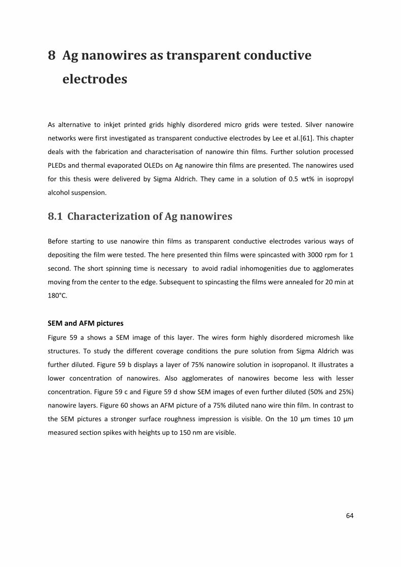
64
8 Ag nanowires as transparent conductive
electrodes
As alternative to inkjet printed grids highly disordered micro grids were tested. Silver nanowire
networks were first investigated as transparent conductive electrodes by Lee et al.[61]. This chapter
deals with the fabrication and characterisation of nanowire thin films. Further solution processed
PLEDs and thermal evaporated OLEDs on Ag nanowire thin films are presented. The nanowires used
for this thesis were delivered by Sigma Aldrich. They came in a solution of 0.5 wt% in isopropyl
alcohol suspension.
8.1 Characterization of Ag nanowires
Before starting to use nanowire thin films as transparent conductive electrodes various ways of
depositing the film were tested. The here presented thin films were spincasted with 3000 rpm for 1
second. The short spinning time is necessary to avoid radial inhomogenities due to agglomerates
moving from the center to the edge. Subsequent to spincasting the films were annealed for 20 min at
180°C.
SEM and AFM pictures
Figure 59 a shows a SEM image of this layer. The wires form highly disordered micromesh like
structures. To study the different coverage conditions the pure solution from Sigma Aldrich was
further diluted. Figure 59 b displays a layer of 75% nanowire solution in isopropanol. It illustrates a
lower concentration of nanowires. Also agglomerates of nanowires become less with lesser
concentration. Figure 59 c and Figure 59 d show SEM images of even further diluted (50% and 25%)
nanowire layers. Figure 60 shows an AFM picture of a 75% diluted nano wire thin film. In contrast to
the SEM pictures a stronger surface roughness impression is visible. On the 10 µm times 10 µm
measured section spikes with heights up to 150 nm are visible.
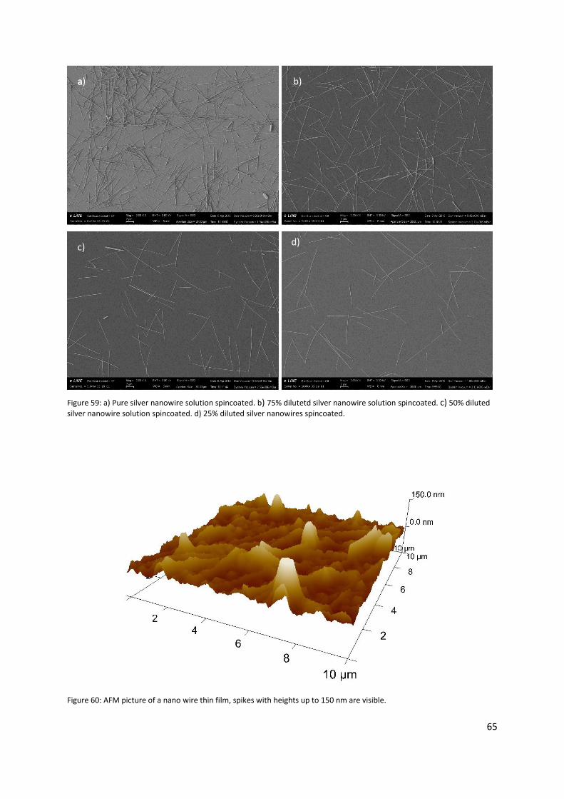
65
Figure 59: a) Pure silver nanowire solution spincoated. b) 75% dilutetd silver nanowire solution spincoated. c) 50% diluted
silver nanowire solution spincoated. d) 25% diluted silver nanowires spincoated.
Figure 60: AFM picture of a nano wire thin film, spikes with heights up to 150 nm are visible.
a
a
n
d
e
l
e
c
t
r
o
l
u
m
i
e
s
c
e
n
c
e
s
p
e
c
t
r
u
m
a
a)
electr
olumi
escen
ce
spectr
um
a
b)
electrolumiescenc
e spectrum
a
c)
anele
ctrolu
miesc
ence
spectr
um
a
d)
a

66
Transmission measurements of various silver nanowire films
According to the SEM Images transmission measurements of the nanowire films were performed.
Therefor the same PerkinElmar 900 UV/VIS as for the silver grid specification was used. All samples
from the SEM measurements were measured. The transmission spectra in Figure 61 confirm the SEM
measurements. The film made of the pure solution from Sigma Aldrich (circle with cross) exhibits the
lowest transmission in total (68% - 70% depending of the wavelength). With a concentration of 75%
nanowires an average transmission of 85% was measured (squares with cross). The transmission of
the films with 50% (open circles) and 25% (open squares) lay close together at 93% to 95% depending
on the wave length. The higher the nanowire concentration the lower the transmission.
400 500 600 700 80040
50
60
70
80
90
100
tra
nsm
issio
n T
(%
)
wavelength (nm)
transmission 100% NW
transmission 75% NW
transmission 50% NW
transmission 25% NW
Figure 61: Transmission of thin film layers of various diluted nanowire solutions.
8.2 Device performance
Based on the investigations of the nanowire thin films in 8.1 a concentration of 60% nanowires was
choosen. On the basis of this concentration the transparent conductive electrodes were fabricated as
described in the following part. Solution processed PLEDs and thermally evaporated OLEDs were
processed on this films equally to chapter 6.
Device fabrication
The pure nanowires exhibited rough surface structure as shown in the SEM and AFM pictures. To
overcome this issue and get a smoother electrode surface the wires were mixed with PEDOT:PSS. The
idea is that the PEDOT:PSS forms a layer in which the nanowires are embedded. Further Nanowires
show a large contact resistance were they lay on each other. [61] Work by Kim et al. showed that a

67
combination of nanowires and PEDOT:PSS in solution enhances the conductivity.[60] The nanowires
were first mixed with various concentrations in PEDOT. The original silver nanowire solution from
Sigma Aldrich was diluted with PEDOT to obtain 60% nanowire solution in PEDOT:PSS. This solutions
were then spincoated and heated for 20 minutes at 180 °C. Baking of the films was necessary to
minimize the contact resist of the nanowires. [61] On this transparent anode 2 additional layer of
PEDOT were added.
Device Characteristics of evaporated Alq3 and NPB devices on nanowire thin film
electrodes
These first devices were made with thermal evaporated Alq3 and NPB. Figure 62 reveals the
problems of nanowires as transparent conductive electrodes. The current density in backward bias
reaches almost 1000 A/m2. This is an indicator for shorts. Further the current density in forward bias
increases almost linear. The maximum luminance of this device is 500 cd/m2, at a bias of 20 V. This is
too high for a reasonable operation of an OLED. The luminance from 0 V to 15 V can be referred as
noise, from this follows the low maximum efficiency of 0.25 cd/A (inset in Figure 62).
-5 0 5 10 15 20-1000
0
1000
2000
curr. den. lum
ina
nce
(cd
/m2)
cu
rre
nt d
en
sity (
A/m
2)
bias (V)
100
200
300
400
500
lum.
15 16 17 18 19 200.0
0.1
0.2
0.3
eff
icie
ncy (
cd
/A)
bias (V)
Figure 62: Voltage-current-luminance characteristics of evaporated OLED on AgNW/PEDOT solution
Although measuring the emission spectra was impossible Figure 63 shows a working device. In this
figure no shadowing is obtained at all, which is comparable to ITO. The green emission is typical for
Alq3. Figure 63 (right) shows the same panel a few minutes later. One can see a colour change.

68
Figure 63: Operating Alq3 OLED on AgNW (left) and degraded Alq3 on AgNW (right).
Device Characteristics of Solution processed OLEDs
The solution processed OLEDs on PEDOT/NW mixtures were processed with the same CPs as the
solution processed on the grids. The solution processed OLEDs on the silver nanowires did not work
at all. Most devices showed shorts and therefore ohmic behaviour in the characteristics. Further they
emitted only light at the edges of the Cathodes before they got short circuited because of defects.
8.3 Discussion on silver nanowires
In contrast to previous observations on the inkjet printed grids, solution processed OLEDs on
nanowires performed far worse than the evaporated. The reason for this behaviour is unclear so far.
Nano wire networks comprise sufficient conductivity for the use in OLEDs. The major benefit of nano
wires is the homogeneity of the electrode, as shown by Figure 63. No field dependent luminescence
inhomogenities are visible compared to the grids. Further is a significant shadowing excluded.
Shortcuts due to the rough surface are still the major problem for achieving higher efficiencies. To
apply nano wires as TCEs this issue needs to be solved.

69
9 Conclusion
The scope of this thesis was the investigation of transparent conductive electrodes in order to find a
viable replacement for ITO. In this context, different materials and layouts have been evaluated. They
can basically be subdivided into
Electrodes based on inkjet printed silver
Electrodes based on inkjet printed copper
Electrodes based on a silver nanowires random microgrid.
Chapter 4 explains all applied methods and experimental details including the process of inkjet
printing. A printed honeycomb layout was chosen in order to minimize coverage and the resulting
unfavourable shadowing during light out coupling. The printed grids were varied with respect to their
size/diameter in order to find the optimum trade-off between shadowing and conductivity.
Chapter 5 presents a conventional OLED using an ITO electrode which is further used as a reference
device for comparison.
Chapter 6 deals with inkjet printed silver electrodes. It was demonstrated that grids with a relatively
high coverage (~ 25%) already show a comparable transmission to ITO. All grids with a larger
diameter are naturally better in transmission compared to ITO. The first set of OLEDs was fabricated
by simply overcoating the electodes with the functional layers required for an OLED. High conductive
and high viscosity PEDOT:PSS (Clevious F CE) was used to guarantee a low voltage drop in the areas
in-between the grid lines as well as a suitable overcoating of the rough and high grid lines. This
resulted in efficiencies and luminance values of 3.4 cd/A and 19000 cd/m2, respectively, which is
already comparable to the ITO device. To overcome the issue that there are significant defects
present in these devices, the electrodes were embedded/planarized (for details of the embedding
process see chapter 4.2) in a second step. Embedding indeed reduced the contribution of shunt
current by several orders of magnitude while the efficiency of the best performing device was
increased to 9.4 cd/A. This corresponds to an increase of 250 % as compared to the ITO reference
device. The electroluminescence spectra of the PLEDs employing grid electrodes remained stable
during the measured voltage sweeps and no significant shift was visible.
Additionally to the solution processed PLEDs thermal evaporated OLEDs are presented in chapter 6.4.
Due to the here unfavourable film formation properties of small molecules, these OLEDs displayed

70
ohmic behaviour in the IV-characteristics. From this it can be concluded that for rough and high grid
electrodes a solution processing is superior.
Chapter 7 presents copper ink based grids. Motivated from the successful implementation of silver
grids, the same structures were tested with copper ink. Here, two different inks with different
properties and sintering procedures were applied. First, formic acid sintering was used giving
conductive structures for defined processing conditions. An embedding process was however not
possible due to high adhesion of the printed and sintered ink on the sacrificial substrate. Therefore a
second ink with lower adhesion was sintered using a IR laser and further on used for the embedding
process. Both procedures gave working devices, their performance however did not reach the values
of the ITO based reference device. The maximum efficiencies were 1.0 cd/A (overcoated) and the
luminance was 2800 cd/m2.
In chapter 8 silver nanowires as highly disordered micro grids in thin films were tested. The
nanowires were mixed with PEDOT and thin films were fabricated on glass substrates. On this thin
films thermal evaporated OLEDs were processed. The devices showed ohmic behaviour due to the
random orientation of the nanowires and delivered efficiencies of 0.3 cd/A.
Table 2 summarizes the figures-of-merit of the most important devices structures.
Table 3: Summarizing the most important grid structures and their performance
Grid structure s [mm] x w
[µm]
Max. Efficency
[cd/A]
Efficency
[cd/A]a)
Max. luminance
[cd/A]
Coverage
[%]
ITO 3.7 2.8 60000 0
3 x 150 overcoated 3.4 3.1 19000 24.5
3 x 150 embedded 7.0 5.2 45000 24.5
8 x 150 embedded 9.4 7.0 26000 11.7
Copper grid 8 x 150
overcoated 1.0 1.0 2800 11.7
a) Measured at 1000 cd/m2

71
So far, inkjet printed silver grids exceed ITO as transparent conductive electrodes in efficiency. With
the applied embedding and flip over process a further increase in efficiency compared to over coated
grids was achieved. The cut-off current was lowered 3 orders of magnitude compared to over coated
grids. The stability of the emission spectra was independent of the grids. Printed copper grids also
gave working devices, their performance, however, did not reach the values of ITO based devices.
The content of this work shows that inkjet printed anode setups are a serious low-cost competitor to
established technologies.
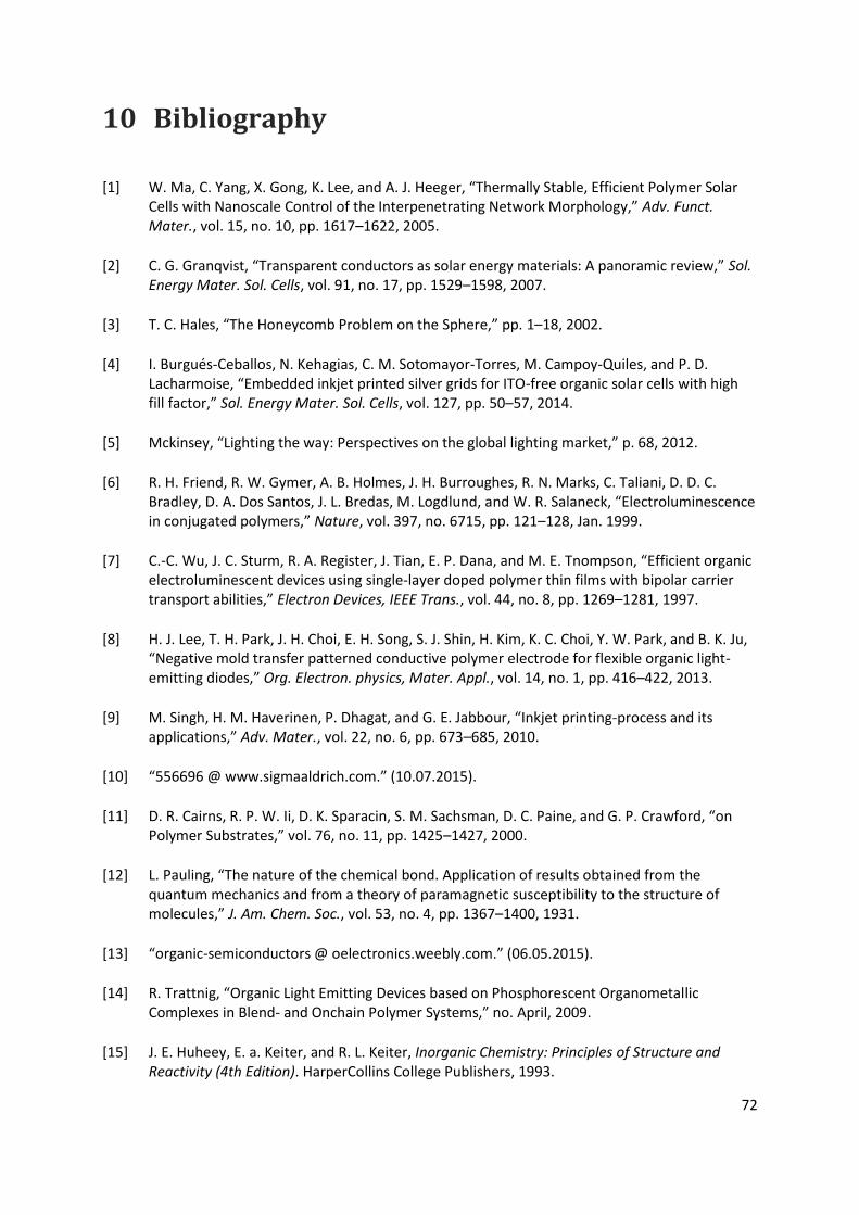
72
10 Bibliography
[1] W. Ma, C. Yang, X. Gong, K. Lee, and A. J. Heeger, “Thermally Stable, Efficient Polymer Solar Cells with Nanoscale Control of the Interpenetrating Network Morphology,” Adv. Funct. Mater., vol. 15, no. 10, pp. 1617–1622, 2005.
[2] C. G. Granqvist, “Transparent conductors as solar energy materials: A panoramic review,” Sol. Energy Mater. Sol. Cells, vol. 91, no. 17, pp. 1529–1598, 2007.
[3] T. C. Hales, “The Honeycomb Problem on the Sphere,” pp. 1–18, 2002.
[4] I. Burgués-Ceballos, N. Kehagias, C. M. Sotomayor-Torres, M. Campoy-Quiles, and P. D. Lacharmoise, “Embedded inkjet printed silver grids for ITO-free organic solar cells with high fill factor,” Sol. Energy Mater. Sol. Cells, vol. 127, pp. 50–57, 2014.
[5] Mckinsey, “Lighting the way: Perspectives on the global lighting market,” p. 68, 2012.
[6] R. H. Friend, R. W. Gymer, A. B. Holmes, J. H. Burroughes, R. N. Marks, C. Taliani, D. D. C. Bradley, D. A. Dos Santos, J. L. Bredas, M. Logdlund, and W. R. Salaneck, “Electroluminescence in conjugated polymers,” Nature, vol. 397, no. 6715, pp. 121–128, Jan. 1999.
[7] C.-C. Wu, J. C. Sturm, R. A. Register, J. Tian, E. P. Dana, and M. E. Tnompson, “Efficient organic electroluminescent devices using single-layer doped polymer thin films with bipolar carrier transport abilities,” Electron Devices, IEEE Trans., vol. 44, no. 8, pp. 1269–1281, 1997.
[8] H. J. Lee, T. H. Park, J. H. Choi, E. H. Song, S. J. Shin, H. Kim, K. C. Choi, Y. W. Park, and B. K. Ju, “Negative mold transfer patterned conductive polymer electrode for flexible organic light-emitting diodes,” Org. Electron. physics, Mater. Appl., vol. 14, no. 1, pp. 416–422, 2013.
[9] M. Singh, H. M. Haverinen, P. Dhagat, and G. E. Jabbour, “Inkjet printing-process and its applications,” Adv. Mater., vol. 22, no. 6, pp. 673–685, 2010.
[10] “556696 @ www.sigmaaldrich.com.” (10.07.2015).
[11] D. R. Cairns, R. P. W. Ii, D. K. Sparacin, S. M. Sachsman, D. C. Paine, and G. P. Crawford, “on Polymer Substrates,” vol. 76, no. 11, pp. 1425–1427, 2000.
[12] L. Pauling, “The nature of the chemical bond. Application of results obtained from the quantum mechanics and from a theory of paramagnetic susceptibility to the structure of molecules,” J. Am. Chem. Soc., vol. 53, no. 4, pp. 1367–1400, 1931.
[13] “organic-semiconductors @ oelectronics.weebly.com.” (06.05.2015).
[14] R. Trattnig, “Organic Light Emitting Devices based on Phosphorescent Organometallic Complexes in Blend- and Onchain Polymer Systems,” no. April, 2009.
[15] J. E. Huheey, E. a. Keiter, and R. L. Keiter, Inorganic Chemistry: Principles of Structure and Reactivity (4th Edition). HarperCollins College Publishers, 1993.

73
[16] C. A. Coulson, Valence. Clarendon Press, 1953.
[17] G. L. Miessler, P. J. Fischer, and D. A. Tarr, Inorganic Chemistry: Pearson New International Edition. Pearson Higher Ed, 2013.
[18] A. D. McNaught and A. D. McNaught, Compendium of chemical terminology, vol. 1669. Blackwell Science Oxford, 1997.
[19] D. I. H. Scheiber, “Structure to Property Relationships in Blue Light Emitting Conjugated Polymers,” no. June, 2008.
[20] R. Marcus, “On the Theory of Oxidation and Reduction Reactions Involving Electron Transfer,” J. Chem. Phys., vol. 42, no. 1952, pp. 966–978, 1956.
[21] H. Shirakawa, E. J. Louis, A. G. MacDiarmid, C. K. Chiang, and A. J. Heeger, “Synthesis of electrically conducting organic polymers: halogen derivatives of polyacetylene, (CH),” J. Chem. Soc. Chem. Commun., no. 16, pp. 578–580, 1977.
[22] L. D. Landau and S. I. Pekar, “Effective Mass of a Polaron,” Sci. York, vol. 423, no. 5, pp. 71–74, 1948.
[23] S. Roth and D. Carroll, One-Dimensional Metals: Conjugated Polymers, Organic Crystals, Carbon Nanotubes. Wiley, 2006.
[24] H. Ibach and H. Lüth, Solid-state physics: An introduction to principles of materials science, vol. 144, no. 3624. 2010.
[25] H. Yersin and K. L. Bray, Transition Metal and Rare Earth Compounds III: Excited States, Transitions, Interactions. Springer, 2004.
[26] M. Born and R. Oppenheimer, “Zur quantentheorie der molekeln,” Ann. Phys., vol. 20, no. 84, pp. 457–484, 1927.
[27] M. H. M. Pienn and Michael H. M. Pienn, “Application of Blue-Emitting Ladder- Type Poly(para-phenylene)s for Solid State Lighting: Efficiency Improvement and Colour Tuning,” no. November 2008, 2008.
[28] H. Haken and H. C. Wolf, “Molekülphysik und Quantenchemie: Einführung in die experimentellen und theoretischen Grundlagen,” Springer-Verlag, Berlin Heidelb., pp. 153–296, 2006.
[29] E. U. Condon, “Nuclear motions associated with electron transitions in diatomic molecules,” Phys. Rev., vol. 32, no. 6, pp. 858–872, 1928.
[30] E. Condon, “A theory of intensity distribution in band systems,” Phys. Rev., vol. 28, no. 6, pp. 1182–1201, 1926.
[31] J. Franck, “Elementary processes,” no. 1923, pp. 536–542, 1924.

74
[32] M. Pope and C. E. Swenberg, Electronic Processes in Organic Crystals and Polymers. Oxford University Press, 1999.
[33] a. Jabłoński, “Efficiency of Anti-Stokes Fluorescence in Dyes,” Nature, vol. 131, no. 3319, pp. 839–840, 1933.
[34] W. Schnabel, Polymers and Light: Fundamentals and Technical Applications. 2007.
[35] S. Braun, W. R. Salaneck, and M. Fahlman, “Energy-level alignment at organic/metal and organic/organic interfaces,” Adv. Mater., vol. 21, no. 14–15, pp. 1450–1472, 2009.
[36] N. Koch, “Organic electronic devices and their functional interfaces,” ChemPhysChem, vol. 8, no. 10, pp. 1438–1455, 2007.
[37] H. Ishii, K. Sugiyama, E. Ito, and K. Seki, “Energy level alignment and interfacial electronic structures at organic/metal and organic/organic interfaces,” Adv. Mater., vol. 11, no. 8, pp. 605 – 625, 1999.
[38] S. Nau, N. Schulte, S. Winkler, J. Frisch, A. Vollmer, N. Koch, S. Sax, and E. J. W. List, “Highly efficient color-stable deep-blue multilayer PLEDs: Preventing PEDOT:PSS-induced interface degradation,” Adv. Mater., vol. 25, no. 32, pp. 4420–4424, 2013.
[39] T. R. Society, R. Society, C. Papers, and P. Character, “Electron Emission in Intense Electric Fields Author ( s ): R . H . Fowler and L . Nordheim Source : Proceedings of the Royal Society of London . Series A , Containing Papers of a Published by : The Royal Society Stable URL : http://www.jstor.org/stable/95,” vol. 119, no. 781, pp. 173–181, 2010.
[40] J. C. Scott and G. G. Malliaras, “Charge injection and recombination at the metal–organic interface,” Chem. Phys. Lett., vol. 299, no. 2, pp. 115–119, 1999.
[41] C. W. Tang and S. a. Vanslyke, “Organic electroluminescent diodes,” Appl. Phys. Lett., vol. 51, no. 1987, pp. 913–915, 1987.
[42] “Aluminium-tris(8-hydroxychinolin) @ de.wikipedia.org.” (08.05.2015).
[43] “Poly-3,4-ethylendioxythiophen @ de.wikipedia.org.” (14.07.2015).
[44] M. Thesis, “Efficiency and Stability of Poly ( indenofluorene ) -based Homo- and Copolymers,” no. April, 2011.
[45] “Indiumzinnoxid @ de.wikipedia.org.” (23.09.2015).
[46] G. Hautier, A. Miglio, G. Ceder, G.-M. Rignanese, and X. Gonze, “Identification and design principles of low hole effective mass p-type transparent conducting oxides.,” Nat. Commun., vol. 4, p. 2292, 2013.
[47] G. Horowitz, P. Delannoy, and H. Bouchriha, “Two‐layer light‐emitting diodes based on sexithiophene and derivatives,” Advanced, pp. 752–755, 1994.
[48] “indium @ www.technologiemetalle.org.” (01.10.2015).

75
[49] S. Harkema, S. Mennema, M. Barink, H. Rooms, J. S. Wilson, T. van Mol, and D. Bollen, “Large area ITO-free flexible white OLEDs with Orgacon PEDOT:PSS and printed metal shunting lines,” Proc. SPIE, vol. 7415, no. 0, p. 74150T–74150T–8, 2009.
[50] J. Park, J. Lee, D. Shin, and S. Park, “Luminance uniformity of large-area OLEDs with an auxiliary metal electrode,” IEEE/OSA J. Disp. Technol., vol. 5, no. 8, pp. 306–311, 2009.
[51] M.-G. Kang and L. J. Guo, “Nanoimprinted Semitransparent Metal Electrodes and Their Application in Organic Light-Emitting Diodes,” Adv. Mater., vol. 19, no. 10, pp. 1391–1396, 2007.
[52] F. L. M. Sam, M. A. Razali, K. D. G. I. Jayawardena, C. A. Mills, L. J. Rozanski, M. J. Beliatis, and S. R. P. Silva, “Silver grid transparent conducting electrodes for organic light emitting diodes,” Org. Electron., vol. 15, no. 12, pp. 3492–3500, Dec. 2014.
[53] D. Zhang, K. Ryu, X. Liu, E. Polikarpov, J. Ly, M. E. Tompson, and C. Zhou, “Transparent, Conductive, and Flexible Carbon Nanotube Films and Their Application in Organic Light-Emitting Diodes,” Nano Lett., vol. 6, no. 9, pp. 1880–1886, Sep. 2006.
[54] J. Li, L. Hu, L. Wang, Y. Zhou, G. Grüner, and T. J. Marks, “Organic Light-Emitting Diodes Having Carbon Nanotube Anodes,” Nano Lett., vol. 6, no. 11, pp. 2472–2477, Nov. 2006.
[55] M. W. Rowell, M. a. Topinka, M. D. McGehee, H.-J. Prall, G. Dennler, N. S. Sariciftci, L. Hu, and G. Gruner, “Organic solar cells with carbon nanotube network electrodes,” Appl. Phys. Lett., vol. 88, no. 23, p. 233506, 2006.
[56] L. Hu, D. S. Hecht, and G. Grüner, “Percolation in Transparent and Conducting Carbon Nanotube Networks,” Nano Lett., vol. 4, no. 12, pp. 2513–2517, Dec. 2004.
[57] A. Kumar and C. Zhou, “The race to replace tin-doped indium oxide: Which material will win?,” ACS Nano, vol. 4, no. 1, pp. 11–14, 2010.
[58] S. De, T. M. Higgins, P. E. Lyons, E. M. Doherty, P. N. Nirmalraj, W. J. Blau, J. J. Boland, and J. N. Coleman, “Silver Nanowire Networks as Flexible ,” ACSNano, vol. 3, no. 7, pp. 1767–1774, 2009.
[59] J. Park and H. Ham, “Sputter-patterned ITO-based organic light-emitting diodes with leakage current cut-off layers,” Org. Electron. physics, Mater. Appl., vol. 12, no. 11, pp. 1872–1878, 2011.
[60] Y. S. Kim, M. H. Chang, E. J. Lee, D. W. Ihm, and J. Y. Kim, “Improved electrical conductivity of PEDOT-based electrode films hybridized with silver nanowires,” Synth. Met., vol. 195, pp. 69–74, 2014.
[61] J. Y. Lee, S. T. Connor, Y. Cui, and P. Peumans, “Solution-processed metal nanowire mesh transparent electrodes,” Nano Lett., vol. 8, pp. 689–692, 2008.
[62] W. Gaynor, G. F. Burkhard, M. D. McGehee, and P. Peumans, “Smooth nanowire/polymer composite transparent electrodes,” Adv. Mater., vol. 23, pp. 2905–2910, 2011.

76
[63] a K. Geim and K. S. Novoselov, “The rise of graphene,” Nat. Mater., vol. 6, no. 3, pp. 183–191, 2007.
[64] T. Fang, A. Konar, H. Xing, and D. Jena, “Carrier statistics and quantum capacitance of graphene sheets and ribbons,” Appl. Phys. Lett., vol. 91, no. 2007, p. 092109, 2007.
[65] J. Wu, M. Agrawal, H. A. Becerril, Z. Bao, Z. Liu, Y. Chen, and P. Peumans, “Organic Light-Emitting Diodes on Solution-Processed Graphene Transparent Electrodes,” ACS Nano, vol. 4, no. 1, pp. 43–48, Jan. 2010.
[66] “Inkjet_printing @ en.wikipedia.org.” (25.08.2015).
[67] S. Magdassi, “Ink requirements and formulations guidelines,” in The chemistry of inkjet inks, Singapore: World Scientific Publishing, 2010, pp. 19–41.
[68] H. J. Gysling, “Nanoinks in inkjet metallization - Evolution of simple additive-type metal patterning,” Curr. Opin. Colloid Interface Sci., vol. 19, no. 2, pp. 155–162, 2014.
[69] “http://www.microdrop.de.” (13.07.2015).
[70] T. Effect, K. D. Sites, E. Properties, and P. Materials, “The Effect of Keto Defect Sites on the Emission Properties of Polyfluorene-Type Materials**,” no. 5, pp. 374–378, 2002.
[71] H. C. L. O. Miesbauer, M. Schmidt, Vakuum in Forschung und Praxis. 2008.
[72] S. Kappaun, H. Scheiber, R. Trattnig, E. Zojer, E. J. W. List, and C. Slugovc, “Defect chemistry of polyfluorenes: identification of the origin of .”
[73] M. Schaer, F. Nüesch, D. Berner, W. Leo, and L. Zuppiroli, “Water vapor and oxygen degradation mechanisms in organic light emitting diodes,” Adv. Funct. Mater., vol. 11, no. 2, pp. 116–121, 2001.
[74] G. Greczynski, T. Kugler, M. Keil, W. Osikowicz, M. Fahlman, and W. R. Salaneck, “Photoelectron spectroscopy of thin films of PEDOT-PSS conjugated polymer blend: A mini-review and some new results,” J. Electron Spectros. Relat. Phenomena, vol. 121, no. 1–3, pp. 1–17, 2001.
[75] A. Van Dijken, A. Perro, E. A. Meulenkamp, and K. Brunner, “The influence of a PEDOT:PSS layer on the efficiency of a polymer light-emitting diode,” Org. Electron. physics, Mater. Appl., vol. 4, no. 2–3, pp. 131–141, 2003.
[76] P. J. Brewer, J. Huang, P. A. Lane, A. J. deMello, D. D. C. Bradley, and J. C. deMello, “Influence of poly(3,4-ethylenedioxythiophene)-poly(styrenesulfonate) in polymer LEDs,” Phys. Rev. B, vol. 74, no. 11, p. 115202, Sep. 2006.
[77] P. J. Brewer, P. A. Lane, J. Huang, A. J. deMello, D. D. C. Bradley, and J. C. deMello, “Role of electron injection in polyfluorene-based light emitting diodes containing PEDOT:PSS,” Phys. Rev. B, vol. 71, no. 20, p. 205209, 2005.

77
[78] C. Y. Chang, F. Y. Tsai, S. J. Jhuo, and M. J. Chen, “Enhanced OLED performance upon photolithographic patterning by using an atomic-layer-deposited buffer layer,” Org. Electron. physics, Mater. Appl., vol. 9, no. 5, pp. 667–672, 2008.
[79] J. Gruner, P. J. Hamer, R. H. Friend, H. Huber, U. Schera, and A. B. Holmes, “A High Efficiency Blue-Light-Emitting Diode Based on Novel Ladder Poly(p-phenylene)s,” Adv. Mater., vol. 6, no. 10, pp. 748–752, 1994.
[80] G. Malliaras, J. Salem, P. Brock, and C. Scott, “Electrical characteristics and efficiency of single-layer organic light-emitting diodes,” Phys. Rev. B, vol. 58, no. 20, pp. R13411–R13414, 1998.
[81] F. Lu, X. Liu, and Y. Xing, “Numerical study of the influence of applied voltage on the current balance factor of single layer organic light-emitting diodes,” J. Appl. Phys., vol. 115, no. 16, p. 164508, 2014.
[82] a. Doraiswamy, C. Jin, R. J. Narayan, P. Mageswaran, P. Mente, R. Modi, R. Auyeung, D. B. Chrisey, a. Ovsianikov, and B. Chichkov, “Two photon induced polymerization of organic-inorganic hybrid biomaterials for microstructured medical devices,” Acta Biomater., vol. 2, no. 3, pp. 267–275, 2006.
[83] K.-B. Kim, Y.-H. Tak, Y.-S. Han, K.-H. Baik, M.-H. Yoon, and M.-H. Lee, “ Relationship between Surface Roughness of Indium Tin Oxide and Leakage Current of Organic Light-Emitting Diode ,” Jpn. J. Appl. Phys., vol. 42, no. Part 2, No. 4B, pp. L438–L440, 2003.
[84] R. D. Deegan, O. Bakajin, T. F. Dupont, G. Huber, S. R. Nagel, and T. A. Witten, “Capillary flow as the cause of ring stains from dried liquid drops,” Nature, vol. 389, no. 6653, pp. 827–829, 1997.

78
11 List of figures
FIGURE 1: ETHENE MOLECULE WITH ITS BONDS TAKEN FROM [13]. LEFT: 2 CARBON AND 4 HYDROGEN ATOMS
FORM A MOLECULE BY HYBRIDIZATION. THE YELLOW DUMBBELL SHAPED ORBITALS REPRESENT SP2-
HYBRIDIZED ORBITALS. RIGHT: THE FORMATION OF ALL BONDS BY OVERLAP ARE SHOWN. TWO SP2
ORBITALS FORM A BOND, OVERLAP OF TWO P ORBITALS FORM A BOND. ............................................ 3
FIGURE 2: SCHEMATIC REPRESENTATION OF SP3 HYBRIDIZATION. RIGHT: 2S AND 2P ORBITALS HYBRIDIZE TO
FORM 4 ENERGETICALLY IDENTICALLY ORBITALS WHICH ARE LOWER IN ENERGY THEN THE GROUND
STATE. LEFT: ETHANE MOLECULE WITH ACCORDING BONDS TAKEN FROM [14]. ......................................... 4
FIGURE 3: RIGHT: SCHEMATIC REPRESENTATION OF SP2 HYBRIDIZATION, 3 ENERGETICALLY IDENTICAL AND
ONE ENERGETICALLY HIGHER LYING ORBITAL ARE FORMED. LEFT: ETHENE MOLECULE WITH ACCORDING
BONDS, TAKEN FROM [14]. ............................................................................................................................ 5
FIGURE 4: SCHEMATIC REPRESENTATION OF SP HYBRIDIZATION. RIGHT: ONE S AND ONE P ORBITAL HYBRIDIZE
TO TWO SP ORBITALS, WHICH ARE LOWER IN ENERGY THEN OTHER HYBRID ORBITALS OF CARBON
MOLECULES. THE TWO REMAINING 2P ORBITALS ARE ENERGITCALLY HIGHER. RIGHT: ETHYNE MOLECULE
WITH ACCORDING BONDS TAKEN FROM [14]. ............................................................................................... 5
FIGURE 5: SCHEMATIC REPRESENTATION OF ENERGY LEVELS (BANDS) IN AN ORGANIC SEMICONDUCTOR (LEFT)
AND AN INORGANIC SEMICONDUCTOR (RIGHT); ON THE LEFT IS THE ENERGY SCALE; EF DENOTES THE
FERMI ENERGY. .............................................................................................................................................. 6
FIGURE 6: ENERGETIC RELATIONS OF VARIOUS POLARONS ARE SHOWN. THE TERM POSITIVE POLARON
DESCRIBES A MISSING ELECTRON IN THE HOMO (HOLE), NEGATIVE POLARON DESCRIBES AN ADDITIONAL
ELECTRON IN THE LUMO, THE TERM BIPOLARON REFERS TO 2 POLARONS. ................................................. 8
FIGURE 7: TWO ELECTRONIC STATES WITH VARIOUS VIBRONIC STATES, S0 LABELS THE SINGLET GROUND STATE
WHILE S1 IS THE SINGLET EXCITED STATE. THE STRAIGHT LINES STAND FOR STIMULATION AND DECAY
UNDER RADIATION WHILE THE WIGGLED LINES MARK RADIATIONLESS DECAY. TAKEN FROM [27]. ........... 9
FIGURE 8: JABLONSKI DIAGRAM OF AN ARBITRARY ORGANIC SEMICONDUCTOR WHERE S0 AND S1 DENOTE THE
SINGLET GROUND AND EXCITED STATE. T1 REPRESENTS THE TRIPLET STATE. THE DASHED LINES STAND
FOR VIBRONIC STATES. KNR DENOTES THE NON-RADIATIVE RECOMBINATION RATE OF AN EXCITON. KFL IS
THE RATE FOR FLUORESCENT RECOMBINED EXCITONS. KISC DESCRIBES THE RATE OF INTER SYSTEM
CROSSING. KPH IS THE RATE OF PHOSPHORESECENT RECOMBINED EXCITONS. THE RATE OF NON-
RADIATIVE DECAY OF PHOSPHORESCENT TRANSITIONS IS DENOTED BY KNR PH. ......................................... 10
FIGURE 9: STANDARD OLED/PLED DEVICE STACK; FROM BOTTOM TO TOP: TRANSPARENT SUBSTRATE;
STRUCTURED ITO LAYER; PEDOT:PSS LAYER; LIGHT EMITTING LAYER; CALCIUM LAYER; ALUMINIUM
LAYER; THE BLACK ARROWS REPRESENT HOLES RESPECTIVELY ELECTRONS WHICH ARE INJECTED; THE RED
WAVE LINE REPRESENTS THE GENERATED PHOTON. .................................................................................. 11
FIGURE 10: LEFT: METAL AND ORGANIC SEMICONDUCTOR ARE FAR APART AND SHARE A COMMON VACUUM
LEVEL. RIGHT: METAL AND ORGANIC SEMICONDUCTOR FORM AN INTERFACE AND A DIPOLE LAYER.

79
FURTHER SHOWN ARE THE METAL WORK FUNCTION (M), THE FERMI ENERGIES OF THE MATERIALS (EF),
THE WORK FUNCTION OF THE ORGANIC LAYER (ORG), THE ELECTRON AFFINITY (A), THE IONISATION
POTENTIAL (I), LUMO AND HOMO. .............................................................................................................. 12
FIGURE 11: LEFT: FLAT BAND REGIME OF AN OLED DEVICE, EA ELECTRON AFFINITY, BG BAND GAP, IP
IONISATION POTENTIAL ARE SHOWN. FURTHER THE ENERGY RELATIONS ARE SHOWN OF PEDOT:PSS
ANODE, ACTIVE LAYER AND CATHODE. RIGHT: OLED UNDER FORWARD BIAS, THE BLUE ARROWS
SYMBOLIZE CHARGE CARRIER INJECTION VIA TUNNELLING, YELLOW ARROWS DENOTE INJECTION DUE TO
THERMAL EMISSION. E- H
+ DENOTE ELECTRONS AND HOLES, THE RED WAVE LINE SYMBOLIZES EMITTED
LIGHT. ........................................................................................................................................................... 13
FIGURE 12: CHEMICAL STRUCTURE OF TRIS(8-HYDROXYQUINOLINATO)ALUMINIUM (ALQ3), TAKEN FROM REF
[42]. .............................................................................................................................................................. 16
FIGURE 13: CHEMICAL STRUCTURE OF POLY(P-PHENYLENE VINYLENE), A SEMI CONDUCTING POLYMER
SHOWING ELECTROLUMINESCENCE TAKEN FROM [34]. ............................................................................. 17
FIGURE 14: CHEMICAL STRUCTURE OF POLY(3,4-DIOXYTHIPHENE) POLYSTERENE SULFONATE TAKEN FROM [44].
...................................................................................................................................................................... 18
FIGURE 15: DIFFERENT TYPES OF INKJET PRINTING ARE SHOWN. LEFT: CONTINUOUS INKJET PRINTING WORKS
WITH PARTLY DEFLECTED INK DROPS. RIGHT: DROP ON DEMAND INKJET PRINTING WHERE INK DROPS
ARE PLACED EXACTLY. .................................................................................................................................. 20
FIGURE 16: BASIC SET UP OF A SINLGE NOZZLE PIEZO ELECTRIC INKJET PRINTHEAD, THE INK IS IN THE GLASS
CAPILLARY FROM WHICH IT IS EJECTED VIA THE PIEZO CRYSTAL [69]. ........................................................ 21
FIGURE 17: PIX DRO LP50 PIEZOELECTRIC PRINTHEAD WITH 128 NOZZLES AT THE NTC WEIZ USED FOR THIS
THESIS. .......................................................................................................................................................... 22
FIGURE 18: EXPLAINATION OF THE PROPOSED MECHANISM OF THE KETO DEFECT. 9-MONOALKYLATED
FLUORINE BUILDING BLOCKS GET (I) GET REDUCED TO FLUORENYL ANIONS WHILE HYDROGEN FORMS.
HYDROPEROXIDE (III) ANIONS ARE FORMED BY THE HYDROGEN AND ATMOSPHERIC OXYGEN. (IV) FINALLY
THE HYDROPEROXIDE ANIONS REARRANGE AND FORM FLUORENONE MOIETIES. THIS WHOLE PROCESS
TAKES PLACE DURING THE SYNTHESIS OF FLUORENE TYPE POLYMERS. [70] ............................................. 22
FIGURE 19: VARIOUS GRID GEOMETRIES FOR INKJET PRINTING; A) 2 MM SPACING WIDTH 90 µM; B) 3 MM
SPACING WIDTH 90 µM; C) 3 MM SPACING WIDTH 150 µM; D) 5 MM SPACING WIDTH 150 µM WITH
BUSBAR; E) 5 MM SPACING WIDTH 150 µM WITHOUT BUSBAR; F) 8 MM SPACING WIDTH 150 µM ........ 25
FIGURE 20: MANUFACTURING PROCESS OF INKJET PRINTED EMBEDDED GRIDS: A) INKJET PRINTING OF THE
GRID. B) COATING THE FINAL SUBSTRATE WITH ORMOPRIME. (BLUE GLASS/PLASTIC; BEIGE ORMOPRIME)
C) COVERING THE GRID WITH ORMOCOMP. D) PLACE ORMOPRIME LAYER ON COVERED GRID. D) FINAL
SUBSTRATE AFTER LIFT-OFF. E) FINAL STACK WITH FINISHED OLED AND STRUCTURED CATHODES. ......... 28
FIGURE 21: CHEMICAL STRUCTURES OF THE INDIVIDUAL COPOLYMER BUILDING BLOCKS: A) 9,9,12,12-
TETRAORGANYL-6,12-DIHYDROINDENO[1,2-B]FLUORENE; B) (E)-4-ORGANYL-N-PHENYL-N-(4-

80
STYRYLPHENYL)ANILINE; C) 9,10-DIORGANYL-PHENANTHRENE; D) N1N
4-BIS(4-ORGANPHENYL)-N
1,N
4-
DIPHENYLBENZENE-1,4-DIAMINE E) 4-ORGANYL-N,N-DIPHENYLANILINE ................................................... 30
FIGURE 22: NPB MOLECULAR STRUCTURE TAKEN FROM [10].............................................................................. 31
FIGURE 23: RIGHT: VOLTAGE-CURRENT-LUMINANCE CHARACTERISTICS OF PLEDS
(ITO/PEDOT:PSS/HIL/LEP/CA/AL) ON ITO. RIGHT: NORMALIZED ELECTROLUMINESCENCE SPECTRUM OF
PLEDS AT 4 V OPERATING VOLTAGE (CIRCLES) AND 11V (SQUARES). ......................................................... 36
FIGURE 24: IMAGE OF A PLED PROCESSED ON AN ITO SUBSTRATES. .................................................................. 37
FIGURE 25: BAND DIAGRAMME OF PEDOT:PSS/HIL/LEP OF THE PRESENTED PLED. TAKEN FROM [38]. ............. 37
FIGURE 26: OPTICAL TRANSMISSION OF: 2 MM SPACING GRID, 5 MM SPACING GRID, ITO, FCE PEDOT:PSS AND
AN ORMOCOMP THIN FILM. ........................................................................................................................ 38
FIGURE 27: PROFILOMETER MEASUREMENT OF AG GRID LINE ON GLASS. ......................................................... 39
FIGURE 28: LEFT: VOLTAGE-CURRENT-LUMINANCE CHARACTERISTICS OF OVER COATED GRID WITH 150 µM
LINE WIDTH AND 3 MM LINE SPACING. RIGHT: ELECTROLUMINESCENCE SPECTRA AT 5 V (OPEN CIRCLES)
AND 13 V (OPEN SQUARES). ......................................................................................................................... 40
FIGURE 29: LOGARITHMIC PLOTTED CUT-OFF CURRENT OF A PLED FABRICATED ON AN OVER COATED GRID
(SQUARE WITH CROSS) AND ON ITO (OPEN TRIANGLES) ............................................................................. 41
FIGURE 30: PROFILOMETER MEASUREMENT OF EMBEDDED SILVER LINE AFTER LIFT OFF, LEFT AND RIGHT IS
ORMOCOMP, IN THE MIDDLE IS THE SILVER LINE WITH SPIKES. ................................................................. 42
FIGURE 31: PROFILOMETER MEASUREMENT OF EMBEDDED AND PEDOT:PSS OVERCOATED GRID LINE. .......... 43
FIGURE 32: LEFT: VOLTAGE-CURRENT-LUMINANCE CHARACTERISTICS OF A PLED ON AN EMBEDDED SILVER
GRID WITH 1.5 MM GRID SPACING AND 90 µM LINE WIDTH. RIGHT: ACCORDING NORMALISED
ELECTROLUMINESCENCE SPECTRUM. .......................................................................................................... 43
FIGURE 33: LEFT: VOLTAGE-CURRENT-LUMINANCE CHARACTERISTICS OF A PLED ON AN EMBEDDED SILVER
GRID WITH 2 MM GRID SPACING AND 90 µM LINE WIDTH. RIGHT: ACCORDING NORMALISED
ELECTROLUMINESCENCE SPECTRUM. .......................................................................................................... 44
FIGURE 34: LEFT: VOLTAGE-CURRENT-LUMINANCE CHARACTERISTICS OF A PLED ON AN EMBEDDED SILVER
GRID WITH 3 MM GRID SPACING AND 90 µM LINE WIDTH. RIGHT: ACCORDING NORMALISED
ELECTROLUMINESCENCE SPECTRUM. .......................................................................................................... 44
FIGURE 35: RIGHT: VOLTAGE-CURRENT-LUMINANCE CHARACTERISTICS OF A PLED ON AN EMBEDDED SILVER
GRID WITH 3 MM GRID SPACING AND 150 µM LINE WIDTH. RIGHT: ACCORDING NORMALISED
ELECTROLUMINESCENCE SPECTRUM. .......................................................................................................... 45
FIGURE 36: LEFT: VOLTAGE-CURRENT-LUMINANCE CHARACTERISTICS OF A PLED ON AN EMBEDDED SILVER
GRID WITH 5 MM GRID SPACING AND 150 µM LINE WIDTH, ADDITIONALLY THIS GRID HAS 2 EXTRA BUS
BARS ON EACH SIDE. RIGHT: ACCORDING NORMALISED ELECTROLUMINESCENCE SPECTRUM. ................ 45
FIGURE 37: LEFT: VOLTAGE-CURRENT-LUMINANCE CHARACTERISTICS OF A PLED ON AN EMBEDDED SILVER
GRID WITH 5 MM GRID SPACING AND 150 µM LINE WIDTH. RIGHT: ACCORDING NORMALISED
ELECTROLUMINESCENCE SPECTRUM. .......................................................................................................... 46

81
FIGURE38:LEFT:VOLTAGE-CURRENT-LUMINANCECHARACTERISTICSOFANEMBEDDEDSILVERGRIDWITH8
MMGRIDSPACINGAND150µMLINEWIDTH.RIGHT:ACCORDINGNORMALISEDELECTROLUMINESCENCE
SPECTRUM....................................................................................................................................................47
FIGURE39:WORKINGPLEDONEMBEDDEDGRIDWITH5MMSPACINGAND150µMLINEWIDTH..................47
FIGURE40:VOLTAGE-CURRENT-LUMINANCECHARACTERISTICSOFOLEDONEMBEDDEDAGGRIDWITH
EVAPORATEDHIL/EMLSYSTEM....................................................................................................................48
FIGURE41:LEFT:LOGARITHMICPLOTOFCURRENTDENSITYVERSUSVOLTAGEOFVARIOUSEMBEDDEDGRID
STRUCTURES,OVERCOATEDGRIDSANDITODEVICES.RIGHT:EFFICIENCYPLOTTEDOVERLUMINANCEOF
EMBEDDEDANDOVERCOATEDGRIDS,FURTHERDEVICESWITHITOANODE.............................................50
FIGURE42:A)OPTICALMICROSCOPEPICTUREOFTHEACOPPERGRIDWITH1.5MMSPACINGAND90µMLINE
WIDTH.B)SHOWSTHESAMEGRIDWITHBIGGERMAGNIFICATIONATTHEEDEGE.C)DISPLAYSTHESAME
GRIDWITHAMAGNIFICATION(100X)INDARKMODE...............................................................................52
FIGURE43:COPPERGRIDWITH1.5MMSPACINGAND90µMLINEWIDETHSINTEREDAT200°C;A)
MICROSCOPEPICTUREOFTHEGRID.B)LINEINMOREDETAIL,THELINEHEIGHTISCLEARLYVISIBLEAT
THEEDGESOFTHELINE.C)DARKMODEPICTUREOFBTOCOMPARETHEDARKSPOTS...........................53
FIGURE44:CURRENT-PHOTOCURRENTCHARACTERISTICSOFSOLUTIONPROCESSEDPLEDSONCOPPERGRIDS
SINTEREDINFORMICACIDAT200°C...........................................................................................................54
FIGURE45:WORKINGPLEDONOVERCOATEDCOPPERGRID,THELUMINESCENTAREASHOWSMANY
FAILURES.......................................................................................................................................................54
FIGURE46:LEFT:CURRENT-VOLTAGE-LUMINANCECHARACTERISTICSOFAPLEDONAOVERCOATEDCOPPER
GRIDWITH3MMSPACINGAND150µMLINEWIDTH.RIGHT:ELECTROLUMINESCENCESPECTRAOFPLEDS
ONOVERCOATEDCOPPERGRIDS.................................................................................................................55
FIGURE47:PLEDSONOVERCOATEDCOPPERGRIDSATVAROUSDRIVINGVOLTAGES........................................56
FIGURE48:CURRENTPHOTOCURRENTCHARACTERISTICSOFPLEDONOVERCOATEDCOPPERGRIDSWITH5
MMSPACINGAND150µMLINEWIDTH......................................................................................................57
FIGURE49:PLEDONOVERCOATEDCOPPERGRIDWITH5MMGRIDSPACINGAND150µMLINEWIDTH
DURINGOPERATION.....................................................................................................................................57
FIGURE50:LEFT:CURRENT-VOLTAGE-LUMINANCECHARACTERISTICSOFAPLEDONANOVERCOATEDCOPPER
GRIDWITH8MMSPACINGAND150µMLINEWIDTH.RIGHT:ACCORDINGELECTROLUMINESCENCE
SPECTRAOFPLEDSONOVERCOATEDCOPPERGRIDS.................................................................................58
FIGURE51:PLEDONOVERCOATEDCOPPERGRIDWITH8MMSPACINGAND150µM......................................58
FIGURE52:MICROSCOPEPICTURESOFCOPPERGRIDSSINTEREDINFORMICACIDA-CINCREASING
MAGNIFICATION...........................................................................................................................................59
FIGURE53:LEFT:CURRENTDENSITYANDLUMINANCEOFPLEDSONEMBEDDEDCOPPERGRIDSWITH1.5MM
SPACINGAND90µMLINEWIDTH.RIGHT:ACCORDINGELECTROLUMINESCENCESPECRTRUM................60
FIGURE54:PLEDONEMBEDDEDINKJETPRINTEDCOPPERGRIDWITH1.5MMLINESPACINGAND90µMLINE
WIDTH..........................................................................................................................................................61

82
FIGURE55:ELECTROLUMINESCENCESPECTRUMOFPLEDONANEMBEDDEDCOPPERGRIDWITH2MMLINE
SPACINGAND90µMLIENWIDTH................................................................................................................61
FIGURE56:OPERATINGPLEDONANEMBEDDEDCOPPERGRIDWITH2MMLINESPACINGAND90µMLINE
WIDTH..........................................................................................................................................................62
FIGURE57:LEFT:VOLTAGE-CURRENT-LUMINANCELUMINANCECHARACTERISTICSOFAPLEDONAN
EMBEDDEDCOPPERGRIDWITH3MMLINESPACINGAND150µMLINEWIDTH.RIGHT:ACCORDING
ELECTROLUMINESCENCESPECTRA...............................................................................................................62
FIGURE58:PLEDONEMBEDDEDCOPPERGRIDWITH3MMSPACINGAND150µMLINEWIDTH......................63
FIGURE59:A)PURESILVERNANOWIRESOLUTIONSPINCOATED.B)75%DILUTETDSILVERNANOWIRE
SOLUTIONSPINCOATED.C)50%DILUTEDSILVERNANOWIRESOLUTIONSPINCOATED.D)25%DILUTED
SILVERNANOWIRESSPINCOATED................................................................................................................65
FIGURE60:AFMPICTUREOFANANOWIRETHINFILM,SPIKESWITHHEIGHTSUPTO150NMAREVISIBLE.....65
FIGURE61:TRANSMISSIONOFTHINFILMLAYERSOFVARIOUSDILUTEDNANOWIRESOLUTIONS....................66
FIGURE62:VOLTAGE-CURRENT-LUMINANCECHARACTERISTICSOFEVAPORATEDOLEDONAGNW/PEDOT
SOLUTION.....................................................................................................................................................67
FIGURE63:OPERATINGALQ3OLEDONAGNW(LEFT)ANDDEGRADEDALQ3ONAGNW(RIGHT).....................68


![An amperometric uric acid biosensor based on Bis[sulfosuccinimidyl] suberate crosslinker/3-aminopropyltriethoxysilane surface modified ITO glass electrode](https://static.fdokumen.com/doc/165x107/63129cf1fc260b71020eb9f6/an-amperometric-uric-acid-biosensor-based-on-bissulfosuccinimidyl-suberate-crosslinker3-aminopropyltriethoxysilane.jpg)