PIC18(L)F2X/45K50 - RS Components
508
2012-2014 Microchip Technology Inc. DS30000684B-page 1 PIC18(L)F2X/45K50 Universal Serial Bus Features: • USB V2.0 Compliant • Crystal-less Full Speed (12 Mb/s) and Low-Speed Operation (1.5 Mb/s) • Supports Control, Interrupt, Isochronous and Bulk Transfers • Supports up to 32 Endpoints (16 Bidirectional) • 1 Kbyte Dual Access RAM for USB • On-Chip USB Transceiver Flexible Oscillator Structure: • 3x and 4xPLL Clock Multipliers • Two External Clock modes, Up to 48 MHz (12 MIPS) • Internal 31 kHz Oscillator • Internal Oscillator, 31 kHz to 16 MHz - Factory calibrated to ± 1% - Self-tune to ± 0.20% max. from USB or secondary oscillator • Secondary Oscillator using Timer1 @ 32 kHz • Fail-Safe Clock Monitor: - Allows for safe shutdown if any clock stops Peripheral Highlights: • Up to 33 I/O pins plus 3 Input-Only Pins: - High-current Sink/Source 25 mA/25 mA - Three programmable external interrupts - 11 programmable interrupts-on-change - Nine programmable weak pull-ups - Programmable slew rate • SR Latch • Enhanced Capture/Compare/PWM (ECCP) module: - One, two or four PWM outputs - Selectable polarity - Programmable dead time - Auto-shutdown and auto-restart - Pulse steering control • Capture/Compare/PWM (CCP) module • Master Synchronous Serial Port (MSSP) module Supporting 3-Wire SPI (all four modes) and I 2 C™ Master and Slave modes • Two Analog Comparators with Input Multiplexing • 10-Bit Analog-to-Digital (A/D) Converter module: - Up to 25 input channels - Auto-acquisition capability - Conversion available during Sleep • Digital-to-Analog Converter (DAC) module: - Fixed Voltage Reference (FVR) with 1.024V, 2.048V and 4.096V output levels - 5-bit rail-to-rail resistive DAC with positive and negative reference selection • High/Low-Voltage Detect module • Charge Time Measurement Unit (CTMU): - Supports capacitive touch sensing for touch screens and capacitive switches • Enhanced USART module: - Supports RS-485, RS-232 and LIN/J2602 - Auto-wake-up on Start bit - Auto-Baud Detect Extreme Low-Power Management with XLP: • Sleep mode: 20 nA, typical • Watchdog Timer: 300 nA, typical • Timer1 Oscillator: 800 nA @ 32 kHz • Peripheral Module Disable Special Microcontroller Features: • Low-Power, High-Speed CMOS Flash Technology • C Compiler Optimized Architecture for Re-Entrant Code • Power Management Features: - Run: CPU on, peripherals on, SRAM on - Idle: CPU off, peripherals on, SRAM on - Sleep: CPU off, peripherals off, SRAM on • Priority Levels for Interrupts • Self-Programmable under Software Control • 8 x 8 Single-Cycle Hardware Multiplier • Extended Watchdog Timer (WDT): - Programmable period from 4 ms to 131s • Single-Supply In-Circuit Serial Programming™ (ICSP™) via Two Pins • In-Circuit Debug (ICD) with Three Breakpoints via Two Pins • Optional dedicated ICD/ICSP Port (44-pin TQFP Package Only) • Wide Operating Voltage Range: - F devices: 2.3V to 5.5V - LF devices: 1.8V to 3.6V • Flash Program Memory of 10,000 Erase/Write Cycles Minimum and 20-year Data Retention 28/40/44-Pin, Low-Power, High-Performance Microcontrollers with XLP Technology
-
Upload
khangminh22 -
Category
Documents
-
view
1 -
download
0
Transcript of PIC18(L)F2X/45K50 - RS Components

PIC18(L)F2X/45K5028/40/44-Pin, Low-Power, High-Performance
Microcontrollers with XLP Technology
Universal Serial Bus Features:
• USB V2.0 Compliant• Crystal-less Full Speed (12 Mb/s) and Low-Speed
Operation (1.5 Mb/s)• Supports Control, Interrupt, Isochronous and Bulk
Transfers• Supports up to 32 Endpoints (16 Bidirectional)• 1 Kbyte Dual Access RAM for USB• On-Chip USB Transceiver
Flexible Oscillator Structure:
• 3x and 4xPLL Clock Multipliers• Two External Clock modes, Up to 48 MHz (12
MIPS)• Internal 31 kHz Oscillator• Internal Oscillator, 31 kHz to 16 MHz
- Factory calibrated to ± 1%- Self-tune to ± 0.20% max. from USB or
secondary oscillator• Secondary Oscillator using Timer1 @ 32 kHz• Fail-Safe Clock Monitor:
- Allows for safe shutdown if any clock stops
Peripheral Highlights:
• Up to 33 I/O pins plus 3 Input-Only Pins:- High-current Sink/Source 25 mA/25 mA- Three programmable external interrupts- 11 programmable interrupts-on-change- Nine programmable weak pull-ups- Programmable slew rate
• SR Latch• Enhanced Capture/Compare/PWM (ECCP)
module:- One, two or four PWM outputs- Selectable polarity- Programmable dead time- Auto-shutdown and auto-restart- Pulse steering control
• Capture/Compare/PWM (CCP) module• Master Synchronous Serial Port (MSSP) module
Supporting 3-Wire SPI (all four modes) and I2C™ Master and Slave modes
• Two Analog Comparators with Input Multiplexing• 10-Bit Analog-to-Digital (A/D) Converter module:
- Up to 25 input channels- Auto-acquisition capability- Conversion available during Sleep
• Digital-to-Analog Converter (DAC) module:- Fixed Voltage Reference (FVR) with 1.024V,
2.048V and 4.096V output levels- 5-bit rail-to-rail resistive DAC with positive
and negative reference selection• High/Low-Voltage Detect module• Charge Time Measurement Unit (CTMU):
- Supports capacitive touch sensing for touch screens and capacitive switches
• Enhanced USART module:- Supports RS-485, RS-232 and LIN/J2602- Auto-wake-up on Start bit- Auto-Baud Detect
Extreme Low-Power Management with XLP:• Sleep mode: 20 nA, typical• Watchdog Timer: 300 nA, typical• Timer1 Oscillator: 800 nA @ 32 kHz• Peripheral Module Disable
Special Microcontroller Features:
• Low-Power, High-Speed CMOS Flash Technology• C Compiler Optimized Architecture for Re-Entrant
Code• Power Management Features:
- Run: CPU on, peripherals on, SRAM on- Idle: CPU off, peripherals on, SRAM on- Sleep: CPU off, peripherals off, SRAM on
• Priority Levels for Interrupts• Self-Programmable under Software Control• 8 x 8 Single-Cycle Hardware Multiplier• Extended Watchdog Timer (WDT):
- Programmable period from 4 ms to 131s• Single-Supply In-Circuit Serial Programming™
(ICSP™) via Two Pins• In-Circuit Debug (ICD) with Three Breakpoints via
Two Pins• Optional dedicated ICD/ICSP Port (44-pin TQFP
Package Only)• Wide Operating Voltage Range:
- F devices: 2.3V to 5.5V- LF devices: 1.8V to 3.6V
• Flash Program Memory of 10,000 Erase/Write Cycles Minimum and 20-year Data Retention
2012-2014 Microchip Technology Inc. DS30000684B-page 1

PIC18(L)F2X/45K50
PIC18(L)F2X/45K50 Family Types
Pin Diagrams
FIGURE 1: 28-PIN SPDIP (300 MIL), SOIC, SSOP
FIGURE 2: 28-PIN QFN
Device
Program Memory Data Memory
Pins I/O
10
-Bit
A/D
Ch
an
ne
ls
Co
mp
ara
tors
CC
P/
EC
CP
BO
R/L
VD
CT
MU
MS
SP
EU
SA
RT
Tim
ers
8-b
it/1
6-b
it
US
B 2
.0
Flash (bytes)
Single-Word Instructions
SRAM(bytes)
Data EEPROM(bytes)
PIC18(L)F45K50 32K 16384 2048 256 40/44 36 25-ch 2 1/1 Yes Yes 1 1 2/2 Yes
PIC18(L)F25K50 32K 16384 2048 256 28 25 14-ch 2 1/1 Yes Yes 1 1 2/2 Yes
PIC18(L)F24K50 16K 8192 2048 256 28 25 14-ch 2 1/1 Yes Yes 1 1 2/2 Yes
1011
2
345
6
1
87
9
12
1314 15
16
17
181920
232425
262728
2221
MCLR/VPP/RE3RA0RA1RA2RA3RA4
RA5VSS
RA7RA6RC0
RC1RC2
VUSB3V3
RB7RB6RB5
RB4RB3RB2RB1RB0VDD
VSS
RC7RC6D+D-
PIC
18(L
)F2
XK
50
10
11
23
6
1
18192021
27
12 13
14
15
8
71617
26 25 24 23 22289
RC
0
54
RB
7R
B6
RB
5R
B4
RB3RB2RB1RB0VDD
VSS
RC7
RC
6D
+D-
MC
LR
/VP
P/R
E3
RA
0R
A1
RA2RA3RA4RA5VSS
RA7RA6
RC
1R
C2
VU
SB
3V
3
PIC18(L)F2XK50
Note: For the QFN package, it is recommended that the bottom pad be connected to VSS.
DS30000684B-page 2 2012-2014 Microchip Technology Inc.

PIC18(L)F2X/45K50
FIGURE 3: 40-PIN PDIP (600 MIL)
FIGURE 4: 40-PIN UQFN
RB7RB6RB5RB4RB3RB2
RB1RB0VDD
VSS
RD7RD6RD5RD4RC7RC6D+
D-RD3RD2
MCLR/VPP/RE3RA0
RA1RA2RA3RA4
RA5RE0RE1RE2VDD
VSS
RA7RA6RC0RC1RC2
VUSB3V3
RD0RD1
1234567891011121314151617181920
4039383736353433323130292827262524232221
PIC
18(L
)F45
K50
10
23456
1
17 18 19 20
11 12 13 14
34
87
40 39 38 37 36 3515 16
27282930
212223242526
32 31
9
33
RA
3R
A2
RA
1R
A0
MC
LR/V
PP/R
E3
RB
3
RB
7R
B6
RB
5R
B4
RC
6D
+D
-R
D3
RD
2R
D1
RD
0V
US
B3V
3R
C2
RC
1
RA6RA7VSS
VDDRE2RE1RE0RA5RA4
RC7RD4RD5RD6RD7VSSVDD
RB0RB1RB2
PIC18(L)F45K50
RC0
Note: For the UQFN package, it is recommended that the bottom pad be connected to VSS.
2012-2014 Microchip Technology Inc. DS30000684B-page 3

PIC18(L)F2X/45K50
FIGURE 5: 44-PIN TQFP
1011
23
6
1
18 19 20 21 2212 13 14 15
38
87
44 43 42 41 40 39
16 17
2930313233
232425262728
36 3435
9
37
RA
3R
A2
RA
1R
A0
MC
LR/V
PP/R
E3
NC
/ICC
K(1
) /ICP
GC
(1)
RB
7R
B6
RB
5R
B4
NC
/IC
DT
(1) /I
CP
GD
(1)
RC
6D
+D
-R
D3
RD
2R
D1
RD
0V
US
B3V
3R
C2
NC
NC/ICRST(1)/ICVPP(1)
RC0RA6RA7VSSVDDRE2RE1RE0RA5RA4
RC7RD4RD5RD6
VSSVDDRB0RB1RB2RB3
RD7 54
RC
1
PIC18(L)F45K50
Note 1: Special ICPORT programming/debug port features available when ICPRT = 1
DS30000684B-page 4 2012-2014 Microchip Technology Inc.
2
01
2-2
01
4 M
icroch
ip T
ech
no
log
y Inc.
DS
30
00
06
84
B-p
ag
e 5
PIC
18(L)F
2X/45K
50
TA
Inte
rru
pts
Pu
ll-u
p
Ba
sic
ICD
R — — — —
R — — — —
R — — — —
R — — — —
R I — — — —
R — — — —
R — — OSC2CLKO
—
R — — OSC1CLKI
—
R INT0 Y — —
R INT1 Y — —
R INT2 Y — —
R — — — —
R IOCB4 Y — —
R(2)
IOCB5 — — —
R IOCB6 Y PGC —
No
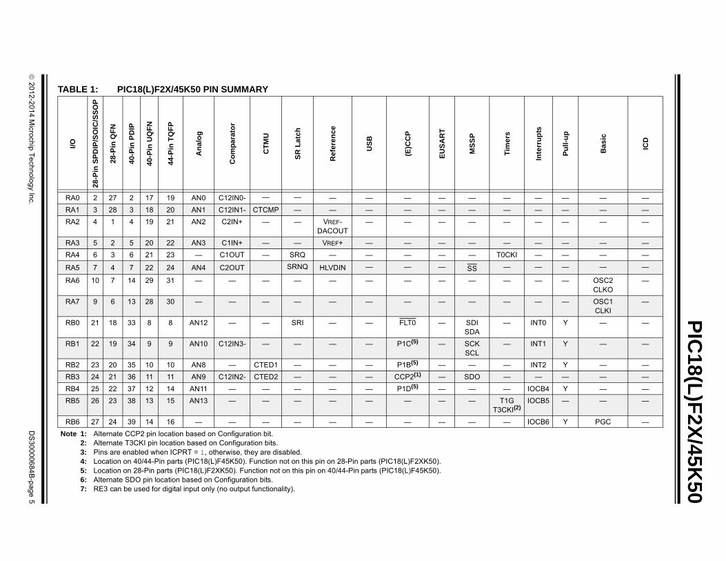
BLE 1: PIC18(L)F2X/45K50 PIN SUMMARY
I/O
28
-Pin
SP
DIP
/SO
IC/S
SO
P
28
-Pin
QF
N
40
-Pin
PD
IP
40
-Pin
UQ
FN
44
-Pin
TQ
FP
An
alo
g
Co
mp
ara
tor
CT
MU
SR
La
tch
Re
fere
nc
e
US
B
(E)C
CP
EU
SA
RT
MS
SP
Tim
ers
A0 2 27 2 17 19 AN0 C12IN0- — — — — — — — —
A1 3 28 3 18 20 AN1 C12IN1- CTCMP — — — — — — —
A2 4 1 4 19 21 AN2 C2IN+ — — VREF-DACOUT
— — — — —
A3 5 2 5 20 22 AN3 C1IN+ — — VREF+ — — — — —
A4 6 3 6 21 23 — C1OUT — SRQ — — — — — T0CK
A5 7 4 7 22 24 AN4 C2OUT SRNQ HLVDIN — — — SS —
A6 10 7 14 29 31 — — — — — — — — — —
A7 9 6 13 28 30 — — — — — — — — — —
B0 21 18 33 8 8 AN12 — — SRI — — FLT0 — SDISDA
—
B1 22 19 34 9 9 AN10 C12IN3- — — — — P1C(5) — SCKSCL
—
B2 23 20 35 10 10 AN8 — CTED1 — — — P1B(5) — — —
B3 24 21 36 11 11 AN9 C12IN2- CTED2 — — — CCP2(1) — SDO —
B4 25 22 37 12 14 AN11 — — — — — P1D(5) — — —
B5 26 23 38 13 15 AN13 — — — — — — — — T1GT3CKI
B6 27 24 39 14 16 — — — — — — — — — —
te 1: Alternate CCP2 pin location based on Configuration bit.2: Alternate T3CKI pin location based on Configuration bits.3: Pins are enabled when ICPRT = 1, otherwise, they are disabled.4: Location on 40/44-Pin parts (PIC18(L)F45K50). Function not on this pin on 28-Pin parts (PIC18(L)F2XK50).5: Location on 28-Pin parts (PIC18(L)F2XK50). Function not on this pin on 40/44-Pin parts (PIC18(L)F45K50).6: Alternate SDO pin location based on Configuration bits.7: RE3 can be used for digital input only (no output functionality).

PIC
18(L)F
2X/45K
50
DS
30
00
06
84
B-p
ag
e 6
2
01
2-2
01
4 M
icroch
ip T
ech
no
log
y Inc.
— IOCB7 Y PGD —
OSCOT1CKIT3CKIT3G
IOCC0 — — —
SOSCI IOCC1 — — —
— IOCC2 — — —
— — — VDDCORE —
— IOCC4 — — —
— IOCC5 — — —
— IOCC6 — — —
— IOCC7 — — —
— — — — —
— — — — —
— — — — —
— — — — —
— — — — —
— — — — —
— — — — —
— — — — —
Tim
ers
Inte
rru
pts
Pu
ll-u
p
Ba
sic
ICD
RB7 28 25 40 15 17 — — — — — — — — —
RC0 11 8 15 30 32 — — — — — — — — — S
RC1 12 9 16 31 35 — — — — — — CCP2 — —
RC2 13 10 17 32 36 AN14 — CTPLS — — — CCP1P1A
— —
— 14 11 18 33 37 — — — — — VUSB3V3 — — —
— 15 12 23 38 42 — — — — — D- — — —
— 16 13 24 39 43 — — — — — D+ — — —
RC6 17 14 25 40 44 AN18 — — — — — — TXCK
—
RC7 18 15 26 1 1 AN19 — — — — — — RXDT
SDO(6)
RD0 — — 19 34 38 AN20 — — — — — — — —
RD1 — — 20 35 39 AN21 — — — — — — — —
RD2 — — 21 36 40 AN22 — — — — — — — —
RD3 — — 22 37 41 AN23 — — — — — — — —
RD4 — — 27 2 2 AN24 — — — — — — — —
RD5 — — 28 3 3 AN25 — — — — — P1B(4) — —
RD6 — — 29 4 4 AN26 — — — — — P1C(4) — —
RD7 — — 30 5 5 AN27 — — — — — P1D(4) — —
TABLE 1: PIC18(L)F2X/45K50 PIN SUMMARY (CONTINUED)I/
O
28
-Pin
SP
DIP
/SO
IC/S
SO
P
28-P
in Q
FN
40-P
in P
DIP
40
-Pin
UQ
FN
44
-Pin
TQ
FP
An
alo
g
Co
mp
ara
tor
CT
MU
SR
La
tch
Re
fere
nc
e
US
B
(E)C
CP
EU
SA
RT
MS
SP
Note 1: Alternate CCP2 pin location based on Configuration bit.2: Alternate T3CKI pin location based on Configuration bits.3: Pins are enabled when ICPRT = 1, otherwise, they are disabled.4: Location on 40/44-Pin parts (PIC18(L)F45K50). Function not on this pin on 28-Pin parts (PIC18(L)F2XK50).5: Location on 28-Pin parts (PIC18(L)F2XK50). Function not on this pin on 40/44-Pin parts (PIC18(L)F45K50).6: Alternate SDO pin location based on Configuration bits.7: RE3 can be used for digital input only (no output functionality).

2
01
2-2
01
4 M
icroch
ip T
ech
no
log
y Inc.
DS
30
00
06
84
B-p
ag
e 7
PIC
18(L)F
2X/45K
50
R — — — —
R — — — —
R — — — —
R — Y MCLRVPP
—
— — VDD —
— — VSS —
— — ICPGC(3) ICCK(3)
— — ICPGD(3) ICDT(3)
— — ICVPP(3) ICRST(3)
TA
Inte
rru
pts
Pu
ll-u
p
Ba
sic
ICD
No
E0 — — 8 23 25 AN5 — — — — — — — — —
E1 — — 9 24 26 AN6 — — — — — — — — —
E2 — — 10 25 27 AN7 — — — — — — — — —
E3(7) 1 26 1 16 18 — — — — — — — — — —
— 20 17 11, 32
7, 26
7, 28
— — — — — — — — — —
— 8,19
5,16
12,31
6,27
6,29
— — — — — — — — — —
— — — – –- 12(3) — — — — — — — — — —
— — — – –- 13(3) — — — — — — — — — —
— — — –- –- 33(3) — — — — — — — — — —
BLE 1: PIC18(L)F2X/45K50 PIN SUMMARY (CONTINUED)I/
O
28
-Pin
SP
DIP
/SO
IC/S
SO
P
28-P
in Q
FN
40-P
in P
DIP
40
-Pin
UQ
FN
44
-Pin
TQ
FP
An
alo
g
Co
mp
ara
tor
CT
MU
SR
La
tch
Re
fere
nc
e
US
B
(E)C
CP
EU
SA
RT
MS
SP
Tim
ers
te 1: Alternate CCP2 pin location based on Configuration bit.2: Alternate T3CKI pin location based on Configuration bits.3: Pins are enabled when ICPRT = 1, otherwise, they are disabled.4: Location on 40/44-Pin parts (PIC18(L)F45K50). Function not on this pin on 28-Pin parts (PIC18(L)F2XK50).5: Location on 28-Pin parts (PIC18(L)F2XK50). Function not on this pin on 40/44-Pin parts (PIC18(L)F45K50).6: Alternate SDO pin location based on Configuration bits.7: RE3 can be used for digital input only (no output functionality).
PIC18(L)F2X/45K50
Table of Contents
1.0 Device Overview ....................................................................................................................................................................... 102.0 Guidelines for Getting Started with PIC18(L)F2X/45K50 Microcontrollers ................................................................................ 233.0 Oscillator Module (With Fail-Safe Clock Monitor)...................................................................................................................... 284.0 Power-Managed Modes ............................................................................................................................................................ 525.0 Reset ......................................................................................................................................................................................... 636.0 Memory Organization ................................................................................................................................................................ 737.0 Flash Program Memory............................................................................................................................................................. 958.0 Data EEPROM Memory .......................................................................................................................................................... 1049.0 8 x 8 Hardware Multiplier......................................................................................................................................................... 10910.0 Interrupts .................................................................................................................................................................................. 11111.0 I/O Ports .................................................................................................................................................................................. 12812.0 Timer0 Module......................................................................................................................................................................... 15313.0 Timer1/3 Module with Gate Control......................................................................................................................................... 15614.0 Timer2 Module......................................................................................................................................................................... 16815.0 Capture/Compare/PWM Modules............................................................................................................................................ 17216.0 Master Synchronous Serial Port (MSSP) Module ................................................................................................................... 20317.0 Enhanced Universal Synchronous Asynchronous Receiver Transmitter (EUSART) .............................................................. 25818.0 Analog-to-Digital Converter (ADC) Module ............................................................................................................................. 28719.0 Comparator Module................................................................................................................................................................. 30120.0 Charge Time Measurement Unit (CTMU)................................................................................................................................ 31021.0 SR Latch.................................................................................................................................................................................. 32522.0 Fixed Voltage Reference (FVR)............................................................................................................................................... 33023.0 Digital-to-Analog Converter (DAC) Module ............................................................................................................................. 33224.0 Universal Serial Bus (USB) ..................................................................................................................................................... 33625.0 High/Low-Voltage Detect (HLVD) ............................................................................................................................................ 36426.0 Special Features of the CPU ................................................................................................................................................... 37027.0 Instruction Set Summary ......................................................................................................................................................... 39028.0 Development Support.............................................................................................................................................................. 44029.0 Electrical Specifications........................................................................................................................................................... 44430.0 DC and AC Characteristics Graphs and Charts ...................................................................................................................... 48531.0 Packaging Information............................................................................................................................................................. 486Appendix A: Revision History............................................................................................................................................................ 503Appendix B: Device Differences........................................................................................................................................................ 504The Microchip Web Site .................................................................................................................................................................... 505Customer Change Notification Service ............................................................................................................................................. 505Customer Support ............................................................................................................................................................................. 505Product Identification System............................................................................................................................................................ 506
DS30000684B-page 8 2012-2014 Microchip Technology Inc.

PIC18(L)F2X/45K50
TO OUR VALUED CUSTOMERS
It is our intention to provide our valued customers with the best documentation possible to ensure successful use of your Microchipproducts. To this end, we will continue to improve our publications to better suit your needs. Our publications will be refined andenhanced as new volumes and updates are introduced.
If you have any questions or comments regarding this publication, please contact the Marketing Communications Department viaE-mail at [email protected]. We welcome your feedback.
Most Current Data Sheet
To obtain the most up-to-date version of this data sheet, please register at our Worldwide Web site at:
http://www.microchip.com
You can determine the version of a data sheet by examining its literature number found on the bottom outside corner of any page.The last character of the literature number is the version number, (e.g., DS30000000A is version A of document DS30000000).
Errata
An errata sheet, describing minor operational differences from the data sheet and recommended workarounds, may exist for currentdevices. As device/documentation issues become known to us, we will publish an errata sheet. The errata will specify the revisionof silicon and revision of document to which it applies.
To determine if an errata sheet exists for a particular device, please check with one of the following:
• Microchip’s Worldwide Web site; http://www.microchip.com• Your local Microchip sales office (see last page)When contacting a sales office, please specify which device, revision of silicon and data sheet (include literature number) you areusing.
Customer Notification System
Register on our web site at www.microchip.com to receive the most current information on all of our products.
2012-2014 Microchip Technology Inc. DS30000684B-page 9

PIC18(L)F2X/45K50
1.0 DEVICE OVERVIEW
This document contains device-specific information forthe following devices:
This family offers the advantages of all PIC18microcontrollers – namely, high computationalperformance at an economical price – with the additionof high-endurance, Flash program memory. On top ofthese features, the PIC18(L)F2X/45K50 familyintroduces design enhancements that make thesemicrocontrollers a logical choice for manyhigh-performance, power sensitive applications.
1.1 New Core Features
1.1.1 XLP TECHNOLOGY
All of the devices in the PIC18(L)F2X/45K50 familyincorporate a range of features that can significantlyreduce power consumption during operation. Keyitems include:
• Alternate Run Modes: By clocking the controller from the Timer1 source or the internal oscillator block, power consumption during code execution can be reduced by as much as 90%.
• Multiple Idle Modes: The controller can also run with its CPU core disabled but the peripherals still active. In these states, power consumption can be reduced even further, to as little as 4% of normal operation requirements.
• Peripheral Module Disable bits: User code can power down individual peripheral modules during Run and Idle modes for further lowering dynamic power reduction.
• On-the-fly Mode Switching: The power-managed modes are invoked by user code during operation, allowing the user to incorporate power-saving ideas into their application’s software design.
• Low Consumption in Key Modules: The power requirements for both Timer1 and the Watchdog Timer are minimized. See Section 29.0 “Electri-cal Specifications” for values.
1.1.2 UNIVERSAL SERIAL BUS (USB)
Devices in the PIC18(L)F2X/45K50 family incorporatea fully-featured USB communications module with abuilt-in transceiver that is compliant with the USBSpecification Revision 2.0. The module supports bothlow-speed and full-speed communication for allsupported data transfer types. The deviceincorporates its own on-chip transceiver and 3.3Vregulator for USB.
1.1.3 MULTIPLE OSCILLATOR OPTIONS AND FEATURES
All of the devices in the PIC18(L)F2X/45K50 familyoffer ten different oscillator options, allowing users awide range of choices in developing applicationhardware. These include:
• Four Crystal modes, using crystals or ceramic resonators
• Six External Clock modes, offering the option of using two pins (oscillator input and a divide-by-four clock output) or one pin (oscillator input, with the second pin reassigned as general I/O)
• Two External RC Oscillator modes with the same pin options as the External Clock modes
• An internal oscillator block which contains a 16 MHz HFINTOSC oscillator and a 31 kHz INTRC oscillator, which together provide eight user selectable clock frequencies, from 31 kHz to 16 MHz. This option frees the two oscillator pins for use as additional general purpose I/O.
• 3x and 4x Phase Lock Loop (PLL) frequency multipliers, available to both external and internal oscillator modes, which allows clock speeds of up to 48 MHz. Used with the internal oscillator, the PLL gives users a complete selection of clock speeds, from 31 kHz to 48 MHz – all without using an external crystal or clock circuit.
Besides its availability as a clock source, the internaloscillator block provides a stable reference source thatgives the family additional features for robustoperation:
• Active Clock Tuning: This option allows the internal oscillator to automatically tune itself to match USB host or external 32.768 kHz secondary oscillator clock sources. Full-speed USB operation can now meet specification requirements without an external crystal, enabling lower-cost designs.
• Fail-Safe Clock Monitor: This option constantly monitors the main clock source against a reference signal provided by the INTRC. If a clock failure occurs, the controller is switched to the internal oscillator block, allowing for continued operation or a safe application shutdown.
• Two-Speed Start-up: This option allows the internal oscillator to serve as the clock source from Power-on Reset, or wake-up from Sleep mode, until the primary clock source is available.
• PIC18(L)F45K50
• PIC18(L)F25K50
• PIC18(L)F24K50
DS30000684B-page 10 2012-2014 Microchip Technology Inc.

PIC18(L)F2X/45K50
1.2 Other Special Features
• Memory Endurance: The Flash cells for both program memory and data EEPROM are rated to last for many thousands of erase/write cycles – up to 10K for program memory and 100K for EEPROM. Data retention without refresh is conservatively estimated to be greater than 40 years.
• Self-Programmability: These devices can write to their own program memory spaces under internal software control. By using a bootloader routine located in the protected Boot Block at the top of program memory, it becomes possible to create an application that can update itself in the field.
• Extended Instruction Set: The PIC18(L)F2X/45K50 family introduces an optional extension to the PIC18 instruction set, which adds eight new instructions and an Indexed Addressing mode. This extension, enabled as a device configuration option, has been specifically designed to optimize re-entrant application code originally developed in high-level languages, such as C.
• Enhanced CCP module: In PWM mode, this module provides 1, 2 or 4 modulated outputs for controlling half-bridge and full-bridge drivers. Other features include:
- Auto-shutdown, for disabling PWM outputs on interrupt or other select conditions
- Auto-restart, to reactivate outputs once the condition has cleared
- Output steering to selectively enable one or more of four outputs to provide the PWM signal.
• Enhanced Addressable EUSART: This serial communication module is capable of standard RS-232 operation and provides support for the LIN bus protocol. Other enhancements include automatic baud rate detection and a 16-bit Baud Rate Generator for improved resolution. When the microcontroller is using the internal oscillator block, the EUSART provides stable operation for applications that talk to the outside world without using an external crystal (or its accompanying power requirement).
• 10-Bit A/D Converter: This module incorporates programmable acquisition time, allowing for a channel to be selected and a conversion to be initiated without waiting for a sampling period and thus, reduce code overhead.
• Dedicated ICD/ICSP™ Port: These devices introduce the use of debugger and programming pins that are not multiplexed with other microcontroller features. Offered as an option in the TQFP packaged devices, this feature allows users to develop I/O intensive applications while retaining the ability to program and debug in the circuit.
• Charge Time Measurement Unit (CTMU): The CTMU is a flexible analog module that provides accurate differential time measurement between pulse sources, as well as asynchronous pulse generation. Together with other on-chip analog modules, the CTMU can precisely measure time, measure capacitance or relative changes in capacitance or generate output pulses that are independent of the system clock.
• SR Latch Output: A single SR latch with multiple Set and Reset inputs as well as separate latch outputs.
1.3 Details on Individual Family Members
Devices in the PIC18(L)F2X/45K50 family are availablein 28-pin and 40/44-pin packages. The block diagramfor the device family is shown in Figure 1-1.
The devices have the following differences:
1. Flash program memory
2. A/D channels
3. I/O ports
4. Input Voltage Range/Power Consumption
All other features for devices in this family are identical.These are summarized in Table 1-1.
The pinouts for all devices are listed in the pin summarytable (Table 1) and I/O description tables (Table 1-2and Table 1-3).
2012-2014 Microchip Technology Inc. DS30000684B-page 11
PIC18(L)F2X/45K50
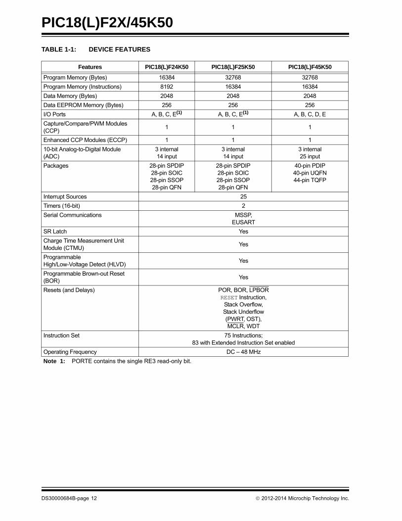
TABLE 1-1: DEVICE FEATURES
Features PIC18(L)F24K50 PIC18(L)F25K50 PIC18(L)F45K50
Program Memory (Bytes) 16384 32768 32768
Program Memory (Instructions) 8192 16384 16384
Data Memory (Bytes) 2048 2048 2048
Data EEPROM Memory (Bytes) 256 256 256
I/O Ports A, B, C, E(1) A, B, C, E(1) A, B, C, D, E
Capture/Compare/PWM Modules (CCP)
1 1 1
Enhanced CCP Modules (ECCP) 1 1 1
10-bit Analog-to-Digital Module (ADC)
3 internal14 input
3 internal14 input
3 internal25 input
Packages 28-pin SPDIP28-pin SOIC28-pin SSOP28-pin QFN
28-pin SPDIP28-pin SOIC28-pin SSOP28-pin QFN
40-pin PDIP40-pin UQFN44-pin TQFP
Interrupt Sources 25
Timers (16-bit) 2
Serial Communications MSSP, EUSART
SR Latch Yes
Charge Time Measurement Unit Module (CTMU)
Yes
Programmable High/Low-Voltage Detect (HLVD)
Yes
Programmable Brown-out Reset (BOR)
Yes
Resets (and Delays) POR, BOR, LPBOR RESET Instruction,
Stack Overflow,Stack Underflow (PWRT, OST), MCLR, WDT
Instruction Set 75 Instructions; 83 with Extended Instruction Set enabled
Operating Frequency DC – 48 MHz
Note 1: PORTE contains the single RE3 read-only bit.
DS30000684B-page 12 2012-2014 Microchip Technology Inc.

PIC18(L)F2X/45K50
FIGURE 1-1: PIC18(L)F2X/45K50 FAMILY BLOCK DIAGRAM
InstructionDecode and
Control
Data Latch
Data Memory
Address Latch
Data Address<12>
12
AccessBSR FSR0FSR1FSR2
inc/declogic
Address
4 12 4
PCH PCL
PCLATH
8
31-Level Stack
Program Counter
PRODLPRODH
8 x 8 Multiply
8
BITOP88
ALU<8>
20
8
8
Table Pointer<21>
inc/dec logic
21
8
Data Bus<8>
Table Latch8
IR
12
3
ROM Latch
PCLATU
PCU
Note 1: RE3 is only available when MCLR functionality is disabled.
2: OSC1/CLKIN and OSC2/CLKO are only available in select oscillator modes and when these pins are not being used as digital I/O. Refer to Section 6.0 “Memory Organization” for additional information.
EUSARTComparators MSSP10-bit ADC
Timer2Timer1 CTMUTimer0
USB
HLVD
ECCP1
BOR DataEEPROM
W
Instruction Bus <16>
STKPTR Bank
8
State machinecontrol signals
Decode
8
8Power-up
Timer
OscillatorStart-up Timer
Power-onReset
WatchdogTimer
OSC1(2)
OSC2(2)
Brown-outReset
InternalOscillator
Fail-SafeClock Monitor
Precision
ReferenceBand GapMCLR(1)
Block
INTRCOscillator
16 MHzOscillator
Single-SupplyProgramming
In-CircuitDebugger
SOSCO
SOSCI
FVR
FVRFVR
DAC
Address Latch
Program Memory(16/32 Kbytes)
Data Latch
PORTA
RA0:RA7
PORTB
RB0:RB7
PORTC
RC0:RC3
PORTD
RD0:RD7
Timer3
SR LatchC1/C2 CCP2
PORTE
RE0:RE2
RE3(1)
DAC
RC6:RC7
DAC
2012-2014 Microchip Technology Inc. DS30000684B-page 13
PIC18(L)F2X/45K50
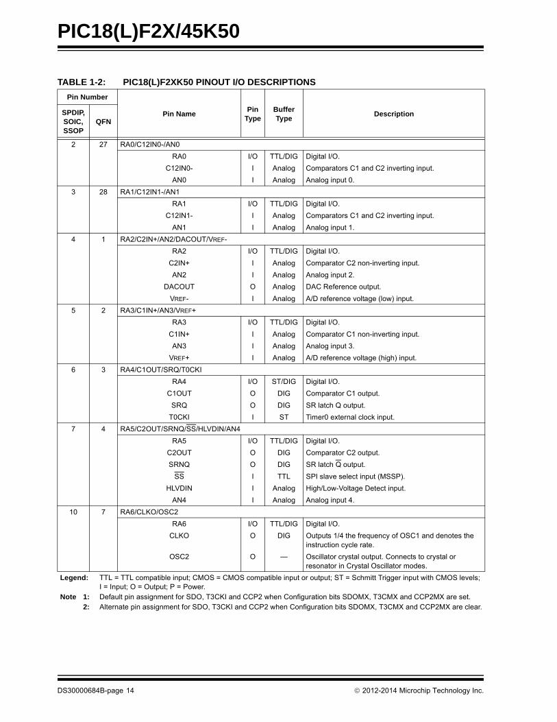
TABLE 1-2: PIC18(L)F2XK50 PINOUT I/O DESCRIPTIONS
Pin Number
Pin NamePin
TypeBuffer Type
DescriptionSPDIP, SOIC, SSOP
QFN
2 27 RA0/C12IN0-/AN0
RA0 I/O TTL/DIG Digital I/O.
C12IN0- I Analog Comparators C1 and C2 inverting input.
AN0 I Analog Analog input 0.
3 28 RA1/C12IN1-/AN1
RA1 I/O TTL/DIG Digital I/O.
C12IN1- I Analog Comparators C1 and C2 inverting input.
AN1 I Analog Analog input 1.
4 1 RA2/C2IN+/AN2/DACOUT/VREF-
RA2 I/O TTL/DIG Digital I/O.
C2IN+ I Analog Comparator C2 non-inverting input.
AN2 I Analog Analog input 2.
DACOUT O Analog DAC Reference output.
VREF- I Analog A/D reference voltage (low) input.
5 2 RA3/C1IN+/AN3/VREF+
RA3 I/O TTL/DIG Digital I/O.
C1IN+ I Analog Comparator C1 non-inverting input.
AN3 I Analog Analog input 3.
VREF+ I Analog A/D reference voltage (high) input.
6 3 RA4/C1OUT/SRQ/T0CKI
RA4 I/O ST/DIG Digital I/O.
C1OUT O DIG Comparator C1 output.
SRQ O DIG SR latch Q output.
T0CKI I ST Timer0 external clock input.
7 4 RA5/C2OUT/SRNQ/SS/HLVDIN/AN4
RA5 I/O TTL/DIG Digital I/O.
C2OUT O DIG Comparator C2 output.
SRNQ O DIG SR latch Q output.
SS I TTL SPI slave select input (MSSP).
HLVDIN I Analog High/Low-Voltage Detect input.
AN4 I Analog Analog input 4.
10 7 RA6/CLKO/OSC2
RA6 I/O TTL/DIG Digital I/O.
CLKO O DIG Outputs 1/4 the frequency of OSC1 and denotes the instruction cycle rate.
OSC2 O — Oscillator crystal output. Connects to crystal or resonator in Crystal Oscillator modes.
Legend: TTL = TTL compatible input; CMOS = CMOS compatible input or output; ST = Schmitt Trigger input with CMOS levels; I = Input; O = Output; P = Power.
Note 1: Default pin assignment for SDO, T3CKI and CCP2 when Configuration bits SDOMX, T3CMX and CCP2MX are set.2: Alternate pin assignment for SDO, T3CKI and CCP2 when Configuration bits SDOMX, T3CMX and CCP2MX are clear.
DS30000684B-page 14 2012-2014 Microchip Technology Inc.

PIC18(L)F2X/45K50
9 6 RA7/CLKI/OSC1
RA7 I/O TTL/DIG Digital I/O.
CLKI I CMOS External clock source input. Always associated with pin function OSC1.
OSC1 I ST Oscillator crystal input or external clock source input ST buffer when configured in RC mode; CMOS otherwise.
21 18 RB0/INT0/FLT0/SRI/SDI/SDA/AN12
RB0 I/O TTL/DIG Digital Output or Input with internal pull-up option.
INT0 I ST External interrupt 0.
FLT0 I ST PWM Fault input for ECCP auto-shutdown.
SRI I ST SR latch input.
SDI I ST SPI data in (MSSP).
SDA I/O I2C™ I2C data I/O (MSSP).
AN12 I Analog Analog input 12.
22 19 RB1/INT1/P1C/SCK/SCL/C12IN3-/AN10
RB1 I/O TTL/DIG Digital Output or Input with internal pull-up option.
INT1 I ST External interrupt 1.
P1C O DIG Enhanced CCP1 PWM output.
SCK I/O ST/DIG Synchronous serial clock input/output for SPI mode (MSSP).
SCL I/O I2C Synchronous serial clock input/output for I2C mode (MSSP).
C12IN3- I Analog Comparators C1 and C2 inverting input.
AN10 I Analog Analog input 10.
23 20 RB2/INT2/CTED1/P1B/AN8
RB2 I/O TTL/DIG Digital Output or Input with internal pull-up option.
INT2 I ST External interrupt 2.
CTED1 I ST CTMU Edge 1 input.
P1B O DIG Enhanced CCP1 PWM output.
AN8 I Analog Analog input 8.
24 21 RB3/CTED2/CCP2/SDO/C12IN2-/AN9
RB3 I/O TTL/DIG Digital Output or Input with internal pull-up option.
CTED2 I ST CTMU Edge 2 input.
CCP2(2) I/O ST/DIG Alternate Capture 2 input/Compare 2 output/PWM 2 output.
SDO(1) O DIG SPI data out (MSSP).
C12IN2- I Analog Comparators C1 and C2 inverting input.
AN9 I Analog Analog input 9.
TABLE 1-2: PIC18(L)F2XK50 PINOUT I/O DESCRIPTIONS (CONTINUED)
Pin Number
Pin NamePin
TypeBuffer Type
DescriptionSPDIP, SOIC, SSOP
QFN
Legend: TTL = TTL compatible input; CMOS = CMOS compatible input or output; ST = Schmitt Trigger input with CMOS levels; I = Input; O = Output; P = Power.
Note 1: Default pin assignment for SDO, T3CKI and CCP2 when Configuration bits SDOMX, T3CMX and CCP2MX are set.2: Alternate pin assignment for SDO, T3CKI and CCP2 when Configuration bits SDOMX, T3CMX and CCP2MX are clear.
2012-2014 Microchip Technology Inc. DS30000684B-page 15

PIC18(L)F2X/45K50
25 22 RB4/IOCB4/P1D/AN11
RB4 I/O TTL/DIG Digital Output or Input with internal pull-up option.
IOCB4 I TTL Interrupt-on-change pin.
P1D O DIG Enhanced CCP1 PWM output.
AN11 I Analog Analog input 11.
26 23 RB5/IOCB5/T3CKI/T1G/AN13
RB5 I/O TTL/DIG Digital Output or Input with internal pull-up option.
IOCB5 I TTL Interrupt-on-change pin.
T3CKI(2) I ST Alternate Timer3 clock input.
T1G I ST Timer1 external clock gate input.
AN13 I Analog Analog input 13.
27 24 RB6/IOCB6/PGC
RB6 I/O TTL/DIG Digital Output or Input with internal pull-up option.
IOCB6 I TTL Interrupt-on-change pin.
PGC I/O ST In-Circuit Debugger and ICSP™ programming clock pin.
28 25 RB7/IOCB7/PGD
RB7 I/O TTL/DIG Digital Output or Input with internal pull-up option.
IOCB7 I TTL Interrupt-on-change pin.
PGD I/O ST/DIG In-Circuit Debugger and ICSP™ programming data pin.
11 8 RC0/IOCC0/T3CKI/T3G/T1CKI/SOSCO
RC0 I/O ST/DIG Digital I/O.
IOCC0 I TTL Interrupt-on-change pin.
T3CKI(1) I ST Timer3 clock input.
T3G I ST Timer3 external clock gate input.
T1CKI I ST Timer1 clock input.
SOSCO O — Secondary oscillator output.
12 9 RC1/IOCC1/CCP2/SOSCI
RC1 I/O ST/DIG Digital I/O.
IOCC1 I TTL Interrupt-on-change pin.
CCP2(1) I/O ST/DIG Capture 2 input/Compare 2 output/PWM 2 output.
SOSCI I Analog Secondary oscillator input.
TABLE 1-2: PIC18(L)F2XK50 PINOUT I/O DESCRIPTIONS (CONTINUED)
Pin Number
Pin NamePin
TypeBuffer Type
DescriptionSPDIP, SOIC, SSOP
QFN
Legend: TTL = TTL compatible input; CMOS = CMOS compatible input or output; ST = Schmitt Trigger input with CMOS levels; I = Input; O = Output; P = Power.
Note 1: Default pin assignment for SDO, T3CKI and CCP2 when Configuration bits SDOMX, T3CMX and CCP2MX are set.2: Alternate pin assignment for SDO, T3CKI and CCP2 when Configuration bits SDOMX, T3CMX and CCP2MX are clear.
DS30000684B-page 16 2012-2014 Microchip Technology Inc.
PIC18(L)F2X/45K50
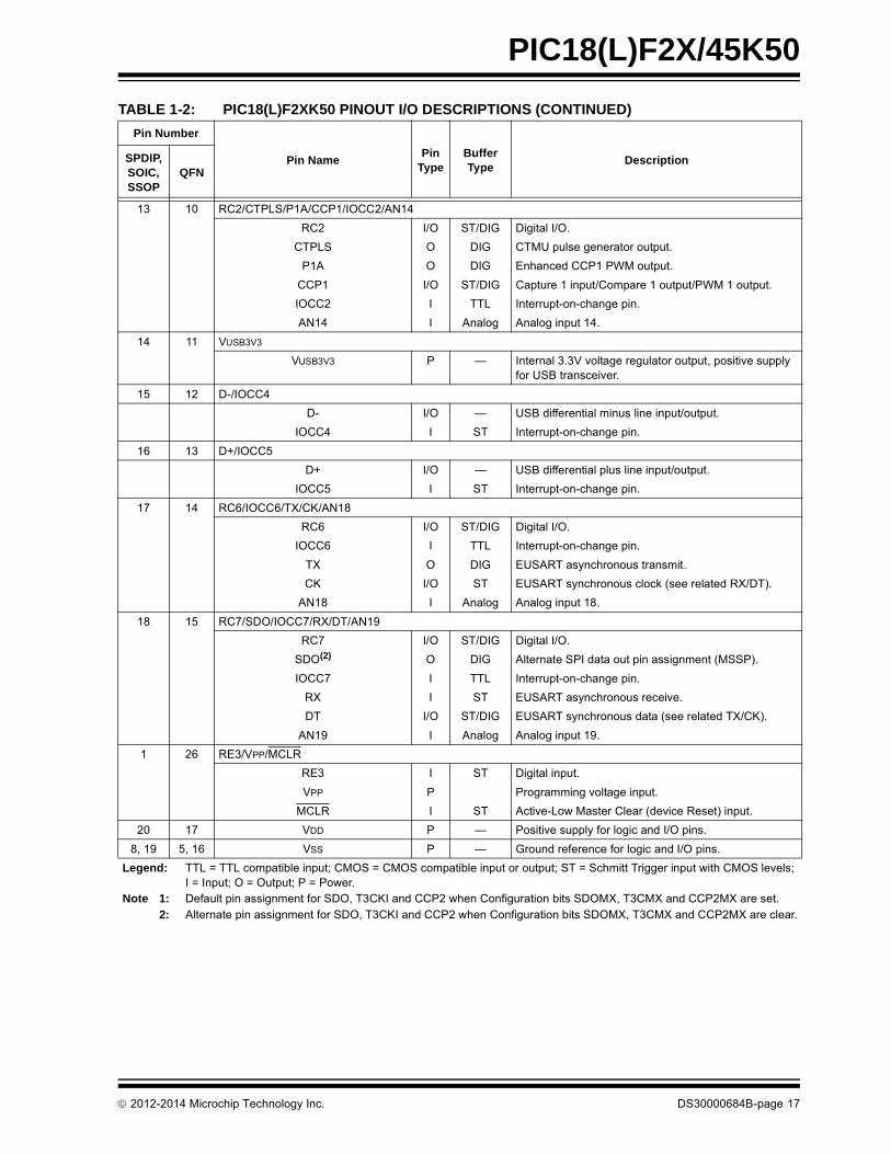
13 10 RC2/CTPLS/P1A/CCP1/IOCC2/AN14
RC2 I/O ST/DIG Digital I/O.
CTPLS O DIG CTMU pulse generator output.
P1A O DIG Enhanced CCP1 PWM output.
CCP1 I/O ST/DIG Capture 1 input/Compare 1 output/PWM 1 output.
IOCC2 I TTL Interrupt-on-change pin.
AN14 I Analog Analog input 14.
14 11 VUSB3V3
VUSB3V3 P — Internal 3.3V voltage regulator output, positive supply for USB transceiver.
15 12 D-/IOCC4
D- I/O — USB differential minus line input/output.
IOCC4 I ST Interrupt-on-change pin.
16 13 D+/IOCC5
D+ I/O — USB differential plus line input/output.
IOCC5 I ST Interrupt-on-change pin.
17 14 RC6/IOCC6/TX/CK/AN18
RC6 I/O ST/DIG Digital I/O.
IOCC6 I TTL Interrupt-on-change pin.
TX O DIG EUSART asynchronous transmit.
CK I/O ST EUSART synchronous clock (see related RX/DT).
AN18 I Analog Analog input 18.
18 15 RC7/SDO/IOCC7/RX/DT/AN19
RC7 I/O ST/DIG Digital I/O.
SDO(2) O DIG Alternate SPI data out pin assignment (MSSP).
IOCC7 I TTL Interrupt-on-change pin.
RX I ST EUSART asynchronous receive.
DT I/O ST/DIG EUSART synchronous data (see related TX/CK).
AN19 I Analog Analog input 19.
1 26 RE3/VPP/MCLR
RE3 I ST Digital input.
VPP P Programming voltage input.
MCLR I ST Active-Low Master Clear (device Reset) input.
20 17 VDD P — Positive supply for logic and I/O pins.
8, 19 5, 16 VSS P — Ground reference for logic and I/O pins.
TABLE 1-2: PIC18(L)F2XK50 PINOUT I/O DESCRIPTIONS (CONTINUED)
Pin Number
Pin NamePin
TypeBuffer Type
DescriptionSPDIP, SOIC, SSOP
QFN
Legend: TTL = TTL compatible input; CMOS = CMOS compatible input or output; ST = Schmitt Trigger input with CMOS levels; I = Input; O = Output; P = Power.
Note 1: Default pin assignment for SDO, T3CKI and CCP2 when Configuration bits SDOMX, T3CMX and CCP2MX are set.2: Alternate pin assignment for SDO, T3CKI and CCP2 when Configuration bits SDOMX, T3CMX and CCP2MX are clear.
2012-2014 Microchip Technology Inc. DS30000684B-page 17

PIC18(L)F2X/45K50
TABLE 1-3: PIC18(L)F45K50 PINOUT I/O DESCRIPTIONS
Pin NumberPin Name
Pin Type
Buffer Type
DescriptionPDIP TQFP UQFN
2 19 17 RA0/C12IN0-/AN0
RA0 I/O TTL/DIG Digital I/O.
C12IN0- I Analog Comparators C1 and C2 inverting input.
AN0 I Analog Analog input 0.
3 20 18 RA1/C12IN1-/AN1
RA1 I/O TTL/DIG Digital I/O.
C12IN1- I Analog Comparators C1 and C2 inverting input.
AN1 I Analog Analog input 1.
4 21 19 RA2/C2IN+/AN2/DACOUT/VREF-
RA2 I/O TTL/DIG Digital I/O.
C2IN+ I Analog Comparator C2 non-inverting input.
AN2 I Analog Analog input 2.
DACOUT O Analog DAC Reference output.
VREF- I Analog A/D reference voltage (low) input.
5 22 20 RA3/C1IN+/AN3/VREF+
RA3 I/O TTL/DIG Digital I/O.
C1IN+ I Analog Comparator C1 non-inverting input.
AN3 I Analog Analog input 3.
VREF+ I Analog A/D reference voltage (high) input.
6 23 21 RA4/C1OUT/SRQ/T0CKI
RA4 I/O ST/DIG Digital I/O.
C1OUT O DIG Comparator C1 output.
SRQ O TTL SR latch Q output.
T0CKI I ST Timer0 external clock input.
7 24 22 RA5/C2OUT/SRNQ/SS/HLVDIN/AN4
RA5 I/O TTL/DIG Digital I/O.
C2OUT O DIG Comparator C2 output.
SRNQ O DIG SR latch Q output.
SS I TTL SPI slave select input (MSSP).
HLVDIN I Analog High/Low-Voltage Detect input.
AN4 I Analog Analog input 4.
14 31 29 RA6/CLKO/OSC2
RA6 I/O TTL/DIG Digital I/O.
CLKO O DIG Outputs 1/4 the frequency of OSC1 and denotes the instruction cycle rate.
OSC2 O — Oscillator crystal output. Connects to crystal or resonator in Crystal Oscillator mode.
13 30 28 RA7/CLKI/OSC1
RA7 I/O TTL/DIG Digital I/O.
CLKI I CMOS External clock source input. Always associated with pin function OSC1.
OSC1 I ST Oscillator crystal input or external clock source input ST buffer when configured in RC mode; CMOS otherwise.
Legend: TTL = TTL compatible input; CMOS = CMOS compatible input or output; ST = Schmitt Trigger input with CMOS levels; I = Input; O = Output; P = Power.
Note 1: Default pin assignment for SDO, T3CKI and CCP2 when Configuration bits SDOMX, T3CMX and CCP2MX are set.
2: Alternate pin assignment for SDO, T3CKI and CCP2 when Configuration bits SDOMX, T3CMX and CCP2MX are clear.
3: Pin is “No Connect”, except on PIC18(L)F45K50 TQFP devices with ICPRT Configuration bit set.
DS30000684B-page 18 2012-2014 Microchip Technology Inc.

PIC18(L)F2X/45K50
33 8 8 RB0/INT0/FLT0/SDI/SDA/SRI/AN12
RB0 I/O TTL/DIG Digital Output or Input with internal pull-up option.
INT0 I ST External interrupt 0.
FLT0 I ST PWM Fault input for ECCP auto-shutdown.
SDI I ST SPI Data in (MSSP).
SDA I/O I2C™ I2C Data I/O (MSSP).
SRI I ST SR latch input.
AN12 I Analog Analog input 12.
34 9 9 RB1/INT1/P1C/SCK/SCL/C12IN3-/AN10
RB1 I/O TTL/DIG Digital Output or Input with internal pull-up option.
INT1 I ST External interrupt 1.
P1C O DIG Enhanced CCP1 PWM output.
SCK I/O ST/DIG Synchronous serial clock input/output for SPI mode (MSSP).
SCL I/O I2C Synchronous serial clock input/output for I2C mode (MSSP).
C12IN3- I Analog Comparators C1 and C2 inverting input.
AN10 I Analog Analog input 10.
35 10 10 RB2/P1B/INT2/CTED1/AN8
RB2 I/O TTL/DIG Digital Output or Input with internal pull-up option.
P1B O DIG Enhanced CCP1 PWM output.
INT2 I ST External interrupt 2.
CTED1 I ST CTMU Edge 1 input.
AN8 I Analog Analog input 8.
36 11 11 RB3/CTED2/SDO/CCP2/C12IN2-/AN9
RB3 I/O TTL/DIG Digital Output or Input with internal pull-up option.
CTED2 I ST CTMU Edge 2 input.
SDO(1) O DIG SPI Data out (MSSP).
CCP2(2) I/O ST Alternate Capture 2 input/Compare 2 output/PWM 2 output.
C12IN2- I Analog Comparators C1 and C2 inverting input.
AN9 I Analog Analog input 9.
37 14 12 RB4/IOCB4/P1D/AN11
RB4 I/O TTL/DIG Digital Output or Input with internal pull-up option.
IOCB4 I TTL Interrupt-on-change pin.
P1D O DIG Enhanced CCP1 PWM output.
AN11 I Analog Analog input 11.
38 15 13 RB5/IOCB5/T3CKI/T1G/AN13
RB5 I/O TTL/DIG Digital Output or Input with internal pull-up option.
IOCB5 I TTL Interrupt-on-change pin.
T3CKI(2) I ST Alternate Timer3 clock input.
T1G I ST Timer1 external clock gate input.
AN13 I Analog Analog input 13.
TABLE 1-3: PIC18(L)F45K50 PINOUT I/O DESCRIPTIONS (CONTINUED)
Pin NumberPin Name
Pin Type
Buffer Type
DescriptionPDIP TQFP UQFN
Legend: TTL = TTL compatible input; CMOS = CMOS compatible input or output; ST = Schmitt Trigger input with CMOS levels; I = Input; O = Output; P = Power.
Note 1: Default pin assignment for SDO, T3CKI and CCP2 when Configuration bits SDOMX, T3CMX and CCP2MX are set.
2: Alternate pin assignment for SDO, T3CKI and CCP2 when Configuration bits SDOMX, T3CMX and CCP2MX are clear.
3: Pin is “No Connect”, except on PIC18(L)F45K50 TQFP devices with ICPRT Configuration bit set.
2012-2014 Microchip Technology Inc. DS30000684B-page 19
PIC18(L)F2X/45K50
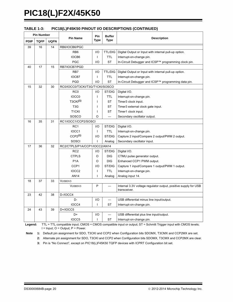
39 16 14 RB6/IOCB6/PGC
RB6 I/O TTL/DIG Digital Output or Input with internal pull-up option.
IOCB6 I TTL Interrupt-on-change pin.
PGC I/O ST In-Circuit Debugger and ICSP™ programming clock pin.
40 17 15 RB7/IOCB7/PGD
RB7 I/O TTL/DIG Digital Output or Input with internal pull-up option.
IOCB7 I TTL Interrupt-on-change pin.
PGD I/O ST In-Circuit Debugger and ICSP™ programming data pin.
15 32 30 RC0/IOCC0/T3CKI/T3G/T1CKI/SOSCO
RC0 I/O ST/DIG Digital I/O.
IOCC0 I TTL Interrupt-on-change pin.
T3CKI(1) I ST Timer3 clock input.
T3G I ST Timer3 external clock gate input.
T1CKI I ST Timer1 clock input.
SOSCO O — Secondary oscillator output.
16 35 31 RC1/IOCC1/CCP2/SOSCI
RC1 I/O ST/DIG Digital I/O.
IOCC1 I TTL Interrupt-on-change pin.
CCP2(1) I/O ST/DIG Capture 2 input/Compare 2 output/PWM 2 output.
SOSCI I Analog Secondary oscillator input.
17 36 32 RC2/CTPLS/P1A/CCP1/IOCC2/AN14
RC2 I/O ST/DIG Digital I/O.
CTPLS O DIG CTMU pulse generator output.
P1A O DIG Enhanced CCP1 PWM output.
CCP1 I/O ST/DIG Capture 1 input/Compare 1 output/PWM 1 output.
IOCC2 I TTL Interrupt-on-change pin.
AN14 I Analog Analog input 14.
18 37 33 VUSB3V3
VUSB3V3 P — Internal 3.3V voltage regulator output, positive supply for USB transceiver.
23 42 38 D-/IOCC4
D- I/O — USB differential minus line input/output.
IOCC4 I ST Interrupt-on-change pin.
24 43 39 D+/IOCC5
D+ I/O — USB differential plus line input/output.
IOCC5 I ST Interrupt-on-change pin.
TABLE 1-3: PIC18(L)F45K50 PINOUT I/O DESCRIPTIONS (CONTINUED)
Pin NumberPin Name
Pin Type
Buffer Type
DescriptionPDIP TQFP UQFN
Legend: TTL = TTL compatible input; CMOS = CMOS compatible input or output; ST = Schmitt Trigger input with CMOS levels; I = Input; O = Output; P = Power.
Note 1: Default pin assignment for SDO, T3CKI and CCP2 when Configuration bits SDOMX, T3CMX and CCP2MX are set.
2: Alternate pin assignment for SDO, T3CKI and CCP2 when Configuration bits SDOMX, T3CMX and CCP2MX are clear.
3: Pin is “No Connect”, except on PIC18(L)F45K50 TQFP devices with ICPRT Configuration bit set.
DS30000684B-page 20 2012-2014 Microchip Technology Inc.

PIC18(L)F2X/45K50
25 44 40 RC6/IOCC6/TX/CK/AN18
RC6 I/O ST/DIG Digital I/O.
IOCC6 I TTL Interrupt-on-change pin.
TX O — EUSART asynchronous transmit.
CK I/O ST EUSART synchronous clock (see related RX/DT).
AN18 I Analog Analog input 18.
26 1 1 RC7/RX/DT/SDO/IOCC7/AN19
RC7 I/O ST/DIG Digital I/O.
RX I ST EUSART asynchronous receive.
DT I/O ST EUSART synchronous data (see related TX/CK).
SDO(2) O DIG Alternate SPI data out (MSSP).
IOCC7 I TTL Interrupt-on-change pin.
AN19 I Analog Analog input 19.
19 38 34 RD0/AN20
RD0 I/O ST/DIG Digital I/O.
AN20 I Analog Analog input 20.
20 39 35 RD1/AN21
RD1 I/O ST/DIG Digital I/O.
AN21 I Analog Analog input 21.
21 40 36 RD2/AN22
RD2 I/O ST/DIG Digital I/O
AN22 I Analog Analog input 22.
22 41 37 RD3/AN23
RD3 I/O ST/DIG Digital I/O.
AN23 I Analog Analog input 23.
27 2 2 RD4/AN24
RD4 I/O ST/DIG Digital I/O.
AN24 I Analog Analog input 24.
28 3 3 RD5/P1B/AN25
RD5 I/O ST/DIG Digital I/O.
P1B O DIG Enhanced CCP1 PWM output.
AN25 I Analog Analog input 25.
29 4 4 RD6/P1C/AN26
RD6 I/O ST/DIG Digital I/O.
P1C O DIG Enhanced CCP1 PWM output.
AN26 I Analog Analog input 26.
30 5 5 RD7/P1D/AN27
RD7 I/O ST/DIG Digital I/O.
P1D O DIG Enhanced CCP1 PWM output.
AN27 I Analog Analog input 27.
TABLE 1-3: PIC18(L)F45K50 PINOUT I/O DESCRIPTIONS (CONTINUED)
Pin NumberPin Name
Pin Type
Buffer Type
DescriptionPDIP TQFP UQFN
Legend: TTL = TTL compatible input; CMOS = CMOS compatible input or output; ST = Schmitt Trigger input with CMOS levels; I = Input; O = Output; P = Power.
Note 1: Default pin assignment for SDO, T3CKI and CCP2 when Configuration bits SDOMX, T3CMX and CCP2MX are set.
2: Alternate pin assignment for SDO, T3CKI and CCP2 when Configuration bits SDOMX, T3CMX and CCP2MX are clear.
3: Pin is “No Connect”, except on PIC18(L)F45K50 TQFP devices with ICPRT Configuration bit set.
2012-2014 Microchip Technology Inc. DS30000684B-page 21

PIC18(L)F2X/45K50
8 25 23 RE0/AN5
RE0 I/O ST/DIG Digital I/O.
AN5 I Analog Analog input 5.
9 26 24 RE1/AN6
RE1 I/O ST/DIG Digital I/O.
AN6 I Analog Analog input 6.
10 27 25 RE2/AN7
RE2 I/O ST Digital I/O.
AN7 I Analog Analog input 7.
1 18 16 RE3/VPP/MCLR
RE3 I ST Digital input.
VPP P Programming voltage input.
MCLR I ST Active-low Master Clear (device Reset) input.
— 12 — ICCK/ICPGC
ICCK I/O ST Dedicated In-Circuit Debugger clock.
ICPGC(3) I/O ST Dedicated ICSP™ programming clock.
— 13 — ICDT/ICPGD
ICDT I/O ST Dedicated In-Circuit Debugger data.
ICPGD(3) I/O ST Dedicated ICSP™ programming data.
— 33 — ICRST/ICVPP
ICRST I ST Dedicated Master Clear Reset input.
ICVPP(3) I P Dedicated programming voltage input.
11,32 7, 28 7, 26 VDD P — Positive supply for logic and I/O pins.
12,31 6, 29 6, 27 VSS P — Ground reference for logic and I/O pins.
34 NC
TABLE 1-3: PIC18(L)F45K50 PINOUT I/O DESCRIPTIONS (CONTINUED)
Pin NumberPin Name
Pin Type
Buffer Type
DescriptionPDIP TQFP UQFN
Legend: TTL = TTL compatible input; CMOS = CMOS compatible input or output; ST = Schmitt Trigger input with CMOS levels; I = Input; O = Output; P = Power.
Note 1: Default pin assignment for SDO, T3CKI and CCP2 when Configuration bits SDOMX, T3CMX and CCP2MX are set.
2: Alternate pin assignment for SDO, T3CKI and CCP2 when Configuration bits SDOMX, T3CMX and CCP2MX are clear.
3: Pin is “No Connect”, except on PIC18(L)F45K50 TQFP devices with ICPRT Configuration bit set.
DS30000684B-page 22 2012-2014 Microchip Technology Inc.

PIC18(L)F2X/45K50
2.0 GUIDELINES FOR GETTING STARTED WITH PIC18(L)F2X/45K50 MICROCONTROLLERS
2.1 Basic Connection Requirements
Getting started with the PIC18(L)F2X/45K50 family of8-bit microcontrollers requires attention to a minimalset of device pin connections before proceeding withdevelopment.
The following pins must always be connected:
• All VDD and VSS pins (see Section 2.2 “Power Supply Pins”)
• MCLR pin (see Section 2.3 “Master Clear (MCLR) Pin”)
• VUSB3V3 pins (see Section 2.4 “Voltage Regulator Pins (VUSB3V3)”)
These pins must also be connected if they are beingused in the end application:
• PGC/PGD pins used for In-Circuit Serial Programming (ICSP) and debugging purposes (see Section 2.5 “ICSP Pins”)
• OSC1 and OSC2 pins when an external oscillator source is used (see Section 2.6 “External Oscillator Pins”)
Additionally, the following pins may be required:
• VREF+/VREF- pins are used when external voltage reference for analog modules is implemented
The minimum mandatory connections are shown inFigure 2-1.
FIGURE 2-1: RECOMMENDED MINIMUM CONNECTIONS
PIC18F2X/45K50
VD
D
VS
S
VDD
VSS
VSS
VDD
VD
D
VS
S
C1
R1
VDD
MCLRVUSB3V3
R2
C7(2)
C2(2)
C3(2)
C4(2)
C6(2)
Key (all values are recommendations):
C1 through C6: 0.1 F, 20V ceramic
R1: 10 kΩ
R2: 100Ω to 470Ω
Note 1: See Section 2.4 “Voltage Regulator Pins (VUSB3V3)” for explanation of VUSB3V3 pin connections.
2: The example shown is for a PIC18F device with five VDD/VSS pairs. Other devices may have more or less pairs; adjust the number of decoupling capacitors appropriately.
(1)
2012-2014 Microchip Technology Inc. DS30684A-page 23

PIC18(L)F2X/45K50
2.2 Power Supply Pins
2.2.1 DECOUPLING CAPACITORS
The use of decoupling capacitors on every pair ofpower supply pins, such as VDD and VSS is required.
Consider the following criteria when using decouplingcapacitors:
• Value and type of capacitor: A 0.1 F (100 nF), 10-20V capacitor is recommended. The capacitor should be a low-ESR device, with a resonance frequency in the range of 200 MHz and higher. Ceramic capacitors are recommended.
• Placement on the printed circuit board: The decoupling capacitors should be placed as close to the pins as possible. It is recommended to place the capacitors on the same side of the board as the device. If space is constricted, the capacitor can be placed on another layer on the PCB using a via; however, ensure that the trace length from the pin to the capacitor is no greater than 0.25 inch (6 mm).
• Handling high-frequency noise: If the board is experiencing high-frequency noise (upward of tens of MHz), add a second ceramic type capacitor in parallel to the above described decoupling capacitor. The value of the second capacitor can be in the range of 0.01 F to 0.001 F. Place this second capacitor next to each primary decoupling capacitor. In high-speed circuit designs, consider implementing a decade pair of capacitances as close to the power and ground pins as possible (e.g., 0.1 F in parallel with 0.001 F).
• Maximizing performance: On the board layout from the power supply circuit, run the power and return traces to the decoupling capacitors first, and then to the device pins. This ensures that the decoupling capacitors are first in the power chain. Equally important is to keep the trace length between the capacitor and the power pins to a minimum, thereby reducing PCB trace inductance.
2.2.2 TANK CAPACITORS
On boards with power traces running longer thansix inches in length, it is suggested to use a tankcapacitor for integrated circuits, includingmicrocontrollers, to supply a local power source. Thevalue of the tank capacitor should be determined basedon the trace resistance that connects the power supplysource to the device, and the maximum current drawnby the device in the application. In other words, selectthe tank capacitor so that it meets the acceptablevoltage sag at the device. Typical values range from4.7 F to 47 F.
2.3 Master Clear (MCLR) Pin
The MCLR pin provides two specific devicefunctions: Device Reset, and Device Programmingand Debugging. If programming and debugging arenot required in the end application, a directconnection to VDD may be all that is required. Theaddition of other components, to help increase theapplication’s resistance to spurious Resets fromvoltage sags, may be beneficial. A typicalconfiguration is shown in Figure 2-1. Other circuitdesigns may be implemented, depending on theapplication’s requirements.
During programming and debugging, the resistanceand capacitance that can be added to the pin mustbe considered. Device programmers and debuggersdrive the MCLR pin. Consequently, specific voltagelevels (VIH and VIL) and fast signal transitions mustnot be adversely affected. Therefore, specific valuesof R1 and C1 will need to be adjusted based on theapplication and PCB requirements. For example, it isrecommended that the capacitor, C1, be isolatedfrom the MCLR pin during programming anddebugging operations by using a jumper (Figure 2-2).The jumper is replaced for normal run-timeoperations.
Any components associated with the MCLR pinshould be placed within 0.25 inch (6 mm) of the pin.
FIGURE 2-2: EXAMPLE OF MCLR PIN CONNECTIONS
Note 1: R1 10 k is recommended. A suggestedstarting value is 10 k. Ensure that theMCLR pin VIH and VIL specifications are met.
2: R2 470 will limit any current flowing intoMCLR from the external capacitor, C, in theevent of MCLR pin breakdown, due toElectrostatic Discharge (ESD) or ElectricalOverstress (EOS). Ensure that the MCLR pinVIH and VIL specifications are met.
C1
R2R1
VDD
MCLR
PIC18F2X/45K50JP
DS30684A-page 24 2012-2014 Microchip Technology Inc.

PIC18(L)F2X/45K50
2.4 Voltage Regulator Pins (VUSB3V3)
The on-chip voltage regulator must always beconnected directly to either a supply voltage or to anexternal capacitor.
When the regulator is enabled (F devices), a low-ESRcapacitor is required on the VUSB3V3 pin to stabilize thevoltage regulator output voltage. The VUSB3V3 pin mustnot be connected to VDD and is recommended to use aceramic capacitor connected to ground. Refer toSection 29.0 “Electrical Specifications” foradditional information.
It is recommended that the trace length not exceed0.25 inch (6 mm). Refer to Section 29.0 “ElectricalSpecifications” for additional information.
When the regulator is disabled (LF devices), theVUSB3V3 pin should be externally tied to a voltagesource maintained at the VDD level. Refer toSection 29.0 “Electrical Specifications” forinformation on VDD and VUSB3V3.
• LF devices (with the name PIC18LF2X/45K50) permanently disable the voltage regulator.The VDD level of these devices must comply with the “voltage regulator disabled” specification for Parameter D001, in Section 29.0 “Electrical Specifications”.
• F devices permanently enable the voltage regulator.These devices require an external capacitor on the VUSB3V3 pin. Refer to Section 29.0 “Electrical Specifications” for additional information.
2.4.1 CONSIDERATIONS FOR CERAMIC CAPACITORS
In recent years, large value, low-voltage, surface-mountceramic capacitors have become very cost effective insizes up to a few tens of microfarad. The low-ESR, smallphysical size and other properties make ceramiccapacitors very attractive in many types of applications.
Ceramic capacitors are suitable for use with theinternal voltage regulator of this microcontroller.However, some care is needed in selecting thecapacitor to ensure that it maintains sufficientcapacitance over the intended operating range of theapplication.
Typical low-cost, ceramic capacitors are available inX5R, X7R and Y5V dielectric ratings (other types arealso available, but are less common). The initial toler-ance specifications for these types of capacitors areoften specified as ±10% to ±20% (X5R and X7R), or-20%/+80% (Y5V). However, the effective capacitancethat these capacitors provide in an application circuit willalso vary based on additional factors, such as theapplied DC bias voltage and the temperature. The totalin-circuit tolerance is, therefore, much wider than theinitial tolerance specification.
The X5R and X7R capacitors typically exhibit satisfac-tory temperature stability (ex: ±15% over a widetemperature range, but consult the manufacturer’s datasheets for exact specifications). However, Y5V capaci-tors typically have extreme temperature tolerancespecifications of +22%/-82%. Due to the extremetemperature tolerance, a 10 F nominal rated Y5V typecapacitor may not deliver enough total capacitance tomeet minimum internal voltage regulator stability andtransient response requirements. Therefore, Y5Vcapacitors are not recommended for use with theinternal regulator if the application must operate over awide temperature range.
In addition to temperature tolerance, the effectivecapacitance of large value ceramic capacitors can varysubstantially, based on the amount of DC voltageapplied to the capacitor. This effect can be very signifi-cant, but is often overlooked or is not alwaysdocumented.
A typical DC bias voltage vs. capacitance graph forX7R type and Y5V type capacitors is shown inFigure 2-3.
FIGURE 2-3: DC BIAS VOLTAGE vs. CAPACITANCE CHARACTERISTICS
When selecting a ceramic capacitor to be used with theinternal voltage regulator, it is suggested to select ahigh-voltage rating, so that the operating voltage is asmall percentage of the maximum rated capacitorvoltage. For example, choose a ceramic capacitorrated at 16V for the 3.3V VUSB3V3 voltage.
-80
-70
-60
-50
-40
-30
-20
-10
0
10
5 10 11 12 13 14 15 16 17
DC Bias Voltage (VDC)
Cap
acit
ance
Ch
an
ge
(%)
0 1 2 3 4 6 7 8 9
16V Capacitor
10V Capacitor
6.3V Capacitor
2012-2014 Microchip Technology Inc. DS30684A-page 25

PIC18(L)F2X/45K50
2.5 ICSP Pins
The PGC and PGD pins are used for In-Circuit SerialProgramming (ICSP) and debugging purposes. It isrecommended to keep the trace length between theICSP connector and the ICSP pins on the device asshort as possible. If the ICSP connector is expected toexperience an ESD event, a series resistor is recom-mended, with the value in the range of a few tens ofohms, not to exceed 100Ω.
Pull-up resistors, series diodes and capacitors on thePGC and PGD pins are not recommended as they willinterfere with the programmer/debugger communica-tions to the device. If such discrete components are anapplication requirement, they should be removed fromthe circuit during programming and debugging. Alter-natively, refer to the AC/DC characteristics and timingrequirements information in the respective deviceFlash programming specification for information oncapacitive loading limits, and pin input voltage high(VIH) and input low (VIL) requirements.
For device emulation, ensure that the “CommunicationChannel Select” (i.e., PGCx/PGDx pins), programmedinto the device, matches the physical connections forthe ICSP to the Microchip debugger/emulator tool.
For more information on available Microchipdevelopment tools connection requirements, refer toSection 28.0 “Development Support”.
2.6 External Oscillator Pins
Many microcontrollers have options for at least twooscillators: a high-frequency primary oscillator and alow-frequency secondary oscillator (refer toSection 3.0 “Oscillator Module (With Fail-SafeClock Monitor)” for details).
The oscillator circuit should be placed on the sameside of the board as the device. Place the oscillatorcircuit close to the respective oscillator pins with nomore than 0.5 inch (12 mm) between the circuitcomponents and the pins. The load capacitors shouldbe placed next to the oscillator itself, on the same sideof the board.
Use a grounded copper pour around the oscillatorcircuit to isolate it from surrounding circuits. Thegrounded copper pour should be routed directly to theMCU ground. Do not run any signal traces or powertraces inside the ground pour. Also, if using a two-sidedboard, avoid any traces on the other side of the boardwhere the crystal is placed.
Layout suggestions are shown in Figure 2-4. In-linepackages may be handled with a single-sided layoutthat completely encompasses the oscillator pins. Withfine-pitch packages, it is not always possible to com-pletely surround the pins and components. A suitablesolution is to tie the broken guard sections to a mirroredground layer. In all cases, the guard trace(s) must bereturned to ground.
In planning the application’s routing and I/Oassignments, ensure that adjacent port pins, and othersignals in close proximity to the oscillator, are benign(i.e., free of high frequencies, short rise and fall times,and other similar noise).
For additional information and design guidance onoscillator circuits, please refer to these MicrochipApplication Notes, available at the corporate web site(www.microchip.com):
• AN826, “Crystal Oscillator Basics and Crystal Selection for rfPIC™ and PICmicro® Devices”
• AN849, “Basic PICmicro® Oscillator Design”
• AN943, “Practical PICmicro® Oscillator Analysis and Design”
• AN949, “Making Your Oscillator Work”
2.7 Unused I/Os
Unused I/O pins should be configured as outputs anddriven to a logic low state. Alternatively, connect a 1 kΩto 10 kΩ resistor to VSS on unused pins and drive theoutput to logic low.
DS30684A-page 26 2012-2014 Microchip Technology Inc.
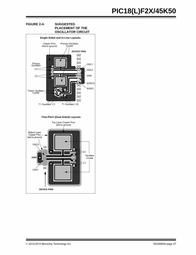
PIC18(L)F2X/45K50
FIGURE 2-4: SUGGESTED PLACEMENT OF THE OSCILLATOR CIRCUIT
GND
`
`
`
OSC1
OSC2
SOSCO
SOSCI
Copper Pour Primary OscillatorCrystal
Timer1 OscillatorCrystal
DEVICE PINS
PrimaryOscillator
C1
C2
T1 Oscillator: C1 T1 Oscillator: C2
(tied to ground)
Single-Sided and In-Line Layouts:
Fine-Pitch (Dual-Sided) Layouts:
GND
OSCO
OSCI
Bottom LayerCopper Pour
OscillatorCrystal
Top Layer Copper Pour
C2
C1
DEVICE PINS
(tied to ground)
(tied to ground)
2012-2014 Microchip Technology Inc. DS30684A-page 27

PIC18(L)F2X/45K50
3.0 OSCILLATOR MODULE (WITH FAIL-SAFE CLOCK MONITOR)
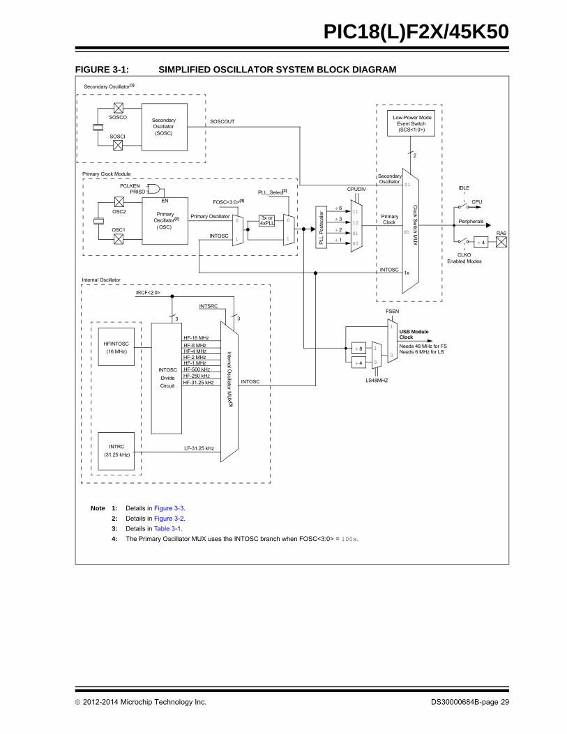
3.1 Overview
The oscillator module has a wide variety of clocksources and selection features that allow it to be usedin a wide range of applications while maximizing perfor-mance and minimizing power consumption. Figure 3-1illustrates a block diagram of the oscillator module.
Clock sources can be configured from externaloscillators, quartz crystal resonators, ceramic resonatorsand Resistor-Capacitor (RC) circuits. In addition, thesystem clock source can be configured from one of threeinternal oscillators, with a choice of speeds selectable viasoftware. Additional clock features include:
• Selectable system clock source between external or internal sources via software.
• Two-Speed Start-up mode, which minimizes latency between external oscillator start-up and code execution.
• Fail-Safe Clock Monitor (FSCM) designed to detect a failure of the external clock source (LP, XT, HS, EC or RC modes) and switch automatically to the internal oscillator.
• Oscillator Start-up Timer (OST) ensures stability of crystal oscillator sources.
The primary clock module can be configured to provideone of six clock sources as the primary clock.
1. RC External Resistor/Capacitor
2. LP Low-Power Crystal
3. XT Crystal/Resonator
4. INTOSC Internal Oscillator
5. HS High-Speed Crystal/Resonator
6. EC External Clock
The HS and EC oscillator circuits can be optimized forpower consumption and oscillator speed using settingsin FOSC<3:0>. Additional FOSC<3:0> selectionsenable RA6 to be used as I/O or CLKO (FOSC/4) forRC, EC and INTOSC Oscillator modes.
Primary clock modes are selectable by the FOSC<3:0>bits of the CONFIG1H Configuration register. Theprimary clock operation is further defined by theseConfiguration and register bits:
1. PCLKEN (CONFIG1H<5>)
2. PRISD (OSCCON2<2>)
3. CFGPLLEN (CONFIG1L<1>)
4. PLLEN (OSCCON2<4>)
5. IRCF<2:0> (OSCCON<6:4>)
6. INTSRC (OSCCON2<5>)
The HFINTOSC and INTRC are factory calibrated highand low-frequency oscillators, respectively, which areused as the internal clock sources.
DS30000684B-page 28 2012-2014 Microchip Technology Inc.
PIC18(L)F2X/45K50
FIGURE 3-1: SIMPLIFIED OSCILLATOR SYSTEM BLOCK DIAGRAM
Note 1: Details in Figure 3-3.
2: Details in Figure 3-2.
3: Details in Table 3-1.
4: The Primary Oscillator MUX uses the INTOSC branch when FOSC<3:0> = 100x.
SOSCO
SOSCI
SecondaryOscillator(SOSC)
Secondary Oscillator(1)
OSC2
OSC1
PrimaryOscillator(2)
(OSC)
Primary Oscillator 0
1
FOSC<3:0>(4)
PLL_Select (3)
0
1
4xPLL
INTOSC
Primary Clock Module
Low-Power ModeEvent Switch(SCS<1:0>)
01
00
1x
SecondaryOscillator
2
PrimaryClock
INTOSC
Clock S
witch M
UX
INTOSC
IRCF<2:0>
INTSRC
HF-16 MHZ
HF-8 MHZ
HF-4 MHZ
HF-2 MHZ
HF-1 MHZ
HF-31.25 kHZ
HF-250 kHZ
HF-500 kHZ
HFINTOSC
INTRC
(16 MHz)
(31.25 kHz)
INTOSC
Divide
Circuit
Internal Oscillator M
UX
(3)
LF-31.25 kHz
3 3
Internal Oscillator
SOSCOUT
PCLKENPRISD
EN
3x or
CPU
Peripherals
IDLE
4
RA6
CLKOEnabled Modes
USB Module1
0
FSEN
8 1
0 4
LS48MHZ
Clock
Needs 48 MHz for FSNeeds 6 MHz for LS
PLL
Pos
tsca
ler
1
2
3
611
10
01
00
CPUDIV
2012-2014 Microchip Technology Inc. DS30000684B-page 29

PIC18(L)F2X/45K50
3.2 Oscillator Control
The OSCCON, OSCCON2 and OSCTUNE registers(Register 3-1 to Register 3-3) control several aspectsof the device clock’s operation, both in full-poweroperation and in power-managed modes.
• Main System Clock Selection (SCS)
• Primary Oscillator Circuit Shutdown (PRISD)
• Secondary Oscillator Enable (SOSCGO)
• Primary Clock Frequency multiplier (PLLEN)
• Internal Frequency selection bits (IRCF, INTSRC)
• Clock Status bits (OSTS, HFIOFS, LFIOFS, SOSCRUN, PLLRDY)
• Power management selection (IDLEN)
3.2.1 MAIN SYSTEM CLOCK SELECTION
The System Clock Select bits, SCS<1:0>, select themain clock source. The available clock sources are:
• Primary clock defined by the FOSC<3:0> bits of CONFIG1H. The primary clock can be the primary oscillator, an external clock, or the internal oscillator block.
• Secondary clock (secondary oscillator)
• Internal oscillator block (HFINTOSC and INTRC).
The clock source changes immediately after one ormore of the bits is written to, following a brief clocktransition interval. The SCS bits are cleared to selectthe primary clock on all forms of Reset.
3.2.2 INTERNAL FREQUENCY SELECTION
The Internal Oscillator Frequency Select bits(IRCF<2:0>) select the frequency output of the internaloscillator block. The choices are the INTRC source(31.25 kHz) and the HFINTOSC source (16 MHz) orone of the frequencies derived from the HFINTOSCpostscaler (31.25 kHz to 16 MHz). If the internal oscil-lator block is supplying the main clock, changing thestates of these bits will have an immediate change onthe internal oscillator’s output. On device Resets, theoutput frequency of the internal oscillator is set to thedefault frequency of 1 MHz.
3.2.3 LOW-FREQUENCY SELECTION
When a nominal output frequency of 31.25 kHz isselected (IRCF<2:0> = 000), users may choosewhich internal oscillator acts as the source. This isdone with the INTSRC bit of the OSCCON2<5>register. See Figure 3-2 and Register 3-1 for specific31.25 kHz selection. This option allows users toselect a 31.25 kHz clock (based on HFINTOSC) thatcan be tuned using the TUN<6:0> bits in theOSCTUNE register, while maintaining power savingswith a very low clock speed. INTRC always remainsthe clock source for features such as the WatchdogTimer and the Fail-Safe Clock Monitor, regardless ofthe setting of the INTSRC bit.
This option allows users to select the tunable and moreprecise HFINTOSC as a clock source, whilemaintaining power savings with a very low clock speed.
3.2.4 POWER MANAGEMENT
The IDLEN bit of the OSCCON register determineswhether the device goes into Sleep mode or one of theIdle modes when the SLEEP instruction is executed.
DS30000684B-page 30 2012-2014 Microchip Technology Inc.

PIC18(L)F2X/45K50
FIGURE 3-2: INTERNAL OSCILLATOR MUX BLOCK DIAGRAM
111110101100
000
INTOSC
31.25 kHz1
0
IRCF<2:0>
INTSRC
HF-16 MHzHF-8 MHzHF-4 MHzHF-2 MHzHF-1 MHz
LF-31.25 kHz
HF-31.25 kHz
3
011HF-500 kHz 010HF-250 kHz 001
TABLE 3-1: PLL_SELECT TRUTH TABLE
Primary Clock MUX Source FOSC<3:0> CFGPLLEN PLLSEL PLLEN SPLLMULT PLL_Select
External Clock (ECHIO/ECHCLKO) 010x 11 x x 3xPLL(1)
0 x x 4xPLL(2)
HS Crystal (HSH) 0010 0 x1
1 3xPLL(1)
0 4xPLL(2)
INTOSC (INTOSCIO, INTOSCCLKO) 100x 0 x OFF
FOSC (all other modes) xxxx x x x x OFF
Note 1: The input clock source must be 16 MHz when 3xPLL is used.
2: The input clock source must be 8 MHz to 12 MHz when 4xPLL is used.
2012-2014 Microchip Technology Inc. DS30000684B-page 31

PIC18(L)F2X/45K50
FIGURE 3-3: SECONDARY OSCILLATOR AND EXTERNAL CLOCK INPUTS
0
1
1
0
EN
SOSCEN SOSCGOT1CON<3>T3CON<3>
To Clock Switch Module
SOSCOUTSecondaryOscillator
SOSCI
SOSCOT1CKI
T3GT3CKI
SOSCEN
SOSCEN
SOSCEN
T3G
T3CMX
T1G
T3CKIT1G
1
0
T1CON<3>
T1CLK_EXT_SRC
T3CLK_EXT_SRC
T3CON<3>
DS30000684B-page 32 2012-2014 Microchip Technology Inc.
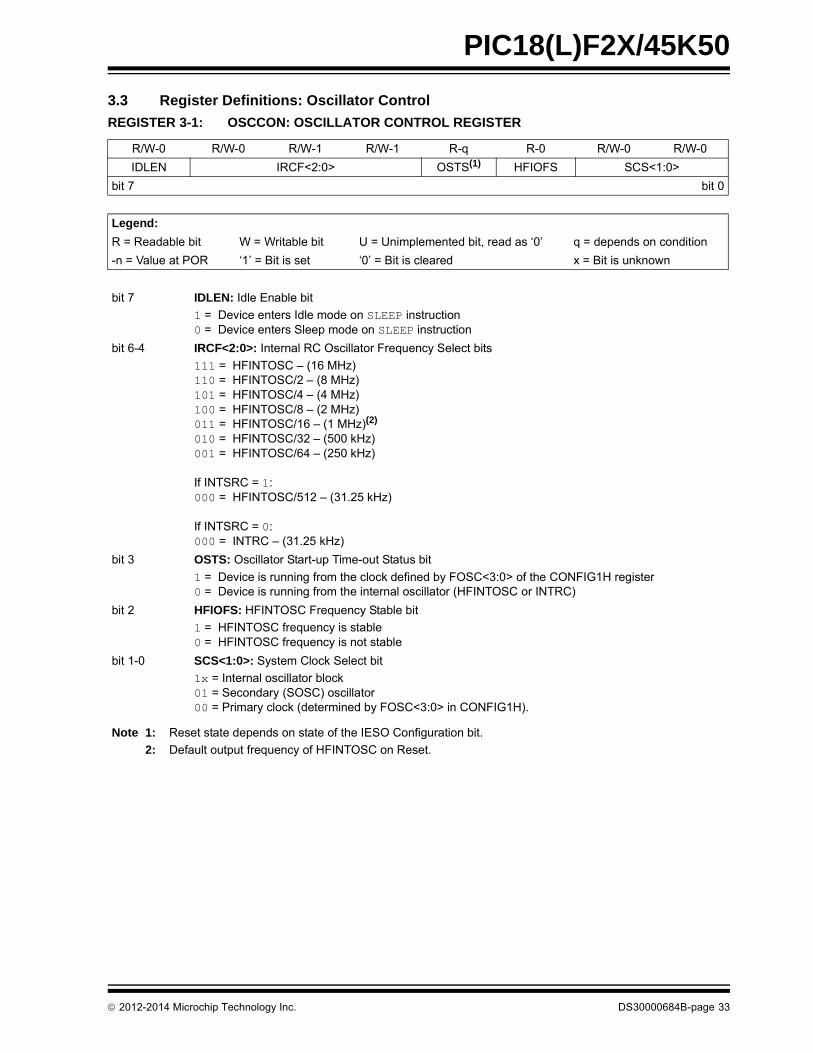
PIC18(L)F2X/45K50
3.3 Register Definitions: Oscillator Control
REGISTER 3-1: OSCCON: OSCILLATOR CONTROL REGISTER
R/W-0 R/W-0 R/W-1 R/W-1 R-q R-0 R/W-0 R/W-0
IDLEN IRCF<2:0> OSTS(1) HFIOFS SCS<1:0>
bit 7 bit 0
Legend:
R = Readable bit W = Writable bit U = Unimplemented bit, read as ‘0’ q = depends on condition
-n = Value at POR ‘1’ = Bit is set ‘0’ = Bit is cleared x = Bit is unknown
bit 7 IDLEN: Idle Enable bit
1 = Device enters Idle mode on SLEEP instruction0 = Device enters Sleep mode on SLEEP instruction
bit 6-4 IRCF<2:0>: Internal RC Oscillator Frequency Select bits
111 = HFINTOSC – (16 MHz)110 = HFINTOSC/2 – (8 MHz) 101 = HFINTOSC/4 – (4 MHz) 100 = HFINTOSC/8 – (2 MHz)011 = HFINTOSC/16 – (1 MHz)(2)
010 = HFINTOSC/32 – (500 kHz)001 = HFINTOSC/64 – (250 kHz)
If INTSRC = 1:000 = HFINTOSC/512 – (31.25 kHz)
If INTSRC = 0:000 = INTRC – (31.25 kHz)
bit 3 OSTS: Oscillator Start-up Time-out Status bit
1 = Device is running from the clock defined by FOSC<3:0> of the CONFIG1H register0 = Device is running from the internal oscillator (HFINTOSC or INTRC)
bit 2 HFIOFS: HFINTOSC Frequency Stable bit
1 = HFINTOSC frequency is stable0 = HFINTOSC frequency is not stable
bit 1-0 SCS<1:0>: System Clock Select bit
1x = Internal oscillator block01 = Secondary (SOSC) oscillator00 = Primary clock (determined by FOSC<3:0> in CONFIG1H).
Note 1: Reset state depends on state of the IESO Configuration bit.
2: Default output frequency of HFINTOSC on Reset.
2012-2014 Microchip Technology Inc. DS30000684B-page 33

PIC18(L)F2X/45K50
REGISTER 3-2: OSCCON2: OSCILLATOR CONTROL REGISTER 2
R-0/0 R-0/q R/W-0 R/W-0/0 R/W-0/u R/W-1/1 R-0/0 R-0/0
PLLRDY SOSCRUN INTSRC PLLEN SOSCGO(1) PRISD HFIOFR LFIOFS
bit 7 bit 0
Legend:
R = Readable bit W = Writable bit U = Unimplemented bit, read as ‘0’ q = depends on condition
‘1’ = Bit is set ‘0’ = Bit is cleared x = Bit is unknown
-n/n = Value at POR and BOR/Value at all other Resets
bit 7 PLLRDY: PLL Run Status bit
1 = System clock comes from PLL0 = System clock comes from an oscillator, other than PLL
bit 6 SOSCRUN: SOSC Run Status bit
1 = System clock comes from secondary SOSC0 = System clock comes from an oscillator, other than SOSC
bit 5 INTSRC: HFINTOSC Divided by 512 Enable bit
1 = HFINTOSC used as the 31.25 kHz system clock reference – high accuracy0 = INTRC used as the 31.25 kHz system clock reference – low power.
bit 4 PLLEN: Software PLL Enable bit
If FOSC<3:0> = 100x, 010x or 001x1 = PLL enabled0 = PLL disabled
Else,No effect on PLL operation.
bit 3 SOSCGO(1): Secondary Oscillator Start Control bit 1 = Secondary oscillator is enabled.0 = Secondary oscillator is shut off if no other sources are requesting it.
bit 2 PRISD: Primary Oscillator Drive Circuit Shutdown bit
1 = Oscillator drive circuit on0 = Oscillator drive circuit off (zero power)
bit 1 HFIOFR: HFINTOSC Status bit
1 = HFINTOSC is running0 = HFINTOSC is not running
bit 0 LFIOFS: INTRC Frequency Stable bit
1 = INTRC is stable0 = INTRC is not stable
Note 1: The SOSCGO bit is only reset on a POR Reset.
DS30000684B-page 34 2012-2014 Microchip Technology Inc.

PIC18(L)F2X/45K50
3.4 Clock Source Modes
Clock source modes can be classified as external orinternal.
• External Clock modes rely on external circuitry for the clock source. Examples are: Clock modules (EC mode), quartz crystal resonators or ceramic resonators (LP, XT and HS modes) and Resistor-Capacitor (RC mode) circuits.
• Internal clock sources are contained internally within the Oscillator block. The Oscillator block has two internal oscillators: the 16 MHz High-Frequency Internal Oscillator (HFINTOSC) and the 31.25 kHz Low-Frequency Internal Oscillator (INTRC).
The system clock can be selected between external orinternal clock sources via the System Clock Select(SCS<1:0>) bits of the OSCCON register. SeeSection 3.11 “Clock Switching” for additionalinformation.
3.5 External Clock Modes
3.5.1 OSCILLATOR START-UP TIMER (OST)
When the oscillator module is configured for LP, XT orHS modes, the Oscillator Start-up Timer (OST) counts1024 oscillations from OSC1. This occurs following aPower-on Reset (POR) and when the Power-up Timer(PWRT) has expired (if configured), or a wake-up fromSleep. During this time, the program counter does notincrement and program execution is suspended. TheOST ensures that the oscillator circuit, using a quartzcrystal resonator or ceramic resonator, has started andis providing a stable system clock to the oscillatormodule. When switching between clock sources, adelay is required to allow the new clock to stabilize.These oscillator delays are shown in Table 3-2.
In order to minimize latency between external oscillatorstart-up and code execution, the Two-Speed ClockStart-up mode can be selected (see Section 3.12“Two-Speed Clock Start-up Mode”).
TABLE 3-2: OSCILLATOR DELAY EXAMPLES
3.5.2 EC MODE
The External Clock (EC) mode allows an externallygenerated logic level as the system clock source. Whenoperating in this mode, an external clock source isconnected to the OSC1 input and the OSC2 is availablefor general purpose I/O. Figure 3-4 shows the pinconnections for EC mode.
The External Clock (EC) offers different power modes,Low Power (ECL), Medium Power (ECM) and HighPower (ECH), selectable by the FOSC<3:0> bits. Eachmode is best suited for a certain range of frequencies.The ranges are:
• ECL – below 4 MHz• ECM – between 4 MHz and 16 MHz• ECH – above 16 MHz
The Oscillator Start-up Timer (OST) is disabled whenEC mode is selected. Therefore, there is no delay inoperation after a Power-on Reset (POR) or Wake-upfrom Sleep. Because the PIC® MCU design is fullystatic, stopping the external clock input will have theeffect of halting the device while leaving all data intact.Upon restarting the external clock, the device willresume operation as if no time had elapsed.
FIGURE 3-4: EXTERNAL CLOCK (EC) MODE OPERATION
Switch From Switch To Frequency Oscillator Delay
Sleep/PORINTRC
HFINTOSC31.25 kHz
31.25 kHz to 16 MHzOscillator Warm-Up Delay (TWARM)
Sleep/POR EC, RC DC – 48 MHz 2 instruction cycles
INTRC (31.25 kHz) EC, RC DC – 48 MHz 1 cycle of each
Sleep/POR LP, XT, HS 32 kHz to 25 MHz 1024 Clock Cycles (OST)
Sleep/POR PLL 32 MHz to 48 MHz 1024 Clock Cycles (OST) + 2 ms
INTRC (31.25 kHz) INTRCHFINTOSC
31.25 kHz to 16 MHz 1 s (approx.)
OSC1/CLKIN
OSC2/CLKOI/O
Clock fromExt. System
PIC® MCU
2012-2014 Microchip Technology Inc. DS30000684B-page 35

PIC18(L)F2X/45K50
3.5.3 LP, XT, HS MODES
The LP, XT and HS modes support the use of quartzcrystal resonators or ceramic resonators connected toOSC1 and OSC2 (Figure 3-5). The mode selects a low,medium or high gain setting of the internal inverter-amplifier to support various resonator types and speed.
LP Oscillator mode selects the lowest gain setting of theinternal inverter-amplifier. LP mode current consumptionis the least of the three modes. This mode is best suitedto drive resonators with a low drive level specification, forexample, tuning fork type crystals.
XT Oscillator mode selects the intermediate gainsetting of the internal inverter-amplifier. XT modecurrent consumption is the medium of the three modes.This mode is best suited to drive resonators with amedium drive level specification.
HS Oscillator mode offers a Medium Power (MP) and aHigh Power (HP) option selectable by the FOSC<3:0>bits. The MP selections are best suited for oscillatorfrequencies between 4 and 16 MHz. The HP selectionhas the highest gain setting of the internal inverter-amplifier and is best suited for frequencies above16 MHz. HS mode is best suited for resonators thatrequire a high drive setting.
FIGURE 3-5: QUARTZ CRYSTAL OPERATION (LP, XT OR HS MODE)
FIGURE 3-6: CERAMIC RESONATOR OPERATION(XT OR HS MODE)
Note 1: A series resistor (RS) may be required forquartz crystals with low drive level.
2: The value of RF varies with the Oscillator modeselected (typically between 2 M to 10 M.
C1
C2
Quartz
RS(1)
OSC1/CLKIN
RF(2) Sleep
To Internal Logic
PIC® MCU
Crystal
OSC2/CLKO
Note 1: Quartz crystal characteristics varyaccording to type, package andmanufacturer. The user should consult themanufacturer data sheets for specificationsand recommended application.
2: Always verify oscillator performance overthe VDD and temperature range that isexpected for the application.
3: For oscillator design assistance, refer to thefollowing Microchip Application Notes:
• AN826, “Crystal Oscillator Basics and Crystal Selection for rfPIC® and PIC® Devices” (DS00826)
• AN849, “Basic PIC® Oscillator Design” (DS00849)
• AN943, “Practical PIC® Oscillator Analysis and Design” (DS00943)
• AN949, “Making Your Oscillator Work” (DS00949)
Note 1: A series resistor (RS) may be required forceramic resonators with low drive level.
2: The value of RF varies with the Oscillator modeselected (typically between 2 M to 10 M.
3: An additional parallel feedback resistor (RP)may be required for proper ceramic resonatoroperation.
C1
C2 Ceramic RS(1)
OSC1/CLKIN
RF(2) Sleep
To Internal Logic
PIC® MCU
RP(3)
Resonator
OSC2/CLKO
DS30000684B-page 36 2012-2014 Microchip Technology Inc.
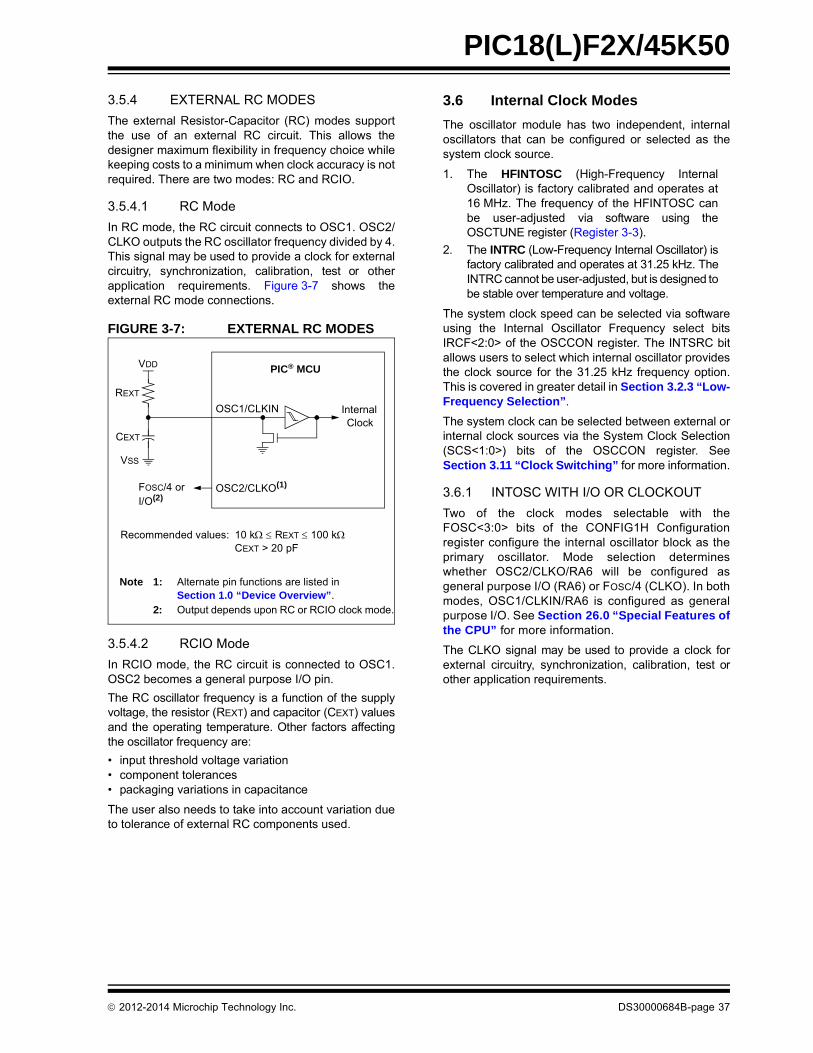
PIC18(L)F2X/45K50
3.5.4 EXTERNAL RC MODES
The external Resistor-Capacitor (RC) modes supportthe use of an external RC circuit. This allows thedesigner maximum flexibility in frequency choice whilekeeping costs to a minimum when clock accuracy is notrequired. There are two modes: RC and RCIO.
3.5.4.1 RC Mode
In RC mode, the RC circuit connects to OSC1. OSC2/CLKO outputs the RC oscillator frequency divided by 4.This signal may be used to provide a clock for externalcircuitry, synchronization, calibration, test or otherapplication requirements. Figure 3-7 shows theexternal RC mode connections.
FIGURE 3-7: EXTERNAL RC MODES
3.5.4.2 RCIO Mode
In RCIO mode, the RC circuit is connected to OSC1.OSC2 becomes a general purpose I/O pin.
The RC oscillator frequency is a function of the supplyvoltage, the resistor (REXT) and capacitor (CEXT) valuesand the operating temperature. Other factors affectingthe oscillator frequency are:
• input threshold voltage variation• component tolerances• packaging variations in capacitance
The user also needs to take into account variation dueto tolerance of external RC components used.
3.6 Internal Clock Modes
The oscillator module has two independent, internaloscillators that can be configured or selected as thesystem clock source.
1. The HFINTOSC (High-Frequency InternalOscillator) is factory calibrated and operates at16 MHz. The frequency of the HFINTOSC canbe user-adjusted via software using theOSCTUNE register (Register 3-3).
2. The INTRC (Low-Frequency Internal Oscillator) isfactory calibrated and operates at 31.25 kHz. TheINTRC cannot be user-adjusted, but is designed tobe stable over temperature and voltage.
The system clock speed can be selected via softwareusing the Internal Oscillator Frequency select bitsIRCF<2:0> of the OSCCON register. The INTSRC bitallows users to select which internal oscillator providesthe clock source for the 31.25 kHz frequency option.This is covered in greater detail in Section 3.2.3 “Low-Frequency Selection”.
The system clock can be selected between external orinternal clock sources via the System Clock Selection(SCS<1:0>) bits of the OSCCON register. SeeSection 3.11 “Clock Switching” for more information.
3.6.1 INTOSC WITH I/O OR CLOCKOUT
Two of the clock modes selectable with theFOSC<3:0> bits of the CONFIG1H Configurationregister configure the internal oscillator block as theprimary oscillator. Mode selection determineswhether OSC2/CLKO/RA6 will be configured asgeneral purpose I/O (RA6) or FOSC/4 (CLKO). In bothmodes, OSC1/CLKIN/RA6 is configured as generalpurpose I/O. See Section 26.0 “Special Features ofthe CPU” for more information.
The CLKO signal may be used to provide a clock forexternal circuitry, synchronization, calibration, test orother application requirements.
OSC2/CLKO(1)
CEXT
REXT
PIC® MCU
OSC1/CLKIN
FOSC/4 or
InternalClock
VDD
VSS
Recommended values: 10 k REXT 100 kCEXT > 20 pF
Note 1: Alternate pin functions are listed in Section 1.0 “Device Overview”.
2: Output depends upon RC or RCIO clock mode.
I/O(2)
2012-2014 Microchip Technology Inc. DS30000684B-page 37

PIC18(L)F2X/45K50
3.6.1.1 OSCTUNE Register
The HFINTOSC oscillator circuits are factory calibratedbut can be adjusted in software by writing to theTUN<6:0> bits of the OSCTUNE register(Register 3-3).
The default value of the TUN<6:0> is ‘0’. The value is a7-bit two’s complement number.
When the OSCTUNE register is modified, theHFINTOSC frequency will begin shifting to the newfrequency. Code execution continues during this shift.There is no indication that the shift has occurred.
The TUN<6:0> bits in OSCTUNE do not affect theINTRC frequency. Operation of features that depend onthe INTRC clock source frequency, such as the Power-up Timer (PWRT), Watchdog Timer (WDT), Fail-SafeClock Monitor (FSCM) and peripherals, are not affectedby the change in frequency.
The OSCTUNE register also implements theSPLLMULT bit, which controls whether 3x or 4xPLLclock multiplication is used when the PLL is enableddynamically in software. For more details about thefunction of the SPLLMULT bit see Section 3.8.2 “PLLin HFINTOSC Modes”.
3.7 Register Definitions: Oscillator Tuning
REGISTER 3-3: OSCTUNE: OSCILLATOR TUNING REGISTER
R/W-0 R/W-0 R/W-0 R/W-0 R/W-0 R/W-0 R/W-0 R/W-0
SPLLMULT TUN<6:0>
bit 7 bit 0
Legend:
R = Readable bit W = Writable bit U = Unimplemented bit, read as ‘0’
-n = Value at POR ‘1’ = Bit is set ‘0’ = Bit is cleared x = Bit is unknown
bit 7 SPLLMULT: Software PLL Multiplier Select bit
If PLL Enabled, SPLLMULT changes are ignored.Else,
Selects which PLL multiplier will be used:1 = 3xPLL is selected0 = 4xPLL is selected
bit 6-0 TUN<6:0>: Frequency Tuning bits – affects HFINTOSC(1)
0111111 = Maximum frequency0111110 = • • •0000001 = 0000000 = Center frequency. Oscillator module is running at the factory calibrated frequency.1111111 = • • •1000000 = Minimum frequency
Note 1: The TUN<6:0> bits may be supplied and controlled by the Active Clock Tuning module (see Section 3.15 “Active Clock Tuning (ACT) Module”) When the Active Clock Tuning is enabled, the TUN<6:0> bits are read-only.
DS30000684B-page 38 2012-2014 Microchip Technology Inc.

PIC18(L)F2X/45K50
3.7.1 INTRC
The Low-Frequency Internal Oscillator (INTRC) is a31.25 kHz internal clock source. The INTRC is nottunable, but is designed to be stable acrosstemperature and voltage. See Section 29.0“Electrical Specifications” for the INTRC accuracyspecifications.
The output of the INTRC can be a clock source to theprimary clock or the INTOSC clock (see Figure 3-1). TheINTRC is also the clock source for the Power-up Timer(PWRT), Watchdog Timer (WDT) and Fail-Safe ClockMonitor (FSCM).
3.7.2 FREQUENCY SELECT BITS (IRCF)
The HFINTOSC (16 MHz) outputs to a divide circuitthat provides frequencies of 16 MHz to 31.25 kHz.These divide circuit frequencies, along with the31.25 kHz INTRC output, are multiplexed to provide asingle INTOSC clock output (see Figure 3-1). TheIRCF<2:0> bits of the OSCCON register and theINTSRC bit of the OSCCON2 register select the outputfrequency of the internal oscillators. One of eightfrequencies can be selected via software:
• 16 MHz
• 8 MHz
• 4 MHz
• 2 MHz
• 1 MHz (Default after Reset)
• 500 kHz
• 250 kHz
• 31 kHz (INTRC or HFINTOSC)
3.7.3 INTOSC FREQUENCY DRIFT
The factory calibrates the internal oscillator block outputs(HFINTOSC) for 16 MHz. However, this frequency maydrift as VDD or temperature changes. It is possible toautomatically tune the HFINTOSC frequency usingUSB or secondary oscillator sources using the activeclock tuning module (see Section 3.15 “Active ClockTuning (ACT) Module”). The HFINTOSC frequencymay be manually adjusted using the TUN<6:0> bits inthe OSCTUNE register. This has no effect on the INTRCclock source frequency.
Manually tuning the HFINTOSC source requiresknowing when to make the adjustment, in whichdirection it should be made and, in some cases, howlarge a change is needed. Three possible compensationtechniques are discussed in the following sections.However, other techniques may be used.
3.7.3.1 Compensating with the EUSART
An adjustment may be required when the EUSARTbegins to generate framing errors or receives data witherrors while in Asynchronous mode. Framing errorsindicate that the device clock frequency is too high; toadjust for this, decrement the value in OSCTUNE toreduce the clock frequency. On the other hand, errorsin data may suggest that the clock speed is too low; tocompensate, increment OSCTUNE to increase theclock frequency.
3.7.3.2 Compensating with the Timers
This technique compares device clock speed to somereference clock. Two timers may be used; one timer isclocked by the peripheral clock, while the other isclocked by a fixed reference source, such as the Tim-er1 oscillator.
Both timers are cleared, but the timer clocked by thereference generates interrupts. When an interruptoccurs, the internally clocked timer is read and bothtimers are cleared. If the internally clocked timer valueis greater than expected, then the internal oscillatorblock is running too fast. To adjust for this, decrementthe OSCTUNE register.
3.7.3.3 Compensating with the CCP Module in Capture Mode
A CCP module can use free running Timer1 or Timer3clocked by the internal oscillator block and an externalevent with a known period (i.e., AC power frequency).The time of the first event is captured in theCCPRxH:CCPRxL registers and is recorded for use later.When the second event causes a capture, the time of thefirst event is subtracted from the time of the secondevent. Since the period of the external event is known,the time difference between events can be calculated.
If the measured time is much greater than thecalculated time, the internal oscillator block is runningtoo fast; to compensate, decrement the OSCTUNEregister. If the measured time is much less than thecalculated time, the internal oscillator block is runningtoo slow; to compensate, increment the OSCTUNEregister.
2012-2014 Microchip Technology Inc. DS30000684B-page 39

PIC18(L)F2X/45K50
DS
3.8 PLL Frequency Multiplier
A Phase-Locked Loop (PLL) circuit is provided as anoption for users who wish to use a lower frequencyoscillator circuit or to clock the device up to its highestrated frequency from the crystal oscillator. This may beuseful for customers who are concerned with EMI dueto high-frequency crystals or users who require higherclock speeds from an internal oscillator.
3.8.1 PLL IN EXTERNAL OSCILLATOR MODES
The PLL can be enabled for any of the externaloscillator modes using the OSC1/OSC2 pins. Medium-power and low-power oscillator mode selections inCONFIG1H<3:0> (FOSC) should not be used with thePLL. The PLL can be enabled using the CFGPLLEN/PLLSEL configuration bits in the CONFIG1L register,or by software using the PLLEN/SPLLMULT specialfunction register bits in OSCCON2 and OSCTUNE,respectively.A selectable 3x or 4x frequency multiplier circuit isprovided. This gives greater flexibility in source clockfrequencies that can be used. Source clockfrequencies between 8 and 12 MHz may use the 4xfrequency multiplier to achieve operating speeds of 32through 48 MHz. A source clock frequency of 16 MHzmay use the 3x frequency multiplier to achieve 48MHz operating speed.
3.8.2 PLL IN HFINTOSC MODES
The PLL can be enabled using the HFINTOSC internaloscillator block. The frequency select bits (IRCF<2:0>in the OSCCON register) should be configured for 16MHz when using the HFINTOSC with 3x frequencymultiplier. The IRCF bits should be configured for 8MHz when using HFINTOSC with 4x frequencymultiplier.
3.9 Effects of Power-Managed Modes on the Various Clock Sources
For more information about the modes discussed in thissection see Section 4.0 “Power-Managed Modes”. Aquick reference list is also available in Table 4-1.
When PRI_IDLE mode is selected, the designatedprimary oscillator continues to run without interruption.For all other power-managed modes, the oscillatorusing the OSC1 pin is disabled. The OSC1 pin (andOSC2 pin, if used by the oscillator) will stop oscillating.
In secondary clock modes (SEC_RUN andSEC_IDLE), the secondary oscillator (SOSC) isoperating and providing the device clock. Thesecondary oscillator may also run in all power-managed modes if required to clock Timer1 or Timer3.
In internal oscillator modes (INTOSC_RUN andINTOSC_IDLE), the internal oscillator block providesthe device clock source. The 31.25 kHz INTRC outputcan be used directly to provide the clock and may beenabled to support various special features, regardlessof the power-managed mode (see Section 26.3“Watchdog Timer (WDT)”, Section 3.12 “Two-Speed Clock Start-up Mode” and Section 3.13 “Fail-Safe Clock Monitor” for more information on WDT,Fail-Safe Clock Monitor and Two-Speed Start-up). TheHFINTOSC output may be used directly to clock thedevice or may be divided down by the postscaler. TheHFINTOSC output is disabled when the clock isprovided directly from the INTRC output.
When the Sleep mode is selected, all clock sources arestopped. Since all the transistor switching currentshave been stopped, Sleep mode achieves the lowestcurrent consumption of the device (only leakagecurrents).
Enabling any on-chip feature that will operate duringSleep will increase the current consumed during Sleep.The INTRC is required to support WDT operation.Other features may be operating that do not require adevice clock source (i.e., SSP slave, INTn pins andothers). Peripherals that may add significant currentconsumption are listed in Table 29-8.
30000684B-page 40 2012-2014 Microchip Technology Inc.

PIC18(L)F2X/45K50
3.10 Power-up Delays
Power-up delays are controlled by two timers, so thatno external Reset circuitry is required for mostapplications. The delays ensure that the device is keptin Reset until the device power supply is stable undernormal circumstances and the primary clock isoperating and stable. For additional information onpower-up delays, see Section 5.7 “Device ResetTimers”.
The first timer is the Power-up Timer (PWRT), whichprovides a fixed delay on power-up. It is enabled byclearing (= 0) the PWRTEN Configuration bit.
The second timer is the Oscillator Start-up Timer(OST), intended to keep the chip in Reset until thecrystal oscillator is stable (LP, XT and HS modes). TheOST does this by counting 1024 oscillator cyclesbefore allowing the oscillator to clock the device.
When the PLL is enabled with external oscillatormodes, the device runs off of the base external oscilla-tor for 2 ms, following the OST delay, so the PLL canlock to the incoming clock frequency.
There is a delay of interval TCSD, following POR, whilethe controller becomes ready to execute instructions.This delay runs concurrently with any other delays.This may be the only delay that occurs when any of theEC, RC or INTIOSC modes are used as the primaryclock source.
When the HFINTOSC is selected as the primary clock,the main system clock can be delayed until theHFINTOSC is stable. This is user selectable by theHFOFST bit of the CONFIG3H Configuration register.When the HFOFST bit is cleared, the main systemclock is delayed until the HFINTOSC is stable. Whenthe HFOFST bit is set, the main system clock startsimmediately.
In either case, the HFIOFS bit of the OSCCON registercan be read to determine whether the HFINTOSC isoperating and stable.
TABLE 3-3: OSC1 AND OSC2 PIN STATES IN SLEEP MODE
OSC Mode OSC1 Pin OSC2 Pin
RC, INTOSC with CLKO Floating, external resistor should pull high At logic low (clock/4 output)
RC with IO Floating, external resistor should pull high Configured as PORTA, bit 6
INTOSC with IO Configured as PORTA, bit 7 Configured as PORTA, bit 6
EC with IO Floating, pulled by external clock Configured as PORTA, bit 6
EC with CLKO Floating, pulled by external clock At logic low (clock/4 output)
LP, XT, HS Feedback inverter disabled at quiescent voltage level
Feedback inverter disabled at quiescent voltage level
Note: See Table 5-2 in Section 5.0 “Reset” for time-outs due to Sleep and MCLR Reset.
2012-2014 Microchip Technology Inc. DS30000684B-page 41

PIC18(L)F2X/45K50
3.11 Clock Switching
The system clock source can be switched betweenexternal and internal clock sources via software usingthe System Clock Select (SCS<1:0>) bits of theOSCCON register.
PIC18(L)F2X/45K50 devices contain circuitry toprevent clock “glitches” when switching between clocksources. A short pause in the device clock occursduring the clock switch. The length of this pause is thesum of two cycles of the old clock source and three tofour cycles of the new clock source. This formulaassumes that the new clock source is stable.
Clock transitions are discussed in greater detail inSection 4.1.2 “Entering Power-Managed Modes”.
3.11.1 SYSTEM CLOCK SELECT (SCS<1:0>) BITS
The System Clock Select (SCS<1:0>) bits of theOSCCON register select the system clock source thatis used for the CPU and peripherals.
• When SCS<1:0> = 00, the system clock source is determined by configuration of the FOSC<3:0> bits in the CONFIG1H Configuration register.
• When SCS<1:0> = 10, the system clock source is chosen by the internal oscillator frequency selected by the INTSRC bit of the OSCCON2<5> register and the IRCF<2:0> bits of the OSCCON register.
• When SCS<1:0> = 01, the system clock source is the 32.768 kHz secondary oscillator shared with Timer1 and Timer3.
After a Reset, the SCS<1:0> bits of the OSCCONregister are always cleared.
3.11.2 OSCILLATOR START-UP TIME-OUT STATUS (OSTS) BIT
The Oscillator Start-up Time-out Status (OSTS) bit ofthe OSCCON register indicates whether the systemclock is running from the external clock source, asdefined by the FOSC<3:0> bits in the CONFIG1HConfiguration register, or from the internal clocksource. In particular, when the primary oscillator is thesource of the primary clock, OSTS indicates that theOscillator Start-up Timer (OST) has timed out for LP,XT or HS modes.
3.11.3 CLOCK SWITCH TIMING
When switching between one oscillator and another,the new oscillator may not be operating which savespower (see Figure 3-8). If this is the case, there is adelay after the SCS<1:0> bits of the OSCCON registerare modified before the frequency change takes place.The OSTS and HFIOFR, LFIOFS bits of the OSCCONand OSCCON2 registers will reflect the current activestatus of the external and HFINTOSC oscillators. Thetiming of a frequency selection is as follows:
1. SCS<1:0> bits of the OSCCON register aremodified.
2. The old clock continues to operate until the newclock is ready.
3. Clock switch circuitry waits for two consecutiverising edges of the old clock after the new clockready signal goes true.
4. The system clock is held low starting at the nextfalling edge of the old clock.
5. Clock switch circuitry waits for an additional tworising edges of the new clock.
6. On the next falling edge of the new clock the lowhold on the system clock is released and newclock is switched in as the system clock.
7. Clock switch is complete.
See Figure 3-1 for more details.
If the HFINTOSC is the source of both the old and newfrequency, there is no start-up delay before the newfrequency is active. This is because the old and newfrequencies are derived from the HFINTOSC via thepostscaler and multiplexer.
Start-up delay specifications are located inSection 29.0 “Electrical Specifications”, under ACSpecifications (Oscillator Module).Note: Any automatic clock switch, which may
occur from Two-Speed Start-up or Fail-Safe Clock Monitor, does not update theSCS<1:0> bits of the OSCCON register.The user can monitor the SOSCRUN andLFIOFS bits of the OSCCON2 register, andthe HFIOFS and OSTS bits of theOSCCON register to determine the currentsystem clock source.
DS30000684B-page 42 2012-2014 Microchip Technology Inc.

PIC18(L)F2X/45K50
3.12 Two-Speed Clock Start-up Mode
Two-Speed Start-up mode provides additional powersavings by minimizing the latency between externaloscillator start-up and code execution. In applicationsthat make heavy use of the Sleep mode, Two-SpeedStart-up will remove the external oscillator start-uptime from the time spent awake and can reduce theoverall power consumption of the device.
This mode allows the application to wake-up fromSleep, perform a few instructions using the HFINTOSCas the clock source and go back to Sleep withoutwaiting for the primary oscillator to become stable.
When the oscillator module is configured for LP, XT orHS modes, the Oscillator Start-up Timer (OST) isenabled (see Section 3.5.1 “Oscillator Start-up Timer(OST)”). The OST will suspend program execution until1024 oscillations are counted. Two-Speed Start-upmode minimizes the delay in code execution byoperating from the internal oscillator as the OST iscounting. When the OST count reaches 1024 and theOSTS bit of the OSCCON register is set, programexecution switches to the external oscillator.
3.12.1 TWO-SPEED START-UP MODE CONFIGURATION
Two-Speed Start-up mode is enabled when all of thefollowing settings are configured as noted:
• Two-Speed Start-up mode is enabled when the IESO of the CONFIG1H Configuration register is set.
• SCS<1:0> (of the OSCCON register) = 00.
• FOSC<2:0> bits of the CONFIG1H Configuration register are configured for LP, XT or HS mode.
Two-Speed Start-up mode becomes active after:
• Power-on Reset (POR) and, if enabled, after Power-up Timer (PWRT) has expired, or
• Wake-up from Sleep.
Note: Executing a SLEEP instruction will abortthe oscillator start-up time and will causethe OSTS bit of the OSCCON register toremain clear.
2012-2014 Microchip Technology Inc. DS30000684B-page 43

PIC18(L)F2X/45K50
3.12.2 TWO-SPEED START-UP SEQUENCE
1. Wake-up from Power-on Reset or Sleep.
2. Instructions begin executing by the internaloscillator at the frequency set in the IRCF<2:0>bits of the OSCCON register.
3. OST enabled to count 1024 external clockcycles.
4. OST timed out. External clock is ready.
5. OSTS is set.
6. Clock switch finishes according to Figure 3-8
3.12.3 CHECKING TWO-SPEED CLOCK STATUS
Checking the state of the OSTS bit of the OSCCONregister will confirm if the microcontroller is runningfrom the external clock source, as defined by theFOSC<2:0> bits in CONFIG1H Configuration register,or the internal oscillator. OSTS = 0 when the externaloscillator is not ready, which indicates that the systemis running from the internal oscillator.
FIGURE 3-8: CLOCK SWITCH TIMING
Old Clock
New Clock
IRCF <2:0>
System Clock
Start-up Time(1) Clock Sync Running
High Speed Low Speed
Select Old Select New
New Clk Ready
Low Speed High Speed
Old Clock
New Clock
IRCF <2:0>
System Clock
Start-up Time(1) Clock Sync Running
Select Old Select New
New Clk Ready
Note 1: Start-up time includes TOST (1024 TOSC) for external clocks, plus TPLL (approx. 2 ms) for HSPLL mode.
DS30000684B-page 44 2012-2014 Microchip Technology Inc.

PIC18(L)F2X/45K50
3.13 Fail-Safe Clock Monitor
The Fail-Safe Clock Monitor (FSCM) allows the deviceto continue operating should the external oscillator fail.The FSCM can detect oscillator failure any time afterthe Oscillator Start-up Timer (OST) has expired. TheFSCM is enabled by setting the FCMEN bit in theCONFIG1H Configuration register. The FSCM isapplicable to all external oscillator modes (LP, XT, HS,EC, RC and RCIO).
FIGURE 3-9: FSCM BLOCK DIAGRAM
3.13.1 FAIL-SAFE DETECTION
The FSCM module detects a failed oscillator bycomparing the external oscillator to the FSCM sampleclock. The sample clock is generated by dividing theINTRC by 64 (see Figure 3-9). Inside the fail detectorblock is a latch. The external clock sets the latch oneach falling edge of the external clock. The sampleclock clears the latch on each rising edge of the sampleclock. A failure is detected when an entire half-cycle ofthe sample clock elapses before the primary clock goeslow.
3.13.2 FAIL-SAFE OPERATION
When the external clock fails, the FSCM switches thedevice clock to an internal clock source and sets the bitflag OSCFIF of the PIR2 register. The OSCFIF flag willgenerate an interrupt if the OSCFIE bit of the PIE2register is also set. The device firmware can then takesteps to mitigate the problems that may arise from afailed clock. The system clock will continue to besourced from the internal clock source until the devicefirmware successfully restarts the external oscillatorand switches back to external operation. An automatictransition back to the failed clock source will not occur.
The internal clock source chosen by the FSCM isdetermined by the IRCF<2:0> bits of the OSCCONregister. This allows the internal oscillator to beconfigured before a failure occurs.
3.13.3 FAIL-SAFE CONDITION CLEARING
The Fail-Safe condition is cleared by either one of thefollowing:
• Any Reset
• By toggling the SCS1 bit of the OSCCON register
Both of these conditions restart the OST. While theOST is running, the device continues to operate fromthe INTOSC selected in OSCCON. When the OSTtimes out, the Fail-Safe condition is cleared and thedevice automatically switches over to the external clocksource. The Fail-Safe condition need not be clearedbefore the OSCFIF flag is cleared.
3.13.4 RESET OR WAKE-UP FROM SLEEP
The FSCM is designed to detect an oscillator failureafter the Oscillator Start-up Timer (OST) has expired.The OST is used after waking up from Sleep and afterany type of Reset. The OST is not used with the EC orRC Clock modes so that the FSCM will be active assoon as the Reset or wake-up has completed.
External
INTRC÷ 64
S
R
Q
31 kHz(~32 s)
488 Hz(~2 ms)
Clock MonitorLatch
ClockFailure
Detected
Oscillator
Clock
Q
Sample ClockNote: Due to the wide range of oscillator start-up
times, the Fail-Safe circuit is not activeduring oscillator start-up (i.e., after exitingReset or Sleep). After an appropriateamount of time, the user should check theOSTS bit of the OSCCON register to verifythe oscillator start-up and that the systemclock switchover has successfullycompleted.
Note: When the device is configured for Fail-Safe clock monitoring in either HS, XT, orLS oscillator modes then the IESO config-uration bit should also be set so that theclock will automatically switch from theinternal clock to the external oscillatorwhen the OST times out.
2012-2014 Microchip Technology Inc. DS30000684B-page 45

PIC18(L)F2X/45K50
FIGURE 3-10: FSCM TIMING DIAGRAM
OSCFIF
SystemClock
Output
Sample Clock
FailureDetected
OscillatorFailure
Note: The system clock is normally at a much higher frequency than the sample clock. The relative frequencies inthis example have been chosen for clarity.
(Q)
Test Test Test
Clock Monitor Output
TABLE 3-4: REGISTERS ASSOCIATED WITH CLOCK SOURCES
Name Bit 7 Bit 6 Bit 5 Bit 4 Bit 3 Bit 2 Bit 1 Bit 0Register on page
INTCON GIE/GIEH PEIE/GIEL TMR0IE INT0IE IOCIE TMR0IF INT0IF IOCIF 114
IPR2 OSCFIP C1IP C2IP EEIP BCLIP HLVDIP TMR3IP CCP2IP 124
OSCCON IDLEN IRCF<2:0> OSTS HFIOFS SCS<1:0> 33
OSCCON2 PLLRDY SOSCRUN INTSRC PLLEN SOSCGO PRISD HFIOFR LFIOFS 34
OSCTUNE SPLLMULT TUN<6:0> 38
PIE2 OSCFIE C1IE C2IE EEIE BCLIE HLVDIE TMR3IE CCP2IE 121
PIR2 OSCFIF C1IF C2IF EEIF BCLIF HLVDIF TMR3IF CCP2IF 118
Legend: — = unimplemented locations, read as ‘0’. Shaded bits are not used by clock sources.
TABLE 3-5: CONFIGURATION REGISTERS ASSOCIATED WITH CLOCK SOURCES
Name Bit 7 Bit 6 Bit 5 Bit 4 Bit 3 Bit 2 Bit 1 Bit 0Register on page
CONFIG1H IESO FCMEN PCLKEN — FOSC<3:0> 373
CONFIG2L — LPBOR — BORV<1:0> BOREN<1:0> PWRTEN 374
Legend: — = unimplemented locations, read as ‘0’. Shaded bits are not used for clock sources.
DS30000684B-page 46 2012-2014 Microchip Technology Inc.

PIC18(L)F2X/45K50
3.14 Oscillator Settings for USB
When the PIC18(L)F2X/45K50 family devices are usedfor USB connectivity, a 6 MHz or 48 MHz clock must beprovided to the USB module for operation in eitherLow-Speed or Full-Speed modes, respectively. Thismay require some forethought in selecting an oscillatorfrequency and programming the device.
The full range of possible oscillator configurationscompatible with USB operation is shown in Table 3-7.
3.14.1 LOW-SPEED OPERATION
The USB clock for Low-Speed mode is derived from theprimary oscillator or from the PLL. In order to operatethe USB module in Low-Speed mode, a 6 MHz clockmust be provided to the USB module.
See Table 3-6 and Table 3-7 for possible combinationswhich can be used for low-speed USB operation.
TABLE 3-6: CLOCK FOR LOW-SPEED USB
System Clock CPUDIV<1:0> Microcontroller Clock LS48MHZ USB Clock
48 11 48/6 = 8 MHz 1 48/8 = 6 MHz
48 10 48/3 = 16 MHz 1 48/8 = 6 MHz
48 01 48/2 = 24 MHz 1 48/8 = 6 MHz
48 00 48 MHz 1 48/8 = 6 MHz
24 11 24/6 = 4 MHz 0 24/4 = 6 MHz
24 10 24/3 = 8 MHz 0 24/4 = 6 MHz
24 01 24/2 = 12 MHz 0 24/4 = 6 MHz
24 00 24 MHz 0 24/4 = 6 MHz
TABLE 3-7: OSCILLATOR CONFIGURATION OPTIONS FOR USB OPERATION
Input Oscillator Frequency
Clock Mode (FOSC<3:0>)
MCU Clock Division (CPUDIV<1:0>)
Microcontroller Clock Frequency
48 MHz EC
6 (11) 8 MHz
3 (10) 16 MHz
2 (01) 24 MHz
None (00) 48 MHz
16 MHzEC, HS or INTOSC with
3xPLL
6 (11) 8 MHz
3 (10) 16 MHz
2 (01) 24 MHz
None (00) 48 MHz
12 MHz EC or HS with 4xPLL
6 (11) 8 MHz
3 (10) 16 MHz
2 (01) 24 MHz
None (00) 48 MHz
24 MHz EC or HS(1)
6 (11) 4 MHz
3 (10) 8 MHz
2 (01) 12 MHz
None (00) 24 MHz
Note 1: The 24 MHz mode (without PLL) is only compatible with low-speed USB. Full-speed USB requires a 48MHz system clock.
2012-2014 Microchip Technology Inc. DS30000684B-page 47
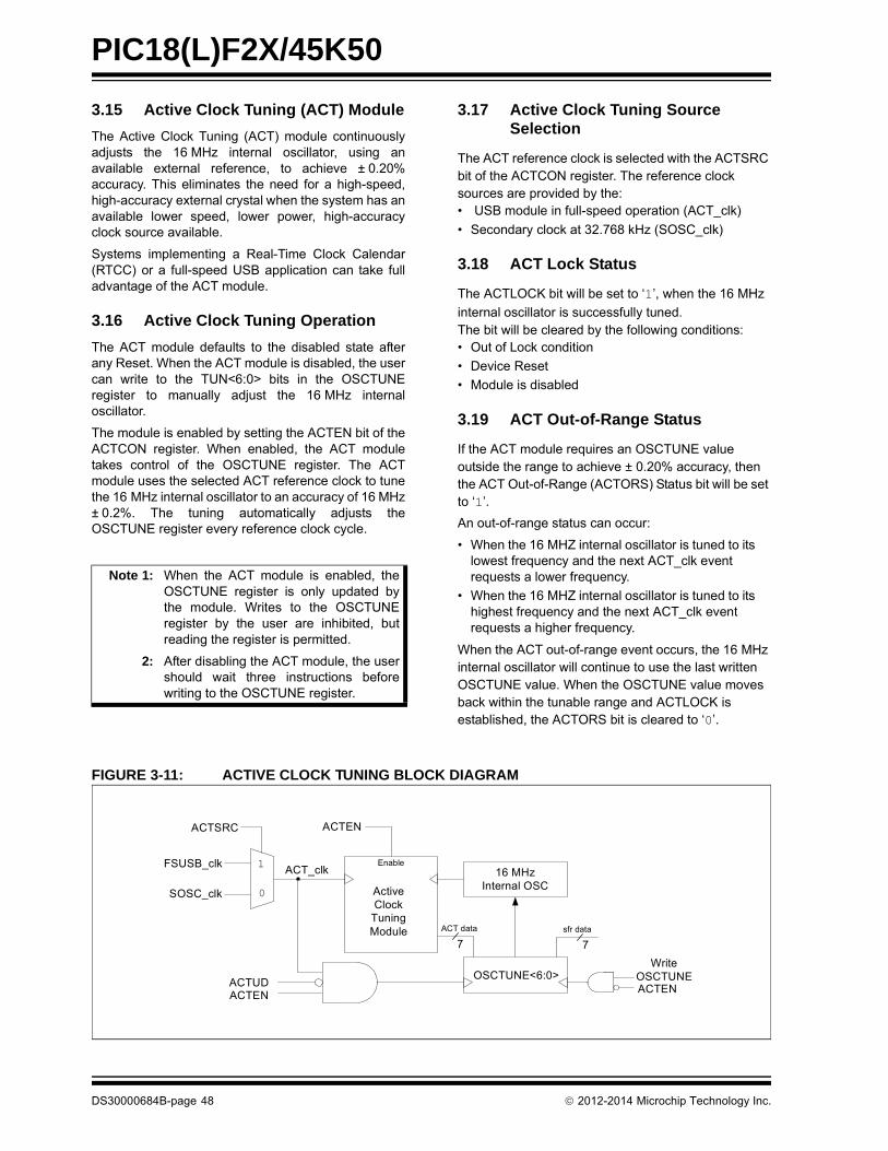
PIC18(L)F2X/45K50
3.15 Active Clock Tuning (ACT) Module
The Active Clock Tuning (ACT) module continuouslyadjusts the 16 MHz internal oscillator, using anavailable external reference, to achieve ± 0.20%accuracy. This eliminates the need for a high-speed,high-accuracy external crystal when the system has anavailable lower speed, lower power, high-accuracyclock source available.
Systems implementing a Real-Time Clock Calendar(RTCC) or a full-speed USB application can take fulladvantage of the ACT module.
3.16 Active Clock Tuning Operation
The ACT module defaults to the disabled state afterany Reset. When the ACT module is disabled, the usercan write to the TUN<6:0> bits in the OSCTUNEregister to manually adjust the 16 MHz internaloscillator.
The module is enabled by setting the ACTEN bit of theACTCON register. When enabled, the ACT moduletakes control of the OSCTUNE register. The ACTmodule uses the selected ACT reference clock to tunethe 16 MHz internal oscillator to an accuracy of 16 MHz± 0.2%. The tuning automatically adjusts theOSCTUNE register every reference clock cycle.
3.17 Active Clock Tuning Source Selection
The ACT reference clock is selected with the ACTSRC bit of the ACTCON register. The reference clock sources are provided by the:• USB module in full-speed operation (ACT_clk)
• Secondary clock at 32.768 kHz (SOSC_clk)
3.18 ACT Lock Status
The ACTLOCK bit will be set to ‘1’, when the 16 MHz
internal oscillator is successfully tuned.The bit will be cleared by the following conditions:• Out of Lock condition
• Device Reset
• Module is disabled
3.19 ACT Out-of-Range Status
If the ACT module requires an OSCTUNE value outside the range to achieve ± 0.20% accuracy, thenthe ACT Out-of-Range (ACTORS) Status bit will be set to ‘1’.
An out-of-range status can occur:
• When the 16 MHZ internal oscillator is tuned to its lowest frequency and the next ACT_clk event requests a lower frequency.
• When the 16 MHZ internal oscillator is tuned to its highest frequency and the next ACT_clk event requests a higher frequency.
When the ACT out-of-range event occurs, the 16 MHz internal oscillator will continue to use the last written OSCTUNE value. When the OSCTUNE value moves back within the tunable range and ACTLOCK is established, the ACTORS bit is cleared to ‘0’.
FIGURE 3-11: ACTIVE CLOCK TUNING BLOCK DIAGRAM
Note 1: When the ACT module is enabled, theOSCTUNE register is only updated bythe module. Writes to the OSCTUNEregister by the user are inhibited, butreading the register is permitted.
2: After disabling the ACT module, the usershould wait three instructions beforewriting to the OSCTUNE register.
ACTSRC
FSUSB_clk
SOSC_clk
ACTEN
Active Clock
Tuning Module
ACT_clkEnable
ACTEN
WriteOSCTUNE
ACTENACTUD
16 MHzInternal OSC
1
0
OSCTUNE<6:0>
77
ACT data sfr data
DS30000684B-page 48 2012-2014 Microchip Technology Inc.

PIC18(L)F2X/45K50
3.20 Active Clock Tuning Update Disable
When the ACT module is enabled, the OSCTUNEregister is continuously updated every ACT_clk period.Setting the ACT Update Disable bit can be used tosuspend updates to the OSCTUNE register, withoutdisabling the module. If the 16 MHz internal oscillatordrifts out of the accuracy range, the ACT Status bits willchange and an interrupt can be generated to notify theapplication.
Clearing the ACTUD bit will engage the ACT updatesto OSCTUNE and an interrupt can be generated tonotify the application.
3.21 Interrupts
The ACT module will set the ACT module InterruptFlag, (ACTIF) when either of the ACT module Statusbits (ACTLOCK or ACTORS) change state, regardlessif the interrupt is enabled, (ACTIE = 1). The ACTIF andACTIE bits are in the PIR1 and PIE1 registers, respec-tively. When ACTIE = 1, an interrupt will be generatedwhenever the ACT module Status bits change.
The ACTIF bit must be cleared in software, regardlessof the interrupt enable setting.
3.22 Operation during Sleep
This ACT module does not run during Sleep and willnot generate interrupts during Sleep.
2012-2014 Microchip Technology Inc. DS30000684B-page 49
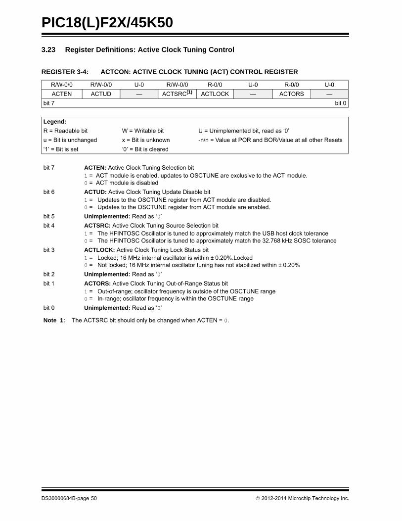
PIC18(L)F2X/45K50
3.23 Register Definitions: Active Clock Tuning Control
REGISTER 3-4: ACTCON: ACTIVE CLOCK TUNING (ACT) CONTROL REGISTER
R/W-0/0 R/W-0/0 U-0 R/W-0/0 R-0/0 U-0 R-0/0 U-0
ACTEN ACTUD — ACTSRC(1) ACTLOCK — ACTORS —
bit 7 bit 0
Legend:
R = Readable bit W = Writable bit U = Unimplemented bit, read as ‘0’
u = Bit is unchanged x = Bit is unknown -n/n = Value at POR and BOR/Value at all other Resets
‘1’ = Bit is set ‘0’ = Bit is cleared
bit 7 ACTEN: Active Clock Tuning Selection bit1 = ACT module is enabled, updates to OSCTUNE are exclusive to the ACT module.0 = ACT module is disabled
bit 6 ACTUD: Active Clock Tuning Update Disable bit1 = Updates to the OSCTUNE register from ACT module are disabled.0 = Updates to the OSCTUNE register from ACT module are enabled.
bit 5 Unimplemented: Read as ‘0’
bit 4 ACTSRC: Active Clock Tuning Source Selection bit1 = The HFINTOSC Oscillator is tuned to approximately match the USB host clock tolerance0 = The HFINTOSC Oscillator is tuned to approximately match the 32.768 kHz SOSC tolerance
bit 3 ACTLOCK: Active Clock Tuning Lock Status bit1 = Locked; 16 MHz internal oscillator is within ± 0.20%.Locked0 = Not locked; 16 MHz internal oscillator tuning has not stabilized within ± 0.20%
bit 2 Unimplemented: Read as ‘0’
bit 1 ACTORS: Active Clock Tuning Out-of-Range Status bit1 = Out-of-range; oscillator frequency is outside of the OSCTUNE range0 = In-range; oscillator frequency is within the OSCTUNE range
bit 0 Unimplemented: Read as ‘0’
Note 1: The ACTSRC bit should only be changed when ACTEN = 0.
DS30000684B-page 50 2012-2014 Microchip Technology Inc.

PIC18(L)F2X/45K50
TABLE 3-8: SUMMARY OF REGISTERS ASSOCIATED WITH ACT SOURCES
TABLE 3-9: SUMMARY OF CONFIGURATION WORD WITH ACT SOURCES
Name Bit 7 Bit 6 Bit 5 Bit 4 Bit 3 Bit 2 Bit 1 Bit 0Register on page
ACTCON ACTEN ACTUD — ACTSRC ACTLOCK — ACTORS — 50
OSCCON IDLEN IRCF<2:0> OSTS HFIOFS SCS<1:0> 33
OSCTUNE SPLLMULT TUN<6:0> 38
OSCCON2 PLLRDY SOSCRUN INTSRC PLLEN SOSCGO PRISD HFIOFR LFIOFS 34
PIR1 ACTIF ADIF RCIF TXIF SSPIF CCP1IF TMR2IF TMR1IF 117
IPR1 ACTIP ADIP RCIP TXIP SSPIP CCP1IP TMR2IP TMR1IP 123
PIE1 ACTIE ADIE RCIE TXIE SSPIE CCP1IE TMR2IE TMR1IE 120
T1CON TMR1CS<1:0> T1CKPS<1:0> SOSCEN T1SYNC RD16 TMR1ON 165
Legend: — = unimplemented location, read as ‘0’. Shaded cells are not used by clock sources.
Name Bit 7 Bit 6 Bit 5 Bit 4 Bit 3 Bit 2 Bit 1 Bit 0Register on page
CONFIG1H IESO FCMEN PCLKEN — FOSC<3:0> 373
2012-2014 Microchip Technology Inc. DS30000684B-page 51
PIC18(L)F2X/45K50
4.0 POWER-MANAGED MODES
PIC18(L)F2X/45K50 devices offer a total of sevenoperating modes for more efficient powermanagement. These modes provide a variety ofoptions for selective power conservation in applicationswhere resources may be limited (i.e., battery-powereddevices).
There are three categories of power-managed modes:
• Run modes
• Idle modes
• Sleep mode
These categories define which portions of the deviceare clocked and sometimes, what speed. The Run andIdle modes may use any of the three available clocksources (primary, secondary or internal oscillatorblock). The Sleep mode does not use a clock source.
The power-managed modes include several power-saving features offered on previous PIC® microcontrollerdevices. One of the clock switching features allows thecontroller to use the secondary oscillator (SOSC) inplace of the primary oscillator. Also included is the Sleepmode, offered by all PIC microcontroller devices, whereall device clocks are stopped.
4.1 Selecting Power-Managed Modes
Selecting a power-managed mode requires twodecisions:
• Whether or not the CPU is to be clocked
• The selection of a clock source
The IDLEN bit (OSCCON<7>) controls CPU clocking,while the SCS<1:0> bits (OSCCON<1:0>) select theclock source. The individual modes, bit settings, clocksources and affected modules are summarized inTable 4-1.
4.1.1 CLOCK SOURCES
The SCS<1:0> bits allow the selection of one of threeclock sources for power-managed modes. They are:
• the primary clock, as defined by the FOSC<3:0> Configuration bits
• the secondary clock (the SOSC oscillator)
• the internal oscillator block
4.1.2 ENTERING POWER-MANAGED MODES
Switching from one power-managed mode to anotherbegins by loading the OSCCON register. TheSCS<1:0> bits select the clock source and determinewhich Run or Idle mode is to be used. Changing thesebits causes an immediate switch to the new clocksource, assuming that it is running. The switch mayalso be subject to clock transition delays. Refer toSection 3.11 “Clock Switching” for more information.
Entry to the power-managed Idle or Sleep modes istriggered by the execution of a SLEEP instruction. Theactual mode that results depends on the status of theIDLEN bit.
Depending on the current mode and the mode beingswitched to, a change to a power-managed mode doesnot always require setting all of these bits. Manytransitions may be done by changing the oscillator selectbits, or changing the IDLEN bit, prior to issuing a SLEEPinstruction. If the IDLEN bit is already configuredcorrectly, it may only be necessary to perform a SLEEPinstruction to switch to the desired mode.
TABLE 4-1: POWER-MANAGED MODES
ModeOSCCON Bits Module Clocking
Available Clock and Oscillator SourceIDLEN(1) SCS<1:0> CPU Peripherals
Sleep 0 N/A Off Off None – All clocks are disabled
PRI_RUN N/A 00 Clocked Clocked Primary – LP, XT, HS, RC, EC and InternalOscillator Block(2).This is the normal full-power execution mode.
SEC_RUN N/A 01 Clocked Clocked Secondary – SOSC Oscillator
RC_RUN N/A 1x Clocked Clocked Internal Oscillator Block(2)
PRI_IDLE 1 00 Off Clocked Primary – LP, XT, HS, HSPLL, RC, EC
SEC_IDLE 1 01 Off Clocked Secondary – SOSC Oscillator
RC_IDLE 1 1x Off Clocked Internal Oscillator Block(2)
Note 1: IDLEN reflects its value when the SLEEP instruction is executed.
2: Includes HFINTOSC and HFINTOSC postscaler, as well as the INTRC source.
DS30000684B-page 52 2012-2014 Microchip Technology Inc.
PIC18(L)F2X/45K50
4.1.3 MULTIPLE FUNCTIONS OF THE SLEEP COMMAND
The power-managed mode that is invoked with theSLEEP instruction is determined by the value of theIDLEN bit at the time the instruction is executed. IfIDLEN = 0, when SLEEP is executed, the device entersthe sleep mode and all clocks stop and minimum poweris consumed. If IDLEN = 1, when SLEEP is executed,the device enters the IDLE mode and the system clockcontinues to supply a clock to the peripherals but isdisconnected from the CPU.
4.2 Run Modes
In the Run modes, clocks to both the core andperipherals are active. The difference between thesemodes is the clock source.
4.2.1 PRI_RUN MODE
The PRI_RUN mode is the normal, full-powerexecution mode of the microcontroller. This is also thedefault mode upon a device Reset, unless Two-SpeedStart-up is enabled (see Section 3.12 “Two-SpeedClock Start-up Mode” for details). In this mode, thedevice is operated off the oscillator defined by theFOSC<3:0> bits of the CONFIG1H Configurationregister.
4.2.2 SEC_RUN MODE
In SEC_RUN mode, the CPU and peripherals areclocked from the secondary external oscillator. Thisgives users the option of lower power consumptionwhile still using a high accuracy clock source.
SEC_RUN mode is entered by setting the SCS<1:0>bits to ‘01’. When SEC_RUN mode is active, all of thefollowing are true:
• The device clock source is switched to the SOSC oscillator (see Figure 4-1)
• The primary oscillator is shut down
• The SOSCRUN bit (OSCCON2<6>) is set
• The OSTS bit (OSCCON<3>) is cleared
On transitions from SEC_RUN mode to PRI_RUNmode, the peripherals and CPU continue to be clockedfrom the SOSC oscillator, while the primary clock isstarted. When the primary clock becomes ready, aclock switch back to the primary clock occurs (see
Figure 4-2). When the clock switch is complete, theSOSCRUN bit is cleared, the OSTS bit is set and theprimary clock is providing the clock. The IDLEN andSCS bits are not affected by the wake-up and theSOSC oscillator continues to run.
4.2.3 RC_RUN MODE
In RC_RUN mode, the CPU and peripherals areclocked from the internal oscillator block using theINTOSC multiplexer. In this mode, the primary clock isshut down. When using the INTRC source, this modeprovides the best power conservation of all the Runmodes, while still executing code. It works well for userapplications which are not highly timing-sensitive or donot require high-speed clocks at all times. If the primaryclock source is the internal oscillator block – eitherINTRC or HFINTOSC – there are no distinguishabledifferences between the PRI_RUN and RC_RUNmodes during execution. Entering or exiting RC_RUNmode, however, causes a clock switch delay.Therefore, if the primary clock source is the internaloscillator block, using RC_RUN mode is notrecommended.
This mode is entered by setting the SCS1 bit to ‘1’. Tomaintain software compatibility with future devices, it isrecommended that the SCS0 bit also be cleared, eventhough the bit is ignored. When the clock source isswitched to the INTOSC multiplexer (see Figure 4-1),the primary oscillator is shut down and the OSTS bit iscleared. The IRCF<2:0> bits (OSCCON<6:4>) may bemodified at any time to immediately change the clockspeed.
When the IRCF bits and the INTSRC bit are all clear,the INTOSC output (HFINTOSC) is not enabled andthe HFIOFS bit will remain clear. There will be no indi-cation of the current clock source. The INTRC sourceis providing the device clocks.
If the IRCF bits are changed from all clear (thus,enabling the INTOSC output) or if INTSRC is set, thenthe HFIOFS bit is set after the INTOSC output becomesstable. For details, see Table 4-2.
Clocks to the device continue while the INTOSC sourcestabilizes after an interval of TIOBST.
If the IRCF bits were previously at a non-zero value, orif INTSRC was set before setting SCS1 and theINTOSC source was already stable, then the HFIOFSbit will remain set.
Note: The secondary external oscillator shouldalready be running prior to enteringSEC_RUN mode. If the SOSCGO bit orany of the SOSCEN bits are not set whenthe SCS<1:0> bits are set to ‘01’, entry toSEC_RUN mode will not occur until theSOSCGO bit is set and secondaryexternal oscillator is ready.
2012-2014 Microchip Technology Inc. DS30000684B-page 53
PIC18(L)F2X/45K50
On transitions from RC_RUN mode to PRI_RUN mode,the device continues to be clocked from the INTOSCmultiplexer while the primary clock is started. When theprimary clock becomes ready, a clock switch to the pri-mary clock occurs (see Figure 4-3). When the clockswitch is complete, the HFIOFS bit is cleared, theOSTS bit is set and the primary clock is providing thedevice clock. The IDLEN and SCS bits are not affectedby the switch. The INTRC source will continue to run ifeither the WDT or the Fail-Safe Clock Monitor isenabled.
FIGURE 4-1: TRANSITION TIMING FOR ENTRY TO SEC_RUN MODE
FIGURE 4-2: TRANSITION TIMING FROM SEC_RUN MODE TO PRI_RUN MODE (HSPLL)
Q4Q3Q2
OSC1
Peripheral
Program
Q1
SOSCI
Q1
Counter
Clock
CPUClock
PC + 2PC
1 2 3 n-1 n
Clock Transition(1)
Q4Q3Q2 Q1 Q3Q2
PC + 4
Note 1: Clock transition typically occurs within 2-4 TOSC.
Q1 Q3 Q4
OSC1
Peripheral
Program PC
SOSC
PLL Clock
Q1
PC + 4
Q2
Output
Q3 Q4 Q1
CPU Clock
PC + 2
Clock
Counter
Q2 Q2 Q3
Note1: TOST = 1024 TOSC; TPLL = 2 ms (approx). These intervals are not shown to scale.
2: Clock transition typically occurs within 2-4 TOSC.
SCS<1:0> bits Changed
TPLL(1)
1 2 n-1 n
Clock
OSTS bit Set
Transition(2)
TOST(1)
DS30000684B-page 54 2012-2014 Microchip Technology Inc.
PIC18(L)F2X/45K50
FIGURE 4-3: TRANSITION TIMING FROM RC_RUN MODE TO PRI_RUN MODE
TABLE 4-2: INTERNAL OSCILLATOR FREQUENCY STABILITY BITS
IRCF<2:0> INTSRC Selected Oscillator Selected Oscillator Stable when:
000 0 INTRC LFIOFS = 1
000 1 HFINTOSC HFIOFS = 1
001-111 x HFINTOSC HFIOFS = 1
Q1 Q3 Q4
OSC1
Peripheral
Program PC
INTOSC
PLL Clock
Q1
PC + 4
Q2
Output
Q3 Q4 Q1
CPU Clock
PC + 2
Clock
Counter
Q2 Q2 Q3
Note1: TOST = 1024 TOSC; TPLL = 2 ms (approx). These intervals are not shown to scale.
2: Clock transition typically occurs within 2-4 TOSC.
SCS<1:0> bits Changed
TPLL(1)
1 2 n-1 n
Clock
OSTS bit Set
Transition(2)
Multiplexer
TOST(1)
2012-2014 Microchip Technology Inc. DS30000684B-page 55

PIC18(L)F2X/45K50
4.3 Sleep Mode
The Power-Managed Sleep mode in the PIC18(L)F2X/45K50 devices is identical to the legacy Sleep modeoffered in all other PIC microcontroller devices. It isentered by clearing the IDLEN bit of the OSCCONregister and executing the SLEEP instruction. This shutsdown the selected oscillator (Figure 4-4) and all clocksource status bits are cleared.
Entering the Sleep mode from either Run or Idle modedoes not require a clock switch. This is because noclocks are needed once the controller has enteredSleep. If the WDT is selected, the INTRC source willcontinue to operate. If the SOSC oscillator is enabled,it will also continue to run.
When a wake event occurs in Sleep mode (by interrupt,Reset or WDT time-out), the device will not be clockeduntil the clock source selected by the SCS<1:0> bitsbecomes ready (see Figure 4-5), or it will be clockedfrom the internal oscillator block if either the Two-SpeedStart-up or the Fail-Safe Clock Monitor are enabled(see Section 26.0 “Special Features of the CPU”). Ineither case, the OSTS bit is set when the primary clockis providing the device clocks. The IDLEN and SCS bitsare not affected by the wake-up.
4.3.1 VOLTAGE REGULATOR POWER MODE
On F devices, an internal voltage regulator providespower to the internal core logic of the chip. DuringSleep mode, the internal voltage regulator can be putinto a lower-power mode, in exchange for longerwake-up time. Similarly, the internal band gap voltagereference may be turned off during Sleep for lower-power consumption. See Register 4-1.
On LF devices, the internal core logic operates fromVDD and the internal voltage regulator is bypassed. TheVREGCON register is, thus, not implemented on LFdevices.
REGISTER 4-1: VREGCON – VOLTAGE REGULATOR POWER CONTROL REGISTER(1)
U-0 U-0 U-0 U-0 U-0 R-0 R/W-0/0 R/W-0/0
— — — — — — VREGPM<1:0>
bit 7 bit 0
Legend:
R = Readable bit W = Writable bit x = Bit is unknown
-n/n = Value at POR and BOR/Value at all other resets ‘0’ = Bit is cleared ‘1’ = bit is set
U = Unimplemented bit, read as ‘0’
bit 7-2 Unimplemented: Read as ‘0’
bit 1-0 VREGPM<1:0>: Voltage Regulator Power mode bits
11 = Band gap not forced in Sleep; LDO off in Sleep; ULP Regulator active
10 = Band gap forced in Sleep; LDO off in Sleep; ULP Regulator active
01 = LDO in Low-Power mode in Sleep, if no peripherals require High-Power mode.
00 = LDO in High-Power mode – always
Note 1: Reset state depends on state of the IESO Configuration bit.
2: Default output frequency of HFINTOSC on Reset.
DS30000684B-page 56 2012-2014 Microchip Technology Inc.

PIC18(L)F2X/45K50
4.4 Idle Modes
The Idle modes allow the controller’s CPU to beselectively shut down while the peripherals continue tooperate. Selecting a particular Idle mode allows usersto further manage power consumption.
If the IDLEN bit is set to a ‘1’ when a SLEEP instruction isexecuted, the peripherals will be clocked from the clocksource selected by the SCS<1:0> bits; however, the CPUwill not be clocked. The clock source status bits are notaffected. Setting IDLEN and executing a SLEEP instruc-tion provides a quick method of switching from a givenRun mode to its corresponding Idle mode.
If the WDT is selected, the INTRC source will continueto operate. If the SOSC oscillator is enabled, it will alsocontinue to run.
Since the CPU is not executing instructions, the onlyexits from any of the Idle modes are by interrupt, WDTtime-out, or a Reset. When a wake event occurs, CPUexecution is delayed by an interval of TCSD while itbecomes ready to execute code. When the CPUbegins executing code, it resumes with the same clocksource for the current Idle mode. For example, whenwaking from RC_IDLE mode, the internal oscillatorblock will clock the CPU and peripherals (in otherwords, RC_RUN mode). The IDLEN and SCS bits arenot affected by the wake-up.
While in any Idle mode or the Sleep mode, a WDTtime-out will result in a WDT wake-up to the Run modecurrently specified by the SCS<1:0> bits.
FIGURE 4-4: TRANSITION TIMING FOR ENTRY TO SLEEP MODE
FIGURE 4-5: TRANSITION TIMING FOR WAKE FROM SLEEP (HSPLL)
4.4.1 PRI_IDLE MODE
This mode is unique among the three low-power Idlemodes, in that it does not disable the primary deviceclock. For timing sensitive applications, this allows forthe fastest resumption of device operation with its moreaccurate primary clock source, since the clock sourcedoes not have to “warm-up” or transition from anotheroscillator.
PRI_IDLE mode is entered from PRI_RUN mode bysetting the IDLEN bit and executing a SLEEP instruc-tion. If the device is in another Run mode, set IDLENfirst, then clear the SCS bits and execute SLEEP.Although the CPU is disabled, the peripherals continue
to be clocked from the primary clock source specifiedby the FOSC<3:0> Configuration bits. The OSTS bitremains set (see Figure 4-6).
When a wake event occurs, the CPU is clocked from theprimary clock source. A delay of interval TCSD isrequired between the wake event and when codeexecution starts. This is required to allow the CPU tobecome ready to execute instructions. After the wake-up, the OSTS bit remains set. The IDLEN and SCS bitsare not affected by the wake-up (see Figure 4-7).
Q4Q3Q2
OSC1
Peripheral
Sleep
Program
Q1Q1
Counter
Clock
CPUClock
PC + 2PC
Q3 Q4 Q1 Q2
OSC1
Peripheral
Program PC
PLL Clock
Q3 Q4
Output
CPU Clock
Q1 Q2 Q3 Q4 Q1 Q2
Clock
Counter PC + 6PC + 4
Q1 Q2 Q3 Q4
Wake Event
Note1: TOST = 1024 TOSC; TPLL = 2 ms (approx). These intervals are not shown to scale.
TOST(1)TPLL(1)
OSTS bit set
PC + 2
2012-2014 Microchip Technology Inc. DS30000684B-page 57
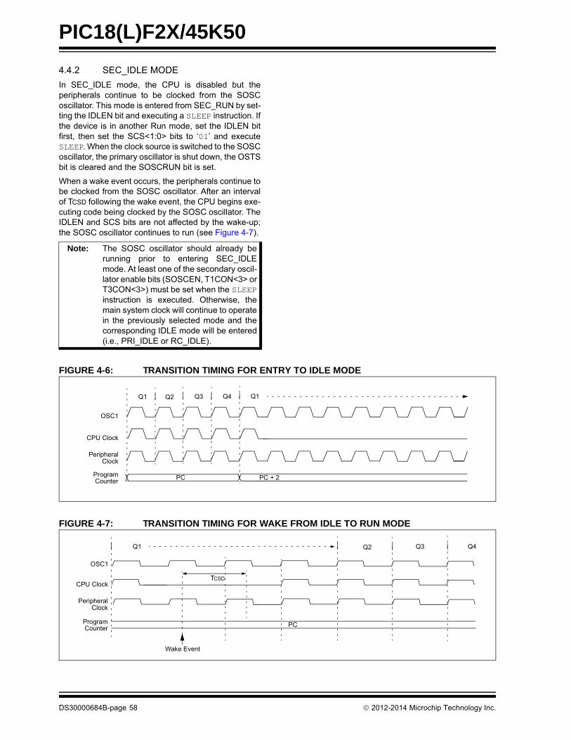
PIC18(L)F2X/45K50
4.4.2 SEC_IDLE MODE
In SEC_IDLE mode, the CPU is disabled but theperipherals continue to be clocked from the SOSCoscillator. This mode is entered from SEC_RUN by set-ting the IDLEN bit and executing a SLEEP instruction. Ifthe device is in another Run mode, set the IDLEN bitfirst, then set the SCS<1:0> bits to ‘01’ and executeSLEEP. When the clock source is switched to the SOSCoscillator, the primary oscillator is shut down, the OSTSbit is cleared and the SOSCRUN bit is set.
When a wake event occurs, the peripherals continue tobe clocked from the SOSC oscillator. After an intervalof TCSD following the wake event, the CPU begins exe-cuting code being clocked by the SOSC oscillator. TheIDLEN and SCS bits are not affected by the wake-up;the SOSC oscillator continues to run (see Figure 4-7).
FIGURE 4-6: TRANSITION TIMING FOR ENTRY TO IDLE MODE
FIGURE 4-7: TRANSITION TIMING FOR WAKE FROM IDLE TO RUN MODE
Note: The SOSC oscillator should already berunning prior to entering SEC_IDLEmode. At least one of the secondary oscil-lator enable bits (SOSCEN, T1CON<3> orT3CON<3>) must be set when the SLEEPinstruction is executed. Otherwise, themain system clock will continue to operatein the previously selected mode and thecorresponding IDLE mode will be entered(i.e., PRI_IDLE or RC_IDLE).
Q1
Peripheral
Program PC PC + 2
OSC1
Q3 Q4 Q1
CPU Clock
Clock
Counter
Q2
OSC1
Peripheral
Program PC
CPU Clock
Q1 Q3 Q4
Clock
Counter
Q2
Wake Event
TCSD
DS30000684B-page 58 2012-2014 Microchip Technology Inc.

PIC18(L)F2X/45K50
4.4.3 RC_IDLE MODE
In RC_IDLE mode, the CPU is disabled but the periph-erals continue to be clocked from the internal oscillatorblock from the HFINTOSC multiplexer output. Thismode allows for controllable power conservation duringIdle periods.
From RC_RUN, this mode is entered by setting theIDLEN bit and executing a SLEEP instruction. If thedevice is in another Run mode, first set IDLEN, then setthe SCS1 bit and execute SLEEP. It is recommendedthat SCS0 also be cleared, although its value isignored, to maintain software compatibility with futuredevices. The HFINTOSC multiplexer may be used toselect a higher clock frequency by modifying the IRCFbits before executing the SLEEP instruction. When theclock source is switched to the HFINTOSC multiplexer,the primary oscillator is shut down and the OSTS bit iscleared.
If the IRCF bits are set to any non-zero value, or theINTSRC bits are set, the HFINTOSC output is enabled.The HFIOFS bit becomes set after the HFINTOSCoutput stabilizes after an interval of TIOBST. Forinformation on the HFIOFS bit, see Table 4-2.
Clocks to the peripherals continue while theHFINTOSC source stabilizes. The HFIOFS bit willremain set if the IRCF bits were previously set at a non-zero value or if INTSRC was set before the SLEEPinstruction was executed and the HFINTOSC sourcewas already stable. If the IRCF bits and INTSRC are allclear, the HFINTOSC output will not be enabled, theHFIOFS bit will remain clear and there will be noindication of the current clock source.
When a wake event occurs, the peripherals continue tobe clocked from the HFINTOSC multiplexer output.After a delay of TCSD following the wake event, the CPUbegins executing code being clocked by theHFINTOSC multiplexer. The IDLEN and SCS bits arenot affected by the wake-up. The INTRC source willcontinue to run if either the WDT or the Fail-Safe ClockMonitor is enabled.
4.5 Exiting Idle and Sleep Modes
An exit from Sleep mode or any of the Idle modes istriggered by any one of the following:
• an interrupt
• a Reset
• a Watchdog Time-out
This section discusses the triggers that cause exitsfrom power-managed modes. The clocking subsystemactions are discussed in each of the power-managedmodes (see Section 4.2 “Run Modes”, Section 4.3“Sleep Mode” and Section 4.4 “Idle Modes”).
4.5.1 EXIT BY INTERRUPT
Any of the available interrupt sources can cause thedevice to exit from an Idle mode or the Sleep mode toa Run mode. To enable this functionality, an interruptsource must be enabled by setting its enable bit in oneof the INTCON or PIE registers. The exit sequence isinitiated when the corresponding interrupt flag bit is set.
The instruction immediately following the SLEEPinstruction is executed on all exits by interrupt from Idleor Sleep modes. Code execution then branches to theinterrupt vector if the GIE/GIEH bit of the INTCONregister is set, otherwise code execution continueswithout branching (see Section 10.0 “Interrupts”).
A fixed delay of interval TCSD following the wake eventis required when leaving Sleep and Idle modes. Thisdelay is required for the CPU to prepare for execution.Instruction execution resumes on the first clock cyclefollowing this delay.
4.5.2 EXIT BY WDT TIME-OUT
A WDT time-out will cause different actions dependingon which power-managed mode the device is in whenthe time-out occurs.
If the device is not executing code (all Idle modes andSleep mode), the time-out will result in an exit from thepower-managed mode (see Section 4.2 “RunModes” and Section 4.3 “Sleep Mode”). If the deviceis executing code (all Run modes), the time-out willresult in a WDT Reset (see Section 26.3 “WatchdogTimer (WDT)”).
The WDT timer and postscaler are cleared by any oneof the following:
• executing a SLEEP instruction
• executing a CLRWDT instruction
• the loss of the currently selected clock source when the Fail-Safe Clock Monitor is enabled
• modifying the IRCF bits in the OSCCON register when the internal oscillator block is the device clock source
2012-2014 Microchip Technology Inc. DS30000684B-page 59

PIC18(L)F2X/45K50
4.5.3 EXIT BY RESET
Exiting Sleep and Idle modes by Reset causes codeexecution to restart at address 0. See Section 5.0“Reset” for more details.
The exit delay time from Reset to the start of codeexecution depends on both the clock sources beforeand after the wake-up and the type of oscillator.
4.5.4 EXIT WITHOUT AN OSCILLATOR START-UP DELAY
Certain exits from power-managed modes do notinvoke the OST at all. There are two cases:
• PRI_IDLE mode, where the primary clock source is not stopped and
• the primary clock source is not any of the LP, XT, HS or HSPLL modes.
In these instances, the primary clock source eitherdoes not require an oscillator start-up delay since it isalready running (PRI_IDLE), or normally does notrequire an oscillator start-up delay (RC, EC, INTOSC,and INTOSCIO modes). However, a fixed delay ofinterval TCSD following the wake event is still requiredwhen leaving Sleep and Idle modes to allow the CPUto prepare for execution. Instruction execution resumeson the first clock cycle following this delay.
4.6 Selective Peripheral Module Control
Idle mode allows users to substantially reduce powerconsumption by stopping the CPU clock. Even so,peripheral modules still remain clocked, and thus, con-sume power. There may be cases where the applica-tion needs what IDLE mode does not provide: theallocation of power resources to the CPU processingwith minimal power consumption from the peripherals.PIC18(L)F2X/45K50 family devices address thisrequirement by allowing peripheral modules to beselectively disabled, reducing or eliminating theirpower consumption. This can be done with control bitsin the Peripheral Module Disable (PMD) registers.These bits generically named XXXMD are located incontrol registers PMD0 or PMD1.
Setting the PMD bit for a module disables all clocksources to that module, reducing its powerconsumption to an absolute minimum. In this state,power to the control and status registers associatedwith the peripheral is removed. Writes to theseregisters have no effect and read values are invalid.Clearing a set PMD bit restores power to theassociated control and status registers, thereby settingthose registers to their default values.
DS30000684B-page 60 2012-2014 Microchip Technology Inc.

PIC18(L)F2X/45K50
4.7 Register Definitions: Peripheral Module Disable
REGISTER 4-2: PMD0: PERIPHERAL MODULE DISABLE REGISTER 0
U-0 R/W-0 R/W-0 R/W-0 U-0 R/W-0 R/W-0 R/W-0
— UARTMD USBMD ACTMD — TMR3MD TMR2MD TMR1MD
bit 7 bit 0
Legend:
R = Readable bit W = Writable bit U = Unimplemented bit, read as ‘0’
-n = Value at POR ‘1’ = Bit is set ‘0’ = Bit is cleared x = Bit is unknown
bit 7 Unimplemented: Read as ‘0’.
bit 6 UARTMD: UART Peripheral Module Disable Control bit
1 = Module is disabled, clock source is disconnected, module does not draw digital power0 = Module is enabled, clock source is connected, module draws digital power
bit 5 USBMD: USB Peripheral Module Disable Control bit
1 = Module is disabled, clock source is disconnected, module does not draw digital power0 = Module is enabled, clock source is connected, module draws digital power
bit 4 ACTMD: Active Clock Tuning Peripheral Module Disable Control bit
1 = Module is disabled and does not draw any digital power0 = Module is enabled and available for use; will draw digital power
bit 3 Unimplemented: Read as ‘0’.
bit 2 TMR3MD: Timer3 Peripheral Module Disable Control bit
1 = Module is disabled, clock source is disconnected, module does not draw digital power0 = Module is enabled, clock source is connected, module draws digital power
bit 1 TMR2MD: Timer2 Peripheral Module Disable Control bit
1 = Module is disabled, clock source is disconnected, module does not draw digital power0 = Module is enabled, clock source is connected, module draws digital power
bit 0 TMR1MD: Timer1 Peripheral Module Disable Control bit
1 = Module is disabled, clock source is disconnected, module does not draw digital power0 = Module is enabled, clock source is connected, module draws digital power
2012-2014 Microchip Technology Inc. DS30000684B-page 61

PIC18(L)F2X/45K50
REGISTER 4-3: PMD1: PERIPHERAL MODULE DISABLE REGISTER 1
U-0 R/W-0 R/W-0 R/W-0 R/W-0 R/W-0 R/W-0 R/W-0
— MSSPMD CTMUMD CMP2MD CMP1MD ADCMD CCP2MD CCP1MD
bit 7 bit 0
Legend:
R = Readable bit W = Writable bit U = Unimplemented bit, read as ‘0’
-n = Value at POR ‘1’ = Bit is set ‘0’ = Bit is cleared x = Bit is unknown
bit 7 Unimplemented: Read as ‘0’
bit 6 MSSPMD: MSSP Peripheral Module Disable Control bit
1 = Module is disabled, clock source is disconnected, module does not draw digital power0 = Module is enabled, clock source is connected, module draws digital power
bit 5 CTMUMD: CTMU Peripheral Module Disable Control bit1 = Module is disabled, clock source is disconnected, module does not draw digital power0 = Module is enabled, clock source is connected, module draws digital power
bit 4 CMP2MD: Comparator 2 Peripheral Module Disable Control bit
1 = Module is disabled, clock source is disconnected, module does not draw digital power0 = Module is enabled, clock source is connected, module draws digital power
bit 3 CMP1MD: Comparator 1 Peripheral Module Disable Control bit
1 = Module is disabled, clock source is disconnected, module does not draw digital power0 = Module is enabled, clock source is connected, module draws digital power
bit 2 ADCMD: Analog-to-Digital Converter Peripheral Module Disable Control bit
1 = Module is disabled, clock source is disconnected, module does not draw digital power0 = Module is enabled, clock source is connected, module draws digital power
bit 1 CCP2MD: CCP2 Peripheral Module Disable Control bit
1 = Module is disabled, clock source is disconnected, module does not draw digital power0 = Module is enabled, clock source is connected, module draws digital power
bit 0 CCP1MD: CCP1 Peripheral Module Disable Control bit
1 = Module is disabled, clock source is disconnected, module does not draw digital power0 = Module is enabled, clock source is connected, module draws digital power
DS30000684B-page 62 2012-2014 Microchip Technology Inc.

PIC18(L)F2X/45K50
5.0 RESET
The PIC18(L)F2X/45K50 devices differentiate betweenvarious kinds of Reset:
a) Power-on Reset (POR)
b) MCLR Reset during normal operation
c) MCLR Reset during power-managed modes
d) Watchdog Timer (WDT) Reset (during execution)
e) Programmable Brown-out Reset (BOR)
f) RESET Instruction
g) Stack Full Reset
h) Stack Underflow Reset
This section discusses Resets generated by MCLR,POR and BOR and covers the operation of the variousstart-up timers. Stack Reset events are covered inSection 6.2.1 “Stack Full and Underflow Resets”.WDT Resets are covered in Section 26.3 “WatchdogTimer (WDT)”.
A simplified block diagram of the On-Chip Reset Circuitis shown in Figure 5-1.
5.1 RCON Register
Device Reset events are tracked through the RCONregister (Register 5-1). The lower five bits of theregister indicate that a specific Reset event hasoccurred. In most cases, these bits can only be clearedby the event and must be set by the application afterthe event. The state of these flag bits, taken together,can be read to indicate the type of Reset that justoccurred. This is described in more detail inSection 5.8 “Reset State of Registers”.
The RCON register also has control bits for settinginterrupt priority (IPEN) and software control of theBOR (SBOREN). Interrupt priority is discussed inSection 10.0 “Interrupts”. BOR is covered inSection 5.5 “Brown-out Reset (BOR)”.
FIGURE 5-1: SIMPLIFIED BLOCK DIAGRAM OF ON-CHIP RESET CIRCUIT
External Reset
MCLR
VDD
OSC1
WDTTime-out
VDDDetect
OST/PWRT
INTRC
POR
OST(2)
10-bit Ripple Counter
PWRT(2)
11-bit Ripple Counter
Enable OST(1)
Enable PWRT
Note 1: See Table 5-2 for time-out situations.
2: PWRT and OST counters are reset by POR and BOR. See Sections 5.4 and 5.5.
Brown-outReset
BOREN
RESETInstruction
StackPointer
Stack Full/Underflow Reset
SleepIdle
1024 Cycles
65.5 ms32 s
MCLRE
S
R QChip_Reset
2012-2014 Microchip Technology Inc. DS30000684B-page 63

PIC18(L)F2X/45K50
5.2 Register Definitions: Reset Control
REGISTER 5-1: RCON: RESET CONTROL REGISTER
R/W-0/0 R/W-q/u U-0 R/W-1/q R-1/q R-1/q R/W-q/u R/W-0/q
IPEN SBOREN(1) — RI TO PD POR(2) BOR
bit 7 bit 0
Legend:
R = Readable bit W = Writable bit U = Unimplemented bit, read as ‘0’
‘1’ = Bit is set ‘0’ = Bit is cleared -n/n = Value at POR and BOR/Value at all other Resets
x = Bit is unknown u = unchanged q = depends on condition
bit 7 IPEN: Interrupt Priority Enable bit
1 = Enable priority levels on interrupts0 = Disable priority levels on interrupts (PIC16CXXX Compatibility mode)
bit 6 SBOREN: BOR Software Enable bit(1)
If BOREN<1:0> = 01:1 = BOR is enabled0 = BOR is disabled
If BOREN<1:0> = 00, 10 or 11:Bit is disabled and read as ‘0’.
bit 5 Unimplemented: Read as ‘0’
bit 4 RI: RESET Instruction Flag bit
1 = The RESET instruction was not executed (set by firmware or Power-on Reset)0 = The RESET instruction was executed causing a device Reset (must be set in firmware after a
code-executed Reset occurs)
bit 3 TO: Watchdog Time-out Flag bit
1 = Set by power-up, CLRWDT instruction or SLEEP instruction 0 = A WDT time-out occurred
bit 2 PD: Power-down Detection Flag bit
1 = Set by power-up or by the CLRWDT instruction0 = Set by execution of the SLEEP instruction
bit 1 POR: Power-on Reset Status bit(2)
1 = No Power-on Reset occurred0 = A Power-on Reset occurred (must be set in software after a Power-on Reset occurs)
bit 0 BOR: Brown-out Reset Status bit(3)
1 = A Brown-out Reset has not occurred (set by firmware only)0 = A Brown-out Reset occurred (must be set by firmware after a POR or Brown-out Reset occurs)
Note 1: When CONFIG2L[2:1] = 01, then the SBOREN Reset state is ‘1’; otherwise, it is ‘0’.
2: The actual Reset value of POR is determined by the type of device Reset. See the notes following this register and Section 5.8 “Reset State of Registers” for additional information.
3: See Table 5-1.
Note 1: Brown-out Reset is indicated when BOR is ‘0’ and POR is ‘1’ (assuming that both POR and BOR were setto ‘1’ by firmware immediately after POR).
2: It is recommended that the POR bit be set after a Power-on Reset has been detected so that subsequentPower-on Resets may be detected.
DS30000684B-page 64 2012-2014 Microchip Technology Inc.

PIC18(L)F2X/45K50
5.3 Master Clear (MCLR)
The MCLR pin provides a method for triggering anexternal Reset of the device. A Reset is generated byholding the pin low. These devices have a noise filter inthe MCLR Reset path which detects and ignores smallpulses. An internal weak pull-up is enabled when thepin is configured as the MCLR input.
The MCLR pin is not driven low by any internal Resets,including the WDT.
In PIC18(L)F2X/45K50 devices, the MCLR input canbe disabled with the MCLRE Configuration bit. WhenMCLR is disabled, the pin becomes a digital input. SeeSection 11.6 “PORTE Registers” for moreinformation.
5.4 Power-on Reset (POR)
A Power-on Reset pulse is generated on-chipwhenever VDD rises above a certain threshold. Thisallows the device to start in the initialized state whenVDD is adequate for operation.
To take advantage of the POR circuitry either leave thepin floating, or tie the MCLR pin through a resistor toVDD. This will eliminate external RC componentsusually needed to create a Power-on Reset delay. Aminimum rise rate for VDD is specified. For a slow risetime, see Figure 5-2.
When the device starts normal operation (i.e., exits theReset condition), device operating parameters (volt-age, frequency, temperature, etc.) must be met toensure proper operation. If these conditions are notmet, the device must be held in Reset until the operat-ing conditions are met.
POR events are captured by the POR bit of the RCONregister. The state of the bit is set to ‘0’ whenever aPOR occurs; it does not change for any other Resetevent. POR is not reset to ‘1’ by any hardware event.To capture multiple events, the user must manually setthe bit to ‘1’ by software following any POR.
FIGURE 5-2: EXTERNAL POWER-ON RESET CIRCUIT (FOR SLOW VDD POWER-UP)
Note 1: External Power-on Reset circuit is requiredonly if the VDD power-up slope is too slow.The diode D helps discharge the capacitorquickly when VDD powers down.
2: 15 k < R < 40 k is recommended to makesure that the voltage drop across R does notviolate the device’s electrical specification.
3: R1 1 k will limit any current flowing intoMCLR from external capacitor C, in the eventof MCLR/VPP pin breakdown, due toElectrostatic Discharge (ESD) or ElectricalOverstress (EOS).
C
R1RD
VDD
MCLR
VDD
PIC® MCU
2012-2014 Microchip Technology Inc. DS30000684B-page 65
PIC18(L)F2X/45K50
5.5 Brown-out Reset (BOR)
PIC18(L)F2X/45K50 devices implement a BOR circuitthat provides the user with a number of configuration andpower-saving options. The BOR is controlled by theBORV<1:0> and BOREN<1:0> bits of the CONFIG2LConfiguration register. There are a total of four BORconfigurations which are summarized in Table 5-1.
The BOR threshold is set by the BORV<1:0> bits. IfBOR is enabled (any values of BOREN<1:0>, except‘00’), any drop of VDD below VBOR for greater thanTBOR will reset the device. A Reset may or may notoccur if VDD falls below VBOR for less than TBOR. Thechip will remain in Brown-out Reset until VDD risesabove VBOR.
If the Power-up Timer is enabled, it will be invoked afterVDD rises above VBOR; it then will keep the chip inReset for an additional time delay, TPWRT. If VDD dropsbelow VBOR while the Power-up Timer is running, thechip will go back into a Brown-out Reset and thePower-up Timer will be initialized. Once VDD risesabove VBOR, the Power-up Timer will execute theadditional time delay.
BOR and the Power-on Timer (PWRT) areindependently configured. Enabling BOR Reset doesnot automatically enable the PWRT.
The BOR circuit has an output that feeds into the PORcircuit and rearms the POR within the operating rangeof the BOR. This early rearming of the POR ensuresthat the device will remain in Reset in the event that VDD
falls below the operating range of the BOR circuitry.
5.5.1 DETECTING BOR
When BOR is enabled, the BOR bit always resets to ‘0’on any BOR or POR event. This makes it difficult todetermine if a BOR event has occurred just by readingthe state of BOR alone. A more reliable method is tosimultaneously check the state of both POR and BOR.This assumes that the POR and BOR bits are reset to‘1’ by software immediately after any POR event. IfBOR is ‘0’ while POR is ‘1’, it can be reliably assumedthat a BOR event has occurred.
5.5.2 SOFTWARE ENABLED BOR
When BOREN<1:0> = 01, the BOR can be enabled ordisabled by the user in software. This is done with theSBOREN control bit of the RCON register. SettingSBOREN enables the BOR to function as previouslydescribed. Clearing SBOREN disables the BORentirely. The SBOREN bit operates only in this mode;otherwise it is read as ‘0’.
Placing the BOR under software control gives the userthe additional flexibility of tailoring the application to theenvironment without having to reprogram the device tochange BOR configuration. It also allows the user totailor device power consumption in software byeliminating the incremental current that the BORconsumes. While the BOR current is typically very small,it may have some impact in low-power applications.
5.5.3 DISABLING BOR IN SLEEP MODE
When BOREN<1:0> = 10, the BOR remains underhardware control and operates as previouslydescribed. Whenever the device enters Sleep mode,however, the BOR is automatically disabled. When thedevice returns to any other operating mode, BOR isautomatically re-enabled.
This mode allows for applications to recover frombrown-out situations, while actively executing code,when the device requires BOR protection the most. Atthe same time, it saves additional power in Sleep modeby eliminating the small incremental BOR current.
5.5.4 MINIMUM BOR ENABLE TIME
Enabling the BOR also enables the Fixed VoltageReference (FVR) when no other peripheral requiring theFVR is active. The BOR becomes active only after theFVR stabilizes. Therefore, to ensure BOR protection,the FVR settling time must be considered whenenabling the BOR in software or when the BOR isautomatically enabled after waking from Sleep. If theBOR is disabled, in software or by reentering Sleepbefore the FVR stabilizes, the BOR circuit will not sensea BOR condition. The FVRST bit of the VREFCON0register can be used to determine FVR stability.
Note: Even when BOR is under softwarecontrol, the BOR Reset voltage level is stillset by the BORV<1:0> Configuration bits.It cannot be changed by software.
DS30000684B-page 66 2012-2014 Microchip Technology Inc.

PIC18(L)F2X/45K50
5.6 Low-Power BOR (LPBOR)
PIC18(L)F2X/45K50 devices implement a low-powerBrown-out Reset circuit (LPBOR). The LPBOR is usedto monitor the external VDD pin.When low voltage is detected, the device is held inReset. When this occurs, the RCON<0> (BOR) bit ischanged to indicate that a BOR reset has occurred.This is the same bit in the RCON register that is set forthe traditional BOR. LPBOR provides the user with a lower power BORoption. In exchange for the lower power, the LPBORcircuit trips at a loose voltage range compared to thetraditional BOR voltage trip point options.
LPBOR is enabled by the Configuration bitCONFIG2L<6> (LPBOR). The threshold of the LPBORis not configurable and its range is specified asparameter D006.
5.7 Device Reset Timers
PIC18(L)F2X/45K50 devices incorporate threeseparate on-chip timers that help regulate the Power-on Reset process. Their main function is to ensure thatthe device clock is stable before code is executed.These timers are:
• Power-up Timer (PWRT)
• Oscillator Start-up Timer (OST)
• PLL Lock Time-out
5.7.1 POWER-UP TIMER (PWRT)
The Power-up Timer (PWRT) of PIC18(L)F2X/45K50devices is an 11-bit counter which uses the INTRCsource as the clock input. This yields an approximatetime interval of 2048 x 32 s = 65.6 ms. While thePWRT is counting, the device is held in Reset.
The power-up time delay depends on the INTRC clockand will vary from chip-to-chip due to temperature andprocess variation.
The PWRT is enabled by clearing the PWRTENConfiguration bit.
5.7.2 OSCILLATOR START-UP TIMER (OST)
The Oscillator Start-up Timer (OST) provides a 1024oscillator cycle (from OSC1 input) delay after thePWRT delay is over. This ensures that the crystaloscillator or resonator has started and stabilized.
The OST time-out is invoked only for XT, LP and HSmodes and only on Power-on Reset, or on exit from allpower-managed modes that stop the external oscillator.
5.7.3 PLL LOCK TIME-OUT
With the PLL enabled, the time-out sequence following aPower-on Reset is slightly different from other oscillatormodes. A separate timer is used to provide a fixed time-out that is sufficient for the PLL to lock to the mainoscillator frequency. This PLL lock time-out (TPLL) istypically 2 ms and follows the oscillator start-up time-out.
5.7.4 TIME-OUT SEQUENCE
On power-up, the time-out sequence is as follows:
1. After the POR pulse has cleared, PWRT time-outis invoked (if enabled).
2. Then, the OST is activated.
The total time-out will vary based on oscillatorconfiguration and the status of the PWRT. Figure 5-3,Figure 5-4, Figure 5-5, Figure 5-6 and Figure 5-7 alldepict time-out sequences on power-up, with thePower-up Timer enabled and the device operating inHS Oscillator mode. Figures 5-3 through 5-6 alsoapply to devices operating in XT or LP modes. Fordevices in RC mode and with the PWRT disabled, onthe other hand, there will be no time-out at all.
Since the time-outs occur from the POR pulse, if MCLRis kept low long enough, all time-outs will expire, afterwhich, bringing MCLR high will allow programexecution to begin immediately (Figure 5-5). This isuseful for testing purposes or to synchronize more thanone PIC MCU device operating in parallel.
TABLE 5-1: BOR CONFIGURATIONS
BOR Configuration Status of SBOREN
(RCON<6>)BOR Operation
BOREN1 BOREN0
0 0 Unavailable BOR disabled; must be enabled by reprogramming the Configuration bits.
0 1 Available BOR enabled by software; operation controlled by SBOREN.
1 0 Unavailable BOR enabled by hardware in Run and Idle modes, disabled during Sleep mode.
1 1 Unavailable BOR enabled by hardware; must be disabled by reprogramming the Configuration bits.
2012-2014 Microchip Technology Inc. DS30000684B-page 67
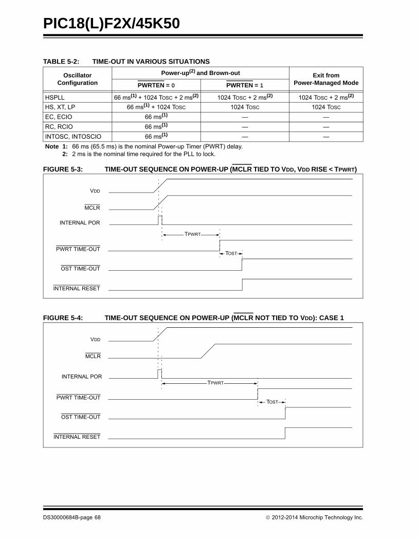
PIC18(L)F2X/45K50
FIGURE 5-3: TIME-OUT SEQUENCE ON POWER-UP (MCLR TIED TO VDD, VDD RISE < TPWRT)
FIGURE 5-4: TIME-OUT SEQUENCE ON POWER-UP (MCLR NOT TIED TO VDD): CASE 1
TABLE 5-2: TIME-OUT IN VARIOUS SITUATIONS
OscillatorConfiguration
Power-up(2) and Brown-out Exit from Power-Managed ModePWRTEN = 0 PWRTEN = 1
HSPLL 66 ms(1) + 1024 TOSC + 2 ms(2) 1024 TOSC + 2 ms(2) 1024 TOSC + 2 ms(2)
HS, XT, LP 66 ms(1) + 1024 TOSC 1024 TOSC 1024 TOSC
EC, ECIO 66 ms(1) — —
RC, RCIO 66 ms(1) — —
INTOSC, INTOSCIO 66 ms(1) — —
Note 1: 66 ms (65.5 ms) is the nominal Power-up Timer (PWRT) delay.2: 2 ms is the nominal time required for the PLL to lock.
TPWRT
TOST
VDD
MCLR
INTERNAL POR
PWRT TIME-OUT
OST TIME-OUT
INTERNAL RESET
TPWRT
TOST
VDD
MCLR
INTERNAL POR
PWRT TIME-OUT
OST TIME-OUT
INTERNAL RESET
DS30000684B-page 68 2012-2014 Microchip Technology Inc.

PIC18(L)F2X/45K50
FIGURE 5-5: TIME-OUT SEQUENCE ON POWER-UP (MCLR NOT TIED TO VDD): CASE 2
FIGURE 5-6: SLOW RISE TIME (MCLR TIED TO VDD, VDD RISE > TPWRT)
VDD
MCLR
INTERNAL POR
PWRT TIME-OUT
OST TIME-OUT
INTERNAL RESET
TPWRT
TOST
VDD
MCLR
INTERNAL POR
PWRT TIME-OUT
OST TIME-OUT
INTERNAL RESET
0V
5V
TPWRT
TOST
2012-2014 Microchip Technology Inc. DS30000684B-page 69

PIC18(L)F2X/45K50
FIGURE 5-7: TIME-OUT SEQUENCE ON POR W/PLL ENABLED (MCLR TIED TO VDD)
TPWRT
TOST
VDD
MCLR
INTERNAL POR
PWRT TIME-OUT
OST TIME-OUT
INTERNAL RESET
PLL TIME-OUT
TPLL
Note: TOST = 1024 clock cycles.TPLL 2 ms max. First three stages of the PWRT timer.
DS30000684B-page 70 2012-2014 Microchip Technology Inc.
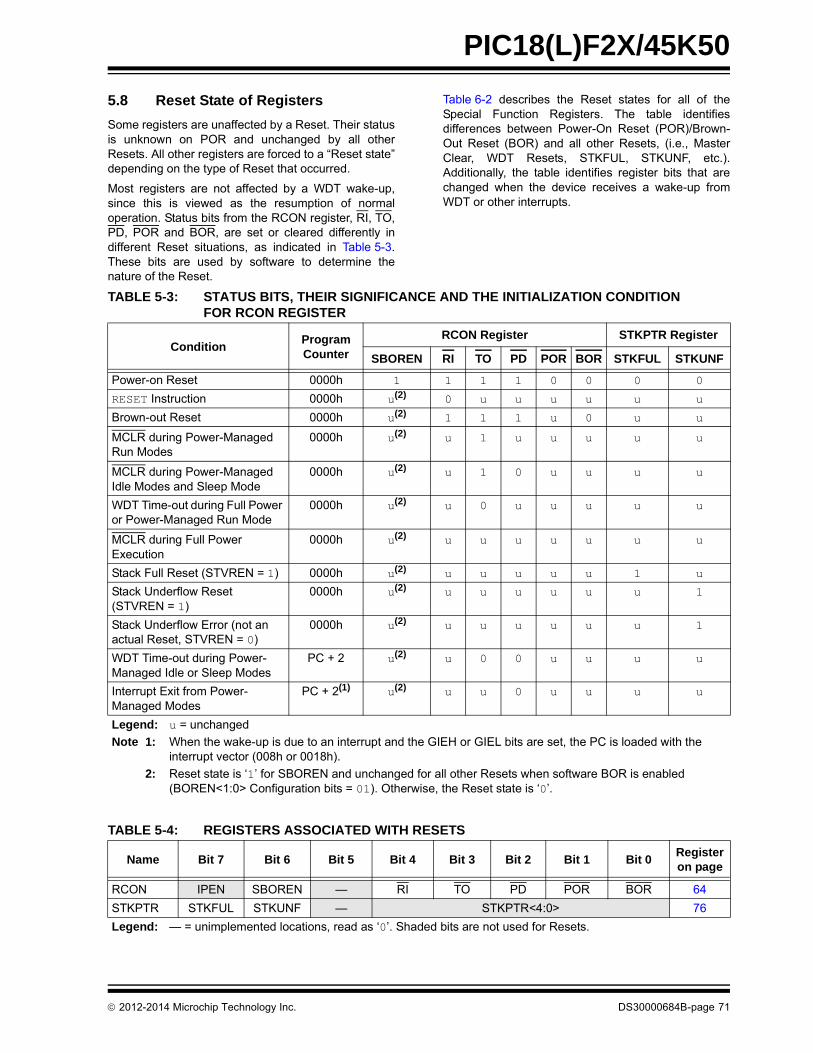
PIC18(L)F2X/45K50
5.8 Reset State of Registers
Some registers are unaffected by a Reset. Their statusis unknown on POR and unchanged by all otherResets. All other registers are forced to a “Reset state”depending on the type of Reset that occurred.
Most registers are not affected by a WDT wake-up,since this is viewed as the resumption of normaloperation. Status bits from the RCON register, RI, TO,PD, POR and BOR, are set or cleared differently indifferent Reset situations, as indicated in Table 5-3.These bits are used by software to determine thenature of the Reset.
Table 6-2 describes the Reset states for all of theSpecial Function Registers. The table identifiesdifferences between Power-On Reset (POR)/Brown-Out Reset (BOR) and all other Resets, (i.e., MasterClear, WDT Resets, STKFUL, STKUNF, etc.).Additionally, the table identifies register bits that arechanged when the device receives a wake-up fromWDT or other interrupts.
TABLE 5-3: STATUS BITS, THEIR SIGNIFICANCE AND THE INITIALIZATION CONDITION FOR RCON REGISTER
ConditionProgram Counter
RCON Register STKPTR Register
SBOREN RI TO PD POR BOR STKFUL STKUNF
Power-on Reset 0000h 1 1 1 1 0 0 0 0
RESET Instruction 0000h u(2) 0 u u u u u u
Brown-out Reset 0000h u(2) 1 1 1 u 0 u u
MCLR during Power-Managed Run Modes
0000h u(2) u 1 u u u u u
MCLR during Power-Managed Idle Modes and Sleep Mode
0000h u(2) u 1 0 u u u u
WDT Time-out during Full Power or Power-Managed Run Mode
0000h u(2) u 0 u u u u u
MCLR during Full Power Execution
0000h u(2) u u u u u u u
Stack Full Reset (STVREN = 1) 0000h u(2) u u u u u 1 u
Stack Underflow Reset (STVREN = 1)
0000h u(2) u u u u u u 1
Stack Underflow Error (not an actual Reset, STVREN = 0)
0000h u(2) u u u u u u 1
WDT Time-out during Power-Managed Idle or Sleep Modes
PC + 2 u(2) u 0 0 u u u u
Interrupt Exit from Power-Managed Modes
PC + 2(1) u(2) u u 0 u u u u
Legend: u = unchanged
Note 1: When the wake-up is due to an interrupt and the GIEH or GIEL bits are set, the PC is loaded with the interrupt vector (008h or 0018h).
2: Reset state is ‘1’ for SBOREN and unchanged for all other Resets when software BOR is enabled (BOREN<1:0> Configuration bits = 01). Otherwise, the Reset state is ‘0’.
TABLE 5-4: REGISTERS ASSOCIATED WITH RESETS
Name Bit 7 Bit 6 Bit 5 Bit 4 Bit 3 Bit 2 Bit 1 Bit 0Register on page
RCON IPEN SBOREN — RI TO PD POR BOR 64
STKPTR STKFUL STKUNF — STKPTR<4:0> 76
Legend: — = unimplemented locations, read as ‘0’. Shaded bits are not used for Resets.
2012-2014 Microchip Technology Inc. DS30000684B-page 71

PIC18(L)F2X/45K50
TABLE 5-5: CONFIGURATION REGISTERS ASSOCIATED WITH RESETS
Name Bit 7 Bit 6 Bit 5 Bit 4 Bit 3 Bit 2 Bit 1 Bit 0Register on page
CONFIG2L — LPBOR — BORV<1:0> BOREN<1:0> PWRTEN 374
CONFIG2H — — WDTPS<3:0> WDTEN<1:0> 375
CONFIG3H MCLRE SDOMX — T3CMX — — PBADEN CCP2MX 376
CONFIG4L DEBUG XINST ICPRT — — LVP — STRVEN 377
Legend: — = unimplemented locations, read as ‘0’. Shaded bits are not used for Resets.
DS30000684B-page 72 2012-2014 Microchip Technology Inc.

PIC18(L)F2X/45K50
6.0 MEMORY ORGANIZATION
There are three types of memory in PIC18 Enhancedmicrocontroller devices:
• Program Memory
• Data RAM
• Data EEPROM
As Harvard architecture devices, the data and programmemories use separate buses; this allows forconcurrent access of the two memory spaces. The dataEEPROM, for practical purposes, can be regarded asa peripheral device, since it is addressed and accessedthrough a set of control registers.
Additional detailed information on the operation of theFlash program memory is provided in Section 7.0“Flash Program Memory”. Data EEPROM isdiscussed separately in Section 8.0 “Data EEPROMMemory”.
6.1 Program Memory Organization
PIC18 microcontrollers implement a 21-bit programcounter, which is capable of addressing a 2-Mbyteprogram memory space. Accessing a location betweenthe upper boundary of the physically implementedmemory and the 2-Mbyte address will return all ‘0’s (aNOP instruction).
This family of devices contain the following:
• PIC18(L)F24K50: 16 Kbytes of Flash memory, up to 8,192 single-word instructions
• PIC18(L)F25K50, PIC18(L)F45K50: 32 Kbytes of Flash memory, up to 16,384 single-word instructions
PIC18 devices have two interrupt vectors. The Resetvector address is at 0000h and the interrupt vectoraddresses are at 0008h and 0018h.
The program memory map for PIC18(L)F2X/45K50devices is shown in Figure 6-1. Memory block detailsare shown in Figure 21-2.
FIGURE 6-1: PROGRAM MEMORY MAP AND STACK FOR PIC18(L)F2X/45K50 DEVICES
PC<20:0>
Stack Level 1
Stack Level 31
Reset Vector
Low Priority Interrupt Vector
CALL,RCALL,RETURNRETFIE,RETLW
21
0000h
0018h
On-ChipProgram Memory
High Priority Interrupt Vector 0008h
Use
r M
em
ory
Spa
ce
1FFFFFh
4000h3FFFh
Read ‘0’
200000h
8000h7FFFh
On-ChipProgram Memory
Read ‘0’
PIC18(L)F25K50
PIC18(L)F45K50
PIC18(L)F24K50
2012-2014 Microchip Technology Inc. DS30000684B-page 73
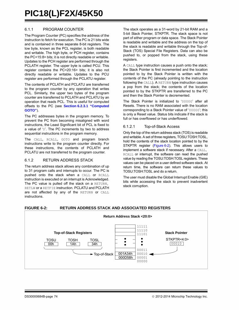
PIC18(L)F2X/45K50
6.1.1 PROGRAM COUNTER
The Program Counter (PC) specifies the address of theinstruction to fetch for execution. The PC is 21 bits wideand is contained in three separate 8-bit registers. Thelow byte, known as the PCL register, is both readableand writable. The high byte, or PCH register, containsthe PC<15:8> bits; it is not directly readable or writable.Updates to the PCH register are performed through thePCLATH register. The upper byte is called PCU. Thisregister contains the PC<20:16> bits; it is also notdirectly readable or writable. Updates to the PCUregister are performed through the PCLATU register.
The contents of PCLATH and PCLATU are transferredto the program counter by any operation that writesPCL. Similarly, the upper two bytes of the programcounter are transferred to PCLATH and PCLATU by anoperation that reads PCL. This is useful for computedoffsets to the PC (see Section 6.2.3.1 “ComputedGOTO”).
The PC addresses bytes in the program memory. Toprevent the PC from becoming misaligned with wordinstructions, the Least Significant bit of PCL is fixed toa value of ‘0’. The PC increments by two to addresssequential instructions in the program memory.
The CALL, RCALL, GOTO and program branchinstructions write to the program counter directly. Forthese instructions, the contents of PCLATH andPCLATU are not transferred to the program counter.
6.1.2 RETURN ADDRESS STACK
The return address stack allows any combination of upto 31 program calls and interrupts to occur. The PC ispushed onto the stack when a CALL or RCALLinstruction is executed or an interrupt is Acknowledged.The PC value is pulled off the stack on a RETURN,RETLW or a RETFIE instruction. PCLATU and PCLATHare not affected by any of the RETURN or CALLinstructions.
The stack operates as a 31-word by 21-bit RAM and a5-bit Stack Pointer, STKPTR. The stack space is notpart of either program or data space. The Stack Pointeris readable and writable and the address on the top ofthe stack is readable and writable through the Top-of-Stack (TOS) Special File Registers. Data can also bepushed to, or popped from the stack, using theseregisters.
A CALL type instruction causes a push onto the stack;the Stack Pointer is first incremented and the locationpointed to by the Stack Pointer is written with thecontents of the PC (already pointing to the instructionfollowing the CALL). A RETURN type instruction causesa pop from the stack; the contents of the locationpointed to by the STKPTR are transferred to the PCand then the Stack Pointer is decremented.
The Stack Pointer is initialized to ‘00000’ after allResets. There is no RAM associated with the locationcorresponding to a Stack Pointer value of ‘00000’; thisis only a Reset value. Status bits indicate if the stack isfull or has overflowed or has underflowed.
6.1.2.1 Top-of-Stack Access
Only the top of the return address stack (TOS) is readableand writable. A set of three registers, TOSU:TOSH:TOSL,hold the contents of the stack location pointed to by theSTKPTR register (Figure 6-2). This allows users toimplement a software stack if necessary. After a CALL,RCALL or interrupt, the software can read the pushedvalue by reading the TOSU:TOSH:TOSL registers. Thesevalues can be placed on a user defined software stack. Atreturn time, the software can return these values toTOSU:TOSH:TOSL and do a return.
The user must disable the Global Interrupt Enable (GIE)bits while accessing the stack to prevent inadvertentstack corruption.
FIGURE 6-2: RETURN ADDRESS STACK AND ASSOCIATED REGISTERS
00011001A34h
111111111011101
000100000100000
00010
Return Address Stack <20:0>
Top-of-Stack000D58h
TOSLTOSHTOSU34h1Ah00h
STKPTR<4:0>
Top-of-Stack Registers Stack Pointer
DS30000684B-page 74 2012-2014 Microchip Technology Inc.

PIC18(L)F2X/45K50
6.1.2.2 Return Stack Pointer (STKPTR)
The STKPTR register (Register 6-1) contains the StackPointer value, the STKFUL (stack full) Status bit andthe STKUNF (Stack Underflow) Status bits. The valueof the Stack Pointer can be 0 through 31. The StackPointer increments before values are pushed onto thestack and decrements after values are popped off thestack. On Reset, the Stack Pointer value will be zero.The user may read and write the Stack Pointer value.This feature can be used by a Real-Time OperatingSystem (RTOS) for return stack maintenance.
After the PC is pushed onto the stack 31 times (withoutpopping any values off the stack), the STKFUL bit isset. The STKFUL bit is cleared by software or by aPOR.
The action that takes place when the stack becomesfull depends on the state of the STVREN (Stack Over-flow Reset Enable) Configuration bit. (Refer toSection 26.1 “Configuration Bits” for a description ofthe device Configuration bits.) If STVREN is set(default), the 31st push will push the (PC + 2) valueonto the stack, set the STKFUL bit and reset thedevice. The STKFUL bit will remain set and the StackPointer will be set to zero.
If STVREN is cleared, the STKFUL bit will be set on the31st push and the Stack Pointer will increment to 31.Any additional pushes will not overwrite the 31st pushand STKPTR will remain at 31.
When the stack has been popped enough times tounload the stack, the next pop will return a value of zeroto the PC and sets the STKUNF bit, while the StackPointer remains at zero. The STKUNF bit will remainset until cleared by software or until a POR occurs.
Note: Returning a value of zero to the PC on anunderflow has the effect of vectoring theprogram to the Reset vector, where thestack conditions can be verified andappropriate actions can be taken. This isnot the same as a Reset, as the contentsof the SFRs are not affected.
2012-2014 Microchip Technology Inc. DS30000684B-page 75
PIC18(L)F2X/45K50
6.1.2.3 PUSH and POP Instructions
Since the Top-of-Stack is readable and writable, theability to push values onto the stack and pull values offthe stack without disturbing normal program executionis a desirable feature. The PIC18 instruction setincludes two instructions, PUSH and POP, that permitthe TOS to be manipulated under software control.TOSU, TOSH and TOSL can be modified to place dataor a return address on the stack.
The PUSH instruction places the current PC value ontothe stack. This increments the Stack Pointer and loadsthe current PC value onto the stack.
The POP instruction discards the current TOS by decre-menting the Stack Pointer. The previous value pushedonto the stack then becomes the TOS value.
6.2 Register Definitions: Stack Pointer
6.2.1 STACK FULL AND UNDERFLOW RESETS
Device Resets on Stack Overflow and Stack Underflowconditions are enabled by setting the STVREN bit inConfiguration Register 4L. When STVREN is set, a fullor underflow will set the appropriate STKFUL orSTKUNF bit and then cause a device Reset. WhenSTVREN is cleared, a full or underflow condition will setthe appropriate STKFUL or STKUNF bit but not causea device Reset. The STKFUL or STKUNF bits arecleared by the user software or a Power-on Reset.
6.2.2 FAST REGISTER STACK
A fast register stack is provided for the Status, WREGand BSR registers, to provide a “fast return” option forinterrupts. The stack for each register is only one leveldeep and is neither readable nor writable. It is loadedwith the current value of the corresponding registerwhen the processor vectors for an interrupt. All inter-rupt sources will push values into the stack registers.The values in the registers are then loaded back intotheir associated registers if the RETFIE, FASTinstruction is used to return from the interrupt.
If both low and high priority interrupts are enabled, thestack registers cannot be used reliably to return fromlow priority interrupts. If a high priority interrupt occurswhile servicing a low priority interrupt, the stack registervalues stored by the low priority interrupt will beoverwritten. In these cases, users must save the keyregisters by software during a low priority interrupt.
If interrupt priority is not used, all interrupts may use thefast register stack for returns from interrupt. If nointerrupts are used, the fast register stack can be usedto restore the Status, WREG and BSR registers at theend of a subroutine call. To use the fast register stackfor a subroutine call, a CALL label, FAST instructionmust be executed to save the STATUS, WREG andBSR registers to the fast register stack. ARETURN, FAST instruction is then executed to restorethese registers from the fast register stack.
Example 6-1 shows a source code example that usesthe fast register stack during a subroutine call andreturn.
REGISTER 6-1: STKPTR: STACK POINTER REGISTER
R/C-0 R/C-0 U-0 R/W-0 R/W-0 R/W-0 R/W-0 R/W-0
STKFUL(1) STKUNF(1) — STKPTR<4:0>
bit 7 bit 0
Legend:
R = Readable bit W = Writable bit U = Unimplemented C = Clearable only bit
-n = Value at POR ‘1’ = Bit is set ‘0’ = Bit is cleared x = Bit is unknown
bit 7 STKFUL: Stack Full Flag bit(1)
1 = Stack became full or overflowed 0 = Stack has not become full or overflowed
bit 6 STKUNF: Stack Underflow Flag bit(1)
1 = Stack Underflow occurred 0 = Stack Underflow did not occur
bit 5 Unimplemented: Read as ‘0’
bit 4-0 STKPTR<4:0>: Stack Pointer Location bits
Note 1: Bit 7 and bit 6 are cleared by user software or by a POR.
DS30000684B-page 76 2012-2014 Microchip Technology Inc.

PIC18(L)F2X/45K50
EXAMPLE 6-1: FAST REGISTER STACK CODE EXAMPLE
6.2.3 LOOK-UP TABLES IN PROGRAM MEMORY
There may be programming situations that require thecreation of data structures, or look-up tables, inprogram memory. For PIC18 devices, look-up tablescan be implemented in two ways:
• Computed GOTO
• Table Reads
6.2.3.1 Computed GOTO
A computed GOTO is accomplished by adding an offsetto the program counter. An example is shown inExample 6-2.
A look-up table can be formed with an ADDWF PCLinstruction and a group of RETLW nn instructions. TheW register is loaded with an offset into the table beforeexecuting a call to that table. The first instruction of thecalled routine is the ADDWF PCL instruction. The nextinstruction executed will be one of the RETLW nninstructions that returns the value ‘nn’ to the callingfunction.
The offset value (in WREG) specifies the number ofbytes that the program counter should advance andshould be multiples of 2 (LSb = 0).
In this method, only one data byte may be stored ineach instruction location and room on the returnaddress stack is required.
EXAMPLE 6-2: COMPUTED GOTO USING AN OFFSET VALUE
6.2.3.2 Table Reads and Table Writes
A better method of storing data in program memoryallows two bytes of data to be stored in each instructionlocation.
Look-up table data may be stored two bytes perprogram word by using table reads and writes. TheTable Pointer (TBLPTR) register specifies the byteaddress and the Table Latch (TABLAT) registercontains the data that is read from or written to programmemory. Data is transferred to or from programmemory one byte at a time.
Table read and table write operations are discussedfurther in Section 7.1 “Table Reads and TableWrites”.
CALL SUB1, FAST ;STATUS, WREG, BSR;SAVED IN FAST REGISTER;STACK
SUB1
RETURN, FAST ;RESTORE VALUES SAVED;IN FAST REGISTER STACK
MOVF OFFSET, WCALL TABLE
ORG nn00hTABLE ADDWF PCL
RETLW nnhRETLW nnhRETLW nnh...
2012-2014 Microchip Technology Inc. DS30000684B-page 77

PIC18(L)F2X/45K50
6.3 PIC18 Instruction Cycle
6.3.1 CLOCKING SCHEME
The microcontroller clock input, whether from aninternal or external source, is internally divided by fourto generate four non-overlapping quadrature clocks(Q1, Q2, Q3 and Q4). Internally, the program counter isincremented on every Q1; the instruction is fetchedfrom the program memory and latched into theinstruction register during Q4. The instruction isdecoded and executed during the following Q1 throughQ4. The clocks and instruction execution flow areshown in Figure 6-3.
6.3.2 INSTRUCTION FLOW/PIPELINING
An “Instruction Cycle” consists of four Q cycles: Q1through Q4. The instruction fetch and execute arepipelined in such a manner that a fetch takes oneinstruction cycle, while the decode and execute takeanother instruction cycle. However, due to thepipelining, each instruction effectively executes in onecycle. If an instruction causes the program counter tochange (e.g., GOTO), then two cycles are required tocomplete the instruction (Example 6-3).
A fetch cycle begins with the Program Counter (PC)incrementing in Q1.
In the execution cycle, the fetched instruction is latchedinto the Instruction Register (IR) in cycle Q1. Thisinstruction is then decoded and executed during theQ2, Q3 and Q4 cycles. Data memory is read during Q2(operand read) and written during Q4 (destinationwrite).
FIGURE 6-3: CLOCK/INSTRUCTION CYCLE
EXAMPLE 6-3: INSTRUCTION PIPELINE FLOW
Q1 Q2 Q3 Q4 Q1 Q2 Q3 Q4 Q1 Q2 Q3 Q4
OSC1
Q1
Q2
Q3
Q4
PC
OSC2/CLKO(RC mode)
PC PC + 2 PC + 4
Fetch INST (PC)Execute INST (PC – 2)
Fetch INST (PC + 2)Execute INST (PC)
Fetch INST (PC + 4)Execute INST (PC + 2)
InternalPhaseClock
All instructions are single cycle, except for any program branches. These take two cycles since the fetch instructionis “flushed” from the pipeline while the new instruction is being fetched and then executed.
TCY0 TCY1 TCY2 TCY3 TCY4 TCY5
1. MOVLW 55h Fetch 1 Execute 1
2. MOVWF PORTB Fetch 2 Execute 2
3. BRA SUB_1 Fetch 3 Execute 3
4. BSF PORTA, BIT3 (Forced NOP) Fetch 4 Flush (NOP)
5. Instruction @ address SUB_1 Fetch SUB_1 Execute SUB_1
DS30000684B-page 78 2012-2014 Microchip Technology Inc.

PIC18(L)F2X/45K50
6.3.3 INSTRUCTIONS IN PROGRAM MEMORY
The program memory is addressed in bytes.Instructions are stored as either two bytes or four bytesin program memory. The Least Significant Byte of aninstruction word is always stored in a program memorylocation with an even address (LSb = 0). To maintainalignment with instruction boundaries, the PCincrements in steps of two and the LSb will always read‘0’ (see Section 6.1.1 “Program Counter”).
Figure 6-4 shows an example of how instruction wordsare stored in the program memory.
The CALL and GOTO instructions have the absoluteprogram memory address embedded into theinstruction. Since instructions are always stored on wordboundaries, the data contained in the instruction is aword address. The word address is written to PC<20:1>,which accesses the desired byte address in programmemory. Instruction #2 in Figure 6-4 shows how theinstruction GOTO 0006h is encoded in the programmemory. Program branch instructions, which encode arelative address offset, operate in the same manner. Theoffset value stored in a branch instruction represents thenumber of single-word instructions that the PC will beoffset by. Section 27.0 “Instruction Set Summary”provides further details of the instruction set.
FIGURE 6-4: INSTRUCTIONS IN PROGRAM MEMORY
6.3.4 TWO-WORD INSTRUCTIONS
The standard PIC18 instruction set has four two-wordinstructions: CALL, MOVFF, GOTO and LSFR. In allcases, the second word of the instruction always has‘1111’ as its four Most Significant bits; the other 12 bitsare literal data, usually a data memory address.
The use of ‘1111’ in the four MSbs of an instructionspecifies a special form of NOP. If the instruction isexecuted in proper sequence – immediately after thefirst word – the data in the second word is accessed
and used by the instruction sequence. If the first wordis skipped for some reason and the second word isexecuted by itself, a NOP is executed instead. This isnecessary for cases when the two-word instruction ispreceded by a conditional instruction that changes thePC. Example 6-4 shows how this works.
EXAMPLE 6-4: TWO-WORD INSTRUCTIONS
Word AddressLSB = 1 LSB = 0
Program MemoryByte Locations
000000h000002h000004h000006h
Instruction 1: MOVLW 055h 0Fh 55h 000008hInstruction 2: GOTO 0006h EFh 03h 00000Ah
F0h 00h 00000ChInstruction 3: MOVFF 123h, 456h C1h 23h 00000Eh
F4h 56h 000010h000012h000014h
Note: See Section 6.8 “PIC18 InstructionExecution and the Extended Instruc-tion Set” for information on two-wordinstructions in the extended instruction set.
CASE 1:
Object Code Source Code
0110 0110 0000 0000 TSTFSZ REG1 ; is RAM location 0?
1100 0001 0010 0011 MOVFF REG1, REG2 ; No, skip this word
1111 0100 0101 0110 ; Execute this word as a NOP
0010 0100 0000 0000 ADDWF REG3 ; continue code
CASE 2:
Object Code Source Code
0110 0110 0000 0000 TSTFSZ REG1 ; is RAM location 0?
1100 0001 0010 0011 MOVFF REG1, REG2 ; Yes, execute this word
1111 0100 0101 0110 ; 2nd word of instruction
0010 0100 0000 0000 ADDWF REG3 ; continue code
2012-2014 Microchip Technology Inc. DS30000684B-page 79

PIC18(L)F2X/45K50
6.4 Data Memory Organization
The data memory in PIC18 devices is implemented asstatic RAM. Each register in the data memory has a12-bit address, allowing up to 4096 bytes of datamemory. The memory space is divided into as many as16 banks that contain 256 bytes each. Figures 6-5through 6-7 show the data memory organization for thePIC18(L)F2X/45K50 devices.
The data memory contains Special Function Registers(SFRs) and General Purpose Registers (GPRs). TheSFRs are used for control and status of the controllerand peripheral functions, while GPRs are used for datastorage and scratchpad operations in the user’sapplication. Any read of an unimplemented location willread as ‘0’s.
The instruction set and architecture allow operationsacross all banks. The entire data memory may beaccessed by Direct, Indirect or Indexed Addressingmodes. Addressing modes are discussed later in thissubsection.
To ensure that commonly used registers (SFRs andselect GPRs) can be accessed in a single cycle, PIC18devices implement an Access Bank. This is a 256-bytememory space that provides fast access to SFRs andthe lower portion of GPR Bank 0 without using the BankSelect Register (BSR). Section 6.4.3 “Access Bank”provides a detailed description of the Access RAM.
6.4.1 USB RAM
Banks 4 through 7 of the data memory are actuallymapped to special dual port RAM. When the USBmodule is disabled, the GPRs in these banks are usedlike any other GPR in the data memory space.When the USB module is enabled, the memory inthese banks is allocated as buffer RAM for USBoperation. This area is shared between themicrocontroller core and the USB Serial InterfaceEngine (SIE) and is used to transfer data directlybetween the two. It is theoretically possible to use theareas of USB RAM that are not allocated as USBbuffers for normal scratchpad memory or othervariable storage. In practice, the dynamic nature ofbuffer allocation makes this risky, at best. Additionally,Bank 4 is used for USB buffer descriptor tables whenthe module is enabled and should not be used for anyother purposes during that time. Additional informationon USB RAM and buffer operation is provided inSection 24.0 “Universal Serial Bus (USB)”.
6.4.2 BANK SELECT REGISTER (BSR)
Large areas of data memory require an efficientaddressing scheme to make rapid access to anyaddress possible. Ideally, this means that an entireaddress does not need to be provided for each read orwrite operation. For PIC18 devices, this is accom-plished with a RAM banking scheme. This divides thememory space into 16 contiguous banks of 256 bytes.Depending on the instruction, each location can beaddressed directly by its full 12-bit address, or an 8-bitlow-order address and a 4-bit Bank Pointer.
Most instructions in the PIC18 instruction set make useof the Bank Pointer, known as the Bank Select Register(BSR). This SFR holds the four Most Significant bits ofa location’s address; the instruction itself includes theeight Least Significant bits. Only the four lower bits ofthe BSR are implemented (BSR<3:0>). The upper fourbits are unused; they will always read ‘0’ and cannot bewritten to. The BSR can be loaded directly by using theMOVLB instruction.
The value of the BSR indicates the bank in datamemory; the eight bits in the instruction show thelocation in the bank and can be thought of as an offsetfrom the bank’s lower boundary. The relationshipbetween the BSR’s value and the bank division in datamemory is shown in Figures 6-5 through 6-7.
Since up to 16 registers may share the same low-orderaddress, the user must always be careful to ensure thatthe proper bank is selected before performing a dataread or write. For example, writing what should beprogram data to an 8-bit address of F9h while the BSRis 0Fh will end up resetting the program counter.
While any bank can be selected, only those banks thatare actually implemented can be read or written to.Writes to unimplemented banks are ignored, whilereads from unimplemented banks will return ‘0’s. Evenso, the STATUS register will still be affected as if theoperation was successful. The data memory maps inFigures 6-5 through 6-7 indicate which banks areimplemented.
In the core PIC18 instruction set, only the MOVFFinstruction fully specifies the 12-bit address of thesource and target registers. This instruction ignores theBSR completely when it executes. All other instructionsinclude only the low-order address as an operand andmust use either the BSR or the Access Bank to locatetheir target registers.
Note: The operation of some aspects of datamemory are changed when the PIC18extended instruction set is enabled. SeeSection 6.7 “Data Memory and theExtended Instruction Set” for moreinformation.
DS30000684B-page 80 2012-2014 Microchip Technology Inc.

PIC18(L)F2X/45K50
FIGURE 6-5: DATA MEMORY MAP FOR PIC18(L)F2X/45K50 DEVICES
Bank 0
Bank 1
Bank 14
Bank 15
Data Memory MapBSR<3:0>
= 0000
= 0001
= 1111
060h05Fh
00h
5Fh60h
FFh
Access Bank
When ‘a’ = 0:
The BSR is ignored and theAccess Bank is used.
The first 96 bytes are general purpose RAM (from Bank 0).
The second 160 bytes areSpecial Function Registers(from Bank 15).
When ‘a’ = 1:
The BSR specifies the Bankused by the instruction.
1FFh
100h0FFh
000hAccess RAM
FFh
00h
FFh
00h
GPR
GPR
Access RAM High
Access RAM Low
Bank 2
= 0110
= 0010
(SFRs)
2FFh
200h
3FFh
300h
4FFh
400h
5FFh
500h
6FFh
600h
7FFh
700h
8FFh
800h
9FFh
900h
AFFh
A00h
BFFh
B00h
CFFh
C00h
DFFh
D00h
E00h
Bank 3
Bank 4
Bank 5
Bank 6
Bank 7
Bank 8
Bank 9
Bank 10
Bank 11
Bank 12
Bank 13
FFh
00h
FFh
00h
FFh
00h
FFh
00h
FFh
00h
FFh
00h
FFh
00h
FFh
00h
FFh
00h
FFh
00h
FFh
00h
FFh
00h
GPR
FFh
00h
= 0011
= 0100
= 0101
= 0111
= 1000
= 1001
= 1010
= 1011
= 1100
= 1101
= 1110
GPR
GPR(2)
GPR(2)
GPR(2)
GPR(2)
Note 1: Addresses F53h through F5Fh arealso used by SFRs, but are notpart of the Access RAM. Usersmust always use the completeaddress or load the proper BSRvalue to access these registers.
2: These banks also serve as RAMbuffer for USB operation. SeeSection 6.4.1 “USB RAM” formore information.
F60h
FFFh
F5Fh
F00h
FFh
00h
SFR(1)
Unimplemented
SFR
F53hF52h
Unimplemented. Read as 00h.
Unimplemented. Read as 00h.
Unimplemented. Read as 00h.
Unimplemented. Read as 00h.
Unimplemented. Read as 00h.
Unimplemented. Read as 00h.
Unimplemented. Read as 00h.
2012-2014 Microchip Technology Inc. DS30000684B-page 81
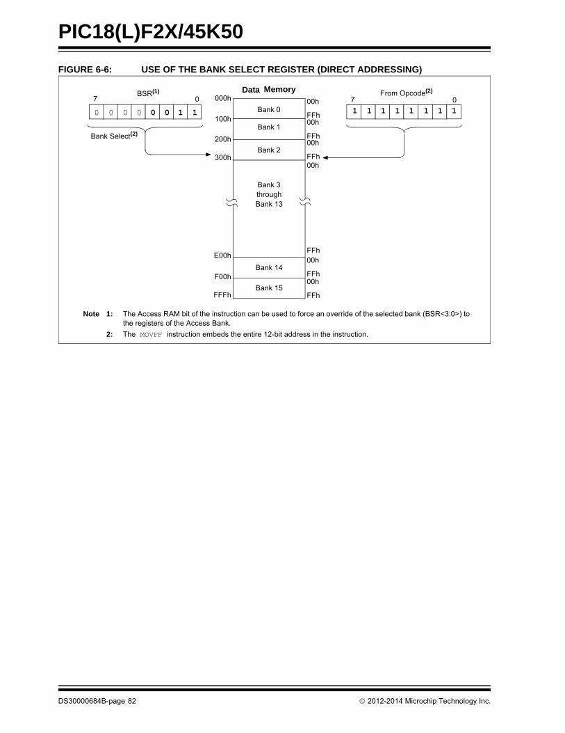
PIC18(L)F2X/45K50
FIGURE 6-6: USE OF THE BANK SELECT REGISTER (DIRECT ADDRESSING)
Note 1: The Access RAM bit of the instruction can be used to force an override of the selected bank (BSR<3:0>) to the registers of the Access Bank.
2: The MOVFF instruction embeds the entire 12-bit address in the instruction.
Data Memory
Bank Select(2)
7 0From Opcode(2)
0 0 0 0
000h
100h
200h
300h
F00h
E00h
FFFh
Bank 0
Bank 1
Bank 2
Bank 14
Bank 15
00h
FFh00h
FFh00h
FFh
00h
FFh00h
FFh
00h
FFh
Bank 3throughBank 13
0 0 1 1 1 1 1 1 1 1 1 1
7 0BSR(1)
DS30000684B-page 82 2012-2014 Microchip Technology Inc.

PIC18(L)F2X/45K50
6.4.3 ACCESS BANK
While the use of the BSR with an embedded 8-bitaddress allows users to address the entire range ofdata memory, it also means that the user must alwaysensure that the correct bank is selected. Otherwise,data may be read from or written to the wrong location.This can be disastrous if a GPR is the intended targetof an operation, but an SFR is written to instead.Verifying and/or changing the BSR for each read orwrite to data memory can become very inefficient.
To streamline access for the most commonly used datamemory locations, the data memory is configured withan Access Bank, which allows users to access amapped block of memory without specifying a BSR.The Access Bank consists of the first 96 bytes of mem-ory (00h-5Fh) in Bank 0 and the last 160 bytes of mem-ory (60h-FFh) in Block 15. The lower half is known asthe “Access RAM” and is composed of GPRs. Thisupper half is also where the device’s SFRs aremapped. These two areas are mapped contiguously inthe Access Bank and can be addressed in a linearfashion by an 8-bit address (Figures 6-5 through 6-7).
The Access Bank is used by core PIC18 instructionsthat include the Access RAM bit (the ‘a’ parameter inthe instruction). When ‘a’ is equal to ‘1’, the instructionuses the BSR and the 8-bit address included in theopcode for the data memory address. When ‘a’ is ‘0’,however, the instruction is forced to use the AccessBank address map; the current value of the BSR isignored entirely.
Using this “forced” addressing allows the instruction tooperate on a data address in a single cycle, withoutupdating the BSR first. For 8-bit addresses of 60h andabove, this means that users can evaluate and operateon SFRs more efficiently. The Access RAM below 60his a good place for data values that the user might needto access rapidly, such as immediate computationalresults or common program variables. Access RAMalso allows for faster and more code efficient contextsaving and switching of variables.
The mapping of the Access Bank is slightly differentwhen the extended instruction set is enabled (XINSTConfiguration bit = 1). This is discussed in more detailin Section 6.7.3 “Mapping the Access Bank inIndexed Literal Offset Mode”.
6.4.4 GENERAL PURPOSE REGISTER FILE
PIC18 devices may have banked memory in the GPRarea. This is data RAM, which is available for use by allinstructions. GPRs start at the bottom of Bank 0(address 000h) and grow upwards towards the bottom ofthe SFR area. GPRs are not initialized by a Power-onReset and are unchanged on all other Resets.
6.4.5 SPECIAL FUNCTION REGISTERS
The Special Function Registers (SFRs) are registersused by the CPU and peripheral modules for controllingthe desired operation of the device. These registers areimplemented as static RAM. SFRs start at the top ofdata memory (FFFh) and extend downward to occupythe top portion of Bank 15 (F53h to FFFh). A list ofthese registers is given in Table 6-1 and Table 6-2.
The SFRs can be classified into two sets: thoseassociated with the “core” device functionality (ALU,Resets and interrupts) and those related to theperipheral functions. The Reset and interrupt registersare described in their respective chapters, while theALU’s STATUS register is described later in thissection. Registers related to the operation of aperipheral feature are described in the chapter for thatperipheral.
The SFRs are typically distributed among theperipherals whose functions they control. Unused SFRlocations are unimplemented and read as ‘0’s.
2012-2014 Microchip Technology Inc. DS30000684B-page 83
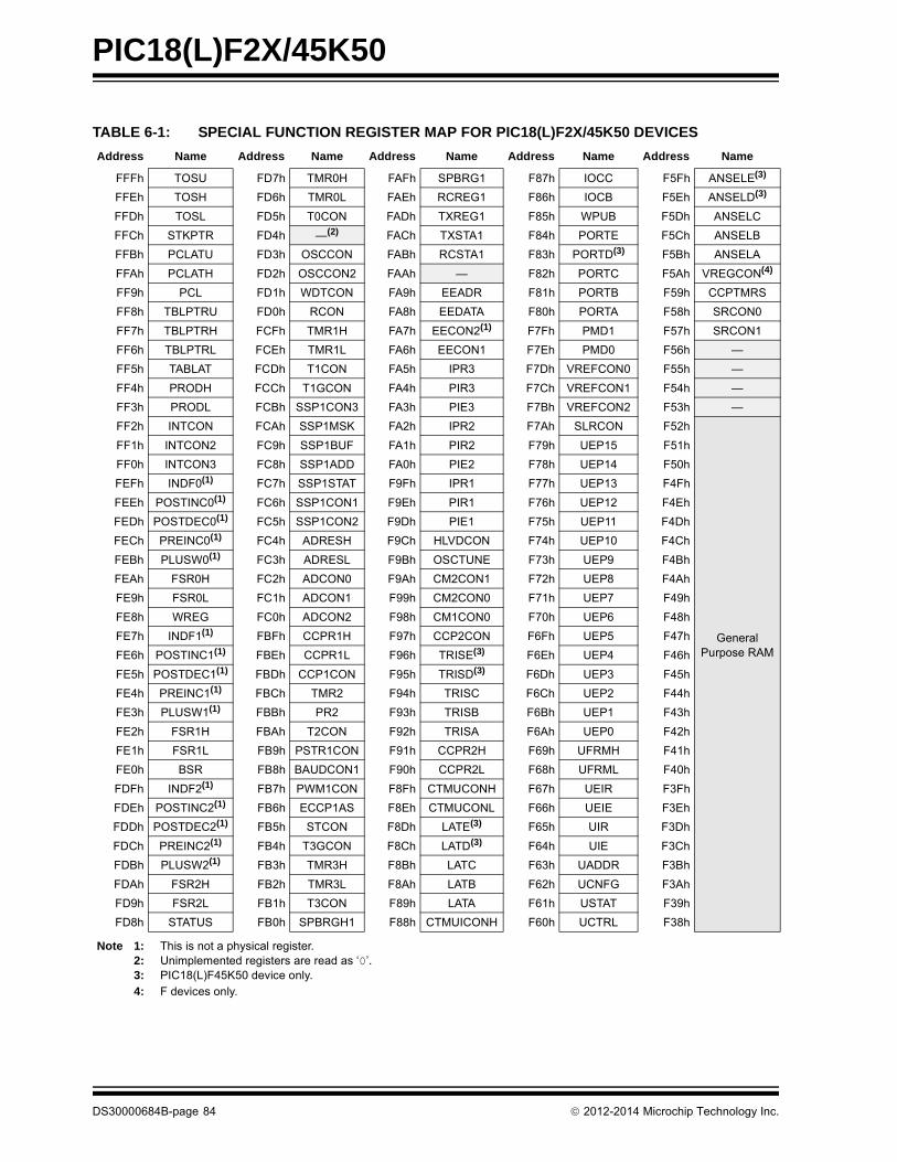
PIC18(L)F2X/45K50
TABLE 6-1: SPECIAL FUNCTION REGISTER MAP FOR PIC18(L)F2X/45K50 DEVICES
Address Name Address Name Address Name Address Name Address Name
FFFh TOSU FD7h TMR0H FAFh SPBRG1 F87h IOCC F5Fh ANSELE(3)
FFEh TOSH FD6h TMR0L FAEh RCREG1 F86h IOCB F5Eh ANSELD(3)
FFDh TOSL FD5h T0CON FADh TXREG1 F85h WPUB F5Dh ANSELC
FFCh STKPTR FD4h —(2) FACh TXSTA1 F84h PORTE F5Ch ANSELB
FFBh PCLATU FD3h OSCCON FABh RCSTA1 F83h PORTD(3) F5Bh ANSELA
FFAh PCLATH FD2h OSCCON2 FAAh — F82h PORTC F5Ah VREGCON(4)
FF9h PCL FD1h WDTCON FA9h EEADR F81h PORTB F59h CCPTMRS
FF8h TBLPTRU FD0h RCON FA8h EEDATA F80h PORTA F58h SRCON0
FF7h TBLPTRH FCFh TMR1H FA7h EECON2(1) F7Fh PMD1 F57h SRCON1
FF6h TBLPTRL FCEh TMR1L FA6h EECON1 F7Eh PMD0 F56h —
FF5h TABLAT FCDh T1CON FA5h IPR3 F7Dh VREFCON0 F55h —
FF4h PRODH FCCh T1GCON FA4h PIR3 F7Ch VREFCON1 F54h —
FF3h PRODL FCBh SSP1CON3 FA3h PIE3 F7Bh VREFCON2 F53h —
FF2h INTCON FCAh SSP1MSK FA2h IPR2 F7Ah SLRCON F52h
General Purpose RAM
FF1h INTCON2 FC9h SSP1BUF FA1h PIR2 F79h UEP15 F51h
FF0h INTCON3 FC8h SSP1ADD FA0h PIE2 F78h UEP14 F50h
FEFh INDF0(1) FC7h SSP1STAT F9Fh IPR1 F77h UEP13 F4Fh
FEEh POSTINC0(1) FC6h SSP1CON1 F9Eh PIR1 F76h UEP12 F4Eh
FEDh POSTDEC0(1) FC5h SSP1CON2 F9Dh PIE1 F75h UEP11 F4Dh
FECh PREINC0(1) FC4h ADRESH F9Ch HLVDCON F74h UEP10 F4Ch
FEBh PLUSW0(1) FC3h ADRESL F9Bh OSCTUNE F73h UEP9 F4Bh
FEAh FSR0H FC2h ADCON0 F9Ah CM2CON1 F72h UEP8 F4Ah
FE9h FSR0L FC1h ADCON1 F99h CM2CON0 F71h UEP7 F49h
FE8h WREG FC0h ADCON2 F98h CM1CON0 F70h UEP6 F48h
FE7h INDF1(1) FBFh CCPR1H F97h CCP2CON F6Fh UEP5 F47h
FE6h POSTINC1(1) FBEh CCPR1L F96h TRISE(3) F6Eh UEP4 F46h
FE5h POSTDEC1(1) FBDh CCP1CON F95h TRISD(3) F6Dh UEP3 F45h
FE4h PREINC1(1) FBCh TMR2 F94h TRISC F6Ch UEP2 F44h
FE3h PLUSW1(1) FBBh PR2 F93h TRISB F6Bh UEP1 F43h
FE2h FSR1H FBAh T2CON F92h TRISA F6Ah UEP0 F42h
FE1h FSR1L FB9h PSTR1CON F91h CCPR2H F69h UFRMH F41h
FE0h BSR FB8h BAUDCON1 F90h CCPR2L F68h UFRML F40h
FDFh INDF2(1) FB7h PWM1CON F8Fh CTMUCONH F67h UEIR F3Fh
FDEh POSTINC2(1) FB6h ECCP1AS F8Eh CTMUCONL F66h UEIE F3Eh
FDDh POSTDEC2(1) FB5h STCON F8Dh LATE(3) F65h UIR F3Dh
FDCh PREINC2(1) FB4h T3GCON F8Ch LATD(3) F64h UIE F3Ch
FDBh PLUSW2(1) FB3h TMR3H F8Bh LATC F63h UADDR F3Bh
FDAh FSR2H FB2h TMR3L F8Ah LATB F62h UCNFG F3Ah
FD9h FSR2L FB1h T3CON F89h LATA F61h USTAT F39h
FD8h STATUS FB0h SPBRGH1 F88h CTMUICONH F60h UCTRL F38h
Note 1: This is not a physical register.2: Unimplemented registers are read as ‘0’.3: PIC18(L)F45K50 device only.4: F devices only.
DS30000684B-page 84 2012-2014 Microchip Technology Inc.

PIC18(L)F2X/45K50
TABLE 6-2: REGISTER FILE SUMMARY FOR PIC18(L)F2X/45K50 DEVICES
Address Name Bit 7 Bit 6 Bit 5 Bit 4 Bit 3 Bit 2 Bit 1 Bit 0Value on
POR, BOR
FFFh TOSU — — — Top-of-Stack, Upper Byte (TOS<20:16>) ---0 0000
FFEh TOSH Top-of-Stack, High Byte (TOS<15:8>) 0000 0000
FFDh TOSL Top-of-Stack, Low Byte (TOS<7:0>) 0000 0000
FFCh STKPTR STKFUL STKUNF — STKPTR<4:0> 00-0 0000
FFBh PCLATU — — — Holding Register for PC<20:16> ---0 0000
FFAh PCLATH Holding Register for PC<15:8> 0000 0000
FF9h PCL Holding Register for PC<7:0> 0000 0000
FF8h TBLPTRU — — Program Memory Table Pointer Upper Byte (TBLPTR<21:16>) --00 0000
FF7h TBLPTRH Program Memory Table Pointer High Byte (TBLPTR<15:8>) 0000 0000
FF6h TBLPTRL Program Memory Table Pointer Low Byte (TBLPTR<7:0>) 0000 0000
FF5h TABLAT Program Memory Table Latch 0000 0000
FF4h PRODH Product Register, High Byte xxxx xxxx
FF3h PRODL Product Register, Low Byte xxxx xxxx
FF2h INTCON GIE/GIEH PEIE/GIEL TMR0IE INT0IE IOCIE TMR0IF INT0IF IOCIF 0000 000x
FF1h INTCON2 RBPU INTEDG0 INTEDG1 INTEDG2 — TMR0IP — IOCIP 1111 -1-1
FF0h INTCON3 INT2IP INT1IP — INT2IE INT1IE — INT2IF INT1IF 11-0 0-00
FEFh INDF0 Uses contents of FSR0 to address data memory – value of FSR0 not changed (not a physical register) ---- ----
FEEh POSTINC0 Uses contents of FSR0 to address data memory – value of FSR0 post-incremented (not a physical register) ---- ----
FEDh POSTDEC0 Uses contents of FSR0 to address data memory – value of FSR0 post-decremented (not a physical register) ---- ----
FECh PREINC0 Uses contents of FSR0 to address data memory – value of FSR0 pre-incremented (not a physical register) ---- ----
FEBh PLUSW0 Uses contents of FSR0 to address data memory – value of FSR0 pre-incremented (not a physical register) – value of FSR0 offset by W
---- ----
FEAh FSR0H — — — — Indirect Data Memory Address Pointer 0, High Byte ---- 0000
FE9h FSR0L Indirect Data Memory Address Pointer 0, Low Byte xxxx xxxx
FE8h WREG Working Register xxxx xxxx
FE7h INDF1 Uses contents of FSR1 to address data memory – value of FSR1 not changed (not a physical register) ---- ----
FE6h POSTINC1 Uses contents of FSR1 to address data memory – value of FSR1 post-incremented (not a physical register) ---- ----
FE5h POSTDEC1 Uses contents of FSR1 to address data memory – value of FSR1 post-incremented (not a physical register) ---- ----
FE4h PREINC1 Uses contents of FSR1 to address data memory – value of FSR1 pre-incremented (not a physical register) ---- ----
FE3h PLUSW1 Uses contents of FSR1 to address data memory – value of FSR1 pre-incremented (not a physical register) – value of FSR1 offset by W
---- ----
FE2h FSR1H — — — — Indirect Data Memory Address Pointer 1, High Byte ---- 0000
FE1h FSR1L Indirect Data Memory Address Pointer 1, Low Byte xxxx xxxx
FE0h BSR — — — — Bank Select Register ---- 0000
FDFh INDF2 Uses contents of FSR2 to address data memory – value of FSR2 not changed (not a physical register) ---- ----
FDEh POSTINC2 Uses contents of FSR2 to address data memory – value of FSR2 post-incremented (not a physical register) ---- ----
FDDh POSTDEC2 Uses contents of FSR2 to address data memory – value of FSR2 post-decremented (not a physical register) ---- ----
FDCh PREINC2 Uses contents of FSR2 to address data memory – value of FSR2 pre-incremented (not a physical register) ---- ----
FDBh PLUSW2 Uses contents of FSR2 to address data memory – value of FSR2 pre-incremented (not a physical register) – value of FSR2 offset by W
---- ----
FDAh FSR2H — — — — Indirect Data Memory Address Pointer 2, High Byte ---- 0000
FD9h FSR2L Indirect Data Memory Address Pointer 2, Low Byte xxxx xxxx
FD8h STATUS — — — N OV Z DC C ---x xxxx
FD7h TMR0H Timer0 Register, High Byte 0000 0000
FD6h TMR0L Timer0 Register, Low Byte xxxx xxxx
FD5h T0CON TMR0ON T08BIT T0CS T0SE PSA T0PS<2:0> 1111 1111
FD3h OSCCON IDLEN IRCF<2:0> OSTS HFIOFS SCS<1:0> 0011 q000
FD2h OSCCON2 PLLRDY SOSCRUN INTSRC PLLEN SOSCGO PRISD HFIOFR LFIOFS 0000 0100
FD1h WDTCON — — — — — — — SWDTEN ---- ---0
FD0h RCON IPEN SBOREN — RI TO PD POR BOR 01-1 1100
Legend: x = unknown, u = unchanged, — = unimplemented, q = value depends on conditionNote 1: PIC18(L)F45K50 devices only.
2: PIC18(L)F2XK50 devices only.
2012-2014 Microchip Technology Inc. DS30000684B-page 85

PIC18(L)F2X/45K50
FCFh TMR1H Holding Register for the Most Significant Byte of the 16-bit TMR1 Register xxxx xxxx
FCEh TMR1L Holding Register for the Least Significant Byte of the 16-bit TMR1 Register xxxx xxxx
FCDh T1CON TMR1CS<1:0> T1CKPS<1:0> SOSCEN T1SYNC RD16 TMR1ON 0000 0000
FCCh T1GCON TMR1GE T1GPOL T1GTM T1GSPM T1GGO/DONE
T1GVAL T1GSS<1:0> 0000 0x00
FCBh SSP1CON3 ACKTIM PCIE SCIE BOEN SDAHT SBCDE AHEN DHEN 0000 0000
FCAh SSP1MSK SSP1 Mask Register bits 1111 1111
FC9h SSP1BUF SSP1 Receive Buffer/Transmit Register xxxx xxxx
FC8h SSP1ADD SSP1 Address Register in I2C™ Slave Mode. SSP1 Baud Rate Reload Register in I2C Master Mode 0000 0000
FC7h SSP1STAT SMP CKE D/A P S R/W UA BF 0000 0000
FC6h SSP1CON1 WCOL SSPOV SSPEN CKP SSPM<3:0> 0000 0000
FC5h SSP1CON2 GCEN ACKSTAT ACKDT ACKEN RCEN PEN RSEN SEN 0000 0000
FC4h ADRESH A/D Result, High Byte xxxx xxxx
FC3h ADRESL A/D Result, Low Byt xxxx xxxx
FC2h ADCON0 — CHS<4:0> GO/DONE ADON -000 0000
FC1h ADCON1 TRIGSEL — — — PVCFG<1:0> NVCFG<1:0> 0--- 0000
FC0h ADCON2 ADFM — ACQT<2:0> ADCS<2:0> 0-00 0000
FBFh CCPR1H Capture/Compare/PWM Register 1, High Byte xxxx xxxx
FBEh CCPR1L Capture/Compare/PWM Register 1, Low Byte xxxx xxxx
FBDh CCP1CON P1M<1:0> DC1B<1:0> CCP1M<3:0> 0000 0000
FBCh TMR2 Timer2 Register 0000 0000
FBBh PR2 Timer2 Period Register 1111 1111
FBAh T2CON — T2OUTPS<3:0> TMR2ON T2CKPS<1:0> -000 0000
FB9h PSTR1CON — — — STR1SYNC STR1D STR1C STR1B STR1A ---0 0001
FB8h BAUDCON1 ABDOVF RCIDL RXDTP TXCKP BRG16 — WUE ABDEN 0100 0-00
FB7h PWM1CON P1RSEN P1DC<6:0> 0000 0000
FB6h ECCP1AS ECCP1ASE ECCP1AS<2:0> PSS1AC<1:0> PSS1BD<1:0> 0000 0000
FB5h ACTCON ACTEN ACTUD — ACTSRC ACTLOCK — ACTORS — 00-0 0-0-
FB4h T3GCON TMR3GE T3GPOL T3GTM T3GSPM T3GGO/DONE
T3GVAL T3GSS<1:0> 0000 0x00
FB3h TMR3H Holding Register for the Most Significant Byte of the 16-bit TMR3 Register xxxx xxxx
FB2h TMR3L Holding Register for the Least Significant Byte of the 16-bit TMR3 Register xxxx xxxx
FB1h T3CON TMR3CS<1:0> T3CKPS<1:0> SOSCEN T3SYNC RD16 TMR3ON 0000 0000
FB0h SPBRGH1 EUSART Baud Rate Generator, High Byte 0000 0000
FAFh SPBRG1 EUSART Baud Rate Generator, Low Byte 0000 0000
FAEh RCREG1 EUSART Receive Register 0000 0000
FADh TXREG1 EUSART Transmit Register 0000 0000
FACh TXSTA1 CSRC TX9 TXEN SYNC SENDB BRGH TRMT TX9D 0000 0010
FABh RCSTA1 SPEN RX9 SREN CREN ADDEN FERR OERR RX9D 0000 000x
FA9h EEADR EEADR<7:0> 0000 0000
FA8h EEDATA EEPROM Data Register 0000 0000
FA7h EECON2 EEPROM Control Register 2 (not a physical register) ---- ----
FA6h EECON1 EEPGD CFGS — FREE WRERR WREN WR RD xx-0 x000
FA5h IPR3 — — — — CTMUIP USBIP TMR3GIP TMR1GIP 0000 1111
FA4h PIR3 — — — — CTMUIF USBIF TMR3GIF TMR1GIF 0000 0000
FA3h PIE3 — — — — CTMUIE USBIE TMR3GIE TMR1GIE 0000 0000
FA2h IPR2 OSCFIP C1IP C2IP EEIP BCLIP HLVDIP TMR3IP CCP2IP 1111 1111
FA1h PIR2 OSCFIF C1IF C2IF EEIF BCLIF HLVDIF TMR3IF CCP2IF 0000 0000
FA0h PIE2 OSCFIE C1IE C2IE EEIE BCLIE HLVDIE TMR3IE CCP2IE 0000 0000
TABLE 6-2: REGISTER FILE SUMMARY FOR PIC18(L)F2X/45K50 DEVICES (CONTINUED)
Address Name Bit 7 Bit 6 Bit 5 Bit 4 Bit 3 Bit 2 Bit 1 Bit 0Value on
POR, BOR
Legend: x = unknown, u = unchanged, — = unimplemented, q = value depends on conditionNote 1: PIC18(L)F45K50 devices only.
2: PIC18(L)F2XK50 devices only.
DS30000684B-page 86 2012-2014 Microchip Technology Inc.

PIC18(L)F2X/45K50
F9Fh IPR1 ACTIP ADIP RCIP TXIP SSPIP CCP1IP TMR2IP TMR1IP 1111 1111
F9Eh PIR1 ACTIF ADIF RCIF TXIF SSPIF CCP1IF TMR2IF TMR1IF 0000 0000
F9Dh PIE1 ACTIE ADIE RCIE TXIE SSPIE CCP1IE TMR2IE TMR1IE 0000 0000
F9Ch HLVDCON VDIRMAG BGVST IRVST HLVDEN HLVDL<3:0> 0000 0000
F9Bh OSCTUNE SPLLMULT TUN<6:0> 0000 0000
F9Ah CM2CON1 MC1OUT MC2OUT C1RSEL C2RSEL C1HYS C2HYS C1SYNC C2SYNC 0000 0000
F99h CM2CON0 C2ON C2OUT C2OE C2POL C2SP C2R C2CH<1:0> 0000 1000
F98h CM1CON0 C1ON C1OUT C1OE C1POL C1SP C1R C1CH<1:0> 0000 1000
F97h CCP2CON — — DC2B<1:0> CCP2M<3:0> --00 0000
F96h TRISE WPUE3 — — — — TRISE2(1) TRISE1(1) TRISE0(1) 1--- -111
F95h TRISD(1) TRISD7 TRISD6 TRISD5 TRISD4 TRISD3 TRISD2 TRISD1 TRISD0 1111 1111
F94h TRISC TRISC7 TRISC6 — — — TRISC2 TRISC1 TRISC0 1111 -111
F93h TRISB TRISB7 TRISB6 TRISB5 TRISB4 TRISB3 TRISB2 TRISB1 TRISB0 1111 1111
F92h TRISA TRISA7 TRISA6 TRISA5 TRISA4 TRISA3 TRISA2 TRISA1 TRISA0 1111 1111
F91h CCPR2H Capture/Compare/PWM Register 2, High Byte xxxx xxxx
F90h CCPR2L Capture/Compare/PWM Register 2, Low Byte xxxx xxxx
F8Fh CTMUCONH CTMUEN — CTMUSIDL TGEN EDGEN EDGSEQEN IDISSEN CTTRIG 0-00 0000
F8Eh CTMUCONL EDG2POL EDG2SEL<1:0> EDG1POL EDG1SEL<1:0> EDG2STAT EDG1STAT 0000 00xx
F8Dh LATE(1) — — — — — LATE2 LATE1 LATE0 ---- -xxx
F8Ch LATD(1) LATD7 LATD6 LATD5 LATD4 LATD3 LATD2 LATD1 LATD0 xxxx xxxx
F8Bh LATC LATC7 LATC6 — — — LATC2 LATC1 LATC0 xxxx -xxx
F8Ah LATB LATB7 LATB6 LATB5 LATB4 LATB3 LATB2 LATB1 LATB0 xxxx xxxx
F89h LATA LATA7 LATA6 LATA5 LATA4 LATA3 LATA2 LATA1 LATA0 xxxx xxxx
F88h CTMUICON ITRIM<5:0> IRNG<1:0> 0000 0000
F87h IOCC IOCC7 IOCC6 IOCC5 IOCC4 — IOCC2 IOCC1 IOCC0 0000 -000
F86h IOCB IOCB7 IOCB6 IOCB5 IOCB4 — — — — 0000 ----
F85h WPUB WPUB7 WPUB6 WPUB5 WPUB4 WPUB3 WPUB2 WPUB1 WPUB0 1111 1111
F84hPORTE(2) — — — — RE3 — — — ---- x---
PORTE(1) — — — — RE3 RE2 RE1 RE0 ---- xxxx
F83h PORTD(1) RD7 RD6 RD5 RD4 RD3 RD2 RD1 RD0 xxxx xxxx
F82h PORTC RC7 RC6 — — — RC2 RC1 RC0 xx-- -xxx
F81h PORTB RB7 RB6 RB5 RB4 RB3 RB2 RB1 RB0 xxxx xxxx
F80h PORTA RA7 RA6 RA5 RA4 RA3 RA2 RA1 RA0 xxxx xxxx
F7Fh PMD1 — MSSPMD CTMUMD CMP2MD CMP1MD ADCMD CCP2MD CCP1MD -000 0000
F7Eh PMD0 — UARTMD USBMD ACTMD — TMR3MD TMR2MD TMR1MD -000 -000
F7Dh VREFCON0 FVREN FVRST FVRS<1:0> — — — — 0001 00--
F7Ch VREFCON1 DACEN DACLPS DACOE — DACPSS<1:0> — DACNSS 000- 00-0
F7Bh VREFCON2 — — — DACR<4:0> ---0 0000
F7Ah SLRCON — — — SLRE SLRD SLRC SLRB SLRA ---1 1111
F79h UEP15 — — — EPHSHK EPCONDIS EPOUTEN EPINEN EPSTALL ---0 0000
F78h UEP14 — — — EPHSHK EPCONDIS EPOUTEN EPINEN EPSTALL ---0 0000
F77h UEP13 — — — EPHSHK EPCONDIS EPOUTEN EPINEN EPSTALL ---0 0000
F76h UEP12 — — — EPHSHK EPCONDIS EPOUTEN EPINEN EPSTALL ---0 0000
F75h UEP11 — — — EPHSHK EPCONDIS EPOUTEN EPINEN EPSTALL ---0 0000
F74h UEP10 — — — EPHSHK EPCONDIS EPOUTEN EPINEN EPSTALL ---0 0000
F73h UEP9 — — — EPHSHK EPCONDIS EPOUTEN EPINEN EPSTALL ---0 0000
F72h UEP8 — — — EPHSHK EPCONDIS EPOUTEN EPINEN EPSTALL ---0 0000
F71h UEP7 — — — EPHSHK EPCONDIS EPOUTEN EPINEN EPSTALL ---0 0000
F70h UEP6 — — — EPHSHK EPCONDIS EPOUTEN EPINEN EPSTALL ---0 0000
TABLE 6-2: REGISTER FILE SUMMARY FOR PIC18(L)F2X/45K50 DEVICES (CONTINUED)
Address Name Bit 7 Bit 6 Bit 5 Bit 4 Bit 3 Bit 2 Bit 1 Bit 0Value on
POR, BOR
Legend: x = unknown, u = unchanged, — = unimplemented, q = value depends on conditionNote 1: PIC18(L)F45K50 devices only.
2: PIC18(L)F2XK50 devices only.
2012-2014 Microchip Technology Inc. DS30000684B-page 87

PIC18(L)F2X/45K50
F6Fh UEP5 — — — EPHSHK EPCONDIS EPOUTEN EPINEN EPSTALL ---0 0000
F6Eh UEP4 — — — EPHSHK EPCONDIS EPOUTEN EPINEN EPSTALL ---0 0000
F6Dh UEP3 — — — EPHSHK EPCONDIS EPOUTEN EPINEN EPSTALL ---0 0000
F6Ch UEP2 — — — EPHSHK EPCONDIS EPOUTEN EPINEN EPSTALL ---0 0000
F6Bh UEP1 — — — EPHSHK EPCONDIS EPOUTEN EPINEN EPSTALL ---0 0000
F6Ah UEP0 — — — EPHSHK EPCONDIS EPOUTEN EPINEN EPSTALL ---0 0000
F69h UFRMH — — — — — FRM<10:8> ---- -xxx
F68h UFRML FRM<7:0> xxxx xxxx
F67h UEIR BTSEF — — BTOEF DFN8EF CRC16EF CRC5EF PIDEF 0--0 0000
F66h UEIE BTSEE — — BTOEE DFN8EE CRC16EE CRC5EE PIDEE 0--0 0000
F65h UIR — SOFIF STALLIF IDLEIF TRNIF ACTVIF UERRIF URSTIF -000 0000
F64h UIE — SOFIE STALLIE IDLEIE TRNIE ACTVIE UERRIE URSTIE -000 0000
F63h UADDR — ADDR<6:0> -000 0000
F62h UCFG UTEYE UOEMON — UPUEN UTRDIS FSEN PPB<1:0> 00-0 0000
F61h USTAT — ENDP<3:0> DIR PPBI — -xxx xxx-
F60h UCON — PPBRST SE0 PKTDIS USBEN RESUME SUSPND — -0x0 000-
F5Fh ANSELE — — — — — ANSE2 ANSE1 ANSE0 ---- -111
F5Eh ANSELD ANSD7 ANSD6 ANSD5 ANSD4 ANSD3 ANSD2 ANSD1 ANSD0 1111 1111
F5Dh ANSELC ANSC7 ANSC6 — — — ANSC2 — — 11-- -1--
F5Ch ANSELB — — ANSB5 ANSB4 ANSB3 ANSB2 ANSB1 ANSB0 --11 1111
F5Bh ANSELA — — ANSA5 — ANSA3 ANSA2 ANSA1 ANSA0 --1- 1111
F5Ah VREGCON — — — — — — VREGPM<1:0> ---- --01
F59h CCPTMRS — — — — C2TSEL — — C1TSEL ---- 0--0
F58h SRCON0 SRLEN SRCLK<2:0> SRQEN SRNQEN SRPS SRPR 0000 0000
F57h SRCON1 SRSPE SRSCKE SRSC2E SRSC1E SRRPE SRRCKE SRRC2E SRRC1E 0000 0000
F56h — — — — — — — — — ---- ----
F55h — — — — — — — — — ---- ----
F54h — — — — — — — — — ---- ----
F53h — — — — — — — — — ---- ----
TABLE 6-2: REGISTER FILE SUMMARY FOR PIC18(L)F2X/45K50 DEVICES (CONTINUED)
Address Name Bit 7 Bit 6 Bit 5 Bit 4 Bit 3 Bit 2 Bit 1 Bit 0Value on
POR, BOR
Legend: x = unknown, u = unchanged, — = unimplemented, q = value depends on conditionNote 1: PIC18(L)F45K50 devices only.
2: PIC18(L)F2XK50 devices only.
DS30000684B-page 88 2012-2014 Microchip Technology Inc.
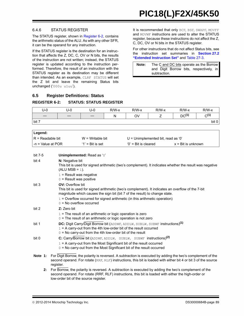
PIC18(L)F2X/45K50
6.4.6 STATUS REGISTER
The STATUS register, shown in Register 6-2, containsthe arithmetic status of the ALU. As with any other SFR,it can be the operand for any instruction.
If the STATUS register is the destination for an instruc-tion that affects the Z, DC, C, OV or N bits, the resultsof the instruction are not written; instead, the STATUSregister is updated according to the instruction per-formed. Therefore, the result of an instruction with theSTATUS register as its destination may be differentthan intended. As an example, CLRF STATUS will setthe Z bit and leave the remaining Status bitsunchanged (‘000u u1uu’).
It is recommended that only BCF, BSF, SWAPF, MOVFFand MOVWF instructions are used to alter the STATUSregister, because these instructions do not affect the Z,C, DC, OV or N bits in the STATUS register.
For other instructions that do not affect Status bits, seethe instruction set summaries in Section 27.2“Extended Instruction Set” and Table 27-3.
6.5 Register Definitions: Status
Note: The C and DC bits operate as the Borrowand Digit Borrow bits, respectively, insubtraction.
REGISTER 6-2: STATUS: STATUS REGISTER
U-0 U-0 U-0 R/W-x R/W-x R/W-x R/W-x R/W-x
— — — N OV Z DC(1) C(1)
bit 7 bit 0
Legend:
R = Readable bit W = Writable bit U = Unimplemented bit, read as ‘0’
-n = Value at POR ‘1’ = Bit is set ‘0’ = Bit is cleared x = Bit is unknown
bit 7-5 Unimplemented: Read as ‘0’
bit 4 N: Negative bit This bit is used for signed arithmetic (two’s complement). It indicates whether the result was negative (ALU MSB = 1).
1 = Result was negative 0 = Result was positive
bit 3 OV: Overflow bit This bit is used for signed arithmetic (two’s complement). It indicates an overflow of the 7-bit magnitude which causes the sign bit (bit 7 of the result) to change state.
1 = Overflow occurred for signed arithmetic (in this arithmetic operation) 0 = No overflow occurred
bit 2 Z: Zero bit
1 = The result of an arithmetic or logic operation is zero0 = The result of an arithmetic or logic operation is not zero
bit 1 DC: Digit Carry/Digit Borrow bit (ADDWF, ADDLW,SUBLW,SUBWF instructions)(1)
1 = A carry-out from the 4th low-order bit of the result occurred0 = No carry-out from the 4th low-order bit of the result
bit 0 C: Carry/Borrow bit (ADDWF, ADDLW, SUBLW, SUBWF instructions)(2)
1 = A carry-out from the Most Significant bit of the result occurred0 = No carry-out from the Most Significant bit of the result occurred
Note 1: For Digit Borrow, the polarity is reversed. A subtraction is executed by adding the two’s complement of the second operand. For rotate (RRF, RLF) instructions, this bit is loaded with either bit 4 or bit 3 of the source register.
2: For Borrow, the polarity is reversed. A subtraction is executed by adding the two’s complement of the second operand. For rotate (RRF, RLF) instructions, this bit is loaded with either the high-order or low-order bit of the source register.
2012-2014 Microchip Technology Inc. DS30000684B-page 89
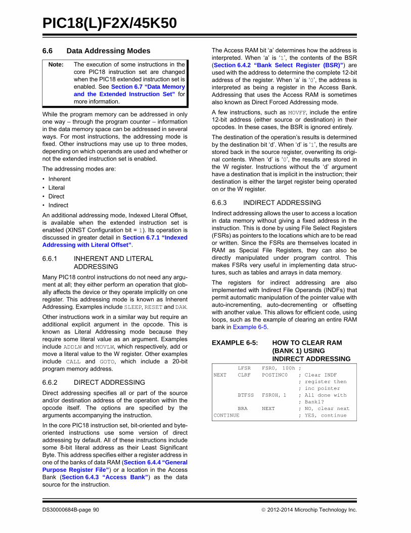
PIC18(L)F2X/45K50
6.6 Data Addressing Modes
While the program memory can be addressed in onlyone way – through the program counter – informationin the data memory space can be addressed in severalways. For most instructions, the addressing mode isfixed. Other instructions may use up to three modes,depending on which operands are used and whether ornot the extended instruction set is enabled.
The addressing modes are:
• Inherent
• Literal
• Direct
• Indirect
An additional addressing mode, Indexed Literal Offset,is available when the extended instruction set isenabled (XINST Configuration bit = 1). Its operation isdiscussed in greater detail in Section 6.7.1 “IndexedAddressing with Literal Offset”.
6.6.1 INHERENT AND LITERAL ADDRESSING
Many PIC18 control instructions do not need any argu-ment at all; they either perform an operation that glob-ally affects the device or they operate implicitly on oneregister. This addressing mode is known as InherentAddressing. Examples include SLEEP, RESET and DAW.
Other instructions work in a similar way but require anadditional explicit argument in the opcode. This isknown as Literal Addressing mode because theyrequire some literal value as an argument. Examplesinclude ADDLW and MOVLW, which respectively, add ormove a literal value to the W register. Other examplesinclude CALL and GOTO, which include a 20-bitprogram memory address.
6.6.2 DIRECT ADDRESSING
Direct addressing specifies all or part of the sourceand/or destination address of the operation within theopcode itself. The options are specified by thearguments accompanying the instruction.
In the core PIC18 instruction set, bit-oriented and byte-oriented instructions use some version of directaddressing by default. All of these instructions includesome 8-bit literal address as their Least SignificantByte. This address specifies either a register address inone of the banks of data RAM (Section 6.4.4 “GeneralPurpose Register File”) or a location in the AccessBank (Section 6.4.3 “Access Bank”) as the datasource for the instruction.
The Access RAM bit ‘a’ determines how the address isinterpreted. When ‘a’ is ‘1’, the contents of the BSR(Section 6.4.2 “Bank Select Register (BSR)”) areused with the address to determine the complete 12-bitaddress of the register. When ‘a’ is ‘0’, the address isinterpreted as being a register in the Access Bank.Addressing that uses the Access RAM is sometimesalso known as Direct Forced Addressing mode.
A few instructions, such as MOVFF, include the entire12-bit address (either source or destination) in theiropcodes. In these cases, the BSR is ignored entirely.
The destination of the operation’s results is determinedby the destination bit ‘d’. When ‘d’ is ‘1’, the results arestored back in the source register, overwriting its origi-nal contents. When ‘d’ is ‘0’, the results are stored inthe W register. Instructions without the ‘d’ argumenthave a destination that is implicit in the instruction; theirdestination is either the target register being operatedon or the W register.
6.6.3 INDIRECT ADDRESSING
Indirect addressing allows the user to access a locationin data memory without giving a fixed address in theinstruction. This is done by using File Select Registers(FSRs) as pointers to the locations which are to be reador written. Since the FSRs are themselves located inRAM as Special File Registers, they can also bedirectly manipulated under program control. Thismakes FSRs very useful in implementing data struc-tures, such as tables and arrays in data memory.
The registers for indirect addressing are alsoimplemented with Indirect File Operands (INDFs) thatpermit automatic manipulation of the pointer value withauto-incrementing, auto-decrementing or offsettingwith another value. This allows for efficient code, usingloops, such as the example of clearing an entire RAMbank in Example 6-5.
EXAMPLE 6-5: HOW TO CLEAR RAM (BANK 1) USING INDIRECT ADDRESSING
Note: The execution of some instructions in thecore PIC18 instruction set are changedwhen the PIC18 extended instruction set isenabled. See Section 6.7 “Data Memoryand the Extended Instruction Set” formore information.
LFSR FSR0, 100h ; NEXT CLRF POSTINC0 ; Clear INDF
; register then ; inc pointer
BTFSS FSR0H, 1 ; All done with; Bank1?
BRA NEXT ; NO, clear next CONTINUE ; YES, continue
DS30000684B-page 90 2012-2014 Microchip Technology Inc.

PIC18(L)F2X/45K50
6.6.3.1 FSR Registers and the INDF Operand
At the core of indirect addressing are three sets of reg-isters: FSR0, FSR1 and FSR2. Each represents a pairof 8-bit registers, FSRnH and FSRnL. Each FSR pairholds a 12-bit value, therefore, the four upper bits of theFSRnH register are not used. The 12-bit FSR value canaddress the entire range of the data memory in a linearfashion. The FSR register pairs, then, serve as pointersto data memory locations.
Indirect addressing is accomplished with a set ofIndirect File Operands, INDF0 through INDF2. Thesecan be thought of as “virtual” registers: they aremapped in the SFR space but are not physicallyimplemented. Reading or writing to a particular INDFregister actually accesses its corresponding FSRregister pair. A read from INDF1, for example, readsthe data at the address indicated by FSR1H:FSR1L.Instructions that use the INDF registers as operandsactually use the contents of their corresponding FSR asa pointer to the instruction’s target. The INDF operandis just a convenient way of using the pointer.
Because indirect addressing uses a full 12-bit address,data RAM banking is not necessary. Thus, the currentcontents of the BSR and the Access RAM bit have noeffect on determining the target address.
6.6.3.2 FSR Registers and POSTINC, POSTDEC, PREINC and PLUSW
In addition to the INDF operand, each FSR register pairalso has four additional indirect operands. Like INDF,these are “virtual” registers which cannot be directlyread or written. Accessing these registers actuallyaccesses the location to which the associated FSRregister pair points, and also performs a specific actionon the FSR value. They are:
• POSTDEC: accesses the location to which the FSR points, then automatically decrements the FSR by 1 afterwards
• POSTINC: accesses the location to which the FSR points, then automatically increments the FSR by 1 afterwards
• PREINC: automatically increments the FSR by 1, then uses the location to which the FSR points in the operation
• PLUSW: adds the signed value of the W register (range of -128 to +127) to that of the FSR and uses the location to which the result points in the operation.
In this context, accessing an INDF register uses thevalue in the associated FSR register without changingit. Similarly, accessing a PLUSW register gives theFSR value an offset by that in the W register; however,neither W nor the FSR is actually changed in theoperation. Accessing the other virtual registerschanges the value of the FSR register.
FIGURE 6-7: INDIRECT ADDRESSING
FSR1H:FSR1L
07
Data Memory
000h
100h
200h
300h
F00h
E00h
FFFh
Bank 0
Bank 1
Bank 2
Bank 14
Bank 15
Bank 3throughBank 13
ADDWF, INDF1, 1
07
Using an instruction with one of theindirect addressing registers as theoperand....
...uses the 12-bit address stored inthe FSR pair associated with thatregister....
...to determine the data memorylocation to be used in that operation.
In this case, the FSR1 pair containsECCh. This means the contents oflocation ECCh will be added to thatof the W register and stored back inECCh.
x x x x 1 1 1 0 1 1 0 0 1 1 0 0
2012-2014 Microchip Technology Inc. DS30000684B-page 91

PIC18(L)F2X/45K50
Operations on the FSRs with POSTDEC, POSTINCand PREINC affect the entire register pair; that is, roll-overs of the FSRnL register from FFh to 00h carry overto the FSRnH register. On the other hand, results ofthese operations do not change the value of any flagsin the STATUS register (e.g., Z, N, OV, etc.).
The PLUSW register can be used to implement a formof indexed addressing in the data memory space. Bymanipulating the value in the W register, users canreach addresses that are fixed offsets from pointeraddresses. In some applications, this can be used toimplement some powerful program control structure,such as software stacks, inside of data memory.
6.6.3.3 Operations by FSRs on FSRs
Indirect addressing operations that target other FSRsor virtual registers represent special cases. Forexample, using an FSR to point to one of the virtualregisters will not result in successful operations. As aspecific case, assume that FSR0H:FSR0L containsFE7h, the address of INDF1. Attempts to read thevalue of the INDF1 using INDF0 as an operand willreturn 00h. Attempts to write to INDF1 using INDF0 asthe operand will result in a NOP.
On the other hand, using the virtual registers to write toan FSR pair may not occur as planned. In these cases,the value will be written to the FSR pair but without anyincrementing or decrementing. Thus, writing to eitherthe INDF2 or POSTDEC2 register will write the samevalue to the FSR2H:FSR2L.
Since the FSRs are physical registers mapped in theSFR space, they can be manipulated through all directoperations. Users should proceed cautiously whenworking on these registers, particularly if their codeuses indirect addressing.
Similarly, operations by indirect addressing are generallypermitted on all other SFRs. Users should exercise theappropriate caution that they do not inadvertently changesettings that might affect the operation of the device.
6.7 Data Memory and the Extended Instruction Set
Enabling the PIC18 extended instruction set (XINSTConfiguration bit = 1) significantly changes certainaspects of data memory and its addressing. Specifi-cally, the use of the Access Bank for many of the corePIC18 instructions is different; this is due to the intro-duction of a new addressing mode for the data memoryspace.
What does not change is just as important. The size ofthe data memory space is unchanged, as well as itslinear addressing. The SFR map remains the same.Core PIC18 instructions can still operate in both Directand Indirect Addressing mode; inherent and literalinstructions do not change at all. Indirect addressingwith FSR0 and FSR1 also remain unchanged.
6.7.1 INDEXED ADDRESSING WITH LITERAL OFFSET
Enabling the PIC18 extended instruction set changesthe behavior of indirect addressing using the FSR2register pair within Access RAM. Under the properconditions, instructions that use the Access Bank – thatis, most bit-oriented and byte-oriented instructions –can invoke a form of indexed addressing using anoffset specified in the instruction. This specialaddressing mode is known as Indexed Addressing withLiteral Offset, or Indexed Literal Offset mode.
When using the extended instruction set, thisaddressing mode requires the following:
• The use of the Access Bank is forced (‘a’ = 0) and
• The file address argument is less than or equal to 5Fh.
Under these conditions, the file address of theinstruction is not interpreted as the lower byte of anaddress (used with the BSR in direct addressing), or asan 8-bit address in the Access Bank. Instead, the valueis interpreted as an offset value to an Address Pointer,specified by FSR2. The offset and the contents ofFSR2 are added to obtain the target address of theoperation.
6.7.2 INSTRUCTIONS AFFECTED BY INDEXED LITERAL OFFSET MODE
Any of the core PIC18 instructions that can use directaddressing are potentially affected by the IndexedLiteral Offset Addressing mode. This includes allbyte-oriented and bit-oriented instructions, or almostone-half of the standard PIC18 instruction set.Instructions that only use Inherent or Literal Addressingmodes are unaffected.
Additionally, byte-oriented and bit-oriented instructionsare not affected if they do not use the Access Bank(Access RAM bit is ‘1’), or include a file address of 60hor above. Instructions meeting these criteria willcontinue to execute as before. A comparison of thedifferent possible addressing modes when theextended instruction set is enabled is shown inFigure 6-8.
Those who desire to use byte-oriented or bit-orientedinstructions in the Indexed Literal Offset mode shouldnote the changes to assembler syntax for this mode.This is described in more detail in Section 27.2.1“Extended Instruction Syntax”.
DS30000684B-page 92 2012-2014 Microchip Technology Inc.

PIC18(L)F2X/45K50
FIGURE 6-8: COMPARING ADDRESSING OPTIONS FOR BIT-ORIENTED AND BYTE-ORIENTED INSTRUCTIONS (EXTENDED INSTRUCTION SET ENABLED)
EXAMPLE INSTRUCTION: ADDWF, f, d, a (Opcode: 0010 01da ffff ffff)
When ‘a’ = 0 and f 60h:
The instruction executes inDirect Forced mode. ‘f’ is inter-preted as a location in theAccess RAM between 060hand 0FFh. This is the same aslocations F60h to FFFh(Bank 15) of data memory.
Locations below 60h are notavailable in this addressingmode.
When ‘a’ = 0 and f5Fh:
The instruction executes inIndexed Literal Offset mode. ‘f’is interpreted as an offset to theaddress value in FSR2. Thetwo are added together toobtain the address of the targetregister for the instruction. Theaddress can be anywhere inthe data memory space.
Note that in this mode, thecorrect syntax is now:ADDWF [k], dwhere ‘k’ is the same as ‘f’.
When ‘a’ = 1 (all values of f):
The instruction executes inDirect mode (also known asDirect Long mode). ‘f’ is inter-preted as a location in one ofthe 16 banks of the datamemory space. The bank isdesignated by the Bank SelectRegister (BSR). The addresscan be in any implementedbank in the data memoryspace.
000h
060h
100h
F00h
F60h
FFFh
Valid range
00h
60h
FFh
Data Memory
Access RAM
Bank 0
Bank 1throughBank 14
Bank 15
SFRs
000h
060h
100h
F00h
F60h
FFFhData Memory
Bank 0
Bank 1throughBank 14
Bank 15
SFRs
FSR2H FSR2L
ffffffff001001da
ffffffff001001da
000h
060h
100h
F00h
F60h
FFFhData Memory
Bank 0
Bank 1throughBank 14
Bank 15
SFRs
for ‘f’
BSR00000000
2012-2014 Microchip Technology Inc. DS30000684B-page 93

PIC18(L)F2X/45K50
6.7.3 MAPPING THE ACCESS BANK IN INDEXED LITERAL OFFSET MODE
The use of Indexed Literal Offset Addressing modeeffectively changes how the first 96 locations of AccessRAM (00h to 5Fh) are mapped. Rather than containingjust the contents of the bottom section of Bank 0, thismode maps the contents from a user defined “window”that can be located anywhere in the data memoryspace. The value of FSR2 establishes the lower bound-ary of the addresses mapped into the window, while theupper boundary is defined by FSR2 plus 95 (5Fh).Addresses in the Access RAM above 5Fh are mappedas previously described (see Section 6.4.3 “AccessBank”). An example of Access Bank remapping in thisaddressing mode is shown in Figure 6-9.
Remapping of the Access Bank applies only to opera-tions using the Indexed Literal Offset mode. Operationsthat use the BSR (Access RAM bit is ‘1’) will continueto use direct addressing as before.
6.8 PIC18 Instruction Execution and the Extended Instruction Set
Enabling the extended instruction set adds eightadditional commands to the existing PIC18 instructionset. These instructions are executed as described inSection 27.2 “Extended Instruction Set”.
FIGURE 6-9: REMAPPING THE ACCESS BANK WITH INDEXED LITERAL OFFSET ADDRESSING
Data Memory
000h
100h
200h
F60h
F00h
FFFh
Bank 1
Bank 15
Bank 2throughBank 14
SFRs
ADDWF f, d, a
FSR2H:FSR2L = 120h
Locations in the regionfrom the FSR2 pointer(120h) to the pointer plus05Fh (17Fh) are mappedto the bottom of theAccess RAM (000h-05Fh).
Special File Registers atF60h through FFFh aremapped to 60h throughFFh, as usual.
Bank 0 addresses below5Fh can still be addressedby using the BSR. Access Bank
00h
60h
FFh
SFRs
Bank 1 “Window”
Bank 0
Window
Example Situation:
120h17Fh
5Fh
Bank 1
DS30000684B-page 94 2012-2014 Microchip Technology Inc.

PIC18(L)F2X/45K50
7.0 FLASH PROGRAM MEMORY
The Flash program memory is readable, writable anderasable during normal operation over the specifiedVDD ranges.
A read from program memory is executed one byte ata time. A write to program memory is executed onblocks of 64 bytes at a time. Program memory iserased in blocks of 64 bytes at a time. A bulk eraseoperation cannot be issued from user code.
Writing or erasing program memory will ceaseinstruction fetches until the operation is complete. Theprogram memory cannot be accessed during the writeor erase, therefore, code cannot execute. An internalprogramming timer terminates program memory writesand erases.
A value written to program memory does not need to bea valid instruction. Executing a program memorylocation that forms an invalid instruction results in aNOP.
7.1 Table Reads and Table Writes
In order to read and write program memory, there aretwo operations that allow the processor to move bytesbetween the program memory space and the data RAM:
• Table Read (TBLRD)
• Table Write (TBLWT)
The program memory space is 16 bits wide, while thedata RAM space is 8 bits wide. Table reads and tablewrites move data between these two memory spacesthrough an 8-bit register (TABLAT).
The table read operation retrieves one byte of datadirectly from program memory and places it into theTABLAT register. Figure 7-1 shows the operation of atable read.
The table write operation stores one byte of data from theTABLAT register into a write block holding register. Theprocedure to write the contents of the holding registersinto program memory is detailed in Section 7.6 “Writingto Flash Program Memory”. Figure 7-2 shows theoperation of a table write with program memory and dataRAM.
Table operations work with byte entities. Tablescontaining data, rather than program instructions, arenot required to be word aligned. Therefore, a table canstart and end at any byte address. If a table write is beingused to write executable code into program memory,program instructions will need to be word aligned.
FIGURE 7-1: TABLE READ OPERATION
Table Pointer(1)
Table Latch (8-bit)Program Memory
TBLPTRH TBLPTRLTABLAT
TBLPTRU
Instruction: TBLRD*
Note 1: Table Pointer register points to a byte in program memory.
Program Memory(TBLPTR)
2012-2014 Microchip Technology Inc. DS30000684B-page 95

PIC18(L)F2X/45K50
FIGURE 7-2: TABLE WRITE OPERATION
7.2 Control Registers
Several control registers are used in conjunction withthe TBLRD and TBLWT instructions. These include the:
• EECON1 register
• EECON2 register
• TABLAT register
• TBLPTR registers
7.2.1 EECON1 AND EECON2 REGISTERS
The EECON1 register (Register 7-1) is the controlregister for memory accesses. The EECON2 register isnot a physical register; it is used exclusively in thememory write and erase sequences. ReadingEECON2 will read all ‘0’s.
The EEPGD control bit determines if the access will bea program or data EEPROM memory access. WhenEEPGD is clear, any subsequent operations willoperate on the data EEPROM memory. When EEPGDis set, any subsequent operations will operate on theprogram memory.
The CFGS control bit determines if the access will beto the Configuration/Calibration registers or to programmemory/data EEPROM memory. When CFGS is set,subsequent operations will operate on Configurationregisters regardless of EEPGD (see Section 26.0“Special Features of the CPU”). When CFGS is clear,memory selection access is determined by EEPGD.
The FREE bit allows the program memory eraseoperation. When FREE is set, an erase operation isinitiated on the next WR command. When FREE isclear, only writes are enabled.
The WREN bit, when set, will allow a write operation.The WREN bit is clear on power-up.
The WRERR bit is set by hardware when the WR bit isset and cleared when the internal programming timerexpires and the write operation is complete.
The WR control bit initiates write operations. The WRbit cannot be cleared, only set, by firmware. The WR bitis cleared by hardware at the completion of the writeoperation.
Table Pointer(1)Table Latch (8-bit)
TBLPTRH TBLPTRL TABLAT
Program Memory(TBLPTR<MSBs>)
TBLPTRU
Instruction: TBLWT*
Note 1: During table writes the Table Pointer does not point directly to Program Memory. The LSBs of TBLPRTLactually point to an address within the write block holding registers. The MSBs of the Table Pointer deter-mine where the write block will eventually be written. The process for writing the holding registers to theprogram memory array is discussed in Section 7.6 “Writing to Flash Program Memory”.
Holding Registers Program Memory
Note: During normal operation, the WRERR isread as ‘1’. This can indicate that a writeoperation was prematurely terminated bya Reset, or a write operation wasattempted improperly.
Note: The EEIF interrupt flag bit of the PIR2register is set when the write is complete.The EEIF flag stays set until cleared byfirmware.
DS30000684B-page 96 2012-2014 Microchip Technology Inc.
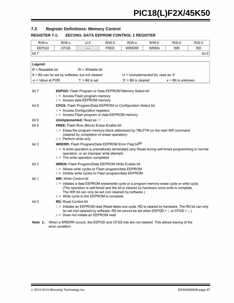
PIC18(L)F2X/45K50
7.3 Register Definitions: Memory Control
REGISTER 7-1: EECON1: DATA EEPROM CONTROL 1 REGISTER
R/W-x R/W-x U-0 R/W-0 R/W-x R/W-0 R/S-0 R/S-0
EEPGD CFGS — FREE WRERR WREN WR RD
bit 7 bit 0
Legend:
R = Readable bit W = Writable bit
S = Bit can be set by software, but not cleared U = Unimplemented bit, read as ‘0’
-n = Value at POR ‘1’ = Bit is set ‘0’ = Bit is cleared x = Bit is unknown
bit 7 EEPGD: Flash Program or Data EEPROM Memory Select bit
1 = Access Flash program memory0 = Access data EEPROM memory
bit 6 CFGS: Flash Program/Data EEPROM or Configuration Select bit
1 = Access Configuration registers0 = Access Flash program or data EEPROM memory
bit 5 Unimplemented: Read as ‘0’
bit 4 FREE: Flash Row (Block) Erase Enable bit
1 = Erase the program memory block addressed by TBLPTR on the next WR command (cleared by completion of erase operation)
0 = Perform write-only
bit 3 WRERR: Flash Program/Data EEPROM Error Flag bit(1)
1 = A write operation is prematurely terminated (any Reset during self-timed programming in normaloperation, or an improper write attempt)
0 = The write operation completed
bit 2 WREN: Flash Program/Data EEPROM Write Enable bit
1 = Allows write cycles to Flash program/data EEPROM0 = Inhibits write cycles to Flash program/data EEPROM
bit 1 WR: Write Control bit
1 = Initiates a data EEPROM erase/write cycle or a program memory erase cycle or write cycle. (The operation is self-timed and the bit is cleared by hardware once write is complete. The WR bit can only be set (not cleared) by software.)
0 = Write cycle to the EEPROM is complete
bit 0 RD: Read Control bit
1 = Initiates an EEPROM read (Read takes one cycle. RD is cleared by hardware. The RD bit can onlybe set (not cleared) by software. RD bit cannot be set when EEPGD = 1 or CFGS = 1.)
0 = Does not initiate an EEPROM read
Note 1: When a WRERR occurs, the EEPGD and CFGS bits are not cleared. This allows tracing of theerror condition.
2012-2014 Microchip Technology Inc. DS30000684B-page 97
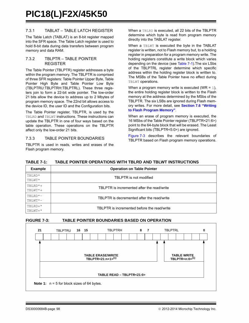
PIC18(L)F2X/45K50
7.3.1 TABLAT – TABLE LATCH REGISTER
The Table Latch (TABLAT) is an 8-bit register mappedinto the SFR space. The Table Latch register is used tohold 8-bit data during data transfers between programmemory and data RAM.
7.3.2 TBLPTR – TABLE POINTER REGISTER
The Table Pointer (TBLPTR) register addresses a bytewithin the program memory. The TBLPTR is comprisedof three SFR registers: Table Pointer Upper Byte, TablePointer High Byte and Table Pointer Low Byte(TBLPTRU:TBLPTRH:TBLPTRL). These three regis-ters join to form a 22-bit wide pointer. The low-order21 bits allow the device to address up to 2 Mbytes ofprogram memory space. The 22nd bit allows access tothe device ID, the user ID and the Configuration bits.
The Table Pointer register, TBLPTR, is used by theTBLRD and TBLWT instructions. These instructions canupdate the TBLPTR in one of four ways based on thetable operation. These operations on the TBLPTRaffect only the low-order 21 bits.
7.3.3 TABLE POINTER BOUNDARIES
TBLPTR is used in reads, writes and erases of theFlash program memory.
When a TBLRD is executed, all 22 bits of the TBLPTRdetermine which byte is read from program memorydirectly into the TABLAT register.
When a TBLWT is executed the byte in the TABLATregister is written, not to Flash memory but, to a holdingregister in preparation for a program memory write. Theholding registers constitute a write block which variesdepending on the device (see Table 7-1).The six LSbsof the TBLPTRL register determine which specificaddress within the holding register block is written to.The MSBs of the Table Pointer have no effect duringTBLWT operations.
When a program memory write is executed (WR = 1),the entire holding register block is written to the Flashmemory at the address determined by the MSbs of theTBLPTR. The six LSBs are ignored during Flash mem-ory writes. For more detail, see Section 7.6 “Writingto Flash Program Memory”.
When an erase of program memory is executed, the16 MSbs of the Table Pointer register (TBLPTR<21:6>)point to the 64-byte block that will be erased. The LeastSignificant bits (TBLPTR<5:0>) are ignored.
Figure 7-3 describes the relevant boundaries ofTBLPTR based on Flash program memory operations.
TABLE 7-1: TABLE POINTER OPERATIONS WITH TBLRD AND TBLWT INSTRUCTIONS
FIGURE 7-3: TABLE POINTER BOUNDARIES BASED ON OPERATION
Example Operation on Table Pointer
TBLRD*TBLWT*
TBLPTR is not modified
TBLRD*+TBLWT*+
TBLPTR is incremented after the read/write
TBLRD*-TBLWT*-
TBLPTR is decremented after the read/write
TBLRD+*TBLWT+*
TBLPTR is incremented before the read/write
21 16 15 8 7 0
TABLE ERASE/WRITE TABLE WRITE
TABLE READ – TBLPTR<21:0>
TBLPTRLTBLPTRHTBLPTRU
TBLPTR<n:0>(1)TBLPTR<21:n+1>(1)
Note 1: n = 5 for block sizes of 64 bytes.
DS30000684B-page 98 2012-2014 Microchip Technology Inc.

PIC18(L)F2X/45K50
7.4 Reading the Flash Program Memory
The TBLRD instruction retrieves data from programmemory and places it into data RAM. Table reads fromprogram memory are performed one byte at a time.
TBLPTR points to a byte address in program space.Executing TBLRD places the byte pointed to intoTABLAT. In addition, TBLPTR can be modifiedautomatically for the next table read operation.
The internal program memory is typically organized bywords. The Least Significant bit of the address selectsbetween the high and low bytes of the word. Figure 7-4shows the interface between the internal programmemory and the TABLAT.
FIGURE 7-4: READS FROM FLASH PROGRAM MEMORY
EXAMPLE 7-1: READING A FLASH PROGRAM MEMORY WORD
(Even Byte Address)
Program Memory
(Odd Byte Address)
TBLRD TABLAT
TBLPTR = xxxxx1
FETCHInstruction Register
(IR) Read Register
TBLPTR = xxxxx0
MOVLW CODE_ADDR_UPPER ; Load TBLPTR with the baseMOVWF TBLPTRU ; address of the wordMOVLW CODE_ADDR_HIGHMOVWF TBLPTRHMOVLW CODE_ADDR_LOWMOVWF TBLPTRL
READ_WORDTBLRD*+ ; read into TABLAT and incrementMOVF TABLAT, W ; get dataMOVWF WORD_EVENTBLRD*+ ; read into TABLAT and incrementMOVFW TABLAT, W ; get dataMOVF WORD_ODD
2012-2014 Microchip Technology Inc. DS30000684B-page 99

PIC18(L)F2X/45K50
7.5 Erasing Flash Program Memory
The minimum erase block is 32 words or 64 bytes. Onlythrough the use of an external programmer, or throughICSP control, can larger blocks of program memory bebulk erased. Word erase in the Flash array is notsupported.
When initiating an erase sequence from themicrocontroller itself, a block of 64 bytes of programmemory is erased. The Most Significant 16 bits of theTBLPTR<21:6> point to the block being erased. TheTBLPTR<5:0> bits are ignored.
The EECON1 register commands the erase operation.The EEPGD bit must be set to point to the Flashprogram memory. The WREN bit must be set to enablewrite operations. The FREE bit is set to select an eraseoperation.
The write initiate sequence for EECON2, shown assteps 4 through 6 in Section 7.5.1 “Flash ProgramMemory Erase Sequence”, is used to guard againstaccidental writes. This is sometimes referred to as along write.
A long write is necessary for erasing the internal Flash.Instruction execution is halted during the long writecycle. The long write is terminated by the internalprogramming timer.
7.5.1 FLASH PROGRAM MEMORY ERASE SEQUENCE
The sequence of events for erasing a block of internalprogram memory is:
1. Load Table Pointer register with address ofblock being erased.
2. Set the EECON1 register for the erase operation:
• set EEPGD bit to point to program memory;
• clear the CFGS bit to access program memory;
• set WREN bit to enable writes;
• set FREE bit to enable the erase.
3. Disable interrupts.
4. Write 55h to EECON2.
5. Write 0AAh to EECON2.
6. Set the WR bit. This will begin the block erasecycle.
7. The CPU will stall for duration of the erase(about 2 ms using internal timer).
8. Re-enable interrupts.
EXAMPLE 7-2: ERASING A FLASH PROGRAM MEMORY BLOCK
MOVLW CODE_ADDR_UPPER ; load TBLPTR with the baseMOVWF TBLPTRU ; address of the memory blockMOVLW CODE_ADDR_HIGHMOVWF TBLPTRH MOVLW CODE_ADDR_LOWMOVWF TBLPTRL
ERASE_BLOCK BSF EECON1, EEPGD ; point to Flash program memoryBCF EECON1, CFGS ; access Flash program memoryBSF EECON1, WREN ; enable write to memoryBSF EECON1, FREE ; enable block Erase operationBCF INTCON, GIE ; disable interrupts
Required MOVLW 55hSequence MOVWF EECON2 ; write 55h
MOVLW 0AAhMOVWF EECON2 ; write 0AAhBSF EECON1, WR ; start erase (CPU stall)BSF INTCON, GIE ; re-enable interrupts
DS30000684B-page 100 2012-2014 Microchip Technology Inc.

PIC18(L)F2X/45K50
7.6 Writing to Flash Program Memory
The programming block size is 64 bytes. Word or byteprogramming is not supported.
Table writes are used internally to load the holdingregisters needed to program the Flash memory. Thereare only as many holding registers as there are bytesin a write block (64 bytes).
Since the Table Latch (TABLAT) is only a single byte,the TBLWT instruction needs to be executed 64 timesfor each programming operation. All of the table writeoperations will essentially be short writes because onlythe holding registers are written. After all the holdingregisters have been written, the programmingoperation of that block of memory is started byconfiguring the EECON1 register for a programmemory write and performing the long write sequence.
The long write is necessary for programming theinternal Flash. Instruction execution is halted during along write cycle. The long write will be terminated bythe internal programming timer.
The EEPROM on-chip timer controls the write time.The write/erase voltages are generated by an on-chipcharge pump, rated to operate over the voltage rangeof the device.
FIGURE 7-5: TABLE WRITES TO FLASH PROGRAM MEMORY
7.6.1 FLASH PROGRAM MEMORY WRITE SEQUENCE
The sequence of events for programming an internalprogram memory location should be:
1. Read 64 bytes into RAM.
2. Update data values in RAM as necessary.
3. Load Table Pointer register with address beingerased.
4. Execute the block erase procedure.
5. Load Table Pointer register with address of firstbyte being written.
6. Write the 64-byte block into the holding registerswith auto-increment (TBLWT*+ or TBLWT+*).
7. Set the EECON1 register for the write operation:
• set EEPGD bit to point to program memory;
• clear the CFGS bit to access program memory;
• set WREN to enable writes.
8. Disable interrupts.
9. Write 55h to EECON2.
10. Write 0AAh to EECON2.
11. Set the WR bit. This will begin the write cycle.
12. The CPU will stall for duration of the write (about2 ms using internal timer).
13. Re-enable interrupts.
14. Verify the memory (table read).
This procedure will require about 6 ms to update eachwrite block of memory. An example of the required codeis given in Example 7-3.
Note: The default value of the holding registers ondevice Resets and after write operations isFFh. A write of FFh to a holding registerdoes not modify that byte. This means thatindividual bytes of program memory maybe modified, provided that the change doesnot attempt to change any bit from a ‘0’ to a‘1’. When modifying individual bytes, it isnot necessary to load all holding registersbefore executing a long write operation.
TABLAT
TBLPTR = xxxxYY(1)TBLPTR = xxxx01TBLPTR = xxxx00
Write Register
TBLPTR = xxxx02
Program Memory
Holding Register Holding Register Holding Register Holding Register
8 8 8 8
Note 1: YY = 3Fh for 64 byte write blocks.
Note: Before setting the WR bit, the TablePointer address needs to be within theintended address range of the bytes in theholding registers.
2012-2014 Microchip Technology Inc. DS30000684B-page 101

PIC18(L)F2X/45K50
EXAMPLE 7-3: WRITING TO FLASH PROGRAM MEMORY
MOVLW D'64’ ; number of bytes in erase blockMOVWF COUNTERMOVLW BUFFER_ADDR_HIGH ; point to bufferMOVWF FSR0HMOVLW BUFFER_ADDR_LOWMOVWF FSR0LMOVLW CODE_ADDR_UPPER ; Load TBLPTR with the baseMOVWF TBLPTRU ; address of the memory blockMOVLW CODE_ADDR_HIGHMOVWF TBLPTRHMOVLW CODE_ADDR_LOWMOVWF TBLPTRL
READ_BLOCKTBLRD*+ ; read into TABLAT, and incMOVF TABLAT, W ; get dataMOVWF POSTINC0 ; store dataDECFSZ COUNTER ; done?BRA READ_BLOCK ; repeat
MODIFY_WORDMOVLW BUFFER_ADDR_HIGH ; point to bufferMOVWF FSR0HMOVLW BUFFER_ADDR_LOWMOVWF FSR0LMOVLW NEW_DATA_LOW ; update buffer wordMOVWF POSTINC0MOVLW NEW_DATA_HIGHMOVWF INDF0
ERASE_BLOCKMOVLW CODE_ADDR_UPPER ; load TBLPTR with the baseMOVWF TBLPTRU ; address of the memory blockMOVLW CODE_ADDR_HIGHMOVWF TBLPTRH MOVLW CODE_ADDR_LOWMOVWF TBLPTRL BSF EECON1, EEPGD ; point to Flash program memoryBCF EECON1, CFGS ; access Flash program memoryBSF EECON1, WREN ; enable write to memoryBSF EECON1, FREE ; enable Erase operationBCF INTCON, GIE ; disable interruptsMOVLW 55h
Required MOVWF EECON2 ; write 55hSequence MOVLW 0AAh
MOVWF EECON2 ; write 0AAhBSF EECON1, WR ; start erase (CPU stall)BSF INTCON, GIE ; re-enable interruptsTBLRD*- ; dummy read decrementMOVLW BUFFER_ADDR_HIGH ; point to bufferMOVWF FSR0HMOVLW BUFFER_ADDR_LOWMOVWF FSR0L
WRITE_BUFFER_BACKMOVLW BlockSize ; number of bytes in holding registerMOVWF COUNTERMOVLW D’64’/BlockSize ; number of write blocks in 64 bytesMOVWF COUNTER2
WRITE_BYTE_TO_HREGSMOVF POSTINC0, W ; get low byte of buffer dataMOVWF TABLAT ; present data to table latchTBLWT+* ; write data, perform a short write
; to internal TBLWT holding register.
DS30000684B-page 102 2012-2014 Microchip Technology Inc.

PIC18(L)F2X/45K50
EXAMPLE 7-3: WRITING TO FLASH PROGRAM MEMORY (CONTINUED)
7.6.2 WRITE VERIFY
Depending on the application, good programmingpractice may dictate that the value written to thememory should be verified against the original value.This should be used in applications where excessivewrites can stress bits near the specification limit.
7.6.3 UNEXPECTED TERMINATION OF WRITE OPERATION
If a write is terminated by an unplanned event, such asloss of power or an unexpected Reset, the memorylocation just programmed should be verified andreprogrammed if needed. If the write operation isinterrupted by a MCLR Reset or a WDT Time-out Resetduring normal operation, the WRERR bit will be setwhich the user can check to decide whether a rewriteof the location(s) is needed.
7.6.4 PROTECTION AGAINST SPURIOUS WRITES
To protect against spurious writes to Flash programmemory, the write initiate sequence must also befollowed. See Section 26.0 “Special Features of theCPU” for more detail.
7.7 Flash Program Operation During Code Protection
See Section 26.5 “Program Verification and CodeProtection” for details on code protection of Flashprogram memory.
DECFSZ COUNTER ; loop until holding registers are fullBRA WRITE_WORD_TO_HREGS
PROGRAM_MEMORYBSF EECON1, EEPGD ; point to Flash program memoryBCF EECON1, CFGS ; access Flash program memoryBSF EECON1, WREN ; enable write to memoryBCF INTCON, GIE ; disable interruptsMOVLW 55h
Required MOVWF EECON2 ; write 55hSequence MOVLW 0AAh
MOVWF EECON2 ; write 0AAhBSF EECON1, WR ; start program (CPU stall)DCFSZ COUNTER2 ; repeat for remaining write blocksBRA WRITE_BYTE_TO_HREGS ;BSF INTCON, GIE ; re-enable interruptsBCF EECON1, WREN ; disable write to memory
TABLE 7-2: REGISTERS ASSOCIATED WITH PROGRAM FLASH MEMORY
Name Bit 7 Bit 6 Bit 5 Bit 4 Bit 3 Bit 2 Bit 1 Bit 0Register on page
TBLPTRU — — Program Memory Table Pointer Upper Byte (TBLPTR<21:16>) —
TBPLTRH Program Memory Table Pointer High Byte (TBLPTR<15:8>) —
TBLPTRL Program Memory Table Pointer Low Byte (TBLPTR<7:0>) —
TABLAT Program Memory Table Latch —
INTCON GIE/GIEH PEIE/GIEL TMR0IE INT0IE IOCIE TMR0IF INT0IF IOCIF 114
EECON2 EEPROM Control Register 2 (not a physical register) —
EECON1 EEPGD CFGS — FREE WRERR WREN WR RD 97
IPR2 OSCFIP C1IP C2IP EEIP BCLIP HLVDIP TMR3IP CCP2IP 124
PIR2 OSCFIF C1IF C2IF EEIF BCLIF HLVDIF TMR3IF CCP2IF 118
PIE2 OSCFIE C1IE C2IE EEIE BCLIE HLVDIE TMR3IE CCP2IE 121
Legend: — = unimplemented, read as ‘0’. Shaded bits are not used during Flash/EEPROM access.
2012-2014 Microchip Technology Inc. DS30000684B-page 103

PIC18(L)F2X/45K50
8.0 DATA EEPROM MEMORY
The data EEPROM is a nonvolatile memory array,separate from the data RAM and program memory,which is used for long-term storage of program data. Itis not directly mapped in either the register file orprogram memory space but is indirectly addressedthrough the Special Function Registers (SFRs). TheEEPROM is readable and writable during normaloperation over the specified VDD range.
Four SFRs are used to read and write to the dataEEPROM as well as the program memory. They are:
• EECON1
• EECON2
• EEDATA
• EEADR
The data EEPROM allows byte read and write. Wheninterfacing to the data memory block, EEDATA holdsthe 8-bit data for read/write, and the EEADR registerholds the address of the EEPROM location beingaccessed.
The EEPROM data memory is rated for high erase/writecycle endurance. A byte write automatically erases thelocation and writes the new data (erase-before-write).The write time is controlled by an on-chip timer; it willvary with voltage and temperature as well as from chip-to-chip. Please refer to the Data EEPROM Memoryparameters in Section 29.0 “Electrical Specifica-tions” for limits.
8.1 EEADR Register
The EEADR register is used to address the dataEEPROM for read and write operations. The 8-bitrange of the register can address a memory range of256 bytes (00h to FFh).
8.2 EECON1 and EECON2 Registers
Access to the data EEPROM is controlled by tworegisters: EECON1 and EECON2. These are the sameregisters which control access to the program memoryand are used in a similar manner for the dataEEPROM.
The EECON1 register (Register 8-1) is the controlregister for data and program memory access. Controlbit EEPGD determines if the access will be to programor data EEPROM memory. When the EEPGD bit isclear, operations will access the data EEPROMmemory. When the EEPGD bit is set, program memoryis accessed.
Control bit, CFGS, determines if the access will be tothe Configuration registers or to program memory/dataEEPROM memory. When the CFGS bit is set,subsequent operations access Configuration registers.When the CFGS bit is clear, the EEPGD bit selectseither program Flash or data EEPROM memory.
The WREN bit, when set, will allow a write operation.On power-up, the WREN bit is clear.
The WRERR bit is set by hardware when the WR bit isset and cleared when the internal programming timerexpires and the write operation is complete.
The WR control bit initiates write operations. The bitcan be set but not cleared by software. It is cleared onlyby hardware at the completion of the write operation.
Control bits, RD and WR, start read and erase/writeoperations, respectively. These bits are set by firmwareand cleared by hardware at the completion of theoperation.
The RD bit cannot be set when accessing programmemory (EEPGD = 1). Program memory is read usingtable read instructions. See Section 7.1 “Table Readsand Table Writes” regarding table reads.
The EECON2 register is not a physical register. It isused exclusively in the memory write and erasesequences. Reading EECON2 will read all ‘0’s.
Note: During normal operation, the WRERRmay read as ‘1’. This can indicate that awrite operation was prematurely termi-nated by a Reset, or a write operation wasattempted improperly.
Note: The EEIF interrupt flag bit of the PIR2register is set when the write is complete.It must be cleared by software.
DS30000684B-page 104 2012-2014 Microchip Technology Inc.

PIC18(L)F2X/45K50
REGISTER 8-1: EECON1: DATA EEPROM CONTROL 1 REGISTER
R/W-x R/W-x U-0 R/W-0 R/W-x R/W-0 R/S-0 R/S-0
EEPGD CFGS — FREE WRERR WREN WR RD
bit 7 bit 0
Legend:
R = Readable bit W = Writable bit
S = Bit can be set by software, but not cleared U = Unimplemented bit, read as ‘0’
-n = Value at POR ‘1’ = Bit is set ‘0’ = Bit is cleared x = Bit is unknown
bit 7 EEPGD: Flash Program or Data EEPROM Memory Select bit
1 = Access Flash program memory0 = Access data EEPROM memory
bit 6 CFGS: Flash Program/Data EEPROM or Configuration Select bit
1 = Access Configuration registers0 = Access Flash program or data EEPROM memory
bit 5 Unimplemented: Read as ‘0’
bit 4 FREE: Flash Row (Block) Erase Enable bit
1 = Erase the program memory block addressed by TBLPTR on the next WR command (cleared by completion of erase operation)
0 = Perform write-only
bit 3 WRERR: Flash Program/Data EEPROM Error Flag bit(1)
1 = A write operation is prematurely terminated (any Reset during self-timed programming in normaloperation, or an improper write attempt)
0 = The write operation completed
bit 2 WREN: Flash Program/Data EEPROM Write Enable bit
1 = Allows write cycles to Flash program/data EEPROM0 = Inhibits write cycles to Flash program/data EEPROM
bit 1 WR: Write Control bit
1 = Initiates a data EEPROM erase/write cycle or a program memory erase cycle or write cycle. (The operation is self-timed and the bit is cleared by hardware once write is complete. The WR bit can only be set (not cleared) by software.)
0 = Write cycle to the EEPROM is complete
bit 0 RD: Read Control bit
1 = Initiates an EEPROM read (Read takes one cycle. RD is cleared by hardware. The RD bit can onlybe set (not cleared) by software. RD bit cannot be set when EEPGD = 1 or CFGS = 1.)
0 = Does not initiate an EEPROM read
Note 1: When a WRERR occurs, the EEPGD and CFGS bits are not cleared. This allows tracing of theerror condition.
2012-2014 Microchip Technology Inc. DS30000684B-page 105

PIC18(L)F2X/45K50
8.3 Reading the Data EEPROM Memory
To read a data memory location, the user must write theaddress to the EEADR register, clear the EEPGD con-trol bit of the EECON1 register and then set control bit,RD. The data is available on the very next instructioncycle; therefore, the EEDATA register can be read bythe next instruction. EEDATA will hold this value untilanother read operation, or until it is written to by theuser (during a write operation).
The basic process is shown in Example 8-1.
8.4 Writing to the Data EEPROM Memory
To write an EEPROM data location, the address mustfirst be written to the EEADR register and the data writ-ten to the EEDATA register. The sequence inExample 8-2 must be followed to initiate the write cycle.
The write will not begin if this sequence is not exactlyfollowed (write 55h to EECON2, write 0AAh toEECON2, then set WR bit) for each byte. It is stronglyrecommended that interrupts be disabled during thiscode segment.
Additionally, the WREN bit in EECON1 must be set toenable writes. This mechanism prevents accidentalwrites to data EEPROM due to unexpected codeexecution (i.e., runaway programs). The WREN bitshould be kept clear at all times, except when updatingthe EEPROM. The WREN bit is not cleared byhardware.
After a write sequence has been initiated, EECON1,EEADR and EEDATA cannot be modified. The WR bitwill be inhibited from being set unless the WREN bit isset. Both WR and WREN cannot be set with the sameinstruction.
At the completion of the write cycle, the WR bit iscleared by hardware and the EEPROM Interrupt Flagbit, EEIF, is set. The user may either enable thisinterrupt or poll this bit. EEIF must be cleared bysoftware.
8.5 Write Verify
Depending on the application, good programmingpractice may dictate that the value written to thememory should be verified against the original value.This should be used in applications where excessivewrites can stress bits near the specification limit.
EXAMPLE 8-1: DATA EEPROM READ
EXAMPLE 8-2: DATA EEPROM WRITE
MOVLW DATA_EE_ADDR ;MOVWF EEADR ; Data Memory Address to readBCF EECON1, EEPGD ; Point to DATA memoryBCF EECON1, CFGS ; Access EEPROMBSF EECON1, RD ; EEPROM ReadMOVF EEDATA, W ; W = EEDATA
MOVLW DATA_EE_ADDR_LOW ;MOVWF EEADR ; Data Memory Address to writeMOVLW DATA_EE_ADDR_HI ;MOVWF EEADRH ;MOVLW DATA_EE_DATA ;MOVWF EEDATA ; Data Memory Value to writeBCF EECON1, EEPGD ; Point to DATA memoryBCF EECON1, CFGS ; Access EEPROMBSF EECON1, WREN ; Enable writesBCF INTCON, GIE ; Disable InterruptsMOVLW 55h ;
Required MOVWF EECON2 ; Write 55hSequence MOVLW 0AAh ;
MOVWF EECON2 ; Write 0AAhBSF EECON1, WR ; Set WR bit to begin writeBSF INTCON, GIE ; Enable Interrupts
; User code executionBCF EECON1, WREN ; Disable writes on write complete (EEIF set)
DS30000684B-page 106 2012-2014 Microchip Technology Inc.

PIC18(L)F2X/45K50
8.6 Operation During Code-Protect
Data EEPROM memory has its own code-protect bits inConfiguration Words. External read and writeoperations are disabled if code protection is enabled.
The microcontroller itself can both read and write to theinternal data EEPROM, regardless of the state of thecode-protect Configuration bit. Refer to Section 26.0“Special Features of the CPU” for additionalinformation.
8.7 Protection Against Spurious Write
There are conditions when the user may not want towrite to the data EEPROM memory. To protect againstspurious EEPROM writes, various mechanisms havebeen implemented. On power-up, the WREN bit iscleared. In addition, writes to the EEPROM are blockedduring the Power-up Timer period (TPWRT).
The write initiate sequence and the WREN bit togetherhelp prevent an accidental write during brown-out,power glitch or software malfunction.
8.8 Using the Data EEPROM
The data EEPROM is a high-endurance, byteaddressable array that has been optimized for thestorage of frequently changing information (e.g.,program variables or other data that are updated often).When variables in one section change frequently, whilevariables in another section do not change, it is possibleto exceed the total number of write cycles to theEEPROM without exceeding the total number of writecycles to a single byte. Refer to the Data EEPROMMemory parameters in Section 29.0 “ElectricalSpecifications” for write cycle limits. If this is the case,then an array refresh must be performed. For thisreason, variables that change infrequently (such asconstants, IDs, calibration, etc.) should be stored inFlash program memory.
A simple data EEPROM refresh routine is shown inExample 8-3.
EXAMPLE 8-3: DATA EEPROM REFRESH ROUTINE
Note: If data EEPROM is only used to storeconstants and/or data that changes rarely,an array refresh is likely not required. Seespecification.
CLRF EEADR ; Start at address 0BCF EECON1, CFGS ; Set for memoryBCF EECON1, EEPGD ; Set for Data EEPROMBCF INTCON, GIE ; Disable interruptsBSF EECON1, WREN ; Enable writes
Loop ; Loop to refresh arrayBSF EECON1, RD ; Read current addressMOVLW 55h ;MOVWF EECON2 ; Write 55hMOVLW 0AAh ;MOVWF EECON2 ; Write 0AAhBSF EECON1, WR ; Set WR bit to begin writeBTFSC EECON1, WR ; Wait for write to completeBRA $-2INCFSZ EEADR, F ; Increment addressBRA LOOP ; Not zero, do it again
BCF EECON1, WREN ; Disable writesBSF INTCON, GIE ; Enable interrupts
2012-2014 Microchip Technology Inc. DS30000684B-page 107
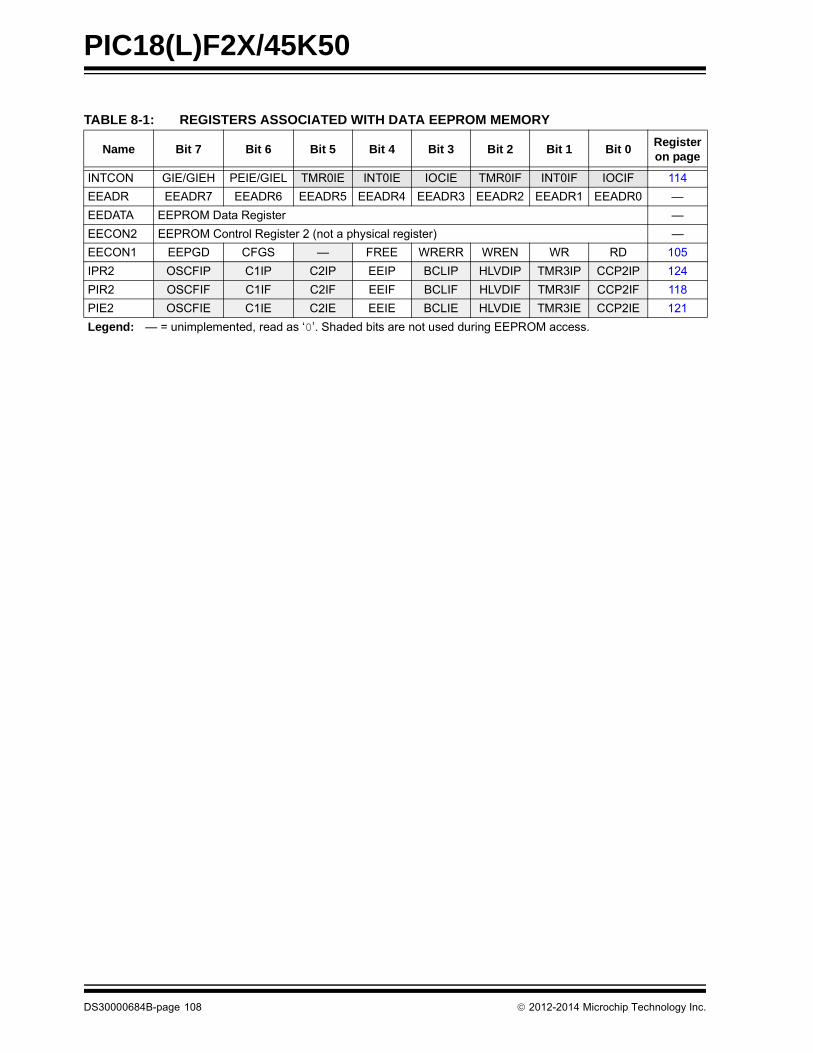
PIC18(L)F2X/45K50
TABLE 8-1: REGISTERS ASSOCIATED WITH DATA EEPROM MEMORY
Name Bit 7 Bit 6 Bit 5 Bit 4 Bit 3 Bit 2 Bit 1 Bit 0Register on page
INTCON GIE/GIEH PEIE/GIEL TMR0IE INT0IE IOCIE TMR0IF INT0IF IOCIF 114
EEADR EEADR7 EEADR6 EEADR5 EEADR4 EEADR3 EEADR2 EEADR1 EEADR0 —
EEDATA EEPROM Data Register —
EECON2 EEPROM Control Register 2 (not a physical register) —
EECON1 EEPGD CFGS — FREE WRERR WREN WR RD 105
IPR2 OSCFIP C1IP C2IP EEIP BCLIP HLVDIP TMR3IP CCP2IP 124
PIR2 OSCFIF C1IF C2IF EEIF BCLIF HLVDIF TMR3IF CCP2IF 118
PIE2 OSCFIE C1IE C2IE EEIE BCLIE HLVDIE TMR3IE CCP2IE 121
Legend: — = unimplemented, read as ‘0’. Shaded bits are not used during EEPROM access.
DS30000684B-page 108 2012-2014 Microchip Technology Inc.
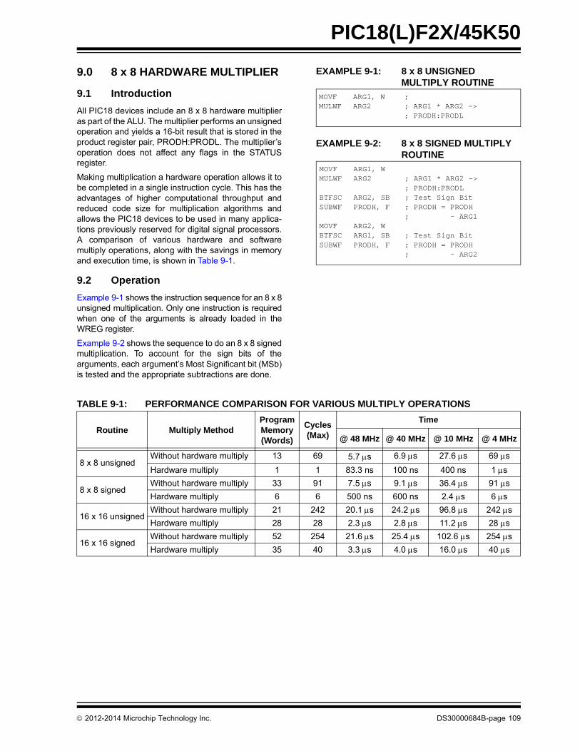
PIC18(L)F2X/45K50
9.0 8 x 8 HARDWARE MULTIPLIER
9.1 Introduction
All PIC18 devices include an 8 x 8 hardware multiplieras part of the ALU. The multiplier performs an unsignedoperation and yields a 16-bit result that is stored in theproduct register pair, PRODH:PRODL. The multiplier’soperation does not affect any flags in the STATUSregister.
Making multiplication a hardware operation allows it tobe completed in a single instruction cycle. This has theadvantages of higher computational throughput andreduced code size for multiplication algorithms andallows the PIC18 devices to be used in many applica-tions previously reserved for digital signal processors.A comparison of various hardware and softwaremultiply operations, along with the savings in memoryand execution time, is shown in Table 9-1.
9.2 Operation
Example 9-1 shows the instruction sequence for an 8 x 8unsigned multiplication. Only one instruction is requiredwhen one of the arguments is already loaded in theWREG register.
Example 9-2 shows the sequence to do an 8 x 8 signedmultiplication. To account for the sign bits of thearguments, each argument’s Most Significant bit (MSb)is tested and the appropriate subtractions are done.
EXAMPLE 9-1: 8 x 8 UNSIGNED MULTIPLY ROUTINE
EXAMPLE 9-2: 8 x 8 SIGNED MULTIPLY ROUTINE
MOVF ARG1, W ; MULWF ARG2 ; ARG1 * ARG2 ->
; PRODH:PRODL
MOVF ARG1, W MULWF ARG2 ; ARG1 * ARG2 ->
; PRODH:PRODL BTFSC ARG2, SB ; Test Sign Bit SUBWF PRODH, F ; PRODH = PRODH
; - ARG1 MOVF ARG2, WBTFSC ARG1, SB ; Test Sign Bit SUBWF PRODH, F ; PRODH = PRODH
; - ARG2
TABLE 9-1: PERFORMANCE COMPARISON FOR VARIOUS MULTIPLY OPERATIONS
Routine Multiply MethodProgramMemory(Words)
Cycles(Max)
Time
@ 48 MHz @ 40 MHz @ 10 MHz @ 4 MHz
8 x 8 unsignedWithout hardware multiply 13 69 5.7 s 6.9 s 27.6 s 69 s
Hardware multiply 1 1 83.3 ns 100 ns 400 ns 1 s
8 x 8 signedWithout hardware multiply 33 91 7.5 s 9.1 s 36.4 s 91 s
Hardware multiply 6 6 500 ns 600 ns 2.4 s 6 s
16 x 16 unsignedWithout hardware multiply 21 242 20.1 s 24.2 s 96.8 s 242 s
Hardware multiply 28 28 2.3 s 2.8 s 11.2 s 28 s
16 x 16 signedWithout hardware multiply 52 254 21.6 s 25.4 s 102.6 s 254 s
Hardware multiply 35 40 3.3 s 4.0 s 16.0 s 40 s
2012-2014 Microchip Technology Inc. DS30000684B-page 109

PIC18(L)F2X/45K50
Example 9-3 shows the sequence to do a 16 x 16unsigned multiplication. Equation 9-1 shows thealgorithm that is used. The 32-bit result is stored in fourregisters (RES<3:0>).
EQUATION 9-1: 16 x 16 UNSIGNED MULTIPLICATION ALGORITHM
EXAMPLE 9-3: 16 x 16 UNSIGNED MULTIPLY ROUTINE
Example 9-4 shows the sequence to do a 16 x 16signed multiply. Equation 9-2 shows the algorithmused. The 32-bit result is stored in four registers(RES<3:0>). To account for the sign bits of the argu-ments, the MSb for each argument pair is tested andthe appropriate subtractions are done.
EQUATION 9-2: 16 x 16 SIGNED MULTIPLICATION ALGORITHM
EXAMPLE 9-4: 16 x 16 SIGNED MULTIPLY ROUTINE
RES3:RES0 = ARG1H:ARG1L ARG2H:ARG2L= (ARG1H ARG2H 216) +
(ARG1H ARG2L 28) +(ARG1L ARG2H 28) +(ARG1L ARG2L)
MOVF ARG1L, WMULWF ARG2L ; ARG1L * ARG2L->
; PRODH:PRODL MOVFF PRODH, RES1 ; MOVFF PRODL, RES0 ;
MOVF ARG1H, W MULWF ARG2H ; ARG1H * ARG2H->
; PRODH:PRODL MOVFF PRODH, RES3 ; MOVFF PRODL, RES2 ;
MOVF ARG1L, W MULWF ARG2H ; ARG1L * ARG2H->
; PRODH:PRODL MOVF PRODL, W ; ADDWF RES1, F ; Add cross MOVF PRODH, W ; products ADDWFC RES2, F ; CLRF WREG ; ADDWFC RES3, F ;
MOVF ARG1H, W ; MULWF ARG2L ; ARG1H * ARG2L->
; PRODH:PRODL MOVF PRODL, W ; ADDWF RES1, F ; Add cross MOVF PRODH, W ; products ADDWFC RES2, F ; CLRF WREG ; ADDWFC RES3, F ;
RES3:RES0 = ARG1H:ARG1L ARG2H:ARG2L= (ARG1H ARG2H 216) +
(ARG1H ARG2L 28) +(ARG1L ARG2H 28) +(ARG1L ARG2L) +(-1 ARG2H<7> ARG1H:ARG1L 216) +(-1 ARG1H<7> ARG2H:ARG2L 216)
MOVF ARG1L, W MULWF ARG2L ; ARG1L * ARG2L ->
; PRODH:PRODL MOVFF PRODH, RES1 ; MOVFF PRODL, RES0 ;
MOVF ARG1H, W MULWF ARG2H ; ARG1H * ARG2H ->
; PRODH:PRODL MOVFF PRODH, RES3 ; MOVFF PRODL, RES2 ;
MOVF ARG1L, W MULWF ARG2H ; ARG1L * ARG2H ->
; PRODH:PRODL MOVF PRODL, W ; ADDWF RES1, F ; Add cross MOVF PRODH, W ; products ADDWFC RES2, F ; CLRF WREG ; ADDWFC RES3, F ;
MOVF ARG1H, W ; MULWF ARG2L ; ARG1H * ARG2L ->
; PRODH:PRODL MOVF PRODL, W ; ADDWF RES1, F ; Add cross MOVF PRODH, W ; products ADDWFC RES2, F ; CLRF WREG ; ADDWFC RES3, F ;
BTFSS ARG2H, 7 ; ARG2H:ARG2L neg? BRA SIGN_ARG1 ; no, check ARG1 MOVF ARG1L, W ; SUBWF RES2 ; MOVF ARG1H, W ; SUBWFB RES3
SIGN_ARG1
BTFSS ARG1H, 7 ; ARG1H:ARG1L neg? BRA CONT_CODE ; no, done MOVF ARG2L, W ; SUBWF RES2 ; MOVF ARG2H, W ; SUBWFB RES3
CONT_CODE
:
DS30000684B-page 110 2012-2014 Microchip Technology Inc.

PIC18(L)F2X/45K50
10.0 INTERRUPTS
The PIC18(L)F2X/45K50 devices have multipleinterrupt sources and an interrupt priority feature thatallows most interrupt sources to be assigned a high orlow priority level (INT0 does not have a priority bit, it isalways a high priority). The high priority interrupt vectoris at 0008h and the low priority interrupt vector is at0018h. A high priority interrupt event will interrupt a lowpriority interrupt that may be in progress.
There are 13 registers used to control interruptoperation.
These registers are:
• INTCON, INTCON2, INTCON3
• PIR1, PIR2, PIR3
• PIE1, PIE2, PIE3
• IPR1, IPR2, IPR3
• RCON
It is recommended that the Microchip header filessupplied with MPLAB® IDE be used for the symbolic bitnames in these registers. This allows the assembler/compiler to automatically take care of the placement ofthese bits within the specified register.
In general, interrupt sources have three bits to controltheir operation. They are:
• Flag bit to indicate that an interrupt event occurred
• Enable bit that allows program execution to branch to the interrupt vector address when the flag bit is set
• Priority bit to select high priority or low priority
10.1 Mid-Range Compatibility
When the IPEN bit is cleared (default state), the interruptpriority feature is disabled and interrupts are compatiblewith PIC microcontroller mid-range devices. InCompatibility mode, the interrupt priority bits of the IPRxregisters have no effect. The PEIE/GIEL bit of theINTCON register is the global interrupt enable for theperipherals. The PEIE/GIEL bit disables only theperipheral interrupt sources and enables the peripheralinterrupt sources when the GIE/GIEH bit is also set. TheGIE/GIEH bit of the INTCON register is the globalinterrupt enable which enables all non-peripheralinterrupt sources and disables all interrupt sources,including the peripherals. All interrupts branch toaddress 0008h in Compatibility mode.
10.2 Interrupt Priority
The interrupt priority feature is enabled by setting theIPEN bit of the RCON register. When interrupt priorityis enabled the GIE/GIEH and PEIE/GIEL global inter-rupt enable bits of Compatibility mode are replaced bythe GIEH high priority, and GIEL low priority, globalinterrupt enables. When set, the GIEH bit of the INT-CON register enables all interrupts that have theirassociated IPRx register or INTCONx register prioritybit set (high priority). When clear, the GIEH bit disablesall interrupt sources including those selected as low pri-ority. When clear, the GIEL bit of the INTCON registerdisables only the interrupts that have their associatedpriority bit cleared (low priority). When set, the GIEL bitenables the low priority sources when the GIEH bit isalso set.
When the interrupt flag, enable bit and appropriateGlobal Interrupt Enable (GIE) bit are all set, theinterrupt will vector immediately to address 0008h forhigh priority, or 0018h for low priority, depending onlevel of the interrupting source’s priority bit. Individualinterrupts can be disabled through their correspondinginterrupt enable bits.
10.3 Interrupt Response
When an interrupt is responded to, the Global InterruptEnable bit is cleared to disable further interrupts. TheGIE/GIEH bit is the global interrupt enable when theIPEN bit is cleared. When the IPEN bit is set, enablinginterrupt priority levels, the GIEH bit is the high priorityglobal interrupt enable and the GIEL bit is the lowpriority global interrupt enable. High priority interruptsources can interrupt a low priority interrupt. Lowpriority interrupts are not processed while high priorityinterrupts are in progress.
The return address is pushed onto the stack and thePC is loaded with the interrupt vector address (0008hor 0018h). Once in the Interrupt Service Routine, thesource(s) of the interrupt can be determined by pollingthe interrupt flag bits in the INTCONx and PIRxregisters. The interrupt flag bits must be cleared bysoftware before re-enabling interrupts to avoidrepeating the same interrupt.
The “return from interrupt” instruction, RETFIE, exitsthe interrupt routine and sets the GIE/GIEH bit (GIEHor GIEL if priority levels are used), which re-enablesinterrupts.
For external interrupt events, such as the INT pins orthe PORTB interrupt-on-change, the interrupt latencywill be three to four instruction cycles. The exactlatency is the same for one-cycle or two-cycleinstructions. Individual interrupt flag bits are set,regardless of the status of their corresponding enablebits or the Global Interrupt Enable bit.
2012-2014 Microchip Technology Inc. DS30000684B-page 111
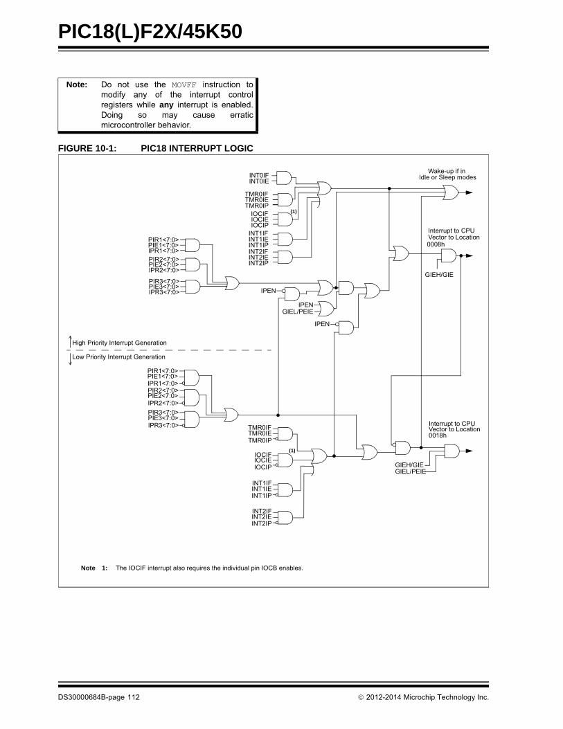
PIC18(L)F2X/45K50
FIGURE 10-1: PIC18 INTERRUPT LOGIC
Note: Do not use the MOVFF instruction tomodify any of the interrupt controlregisters while any interrupt is enabled.Doing so may cause erraticmicrocontroller behavior.
TMR0IE
GIEH/GIE
Wake-up if in
Interrupt to CPUVector to Location0008h
INT2IFINT2IEINT2IP
INT1IFINT1IEINT1IP
TMR0IFTMR0IETMR0IP
IOCIFIOCIEIOCIP
TMR0IF
TMR0IP
INT1IFINT1IEINT1IPINT2IFINT2IEINT2IP
IOCIFIOCIEIOCIP
INT0IFINT0IE
GIEL/PEIE
Interrupt to CPUVector to Location
IPEN
IPEN
0018h
High Priority Interrupt Generation
Low Priority Interrupt Generation
Idle or Sleep modes
GIEH/GIE
Note 1: The IOCIF interrupt also requires the individual pin IOCB enables.
(1)
(1)
PIR1<7:0>PIE1<7:0>IPR1<7:0>PIR2<7:0>PIE2<7:0>IPR2<7:0>
PIR3<7:0>PIE3<7:0>IPR3<7:0>
PIR1<7:0>PIE1<7:0>IPR1<7:0>PIR2<7:0>PIE2<7:0>IPR2<7:0>
PIR3<7:0>PIE3<7:0>IPR3<7:0>
IPENGIEL/PEIE
DS30000684B-page 112 2012-2014 Microchip Technology Inc.

PIC18(L)F2X/45K50
10.4 INTCON Registers
The INTCON registers are readable and writableregisters, which contain various enable, priority andflag bits.
10.5 PIR Registers
The PIR registers contain the individual flag bits for theperipheral interrupts. Due to the number of peripheralinterrupt sources, there are three Peripheral InterruptRequest Flag registers (PIR1, PIR2 and PIR3).
10.6 PIE Registers
The PIE registers contain the individual enable bits forthe peripheral interrupts. Due to the number ofperipheral interrupt sources, there are three PeripheralInterrupt Enable registers (PIE1, PIE2 and PIE3). WhenIPEN = 0, the PEIE/GIEL bit must be set to enable anyof these peripheral interrupts.
10.7 IPR Registers
The IPR registers contain the individual priority bits for theperipheral interrupts. Due to the number of peripheralinterrupt sources, there are three Peripheral InterruptPriority registers (IPR1, IPR2 and IPR3). Using the prioritybits requires that the Interrupt Priority Enable (IPEN) bit beset.
2012-2014 Microchip Technology Inc. DS30000684B-page 113
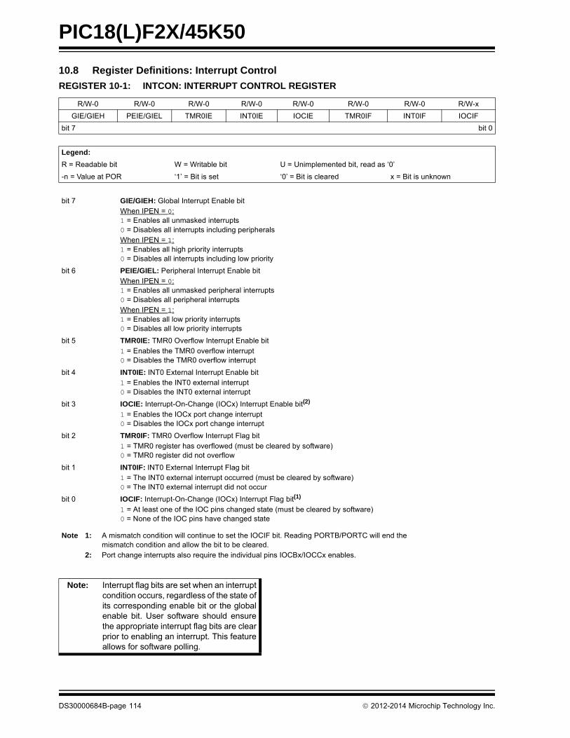
PIC18(L)F2X/45K50
10.8 Register Definitions: Interrupt Control
REGISTER 10-1: INTCON: INTERRUPT CONTROL REGISTER
R/W-0 R/W-0 R/W-0 R/W-0 R/W-0 R/W-0 R/W-0 R/W-x
GIE/GIEH PEIE/GIEL TMR0IE INT0IE IOCIE TMR0IF INT0IF IOCIF
bit 7 bit 0
Legend:
R = Readable bit W = Writable bit U = Unimplemented bit, read as ‘0’
-n = Value at POR ‘1’ = Bit is set ‘0’ = Bit is cleared x = Bit is unknown
bit 7 GIE/GIEH: Global Interrupt Enable bitWhen IPEN = 0:1 = Enables all unmasked interrupts0 = Disables all interrupts including peripheralsWhen IPEN = 1:1 = Enables all high priority interrupts 0 = Disables all interrupts including low priority
bit 6 PEIE/GIEL: Peripheral Interrupt Enable bitWhen IPEN = 0:1 = Enables all unmasked peripheral interrupts 0 = Disables all peripheral interrupts When IPEN = 1:1 = Enables all low priority interrupts 0 = Disables all low priority interrupts
bit 5 TMR0IE: TMR0 Overflow Interrupt Enable bit 1 = Enables the TMR0 overflow interrupt 0 = Disables the TMR0 overflow interrupt
bit 4 INT0IE: INT0 External Interrupt Enable bit 1 = Enables the INT0 external interrupt 0 = Disables the INT0 external interrupt
bit 3 IOCIE: Interrupt-On-Change (IOCx) Interrupt Enable bit(2) 1 = Enables the IOCx port change interrupt 0 = Disables the IOCx port change interrupt
bit 2 TMR0IF: TMR0 Overflow Interrupt Flag bit 1 = TMR0 register has overflowed (must be cleared by software) 0 = TMR0 register did not overflow
bit 1 INT0IF: INT0 External Interrupt Flag bit 1 = The INT0 external interrupt occurred (must be cleared by software) 0 = The INT0 external interrupt did not occur
bit 0 IOCIF: Interrupt-On-Change (IOCx) Interrupt Flag bit(1) 1 = At least one of the IOC pins changed state (must be cleared by software) 0 = None of the IOC pins have changed state
Note 1: A mismatch condition will continue to set the IOCIF bit. Reading PORTB/PORTC will end the mismatch condition and allow the bit to be cleared.
2: Port change interrupts also require the individual pins IOCBx/IOCCx enables.
Note: Interrupt flag bits are set when an interruptcondition occurs, regardless of the state ofits corresponding enable bit or the globalenable bit. User software should ensurethe appropriate interrupt flag bits are clearprior to enabling an interrupt. This featureallows for software polling.
DS30000684B-page 114 2012-2014 Microchip Technology Inc.

PIC18(L)F2X/45K50
REGISTER 10-2: INTCON2: INTERRUPT CONTROL 2 REGISTER
R/W-1 R/W-1 R/W-1 R/W-1 U-0 R/W-1 U-0 R/W-1
RBPU INTEDG0 INTEDG1 INTEDG2 — TMR0IP — IOCIP
bit 7 bit 0
Legend:
R = Readable bit W = Writable bit U = Unimplemented bit, read as ‘0’
-n = Value at POR ‘1’ = Bit is set ‘0’ = Bit is cleared x = Bit is unknown
bit 7 RBPU: PORTB Pull-up Enable bit
1 = All PORTB pull-ups are disabled 0 = PORTB pull-ups are enabled provided that the pin is an input and the corresponding WPUB bit is
set.
bit 6 INTEDG0: External Interrupt 0 Edge Select bit
1 = Interrupt on rising edge 0 = Interrupt on falling edge
bit 5 INTEDG1: External Interrupt 1 Edge Select bit
1 = Interrupt on rising edge 0 = Interrupt on falling edge
bit 4 INTEDG2: External Interrupt 2 Edge Select bit
1 = Interrupt on rising edge 0 = Interrupt on falling edge
bit 3 Unimplemented: Read as ‘0’
bit 2 TMR0IP: TMR0 Overflow Interrupt Priority bit
1 = High priority 0 = Low priority
bit 1 Unimplemented: Read as ‘0’
bit 0 IOCIP: Port Change Interrupt Priority bit
1 = High priority 0 = Low priority
Note: Interrupt flag bits are set when an interruptcondition occurs, regardless of the state ofits corresponding enable bit or the globalenable bit. User software should ensurethe appropriate interrupt flag bits are clearprior to enabling an interrupt. This featureallows for software polling.
2012-2014 Microchip Technology Inc. DS30000684B-page 115

PIC18(L)F2X/45K50
REGISTER 10-3: INTCON3: INTERRUPT CONTROL 3 REGISTER
R/W-1 R/W-1 U-0 R/W-0 R/W-0 U-0 R/W-0 R/W-0
INT2IP INT1IP — INT2IE INT1IE — INT2IF INT1IF
bit 7 bit 0
Legend:
R = Readable bit W = Writable bit U = Unimplemented bit, read as ‘0’
-n = Value at POR ‘1’ = Bit is set ‘0’ = Bit is cleared x = Bit is unknown
bit 7 INT2IP: INT2 External Interrupt Priority bit
1 = High priority 0 = Low priority
bit 6 INT1IP: INT1 External Interrupt Priority bit
1 = High priority 0 = Low priority
bit 5 Unimplemented: Read as ‘0’
bit 4 INT2IE: INT2 External Interrupt Enable bit
1 = Enables the INT2 external interrupt 0 = Disables the INT2 external interrupt
bit 3 INT1IE: INT1 External Interrupt Enable bit
1 = Enables the INT1 external interrupt 0 = Disables the INT1 external interrupt
bit 2 Unimplemented: Read as ‘0’
bit 1 INT2IF: INT2 External Interrupt Flag bit
1 = The INT2 external interrupt occurred (must be cleared by software) 0 = The INT2 external interrupt did not occur
bit 0 INT1IF: INT1 External Interrupt Flag bit
1 = The INT1 external interrupt occurred (must be cleared by software) 0 = The INT1 external interrupt did not occur
Note: Interrupt flag bits are set when an interruptcondition occurs, regardless of the state ofits corresponding enable bit or the globalenable bit. User software should ensurethe appropriate interrupt flag bits are clearprior to enabling an interrupt. This featureallows for software polling.
DS30000684B-page 116 2012-2014 Microchip Technology Inc.

PIC18(L)F2X/45K50
REGISTER 10-4: PIR1: PERIPHERAL INTERRUPT REQUEST (FLAG) REGISTER 1
R/W-0 R/W-0 R-0 R-0 R/W-0 R/W-0 R/W-0 R/W-0
ACTIF ADIF RCIF TXIF SSPIF CCP1IF TMR2IF TMR1IF
bit 7 bit 0
Legend:
R = Readable bit W = Writable bit U = Unimplemented bit, read as ‘0’
-n = Value at POR ‘1’ = Bit is set ‘0’ = Bit is cleared x = Bit is unknown
bit 7 ACTIF: Active Clock Tuning Interrupt Flag bit
1 = An Active Clock Tuning Event generated an interrupt (must be cleared in software)0 = No Active Clock Tuning interrupt is pending
bit 6 ADIF: A/D Converter Interrupt Flag bit
1 = An A/D conversion completed (must be cleared by software) 0 = The A/D conversion is not complete or has not been started
bit 5 RCIF: EUSART Receive Interrupt Flag bit
1 = The EUSART receive buffer, RCREG1, is full (cleared when RCREG1 is read) 0 = The EUSART receive buffer is empty
bit 4 TXIF: EUSART Transmit Interrupt Flag bit
1 = The EUSART transmit buffer, TXREG1, is empty (cleared when TXREG1 is written) 0 = The EUSART transmit buffer is full
bit 3 SSPIF: Master Synchronous Serial Port Interrupt Flag bit
1 = The transmission/reception is complete (must be cleared by software)0 = Waiting to transmit/receive
bit 2 CCP1IF: CCP1 Interrupt Flag bit
Capture mode: 1 = A TMR1 register capture occurred (must be cleared by software) 0 = No TMR1 register capture occurred
Compare mode: 1 = A TMR1 register compare match occurred (must be cleared by software) 0 = No TMR1 register compare match occurredPWM mode: Unused in this mode
bit 1 TMR2IF: TMR2 to PR2 Match Interrupt Flag bit
1 = TMR2 to PR2 match occurred (must be cleared by software) 0 = No TMR2 to PR2 match occurred
bit 0 TMR1IF: TMR1 Overflow Interrupt Flag bit
1 = TMR1 register overflowed (must be cleared by software)0 = TMR1 register did not overflow
Note 1: Interrupt flag bits are set when aninterrupt condition occurs, regardless ofthe state of its corresponding enable bitor the Global Interrupt Enable bit, GIE/GIEH of the INTCON register.
2: User software should ensure the appro-priate interrupt flag bits are cleared priorto enabling an interrupt and after servic-ing that interrupt.
2012-2014 Microchip Technology Inc. DS30000684B-page 117
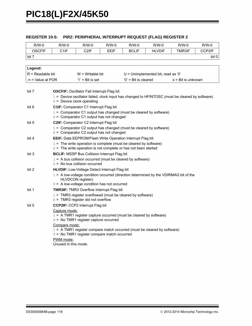
PIC18(L)F2X/45K50
REGISTER 10-5: PIR2: PERIPHERAL INTERRUPT REQUEST (FLAG) REGISTER 2
R/W-0 R/W-0 R/W-0 R/W-0 R/W-0 R/W-0 R/W-0 R/W-0
OSCFIF C1IF C2IF EEIF BCLIF HLVDIF TMR3IF CCP2IF
bit 7 bit 0
Legend:
R = Readable bit W = Writable bit U = Unimplemented bit, read as ‘0’
-n = Value at POR ‘1’ = Bit is set ‘0’ = Bit is cleared x = Bit is unknown
bit 7 OSCFIF: Oscillator Fail Interrupt Flag bit
1 = Device oscillator failed, clock input has changed to HFINTOSC (must be cleared by software)0 = Device clock operating
bit 6 C1IF: Comparator C1 Interrupt Flag bit
1 = Comparator C1 output has changed (must be cleared by software)0 = Comparator C1 output has not changed
bit 5 C2IF: Comparator C2 Interrupt Flag bit
1 = Comparator C2 output has changed (must be cleared by software)0 = Comparator C2 output has not changed
bit 4 EEIF: Data EEPROM/Flash Write Operation Interrupt Flag bit
1 = The write operation is complete (must be cleared by software)0 = The write operation is not complete or has not been started
bit 3 BCLIF: MSSP Bus Collision Interrupt Flag bit
1 = A bus collision occurred (must be cleared by software)0 = No bus collision occurred
bit 2 HLVDIF: Low-Voltage Detect Interrupt Flag bit
1 = A low-voltage condition occurred (direction determined by the VDIRMAG bit of theHLVDCON register)
0 = A low-voltage condition has not occurred
bit 1 TMR3IF: TMR3 Overflow Interrupt Flag bit
1 = TMR3 register overflowed (must be cleared by software)0 = TMR3 register did not overflow
bit 0 CCP2IF: CCP2 Interrupt Flag bit
Capture mode: 1 = A TMR1 register capture occurred (must be cleared by software) 0 = No TMR1 register capture occurred
Compare mode: 1 = A TMR1 register compare match occurred (must be cleared by software) 0 = No TMR1 register compare match occurred
PWM mode:Unused in this mode.
DS30000684B-page 118 2012-2014 Microchip Technology Inc.

PIC18(L)F2X/45K50
REGISTER 10-6: PIR3: PERIPHERAL INTERRUPT (FLAG) REGISTER 3
U-0 U-0 U-0 U-0 R/W-0 R/W-0 R/W-0 R/W-0
— — — — CTMUIF USBIF TMR3GIF TMR1GIF
bit 7 bit 0
Legend:
R = Readable bit W = Writable bit U = Unimplemented bit, read as ‘0’
-n = Value at POR ‘1’ = Bit is set ‘0’ = Bit is cleared x = Bit is unknown
bit 7-4 Unimplemented: Read as ‘0’
bit 3 CTMUIF: CTMU Interrupt Flag bit
1 = CTMU interrupt occurred (must be cleared in software)0 = No CTMU interrupt occurred
bit 2 USBIF: USB Interrupt Flag bit
1 = USB requested an interrupt (must be cleared in software)0 = No USB interrupt request
bit 1 TMR3GIF: TMR3 Gate Interrupt Flag bit
1 = TMR gate interrupt occurred (must be cleared in software)0 = No TMR gate occurred
bit 0 TMR1GIF: TMR1 Gate Interrupt Flag bit
1 = TMR gate interrupt occurred (must be cleared in software)0 = No TMR gate occurred
2012-2014 Microchip Technology Inc. DS30000684B-page 119

PIC18(L)F2X/45K50
REGISTER 10-7: PIE1: PERIPHERAL INTERRUPT ENABLE (FLAG) REGISTER 1
R/W-0 R/W-0 R/W-0 R/W-0 R/W-0 R/W-0 R/W-0 R/W-0
ACTIE ADIE RCIE TXIE SSPIE CCP1IE TMR2IE TMR1IE
bit 7 bit 0
Legend:
R = Readable bit W = Writable bit U = Unimplemented bit, read as ‘0’
-n = Value at POR ‘1’ = Bit is set ‘0’ = Bit is cleared x = Bit is unknown
bit 7 ACTIE: Active Clock Tuning Interrupt Enable bit
1 = Enables Active Clock Tuning interrupt 0 = Disables Active Clock Tuning interrupt
bit 6 ADIE: A/D Converter Interrupt Enable bit
1 = Enables the A/D interrupt 0 = Disables the A/D interrupt
bit 5 RCIE: EUSART Receive Interrupt Enable bit
1 = Enables the EUSART receive interrupt 0 = Disables the EUSART receive interrupt
bit 4 TXIE: EUSART Transmit Interrupt Enable bit
1 = Enables the EUSART transmit interrupt 0 = Disables the EUSART transmit interrupt
bit 3 SSPIE: Master Synchronous Serial Port Interrupt Enable bit
1 = Enables the MSSP interrupt 0 = Disables the MSSP interrupt
bit 2 CCP1IE: CCP1 Interrupt Enable bit
1 = Enables the CCP1 interrupt 0 = Disables the CCP1 interrupt
bit 1 TMR2IE: TMR2 to PR2 Match Interrupt Enable bit
1 = Enables the TMR2 to PR2 match interrupt 0 = Disables the TMR2 to PR2 match interrupt
bit 0 TMR1IE: TMR1 Overflow Interrupt Enable bit
1 = Enables the TMR1 overflow interrupt 0 = Disables the TMR1 overflow interrupt
DS30000684B-page 120 2012-2014 Microchip Technology Inc.

PIC18(L)F2X/45K50
REGISTER 10-8: PIE2: PERIPHERAL INTERRUPT ENABLE (FLAG) REGISTER 2
R/W-0 R/W-0 R/W-0 R/W-0 R/W-0 R/W-0 R/W-0 R/W-0
OSCFIE C1IE C2IE EEIE BCLIE HLVDIE TMR3IE CCP2IE
bit 7 bit 0
Legend:
R = Readable bit W = Writable bit U = Unimplemented bit, read as ‘0’
-n = Value at POR ‘1’ = Bit is set ‘0’ = Bit is cleared x = Bit is unknown
bit 7 OSCFIE: Oscillator Fail Interrupt Enable bit
1 = Enabled0 = Disabled
bit 6 C1IE: Comparator C1 Interrupt Enable bit
1 = Enabled0 = Disabled
bit 5 C2IE: Comparator C2 Interrupt Enable bit
1 = Enabled0 = Disabled
bit 4 EEIE: Data EEPROM/Flash Write Operation Interrupt Enable bit
1 = Enabled0 = Disabled
bit 3 BCLIE: MSSP Bus Collision Interrupt Enable bit
1 = Enabled0 = Disabled
bit 2 HLVDIE: Low-Voltage Detect Interrupt Enable bit
1 = Enabled0 = Disabled
bit 1 TMR3IE: TMR3 Overflow Interrupt Enable bit
1 = Enabled0 = Disabled
bit 0 CCP2IE: CCP2 Interrupt Enable bit
1 = Enabled0 = Disabled
2012-2014 Microchip Technology Inc. DS30000684B-page 121
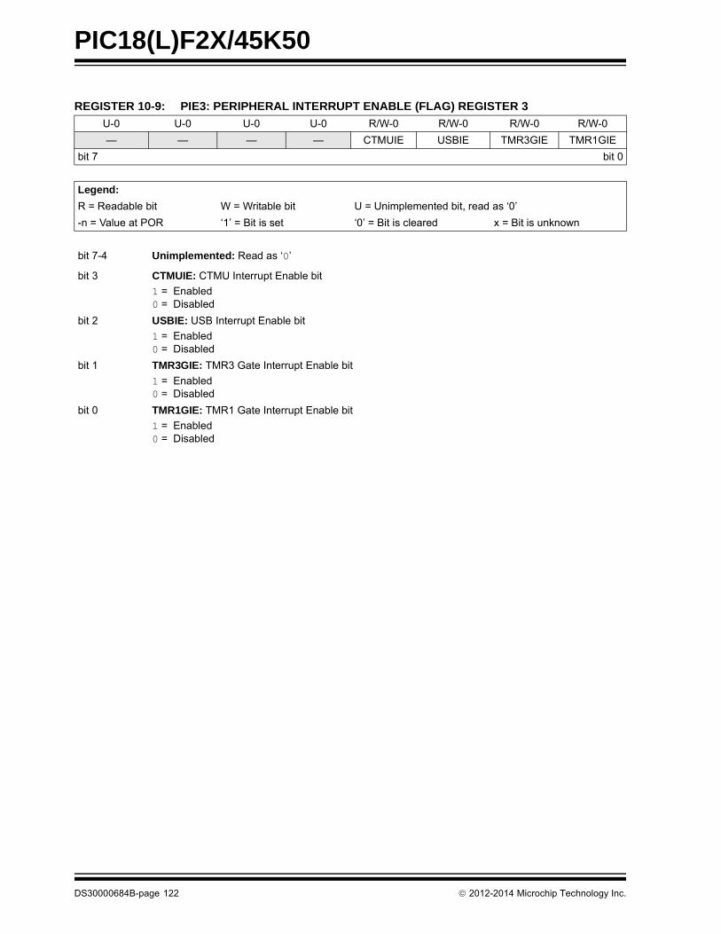
PIC18(L)F2X/45K50
REGISTER 10-9: PIE3: PERIPHERAL INTERRUPT ENABLE (FLAG) REGISTER 3
U-0 U-0 U-0 U-0 R/W-0 R/W-0 R/W-0 R/W-0
— — — — CTMUIE USBIE TMR3GIE TMR1GIE
bit 7 bit 0
Legend:
R = Readable bit W = Writable bit U = Unimplemented bit, read as ‘0’
-n = Value at POR ‘1’ = Bit is set ‘0’ = Bit is cleared x = Bit is unknown
bit 7-4 Unimplemented: Read as ‘0’
bit 3 CTMUIE: CTMU Interrupt Enable bit
1 = Enabled0 = Disabled
bit 2 USBIE: USB Interrupt Enable bit
1 = Enabled0 = Disabled
bit 1 TMR3GIE: TMR3 Gate Interrupt Enable bit
1 = Enabled0 = Disabled
bit 0 TMR1GIE: TMR1 Gate Interrupt Enable bit
1 = Enabled0 = Disabled
DS30000684B-page 122 2012-2014 Microchip Technology Inc.
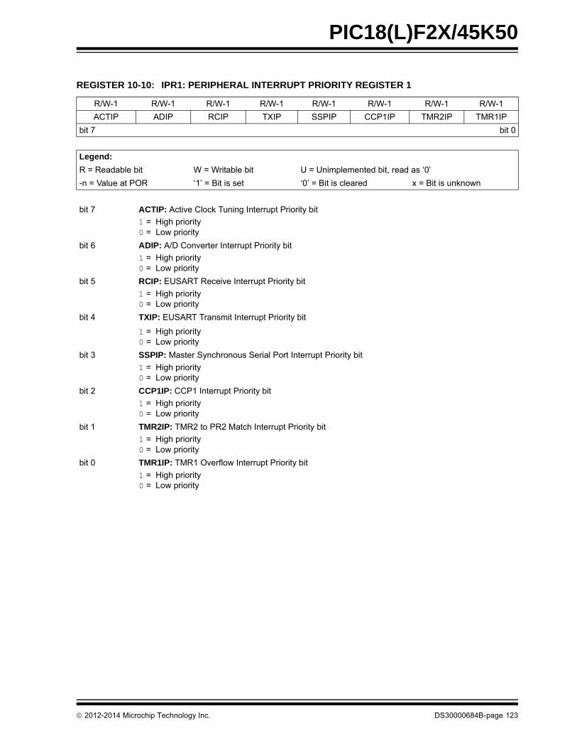
PIC18(L)F2X/45K50
REGISTER 10-10: IPR1: PERIPHERAL INTERRUPT PRIORITY REGISTER 1
R/W-1 R/W-1 R/W-1 R/W-1 R/W-1 R/W-1 R/W-1 R/W-1
ACTIP ADIP RCIP TXIP SSPIP CCP1IP TMR2IP TMR1IP
bit 7 bit 0
Legend:
R = Readable bit W = Writable bit U = Unimplemented bit, read as ‘0’
-n = Value at POR ‘1’ = Bit is set ‘0’ = Bit is cleared x = Bit is unknown
bit 7 ACTIP: Active Clock Tuning Interrupt Priority bit
1 = High priority 0 = Low priority
bit 6 ADIP: A/D Converter Interrupt Priority bit
1 = High priority 0 = Low priority
bit 5 RCIP: EUSART Receive Interrupt Priority bit
1 = High priority 0 = Low priority
bit 4 TXIP: EUSART Transmit Interrupt Priority bit
1 = High priority 0 = Low priority
bit 3 SSPIP: Master Synchronous Serial Port Interrupt Priority bit
1 = High priority 0 = Low priority
bit 2 CCP1IP: CCP1 Interrupt Priority bit
1 = High priority 0 = Low priority
bit 1 TMR2IP: TMR2 to PR2 Match Interrupt Priority bit
1 = High priority 0 = Low priority
bit 0 TMR1IP: TMR1 Overflow Interrupt Priority bit
1 = High priority 0 = Low priority
2012-2014 Microchip Technology Inc. DS30000684B-page 123

PIC18(L)F2X/45K50
REGISTER 10-11: IPR2: PERIPHERAL INTERRUPT PRIORITY REGISTER 2
R/W-1 R/W-1 R/W-1 R/W-1 R/W-1 R/W-1 R/W-1 R/W-1
OSCFIP C1IP C2IP EEIP BCLIP HLVDIP TMR3IP CCP2IP
bit 7 bit 0
Legend:
R = Readable bit W = Writable bit U = Unimplemented bit, read as ‘0’
-n = Value at POR ‘1’ = Bit is set ‘0’ = Bit is cleared x = Bit is unknown
bit 7 OSCFIP: Oscillator Fail Interrupt Priority bit
1 = High priority0 = Low priority
bit 6 C1IP: Comparator C1 Interrupt Priority bit
1 = High priority0 = Low priority
bit 5 C2IP: Comparator C2 Interrupt Priority bit
1 = High priority0 = Low priority
bit 4 EEIP: Data EEPROM/Flash Write Operation Interrupt Priority bit
1 = High priority0 = Low priority
bit 3 BCLIP: MSSP Bus Collision Interrupt Priority bit
1 = High priority0 = Low priority
bit 2 HLVDIP: Low-Voltage Detect Interrupt Priority bit
1 = High priority0 = Low priority
bit 1 TMR3IP: TMR3 Overflow Interrupt Priority bit
1 = High priority0 = Low priority
bit 0 CCP2IP: CCP2 Interrupt Priority bit
1 = High priority0 = Low priority
DS30000684B-page 124 2012-2014 Microchip Technology Inc.

PIC18(L)F2X/45K50
REGISTER 10-12: IPR3: PERIPHERAL INTERRUPT PRIORITY REGISTER 3
U-0 U-0 U-0 U-0 R/W-1 R/W-1 R/W-1 R/W-1
— — — — CTMUIP USBIP TMR3GIP TMR1GIP
bit 7 bit 0
Legend:
R = Readable bit W = Writable bit U = Unimplemented bit, read as ‘0’
-n = Value at POR ‘1’ = Bit is set ‘0’ = Bit is cleared x = Bit is unknown
bit 7-4 Unimplemented: Read as ‘0’
bit 3 CTMUIP: CTMU Interrupt Priority bit
1 = High priority0 = Low priority
bit 2 USBIP: USB Interrupt Priority bit
1 = High priority0 = Low priority
bit 1 TMR3GIP: TMR3 Gate Interrupt Priority bit
1 = High priority0 = Low priority
bit 0 TMR1GIP: TMR1 Gate Interrupt Priority bit
1 = High priority0 = Low priority
2012-2014 Microchip Technology Inc. DS30000684B-page 125

PIC18(L)F2X/45K50
10.9 INTn Pin Interrupts
External interrupts on the RB0/INT0, RB1/INT1 andRB2/INT2 pins are edge-triggered. If the correspondingINTEDGx bit in the INTCON2 register is set (= 1), theinterrupt is triggered by a rising edge; if the bit is clear,the trigger is on the falling edge. When a valid edgeappears on the RBx/INTx pin, the corresponding flagbit, INTxF, is set. This interrupt can be disabled byclearing the corresponding enable bit, INTxE. Flag bit,INTxF, must be cleared by software in the InterruptService Routine before re-enabling the interrupt.
All external interrupts (INT0, INT1 and INT2) can wake-up the processor from Idle or Sleep modes if bit INTxEwas set prior to going into those modes. If the GlobalInterrupt Enable bit, GIE/GIEH, is set, the processorwill branch to the interrupt vector following wake-up.
Interrupt priority for INT1 and INT2 is determined bythe value contained in the interrupt priority bits, INT1IPand INT2IP of the INTCON3 register. There is no prior-ity bit associated with INT0. It is always a high priorityinterrupt source.
10.10 TMR0 Interrupt
In 8-bit mode (which is the default), an overflow in theTMR0 register (FFh 00h) will set flag bit, TMR0IF. In16-bit mode, an overflow in the TMR0H:TMR0L regis-ter pair (FFFFh 0000h) will set TMR0IF. The interruptcan be enabled/disabled by setting/clearing enable bit,TMR0IE of the INTCON register. Interrupt priority forTimer0 is determined by the value contained in theinterrupt priority bit, TMR0IP of the INTCON2 register.See Section 12.0 “Timer0 Module” for further detailson the Timer0 module.
10.11 PORTB/PORTC Interrupt-on-Change
An input change on PORTB<7:4> or PORTC<2:0> setsflag bit, IOCIF of the INTCON register. The interruptcan be enabled/disabled by setting/clearing enable bit,IOCIE of the INTCON register. Pins must also beindividually enabled with the IOCB/IOCC register.Interrupt priority for interrupt-on-change is determinedby the value contained in the interrupt priority bit, IOCIPof the INTCON2 register.
10.12 Context Saving During Interrupts
During interrupts, the return PC address is saved onthe stack. Additionally, the WREG, STATUS and BSRregisters are saved on the fast return stack. If a fastreturn from interrupt is not used (see Section 6.2.2“Fast Register Stack”), the user may need to save theWREG, STATUS and BSR registers on entry to theInterrupt Service Routine. Depending on the user’sapplication, other registers may also need to be saved.Example 10-1 saves and restores the WREG, STATUSand BSR registers during an Interrupt Service Routine.
EXAMPLE 10-1: SAVING STATUS, WREG AND BSR REGISTERS IN RAM
MOVWF W_TEMP ; W_TEMP is in virtual bankMOVFF STATUS, STATUS_TEMP ; STATUS_TEMP located anywhereMOVFF BSR, BSR_TEMP ; BSR_TMEP located anywhere;; USER ISR CODE;MOVFF BSR_TEMP, BSR ; Restore BSRMOVF W_TEMP, W ; Restore WREGMOVFF STATUS_TEMP, STATUS ; Restore STATUS
DS30000684B-page 126 2012-2014 Microchip Technology Inc.

PIC18(L)F2X/45K50
TABLE 10-1: REGISTERS ASSOCIATED WITH INTERRUPTS
Name Bit 7 Bit 6 Bit 5 Bit 4 Bit 3 Bit 2 Bit 1 Bit 0Register on page
ANSELB — — ANSB5 ANSB4 ANSB3 ANSB2 ANSB1 ANSB0 148
INTCON GIE/GIEH PEIE/GIEL TMR0IE INT0IE IOCIE TMR0IF INT0IF IOCIF 114
INTCON2 RBPU INTEDG0 INTEDG1 INTEDG2 — TMR0IP — IOCIP 115
INTCON3 INT2IP INT1IP — INT2IE INT1IE — INT2IF INT1IF 116
IOCB IOCB7 IOCB6 IOCB5 IOCB4 — — — — 151
IOCC IOCC7 IOCC6 IOCC5 IOCC4 — IOCC2 IOCC1 IOCC0 151
IPR1 ACTIP ADIP RCIP TXIP SSPIP CCP1IP TMR2IP TMR1IP 123
IPR2 OSCFIP C1IP C2IP EEIP BCLIP HLVDIP TMR3IP CCP2IP 124
IPR3 — — — — CTMUIP USBIP TMR3GIP TMR1GIP 125
PIE1 ACTIE ADIE RCIE TXIE SSPIE CCP1IE TMR2IE TMR1IE 120
PIE2 OSCFIE C1IE C2IE EEIE BCLIE HLVDIE TMR3IE CCP2IE 121
PIE3 — — — — CTMUIE USBIE TMR3GIE TMR1GIE 122
PIR1 ACTIF ADIF RCIF TXIF SSPIF CCP1IF TMR2IF TMR1IF 117
PIR2 OSCFIF C1IF C2IF EEIF BCLIF HLVDIF TMR3IF CCP2IF 118
PIR3 — — — — CTMUIF USBIF TMR3GIF TMR1GIF 119
PORTB RB7 RB6 RB5 RB4 RB3 RB2 RB1 RB0 146
RCON IPEN SBOREN — RI TO PD POR BOR 64
Legend: — = unimplemented locations, read as ‘0’. Shaded bits are not used for interrupts.
TABLE 10-2: CONFIGURATION REGISTERS ASSOCIATED WITH INTERRUPTS
Name Bit 7 Bit 6 Bit 5 Bit 4 Bit 3 Bit 2 Bit 1 Bit 0Register on page
CONFIG3H MCLRE SDOMX — T3CMX — — PBADEN CCP2MX 376
CONFIG4L DEBUG XINST ICPRT — — LVP — STRVEN 377
Legend: — = unimplemented locations, read as ‘0’. Shaded bits are not used for interrupts.
2012-2014 Microchip Technology Inc. DS30000684B-page 127
PIC18(L)F2X/45K50
DS
11.0 I/O PORTS
Depending on the device selected and featuresenabled, there are up to five ports available. All pins ofthe I/O ports are multiplexed with one or more alternatefunctions from the peripheral features on the device. Ingeneral, when a peripheral is enabled, that pin may notbe used as a general purpose I/O pin.
Each port has five registers for its operation. Theseregisters are:
• TRIS register (data direction register)
• PORT register (reads the levels on the pins of the device)
• LAT register (output latch)
• ANSEL register (analog input control)
• SLRCON register (port slew rate control)
The Data Latch (LAT register) is useful for read-modify-write operations on the value that the I/O pins aredriving.
A simplified model of a generic I/O port, without theinterfaces to other peripherals, is shown in Figure 11-1.
FIGURE 11-1: GENERIC I/O PORT OPERATION
11.1 PORTA Registers
PORTA is an 8-bit wide, bidirectional port. Thecorresponding data direction register is TRISA. Settinga TRISA bit (= 1) will make the corresponding PORTApin an input (i.e., disable the output driver). Clearing aTRISA bit (= 0) will make the corresponding PORTA pinan output (i.e., enable the output driver and put thecontents of the output latch on the selected pin).
Reading the PORTA register reads the status of thepins, whereas writing to it, will write to the PORT latch.
The Data Latch (LATA) register is also memory mapped.Read-modify-write operations on the LATA register readand write the latched output value for PORTA.
The RA4 pin is multiplexed with the Timer0 moduleclock input and one of the comparator outputs tobecome the RA4/T0CKI/C1OUT pin. Pins RA6 andRA7 are multiplexed with the main oscillator pins; theyare enabled as oscillator or I/O pins by the selection ofthe main oscillator in the Configuration register (seeSection 26.1 “Configuration Bits” for details). Whenthey are not used as port pins, RA6 and RA7 and theirassociated TRIS and LAT bits are read as ‘0’.
The other PORTA pins are multiplexed with analoginputs, the analog VREF+ and VREF- inputs, and thecomparator voltage reference output. The operation ofpins RA<3:0> and RA5 as analog is selected by settingthe ANSELA<5, 3:0> bits in the ANSELA register whichis the default setting after a Power-on Reset.
Pins RA0 through RA5 may also be used as comparatorinputs or outputs by setting the appropriate bits in theCM1CON0 and CM2CON0 registers.
The RA4/T0CKI/C1OUT pin is a Schmitt Trigger input.All other PORTA pins have TTL input levels and fullCMOS output drivers.
The TRISA register controls the drivers of the PORTApins, even when they are being used as analog inputs.The user should ensure the bits in the TRISA registerare maintained set when using them as analog inputs.
EXAMPLE 11-1: INITIALIZING PORTA
DataBus
WR LAT
WR TRIS
RD Port
Data Latch
TRIS Latch
RD TRIS
InputBuffer
I/O pin(1)
QD
CK
QD
CK
EN
Q D
EN
RD LAT
or Port
Note 1: I/O pins have diode protection to VDD and VSS.
TRISx
ANSELx
Note: On a Power-on Reset, RA5 and RA<3:0>are configured as analog inputs and readas ‘0’. RA4 is configured as a digital input.
MOVLB 0xF ; Set BSR for banked SFRsCLRF LATA ; Initialize PORTA by
; clearing output; data latches
CLRF ANSELA ; Configure I/O ; for digital inputs
MOVLW 0CFh ; Value used to ; initialize data ; direction
MOVWF TRISA ; Set RA<3:0> as inputs; RA<5:4> as outputs
30000684B-page 128 2012-2014 Microchip Technology Inc.
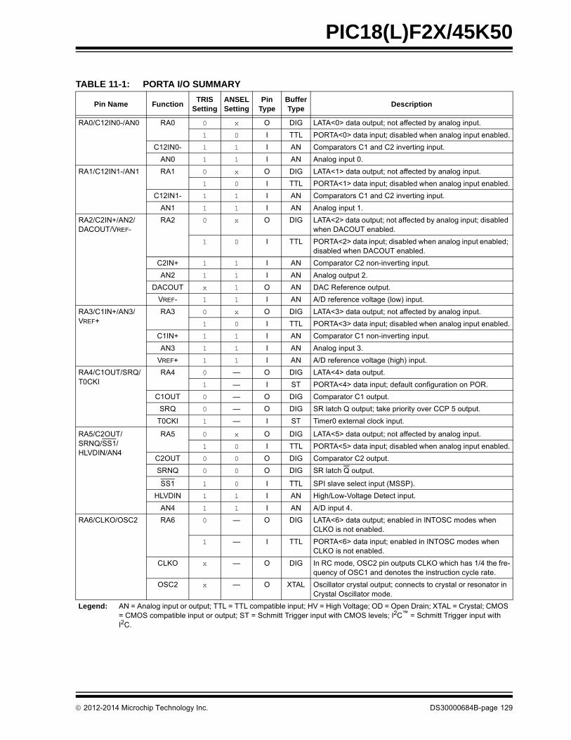
PIC18(L)F2X/45K50
TABLE 11-1: PORTA I/O SUMMARY
Pin Name FunctionTRIS
SettingANSELSetting
PinType
Buffer Type
Description
RA0/C12IN0-/AN0 RA0 0 x O DIG LATA<0> data output; not affected by analog input.
1 0 I TTL PORTA<0> data input; disabled when analog input enabled.
C12IN0- 1 1 I AN Comparators C1 and C2 inverting input.
AN0 1 1 I AN Analog input 0.
RA1/C12IN1-/AN1 RA1 0 x O DIG LATA<1> data output; not affected by analog input.
1 0 I TTL PORTA<1> data input; disabled when analog input enabled.
C12IN1- 1 1 I AN Comparators C1 and C2 inverting input.
AN1 1 1 I AN Analog input 1.
RA2/C2IN+/AN2/DACOUT/VREF-
RA2 0 x O DIG LATA<2> data output; not affected by analog input; disabled when DACOUT enabled.
1 0 I TTL PORTA<2> data input; disabled when analog input enabled; disabled when DACOUT enabled.
C2IN+ 1 1 I AN Comparator C2 non-inverting input.
AN2 1 1 I AN Analog output 2.
DACOUT x 1 O AN DAC Reference output.
VREF- 1 1 I AN A/D reference voltage (low) input.
RA3/C1IN+/AN3/VREF+
RA3 0 x O DIG LATA<3> data output; not affected by analog input.
1 0 I TTL PORTA<3> data input; disabled when analog input enabled.
C1IN+ 1 1 I AN Comparator C1 non-inverting input.
AN3 1 1 I AN Analog input 3.
VREF+ 1 1 I AN A/D reference voltage (high) input.
RA4/C1OUT/SRQ/T0CKI
RA4 0 — O DIG LATA<4> data output.
1 — I ST PORTA<4> data input; default configuration on POR.
C1OUT 0 — O DIG Comparator C1 output.
SRQ 0 — O DIG SR latch Q output; take priority over CCP 5 output.
T0CKI 1 — I ST Timer0 external clock input.
RA5/C2OUT/SRNQ/SS1/HLVDIN/AN4
RA5 0 x O DIG LATA<5> data output; not affected by analog input.
1 0 I TTL PORTA<5> data input; disabled when analog input enabled.
C2OUT 0 0 O DIG Comparator C2 output.
SRNQ 0 0 O DIG SR latch Q output.
SS1 1 0 I TTL SPI slave select input (MSSP).
HLVDIN 1 1 I AN High/Low-Voltage Detect input.
AN4 1 1 I AN A/D input 4.
RA6/CLKO/OSC2 RA6 0 — O DIG LATA<6> data output; enabled in INTOSC modes when CLKO is not enabled.
1 — I TTL PORTA<6> data input; enabled in INTOSC modes when CLKO is not enabled.
CLKO x — O DIG In RC mode, OSC2 pin outputs CLKO which has 1/4 the fre-quency of OSC1 and denotes the instruction cycle rate.
OSC2 x — O XTAL Oscillator crystal output; connects to crystal or resonator in Crystal Oscillator mode.
Legend: AN = Analog input or output; TTL = TTL compatible input; HV = High Voltage; OD = Open Drain; XTAL = Crystal; CMOS = CMOS compatible input or output; ST = Schmitt Trigger input with CMOS levels; I2C™ = Schmitt Trigger input with I2C.
2012-2014 Microchip Technology Inc. DS30000684B-page 129
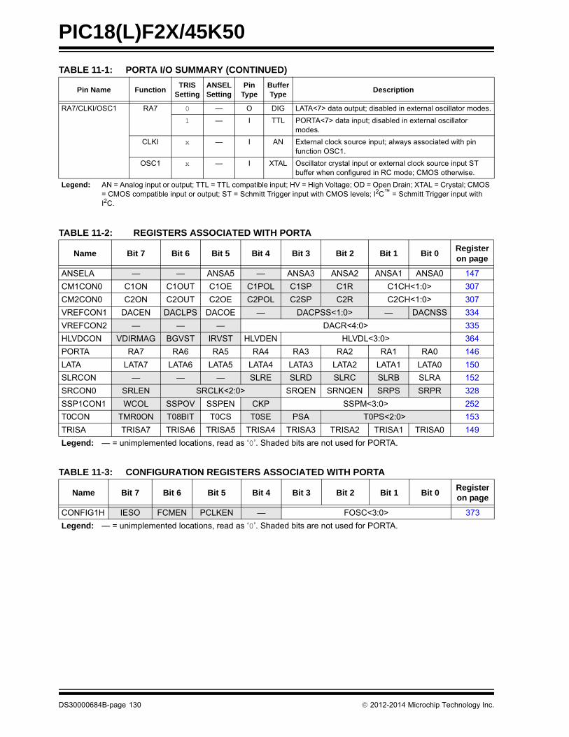
PIC18(L)F2X/45K50
RA7/CLKI/OSC1 RA7 0 — O DIG LATA<7> data output; disabled in external oscillator modes.
1 — I TTL PORTA<7> data input; disabled in external oscillator modes.
CLKI x — I AN External clock source input; always associated with pin function OSC1.
OSC1 x — I XTAL Oscillator crystal input or external clock source input ST buffer when configured in RC mode; CMOS otherwise.
TABLE 11-1: PORTA I/O SUMMARY (CONTINUED)
Pin Name FunctionTRIS
SettingANSELSetting
PinType
Buffer Type
Description
Legend: AN = Analog input or output; TTL = TTL compatible input; HV = High Voltage; OD = Open Drain; XTAL = Crystal; CMOS = CMOS compatible input or output; ST = Schmitt Trigger input with CMOS levels; I2C™ = Schmitt Trigger input with I2C.
TABLE 11-2: REGISTERS ASSOCIATED WITH PORTA
Name Bit 7 Bit 6 Bit 5 Bit 4 Bit 3 Bit 2 Bit 1 Bit 0Register on page
ANSELA — — ANSA5 — ANSA3 ANSA2 ANSA1 ANSA0 147
CM1CON0 C1ON C1OUT C1OE C1POL C1SP C1R C1CH<1:0> 307
CM2CON0 C2ON C2OUT C2OE C2POL C2SP C2R C2CH<1:0> 307
VREFCON1 DACEN DACLPS DACOE — DACPSS<1:0> — DACNSS 334
VREFCON2 — — — DACR<4:0> 335
HLVDCON VDIRMAG BGVST IRVST HLVDEN HLVDL<3:0> 364
PORTA RA7 RA6 RA5 RA4 RA3 RA2 RA1 RA0 146
LATA LATA7 LATA6 LATA5 LATA4 LATA3 LATA2 LATA1 LATA0 150
SLRCON — — — SLRE SLRD SLRC SLRB SLRA 152
SRCON0 SRLEN SRCLK<2:0> SRQEN SRNQEN SRPS SRPR 328
SSP1CON1 WCOL SSPOV SSPEN CKP SSPM<3:0> 252
T0CON TMR0ON T08BIT T0CS T0SE PSA T0PS<2:0> 153
TRISA TRISA7 TRISA6 TRISA5 TRISA4 TRISA3 TRISA2 TRISA1 TRISA0 149
Legend: — = unimplemented locations, read as ‘0’. Shaded bits are not used for PORTA.
TABLE 11-3: CONFIGURATION REGISTERS ASSOCIATED WITH PORTA
Name Bit 7 Bit 6 Bit 5 Bit 4 Bit 3 Bit 2 Bit 1 Bit 0Register on page
CONFIG1H IESO FCMEN PCLKEN — FOSC<3:0> 373
Legend: — = unimplemented locations, read as ‘0’. Shaded bits are not used for PORTA.
DS30000684B-page 130 2012-2014 Microchip Technology Inc.

PIC18(L)F2X/45K50
11.1.1 PORTA OUTPUT PRIORITY
Each PORTA pin is multiplexed with other functions.The pins, their combined functions and their outputpriorities are briefly described here. For additionalinformation, refer to the appropriate section in this datasheet.
When multiple outputs are enabled, the actual pincontrol goes to the peripheral with the higher priority.Table 11-4 lists the PORTA pin functions from thehighest to the lowest priority.
Analog input functions, such as ADC and comparator,are not shown in the priority lists.
These inputs are active when the I/O pin is set forAnalog mode using the ANSELx registers. Digitaloutput functions may control the pin when it is in Analogmode with the priority shown below.
2012-2014 Microchip Technology Inc. DS30000684B-page 131

PIC18(L)F2X/45K50
TABLE 11-4: PORT PIN FUNCTION PRIORITY
Port bitPort Function Priority by Port Pin
PORTA PORTB PORTC PORTD(2) PORTE(2)
0 RA0 SDA SOSCO
RB0
RC0 RD0 RE0
1 RA1 SCL SOSCI
SCK CCP2(3) RE1
P1C(1) RD1
RB1 RC1
2 DACOUT CCP1
RA2 P1B(1) P1A RD2 RE2
RB2 CTPLS
RC2
3 RA3 SDO(3) MCLR
CCP2(4) RD3 VPP
RE3
RB3
4 SRQ P1D(1) D-
C1OUT RB4
RD4
RA4
5 SRNQ D+ P1B
C2OUT RD5
RA5
RB5
6 OSC2 PGC TX/CK
CLKO ICDCK P1C
RA6 RB6 RD6
RC6
7 OSC1 PGD RX/DT
RA7 ICDDT P1D
RB7 RC7 RD7
Note 1: PIC18(L)F2XK50 devices.
2: PIC18(L)F45K50 devices.
3: Function default pin.
4: Function alternate pin.
DS30000684B-page 132 2012-2014 Microchip Technology Inc.

PIC18(L)F2X/45K50
11.2 PORTB Registers
PORTB is an 8-bit wide, bidirectional port. Thecorresponding data direction register is TRISB. Settinga TRISB bit (= 1) will make the corresponding PORTBpin an input (i.e., disable the output driver). Clearing aTRISB bit (= 0) will make the corresponding PORTBpin an output (i.e., enable the output driver and put thecontents of the output latch on the selected pin).
The Data Latch register (LATB) is also memorymapped. Read-modify-write operations on the LATBregister read and write the latched output value forPORTB.
EXAMPLE 11-2: INITIALIZING PORTB
11.2.1 PORTB OUTPUT PRIORITY
Each PORTB pin is multiplexed with other functions.The pins, their combined functions and their outputpriorities are briefly described here. For additionalinformation, refer to the appropriate section in this datasheet.
When multiple outputs are enabled, the actual pincontrol goes to the peripheral with the higher priority.Table 11-4 lists the PORTB pin functions from thehighest to the lowest priority.
Analog input functions, such as ADC, comparator andSR latch inputs, are not shown in the priority lists.
These inputs are active when the I/O pin is set forAnalog mode using the ANSELx registers. Digitaloutput functions may control the pin when it is in Analogmode with the priority shown below.
11.3 Additional PORTB Pin Functions
PORTB pins RB<7:4> have an interrupt-on-changeoption. All PORTB pins have a weak pull-up option.
11.3.1 WEAK PULL-UPS
Each of the PORTB pins has an individually controlledweak internal pull-up. When set, each bit of the WPUBregister enables the corresponding pin pull-up. Whencleared, the RBPU bit of the INTCON2 register enablespull-ups on all pins which also have their correspondingWPUB bit set. When set, the RBPU bit disables allweak pull-ups. The weak pull-up is automatically turnedoff when the port pin is configured as an output. Thepull-ups are disabled on a Power-on Reset.
11.3.2 INTERRUPT-ON-CHANGE
Four of the PORTB pins (RB<7:4>) are individuallyconfigurable as interrupt-on-change pins. Control bitsin the IOCB register enable (when set) or disable (whenclear) the interrupt function for each pin.
When set, the IOCIE bit of the INTCON registerenables interrupts on all pins which also have theircorresponding IOCB bit set. When clear, the IOCIE bitdisables all interrupt-on-changes.
Only pins configured as inputs can cause this interruptto occur (i.e., any RB<7:4> pin configured as an outputis excluded from the interrupt-on-change comparison).
For enabled interrupt-on-change pins, the values arecompared with the old value latched on the last read ofPORTB. The ‘mismatch’ outputs of the last read areOR’d together to set the interrupt-on-change Interruptflag bit (IOCIF) in the INTCON register.
This interrupt can wake the device from the Sleepmode, or any of the Idle modes. The user, in theInterrupt Service Routine, can clear the interrupt in thefollowing manner:
a) Any read or write of PORTB to clear the mis-match condition (except when PORTB is thesource or destination of a MOVFF instruction).
b) Execute at least one instruction after reading orwriting PORTB, then clear the flag bit, IOCIF.
MOVLB 0xF ; Set BSR for banked SFRsCLRF LATB ; Initialize PORTB by
; clearing output; data latches
MOVLW 0F0h ; Value for initMOVWF ANSELB ; Enable RB<3:0> for
; digital input pins; (not required if config bit; PBADEN is clear)
MOVLW 0CFh ; Value used to; initialize data ; direction
MOVWF TRISB ; Set RB<3:0> as inputs; RB<5:4> as outputs; RB<7:6> as inputs
Note: On a Power-on Reset, RB<5:0> areconfigured as analog inputs by default andread as ‘0’; RB<7:6> are configured asdigital inputs.
When the PBADEN Configuration bit isset to ‘0’, RB<5:0> will alternatively beconfigured as digital inputs on POR.
2012-2014 Microchip Technology Inc. DS30000684B-page 133
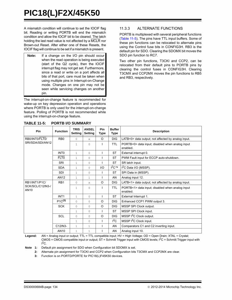
PIC18(L)F2X/45K50
A mismatch condition will continue to set the IOCIF flagbit. Reading or writing PORTB will end the mismatchcondition and allow the IOCIF bit to be cleared. The latchholding the last read value is not affected by a MCLR norBrown-out Reset. After either one of these Resets, theIOCIF flag will continue to be set if a mismatch is present.
The interrupt-on-change feature is recommended forwake-up on key depression operation and operationswhere PORTB is only used for the interrupt-on-changefeature. Polling of PORTB is not recommended whileusing the interrupt-on-change feature.
11.3.3 ALTERNATE FUNCTIONS
PORTB is multiplexed with several peripheral functions(Table 11-5). The pins have TTL input buffers. Some ofthese pin functions can be relocated to alternate pinsusing the Control fuse bits in CONFIG3H. RB3 is thedefault pin for SDO. Clearing the SDOMX bit moves theSDO pin function to RC7.
Two other pin functions, T3CKI and CCP2, can berelocated from their default pins to PORTB pins byclearing the control fuses in CONFIG3H. ClearingT3CMX and CCP2MX moves the pin functions to RB5and RB3, respectively.
Note: If a change on the I/O pin should occurwhen the read operation is being executed(start of the Q2 cycle), then the IOCIFinterrupt flag may not get set. Furthermore,since a read or write on a port affects allbits of that port, care must be taken whenusing multiple pins in Interrupt-on-Changemode. Changes on one pin may not beseen while servicing changes on anotherpin.
TABLE 11-5: PORTB I/O SUMMARY
Pin FunctionTRIS
SettingANSEL Setting
Pin Type
BufferType
Description
RB0/INT0/FLT0/SRI/SDA/SDI/AN12
RB0 0 x O DIG LATB<0> data output; not affected by analog input.
1 0 I TTL PORTB<0> data input; disabled when analog input enabled.
INT0 1 0 I ST External interrupt 0.
FLT0 1 0 I ST PWM Fault input for ECCP auto-shutdown.
SRI 1 0 I ST SR latch input.
SDA 1 0 I/O I2C™ I2C Data I/O (MSSP).
SDI 1 0 I ST SPI Data in (MSSP).
AN12 1 1 I AN Analog input 12.
RB1/INT1/P1C/SCK/SCL/C12IN3-/AN10
RB1 0 x O DIG LATB<1> data output; not affected by analog input.
1 0 I TTL PORTB<1> data input; disabled when analog input enabled.
INT1 1 0 I ST External Interrupt 1.
P1C(3) 0 0 O DIG Enhanced CCP1 PWM output 3.
SCK 0 0 O DIG MSSP SPI Clock output.
1 0 I ST MSSP SPI Clock input.
SCL 0 0 O DIG MSSP I2C Clock output.
1 0 I I2C MSSP I2C Clock input.
C12IN3- 1 1 I AN Comparators C1 and C2 inverting input.
AN10 1 1 I AN Analog input 10.
Legend: AN = Analog input or output; TTL = TTL compatible input; HV = High Voltage; OD = Open Drain; XTAL = Crystal; CMOS = CMOS compatible input or output; ST = Schmitt Trigger input with CMOS levels; I2C = Schmitt Trigger input with I2C.
Note 1: Default pin assignment for SDO when Configuration bit SDOMX is set.2: Alternate pin assignment for T3CKI and CCP2 when Configuration bits T3CMX and CCP2MX are clear.3: Function is on PORTD/PORTE for PIC18(L)F45K50 devices.
DS30000684B-page 134 2012-2014 Microchip Technology Inc.

PIC18(L)F2X/45K50
RB2/INT2/CTED1/P1B/AN8
RB2 0 x O DIG LATB<2> data output; not affected by analog input.
1 0 I TTL PORTB<2> data input; disabled when analog input enabled.
INT2 1 0 I ST External interrupt 2.
CTED1 1 0 I ST CTMU Edge 1 input.
P1B(3) 0 0 O DIG Enhanced CCP1 PWM output 2.
AN8 1 1 I AN Analog input 8.
RB3/CTED2/CCP2/SDO/C12IN2-/AN9
RB3 0 x O DIG LATB<3> data output; not affected by analog input.
1 0 I TTL PORTB<3> data input; disabled when analog input enabled.
CTED2 1 0 I ST CTMU Edge 2 input.
CCP2(2) 0 0 O DIG Compare 2 output/PWM 2 output.
1 0 I ST Capture 2 input.
SDO(1) 0 0 O DIG MSSP SPI data output.
C12IN2- 1 1 I AN Comparators C1 and C2 inverting input.
AN9 1 1 I AN Analog input 9.
RB4/IOCB4/P1D/AN11
RB4 0 x O DIG LATB<4> data output; not affected by analog input.
1 0 I TTL PORTB<4> data input; disabled when analog input enabled.
IOCB4 1 0 I TTL Interrupt-on-change pin.
P1D(3) 0 0 O DIG Enhanced CCP1 PWM output 4.
AN11 1 1 I AN Analog input 11.
RB5/IOCB5/T3CKI/T1G/AN13
RB5 0 x O DIG LATB<5> data output; not affected by analog input.
1 0 I TTL PORTB<5> data input; disabled when analog input enabled.
IOCB5 1 0 I TTL Interrupt-on-change pin 1.
T3CKI(2) 1 0 I ST Timer3 clock input.
T1G 1 0 I ST Timer1 external clock gate input.
AN13 1 1 I AN Analog input 13.
RB6/IOCB6/PGC RB6 0 — O DIG LATB<6> data output; not affected by analog input.
1 — I TTL PORTB<6> data input; disabled when analog input enabled.
IOCB6 1 — I TTL Interrupt-on-change pin.
PGC x — I ST In-Circuit Debugger and ICSPTM programming clock input.
RB7/IOCB7/PGD RB7 0 — O DIG LATB<7> data output; not affected by analog input.
1 — I TTL PORTB<7> data input; disabled when analog input enabled.
IOCB7 1 — I TTL Interrupt-on-change pin.
PGD x — O DIG In-Circuit Debugger and ICSPTM programming data output.
x — I ST In-Circuit Debugger and ICSPTM programming data input.
TABLE 11-5: PORTB I/O SUMMARY (CONTINUED)
Pin FunctionTRIS
SettingANSEL Setting
Pin Type
BufferType
Description
Legend: AN = Analog input or output; TTL = TTL compatible input; HV = High Voltage; OD = Open Drain; XTAL = Crystal; CMOS = CMOS compatible input or output; ST = Schmitt Trigger input with CMOS levels; I2C = Schmitt Trigger input with I2C.
Note 1: Default pin assignment for SDO when Configuration bit SDOMX is set.2: Alternate pin assignment for T3CKI and CCP2 when Configuration bits T3CMX and CCP2MX are clear.3: Function is on PORTD/PORTE for PIC18(L)F45K50 devices.
2012-2014 Microchip Technology Inc. DS30000684B-page 135
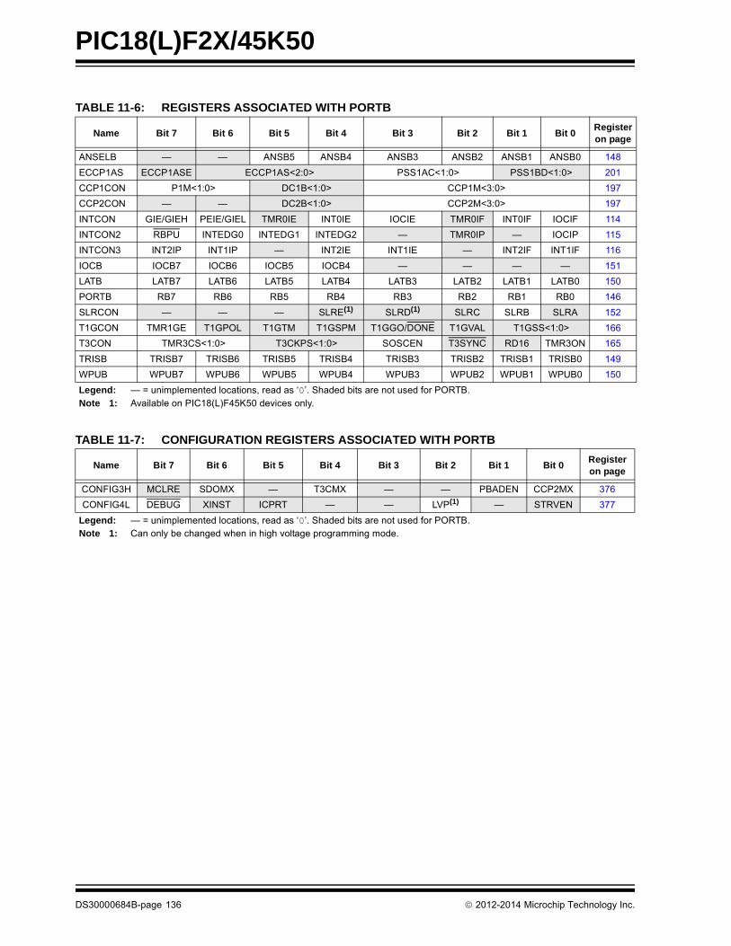
PIC18(L)F2X/45K50
TABLE 11-6: REGISTERS ASSOCIATED WITH PORTB
Name Bit 7 Bit 6 Bit 5 Bit 4 Bit 3 Bit 2 Bit 1 Bit 0Register on page
ANSELB — — ANSB5 ANSB4 ANSB3 ANSB2 ANSB1 ANSB0 148
ECCP1AS ECCP1ASE ECCP1AS<2:0> PSS1AC<1:0> PSS1BD<1:0> 201
CCP1CON P1M<1:0> DC1B<1:0> CCP1M<3:0> 197
CCP2CON — — DC2B<1:0> CCP2M<3:0> 197
INTCON GIE/GIEH PEIE/GIEL TMR0IE INT0IE IOCIE TMR0IF INT0IF IOCIF 114
INTCON2 RBPU INTEDG0 INTEDG1 INTEDG2 — TMR0IP — IOCIP 115
INTCON3 INT2IP INT1IP — INT2IE INT1IE — INT2IF INT1IF 116
IOCB IOCB7 IOCB6 IOCB5 IOCB4 — — — — 151
LATB LATB7 LATB6 LATB5 LATB4 LATB3 LATB2 LATB1 LATB0 150
PORTB RB7 RB6 RB5 RB4 RB3 RB2 RB1 RB0 146
SLRCON — — — SLRE(1) SLRD(1) SLRC SLRB SLRA 152
T1GCON TMR1GE T1GPOL T1GTM T1GSPM T1GGO/DONE T1GVAL T1GSS<1:0> 166
T3CON TMR3CS<1:0> T3CKPS<1:0> SOSCEN T3SYNC RD16 TMR3ON 165
TRISB TRISB7 TRISB6 TRISB5 TRISB4 TRISB3 TRISB2 TRISB1 TRISB0 149
WPUB WPUB7 WPUB6 WPUB5 WPUB4 WPUB3 WPUB2 WPUB1 WPUB0 150
Legend: — = unimplemented locations, read as ‘0’. Shaded bits are not used for PORTB.Note 1: Available on PIC18(L)F45K50 devices only.
TABLE 11-7: CONFIGURATION REGISTERS ASSOCIATED WITH PORTB
Name Bit 7 Bit 6 Bit 5 Bit 4 Bit 3 Bit 2 Bit 1 Bit 0Register on page
CONFIG3H MCLRE SDOMX — T3CMX — — PBADEN CCP2MX 376
CONFIG4L DEBUG XINST ICPRT — — LVP(1) — STRVEN 377
Legend: — = unimplemented locations, read as ‘0’. Shaded bits are not used for PORTB.Note 1: Can only be changed when in high voltage programming mode.
DS30000684B-page 136 2012-2014 Microchip Technology Inc.

PIC18(L)F2X/45K50
11.4 PORTC Registers
PORTC is an 8-bit wide, bidirectional port. Thecorresponding data direction register is TRISC. Settinga TRISC bit (= 1) will make the corresponding PORTCpin an input (i.e., disable the output driver). Clearing aTRISC bit (= 0) will make the corresponding PORTCpin an output (i.e., enable the output driver and put thecontents of the output latch on the selected pin).
The Data Latch register (LATC) is also memorymapped. Read-modify-write operations on the LATCregister read and write the latched output value forPORTC.
PORTC is multiplexed with several peripheral functions(Table 11-8). The pins have Schmitt Trigger input buf-fers.
Some of these pin functions can be relocated to alter-nate pins using the Control fuse bits in CONFIG3H.RC0 is the default pin for T3CKI. Clearing the T3CMXbit moves the pin function to RB5. RC1 is the default pinfor the CCP2 peripheral pin. Clearing the CCP2MX bitmoves the pin function to the RB3 pin.
When enabling peripheral functions, care should betaken in defining TRIS bits for each PORTC pin. TheEUSART and MSSP peripherals override the TRIS bitto make a pin an output or an input, depending on theperipheral configuration. Refer to the correspondingperipheral section for additional information.
The contents of the TRISC register are affected byperipheral overrides. Reading TRISC always returnsthe current contents, even though a peripheral devicemay be overriding one or more of the pins.
EXAMPLE 11-3: INITIALIZING PORTC
11.4.1 PORTC OUTPUT PRIORITY
Each PORTC pin is multiplexed with other functions.The pins, their combined functions and their outputpriorities are briefly described here. For additionalinformation, refer to the appropriate section in this datasheet.
When multiple outputs are enabled, the actual pincontrol goes to the peripheral with the higher priority.Table 11-4 lists the PORTC pin functions from thehighest to the lowest priority.
Analog input functions, such as ADC, comparator andSR latch inputs, are not shown in the priority lists.
These inputs are active when the I/O pin is set forAnalog mode using the ANSELx registers. Digitaloutput functions may control the pin when it is in Analogmode with the priority shown below.
11.4.2 INTERRUPT-ON-CHANGE
All of the PORTC pins (RC<7:4> and RC<2:0>) areindividually configurable as interrupt-on-change pins.Control bits in the IOCC register enable (when set) ordisable (when clear) the interrupt function for each pin.See Section 11.3.2 “Interrupt-on-Change” fordetails on operation of interrupt-on-change.
Note: On a Power-on Reset, these pins areconfigured as analog inputs.
MOVLB 0xF ; Set BSR for banked SFRsCLRF LATC ; Initialize PORTC by
; clearing output; data latches
MOVLW 0CFh ; Value used to ; initialize data ; direction
MOVWF TRISC ; Set RC<3:0> as inputs; RC<5:4> as outputs; RC<7:6> as inputs
MOVLW 30h ; Value used to; enable digital inputs
MOVWF ANSELC ; RC<3:2> dig input enable; No ANSEL bits for RC<1:0>; RC<7:6> dig input enable
2012-2014 Microchip Technology Inc. DS30000684B-page 137

PIC18(L)F2X/45K50
TABLE 11-8: PORTC I/O SUMMARY
Pin Name FunctionTRIS
SettingANSEL setting
Pin Type
Buffer Type
Description
RC0/IOCC0/T3CKI/T3G/T1CKI/SOSCO
RC0 0 — O DIG LATC<0> data output; not affected by analog input.
1 — I ST PORTC<0> data input; disabled when analog input enabled.
IOCC0 1 — I TTL Interrupt-on-change pin.
T3CKI(1) 1 — I ST Timer3 clock input.
T3G 1 — I ST Timer3 external clock gate input.
T1CKI 1 — I ST Timer1 clock input.
SOSCO x — O XTAL Secondary oscillator output.
RC1/IOCC1/CCP2/SOSCI
RC1 0 — O DIG LATC<1> data output; not affected by analog input.
1 — I ST PORTC<1> data input; disabled when analog input enabled.
IOCC1 1 — I TTL Interrupt-on-change pin.
CCP2(1) 0 — O DIG Compare 2 output/PWM 2 output.
1 — I ST Capture 2 input.
SOSCI x — I XTAL Secondary oscillator input.
RC2/CTPLS/P1A/CCP1/IOCC2/AN14
RC2 0 0 O DIG LATC<2> data output; not affected by analog input.
1 0 I ST PORTC<2> data input; disabled when analog input enabled.
CTPLS 0 0 O DIG CTMU pulse generator output.
P1A 0 0 O DIG Enhanced CCP1 PWM output 1.
CCP1 0 0 O DIG Compare 1 output/PWM 1 output.
1 0 I ST Capture 1 input.
IOCC2 1 — I TTL Interrupt-on-change pin.
AN14 1 1 I AN Analog input 14.
D-/IOCC4 D- — — I XCVR USB bus differential minus line input.
— — O XCVR USB bus differential minus line output.
IOCC4 — — I ST Interrupt-on-change pin.
D+/IOCC5 D+ — — I XCVR USB bus differential minus line input.
— — O XCVR USB bus differential minus line output.
IOCC5 — — I ST Interrupt-on-change pin.
Legend: AN = Analog input or output; TTL = TTL compatible input; HV = High Voltage; OD = Open Drain; XTAL = Crystal; CMOS = CMOS compatible input or output; ST = Schmitt Trigger input with CMOS levels; I2C™ = Schmitt Trigger input with I2C.
Note 1: Default pin assignment for T3CKI and CCP2 when Configuration bits T3CMX and CCP2MX are set.2: Alternate pin assignment for SDO when Configuration bit SDOMX is clear.3: Function is on PORTD/PORTE for PIC18(L)F45K50 devices.
DS30000684B-page 138 2012-2014 Microchip Technology Inc.
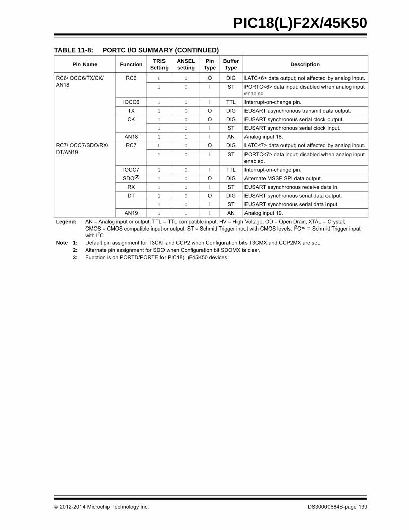
PIC18(L)F2X/45K50
Pin Name FunctionTRIS
SettingANSEL setting
Pin Type
Buffer Type
Description
RC6/IOCC6/TX/CK/AN18
RC6 0 0 O DIG LATC<6> data output; not affected by analog input.
1 0 I ST PORTC<6> data input; disabled when analog input enabled.
IOCC6 1 0 I TTL Interrupt-on-change pin.
TX 1 0 O DIG EUSART asynchronous transmit data output.
CK 1 0 O DIG EUSART synchronous serial clock output.
1 0 I ST EUSART synchronous serial clock input.
AN18 1 1 I AN Analog input 18.
RC7/IOCC7/SDO/RX/DT/AN19
RC7 0 0 O DIG LATC<7> data output; not affected by analog input.
1 0 I ST PORTC<7> data input; disabled when analog input enabled.
IOCC7 1 0 I TTL Interrupt-on-change pin.
SDO(2) 1 0 O DIG Alternate MSSP SPI data output.
RX 1 0 I ST EUSART asynchronous receive data in.
DT 1 0 O DIG EUSART synchronous serial data output.
1 0 I ST EUSART synchronous serial data input.
AN19 1 1 I AN Analog input 19.
Legend: AN = Analog input or output; TTL = TTL compatible input; HV = High Voltage; OD = Open Drain; XTAL = Crystal; CMOS = CMOS compatible input or output; ST = Schmitt Trigger input with CMOS levels; I2C™ = Schmitt Trigger input with I2C.
Note 1: Default pin assignment for T3CKI and CCP2 when Configuration bits T3CMX and CCP2MX are set.2: Alternate pin assignment for SDO when Configuration bit SDOMX is clear.3: Function is on PORTD/PORTE for PIC18(L)F45K50 devices.
TABLE 11-8: PORTC I/O SUMMARY (CONTINUED)
2012-2014 Microchip Technology Inc. DS30000684B-page 139
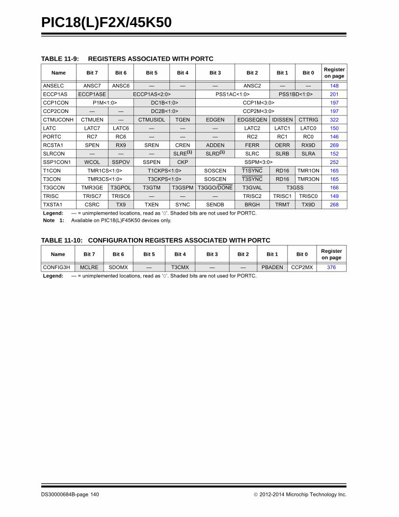
PIC18(L)F2X/45K50
TABLE 11-9: REGISTERS ASSOCIATED WITH PORTC
Name Bit 7 Bit 6 Bit 5 Bit 4 Bit 3 Bit 2 Bit 1 Bit 0Register on page
ANSELC ANSC7 ANSC6 — — — ANSC2 — — 148
ECCP1AS ECCP1ASE ECCP1AS<2:0> PSS1AC<1:0> PSS1BD<1:0> 201
CCP1CON P1M<1:0> DC1B<1:0> CCP1M<3:0> 197
CCP2CON — — DC2B<1:0> CCP2M<3:0> 197
CTMUCONH CTMUEN — CTMUSIDL TGEN EDGEN EDGSEQEN IDISSEN CTTRIG 322
LATC LATC7 LATC6 — — — LATC2 LATC1 LATC0 150
PORTC RC7 RC6 — — — RC2 RC1 RC0 146
RCSTA1 SPEN RX9 SREN CREN ADDEN FERR OERR RX9D 269
SLRCON — — — SLRE(1) SLRD(1) SLRC SLRB SLRA 152
SSP1CON1 WCOL SSPOV SSPEN CKP SSPM<3:0> 252
T1CON TMR1CS<1:0> T1CKPS<1:0> SOSCEN T1SYNC RD16 TMR1ON 165
T3CON TMR3CS<1:0> T3CKPS<1:0> SOSCEN T3SYNC RD16 TMR3ON 165
T3GCON TMR3GE T3GPOL T3GTM T3GSPM T3GGO/DONE T3GVAL T3GSS 166
TRISC TRISC7 TRISC6 — — — TRISC2 TRISC1 TRISC0 149
TXSTA1 CSRC TX9 TXEN SYNC SENDB BRGH TRMT TX9D 268
Legend: — = unimplemented locations, read as ‘0’. Shaded bits are not used for PORTC.Note 1: Available on PIC18(L)F45K50 devices only.
TABLE 11-10: CONFIGURATION REGISTERS ASSOCIATED WITH PORTC
Name Bit 7 Bit 6 Bit 5 Bit 4 Bit 3 Bit 2 Bit 1 Bit 0Register on page
CONFIG3H MCLRE SDOMX — T3CMX — — PBADEN CCP2MX 376
Legend: — = unimplemented locations, read as ‘0’. Shaded bits are not used for PORTC.
DS30000684B-page 140 2012-2014 Microchip Technology Inc.

PIC18(L)F2X/45K50
11.5 PORTD Registers
PORTD is an 8-bit wide, bidirectional port. Thecorresponding data direction register is TRISD. Settinga TRISD bit (= 1) will make the corresponding PORTDpin an input (i.e., disable the output driver). Clearing aTRISD bit (= 0) will make the corresponding PORTDpin an output (i.e., enable the output driver and put thecontents of the output latch on the selected pin).
The Data Latch register (LATD) is also memorymapped. Read-modify-write operations on the LATDregister read and write the latched output value forPORTD.
All pins on PORTD are implemented with SchmittTrigger input buffers. Each pin is individuallyconfigurable as an input or output.
All of the PORTD pins are multiplexed with analog anddigital peripheral modules. See Table 11-11.
EXAMPLE 11-4: INITIALIZING PORTD
11.5.1 PORTD OUTPUT PRIORITY
Each PORTD pin is multiplexed with other functions.The pins, their combined functions and their outputpriorities are briefly described here. For additionalinformation, refer to the appropriate section in this datasheet.
When multiple outputs are enabled, the actual pincontrol goes to the peripheral with the higher priority.Table 11-4 lists the PORTD pin functions from thehighest to the lowest priority.
Analog input functions, such as ADC, comparator andSR latch inputs, are not shown in the priority lists.
These inputs are active when the I/O pin is set forAnalog mode using the ANSELx registers. Digitaloutput functions may control the pin when it is in Analogmode with the priority shown below.
Note: PORTD is only available on 40-pin and44-pin devices.
Note: On a Power-on Reset, these pins areconfigured as analog inputs.
MOVLB 0xF ; Set BSR for banked SFRsCLRF LATD ; Initialize PORTD by ; clearing output ; data latchesMOVLW 0CFh ; Value used to
; initialize data ; direction
MOVWF TRISD ; Set RD<3:0> as inputs; RD<5:4> as outputs; RD<7:6> as inputs
MOVLW 30h ; Value used to; enable digital inputs
MOVWF ANSELD ; RD<3:0> dig input enable; RC<7:6> dig input enable
2012-2014 Microchip Technology Inc. DS30000684B-page 141
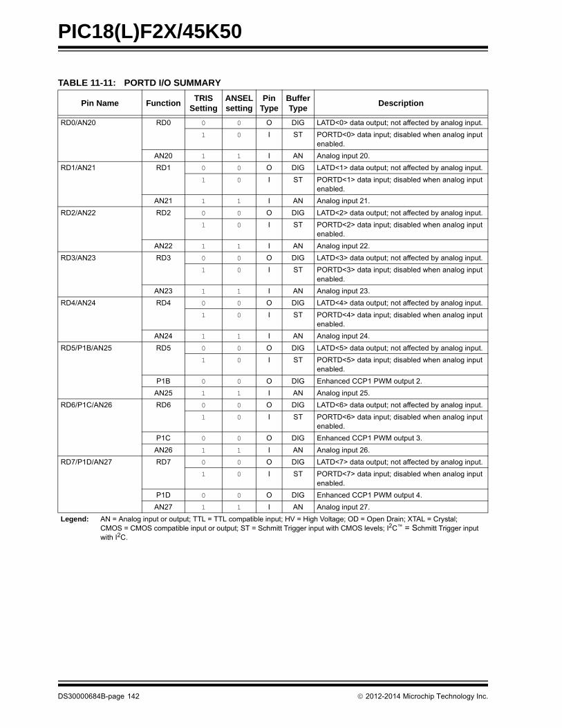
PIC18(L)F2X/45K50
TABLE 11-11: PORTD I/O SUMMARY
Pin Name FunctionTRIS
SettingANSEL setting
Pin Type
Buffer Type
Description
RD0/AN20 RD0 0 0 O DIG LATD<0> data output; not affected by analog input.
1 0 I ST PORTD<0> data input; disabled when analog input enabled.
AN20 1 1 I AN Analog input 20.
RD1/AN21 RD1 0 0 O DIG LATD<1> data output; not affected by analog input.
1 0 I ST PORTD<1> data input; disabled when analog input enabled.
AN21 1 1 I AN Analog input 21.
RD2/AN22 RD2 0 0 O DIG LATD<2> data output; not affected by analog input.
1 0 I ST PORTD<2> data input; disabled when analog input enabled.
AN22 1 1 I AN Analog input 22.
RD3/AN23 RD3 0 0 O DIG LATD<3> data output; not affected by analog input.
1 0 I ST PORTD<3> data input; disabled when analog input enabled.
AN23 1 1 I AN Analog input 23.
RD4/AN24 RD4 0 0 O DIG LATD<4> data output; not affected by analog input.
1 0 I ST PORTD<4> data input; disabled when analog input enabled.
AN24 1 1 I AN Analog input 24.
RD5/P1B/AN25 RD5 0 0 O DIG LATD<5> data output; not affected by analog input.
1 0 I ST PORTD<5> data input; disabled when analog input enabled.
P1B 0 0 O DIG Enhanced CCP1 PWM output 2.
AN25 1 1 I AN Analog input 25.
RD6/P1C/AN26 RD6 0 0 O DIG LATD<6> data output; not affected by analog input.
1 0 I ST PORTD<6> data input; disabled when analog input enabled.
P1C 0 0 O DIG Enhanced CCP1 PWM output 3.
AN26 1 1 I AN Analog input 26.
RD7/P1D/AN27 RD7 0 0 O DIG LATD<7> data output; not affected by analog input.
1 0 I ST PORTD<7> data input; disabled when analog input enabled.
P1D 0 0 O DIG Enhanced CCP1 PWM output 4.
AN27 1 1 I AN Analog input 27.
Legend: AN = Analog input or output; TTL = TTL compatible input; HV = High Voltage; OD = Open Drain; XTAL = Crystal; CMOS = CMOS compatible input or output; ST = Schmitt Trigger input with CMOS levels; I2C™ = Schmitt Trigger input with I2C.
DS30000684B-page 142 2012-2014 Microchip Technology Inc.

PIC18(L)F2X/45K50
TABLE 11-12: REGISTERS ASSOCIATED WITH PORTD
Name Bit 7 Bit 6 Bit 5 Bit 4 Bit 3 Bit 2 Bit 1 Bit 0Register on
page
ANSELD(1) ANSD7 ANSD6 ANSD5 ANSD4 ANSD3 ANSD2 ANSD1 ANSD0 148
CCP1CON P1M<1:0> DC1B<1:0> CCP1M<3:0> 197
LATD(1) LATD7 LATD6 LATD5 LATD4 LATD3 LATD2 LATD1 LATD0 150
PORTD(1) RD7 RD6 RD5 RD4 RD3 RD2 RD1 RD0 146
SLRCON(1) — — — SLRE SLRD SLRC SLRB SLRA 152
SSP1CON1 WCOL SSPOV SSPEN CKP SSPM<3:0> 252
TRISD(1) TRISD7 TRISD6 TRISD5 TRISD4 TRISD3 TRISD2 TRISD1 TRISD0 149
Legend: — = unimplemented locations, read as ‘0’. Shaded bits are not used for PORTD.
Note 1: Available on PIC18(L)F45K50 devices only.
2012-2014 Microchip Technology Inc. DS30000684B-page 143

PIC18(L)F2X/45K50
11.6 PORTE Registers
Depending on the particular PIC18(L)F2X/45K50device selected, PORTE is implemented in twodifferent ways.
11.6.1 PORTE ON 40/44-PIN DEVICES
For PIC18(L)F2X/45K50 devices, PORTE is a 4-bitwide port. Three pins (RE0/AN5, RE1/AN6 and RE2/AN7) are individually configurable as inputs or outputs.These pins have Schmitt Trigger input buffers. Whenselected as an analog input, these pins will read as ‘0’s.
The corresponding data direction register is TRISE.Setting a TRISE bit (= 1) will make the correspondingPORTE pin an input (i.e., disable the output driver).Clearing a TRISE bit (= 0) will make the correspondingPORTE pin an output (i.e., enable the output driver andput the contents of the output latch on the selected pin).
TRISE controls the direction of the REx pins, evenwhen they are being used as analog inputs. The usermust make sure to keep the pins configured as inputswhen using them as analog inputs.
The Data Latch register (LATE) is also memorymapped. Read-modify-write operations on the LATEregister read and write the latched output value forPORTE.
The fourth pin of PORTE (MCLR/VPP/RE3) is an input-only pin. Its operation is controlled by the MCLREConfiguration bit. When selected as a port pin(MCLRE = 0), it functions as a digital input-only pin; assuch, it does not have TRIS or LAT bits associated with itsoperation. Otherwise, it functions as the device’s MasterClear input. In either configuration, RE3 also functions asthe programming voltage input during programming.
EXAMPLE 11-5: INITIALIZING PORTE
11.6.2 PORTE ON 28-PIN DEVICES
For PIC18(L)F2XK50 devices, PORTE is only availablewhen Master Clear functionality is disabled(MCLR = 0). In these cases, PORTE is a single bit,input-only port comprised of RE3 only. The pin oper-ates as previously described.
11.6.3 RE3 WEAK PULL-UP
The port RE3 pin has an individually controlled weakinternal pull-up. When set, the WPUE3 (TRISE<7>) bitenables the RE3 pin pull-up. The RBPU bit of the INT-CON2 register controls pull-ups on both PORTB andPORTE. When RBPU = 0, the weak pull-ups becomeactive on all pins which have the WPUE3 or WPUBxbits set. When set, the RBPU bit disables all weak pull-ups. The pull-ups are disabled on a Power-on Reset.When the RE3 port pin is configured as MCLR, (CON-FIG3H<7>, MCLRE = 1 and CONFIG4L<2>, LVP = 0),or configured for Low-Voltage Programming, (MCLRE= x and LVP = 1), the pull-up is always enabled and theWPUE3 bit has no effect.
11.6.4 PORTE OUTPUT PRIORITY
Each PORTE pin is multiplexed with other functions.The pins, their combined functions and their outputpriorities are briefly described here. For additionalinformation, refer to the appropriate section in this datasheet.
When multiple outputs are enabled, the actual pincontrol goes to the peripheral with the higher priority.Table 11-4 lists the PORTE pin functions from thehighest to the lowest priority.
Analog input functions, such as ADC, comparator andSR latch inputs, are not shown in the priority lists.
These inputs are active when the I/O pin is set forAnalog mode using the ANSELx registers. Digitaloutput functions may control the pin when it is in Analogmode with the priority shown below.
Note: On a Power-on Reset, RE<2:0> areconfigured as analog inputs.
Note: On a Power-on Reset, RE3 is enabled asa digital input-only if Master Clearfunctionality is disabled.
CLRF LATE ; Initialize PORTE by; clearing output; data latches
CLRF ANSELE ; Configure analog pins ; for digital only
MOVLW 05h ; Value used to ; initialize data ; direction
MOVWF TRISE ; Set RE<0> as input; RE<1> as output; RE<2> as input
DS30000684B-page 144 2012-2014 Microchip Technology Inc.

PIC18(L)F2X/45K50
TABLE 11-13: PORTE I/O SUMMARY
Pin FunctionTRIS
SettingANSEL Setting
Pin Type
BufferType
Description
RE0/AN5 RE0 0 0 O DIG LATE<0> data output; not affected by analog input.
1 0 I ST PORTE<0> data input; disabled when analog input enabled.
AN5 1 1 I AN Analog input 5.
RE1/AN6 RE1 0 0 O DIG LATE<1> data output; not affected by analog input.
1 0 I ST PORTE<1> data input; disabled when analog input enabled.
AN6 1 1 I AN Analog input 6.
RE2/AN7 RE2 0 0 O DIG LATE<2> data output; not affected by analog input.
1 0 I ST PORTE<2> data input; disabled when analog input enabled.
AN7 1 1 I AN Analog input 7.
RE3/VPP/MCLR RE3 — — I ST PORTE<3> data input; enabled when Configuration bit MCLRE = 0.
VPP — — P AN Programming voltage input; always available
MCLR — — I ST Active-low Master Clear (device Reset) input; enabled when configuration bit MCLRE = 1.
Legend: AN = Analog input or output; TTL = TTL compatible input; HV = High Voltage; OD = Open Drain; XTAL = Crystal; CMOS = CMOS compatible input or output; ST = Schmitt Trigger input with CMOS levels; I2C™ = Schmitt Trigger input with I2C.
TABLE 11-14: REGISTERS ASSOCIATED WITH PORTE
Name Bit 7 Bit 6 Bit 5 Bit 4 Bit 3 Bit 2 Bit 1 Bit 0Register on page
ANSELE(1) — — — — — ANSE2 ANSE1 ANSE0 149
INTCON2 RBPU INTEDG0 INTEDG1 INTEDG2 — TMR0IP — IOCIP 115
LATE(1) — — — — — LATE2 LATE1 LATE0 150
PORTE — — — — RE3 RE2(1) RE1(1) RE0(1) 147
SLRCON — — — SLRE(1) SLRD(1) SLRC SLRB SLRA 152
TRISE WPUE3 — — — — TRISE2(1) TRISE1(1) TRISE0(1) 149
Legend: — = unimplemented locations, read as ‘0’. Shaded bits are not used for PORTE.
Note 1: Available on PIC18(L)F45K50 devices only.
TABLE 11-15: CONFIGURATION REGISTERS ASSOCIATED WITH PORTE
Name Bit 7 Bit 6 Bit 5 Bit 4 Bit 3 Bit 2 Bit 1 Bit 0Registeron page
CONFIG3H MCLRE SDOMX — T3CMX — — PBADEN CCP2MX 376
CONFIG4L DEBUG XINST — — — LVP(1) — STRVEN 377
Legend: — = unimplemented locations, read as ‘0’. Shaded bits are not used for interrupts.
Note 1: Can only be changed when in high-voltage programming mode.
2012-2014 Microchip Technology Inc. DS30000684B-page 145

PIC18(L)F2X/45K50
11.7 Port Analog Control
Most port pins are multiplexed with analog functionssuch as the Analog-to-Digital Converter andcomparators. When these I/O pins are to be used asanalog inputs it is necessary to disable the digital inputbuffer to avoid excessive current caused by improperbiasing of the digital input. Individual control of thedigital input buffers on pins which share analogfunctions is provided by the ANSELA, ANSELB,ANSELC, ANSELD and ANSELE registers. Setting anANSx bit high will disable the associated digital inputbuffer and cause all reads of that pin to return ‘0’ whileallowing analog functions of that pin to operatecorrectly.
The state of the ANSx bits has no affect on digitaloutput functions. A pin with the associated TRISx bitclear and ANSx bit set will still operate as a digitaloutput but the input mode will be analog. This cancause unexpected behavior when performing read-modify-write operations on the affected port.
All ANSEL register bits default to ‘1’ upon POR andBOR, disabling digital inputs for their associated portpins. All TRIS register bits default to ‘1’ upon POR orBOR, disabling digital outputs for their associated portpins. As a result, all port pins that have an ANSELregister will default to analog inputs upon POR or BOR.
11.8 Port Slew Rate Control
The output slew rate of each port is programmable toselect either the standard transition rate or a reducedtransition rate of approximately 0.1 times the standardto minimize EMI. The reduced transition time is thedefault slew rate for all ports.
11.9 Register Definitions – Port Control
REGISTER 11-1: PORTx(1): PORTx REGISTER
R/W-u/x R/W-u/x R/W-u/x R/W-u/x R/W-u/x R/W-u/x R/W-u/x R/W-u/x
Rx7 Rx6 Rx5 Rx4 Rx3 Rx2 Rx1 Rx0
bit 7 bit 0
Legend:
R = Readable bit W = Writable bit U = Unimplemented bit, read as ‘0’
‘1’ = Bit is set ‘0’ = Bit is cleared x = Bit is unknown
-n/n = Value at POR and BOR/Value at all other Resets
bit 7-0 Rx<7:0>: PORTx I/O bit values(2)
Note 1: Register Description for PORTA, PORTB, PORTC and PORTD.
2: Writes to PORTx are written to corresponding LATx register. Reads from PORTx register is return of I/O pin values.
DS30000684B-page 146 2012-2014 Microchip Technology Inc.

PIC18(L)F2X/45K50
REGISTER 11-2: PORTE: PORTE REGISTER
U-0 U-0 U-0 U-0 R/W-u/x R/W-u/x R/W-u/x R/W-u/x
— — — — RE3(1) RE2(2), (3) RE1(2), (3) RE0(2), (3)
bit 7 bit 0
Legend:
R = Readable bit W = Writable bit U = Unimplemented bit, read as ‘0’
‘1’ = Bit is set ‘0’ = Bit is cleared x = Bit is unknown
-n/n = Value at POR and BOR/Value at all other Resets
bit 7-4 Unimplemented: Read as ‘0’
bit 3 RE3: PORTE Input bit value(1)
bit 2-0 RE<2:0>: PORTE I/O bit values(2), (3)
Note 1: Port is available as input-only when MCLRE = 0.
2: Writes to PORTx are written to corresponding LATx register. Reads from PORTx register is return of I/O pin values.
3: Available on PIC18(L)F45K50 devices.
REGISTER 11-3: ANSELA – PORTA ANALOG SELECT REGISTER
U-0 U-0 R/W-1 U-0 R/W-1 R/W-1 R/W-1 R/W-1
— — ANSA5 — ANSA3 ANSA2 ANSA1 ANSA0
bit 7 bit 0
Legend:
R = Readable bit W = Writable bit U = Unimplemented bit, read as ‘0’
-n = Value at POR ‘1’ = Bit is set ‘0’ = Bit is cleared x = Bit is unknown
bit 7-6 Unimplemented: Read as ‘0’
bit 5 ANSA5: RA5 Analog Select bit
1 = Digital input buffer disabled0 = Digital input buffer enabled
bit 4 Unimplemented: Read as ‘0’
bit 3-0 ANSA<3:0>: RA<3:0> Analog Select bit
1 = Digital input buffer disabled0 = Digital input buffer enabled
2012-2014 Microchip Technology Inc. DS30000684B-page 147

PIC18(L)F2X/45K50
REGISTER 11-4: ANSELB – PORTB ANALOG SELECT REGISTER
U-0 U-0 R/W-1 R/W-1 R/W-1 R/W-1 R/W-1 R/W-1
— — ANSB5 ANSB4 ANSB3 ANSB2 ANSB1 ANSB0
bit 7 bit 0
Legend:
R = Readable bit W = Writable bit U = Unimplemented bit, read as ‘0’
-n = Value at POR ‘1’ = Bit is set ‘0’ = Bit is cleared x = Bit is unknown
bit 7-6 Unimplemented: Read as ‘0’
bit 5-0 ANSB<5:0>: RB<5:0> Analog Select bit
1 = Digital input buffer disabled0 = Digital input buffer enabled
REGISTER 11-5: ANSELC – PORTC ANALOG SELECT REGISTER
R/W-1 R/W-1 U-0 U-0 U-0 R/W-1 U-0 U-0
ANSC7 ANSC6 — — — ANSC2 — —
bit 7 bit 0
Legend:
R = Readable bit W = Writable bit U = Unimplemented bit, read as ‘0’
-n = Value at POR ‘1’ = Bit is set ‘0’ = Bit is cleared x = Bit is unknown
bit 7-6 ANSC<7:6>: RC<7:6> Analog Select bit
1 = Digital input buffer disabled0 = Digital input buffer enabled
bit 5-3 Unimplemented: Read as ‘0’
bit 2 ANSC<2>: RC<2> Analog Select bit
1 = Digital input buffer disabled0 = Digital input buffer enabled
bit 1-0 Unimplemented: Read as ‘0’
REGISTER 11-6: ANSELD – PORTD ANALOG SELECT REGISTER
R/W-1 R/W-1 R/W-1 R/W-1 R/W-1 R/W-1 R/W-1 R/W-1
ANSD7 ANSD6 ANSD5 ANSD4 ANSD3 ANSD2 ANSD1 ANSD0
bit 7 bit 0
Legend:
R = Readable bit W = Writable bit U = Unimplemented bit, read as ‘0’
-n = Value at POR ‘1’ = Bit is set ‘0’ = Bit is cleared x = Bit is unknown
bit 7-0 ANSD<7:0>: RD<7:0> Analog Select bit
1 = Digital input buffer disabled0 = Digital input buffer enabled
DS30000684B-page 148 2012-2014 Microchip Technology Inc.

PIC18(L)F2X/45K50
REGISTER 11-7: ANSELE – PORTE ANALOG SELECT REGISTER
U-0 U-0 U-0 U-0 U-0 R/W-1 R/W-1 R/W-1
— — — — — ANSE2(1) ANSE1(1) ANSE0(1)
bit 7 bit 0
Legend:
R = Readable bit W = Writable bit U = Unimplemented bit, read as ‘0’
-n = Value at POR ‘1’ = Bit is set ‘0’ = Bit is cleared x = Bit is unknown
bit 7-3 Unimplemented: Read as ‘0’
bit 2-0 ANSE<2:0>: RE<2:0> Analog Select bit(1)
1 = Digital input buffer disabled0 = Digital input buffer enabled
Note 1: Available on PIC18(L)F45K50 devices only.
REGISTER 11-8: TRISx: PORTx TRI-STATE REGISTER(1)
R/W-1 R/W-1 R/W-1 R/W-1 R/W-1 R/W-1 R/W-1 R/W-1
TRISx7 TRISx6 TRISx5 TRISx4 TRISx3 TRISx2 TRISx1 TRISx0
bit 7 bit 0
Legend:
R = Readable bit W = Writable bit U = Unimplemented bit, read as ‘0’
-n = Value at POR ‘1’ = Bit is set ‘0’ = Bit is cleared x = Bit is unknown
bit 7-0 TRISx<7:0>: PORTx Tri-State Control bit
1 = PORTx pin configured as an input (tri-stated)0 = PORTx pin configured as an output
Note 1: Register description for TRISA, TRISB, TRISC and TRISD.
REGISTER 11-9: TRISE: PORTE TRI-STATE REGISTER
R/W-1 U-0 U-0 U-0 U-0 R/W-1 R/W-1 R/W-1
WPUE3 — — — — TRISE2(1) TRISE1(1) TRISE0(1)
bit 7 bit 0
Legend:
R = Readable bit W = Writable bit U = Unimplemented bit, read as ‘0’
-n = Value at POR ‘1’ = Bit is set ‘0’ = Bit is cleared x = Bit is unknown
bit 7 WPUE3: Weak Pull-up Register bits
1 = Pull-up enabled on PORT pin0 = Pull-up disabled on PORT pin
bit 6-3 Unimplemented: Read as ‘0’
bit 2-0 TRISE<2:0>: PORTE Tri-State Control bit(1)
1 = PORTE pin configured as an input (tri-stated)0 = PORTE pin configured as an output
Note 1: Available on PIC18(L)F45K50 devices only.
2012-2014 Microchip Technology Inc. DS30000684B-page 149

PIC18(L)F2X/45K50
REGISTER 11-10: LATx: PORTx OUTPUT LATCH REGISTER(1)
R/W-x/u R/W-x/u R/W-x/u R/W-x/u R/W-x/u R/W-x/u R/W-x/u R/W-x/u
LATx7 LATx6 LATx5 LATx4 LATx3 LATx2 LATx1 LATx0
bit 7 bit 0
Legend:
R = Readable bit W = Writable bit U = Unimplemented bit, read as ‘0’
-n = Value at POR ‘1’ = Bit is set ‘0’ = Bit is cleared x = Bit is unknown
bit 7-0 LATx<7:0>: PORTx Output Latch bit value(2)
Note 1: Register Description for LATA, LATB, LATC and LATD.
2: Writes to PORTA are written to corresponding LATA register. Reads from PORTA register is return of I/O pin values.
REGISTER 11-11: LATE: PORTE OUTPUT LATCH REGISTER(1)
U-0 U-0 U-0 U-0 U-0 R/W-x/u R/W-x/u R/W-x/u
— — — — — LATE2 LATE1 LATE0
bit 7 bit 0
Legend:
R = Readable bit W = Writable bit U = Unimplemented bit, read as ‘0’
-n = Value at POR ‘1’ = Bit is set ‘0’ = Bit is cleared x = Bit is unknown
bit 7-3 Unimplemented: Read as ‘0’
bit 2-0 LATE<2:0>: PORTE Output Latch bit value(2)
Note 1: Available on PIC18(L)F45K50 devices only.
2: Writes to PORTE are written to corresponding LATE register. Reads from PORTE register is return of I/O pin values.
REGISTER 11-12: WPUB: WEAK PULL-UP PORTB REGISTER
R/W-1 R/W-1 R/W-1 R/W-1 R/W-1 R/W-1 R/W-1 R/W-1
WPUB7 WPUB6 WPUB5 WPUB4 WPUB3 WPUB2 WPUB1 WPUB0
bit 7 bit 0
Legend:
R = Readable bit W = Writable bit U = Unimplemented bit, read as ‘0’
-n = Value at POR ‘1’ = Bit is set ‘0’ = Bit is cleared x = Bit is unknown
bit 7-0 WPUB<7:0>: Weak Pull-up Register bits
1 = Pull-up enabled on PORTB pin0 = Pull-up disabled on PORTB pin
DS30000684B-page 150 2012-2014 Microchip Technology Inc.

PIC18(L)F2X/45K50
REGISTER 11-14: IOCC: INTERRUPT-ON-CHANGE PORTC CONTROL REGISTER
REGISTER 11-13: IOCB: INTERRUPT-ON-CHANGE PORTB CONTROL REGISTER
R/W-0 R/W-0 R/W-0 R/W-0 U-0 U-0 U-0 U-0
IOCB7 IOCB6 IOCB5 IOCB4 — — — —
bit 7 bit 0
Legend:
R = Readable bit W = Writable bit U = Unimplemented bit, read as ‘0’
-n = Value at POR ‘1’ = Bit is set ‘0’ = Bit is cleared x = Bit is unknown
bit 7-4 IOCB<7:4>: Interrupt-on-Change PORTB control bits
1 = Interrupt-on-change enabled(1)
0 = Interrupt-on-change disabled
bit 3-0 Unimplemented: Read as ‘0’
Note 1: Interrupt-on-change requires that the IOCIE bit (INTCON<3>) is set.
R/W-0 R/W-0 R/W-0 R/W-0 U-0 R/W-0 R/W-0 R/W-0
IOCC7 IOCC6 IOCC5 IOCC4 — IOCC2 IOCC1 IOCC0
bit 7 bit 0
Legend:
R = Readable bit W = Writable bit U = Unimplemented bit, read as ‘0’
-n = Value at POR ‘1’ = Bit is set ‘0’ = Bit is cleared x = Bit is unknown
bit 7-4 IOCC<7:4>: Interrupt-on-Change PORTC control bits
1 = Interrupt-on-change enabled(1)
0 = Interrupt-on-change disabled
bit 3 Unimplemented: Read as ‘0’
bit 2-0 IOCC<2:0>: Interrupt-on-Change PORTC control bits
1 = Interrupt-on-change enabled(1)
0 = Interrupt-on-change disabled
Note 1: Interrupt-on-change requires that the IOCIE bit (INTCON<3>) is set.
2012-2014 Microchip Technology Inc. DS30000684B-page 151

PIC18(L)F2X/45K50
REGISTER 11-15: SLRCON: SLEW RATE CONTROL REGISTER
U-0 U-0 U-0 R/W-1 R/W-1 R/W-1 R/W-1 R/W-1
— — — SLRE(1) SLRD(1) SLRC SLRB SLRA
bit 7 bit 0
Legend:
R = Readable bit W = Writable bit U = Unimplemented bit, read as ‘0’
-n = Value at POR ‘1’ = Bit is set ‘0’ = Bit is cleared x = Bit is unknown
bit 7-5 Unimplemented: Read as ‘0’
bit 4 SLRE: PORTE Slew Rate Control bit(1)
1 = All outputs on PORTE slew at a limited rate0 = All outputs on PORTE slew at the standard rate
bit 3 SLRD: PORTD Slew Rate Control bit(1)
1 = All outputs on PORTD slew at a limited rate0 = All outputs on PORTD slew at the standard rate
bit 2 SLRC: PORTC Slew Rate Control bit
1 = All outputs on PORTC slew at a limited rate0 = All outputs on PORTC slew at the standard rate
bit 1 SLRB: PORTB Slew Rate Control bit
1 = All outputs on PORTB slew at a limited rate0 = All outputs on PORTB slew at the standard rate
bit 0 SLRA: PORTA Slew Rate Control bit
1 = All outputs on PORTA slew at a limited rate(2)
0 = All outputs on PORTA slew at the standard rate
Note 1: These bits are available on PIC18(L)F45K50 devices.
2: The slew rate of RA6 defaults to standard rate when the pin is used as CLKO.
DS30000684B-page 152 2012-2014 Microchip Technology Inc.
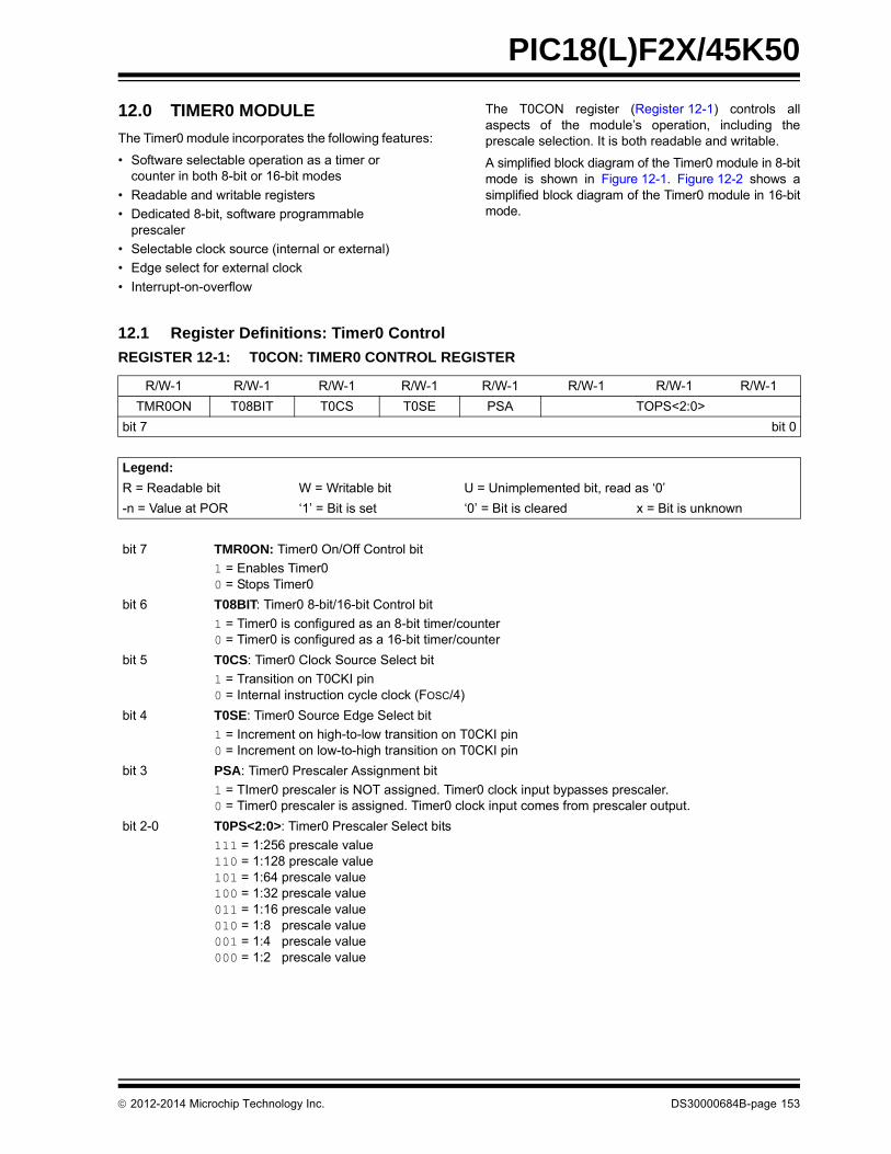
PIC18(L)F2X/45K50
12.0 TIMER0 MODULE
The Timer0 module incorporates the following features:
• Software selectable operation as a timer or counter in both 8-bit or 16-bit modes
• Readable and writable registers
• Dedicated 8-bit, software programmable prescaler
• Selectable clock source (internal or external)
• Edge select for external clock
• Interrupt-on-overflow
The T0CON register (Register 12-1) controls allaspects of the module’s operation, including theprescale selection. It is both readable and writable.
A simplified block diagram of the Timer0 module in 8-bitmode is shown in Figure 12-1. Figure 12-2 shows asimplified block diagram of the Timer0 module in 16-bitmode.
12.1 Register Definitions: Timer0 Control
REGISTER 12-1: T0CON: TIMER0 CONTROL REGISTER
R/W-1 R/W-1 R/W-1 R/W-1 R/W-1 R/W-1 R/W-1 R/W-1
TMR0ON T08BIT T0CS T0SE PSA TOPS<2:0>
bit 7 bit 0
Legend:
R = Readable bit W = Writable bit U = Unimplemented bit, read as ‘0’
-n = Value at POR ‘1’ = Bit is set ‘0’ = Bit is cleared x = Bit is unknown
bit 7 TMR0ON: Timer0 On/Off Control bit
1 = Enables Timer00 = Stops Timer0
bit 6 T08BIT: Timer0 8-bit/16-bit Control bit
1 = Timer0 is configured as an 8-bit timer/counter0 = Timer0 is configured as a 16-bit timer/counter
bit 5 T0CS: Timer0 Clock Source Select bit
1 = Transition on T0CKI pin0 = Internal instruction cycle clock (FOSC/4)
bit 4 T0SE: Timer0 Source Edge Select bit
1 = Increment on high-to-low transition on T0CKI pin0 = Increment on low-to-high transition on T0CKI pin
bit 3 PSA: Timer0 Prescaler Assignment bit
1 = TImer0 prescaler is NOT assigned. Timer0 clock input bypasses prescaler.0 = Timer0 prescaler is assigned. Timer0 clock input comes from prescaler output.
bit 2-0 T0PS<2:0>: Timer0 Prescaler Select bits
111 = 1:256 prescale value110 = 1:128 prescale value101 = 1:64 prescale value100 = 1:32 prescale value011 = 1:16 prescale value010 = 1:8 prescale value001 = 1:4 prescale value000 = 1:2 prescale value
2012-2014 Microchip Technology Inc. DS30000684B-page 153

PIC18(L)F2X/45K50
12.2 Timer0 Operation
Timer0 can operate as either a timer or a counter; themode is selected with the T0CS bit of the T0CONregister. In Timer mode (T0CS = 0), the moduleincrements on every clock by default unless a differentprescaler value is selected (see Section 12.4“Prescaler”). Timer0 incrementing is inhibited for twoinstruction cycles following a TMR0 register write. Theuser can work around this by adjusting the value writtento the TMR0 register to compensate for the anticipatedmissing increments.
The Counter mode is selected by setting the T0CS bit(= 1). In this mode, Timer0 increments either on everyrising or falling edge of pin RA4/T0CKI. The increment-ing edge is determined by the Timer0 Source EdgeSelect bit, T0SE of the T0CON register; clearing this bitselects the rising edge. Restrictions on the externalclock input are discussed below.
An external clock source can be used to drive Timer0;however, it must meet certain requirements (seeTable 29-22) to ensure that the external clock can besynchronized with the internal phase clock (TOSC).There is a delay between synchronization and theonset of incrementing the timer/counter.
12.3 Timer0 Reads and Writes in 16-Bit Mode
TMR0H is not the actual high byte of Timer0 in 16-bitmode; it is actually a buffered version of the real highbyte of Timer0 which is neither directly readable norwritable (refer to Figure 12-2). TMR0H is updated withthe contents of the high byte of Timer0 during a read ofTMR0L. This provides the ability to read all 16 bits ofTimer0 without the need to verify that the read of thehigh and low byte were valid. Invalid reads couldotherwise occur due to a rollover between successivereads of the high and low byte.
Similarly, a write to the high byte of Timer0 must alsotake place through the TMR0H Buffer register. Writingto TMR0H does not directly affect Timer0. Instead, thehigh byte of Timer0 is updated with the contents ofTMR0H when a write occurs to TMR0L. This allows all16 bits of Timer0 to be updated at once.
FIGURE 12-1: TIMER0 BLOCK DIAGRAM (8-BIT MODE)
Note: Upon Reset, Timer0 is enabled in 8-bit mode with clock input from T0CKI max. prescale.
T0CKI pin
T0SE
0
1
1
0
T0CS
FOSC/4
ProgrammablePrescaler
Sync withInternalClocks
TMR0L
(2 TCY Delay)
Internal Data BusPSA
T0PS<2:0>
Set TMR0IFon Overflow
3 8
8
DS30000684B-page 154 2012-2014 Microchip Technology Inc.

PIC18(L)F2X/45K50
FIGURE 12-2: TIMER0 BLOCK DIAGRAM (16-BIT MODE)
12.4 Prescaler
An 8-bit counter is available as a prescaler for the Timer0module. The prescaler is not directly readable or writable;its value is set by the PSA and T0PS<2:0> bits of theT0CON register which determine the prescalerassignment and prescale ratio.
Clearing the PSA bit assigns the prescaler to theTimer0 module. When the prescaler is assigned,prescale values from 1:2 through 1:256 in integerpower-of-2 increments are selectable.
When assigned to the Timer0 module, all instructionswriting to the TMR0 register (e.g., CLRF TMR0, MOVWFTMR0, BSF TMR0, etc.) clear the prescaler count.
12.4.1 SWITCHING PRESCALER ASSIGNMENT
The prescaler assignment is fully under softwarecontrol and can be changed “on-the-fly” during programexecution.
12.5 Timer0 Interrupt
The TMR0 interrupt is generated when the TMR0 reg-ister overflows from FFh to 00h in 8-bit mode, or fromFFFFh to 0000h in 16-bit mode. This overflow sets theTMR0IF flag bit. The interrupt can be masked by clear-ing the TMR0IE bit of the INTCON register. Beforere-enabling the interrupt, the TMR0IF bit must becleared by software in the Interrupt Service Routine.
Since Timer0 is shut down in Sleep mode, the TMR0interrupt cannot awaken the processor from Sleep.
TABLE 12-1: REGISTERS ASSOCIATED WITH TIMER0
Note: Upon Reset, Timer0 is enabled in 8-bit mode with clock input from T0CKI max. prescale.
T0CKI pin
T0SE
0
1
1
0
T0CS
FOSC/4
ProgrammablePrescaler
Sync withInternalClocks
TMR0L
(2 TCY Delay)
Internal Data Bus
8
PSA
T0PS<2:0>
Set TMR0IFon Overflow
3
TMR0
TMR0H
High Byte
88
8
Read TMR0L
Write TMR0L
8
Note: Writing to TMR0 when the prescaler isassigned to Timer0 will clear the prescalercount but will not change the prescalerassignment.
Name Bit 7 Bit 6 Bit 5 Bit 4 Bit 3 Bit 2 Bit 1 Bit 0Register on page
INTCON GIE/GIEH PEIE/GIEL TMR0IE INT0IE IOCIE TMR0IF INT0IF IOCIF 114
INTCON2 RBPU INTEDG0 INTEDG1 INTEDG2 — TMR0IP — IOCIP 115
T0CON TMR0ON T08BIT T0CS T0SE PSA T0PS<2:0> 153
TMR0H Timer0 Register, High Byte —
TMR0L Timer0 Register, Low Byte —
TRISA TRISA7 TRISA6 TRISA5 TRISA4 TRISA3 TRISA2 TRISA1 TRISA0 149
Legend: — = unimplemented locations, read as ‘0’. Shaded bits are not used by Timer0.
2012-2014 Microchip Technology Inc. DS30000684B-page 155
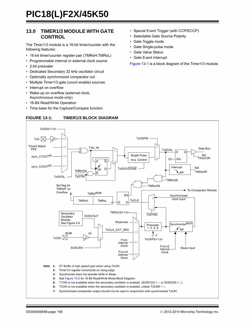
PIC18(L)F2X/45K50
13.0 TIMER1/3 MODULE WITH GATE CONTROL
The Timer1/3 module is a 16-bit timer/counter with thefollowing features:
• 16-bit timer/counter register pair (TMRxH:TMRxL)
• Programmable internal or external clock source
• 2-bit prescaler
• Dedicated Secondary 32 kHz oscillator circuit
• Optionally synchronized comparator out
• Multiple Timer1/3 gate (count enable) sources
• Interrupt on overflow
• Wake-up on overflow (external clock, Asynchronous mode only)
• 16-Bit Read/Write Operation
• Time base for the Capture/Compare function
• Special Event Trigger (with CCP/ECCP)
• Selectable Gate Source Polarity
• Gate Toggle mode
• Gate Single-pulse mode
• Gate Value Status
• Gate Event Interrupt
Figure 13-1 is a block diagram of the Timer1/3 module.
FIGURE 13-1: TIMER1/3 BLOCK DIAGRAM
TMRxH TMRxL
TxSYNC
TxCKPS<1:0>
Prescaler1, 2, 4, 8
0
1
Synchronizedclock input
2
Set flag bitTMRxIF onOverflow TMRx(2),(4)
TMRxON
Note 1: ST Buffer is high speed type when using TxCKI.
2: Timer1/3 register increments on rising edge.
3: Synchronize does not operate while in Sleep.
4: See Figure 13-2 for 16-Bit Read/Write Mode Block Diagram.
5: T1CKI is not available when the secondary oscillator is enabled. (SOSCGO = 1 or SOSCEN = 1)
6: T3CKI is not available when the secondary oscillator is enabled, unless T3CMX = 1.
7: Synchronized comparator output should not be used in conjunction with synchronized TxCKI.
TxG
FOSC/4Internal
Clock
SOSCOUT
1
0TxCKI
TMRxCS<1:0>
(5)
Synchronize(3),(7)
det
Sleep input
TMRxGE
0
1
00
01
10
11
TxGPOL
D
QCK
Q
0
1
TxGVAL
TxGTM
Single Pulse
Acq. Control
TxGSPM
TxGGO/DONE
TxGSS<1:0>
10
11
00
01FOSC
InternalClock
Reserved
R
D
EN
Q
Q1RD
TXGCON
Data Bus
det
Interrupt
TMRxGIF
Set
TxCLK
FOSC/2InternalClock
D
EN
Q
TxG_IN
TMRxON
Timer2 Match PR2
sync_C2OUT(7)
sync_C1OUT(7)
To Comparator Module
,(6)
SOSCEN
SecondaryOscillatorModuleSee Figure 2-4
TxCLK_EXT_SRC(1)
DS30000684B-page 156 2012-2014 Microchip Technology Inc.
PIC18(L)F2X/45K50
13.1 Timer1/3 Operation
The Timer1/3 module is a 16-bit incrementing counterwhich is accessed through the TMRxH:TMRxL registerpair. Writes to TMRxH or TMRxL directly update thecounter.
When used with an internal clock source, the module isa timer and increments on every instruction cycle.When used with an external clock source, the modulecan be used as either a timer or counter andincrements on every selected edge of the externalsource.
Timer1/3 is enabled by configuring the TMRxON andTMRxGE bits in the TxCON and TxGCON registers,respectively. Table 13-1 displays the Timer1/3 enableselections.
13.2 Clock Source Selection
The TMRxCS<1:0> and SOSCEN bits of the TxCONregister are used to select the clock source for Timer1/3.The dedicated secondary oscillator circuit can be usedas the clock source for Timer1 and Timer3,simultaneously. Any of the SOSCEN bits will enable thesecondary oscillator circuit and select it as the clocksource for that particular timer. Table 13-2 displays theclock source selections.
13.2.1 INTERNAL CLOCK SOURCE
When the internal clock source is selected theTMRxH:TMRxL register pair will increment on multiplesof FOSC as determined by the Timer1/3 prescaler.
When the FOSC internal clock source is selected, theTimer1/3 register value will increment by four countsevery instruction clock cycle. Due to this condition, a2 LSB error in resolution will occur when reading theTimer1/3 value. To utilize the full resolution of Timer1/3,an asynchronous input signal must be used to gate theTimer1/3 clock input.
The following asynchronous sources may be used:
• Asynchronous event on the TxG pin to Timer1/3 gate
• C1 or C2 comparator input to Timer1/3 gate
13.2.2 EXTERNAL CLOCK SOURCE
When the external clock source is selected, the Timer1/3module may work as a timer or a counter.
When enabled to count, Timer1/3 is incremented on therising edge of the external clock input of the TxCKI pin.This external clock source can be synchronized to themicrocontroller system clock or it can runasynchronously.
When used as a timer with a clock oscillator, anexternal 32.768 kHz crystal can be used in conjunctionwith the dedicated secondary internal oscillator circuit.
TABLE 13-1: TIMER1/3 ENABLE SELECTIONS
TMRxON TMRxGETimer1/3
Operation
0 0 Off
0 1 Off
1 0 Always On
1 1 Count Enabled
Note: In Counter mode, a falling edge must beregistered by the counter prior to the firstincrementing rising edge after any one ormore of the following conditions:
• Timer1/3 enabled after POR
• Write to TMRxH or TMRxL
• Timer1/3 is disabled
• Timer1/3 is disabled (TMRxON = 0) when TxCKI is high then Timer1/3 is enabled (TMRxON=1) when TxCKI is low.
TABLE 13-2: CLOCK SOURCE SELECTIONS
TMRxCS1 TMRxCS0 SOSCEN Clock Source
0 1 x System Clock (FOSC)
0 0 x Instruction Clock (FOSC/4)
1 0 0 External Clocking on TxCKI Pin
1 0 1 Oscillator Circuit on SOSCI/SOSCO Pins
2012-2014 Microchip Technology Inc. DS30000684B-page 157
PIC18(L)F2X/45K50
13.3 Timer1/3 Prescaler
Timer1/3 has four prescaler options allowing 1, 2, 4 or 8divisions of the clock input. The TxCKPS bits of theTxCON register control the prescale counter. Theprescale counter is not directly readable or writable;however, the prescaler counter is cleared upon a write toTMRxH or TMRxL.
13.4 Secondary Oscillator
A dedicated secondary low-power 32.768 kHzoscillator circuit is built-in between pins SOSCI (input)and SOSCO (amplifier output). This internal circuit is tobe used in conjunction with an external 32.768 kHzcrystal.
The oscillator circuit is enabled by setting the SOSCENbit of the TxCON register, the SOSCGO bit of theOSCCON2 register or by selecting the secondaryoscillator as the system clock by setting SCS<1:0> =01 in the OSCCON register. The oscillator will continueto run during Sleep.
13.5 Timer1/3 Operation in Asynchronous Counter Mode
If control bit TxSYNC of the TxCON register is set, theexternal clock input is not synchronized. The timerincrements asynchronously to the internal phaseclocks. If external clock source is selected then thetimer will continue to run during Sleep and cangenerate an interrupt on overflow, which will wake-upthe processor. However, special precautions insoftware are needed to read/write the timer (seeSection 13.5.1 “Reading and Writing Timer1/3 inAsynchronous Counter Mode”).
13.5.1 READING AND WRITING TIMER1/3 IN ASYNCHRONOUS COUNTER MODE
Reading TMRxH or TMRxL while the timer is runningfrom an external asynchronous clock will ensure a validread (taken care of in hardware). However, the usershould keep in mind that reading the 16-bit timer in two8-bit values itself, poses certain problems, since thetimer may overflow between the reads. For writes, it isrecommended that the user simply stop the timer andwrite the desired values. A write contention may occurby writing to the timer registers, while the register isincrementing. This may produce an unpredictablevalue in the TMRxH:TMRxL register pair.
13.6 Timer1/3 16-Bit Read/Write Mode
Timer1/3 can be configured to read and write all 16 bitsof data, to and from, the 8-bit TMRxL and TMRxH reg-isters, simultaneously. The 16-bit read and write opera-tions are enabled by setting the RD16 bit of the TxCONregister.
To accomplish this function, the TMRxH register valueis mapped to a buffer register called the TMRxH bufferregister. While in 16-Bit mode, the TMRxH register isnot directly readable or writable and all read and writeoperations take place through the use of this TMRxHbuffer register.
When a read from the TMRxL register is requested, thevalue of the TMRxH register is simultaneously loadedinto the TMRxH buffer register. When a read from theTMRxH register is requested, the value is providedfrom the TMRxH buffer register instead. This providesthe user with the ability to accurately read all 16 bits ofthe Timer1/3 value from a single instance in time.
In contrast, when not in 16-Bit mode, the user mustread each register separately and determine if thevalues have become invalid due to a rollover that mayhave occurred between the read operations.
When a write request of the TMRxL register isrequested, the TMRxH buffer register is simultaneouslyupdated with the contents of the TMRxH register. Thevalue of TMRxH must be preloaded into the TMRxHbuffer register prior to the write request for the TMRxLregister. This provides the user with the ability to writeall 16 bits to the TMRxL:TMRxH register pair at thesame time.
Any requests to write to the TMRxH directly does notclear the Timer1/3 prescaler value. The prescaler valueis only cleared through write requests to the TMRxLregister.
Note: The oscillator requires a start-up andstabilization time before use. Thus,SOSCEN should be set and a suitabledelay observed prior to enabling Timer1/3.
Note: When switching from synchronous toasynchronous operation, it is possible toskip an increment. When switching fromasynchronous to synchronous operation,it is possible to produce an additionalincrement.
DS30000684B-page 158 2012-2014 Microchip Technology Inc.

PIC18(L)F2X/45K50
FIGURE 13-2: TIMER1/3 16-BIT READ/WRITE MODE BLOCK DIAGRAM
13.7 Timer1/3 Gate
Timer1/3 can be configured to count freely or the countcan be enabled and disabled using Timer1/3 gatecircuitry. This is also referred to as Timer1/3 GateEnable.
Timer1/3 gate can also be driven by multiple selectablesources.
13.7.1 TIMER1/3 GATE ENABLE
The Timer1/3 Gate Enable mode is enabled by settingthe TMRxGE bit of the TxGCON register. The polarityof the Timer1/3 Gate Enable mode is configured usingthe TxGPOL bit of the TxGCON register.
When Timer1/3 Gate Enable mode is enabled,Timer1/3 will increment on the rising edge of theTimer1/3 clock source. When Timer1/3 Gate Enablemode is disabled, no incrementing will occur andTimer1/3 will hold the current count. See Figure 13-4for timing details.
13.7.2 TIMER1/3 GATE SOURCE SELECTION
The Timer1/3 gate source can be selected from one offour different sources. Source selection is controlled bythe TxGSS bits of the TxGCON register. The polarityfor each available source is also selectable. Polarityselection is controlled by the TxGPOL bit of theTxGCON register.
13.7.2.1 TxG Pin Gate Operation
The TxG pin is one source for Timer1/3 gate control. Itcan be used to supply an external source to the Tim-er1/3 gate circuitry.
13.7.2.2 Timer2 Match Gate Operation
The TMR2 register will increment until it matches thevalue in the PR2 register. On the very next incrementcycle, TMR2 will be reset to 00h. When this Resetoccurs, a low-to-high pulse will automatically be gener-ated and internally supplied to the Timer1/3 gatecircuitry. See Section 13.7.2 “Timer1/3 Gate SourceSelection” for more information.
13.7.2.3 Comparator C1 Gate Operation
The output resulting from a Comparator 1 operation canbe selected as a source for Timer1/3 gate control. TheComparator 1 output (sync_C1OUT) can besynchronized to the Timer1/3 clock or left asynchronous.For more information see Section 19.8.3“Synchronizing Comparator Output to Timer1”.
13.7.2.4 Comparator C2 Gate Operation
The output resulting from a Comparator 2 operationcan be selected as a source for Timer1/3 gate control.The Comparator 2 output (sync_C2OUT) can besynchronized to the Timer1/3 clock or leftasynchronous. For more information seeSection 19.8.3 “Synchronizing Comparator Outputto Timer1”.
TABLE 13-3: TIMER1/3 GATE ENABLE SELECTIONS
TxCLK TxGPOL TxGTimer1/3
Operation
0 0 Counts
0 1 Holds Count
1 0 Holds Count
1 1 Counts
TMR1L
Internal Data Bus
8
Set TMR1IF
on Overflow
TMR1
TMR1H
High Byte
88
8
Read TMR1L
Write TMR1L
8
From Timer1/3Circuitry
TABLE 13-4: TIMER1/3 GATE SOURCES
TxGSS Timer1/3 Gate Source
00 Timer1/3 Gate Pin (TxG)
01 Timer2 Match to PR2(TMR2 increments to match PR2)
10 Comparator 1 Output sync_C1OUT(optionally Timer1/3 synchronized output)
11 Comparator 2 Output sync_C2OUT(optionally Timer1/3 synchronized output)
2012-2014 Microchip Technology Inc. DS30000684B-page 159

PIC18(L)F2X/45K50
13.7.3 TIMER1/3 GATE TOGGLE MODE
When Timer1/3 Gate Toggle mode is enabled, it is pos-sible to measure the full-cycle length of a Timer1/3 gatesignal, as opposed to the duration of a single levelpulse.
The Timer1/3 gate source is routed through a flip-flopthat changes state on every incrementing edge of thesignal. See Figure 13-5 for timing details.
Timer1/3 Gate Toggle mode is enabled by setting theTxGTM bit of the TxGCON register. When the TxGTMbit is cleared, the flip-flop is cleared and held clear. Thisis necessary in order to control which edge ismeasured.
13.7.4 TIMER1/3 GATE SINGLE-PULSE MODE
When Timer1/3 Gate Single-Pulse mode is enabled, itis possible to capture a single-pulse gate event.Timer1/3 Gate Single-Pulse mode is first enabled bysetting the TxGSPM bit in the TxGCON register. Next,the TxGGO/DONE bit in the TxGCON register must beset. The Timer1/3 will be fully enabled on the nextincrementing edge. On the next trailing edge of thepulse, the TxGGO/DONE bit will automatically becleared. No other gate events will be allowed toincrement Timer1/3 until the TxGGO/DONE bit is onceagain set in software.
Clearing the TxGSPM bit of the TxGCON register willalso clear the TxGGO/DONE bit. See Figure 13-6 fortiming details.
Enabling the Toggle mode and the Single-Pulse modesimultaneously will permit both sections to worktogether. This allows the cycle times on the Timer1/3gate source to be measured. See Figure 13-7 for timingdetails.
13.7.5 TIMER1/3 GATE VALUE STATUS
When Timer1/3 Gate Value Status is utilized, it ispossible to read the most current level of the gatecontrol value. The value is stored in the TxGVAL bit inthe TxGCON register. The TxGVAL bit is valid evenwhen the Timer1/3 gate is not enabled (TMRxGE bit iscleared).
13.7.6 TIMER1/3 GATE EVENT INTERRUPT
When Timer1/3 Gate Event Interrupt is enabled, it ispossible to generate an interrupt upon the completionof a gate event. When the falling edge of TxGVALoccurs, the TMRxGIF flag bit in the PIR3 register will beset. If the TMRxGIE bit in the PIE3 register is set, thenan interrupt will be recognized.
The TMRxGIF flag bit operates even when the Tim-er1/3 gate is not enabled (TMRxGE bit is cleared).
For more information on selecting high or low prioritystatus for the Timer1/3 Gate Event Interrupt seeSection 10.0 “Interrupts”.
Note: Enabling Toggle mode at the same timeas changing the gate polarity may result inindeterminate operation.
DS30000684B-page 160 2012-2014 Microchip Technology Inc.

PIC18(L)F2X/45K50
13.8 Timer1/3 Interrupt
The Timer1/3 register pair (TMRxH:TMRxL)increments to FFFFh and rolls over to 0000h. WhenTimer1/3 rolls over, the Timer1/3 interrupt flag bit of thePIR1/2 register is set. To enable the interrupt onrollover, you must set these bits:
• TMRxON bit of the TxCON register
• TMRxIE bits of the PIE1 or PIE2 registers
• PEIE/GIEL bit of the INTCON register
• GIE/GIEH bit of the INTCON register
The interrupt is cleared by clearing the TMRxIF bit inthe Interrupt Service Routine.
For more information on selecting high or low prioritystatus for the Timer1/3 Overflow Interrupt, seeSection 10.0 “Interrupts”.
13.9 Timer1/3 Operation During Sleep
Timer1/3 can only operate during Sleep when set up inAsynchronous Counter mode. In this mode, an externalcrystal or clock source can be used to increment thecounter. To set up the timer to wake the device:
• TMRxON bit of the TxCON register must be set
• TMRxIE bit of the PIE1/2 register must be set
• PEIE/GIEL bit of the INTCON register must be set
• TxSYNC bit of the TxCON register must be set
• TMRxCS bits of the TxCON register must be configured
• SOSCEN bit of the TxCON register must be configured
The device will wake-up on an overflow and executethe next instruction. If the GIE/GIEH bit of the INTCONregister is set, the device will call the Interrupt ServiceRoutine.
The secondary oscillator will continue to operate inSleep regardless of the TxSYNC bit setting.
13.10 ECCP/CCP Capture/Compare Time Base
The CCP modules use the TMRxH:TMRxL register pairas the time base when operating in Capture orCompare mode.
In Capture mode, the value in the TMRxH:TMRxLregister pair is copied into the CCPRxH:CCPRxLregister pair on a configured event.
In Compare mode, an event is triggered when the valueCCPRxH:CCPRxL register pair matches the value inthe TMRxH:TMRxL register pair. This event can be aSpecial Event Trigger.
For more information, see Section 15.0“Capture/Compare/PWM Modules”.
13.11 ECCP/CCP Special Event Trigger
When any of the CCP’s are configured to trigger aspecial event, the trigger will clear the TMRxH:TMRxLregister pair. This special event does not cause aTimer1/3 interrupt. The CCP module may still beconfigured to generate a CCP interrupt.
In this mode of operation, the CCPRxH:CCPRxLregister pair becomes the period register for Timer1/3.
Timer1/3 should be synchronized and FOSC/4 shouldbe selected as the clock source in order to utilize theSpecial Event Trigger. Asynchronous operation of Tim-er1/3 can cause a Special Event Trigger to be missed.
In the event that a write to TMRxH or TMRxL coincideswith a Special Event Trigger from the CCP, the write willtake precedence.
For more information, see Section 18.2.8 “SpecialEvent Trigger”.
FIGURE 13-3: TIMER1/3 INCREMENTING EDGE
Note: The TMRxH:TMRxL register pair and theTMRxIF bit should be cleared beforeenabling interrupts.
TXCKI = 1
when TMRxEnabled
TXCKI = 0
when TMRXEnabled
Note 1: Arrows indicate counter increments.
2: In Counter mode, a falling edge must be registered by the counter prior to the first incrementing rising edge of the clock.
2012-2014 Microchip Technology Inc. DS30000684B-page 161

PIC18(L)F2X/45K50
FIGURE 13-4: TIMER1/3 GATE ENABLE MODE
FIGURE 13-5: TIMER1/3 GATE TOGGLE MODE
TMRxGE
TxGPOL
TxG_IN
TxCKI
TxGVAL
Timer1/3 N N + 1 N + 2 N + 3 N + 4
TMRxGE
TxGPOL
TxGTM
TxTxG_IN
TxCKI
TxGVAL
Timer1/3 N N + 1 N + 2 N + 3 N + 4 N + 5 N + 6 N + 7 N + 8
DS30000684B-page 162 2012-2014 Microchip Technology Inc.
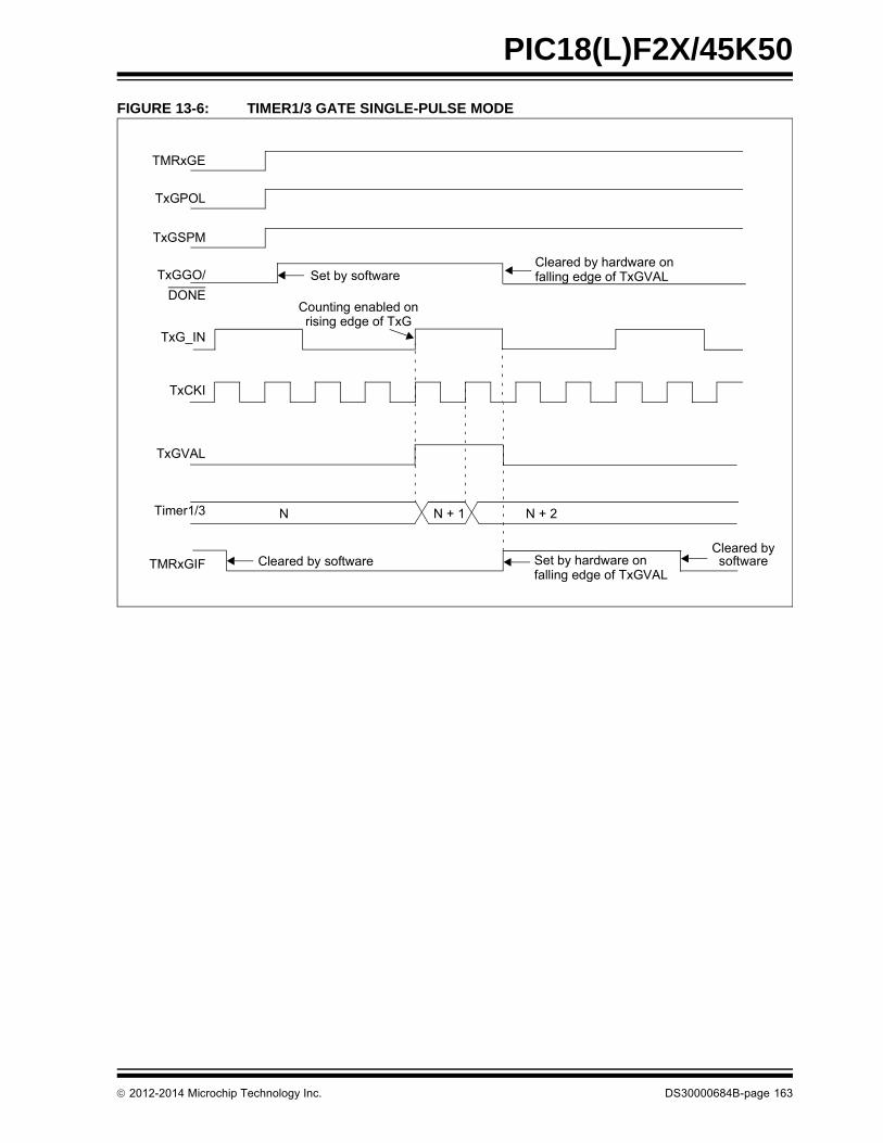
PIC18(L)F2X/45K50
FIGURE 13-6: TIMER1/3 GATE SINGLE-PULSE MODE
TMRxGE
TxGPOL
TxG_IN
TxCKI
TxGVAL
Timer1/3 N N + 1 N + 2
TxGSPM
TxGGO/
DONE
Set by softwareCleared by hardware onfalling edge of TxGVAL
Set by hardware onfalling edge of TxGVAL
Cleared by softwareCleared bysoftwareTMRxGIF
Counting enabled onrising edge of TxG
2012-2014 Microchip Technology Inc. DS30000684B-page 163

PIC18(L)F2X/45K50
FIGURE 13-7: TIMER1/3 GATE SINGLE-PULSE AND TOGGLE COMBINED MODE
13.12 Peripheral Module Disable
When a peripheral module is not used or inactive, themodule can be disabled by setting the Module Disablebit in the PMD registers. This will reduce power con-sumption to an absolute minimum. Setting the PMDbits holds the module in Reset and disconnects themodule’s clock source. The Module Disable bits forTimer1 (TMR1MD) and Timer3 (TMR3MD) are in thePMD0 Register. See Section 4.0 “Power-ManagedModes” for more information.
TMRxGE
TxGPOL
TxG_IN
TxCKI
TxGVAL
Timer1/3 N N + 1 N + 2
TxGSPM
TxGGO/
DONE
Set by softwareCleared by hardware onfalling edge of TxGVAL
Set by hardware onfalling edge of TxGVALCleared by software
Cleared bysoftwareTMRxGIF
TxGTM
Counting enabled onrising edge of TxG
N + 4N + 3
DS30000684B-page 164 2012-2014 Microchip Technology Inc.
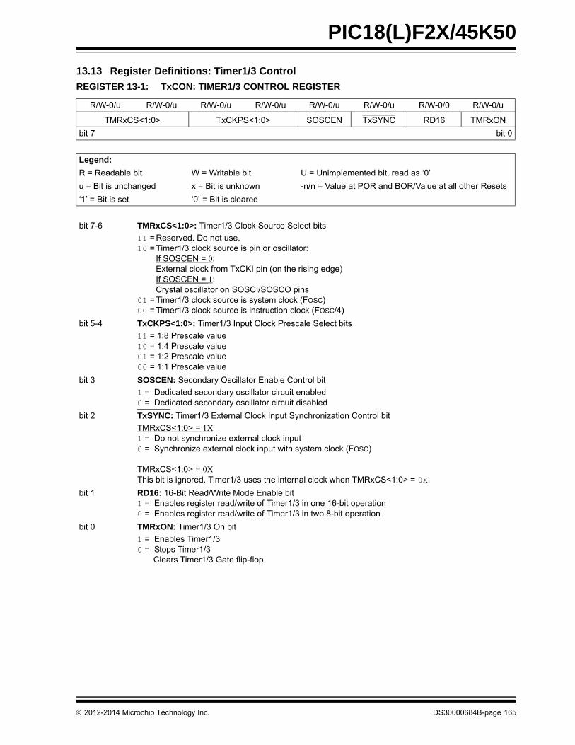
PIC18(L)F2X/45K50
13.13 Register Definitions: Timer1/3 Control
REGISTER 13-1: TxCON: TIMER1/3 CONTROL REGISTER
R/W-0/u R/W-0/u R/W-0/u R/W-0/u R/W-0/u R/W-0/u R/W-0/0 R/W-0/u
TMRxCS<1:0> TxCKPS<1:0> SOSCEN TxSYNC RD16 TMRxON
bit 7 bit 0
Legend:
R = Readable bit W = Writable bit U = Unimplemented bit, read as ‘0’
u = Bit is unchanged x = Bit is unknown -n/n = Value at POR and BOR/Value at all other Resets
‘1’ = Bit is set ‘0’ = Bit is cleared
bit 7-6 TMRxCS<1:0>: Timer1/3 Clock Source Select bits
11 = Reserved. Do not use.10 = Timer1/3 clock source is pin or oscillator:
If SOSCEN = 0:External clock from TxCKI pin (on the rising edge)If SOSCEN = 1:Crystal oscillator on SOSCI/SOSCO pins
01 = Timer1/3 clock source is system clock (FOSC)00 = Timer1/3 clock source is instruction clock (FOSC/4)
bit 5-4 TxCKPS<1:0>: Timer1/3 Input Clock Prescale Select bits
11 = 1:8 Prescale value10 = 1:4 Prescale value01 = 1:2 Prescale value00 = 1:1 Prescale value
bit 3 SOSCEN: Secondary Oscillator Enable Control bit
1 = Dedicated secondary oscillator circuit enabled0 = Dedicated secondary oscillator circuit disabled
bit 2 TxSYNC: Timer1/3 External Clock Input Synchronization Control bit
TMRxCS<1:0> = 1X1 = Do not synchronize external clock input0 = Synchronize external clock input with system clock (FOSC)
TMRxCS<1:0> = 0XThis bit is ignored. Timer1/3 uses the internal clock when TMRxCS<1:0> = 0X.
bit 1 RD16: 16-Bit Read/Write Mode Enable bit1 = Enables register read/write of Timer1/3 in one 16-bit operation0 = Enables register read/write of Timer1/3 in two 8-bit operation
bit 0 TMRxON: Timer1/3 On bit
1 = Enables Timer1/30 = Stops Timer1/3
Clears Timer1/3 Gate flip-flop
2012-2014 Microchip Technology Inc. DS30000684B-page 165

PIC18(L)F2X/45K50
REGISTER 13-2: TxGCON: TIMER1/3 GATE CONTROL REGISTER
R/W-0/u R/W-0/u R/W-0/u R/W-0/u R/W/HC-0/u R-x/x R/W-0/u R/W-0/u
TMRxGE TxGPOL TxGTM TxGSPM TxGGO/DONE TxGVAL TxGSS<1:0>
bit 7 bit 0
Legend:
R = Readable bit W = Writable bit U = Unimplemented bit, read as ‘0’
u = Bit is unchanged x = Bit is unknown -n/n = Value at POR and BOR/Value at all other Resets
‘1’ = Bit is set ‘0’ = Bit is cleared HC = Bit is cleared by hardware
bit 7 TMRxGE: Timer1/3 Gate Enable bitIf TMRxON = 0:This bit is ignoredIf TMRxON = 1:1 = Timer1/3 counting is controlled by the Timer1/3 gate function0 = Timer1/3 counts regardless of Timer1/3 gate function
bit 6 TxGPOL: Timer1/3 Gate Polarity bit1 = Timer1/3 gate is active-high (Timer1/3 counts when gate is high)0 = Timer1/3 gate is active-low (Timer1/3 counts when gate is low)
bit 5 TxGTM: Timer1/3 Gate Toggle Mode bit1 = Timer1/3 Gate Toggle mode is enabled0 = Timer1/3 Gate Toggle mode is disabled and toggle flip-flop is clearedTimer1/3 gate flip-flop toggles on every rising edge.
bit 4 TxGSPM: Timer1/3 Gate Single-Pulse Mode bit1 = Timer1/3 gate Single-Pulse mode is enabled and is controlling Timer1/3 gate0 = Timer1/3 gate Single-Pulse mode is disabled
bit 3 TxGGO/DONE: Timer1/3 Gate Single-Pulse Acquisition Status bit1 = Timer1/3 gate single-pulse acquisition is ready, waiting for an edge0 = Timer1/3 gate single-pulse acquisition has completed or has not been startedThis bit is automatically cleared when TxGSPM is cleared.
bit 2 TxGVAL: Timer1/3 Gate Current State bitIndicates the current state of the Timer1/3 gate that could be provided to TMRxH:TMRxL.Unaffected by Timer1/3 Gate Enable (TMRxGE).
bit 1-0 TxGSS<1:0>: Timer1/3 Gate Source Select bits00 = Timer1/3 Gate pin01 = Timer2 Match PR2 output10 = Comparator 1 optionally synchronized output (sync_C1OUT)11 = Comparator 2 optionally synchronized output (sync_C2OUT)
DS30000684B-page 166 2012-2014 Microchip Technology Inc.

PIC18(L)F2X/45K50
TABLE 13-5: REGISTERS ASSOCIATED WITH TIMER1/3 AS A TIMER/COUNTER
TABLE 13-6: CONFIGURATION REGISTERS ASSOCIATED WITH TIMER1/3
Name Bit 7 Bit 6 Bit 5 Bit 4 Bit 3 Bit 2 Bit 1 Bit 0Register on page
ANSELB — — ANSB5 ANSB4 ANSB3 ANSB2 ANSB1 ANSB0 148
INTCON GIE/GIEH PEIE/GIEL TMR0IE INT0IE IOCIE TMR0IF INT0IF IOCIF 114
IPR1 ACTIP ADIP RCIP TXIP SSPIP CCP1IP TMR2IP TMR1IP 123
IPR2 OSCFIP C1IP C2IP EEIP BCLIP HLVDIP TMR3IP CCP2IP 124
IPR3 — — — — CTMUIP USBIP TMR3GIP TMR1GIP 125
PIE1 ACTIE ADIE RCIE TXIE SSPIE CCP1IE TMR2IE TMR1IE 120
PIE2 OSCFIE C1IE C2IE EEIE BCLIE HLVDIE TMR3IE CCP2IE 121
PIE3 — — — — CTMUIE USBIE TMR3GIE TMR1GIE 122
PIR1 ACTIF ADIF RCIF TXIF SSPIF CCP1IF TMR2IF TMR1IF 117
PIR2 OSCFIF C1IF C2IF EEIF BCLIF HLVDIF TMR3IF CCP2IF 118
PIR3 — — — — CTMUIF USBIF TMR3GIF TMR1GIF 119
PMD0 — UARTMD USBMD ACTMD — TMR3MD TMR2MD TMR1MD 61
T1CON TMR1CS<1:0> T1CKPS<1:0> SOSCEN T1SYNC RD16 TMR1ON 165
T1GCON TMR1GE T1GPOL T1GTM T1GSPM T1GGO/DONE T1GVAL T1GSS<1:0> 166
T3CON TMR3CS<1:0> T3CKPS<1:0> SOSCEN T3SYNC RD16 TMR3ON 165
T3GCON TMR3GE T3GPOL T3GTM T3GSPM T3GGO/DONE T3GVAL T3GSS<1:0> 166
TMRxH Timer1/3 Register, High Byte —
TMRxL Timer1/3 Register, Low Byte —
TRISB TRISB7 TRISB6 TRISB5 TRISB4 TRISB3 TRISB2 TRISB1 TRISB0 149
TRISC TRISC7 TRISC6 — — — TRISC2 TRISC1 TRISC0 149
Name Bit 7 Bit 6 Bit 5 Bit 4 Bit 3 Bit 2 Bit 1 Bit 0Register on page
CONFIG3H MCLRE SDOMX — T3CMX — — PBADEN CCP2MX 376
2012-2014 Microchip Technology Inc. DS30000684B-page 167

PIC18(L)F2X/45K50
14.0 TIMER2 MODULE
The Timer2 module incorporates the following features:
• 8-bit Timer and Period registers (TMR2 and PR2, respectively)
• Readable and writable (both registers)
• Software programmable prescaler (1:1, 1:4, 1:16)
• Software programmable postscaler (1:1 to 1:16)
• Interrupt on TMR2 match with PR2, respectively
• Optional use as the shift clock for the MSSP module
See Figure 14-1 for a block diagram of Timer2.
FIGURE 14-1: TIMER2 BLOCK DIAGRAM
Comparator
TMRxSets Flag
TMRx
Output
Reset
Postscaler
Prescaler
PRx
2
FOSC/4
1:1 to 1:16
1:1, 1:4, 1:16
EQ
4
bit TMRxIF
TxOUTPS<3:0>
TxCKPS<1:0>
DS30000684B-page 168 2012-2014 Microchip Technology Inc.

PIC18(L)F2X/45K50
14.1 Timer2 Operation
The clock input to the Timer2 module is the systeminstruction clock (FOSC/4).
TMR2 increments from 00h on each clock edge.
A 4-bit counter/prescaler on the clock input allows directinput, divide-by-4 and divide-by-16 prescale options.These options are selected by the prescaler control bits,T2CKPS<1:0> of the T2CON register. The value ofTMR2 is compared to that of the Period register, PR2, oneach clock cycle. When the two values match, thecomparator generates a match signal as the timeroutput. This signal also resets the value of TMR2 to 00hon the next cycle and drives the outputcounter/postscaler (see Section 14.2 “Timer2Interrupt”).
The TMR2 and PR2 registers are both directly readableand writable. The TMR2 register is cleared on anydevice Reset, whereas the PR2 register initializes toFFh. Both the prescaler and postscaler counters arecleared on the following events:
• a write to the TMR2 register
• a write to the T2CON register
• Power-on Reset (POR)
• Brown-out Reset (BOR)
• MCLR Reset
• Watchdog Timer (WDT) Reset
• Stack Overflow Reset
• Stack Underflow Reset
• RESET Instruction
14.2 Timer2 Interrupt
Timer2 can also generate an optional device interrupt.The Timer2 output signal (TMR2-to-PR2 match)provides the input for the 4-bit counter/postscaler. Thiscounter generates the TMR2 match interrupt flag whichis latched in TMR2IF of the PIR1 register. The interruptis enabled by setting the TMR2 Match Interrupt Enablebit, TMR2IE of the PIE1 register. Interrupt Priority isselected with the TMR2IP bit in the IPR1 register.
A range of 16 postscale options (from 1:1 through 1:16inclusive) can be selected with the postscaler controlbits, T2OUTPS<3:0>, of the T2CON register.
14.3 Timer2 Output
The unscaled output of TMR2 is available primarily tothe CCP modules, where it is used as a time base foroperations in PWM mode.
Timer2 can be optionally used as the shift clock sourcefor the MSSP module operating in SPI mode by settingSSPM<3:0> = 0011 in the SSPxCON1 register.Additional information is provided in Section 16.0“Master Synchronous Serial Port (MSSP) Module”.
14.4 Timer2 Operation During Sleep
The Timer2 timers cannot be operated while theprocessor is in Sleep mode. The contents of the TMR2and PR2 registers will remain unchanged while theprocessor is in Sleep mode.
14.5 Peripheral Module Disable
When a peripheral module is not used or inactive, themodule can be disabled by setting the Module Disablebit in the PMD registers. This will reduce power con-sumption to an absolute minimum. Setting the PMDbits holds the module in Reset and disconnects themodule’s clock source. The Module Disable bit for Tim-er2 (TMR2MD) is in the PMD0 register. SeeSection 4.0 “Power-Managed Modes” for moreinformation.
Note: TMR2 is not cleared when T2CON iswritten.
2012-2014 Microchip Technology Inc. DS30000684B-page 169

PIC18(L)F2X/45K50
14.6 Register Definitions: Timer2 Control
REGISTER 14-1: T2CON: TIMER2 CONTROL REGISTER
U-0 R/W-0 R/W-0 R/W-0 R/W-0 R/W-0 R/W-0 R/W-0
— T2OUTPS<3:0> TMR2ON T2CKPS<1:0>
bit 7 bit 0
Legend:
R = Readable bit W = Writable bit U = Unimplemented bit, read as ‘0’
u = Bit is unchanged x = Bit is unknown -n/n = Value at POR and BOR/Value at all other Resets
‘1’ = Bit is set ‘0’ = Bit is cleared
bit 7 Unimplemented: Read as ‘0’
bit 6-3 T2OUTPS<3:0>: Timer2 Output Postscaler Select bits
0000 = 1:1 Postscaler0001 = 1:2 Postscaler0010 = 1:3 Postscaler0011 = 1:4 Postscaler0100 = 1:5 Postscaler0101 = 1:6 Postscaler0110 = 1:7 Postscaler0111 = 1:8 Postscaler1000 = 1:9 Postscaler1001 = 1:10 Postscaler1010 = 1:11 Postscaler1011 = 1:12 Postscaler1100 = 1:13 Postscaler1101 = 1:14 Postscaler1110 = 1:15 Postscaler1111 = 1:16 Postscaler
bit 2 TMR2ON: Timer2 On bit
1 = Timer2 is on0 = Timer2 is off
bit 1-0 T2CKPS<1:0>: Timer2-type Clock Prescale Select bits
00 = Prescaler is 101 = Prescaler is 41x = Prescaler is 16
DS30000684B-page 170 2012-2014 Microchip Technology Inc.

PIC18(L)F2X/45K50
TABLE 14-1: SUMMARY OF REGISTERS ASSOCIATED WITH TIMER2
Name Bit 7 Bit 6 Bit 5 Bit 4 Bit 3 Bit 2 Bit 1 Bit 0Register on page
INTCON GIE/GIEH PEIE/GIEL TMR0IE INT0IE IOCIE TMR0IF INT0IF IOCIF 114
IPR1 ACTIP ADIP RCIP TXIP SSPIP CCP1IP TMR2IP TMR1IP 123
PIE1 ACTIE ADIE RCIE TXIE SSPIE CCP1IE TMR2IE TMR1IE 120
PIR1 ACTIF ADIF RCIF TXIF SSPIF CCP1IF TMR2IF TMR1IF 117
PMD0 — UARTMD USBMD ACTMD — TMR3MD TMR2MD TMR1MD 61
PR2 Timer2 Period Register —
T2CON — T2OUTPS<3:0> TMR2ON T2CKPS<1:0> 165
TMR2 Timer2 Register —
Legend: — = unimplemented locations, read as ‘0’. Shaded bits are not used by Timer2.
2012-2014 Microchip Technology Inc. DS30000684B-page 171

PIC18(L)F2X/45K50
15.0 CAPTURE/COMPARE/PWM MODULES
The Capture/Compare/PWM module is a peripheralwhich allows the user to time and control differentevents, and to generate Pulse-Width Modulation(PWM) signals. In Capture mode, the peripheral allowsthe timing of the duration of an event. The Comparemode allows the user to trigger an external event whena predetermined amount of time has expired. ThePWM mode can generate Pulse-Width Modulatedsignals of varying frequency and duty cycle.
This family of devices contains one Enhanced Capture/Compare/PWM module (ECCP1) and one standardCapture/Compare/PWM module (CCP2).
The Capture and Compare functions are identical forthe CCP/ECCP modules. The difference between CCPand ECCP modules are in the Pulse-Width Modulation(PWM) function. In CCP modules, the standard PWMfunction is identical. In ECCP modules, the EnhancedPWM function has either full-bridge or half-bridge PWMoutput. Full-bridge ECCP modules have four availableI/O pins while half-bridge ECCP modules only have twoavailable I/O pins. ECCP PWM modules are backwardcompatible with CCP PWM modules and can beconfigured as standard PWM modules.
15.1 Capture Mode
The Capture mode function described in this section isidentical for all CCP and ECCP modules available onthis device family.
Capture mode makes use of the 16-bit Timerresources, Timer1 and Timer3. The timer resources foreach CCP capture function are independent and areselected using the CCPTMRS register. When an eventoccurs on the CCPx pin, the 16-bit CCPRxH:CCPRxLregister pair captures and stores the 16-bit value of theTMRxH:TMRxL register pair, respectively. An event isdefined as one of the following and is configured by theCCPxM<3:0> bits of the CCPxCON register:
• Every falling edge
• Every rising edge
• Every 4th rising edge
• Every 16th rising edge
When a capture is made, the corresponding InterruptRequest Flag bit CCPxIF of the PIR1 and PIR2 registeris set. The interrupt flag must be cleared in software. Ifanother capture occurs before the value in theCCPRxH:CCPRxL register pair is read, the oldcaptured value is overwritten by the new capturedvalue.
Figure 15-1 shows a simplified diagram of the Captureoperation.
FIGURE 15-1: CAPTURE MODE OPERATION BLOCK DIAGRAM
Note 1: In devices with more than one CCPmodule, it is very important to pay closeattention to the register names used. Anumber placed after the module acronymis used to distinguish between separatemodules. For example, the CCP1CONand CCP2CON control the sameoperational aspects of two completelydifferent CCP modules.
2: Throughout this section, genericreferences to a CCP module in any of itsoperating modes may be interpreted asbeing equally applicable to ECCP1 andCCP2. Register names, module signals,I/O pins and bit names may use thegeneric designator ‘x’ to indicate the use ofa numeral to distinguish a particularmodule, when required.
CCPRxH CCPRxL
TMRxH TMRxL
Set Flag bit CCPxIF(PIRx register)
CaptureEnable
CCPxM<3:0>
Prescaler 1, 4, 16
andEdge Detect
pinCCPx
System Clock (FOSC)
DS30000684B-page 172 2012-2014 Microchip Technology Inc.

PIC18(L)F2X/45K50
15.1.1 CCP PIN CONFIGURATION
In Capture mode, the CCPx pin should be configuredas an input by setting the associated TRIS control bit.
Some CCPx outputs are multiplexed on a couple ofpins. Table 15-1 shows the CCP output pinmultiplexing. Selection of the output pin is determinedby the CCPxMX bits in Configuration register 3H(CONFIG3H). Refer to Register 26-5 for more details.
15.1.2 TIMER1 MODE RESOURCE
The 16-bit Timer resource must be running in Timermode or Synchronized Counter mode for the CCPmodule to use the capture feature. In AsynchronousCounter mode, the capture operation may not work.
See Section 13.0 “Timer1/3 Module with GateControl” for more information on configuring the 16-bitTimers.
15.1.3 SOFTWARE INTERRUPT MODE
When the Capture mode is changed, a false captureinterrupt may be generated. The user should keep theCCPxIE interrupt enable bit of the PIEx register clear toavoid false interrupts. Additionally, the user shouldclear the CCPxIF interrupt flag bit of the PIRx registerfollowing any change in Operating mode.
Note: If the CCPx pin is configured as an output,a write to the port can cause a capturecondition.
TABLE 15-1: CCP PIN MULTIPLEXING
CCP OUTPUT CONFIG 3H Control Bit Bit Value I/O pin
CCP2 CCP2MX0 RB3
1(*) RC1
Legend: * = Default
Note: Clocking the 16-bit Timer resource fromthe system clock (FOSC) should not beused in Capture mode. In order forCapture mode to recognize the triggerevent on the CCPx pin, the Timer resourcemust be clocked from the instruction clock(FOSC/4) or from an external clock source.
2012-2014 Microchip Technology Inc. DS30000684B-page 173

PIC18(L)F2X/45K50
15.1.4 CCP PRESCALER
There are four prescaler settings specified by theCCPxM<3:0> bits of the CCPxCON register. Wheneverthe CCP module is turned off, or the CCP module is notin Capture mode, the prescaler counter is cleared. AnyReset will clear the prescaler counter.
Switching from one capture prescaler to another doesnot clear the prescaler and may generate a falseinterrupt. To avoid this unexpected operation, turn themodule off by clearing the CCPxCON register beforechanging the prescaler. Example 15-1 demonstratesthe code to perform this function.
EXAMPLE 15-1: CHANGING BETWEEN CAPTURE PRESCALERS
15.1.5 CAPTURE DURING SLEEP
Capture mode requires a 16-bit TimerX module for useas a time base. There are four options for driving the16-bit TimerX module in Capture mode. It can be drivenby the system clock (FOSC), the instruction clock (FOSC/4), or by the external clock sources, the SecondaryOscillator (SOSC), or the TxCKI clock input. When the16-bit TimerX resource is clocked by FOSC or FOSC/4,TimerX will not increment during Sleep. When thedevice wakes from Sleep, TimerX will continue from itsprevious state. Capture mode will operate during Sleepwhen the 16-bit TimerX resource is clocked by one ofthe external clock sources (SOSC or the TxCKI pin).
#define NEW_CAPT_PS 0x06 //Capture// Prescale 4th
... // rising edgeCCPxCON = 0; // Turn the CCP
// Module OffCCPxCON = NEW_CAPT_PS; // Turn CCP module
// on with new // prescale value
DS30000684B-page 174 2012-2014 Microchip Technology Inc.

PIC18(L)F2X/45K50
TABLE 15-2: REGISTERS ASSOCIATED WITH CAPTURE
Name Bit 7 Bit 6 Bit 5 Bit 4 Bit 3 Bit 2 Bit 1 Bit 0Register on page
CCP1CON P1M<1:0> DC1B<1:0> CCP1M<3:0> 197
CCP2CON — — DC2B<1:0> CCP2M<3:0> 197
CCPR1H Capture/Compare/PWM Register 1, High Byte (MSB) —
CCPR1L Capture/Compare/PWM Register 1, Low Byte (LSB) —
CCPR2H Capture/Compare/PWM Register 2, High Byte (MSB) —
CCPR2L Capture/Compare/PWM Register 2, Low Byte (LSB) —
CCPTMRS — — — — C2TSEL — — C1TSEL 200
INTCON GIE/GIEH PEIE/GIEL TMR0IE INT0IE IOCIE TMR0IF INT0IF IOCIF 114
IPR1 ACTIP ADIP RCIP TXIP SSPIP CCP1IP TMR2IP TMR1IP 123
IPR2 OSCFIP C1IP C2IP EEIP BCLIP HLVDIP TMR3IP CCP2IP 124
PIE1 ACTIE ADIE RCIE TXIE SSPIE CCP1IE TMR2IE TMR1IE 120
PIE2 OSCFIE C1IE C2IE EEIE BCLIE HLVDIE TMR3IE CCP2IE 121
PIR1 ACTIF ADIF RCIF TXIF SSPIF CCP1IF TMR2IF TMR1IF 117
PIR2 OSCFIF C1IF C2IF EEIF BCLIF HLVDIF TMR3IF CCP2IF 118
PMD0 — UARTMD USBMD ACTMD — TMR3MD TMR2MD TMR1MD 61
PMD1 — MSSPMD CTMUMD CMP2MD CMP1MD ADCMD CCP2MD CCP1MD 62
T1CON TMR1CS<1:0> T1CKPS<1:0> SOSCEN T1SYNC RD16 TMR1ON 165
T1GCON TMR1GE T1GPOL T1GTM T1GSPM T1GGO/DONE T1GVAL T1GSS<1:0> 166
T3CON TMR3CS<1:0> T3CKPS<1:0> SOSCEN T3SYNC RD16 TMR3ON 165
T3GCON TMR3GE T3GPOL T3GTM T3GSPM T3GGO/DONE T3GVAL T3GSS<1:0> 166
TMR1H Holding Register for the Most Significant Byte of the 16-bit TMR1 Register —
TMR1L Holding Register for the Least Significant Byte of the 16-bit TMR1 Register —
TMR3H Holding Register for the Most Significant Byte of the 16-bit TMR3 Register —
TMR3L Holding Register for the Least Significant Byte of the 16-bit TMR3 Register —
TRISB TRISB7 TRISB6 TRISB5 TRISB4 TRISB3 TRISB2 TRISB1 TRISB0 149
TRISC TRISC7 TRISC6 — — — TRISC2 TRISC1 TRISC0 149
Legend: — = Unimplemented location, read as ‘0’. Shaded bits are not used by Capture mode.
TABLE 15-3: CONFIGURATION REGISTERS ASSOCIATED WITH CAPTURE
Name Bit 7 Bit 6 Bit 5 Bit 4 Bit 3 Bit 2 Bit 1 Bit 0Register on page
CONFIG3H MCLRE SDOMX — T3CMX — — PBADEN CCP2MX 376
Legend: — = Unimplemented location, read as ‘0’. Shaded bits are not used by Capture mode.
2012-2014 Microchip Technology Inc. DS30000684B-page 175

PIC18(L)F2X/45K50
15.2 Compare Mode
The Compare mode function described in this sectionis identical for all CCP and ECCP modules available onthis device family.
Compare mode makes use of the 16-bit Timerresources, Timer1 and Timer3. The 16-bit value of theCCPRxH:CCPRxL register pair is constantly comparedagainst the 16-bit value of the TMRxH:TMRxL registerpair. When a match occurs, one of the following eventscan occur:
• Toggle the CCPx output
• Set the CCPx output
• Clear the CCPx output
• Generate a Special Event Trigger
• Generate a Software Interrupt
The action on the pin is based on the value of theCCPxM<3:0> control bits of the CCPxCON register. Atthe same time, the interrupt flag CCPxIF bit is set.
All Compare modes can generate an interrupt.
Figure 15-2 shows a simplified diagram of theCompare operation.
FIGURE 15-2: COMPARE MODE OPERATION BLOCK DIAGRAM
15.2.1 CCP PIN CONFIGURATION
The user must configure the CCPx pin as an output byclearing the associated TRIS bit.
Some CCPx outputs are multiplexed on a couple ofpins. Table 15-1 shows the CCP output pinmultiplexing. Selection of the output pin is determinedby the CCPxMX bits in Configuration register 3H(CONFIG3H). Refer to Register 26-5 for more details.
15.2.2 TimerX MODE RESOURCE
In Compare mode, 16-bit TimerX resource must berunning in either Timer mode or Synchronized Countermode. The compare operation may not work inAsynchronous Counter mode.
See Section 13.0 “Timer1/3 Module with GateControl” for more information on configuring the 16-bitTimerX resources.
15.2.3 SOFTWARE INTERRUPT MODE
When Generate Software Interrupt mode is chosen(CCPxM<3:0> = 1010), the CCPx module does notassert control of the CCPx pin (see the CCPxCONregister).
CCPRxH CCPRxL
TMRxH TMRxL
ComparatorQ S
R
OutputLogic
Special Event Trigger
Set CCPxIF Interrupt Flag(PIRx)
Match
TRIS
CCPxM<3:0>Mode Select
Output Enable
Pin
Special Event Trigger function on
• ECCP1 and CCP2 will:- Reset TimerX – TMRxH:TMRxL = 0x0000- TimerX Interrupt Flag, (TMRxIF) is not set
Additional Function on
• CCP2 will- Set ADCON0<1>, GO/DONE bit to start an ADC
Conversion if ADCON<0>, ADON = 1, and if ADCON1<7>, TRIGSEL = 0.
CCPx 4
Note: Clearing the CCPxCON register will forcethe CCPx compare output latch to thedefault low level. This is not the PORT I/Odata latch.
Note: Clocking TimerX from the system clock(FOSC) should not be used in Comparemode. In order for Compare mode torecognize the trigger event on the CCPxpin, TimerX must be clocked from theinstruction clock (FOSC/4) or from anexternal clock source.
DS30000684B-page 176 2012-2014 Microchip Technology Inc.
PIC18(L)F2X/45K50
15.2.4 SPECIAL EVENT TRIGGER
When Special Event Trigger mode is selected(CCPxM<3:0> = 1011), and a match of theTMRxH:TMRxL and the CCPRxH:CCPRxL registersoccurs, all CCPx and ECCPx modules will immediately:
• Set the CCP interrupt flag bit – CCPxIF
• CCP2 will start an ADC conversion, if the ADC is enabled and TRIGSEL is configured for CCP2.
On the next TimerX rising clock edge:
• A Reset of TimerX register pair occurs – TMRxH:TMRxL = 0x0000,
This Special Event Trigger mode does not:
• Assert control over the CCPx or ECCPx pins.
• Set the TMRxIF interrupt bit when the TMRxH:TMRxL register pair is reset. (TMRxIF gets set on a TimerX overflow.)
If the value of the CCPRxH:CCPRxL registers aremodified when a match occurs, the user should beaware that the automatic reset of TimerX occurs on thenext rising edge of the clock. Therefore, modifying theCCPRxH:CCPRxL registers before this reset occurswill allow the TimerX to continue without being reset,inadvertently resulting in the next event beingadvanced or delayed.
The Special Event Trigger mode allows theCCPRxH:CCPRxL register pair to effectively provide a16-bit programmable period register for TimerX.
15.2.5 COMPARE DURING SLEEP
The Compare mode is dependent upon the systemclock (FOSC) for proper operation. Since FOSC is shutdown during Sleep mode, the Compare mode will notfunction properly during Sleep.
2012-2014 Microchip Technology Inc. DS30000684B-page 177

PIC18(L)F2X/45K50
TABLE 15-4: REGISTERS ASSOCIATED WITH COMPARE
Name Bit 7 Bit 6 Bit 5 Bit 4 Bit 3 Bit 2 Bit 1 Bit 0Register on page
CCP1CON P1M<1:0> DC1B<1:0> CCP1M<3:0> 197
CCP2CON — — DC2B<1:0> CCP2M<3:0> 197
CCPR1H Capture/Compare/PWM Register 1, High Byte (MSB) —
CCPR1L Capture/Compare/PWM Register 1, Low Byte (LSB) —
CCPR2H Capture/Compare/PWM Register 2, High Byte (MSB) —
CCPR2L Capture/Compare/PWM Register 2, Low Byte (LSB) —
CCPTMRS — — — — C2TSEL — — C1TSEL 200
ADCON1 TRIGSEL — — — PVCFG<1:0> NVCFG<1:0> 295
INTCON GIE/GIEH PEIE/GIEL TMR0IE INT0IE IOCIE TMR0IF INT0IF IOCIF 114
IPR1 ACTIP ADIP RCIP TXIP SSPIP CCP1IP TMR2IP TMR1IP 123
IPR2 OSCFIP C1IP C2IP EEIP BCLIP HLVDIP TMR3IP CCP2IP 124
PIE1 ACTIE ADIE RCIE TXIE SSPIE CCP1IE TMR2IE TMR1IE 120
PIE2 OSCFIE C1IE C2IE EEIE BCLIE HLVDIE TMR3IE CCP2IE 121
PIR1 ACTIF ADIF RCIF TXIF SSPIF CCP1IF TMR2IF TMR1IF 117
PIR2 OSCFIF C1IF C2IF EEIF BCLIF HLVDIF TMR3IF CCP2IF 118
PMD0 — UARTMD USBMD ACTMD — TMR3MD TMR2MD TMR1MD 61
PMD1 — MSSPMD CTMUMD CMP2MD CMP1MD ADCMD CCP2MD CCP1MD 62
T1CON TMR1CS<1:0> T1CKPS<1:0> SOSCEN T1SYNC RD16 TMR1ON 165
T1GCON TMR1GE T1GPOL T1GTM T1GSPM T1GGO/DONE T1GVAL T1GSS<1:0> 166
T3CON TMR3CS<1:0> T3CKPS<1:0> SOSCEN T3SYNC RD16 TMR3ON 165
T3GCON TMR3GE T3GPOL T3GTM T3GSPM T3GGO/DONE T3GVAL T3GSS<1:0> 166
TMR1H Holding Register for the Most Significant Byte of the 16-bit TMR1 Register —
TMR1L Holding Register for the Least Significant Byte of the 16-bit TMR1 Register —
TMR3H Holding Register for the Most Significant Byte of the 16-bit TMR3 Register —
TMR3L Holding Register for the Least Significant Byte of the 16-bit TMR3 Register —
TRISB TRISB7 TRISB6 TRISB5 TRISB4 TRISB3 TRISB2 TRISB1 TRISB0 149
TRISC TRISC7 TRISC6 — — — TRISC2 TRISC1 TRISC0 149
Legend: — = Unimplemented location, read as ‘0’. Shaded bits are not used by Capture mode.
TABLE 15-5: CONFIGURATION REGISTERS ASSOCIATED WITH CAPTURE
Name Bit 7 Bit 6 Bit 5 Bit 4 Bit 3 Bit 2 Bit 1 Bit 0Register on page
CONFIG3H MCLRE SDOMX — T3CMX — — PBADEN CCP2MX 376
Legend: — = Unimplemented location, read as ‘0’. Shaded bits are not used by Capture mode.
DS30000684B-page 178 2012-2014 Microchip Technology Inc.

PIC18(L)F2X/45K50
15.3 PWM Overview
Pulse-Width Modulation (PWM) is a scheme thatprovides power to a load by switching quickly betweenfully on and fully off states. The PWM signal resemblesa square wave where the high portion of the signal isconsidered the on state and the low portion of the signalis considered the off state. The high portion, also knownas the pulse width, can vary in time and is defined insteps. A larger number of steps applied, whichlengthens the pulse width, also supplies more power tothe load. Lowering the number of steps applied, whichshortens the pulse width, supplies less power. ThePWM period is defined as the duration of one completecycle or the total amount of on and off time combined.
PWM resolution defines the maximum number of stepsthat can be present in a single PWM period. A higherresolution allows for more precise control of the pulsewidth time and in turn the power that is applied to theload.
The term duty cycle describes the proportion of the ontime to the off time and is expressed in percentages,where 0% is fully off and 100% is fully on. A lower dutycycle corresponds to less power applied and a higherduty cycle corresponds to more power applied.
Figure 15-3 shows a typical waveform of the PWMsignal.
15.3.1 STANDARD PWM OPERATION
The standard PWM function described in this section isavailable and identical for CCP and ECCP modules.
The standard PWM mode generates a Pulse-WidthModulation (PWM) signal on the CCPx pin with up to 10bits of resolution. The period, duty cycle, and resolutionare controlled by the following registers:
• PR2 register
• T2CON register
• CCPRxL registers
• CCPxCON registers
Figure 15-4 shows a simplified block diagram of PWMoperation.
FIGURE 15-3: CCP PWM OUTPUT SIGNAL
FIGURE 15-4: SIMPLIFIED PWM BLOCK DIAGRAM
15.3.2 SETUP FOR PWM OPERATION
The following steps should be taken when configuringthe CCP module for standard PWM operation:
1. Disable the CCPx pin output driver by setting theassociated TRIS bit.
2. Load the PR2 register for Timer2 with the PWMperiod value.
3. Configure the CCP module for the PWM modeby loading the CCPxCON register with theappropriate values.
4. Load the CCPRxL register and the DCxB<1:0>bits of the CCPxCON register, with the PWMduty cycle value.
Note 1: The corresponding TRIS bit must becleared to enable the PWM output on theCCPx pin.
2: Clearing the CCPxCON register willrelinquish control of the CCPx pin.
Period
Pulse Width
TMR2 = 0
TMR2 = CCPRxH:CCPxCON<5:4>
TMR2 = PR2
CCPRxL
CCPRxH(2) (Slave)
Comparator
TMR2
PR2
(1)
R Q
S
Duty Cycle RegistersCCPxCON<5:4>
Clear Timer,toggle CCPx pin and latch duty cycle
Note 1: The 8-bit timer TMR2 register is concatenated with the 2-bit internal system clock (FOSC), or two bits of the prescaler, to create the 10-bit time base.
2: In PWM mode, CCPRxH is a read-only register.
TRIS
CCPx
Comparator
2012-2014 Microchip Technology Inc. DS30000684B-page 179
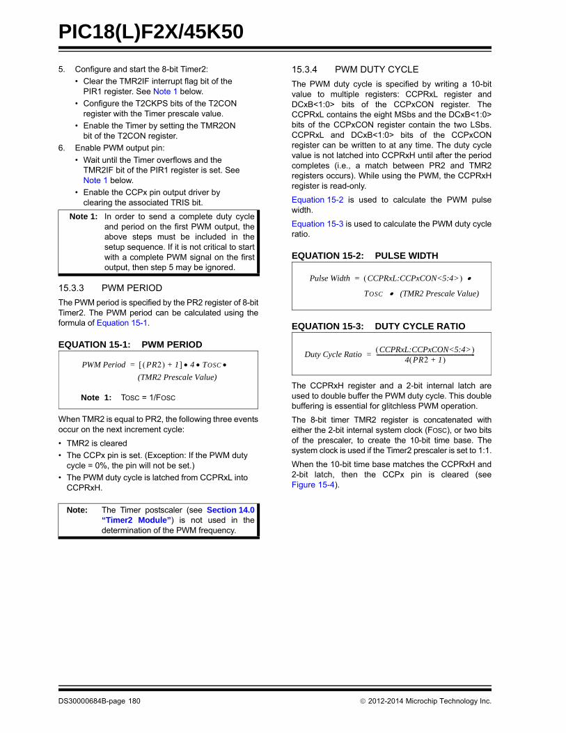
PIC18(L)F2X/45K50
5. Configure and start the 8-bit Timer2:
• Clear the TMR2IF interrupt flag bit of the PIR1 register. See Note 1 below.
• Configure the T2CKPS bits of the T2CON register with the Timer prescale value.
• Enable the Timer by setting the TMR2ON bit of the T2CON register.
6. Enable PWM output pin:
• Wait until the Timer overflows and the TMR2IF bit of the PIR1 register is set. See Note 1 below.
• Enable the CCPx pin output driver by clearing the associated TRIS bit.
15.3.3 PWM PERIOD
The PWM period is specified by the PR2 register of 8-bitTimer2. The PWM period can be calculated using theformula of Equation 15-1.
EQUATION 15-1: PWM PERIOD
When TMR2 is equal to PR2, the following three eventsoccur on the next increment cycle:
• TMR2 is cleared
• The CCPx pin is set. (Exception: If the PWM duty cycle = 0%, the pin will not be set.)
• The PWM duty cycle is latched from CCPRxL into CCPRxH.
15.3.4 PWM DUTY CYCLE
The PWM duty cycle is specified by writing a 10-bitvalue to multiple registers: CCPRxL register andDCxB<1:0> bits of the CCPxCON register. TheCCPRxL contains the eight MSbs and the DCxB<1:0>bits of the CCPxCON register contain the two LSbs.CCPRxL and DCxB<1:0> bits of the CCPxCONregister can be written to at any time. The duty cyclevalue is not latched into CCPRxH until after the periodcompletes (i.e., a match between PR2 and TMR2registers occurs). While using the PWM, the CCPRxHregister is read-only.
Equation 15-2 is used to calculate the PWM pulsewidth.
Equation 15-3 is used to calculate the PWM duty cycleratio.
EQUATION 15-2: PULSE WIDTH
EQUATION 15-3: DUTY CYCLE RATIO
The CCPRxH register and a 2-bit internal latch areused to double buffer the PWM duty cycle. This doublebuffering is essential for glitchless PWM operation.
The 8-bit timer TMR2 register is concatenated witheither the 2-bit internal system clock (FOSC), or two bitsof the prescaler, to create the 10-bit time base. Thesystem clock is used if the Timer2 prescaler is set to 1:1.
When the 10-bit time base matches the CCPRxH and2-bit latch, then the CCPx pin is cleared (seeFigure 15-4).
Note 1: In order to send a complete duty cycleand period on the first PWM output, theabove steps must be included in thesetup sequence. If it is not critical to startwith a complete PWM signal on the firstoutput, then step 5 may be ignored.
Note: The Timer postscaler (see Section 14.0“Timer2 Module”) is not used in thedetermination of the PWM frequency.
PWM Period PR2 1+ 4 TOSC =
(TMR2 Prescale Value)
Note 1: TOSC = 1/FOSC
Pulse Width CCPRxL:CCPxCON<5:4> =
TOSC (TMR2 Prescale Value)
Duty Cycle RatioCCPRxL:CCPxCON<5:4>
4 PR2 1+ -----------------------------------------------------------------------=
DS30000684B-page 180 2012-2014 Microchip Technology Inc.

PIC18(L)F2X/45K50
15.3.5 PWM RESOLUTION
The resolution determines the number of available dutycycles for a given period. For example, a 10-bit resolutionwill result in 1024 discrete duty cycles, whereas an 8-bitresolution will result in 256 discrete duty cycles.
The maximum PWM resolution is 10 bits when PR2 is255. The resolution is a function of the PR2 registervalue as shown by Equation 15-4.
EQUATION 15-4: PWM RESOLUTION
15.3.6 OPERATION IN SLEEP MODE
In Sleep mode, the TMR2 register will not incrementand the state of the module will not change. If the CCPxpin is driving a value, it will continue to drive that value.When the device wakes up, TMR2 will continue from itsprevious state.
15.3.7 CHANGES IN SYSTEM CLOCK FREQUENCY
The PWM frequency is derived from the system clockfrequency. Any changes in the system clock frequencywill result in changes to the PWM frequency. SeeSection 3.0 “Oscillator Module (With Fail-SafeClock Monitor)” for additional details.
15.3.8 EFFECTS OF RESET
Any Reset will force all ports to Input mode and theCCP registers to their Reset states.
Note: If the pulse width value is greater than theperiod the assigned PWM pin(s) willremain unchanged.
Resolution4 PR2 1+ log
2 log------------------------------------------ bits=
TABLE 15-6: EXAMPLE PWM FREQUENCIES AND RESOLUTIONS (FOSC = 32 MHz)
PWM Frequency 1.95 kHz 7.81 kHz 31.25 kHz 125 kHz 250 kHz 333.3 kHz
Timer Prescale (1, 4, 16) 16 4 1 1 1 1
PR2 Value 0xFF 0xFF 0xFF 0x3F 0x1F 0x17
Maximum Resolution (bits) 10 10 10 8 7 6.6
TABLE 15-7: EXAMPLE PWM FREQUENCIES AND RESOLUTIONS (FOSC = 20 MHz)
PWM Frequency 1.22 kHz 4.88 kHz 19.53 kHz 78.12 kHz 156.3 kHz 208.3 kHz
Timer Prescale (1, 4, 16) 16 4 1 1 1 1
PR2 Value 0xFF 0xFF 0xFF 0x3F 0x1F 0x17
Maximum Resolution (bits) 10 10 10 8 7 6.6
TABLE 15-8: EXAMPLE PWM FREQUENCIES AND RESOLUTIONS (FOSC = 8 MHz)
PWM Frequency 1.22 kHz 4.90 kHz 19.61 kHz 76.92 kHz 153.85 kHz 200.0 kHz
Timer Prescale (1, 4, 16) 16 4 1 1 1 1
PR2 Value 0x65 0x65 0x65 0x19 0x0C 0x09
Maximum Resolution (bits) 8 8 8 6 5 5
2012-2014 Microchip Technology Inc. DS30000684B-page 181

PIC18(L)F2X/45K50
TABLE 15-10: CONFIGURATION REGISTERS ASSOCIATED WITH CAPTURE
TABLE 15-9: REGISTERS ASSOCIATED WITH STANDARD PWM
Name Bit 7 Bit 6 Bit 5 Bit 4 Bit 3 Bit 2 Bit 1 Bit 0Register on page
CCP1CON P1M<1:0> DC1B<1:0> CCP1M<3:0> 197
CCP2CON — — DC2B<1:0> CCP2M<3:0> 197
CCPTMRS — — — — C2TSEL — — C1TSEL 200
INTCON GIE/GIEH PEIE/GIEL TMR0IE INT0IE IOCIE TMR0IF INT0IF IOCIF 114
IPR1 ACTIP ADIP RCIP TXIP SSPIP CCP1IP TMR2IP TMR1IP 123
IPR2 OSCFIP C1IP C2IP EEIP BCLIP HLVDIP TMR3IP CCP2IP 124
PIE1 ACTIE ADIE RCIE TXIE SSPIE CCP1IE TMR2IE TMR1IE 120
PIE2 OSCFIE C1IE C2IE EEIE BCLIE HLVDIE TMR3IE CCP2IE 121
PIR1 ACTIF ADIF RCIF TXIF SSPIF CCP1IF TMR2IF TMR1IF 117
PIR2 OSCFIF C1IF C2IF EEIF BCLIF HLVDIF TMR3IF CCP2IF 118
PMD0 — UARTMD USBMD ACTMD — TMR3MD TMR2MD TMR1MD 61
PMD1 — MSSPMD CTMUMD CMP2MD CMP1MD ADCMD CCP2MD CCP1MD 62
PR2 Timer2 Period Register —
T2CON — T2OUTPS<3:0> TMR2ON T2CKPS<1:0> 170
TMR2 Timer2 Period Register —
TRISB TRISB7 TRISB6 TRISB5 TRISB4 TRISB3 TRISB2 TRISB1 TRISB0 149
TRISC TRISC7 TRISC6 — — — TRISC2 TRISC1 TRISC0 149
Legend: — = Unimplemented location, read as ‘0’. Shaded bits are not used by Capture mode.
Name Bit 7 Bit 6 Bit 5 Bit 4 Bit 3 Bit 2 Bit 1 Bit 0Register on page
CONFIG3H MCLRE SDOMX — T3CMX — — PBADEN CCP2MX 376
Legend: — = Unimplemented location, read as ‘0’. Shaded bits are not used by Capture mode.
DS30000684B-page 182 2012-2014 Microchip Technology Inc.
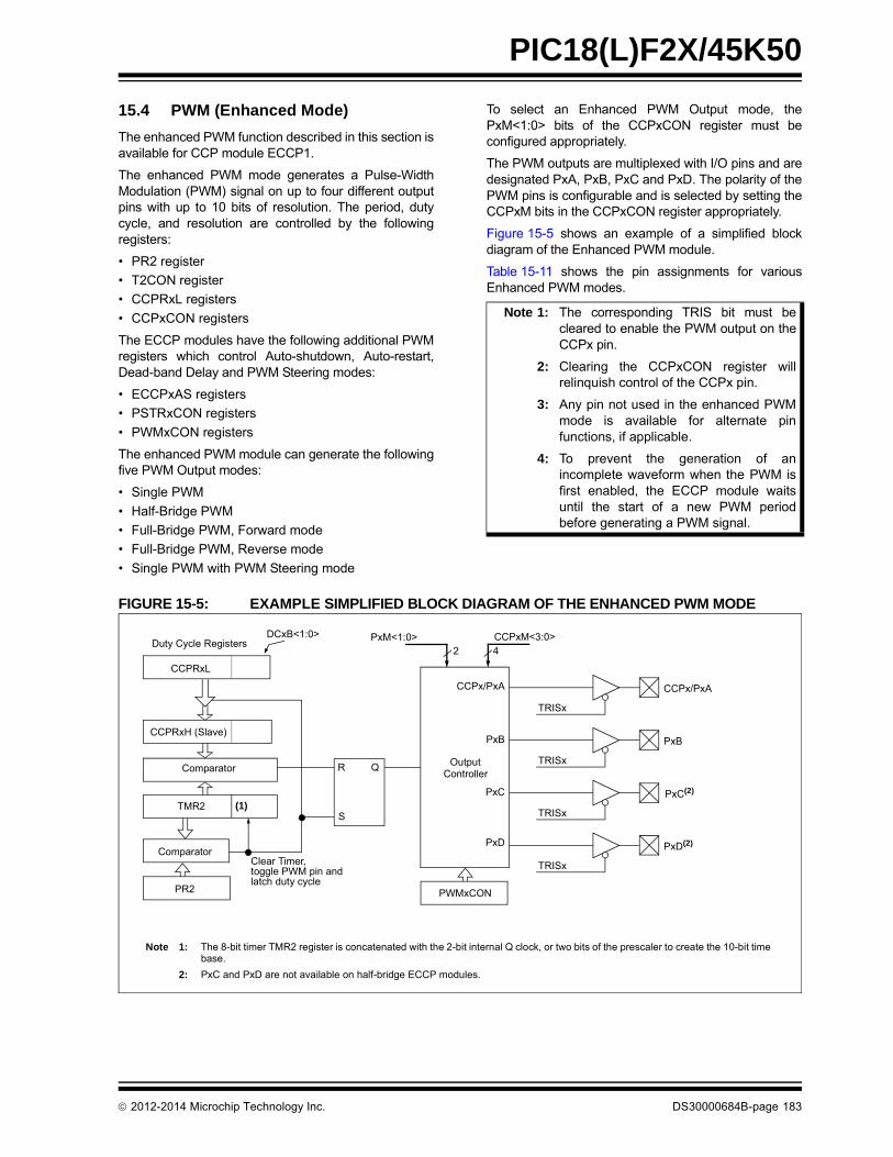
PIC18(L)F2X/45K50
15.4 PWM (Enhanced Mode)
The enhanced PWM function described in this section isavailable for CCP module ECCP1.
The enhanced PWM mode generates a Pulse-WidthModulation (PWM) signal on up to four different outputpins with up to 10 bits of resolution. The period, dutycycle, and resolution are controlled by the followingregisters:
• PR2 register
• T2CON register
• CCPRxL registers
• CCPxCON registers
The ECCP modules have the following additional PWMregisters which control Auto-shutdown, Auto-restart,Dead-band Delay and PWM Steering modes:
• ECCPxAS registers
• PSTRxCON registers
• PWMxCON registers
The enhanced PWM module can generate the followingfive PWM Output modes:
• Single PWM
• Half-Bridge PWM
• Full-Bridge PWM, Forward mode
• Full-Bridge PWM, Reverse mode
• Single PWM with PWM Steering mode
To select an Enhanced PWM Output mode, thePxM<1:0> bits of the CCPxCON register must beconfigured appropriately.
The PWM outputs are multiplexed with I/O pins and aredesignated PxA, PxB, PxC and PxD. The polarity of thePWM pins is configurable and is selected by setting theCCPxM bits in the CCPxCON register appropriately.
Figure 15-5 shows an example of a simplified blockdiagram of the Enhanced PWM module.
Table 15-11 shows the pin assignments for variousEnhanced PWM modes.
FIGURE 15-5: EXAMPLE SIMPLIFIED BLOCK DIAGRAM OF THE ENHANCED PWM MODE
Note 1: The corresponding TRIS bit must becleared to enable the PWM output on theCCPx pin.
2: Clearing the CCPxCON register willrelinquish control of the CCPx pin.
3: Any pin not used in the enhanced PWMmode is available for alternate pinfunctions, if applicable.
4: To prevent the generation of anincomplete waveform when the PWM isfirst enabled, the ECCP module waitsuntil the start of a new PWM periodbefore generating a PWM signal.
CCPRxL
CCPRxH (Slave)
Comparator
TMR2
Comparator
PR2
(1)
R Q
S
Duty Cycle RegistersDCxB<1:0>
Clear Timer,toggle PWM pin and latch duty cycle
Note 1: The 8-bit timer TMR2 register is concatenated with the 2-bit internal Q clock, or two bits of the prescaler to create the 10-bit timebase.
2: PxC and PxD are not available on half-bridge ECCP modules.
TRISx
CCPx/PxA
TRISx
PxB
TRISx
PxC(2)
TRISx
PxD(2)
OutputController
PxM<1:0>2
CCPxM<3:0>4
PWMxCON
CCPx/PxA
PxB
PxC
PxD
2012-2014 Microchip Technology Inc. DS30000684B-page 183

PIC18(L)F2X/45K50
FIGURE 15-6: EXAMPLE PWM (ENHANCED MODE) OUTPUT RELATIONSHIPS (ACTIVE-HIGH STATE)
TABLE 15-11: EXAMPLE PIN ASSIGNMENTS FOR VARIOUS PWM ENHANCED MODES
ECCP Mode PxM<1:0> CCPx/PxA PxB PxC PxD
Single 00 Yes(1) Yes(1) Yes(1) Yes(1)
Half-Bridge 10 Yes Yes No No
Full-Bridge, Forward 01 Yes Yes Yes Yes
Full-Bridge, Reverse 11 Yes Yes Yes Yes
Note 1: PWM Steering enables outputs in Single mode.
0
Period
00
10
01
11
SignalPRX+1
PxM<1:0>
PxA Modulated
PxA Modulated
PxB Modulated
PxA Active
PxB Inactive
PxC Inactive
PxD Modulated
PxA Inactive
PxB Modulated
PxC Active
PxD Inactive
PulseWidth
(Single Output)
(Half-Bridge)
(Full-Bridge,Forward)
(Full-Bridge,Reverse)
Delay(1) Delay(1)
Relationships:• Period = 4 * TOSC * (PRx + 1) * (TMRx Prescale Value)• Pulse Width = TOSC * (CCPRxL<7:0>:CCPxCON<5:4>) * (TMRx Prescale Value)• Delay = 4 * TOSC * (PWMxCON<6:0>)
Note 1: Dead-band delay is programmed using the PWMxCON register (Section 15.4.5 “Programmable Dead-Band DelayMode”).
DS30000684B-page 184 2012-2014 Microchip Technology Inc.
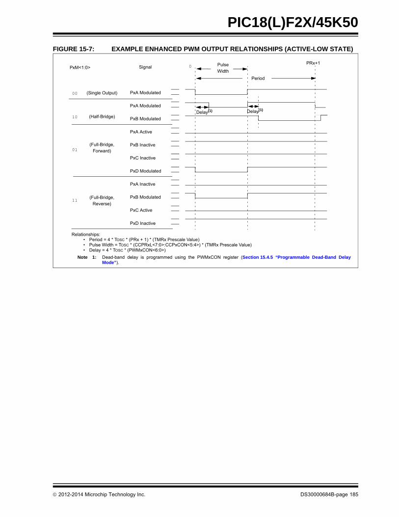
PIC18(L)F2X/45K50
FIGURE 15-7: EXAMPLE ENHANCED PWM OUTPUT RELATIONSHIPS (ACTIVE-LOW STATE)
0
Period
00
10
01
11
SignalPRx+1
PxM<1:0>
PxA Modulated
PxA Modulated
PxB Modulated
PxA Active
PxB Inactive
PxC Inactive
PxD Modulated
PxA Inactive
PxB Modulated
PxC Active
PxD Inactive
Pulse
Width
(Single Output)
(Half-Bridge)
(Full-Bridge,
Forward)
(Full-Bridge,
Reverse)
Delay(1) Delay(1)
Relationships:• Period = 4 * TOSC * (PRx + 1) * (TMRx Prescale Value)• Pulse Width = TOSC * (CCPRxL<7:0>:CCPxCON<5:4>) * (TMRx Prescale Value)• Delay = 4 * TOSC * (PWMxCON<6:0>)
Note 1: Dead-band delay is programmed using the PWMxCON register (Section 15.4.5 “Programmable Dead-Band DelayMode”).
2012-2014 Microchip Technology Inc. DS30000684B-page 185

PIC18(L)F2X/45K50
15.4.1 HALF-BRIDGE MODE
In Half-Bridge mode, two pins are used as outputs todrive push-pull loads. The PWM output signal is outputon the CCPx/PxA pin, while the complementary PWMoutput signal is output on the PxB pin (see Figure 15-9).This mode can be used for half-bridge applications, asshown in Figure 15-9, or for full-bridge applications,where four power switches are being modulated withtwo PWM signals.
In Half-Bridge mode, the programmable dead-band delaycan be used to prevent shoot-through current in half-bridge power devices. The value of the PDC<6:0> bits ofthe PWMxCON register sets the number of instructioncycles before the output is driven active. If the value isgreater than the duty cycle, the corresponding outputremains inactive during the entire cycle. SeeSection 15.4.5 “Programmable Dead-Band DelayMode” for more details of the dead-band delayoperations.
Since the PxA and PxB outputs are multiplexed with thePORT data latches, the associated TRIS bits must becleared to configure PxA and PxB as outputs.
FIGURE 15-8: EXAMPLE OF HALF-BRIDGE PWM OUTPUT
FIGURE 15-9: EXAMPLE OF HALF-BRIDGE APPLICATIONS
Period
Pulse Width
td
td
(1)
PxA(2)
PxB(2)
td = Dead-Band Delay
Period
(1) (1)
Note 1: At this time, the TMRx register is equal to thePRx register.
2: Output signals are shown as active-high.
PxA
PxB
FETDriver
FETDriver
Load
+
-
+
-
FETDriver
FETDriver
V+
Load
FETDriver
FETDriver
PxA
PxB
Standard Half-Bridge Circuit (“Push-Pull”)
Half-Bridge Output Driving a Full-Bridge Circuit
DS30000684B-page 186 2012-2014 Microchip Technology Inc.
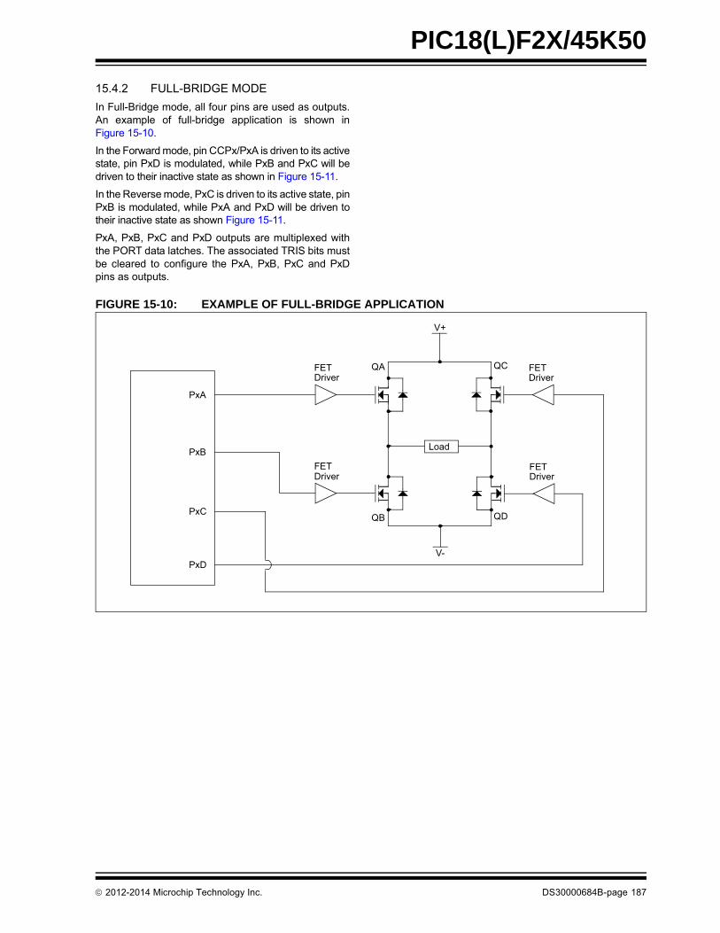
PIC18(L)F2X/45K50
15.4.2 FULL-BRIDGE MODE
In Full-Bridge mode, all four pins are used as outputs.An example of full-bridge application is shown inFigure 15-10.
In the Forward mode, pin CCPx/PxA is driven to its activestate, pin PxD is modulated, while PxB and PxC will bedriven to their inactive state as shown in Figure 15-11.
In the Reverse mode, PxC is driven to its active state, pinPxB is modulated, while PxA and PxD will be driven totheir inactive state as shown Figure 15-11.
PxA, PxB, PxC and PxD outputs are multiplexed withthe PORT data latches. The associated TRIS bits mustbe cleared to configure the PxA, PxB, PxC and PxDpins as outputs.
FIGURE 15-10: EXAMPLE OF FULL-BRIDGE APPLICATION
PxA
PxC
FETDriver
FETDriver
V+
V-
Load
FETDriver
FETDriver
PxB
PxD
QA
QB QD
QC
2012-2014 Microchip Technology Inc. DS30000684B-page 187

PIC18(L)F2X/45K50
FIGURE 15-11: EXAMPLE OF FULL-BRIDGE PWM OUTPUT
Period
Pulse Width
PxA(2)
PxB(2)
PxC(2)
PxD(2)
Forward Mode
(1)
Period
Pulse Width
PxA(2)
PxC(2)
PxD(2)
PxB(2)
Reverse Mode
(1)
(1)(1)
Note 1: At this time, the TMRx register is equal to the PRx register.
2: Output signal is shown as active-high.
DS30000684B-page 188 2012-2014 Microchip Technology Inc.
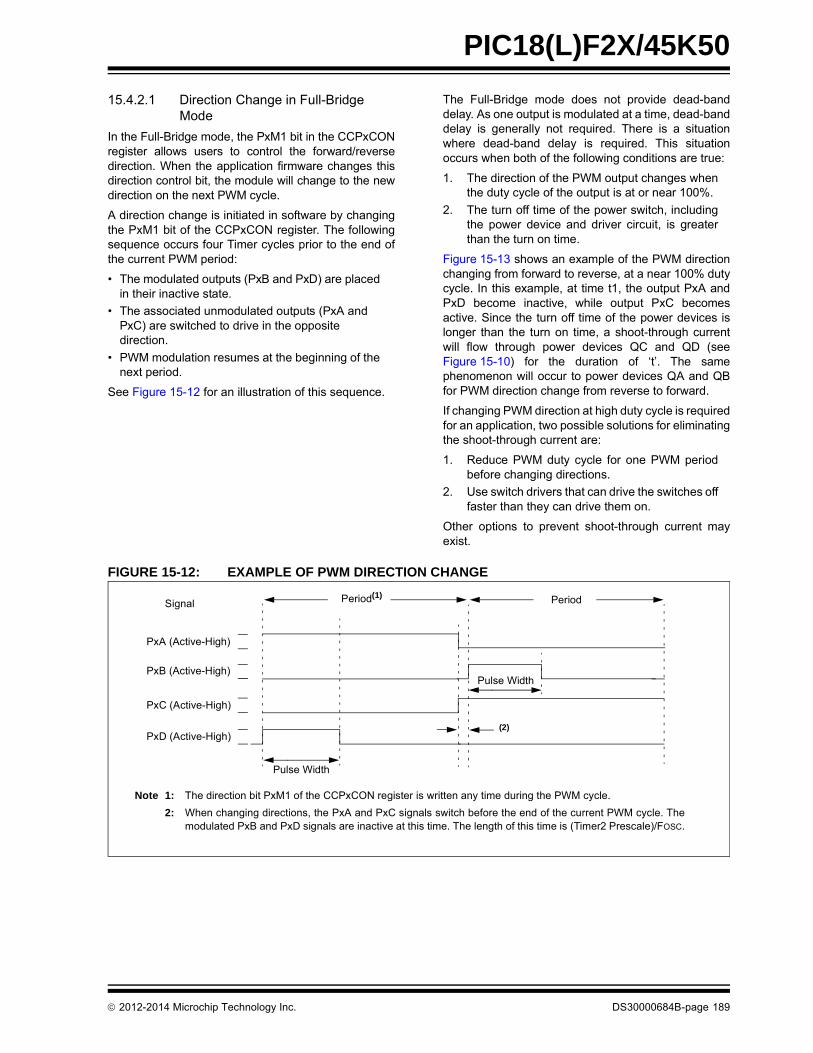
PIC18(L)F2X/45K50
15.4.2.1 Direction Change in Full-Bridge Mode
In the Full-Bridge mode, the PxM1 bit in the CCPxCONregister allows users to control the forward/reversedirection. When the application firmware changes thisdirection control bit, the module will change to the newdirection on the next PWM cycle.
A direction change is initiated in software by changingthe PxM1 bit of the CCPxCON register. The followingsequence occurs four Timer cycles prior to the end ofthe current PWM period:
• The modulated outputs (PxB and PxD) are placed in their inactive state.
• The associated unmodulated outputs (PxA and PxC) are switched to drive in the opposite direction.
• PWM modulation resumes at the beginning of the next period.
See Figure 15-12 for an illustration of this sequence.
The Full-Bridge mode does not provide dead-banddelay. As one output is modulated at a time, dead-banddelay is generally not required. There is a situationwhere dead-band delay is required. This situationoccurs when both of the following conditions are true:
1. The direction of the PWM output changes whenthe duty cycle of the output is at or near 100%.
2. The turn off time of the power switch, includingthe power device and driver circuit, is greaterthan the turn on time.
Figure 15-13 shows an example of the PWM directionchanging from forward to reverse, at a near 100% dutycycle. In this example, at time t1, the output PxA andPxD become inactive, while output PxC becomesactive. Since the turn off time of the power devices islonger than the turn on time, a shoot-through currentwill flow through power devices QC and QD (seeFigure 15-10) for the duration of ‘t’. The samephenomenon will occur to power devices QA and QBfor PWM direction change from reverse to forward.
If changing PWM direction at high duty cycle is requiredfor an application, two possible solutions for eliminatingthe shoot-through current are:
1. Reduce PWM duty cycle for one PWM periodbefore changing directions.
2. Use switch drivers that can drive the switches offfaster than they can drive them on.
Other options to prevent shoot-through current mayexist.
FIGURE 15-12: EXAMPLE OF PWM DIRECTION CHANGE
Pulse Width
Period(1)Signal
Note 1: The direction bit PxM1 of the CCPxCON register is written any time during the PWM cycle.
2: When changing directions, the PxA and PxC signals switch before the end of the current PWM cycle. Themodulated PxB and PxD signals are inactive at this time. The length of this time is (Timer2 Prescale)/FOSC.
Period
(2)
PxA (Active-High)
PxB (Active-High)
PxC (Active-High)
PxD (Active-High)
Pulse Width
2012-2014 Microchip Technology Inc. DS30000684B-page 189

PIC18(L)F2X/45K50
FIGURE 15-13: EXAMPLE OF PWM DIRECTION CHANGE AT NEAR 100% DUTY CYCLE
15.4.3 ENHANCED PWM AUTO-SHUTDOWN MODE
The PWM mode supports an Auto-Shutdown mode thatwill disable the PWM outputs when an externalshutdown event occurs. Auto-Shutdown mode placesthe PWM output pins into a predetermined state. Thismode is used to help prevent the PWM from damagingthe application.
The auto-shutdown sources are selected using theECCPxAS register. A shutdown event may be generatedby:
• A logic ‘0’ on the FLTx pin
• Comparator Cx (async_CxOUT)
• Setting the ECCPxASE bit in firmware
A shutdown condition is indicated by the ECCPxASE(Auto-Shutdown Event Status) bit of the ECCPxASregister. If the bit is a ‘0’, the PWM pins are operatingnormally. If the bit is a ‘1’, the PWM outputs are in theshutdown state.
When a shutdown event occurs, two things happen:
The ECCPxASE bit is set to ‘1’. The ECCPxASE willremain set until cleared in firmware or an auto-restartoccurs (see Section 15.4.4 “Auto-Restart Mode”).
The enabled PWM pins are asynchronously placed intheir shutdown states. The PWM output pins aregrouped into pairs [PxA/PxC] and [PxB/PxD]. The state
of each pin pair is determined by the PSSxAC<1:0> andPSSxBD<1:0> bits of the ECCPxAS register. Each pinpair may be placed into one of three states:
• Drive logic ‘1’
• Drive logic ‘0’
• Tri-state (high-impedance)
Forward Period Reverse Period
PxA
TON
TOFF
T = TOFF – TON
PxB
PxC
PxD
External Switch D
PotentialShoot-Through Current
Note 1: All signals are shown as active-high.
2: TON is the turn-on delay of power switch QC and its driver.
3: TOFF is the turn-off delay of power switch QD and its driver.
External Switch C
t1
PW
PW
Note 1: The auto-shutdown condition is a level-based signal, not an edge-based signal.As long as the level is present, the auto-shutdown will persist.
2: Writing to the ECCPxASE bit is disabledwhile an auto-shutdown conditionpersists.
3: Once the auto-shutdown condition hasbeen removed and the PWM restarted(either through firmware or auto-restart),the PWM signal will always restart at thebeginning of the next PWM period.
DS30000684B-page 190 2012-2014 Microchip Technology Inc.

PIC18(L)F2X/45K50
FIGURE 15-14: PWM AUTO-SHUTDOWN WITH FIRMWARE RESTART (PxRSEN = 0)
15.4.4 AUTO-RESTART MODE
The Enhanced PWM can be configured toautomatically restart the PWM signal once the auto-shutdown condition has been removed. Auto-restart isenabled by setting the PxRSEN bit in the PWMxCONregister.
If auto-restart is enabled, the ECCPxASE bit willremain set as long as the auto-shutdown condition isactive. When the auto-shutdown condition is removed,the ECCPxASE bit will be cleared via hardware andnormal operation will resume.
FIGURE 15-15: PWM AUTO-SHUTDOWN WITH AUTO-RESTART (PXRSEN = 1)
Shutdown
PWM
ECCPxASE bit
Activity
Event
ShutdownEvent Occurs
ShutdownEvent Clears
PWMResumes
PWM Period
Start ofPWM Period
ECCPxASECleared byFirmware
TimerOverflow
TimerOverflow
TimerOverflow
TimerOverflow
Missing Pulse(Auto-Shutdown)
Missing Pulse(ECCPxASE not clear)
TimerOverflow
Shutdown
PWM
ECCPxASE bit
Activity
Event
ShutdownEvent Occurs
ShutdownEvent Clears
PWM Period
Start ofPWM Period
ECCPxASECleared byHardware
TimerOverflow
TimerOverflow
TimerOverflow
TimerOverflow
Missing Pulse(Auto-Shutdown)
Missing Pulse(ECCPxASE not clear)
TimerOverflow
PWMResumes
2012-2014 Microchip Technology Inc. DS30000684B-page 191

PIC18(L)F2X/45K50
15.4.5 PROGRAMMABLE DEAD-BAND DELAY MODE
In half-bridge applications where all power switches aremodulated at the PWM frequency, the power switchesnormally require more time to turn off than to turn on. Ifboth the upper and lower power switches are switchedat the same time (one turned on, and the other turnedoff), both switches may be on for a short period of timeuntil one switch completely turns off. During this briefinterval, a very high current (shoot-through current) willflow through both power switches, shorting the bridgesupply. To avoid this potentially destructive shoot-through current from flowing during switching, turningon either of the power switches is normally delayed toallow the other switch to completely turn off.
In Half-Bridge mode, a digitally programmable dead-band delay is available to avoid shoot-through currentfrom destroying the bridge power switches. The delayoccurs at the signal transition from the non-active stateto the active state. See Figure 15-16 for illustration.The lower seven bits of the associated PWMxCONregister (Register 15-5) sets the delay period in termsof microcontroller instruction cycles (TCY or 4 TOSC).
FIGURE 15-16: EXAMPLE OF HALF-BRIDGE PWM OUTPUT
FIGURE 15-17: EXAMPLE OF HALF-BRIDGE APPLICATIONS
Period
Pulse Width
td
td
(1)
PxA(2)
PxB(2)
td = Dead-Band Delay
Period
(1) (1)
Note 1: At this time, the TMRx register is equal to thePRx register.
2: Output signals are shown as active-high.
PxA
PxB
FETDriver
FETDriver
V+
V-
Load
+V-
+V-
Standard Half-Bridge Circuit (“Push-Pull”)
DS30000684B-page 192 2012-2014 Microchip Technology Inc.

PIC18(L)F2X/45K50
15.4.6 PWM STEERING MODE
In Single Output mode, PWM steering allows any of thePWM pins to be the modulated signal. Additionally, thesame PWM signal can be simultaneously available onmultiple pins.
Once the Single Output mode is selected(CCPxM<3:2> = 11 and PxM<1:0> = 00 of theCCPxCON register), the user firmware can bring outthe same PWM signal to one, two, three or four outputpins by setting the appropriate Steering Enable bits(STRxA, STRxB, STRxC and/or STRxD) of thePSTRxCON register, as shown in Table 15-12.
While the PWM Steering mode is active, CCPxM<1:0>bits of the CCPxCON register select the PWM outputpolarity for the PxD, PxC, PxB and PxA pins.
The PWM auto-shutdown operation also applies toPWM Steering mode as described in Section 15.4.3“Enhanced PWM Auto-Shutdown Mode”. An auto-shutdown event will only affect pins that have PWMoutputs enabled.
FIGURE 15-18: SIMPLIFIED STEERING BLOCK DIAGRAM
15.4.6.1 Steering Synchronization
The STRxSYNC bit of the PSTRxCON register givesthe user two selections of when the steering event willhappen. When the STRxSYNC bit is ‘0’, the steeringevent will happen at the end of the instruction thatwrites to the PSTRxCON register. In this case, theoutput signal at the PxA, PxB, PxC and PxD pins maybe an incomplete PWM waveform. This operation isuseful when the user firmware needs to immediatelyremove a PWM signal from the pin.
When the STRxSYNC bit is ‘1’, the effective steeringupdate will happen at the beginning of the next PWMperiod. In this case, steering on/off the PWM output willalways produce a complete PWM waveform.
Figures 15-19 and 15-20 illustrate the timing diagramsof the PWM steering depending on the STRxSYNCsetting.
Note: The associated TRIS bits must be set tooutput (‘0’) to enable the pin output driverin order to see the PWM signal on the pin.
1
0TRIS
PxA pin
PORT Data
PxA Signal
STRxA
1
0TRIS
PxB pin
PORT Data
STRxB
1
0TRIS
PxC pin
PORT Data
STRxC
1
0TRIS
PxD pin
PORT Data
STRxD
Note 1: Port outputs are configured as shown whenthe CCPxCON register bits PxM<1:0> = 00and CCPxM<3:2> = 11.
2: Single PWM output requires setting at leastone of the STRx bits.
CCPxM1
CCPxM0
CCPxM1
CCPxM0
2012-2014 Microchip Technology Inc. DS30000684B-page 193

PIC18(L)F2X/45K50
15.4.7 START-UP CONSIDERATIONS
When any PWM mode is used, the applicationhardware must use the proper external pull-up and/orpull-down resistors on the PWM output pins.
The CCPxM<1:0> bits of the CCPxCON register allowthe user to choose whether the PWM output signals areactive-high or active-low for each pair of PWM outputpins (PxA/PxC and PxB/PxD). The PWM outputpolarities must be selected before the PWM pin outputdrivers are enabled. Changing the polarityconfiguration while the PWM pin output drivers areenabled is not recommended since it may result indamage to the application circuits.
The PxA, PxB, PxC and PxD output latches may not bein the proper states when the PWM module isinitialized. Enabling the PWM pin output drivers at thesame time as the Enhanced PWM modes may causedamage to the application circuit. The Enhanced PWM
modes must be enabled in the proper Output mode andcomplete a full PWM cycle before enabling the PWMpin output drivers. The completion of a full PWM cycleis indicated by the TMR2IF bit of the PIR1 registerbeing set as the second PWM period begins.
FIGURE 15-19: EXAMPLE OF STEERING EVENT AT END OF INSTRUCTION (STRxSYNC = 0)
FIGURE 15-20: EXAMPLE OF STEERING EVENT AT BEGINNING OF INSTRUCTION(STRxSYNC = 1)
Note: When the microcontroller is released fromReset, all of the I/O pins are in the high-impedance state. The external circuitsmust keep the power switch devices in theOff state until the microcontroller drivesthe I/O pins with the proper signal levels oractivates the PWM output(s).
PWM
P1n = PWM
STRx
P1<D:A> PORT Data
PWM Period
PORT Data
PWM
PORT Data
P1n = PWM
STRx
P1<D:A> PORT Data
DS30000684B-page 194 2012-2014 Microchip Technology Inc.
PIC18(L)F2X/45K50
15.4.8 SETUP FOR ECCP PWM OPERATION USING ECCP1 AND TIMER2
The following steps should be taken when configuringthe ECCP1 module for PWM operation using Timer2:
1. Configure the PWM pins to be used (P1A, P1B,P1C, and P1D):
• Configure PWM outputs to be used as inputs by setting the corresponding TRIS bits. This prevents spurious outputs during setup.
• Set the PSTR1CON bits for each PWM output to be used.
2. Set the PWM period by loading the PR2 register.
3. Configure auto-shutdown as OFF or select thesource with the CCP1AS<2:0> bits of theECCP1AS register.
4. Configure the auto-shutdown sources asneeded:
• Configure each comparator used.
• Configure the comparator inputs as analog.
• Configure the FLT0 input pin and clear ANSB0.
5. Force a shutdown condition (OFF included):
• Configure safe starting output levels by setting the default shutdown drive states with the PSS1AC<1:0> and PSS1BD<1:0> bits of the ECCP1AS register.
• Clear the P1RSEN bit of the PWM1CON register.
• Set the CCP1AS bit of the ECCP1AS register.
6. Configure the ECCP1 module for the desiredPWM mode and configuration by loading theCCP1CON register with the appropriate values:
• Select one of the available output configura-tions and direction with the P1M<1:0> bits.
• Select the polarities of the PWM output signals with the CCP1M<3:0> bits.
7. Set the 10-bit PWM duty cycle:
• Load the eight MS bits into the CCPR1L register.
• Load the two LS bits into the DC<1:0> bits of the CCP1CON register.
8. For Half-Bridge Output mode, set the dead-band delay by loading P1DC<6:0> bits of thePWM1CON register with the appropriate value.
9. Configure and start TMR2:
• Set the TMR2 prescale value by loading the T2CKPS bits of the T2CON register.
• Start Timer2 by setting the TMR2ON bit.
10. Enable the ECCP1/P1A, P1B, P1C and/or P1Dpin outputs by clearing the respective TRIS bits.
11. Start the PWM:
• If shutdown auto-restart is used, then set the P1RSEN bit of the PWM1CON register.
• If shutdown auto-restart is not used, then clear the CCP1ASE bit of the ECCP1AS register.
2012-2014 Microchip Technology Inc. DS30000684B-page 195

PIC18(L)F2X/45K50
TABLE 15-12: REGISTERS ASSOCIATED WITH ENHANCED PWM
Name Bit 7 Bit 6 Bit 5 Bit 4 Bit 3 Bit 2 Bit 1 Bit 0Register on
page
ECCP1AS ECCP1ASE ECCP1AS<2:0> PSS1AC<1:0> PSS1BD<1:0> 201
CCP1CON P1M<1:0> DC1B<1:0> CCP1M<3:0> 197
CCPTMRS — — — — C2TSEL — — C1TSEL 200
INTCON GIE/GIEH PEIE/GIEL TMR0IE INT0IE IOCIE TMR0IF INT0IF IOCIF 114
IPR1 ACTIP ADIP RCIP TXIP SSPIP CCP1IP TMR2IP TMR1IP 123
IPR2 OSCFIP C1IP C2IP EEIP BCLIP HLVDIP TMR3IP CCP2IP 124
PIE1 ACTIE ADIE RCIE TXIE SSPIE CCP1IE TMR2IE TMR1IE 120
PIE2 OSCFIE C1IE C2IE EEIE BCLIE HLVDIE TMR3IE CCP2IE 121
PIR1 ACTIF ADIF RCIF TXIF SSPIF CCP1IF TMR2IF TMR1IF 117
PIR2 OSCFIF C1IF C2IF EEIF BCLIF HLVDIF TMR3IF CCP2IF 118
PMD0 — UARTMD USBMD ACTMD — TMR3MD TMR2MD TMR1MD 61
PMD1 — MSSPMD CTMUMD CMP2MD CMP1MD ADCMD CCP2MD CCP1MD 62
PR2 Timer2 Period Register —
PSTR1CON — — — STR1SYNC STR1D STR1C STR1B STR1A 202
PWM1CON P1RSEN P1DC<6:0> 202
T2CON — T2OUTPS<3:0> TMR2ON T2CKPS<1:0> 170
TMR2 Timer2 Period Register —
TRISB TRISB7 TRISB6 TRISB5 TRISB4 TRISB3 TRISB2 TRISB1 TRISB0 149
TRISC TRISC7 TRISC6 — — — TRISC2 TRISC1 TRISC0 149
TRISD(1) TRISD7 TRISD6 TRISD5 TRISD4 TRISD3 TRISD2 TRISD1 TRISD0 149
Legend: — = Unimplemented location, read as ‘0’. Shaded bits are not used by Capture mode.
Note 1: These registers/bits are available on PIC18(L)F45K50 devices.
DS30000684B-page 196 2012-2014 Microchip Technology Inc.
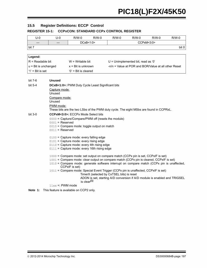
PIC18(L)F2X/45K50
15.5 Register Definitions: ECCP Control
REGISTER 15-1: CCPxCON: STANDARD CCPx CONTROL REGISTER
U-0 U-0 R/W-0 R/W-0 R/W-0 R/W-0 R/W-0 R/W-0
— — DCxB<1:0> CCPxM<3:0>
bit 7 bit 0
Legend:
R = Readable bit W = Writable bit U = Unimplemented bit, read as ‘0’
u = Bit is unchanged x = Bit is unknown -n/n = Value at POR and BOR/Value at all other Reset
‘1’ = Bit is set ‘0’ = Bit is cleared
bit 7-6 Unused
bit 5-4 DCxB<1:0>: PWM Duty Cycle Least Significant bits
Capture mode:Unused
Compare mode:Unused
PWM mode:These bits are the two LSbs of the PWM duty cycle. The eight MSbs are found in CCPRxL.
bit 3-0 CCPxM<3:0>: ECCPx Mode Select bits
0000 = Capture/Compare/PWM off (resets the module)0001 = Reserved 0010 = Compare mode: toggle output on match0011 = Reserved
0100 = Capture mode: every falling edge 0101 = Capture mode: every rising edge0110 = Capture mode: every 4th rising edge 0111 = Capture mode: every 16th rising edge
1000 = Compare mode: set output on compare match (CCPx pin is set, CCPxIF is set)1001 = Compare mode: clear output on compare match (CCPx pin is cleared, CCPxIF is set)1010 = Compare mode: generate software interrupt on compare match (CCPx pin is unaffected,
CCPxIF is set)1011 = Compare mode: Special Event Trigger (CCPx pin is unaffected, CCPxIF is set)
TimerX (selected by CxTSEL bits) is resetADON is set, starting A/D conversion if A/D module is enabled and TRIGSELis clear(1)
11xx =: PWM mode
Note 1: This feature is available on CCP2 only.
2012-2014 Microchip Technology Inc. DS30000684B-page 197

PIC18(L)F2X/45K50
REGISTER 15-2: CCPxCON: ENHANCED CCPx CONTROL REGISTER
R/x-0 R/W-0 R/W-0 R/W-0 R/W-0 R/W-0 R/W-0 R/W-0
PxM<1:0> DCxB<1:0> CCPxM<3:0>
bit 7 bit 0
Legend:
R = Readable bit W = Writable bit U = Unimplemented bit, read as ‘0’
u = Bit is unchanged x = Bit is unknown -n/n = Value at POR and BOR/Value at all other Reset
‘1’ = Bit is set ‘0’ = Bit is cleared
bit 7-6 PxM<1:0>: Enhanced PWM Output Configuration bitsIf CCPxM<3:2> = 00, 01, 10: (Capture/Compare modes)
xx = PxA assigned as Capture/Compare input; PxB, PxC, PxD assigned as port pins
Half-Bridge ECCP Modules(1):If CCPxM<3:2> = 11: (PWM modes)
0x = Single output; PxA modulated; PxB assigned as port pin 1x = Half-bridge output; PxA, PxB modulated with dead-band control
Full-Bridge ECCP Modules(1):If CCPxM<3:2> = 11: (PWM modes)
00 = Single output; PxA modulated; PxB, PxC, PxD assigned as port pins 01 = Full-bridge output forward; PxD modulated; PxA active; PxB, PxC inactive10 = Half-bridge output; PxA, PxB modulated with dead-band control; PxC, PxD assigned as port
pins 11 = Full-bridge output reverse; PxB modulated; PxC active; PxA, PxD inactive
bit 5-4 DCxB<1:0>: PWM Duty Cycle Least Significant bits
Capture mode:Unused
Compare mode:Unused
PWM mode:These bits are the two LSbs of the PWM duty cycle. The eight MSbs are found in CCPRxL.
Note 1: See Table 15-1 to determine full-bridge and half-bridge ECCPs for the device being used.
DS30000684B-page 198 2012-2014 Microchip Technology Inc.

PIC18(L)F2X/45K50
bit 3-0 CCPxM<3:0>: ECCPx Mode Select bits
0000 = Capture/Compare/PWM off (resets the module)0001 = Reserved 0010 = Compare mode: toggle output on match0011 = Reserved
0100 = Capture mode: every falling edge 0101 = Capture mode: every rising edge0110 = Capture mode: every 4th rising edge 0111 = Capture mode: every 16th rising edge
1000 = Compare mode: set output on compare match (CCPx pin is set, CCPxIF is set)1001 = Compare mode: clear output on compare match (CCPx pin is cleared, CCPxIF is set)1010 = Compare mode: generate software interrupt on compare match (CCPx pin is unaffected,
CCPxIF is set)1011 = Compare mode: Special Event Trigger (CCPx pin is unaffected, CCPxIF is set)
TimerX is reset
Half-Bridge ECCP Modules(1):1100 = PWM mode: PxA active-high; PxB active-high 1101 = PWM mode: PxA active-high; PxB active-low1110 = PWM mode: PxA active-low; PxB active-high1111 = PWM mode: PxA active-low; PxB active-low
Full-Bridge ECCP Modules(1):1100 = PWM mode: PxA, PxC active-high; PxB, PxD active-high 1101 = PWM mode: PxA, PxC active-high; PxB, PxD active-low1110 = PWM mode: PxA, PxC active-low; PxB, PxD active-high1111 = PWM mode: PxA, PxC active-low; PxB, PxD active-low
REGISTER 15-2: CCPxCON: ENHANCED CCPx CONTROL REGISTER (CONTINUED)
Note 1: See Table 15-1 to determine full-bridge and half-bridge ECCPs for the device being used.
2012-2014 Microchip Technology Inc. DS30000684B-page 199

PIC18(L)F2X/45K50
REGISTER 15-3: CCPTMRS: PWM TIMER SELECTION CONTROL REGISTER 0
U-0 U-0 U-0 U-0 R/W-0 U-0 U-0 R/W-0
— — — — C2TSEL — — C1TSEL
bit 7 bit 0
Legend:
R = Readable bit W = Writable bit U = Unimplemented bit, read as ‘0’
u = Bit is unchanged x = Bit is unknown -n/n = Value at POR and BOR/Value at all other Resets
‘1’ = Bit is set ‘0’ = Bit is cleared
bit 7-4 Unimplemented: Read as ‘0’
bit 3 C2TSEL: CCP2 Timer Selection bit0 = CCP2 – Capture/Compare modes use TMR1, PWM modes use TMR21 = CCP2 – Capture/Compare modes use TMR3, PWM modes use TMR2
bit 2-1 Unimplemented: Read as ‘0’
bit 0 C1TSEL: ECCP1 Timer Selection bit0 = ECCP1 – Capture/Compare modes use TMR1, PWM modes use TMR21 = ECCP1 – Capture/Compare modes use TMR3, PWM modes use TMR2
DS30000684B-page 200 2012-2014 Microchip Technology Inc.

PIC18(L)F2X/45K50
REGISTER 15-4: ECCPxAS: CCPX AUTO-SHUTDOWN CONTROL REGISTER
R/W-0 R/W-0 R/W-0 R/W-0 R/W-0 R/W-0 R/W-0 R/W-0
ECCPxASE ECCPxAS<2:0> PSSxAC<1:0> PSSxBD<1:0>
bit 7 bit 0
Legend:
R = Readable bit W = Writable bit U = Unimplemented bit, read as ‘0’
u = Bit is unchanged x = Bit is unknown -n/n = Value at POR and BOR/Value at all other Resets
‘1’ = Bit is set ‘0’ = Bit is cleared
bit 7 ECCPxASE: CCPx Auto-shutdown Event Status bitif PxRSEN = 1; 1 = An Auto-shutdown event occurred; ECCPxASE bit will automatically clear when event goes away;
CCPx outputs in shutdown state0 = CCPx outputs are operatingif PxRSEN = 0;1 = An Auto-shutdown event occurred; bit must be cleared in software to restart PWM;
CCPx outputs in shutdown state0 = CCPx outputs are operating
bit 6-4 ECCPxAS<2:0>: CCPx Auto-Shutdown Source Select bits (1)
000 = Auto-shutdown is disabled001 = Comparator C1 (async_C1OUT) – output high will cause shutdown event010 = Comparator C2 (async_C2OUT) – output high will cause shutdown event011 = Either Comparator C1 or C2 – output high will cause shutdown event100 = FLT0 pin - low level will cause shutdown event101 = FLT0 pin or Comparator C1 (async_C1OUT) – low level will cause shutdown event110 = FLT0 pin or Comparator C2 (async_C2OUT) – low level will cause shutdown event111 = FLT0 pin or Comparators C1 or C2 – low level will cause shutdown event
bit 3-2 PSSxAC<1:0>: Pins PxA and PxC Shutdown State Control bits00 = Drive pins PxA and PxC to ‘0’01 = Drive pins PxA and PxC to ‘1’1x = Pins PxA and PxC tri-state
bit 1-0 PSSxBD<1:0>: Pins PxB and PxD Shutdown State Control bits00 = Drive pins PxB and PxD to ‘0’01 = Drive pins PxB and PxD to ‘1’1x = Pins PxB and PxD tri-state
Note 1: If C1SYNC or C2SYNC bits in the CM2CON1 register are enabled, the shutdown will be delayed by Tim-er1.
2012-2014 Microchip Technology Inc. DS30000684B-page 201

PIC18(L)F2X/45K50
REGISTER 15-5: PWMxCON: ENHANCED PWM CONTROL REGISTER
R/W-0 R/W-0 R/W-0 R/W-0 R/W-0 R/W-0 R/W-0 R/W-0
PxRSEN PxDC<6:0>
bit 7 bit 0
Legend:
R = Readable bit W = Writable bit U = Unimplemented bit, read as ‘0’
u = Bit is unchanged x = Bit is unknown -n/n = Value at POR and BOR/Value at all other Resets
‘1’ = Bit is set ‘0’ = Bit is cleared
bit 7 PxRSEN: PWM Restart Enable bit1 = Upon auto-shutdown, the ECCPxASE bit clears automatically once the shutdown event goes
away; the PWM restarts automatically0 = Upon auto-shutdown, ECCPxASE must be cleared in software to restart the PWM
bit 6-0 PxDC<6:0>: PWM Delay Count bitsPxDCx = Number of FOSC/4 (4 * TOSC) cycles between the scheduled time when a PWM signal
should transition active and the actual time it transitions active
REGISTER 15-6: PSTRxCON: PWM STEERING CONTROL REGISTER(1)
U-0 U-0 U-0 R/W-0 R/W-0 R/W-0 R/W-0 R/W-1
— — — STRxSYNC STRxD STRxC STRxB STRxA
bit 7 bit 0
Legend:
R = Readable bit W = Writable bit U = Unimplemented bit, read as ‘0’
u = Bit is unchanged x = Bit is unknown -n/n = Value at POR and BOR/Value at all other Resets
‘1’ = Bit is set ‘0’ = Bit is cleared
bit 7-5 Unimplemented: Read as ‘0’
bit 4 STRxSYNC: Steering Sync bit1 = Output steering update occurs on next PWM period0 = Output steering update occurs at the beginning of the instruction cycle boundary
bit 3 STRxD: Steering Enable bit D1 = PxD pin has the PWM waveform with polarity control from CCPxM<1:0>0 = PxD pin is assigned to port pin
bit 2 STRxC: Steering Enable bit C1 = PxC pin has the PWM waveform with polarity control from CCPxM<1:0>0 = PxC pin is assigned to port pin
bit 1 STRxB: Steering Enable bit B1 = PxB pin has the PWM waveform with polarity control from CCPxM<1:0>0 = PxB pin is assigned to port pin
bit 0 STRxA: Steering Enable bit A1 = PxA pin has the PWM waveform with polarity control from CCPxM<1:0>0 = PxA pin is assigned to port pin
Note 1: The PWM Steering mode is available only when the CCPxCON register bits CCPxM<3:2> = 11 and PxM<1:0> = 00.
DS30000684B-page 202 2012-2014 Microchip Technology Inc.
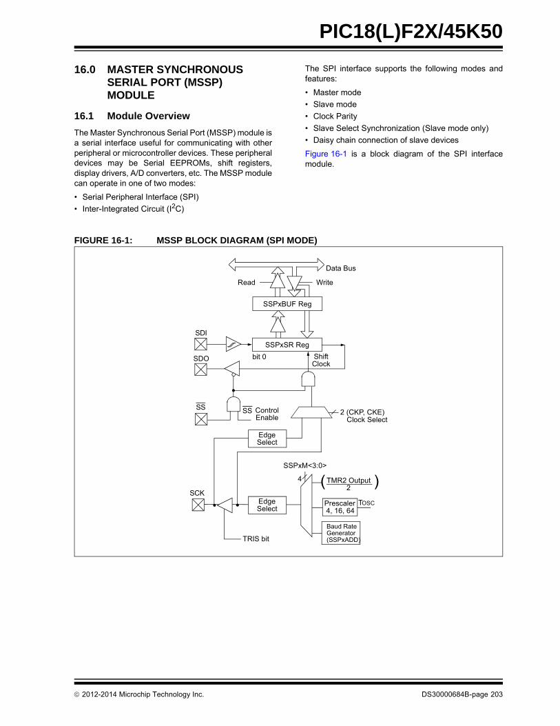
PIC18(L)F2X/45K50
16.0 MASTER SYNCHRONOUS SERIAL PORT (MSSP) MODULE
16.1 Module Overview
The Master Synchronous Serial Port (MSSP) module isa serial interface useful for communicating with otherperipheral or microcontroller devices. These peripheraldevices may be Serial EEPROMs, shift registers,display drivers, A/D converters, etc. The MSSP modulecan operate in one of two modes:
• Serial Peripheral Interface (SPI)
• Inter-Integrated Circuit (I2C)
The SPI interface supports the following modes andfeatures:
• Master mode
• Slave mode
• Clock Parity
• Slave Select Synchronization (Slave mode only)
• Daisy chain connection of slave devices
Figure 16-1 is a block diagram of the SPI interfacemodule.
FIGURE 16-1: MSSP BLOCK DIAGRAM (SPI MODE)
( )
Read Write
Data Bus
SSPxSR Reg
SSPxM<3:0>
bit 0 ShiftClock
SS ControlEnable
EdgeSelect
Clock Select
TMR2 Output
TOSCPrescaler4, 16, 64
2
EdgeSelect
2 (CKP, CKE)
4
TRIS bit
SDO
SSPxBUF Reg
SDI
SS
SCK
Baud RateGenerator(SSPxADD)
2012-2014 Microchip Technology Inc. DS30000684B-page 203

PIC18(L)F2X/45K50
The I2C interface supports the following modes andfeatures:
• Master mode
• Slave mode
• Byte NACKing (Slave mode)
• Limited Multi-master support
• 7-bit and 10-bit addressing
• Start and Stop interrupts
• Interrupt masking
• Clock stretching
• Bus collision detection
• General call address matching
• Address masking
• Address Hold and Data Hold modes
• Selectable SDA hold times
Figure 16-2 is a block diagram of the I2C interfacemodule in Master mode. Figure 16-3 is a diagram of theI2C interface module in Slave mode.
FIGURE 16-2: MSSP BLOCK DIAGRAM (I2C™ MASTER MODE)
Read Write
SSPxSR
Start bit, Stop bit,
Start bit Detect,
SSPxBUF
InternalData Bus
Set/Reset: S, P, SSPxSTAT, WCOL, SSPOV
ShiftClock
MSb LSb
SDA
AcknowledgeGenerate (SSPxCON2)
Stop bit DetectWrite Collision Detect
Clock ArbitrationState Counter forend of XMIT/RCV
SCL
SCL in
Bus Collision
SDA in
Re
ceiv
e E
nab
le (
RC
EN
)
Clo
ck C
ntl
Clo
ck A
rbitr
ate
/BC
OL
Det
ect
(Hol
d of
f cl
ock
sour
ce)
[SSPxM 3:0]
Baud Rate
Reset SEN, PEN (SSPxCON2)
Generator(SSPxADD)
Address Match Detect
Set SSPIF, BCLIF
DS30000684B-page 204 2012-2014 Microchip Technology Inc.

PIC18(L)F2X/45K50
FIGURE 16-3: MSSP BLOCK DIAGRAM (I2C™ SLAVE MODE)
Read Write
SSPxSR Reg
Match Detect
SSPxADD Reg
Start andStop bit Detect
SSPxBUF Reg
InternalData Bus
Addr Match
Set, ResetS, P bits
(SSPxSTAT Reg)
SCL
SDA
ShiftClock
MSb LSb
SSPxMSK Reg
2012-2014 Microchip Technology Inc. DS30000684B-page 205

PIC18(L)F2X/45K50
16.2 SPI Mode Overview
The Serial Peripheral Interface (SPI) bus is asynchronous serial data communication bus thatoperates in Full-Duplex mode. Devices communicatein a master/slave environment where the master deviceinitiates the communication. A slave device iscontrolled through a chip select known as Slave Select.
The SPI bus specifies four signal connections:
• Serial Clock (SCK)
• Serial Data Out (SDO)
• Serial Data In (SDI)
• Slave Select (SS)
Figure 16-1 shows the block diagram of the MSSPmodule when operating in SPI Mode.
The SPI bus operates with a single master device andone or more slave devices. When multiple slavedevices are used, an independent Slave Selectconnection is required from the master device to eachslave device.
Figure 16-4 shows a typical connection between amaster device and multiple slave devices.
The master selects only one slave at a time. Most slavedevices have tri-state outputs so their output signalappears disconnected from the bus when they are notselected.
Transmissions involve two shift registers, eight bits insize, one in the master and one in the slave. With eitherthe master or the slave device, data is always shiftedout one bit at a time, with the Most Significant bit (MSb)shifted out first. At the same time, a new LeastSignificant bit (LSb) is shifted into the same register.
Figure 16-5 shows a typical connection between twoprocessors configured as master and slave devices.
Data is shifted out of both shift registers on theprogrammed clock edge and latched on the oppositeedge of the clock.
The master device transmits information out on its SDOoutput pin which is connected to, and received by, theslave’s SDI input pin. The slave device transmits infor-mation out on its SDO output pin, which is connectedto, and received by, the master’s SDI input pin.
To begin communication, the master device first sendsout the clock signal. Both the master and the slavedevices should be configured for the same clockpolarity.
The master device starts a transmission by sending outthe MSb from its shift register. The slave device readsthis bit from that same line and saves it into the LSbposition of its shift register.
During each SPI clock cycle, a full-duplex datatransmission occurs. This means that at the same time,the slave device is sending out the MSb from its shift
register and the master device is reading this bit fromthat same line and saving it as the LSb of its shiftregister.
After eight bits have been shifted out, the master andslave have exchanged register values.
If there is more data to exchange, the shift registers areloaded with new data and the process repeats itself.
Whether the data is meaningful or not (dummy data),depends on the application software. This leads tothree scenarios for data transmission:
• Master sends useful data and slave sends dummy data.
• Master sends useful data and slave sends useful data.
• Master sends dummy data and slave sends useful data.
Transmissions may involve any number of clockcycles. When there is no more data to be transmitted,the master stops sending the clock signal and itdeselects the slave.
Every slave device connected to the bus that has notbeen selected through its slave select line must disre-gard the clock and transmission signals and must nottransmit out any data of its own.
DS30000684B-page 206 2012-2014 Microchip Technology Inc.

PIC18(L)F2X/45K50
FIGURE 16-4: SPI MASTER AND MULTIPLE SLAVE CONNECTION
16.2.1 SPI MODE REGISTERS
The MSSP module has five registers for SPI modeoperation. These are:
• MSSP STATUS register (SSPxSTAT)
• MSSP Control register 1 (SSPxCON1)
• MSSP Control register 3 (SSPxCON3)
• MSSP Data Buffer register (SSPxBUF)
• MSSP Address register (SSPxADD)
• MSSP Shift register (SSPxSR) (Not directly accessible)
SSPxCON1 and SSPxSTAT are the control andSTATUS registers in SPI mode operation. TheSSPxCON1 register is readable and writable. Thelower six bits of the SSPxSTAT are read-only. Theupper two bits of the SSPxSTAT are read/write.
In one SPI Master mode, SSPxADD can be loadedwith a value used in the Baud Rate Generator. Moreinformation on the Baud Rate Generator is available inSection 16.7 “Baud Rate Generator”.
SSPxSR is the shift register used for shifting data inand out. SSPxBUF provides indirect access to theSSPxSR register. SSPxBUF is the buffer register towhich data bytes are written, and from which databytes are read.
In receive operations, SSPxSR and SSPxBUFtogether create a buffered receiver. When SSPxSRreceives a complete byte, it is transferred to SSPxBUFand the SSPIF interrupt is set.
During transmission, the SSPxBUF is not buffered. Awrite to SSPxBUF will write to both SSPxBUF andSSPxSR.
16.2.2 SPI MODE OPERATION
When initializing the SPI, several options need to bespecified. This is done by programming the appropriatecontrol bits (SSPxCON1<5:0> and SSPxSTAT<7:6>).These control bits allow the following to be specified:
• Master mode (SCK is the clock output)
• Slave mode (SCK is the clock input)
• Clock Polarity (Idle state of SCK)
• Data Input Sample Phase (middle or end of data output time)
• Clock Edge (output data on rising/falling edge of SCK)
• Clock Rate (Master mode only)
• Slave Select mode (Slave mode only)
To enable the serial port, SSPx Enable bit, SSPxEN ofthe SSPxCON1 register, must be set. To reset or recon-figure SPI mode, clear the SSPxEN bit, re-initialize theSSPxCONx registers and then set the SSPxEN bit.This configures the SDI, SDO, SCK and SS pins asserial port pins. For the pins to behave as the serial portfunction, some must have their data direction bits (inthe TRIS register) appropriately programmed asfollows:
• SDI must have corresponding TRIS bit set
• SDO must have corresponding TRIS bit cleared
• SCK (Master mode) must have corresponding TRIS bit cleared
• SCK (Slave mode) must have corresponding TRIS bit set
• SS must have corresponding TRIS bit set
SPI MasterSCLK
SDO
SDI
General I/O
General I/O
General I/O
SCLK
SDI
SDO
SS
SPI Slave#1
SCLK
SDI
SDO
SS
SPI Slave#2
SCLK
SDI
SDO
SS
SPI Slave#3
2012-2014 Microchip Technology Inc. DS30000684B-page 207
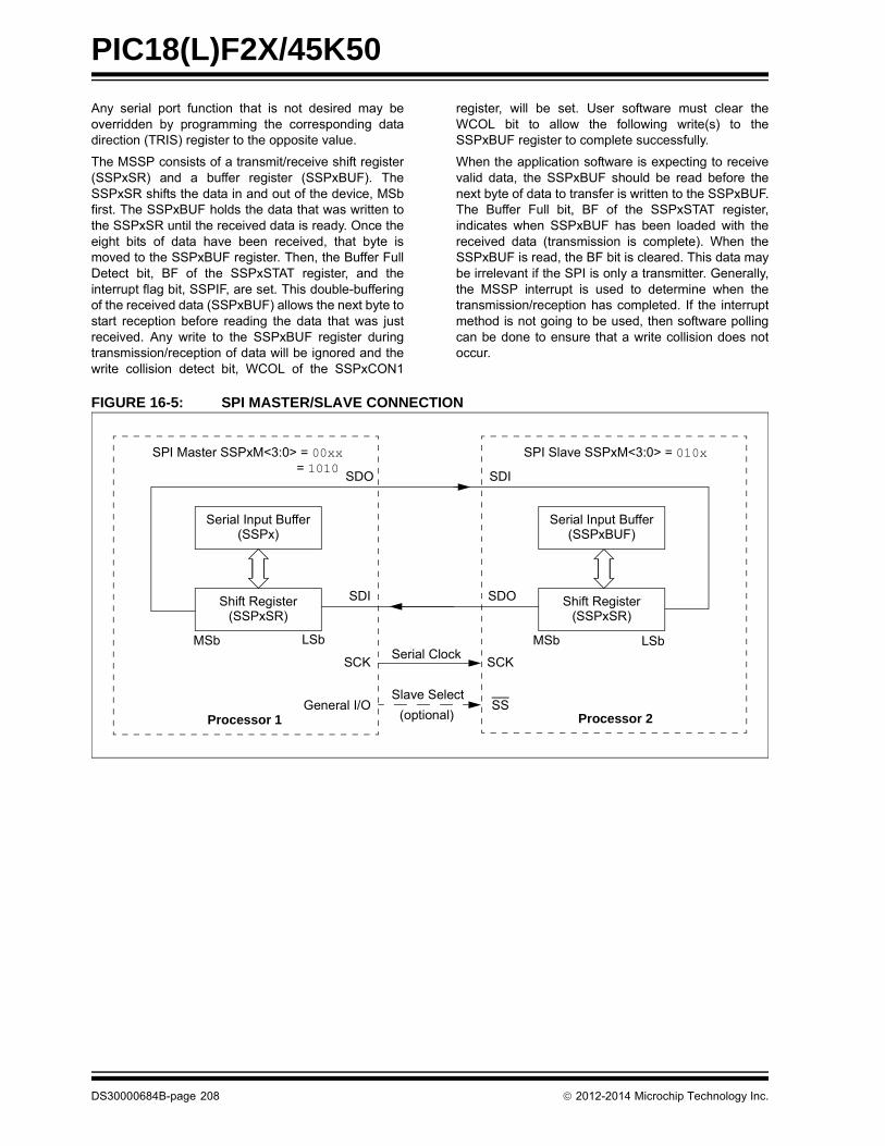
PIC18(L)F2X/45K50
Any serial port function that is not desired may beoverridden by programming the corresponding datadirection (TRIS) register to the opposite value.
The MSSP consists of a transmit/receive shift register(SSPxSR) and a buffer register (SSPxBUF). TheSSPxSR shifts the data in and out of the device, MSbfirst. The SSPxBUF holds the data that was written tothe SSPxSR until the received data is ready. Once theeight bits of data have been received, that byte ismoved to the SSPxBUF register. Then, the Buffer FullDetect bit, BF of the SSPxSTAT register, and theinterrupt flag bit, SSPIF, are set. This double-bufferingof the received data (SSPxBUF) allows the next byte tostart reception before reading the data that was justreceived. Any write to the SSPxBUF register duringtransmission/reception of data will be ignored and thewrite collision detect bit, WCOL of the SSPxCON1
register, will be set. User software must clear theWCOL bit to allow the following write(s) to theSSPxBUF register to complete successfully.
When the application software is expecting to receivevalid data, the SSPxBUF should be read before thenext byte of data to transfer is written to the SSPxBUF.The Buffer Full bit, BF of the SSPxSTAT register,indicates when SSPxBUF has been loaded with thereceived data (transmission is complete). When theSSPxBUF is read, the BF bit is cleared. This data maybe irrelevant if the SPI is only a transmitter. Generally,the MSSP interrupt is used to determine when thetransmission/reception has completed. If the interruptmethod is not going to be used, then software pollingcan be done to ensure that a write collision does notoccur.
FIGURE 16-5: SPI MASTER/SLAVE CONNECTION
Serial Input Buffer(SSPx)
Shift Register(SSPxSR)
MSb LSb
SDO
SDI
Processor 1
SCK
SPI Master SSPxM<3:0> = 00xx
Serial Input Buffer(SSPxBUF)
Shift Register(SSPxSR)
LSbMSb
SDI
SDO
Processor 2
SCK
SPI Slave SSPxM<3:0> = 010x
Serial Clock
SSSlave Select
General I/O(optional)
= 1010
DS30000684B-page 208 2012-2014 Microchip Technology Inc.

PIC18(L)F2X/45K50
16.2.3 SPI MASTER MODE
The master can initiate the data transfer at any timebecause it controls the SCK line. The masterdetermines when the slave (Processor 2, Figure 16-5)is to broadcast data by the software protocol.
In Master mode, the data is transmitted/received assoon as the SSPxBUF register is written to. If the SPIis only going to receive, the SDO output could be dis-abled (programmed as an input). The SSPxSR registerwill continue to shift in the signal present on the SDI pinat the programmed clock rate. As each byte isreceived, it will be loaded into the SSPxBUF register asif a normal received byte (interrupts and Status bitsappropriately set).
The clock polarity is selected by appropriatelyprogramming the CKP bit of the SSPxCON1 registerand the CKE bit of the SSPxSTAT register. This then,would give waveforms for SPI communication asshown in Figure 16-6, Figure 16-8 and Figure 16-9,where the MSB is transmitted first. In Master mode, theSPI clock rate (bit rate) is user programmable to be oneof the following:
• FOSC/4 (or TCY)
• FOSC/16 (or 4 * TCY)
• FOSC/64 (or 16 * TCY)
• Timer2 output/2
• FOSC/(4 * (SSPxADD + 1))
Figure 16-6 shows the waveforms for Master mode.
When the CKE bit is set, the SDO data is valid beforethere is a clock edge on SCK. The change of the inputsample is shown based on the state of the SMP bit. Thetime when the SSPxBUF is loaded with the receiveddata is shown.
FIGURE 16-6: SPI MODE WAVEFORM (MASTER MODE)
SCK(CKP = 0
SCK(CKP = 1
SCK(CKP = 0
SCK(CKP = 1
4 ClockModes
InputSample
InputSample
SDI
bit 7 bit 0
SDO bit 7 bit 6 bit 5 bit 4 bit 3 bit 2 bit 1 bit 0
bit 7
SDI
SSPIF
(SMP = 1)
(SMP = 0)
(SMP = 1)
CKE = 1)
CKE = 0)
CKE = 1)
CKE = 0)
(SMP = 0)
Write toSSPxBUF
SSPxSR toSSPxBUF
SDO bit 7 bit 6 bit 5 bit 4 bit 3 bit 2 bit 1 bit 0
(CKE = 0)
(CKE = 1)
bit 0
2012-2014 Microchip Technology Inc. DS30000684B-page 209

PIC18(L)F2X/45K50
16.2.4 SPI SLAVE MODE
In Slave mode, the data is transmitted and received asexternal clock pulses appear on SCK. When the lastbit is latched, the SSPIF interrupt flag bit is set.
Before enabling the module in SPI Slave mode, the clockline must match the proper Idle state. The clock line canbe observed by reading the SCK pin. The Idle state isdetermined by the CKP bit of the SSPxCON1 register.
While in Slave mode, the external clock is supplied bythe external clock source on the SCK pin. This externalclock must meet the minimum high and low times asspecified in the electrical specifications.
While in Sleep mode, the slave can transmit/receivedata. The shift register is clocked from the SCK pininput and when a byte is received, the device will gen-erate an interrupt. If enabled, the device will wake-upfrom Sleep.
16.2.4.1 Daisy-Chain Configuration
The SPI bus can sometimes be connected in a daisy-chain configuration. The first slave output is connectedto the second slave input, the second slave output isconnected to the third slave input, and so on. The finalslave output is connected to the master input. Eachslave sends out, during a second group of clockpulses, an exact copy of what was received during thefirst group of clock pulses. The whole chain acts asone large communication shift register. The daisy-chain feature only requires a single Slave Select linefrom the master device.
Figure 16-7 shows the block diagram of a typicaldaisy-chain connection when operating in SPI mode.
In a daisy-chain configuration, only the most recentbyte on the bus is required by the slave. Setting theBOEN bit of the SSPxCON3 register will enable writesto the SSPxBUF register, even if the previous byte hasnot been read. This allows the software to ignore datathat may not apply to it.
16.2.5 SLAVE SELECT SYNCHRONIZATION
The Slave Select can also be used to synchronizecommunication. The Slave Select line is held high untilthe master device is ready to communicate. When theSlave Select line is pulled low, the slave knows that anew transmission is starting.
If the slave fails to receive the communication properly,it will be reset at the end of the transmission, when theSlave Select line returns to a high state. The slave isthen ready to receive a new transmission when theSlave Select line is pulled low again. If the Slave Selectline is not used, there is a risk that the slave will even-tually become out of sync with the master. If the slavemisses a bit, it will always be one bit off in future trans-missions. Use of the Slave Select line allows the slaveand master to align themselves at the beginning ofeach transmission.
The SS pin allows a Synchronous Slave mode. TheSPI must be in Slave mode with SS pin control enabled(SSPxCON1<3:0> = 0100).
When the SS pin is low, transmission and reception areenabled and the SDO pin is driven.
When the SS pin goes high, the SDO pin is no longerdriven, even if in the middle of a transmitted byte andbecomes a floating output. External pull-up/pull-downresistors may be desirable depending on the applica-tion.
When the SPI module resets, the bit counter is forcedto ‘0’. This can be done by either forcing the SS pin toa high level or clearing the SSPxEN bit.
Note 1: When the SPI is in Slave mode with SS pincontrol enabled (SSPxCON1<3:0> =0100), the SPI module will reset if the SSpin is set to VDD.
2: When the SPI is used in Slave mode withCKE set; the user must enable SS pincontrol.
3: While operated in SPI Slave mode theSMP bit of the SSPxSTAT register mustremain clear.
DS30000684B-page 210 2012-2014 Microchip Technology Inc.

PIC18(L)F2X/45K50
FIGURE 16-7: SPI DAISY-CHAIN CONNECTION
FIGURE 16-8: SLAVE SELECT SYNCHRONOUS WAVEFORM
SPI MasterSCLK
SDO
SDI
General I/O
SCLK
SDI
SDO
SS
SPI Slave#1
SCLK
SDI
SDO
SS
SPI Slave#2
SCLK
SDI
SDO
SS
SPI Slave#3
SCK(CKP = 1
SCK(CKP = 0
InputSample
SDI
bit 7
SDO bit 7 bit 6 bit 7
SSPIFInterrupt
CKE = 0)
CKE = 0)
Write toSSPxBUF
SSPxSR toSSPxBUF
SS
Flag
bit 0
bit 7
bit 0
bit 6
SSPxBUF toSSPxSR
Shift register SSPxSRand bit count are reset
2012-2014 Microchip Technology Inc. DS30000684B-page 211

PIC18(L)F2X/45K50
FIGURE 16-9: SPI MODE WAVEFORM (SLAVE MODE WITH CKE = 0)
FIGURE 16-10: SPI MODE WAVEFORM (SLAVE MODE WITH CKE = 1)
SCK(CKP = 1
SCK(CKP = 0
InputSample
SDI
bit 7
SDO bit 7 bit 6 bit 5 bit 4 bit 3 bit 2 bit 1 bit 0
SSPIFInterrupt
CKE = 0)
CKE = 0)
Write toSSPxBUF
SSPxSR toSSPxBUF
SS
Flag
Optional
bit 0
detection active
Write Collision
Valid
SCK(CKP = 1
SCK(CKP = 0
InputSample
SDI
bit 7 bit 0
SDO bit 7 bit 6 bit 5 bit 4 bit 3 bit 2 bit 1 bit 0
SSPIFInterrupt
CKE = 1)
CKE = 1)
Write toSSPxBUF
SSPxSR toSSPxBUF
SS
Flag
Not Optional
Write Collisiondetection active
Valid
DS30000684B-page 212 2012-2014 Microchip Technology Inc.

PIC18(L)F2X/45K50
16.2.6 SPI OPERATION IN SLEEP MODE
In SPI Master mode, module clocks may be operatingat a different speed than when in Full-Power mode; inthe case of the Sleep mode, all clocks are halted.
Special care must be taken by the user when the MSSPclock is much faster than the system clock.
In Slave mode, when MSSP interrupts are enabled,after the master completes sending data, an MSSPinterrupt will wake the controller from Sleep.
If an exit from Sleep mode is not desired, MSSPinterrupts should be disabled.
In SPI Master mode, when the Sleep mode is selected,all module clocks are halted and the transmission/reception will remain in that state until the devicewakes. After the device returns to Run mode, themodule will resume transmitting and receiving data.
In SPI Slave mode, the SPI Transmit/Receive Shiftregister operates asynchronously to the device. Thisallows the device to be placed in Sleep mode and datato be shifted into the SPI Transmit/Receive Shiftregister. When all eight bits have been received, theMSSP interrupt flag bit will be set and if enabled, willwake the device.
TABLE 16-1: REGISTERS ASSOCIATED WITH SPI OPERATION
Name Bit 7 Bit 6 Bit 5 Bit 4 Bit 3 Bit 2 Bit 1 Bit 0Register on page
ANSELA — — ANSA5 — ANSA3 ANSA2 ANSA1 ANSA0 147
ANSELB — — ANSB5 ANSB4 ANSB3 ANSB2 ANSB1 ANSB0 148
INTCON GIE/GIEH PEIE/GIEL TMR0IE INT0IE IOCIE TMR0IF INT0IF IOCIF 114
IPR1 ACTIP ADIP RCIP TXIP SSPIP CCP1IP TMR2IP TMR1IP 123
PIE1 ACTIE ADIE RCIE TXIE SSPIE CCP1IE TMR2IE TMR1IE 120
PIR1 ACTIF ADIF RCIF TXIF SSPIF CCP1IF TMR2IF TMR1IF 117
PMD1 — MSSPMD CTMUMD CMP2MD CMP1MD ADCMD CCP2MD CCP1MD 62
SSP1BUF SSP1 Receive Buffer/Transmit Register —
SSP1CON1 WCOL SSPOV SSPEN CKP SSPM<3:0> 252
SSP1CON3 ACKTIM PCIE SCIE BOEN SDAHT SBCDE AHEN DHEN 255
SSP1STAT SMP CKE D/A P S R/W UA BF 251
TRISA TRISA7 TRISA6 TRISA5 TRISA4 TRISA3 TRISA2 TRISA1 TRISA0 149
TRISB TRISB7 TRISB6 TRISB5 TRISB4 TRISB3 TRISB2 TRISB1 TRISB0 149
TRISC TRISC7 TRISC6 — — — TRISC2 TRISC1 TRISC0 149
Legend: Shaded bits are not used by the MSSP in SPI mode.
2012-2014 Microchip Technology Inc. DS30000684B-page 213
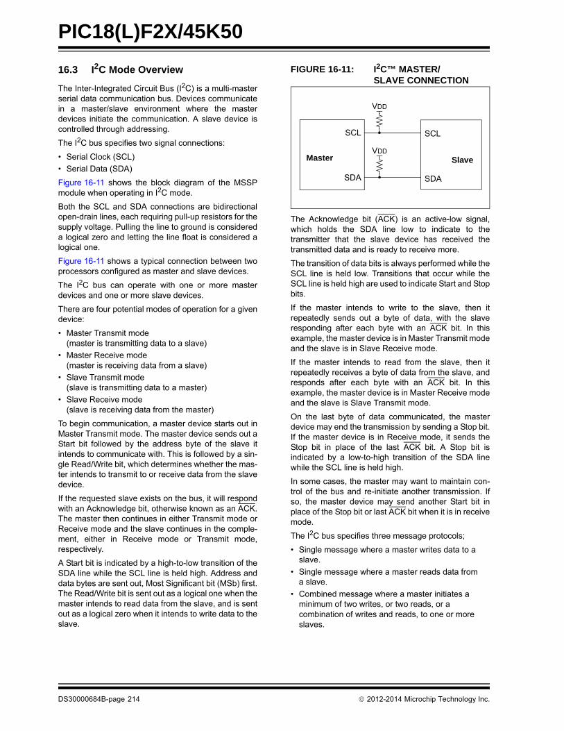
PIC18(L)F2X/45K50
16.3 I2C Mode Overview
The Inter-Integrated Circuit Bus (I2C) is a multi-masterserial data communication bus. Devices communicatein a master/slave environment where the masterdevices initiate the communication. A slave device iscontrolled through addressing.
The I2C bus specifies two signal connections:
• Serial Clock (SCL)
• Serial Data (SDA)
Figure 16-11 shows the block diagram of the MSSPmodule when operating in I2C mode.
Both the SCL and SDA connections are bidirectionalopen-drain lines, each requiring pull-up resistors for thesupply voltage. Pulling the line to ground is considereda logical zero and letting the line float is considered alogical one.
Figure 16-11 shows a typical connection between twoprocessors configured as master and slave devices.
The I2C bus can operate with one or more masterdevices and one or more slave devices.
There are four potential modes of operation for a givendevice:
• Master Transmit mode(master is transmitting data to a slave)
• Master Receive mode(master is receiving data from a slave)
• Slave Transmit mode(slave is transmitting data to a master)
• Slave Receive mode(slave is receiving data from the master)
To begin communication, a master device starts out inMaster Transmit mode. The master device sends out aStart bit followed by the address byte of the slave itintends to communicate with. This is followed by a sin-gle Read/Write bit, which determines whether the mas-ter intends to transmit to or receive data from the slavedevice.
If the requested slave exists on the bus, it will respondwith an Acknowledge bit, otherwise known as an ACK.The master then continues in either Transmit mode orReceive mode and the slave continues in the comple-ment, either in Receive mode or Transmit mode,respectively.
A Start bit is indicated by a high-to-low transition of theSDA line while the SCL line is held high. Address anddata bytes are sent out, Most Significant bit (MSb) first.The Read/Write bit is sent out as a logical one when themaster intends to read data from the slave, and is sentout as a logical zero when it intends to write data to theslave.
FIGURE 16-11: I2C™ MASTER/SLAVE CONNECTION
The Acknowledge bit (ACK) is an active-low signal,which holds the SDA line low to indicate to thetransmitter that the slave device has received thetransmitted data and is ready to receive more.
The transition of data bits is always performed while theSCL line is held low. Transitions that occur while theSCL line is held high are used to indicate Start and Stopbits.
If the master intends to write to the slave, then itrepeatedly sends out a byte of data, with the slaveresponding after each byte with an ACK bit. In thisexample, the master device is in Master Transmit modeand the slave is in Slave Receive mode.
If the master intends to read from the slave, then itrepeatedly receives a byte of data from the slave, andresponds after each byte with an ACK bit. In thisexample, the master device is in Master Receive modeand the slave is Slave Transmit mode.
On the last byte of data communicated, the masterdevice may end the transmission by sending a Stop bit.If the master device is in Receive mode, it sends theStop bit in place of the last ACK bit. A Stop bit isindicated by a low-to-high transition of the SDA linewhile the SCL line is held high.
In some cases, the master may want to maintain con-trol of the bus and re-initiate another transmission. Ifso, the master device may send another Start bit inplace of the Stop bit or last ACK bit when it is in receivemode.
The I2C bus specifies three message protocols;
• Single message where a master writes data to a slave.
• Single message where a master reads data from a slave.
• Combined message where a master initiates a minimum of two writes, or two reads, or a combination of writes and reads, to one or more slaves.
Master
SCL
SDA
SCL
SDA
SlaveVDD
VDD
DS30000684B-page 214 2012-2014 Microchip Technology Inc.
PIC18(L)F2X/45K50
When one device is transmitting a logical one, or lettingthe line float, and a second device is transmitting alogical zero, or holding the line low, the first device candetect that the line is not a logical one. This detection,when used on the SCL line, is called clock stretching.Clock stretching give slave devices a mechanism tocontrol the flow of data. When this detection is used onthe SDA line, it is called arbitration. Arbitration ensuresthat there is only one master device communicating atany single time.
16.3.1 CLOCK STRETCHING
When a slave device has not completed processingdata, it can delay the transfer of more data through theprocess of clock stretching. An addressed slave devicemay hold the SCL clock line low after receiving orsending a bit, indicating that it is not yet ready tocontinue. The master that is communicating with theslave will attempt to raise the SCL line in order totransfer the next bit, but will detect that the clock linehas not yet been released. Because the SCLconnection is open-drain, the slave has the ability tohold that line low until it is ready to continuecommunicating.
Clock stretching allows receivers that cannot keep upwith a transmitter to control the flow of incoming data.
16.3.2 ARBITRATION
Each master device must monitor the bus for Start andStop bits. If the device detects that the bus is busy, itcannot begin a new message until the bus returns to anIdle state.
However, two master devices may try to initiate atransmission on or about the same time. When thisoccurs, the process of arbitration begins. Eachtransmitter checks the level of the SDA data line andcompares it to the level that it expects to find. The firsttransmitter to observe that the two levels do not match,loses arbitration, and must stop transmitting on theSDA line.
For example, if one transmitter holds the SDA line to alogical one (lets it float) and a second transmitter holdsit to a logical zero (pulls it low), the result is that theSDA line will be low. The first transmitter then observesthat the level of the line is different than expected andconcludes that another transmitter is communicating.
The first transmitter to notice this difference is the onethat loses arbitration and must stop driving the SDAline. If this transmitter is also a master device, it alsomust stop driving the SCL line. It then can monitor thelines for a Stop condition before trying to reissue itstransmission. In the meantime, the other device thathas not noticed any difference between the expectedand actual levels on the SDA line continues with itsoriginal transmission. It can do so without any compli-cations, because so far, the transmission appearsexactly as expected with no other transmitter disturbingthe message.
Slave Transmit mode can also be arbitrated, when amaster addresses multiple slaves, but this is lesscommon.
If two master devices are sending a message to twodifferent slave devices at the address stage, the mastersending the lower slave address always winsarbitration. When two master devices send messagesto the same slave address, and addresses cansometimes refer to multiple slaves, the arbitrationprocess must continue into the data stage.
Arbitration usually occurs very rarely, but it is anecessary process for proper multi-master support.
2012-2014 Microchip Technology Inc. DS30000684B-page 215

PIC18(L)F2X/45K50
16.4 I2C Mode Operation
All MSSP I2C communication is byte oriented andshifted out MSb first. Six SFR registers and twointerrupt flags interface the module with the PICmicrocontroller and user software. Two pins, SDA andSCL, are exercised by the module to communicatewith other external I2C devices.
16.4.1 BYTE FORMAT
All communication in I2C is done in 9-bit segments. Abyte is sent from a master to a slave or vice-versa,followed by an Acknowledge bit sent back. After the8th falling edge of the SCL line, the device outputtingdata on the SDA changes that pin to an input andreads in an acknowledge value on the next clockpulse.
The clock signal, SCL, is provided by the master. Datais valid to change while the SCL signal is low, andsampled on the rising edge of the clock. Changes onthe SDA line while the SCL line is high define specialconditions on the bus, explained below.
16.4.2 DEFINITION OF I2C TERMINOLOGY
There is language and terminology in the descriptionof I2C communication that have definitions specific toI2C. That word usage is defined below and may beused in the rest of this document without explana-tion. This table was adapted from the Phillips I2Cspecification.
16.4.3 SDA AND SCL PINS
Selection of any I2C mode with the SSPxEN bit set,forces the SCL and SDA pins to be open-drain. Thesepins should be set by the user to inputs by setting theappropriate TRIS bits.
16.4.4 SDA HOLD TIME
The hold time of the SDA pin is selected by the SDAHTbit of the SSPxCON3 register. Hold time is the timeSDA is held valid after the falling edge of SCL. Settingthe SDAHT bit selects a longer 300 ns minimum holdtime and may help on buses with large capacitance.
TABLE 16-2: I2C™ BUS TERMS
Note: Data is tied to output zero when an I2C™mode is enabled.
TERM Description
Transmitter The device which shifts data out onto the bus.
Receiver The device which shifts data in from the bus.
Master The device that initiates a transfer, generates clock signals and terminates a transfer.
Slave The device addressed by the master.
Multi-master A bus with more than one device that can initiate data transfers.
Arbitration Procedure to ensure that only one master at a time controls the bus. Winning arbitration ensures that the message is not corrupted.
Synchronization Procedure to synchronize the clocks of two or more devices on the bus.
Idle No master is controlling the bus, and both SDA and SCL lines are high.
Active Any time one or more master devices are controlling the bus.
Addressed Slave
Slave device that has received a matching address and is actively being clocked by a master.
Matching Address
Address byte that is clocked into a slave that matches the value stored in SSPxADD.
Write Request Slave receives a matching address with R/W bit clear, and is ready to clock in data.
Read Request Master sends an address byte with the R/W bit set, indicating that it wishes to clock data out of the Slave. This data is the next and all following bytes until a Restart or Stop.
Clock Stretching When a device on the bus holds SCL low to stall communication.
Bus Collision Any time the SDA line is sampled low by the module while it is out-putting and expected high state.
DS30000684B-page 216 2012-2014 Microchip Technology Inc.

PIC18(L)F2X/45K50
16.4.5 START CONDITION
The I2C specification defines a Start condition as atransition of SDA from a high-to-low state while SCLline is high. A Start condition is always generated bythe master and signifies the transition of the bus froman Idle to an active state. Figure 16-10 shows waveforms for Start and Stop conditions.
A bus collision can occur on a Start condition if themodule samples the SDA line low before asserting itlow. This does not conform to the I2C specification thatstates no bus collision can occur on a Start.
16.4.6 STOP CONDITION
A Stop condition is a transition of the SDA line from alow-to-high state while the SCL line is high.
16.4.7 RESTART CONDITION
A Restart is valid any time that a Stop would be valid.A master can issue a Restart if it wishes to hold thebus after terminating the current transfer. A Restarthas the same effect on the slave that a Start would,resetting all slave logic and preparing it to clock in anaddress. The master may want to address the same oranother slave.
In 10-bit Addressing Slave mode a Restart is requiredfor the master to clock data out of the addressed slave.Once a slave has been fully addressed, matching bothhigh and low address bytes, the master can issue aRestart and the high address byte with the R/W bit set.The slave logic will then hold the clock and prepare toclock out data.
After a full match with R/W clear in 10-bit mode, a priormatch flag is set and maintained. Until a Stopcondition, a high address with R/W clear, or highaddress match fails.
16.4.8 START/STOP CONDITION INTERRUPT MASKING
The SCIE and PCIE bits of the SSPxCON3 registercan enable the generation of an interrupt in Slavemodes that do not typically support this function. Slavemodes where interrupt on Start and Stop detect arealready enabled, these bits will have no effect.
FIGURE 16-12: I2C™ START AND STOP CONDITIONS
FIGURE 16-13: I2C™ RESTART CONDITION
Note: At least one SCL low time must appearbefore a Stop is valid, therefore, if the SDAline goes low then high again while the SCLline stays high, only the Start condition isdetected.
SDA
SCL
P
Stop
Condition
S
Start
Condition
Change of
Data Allowed
Change of
Data Allowed
Restart
Condition
Sr
Change of
Data AllowedChange of
Data Allowed
2012-2014 Microchip Technology Inc. DS30000684B-page 217

PIC18(L)F2X/45K50
16.4.9 ACKNOWLEDGE SEQUENCE
The 9th SCL pulse for any transferred byte in I2C isdedicated as an Acknowledge. It allows receivingdevices to respond back to the transmitter by pullingthe SDA line low. The transmitter must release controlof the line during this time to shift in the response. TheAcknowledge (ACK) is an active-low signal, pulling theSDA line low indicated to the transmitter that thedevice has received the transmitted data and is readyto receive more.
The result of an ACK is placed in the ACKSTAT bit ofthe SSPxCON2 register.
Slave software, when the AHEN and DHEN bits areset, allow the user to set the ACK value sent back tothe transmitter. The ACKDT bit of the SSPxCON2register is set/cleared to determine the response.
Slave hardware will generate an ACK response if theAHEN and DHEN bits of the SSPxCON3 register areclear.
There are certain conditions where an ACK will not besent by the slave. If the BF bit of the SSPxSTATregister or the SSPOV bit of the SSPxCON1 registerare set when a byte is received.
When the module is addressed, after the 8th fallingedge of SCL on the bus, the ACKTIM bit of the SSPx-CON3 register is set. The ACKTIM bit indicates theacknowledge time of the active bus.
The ACKTIM Status bit is only active when the AHENbit or DHEN bit is enabled.
16.5 I2C Slave Mode Operation
The MSSP Slave mode operates in one of four modesselected in the SSPxM bits of SSPxCON1 register. Themodes can be divided into 7-bit and 10-bit Addressingmode. 10-bit Addressing modes operate the same as7-bit with some additional overhead for handling thelarger addresses.
Modes with Start and Stop bit interrupts operated thesame as the other modes with SSPIF additionally get-ting set upon detection of a Start, Restart, or Stopcondition.
16.5.1 SLAVE MODE ADDRESSES
The SSPxADD register (Register 16-6) contains theSlave mode address. The first byte received after aStart or Restart condition is compared against thevalue stored in this register. If the byte matches, thevalue is loaded into the SSPxBUF register and aninterrupt is generated. If the value does not match, themodule goes Idle and no indication is given to thesoftware that anything happened.
The SSPx Mask register (Register 16-5) affects theaddress matching process. See Section 16.5.9“SSPx Mask Register” for more information.
16.5.1.1 I2C Slave 7-Bit Addressing Mode
In 7-bit Addressing mode, the LSb of the received databyte is ignored when determining if there is an addressmatch.
16.5.1.2 I2C Slave 10-Bit Addressing Mode
In 10-bit Addressing mode, the first received byte iscompared to the binary value of ‘1 1 1 1 0 A9 A8 0’. A9and A8 are the two MSb of the 10-bit address andstored in bits 2 and 1 of the SSPxADD register.
After the acknowledge of the high byte the UA bit is setand SCL is held low until the user updates SSPxADDwith the low address. The low address byte is clockedin and all eight bits are compared to the low addressvalue in SSPxADD. Even if there is not an addressmatch; SSPIF and UA are set, and SCL is held lowuntil SSPxADD is updated to receive a high byteagain. When SSPxADD is updated the UA bit iscleared. This ensures the module is ready to receivethe high address byte on the next communication.
A high and low address match as a write request isrequired at the start of all 10-bit addressingcommunication. A transmission can be initiated byissuing a Restart once the slave is addressed, andclocking in the high address with the R/W bit set. Theslave hardware will then acknowledge the readrequest and prepare to clock out data. This is onlyvalid for a slave after it has received a complete highand low address byte match.
DS30000684B-page 218 2012-2014 Microchip Technology Inc.

PIC18(L)F2X/45K50
16.5.2 SLAVE RECEPTION
When the R/W bit of a matching received address byteis clear, the R/W bit of the SSPxSTAT register iscleared. The received address is loaded into theSSPxBUF register and acknowledged.
When the overflow condition exists for a receivedaddress, then not Acknowledge is given. An overflowcondition is defined as either bit BF of the SSPxSTATregister is set, or bit SSPOV of the SSPxCON1 registeris set. The BOEN bit of the SSPxCON3 register modi-fies this operation. For more information seeRegister 16-4.
An MSSP interrupt is generated for each transferreddata byte. Flag bit, SSPIF, must be cleared by software.
When the SEN bit of the SSPxCON2 register is set,SCL will be held low (clock stretch) following eachreceived byte. The clock must be released by settingthe CKP bit of the SSPxCON1 register, exceptsometimes in 10-bit mode. See Section 16.2.3 “SPIMaster Mode” for more detail.
16.5.2.1 7-Bit Addressing Reception
This section describes a standard sequence ofevents for the MSSP module configured as an I2Cslave in 7-bit Addressing mode. All decisions madeby hardware or software and their effect on reception.Figure 16-13 and Figure 16-14 is used as a visualreference for this description.
This is a step by step process of what typically mustbe done to accomplish I2C communication.
1. Start bit detected.
2. S bit of SSPxSTAT is set; SSPIF is set if interrupton Start detect is enabled.
3. Matching address with R/W bit clear is received.
4. The slave pulls SDA low sending an ACK to themaster, and sets SSPIF bit.
5. Software clears the SSPIF bit.
6. Software reads received address fromSSPxBUF clearing the BF flag.
7. If SEN = 1; Slave software sets CKP bit torelease the SCL line.
8. The master clocks out a data byte.
9. Slave drives SDA low sending an ACK to themaster, and sets SSPIF bit.
10. Software clears SSPIF.
11. Software reads the received byte fromSSPxBUF clearing BF.
12. Steps 8-12 are repeated for all received bytesfrom the master.
13. Master sends Stop condition, setting P bit ofSSPxSTAT, and the bus goes Idle.
16.5.2.2 7-Bit Reception with AHEN and DHEN
Slave device reception with AHEN and DHEN setoperate the same as without these options with extrainterrupts and clock stretching added after the 8th fall-ing edge of SCL. These additional interrupts allow theslave software to decide whether it wants to ACK thereceive address or data byte, rather than the hard-ware. This functionality adds support for PMBus™ thatwas not present on previous versions of this module.
This list describes the steps that need to be taken byslave software to use these options for I2Ccommunication. Figure 16-15 displays a module usingboth address and data holding. Figure 16-16 includesthe operation with the SEN bit of the SSPxCON2register set.
1. S bit of SSPxSTAT is set; SSPIF is set if interrupton Start detect is enabled.
2. Matching address with R/W bit clear is clockedin. SSPIF is set and CKP cleared after the 8thfalling edge of SCL.
3. Slave clears the SSPIF.
4. Slave can look at the ACKTIM bit of the SSPx-CON3 register to determine if the SSPIF wasafter or before the ACK.
5. Slave reads the address value from SSPxBUF,clearing the BF flag.
6. Slave sets ACK value clocked out to the masterby setting ACKDT.
7. Slave releases the clock by setting CKP.
8. SSPIF is set after an ACK, not after a NACK.
9. If SEN = 1 the slave hardware will stretch theclock after the ACK.
10. Slave clears SSPIF.
11. SSPIF set and CKP cleared after 8th fallingedge of SCL for a received data byte.
12. Slave looks at ACKTIM bit of SSPxCON3 todetermine the source of the interrupt.
13. Slave reads the received data from SSPxBUFclearing BF.
14. Steps 7-14 are the same for each received databyte.
15. Communication is ended by either the slavesending an ACK = 1, or the master sending aStop condition. If a Stop is sent and Interrupt onStop detect is disabled, the slave will only knowby polling the P bit of the SSTSTAT register.
Note: SSPIF is still set after the 9th falling edge ofSCL even if there is no clock stretching andBF has been cleared. Only if NACK is sentto master is SSPIF not set.
2012-2014 Microchip Technology Inc. DS30000684B-page 219

PIC18(L)F2X/45K50
FIGURE 16-14: I2C™ SLAVE, 7-BIT ADDRESS, RECEPTION (SEN = 0, AHEN = 0, DHEN = 0)
Rec
eivi
ng
Ad
dre
ss
AC
K
Rec
eiv
ing
Dat
a
AC
K
Rec
eiv
ing
Dat
aA
CK
=1
A7
A6
A5
A4
A3
A2
A1
D7
D6
D5
D4
D3
D2
D1
D0
D7
D6
D5
D4
D3
D2
D1
D0
SD
A
SC
L
SS
PIF
BF
SS
PO
V
12
34
56
78
12
34
56
78
12
34
56
78
99
9
AC
K is
no
t se
nt.
SS
PO
V s
et b
ecau
seS
SP
xBU
F is
stil
l fu
ll.
Cle
are
d b
y so
ftwar
e
Firs
t by
te o
f da
ta is
ava
ilabl
e in
SS
PxB
UF
SS
PxB
UF
is r
ead
SS
PIF
set
on
9th
falli
ng e
dge
of
SC
LC
lea
red
by s
oftw
are
P
Bu
s M
ast
er
send
s S
top
cond
ition
S
Fro
m S
lave
to M
aste
r
DS30000684B-page 220 2012-2014 Microchip Technology Inc.

PIC18(L)F2X/45K50
FIGURE 16-15: I2C™ SLAVE, 7-BIT ADDRESS, RECEPTION (SEN = 1, AHEN = 0, DHEN = 0)
SE
NS
EN
A7
A6
A5
A4
A3
A2
A1
D7
D6
D5
D4
D3
D2
D1
D0
D7
D6
D5
D4
D3
D2
D1
D0
SD
A
SC
L1
23
45
67
89
12
34
56
78
91
23
45
67
89
P
SS
PIF
set
on
9th
SC
L is
not
hel
dC
KP
is w
ritte
n to
‘1’ i
n s
oftw
are,
C
KP
is w
ritte
n to
‘1’ i
n s
oftw
are,
AC
K
low
bec
aus
e
falli
ng e
dge
of
SC
L
rele
asin
g S
CL A
CK
is n
ot s
ent.
Bus
Mas
ter
send
s
CK
P
SS
PO
V
BF
SS
PIF
SS
PO
V s
et b
eca
use
SS
PxB
UF
is s
till f
ull.
Cle
are
d b
y so
ftwa
re
Firs
t byt
e o
f da
ta is
ava
ilabl
e in
SS
PxB
UF
AC
K=1
Cle
ared
by
softw
are
SS
PxB
UF
is r
ead
Clo
ck is
hel
d lo
w u
ntil
CK
P is
se
t to
‘1’
rele
asi
ng S
CL
Sto
p c
ondi
tion
S
AC
K
AC
KR
ecei
ve A
ddre
ssR
ecei
ve D
ata
Rec
eive
Dat
a
R/W
=0
2012-2014 Microchip Technology Inc. DS30000684B-page 221

PIC18(L)F2X/45K50
FIGURE 16-16: I2C™ SLAVE, 7-BIT ADDRESS, RECEPTION (SEN = 0, AHEN = 1, DHEN = 1)
Rec
eiv
ing
Add
ress
Rec
eiv
ing
Dat
aR
ece
ive
d D
ata
P
A7
A6
A5
A4
A3
A2
A1
D7
D6
D5
D4
D3
D2
D1
D0
D7
D6
D5
D4
D3
D2
D1
D0
SD
A
SC
L
BF
CK
P S P
12
34
56
78
91
23
45
67
89
12
34
56
78
Ma
ster
sen
dsS
top
con
ditio
n
S
Da
ta is
re
ad f
rom
SS
PxB
UF
Cle
are
d b
y so
ftwar
eS
SP
IF is
set
on
9th
falli
ng
edg
e o
f S
CL,
afte
r A
CK
CK
P s
et b
y so
ftwar
e,
SC
L is
rel
eas
ed
Sla
ve s
oftw
are
9
AC
KT
IM c
lear
ed b
yh
ard
war
e in
9th
ri
sing
edg
e o
f SC
L
sets
AC
KD
T to
not
AC
K
Wh
en D
HE
N=1
:C
KP
is c
lea
red
by
hard
wa
re o
n 8
th f
allin
ge
dge
of
SC
L
Sla
ve s
oftw
are
clea
rs A
CK
DT
to
AC
K t
he r
ecei
ved
byt
e
AC
KT
IM s
et b
y ha
rdw
are
on 8
th fa
llin
g e
dge
of S
CL
Whe
n A
HE
N=1
:C
KP
is c
lear
ed b
y h
ard
war
ean
d S
CL
is s
tret
ched
Add
ress
isre
ad fr
om
S
SB
UF
AC
KT
IM s
et b
y ha
rdw
are
on 8
th fa
lling
edg
e o
f SC
L
AC
K
Ma
ster
Rel
eas
es
SD
Ato
sla
ve fo
r A
CK
se
que
nce
No
inte
rru
pta
fter
not A
CK
from
Sla
ve
AC
K=1
AC
K
AC
KD
T
AC
KT
IM
SS
PIF
If A
HE
N=1
:S
SP
IF is
set
DS30000684B-page 222 2012-2014 Microchip Technology Inc.
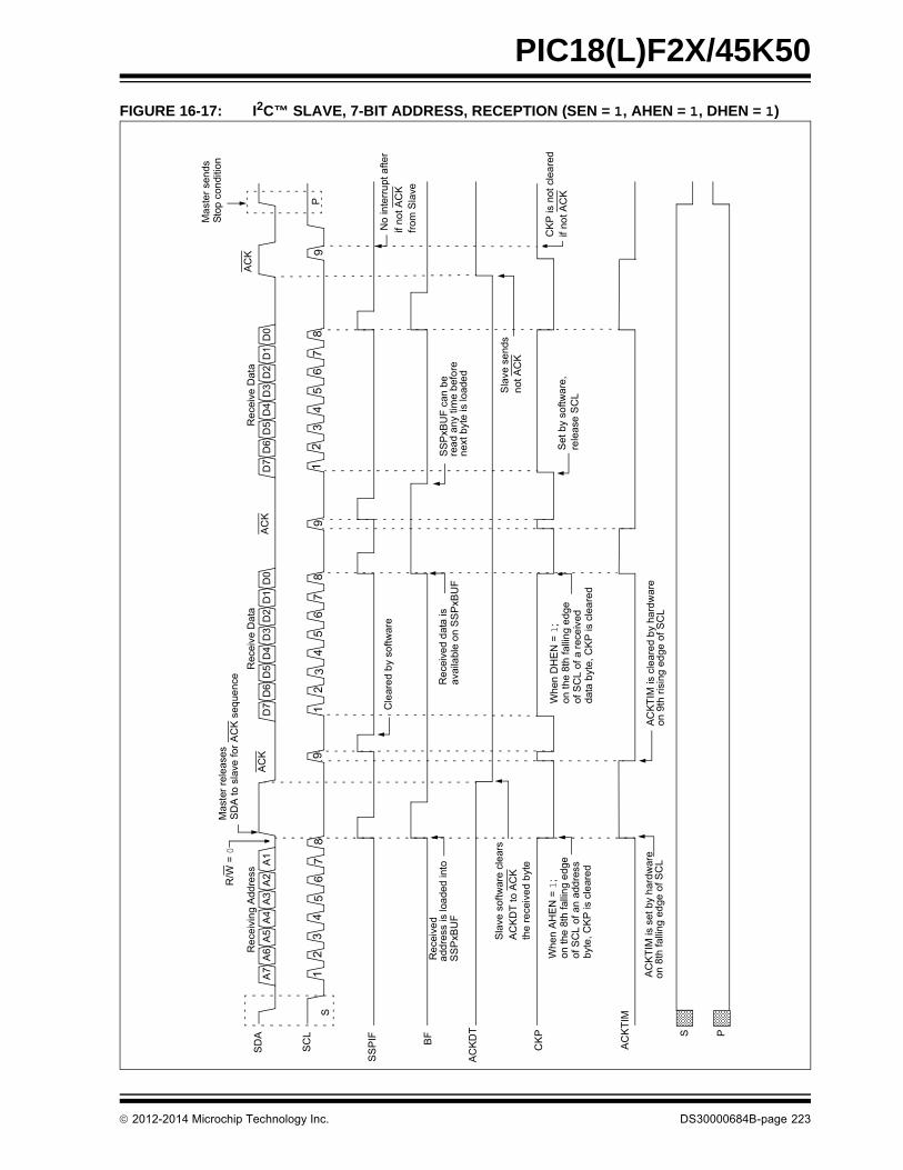
PIC18(L)F2X/45K50
FIGURE 16-17: I2C™ SLAVE, 7-BIT ADDRESS, RECEPTION (SEN = 1, AHEN = 1, DHEN = 1)
Re
ceiv
ing
Add
ress
Rec
eive
Da
taR
ece
ive
Dat
a
A7
A6
A5
A4
A3
A2
A1
D7
D6
D5
D4
D3
D2
D1
D0
D7
D6
D5
D4
D3
D2
D1
D0
SD
A
SC
L
SS
PIF BF
AC
KD
T
CK
P S P
AC
K
S1
23
45
67
89
12
34
56
78
91
23
45
67
89
AC
K
AC
K
Cle
are
d b
y so
ftwar
e
AC
KT
IM is
cle
are
d b
y ha
rdw
are
SS
PxB
UF
can
be
Set
by
softw
are
,
rea
d a
ny ti
me
bef
ore
nex
t by
te is
load
ed
rele
ase
SC
L
on 9
th r
isin
g e
dge
of
SC
L
Re
ceiv
ed
add
ress
is lo
ade
d in
to
SS
PxB
UF
Sla
ve s
oftw
are
cle
ars
AC
KD
T t
o A
CK
R/W
= 0
Mas
ter
rele
ases
SD
A to
sla
ve fo
r A
CK
seq
uenc
e
the
re
ceiv
ed
byt
e
Whe
n A
HE
N=1
;on
the
8th
falli
ng
edg
eof
SC
L o
f an
add
ress
byte
, CK
P is
cle
are
d
AC
KT
IM is
set
by
har
dwar
eon
8th
fal
ling
ed
ge o
f SC
L
Whe
n D
HE
N =
1;
on t
he 8
th fa
llin
g e
dge
of S
CL
of
a re
ceiv
edda
ta b
yte,
CK
P is
cle
are
d
Re
ceiv
ed
dat
a is
ava
ilabl
e o
n S
SP
xBU
F
Sla
ve s
end
sn
ot A
CK
CK
P is
not
cle
are
dif
not A
CK
P
Ma
ster
sen
dsS
top
con
ditio
n
No
inte
rru
pt a
fter
if no
t AC
Kfr
om S
lave
AC
KT
IM
2012-2014 Microchip Technology Inc. DS30000684B-page 223
PIC18(L)F2X/45K50
16.5.3 SLAVE TRANSMISSION
When the R/W bit of the incoming address byte is setand an address match occurs, the R/W bit of theSSPxSTAT register is set. The received address isloaded into the SSPxBUF register, and an ACK pulse issent by the slave on the ninth bit.
Following the ACK, slave hardware clears the CKP bitand the SCL pin is held low (see Section 16.5.6“Clock Stretching” for more detail). By stretching theclock, the master will be unable to assert another clockpulse until the slave is done preparing the transmitdata.
The transmit data must be loaded into the SSPxBUFregister which also loads the SSPxSR register. Thenthe SCL pin should be released by setting the CKP bitof the SSPxCON1 register. The eight data bits areshifted out on the falling edge of the SCL input. Thisensures that the SDA signal is valid during the SCLhigh time.
The ACK pulse from the master-receiver is latched onthe rising edge of the ninth SCL input pulse. This ACKvalue is copied to the ACKSTAT bit of the SSPxCON2register. If ACKSTAT is set (not ACK), then the datatransfer is complete. In this case, when the not ACK islatched by the slave, the slave goes Idle and waits foranother occurrence of the Start bit. If the SDA line waslow (ACK), the next transmit data must be loaded intothe SSPxBUF register. Again, the SCL pin must bereleased by setting bit CKP.
An MSSP interrupt is generated for each data transferbyte. The SSPIF bit must be cleared by software andthe SSPxSTAT register is used to determine the statusof the byte. The SSPIF bit is set on the falling edge ofthe ninth clock pulse.
16.5.3.1 Slave Mode Bus Collision
A slave receives a Read request and begins shiftingdata out on the SDA line. If a bus collision is detectedand the SBCDE bit of the SSPxCON3 register is set,the BCLIF bit of the PIRx register is set. Once a bus col-lision is detected, the slave goes Idle and waits to beaddressed again. User software can use the BCLIF bitto handle a slave bus collision.
16.5.3.2 7-Bit Transmission
A master device can transmit a read request to aslave, and then clock data out of the slave. The listbelow outlines what software for a slave will need to doto accomplish a standard transmission. Figure 16-17can be used as a reference to this list.
1. Master sends a Start condition on SDA andSCL.
2. S bit of SSPxSTAT is set; SSPIF is set if interrupton Start detect is enabled.
3. Matching address with R/W bit set is received bythe slave setting SSPIF bit.
4. Slave hardware generates an ACK and setsSSPIF.
5. SSPIF bit is cleared by user.
6. Software reads the received address fromSSPxBUF, clearing BF.
7. R/W is set so CKP was automatically clearedafter the ACK.
8. The slave software loads the transmit data intoSSPxBUF.
9. CKP bit is set releasing SCL, allowing the mas-ter to clock the data out of the slave.
10. SSPIF is set after the ACK response from themaster is loaded into the ACKSTAT register.
11. SSPIF bit is cleared.
12. The slave software checks the ACKSTAT bit tosee if the master wants to clock out more data.
13. Steps 9-13 are repeated for each transmittedbyte.
14. If the master sends a not ACK; the clock is notheld, but SSPIF is still set.
15. The master sends a Restart condition or a Stop.
16. The slave is no longer addressed.
Note 1: If the master ACKs the clock will bestretched.
2: ACKSTAT is the only bit updated on therising edge of SCL (9th) rather than thefalling.
DS30000684B-page 224 2012-2014 Microchip Technology Inc.

PIC18(L)F2X/45K50
FIGURE 16-18: I2C™ SLAVE, 7-BIT ADDRESS, TRANSMISSION (AHEN = 0)
Rec
eivi
ng A
ddre
ssA
uto
mat
icT
rans
mitt
ing
Da
taA
uto
ma
ticT
ran
smitt
ing
Dat
a
A7
A6
A5
A4
A3
A2
A1
D7
D6
D5
D4
D3
D2
D1
D0
D7
D6
D5
D4
D3
D2
D1
D0
12
34
56
78
91
23
45
67
89
12
34
56
78
9
SD
A
SC
L
SS
PIF
BF
CK
P
AC
KS
TA
T
R/W
D/A S P
Re
ceiv
ed
add
ress
Wh
en R
/W is
se
t
R/W
is c
opie
d fr
om th
e
Ind
icat
es
an a
ddr
ess
is r
ead
from
SS
PxB
UF
SC
L is
alw
ays
hel
d lo
w a
fter
9th
SC
Lfa
llin
g e
dge
mat
chin
g a
ddr
ess
byt
e
has
been
re
ceiv
ed
Mas
ters
not
AC
Kis
cop
ied
to
AC
KS
TA
T
CK
P is
not
h
eld
for
not
AC
K
BF
is a
uto
ma
tical
ly
clea
red
aft
er 8
th f
allin
ged
ge o
f S
CL
Dat
a to
tra
nsm
it is
load
ed in
to S
SP
xBU
F
Se
t by
soft
war
e
Cle
are
d b
y so
ftw
are
AC
KA
CK
AC
KR
/W=1
SP
Mas
ter
send
sS
top
con
ditio
n
2012-2014 Microchip Technology Inc. DS30000684B-page 225

PIC18(L)F2X/45K50
16.5.3.3 7-Bit Transmission with Address Hold Enabled
Setting the AHEN bit of the SSPxCON3 registerenables additional clock stretching and interruptgeneration after the 8th falling edge of a receivedmatching address. Once a matching address hasbeen clocked in, CKP is cleared and the SSPIFinterrupt is set.
Figure 16-18 displays a standard waveform of a 7-bitAddress Slave Transmission with AHEN enabled.
1. Bus starts Idle.
2. Master sends Start condition; the S bit ofSSPxSTAT is set; SSPIF is set if interrupt onStart detect is enabled.
3. Master sends matching address with R/W bitset. After the 8th falling edge of the SCL line theCKP bit is cleared and SSPIF interrupt isgenerated.
4. Slave software clears SSPIF.
5. Slave software reads ACKTIM bit of SSPxCON3register, and R/W and D/A of the SSPxSTATregister to determine the source of the interrupt.
6. Slave reads the address value from the SSPxBUFregister clearing the BF bit.
7. Slave software decides from this information if itwishes to ACK or not ACK and sets ACKDT bitof the SSPxCON2 register accordingly.
8. Slave sets the CKP bit releasing SCL.
9. Master clocks in the ACK value from the slave.
10. Slave hardware automatically clears the CKP bitand sets SSPIF after the ACK if the R/W bit isset.
11. Slave software clears SSPIF.
12. Slave loads value to transmit to the master intoSSPxBUF setting the BF bit.
13. Slave sets CKP bit releasing the clock.
14. Master clocks out the data from the slave andsends an ACK value on the 9th SCL pulse.
15. Slave hardware copies the ACK value into theACKSTAT bit of the SSPxCON2 register.
16. Steps 10-15 are repeated for each bytetransmitted to the master from the slave.
17. If the master sends a not ACK the slavereleases the bus allowing the master to send aStop and end the communication.
Note: SSPxBUF cannot be loaded until after theACK.
Note: Master must send a not ACK on the last byteto ensure that the slave releases the SCLline to receive a Stop.
DS30000684B-page 226 2012-2014 Microchip Technology Inc.
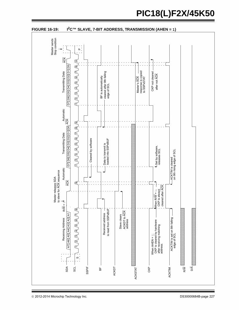
PIC18(L)F2X/45K50
FIGURE 16-19: I2C™ SLAVE, 7-BIT ADDRESS, TRANSMISSION (AHEN = 1)
Rec
eiv
ing
Ad
dres
sA
utom
atic
Tra
nsm
ittin
g D
ata
Aut
oma
ticT
rans
mitt
ing
Da
ta
A7
A6
A5
A4
A3
A2
A1
D7
D6
D5
D4
D3
D2
D1
D0
D7
D6
D5
D4
D3
D2
D1
D0
12
34
56
78
91
23
45
67
89
12
34
56
78
9
SD
A
SC
L
SS
PIF
BF
AC
KD
T
AC
KS
TAT
CK
P
R/W D/A
Rec
eiv
ed a
ddr
ess
is r
ead
from
SS
PxB
UF
BF
is a
utom
atic
ally
cl
eare
d a
fter
8th
falli
ng
edg
e o
f S
CL
Dat
a to
tra
nsm
it is
loa
ded
into
SS
PxB
UF
Cle
ared
by
softw
are
Sla
ve c
lea
rs
AC
KD
T t
o A
CK
addr
ess
Ma
ster
’s A
CK
resp
onse
is c
opie
dto
SS
PxS
TAT
CK
P n
ot c
lear
ed
afte
r no
t A
CK
Se
t by
softw
are,
rele
ase
s S
CL
AC
KT
IM is
cle
ared
on
9th
risi
ng e
dge
of S
CL
AC
KT
IM is
set
on
8th
fal
ling
edg
e of
SC
L
Whe
n A
HE
N =
1;
CK
P is
cle
ared
by
har
dwar
eaf
ter
rece
ivin
g m
atch
ing
add
ress
.
Whe
n R
/W =
1;
CK
P is
alw
ays
clea
red
afte
r A
CK
SP
Mas
ter
send
sS
top
cond
ition
AC
KR
/W=1M
ast
er r
ele
ases
SD
Ato
sla
ve f
or A
CK
seq
uen
ce
AC
KA
CK
AC
KT
IM
2012-2014 Microchip Technology Inc. DS30000684B-page 227

PIC18(L)F2X/45K50
16.5.4 SLAVE MODE 10-BIT ADDRESS RECEPTION
This section describes a standard sequence ofevents for the MSSP module configured as an I2Cslave in 10-bit Addressing mode.
Figure 16-19 and is used as a visual reference for thisdescription.
This is a step by step process of what must be done byslave software to accomplish I2C communication.
1. Bus starts Idle.
2. Master sends Start condition; S bit of SSPxSTATis set; SSPIF is set if interrupt on Start detect isenabled.
3. Master sends matching high address with R/Wbit clear; UA bit of the SSPxSTAT register is set.
4. Slave sends ACK and SSPIF is set.
5. Software clears the SSPIF bit.
6. Software reads received address from SSPxBUFclearing the BF flag.
7. Slave loads low address into SSPxADD,releasing SCL.
8. Master sends matching low address byte to theslave; UA bit is set.
9. Slave sends ACK and SSPIF is set.
10. Slave clears SSPIF.
11. Slave reads the received matching addressfrom SSPxBUF clearing BF.
12. Slave loads high address into SSPxADD.
13. Master clocks a data byte to the slave and clocksout the slaves ACK on the 9th SCL pulse; SSPIFis set.
14. If SEN bit of SSPxCON2 is set, CKP is clearedby hardware and the clock is stretched.
15. Slave clears SSPIF.
16. Slave reads the received byte from SSPxBUFclearing BF.
17. If SEN is set the slave sets CKP to release theSCL.
18. Steps 13-17 repeat for each received byte.
19. Master sends Stop to end the transmission.
16.5.5 10-BIT ADDRESSING WITH ADDRESS OR DATA HOLD
Reception using 10-bit addressing with AHEN orDHEN set is the same as with 7-bit modes. The onlydifference is the need to update the SSPxADD registerusing the UA bit. All functionality, specifically when theCKP bit is cleared and SCL line is held low are thesame. Figure 16-20 can be used as a reference of aslave in 10-bit addressing with AHEN set.
Figure 16-21 shows a standard waveform for a slavetransmitter in 10-bit Addressing mode.
Note: Updates to the SSPxADD register are notallowed until after the ACK sequence.
Note: If the low address does not match, SSPIFand UA are still set so that the slave soft-ware can set SSPxADD back to the highaddress. BF is not set because there is nomatch. CKP is unaffected.
DS30000684B-page 228 2012-2014 Microchip Technology Inc.
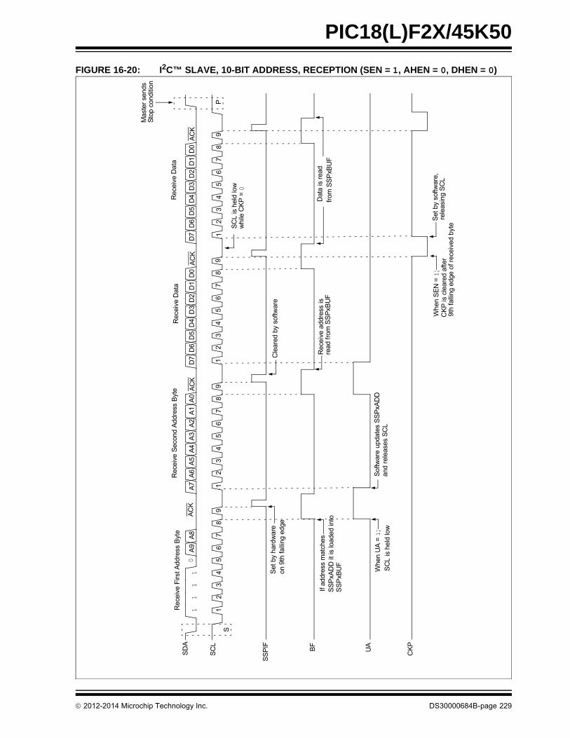
PIC18(L)F2X/45K50
FIGURE 16-20: I2C™ SLAVE, 10-BIT ADDRESS, RECEPTION (SEN = 1, AHEN = 0, DHEN = 0)
SS
PIF
Rec
eive
Firs
t Add
ress
Byt
e
AC
K
Rec
eive
Sec
ond
Add
ress
Byt
e AC
K
Rec
eive
Dat
a
AC
K
Rec
eive
Dat
a
AC
K1
11
10
A9
A8
A7
A6
A5
A4
A3
A2
A1
A0
D7
D6
D5
D4
D3
D2
D1
D0
D7
D6
D5
D4
D3
D2
D1
D0
SD
A
SC
L
UA
CK
P
12
34
56
78
91
23
45
67
89
12
34
56
78
91
23
45
67
89
P
Mas
ter
send
sS
top
cond
ition
Cle
ared
by
softw
are
Rec
eive
add
ress
is
Sof
twar
e up
date
s S
SP
xAD
D
Dat
a is
rea
d
SC
L is
hel
d lo
w
Set
by
softw
are,
whi
le C
KP
= 0
from
SS
PxB
UF
rele
asin
g S
CL
Whe
n S
EN
= 1
;C
KP
is c
lear
ed a
fter
9th
falli
ng e
dge
of r
ecei
ved
byte
read
from
SS
PxB
UF
and
rele
ases
SC
LW
hen
UA
= 1
;
If ad
dres
s m
atch
es
Set
by
hard
war
eon
9th
falli
ng e
dge
SS
PxA
DD
it is
load
ed in
to
SS
PxB
UF
SC
L is
hel
d lo
w
S
BF
2012-2014 Microchip Technology Inc. DS30000684B-page 229

PIC18(L)F2X/45K50
FIGURE 16-21: I2C™ SLAVE, 10-BIT ADDRESS, RECEPTION (SEN = 0, AHEN = 1, DHEN = 0)
Rec
eiv
e F
irst
Add
ress
Byt
e
UA
Rec
eiv
e S
eco
nd A
ddre
ss B
yte
UA
Rec
eiv
e D
ata
AC
K
Rec
eive
Dat
a
11
11
0A
9A
8A
7A
6A
5A
4A
3A
2A
1A
0D
7D
6D
5D
4D
3D
2D
1D
0D
7D
6D
5S
DA
SC
L
SS
PIF
BF
AC
KD
T
UA
CK
P
AC
KT
IM
12
34
56
78
9S
AC
KA
CK
12
34
56
78
91
23
45
67
89
12
SS
PxB
UF
is r
ead
fro
m
Rec
eiv
ed d
ata
SS
PxB
UF
can
be
read
any
time
bef
ore
the
ne
xt r
ece
ived
byt
e
Cle
ared
by
softw
are
falli
ng e
dge
of S
CL
not a
llow
ed u
ntil
9th
Upd
ate
to S
SP
xAD
D is
Set
CK
P w
ith s
oftw
are
rele
ases
SC
L
SC
Lcl
ears
UA
and
rel
eas
esU
pda
te o
f SS
PxA
DD
,
Se
t by
hard
wa
reo
n 9
th f
allin
g e
dge
Sla
ve s
oftw
are
cle
ars
AC
KD
T to
AC
Kth
e re
ceiv
ed b
yte
If w
hen
AH
EN
=1
;o
n th
e 8
th f
allin
g e
dge
of S
CL
of a
n a
ddre
ssb
yte,
CK
P is
cle
are
d
AC
KT
IM is
se
t by
hard
wa
reon
8th
falli
ng
edg
e of
SC
L
Cle
are
d b
y so
ftwar
e
R/W
= 0
DS30000684B-page 230 2012-2014 Microchip Technology Inc.

PIC18(L)F2X/45K50
FIGURE 16-22: I2C™ SLAVE, 10-BIT ADDRESS, TRANSMISSION (SEN = 0, AHEN = 0, DHEN = 0)
Rec
eivi
ng A
ddre
ss
AC
K
Rec
eiv
ing
Sec
ond
Ad
dre
ss B
yte
Sr
Re
ceiv
e F
irst
Add
ress
Byt
e
AC
K
Tra
nsm
ittin
g D
ata
Byt
e
11
11
0A
9A
8A
7A
6A
5A
4A
3A
2A
1A
01
11
10
A9
A8
D7
D6
D5
D4
D3
D2
D1
D0
SD
A
SC
L
SS
PIF BF
UA
CK
P
R/W D/A
12
34
56
78
91
23
45
67
89
12
34
56
78
91
23
45
67
89AC
K =
1
P
Ma
ster
sen
ds
Sto
p c
ondi
tion
Ma
ste
r se
nds
not A
CK
Mas
ter
send
s R
esta
rt e
vent
AC
K
R/W
= 0
S
Cle
are
d b
y so
ftwar
e
Aft
er S
SP
xAD
D is
upd
ate
d, U
A is
cle
ared
and
SC
L is
rel
eas
ed
Hig
h a
ddr
ess
is lo
ade
d
Rec
eive
d a
ddre
ss is
Dat
a to
tran
smit
is
Se
t by
softw
are
Indi
cate
s a
n a
ddre
ss
Whe
n R
/W =
1;
R/W
is c
opie
d fr
om th
e
Se
t by
hard
wa
re
UA
ind
icat
es
SS
PxA
DD
SS
PxB
UF
loa
ded
with
rec
eiv
ed a
ddr
ess
mus
t be
upd
ate
d
has
bee
n r
ece
ive
d
loa
ded
into
SS
PxB
UF
rele
ase
s S
CL
Ma
ste
rs n
ot A
CK
is c
opi
ed
ma
tchi
ng
add
ress
byt
e
CK
P is
cle
are
d o
n9t
h fa
lling
ed
ge o
f SC
L
rea
d fr
om S
SP
xBU
F
back
into
SS
PxA
DD
AC
KS
TAT
Set
by
hard
wa
re
2012-2014 Microchip Technology Inc. DS30000684B-page 231

PIC18(L)F2X/45K50
16.5.6 CLOCK STRETCHING
Clock stretching occurs when a device on the busholds the SCL line low effectively pausing communica-tion. The slave may stretch the clock to allow moretime to handle data or prepare a response for the mas-ter device. A master device is not concerned withstretching as anytime it is active on the bus and nottransferring data it is stretching. Any stretching doneby a slave is invisible to the master software and han-dled by the hardware that generates SCL.
The CKP bit of the SSPxCON1 register is used tocontrol stretching in software. Any time the CKP bit iscleared, the module will wait for the SCL line to go lowand then hold it. Setting CKP will release SCL andallow more communication.
16.5.6.1 Normal Clock Stretching
Following an ACK if the R/W bit of SSPxSTAT is set, aread request, the slave hardware will clear CKP. Thisallows the slave time to update SSPxBUF with data totransfer to the master. If the SEN bit of SSPxCON2 isset, the slave hardware will always stretch the clockafter the ACK sequence. Once the slave is ready; CKPis set by software and communication resumes.
16.5.6.2 10-Bit Addressing Mode
In 10-bit Addressing mode, when the UA bit is set, theclock is always stretched. This is the only time the SCLis stretched without CKP being cleared. SCL isreleased immediately after a write to SSPxADD.
16.5.6.3 Byte NACKing
When the AHEN bit of SSPxCON3 is set; CKP iscleared by hardware after the 8th falling edge of SCLfor a received matching address byte. When theDHEN bit of SSPxCON3 is set; CKP is cleared afterthe 8th falling edge of SCL for received data.
Stretching after the 8th falling edge of SCL allows theslave to look at the received address or data anddecide if it wants to ACK the received data.
16.5.7 CLOCK SYNCHRONIZATION AND THE CKP BIT
Any time the CKP bit is cleared, the module will waitfor the SCL line to go low and then hold it. However,clearing the CKP bit will not assert the SCL output lowuntil the SCL output is already sampled low. There-fore, the CKP bit will not assert the SCL line until anexternal I2C master device has already asserted theSCL line. The SCL output will remain low until the CKPbit is set and all other devices on the I2C bus havereleased SCL. This ensures that a write to the CKP bitwill not violate the minimum high time requirement forSCL (see Figure 16-22).
FIGURE 16-23: CLOCK SYNCHRONIZATION TIMING
Note 1: The BF bit has no effect on whether theclock will be stretched or not. This isdifferent than previous versions of themodule that would not stretch the clock,clear CKP, if SSPxBUF was read beforethe 9th falling edge of SCL.
2: Previous versions of the module did notstretch the clock for a transmission ifSSPxBUF was loaded before the 9th fall-ing edge of SCL. It is now always clearedfor read requests.
Note: Previous versions of the module did notstretch the clock if the second address bytedid not match.
SDA
SCL
DX ‚ – 1DX
WR
Q1 Q2 Q3 Q4 Q1 Q2 Q3 Q4 Q1 Q2 Q3 Q4 Q1 Q2 Q3 Q4 Q1 Q2 Q3 Q4 Q1 Q2 Q3 Q4 Q1 Q2 Q3 Q4
SSPxCON1
CKP
Master devicereleases clock
Master deviceasserts clock
DS30000684B-page 232 2012-2014 Microchip Technology Inc.

PIC18(L)F2X/45K50
16.5.8 GENERAL CALL ADDRESS SUPPORT
The addressing procedure for the I2C bus is such thatthe first byte after the Start condition usuallydetermines which device will be the slave addressedby the master device. The exception is the general calladdress which can address all devices. When thisaddress is used, all devices should, in theory, respondwith an acknowledge.
The general call address is a reserved address in theI2C protocol, defined as address 0x00. When theGCEN bit of the SSPxCON2 register is set, the slavemodule will automatically ACK the reception of thisaddress regardless of the value stored in SSPxADD.After the slave clocks in an address of all zeros with theR/W bit clear, an interrupt is generated and slave soft-ware can read SSPxBUF and respond. Figure 16-23shows a general call reception sequence.
In 10-bit Address mode, the UA bit will not be set onthe reception of the general call address. The slavewill prepare to receive the second byte as data, just asit would in 7-bit mode.
If the AHEN bit of the SSPxCON3 register is set, justas with any other address reception, the slavehardware will stretch the clock after the 8th fallingedge of SCL. The slave must then set its ACKDTvalue and release the clock with communicationprogressing as it would normally.
FIGURE 16-24: SLAVE MODE GENERAL CALL ADDRESS SEQUENCE
16.5.9 SSPx MASK REGISTER
An SSPx Mask (SSPxMSK) register (Register 16-5) isavailable in I2C Slave mode as a mask for the valueheld in the SSPxSR register during an addresscomparison operation. A zero (‘0’) bit in the SSPxMSKregister has the effect of making the corresponding bitof the received address a “don’t care”.
This register is reset to all ‘1’s upon any Resetcondition and, therefore, has no effect on standardSSPx operation until written with a mask value.
The SSPx Mask register is active during:
• 7-bit Address mode: address compare of A<7:1>.
• 10-bit Address mode: address compare of A<7:0> only. The SSPx mask has no effect during the reception of the first (high) byte of the address.
SDA
SCL
S
SSPIF
BF (SSPxSTAT<0>)
Cleared by software
SSPxBUF is read
R/W = 0
ACKGeneral Call Address
Address is compared to General Call Address
Receiving Data ACK
1 2 3 4 5 6 7 8 9 1 2 3 4 5 6 7 8 9
D7 D6 D5 D4 D3 D2 D1 D0
after ACK, set interrupt
GCEN (SSPxCON2<7>)
’1’
2012-2014 Microchip Technology Inc. DS30000684B-page 233

PIC18(L)F2X/45K50
16.6 I2C Master Mode
Master mode is enabled by setting and clearing theappropriate SSPxM bits in the SSPxCON1 register andby setting the SSPxEN bit. In Master mode, the SCLand SDA lines are set as inputs and are manipulated bythe MSSP hardware.
Master mode of operation is supported by interruptgeneration on the detection of the Start and Stop con-ditions. The Stop (P) and Start (S) bits are cleared froma Reset or when the MSSP module is disabled. Controlof the I2C bus may be taken when the P bit is set, or thebus is Idle.
In Firmware Controlled Master mode, user codeconducts all I2C bus operations based on Start andStop bit condition detection. Start and Stop conditiondetection is the only active circuitry in this mode. Allother communication is done by the user softwaredirectly manipulating the SDA and SCL lines.
The following events will cause the SSPx Interrupt Flagbit, SSPIF, to be set (SSPx interrupt, if enabled):
• Start condition detected
• Stop condition detected
• Data transfer byte transmitted/received
• Acknowledge transmitted/received
• Repeated Start generated
16.6.1 I2C MASTER MODE OPERATION
The master device generates all of the serial clockpulses and the Start and Stop conditions. A transfer isended with a Stop condition or with a Repeated Startcondition. Since the Repeated Start condition is alsothe beginning of the next serial transfer, the I2C bus willnot be released.
In Master Transmitter mode, serial data is outputthrough SDA, while SCL outputs the serial clock. Thefirst byte transmitted contains the slave address of thereceiving device (7 bits) and the Read/Write (R/W) bit.In this case, the R/W bit will be logic ‘0’. Serial data istransmitted eight bits at a time. After each byte is trans-mitted, an Acknowledge bit is received. Start and Stopconditions are output to indicate the beginning and theend of a serial transfer.
In Master Receive mode, the first byte transmitted con-tains the slave address of the transmitting device(7 bits) and the R/W bit. In this case, the R/W bit will belogic ‘1’. Thus, the first byte transmitted is a 7-bit slaveaddress followed by a ‘1’ to indicate the receive bit.Serial data is received via SDA, while SCL outputs theserial clock. Serial data is received eight bits at a time.After each byte is received, an Acknowledge bit istransmitted. Start and Stop conditions indicate thebeginning and end of transmission.
A Baud Rate Generator is used to set the clockfrequency output on SCL. See Section 16.7 “BaudRate Generator” for more detail.
Note 1: The MSSP module, when configured inI2C Master mode, does not allow queuingof events. For instance, the user is notallowed to initiate a Start condition andimmediately write the SSPxBUF registerto initiate transmission before the Startcondition is complete. In this case, theSSPxBUF will not be written to and theWCOL bit will be set, indicating that awrite to the SSPxBUF did not occur
2: When in Master mode, Start/Stopdetection is masked and an interrupt isgenerated when the SEN/PEN bit iscleared and the generation is complete.
DS30000684B-page 234 2012-2014 Microchip Technology Inc.

PIC18(L)F2X/45K50
16.6.2 CLOCK ARBITRATION
Clock arbitration occurs when the master, during anyreceive, transmit or Repeated Start/Stop condition,releases the SCL pin (SCL allowed to float high). Whenthe SCL pin is allowed to float high, the Baud Rate Gen-erator (BRG) is suspended from counting until the SCLpin is actually sampled high. When the SCL pin is sam-pled high, the Baud Rate Generator is reloaded withthe contents of SSPxADD<7:0> and begins counting.This ensures that the SCL high time will always be atleast one BRG rollover count in the event that the clockis held low by an external device (Figure 16-25).
FIGURE 16-25: BAUD RATE GENERATOR TIMING WITH CLOCK ARBITRATION
16.6.3 WCOL STATUS FLAG
If the user writes the SSPxBUF when a Start, Restart,Stop, Receive or Transmit sequence is in progress, theWCOL is set and the contents of the buffer areunchanged (the write does not occur). Any time theWCOL bit is set it indicates that an action on SSPxBUFwas attempted while the module was not Idle.
SDA
SCL
SCL deasserted but slave holds
DX ‚ – 1DX
BRG
SCL is sampled high, reload takesplace and BRG starts its count
03h 02h 01h 00h (hold off) 03h 02h
Reload
BRGValue
SCL low (clock arbitration)SCLSCL allowed to transition high
BRG decrements onQ2 and Q4 cycles
Note: Because queuing of events is not allowed,writing to the lower five bits of SSPxCON2is disabled until the Start condition iscomplete.
2012-2014 Microchip Technology Inc. DS30000684B-page 235

PIC18(L)F2X/45K50
16.6.4 I2C MASTER MODE START CONDITION TIMING
To initiate a Start condition, the user sets the StartEnable bit, SEN, of the SSPxCON2 register. If theSDA and SCL pins are sampled high, the Baud RateGenerator is reloaded with the contents ofSSPxADD<7:0> and starts its count. If SCL and SDAare both sampled high when the Baud Rate Generatortimes out (TBRG), the SDA pin is driven low. The actionof the SDA being driven low while SCL is high is theStart condition and causes the S bit of the SSPxSTAT1register to be set. Following this, the Baud Rate Gen-erator is reloaded with the contents of SSPxADD<7:0>and resumes its count. When the Baud Rate Genera-tor times out (TBRG), the SEN bit of the SSPxCON2register will be automatically cleared by hardware; theBaud Rate Generator is suspended, leaving the SDAline held low and the Start condition is complete.
FIGURE 16-26: FIRST START BIT TIMING
Note 1: If at the beginning of the Start condition,the SDA and SCL pins are already sam-pled low, or if during the Start condition,the SCL line is sampled low before theSDA line is driven low, a bus collisionoccurs, the Bus Collision Interrupt Flag,BCLIF, is set, the Start condition isaborted and the I2C module is reset intoits Idle state.
2: The Philips I2C Specification states that abus collision cannot occur on a Start.
SDA
SCLS
TBRG
1st bit 2nd bit
TBRG
SDA = 1, At completion of Start bit,
SCL = 1
Write to SSPxBUF occurs hereTBRG
hardware clears SEN bit
TBRG
Write to SEN bit occurs here Set S bit (SSPxSTAT<3>)
and sets SSPIF bit
DS30000684B-page 236 2012-2014 Microchip Technology Inc.

PIC18(L)F2X/45K50
16.6.5 I2C MASTER MODE REPEATED START CONDITION TIMING
A Repeated Start condition occurs when the RSEN bitof the SSPxCON2 register is programmed high and themaster state machine is no longer active. When theRSEN bit is set, the SCL pin is asserted low. When theSCL pin is sampled low, the Baud Rate Generator isloaded and begins counting. The SDA pin is released(brought high) for one Baud Rate Generator count(TBRG). When the Baud Rate Generator times out, ifSDA is sampled high, the SCL pin will be deasserted(brought high). When SCL is sampled high, the BaudRate Generator is reloaded and begins counting. SDAand SCL must be sampled high for one TBRG. Thisaction is then followed by assertion of the SDA pin(SDA= 0) for one TBRG while SCL is high. SCL isasserted low. Following this, the RSEN bit of the SSPx-CON2 register will be automatically cleared and theBaud Rate Generator will not be reloaded, leaving theSDA pin held low. As soon as a Start condition isdetected on the SDA and SCL pins, the S bit of theSSPxSTAT register will be set. The SSPIF bit will not beset until the Baud Rate Generator has timed out.
FIGURE 16-27: REPEAT START CONDITION WAVEFORM
Note 1: If RSEN is programmed while any otherevent is in progress, it will not take effect.
2: A bus collision during the Repeated Startcondition occurs if:
• SDA is sampled low when SCL goes from low-to-high.
• SCL goes low before SDA is asserted low. This may indicate that another master is attempting to transmit a data ‘1’.
SDA
SCL
Repeated Start
Write to SSPxCON2
Write to SSPxBUF occurs here
At completion of Start bit, hardware clears RSEN bit
1st bit
S bit set by hardware
TBRG
TBRG
SDA = 1, SDA = 1,
SCL (no change) SCL = 1
occurs here
TBRG TBRG TBRG
and sets SSPIF
Sr
2012-2014 Microchip Technology Inc. DS30000684B-page 237
PIC18(L)F2X/45K50
16.6.6 I2C MASTER MODE TRANSMISSION
Transmission of a data byte, a 7-bit address or theother half of a 10-bit address is accomplished by simplywriting a value to the SSPxBUF register. This action willset the Buffer Full flag bit, BF, and allow the Baud RateGenerator to begin counting and start the next trans-mission. Each bit of address/data will be shifted outonto the SDA pin after the falling edge of SCL isasserted. SCL is held low for one Baud Rate Generatorrollover count (TBRG). Data should be valid before SCLis released high. When the SCL pin is released high, itis held that way for TBRG. The data on the SDA pinmust remain stable for that duration and some holdtime after the next falling edge of SCL. After the eighthbit is shifted out (the falling edge of the eighth clock),the BF flag is cleared and the master releases SDA.This allows the slave device being addressed torespond with an ACK bit during the ninth bit time if anaddress match occurred, or if data was received prop-erly. The status of ACK is written into the ACKSTAT biton the rising edge of the ninth clock. If the masterreceives an Acknowledge, the Acknowledge Status bit,ACKSTAT, is cleared. If not, the bit is set. After the ninthclock, the SSPIF bit is set and the master clock (BaudRate Generator) is suspended until the next data byteis loaded into the SSPxBUF, leaving SCL low and SDAunchanged (Figure 16-27).
After the write to the SSPxBUF, each bit of the addresswill be shifted out on the falling edge of SCL until allseven address bits and the R/W bit are completed. Onthe falling edge of the eighth clock, the master willrelease the SDA pin, allowing the slave to respond withan Acknowledge. On the falling edge of the ninth clock,the master will sample the SDA pin to see if the addresswas recognized by a slave. The status of the ACK bit isloaded into the ACKSTAT Status bit of the SSPxCON2register. Following the falling edge of the ninth clocktransmission of the address, the SSPIF is set, the BFflag is cleared and the Baud Rate Generator is turnedoff until another write to the SSPxBUF takes place,holding SCL low and allowing SDA to float.
16.6.6.1 BF Status Flag
In Transmit mode, the BF bit of the SSPxSTAT registeris set when the CPU writes to SSPxBUF and is clearedwhen all eight bits are shifted out.
16.6.6.2 WCOL Status Flag
If the user writes the SSPxBUF when a transmit isalready in progress (i.e., SSPxSR is still shifting out adata byte), the WCOL is set and the contents of thebuffer are unchanged (the write does not occur).
WCOL must be cleared by software before the nexttransmission.
16.6.6.3 ACKSTAT Status Flag
In Transmit mode, the ACKSTAT bit of the SSPxCON2register is cleared when the slave has sent anAcknowledge (ACK = 0) and is set when the slavedoes not Acknowledge (ACK = 1). A slave sends anAcknowledge when it has recognized its address(including a general call), or when the slave hasproperly received its data.
16.6.6.4 Typical Transmit Sequence:
1. The user generates a Start condition by settingthe SEN bit of the SSPxCON2 register.
2. SSPIF is set by hardware on completion of theStart.
3. SSPIF is cleared by software.
4. The MSSP module will wait the required starttime before any other operation takes place.
5. The user loads the SSPxBUF with the slaveaddress to transmit.
6. Address is shifted out the SDA pin until all eightbits are transmitted. Transmission begins assoon as SSPxBUF is written to.
7. The MSSP module shifts in the ACK bit from theslave device and writes its value into theACKSTAT bit of the SSPxCON2 register.
8. The MSSP module generates an interrupt at theend of the ninth clock cycle by setting the SSPIFbit.
9. The user loads the SSPxBUF with eight bits ofdata.
10. Data is shifted out the SDA pin until all eight bitsare transmitted.
11. The MSSP module shifts in the ACK bit from theslave device and writes its value into theACKSTAT bit of the SSPxCON2 register.
12. Steps 8-11 are repeated for all transmitted databytes.
13. The user generates a Stop or Restart conditionby setting the PEN or RSEN bits of the SSPx-CON2 register. Interrupt is generated once theStop/Restart condition is complete.
DS30000684B-page 238 2012-2014 Microchip Technology Inc.

PIC18(L)F2X/45K50
FIGURE 16-28: I2C™ MASTER MODE WAVEFORM (TRANSMISSION, 7 OR 10-BIT ADDRESS)
SD
A
SC
L
SS
PIF
BF
(S
SP
xSTA
T<
0>
)
SE
N
A7
A6
A5
A4
A3
A2
A1
AC
K =
0D
7D
6D
5D
4D
3D
2D
1D
0
AC
KT
ran
smitt
ing
Dat
a o
r S
eco
nd H
alf
R/W
= 0
Tra
nsm
it A
ddr
ess
to S
lave
12
34
56
78
91
23
45
67
89
P
Cle
are
d b
y so
ftwar
e se
rvic
e r
out
ine
SS
PxB
UF
is w
ritte
n by
so
ftwa
re
from
SS
Px
inte
rrup
t
Afte
r S
tart
co
nditi
on,
SE
N c
lear
ed b
y h
ardw
are
S
SS
PxB
UF
writ
ten
with
7-b
it a
ddre
ss a
nd
R/W
star
t tra
nsm
it
SC
L h
eld
low
whi
le C
PU
resp
ond
s to
SS
PIF
SE
N =
0
of 1
0-b
it A
ddre
ss
Wri
te S
SP
xCO
N2
<0>
SE
N =
1S
tart
con
ditio
n b
egin
sF
rom
sla
ve,
clea
r A
CK
STA
T b
it S
SP
xCO
N2<
6>
AC
KS
TAT
in
SS
PxC
ON
2 =
1
Cle
ared
by
softw
are
SS
PxB
UF
writ
ten
PE
N
R/W
Cle
are
d b
y so
ftwar
e
2012-2014 Microchip Technology Inc. DS30000684B-page 239
PIC18(L)F2X/45K50
16.6.7 I2C MASTER MODE RECEPTION
Master mode reception is enabled by programming theReceive Enable bit, RCEN, of the SSPxCON2 register.
The Baud Rate Generator begins counting and on eachrollover, the state of the SCL pin changes (high-to-low/low-to-high) and data is shifted into the SSPxSR. Afterthe falling edge of the eighth clock, the receive enableflag is automatically cleared, the contents of theSSPxSR are loaded into the SSPxBUF, the BF flag bitis set, the SSPIF flag bit is set and the Baud Rate Gen-erator is suspended from counting, holding SCL low.The MSSP is now in Idle state awaiting the next com-mand. When the buffer is read by the CPU, the BF flagbit is automatically cleared. The user can then send anAcknowledge bit at the end of reception by setting theAcknowledge Sequence Enable bit, ACKEN, of theSSPxCON2 register.
16.6.7.1 BF Status Flag
In receive operation, the BF bit is set when an addressor data byte is loaded into SSPxBUF from SSPxSR. Itis cleared when the SSPxBUF register is read.
16.6.7.2 SSPOV Status Flag
In receive operation, the SSPOV bit is set when eightbits are received into the SSPxSR and the BF flag bit isalready set from a previous reception.
16.6.7.3 WCOL Status Flag
If the user writes the SSPxBUF when a receive isalready in progress (i.e., SSPxSR is still shifting in adata byte), the WCOL bit is set and the contents of thebuffer are unchanged (the write does not occur).
16.6.7.4 Typical Receive Sequence:
1. The user generates a Start condition by settingthe SEN bit of the SSPxCON2 register.
2. SSPIF is set by hardware on completion of theStart.
3. SSPIF is cleared by software.
4. User writes SSPxBUF with the slave address totransmit and the R/W bit set.
5. Address is shifted out the SDA pin until all eightbits are transmitted. Transmission begins assoon as SSPxBUF is written to.
6. The MSSP module shifts in the ACK bit from theslave device and writes its value into theACKSTAT bit of the SSPxCON2 register.
7. The MSSP module generates an interrupt at theend of the ninth clock cycle by setting the SSPIFbit.
8. User sets the RCEN bit of the SSPxCON2 regis-ter and the Master clocks in a byte from the slave.
9. After the 8th falling edge of SCL, SSPIF and BFare set.
10. Master clears SSPIF and reads the receivedbyte from SSPxUF, clears BF.
11. Master sets ACK value sent to slave in ACKDTbit of the SSPxCON2 register and initiates theACK by setting the ACKEN bit.
12. Masters ACK is clocked out to the slave andSSPIF is set.
13. User clears SSPIF.
14. Steps 8-13 are repeated for each received bytefrom the slave.
15. Master sends a not ACK or Stop to endcommunication.
Note: The MSSP module must be in an Idlestate before the RCEN bit is set or theRCEN bit will be disregarded.
DS30000684B-page 240 2012-2014 Microchip Technology Inc.
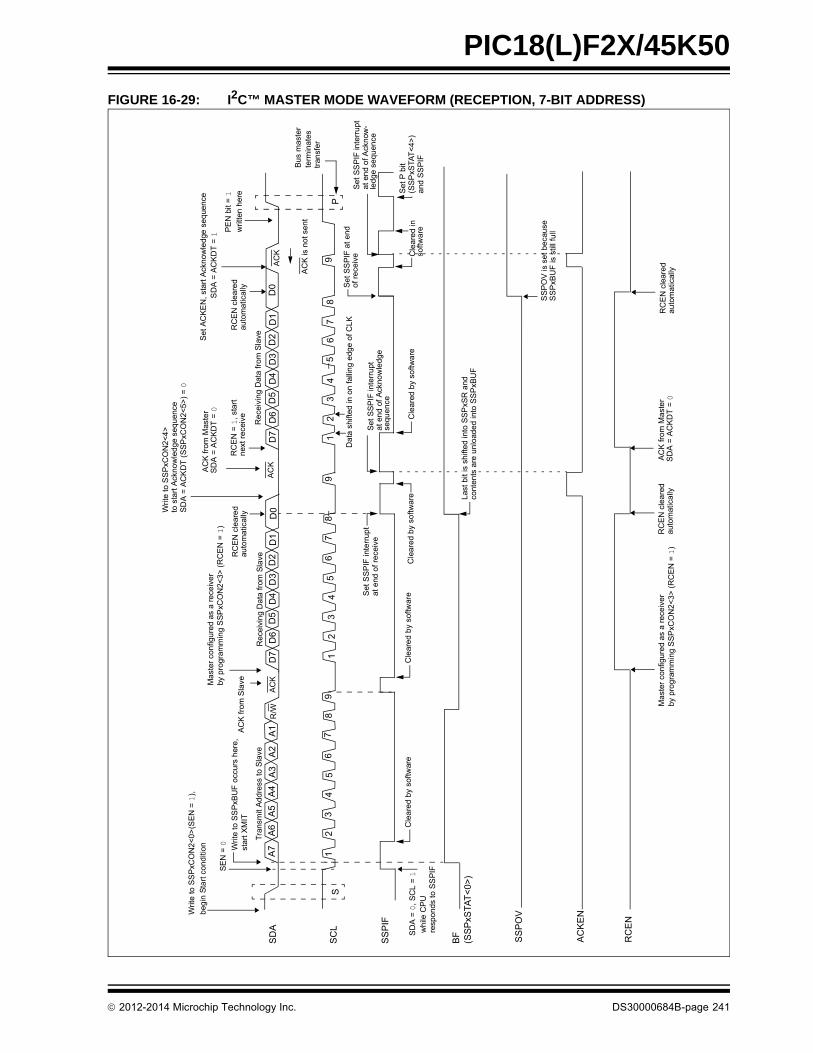
PIC18(L)F2X/45K50
FIGURE 16-29: I2C™ MASTER MODE WAVEFORM (RECEPTION, 7-BIT ADDRESS)
P9
87
65
D0
D1
D2
D3
D4
D5
D6
D7
S
A7
A6
A5
A4
A3
A2
A1
SD
A
SC
L1
23
45
67
89
12
34
56
78
91
23
4
Bu
s m
aste
rte
rmin
ate
str
ansf
er
AC
K
Re
ceiv
ing
Dat
a fr
om
Sla
veR
ece
ivin
g D
ata
from
Sla
ve
D0
D1
D2
D3
D4
D5
D6
D7
AC
K
Tra
nsm
it A
dd
ress
to
Sla
ve
SS
PIF
BF
AC
K is
no
t se
nt
Wri
te to
SS
PxC
ON
2<
0>
(SE
N =
1),
Writ
e to
SS
PxB
UF
occ
urs
her
e,
AC
K fr
om
Sla
veMa
ste
r co
nfig
ure
d a
s a
re
ceiv
er
by p
rog
ram
min
g S
SP
xCO
N2
<3
> (
RC
EN
= 1
)P
EN
bit
= 1
wri
tten
he
re
Da
ta s
hifte
d in
on
falli
ng
edg
e o
f CL
K
Cle
are
d b
y so
ftwar
e
sta
rt X
MIT
SE
N =
0
SS
PO
V
SD
A =
0,
SC
L =
1w
hile
CP
U
(SS
PxS
TAT
<0>
)
AC
K
Cle
are
d b
y so
ftwa
reC
lea
red
by
softw
are
Set
SS
PIF
inte
rru
pt
at
end
of
rece
ive
Se
t P
bit
(SS
PxS
TAT
<4
>)
and
SS
PIF
Cle
are
d in
softw
are
AC
K f
rom
Mas
ter
Se
t S
SP
IF a
t e
nd
Se
t S
SP
IF in
terr
upt
at e
nd
of
Ack
no
wle
dg
ese
qu
en
ce
Se
t S
SP
IF in
terr
up
ta
t en
d o
f Ack
now
-le
dg
e se
qu
ence
of r
ece
ive
Se
t A
CK
EN
, st
art
Ack
no
wle
dge
se
que
nce
SS
PO
V is
se
t b
eca
use
SS
PxB
UF
is s
till f
ull
SD
A =
AC
KD
T =
1
RC
EN
cle
are
dau
tom
atic
ally
RC
EN
= 1
, st
art
next
re
ceiv
e
Wri
te to
SS
PxC
ON
2<
4>
to s
tart
Ack
now
ledg
e se
quen
ceS
DA
= A
CK
DT
(S
SP
xCO
N2
<5
>)
= 0
RC
EN
cle
are
dau
tom
atic
ally
resp
on
ds
to S
SP
IF
AC
KE
Nbeg
in S
tart
co
nd
itio
n
Cle
are
d b
y so
ftwar
e
SD
A =
AC
KD
T =
0
Last
bit
is s
hifte
d in
to S
SP
xSR
and
cont
en
ts a
re u
nlo
ade
d in
to S
SP
xBU
F
RC
EN
Ma
ster
co
nfig
ure
d a
s a
re
ceiv
er
by
pro
gra
mm
ing
SS
PxC
ON
2<
3>
(R
CE
N =
1)
RC
EN
cle
are
dau
tom
atic
ally
AC
K f
rom
Ma
ste
rS
DA
= A
CK
DT
= 0
R
CE
N c
lea
red
au
tom
atic
ally
R/W
2012-2014 Microchip Technology Inc. DS30000684B-page 241

PIC18(L)F2X/45K50
16.6.8 ACKNOWLEDGE SEQUENCE TIMING
An Acknowledge sequence is enabled by setting theAcknowledge Sequence Enable bit, ACKEN, of theSSPxCON2 register. When this bit is set, the SCL pin ispulled low and the contents of the Acknowledge data bitare presented on the SDA pin. If the user wishes to gen-erate an Acknowledge, then the ACKDT bit should becleared. If not, the user should set the ACKDT bit beforestarting an Acknowledge sequence. The Baud RateGenerator then counts for one rollover period (TBRG)and the SCL pin is deasserted (pulled high). When theSCL pin is sampled high (clock arbitration), the BaudRate Generator counts for TBRG. The SCL pin is thenpulled low. Following this, the ACKEN bit is automaticallycleared, the Baud Rate Generator is turned off and theMSSP module then goes into Idle mode (Figure 16-29).
16.6.8.1 WCOL Status Flag
If the user writes the SSPxBUF when an Acknowledgesequence is in progress, then WCOL is set and thecontents of the buffer are unchanged (the write doesnot occur).
16.6.9 STOP CONDITION TIMING
A Stop bit is asserted on the SDA pin at the end of areceive/transmit by setting the Stop Sequence Enablebit, PEN, of the SSPxCON2 register. At the end of areceive/transmit, the SCL line is held low after thefalling edge of the ninth clock. When the PEN bit is set,the master will assert the SDA line low. When the SDAline is sampled low, the Baud Rate Generator isreloaded and counts down to ‘0’. When the Baud RateGenerator times out, the SCL pin will be brought highand one TBRG (Baud Rate Generator rollover count)later, the SDA pin will be deasserted. When the SDApin is sampled high while SCL is high, the P bit of theSSPxSTAT register is set. A TBRG later, the PEN bit iscleared and the SSPIF bit is set (Figure 16-30).
16.6.9.1 WCOL Status Flag
If the user writes the SSPxBUF when a Stop sequenceis in progress, then the WCOL bit is set and thecontents of the buffer are unchanged (the write doesnot occur).
FIGURE 16-30: ACKNOWLEDGE SEQUENCE WAVEFORM
FIGURE 16-31: STOP CONDITION RECEIVE OR TRANSMIT MODE
Note: TBRG = one Baud Rate Generator period.
SDA
SCL
SSPIF set at
Acknowledge sequence starts here,write to SSPxCON2
ACKEN automatically cleared
Cleared in
TBRG TBRG
the end of receive
8
ACKEN = 1, ACKDT = 0
D0
9
SSPIF
software SSPIF set at the endof Acknowledge sequence
Cleared insoftware
ACK
SCL
SDA
SDA asserted low before rising edge of clock
Write to SSPxCON2,set PEN
Falling edge of
SCL = 1 for TBRG, followed by SDA = 1 for TBRG
9th clock
SCL brought high after TBRG
Note: TBRG = one Baud Rate Generator period.
TBRG TBRG
after SDA sampled high. P bit (SSPxSTAT<4>) is set.
TBRG
to set up Stop condition
ACK
P
TBRG
PEN bit (SSPxCON2<2>) is cleared by hardware and the SSPIF bit is set
DS30000684B-page 242 2012-2014 Microchip Technology Inc.

PIC18(L)F2X/45K50
16.6.10 SLEEP OPERATION
While in Sleep mode, the I2C slave module can receiveaddresses or data and when an address match orcomplete byte transfer occurs, wake the processorfrom Sleep (if the MSSP interrupt is enabled).
16.6.11 EFFECTS OF A RESET
A Reset disables the MSSP module and terminates thecurrent transfer.
16.6.12 MULTI-MASTER MODE
In Multi-Master mode, the interrupt generation on thedetection of the Start and Stop conditions allows thedetermination of when the bus is free. The Stop (P) andStart (S) bits are cleared from a Reset or when theMSSP module is disabled. Control of the I2C bus maybe taken when the P bit of the SSPxSTAT register isset, or the bus is Idle, with both the S and P bits clear.When the bus is busy, enabling the SSP interrupt willgenerate the interrupt when the Stop condition occurs.
In multi-master operation, the SDA line must bemonitored for arbitration to see if the signal level is theexpected output level. This check is performed byhardware with the result placed in the BCLIF bit.
The states where arbitration can be lost are:
• Address Transfer
• Data Transfer
• A Start Condition
• A Repeated Start Condition
• An Acknowledge Condition
2012-2014 Microchip Technology Inc. DS30000684B-page 243

PIC18(L)F2X/45K50
16.6.13 MULTI -MASTER COMMUNICATION, BUS COLLISION AND BUS ARBITRATION
Multi-Master mode support is achieved by busarbitration. When the master outputs address/data bitsonto the SDA pin, arbitration takes place when themaster outputs a ‘1’ on SDA, by letting SDA float highand another master asserts a ‘0’. When the SCL pinfloats high, data should be stable. If the expected dataon SDA is a ‘1’ and the data sampled on the SDA pin is‘0’, then a bus collision has taken place. The master willset the Bus Collision Interrupt Flag, BCLIF, and resetthe I2C port to its Idle state (Figure 16-31).
If a transmit was in progress when the bus collisionoccurred, the transmission is halted, the BF flag iscleared, the SDA and SCL lines are deasserted and theSSPxBUF can be written to. When the user servicesthe bus collision Interrupt Service Routine and if the I2Cbus is free, the user can resume communication byasserting a Start condition.
If a Start, Repeated Start, Stop or Acknowledgecondition was in progress when the bus collisionoccurred, the condition is aborted, the SDA and SCLlines are deasserted and the respective control bits inthe SSPxCON2 register are cleared. When the userservices the bus collision Interrupt Service Routine andif the I2C bus is free, the user can resumecommunication by asserting a Start condition.
The master will continue to monitor the SDA and SCLpins. If a Stop condition occurs, the SSPIF bit will be set.
A write to the SSPxBUF will start the transmission ofdata at the first data bit, regardless of where thetransmitter left off when the bus collision occurred.
In Multi-Master mode, the interrupt generation on thedetection of Start and Stop conditions allows thedetermination of when the bus is free. Control of the I2Cbus can be taken when the P bit is set in the SSPxSTATregister, or the bus is Idle and the S and P bits arecleared.
FIGURE 16-32: BUS COLLISION TIMING FOR TRANSMIT AND ACKNOWLEDGE
SDA
SCL
BCLIF
SDA released
SDA line pulled lowby another source
Sample SDA. While SCL is high,data does not match what is driven
Bus collision has occurred.
Set bus collisioninterrupt (BCLIF)
by the master.
by master
Data changeswhile SCL = 0
DS30000684B-page 244 2012-2014 Microchip Technology Inc.
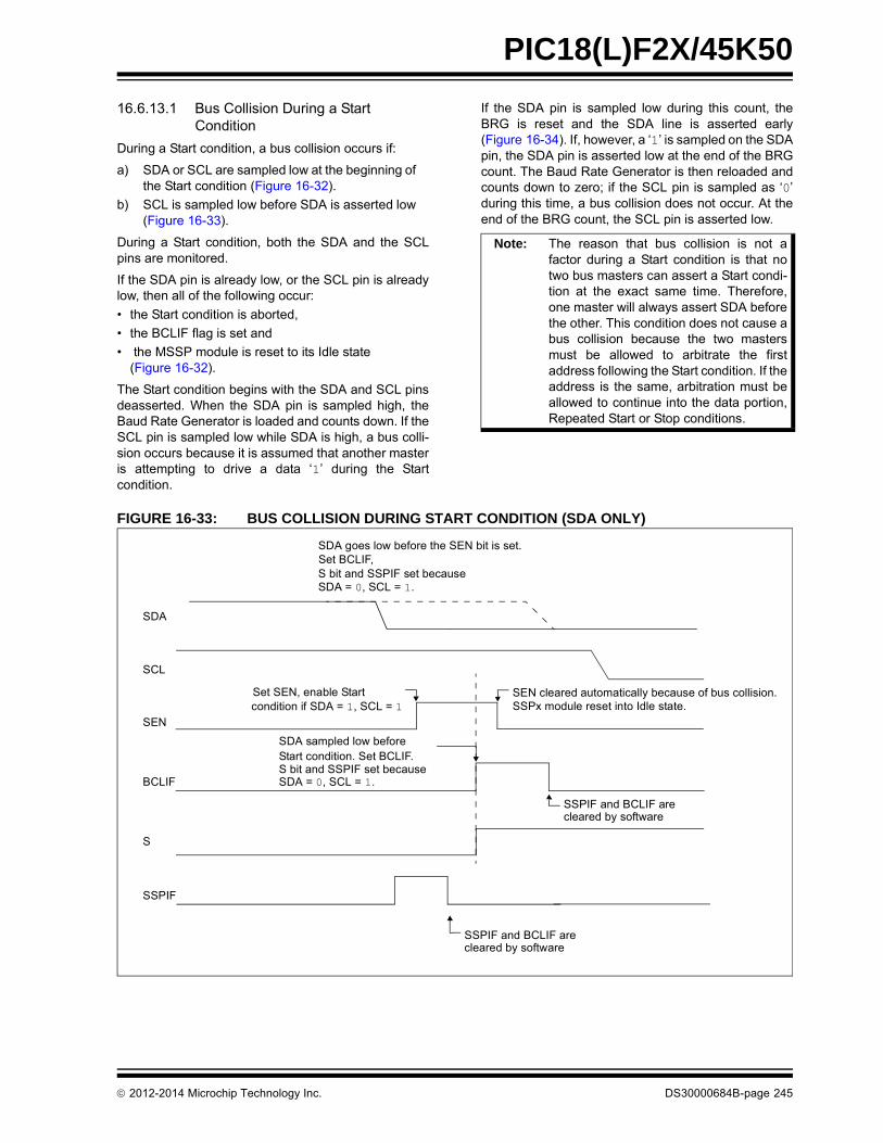
PIC18(L)F2X/45K50
16.6.13.1 Bus Collision During a Start Condition
During a Start condition, a bus collision occurs if:
a) SDA or SCL are sampled low at the beginning ofthe Start condition (Figure 16-32).
b) SCL is sampled low before SDA is asserted low(Figure 16-33).
During a Start condition, both the SDA and the SCLpins are monitored.
If the SDA pin is already low, or the SCL pin is alreadylow, then all of the following occur:
• the Start condition is aborted,
• the BCLIF flag is set and
• the MSSP module is reset to its Idle state (Figure 16-32).
The Start condition begins with the SDA and SCL pinsdeasserted. When the SDA pin is sampled high, theBaud Rate Generator is loaded and counts down. If theSCL pin is sampled low while SDA is high, a bus colli-sion occurs because it is assumed that another masteris attempting to drive a data ‘1’ during the Startcondition.
If the SDA pin is sampled low during this count, theBRG is reset and the SDA line is asserted early(Figure 16-34). If, however, a ‘1’ is sampled on the SDApin, the SDA pin is asserted low at the end of the BRGcount. The Baud Rate Generator is then reloaded andcounts down to zero; if the SCL pin is sampled as ‘0’during this time, a bus collision does not occur. At theend of the BRG count, the SCL pin is asserted low.
FIGURE 16-33: BUS COLLISION DURING START CONDITION (SDA ONLY)
Note: The reason that bus collision is not afactor during a Start condition is that notwo bus masters can assert a Start condi-tion at the exact same time. Therefore,one master will always assert SDA beforethe other. This condition does not cause abus collision because the two mastersmust be allowed to arbitrate the firstaddress following the Start condition. If theaddress is the same, arbitration must beallowed to continue into the data portion,Repeated Start or Stop conditions.
SDA
SCL
SEN
SDA sampled low before
SDA goes low before the SEN bit is set.
S bit and SSPIF set because
SSPx module reset into Idle state.SEN cleared automatically because of bus collision.
S bit and SSPIF set because
Set SEN, enable Startcondition if SDA = 1, SCL = 1
SDA = 0, SCL = 1.
BCLIF
S
SSPIF
SDA = 0, SCL = 1.
SSPIF and BCLIF arecleared by software
SSPIF and BCLIF arecleared by software
Set BCLIF,
Start condition. Set BCLIF.
2012-2014 Microchip Technology Inc. DS30000684B-page 245

PIC18(L)F2X/45K50
FIGURE 16-34: BUS COLLISION DURING START CONDITION (SCL = 0)
FIGURE 16-35: BRG RESET DUE TO SDA ARBITRATION DURING START CONDITION
SDA
SCL
SENbus collision occurs. Set BCLIF.SCL = 0 before SDA = 0,
Set SEN, enable Startsequence if SDA = 1, SCL = 1
TBRG TBRG
SDA = 0, SCL = 1
BCLIF
S
SSPIF
Interrupt clearedby software
bus collision occurs. Set BCLIF.SCL = 0 before BRG time-out,
’0’ ’0’
’0’’0’
SDA
SCL
SEN
Set SLess than TBRG
TBRG
SDA = 0, SCL = 1
BCLIF
S
SSPIF
S
Interrupts clearedby softwareset SSPIF
SDA = 0, SCL = 1,
SCL pulled low after BRGtime-out
Set SSPIF
’0’
SDA pulled low by other master.Reset BRG and assert SDA.
Set SEN, enable Startsequence if SDA = 1, SCL = 1
DS30000684B-page 246 2012-2014 Microchip Technology Inc.

PIC18(L)F2X/45K50
16.6.13.2 Bus Collision During a Repeated Start Condition
During a Repeated Start condition, a bus collisionoccurs if:
a) A low level is sampled on SDA when SCL goesfrom low level to high level.
b) SCL goes low before SDA is asserted low,indicating that another master is attempting totransmit a data ‘1’.
When the user releases SDA and the pin is allowed tofloat high, the BRG is loaded with SSPxADD andcounts down to zero. The SCL pin is then deassertedand when sampled high, the SDA pin is sampled.
If SDA is low, a bus collision has occurred (i.e., anothermaster is attempting to transmit a data ‘0’, Figure 16-35).If SDA is sampled high, the BRG is reloaded and beginscounting. If SDA goes from high-to-low before the BRGtimes out, no bus collision occurs because no twomasters can assert SDA at exactly the same time.
If SCL goes from high-to-low before the BRG times outand SDA has not already been asserted, a bus collisionoccurs. In this case, another master is attempting totransmit a data ‘1’ during the Repeated Start condition,see Figure 16-36.
If, at the end of the BRG time-out, both SCL and SDAare still high, the SDA pin is driven low and the BRG isreloaded and begins counting. At the end of the count,regardless of the status of the SCL pin, the SCL pin isdriven low and the Repeated Start condition iscomplete.
FIGURE 16-36: BUS COLLISION DURING A REPEATED START CONDITION (CASE 1)
FIGURE 16-37: BUS COLLISION DURING REPEATED START CONDITION (CASE 2)
SDA
SCL
RSEN
BCLIF
S
SSPIF
Sample SDA when SCL goes high.If SDA = 0, set BCLIF and release SDA and SCL.
Cleared by software
’0’
’0’
SDA
SCL
BCLIF
RSEN
S
SSPIF
Interrupt clearedby software
SCL goes low before SDAset BCLIF. Release SDA and SCL.
TBRG TBRG
’0’
2012-2014 Microchip Technology Inc. DS30000684B-page 247

PIC18(L)F2X/45K50
16.6.13.3 Bus Collision During a Stop Condition
Bus collision occurs during a Stop condition if:
a) After the SDA pin has been deasserted andallowed to float high, SDA is sampled low afterthe BRG has timed out.
b) After the SCL pin is deasserted, SCL is sampledlow before SDA goes high.
The Stop condition begins with SDA asserted low.When SDA is sampled low, the SCL pin is allowed tofloat. When the pin is sampled high (clock arbitration),the Baud Rate Generator is loaded with SSPxADD andcounts down to 0. After the BRG times out, SDA issampled. If SDA is sampled low, a bus collision hasoccurred. This is due to another master attempting todrive a data ‘0’ (Figure 16-37). If the SCL pin is sampledlow before SDA is allowed to float high, a bus collisionoccurs. This is another case of another masterattempting to drive a data ‘0’ (Figure 16-38).
FIGURE 16-38: BUS COLLISION DURING A STOP CONDITION (CASE 1)
FIGURE 16-39: BUS COLLISION DURING A STOP CONDITION (CASE 2)
SDA
SCL
BCLIF
PEN
P
SSPIF
TBRG TBRG TBRG
SDA asserted low
SDA sampledlow after TBRG,set BCLIF
’0’
’0’
SDA
SCL
BCLIF
PEN
P
SSPIF
TBRG TBRG TBRG
Assert SDA SCL goes low before SDA goes high,set BCLIF
’0’
’0’
DS30000684B-page 248 2012-2014 Microchip Technology Inc.

PIC18(L)F2X/45K50
TABLE 16-3: REGISTERS ASSOCIATED WITH I2C™ OPERATION
Name Bit 7 Bit 6 Bit 5 Bit 4 Bit 3 Bit 2 Bit 1 Bit 0Register on page
ANSELB — — ANSB5 ANSB4 ANSB3 ANSB2 ANSB1 ANSB0 148
INTCON GIE/GIEH PEIE/GIEL TMR0IE INT0IE IOCIE TMR0IF INT0IF IOCIF 114
IPR1 ACTIP ADIP RCIP TXIP SSPIP CCP1IP TMR2IP TMR1IP 123
IPR2 OSCFIP C1IP C2IP EEIP BCLIP HLVDIP TMR3IP CCP2IP 124
PIE1 ACTIE ADIE RCIE TXIE SSPIE CCP1IE TMR2IE TMR1IE 120
PIE2 OSCFIE C1IE C2IE EEIE BCLIE HLVDIE TMR3IE CCP2IE 121
PIR1 ACTIF ADIF RCIF TXIF SSPIF CCP1IF TMR2IF TMR1IF 117
PIR2 OSCFIF C1IF C2IF EEIF BCLIF HLVDIF TMR3IF CCP2IF 118
PMD1 — MSSPMD CTMUMD CMP2MD CMP1MD ADCMD CCP2MD CCP1MD 62
SSP1ADD SSP1 Address Register in I2C™ Slave Mode. SSP1 Baud Rate Reload Register in I2C Master mode. 257
SSP1BUF SSP1 Receive Buffer/Transmit Register —
SSP1CON1 WCOL SSPOV SSPEN CKP SSPM<3:0> 252
SSP1CON2 GCEN ACKSTAT ACKDT ACKEN RCEN PEN RSEN SEN 254
SSP1CON3 ACKTIM PCIE SCIE BOEN SDAHT SBCDE AHEN DHEN 255
SSP1MSK SSP1 MASK Register bits 256
SSP1STAT SMP CKE D/A P S R/W UA BF 251
TRISB TRISB7 TRISB6 TRISB5 TRISB4 TRISB3 TRISB2 TRISB1 TRISB0 149
Legend: Shaded bits are not used by the MSSP in I2C mode.
2012-2014 Microchip Technology Inc. DS30000684B-page 249

PIC18(L)F2X/45K50
16.7 Baud Rate Generator
The MSSP module has a Baud Rate Generator avail-able for clock generation in both I2C and SPI Mastermodes. The Baud Rate Generator (BRG) reload valueis placed in the SSPxADD register (Register 16-6).When a write occurs to SSPxBUF, the Baud Rate Gen-erator will automatically begin counting down.
Once the given operation is complete, the internal clockwill automatically stop counting and the clock pin willremain in its last state.
An internal signal “Reload” in Figure 16-39 triggers thevalue from SSPxADD to be loaded into the BRGcounter. This occurs twice for each oscillation of themodule clock line. The logic dictating when the reloadsignal is asserted depends on the mode the MSSP isbeing operated in.
Table 16-4 demonstrates clock rates based oninstruction cycles and the BRG value loaded intoSSPxADD.
EQUATION 16-1:
FIGURE 16-40: BAUD RATE GENERATOR BLOCK DIAGRAM
FCLOCKFOSC
SSPxADD 1+ 4 -------------------------------------------------=
Note: Values of 0x00, 0x01 and 0x02 are not validfor SSPxADD when used as a Baud RateGenerator for I2C™. This is an implementa-tion limitation.
SSPxM<3:0>
BRG Down CounterSSPxCLK FOSC/2
SSPxADD<7:0>
SSPxM<3:0>
SCL
Reload
Control
Reload
TABLE 16-4: MSSP CLOCK RATE W/BRG
FOSC FCY BRG ValueFCLOCK
(2 Rollovers of BRG)
32 MHz 8 MHz 13h 400 kHz(1)
32 MHz 8 MHz 19h 308 kHz
32 MHz 8 MHz 4Fh 100 kHz
16 MHz 4 MHz 09h 400 kHz(1)
16 MHz 4 MHz 0Ch 308 kHz
16 MHz 4 MHz 27h 100 kHz
4 MHz 1 MHz 09h 100 kHz
Note 1: The I2C™ interface does not conform to the 400 kHz I2C specification (which applies to rates greater than 100 kHz) in all details, but may be used with care where higher rates are required by the application.
DS30000684B-page 250 2012-2014 Microchip Technology Inc.
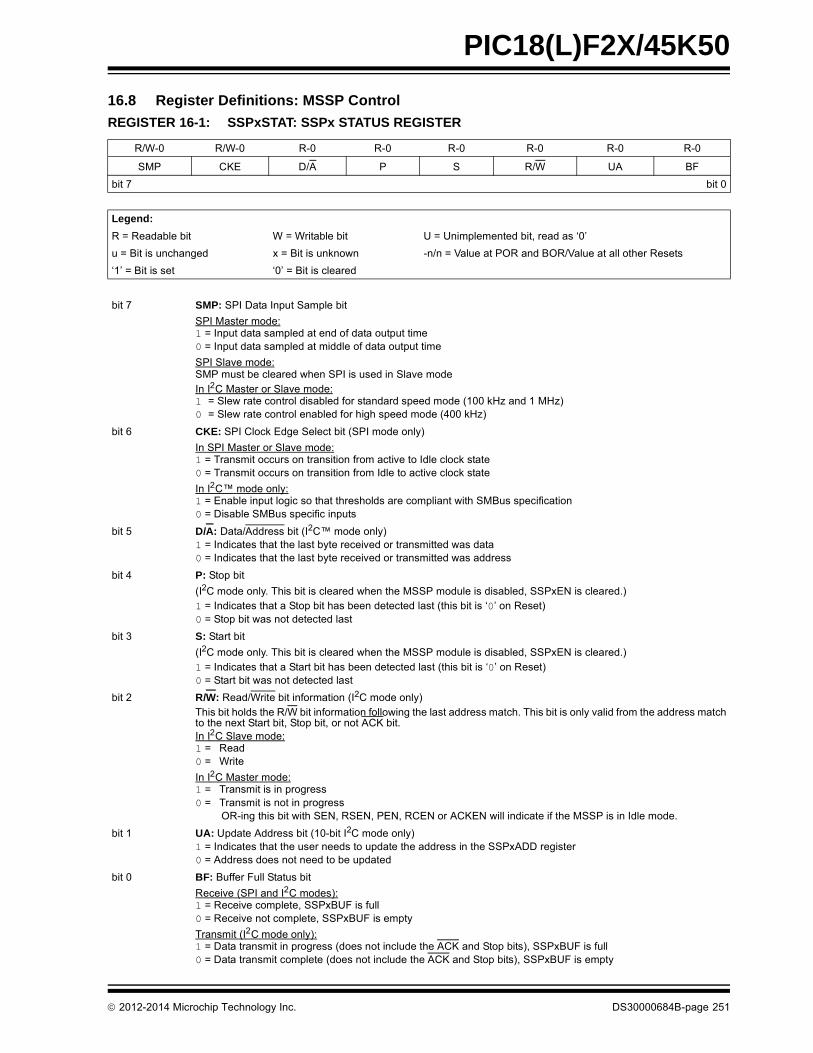
PIC18(L)F2X/45K50
16.8 Register Definitions: MSSP Control
REGISTER 16-1: SSPxSTAT: SSPx STATUS REGISTER
R/W-0 R/W-0 R-0 R-0 R-0 R-0 R-0 R-0
SMP CKE D/A P S R/W UA BF
bit 7 bit 0
Legend:
R = Readable bit W = Writable bit U = Unimplemented bit, read as ‘0’
u = Bit is unchanged x = Bit is unknown -n/n = Value at POR and BOR/Value at all other Resets
‘1’ = Bit is set ‘0’ = Bit is cleared
bit 7 SMP: SPI Data Input Sample bit
SPI Master mode:1 = Input data sampled at end of data output time0 = Input data sampled at middle of data output time
SPI Slave mode:SMP must be cleared when SPI is used in Slave modeIn I2 C Master or Slave mode: 1 = Slew rate control disabled for standard speed mode (100 kHz and 1 MHz)0 = Slew rate control enabled for high speed mode (400 kHz)
bit 6 CKE: SPI Clock Edge Select bit (SPI mode only)
In SPI Master or Slave mode:1 = Transmit occurs on transition from active to Idle clock state0 = Transmit occurs on transition from Idle to active clock state
In I2 C™ mode only: 1 = Enable input logic so that thresholds are compliant with SMBus specification0 = Disable SMBus specific inputs
bit 5 D/A: Data/Address bit (I2C™ mode only) 1 = Indicates that the last byte received or transmitted was data0 = Indicates that the last byte received or transmitted was address
bit 4 P: Stop bit
(I2C mode only. This bit is cleared when the MSSP module is disabled, SSPxEN is cleared.)1 = Indicates that a Stop bit has been detected last (this bit is ‘0’ on Reset)0 = Stop bit was not detected last
bit 3 S: Start bit
(I2C mode only. This bit is cleared when the MSSP module is disabled, SSPxEN is cleared.)1 = Indicates that a Start bit has been detected last (this bit is ‘0’ on Reset)0 = Start bit was not detected last
bit 2 R/W: Read/Write bit information (I2C mode only)This bit holds the R/W bit information following the last address match. This bit is only valid from the address matchto the next Start bit, Stop bit, or not ACK bit.In I2 C Slave mode:1 = Read0 = Write
In I2 C Master mode:1 = Transmit is in progress0 = Transmit is not in progress
OR-ing this bit with SEN, RSEN, PEN, RCEN or ACKEN will indicate if the MSSP is in Idle mode.
bit 1 UA: Update Address bit (10-bit I2C mode only)1 = Indicates that the user needs to update the address in the SSPxADD register0 = Address does not need to be updated
bit 0 BF: Buffer Full Status bit
Receive (SPI and I2 C modes):1 = Receive complete, SSPxBUF is full0 = Receive not complete, SSPxBUF is empty
Transmit (I2 C mode only):1 = Data transmit in progress (does not include the ACK and Stop bits), SSPxBUF is full0 = Data transmit complete (does not include the ACK and Stop bits), SSPxBUF is empty
2012-2014 Microchip Technology Inc. DS30000684B-page 251

PIC18(L)F2X/45K50
REGISTER 16-2: SSPxCON1: SSPx CONTROL REGISTER 1
R/C/HS-0 R/C/HS-0 R/W-0 R/W-0 R/W-0 R/W-0 R/W-0 R/W-0
WCOL SSPOV SSPEN CKP SSPM<3:0>
bit 7 bit 0
Legend:
R = Readable bit W = Writable bit U = Unimplemented bit, read as ‘0’
u = Bit is unchanged x = Bit is unknown -n/n = Value at POR and BOR/Value at all other Resets
‘1’ = Bit is set ‘0’ = Bit is cleared HS = Bit is set by hardware C = User cleared
bit 7 WCOL: Write Collision Detect bitMaster mode:1 = A write to the SSPxBUF register was attempted while the I2C™ conditions were not valid for a transmission
to be started0 = No collisionSlave mode:1 = The SSPxBUF register is written while it is still transmitting the previous word (must be cleared in software)0 = No collision
bit 6 SSPOV: Receive Overflow Indicator bit(1)
In SPI mode:1 = A new byte is received while the SSPxBUF register is still holding the previous data. In case of overflow, the data
in SSPxSR is lost. Overflow can only occur in Slave mode. In Slave mode, the user must read the SSPxBUF, even if only transmitting data, to avoid setting overflow. In Master mode, the overflow bit is not set since each new recep-tion (and transmission) is initiated by writing to the SSPxBUF register (must be cleared in software).
0 = No overflowIn I2 C mode:1 = A byte is received while the SSPxBUF register is still holding the previous byte. SSPOV is a “don’t care” in
Transmit mode (must be cleared in software). 0 = No overflow
bit 5 SSPEN: Synchronous Serial Port Enable bitIn both modes, when enabled, these pins must be properly configured as input or outputIn SPI mode:1 = Enables serial port and configures SCK, SDO, SDI and SS as the source of the serial port pins(2)
0 = Disables serial port and configures these pins as I/O port pinsIn I2 C mode:1 = Enables the serial port and configures the SDA and SCL pins as the source of the serial port pins(3)
0 = Disables serial port and configures these pins as I/O port pins
bit 4 CKP: Clock Polarity Select bit In SPI mode:1 = Idle state for clock is a high level 0 = Idle state for clock is a low levelIn I2 C Slave mode:SCL release control1 = Enable clock 0 = Holds clock low (clock stretch). (Used to ensure data setup time.)In I2 C Master mode:Unused in this mode
DS30000684B-page 252 2012-2014 Microchip Technology Inc.

PIC18(L)F2X/45K50
bit 3-0 SSPM<3:0>: Synchronous Serial Port Mode Select bits0000 = SPI Master mode, clock = FOSC/40001 = SPI Master mode, clock = FOSC/16 0010 = SPI Master mode, clock = FOSC/64 0011 = SPI Master mode, clock = TMR2 output/2 0100 = SPI Slave mode, clock = SCK pin, SS pin control enabled 0101 = SPI Slave mode, clock = SCK pin, SS pin control disabled, SS can be used as I/O pin0110 = I2C Slave mode, 7-bit address 0111 = I2C Slave mode, 10-bit address 1000 = I2C Master mode, clock = FOSC / (4 * (SSPxADD+1))(4)
1001 = Reserved1010 = SPI Master mode, clock = FOSC/(4 * (SSPxADD+1))1011 = I2C firmware controlled Master mode (slave idle) 1100 = Reserved 1101 = Reserved 1110 = I2C Slave mode, 7-bit address with Start and Stop bit interrupts enabled 1111 = I2C Slave mode, 10-bit address with Start and Stop bit interrupts enabled
Note 1: In Master mode, the overflow bit is not set since each new reception (and transmission) is initiated by writing to the SSPxBUF register.
2: When enabled, these pins must be properly configured as input or output.3: When enabled, the SDA and SCL pins must be configured as inputs.4: SSPxADD values of 0, 1 or 2 are not supported for I2C mode.
REGISTER 16-2: SSPxCON1: SSPx CONTROL REGISTER 1 (CONTINUED)
2012-2014 Microchip Technology Inc. DS30000684B-page 253

PIC18(L)F2X/45K50
REGISTER 16-3: SSPxCON2: SSPx CONTROL REGISTER 2
R/W-0 R-0 R/W-0 R/S/HC-0 R/S/HC-0 R/S/HC-0 R/S/HC-0 R/W/HC-0
GCEN ACKSTAT ACKDT ACKEN(1) RCEN(1) PEN(1) RSEN(1) SEN(1)
bit 7 bit 0
Legend:
R = Readable bit W = Writable bit U = Unimplemented bit, read as ‘0’
u = Bit is unchanged x = Bit is unknown -n/n = Value at POR and BOR/Value at all other Resets
‘1’ = Bit is set ‘0’ = Bit is cleared HC = Cleared by hardware S = User set
bit 7 GCEN: General Call Enable bit (in I2C™ Slave mode only)1 = Enable interrupt when a general call address (0x00 or 00h) is received in the SSPxSR0 = General call address disabled
bit 6 ACKSTAT: Acknowledge Status bit (in I2C mode only)1 = Acknowledge was not received0 = Acknowledge was received
bit 5 ACKDT: Acknowledge Data bit (in I2C mode only)
In Receive mode:Value transmitted when the user initiates an Acknowledge sequence at the end of a receive1 = Not Acknowledge0 = Acknowledge
bit 4 ACKEN(1): Acknowledge Sequence Enable bit (in I2C Master mode only)
In Master Receive mode:1 = Initiate Acknowledge sequence on SDA and SCL pins, and transmit ACKDT data bit.
Automatically cleared by hardware.0 = Acknowledge sequence idle
bit 3 RCEN(1): Receive Enable bit (in I2C Master mode only)
1 = Enables Receive mode for I2C0 = Receive idle
bit 2 PEN(1): Stop Condition Enable bit (in I2C Master mode only)
SCK Release Control:1 = Initiate Stop condition on SDA and SCL pins. Automatically cleared by hardware.0 = Stop condition Idle
bit 1 RSEN(1): Repeated Start Condition Enabled bit (in I2C Master mode only)
1 = Initiate Repeated Start condition on SDA and SCL pins. Automatically cleared by hardware.0 = Repeated Start condition Idle
bit 0 SEN(1): Start Condition Enabled bit (in I2C Master mode only)
In Master mode:1 = Initiate Start condition on SDA and SCL pins. Automatically cleared by hardware.0 = Start condition Idle
In Slave mode:1 = Clock stretching is enabled for both slave transmit and slave receive (stretch enabled)0 = Clock stretching is disabled
Note 1: For bits ACKEN, RCEN, PEN, RSEN, SEN: If the I2C module is not in the Idle mode, this bit may not be set (no spooling) and the SSPxBUF may not be written (or writes to the SSPxBUF are disabled).
DS30000684B-page 254 2012-2014 Microchip Technology Inc.

PIC18(L)F2X/45K50
REGISTER 16-4: SSPxCON3: SSPx CONTROL REGISTER 3
R-0 R/W-0 R/W-0 R/W-0 R/W-0 R/W-0 R/W-0 R/W-0
ACKTIM PCIE SCIE BOEN SDAHT SBCDE AHEN DHEN
bit 7 bit 0
Legend:
R = Readable bit W = Writable bit U = Unimplemented bit, read as ‘0’
u = Bit is unchanged x = Bit is unknown -n/n = Value at POR and BOR/Value at all other Resets
‘1’ = Bit is set ‘0’ = Bit is cleared
bit 7 ACKTIM: Acknowledge Time Status bit (I2C™ mode only)(3)
1 = Indicates the I2C bus is in an Acknowledge sequence, set on 8th falling edge of SCL clock0 = Not an Acknowledge sequence, cleared on 9th rising edge of SCL clock
bit 6 PCIE: Stop Condition Interrupt Enable bit (I2C mode only)
1 = Enable interrupt on detection of Stop condition0 = Stop detection interrupts are disabled(2)
bit 5 SCIE: Start Condition Interrupt Enable bit (I2C mode only)
1 = Enable interrupt on detection of Start or Restart conditions0 = Start detection interrupts are disabled(2)
bit 4 BOEN: Buffer Overwrite Enable bit
In SPI Slave mode:(1)
1 = SSPxBUF updates every time that a new data byte is shifted in ignoring the BF bit0 = If new byte is received with BF bit of the SSPxSTAT register already set, SSPOV bit of the
SSPxCON1 register is set, and the buffer is not updatedIn I2C Master mode:
This bit is ignored.In I2C Slave mode:
1 = SSPxBUF is updated and ACK is generated for a received address/data byte, ignoring thestate of the SSPOV bit only if the BF bit = 0.
0 = SSPxBUF is only updated when SSPOV is clear
bit 3 SDAHT: SDA Hold Time Selection bit (I2C mode only)
1 = Minimum of 300 ns hold time on SDA after the falling edge of SCL0 = Minimum of 100 ns hold time on SDA after the falling edge of SCL
bit 2 SBCDE: Slave Mode Bus Collision Detect Enable bit (I2C Slave mode only)
If on the rising edge of SCL, SDA is sampled low when the module is outputting a high state, the BCLIFbit of the PIR2 register is set, and bus goes idle
1 = Enable slave bus collision interrupts0 = Slave bus collision interrupts are disabled
bit 1 AHEN: Address Hold Enable bit (I2C Slave mode only)
1 = Following the 8th falling edge of SCL for a matching received address byte; CKP bit of the SSPx-CON1 register will be cleared and the SCL will be held low.
0 = Address holding is disabled
Note 1: For daisy-chained SPI operation; allows the user to ignore all but the last received byte. SSPOV is still set when a new byte is received and BF = 1, but hardware continues to write the most recent byte to SSPxBUF.
2: This bit has no effect in Slave modes for which Start and Stop condition detection is explicitly listed as enabled.
3: The ACKTIM Status bit is active only when the AHEN bit or DHEN bit is set.
2012-2014 Microchip Technology Inc. DS30000684B-page 255

PIC18(L)F2X/45K50
bit 0 DHEN: Data Hold Enable bit (I2C Slave mode only)
1 = Following the 8th falling edge of SCL for a received data byte; slave hardware clears the CKP bitof the SSPxCON1 register and SCL is held low.
0 = Data holding is disabled
REGISTER 16-4: SSPxCON3: SSPx CONTROL REGISTER 3 (CONTINUED)
Note 1: For daisy-chained SPI operation; allows the user to ignore all but the last received byte. SSPOV is still set when a new byte is received and BF = 1, but hardware continues to write the most recent byte to SSPxBUF.
2: This bit has no effect in Slave modes for which Start and Stop condition detection is explicitly listed as enabled.
3: The ACKTIM Status bit is active only when the AHEN bit or DHEN bit is set.
REGISTER 16-5: SSPxMSK: SSPx MASK REGISTER
R/W-1 R/W-1 R/W-1 R/W-1 R/W-1 R/W-1 R/W-1 R/W-1
MSK7 MSK6 MSK5 MSK4 MSK3 MSK2 MSK1 MSK0
bit 7 bit 0
Legend:
R = Readable bit W = Writable bit U = Unimplemented bit, read as ‘0’
u = Bit is unchanged x = Bit is unknown -n/n = Value at POR and BOR/Value at all other Resets
‘1’ = Bit is set ‘0’ = Bit is cleared
bit 7-1 MSK<7:1>: Mask bits1 = The received address bit n is compared to SSPxADD<n> to detect I2C™ address match0 = The received address bit n is not used to detect I2C address match
bit 0 MSK<0>: Mask bit for I2C Slave mode, 10-bit AddressI2C Slave mode, 10-bit address (SSPxM<3:0> = 0111 or 1111):1 = The received address bit 0 is compared to SSPxADD<0> to detect I2C address match0 = The received address bit 0 is not used to detect I2C address matchI2C Slave mode, 7-bit address, the bit is ignored
DS30000684B-page 256 2012-2014 Microchip Technology Inc.

PIC18(L)F2X/45K50
REGISTER 16-6: SSPxADD: MSSP ADDRESS AND BAUD RATE REGISTER (I2C™ MODE)
R/W-0 R/W-0 R/W-0 R/W-0 R/W-0 R/W-0 R/W-0 R/W-0
ADD<7:0>
bit 7 bit 0
Legend:
R = Readable bit W = Writable bit U = Unimplemented bit, read as ‘0’
u = Bit is unchanged x = Bit is unknown -n/n = Value at POR and BOR/Value at all other Resets
‘1’ = Bit is set ‘0’ = Bit is cleared
Master mode:
bit 7-0 ADD<7:0>: Baud Rate Clock Divider bitsSCL pin clock period = ((ADD<7:0> + 1) *4)/FOSC
10-Bit Slave mode — Most Significant Address byte:
bit 7-3 Not used: Unused for Most Significant Address byte. Bit state of this register is a “don’t care”. Bit pattern sent by master is fixed by I2C™ specification and must be equal to ‘11110’. However, those bits are compared by hardware and are not affected by the value in this register.
bit 2-1 ADD<2:1>: Two Most Significant bits of 10-bit address
bit 0 Not used: Unused in this mode. Bit state is a “don’t care”.
10-Bit Slave mode — Least Significant Address byte:
bit 7-0 ADD<7:0>: Eight Least Significant bits of 10-bit address
7-Bit Slave mode:
bit 7-1 ADD<7:1>: 7-bit address
bit 0 Not used: Unused in this mode. Bit state is a “don’t care”.
2012-2014 Microchip Technology Inc. DS30000684B-page 257
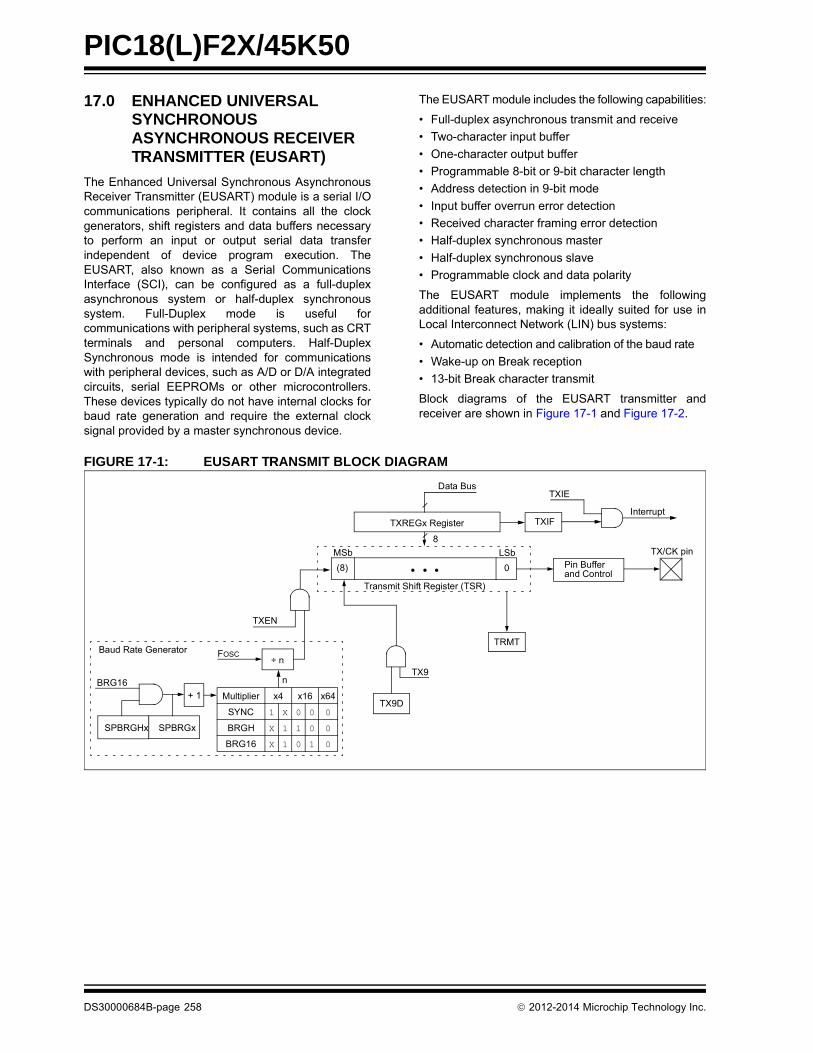
PIC18(L)F2X/45K50
17.0 ENHANCED UNIVERSAL SYNCHRONOUS ASYNCHRONOUS RECEIVER TRANSMITTER (EUSART)
The Enhanced Universal Synchronous AsynchronousReceiver Transmitter (EUSART) module is a serial I/Ocommunications peripheral. It contains all the clockgenerators, shift registers and data buffers necessaryto perform an input or output serial data transferindependent of device program execution. TheEUSART, also known as a Serial CommunicationsInterface (SCI), can be configured as a full-duplexasynchronous system or half-duplex synchronoussystem. Full-Duplex mode is useful forcommunications with peripheral systems, such as CRTterminals and personal computers. Half-DuplexSynchronous mode is intended for communicationswith peripheral devices, such as A/D or D/A integratedcircuits, serial EEPROMs or other microcontrollers.These devices typically do not have internal clocks forbaud rate generation and require the external clocksignal provided by a master synchronous device.
The EUSART module includes the following capabilities:
• Full-duplex asynchronous transmit and receive
• Two-character input buffer
• One-character output buffer
• Programmable 8-bit or 9-bit character length
• Address detection in 9-bit mode
• Input buffer overrun error detection
• Received character framing error detection
• Half-duplex synchronous master
• Half-duplex synchronous slave
• Programmable clock and data polarity
The EUSART module implements the followingadditional features, making it ideally suited for use inLocal Interconnect Network (LIN) bus systems:
• Automatic detection and calibration of the baud rate
• Wake-up on Break reception
• 13-bit Break character transmit
Block diagrams of the EUSART transmitter andreceiver are shown in Figure 17-1 and Figure 17-2.
FIGURE 17-1: EUSART TRANSMIT BLOCK DIAGRAM
TXIF
TXIE
Interrupt
TXEN
TX9D
MSb LSb
Data Bus
TXREGx Register
Transmit Shift Register (TSR)
(8) 0
TX9
TRMT
TX/CK pin
Pin Bufferand Control
8
SPBRGxSPBRGHx
BRG16
FOSC÷ n
n
+ 1 Multiplier x4 x16 x64
SYNC 1 X 0 0 0
BRGH X 1 1 0 0
BRG16 X 1 0 1 0
Baud Rate Generator
• • •
DS30000684B-page 258 2012-2014 Microchip Technology Inc.
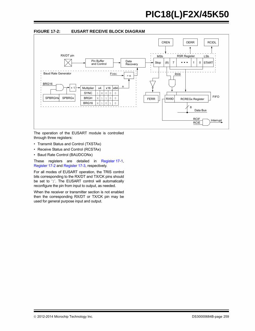
PIC18(L)F2X/45K50
FIGURE 17-2: EUSART RECEIVE BLOCK DIAGRAM
The operation of the EUSART module is controlledthrough three registers:
• Transmit Status and Control (TXSTAx)
• Receive Status and Control (RCSTAx)
• Baud Rate Control (BAUDCONx)
These registers are detailed in Register 17-1,Register 17-2 and Register 17-3, respectively.
For all modes of EUSART operation, the TRIS controlbits corresponding to the RX/DT and TX/CK pins shouldbe set to ‘1’. The EUSART control will automaticallyreconfigure the pin from input to output, as needed.
When the receiver or transmitter section is not enabledthen the corresponding RX/DT or TX/CK pin may beused for general purpose input and output.
RX/DT pin
Pin Bufferand Control
DataRecovery
CREN OERR
FERR
RSR RegisterMSb LSb
RX9D RCREGx RegisterFIFO
InterruptRCIFRCIE
Data Bus8
Stop START(8) 7 1 0
RX9
• • •
SPBRGxSPBRGHx
BRG16
RCIDL
FOSC÷ n
n+ 1 Multiplier x4 x16 x64
SYNC 1 X 0 0 0
BRGH X 1 1 0 0
BRG16 X 1 0 1 0
Baud Rate Generator
2012-2014 Microchip Technology Inc. DS30000684B-page 259
PIC18(L)F2X/45K50
17.1 EUSART Asynchronous Mode
The EUSART transmits and receives data using thestandard non-return-to-zero (NRZ) format. NRZ isimplemented with two levels: a VOH mark state whichrepresents a ‘1’ data bit, and a VOL space state whichrepresents a ‘0’ data bit. NRZ refers to the fact thatconsecutively transmitted data bits of the same valuestay at the output level of that bit without returning to aneutral level between each bit transmission. An NRZtransmission port idles in the mark state. Each charactertransmission consists of one Start bit followed by eightor nine data bits and is always terminated by one ormore Stop bits. The Start bit is always a space and theStop bits are always marks. The most common dataformat is 8 bits. Each transmitted bit persists for a periodof 1/(Baud Rate). An on-chip dedicated 8-bit/16-bit BaudRate Generator is used to derive standard baud ratefrequencies from the system oscillator. See Table 17-5for examples of baud rate configurations.
The EUSART transmits and receives the LSb first. TheEUSART’s transmitter and receiver are functionallyindependent, but share the same data format and baudrate. Parity is not supported by the hardware, but canbe implemented in software and stored as the ninthdata bit.
17.1.1 EUSART ASYNCHRONOUS TRANSMITTER
The EUSART transmitter block diagram is shown inFigure 17-1. The heart of the transmitter is the serialTransmit Shift Register (TSR), which is not directlyaccessible by software. The TSR obtains its data fromthe transmit buffer, which is the TXREGx register.
17.1.1.1 Enabling the Transmitter
The EUSART transmitter is enabled for asynchronousoperations by configuring the following three controlbits:
• TXEN = 1
• SYNC = 0
• SPEN = 1
All other EUSART control bits are assumed to be intheir default state.
Setting the TXEN bit of the TXSTAx register enables thetransmitter circuitry of the EUSART. Clearing the SYNCbit of the TXSTAx register configures the EUSART forasynchronous operation. Setting the SPEN bit of theRCSTAx register enables the EUSART andautomatically configures the TX/CK I/O pin as an output.If the TX/CK pin is shared with an analog peripheral theanalog I/O function must be disabled by clearing thecorresponding ANSEL bit.
17.1.1.2 Transmitting Data
A transmission is initiated by writing a character to theTXREGx register. If this is the first character, or theprevious character has been completely flushed fromthe TSR, the data in the TXREGx is immediatelytransferred to the TSR register. If the TSR still containsall or part of a previous character, the new characterdata is held in the TXREGx until the Stop bit of theprevious character has been transmitted. The pendingcharacter in the TXREGx is then transferred to the TSRin one TCY immediately following the Stop bittransmission. The transmission of the Start bit, data bitsand Stop bit sequence commences immediatelyfollowing the transfer of the data to the TSR from theTXREGx.
17.1.1.3 Transmit Data Polarity
The polarity of the transmit data can be controlled withthe TXCKP bit of the BAUDCONx register. The defaultstate of this bit is ‘0’ which selects high true transmitidle and data bits. Setting the TXCKP bit to ‘1’ will invertthe transmit data resulting in low true idle and data bits.The TXCKP bit controls transmit data polarity only inAsynchronous mode. In Synchronous mode theTXCKP bit has a different function.
17.1.1.4 Transmit Interrupt Flag
The TXIF interrupt flag bit of the PIR1 register is setwhenever the EUSART transmitter is enabled and nocharacter is being held for transmission in the TXREGx.In other words, the TXIF bit is only clear when the TSRis busy with a character and a new character has beenqueued for transmission in the TXREGx. The TXIF flagbit is not cleared immediately upon writing TXREGx.TXIF becomes valid in the second instruction cyclefollowing the write execution. Polling TXIF immediatelyfollowing the TXREGx write will return invalid results.The TXIF bit is read-only, it cannot be set or cleared bysoftware.
The TXIF interrupt can be enabled by setting the TXIEinterrupt enable bit of the PIE1 register. However, theTXIF flag bit will be set whenever the TXREGx isempty, regardless of the state of TXIE enable bit.
To use interrupts when transmitting data, set the TXIEbit only when there is more data to send. Clear theTXIE interrupt enable bit upon writing the last characterof the transmission to the TXREGx.
Note: The TXIF transmitter interrupt flag is setwhen the TXEN enable bit is set.
DS30000684B-page 260 2012-2014 Microchip Technology Inc.

PIC18(L)F2X/45K50
17.1.1.5 TSR Status
The TRMT bit of the TXSTAx register indicates thestatus of the TSR register. This is a read-only bit. TheTRMT bit is set when the TSR register is empty and iscleared when a character is transferred to the TSRregister from the TXREGx. The TRMT bit remains clearuntil all bits have been shifted out of the TSR register.No interrupt logic is tied to this bit, so the user needs topoll this bit to determine the TSR status.
17.1.1.6 Transmitting 9-Bit Characters
The EUSART supports 9-bit character transmissions.When the TX9 bit of the TXSTAx register is set theEUSART will shift 9 bits out for each character transmit-ted. The TX9D bit of the TXSTAx register is the ninth,and Most Significant, data bit. When transmitting 9-bitdata, the TX9D data bit must be written before writingthe 8 Least Significant bits into the TXREGx. All ninebits of data will be transferred to the TSR shift registerimmediately after the TXREGx is written.
A special 9-bit Address mode is available for use withmultiple receivers. See Section 17.1.2.8 “AddressDetection” for more information on the Address mode.
17.1.1.7 Asynchronous Transmission Setup
1. Initialize the SPBRGHx:SPBRGx register pairand the BRGH and BRG16 bits to achieve thedesired baud rate (see Section 17.4 “EUSARTBaud Rate Generator (BRG)”).
2. Set the RX/DT and TX/CK TRIS controls to ‘1’.
3. Enable the asynchronous serial port by clearingthe SYNC bit and setting the SPEN bit.
4. If 9-bit transmission is desired, set the TX9control bit. A set ninth data bit will indicate thatthe eight Least Significant data bits are anaddress when the receiver is set for addressdetection.
5. Set the TXCKP control bit if inverted transmitdata polarity is desired.
6. Enable the transmission by setting the TXENcontrol bit. This will cause the TXIF interrupt bitto be set.
7. If interrupts are desired, set the TXIE interruptenable bit. An interrupt will occur immediatelyprovided that the GIE/GIEH and PEIE/GIEL bitsof the INTCON register are also set.
8. If 9-bit transmission is selected, the ninth bitshould be loaded into the TX9D data bit.
9. Load 8-bit data into the TXREGx register. Thiswill start the transmission.
FIGURE 17-3: ASYNCHRONOUS TRANSMISSION
Note: The TSR register is not mapped in datamemory, so it is not available to the user.
Word 1Stop bit
Word 1Transmit Shift Reg
Start bit bit 0 bit 1 bit 7/8
Write to TXREGxWord 1
BRG Output(Shift Clock)
TX/CK
TXIF bit(Transmit Buffer
Reg. Empty Flag)
TRMT bit(Transmit Shift
Reg. Empty Flag)
1 TCY
pin
2012-2014 Microchip Technology Inc. DS30000684B-page 261

PIC18(L)F2X/45K50
FIGURE 17-4: ASYNCHRONOUS TRANSMISSION (BACK-TO-BACK)
Transmit Shift Reg
Write to TXREGx
BRG Output(Shift Clock)
TX/CK
TXIF bit(Interrupt Reg. Flag)
TRMT bit(Transmit Shift
Reg. Empty Flag)
Word 1 Word 2
Word 1 Word 2
Start bit Stop bit Start bit
Transmit Shift Reg
Word 1 Word 2bit 0 bit 1 bit 7/8 bit 0
Note: This timing diagram shows two consecutive transmissions.
1 TCY
1 TCY
pin
TABLE 17-1: REGISTERS ASSOCIATED WITH ASYNCHRONOUS TRANSMISSION
Name Bit 7 Bit 6 Bit 5 Bit 4 Bit 3 Bit 2 Bit 1 Bit 0Register on page
BAUDCON1 ABDOVF RCIDL RXDTP TXCKP BRG16 — WUE ABDEN 270
INTCON GIE/GIEH PEIE/GIEL TMR0IE INT0IE IOCIE TMR0IF INT0IF IOCIF 114
IPR1 ACTIP ADIP RCIP TXIP SSPIP CCP1IP TMR2IP TMR1IP 123
PIE1 ACTIE ADIE RCIE TXIE SSPIE CCP1IE TMR2IE TMR1IE 120
PIR1 ACTIF ADIF RCIF TXIF SSPIF CCP1IF TMR2IF TMR1IF 117
PMD0 — UARTMD USBMD ACTMD — TMR3MD TMR2MD TMR1MD 61
RCSTA1 SPEN RX9 SREN CREN ADDEN FERR OERR RX9D 269
SPBRG1 EUSART Baud Rate Generator, Low Byte —
SPBRGH1 EUSART Baud Rate Generator, High Byte —
TXREG1 EUSART Transmit Register —
TXSTA1 CSRC TX9 TXEN SYNC SENDB BRGH TRMT TX9D 268
Legend: — = unimplemented locations, read as ‘0’. Shaded bits are not used for asynchronous transmission.
DS30000684B-page 262 2012-2014 Microchip Technology Inc.
PIC18(L)F2X/45K50
17.1.2 EUSART ASYNCHRONOUS RECEIVER
The Asynchronous mode would typically be used inRS-232 systems. The receiver block diagram is shownin Figure 17-2. The data is received on the RX/DT pinand drives the data recovery block. The data recoveryblock is actually a high-speed shifter operating at 16times the baud rate, whereas the serial Receive ShiftRegister (RSR) operates at the bit rate. When all eightor nine bits of the character have been shifted in, theyare immediately transferred to a two character First-In-First-Out (FIFO) memory. The FIFO buffering allowsreception of two complete characters and the start of athird character before software must start servicing theEUSART receiver. The FIFO and RSR registers are notdirectly accessible by software. Access to the receiveddata is via the RCREGx register.
17.1.2.1 Enabling the Receiver
The EUSART receiver is enabled for asynchronousoperation by configuring the following three control bits:
• CREN = 1
• SYNC = 0
• SPEN = 1
All other EUSART control bits are assumed to be intheir default state.
Setting the CREN bit of the RCSTAx register enablesthe receiver circuitry of the EUSART. Clearing theSYNC bit of the TXSTAx register configures theEUSART for asynchronous operation. Setting theSPEN bit of the RCSTAx register enables theEUSART. The RX/DT I/O pin must be configured as aninput by setting the corresponding TRIS control bit. Ifthe RX/DT pin is shared with an analog peripheral theanalog I/O function must be disabled by clearing thecorresponding ANSEL bit.
17.1.2.2 Receiving Data
The receiver data recovery circuit initiates characterreception on the falling edge of the first bit. The first bit,also known as the Start bit, is always a zero. The datarecovery circuit counts one-half bit time to the center ofthe Start bit and verifies that the bit is still a zero. If it isnot a zero then the data recovery circuit abortscharacter reception, without generating an error, andresumes looking for the falling edge of the Start bit. Ifthe Start bit zero verification succeeds then the datarecovery circuit counts a full bit time to the center of thenext bit. The bit is then sampled by a majority detectcircuit and the resulting ‘0’ or ‘1’ is shifted into the RSR.This repeats until all data bits have been sampled andshifted into the RSR. One final bit time is measured andthe level sampled. This is the Stop bit, which is alwaysa ‘1’. If the data recovery circuit samples a ‘0’ in theStop bit position then a framing error is set for thischaracter, otherwise the framing error is cleared for thischaracter. See Section 17.1.2.5 “Receive FramingError” for more information on framing errors.
Immediately after all data bits and the Stop bit havebeen received, the character in the RSR is transferredto the EUSART receive FIFO and the RCIF interruptflag bit of the PIR1 register is set. The top character inthe FIFO is transferred out of the FIFO by reading theRCREGx register.
17.1.2.3 Receive Data Polarity
The polarity of the receive data can be controlled withthe RXDTP bit of the BAUDCONx register. The defaultstate of this bit is ‘0’ which selects high true receive Idleand data bits. Setting the RXDTP bit to ‘1’ will invert thereceive data resulting in low true Idle and data bits. TheRXDTP bit controls receive data polarity only inAsynchronous mode. In Synchronous mode theRXDTP bit has a different function.
Note: If the receive FIFO is overrun, no additionalcharacters will be received until the overruncondition is cleared. See Section 17.1.2.6“Receive Overrun Error” for moreinformation on overrun errors.
2012-2014 Microchip Technology Inc. DS30000684B-page 263
PIC18(L)F2X/45K50
17.1.2.4 Receive Interrupts
The RCIF interrupt flag bit of the PIR1 register is setwhenever the EUSART receiver is enabled and there isan unread character in the receive FIFO. The RCIFinterrupt flag bit is read-only, it cannot be set or clearedby software.
RCIF interrupts are enabled by setting the followingbits:
• RCIE interrupt enable bit of the PIE1 register
• PEIE/GIEL peripheral interrupt enable bit of the INTCON register
• GIE/GIEH global interrupt enable bit of the INTCON register
The RCIF interrupt flag bit will be set when there is anunread character in the FIFO, regardless of the state ofinterrupt enable bits.
17.1.2.5 Receive Framing Error
Each character in the receive FIFO buffer has acorresponding framing error Status bit. A framing errorindicates that a Stop bit was not seen at the expectedtime. The framing error status is accessed via theFERR bit of the RCSTAx register. The FERR bitrepresents the status of the top unread character in thereceive FIFO. Therefore, the FERR bit must be readbefore reading the RCREGx.
The FERR bit is read-only and only applies to the topunread character in the receive FIFO. A framing error(FERR = 1) does not preclude reception of additionalcharacters. It is not necessary to clear the FERR bit.Reading the next character from the FIFO buffer willadvance the FIFO to the next character and the nextcorresponding framing error.
The FERR bit can be forced clear by clearing the SPENbit of the RCSTAx register which resets the EUSART.Clearing the CREN bit of the RCSTAx register does notaffect the FERR bit. A framing error by itself does notgenerate an interrupt.
17.1.2.6 Receive Overrun Error
The receive FIFO buffer can hold two characters. Anoverrun error will be generated if a third character, in itsentirety, is received before the FIFO is accessed. Whenthis happens the OERR bit of the RCSTAx register isset. The characters already in the FIFO buffer can beread but no additional characters will be received untilthe error is cleared. The error must be cleared by eitherclearing the CREN bit of the RCSTAx register or byresetting the EUSART by clearing the SPEN bit of theRCSTAx register.
17.1.2.7 Receiving 9-Bit Characters
The EUSART supports 9-bit character reception. Whenthe RX9 bit of the RCSTAx register is set, the EUSARTwill shift nine bits into the RSR for each characterreceived. The RX9D bit of the RCSTAx register is theninth and Most Significant data bit of the top unreadcharacter in the receive FIFO. When reading 9-bit datafrom the receive FIFO buffer, the RX9D data bit mustbe read before reading the eight Least Significant bitsfrom the RCREGx.
17.1.2.8 Address Detection
A special Address Detection mode is available for usewhen multiple receivers share the same transmissionline, such as in RS-485 systems. Address detection isenabled by setting the ADDEN bit of the RCSTAxregister.
Address detection requires 9-bit character reception.When address detection is enabled, only characterswith the ninth data bit set will be transferred to thereceive FIFO buffer, thereby setting the RCIF interruptbit. All other characters will be ignored.
Upon receiving an address character, user softwaredetermines if the address matches its own. Uponaddress match, user software must disable addressdetection by clearing the ADDEN bit before the nextStop bit occurs. When user software detects the end ofthe message, determined by the message protocolused, software places the receiver back into theAddress Detection mode by setting the ADDEN bit.
Note: If all receive characters in the receiveFIFO have framing errors, repeated readsof the RCREGx will not clear the FERRbit.
DS30000684B-page 264 2012-2014 Microchip Technology Inc.

PIC18(L)F2X/45K50
17.1.2.9 Asynchronous Reception Setup:
1. Initialize the SPBRGHx:SPBRGx register pairand the BRGH and BRG16 bits to achieve thedesired baud rate (see Section 17.4 “EUSARTBaud Rate Generator (BRG)”).
2. Set the RX/DT and TX/CK TRIS controls to ‘1’.
3. Enable the serial port by setting the SPEN bitand the RX/DT pin TRIS bit. The SYNC bit mustbe clear for asynchronous operation.
4. If interrupts are desired, set the RCIE interruptenable bit and set the GIE/GIEH and PEIE/GIELbits of the INTCON register.
5. If 9-bit reception is desired, set the RX9 bit.
6. Set the RXDTP if inverted receive polarity isdesired.
7. Enable reception by setting the CREN bit.
8. The RCIF interrupt flag bit will be set when acharacter is transferred from the RSR to thereceive buffer. An interrupt will be generated ifthe RCIE interrupt enable bit was also set.
9. Read the RCSTAx register to get the error flagsand, if 9-bit data reception is enabled, the ninthdata bit.
10. Get the received eight Least Significant data bitsfrom the receive buffer by reading the RCREGxregister.
11. If an overrun occurred, clear the OERR flag byclearing the CREN receiver enable bit.
17.1.2.10 9-Bit Address Detection Mode Setup
This mode would typically be used in RS-485 systems.To set up an Asynchronous Reception with AddressDetect Enable:
1. Initialize the SPBRGHx, SPBRGx register pairand the BRGH and BRG16 bits to achieve thedesired baud rate (see Section 17.4 “EUSARTBaud Rate Generator (BRG)”).
2. Set the RX/DT and TX/CK TRIS controls to ‘1’.
3. Enable the serial port by setting the SPEN bit.The SYNC bit must be clear for asynchronousoperation.
4. If interrupts are desired, set the RCIE interruptenable bit and set the GIE/GIEH and PEIE/GIELbits of the INTCON register.
5. Enable 9-bit reception by setting the RX9 bit.
6. Enable address detection by setting the ADDENbit.
7. Set the RXDTP if inverted receive polarity isdesired.
8. Enable reception by setting the CREN bit.
9. The RCIF interrupt flag bit will be set when acharacter with the ninth bit set is transferredfrom the RSR to the receive buffer. An interruptwill be generated if the RCIE interrupt enable bitwas also set.
10. Read the RCSTAx register to get the error flags.The ninth data bit will always be set.
11. Get the received eight Least Significant data bitsfrom the receive buffer by reading the RCREGxregister. Software determines if this is thedevice’s address.
12. If an overrun occurred, clear the OERR flag byclearing the CREN receiver enable bit.
13. If the device has been addressed, clear theADDEN bit to allow all received data into thereceive buffer and generate interrupts.
2012-2014 Microchip Technology Inc. DS30000684B-page 265

PIC18(L)F2X/45K50
FIGURE 17-5: ASYNCHRONOUS RECEPTION
Startbit bit 7/8bit 1bit 0 bit 7/8 bit 0Stop
bit
Startbit
Startbitbit 7/8 Stop
bitRX/DT pin
RegRcv Buffer Reg
Rcv Shift
Read RcvBuffer RegRCREGx
RCIF(Interrupt Flag)
OERR bit
CREN
Word 1RCREGx
Word 2RCREGx
Stopbit
Note: This timing diagram shows three words appearing on the RX/DT input. The RCREGx (receive buffer) is read after the thirdword, causing the OERR (overrun) bit to be set.
RCIDL
TABLE 17-2: REGISTERS ASSOCIATED WITH ASYNCHRONOUS RECEPTION
Name Bit 7 Bit 6 Bit 5 Bit 4 Bit 3 Bit 2 Bit 1 Bit 0Register on page
BAUDCON1 ABDOVF RCIDL RXDTP TXCKP BRG16 — WUE ABDEN 270
INTCON GIE/GIEH PEIE/GIEL TMR0IE INT0IE IOCIE TMR0IF INT0IF IOCIF 114
IPR1 ACTIP ADIP RCIP TXIP SSPIP CCP1IP TMR2IP TMR1IP 123
PIE1 ACTIE ADIE RCIE TXIE SSPIE CCP1IE TMR2IE TMR1IE 120
PIR1 ACTIF ADIF RCIF TXIF SSPIF CCP1IF TMR2IF TMR1IF 117
PMD0 — UARTMD USBMD ACTMD — TMR3MD TMR2MD TMR1MD 61
RCREG1 EUSART Receive Register —
RCSTA1 SPEN RX9 SREN CREN ADDEN FERR OERR RX9D 269
SPBRG1 EUSART Baud Rate Generator, Low Byte —
SPBRGH1 EUSART Baud Rate Generator, High Byte —
TRISC TRISC7 TRISC6 — — — TRISC2 TRISC1 TRISC0 149
TXSTA1 CSRC TX9 TXEN SYNC SENDB BRGH TRMT TX9D 268
Legend: — = unimplemented locations, read as ‘0’. Shaded bits are not used for asynchronous reception.
DS30000684B-page 266 2012-2014 Microchip Technology Inc.

PIC18(L)F2X/45K50
17.2 Clock Accuracy with Asynchronous Operation
The factory calibrates the internal oscillator blockoutput (HFINTOSC). However, the HFINTOSCfrequency may drift as VDD or temperature changes,and this directly affects the asynchronous baud rate.Two methods may be used to adjust the baud rateclock, but both require a reference clock source ofsome kind.
The first (preferred) method uses the OSCTUNEregister to adjust the HFINTOSC output. Adjusting thevalue in the OSCTUNE register allows for fineresolution changes to the system clock source. See 3.6“Internal Clock Modes” for more information.
The other method adjusts the value in the Baud RateGenerator. This can be done automatically with theAuto-Baud Detect feature (see Section 17.4.1 “Auto-Baud Detect”). There may not be fine enoughresolution when adjusting the Baud Rate Generator tocompensate for a gradual change in the peripheralclock frequency.
2012-2014 Microchip Technology Inc. DS30000684B-page 267
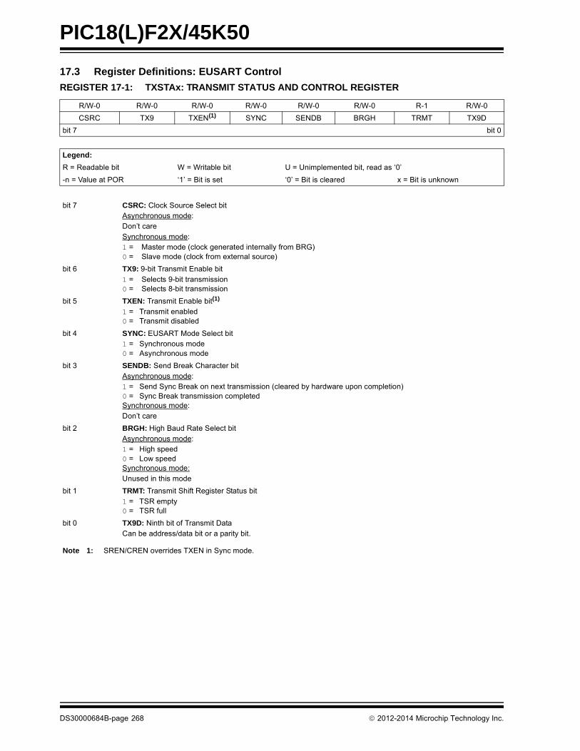
PIC18(L)F2X/45K50
17.3 Register Definitions: EUSART Control
REGISTER 17-1: TXSTAx: TRANSMIT STATUS AND CONTROL REGISTER
R/W-0 R/W-0 R/W-0 R/W-0 R/W-0 R/W-0 R-1 R/W-0
CSRC TX9 TXEN(1) SYNC SENDB BRGH TRMT TX9D
bit 7 bit 0
Legend:
R = Readable bit W = Writable bit U = Unimplemented bit, read as ‘0’
-n = Value at POR ‘1’ = Bit is set ‘0’ = Bit is cleared x = Bit is unknown
bit 7 CSRC: Clock Source Select bitAsynchronous mode: Don’t careSynchronous mode: 1 = Master mode (clock generated internally from BRG)0 = Slave mode (clock from external source)
bit 6 TX9: 9-bit Transmit Enable bit1 = Selects 9-bit transmission0 = Selects 8-bit transmission
bit 5 TXEN: Transmit Enable bit(1)
1 = Transmit enabled0 = Transmit disabled
bit 4 SYNC: EUSART Mode Select bit 1 = Synchronous mode 0 = Asynchronous mode
bit 3 SENDB: Send Break Character bitAsynchronous mode:1 = Send Sync Break on next transmission (cleared by hardware upon completion)0 = Sync Break transmission completedSynchronous mode:Don’t care
bit 2 BRGH: High Baud Rate Select bitAsynchronous mode: 1 = High speed 0 = Low speedSynchronous mode: Unused in this mode
bit 1 TRMT: Transmit Shift Register Status bit1 = TSR empty 0 = TSR full
bit 0 TX9D: Ninth bit of Transmit DataCan be address/data bit or a parity bit.
Note 1: SREN/CREN overrides TXEN in Sync mode.
DS30000684B-page 268 2012-2014 Microchip Technology Inc.

PIC18(L)F2X/45K50
REGISTER 17-2: RCSTAx: RECEIVE STATUS AND CONTROL REGISTER
R/W-0 R/W-0 R/W-0 R/W-0 R/W-0 R-0 R-0 R-0
SPEN RX9 SREN CREN ADDEN FERR OERR RX9D
bit 7 bit 0
Legend:
R = Readable bit W = Writable bit U = Unimplemented bit, read as ‘0’
-n = Value at POR ‘1’ = Bit is set ‘0’ = Bit is cleared x = Bit is unknown
bit 7 SPEN: Serial Port Enable bit
1 = Serial port enabled (configures RX/DT and TX/CK pins as serial port pins)0 = Serial port disabled (held in Reset)
bit 6 RX9: 9-bit Receive Enable bit
1 = Selects 9-bit reception0 = Selects 8-bit reception
bit 5 SREN: Single Receive Enable bit
Asynchronous mode:
Don’t careSynchronous mode – Master:
1 = Enables single receive0 = Disables single receiveThis bit is cleared after reception is complete.Synchronous mode – Slave
Don’t care
bit 4 CREN: Continuous Receive Enable bit
Asynchronous mode:
1 = Enables receiver0 = Disables receiverSynchronous mode:
1 = Enables continuous receive until enable bit CREN is cleared (CREN overrides SREN)0 = Disables continuous receive
bit 3 ADDEN: Address Detect Enable bit
Asynchronous mode 9-bit (RX9 = 1):
1 = Enables address detection, enable interrupt and load the receive buffer when RSR<8> is set0 = Disables address detection, all bytes are received and ninth bit can be used as parity bitAsynchronous mode 8-bit (RX9 = 0):
Don’t care
bit 2 FERR: Framing Error bit
1 = Framing error (can be updated by reading RCREGx register and receive next valid byte)0 = No framing error
bit 1 OERR: Overrun Error bit
1 = Overrun error (can be cleared by clearing bit CREN) 0 = No overrun error
bit 0 RX9D: Ninth bit of Received Data
This can be address/data bit or a parity bit and must be calculated by user firmware.
2012-2014 Microchip Technology Inc. DS30000684B-page 269

PIC18(L)F2X/45K50
REGISTER 17-3: BAUDCONx: BAUD RATE CONTROL REGISTER
R/W-0 R-1 R/W-0 R/W-0 R/W-0 U-0 R/W-0 R/W-0
ABDOVF RCIDL RXDTP TXCKP BRG16 — WUE ABDEN
bit 7 bit 0
Legend:
R = Readable bit W = Writable bit U = Unimplemented bit, read as ‘0’
-n = Value at POR ‘1’ = Bit is set ‘0’ = Bit is cleared x = Bit is unknown
bit 7 ABDOVF: Auto-Baud Detect Overflow bitAsynchronous mode:1 = Auto-baud timer overflowed0 = Auto-baud timer did not overflowSynchronous mode:Don’t care
bit 6 RCIDL: Receive Idle Flag bitAsynchronous mode:1 = Receiver is Idle0 = Start bit has been detected and the receiver is activeSynchronous mode:Don’t care
bit 5 RXDTP: Data/Receive Polarity Select bitAsynchronous mode:1 = Receive data (RX) is inverted (active-low)0 = Receive data (RX) is not inverted (active-high)Synchronous mode:1 = Data (DT) is inverted (active-low)0 = Data (DT) is not inverted (active-high)
bit 4 TXCKP: Clock/Transmit Polarity Select bitAsynchronous mode:1 = Idle state for transmit (TX) is low0 = Idle state for transmit (TX) is highSynchronous mode:1 = Data changes on the falling edge of the clock and is sampled on the rising edge of the clock0 = Data changes on the rising edge of the clock and is sampled on the falling edge of the clock
bit 3 BRG16: 16-bit Baud Rate Generator bit1 = 16-bit Baud Rate Generator is used (SPBRGHx:SPBRGx)0 = 8-bit Baud Rate Generator is used (SPBRGx)
bit 2 Unimplemented: Read as ‘0’
bit 1 WUE: Wake-up Enable bitAsynchronous mode:1 = Receiver is waiting for a falling edge. No character will be received but RCIF will be set on the falling
edge. WUE will automatically clear on the rising edge.0 = Receiver is operating normallySynchronous mode:Don’t care
bit 0 ABDEN: Auto-Baud Detect Enable bitAsynchronous mode:1 = Auto-Baud Detect mode is enabled (clears when auto-baud is complete)0 = Auto-Baud Detect mode is disabledSynchronous mode:Don’t care
DS30000684B-page 270 2012-2014 Microchip Technology Inc.

PIC18(L)F2X/45K50
17.4 EUSART Baud Rate Generator (BRG)
The Baud Rate Generator (BRG) is an 8-bit or 16-bittimer that is dedicated to the support of both theasynchronous and synchronous EUSART operation.By default, the BRG operates in 8-bit mode. Setting theBRG16 bit of the BAUDCONx register selects 16-bitmode.
The SPBRGHx:SPBRGx register pair determines theperiod of the free running baud rate timer. InAsynchronous mode the multiplier of the baud rateperiod is determined by both the BRGH bit of theTXSTAx register and the BRG16 bit of the BAUDCONxregister. In Synchronous mode, the BRGH bit is ignored.
Table 17-3 contains the formulas for determining thebaud rate. Example 17-1 provides a sample calculationfor determining the baud rate and baud rate error.
Typical baud rates and error values for variousAsynchronous modes have been computed for yourconvenience and are shown in Table 17-5. It may beadvantageous to use the high baud rate (BRGH = 1),or the 16-bit BRG (BRG16 = 1) to reduce the baud rateerror. The 16-bit BRG mode is used to achieve slowbaud rates for fast oscillator frequencies.
Writing a new value to the SPBRGHx, SPBRGxregister pair causes the BRG timer to be reset (orcleared). This ensures that the BRG does not wait for atimer overflow before outputting the new baud rate.
If the system clock is changed during an active receiveoperation, a receive error or data loss may result. Toavoid this problem, check the status of the RCIDL bit tomake sure that the receive operation is Idle beforechanging the system clock.
EXAMPLE 17-1: CALCULATING BAUD RATE ERROR
For a device with FOSC of 16 MHz, desired baud rateof 9600, Asynchronous mode, 8-bit BRG:
Solving for SPBRGHx:SPBRGx:
X
FOSC
Desired Baud Rate---------------------------------------------
64--------------------------------------------- 1–=
Desired Baud Rate FOSC
64 [SPBRGHx:SPBRGx] 1+ --------------------------------------------------------------------------=
160000009600
------------------------
64------------------------ 1–=
25.042 25= =
Calculated Baud Rate 16000000
64 25 1+ ---------------------------=
9615=
ErrorCalc. Baud Rate Desired Baud Rate –
Desired Baud Rate --------------------------------------------------------------------------------------------=
9615 9600–
9600---------------------------------- 0.16%= =
TABLE 17-3: BAUD RATE FORMULAS
Configuration BitsBRG/EUSART Mode Baud Rate Formula
SYNC BRG16 BRGH
0 0 0 8-bit/Asynchronous FOSC/[64 (n+1)]
0 0 1 8-bit/AsynchronousFOSC/[16 (n+1)]
0 1 0 16-bit/Asynchronous
0 1 1 16-bit/Asynchronous
FOSC/[4 (n+1)]1 0 x 8-bit/Synchronous
1 1 x 16-bit/Synchronous
Legend: x = Don’t care, n = value of SPBRGHx, SPBRGx register pair.
2012-2014 Microchip Technology Inc. DS30000684B-page 271

PIC18(L)F2X/45K50
TABLE 17-4: REGISTERS ASSOCIATED WITH BAUD RATE GENERATOR
Name Bit 7 Bit 6 Bit 5 Bit 4 Bit 3 Bit 2 Bit 1 Bit 0Register on page
BAUDCON1 ABDOVF RCIDL RXDTP TXCKP BRG16 — WUE ABDEN 270
PMD0 — UARTMD USBMD ACTMD — TMR3MD TMR2MD TMR1MD 61
RCSTA1 SPEN RX9 SREN CREN ADDEN FERR OERR RX9D 269
SPBRG1 EUSART Baud Rate Generator, Low Byte —
SPBRGH1 EUSART Baud Rate Generator, High Byte —
PIR1 ACTIF ADIF RCIF TXIF SSPIF CCP1IF TMR2IF TMR1IF 117
TXSTA1 CSRC TX9 TXEN SYNC SENDB BRGH TRMT TX9D 268
Legend: — = unimplemented, read as ‘0’. Shaded bits are not used by the BRG.
TABLE 17-5: BAUD RATES FOR ASYNCHRONOUS MODES
BAUDRATE
SYNC = 0, BRGH = 0, BRG16 = 0
FOSC = 48.000 MHz FOSC = 18.432 MHz FOSC = 16.000 MHz FOSC = 11.0592 MHz
ActualRate
%Error
SPBRxGvalue
(decimal)
ActualRate
%Error
SPBRGxvalue
(decimal)
ActualRate
%Error
SPBRGxvalue
(decimal)
ActualRate
%Error
SPBRGxvalue
(decimal)
300 — — — — — — — — — — — —
1200 — — — 1200 0.00 239 1202 0.16 207 1200 0.00 143
2400 — — — 2400 0.00 119 2404 0.16 103 2400 0.00 71
9600 9615 0.16 77 9600 0.00 29 9615 0.16 25 9600 0.00 17
10417 10417 0.00 71 10286 -1.26 27 10417 0.00 23 10165 -2.42 16
19.2k 19.23k 0.16 38 19.20k 0.00 14 19.23k 0.16 12 19.20k 0.00 8
57.6k 57.69k 0.16 12 57.60k 0.00 7 — — — 57.60k 0.00 2
115.2k — — — — — — — — — — — —
BAUDRATE
SYNC = 0, BRGH = 0, BRG16 = 0
FOSC = 8.000 MHz FOSC = 4.000 MHz FOSC = 3.6864 MHz FOSC = 1.000 MHz
ActualRate
%Error
SPBRGxvalue
(decimal)
ActualRate
%Error
SPBRGxvalue
(decimal)
ActualRate
%Error
SPBRGxvalue
(decimal)
ActualRate
%Error
SPBRGxvalue
(decimal)
300 — — — 300 0.16 207 300 0.00 191 300 0.16 51
1200 1202 0.16 103 1202 0.16 51 1200 0.00 47 1202 0.16 12
2400 2404 0.16 51 2404 0.16 25 2400 0.00 23 — — —
9600 9615 0.16 12 — — — 9600 0.00 5 — — —
10417 10417 0.00 11 10417 0.00 5 — — — — — —
19.2k — — — — — — 19.20k 0.00 2 — — —
57.6k — — — — — — 57.60k 0.00 0 — — —
115.2k — — — — — — — — — — — —
DS30000684B-page 272 2012-2014 Microchip Technology Inc.
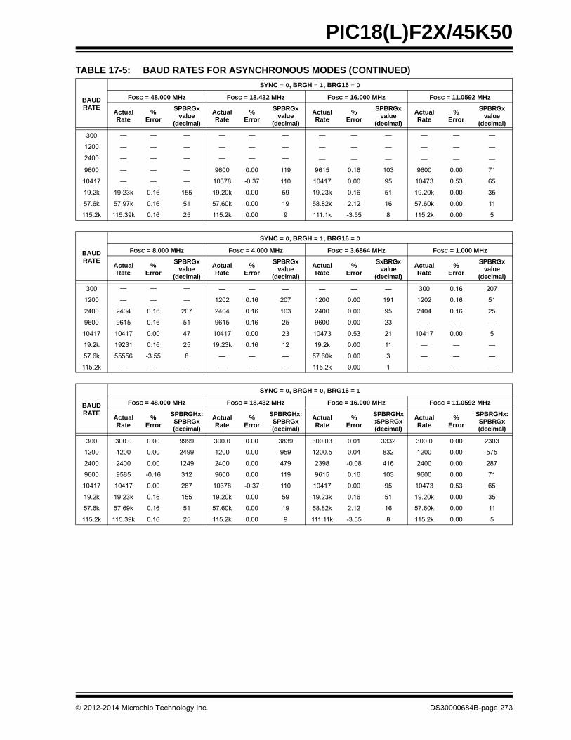
PIC18(L)F2X/45K50
BAUDRATE
SYNC = 0, BRGH = 1, BRG16 = 0
FOSC = 48.000 MHz FOSC = 18.432 MHz FOSC = 16.000 MHz FOSC = 11.0592 MHz
ActualRate
%Error
SPBRGxvalue
(decimal)
ActualRate
%Error
SPBRGxvalue
(decimal)
ActualRate
%Error
SPBRGxvalue
(decimal)
ActualRate
%Error
SPBRGxvalue
(decimal)
300 — — — — — — — — — — — —
1200 — — — — — — — — — — — —
2400 — — — — — — — — — — — —
9600 — — — 9600 0.00 119 9615 0.16 103 9600 0.00 71
10417 — — — 10378 -0.37 110 10417 0.00 95 10473 0.53 65
19.2k 19.23k 0.16 155 19.20k 0.00 59 19.23k 0.16 51 19.20k 0.00 35
57.6k 57.97k 0.16 51 57.60k 0.00 19 58.82k 2.12 16 57.60k 0.00 11
115.2k 115.39k 0.16 25 115.2k 0.00 9 111.1k -3.55 8 115.2k 0.00 5
BAUDRATE
SYNC = 0, BRGH = 1, BRG16 = 0
FOSC = 8.000 MHz FOSC = 4.000 MHz FOSC = 3.6864 MHz FOSC = 1.000 MHz
ActualRate
%Error
SPBRGxvalue
(decimal)
ActualRate
%Error
SPBRGxvalue
(decimal)
ActualRate
%Error
SxBRGxvalue
(decimal)
ActualRate
%Error
SPBRGxvalue
(decimal)
300 — — — — — — — — — 300 0.16 207
1200 — — — 1202 0.16 207 1200 0.00 191 1202 0.16 51
2400 2404 0.16 207 2404 0.16 103 2400 0.00 95 2404 0.16 25
9600 9615 0.16 51 9615 0.16 25 9600 0.00 23 — — —
10417 10417 0.00 47 10417 0.00 23 10473 0.53 21 10417 0.00 5
19.2k 19231 0.16 25 19.23k 0.16 12 19.2k 0.00 11 — — —
57.6k 55556 -3.55 8 — — — 57.60k 0.00 3 — — —
115.2k — — — — — — 115.2k 0.00 1 — — —
BAUDRATE
SYNC = 0, BRGH = 0, BRG16 = 1
FOSC = 48.000 MHz FOSC = 18.432 MHz FOSC = 16.000 MHz FOSC = 11.0592 MHz
ActualRate
%Error
SPBRGHx:SPBRGx(decimal)
ActualRate
%Error
SPBRGHx:SPBRGx(decimal)
ActualRate
%Error
SPBRGHx:SPBRGx(decimal)
ActualRate
%Error
SPBRGHx:SPBRGx(decimal)
300 300.0 0.00 9999 300.0 0.00 3839 300.03 0.01 3332 300.0 0.00 2303
1200 1200 0.00 2499 1200 0.00 959 1200.5 0.04 832 1200 0.00 575
2400 2400 0.00 1249 2400 0.00 479 2398 -0.08 416 2400 0.00 287
9600 9585 -0.16 312 9600 0.00 119 9615 0.16 103 9600 0.00 71
10417 10417 0.00 287 10378 -0.37 110 10417 0.00 95 10473 0.53 65
19.2k 19.23k 0.16 155 19.20k 0.00 59 19.23k 0.16 51 19.20k 0.00 35
57.6k 57.69k 0.16 51 57.60k 0.00 19 58.82k 2.12 16 57.60k 0.00 11
115.2k 115.39k 0.16 25 115.2k 0.00 9 111.11k -3.55 8 115.2k 0.00 5
TABLE 17-5: BAUD RATES FOR ASYNCHRONOUS MODES (CONTINUED)
2012-2014 Microchip Technology Inc. DS30000684B-page 273

PIC18(L)F2X/45K50
BAUDRATE
SYNC = 0, BRGH = 0, BRG16 = 1
FOSC = 8.000 MHz FOSC = 4.000 MHz FOSC = 3.6864 MHz FOSC = 1.000 MHz
ActualRate
%Error
SPBRGHx:SPBRGx(decimal)
ActualRate
%Error
SPBRGHx:SPBRGx(decimal)
ActualRate
%Error
SPBRGHx:SPBRGx(decimal)
ActualRate
%Error
SPBRGHx:SPBRGx(decimal)
300 299.9 -0.02 1666 300.1 0.04 832 300.0 0.00 767 300.5 0.16 207
1200 1199 -0.08 416 1202 0.16 207 1200 0.00 191 1202 0.16 51
2400 2404 0.16 207 2404 0.16 103 2400 0.00 95 2404 0.16 25
9600 9615 0.16 51 9615 0.16 25 9600 0.00 23 — — —
10417 10417 0.00 47 10417 0.00 23 10473 0.53 21 10417 0.00 5
19.2k 19.23k 0.16 25 19.23k 0.16 12 19.20k 0.00 11 — — —
57.6k 55556 -3.55 8 — — — 57.60k 0.00 3 — — —
115.2k — — — — — — 115.2k 0.00 1 — — —
BAUDRATE
SYNC = 0, BRGH = 1, BRG16 = 1 or SYNC = 1, BRG16 = 1
FOSC = 48.000 MHz FOSC = 18.432 MHz FOSC = 16.000 MHz FOSC = 11.0592 MHz
ActualRate
%Error
SPBRGHx:SPBRGx(decimal)
ActualRate
%Error
SPBRGHx:SPBRGx(decimal)
ActualRate
%Error
SPBRGHx:SPBRGx(decimal)
ActualRate
%Error
SPBRGHx:SPBRGx(decimal)
300 300 0.00 39999 300.0 0.00 15359 300.0 0.00 13332 300.0 0.00 9215
1200 1200 0.00 9999 1200 0.00 3839 1200.1 0.01 3332 1200 0.00 2303
2400 2400 0.00 4999 2400 0.00 1919 2399.5 -0.02 1666 2400 0.00 1151
9600 9600 0.00 1249 9600 0.00 479 9592 -0.08 416 9600 0.00 287
10417 10417 0.00 1151 10425 0.08 441 10417 0.00 383 10433 0.16 264
19.2k 19.2k 0.00 624 19.20k 0.00 239 19.23k 0.16 207 19.20k 0.00 143
57.6k 57.69k 0.16 207 57.60k 0.00 79 57.97k 0.64 68 57.60k 0.00 47
115.2k 115.39k 0.16 103 115.2k 0.00 39 114.29k -0.79 34 115.2k 0.00 23
BAUDRATE
SYNC = 0, BRGH = 1, BRG16 = 1 or SYNC = 1, BRG16 = 1
FOSC = 8.000 MHz FOSC = 4.000 MHz FOSC = 3.6864 MHz FOSC = 1.000 MHz
ActualRate
%Error
SPBRGHx:SPBRGx(decimal)
ActualRate
%Error
SPBRGHx:SPBRGx(decimal)
ActualRate
%Error
SPBRGHx:SPBRGx (decimal)
ActualRate
%Error
SPBRGHx:SPBRGx(decimal)
300 300.0 0.00 6666 300.0 0.01 3332 300.0 0.00 3071 300.1 0.04 832
1200 1200 -0.02 1666 1200 0.04 832 1200 0.00 767 1202 0.16 207
2400 2401 0.04 832 2398 0.08 416 2400 0.00 383 2404 0.16 103
9600 9615 0.16 207 9615 0.16 103 9600 0.00 95 9615 0.16 25
10417 10417 0.00 191 10417 0.00 95 10473 0.53 87 10417 0.00 23
19.2k 19.23k 0.16 103 19.23k 0.16 51 19.20k 0.00 47 19.23k 0.16 12
57.6k 57.14k -0.79 34 58.82k 2.12 16 57.60k 0.00 15 — — —
115.2k 117.6k 2.12 16 111.1k -3.55 8 115.2k 0.00 7 — — —
TABLE 17-5: BAUD RATES FOR ASYNCHRONOUS MODES (CONTINUED)
DS30000684B-page 274 2012-2014 Microchip Technology Inc.

PIC18(L)F2X/45K50
17.4.1 AUTO-BAUD DETECT
The EUSART module supports automatic detectionand calibration of the baud rate.
In the Auto-Baud Detect (ABD) mode, the clock to theBRG is reversed. Rather than the BRG clocking theincoming RX signal, the RX signal is timing the BRG.The Baud Rate Generator is used to time the period ofa received 55h (ASCII “U”) which is the Sync characterfor the LIN bus. The unique feature of this character isthat it has five rising edges including the Stop bit edge.
Setting the ABDEN bit of the BAUDCONx registerstarts the auto-baud calibration sequence(Section 17.4.2 “Auto-Baud Overflow”). While theABD sequence takes place, the EUSART statemachine is held in Idle. On the first rising edge of thereceive line, after the Start bit, the SPBRGx beginscounting up using the BRG counter clock as shown inTable 17-6. The fifth rising edge will occur on the RX/DT pin at the end of the eighth bit period. At that time,an accumulated value totaling the proper BRG periodis left in the SPBRGHx:SPBRGx register pair, theABDEN bit is automatically cleared, and the RCIFinterrupt flag is set. A read operation on the RCREGxneeds to be performed to clear the RCIF interrupt.RCREGx content should be discarded. Whencalibrating for modes that do not use the SPBRGHxregister the user can verify that the SPBRGx registerdid not overflow by checking for 00h in the SPBRGHxregister.
The BRG auto-baud clock is determined by the BRG16and BRGH bits as shown in Table 17-6. During ABD,both the SPBRGHx and SPBRGx registers are used asa 16-bit counter, independent of the BRG16 bit setting.While calibrating the baud rate period, the SPBRGHx
and SPBRGx registers are clocked at 1/8th the BRGbase clock rate. The resulting byte measurement is theaverage bit time when clocked at full speed.
FIGURE 17-6: AUTOMATIC BAUD RATE CALIBRATION
Note 1: If the WUE bit is set with the ABDEN bit,auto-baud detection will occur on the bytefollowing the Break character (seeSection 17.4.3 “Auto-Wake-up onBreak”).
2: It is up to the user to determine that theincoming character baud rate is within therange of the selected BRG clock source.Some combinations of oscillator frequencyand EUSART baud rates are not possible.
3: During the auto-baud process, the auto-baud counter starts counting at 1. Uponcompletion of the auto-baud sequence, toachieve maximum accuracy, subtract 1from the SPBRGHx:SPBRGx register pair.
TABLE 17-6: BRG COUNTER CLOCK RATES
BRG16 BRGHBRG Base
ClockBRG ABD
Clock
0 0 FOSC/64 FOSC/512
0 1 FOSC/16 FOSC/128
1 0 FOSC/16 FOSC/128
1 1 FOSC/4 FOSC/32
Note: During the ABD sequence, SPBRGx andSPBRGHx registers are both used as a16-bit counter, independent of BRG16setting.
BRG Value
RX/DT pin
ABDEN bit
RCIF bit
bit 0 bit 1
(Interrupt)
ReadRCREGx
BRG Clock
Start
Auto ClearedSet by User
XXXXh 0000h
Edge #1
bit 2 bit 3Edge #2
bit 4 bit 5Edge #3
bit 6 bit 7Edge #4
Stop bit
Edge #5
001Ch
Note 1: The ABD sequence requires the EUSART module to be configured in Asynchronous mode.
SPBRGx XXh 1Ch
SPBRGHx XXh 00h
RCIDL
2012-2014 Microchip Technology Inc. DS30000684B-page 275

PIC18(L)F2X/45K50
17.4.2 AUTO-BAUD OVERFLOW
During the course of automatic baud detection, theABDOVF bit of the BAUDCONx register will be set if thebaud rate counter overflows before the fifth rising edgeis detected on the RX pin. The ABDOVF bit indicatesthat the counter has exceeded the maximum count thatcan fit in the 16 bits of the SPBRGHx:SPBRGx registerpair. After the ABDOVF has been set, the counter con-tinues to count until the fifth rising edge is detected onthe RX/DT pin. Upon detecting the fifth RX/DT edge, thehardware will set the RCIF interrupt flag and clear theABDEN bit of the BAUDCONx register. The RCIF flagcan be subsequently cleared by reading the RCREGx.The ABDOVF flag can be cleared by software directly.
To terminate the auto-baud process before the RCIFflag is set, clear the ABDEN bit then clear the ABDOVFbit. The ABDOVF bit will remain set if the ABDEN bit isnot cleared first.
17.4.3 AUTO-WAKE-UP ON BREAK
During Sleep mode, all clocks to the EUSART aresuspended. Because of this, the Baud Rate Generatoris inactive and a proper character reception cannot beperformed. The Auto-Wake-up feature allows thecontroller to wake-up due to activity on the RX/DT line.This feature is available only in Asynchronous mode.
The Auto-Wake-up feature is enabled by setting theWUE bit of the BAUDCONx register. Once set, thenormal receive sequence on RX/DT is disabled, andthe EUSART remains in an Idle state, monitoring for awake-up event independent of the CPU mode. A wake-up event consists of a high-to-low transition on the RX/DT line. (This coincides with the start of a Sync Breakor a wake-up signal character for the LIN protocol.)
The EUSART module generates an RCIF interruptcoincident with the wake-up event. The interrupt isgenerated synchronously to the Q clocks in normal CPUoperating modes (Figure 17-7), and asynchronously ifthe device is in Sleep mode (Figure 17-8). The interruptcondition is cleared by reading the RCREGx register.
The WUE bit is automatically cleared by the low-to-hightransition on the RX line at the end of the Break. Thissignals to the user that the Break event is over. At thispoint, the EUSART module is in Idle mode waiting toreceive the next character.
17.4.3.1 Special Considerations
Break Character
To avoid character errors or character fragments duringa wake-up event, the wake-up character must be allzeros.
When the wake-up is enabled the function worksindependent of the low time on the data stream. If theWUE bit is set and a valid non-zero character isreceived, the low time from the Start bit to the first risingedge will be interpreted as the wake-up event. Theremaining bits in the character will be received as afragmented character and subsequent characters canresult in framing or overrun errors.
Therefore, the initial character in the transmission mustbe all ‘0’s. This must be 10 or more bit times, 13-bittimes recommended for LIN bus, or any number of bittimes for standard RS-232 devices.
Oscillator Startup Time
Oscillator start-up time must be considered, especiallyin applications using oscillators with longer start-upintervals (i.e., LP, XT or HS/PLL mode). The SyncBreak (or wake-up signal) character must be ofsufficient length, and be followed by a sufficientinterval, to allow enough time for the selected oscillatorto start and provide proper initialization of the EUSART.
WUE Bit
The wake-up event causes a receive interrupt bysetting the RCIF bit. The WUE bit is cleared byhardware by a rising edge on RX/DT. The interruptcondition is then cleared by software by reading theRCREGx register and discarding its contents.
To ensure that no actual data is lost, check the RCIDLbit to verify that a receive operation is not in processbefore setting the WUE bit. If a receive operation is notoccurring, the WUE bit may then be set just prior toentering the Sleep mode.
DS30000684B-page 276 2012-2014 Microchip Technology Inc.

PIC18(L)F2X/45K50
FIGURE 17-7: AUTO-WAKE-UP BIT (WUE) TIMING DURING NORMAL OPERATION
FIGURE 17-8: AUTO-WAKE-UP BIT (WUE) TIMINGS DURING SLEEP
Q1 Q2 Q3 Q4 Q1 Q2 Q3Q4 Q1Q2 Q3 Q4 Q1Q2 Q3 Q4 Q1Q2 Q3 Q4 Q1Q2 Q3 Q4 Q1 Q2 Q3 Q4 Q1Q2 Q3 Q4 Q1 Q2 Q3 Q4 Q1Q2 Q3 Q4
OSC1
WUE bit
RX/DT Line
RCIF
Bit set by user Auto Cleared
Cleared due to User Read of RCREGx
Note 1: The EUSART remains in Idle while the WUE bit is set.
Q1Q2Q3 Q4 Q1Q2 Q3 Q4 Q1Q2 Q3 Q4 Q1 Q2 Q3 Q4 Q1Q2 Q3 Q4 Q1Q2 Q3 Q4 Q1 Q2Q3 Q4 Q1Q2 Q3 Q4
OSC1
WUE bit
RX/DT Line
RCIF
Bit Set by User Auto Cleared
Cleared due to User Read of RCREGxSleep Command Executed
Note 1
Note 1: If the wake-up event requires long oscillator warm-up time, the automatic clearing of the WUE bit can occur while the stposc signal isstill active. This sequence should not depend on the presence of Q clocks.
2: The EUSART remains in Idle while the WUE bit is set.
Sleep Ends
2012-2014 Microchip Technology Inc. DS30000684B-page 277

PIC18(L)F2X/45K50
17.4.4 BREAK CHARACTER SEQUENCE
The EUSART module has the capability of sending thespecial Break character sequences that are required bythe LIN bus standard. A Break character consists of aStart bit, followed by 12 ‘0’ bits and a Stop bit.
To send a Break character, set the SENDB and TXENbits of the TXSTAx register. The Break character trans-mission is then initiated by a write to the TXREGx. Thevalue of data written to TXREGx will be ignored and all‘0’s will be transmitted.
The SENDB bit is automatically reset by hardware afterthe corresponding Stop bit is sent. This allows the userto preload the transmit FIFO with the next transmit bytefollowing the Break character (typically, the Synccharacter in the LIN specification).
The TRMT bit of the TXSTAx register indicates when thetransmit operation is active or Idle, just as it does duringnormal transmission. See Figure 17-9 for the timing ofthe Break character sequence.
17.4.4.1 Break and Sync Transmit Sequence
The following sequence will start a message frameheader made up of a Break, followed by an auto-baudSync byte. This sequence is typical of a LIN busmaster.
1. Configure the EUSART for the desired mode.
2. Set the TXEN and SENDB bits to enable theBreak sequence.
3. Load the TXREGx with a dummy character toinitiate transmission (the value is ignored).
4. Write ‘55h’ to TXREGx to load the Sync charac-ter into the transmit FIFO buffer.
5. After the Break has been sent, the SENDB bit isreset by hardware and the Sync character isthen transmitted.
When the TXREGx becomes empty, as indicated bythe TXIF, the next data byte can be written to TXREGx.
17.4.5 RECEIVING A BREAK CHARACTER
The Enhanced EUSART module can receive a Breakcharacter in two ways.
The first method to detect a Break character uses theFERR bit of the RCSTAx register and the Receiveddata as indicated by RCREGx. The Baud RateGenerator is assumed to have been initialized to theexpected baud rate.
A Break character has been received when;
• RCIF bit is set
• FERR bit is set
• RCREGx = 00h
The second method uses the Auto-Wake-up featuredescribed in Section 17.4.3 “Auto-Wake-up onBreak”. By enabling this feature, the EUSART willsample the next two transitions on RX/DT, cause anRCIF interrupt, and receive the next data byte followedby another interrupt.
Note that following a Break character, the user willtypically want to enable the Auto-Baud Detect feature.For both methods, the user can set the ABDEN bit ofthe BAUDCONx register before placing the EUSART inSleep mode.
FIGURE 17-9: SEND BREAK CHARACTER SEQUENCE
Write to TXREGxDummy Write
BRG Output(Shift Clock)
Start bit bit 0 bit 1 bit 11 Stop bit
Break
TXIF bit(Transmit
interrupt Flag)
TX/CK (pin)
TRMT bit(Transmit Shift
Reg. Empty Flag)
SENDB(send Break
control bit)
SENDB Sampled Here Auto Cleared
DS30000684B-page 278 2012-2014 Microchip Technology Inc.

PIC18(L)F2X/45K50
17.5 EUSART Synchronous Mode
Synchronous serial communications are typically usedin systems with a single master and one or moreslaves. The master device contains the necessarycircuitry for baud rate generation and supplies the clockfor all devices in the system. Slave devices can takeadvantage of the master clock by eliminating theinternal clock generation circuitry.
There are two signal lines in Synchronous mode: abidirectional data line and a clock line. Slaves use theexternal clock supplied by the master to shift the serialdata into and out of their respective receive andtransmit shift registers. Since the data line isbidirectional, synchronous operation is half-duplexonly. Half-duplex refers to the fact that master andslave devices can receive and transmit data but notboth simultaneously. The EUSART can operate aseither a master or slave device.
Start and Stop bits are not used in synchronoustransmissions.
17.5.1 SYNCHRONOUS MASTER MODE
The following bits are used to configure the EUSARTfor Synchronous Master operation:
• SYNC = 1
• CSRC = 1
• SREN = 0 (for transmit); SREN = 1 (for receive)
• CREN = 0 (for transmit); CREN = 1 (for receive)
• SPEN = 1
Setting the SYNC bit of the TXSTAx register configuresthe device for synchronous operation. Setting the CSRCbit of the TXSTAx register configures the device as amaster. Clearing the SREN and CREN bits of theRCSTAx register ensures that the device is in theTransmit mode, otherwise the device will be configuredto receive. Setting the SPEN bit of the RCSTAx registerenables the EUSART. If the RX/DT or TX/CK pins areshared with an analog peripheral the analog I/O functionsmust be disabled by clearing the corresponding ANSELbits.
The TRIS bits corresponding to the RX/DT and TX/CK pins should be set.
17.5.1.1 Master Clock
Synchronous data transfers use a separate clock line,which is synchronous with the data. A device configuredas a master transmits the clock on the TX/CK line. TheTX/CK pin output driver is automatically enabled whenthe EUSART is configured for synchronous transmit orreceive operation. Serial data bits change on the leadingedge to ensure they are valid at the trailing edge of eachclock. One clock cycle is generated for each data bit.Only as many clock cycles are generated as there aredata bits.
17.5.1.2 Clock Polarity
A clock polarity option is provided for Microwirecompatibility. Clock polarity is selected with the TXCKPbit of the BAUDCONx register. Setting the TXCKP bitsets the clock Idle state as high. When the TXCKP bitis set, the data changes on the falling edge of eachclock and is sampled on the rising edge of each clock.Clearing the TXCKP bit sets the Idle state as low. Whenthe TXCKP bit is cleared, the data changes on therising edge of each clock and is sampled on the fallingedge of each clock.
17.5.1.3 Synchronous Master Transmission
Data is transferred out of the device on the RX/DT pin.The RX/DT and TX/CK pin output drivers are automat-ically enabled when the EUSART is configured forsynchronous master transmit operation.
A transmission is initiated by writing a character to theTXREGx register. If the TSR still contains all or part ofa previous character the new character data is held inthe TXREGx until the last bit of the previous characterhas been transmitted. If this is the first character, or theprevious character has been completely flushed fromthe TSR, the data in the TXREGx is immediately trans-ferred to the TSR. The transmission of the charactercommences immediately following the transfer of thedata to the TSR from the TXREGx.
Each data bit changes on the leading edge of themaster clock and remains valid until the subsequentleading clock edge.
17.5.1.4 Data Polarity
The polarity of the transmit and receive data can becontrolled with the RXDTP bit of the BAUDCONxregister. The default state of this bit is ‘0’ which selectshigh true transmit and receive data. Setting the RXDTPbit to ‘1’ will invert the data resulting in low true transmitand receive data.
Note: The TSR register is not mapped in datamemory, so it is not available to the user.
2012-2014 Microchip Technology Inc. DS30000684B-page 279

PIC18(L)F2X/45K50
17.5.1.5 Synchronous Master Transmission Setup
1. Initialize the SPBRGHx, SPBRGx register pairand the BRGH and BRG16 bits to achieve thedesired baud rate (see Section 17.4 “EUSARTBaud Rate Generator (BRG)”).
2. Set the RX/DT and TX/CK TRIS controls to ‘1’.
3. Enable the synchronous master serial port bysetting bits SYNC, SPEN and CSRC. Set theTRIS bits corresponding to the RX/DT and TX/CK I/O pins.
4. Disable Receive mode by clearing bits SRENand CREN.
5. Enable Transmit mode by setting the TXEN bit.
6. If 9-bit transmission is desired, set the TX9 bit.
7. If interrupts are desired, set the TXIE, GIE/GIEHand PEIE/GIEL interrupt enable bits.
8. If 9-bit transmission is selected, the ninth bitshould be loaded in the TX9D bit.
9. Start transmission by loading data to theTXREGx register.
FIGURE 17-10: SYNCHRONOUS TRANSMISSION
FIGURE 17-11: SYNCHRONOUS TRANSMISSION (THROUGH TXEN)
bit 0 bit 1 bit 7
Word 1
bit 2 bit 0 bit 1 bit 7RX/DT
Write toTXREGx Reg
TXIF bit(Interrupt Flag)
TXEN bit‘1’ ‘1’
Word 2
TRMT bit
Write Word 1 Write Word 2
Note: Sync Master mode, SPBRGx = 0, continuous transmission of two 8-bit words.
pin
TX/CK pin
TX/CK pin
(SCKP = 0)
(SCKP = 1)
RX/DT pin
TX/CK pin
Write toTXREGx reg
TXIF bit
TRMT bit
bit 0 bit 1 bit 2 bit 6 bit 7
TXEN bit
DS30000684B-page 280 2012-2014 Microchip Technology Inc.

PIC18(L)F2X/45K50
TABLE 17-7: REGISTERS ASSOCIATED WITH SYNCHRONOUS MASTER TRANSMISSION
Name Bit 7 Bit 6 Bit 5 Bit 4 Bit 3 Bit 2 Bit 1 Bit 0Register on page
BAUDCON1 ABDOVF RCIDL RXDTP TXCKP BRG16 — WUE ABDEN 270
INTCON GIE/GIEH PEIE/GIEL TMR0IE INT0IE IOCIE TMR0IF INT0IF IOCIF 114
IPR1 ACTIP ADIP RCIP TXIP SSPIP CCP1IP TMR2IP TMR1IP 123
PIE1 ACTIE ADIE RCIE TXIE SSPIE CCP1IE TMR2IE TMR1IE 120
PIR1 ACTIF ADIF RCIF TXIF SSPIF CCP1IF TMR2IF TMR1IF 117
PMD0 — UARTMD USBMD ACTMD — TMR3MD TMR2MD TMR1MD 61
RCSTA1 SPEN RX9 SREN CREN ADDEN FERR OERR RX9D 269
SPBRG1 EUSART Baud Rate Generator, Low Byte —
SPBRGH1 EUSART Baud Rate Generator, High Byte —
TRISC TRISC7 TRISC6 — — — TRISC2 TRISC1 TRISC0 149
TXREG1 EUSART Transmit Register —
TXSTA1 CSRC TX9 TXEN SYNC SENDB BRGH TRMT TX9D 268
Legend: — = unimplemented locations, read as ‘0’. Shaded bits are not used for synchronous master transmission.
2012-2014 Microchip Technology Inc. DS30000684B-page 281

PIC18(L)F2X/45K50
17.5.1.6 Synchronous Master Reception
Data is received at the RX/DT pin. The RX/DT pinoutput driver must be disabled by setting thecorresponding TRIS bits when the EUSART isconfigured for synchronous master receive operation.
In Synchronous mode, reception is enabled by settingeither the Single Receive Enable bit (SREN of theRCSTAx register) or the Continuous Receive Enablebit (CREN of the RCSTAx register).
When SREN is set and CREN is clear, only as manyclock cycles are generated as there are data bits in asingle character. The SREN bit is automatically clearedat the completion of one character. When CREN is set,clocks are continuously generated until CREN iscleared. If CREN is cleared in the middle of a characterthe CK clock stops immediately and the partial charac-ter is discarded. If SREN and CREN are both set, thenSREN is cleared at the completion of the first characterand CREN takes precedence.
To initiate reception, set either SREN or CREN. Data issampled at the RX/DT pin on the trailing edge of theTX/CK clock pin and is shifted into the Receive ShiftRegister (RSR). When a complete character isreceived into the RSR, the RCIF bit is set and thecharacter is automatically transferred to the twocharacter receive FIFO. The Least Significant eight bitsof the top character in the receive FIFO are available inRCREGx. The RCIF bit remains set as long as thereare un-read characters in the receive FIFO.
17.5.1.7 Slave Clock
Synchronous data transfers use a separate clock line,which is synchronous with the data. A device configuredas a slave receives the clock on the TX/CK line. The TX/CK pin output driver must be disabled by setting theassociated TRIS bit when the device is configured forsynchronous slave transmit or receive operation. Serialdata bits change on the leading edge to ensure they arevalid at the trailing edge of each clock. One data bit istransferred for each clock cycle. Only as many clockcycles should be received as there are data bits.
17.5.1.8 Receive Overrun Error
The receive FIFO buffer can hold two characters. Anoverrun error will be generated if a third character, in itsentirety, is received before RCREGx is read to accessthe FIFO. When this happens the OERR bit of theRCSTAx register is set. Previous data in the FIFO willnot be overwritten. The two characters in the FIFObuffer can be read, however, no additional characterswill be received until the error is cleared. The OERR bitcan only be cleared by clearing the overrun condition.If the overrun error occurred when the SREN bit is setand CREN is clear then the error is cleared by readingRCREGx.
If the overrun occurred when the CREN bit is set thenthe error condition is cleared by either clearing theCREN bit of the RCSTAx register or by clearing theSPEN bit which resets the EUSART.
17.5.1.9 Receiving 9-Bit Characters
The EUSART supports 9-bit character reception. Whenthe RX9 bit of the RCSTAx register is set the EUSARTwill shift 9-bits into the RSR for each characterreceived. The RX9D bit of the RCSTAx register is theninth, and Most Significant, data bit of the top unreadcharacter in the receive FIFO. When reading 9-bit datafrom the receive FIFO buffer, the RX9D data bit mustbe read before reading the eight Least Significant bitsfrom the RCREGx.
17.5.1.10 Synchronous Master Reception Setup
1. Initialize the SPBRGHx, SPBRGx register pairfor the appropriate baud rate. Set or clear theBRGH and BRG16 bits, as required, to achievethe desired baud rate.
2. Set the RX/DT and TX/CK TRIS controls to ‘1’.
3. Enable the synchronous master serial port bysetting bits SYNC, SPEN and CSRC. DisableRX/DT and TX/CK output drivers by setting thecorresponding TRIS bits.
4. Ensure bits CREN and SREN are clear.
5. If using interrupts, set the GIE/GIEH and PEIE/GIEL bits of the INTCON register and set RCIE.
6. If 9-bit reception is desired, set bit RX9.
7. Start reception by setting the SREN bit or forcontinuous reception, set the CREN bit.
8. Interrupt flag bit RCIF will be set when receptionof a character is complete. An interrupt will begenerated if the enable bit RCIE was set.
9. Read the RCSTAx register to get the ninth bit (ifenabled) and determine if any error occurredduring reception.
10. Read the 8-bit received data by reading theRCREGx register.
11. If an overrun error occurs, clear the error byeither clearing the CREN bit of the RCSTAxregister or by clearing the SPEN bit which resetsthe EUSART.
DS30000684B-page 282 2012-2014 Microchip Technology Inc.

PIC18(L)F2X/45K50
FIGURE 17-12: SYNCHRONOUS RECEPTION (MASTER MODE, SREN)
CREN bit
RX/DT
Write tobit SREN
SREN bit
RCIF bit(Interrupt)
ReadRCREGx
‘0’
bit 0 bit 1 bit 2 bit 3 bit 4 bit 5 bit 6 bit 7
‘0’
Note: Timing diagram demonstrates Sync Master mode with bit SREN = 1 and bit BRGH = 0.
TX/CK pin
TX/CK pin
pin
(SCKP = 0)
(SCKP = 1)
TABLE 17-8: REGISTERS ASSOCIATED WITH SYNCHRONOUS MASTER RECEPTION
Name Bit 7 Bit 6 Bit 5 Bit 4 Bit 3 Bit 2 Bit 1 Bit 0Register on page
BAUDCON1 ABDOVF RCIDL RXDTP TXCKP BRG16 — WUE ABDEN 270
INTCON GIE/GIEH PEIE/GIEL TMR0IE INT0IE IOCIE TMR0IF INT0IF IOCIF 114
IPR1 ACTIP ADIP RCIP TXIP SSPIP CCP1IP TMR2IP TMR1IP 123
PIE1 ACTIE ADIE RCIE TXIE SSPIE CCP1IE TMR2IE TMR1IE 120
PIR1 ACTIF ADIF RCIF TXIF SSPIF CCP1IF TMR2IF TMR1IF 117
PMD0 — UARTMD USBMD ACTMD — TMR3MD TMR2MD TMR1MD 61
RCREG1 EUSART Receive Register —
RCSTA1 SPEN RX9 SREN CREN ADDEN FERR OERR RX9D 269
SPBRG1 EUSART Baud Rate Generator, Low Byte —
SPBRGH1 EUSART Baud Rate Generator, High Byte —
TXSTA1 CSRC TX9 TXEN SYNC SENDB BRGH TRMT TX9D 268
Legend: — = unimplemented locations, read as ‘0’. Shaded bits are not used for synchronous master reception.
2012-2014 Microchip Technology Inc. DS30000684B-page 283
PIC18(L)F2X/45K50
17.5.2 SYNCHRONOUS SLAVE MODE
The following bits are used to configure the EUSARTfor Synchronous slave operation:
• SYNC = 1
• CSRC = 0
• SREN = 0 (for transmit); SREN = 1 (for receive)
• CREN = 0 (for transmit); CREN = 1 (for receive)
• SPEN = 1
Setting the SYNC bit of the TXSTAx register configuresthe device for synchronous operation. Clearing theCSRC bit of the TXSTAx register configures the device asa slave. Clearing the SREN and CREN bits of theRCSTAx register ensures that the device is in theTransmit mode, otherwise the device will be configured toreceive. Setting the SPEN bit of the RCSTAx registerenables the EUSART. If the RX/DT or TX/CK pins areshared with an analog peripheral the analog I/O functionsmust be disabled by clearing the corresponding ANSELbits.
RX/DT and TX/CK pin output drivers must be disabledby setting the corresponding TRIS bits.
17.5.2.1 EUSART Synchronous Slave Transmit
The operation of the Synchronous Master and Slavemodes are identical (see Section 17.5.1.3“Synchronous Master Transmission”), except in thecase of the Sleep mode.
If two words are written to the TXREGx and then theSLEEP instruction is executed, the following will occur:
1. The first character will immediately transfer tothe TSR register and transmit.
2. The second word will remain in TXREGxregister.
3. The TXIF bit will not be set.
4. After the first character has been shifted out ofTSR, the TXREGx register will transfer thesecond character to the TSR and the TXIF bit willnow be set.
5. If the PEIE/GIEL and TXIE bits are set, theinterrupt will wake the device from Sleep andexecute the next instruction. If the GIE/GIEH bitis also set, the program will call the InterruptService Routine.
17.5.2.2 Synchronous Slave Transmission Setup:
1. Set the SYNC and SPEN bits and clear theCSRC bit.
2. Set the RX/DT and TX/CK TRIS controls to ‘1’.
3. Clear the CREN and SREN bits.
4. If using interrupts, ensure that the GIE/GIEHand PEIE/GIEL bits of the INTCON register areset and set the TXIE bit.
5. If 9-bit transmission is desired, set the TX9 bit.
6. Enable transmission by setting the TXEN bit.
7. If 9-bit transmission is selected, insert the MostSignificant bit into the TX9D bit.
8. Start transmission by writing the LeastSignificant eight bits to the TXREGx register.
DS30000684B-page 284 2012-2014 Microchip Technology Inc.

PIC18(L)F2X/45K50
TABLE 17-9: REGISTERS ASSOCIATED WITH SYNCHRONOUS SLAVE TRANSMISSION
Name Bit 7 Bit 6 Bit 5 Bit 4 Bit 3 Bit 2 Bit 1 Bit 0Register on page
BAUDCON1 ABDOVF RCIDL RXDTP TXCKP BRG16 — WUE ABDEN 270
INTCON GIE/GIEH PEIE/GIEL TMR0IE INT0IE IOCIE TMR0IF INT0IF IOCIF 114
IPR1 ACTIP ADIP RCIP TXIP SSPIP CCP1IP TMR2IP TMR1IP 123
PIE1 ACTIE ADIE RCIE TXIE SSPIE CCP1IE TMR2IE TMR1IE 120
PIR1 ACTIF ADIF RCIF TXIF SSP1F CCP1IF TMR2IF TMR1IF 117
PMD0 — UARTMD USBMD ACTMD — TMR3MD TMR2MD TMR1MD 61
RCSTA1 SPEN RX9 SREN CREN ADDEN FERR OERR RX9D 269
SPBRG1 EUSART Baud Rate Generator, Low Byte —
SPBRGH1 EUSART Baud Rate Generator, High Byte —
TRISC TRISC7 TRISC6 — — — TRISC2 TRISC1 TRISC0 149
TXREG1 EUSART Transmit Register —
TXSTA1 CSRC TX9 TXEN SYNC SENDB BRGH TRMT TX9D 268
Legend: — = unimplemented locations, read as ‘0’. Shaded bits are not used for synchronous slave transmission.
2012-2014 Microchip Technology Inc. DS30000684B-page 285
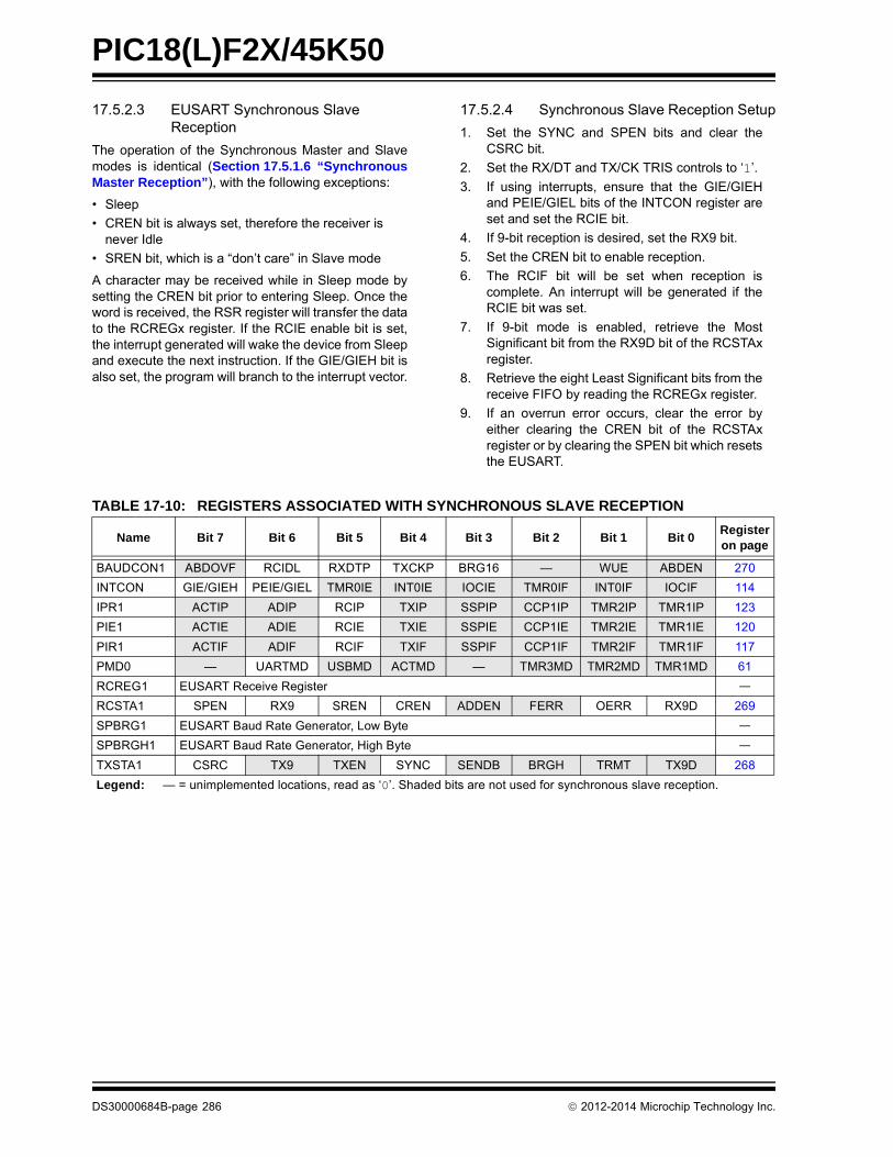
PIC18(L)F2X/45K50
17.5.2.3 EUSART Synchronous Slave Reception
The operation of the Synchronous Master and Slavemodes is identical (Section 17.5.1.6 “SynchronousMaster Reception”), with the following exceptions:
• Sleep
• CREN bit is always set, therefore the receiver is never Idle
• SREN bit, which is a “don’t care” in Slave mode
A character may be received while in Sleep mode bysetting the CREN bit prior to entering Sleep. Once theword is received, the RSR register will transfer the datato the RCREGx register. If the RCIE enable bit is set,the interrupt generated will wake the device from Sleepand execute the next instruction. If the GIE/GIEH bit isalso set, the program will branch to the interrupt vector.
17.5.2.4 Synchronous Slave Reception Setup
1. Set the SYNC and SPEN bits and clear theCSRC bit.
2. Set the RX/DT and TX/CK TRIS controls to ‘1’.
3. If using interrupts, ensure that the GIE/GIEHand PEIE/GIEL bits of the INTCON register areset and set the RCIE bit.
4. If 9-bit reception is desired, set the RX9 bit.
5. Set the CREN bit to enable reception.
6. The RCIF bit will be set when reception iscomplete. An interrupt will be generated if theRCIE bit was set.
7. If 9-bit mode is enabled, retrieve the MostSignificant bit from the RX9D bit of the RCSTAxregister.
8. Retrieve the eight Least Significant bits from thereceive FIFO by reading the RCREGx register.
9. If an overrun error occurs, clear the error byeither clearing the CREN bit of the RCSTAxregister or by clearing the SPEN bit which resetsthe EUSART.
TABLE 17-10: REGISTERS ASSOCIATED WITH SYNCHRONOUS SLAVE RECEPTION
Name Bit 7 Bit 6 Bit 5 Bit 4 Bit 3 Bit 2 Bit 1 Bit 0Register on page
BAUDCON1 ABDOVF RCIDL RXDTP TXCKP BRG16 — WUE ABDEN 270
INTCON GIE/GIEH PEIE/GIEL TMR0IE INT0IE IOCIE TMR0IF INT0IF IOCIF 114
IPR1 ACTIP ADIP RCIP TXIP SSPIP CCP1IP TMR2IP TMR1IP 123
PIE1 ACTIE ADIE RCIE TXIE SSPIE CCP1IE TMR2IE TMR1IE 120
PIR1 ACTIF ADIF RCIF TXIF SSPIF CCP1IF TMR2IF TMR1IF 117
PMD0 — UARTMD USBMD ACTMD — TMR3MD TMR2MD TMR1MD 61
RCREG1 EUSART Receive Register —
RCSTA1 SPEN RX9 SREN CREN ADDEN FERR OERR RX9D 269
SPBRG1 EUSART Baud Rate Generator, Low Byte —
SPBRGH1 EUSART Baud Rate Generator, High Byte —
TXSTA1 CSRC TX9 TXEN SYNC SENDB BRGH TRMT TX9D 268
Legend: — = unimplemented locations, read as ‘0’. Shaded bits are not used for synchronous slave reception.
DS30000684B-page 286 2012-2014 Microchip Technology Inc.

PIC18(L)F2X/45K50
18.0 ANALOG-TO-DIGITAL CONVERTER (ADC) MODULE
The Analog-to-Digital Converter (ADC) allowsconversion of an analog input signal to a 10-bit binaryrepresentation of that signal. This device uses analoginputs, which are multiplexed into a single sample andhold circuit. The output of the sample and hold isconnected to the input of the converter. The convertergenerates a 10-bit binary result via successiveapproximation and stores the conversion result into theADC result registers (ADRESL and ADRESH).
The ADC voltage reference is software selectable toeither VDD or a voltage applied to the external referencepins.
The ADC can generate an interrupt upon completion ofa conversion. This interrupt can be used to wake-up thedevice from Sleep.
Figure 18-1 shows the block diagram of the ADC.
FIGURE 18-1: ADC BLOCK DIAGRAM
Note: Additional ADC channels AN5-AN7 and AN20-AN27 are only available on PIC18(L)F45K50 devices.
11111
11110
11101
11100
11011
FVR BUF2
DAC
CTMU
Temperature Diode
AN27(1)
00101
00100
AN5(1)
AN4
00011
00010
AN3
AN2
00001
00000
AN1
AN0
5CHS<4:0>
10-Bit ADC
ADCMD
ADON
GO/DONE
10
0 = Left Justify1 = Right Justify
ADFM
10
ADRESH ADRESL
00
01
AVDD
10
11
FVR BUF2
Reserved
VREF+/AN3
2PVCFG<1:0>
00
01
AVSS
10
11
Reserved
Reserved
VREF-/AN2
2NVCFG<1:0>
2012-2014 Microchip Technology Inc. DS30000684B-page 287

PIC18(L)F2X/45K50
18.1 ADC Configuration
When configuring and using the ADC the followingfunctions must be considered:
• Port configuration
• Channel selection
• ADC voltage reference selection
• ADC conversion clock source
• Interrupt control
• Results formatting
18.1.1 PORT CONFIGURATION
The ANSELx and TRISx registers configure the A/Dport pins. Any port pin needed as an analog inputshould have its corresponding ANSx bit set to disablethe digital input buffer and TRISx bit set to disable thedigital output driver. If the TRISx bit is cleared, thedigital output level (VOH or VOL) will be converted.
The A/D operation is independent of the state of theANSx bits and the TRIS bits.
18.1.2 CHANNEL SELECTION
The CHS bits of the ADCON0 register determine whichchannel is connected to the sample and hold circuit.
When changing channels, a delay is required beforestarting the next conversion. Refer to Section 18.2“ADC Operation” for more information.
18.1.3 ADC VOLTAGE REFERENCE
The PVCFG<1:0> and NVCFG<1:0> bits of theADCON1 register provide independent control of thepositive and negative voltage references.
The positive voltage reference can be:
• VDD
• the fixed voltage reference (FVR BUF2)
• an external voltage source (VREF+)
The negative voltage reference can be:
• VSS
• an external voltage source (VREF-)
18.1.4 SELECTING AND CONFIGURING ACQUISITION TIME
The ADCON2 register allows the user to select anacquisition time that occurs each time the GO/DONEbit is set.
Acquisition time is set with the ACQT<2:0> bits of theADCON2 register. Acquisition delays cover a range of2 to 20 TAD. When the GO/DONE bit is set, the A/Dmodule continues to sample the input for the selectedacquisition time, then automatically begins aconversion. Since the acquisition time is programmed,there is no need to wait for an acquisition time betweenselecting a channel and setting the GO/DONE bit.
Manual acquisition is selected whenACQT<2:0> = 000. When the GO/DONE bit is set,sampling is stopped and a conversion begins. The useris responsible for ensuring the required acquisition timehas passed between selecting the desired inputchannel and setting the GO/DONE bit. This option isalso the default Reset state of the ACQT<2:0> bits andis compatible with devices that do not offerprogrammable acquisition times.
In either case, when the conversion is completed, theGO/DONE bit is cleared, the ADIF flag is set and theA/D begins sampling the currently selected channelagain. When an acquisition time is programmed, thereis no indication of when the acquisition time ends andthe conversion begins.
Note 1: When reading the PORT register, all pinswith their corresponding ANSx bit setread as cleared (a low level). However,analog conversion of pins configured asdigital inputs (ANSx bit cleared andTRISx bit set) will be accuratelyconverted.
2: Analog levels on any pin with the corre-sponding ANSx bit cleared may causethe digital input buffer to consume currentout of the device’s specification limits.
3: The PBADEN bit in ConfigurationRegister 3H configures PORTB pins toreset as analog or digital pins bycontrolling how the bits in ANSELB arereset.
DS30000684B-page 288 2012-2014 Microchip Technology Inc.

PIC18(L)F2X/45K50
18.1.5 CONVERSION CLOCK
The source of the conversion clock is softwareselectable via the ADCS bits of the ADCON2 register.There are seven possible clock options:
• FOSC/2
• FOSC/4
• FOSC/8
• FOSC/16
• FOSC/32
• FOSC/64
• FRC (dedicated internal oscillator)
The time to complete one bit conversion is defined asTAD. One full 10-bit conversion requires 11 TAD periodsas shown in Figure 18-3.
For correct conversion, the appropriate TAD specificationmust be met. See A/D conversion requirements inTable 29-33 for more information. Table 18-1 givesexamples of appropriate ADC clock selections.
18.1.6 INTERRUPTS
The ADC module allows for the ability to generate aninterrupt upon completion of an Analog-to-DigitalConversion. The ADC interrupt enable is the ADIE bitin the PIE1 register and the interrupt priority is the ADIPbit in the IPR1 register. The ADC interrupt flag is theADIF bit in the PIR1 register. The ADIF bit must becleared by software.
This interrupt can be generated while the device isoperating or while in Sleep. If the device is in Sleep, theinterrupt will wake-up the device. Upon waking fromSleep, the next instruction following the SLEEPinstruction is always executed. If the user is attemptingto wake-up from Sleep and resume in-line codeexecution, the global interrupt must be disabled. If theglobal interrupt is enabled, execution will switch to theInterrupt Service Routine.
Note: Unless using the FRC, any changes in thesystem clock frequency will change theADC clock frequency, which mayadversely affect the ADC result.
Note: The ADIF bit is set at the completion ofevery conversion, regardless of whetheror not the ADC interrupt is enabled.
TABLE 18-1: ADC CLOCK PERIOD (TAD) vs. DEVICE OPERATING FREQUENCIES
AD Clock Period (TAD) Device Frequency (FOSC)
ADC Clock Source ADCS<2:0> 48 MHz 16 MHz 4 MHz 1 MHz
FOSC/2 000 41.17 ns(2) 125 ns(2) 500 ns(2) 2.0 s
FOSC/4 100 83.3 ns(2) 250 ns(2) 1.0 s 4.0 s(3)
FOSC/8 001 166.7 ns(2) 500 ns(2) 2.0 s 8.0 s(3)
FOSC/16 101 333.3 ns(2) 1.0 s 4.0 s(3) 16.0 s(3)
FOSC/32 010 666.7 ns(2) 2.0 s 8.0 s(3) 32.0 s(3)
FOSC/64 110 1.3 s 4.0 s(3) 16.0 s(3) 64.0 s(3)
FRC 011 1-4 s(1,4) 1-4 s(1,4) 1-4 s(1,4) 1-4 s(1,4)
Legend: Shaded cells are outside the recommended range.
Note 1: The FRC source has a typical TAD time of 1.7 s.
2: These values violate the minimum required TAD time.
3: For faster conversion times, the selection of another clock source is recommended.
4: When the device frequency is greater than 1 MHz, the FRC clock source is only recommended if the conversion will be performed during Sleep.
2012-2014 Microchip Technology Inc. DS30000684B-page 289

PIC18(L)F2X/45K50
18.1.7 RESULT FORMATTING
The 10-bit A/D conversion result can be supplied in twoformats, left justified or right justified. The ADFM bit ofthe ADCON2 register controls the output format.
Figure 18-2 shows the two output formats.
FIGURE 18-2: 10-BIT A/D CONVERSION RESULT FORMAT
ADRESH ADRESL
(ADFM = 0) MSB LSB
bit 7 bit 0 bit 7 bit 0
10-bit A/D Result Unimplemented: Read as ‘0’
(ADFM = 1) MSB LSB
bit 7 bit 0 bit 7 bit 0
Unimplemented: Read as ‘0’ 10-bit A/D Result
DS30000684B-page 290 2012-2014 Microchip Technology Inc.

PIC18(L)F2X/45K50
18.2 ADC Operation
18.2.1 STARTING A CONVERSION
To enable the ADC module, the ADON bit of theADCON0 register must be set to a ‘1’. Setting the GO/DONE bit of the ADCON0 register to a ‘1’ will, depend-ing on the ACQT bits of the ADCON2 register, eitherimmediately start the Analog-to-Digital conversion orstart an acquisition delay followed by the Analog-to-Digital conversion.
Figure 18-3 shows the operation of the A/D converterafter the GO bit has been set and the ACQT<2:0> bitsare cleared. A conversion is started after the followinginstruction to allow entry into SLEEP mode before theconversion begins.
Figure 18-4 shows the operation of the A/D converterafter the GO bit has been set and the ACQT<2:0> bitsare set to ‘010’ which selects a 4 TAD acquisition timebefore the conversion starts.
FIGURE 18-3: A/D CONVERSION TAD CYCLES (ACQT<2:0> = 000, TACQ = 0)
FIGURE 18-4: A/D CONVERSION TAD CYCLES (ACQT<2:0> = 010, TACQ = 4 TAD)
Note: The GO/DONE bit should not be set in thesame instruction that turns on the ADC.Refer to Section 18.2.10 “A/D Conver-sion Procedure”.
TAD1 TAD2 TAD3 TAD4 TAD5 TAD6 TAD7 TAD8 TAD11
Set GO bit
Holding capacitor is disconnected from analog input (typically 100 ns)
TAD9 TAD10TCY - TAD
ADRESH:ADRESL is loaded, GO bit is cleared, ADIF bit is set, holding capacitor is connected to analog input.
Conversion starts
b0b9 b6 b5 b4 b3 b2 b1b8 b7
On the following cycle:
2 TAD
Discharge
1 2 3 4 5 6 7 8 11
Set GO bit
(Holding capacitor is disconnected from analog input)
9 10
Conversion starts
1 2 3 4
(Holding capacitor continuesacquiring input)
TACQT Cycles TAD Cycles
AutomaticAcquisition
Time
b0b9 b6 b5 b4 b3 b2 b1b8 b7
ADRESH:ADRESL is loaded, GO bit is cleared, ADIF bit is set, holding capacitor is connected to analog input.
On the following cycle:
2 TAD
Discharge
2012-2014 Microchip Technology Inc. DS30000684B-page 291
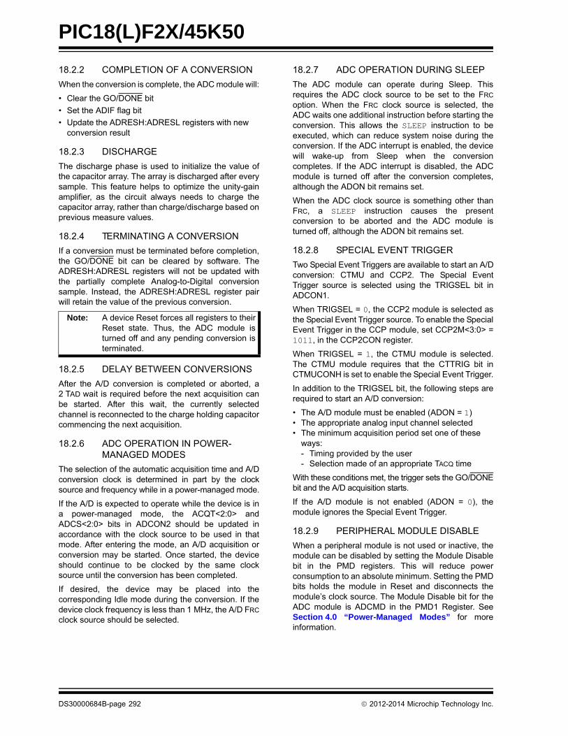
PIC18(L)F2X/45K50
18.2.2 COMPLETION OF A CONVERSION
When the conversion is complete, the ADC module will:
• Clear the GO/DONE bit
• Set the ADIF flag bit
• Update the ADRESH:ADRESL registers with new conversion result
18.2.3 DISCHARGE
The discharge phase is used to initialize the value ofthe capacitor array. The array is discharged after everysample. This feature helps to optimize the unity-gainamplifier, as the circuit always needs to charge thecapacitor array, rather than charge/discharge based onprevious measure values.
18.2.4 TERMINATING A CONVERSION
If a conversion must be terminated before completion,the GO/DONE bit can be cleared by software. TheADRESH:ADRESL registers will not be updated withthe partially complete Analog-to-Digital conversionsample. Instead, the ADRESH:ADRESL register pairwill retain the value of the previous conversion.
18.2.5 DELAY BETWEEN CONVERSIONS
After the A/D conversion is completed or aborted, a2 TAD wait is required before the next acquisition canbe started. After this wait, the currently selectedchannel is reconnected to the charge holding capacitorcommencing the next acquisition.
18.2.6 ADC OPERATION IN POWER-MANAGED MODES
The selection of the automatic acquisition time and A/Dconversion clock is determined in part by the clocksource and frequency while in a power-managed mode.
If the A/D is expected to operate while the device is ina power-managed mode, the ACQT<2:0> andADCS<2:0> bits in ADCON2 should be updated inaccordance with the clock source to be used in thatmode. After entering the mode, an A/D acquisition orconversion may be started. Once started, the deviceshould continue to be clocked by the same clocksource until the conversion has been completed.
If desired, the device may be placed into thecorresponding Idle mode during the conversion. If thedevice clock frequency is less than 1 MHz, the A/D FRC
clock source should be selected.
18.2.7 ADC OPERATION DURING SLEEP
The ADC module can operate during Sleep. Thisrequires the ADC clock source to be set to the FRC
option. When the FRC clock source is selected, theADC waits one additional instruction before starting theconversion. This allows the SLEEP instruction to beexecuted, which can reduce system noise during theconversion. If the ADC interrupt is enabled, the devicewill wake-up from Sleep when the conversioncompletes. If the ADC interrupt is disabled, the ADCmodule is turned off after the conversion completes,although the ADON bit remains set.
When the ADC clock source is something other thanFRC, a SLEEP instruction causes the presentconversion to be aborted and the ADC module isturned off, although the ADON bit remains set.
18.2.8 SPECIAL EVENT TRIGGER
Two Special Event Triggers are available to start an A/Dconversion: CTMU and CCP2. The Special EventTrigger source is selected using the TRIGSEL bit inADCON1.
When TRIGSEL = 0, the CCP2 module is selected asthe Special Event Trigger source. To enable the SpecialEvent Trigger in the CCP module, set CCP2M<3:0> =1011, in the CCP2CON register.
When TRIGSEL = 1, the CTMU module is selected.The CTMU module requires that the CTTRIG bit inCTMUCONH is set to enable the Special Event Trigger.
In addition to the TRIGSEL bit, the following steps arerequired to start an A/D conversion:
• The A/D module must be enabled (ADON = 1)• The appropriate analog input channel selected• The minimum acquisition period set one of these
ways:- Timing provided by the user- Selection made of an appropriate TACQ time
With these conditions met, the trigger sets the GO/DONEbit and the A/D acquisition starts.
If the A/D module is not enabled (ADON = 0), themodule ignores the Special Event Trigger.
18.2.9 PERIPHERAL MODULE DISABLE
When a peripheral module is not used or inactive, themodule can be disabled by setting the Module Disablebit in the PMD registers. This will reduce powerconsumption to an absolute minimum. Setting the PMDbits holds the module in Reset and disconnects themodule’s clock source. The Module Disable bit for theADC module is ADCMD in the PMD1 Register. SeeSection 4.0 “Power-Managed Modes” for moreinformation.
Note: A device Reset forces all registers to theirReset state. Thus, the ADC module isturned off and any pending conversion isterminated.
DS30000684B-page 292 2012-2014 Microchip Technology Inc.
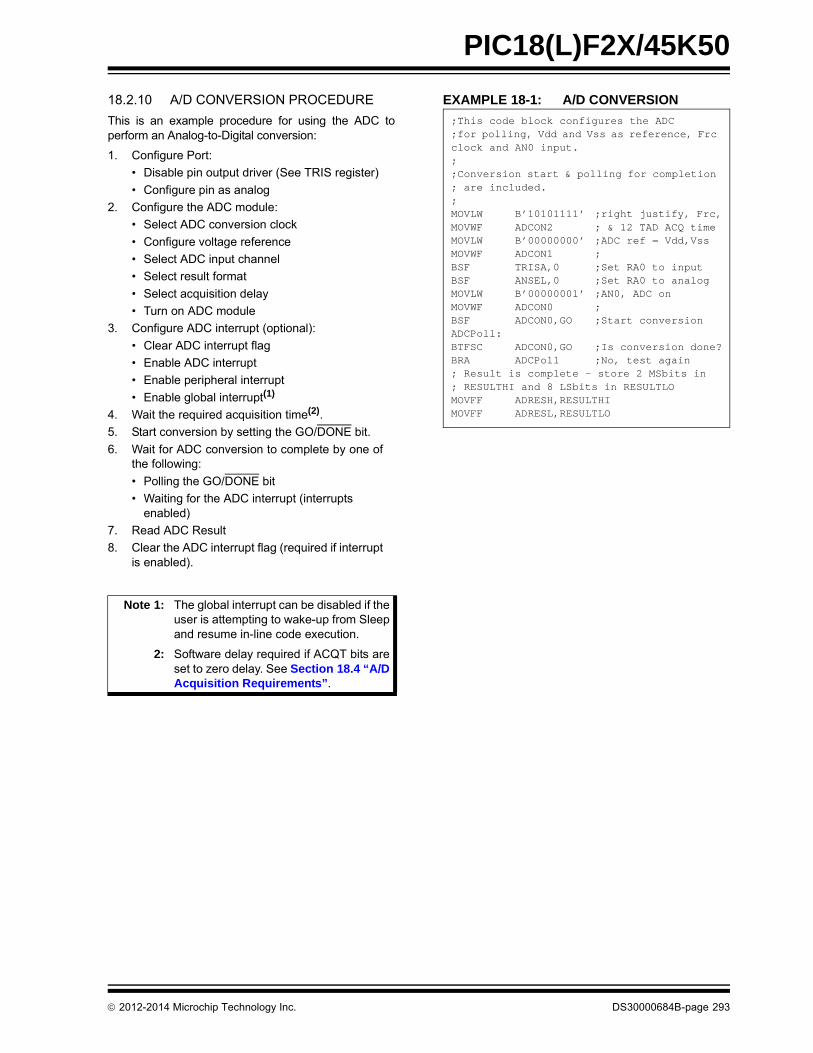
PIC18(L)F2X/45K50
18.2.10 A/D CONVERSION PROCEDURE
This is an example procedure for using the ADC toperform an Analog-to-Digital conversion:
1. Configure Port:
• Disable pin output driver (See TRIS register)
• Configure pin as analog
2. Configure the ADC module:
• Select ADC conversion clock
• Configure voltage reference
• Select ADC input channel
• Select result format
• Select acquisition delay
• Turn on ADC module
3. Configure ADC interrupt (optional):
• Clear ADC interrupt flag
• Enable ADC interrupt
• Enable peripheral interrupt
• Enable global interrupt(1)
4. Wait the required acquisition time(2).
5. Start conversion by setting the GO/DONE bit.
6. Wait for ADC conversion to complete by one ofthe following:
• Polling the GO/DONE bit
• Waiting for the ADC interrupt (interrupts enabled)
7. Read ADC Result
8. Clear the ADC interrupt flag (required if interruptis enabled).
EXAMPLE 18-1: A/D CONVERSION
Note 1: The global interrupt can be disabled if theuser is attempting to wake-up from Sleepand resume in-line code execution.
2: Software delay required if ACQT bits areset to zero delay. See Section 18.4 “A/DAcquisition Requirements”.
;This code block configures the ADC;for polling, Vdd and Vss as reference, Frc clock and AN0 input.;;Conversion start & polling for completion ; are included.;MOVLW B’10101111’ ;right justify, Frc,MOVWF ADCON2 ; & 12 TAD ACQ timeMOVLW B’00000000’ ;ADC ref = Vdd,VssMOVWF ADCON1 ;BSF TRISA,0 ;Set RA0 to inputBSF ANSEL,0 ;Set RA0 to analogMOVLW B’00000001’ ;AN0, ADC onMOVWF ADCON0 ;BSF ADCON0,GO ;Start conversionADCPoll:BTFSC ADCON0,GO ;Is conversion done?BRA ADCPoll ;No, test again; Result is complete - store 2 MSbits in; RESULTHI and 8 LSbits in RESULTLOMOVFF ADRESH,RESULTHIMOVFF ADRESL,RESULTLO
2012-2014 Microchip Technology Inc. DS30000684B-page 293
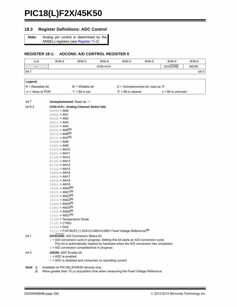
PIC18(L)F2X/45K50
18.3 Register Definitions: ADC Control
Note: Analog pin control is determined by theANSELx registers (see Register 11-2)
REGISTER 18-1: ADCON0: A/D CONTROL REGISTER 0
U-0 R/W-0 R/W-0 R/W-0 R/W-0 R/W-0 R/W-0 R/W-0
— CHS<4:0> GO/DONE ADON
bit 7 bit 0
Legend:
R = Readable bit W = Writable bit U = Unimplemented bit, read as ‘0’
-n = Value at POR ‘1’ = Bit is set ‘0’ = Bit is cleared x = Bit is unknown
bit 7 Unimplemented: Read as ‘0’
bit 6-2 CHS<4:0>: Analog Channel Select bits00000 = AN000001 = AN100010 = AN200011 = AN300100 = AN400101 = AN5(1)
00110 = AN6(1)
00111 = AN7(1)
01000 = AN801001 = AN901010 = AN1001011 = AN1101100 = AN1201101 = AN1301110 = AN1401111 = AN1510000 = AN1610001 = AN1710010 = AN1810011 = AN1910100 = AN20(1)
10101 = AN21(1)
10110 = AN22(1)
10111 = AN23(1)
11000 = AN24(1)
11001 = AN25(1)
11010 = AN26(1)
11011 = AN27(1)
11100 = Temperature Diode11101 = CTMU11110 = DAC11111 = FVR BUF2 (1.024V/2.048V/4.096V Fixed Voltage Reference)(2)
bit 1 GO/DONE: A/D Conversion Status bit1 = A/D conversion cycle in progress. Setting this bit starts an A/D conversion cycle. This bit is automatically cleared by hardware when the A/D conversion has completed.0 = A/D conversion completed/not in progress
bit 0 ADON: ADC Enable bit1 = ADC is enabled0 = ADC is disabled and consumes no operating current
Note 1: Available on PIC18(L)F45K50 devices only.2: Allow greater than 15 s acquisition time when measuring the Fixed Voltage Reference.
DS30000684B-page 294 2012-2014 Microchip Technology Inc.

PIC18(L)F2X/45K50
REGISTER 18-2: ADCON1: A/D CONTROL REGISTER 1
R/W-0 U-0 U-0 U-0 R/W-0 R/W-0 R/W-0 R/W-0
TRIGSEL — — — PVCFG<1:0> NVCFG<1:0>
bit 7 bit 0
Legend:
R = Readable bit W = Writable bit U = Unimplemented bit, read as ‘0’
-n = Value at POR ‘1’ = Bit is set ‘0’ = Bit is cleared x = Bit is unknown
bit 7 TRIGSEL: Special Trigger Select bit1 = Selects the special trigger from CTMU0 = Selects the special trigger from CCP2
bit 6-4 Unimplemented: Read as ‘0’
bit 3-2 PVCFG<1:0>: Positive Voltage Reference Configuration bits
00 = A/D VREF+ connected to internal signal, AVDD
01 = A/D VREF+ connected to external pin, VREF+10 = A/D VREF+ connected to internal signal, FVR BUF2
11 = Reserved
bit 1-0 NVCFG<1:0>: Negative Voltage Reference Configuration bits
00 = A/D VREF- connected to internal signal, AVSS
01 = A/D VREF- connected to external pin, VREF-10 = Reserved
11 = Reserved
2012-2014 Microchip Technology Inc. DS30000684B-page 295

PIC18(L)F2X/45K50
REGISTER 18-3: ADCON2: A/D CONTROL REGISTER 2
R/W-0 U-0 R/W-0 R/W-0 R/W-0 R/W-0 R/W-0 R/W-0
ADFM — ACQT<2:0> ADCS<2:0>
bit 7 bit 0
Legend:
R = Readable bit W = Writable bit U = Unimplemented bit, read as ‘0’
-n = Value at POR ‘1’ = Bit is set ‘0’ = Bit is cleared x = Bit is unknown
bit 7 ADFM: A/D Conversion Result Format Select bit
1 = Right justified0 = Left justified
bit 6 Unimplemented: Read as ‘0’
bit 5-3 ACQT<2:0>: A/D Acquisition time select bits. Acquisition time is the duration that the A/D charge holding capacitor remains connected to A/D channel from the instant the GO/DONE bit is set until conversions begins.
000 = 0(1)
001 = 2 TAD
010 = 4 TAD
011 = 6 TAD
100 = 8 TAD
101 = 12 TAD
110 = 16 TAD
111 = 20 TAD
bit 2-0 ADCS<2:0>: A/D Conversion Clock Select bits
000 = FOSC/2001 = FOSC/8010 = FOSC/32011 = FRC(1) (clock derived from a dedicated internal oscillator = 600 kHz nominal)100 = FOSC/4101 = FOSC/16110 = FOSC/64111 = FRC(1) (clock derived from a dedicated internal oscillator = 600 kHz nominal)
Note 1: When the A/D clock source is selected as FRC then the start of conversion is delayed by one instruction cycle after the GO/DONE bit is set to allow the SLEEP instruction to be executed.
DS30000684B-page 296 2012-2014 Microchip Technology Inc.

PIC18(L)F2X/45K50
REGISTER 18-4: ADRESH: ADC RESULT REGISTER HIGH (ADRESH) ADFM = 0
R/W-x R/W-x R/W-x R/W-x R/W-x R/W-x R/W-x R/W-x
ADRES<9:2>
bit 7 bit 0
Legend:
R = Readable bit W = Writable bit U = Unimplemented bit, read as ‘0’
-n = Value at POR ‘1’ = Bit is set ‘0’ = Bit is cleared x = Bit is unknown
bit 7-0 ADRES<9:2>: ADC Result Register bitsUpper eight bits of 10-bit conversion result
REGISTER 18-5: ADRESL: ADC RESULT REGISTER LOW (ADRESL) ADFM = 0
R/W-x R/W-x R/W-x R/W-x R/W-x R/W-x R/W-x R/W-x
ADRES<1:0> r r r r r r
bit 7 bit 0
Legend: r = Reserved bit
R = Readable bit W = Writable bit U = Unimplemented bit, read as ‘0’
-n = Value at POR ‘1’ = Bit is set ‘0’ = Bit is cleared x = Bit is unknown
bit 7-6 ADRES<1:0>: ADC Result Register bitsLower two bits of 10-bit conversion result
bit 5-0 Reserved: Do not use.
REGISTER 18-6: ADRESH: ADC RESULT REGISTER HIGH (ADRESH) ADFM = 1
R/W-x R/W-x R/W-x R/W-x R/W-x R/W-x R/W-x R/W-x
r r r r r r ADRES<9:8>
bit 7 bit 0
Legend: r = Reserved bit
R = Readable bit W = Writable bit U = Unimplemented bit, read as ‘0’
-n = Value at POR ‘1’ = Bit is set ‘0’ = Bit is cleared x = Bit is unknown
bit 7-2 Reserved: Do not use.
bit 1-0 ADRES<9:8>: ADC Result Register bitsUpper two bits of 10-bit conversion result
REGISTER 18-7: ADRESL: ADC RESULT REGISTER LOW (ADRESL) ADFM = 1
R/W-x R/W-x R/W-x R/W-x R/W-x R/W-x R/W-x R/W-x
ADRES<7:0>
bit 7 bit 0
Legend:
R = Readable bit W = Writable bit U = Unimplemented bit, read as ‘0’
-n = Value at POR ‘1’ = Bit is set ‘0’ = Bit is cleared x = Bit is unknown
bit 7-0 ADRES<7:0>: ADC Result Register bitsLower eight bits of 10-bit conversion result
2012-2014 Microchip Technology Inc. DS30000684B-page 297

PIC18(L)F2X/45K50
18.4 A/D Acquisition Requirements
For the ADC to meet its specified accuracy, the chargeholding capacitor (CHOLD) must be allowed to fullycharge to the input channel voltage level. The AnalogInput model is shown in Figure 18-5. The sourceimpedance (RS) and the internal sampling switch (RSS)impedance directly affect the time required to charge thecapacitor CHOLD. The sampling switch (RSS) impedancevaries over the device voltage (VDD), see Figure 18-5.The maximum recommended impedance for analogsources is 10 k. As the source impedance isdecreased, the acquisition time may be decreased.After the analog input channel is selected (or changed),
an A/D acquisition must be done before the conversioncan be started. To calculate the minimum acquisitiontime, Equation 18-1 may be used. This equationassumes that 1/2 LSb error is used (1024 steps for theADC). The 1/2 LSb error is the maximum error allowedfor the ADC to meet its specified resolution.
EQUATION 18-1: ACQUISITION TIME EXAMPLE
TACQ Amplifier Settling Time Hold Capacitor Charging Time Temperature Coefficient+ +=
TAMP TC TCOFF+ +=
5µs TC Temperature - 25°C 0.05µs/°C + +=
TC CHOLD RIC RSS RS+ + ln(1/2047)–=
13.5pF 1k 700 10k+ + – ln(0.0004885)=
1.20= µs
TACQ 5µs 1.20µs 50°C- 25°C 0.05s/°C + +=
7.45µs=
VAPPLIED 1 e
Tc–RC---------
–
VAPPLIED 11
2047------------–
=
VAPPLIED 11
2047------------–
VCHOLD=
VAPPLIED 1 e
TC–RC----------
–
VCHOLD=
;[1] VCHOLD charged to within 1/2 lsb
;[2] VCHOLD charge response to VAPPLIED
;combining [1] and [2]
The value for TC can be approximated with the following equations:
Solving for TC:
Therefore:
Temperature 50°C and external impedance of 10k 3.0V VDD=Assumptions:
Note 1: The reference voltage (VREF) has no effect on the equation, since it cancels itself out.
2: The charge holding capacitor (CHOLD) is discharged after each conversion.
3: The maximum recommended impedance for analog sources is 10 k. This is required to meet the pin leakage specification.
DS30000684B-page 298 2012-2014 Microchip Technology Inc.
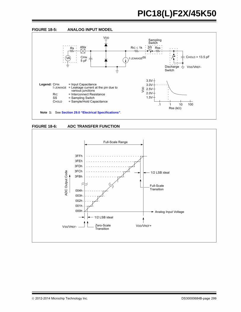
PIC18(L)F2X/45K50
FIGURE 18-5: ANALOG INPUT MODEL
FIGURE 18-6: ADC TRANSFER FUNCTION
CPINVA
Rs ANx
5 pF
VD
D
I LEAKAGE(1)
RIC 1k
SamplingSwitch
SS Rss
CHOLD = 13.5 pF
VSS/VREF-
2.5V
Rss (k)
2.0V1.5V
.1 1 10
VDD
Legend: CPINI LEAKAGE
RIC
SSCHOLD
= Input Capacitance= Leakage current at the pin due to
= Interconnect Resistance= Sampling Switch= Sample/Hold Capacitance
various junctions
DischargeSwitch
3.0V3.5V
100
Note 1: See Section 29.0 “Electrical Specifications”.
3FFh
3FEh
AD
C O
utp
ut
Co
de
3FDh
3FCh
004h
003h
002h
001h
000h
Full-Scale
3FBh
1/2 LSB ideal
VSS/VREF- Zero-ScaleTransition
VDD/VREF+
Transition
1/2 LSB ideal
Full-Scale Range
Analog Input Voltage
2012-2014 Microchip Technology Inc. DS30000684B-page 299

PIC18(L)F2X/45K50
TABLE 18-3: CONFIGURATION REGISTERS ASSOCIATED WITH THE ADC MODULE
TABLE 18-2: REGISTERS ASSOCIATED WITH A/D OPERATION
Name Bit 7 Bit 6 Bit 5 Bit 4 Bit 3 Bit 2 Bit 1 Bit 0Register on page
ADCON0 — CHS<4:0> GO/DONE ADON 294
ADCON1 TRIGSEL — — — PVCFG<1:0> NVCFG<1:0> 295
ADCON2 ADFM — ACQT<2:0> ADCS<2:0> 296
ADRESH A/D Result, High Byte 297
ADRESL A/D Result, Low Byte 297
ANSELA — — ANSA5 — ANSA3 ANSA2 ANSA1 ANSA0 147
ANSELB — — ANSB5 ANSB4 ANSB3 ANSB2 ANSB1 ANSB0 148
ANSELC ANSC7 ANSC6 — — — ANSC2 — — 148
ANSELD(1) ANSD7 ANSD6 ANSD5 ANSD4 ANSD3 ANSD2 ANSD1 ANSD0 148
ANSELE(1) — — — — — ANSE2 ANSE1 ANSE0 149
CTMUCONH CTMUEN — CTMUSIDL TGEN EDGEN EDGSEQEN IDISSEN CTTRIG 322
INTCON GIE/GIEH PEIE/GIEL TMR0IE INT0IE IOCIE TMR0IF INT0IF IOCIF 114
IPR1 ACTIP ADIP RCIP TXIP SSPIP CCP1IP TMR2IP TMR1IP 123
PIE1 ACTIE ADIE RCIE TXIE SSPIE CCP1IE TMR2IE TMR1IE 120
PIR1 ACTIF ADIF RCIF TXIF SSPIF CCP1IF TMR2IF TMR1IF 117
PMD1 — MSSPMD CTMUMD CMP2MD CMP1MD ADCMD CCP2MD CCP1MD 62
TRISA TRISA7 TRISA6 TRISA5 TRISA4 TRISA3 TRISA2 TRISA1 TRISA0 149
TRISB TRISB7 TRISB6 TRISB5 TRISB4 TRISB3 TRISB2 TRISB1 TRISB0 149
TRISC TRISC7 TRISC6 — — — TRISC2 TRISC1 TRISC0 149
TRISD(1) TRISD7 TRISD6 TRISD5 TRISD4 TRISD3 TRISD2 TRISD1 TRISD0 149
TRISE WPUE3 — — — — TRISE2(1) TRISE1(1) TRISE0(1) 149
Legend: — = unimplemented locations, read as ‘0’. Shaded bits are not used by this module.
Note 1: Available on PIC18(L)F45K50 devices.
Name Bit 7 Bit 6 Bit 5 Bit 4 Bit 3 Bit 2 Bit 1 Bit 0Register on page
CONFIG3H MCLRE SDOMX — T3CMX — — PBADEN CCP2MX 376
Legend: — = unimplemented locations, read as ‘0’. Shaded bits are not used by the ADC module.
DS30000684B-page 300 2012-2014 Microchip Technology Inc.

PIC18(L)F2X/45K50
19.0 COMPARATOR MODULE
Comparators are used to interface analog circuits to adigital circuit by comparing two analog voltages andproviding a digital indication of their relative magnitudes.The comparators are very useful mixed signal buildingblocks because they provide analog functionalityindependent of the program execution. The analogcomparator module includes the following features:
• Independent comparator control
• Programmable input selection
• Comparator output is available internally/externally
• Programmable output polarity
• Interrupt-on-change
• Wake-up from Sleep
• Programmable Speed/Power optimization
• PWM shutdown
• Programmable and fixed voltage reference
19.1 Comparator Overview
A single comparator is shown in Figure 19-1 along withthe relationship between the analog input levels andthe digital output. When the analog voltage at VIN+ isless than the analog voltage at VIN-, the output of thecomparator is a digital low level. When the analogvoltage at VIN+ is greater than the analog voltage atVIN-, the output of the comparator is a digital high level.
FIGURE 19-1: SINGLE COMPARATOR
–
+VIN+
VIN-Output
Output
VIN+VIN-
Note: The black areas of the output of thecomparator represents the uncertaintydue to input offsets and response time.
2012-2014 Microchip Technology Inc. DS30000684B-page 301

PIC18(L)F2X/45K50
FIGURE 19-2: COMPARATOR C1/C2 SIMPLIFIED BLOCK DIAGRAM
Note 1: When C1ON = 0, the C1 comparator will produce a ‘0’ output to the XOR Gate.2: Q1 and Q3 are phases of the four-phase system clock (FOSC).3: Q1 is held high during Sleep mode.4: Synchronized comparator output should not be used to gate Timer1 in conjunction with synchronized T1CKI.
Cx
CxPOL to PWM Logic
0
1
2
3
CxON(1)
CxCH<1:0>
2
0
1
CxR
CM2CON1 (MCxOUT)
To Interrupts
CxVIN-
CxVIN+
C12IN0-
C12IN1-
C12IN2-
C12IN3-
CxIN+
D Q
ENQ1(2),(3)
D Q
ENCL
Read or Write
Reset
+
-
0
1
DAC Output
CXRSEL
FVR BUF1
CxSP
CXVREFCxOE
CxOUT
Timer1 Clock
D Q
sync_CxOUT
To CMxCON0 (CxOUT)
(CxIF)
of CMxCON0
Q3(2)
0
1
CxSYNC
async_CXOUT
TRIS bit
- to SR Latch- to TxG MUX(4)
DS30000684B-page 302 2012-2014 Microchip Technology Inc.
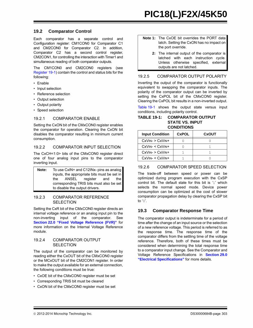
PIC18(L)F2X/45K50
19.2 Comparator Control
Each comparator has a separate control andConfiguration register: CM1CON0 for Comparator C1and CM2CON0 for Comparator C2. In addition,Comparator C2 has a second control register,CM2CON1, for controlling the interaction with Timer1 andsimultaneous reading of both comparator outputs.
The CM1CON0 and CM2CON0 registers (seeRegister 19-1) contain the control and status bits for thefollowing:
• Enable
• Input selection
• Reference selection
• Output selection
• Output polarity
• Speed selection
19.2.1 COMPARATOR ENABLE
Setting the CxON bit of the CMxCON0 register enablesthe comparator for operation. Clearing the CxON bitdisables the comparator resulting in minimum currentconsumption.
19.2.2 COMPARATOR INPUT SELECTION
The CxCH<1:0> bits of the CMxCON0 register directone of four analog input pins to the comparatorinverting input.
19.2.3 COMPARATOR REFERENCE SELECTION
Setting the CxR bit of the CMxCON0 register directs aninternal voltage reference or an analog input pin to thenon-inverting input of the comparator. SeeSection 22.0 “Fixed Voltage Reference (FVR)” formore information on the Internal Voltage Referencemodule.
19.2.4 COMPARATOR OUTPUT SELECTION
The output of the comparator can be monitored byreading either the CxOUT bit of the CMxCON0 registeror the MCxOUT bit of the CM2CON1 register. In orderto make the output available for an external connection,the following conditions must be true:
• CxOE bit of the CMxCON0 register must be set
• Corresponding TRIS bit must be cleared
• CxON bit of the CMxCON0 register must be set
19.2.5 COMPARATOR OUTPUT POLARITY
Inverting the output of the comparator is functionallyequivalent to swapping the comparator inputs. Thepolarity of the comparator output can be inverted bysetting the CxPOL bit of the CMxCON0 register.Clearing the CxPOL bit results in a non-inverted output.
Table 19-1 shows the output state versus inputconditions, including polarity control.
19.2.6 COMPARATOR SPEED SELECTION
The trade-off between speed or power can beoptimized during program execution with the CxSPcontrol bit. The default state for this bit is ‘1’ whichselects the normal speed mode. Device powerconsumption can be optimized at the cost of slowercomparator propagation delay by clearing the CxSP bitto ‘0’.
19.3 Comparator Response Time
The comparator output is indeterminate for a period oftime after the change of an input source or the selectionof a new reference voltage. This period is referred to asthe response time. The response time of thecomparator differs from the settling time of the voltagereference. Therefore, both of these times must beconsidered when determining the total response timeto a comparator input change. See the Comparator andVoltage Reference Specifications in Section 29.0“Electrical Specifications” for more details.
Note: To use CxIN+ and C12INx- pins as analoginputs, the appropriate bits must be set inthe ANSEL register and thecorresponding TRIS bits must also be setto disable the output drivers.
Note 1: The CxOE bit overrides the PORT datalatch. Setting the CxON has no impact onthe port override.
2: The internal output of the comparator islatched with each instruction cycle.Unless otherwise specified, externaloutputs are not latched.
TABLE 19-1: COMPARATOR OUTPUT STATE VS. INPUT CONDITIONS
Input Condition CxPOL CxOUT
CxVIN- > CxVIN+ 0 0
CxVIN- < CxVIN+ 0 1
CxVIN- > CxVIN+ 1 1
CxVIN- < CxVIN+ 1 0
2012-2014 Microchip Technology Inc. DS30000684B-page 303
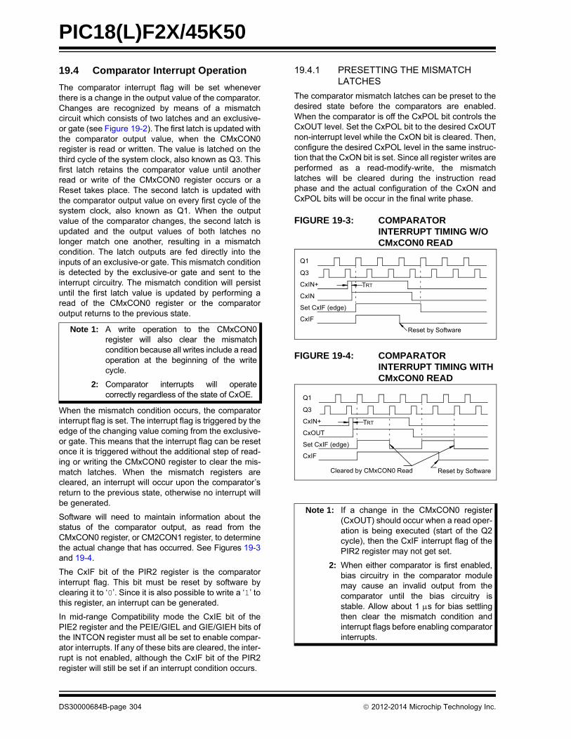
PIC18(L)F2X/45K50
19.4 Comparator Interrupt Operation
The comparator interrupt flag will be set wheneverthere is a change in the output value of the comparator.Changes are recognized by means of a mismatchcircuit which consists of two latches and an exclusive-or gate (see Figure 19-2). The first latch is updated withthe comparator output value, when the CMxCON0register is read or written. The value is latched on thethird cycle of the system clock, also known as Q3. Thisfirst latch retains the comparator value until anotherread or write of the CMxCON0 register occurs or aReset takes place. The second latch is updated withthe comparator output value on every first cycle of thesystem clock, also known as Q1. When the outputvalue of the comparator changes, the second latch isupdated and the output values of both latches nolonger match one another, resulting in a mismatchcondition. The latch outputs are fed directly into theinputs of an exclusive-or gate. This mismatch conditionis detected by the exclusive-or gate and sent to theinterrupt circuitry. The mismatch condition will persistuntil the first latch value is updated by performing aread of the CMxCON0 register or the comparatoroutput returns to the previous state.
When the mismatch condition occurs, the comparatorinterrupt flag is set. The interrupt flag is triggered by theedge of the changing value coming from the exclusive-or gate. This means that the interrupt flag can be resetonce it is triggered without the additional step of read-ing or writing the CMxCON0 register to clear the mis-match latches. When the mismatch registers arecleared, an interrupt will occur upon the comparator’sreturn to the previous state, otherwise no interrupt willbe generated.
Software will need to maintain information about thestatus of the comparator output, as read from theCMxCON0 register, or CM2CON1 register, to determinethe actual change that has occurred. See Figures 19-3and 19-4.
The CxIF bit of the PIR2 register is the comparatorinterrupt flag. This bit must be reset by software byclearing it to ‘0’. Since it is also possible to write a ‘1’ tothis register, an interrupt can be generated.
In mid-range Compatibility mode the CxIE bit of thePIE2 register and the PEIE/GIEL and GIE/GIEH bits ofthe INTCON register must all be set to enable compar-ator interrupts. If any of these bits are cleared, the inter-rupt is not enabled, although the CxIF bit of the PIR2register will still be set if an interrupt condition occurs.
19.4.1 PRESETTING THE MISMATCH LATCHES
The comparator mismatch latches can be preset to thedesired state before the comparators are enabled.When the comparator is off the CxPOL bit controls theCxOUT level. Set the CxPOL bit to the desired CxOUTnon-interrupt level while the CxON bit is cleared. Then,configure the desired CxPOL level in the same instruc-tion that the CxON bit is set. Since all register writes areperformed as a read-modify-write, the mismatchlatches will be cleared during the instruction readphase and the actual configuration of the CxON andCxPOL bits will be occur in the final write phase.
FIGURE 19-3: COMPARATOR INTERRUPT TIMING W/O CMxCON0 READ
FIGURE 19-4: COMPARATOR INTERRUPT TIMING WITH CMxCON0 READ
Note 1: A write operation to the CMxCON0register will also clear the mismatchcondition because all writes include a readoperation at the beginning of the writecycle.
2: Comparator interrupts will operatecorrectly regardless of the state of CxOE.
Note 1: If a change in the CMxCON0 register(CxOUT) should occur when a read oper-ation is being executed (start of the Q2cycle), then the CxIF interrupt flag of thePIR2 register may not get set.
2: When either comparator is first enabled,bias circuitry in the comparator modulemay cause an invalid output from thecomparator until the bias circuitry isstable. Allow about 1 s for bias settlingthen clear the mismatch condition andinterrupt flags before enabling comparatorinterrupts.
Q1
Q3
CxIN+
CxIN
Set CxIF (edge)
CxIF
TRT
Reset by Software
Q1
Q3
CxIN+
CxOUT
Set CxIF (edge)
CxIF
TRT
Reset by SoftwareCleared by CMxCON0 Read
DS30000684B-page 304 2012-2014 Microchip Technology Inc.

PIC18(L)F2X/45K50
19.5 Operation During Sleep
The comparator, if enabled before entering Sleep mode,remains active during Sleep. The additional currentconsumed by the comparator is shown separately inSection 29.0 “Electrical Specifications”. If thecomparator is not used to wake the device, powerconsumption can be minimized while in Sleep mode byturning off the comparator. Each comparator is turned offby clearing the CxON bit of the CMxCON0 register.
A change to the comparator output can wake-up thedevice from Sleep. To enable the comparator to wakethe device from Sleep, the CxIE bit of the PIE2 registerand the PEIE/GIEL bit of the INTCON register must beset. The instruction following the SLEEP instructionalways executes following a wake from Sleep. If theGIE/GIEH bit of the INTCON register is also set, thedevice will then execute the Interrupt Service Routine.
19.6 Effects of a Reset
A device Reset forces the CMxCON0 and CM2CON1registers to their Reset states. This forces bothcomparators and the voltage references to their Offstates.Comparator Control Registers.
19.7 Analog Input Connection Considerations
A simplified circuit for an analog input is shown inFigure 19-5. Since the analog input pins share theirconnection with a digital input, they have reversebiased ESD protection diodes to VDD and VSS. Theanalog input, therefore, must be between VSS and VDD.If the input voltage deviates from this range by morethan 0.6V in either direction, one of the diodes isforward biased and a latch-up may occur.
A maximum source impedance of 10 k is recommendedfor the analog sources. Also, any external componentconnected to an analog input pin, such as a capacitor ora Zener diode, should have very little leakage current tominimize inaccuracies introduced.
FIGURE 19-5: ANALOG INPUT MODEL
Note 1: When reading a PORT register, all pinsconfigured as analog inputs will read as a‘0’. Pins configured as digital inputs willconvert as an analog input, according tothe input specification.
2: Analog levels on any pin defined as adigital input, may cause the input buffer toconsume more current than is specified.
VA
Rs < 10K
CPIN5 pF
VDD
VT 0.6V
VT 0.6V
RIC
ILEAKAGE(1)
Vss
AIN
Legend: CPIN = Input CapacitanceILEAKAGE = Leakage Current at the pin due to various junctionsRIC = Interconnect ResistanceRS = Source ImpedanceVA = Analog VoltageVT = Threshold Voltage
Note 1: See Section 29.0 “Electrical Specifications”.
To Comparator
2012-2014 Microchip Technology Inc. DS30000684B-page 305

PIC18(L)F2X/45K50
19.8 Additional Comparator Features
There are four additional comparator features:
• Simultaneous read of comparator outputs
• Internal reference selection
• Hysteresis selection
• Output Synchronization
19.8.1 SIMULTANEOUS COMPARATOR OUTPUT READ
The MC1OUT and MC2OUT bits of the CM2CON1register are mirror copies of both comparator outputs.The ability to read both outputs simultaneously from asingle register eliminates the timing skew of readingseparate registers.
19.8.2 INTERNAL REFERENCE SELECTION
There are two internal voltage references available tothe non-inverting input of each comparator. One ofthese is the Fixed Voltage Reference (FVR) and theother is the variable Digital-to-Analog Converter (DAC).The CxRSEL bit of the CM2CON1 register determineswhich of these references is routed to the ComparatorVoltage reference output (CXVREF). Further routing tothe comparator is accomplished by the CxR bit of theCMxCON0 register. See Section 22.0 “Fixed VoltageReference (FVR)” and Figure 19-2 for more detail.
19.8.3 SYNCHRONIZING COMPARATOR OUTPUT TO TIMER1
The Comparator Cx output can be synchronized withTimer1 by setting the CxSYNC bit of the CM2CON1register. When enabled, the Cx output is latched onthe falling edge of the Timer1 source clock. To preventa race condition when gating Timer1 clock with thecomparator output, Timer1 increments on the risingedge of its clock source, and the falling edge latchesthe comparator output. See the Comparator BlockDiagram (Figure 19-2) and the Timer1 Block Diagram(Figure 13-1) for more information.
Note 1: Obtaining the status of C1OUT orC2OUT by reading CM2CON1 does notaffect the comparator interrupt mismatchregisters.
Note 1: The comparator synchronized outputshould not be used to gate the externalTimer1 clock when the Timer1synchronizer is enabled.
2: The Timer1 prescale should be set to 1:1when synchronizing the comparatoroutput as unexpected results may occurwith other prescale values.
DS30000684B-page 306 2012-2014 Microchip Technology Inc.

PIC18(L)F2X/45K50
19.9 Register Definitions: Comparator Control
REGISTER 19-1: CMxCON0: COMPARATOR x CONTROL REGISTER
R/W-0 R-0 R/W-0 R/W-0 R/W-1 R/W-0 R/W-0 R/W-0
CxON CxOUT CxOE CxPOL CxSP CxR CxCH<1:0>
bit 7 bit 0
Legend:
R = Readable bit W = Writable bit U = Unimplemented bit, read as ‘0’
-n = Value at POR ‘1’ = Bit is set ‘0’ = Bit is cleared x = Bit is unknown
bit 7 CxON: Comparator Cx Enable bit
1 = Comparator Cx is enabled0 = Comparator Cx is disabled
bit 6 CxOUT: Comparator Cx Output bit
If CxPOL = 1 (inverted polarity):CxOUT = 0 when CxVIN+ > CxVIN-CxOUT = 1 when CxVIN+ < CxVIN-If CxPOL = 0 (non-inverted polarity):CxOUT = 1 when CxVIN+ > CxVIN-CxOUT = 0 when CxVIN+ < CxVIN-
bit 5 CxOE: Comparator Cx Output Enable bit
1 = CxOUT is present on the CxOUT pin(1)
0 = CxOUT is internal only
bit 4 CxPOL: Comparator Cx Output Polarity Select bit
1 = CxOUT logic is inverted0 = CxOUT logic is not inverted
bit 3 CxSP: Comparator Cx Speed/Power Select bit
1 = Cx operates in normal power, higher speed mode0 = Cx operates in low-power, low-speed mode
bit 2 CxR: Comparator Cx Reference Select bit (non-inverting input)
1 = CxVIN+ connects to CXVREF output0 = CxVIN+ connects to C12IN+ pin
bit 1-0 CxCH<1:0>: Comparator Cx Channel Select bit
00 = C12IN0- pin of Cx connects to CxVIN-01 = C12IN1- pin of Cx connects to CXVIN-10 = C12IN2- pin of Cx connects to CxVIN-11 = C12IN3- pin of Cx connects to CxVIN-
Note 1: Comparator output requires the following three conditions: CxOE = 1, CxON = 1 and corresponding port TRIS bit = 0.
2012-2014 Microchip Technology Inc. DS30000684B-page 307
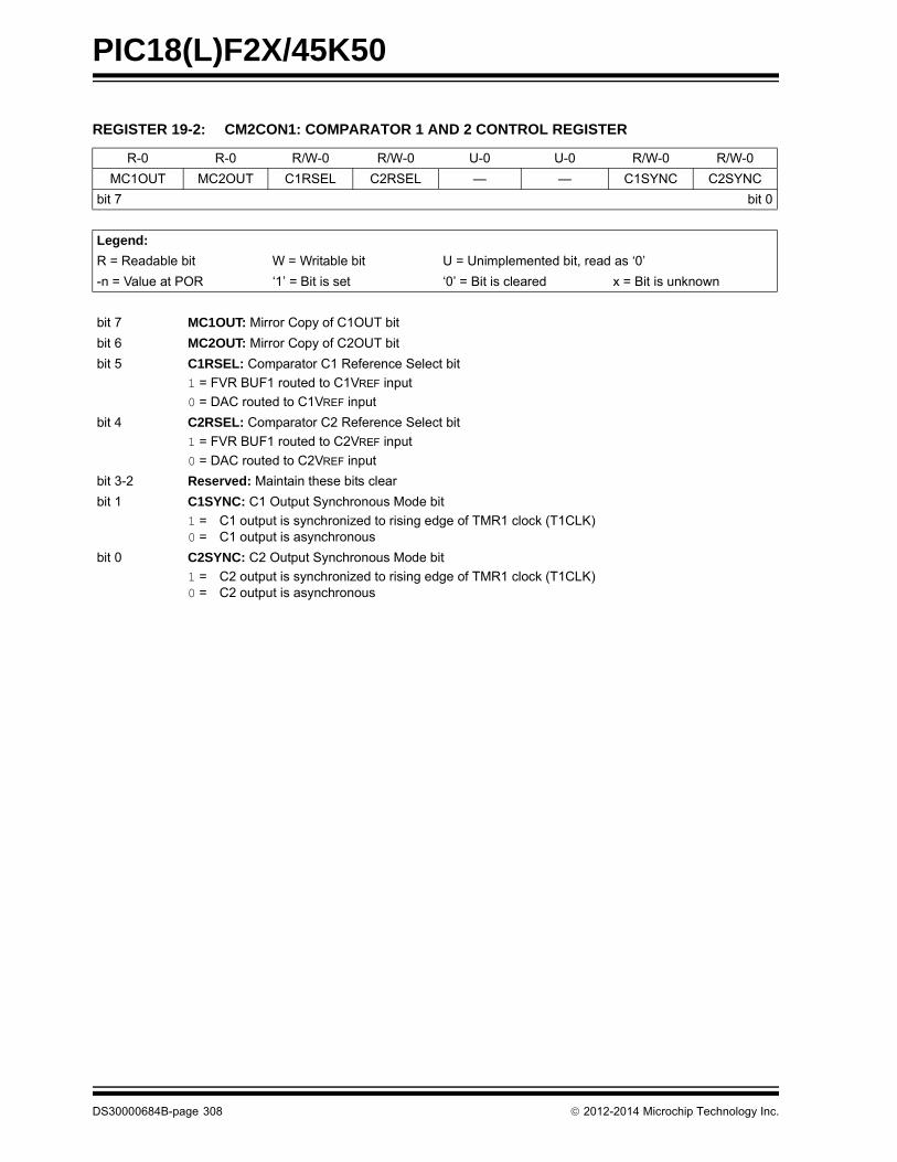
PIC18(L)F2X/45K50
REGISTER 19-2: CM2CON1: COMPARATOR 1 AND 2 CONTROL REGISTER
R-0 R-0 R/W-0 R/W-0 U-0 U-0 R/W-0 R/W-0
MC1OUT MC2OUT C1RSEL C2RSEL — — C1SYNC C2SYNC
bit 7 bit 0
Legend:
R = Readable bit W = Writable bit U = Unimplemented bit, read as ‘0’
-n = Value at POR ‘1’ = Bit is set ‘0’ = Bit is cleared x = Bit is unknown
bit 7 MC1OUT: Mirror Copy of C1OUT bit
bit 6 MC2OUT: Mirror Copy of C2OUT bit
bit 5 C1RSEL: Comparator C1 Reference Select bit
1 = FVR BUF1 routed to C1VREF input
0 = DAC routed to C1VREF input
bit 4 C2RSEL: Comparator C2 Reference Select bit
1 = FVR BUF1 routed to C2VREF input
0 = DAC routed to C2VREF input
bit 3-2 Reserved: Maintain these bits clear
bit 1 C1SYNC: C1 Output Synchronous Mode bit
1 = C1 output is synchronized to rising edge of TMR1 clock (T1CLK)0 = C1 output is asynchronous
bit 0 C2SYNC: C2 Output Synchronous Mode bit
1 = C2 output is synchronized to rising edge of TMR1 clock (T1CLK)0 = C2 output is asynchronous
DS30000684B-page 308 2012-2014 Microchip Technology Inc.

PIC18(L)F2X/45K50
TABLE 19-2: REGISTERS ASSOCIATED WITH COMPARATOR MODULE
Name Bit 7 Bit 6 Bit 5 Bit 4 Bit 3 Bit 2 Bit 1 Bit 0Register on page
ANSELA — — ANSA5 — ANSA3 ANSA2 ANSA1 ANSA0 147
ANSELB — — ANSB5 ANSB4 ANSB3 ANSB2 ANSB1 ANSB0 148
CM2CON1 MC1OUT MC2OUT C1RSEL C2RSEL C1HYS C2HYS C1SYNC C2SYNC 308
CM1CON0 C1ON C1OUT C1OE C1POL C1SP C1R C1CH<1:0> 307
CM2CON0 C2ON C2OUT C2OE C2POL C2SP C2R C2CH<1:0> 307
VREFCON1 DACEN DACLPS DACOE — DACPSS<1:0> — DACNSS 334
VREFCON2 — — — DACR<4:0> 335
VREFCON0 FVREN FVRST FVRS<1:0> — — — — 331
INTCON GIE/GIEH PEIE/GIEL TMR0IE INT0IE IOCIE TMR0IF INT0IF IOCIF 114
IPR2 OSCFIP C1IP C2IP EEIP BCLIP HLVDIP TMR3IP CCP2IP 124
PIE2 OSCFIE C1IE C2IE EEIE BCLIE HLVDIE TMR3IE CCP2IE 121
PIR2 OSCFIF C1IF C2IF EEIF BCLIF HLVDIF TMR3IF CCP2IF 118
PMD1 — MSSPMD CTMUMD CMP2MD CMP1MD ADCMD CCP2MD CCP1MD 62
TRISA TRISA7 TRISA6 TRISA5 TRISA4 TRISA3 TRISA2 TRISA1 TRISA0 149
TRISB TRISB7 TRISB6 TRISB5 TRISB4 TRISB3 TRISB2 TRISB1 TRISB0 149
Legend: — = unimplemented locations, read as ‘0’. Shaded bits are not used by the comparator module.
2012-2014 Microchip Technology Inc. DS30000684B-page 309

PIC18(L)F2X/45K50
20.0 CHARGE TIME MEASUREMENT UNIT (CTMU)
The Charge Time Measurement Unit (CTMU) is aflexible analog module that provides accuratedifferential time measurement between pulse sources,as well as asynchronous pulse generation. By workingwith other on-chip analog modules, the CTMU can beused to precisely measure time, measure capacitance,measure relative changes in capacitance or generateoutput pulses with a specific time delay. The CTMU isideal for interfacing with capacitive-based sensors.
The module includes the following key features:
• Up to 28(1) channels available for capacitive or time measurement input
• On-chip precision current source
• Four-edge input trigger sources
• Polarity control for each edge source
• Control of edge sequence
• Control of response to edges
• High precision time measurement
• Time delay of external or internal signal asynchronous to system clock
• Accurate current source suitable for capacitive measurement
The CTMU works in conjunction with the A/D Converterto provide up to 28(1) channels for time or chargemeasurement, depending on the specific device andthe number of A/D channels available. When config-ured for time delay, the CTMU is connected to theC12IN1- input of Comparator 2. The level-sensitiveinput edge sources can be selected from four sources:two external input pins (CTED1/CTED2) or the ECCP1/CCP2 Special Event Triggers.
Figure 20-1 provides a block diagram of the CTMU.
FIGURE 20-1: CTMU BLOCK DIAGRAM
Note 1: PIC18(L)F2XK50 devices have up to 17channels available.
CTED1
CTED2
Current Source
EdgeControlLogic
CTMUCONH/CTMUCONL
PulseGenerator
CCP2
ECCP1
CurrentControl
ITRIM<5:0>IRNG<1:0>
CTMUICON
CTMUControlLogic
EDGENEDGSEQENEDG1SELxEDG1POLEDG2SELxEDG2POL
EDG1STATEDG2STAT
TGENIDISSEN
CTPLS
Comparator 2 Output
CTTRIG
Comparator C1/C2 Input
A/D Converter
A/D Special Event Trigger
DS30000684B-page 310 2012-2014 Microchip Technology Inc.
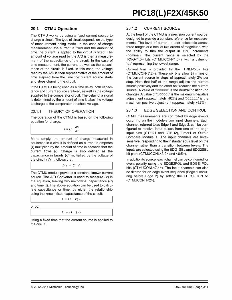
PIC18(L)F2X/45K50
20.1 CTMU Operation
The CTMU works by using a fixed current source tocharge a circuit. The type of circuit depends on the typeof measurement being made. In the case of chargemeasurement, the current is fixed and the amount oftime the current is applied to the circuit is fixed. Theamount of voltage read by the A/D is then a measure-ment of the capacitance of the circuit. In the case oftime measurement, the current, as well as the capaci-tance of the circuit, is fixed. In this case, the voltageread by the A/D is then representative of the amount oftime elapsed from the time the current source startsand stops charging the circuit.
If the CTMU is being used as a time delay, both capaci-tance and current source are fixed, as well as the voltagesupplied to the comparator circuit. The delay of a signalis determined by the amount of time it takes the voltageto charge to the comparator threshold voltage.
20.1.1 THEORY OF OPERATION
The operation of the CTMU is based on the followingequation for charge:
More simply, the amount of charge measured incoulombs in a circuit is defined as current in amperes(I) multiplied by the amount of time in seconds that thecurrent flows (t). Charge is also defined as thecapacitance in farads (C) multiplied by the voltage ofthe circuit (V). It follows that:
The CTMU module provides a constant, known currentsource. The A/D Converter is used to measure (V) inthe equation, leaving two unknowns: capacitance (C)and time (t). The above equation can be used to calcu-late capacitance or time, by either the relationshipusing the known fixed capacitance of the circuit:
or by:
using a fixed time that the current source is applied tothe circuit.
20.1.2 CURRENT SOURCE
At the heart of the CTMU is a precision current source,designed to provide a constant reference for measure-ments. The level of current is user selectable acrossthree ranges or a total of two orders of magnitude, withthe ability to trim the output in ±2% increments(nominal). The current range is selected by theIRNG<1:0> bits (CTMUICON<1:0>), with a value of‘01’ representing the lowest range.
Current trim is provided by the ITRIM<5:0> bits(CTMUICON<7:2>). These six bits allow trimming ofthe current source in steps of approximately 2% perstep. Note that half of the range adjusts the currentsource positively and the other half reduces the currentsource. A value of ‘000000’ is the neutral position (nochange). A value of ‘100001’ is the maximum negativeadjustment (approximately -62%) and ‘011111’ is themaximum positive adjustment (approximately +62%).
20.1.3 EDGE SELECTION AND CONTROL
CTMU measurements are controlled by edge eventsoccurring on the module’s two input channels. Eachchannel, referred to as Edge 1 and Edge 2, can be con-figured to receive input pulses from one of the edgeinput pins (CTED1 and CTED2), Timer1 or OutputCompare Module 1. The input channels are level-sensitive, responding to the instantaneous level on thechannel rather than a transition between levels. Theinputs are selected using the EDG1SEL and EDG2SELbit pairs (CTMUCONL<3:2> and <6:5>).
In addition to source, each channel can be configured forevent polarity using the EDGE2POL and EDGE1POLbits (CTMUCONL<7,4>). The input channels can alsobe filtered for an edge event sequence (Edge 1 occur-ring before Edge 2) by setting the EDGSEQEN bit(CTMUCONH<2>).
I = C •dVdT
I t C V.=
t C V I=
C I t V=
2012-2014 Microchip Technology Inc. DS30000684B-page 311
PIC18(L)F2X/45K50
20.1.4 EDGE STATUS
The CTMUCONL register also contains two status bits:EDG2STAT and EDG1STAT (CTMUCONL<1:0>).Their primary function is to show if an edge responsehas occurred on the corresponding channel. TheCTMU automatically sets a particular bit when an edgeresponse is detected on its channel. The level-sensitivenature of the input channels also means that the statusbits become set immediately if the channel’s configura-tion is changed and is the same as the channel’scurrent state.
The module uses the edge status bits to control the cur-rent source output to external analog modules (such asthe A/D Converter). Current is only supplied to externalmodules when only one (but not both) of the status bitsis set, and shuts current off when both bits are eitherset or cleared. This allows the CTMU to measure cur-rent only during the interval between edges. After bothstatus bits are set, it is necessary to clear them beforeanother measurement is taken. Both bits should becleared simultaneously, if possible, to avoid re-enablingthe CTMU current source.
In addition to being set by the CTMU hardware, theedge status bits can also be set by software. This isalso the user’s application to manually enable ordisable the current source. Setting either one (but notboth) of the bits enables the current source. Setting orclearing both bits at once disables the source.
20.1.5 INTERRUPTS
The CTMU sets its interrupt flag (PIR3<3>) wheneverthe current source is enabled, then disabled. Aninterrupt is generated only if the correspondinginterrupt enable bit (PIE3<3>) is also set. If edgesequencing is not enabled (i.e., Edge 1 must occurbefore Edge 2), it is necessary to monitor the edgeStatus bits and determine which edge occurred last andcaused the interrupt.
20.2 CTMU Module Initialization
The following sequence is a general guideline used toinitialize the CTMU module:
1. Select the current source range using the IRNGbits (CTMUICON<1:0>).
2. Adjust the current source trim using the ITRIMbits (CTMUICON<7:2>).
3. Configure the edge input sources for Edge 1 andEdge 2 by setting the EDG1SEL and EDG2SELbits (CTMUCONL<3:2 and 6:5>).
4. Configure the input polarities for the edge inputsusing the EDG1POL and EDG2POL bits(CTMUCONL<4,7>). The default configurationis for negative edge polarity (high-to-lowtransitions).
5. Enable edge sequencing using the EDGSEQENbit (CTMUCONH<2>). By default, edgesequencing is disabled.
6. Select the operating mode (Measurement orTime Delay) with the TGEN bit. The defaultmode is Time/Capacitance Measurement.
7. Discharge the connected circuit by setting theIDISSEN bit (CTMUCONH<1>); after waiting asufficient time for the circuit to discharge, clearIDISSEN.
8. Disable the module by clearing the CTMUEN bit(CTMUCONH<7>).
9. Enable the module by setting the CTMUEN bit.
10. Clear the Edge Status bits: EDG2STAT andEDG1STAT (CTMUCONL<1:0>).
11. Enable both edge inputs by setting the EDGENbit (CTMUCONH<3>).
Depending on the type of measurement or pulsegeneration being performed, one or more additionalmodules may also need to be initialized and configuredwith the CTMU module:
• Edge Source Generation: In addition to the external edge input pins, both Timer1 and the Output Compare/PWM1 module can be used as edge sources for the CTMU.
• Capacitance or Time Measurement: The CTMU module uses the A/D Converter to measure the voltage across a capacitor that is connected to one of the analog input channels.
• Pulse Generation: When generating system clock independent output pulses, the CTMU module uses Comparator 2 and the associated comparator voltage reference.
DS30000684B-page 312 2012-2014 Microchip Technology Inc.
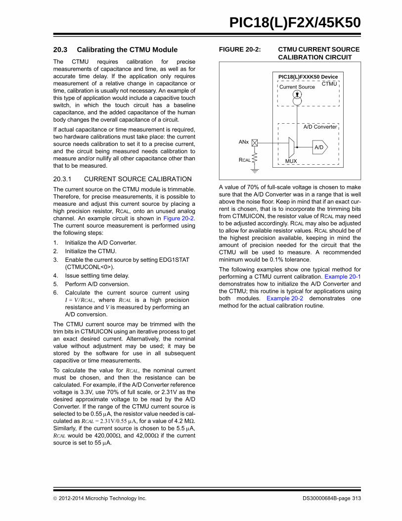
PIC18(L)F2X/45K50
20.3 Calibrating the CTMU Module
The CTMU requires calibration for precisemeasurements of capacitance and time, as well as foraccurate time delay. If the application only requiresmeasurement of a relative change in capacitance ortime, calibration is usually not necessary. An example ofthis type of application would include a capacitive touchswitch, in which the touch circuit has a baselinecapacitance, and the added capacitance of the humanbody changes the overall capacitance of a circuit.
If actual capacitance or time measurement is required,two hardware calibrations must take place: the currentsource needs calibration to set it to a precise current,and the circuit being measured needs calibration tomeasure and/or nullify all other capacitance other thanthat to be measured.
20.3.1 CURRENT SOURCE CALIBRATION
The current source on the CTMU module is trimmable.Therefore, for precise measurements, it is possible tomeasure and adjust this current source by placing ahigh precision resistor, RCAL, onto an unused analogchannel. An example circuit is shown in Figure 20-2.The current source measurement is performed usingthe following steps:
1. Initialize the A/D Converter.
2. Initialize the CTMU.
3. Enable the current source by setting EDG1STAT(CTMUCONL<0>).
4. Issue settling time delay.
5. Perform A/D conversion.
6. Calculate the current source current usingI = V/RCAL, where RCAL is a high precisionresistance and V is measured by performing anA/D conversion.
The CTMU current source may be trimmed with thetrim bits in CTMUICON using an iterative process to getan exact desired current. Alternatively, the nominalvalue without adjustment may be used; it may bestored by the software for use in all subsequentcapacitive or time measurements.
To calculate the value for RCAL, the nominal currentmust be chosen, and then the resistance can becalculated. For example, if the A/D Converter referencevoltage is 3.3V, use 70% of full scale, or 2.31V as thedesired approximate voltage to be read by the A/DConverter. If the range of the CTMU current source isselected to be 0.55 A, the resistor value needed is cal-culated as RCAL = 2.31V/0.55 A, for a value of 4.2 MΩ.Similarly, if the current source is chosen to be 5.5 A,RCAL would be 420,000Ω, and 42,000Ω if the currentsource is set to 55 A.
FIGURE 20-2: CTMU CURRENT SOURCE CALIBRATION CIRCUIT
A value of 70% of full-scale voltage is chosen to makesure that the A/D Converter was in a range that is wellabove the noise floor. Keep in mind that if an exact cur-rent is chosen, that is to incorporate the trimming bitsfrom CTMUICON, the resistor value of RCAL may needto be adjusted accordingly. RCAL may also be adjustedto allow for available resistor values. RCAL should be ofthe highest precision available, keeping in mind theamount of precision needed for the circuit that theCTMU will be used to measure. A recommendedminimum would be 0.1% tolerance.
The following examples show one typical method forperforming a CTMU current calibration. Example 20-1demonstrates how to initialize the A/D Converter andthe CTMU; this routine is typical for applications usingboth modules. Example 20-2 demonstrates onemethod for the actual calibration routine.
PIC18(L)FXXK50 Device
A/D Converter
CTMU
ANx
RCAL
Current Source
MUX
A/D
2012-2014 Microchip Technology Inc. DS30000684B-page 313

PIC18(L)F2X/45K50
EXAMPLE 20-1: SETUP FOR CTMU CALIBRATION ROUTINES
#include "p18cxxx.h"/**************************************************************************//*Set up CTMU *****************************************************************//**************************************************************************/void setup(void)
//CTMUCONH/1 - CTMU Control registers CTMUCONH = 0x00; //make sure CTMU is disabled CTMUCONL = 0x90; //CTMU continues to run when emulator is stopped,CTMU continues //to run in idle mode,Time Generation mode disabled, Edges are blocked //No edge sequence order, Analog current source not grounded, trigger //output disabled, Edge2 polarity = positive level, Edge2 source = //source 0, Edge1 polarity = positive level, Edge1 source = source 0, //CTMUICON - CTMU Current Control Register CTMUICON = 0x01; //0.55uA, Nominal - No Adjustment /**************************************************************************///Set up AD converter;/**************************************************************************/
TRISA=0x04; //set channel 2 as an input // Configure AN2 as an analog channel
ANSELAbits.ANSA2=1;TRISAbits.TRISA2=1;
// ADCON2 ADCON2bits.ADFM=1; // Results format 1= Right justified ADCON2bits.ACQT=1; // Acquition time 7 = 20TAD 2 = 4TAD 1=2TAD ADCON2bits.ADCS=2; // Clock conversion bits 6= FOSC/64 2=FOSC/32
// ADCON1 ADCON1bits.PVCFG0 =0; // Vref+ = AVdd ADCON1bits.NVCFG1 =0; // Vref- = AVss // ADCON0 ADCON0bits.CHS=2; // Select ADC channel
ADCON0bits.ADON=1; // Turn on ADC
DS30000684B-page 314 2012-2014 Microchip Technology Inc.

PIC18(L)F2X/45K50
EXAMPLE 20-2: CURRENT CALIBRATION ROUTINE#include "p18cxxx.h"
#define COUNT 500 //@ 8MHz = 125uS.#define DELAY for(i=0;i<COUNT;i++)#define RCAL .027 //R value is 4200000 (4.2M) //scaled so that result is in //1/100th of uA#define ADSCALE 1023 //for unsigned conversion 10 sig bits#define ADREF 3.3 //Vdd connected to A/D Vr+
int main(void) int i; int j = 0; //index for loop unsigned int Vread = 0; double VTot = 0; float Vavg=0, Vcal=0, CTMUISrc = 0; //float values stored for calcs
//assume CTMU and A/D have been set up correctly//see Example 25-1 for CTMU & A/D setupsetup();
CTMUCONHbits.CTMUEN = 1; //Enable the CTMUCTMUCONLbits.EDG1STAT = 0; // Set Edge status bits to zeroCTMUCONLbits.EDG2STAT = 0; for(j=0;j<10;j++) CTMUCONHbits.IDISSEN = 1; //drain charge on the circuit DELAY; //wait 125us CTMUCONHbits.IDISSEN = 0; //end drain of circuit CTMUCONLbits.EDG1STAT = 1; //Begin charging the circuit //using CTMU current source DELAY; //wait for 125us CTMUCONLbits.EDG1STAT = 0; //Stop charging circuit PIR1bits.ADIF = 0; //make sure A/D Int not set ADCON0bits.GO=1; //and begin A/D conv. while(!PIR1bits.ADIF); //Wait for A/D convert complete Vread = ADRES; //Get the value from the A/D PIR1bits.ADIF = 0; //Clear A/D Interrupt Flag VTot += Vread; //Add the reading to the total Vavg = (float)(VTot/10.000); //Average of 10 readings Vcal = (float)(Vavg/ADSCALE*ADREF); CTMUISrc = Vcal/RCAL; //CTMUISrc is in 1/100ths of uA
2012-2014 Microchip Technology Inc. DS30000684B-page 315

PIC18(L)F2X/45K50
20.3.2 CAPACITANCE CALIBRATION
There is a small amount of capacitance from theinternal A/D Converter sample capacitor as well asstray capacitance from the circuit board traces andpads that affect the precision of capacitancemeasurements. A measurement of the straycapacitance can be taken by making sure the desiredcapacitance to be measured has been removed. Themeasurement is then performed using the followingsteps:
1. Initialize the A/D Converter and the CTMU.
2. Set EDG1STAT (= 1).
3. Wait for a fixed delay of time t.
4. Clear EDG1STAT.
5. Perform an A/D conversion.
6. Calculate the stray and A/D sample capacitances:
where I is known from the current source measurementstep, t is a fixed delay and V is measured by performingan A/D conversion.
This measured value is then stored and used forcalculations of time measurement or subtracted forcapacitance measurement. For calibration, it isexpected that the capacitance of CSTRAY + CAD isapproximately known. CAD is approximately 4 pF.
An iterative process may need to be used to adjust thetime, t, that the circuit is charged to obtain a reasonablevoltage reading from the A/D Converter. The value of tmay be determined by setting COFFSET to a theoreticalvalue, then solving for t. For example, if CSTRAY istheoretically calculated to be 11 pF, and V is expectedto be 70% of VDD, or 2.31V, then t would be:
or 63 s.
See Example 20-3 for a typical routine for CTMUcapacitance calibration.
COFFSET CSTRAY CAD+ I t V= =
(4 pF + 11 pF) • 2.31V/0.55 A
DS30000684B-page 316 2012-2014 Microchip Technology Inc.

PIC18(L)F2X/45K50
EXAMPLE 20-3: CAPACITANCE CALIBRATION ROUTINE
#include "p18cxxx.h"
#define COUNT 25 //@ 8MHz INTFRC = 62.5 us.#define ETIME COUNT*2.5 //time in uS#define DELAY for(i=0;i<COUNT;i++)#define ADSCALE 1023 //for unsigned conversion 10 sig bits#define ADREF 3.3 //Vdd connected to A/D Vr+#define RCAL .027 //R value is 4200000 (4.2M) //scaled so that result is in //1/100th of uA
int main(void) int i; int j = 0; //index for loop unsigned int Vread = 0; float CTMUISrc, CTMUCap, Vavg, VTot, Vcal;
//assume CTMU and A/D have been set up correctly//see Example 25-1 for CTMU & A/D setupsetup();
CTMUCONHbits.CTMUEN = 1; //Enable the CTMUCTMUCONLbits.EDG1STAT = 0; // Set Edge status bits to zeroCTMUCONLbits.EDG2STAT = 0; for(j=0;j<10;j++) CTMUCONHbits.IDISSEN = 1; //drain charge on the circuit DELAY; //wait 125us CTMUCONHbits.IDISSEN = 0; //end drain of circuit CTMUCONLbits.EDG1STAT = 1; //Begin charging the circuit //using CTMU current source DELAY; //wait for 125us CTMUCONLbits.EDG1STAT = 0; //Stop charging circuit PIR1bits.ADIF = 0; //make sure A/D Int not set ADCON0bits.GO=1; //and begin A/D conv. while(!PIR1bits.ADIF); //Wait for A/D convert complete Vread = ADRES; //Get the value from the A/D PIR1bits.ADIF = 0; //Clear A/D Interrupt Flag VTot += Vread; //Add the reading to the total Vavg = (float)(VTot/10.000); //Average of 10 readings Vcal = (float)(Vavg/ADSCALE*ADREF); CTMUISrc = Vcal/RCAL; //CTMUISrc is in 1/100ths of uA CTMUCap = (CTMUISrc*ETIME/Vcal)/100;
2012-2014 Microchip Technology Inc. DS30000684B-page 317

PIC18(L)F2X/45K50
20.4 Measuring Capacitance with the CTMU
There are two separate methods of measuringcapacitance with the CTMU. The first is the absolutemethod, in which the actual capacitance value isdesired. The second is the relative method, in whichthe actual capacitance is not needed, rather anindication of a change in capacitance is required.
20.4.1 ABSOLUTE CAPACITANCE MEASUREMENT
For absolute capacitance measurements, both thecurrent and capacitance calibration steps found inSection 20.3 “Calibrating the CTMU Module”should be followed. Capacitance measurements arethen performed using the following steps:
1. Initialize the A/D Converter.
2. Initialize the CTMU.
3. Set EDG1STAT.
4. Wait for a fixed delay, T.
5. Clear EDG1STAT.
6. Perform an A/D conversion.
7. Calculate the total capacitance, CTOTAL = (I * T)/V,where I is known from the current sourcemeasurement step (see Section 20.3.1 “CurrentSource Calibration”), T is a fixed delay and V ismeasured by performing an A/D conversion.
8. Subtract the stray and A/D capacitance(COFFSET from Section 20.3.2 “CapacitanceCalibration”) from CTOTAL to determine themeasured capacitance.
20.4.2 RELATIVE CHARGE MEASUREMENT
An application may not require precise capacitancemeasurements. For example, when detecting a validpress of a capacitance-based switch, detecting a rela-tive change of capacitance is of interest. In this type ofapplication, when the switch is open (or not touched),the total capacitance is the capacitance of the combina-tion of the board traces, the A/D Converter, etc. A largervoltage will be measured by the A/D Converter. Whenthe switch is closed (or is touched), the totalcapacitance is larger due to the addition of thecapacitance of the human body to the above listedcapacitances, and a smaller voltage will be measuredby the A/D Converter.
Detecting capacitance changes is easily accomplishedwith the CTMU using these steps:
1. Initialize the A/D Converter and the CTMU.
2. Set EDG1STAT.
3. Wait for a fixed delay.
4. Clear EDG1STAT.
5. Perform an A/D conversion.
The voltage measured by performing the A/Dconversion is an indication of the relative capacitance.Note that in this case, no calibration of the currentsource or circuit capacitance measurement is needed.See Example 20-4 for a sample software routine for acapacitive touch switch.
DS30000684B-page 318 2012-2014 Microchip Technology Inc.

PIC18(L)F2X/45K50
EXAMPLE 20-4: ROUTINE FOR CAPACITIVE TOUCH SWITCH
#include "p18cxxx.h"
#define COUNT 500 //@ 8MHz = 125uS.#define DELAY for(i=0;i<COUNT;i++)#define OPENSW 1000 //Un-pressed switch value#define TRIP 300 //Difference between pressed //and un-pressed switch#define HYST 65 //amount to change //from pressed to un-pressed#define PRESSED 1#define UNPRESSED 0
int main(void) unsigned int Vread; //storage for reading unsigned int switchState; int i; //assume CTMU and A/D have been set up correctly //see Example 25-1 for CTMU & A/D setup setup(); CTMUCONHbits.CTMUEN = 1; // Enable the CTMU CTMUCONLbits.EDG1STAT = 0; // Set Edge status bits to zero CTMUCONLbits.EDG2STAT = 0; CTMUCONHbits.IDISSEN = 1; //drain charge on the circuit DELAY; //wait 125us CTMUCONHbits.IDISSEN = 0; //end drain of circuit CTMUCONLbits.EDG1STAT = 1; //Begin charging the circuit //using CTMU current source DELAY; //wait for 125us CTMUCONLbits.EDG1STAT = 0; //Stop charging circuit PIR1bits.ADIF = 0; //make sure A/D Int not set ADCON0bits.GO=1; //and begin A/D conv. while(!PIR1bits.ADIF); //Wait for A/D convert complete Vread = ADRES; //Get the value from the A/D if(Vread < OPENSW - TRIP) switchState = PRESSED; else if(Vread > OPENSW - TRIP + HYST) switchState = UNPRESSED;
2012-2014 Microchip Technology Inc. DS30000684B-page 319

PIC18(L)F2X/45K50
20.5 Measuring Time with the CTMU Module
Time can be precisely measured after the ratio (C/I) ismeasured from the current and capacitance calibrationstep by following these steps:
1. Initialize the A/D Converter and the CTMU.
2. Set EDG1STAT.
3. Set EDG2STAT.
4. Perform an A/D conversion.
5. Calculate the time between edges as T = (C/I) * V,where I is calculated in the current calibration step(Section 20.3.1 “Current Source Calibration”),C is calculated in the capacitance calibration step(Section 20.3.2 “Capacitance Calibration”) andV is measured by performing the A/D conversion.
It is assumed that the time measured is small enoughthat the capacitance, COFFSET, provides a valid voltageto the A/D Converter. For the smallest time measure-ment, always set the A/D Channel Select register(AD1CHS) to an unused A/D channel; the correspond-ing pin for which is not connected to any circuit boardtrace. This minimizes added stray capacitance, keep-ing the total circuit capacitance close to that of the A/DConverter itself (4-5 pF). To measure longer timeintervals, an external capacitor may be connected to anA/D channel and this channel selected when making atime measurement.
FIGURE 20-3: TYPICAL CONNECTIONS AND INTERNAL CONFIGURATION FOR TIME MEASUREMENT
A/D Converter
CTMUCTED1
CTED2
ANX
Output Pulse
EDG1
EDG2
CAD
RPR
Current Source
PIC18(L)FXXK22 Device
DS30000684B-page 320 2012-2014 Microchip Technology Inc.
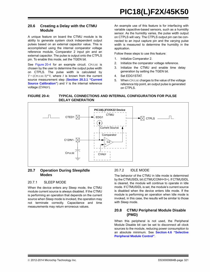
PIC18(L)F2X/45K50
20.6 Creating a Delay with the CTMU Module
A unique feature on board the CTMU module is itsability to generate system clock independent outputpulses based on an external capacitor value. This isaccomplished using the internal comparator voltagereference module, Comparator 2 input pin and anexternal capacitor. The pulse is output onto the CTPLSpin. To enable this mode, set the TGEN bit.
See Figure 20-4 for an example circuit. CPULSE ischosen by the user to determine the output pulse widthon CTPLS. The pulse width is calculated byT = (CPULSE/I)*V, where I is known from the currentsource measurement step (Section 20.3.1 “CurrentSource Calibration”) and V is the internal referencevoltage (CVREF).
An example use of this feature is for interfacing withvariable capacitive-based sensors, such as a humiditysensor. As the humidity varies, the pulse width outputon CTPLS will vary. The CTPLS output pin can be con-nected to an input capture pin and the varying pulsewidth is measured to determine the humidity in theapplication.
Follow these steps to use this feature:
1. Initialize Comparator 2.
2. Initialize the comparator voltage reference.
3. Initialize the CTMU and enable time delaygeneration by setting the TGEN bit.
4. Set EDG1STAT.
5. When CPULSE charges to the value of the voltagereference trip point, an output pulse is generatedon CTPLS.
FIGURE 20-4: TYPICAL CONNECTIONS AND INTERNAL CONFIGURATION FOR PULSE DELAY GENERATION
20.7 Operation During Sleep/Idle Modes
20.7.1 SLEEP MODE
When the device enters any Sleep mode, the CTMUmodule current source is always disabled. If the CTMUis performing an operation that depends on the currentsource when Sleep mode is invoked, the operation maynot terminate correctly. Capacitance and timemeasurements may return erroneous values.
20.7.2 IDLE MODE
The behavior of the CTMU in Idle mode is determinedby the CTMUSIDL bit (CTMUCONH<5>). If CTMUSIDLis cleared, the module will continue to operate in Idlemode. If CTMUSIDL is set, the module’s current sourceis disabled when the device enters Idle mode. If themodule is performing an operation when Idle mode isinvoked, in this case, the results will be similar to thosewith Sleep mode.
20.8 CTMU Peripheral Module Disable (PMD)
When this peripheral is not used, the PeripheralModule Disable bit can be set to disconnect all clocksources to the module, reducing power consumption toan absolute minimum. See Section 4.6 “SelectivePeripheral Module Control”.
C2
CVREF
CTPLS
PIC18(L)FXXK22 Device
Current Source
Comparator
CTMUCTED1
C12IN1-
CPULSE
EDG1
2012-2014 Microchip Technology Inc. DS30000684B-page 321

PIC18(L)F2X/45K50
20.9 Effects of a Reset on CTMU
Upon Reset, all registers of the CTMU are cleared. Thisleaves the CTMU module disabled, its current source isturned off and all configuration options return to theirdefault settings. The module needs to be re-initializedfollowing any Reset.
If the CTMU is in the process of taking a measurement atthe time of Reset, the measurement will be lost. A partialcharge may exist on the circuit that was being measured,and should be properly discharged before the CTMUmakes subsequent attempts to make a measurement.The circuit is discharged by setting and then clearing theIDISSEN bit (CTMUCONH<1>) while the A/D Converteris connected to the appropriate channel.
20.10 Registers
There are three control registers for the CTMU:
• CTMUCONH
• CTMUCONL
• CTMUICON
The CTMUCONH and CTMUCONL registers(Register 20-1 and Register 20-2) contain control bitsfor configuring the CTMU module edge source selec-tion, edge source polarity selection, edge sequencing,A/D trigger, analog circuit capacitor discharge andenables. The CTMUICON register (Register 20-3) hasbits for selecting the current source range and currentsource trim.
20.11 Register Definitions: CTMU Control
REGISTER 20-1: CTMUCONH: CTMU CONTROL REGISTER 0
R/W-0 U-0 R/W-0 R/W-0 R/W-0 R/W-0 R/W-0 U-0
CTMUEN — CTMUSIDL TGEN EDGEN EDGSEQEN IDISSEN CTTRIG
bit 7 bit 0
Legend:
R = Readable bit W = Writable bit U = Unimplemented bit, read as ‘0’
-n = Value at POR ‘1’ = Bit is set ‘0’ = Bit is cleared x = Bit is unknown
bit 7 CTMUEN: CTMU Enable bit
1 = Module is enabled0 = Module is disabled
bit 6 Unimplemented: Read as ‘0’
bit 5 CTMUSIDL: Stop in Idle Mode bit
1 = Discontinue module operation when device enters Idle mode0 = Continue module operation in Idle mode
bit 4 TGEN: Time Generation Enable bit
1 = Enables edge delay generation0 = Disables edge delay generation
bit 3 EDGEN: Edge Enable bit
1 = Edges are not blocked0 = Edges are blocked
bit 2 EDGSEQEN: Edge Sequence Enable bit
1 = Edge 1 event must occur before Edge 2 event can occur0 = No edge sequence is needed
bit 1 IDISSEN: Analog Current Source Control bit
1 = Analog current source output is grounded0 = Analog current source output is not grounded
bit 0 CTTRIG: CTMU Special Event Trigger Control Bit
1 = CTMU Special Event Trigger is enabled0 = CTMU Special Event Trigger is disabled
DS30000684B-page 322 2012-2014 Microchip Technology Inc.

PIC18(L)F2X/45K50
REGISTER 20-2: CTMUCONL: CTMU CONTROL REGISTER 1
R/W-0 R/W-0 R/W-0 R/W-0 R/W-0 R/W-0 R/W-0 R/W-0
EDG2POL EDG2SEL<1:0> EDG1POL EDG1SEL<1:0> EDG2STAT EDG1STAT
bit 7 bit 0
Legend:
R = Readable bit W = Writable bit U = Unimplemented bit, read as ‘0’
-n = Value at POR ‘1’ = Bit is set ‘0’ = Bit is cleared x = Bit is unknown
bit 7 EDG2POL: Edge 2 Polarity Select bit
1 = Edge 2 programmed for a positive edge response0 = Edge 2 programmed for a negative edge response
bit 6-5 EDG2SEL<1:0>: Edge 2 Source Select bits
11 = CTED1 pin10 = CTED2 pin01 = ECCP1 Special Event Trigger00 = CCP2 Special Event Trigger
bit 4 EDG1POL: Edge 1 Polarity Select bit
1 = Edge 1 programmed for a positive edge response0 = Edge 1 programmed for a negative edge response
bit 3-2 EDG1SEL<1:0>: Edge 1 Source Select bits
11 = CTED1 pin10 = CTED2 pin01 = ECCP1 Special Event Trigger00 = CCP2 Special Event Trigger
bit 1 EDG2STAT: Edge 2 Status bit
1 = Edge 2 event has occurred0 = Edge 2 event has not occurred
bit 0 EDG1STAT: Edge 1 Status bit
1 = Edge 1 event has occurred0 = Edge 1 event has not occurred
2012-2014 Microchip Technology Inc. DS30000684B-page 323

PIC18(L)F2X/45K50
REGISTER 20-3: CTMUICON: CTMU CURRENT CONTROL REGISTER
R/W-0 R/W-0 R/W-0 R/W-0 R/W-0 R/W-0 R/W-0 R/W-0
ITRIM<5:0> IRNG<1:0>
bit 7 bit 0
Legend:
R = Readable bit W = Writable bit U = Unimplemented bit, read as ‘0’
-n = Value at POR ‘1’ = Bit is set ‘0’ = Bit is cleared x = Bit is unknown
bit 7-2 ITRIM<5:0>: Current Source Trim bits
011111 = Maximum positive change from nominal current011110...000001 = Minimum positive change from nominal current000000 = Nominal current output specified by IRNG<1:0>111111 = Minimum negative change from nominal current...100010100001 = Maximum negative change from nominal current
bit 1-0 IRNG<1:0>: Current Source Range Select bits (see Table 29-14)
11 = 100 Base current10 = 10 Base current01 = Base current level00 = Current source disabled
TABLE 20-1: REGISTERS ASSOCIATED WITH CTMU MODULE
Name Bit 7 Bit 6 Bit 5 Bit 4 Bit 3 Bit 2 Bit 1 Bit 0Register on page
CTMUCONH CTMUEN — CTMUSIDL TGEN EDGEN EDGSEQEN IDISSEN CTTRIG 322
CTMUCONL EDG2POL EDG2SEL<1:0> EDG1POL EDG1SEL<1:0> EDG2STAT EDG1STAT 323
CTMUICON ITRIM<5:0> IRNG<1:0> 324
IPR3 — — — — CTMUIP USBIP TMR3GIP TMR1GIP 125
PIE3 — — — — CTMUIE USBIE TMR3GIE TMR1GIE 122
PIR3 — — — — CTMUIF USBIF TMR3GIF TMR1GIF 119
PMD1 — MSSPMD CTMUMD CMP2MD CMP1MD ADCMD CCP2MD CCP1MD 62
Legend: — = Unimplemented, read as ‘0’. Shaded bits are not used during CTMU operation.
DS30000684B-page 324 2012-2014 Microchip Technology Inc.
PIC18(L)F2X/45K50
21.0 SR LATCH
The module consists of a single SR latch with multipleSet and Reset inputs as well as separate latch outputs.The SR latch module includes the following features:
• Programmable input selection
• SR latch output is available internally/externally
• Selectable Q and Q output
• Firmware Set and Reset
The SR latch can be used in a variety of analogapplications, including oscillator circuits, one-shotcircuit, hysteretic controllers, and analog timingapplications.
21.1 Latch Operation
The latch is a Set-Reset Latch that does not depend ona clock source. Each of the Set and Reset inputs areactive-high. The latch can be set or reset by:
• Software control (SRPS and SRPR bits)
• Comparator C1 output (sync_C1OUT)
• Comparator C2 output (sync_C2OUT)
• SRI Pin
• Programmable clock (DIVSRCLK)
The SRPS and the SRPR bits of the SRCON0 registermay be used to set or reset the SR latch, respectively.The latch is Reset-dominant. Therefore, if both Set andReset inputs are high, the latch will go to the Resetstate. Both the SRPS and SRPR bits are self resettingwhich means that a single write to either of the bits is allthat is necessary to complete a latch Set or Resetoperation.
The output from Comparator C1 or C2 can be used asthe Set or Reset inputs of the SR latch. The output ofeither Comparator can be synchronized to the Timer1clock source. See Section 19.0 “ComparatorModule” and Section 13.0 “Timer1/3 Module withGate Control” for more information.
An external source on the SRI pin can be used as theSet or Reset inputs of the SR latch.
An internal clock source, DIVSRCLK, is available and itcan periodically set or reset the SR latch. TheSRCLK<2:0> bits in the SRCON0 register are used toselect the clock source period. The SRSCKE andSRRCKE bits of the SRCON1 register enable the clocksource to set or reset the SR latch, respectively.
21.2 Latch Output
The SRQEN and SRNQEN bits of the SRCON0 registercontrol the Q and Q latch outputs. Both of the SR latchoutputs may be directly output to I/O pins at the sametime. Control is determined by the state of bits SRQENand SRNQEN in the SRCON0 register.
The applicable TRIS bit of the corresponding port mustbe cleared to enable the port pin output driver.
21.3 DIVSRCLK Clock Generation
The DIVSRCLK clock signal is generated from theperipheral clock which is pre-scaled by a valuedetermined by the SRCLK<2:0> bits. See Figure 21-1and Table 21-1 for additional detail.
21.4 Effects of a Reset
Upon any device Reset, the SR latch is not initialized,and the SRQ and SRNQ outputs are unknown. Theuser’s firmware is responsible to initialize the latchoutput before enabling it to the output pins.
2012-2014 Microchip Technology Inc. DS30000684B-page 325
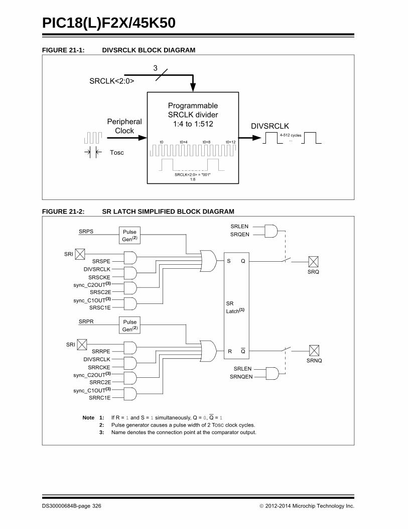
PIC18(L)F2X/45K50
FIGURE 21-1: DIVSRCLK BLOCK DIAGRAM
FIGURE 21-2: SR LATCH SIMPLIFIED BLOCK DIAGRAM
3
SRCLK<2:0>
PeripheralClock
DIVSRCLK
ProgrammableSRCLK divider
1:4 to 1:512
Tosc
4-512 cycles...
SRCLK<2:0> = "001"1:8
t0+4t0 t0+8 t0+12
SRPS
S
R
Q
Q
Note 1: If R = 1 and S = 1 simultaneously, Q = 0, Q = 12: Pulse generator causes a pulse width of 2 TOSC clock cycles.3: Name denotes the connection point at the comparator output.
Pulse
Gen(2)
SR
Latch(1)
SRQEN
SRSPE
SRSC2E
SRSCKE
DIVSRCLK
sync_C2OUT(3)
SRSC1Esync_C1OUT(3)
SRPR Pulse
Gen(2)
SRRPE
SRRC2E
SRRCKE
DIVSRCLK
sync_C2OUT(3)
SRRC1Esync_C1OUT(3)
SRLEN
SRNQEN
SRLEN
SRQ
SRNQ
SRI
SRI
DS30000684B-page 326 2012-2014 Microchip Technology Inc.

PIC18(L)F2X/45K50
TABLE 21-1: DIVSRCLK FREQUENCY TABLE
SRCLK<2:0> Divider FOSC = 20 MHz FOSC = 16 MHz FOSC = 8 MHz FOSC = 4 MHz FOSC = 1 MHz
111 512 25.6 s 32 s 64 s 128 s 512 s
110 256 12.8 s 16 s 32 s 64 s 256 s
101 128 6.4 s 8 s 16 s 32 s 128 s
100 64 3.2 s 4 s 8 s 16 s 64 s
011 32 1.6 s 2 s 4 s 8 s 32 s
010 16 0.8 s 1 s 2 s 4 s 16 s
001 8 0.4 s 0.5 s 1 s 2 s 8 s
000 4 0.2 s 0.25 s 0.5 s 1 s 4 s
2012-2014 Microchip Technology Inc. DS30000684B-page 327

PIC18(L)F2X/45K50
21.5 Register Definitions: SR Latch Control
REGISTER 21-1: SRCON0: SR LATCH CONTROL REGISTER
R/W-0 R/W-0 R/W-0 R/W-0 R/W-0 R/W-0 R/W-0 R/W-0
SRLEN SRCLK<2:0> SRQEN SRNQEN SRPS SRPR
bit 7 bit 0
Legend:
R = Readable bit W = Writable bit U = Unimplemented C = Clearable only bit
-n = Value at POR ‘1’ = Bit is set ‘0’ = Bit is cleared x = Bit is unknown
bit 7 SRLEN: SR Latch Enable bit(1)
1 = SR latch is enabled0 = SR latch is disabled
bit 6-4 SRCLK<2:0>: SR Latch Clock Divider Bits
000 = Generates a 2 TOSC wide pulse on DIVSRCLK every 4 peripheral clock cycles001 = Generates a 2 TOSC wide pulse on DIVSRCLK every 8 peripheral clock cycles010 = Generates a 2 TOSC wide pulse on DIVSRCLK every 16 peripheral clock cycles011 = Generates a 2 TOSC wide pulse on DIVSRCLK every 32 peripheral clock cycles100 = Generates a 2 TOSC wide pulse on DIVSRCLK every 64 peripheral clock cycles101 = Generates a 2 TOSC wide pulse on DIVSRCLK every 128 peripheral clock cycles110 = Generates a 2 TOSC wide pulse on DIVSRCLK every 256 peripheral clock cycles111 = Generates a 2 TOSC wide pulse on DIVSRCLK every 512 peripheral clock cycles
bit 3 SRQEN: SR Latch Q Output Enable bit
1 = Q is present on the SRQ pin0 = Q is internal only
bit 2 SRNQEN: SR Latch Q Output Enable bit
1 = Q is present on the SRNQ pin0 = Q is internal only
bit 1 SRPS: Pulse Set Input of the SR Latch bit(2)
1 = Pulse set input for 2 TOSC clock cycles0 = No effect on set input
bit 0 SRPR: Pulse Reset Input of the SR Latch bit(2)
1 = Pulse Reset input for 2 TOSC clock cycles0 = No effect on Reset input
Note 1: Changing the SRCLK bits while the SR latch is enabled may cause false triggers to the Set and Reset inputs of the latch.
2: Set only, always reads back ‘0’.
DS30000684B-page 328 2012-2014 Microchip Technology Inc.

PIC18(L)F2X/45K50
REGISTER 21-2: SRCON1: SR LATCH CONTROL REGISTER 1
R/W-0 R/W-0 R/W-0 R/W-0 R/W-0 R/W-0 R/W-0 R/W-0
SRSPE SRSCKE SRSC2E SRSC1E SRRPE SRRCKE SRRC2E SRRC1E
bit 7 bit 0
Legend:
R = Readable bit W = Writable bit U = Unimplemented C = Clearable only bit
-n = Value at POR ‘1’ = Bit is set ‘0’ = Bit is cleared x = Bit is unknown
bit 7 SRSPE: SR Latch Peripheral Set Enable bit
1 = SRI pin status sets SR latch0 = SRI pin status has no effect on SR latch
bit 6 SRSCKE: SR Latch Set Clock Enable bit
1 = Set input of SR latch is pulsed with DIVSRCLK 0 = Set input of SR latch is not pulsed with DIVSRCLK
bit 5 SRSC2E: SR Latch C2 Set Enable bit
1 = C2 Comparator output sets SR latch0 = C2 Comparator output has no effect on SR latch
bit 4 SRSC1E: SR Latch C1 Set Enable bit
1 = C1 Comparator output sets SR latch0 = C1 Comparator output has no effect on SR latch
bit 3 SRRPE: SR Latch Peripheral Reset Enable bit
1 = SRI pin resets SR latch0 = SRI pin has no effect on SR latch
bit 2 SRRCKE: SR Latch Reset Clock Enable bit
1 = Reset input of SR latch is pulsed with DIVSRCLK 0 = Reset input of SR latch is not pulsed with DIVSRCLK
bit 1 SRRC2E: SR Latch C2 Reset Enable bit
1 = C2 Comparator output resets SR latch0 = C2 Comparator output has no effect on SR latch
bit 0 SRRC1E: SR Latch C1 Reset Enable bit
1 = C1 Comparator output resets SR latch0 = C1 Comparator output has no effect on SR latch
TABLE 21-2: REGISTERS ASSOCIATED WITH THE SR LATCH
Name Bit 7 Bit 6 Bit 5 Bit 4 Bit 3 Bit 2 Bit 1 Bit 0Register on page
SRCON0 SRLEN SRCLK<2:0> SRQEN SRNQEN SRPS SRPR 328
SRCON1 SRSPE SRSCKE SRSC2E SRSC1E SRRPE SRRCKE SRRC2E SRRC1E 329
TRISA TRISA7 TRISA6 TRISA5 TRISA4 TRISA3 TRISA2 TRISA1 TRISA0 149
TRISB TRISB7 TRISB6 TRISB5 TRISB4 TRISB3 TRISB2 TRISB1 TRISB0 149
WPUB WPUB7 WPUB6 WPUB5 WPUB4 WPUB3 WPUB2 WPUB1 WPUB0 150
Legend: Shaded bits are not used with this module.
2012-2014 Microchip Technology Inc. DS30000684B-page 329
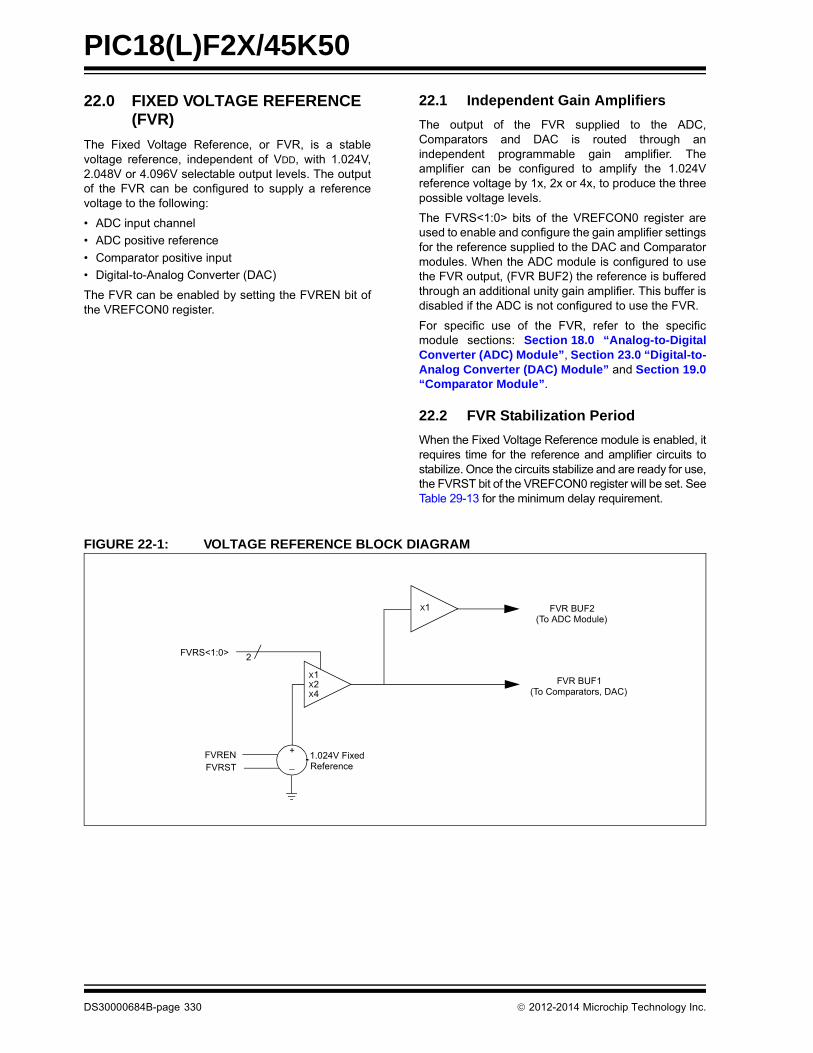
PIC18(L)F2X/45K50
22.0 FIXED VOLTAGE REFERENCE (FVR)
The Fixed Voltage Reference, or FVR, is a stablevoltage reference, independent of VDD, with 1.024V,2.048V or 4.096V selectable output levels. The outputof the FVR can be configured to supply a referencevoltage to the following:
• ADC input channel
• ADC positive reference
• Comparator positive input
• Digital-to-Analog Converter (DAC)
The FVR can be enabled by setting the FVREN bit ofthe VREFCON0 register.
22.1 Independent Gain Amplifiers
The output of the FVR supplied to the ADC,Comparators and DAC is routed through anindependent programmable gain amplifier. Theamplifier can be configured to amplify the 1.024Vreference voltage by 1x, 2x or 4x, to produce the threepossible voltage levels.
The FVRS<1:0> bits of the VREFCON0 register areused to enable and configure the gain amplifier settingsfor the reference supplied to the DAC and Comparatormodules. When the ADC module is configured to usethe FVR output, (FVR BUF2) the reference is bufferedthrough an additional unity gain amplifier. This buffer isdisabled if the ADC is not configured to use the FVR.
For specific use of the FVR, refer to the specificmodule sections: Section 18.0 “Analog-to-DigitalConverter (ADC) Module”, Section 23.0 “Digital-to-Analog Converter (DAC) Module” and Section 19.0“Comparator Module”.
22.2 FVR Stabilization Period
When the Fixed Voltage Reference module is enabled, itrequires time for the reference and amplifier circuits tostabilize. Once the circuits stabilize and are ready for use,the FVRST bit of the VREFCON0 register will be set. SeeTable 29-13 for the minimum delay requirement.
FIGURE 22-1: VOLTAGE REFERENCE BLOCK DIAGRAM
FVRS<1:0>
X1
X1X2X4
2
FVR BUF2(To ADC Module)
FVR BUF1(To Comparators, DAC)
+
_FVRENFVRST
1.024V FixedReference
DS30000684B-page 330 2012-2014 Microchip Technology Inc.

PIC18(L)F2X/45K50
22.3 Register Definitions: FVR Control
REGISTER 22-1: VREFCON0: FIXED VOLTAGE REFERENCE CONTROL REGISTER
R/W-0 R/W-0 R/W-0 R/W-1 U-0 U-0 U-0 U-0
FVREN FVRST FVRS<1:0> — — — —
bit 7 bit 0
Legend:
R = Readable bit W = Writable bit U = Unimplemented bit, read as ‘0’
u = Bit is unchanged x = Bit is unknown -n/n = Value at POR and BOR/Value at all other Resets
‘1’ = Bit is set ‘0’ = Bit is cleared
bit 7 FVREN: Fixed Voltage Reference Enable bit0 = Fixed Voltage Reference is disabled1 = Fixed Voltage Reference is enabled
bit 6 FVRST: Fixed Voltage Reference Ready Flag bit0 = Fixed Voltage Reference output is not ready or not enabled1 = Fixed Voltage Reference output is ready for use
bit 5-4 FVRS<1:0>: Fixed Voltage Reference Selection bits00 = Fixed Voltage Reference Peripheral output is off01 = Fixed Voltage Reference Peripheral output is 1x (1.024V)10 = Fixed Voltage Reference Peripheral output is 2x (2.048V)(1)
11 = Fixed Voltage Reference Peripheral output is 4x (4.096V)(1)
bit 3-2 Reserved: Read as ‘0’. Maintain these bits clear.
bit 1-0 Unimplemented: Read as ‘0’.
Note 1: Fixed Voltage Reference output cannot exceed VDD.
TABLE 22-1: SUMMARY OF REGISTERS ASSOCIATED WITH FIXED VOLTAGE REFERENCE
Name Bit 7 Bit 6 Bit 5 Bit 4 Bit 3 Bit 2 Bit 1 Bit 0Register on page
VREFCON0 FVREN FVRST FVRS<1:0> — — — — 331
Legend: — = unimplemented locations, read as ‘0’. Shaded bits are not used by the FVR module.
2012-2014 Microchip Technology Inc. DS30000684B-page 331

PIC18(L)F2X/45K50
23.0 DIGITAL-TO-ANALOG CONVERTER (DAC) MODULE
The Digital-to-Analog Converter supplies a variablevoltage reference, ratiometric with the input source,with 32 selectable output levels.
The input of the DAC can be connected to:
• External VREF pins
• VDD supply voltage
• FVR (Fixed Voltage Reference)
The output of the DAC can be configured to supply areference voltage to the following:
• Comparator positive input
• ADC input channel
• DACOUT pin
The Digital-to-Analog Converter (DAC) can be enabledby setting the DACEN bit of the VREFCON1 register.
23.1 Output Voltage Selection
The DAC has 32 voltage level ranges. The 32 levelsare set with the DACR<4:0> bits of the VREFCON2register.
The DAC output voltage is determined by the followingequations:
EQUATION 23-1: DAC OUTPUT VOLTAGE
23.2 Ratiometric Output Level
The DAC output value is derived using a resistor ladderwith each end of the ladder tied to a positive andnegative voltage reference input source. If the voltageof either input source fluctuates, a similar fluctuation willresult in the DAC output value.
The value of the individual resistors within the laddercan be found in Section 29.0 “ElectricalSpecifications”.
23.3 Low-Power Voltage State
In order for the DAC module to consume the leastamount of power, one of the two voltage reference inputsources to the resistor ladder must be disconnected.Either the positive voltage source, (VSRC+), or thenegative voltage source, (VSRC-) can be disabled.
The negative voltage source is disabled by setting theDACLPS bit in the VREFCON1 register. Clearing theDACLPS bit in the VREFCON1 register disables thepositive voltage source.
23.4 Output Clamped to Positive Voltage Source
The DAC output voltage can be set to VSRC+ with theleast amount of power consumption by performing thefollowing:
• Clearing the DACEN bit in the VREFCON1 register.
• Setting the DACLPS bit in the VREFCON1 register.
• Configuring the DACPSS bits to the proper positive source.
• Configuring the DACRx bits to ‘11111’ in the VREFCON2 register.
This is also the method used to output the voltage levelfrom the FVR to an output pin. See Section 23.6 “DACVoltage Reference Output” for more information.
23.5 Output Clamped to Negative Voltage Source
The DAC output voltage can be set to VSRC- with theleast amount of power consumption by performing thefollowing:
• Clearing the DACEN bit in the VREFCON1 register.
• Clearing the DACLPS bit in the VREFCON1 register.
• Configuring the DACPSS bits to the proper negative source.
• Configuring the DACRx bits to ‘00000’ in the VREFCON2 register.
This allows the comparator to detect a zero-crossingwhile not consuming additional current through the DACmodule.
23.6 DAC Voltage Reference Output
The DAC can be output to the DACOUT pin by settingthe DACOE bit of the VREFCON1 register to ‘1’.Selecting the DAC reference voltage for output on theDACOUT pin automatically overrides the digital outputbuffer and digital input threshold detector functions ofthat pin. Reading the DACOUT pin when it has beenconfigured for DAC reference voltage output will alwaysreturn a ‘0’.
Due to the limited current drive capability, a buffer mustbe used on the DAC voltage reference output forexternal connections to DACOUT. Figure 23-2 showsan example buffering technique.
VOUT VSRC+ VSRC-– DACR<4:0>
25-------------------------------
= + VSRC-
VSRC+ = VDD, VREF+ or FVR1
VSRC- = VSS or VREF-
DS30000684B-page 332 2012-2014 Microchip Technology Inc.

PIC18(L)F2X/45K50
FIGURE 23-1: DIGITAL-TO-ANALOG CONVERTER BLOCK DIAGRAM
FIGURE 23-2: VOLTAGE REFERENCE OUTPUT BUFFER EXAMPLE
32
-to
-1 M
UX
DACR<4:0>
R
VREF-
DACNSS
R
R
R
R
R
R
32DAC Output
DACOUT
5
(to Comparators andADC Modules)
DACOE
VDD
VREF+
DACPSS<1:0>
2
DACEN
Steps
Digital-to-Analog Converter (DAC)
FVR BUF1
R
VSRC-
VSRC+
VSS
DACLPS
11111
11110
00001
00000
1
0
Reserved 1110
0100
DACOUT Buffered DAC Output+–
DACModule
Voltage Reference
Output Impedance
R
PIC® MCU
2012-2014 Microchip Technology Inc. DS30000684B-page 333

PIC18(L)F2X/45K50
23.7 Operation During Sleep
When the device wakes up from Sleep through aninterrupt or a Watchdog Timer time-out, the contents ofthe VREFCON1 register are not affected. To minimizecurrent consumption in Sleep mode, the voltagereference should be disabled.
23.8 Effects of a Reset
A device Reset affects the following:
• DAC is disabled
• DAC output voltage is removed from the DACOUT pin
• The DACR<4:0> range select bits are cleared
23.9 Register Definitions: DAC Control
REGISTER 23-1: VREFCON1: VOLTAGE REFERENCE CONTROL REGISTER 0
R/W-0 R/W-0 R/W-0 U-0 R/W-0 R/W-0 U-0 R/W-0
DACEN DACLPS DACOE — DACPSS<1:0> — DACNSS
bit 7 bit 0
Legend:
R = Readable bit W = Writable bit U = Unimplemented bit, read as ‘0’
u = Bit is unchanged x = Bit is unknown -n/n = Value at POR and BOR/Value at all other Resets
‘1’ = Bit is set ‘0’ = Bit is cleared
bit 7 DACEN: DAC Enable bit1 = DAC is enabled0 = DAC is disabled
bit 6 DACLPS: DAC Low-Power Voltage Source Select bit
1 = DAC Positive reference source selected0 = DAC Negative reference source selected
bit 5 DACOE: DAC Voltage Output Enable bit1 = DAC voltage level is also an output on the DACOUT pin0 = DAC voltage level is disconnected from the DACOUT pin
bit 4 Unimplemented: Read as ‘0’
bit 3-2 DACPSS<1:0>: DAC Positive Source Select bits00 = VDD
01 = VREF+10 = FVR BUF1 output11 = Reserved, do not use
bit 1 Unimplemented: Read as ‘0’
bit 0 DACNSS: DAC Negative Source Select bits1 = VREF-0 = VSS
DS30000684B-page 334 2012-2014 Microchip Technology Inc.

PIC18(L)F2X/45K50
REGISTER 23-2: VREFCON2: VOLTAGE REFERENCE CONTROL REGISTER 1
U-0 U-0 U-0 R/W-0 R/W-0 R/W-0 R/W-0 R/W-0
— — — DACR<4:0>
bit 7 bit 0
Legend:
R = Readable bit W = Writable bit U = Unimplemented bit, read as ‘0’
u = Bit is unchanged x = Bit is unknown -n/n = Value at POR and BOR/Value at all other Resets
‘1’ = Bit is set ‘0’ = Bit is cleared
bit 7-5 Unimplemented: Read as ‘0’
bit 4-0 DACR<4:0>: DAC Voltage Output Select bits
VOUT = ((VSRC+) - (VSRC-))*(DACR<4:0>/(25)) + VSRC-
TABLE 23-1: REGISTERS ASSOCIATED WITH DAC MODULE
Name Bit 7 Bit 6 Bit 5 Bit 4 Bit 3 Bit 2 Bit 1 Bit 0Register on page
VREFCON1 DACEN DACLPS DACOE — DACPSS<1:0> — DACNSS 334
VREFCON2 — — — DACR<4:0> 335
Legend: — = Unimplemented locations, read as ‘0’. Shaded bits are not used by the DAC module.
2012-2014 Microchip Technology Inc. DS30000684B-page 335

PIC18(L)F2X/45K50
24.0 UNIVERSAL SERIAL BUS (USB)
This section describes the details of the USBperipheral. Because of the very specific nature of themodule, knowledge of USB is expected. Somehigh-level USB information is provided in Section 3.14“Oscillator Settings for USB” only for applicationdesign reference. Designers are encouraged to refer tothe official specification published by the USBImplementers Forum (USB-IF) for the latestinformation.
24.1 Overview of the USB Peripheral
PIC18F2X/45K50 devices contain a full-speed andlow-speed compatible USB Serial Interface Engine(SIE) that allows fast communication between any USB
host and the PIC microcontroller. The SIE can be inter-faced directly to the USB by utilizing the internal trans-ceiver.
Some special hardware features have been included toimprove performance. Dual access port memory in thedevice’s data memory space (USB RAM) has beensupplied to share direct memory access between themicrocontroller core and the SIE. Buffer descriptors arealso provided, allowing users to freely program end-point memory usage within the USB RAM space.Figure 24-1 presents a general overview of the USBperipheral and its features.
FIGURE 24-1: USB PERIPHERAL AND OPTIONS
1 kbyteUSB RAM
USBSIE
USB Control and
Transceiver
P
P
D+D-
Internal Pull-ups
FSENUPUEN
USB Clock from theOscillator Module
PIC18(L)F2XK50/PIC18(L)F45K50 Family
USB BusFS
Note 1: The internal pull-up resistors should be disabled (UPUEN = 0) if external pull-up resistors are used.
2: PIC18F2X/45K50 devices only.
3: See Section 2.4 “Voltage Regulator Pins (VUSB3V3)” for details on how to connect this pin.
Configuration
VUSB3V3(3)
3.3V LDO Regulator(2)
UOE
UTRDIS
DS30000684B-page 336 2012-2014 Microchip Technology Inc.
PIC18(L)F2X/45K50
24.2 USB Status and Control
The operation of the USB module is configured andmanaged through three control registers. In addition, atotal of 14 registers are used to manage the actual USBtransactions. The registers are:
• USB Control register (UCON)• USB Configuration register (UCFG)• USB Transfer Status register (USTAT)• USB Device Address register (UADDR)• Frame Number registers (UFRMH:UFRML)• Endpoint Enable registers 0 through 7 (UEPn)
24.2.1 USB CONTROL REGISTER (UCON)
The USB Control register (Register 24-1) contains bitsneeded to control the module behavior during transfers.The register contains bits that control the following:
• Main USB Peripheral Enable• Ping-Pong Buffer Pointer Reset• Control of the Suspend mode• Packet Transfer Disable
In addition, the USB Control register contains a statusbit, SE0 (UCON<5>), which is used to indicate theoccurrence of a single-ended zero on the bus. Whenthe USB module is enabled, this bit should be moni-tored to determine whether the differential data lineshave come out of a single-ended zero condition. Thishelps to differentiate the initial power-up state from theUSB Reset signal.
The overall operation of the USB module is controlledby the USBEN bit (UCON<3>). Setting this bit activatesthe module and resets all of the PPBI bits in the BufferDescriptor Table to ‘0’. This bit also activates the inter-nal pull-up resistors, if they are enabled. Thus, this bitcan be used as a soft attach/detach to the USB.Although all Status and control bits are ignored whenthis bit is clear, the module needs to be fully preconfig-ured prior to setting this bit. This bit cannot be set untilthe USB module is supplied with an active clocksource. If the PLL is being used, it should be enabledat least two milliseconds (enough time for the PLL tolock) before attempting to set the USBEN bit.
Note: When disabling the USB module, makesure the SUSPND bit (UCON<1>) is clearprior to clearing the USBEN bit. Clearingthe USBEN bit, when the module is in thesuspended state, may prevent the modulefrom fully powering down.
2012-2014 Microchip Technology Inc. DS30000684B-page 337

PIC18(L)F2X/45K50
REGISTER 24-1: UCON: USB CONTROL REGISTER
U-0 R/W-0 R-x R/C-0 R/W-0 R/W-0 R/W-0 U-0
— PPBRST SE0 PKTDIS USBEN(1) RESUME SUSPND —
bit 7 bit 0
Legend: C = Clearable bit
R = Readable bit W = Writable bit U = Unimplemented bit, read as ‘0’
-n = Value at POR ‘1’ = Bit is set ‘0’ = Bit is cleared x = Bit is unknown
bit 7 Unimplemented: Read as ‘0’
bit 6 PPBRST: Ping-Pong Buffers Reset bit
1 = Reset all Ping-Pong Buffer Pointers to the Even Buffer Descriptor (BD) banks0 = Ping-Pong Buffer Pointers not being reset
bit 5 SE0: Live Single-Ended Zero Flag bit
1 = Single-ended zero active on the USB bus0 = No single-ended zero detected
bit 4 PKTDIS: Packet Transfer Disable bit
1 = SIE token and packet processing disabled, automatically set when a SETUP token is received0 = SIE token and packet processing enabled
bit 3 USBEN: USB Module Enable bit(1)
1 = USB module and supporting circuitry enabled (device attached)0 = USB module and supporting circuitry disabled (device detached)
bit 2 RESUME: Resume Signaling Enable bit
1 = Resume signaling activated0 = Resume signaling disabled
bit 1 SUSPND: Suspend USB bit
1 = USB module and supporting circuitry in Power Conserve mode, SIE clock inactive0 = USB module and supporting circuitry in normal operation, SIE clock clocked at the configured rate
bit 0 Unimplemented: Read as ‘0’
Note 1: This bit cannot be set if the USB module does not have an appropriate clock source.
DS30000684B-page 338 2012-2014 Microchip Technology Inc.

PIC18(L)F2X/45K50
The PPBRST bit (UCON<6>) controls the Reset statuswhen Double-Buffering mode (ping-pong buffering) isused. When the PPBRST bit is set, all Ping-Pong Buf-fer Pointers are set to the Even buffers. PPBRST hasto be cleared by firmware. This bit is ignored in buffer-ing modes not using ping-pong buffering.
The PKTDIS bit (UCON<4>) is a flag indicating that theSIE has disabled packet transmission and reception.This bit is set by the SIE when a SETUP token isreceived to allow setup processing. This bit cannot beset by the microcontroller, only cleared; clearing itallows the SIE to continue transmission and/orreception. Any pending events within the BufferDescriptor Table will still be available, indicated withinthe USTAT register’s FIFO buffer.
The RESUME bit (UCON<2>) allows the peripheral toperform a remote wake-up by executing Resumesignaling. To generate a valid remote wake-up,firmware must set RESUME for 10 ms and then clearthe bit. For more information on “resume signaling”,see the “Universal Serial Bus SpecificationRevision 2.0”.
The SUSPND bit (UCON<1>) places the module andsupporting circuitry in a Low-Power mode. The inputclock to the SIE is also disabled. This bit should be setby the software in response to an IDLEIF interrupt. Itshould be reset by the microcontroller firmware after anACTVIF interrupt is observed. When this bit is active,the device remains attached to the bus but the trans-ceiver outputs remain Idle. The voltage on the VUSB3V3
pin may vary depending on the value of this bit. Settingthis bit before a IDLEIF request will result in unpredict-able bus behavior.
24.2.2 USB CONFIGURATION REGISTER (UCFG)
Prior to communicating over USB, the module’sassociated internal and/or external hardware must beconfigured. Most of the configuration is performed withthe UCFG register (Register 24-2).The UCFG registercontains most of the bits that control the system levelbehavior of the USB module. These include:
• Bus Speed (full speed versus low speed)• On-Chip Pull-up Resistor Enable• Ping-Pong Buffer Usage
The UTEYE bit, UCFG<7>, enables eye pattern gener-ation, which aids in module testing, debugging andUSB certifications.
24.2.2.1 Internal Transceiver
The USB peripheral has a built-in, USB 2.0, full-speedand low-speed capable transceiver, internally con-nected to the SIE. This feature is useful for low-cost,single chip applications. Enabling the USB module(USBEN = 1) will also enable the internal transceiver.The FSEN bit (UCFG<2>) controls the transceiverspeed; setting the bit enables full-speed operation.
The on-chip USB pull-up resistors are controlled by theUPUEN bit (UCFG<4>). They can only be selectedwhen the on-chip transceiver is enabled.
The internal USB transceiver obtains power from theVUSB3V3 pin. In order to meet USB signaling levelspecifications, VUSB3V3 must be supplied with a voltagesource between 3.0V and 3.6V. The best electricalsignal quality is obtained when a 3.3V supply is usedand locally bypassed with a high quality ceramiccapacitor. The capacitor should be placed as close aspossible to the VUSB3V3 and VSS pins found on thesame edge of the package.
The D+ and D- signal lines can be routed directly totheir respective pins on the USB connector or cable (forhard-wired applications). No additional resistors,capacitors, or magnetic components are required asthe D+ and D- drivers have controlled slew rate andoutput impedance intended to match with thecharacteristic impedance of the USB cable.
In order to meet the USB specifications, the tracesshould be less than 30 cm long. Ideally, these tracesshould be designed to have a characteristic impedancematching that of the USB cable.
Note: While in Suspend mode, a typicalbus-powered USB device is limited to2.5 mA of current. This is the completecurrent which may be drawn by the PIC®
device and its supporting circuitry. Careshould be taken to assure minimumcurrent draw when the device entersSuspend mode.
Note: The USB speed, transceiver and pull-upshould only be configured during themodule setup phase. It is notrecommended to switch these settingswhile the module is enabled.
2012-2014 Microchip Technology Inc. DS30000684B-page 339
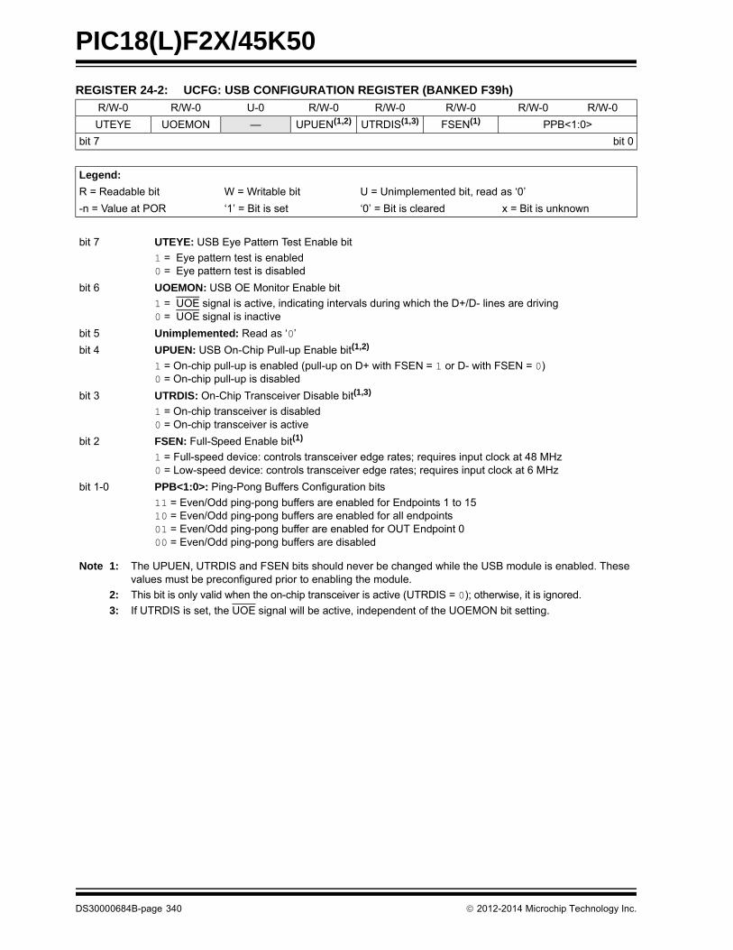
PIC18(L)F2X/45K50
REGISTER 24-2: UCFG: USB CONFIGURATION REGISTER (BANKED F39h)
R/W-0 R/W-0 U-0 R/W-0 R/W-0 R/W-0 R/W-0 R/W-0
UTEYE UOEMON — UPUEN(1,2) UTRDIS(1,3) FSEN(1) PPB<1:0>
bit 7 bit 0
Legend:
R = Readable bit W = Writable bit U = Unimplemented bit, read as ‘0’
-n = Value at POR ‘1’ = Bit is set ‘0’ = Bit is cleared x = Bit is unknown
bit 7 UTEYE: USB Eye Pattern Test Enable bit
1 = Eye pattern test is enabled0 = Eye pattern test is disabled
bit 6 UOEMON: USB OE Monitor Enable bit
1 = UOE signal is active, indicating intervals during which the D+/D- lines are driving0 = UOE signal is inactive
bit 5 Unimplemented: Read as ‘0’
bit 4 UPUEN: USB On-Chip Pull-up Enable bit(1,2)
1 = On-chip pull-up is enabled (pull-up on D+ with FSEN = 1 or D- with FSEN = 0)0 = On-chip pull-up is disabled
bit 3 UTRDIS: On-Chip Transceiver Disable bit(1,3)
1 = On-chip transceiver is disabled0 = On-chip transceiver is active
bit 2 FSEN: Full-Speed Enable bit(1)
1 = Full-speed device: controls transceiver edge rates; requires input clock at 48 MHz0 = Low-speed device: controls transceiver edge rates; requires input clock at 6 MHz
bit 1-0 PPB<1:0>: Ping-Pong Buffers Configuration bits
11 = Even/Odd ping-pong buffers are enabled for Endpoints 1 to 1510 = Even/Odd ping-pong buffers are enabled for all endpoints01 = Even/Odd ping-pong buffer are enabled for OUT Endpoint 000 = Even/Odd ping-pong buffers are disabled
Note 1: The UPUEN, UTRDIS and FSEN bits should never be changed while the USB module is enabled. These values must be preconfigured prior to enabling the module.
2: This bit is only valid when the on-chip transceiver is active (UTRDIS = 0); otherwise, it is ignored.
3: If UTRDIS is set, the UOE signal will be active, independent of the UOEMON bit setting.
DS30000684B-page 340 2012-2014 Microchip Technology Inc.

PIC18(L)F2X/45K50
24.2.2.2 Internal Pull-up Resistors
The PIC18F2X/45K50 devices have built-in pull-upresistors designed to meet the requirements forlow-speed and full-speed USB. The UPUEN bit(UCFG<4>) enables the internal pull-ups. Figure 24-1shows the pull-ups and their control.
24.2.2.3 External Pull-up Resistors
External pull-up may also be used. The VUSB3V3 pin maybe used to pull up D+ or D-. The pull-up resistor must be1.5 k (±5%) as required by the USB specifications.Figure 24-2 shows an example.
FIGURE 24-2: EXTERNAL CIRCUITRY
24.2.2.4 Ping-Pong Buffer Configuration
The usage of ping-pong buffers is configured using thePPB<1:0> bits. Refer to Section 24.4.4 “Ping-PongBuffering” for a complete explanation of the ping-pongbuffers.
24.2.2.5 Eye Pattern Test Enable
An automatic eye pattern test can be generated by themodule when the UCFG<7> bit is set. The eye patternoutput will be observable based on module settings,meaning that the user is first responsible for configuringthe SIE clock settings, pull-up resistor and Transceivermode. In addition, the module has to be enabled.
Once UTEYE is set, the module emulates a switch froma receive to transmit state and will start transmitting aJ-K-J-K bit sequence (K-J-K-J for full speed). Thesequence will be repeated indefinitely while the EyePattern Test mode is enabled.
Note that this bit should never be set while the moduleis connected to an actual USB system. This Test modeis intended for board verification to aid with USB certi-fication tests. It is intended to show a system developerthe noise integrity of the USB signals which can beaffected by board traces, impedance mismatches andproximity to other system components. It does notproperly test the transition from a receive to a transmitstate. Although the eye pattern is not meant to replacethe more complex USB certification test, it should aidduring first order system debugging.
Note: The official USB specifications requirethat USB devices must never source anycurrent onto the +5V VBUS line of the USBcable. Additionally, USB devices mustnever source any current on the D+ andD- data lines whenever the +5V VBUS lineis less than 1.17V. In order to meet thisrequirement, applications which are notpurely bus powered should monitor theVBUS line and avoid turning on the USBmodule and the D+ or D- pull-up resistoruntil VBUS is greater than 1.17V. VBUS canbe connected to a resistive divider andmonitored by an analog capable pin.
PIC®
MicrocontrollerHost
Controller/HUB
VUSB
D+
D-
Note: The above setting shows a typical connectionfor a full-speed configuration using an on-chipregulator and an external pull-up resistor.
1.5 k
2012-2014 Microchip Technology Inc. DS30000684B-page 341

PIC18(L)F2X/45K50
24.2.3 USB STATUS REGISTER (USTAT)
The USB Status register reports the transaction statuswithin the SIE. When the SIE issues a USB transfercomplete interrupt, USTAT should be read to determinethe status of the transfer. USTAT contains the transferendpoint number, direction and Ping-Pong BufferPointer value (if used).
The USTAT register is actually a read window into afour-byte status FIFO, maintained by the SIE. It allowsthe microcontroller to process one transfer while theSIE processes additional endpoints (Figure 24-3).When the SIE completes using a buffer for reading orwriting data, it updates the USTAT register. If anotherUSB transfer is performed before a transactioncomplete interrupt is serviced, the SIE will store thestatus of the next transfer into the status FIFO.
Clearing the transfer complete flag bit, TRNIF, causesthe SIE to advance the FIFO. If the next data in theFIFO holding register is valid, the SIE will reassert theinterrupt within 6 TCY of clearing TRNIF. If no additionaldata is present, TRNIF will remain clear; USTAT datawill no longer be reliable.
FIGURE 24-3: USTAT FIFO
Note: The data in the USB Status register isvalid two SIE clocks after the TRNIF inter-rupt flag is asserted.
In low-speed operation with the systemclock operating at 48 MHz, a delay maybe required between receiving the TRNIFinterrupt and processing the data in theUSTAT register.
Note: If an endpoint request is received whilethe USTAT FIFO is full, the SIE willautomatically issue a NAK back to thehost.
Data Bus
USTAT from SIE
4-Byte FIFOfor USTAT
Clearing TRNIFAdvances FIFO
REGISTER 24-3: USTAT: USB STATUS REGISTER (ACCESS F64h)
U-0 R-x R-x R-x R-x R-x R-x U-0
— ENDP<3:0> DIR PPBI(1) —
bit 7 bit 0
Legend:
R = Readable bit W = Writable bit U = Unimplemented bit, read as ‘0’
-n = Value at POR ‘1’ = Bit is set ‘0’ = Bit is cleared x = Bit is unknown
bit 7 Unimplemented: Read as ‘0’
bit 6-3 ENDP<3:0>: Encoded Number of Last Endpoint Activity bits(represents the number of the BDT updated by the last USB transfer)
1111 = Endpoint 151110 = Endpoint 14...0001 = Endpoint 10000 = Endpoint 0
bit 2 DIR: Last BD Direction Indicator bit
1 = The last transaction was an IN token0 = The last transaction was an OUT or SETUP token
bit 1 PPBI: Ping-Pong BD Pointer Indicator bit(1)
1 = The last transaction was to the Odd BD bank0 = The last transaction was to the Even BD bank
bit 0 Unimplemented: Read as ‘0’
Note 1: This bit is only valid for endpoints with available Even and Odd BD registers.
DS30000684B-page 342 2012-2014 Microchip Technology Inc.
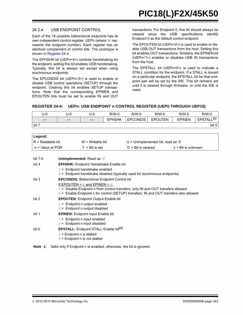
PIC18(L)F2X/45K50
24.2.4 USB ENDPOINT CONTROL
Each of the 16 possible bidirectional endpoints has itsown independent control register, UEPn (where ‘n’ rep-resents the endpoint number). Each register has anidentical complement of control bits. The prototype isshown in Register 24-4.
The EPHSHK bit (UEPn<4>) controls handshaking forthe endpoint; setting this bit enables USB handshaking.Typically, this bit is always set except when usingisochronous endpoints.
The EPCONDIS bit (UEPn<3>) is used to enable ordisable USB control operations (SETUP) through theendpoint. Clearing this bit enables SETUP transac-tions. Note that the corresponding EPINEN andEPOUTEN bits must be set to enable IN and OUT
transactions. For Endpoint 0, this bit should always becleared since the USB specifications identifyEndpoint 0 as the default control endpoint.
The EPOUTEN bit (UEPn<2>) is used to enable or dis-able USB OUT transactions from the host. Setting thisbit enables OUT transactions. Similarly, the EPINEN bit(UEPn<1>) enables or disables USB IN transactionsfrom the host.
The EPSTALL bit (UEPn<0>) is used to indicate aSTALL condition for the endpoint. If a STALL is issuedon a particular endpoint, the EPSTALL bit for that end-point pair will be set by the SIE. This bit remains setuntil it is cleared through firmware, or until the SIE isreset.
REGISTER 24-4: UEPn: USB ENDPOINT n CONTROL REGISTER (UEP0 THROUGH UEP15)
U-0 U-0 U-0 R/W-0 R/W-0 R/W-0 R/W-0 R/W-0
— — — EPHSHK EPCONDIS EPOUTEN EPINEN EPSTALL(1)
bit 7 bit 0
Legend:
R = Readable bit W = Writable bit U = Unimplemented bit, read as ‘0’
-n = Value at POR ‘1’ = Bit is set ‘0’ = Bit is cleared x = Bit is unknown
bit 7-5 Unimplemented: Read as ‘0’
bit 4 EPHSHK: Endpoint Handshake Enable bit
1 = Endpoint handshake enabled0 = Endpoint handshake disabled (typically used for isochronous endpoints)
bit 3 EPCONDIS: Bidirectional Endpoint Control bit
If EPOUTEN = 1 and EPINEN = 1:1 = Disable Endpoint n from control transfers; only IN and OUT transfers allowed0 = Enable Endpoint n for control (SETUP) transfers; IN and OUT transfers also allowed
bit 2 EPOUTEN: Endpoint Output Enable bit
1 = Endpoint n output enabled0 = Endpoint n output disabled
bit 1 EPINEN: Endpoint Input Enable bit
1 = Endpoint n input enabled0 = Endpoint n input disabled
bit 0 EPSTALL: Endpoint STALL Enable bit(1)
1 = Endpoint n is stalled 0 = Endpoint n is not stalled
Note 1: Valid only if Endpoint n is enabled; otherwise, the bit is ignored.
2012-2014 Microchip Technology Inc. DS30000684B-page 343

PIC18(L)F2X/45K50
24.2.5 USB ADDRESS REGISTER (UADDR)
The USB Address register contains the unique USBaddress that the peripheral will decode when active.UADDR is reset to 00h when a USB Reset is received,indicated by URSTIF, or when a Reset is received fromthe microcontroller. The USB address must be writtenby the microcontroller during the USB setup phase(enumeration) as part of the Microchip USB firmwaresupport.
24.2.6 USB FRAME NUMBER REGISTERS (UFRMH:UFRML)
The Frame Number registers contain the 11-bit framenumber. The low-order byte is contained in UFRML,while the three high-order bits are contained inUFRMH. The register pair is updated with the currentframe number whenever a SOF token is received. Forthe microcontroller, these registers are read-only. TheFrame Number registers are primarily used forisochronous transfers. The contents of the UFRMH andUFRML registers are only valid when the 48 MHz SIEclock is active (i.e., contents are inaccurate whenSUSPND (UCON<1>) bit = 1).
24.3 USB RAM
USB data moves between the microcontroller core andthe SIE through a memory space known as the USBRAM. This is a special dual access memory that ismapped into the normal data memory space in Banks4 through 7 (400h to 7FFh) for a total of 1024 bytes(Figure 24-4).
Bank 4 (400h through 4FFh) is used specifically forendpoint buffer control. Depending on the type ofbuffering being used, all but eight bytes of Bank 4 mayalso be available for use as USB buffer space.
Although USB RAM is available to the microcontrolleras data memory, the sections that are being accessedby the SIE should not be accessed by themicrocontroller. A semaphore mechanism is used todetermine the access to a particular buffer at any giventime. This is discussed in Section 24.4.1.1 “BufferOwnership”.
FIGURE 24-4: IMPLEMENTATION OF USB RAM IN DATA MEMORY SPACE
400h
7FFh
Buffer Descriptors,
USB Data or User Data
SFRs
3FFh
000h
F60h
FFFh
Banks 4 to 7
(USB RAM)
F5FhF53hF52h
800h
Banks 8to 14
User Data
Unused
Banks 15
USB Data or User Data
4FFh
500h
DS30000684B-page 344 2012-2014 Microchip Technology Inc.

PIC18(L)F2X/45K50
24.4 Buffer Descriptors and the Buffer Descriptor Table
The registers in Bank 4 are used specifically for end-point buffer control in a structure known as the BufferDescriptor Table (BDT). This provides a flexible methodfor users to construct and control endpoint buffers ofvarious lengths and configuration.
The BDT is composed of Buffer Descriptors (BD) whichare used to define and control the actual buffers in theUSB RAM space. Each BD, in turn, consists of fourregisters, where n represents one of the 64 possibleBDs (range of 0 to 63):
• BDnSTAT: BD Status register
• BDnCNT: BD Byte Count register
• BDnADRL: BD Address Low register
• BDnADRH: BD Address High register
BDs always occur as a four-byte block in the sequence:BDnSTAT:BDnCNT:BDnADRL:BDnADRH. The addressof BDnSTAT is always an offset of (4n – 1) (in hexa-decimal) from 400h, with n being the buffer descriptornumber.
Depending on the buffering configuration used(Section 24.4.4 “Ping-Pong Buffering”), there are upto 32, 33 or 64 sets of buffer descriptors. At a minimum,the BDT must be at least eight bytes long. This isbecause the USB specification mandates that everydevice must have Endpoint 0, with both input and out-put for initial setup. Depending on the endpoint andbuffering configuration, the BDT can be as long as 256bytes.
Although they can be thought of as Special FunctionRegisters, the Buffer Descriptor Status and Addressregisters are not hardware mapped, as conventionalmicrocontroller SFRs in Bank 15 are. If the endpoint cor-responding to a particular BD is not enabled, its registersare not used. Instead of appearing as unimplementedaddresses, however, they appear as available RAM.Only when an endpoint is enabled by setting theUEPn<1> bit does the memory at those addressesbecome functional as BD registers. As with any addressin the data memory space, the BD registers have anindeterminate value on any device Reset.
Figure 24-5 provides an example of a BD for a 64-bytebuffer, starting at 500h. A particular set of BD registersis only valid if the corresponding endpoint has beenenabled using the UEPn register. All BD registers areavailable in USB RAM. The BD for each endpointshould be set up prior to enabling the endpoint.
24.4.1 BD STATUS AND CONFIGURATION
Buffer descriptors not only define the size of an end-point buffer, but also determine its configuration andcontrol. Most of the configuration is done with the BDStatus register, BDnSTAT. Each BD has its own uniqueand correspondingly numbered BDnSTAT register.
FIGURE 24-5: EXAMPLE OF A BUFFER DESCRIPTOR
Unlike other control registers, the bit configuration forthe BDnSTAT register is context sensitive. There aretwo distinct configurations, depending on whether themicrocontroller or the USB module is modifying the BDand buffer at a particular time. Only three bit definitionsare shared between the two.
24.4.1.1 Buffer Ownership
Because the buffers and their BDs are shared betweenthe CPU and the USB module, a simple semaphoremechanism is used to distinguish which is allowed toupdate the BD and associated buffers in memory.
This is done by using the UOWN bit (BDnSTAT<7>) asa semaphore to distinguish which is allowed to updatethe BD and associated buffers in memory. UOWN is theonly bit that is shared between the two configurationsof BDnSTAT.
When UOWN is clear, the BD entry is “owned” by themicrocontroller core. When the UOWN bit is set, the BDentry and the buffer memory are “owned” by the USBperipheral. The core should not modify the BD or itscorresponding data buffer during this time. Note thatthe microcontroller core can still read BDnSTAT whilethe SIE owns the buffer and vice versa.
The buffer descriptors have a different meaning basedon the source of the register update. Prior to placingownership with the USB peripheral, the user canconfigure the basic operation of the peripheral throughthe BDnSTAT bits. During this time, the byte count andbuffer location registers can also be set.
400h
USB Data
Buffer
Buffer
BD0STAT
BD0CNT
BD0ADRL
BD0ADRH
401h
402h
403h
500h
53Fh
Descriptor
Note: Memory regions are not to scale.
40h
00h
05hStarting
Size of Block
(xxh)
RegistersAddress Contents
Address
2012-2014 Microchip Technology Inc. DS30000684B-page 345

PIC18(L)F2X/45K50
When UOWN is set, the user can no longer depend onthe values that were written to the BDs. From this point,the SIE updates the BDs as necessary, overwriting theoriginal BD values. The BDnSTAT register is updatedby the SIE with the token PID and the transfer count,BDnCNT, is updated.
The BDnSTAT byte of the BDT should always be thelast byte updated when preparing to arm an endpoint.The SIE will clear the UOWN bit when a transactionhas completed.
No hardware mechanism exists to block access whenthe UOWN bit is set. Thus, unexpected behavior canoccur if the microcontroller attempts to modify memorywhen the SIE owns it. Similarly, reading such memorymay produce inaccurate data until the USB peripheralreturns ownership to the microcontroller.
24.4.1.2 BDnSTAT Register (CPU Mode)
When UOWN = 0, the microcontroller core owns theBD. At this point, the other seven bits of the registertake on control functions.
The Data Toggle Sync Enable bit, DTSEN(BDnSTAT<3>), controls data toggle parity checking.Setting DTSEN enables data toggle synchronization bythe SIE. When enabled, it checks the data packet’s par-ity against the value of DTS (BDnSTAT<6>). If a packetarrives with an incorrect synchronization, the data willessentially be ignored. It will not be written to the USBRAM and the USB transfer complete interrupt flag willnot be set. The SIE will send an ACK token back to thehost to Acknowledge receipt, however. The effects ofthe DTSEN bit on the SIE are summarized inTable 24-1.
The Buffer Stall bit, BSTALL (BDnSTAT<2>), providessupport for control transfers, usually one-time stalls onEndpoint 0. It also provides support for the SET_FEA-TURE/CLEAR_FEATURE commands specified inChapter 9 of the USB specification; typically,continuous STALLs to any endpoint other than thedefault control endpoint.
The BSTALL bit enables buffer stalls. Setting BSTALLcauses the SIE to return a STALL token to the host if areceived token would use the BD in that location. TheEPSTALL bit in the corresponding UEPn control regis-ter is set and a STALL interrupt is generated when aSTALL is issued to the host. The UOWN bit remains setand the BDs are not changed unless a SETUP token isreceived. In this case, the STALL condition is clearedand the ownership of the BD is returned to themicrocontroller core.
The BD<9:8> bits (BDnSTAT<1:0>) store the two MostSignificant digits of the SIE byte count; the lower eightdigits are stored in the corresponding BDnCNTregister. See Section 24.4.2 “BD Byte Count” formore information.
Note: The firmware should not set the UOWN bitin the same instruction cycles as any othermodifications to the BDnSTAT softregister. The UOWN bit should only be setin a separate instruction cycle, only afterall other bits in BDnSTAT (andaddress/count registers) have been fullyupdated.
TABLE 24-1: EFFECT OF DTSEN BIT ON ODD/EVEN (DATA0/DATA1) PACKET RECEPTION
OUT Packetfrom Host
BDnSTAT Settings Device Response after Receiving Packet
DTSEN DTS Handshake UOWN TRNIF BDnSTAT and USTAT Status
DATA0 1 0 ACK 0 1 Updated
DATA1 1 0 ACK 1 0 Not Updated
DATA0 1 1 ACK 1 0 Not Updated
DATA1 1 1 ACK 0 1 Updated
Either 0 x ACK 0 1 Updated
Either, with error x x NAK 1 0 Not Updated
Legend: x = don’t care
DS30000684B-page 346 2012-2014 Microchip Technology Inc.

PIC18(L)F2X/45K50
REGISTER 24-5: BDnSTAT: BUFFER DESCRIPTOR n STATUS REGISTER (BD0STAT THROUGH BD63STAT), CPU MODE (BANKED 4xxh)
R/W-x R/W-x U-0 U-0 R/W-x R/W-x R/W-x R/W-x
UOWN(1) DTS(2) —(3) —(3) DTSEN BSTALL BC9 BC8
bit 7 bit 0
Legend:
R = Readable bit W = Writable bit U = Unimplemented bit, read as ‘0’
-n = Value at POR ‘1’ = Bit is set ‘0’ = Bit is cleared x = Bit is unknown
bit 7 UOWN: USB Own bit(1)
0 = The microcontroller core owns the BD and its corresponding buffer
bit 6 DTS: Data Toggle Synchronization bit(2)
1 = Data 1 packet0 = Data 0 packet
bit 5-4 Unimplemented: These bits should always be programmed to ‘0’(3).
bit 3 DTSEN: Data Toggle Synchronization Enable bit
1 = Data toggle synchronization is enabled; data packets with incorrect Sync value will be ignoredexcept for a SETUP transaction, which is accepted even if the data toggle bits do not match
0 = No data toggle synchronization is performed
bit 2 BSTALL: Buffer Stall Enable bit
1 = Buffer stall enabled; STALL handshake issued if a token is received that would use the BD in thegiven location (UOWN bit remains set, BD value is unchanged)
0 = Buffer stall disabled
bit 1-0 BC<9:8>: Byte Count 9 and 8 bits
The byte count bits represent the number of bytes that will be transmitted for an IN token or receivedduring an OUT token. Together with BC<7:0>, the valid byte counts are 0-1023.
Note 1: This bit must be initialized by the user to the desired value prior to enabling the USB module.
2: This bit is ignored unless DTSEN = 1.
3: If these bits are set, USB communication may not work. Hence, these bits should always be maintained as ‘0’.
2012-2014 Microchip Technology Inc. DS30000684B-page 347

PIC18(L)F2X/45K50
24.4.1.3 BDnSTAT Register (SIE Mode)
When the BD and its buffer are owned by the SIE, mostof the bits in BDnSTAT take on a different meaning. Theconfiguration is shown in Register 24-6. Once theUOWN bit is set, any data or control settings previouslywritten there by the user will be overwritten with datafrom the SIE.
The BDnSTAT register is updated by the SIE with thetoken Packet Identifier (PID) which is stored inBDnSTAT<5:3>. The transfer count in the correspond-ing BDnCNT register is updated. Values that overflowthe 8-bit register carry over to the two Most Significantdigits of the count, stored in BDnSTAT<1:0>.
24.4.2 BD BYTE COUNT
The byte count represents the total number of bytesthat will be transmitted during an IN transfer. After an INtransfer, the SIE will return the number of bytes sent tothe host.
For an OUT transfer, the byte count represents themaximum number of bytes that can be received andstored in USB RAM. After an OUT transfer, the SIE willreturn the actual number of bytes received. If thenumber of bytes received exceeds the correspondingbyte count, the data packet will be rejected and a NAKhandshake will be generated. When this happens, thebyte count will not be updated.
The 10-bit byte count is distributed over two registers.The lower eight bits of the count reside in the BDnCNTregister. The upper two bits reside in BDnSTAT<1:0>.This represents a valid byte range of 0 to 1023.
24.4.3 BD ADDRESS VALIDATION
The BD Address register pair contains the starting RAMaddress location for the corresponding endpoint buffer.No mechanism is available in hardware to validate theBD address.
If the value of the BD address does not point to anaddress in the USB RAM, or if it points to an addresswithin another endpoint’s buffer, data is likely to be lostor overwritten. Similarly, overlapping a receive buffer(OUT endpoint) with a BD location in use can yieldunexpected results. When developing USBapplications, the user may want to consider theinclusion of software-based address validation in theircode.
REGISTER 24-6: BDnSTAT: BUFFER DESCRIPTOR n STATUS REGISTER (BD0STAT THROUGH
BD63STAT), SIE MODE (DATA RETURNED BY THE SIDE TO THE MCU)
R/W-x U-x R/W-x R/W-x R/W-x R/W-x R/W-x R/W-x
UOWN — PID3 PID2 PID1 PID0 BC9 BC8
bit 7 bit 0
Legend:
R = Readable bit W = Writable bit U = Unimplemented bit, read as ‘0’
-n = Value at POR ‘1’ = Bit is set ‘0’ = Bit is cleared x = Bit is unknown
bit 7 UOWN: USB Own bit
1 = The SIE owns the BD and its corresponding buffer
bit 6 Reserved: Not written by the SIE
bit 5-2 PID<3:0>: Packet Identifier bits
The received token PID value of the last transfer (IN, OUT or SETUP transactions only).
bit 1-0 BC<9:8>: Byte Count 9 and 8 bits
These bits are updated by the SIE to reflect the actual number of bytes received on an OUT transferand the actual number of bytes transmitted on an IN transfer.
DS30000684B-page 348 2012-2014 Microchip Technology Inc.

PIC18(L)F2X/45K50
24.4.4 PING-PONG BUFFERING
An endpoint is defined to have a ping-pong buffer whenit has two sets of BD entries: one set for an Eventransfer and one set for an Odd transfer. This allows theCPU to process one BD while the SIE is processing theother BD. Double-buffering BDs in this way allows formaximum throughput to/from the USB.
The USB module supports four modes of operation:
• No ping-pong support
• Ping-pong buffer support for OUT Endpoint 0 only
• Ping-pong buffer support for all endpoints
• Ping-pong buffer support for all other Endpoints except Endpoint 0
The ping-pong buffer settings are configured using thePPB<1:0> bits in the UCFG register.
The USB module keeps track of the Ping-Pong Pointerindividually for each endpoint. All pointers are initiallyreset to the Even BD when the module is enabled. After
the completion of a transaction (UOWN cleared by theSIE), the pointer is toggled to the Odd BD. After thecompletion of the next transaction, the pointer istoggled back to the Even BD and so on.
The Even/Odd status of the last transaction is stored inthe PPBI bit of the USTAT register. The user can resetall Ping-Pong Pointers to Even using the PPBRST bit.
Figure 24-6 shows the four different modes ofoperation and how USB RAM is filled with the BDs.
BDs have a fixed relationship to a particular endpoint,depending on the buffering configuration. The mappingof BDs to endpoints is detailed in Table 24-2. Thisrelationship also means that gaps may occur in theBDT if endpoints are not enabled contiguously. Thistheoretically means that the BDs for disabled endpointscould be used as buffer space. In practice, usersshould avoid using such spaces in the BDT unless amethod of validating BD addresses is implemented.
FIGURE 24-6: BUFFER DESCRIPTOR TABLE MAPPING FOR BUFFERING MODES
EP1 IN Even
EP1 OUT Even
EP1 OUT Odd
EP1 IN Odd
Descriptor
Descriptor
Descriptor
Descriptor
EP1 IN
EP15 IN
EP1 OUT
EP0 OUT
PPB<1:0> = 00
EP0 IN
EP1 IN
No Ping-Pong
EP15 IN
EP0 IN
EP0 OUT Even
PPB<1:0> = 01
EP0 OUT Odd
EP1 OUT
Ping-Pong Buffer
EP15 IN Odd
EP0 IN Even
EP0 OUT Even
PPB<1:0> = 10
EP0 OUT Odd
EP0 IN Odd
Ping-Pong Buffers
Descriptor
Descriptor
Descriptor
Descriptor
Descriptor
Descriptor
Descriptor
Descriptor
Descriptor
Descriptor
Descriptor
Descriptor
400h
4FFh 4FFh 4FFh
400h 400h
47Fh
483h
Availableas
Data RAM Availableas
Data RAM
Maximum Memory Used: 128 BytesMaximum BDs: 32 (BD0 to BD31)
Maximum Memory Used: 132 BytesMaximum BDs: 33 (BD0 to BD32)
Maximum Memory Used: 256 BytesMaximum BDs:
64 (BD0 to BD63)
Note: Memory area is not shown to scale.
Descriptor
Descriptor
Descriptor
Descriptor
Buffers on EP0 OUT on all EPs
EP1 IN Even
EP1 OUT Even
EP1 OUT Odd
EP1 IN Odd
Descriptor
Descriptor
Descriptor
Descriptor
EP15 IN Odd
EP0 OUT
PPB<1:0> = 11
EP0 IN
Ping-Pong Buffers
Descriptor
Descriptor
Descriptor
4FFh
400h
Maximum Memory Used: 248 BytesMaximum BDs:
62 (BD0 to BD61)
on all Other EPsExcept EP0
Availableas
Data RAM
4F7h
2012-2014 Microchip Technology Inc. DS30000684B-page 349

PIC18(L)F2X/45K50
TABLE 24-2: ASSIGNMENT OF BUFFER DESCRIPTORS FOR THE DIFFERENT BUFFERING MODES
Endpoint
BDs Assigned to Endpoint
Mode 0(No Ping-Pong)
Mode 1(Ping-Pong on EP0 OUT)
Mode 2(Ping-Pong on all EPs)
Mode 3(Ping-Pong on all other EPs,
except EP0)
Out In Out In Out In Out In
0 0 1 0 (E), 1 (O) 2 0 (E), 1 (O) 2 (E), 3 (O) 0 1
1 2 3 3 4 4 (E), 5 (O) 6 (E), 7 (O) 2 (E), 3 (O) 4 (E), 5 (O)
2 4 5 5 6 8 (E), 9 (O) 10 (E), 11 (O) 6 (E), 7 (O) 8 (E), 9 (O)
3 6 7 7 8 12 (E), 13 (O) 14 (E), 15 (O) 10 (E), 11 (O) 12 (E), 13 (O)
4 8 9 9 10 16 (E), 17 (O) 18 (E), 19 (O) 14 (E), 15 (O) 16 (E), 17 (O)
5 10 11 11 12 20 (E), 21 (O) 22 (E), 23 (O) 18 (E), 19 (O) 20 (E), 21 (O)
6 12 13 13 14 24 (E), 25 (O) 26 (E), 27 (O) 22 (E), 23 (O) 24 (E), 25 (O)
7 14 15 15 16 28 (E), 29 (O) 30 (E), 31 (O) 26 (E), 27 (O) 28 (E), 29 (O)
8 16 17 17 18 32 (E), 33 (O) 34 (E), 35 (O) 30 (E), 31 (O) 32 (E), 33 (O)
9 18 19 19 20 36 (E), 37 (O) 38 (E), 39 (O) 34 (E), 35 (O) 36 (E), 37 (O)
10 20 21 21 22 40 (E), 41 (O) 42 (E), 43 (O) 38 (E), 39 (O) 40 (E), 41 (O)
11 22 23 23 24 44 (E), 45 (O) 46 (E), 47 (O) 42 (E), 43 (O) 44 (E), 45 (O)
12 24 25 25 26 48 (E), 49 (O) 50 (E), 51 (O) 46 (E), 47 (O) 48 (E), 49 (O)
13 26 27 27 28 52 (E), 53 (O) 54 (E), 55 (O) 50 (E), 51 (O) 52 (E), 53 (O)
14 28 29 29 30 56 (E), 57 (O) 58 (E), 59 (O) 54 (E), 55 (O) 56 (E), 57 (O)
15 30 31 31 32 60 (E), 61 (O) 62 (E), 63 (O) 58 (E), 59 (O) 60 (E), 61 (O)
Legend: (E) = Even transaction buffer, (O) = Odd transaction buffer
TABLE 24-3: SUMMARY OF USB BUFFER DESCRIPTOR TABLE REGISTERS
Name Bit 7 Bit 6 Bit 5 Bit 4 Bit 3 Bit 2 Bit 1 Bit 0
BDnSTAT(1) UOWN DTS(4) PID3(2) PID2(2) PID1(2)
DTSEN(3)PID0(2)
BSTALL(3)BC9 BC8
BDnCNT(1) Byte Count
BDnADRL(1) Buffer Address Low
BDnADRH(1) Buffer Address High
Note 1: For buffer descriptor registers, n may have a value of 0 to 63. For the sake of brevity, all 64 registers are shown as one generic prototype. All registers have indeterminate Reset values (xxxx xxxx).
2: Bits 5 through 2 of the BDnSTAT register are used by the SIE to return PID<3:0> values once the register is turned over to the SIE (UOWN bit is set). Once the registers have been under SIE control, the values written for DTSEN and BSTALL are no longer valid.
3: Prior to turning the buffer descriptor over to the SIE (UOWN bit is cleared), bits 5 through 2 of the BDnSTAT register are used to configure the DTSEN and BSTALL settings.
4: This bit is ignored unless DTSEN = 1.
DS30000684B-page 350 2012-2014 Microchip Technology Inc.

PIC18(L)F2X/45K50
24.5 USB Interrupts
The USB module can generate multiple interrupt con-ditions. To accommodate all of these interrupt sources,the module is provided with its own interrupt logicstructure, similar to that of the microcontroller. USBinterrupts are enabled with one set of control registersand trapped with a separate set of flag registers. Allsources are funneled into a single USB interruptrequest, USBIF (PIR3<2>), in the microcontroller’sinterrupt logic.
Figure 24-7 shows the interrupt logic for the USBmodule. There are two layers of interrupt registers inthe USB module. The top level consists of overall USBStatus interrupts; these are enabled and flagged in theUIE and UIR registers, respectively. The second levelconsists of USB error conditions, which are enabledand flagged in the UEIR and UEIE registers. Aninterrupt condition in any of these triggers a USB ErrorInterrupt Flag (UERRIF) in the top level.
Interrupts may be used to trap routine events in a USBtransaction. Figure 24-8 shows some common eventswithin a USB frame and their corresponding interrupts.
FIGURE 24-7: USB INTERRUPT LOGIC FUNNEL
FIGURE 24-8: EXAMPLE OF A USB TRANSACTION AND INTERRUPT EVENTS
BTSEFBTSEE
BTOEFBTOEE
DFN8EFDFN8EE
CRC16EFCRC16EE
CRC5EFCRC5EE
PIDEFPIDEE
SOFIFSOFIE
TRNIFTRNIE
IDLEIFIDLEIE
STALLIFSTALLIE
ACTVIFACTVIE
URSTIFURSTIE
UERRIF
UERRIE
USBIF
Second Level USB Interrupts(USB Error Conditions)
UEIR (Flag) and UEIE (Enable) Registers
Top Level USB Interrupts(USB Status Interrupts)
UIR (Flag) and UIE (Enable) Registers
USB Reset
SOFRESET SETUP DATA STATUS SOF
SETUPToken Data ACK
OUT Token Empty Data ACKStart-of-Frame (SOF)
IN Token Data ACK
SOFIF
URSTIF
1 ms Frame
Differential Data
From Host From Host To Host
From Host To Host From Host
From Host From Host To Host
Transaction
Control Transfer(1)
TransactionComplete
Note 1: The control transfer shown here is only an example showing events that can occur for every transaction. Typical control transfers will spread across multiple frames.
Set TRNIF
Set TRNIF
Set TRNIF
2012-2014 Microchip Technology Inc. DS30000684B-page 351

PIC18(L)F2X/45K50
24.5.1 USB INTERRUPT STATUS REGISTER (UIR)
The USB Interrupt Status register (Register 24-7)contains the flag bits for each of the USB Statusinterrupt sources. Each of these sources has acorresponding interrupt enable bit in the UIE register.All of the USB status flags are ORed together togenerate the USBIF interrupt flag for themicrocontroller’s interrupt funnel.
Once an interrupt bit has been set by the SIE, it mustbe cleared by software by writing a ‘0’. The flag bitscan also be set in software which can aid in firmwaredebugging.
When the USB module is in the Low-Power Suspendmode (UCON<1> = 1), the SIE does not get clocked.
When in this state, the SIE cannot process packetsand, therefore, cannot detect new interrupt conditionsother than the Activity Detect Interrupt, ACTVIF. TheACTVIF bit is typically used by USB firmware to detectwhen the microcontroller should bring the USB module
out of the Low-Power Suspend mode (UCON<1> = 0).
REGISTER 24-7: UIR: USB INTERRUPT STATUS REGISTER
U-0 R/W-0 R/W-0 R/W-0 R/W-0 R/W-0 R-0 R/W-0
— SOFIF STALLIF IDLEIF(1) TRNIF(2) ACTVIF(3) UERRIF(4) URSTIF
bit 7 bit 0
Legend:
R = Readable bit W = Writable bit U = Unimplemented bit, read as ‘0’
-n = Value at POR ‘1’ = Bit is set ‘0’ = Bit is cleared x = Bit is unknown
bit 7 Unimplemented: Read as ‘0’
bit 6 SOFIF: Start-of-Frame Token Interrupt bit
1 = A Start-of-Frame token received by the SIE0 = No Start-of-Frame token received by the SIE
bit 5 STALLIF: A STALL Handshake Interrupt bit
1 = A STALL handshake was sent by the SIE0 = A STALL handshake has not been sent
bit 4 IDLEIF: Idle Detect Interrupt bit(1)
1 = Idle condition detected (constant Idle state of 3 ms or more)0 = No Idle condition detected
bit 3 TRNIF: Transaction Complete Interrupt bit(2)
1 = Processing of pending transaction is complete; read USTAT register for endpoint information0 = Processing of pending transaction is not complete or no transaction is pending
bit 2 ACTVIF: Bus Activity Detect Interrupt bit(3)
1 = Activity on the D+/D- lines was detected0 = No activity detected on the D+/D- lines
bit 1 UERRIF: USB Error Condition Interrupt bit(4)
1 = An unmasked error condition has occurred0 = No unmasked error condition has occurred
bit 0 URSTIF: USB Reset Interrupt bit
1 = Valid USB Reset occurred; 00h is loaded into UADDR register0 = No USB Reset has occurred
Note 1: Once an Idle state is detected, the user may want to place the USB module in Suspend mode.
2: Clearing this bit will cause the USTAT FIFO to advance (valid only for IN, OUT and SETUP tokens).
3: This bit is typically unmasked only following the detection of a UIDLE interrupt event.
4: Only error conditions enabled through the UEIE register will set this bit. This bit is a status bit only and cannot be set or cleared by the user.
DS30000684B-page 352 2012-2014 Microchip Technology Inc.
PIC18(L)F2X/45K50
24.5.1.1 Bus Activity Detect Interrupt Bit (ACTVIF)
The ACTVIF bit cannot be cleared immediately afterthe USB module wakes up from Suspend or while theUSB module is suspended. A few clock cycles arerequired to synchronize the internal hardware statemachine before the ACTVIF bit can be cleared byfirmware. Clearing the ACTVIF bit before the internalhardware is synchronized may not have an effect onthe value of ACTVIF. Additionally, if the USB moduleuses the clock from the 48 MHz PLL source, then after
clearing the SUSPND bit, the USB module may not beimmediately operational while waiting for the 48 MHzPLL to lock. The application code should clear theACTVIF flag as shown in Example 24-1.
Only one ACTVIF interrupt is generated whenresuming from the USB bus Idle condition. If userfirmware clears the ACTVIF bit, the bit will notimmediately become set again, even when there iscontinuous bus traffic. Bus traffic must cease longenough to generate another IDLEIF condition beforeanother ACTVIF interrupt can be generated.
EXAMPLE 24-1: CLEARING ACTVIF BIT (UIR<2>)
Assembly:
BCF UCON, SUSPNDLOOP:
BTFSS UIR, ACTVIFBRA DONEBCF UIR, ACTVIFBRA LOOP
DONE:
C:
UCONbits.SUSPND = 0;
while (UIRbits.ACTVIF) UIRbits.ACTVIF = 0;
2012-2014 Microchip Technology Inc. DS30000684B-page 353
PIC18(L)F2X/45K50
24.5.2 USB INTERRUPT ENABLE REGISTER (UIE)
The USB Interrupt Enable register (Register 24-8)contains the enable bits for the USB Status interruptsources. Setting any of these bits will enable therespective interrupt source in the UIR register.
The values in this register only affect the propagationof an interrupt condition to the microcontroller’sinterrupt logic. The flag bits are still set by theirinterrupt conditions, allowing them to be polled andserviced without actually generating an interrupt.
REGISTER 24-8: UIE: USB INTERRUPT ENABLE REGISTER
U-0 R/W-0 R/W-0 R/W-0 R/W-0 R/W-0 R/W-0 R/W-0
— SOFIE STALLIE IDLEIE TRNIE ACTVIE UERRIE URSTIE
bit 7 bit 0
Legend:
R = Readable bit W = Writable bit U = Unimplemented bit, read as ‘0’
-n = Value at POR ‘1’ = Bit is set ‘0’ = Bit is cleared x = Bit is unknown
bit 7 Unimplemented: Read as ‘0’
bit 6 SOFIE: Start-of-Frame Token Interrupt Enable bit
1 = Start-of-Frame token interrupt enabled0 = Start-of-Frame token interrupt disabled
bit 5 STALLIE: STALL Handshake Interrupt Enable bit
1 = STALL interrupt enabled0 = STALL interrupt disabled
bit 4 IDLEIE: Idle Detect Interrupt Enable bit
1 = Idle detect interrupt enabled0 = Idle detect interrupt disabled
bit 3 TRNIE: Transaction Complete Interrupt Enable bit
1 = Transaction interrupt enabled0 = Transaction interrupt disabled
bit 2 ACTVIE: Bus Activity Detect Interrupt Enable bit
1 = Bus activity detect interrupt enabled0 = Bus activity detect interrupt disabled
bit 1 UERRIE: USB Error Interrupt Enable bit
1 = USB error interrupt enabled0 = USB error interrupt disabled
bit 0 URSTIE: USB Reset Interrupt Enable bit
1 = USB Reset interrupt enabled0 = USB Reset interrupt disabled
DS30000684B-page 354 2012-2014 Microchip Technology Inc.

PIC18(L)F2X/45K50
24.5.3 USB ERROR INTERRUPT STATUS REGISTER (UEIR)
The USB Error Interrupt Status register (Register 24-9)contains the flag bits for each of the error sourceswithin the USB peripheral. Each of these sources iscontrolled by a corresponding interrupt enable bit inthe UEIE register. All of the USB error flags are ORedtogether to generate the USB Error Interrupt Flag(UERRIF) at the top level of the interrupt logic.
Each error bit is set as soon as the error condition isdetected. Thus, the interrupt will typically notcorrespond with the end of a token being processed.
Once an interrupt bit has been set by the SIE, it mustbe cleared by software by writing a ‘0’.
REGISTER 24-9: UEIR: USB ERROR INTERRUPT STATUS REGISTER
R/C-0 U-0 U-0 R/C-0 R/C-0 R/C-0 R/C-0 R/C-0
BTSEF — — BTOEF DFN8EF CRC16EF CRC5EF PIDEF
bit 7 bit 0
Legend:
R = Readable bit C = Clearable bit U = Unimplemented bit, read as ‘0’
-n = Value at POR ‘1’ = Bit is set ‘0’ = Bit is cleared x = Bit is unknown
bit 7 BTSEF: Bit Stuff Error Flag bit
1 = A bit stuff error has been detected0 = No bit stuff error
bit 6-5 Unimplemented: Read as ‘0’
bit 4 BTOEF: Bus Turnaround Time-out Error Flag bit
1 = Bus turnaround time-out has occurred (more than 16 bit times of Idle from previous EOP elapsed)0 = No bus turnaround time-out
bit 3 DFN8EF: Data Field Size Error Flag bit
1 = The data field was not an integral number of bytes0 = The data field was an integral number of bytes
bit 2 CRC16EF: CRC16 Failure Flag bit
1 = The CRC16 failed0 = The CRC16 passed
bit 1 CRC5EF: CRC5 Host Error Flag bit
1 = The token packet was rejected due to a CRC5 error0 = The token packet was accepted
bit 0 PIDEF: PID Check Failure Flag bit
1 = PID check failed0 = PID check passed
2012-2014 Microchip Technology Inc. DS30000684B-page 355

PIC18(L)F2X/45K50
24.5.4 USB ERROR INTERRUPT ENABLE REGISTER (UEIE)
The USB Error Interrupt Enable register(Register 24-10) contains the enable bits for each ofthe USB error interrupt sources. Setting any of thesebits will enable the respective error interrupt source inthe UEIR register to propagate into the UERR bit atthe top level of the interrupt logic.
As with the UIE register, the enable bits only affect thepropagation of an interrupt condition to the micro-controller’s interrupt logic. The flag bits are still set bytheir interrupt conditions, allowing them to be polledand serviced without actually generating an interrupt.
REGISTER 24-10: UEIE: USB ERROR INTERRUPT ENABLE REGISTER
R/W-0 U-0 U-0 R/W-0 R/W-0 R/W-0 R/W-0 R/W-0
BTSEE — — BTOEE DFN8EE CRC16EE CRC5EE PIDEE
bit 7 bit 0
Legend:
R = Readable bit W = Writable bit U = Unimplemented bit, read as ‘0’
-n = Value at POR ‘1’ = Bit is set ‘0’ = Bit is cleared x = Bit is unknown
bit 7 BTSEE: Bit Stuff Error Interrupt Enable bit
1 = Bit stuff error interrupt enabled0 = Bit stuff error interrupt disabled
bit 6-5 Unimplemented: Read as ‘0’
bit 4 BTOEE: Bus Turnaround Time-out Error Interrupt Enable bit
1 = Bus turnaround time-out error interrupt enabled0 = Bus turnaround time-out error interrupt disabled
bit 3 DFN8EE: Data Field Size Error Interrupt Enable bit
1 = Data field size error interrupt enabled0 = Data field size error interrupt disabled
bit 2 CRC16EE: CRC16 Failure Interrupt Enable bit
1 = CRC16 failure interrupt enabled0 = CRC16 failure interrupt disabled
bit 1 CRC5EE: CRC5 Host Error Interrupt Enable bit
1 = CRC5 host error interrupt enabled0 = CRC5 host error interrupt disabled
bit 0 PIDEE: PID Check Failure Interrupt Enable bit
1 = PID check failure interrupt enabled0 = PID check failure interrupt disabled
DS30000684B-page 356 2012-2014 Microchip Technology Inc.

PIC18(L)F2X/45K50
24.6 USB Power Modes
Many USB applications will likely have several differentsets of power requirements and configuration. Themost common power modes encountered are BusPower Only, Self-Power Only and Dual Power withSelf-Power Dominance. The most common cases arepresented here. Also provided is a means of estimatingthe current consumption of the USB transceiver.
24.6.1 BUS POWER ONLY
In Bus Power Only mode, all power for the applicationis drawn from the USB (Figure 24-9). This is effectivelythe simplest power method for the device.
In order to meet the inrush current requirements of theUSB 2.0 specifications, the total effective capacitanceappearing across VBUS and ground must be no morethan 10 µF. If not, some kind of inrush liming isrequired. For more details, see section 7.2.4 of theUSB 2.0 specification.
According to the USB 2.0 specification, all USB devicesmust also support a Low-Power Suspend mode. In theUSB Suspend mode, devices must consume no morethan 2.5 mA from the 5V VBUS line of the USB cable.
The host signals the USB device to enter the Suspendmode by stopping all USB traffic to that device for morethan 3 ms. This condition will cause the IDLEIF bit inthe UIR register to become set.
During the USB Suspend mode, the D+ or D- pull-upresistor must remain active, which will consume someof the allowed suspend current: 2.5 mA budget.
FIGURE 24-9: BUS POWER ONLY
24.6.2 SELF-POWER ONLY
In Self-Power Only mode, the USB application providesits own power, with very little power being pulled fromthe USB. Figure 24-10 shows an example.
In order to meet compliance specifications, the USBmodule (and the D+ or D- pull-up resistor) should notbe enabled until the host actively drives VBUS high.
The application should never source any current ontothe 5V VBUS pin of the USB cable.
FIGURE 24-10: SELF-POWER ONLY
VDD
VUSB
VSS
VBUS
VDD
VUSB
VSS
VSELF
2012-2014 Microchip Technology Inc. DS30000684B-page 357
PIC18(L)F2X/45K50
24.6.3 DUAL POWER WITH SELF-POWER DOMINANCE
Some applications may require a dual power option.This allows the application to use internal power pri-marily, but switch to power from the USB when no inter-nal power is available. Figure 24-11 shows a simpleDual Power with Self-Power Dominance mode exam-ple, which automatically switches between Self-PowerOnly and USB Bus Power Only modes.
Dual power devices must also meet all of the specialrequirements for inrush current and Suspend modecurrent and must not enable the USB module untilVBUS is driven high. See Section 24.6.1 “Bus PowerOnly” and Section 24.6.2 “Self-Power Only” fordescriptions of those requirements. Additionally, dualpower devices must never source current onto the 5VVBUS pin of the USB cable.
FIGURE 24-11: DUAL POWER EXAMPLE
24.6.4 USB TRANSCEIVER CURRENT CONSUMPTION
The USB transceiver consumes a variable amount ofcurrent depending on the characteristic impedance ofthe USB cable, the length of the cable, the VUSB3V3
supply voltage and the actual data patterns movingacross the USB cable. Longer cables have largercapacitances and consume more total energy whenswitching output states.
Data patterns that consist of “IN” traffic consume farmore current than “OUT” traffic. IN traffic requires thePIC® device to drive the USB cable, whereas OUTtraffic requires that the host drive the USB cable.
The data that is sent across the USB cable is NRZIencoded. In the NRZI encoding scheme, ‘0’ bits causea toggling of the output state of the transceiver (eitherfrom a “J” state to a “K” state, or vise versa). With theexception of the effects of bit-stuffing, NRZI encoded ‘1’bits do not cause the output state of the transceiver tochange. Therefore, IN traffic consisting of data bits ofvalue, ‘0’, cause the most current consumption, as thetransceiver must charge/discharge the USB cable inorder to change states.
More details about NRZI encoding and bit-stuffing canbe found in the USB 2.0 specification’s section 7.1,although knowledge of such details is not required tomake USB applications using the PIC18F2X/45K50 ofmicrocontrollers. Among other things, the SIE handlesbit-stuffing/unstuffing, NRZI encoding/decoding andCRC generation/checking in hardware.
The total transceiver current consumption will beapplication-specific. However, to help estimate howmuch current actually may be required in full-speedapplications, Equation 24-1 can be used.
Example 24-2 shows how this equation can be used fora theoretical application.
Note: Users should keep in mind the limits fordevices drawing power from the USB.According to USB Specification 2.0, thiscannot exceed 100 mA per low-powerdevice or 500 mA per high-power device.
VDD
VUSB
VSS
VBUS
VSELF~5V
~5V
100 k
DS30000684B-page 358 2012-2014 Microchip Technology Inc.

PIC18(L)F2X/45K50
EQUATION 24-1: ESTIMATING USB TRANSCEIVER CURRENT CONSUMPTION
EXAMPLE 24-2: CALCULATING USB TRANSCEIVER CURRENT†
IXCVR = + IPULLUP(60 mA • VUSB3V3 • PZERO • PIN • LCABLE)
(3.3V • 5m)
Legend: VUSB: Voltage applied to the VUSB3V3 pin in volts. (Should be 3.0V to 3.6V.)
PZERO: Percentage (in decimal) of the IN traffic bits sent by the PIC® device that are a value of ‘0’.
PIN: Percentage (in decimal) of total bus bandwidth that is used for IN traffic.
LCABLE: Length (in meters) of the USB cable. The USB 2.0 specification requires that full-speed applicationsuse cables no longer than 5m.
IPULLUP: Current which the nominal, 1.5 k pull-up resistor (when enabled) must supply to the USB cable. Onthe host or hub end of the USB cable, 15 k nominal resistors (14.25 k to 24.8 k) are present whichpull both the D+ and D- lines to ground. During bus Idle conditions (such as between packets or duringUSB Suspend mode), this results in up to 218 A of quiescent current drawn at 3.3V.
IPULLUP is also dependant on bus traffic conditions and can be as high as 2.2 mA when the USB bandwidthis fully utilized (either IN or OUT traffic) for data that drives the lines to the “K” state most of the time.
For this example, the following assumptions are made about the application:
• 3.3V will be applied to VUSB3V3 and VDD, with the core voltage regulator enabled.
• This is a full-speed application that uses one interrupt IN endpoint that can send one packet of 64 bytes every 1 ms, with no restrictions on the values of the bytes being sent. The application may or may not have addi-tional traffic on OUT endpoints.
• A regular USB “B” or “mini-B” connector will be used on the application circuit board.
In this case, PZERO = 100% = 1, because there should be no restriction on the value of the data moving throughthe IN endpoint. All 64 kBps of data could potentially be bytes of value, 00h. Since ‘0’ bits cause toggling of theoutput state of the transceiver, they cause the USB transceiver to consume extra current charging/discharging thecable. In this case, 100% of the data bits sent can be of value ‘0’. This should be considered the “max” value, asnormal data will consist of a fair mix of ones and zeros.
This application uses 64 kBps for IN traffic out of the total bus bandwidth of 1.5 MBps (12 Mbps), therefore:
Since a regular “B” or “mini-B” connector is used in this application, the end user may plug in any type of cable upto the maximum allowed 5 m length. Therefore, we use the worst-case length:
LCABLE = 5 meters
Assume IPULLUP = 2.2 mA. The actual value of IPULLUP will likely be closer to 218 A, but allow for the worst-case.USB bandwidth is shared between all the devices which are plugged into the root port (via hubs). If the applicationis plugged into a USB 1.1 hub that has other devices plugged into it, your device may see host to device traffic onthe bus, even if it is not addressed to your device. Since any traffic, regardless of source, can increase the IPULLUP
current above the base 218 A, it is safest to allow for the worst-case of 2.2 mA.
Therefore:
The calculated value should be considered an approximation and additional guardband or application-specific prod-uct testing is recommended. The transceiver current is “in addition to” the rest of the current consumed by thePIC18F2X/45K50 device that is needed to run the core, drive the other I/O lines, power the various modules, etc.
Pin =64 kBps
1.5 MBps = 4.3% = 0.043
IXCVR = + 2.2 mA = 4.8 mA(60 mA • 3.3V • 1 • 0.043 • 5m)
(3.3V • 5m)
2012-2014 Microchip Technology Inc. DS30000684B-page 359

PIC18(L)F2X/45K50
24.7 Oscillator
The USB module has specific clock requirements. Forfull-speed operation, the clock source must be 48 MHz.Even so, the microcontroller core and other peripheralsare not required to run at that clock speed. Availableclocking options are described in detail in Section 3.14“Oscillator Settings for USB”.
24.8 Interrupt-On-Change for D+/D- pins
The PIC18(L)F2X/45K50 has interrupt-on-changefunctionality on both D+ and D- data pins. This featureallows the device to detect voltage level changeswhen first connected to a USB host/hub.
The USB host/hub has 15K pull-down resistors on the D+and D- pins. When the PIC18(L)F2X/45K50 attaches tothe bus the D+ and D- pins can detect voltage changes.External resistors are needed for each pin to maintain ahigh state on the pins when detached.
The USB module must be disabled (USBEN = 0) forthe interrupt-on-change to function. Enabling the USBmodule (USBEN = 1) will automatically disable theinterrupt-on-change for D+ and D- pins. Refer toSection 11.3.2 “Interrupt-on-Change” andSection 11.4.2 “Interrupt-on-Change” for moredetails.
24.9 USB Firmware and Drivers
Microchip provides a number of application-specificresources, such as USB firmware and driver support.Refer to www.microchip.com for the latest firmware anddriver support.
DS30000684B-page 360 2012-2014 Microchip Technology Inc.
PIC18(L)F2X/45K50
TABLE 24-4: REGISTERS ASSOCIATED WITH USB MODULE OPERATION(1)
Name Bit 7 Bit 6 Bit 5 Bit 4 Bit 3 Bit 2 Bit 1 Bit 0Register on page
INTCON GIE/GIEH PEIE/GIEL TMR0IE INT0IE IOCIE TMR0IF INT0IF IOCIF 114
IPR3 — — — — CTMUIP USBIP TMR3GIP TMR1GIP 125
PIR3 — — — — CTMUIF USBIF TMR3GIF TMR1GIF 119
PIE3 — — — — CTMUIE USBIE TMR3GIE TMR1GIE 122
UCON — PPBRST SE0 PKTDIS USBEN RESUME SUSPND — 338
UCFG UTEYE UOEMON — UPUEN UTRDIS FSEN PPB<1:0>1 340
USTAT — ENDP<3:0> DIR PPBI — 342
UADDR — ADDR<6:0> 344
UFRML FRM<7:0> 337
UFRMH — — — — — FRM<10:8> 337
UIR — SOFIF STALLIF IDLEIF TRNIF ACTVIF UERRIF URSTIF 352
UIE — SOFIE STALLIE IDLEIE TRNIE ACTVIE UERRIE URSTIE 354
UEIR BTSEF — — BTOEF DFN8EF CRC16EF CRC5EF PIDEF 355
UEIE BTSEE — — BTOEE DFN8EE CRC16EE CRC5EE PIDEE 356
UEP0 — — — EPHSHK EPCONDIS EPOUTEN EPINEN EPSTALL 343
UEP1 — — — EPHSHK EPCONDIS EPOUTEN EPINEN EPSTALL 343
UEP2 — — — EPHSHK EPCONDIS EPOUTEN EPINEN EPSTALL 343
UEP3 — — — EPHSHK EPCONDIS EPOUTEN EPINEN EPSTALL 343
UEP4 — — — EPHSHK EPCONDIS EPOUTEN EPINEN EPSTALL 343
UEP5 — — — EPHSHK EPCONDIS EPOUTEN EPINEN EPSTALL 343
UEP6 — — — EPHSHK EPCONDIS EPOUTEN EPINEN EPSTALL 343
UEP7 — — — EPHSHK EPCONDIS EPOUTEN EPINEN EPSTALL 343
UEP8 — — — EPHSHK EPCONDIS EPOUTEN EPINEN EPSTALL 343
UEP9 — — — EPHSHK EPCONDIS EPOUTEN EPINEN EPSTALL 343
UEP10 — — — EPHSHK EPCONDIS EPOUTEN EPINEN EPSTALL 343
UEP11 — — — EPHSHK EPCONDIS EPOUTEN EPINEN EPSTALL 343
UEP12 — — — EPHSHK EPCONDIS EPOUTEN EPINEN EPSTALL 343
UEP13 — — — EPHSHK EPCONDIS EPOUTEN EPINEN EPSTALL 343
UEP14 — — — EPHSHK EPCONDIS EPOUTEN EPINEN EPSTALL 343
UEP15 — — — EPHSHK EPCONDIS EPOUTEN EPINEN EPSTALL 343
Legend: — = unimplemented, read as ‘0’. Shaded cells are not used by the USB module.Note 1: This table includes only those hardware mapped SFRs located in Bank 15 of the data memory space. The Buffer
Descriptor registers, which are mapped into Bank 4 and are not true SFRs, are listed separately in Table 24-3.
2012-2014 Microchip Technology Inc. DS30000684B-page 361

PIC18(L)F2X/45K50
24.10 Overview of USB
This section presents some of the basic USB conceptsand useful information necessary to design a USBdevice. Although much information is provided in thissection, there is a plethora of information providedwithin the USB specifications and class specifications.Thus, the reader is encouraged to refer to the USBspecifications for more information (www.usb.org). Ifyou are very familiar with the details of USB, then thissection serves as a basic, high-level refresher of USB.
24.10.1 LAYERED FRAMEWORK
USB device functionality is structured into a layeredframework graphically shown in Figure 24-12. Eachlevel is associated with a functional level within thedevice. The highest layer, other than the device, is theconfiguration. A device may have multiple configura-tions. For example, a particular device may havemultiple power requirements based on Self-Power Onlyor Bus Power Only modes.
For each configuration, there may be multipleinterfaces. Each interface could support a particularmode of that configuration.
Below the interface is the endpoint(s). Data is directlymoved at this level. There can be as many as16 bidirectional endpoints. Endpoint 0 is always acontrol endpoint and by default, when the device is onthe bus, Endpoint 0 must be available to configure thedevice.
24.10.2 FRAMES
Information communicated on the bus is grouped into1 ms time slots, referred to as frames. Each frame cancontain many transactions to various devices andendpoints. Figure 24-8 shows an example of atransaction within a frame.
24.10.3 TRANSFERS
There are four transfer types defined in the USBspecification.
• Isochronous: This type provides a transfer method for large amounts of data (up to 1023 bytes) with timely delivery ensured; however, the data integrity is not ensured. This is good for streaming applications where small data loss is not critical, such as audio.
• Bulk: This type of transfer method allows for large amounts of data to be transferred with ensured data integrity; however, the delivery timeliness is not ensured.
• Interrupt: This type of transfer provides for ensured timely delivery for small blocks of data, plus data integrity is ensured.
• Control: This type provides for device setup control.
While full-speed devices support all transfer types,low-speed devices are limited to interrupt and controltransfers only.
24.10.4 POWER
Power is available from the Universal Serial Bus. TheUSB specification defines the bus power requirements.Devices may either be self-powered or bus powered.Self-powered devices draw power from an externalsource, while bus powered devices use power suppliedfrom the bus.
FIGURE 24-12: USB LAYERS
Device
Configuration
Interface
Endpoint
Interface
Endpoint Endpoint Endpoint Endpoint
To other Configurations (if any)
To other Interfaces (if any)
DS30000684B-page 362 2012-2014 Microchip Technology Inc.

PIC18(L)F2X/45K50
The USB specification limits the power taken from thebus. Each device is ensured 100 mA at approximately5V (one unit load). Additional power may be requested,up to a maximum of 500 mA. Note that power aboveone unit load is a request and the host or hub is notobligated to provide the extra current. Thus, a devicecapable of consuming more than one unit load must beable to maintain a low-power configuration of a one unitload or less, if necessary.
The USB specification also defines a Suspend mode.In this situation, current must be limited to 500 A,averaged over 1 second. A device must enter aSuspend state after 3 ms of inactivity (i.e., no SOFtokens for 3 ms). A device entering Suspend modemust drop current consumption within 10 ms afterSuspend. Likewise, when signaling a wake-up, thedevice must signal a wake-up within 10 ms of drawingcurrent above the Suspend limit.
24.10.5 ENUMERATION
When the device is initially attached to the bus, the hostenters an enumeration process in an attempt to identifythe device. Essentially, the host interrogates the device,gathering information such as power consumption, datarates and sizes, protocol and other descriptiveinformation; descriptors contain this information. Atypical enumeration process would be as follows:
1. USB Reset: Reset the device. Thus, the deviceis not configured and does not have an address(address 0).
2. Get Device Descriptor: The host requests asmall portion of the device descriptor.
3. USB Reset: Reset the device again.
4. Set Address: The host assigns an address to thedevice.
5. Get Device Descriptor: The host retrieves thedevice descriptor, gathering info such asmanufacturer, type of device, maximum controlpacket size.
6. Get configuration descriptors.
7. Get any other descriptors.
8. Set a configuration.
The exact enumeration process depends on the host.
24.10.6 DESCRIPTORS
There are eight different standard descriptor types ofwhich five are most important for this device.
24.10.6.1 Device Descriptor
The device descriptor provides general information,such as manufacturer, product number, serial number,the class of the device and the number of configurations.There is only one device descriptor.
24.10.6.2 Configuration Descriptor
The configuration descriptor provides information onthe power requirements of the device and how manydifferent interfaces are supported when in this configu-ration. There may be more than one configuration for adevice (i.e., low-power and high-power configurations).
24.10.6.3 Interface Descriptor
The interface descriptor details the number of end-points used in this interface, as well as the class of theinterface. There may be more than one interface for aconfiguration.
24.10.6.4 Endpoint Descriptor
The endpoint descriptor identifies the transfer type(Section 24.10.3 “Transfers”) and direction, as wellas some other specifics for the endpoint. There may bemany endpoints in a device and endpoints may beshared in different configurations.
24.10.6.5 String Descriptor
Many of the previous descriptors reference one ormore string descriptors. String descriptors providehuman readable information about the layer(Section 24.10.1 “Layered Framework”) theydescribe. Often these strings show up in the host tohelp the user identify the device. String descriptors aregenerally optional to save memory and are encoded ina unicode format.
24.10.7 BUS SPEED
Each USB device must indicate its bus presence andspeed to the host. This is accomplished through a1.5 k resistor which is connected to the bus at thetime of the attachment event.
Depending on the speed of the device, the resistoreither pulls up the D+ or D- line to 3.3V. For alow-speed device, the pull-up resistor is connected tothe D- line. For a full-speed device, the pull-up resistoris connected to the D+ line.
24.10.8 CLASS SPECIFICATIONS AND DRIVERS
USB specifications include class specifications whichoperating system vendors optionally support.Examples of classes include Audio, Mass Storage,Communications and Human Interface (HID). In mostcases, a driver is required at the host side to ‘talk’ to theUSB device. In custom applications, a driver may needto be developed. Fortunately, drivers are available formost common host systems for the most commonclasses of devices. Thus, these drivers can be reused.
2012-2014 Microchip Technology Inc. DS30000684B-page 363

PIC18(L)F2X/45K50
25.0 HIGH/LOW-VOLTAGE DETECT (HLVD)
The PIC18(L)F2X/45K50 devices have a High/Low-Voltage Detect module (HLVD). This is a programmablecircuit that sets both a device voltage trip point and thedirection of change from that point. If the deviceexperiences an excursion past the trip point in thatdirection, an interrupt flag is set. If the interrupt isenabled, the program execution branches to theinterrupt vector address and the software responds tothe interrupt.
The High/Low-Voltage Detect Control register(Register 25-1) completely controls the operation of theHLVD module. This allows the circuitry to be “turnedoff” by the user under software control, whichminimizes the current consumption for the device.
The module’s block diagram is shown in Figure 25-1.
25.1 Register – HLVD Control
REGISTER 25-1: HLVDCON: HIGH/LOW-VOLTAGE DETECT CONTROL REGISTER
R/W-0 R-0 R-0 R/W-0 R/W-0 R/W-1 R/W-0 R/W-1
VDIRMAG BGVST IRVST HLVDEN HLVDL<3:0>
bit 7 bit 0
Legend:
R = Readable bit W = Writable bit U = Unimplemented bit, read as ‘0’
-n = Value at POR ‘1’ = Bit is set ‘0’ = Bit is cleared x = Bit is unknown
bit 7 VDIRMAG: Voltage Direction Magnitude Select bit
1 = Event occurs when voltage equals or exceeds trip point (HLVDL<3:0>)0 = Event occurs when voltage equals or falls below trip point (HLVDL<3:0>)
bit 6 BGVST: Band Gap Reference Voltages Stable Status Flag bit
1 = Internal band gap voltage references are stable0 = Internal band gap voltage reference is not stable
bit 5 IRVST: Internal Reference Voltage Stable Flag bit
1 = Indicates that the voltage detect logic will generate the interrupt flag at the specified voltage range0 = Indicates that the voltage detect logic will not generate the interrupt flag at the specified voltage
range and the HLVD interrupt should not be enabled
bit 4 HLVDEN: High/Low-Voltage Detect Power Enable bit
1 = HLVD enabled0 = HLVD disabled
bit 3-0 HLVDL<3:0>: Voltage Detection Level bits(1)
1111 = External analog input is used (input comes from the HLVDIN pin) 1110 = Maximum setting ...0000 = Minimum setting
Note 1: See Table 29-15 for specifications.
DS30000684B-page 364 2012-2014 Microchip Technology Inc.

PIC18(L)F2X/45K50
The module is enabled by setting the HLVDEN bit(HLVDCON<4>). Each time the HLVD module isenabled, the circuitry requires some time to stabilize.The IRVST bit (HLVDCON<5>) is a read-only bit usedto indicate when the circuit is stable. The module canonly generate an interrupt after the circuit is stable andIRVST is set.
The VDIRMAG bit (HLVDCON<7>) determines theoverall operation of the module. When VDIRMAG iscleared, the module monitors for drops in VDD below apredetermined set point. When the bit is set, themodule monitors for rises in VDD above the set point.
25.2 Operation
When the HLVD module is enabled, a comparator usesan internally generated reference voltage as the setpoint. The set point is compared with the trip point,where each node in the resistor divider represents a
trip point voltage. The “trip point” voltage is the voltagelevel at which the device detects a high or low-voltageevent, depending on the configuration of the module.
When the supply voltage is equal to the trip point, thevoltage tapped off of the resistor array is equal to theinternal reference voltage generated by the voltagereference module. The comparator then generates aninterrupt signal by setting the HLVDIF bit.
The trip point voltage is software programmable to any of16 values. The trip point is selected by programming theHLVDL<3:0> bits (HLVDCON<3:0>).
The HLVD module has an additional feature that allowsthe user to supply the trip voltage to the module from anexternal source. This mode is enabled when bits,HLVDL<3:0>, are set to ‘1111’. In this state, thecomparator input is multiplexed from the external inputpin, HLVDIN. This gives users the flexibility of configur-ing the High/Low-Voltage Detect interrupt to occur atany voltage in the valid operating range.
FIGURE 25-1: HLVD MODULE BLOCK DIAGRAM (WITH EXTERNAL INPUT)
Set
VDD
16
-to
-1 M
UX
HLVDEN
HLVDCONHLVDL<3:0>Register
HLVDIN
VDD
Externally GeneratedTrip Point
HLVDIF
HLVDEN
BORENInternal Voltage
Reference
VDIRMAG
1.024V Typical
2012-2014 Microchip Technology Inc. DS30000684B-page 365

PIC18(L)F2X/45K50
25.3 HLVD Setup
To set up the HLVD module:
1. Select the desired HLVD trip point by writing thevalue to the HLVDL<3:0> bits.
2. Set the VDIRMAG bit to detect high voltage(VDIRMAG = 1) or low voltage (VDIRMAG = 0).
3. Enable the HLVD module by setting theHLVDEN bit.
4. Clear the HLVD interrupt flag (PIR2<2>), whichmay have been set from a previous interrupt.
5. If interrupts are desired, enable the HLVDinterrupt by setting the HLVDIE and GIE/GIEHbits (PIE2<2> and INTCON<7>, respectively).
An interrupt will not be generated until theIRVST bit is set.
25.4 Current Consumption
When the module is enabled, the HLVD comparatorand voltage divider are enabled and consume staticcurrent. The total current consumption, when enabled,is specified in Section 29.0 “Electrical Specifica-tions”. Depending on the application, the HLVD mod-ule does not need to operate constantly. To reducecurrent requirements, the HLVD circuitry may onlyneed to be enabled for short periods where the voltageis checked. After such a check, the module could bedisabled.
25.5 HLVD Start-up Time
The internal reference voltage of the HLVD module,specified in Section 29.0 “Electrical Specifications”,may be used by other internal circuitry, such as theprogrammable Brown-out Reset. If the HLVD or othercircuits using the voltage reference are disabled tolower the device’s current consumption, the referencevoltage circuit will require time to become stable beforea low or high-voltage condition can be reliablydetected. This start-up time, TIRVST, is an interval thatis independent of device clock speed.
The HLVD interrupt flag is not enabled until TIRVST hasexpired and a stable reference voltage is reached. Forthis reason, brief excursions beyond the set point maynot be detected during this interval (see Figure 25-2 orFigure 25-3).
Note: Before changing any module settings(VDIRMAG, HLVDL<3:0>), first disable themodule (HLVDEN = 0), make the changesand re-enable the module. This preventsthe generation of false HLVD events.
DS30000684B-page 366 2012-2014 Microchip Technology Inc.
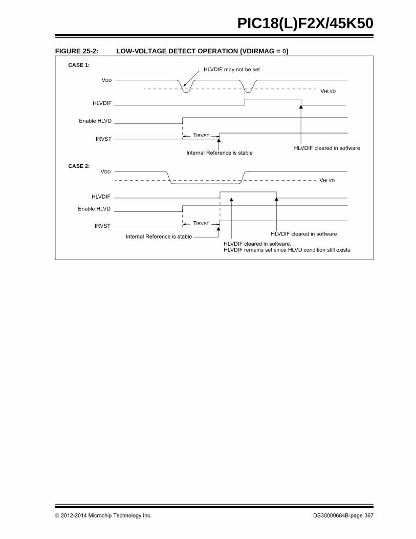
PIC18(L)F2X/45K50
FIGURE 25-2: LOW-VOLTAGE DETECT OPERATION (VDIRMAG = 0)
VHLVD
VDD
HLVDIF
VHLVD
VDD
Enable HLVD
TIRVST
HLVDIF may not be set
Enable HLVD
HLVDIF
HLVDIF cleared in software
HLVDIF cleared in software
HLVDIF cleared in software,
CASE 1:
CASE 2:
HLVDIF remains set since HLVD condition still exists
TIRVST
Internal Reference is stable
Internal Reference is stable
IRVST
IRVST
2012-2014 Microchip Technology Inc. DS30000684B-page 367
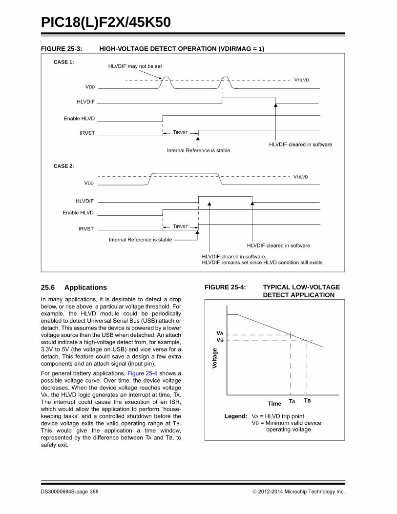
PIC18(L)F2X/45K50
FIGURE 25-3: HIGH-VOLTAGE DETECT OPERATION (VDIRMAG = 1)
25.6 Applications
In many applications, it is desirable to detect a dropbelow, or rise above, a particular voltage threshold. Forexample, the HLVD module could be periodicallyenabled to detect Universal Serial Bus (USB) attach ordetach. This assumes the device is powered by a lowervoltage source than the USB when detached. An attachwould indicate a high-voltage detect from, for example,3.3V to 5V (the voltage on USB) and vice versa for adetach. This feature could save a design a few extracomponents and an attach signal (input pin).
For general battery applications, Figure 25-4 shows apossible voltage curve. Over time, the device voltagedecreases. When the device voltage reaches voltageVA, the HLVD logic generates an interrupt at time, TA.The interrupt could cause the execution of an ISR,which would allow the application to perform “house-keeping tasks” and a controlled shutdown before thedevice voltage exits the valid operating range at TB.This would give the application a time window,represented by the difference between TA and TB, tosafely exit.
FIGURE 25-4: TYPICAL LOW-VOLTAGE DETECT APPLICATION
VHLVD
VDD
HLVDIF
VHLVD
VDD
Enable HLVD
TIRVST
HLVDIF may not be set
Enable HLVD
HLVDIF
HLVDIF cleared in software
HLVDIF cleared in software
HLVDIF cleared in software,
CASE 1:
CASE 2:
HLVDIF remains set since HLVD condition still exists
TIRVST
IRVST
Internal Reference is stable
Internal Reference is stable
IRVST
Time
Vo
lta
ge
VA
VB
TA TB
VA = HLVD trip pointVB = Minimum valid device operating voltage
Legend:
DS30000684B-page 368 2012-2014 Microchip Technology Inc.

PIC18(L)F2X/45K50
25.7 Operation During Sleep
When enabled, the HLVD circuitry continues to operateduring Sleep. If the device voltage crosses the trippoint, the HLVDIF bit will be set and the device willwake-up from Sleep. Device execution will continuefrom the interrupt vector address if interrupts havebeen globally enabled.
25.8 Effects of a Reset
A device Reset forces all registers to their Reset state.This forces the HLVD module to be turned off.
TABLE 25-1: REGISTERS ASSOCIATED WITH HIGH/LOW-VOLTAGE DETECT MODULE
Name Bit 7 Bit 6 Bit 5 Bit 4 Bit 3 Bit 2 Bit 1 Bit 0Register on page
HLVDCON VDIRMAG BGVST IRVST HLVDEN HLVDL<3:0> 364
INTCON GIE/GIEH PEIE/GIEL TMR0IE INT0IE IOCIE TMR0IF INT0IF IOCIF 114
IPR2 OSCFIP C1IP C2IP EEIP BCLIP HLVDIP TMR3IP CCP2IP 124
PIE2 OSCFIE C1IE C2IE EEIE BCLIE HLVDIE TMR3IE CCP2IE 121
PIR2 OSCFIF C1IF C2IF EEIF BCLIF HLVDIF TMR3IF CCP2IF 118
TRISA TRISA7 TRISA6 TRISA5 TRISA4 TRISA3 TRISA2 TRISA1 TRISA0 149
Legend: — = Unimplemented locations, read as ‘0’. Shaded bits are unused by the HLVD module.
2012-2014 Microchip Technology Inc. DS30000684B-page 369

PIC18(L)F2X/45K50
26.0 SPECIAL FEATURES OF THE CPU
PIC18(L)F2X/45K50 devices include several featuresintended to maximize reliability and minimize cost throughelimination of external components. These are:
• Oscillator Selection
• Resets:
- Power-on Reset (POR)
- Power-up Timer (PWRT)
- Oscillator Start-up Timer (OST)
- Brown-out Reset (BOR)
• Interrupts
• Watchdog Timer (WDT)
• Code Protection
• ID Locations
• In-Circuit Serial Programming™
The oscillator can be configured for the applicationdepending on frequency, power, accuracy and cost. Allof the options are discussed in detail in Section 3.0“Oscillator Module (With Fail-Safe Clock Monitor)”.
A complete discussion of device Resets and interruptsis available in previous sections of this data sheet.
In addition to their Power-up and Oscillator Start-upTimers provided for Resets, PIC18(L)F2X/45K50devices have a Watchdog Timer, which is eitherpermanently enabled via the Configuration bits orsoftware controlled (if configured as disabled).
The inclusion of an internal RC oscillator also providesthe additional benefits of a Fail-Safe Clock Monitor(FSCM) and Two-Speed Start-up. FSCM provides forbackground monitoring of the peripheral clock andautomatic switchover in the event of its failure. Two-Speed Start-up enables code to be executed almostimmediately on start-up, while the primary clock sourcecompletes its start-up delays.
All of these features are enabled and configured bysetting the appropriate Configuration register bits.
26.1 Configuration Bits
The Configuration bits can be programmed (read as‘0’) or left unprogrammed (read as ‘1’) to select variousdevice configurations. These bits are mapped startingat program memory location 300000h.
The user will note that address 300000h is beyond theuser program memory space. In fact, it belongs to theconfiguration memory space (300000h-3FFFFFh), whichcan only be accessed using table reads and table writes.
Programming the Configuration registers is done in amanner similar to programming the Flash memory. TheWR bit in the EECON1 register starts a self-timed writeto the Configuration register. In normal operation mode,a TBLWT instruction with the TBLPTR pointing to theConfiguration register sets up the address and the datafor the Configuration register write. Setting the WR bitstarts a long write to the Configuration register. TheConfiguration registers are written a byte at a time. Towrite or erase a configuration cell, a TBLWT instructioncan write a ‘1’ or a ‘0’ into the cell. For additional detailson Flash programming, refer to Section 7.6 “Writingto Flash Program Memory”.
DS30000684B-page 370 2012-2014 Microchip Technology Inc.

PIC18(L)F2X/45K50
TABLE 26-1: CONFIGURATION BITS AND DEVICE IDs
Address Name Bit 7 Bit 6 Bit 5 Bit 4 Bit 3 Bit 2 Bit 1 Bit 0Default/
Unprogrammed Value
300000h CONFIG1L — — LS48MHZ CPUDIV<1:0> — CFGPLLEN PLLSEL 0000 0000
300001h CONFIG1H IESO FCMEN PCLKEN — FOSC<3:0> 0010 0101
300002h CONFIG2L — LPBOR — BORV<1:0> BOREN<1:0> PWRTEN 0101 1111
300003h CONFIG2H — — WDTPS<3:0> WDTEN<1:0> 0011 1111
300004h CONFIG3L — — — — — — — — 0000 0000
300005h CONFIG3H MCLRE SDOMX — T3CMX — — PBADEN CCP2MX 1101 0011
300006h CONFIG4L DEBUG XINST ICPRT(5) — — LVP(1) — STRVEN 1010 0101
300007h CONFIG4H — — — — — — — — 1111 1111
300008h CONFIG5L — — — — CP3(2) CP2(2) CP1 CP0 0000 1111
300009h CONFIG5H CPD CPB — — — — — — 1100 0000
30000Ah CONFIG6L — — — — WRT3(2) WRT2(2) WRT1 WRT0 0000 1111
30000Bh CONFIG6H WRTD WRTB WRTC(3) — — — — — 1110 0000
30000Ch CONFIG7L — — — — EBTR3(2) EBTR2(2) EBTR1 EBTR0 0000 1111
30000Dh CONFIG7H — EBTRB — — — — — — 0100 0000
3FFFFEh DEVID1(4) DEV<2:0> REV<4:0> qqqq qqqq
3FFFFFh DEVID2(4) DEV<10:3> 0101 1100
Legend: – = unimplemented, q = value depends on condition. Shaded bits are unimplemented, read as ‘0’.
Note 1: Can only be changed when in high voltage programming mode.
2: Available on PIC18(L)F45K50 and PIC18(L)F25K50 devices only.
3: In user mode, this bit is read-only and cannot be self-programmed.
4: See Register 26-13 and Register 26-14 for DEVID values. DEVID registers are read-only and cannot be programmed by the user.
5: Available only on 44-pin TQFP package devices. Program this bit clear on all other devices.
2012-2014 Microchip Technology Inc. DS30000684B-page 371

PIC18(L)F2X/45K50
26.2 Register Definitions: Configuration Word
REGISTER 26-1: CONFIG1L: CONFIGURATION REGISTER 1 LOW
U-0 U-0 R/P-0 R/P-0 R/P-0 U-0 R/P-0 R/P-0
— — LS48MHZ CPUDIV<1:0> — CFGPLLEN PLLSEL
bit 7 bit 0
Legend:
R = Readable bit P = Programmable bit U = Unimplemented bit, read as ‘0’
-n = Value when device is unprogrammed x = Bit is unknown
bit 7-6 Unimplemented: Read as ‘0’
bit 5 LS48MHZ: USB Low-Speed Clock Selection bitSelects the clock source for Low-speed USB operation1 = System clock is expected at 48 MHz, FS/LS USB clock divide-by is set to 80 = System clock is expected at 24 MHz, FS/LS USB clock divide-by is set to 4
bit 4-3 CPUDIV<1:0>: CPU System Clock Selection bits11 = CPU system clock divided by 610 = CPU system clock divided by 301 = CPU system clock divided by 200 = No CPU system clock divide
bit 2 Unimplemented: Read as ‘0’
bit 1 CFGPLLEN: PLL Enable bit(1)
1 = Oscillator multiplied by 3 or 4, depending on the PLLSEL bit0 = Oscillator used directly
bit 0 PLLSEL: PLL Multiplier Selection bit1 = Output frequency is 3x the input frequency0 = Output frequency is 4x the input frequency
Note 1: See Table 3-1 for conditions under which the CFGPLLEN fuse is available.
DS30000684B-page 372 2012-2014 Microchip Technology Inc.

PIC18(L)F2X/45K50
REGISTER 26-2: CONFIG1H: CONFIGURATION REGISTER 1 HIGH
R/P-0 R/P-0 R/P-1 U-0 R/P-0 R/P-1 R/P-0 R/P-1
IESO FCMEN PCLKEN — FOSC<3:0>
bit 7 bit 0
Legend:
R = Readable bit P = Programmable bit U = Unimplemented bit, read as ‘0’
-n = Value when device is unprogrammed x = Bit is unknown
bit 7 IESO(1): Internal/External Oscillator Switchover bit1 = Oscillator Switchover mode enabled0 = Oscillator Switchover mode disabled
bit 6 FCMEN(1): Fail-Safe Clock Monitor Enable bit1 = Fail-Safe Clock Monitor enabled0 = Fail-Safe Clock Monitor disabled
bit 5 PCLKEN: Primary Clock Enable bit1 = Primary Clock is always enabled0 = Primary Clock can be disabled by software
bit 4 Unimplemented: Read as ‘0’
bit 3-0 FOSC<3:0>: Oscillator Selection bits1111 = Reserved1110 = Reserved1101 = EC oscillator (low power, <4 MHz)1100 = EC oscillator, CLKO function on OSC2 (low power, <4 MHz)1011 = EC oscillator (medium power, 4 MHz - 16 MHz)1010 = EC oscillator, CLKO function on OSC2 (medium power, 4 MHz - 16 MHz)1001 = Internal oscillator block, CLKO function on OSC21000 = Internal oscillator block0111 = External RC oscillator0110 = External RC oscillator, CLKO function on OSC2 0101 = EC oscillator (high power, 16 MHz - 48 MHz)0100 = EC oscillator, CLKO function on OSC2 (high power, 16 MHz - 48 MHz)0011= HS oscillator (medium power, 4 MHz - 16 MHz)0010= HS oscillator (high power, 16 MHz - 25 MHz)0001= XT oscillator0000= LP oscillator
Note 1: When FOSC<3:0> is configured for HS, XT, or LP oscillator and FCMEN bit is set, then the IESO bit should also be set to prevent a false failed clock indication and to enable automatic clock switch over from the internal oscillator block to the external oscillator when the OST times out.
2012-2014 Microchip Technology Inc. DS30000684B-page 373

PIC18(L)F2X/45K50
REGISTER 26-3: CONFIG2L: CONFIGURATION REGISTER 2 LOW
U-0 R/P-1 U-0 R/P-1 R/P-1 R/P-1 R/P-1 R/P-1
— LPBOR — BORV<1:0>(1) BOREN<1:0>(2) PWRTEN(2)
bit 7 bit 0
Legend:
R = Readable bit P = Programmable bit U = Unimplemented bit, read as ‘0’
-n = Value when device is unprogrammed x = Bit is unknown
bit 7 Unimplemented: Read as ‘0’
bit 6 LPBOR: Low-Power Brown-out Reset Enable bits1 = Low-Power Brown-out Reset disabled 0 = Low-Power Brown-out Reset enabled
bit 5 Unimplemented: Read as ‘0’
bit 4-3 BORV<1:0>: Brown-out Reset Voltage bits(1)
11 = VBOR set to 1.9V nominal10 = VBOR set to 2.2V nominal01 = VBOR set to 2.5V nominal00 = VBOR set to 2.85V nominal
bit 2-1 BOREN<1:0>: Brown-out Reset Enable bits(2)
11 = Brown-out Reset enabled in hardware only (SBOREN is disabled)10 = Brown-out Reset enabled in hardware only and disabled in Sleep mode
(SBOREN is disabled) 01 = Brown-out Reset enabled and controlled by software (SBOREN is enabled) 00 = Brown-out Reset disabled in hardware and software
bit 0 PWRTEN: Power-up Timer Enable bit(2)
1 = PWRT disabled 0 = PWRT enabled
Note 1: See Table 29-1 for specifications.
2: The Power-up Timer is decoupled from Brown-out Reset, allowing these features to be independently controlled.
DS30000684B-page 374 2012-2014 Microchip Technology Inc.

PIC18(L)F2X/45K50
REGISTER 26-4: CONFIG2H: CONFIGURATION REGISTER 2 HIGH
U-0 U-0 R/P-1 R/P-1 R/P-1 R/P-1 R/P-1 R/P-1
— — WDTPS<3:0> WDTEN<1:0>
bit 7 bit 0
Legend:
R = Readable bit P = Programmable bit U = Unimplemented bit, read as ‘0’
-n = Value when device is unprogrammed x = Bit is unknown
bit 7-6 Unimplemented: Read as ‘0’
bit 5-2 WDTPS<3:0>: Watchdog Timer Postscale Select bits1111 = 1:32,7681110 = 1:16,3841101 = 1:8,1921100 = 1:4,0961011 = 1:2,0481010 = 1:1,0241001 = 1:5121000 = 1:2560111 = 1:1280110 = 1:640101 = 1:320100 = 1:160011 = 1:80010 = 1:40001 = 1:20000 = 1:1
bit 1-0 WDTEN<1:0>: Watchdog Timer Enable bits11 = WDT enabled in hardware; SWDTEN bit disabled10 = WDT controlled by the SWDTEN bit 01 = WDT enabled when device is active, disabled when device is in Sleep; SWDTEN bit disabled00 = WDT disabled in hardware; SWDTEN bit disabled
2012-2014 Microchip Technology Inc. DS30000684B-page 375

PIC18(L)F2X/45K50
REGISTER 26-5: CONFIG3H: CONFIGURATION REGISTER 3 HIGH
R/P-1 R/P-1 U-0 R/P-1 U-0 U-0 R/P-1 R/P-1
MCLRE SDOMX — T3CMX — — PBADEN CCP2MX
bit 7 bit 0
Legend:
R = Readable bit P = Programmable bit U = Unimplemented bit, read as ‘0’
-n = Value when device is unprogrammed x = Bit is unknown
bit 7 MCLRE: MCLR Pin Enable bit 1 = MCLR pin enabled; RE3 input pin disabled0 = RE3 input pin enabled; MCLR disabled
bit 6 SDOMX: SDO Output MUX bit1 = SDO is on RB30 = SDO is on RC7
bit 5 Unimplemented: Read as ‘0’
bit 4 T3CMX: Timer3 Clock Input MUX bit1 = T3CKI is on RC00 = T3CKI is on RB5
bit 3-2 Unimplemented: Read as ‘0’
bit 1 PBADEN: PORTB A/D Enable bit1 = ANSELB<5:0> resets to 1, PORTB<5:0> pins are configured as analog inputs on Reset0 = ANSELB<5:0> resets to 0, PORTB<4:0> pins are configured as digital I/O on Reset
bit 0 CCP2MX: CCP2 MUX bit1 = CCP2 input/output is multiplexed with RC1 0 = CCP2 input/output is multiplexed with RB3
DS30000684B-page 376 2012-2014 Microchip Technology Inc.

PIC18(L)F2X/45K50
REGISTER 26-6: CONFIG4L: CONFIGURATION REGISTER 4 LOW
R/P-1 R/P-0 R/P-1 U-0 U-0 R/P-1 U-0 R/P-1
DEBUG(2) XINST ICPRT(3) — — LVP(1) — STVREN
bit 7 bit 0
Legend:
R = Readable bit P = Programmable bit U = Unimplemented bit, read as ‘0’
-n = Value when device is unprogrammed x = Bit is unknown
bit 7 DEBUG: Background Debugger Enable bit(2)
1 = Background debugger disabled, RB6 and RB7 configured as general purpose I/O pins 0 = Background debugger enabled, RB6 and RB7 are dedicated to In-Circuit Debug
bit 6 XINST: Extended Instruction Set Enable bit1 = Instruction set extension and Indexed Addressing mode enabled 0 = Instruction set extension and Indexed Addressing mode disabled (Legacy mode)
bit 5 ICPRT: Dedicated In-Circuit (ICD) Port Enable bit(3)
1 = ICPORT enabled (ICD function on dedicated ICD pins)0 = ICPORT disabled (ICD function on default ICD pins, RB6/7)
bit 4-3 Unimplemented: Read as ‘0’
bit 2 LVP: Single-Supply ICSP™ Enable bit1 = Single-Supply ICSP™ enabled 0 = Single-Supply ICSP™ disabled
bit 1 Unimplemented: Read as ‘0’
bit 0 STVREN: Stack Full/Underflow Reset Enable bit1 = Stack full/underflow will cause Reset 0 = Stack full/underflow will not cause Reset
Note 1: Can only be changed by a programmer in high-voltage programming mode.2: The DEBUG bit is managed automatically by device development tools including debuggers and programmers. For
normal device operations, this bit should be maintained as a ‘1’.3: Available only on 44-pin TQFP package devices. Program this bit clear on all other devices.
2012-2014 Microchip Technology Inc. DS30000684B-page 377

PIC18(L)F2X/45K50
REGISTER 26-7: CONFIG5L: CONFIGURATION REGISTER 5 LOW
U-0 U-0 U-0 U-0 R/C-1 R/C-1 R/C-1 R/C-1
— — — — CP3(1) CP2(1) CP1 CP0
bit 7 bit 0
Legend:
R = Readable bit U = Unimplemented bit, read as ‘0’
-n = Value when device is unprogrammed C = Clearable only bit
bit 7-4 Unimplemented: Read as ‘0’
bit 3 CP3: Code Protection bit(1)
1 = Block 3 not code-protected 0 = Block 3 code-protected
bit 2 CP2: Code Protection bit(1)
1 = Block 2 not code-protected 0 = Block 2 code-protected
bit 1 CP1: Code Protection bit1 = Block 1 not code-protected 0 = Block 1 code-protected
bit 0 CP0: Code Protection bit1 = Block 0 not code-protected 0 = Block 0 code-protected
Note 1: Available on PIC18(L)F45K50 and PIC18(L)F25K50 devices.
REGISTER 26-8: CONFIG5H: CONFIGURATION REGISTER 5 HIGH
R/C-1 R/C-1 U-0 U-0 U-0 U-0 U-0 U-0
CPD CPB — — — — — —
bit 7 bit 0
Legend:
R = Readable bit U = Unimplemented bit, read as ‘0’
-n = Value when device is unprogrammed C = Clearable only bit
bit 7 CPD: Data EEPROM Code Protection bit1 = Data EEPROM not code-protected0 = Data EEPROM code-protected
bit 6 CPB: Boot Block Code Protection bit1 = Boot Block not code-protected0 = Boot Block code-protected
bit 5-0 Unimplemented: Read as ‘0’
DS30000684B-page 378 2012-2014 Microchip Technology Inc.

PIC18(L)F2X/45K50
REGISTER 26-9: CONFIG6L: CONFIGURATION REGISTER 6 LOW
U-0 U-0 U-0 U-0 R/C-1 R/C-1 R/C-1 R/C-1
— — — — WRT3(1) WRT2(1) WRT1 WRT0
bit 7 bit 0
Legend:
R = Readable bit U = Unimplemented bit, read as ‘0’
-n = Value when device is unprogrammed C = Clearable only bit
bit 7-4 Unimplemented: Read as ‘0’
bit 3 WRT3: Write Protection bit(1)
1 = Block 3 not write-protected 0 = Block 3 write-protected
bit 2 WRT2: Write Protection bit(1)
1 = Block 2 not write-protected0 = Block 2 write-protected
bit 1 WRT1: Write Protection bit1 = Block 1 not write-protected0 = Block 1 write-protected
bit 0 WRT0: Write Protection bit1 = Block 0 not write-protected0 = Block 0 write-protected
Note 1: Available on PIC18(L)F45K50 and PIC18(L)F25K50 devices.
2012-2014 Microchip Technology Inc. DS30000684B-page 379

PIC18(L)F2X/45K50
REGISTER 26-10: CONFIG6H: CONFIGURATION REGISTER 6 HIGH
R/C-1 R/C-1 R/C-1 U-0 U-0 U-0 U-0 U-0
WRTD WRTB WRTC(1) — — — — —
bit 7 bit 0
Legend:
R = Readable bit U = Unimplemented bit, read as ‘0’
-n = Value when device is unprogrammed C = Clearable only bit
bit 7 WRTD: Data EEPROM Write Protection bit1 = Data EEPROM not write-protected0 = Data EEPROM write-protected
bit 6 WRTB: Boot Block Write Protection bit1 = Boot Block not write-protected0 = Boot Block write-protected
bit 5 WRTC: Configuration Register Write Protection bit(1)
1 = Configuration registers not write-protected0 = Configuration registers write-protected
bit 4-0 Unimplemented: Read as ‘0’
Note 1: This bit is read-only in normal execution mode; it can be written only in ICSP™ mode.
REGISTER 26-11: CONFIG7L: CONFIGURATION REGISTER 7 LOW
U-0 U-0 U-0 U-0 R/C-1 R/C-1 R/C-1 R/C-1
— — — — EBTR3(1) EBTR2(1) EBTR1 EBTR0
bit 7 bit 0
Legend:
R = Readable bit U = Unimplemented bit, read as ‘0’
-n = Value when device is unprogrammed C = Clearable only bit
bit 7-4 Unimplemented: Read as ‘0’
bit 3 EBTR3: Table Read Protection bit(1)
1 = Block 3 not protected from table reads executed in other blocks0 = Block 3 protected from table reads executed in other blocks
bit 2 EBTR2: Table Read Protection bit(1)
1 = Block 2 not protected from table reads executed in other blocks 0 = Block 2 protected from table reads executed in other blocks
bit 1 EBTR1: Table Read Protection bit1 = Block 1 not protected from table reads executed in other blocks 0 = Block 1 protected from table reads executed in other blocks
bit 0 EBTR0: Table Read Protection bit1 = Block 0 not protected from table reads executed in other blocks 0 = Block 0 protected from table reads executed in other blocks
Note 1: Available on PIC18(L)F45K50 and PIC18(L)F25K50 devices.
DS30000684B-page 380 2012-2014 Microchip Technology Inc.

PIC18(L)F2X/45K50
REGISTER 26-12: CONFIG7H: CONFIGURATION REGISTER 7 HIGH
U-0 R/C-1 U-0 U-0 U-0 U-0 U-0 U-0
— EBTRB — — — — — —
bit 7 bit 0
Legend:
R = Readable bit U = Unimplemented bit, read as ‘0’
-n = Value when device is unprogrammed C = Clearable only bit
bit 7 Unimplemented: Read as ‘0’
bit 6 EBTRB: Boot Block Table Read Protection bit1 = Boot Block not protected from table reads executed in other blocks0 = Boot Block protected from table reads executed in other blocks
bit 5-0 Unimplemented: Read as ‘0’
REGISTER 26-13: DEVID1: DEVICE ID REGISTER 1
R R R R R R R R
DEV2 DEV1 DEV0 REV4 REV3 REV2 REV1 REV0
bit 7 bit 0
Legend:
R = Readable bit U = Unimplemented bit, read as ‘0’
-n = Value when device is unprogrammed C = Clearable only bit
bit 7-5 DEV<2:0>: Device ID bitsThese bits, together with DEV<10:3> in DEVID2, determine the device ID. See Table 26-2 for complete Device ID list.
bit 4-0 REV<4:0>: Revision ID bitsThese bits indicate the device revision.
REGISTER 26-14: DEVID2: DEVICE ID REGISTER 2
R R R R R R R R
DEV10 DEV9 DEV8 DEV7 DEV6 DEV5 DEV4 DEV3
bit 7 bit 0
Legend:
R = Readable bit U = Unimplemented bit, read as ‘0’
-n = Value when device is unprogrammed C = Clearable only bit
bit 7-0 DEV<10:3>: Device ID bitsThese bits, together with DEV<2:0> in DEVID1, determine the device ID. See Table 26-2 for complete Device ID list.
2012-2014 Microchip Technology Inc. DS30000684B-page 381

PIC18(L)F2X/45K50
TABLE 26-2: DEVICE ID TABLE FOR THE PIC18(L)F2X/45K50 FAMILY
DEV<10:3> DEV<2:0> Part Number
0101 1100
000 PIC18F45K50
001 PIC18F25K50
011 PIC18F24K50
100 PIC18LF45K50
101 PIC18LF25K50
111 PIC18LF24K50
DS30000684B-page 382 2012-2014 Microchip Technology Inc.

PIC18(L)F2X/45K50
26.3 Watchdog Timer (WDT)
For PIC18(L)F2X/45K50 devices, the WDT is driven bythe INTRC source. When the WDT is enabled, theclock source is also enabled. The nominal WDT periodis 4 ms and has the same stability as the INTRCoscillator.
The 4 ms period of the WDT is multiplied by a 16-bitpostscaler. Any output of the WDT postscaler isselected by a multiplexer, controlled by bits in Configu-ration Register 2H. Available periods range from 4 msto 131.072 seconds (2.18 minutes). The WDT andpostscaler are cleared when any of the following eventsoccur: a SLEEP or CLRWDT instruction is executed, theIRCF bits of the OSCCON register are changed or aclock failure has occurred.
FIGURE 26-1: WDT BLOCK DIAGRAM
Note 1: The CLRWDT and SLEEP instructionsclear the WDT and postscaler countswhen executed.
2: Changing the setting of the IRCF bits ofthe OSCCON register clears the WDTand postscaler counts.
3: When a CLRWDT instruction is executed,the postscaler count will be cleared.
INTRC Source
WDT
Wake-up
Reset
WDT Counter
Programmable Postscaler1:1 to 1:32,768
Enable WDT
WDTPS<3:0>
SWDTENWDTEN
CLRWDT
4
from Power
Reset
All Device Resets
Sleep
128
Change on IRCF bitsManaged Modes
2012-2014 Microchip Technology Inc. DS30000684B-page 383

PIC18(L)F2X/45K50
26.3.1 CONTROL REGISTER
Register 26-15 shows the WDTCON register. This is areadable and writable register which contains a controlbit that allows software to override the WDT enableConfiguration bit, but only if the Configuration bit hasdisabled the WDT.
26.4 Register Definitions: WDT Control
TABLE 26-4: CONFIGURATION REGISTERS ASSOCIATED WITH WATCHDOG TIMER
REGISTER 26-15: WDTCON: WATCHDOG TIMER CONTROL REGISTER
U-0 U-0 U-0 U-0 U-0 U-0 U-0 R/W-0
— — — — — — — SWDTEN(1)
bit 7 bit 0
Legend:
R = Readable bit W = Writable bit U = Unimplemented bit, read as ‘0’
-n = Value at POR ‘1’ = Bit is set ‘0’ = Bit is cleared x = Bit is unknown
bit 7-1 Unimplemented: Read as ‘0’
bit 0 SWDTEN: Software Enable or Disable the Watchdog Timer bit(1)
1 = WDT is turned on0 = WDT is turned off (Reset value)
Note 1: This bit has no effect unless the Configuration bit, WDTEN<1:0>, is set to 10b (SWDTEN enabled).
TABLE 26-3: REGISTERS ASSOCIATED WITH WATCHDOG TIMER
Name Bit 7 Bit 6 Bit 5 Bit 4 Bit 3 Bit 2 Bit 1 Bit 0Register on page
RCON IPEN SBOREN — RI TO PD POR BOR 64
WDTCON — — — — — — — SWDTEN 384
Legend: — = unimplemented, read as ‘0’. Shaded bits are not used by the Watchdog Timer.
Name Bit 7 Bit 6 Bit 5 Bit 4 Bit 3 Bit 2 Bit 1 Bit 0Register on page
CONFIG2H — — WDTPS<3:0> WDTEN<1:0> 375
Legend: — = unimplemented, read as ‘0’. Shaded bits are not used by the Watchdog Timer.
DS30000684B-page 384 2012-2014 Microchip Technology Inc.

PIC18(L)F2X/45K50
26.5 Program Verification and Code Protection
The overall structure of the code protection on thePIC18 Flash devices differs significantly from other PICmicrocontroller devices.
The user program memory is divided into three or fiveblocks, depending on the device. One of these is aBoot Block of 0.5K or 2K bytes, depending on thedevice. The remainder of the memory is divided intoindividual blocks on binary boundaries.
Each of the blocks has three code protection bitsassociated with them. They are:
• Code-Protect bit (CPn)
• Write-Protect bit (WRTn)
• External Block Table Read bit (EBTRn)
Figure 26-2 shows the program memory organizationfor 16 and 32-Kbyte devices and the specific codeprotection bit associated with each block. The actuallocations of the bits are summarized in Table 26-5.
FIGURE 26-2: CODE-PROTECTED PROGRAM MEMORY FOR PIC18(L)F2X/45K50
MEMORY SIZE/DEVICEBlock Code Protection
Controlled By:16 Kbytes(PIC18(L)F24K50)
32 Kbytes(PIC18(L)FX5K50)
Boot Block(000h-7FFh)
Boot Block(000h-7FFh)
CPB, WRTB, EBTRB
Block 0(800h-1FFFh)
Block 0(800h-1FFFh)
CP0, WRT0, EBTR0
Block 1(2000h-3FFFh)
Block 1(2000h-3FFFh)
CP1, WRT1, EBTR1
UnimplementedRead ‘0’s
(4000h-1FFFFFh)
Block 2(4000h-5FFFh)
CP2, WRT2, EBTR2
Block 3(6000h-7FFFh)
CP3, WRT3, EBTR3
UnimplementedRead ‘0’s
(8000h-1FFFFFh)
(Unimplemented Memory Space)
TABLE 26-5: CONFIGURATION REGISTERS ASSOCIATED WITH CODE PROTECTION
File Name Bit 7 Bit 6 Bit 5 Bit 4 Bit 3 Bit 2 Bit 1 Bit 0
300008h CONFIG5L — — — — CP3(1) CP2(1) CP1 CP0
300009h CONFIG5H CPD CPB — — — — — —
30000Ah CONFIG6L — — — — WRT3(1) WRT2(1) WRT1 WRT0
30000Bh CONFIG6H WRTD WRTB WRTC(2) — — — — —
30000Ch CONFIG7L — — — — EBTR3(1) EBTR2(1) EBTR1 EBTR0
30000Dh CONFIG7H — EBTRB — — — — — —
Legend: Shaded bits are unimplemented.
Note 1: Available on PIC18(L)F45K50 and PIC18(L)F25K50 devices only.
2: In User mode, this bit is read-only and cannot be self-programmed.
2012-2014 Microchip Technology Inc. DS30000684B-page 385
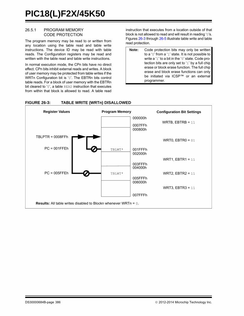
PIC18(L)F2X/45K50
26.5.1 PROGRAM MEMORYCODE PROTECTION
The program memory may be read to or written fromany location using the table read and table writeinstructions. The device ID may be read with tablereads. The Configuration registers may be read andwritten with the table read and table write instructions.
In normal execution mode, the CPn bits have no directeffect. CPn bits inhibit external reads and writes. A blockof user memory may be protected from table writes if theWRTn Configuration bit is ‘0’. The EBTRn bits controltable reads. For a block of user memory with the EBTRnbit cleared to ‘0’, a table READ instruction that executesfrom within that block is allowed to read. A table read
instruction that executes from a location outside of thatblock is not allowed to read and will result in reading ‘0’s.Figures 26-3 through 26-5 illustrate table write and tableread protection.
FIGURE 26-3: TABLE WRITE (WRTn) DISALLOWED
Note: Code protection bits may only be writtento a ‘0’ from a ‘1’ state. It is not possible towrite a ‘1’ to a bit in the ‘0’ state. Code pro-tection bits are only set to ‘1’ by a full chiperase or block erase function. The full chiperase and block erase functions can onlybe initiated via ICSP™ or an externalprogrammer.
000000h
0007FFh000800h
001FFFh002000h
003FFFh004000h
005FFFh006000h
007FFFh
WRTB, EBTRB = 11
WRT0, EBTR0 = 01
WRT1, EBTR1 = 11
WRT2, EBTR2 = 11
WRT3, EBTR3 = 11
TBLWT*
TBLPTR = 0008FFh
PC = 001FFEh
TBLWT*PC = 005FFEh
Register Values Program Memory Configuration Bit Settings
Results: All table writes disabled to Blockn whenever WRTn = 0.
DS30000684B-page 386 2012-2014 Microchip Technology Inc.

PIC18(L)F2X/45K50
FIGURE 26-4: EXTERNAL BLOCK TABLE READ (EBTRn) DISALLOWED
FIGURE 26-5: INTERNAL BLOCK TABLE READ (EBTRn) ALLOWED
WRTB, EBTRB = 11
WRT0, EBTR0 = 10
WRT1, EBTR1 = 11
WRT2, EBTR2 = 11
WRT3, EBTR3 = 11
TBLRD*
TBLPTR = 0008FFh
PC = 003FFEh
Results: All table reads from external blocks to Blockn are disabled whenever EBTRn = 0.TABLAT register returns a value of ‘0’.
Register Values Program Memory Configuration Bit Settings
000000h
0007FFh000800h
001FFFh002000h
003FFFh004000h
005FFFh006000h
007FFFh
WRTB, EBTRB = 11
WRT0, EBTR0 = 10
WRT1, EBTR1 = 11
WRT2, EBTR2 = 11
WRT3, EBTR3 = 11
TBLRD*
TBLPTR = 0008FFh
PC = 001FFEh
Register Values Program Memory Configuration Bit Settings
Results: Table reads permitted within Blockn, even when EBTRBn = 0.TABLAT register returns the value of the data at the location TBLPTR.
000000h
0007FFh000800h
001FFFh002000h
003FFFh004000h
005FFFh006000h
007FFFh
2012-2014 Microchip Technology Inc. DS30000684B-page 387

PIC18(L)F2X/45K50
26.5.2 DATA EEPROM CODE PROTECTION
The entire data EEPROM is protected from externalreads and writes by two bits: CPD and WRTD. CPDinhibits external reads and writes of data EEPROM.WRTD inhibits internal and external writes to dataEEPROM. The CPU can always read data EEPROMunder normal operation, regardless of the protection bitsettings.
26.5.3 CONFIGURATION REGISTER PROTECTION
The Configuration registers can be write-protected.The WRTC bit controls protection of the Configurationregisters. In normal execution mode, the WRTC bit isreadable only. WRTC can only be written via ICSP oran external programmer.
26.6 ID Locations
Eight memory locations (200000h-200007h) aredesignated as ID locations, where the user can storechecksum or other code identification numbers. Theselocations are both readable and writable during normalexecution through the TBLRD and TBLWT instructionsor during program/verify. The ID locations can be readwhen the device is code-protected.
26.7 In-Circuit Serial Programming
PIC18(L)F2X/45K50 devices can be seriallyprogrammed while in the end application circuit. This issimply done with two lines for clock and data and threeother lines for power, ground and the programmingvoltage. This allows customers to manufacture boardswith unprogrammed devices and then program themicrocontroller just before shipping the product. Thisalso allows the most recent firmware or a customfirmware to be programmed.
26.8 In-Circuit Debugger
When the DEBUG Configuration bit is programmed toa ‘0’, the In-Circuit Debugger functionality is enabled.This function allows simple debugging functions whenused with MPLAB® IDE. When the microcontroller hasthis feature enabled, some resources are not availablefor general use. Table 26-6 shows which resources arerequired by the background debugger.
TABLE 26-6: DEBUGGER RESOURCES
To use the In-Circuit Debugger function of themicrocontroller, the design must implement In-CircuitSerial Programming connections to the following pins:
• MCLR/VPP/RE3
• VDD
• VSS
• RB7
• RB6
This will interface to the In-Circuit Debugger moduleavailable from Microchip or one of the third partydevelopment tool companies.
26.9 Special ICPORT Features (44-Pin TQFP Package Only)
Under specific circumstances, the No Connect (NC)pins of devices in 44-pin TQFP packages can provideadditional functionality. These features are controlledby device Configuration bits and are available only inthis package type and pin count.
26.9.1 DEDICATED ICD/ICSP PORT
The 44-pin TQFP devices can use NC pins to providean alternate port for In-Circuit Debugging (ICD) and In-Circuit Serial Programming (ICSP). These pins are col-lectively known as the dedicated ICSP/ICD port, sincethey are not shared with any other function of thedevice.
When implemented, the dedicated port activates threeNC pins to provide an alternate device Reset, data andclock ports. None of these ports overlap with standardI/O pins, making the I/O pins available to the user’sapplication. The port functions the same way as thelegacy ICSP/ICD/MCLR pins on RB6/RB7/MCLR andthey have the same electrical specifications as theirrespective pins.
Table 26-7 identifies the functionally equivalent pinsfor ICSP and ICD purposes. The dedicated ICSP/ICDport is enabled by setting the ICPRT Configuration bit.This bit is set by default on 44-pin TQFP devices andcan only be set and cleared when using the MCLR/RB6/RB7 ICSP interface.
When ICPRT is set, several things must be taken intoconsideration. First and foremost, the ICRST pinfunctions as an additional MCLR pin and must bepulled high to keep the part out of Reset. Second, whilethe MCLR/RB6/RB7 pins can still be used to programthe part, the dedicated ICPORT pins must be used todebug the part. Finally, the MCLRE bit still works asnormal, meaning that if ICPRT = 1 and MCLRE = 0,MCLR will function as a general purpose RE3 input,with the ICRST providing the normal MCLR Resetfunctions.
I/O pins: RB6, RB7
DS30000684B-page 388 2012-2014 Microchip Technology Inc.

PIC18(L)F2X/45K50
TABLE 26-7: EQUIVALENT PINS FOR LEGACY AND DEDICATED ICD/ICSP™ PORTS
26.10 Single-Supply ICSP Programming
The LVP Configuration bit enables Single-Supply ICSPProgramming (formerly known as Low-Voltage ICSPProgramming or LVP). When Single-Supply Program-ming is enabled, the microcontroller can be programmedwithout requiring high voltage being applied to theMCLR/VPP/RE3 pin. See “PIC18(L)F2X/4XK50 FlashMemory Programming Specification” (DS41630) formore details about low voltage programming.
The LVP bit may be set or cleared only when usingstandard high-voltage programming (VIHH applied tothe MCLR/VPP/RE3 pin). Once LVP has been disabled,only the standard high-voltage programming isavailable and must be used to program the device.
Memory that is not code-protected can be erased usingeither a block erase, or erased row by row, then writtenat any specified VDD. If code-protected memory is to beerased, a block erase is required.
Pin NamePin
TypePin FunctionLegacy
PortDedicated
Port
MCLR/VPP/RE3
NC/ICRST/ICVPP
P Device Reset and Programming Enable
RB6/IOCB6/PGC
NC/ICCK/ICPGC
I Serial Clock
RB7/IOCB7/PGD
NC/ICDT/ICPGD
I/O Serial Data
Legend: I = Input, O = Output, P = Power
Note 1: High-voltage programming is alwaysavailable, regardless of the state of theLVP bit, by applying VIHH to the MCLRpin.
2: By default, Single-Supply ICSP™ isenabled in unprogrammed devices (assupplied from Microchip) and eraseddevices.
3: While in Low-Voltage ICSP™ mode,MCLR is always enabled, regardless ofthe MCLRE bit, and the RE3 pin can nolonger be used as a general purposeinput.
2012-2014 Microchip Technology Inc. DS30000684B-page 389

PIC18(L)F2X/45K50
27.0 INSTRUCTION SET SUMMARY
PIC18(L)F2X/45K50 devices incorporate the standardset of 75 PIC18 core instructions, as well as an extendedset of eight new instructions, for the optimization of codethat is recursive or that utilizes a software stack. Theextended set is discussed later in this section.
27.1 Standard Instruction Set
The standard PIC18 instruction set adds manyenhancements to the previous PIC MCU instructionsets, while maintaining an easy migration from thesePIC MCU instruction sets. Most instructions are asingle program memory word (16 bits), but there arefour instructions that require two program memorylocations.
Each single-word instruction is a 16-bit word dividedinto an opcode, which specifies the instruction type andone or more operands, which further specify theoperation of the instruction.
The instruction set is highly orthogonal and is groupedinto four basic categories:
• Byte-oriented operations
• Bit-oriented operations
• Literal operations
• Control operations
The PIC18 instruction set summary in Table 27-2 listsbyte-oriented, bit-oriented, literal and controloperations. Table 27-1 shows the opcode fielddescriptions.
Most byte-oriented instructions have three operands:
1. The file register (specified by ‘f’)
2. The destination of the result (specified by ‘d’)
3. The accessed memory (specified by ‘a’)
The file register designator ‘f’ specifies which fileregister is to be used by the instruction. The destinationdesignator ‘d’ specifies where the result of the opera-tion is to be placed. If ‘d’ is zero, the result is placed inthe WREG register. If ‘d’ is one, the result is placed inthe file register specified in the instruction.
All bit-oriented instructions have three operands:
1. The file register (specified by ‘f’)
2. The bit in the file register (specified by ‘b’)
3. The accessed memory (specified by ‘a’)
The bit field designator ‘b’ selects the number of the bitaffected by the operation, while the file registerdesignator ‘f’ represents the number of the file in whichthe bit is located.
The literal instructions may use some of the followingoperands:
• A literal value to be loaded into a file register (specified by ‘k’)
• The desired FSR register to load the literal value into (specified by ‘f’)
• No operand required (specified by ‘—’)
The control instructions may use some of the followingoperands:
• A program memory address (specified by ‘n’)
• The mode of the CALL or RETURN instructions (specified by ‘s’)
• The mode of the table read and table write instructions (specified by ‘m’)
• No operand required (specified by ‘—’)
All instructions are a single word, except for fourdouble-word instructions. These instructions weremade double-word to contain the required informationin 32 bits. In the second word, the 4 MSbs are ‘1’s. Ifthis second word is executed as an instruction (byitself), it will execute as a NOP.
All single-word instructions are executed in a singleinstruction cycle, unless a conditional test is true or theprogram counter is changed as a result of the instruc-tion. In these cases, the execution takes two instructioncycles, with the additional instruction cycle(s) executedas a NOP.
The double-word instructions execute in two instructioncycles.
One instruction cycle consists of four oscillator periods.Thus, for an oscillator frequency of 4 MHz, the normalinstruction execution time is 1 s. If a conditional test istrue, or the program counter is changed as a result ofan instruction, the instruction execution time is 2 s.Two-word branch instructions (if true) would take 3 s.
Figure 27-1 shows the general formats that the instruc-tions can have. All examples use the convention ‘nnh’to represent a hexadecimal number.
The Instruction Set Summary, shown in Table 27-2,lists the standard instructions recognized by theMicrochip Assembler (MPASMTM).
Section 27.1.1 “Standard Instruction Set” providesa description of each instruction.
DS30000684B-page 390 2012-2014 Microchip Technology Inc.

PIC18(L)F2X/45K50
TABLE 27-1: OPCODE FIELD DESCRIPTIONS
Field Description
a RAM access bita = 0: RAM location in Access RAM (BSR register is ignored)a = 1: RAM bank is specified by BSR register
bbb Bit address within an 8-bit file register (0 to 7).
BSR Bank Select Register. Used to select the current RAM bank.
C, DC, Z, OV, N ALU Status bits: Carry, Digit Carry, Zero, Overflow, Negative.
d Destination select bitd = 0: store result in WREGd = 1: store result in file register f
dest Destination: either the WREG register or the specified register file location.
f 8-bit Register file address (00h to FFh) or 2-bit FSR designator (0h to 3h).
fs 12-bit Register file address (000h to FFFh). This is the source address.
fd 12-bit Register file address (000h to FFFh). This is the destination address.
GIE Global Interrupt Enable bit.
k Literal field, constant data or label (may be either an 8-bit, 12-bit or a 20-bit value).
label Label name.
mm The mode of the TBLPTR register for the table read and table write instructions.Only used with table read and table write instructions:
* No change to register (such as TBLPTR with table reads and writes)
*+ Post-Increment register (such as TBLPTR with table reads and writes)
*- Post-Decrement register (such as TBLPTR with table reads and writes)
+* Pre-Increment register (such as TBLPTR with table reads and writes)
n The relative address (2’s complement number) for relative branch instructions or the direct address for CALL/BRANCH and RETURN instructions.
PC Program Counter.
PCL Program Counter Low Byte.
PCH Program Counter High Byte.
PCLATH Program Counter High Byte Latch.
PCLATU Program Counter Upper Byte Latch.
PD Power-down bit.
PRODH Product of Multiply High Byte.
PRODL Product of Multiply Low Byte.
s Fast Call/Return mode select bits = 0: do not update into/from shadow registerss = 1: certain registers loaded into/from shadow registers (Fast mode)
TBLPTR 21-bit Table Pointer (points to a Program Memory location).
TABLAT 8-bit Table Latch.
TO Time-out bit.
TOS Top-of-Stack.
u Unused or unchanged.
WDT Watchdog Timer.
WREG Working register (accumulator).
x Don’t care (‘0’ or ‘1’). The assembler will generate code with x = 0. It is the recommended form of use for compatibility with all Microchip software tools.
zs 7-bit offset value for indirect addressing of register files (source).
zd 7-bit offset value for indirect addressing of register files (destination).
Optional argument.
[text] Indicates an indexed address.
(text) The contents of text.
[expr]<n> Specifies bit n of the register indicated by the pointer expr.
Assigned to.
< > Register bit field.
In the set of.
italics User defined term (font is Courier).
2012-2014 Microchip Technology Inc. DS30000684B-page 391

PIC18(L)F2X/45K50
FIGURE 27-1: GENERAL FORMAT FOR INSTRUCTIONS
Byte-oriented file register operations
15 10 9 8 7 0
d = 0 for result destination to be WREG register
OPCODE d a f (FILE #)
d = 1 for result destination to be file register (f)a = 0 to force Access Bank
Bit-oriented file register operations
15 12 11 9 8 7 0
OPCODE b (BIT #) a f (FILE #)
b = 3-bit position of bit in file register (f)
Literal operations
15 8 7 0
OPCODE k (literal)
k = 8-bit immediate value
Byte to Byte move operations (2-word)
15 12 11 0
OPCODE f (Source FILE #)
CALL, GOTO and Branch operations
15 8 7 0
OPCODE n<7:0> (literal)
n = 20-bit immediate value
a = 1 for BSR to select bankf = 8-bit file register address
a = 0 to force Access Banka = 1 for BSR to select bankf = 8-bit file register address
15 12 11 0
1111 n<19:8> (literal)
15 12 11 0
1111 f (Destination FILE #)
f = 12-bit file register address
Control operations
Example Instruction
ADDWF MYREG, W, B
MOVFF MYREG1, MYREG2
BSF MYREG, bit, B
MOVLW 7Fh
GOTO Label
15 8 7 0
OPCODE n<7:0> (literal)
15 12 11 0
1111 n<19:8> (literal)
CALL MYFUNC
15 11 10 0
OPCODE n<10:0> (literal)
S = Fast bit
BRA MYFUNC
15 8 7 0
OPCODE n<7:0> (literal) BC MYFUNC
S
DS30000684B-page 392 2012-2014 Microchip Technology Inc.

PIC18(L)F2X/45K50
TABLE 27-2: PIC18 INSTRUCTION SET
Mnemonic,Operands
Description Cycles16-Bit Instruction Word Status
AffectedNotes
MSb LSb
BYTE-ORIENTED OPERATIONS
ADDWFADDWFCANDWFCLRFCOMFCPFSEQCPFSGTCPFSLTDECFDECFSZDCFSNZINCFINCFSZINFSNZIORWFMOVFMOVFF
MOVWFMULWFNEGFRLCFRLNCFRRCFRRNCFSETFSUBFWB
SUBWFSUBWFB
SWAPFTSTFSZXORWF
f, d, af, d, af, d, af, af, d, af, af, af, af, d, af, d, af, d, af, d, af, d, af, d, af, d, af, d, afs, fd
f, af, af, af, d, af, d, af, d, af, d, af, af, d, a
f, d, af, d, a
f, d, af, af, d, a
Add WREG and fAdd WREG and CARRY bit to fAND WREG with fClear fComplement fCompare f with WREG, skip =Compare f with WREG, skip >Compare f with WREG, skip <Decrement fDecrement f, Skip if 0Decrement f, Skip if Not 0Increment fIncrement f, Skip if 0Increment f, Skip if Not 0Inclusive OR WREG with fMove fMove fs (source) to 1st word
fd (destination) 2nd wordMove WREG to fMultiply WREG with fNegate fRotate Left f through CarryRotate Left f (No Carry)Rotate Right f through CarryRotate Right f (No Carry)Set fSubtract f from WREG with borrow Subtract WREG from fSubtract WREG from f with borrowSwap nibbles in fTest f, skip if 0Exclusive OR WREG with f
111111 (2 or 3)1 (2 or 3)1 (2 or 3)11 (2 or 3)1 (2 or 3)11 (2 or 3)1 (2 or 3)112
111111111
11
11 (2 or 3)1
001000100001011000010110011001100000001001000010001101000001010111001111011000000110001101000011010001100101
01010101
001101100001
01da00da01da101a11da001a010a000a01da11da11da10da11da10da00da00daffffffff111a001a110a01da01da00da00da100a01da
11da10da
10da011a10da
ffffffffffffffffffffffffffffffffffffffffffffffffffffffffffffffffffffffffffffffffffffffffffffffffffffffffffff
ffffffff
ffffffffffff
ffffffffffffffffffffffffffffffffffffffffffffffffffffffffffffffffffffffffffffffffffffffffffffffffffffffffffff
ffffffff
ffffffffffff
C, DC, Z, OV, NC, DC, Z, OV, NZ, NZZ, NNoneNoneNoneC, DC, Z, OV, NNoneNoneC, DC, Z, OV, NNoneNoneZ, NZ, NNone
NoneNoneC, DC, Z, OV, NC, Z, NZ, NC, Z, NZ, NNoneC, DC, Z, OV, N
C, DC, Z, OV, NC, DC, Z, OV, N
NoneNoneZ, N
1, 21, 21,221, 2441, 21, 2, 3, 41, 2, 3, 41, 21, 2, 3, 441, 21, 21
1, 2
1, 2
1, 2
1, 2
41, 2
Note 1: When a PORT register is modified as a function of itself (e.g., MOVF PORTB, 1, 0), the value used will be that value present on the pins themselves. For example, if the data latch is ‘1’ for a pin configured as input and is driven low by an external device, the data will be written back with a ‘0’.
2: If this instruction is executed on the TMR0 register (and where applicable, ‘d’ = 1), the prescaler will be cleared if assigned.
3: If Program Counter (PC) is modified or a conditional test is true, the instruction requires two cycles. The second cycle is executed as a NOP.
4: Some instructions are two-word instructions. The second word of these instructions will be executed as a NOP unless the first word of the instruction retrieves the information embedded in these 16 bits. This ensures that all program memory locations have a valid instruction.
2012-2014 Microchip Technology Inc. DS30000684B-page 393
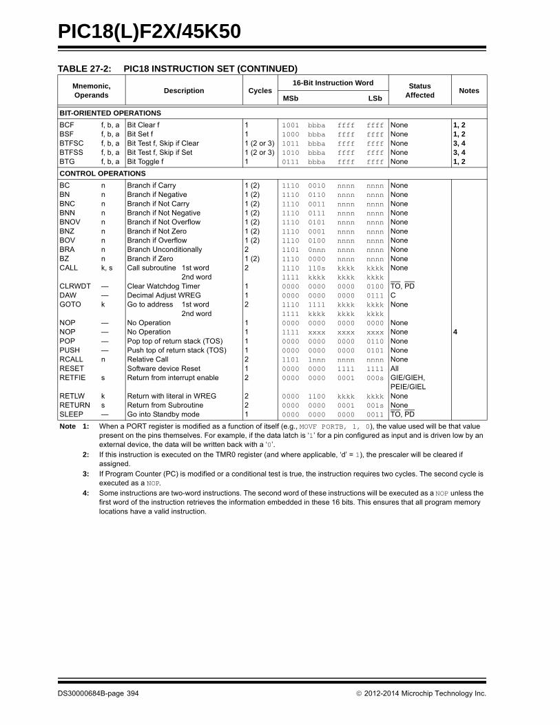
PIC18(L)F2X/45K50
BIT-ORIENTED OPERATIONS
BCFBSFBTFSCBTFSSBTG
f, b, af, b, af, b, af, b, af, b, a
Bit Clear fBit Set fBit Test f, Skip if ClearBit Test f, Skip if SetBit Toggle f
111 (2 or 3)1 (2 or 3)1
10011000101110100111
bbbabbbabbbabbbabbba
ffffffffffffffffffff
ffffffffffffffffffff
NoneNoneNoneNoneNone
1, 21, 23, 43, 41, 2
CONTROL OPERATIONS
BCBNBNCBNNBNOVBNZBOVBRABZCALL
CLRWDTDAWGOTO
NOPNOPPOPPUSHRCALLRESETRETFIE
RETLWRETURNSLEEP
nnnnnnnnnk, s
——k
————n
s
ks—
Branch if CarryBranch if NegativeBranch if Not CarryBranch if Not NegativeBranch if Not OverflowBranch if Not ZeroBranch if OverflowBranch Unconditionally Branch if ZeroCall subroutine 1st word
2nd wordClear Watchdog TimerDecimal Adjust WREGGo to address 1st word
2nd wordNo OperationNo OperationPop top of return stack (TOS)Push top of return stack (TOS)Relative CallSoftware device ResetReturn from interrupt enable
Return with literal in WREG Return from SubroutineGo into Standby mode
1 (2)1 (2)1 (2)1 (2)1 (2)1 (2)1 (2)21 (2)2
112
1111212
221
1110111011101110111011101110110111101110111100000000111011110000111100000000110100000000
000000000000
00100110001101110101000101000nnn0000110skkkk000000001111kkkk0000xxxx000000001nnn00000000
110000000000
nnnnnnnnnnnnnnnnnnnnnnnnnnnnnnnnnnnnkkkkkkkk00000000kkkkkkkk0000xxxx00000000nnnn11110001
kkkk00010000
nnnnnnnnnnnnnnnnnnnnnnnnnnnnnnnnnnnnkkkkkkkk01000111kkkkkkkk0000xxxx01100101nnnn1111000s
kkkk001s0011
NoneNoneNoneNoneNoneNoneNoneNoneNoneNone
TO, PDCNone
NoneNoneNoneNoneNoneAllGIE/GIEH, PEIE/GIELNoneNoneTO, PD
4
TABLE 27-2: PIC18 INSTRUCTION SET (CONTINUED)
Mnemonic,Operands
Description Cycles16-Bit Instruction Word Status
AffectedNotes
MSb LSb
Note 1: When a PORT register is modified as a function of itself (e.g., MOVF PORTB, 1, 0), the value used will be that value present on the pins themselves. For example, if the data latch is ‘1’ for a pin configured as input and is driven low by an external device, the data will be written back with a ‘0’.
2: If this instruction is executed on the TMR0 register (and where applicable, ‘d’ = 1), the prescaler will be cleared if assigned.
3: If Program Counter (PC) is modified or a conditional test is true, the instruction requires two cycles. The second cycle is executed as a NOP.
4: Some instructions are two-word instructions. The second word of these instructions will be executed as a NOP unless the first word of the instruction retrieves the information embedded in these 16 bits. This ensures that all program memory locations have a valid instruction.
DS30000684B-page 394 2012-2014 Microchip Technology Inc.
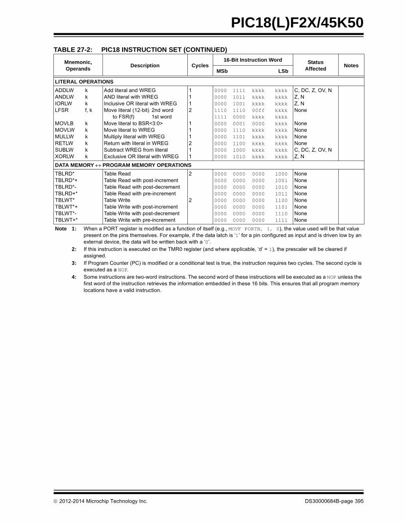
PIC18(L)F2X/45K50
LITERAL OPERATIONS
ADDLWANDLWIORLWLFSR
MOVLBMOVLWMULLWRETLWSUBLWXORLW
kkkf, k
kkkkkk
Add literal and WREGAND literal with WREGInclusive OR literal with WREGMove literal (12-bit) 2nd word to FSR(f) 1st wordMove literal to BSR<3:0>Move literal to WREGMultiply literal with WREGReturn with literal in WREG Subtract WREG from literalExclusive OR literal with WREG
1112
111211
00000000000011101111000000000000000000000000
11111011100111100000000111101101110010001010
kkkkkkkkkkkk00ffkkkk0000kkkkkkkkkkkkkkkkkkkk
kkkkkkkkkkkkkkkkkkkkkkkkkkkkkkkkkkkkkkkkkkkk
C, DC, Z, OV, NZ, NZ, NNone
NoneNoneNoneNoneC, DC, Z, OV, NZ, N
DATA MEMORY PROGRAM MEMORY OPERATIONS
TBLRD*TBLRD*+TBLRD*-TBLRD+*TBLWT*TBLWT*+TBLWT*-TBLWT+*
Table ReadTable Read with post-incrementTable Read with post-decrementTable Read with pre-incrementTable WriteTable Write with post-incrementTable Write with post-decrementTable Write with pre-increment
2
2
00000000000000000000000000000000
00000000000000000000000000000000
00000000000000000000000000000000
10001001101010111100110111101111
NoneNoneNoneNoneNoneNoneNoneNone
TABLE 27-2: PIC18 INSTRUCTION SET (CONTINUED)
Mnemonic,Operands
Description Cycles16-Bit Instruction Word Status
AffectedNotes
MSb LSb
Note 1: When a PORT register is modified as a function of itself (e.g., MOVF PORTB, 1, 0), the value used will be that value present on the pins themselves. For example, if the data latch is ‘1’ for a pin configured as input and is driven low by an external device, the data will be written back with a ‘0’.
2: If this instruction is executed on the TMR0 register (and where applicable, ‘d’ = 1), the prescaler will be cleared if assigned.
3: If Program Counter (PC) is modified or a conditional test is true, the instruction requires two cycles. The second cycle is executed as a NOP.
4: Some instructions are two-word instructions. The second word of these instructions will be executed as a NOP unless the first word of the instruction retrieves the information embedded in these 16 bits. This ensures that all program memory locations have a valid instruction.
2012-2014 Microchip Technology Inc. DS30000684B-page 395

PIC18(L)F2X/45K50
27.1.1 STANDARD INSTRUCTION SET
ADDLW ADD literal to W
Syntax: ADDLW k
Operands: 0 k 255
Operation: (W) + k W
Status Affected: N, OV, C, DC, Z
Encoding: 0000 1111 kkkk kkkk
Description: The contents of W are added to the 8-bit literal ‘k’ and the result is placed in W.
Words: 1
Cycles: 1
Q Cycle Activity:
Q1 Q2 Q3 Q4
Decode Readliteral ‘k’
Process Data
Write to W
Example: ADDLW 15h
Before Instruction
W = 10h
After Instruction
W = 25h
ADDWF ADD W to f
Syntax: ADDWF f ,d ,a
Operands: 0 f 255d [0,1]a [0,1]
Operation: (W) + (f) dest
Status Affected: N, OV, C, DC, Z
Encoding: 0010 01da ffff ffff
Description: Add W to register ‘f’. If ‘d’ is ‘0’, the result is stored in W. If ‘d’ is ‘1’, the result is stored back in register ‘f’. If ‘a’ is ‘0’, the Access Bank is selected. If ‘a’ is ‘1’, the BSR is used to select the GPR bank.If ‘a’ is ‘0’ and the extended instruction set is enabled, this instruction operates in Indexed Literal Offset Addressing mode whenever f 95 (5Fh). See Section 27.2.3 “Byte-Oriented and Bit-Oriented Instructions in Indexed Literal Offset Mode” for details.
Words: 1
Cycles: 1
Q Cycle Activity:
Q1 Q2 Q3 Q4
Decode Readregister ‘f’
Process Data
Write todestination
Example: ADDWF REG, 0, 0
Before Instruction
W = 17hREG = 0C2h
After Instruction
W = 0D9hREG = 0C2h
Note: All PIC18 instructions may take an optional label argument preceding the instruction mnemonic for use insymbolic addressing. If a label is used, the instruction format then becomes: label instruction argument(s).
DS30000684B-page 396 2012-2014 Microchip Technology Inc.

PIC18(L)F2X/45K50
ADDWFC ADD W and CARRY bit to f
Syntax: ADDWFC f ,d ,a
Operands: 0 f 255d [0,1]a [0,1]
Operation: (W) + (f) + (C) dest
Status Affected: N,OV, C, DC, Z
Encoding: 0010 00da ffff ffff
Description: Add W, the CARRY flag and data mem-ory location ‘f’. If ‘d’ is ‘0’, the result is placed in W. If ‘d’ is ‘1’, the result is placed in data memory location ‘f’. If ‘a’ is ‘0’, the Access Bank is selected. If ‘a’ is ‘1’, the BSR is used to select the GPR bank.If ‘a’ is ‘0’ and the extended instruction set is enabled, this instruction operates in Indexed Literal Offset Addressing mode whenever f 95 (5Fh). See Section 27.2.3 “Byte-Oriented and Bit-Oriented Instructions in Indexed Literal Offset Mode” for details.
Words: 1
Cycles: 1
Q Cycle Activity:
Q1 Q2 Q3 Q4
Decode Readregister ‘f’
Process Data
Write to destination
Example: ADDWFC REG, 0, 1
Before InstructionCARRY bit = 1REG = 02hW = 4Dh
After InstructionCARRY bit = 0REG = 02hW = 50h
ANDLW AND literal with W
Syntax: ANDLW k
Operands: 0 k 255
Operation: (W) .AND. k W
Status Affected: N, Z
Encoding: 0000 1011 kkkk kkkk
Description: The contents of W are AND’ed with the 8-bit literal ‘k’. The result is placed in W.
Words: 1
Cycles: 1
Q Cycle Activity:
Q1 Q2 Q3 Q4
Decode Read literal ‘k’
Process Data
Write to W
Example: ANDLW 05Fh
Before Instruction
W = A3h
After Instruction
W = 03h
2012-2014 Microchip Technology Inc. DS30000684B-page 397

PIC18(L)F2X/45K50
ANDWF AND W with f
Syntax: ANDWF f ,d ,a
Operands: 0 f 255d [0,1]a [0,1]
Operation: (W) .AND. (f) dest
Status Affected: N, Z
Encoding: 0001 01da ffff ffff
Description: The contents of W are AND’ed with register ‘f’. If ‘d’ is ‘0’, the result is stored in W. If ‘d’ is ‘1’, the result is stored back in register ‘f’. If ‘a’ is ‘0’, the Access Bank is selected. If ‘a’ is ‘1’, the BSR is used to select the GPR bank.If ‘a’ is ‘0’ and the extended instruction set is enabled, this instruction operates in Indexed Literal Offset Addressing mode whenever f 95 (5Fh). See Section 27.2.3 “Byte-Oriented and Bit-Oriented Instructions in Indexed Literal Offset Mode” for details.
Words: 1
Cycles: 1
Q Cycle Activity:
Q1 Q2 Q3 Q4
Decode Readregister ‘f’
Process Data
Write to destination
Example: ANDWF REG, 0, 0
Before Instruction
W = 17hREG = C2h
After Instruction
W = 02hREG = C2h
BC Branch if Carry
Syntax: BC n
Operands: -128 n 127
Operation: if CARRY bit is ‘1’(PC) + 2 + 2n PC
Status Affected: None
Encoding: 1110 0010 nnnn nnnn
Description: If the CARRY bit is ‘1’, then the program will branch.The 2’s complement number ‘2n’ is added to the PC. Since the PC will have incremented to fetch the next instruction, the new address will be PC + 2 + 2n. This instruction is then a two-cycle instruction.
Words: 1
Cycles: 1(2)
Q Cycle Activity:If Jump:
Q1 Q2 Q3 Q4
Decode Read literal ‘n’
Process Data
Write to PC
No operation
No operation
No operation
No operation
If No Jump:
Q1 Q2 Q3 Q4
Decode Read literal ‘n’
Process Data
No operation
Example: HERE BC 5
Before InstructionPC = address (HERE)
After InstructionIf CARRY = 1;
PC = address (HERE + 12)If CARRY = 0;
PC = address (HERE + 2)
DS30000684B-page 398 2012-2014 Microchip Technology Inc.

PIC18(L)F2X/45K50
BCF Bit Clear f
Syntax: BCF f, b ,a
Operands: 0 f 2550 b 7a [0,1]
Operation: 0 f<b>
Status Affected: None
Encoding: 1001 bbba ffff ffff
Description: Bit ‘b’ in register ‘f’ is cleared.If ‘a’ is ‘0’, the Access Bank is selected. If ‘a’ is ‘1’, the BSR is used to select the GPR bank.If ‘a’ is ‘0’ and the extended instruction set is enabled, this instruction operates in Indexed Literal Offset Addressing mode whenever f 95 (5Fh). See Section 27.2.3 “Byte-Oriented and Bit-Oriented Instructions in Indexed Literal Offset Mode” for details.
Words: 1
Cycles: 1
Q Cycle Activity:
Q1 Q2 Q3 Q4
Decode Readregister ‘f’
Process Data
Writeregister ‘f’
Example: BCF FLAG_REG, 7, 0
Before InstructionFLAG_REG = C7h
After InstructionFLAG_REG = 47h
BN Branch if Negative
Syntax: BN n
Operands: -128 n 127
Operation: if NEGATIVE bit is ‘1’(PC) + 2 + 2n PC
Status Affected: None
Encoding: 1110 0110 nnnn nnnn
Description: If the NEGATIVE bit is ‘1’, then the program will branch.The 2’s complement number ‘2n’ is added to the PC. Since the PC will have incremented to fetch the next instruction, the new address will be PC + 2 + 2n. This instruction is then a two-cycle instruction.
Words: 1
Cycles: 1(2)
Q Cycle Activity:If Jump:
Q1 Q2 Q3 Q4
Decode Read literal ‘n’
Process Data
Write to PC
No operation
No operation
No operation
No operation
If No Jump:
Q1 Q2 Q3 Q4
Decode Read literal ‘n’
Process Data
No operation
Example: HERE BN Jump
Before InstructionPC = address (HERE)
After InstructionIf NEGATIVE = 1;
PC = address (Jump)If NEGATIVE = 0;
PC = address (HERE + 2)
2012-2014 Microchip Technology Inc. DS30000684B-page 399

PIC18(L)F2X/45K50
BNC Branch if Not Carry
Syntax: BNC n
Operands: -128 n 127
Operation: if CARRY bit is ‘0’(PC) + 2 + 2n PC
Status Affected: None
Encoding: 1110 0011 nnnn nnnn
Description: If the CARRY bit is ‘0’, then the program will branch.The 2’s complement number ‘2n’ is added to the PC. Since the PC will have incremented to fetch the next instruction, the new address will be PC + 2 + 2n. This instruction is then a two-cycle instruction.
Words: 1
Cycles: 1(2)
Q Cycle Activity:If Jump:
Q1 Q2 Q3 Q4
Decode Read literal ‘n’
Process Data
Write to PC
No operation
No operation
No operation
No operation
If No Jump:
Q1 Q2 Q3 Q4
Decode Read literal ‘n’
Process Data
No operation
Example: HERE BNC Jump
Before InstructionPC = address (HERE)
After InstructionIf CARRY = 0;
PC = address (Jump)If CARRY = 1;
PC = address (HERE + 2)
BNN Branch if Not Negative
Syntax: BNN n
Operands: -128 n 127
Operation: if NEGATIVE bit is ‘0’(PC) + 2 + 2n PC
Status Affected: None
Encoding: 1110 0111 nnnn nnnn
Description: If the NEGATIVE bit is ‘0’, then the program will branch.The 2’s complement number ‘2n’ is added to the PC. Since the PC will have incremented to fetch the next instruction, the new address will be PC + 2 + 2n. This instruction is then a two-cycle instruction.
Words: 1
Cycles: 1(2)
Q Cycle Activity:If Jump:
Q1 Q2 Q3 Q4
Decode Read literal ‘n’
Process Data
Write to PC
No operation
No operation
No operation
No operation
If No Jump:
Q1 Q2 Q3 Q4
Decode Read literal ‘n’
Process Data
No operation
Example: HERE BNN Jump
Before InstructionPC = address (HERE)
After InstructionIf NEGATIVE = 0;
PC = address (Jump)If NEGATIVE = 1;
PC = address (HERE + 2)
DS30000684B-page 400 2012-2014 Microchip Technology Inc.

PIC18(L)F2X/45K50
BNOV Branch if Not Overflow
Syntax: BNOV n
Operands: -128 n 127
Operation: if OVERFLOW bit is ‘0’(PC) + 2 + 2n PC
Status Affected: None
Encoding: 1110 0101 nnnn nnnn
Description: If the OVERFLOW bit is ‘0’, then the program will branch.The 2’s complement number ‘2n’ is added to the PC. Since the PC will have incremented to fetch the next instruction, the new address will be PC + 2 + 2n. This instruction is then a two-cycle instruction.
Words: 1
Cycles: 1(2)
Q Cycle Activity:If Jump:
Q1 Q2 Q3 Q4
Decode Read literal ‘n’
Process Data
Write to PC
No operation
No operation
No operation
No operation
If No Jump:
Q1 Q2 Q3 Q4
Decode Read literal ‘n’
Process Data
No operation
Example: HERE BNOV Jump
Before InstructionPC = address (HERE)
After InstructionIf OVERFLOW = 0;
PC = address (Jump)If OVERFLOW = 1;
PC = address (HERE + 2)
BNZ Branch if Not Zero
Syntax: BNZ n
Operands: -128 n 127
Operation: if ZERO bit is ‘0’(PC) + 2 + 2n PC
Status Affected: None
Encoding: 1110 0001 nnnn nnnn
Description: If the ZERO bit is ‘0’, then the program will branch.The 2’s complement number ‘2n’ is added to the PC. Since the PC will have incremented to fetch the next instruction, the new address will be PC + 2 + 2n. This instruction is then a two-cycle instruction.
Words: 1
Cycles: 1(2)
Q Cycle Activity:If Jump:
Q1 Q2 Q3 Q4
Decode Read literal ‘n’
Process Data
Write to PC
No operation
No operation
No operation
No operation
If No Jump:
Q1 Q2 Q3 Q4
Decode Read literal ‘n’
Process Data
No operation
Example: HERE BNZ Jump
Before InstructionPC = address (HERE)
After InstructionIf ZERO = 0;
PC = address (Jump)If ZERO = 1;
PC = address (HERE + 2)
2012-2014 Microchip Technology Inc. DS30000684B-page 401
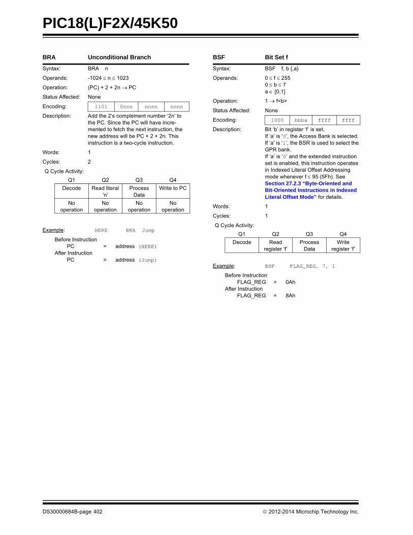
PIC18(L)F2X/45K50
BRA Unconditional Branch
Syntax: BRA n
Operands: -1024 n 1023
Operation: (PC) + 2 + 2n PC
Status Affected: None
Encoding: 1101 0nnn nnnn nnnn
Description: Add the 2’s complement number ‘2n’ to the PC. Since the PC will have incre-mented to fetch the next instruction, the new address will be PC + 2 + 2n. This instruction is a two-cycle instruction.
Words: 1
Cycles: 2
Q Cycle Activity:
Q1 Q2 Q3 Q4
Decode Read literal ‘n’
Process Data
Write to PC
No operation
No operation
No operation
No operation
Example: HERE BRA Jump
Before InstructionPC = address (HERE)
After InstructionPC = address (Jump)
BSF Bit Set f
Syntax: BSF f, b ,a
Operands: 0 f 2550 b 7a [0,1]
Operation: 1 f<b>
Status Affected: None
Encoding: 1000 bbba ffff ffff
Description: Bit ‘b’ in register ‘f’ is set. If ‘a’ is ‘0’, the Access Bank is selected. If ‘a’ is ‘1’, the BSR is used to select the GPR bank.If ‘a’ is ‘0’ and the extended instruction set is enabled, this instruction operates in Indexed Literal Offset Addressing mode whenever f 95 (5Fh). See Section 27.2.3 “Byte-Oriented and Bit-Oriented Instructions in Indexed Literal Offset Mode” for details.
Words: 1
Cycles: 1
Q Cycle Activity:
Q1 Q2 Q3 Q4
Decode Readregister ‘f’
Process Data
Writeregister ‘f’
Example: BSF FLAG_REG, 7, 1
Before InstructionFLAG_REG = 0Ah
After InstructionFLAG_REG = 8Ah
DS30000684B-page 402 2012-2014 Microchip Technology Inc.

PIC18(L)F2X/45K50
BTFSC Bit Test File, Skip if Clear
Syntax: BTFSC f, b ,a
Operands: 0 f 2550 b 7a [0,1]
Operation: skip if (f<b>) = 0
Status Affected: None
Encoding: 1011 bbba ffff ffff
Description: If bit ‘b’ in register ‘f’ is ‘0’, then the next instruction is skipped. If bit ‘b’ is ‘0’, then the next instruction fetched during the current instruction execution is discarded and a NOP is executed instead, making this a two-cycle instruction. If ‘a’ is ‘0’, the Access Bank is selected. If ‘a’ is ‘1’, the BSR is used to select the GPR bank.If ‘a’ is ‘0’ and the extended instruction set is enabled, this instruction operates in Indexed Literal Offset Addressing mode whenever f 95 (5Fh). See Section 27.2.3 “Byte-Oriented and Bit-Oriented Instructions in Indexed Literal Offset Mode” for details.
Words: 1
Cycles: 1(2)Note: Three cycles if skip and followed
by a 2-word instruction.
Q Cycle Activity:
Q1 Q2 Q3 Q4
Decode Readregister ‘f’
Process Data
No operation
If skip:
Q1 Q2 Q3 Q4
No operation
No operation
No operation
No operation
If skip and followed by 2-word instruction:
Q1 Q2 Q3 Q4
No operation
No operation
No operation
No operation
No operation
No operation
No operation
No operation
Example: HEREFALSETRUE
BTFSC::
FLAG, 1, 0
Before InstructionPC = address (HERE)
After InstructionIf FLAG<1> = 0;
PC = address (TRUE)If FLAG<1> = 1;
PC = address (FALSE)
BTFSS Bit Test File, Skip if Set
Syntax: BTFSS f, b ,a
Operands: 0 f 2550 b < 7a [0,1]
Operation: skip if (f<b>) = 1
Status Affected: None
Encoding: 1010 bbba ffff ffff
Description: If bit ‘b’ in register ‘f’ is ‘1’, then the next instruction is skipped. If bit ‘b’ is ‘1’, then the next instruction fetched during the current instruction execution is discarded and a NOP is executed instead, making this a two-cycle instruction. If ‘a’ is ‘0’, the Access Bank is selected. If ‘a’ is ‘1’, the BSR is used to select the GPR bank.If ‘a’ is ‘0’ and the extended instruction set is enabled, this instruction operates in Indexed Literal Offset Addressing mode whenever f 95 (5Fh). See Section 27.2.3 “Byte-Oriented and Bit-Oriented Instructions in Indexed Literal Offset Mode” for details.
Words: 1
Cycles: 1(2)Note: Three cycles if skip and followed
by a 2-word instruction.
Q Cycle Activity:
Q1 Q2 Q3 Q4
Decode Readregister ‘f’
Process Data
No operation
If skip:
Q1 Q2 Q3 Q4
No operation
No operation
No operation
No operation
If skip and followed by 2-word instruction:
Q1 Q2 Q3 Q4
No operation
No operation
No operation
No operation
No operation
No operation
No operation
No operation
Example: HEREFALSETRUE
BTFSS::
FLAG, 1, 0
Before InstructionPC = address (HERE)
After InstructionIf FLAG<1> = 0;
PC = address (FALSE)If FLAG<1> = 1;
PC = address (TRUE)
2012-2014 Microchip Technology Inc. DS30000684B-page 403

PIC18(L)F2X/45K50
BTG Bit Toggle f
Syntax: BTG f, b ,a
Operands: 0 f 2550 b < 7a [0,1]
Operation: (f<b>) f<b>
Status Affected: None
Encoding: 0111 bbba ffff ffff
Description: Bit ‘b’ in data memory location ‘f’ is inverted.If ‘a’ is ‘0’, the Access Bank is selected. If ‘a’ is ‘1’, the BSR is used to select the GPR bank.If ‘a’ is ‘0’ and the extended instruction set is enabled, this instruction operates in Indexed Literal Offset Addressing mode whenever f 95 (5Fh). See Section 27.2.3 “Byte-Oriented and Bit-Oriented Instructions in Indexed Literal Offset Mode” for details.
Words: 1
Cycles: 1
Q Cycle Activity:
Q1 Q2 Q3 Q4
Decode Readregister ‘f’
Process Data
Writeregister ‘f’
Example: BTG PORTC, 4, 0
Before Instruction:PORTC = 0111 0101 [75h]
After Instruction:PORTC = 0110 0101 [65h]
BOV Branch if Overflow
Syntax: BOV n
Operands: -128 n 127
Operation: if OVERFLOW bit is ‘1’(PC) + 2 + 2n PC
Status Affected: None
Encoding: 1110 0100 nnnn nnnn
Description: If the OVERFLOW bit is ‘1’, then the program will branch.The 2’s complement number ‘2n’ is added to the PC. Since the PC will have incremented to fetch the next instruction, the new address will be PC + 2 + 2n. This instruction is then a two-cycle instruction.
Words: 1
Cycles: 1(2)
Q Cycle Activity:If Jump:
Q1 Q2 Q3 Q4
Decode Read literal ‘n’
Process Data
Write to PC
No operation
No operation
No operation
No operation
If No Jump:
Q1 Q2 Q3 Q4
Decode Read literal ‘n’
Process Data
No operation
Example: HERE BOV Jump
Before InstructionPC = address (HERE)
After InstructionIf OVERFLOW = 1;
PC = address (Jump)If OVERFLOW = 0;
PC = address (HERE + 2)
DS30000684B-page 404 2012-2014 Microchip Technology Inc.

PIC18(L)F2X/45K50
BZ Branch if Zero
Syntax: BZ n
Operands: -128 n 127
Operation: if ZERO bit is ‘1’(PC) + 2 + 2n PC
Status Affected: None
Encoding: 1110 0000 nnnn nnnn
Description: If the ZERO bit is ‘1’, then the program will branch.The 2’s complement number ‘2n’ is added to the PC. Since the PC will have incremented to fetch the next instruction, the new address will be PC + 2 + 2n. This instruction is then a two-cycle instruction.
Words: 1
Cycles: 1(2)
Q Cycle Activity:If Jump:
Q1 Q2 Q3 Q4
Decode Read literal ‘n’
Process Data
Write to PC
No operation
No operation
No operation
No operation
If No Jump:
Q1 Q2 Q3 Q4
Decode Read literal ‘n’
Process Data
No operation
Example: HERE BZ Jump
Before InstructionPC = address (HERE)
After InstructionIf ZERO = 1;
PC = address (Jump)If ZERO = 0;
PC = address (HERE + 2)
CALL Subroutine Call
Syntax: CALL k ,s
Operands: 0 k 1048575s [0,1]
Operation: (PC) + 4 TOS,k PC<20:1>,if s = 1(W) WS,(Status) STATUSS,(BSR) BSRS
Status Affected: None
Encoding:1st word (k<7:0>)2nd word(k<19:8>)
11101111
110sk19kkk
k7kkkkkkk
kkkk0kkkk8
Description: Subroutine call of entire 2-Mbyte memory range. First, return address (PC + 4) is pushed onto the return stack. If ‘s’ = 1, the W, Status and BSR registers are also pushed into their respective shadow registers, WS, STATUSS and BSRS. If ‘s’ = 0, no update occurs. Then, the 20-bit value ‘k’ is loaded into PC<20:1>. CALL is a two-cycle instruction.
Words: 2
Cycles: 2
Q Cycle Activity:
Q1 Q2 Q3 Q4
Decode Read literal ‘k’<7:0>,
PUSH PC to stack
Read literal ‘k’<19:8>,
Write to PC
No operation
No operation
No operation
No operation
Example: HERE CALL THERE, 1
Before InstructionPC = address (HERE)
After InstructionPC = address (THERE)TOS = address (HERE + 4)WS = WBSRS = BSRSTATUSS = Status
2012-2014 Microchip Technology Inc. DS30000684B-page 405
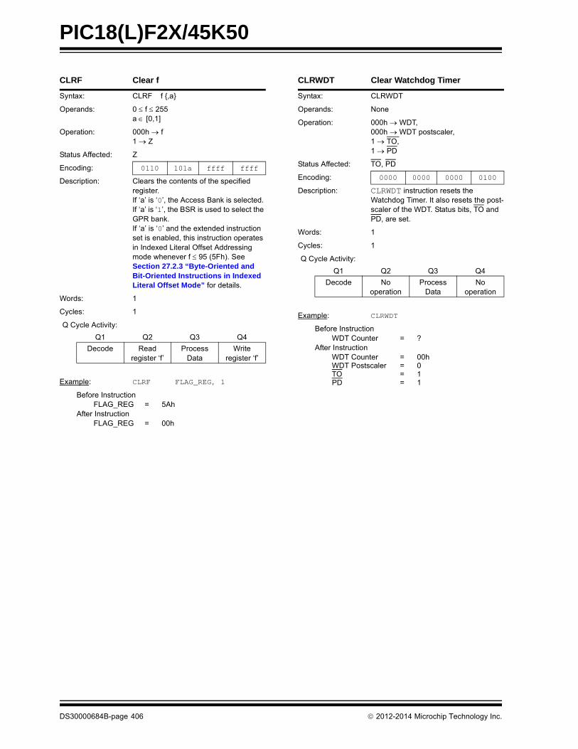
PIC18(L)F2X/45K50
CLRF Clear f
Syntax: CLRF f ,a
Operands: 0 f 255a [0,1]
Operation: 000h f1 Z
Status Affected: Z
Encoding: 0110 101a ffff ffff
Description: Clears the contents of the specified register. If ‘a’ is ‘0’, the Access Bank is selected. If ‘a’ is ‘1’, the BSR is used to select the GPR bank.If ‘a’ is ‘0’ and the extended instruction set is enabled, this instruction operates in Indexed Literal Offset Addressing mode whenever f 95 (5Fh). See Section 27.2.3 “Byte-Oriented and Bit-Oriented Instructions in Indexed Literal Offset Mode” for details.
Words: 1
Cycles: 1
Q Cycle Activity:
Q1 Q2 Q3 Q4
Decode Readregister ‘f’
Process Data
Writeregister ‘f’
Example: CLRF FLAG_REG, 1
Before InstructionFLAG_REG = 5Ah
After InstructionFLAG_REG = 00h
CLRWDT Clear Watchdog Timer
Syntax: CLRWDT
Operands: None
Operation: 000h WDT,000h WDT postscaler,1 TO,1 PD
Status Affected: TO, PD
Encoding: 0000 0000 0000 0100
Description: CLRWDT instruction resets the Watchdog Timer. It also resets the post-scaler of the WDT. Status bits, TO and PD, are set.
Words: 1
Cycles: 1
Q Cycle Activity:
Q1 Q2 Q3 Q4
Decode Nooperation
Process Data
No operation
Example: CLRWDT
Before InstructionWDT Counter = ?
After InstructionWDT Counter = 00hWDT Postscaler = 0TO = 1PD = 1
DS30000684B-page 406 2012-2014 Microchip Technology Inc.
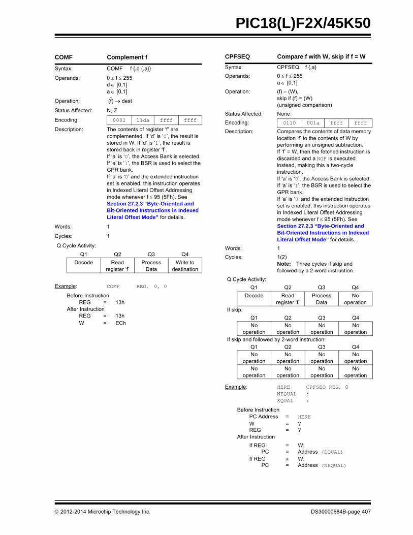
PIC18(L)F2X/45K50
COMF Complement f
Syntax: COMF f ,d ,a
Operands: 0 f 255d [0,1]a [0,1]
Operation: (f) dest
Status Affected: N, Z
Encoding: 0001 11da ffff ffff
Description: The contents of register ‘f’ are complemented. If ‘d’ is ‘0’, the result is stored in W. If ‘d’ is ‘1’, the result is stored back in register ‘f’. If ‘a’ is ‘0’, the Access Bank is selected. If ‘a’ is ‘1’, the BSR is used to select the GPR bank.If ‘a’ is ‘0’ and the extended instruction set is enabled, this instruction operates in Indexed Literal Offset Addressing mode whenever f 95 (5Fh). See Section 27.2.3 “Byte-Oriented and Bit-Oriented Instructions in Indexed Literal Offset Mode” for details.
Words: 1
Cycles: 1
Q Cycle Activity:
Q1 Q2 Q3 Q4
Decode Readregister ‘f’
Process Data
Write todestination
Example: COMF REG, 0, 0
Before InstructionREG = 13h
After InstructionREG = 13hW = ECh
CPFSEQ Compare f with W, skip if f = W
Syntax: CPFSEQ f ,a
Operands: 0 f 255a [0,1]
Operation: (f) – (W), skip if (f) = (W) (unsigned comparison)
Status Affected: None
Encoding: 0110 001a ffff ffff
Description: Compares the contents of data memory location ‘f’ to the contents of W by performing an unsigned subtraction.If ‘f’ = W, then the fetched instruction is discarded and a NOP is executed instead, making this a two-cycle instruction. If ‘a’ is ‘0’, the Access Bank is selected. If ‘a’ is ‘1’, the BSR is used to select the GPR bank.If ‘a’ is ‘0’ and the extended instruction set is enabled, this instruction operates in Indexed Literal Offset Addressing mode whenever f 95 (5Fh). See Section 27.2.3 “Byte-Oriented and Bit-Oriented Instructions in Indexed Literal Offset Mode” for details.
Words: 1
Cycles: 1(2)Note: Three cycles if skip and followed by a 2-word instruction.
Q Cycle Activity:
Q1 Q2 Q3 Q4
Decode Readregister ‘f’
Process Data
No operation
If skip:
Q1 Q2 Q3 Q4No
operationNo
operationNo
operationNo
operationIf skip and followed by 2-word instruction:
Q1 Q2 Q3 Q4No
operationNo
operationNo
operationNo
operationNo
operationNo
operationNo
operationNo
operation
Example: HERE CPFSEQ REG, 0NEQUAL :EQUAL :
Before InstructionPC Address = HEREW = ?REG = ?
After Instruction
If REG = W;PC = Address (EQUAL)
If REG W;PC = Address (NEQUAL)
2012-2014 Microchip Technology Inc. DS30000684B-page 407

PIC18(L)F2X/45K50
CPFSGT Compare f with W, skip if f > W
Syntax: CPFSGT f ,a
Operands: 0 f 255a [0,1]
Operation: (f) –W),skip if (f) > (W) (unsigned comparison)
Status Affected: None
Encoding: 0110 010a ffff ffff
Description: Compares the contents of data memory location ‘f’ to the contents of the W by performing an unsigned subtraction.If the contents of ‘f’ are greater than the contents of WREG, then the fetched instruction is discarded and a NOP is executed instead, making this a two-cycle instruction. If ‘a’ is ‘0’, the Access Bank is selected. If ‘a’ is ‘1’, the BSR is used to select the GPR bank.If ‘a’ is ‘0’ and the extended instruction set is enabled, this instruction operates in Indexed Literal Offset Addressing mode whenever f 95 (5Fh). See Section 27.2.3 “Byte-Oriented and Bit-Oriented Instructions in Indexed Literal Offset Mode” for details.
Words: 1
Cycles: 1(2)Note: Three cycles if skip and followed
by a 2-word instruction.
Q Cycle Activity:
Q1 Q2 Q3 Q4Decode Read
register ‘f’Process
DataNo
operationIf skip:
Q1 Q2 Q3 Q4No
operationNo
operationNo
operationNo
operationIf skip and followed by 2-word instruction:
Q1 Q2 Q3 Q4No
operationNo
operationNo
operationNo
operationNo
operationNo
operationNo
operationNo
operation
Example: HERE CPFSGT REG, 0NGREATER :GREATER :
Before InstructionPC = Address (HERE)W = ?
After Instruction
If REG W;PC = Address (GREATER)
If REG W;PC = Address (NGREATER)
CPFSLT Compare f with W, skip if f < W
Syntax: CPFSLT f ,a
Operands: 0 f 255a [0,1]
Operation: (f) –W),skip if (f) < (W) (unsigned comparison)
Status Affected: None
Encoding: 0110 000a ffff ffff
Description: Compares the contents of data memory location ‘f’ to the contents of W by performing an unsigned subtraction.If the contents of ‘f’ are less than the contents of W, then the fetched instruction is discarded and a NOP is executed instead, making this a two-cycle instruction. If ‘a’ is ‘0’, the Access Bank is selected. If ‘a’ is ‘1’, the BSR is used to select the GPR bank.
Words: 1
Cycles: 1(2)Note: Three cycles if skip and followed by a 2-word instruction.
Q Cycle Activity:
Q1 Q2 Q3 Q4
Decode Readregister ‘f’
Process Data
No operation
If skip:
Q1 Q2 Q3 Q4
No operation
No operation
No operation
No operation
If skip and followed by 2-word instruction:
Q1 Q2 Q3 Q4
No operation
No operation
No operation
No operation
No operation
No operation
No operation
No operation
Example: HERE CPFSLT REG, 1NLESS :LESS :
Before InstructionPC = Address (HERE)W = ?
After Instruction
If REG < W;PC = Address (LESS)If REG W;PC = Address (NLESS)
DS30000684B-page 408 2012-2014 Microchip Technology Inc.
PIC18(L)F2X/45K50
DAW Decimal Adjust W Register
Syntax: DAW
Operands: None
Operation: If [W<3:0> > 9] or [DC = 1] then(W<3:0>) + 6 W<3:0>;else (W<3:0>) W<3:0>;
If [W<7:4> + DC > 9] or [C = 1] then(W<7:4>) + 6 + DC W<7:4>;C = 1;else (W<7:4>) + DC W<7:4>
Status Affected: C
Encoding: 0000 0000 0000 0111
Description: DAW adjusts the eight-bit value in W, resulting from the earlier addition of two variables (each in packed BCD format) and produces a correct packed BCD result.
Words: 1
Cycles: 1
Q Cycle Activity:
Q1 Q2 Q3 Q4
Decode Readregister W
Process Data
WriteW
Example1:
DAW
Before Instruction
W = A5hC = 0DC = 0
After Instruction
W = 05hC = 1DC = 0
Example 2:
Before Instruction
W = CEhC = 0DC = 0
After Instruction
W = 34hC = 1DC = 0
DECF Decrement f
Syntax: DECF f ,d ,a
Operands: 0 f 255d [0,1]a [0,1]
Operation: (f) – 1 dest
Status Affected: C, DC, N, OV, Z
Encoding: 0000 01da ffff ffff
Description: Decrement register ‘f’. If ‘d’ is ‘0’, the result is stored in W. If ‘d’ is ‘1’, the result is stored back in register ‘f’. If ‘a’ is ‘0’, the Access Bank is selected. If ‘a’ is ‘1’, the BSR is used to select the GPR bank.If ‘a’ is ‘0’ and the extended instruction set is enabled, this instruction operates in Indexed Literal Offset Addressing mode whenever f 95 (5Fh). See Section 27.2.3 “Byte-Oriented and Bit-Oriented Instructions in Indexed Literal Offset Mode” for details.
Words: 1
Cycles: 1
Q Cycle Activity:
Q1 Q2 Q3 Q4
Decode Readregister ‘f’
Process Data
Write to destination
Example: DECF CNT, 1, 0
Before InstructionCNT = 01hZ = 0
After InstructionCNT = 00hZ = 1
2012-2014 Microchip Technology Inc. DS30000684B-page 409

PIC18(L)F2X/45K50
DECFSZ Decrement f, skip if 0
Syntax: DECFSZ f ,d ,a
Operands: 0 f 255d [0,1]a [0,1]
Operation: (f) – 1 dest,skip if result = 0
Status Affected: None
Encoding: 0010 11da ffff ffff
Description: The contents of register ‘f’ are decremented. If ‘d’ is ‘0’, the result is placed in W. If ‘d’ is ‘1’, the result is placed back in register ‘f’.If the result is ‘0’, the next instruction, which is already fetched, is discarded and a NOP is executed instead, making it a two-cycle instruction.If ‘a’ is ‘0’, the Access Bank is selected. If ‘a’ is ‘1’, the BSR is used to select the GPR bank.If ‘a’ is ‘0’ and the extended instruction set is enabled, this instruction operates in Indexed Literal Offset Addressing mode whenever f 95 (5Fh). See Section 27.2.3 “Byte-Oriented and Bit-Oriented Instructions in Indexed Literal Offset Mode” for details.
Words: 1
Cycles: 1(2)Note: Three cycles if skip and followed by a 2-word instruction.
Q Cycle Activity:
Q1 Q2 Q3 Q4
Decode Readregister ‘f’
Process Data
Write to destination
If skip:
Q1 Q2 Q3 Q4
No operation
No operation
No operation
No operation
If skip and followed by 2-word instruction:
Q1 Q2 Q3 Q4
No operation
No operation
No operation
No operation
No operation
No operation
No operation
No operation
Example: HERE DECFSZ CNT, 1, 1 GOTO LOOPCONTINUE
Before InstructionPC = Address (HERE)
After InstructionCNT = CNT - 1If CNT = 0;
PC = Address (CONTINUE)If CNT 0;
PC = Address (HERE + 2)
DCFSNZ Decrement f, skip if not 0
Syntax: DCFSNZ f ,d ,a
Operands: 0 f 255d [0,1]a [0,1]
Operation: (f) – 1 dest,skip if result 0
Status Affected: None
Encoding: 0100 11da ffff ffff
Description: The contents of register ‘f’ are decremented. If ‘d’ is ‘0’, the result is placed in W. If ‘d’ is ‘1’, the result is placed back in register ‘f’.If the result is not ‘0’, the next instruction, which is already fetched, is discarded and a NOP is executed instead, making it a two-cycle instruction. If ‘a’ is ‘0’, the Access Bank is selected. If ‘a’ is ‘1’, the BSR is used to select the GPR bank.If ‘a’ is ‘0’ and the extended instruction set is enabled, this instruction operates in Indexed Literal Offset Addressing mode whenever f 95 (5Fh). See Section 27.2.3 “Byte-Oriented and Bit-Oriented Instructions in Indexed Literal Offset Mode” for details.
Words: 1
Cycles: 1(2)Note: Three cycles if skip and followed by a 2-word instruction.
Q Cycle Activity:
Q1 Q2 Q3 Q4
Decode Readregister ‘f’
Process Data
Write to destination
If skip:
Q1 Q2 Q3 Q4
No operation
No operation
No operation
No operation
If skip and followed by 2-word instruction:
Q1 Q2 Q3 Q4
No operation
No operation
No operation
No operation
No operation
No operation
No operation
No operation
Example: HERE DCFSNZ TEMP, 1, 0ZERO : NZERO :
Before InstructionTEMP = ?
After InstructionTEMP = TEMP – 1,If TEMP = 0;
PC = Address (ZERO)If TEMP 0;
PC = Address (NZERO)
DS30000684B-page 410 2012-2014 Microchip Technology Inc.
PIC18(L)F2X/45K50
GOTO Unconditional Branch
Syntax: GOTO k
Operands: 0 k 1048575
Operation: k PC<20:1>
Status Affected: None
Encoding:1st word (k<7:0>)2nd word(k<19:8>)
11101111
1111k19kkk
k7kkkkkkk
kkkk0kkkk8
Description: GOTO allows an unconditional branch anywhere within entire 2-Mbyte memory range. The 20-bit value ‘k’ is loaded into PC<20:1>. GOTO is always a two-cycle instruction.
Words: 2
Cycles: 2
Q Cycle Activity:
Q1 Q2 Q3 Q4
Decode Read literal ‘k’<7:0>,
No operation
Read literal ‘k’<19:8>,
Write to PC
No operation
No operation
No operation
No operation
Example: GOTO THERE
After InstructionPC = Address (THERE)
INCF Increment f
Syntax: INCF f ,d ,a
Operands: 0 f 255d [0,1]a [0,1]
Operation: (f) + 1 dest
Status Affected: C, DC, N, OV, Z
Encoding: 0010 10da ffff ffff
Description: The contents of register ‘f’ are incremented. If ‘d’ is ‘0’, the result is placed in W. If ‘d’ is ‘1’, the result is placed back in register ‘f’. If ‘a’ is ‘0’, the Access Bank is selected. If ‘a’ is ‘1’, the BSR is used to select the GPR bank.If ‘a’ is ‘0’ and the extended instruction set is enabled, this instruction operates in Indexed Literal Offset Addressing mode whenever f 95 (5Fh). See Section 27.2.3 “Byte-Oriented and Bit-Oriented Instructions in Indexed Literal Offset Mode” for details.
Words: 1
Cycles: 1
Q Cycle Activity:
Q1 Q2 Q3 Q4
Decode Readregister ‘f’
Process Data
Write to destination
Example: INCF CNT, 1, 0
Before InstructionCNT = FFhZ = 0C = ?DC = ?
After InstructionCNT = 00hZ = 1C = 1DC = 1
2012-2014 Microchip Technology Inc. DS30000684B-page 411

PIC18(L)F2X/45K50
INCFSZ Increment f, skip if 0
Syntax: INCFSZ f ,d ,a
Operands: 0 f 255d [0,1]a [0,1]
Operation: (f) + 1 dest,skip if result = 0
Status Affected: None
Encoding: 0011 11da ffff ffff
Description: The contents of register ‘f’ are incremented. If ‘d’ is ‘0’, the result is placed in W. If ‘d’ is ‘1’, the result is placed back in register ‘f’.If the result is ‘0’, the next instruction, which is already fetched, is discarded and a NOP is executed instead, making it a two-cycle instruction. If ‘a’ is ‘0’, the Access Bank is selected. If ‘a’ is ‘1’, the BSR is used to select the GPR bank.If ‘a’ is ‘0’ and the extended instruction set is enabled, this instruction operates in Indexed Literal Offset Addressing mode whenever f 95 (5Fh). See Section 27.2.3 “Byte-Oriented and Bit-Oriented Instructions in Indexed Literal Offset Mode” for details.
Words: 1
Cycles: 1(2)Note: 3 cycles if skip and followed
by a 2-word instruction.
Q Cycle Activity:
Q1 Q2 Q3 Q4
Decode Readregister ‘f’
Process Data
Write to destination
If skip:
Q1 Q2 Q3 Q4
No operation
No operation
No operation
No operation
If skip and followed by 2-word instruction:
Q1 Q2 Q3 Q4
No operation
No operation
No operation
No operation
No operation
No operation
No operation
No operation
Example: HERE INCFSZ CNT, 1, 0NZERO : ZERO :
Before InstructionPC = Address (HERE)
After InstructionCNT = CNT + 1If CNT = 0;PC = Address (ZERO)If CNT 0;PC = Address (NZERO)
INFSNZ Increment f, skip if not 0
Syntax: INFSNZ f ,d ,a
Operands: 0 f 255d [0,1]a [0,1]
Operation: (f) + 1 dest, skip if result 0
Status Affected: None
Encoding: 0100 10da ffff ffff
Description: The contents of register ‘f’ are incremented. If ‘d’ is ‘0’, the result is placed in W. If ‘d’ is ‘1’, the result is placed back in register ‘f’.If the result is not ‘0’, the next instruction, which is already fetched, is discarded and a NOP is executed instead, making it a two-cycle instruction. If ‘a’ is ‘0’, the Access Bank is selected. If ‘a’ is ‘1’, the BSR is used to select the GPR bank.If ‘a’ is ‘0’ and the extended instruction set is enabled, this instruction operates in Indexed Literal Offset Addressing mode whenever f 95 (5Fh). See Section 27.2.3 “Byte-Oriented and Bit-Oriented Instructions in Indexed Literal Offset Mode” for details.
Words: 1
Cycles: 1(2)Note: 3 cycles if skip and followed
by a 2-word instruction.
Q Cycle Activity:
Q1 Q2 Q3 Q4
Decode Readregister ‘f’
Process Data
Write to destination
If skip:
Q1 Q2 Q3 Q4
No operation
No operation
No operation
No operation
If skip and followed by 2-word instruction:
Q1 Q2 Q3 Q4
No operation
No operation
No operation
No operation
No operation
No operation
No operation
No operation
Example: HERE INFSNZ REG, 1, 0ZERONZERO
Before InstructionPC = Address (HERE)
After InstructionREG = REG + 1If REG 0;PC = Address (NZERO)If REG = 0;PC = Address (ZERO)
DS30000684B-page 412 2012-2014 Microchip Technology Inc.

PIC18(L)F2X/45K50
IORLW Inclusive OR literal with W
Syntax: IORLW k
Operands: 0 k 255
Operation: (W) .OR. k W
Status Affected: N, Z
Encoding: 0000 1001 kkkk kkkk
Description: The contents of W are ORed with the eight-bit literal ‘k’. The result is placed in W.
Words: 1
Cycles: 1
Q Cycle Activity:
Q1 Q2 Q3 Q4
Decode Read literal ‘k’
Process Data
Write to W
Example: IORLW 35h
Before Instruction
W = 9Ah
After Instruction
W = BFh
IORWF Inclusive OR W with f
Syntax: IORWF f ,d ,a
Operands: 0 f 255d [0,1]a [0,1]
Operation: (W) .OR. (f) dest
Status Affected: N, Z
Encoding: 0001 00da ffff ffff
Description: Inclusive OR W with register ‘f’. If ‘d’ is ‘0’, the result is placed in W. If ‘d’ is ‘1’, the result is placed back in register ‘f’. If ‘a’ is ‘0’, the Access Bank is selected. If ‘a’ is ‘1’, the BSR is used to select the GPR bank.If ‘a’ is ‘0’ and the extended instruction set is enabled, this instruction operates in Indexed Literal Offset Addressing mode whenever f 95 (5Fh). See Section 27.2.3 “Byte-Oriented and Bit-Oriented Instructions in Indexed Literal Offset Mode” for details.
Words: 1
Cycles: 1
Q Cycle Activity:
Q1 Q2 Q3 Q4
Decode Readregister ‘f’
Process Data
Write to destination
Example: IORWF RESULT, 0, 1
Before InstructionRESULT = 13hW = 91h
After InstructionRESULT = 13hW = 93h
2012-2014 Microchip Technology Inc. DS30000684B-page 413

PIC18(L)F2X/45K50
LFSR Load FSR
Syntax: LFSR f, k
Operands: 0 f 20 k 4095
Operation: k FSRf
Status Affected: None
Encoding: 11101111
11100000
00ffk7kkk
k11kkkkkkk
Description: The 12-bit literal ‘k’ is loaded into the File Select Register pointed to by ‘f’.
Words: 2
Cycles: 2
Q Cycle Activity:
Q1 Q2 Q3 Q4
Decode Read literal ‘k’ MSB
Process Data
Writeliteral ‘k’ MSB to FSRfH
Decode Read literal ‘k’ LSB
Process Data
Write literal ‘k’ to FSRfL
Example: LFSR 2, 3ABh
After InstructionFSR2H = 03hFSR2L = ABh
MOVF Move f
Syntax: MOVF f ,d ,a
Operands: 0 f 255d [0,1]a [0,1]
Operation: f dest
Status Affected: N, Z
Encoding: 0101 00da ffff ffff
Description: The contents of register ‘f’ are moved to a destination dependent upon the status of ‘d’. If ‘d’ is ‘0’, the result is placed in W. If ‘d’ is ‘1’, the result is placed back in register ‘f’. Location ‘f’ can be anywhere in the 256-byte bank.If ‘a’ is ‘0’, the Access Bank is selected. If ‘a’ is ‘1’, the BSR is used to select the GPR bank.If ‘a’ is ‘0’ and the extended instruction set is enabled, this instruction operates in Indexed Literal Offset Addressing mode whenever f 95 (5Fh). See Section 27.2.3 “Byte-Oriented and Bit-Oriented Instructions in Indexed Literal Offset Mode” for details.
Words: 1
Cycles: 1
Q Cycle Activity:
Q1 Q2 Q3 Q4
Decode Readregister ‘f’
Process Data
Write W
Example: MOVF REG, 0, 0
Before InstructionREG = 22hW = FFh
After InstructionREG = 22hW = 22h
DS30000684B-page 414 2012-2014 Microchip Technology Inc.

PIC18(L)F2X/45K50
MOVFF Move f to f
Syntax: MOVFF fs,fd
Operands: 0 fs 40950 fd 4095
Operation: (fs) fd
Status Affected: None
Encoding:1st word (source)2nd word (destin.)
11001111
ffffffff
ffffffff
ffffsffffd
Description: The contents of source register ‘fs’ are moved to destination register ‘fd’. Location of source ‘fs’ can be anywhere in the 4096-byte data space (000h to FFFh) and location of destination ‘fd’ can also be anywhere from 000h to FFFh.Either source or destination can be W (a useful special situation).MOVFF is particularly useful for transferring a data memory location to a peripheral register (such as the transmit buffer or an I/O port).The MOVFF instruction cannot use the PCL, TOSU, TOSH or TOSL as the destination register.
Words: 2
Cycles: 2 (3)
Q Cycle Activity:
Q1 Q2 Q3 Q4
Decode Readregister ‘f’
(src)
Process Data
No operation
Decode No operation
No dummy read
No operation
Write register ‘f’
(dest)
Example: MOVFF REG1, REG2
Before InstructionREG1 = 33hREG2 = 11h
After InstructionREG1 = 33hREG2 = 33h
MOVLB Move literal to low nibble in BSR
Syntax: MOVLB k
Operands: 0 k 255
Operation: k BSR
Status Affected: None
Encoding: 0000 0001 kkkk kkkk
Description: The eight-bit literal ‘k’ is loaded into the Bank Select Register (BSR). The value of BSR<7:4> always remains ‘0’, regardless of the value of k7:k4.
Words: 1
Cycles: 1
Q Cycle Activity:
Q1 Q2 Q3 Q4
Decode Readliteral ‘k’
Process Data
Write literal ‘k’ to BSR
Example: MOVLB 5
Before InstructionBSR Register = 02h
After InstructionBSR Register = 05h
2012-2014 Microchip Technology Inc. DS30000684B-page 415

PIC18(L)F2X/45K50
MOVLW Move literal to W
Syntax: MOVLW k
Operands: 0 k 255
Operation: k W
Status Affected: None
Encoding: 0000 1110 kkkk kkkk
Description: The eight-bit literal ‘k’ is loaded into W.
Words: 1
Cycles: 1
Q Cycle Activity:
Q1 Q2 Q3 Q4
Decode Readliteral ‘k’
Process Data
Write to W
Example: MOVLW 5Ah
After Instruction
W = 5Ah
MOVWF Move W to f
Syntax: MOVWF f ,a
Operands: 0 f 255a [0,1]
Operation: (W) f
Status Affected: None
Encoding: 0110 111a ffff ffff
Description: Move data from W to register ‘f’. Location ‘f’ can be anywhere in the 256-byte bank. If ‘a’ is ‘0’, the Access Bank is selected. If ‘a’ is ‘1’, the BSR is used to select the GPR bank.If ‘a’ is ‘0’ and the extended instruction set is enabled, this instruction operates in Indexed Literal Offset Addressing mode whenever f 95 (5Fh). See Section 27.2.3 “Byte-Oriented and Bit-Oriented Instructions in Indexed Literal Offset Mode” for details.
Words: 1
Cycles: 1
Q Cycle Activity:
Q1 Q2 Q3 Q4
Decode Readregister ‘f’
Process Data
Writeregister ‘f’
Example: MOVWF REG, 0
Before Instruction
W = 4FhREG = FFh
After Instruction
W = 4FhREG = 4Fh
DS30000684B-page 416 2012-2014 Microchip Technology Inc.
PIC18(L)F2X/45K50
MULLW Multiply literal with W
Syntax: MULLW k
Operands: 0 k 255
Operation: (W) x k PRODH:PRODL
Status Affected: None
Encoding: 0000 1101 kkkk kkkk
Description: An unsigned multiplication is carried out between the contents of W and the 8-bit literal ‘k’. The 16-bit result is placed in the PRODH:PRODL register pair. PRODH contains the high byte.W is unchanged.None of the Status flags are affected.Note that neither overflow nor carry is possible in this operation. A zero result is possible but not detected.
Words: 1
Cycles: 1
Q Cycle Activity:
Q1 Q2 Q3 Q4
Decode Read literal ‘k’
Process Data
Write registers PRODH:PRODL
Example: MULLW 0C4h
Before Instruction
W = E2hPRODH = ?PRODL = ?
After Instruction
W = E2hPRODH = ADhPRODL = 08h
MULWF Multiply W with f
Syntax: MULWF f ,a
Operands: 0 f 255a [0,1]
Operation: (W) x (f) PRODH:PRODL
Status Affected: None
Encoding: 0000 001a ffff ffff
Description: An unsigned multiplication is carried out between the contents of W and the register file location ‘f’. The 16-bit result is stored in the PRODH:PRODL register pair. PRODH contains the high byte. Both W and ‘f’ are unchanged.None of the Status flags are affected.Note that neither overflow nor carry is possible in this operation. A zero result is possible but not detected.If ‘a’ is ‘0’, the Access Bank is selected. If ‘a’ is ‘1’, the BSR is used to select the GPR bank.If ‘a’ is ‘0’ and the extended instruction set is enabled, this instruction operates in Indexed Literal Offset Addressing mode whenever f 95 (5Fh). See Section 27.2.3 “Byte-Oriented and Bit-Oriented Instructions in Indexed Literal Offset Mode” for details.
Words: 1
Cycles: 1
Q Cycle Activity:
Q1 Q2 Q3 Q4
Decode Readregister ‘f’
Process Data
Writeregisters PRODH:PRODL
Example: MULWF REG, 1
Before Instruction
W = C4hREG = B5hPRODH = ?PRODL = ?
After Instruction
W = C4hREG = B5hPRODH = 8AhPRODL = 94h
2012-2014 Microchip Technology Inc. DS30000684B-page 417

PIC18(L)F2X/45K50
NEGF Negate f
Syntax: NEGF f ,a
Operands: 0 f 255a [0,1]
Operation: ( f ) + 1 f
Status Affected: N, OV, C, DC, Z
Encoding: 0110 110a ffff ffff
Description: Location ‘f’ is negated using two’s complement. The result is placed in the data memory location ‘f’. If ‘a’ is ‘0’, the Access Bank is selected. If ‘a’ is ‘1’, the BSR is used to select the GPR bank.If ‘a’ is ‘0’ and the extended instruction set is enabled, this instruction operates in Indexed Literal Offset Addressing mode whenever f 95 (5Fh). See Section 27.2.3 “Byte-Oriented and Bit-Oriented Instructions in Indexed Literal Offset Mode” for details.
Words: 1
Cycles: 1
Q Cycle Activity:
Q1 Q2 Q3 Q4
Decode Readregister ‘f’
Process Data
Write register ‘f’
Example: NEGF REG, 1
Before InstructionREG = 0011 1010 [3Ah]
After InstructionREG = 1100 0110 [C6h]
NOP No Operation
Syntax: NOP
Operands: None
Operation: No operation
Status Affected: None
Encoding: 00001111
0000xxxx
0000xxxx
0000xxxx
Description: No operation.
Words: 1
Cycles: 1
Q Cycle Activity:
Q1 Q2 Q3 Q4
Decode No operation
No operation
No operation
Example:
None.
DS30000684B-page 418 2012-2014 Microchip Technology Inc.
PIC18(L)F2X/45K50
POP Pop Top of Return Stack
Syntax: POP
Operands: None
Operation: (TOS) bit bucket
Status Affected: None
Encoding: 0000 0000 0000 0110
Description: The TOS value is pulled off the return stack and is discarded. The TOS value then becomes the previous value that was pushed onto the return stack.This instruction is provided to enable the user to properly manage the return stack to incorporate a software stack.
Words: 1
Cycles: 1
Q Cycle Activity:
Q1 Q2 Q3 Q4
Decode Nooperation
POP TOS value
Nooperation
Example: POPGOTO NEW
Before InstructionTOS = 0031A2hStack (1 level down) = 014332h
After InstructionTOS = 014332hPC = NEW
PUSH Push Top of Return Stack
Syntax: PUSH
Operands: None
Operation: (PC + 2) TOS
Status Affected: None
Encoding: 0000 0000 0000 0101
Description: The PC + 2 is pushed onto the top of the return stack. The previous TOS value is pushed down on the stack.This instruction allows implementing a software stack by modifying TOS and then pushing it onto the return stack.
Words: 1
Cycles: 1
Q Cycle Activity:
Q1 Q2 Q3 Q4
Decode PUSH PC + 2 onto return stack
No operation
No operation
Example: PUSH
Before InstructionTOS = 345AhPC = 0124h
After InstructionPC = 0126hTOS = 0126hStack (1 level down) = 345Ah
2012-2014 Microchip Technology Inc. DS30000684B-page 419

PIC18(L)F2X/45K50
RCALL Relative Call
Syntax: RCALL n
Operands: -1024 n 1023
Operation: (PC) + 2 TOS,(PC) + 2 + 2n PC
Status Affected: None
Encoding: 1101 1nnn nnnn nnnn
Description: Subroutine call with a jump up to 1K from the current location. First, return address (PC + 2) is pushed onto the stack. Then, add the 2’s complement number ‘2n’ to the PC. Since the PC will have incremented to fetch the next instruction, the new address will be PC + 2 + 2n. This instruction is a two-cycle instruction.
Words: 1
Cycles: 2
Q Cycle Activity:
Q1 Q2 Q3 Q4
Decode Read literal ‘n’
PUSH PC to stack
Process Data
Write to PC
No operation
No operation
No operation
No operation
Example: HERE RCALL Jump
Before InstructionPC = Address (HERE)
After InstructionPC = Address (Jump)TOS = Address (HERE + 2)
RESET Reset
Syntax: RESET
Operands: None
Operation: Reset all registers and flags that are affected by a MCLR Reset.
Status Affected: All
Encoding: 0000 0000 1111 1111
Description: This instruction provides a way to execute a MCLR Reset by software.
Words: 1
Cycles: 1
Q Cycle Activity:
Q1 Q2 Q3 Q4
Decode Start Reset
No operation
No operation
Example: RESET
After InstructionRegisters = Reset ValueFlags* = Reset Value
DS30000684B-page 420 2012-2014 Microchip Technology Inc.

PIC18(L)F2X/45K50
RETFIE Return from Interrupt
Syntax: RETFIE s
Operands: s [0,1]
Operation: (TOS) PC,1 GIE/GIEH or PEIE/GIEL,if s = 1(WS) W,(STATUSS) Status,(BSRS) BSR,PCLATU, PCLATH are unchanged.
Status Affected: GIE/GIEH, PEIE/GIEL.
Encoding: 0000 0000 0001 000s
Description: Return from interrupt. Stack is popped and Top-of-Stack (TOS) is loaded into the PC. Interrupts are enabled by setting either the high or low priority global interrupt enable bit. If ‘s’ = 1, the contents of the shadow registers, WS, STATUSS and BSRS, are loaded into their corresponding registers, W, STATUS and BSR. If ‘s’ = 0, no update of these registers occurs.
Words: 1
Cycles: 2
Q Cycle Activity:
Q1 Q2 Q3 Q4
Decode No operation
No operation
POP PC from stack
Set GIEH or GIEL
No operation
No operation
No operation
No operation
Example: RETFIE 1
After InterruptPC = TOSW = WSBSR = BSRSStatus = STATUSSGIE/GIEH, PEIE/GIEL = 1
RETLW Return literal to W
Syntax: RETLW k
Operands: 0 k 255
Operation: k W,(TOS) PC,PCLATU, PCLATH are unchanged
Status Affected: None
Encoding: 0000 1100 kkkk kkkk
Description: W is loaded with the eight-bit literal ‘k’. The program counter is loaded from the top of the stack (the return address). The high address latch (PCLATH) remains unchanged.
Words: 1
Cycles: 2
Q Cycle Activity:
Q1 Q2 Q3 Q4
Decode Readliteral ‘k’
Process Data
POP PC from stack, Write to W
No operation
No operation
No operation
No operation
Example:
CALL TABLE ; W contains table ; offset value ; W now has ; table value :TABLE
ADDWF PCL ; W = offsetRETLW k0 ; Begin tableRETLW k1 ;
: :
RETLW kn ; End of table
Before InstructionW = 07h
After InstructionW = value of kn
2012-2014 Microchip Technology Inc. DS30000684B-page 421

PIC18(L)F2X/45K50
RETURN Return from Subroutine
Syntax: RETURN s
Operands: s [0,1]
Operation: (TOS) PC,if s = 1(WS) W,(STATUSS) Status,(BSRS) BSR,PCLATU, PCLATH are unchanged
Status Affected: None
Encoding: 0000 0000 0001 001s
Description: Return from subroutine. The stack is popped and the top of the stack (TOS) is loaded into the program counter. If ‘s’= 1, the contents of the shadow registers, WS, STATUSS and BSRS, are loaded into their corresponding registers, W, STATUS and BSR. If ‘s’ = 0, no update of these registers occurs.
Words: 1
Cycles: 2
Q Cycle Activity:
Q1 Q2 Q3 Q4
Decode No operation
Process Data
POP PC from stack
No operation
No operation
No operation
No operation
Example: RETURN
After Instruction:PC = TOS
RLCF Rotate Left f through Carry
Syntax: RLCF f ,d ,a
Operands: 0 f 255d [0,1]a [0,1]
Operation: (f<n>) dest<n + 1>,(f<7>) C,(C) dest<0>
Status Affected: C, N, Z
Encoding: 0011 01da ffff ffff
Description: The contents of register ‘f’ are rotated one bit to the left through the CARRY flag. If ‘d’ is ‘0’, the result is placed in W. If ‘d’ is ‘1’, the result is stored back in register ‘f’. If ‘a’ is ‘0’, the Access Bank is selected. If ‘a’ is ‘1’, the BSR is used to select the GPR bank.If ‘a’ is ‘0’ and the extended instruction set is enabled, this instruction operates in Indexed Literal Offset Addressing mode whenever f 95 (5Fh). See Section 27.2.3 “Byte-Oriented and Bit-Oriented Instructions in Indexed Literal Offset Mode” for details.
Words: 1
Cycles: 1
Q Cycle Activity:
Q1 Q2 Q3 Q4
Decode Readregister ‘f’
Process Data
Write to destination
Example: RLCF REG, 0, 0
Before InstructionREG = 1110 0110C = 0
After InstructionREG = 1110 0110W = 1100 1100C = 1
C register f
DS30000684B-page 422 2012-2014 Microchip Technology Inc.

PIC18(L)F2X/45K50
RLNCF Rotate Left f (No Carry)
Syntax: RLNCF f ,d ,a
Operands: 0 f 255d [0,1]a [0,1]
Operation: (f<n>) dest<n + 1>,(f<7>) dest<0>
Status Affected: N, Z
Encoding: 0100 01da ffff ffff
Description: The contents of register ‘f’ are rotated one bit to the left. If ‘d’ is ‘0’, the result is placed in W. If ‘d’ is ‘1’, the result is stored back in register ‘f’.If ‘a’ is ‘0’, the Access Bank is selected. If ‘a’ is ‘1’, the BSR is used to select the GPR bank.If ‘a’ is ‘0’ and the extended instruction set is enabled, this instruction operates in Indexed Literal Offset Addressing mode whenever f 95 (5Fh). See Section 27.2.3 “Byte-Oriented and Bit-Oriented Instructions in Indexed Literal Offset Mode” for details.
Words: 1
Cycles: 1
Q Cycle Activity:
Q1 Q2 Q3 Q4
Decode Readregister ‘f’
Process Data
Write to destination
Example: RLNCF REG, 1, 0
Before InstructionREG = 1010 1011
After InstructionREG = 0101 0111
register f
RRCF Rotate Right f through Carry
Syntax: RRCF f ,d ,a
Operands: 0 f 255d [0,1]a [0,1]
Operation: (f<n>) dest<n – 1>,(f<0>) C,(C) dest<7>
Status Affected: C, N, Z
Encoding: 0011 00da ffff ffff
Description: The contents of register ‘f’ are rotated one bit to the right through the CARRY flag. If ‘d’ is ‘0’, the result is placed in W. If ‘d’ is ‘1’, the result is placed back in register ‘f’. If ‘a’ is ‘0’, the Access Bank is selected. If ‘a’ is ‘1’, the BSR is used to select the GPR bank.If ‘a’ is ‘0’ and the extended instruction set is enabled, this instruction operates in Indexed Literal Offset Addressing mode whenever f 95 (5Fh). See Section 27.2.3 “Byte-Oriented and Bit-Oriented Instructions in Indexed Literal Offset Mode” for details.
Words: 1
Cycles: 1
Q Cycle Activity:
Q1 Q2 Q3 Q4
Decode Readregister ‘f’
Process Data
Write to destination
Example: RRCF REG, 0, 0
Before InstructionREG = 1110 0110C = 0
After InstructionREG = 1110 0110W = 0111 0011C = 0
C register f
2012-2014 Microchip Technology Inc. DS30000684B-page 423

PIC18(L)F2X/45K50
RRNCF Rotate Right f (No Carry)
Syntax: RRNCF f ,d ,a
Operands: 0 f 255d [0,1]a [0,1]
Operation: (f<n>) dest<n – 1>,(f<0>) dest<7>
Status Affected: N, Z
Encoding: 0100 00da ffff ffff
Description: The contents of register ‘f’ are rotated one bit to the right. If ‘d’ is ‘0’, the result is placed in W. If ‘d’ is ‘1’, the result is placed back in register ‘f’.If ‘a’ is ‘0’, the Access Bank will be selected, overriding the BSR value. If ‘a’ is ‘1’, then the bank will be selected as per the BSR value.If ‘a’ is ‘0’ and the extended instruction set is enabled, this instruction operates in Indexed Literal Offset Addressing mode whenever f 95 (5Fh). See Section 27.2.3 “Byte-Oriented and Bit-Oriented Instructions in Indexed Literal Offset Mode” for details.
Words: 1
Cycles: 1
Q Cycle Activity:
Q1 Q2 Q3 Q4
Decode Readregister ‘f’
Process Data
Write to destination
Example 1: RRNCF REG, 1, 0
Before InstructionREG = 1101 0111
After InstructionREG = 1110 1011
Example 2: RRNCF REG, 0, 0
Before Instruction
W = ?REG = 1101 0111
After Instruction
W = 1110 1011REG = 1101 0111
register f
SETF Set f
Syntax: SETF f ,a
Operands: 0 f 255a [0,1]
Operation: FFh f
Status Affected: None
Encoding: 0110 100a ffff ffff
Description: The contents of the specified register are set to FFh. If ‘a’ is ‘0’, the Access Bank is selected. If ‘a’ is ‘1’, the BSR is used to select the GPR bank.If ‘a’ is ‘0’ and the extended instruction set is enabled, this instruction operates in Indexed Literal Offset Addressing mode whenever f 95 (5Fh). See Section 27.2.3 “Byte-Oriented and Bit-Oriented Instructions in Indexed Literal Offset Mode” for details.
Words: 1
Cycles: 1
Q Cycle Activity:
Q1 Q2 Q3 Q4
Decode Readregister ‘f’
Process Data
Writeregister ‘f’
Example: SETF REG, 1
Before InstructionREG = 5Ah
After InstructionREG = FFh
DS30000684B-page 424 2012-2014 Microchip Technology Inc.

PIC18(L)F2X/45K50
SLEEP Enter Sleep mode
Syntax: SLEEP
Operands: None
Operation: 00h WDT,0 WDT postscaler,1 TO,0 PD
Status Affected: TO, PD
Encoding: 0000 0000 0000 0011
Description: The Power-down Status bit (PD) is cleared. The Time-out Status bit (TO) is set. The Watchdog Timer and its postscaler are cleared.The processor is put into Sleep mode with the oscillator stopped.
Words: 1
Cycles: 1
Q Cycle Activity:
Q1 Q2 Q3 Q4
Decode No operation
Process Data
Go toSleep
Example: SLEEP
Before InstructionTO = ?PD = ?
After InstructionTO = 1 †PD = 0
† If WDT causes wake-up, this bit is cleared.
SUBFWB Subtract f from W with borrow
Syntax: SUBFWB f ,d ,a
Operands: 0 f 255d [0,1]a [0,1]
Operation: (W) – (f) – (C) dest
Status Affected: N, OV, C, DC, Z
Encoding: 0101 01da ffff ffff
Description: Subtract register ‘f’ and CARRY flag (borrow) from W (2’s complement method). If ‘d’ is ‘0’, the result is stored in W. If ‘d’ is ‘1’, the result is stored in register ‘f’. If ‘a’ is ‘0’, the Access Bank is selected. If ‘a’ is ‘1’, the BSR is used to select the GPR bank.If ‘a’ is ‘0’ and the extended instruction set is enabled, this instruction operates in Indexed Literal Offset Addressing mode whenever f 95 (5Fh). See Section 27.2.3 “Byte-Oriented and Bit-Oriented Instructions in Indexed Literal Offset Mode” for details.
Words: 1
Cycles: 1
Q Cycle Activity:
Q1 Q2 Q3 Q4
Decode Readregister ‘f’
Process Data
Write to destination
Example 1: SUBFWB REG, 1, 0
Before InstructionREG = 3W = 2C = 1
After InstructionREG = FFW = 2C = 0Z = 0N = 1 ; result is negative
Example 2: SUBFWB REG, 0, 0
Before InstructionREG = 2W = 5C = 1
After InstructionREG = 2W = 3C = 1Z = 0N = 0 ; result is positive
Example 3: SUBFWB REG, 1, 0
Before InstructionREG = 1W = 2C = 0
After InstructionREG = 0W = 2C = 1Z = 1 ; result is zeroN = 0
2012-2014 Microchip Technology Inc. DS30000684B-page 425

PIC18(L)F2X/45K50
SUBLW Subtract W from literal
Syntax: SUBLW k
Operands: 0 k 255
Operation: k – (W) W
Status Affected: N, OV, C, DC, Z
Encoding: 0000 1000 kkkk kkkk
Description W is subtracted from the eight-bit literal ‘k’. The result is placed in W.
Words: 1
Cycles: 1
Q Cycle Activity:
Q1 Q2 Q3 Q4
Decode Readliteral ‘k’
Process Data
Write to W
Example 1: SUBLW 02h
Before InstructionW = 01hC = ?
After InstructionW = 01hC = 1 ; result is positiveZ = 0N = 0
Example 2: SUBLW 02h
Before InstructionW = 02hC = ?
After InstructionW = 00hC = 1 ; result is zeroZ = 1N = 0
Example 3: SUBLW 02h
Before InstructionW = 03hC = ?
After InstructionW = FFh ; (2’s complement)C = 0 ; result is negativeZ = 0N = 1
SUBWF Subtract W from f
Syntax: SUBWF f ,d ,a
Operands: 0 f 255d [0,1]a [0,1]
Operation: (f) – (W) dest
Status Affected: N, OV, C, DC, Z
Encoding: 0101 11da ffff ffff
Description: Subtract W from register ‘f’ (2’s complement method). If ‘d’ is ‘0’, the result is stored in W. If ‘d’ is ‘1’, the result is stored back in register ‘f’. If ‘a’ is ‘0’, the Access Bank is selected. If ‘a’ is ‘1’, the BSR is used to select the GPR bank.If ‘a’ is ‘0’ and the extended instruction set is enabled, this instruction operates in Indexed Literal Offset Addressing mode whenever f 95 (5Fh). See Section 27.2.3 “Byte-Oriented and Bit-Oriented Instructions in Indexed Literal Offset Mode” for details.
Words: 1
Cycles: 1
Q Cycle Activity:
Q1 Q2 Q3 Q4
Decode Readregister ‘f’
Process Data
Write to destination
Example 1: SUBWF REG, 1, 0
Before InstructionREG = 3W = 2C = ?
After InstructionREG = 1W = 2C = 1 ; result is positiveZ = 0N = 0
Example 2: SUBWF REG, 0, 0
Before InstructionREG = 2W = 2C = ?
After InstructionREG = 2W = 0C = 1 ; result is zeroZ = 1N = 0
Example 3: SUBWF REG, 1, 0
Before InstructionREG = 1W = 2C = ?
After InstructionREG = FFh ;(2’s complement)W = 2C = 0 ; result is negativeZ = 0N = 1
DS30000684B-page 426 2012-2014 Microchip Technology Inc.

PIC18(L)F2X/45K50
SUBWFB Subtract W from f with Borrow
Syntax: SUBWFB f ,d ,a
Operands: 0 f 255d [0,1]a [0,1]
Operation: (f) – (W) – (C) dest
Status Affected: N, OV, C, DC, Z
Encoding: 0101 10da ffff ffff
Description: Subtract W and the CARRY flag (borrow) from register ‘f’ (2’s comple-ment method). If ‘d’ is ‘0’, the result is stored in W. If ‘d’ is ‘1’, the result is stored back in register ‘f’.If ‘a’ is ‘0’, the Access Bank is selected. If ‘a’ is ‘1’, the BSR is used to select the GPR bank.If ‘a’ is ‘0’ and the extended instruction set is enabled, this instruction operates in Indexed Literal Offset Addressing mode whenever f 95 (5Fh). See Section 27.2.3 “Byte-Oriented and Bit-Oriented Instructions in Indexed Literal Offset Mode” for details.
Words: 1
Cycles: 1
Q Cycle Activity:
Q1 Q2 Q3 Q4Decode Read
register ‘f’Process
DataWrite to
destination
Example 1: SUBWFB REG, 1, 0
Before InstructionREG = 19h (0001 1001)W = 0Dh (0000 1101)C = 1
After InstructionREG = 0Ch (0000 1100)W = 0Dh (0000 1101)C = 1Z = 0N = 0 ; result is positive
Example 2: SUBWFB REG, 0, 0
Before InstructionREG = 1Bh (0001 1011)W = 1Ah (0001 1010)C = 0
After InstructionREG = 1Bh (0001 1011)W = 00hC = 1Z = 1 ; result is zeroN = 0
Example 3: SUBWFB REG, 1, 0
Before InstructionREG = 03h (0000 0011)W = 0Eh (0000 1110)C = 1
After InstructionREG = F5h (1111 0101)
; [2’s comp]W = 0Eh (0000 1110)C = 0Z = 0N = 1 ; result is negative
SWAPF Swap f
Syntax: SWAPF f ,d ,a
Operands: 0 f 255d [0,1]a [0,1]
Operation: (f<3:0>) dest<7:4>,(f<7:4>) dest<3:0>
Status Affected: None
Encoding: 0011 10da ffff ffff
Description: The upper and lower nibbles of register ‘f’ are exchanged. If ‘d’ is ‘0’, the result is placed in W. If ‘d’ is ‘1’, the result is placed in register ‘f’.If ‘a’ is ‘0’, the Access Bank is selected. If ‘a’ is ‘1’, the BSR is used to select the GPR bank.If ‘a’ is ‘0’ and the extended instruction set is enabled, this instruction operates in Indexed Literal Offset Addressing mode whenever f 95 (5Fh). See Section 27.2.3 “Byte-Oriented and Bit-Oriented Instructions in Indexed Literal Offset Mode” for details.
Words: 1
Cycles: 1
Q Cycle Activity:
Q1 Q2 Q3 Q4
Decode Readregister ‘f’
Process Data
Write to destination
Example: SWAPF REG, 1, 0
Before InstructionREG = 53h
After InstructionREG = 35h
2012-2014 Microchip Technology Inc. DS30000684B-page 427
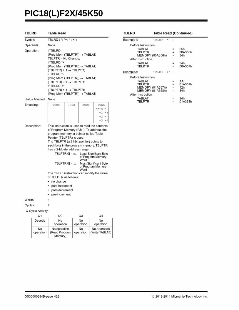
PIC18(L)F2X/45K50
TBLRD Table Read
Syntax: TBLRD ( *; *+; *-; +*)
Operands: None
Operation: if TBLRD *,(Prog Mem (TBLPTR)) TABLAT;TBLPTR – No Change;if TBLRD *+,(Prog Mem (TBLPTR)) TABLAT;(TBLPTR) + 1 TBLPTR;if TBLRD *-,(Prog Mem (TBLPTR)) TABLAT;(TBLPTR) – 1 TBLPTR;if TBLRD +*,(TBLPTR) + 1 TBLPTR;(Prog Mem (TBLPTR)) TABLAT;
Status Affected: None
Encoding: 0000 0000 0000 10nn nn=0 * =1 *+ =2 *- =3 +*
Description: This instruction is used to read the contents of Program Memory (P.M.). To address the program memory, a pointer called Table Pointer (TBLPTR) is used.The TBLPTR (a 21-bit pointer) points to each byte in the program memory. TBLPTR has a 2-Mbyte address range.
TBLPTR[0] = 0: Least Significant Byte of Program Memory Word
TBLPTR[0] = 1: Most Significant Byte of Program Memory Word
The TBLRD instruction can modify the value of TBLPTR as follows:• no change• post-increment• post-decrement• pre-increment
Words: 1
Cycles: 2
Q Cycle Activity:
Q1 Q2 Q3 Q4
Decode No operation
No operation
No operation
No operation
No operation(Read Program
Memory)
No operation
No operation(Write TABLAT)
TBLRD Table Read (Continued)
Example1: TBLRD *+ ;
Before InstructionTABLAT = 55hTBLPTR = 00A356hMEMORY (00A356h) = 34h
After InstructionTABLAT = 34hTBLPTR = 00A357h
Example2: TBLRD +* ;
Before InstructionTABLAT = AAhTBLPTR = 01A357hMEMORY (01A357h) = 12hMEMORY (01A358h) = 34h
After InstructionTABLAT = 34hTBLPTR = 01A358h
DS30000684B-page 428 2012-2014 Microchip Technology Inc.
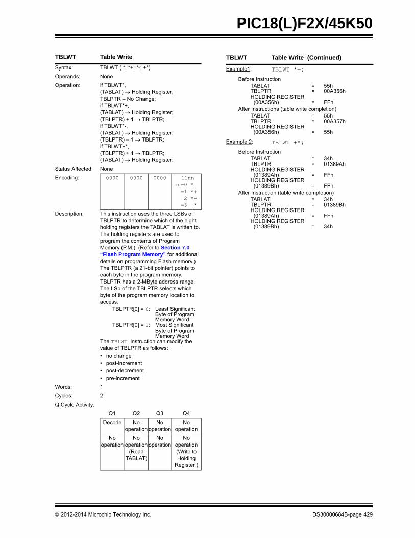
PIC18(L)F2X/45K50
TBLWT Table Write
Syntax: TBLWT ( *; *+; *-; +*)
Operands: None
Operation: if TBLWT*,(TABLAT) Holding Register;TBLPTR – No Change;if TBLWT*+,(TABLAT) Holding Register;(TBLPTR) + 1 TBLPTR;if TBLWT*-,(TABLAT) Holding Register;(TBLPTR) – 1 TBLPTR;if TBLWT+*,(TBLPTR) + 1 TBLPTR;(TABLAT) Holding Register;
Status Affected: None
Encoding: 0000 0000 0000 11nnnn=0 * =1 *+ =2 *- =3 +*
Description: This instruction uses the three LSBs of TBLPTR to determine which of the eight holding registers the TABLAT is written to. The holding registers are used to program the contents of Program Memory (P.M.). (Refer to Section 7.0 “Flash Program Memory” for additional details on programming Flash memory.)The TBLPTR (a 21-bit pointer) points to each byte in the program memory. TBLPTR has a 2-MByte address range. The LSb of the TBLPTR selects which byte of the program memory location to access.
TBLPTR[0] = 0: Least Significant Byte of Program Memory Word
TBLPTR[0] = 1: Most Significant Byte of Program Memory Word
The TBLWT instruction can modify the value of TBLPTR as follows:• no change• post-increment• post-decrement• pre-increment
Words: 1
Cycles: 2
Q Cycle Activity:
Q1 Q2 Q3 Q4
Decode No operation
No operation
No operation
No operation
No operation
(ReadTABLAT)
No operation
No operation(Write to Holding
Register )
TBLWT Table Write (Continued)
Example1: TBLWT *+;
Before InstructionTABLAT = 55hTBLPTR = 00A356hHOLDING REGISTER (00A356h) = FFh
After Instructions (table write completion)TABLAT = 55hTBLPTR = 00A357hHOLDING REGISTER (00A356h) = 55h
Example 2: TBLWT +*;
Before InstructionTABLAT = 34hTBLPTR = 01389AhHOLDING REGISTER (01389Ah) = FFhHOLDING REGISTER (01389Bh) = FFh
After Instruction (table write completion)TABLAT = 34hTBLPTR = 01389BhHOLDING REGISTER (01389Ah) = FFhHOLDING REGISTER (01389Bh) = 34h
2012-2014 Microchip Technology Inc. DS30000684B-page 429
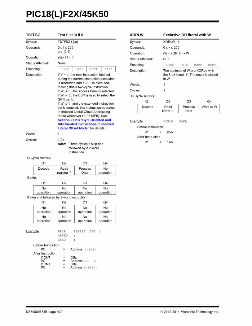
PIC18(L)F2X/45K50
TSTFSZ Test f, skip if 0
Syntax: TSTFSZ f ,a
Operands: 0 f 255a [0,1]
Operation: skip if f = 0
Status Affected: None
Encoding: 0110 011a ffff ffff
Description: If ‘f’ = 0, the next instruction fetched during the current instruction execution is discarded and a NOP is executed, making this a two-cycle instruction. If ‘a’ is ‘0’, the Access Bank is selected. If ‘a’ is ‘1’, the BSR is used to select the GPR bank.If ‘a’ is ‘0’ and the extended instruction set is enabled, this instruction operates in Indexed Literal Offset Addressing mode whenever f 95 (5Fh). See Section 27.2.3 “Byte-Oriented and Bit-Oriented Instructions in Indexed Literal Offset Mode” for details.
Words: 1
Cycles: 1(2)Note: Three cycles if skip and
followed by a 2-word instruction.
Q Cycle Activity:
Q1 Q2 Q3 Q4
Decode Readregister ‘f’
Process Data
No operation
If skip:
Q1 Q2 Q3 Q4
No operation
No operation
No operation
No operation
If skip and followed by 2-word instruction:
Q1 Q2 Q3 Q4
No operation
No operation
No operation
No operation
No operation
No operation
No operation
No operation
Example: HERE TSTFSZ CNT, 1NZERO :ZERO :
Before InstructionPC = Address (HERE)
After InstructionIf CNT = 00h,PC = Address (ZERO)If CNT 00h,PC = Address (NZERO)
XORLW Exclusive OR literal with W
Syntax: XORLW k
Operands: 0 k 255
Operation: (W) .XOR. k W
Status Affected: N, Z
Encoding: 0000 1010 kkkk kkkk
Description: The contents of W are XORed with the 8-bit literal ‘k’. The result is placed in W.
Words: 1
Cycles: 1
Q Cycle Activity:
Q1 Q2 Q3 Q4
Decode Readliteral ‘k’
Process Data
Write to W
Example: XORLW 0AFh
Before Instruction
W = B5h
After Instruction
W = 1Ah
DS30000684B-page 430 2012-2014 Microchip Technology Inc.

PIC18(L)F2X/45K50
XORWF Exclusive OR W with f
Syntax: XORWF f ,d ,a
Operands: 0 f 255d [0,1]a [0,1]
Operation: (W) .XOR. (f) dest
Status Affected: N, Z
Encoding: 0001 10da ffff ffff
Description: Exclusive OR the contents of W with register ‘f’. If ‘d’ is ‘0’, the result is stored in W. If ‘d’ is ‘1’, the result is stored back in the register ‘f’. If ‘a’ is ‘0’, the Access Bank is selected. If ‘a’ is ‘1’, the BSR is used to select the GPR bank.If ‘a’ is ‘0’ and the extended instruction set is enabled, this instruction operates in Indexed Literal Offset Addressing mode whenever f 95 (5Fh). See Section 27.2.3 “Byte-Oriented and Bit-Oriented Instructions in Indexed Literal Offset Mode” for details.
Words: 1
Cycles: 1
Q Cycle Activity:
Q1 Q2 Q3 Q4
Decode Readregister ‘f’
Process Data
Write to destination
Example: XORWF REG, 1, 0
Before InstructionREG = AFhW = B5h
After InstructionREG = 1AhW = B5h
2012-2014 Microchip Technology Inc. DS30000684B-page 431
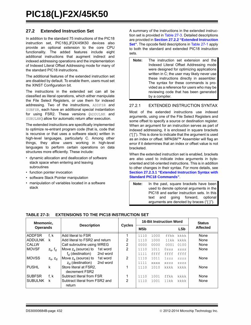
PIC18(L)F2X/45K50
27.2 Extended Instruction Set
In addition to the standard 75 instructions of the PIC18instruction set, PIC18(L)F2X/45K50 devices alsoprovide an optional extension to the core CPUfunctionality. The added features include eightadditional instructions that augment indirect andindexed addressing operations and the implementationof Indexed Literal Offset Addressing mode for many ofthe standard PIC18 instructions.
The additional features of the extended instruction setare disabled by default. To enable them, users must setthe XINST Configuration bit.
The instructions in the extended set can all beclassified as literal operations, which either manipulatethe File Select Registers, or use them for indexedaddressing. Two of the instructions, ADDFSR andSUBFSR, each have an additional special instantiationfor using FSR2. These versions (ADDULNK andSUBULNK) allow for automatic return after execution.
The extended instructions are specifically implementedto optimize re-entrant program code (that is, code thatis recursive or that uses a software stack) written inhigh-level languages, particularly C. Among otherthings, they allow users working in high-levellanguages to perform certain operations on datastructures more efficiently. These include:
• dynamic allocation and deallocation of software stack space when entering and leaving subroutines
• function pointer invocation
• software Stack Pointer manipulation
• manipulation of variables located in a software stack
A summary of the instructions in the extended instruc-tion set is provided in Table 27-3. Detailed descriptionsare provided in Section 27.2.2 “Extended InstructionSet”. The opcode field descriptions in Table 27-1 applyto both the standard and extended PIC18 instructionsets.
27.2.1 EXTENDED INSTRUCTION SYNTAX
Most of the extended instructions use indexedarguments, using one of the File Select Registers andsome offset to specify a source or destination register.When an argument for an instruction serves as part ofindexed addressing, it is enclosed in square brackets(“[ ]”). This is done to indicate that the argument is usedas an index or offset. MPASM™ Assembler will flag anerror if it determines that an index or offset value is notbracketed.
When the extended instruction set is enabled, bracketsare also used to indicate index arguments in byte-oriented and bit-oriented instructions. This is in additionto other changes in their syntax. For more details, seeSection 27.2.3.1 “Extended Instruction Syntax withStandard PIC18 Commands”.
TABLE 27-3: EXTENSIONS TO THE PIC18 INSTRUCTION SET
Note: The instruction set extension and theIndexed Literal Offset Addressing modewere designed for optimizing applicationswritten in C; the user may likely never usethese instructions directly in assembler.The syntax for these commands is pro-vided as a reference for users who may bereviewing code that has been generatedby a compiler.
Note: In the past, square brackets have beenused to denote optional arguments in thePIC18 and earlier instruction sets. In thistext and going forward, optionalarguments are denoted by braces (“ ”).
Mnemonic,Operands
Description Cycles16-Bit Instruction Word Status
AffectedMSb LSb
ADDFSRADDULNKCALLWMOVSF
MOVSS
PUSHL
SUBFSRSUBULNK
f, kk
zs, fd
zs, zd
k
f, kk
Add literal to FSRAdd literal to FSR2 and returnCall subroutine using WREGMove zs (source) to 1st word fd (destination) 2nd wordMove zs (source) to 1st word zd (destination) 2nd wordStore literal at FSR2, decrement FSR2Subtract literal from FSRSubtract literal from FSR2 and return
1222
2
1
12
11101110000011101111111011111110
11101110
1000100000001011ffff1011xxxx1010
10011001
ffkk 11kk 00010zzzffff1zzzxzzzkkkk
ffkk11kk
kkkkkkkk0100zzzzffffzzzzzzzzkkkk
kkkkkkkk
NoneNoneNoneNone
None
None
NoneNone
DS30000684B-page 432 2012-2014 Microchip Technology Inc.

PIC18(L)F2X/45K50
27.2.2 EXTENDED INSTRUCTION SET
ADDFSR Add Literal to FSR
Syntax: ADDFSR f, k
Operands: 0 k 63f [ 0, 1, 2 ]
Operation: FSR(f) + k FSR(f)
Status Affected: None
Encoding: 1110 1000 ffkk kkkk
Description: The 6-bit literal ‘k’ is added to the contents of the FSR specified by ‘f’.
Words: 1
Cycles: 1
Q Cycle Activity:
Q1 Q2 Q3 Q4
Decode Readliteral ‘k’
Process Data
Write to FSR
Example: ADDFSR 2, 23h
Before InstructionFSR2 = 03FFh
After InstructionFSR2 = 0422h
ADDULNK Add Literal to FSR2 and Return
Syntax: ADDULNK k
Operands: 0 k 63
Operation: FSR2 + k FSR2,
(TOS) PC
Status Affected: None
Encoding: 1110 1000 11kk kkkk
Description: The 6-bit literal ‘k’ is added to the contents of FSR2. A RETURN is then executed by loading the PC with the TOS. The instruction takes two cycles to execute; a NOP is performed during the second cycle.This may be thought of as a special case of the ADDFSR instruction, where f = 3 (binary ‘11’); it operates only on FSR2.
Words: 1
Cycles: 2
Q Cycle Activity:
Q1 Q2 Q3 Q4
Decode Readliteral ‘k’
Process Data
Write to FSR
No Operation
No Operation
No Operation
No Operation
Example: ADDULNK 23h
Before InstructionFSR2 = 03FFhPC = 0100h
After InstructionFSR2 = 0422hPC = (TOS)
Note: All PIC18 instructions may take an optional label argument preceding the instruction mnemonic for use insymbolic addressing. If a label is used, the instruction syntax then becomes: label instruction argument(s).
2012-2014 Microchip Technology Inc. DS30000684B-page 433

PIC18(L)F2X/45K50
CALLW Subroutine Call Using WREG
Syntax: CALLW
Operands: None
Operation: (PC + 2) TOS,(W) PCL,(PCLATH) PCH,(PCLATU) PCU
Status Affected: None
Encoding: 0000 0000 0001 0100
Description First, the return address (PC + 2) is pushed onto the return stack. Next, the contents of W are written to PCL; the existing value is discarded. Then, the contents of PCLATH and PCLATU are latched into PCH and PCU, respectively. The second cycle is executed as a NOP instruction while the new next instruction is fetched.Unlike CALL, there is no option to update W, Status or BSR.
Words: 1
Cycles: 2
Q Cycle Activity:
Q1 Q2 Q3 Q4
Decode Read WREG
PUSH PC to stack
No operation
No operation
No operation
No operation
No operation
Example: HERE CALLW
Before InstructionPC = address (HERE)PCLATH = 10hPCLATU = 00hW = 06h
After InstructionPC = 001006hTOS = address (HERE + 2)PCLATH = 10hPCLATU = 00hW = 06h
MOVSF Move Indexed to f
Syntax: MOVSF [zs], fd
Operands: 0 zs 1270 fd 4095
Operation: ((FSR2) + zs) fd
Status Affected: None
Encoding:1st word (source)2nd word (destin.)
11101111
1011ffff
0zzzffff
zzzzsffffd
Description: The contents of the source register are moved to destination register ‘fd’. The actual address of the source register is determined by adding the 7-bit literal offset ‘zs’ in the first word to the value of FSR2. The address of the destination register is specified by the 12-bit literal ‘fd’ in the second word. Both addresses can be anywhere in the 4096-byte data space (000h to FFFh).The MOVSF instruction cannot use the PCL, TOSU, TOSH or TOSL as the destination register.If the resultant source address points to an indirect addressing register, the value returned will be 00h.
Words: 2
Cycles: 2
Q Cycle Activity:
Q1 Q2 Q3 Q4
Decode Determine source addr
Determinesource addr
Read source reg
Decode No operation
No dummy read
No operation
Write register ‘f’
(dest)
Example: MOVSF [05h], REG2
Before InstructionFSR2 = 80hContents of 85h = 33hREG2 = 11h
After InstructionFSR2 = 80hContentsof 85h = 33hREG2 = 33h
DS30000684B-page 434 2012-2014 Microchip Technology Inc.

PIC18(L)F2X/45K50
MOVSS Move Indexed to Indexed
Syntax: MOVSS [zs], [zd]
Operands: 0 zs 1270 zd 127
Operation: ((FSR2) + zs) ((FSR2) + zd)
Status Affected: None
Encoding:1st word (source)2nd word (dest.)
11101111
1011xxxx
1zzzxzzz
zzzzszzzzd
Description The contents of the source register are moved to the destination register. The addresses of the source and destination registers are determined by adding the 7-bit literal offsets ‘zs’ or ‘zd’, respectively, to the value of FSR2. Both registers can be located anywhere in the 4096-byte data memory space (000h to FFFh).The MOVSS instruction cannot use the PCL, TOSU, TOSH or TOSL as the destination register.If the resultant source address points to an indirect addressing register, the value returned will be 00h. If the resultant destination address points to an indirect addressing register, the instruction will execute as a NOP.
Words: 2
Cycles: 2
Q Cycle Activity:
Q1 Q2 Q3 Q4
Decode Determine source addr
Determinesource addr
Read source reg
Decode Determinedest addr
Determinedest addr
Write to dest reg
Example: MOVSS [05h], [06h]
Before InstructionFSR2 = 80hContentsof 85h = 33hContentsof 86h = 11h
After InstructionFSR2 = 80hContentsof 85h = 33hContentsof 86h = 33h
PUSHL Store Literal at FSR2, Decrement FSR2
Syntax: PUSHL k
Operands: 0k 255
Operation: k (FSR2),FSR2 – 1 FSR2
Status Affected: None
Encoding: 1111 1010 kkkk kkkk
Description: The 8-bit literal ‘k’ is written to the data memory address specified by FSR2. FSR2 is decremented by 1 after the operation. This instruction allows users to push values onto a software stack.
Words: 1
Cycles: 1
Q Cycle Activity:
Q1 Q2 Q3 Q4
Decode Read ‘k’ Processdata
Write todestination
Example: PUSHL 08h
Before InstructionFSR2H:FSR2L = 01EChMemory (01ECh) = 00h
After InstructionFSR2H:FSR2L = 01EBhMemory (01ECh) = 08h
2012-2014 Microchip Technology Inc. DS30000684B-page 435

PIC18(L)F2X/45K50
SUBFSR Subtract Literal from FSR
Syntax: SUBFSR f, k
Operands: 0 k 63
f [ 0, 1, 2 ]
Operation: FSR(f) – k FSRf
Status Affected: None
Encoding: 1110 1001 ffkk kkkk
Description: The 6-bit literal ‘k’ is subtracted from the contents of the FSR specified by ‘f’.
Words: 1
Cycles: 1
Q Cycle Activity:
Q1 Q2 Q3 Q4
Decode Readregister ‘f’
Process Data
Write to destination
Example: SUBFSR 2, 23h
Before InstructionFSR2 = 03FFh
After InstructionFSR2 = 03DCh
SUBULNK Subtract Literal from FSR2 and Return
Syntax: SUBULNK k
Operands: 0 k 63
Operation: FSR2 – k FSR2
(TOS) PC
Status Affected: None
Encoding: 1110 1001 11kk kkkk
Description: The 6-bit literal ‘k’ is subtracted from the contents of the FSR2. A RETURN is then executed by loading the PC with the TOS. The instruction takes two cycles to execute; a NOP is performed during the second cycle.This may be thought of as a special case of the SUBFSR instruction, where f = 3 (binary ‘11’); it operates only on FSR2.
Words: 1
Cycles: 2
Q Cycle Activity:
Q1 Q2 Q3 Q4
Decode Readregister ‘f’
Process Data
Write to destination
NoOperation
NoOperation
NoOperation
NoOperation
Example: SUBULNK 23h
Before InstructionFSR2 = 03FFhPC = 0100h
After InstructionFSR2 = 03DChPC = (TOS)
DS30000684B-page 436 2012-2014 Microchip Technology Inc.
PIC18(L)F2X/45K50
27.2.3 BYTE-ORIENTED AND BIT-ORIENTED INSTRUCTIONS IN INDEXED LITERAL OFFSET MODE
In addition to eight new commands in the extended set,enabling the extended instruction set also enablesIndexed Literal Offset Addressing mode (Section 6.7.1“Indexed Addressing with Literal Offset”). This hasa significant impact on the way that many commands ofthe standard PIC18 instruction set are interpreted.
When the extended set is disabled, addressesembedded in opcodes are treated as literal memorylocations: either as a location in the Access Bank (‘a’ =0), or in a GPR bank designated by the BSR (‘a’ = 1).When the extended instruction set is enabled and ‘a’ =0, however, a file register argument of 5Fh or less isinterpreted as an offset from the pointer value in FSR2and not as a literal address. For practical purposes, thismeans that all instructions that use the Access RAM bitas an argument – that is, all byte-oriented and bit-oriented instructions, or almost half of the core PIC18instructions – may behave differently when theextended instruction set is enabled.
When the content of FSR2 is 00h, the boundaries of theAccess RAM are essentially remapped to their originalvalues. This may be useful in creating backwardcompatible code. If this technique is used, it may benecessary to save the value of FSR2 and restore itwhen moving back and forth between C and assemblyroutines in order to preserve the Stack Pointer. Usersmust also keep in mind the syntax requirements of theextended instruction set (see Section 27.2.3.1“Extended Instruction Syntax with Standard PIC18Commands”).
Although the Indexed Literal Offset Addressing modecan be very useful for dynamic stack and pointermanipulation, it can also be very annoying if a simplearithmetic operation is carried out on the wrongregister. Users who are accustomed to the PIC18programming must keep in mind that, when theextended instruction set is enabled, register addressesof 5Fh or less are used for Indexed Literal OffsetAddressing.
Representative examples of typical byte-oriented andbit-oriented instructions in the Indexed Literal OffsetAddressing mode are provided on the following page toshow how execution is affected. The operand condi-tions shown in the examples are applicable to allinstructions of these types.
27.2.3.1 Extended Instruction Syntax with Standard PIC18 Commands
When the extended instruction set is enabled, the fileregister argument, ‘f’, in the standard byte-oriented andbit-oriented commands is replaced with the literal offsetvalue, ‘k’. As already noted, this occurs only when ‘f’ isless than or equal to 5Fh. When an offset value is used,it must be indicated by square brackets (“[ ]”). As withthe extended instructions, the use of brackets indicatesto the compiler that the value is to be interpreted as anindex or an offset. Omitting the brackets, or using avalue greater than 5Fh within brackets, will generate anerror in the MPASM assembler.
If the index argument is properly bracketed for IndexedLiteral Offset Addressing, the Access RAM argument isnever specified; it will automatically be assumed to be‘0’. This is in contrast to standard operation (extendedinstruction set disabled) when ‘a’ is set on the basis ofthe target address. Declaring the Access RAM bit inthis mode will also generate an error in the MPASMassembler.
The destination argument, ‘d’, functions as before.
In the latest versions of the MPASM™ assembler,language support for the extended instruction set mustbe explicitly invoked. This is done with either thecommand line option, /y, or the PE directive in thesource listing.
27.2.4 CONSIDERATIONS WHEN ENABLING THE EXTENDED INSTRUCTION SET
It is important to note that the extensions to the instruc-tion set may not be beneficial to all users. In particular,users who are not writing code that uses a softwarestack may not benefit from using the extensions to theinstruction set.
Additionally, the Indexed Literal Offset Addressingmode may create issues with legacy applicationswritten to the PIC18 assembler. This is becauseinstructions in the legacy code may attempt to addressregisters in the Access Bank below 5Fh. Since theseaddresses are interpreted as literal offsets to FSR2when the instruction set extension is enabled, theapplication may read or write to the wrong dataaddresses.
When porting an application to the PIC18(L)F2X/45K50, it is very important to consider the type of code.A large, re-entrant application that is written in ‘C’ andwould benefit from efficient compilation will do wellwhen using the instruction set extensions. Legacyapplications that heavily use the Access Bank will mostlikely not benefit from using the extended instructionset.
Note: Enabling the PIC18 instruction setextension may cause legacy applicationsto behave erratically or fail entirely.
2012-2014 Microchip Technology Inc. DS30000684B-page 437

PIC18(L)F2X/45K50
ADDWFADD W to Indexed(Indexed Literal Offset mode)
Syntax: ADDWF [k] ,d
Operands: 0 k 95d [0,1]
Operation: (W) + ((FSR2) + k) dest
Status Affected: N, OV, C, DC, Z
Encoding: 0010 01d0 kkkk kkkk
Description: The contents of W are added to the contents of the register indicated by FSR2, offset by the value ‘k’. If ‘d’ is ‘0’, the result is stored in W. If ‘d’ is ‘1’, the result is stored back in register ‘f’.
Words: 1
Cycles: 1
Q Cycle Activity:
Q1 Q2 Q3 Q4
Decode Read ‘k’ Process Data
Write todestination
Example: ADDWF [OFST] , 0
Before Instruction
W = 17hOFST = 2ChFSR2 = 0A00hContentsof 0A2Ch = 20h
After Instruction
W = 37hContentsof 0A2Ch = 20h
BSFBit Set Indexed (Indexed Literal Offset mode)
Syntax: BSF [k], b
Operands: 0 f 950 b 7
Operation: 1 ((FSR2) + k)<b>
Status Affected: None
Encoding: 1000 bbb0 kkkk kkkk
Description: Bit ‘b’ of the register indicated by FSR2, offset by the value ‘k’, is set.
Words: 1
Cycles: 1
Q Cycle Activity:
Q1 Q2 Q3 Q4
Decode Readregister ‘f’
Process Data
Write todestination
Example: BSF [FLAG_OFST], 7
Before InstructionFLAG_OFST = 0AhFSR2 = 0A00hContents of 0A0Ah = 55h
After InstructionContentsof 0A0Ah = D5h
SETFSet Indexed(Indexed Literal Offset mode)
Syntax: SETF [k]
Operands: 0 k 95
Operation: FFh ((FSR2) + k)
Status Affected: None
Encoding: 0110 1000 kkkk kkkk
Description: The contents of the register indicated by FSR2, offset by ‘k’, are set to FFh.
Words: 1
Cycles: 1
Q Cycle Activity:
Q1 Q2 Q3 Q4
Decode Read ‘k’ Process Data
Writeregister
Example: SETF [OFST]
Before InstructionOFST = 2ChFSR2 = 0A00hContentsof 0A2Ch = 00h
After InstructionContentsof 0A2Ch = FFh
DS30000684B-page 438 2012-2014 Microchip Technology Inc.

PIC18(L)F2X/45K50
27.2.5 SPECIAL CONSIDERATIONS WITH MICROCHIP MPLAB® IDE TOOLS
The latest versions of Microchip’s software tools havebeen designed to fully support the extended instructionset of the PIC18(L)F2X/45K50 family of devices. Thisincludes the MPLAB C18 C compiler, MPASMassembly language and MPLAB IntegratedDevelopment Environment (IDE).
When selecting a target device for softwaredevelopment, MPLAB IDE will automatically set defaultConfiguration bits for that device. The default setting forthe XINST Configuration bit is ‘0’, disabling theextended instruction set and Indexed Literal OffsetAddressing mode. For proper execution of applicationsdeveloped to take advantage of the extendedinstruction set, XINST must be set duringprogramming.
To develop software for the extended instruction set,the user must enable support for the instructions andthe Indexed Addressing mode in their language tool(s).Depending on the environment being used, this may bedone in several ways:
• A menu option, or dialog box within the environment, that allows the user to configure the language tool and its settings for the project
• A command line option
• A directive in the source code
These options vary between different compilers,assemblers and development environments. Users areencouraged to review the documentation accompanyingtheir development systems for the appropriateinformation.
2012-2014 Microchip Technology Inc. DS30000684B-page 439

PIC18(L)F2X/45K50
28.0 DEVELOPMENT SUPPORT
The PIC microcontrollers (MCU) and dsPIC® digitalsignal controllers (DSC) are supported with a full rangeof software and hardware development tools:
• Integrated Development Environment- MPLAB® X IDE Software
• Compilers/Assemblers/Linkers- MPLAB XC Compiler - MPASMTM Assembler- MPLINKTM Object Linker/
MPLIBTM Object Librarian- MPLAB Assembler/Linker/Librarian for
Various Device Families• Simulators
- MPLAB X SIM Software Simulator• Emulators
- MPLAB REAL ICE™ In-Circuit Emulator• In-Circuit Debuggers/Programmers
- MPLAB ICD 3- PICkit™ 3
• Device Programmers- MPLAB PM3 Device Programmer
• Low-Cost Demonstration/Development Boards, Evaluation Kits and Starter Kits
• Third-party development tools
28.1 MPLAB X Integrated Development Environment Software
The MPLAB X IDE is a single, unified graphical userinterface for Microchip and third-party software, andhardware development tool that runs on Windows®,Linux and Mac OS® X. Based on the NetBeans IDE,MPLAB X IDE is an entirely new IDE with a host of freesoftware components and plug-ins for high-performance application development and debugging.Moving between tools and upgrading from softwaresimulators to hardware debugging and programmingtools is simple with the seamless user interface.
With complete project management, visual call graphs,a configurable watch window and a feature-rich editorthat includes code completion and context menus,MPLAB X IDE is flexible and friendly enough for newusers. With the ability to support multiple tools onmultiple projects with simultaneous debugging, MPLABX IDE is also suitable for the needs of experiencedusers.
Feature-Rich Editor:
• Color syntax highlighting• Smart code completion makes suggestions and
provides hints as you type• Automatic code formatting based on user-defined
rules• Live parsing
User-Friendly, Customizable Interface:
• Fully customizable interface: toolbars, toolbar buttons, windows, window placement, etc.
• Call graph window
Project-Based Workspaces:
• Multiple projects• Multiple tools• Multiple configurations• Simultaneous debugging sessions
File History and Bug Tracking:
• Local file history feature• Built-in support for Bugzilla issue tracker
DS30000684B-page 440 2012-2014 Microchip Technology Inc.

PIC18(L)F2X/45K50
28.2 MPLAB XC Compilers
The MPLAB XC Compilers are complete ANSI Ccompilers for all of Microchip’s 8, 16, and 32-bit MCUand DSC devices. These compilers provide powerfulintegration capabilities, superior code optimization andease of use. MPLAB XC Compilers run on Windows,Linux or MAC OS X.
For easy source level debugging, the compilers providedebug information that is optimized to the MPLAB XIDE.
The free MPLAB XC Compiler editions support alldevices and commands, with no time or memoryrestrictions, and offer sufficient code optimization formost applications.
MPLAB XC Compilers include an assembler, linker andutilities. The assembler generates relocatable objectfiles that can then be archived or linked with otherrelocatable object files and archives to create anexecutable file. MPLAB XC Compiler uses theassembler to produce its object file. Notable features ofthe assembler include:
• Support for the entire device instruction set• Support for fixed-point and floating-point data• Command-line interface• Rich directive set• Flexible macro language• MPLAB X IDE compatibility
28.3 MPASM Assembler
The MPASM Assembler is a full-featured, universalmacro assembler for PIC10/12/16/18 MCUs.
The MPASM Assembler generates relocatable objectfiles for the MPLINK Object Linker, Intel® standard HEXfiles, MAP files to detail memory usage and symbolreference, absolute LST files that contain source linesand generated machine code, and COFF files fordebugging.
The MPASM Assembler features include:
• Integration into MPLAB X IDE projects• User-defined macros to streamline
assembly code• Conditional assembly for multipurpose
source files• Directives that allow complete control over the
assembly process
28.4 MPLINK Object Linker/MPLIB Object Librarian
The MPLINK Object Linker combines relocatableobjects created by the MPASM Assembler. It can linkrelocatable objects from precompiled libraries, usingdirectives from a linker script.
The MPLIB Object Librarian manages the creation andmodification of library files of precompiled code. Whena routine from a library is called from a source file, onlythe modules that contain that routine will be linked inwith the application. This allows large libraries to beused efficiently in many different applications.
The object linker/library features include:
• Efficient linking of single libraries instead of many smaller files
• Enhanced code maintainability by grouping related modules together
• Flexible creation of libraries with easy module listing, replacement, deletion and extraction
28.5 MPLAB Assembler, Linker and Librarian for Various Device Families
MPLAB Assembler produces relocatable machinecode from symbolic assembly language for PIC24,PIC32 and dsPIC DSC devices. MPLAB XC Compileruses the assembler to produce its object file. Theassembler generates relocatable object files that canthen be archived or linked with other relocatable objectfiles and archives to create an executable file. Notablefeatures of the assembler include:
• Support for the entire device instruction set• Support for fixed-point and floating-point data• Command-line interface• Rich directive set• Flexible macro language• MPLAB X IDE compatibility
2012-2014 Microchip Technology Inc. DS30000684B-page 441

PIC18(L)F2X/45K50
28.6 MPLAB X SIM Software Simulator
The MPLAB X SIM Software Simulator allows codedevelopment in a PC-hosted environment bysimulating the PIC MCUs and dsPIC DSCs on aninstruction level. On any given instruction, the dataareas can be examined or modified and stimuli can beapplied from a comprehensive stimulus controller.Registers can be logged to files for further run-timeanalysis. The trace buffer and logic analyzer displayextend the power of the simulator to record and trackprogram execution, actions on I/O, most peripheralsand internal registers.
The MPLAB X SIM Software Simulator fully supportssymbolic debugging using the MPLAB XC Compilers,and the MPASM and MPLAB Assemblers. Thesoftware simulator offers the flexibility to develop anddebug code outside of the hardware laboratoryenvironment, making it an excellent, economicalsoftware development tool.
28.7 MPLAB REAL ICE In-Circuit Emulator System
The MPLAB REAL ICE In-Circuit Emulator System isMicrochip’s next generation high-speed emulator forMicrochip Flash DSC and MCU devices. It debugs andprograms all 8, 16 and 32-bit MCU, and DSC deviceswith the easy-to-use, powerful graphical user interface ofthe MPLAB X IDE.
The emulator is connected to the design engineer’sPC using a high-speed USB 2.0 interface and isconnected to the target with either a connectorcompatible with in-circuit debugger systems (RJ-11)or with the new high-speed, noise tolerant, Low-Voltage Differential Signal (LVDS) interconnection(CAT5).
The emulator is field upgradeable through futurefirmware downloads in MPLAB X IDE. MPLAB REALICE offers significant advantages over competitiveemulators including full-speed emulation, run-timevariable watches, trace analysis, complex breakpoints,logic probes, a ruggedized probe interface and long (upto three meters) interconnection cables.
28.8 MPLAB ICD 3 In-Circuit Debugger System
The MPLAB ICD 3 In-Circuit Debugger System isMicrochip’s most cost-effective, high-speed hardwaredebugger/programmer for Microchip Flash DSC andMCU devices. It debugs and programs PIC Flashmicrocontrollers and dsPIC DSCs with the powerful,yet easy-to-use graphical user interface of the MPLABIDE.
The MPLAB ICD 3 In-Circuit Debugger probe isconnected to the design engineer’s PC using a high-speed USB 2.0 interface and is connected to the targetwith a connector compatible with the MPLAB ICD 2 orMPLAB REAL ICE systems (RJ-11). MPLAB ICD 3supports all MPLAB ICD 2 headers.
28.9 PICkit 3 In-Circuit Debugger/Programmer
The MPLAB PICkit 3 allows debugging andprogramming of PIC and dsPIC Flash microcontrollersat a most affordable price point using the powerfulgraphical user interface of the MPLAB IDE. TheMPLAB PICkit 3 is connected to the design engineer’sPC using a full-speed USB interface and can beconnected to the target via a Microchip debug (RJ-11)connector (compatible with MPLAB ICD 3 and MPLABREAL ICE). The connector uses two device I/O pinsand the Reset line to implement in-circuit debuggingand In-Circuit Serial Programming (ICSP).
28.10 MPLAB PM3 Device Programmer
The MPLAB PM3 Device Programmer is a universal,CE compliant device programmer with programmablevoltage verification at VDDMIN and VDDMAX formaximum reliability. It features a large LCD display(128 x 64) for menus and error messages, and amodular, detachable socket assembly to supportvarious package types. The ICSP cable assembly isincluded as a standard item. In Stand-Alone mode, theMPLAB PM3 Device Programmer can read, verify andprogram PIC devices without a PC connection. It canalso set code protection in this mode. The MPLAB PM3connects to the host PC via an RS-232 or USB cable.The MPLAB PM3 has high-speed communications andoptimized algorithms for quick programming of largememory devices, and incorporates an MMC card for filestorage and data applications.
DS30000684B-page 442 2012-2014 Microchip Technology Inc.
PIC18(L)F2X/45K50
28.11 Demonstration/Development Boards, Evaluation Kits, and Starter Kits
A wide variety of demonstration, development andevaluation boards for various PIC MCUs and dsPICDSCs allows quick application development on fullyfunctional systems. Most boards include prototypingareas for adding custom circuitry and provideapplication firmware and source code for examinationand modification.
The boards support a variety of features, including LEDs,temperature sensors, switches, speakers, RS-232interfaces, LCD displays, potentiometers and additionalEEPROM memory.
The demonstration and development boards can beused in teaching environments, for prototyping customcircuits and for learning about various microcontrollerapplications.
In addition to the PICDEM™ and dsPICDEM™demonstration/development board series of circuits,Microchip has a line of evaluation kits anddemonstration software for analog filter design,KEELOQ® security ICs, CAN, IrDA®, PowerSmartbattery management, SEEVAL® evaluation system,Sigma-Delta ADC, flow rate sensing, plus many more.
Also available are starter kits that contain everythingneeded to experience the specified device. This usuallyincludes a single application and debug capability, allon one board.
Check the Microchip web page (www.microchip.com)for the complete list of demonstration, developmentand evaluation kits.
28.12 Third-Party Development Tools
Microchip also offers a great collection of tools fromthird-party vendors. These tools are carefully selectedto offer good value and unique functionality.
• Device Programmers and Gang Programmers from companies, such as SoftLog and CCS
• Software Tools from companies, such as Gimpel and Trace Systems
• Protocol Analyzers from companies, such as Saleae and Total Phase
• Demonstration Boards from companies, such as MikroElektronika, Digilent® and Olimex
• Embedded Ethernet Solutions from companies, such as EZ Web Lynx, WIZnet and IPLogika®
2012-2014 Microchip Technology Inc. DS30000684B-page 443

PIC18(L)F2X/45K50
DS
29.0 ELECTRICAL SPECIFICATIONS
29.1 Absolute Maximum Ratings (†)
Ambient temperature under bias............................................................................................................ .-40°C to +125°C
Storage temperature .............................................................................................................................. -65°C to +150°C
Voltage on pins with respect to VSS
on VDD pin
PIC18LF2X/45K50.................................................................................................... -0.3V to +4.5V
PIC18F2X/45K50...................................................................................................... -0.3V to +6.5V
on VUSB3V3 pin(3)...................................................................................................................... -0.3V to +4.0V
on D+ and D- pins
0 source impedance(5) .......................................................................... -0.5V to (VUSB3V3 + 0.5V)
source impedance 28, VUSB3V3 3.0V ............................................................... -1.0V to + 4.6V)
on MCLR/nICRST pin(2)..............................................................................................................0V to +11.0V
on all other pins............................................................................................................. -0.3V to (VDD + 0.3V)
Total power dissipation(1) ..........................................................................................................................................1.0W
Maximum current
out of VSS pin
-40°C to +125°C .................................................................................................................. 125 mA
into VDD pin
-40°C to +125°C ............................................................................................ ........................ 85 mA
Input clamp current, IIK (VI < 0 or VI > VDD)(4) 20 mA
Output clamp current, IOK (VO < 0 or VO > VDD)(4) 20 mA
Maximum output current
sunk by any I/O pin ...............................................................................................................................25 mA
sourced by any I/O pin ..........................................................................................................................25 mA
Maximum current
sunk byall ports (-40°C to +125°C) ................................................................................................... 110 mA
sourced by all ports (-40°C to +125°C) .................................................................................................70 mA
Note 1: Power dissipation is calculated as follows: Pdis = VDD x IDD – IOH + (VDD – VOH) x IOH + (VOL x IOL)
2: Voltage spikes below VSS at the MCLR/VPP/RE3 pin, inducing currents greater than 80 mA, may causelatch-up. Thus, a series resistor of 50-100 should be used when applying a “low” level to the MCLR/VPP/RE3 pin, rather than pulling this pin directly to VSS.
3: VUSB3V3 must always be VDD + 0.3V. VUSB3V3 must also be maintained VDD – 0.3V on PIC18LF2X/45K50 devices.
4: Stress rating only. For proper functional operation, I/O pins should be maintained within the -0.3V to(VDD + 0.3V) range, which will not result in injected current. See TB3013 technical brief (DS93013) fordetails.
5: The original Universal Serial Bus Specification Revision 2.0 indicated that USB devices should withstand24-hour short circuits of D+ or D- to VBUS voltages. This requirement was later removed in an EngineeringChange Notice (ECN) supplement to the USB specifications, which supersedes the original specifications.PIC18F2X/45K50 family devices will typically be able to survive this short-circuit test, but it is recommendedto adhere to the absolute maximum specified here to avoid damaging the device.
† NOTICE: Stresses above those listed under “Absolute Maximum Ratings” may cause permanent damage to the device. This is a stress rating only and functional operation of the device at those or any other conditions above those indicated in the operation listings of this specification is not implied. Exposure to maximum rating conditions for extended periods may affect device reliability.
30000684B-page 444 2012-2014 Microchip Technology Inc.

PIC18(L)F2X/45K50
29.2 Standard Operating Conditions
The standard operating conditions for any device are defined as:
Operating Voltage: VDDMIN VDD VDDMAX
Operating Temperature: TA_MIN TA TA_MAX
VDD — Operating Supply Voltage
PIC18LF2X/45K50
VDDMIN (Fosc 4 MHz, Industrial Temperature)...................................................................... +1.8V
VDDMIN (Fosc 48 MHz) ......................................................................................................... +2.7V
VDDMAX .................................................................................................................................... +3.6V
PIC18F2X/45K50
VDDMIN (Fosc 20 MHz, Industrial Temperature).................................................................... +2.3V
VDDMIN (Fosc 16 MHz, Extended Temperature) ................................................................... +2.3V
VDDMIN (Fosc 48 MHz) ......................................................................................................... +2.7V
VDDMAX .................................................................................................................................... +5.5V
TA — Operating Ambient Temperature Range
Industrial Temperature
TA_MIN...................................................................................................................................... -40°C
TA_MAX.................................................................................................................................... +85°C
Extended Temperature
TA_MIN...................................................................................................................................... -40°C
TA_MAX.................................................................................................................................. +125°C
2012-2014 Microchip Technology Inc. DS30000684B-page 445

PIC18(L)F2X/45K50
FIGURE 29-1: PIC18LF2X/45K50 FAMILY VOLTAGE-FREQUENCY GRAPH (INDUSTRIAL AND EXTENDED TEMPERATURE)
FIGURE 29-2: PIC18F2X/45K50 FAMILY VOLTAGE-FREQUENCY GRAPH (INDUSTRIAL TEMPERATURE)
Frequency (MHz)
Vo
lta
ge
3.6V
1.8V
3.0V
2.7V
2.3V
16 20
Note 1: Maximum Frequency 4 MHz, 1.8V to 2.7V, -40°C to +85°C
2: Maximum Frequency 48 MHz, 2.7V to 3.6V, -40°C to +85°C
5.5V
5.0V
4.0V
484
Frequency (MHz)
Vo
lta
ge
3.6V
1.8V
3.0V
2.7V
2.3V
30 40
Note 1: Maximum Frequency 20 MHz, 2.3V to 2.7V, -40°C to +85°C
2: Maximum Frequency 48 MHz, 2.7V to 5.5V, -40°C to +85°C
5.5V
5.0V
4.0V
4820
DS30000684B-page 446 2012-2014 Microchip Technology Inc.

PIC18(L)F2X/45K50
FIGURE 29-3: PIC18F2X/45K50 FAMILY VOLTAGE-FREQUENCY GRAPH (EXTENDED TEMPERATURE)
Frequency (MHz)
Vo
lta
ge
3.6V
1.8V
64
3.0V
2.7V
2.3V
10 20 6030 40
Note 1: Maximum Frequency 16 MHz, 2.3V to 2.7V, +85°C to +125°C
2: Maximum Frequency 48 MHz, 2.7V to 5.5V, +85°C to +125°C
5.5V
5.0V
4.0V
4816
2012-2014 Microchip Technology Inc. DS30000684B-page 447

PIC18(L)F2X/45K50
29.3 DC Characteristics
TABLE 29-1: SUPPLY VOLTAGE, PIC18(L)F2X/45K50
PIC18(L)F2X/45K50Standard Operating Conditions (unless otherwise stated)
Param. No.
Symbol Characteristic Min. Typ. Max. Units Conditions
D001 VDD Supply Voltage PIC18LF2X/45K50 1.8 — 3.6 V Regulator disabled
PIC18F2X/45K50 2.3 — 5.5 V Regulator enabled
D001B VUSB3V3 USB Supply Voltage 3.0 3.3 3.6 V USB module enabled
D001CD001D
VUSB3V3 Capacitor Charging (PIC18F2X/45K50)
Charging current — 200 — mA Note 4, 5
Source/sink capability when charging is complete
— 0.0 — mA Note 4
D002 VDR RAM Data Retention Voltage(1) 1.5 — — V
D003 VPOR VDD Start Voltage to ensure internal Power-on Reset signal
— — 0.7 V See section on Power-on Reset for details
D004 SVDD VDD Rise Rate to ensure internal Power-on Reset signal
0.05 — — V/ms See section on Power-on Reset for details
D005 VBOR Brown-out Reset Voltage
BORV<1:0> = 11(2) 1.75 1.9 2.05 V
BORV<1:0> = 10 2.05 2.2 2.35 V
BORV<1:0> = 01 2.35 2.5 2.65 V
BORV<1:0> = 00(3) 2.65 2.85 3.05 V
D006 VLPBOR Low-Power Brown-out Reset (LPBOR) Voltage
1.8V — 2.1 V
Note 1: This is the limit to which VDD can be lowered in Sleep mode, or during a device Reset, without losing RAM data.
2: On LF devices with BOR enabled, operation is supported until a BOR occurs. This is valid although VDD may be below the minimum rated supply voltage.
3: With BOR enabled, full-speed operation (FOSC = 48 MHz) is supported until a BOR occurs. This is valid although VDD may be below the minimum voltage for this frequency.
4: This is the inrush current associated with initial charging of the VUSB3V3 capacitor during a fast VDD ramp. The microcontroller can still start-up from VDD power sources that are limited to significantly less than this value.
5: The VUSB3V3 regulator is only designed to supply the current requirements of the microcontroller and USB transceiver. It is not intended to supply external loads.
DS30000684B-page 448 2012-2014 Microchip Technology Inc.

PIC18(L)F2X/45K50
TABLE 29-2: POWER-DOWN CURRENT, PIC18(L)F2X/45K50
PIC18LF2X/45K50 Standard Operating Conditions (unless otherwise stated)
PIC18F2X/45K50 Standard Operating Conditions (unless otherwise stated)
Param. No.
Device CharacteristicsTyp.
+25°CTyp.
+60°CMax.
+85°CMax.
+125°CUnits
Conditions
VDD Notes
Power-down Base Current (IPD)(1)
D006 Sleep mode 0.01 0.04 2 10 A 1.8V WDT, BOR, FVR and SOSC disabled, all Peripherals inactive
0.01 0.06 2 40 A 3.0V
12 13 25 35 A 2.3V
13 14 30 40 A 3.0V
13 14 35 50 A 5.0V
Power-down Module Differential Current (delta IPD)
D007 Watchdog Timer 0.3 0.3 2.5 2.5 A 1.8V
0.5 0.5 2.5 5 A 3.0V
0.35 0.35 5.0 5.0 A 2.3V
0.5 0.5 5.0 5.0 A 3.0V
0.5 0.5 5.0 5.0 A 5.0V
D008 Brown-out Reset(2) 8 8.5 15 16 A 2.0V
9 9.5 15 16 A 3.0V
3.4 3.4 15 16 A 2.3V
3.8 3.8 15 16 A 3.0V
5.2 5.2 15 16 A 5.0V
D010 High/Low Voltage Detect(2) 6.5 6.7 15 15 A 2.0V
7 7.5 15 15 A 3.0V
2.1 2.1 15 15 A 2.3V
2.4 2.4 15 15 A 3.0V
3.2 3.2 15 15 A 5.0V
D011 Secondary Oscillator 0.5 1 3 10 A 1.8V
32 kHz on SOSC
0.6 1.1 4 10 A 3.0V
0.5 1 3 10 A 2.3V
0.6 1.1 4 10 A 3.0V
0.6 1.1 5 10 A 5.0V
Note 1: The power-down current in Sleep mode does not depend on the oscillator type. Power-down current is measured with the part in Sleep mode, with all I/O pins in high-impedance state and tied to VDD or VSS and all features that add delta current disabled (such as WDT, Timer1 Oscillator, BOR, etc.).
2: On LF devices, the BOR, HLVD and FVR enable internal band gap reference. With more than one of these modules enabled, the current consumption will be less than the sum of the specifications. On F devices, the internal band gap reference is always enabled and its current consumption is included in the Power-down Base Current (IPD).
3: A/D converter differential currents apply only in Run mode. In Sleep or Idle mode both the ADC and the FRC turn off as soon as conversion (if any) is complete.
2012-2014 Microchip Technology Inc. DS30000684B-page 449
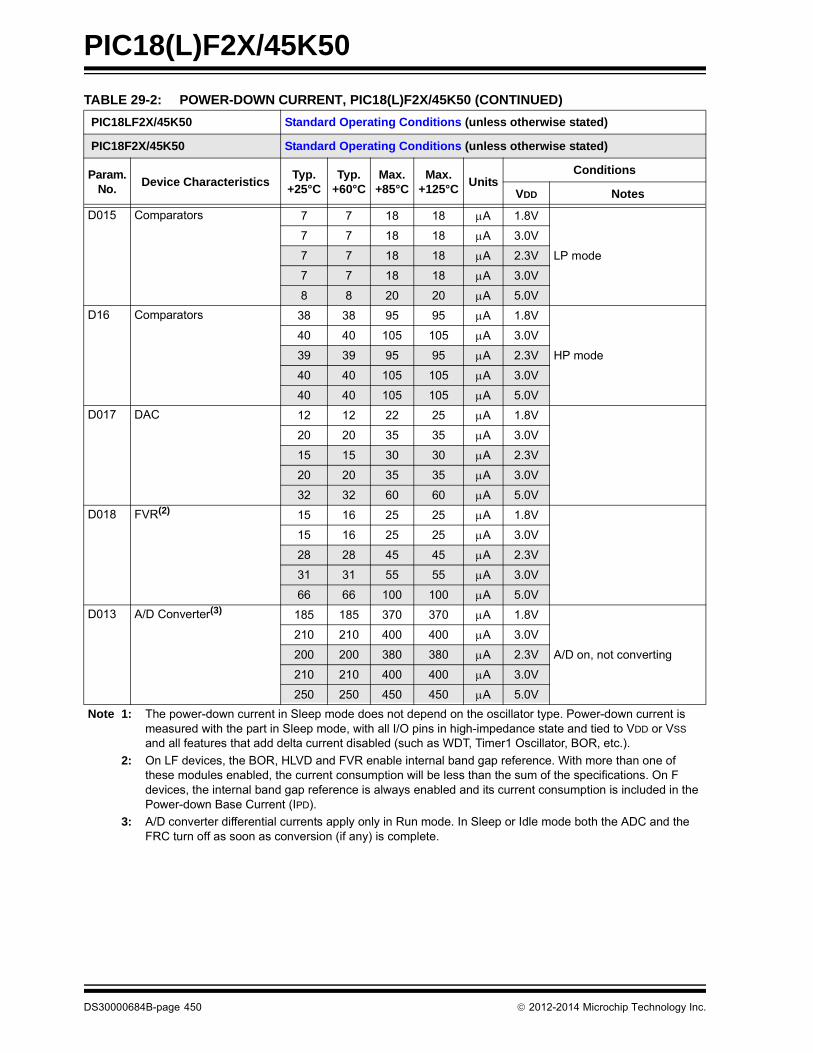
PIC18(L)F2X/45K50
D015 Comparators 7 7 18 18 A 1.8V
LP mode
7 7 18 18 A 3.0V
7 7 18 18 A 2.3V
7 7 18 18 A 3.0V
8 8 20 20 A 5.0V
D16 Comparators 38 38 95 95 A 1.8V
HP mode
40 40 105 105 A 3.0V
39 39 95 95 A 2.3V
40 40 105 105 A 3.0V
40 40 105 105 A 5.0V
D017 DAC 12 12 22 25 A 1.8V
20 20 35 35 A 3.0V
15 15 30 30 A 2.3V
20 20 35 35 A 3.0V
32 32 60 60 A 5.0V
D018 FVR(2) 15 16 25 25 A 1.8V
15 16 25 25 A 3.0V
28 28 45 45 A 2.3V
31 31 55 55 A 3.0V
66 66 100 100 A 5.0V
D013 A/D Converter(3) 185 185 370 370 A 1.8V
A/D on, not converting
210 210 400 400 A 3.0V
200 200 380 380 A 2.3V
210 210 400 400 A 3.0V
250 250 450 450 A 5.0V
TABLE 29-2: POWER-DOWN CURRENT, PIC18(L)F2X/45K50 (CONTINUED)
PIC18LF2X/45K50 Standard Operating Conditions (unless otherwise stated)
PIC18F2X/45K50 Standard Operating Conditions (unless otherwise stated)
Param. No.
Device CharacteristicsTyp.
+25°CTyp.
+60°CMax.
+85°CMax.
+125°CUnits
Conditions
VDD Notes
Note 1: The power-down current in Sleep mode does not depend on the oscillator type. Power-down current is measured with the part in Sleep mode, with all I/O pins in high-impedance state and tied to VDD or VSS and all features that add delta current disabled (such as WDT, Timer1 Oscillator, BOR, etc.).
2: On LF devices, the BOR, HLVD and FVR enable internal band gap reference. With more than one of these modules enabled, the current consumption will be less than the sum of the specifications. On F devices, the internal band gap reference is always enabled and its current consumption is included in the Power-down Base Current (IPD).
3: A/D converter differential currents apply only in Run mode. In Sleep or Idle mode both the ADC and the FRC turn off as soon as conversion (if any) is complete.
DS30000684B-page 450 2012-2014 Microchip Technology Inc.

PIC18(L)F2X/45K50
TABLE 29-3: RC RUN SUPPLY CURRENT, PIC18(L)F2X/45K50
PIC18LF2X/45K50 Standard Operating Conditions (unless otherwise stated)
PIC18F2X/45K50 Standard Operating Conditions (unless otherwise stated)
Param. No.
Device Characteristics Typ. Max. Units Conditions
D020 Supply Current (IDD)(1),(2) 3.6 23 A -40°C VDD = 1.8V FOSC = 31 kHz(RC_RUN mode, INTRC source)
3.9 25 A +25°C
3.9 — A +60°C
3.9 28 A +85°C
4.0 30 A +125°C
D021 8.1 26 A -40°C VDD = 3.0V
8.4 30 A +25°C
8.6 — A +60°C
8.7 35 A +85°C
10.7 40 A +125°C
D022 16 35 A -40°C VDD = 2.3V FOSC = 31 kHz(RC_RUN mode, INTRC source)
17 35 A +25°C
18 35 A +85°C
19 50 A +125°C
D023 18 50 A -40°C VDD = 3.0V
20 50 A +25°C
21 50 A +85°C
22 60 A +125°C
D024 19 55 A -40°C VDD = 5.0V
21 55 A +25°C
22 55 A +85°C
23 70 A +125°C
Note 1: The supply current is mainly a function of operating voltage, frequency and mode. Other factors, such as I/O pin loading and switching rate, oscillator type and circuit, internal code execution pattern and temperature, also have an impact on the current consumption.Test condition: All Peripheral Module Control bits in PMD0 and PMD1 set to ‘1’.
2: The test conditions for all IDD measurements in active operation mode are: All I/O pins set as outputs driven to Vss;MCLR = VDD;OSC1 = external square wave, from rail-to-rail (PRI_RUN and PRI_IDLE only).
2012-2014 Microchip Technology Inc. DS30000684B-page 451

PIC18(L)F2X/45K50
D030 0.35 0.50 mA -40°C to +125°C VDD = 1.8V FOSC = 1 MHz(RC_RUN mode, HFINTOSC source)
D031 0.45 0.65 mA -40°C to +125°C VDD = 3.0V
D032 0.40 0.60 mA -40°C to +125°C VDD = 2.3V FOSC = 1 MHz(RC_RUN mode, HFINTOSC source)
D033 0.50 0.65 mA -40°C to +125°C VDD = 3.0V
D034 0.55 0.75 mA -40°C to +125°C VDD = 5.0V
D035 1.3 2.0 mA -40°C to +125°C VDD = 1.8V FOSC = 16 MHz(RC_RUN mode, HFINTOSC source)
D036 2.2 3.0 mA -40°C to +125°C VDD = 3.0V
D037 1.7 2.0 mA -40°C to +125°C VDD = 2.3V FOSC = 16 MHz(RC_RUN mode, HFINTOSC source)
D038 2.2 3.0 mA -40°C to +125°C VDD = 3.0V
D039 2.5 3.5 mA -40°C to +125°C VDD = 5.0V
D041 6.2 8.5 mA -40°C to +125°C VDD = 3.0V FOSC = 48 MHz(RC_RUN mode, HFINTOSC + PLL source)
D043 6.2 8.5 mA -40°C to +125°C VDD = 3.0V FOSC = 48 MHz(RC_RUN mode, HFINTOSC + PLL source)
D044 6.8 9.5 mA -40°C to +125°C VDD = 5.0V
TABLE 29-3: RC RUN SUPPLY CURRENT, PIC18(L)F2X/45K50 (CONTINUED)
PIC18LF2X/45K50 Standard Operating Conditions (unless otherwise stated)
PIC18F2X/45K50 Standard Operating Conditions (unless otherwise stated)
Param. No.
Device Characteristics Typ. Max. Units Conditions
Note 1: The supply current is mainly a function of operating voltage, frequency and mode. Other factors, such as I/O pin loading and switching rate, oscillator type and circuit, internal code execution pattern and temperature, also have an impact on the current consumption.Test condition: All Peripheral Module Control bits in PMD0 and PMD1 set to ‘1’.
2: The test conditions for all IDD measurements in active operation mode are: All I/O pins set as outputs driven to Vss;MCLR = VDD;OSC1 = external square wave, from rail-to-rail (PRI_RUN and PRI_IDLE only).
DS30000684B-page 452 2012-2014 Microchip Technology Inc.

PIC18(L)F2X/45K50
TABLE 29-4: RC IDLE SUPPLY CURRENT, PIC18(L)F2X/45K50
PIC18LF2X/45K50 Standard Operating Conditions (unless otherwise stated)
PIC18F2X/45K50 Standard Operating Conditions (unless otherwise stated)
Param. No.
Device Characteristics Typ. Max. Units Conditions
D045 Supply Current (IDD)(1),(2) 0.5 18 A -40°C VDD = 1.8V FOSC = 31 kHz(RC_IDLE mode, INTRC source)
0.6 18 A +25°C
0.7 — A +60°C
0.75 20 A +85°C
2.3 22 A +125°C
D046 1.1 20 A -40°C VDD = 3.0V
1.2 20 A +25°C
1.3 — A +60°C
1.4 22 A +85°C
3.2 25 A +125°C
D047 17 30 A -40°C VDD = 2.3V FOSC = 31 kHz(RC_IDLE mode, INTRC source)
13 30 A +25°C
14 30 A +85°C
15 45 A +125°C
D048 19 35 A -40°C VDD = 3.0V
15 35 A +25°C
16 35 A +85°C
17 50 A +125°C
D049 21 40 A -40°C VDD = 5.0V
15 40 A +25°C
16 40 A +85°C
18 60 A +125°C
Note 1: The supply current is mainly a function of operating voltage, frequency and mode. Other factors, such as I/O pin loading and switching rate, oscillator type and circuit, internal code execution pattern and temperature, also have an impact on the current consumption.Test condition: All Peripheral Module Control bits in PMD0 and PMD1 set to ‘1’.
2: The test conditions for all IDD measurements in active operation mode are: All I/O pins set as outputs driven to Vss;MCLR = VDD;OSC1 = external square wave, from rail-to-rail (PRI_RUN and PRI_IDLE only).
2012-2014 Microchip Technology Inc. DS30000684B-page 453
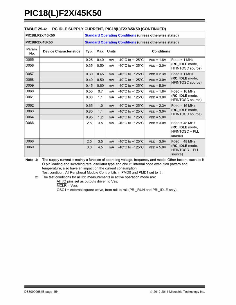
PIC18(L)F2X/45K50
D055 0.25 0.40 mA -40°C to +125°C VDD = 1.8V FOSC = 1 MHz(RC_IDLE mode, HFINTOSC source)
D056 0.35 0.50 mA -40°C to +125°C VDD = 3.0V
D057 0.30 0.45 mA -40°C to +125°C VDD = 2.3V FOSC = 1 MHz(RC_IDLE mode, HFINTOSC source)
D058 0.40 0.50 mA -40°C to +125°C VDD = 3.0V
D059 0.45 0.60 mA -40°C to +125°C VDD = 5.0V
D060 0.50 0.7 mA -40°C to +125°C VDD = 1.8V FOSC = 16 MHz(RC_IDLE mode, HFINTOSC source)
D061 0.80 1.1 mA -40°C to +125°C VDD = 3.0V
D062 0.65 1.0 mA -40°C to +125°C VDD = 2.3V FOSC = 16 MHz(RC_IDLE mode, HFINTOSC source)
D063 0.80 1.1 mA -40°C to +125°C VDD = 3.0V
D064 0.95 1.2 mA -40°C to +125°C VDD = 5.0V
D066 2.5 3.5 mA -40°C to +125°C VDD = 3.0V FOSC = 48 MHz(RC_IDLE mode, HFINTOSC + PLL source)
D068 2.5 3.5 mA -40°C to +125°C VDD = 3.0V FOSC = 48 MHz(RC_IDLE mode, HFINTOSC + PLL source)
D069 3.0 4.5 mA -40°C to +125°C VDD = 5.0V
TABLE 29-4: RC IDLE SUPPLY CURRENT, PIC18(L)F2X/45K50 (CONTINUED)
PIC18LF2X/45K50 Standard Operating Conditions (unless otherwise stated)
PIC18F2X/45K50 Standard Operating Conditions (unless otherwise stated)
Param. No.
Device Characteristics Typ. Max. Units Conditions
Note 1: The supply current is mainly a function of operating voltage, frequency and mode. Other factors, such as I/O pin loading and switching rate, oscillator type and circuit, internal code execution pattern and temperature, also have an impact on the current consumption.Test condition: All Peripheral Module Control bits in PMD0 and PMD1 set to ‘1’.
2: The test conditions for all IDD measurements in active operation mode are: All I/O pins set as outputs driven to Vss;MCLR = VDD;OSC1 = external square wave, from rail-to-rail (PRI_RUN and PRI_IDLE only).
DS30000684B-page 454 2012-2014 Microchip Technology Inc.

PIC18(L)F2X/45K50
TABLE 29-5: PRIMARY RUN SUPPLY CURRENT, PIC18(L)F2X/45K50
PIC18LF2X/45K50 Standard Operating Conditions (unless otherwise stated)
PIC18F2X/45K50 Standard Operating Conditions (unless otherwise stated)
Param. No.
Device Characteristics Typ. Max. Units Conditions
D070 Supply Current (IDD)(1),(2) 0.11 0.20 mA -40°C to +125°C VDD = 1.8V FOSC = 1 MHz(PRI_RUN mode,ECM source)
D071 0.17 0.25 mA -40°C to +125°C VDD = 3.0V
D072 0.15 0.25 mA -40°C to +125°C VDD = 2.3V FOSC = 1 MHz(PRI_RUN mode,ECM source)
D073 0.20 0.30 mA -40°C to +125°C VDD = 3.0V
D074 0.25 0.35 mA -40°C to +125°C VDD = 5.0V
D075 1.45 2.0 mA -40°C to +125°C VDD = 1.8V FOSC = 20 MHz(PRI_RUN mode,ECH source)
D076 2.60 3.5 mA -40°C to +125°C VDD = 3.0V
D077 1.95 2.5 mA -40°C to +125°C VDD = 2.3V FOSC = 20 MHz(PRI_RUN mode,ECH source)
D078 2.65 3.5 mA -40°C to +125°C VDD = 3.0V
D079 2.95 4.5 mA -40°C to +125°C VDD = 5.0V
D080 7.5 10 mA -40°C to +125°C VDD = 3.0V FOSC = 48 MHz(PRI_RUN,ECH oscillator)
D081 7.5 10 mA -40°C to +125°C VDD = 3.0V FOSC = 48 MHz(PRI_RUN mode,ECH source)
D082 8.5 11.5 mA -40°C to +125°C VDD = 5.0V
D083 1.0 1.5 mA -40°C to +125°C VDD = 1.8V FOSC = 4 MHz16 MHz Internal(PRI_RUN mode,ECM + PLL source)
D084 1.8 3.0 mA -40°C to +125°C VDD = 3.0V
D085 1.4 2.0 mA -40°C to +125°C VDD = 2.3V FOSC = 4 MHz16 MHz Internal(PRI_RUN mode,ECM + PLL source)
D086 1.85 2.5 mA -40°C to +125°C VDD = 3.0V
D087 2.1 3.0 mA -40°C to +125°C VDD = 5.0V
D088 6.35 9.0 mA -40°C to +125°C VDD = 3.0V FOSC = 16 MHz48 MHz Internal(PRI_RUN mode,ECH + PLL source)
D089 6.35 9.0 mA -40°C to +125°C VDD = 3.0V FOSC = 16 MHz48 MHz Internal(PRI_RUN mode,ECH + PLL source)
D090 7.0 10 mA -40°C to +125°C VDD = 5.0V
Note 1: The supply current is mainly a function of operating voltage, frequency and mode. Other factors, such as I/O pin loading and switching rate, oscillator type and circuit, internal code execution pattern and temperature, also have an impact on the current consumption.Test condition: All Peripheral Module Control bits in PMD0 and PMD1 set to ‘1’.
2: The test conditions for all IDD measurements in active operation mode are: All I/O pins set as outputs driven to Vss;MCLR = VDD;OSC1 = external square wave, from rail-to-rail (PRI_RUN and PRI_IDLE only).
2012-2014 Microchip Technology Inc. DS30000684B-page 455

PIC18(L)F2X/45K50
TABLE 29-6: PRIMARY IDLE SUPPLY CURRENT, PIC18(L)F2X/45K50
PIC18LF2X/45K50 Standard Operating Conditions (unless otherwise stated)
PIC18F2X/45K50 Standard Operating Conditions (unless otherwise stated)
Param. No.
Device Characteristics Typ. Max. Units Conditions
D100 Supply Current (IDD)(1),(2) 0.030 0.050 mA -40°C to +125°C VDD = 1.8V Fosc = 1 MHz(PRI_IDLE mode,ECM source)
D101 0.045 0.065 mA -40°C to +125°C VDD = 3.0V
D102 0.06 0.12 mA -40°C to +125°C VDD = 2.3V Fosc = 1 MHz(PRI_IDLE mode,ECM source)
D103 0.08 0.15 mA -40°C to +125°C VDD = 3.0V
D104 0.13 0.20 mA -40°C to +125°C VDD = 5.0V
D105 0.45 0.8 mA -40°C to +125°C VDD = 1.8V Fosc = 20 MHz(PRI_IDLE mode,ECH source)
D106 0.70 1.0 mA -40°C to +125°C VDD = 3.0V
D107 0.55 0.8 mA -40°C to +125°C VDD = 2.3V Fosc = 20 MHz(PRI_IDLE mode,ECH source)
D108 0.75 1.0 mA -40°C to +125°C VDD = 3.0V
D109 0.90 1.2 mA -40°C to +125°C VDD = 5.0V
D110 2.25 3.0 mA -40°C to +125°C VDD = 3.0V Fosc = 48 MHz(PRI_IDLE mode,ECH source)
D111 2.25 3.0 mA -40°C to +125°C VDD = 3.0V Fosc = 48 MHz(PRI_IDLE mode,ECH source)
D112 2.60 3.5 mA -40°C to +125°C VDD = 5.0V
D113 0.35 0.6 mA -40°C to +125°C VDD = 1.8V Fosc = 4 MHz16 MHz Internal(PRI_IDLE mode,ECM + PLL source)
D114 0.55 0.8 mA -40°C to +125°C VDD = 3.0V
D115 0.45 0.6 mA -40°C to +125°C VDD = 2.3V Fosc = 4 MHz16 MHz Internal(PRI_IDLE mode,ECM + PLL source)
D116 0.60 0.9 mA -40°C to +125°C VDD = 3.0V
D117 0.70 1.0 mA -40°C to +125°C VDD = 5.0V
D118 2.2 3.0 mA -40°C to +125°C VDD = 3.0V Fosc = 16 MHz48 MHz Internal(PRI_IDLE mode,ECH + PLL source)
D119 2.2 3.0 mA -40°C to +125°C VDD = 3.0V Fosc = 16 MHz48 MHz Internal(PRI_IDLE mode,ECH + PLL source)
D120 2.5 3.5 mA -40°C to +125°C VDD = 5.0V
Note 1: The supply current is mainly a function of operating voltage, frequency and mode. Other factors, such as I/O pin loading and switching rate, oscillator type and circuit, internal code execution pattern and temperature, also have an impact on the current consumption.Test condition: All Peripheral Module Control bits in PMD0 and PMD1 set to ‘1’.
2: The test conditions for all IDD measurements in active operation mode are: All I/O pins set as outputs driven to Vss;MCLR = VDD;OSC1 = external square wave, from rail-to-rail (PRI_RUN and PRI_IDLE only).
DS30000684B-page 456 2012-2014 Microchip Technology Inc.

PIC18(L)F2X/45K50
TABLE 29-7: SECONDARY OSCILLATOR SUPPLY CURRENT, PIC18(L)F2X/45K50
PIC18LF2X/45K50 Standard Operating Conditions (unless otherwise stated)
PIC18F2X/45K50 Standard Operating Conditions (unless otherwise stated)
Param. No.
Device Characteristics Typ. Max. Units Conditions
D130 Supply Current (IDD)(1),(2) 3.5 23 A -40°C VDD = 1.8V Fosc = 32 kHz(SEC_RUN mode, SOSC source)
3.7 25 A +25°C
3.8 — A +60°C
4.0 28 A +85°C
5.1 30 A +125°C
D131 6.2 26 A -40°C VDD = 3.0V
6.4 30 A +25°C
6.5 — A +60°C
6.8 35 A +85°C
7.8 40 A +125°C
D132 15 35 A -40°C VDD = 2.3V Fosc = 32 kHz(SEC_RUN mode, SOSC source)
16 35 A +25°C
17 35 A +85°C
19 50 A +125°C
D133 18 50 A -40°C VDD = 3.0V
19 50 A +25°C
21 50 A +85°C
22 60 A +125°C
D134 19 55 A -40°C VDD = 5.0V
20 55 A +25°C
22 55 A +85°C
23 70 A +125°C
Note 1: The supply current is mainly a function of operating voltage, frequency and mode. Other factors, such as I/O pin loading and switching rate, oscillator type and circuit, internal code execution pattern and temperature, also have an impact on the current consumption.Test condition: All Peripheral Module Control bits in PMD0 and PMD1 set to ‘1’.
2: The test conditions for all IDD measurements in active operation mode are: All I/O pins set as outputs driven to Vss;MCLR = VDD;SOSCI / SOSCO = complementary external square wave, from rail-to-rail.
2012-2014 Microchip Technology Inc. DS30000684B-page 457
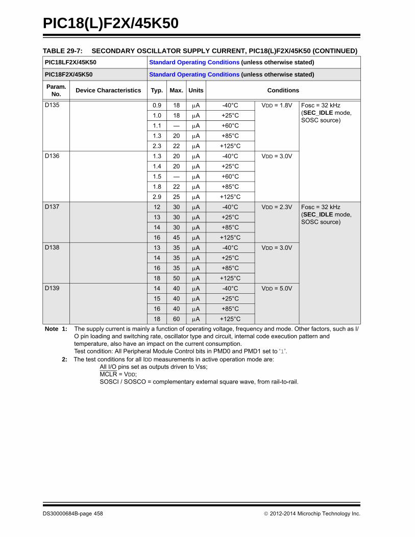
PIC18(L)F2X/45K50
D135 0.9 18 A -40°C VDD = 1.8V Fosc = 32 kHz(SEC_IDLE mode, SOSC source)
1.0 18 A +25°C
1.1 — A +60°C
1.3 20 A +85°C
2.3 22 A +125°C
D136 1.3 20 A -40°C VDD = 3.0V
1.4 20 A +25°C
1.5 — A +60°C
1.8 22 A +85°C
2.9 25 A +125°C
D137 12 30 A -40°C VDD = 2.3V Fosc = 32 kHz(SEC_IDLE mode, SOSC source)
13 30 A +25°C
14 30 A +85°C
16 45 A +125°C
D138 13 35 A -40°C VDD = 3.0V
14 35 A +25°C
16 35 A +85°C
18 50 A +125°C
D139 14 40 A -40°C VDD = 5.0V
15 40 A +25°C
16 40 A +85°C
18 60 A +125°C
TABLE 29-7: SECONDARY OSCILLATOR SUPPLY CURRENT, PIC18(L)F2X/45K50 (CONTINUED)
PIC18LF2X/45K50 Standard Operating Conditions (unless otherwise stated)
PIC18F2X/45K50 Standard Operating Conditions (unless otherwise stated)
Param. No.
Device Characteristics Typ. Max. Units Conditions
Note 1: The supply current is mainly a function of operating voltage, frequency and mode. Other factors, such as I/O pin loading and switching rate, oscillator type and circuit, internal code execution pattern and temperature, also have an impact on the current consumption.Test condition: All Peripheral Module Control bits in PMD0 and PMD1 set to ‘1’.
2: The test conditions for all IDD measurements in active operation mode are: All I/O pins set as outputs driven to Vss;MCLR = VDD;SOSCI / SOSCO = complementary external square wave, from rail-to-rail.
DS30000684B-page 458 2012-2014 Microchip Technology Inc.

PIC18(L)F2X/45K50
TABLE 29-8: INPUT/OUTPUT CHARACTERISTICS, PIC18(L)F2X/45K50
DC CHARACTERISTICS Standard Operating Conditions (unless otherwise stated)
Param.No.
Symbol Characteristic Min. Typ.† Max. Units Conditions
VIL Input Low Voltage
I/O PORT:
D140 with TTL buffer — — 0.8 V 4.5V VDD 5.5V
D140A — — 0.15 VDD V 1.8V VDD 4.5V
D141 with Schmitt Trigger buffer — — 0.2 VDD V 2.0V VDD 5.5V
with I2C™ levels — — 0.3 VDD V
with SMBus levels — — 0.8 V 2.7V VDD 5.5V
D142 MCLR, OSC1 (RC mode)(1) — — 0.2 VDD V
D142A OSC1 (HS mode) — — 0.3 VDD V
VIH Input High Voltage
I/O ports:
D147 with TTL buffer 2.0 — — V 4.5V VDD 5.5V
D147A 0.25 VDD + 0.8 — — V 1.8V VDD 4.5V
D148 with Schmitt Trigger buffer 0.8 VDD — — V 2.0V VDD 5.5V
with I2C levels 0.7 VDD — — V
with SMBus levels 2.1 — — V 2.7V VDD 5.5V
D149 MCLR 0.8 VDD — — V
D150A OSC1 (HS mode) 0.7 VDD — — V
D150B OSC1 (RC mode)(1) 0.9 VDD — — V
IIL Input Leakage I/O and MCLR(2),(3)
VSS VPIN VDD, Pin at high-impedance
D155 I/O ports and MCLR ———
0.10.74
50100200
nAnAnA
+25°C(4)
+60°C+85°C
IPU Weak Pull-up Current(4)
D158 IPURB PORTB weak pull-up current 25 85 200 A VDD = 3.3V, VPIN = VSS
25 130 300 A VDD = 5.0V, VPIN = VSS
Note 1: In RC oscillator configuration, the OSC1/CLKIN pin is a Schmitt Trigger input. It is not recommended that the PIC® device be driven with an external clock while in RC mode.
2: The leakage current on the MCLR pin is strongly dependent on the applied voltage level. The specified levels represent normal operating conditions. Higher leakage current may be measured at different input voltages.
3: Negative current is defined as current sourced by the pin.4: Parameter is characterized but not tested.
2012-2014 Microchip Technology Inc. DS30000684B-page 459

PIC18(L)F2X/45K50
VOL Output Low Voltage
D159 I/O ports — — 0.6 V IOL = 8 mA, VDD = 5VIOL = 6 mA, VDD = 3.3VIOL = 1.8 mA, VDD = 1.8V
IPUMCLR MCLR and ICRST weak pull-up current
25 85 200 A VDD = 3.3V, VPIN = VSS
D160 25 130 300 A VDD = 5.0V, VPIN = VSS
VOH Output High Voltage(3)
D161 I/O ports VDD - 0.7 — — V IOH = 3.5 mA, VDD = 5VIOH = 3 mA, VDD = 3.3VIOH = 1 mA, VDD = 1.8V
TABLE 29-8: INPUT/OUTPUT CHARACTERISTICS, PIC18(L)F2X/45K50 (CONTINUED)
DC CHARACTERISTICS Standard Operating Conditions (unless otherwise stated)
Param.No.
Symbol Characteristic Min. Typ.† Max. Units Conditions
Note 1: In RC oscillator configuration, the OSC1/CLKIN pin is a Schmitt Trigger input. It is not recommended that the PIC® device be driven with an external clock while in RC mode.
2: The leakage current on the MCLR pin is strongly dependent on the applied voltage level. The specified levels represent normal operating conditions. Higher leakage current may be measured at different input voltages.
3: Negative current is defined as current sourced by the pin.4: Parameter is characterized but not tested.
DS30000684B-page 460 2012-2014 Microchip Technology Inc.

PIC18(L)F2X/45K50
TABLE 29-9: MEMORY PROGRAMMING REQUIREMENTS
Standard Operating Conditions (unless otherwise stated)
Param.No.
Sym. Characteristic Min. Typ.† Max. Units Conditions
Internal Program Memory Programming Specifications(1)
D170 VPP Voltage on MCLR/VPP pin 8 — 9 V (Note 3), (Note 4)
D171 IDDP Supply Current during Programming
— — 10 mA
Data EEPROM Memory
D172 ED Byte Endurance 100K — — E/W -40C to +85C
D173 VDRW VDD for Read/Write VDDMIN — VDDMAX V Using EECON to read/write
D175 TDEW Erase/Write Cycle Time — 3 4 ms
D176 TRETD Characteristic Retention — 40 — Year Provided no other specifications are violated
D177 TREF Number of Total Erase/Write Cycles before Refresh(2)
1M 10M — E/W -40°C to +85°C
Program Flash Memory
D178 EP Cell Endurance 10K — — E/W -40C to +85C (Note 5)
D179 VPR VDD for Read VDDMIN — VDDMAX V
D181 VIW VDD for Row Erase or Write 2.2 — VDDMAX V PIC18LF2X/45K50
D182 VIW VDDMIN — VDDMAX V PIC18F2X/45K50
D183 TIW Self-timed Write Cycle Time — 2 — ms
D184 TRETD Characteristic Retention — 40 — Year Provided no other specifications are violated
† Data in “Typ” column is at 3.0V, 25°C unless otherwise stated. These parameters are for design guidance only and are not tested.
Note 1: These specifications are for programming the on-chip program memory through the use of table write instructions.
2: Refer to Section 8.8 “Using the Data EEPROM” for a more detailed discussion on data EEPROM endurance.
3: Required only if single-supply programming is disabled.4: The MPLAB ICD 2 does not support variable VPP output. Circuitry to limit the ICD 2 VPP voltage must be
placed between the ICD 2 and target system when programming or debugging with the ICD 2.5: Self-write and Block Erase.
2012-2014 Microchip Technology Inc. DS30000684B-page 461

PIC18(L)F2X/45K50
TABLE 29-10: USB MODULE SPECIFICATIONS
Standard Operating Conditions (unless otherwise stated)
Param.No.
Sym. Characteristic Min. Typ. Max. Units Conditions
D313 VUSB USB Voltage 3.0 — 3.6 V Voltage on VUSB3V3 pin must be in this range for proper USB operation
D314 IIL Input Leakage on pin — — ± 1 A VSS VPIN VDD pin athighimpedance
D315 VILUSB Input Low Voltage for USB Buffer
— — 0.8 V For VUSB3V3 range
D316 VIHUSB Input High Voltage for USB Buffer
2.0 — — V For VUSB3V3 range
D318 VDIFS Differential Input Sensitivity — — 0.2 V The difference between D+ and D- must exceed this value while VCM is met
D319 VCM Differential Common Mode Range
0.8 — 2.5 V
D320 ZOUT Driver Output Impedance(1) 28 — 44
D321 VOL Voltage Output Low 0.0 — 0.3 V 1.5 kload connected to 3.6V
D322 VOH Voltage Output High 2.8 — 3.6 V 1.5 kload connected to ground
D323 CUSB VUSB Capacitor Value 0.33 0.47 8 µF
Note 1: The D+ and D- signal lines have been built-in impedance matching resistors. No external resistors, capacitors or magnetic components are necessary on the D+/D- signal paths between the PIC18(L)F2X/45K50 family device and USB cable.
DS30000684B-page 462 2012-2014 Microchip Technology Inc.

PIC18(L)F2X/45K50
29.4 Analog Characteristics
TABLE 29-11: COMPARATOR SPECIFICATIONS
Standard Operating Conditions (unless otherwise stated)
Param.No.
Sym. Characteristics Min. Typ. Max. Units Comments
CM01 VIOFF Input Offset Voltage — 3 30 mV High-Power modeVREF = VDD/2
— 4 40 mV Low-Power modeVREF = VDD/2
CM02 VICM Input Common-mode Voltage VSS — VDD V
CM04* TRESP Response Time(1) — 200 400 ns High-Power mode
— 600 3500 ns Low-Power mode
CM05* TMC2OV Comparator Mode Change to Output Valid
— — 10 s
* These parameters are characterized but not tested.Note 1: Response time measured with one comparator input at VDD/2, while the other input transitions from VSS to
VDD.
TABLE 29-12: DIGITAL-TO-ANALOG CONVERTER (DAC) SPECIFICATIONS
Standard Operating Conditions (unless otherwise stated)2.0V < VDD < 5.5V, -40°C < TA < +125°C
Param.No.
Sym. Characteristics Min. Typ. Max. Units Comments
CV01* CLSB Step Size(2) — VDD/32 — V
CV02* CACC Absolute Accuracy — — 1/2 LSb VSRC 2.0V
CV03* CR Unit Resistor Value (R) — 5k —
CV04* CST Settling Time(1) — — 10 s
CV05* VSRC+ DAC Positive Reference VSRC- + 2 — VDD V
CV06* VSRC- DAC Negative Reference VSS — VSRC+ – 2 V
CV07* VSRC DAC Reference Range (VSRC+ - VSRC-) 2 — VDD V
* These parameters are characterized but not tested.
Note 1: Settling time measured while CVRR = 1 and CVR3:CVR0 transitions from ‘0000’ to ‘1111’.
2: See Section 23.0 “Digital-to-Analog Converter (DAC) Module” for more information.
2012-2014 Microchip Technology Inc. DS30000684B-page 463

PIC18(L)F2X/45K50
FIGURE 29-4: HIGH/LOW-VOLTAGE DETECT CHARACTERISTICS
TABLE 29-13: FIXED VOLTAGE REFERENCE (FVR) SPECIFICATIONS
Standard Operating Conditions (unless otherwise stated)
Param. No.
Sym. Characteristics Min. Typ. Max. Units Comments
VR01 VROUT VR voltage output to ADC 0.973 1.024 1.085 V 1x output, VDD 2.5V
1.946 2.048 2.171 V 2x output, VDD 2.5V
3.891 4.096 4.342 V 4x output, VDD 4.75V (PIC18F2X/45K50)
VR02 VROUT VR voltage output all other modules
0.942 1.024 1.096 V 1x output, VDD 2.5V
1.884 2.048 2.191 V 2x output, VDD 2.5V
3.768 4.096 4.383 V 4x output, VDD 4.75V (PIC18F2X/45K50)
VR04* TSTABLE Settling Time — 25 100 s 0 to 85°C
* These parameters are characterized but not tested.
TABLE 29-14: CHARGE TIME MEASUREMENT UNIT (CTMU) SPECIFICATIONS
Standard Operating Conditions (unless otherwise stated)
Param. No.
Sym. Characteristics Min. Typ.(1) Max. Units Comments
CT01 IOUT1 CTMU Current Source,Base Range
— 0.55 — A IRNG<1:0> = 01
CT02 IOUT2 CTMU Current Source,10X Range
— 5.5 — A IRNG<1:0> = 10
CT03 IOUT3 CTMU Current Source,100X Range
— 55 — A IRNG<1:0> = 11VDD 3.0V
Note 1: Nominal value at center point of current trim range (CTMUICON<7:2> = 000000).
VHLVD
HLVDIF
VDD
(HLVDIF set by hardware)
(HLVDIF can be cleared by software)
DS30000684B-page 464 2012-2014 Microchip Technology Inc.
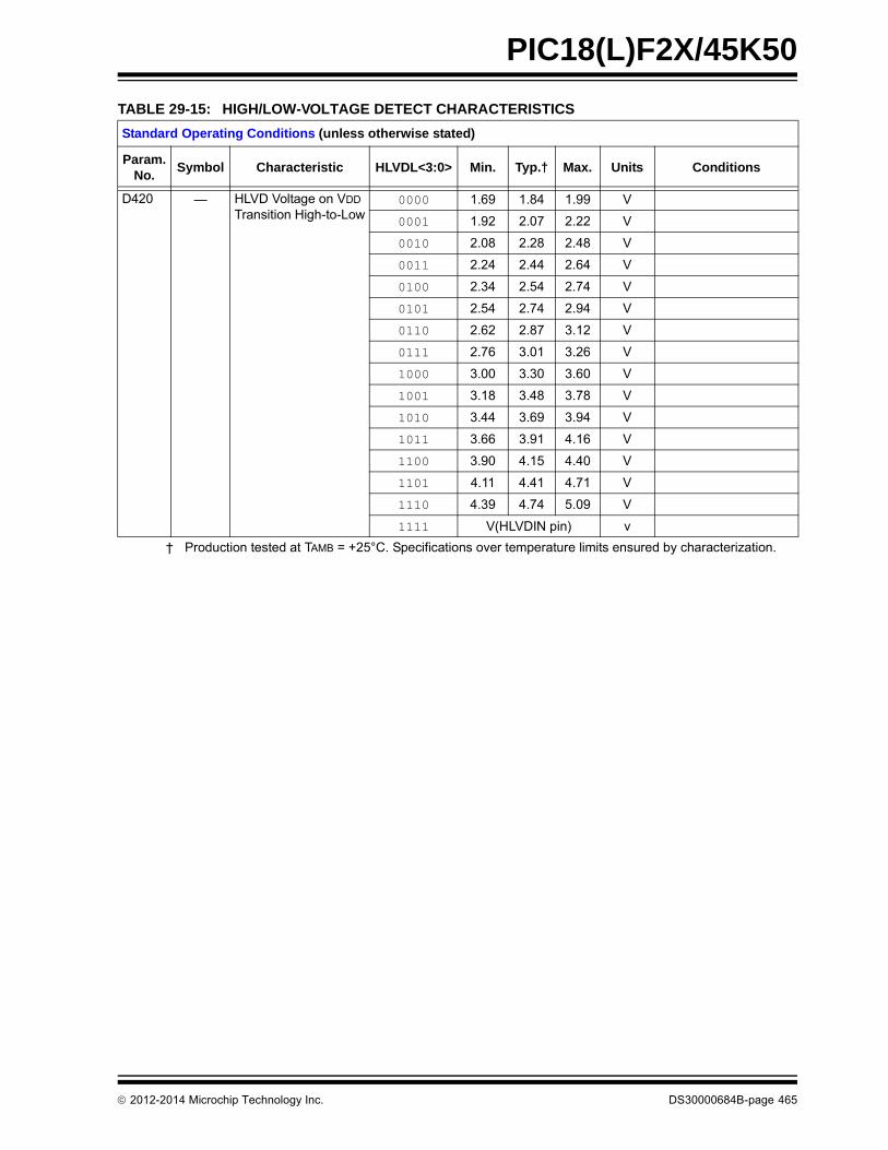
PIC18(L)F2X/45K50
TABLE 29-15: HIGH/LOW-VOLTAGE DETECT CHARACTERISTICS
Standard Operating Conditions (unless otherwise stated)
Param. No.
Symbol Characteristic HLVDL<3:0> Min. Typ.† Max. Units Conditions
D420 — HLVD Voltage on VDD Transition High-to-Low
0000 1.69 1.84 1.99 V
0001 1.92 2.07 2.22 V
0010 2.08 2.28 2.48 V
0011 2.24 2.44 2.64 V
0100 2.34 2.54 2.74 V
0101 2.54 2.74 2.94 V
0110 2.62 2.87 3.12 V
0111 2.76 3.01 3.26 V
1000 3.00 3.30 3.60 V
1001 3.18 3.48 3.78 V
1010 3.44 3.69 3.94 V
1011 3.66 3.91 4.16 V
1100 3.90 4.15 4.40 V
1101 4.11 4.41 4.71 V
1110 4.39 4.74 5.09 V
1111 V(HLVDIN pin) v
† Production tested at TAMB = +25°C. Specifications over temperature limits ensured by characterization.
2012-2014 Microchip Technology Inc. DS30000684B-page 465

PIC18(L)F2X/45K50
29.5 AC (Timing) Characteristics
29.5.1 TIMING PARAMETER SYMBOLOGY
The timing parameter symbols have been createdusing one of the following formats:
1. TppS2ppS 3. TCC:ST (I2C™ specifications only)
2. TppS 4. Ts (I2C specifications only)
T
F Frequency T Time
Lowercase letters (pp) and their meanings:
pp
cc CCP1 osc OSC1
ck CLKO rd RD
cs CS rw RD or WR
di SDI sc SCK
do SDO ss SS
dt Data in t0 T0CKI
io I/O port t1 T13CKI
mc MCLR wr WR
Uppercase letters and their meanings:
S
F Fall P Period
H High R Rise
I Invalid (High-impedance) V Valid
L Low Z High-impedance
I2C only
AA output access High High
BUF Bus free Low Low
TCC:ST (I2C specifications only)
CC
HD Hold SU Setup
ST
DAT DATA input hold STO Stop condition
STA Start condition
DS30000684B-page 466 2012-2014 Microchip Technology Inc.

PIC18(L)F2X/45K50
29.5.2 TIMING CONDITIONS
The temperature and voltages specified in Table 29-16apply to all timing specifications unless otherwisenoted. Figure 29-5 specifies the Load conditions for thetiming specifications.
FIGURE 29-5: LOAD CONDITIONS FOR DEVICE TIMING SPECIFICATIONS
TABLE 29-16: TEMPERATURE AND VOLTAGE SPECIFICATIONS – AC
AC CHARACTERISTICSStandard Operating Conditions (unless otherwise stated)Operating voltage VDD range as described in Table 29-1 and Table 29-9.
VDD/2
CL
RL
Pin
Pin
VSS
VSS
CL
RL = 464
CL = 50 pF for all pins except OSC2/CLKOand including D and E outputs as ports
Load Condition 1 Load Condition 2
Legend:
2012-2014 Microchip Technology Inc. DS30000684B-page 467

PIC18(L)F2X/45K50
29.5.3 TIMING DIAGRAMS AND SPECIFICATIONS
FIGURE 29-6: EXTERNAL CLOCK TIMING (ALL MODES EXCEPT PLL)
TABLE 29-17: EXTERNAL CLOCK TIMING REQUIREMENTS
Param.No.
Symbol Characteristic Min. Max. Units Conditions
1A FOSC External CLKIN Frequency(1)
DCDCDC
41648
MHzMHzMHz
EC, ECIO Oscillator mode (low power)EC, ECIO Oscillator mode (medium power)EC, ECIO Oscillator mode (high power)
Oscillator Frequency(1) DC 4 MHz RC Oscillator mode
5 200 kHz LP Oscillator mode
0.1 4 MHz XT Oscillator mode
4 4 MHz HS Oscillator mode, VDD < 2.7V
4 16 MHz HS Oscillator mode, VDD 2.7V, Medium-Power mode (HSMP)
4 20 MHz HS Oscillator mode, VDD 2.7V, High-Power mode (HSHP)
1 TOSC External CLKIN Period(1) 0.2562.520.8
———
snsns
EC, ECIO Oscillator mode (low power)EC, ECIO Oscillator mode (medium power)EC, ECIO Oscillator mode (high power)
Oscillator Period(1) 250 — ns RC Oscillator mode
5 200 s LP Oscillator mode
0.25250
10250
sns
XT Oscillator modeHS Oscillator mode, VDD < 2.7V
62.5 250 ns HS Oscillator mode, VDD 2.7V, Medium-Power mode (HSMP)
50 250 ns HS Oscillator mode, VDD 2.7V, High-Power mode (HSHP)
2 TCY Instruction Cycle Time(1) 83.3 — ns TCY = 4/FOSC
3 TOSL,TOSH
External Clock in (OSC1) High or Low Time
2.5 — s LP Oscillator mode
30 — ns XT Oscillator mode
10 — ns HS Oscillator mode
4 TOSR,TOSF
External Clock in (OSC1) Rise or Fall Time
— 50 ns LP Oscillator mode
— 20 ns XT Oscillator mode
— 7.5 ns HS Oscillator mode
Note 1: Instruction cycle period (TCY) equals four times the input oscillator time base period for all configurations except PLL. All specified values are based on characterization data for that particular oscillator type under standard operating condi-tions with the device executing code. Exceeding these specified limits may result in an unstable oscillator operation and/or higher than expected current consumption. All devices are tested to operate at “min.” values with an external clock applied to the OSC1/CLKIN pin. When an external clock input is used, the “max.” cycle time limit is “DC” (no clock) for all devices.
OSC1
CLKO
Q4 Q1 Q2 Q3 Q4 Q1
1
2
3 3 4 4
DS30000684B-page 468 2012-2014 Microchip Technology Inc.

PIC18(L)F2X/45K50
TABLE 29-18: PLL CLOCK TIMING SPECIFICATIONS
Param. No.
Sym. Characteristic Min. Max. Units Conditions
F10 FOSC 4xPLL Oscillator Frequency Range 4 5 MHz VDD < 2.7V,-40°C to +85°C
4 12 MHz 2.7V VDD,-40°C to +85°C
F10B FOSC 3xPLL Oscillator Frequency Range 4 4 MHz 2.7V VDD,-40°C to +85°C
F11 FSYS On-Chip VCO System Frequency 16 20 MHz VDD < 2.7V,-40°C to +85°C
16 48 MHz 2.7V VDD,-40°C to +85°C
F12 trc PLL Start-up Time (Lock Time) — 2 ms
TABLE 29-19: INTERNAL OSCILLATORS ACCURACY (PIC18(L)F2X/45K50)
Standard Operating Conditions (unless otherwise stated)
Param.No.
Characteristic Min. Typ. Max. Units Conditions
OA1 HF-INTOSC Accuracy(1)
-2 ±1 +2 % +0°C to +70°C
-3 — +2 % +70°C to +85°C
-5 — +5 % -40°C to +125°C
OA1B HF-INTOSC Accuracy with Active Clock Tuning (ACT)
-0.20 ±0.05 +0.20 % -40°C to +85°C(2), Active Clock Tune is enabled and locked.
OA1C OSCTUNE Step Size — 0.1 — %
OA2 INTRC Accuracy @ Freq = 31.25 kHz
26.5625 — 35.9375 kHz -40°C to +85°C
25 — 37.2 kHz +85°C to +125°C
Note 1: Frequency calibrated at 25°C. OSCTUNE register can be used to compensate for temperature drift.
2: Accuracy measured with respect to reference source.
2012-2014 Microchip Technology Inc. DS30000684B-page 469
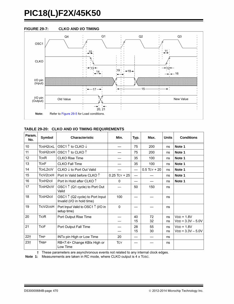
PIC18(L)F2X/45K50
FIGURE 29-7: CLKO AND I/O TIMING
Note: Refer to Figure 29-5 for Load conditions.
OSC1
CLKO
I/O pin(Input)
I/O pin(Output)
Q4 Q1 Q2 Q3
10
1314
17
20, 21
19 18
15
11
12
16
Old Value New Value
TABLE 29-20: CLKO AND I/O TIMING REQUIREMENTS
Param.No.
Symbol Characteristic Min. Typ. Max. Units Conditions
10 TOSH2CKL OSC1 to CLKO — 75 200 ns Note 1
11 TOSH2CKH OSC1 to CLKO — 75 200 ns Note 1
12 TCKR CLKO Rise Time — 35 100 ns Note 1
13 TCKF CLKO Fall Time — 35 100 ns Note 1
14 TCKL2IOV CLKO to Port Out Valid — — 0.5 TCY + 20 ns Note 1
15 TIOV2CKH Port In Valid before CLKO 0.25 TCY + 25 — — ns Note 1
16 TCKH2IOI Port In Hold after CLKO 0 — — ns Note 1
17 TOSH2IOV OSC1 (Q1 cycle) to Port Out Valid
— 50 150 ns
18 TOSH2IOI OSC1 (Q2 cycle) to Port Input Invalid (I/O in hold time)
100 — — ns
19 TIOV2OSH Port Input Valid to OSC1 (I/O in setup time)
0 — — ns
20 TIOR Port Output Rise Time ——
4015
7232
nsns
VDD = 1.8VVDD = 3.3V – 5.0V
21 TIOF Port Output Fall Time ——
2815
5530
nsns
VDD = 1.8VVDD = 3.3V – 5.0V
22† TINP INTx pin High or Low Time 20 — — ns
23† TRBP RB<7:4> Change KBIx High or Low Time
TCY — — ns
† These parameters are asynchronous events not related to any internal clock edges.Note 1: Measurements are taken in RC mode, where CLKO output is 4 x TOSC.
DS30000684B-page 470 2012-2014 Microchip Technology Inc.

PIC18(L)F2X/45K50
FIGURE 29-8: RESET, WATCHDOG TIMER, OSCILLATOR START-UP TIMER AND POWER-UP TIMER TIMING
FIGURE 29-9: BROWN-OUT RESET TIMING
VDD
MCLR
InternalPOR
PWRTTime-out
OSCTime-out
InternalReset
WatchdogTimerReset
33
32
30
3134
I/O pins
34
Note: Refer to Figure 29-5 for Load conditions.
VDD BVDD
35VBGAP = 1.2V
VIVRST
Enable Internal
Internal Reference36
Reference Voltage
Voltage Stable
2012-2014 Microchip Technology Inc. DS30000684B-page 471
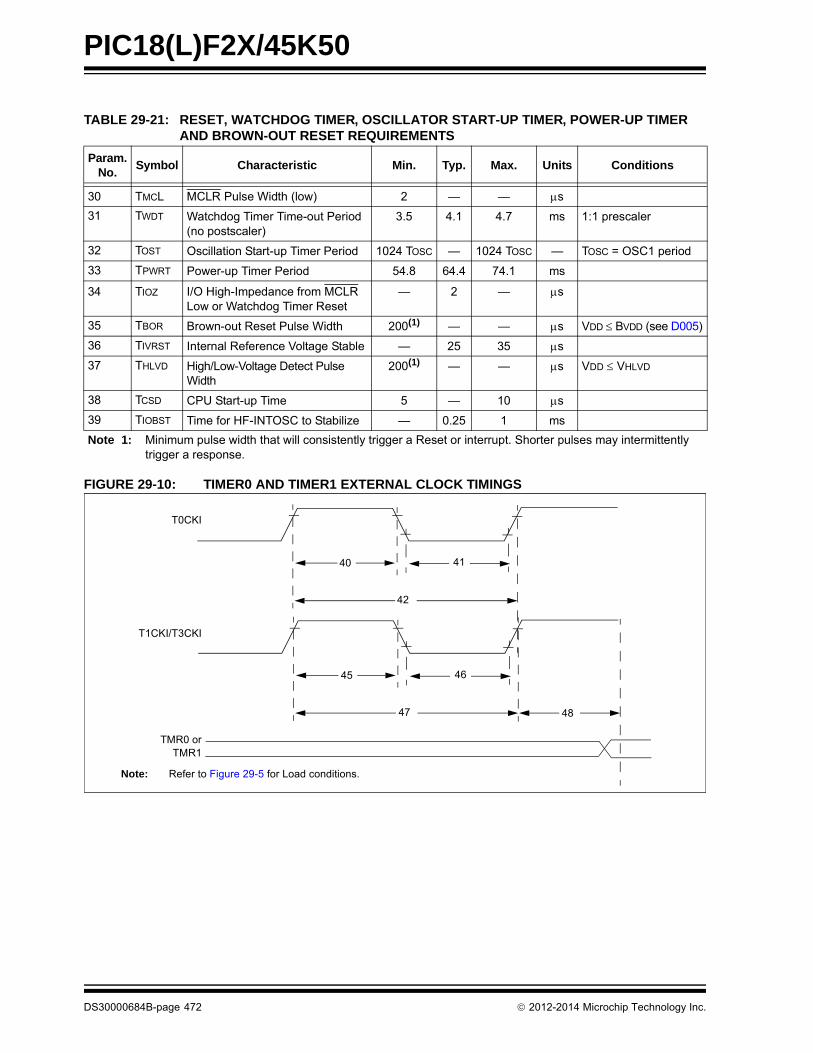
PIC18(L)F2X/45K50
FIGURE 29-10: TIMER0 AND TIMER1 EXTERNAL CLOCK TIMINGS
TABLE 29-21: RESET, WATCHDOG TIMER, OSCILLATOR START-UP TIMER, POWER-UP TIMER AND BROWN-OUT RESET REQUIREMENTS
Param. No.
Symbol Characteristic Min. Typ. Max. Units Conditions
30 TMCL MCLR Pulse Width (low) 2 — — s
31 TWDT Watchdog Timer Time-out Period (no postscaler)
3.5 4.1 4.7 ms 1:1 prescaler
32 TOST Oscillation Start-up Timer Period 1024 TOSC — 1024 TOSC — TOSC = OSC1 period
33 TPWRT Power-up Timer Period 54.8 64.4 74.1 ms
34 TIOZ I/O High-Impedance from MCLR Low or Watchdog Timer Reset
— 2 — s
35 TBOR Brown-out Reset Pulse Width 200(1) — — s VDD BVDD (see D005)
36 TIVRST Internal Reference Voltage Stable — 25 35 s
37 THLVD High/Low-Voltage Detect Pulse Width
200(1) — — s VDD VHLVD
38 TCSD CPU Start-up Time 5 — 10 s
39 TIOBST Time for HF-INTOSC to Stabilize — 0.25 1 ms
Note 1: Minimum pulse width that will consistently trigger a Reset or interrupt. Shorter pulses may intermittently trigger a response.
Note: Refer to Figure 29-5 for Load conditions.
46
47
45
48
41
42
40
T0CKI
T1CKI/T3CKI
TMR0 orTMR1
DS30000684B-page 472 2012-2014 Microchip Technology Inc.
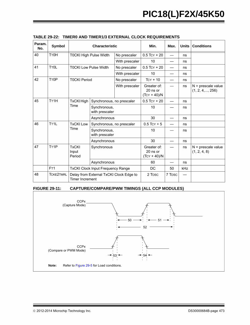
PIC18(L)F2X/45K50
FIGURE 29-11: CAPTURE/COMPARE/PWM TIMINGS (ALL CCP MODULES)
TABLE 29-22: TIMER0 AND TIMER1/3 EXTERNAL CLOCK REQUIREMENTS
Param. No.
Symbol Characteristic Min. Max. Units Conditions
40 TT0H T0CKI High Pulse Width No prescaler 0.5 TCY + 20 — ns
With prescaler 10 — ns
41 TT0L T0CKI Low Pulse Width No prescaler 0.5 TCY + 20 — ns
With prescaler 10 — ns
42 TT0P T0CKI Period No prescaler TCY + 10 — ns
With prescaler Greater of:20 ns or
(TCY + 40)/N
— ns N = prescale value (1, 2, 4,..., 256)
45 TT1H TxCKI High Time
Synchronous, no prescaler 0.5 TCY + 20 — ns
Synchronous,with prescaler
10 — ns
Asynchronous 30 — ns
46 TT1L TxCKI Low Time
Synchronous, no prescaler 0.5 TCY + 5 — ns
Synchronous, with prescaler
10 — ns
Asynchronous 30 — ns
47 TT1P TxCKI Input Period
Synchronous Greater of:20 ns or
(TCY + 40)/N
— ns N = prescale value (1, 2, 4, 8)
Asynchronous 60 — ns
FT1 TxCKI Clock Input Frequency Range DC 50 kHz
48 TCKE2TMRL Delay from External TxCKI Clock Edge to Timer Increment
2 TOSC 7 TOSC —
Note: Refer to Figure 29-5 for Load conditions.
CCPx(Capture Mode)
50 51
52
CCPx
53 54
(Compare or PWM Mode)
2012-2014 Microchip Technology Inc. DS30000684B-page 473

PIC18(L)F2X/45K50
FIGURE 29-12: EXAMPLE SPI MASTER MODE TIMING (CKE = 0)
TABLE 29-23: CAPTURE/COMPARE/PWM REQUIREMENTS (ALL CCP MODULES)
Param.No.
Symbol Characteristic Min. Max. Units Conditions
50 TCCL CCPx Input Low Time No prescaler 0.5 TCY + 20 — ns
With prescaler 10 — ns
51 TCCH CCPx Input High Time No prescaler 0.5 TCY + 20 — ns
With prescaler 10 — ns
52 TCCP CCPx Input Period 3 TCY + 40N
— ns N = prescale value (1, 4 or 16)
53 TCCR CCPx Output Fall Time — 25 ns
54 TCCF CCPx Output Fall Time — 25 ns
SS
SCK(CKP = 0)
SCK(CKP = 1)
SDO
SDI
70
71 72
7374
75, 76
787980
7978
MSb LSbbit 6 - - - - - -1
MSb In LSb Inbit 6 - - - -1
Note: Refer to Figure 29-5 for Load conditions.
DS30000684B-page 474 2012-2014 Microchip Technology Inc.

PIC18(L)F2X/45K50
FIGURE 29-13: EXAMPLE SPI MASTER MODE TIMING (CKE = 1)
TABLE 29-24: EXAMPLE SPI MODE REQUIREMENTS (MASTER MODE, CKE = 0 OR 1)
Param.No.
Symbol Characteristic Min. Max. Units Conditions
73 TDIV2SCH, TDIV2SCL
Setup Time of SDI Data Input to SCK Edge 25 — ns
74 TSCH2DIL, TSCL2DIL
Hold Time of SDI Data Input to SCK Edge 25 — ns
75 TDOR SDO Data Output Rise Time — 30 ns Note 1
76 TDOF SDO Data Output Fall Time — 20 ns Note 1
78 TSCR SCK Output Rise Time (Master mode) — 30 ns Note 1
79 TSCF SCK Output Fall Time (Master mode) — 20 ns Note 1
80 TSCH2DOV,TSCL2DOV
SDO Data Output Valid after SCK Edge — 20 ns
81 TDOV2SCH,TDOV2SCL
SDO Data Output Setup to SCK Edge TCY — ns
Note 1: When the slew rate control limiting I/O port feature is disabled.
SS
SCK(CKP = 0)
SCK(CKP = 1)
SDO
SDI
81
71 72
74
75, 76
78
80
MSb
7973
MSb In
bit 6 - - - - - -1
LSb Inbit 6 - - - -1
LSb
Note: Refer to Figure 29-5 for Load conditions.
2012-2014 Microchip Technology Inc. DS30000684B-page 475

PIC18(L)F2X/45K50
FIGURE 29-14: EXAMPLE SPI SLAVE MODE TIMING (CKE = 0)
SS
SCK(CKP = 0)
SCK(CKP = 1)
SDO
SDI
70
71 72
7374
75, 76 77
787980
7978
SDI
MSb LSbbit 6 - - - - - -1
MSb In bit 6 - - - -1 LSb In
83
Note: Refer to Figure 29-5 for Load conditions.
TABLE 29-25: EXAMPLE SPI MODE REQUIREMENTS (SLAVE MODE TIMING, CKE = 0 OR 1)
Param.No.
Symbol Characteristic Min. Max. Units Conditions
70 TSSL2SCH, TSSL2SCL
SS to SCK or SCK Input TCY — ns
71 TSCH SCK Input High Time Continuous 25 — ns
72 TSCL SCK Input Low Time Continuous 30 — ns
73 TDIV2SCH, TDIV2SCL
Setup Time of SDI Data Input to SCK Edge 25 — ns
74 TSCH2DIL, TSCL2DIL
Hold Time of SDI Data Input to SCK Edge 25 — ns
75 TDOR SDO Data Output Rise Time — 30 ns Note 1
76 TDOF SDO Data Output Fall Time — 20 ns Note 1
77 TSSH2DOZ SS to SDO Output High-Impedance 10 50 ns
80 TSCH2DOV,TSCL2DOV
SDO Data Output Valid after SCK Edge — 60 ns Note 1
82 TSSL2DOV SDO Data Output Valid after SS Edge — 60 ns Note 1
83 TSCH2SSH,TSCL2SSH
SS after SCK edge 1.5 TCY + 40 — ns
Note 1: When the slew rate control limiting I/O port feature is disabled.
DS30000684B-page 476 2012-2014 Microchip Technology Inc.

PIC18(L)F2X/45K50
FIGURE 29-15: EXAMPLE SPI SLAVE MODE TIMING (CKE = 1)
FIGURE 29-16: I2C™ BUS START/STOP BITS TIMING
SS
SCK(CKP = 0)
SCK(CKP = 1)
SDO
SDI
70
71 72
82
SDI
74
75, 76
MSb bit 6 - - - - - -1 LSb
77
MSb In bit 6 - - - -1 LSb In
80
83
Note: Refer to Figure 29-5 for Load conditions.
Note: Refer to Figure 29-5 for Load conditions.
91
92
93SCL
SDA
StartCondition
StopCondition
90
2012-2014 Microchip Technology Inc. DS30000684B-page 477
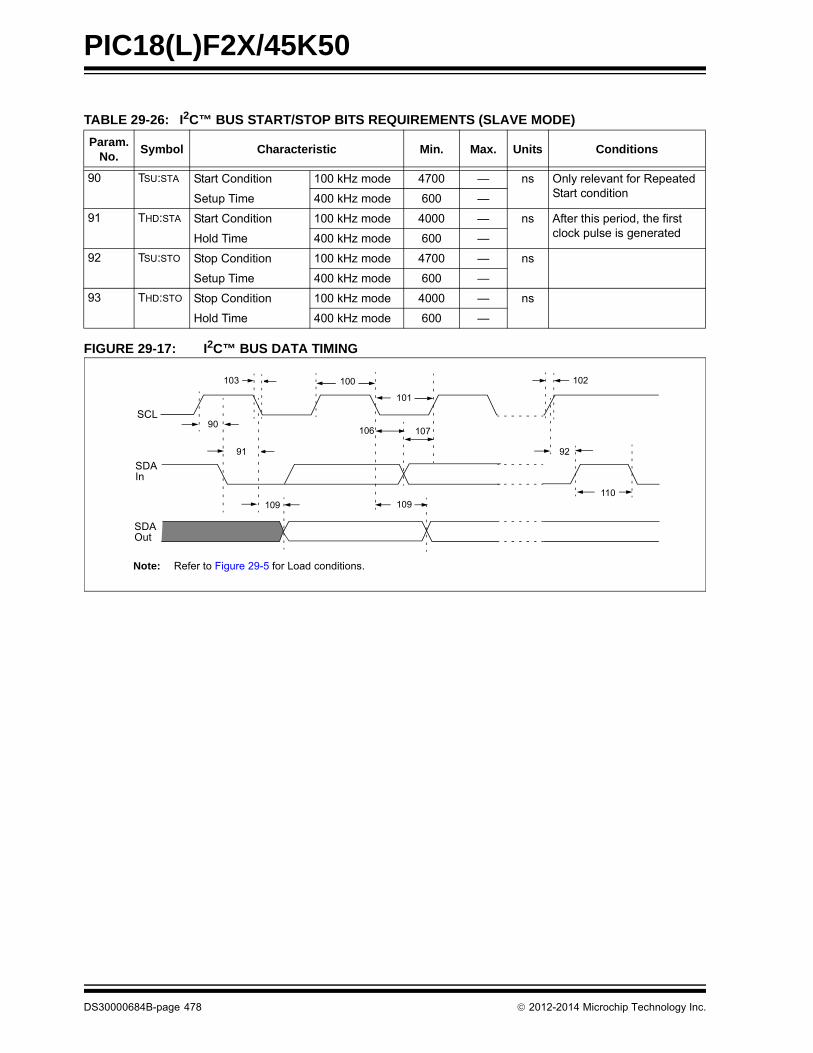
PIC18(L)F2X/45K50
FIGURE 29-17: I2C™ BUS DATA TIMING
TABLE 29-26: I2C™ BUS START/STOP BITS REQUIREMENTS (SLAVE MODE)
Param. No.
Symbol Characteristic Min. Max. Units Conditions
90 TSU:STA Start Condition 100 kHz mode 4700 — ns Only relevant for Repeated Start conditionSetup Time 400 kHz mode 600 —
91 THD:STA Start Condition 100 kHz mode 4000 — ns After this period, the first clock pulse is generatedHold Time 400 kHz mode 600 —
92 TSU:STO Stop Condition 100 kHz mode 4700 — ns
Setup Time 400 kHz mode 600 —
93 THD:STO Stop Condition 100 kHz mode 4000 — ns
Hold Time 400 kHz mode 600 —
Note: Refer to Figure 29-5 for Load conditions.
90
91 92
100
101
103
106 107
109 109110
102
SCL
SDAIn
SDAOut
DS30000684B-page 478 2012-2014 Microchip Technology Inc.

PIC18(L)F2X/45K50
TABLE 29-27: I2C™ BUS DATA REQUIREMENTS (SLAVE MODE)
Param. No.
Symbol Characteristic Min. Max. Units Conditions
100 THIGH Clock High Time 100 kHz mode 4.0 — s Must operate at a minimum of 1.5 MHz
400 kHz mode 0.6 — s Must operate at a minimum of 10 MHz
SSP Module 1.5 TCY —
101 TLOW Clock Low Time 100 kHz mode 4.7 — s Must operate at a minimum of 1.5 MHz
400 kHz mode 1.3 — s Must operate at a minimum of 10 MHz
SSP Module 1.5 TCY —
102 TR SDA and SCL Rise Time 100 kHz mode — 1000 ns
400 kHz mode 20 + 0.1 CB 300 ns CB is specified to be from 10 to 400 pF
103 TF SDA and SCL Fall Time 100 kHz mode — 300 ns
400 kHz mode 20 + 0.1 CB 300 ns CB is specified to be from 10 to 400 pF
90 TSU:STA Start Condition Setup Time
100 kHz mode 4.7 — s Only relevant for Repeated Start condition400 kHz mode 0.6 — s
91 THD:STA Start Condition Hold Time
100 kHz mode 4.0 — s After this period, the first clock pulse is generated400 kHz mode 0.6 — s
106 THD:DAT Data Input Hold Time 100 kHz mode 0 — ns
400 kHz mode 0 0.9 s
107 TSU:DAT Data Input Setup Time 100 kHz mode 250 — ns Note 2
400 kHz mode 100 — ns
92 TSU:STO Stop Condition Setup Time
100 kHz mode 4.7 — s
400 kHz mode 0.6 — s
109 TAA Output Valid from Clock 100 kHz mode — 3500 ns Note 1
400 kHz mode — — ns
110 TBUF Bus Free Time 100 kHz mode 4.7 — s Time the bus must be free before a new transmission can start
400 kHz mode 1.3 — s
D102 CB Bus Capacitive Loading — 400 pF
Note 1: As a transmitter, the device must provide this internal minimum delay time to bridge the undefined region (min. 300 ns) of the falling edge of SCL to avoid unintended generation of Start or Stop conditions.
2: A fast mode I2C™ bus device can be used in a standard mode I2C bus system but the requirement, TSU:DAT 250 ns, must then be met. This will automatically be the case if the device does not stretch the LOW period of the SCL signal. If such a device does stretch the LOW period of the SCL signal, it must output the next data bit to the SDA line, TR max. + TSU:DAT = 1000 + 250 = 1250 ns (according to the standard mode I2C bus specification), before the SCL line is released.
2012-2014 Microchip Technology Inc. DS30000684B-page 479

PIC18(L)F2X/45K50
FIGURE 29-18: MASTER SSP I2C™ BUS START/STOP BITS TIMING WAVEFORMS
FIGURE 29-19: MASTER SSP I2C™ BUS DATA TIMING
Note: Refer to Figure 29-5 for Load conditions.
91 93SCL
SDA
StartCondition
StopCondition
90 92
TABLE 29-28: MASTER SSP I2C™ BUS START/STOP BITS REQUIREMENTS
Param.No.
Symbol Characteristic Min. Max. Units Conditions
90 TSU:STA Start Condition 100 kHz mode 2(TOSC)(BRG + 1) — ns Only relevant for Repeated Start condition
Setup Time 400 kHz mode 2(TOSC)(BRG + 1) —
1 MHz mode(1) 2(TOSC)(BRG + 1) —
91 THD:STA Start Condition 100 kHz mode 2(TOSC)(BRG + 1) — ns After this period, the first clock pulse is generated
Hold Time 400 kHz mode 2(TOSC)(BRG + 1) —
1 MHz mode(1) 2(TOSC)(BRG + 1) —
92 TSU:STO Stop Condition 100 kHz mode 2(TOSC)(BRG + 1) — ns
Setup Time 400 kHz mode 2(TOSC)(BRG + 1) —
1 MHz mode(1) 2(TOSC)(BRG + 1) —
93 THD:STO Stop Condition 100 kHz mode 2(TOSC)(BRG + 1) — ns
Hold Time 400 kHz mode 2(TOSC)(BRG + 1) —
1 MHz mode(1) 2(TOSC)(BRG + 1) —
Note 1: Maximum pin capacitance = 10 pF for all I2C™ pins.
Note: Refer to Figure 29-5 for Load conditions.
9091 92
100
101
103
106107
109 109 110
102
SCL
SDAIn
SDAOut
DS30000684B-page 480 2012-2014 Microchip Technology Inc.

PIC18(L)F2X/45K50
TABLE 29-29: MASTER SSP I2C™ BUS DATA REQUIREMENTS
Param.No.
Symbol Characteristic Min. Max. Units Conditions
100 THIGH Clock High Time 100 kHz mode 2(TOSC)(BRG + 1) — ms
400 kHz mode 2(TOSC)(BRG + 1) — ms
1 MHz mode(1) 2(TOSC)(BRG + 1) — ms
101 TLOW Clock Low Time 100 kHz mode 2(TOSC)(BRG + 1) — ms
400 kHz mode 2(TOSC)(BRG + 1) — ms
1 MHz mode(1) 2(TOSC)(BRG + 1) — ms
102 TR SDA and SCL Rise Time
100 kHz mode — 1000 ns CB is specified to be from 10 to 400 pF 400 kHz mode 20 + 0.1 CB 300 ns
1 MHz mode(1) — 300 ns
103 TF SDA and SCL Fall Time
100 kHz mode — 300 ns CB is specified to be from 10 to 400 pF 400 kHz mode 20 + 0.1 CB 300 ns
1 MHz mode(1) — 100 ns
90 TSU:STA Start Condition Setup Time
100 kHz mode 2(TOSC)(BRG + 1) — ms Only relevant for Repeated Start condition
400 kHz mode 2(TOSC)(BRG + 1) — ms
1 MHz mode(1) 2(TOSC)(BRG + 1) — ms
91 THD:STA Start Condition Hold Time
100 kHz mode 2(TOSC)(BRG + 1) — ms After this period, the first clock pulse is generated400 kHz mode 2(TOSC)(BRG + 1) — ms
1 MHz mode(1) 2(TOSC)(BRG + 1) — ms
106 THD:DAT Data Input Hold Time
100 kHz mode 0 — ns
400 kHz mode 0 0.9 ms
107 TSU:DAT Data Input Setup Time
100 kHz mode 250 — ns Note 2
400 kHz mode 100 — ns
92 TSU:STO Stop Condition Setup Time
100 kHz mode 2(TOSC)(BRG + 1) — ms
400 kHz mode 2(TOSC)(BRG + 1) — ms
1 MHz mode(1) 2(TOSC)(BRG + 1) — ms
109 TAA Output Valid from Clock
100 kHz mode — 3500 ns
400 kHz mode — 1000 ns
1 MHz mode(1) — — ns
110 TBUF Bus Free Time 100 kHz mode 4.7 — ms Time the bus must be free before a new transmission can start
400 kHz mode 1.3 — ms
D102 CB Bus Capacitive Loading — 400 pF
Note 1: Maximum pin capacitance = 10 pF for all I2C™ pins.
2: A fast mode I2C bus device can be used in a standard mode I2C bus system, but parameter 107 250 ns must then be met. This will automatically be the case if the device does not stretch the LOW period of the SCL signal. If such a device does stretch the LOW period of the SCL signal, it must output the next data bit to the SDA line, parameter 102 + parameter 107 = 1000 + 250 = 1250 ns (for 100 kHz mode), before the SCL line is released.
2012-2014 Microchip Technology Inc. DS30000684B-page 481

PIC18(L)F2X/45K50
FIGURE 29-20: EUSART SYNCHRONOUS TRANSMISSION (MASTER/SLAVE) TIMING
FIGURE 29-21: EUSART SYNCHRONOUS RECEIVE (MASTER/SLAVE) TIMING
121 121
120122
TX/CK
RX/DTpin
pin
Note: Refer to Figure 29-5 for Load conditions.
TABLE 29-30: EUSART SYNCHRONOUS TRANSMISSION REQUIREMENTS
Param. No.
Symbol Characteristic Min. Max. Units Conditions
120 TCKH2DTV SYNC XMIT (MASTER & SLAVE)Clock High to Data Out Valid — 40 ns
121 TCKRF Clock Out Rise Time and Fall Time (Master mode)
— 20 ns Note 1
122 TDTRF Data Out Rise Time and Fall Time — 20 ns Note 1
Note 1: When the slew rate control limiting I/O port feature is disabled.
125
126
TX/CK
RX/DT
pin
pin
Note: Refer to Figure 29-5 for Load conditions.
TABLE 29-31: EUSART SYNCHRONOUS RECEIVE REQUIREMENTS
Param. No.
Symbol Characteristic Min. Max. Units Conditions
125 TDTV2CKL SYNC RCV (MASTER & SLAVE)Data Setup before CK (DT setup time) 10 — ns
126 TCKL2DTL Data Hold after CK (DT hold time) 15 — ns
DS30000684B-page 482 2012-2014 Microchip Technology Inc.

PIC18(L)F2X/45K50
FIGURE 29-22: A/D CONVERSION TIMING
TABLE 29-32: A/D CONVERTER CHARACTERISTICS (PIC18(L)F2X/45K50)(1)
PIC18(L)F2X/45K50Standard Operating Conditions (unless otherwise stated)Operating temperature: Tested at +25°C
Param.No.
Symbol Characteristic Min. Typ. Max. Units Conditions
A01 NR Resolution — — 10 bits VREF 3.0V
A03 EIL Integral Linearity Error — ±0.5 ±1 LSb VREF = 3.0V
A04 EDL Differential Linearity Error — ±0.5 ±1 LSb VREF 3.0V
A06 EOFF Offset Error — ±0.7 ±2 LSb VREF 3.0V
A07 EGN Gain Error — ±0.7 ±2 LSb VREF 3.0V
A08 ETOTL Total Error — ±0.8 ±3 LSb VREF 3.0V
A20 VREF Reference Voltage Range(VREFH – VREFL)
2 — VDD V
A21 VREFH Reference Voltage High VDD/2 — VDD + 0.3 V
A22 VREFL Reference Voltage Low VSS – 0.3V — VDD/2 V
A25 VAIN Analog Input Voltage VREFL — VREFH V
A30 ZAIN Recommended Impedance of Analog Voltage Source
— — 10 k
Note 1: The A/D conversion result never decreases with an increase in the input voltage and has no missing codes.
131
130
132
BSF ADCON0, GO
Q4
A/D CLK
A/D DATA
ADRES
ADIF
GO
SAMPLE
OLD_DATA
SAMPLING STOPPED
DONE
NEW_DATA
(Note 2)
9 8 7 2 1 0
Note 1: If the A/D clock source is selected as RC, a time of TCY is added before the A/D clock starts. This allows the SLEEP instruction to be executed.
2: This is a minimal RC delay (typically 100 ns), which also disconnects the holding capacitor from the analog input.
.. . . . .
TCY
2012-2014 Microchip Technology Inc. DS30000684B-page 483

PIC18(L)F2X/45K50
TABLE 29-33: A/D CONVERSION REQUIREMENTS (PIC18(L)F2X/45K50)
Standard Operating Conditions (unless otherwise stated)Operating temperature: Tested at +25°C
Param. No.
Symbol Characteristic Min. Typ. Max. Units Conditions
130 TAD A/D Clock Period 1 — 25 s -40C to +85C
131 TCNV Conversion Time (not including acquisition time)(1)
12 — 12 TAD
132 TACQ Acquisition Time(2) 1.4 — — s VDD = 3V, Rs = 50
135 TSWC Switching Time from Convert Sample — — (Note 3) —
136 TDIS Discharge Time 2 — 2 TAD
Note 1: ADRES register may be read on the following TCY cycle.
2: The time for the holding capacitor to acquire the “New” input voltage when the voltage changes full scale after the conversion (VDD to VSS or VSS to VDD). The source impedance (RS) on the input channels is 50 .
3: On the following cycle of the device clock.
DS30000684B-page 484 2012-2014 Microchip Technology Inc.

2012-2014 Microchip Technology Inc. DS30000684B-page 485
PIC18(L)F2X/45K50
30.0 DC AND AC CHARACTERISTICS GRAPHS AND CHARTS
Graphs and charts are not available at this time.

PIC18(L)F2X/45K50
31.0 PACKAGING INFORMATION
31.1 Package Marking Information
Legend: XX...X Customer-specific information or Microchip part numberY Year code (last digit of calendar year)YY Year code (last 2 digits of calendar year)WW Week code (week of January 1 is week ‘01’)NNN Alphanumeric traceability code Pb-free JEDEC® designator for Matte Tin (Sn)* This package is Pb-free. The Pb-free JEDEC designator ( )
can be found on the outer packaging for this package.
Note: In the event the full Microchip part number cannot be marked on one line, it willbe carried over to the next line, thus limiting the number of availablecharacters for customer-specific information.
3e
3e
28-Lead SPDIP (.300”) Example
PIC18F25K50
14070173e
28-Lead SOIC (7.50 mm) Example
YYWWNNNXXXXXXXXXXXXXXXXXXXXXXXXXXXXXXXXXXXXXXXXXXXXXXXXXXXXXXXXXXXX PIC18F25K50
3e
28-Lead SSOP (5.30 mm) Example
PIC18F25K50
1407017
3e-E/SS
-E/SP
-E/SO
1407017
DS30000684B-page 486 2012-2014 Microchip Technology Inc.

PIC18(L)F2X/45K50
Package Marking Information (Continued)
Legend: XX...X Customer-specific information or Microchip part numberY Year code (last digit of calendar year)YY Year code (last 2 digits of calendar year)WW Week code (week of January 1 is week ‘01’)NNN Alphanumeric traceability code Pb-free JEDEC® designator for Matte Tin (Sn)* This package is Pb-free. The Pb-free JEDEC designator ( )
can be found on the outer packaging for this package.
Note: In the event the full Microchip part number cannot be marked on one line, it willbe carried over to the next line, thus limiting the number of availablecharacters for customer-specific information.
3e
3e
28-Lead QFN (6x6 mm) Example
XXXXXXXXXXXXXXXXYYWWNNN
PIN 1 PIN 118F25K50
-E/ML
1407017
3e
40-Lead UQFN (5x5x0.5 mm) Example
PIN 1 PIN 1PIC18F
-E/MV1407017
3e
45K50
40-Lead PDIP (600 mil) Example
XXXXXXXXXXXXXXXXXXYYWWNNN
XXXXXXXXXXXXXXXXXXXXXXXXXXXXXXXXXXXX PIC18F45K50
1401017
-E/P 3e
2012-2014 Microchip Technology Inc. DS30000684B-page 487
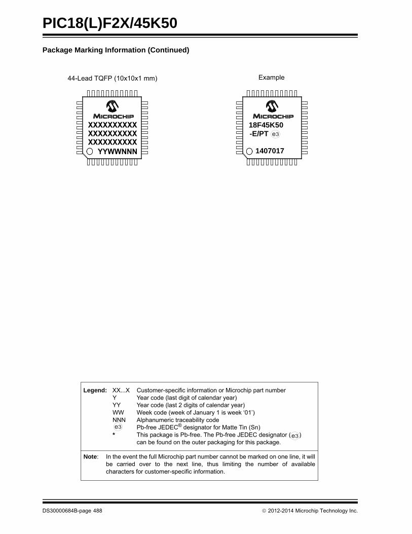
PIC18(L)F2X/45K50
Package Marking Information (Continued)
Legend: XX...X Customer-specific information or Microchip part numberY Year code (last digit of calendar year)YY Year code (last 2 digits of calendar year)WW Week code (week of January 1 is week ‘01’)NNN Alphanumeric traceability code Pb-free JEDEC® designator for Matte Tin (Sn)* This package is Pb-free. The Pb-free JEDEC designator ( )
can be found on the outer packaging for this package.
Note: In the event the full Microchip part number cannot be marked on one line, it willbe carried over to the next line, thus limiting the number of availablecharacters for customer-specific information.
3e
3e
44-Lead TQFP (10x10x1 mm) Example
XXXXXXXXXX
YYWWNNNXXXXXXXXXXXXXXXXXXXX
18F45K50-E/PT
1407017
3e
DS30000684B-page 488 2012-2014 Microchip Technology Inc.

PIC18(L)F2X/45K50
31.2 Package Details
The following sections give the technical details of the packages.
!" !"#$%&"' ()"&'"!&)&#*&&&# +%&,&!&- '!!#.#&"#'#%!&"!!#%!&"!!!&$#/!# '!#&.0
1,2 1!'! &$& "!**&"&&!
!" 3&'!&"&4#*!(!!&4%&&#&&&255***''54
6&! 7,8.'!9'&! 7 7: ;
7"')%! 7 <& 1, && = = ##4 4!! - 1!&& = ="#&"#>#& . - --##4>#& . < : 9& - -? && 9 - 9# 4!! < 69#>#& ) 9*9#>#& ) < : *+ 1 = = -
NOTE 1
N
1 2
D
E1
eB
c
E
L
A2
eb
b1A1
A
3
* ,1
2012-2014 Microchip Technology Inc. DS30000684B-page 489

PIC18(L)F2X/45K50
Note: For the most current package drawings, please see the Microchip Packaging Specification located at http://www.microchip.com/packaging
DS30000684B-page 490 2012-2014 Microchip Technology Inc.

PIC18(L)F2X/45K50
Note: For the most current package drawings, please see the Microchip Packaging Specification located at http://www.microchip.com/packaging
2012-2014 Microchip Technology Inc. DS30000684B-page 491
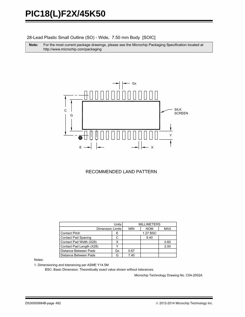
PIC18(L)F2X/45K50
Note: For the most current package drawings, please see the Microchip Packaging Specification located at http://www.microchip.com/packaging
DS30000684B-page 492 2012-2014 Microchip Technology Inc.

PIC18(L)F2X/45K50
#$ % &'%
!" !"#$%&"' ()"&'"!&)&#*&&&# '!!#.#&"#'#%!&"!!#%!&"!!!&$#''!#- '!#&.0
1,2 1!'! &$& "!**&"&&!.32 %'!("!"*&"&&(%%'&"!!
!" 3&'!&"&4#*!(!!&4%&&#&&&255***''54
6&! 99. .'!9'&! 7 7: ;
7"')%! 7 <& ?1,: 8& = = ##4 4!! ? <&#%% = =: >#& . < <##4>#& . - ?: 9& 3&9& 9 3&& 9 .39# 4!! = 3& @ @ <@9#>#& ) = -<
LL1
cA2
A1
A
EE1
D
N
1 2
NOTE 1b
e
φ
* ,-1
2012-2014 Microchip Technology Inc. DS30000684B-page 493
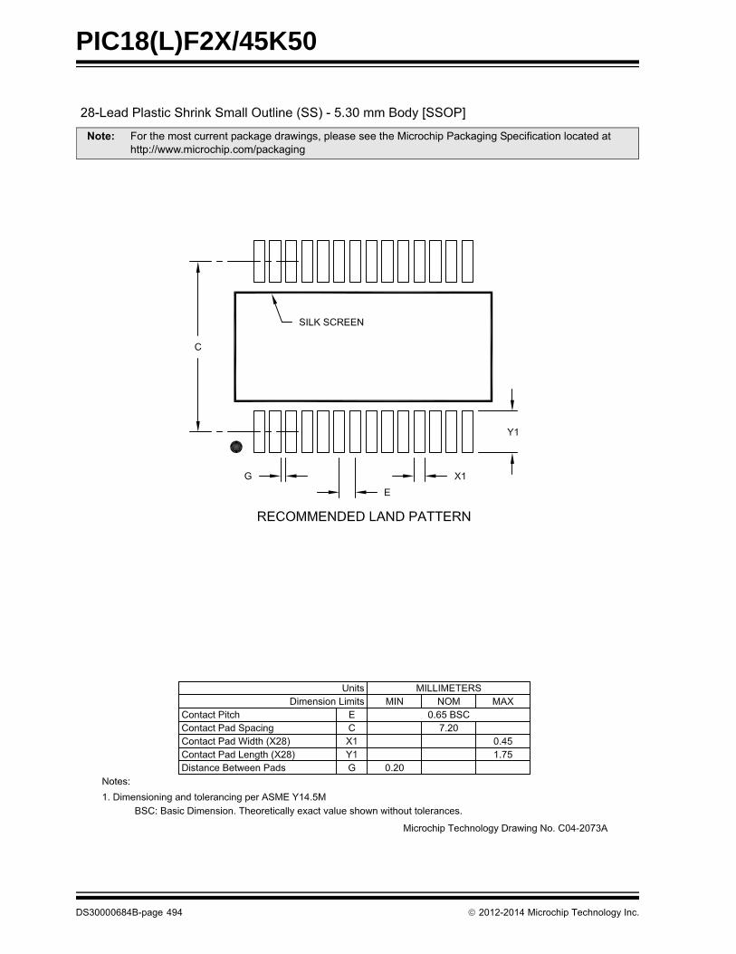
PIC18(L)F2X/45K50
Note: For the most current package drawings, please see the Microchip Packaging Specification located at http://www.microchip.com/packaging
DS30000684B-page 494 2012-2014 Microchip Technology Inc.

PIC18(L)F2X/45K50
2012-2014 Microchip Technology Inc. DS30000684B-page 495

PIC18(L)F2X/45K50
( )
!" 3&'!&"&4#*!(!!&4%&&#&&&255***''54
DS30000684B-page 496 2012-2014 Microchip Technology Inc.

PIC18(L)F2X/45K50
Note: For the most current package drawings, please see the Microchip Packaging Specification located at http://www.microchip.com/packaging
2012-2014 Microchip Technology Inc. DS30000684B-page 497

PIC18(L)F2X/45K50
Note: For the most current package drawings, please see the Microchip Packaging Specification located at http://www.microchip.com/packaging
DS30000684B-page 498 2012-2014 Microchip Technology Inc.

PIC18(L)F2X/45K50
Note: For the most current package drawings, please see the Microchip Packaging Specification located at http://www.microchip.com/packaging
2012-2014 Microchip Technology Inc. DS30000684B-page 499
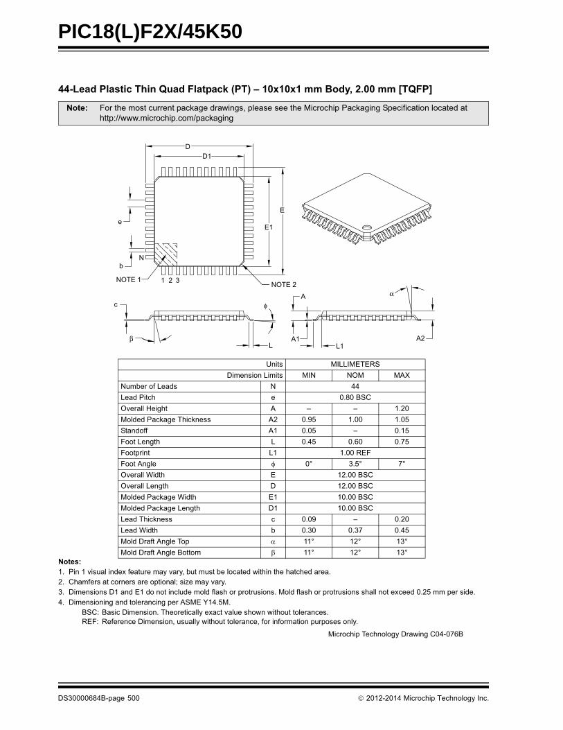
PIC18(L)F2X/45K50
((*# +,-*././.0'*+,
!" !"#$%&"' ()"&'"!&)&#*&&&# ,'%!&!&V!W' - '!!#.#&"#'#%!&"!!#%!&"!!!&$#''!# '!#&.0
1,2 1!'! &$& "!**&"&&!.32 %'!("!"*&"&&(%%'&"!!
!" 3&'!&"&4#*!(!!&4%&&#&&&255***''54
6&! 99. .'!9'&! 7 7: ;
7"')%9#! 7 9#& <1,: 8& = = ##4 4!! &#%% = 3&9& 9 ? 3&& 9 .33& @ -@ @: >#& . 1,: 9& 1,##4>#& . 1,##49& 1,9# 4!! = 9#>#& ) - - #%& @ @ -@#%&1&&' @ @ -@
A
E
E1
DD1
e
b
NOTE 1NOTE 2
N
1 2 3
c
A1L
A2L1
α
φ
β
* ,?1
DS30000684B-page 500 2012-2014 Microchip Technology Inc.
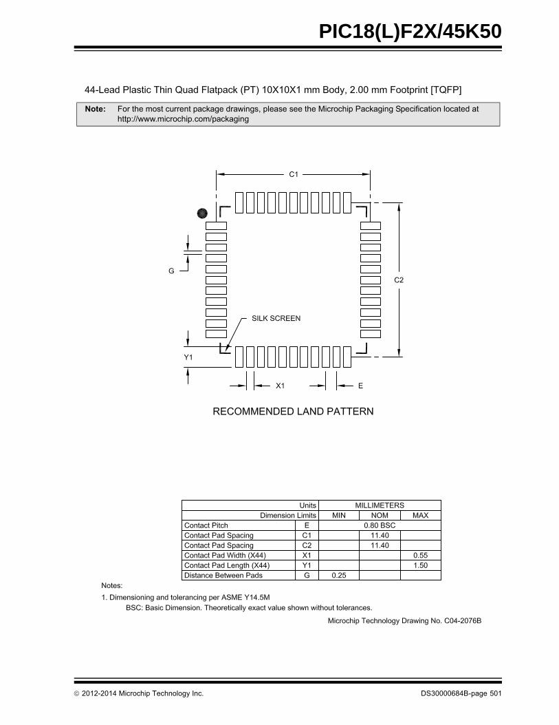
PIC18(L)F2X/45K50
Note: For the most current package drawings, please see the Microchip Packaging Specification located at http://www.microchip.com/packaging
2012-2014 Microchip Technology Inc. DS30000684B-page 501

PIC18(L)F2X/45K50
NOTES:
DS30000684B-page 502 2012-2014 Microchip Technology Inc.
PIC18(L)F2X/45K50
APPENDIX A: REVISION HISTORY
Revision A (08/2012)
Initial release.
Revision B (07/2014)
Updated Figures 2, 4 and 3-1; Updated Section 1.2(Other Special Features), Section 2.4 (VoltageRegulator Pins (VUSB3V3)) and Section 26.9.1(Dedicated ICD/ICSP Port); Added note toSection 24.4.1.1 (Buffer Ownership), Updated Tables3-6 and 3-7; Updated Chapter 29.0 (ElectricalSpecifications), Chapter 31 (Packaging Information)and the Product Identification System page; Otherminor corrections.
2012-2014 Microchip Technology Inc. DS30000684B-page 503

PIC18(L)F2X/45K50
APPENDIX B: DEVICE DIFFERENCES
The differences between the devices listed in this datasheet are shown in Table B-1.
TABLE B-1: DEVICE DIFFERENCES
Features PIC18F24K50 PIC18LF24K50 PIC18F25K50 PIC18LF25K50 PIC18F45K50 PIC18LF45K50
Program Memory (Bytes) 16384 16384 32768 32768 32768 32768
VDD Range 2.3V to 5.5V 1.8V to 3.6V 2.3V to 5.5V 1.8V to 3.6V 2.3V to 5.5V 1.8V to 3.6V
I/O Ports Ports A, B, C, (E)
Ports A, B, C, (E) Ports A, B, C, (E)
Ports A, B, C, (E) Ports A, B, C, D, E
Ports A, B, C, D, E
10-Bit Analog-to-Digital Module
14 input channels
14 input channels
14 input channels
14 input channels
25 input channels
25 input channels
Packages 28-pin SPDIP28-pin SOIC28-pin SSOP28-pin QFN
28-pin SPDIP28-pin SOIC28-pin SSOP28-pin QFN
28-pin SPDIP28-pin SOIC28-pin SSOP28-pin QFN
28-pin SPDIP28-pin SOIC28-pin SSOP28-pin QFN
40-pin PDIP40-pin UQFN44-pin TQFP
40-pin PDIP40-pin UQFN44-pin TQFP
DS30000684B-page 504 2012-2014 Microchip Technology Inc.

2012-2014 Microchip Technology Inc. DS30000684B-page 505
PIC18(L)F2X/45K50
THE MICROCHIP WEB SITE
Microchip provides online support via our WWW site atwww.microchip.com. This web site is used as a meansto make files and information easily available tocustomers. Accessible by using your favorite Internetbrowser, the web site contains the followinginformation:
• Product Support – Data sheets and errata, application notes and sample programs, design resources, user’s guides and hardware support documents, latest software releases and archived software
• General Technical Support – Frequently Asked Questions (FAQ), technical support requests, online discussion groups, Microchip consultant program member listing
• Business of Microchip – Product selector and ordering guides, latest Microchip press releases, listing of seminars and events, listings of Microchip sales offices, distributors and factory representatives
CUSTOMER CHANGE NOTIFICATION SERVICE
Microchip’s customer notification service helps keepcustomers current on Microchip products. Subscriberswill receive e-mail notification whenever there arechanges, updates, revisions or errata related to aspecified product family or development tool of interest.
To register, access the Microchip web site atwww.microchip.com. Under “Support”, click on“Customer Change Notification” and follow theregistration instructions.
CUSTOMER SUPPORT
Users of Microchip products can receive assistancethrough several channels:
• Distributor or Representative
• Local Sales Office
• Field Application Engineer (FAE)
• Technical Support
Customers should contact their distributor,representative or Field Application Engineer (FAE) forsupport. Local sales offices are also available to helpcustomers. A listing of sales offices and locations isincluded in the back of this document.
Technical support is available through the web siteat: http://microchip.com/support
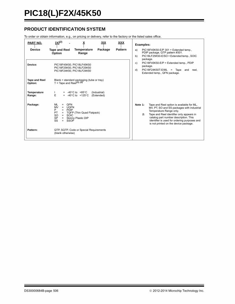
PIC18(L)F2X/45K50
DS30000684B-page 506 2012-2014 Microchip Technology Inc.
PRODUCT IDENTIFICATION SYSTEM
To order or obtain information, e.g., on pricing or delivery, refer to the factory or the listed sales office.
PART NO. X /XX XXX
PatternPackageTemperatureRange
Device
Device: PIC18F45K50, PIC18LF45K50PIC18F25K50, PIC18LF25K50PIC18F24K50, PIC18LF24K50
Tape and ReelOption:
Blank = standard packaging (tube or tray)T = Tape and Reel(1), (2)
Temperature Range:
I = -40C to +85C (Industrial)E = -40C to +125C (Extended)
Package: ML = QFNMV = UQFNP = PDIPPT = TQFP (Thin Quad Flatpack)SO = SOICSP = Skinny Plastic DIPSS = SSOP
Pattern: QTP, SQTP, Code or Special Requirements (blank otherwise)
Examples:
a) PIC18F45K50-E/P 301 = Extended temp., PDIP package, QTP pattern #301.
b) PIC18LF25K50-E/SO = Extended temp., SOIC package.
c) PIC18F45K50-E/P = Extended temp., PDIP package.
d) PIC18F24K50T-E/ML = Tape and reel,Extended temp., QFN package.
Note 1: Tape and Reel option is available for ML, MV, PT, SO and SS packages with industrial Temperature Range only.
2: Tape and Reel identifier only appears in catalog part number description. This identifier is used for ordering purposes and is not printed on the device package.
[X](2)
Tape and Reel Option
-
Note the following details of the code protection feature on Microchip devices:
• Microchip products meet the specification contained in their particular Microchip Data Sheet.
• Microchip believes that its family of products is one of the most secure families of its kind on the market today, when used in the intended manner and under normal conditions.
• There are dishonest and possibly illegal methods used to breach the code protection feature. All of these methods, to our knowledge, require using the Microchip products in a manner outside the operating specifications contained in Microchip’s Data Sheets. Most likely, the person doing so is engaged in theft of intellectual property.
• Microchip is willing to work with the customer who is concerned about the integrity of their code.
• Neither Microchip nor any other semiconductor manufacturer can guarantee the security of their code. Code protection does not mean that we are guaranteeing the product as “unbreakable.”
Code protection is constantly evolving. We at Microchip are committed to continuously improving the code protection features of ourproducts. Attempts to break Microchip’s code protection feature may be a violation of the Digital Millennium Copyright Act. If such actsallow unauthorized access to your software or other copyrighted work, you may have a right to sue for relief under that Act.
Information contained in this publication regarding deviceapplications and the like is provided only for your convenienceand may be superseded by updates. It is your responsibility toensure that your application meets with your specifications.MICROCHIP MAKES NO REPRESENTATIONS ORWARRANTIES OF ANY KIND WHETHER EXPRESS ORIMPLIED, WRITTEN OR ORAL, STATUTORY OROTHERWISE, RELATED TO THE INFORMATION,INCLUDING BUT NOT LIMITED TO ITS CONDITION,QUALITY, PERFORMANCE, MERCHANTABILITY ORFITNESS FOR PURPOSE. Microchip disclaims all liabilityarising from this information and its use. Use of Microchipdevices in life support and/or safety applications is entirely atthe buyer’s risk, and the buyer agrees to defend, indemnify andhold harmless Microchip from any and all damages, claims,suits, or expenses resulting from such use. No licenses areconveyed, implicitly or otherwise, under any Microchipintellectual property rights.
2012-2014 Microchip Technology Inc.
QUALITY MANAGEMENT SYSTEM CERTIFIED BY DNV
== ISO/TS 16949 ==
Trademarks
The Microchip name and logo, the Microchip logo, dsPIC, FlashFlex, flexPWR, JukeBlox, KEELOQ, KEELOQ logo, Kleer, LANCheck, MediaLB, MOST, MOST logo, MPLAB, OptoLyzer, PIC, PICSTART, PIC32 logo, RightTouch, SpyNIC, SST, SST Logo, SuperFlash and UNI/O are registered trademarks of Microchip Technology Incorporated in the U.S.A. and other countries.
The Embedded Control Solutions Company and mTouch are registered trademarks of Microchip Technology Incorporated in the U.S.A.
Analog-for-the-Digital Age, BodyCom, chipKIT, chipKIT logo, CodeGuard, dsPICDEM, dsPICDEM.net, ECAN, In-Circuit Serial Programming, ICSP, Inter-Chip Connectivity, KleerNet, KleerNet logo, MiWi, MPASM, MPF, MPLAB Certified logo, MPLIB, MPLINK, MultiTRAK, NetDetach, Omniscient Code Generation, PICDEM, PICDEM.net, PICkit, PICtail, RightTouch logo, REAL ICE, SQI, Serial Quad I/O, Total Endurance, TSHARC, USBCheck, VariSense, ViewSpan, WiperLock, Wireless DNA, and ZENA are trademarks of Microchip Technology Incorporated in the U.S.A. and other countries.
SQTP is a service mark of Microchip Technology Incorporated in the U.S.A.
Silicon Storage Technology is a registered trademark of Microchip Technology Inc. in other countries.
GestIC is a registered trademarks of Microchip Technology Germany II GmbH & Co. KG, a subsidiary of Microchip Technology Inc., in other countries.
All other trademarks mentioned herein are property of their respective companies.
© 2012-2014, Microchip Technology Incorporated, Printed in the U.S.A., All Rights Reserved.
ISBN: 978-1-63276-360-0
Microchip received ISO/TS-16949:2009 certification for its worldwide
DS30000684B-page 507
headquarters, design and wafer fabrication facilities in Chandler and Tempe, Arizona; Gresham, Oregon and design centers in California and India. The Company’s quality system processes and procedures are for its PIC® MCUs and dsPIC® DSCs, KEELOQ® code hopping devices, Serial EEPROMs, microperipherals, nonvolatile memory and analog products. In addition, Microchip’s quality system for the design and manufacture of development systems is ISO 9001:2000 certified.

DS30000684B-page 508 2012-2014 Microchip Technology Inc.
AMERICASCorporate Office2355 West Chandler Blvd.Chandler, AZ 85224-6199Tel: 480-792-7200 Fax: 480-792-7277Technical Support: http://www.microchip.com/supportWeb Address: www.microchip.com
AtlantaDuluth, GA Tel: 678-957-9614 Fax: 678-957-1455
Austin, TXTel: 512-257-3370
BostonWestborough, MA Tel: 774-760-0087 Fax: 774-760-0088
ChicagoItasca, IL Tel: 630-285-0071 Fax: 630-285-0075
ClevelandIndependence, OH Tel: 216-447-0464 Fax: 216-447-0643
DallasAddison, TX Tel: 972-818-7423 Fax: 972-818-2924
DetroitNovi, MI Tel: 248-848-4000
Houston, TX Tel: 281-894-5983
IndianapolisNoblesville, IN Tel: 317-773-8323Fax: 317-773-5453
Los AngelesMission Viejo, CA Tel: 949-462-9523 Fax: 949-462-9608
New York, NY Tel: 631-435-6000
San Jose, CA Tel: 408-735-9110
Canada - TorontoTel: 905-673-0699 Fax: 905-673-6509
ASIA/PACIFICAsia Pacific OfficeSuites 3707-14, 37th FloorTower 6, The GatewayHarbour City, KowloonHong KongTel: 852-2943-5100Fax: 852-2401-3431
Australia - SydneyTel: 61-2-9868-6733Fax: 61-2-9868-6755
China - BeijingTel: 86-10-8569-7000 Fax: 86-10-8528-2104
China - ChengduTel: 86-28-8665-5511Fax: 86-28-8665-7889
China - ChongqingTel: 86-23-8980-9588Fax: 86-23-8980-9500
China - HangzhouTel: 86-571-8792-8115 Fax: 86-571-8792-8116
China - Hong Kong SARTel: 852-2943-5100 Fax: 852-2401-3431
China - NanjingTel: 86-25-8473-2460Fax: 86-25-8473-2470
China - QingdaoTel: 86-532-8502-7355Fax: 86-532-8502-7205
China - ShanghaiTel: 86-21-5407-5533 Fax: 86-21-5407-5066
China - ShenyangTel: 86-24-2334-2829Fax: 86-24-2334-2393
China - ShenzhenTel: 86-755-8864-2200 Fax: 86-755-8203-1760
China - WuhanTel: 86-27-5980-5300Fax: 86-27-5980-5118
China - XianTel: 86-29-8833-7252Fax: 86-29-8833-7256
China - XiamenTel: 86-592-2388138 Fax: 86-592-2388130
China - ZhuhaiTel: 86-756-3210040 Fax: 86-756-3210049
ASIA/PACIFICIndia - BangaloreTel: 91-80-3090-4444 Fax: 91-80-3090-4123
India - New DelhiTel: 91-11-4160-8631Fax: 91-11-4160-8632
India - PuneTel: 91-20-3019-1500
Japan - OsakaTel: 81-6-6152-7160 Fax: 81-6-6152-9310
Japan - TokyoTel: 81-3-6880- 3770 Fax: 81-3-6880-3771
Korea - DaeguTel: 82-53-744-4301Fax: 82-53-744-4302
Korea - SeoulTel: 82-2-554-7200Fax: 82-2-558-5932 or 82-2-558-5934
Malaysia - Kuala LumpurTel: 60-3-6201-9857Fax: 60-3-6201-9859
Malaysia - PenangTel: 60-4-227-8870Fax: 60-4-227-4068
Philippines - ManilaTel: 63-2-634-9065Fax: 63-2-634-9069
SingaporeTel: 65-6334-8870Fax: 65-6334-8850
Taiwan - Hsin ChuTel: 886-3-5778-366Fax: 886-3-5770-955
Taiwan - KaohsiungTel: 886-7-213-7830
Taiwan - TaipeiTel: 886-2-2508-8600 Fax: 886-2-2508-0102
Thailand - BangkokTel: 66-2-694-1351Fax: 66-2-694-1350
EUROPEAustria - WelsTel: 43-7242-2244-39Fax: 43-7242-2244-393Denmark - CopenhagenTel: 45-4450-2828 Fax: 45-4485-2829
France - ParisTel: 33-1-69-53-63-20 Fax: 33-1-69-30-90-79
Germany - DusseldorfTel: 49-2129-3766400
Germany - MunichTel: 49-89-627-144-0 Fax: 49-89-627-144-44
Germany - PforzheimTel: 49-7231-424750
Italy - Milan Tel: 39-0331-742611 Fax: 39-0331-466781
Italy - VeniceTel: 39-049-7625286
Netherlands - DrunenTel: 31-416-690399 Fax: 31-416-690340
Poland - WarsawTel: 48-22-3325737
Spain - MadridTel: 34-91-708-08-90Fax: 34-91-708-08-91
Sweden - StockholmTel: 46-8-5090-4654
UK - WokinghamTel: 44-118-921-5800Fax: 44-118-921-5820
Worldwide Sales and Service
03/25/14