
FUZE Hardware Ref - RS Components
87
FUZE Hardware Ref Contents Introduction 4 1 Overview 5 1.1 System Circuit Diagram 6 2. Keypad 7 2.1 Circuit Diagram 7 2.2 Operation 8 2.2.1 Reading the switches. 8 2.2.2 Ghost Keys 9 2.2.3 Debouncing the Keypad 10 2.2.4 Converting Single and Double Keypresses to Characters 11 3 Video 13 3.1 Circuit Diagram 13 3.2 Operation 13 3.2.1 Composite Video Basics 13 3.2.2 Video Circuit Basics 15 3.2.3 Video Firmware Details 16 3.2.4 Composite Video Details 18 3.2.6 Bitmapped Video Basics 19 4. Audio 22 4.1 Circuit Diagram 22 4.2 Operation 22 4.2.1 Circuit Details 22 4.2.2 Using Timer 0 To Generate Audio 27 4.2.3 Making It Easy With Pitch> . 28 4.2.4 Audio In 31 5. Storage 32 5.1 Circuit Diagram 32 5.2 Hardware Operation 32
-
Upload
khangminh22 -
Category
Documents
-
view
2 -
download
0
Transcript of FUZE Hardware Ref - RS Components

FUZE Hardware RefContents
Introduction! 4
1 Overview! 5
1.1 System Circuit Diagram! 6
2. Keypad! 7
2.1 Circuit Diagram! 7
2.2 Operation! 82.2.1 Reading the switches.! 82.2.2 Ghost Keys! 92.2.3 Debouncing the Keypad! 102.2.4 Converting Single and Double Keypresses to Characters! 11
3 Video ! 13
3.1 Circuit Diagram! 13
3.2 Operation! 133.2.1 Composite Video Basics! 133.2.2 Video Circuit Basics! 153.2.3 Video Firmware Details! 163.2.4 Composite Video Details! 183.2.6 Bitmapped Video Basics! 19
4. Audio ! 22
4.1 Circuit Diagram! 22
4.2 Operation! 224.2.1 Circuit Details! 224.2.2 Using Timer 0 To Generate Audio ! 274.2.3 Making It Easy With Pitch> .! 284.2.4 Audio In! 31
5. Storage ! 32
5.1 Circuit Diagram! 32
5.2 Hardware Operation! 32

5.2.1. Electrical Connections! 325.2.2 The SPI Protocol! 335.2.3 The Flash Chip Commands! 34
5.3 Firmware Operation! 355.3.1 Virtual Blocks! 355.3.2 Purging! 375.3.3 Virtual Table Purging! 395.3.4 Conclusions! 40
6. RAM! 41
6.1 Circuit Diagram! 41
6.2 Operation! 416.2.1. Electrical Connections! 416.2.2 The SPI Protocol! 41
6.3 Firmware Operation! 426.3.1 Locality! 436.3.2 Pipelining! 436.3.3 Branch Caching! 446.3.4 Conclusions! 45
7. USB! 46
7.1 Circuit Diagram! 46
7.2 Hardware Operation! 46
7.3 Firmware Operation! 487.3.1 AVR Flash Memory Organization! 487.3.2 The Bootloader Key! 487.3.3 Realtime Requirements! 487.3.4 Chicken And Egg! 497.3.5 Licensing! 49
8. Microcontroller! 50
8.1 Circuit Diagram! 50
8.2 Operation! 508.2.1 How FIGnition Uses Pins! 508.2.2 AVR Block Diagram! 528.2.3 FIGnition's Firmware Overview! 53
9. Expanding FIGnition! 58

9.1 Circuit Diagram! 58
9.2 Operation! 589.2.1 Controlling the LED! 599.2.2 Default I/O ! 609.2.3 Reading Analog Channel 5.! 609.2.4 I/O Trade-Off! 63
9.3 Using SPI to talk to an Arduino! 64
9.4 Using I2C to talk to a Maxim Digital To Analogue Converter.! 66
9.5 Using I2C to talk to a Microchip I/O Expander! 68
9.6 Using SPI to backup the external Flash.! 70
Appendix A: Potential Dividers! 73
Circuit Diagram! 73
Operation! 73Detailed Explanation! 75Simulation! 79Code Description! 80
Appendix B Diodes ! 82
B.1 Signal Diodes! 82
B.2 Zener Diodes! 83
Appendix C Capacitors! 85
C.1 How Capacitors Work! 85
C.2 Capacitors As Temporary Power Sources! 86
C.3 De-coupling Capacitors! 87
C.4 Capacitors As Audio Filters! 87

IntroductionFIGnition FUZE's hardware contains the essentials of a true computer: a keypad for typing programs and entering text; a power supply connector; it can output data to the user (via video and audio); it runs programs from RAM; it has built-in storage for when the computer is turned off; it has a CPU for running programs and a built-in program which manages all these features and implements a fully-featured programming language (FIGnition Forth).
All true computers are like this; the only difference is the level of sophistication for each of these parts. This manual takes you through the design and construction of every aspect of FIGnition: bottom up from the components themselves to the way they interface to FIGni-tion's processor chip to the code that manages each part.
FIGnition is a computer designed to be built, programmed and understood. The firmware is fully open-sourced and the circuit is Open-Source Hardware compliant. This document covers its operation with a view to understanding it, but it is not a substitute for an electron-ics or programming course. For this you would find this additional material useful:
• An Electronics Tutorial.
• The User Guide for the AtMega168 and AtMega328.
• The FIGnition firmware source, which is on GitHub at: https://github.com/Snial/FIGnition
• The FIGnition programming Tutorial, Topics and Command Reference guides.
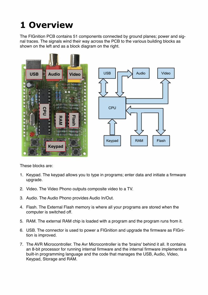
1 OverviewThe FIGnition PCB contains 51 components connected by ground planes; power and sig-nal traces. The signals wind their way across the PCB to the various building blocks as shown on the left and as a block diagram on the right.
Flash
RA
M
CPU
VideoAudioUSB
Keypad
These blocks are:
1. Keypad. The keypad allows you to type in programs; enter data and initiate a firmware upgrade.
2. Video. The Video Phono outputs composite video to a TV.
3. Audio. The Audio Phono provides Audio In/Out.
4. Flash. The External Flash memory is where all your programs are stored when the computer is switched off.
5. RAM. The external RAM chip is loaded with a program and the program runs from it.
6. USB. The connector is used to power a FIGnition and upgrade the firmware as FIGni-tion is improved.
7. The AVR Microcontroller. The Avr Microcontroller is the 'brains' behind it all. It contains an 8-bit processor for running internal firmware and the internal firmware implements a built-in programming language and the code that manages the USB, Audio, Video, Keypad, Storage and RAM.
8. Arduino Headers.
The block diagram tells you some basic information about the structure of the computer. For example, the arrow between USB and CPU is two-headed, because data goes in both directions. The arrow from the keypad is single-headed, because data only goes from the keypad. RAM and Flash share a multi-head arrow, because data transfer is shared be-tween them.
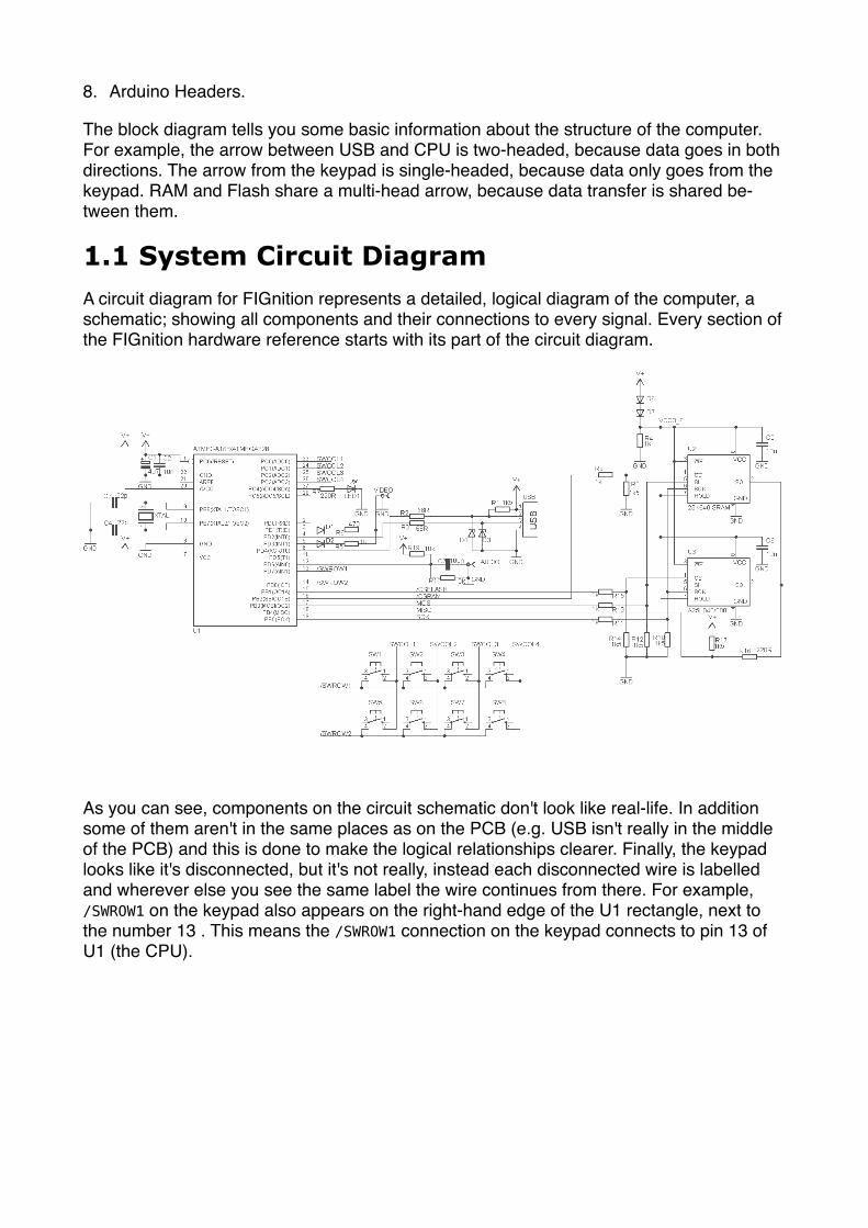
1.1 System Circuit DiagramA circuit diagram for FIGnition represents a detailed, logical diagram of the computer, a schematic; showing all components and their connections to every signal. Every section of the FIGnition hardware reference starts with its part of the circuit diagram.
As you can see, components on the circuit schematic don't look like real-life. In addition some of them aren't in the same places as on the PCB (e.g. USB isn't really in the middle of the PCB) and this is done to make the logical relationships clearer. Finally, the keypad looks like it's disconnected, but it's not really, instead each disconnected wire is labelled and wherever else you see the same label the wire continues from there. For example, /SWROW1 on the keypad also appears on the right-hand edge of the U1 rectangle, next to the number 13 . This means the /SWROW1 connection on the keypad connects to pin 13 of U1 (the CPU).
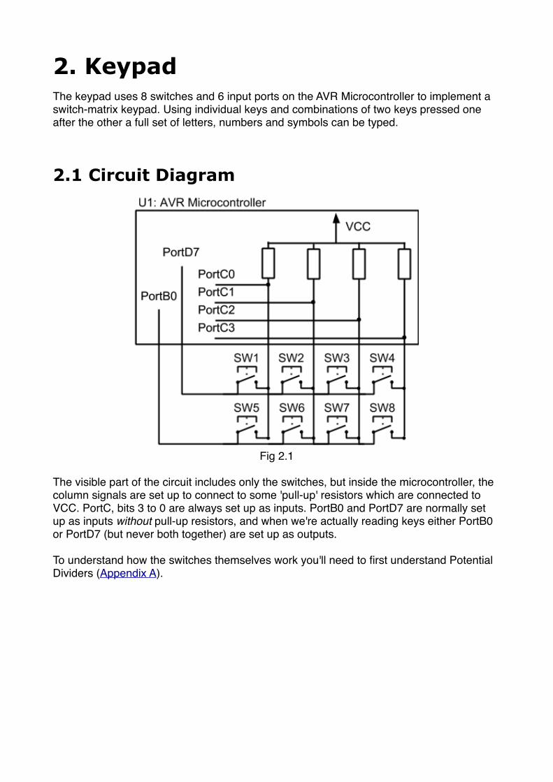
2. KeypadThe keypad uses 8 switches and 6 input ports on the AVR Microcontroller to implement a switch-matrix keypad. Using individual keys and combinations of two keys pressed one after the other a full set of letters, numbers and symbols can be typed.
2.1 Circuit Diagram
Fig 2.1
The visible part of the circuit includes only the switches, but inside the microcontroller, the column signals are set up to connect to some 'pull-up' resistors which are connected to VCC. PortC, bits 3 to 0 are always set up as inputs. PortB0 and PortD7 are normally set up as inputs without pull-up resistors, and when we're actually reading keys either PortB0 or PortD7 (but never both together) are set up as outputs.
To understand how the switches themselves work you'll need to first understand Potential Dividers (Appendix A).
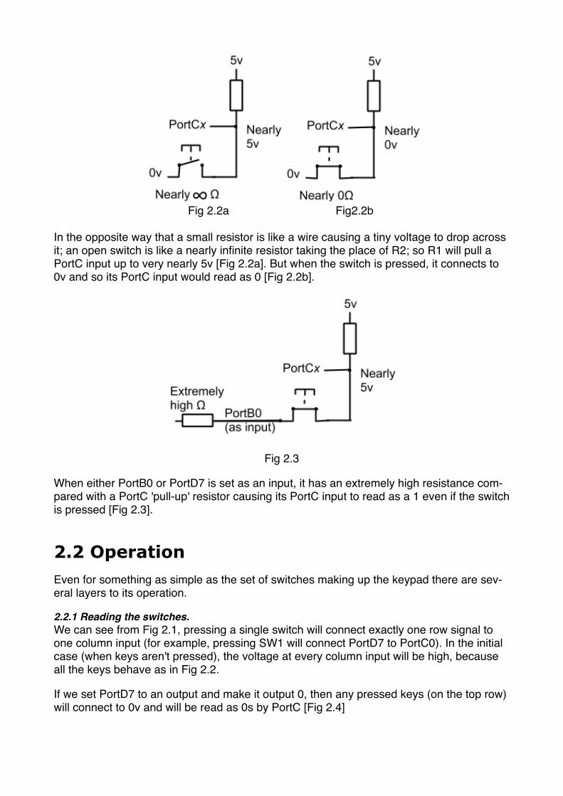
! Fig 2.2a! Fig2.2b
In the opposite way that a small resistor is like a wire causing a tiny voltage to drop across it; an open switch is like a nearly infinite resistor taking the place of R2; so R1 will pull a PortC input up to very nearly 5v [Fig 2.2a]. But when the switch is pressed, it connects to 0v and so its PortC input would read as 0 [Fig 2.2b].
Fig 2.3
When either PortB0 or PortD7 is set as an input, it has an extremely high resistance com-pared with a PortC 'pull-up' resistor causing its PortC input to read as a 1 even if the switch is pressed [Fig 2.3].
2.2 OperationEven for something as simple as the set of switches making up the keypad there are sev-eral layers to its operation.
2.2.1 Reading the switches.We can see from Fig 2.1, pressing a single switch will connect exactly one row signal to one column input (for example, pressing SW1 will connect PortD7 to PortC0). In the initial case (when keys aren't pressed), the voltage at every column input will be high, because all the keys behave as in Fig 2.2.
If we set PortD7 to an output and make it output 0, then any pressed keys (on the top row) will connect to 0v and will be read as 0s by PortC [Fig 2.4]
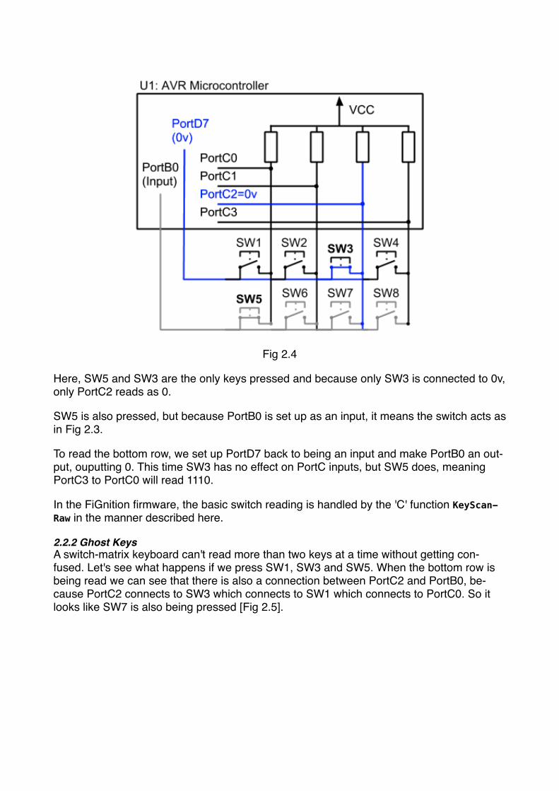
Fig 2.4
Here, SW5 and SW3 are the only keys pressed and because only SW3 is connected to 0v, only PortC2 reads as 0.
SW5 is also pressed, but because PortB0 is set up as an input, it means the switch acts as in Fig 2.3.
To read the bottom row, we set up PortD7 back to being an input and make PortB0 an out-put, ouputting 0. This time SW3 has no effect on PortC inputs, but SW5 does, meaning PortC3 to PortC0 will read 1110.
In the FiGnition firmware, the basic switch reading is handled by the 'C' function KeyScan-Raw in the manner described here.
2.2.2 Ghost KeysA switch-matrix keyboard can't read more than two keys at a time without getting con-fused. Let's see what happens if we press SW1, SW3 and SW5. When the bottom row is being read we can see that there is also a connection between PortC2 and PortB0, be-cause PortC2 connects to SW3 which connects to SW1 which connects to PortC0. So it looks like SW7 is also being pressed [Fig 2.5].
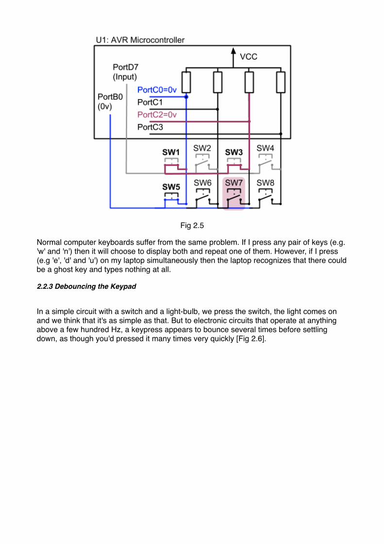
Fig 2.5
Normal computer keyboards suffer from the same problem. If I press any pair of keys (e.g. 'w' and 'n') then it will choose to display both and repeat one of them. However, if I press (e.g 'e', 'd' and 'u') on my laptop simultaneously then the laptop recognizes that there could be a ghost key and types nothing at all.
2.2.3 Debouncing the Keypad
In a simple circuit with a switch and a light-bulb, we press the switch, the light comes on and we think that it's as simple as that. But to electronic circuits that operate at anything above a few hundred Hz, a keypress appears to bounce several times before settling down, as though you'd pressed it many times very quickly [Fig 2.6].
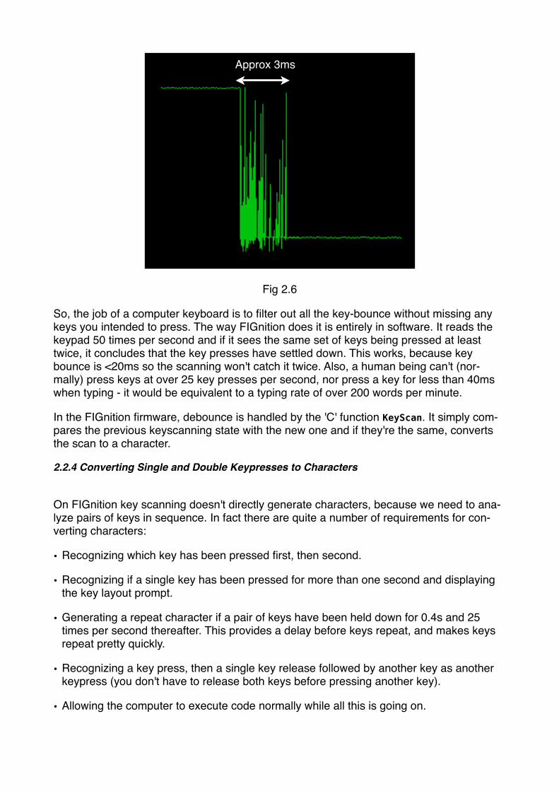
Approx 3ms
Fig 2.6
So, the job of a computer keyboard is to filter out all the key-bounce without missing any keys you intended to press. The way FIGnition does it is entirely in software. It reads the keypad 50 times per second and if it sees the same set of keys being pressed at least twice, it concludes that the key presses have settled down. This works, because key bounce is <20ms so the scanning won't catch it twice. Also, a human being can't (nor-mally) press keys at over 25 key presses per second, nor press a key for less than 40ms when typing - it would be equivalent to a typing rate of over 200 words per minute.
In the FIGnition firmware, debounce is handled by the 'C' function KeyScan. It simply com-pares the previous keyscanning state with the new one and if they're the same, converts the scan to a character.
2.2.4 Converting Single and Double Keypresses to Characters
On FIGnition key scanning doesn't directly generate characters, because we need to ana-lyze pairs of keys in sequence. In fact there are quite a number of requirements for con-verting characters:
• Recognizing which key has been pressed first, then second.
• Recognizing if a single key has been pressed for more than one second and displaying the key layout prompt.
• Generating a repeat character if a pair of keys have been held down for 0.4s and 25 times per second thereafter. This provides a delay before keys repeat, and makes keys repeat pretty quickly.
• Recognizing a key press, then a single key release followed by another key as another keypress (you don't have to release both keys before pressing another key).
• Allowing the computer to execute code normally while all this is going on.
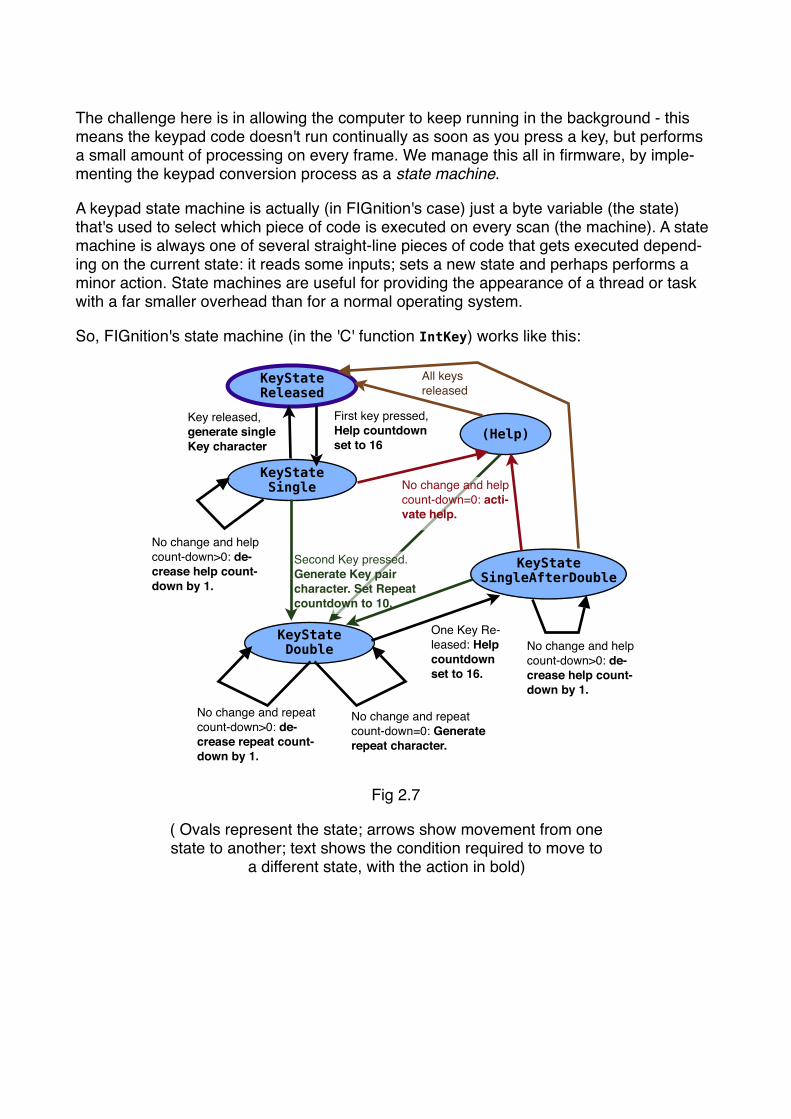
The challenge here is in allowing the computer to keep running in the background - this means the keypad code doesn't run continually as soon as you press a key, but performs a small amount of processing on every frame. We manage this all in firmware, by imple-menting the keypad conversion process as a state machine.
A keypad state machine is actually (in FIGnition's case) just a byte variable (the state) that's used to select which piece of code is executed on every scan (the machine). A state machine is always one of several straight-line pieces of code that gets executed depend-ing on the current state: it reads some inputs; sets a new state and perhaps performs a minor action. State machines are useful for providing the appearance of a thread or task with a far smaller overhead than for a normal operating system.
So, FIGnition's state machine (in the 'C' function IntKey) works like this:
KeyStateReleased
KeyStateSingle
First key pressed, Help countdown set to 16
KeyStateDouble
No change and help count-down>0: de-crease help count-down by 1.
(Help)Key released, generate single Key character
All keysreleased
No change and repeat count-down>0: de-crease repeat count-down by 1.
No change and repeat count-down=0: Generate repeat character.
KeyStateSingleAfterDouble
One Key Re-leased: Help countdown set to 16.
No change and help count-down>0: de-crease help count-down by 1.
No change and help count-down=0: acti-vate help.
Second Key pressed. Generate Key pair character. Set Repeat countdown to 10.
Fig 2.7
( Ovals represent the state; arrows show movement from one state to another; text shows the condition required to move to
a different state, with the action in bold)
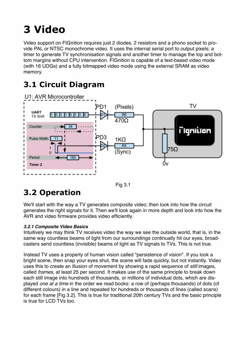
3 VideoVideo support on FIGnition requires just 2 diodes, 2 resistors and a phono socket to pro-vide PAL or NTSC monochrome video. It uses the internal serial port to output pixels; a timer to generate TV synchronisation signals and another timer to manage the top and bot-tom margins without CPU intervention. FIGnition is capable of a text-based video mode (with 16 UDGs) and a fully bitmapped video mode using the external SRAM as video memory.
3.1 Circuit Diagram
Fig 3.13.2 OperationWe'll start with the way a TV generates composite video; then look into how the circuit generates the right signals for it. Then we'll look again in more depth and look into how the AVR and video firmware provides video efficiently.
3.2.1 Composite Video BasicsIntuitively we may think TV receives video the way we see the outside world, that is, in the same way countless beams of light from our surroundings continually hit our eyes, broad-casters send countless (invisible) beams of light as TV signals to TVs. This is not true.
Instead TV uses a property of human vision called "persistence of vision". If you look a bright scene, then snap your eyes shut, the scene will fade quickly, but not instantly. Video uses this to create an illusion of movement by showing a rapid sequence of still images, called frames, at least 25 per second. It makes use of the same principle to break down each still image into hundreds of thousands, or millions of individual dots, which are dis-played one at a time in the order we read books: a row of (perhaps thousands) of dots (of different colours) in a line and repeated for hundreds or thousands of lines (called scans) for each frame [Fig 3.2]. This is true for traditional 20th century TVs and the basic principle is true for LCD TVs too.
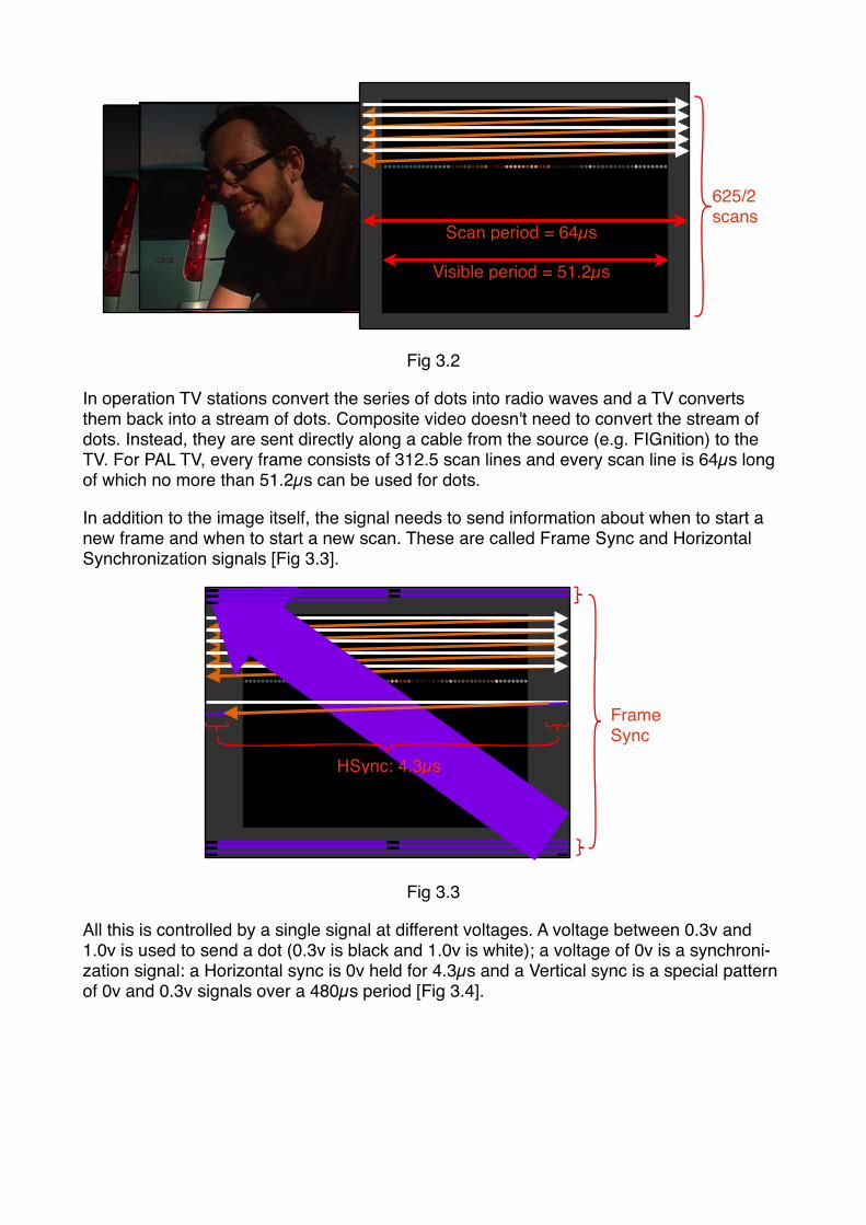
625/2 scans
Scan period = 64µs
Visible period = 51.2µs
Fig 3.2
In operation TV stations convert the series of dots into radio waves and a TV converts them back into a stream of dots. Composite video doesn't need to convert the stream of dots. Instead, they are sent directly along a cable from the source (e.g. FIGnition) to the TV. For PAL TV, every frame consists of 312.5 scan lines and every scan line is 64µs long of which no more than 51.2µs can be used for dots.
In addition to the image itself, the signal needs to send information about when to start a new frame and when to start a new scan. These are called Frame Sync and Horizontal Synchronization signals [Fig 3.3].
FrameSync
HSync: 4.3µs
Fig 3.3
All this is controlled by a single signal at different voltages. A voltage between 0.3v and 1.0v is used to send a dot (0.3v is black and 1.0v is white); a voltage of 0v is a synchroni-zation signal: a Horizontal sync is 0v held for 4.3µs and a Vertical sync is a special pattern of 0v and 0.3v signals over a 480µs period [Fig 3.4].
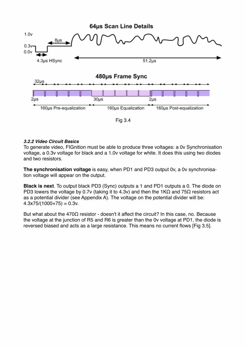
Fig 3.4
3.2.2 Video Circuit BasicsTo generate video, FIGnition must be able to produce three voltages: a 0v Synchronisation voltage, a 0.3v voltage for black and a 1.0v voltage for white. It does this using two diodes and two resistors.
The synchronisation voltage is easy, when PD1 and PD3 output 0v, a 0v synchronisa-tion voltage will appear on the output.
Black is next. To output black PD3 (Sync) outputs a 1 and PD1 outputs a 0. The diode on PD3 lowers the voltage by 0.7v (taking it to 4.3v) and then the 1KΩ and 75Ω resistors act as a potential divider (see Appendix A). The voltage on the potential divider will be: 4.3x75/(1000+75) = 0.3v.
But what about the 470Ω resistor - doesn't it affect the circuit? In this case, no. Because the voltage at the junction of R5 and R6 is greater than the 0v voltage at PD1, the diode is reversed biased and acts as a large resistance. This means no current flows [Fig 3.5].
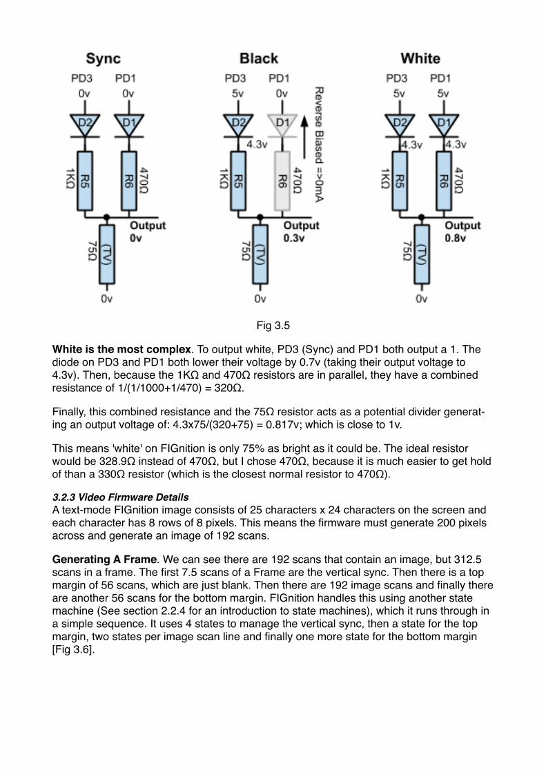
Fig 3.5
White is the most complex. To output white, PD3 (Sync) and PD1 both output a 1. The diode on PD3 and PD1 both lower their voltage by 0.7v (taking their output voltage to 4.3v). Then, because the 1KΩ and 470Ω resistors are in parallel, they have a combined resistance of 1/(1/1000+1/470) = 320Ω.
Finally, this combined resistance and the 75Ω resistor acts as a potential divider generat-ing an output voltage of: 4.3x75/(320+75) = 0.817v; which is close to 1v.
This means 'white' on FIGnition is only 75% as bright as it could be. The ideal resistor would be 328.9Ω instead of 470Ω, but I chose 470Ω, because it is much easier to get hold of than a 330Ω resistor (which is the closest normal resistor to 470Ω).
3.2.3 Video Firmware DetailsA text-mode FIGnition image consists of 25 characters x 24 characters on the screen and each character has 8 rows of 8 pixels. This means the firmware must generate 200 pixels across and generate an image of 192 scans.
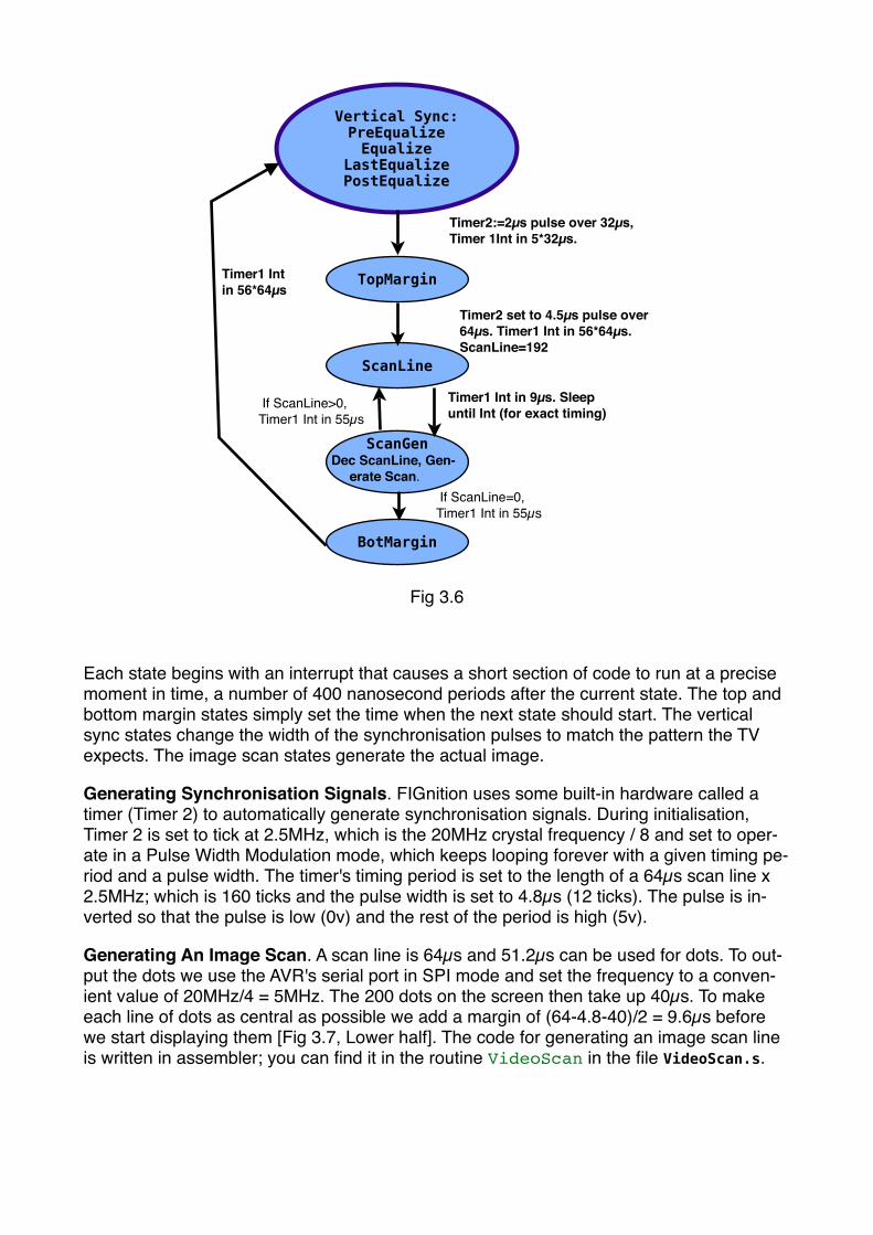
Generating A Frame. We can see there are 192 scans that contain an image, but 312.5 scans in a frame. The first 7.5 scans of a Frame are the vertical sync. Then there is a top margin of 56 scans, which are just blank. Then there are 192 image scans and finally there are another 56 scans for the bottom margin. FIGnition handles this using another state machine (See section 2.2.4 for an introduction to state machines), which it runs through in a simple sequence. It uses 4 states to manage the vertical sync, then a state for the top margin, two states per image scan line and finally one more state for the bottom margin [Fig 3.6].
Vertical Sync:PreEqualizeEqualize
LastEqualizePostEqualize
If ScanLine>0, Timer1 Int in 55µs
TopMargin
ScanLine
ScanGenDec ScanLine, Gen-
erate Scan.
BotMargin
Timer2 set to 4.5µs pulse over 64µs. Timer1 Int in 56*64µs. ScanLine=192
Timer2:=2µs pulse over 32µs, Timer 1Int in 5*32µs.
Timer1 Int in 9µs. Sleep until Int (for exact timing)
If ScanLine=0, Timer1 Int in 55µs
Timer1 Int in 56*64µs
Fig 3.6
Each state begins with an interrupt that causes a short section of code to run at a precise moment in time, a number of 400 nanosecond periods after the current state. The top and bottom margin states simply set the time when the next state should start. The vertical sync states change the width of the synchronisation pulses to match the pattern the TV expects. The image scan states generate the actual image.
Generating Synchronisation Signals. FIGnition uses some built-in hardware called a timer (Timer 2) to automatically generate synchronisation signals. During initialisation, Timer 2 is set to tick at 2.5MHz, which is the 20MHz crystal frequency / 8 and set to oper-ate in a Pulse Width Modulation mode, which keeps looping forever with a given timing pe-riod and a pulse width. The timer's timing period is set to the length of a 64µs scan line x 2.5MHz; which is 160 ticks and the pulse width is set to 4.8µs (12 ticks). The pulse is in-verted so that the pulse is low (0v) and the rest of the period is high (5v).
Generating An Image Scan. A scan line is 64µs and 51.2µs can be used for dots. To out-put the dots we use the AVR's serial port in SPI mode and set the frequency to a conven-ient value of 20MHz/4 = 5MHz. The 200 dots on the screen then take up 40µs. To make each line of dots as central as possible we add a margin of (64-4.8-40)/2 = 9.6µs before we start displaying them [Fig 3.7, Lower half]. The code for generating an image scan line is written in assembler; you can find it in the routine VideoScan in the file VideoScan.s.
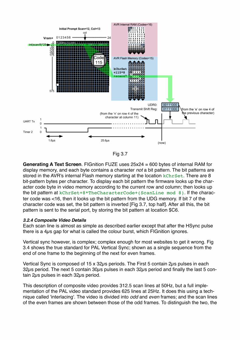
Fig 3.7
Generating A Text Screen. FIGnition FUZE uses 25x24 = 600 bytes of internal RAM for display memory, and each byte contains a character not a bit pattern. The bit patterns are stored in the AVR's internal Flash memory starting at the location kChrSet. There are 8 bit-pattern bytes per character. To display each bit pattern the firmware looks up the char-acter code byte in video memory according to the current row and column; then looks up the bit pattern at kChrSet+8*TheCharacterCode+(ScanLine mod 8). If the charac-ter code was <16, then it looks up the bit pattern from the UDG memory. If bit 7 of the character code was set, the bit pattern is inverted [Fig 3.7, top half]. After all this, the bit pattern is sent to the serial port, by storing the bit pattern at location $C6.
3.2.4 Composite Video DetailsEach scan line is almost as simple as described earlier except that after the HSync pulse there is a 4µs gap for what is called the colour burst, which FIGnition ignores.
Vertical sync however, is complex; complex enough for most websites to get it wrong. Fig 3.4 shows the true standard for PAL Vertical Sync; shown as a single sequence from the end of one frame to the beginning of the next for even frames.
Vertical Sync is composed of 15 x 32µs periods. The First 5 contain 2µs pulses in each 32µs period. The next 5 contain 30µs pulses in each 32µs period and finally the last 5 con-tain 2µs pulses in each 32µs period.
This description of composite video provides 312.5 scan lines at 50Hz, but a full imple-mentation of the PAL video standard provides 625 lines at 25Hz. It does this using a tech-nique called 'interlacing'. The video is divided into odd and even frames; and the scan lines of the even frames are shown between those of the odd frames. To distinguish the two, the
VSync part of a frame is slightly different for even frames. Since FIGnition doesn't use in-terlacing, we won't cover it any further here.
NTSC Video. FIGnition is capable of displaying NTSC video using slightly different firm-ware. NTSC video is used in the US, Canada and parts of South America and provides 525 lines each of 63.9µs. This means there are 14 x 31.95µs periods in the VSync portion leaving 31 scans for the top margin and 32 scans for the bottom margin.
3.2.6 Bitmapped Video BasicsThe Bitmapped video and Blitter (Sprite Engine) are covered in more detail in the Firm-ware Reference, but some of the basics are worth covering here.
Bandwidth. After FIGnition was designed it was discovered that the serial SRAM could be read fast enough to generate a full bitmapped image on a TV. The Serial SRAM is read at 10MHz and requires 9 bit times to read each byte. Therefore in a single 64µs video scan we can (in theory) read up to 64µs x 10MHz / 9CyclesPerByte = A theoretical maximum of 71 bytes. Video data is pumped out of the USART at 5MHz for 40µs requiring only 25 bytes per scan. Therefore we can copy bitmapped data from the serial SRAM to the USART quickly enough. A 160x160 bitmapped image was chosen (using 3200 bytes) to leave adequate room for programs from a FIGnition's standard 8Kb of SRAM.
Interrupting SRAM. FIGnition uses the serial SRAM to execute Forth programs. To read a bitmapped video image from the SRAM means interrupting its use for reading programs and then restoring it at the end. However, it's not possible to read the current SRAM ad-dress from the chip and it's not practical to analyze the firmware to work out which address was last read or written.
The solution is to only use the SRAM for video when the SRAM gets deselected, which happens every time a Forth program jumps to a different location; reads or writes a vari-able or executes a Forth command1 in ROM. When the SRAM is deselected, PortB1 goes high and because it's possible to automatically generate an interrupt when a port pin changes (Chapter 13 of AtMega328 User Manual) it's possible to notify the AVR when the SRAM is free to be used to generate bitmapped video.
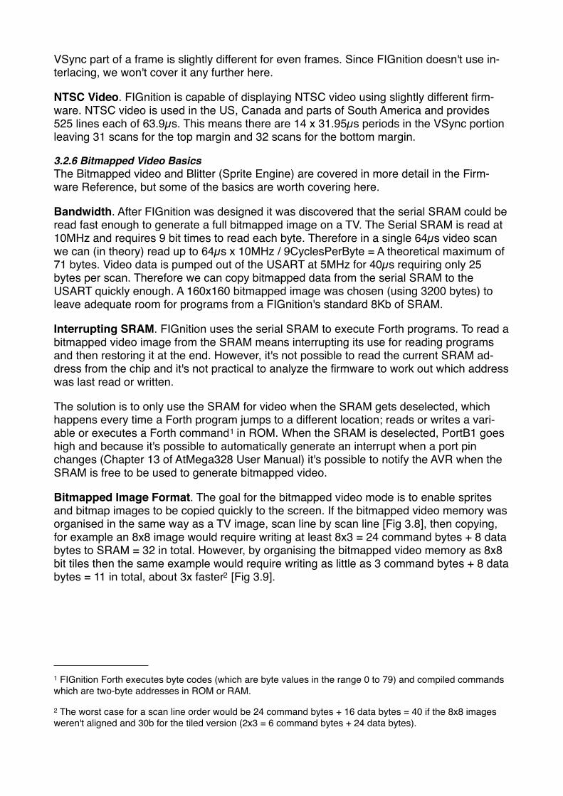
Bitmapped Image Format. The goal for the bitmapped video mode is to enable sprites and bitmap images to be copied quickly to the screen. If the bitmapped video memory was organised in the same way as a TV image, scan line by scan line [Fig 3.8], then copying, for example an 8x8 image would require writing at least 8x3 = 24 command bytes + 8 data bytes to SRAM = 32 in total. However, by organising the bitmapped video memory as 8x8 bit tiles then the same example would require writing as little as 3 command bytes + 8 data bytes = 11 in total, about 3x faster2 [Fig 3.9].
1 FIGnition Forth executes byte codes (which are byte values in the range 0 to 79) and compiled commands which are two-byte addresses in ROM or RAM.
2 The worst case for a scan line order would be 24 command bytes + 16 data bytes = 40 if the 8x8 images weren't aligned and 30b for the tiled version (2x3 = 6 command bytes + 24 data bytes).
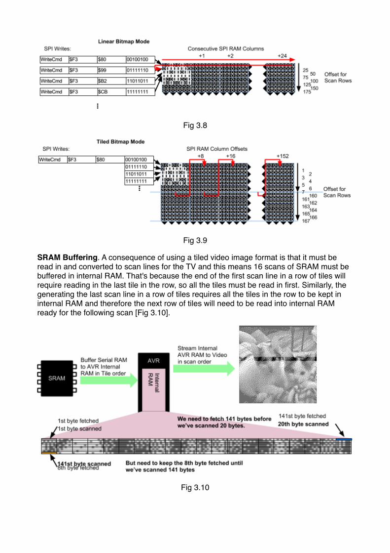
Fig 3.8
Fig 3.9
SRAM Buffering. A consequence of using a tiled video image format is that it must be read in and converted to scan lines for the TV and this means 16 scans of SRAM must be buffered in internal RAM. That's because the end of the first scan line in a row of tiles will require reading in the last tile in the row, so all the tiles must be read in first. Similarly, the generating the last scan line in a row of tiles requires all the tiles in the row to be kept in internal RAM and therefore the next row of tiles will need to be read into internal RAM ready for the following scan [Fig 3.10].
Fig 3.10

For this reason, the bitmapped video code prepares to prefetch SRAM 16 scan lines be-fore bitmapped image generation starts. The firmware allocates 320 bytes of the Text mode video buffer for prefetching the two rows of tiles (in bitmapped mode the text mode video buffer is free for other uses). The first 8 scans are enough time for most Forth pro-grams to deselect SRAM at some point (about 35 instructions).
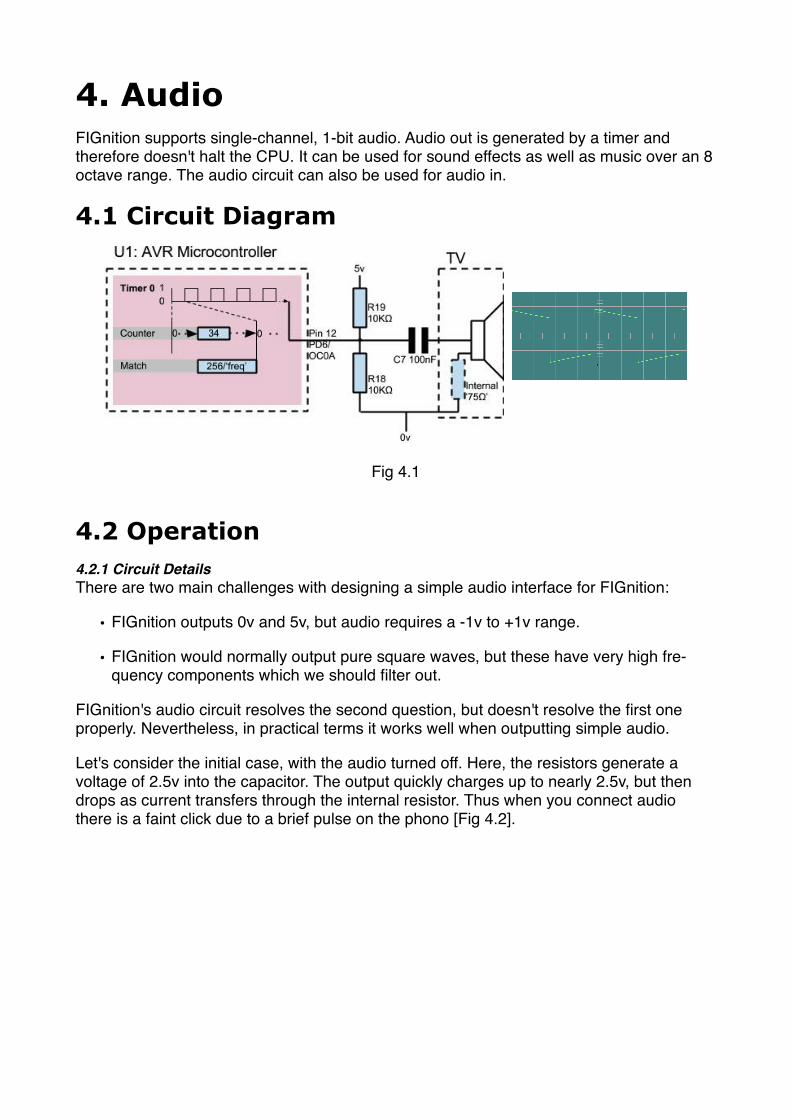
4. AudioFIGnition supports single-channel, 1-bit audio. Audio out is generated by a timer and therefore doesn't halt the CPU. It can be used for sound effects as well as music over an 8 octave range. The audio circuit can also be used for audio in.
4.1 Circuit Diagram
Fig 4.1
4.2 Operation4.2.1 Circuit DetailsThere are two main challenges with designing a simple audio interface for FIGnition:
• FIGnition outputs 0v and 5v, but audio requires a -1v to +1v range.
• FIGnition would normally output pure square waves, but these have very high fre-quency components which we should filter out.
FIGnition's audio circuit resolves the second question, but doesn't resolve the first one properly. Nevertheless, in practical terms it works well when outputting simple audio.
Let's consider the initial case, with the audio turned off. Here, the resistors generate a voltage of 2.5v into the capacitor. The output quickly charges up to nearly 2.5v, but then drops as current transfers through the internal resistor. Thus when you connect audio there is a faint click due to a brief pulse on the phono [Fig 4.2].
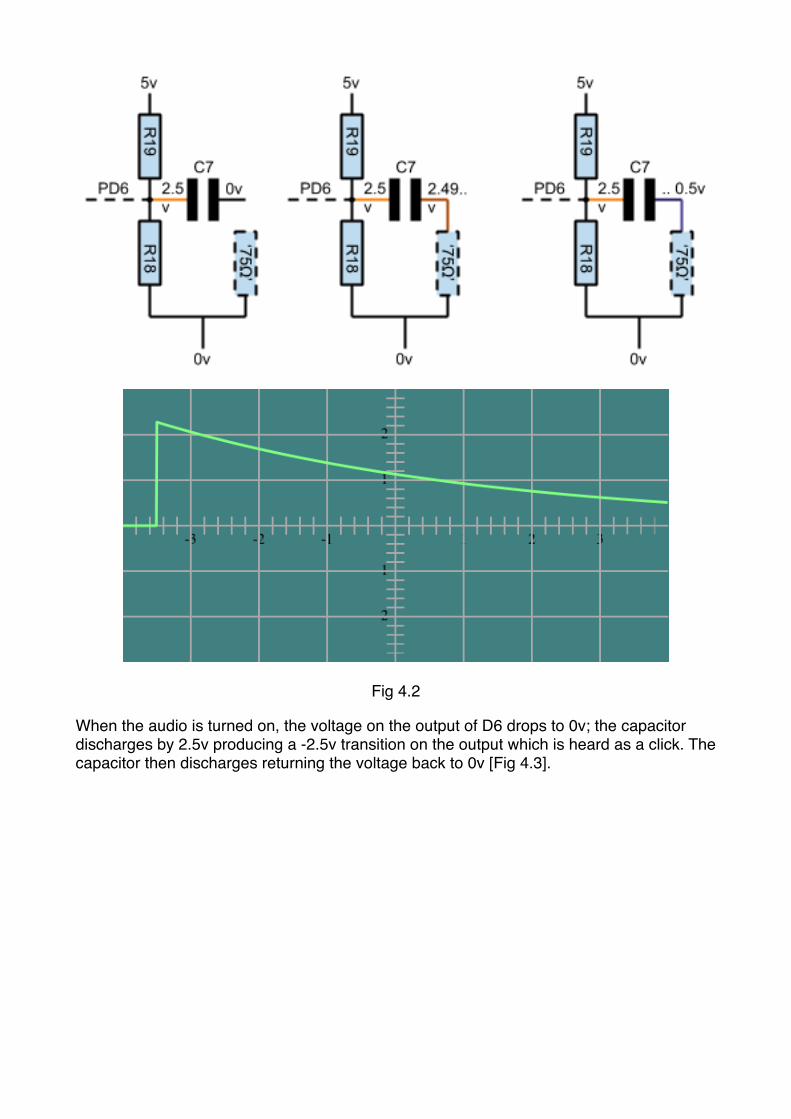
Fig 4.2
When the audio is turned on, the voltage on the output of D6 drops to 0v; the capacitor discharges by 2.5v producing a -2.5v transition on the output which is heard as a click. The capacitor then discharges returning the voltage back to 0v [Fig 4.3].
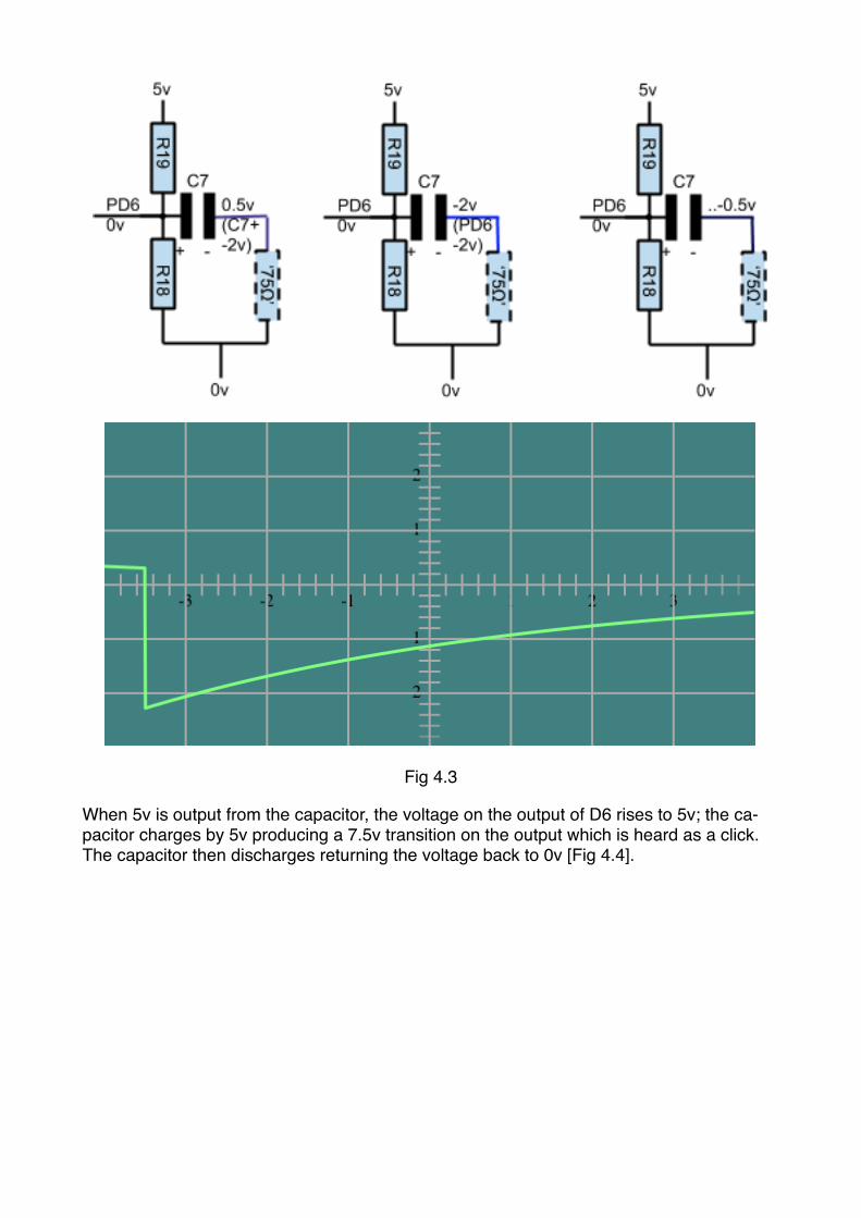
Fig 4.3
When 5v is output from the capacitor, the voltage on the output of D6 rises to 5v; the ca-pacitor charges by 5v producing a 7.5v transition on the output which is heard as a click. The capacitor then discharges returning the voltage back to 0v [Fig 4.4].
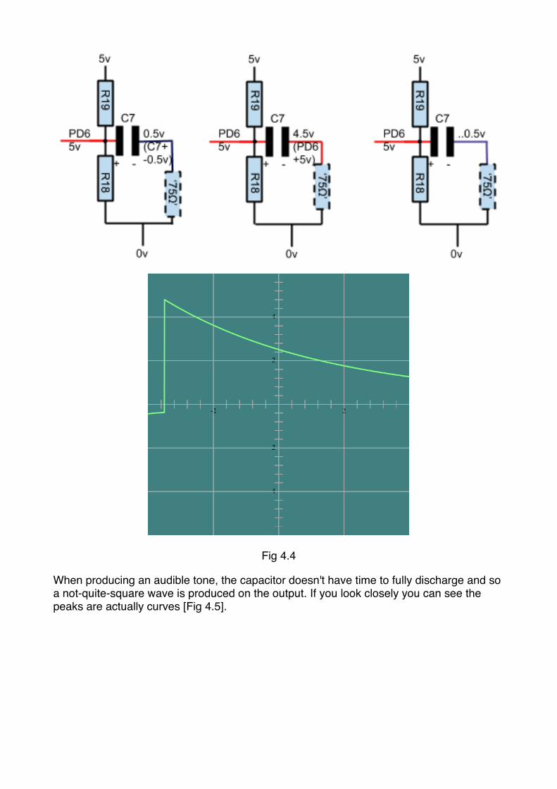
Fig 4.4
When producing an audible tone, the capacitor doesn't have time to fully discharge and so a not-quite-square wave is produced on the output. If you look closely you can see the peaks are actually curves [Fig 4.5].
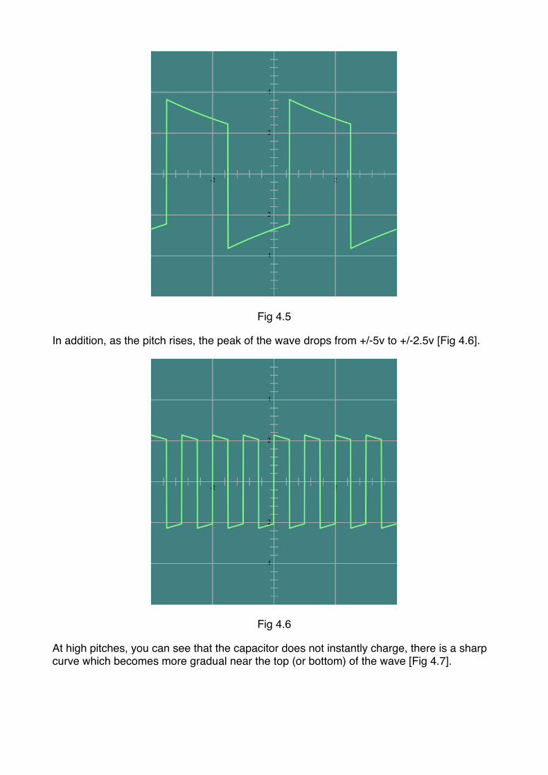
Fig 4.5
In addition, as the pitch rises, the peak of the wave drops from +/-5v to +/-2.5v [Fig 4.6].
Fig 4.6
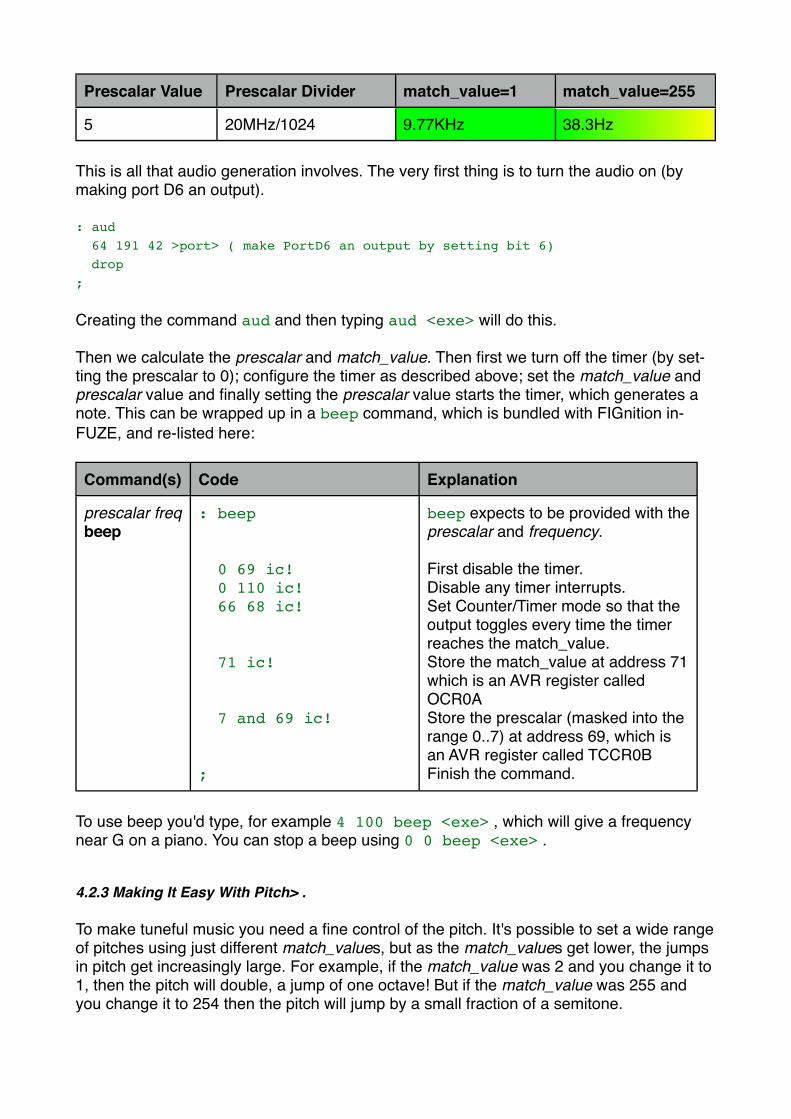
At high pitches, you can see that the capacitor does not instantly charge, there is a sharp curve which becomes more gradual near the top (or bottom) of the wave [Fig 4.7].
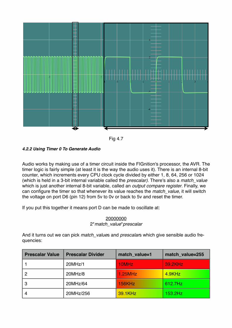
Fig 4.7
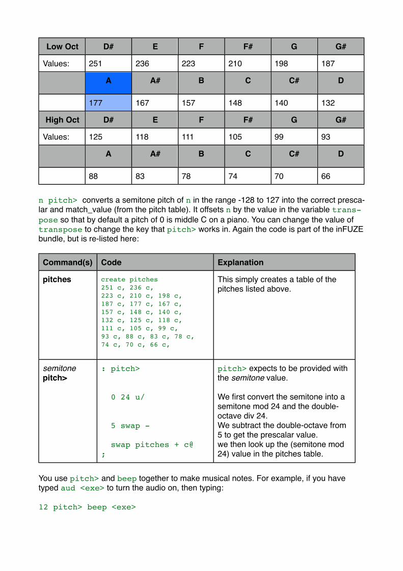
4.2.2 Using Timer 0 To Generate Audio
Audio works by making use of a timer circuit inside the FIGnition's processor, the AVR. The timer logic is fairly simple (at least it is the way the audio uses it). There is an internal 8-bit counter, which increments every CPU clock cycle divided by either 1, 8, 64, 256 or 1024 (which is held in a 3-bit internal variable called the prescalar). There's also a match_value which is just another internal 8-bit variable, called an output compare register. Finally, we can configure the timer so that whenever its value reaches the match_value, it will switch the voltage on port D6 (pin 12) from 5v to 0v or back to 5v and reset the timer.
If you put this together it means port D can be made to oscillate at:
200000002*match_value*prescalar
And it turns out we can pick match_values and prescalars which give sensible audio fre-quencies:
Prescalar Value Prescalar Divider match_value=1 match_value=255
1 20MHz/1 10MHz 39.2KHz
2 20MHz/8 1.25MHz 4.9KHz
3 20MHz/64 156KHz 612.7Hz
4 20MHz/256 39.1KHz 153.2Hz
Prescalar Value Prescalar Divider match_value=1 match_value=255
5 20MHz/1024 9.77KHz 38.3Hz
This is all that audio generation involves. The very first thing is to turn the audio on (by making port D6 an output).
: aud 64 191 42 >port> ( make PortD6 an output by setting bit 6) drop;
Creating the command aud and then typing aud <exe> will do this.
Then we calculate the prescalar and match_value. Then first we turn off the timer (by set-ting the prescalar to 0); configure the timer as described above; set the match_value and prescalar value and finally setting the prescalar value starts the timer, which generates a note. This can be wrapped up in a beep command, which is bundled with FIGnition in-FUZE, and re-listed here:
Command(s) Code Explanation
prescalar freq beep
: beep
0 69 ic! 0 110 ic! 66 68 ic!
71 ic!
7 and 69 ic!
;
beep expects to be provided with the prescalar and frequency.
First disable the timer.Disable any timer interrupts.Set Counter/Timer mode so that the output toggles every time the timer reaches the match_value.Store the match_value at address 71 which is an AVR register called OCR0AStore the prescalar (masked into the range 0..7) at address 69, which is an AVR register called TCCR0BFinish the command.
To use beep you'd type, for example 4 100 beep <exe> , which will give a frequency near G on a piano. You can stop a beep using 0 0 beep <exe> .
4.2.3 Making It Easy With Pitch> .
To make tuneful music you need a fine control of the pitch. It's possible to set a wide range of pitches using just different match_values, but as the match_values get lower, the jumps in pitch get increasingly large. For example, if the match_value was 2 and you change it to 1, then the pitch will double, a jump of one octave! But if the match_value was 255 and you change it to 254 then the pitch will jump by a small fraction of a semitone.

For tuneful music we therefore need to use large match_values. It turns out we can create a useful range of about 2 octaves from match_values of about 64 to 255, and because the prescalar shifts by 2 octaves at a time, we can obtain a continual musical range of about 8 octaves. The frequency calculations are given in the AVR datasheet as:
The standard concert pitch is A440, which is at 440Hz, so we need to find N and OCRnx to match that: N.(1+OCR0A) = fclk/fOC0A , which is 20x106/440 = 45,454, which means that N (the prescalar value) must be about 256 so that OCRnx is <256. If N is 256, then OCR0A will be 88. Higher pitches are lower values, by successively dividing by 2(1/12). Similarly, lower pitches are higher values, by successively multiplying by 2(1/12). This gives the following pitch table:
Low Oct D# E F F# G G#
Values: 251 236 223 210 198 187
A A# B C C# D
177 167 157 148 140 132
High Oct D# E F F# G G#
Values: 125 118 111 105 99 93
A A# B C C# D
88 83 78 74 70 66
n pitch> converts a semitone pitch of n in the range -128 to 127 into the correct presca-lar and match_value (from the pitch table). It offsets n by the value in the variable trans-pose so that by default a pitch of 0 is middle C on a piano. You can change the value of transpose to change the key that pitch> works in. Again the code is part of the inFUZE bundle, but is re-listed here:
Command(s) Code Explanation
pitches create pitches251 c, 236 c,223 c, 210 c, 198 c,187 c, 177 c, 167 c,157 c, 148 c, 140 c,132 c, 125 c, 118 c,111 c, 105 c, 99 c,93 c, 88 c, 83 c, 78 c,74 c, 70 c, 66 c,
This simply creates a table of the pitches listed above.
semitone pitch>
: pitch>
0 24 u/
5 swap -
swap pitches + c@;
pitch> expects to be provided with the semitone value.
We first convert the semitone into a semitone mod 24 and the double-octave div 24.We subtract the double-octave from 5 to get the prescalar value.we then look up the (semitone mod 24) value in the pitches table.
You use pitch> and beep together to make musical notes. For example, if you have typed aud <exe> to turn the audio on, then typing:
12 pitch> beep <exe>
Will play the C above middle 'C'. Type 0 0 beep <exe> to end it.
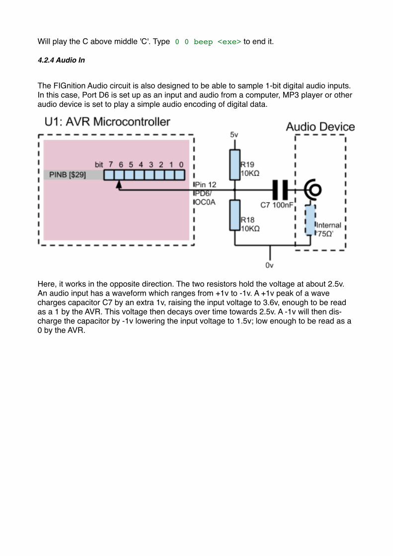
4.2.4 Audio In
The FIGnition Audio circuit is also designed to be able to sample 1-bit digital audio inputs. In this case, Port D6 is set up as an input and audio from a computer, MP3 player or other audio device is set to play a simple audio encoding of digital data.
Here, it works in the opposite direction. The two resistors hold the voltage at about 2.5v. An audio input has a waveform which ranges from +1v to -1v. A +1v peak of a wave charges capacitor C7 by an extra 1v, raising the input voltage to 3.6v, enough to be read as a 1 by the AVR. This voltage then decays over time towards 2.5v. A -1v will then dis-charge the capacitor by -1v lowering the input voltage to 1.5v; low enough to be read as a 0 by the AVR.
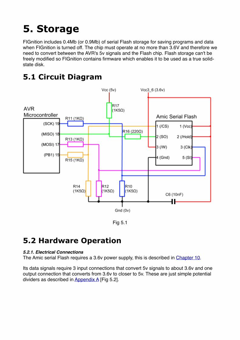
5. StorageFIGnition includes 0.4Mb (or 0.9Mb) of serial Flash storage for saving programs and data when FIGnition is turned off. The chip must operate at no more than 3.6V and therefore we need to convert between the AVR's 5v signals and the Flash chip. Flash storage can't be freely modified so FIGnition contains firmware which enables it to be used as a true solid-state disk.
5.1 Circuit Diagram
Fig 5.1
5.2 Hardware Operation5.2.1. Electrical ConnectionsThe Amic serial Flash requires a 3.6v power supply, this is described in Chapter 10.
Its data signals require 3 input connections that convert 5v signals to about 3.6v and one output connection that converts from 3.6v to closer to 5v. These are just simple potential dividers as described in Appendix A [Fig 5.2].
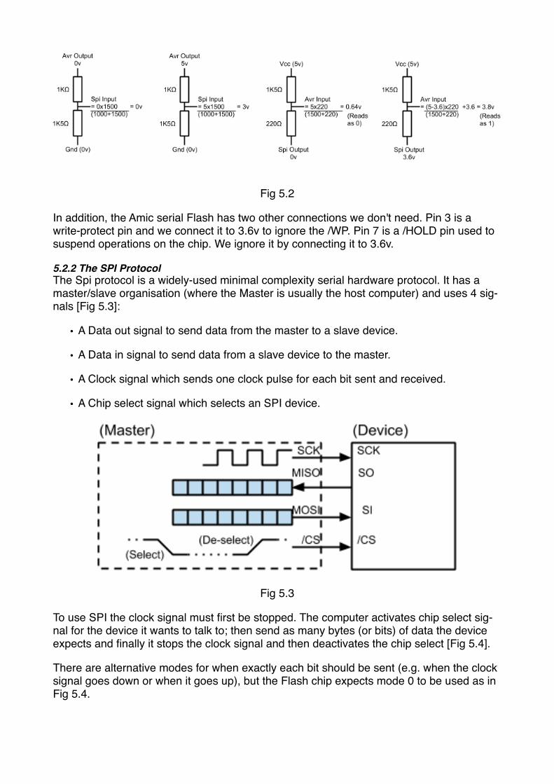
Fig 5.2
In addition, the Amic serial Flash has two other connections we don't need. Pin 3 is a write-protect pin and we connect it to 3.6v to ignore the /WP. Pin 7 is a /HOLD pin used to suspend operations on the chip. We ignore it by connecting it to 3.6v.
5.2.2 The SPI ProtocolThe Spi protocol is a widely-used minimal complexity serial hardware protocol. It has a master/slave organisation (where the Master is usually the host computer) and uses 4 sig-nals [Fig 5.3]:
• A Data out signal to send data from the master to a slave device.
• A Data in signal to send data from a slave device to the master.
• A Clock signal which sends one clock pulse for each bit sent and received.
• A Chip select signal which selects an SPI device.
Fig 5.3
To use SPI the clock signal must first be stopped. The computer activates chip select sig-nal for the device it wants to talk to; then send as many bytes (or bits) of data the device expects and finally it stops the clock signal and then deactivates the chip select [Fig 5.4].
There are alternative modes for when exactly each bit should be sent (e.g. when the clock signal goes down or when it goes up), but the Flash chip expects mode 0 to be used as in Fig 5.4.
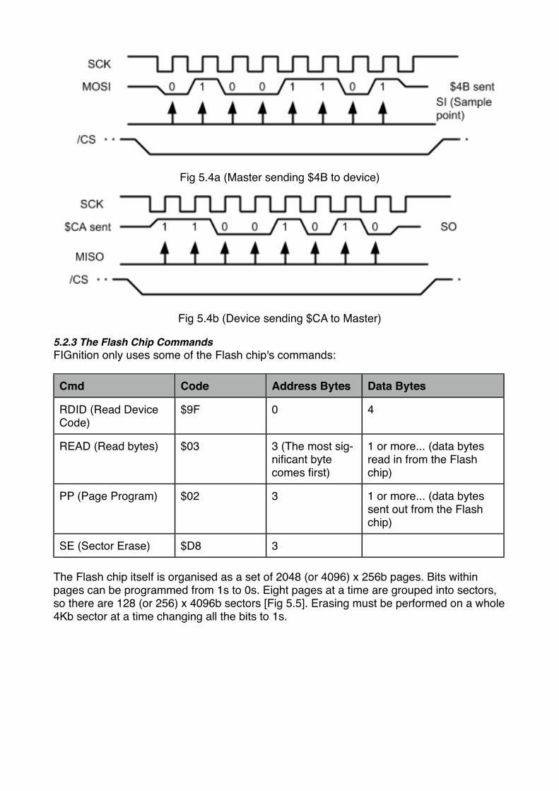
Fig 5.4a (Master sending $4B to device)
Fig 5.4b (Device sending $CA to Master)
5.2.3 The Flash Chip CommandsFIGnition only uses some of the Flash chip's commands:
Cmd Code Address Bytes Data Bytes
RDID (Read Device Code)
$9F 0 4
READ (Read bytes) $03 3 (The most sig-nificant byte comes first)
1 or more... (data bytes read in from the Flash chip)
PP (Page Program) $02 3 1 or more... (data bytes sent out from the Flash chip)
SE (Sector Erase) $D8 3
The Flash chip itself is organised as a set of 2048 (or 4096) x 256b pages. Bits within pages can be programmed from 1s to 0s. Eight pages at a time are grouped into sectors, so there are 128 (or 256) x 4096b sectors [Fig 5.5]. Erasing must be performed on a whole 4Kb sector at a time changing all the bits to 1s.
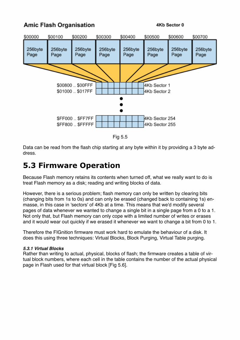
Fig 5.5
Data can be read from the flash chip starting at any byte within it by providing a 3 byte ad-dress.
5.3 Firmware OperationBecause Flash memory retains its contents when turned off, what we really want to do is treat Flash memory as a disk; reading and writing blocks of data.
However, there is a serious problem; flash memory can only be written by clearing bits (changing bits from 1s to 0s) and can only be erased (changed back to containing 1s) en-masse, in this case in 'sectors' of 4Kb at a time. This means that we'd modify several pages of data whenever we wanted to change a single bit in a single page from a 0 to a 1. Not only that, but Flash memory can only cope with a limited number of writes or erases and it would wear out quickly if we erased it whenever we want to change a bit from 0 to 1.
Therefore the FIGnition firmware must work hard to emulate the behaviour of a disk. It does this using three techniques: Virtual Blocks, Block Purging, Virtual Table purging.
5.3.1 Virtual BlocksRather than writing to actual, physical, blocks of flash; the firmware creates a table of vir-tual block numbers, where each cell in the table contains the number of the actual physical page in Flash used for that virtual block [Fig 5.6].
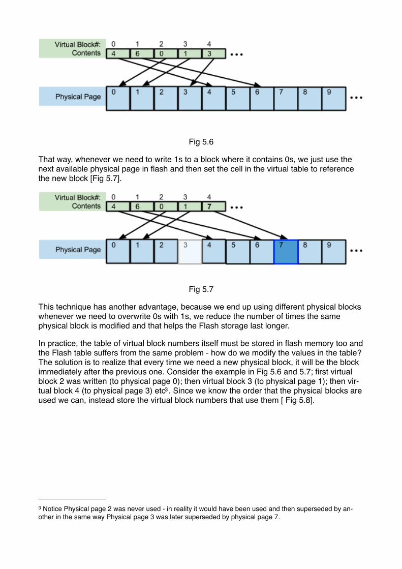
Fig 5.6
That way, whenever we need to write 1s to a block where it contains 0s, we just use the next available physical page in flash and then set the cell in the virtual table to reference the new block [Fig 5.7].
Fig 5.7
This technique has another advantage, because we end up using different physical blocks whenever we need to overwrite 0s with 1s, we reduce the number of times the same physical block is modified and that helps the Flash storage last longer.
In practice, the table of virtual block numbers itself must be stored in flash memory too and the Flash table suffers from the same problem - how do we modify the values in the table? The solution is to realize that every time we need a new physical block, it will be the block immediately after the previous one. Consider the example in Fig 5.6 and 5.7; first virtual block 2 was written (to physical page 0); then virtual block 3 (to physical page 1); then vir-tual block 4 (to physical page 3) etc3. Since we know the order that the physical blocks are used we can, instead store the virtual block numbers that use them [ Fig 5.8].
3 Notice Physical page 2 was never used - in reality it would have been used and then superseded by an-other in the same way Physical page 3 was later superseded by physical page 7.
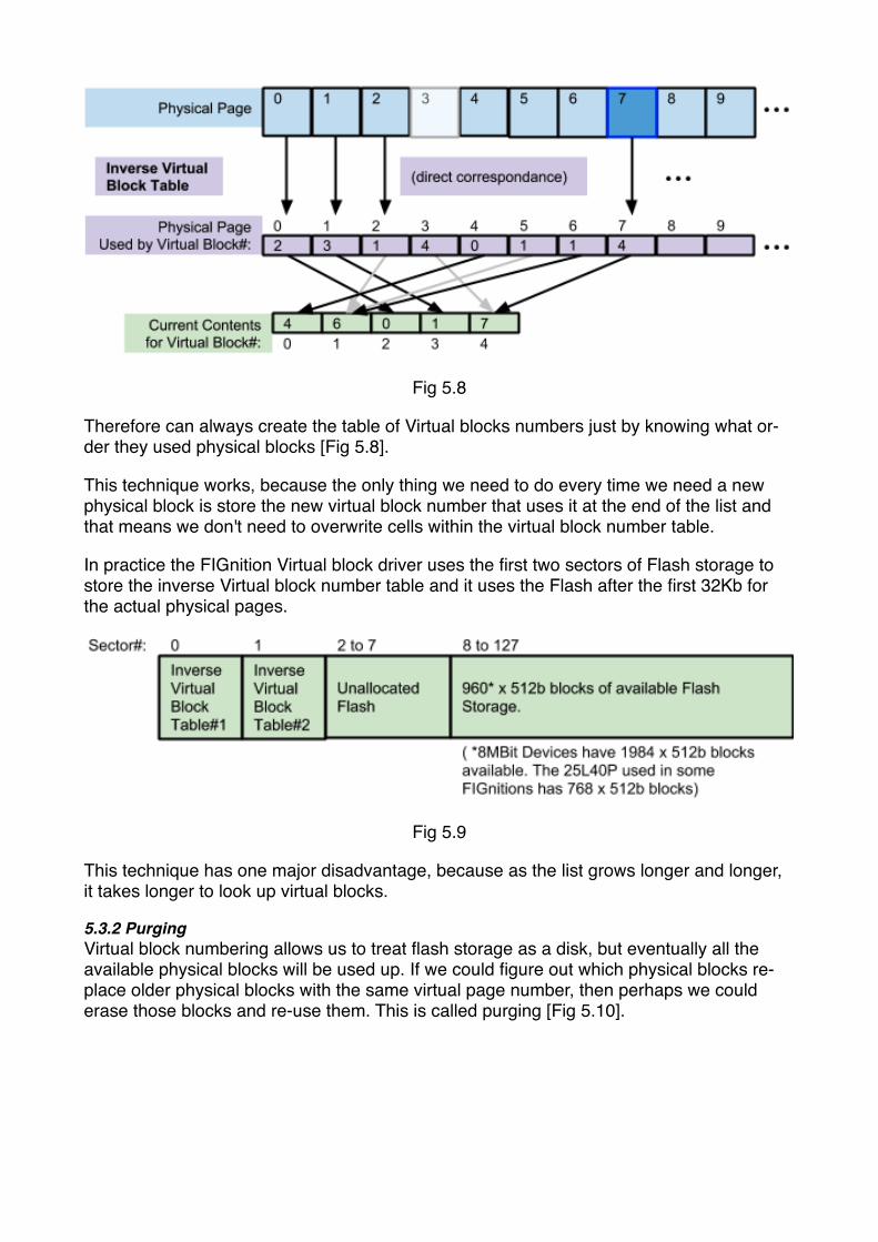
Fig 5.8
Therefore can always create the table of Virtual blocks numbers just by knowing what or-der they used physical blocks [Fig 5.8].
This technique works, because the only thing we need to do every time we need a new physical block is store the new virtual block number that uses it at the end of the list and that means we don't need to overwrite cells within the virtual block number table.
In practice the FIGnition Virtual block driver uses the first two sectors of Flash storage to store the inverse Virtual block number table and it uses the Flash after the first 32Kb for the actual physical pages.
Fig 5.9
This technique has one major disadvantage, because as the list grows longer and longer, it takes longer to look up virtual blocks.
5.3.2 PurgingVirtual block numbering allows us to treat flash storage as a disk, but eventually all the available physical blocks will be used up. If we could figure out which physical blocks re-place older physical blocks with the same virtual page number, then perhaps we could erase those blocks and re-use them. This is called purging [Fig 5.10].
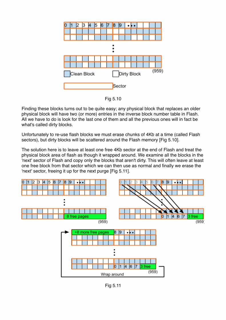
Fig 5.10
Finding these blocks turns out to be quite easy; any physical block that replaces an older physical block will have two (or more) entries in the inverse block number table in Flash. All we have to do is look for the last one of them and all the previous ones will in fact be what's called dirty blocks.
Unfortunately to re-use flash blocks we must erase chunks of 4Kb at a time (called Flash sectors), but dirty blocks will be scattered around the Flash memory [Fig 5.10].
The solution here is to leave at least one free 4Kb sector at the end of Flash and treat the physical block area of flash as though it wrapped around. We examine all the blocks in the 'next' sector of Flash and copy only the blocks that aren't dirty. This will often leave at least one free block from that sector which we can then use as normal and finally we erase the 'next' sector, freeing it up for the next purge [Fig 5.11].
Fig 5.11
If it turns out there weren't any dirty blocks in that 'next' sector we just repeat the process until we purge a sector with dirty blocks. This will be the case in Fig 5.11 when purging reaches the third from the last Sector (sector 125).
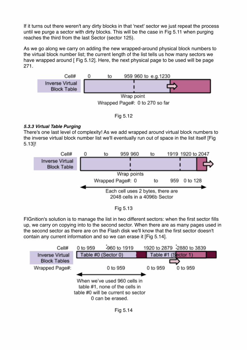
As we go along we carry on adding the new wrapped-around physical block numbers to the virtual block number list; the current length of the list tells us how many sectors we have wrapped around [ Fig 5.12]. Here, the next physical page to be used will be page 271.
Fig 5.12
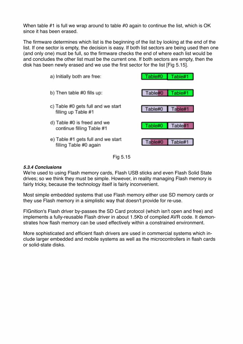
5.3.3 Virtual Table PurgingThere's one last level of complexity! As we add wrapped around virtual block numbers to the inverse virtual block number list we'll eventually run out of space in the list itself [Fig 5.13]!
Fig 5.13
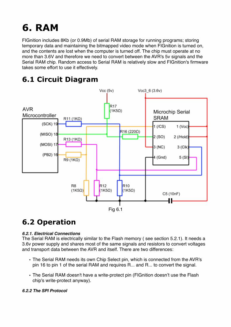
FIGnition's solution is to manage the list in two different sectors: when the first sector fills up, we carry on copying into to the second sector. When there are as many pages used in the second sector as there are on the Flash disk we'll know that the first sector doesn't contain any current information and so we can erase it [Fig 5.14].
Fig 5.14
When table #1 is full we wrap around to table #0 again to continue the list, which is OK since it has been erased.
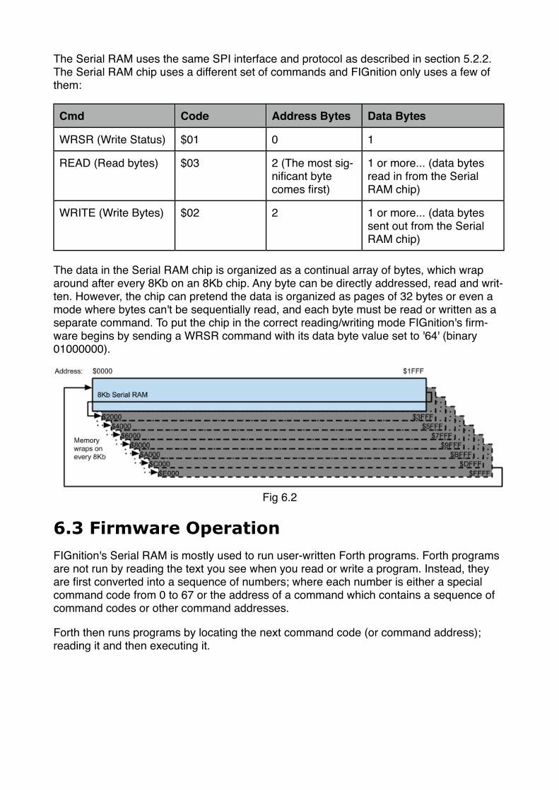
The firmware determines which list is the beginning of the list by looking at the end of the list. If one sector is empty, the decision is easy. If both list sectors are being used then one (and only one) must be full, so the firmware checks the end of where each list would be and concludes the other list must be the current one. If both sectors are empty, then the disk has been newly erased and we use the first sector for the list [Fig 5.15].
Fig 5.15
5.3.4 ConclusionsWe're used to using Flash memory cards, Flash USB sticks and even Flash Solid State drives; so we think they must be simple. However, in reality managing Flash memory is fairly tricky, because the technology itself is fairly inconvenient.
Most simple embedded systems that use Flash memory either use SD memory cards or they use Flash memory in a simplistic way that doesn't provide for re-use.
FIGnition's Flash driver by-passes the SD Card protocol (which isn't open and free) and implements a fully-reusable Flash driver in about 1.5Kb of compiled AVR code. It demon-strates how flash memory can be used effectively within a constrained environment.
More sophisticated and efficient flash drivers are used in commercial systems which in-clude larger embedded and mobile systems as well as the microcontrollers in flash cards or solid-state disks.
6. RAMFIGnition includes 8Kb (or 0.9Mb) of serial RAM storage for running programs; storing temporary data and maintaining the bitmapped video mode when FIGnition is turned on, and the contents are lost when the computer is turned off. The chip must operate at no more than 3.6V and therefore we need to convert between the AVR's 5v signals and the Serial RAM chip. Random access to Serial RAM is relatively slow and FIGnition's firmware takes some effort to use it effectively.
6.1 Circuit Diagram
Fig 6.1
6.2 Operation6.2.1. Electrical ConnectionsThe Serial RAM is electrically similar to the Flash memory ( see section 5.2.1). It needs a 3.6v power supply and shares most of the same signals and resistors to convert voltages and transport data between the AVR and itself. There are two differences:
• The Serial RAM needs its own Chip Select pin, which is connected from the AVR's pin 16 to pin 1 of the serial RAM and requires R... and R... to convert the signal.
• The Serial RAM doesn't have a write-protect pin (FIGnition doesn’t use the Flash chip's write-protect anyway).
6.2.2 The SPI Protocol
The Serial RAM uses the same SPI interface and protocol as described in section 5.2.2. The Serial RAM chip uses a different set of commands and FIGnition only uses a few of them:
Cmd Code Address Bytes Data Bytes
WRSR (Write Status) $01 0 1
READ (Read bytes) $03 2 (The most sig-nificant byte comes first)
1 or more... (data bytes read in from the Serial RAM chip)
WRITE (Write Bytes) $02 2 1 or more... (data bytes sent out from the Serial RAM chip)
The data in the Serial RAM chip is organized as a continual array of bytes, which wrap around after every 8Kb on an 8Kb chip. Any byte can be directly addressed, read and writ-ten. However, the chip can pretend the data is organized as pages of 32 bytes or even a mode where bytes can't be sequentially read, and each byte must be read or written as a separate command. To put the chip in the correct reading/writing mode FIGnition's firm-ware begins by sending a WRSR command with its data byte value set to '64' (binary 01000000).
Fig 6.2
6.3 Firmware OperationFIGnition's Serial RAM is mostly used to run user-written Forth programs. Forth programs are not run by reading the text you see when you read or write a program. Instead, they are first converted into a sequence of numbers; where each number is either a special command code from 0 to 67 or the address of a command which contains a sequence of command codes or other command addresses.
Forth then runs programs by locating the next command code (or command address); reading it and then executing it.
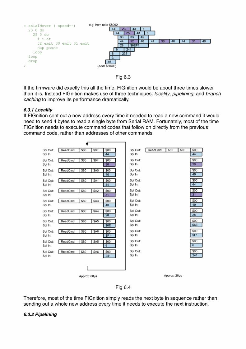
Fig 6.3
If the firmware did exactly this all the time, FIGnition would be about three times slower than it is. Instead FIGnition makes use of three techniques: locality, pipelining, and branch caching to improve its performance dramatically.
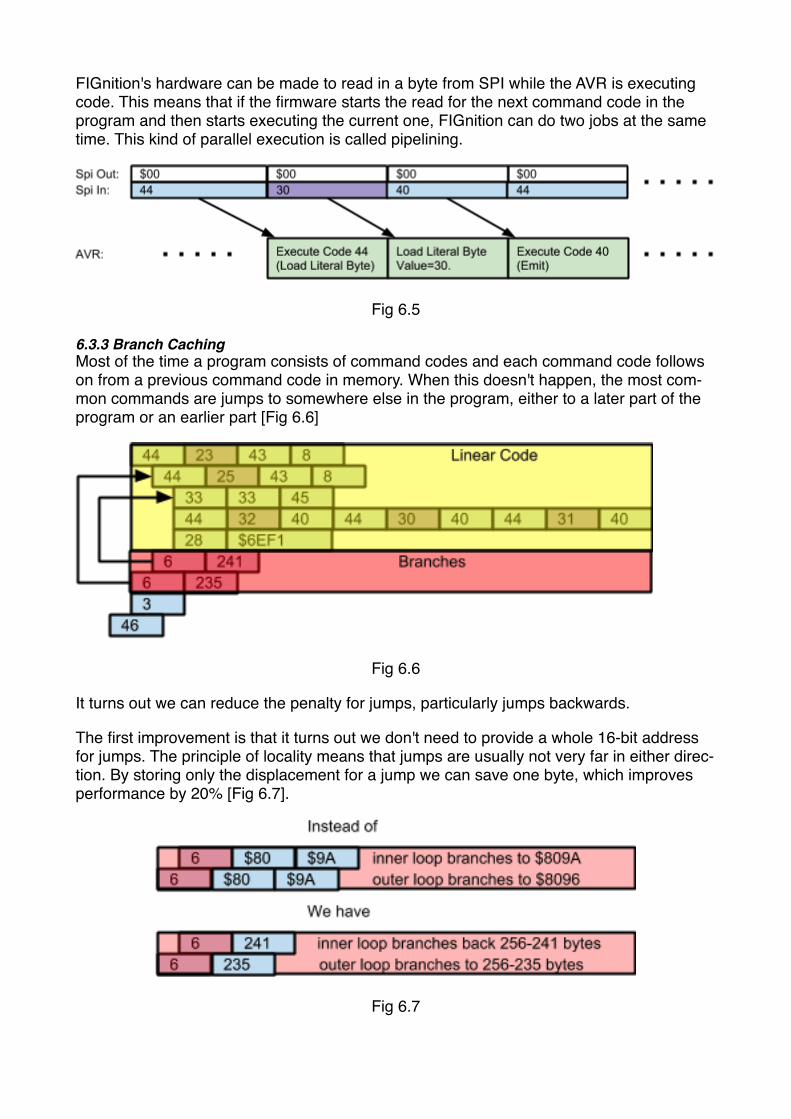
6.3.1 LocalityIf FIGnition sent out a new address every time it needed to read a new command it would need to send 4 bytes to read a single byte from Serial RAM. Fortunately, most of the time FIGnition needs to execute command codes that follow on directly from the previous command code, rather than addresses of other commands.
Fig 6.4
Therefore, most of the time FIGnition simply reads the next byte in sequence rather than sending out a whole new address every time it needs to execute the next instruction.
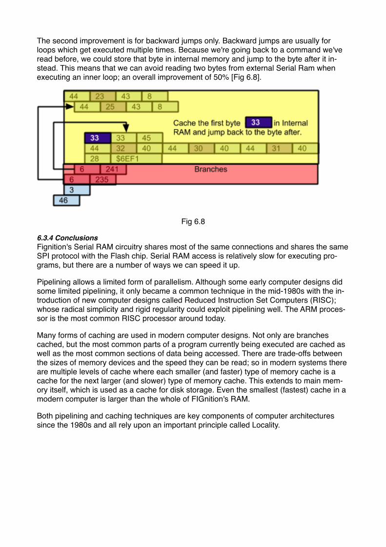
6.3.2 Pipelining
FIGnition's hardware can be made to read in a byte from SPI while the AVR is executing code. This means that if the firmware starts the read for the next command code in the program and then starts executing the current one, FIGnition can do two jobs at the same time. This kind of parallel execution is called pipelining.
Fig 6.5
6.3.3 Branch CachingMost of the time a program consists of command codes and each command code follows on from a previous command code in memory. When this doesn't happen, the most com-mon commands are jumps to somewhere else in the program, either to a later part of the program or an earlier part [Fig 6.6]
Fig 6.6
It turns out we can reduce the penalty for jumps, particularly jumps backwards.
The first improvement is that it turns out we don't need to provide a whole 16-bit address for jumps. The principle of locality means that jumps are usually not very far in either direc-tion. By storing only the displacement for a jump we can save one byte, which improves performance by 20% [Fig 6.7].
Fig 6.7
The second improvement is for backward jumps only. Backward jumps are usually for loops which get executed multiple times. Because we're going back to a command we've read before, we could store that byte in internal memory and jump to the byte after it in-stead. This means that we can avoid reading two bytes from external Serial Ram when executing an inner loop; an overall improvement of 50% [Fig 6.8].
Fig 6.8
6.3.4 ConclusionsFignition's Serial RAM circuitry shares most of the same connections and shares the same SPI protocol with the Flash chip. Serial RAM access is relatively slow for executing pro-grams, but there are a number of ways we can speed it up.
Pipelining allows a limited form of parallelism. Although some early computer designs did some limited pipelining, it only became a common technique in the mid-1980s with the in-troduction of new computer designs called Reduced Instruction Set Computers (RISC); whose radical simplicity and rigid regularity could exploit pipelining well. The ARM proces-sor is the most common RISC processor around today.
Many forms of caching are used in modern computer designs. Not only are branches cached, but the most common parts of a program currently being executed are cached as well as the most common sections of data being accessed. There are trade-offs between the sizes of memory devices and the speed they can be read; so in modern systems there are multiple levels of cache where each smaller (and faster) type of memory cache is a cache for the next larger (and slower) type of memory cache. This extends to main mem-ory itself, which is used as a cache for disk storage. Even the smallest (fastest) cache in a modern computer is larger than the whole of FIGnition's RAM.
Both pipelining and caching techniques are key components of computer architectures since the 1980s and all rely upon an important principle called Locality.
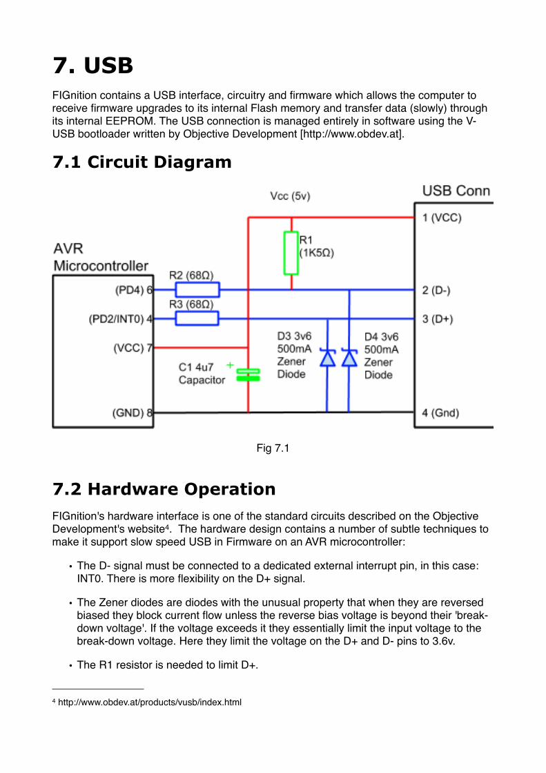
7. USBFIGnition contains a USB interface, circuitry and firmware which allows the computer to receive firmware upgrades to its internal Flash memory and transfer data (slowly) through its internal EEPROM. The USB connection is managed entirely in software using the V-USB bootloader written by Objective Development [http://www.obdev.at].
7.1 Circuit Diagram
Fig 7.1
7.2 Hardware OperationFIGnition's hardware interface is one of the standard circuits described on the Objective Development's website4. The hardware design contains a number of subtle techniques to make it support slow speed USB in Firmware on an AVR microcontroller:
• The D- signal must be connected to a dedicated external interrupt pin, in this case: INT0. There is more flexibility on the D+ signal.
• The Zener diodes are diodes with the unusual property that when they are reversed biased they block current flow unless the reverse bias voltage is beyond their 'break-down voltage'. If the voltage exceeds it they essentially limit the input voltage to the break-down voltage. Here they limit the voltage on the D+ and D- pins to 3.6v.
• The R1 resistor is needed to limit D+.
4 http://www.obdev.at/products/vusb/index.html
• The small resistors R2 and R3 limit the current flow to PD4 and PD2, because the current flow on these signals may still be higher than most of FIGnition's signals, high current rated resistors are needed for R2 and R3.
• The C1 capacitor is the main decoupling capacitor for the whole computer, which is why it's the largest capacitor in FIGnition.
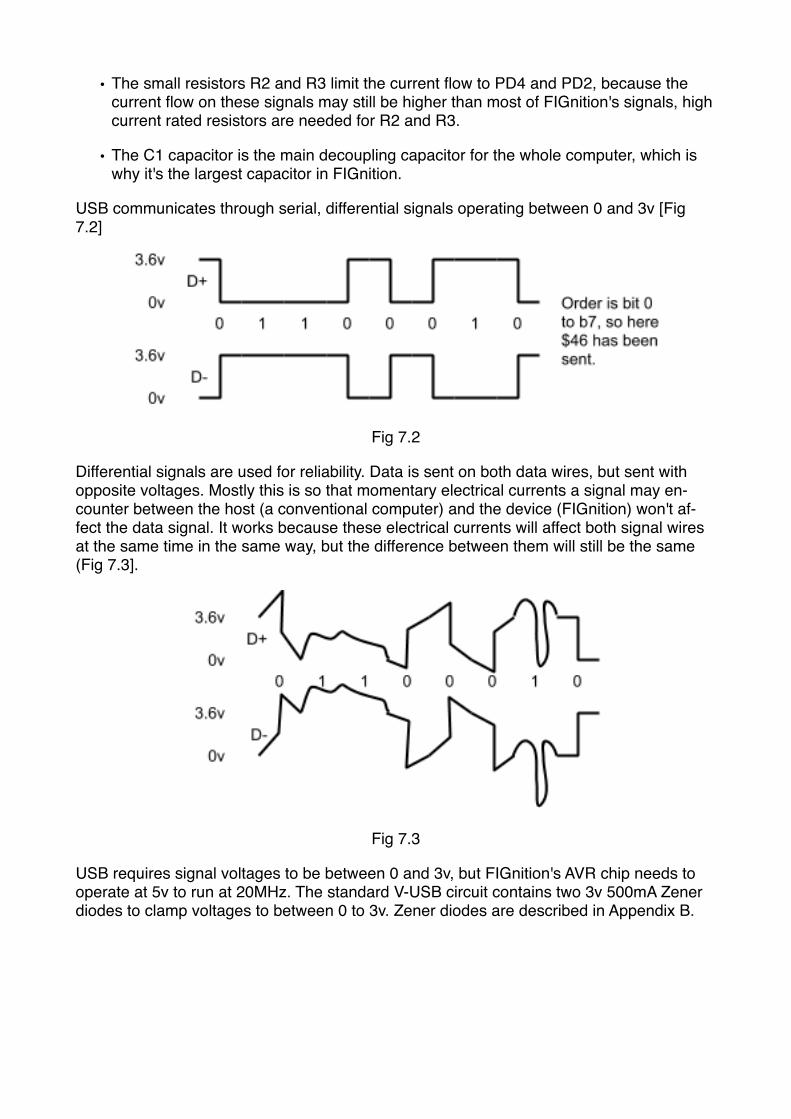
USB communicates through serial, differential signals operating between 0 and 3v [Fig 7.2]
Fig 7.2
Differential signals are used for reliability. Data is sent on both data wires, but sent with opposite voltages. Mostly this is so that momentary electrical currents a signal may en-counter between the host (a conventional computer) and the device (FIGnition) won't af-fect the data signal. It works because these electrical currents will affect both signal wires at the same time in the same way, but the difference between them will still be the same (Fig 7.3].
Fig 7.3
USB requires signal voltages to be between 0 and 3v, but FIGnition's AVR chip needs to operate at 5v to run at 20MHz. The standard V-USB circuit contains two 3v 500mA Zener diodes to clamp voltages to between 0 to 3v. Zener diodes are described in Appendix B.
7.3 Firmware OperationThe V-USB firmware is described well on the Objective Development's website5. Here we cover just a few important points.
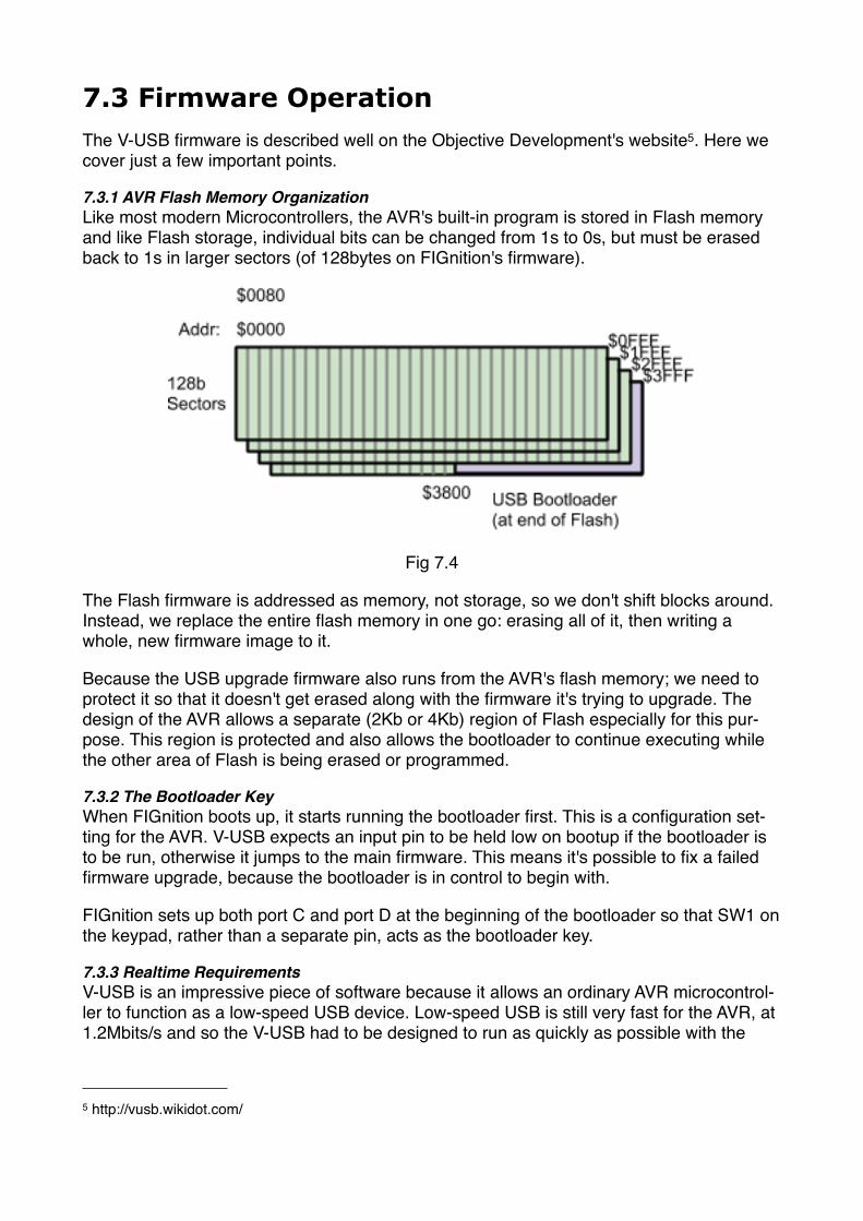
7.3.1 AVR Flash Memory OrganizationLike most modern Microcontrollers, the AVR's built-in program is stored in Flash memory and like Flash storage, individual bits can be changed from 1s to 0s, but must be erased back to 1s in larger sectors (of 128bytes on FIGnition's firmware).
Fig 7.4
The Flash firmware is addressed as memory, not storage, so we don't shift blocks around. Instead, we replace the entire flash memory in one go: erasing all of it, then writing a whole, new firmware image to it.
Because the USB upgrade firmware also runs from the AVR's flash memory; we need to protect it so that it doesn't get erased along with the firmware it's trying to upgrade. The design of the AVR allows a separate (2Kb or 4Kb) region of Flash especially for this pur-pose. This region is protected and also allows the bootloader to continue executing while the other area of Flash is being erased or programmed.
7.3.2 The Bootloader KeyWhen FIGnition boots up, it starts running the bootloader first. This is a configuration set-ting for the AVR. V-USB expects an input pin to be held low on bootup if the bootloader is to be run, otherwise it jumps to the main firmware. This means it's possible to fix a failed firmware upgrade, because the bootloader is in control to begin with.
FIGnition sets up both port C and port D at the beginning of the bootloader so that SW1 on the keypad, rather than a separate pin, acts as the bootloader key.
7.3.3 Realtime RequirementsV-USB is an impressive piece of software because it allows an ordinary AVR microcontrol-ler to function as a low-speed USB device. Low-speed USB is still very fast for the AVR, at 1.2Mbits/s and so the V-USB had to be designed to run as quickly as possible with the
5 http://vusb.wikidot.com/

core routines written in assembler and making use of a number of smart techniques to achieve the required performance.
7.3.4 Chicken And EggIf FIGnition uses V-USB to load its firmware, how was V-USB programmed into a FIGnition in the first place? The answer is to use a different technique: an In-Circuit-System-Programmer (ICSP) to program the bootloader.
FIGnition's ICSP was a home-brew programmer. After FIGnition was development it was possible to use a FIGnition itself as an In-Circuit-System-Programmer to program new, blank AVR chips complete with a firmware and a bootloader.
7.3.5 LicensingUSB is a data transfer protocol; a set of rules for transferring data over a medium, in this case a shielded cable with differential +/- 3.6v signals.
In this sense it's like pen and paper or talking on a phone, except that you have to pay the USB consortium for the right to choose what you want to say. V-USB too is licensed and FIGnition is allowed to use it by kind permission from Objective Development, because it changes nothing in the USB implementation, on condition that Objective Development is credited.
Licensing limits the kind of data transfer FIGnition can support for free. It's not permissible for FIGnition to transfer programs to and from serial RAM; to treat the serial Flash chip as an external drive or provide serial-over-USB unless licensing fees are paid per FIGnition sold and for the vendor (nichemachines) and device IDs themselves.
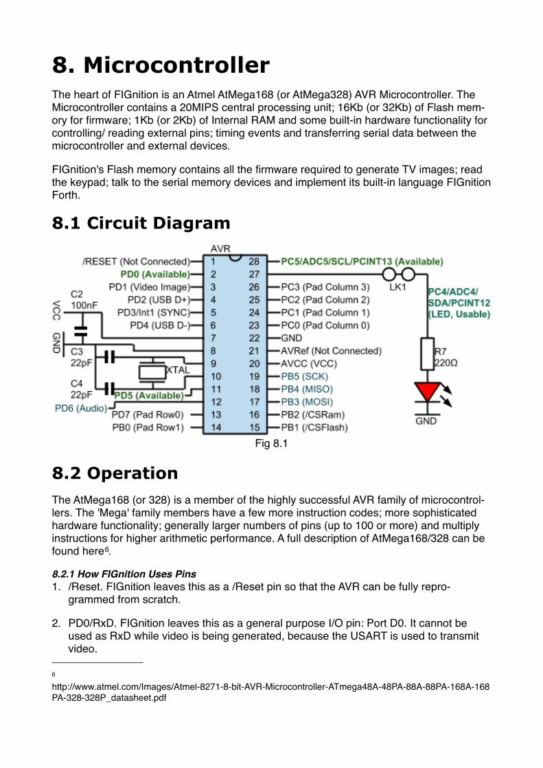
8. MicrocontrollerThe heart of FIGnition is an Atmel AtMega168 (or AtMega328) AVR Microcontroller. The Microcontroller contains a 20MIPS central processing unit; 16Kb (or 32Kb) of Flash mem-ory for firmware; 1Kb (or 2Kb) of Internal RAM and some built-in hardware functionality for controlling/ reading external pins; timing events and transferring serial data between the microcontroller and external devices.
FIGnition's Flash memory contains all the firmware required to generate TV images; read the keypad; talk to the serial memory devices and implement its built-in language FIGnition Forth.
8.1 Circuit Diagram
Fig 8.1
8.2 OperationThe AtMega168 (or 328) is a member of the highly successful AVR family of microcontrol-lers. The 'Mega' family members have a few more instruction codes; more sophisticated hardware functionality; generally larger numbers of pins (up to 100 or more) and multiply instructions for higher arithmetic performance. A full description of AtMega168/328 can be found here6.
8.2.1 How FIGnition Uses Pins1. /Reset. FIGnition leaves this as a /Reset pin so that the AVR can be fully repro-
grammed from scratch.
2. PD0/RxD. FIGnition leaves this as a general purpose I/O pin: Port D0. It cannot be used as RxD while video is being generated, because the USART is used to transmit video.
6 http://www.atmel.com/Images/Atmel-8271-8-bit-AVR-Microcontroller-ATmega48A-48PA-88A-88PA-168A-168PA-328-328P_datasheet.pdf

3. PD1/TxD. FIGnition enables this pin as the USART's TxD pins and transmits video pix-els through it. It can't be used as a general purpose IO pin unless video is turned off.
4. PD2/INT0. FIGnition's Bootloader uses this as the USB Interrupt pin.
5. PD3/INT1. This pin is used for video SYNC generation.
6. PD4. FIGnition's Bootloader uses this as the USB transmit pin.
7. This is always VCC.
8. This is always GND.
9. This is always a clock input pin. The only way to change this is to reprogram the AVR fuses using an ICSP.
10.This is always a clock input pin, like pin 9.
11.Port D5. This is free for user I/O.
12.Port D6/AIN0. This is used for audio.It can be used for other purposes to a limited de-gree (the audio circuitry may interfere with alternative applications).
13.Port D7.This is used as a Row select output for the top row of the keyboard. It can't be re-used unless the keyboard scanning is disabled.
14.Port B0. Is also used as a Row select output for the bottom row of the keyboard.
15.Port B1. This is used to select the serial Flash chip. It can be re-used to a limited de-gree if you remove the Flash IC, but the potential dividers may still interfere.
16.Port B2. This is used to select the serial Memory chip. It can't be re-used if you want to be able to program FIGnition in Forth.
17.Port B3. This is used in SPI mode. It can be used to drive other devices besides the serial Flash and SRAM using the spi driver in the Forth ROM.
18.Port B4. This is used in SPI mode and can be re-used as for Port B3.
19.Port B5. This is used in SPI mode and can be re-used as for Port B3.
20.AVCC. This is always VCC.
21.AREF. This is unused; you can use this if you want to measure an analog input (the logger program in the inFUZE bundle uses this pin).
22.GND. This is always GND.
23.PC0. This is used as a column select 0 input. It can't be re-used unless the keyboard scanning is disabled.
24.PC1. This is used as a column select 1 input. It can't be re-used unless the keyboard scanning is disabled.
25.PC2. This is used as a column select 2 input. It can't be re-used unless the keyboard scanning is disabled.
26.PC3. This is used as a column select 3 input. It can't be re-used unless the keyboard scanning is disabled.
27.PC4. This is used as the LED output. It can be fully re-used if the track between the pins of LK1 is cut. PC4 is part of the AVR's built-in I2C interface.
28.PC5. This pin is free.
Of all the pins on FIGnition's AVR chip, only Port D0, Port D3; Port D5 and Port C5 are generally available for I/O. Port C4 can be used if the LK1 track is cut. Port D6 may have some limited usage and some other I/O ports can be used with a corresponding loss of basic FIGnition functionality.
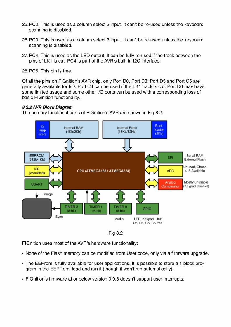
8.2.2 AVR Block DiagramThe primary functional parts of FIGnition's AVR are shown in Fig 8.2.
Fig 8.2
FIGnition uses most of the AVR's hardware functionality:
• None of the Flash memory can be modified from User code, only via a firmware upgrade.
• The EEProm is fully available for user applications. It is possible to store a 1 block pro-gram in the EEPRom; load and run it (though it won't run automatically).
• FIGnition's firmware at or below version 0.9.8 doesn't support user interrupts.
• Timer 0 is fully available for user applications and timer 1's OCRB and timer 2's OCRB registers can be used too (though the timer configurations themselves can't be changed without disrupting video).
• The analog comparator and the A/D circuitry can be used to a limited degree since AIN0 on pin has limited availability and the ADC channels 4 and 5 can be used.
• The I2C (also called TWI) unit can be used.
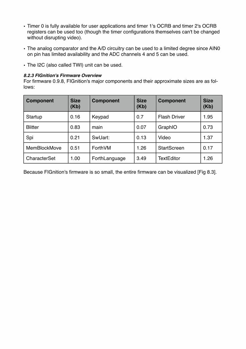
8.2.3 FIGnition's Firmware OverviewFor firmware 0.9.8, FIGnition's major components and their approximate sizes are as fol-lows:
Component Size (Kb)
Component Size (Kb)
Component Size (Kb)
Startup 0.16 Keypad 0.7 Flash Driver 1.95
Blitter 0.83 main 0.07 GraphIO 0.73
Spi 0.21 SwUart: 0.13 Video 1.37
MemBlockMove 0.51 ForthVM 1.26 StartScreen 0.17
CharacterSet 1.00 ForthLanguage 3.49 TextEditor 1.26
Because FIGnition's firmware is so small, the entire firmware can be visualized [Fig 8.3].
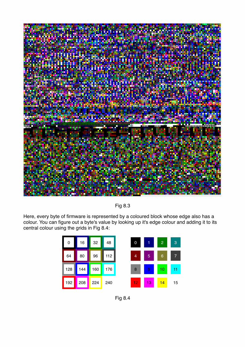
Fig 8.3
Here, every byte of firmware is represented by a coloured block whose edge also has a colour. You can figure out a byte's value by looking up it's edge colour and adding it to its central colour using the grids in Fig 8.4:
0 16 32 48
64 80 96 112
128 144 160 176
192 208 224 240
0 1 2 3
4 5 6 7
8 9 10 11
12 13 14 15
Fig 8.4
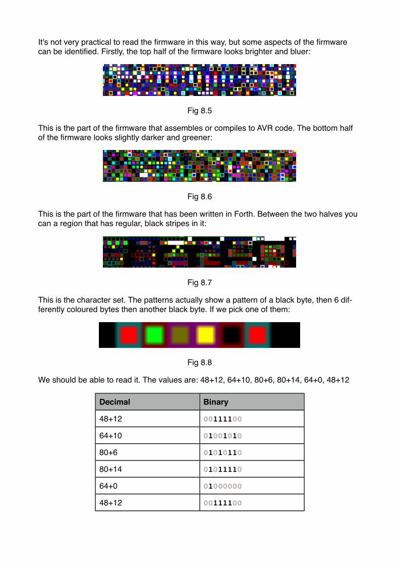
It's not very practical to read the firmware in this way, but some aspects of the firmware can be identified. Firstly, the top half of the firmware looks brighter and bluer:
Fig 8.5
This is the part of the firmware that assembles or compiles to AVR code. The bottom half of the firmware looks slightly darker and greener:
Fig 8.6
This is the part of the firmware that has been written in Forth. Between the two halves you can a region that has regular, black stripes in it:
Fig 8.7
This is the character set. The patterns actually show a pattern of a black byte, then 6 dif-ferently coloured bytes then another black byte. If we pick one of them:
Fig 8.8
We should be able to read it. The values are: 48+12, 64+10, 80+6, 80+14, 64+0, 48+12
Decimal Binary
48+12 00111100
64+10 01001010
80+6 01010110
80+14 01011110
64+0 01000000
48+12 00111100

You should just be able to see FIGnition's @ symbol.
FIGnition's firmware has two major processes, a background task for generating video and a foreground task for running Forth programs and interacting with the user.
The main thread of execution is as follows [Fig 8.4]:
Standard C Startup
Init DriversKeypad: SPI, Serial RAM Chip and start Video
Start Forth Virtual Machine:Init the Instruction Pointer (IP) with Forth ROM Boot address. Re-
set the return and data stack pointer. Start SRAM reading from IP
Execute Forth:
IP<$8000? Ins<=#Byte Codes
Read Ins Byte from Flash
Read Ins Byte from SRAM
Execute Ins
Read addrLo byte from Sram/Flash. Save on return stack; set IP to ins*256+addrLo
Yes Yes
NoNo
Fig 8.4
At this point Forth is being executed from the Forth ROM. Its execution path starts at cold [Fig 8.5]:
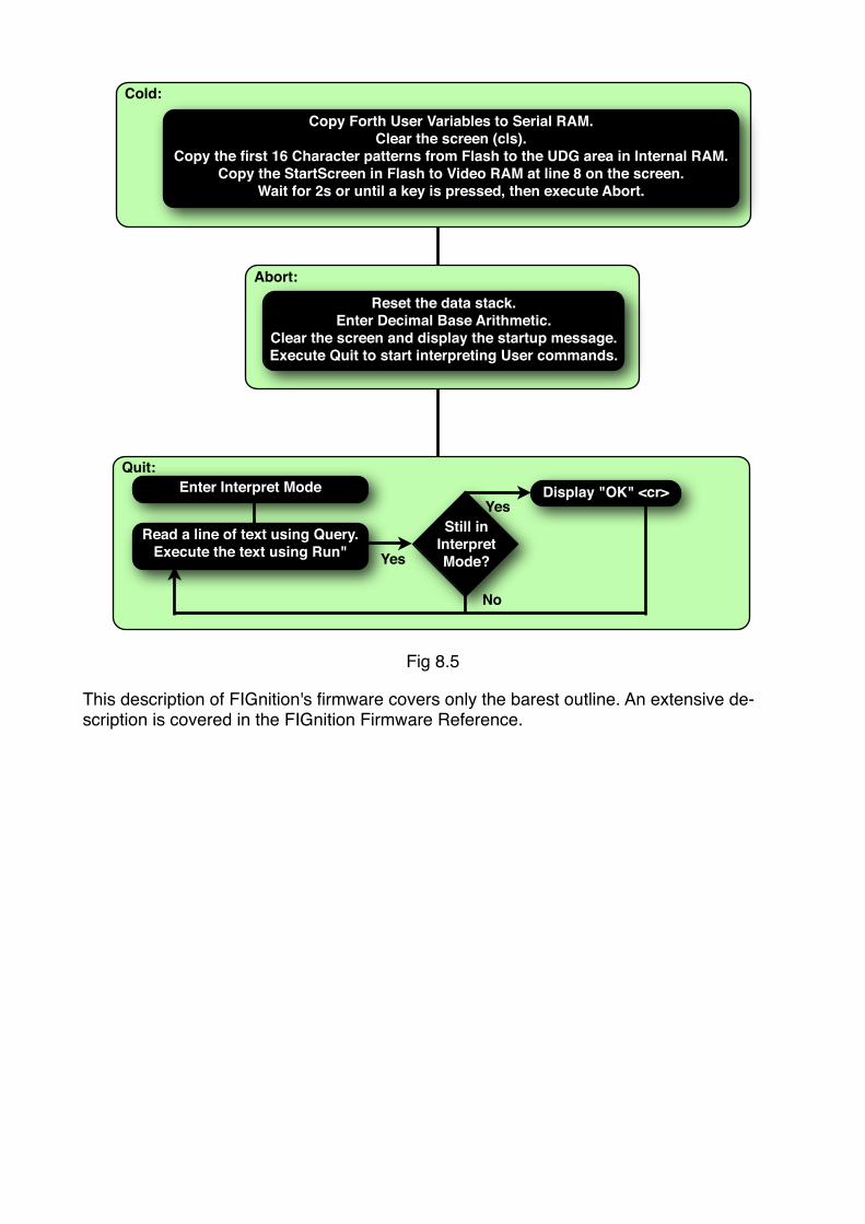
Cold:
Copy Forth User Variables to Serial RAM.Clear the screen (cls).
Copy the first 16 Character patterns from Flash to the UDG area in Internal RAM.Copy the StartScreen in Flash to Video RAM at line 8 on the screen.
Wait for 2s or until a key is pressed, then execute Abort.
Abort:Reset the data stack.
Enter Decimal Base Arithmetic.Clear the screen and display the startup message.Execute Quit to start interpreting User commands.
Quit:
Still inInterpretMode?
Yes
Yes
Enter Interpret Mode
No
Read a line of text using Query.Execute the text using Run"
Display "OK" <cr>
Fig 8.5
This description of FIGnition's firmware covers only the barest outline. An extensive de-scription is covered in the FIGnition Firmware Reference.
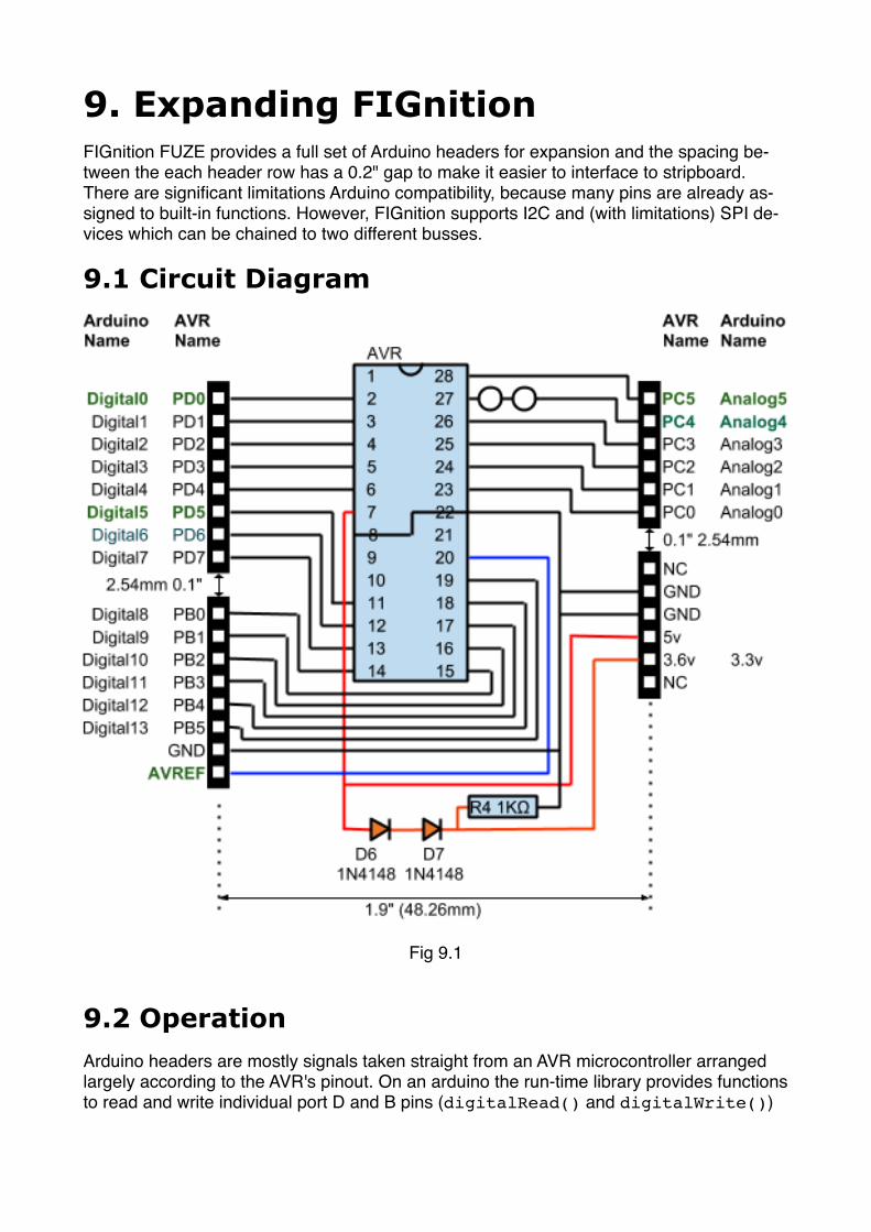
9. Expanding FIGnitionFIGnition FUZE provides a full set of Arduino headers for expansion and the spacing be-tween the each header row has a 0.2" gap to make it easier to interface to stripboard. There are significant limitations Arduino compatibility, because many pins are already as-signed to built-in functions. However, FIGnition supports I2C and (with limitations) SPI de-vices which can be chained to two different busses.
9.1 Circuit Diagram
Fig 9.1
9.2 OperationArduino headers are mostly signals taken straight from an AVR microcontroller arranged largely according to the AVR's pinout. On an arduino the run-time library provides functions to read and write individual port D and B pins (digitalRead() and digitalWrite())
and there is another function (analogRead()) which selects and reads the specified port C pin.
FIGnition provides direct access to the AVR's ports using ic@, ic!, i@ and i! which means that individual pins and groups of pins can be read and written.
Arduino supports a 3.3v output, but on FIGnition this is a 3.6v output. The 3.6v output is achieved by using a pair of diodes as a voltage regulator. Connecting diodes in a forward-biased direction has the effect of dropping an input voltage by 0.7 at its output [See Ap-pendix B]. Thus, two diodes in series will drop an input voltage by 1.4v, low enough to power FIGnition's memory chips. A 1K resistor is used to provide enough of a loading cur-rent (3.6mA) for the diodes to switch on.
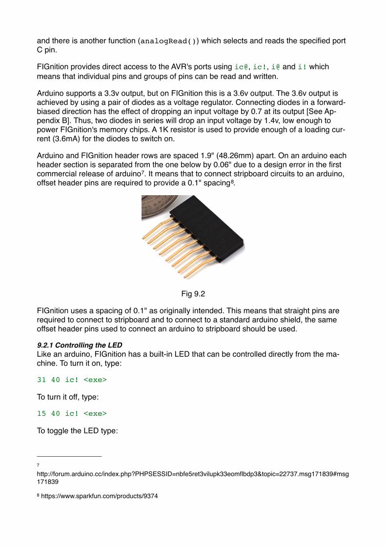
Arduino and FIGnition header rows are spaced 1.9" (48.26mm) apart. On an arduino each header section is separated from the one below by 0.06" due to a design error in the first commercial release of arduino7. It means that to connect stripboard circuits to an arduino, offset header pins are required to provide a 0.1" spacing8.
Fig 9.2
FIGnition uses a spacing of 0.1" as originally intended. This means that straight pins are required to connect to stripboard and to connect to a standard arduino shield, the same offset header pins used to connect an arduino to stripboard should be used.
9.2.1 Controlling the LEDLike an arduino, FIGnition has a built-in LED that can be controlled directly from the ma-chine. To turn it on, type:
31 40 ic! <exe>
To turn it off, type:
15 40 ic! <exe>
To toggle the LED type:
7 http://forum.arduino.cc/index.php?PHPSESSID=nbfe5ret3vilupk33eomflbdp3&topic=22737.msg171839#msg171839
8 https://www.sparkfun.com/products/9374
16 38 ic! <exe>
Using Forth, for example it's easy to write blinky, the standard embedded "Hello World" program.
: blinky ( speed) begin 16 38 ic! ( toggle the LED) dup pause ( wait a little while) inkey until drop;
Typing, for example: 7 blinky <exe> will make the led blink at about 3Hz (about 4Hz for NTSC FIGnitions) until you press a key.
9.2.2 Default I/OThe following pins are free for using with an Arduino Shield. You can set them up as digital inputs or outputs and control them from Forth.
Arduino Header Name
AVR Port
Forth Setup as output Forth output.
Digital 0 PortD0
1 $FE $2A >port> drop 1 $FE $2B >port> drop or0 $FE $2B >port> drop to set or reset the pin.
Digital 5 PortD5
32 $DF $2A >port> drop 32 $DF $2B >port> drop or0 $DF $2B >port> drop to set or reset the pin.
Analog 5
PortC5
32 $DF $27 >port> drop 32 $F7 $28 >port> drop or0 $F7 $28 >port> drop to set or reset the pin.
9.2.3 Reading Analog Channel 5.FIGnition can read analog ports by simply connecting an analog input to Pin 28. Here the reference voltage will be Vcc. The adc can measure voltages with smaller voltage steps if you choose a different reference voltage <Vcc by connecting AVRef to a different refer-ence voltage.
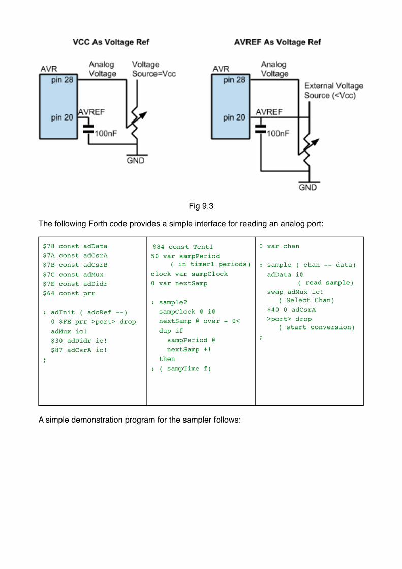
Fig 9.3
The following Forth code provides a simple interface for reading an analog port:
$78 const adData$7A const adCsrA$7B const adCsrB$7C const adMux$7E const adDidr$64 const prr
: adInit ( adcRef --) 0 $FE prr >port> drop adMux ic! $30 adDidr ic! $87 adCsrA ic!;
$84 const Tcnt150 var sampPeriod! !! ( in timer1 periods)clock var sampClock0 var nextSamp
: sample? sampClock @ i@ nextSamp @ over - 0< dup if sampPeriod @ nextSamp +! then; ( sampTime f)
0 var chan
: sample ( chan -- data) adData i@! ! !! ! ( read sample) swap adMux ic!! !! ( Select Chan) $40 0 adCsrA >port> drop!! !! ( start conversion);
A simple demonstration program for the sampler follows:

: analogDemo ( tks port) dup adInit begin begin over sample? until dup sample . inkey until drop drop;
: degC 267 - 704 u* swap drop 10 /;
: tempDemo $C8 adInit begin 50 pause $C8 sample degC . inkey until;
The demonstration program expects you to type tks port analogDemo <exe> and it will start displaying samples from the port every tks /50ths of a second. For example:
10 $45 analogDemo <exe>
displays the output from analog port 5 every 0.2s seconds until you press a key.
The AtMega168 and AtMega328 both support an internal temperature sensor on analog port 8 (there's no input pin for this, it's purely internal). Using the internal temperature sen-sor requires you to also use the internal 1.1v reference (you will still benefit from connect-ing AVREF to GND using a capacitor (e.g. 100nF))
You can read the current raw temperature conversion voltages using, for example:
50 $C8 analogDemo <exe>
But we can convert this directly to a temperature. The AtMega328 Manual, section 24.7 says:
Rearranging, this becomes:
And Vin in mV is related to the temperature according to:
And therefore:
This is what tempDemo calculates:
tempDemo <exe>
How does the analog port code work? To initialize the adc you provide the temperature reference and channel selection as a combined value and then execute adInit. To use an external adc with Vcc as the reference voltage you set the value of the port: 0..5 + $40 (as in the analogDemo). For the internal temperature reference you must provide the in-ternal reference voltage: 1.1v which is encoded as $C0 + the port => $C8, hence the tem-perature demo starts with $C8 adInit. To use AVREF as the voltage reference the upper bits will be 0, so you would just use $5 adInit .
The sample? period code is a timeout mechanism that allows your program to use either the internal TCNT1 timer (which has a 0.4µs resolution up to 13.1ms) or the clock timer (which has a 50ms resolution up to 655s) and still do background processing. The follow-ing code snippet shows how:
begin sample? if chan sample processSample then backgroundProcessingcondition until
To set the sample period in units for the current timer you would type:
aValue samplePeriod ! <exe>
To switch to the TCNT1 timer you would type:
Tcnt1 sampClock ! <exe> ( clock sampClock ! to switch back)
So, 1250 samplePeriod ! Tcnt1 sampClock ! <exe> would make the sample period 500µs. Note, owing to the video generation on FIGnition, sample periods <10ms cannot be reliably measured.
9.2.4 I/O Trade-OffAccess more I/O pins can be achieved with a trade-off in FIGnition's Functionality.
Functionality Lost Ports Gained
LED PortC4 and I2C. To use C4 as I/O you must carefully cut the track between the pins of LK1. This can be done using a sharp craft knife.
Audio PortD6
Keypad PortC0 to PortC3 can be used as I/O pins, but it will con-fuse the keyboard driver and you won't be able to use the keypad after making any changes.
Arduino Header Name
AVR Port
Forth Setup as output Forth output.
Digital 6 PortD6
64 $BF $2A >port> drop 64 $BF $2B >port> drop or0 $BF $2B >port> drop to set or reset the pin.
Analog 4
PortC4
16 $EF $27 >port> drop 16 $Ef $28 >port> drop or0 $EF $28 >port> drop to set or reset the pin.
Analog 3 to Analog 0
PortC3 to 0
32 $DF $27 >port> drop 32 $F7 $28 >port> drop or0 $F7 $28 >port> drop to set or reset the pin.
9.3 Using SPI to talk to an ArduinoThe easiest way for FIGnition to talk to Arduino (also available from RS) is by setting up Arduino as an SPI Slave and then sending and receiving data from it. All you need to do is connect the FIGnition and arduino as shown in Fig 9.4:
Fig 9.4
A simple Arduino / FIGnition communication demo follows:
Arduino Slave FIGnition Master
#include <SPI.h>
void setup (void){ Serial.begin (115200); // debugging pinMode(MISO, OUTPUT); // MISO SPCR |= _BV(SPE); // Slave Mode} // end of setup
// main loopvoid loop (void){ if(SPSR&SPIF) { // print(SPDR); }} // end of loop
vram 600 + const spiPcktspiPckt 10 + const spiSrc
create spiBuff $2B20 , spiSrc , 1 , 0 , 0 ,
: spiDemo spiBuff spiPckt 10 cmove $20 $DF $2A >port> drop begin key dup emit dup spiSrc ic! spiPckt >spi 127 = until;
The arduino code is written as a standard sketch. Sketches always have a setup function which performs initializations and a loop function which is executed repeatedly. Here, setup simply activates the arduino's serial port; sets up the MISO pin to be an output (be-cause we want it to operate in Slave Out mode) and finally enables slave mode. The ardu-

ino's loop function tests to see if the SPI slave has received a byte and if so, reads the SPi Data Register and displays the character.
The FIGnition code is similarly fairly simple. To use SPI on FIGnition we need to define an SPI Packet format, because FIGnition already uses SPI when executing code so FIGnition needs a special SPI driver. The Spi driver expects a port pin to be defined for the Slave select, then a source packet to be sent to the Spi device and an address for a destination packet to be received from the Spi device afterwards.
Here we place the spi packet at the beginning of the UDG area ( vram 600 +). The Slave select is defined as PORTD ($2B) bit 5 ($20)on FIGnition. The source packet starts at spiSrc which is 10 bytes after the spi packet and it's length is 1. We don't need a destina-tion packet, so the next two words are 0, 0.
The main code sets up PortD5 to be an output, then goes into a loop. It waits for a key-press, displays it; stores the key press in the spiSrc address and finally sends the spi packet ( spiPckt >spi).
To Use it you need to load the programs (but don't run it yet) on your arduino and FIGni-tion; then execute spiDemo <exe> on FIGnition and finally run the sketch on the arduino.
After that, whatever you type on FIGnition should be sent to the arduino and output on its monitor (although carriage returns will be displayed incorrectly).
9.4 Using I2C to talk to a Maxim Digital To Analogue Converter.FIGnition can be setup to talk to a Max517 or a Max519 DAC (RS Parts: 622-9392 and 540-4019). To setup FIGnition to use I2C, you must first cut the track between the pins of LK1 in order to disable the LED.
Cut Here
Fig 9.4
To use I2C with a FIGnition you must then add two resistors (2K2 resistors will work well) between Pin 27 and Vcc and between Pin 28 and Vcc.
Fig 9.5
You only need one pair of resistors to manage all the I2C devices FIGnition controls. A simple circuit for a Maxim517 DAC, with its I2C address offset set to 0 is:
Fig 9.6
Next you need to write some Forth code to be able to talk to I2C devices.
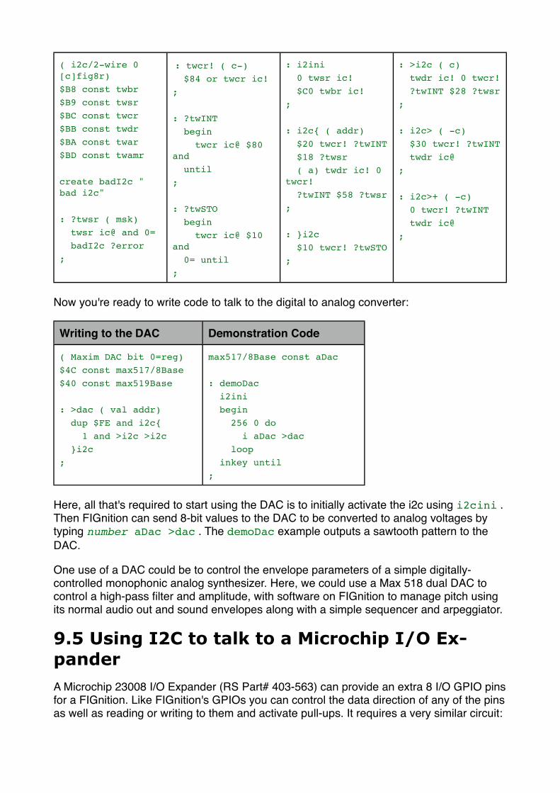
( i2c/2-wire 0 [c]fig8r)$B8 const twbr$B9 const twsr$BC const twcr$BB const twdr$BA const twar$BD const twamr
create badI2c " bad i2c"
: ?twsr ( msk) twsr ic@ and 0= badI2c ?error;
: twcr! ( c-) $84 or twcr ic!;
: ?twINT begin twcr ic@ $80 and until;
: ?twSTO begin twcr ic@ $10 and 0= until;
: i2ini 0 twsr ic! $C0 twbr ic!;
: i2c{ ( addr) $20 twcr! ?twINT $18 ?twsr ( a) twdr ic! 0 twcr! ?twINT $58 ?twsr;
: }i2c $10 twcr! ?twSTO;
: >i2c ( c) twdr ic! 0 twcr! ?twINT $28 ?twsr;
: i2c> ( -c) $30 twcr! ?twINT twdr ic@;
: i2c>+ ( -c) 0 twcr! ?twINT twdr ic@;
Now you're ready to write code to talk to the digital to analog converter:
Writing to the DAC Demonstration Code
( Maxim DAC bit 0=reg)$4C const max517/8Base$40 const max519Base
: >dac ( val addr) dup $FE and i2c{ 1 and >i2c >i2c }i2c;
max517/8Base const aDac
: demoDac i2ini begin 256 0 do i aDac >dac loop inkey until;
Here, all that's required to start using the DAC is to initially activate the i2c using i2cini . Then FIGnition can send 8-bit values to the DAC to be converted to analog voltages by typing number aDac >dac . The demoDac example outputs a sawtooth pattern to the DAC.
One use of a DAC could be to control the envelope parameters of a simple digitally-controlled monophonic analog synthesizer. Here, we could use a Max 518 dual DAC to control a high-pass filter and amplitude, with software on FIGnition to manage pitch using its normal audio out and sound envelopes along with a simple sequencer and arpeggiator.
9.5 Using I2C to talk to a Microchip I/O Ex-panderA Microchip 23008 I/O Expander (RS Part# 403-563) can provide an extra 8 I/O GPIO pins for a FIGnition. Like FIGnition's GPIOs you can control the data direction of any of the pins as well as reading or writing to them and activate pull-ups. It requires a very similar circuit:
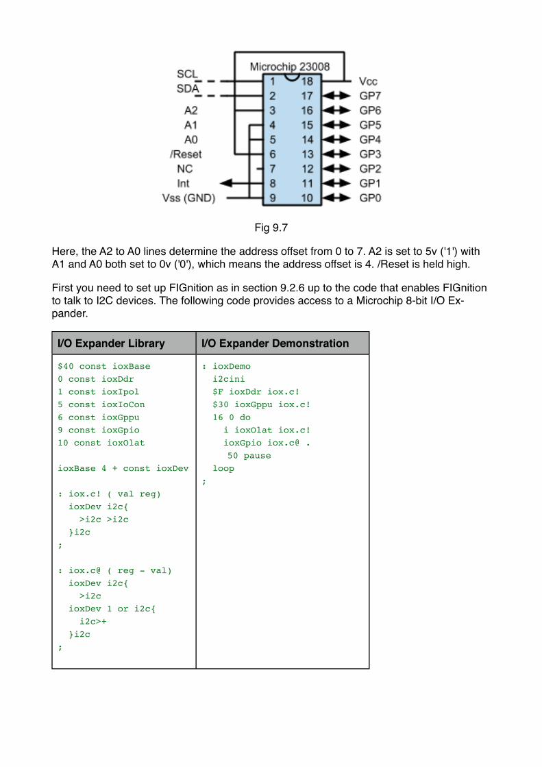
Fig 9.7
Here, the A2 to A0 lines determine the address offset from 0 to 7. A2 is set to 5v ('1') with A1 and A0 both set to 0v ('0'), which means the address offset is 4. /Reset is held high.
First you need to set up FIGnition as in section 9.2.6 up to the code that enables FIGnition to talk to I2C devices. The following code provides access to a Microchip 8-bit I/O Ex-pander.
I/O Expander Library I/O Expander Demonstration
$40 const ioxBase0 const ioxDdr1 const ioxIpol5 const ioxIoCon6 const ioxGppu9 const ioxGpio10 const ioxOlat
ioxBase 4 + const ioxDev
: iox.c! ( val reg) ioxDev i2c{ >i2c >i2c }i2c;
: iox.c@ ( reg - val) ioxDev i2c{ >i2c ioxDev 1 or i2c{ i2c>+ }i2c;
: ioxDemo i2cini $F ioxDdr iox.c! $30 ioxGppu iox.c! 16 0 do i ioxOlat iox.c! ioxGpio iox.c@ . ! 50 pause loop;
The ioxDev is set to ioxBase+4 because the address offset in the example circuit has been set to 4. To use the I/O expander you must first execute i2cini.
By default the ports are set up as input ports with pull-ups turned off. To read the port's in-put pins you'd type:
ioxGpio iox.c@ <exe>
Which would put the value of the port's inputs on the stack (which you could then display using . <exe> ).
To enable or disable pull-ups on the input port you would type (for example):
$40 ioxGppu iox.c! <exe>
This would enable the pull-up on port bit 6 and disable all the others.
To change the data direction of the ports you'd type (for example):
$B ioxDdr iox.c! <exe>
This would make port bits 3, 1 and 0 outputs.
To write a value to the port you'd type (for example):
$2 ioxOlat iox.c! <exe>
Which would output 0 to bit 3, 1 to bit 1 and 0 to bit 0 of the output port bits.
The ioxDemo example initializes the i2c; sets the bottom 4 port bits to outputs then acti-vates pull-ups on port bits 4 and 5. After that it goes into a loop where every second it out-puts the values 0 to 15 on port bits 0..3 and displays the input value of the port.
9.6 Using SPI to backup the external Flash.As standard, FIGnition only supports a single external Flash chip for storage, which means it isn't possible in Forth to copy blocks to another Flash chip or backup the external Flash. However it's possible to do this by adding a small shield design and writing a program that uses the Forth Spi Driver. 1Mbyte SPI Amic Flash chips can be bought from RS Compo-nents, part number: 711-7972. First the circuit:
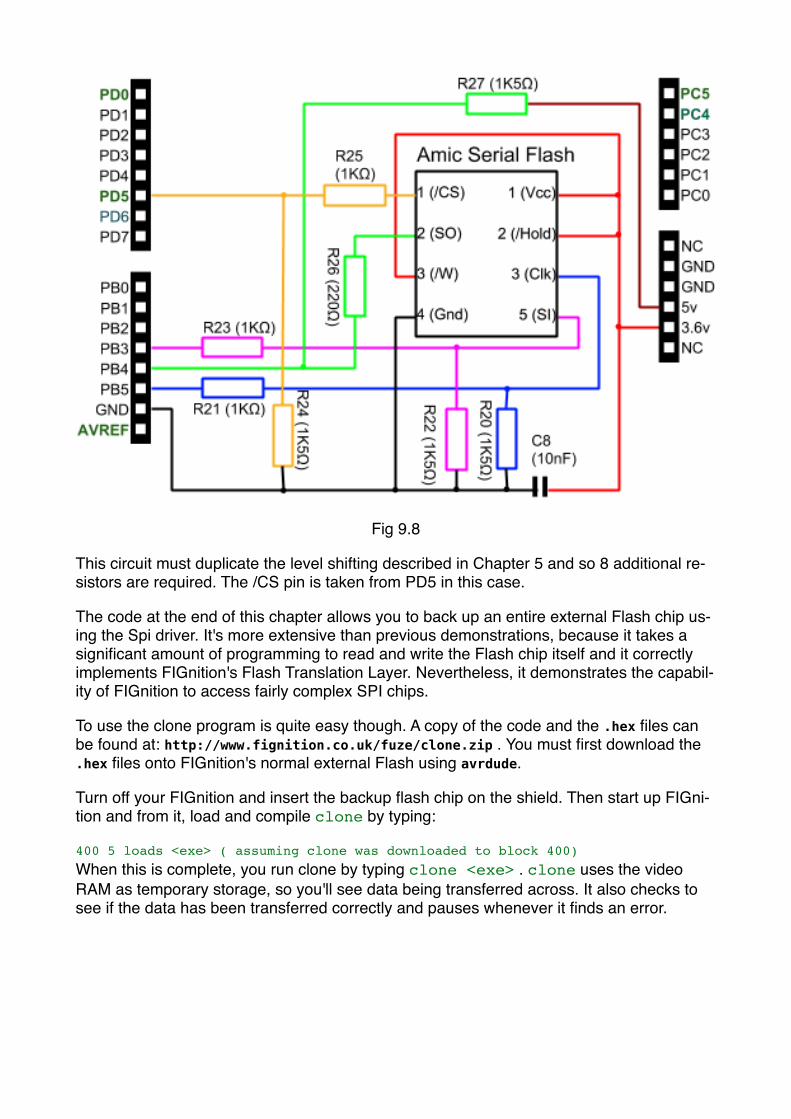
Fig 9.8
This circuit must duplicate the level shifting described in Chapter 5 and so 8 additional re-sistors are required. The /CS pin is taken from PD5 in this case.
The code at the end of this chapter allows you to back up an entire external Flash chip us-ing the Spi driver. It's more extensive than previous demonstrations, because it takes a significant amount of programming to read and write the Flash chip itself and it correctly implements FIGnition's Flash Translation Layer. Nevertheless, it demonstrates the capabil-ity of FIGnition to access fairly complex SPI chips.
To use the clone program is quite easy though. A copy of the code and the .hex files can be found at: http://www.fignition.co.uk/fuze/clone.zip . You must first download the .hex files onto FIGnition's normal external Flash using avrdude.
Turn off your FIGnition and insert the backup flash chip on the shield. Then start up FIGni-tion and from it, load and compile clone by typing:
400 5 loads <exe> ( assuming clone was downloaded to block 400)
When this is complete, you run clone by typing clone <exe> . clone uses the video RAM as temporary storage, so you'll see data being transferred across. It also checks to see if the data has been transferred correctly and pauses whenever it finds an error.

vram 600 + const spiPcktvram const spiSrc
$9F const amicId$05 const amicSr$06 const amicWren$C7 const amicCE$02 const amicPP$0B const amicRB
create spiBuff $2A20 , spiSrc , 1 , spiSrc , 4 ,
vram 610 + const srPckt
$2013 const amic4b$3013 const amic4s$3014 const amic8s
0 var spiAddr: spiSrc ( addr) dup spiAddr ! spiBuff 2+ dup >r i! 0 r 2+ i! 0 r> 6 + i!;
: spiC! ( b) spiAddr ic! 1 spiAddr 1+;
: spiDst ( len a) dup spiAddr ! spiBuff 4 + dup >r i! r> 2+ ic!;
( dLen ds sr): spiMsg srPckt dup spiSrc spiC! 1+ spiDst;
: amicId 4 amicId spiMsg spiPckt >spi! srPckt 1+ i@ >r r amic4b = if 2048 256 then ( end strt) r amic4s = if 2048 128 then ( end strt) r> amic 8s = if 4096 128 then ( end strt);
: amicWait 1 amicSr spiMsg begin spiPckt dup >spi 10 + ic@ 1 and 0= until;
: amicErase 0 amicWren spiMsg spiPckt >spi 0 amicCE spiMsg spiPckt >spi amicWait;
: blkEmpty -1 vram 512 + vram do i i@ 1+ if drop 0 leave then 2 +loop;
0 var virts1024 arr virtBlks
: swapb dup 8 << swap 8 >> or;
: wrPg ( pg) 0 amicWren spiMsg spiPckt >spi vram spiSrc $401 spiPckt 4 + i! amicPP vram ic! swapb vram 1+ i! 0 vram 3 + ic! spiPckt >spi amicWait ;
: chkFail ( addr) 0 23 at ." Fail:" .hex drop 1 key drop;
: chkPg ( blk a) >r vram spiSrc $400 spiPckt 4 + i! $001 spiPckt 8 + i! amicRB vram ic! swapb vram 1+ i! 0 vram 3 + ic! vram swapb spiPckt 6 + i! spiPckt >spi vram 4 + r 256 + r> do dup ic@ i c@ - if chkFail leave then 1+ 2 +loop;
: chkBlk ( absBlk) dup -512 chkPg drop 1+ -256 chkPg drop;
: cpBlk ( st vBlk) dup blk> drop blkEmpty if ;s
then dup virts virtBlks ! 1 virts +! vram dup 4 + 512 cmove + dup wrPg vram 260 + dup 4 + 256 cmove 1+ wrPg 1- chkBlk;
: cpVTable 0 virtBlks ( a) vram 260 + 256 -1 fill virts @ 0 do c@ i 255 and 1 xor vram 260 + ic! i 255 and 0= if i 8 >> wrPg vram 260 + 256 -1 fill then loop virts @ 8 >> wrPg!( flush last page);
: chkVTable virts @ 7 >> 0 do i i 7 << virtBlks chkPg drop loop;
: clone spiBuff spiPckt 10 cmove $20 $DF $2A >port> drop 0 virts ! amicErase amicId 2dup - 0 do i cpBlk loop cpVTable chkVTable;
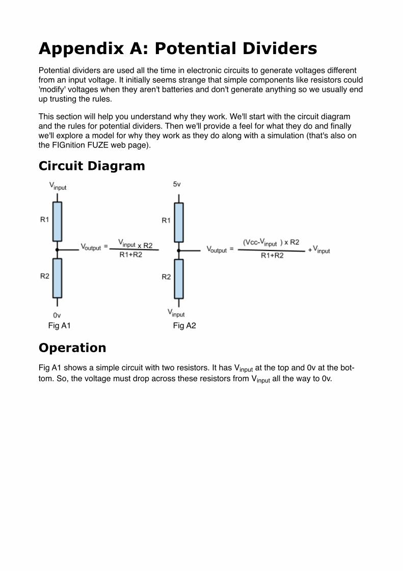
Appendix A: Potential DividersPotential dividers are used all the time in electronic circuits to generate voltages different from an input voltage. It initially seems strange that simple components like resistors could 'modify' voltages when they aren't batteries and don't generate anything so we usually end up trusting the rules.
This section will help you understand why they work. We'll start with the circuit diagram and the rules for potential dividers. Then we'll provide a feel for what they do and finally we'll explore a model for why they work as they do along with a simulation (that's also on the FIGnition FUZE web page).
Circuit Diagram
! Fig A1! Fig A2
OperationFig A1 shows a simple circuit with two resistors. It has Vinput at the top and 0v at the bot-tom. So, the voltage must drop across these resistors from Vinput all the way to 0v.
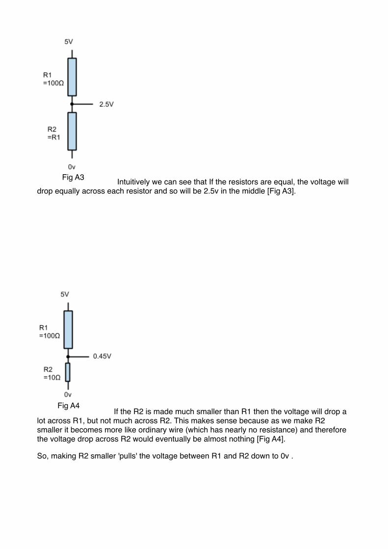
Fig A3 Intuitively we can see that If the resistors are equal, the voltage will drop equally across each resistor and so will be 2.5v in the middle [Fig A3].
Fig A4If the R2 is made much smaller than R1 then the voltage will drop a
lot across R1, but not much across R2. This makes sense because as we make R2 smaller it becomes more like ordinary wire (which has nearly no resistance) and therefore the voltage drop across R2 would eventually be almost nothing [Fig A4].
So, making R2 smaller 'pulls' the voltage between R1 and R2 down to 0v .

Fig A5 Similarly, if we restore R2, then make R1 much smaller than R2, the voltage drop across R1 becomes smaller and so the voltage between R1 and R2 is 'pulled up' towards 5v [Fig A5].
Detailed ExplanationThe point of electricity is that it uses electrical current (electrons) to carry energy and so Electrical/electronic circuits are really just a very flexible means of transporting energy from one place to another.
'Volts' are a measure of this: the amount of energy carried per electron, which is why the Units of volts are Joules/Coulomb (because Joules are a measure of energy and a Cou-lomb is the charge on roughly 6 241 509 324 000 000 000 electrons).
Therefore, when we say that a closed (connected) circuit has 5v on one end and 0v on the other it means that energy is lost across the circuit. The energy 'lost' is really used to pro-vide light or switch transistors or move motors or (if all else fails) give off heat.
The power output by a circuit is therefore the energy per electron (Volts) multiplied by the rate of electrons (the current, in electrons per second). And this is simply:
Power (
Joulessecond
) = Volts x Current =
JoulesCoulomb
x second
Coulombs = Joulessecond
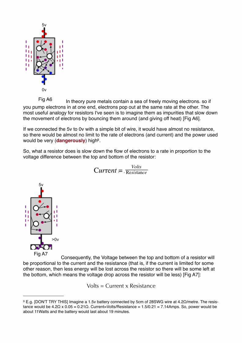
Fig A6 In theory pure metals contain a sea of freely moving electrons. so if you pump electrons in at one end, electrons pop out at the same rate at the other. The most useful analogy for resistors I've seen is to imagine them as impurities that slow down the movement of electrons by bouncing them around (and giving off heat) [Fig A6].
If we connected the 5v to 0v with a simple bit of wire, it would have almost no resistance, so there would be almost no limit to the rate of electrons (and current) and the power used would be very (dangerously) high9.
So, what a resistor does is slow down the flow of electrons to a rate in proportion to the voltage difference between the top and bottom of the resistor:
Fig A7Consequently, the Voltage between the top and bottom of a resistor will
be proportional to the current and the resistance (that is, if the current is limited for some other reason, then less energy will be lost across the resistor so there will be some left at the bottom, which means the voltage drop across the resistor will be less) [Fig A7]:
Volts = Current x Resistance
9 E.g. [DON'T TRY THIS] Imagine a 1.5v battery connected by 5cm of 28SWG wire at 4.2Ω/metre. The resis-tance would be 4.2Ω x 0.05 = 0.21Ω. Current=Volts/Resistance = 1.5/0.21 = 7.14Amps. So, power would be about 11Watts and the battery would last about 19 minutes.


Fig A8 This is all we need to know to simulate and understand potential divid-ers. Let's look at a simple potential divider. At the moment of connection we have 5v at the top of R1 and 0v at the bottom. Electrons would flow through that resistor at the rate: 5v / 100Ω = 50mA and lose all their energy in the process [Fig A8].
So initially the second resistor would see 0v at the top and bottom along with an accumula-tion of electrons with no energy at the top. Since they have no energy (i.e. because there's no voltage difference) electrons aren't pumped into the top and out of the bottom of R2.
Fig A9 [Fig A9] The build-up of charge at the bottom of R1 then serves to limit the current going through R1 (because electrons repel each other), and this causes the voltage to start to rise at the bottom of R1, because as the current flow becomes more lim-ited, less energy is lost through R1 and therefore electrons with energy are pumped out of the bottom of R1.

Now R2 now sees a build-up of electrons with energy (i.e. voltage) at the top end and cur-rent starts to flow through R2 according to the voltage difference between the two.
Fig A10 The current flow through both resistors eventually10 reaches equilibrium according to 5v divided by the sum of R1 and R2 [Fig A10]. Similarly, the voltage between R1 and R2 stabilizes at Volts x R2/(R1+R2):
Simulation
resSim can simulate the voltages and currents on a number of resistors in series. This version uses 16-bit integer (whole-number) arithmetic and is usable, but not very accurate. You must first find two free pages of Flash (by using n edit <exe> until you find two pages that are clear). Then load resSim from the website using avrdude to download resSim00.hex and resSim01.hex. After each .hex file is loaded you will need to copy it to flash by rebooting FIGnition and typing: -1 n cp <exe> .
Now type (n+1) load <exe> to load resSim and then you run it by typing resSim <exe> . A list of numbers will appear, these are the voltages and currents at the bottom of each resistor. By default the simulation feeds 5v into a 10Ω resistor followed by a 15Ω re-sistor (this is similar to the potential divider used to convert the AVR's 5v signals to the memory chip 3v signals). The initial numbers will go:
Volts1! Current1! Volts2! Current20.00! 0.50! 0.00! 0.000.50! 0.45! 0.00! 0.000.95! 0.41! 0.01! 0.03
10 'Eventually' is really very quick - within nanoseconds!

1.32! 0.37! 0.01! 0.061.62! 0.34! 0.00! 0.11etc to the bottom of the screen where it says:2.95! 0.21! 0.00! 0.20more>>Pressing any key refreshes it with a new list which stabilizes at the bottom with:2.98! 0.20! 0.00! 0.20more>>Pressing keys just repeats that line on new screens. If you keep pressing <space> quickly, it'll eventually break out of the program.
What the numbers mean is that at the bottom of R1 the voltage is 2.98v (approximately 3v) and that the overall current is 0.2A. This is correct according to the rules:
Current = InputVolts / (R1+R2) = 5 / (10+15) = 0.2A
PotentialVoltage = InputVolts x R2 / (R1+R2) = 5 x 15 / (10+15) = 3v.
You can create other setups using the setRes and >res commands. First define the num-ber of resistors using setRes: e.g. 3 setRes <exe> .
Now define each resistor value using >res. For example, 10 >res 10 >res 10 >res <exe>. This defines three 10Ω resistors in series. Finally, run the simulation by typing resSim <exe> (you'll notice in this case there is too much text to fit on a line and the last current value is displayed on a second line). After a few pages of numbers, the values sta-bilize to:
Volts1! Current1! Volts2! Current2! Volts3! Current33.29! 0.17! 1.62! 0.17! 0.00! 0.16
Again, the calculations are (approximately) correct:
Current = InputVolts / (R1+R2+R3) = 5 / (10+10+10) = 0.16666A
There are two potential voltages to consider, the one between R1 and R2 and the one be-tween R2 and R3:
PDFromR2toGnd = InputVolts x (R2+R3) / (R1+R2+R3) = 5 x 15 / (10+15) = 3.33v
PDFromR3toGnd = InputVolts x R3 / (R1+R2+R3) = 5 x 15 / (10+15) = 1.666v
resSim can simulate up to 10 resistors in series, but the 16-bit calculations will become more inaccurate when you add more resistors.
Code Description
The main part of the code is the command calcRes.

Command(s) Code Explanation
calcRes dup v @ over 1+ v @ - over res @ >r r 1 >> + r> / over 1+ curr @ 4 + 10 / -
over res @ over * >r over v @ r> - >r over 1+ vNew r swap !
r> .3sf dup .3sf
2dup swap 1+ iNew ! neg swap iNew +!
First we calculate the current* as the voltage difference between the top and bottom of this resistor divided by this resistor and subtract 10% of the charge left over from the last itera-tion.
Then we calculate the output voltage according to that current, this resistor and the input voltage.
We copy the output voltage as the voltage below this resistor.
Then we display the output voltage and output current.
Finally, we store the new current and subtract the current from the current above this resistor.
[*Actually charge is being calculated, because the simulation is done in discrete time intervals]

Appendix B DiodesDiodes are the simplest semiconductors. FIGnition uses a simple low-power signal diode in two different ways and a different type of diode (a Zener diode) in one way. Here’s how they work.
B.1 Signal Diodes
!! (acceptor)!! ! (donator)
A diode is constructed from silicon (which doesn’t normally conduct) with tiny amounts of impurities. For example, adding about 1 in 108 atoms of Boron makes silicon good at ac-cepting electrons whereas adding Arsenic makes Silicon good at donating electrons.
By themselves, either type of ‘doped’ Silicon will conduct electricity in either direction, but if you put them together; a natural electrical barrier appears: the N-type Silicon donates some electrons to the P-type (which accepts them) and this causes the N-type Silicon to become positively charged (because it’s lost some electrons) and the P-type Silicon to be-come negatively charged (because it’s gained some electrons).
This barrier quickly reaches equilibrium: the more electrons that reach the P-type Silicon, the more likely they are to be attracted to the positively charged N-type; but the more they cross back the other way, the more opportunities there are for the N-type to donate elec-trons to the P-type.
If we apply a small negative voltage11 to the N-type Silicon the barrier gets smaller, be-cause electrons fill the positively charged N-type region. A few electrons will actually make it all the way across, causing a tiny current to flow.
11 In this appendix we’ll talk about negative voltages instead of positive voltages, because electrons actually flow from the negatively charged end of a circuit (which we normally call ground) to the positively charged side - it would look odd to talk about a positive voltage and have to show electrons being pumped in from the opposite side.
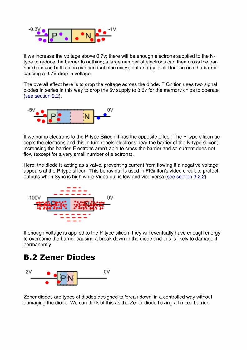
If we increase the voltage above 0.7v; there will be enough electrons supplied to the N-type to reduce the barrier to nothing; a large number of electrons can then cross the bar-rier (because both sides can conduct electricity), but energy is still lost across the barrier causing a 0.7V drop in voltage.
The overall effect here is to drop the voltage across the diode. FIGnition uses two signal diodes in series in this way to drop the 5v supply to 3.6v for the memory chips to operate (see section 9.2).
If we pump electrons to the P-type Silicon it has the opposite effect. The P-type silicon ac-cepts the electrons and this in turn repels electrons near the barrier of the N-type silicon; increasing the barrier. Electrons aren’t able to cross the barrier and so current does not flow (except for a very small number of electrons).
Here, the diode is acting as a valve, preventing current from flowing if a negative voltage appears at the P-type silicon. This behaviour is used in FIGniton’s video circuit to protect outputs when Sync is high while Video out is low and vice versa (see section 3.2.2).
If enough voltage is applied to the P-type silicon, they will eventually have enough energy to overcome the barrier causing a break down in the diode and this is likely to damage it permanently
B.2 Zener Diodes
Zener diodes are types of diodes designed to 'break down' in a controlled way without damaging the diode. We can think of this as the Zener diode having a limited barrier.

As before, when the breakdown voltage is exceeded; all the remaining electrical energy is transferred through the diode. However, because the breakdown voltage is designed to be much smaller than the N-type and P-type silicon can cope with, the diode remains func-tional and the effect is to maintain the potential difference at the break-down voltage.
FIGnition uses Zener diodes to limit the voltage on the USB d+ and d- signals to the speci-fied 3.6v while allowing FIGnition's AVR microcontroller to operate at 5v. This is described in section 7.1.

Appendix C CapacitorsCapacitors can be used to temporarily store charge and to smooth voltage regularities. FiGnition uses them in both of these ways.
C.1 How Capacitors WorkCapacitors are basically metal plates with a large surface area separated by a thin insulat-ing material. The large metal plates allow a relatively large surface area for a lot of elec-trons and it’s this that enables capacitors to store charge. It’s even possible to build one using drinks cans and waxed paper12(but I wouldn’t recommend it, because of the danger of suddenly discharging a relatively large amount of charge if you short-circuit it).
!
So the question is: if they have an insulating layer, how do they allow current to pass through them? And the answer is that electrons don’t pass through them; instead charge is displaced (because electrons repel each other) and this explains their characteristics.
!
Imagine a 5v electrical power source is applied to one side of a capacitor (through a resis-tor). Initially it starts off at 0v, but eventually electrons build up (they can’t go anywhere) until there’s 5v on that side. Meanwhile, on the other side, the initial rush of charge repels lots of electrons, but eventually there are few left at the right-hand plate to repel and so the flow of charge there falls to a trickle.
12 DIY Capacitor image from http://rimstar.org/science_electronics_projects/make_electrolytic_capacitor.htm
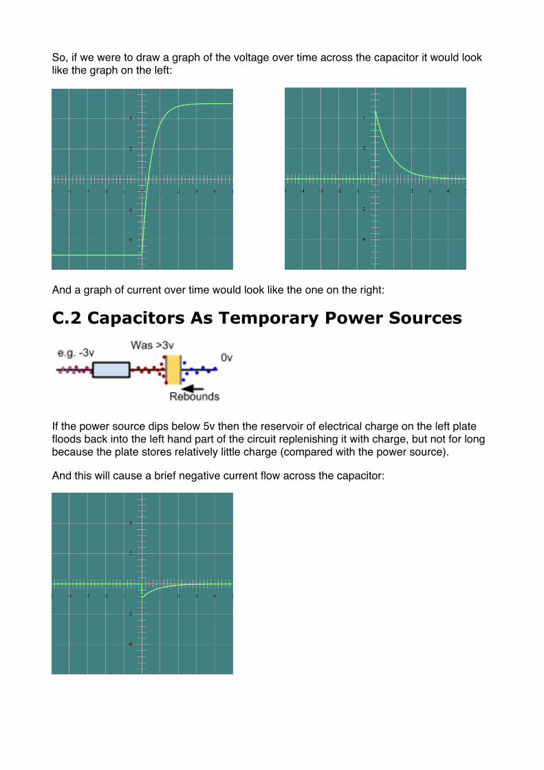
So, if we were to draw a graph of the voltage over time across the capacitor it would look like the graph on the left:
!! !
And a graph of current over time would look like the one on the right:
C.2 Capacitors As Temporary Power Sources
If the power source dips below 5v then the reservoir of electrical charge on the left plate floods back into the left hand part of the circuit replenishing it with charge, but not for long because the plate stores relatively little charge (compared with the power source).
And this will cause a brief negative current flow across the capacitor:

FIGnition uses this feature in the large capacitor C1 to provide a more constant power supply to the board: a large capacitor provides some temporary electrical energy to cover up any of the expected ebb and flow of power from the USB cable.
C.3 De-coupling CapacitorsFIGnition uses smaller capacitors in a similar way to smooth power to its high frequency integrated circuits. The use of electrical power by a circuit’s components will cause tran-sient power surges and losses in other parts of the circuit. Small capacitors placed next to individual chips (here we use 10nF capacitors) provide tiny charge reservoirs which smooth out these transients, effectively de-coupling the chip’s power source from the rest of the circuit.
C.4 Capacitors As Audio FiltersThe ability capacitors have for smoothing out transients is the same as filtering out the amplitudes of high frequencies: they diminish as the signal becomes smoothed out.
Using different resistor values and capacitor values allows us to change the frequency at which this happens. The frequency will be:
Audio circuits assume an inline resistance of about 75Ω so FIGnition uses a 100nF polyes-ter capacitor to filter out frequencies above 20KHz since 1/(2π * 75 * 100*10-9=21.2KHz). For audio output this is useful because the audio pin on a FIGnition outputs square waves, which have nasty high-frequency components which audio equipment won’t like.
On the audio input side it means that noise above 20KHz is filtered out which helps to make the audio loader reliable.