
MB86276 - RS Components
332
MB86276 <LIME> Graphics Display Controller Specifications Revision 1.0 18th October, 2006 Copyright © FUJITSU LIMITED 2004-2006 ALL RIGHTS RESERVED
-
Upload
khangminh22 -
Category
Documents
-
view
0 -
download
0
Transcript of MB86276 - RS Components

MB86276 <LIME> Graphics Display Controller
Specifications
Revision 1.0 18th October, 2006
Copyright © FUJITSU LIMITED 2004-2006
ALL RIGHTS RESERVED

FUJITSU CONFIDENTIAL
MB86276 <LIME> 1 GDC Specifications Manual Rev0.97
<Notes>
The specifications in this manual are subject to change without notice. Contact our Sales Department before purchasing the product described in this manual.
Information and circuit diagrams in this manual are only examples of device applications, they are not intended to be used in actual equipment. Also, Fujitsu accepts no responsibility for infringement of patents or other rights owned by third parties caused by use of the information and circuit diagrams.
The contents of this manual must not be reprinted or duplicated without permission of Fujitsu.
Fujitsu’s semiconductor devices are intended for standard uses (such as office equipment (computers and OA equipment), industrial/communications/measuring equipment, and personal/home equipment). Customers using semiconductor devices for special applications (including aerospace, nuclear, military and medical applications) in which a failure or malfunction might endanger life or limb and which require extremely high reliability must contact our Sales Department first. If damage is caused by such use of our semiconductor devices without first consulting our Sales Department, Fujitsu will not assume any responsibility for the loss.
Semiconductor devices fail with a known probability. Customers must use safety design (such as redundant design, fireproof design, over-current prevention design, and malfunction prevention design) so that failures will not cause accidents, injury or death).
If the products described in this manual fall within the goods or technologies regulated by the Foreign Exchange and Foreign Trade Law, permission must be obtained before exporting the goods or technologies.
Burns There is a danger of burns because the IC surface is heated
depending on the IC operating conditions. In this case, take
safety measures.
All Rights Reserved The contents of this document are subject to change without notice. Customers are advised to consult with FUJITSU sales representatives before ordering. The information and circuit diagrams in this document are presented as examples of semiconductor device applications, and are not intended to be incorporated in devices for actual use. Also, FUJITSU is unable to assume responsibility for infringement of any patent rights or other rights of third parties arising from the use of this information or circuit diagrams. The products described in this document are designed, developed and manufactured as contemplated for general use, including without limitation, ordinary industrial use, general office use, personal use, and household use, but are not designed, developed and manufactured as contemplated (1) for use accompanying fatal risks or dangers that, unless extremely high safety is secured, could have a serious effect to the public, and could lead directly to death, personal injury, severe physical damage or other loss (i.e., nuclear reaction control in nuclear facility, aircraft flight control, air traffic control, mass transport control, medical life support system, missile launch control in weapon system), or (2) for use requiring extremely high reliability (i.e., submersible repeater and artificial satellite). Please note that Fujitsu will not be liable against you and/or any third party for any claims or damages arising in connection with above-mentioned uses of the products. Any semiconductor devices have an inherent chance of failure. You must protect against injury, damage or loss from such failures by incorporating safety design measures into your facility and equipment such as redundancy, fire protection, and prevention of over-current levels and other abnormal operating conditions. If any products described in this document represent goods or technologies subject to certain restrictions on export under the Foreign Exchange and Foreign Trade Law of Japan, the prior authorization by Japanese government will be required for export of those products from Japan.
! CAUTION

FUJITSU CONFIDENTIAL
MB86276 <LIME> 2 GDC Specifications Manual Rev 1.0
Revision history
Date Version Page count Change
2005.2.10 0.1 176 First edition
2005.3.12 0.2 225 The description of Video Capture is added.
2005.6.15 0.92 237 The pin list and the description of modeis are added.
2005.7.14 0.93b 278 DC, AC characteristics are added.
The description of Memory Map, Dual Monitor, and
the capacity of SDRAM are updated.
The table of the pin multiplex is updated.
Other update.
2005.8.17 0.93c 278 The description of the unimplemented functions, the geometry registers and the analog RGB output, were deleted.
2005.9.19 0.93d 278 Misprint correction.
2005.10.17 0.94 282 P.14 The pin list of thermal balls is added.
P.15-16 Several pins are renamed to "TESTH" or "TESTL".
P.26 "TESTL" is added in the table of test pins.
P.30 RDY_MODE, ENDIAN signals are added.
P.31 The table of GMODE is updated.
P.249 The lost character is displayed.
2006.1.18 0.95 281 P.18-19 The description "TOP VIEW" is inserted in Pin diagram.
P.28 The description was doubled about RDY_MODE and BS_MODE
is deleted.
P.29-30 "Connection to CPU" is updated.
P.31 The paragraph "Graphics memory interface" is moved from
Chapter 3.
P.64 The table of "Resolution and Display Frequency" is updated.
P.150-151 The LOWD field of MMR register is updated.
Other: Misprint correction.
2006.1.27 0.96 297 P.10 Connectable Memoey configuration is updated.
P.21 The description of the symbol regarding VDD/GND is added.
P.30 The connection between CPU and Lime is updated.
P.31 The pin information of serial host interface is added.
P.66 Connection with memory is updated.
P.81 Chapter 6.8 in previous version is removed.
P.153 The description of CCF register is added.
P.160 The description of I2C I/F register is added.
P.291 The note about AC timing specification of Host I/F is added.
Other: Misprint correction.

FUJITSU CONFIDENTIAL
MB86276 <LIME> 3 GDC Specifications Manual Rev 1.0
Date Version Page count Change
2006.2.14
2006.3.30
0.97
0.97a
327 P.23 The description "TESTL" is updated.
P.47 The protocol for general call address is updated.
P.47 Misprint about Acknowledge in the protocol for SCI are corrected.
P.51 Line transfer of SCI is updated.
P.52 The description of I2C interface was added at ver.0.96.
P.138 SCI register list is added.
P.160 The description of SCI registers are added.
P.177 DCM,DCE,DCEE registers are changed to DCM0/1/2/3 registers.
P.279 Timing chart of Host interface for SH3/4, V832, SPARClite
are added.
P.295 Timing chart of Host interface for 16bit CPU, 16bit AD-MUX CPU,
32bit AD-MUX CPU are added.
Other: Misprint correction.
2006.10.18
1.0 P.28 Note of XRDY signal is updated.
P.33 Connection of XWE1 signal is updated.
P.47 Description of 16-bit CPU mode is added.
P.161 Host register descriptions are added, DMA_ST_ADR, DMA_ED_ADR, ERR_ADR, ERR_DETECT, INT_MSK.
P.172 Add Revision Register :PIO Base + 0x84
P.316 Video Capture AC Timing Hold 2ns => 0ns
P.321 Clear the meaning of tr,tf

FUJITSU CONFIDENTIAL
MB86276 <LIME> 4 GDC Specifications Manual Rev 1.0
1 GENERAL 10 1.1 Features...................................................................................................................................... 10 1.2 Functional Overview ................................................................................................................... 11
1.2.1 Host CPU interface................................................................................................................ 11 1.2.2 External memory interface .................................................................................................... 12 1.2.3 Display controller ................................................................................................................... 13 1.2.4 2D Drawing............................................................................................................................ 15 1.2.5 Special effects ....................................................................................................................... 17
2 Pins 20 2.1 Pin assignment diagram ............................................................................................................. 20 2.2 Pin assignment table................................................................................................................... 22 2.3 Pin mutiplex table........................................................................................................................ 24 2.4 Host CPU interface ..................................................................................................................... 28
2.4.1 Ready signal mode................................................................................................................ 30 2.4.2 BS signal mode ..................................................................................................................... 31 2.4.3 Endian ................................................................................................................................... 31 2.4.4 Note about the connection to CPU........................................................................................ 32
2.5 Graphics memory interface......................................................................................................... 35 2.6 Video output interface................................................................................................................. 36 2.7 Video capture interface............................................................................................................... 37 2.8 I2C interface ................................................................................................................................ 38 2.9 GPIO interface ............................................................................................................................ 38 2.10 General purpose mode pins ....................................................................................................... 38 2.11 Clock input .................................................................................................................................. 39 2.12 Test pins...................................................................................................................................... 40 2.13 Reset sequence.......................................................................................................................... 40 2.14 How to switch internal operating frequency................................................................................ 40 3 PROCEDURE OF THE HARDWARE INITIALIZATION 41 3.1 Hardware reset ........................................................................................................................... 41 3.2 Re-reset ...................................................................................................................................... 41 3.3 Software reset............................................................................................................................. 41 4 HOST INTERFACE 42 4.1 Access Mode .............................................................................................................................. 43
4.1.1 SRAM interface ..................................................................................................................... 43 4.1.2 FIFO interface (fixed transfer destination address)............................................................... 43
4.2 DMA Transfer .............................................................................................................................. 44 4.2.1 Data transfer unit ................................................................................................................... 44 4.2.2 Address mode ....................................................................................................................... 44 4.2.3 Bus mode .............................................................................................................................. 45 4.2.4 DMA transfer request ............................................................................................................ 45 4.2.5 Ending DMA transfer ............................................................................................................. 45
4.3 Transfer of Local Display List...................................................................................................... 46 4.4 Interrupt....................................................................................................................................... 47
4.4.1 Address Error Interrupt.......................................................................................................... 47 4.5 SH3 Mode ................................................................................................................................... 47 4.6 Wait ............................................................................................................................................. 47 4.7 16-bit CPU mode ........................................................................................................................ 47 4.8 Serial Control Interface (SCI)...................................................................................................... 49
4.8.1 Protcol of SCI as I2C slave ................................................................................................... 49
FUJITSU CONFIDENTIAL
MB86276 <LIME> 5 GDC Specifications Manual Rev 1.0
4.8.2 General call address ............................................................................................................. 49 4.8.3 TRANS_MODE register access ............................................................................................ 49 4.8.4 Internal address register access ........................................................................................... 50 4.8.5 Internal data register access ................................................................................................. 50
5 I2C Interface Controller 54 5.1 Features...................................................................................................................................... 54 5.2 Block diagram ............................................................................................................................. 55
5.2.1 Block Diagram ....................................................................................................................... 55 5.2.2 Block Function Overview....................................................................................................... 56
5.3 Example application.................................................................................................................... 57 5.3.1 Connection Diagram.............................................................................................................. 57 5.3.2 START condition.................................................................................................................... 58 5.3.3 STOP condition ..................................................................................................................... 58 5.3.4 Addressing............................................................................................................................. 59 5.3.5 Synchronization of SCL......................................................................................................... 59 5.3.6 Arbitration .............................................................................................................................. 60 5.3.7 Acknowledge ......................................................................................................................... 60 5.3.8 Bus error................................................................................................................................ 60 5.3.9 Initialize.................................................................................................................................. 61 5.3.10 1-byte transfer from master to slave ..................................................................................... 62 5.3.11 1-byte transfer from slave to master...................................................................................... 63 5.3.12 Recovery from bus error........................................................................................................ 64
5.4 Note ............................................................................................................................................ 65 6 Graphics Memory 66 6.1 Configuration............................................................................................................................... 66
6.1.1 Data type ............................................................................................................................... 66 6.1.2 Memory Mapping................................................................................................................... 67 6.1.3 Data Format........................................................................................................................... 69
6.2 Frame Management ................................................................................................................... 70 6.2.1 Single Buffer .......................................................................................................................... 70 6.2.2 Double Buffer......................................................................................................................... 70
6.3 Memory Access........................................................................................................................... 70 6.3.1 Priority of memory accessing ................................................................................................ 70
6.4 Connection with memory ............................................................................................................ 71 6.4.1 Connection with memory....................................................................................................... 71
7 DISPLAY CONTROLLER 72 7.1 Overview ..................................................................................................................................... 72 7.2 Display Function ......................................................................................................................... 73
7.2.1 Layer configuration................................................................................................................ 73 7.2.2 Overlay .................................................................................................................................. 74 7.2.3 Display parameters................................................................................................................ 76 7.2.4 Display position control ......................................................................................................... 77
7.3 Display Color............................................................................................................................... 79 7.4 Cursor ......................................................................................................................................... 80
7.4.1 Cursor display function.......................................................................................................... 80 7.4.2 Cursor control ........................................................................................................................ 80
7.5 Display Scan Control .................................................................................................................. 81 7.5.1 Applicable display.................................................................................................................. 81 7.5.2 Interlace display..................................................................................................................... 82
7.6 The external synchronous signal ................................................................................................ 83

FUJITSU CONFIDENTIAL
MB86276 <LIME> 6 GDC Specifications Manual Rev 1.0
7.7 An example of the external synchronization circuit .................................................................... 83 7.8 Programmable YCbCr/RGB conversion for L1-layer display...................................................... 86 7.9 DCLKO shift ................................................................................................................................ 88 7.10 Syncronous register update of display........................................................................................ 88 7.11 Dual Display................................................................................................................................ 89
7.11.1 Overview................................................................................................................................ 89 7.11.2 Destination Control ................................................................................................................ 89 7.11.3 Output Signal Control ............................................................................................................ 90 7.11.4 Output Circuit Example ......................................................................................................... 91 7.11.5 Display Clock and Timing ..................................................................................................... 93 7.11.6 Limitation ............................................................................................................................... 93
8 Video Capture 94 8.1 Video Capture function ............................................................................................................... 94
8.1.1 Input data Formats ................................................................................................................ 94 8.1.2 Capturing of Video Signal...................................................................................................... 94 8.1.3 Non-interlace Transformation ................................................................................................ 94
8.2 Video Buffer ................................................................................................................................ 95 8.2.1 Data Form.............................................................................................................................. 95 8.2.2 Synchronous Control............................................................................................................. 95 8.2.3 Area Allocation....................................................................................................................... 95 8.2.4 Window Display..................................................................................................................... 96 8.2.5 Interlace Display.................................................................................................................... 96 8.2.6 RGB555 Mode....................................................................................................................... 96
8.3 Scaling ........................................................................................................................................ 97 8.3.1 Down-scaling Function .......................................................................................................... 97 8.3.2 Up-scaling Function............................................................................................................... 97 8.3.3 Flow of image processing...................................................................................................... 99
8.4 External video signal input conditions....................................................................................... 102 8.4.1 RTB656 YUV422 input format............................................................................................. 102 8.4.2 RGB input format................................................................................................................. 104
8.5 Input Video Signal Parameter Setup ........................................................................................ 109 9 DRAWING PROCESSING 110 9.1 Coordinate System ................................................................................................................... 110
9.1.1 Drawing coordinates............................................................................................................ 110 9.1.2 Texture coordinates ..............................................................................................................111 9.1.3 Frame buffer .........................................................................................................................111
9.2 Figure Drawing.......................................................................................................................... 112 9.2.1 Drawing primitives ............................................................................................................... 112 9.2.2 Polygon drawing function .................................................................................................... 112 9.2.3 Drawing parameters ............................................................................................................ 113 9.2.4 Anti-aliasing function ........................................................................................................... 114
9.3 Bit Map Processing................................................................................................................... 115 9.3.1 BLT ...................................................................................................................................... 115 9.3.2 Pattern data format.............................................................................................................. 115
9.4 Texture Mapping ....................................................................................................................... 116 9.4.1 Texture size ......................................................................................................................... 116 9.4.2 Texture color ........................................................................................................................ 116 9.4.3 Texture Wrapping ................................................................................................................ 116 9.4.4 Filtering................................................................................................................................ 117 9.4.5 8.4.5 Texture blending ......................................................................................................... 117

FUJITSU CONFIDENTIAL
MB86276 <LIME> 7 GDC Specifications Manual Rev 1.0
9.5 Rendering ................................................................................................................................. 118 9.5.1 Tiling .................................................................................................................................... 118 9.5.2 Alpha blending..................................................................................................................... 118 9.5.3 Logic operation.................................................................................................................... 119 9.5.4 Hidden plane management (Optional function)................................................................... 119
9.6 Drawing Attributes..................................................................................................................... 120 9.6.1 Line drawing attributes ........................................................................................................ 120 9.6.2 Triangle drawing attributes .................................................................................................. 120 9.6.3 Texture attributes................................................................................................................. 121 9.6.4 BLT attributes ...................................................................................................................... 121 9.6.5 Character pattern drawing attributes ................................................................................... 121
10 DISPLAY LIST 122 10.1 Overview ................................................................................................................................... 122
10.1.1 Header format...................................................................................................................... 123 10.2 Rendering Command................................................................................................................ 124
10.2.1 Command list....................................................................................................................... 124 10.2.2 Details of rendering commands........................................................................................... 128
11 GDC Register MAP 138 11.1 Local memory register list......................................................................................................... 138
11.1.1 Host interface register list.................................................................................................... 138 11.1.2 SCI register list .................................................................................................................... 140 11.1.3 I2C interface register list ...................................................................................................... 141 11.1.4 GPIO register list ................................................................................................................. 142 11.1.5 Graphics memory interface register list............................................................................... 142 11.1.6 Display controller register list .............................................................................................. 143 11.1.7 Video capture register list .................................................................................................... 149 11.1.8 Drawing engine register list ................................................................................................. 151
12 Explanation of GDC Registers 157 12.1 Host interface registers............................................................................................................. 158
XINT polarity change signal ........................................................................................................... 163 “0” is Low Active, “1” is High Active. ............................................................................................... 163 12.1.1 SCI registers........................................................................................................................ 164 12.1.2 GPIO control registers......................................................................................................... 167 12.1.3 Peripheral Interrupt related registers................................................................................... 169 12.1.4 I2C Interface Registers ........................................................................................................ 173
12.2 Graphics memory interface registers........................................................................................ 179 12.3 Display control registers ........................................................................................................... 182 12.4 Video capture registers ............................................................................................................. 233 12.5 Drawing registers ...................................................................................................................... 248
12.5.1 Drawing control registers..................................................................................................... 248 12.5.2 Drawing mode registers ...................................................................................................... 251 12.5.3 Triangle drawing registers ................................................................................................... 266 12.5.4 Line drawing registers ......................................................................................................... 269 12.5.5 Pixel drawing registers ........................................................................................................ 270 12.5.6 Rectangle drawing registers................................................................................................ 270 12.5.7 Blt registers.......................................................................................................................... 271 12.5.8 2D line with XY setup drawing registers.............................................................................. 272 12.5.9 2D triangle with XY setup drawing registers ....................................................................... 273 12.5.10 Display list FIFO registers............................................................................................ 274
13 TIMING DIAGRAM 275 13.1 Graphics Memory Interface ...................................................................................................... 275

FUJITSU CONFIDENTIAL
MB86276 <LIME> 8 GDC Specifications Manual Rev 1.0
13.1.1 Timing of read access to same row address....................................................................... 275 13.1.2 Timing of read access to different row addresses............................................................... 276 13.1.3 Timing of write access to same row address ...................................................................... 277 13.1.4 Timing of write access to different row addresses .............................................................. 278 13.1.5 Timing of read/write access to same row address .............................................................. 279 13.1.6 Delay between ACTV commands........................................................................................ 280 13.1.7 Delay between Refresh command and next ACTV command............................................ 280
13.2 Display Timing........................................................................................................................... 281 13.2.1 Non-interlace mode ............................................................................................................. 281 13.2.2 Interlace video mode ........................................................................................................... 282 13.2.3 Composite synchronous signal ........................................................................................... 283
13.3 Host interface Timing ................................................................................................................ 284 13.3.1 CPU read/write timing diagram in SH3 mode (Normally Not Ready Mode)........................ 284 13.3.2 CPU read/write timing diagram in SH3 mode (Normally Ready Mode) .............................. 285 13.3.3 CPU read/write timing diagram in SH4 mode (Normally Not Ready Mode)........................ 286 13.3.4 CPU read/write timing diagram in SH4 mode (Normally Ready Mode) .............................. 287 13.3.5 CPU read/write timing diagram in V832 mode (Normally Not Ready Mode) ...................... 288 13.3.6 CPU read/write timing diagram in V832 mode (Normally Ready Mode)............................. 289 13.3.7 CPU read/write timing diagram in SPARClite (Normally Not Ready Mode)........................ 290 13.3.8 CPU read/write timing diagram in SPARClite (Normally Ready Mode) .............................. 291 13.3.9 SH4 single-address DMA write (transfer of 1 long word) .................................................... 292 13.3.10 SH4 single-address DMA write (transfer of 8 long words)........................................... 293 13.3.11 SH3/4 dual-address DMA (transfer of 1 long word)..................................................... 294 13.3.12 SH3/4 dual-address DMA (transfer of 8 long words) ................................................... 294 13.3.13 V832 DMA transfer ...................................................................................................... 295 13.3.14 SH4 single-address DMA transfer end timing.............................................................. 296 13.3.15 SH3/4 dual-address DMA transfer end timing ............................................................. 296 13.3.16 V832 DMA transfer end timing..................................................................................... 297 13.3.17 SH4 dual DMA write without ACK................................................................................ 298 13.3.18 Dual-address DMA (without ACK) end timing.............................................................. 299 13.3.19 CPU write timing diagram in 16bit CPU mode (Normally Not Ready Mode)............... 300 13.3.20 CPU read timing diagram in 16bit CPU mode (Normally Not Ready Mode) ............... 301 13.3.21 CPU write timing diagram in 16bit AD-MUX CPU mode (Normally Not Ready Mode) 302 13.3.22 CPU read timing diagram in 16bit AD-MUX CPU mode (Normally Not Ready Mode) 303 13.3.23 CPU write timing diagram in 32bit AD-MUX CPU mode (Normally Not Ready Mode) 304 13.3.24 CPU read timing diagram in 32bit AD-MUX CPU mode (Normally Not Ready Mode) 305
14 ELECTRICAL CHARACTERISTICS 306 14.1 Introduction ............................................................................................................................... 306 14.2 Maximum Rating ....................................................................................................................... 306 14.3 Recommended Operating Conditions....................................................................................... 307
14.3.1 Recommended operating conditions................................................................................... 307 14.3.2 Note at power-on................................................................................................................. 308
14.4 DC Characteristics .................................................................................................................... 309 14.4.1 DC Characteristics .............................................................................................................. 309 14.4.2 V-I characteristics diagram.................................................................................................. 310
14.5 AC Characteristics .................................................................................................................... 311 14.5.1 Host interface ...................................................................................................................... 311 14.5.2 I2C Interface......................................................................................................................... 313 14.5.3 Video interface..................................................................................................................... 314 14.5.4 Video capture interface ....................................................................................................... 316

FUJITSU CONFIDENTIAL
MB86276 <LIME> 9 GDC Specifications Manual Rev 1.0
14.5.5 Graphics memory interface ................................................................................................. 316 14.5.6 PLL specifications................................................................................................................ 320
14.6 AC Characteristics Measuring Conditions ................................................................................ 321 14.7 Timing Diagram......................................................................................................................... 322
14.7.1 Host interface ...................................................................................................................... 322 14.7.2 Video interface..................................................................................................................... 327 14.7.3 Video capture interface ....................................................................................................... 329

FUJITSU CONFIDENTIAL
MB86276 <LIME> 10 GDC Specifications Manual Rev 1.0
1 GENERAL 1.1 Features CMOS 0.18µm technology
Internal and memory frequency : 133MHz (generated by on-chip PLL)
Base-clock for display clocks : 400.9MHz (generated by on-chip PLL)
Display resolutions typically from 320x240 up to 1280x768
6 layers of overlay display (windows)
Alpha Plane and constant alpha value for each layer
Digital Video input (various formats including YUV,RGB)
Video Scaler (up/down scaling)
Brightness, Contrast, Saturation control for video input
RGB digital output (8bit x 3)
Built-in alpha blending, anti-aliasing and chroma-keying
Rendering Engine for various kinds of 2D graphic acceleration functions
Texture Mapping Unit for 2D polygon support up to 4096x4096 textures
Bit-Blt Unit for transfers up to 4096x4096 areas
Alpha Bit-Blt and ROP2 functions
External 32-bit SDRAM interface for up to 64MB graphic memory
Parallel host interface (FR,SH3,SH4,V850,SparcLite etc)
New additional serial control interface as host interface (I2C based)
Internal and external DMA support
I2C interface and GPIO inputs/outputs
Supply voltage 3.3V (I/O), 1.8V (Internal)
BGA-256 Package (1.27mm pitch)
Typical power consumption < 1.0W (estimated)
Temperature range -40..+85 °C

FUJITSU CONFIDENTIAL
MB86276 <LIME> 11 GDC Specifications Manual Rev 1.0
1.2 Functional Overview 1.2.1 Host CPU interface
Supported CPU LIME can be connected to SH3 and SH4 manufactured by RENESAS, V832 by NEC, CPU with address and data multiplex bus like PowerPC by Freescale, FR and SPARClite (MB86833) by Fujitsu.
External Bus Clock Can be connected at max. 66 MHz (when using SH4 interface)
Ready Mode Supports normal ready/not ready.
Endian Supports little endian. Big endian is also available in 16bit mode.
Access Mode SRAM interface
FIFO interface (transfer destination address fixed)
DMA transfer Supports 1-double word (32 bits) /8-double word (32 bytes) (only SH4) for transfer unit.
ACK used/unused mode can be selected as protocol (only for DAM in dual address mode)
Supports dual address/mode single address mode (only SH4).
Supports cycle steel/burst.
Supports local display list transfer.
Interrupt Vertical (frame) synchronous detection
Field synchronous detection
External synchronous error detection
Drawing command error
Drawing command execution end

FUJITSU CONFIDENTIAL
MB86276 <LIME> 12 GDC Specifications Manual Rev 1.0
1.2.2 External memory interface
LIME can connect SDRAM that data bus width is 32 bits.
Max. 133 MHz is available for operating frequency.
Connectable memory configuration is as shown below.
External Memory Configuration
Type Data bus width Use count Total capacity
SDRAM 64 Mbits (x32 Bits) 32 Bits 1 8 Mbytes
SDRAM 64 Mbits (x16 Bits) 32 Bits 2 16 Mbytes
SDRAM 128 Mbits (x32 Bits) 32 Bits 1 16 Mbytes
SDRAM 128 Mbits (x16 Bits) 32 Bits 2 32 Mbytes
SDRAM 256 Mbits (x32 Bits) 32 Bits 1 32 Mbytes
SDRAM 256 Mbits (x16 Bits) 32 Bits 2 64 Mbytes
SDRAM 512 Mbits (x32 Bits) 32 Bits 1 64 Mbytes
Please note that EMRS of SDRAM is not supported at LIME.
FUJITSU CONFIDENTIAL
MB86276 <LIME> 13 GDC Specifications Manual Rev 1.0
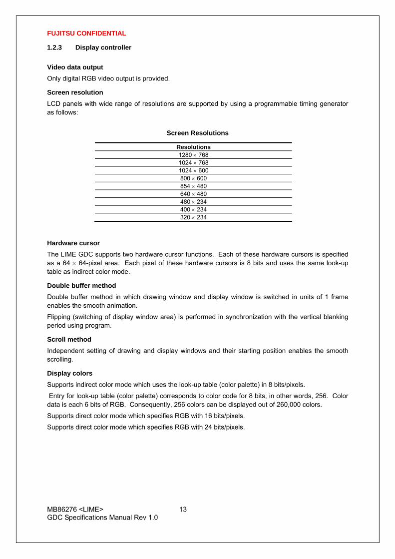
1.2.3 Display controller
Video data output Only digital RGB video output is provided.
Screen resolution
LCD panels with wide range of resolutions are supported by using a programmable timing generator as follows:
Screen Resolutions
Resolutions 1280 × 768 1024 × 768 1024 × 600 800 × 600 854 × 480 640 × 480 480 × 234 400 × 234 320 × 234
Hardware cursor The LIME GDC supports two hardware cursor functions. Each of these hardware cursors is specified as a 64 × 64-pixel area. Each pixel of these hardware cursors is 8 bits and uses the same look-up table as indirect color mode.
Double buffer method Double buffer method in which drawing window and display window is switched in units of 1 frame enables the smooth animation.
Flipping (switching of display window area) is performed in synchronization with the vertical blanking period using program.
Scroll method Independent setting of drawing and display windows and their starting position enables the smooth scrolling.
Display colors
Supports indirect color mode which uses the look-up table (color palette) in 8 bits/pixels.
Entry for look-up table (color palette) corresponds to color code for 8 bits, in other words, 256. Color data is each 6 bits of RGB. Consequently, 256 colors can be displayed out of 260,000 colors.
Supports direct color mode which specifies RGB with 16 bits/pixels.
Supports direct color mode which specifies RGB with 24 bits/pixels.

FUJITSU CONFIDENTIAL
MB86276 <LIME> 14 GDC Specifications Manual Rev 1.0
Overlay Traditional compatibility mode Up to four extra layers (C, W, M and B) can be displayed overlaid.
The overlay position for the hardware cursors is above/below the top layer (C).
The transparent mode or the blend mode can be selected for overlay.
The M- and B-layers can be split into separate windows.
Window display can be performed for the W-layer.
Two palettes are provided: C-layer and M-/B-layer.
The W-layer is used as the video input layer.
Window mode
• Up to six screens (L0 to 5) can be displayed overlaid.
• The overlay sequence of the L0- to L5-layers can be changed arbitrarily.
• The overlay position for the hardware cursors is above/below the L0-layer.
• The transparent mode or the blend mode can be selected for overlay.
• The L5-layer can be used as the blend coefficient plane (8 bits/pixel).
• Window display can be performed for all layers.
• Four palettes corresponded to L0 to 3 are provided.
• The L1-layer is used as the video input layer.
• Background color display is supported in window display for all layers.
L0, L2, L4 (0,0) L3, L5 (HDB+1, 0)L1 (WX, WY)
L0 (L0WX, L0WY) L2 (L2WX, L2WY)
L1 (L1WX, L1WY)L5 (L5WX, L5WY)
L4 (L4WX, L4WY)
L3 (L3WX, L3WY)

FUJITSU CONFIDENTIAL
MB86276 <LIME> 15 GDC Specifications Manual Rev 1.0
1.2.4 2D Drawing
2D Primitives The LIME GDC can perform 2D drawing for graphics memory (drawing plane) in direct color mode or indirect color mode.
Bold lines with width and broken lines can be drawn. With anti-aliasing smooth diagonal lines also can be drawn.
A triangle can be tiled in a single color or 2D pattern (tiling), or mapped with a texture pattern by specifying coordinates of the 2D pattern at each vertex (texture mapping). At texture mapping, drawing/non-drawing can be set in pixel units. Moreover, transparent processing can be performed using alpha blending. When drawing in single color or tiling without Gouraud shading or texture mapping, 2D Line with XY setup and 2D Triangle with XY setup can be used. Only vertex coordinates are set for these primitives. 2D Triangle with XY setup is also used to draw polygons.
2D Primitives
Primitive type Description Point Plots point Line Draws line Triangle Draws triangle 2D Line with XY setup Draws lines
Compared to line, this reduces the host CPU processing load. 2D Triangle with XY setup Draws ltriangles
Compared to tiangle, this reduces the host CPU processing load.
Arbitrary polygon Draws arbitrary closed polygon containing concave shapes consisting of vertices
Arbitrary polygon drawing Using this function, arbitrary closed polygon containing concave shapes consisting of vertices can be drawn. (There is no restriction on the count of vertices, however, the polygon with its sides crossed are not supported.) In this case, as a work area for drawing, polygon drawing flag buffer is used on the graphics memory. In drawing polygon, draw triangle for polygon drawing flag buffer using 2D Triangle with XY setup. Decide any vertex as a starting point to draw triangle along the periphery. It enables you to draw final polygon form in single color or with tiling or with texture mapping in a drawing frame.

FUJITSU CONFIDENTIAL
MB86276 <LIME> 16 GDC Specifications Manual Rev 1.0
BLT/Rectangle drawing This function draws a rectangle using logic operations. It is used to draw pattern and copy the image pattern within the drawing frame. It is also used for clearing drawing frame and Z buffer.
BLT Attributes
Attribute Description Raster operation Selects two source logical operation mode Transparent processing Performs BLT without drawing pixel consistent with the
transparent color. Alpha blending The alpha map and source in the memory is subjected to alpha
blending and then copied to the destination.
Pattern (Text) drawing This function draws a binary pattern (text) in a specified color.
Pattern (Text) Drawing Attributes
Attribute Description Enlarge Vertically × 2
Horizontally × 2 Vertically and Horizontally × 2
Shrink Vertically × 1/2 Horizontally 1/2 Vertically and Horizontally 1/2
Drawing clipping This function sets a rectangle frame in drawing frame to prohibit the drawing of the outside the frame.
Hidden plane management (Optional function) LIME GDC supports the Z buffer for hidden plane management as a optional function.

FUJITSU CONFIDENTIAL
MB86276 <LIME> 17 GDC Specifications Manual Rev 1.0
1.2.5 Special effects
Anti-aliasing Anti-aliasing manipulates line borders of polygons in sub-pixel units and blend the pre-drawing pixel color with color to make the jaggies be seen smooth. It is used as a functional option for 2D drawing (in direct color mode only).
Bold line and broken line drawing This function draws lines of a specific width and a broken line.
Line Drawing Attributes
Attribute Description Line width Selectable from 1 to 32 pixels Broken line Set by 32 bit or 24 bit of broken line pattern
Not support the Anti-aliasing of dashed line patterns.

FUJITSU CONFIDENTIAL
MB86276 <LIME> 18 GDC Specifications Manual Rev 1.0
Alpha blending Alpha blending blends two image colors to provide a transparent effect. LIME GDC supports two types of blending; blending two different colors at drawing, and blending overlay planes at display. Transparent color is not used for these blending options.
Set a transparent coefficient to the register; the transparent coefficient is applied for transparency processing of one plane.
In addition to the above, the following settings can be performed at texture mapping. When the most significant bit of each texture cell is 1, drawing or transparency can be set. When the most significant bit of each texture cell is 0, non-drawing can be set.
Alpha Blending
Type Description Drawing Transparent ratio set in particular register
While one primitive (polygon, pattern, etc.), being drawn, registered transparent ratio applied
Overlay display Blends top layer pixel color with lower layer pixel color
Transparent coefficient set in particular register
Registered transparent coefficient applied during one frame scan
Gouraud Shading Gouraud shading can be used in the direct color mode to provide real shading and color gradation.
FUJITSU CONFIDENTIAL
MB86276 <LIME> 19 GDC Specifications Manual Rev 1.0
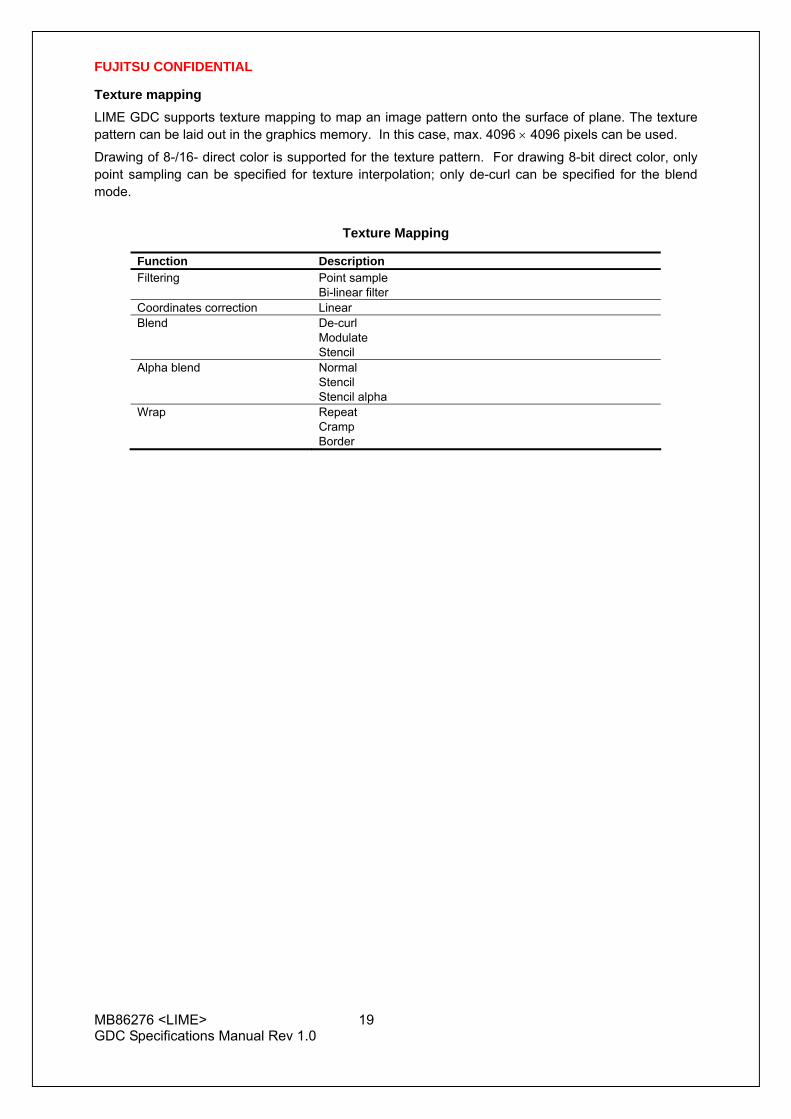
Texture mapping LIME GDC supports texture mapping to map an image pattern onto the surface of plane. The texture pattern can be laid out in the graphics memory. In this case, max. 4096 × 4096 pixels can be used.
Drawing of 8-/16- direct color is supported for the texture pattern. For drawing 8-bit direct color, only point sampling can be specified for texture interpolation; only de-curl can be specified for the blend mode.
Texture Mapping
Function Description Filtering Point sample
Bi-linear filter Coordinates correction Linear Blend De-curl
Modulate Stencil
Alpha blend Normal Stencil Stencil alpha
Wrap Repeat Cramp Border

FUJITSU CONFIDENTIAL
MB86276 <LIME> 20 GDC Specifications Manual Rev 1.0
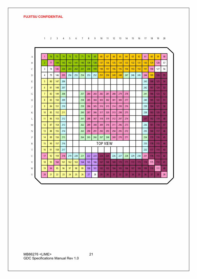
2 Pins 2.1 Pin assignment diagram
1 2 3 4 5 6 7 8 9 10 11 12 13 14 15 16 17 18 19 20
A VSS VINF VINVS BI0 BI3 GI0 GI3 RI0 RI3 BO4 BO0 GO4 GO0 RO5 RO2 DCLKO VSS DCLKIVSYNC VSS
B RGBCK VSS VINHS BI1 BI4 GI1 GI4 RI1 RI4 BO5 BO1 GO5 GO1 RO6 RO3 RO0 HSYNCCSYNC VSS GMOD0
C XPLLT XTST VSS BI2 BI5 GI2 GI5 RI2 RI5 BO6 BO2 GO6 GO2 RO7 RO4 RO1 DISP VSS GMOD1GMOD2
D XSM SCL SDA VSS VDDE VDDE VDDI VDDE VDDE BO7 BO3 GO7 GO3 VDDI VDDE VDDE VSS GV D31 D30
E MD0 MD1 MD2 VDDE VDDE D29 D28 D27
F MD3 MD4 MD5 VDDE VDDE D26 D25 D24
G MD6 MD7 MD8 VDDI VDDI VSS VSS VSS VSS VSS VSS VSS VDDI D23 D22 D21
H MD9 MD10 MD11 VDDE VDDI VSS VSS VSS VSS VSS VSS VSS VDDE D20 D19 D18
J MD12 MD13 MD14 VDDE VDDI VSS VSS VSS VSS VSS VSS VSS VDDE D17 D16 D15
K MD15 MD16 MD17 MD18 VDDI VSS VSS VSS VSS VSS VSS VSS VDDE D14 D13 D12
L MD19 MD20 MD21 VDDE VDDI VSS VSS VSS VSS VSS VSS VSS D11 D10 D9 D8
M MD22 MD23 MD24 VDDE VDDI VSS VSS VSS VSS VSS VSS VSS VDDE D7 D6 D5
N MD25 MD26 MD27 VDDE VDDI VSS VSS VSS VSS VSS VSS VSS VDDE D4 D3 D2
P MD28 MD29 MD30 VDDI VDDI VDDI VDDI VDDI VDDI VSS VSS VSS VDDI D1 D0 DRACK
R MD31MDQM0MDQM1VDDE TOP VIEW VDDEDTACKXWE3 XWE2
T MCLKIMDQM2MDQM3VDDE VDDE XWE1 XWE0 A23
U VSS MA0 MA1 VSS VDDE VDDE VDDI PLLVSPLLVDMODE0 XINT VDDE VDDE VDDI VDDE VDDE VSS A22 A21 A20
V MCLKO MA2 VSS MA9 MA12 MRAS CLKS0 XRST CLKS1 BS_M XRDY XRD A1 A4 A7 A10 A13 VSS A19 A18
W MA3 VSS MA6 MA8 MA11 MA14 MWE CKM S RDY_MMODE2 XCS A0 A3 A6 A9 A12 A15 VSS A17
Y VSS MA4 MA5 MA7 MA10 MA13 MCAS CLK VPD BCLKIMODE1DREQ XBS A2 A5 A8 A11 A14 A16 VSS
FUJITSU CONFIDENTIAL
MB86276 <LIME> 21 GDC Specifications Manual Rev 1.0
1 2 3 4 5 6 7 8 9 10 11 12 13 14 15 16 17 18 19 20
A 1 76 75 74 73 72 71 70 69 68 67 66 65 64 63 62 61 60 59 58
B 2 77 144 143 142 141 140 139 138 137 136 135 134 133 132 131 130 129 128 57
C 3 78 145 204 203 202 201 200 199 198 197 196 195 194 193 192 191 190 127 56
D 4 79 146 205 256 255 254 253 252 251 250 249 248 247 246 245 244 189 126 55
E 5 80 147 206 243 188 125 54
F 6 81 148 207 242 187 124 53
G 7 82 149 208 257 284 283 282 281 280 279 278 241 186 123 52
H 8 83 150 209 258 285 304 303 302 301 300 277 240 185 122 51
J 9 84 151 210 259 286 305 316 315 314 299 276 239 184 121 50
K 10 85 152 211 260 287 306 317 320 313 298 275 238 183 120 49
L 11 86 153 212 261 288 307 318 319 312 297 274 237 182 119 48
M 12 87 154 213 262 289 308 309 310 311 296 273 236 181 118 47
N 13 88 155 214 263 290 291 292 293 294 295 272 235 180 117 46
P 14 89 156 215 264 265 266 267 268 269 270 271 234 179 116 45
R 15 90 157 216 TOP VIEW 233 178 115 44
T 16 91 158 217 232 177 114 43
U 17 92 159 218 219 220 221 222 223 224 225 226 227 228 229 230 231 176 113 42
V 18 93 160 161 162 163 164 165 166 167 168 169 170 171 172 173 174 175 112 41
W 19 94 95 96 97 98 99 100 101 102 103 104 105 106 107 108 109 110 111 40
Y 20 21 22 23 24 25 26 27 28 29 30 31 32 33 34 35 36 37 38 39
FUJITSU CONFIDENTIAL
MB86276 <LIME> 22 GDC Specifications Manual Rev 1.0
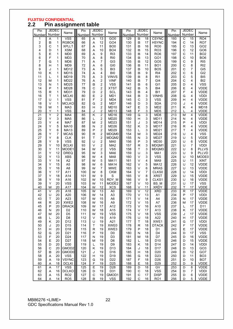
2.2 Pin assignment table
PinNumber Name Pin
Number Name PinNumber Name Pin
Number Name
1 A 1 VSS 65 A 13 GO0 129 B 18 CSYNC 193 C 15 RO42 B 1 RGBCK 66 A 12 GO4 130 B 17 HSYNC 194 C 14 RO73 C 1 XPLLT 67 A 11 BO0 131 B 16 RO0 195 C 13 GO24 D 1 XSM 68 A 10 BO4 132 B 15 RO3 196 C 12 GO65 E 1 MD0 69 A 9 RI3 133 B 14 RO6 197 C 11 BO26 F 1 MD3 70 A 8 RI0 134 B 13 GO1 198 C 10 BO67 G 1 MD6 71 A 7 GI3 135 B 12 GO5 199 C 9 RI58 H 1 MD9 72 A 6 GI0 136 B 11 BO1 200 C 8 RI29 J 1 MD12 73 A 5 BI3 137 B 10 BO5 201 C 7 GI510 K 1 MD15 74 A 4 BI0 138 B 9 RI4 202 C 6 GI211 L 1 MD19 75 A 3 VINVS 139 B 8 RI1 203 C 5 BI512 M 1 MD22 76 A 2 VINF 140 B 7 GI4 204 C 4 BI213 N 1 MD25 77 B 2 VSS 141 B 6 GI1 205 D 4 VSS14 P 1 MD28 78 C 2 XTST 142 B 5 BI4 206 E 4 VDDE15 R 1 MD31 79 D 2 SCL 143 B 4 BI1 207 F 4 VDDE16 T 1 MCLKI 80 E 2 MD1 144 B 3 VINHS 208 G 4 VDDI17 U 1 VSS 81 F 2 MD4 145 C 3 VSS 209 H 4 VDDE18 V 1 MCLKO 82 G 2 MD7 146 D 3 SDA 210 J 4 VDDE19 W 1 MA3 83 H 2 MD10 147 E 3 MD2 211 K 4 MD1820 Y 1 VSS 84 J 2 MD13 148 F 3 MD5 212 L 4 VDDE21 Y 2 MA4 85 K 2 MD16 149 G 3 MD8 213 M 4 VDDE22 Y 3 MA5 86 L 2 MD20 150 H 3 MD11 214 N 4 VDDE23 Y 4 MA7 87 M 2 MD23 151 J 3 MD14 215 P 4 VDDI24 Y 5 MA10 88 N 2 MD26 152 K 3 MD17 216 R 4 VDDE25 Y 6 MA13 89 P 2 MD29 153 L 3 MD21 217 T 4 VDDE26 Y 7 MCAS 90 R 2 MDQM0 154 M 3 MD24 218 U 4 VSS27 Y 8 CLK 91 T 2 MDQM2 155 N 3 MD27 219 U 5 VDDE28 Y 9 VSS 92 U 2 MA0 156 P 3 MD30 220 U 6 VDDE29 Y 10 BCLKI 93 V 2 MA2 157 R 3 MDQM1 221 U 7 VDDI30 Y 11 MODE1 94 W 2 VSS 158 T 3 MDQM3 222 U 8 PLLVS31 Y 12 DREQ 95 W 3 MA6 159 U 3 MA1 223 U 9 PLLVD32 Y 13 XBS 96 W 4 MA8 160 V 3 VSS 224 U 10 MODE033 Y 14 A2 97 W 5 MA11 161 V 4 MA9 225 U 11 XINT34 Y 15 A5 98 W 6 MA14 162 V 5 MA12 226 U 12 VDDE35 Y 16 A8 99 W 7 MWE 163 V 6 MRAS 227 U 13 VDDE36 Y 17 A11 100 W 8 CKM 164 V 7 CLKS0 228 U 14 VDDI37 Y 18 A14 101 W 9 S 165 V 8 XRST 229 U 15 VDDE38 Y 19 A16 102 W 10 RDY_M 166 V 9 CLKS1 230 U 16 VDDE39 Y 20 VSS 103 W 11 MODE2 167 V 10 BS_M 231 U 17 VSS40 W 20 A17 104 W 12 XCS 168 V 11 XRDY 232 T 17 VDDE41 V 20 A18 105 W 13 A0 169 V 12 XRD 233 R 17 VDDE42 U 20 A20 106 W 14 A3 170 V 13 A1 234 P 17 VDDI43 T 20 A23 107 W 15 A6 171 V 14 A4 235 N 17 VDDE44 R 20 XWE2 108 W 16 A9 172 V 15 A7 236 M 17 VDDE45 P 20 DRACK 109 W 17 A12 173 V 16 A10 237 L 17 D1146 N 20 D2 110 W 18 A15 174 V 17 A13 238 K 17 VDDE47 M 20 D5 111 W 19 VSS 175 V 18 VSS 239 J 17 VDDE48 L 20 D8 112 V 19 A19 176 U 18 A22 240 H 17 VDDE49 K 20 D12 113 U 19 A21 177 T 18 XWE1 241 G 17 VDDI50 J 20 D15 114 T 19 XWE0 178 R 18 DTACK 242 F 17 VDDE51 H 20 D18 115 R 19 XWE3 179 P 18 D1 243 E 17 VDDE52 G 20 D21 116 P 19 D0 180 N 18 D4 244 D 17 VSS53 F 20 D24 117 N 19 D3 181 M 18 D7 245 D 16 VDDE54 E 20 D27 118 M 19 D6 182 L 18 D10 246 D 15 VDDE55 D 20 D30 119 L 19 D9 183 K 18 D14 247 D 14 VDDI56 C 20 GMOD2 120 K 19 D13 184 J 18 D17 248 D 13 GO357 B 20 GMOD0 121 J 19 D16 185 H 18 D20 249 D 12 GO758 A 20 VSS 122 H 19 D19 186 G 18 D23 250 D 11 BO359 A 19 VSYNC 123 G 19 D22 187 F 18 D26 251 D 10 BO760 A 18 DCLKI 124 F 19 D25 188 E 18 D29 252 D 9 VDDE61 A 17 VSS 125 E 19 D28 189 D 18 GV 253 D 8 VDDE62 A 16 DCLKO 126 D 19 D31 190 C 18 VSS 254 D 7 VDDI63 A 15 RO2 127 C 19 GMOD1 191 C 17 DISP 255 D 6 VDDE64 A 14 RO5 128 B 19 VSS 192 C 16 RO1 256 D 5 VDDE
JEDECNumber
JEDECNumber
JEDECNumber
JEDECNumber

FUJITSU CONFIDENTIAL
MB86276 <LIME> 23 GDC Specifications Manual Rev 1.0
Group Symbol description
GND group: VSS/PLLVSS/Low Ground
TESTL Connect Ground.
1.8V group: VDDL/VDDI 1.8-V power supply
PLLVDD PLL power supply (1.8 V)
3.3V group: VDDH/VDDE 3.3-V power supply
TESTH Input a 3.3 V-power supply
PinNumber Name
257 G 7 VDDI258 H 7 VDDI259 J 7 VDDI260 K 7 VDDI261 L 7 VDDI262 M 7 VDDI263 N 7 VDDI264 P 7 VDDI265 P 8 VDDI266 P 9 VDDI267 P 10 VDDI268 P 11 VDDI269 P 12 VSS270 P 13 VSS271 P 14 VSS272 N 14 VSS273 M 14 VSS274 L 14 VSS275 K 14 VSS276 J 14 VSS277 H 14 VSS278 G 14 VSS279 G 13 VSS280 G 12 VSS281 G 11 VSS282 G 10 VSS283 G 9 VSS284 G 8 VSS285 H 8 VSS286 J 8 VSS287 K 8 VSS288 L 8 VSS289 M 8 VSS290 N 8 VSS291 N 9 VSS292 N 10 VSS293 N 11 VSS294 N 12 VSS295 N 13 VSS296 M 13 VSS297 L 13 VSS298 K 13 VSS299 J 13 VSS300 H 13 VSS301 H 12 VSS302 H 11 VSS303 H 10 VSS304 H 9 VSS305 J 9 VSS306 K 9 VSS307 L 9 VSS308 M 9 VSS309 M 10 VSS310 M 11 VSS311 M 12 VSS312 L 12 VSS313 K 12 VSS314 J 12 VSS315 J 11 VSS316 J 10 VSS317 K 10 VSS318 L 10 VSS319 L 11 VSS320 K 11 VSS
JEDECNumber

FUJITSU CONFIDENTIAL
MB86276 <LIME> 24 GDC Specifications Manual Rev 1.0
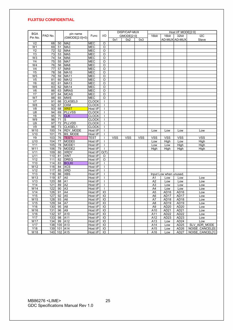
2.3 Pin mutiplex table
DISP/CAP-MUX Host I/F MODE[2:0]GMODE[2:0] 16bit 16bit 32bit I2C
0x1 0x2 0x3 AD-MUX AD-MUX SlaveA2 1 1 VINFID CAP IA3 2 2 VINVSYNC CAP IB3 3 3 VINHSYNC CAP IB1 5 4 RGBCLK CAP IC1 8 5 TESTH TEST I VDDE VDDE VDDE VDDE VDDE VDDE VDDEC2 9 6 TESTH TEST I VDDE VDDE VDDE VDDE VDDE VDDE VDDED1 10 7 TESTH TEST I VDDE VDDE VDDE VDDE VDDE VDDE VDDED2 11 8 SCL I2C IOD3 12 9 SDA I2C IOE1 16 10 MD0 MEC IOE2 17 11 MD1 MEC IOE3 18 12 MD2 MEC IOF1 19 13 MD3 MEC IOF2 23 14 MD4 MEC IOF3 24 15 MD5 MEC IOG1 25 16 MD6 MEC IOG2 26 17 MD7 MEC IOG3 27 18 MD8 MEC IOH1 28 19 MD9 MEC IOH2 29 20 MD10 MEC IOH3 30 21 MD11 MEC IOJ1 31 22 MD12 MEC IOJ2 32 23 MD13 MEC IOJ3 34 24 MD14 MEC IOK1 35 25 MD15 MEC IOK2 36 26 MD16 MEC IOK3 37 27 MD17 MEC IOK4 38 28 MD18 MEC IOL1 39 29 MD19 MEC IOL2 40 30 MD20 MEC IOL3 41 31 MD21 MEC IOM1 42 32 MD22 MEC IOM2 43 33 MD23 MEC IOM3 47 34 MD24 MEC ION1 48 35 MD25 MEC ION2 49 36 MD26 MEC ION3 50 37 MD27 MEC IOP1 51 38 MD28 MEC IOP2 52 39 MD29 MEC IOP3 53 40 MD30 MEC IOR1 54 41 MD31 MEC IOT1 58 42 MCLKI MEC IV1 60 43 MCLKO MEC OR2 62 44 MDQM0 MEC OR3 63 45 MDQM1 MEC OT2 64 46 MDQM2 MEC OT3 65 47 MDQM3 MEC OU2 66 48 MA0 MEC OU3 67 49 MA1 MEC O
I/OFuncpin name(GMODE[2:0]=0)PAD No.BGA
Pin No.
FUJITSU CONFIDENTIAL
MB86276 <LIME> 25 GDC Specifications Manual Rev 1.0
DISP/CAP-MUX Host I/F MODE[2:0]GMODE[2:0] 16bit 16bit 32bit I2C
0x1 0x2 0x3 AD-MUX AD-MUX SlaveV2 68 50 MA2 MEC OW1 69 51 MA3 MEC OY2 72 52 MA4 MEC OY3 73 53 MA5 MEC OW3 74 54 MA6 MEC OY4 75 55 MA7 MEC OW4 76 56 MA8 MEC OV4 77 57 MA9 MEC OY5 78 58 MA10 MEC OW5 79 59 MA11 MEC OV5 81 60 MA12 MEC OY6 82 61 MA13 MEC OW6 83 62 MA14 MEC OV6 86 63 MRAS MEC OY7 87 64 MCAS MEC OW7 88 65 MWE MEC OV7 91 66 CLKSEL0 CLOCK IW8 92 67 CKM CLOCK IV8 93 68 XRST Host I/F IU8 94 69 PLLVSS CLOCK IY8 95 70 CLK CLOCK IW9 96 71 S CLOCK IU9 97 72 PLLVDD CLOCK IV9 98 73 CLKSEL1 CLOCK I
W10 100 74 RDY_MODE Host I/F I Low Low Low LowV10 101 75 BS_MODE Host I/F IY9 103 76 TESTL TEST I VSS VSS VSS VSS VSS VSS VSS
U10 104 77 MODE0 Host I/F I Low High Low HighY11 105 78 MODE1 Host I/F I Low Low High HighW11 106 79 MODE2 Host I/F I High High High HighV11 109 80 XRDY Host I/F O(T)U11 110 81 XINT Host I/F OY12 111 82 DREQ Host I/F OY10 114 83 BCLKI Host I/F IW12 116 84 XCS Host I/F IV12 117 85 XRD Host I/F IY13 118 86 XBS Host I/F I Input Low when unused.W13 119 87 A0 Host I/F I A1 Low Low LowV13 120 88 A1 Host I/F I A2 Low Low LowY14 121 89 A2 Host I/F I A3 Low Low LowW14 122 90 A3 Host I/F I A4 Low Low LowV14 126 91 A4 Host I/F IO A5 AD16 AD16 LowY15 127 92 A5 Host I/F IO A6 AD17 AD17 LowW15 128 93 A6 Host I/F IO A7 AD18 AD18 LowV15 129 94 A7 Host I/F IO A8 AD19 AD19 LowY16 130 95 A8 Host I/F IO A9 AD20 AD20 LowW16 131 96 A9 Host I/F IO A10 AD21 AD21 LowV16 132 97 A10 Host I/F IO A11 AD22 AD22 LowY17 133 98 A11 Host I/F IO A12 AD23 AD23 LowW17 134 99 A12 Host I/F IO A13 Low AD24 LowV17 138 100 A13 Host I/F IO A14 Low AD25 SLV_ADR_MODEY18 139 101 A14 Host I/F IO A15 Low AD26 NOISE_CANCEL[0]W18 140 102 A15 Host I/F IO A16 Low AD27 NOISE_CANCEL[1]
I/OBGAPin No. PAD No. pin name
(GMODE[2:0]=0) Func
FUJITSU CONFIDENTIAL
MB86276 <LIME> 26 GDC Specifications Manual Rev 1.0
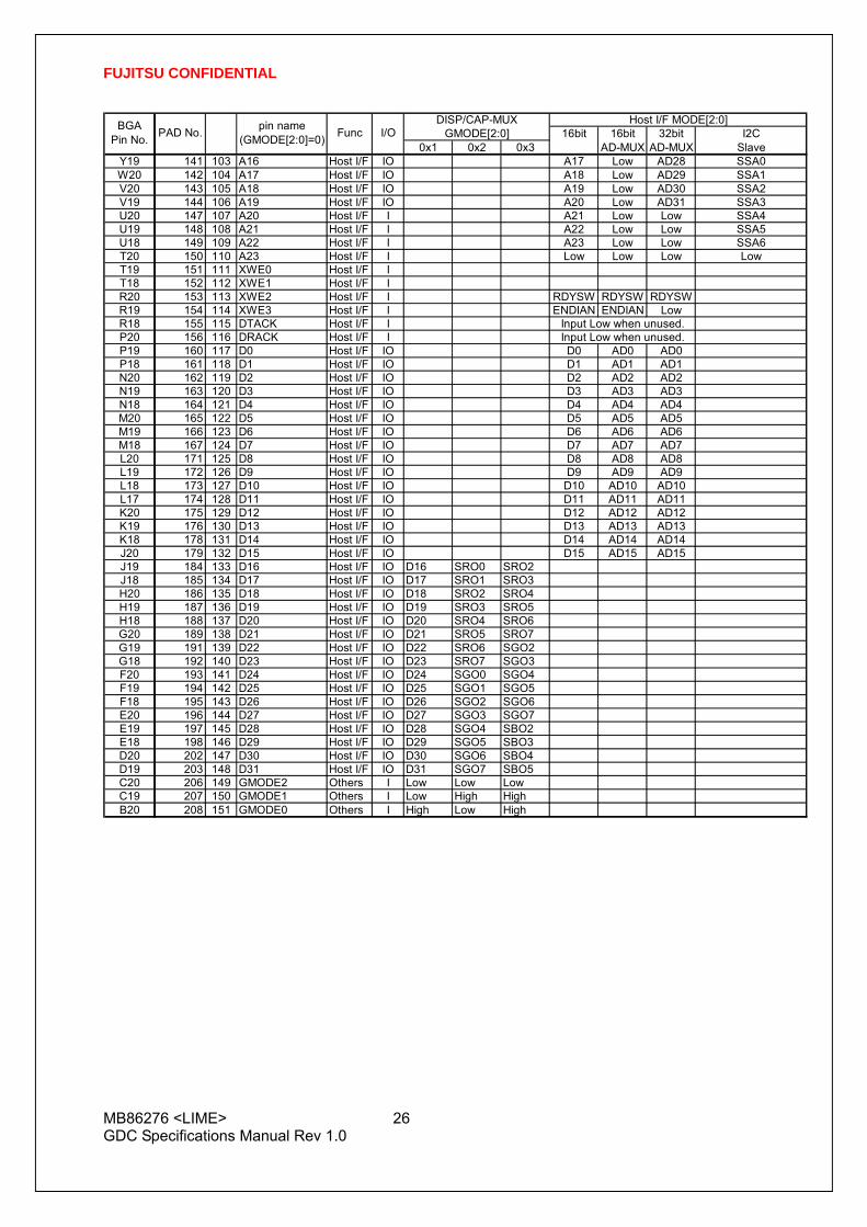
DISP/CAP-MUX Host I/F MODE[2:0]GMODE[2:0] 16bit 16bit 32bit I2C
0x1 0x2 0x3 AD-MUX AD-MUX SlaveY19 141 103 A16 Host I/F IO A17 Low AD28 SSA0W20 142 104 A17 Host I/F IO A18 Low AD29 SSA1V20 143 105 A18 Host I/F IO A19 Low AD30 SSA2V19 144 106 A19 Host I/F IO A20 Low AD31 SSA3U20 147 107 A20 Host I/F I A21 Low Low SSA4U19 148 108 A21 Host I/F I A22 Low Low SSA5U18 149 109 A22 Host I/F I A23 Low Low SSA6T20 150 110 A23 Host I/F I Low Low Low LowT19 151 111 XWE0 Host I/F IT18 152 112 XWE1 Host I/F IR20 153 113 XWE2 Host I/F I RDYSW RDYSW RDYSWR19 154 114 XWE3 Host I/F I ENDIAN ENDIAN LowR18 155 115 DTACK Host I/F I Input Low when unused.P20 156 116 DRACK Host I/F I Input Low when unused.P19 160 117 D0 Host I/F IO D0 AD0 AD0P18 161 118 D1 Host I/F IO D1 AD1 AD1N20 162 119 D2 Host I/F IO D2 AD2 AD2N19 163 120 D3 Host I/F IO D3 AD3 AD3N18 164 121 D4 Host I/F IO D4 AD4 AD4M20 165 122 D5 Host I/F IO D5 AD5 AD5M19 166 123 D6 Host I/F IO D6 AD6 AD6M18 167 124 D7 Host I/F IO D7 AD7 AD7L20 171 125 D8 Host I/F IO D8 AD8 AD8L19 172 126 D9 Host I/F IO D9 AD9 AD9L18 173 127 D10 Host I/F IO D10 AD10 AD10L17 174 128 D11 Host I/F IO D11 AD11 AD11K20 175 129 D12 Host I/F IO D12 AD12 AD12K19 176 130 D13 Host I/F IO D13 AD13 AD13K18 178 131 D14 Host I/F IO D14 AD14 AD14J20 179 132 D15 Host I/F IO D15 AD15 AD15J19 184 133 D16 Host I/F IO D16 SRO0 SRO2J18 185 134 D17 Host I/F IO D17 SRO1 SRO3H20 186 135 D18 Host I/F IO D18 SRO2 SRO4H19 187 136 D19 Host I/F IO D19 SRO3 SRO5H18 188 137 D20 Host I/F IO D20 SRO4 SRO6G20 189 138 D21 Host I/F IO D21 SRO5 SRO7G19 191 139 D22 Host I/F IO D22 SRO6 SGO2G18 192 140 D23 Host I/F IO D23 SRO7 SGO3F20 193 141 D24 Host I/F IO D24 SGO0 SGO4F19 194 142 D25 Host I/F IO D25 SGO1 SGO5F18 195 143 D26 Host I/F IO D26 SGO2 SGO6E20 196 144 D27 Host I/F IO D27 SGO3 SGO7E19 197 145 D28 Host I/F IO D28 SGO4 SBO2E18 198 146 D29 Host I/F IO D29 SGO5 SBO3D20 202 147 D30 Host I/F IO D30 SGO6 SBO4D19 203 148 D31 Host I/F IO D31 SGO7 SBO5C20 206 149 GMODE2 Others I Low Low LowC19 207 150 GMODE1 Others I Low High HighB20 208 151 GMODE0 Others I High Low High
BGAPin No. PAD No. pin name
(GMODE[2:0]=0) Func I/O

FUJITSU CONFIDENTIAL
MB86276 <LIME> 27 GDC Specifications Manual Rev 1.0
DISP/CAP-MUX Host I/F MODE[2:0]GMODE[2:0] 16bit 16bit 32bit I2C
0x1 0x2 0x3 AD-MUX AD-MUX SlaveD18 209 152 GV DISP OC17 202 153 DISPE DISP OB18 213 154 CSYNC DISP OA19 214 155 VSYNC DISP IOB17 215 156 HSYNC DISP IOA18 218 157 DCLKI DISP IA16 220 158 DCLKO DISP OB16 223 159 RO0 DISP O RO0 SBO0 SBO6C16 224 160 RO1 DISP O RO1 SBO1 SBO7A15 226 161 RO2 DISP O RO2 SBO2 RO2B15 227 162 RO3 DISP O RO3 SBO3 RO3C15 228 163 RO4 DISP O RO4 SBO4 RO4A14 229 164 RO5 DISP O RO5 SBO5 RO5B14 230 165 RO6 DISP O RO6 SBO6 RO6C14 233 166 RO7 DISP O RO7 SBO7 RO7A13 234 167 GO0 DISP O GO0 RO2 GO2B13 236 168 GO1 DISP O GO1 RO3 GO3C13 237 169 GO2 DISP O GO2 RO4 GO4D13 238 170 GO3 DISP O GO3 RO5 GO5A12 239 171 GO4 DISP O GO4 RO6 GO6B12 240 172 GO5 DISP O GO5 RO7 GO7C12 241 173 GO6 DISP O GO6 GO2 BO2D12 242 174 GO7 DISP O GO7 GO3 BO3A11 245 175 BO0 DISP O BO0 GO4 BO4B11 246 176 BO1 DISP O BO1 GO5 BO5C11 247 177 BO2 DISP O BO2 GO6 BO6D11 249 178 BO3 DISP O BO3 GO7 BO7A10 250 179 BO4 DISP O BO4 BO2B10 251 180 BO5 DISP O BO5 BO3C10 252 181 BO6 DISP O BO6 BO4D10 253 182 BO7 DISP O BO7 BO5C9 259 183 RI5 CAP I/O GPIO0 BO6 RI5B9 260 184 RI4 CAP I/O GPIO1 BO7 RI4A9 261 185 RI3 CAP I/O GPIO2 GPIO0 RI3C8 262 186 RI2 CAP I/O GPIO3 GPIO1 RI2B8 263 187 RI1 CAP I/O GPIO4 GPIO2 RI1A8 266 188 RI0 CAP I RI0C7 267 189 GI5 CAP I GI5B7 268 190 GI4 CAP I GI4A7 269 191 GI3 CAP I GI3C6 270 192 GI2 CAP I GI2B6 274 193 GI1 CAP I VIN7 VIN7 GI1A6 275 194 GI0 CAP I VIN6 VIN6 GI0C5 276 195 BI5 CAP I VIN5 VIN5 BI5B5 277 196 BI4 CAP I VIN4 VIN4 BI4A5 279 197 BI3 CAP I VIN3 VIN3 BI3C4 280 198 BI2 CAP I VIN2 VIN2 BI2B4 281 199 BI1 CAP I VIN1 VIN1 BI1A4 282 200 BI0 CAP I VIN0 VIN0 BI0
Func I/OBGAPin No. PAD No. pin name
(GMODE[2:0]=0)
FUJITSU CONFIDENTIAL
MB86276 <LIME> 28 GDC Specifications Manual Rev 1.0
2.4 Host CPU interface 1)Parallel interface mode
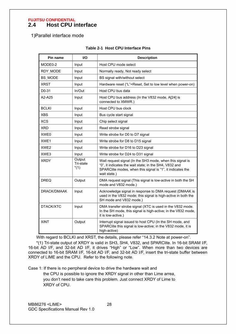
Table 2-1 Host CPU Interface Pins
Pin name I/O Description
MODE0-2 Input Host CPU mode select
RDY_MODE Input Normally ready, Not ready select
BS_MODE Input BS signal with/without select
XRST Input Hardware reset (“L”=Reset, Set to low level when power-on)
D0-31 In/Out Host CPU bus data
A2-A25 Input Host CPU bus address (In the V832 mode, A[24] is connected to XMWR.)
BCLKI Input Host CPU bus clock
XBS Input Bus cycle start signal
XCS Input Chip select signal
XRD Input Read strobe signal
XWE0 Input Write strobe for D0 to D7 signal
XWE1 Input Write strobe for D8 to D15 signal
XWE2 Input Write strobe for D16 to D23 signal
XWE3 Input Write strobe for D24 to D31 signal
XRDY Output Tri-state *(1)
Wait request signal (In the SH3 mode, when this signal is “0”, it indicates the wait state; in the SH4, V832 and SPARClite modes, when this signal is “1”, it indicates the wait state.)
DREQ Output DMA request signal (This signal is low-active in both the SH mode and V832 mode.)
DRACK/DMAAK Input Acknowledge signal in response to DMA request (DMAAK is used in the V832 mode; this signal is high-active in both the SH mode and V832 mode.)
DTACK/XTC Input DMA transfer strobe signal (XTC is used in the V832 mode. In the SH mode, this signal is high-active; in the V832 mode, it is low-active.)
XINT Output Interrupt signal issued to host CPU (In the SH mode, and SPARClite this signal is low-active; in the V832 mode, it is high-active)
With regard to BCLKI and XRST, the details, please refer “14.3.2 Note at power-on”. *(1) Tri-state output of XRDY is valid in SH3, SH4, V832, and SPARClite. In 16-bit SRAM I/F, 16-bit AD I/F, and 32-bit AD I/F, it drives “High” or “Low”. When more than two devices are connected to 16-bit SRAM I/F, 16-bit AD I/F, and 32-bit AD I/F, insert the tri-state buffer between XRDY of LIME and the CPU. Refer to the following note. Case 1: If there is no perrpheral device to drive the hardware wait and the CPU is possible to ignore the XRDY signal in other than Lime arrea, you don’t need to take care this problem. Just connect XRDY of Lime to XRDY of CPU.

FUJITSU CONFIDENTIAL
MB86276GDC Spe
Case 2: If the condition is other than the above, put the tri-state buffer between Lime’s XRDY and CPU’s XRDY like the below.
CPU Lime
XCSx XCSn
<LIME> 29 cifications Manual Rev 1.0
P
Pull-up/down
XCS
eripheral device
XCS

FUJITSU CONFIDENTIAL
MB86276 <LIME> 30 GDC Specifications Manual Rev 1.0
LIME can be connected to the Renesas SH4 (SH7750), SH3 (SH7709) NEC V832 and Fujitsu SPARClite (MB86833) without external circuit. In the SRAM interface mode, LIME can be used with any other CPU as well. The host CPU is specified by the MODE0 to 2 pins.
MODE 2 MODE 1 MODE 0 CPU
L L L SH3
L L H SH4
L H L V832
L H H SPARClite
H L L General-purpose 16bit CPU with SRAM interface
H L H General-porpose 16bit CPU with address and data multiplex interface
H H L General-purpose 32bit CPU with address and data multiplex interface
H H H I2C Slave
2.4.1 Ready signal mode
The MODE2 pin can be used to set the ready signal level when the bus cycle of the host CPU terminates. For the normally not ready mode, set the software wait to 0 or 1 cycles. When using this device in the normally ready mode, set the software wait to 2 cycles. When using this device in the normally not ready mode, set the software wait to one cycle. (When BS_MODE = H, three cycles are needed for the software wait.)
The ‘normally not ready mode’ is the mode in which the LIME XRDY signal is always in the wait state and Ready is returned only when read/write is ready.
The ‘normal ready mode’ is the mode in which the LIME XRDY signal is always in the Ready state and it is put into the wait state only when read/write cannot be performed immediately.
Ready Signal Mode
RDY_MODE Ready signal operation
L Recognizes XRDY signal as ‘not ready level’ and terminates bus cycle (normally not ready mode)
H Recognizes XRDY signal as ‘ready level’ and terminates bus cycle (normally ready mode)
RDYSW is for an active signal level on 16bit SRAM I/F, 16bit A/D multiplexed I/F, and 32bit A/D multiplexed I/F modes. High active or low active can be selected.
Active level of ready signal for 16bit CPU and A/D multiplexed CPU
RDYSW RDYSW signal operation L Recognizes XRDY signal as “L” =”Ready”, “H”=”Wait” H Recognizes XRDY signal as “H” =”Ready”, “L”=”Wait”

FUJITSU CONFIDENTIAL
MB86276 <LIME> 31 GDC Specifications Manual Rev 1.0
2.4.2 BS signal mode
Connection to a CPU without the BS signal can be made via the BS_MODE signal. This setting can be performed for all CPU modes. To connect to a CPU without the BS signal, set the BS_MODE signal to “High” level. This function isn’t supported in 16bit SRAM mode.
When not using the BS signal, fix the BS pin of LIME at “High” level.
When using the BS_MODE signal as “High” level, with the normally ready mode established, set the CPU software wait to three cycles.
BS Signal Mode
BS_MODE Operation of BS signal L Connects to CPU with BS signal H Connects to CPU without BS signal
2.4.3 Endian
LIME has bi-endian mode for a halfword ordering of 16bit CPU.
ENDIAN signal is for 16bit SRAM I/F and 16bit A/D multiplexed I/F modes.The half word ordering of Lime can be selected from either little or big.
In the case of CPUs with the byte swapping, please note it.
LIME operates in little-endian mode. All the register address descriptions in the specifications are byte address in little endian. When using a big-endian CPU, note that the byte-or word-addresses are different from these descriptions.
Endian Mode for 16-bit CPU
ENDIAN Operation of BS signal L Little endian for the halfword ordering H Big endian for the halfword ordering
FUJITSU CONFIDENTIAL
MB86276 <LIME> 32 GDC Specifications Manual Rev 1.0
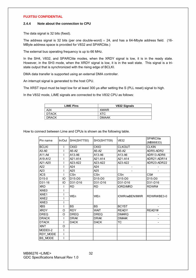
2.4.4 Note about the connection to CPU
The data signal is 32 bits (fixed).
The address signal is 32 bits (per one double-word) × 24, and has a 64-Mbyte address field. (16-MByte address space is provided for V832 and SPARClite.)
The external bus operating frequency is up to 66 MHz.
In the SH4, V832, and SPARClite modes, when the XRDY signal is low, it is in the ready state. However, in the SH3 mode, when the XRDY signal is low, it is in the wait state. This signal is a tri-state output that is synchronized with the rising edge of BCLKI.
DMA data transfer is supported using an external DMA controller.
An interrupt signal is generated to the host CPU.
The XRST input must be kept low for at least 300 µs after setting the S (PLL reset) signal to high.
In the V832 mode, LIME signals are connected to the V832 CPU as follows:
LIME Pins V832 Signals
A24 XMWR DTACK XTC DRACK DMAAK
How to connect between Lime and CPUs is shown as the following table.
Pin name In/Out SH4(SH7750) SH3(SH7709) V832SPARClite(MB86833)
BCLKI I CKIO CKIO CLKOUT CLKINA3-A0 I A5-A2 A5-A2 A5-A2 ADR5-ADR2A11-A4 I A13-A6 A13-A6 A13-A6 ADR13-ADR6A19-A12 I A21-A14 A21-A14 A21-A14 ADR21-ADR14A21-A20 I A23-A22 A23-A22 A23-A22 ADR23-ADR22A22 I A24 A24 - -A23 I A25 A25 - -XCS I CSn CSn CSn CS#D15-0 IO D15-D0 D15-D0 D15-D0 D15-D0D31-16 IO D31-D16 D31-D16 D31-D16 D31-D16XRD I RD RD IORD/MRD RDWR#XWE0 IXWE1 IXWE2 IXWE3 IXBS I BS BS BCYST -XRDY O RDY WAIT READY READY#DREQ O DREQ DREQ DMARQ -DRACK I DRAK DRAK DMAAK -DTACK I DACK DACK TC -XINT OMODE0-2 IRDY_MODE IBS_MODE I
WEn WEn IOWR/xxBEN/MWR RDWR#/BE3-0

FUJITSU CONFIDENTIAL
MB86276 <LIME> 33 GDC Specifications Manual Rev 1.0
Pin name In/Out MB90470 MB90480 MB91460
BCLKI I CLK CLK SYSCLKA3-A0 I A04-A01 A04-A01 A04-A01A11-A4 I A12-A05 A12-A05 A12-A05A19-A12 I A20-A13 A20-A13 A20-A13A21-A20 I A22-A21 A22-A21 A22-A21A22 I A23 A23 A23A23 I - - -XCS I CSn CSn CSnXD15-0 IO AD15-AD0 AD15-AD0 D31-D16D31-16 IO - - -XRD I RD RD IORDXXWE0 I WRL WRL IOWRXXWE1 I WRH WRH -XWE2 I - - -XWE3 I - - -XBS I ALE ALE ASXXRDY O RDY RDY RDYDREQ O - - -DRACK I - - -DTACK I - - -XINT OMODE0-2 IRDY_MODE IBS_MODE I
Pin name In/Out MPC5200(16bit AD-MUX)
MPC5554(16bit AD-MUX)
MPC5200(32bit AD-MUX)
MPC5554(32bit AD-MUX)
BCLKI I PCI_CLOCK PCI_CLOCK PCI_CLOCK PCI_CLOCKA3-A0 I - - - -A11-A4 I EXT_AD[23:16] EXT_AD[23:16] EXT_AD[23:16] EXT_AD[23:16]A19-A12 I - - EXT_AD[31:24] EXT_AD[31:24]A21-A20 I - - - -A22 I - - - -A23 I - - - -XCS I LP_CSn LP_CSn LP_CSn LP_CSnD15-0 IO EXT_AD[15:0] EXT_AD[15:0] EXT_AD[15:0] EXT_AD[15:0]D31-16 IO - - - -XRD I High(*1) High(*1) High(*1) High(*1)XWE0 I LP_RW LP_RW LP_RW LP_RWXWE1 I LP_RW LP_RW LP_RW LP_RWXWE2 I - - - -XWE3 I - - - -XBS I LP_ALE LP_ALE LP_ALE LP_ALEXRDY O LP_ACK LP_ACK LP_ACK LP_ACKDREQ O - - - -DRACK I - - - -DTACK I - - - -XINT OMODE0-2 IRDY_MODE IBS_MODE I
*1: Unused because read control signal is included in LP_RW

FUJITSU CONFIDENTIAL
MB86276 <LIME> 34 GDC Specifications Manual Rev 1.0
2)Serial interface mode
Serial host interface pins
Pin name I/O Multiplexed pin name Description
SDA I/O --- I2C serial data line.
This pin is the same as I2C interface’s one.
SCL I/O --- I2C serial clock line. It is the same as I2C interface’s one.
This pin is the same as I2C interface’s one.
NOISE_CANCEL[1:0] I A[15:14] Noise Cancel Pins.
It determines the period of noise cancellation for I2C signal.
00 Non noise cancellation An input signal is used without noise cancellation.
01 BCLK*1 (e.g. When BCLK is 50MHz, it is canceled a noise within 20ns pulse.)
10 BCLK*2 (e.g. When BCLK is 50MHz, it is canceled a noise within 40ns pulse.)
11 BCLK*3 (e.g. When BCLK is 50MHz, it is canceled a noise within 60ns pulse.)
BCLKI I -- System clock. This pin is the same as parallel interface’ one. Please input within 10 to 50MHz when I2C slave mode.
SLV_ADR_MODE I A13 It determines the slave address mode. 0 General call address of I2C standard is selected. Default slave address is 7'b111_0000. 1 SSA0-SSA6 pins are selected as a slave address.
SSA0-SSA6 I A[22:16] These pins are valid when SLV_ADR_MODE is “1".

FUJITSU CONFIDENTIAL
MB86276 <LIME> 35 GDC Specifications Manual Rev 1.0
2.5 Graphics memory interface
Graphics memory interface pins
Pin name I/O Description
MD31 - MD0 I/O Graphics memory bus data
MA14 - MA0 Output Graphics memory bus data
MRAS Output Row address strobe
MCAS Output Column address strobe
MWE Output Write enable
DQM3 - DQM0 Output Data mask
MCLK1 Input Graphics memory clock input
Connect the interface to the external memory used as memory for image data. The interface can be connected to 64-/128-/256-Mbit SDRAM (16- or 32-bit length data bus) without using any external circuit.
Connect MCLKI to MCLK0.
Connect 0 to XCS of SDRAM.
Connect 1 to CKE of SDRAM
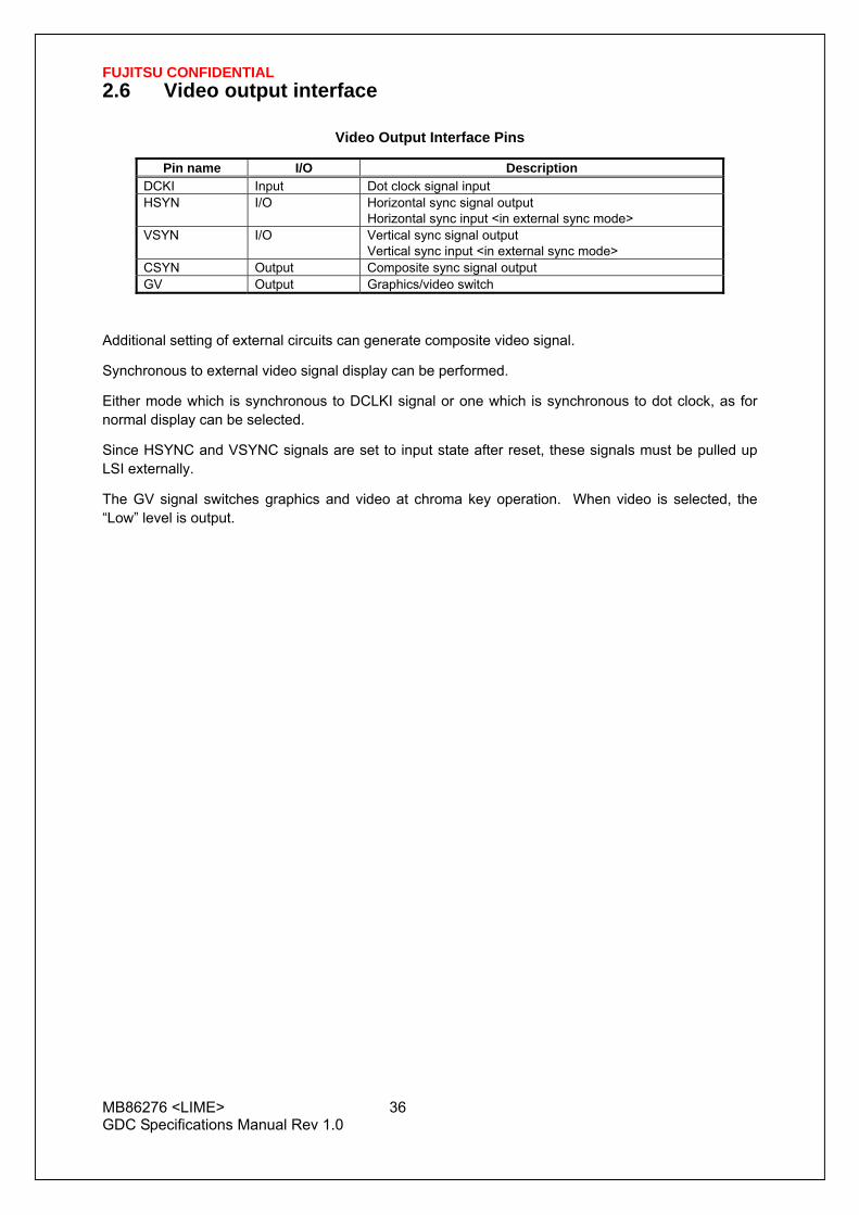
FUJITSU CONFIDENTIAL
MB86276 <LIME> 36 GDC Specifications Manual Rev 1.0
2.6 Video output interface
Video Output Interface Pins
Pin name I/O Description DCKI Input Dot clock signal input HSYN I/O Horizontal sync signal output
Horizontal sync input <in external sync mode> VSYN I/O Vertical sync signal output
Vertical sync input <in external sync mode> CSYN Output Composite sync signal output GV Output Graphics/video switch
Additional setting of external circuits can generate composite video signal.
Synchronous to external video signal display can be performed.
Either mode which is synchronous to DCLKI signal or one which is synchronous to dot clock, as for normal display can be selected.
Since HSYNC and VSYNC signals are set to input state after reset, these signals must be pulled up LSI externally.
The GV signal switches graphics and video at chroma key operation. When video is selected, the “Low” level is output.

FUJITSU CONFIDENTIAL
MB86276 <LIME> 37 GDC Specifications Manual Rev 1.0
2.7 Video capture interface 1) ITU-656 Input Signals
Table 2-3 Video Capture Interface Pins
Pin name I/O Description
(CCLK) Input Digital video input clock signal input This pin is multiplexed RGBCLK. Please see RGBCLK.
VI7-0 Input ITU656 Digital video data input. These pins are multiplexed MD63-MD56.
Inputs ITU-RBT-656 format digital video signal
2)RGB Input Signals The signals used for video capture are not assigned on dedicated pins but share the same pins with other functions. There is a set of signals corresponding to the RGB capture modes.
There is a possibility of sharing these pins with other pins. (TBD) Direct Input Mode
Pin name I/O Description
RGBCLK Input Clock for RGB input. This pin is multiplexed CCLK.
RI5-0 Input Red component value. GI5-0 Input Green component value. BI5-0 Input Blue component value. VSYNCI Input Vertical sync for RGB capture. HSYNCI Input Horizontal sync for RGB capture.
Note : - the RGB bit of VCM(video capture mode) register enables RGB input mode of video capture.

FUJITSU CONFIDENTIAL
MB86276 <LIME> 38 GDC Specifications Manual Rev 1.0
2.8 I2C interface
Pin name I/O Description SDA I/O I2C serial data line. SCL I/O I2C serial clock line.
Note) Input voltage level is 3.3V. Please be careful, it does not support to 5V input. (The device whose output voltage is 5V is not connectable.)
2.9 GPIO interface
Pin name I/O Description
GPIO4-0 I/O General-purpose IO pin.
A direct value is controlled and read by the inside register. Moreover, interruption can be generated with the value of a pin.
2.10 General purpose mode pins
GMODE 2
GMODE 1
GMODE 0 PIN Multiplex
Host Interface Primary RGB output
Secondary RGB output
Video Capture GPIO
L L L 32bit CPU I2C Slave RGB888 -- Native
RGB666 --
L L H 32bit CPU I2C Slave RGB888 -- RBT656/601 GPIO[4:0]
L H L 16bit CPU I2C Slave RGB888 RGB666 RBT656/601 GPIO[2:0]
L H H 16bit CPU
I2C Slave RGB666 RGB666
Native
RGB666 --
H L L Reserved Reserved Reserved Reserved Reserved
H L H Reserved Reserved Reserved Reserved Reserved
H H L Reserved Reserved Reserved Reserved Reserved
H H H Reserved Reserved Reserved Reserved Reserved

FUJITSU CONFIDENTIAL
MB86276 <LIME> 39 GDC Specifications Manual Rev 1.0
2.11 Clock input
Pin name I/O Description
CLK Input Clock input signal
S Input PLL reset signal
CKM Input Clock mode signal
CLKSEL [1:0] Input Clock rate select signal
Inputs source clock for internal operation clock and display dot clock. Normally, 4 Fsc (= 14.31818 MHz: NTSC) is input. An internal PLL generates the internal operation clock of 133 MHz/100 MHz and the display base clock of 400 MHz. Even if don’t use an internal PLL (use BCLKI as internal clock and use DCLKI as dot clock), don’t stop the PLL (Not fixed the S pin to low level).
CKM Clock mode
L Output from internal PLL selected
H BLCKI clock selected
When CKM = L, selects input clock frequency when built-in PLL used according to setting of CSL pins
CSL1 CSL0 Input clock frequency
Multiplication rate
Display reference clock
L L Inputs 13.5-MHz clock frequency
× 29 391.5 MHz
L H Inputs 14.32-MHz clock frequency
× 28 400.96 MHz
H L Inputs 17.73-MHz clock frequency
× 22 390.06 MHz
H H Inputs 33.33-MHz clock frequency × 12 399.96
Please connect the crystal oscillator directly with the terminal CLK.

FUJITSU CONFIDENTIAL
MB86276 <LIME> 40 GDC Specifications Manual Rev 1.0
2.12 Test pins
Table 2-5 Test Pins
Pin name I/O Description
TESTL Input Input 0-V power.
TESTH Input Input 3.3-V power.
2.13 Reset sequence See “13.3.2 Note at power-on”. 2.14 How to switch internal operating frequency Switch the operating frequency immediately after a reset (before rewriting MMR mode register of
external memory interface).
Any operating frequency can be selected from the five combinations shown in Table 2-6.
Table 2-6 Frequency Setting Combinations
Clock for Rendering Engine and Memory interface
133 MHz
100 MHz

FUJITSU CONFIDENTIAL
MB86276 <LIME> 41 GDC Specifications Manual Rev 1.0
3 PROCEDURE OF THE HARDWARE INITIALIZATION 3.1 Hardware reset
1.Do the hardware reset. (see section xx.x.x)
2.After the hardware reset, set the CCF(Change of Frequency) register (section xx.x.x). In being unstable cycle after the hardware reset, keep 32 bus cycles open.
3.Set the graphics memory interface register, MMR (Memory I/F Mode Register).
After setting the CCF register, take 200 us to set the MMR register. In being unstable memory access cycle, keep 32 bus cycles open.
4.Other registers, except for the CCF register and the MMR register, should be set after setting the CCF register.
In case of not using memory access, the MMR register could be set in any order after the CCF register is set.
3.2 Re-reset
1. Reset XRST signal.
2. See section x.x for registers setting after the procedure of re-reset. 3.3 Software reset 1. Set the value of the SRST register (see section xx.x.x) for re-reset. 2. It is not necessary to reset the CCF register and the MMR register again.

FUJITSU CONFIDENTIAL
MB86276 <LIME> 42 GDC Specifications Manual Rev 1.0
4 HOST INTERFACE
Select the host CPU by setting the MODE0 to MODE2 signals as follows:
Table 4-1 CPU Type Setting
MODE 2 MODE 1 MODE 0 CPU L L L SH3
L L H SH4
L H L V832
L H H SPARClite
H L L General 16bit CPU with SRAM interface
H L H General 16bit CPU with address and data multiplex interface
H H L General 32bit CPU with address and data multiplex interface
H H H I2C Slave

FUJITSU CONFIDENTIAL
MB86276 <LIME> 43 GDC Specifications Manual Rev 1.0
4.1 Access Mode 4.1.1 SRAM interface
Data can be transferred to/from LIME using SRAM access protocol. LIME internal registers and graphics memory are all mapped to the physical address area of the host processor.
LIME uses hardware wait based on the XRDY signal, enabling the hardware wait setting of the host CPU. When using the normally not ready mode, set the software wait to “1”. When using the normally ready mode, set the software wait to “2”. (When using the BS_MODE signal as “High” level, with the normally ready mode established, set the CPU software wait to three cycles.) Switch the ready mode using the RDY_MODE signal.
CPU Read The host processor reads data from internal registers and memory of LIME in double-word (32 bit) units. Valid data is output continuously while XRD and XCS are being asserted at a “Low” level after XRDY has been asserted.
CPU Write The host CPU writes data to internal registers and memory of LIME in byte, word(16 bit) and double-word( 32 bit) units.
4.1.2 FIFO interface (fixed transfer destination address)
This interface transfers display lists stored in host memory. Display list information is transferred efficiently using a single address mode DMA transfer. Data can be transferred to FIFO in relation to FIFO buffer area mapped in memory area using SRAM interface or dual address mode.

FUJITSU CONFIDENTIAL
MB86276 <LIME> 44 GDC Specifications Manual Rev 1.0
4.2 DMA Transfer 4.2.1 Data transfer unit
DMA transfer is performed in double-word (32 bits) units or 8 double-word (32 bytes) units. Byte and word access is not supported.
Note: 8 double-word transfer is supported only in the SH4 mode.
4.2.2 Address mode
Dual address mode (mode using ACK) DMA is performed at memory-to-memory transfer between host memory and registers mapped in memory space or graphics memory (destination). Both the host memory address and LIME is used. In the SH4 mode, the 1 double-word transfer (32 bits) and 8 double-word transfer (32 bytes) can be used.
When the CPU transfer destination address is fixed, data can also be transferred to the FIFO interface. However, in this case, even the SH4 mode supports only the 1 double-word transfer.
DREQ and DRACK pins and SRAM interface signals are used. In V832, the DREQ, DMAAK, and XTC pins and SRAM interface signals are used.
Note: The SH3 mode supports the direct address mode; it does not support the indirect address mode.
Dual address mode (mode not using ACK) When not using the ACK signal with the dual address mode established, set bit3 at HostBase+0004h (DNA: Dual address No Ack mode) to 1.
When the ACK is not used, the DREQ signal is in the edge mode and the DREQ signal is negated per transfer and then reasserted it in the next cycle. If processing cannot be performed immediately inside LIME, the DREQ signal remains negated.
The transfer count register (DTC) of LIME is not used, so in order to end DMA transfer, write “1” to the DMA transfer stop register (DTS) from the CPU.
Note 1: In the dual DMA mode (mode without ACK), the destination address can be used only for the FIFO.
In DMA transfer to the graphics memory, etc., use the dual DMA mode.
Note 2: DMA read is not supported.
Single address mode (FIFO interface) Data is transferred between host memory (source) and FIFO (destination). Only the address output from the host memory is used, and the data is transferred to the FIFO. This mode does not support data write to the host memory. When the FIFO is full, the DMA transfer is suspended.
The 1 double-word transfer (32 bits) and the 8 double-word transfer (32 B) can be used.
DREQ, DTACK, and DRACK signal are used.
Note: The single-address mode is supported only in the SH4 mode.

FUJITSU CONFIDENTIAL
MB86276 <LIME> 45 GDC Specifications Manual Rev 1.0
4.2.3 Bus mode
LIME supports the DMA transfer cycle steal mode and burst mode according to setting of external DMA mode.
Cycle steal mode (In the V832 mode, the burst mode is called the single transfer mode.) In the cycle steal mode, the right to use the bus is obtained or released at every data transfer of 1 unit. The DMA transfer unit can be selected from between the 1 double-word (32 bits) and 8 double-words (32 B).
Burst mode (In the V832 mode, the burst mode is called the demand transfer mode.) When DMA transfer is started, the right to use the bus is acquired and the transfer begins. The data transfer unit can be selected from between the 1 double-word (32 bits) and 8 double-words (32 B).
Note: When performing DMA transfer in the dual-address mode, a function for automatically negating DREQ is provided based on the setting of the DBM register.
4.2.4 DMA transfer request
Single-address mode
DMA is started when the LIME issues an external request to DMAC of the host processor.
Set the transfer count in the transfer count register of the LIME and then issue DREQ.
Fix the CPU destination address to the FIFO address.
Dual-address mode
DMA is started by two procedures: LIME issues an external request to DMAC of the host processor, or the CPU itself is started (auto request mode, etc.). In Ack use mode, set the transfer count in the transfer count register of LIME and then issue DREQ.
Note: In the Ack unused mode and the V832 mode requires no setting of the transfer count register.
4.2.5 Ending DMA transfer
SH3/SH4
When the LIME transfer count register is set to 0, DMA transfer ends and DREQ is negated.
V832
When the XTC signal from the CPU is low-asserted while the DMAAK signal to S LIME is high-asserted, the end of DMA transfer is recognized and DREQ is negated.
The end of DMA transfer is detected in two ways: the DMA status register (DST) is polled, and an interrupt to end the drawing command (FD000000H) is added to the display list and the interrupt is detected.
In the dual address mode (mode not using ACK), the DMA transfer count register (DTC) is not used, so the DMA ending cannot be determined. The DREQ signal can be negated to end DMA by writing 1 from the CPU to the DMA transfer stop register (DTS) of LIME at DMA transfer end.
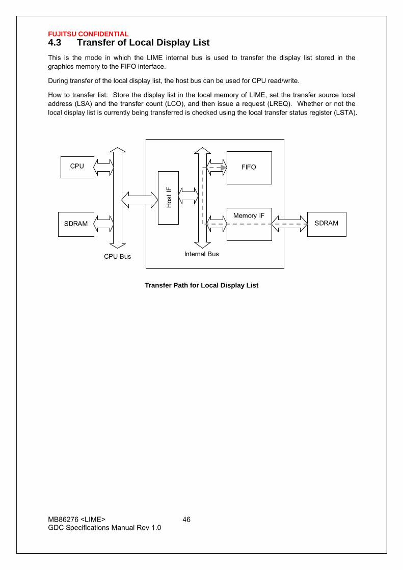
FUJITSU CONFIDENTIAL
MB86276 <LIME> 46 GDC Specifications Manual Rev 1.0
4.3 Transfer of Local Display List This is the mode in which the LIME internal bus is used to transfer the display list stored in the graphics memory to the FIFO interface.
During transfer of the local display list, the host bus can be used for CPU read/write.
How to transfer list: Store the display list in the local memory of LIME, set the transfer source local address (LSA) and the transfer count (LCO), and then issue a request (LREQ). Whether or not the local display list is currently being transferred is checked using the local transfer status register (LSTA).
Transfer Path for Local Display List
CPU
SDRAM
Hos
t IF
SDRAMMemory IF
FIFO
Internal Bus CPU Bus

FUJITSU CONFIDENTIAL
MB86276 <LIME> 47 GDC Specifications Manual Rev 1.0
4.4 Interrupt LIME issues interrupt requests to the host CPU. Following shows the types of interrupt factor and they can be enabled/disabled by IMASK (Interrupt Mask Register).
Vertical synchronization detect
Field synchronization detect
External synchronization error detect
Drawing command error
Drawing command execution end
GPIO pinmonitoring
4.4.1 Address Error Interrupt
Certain addresses are invalid depending on operation. For example the Burst Controller cannot access the Host Interface internal registers. If an attempt is made to do this then the access will be terminated and an Address Error Interrupt triggered.
4.5 SH3 Mode In the SH3 mode, operation is assured under the following conditions:
Normally not ready mode
BCLK (CPU bus clock) is 50 MHz or less.
The XWAIT setup time is 9.0 ns or less.
Normally ready mode
Three cycles or more are set for the software wait.
4.6 Wait Software wait The software wait is a wait performed on the CPU side; this wait specifies how many cycles of the ready signal (XRDY) sampling timing is ignored.
Hardware wait The hardware wait is a wait on the LIME side that occurs when LIME itself cannot read/write data immediately.
4.7 16-bit CPU mode In the 16-bit CPU mode (16-bit SRAM I/F, 16-bit AD I/F), the data is accessed in the following rules.

FUJITSU CONFIDENTIAL
MB86276 <LIME> 48 GDC Specifications Manual Rev 1.0
1. The data is accessed in the following order, lower 16-bit of 32-bit and upper 16-bit of 32-bit continuosly.
2. The address is accessed ountinuosly.
If those rules are not kept, it returns an error. Refer to the related Host Interface register in details.

FUJITSU CONFIDENTIAL
MB86276 <LIME> 49 GDC Specifications Manual Rev 1.0
4.8 Serial Control Interface (SCI)
4.8.1 Protcol of SCI as I2C slave
S Start condition RW 0:Writte (Host -> Slave(LIME))
1:Read (Slave(LIME) -> Host) DATA RW=0: Write data from Host
RW=1: Read data from Slave A Acknowledge NA Non Acknowledge P Stop condition Pattern Slave output
The protocols of the serial control interface are shown in the figure below. The parts with pattern are shown as the output from Lime.
4.8.2 General call address
The access of the general call address is executed only by the following protcol without any relation to the status of TRANS_MODE.
S SLAVE ADDRESS(7bit)
0x00
W A SLAVE ADDRESS(7bit)
0x06
A SLAVE ADDRESS(7bit)
0xXX
A P
Dispatch the general call address in the first byte, then dispatch the initial command in the second byte, and then dispatch the slave address in the third byte. It is able to set any address as I2C slave address.
4.8.3 TRANS_MODE register access
The access of TRANS_MODE register is executed only by the following protcol without any relation to the status of TRANS_MODE.
1)Write
S SLAVE ADDRESS(7bit) W A SCI Address=0x00(8bit) A TRANS_MODE A P
2)Read
S SLAVE ADDRESS(7bit) W A SCI Address=0x07(8bit) A SCI Address=0x00(8bit) A P
Dispatch the SCI read address in the third byte before a read protcol.
S SLAVE ADDRESS(7bit) R A TRANS_MODE NA P

FUJITSU CONFIDENTIAL
MB86276 <LIME> 50 GDC Specifications Manual Rev 1.0
4.8.4 Internal address register access
The access of the internal address register is executed only by the following protcol without any relation to the status of TRANS_MODE.
1)Write
S SLAVE ADDRESS(7bit) W A SCI Address=0x01(8bit) A
IA32[31:24] A IA32[23:16] A IA32[15:8] A IA32[7:0] A P
2)Read
S SLAVE ADDRESS(7bit) W A SCI Address=0x07(8bit) A SCI Address=0x01(8bit) A P
Dispatch the SCI read address in the third byte before a read protcol.
S SLAVE ADDRESS(7bit) R A
ID32[31:24] A ID32[23:16] A ID32[15:8] A ID32[7:0] NA P
In case of the auto incremntal mode, it is read a value after the transfer finished. Please note that the value of this address register means word address.
4.8.5 Internal data register access
The access of the internal data register is executed by each protcol of TRANS_MODE. 1)32bit Single Write
S SLAVE ADDRESS(7bit) W A SCI Address=0x00(8bit) A TRANS_MODE=0x00(8bit) A P
It is not necessary to update when TRANS_MODE remains unchanged from the previous state.
S SLAVE ADDRESS(7bit) W A SCI Address=0x01(8bit) A
IA32[31:24] A IA32[23:16] A IA32[15:8] A IA32[7:0] A P
S SLAVE ADDRESS(7bit) W A SCI Address=0x02(8bit) A
ID32[31:24] A ID32[23:16] A ID32[15:8] A ID32[7:0] A P
2)32bit Single Read
S SLAVE ADDRESS(7bit) W A SCI Address=0x00(8bit) A TRANS_MODE=0x00(8bit) A P
It is not necessary to update when TRANS_MODE remains unchanged from the previous state.
S SLAVE ADDRESS(7bit) W A SCI Address=0x01(8bit) A
Dispatch the SCI read address in the third byte before a read protcol.
IA32[31:24] A IA32[23:16] A IA32[15:8] A IA32[7:0] A P
S SLAVE ADDRESS(7bit) W A SCI Address=0x07(8bit) A Read register=0x02(8bit) A P
S SLAVE ADDRESS(7bit) R A
ID32[31:24] A ID32[23:16] A ID32[15:8] A ID32[7:0] NA P

FUJITSU CONFIDENTIAL
MB86276 <LIME> 51 GDC Specifications Manual Rev 1.0
3)N words burst write to the same address
S SLAVE ADDRESS(7bit) W A SCI Address=0x00(8bit) A TRANS_MODE=0x01(8bit) A P
It is not necessary to update when TRANS_MODE remains unchanged from the previous state.
S SLAVE ADDRESS(7bit) W A SCI Address=0x01(8bit) A
IA32[31:24] A IA32[23:16] A IA32[15:8] A IA32[7:0] A P
S SLAVE ADDRESS(7bit) W A SCI Address=0x02(8bit) A
ID32[31:24] A ID32[23:16] A ID32[15:8] A ID32[7:0] A
P
It keeps writing word data to the same address until the stop condition is detected.. 4)N words burst read to the same address
S SLAVE ADDRESS(7bit) W A SCI Address=0x00(8bit) A TRANS_MODE=0x01(8bit) A P
It is not necessary to update when TRANS_MODE remains unchanged from the previous state.
S SLAVE ADDRESS(7bit) W A SCI Address=0x01(8bit) A
IA32[31:24] A IA32[23:16] A IA32[15:8] A IA32[7:0] A P
S SLAVE ADDRESS(7bit) W A SCI Address=0x07(8bit) A Read register=0x02(8bit) A P
S SLAVE ADDRESS(7bit) R A
ID32[31:24] A ID32[23:16] A ID32[15:8] A ID32[7:0] A
ID32[31:24] A ID32[23:16] A ID32[15:8] A ID32[7:0] NA
P
It keeps reading from the same address until the stop condition is detected..

FUJITSU CONFIDENTIAL
MB86276 <LIME> 52 GDC Specifications Manual Rev 1.0
5)N words burst write to the auto incremental address
S SLAVE ADDRESS(7bit) W A SCI Address=0x00(8bit) A TRANS_MODE=0x02(8bit) A P
It is not necessary to update when TRANS_MODE remains unchanged from the previous state.
S SLAVE ADDRESS(7bit) W A SCI Address=0x01(8bit) A
IA32[31:24] A IA32[23:16] A IA32[15:8] A IA32[7:0] A P
S SLAVE ADDRESS(7bit) W A SCI Address=0x02(8bit) A
ID32[31:24] A ID32[23:16] A ID32[15:8] A ID32[7:0] A
P
It keeps writing word data to the auto incremental address until the stop condition is detected.. 6)N words burst read to the auto incremental address
S SLAVE ADDRESS(7bit) W A SCI Address=0x00(8bit) A TRANS_MODE=0x02(8bit) A P
It is not necessary to update when TRANS_MODE remains unchanged from the previous state.
S SLAVE ADDRESS(7bit) W A SCI Address=0x01(8bit) A
IA32[31:24] A IA32[23:16] A IA32[15:8] A IA32[7:0] A P
S SLAVE ADDRESS(7bit) W A SCI Address=0x07(8bit) A Read register=0x02(8bit) A P
S SLAVE ADDRESS(7bit) R A
ID32[31:24] A ID32[23:16] A ID32[15:8] A ID32[7:0] A
ID32[31:24] A ID32[23:16] A ID32[15:8] A ID32[7:0] NA
P
It keeps reading from the auto incremntal address until the stop condition is detected..

FUJITSU CONFIDENTIAL
MB86276 <LIME> 53 GDC Specifications Manual Rev 1.0
7)Line transfer to send the same data to the auto incremental address
Set the line transfer mode S SLAVE ADDRESS(7bit) W A SCI Address=0x00(8bit) A TRANS_MODE=0x03(8bit) A P
It is not necessary to update when TRANS_MODE remains unchanged from the previous state. Set the start address for the line transfer
S SLAVE ADDRESS(7bit) W A SCI Address=0x01(8bit) A
IA32[31:24] A IA32[23:16] A IA32[15:8] A IA32[7:0] A P
Set the source data S SLAVE ADDRESS(7bit) W A SCI Address=0x02(8bit) A
ID32[31:24] A ID32[23:16] A ID32[15:8] A ID32[7:0] A P
Set the number of transfer S SLAVE ADDRESS(7bit) W A SCI Address=0x03(8bit) A
HLINE_NUM[31:24] A HLINE_NUM[23:16] A HLINE_NUM[15:8] A HLINE_NUM[7:0] A P
It keeps writing the same source data to the auto incremental address until the number of HLINE_NUM becomes zero..
Start transfer S SLAVE ADDRESS(7bit) W A SCI Address=0x06(8bit) A Any data(8bit) A P
Confirm the status of this transfer as below until the transfer terminated.
Set the transfer mode S SLAVE ADDRESS(7bit) W A SCI Address=0x00(8bit) A TRANS_MODE=0x00(8bit) A P
Set the read register
S SLAVE ADDRESS(7bit) W A SCI Address=0x07(8bit) A TRANS_MODE=0x0B(8bit) A P
Read the status register
S SLAVE ADDRESS(7bit) R A STATUS NA P

FUJITSU CONFIDENTIAL
MB86276 <LIME> 54 GDC Specifications Manual Rev 1.0
5 I2C Interface Controller 5.1 Features
- Master transmission and receipt - Slave transmission and receipt - Arbitration - Clock synchronization - Detection of slave address - Detection of general call address - Detection of transfer direction - Repeated generation and detection of START condition - Detection of bus error - Correspondence to standard-mode (100kbit/s ) / high-speed-mode (400kbit/s)

FUJITSU CONFIDENTIAL
MB86276 <LIME> 55 GDC Specifications Manual Rev 1.0
5.2 Block diagram 5.2.1 Block Diagram
noise filter START condition/STOP condition detecting circuit
ADR
Comparater
DAR
BSR
BCR
CCR
Arbitration Lost detecting circuit
START condition/STOP condition generating circuit
Shift Clock generating circuit
Host Bus
SDASCL
Host IF
I2C UNIT

FUJITSU CONFIDENTIAL
MB86276 <LIME> 56 GDC Specifications Manual Rev 1.0
5.2.2 Block Function Overview
START condition / STOP condition detecting circuit This circuit performs detection of START condition and STOP condition from the state of SDA
and SCL. START condition / STOP condition generating circuit This circuit performs generation of START condition and STOP condition by changing the state of
SDA and SCL. Arbitration Lost detecting circuit This circuit compares the data output to SDA line with the data input into SDA line at the time of
data transmission, and it checks whether these data is in agreement. When not in agreement, it generates arbitration lost.
Shift Clock generating circuit This circuit performs generating timing count of the clock for serial data transfer, and output
control of SCL clock by setup of a clock control register. Comparater Comparater compares whether the received address and the self-address appointed to be the
address register is in agreement, and whether the received address is a global address. ADR ADR is the 7-bit register which appoints a slave address. DAR DAR is the 8-bit register used by serial data transfer. BSR BSR is the 8-bit register for the state of I2C bus etc. This register has following functions: - detection of repeated START condition - detection of arbitration lost - storage of acknowledge bit - data transfer direction - detection of addressing - detection of general call address - detection of the 1st byte BCR BCR is the 8-bit register which performs control and interruption of I2C bus. This register has
following functions: - request / permission of interruption - generation of START condition - selection of master / slave - permission to generate acknowledge
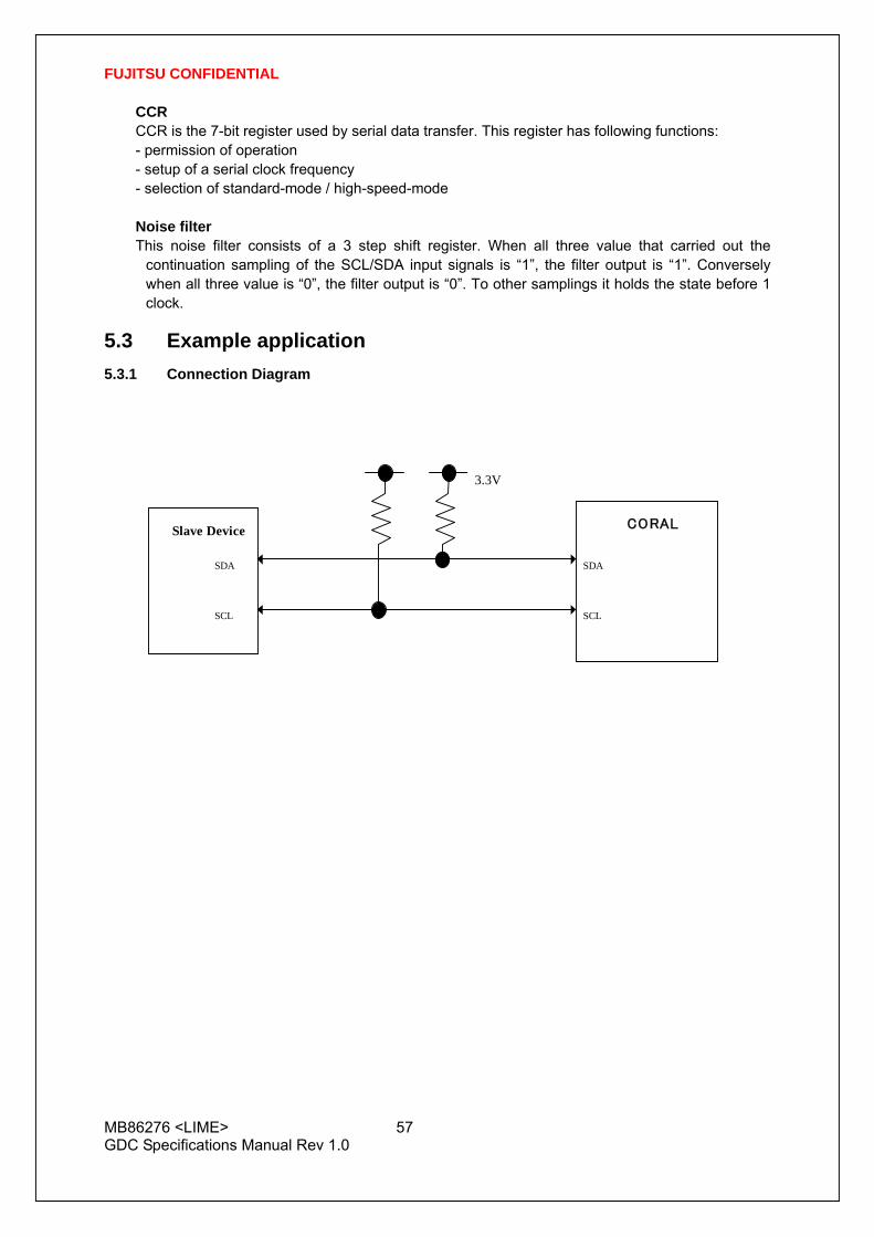
FUJITSU CONFIDENTIAL
MB86276 <LIME> 57 GDC Specifications Manual Rev 1.0
CCR CCR is the 7-bit register used by serial data transfer. This register has following functions: - permission of operation - setup of a serial clock frequency - selection of standard-mode / high-speed-mode Noise filter This noise filter consists of a 3 step shift register. When all three value that carried out the
continuation sampling of the SCL/SDA input signals is “1”, the filter output is “1”. Conversely when all three value is “0”, the filter output is “0”. To other samplings it holds the state before 1 clock.
5.3 Example application 5.3.1 Connection Diagram
SDA
SCL
SDA
SCL
Slave Device CORAL
3.3V

FUJITSU CONFIDENTIAL
MB86276 <LIME> 58 GDC Specifications Manual Rev 1.0
5.4 Function overview Two bi-directional buses, serial data line (SDA) and serial clock line (SCL), carry information at I2C-bus. Scarlet I2C interface has SDA input (SDAI) and SDA output (SDAO) for SDA and is connected to SDA line via open-drain I/O cell. And this interface also has SCL input (SCLI) and SCL output (SCLO) for SCL line and is connected to SCL line via open-drain I/O cell. The wired theory is used when the interface is connected to SDA line and SCL line.
5.3.2 START condition
If “1” is written to MSS bit while the bus is free, this module will become a master mode and will generate START condition simultaneously. In a master mode, even if a bus is in a use state (BB=1), START condition can be generated again by writing “1” to SCC bit. There are two conditions to generate START condition. - “1” writing to MSS bit in the state where the bus is not used (MSS=0 & BB=0 & INT=0 & AL=0) - “1” writing to SCC bit in the interruption state in a master mode (MSS=1 & BB=1 & INT=1 & AL=0) If “1” writing is performed to MSS bit in an idol state, AL bit will be set to “1”. “1” writing to MSS bit other than the above is disregarded.
5.3.3 STOP condition
If “0” is written to MSS bit in a master mode (MSS=1), this module will generate STOP condition and will become a slave mode. There is a condition to generate STOP condition. - “0” writing to MSS bit in the interruption state in a master mode (MSS=1 & BB=1 & INT=1 & AL=0) “0” writing to MSS bit other than the above is disregarded.
START condition
SDA
SCL
STOP condition
SDA
SCL
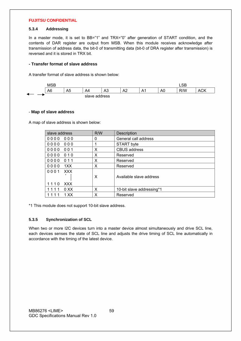
FUJITSU CONFIDENTIAL
MB86276 <LIME> 59 GDC Specifications Manual Rev 1.0
5.3.4 Addressing
In a master mode, it is set to BB=”1” and TRX=”0” after generation of START condition, and the contents of DAR register are output from MSB. When this module receives acknowledge after transmission of address data, the bit-0 of transmitting data (bit-0 of DRA register after transmission) is reversed and it is stored in TRX bit. - Transfer format of slave address A transfer format of slave address is shown below:
MSB LSB A6 A5 A4 A3 A2 A1 A0 R/W ACK slave address
- Map of slave address A map of slave address is shown below:
slave address R/W Description 0 0 0 0 0 0 0 0 General call address 0 0 0 0 0 0 0 1 START byte 0 0 0 0 0 0 1 X CBUS address 0 0 0 0 0 1 0 X Reserved 0 0 0 0 0 1 1 X Reserved 0 0 0 0 1XX X Reserved 0 0 0 1 XXX -----
- X Available slave address
1 1 1 0 XXX 1 1 1 1 0 XX X 10-bit slave addressing*1 1 1 1 1 1 XX X Reserved
*1 This module does not support 10-bit slave address.
5.3.5 Synchronization of SCL
When two or more I2C devices turn into a master device almost simultaneously and drive SCL line, each devices senses the state of SCL line and adjusts the drive timing of SCL line automatically in accordance with the timing of the latest device.

FUJITSU CONFIDENTIAL
MB86276 <LIME> 60 GDC Specifications Manual Rev 1.0
5.3.6 Arbitration
When other masters have transmitted data simultaneously at the time of master transmission, arbitration takes places. When its own transmitting data is “1” and the data on SDA line is “0”, the master considers that the arbitration was lost and sets “1” to AL. And if the master is going to generate START condition while the bus is in use by other master, it will consider that arbitration was lost and will set “1” to AL. When the START condition which other masters generated is detected by the time the master actually generated START condition, even when it checked the bus is in nonuse state and wrote in MSS=”1”, it considers that the arbitration was lost and sets “1” to AL. When AL bit is set to “1”, a master will set MSS=”0” and TRX= “0” and it will be a slave receiving mode. When the arbitration is lost (it has no royalty of a bus), a master stops a drive of SDA. However, a drive of SCL is not stopped until 1 byte transfer is completed and interruption is cleared.
5.3.7 Acknowledge
Acknowledge is transmitted from a reception side to a transmission side. At the time of data reception, acknowledge is stored in LRB bit by ACK bit. When the acknowledge from a master reception side is not received at the time of slave transmission, it sets TRX=”0” and becomes slave receiving mode. Thereby, a master can generate STOP condition when a slave opens SCL.
5.3.8 Bus error
When the following conditions are satisfied, it is judged as a bus error, and this interface will be in a stop state. - Detection of the basic regulation violation on I2C-bus under data transfer (including ACK bit) - Detection of STOP condition in a master mode - Detection of the basic regulation violation on I2C-bus at the time of bus idol
SDA changed under data transmission (SCL=H). It becomes bus error.
SDA
SCL START 31 2
D7 D6 D5

FUJITSU CONFIDENTIAL
MB86276 <LIME> 61 GDC Specifications Manual Rev 1.0
5.3.9 Initialize
Start
setup of slave address
setup of clock frequency setup of macro enable
setup of interruption
End
ADR: write
CCR: write CS[4:0]: write EN: 1write
BCR: write BER: 0write BEIE: 1write INT: 0write INTE: 1write

FUJITSU CONFIDENTIAL
MB86276 <LIME> 62 GDC Specifications Manual Rev 1.0
5.3.10 1-byte transfer from master to slave
Start
START condition
Transfer of address data
End
DAR: write MSS: 1write
LRB reset
INT set, TRX set DAR: write INT: 0write
master
BB set,TRX set
Acknowledge
Interruption
data transfer
acknowledge
interruption
STOP condition
LRB reset
INT set
MSS: 0write INT reset BB reset, TRX reset
slave
BB set,TRX reset
AAS set
INT set,TRX reset ACK: 1write INT: 0write
INT setDAR: read INT: 0write
BB reset,TRX reset AAS reset
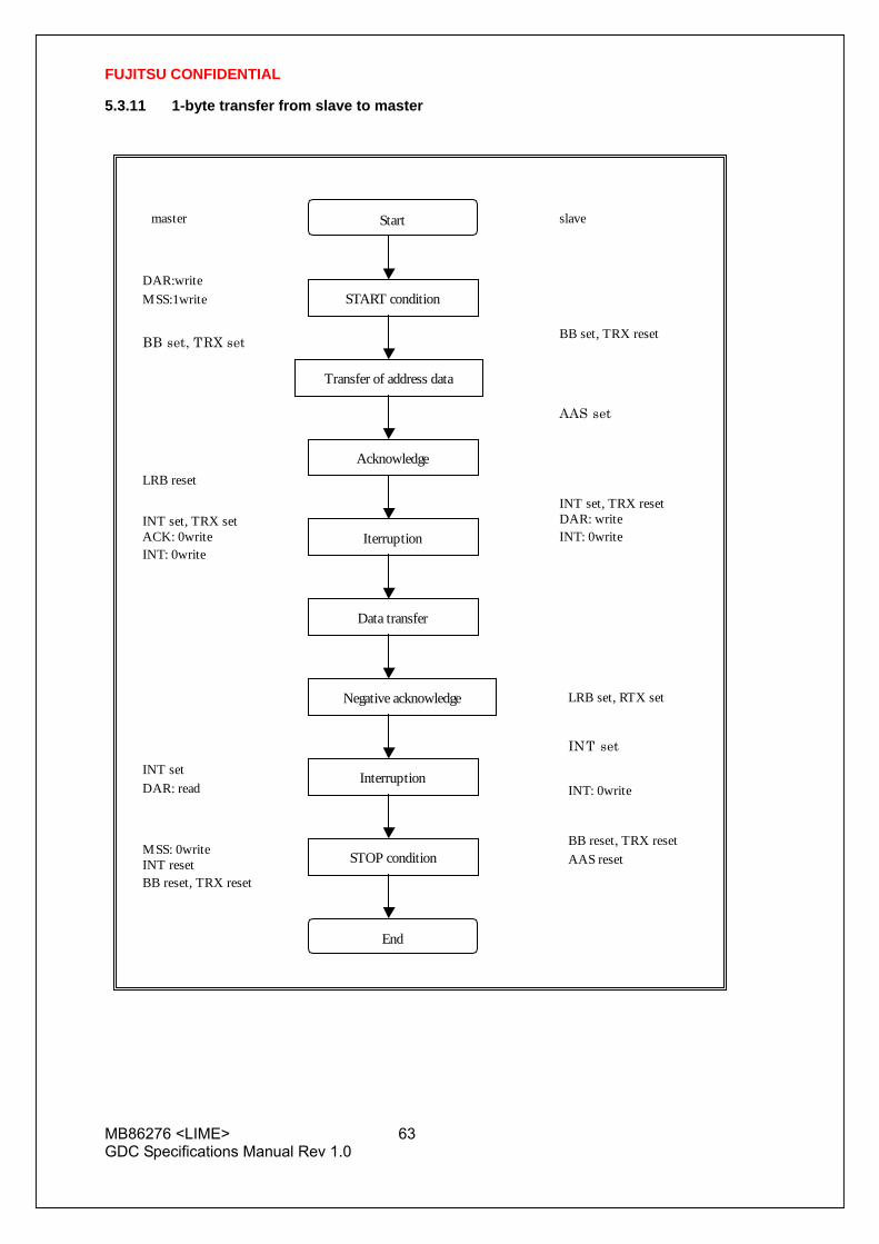
FUJITSU CONFIDENTIAL
MB86276 <LIME> 63 GDC Specifications Manual Rev 1.0
5.3.11 1-byte transfer from slave to master
Start
START condition
Transfer of address data
End
DAR:write MSS:1write
LRB reset
INT set, TRX set ACK: 0write INT: 0write
master
BB set, TRX set
Acknowledge
Iterruption
Data transfer
Negative acknowledge
Interruption
STOP condition
INT set DAR: read
MSS: 0write INT reset BB reset, TRX reset
slave
BB set, TRX reset
AAS set
INT set, TRX reset DAR: write INT: 0write
INT set
BB reset, TRX reset AAS reset
LRB set, RTX set
INT: 0write

FUJITSU CONFIDENTIAL
MB86276 <LIME> 64 GDC Specifications Manual Rev 1.0
5.3.12 Recovery from bus error
Start
Cancellation of error flag
Setup of clock frequency Setup of macro enable
Setup of interruption
End
CCR: write CS[4:0]: write EN: 1write
BCR: write BER: 0write BEIE: 1write INT: 0write INTE: 1write
BCR: write BER: 0write BEIE: 1write

FUJITSU CONFIDENTIAL
MB86276 <LIME> 65 GDC Specifications Manual Rev 1.0
5.4 Note A ) About a 10-bit slave address
This module does not support the 10-bit slave address. Therefore, please do not specify the slave address of from 78H to 7bH to this module. If it is specified by mistake, a normal transfer cannot be performed although acknowledge bit is returned at the time of 1 byte reception.
B ) About competition of SCC, MSS, and INT bit
Competition of the following byte transfer, generation of START condition, and generation of STOP condition happens by the simultaneous writing of SCC, MSS, and INT bit. At this time the priority is as follows.
1) The following byte transfer and generation of STOP condition If “0” is written to INT bit and “0” is written to MSS bit, priority will be given to “0” writing to MSS bit and STOP condition will be generated.
2) The following byte transfer and generation of START condition If “0” is written to INT bit and “1” is written to SCC bit, priority will be given to “1” writing to SCC bit and START condition will be generated.
3) Generation of START condition and generation of STOP condition The simultaneous writing of “1” in SCC bit and “0” to MSS bit is prohibition.
C ) About setup of S serial transfer clock
When the delay of the positive edge of SCL terminal is large or when the clock is extended by the slave device, it may become smaller than setting value (calculation value) because of generation of overhead.

FUJITSU CONFIDENTIAL
MB86276 <LIME> 66 GDC Specifications Manual Rev 1.0
6 Graphics Memory 6.1 Configuration
The LIME GDC uses local external memory (Graphics memory) for drawing and display management. The configuration of this Graphics memory is described as follows:
6.1.1 Data type
The LIME GDC handles the following types of data. Display list can be stored in the host (main) memory as well. Texture/tile pattern and text pattern can be defined by a display list as well. Drawing Frame This is a rectangular image data field for 2D drawing. The LIME GDC is able to have plural drawing frames and display a part of these area if it is set to be bigger than display size. The maximum size is 4096x4096 pixel in 32 pixel units. And both indirect color ( 8 bits / pixel) and direct color ( 16 bits / pixel) mode are applicable. Display Frame This is a rectangle picture area for display. The LIME GDC is able to set display layer up to 6 layers. Z Buffer Z buffer is required for eliminating hidden surfaces. In 16 bits modes, 2 bytes and in 8 bits mode, 1 byte are required per 1 pixel. This area has to be cleared before drawing. Polygon Drawing Flag Buffer This area is used for polygon drawing. It is required 1 bit memory area per 1 pixel and 1 x-axis line area both backward and forward of it. Initially, this area has to be cleared.
Specially, when you use Polygon with Shadow, required area is depending on geometory view volume clip parameter. (Normally depending on drawing clipping parameter) Above “Y resolution” is “Possible_view_clipped_Max_Ydc-Possible_view_clipped_Min_Ydc+1+6”. (+6 mergin must be needed) Displaylist Buffer The displaylist is a list of drawing commands and parameters. Texture Pattern This pattern is used for texture mapping. The maximum size is up to 4096 x 4096 pixels. Cursor Pattern
Frame buffer, Z buffer, Displaylist and etc
By XRES size
By drawing frame sizy
By XRES size
Frame buffer, Z buffer,Displaylist and etc
Polygon drawing flag area => (Y resolution + 2) * X resolution
Base Address of Polygon Drawing Buffer(PFBR)
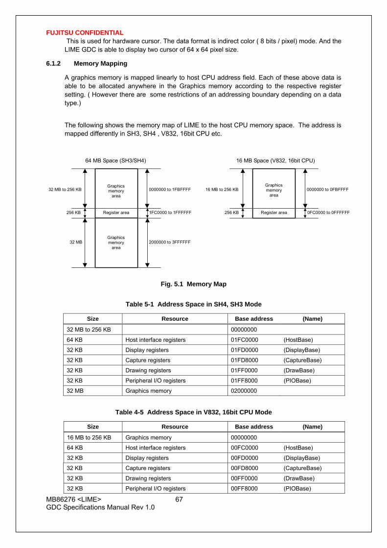
FUJITSU CONFIDENTIAL
MB86276 <LIME> 67 GDC Specifications Manual Rev 1.0
This is used for hardware cursor. The data format is indirect color ( 8 bits / pixel) mode. And the LIME GDC is able to display two cursor of 64 x 64 pixel size.
6.1.2 Memory Mapping
A graphics memory is mapped linearly to host CPU address field. Each of these above data is able to be allocated anywhere in the Graphics memory according to the respective register setting. ( However there are some restrictions of an addressing boundary depending on a data type.)
The following shows the memory map of LIME to the host CPU memory space. The address is mapped differently in SH3, SH4 , V832, 16bit CPU etc.
Fig. 5.1 Memory Map
Table 5-1 Address Space in SH4, SH3 Mode
Size Resource Base address (Name)
32 MB to 256 KB 00000000
64 KB Host interface registers 01FC0000 (HostBase)
32 KB Display registers 01FD0000 (DisplayBase)
32 KB Capture registers 01FD8000 (CaptureBase)
32 KB Drawing registers 01FF0000 (DrawBase)
32 KB Peripheral I/O registers 01FF8000 (PIOBase)
32 MB Graphics memory 02000000
Table 4-5 Address Space in V832, 16bit CPU Mode
Size Resource Base address (Name)
16 MB to 256 KB Graphics memory 00000000
64 KB Host interface registers 00FC0000 (HostBase)
32 KB Display registers 00FD0000 (DisplayBase)
32 KB Capture registers 00FD8000 (CaptureBase)
32 KB Drawing registers 00FF0000 (DrawBase)
32 KB Peripheral I/O registers 00FF8000 (PIOBase)
Register area
Graphicsmemory
area32 MB to 256 KB
256 KB
0000000 to 1FBFFFF
1FC0000 to 1FFFFFF
2000000 to 3FFFFFF
64 MB Space (SH3/SH4)
Register area256 KB 0FC0000 to 0FFFFFF
16 MB Space (V832, 16bit CPU)
32 MB
0000000 to 0FBFFFFGraphicsmemory
area
Graphicsmemory
area
16 MB to 256 KB

FUJITSU CONFIDENTIAL
MB86276 <LIME> 68 GDC Specifications Manual Rev 1.0
When the SH3 or SH4 mode is used, the register area can be moved by writing 1 to bit 0 at HostBase + 005Ch (RSW: Register location Switch). In the initial state, the register space is at the center (1FC0000) of the 64 MB space; access LIME after about 20 bus clocks after writing 1 to RSW.
Fig. 4.2 Memory Map
Table 4-6 Address Mapping in SH3/SH4 Mode
Size Resource Base address (Name)
64 MB to 256 KB Graphics memory 00000000
64 KB Host interface registers 03FC0000 (HostBase)
32 KB Display registers 03FD0000 (DisplayBase)
32 KB Capture registers 03FD8000 (CaptureBase)
32 KB Drawing registers 03FF0000 (DrawBase)
32 KB Peripheral I/O registers 03FF8000 (PIOBase)
Register area
Graphics memory area 32 MB to 256 KB
256 KB
0000000 to 1FFFFFF
3FC0000 to 3FFFFFF
2000000 to 3FBFFFF
64 MB space (SH3/SH4)
32 MB Graphics memory area

FUJITSU CONFIDENTIAL
MB86276 <LIME> 69 GDC Specifications Manual Rev 1.0
6.1.3 Data Format
Direct Color ( 16 bits / pixel ) This data format is described RGB as each 5 bit. Bit15 is used for alpha bit of layer blending.
15 14 13 12 11 10 9 8 7 6 5 4 3 2 1 0
A R G B
Indirect Color ( 8 bits / pixel ) This data format is a color index code for looking up table (palette).
7 6 5 4 3 2 1 0
Color Code
Z Value(Optional function) It is possible to use Z value as 8 bits or 16 bits. These data format are unsigned integer. 1 ) 16 bits mode
15 14 13 12 11 10 9 8 7 6 5 4 3 2 1 0
Unsigned Integer
2 ) 8 bits mode 7 6 5 4 3 2 1 0
Unsigned Integer
Polygon Drawing Flag This data format is 1 bit per 1 pixel.
15 14 13 12 11 10 9 8 7 6 5 4 3 2 1 0
P15 P14 P13 P12 P11 P10 P9 P8 P7 P6 P5 P4 P3 P2 P1 P031 30 29 28 27 26 25 24 23 22 21 20 19 18 17 16
P31 P30 P29 P28 P27 P26 P25 P24 P23 P22 P21 P20 P19 P18 P17 P16
Texture / Tile Pattern It is possible to use a pattern as direct color mode ( 16 bits / pixel) or indirect color mode ( 8 bits / pixel). 1 ) Direct color mode ( 16 bits / pixel) This data format is described RGB as each 5 bit. Bit15 is used for alpha bit of stencil or stencil blending. ( Only texture mapping)
15 14 13 12 11 10 9 8 7 6 5 4 3 2 1 0
A R G B
2) Indirect color mode ( 8 bits / pixel) This data format is a color index code for looking up table (palette).
7 6 5 4 3 2 1 0
Color Code
Cursor Pattern This data format is a color index code for looking up table (palette).
7 6 5 4 3 2 1 0
Color Code

FUJITSU CONFIDENTIAL
MB86276 <LIME> 70 GDC Specifications Manual Rev 1.0
6.2 Frame Management
6.2.1 Single Buffer
The entire or partial area of the drawing frame is assigned as a display frame. The display field is scrolled by relocating the position of the display frame. When the display frame crosses the border of the drawing frame, the other side of the drawing frame is displayed, assuming that the drawing frame is rolled over (top and left edges assumed logically connected to bottom and right edges, respectively). To avoid the affect of drawing on display, the drawing data can be transferred to the Graphics Memory in the blanking time period.
6.2.2 Double Buffer
Two drawing frames are set. While one frame is displayed, drawing is done at the other frame. Flicker-less animation can be performed by flipping these two frames back and forth. Flipping is done in the blanking time period. There are two flipping modes: automatically at every scan frame period, and by user control. The double buffer is assigned independently for the L2, L3, L4, L5 layers.
6.3 Memory Access 6.3.1 Priority of memory accessing
The priority of Graphics memory accessing is the follows: 1. Refresh 2. Video Capture 3. Display processing 4. Host CPU accessing 5. Drawing accessing

FUJITSU CONFIDENTIAL
MB86276 <LIME> 71 GDC Specifications Manual Rev 1.0
6.4 Connection with memory 6.4.1 Connection with memory
The memory controller of LIME GDC supports simple connection with SDRAM by setting MMR(Memory Mode Register). If there is N(=11 to 13) address pins in SDRAM, please connect the SDRAM address(A[n]) pin to the LIME’s memory address(MA[n]) pin and SDRAM bank pin to the LIME’s next address(MA[N]) pin. Then please set MMR by a number and type of memory. The follows are the connection table between LIME pin and SDRAM pin.
64M bit SDRAM(x16 bit) 64M bit SDRAM(x32 bit)
LIME pins SDRAM pins LIME pins SDRAM pins MA[11:0] A[11:0] MA[10:0] A[10:0]
MA12 BA0 MA11 BA0 MA13 BA1 MA12 BA1
128M bit SDRAM(x16 bit) 128M bit SDRAM(x32 bit) LIME pins SDRAM pins LIME pins SDRAM pins MA[11:0] A[11:0] MA[11:0] A[11:0]
MA12 BA0 MA12 BA0 MA13 BA1 MA13 BA1
256M bit SDRAM(x16 bit) 256M bit SDRAM(x32 bit) LIME pins SDRAM pins LIME pins SDRAM pins MA[12:0] A[12:0] MA[11:0] A[11:0]
MA13 BA0 MA12 BA0 MA14 BA1 MA13 BA1
512M bit SDRAM(x32 bit)
LIME pins SDRAM pins MA[12:0] A[12:0] MA13 BA0 MA14 BA1

FUJITSU CONFIDENTIAL
MB86276 <LIME> 72 GDC Specifications Manual Rev 1.0
7 DISPLAY CONTROLLER 7.1 Overview Display control Window display can be performed for six layers. Window scrolling, etc., can also be performed.
Backward compatibility Backward compatibility with previous products is supported in the four-layer display mode or in the left/right split display mode.
Video timing generator The video display timing is generated according to the display resolution (from 320 × 240 to 1280x768).
Color look-up There are two sets of color look-up tables by palette RAM for the indirect color mode (8 bits/pixel).
Cursor Two sets of hardware cursor patterns (8 bits/pixel, 64 × 64 pixels each) can be used.

FUJITSU CONFIDENTIAL
MB86276 <LIME> 73 GDC Specifications Manual Rev 1.0
7.2 Display Function 7.2.1 Layer configuration
Six-layer window display is performed. Layer overlay sequence can be set in any order. A four-layer display mode and left/right split display mode are also provided, supporting backward compatibility with previous products.
Configuration of Display Layers
The correspondence between the display layers for this product and for previous products is shown below.
Coordinates of starting point Width/height Layer
correspondence Window mode Compatibility mode Window mode Compatibility mode
L0 C (L0WX, L0WY) (0, 0) (L0WW, L0WH + 1) (HDP + 1, VDP + 1)
L1 W (L1WX, L1WY) (WX, WY) (L1WW, L1WH + 1) (WW, WH + 1)
L2 ML (L2WX, L2WY) (0, 0) (L2WW, L2WH + 1) (HDB + 1, VDP + 1)
L3 MR (L3WX, L3WY) (HDB, 0) (L3WW, L3WH + 1) (HDP − HDB, VDP + 1)
L4 BL (L4WX, L4WY) (0, 0) (L4WW, L4WH + 1) (HDB + 1, VDP + 1)
L5 BR (L5WX, L5WY) (HDB, 0) (L5WW, L5WH + 1) (HDP − HDB, VDP + 1)
C, W, ML, MR, BL, and BR above mean layers for previous products. The window mode or the compatibility mode can be selected for each layer. It is possible to use new functions through minor program changes by allowing the coexistence of display modes instead of separating them completely.
However, if high resolutions are displayed, the count of layers that can be displayed simultaneously and pixel data may be restricted according to the graphics memory ability to supply data.
L0 (L0WX,L0WY) L2 (L2WX,L2WY)
L1 (L1WX,L1WY)L5 (L5WX,L5WY)
L4 (L4WX,L4WY)
L3 (L3WX,L3WY)
(a) Six layerd window display
L0,L2,L4 (0,0) L3,L5 (HDB+1,0)L1 (WX,WY)
(b) Four layered display for downward compatibility
background color

FUJITSU CONFIDENTIAL
MB86276 <LIME> 74 GDC Specifications Manual Rev 1.0
7.2.2 Overlay
(1) Overview
Image data for the six layers (L0 to L5) is processed as shown below.
The fundamental flow is: Palette → Layer selection → Blending. The palettes convert 8-bit color codes to the RGB format. The layer selector exchanges the layer overlay sequence arbitrarily. The blender performs blending using the blend coefficient defined for each layer or overlays in accordance with the transparent-color definition.
The L0 layer corresponds to the C layer for previous products and shares the palettes with the cursor. As a result, the L0 layer and cursor are overlaid before blend operation.
The L1 layer corresponds to the W layer for previous products. To implement backward compatibility with previous products, the L1 layer and lower layers are overlaid before blend operation.
The L2 to L5 layers have two paths; in one path, these layers are input to the blender separately and in the other, these layers and the L1 layer are overlaid and then are input to the blender. When performing processing using the extended mode, select the former; when performing the same processing as previous products, select the latter. It is possible to specify which one to select for each layer.
Pallet-1
YUV/RGB
Pallet-2
Pallet-3
Pallet-0
Laye
r Sel
ecto
r
L0(C) data
L2(ML) data
Cursor0 data
L2 data
L3 data
L4 data
L5 data Bl
ende
r Ove
rlay
Cursor1 data
L1(W) data
L4(BL) data
L3(MR) data
L5(BR) data

FUJITSU CONFIDENTIAL
MB86276 <LIME> 75 GDC Specifications Manual Rev 1.0
(2) Overlay mode
Image layer overlay is performed in two modes: simple priority mode, and blend mode.
In the simple priority mode, processing is performed according to the transparent color defined for each layer. When the color is a transparent color, the value of the lower layer is used as the image value for the next stage; when the color is not a transparent color, the value of the layer is used as the image value for the next stage.
Dview = Dnew (when Dnew does not match transparent color)
= Dlower (when Dnew matches transparent color)
When the L1 layer is in the YCbCr mode, transparent color checking is not performed for the L1 layer; processing is always performed assuming that transparent color is not used.
In the blend mode, the blend ratio “r” defined for each layer is specified using 8-bit tolerance, and the following operation is performed:
Dview = Dnew*r + Dlower*(1 – r)
Blending is enabled for each layer by mode setting and a specific bit of the pixel is set to “1”. For 8 bits/pixel, the MSB of RAM data enables blending; for 16 bits/pixel, the MSB of data of the relevant layer enables blending; for 24 bits/pixel, the MSB of the word enables blending.
(3) Blend coefficient layer
In the normal blend mode, the blend coefficient is fixed for each layer. However, in the blend coefficient layer mode, the L5 layer can be used as the blend coefficient layer. In this mode, the blend coefficient can be specified for each pixel, providing gradation, for example. When using this mode, set the L5 layer to 8 bits/pixel, widow display mode and extend overlay mode.

FUJITSU CONFIDENTIAL
MB86276 <LIME> 76 GDC Specifications Manual Rev 1.0
7.2.3 Display parameters
The display area is defined according to the following parameters. Each parameter is set independently at the respective register.
Display Parameters Note: The actual parameter settings are little different from the above. The details, please refer “14.3.1 Interlaced mode”.
HTP Horizontal Total Pixels HSP Horizontal Synchronize pulse Position HSW Horizontal Synchronize pulse Width HDP Horizontal Display Period HDB Horizontal Display Boundary VTR Vertical Total Raster VSP Vertical Synchronize pulse Position VSW Vertical Synchronize pulse Width VDP Vertical Display Period LnWX Layer n Window position X LnWY Layer n Window position Y LnWW Layer n Window Width LnWH Layer n Window Height
When not splitting the window, set HDP to HDB and display only the left side of the window. The settings must meet the following relationship:
0 < HDB ≤ HDP < HSP < HSP + HSW + 1 < HTP
0 < VDP < VSP < VSP + VSW + 1 < VTR
HTP
HSP
HDB HDP
LnWY
LnWX LnWW
LnWH
VD
P
VS
P
VTR
VSW
HSW

FUJITSU CONFIDENTIAL
MB86276 <LIME> 77 GDC Specifications Manual Rev 1.0
7.2.4 Display position control
The graphic image data to be displayed is located in the logical 2D coordinates space (logical graphics space) in the Graphics Memory. There are six logical graphics spaces as follows:
L0 layer
L1 layer
L2 layer
L3 layer
L4 layer
L5 layer
The relation between the logical graphics space and display position is defined as follows:
Display Position Parameters
OA Origin Address Origin address of logical graphics space. Memory address of top left
edge pixel in logical frame origin W Stride Width of logical graphics space. Defined in 64-byte unit H Height Height of logical graphics space. Total raster (pixel) count of field DA Display Address Display origin address. Top left position address of display frame
origin DX DY
Display Position Display origin coordinates. Coordinates in logical frame space of display frame origin
Stride (W)
Hei
ght (
H)
Origin Address (OA) Display Address (DA) Display Position X,Y (DX,DY)
VDP
Logical Frame
Display Frame
HDP

FUJITSU CONFIDENTIAL
MB86276 <LIME> 78 GDC Specifications Manual Rev 1.0
MB86276 scans the logical graphics space as if the entire space is rolled over in both the horizontal and vertical directions. Using this function, if the display frame crosses the border of the logical graphics space, the part outside the border is covered with the other side of the logical graphics space, which is assumed to be connected cyclically as shown below:
Wrap Around of Display Frame
The expression of the X and Y coordinates in the frame and their corresponding linear addresses (in bytes) is shown below.
A(x,y) = x × bpp/8 + 64wy (bpp = 8 or 16)
The origin of the displayed coordinates has to be within the frame. To be more specific, the parameters are subject to the following constraints:
0 ≤ DX < w × 64 × 8/bpp (bpp = 8 or 16)
0 ≤ DY < H
DX, DY, and DA have to indicate the same point within the frame. In short, the following relationship must be satisfied.
DA = OA + DX × bpp/8 + 64w × DY (bpp = 8 or 16)
64 w
L
Logical Frame Origin
Additionally drawn area New display origin
Previous display origin

FUJITSU CONFIDENTIAL
MB86276 <LIME> 79 GDC Specifications Manual Rev 1.0
7.3 Display Color Color data is displayed in the following modes:
Indirect color (8 bits/pixel) In this mode, the index of the palette RAM is displayed. Data is converted to image data consisting of 6 bits for R, G, and B via the palette RAM and is then displayed.
Direct color (16 bits/pixel) Each level of R, G, and B is represented using 5 bits.
Direct color (24 bits/pixel) Each level of R, G, and B is represented using 8 bits.
YCbCr color (16 bits/pixel) In this mode, image data is displayed with YCbCr = 4:2:2. Data is converted to image data consisting of 8 bits for R, G, and B using the operation circuit and is then displayed.
The display colors for each layer are shown below. Layer Compatibility mode Extended mode
L0 Direct color (16, 24), Indirect color (P0) Direct color (16, 24), Indirect color (P0)
L1 Direct color (16, 24), Indirect color (P1), YCbCr Direct color (16, 24), Indirect color (P1), YCbCr
L2 Direct color (16, 24), Indirect color (P1) Direct color (16, 24), Indirect color (P2)
L3 Direct color (16, 24), Indirect color (P1) Direct color (16, 24), Indirect color (P3)
L4 Direct color (16, 24), Indirect color (P1) Direct color (16, 24)
L5 Direct color (16, 24), Indirect color (P1) Direct color (16, 24)
“Pn” stands for the corresponding palette RAM. Four palettes are used as follows:
Palette 0 (P0) This palette corresponds to the C-layer palette for previous products. This palette is used for the L0 layer. This palette can also be used for the cursor.
Palette 1 (P1) This palette corresponds to the M/B layer palette for previous products. In the compatibility mode, this palette is common to layers L1 to 5. In the extended mode, this palette is dedicated to the L1 layer.
Palette 2 (P2) This palette is dedicated to the L2 layer. This palette can be used only for the extended mode.
Palette 3 (P3) This palette is dedicated to the L3 layer. This palette can be used only for the extended mode.

FUJITSU CONFIDENTIAL
MB86276 <LIME> 80 GDC Specifications Manual Rev 1.0
7.4 Cursor 7.4.1 Cursor display function
LIME GDC can display two hardware cursors. Each cursor is specified as 64 × 64 pixels, and the cursor pattern is set in the Graphics Memory. The indirect color mode (8 bits/pixel) is used and the L0 layer palette is used. However, transparent color control (handling of transparent color code and code 0) is independent of L0 layer. Blending with lower layer is not performed.
7.4.2 Cursor control
The display priority for hardware cursors is programmable. The cursor can be displayed either on upper or lower the L0 layer using this feature. A separate setting can be made for each hardware cursor. If part of a hardware cursor crosses the display frame border, the part outside the border is not shown.
Usually, cursor 0 is preferred to cursor 1. However, with cursor 1 displayed upper the L0 layer and cursor 0 displayed lower the L0 layer, the cursor 1 display is preferred to the cursor 0.

FUJITSU CONFIDENTIAL
MB86276 <LIME> 81 GDC Specifications Manual Rev 1.0
7.5 Display Scan Control 7.5.1 Applicable display
The following table shows typical display resolutions and their synchronous signal frequencies. The pixel clock frequency is determined by setting the division rate of the display reference clock. The display reference clock is either the internal PLL (400.9 MHz at input frequency of 14.318 MHz), or the clock supplied to the DCLKI input pin. The following table gives the clock division rate used when the internal PLL is the display reference clock:
Resolution and Display Frequency
Resolution Division rate of reference
clock Pixel
frequencyHorizontal total pixel
count Horizontal frequency
Vertical total raster
count Vertical
frequency
320 × 240 1/60 6.7 MHz 424 15.76 kHz 263 59.9 Hz
400 × 240 1/48 8.4 MHz 530 15.76 kHz 263 59.9 Hz
480 × 240 1/40 10.0 MHz 636 15.76 kHz 263 59.9 Hz
640 × 480 1/16 25.1 MHz 800 31.5 kHz 525 59.7 Hz
854 × 480 1/12 33.4 MHz 1062 31.3 kHz 525 59.9 Hz
800 × 600 1/10 40.1 MHz 1056 38.0 kHz 633 60.0 Hz
1024 × 768 1/6 66.8 MHz 1389 48.1 kHz 806 59.9 Hz
Pixel frequency = 14.318 MHz × 28 × reference clock division rate (when internal PLL selected)
= DCLKI input frequency × reference clock division rate (when DCLKI selected)
Horizontal frequency = Pixel frequency/Horizontal total pixel count
Vertical frequency = Horizontal frequency/Vertical total raster count

FUJITSU CONFIDENTIAL
MB86276 <LIME> 82 GDC Specifications Manual Rev 1.0
7.5.2 Interlace display
LIME GDC can perform both a non-interlace display and an interlace display.
When the DCM register synchronization mode is set to interlace video (11), images in memory are output in odd and even rasters alternately to each field, and one frame (odd + even fields) forms one screen.
When the DCM register synchronization mode is set to interlace (10), images in memory are output in raster order. The same image data is output to odd fields and even fields. Consequently, the count of rasters on the screen is half of that of interlace video. However, unlike the non-interlace mode, there is a distinction between odd and even fields depending on the phase relationship between the horizontal and vertical synchronous signals.
Display Difference between Synchronization Modes
Odd
Eve
Non-Interlace Interlace Video Interlace

FUJITSU CONFIDENTIAL
MB86276 <LIME> 83 GDC Specifications Manual Rev 1.0
7.6 The external synchronous signal The display scan can be performed by synchronizing horizontal/vertical synchronous signal from the external. In selecting the external synchronization mode, LIME is sampling the HSYNC signal and displays the synchronizing the external video signal. Either the internal PLL clock or the DCLKI input signal could be selected for the sampling clock. Also, the superimposed analog output is performed by the chroma key process. The following diagram shows an example of the external synchronization circuit.
7.7 An example of the external synchronization circuit The external synchronization mode is performed by setting the ESY bit of the DCM register. In setting the external synchronization mode, HSYNC, VSYNC, and EO pin of LIME is changed to the input mode. After that it needs to be provided the synchronous signal by using the 3 state buffer from the external. When turning off the external synchronization mode, LIME internal ESY bit needs to be switched OFF after disconnecting the synchronous input signal from the external. The buffer of the external synchronization signal must not be switched ON when the synchronous output signal of LIME is ON. Follow the previous instruction to prevent simultaneous ON from occurring.
In using the external synchronous signal with the display clock based on the internal PLL, LIME extends the clock period and fits the clock phase with the horizontal synchronous signal phase after inputting the horizontal synchronous pulse. The following caution is necessary. In case of connecting the high speed transmit signal, such as LVDS, with the digital RGB output, PLL with a built-in the high speed serial transmission is temporally unstable due to this connection. Therefore, the external synchronous signal based on the internal PLL must not be used with high speed synchronous transmit signal.
HSYNC
VSYNC
LIME
Video SW
Analog RGB In
SuperimposedAnalog RGB Out
Hsync In Vsync In
GV
(Pedestal Clump Input)
Compare
3 states
KEYC
External Sync Enable
Hsync Out
Vsync Out Cursor 0Cursor 1
L0buffer
register
CKM bit
ESY bit
Display TimmingGenerator
DA
C
D-FFsLatency compensation for DAC
L0L1L2L3L4L5 O
verla
p

FUJITSU CONFIDENTIAL
MB86276 <LIME> 84 GDC Specifications Manual Rev 1.0
The synchronization of the horizontal direction is controlled by the following state diagram. The finite state diagram is controlled by the horizontal resolution counter. The period of outputting the signal is assigned the Disp state. When the value of the horizontal resolution counter matches that of the HDP register, it ends to output the signal and the current state is transmitted from Disp state to Fporch state (front porch). In the Fporch state, when the value of the vertical resolution register matches that of the HSP register, the current state is transmitted to the Sync state. In this state, it waits for the horizontal synchronous signal from the external. LIME detects the negative edge of the horizontal synchronous pulse from the external and synchronizes it. In detecting the horizontal synchronous signal from the external, the current state is transmitted to the Bporch state (back porch). The horizontal resolution register does not count in the Sync state, instead the horizontal synchronous counter is incremented from zero. When the value of this counter matches the setting value of the HSW register, the current state is transmitted to the Bporch state without detecting the horizontal synchronous signal form the external. When the value of the horizontal resolution counter matches that of the HTP register in the Bporch state, the horizontal resolution counter is reset, and also the current state is transmitted to the Disp state and it begins to display the next cluster.
D isp
Sync
The horizontal resolution counter = HDP
otherwise otherwise
otherwise
W hen the horizontal resolution counter m atches the HTP, it is initialized.
detecting the external horizontal synchronous signal or the horizontal synchronous pulse counter = HSW
otherwiseThe horizontal resolution counter is is halted, starts to count the horizontalsynchronous pulse counter.
Fporch
Bporch
The
horiz
onta
l res
olut
ion
coun
ter =
HS
P
The
horiz
onta
l res
olut
ion
coun
ter =
HTP

FUJITSU CONFIDENTIAL
MB86276 <LIME> 85 GDC Specifications Manual Rev 1.0
The synchronization of vertical direction is controlled by the following state diagram.
The state diagram of the vertical direction is controlled by the value of the cluster counter. The period of outputting the signal is assigned the Disp state. When the value of the cluster counter matches the value of the VDP register, it ends to output the signal and the current state is transmitted from the Disp state to the Fporch state. In the Fporch state, it waits the external synchronous pulse to be asserted. In detecting the external synchronous pulse to be asserted, the current state is transmitted to the Sync state. In the Sync state, it waits for the negative edge of the external synchronous signal. In detecting the negative edge, the current state is transmitted to the Bporch state. When the value of the cluster counter matches the values of the VTR register, the cluster counter is reset, and also the current state is transmitted to the Disp state and it starts to display the next field.
The
clus
ter c
ount
er
= V
TR
D isp The cluster counter = VDP
otherwise otherwise
otherwise W hen the cluster counter m atches the VTP, it is in itia lized.
detecting the negative edge of the external vertical synchronous pulse
otherwise
dete
ctin
g th
e ex
tern
al
verti
cal s
ynch
rono
us
puls
e to
be
asse
rted
Fporch
Bporch Sync

FUJITSU CONFIDENTIAL
MB86276 <LIME> 86 GDC Specifications Manual Rev 1.0
7.8 Programmable YCbCr/RGB conversion for L1-layer display L1-layer can display video data in YCbCr format but RGB conversion coefficients are hard-wired and
fixed about previous products. LIME can program RGB conversion coefficients by registers.
YCbCr data is converted by following expression.
R = a11*Y + a12*(Cb−128) + a13*(Cr−128) + b1
G = a21*Y + a22*(Cb−128) + a23*(Cr−128) + b2
B = a31*Y + a32*(Cb−128) + a33*(Cr−128) + b3
aij ---- 11bit signed real ( lower 8bit is fraction, two's complement )
bi ----- 9bit signed integer ( two's complement )
It is represended by matrix operation.
These parameters are set on registers shown bellow.
L1YCR0 (a12,a11), L1YCR1(b1,a13)
L1YCG0 (a22,a21), L1YCG1(b2,a23)
L1YCB0 (a32,a31), L1YCB1(b3,a33)
Same conversion with previous products is applied by initial values of these registers after reset.
The register values just after reset is as follow.
a11 = 0x12b (299/256) , a12 = 0x0, a13 = 0x198 (408/256)
a21 = 0x12b (299/256), a22 = 0x79c (-100/256), a23 = 0x72f (-209/256)
a31 = 0x12b (299/256), a32 = 0x204 (516/256), a33 = 0x0
b1= b2= b3= 0x1f0 (-16)
It is possible to control brightness, contrast, hue , color saturation by change these parameters.
Addition of a constant value into b means inclease of brightness.
Multiplication of a constant scalar value greater than one into A means increase of contrast.
Two dimentional rotation of Cb-128 and Cr-128 means change of hue.
Color saturation is intensity of color, relative to Y-component.
New coefficients including these changes can be got by following expression.
R G B
a11
a21
a31
a12
a22
a32
a13
a23
a33
Y Cb-128Cr-128
where , b =b1
b2
b3
= A + b A =

FUJITSU CONFIDENTIAL
MB86276 <LIME> 87 GDC Specifications Manual Rev 1.0
A0 , b0 : initial value
c1: contrast parameter, 1 is standard. 1.2 is stronger, for example.
c2: color saturation parameter, 1 is standard. 0 means mono chrome image.
c3: brightness parameter, 0 is standard.
t : hue rotation parameter, 0-deg is standard
Note: new aij and bi should be clipped in valid range of value for corresponding registers.
1 0 0
0 cos(t) -sin(t)
0 sin(t) cos(t)
A = c1 A0
b = bo + c3 c3 c3
1 0 0
0c2
0
00c2
= A0
c1
00
0cos(t)c1c2
-sin(t)c1c2
0sin(t)c1c2
cos(t)c1c2

FUJITSU CONFIDENTIAL
MB86276 <LIME> 88 GDC Specifications Manual Rev 1.0
7.9 DCLKO shift 1) Delay
DCLKO delay function is available if internal PLL is used for DCLK. DCKD field in DCM3 register defines delay value by internal PLL clock cycle.
DCKD delay
000000 No additional delay
000010 +2 PLL clock
000100 +3 PLL clock
000110 +4 PLL clock
: :
111110 +33 PLL clock
2) Inversion
DCLKO inversion is also available with/without delay function. This function is effective with no relation to DCLK clock source.
CKinv-bit of DCM3 enables this function.
7.10 Syncronous register update of display To update position related parameters without disturbing display, it is need to update synchronously with VSYNC interrupt and finish at a time.
This synchronous register update mode eases this limitation. In this mode, written parameters are hold in intermediate registers and update at once synchronously with VSYNC.
RUM-bit of DCM2 register enables this mode.
RUF-bit of DCM2 register controls start of update and shows whether update is done or not.
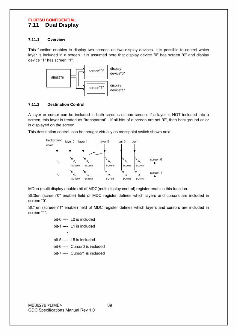
FUJITSU CONFIDENTIAL
MB86276 <LIME> 89 GDC Specifications Manual Rev 1.0
7.11 Dual Display 7.11.1 Overview
This function enables to display two screens on two display devices. It is possible to control which layer is included in a screen. It is assumed here that display device "0" has screen "0" and display device "1" has screen "1".
screen"1"
screen"0" displaydevice"0"
displaydevice"1"
MB86276
7.11.2 Destination Control
A layer or cursor can be included in both screens or one screen. If a layer is NOT included into a screen, this layer is treated as "transparent" . If all bits of a screen are set "0", then background color is displayed on the screen.
This destination control can be thought virtually as crosspoint switch shown next
SC0en6
SC1en6
SC0en7
SC1en7
SC0en5
SC1en5
SC0en1
SC1en1
SC0en0
SC1en0
screen 0
layer 0
screen 1
background color
layer 1 layer 5 cur 0 cur 1
MDen (multi display enable) bit of MDC(multi display control) register enables this function.
SC0en (screen"0" enable) field of MDC register defines which layers and cursors are included in screen “0”.
SC1en (screeen"1" enable) field of MDC register defines which layers and cursors are included in screen “1”.
bit-0 ---- L0 is included
bit-1 ---- L1 is included
:
bit-5 ---- L5 is included
bit-6 ---- Cursor0 is included
bit-7 ---- Cursor1 is included

FUJITSU CONFIDENTIAL
MB86276 <LIME> 90 GDC Specifications Manual Rev 1.0
7.11.3 Output Signal Control
There are two modes to output two screens. In parallel mode, one screen is output at digital RGB1 while another screen is output at digital RGB2. In multiplex mode, two screens are multiplexed and output at digital RGB1.
(1) parallel output mode
sc0
Digital RGB2
Digital RGB1
DCLKO (BE)
DCLKO (SE)
sc0 sc0
DE
sc0 sc0 sc0
(2) multiplex output mode
sc1 sc0 sc1 sc0 sc1sc0Digital RGB1
DCLKO (BE)
DCLKO (SE)
DE
In BE (bi-edge) DCLKO mode, two ouput phases can be identified both edge of DCLKO.
In SE (single-edge) DCLKO mode, two output phases cab be identified an edge of HSYNC or DE.
sc0 sc1Digital RGB
DCLKO (SE)
HSYNC
even clocks
DE
ref edge sc0 is first
POM(parallel output mode) bit in DCM3 register defines which output mode is used, parallel or multiplex. POM=0 means multiplex, POM=1 means parallel, respectively.
CKed( clock edge) bit in DCM3 register defines which DCLKO clock mode is used, BE(bi-edge) or SE(single-edge). DCKed=0
FUJITSU CONFIDENTIAL
MB86276 <LIME> 91 GDC Specifications Manual Rev 1.0
7.11.4 Output Circuit Example
There are three types of output circuit for dual display, primalry.
Parallel, Digital Multiplex(SE), Digital Multiplex(BE)
Here these three examples are described.
(1) Parallel output
Two screens are given as digital signals in this example.
MB86276 (pallarel output)
DR[7:2]DG[7:2]DB[7:2]
DCLKO
HSYNCVSYNC
R0
HSYNC0VSYNC0
(BE mode)
G0B0
R1G1B1HSYNC1VSYNC1
displaydevice"0"
displaydevice"1"
(POM=1,DCKed=1)
DR[7:2]DG[7:2]DB[7:2]
DCLKO
(2) Multiplexed digital output with SE mode DCLKO
In this case, CPLD can be used to demultiplex two digital streams of each screen. In following example, one economical CPLD demultiplexes RGB 6bit/component video data stream.
DCKi
VSiHSi
Di[18]
DCK0
VS0HS0
D0[18]
D0[17:0]Di[17:0]
DR[7:2]DG[7:2]DB[7:2]
DCLKOHSYNCVSYNC
DE
XC9572XL-TQ100
R0,G0,B0
DCLK0HSYNC0VSYNC0DE0
R1,G1,B1
DCLK1HSYNC1VSYNC1DE1
(SE mode)
MB86276 (mux output)
displaydevice "0"
displaydevice "1"
D1[17:0]
DCK1
VS1HS1
D1[18]
(POM=0,DCKed=0)
FUJITSU CONFIDENTIAL
MB86276 <LIME> 92 GDC Specifications Manual Rev 1.0
module XC9572XL ( DCKi, HSi,VSi,Di, DCK0,HS0,VS0,D0, DCK1,HS1,VS1,D1 );
input DCKi,HSi,VSi;
input[18:0] Di;
output DCK0,HS0,VS0, DCK1,HS1,VS1;
output[18:0] D0,D1;
reg HS0,HS1, VS0,VS1, DCK0,DCK1;
reg[18:0] D0,D1;
always @(posedge DCKi) begin
HS0 <= HSi; HS1 <= HS0;
VS0 <= VSi; VS1 <= VS0;
DCK0 <= (HS0&!HSi)? 0: !DCK0; // sync to ref edge : flip
DCK1 <= DCK0;
if(DCK0) D0 <= Di;
if(DCK1) D1 <= Di;
end
endmodule
Di
DCLKi
HSi
even clocks
ref edge
sc0 sc1 sc0 sc1 sc1
sc0 sc0
sc1 sc1
DCK0
D0[18:0]
DCK1
D1[18:0]
read point
read point

FUJITSU CONFIDENTIAL
MB86276 <LIME> 93 GDC Specifications Manual Rev 1.0
(3) Multiplexed digital output with BE mode DCLKO
If a receiving device can select data strobe edge, it can be used to demultiplex two screens with rising and falling edge of DCLKO.
0
1
DR[7:2]DG[7:2]DB[7:2]
DCLKOHSYNCVSYNC
DE
pos edge mode
(BE mode)
MB86276 (mux outpuut) mode
display device"0"
display device"1"
(POM=0,DCKed=1) neg edge mode
mode
7.11.5 Display Clock and Timing
It is need to supply display clock of twice frequency for dual display function to work. VGA display uses 25MHz display clock, typically in single display mode while 50MHz display clock is need for dual display mode. The timing parameters such as HTP except scaling ratio (SC) are same.
Maximum display clock frequency determines maximum available resolution. It is 800 x 480. 66MHz DCLK clock is need for it.
7.11.6 Limitation
Two display devices has same scan rate and resolution with common sync signals.
The external sync mode can not be used in dual display mode.
FUJITSU CONFIDENTIAL
MB86276 <LIME> 94 GDC Specifications Manual Rev 1.0
8 Video Capture 8.1 Video Capture function 8.1.1 Input data Formats
The digital video stream of ITU RBT-656 or RGB666 format conformity is inputted (for details refer to 8.5 external video signal input conditions).
8.1.2 Capturing of Video Signal
“LIME” becomes effective when VIE of a video capture mode register (VCM) is 1, and it is CCLK. Synchronizing with a clock, video stream data is captured from 8-bit VI pin or 20-bit RGB input pin.
8.1.3 Non-interlace Transformation
Captured video graphics can be displayed in non-interlaced format. Two modes (BOB and WEAVE) can be selected at non-interlace transformation.
- BOB Mode
In odd fields, the even-field raster generated by average interpolation are added to produce one frame. In even fields, the odd-field raster generated by average interpolation are added to produce one frame.
In order to choose BOB mode, while enable vertical interpolation in VI bit of a VCM (Video Capture Mode) register, the L1IM bit of L1M (L1-layer Mode) register is set as 0.
- WEAVE Mode
Odd and even fields are merged in the video capture buffer to produce one frame. Vertical resolutions in the WEAVE mode are higher than those in the BOB mode but raster dislocation appears at moving places.
In order to choose WEAVE mode, while disable vertical interpolation in VI bit of a VCM (Video Capture Mode) register, the L1IM bit of L1M (L1-layer Mode) register is set as 1.

FUJITSU CONFIDENTIAL
MB86276 <LIME> 95 GDC Specifications Manual Rev 1.0
8.2 Video Buffer 8.2.1 Data Form
The video capture unit of MB86276 “LIME” accepts YUV422 video data primarily, but RGB video data is also accepted via an internal RGB preprocessor which converts RGB to YUV422.
Captured pixels are stored in YCbCr format in graphics memory, 16 bits per pixel. The video data is converted to RGB when it is displayed.
31 24 23 16 15 8 7 0
Y1 Cr Y0 Cb
7 6 5 4 3 2 1 0
Y0,Y1 Y7 Y6 Y5 Y4 Y3 Y2 Y1 Y0
Cr,Cb C7 C6 C5 C4 C3 C2 C1 C0
8.2.2 Synchronous Control
Writing to the graphics memory of video image data and scan for a display are performed independently. The graphics memory for video captures is controlled by the ring buffer system. It displays the frame, when the image data for one frame can be preparing on a memory. When the frame rate of a video capture differs from the frame rate of a display, the continuation display of top omission or the same frame occurs.
8.2.3 Area Allocation
Allocate an area of about 2.2 frames to the video capture buffer. The size of this area is equivalent to the size that considers the margin equivalent to the double buffer of the frame. Set the starting address and upper-limit address of the area in the CBOA/CBLA registers. Here, specify the raster start position as the upper-limit address.
To allocate n rasters as the video capture buffer, set the upper-limit value as follows:
CBLA = CBOA + 64 (n-2) × CBW
In addition, the head addresses of n+1 raster are 64n×CBW, and CBLA+2 raster becomes a buffer domain. For reduced display, allocate the buffer area of the reduced frame size.

FUJITSU CONFIDENTIAL
MB86276 <LIME> 96 GDC Specifications Manual Rev 1.0
8.2.4 Window Display
The captured video picture is displayed using L1 layer. The whole or a part captured picture can be displayed as the whole screen or a window.
When performing a capture display, L1 layer is set as capture synchronous mode (L1CS=1). In this mode, L1 layer display displays the newest frame in a video capture buffer. Usually, the display address used in the mode is disregarded.
The stride of L1 layer needs to be in agreement with the stride of a video capture buffer. When not in agreement, the picture distorted aslant is displayed.
The display size of L1 layer is made in agreement with the picture size after reduction of a video capture. Invalid data will be displayed if the display size of L1 layer is set up more greatly than capture picture size.
Although selection of a RGB display and a YCbCr display can be performed in L1 layer, in performing a video capture, it chooses YcbCr form (L1YC=1).
8.2.5 Interlace Display
It is possible to display the picture taken in to the video capture buffer in WEAVE mode in an interlace. A setup confirms WEAVE mode and chooses an interlace & video display with display scan.
However, when display scan is asynchronous, flicker will come out in a scene with a motion. In order to prevent this, OO (Odd Only) bit of a CBM (Capture Buffer Mode) register is set as 1.
When synchronizing display scan with a capture, a capture input and a display output can be made to correspond to 1 to 1. In this case, the difference of flicker of an input and an output is lost. Please refer to "8.8 Capture synchronous display."
8.2.6 RGB555 Mode
As an alternative method, a special RGB555-mode can be used which is dedicated for applications where grabbed pictures should be processed further. In this mode, a single buffer is used instead of a ring buffer. In addition, data is directly stored in LIME's RGB555 format in the L1-Layer (see settings of the CBM register). This makes it possible to copy rectangular areas from the L1-layer directly to the texture buffer or to other memory locations using the BitBlt function. Note that the input and output frame rate should be identical if a single buffer method is used and that the lower bits are ignored to form the RGB555 format.

FUJITSU CONFIDENTIAL
MB86276 <LIME> 97 GDC Specifications Manual Rev 1.0
8.3 Scaling 8.3.1 Down-scaling Function
When the CM bits of the video capture mode register (VCM) are 11, LIME reduces the video screen size. The reduction can be set independently in the vertical and horizontal scales. The reduction is set per line in the vertical direction and in 2-pixel units in the horizontal direction. The scale setting value is defined by an input/output value. It is a 16-bit fixed fraction where the integer is represented by 5 bits and the fraction is represented by 11 bits. Valid setting values are from 0800H to FFFFH. Set the vertical direction at bit 31 to bit 16 of the capture scale register (CSC) and the horizontal direction at bits 15 to bit 00. The initial value for this register is 08000800H (once). An example of the expressions for setting a reduction in the vertical and horizontal directions is shown below.
Reduction in vertical direction 576 -> 490 lines 576/490 = 1.176
1.176×2048=2408 -> 0968H
Reduction in horizontal direction 720 -> 648 pixels 720/648 = 1.111
1.111×2048=2275 -> 08E3H Therefore, 096808E3H is set in CSC.
The capture horizontal pixel register (CHP) is used to limit the number of pixels processed during scaling. It is not used to set scaling values. Clamp processing is performed on the video streaming data outside the values set in CHP. Usually, the defaults for these registers are used.
8.3.2 Up-scaling Function
LIME is able to enlarge the size of a video capture picture by the factor of 2 in both the horizontal and vertical directions. This feature can be used to realize full-screen modes of video input streams which have a resolution less than actual display size. In order to use magnify (up-scaling) mode, the horizontal and vertical factor must be less than one. Do not specify different scaling ways (reduction/enlargement) for horizontal and vertical factors ! Also initialize the following registers as follows : Set the magnify flag in the L1-layer mode register of the display controller.
Set the picture source size (before magnification) into CMSHP and CMSVL. Set the final picture size (after magnification) into CMDHP and CMDVL. An example of the expressions for setting an enlargement in the vertical and horizontal directions is shown below : If the input picture size is 480x360 and the display picture size is 640x480, then the parameters for each register are as follows. HSCALE=(480/640)*2048=0x0600 VSCALE=(360/480)*2048=0x0600 CMSHP=0x00f0 CMSVL=0x0168 CMDHP=0x0140 CMDVL=0x01e0 L1WW=0x0280 L1WH=0x01df

FUJITSU CONFIDENTIAL
MB86276 <LIME> 98 GDC Specifications Manual Rev 1.0
Note:
- Smooth continuation operation to Down Scaling mode and Up Scaling mode cannot be performed. The picture disorder of some arises at the time of a change. This is the restrictions for Up Scaling mode and Down Scaling mode using the same interpolate circuit.

FUJITSU CONFIDENTIAL
MB86276 <LIME> 99 GDC Specifications Manual Rev 1.0
8.3.3 Flow of image processing
As for the capture image displayed on L1 layer window, image processing is performed by the following flow.
Figure 8.1 Flow of image processing
Non-interlace interpolation processing
When VI of a video capture mode register (VCM) is 0, an interlace screen is interpolated vertically using the data in the same field. A screen is doubled vertically. When VI is 1, it is not interpolated vertically.
Horizontal low-pass filter processing
As a preprocessing when scaling down a picture horizontally, a low-pass filter can be covered horizontally. Regardless of scaling up and scaling down of a picture, ON/OFF is possible for a level low path filter (LPF).
The horizontal low-pass filter consists of FIR filters of five taps. A coefficient is specified in the following register.
CHLPF_Y Horizontal LPF Luminance element and RGB element
coefficient code
CHLPF_C Horizontal LPF chrominance element coefficient code
The coefficient is specified by the coefficient code in two bits independently by luminance (Y) signal and chrominance (Cb and Cr) signals. The coefficient is a symmetric coefficient.
Scaler
Video- Input
(656/RGB)
Video Output
MB86276
horizontal
LPF horizontal
down scaling
vertical
down scaling
vertical
LPF
horizontal
up scaling
Display Controller
Non-interlace
interpolation
On / Off
Cap
ture
buf
fer c
ontro
ller
VRA
M
Color conversion
matrix
656(YUV422)
RGB
RGB
RGB
YUV422
RGB
YUV / RGB
vertical
up scaling
vertical
interpolator
horizontal
interpolator
Line
Buffer
FUJITSU CONFIDENTIAL
MB86276 <LIME> 100 GDC Specifications Manual Rev 1.0
CHLPF_x K0 K1 K2 K3 K4
00 0 0 1 0 0
01 0 1/4 2/4 1/4 0
10 0 3/16 10/16 3/16 0
11 3/32 8/32 10/32 10/32 3/32
Horizontal LPF becomes turning off (through) because of the setting of the coefficient code "00".
Note:
- In the case of Native RGB mode (NRGB=1), only a setup of CHLPF_Y code becomes effective.
Down and Up scaling processing of horizontal direction
Please set bit15-00 of capture scale register (CSC) to do the down and up scaling processing of horizontal direction.
Horizontal direction is scaled down before writing in VRAM. Horizontal direction is scaled up after reading from VRAM.
The interpolation filter processing of luminance (Y) signal is done by cubic interpolation (Cubic Interpolate) method. The interpolation filter processing of chrominance (Cb and Cr) signal is done by BiLinear interpolation (BiLinear Interpolate) method. The interpolation filter processing of Native-RGB signal is done by cubic interpolation (Cubic Interpolate) method.
Vertical low-pass filter processing
The low-pass filter can be put on the vertical direction as a preprocessing when the image is scaled down to the vertical direction. Vertical low-pass filter (LPF) can be set to turning on regardless of the scaling up or down of the vertical direction.
A vertical low-pass filter is composed of the FIR filter of three taps. The coefficient is specified by the following register.
CVLPF_Y Vertical LPF Luminance element and RGB element coefficient
code
CVLPF_C Vertical LPF chrominance element coefficient code
The coefficient is specified by the coefficient code in two bits independently by luminance (Y) signal and chrominance (Cb and Cr) signals. The coefficient is a symmetric coefficient.

FUJITSU CONFIDENTIAL
MB86276 <LIME> 101 GDC Specifications Manual Rev 1.0
CVLPF_x K0 K1 K2
00 0 1 0
01 1/4 2/4 1/4
10 3/16 10/16 3/16
11 Prohibition of setting
Vertical LPF becomes turning off (through) because of the setting of the coefficient code "00".
Note:
- In the case of Native RGB mode (NRGB=1), only a setup of CVLPF_Y code becomes effective.
Down and up scaling processing of Vertical direction
Please set bit31-16 of capture scale register (CSC) to do the down and up scaling processing in the vertical direction.
The vertical direction is scaled down before writing in VRAM. The vertical direction is scaled up after reading from VRAM.
The interpolation filter processing of luminance (Y) signal is done by cubic interpolation (Cubic Interpolate) method. The interpolation filter processing of chrominance (Cb and Cr) signal is done by BiLinear interpolation (BiLinear Interpolate) method. The interpolation filter processing of Native-RGB signal is done by cubic interpolation (Cubic Interpolate) method.

FUJITSU CONFIDENTIAL
MB86276 <LIME> 102 GDC Specifications Manual Rev 1.0
8.4 External video signal input conditions 8.4.1 RTB656 YUV422 input format
The ITU R.BT-656 format is widely used for digital transmission of NTSC and PAL signals. The format corresponds to YUV422. Interlaced video display signals can be captured and displayed non-interlaced with linear interpolation. When the VIE bit of the video capture mode register (VCM) is 1, LIME is able to capture video stream data from the 8-bit VI pin in synchronization with the CCLK clock. In this mode, only a digital video stream conforming to ITU-RBT656 can be processed. For this reason, a Y,Cb,Cr 4:2:2 format to which timing reference codes are added is used. The video stream is captured according to the timing reference codes; LIME automatically supports both NTSC and PAL. However, to detect error codes, set NTSC/PAL in the VS bit of VCM. If NTSC is not set, reference the number of data in the capture data count register (CDCN). If PAL is not set, reference the number of data in the capture data counter register (CDCP). If the reference data does not match the stream data, bit 4 to bit 0 of the video capture status register (VCS) will be values other than 0000.
1) RTB656 input format VI[7:0] Synchronous code and image data (Cb,Y,Cr,Y) are input as data of eight multiple bits synchronizing with 27MHz clock, and an valid pixel is transmitted while placed between a synchronous code named SAV and EAV.
SAV : Beginning code of active video data (4 Byte)
EAV : End code of active video data (4 Byte)
T : 27MHz
[ ] : 625/50 series (PAL)
SAVEAV Multiplexed video data
Cb,Y,Cr,Y,Cb,Y,Cr,Y,….. 8 bit VI[7:0]
4T
H-BLANK 276T [288T]
ACTIVE-VIDEO 1440T [1440T]
EAV
4T
Blanking data
80,10,80,10,80,.
ACTIVE-VIDEO -LINE 1716T [1728T]
BLANKING PERIOD
TIMING REF-CODE 720 PIXELS YUV4:2:2 DATA TIMING
REF-CODE BLANKINGPERIOD
… 80 10 FF 00 00 SAV Cb0 Y0 Cr0 Y1 Cb2 Y2 … Cr718 Y719 FF 00 00 EAV 80 10 …

FUJITSU CONFIDENTIAL
MB86276 <LIME> 103 GDC Specifications Manual Rev 1.0
2) RTB656 synchronous code (4 Byte) format
SYNC code (static) EAV/SAV Word
Bit first second third forth
7 1 0 0 1 (static)
6 1 0 0 F 0:first field 1:second field
5 1 0 0 V 0:ACTIVE-VIDEO 1:VBI
4 1 0 0 H 0:SAV 1:EAV
3 1 0 0 P3 Guard bit
2 1 0 0 P2 Guard bit
1 1 0 0 P1 Guard bit
0 1 0 0 P0 Guard bit
3) SAV/EAV timing base signal
Bit 7 6 5 4 3 2 1 0
Function static F V H P3 P2 P1 P0
80 1 0 0 0 0 0 0 0
9D 1 0 0 1 1 1 0 1
AB 1 0 1 0 1 0 1 1
B6 1 0 1 1 0 1 1 0
C7 1 1 0 0 0 1 1 1
DA 1 1 0 1 1 0 1 0
EC 1 1 1 0 1 1 0 0
F1 1 1 1 1 0 0 0 1
80 : SAV code of first field valid pixel period (Active-video)
9D : EAV code of first field valid pixel period (Active-video)
AB : SAV code of first field vertical retrace line period
B6 : EAV code of first field vertical retrace line period
C7 : SAV code of second field valid pixel period (Active-video)
DA : EAV code of second field valid pixel period (Active-video)
EC : SAV code of second field vertical retrace line period
F1 : EAV code of second field vertical retrace line period

FUJITSU CONFIDENTIAL
MB86276 <LIME> 104 GDC Specifications Manual Rev 1.0
8.4.2 RGB input format
There are the two data-processing methods in RGB input video capture function. One is the method of processing with Native RGB. Another is the method of converting RGB into YUV422 by the internal RGB pre processor.
RGB input function is suitable for relatively high speed non-interlaced video signals but the de-interlacing operation is not available in this mode. The maximum input rate is 66Mpixel/sec. RGB component data is 6bit.
Note:
- In Native RGB mode, NRGB=1 is set up.
1) RGB Input Signals
The signals used for RGB video capture are not assigned dedicated terminals but share same pins with other functions.
Name I/O Function
RGBCLK Input Clock for RGB input
RI5-0 Input Red component value
GI5-0 Input Green component value
BI5-0 Input Blue component value
VSYNCI Input Vertical sync for RGB capture
HSYNCI Input Horizontal sync for RGB capture
Note :
- input pins are shared with the ITU656 input and memory data bus. - the VIS bit of the VCM (video capture mode) register selects which mode (ITU656 or RGB) is used.
2) Captured Range
Instead of embedded sync code method used in ITU656 mode, the capture range in RGB mode is specified by the following register parameters:
a) RGB input mode of capture: Set RGB666 input flag(VIS) in VCM. In Native RGB mode, NRGB in VCM =1 is set up. b) HSYNC Cycle: Set the number of HSYNC Cycles in RGBHC. c) Horizontal Enable area: Set enables area start position and
enable picture size into RGBHST and RGBHEN. d) Vertical Enable area: Set enables area start position and
enable picture size into RGBVST and RGBVEN.
The Captured area is defined according to the following parameters. Each parameter is set independently at the respective register.:

FUJITSU CONFIDENTIAL
MB86276 <LIME> 105 GDC Specifications Manual Rev 1.0
RGBHC RGB input Hsync Cycle RGBHST RGB input Horizontal enable area STart position RGBHEN RGB input Horizontal enable area size RGBVST RGB input Vertical ENable area STart position RGBVEN RGB input Vertical ENable area size
Note: The actual parameter settings are little different from the above. The details, please refer “Explanation of Registers”.
e) Convert Matrix Coefficient
In order to change the color conversion matrix, set up RGBCMY, RGBCb, RGBCr and RGBCMb.
Note:
The maximum horizontal enable area size(RGBHEN) which can be captured is 840 pixels. This is the restriction by line buffer size in a video capture module.
VSYNC
HS
YN
C
RGBHST
RGBVST
RGBHEN(~840)
RGBVEN
(~4096) captured
RGBHC

FUJITSU CONFIDENTIAL
MB86276 <LIME> 106 GDC Specifications Manual Rev 1.0
3) Input Operation At the time of a RGB input, the synchronization of data is taken by VSYNC and SYNCI, which are inputted with Data RI, GI and BI.
Input rule of HSYNCI
The positive or negative edge of VINHSYNC is considered as a horizontal synchronization by register setup(HP). Input the signal of 1 or more RGBCLKs –(840+α)RGBCLK cycle.
Note: The maximum horizontal enable area size(RGBHEN) which can be captured is 840 pixels. This is the restriction by line buffer size in a video capture module.
Valid data input rule to HSYNC
The valid image data input rule to HSYNC is shown.
Input data is inputted synchronizing with HSYNC of each line. (The synchronization of data needs to make a synchronization establish by HSYNC in each line unit. Since the sampling clock of image data is generated from HSYNC, it is because a clock may have jitter per line.)
RGBCLK
HSYNCI
RI5-0
GI5-0
BI5-0
RGBHST captured
RGBCLK
HSYNCI ∬
~840RGBCLK+α(HBLANK)
More than 1 RGBCLK ∬
∬∬
HSYNC(internal
RGB input
function)
∬ ∬

FUJITSU CONFIDENTIAL
MB86276 <LIME> 107 GDC Specifications Manual Rev 1.0
VSYNCI
HSYNCI
start to capture RGBVST
Input rule of VINVSYNC A VSYNCI signal is synchronizing with HSYNCI. Moreover, VSYNCI is sampled by HSYNCI , and it considers as a VSYNC signal. Width is made into at least one line or more although a VSYNCI signal does not need to synchronize with HSYNC at this time. The positive or negative of VSYNCI is set to VSYNC by register setup(VP).
valid line input rule to HSYNC
The valid image data input rule to VSYNC is shown.
More than 1 line
1RGBCLK HSYNC(internal RGB
input function)
VSYNCI
~840RGBCLK+αRGBCLK

FUJITSU CONFIDENTIAL
MB86276 <LIME> 108 GDC Specifications Manual Rev 1.0
4) Conversion Operation
RGB input data is converted to YCbCr by the following matrix operation :
Y = a11*R + a12*G + a13*B + b1
Cb= a21*R + a22*G + a23*B + b2 aij : 10bit signed real ( lower 8bit is fraction )
Cr= a31*R + a32*G + a33*B + b3 bi: 8bit unsigned integer
Note: - registers can define each coefficient. - Cb and Cr components are reduced to half after this operation to form in 4:2:2 format.
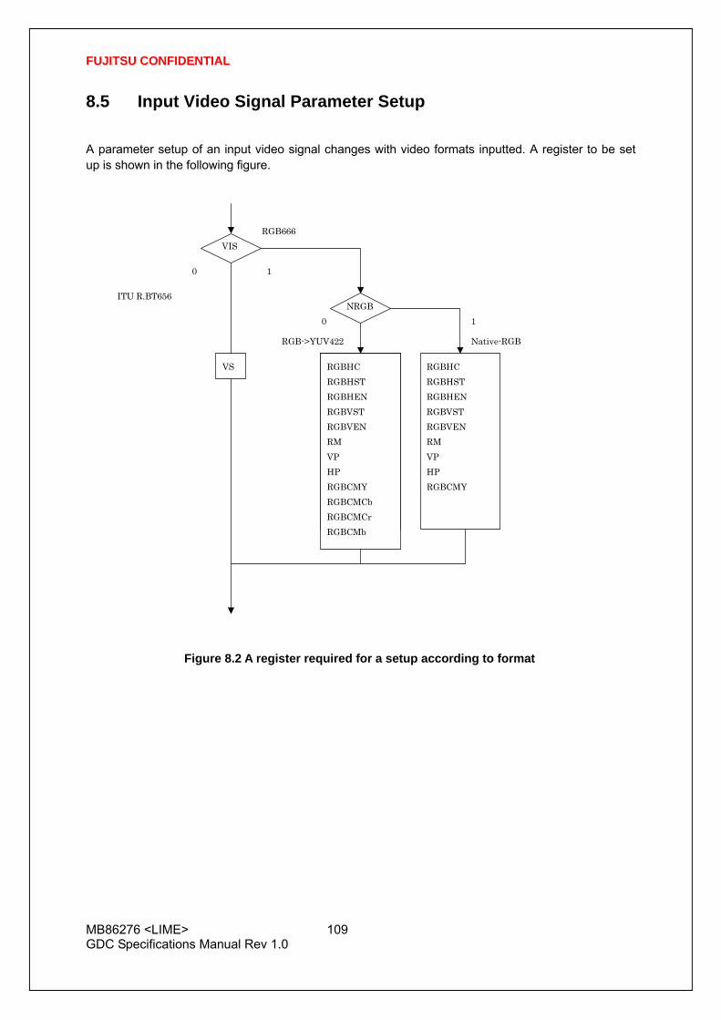
FUJITSU CONFIDENTIAL
MB86276 <LIME> 109 GDC Specifications Manual Rev 1.0
8.5 Input Video Signal Parameter Setup
A parameter setup of an input video signal changes with video formats inputted. A register to be set up is shown in the following figure.
Figure 8.2 A register required for a setup according to format
ITU R.BT656
RGB666 VIS
NRGB
1 0
1 0
RGB->YUV422 Native-RGB
RGBHC RGBHST RGBHEN RGBVST RGBVEN RM VP HP RGBCMY
VS RGBHC RGBHST RGBHEN RGBVST RGBVEN RM VP HP RGBCMY RGBCMCb RGBCMCr RGBCMb

FUJITSU CONFIDENTIAL
MB86276 <LIME> 110 GDC Specifications Manual Rev 1.0
9 DRAWING PROCESSING 9.1 Coordinate System 9.1.1 Drawing coordinates
LIME GDC draws data in the drawing frame in the graphics memory that finally uses the drawing coordinates (device coordinates).
Drawing frame is treated as 2D coordinates with the origin at the top left as shown in the figure below. The maximum coordinates is 4096 × 4096. Each drawing frame is located in the Graphics Memory by setting the address of the origin and resolution of X direction (size). Although the size of Y direction does not need to be set, Y coordinates which are max. at drawing must not be overlapped with other area. In addition, at drawing, specifying the clip frame (top left and bottom right coordinates) can prevent the drawing of images outside the clip frame.
X (max. 4096)
Y (m
ax. 4
096)
Origin Drawing frame size X
Dra
win
g fra
me
size
Y (Xmin, Ymin)
(Xmax, Ymax)
Clip frame

FUJITSU CONFIDENTIAL
MB86276 <LIME> 111 GDC Specifications Manual Rev 1.0
9.1.2 Texture coordinates
Texture coordinate is a 2D coordinate system represented as S and T (S: horizontal, T: vertical). Any integer in a range of −8192 to +8191 can be used as the S and T coordinates. The texture coordinates is correlated to the 2D coordinates of a vertex. One texture pattern can be applied to up to 4096 × 4096 pixels. The pattern size is set in the register. When the S and T coordinates exceed the maximum pattern size, the repeat, cramp or border color option is selected.
9.1.3 Frame buffer
For drawing, the following area must be assigned to the Graphics Memory. The frame size (count of pixels on X direction) is common for these areas.
Drawing frame The results of drawing are stored in the graphical image data area. Both the direct and indirect color mode are applicable.
Z buffer (Optional function) Z buffer is required for eliminating hidden surfaces. In 16 bits mode, 2 bytes and in 8 bits mode, 1 byte are required per 1 pixel.
Polygon drawing flag buffer This area is used for polygon drawing. 1 bit is required per 1 pixel.
S (max. ±8192)
T (m
ax. ±
8192
)
Origin
max. 4096 pixels
max
. 409
6 pi
xels
Texture pattern

FUJITSU CONFIDENTIAL
MB86276 <LIME> 112 GDC Specifications Manual Rev 1.0
9.2 Figure Drawing 9.2.1 Drawing primitives
LIME GDC is supported the rendering command that is compatible with the LIME. The following types of figure drawing primitives are compatible with the LIME.
Point
Line
Triangle
2DLine with XY setup
2DTriangle with XY setup
Polygon
9.2.2 Polygon drawing function
An irregular polygon (including concave shape) is drawn by hardware in the following manner:
1. Execute PolygonBegin command.
Initialize polygon drawing hardware.
2. Draw vertices.
Draw outline of polygon and plot all vertices to polygon draw flag buffer using 2D Triangle with XY setup.
3. Execute PolygonEnd command.
Copy shape in polygon draw flag buffer to drawing frame and fill shape with color or specified tiling pattern.

FUJITSU CONFIDENTIAL
MB86276 <LIME> 113 GDC Specifications Manual Rev 1.0
9.2.3 Drawing parameters
The triangles (Right triangle and Left triangle) are distinguished according to the locations of three vertices as follows (not used for 2D Triangle with XY setup):
The following parameters are required for drawing triangles (for 2D Triangle with XY setup, X and Y coordinates of each vertex are specified).
Note: Be careful about the positional relationship between coordinates Xs, XUs, and XLs. For example, in the above diagram, when a right-hand triangle is drawn using the parameter that shows the coordinates positional relationship Xs (upper edge start Y coordinates) > XUs or Xs (lower edge start Y coordinates) > XLs, the appropriate picture may not be drawn.
V0
Upper edge
Long edge
V1
Lower edgeV2
Upper triangle
Lower triangle
V1
V0
V2
Upper edge
Lower edge
Long edge Upper triangle
Lower triangle
Right-hand triangle Left-hand triangle
XUs
XLs
Ys Xs,Zs,Rs,Gs,Bs,Ss,Ts,Qs
Upper edge start Y coordinates
dXdy dZdy dRdy dGdy dBdy dSdy dTdy dQdy
dXUdy
dXLdy
Lower edge start Y coordinates
dZdx,dRdx,dGdx,dBdx,dSdx,dTdx,dQdx
USN
LSN

FUJITSU CONFIDENTIAL
MB86276 <LIME> 114 GDC Specifications Manual Rev 1.0
Ys Y coordinates start position of long edge in drawing triangle
Xs X coordinates start position of long edge corresponding to Ys
XUs X coordinates start position of upper edge
XLs X coordinates start position of lower edge
Zs Z coordinates start position of long edge corresponding to Ys
Rs R color value of long edge corresponding to Ys
Gs G color value of long edge corresponding to Ys
Bs B color value of long edge corresponding to Ys
Ss S coordinate of textures of long edge corresponding to Ys
Ts T coordinate of textures of long edge corresponding to Ys
Qs Q perspective correction value of texture of long edge corresponding to Ys
dXdy X DDA value of long edge direction
dXUdy X DDA value of upper edge direction
dXLdy X DDA value of lower edge direction
dZdy Z DDA value of long edge direction
dRdy R DDA value of long edge direction
dGdy G DDA value of long edge direction
dBdy B DDA value of long edge direction
dSdy S DDA value of long edge direction
dTdy T DDA value of long edge direction
dQdy Q DDA value of long edge direction
USN Count of spans of upper triangle
LSN Count of spans of lower triangle
dZdx Z DDA value of horizontal direction
dRdx R DDA value of horizontal direction
dGdx G DDA value of horizontal direction
dBdx B DDA value of horizontal direction
dSdx S DDA value of horizontal direction
dTdx T DDA value of horizontal direction
dQdx Q DDA value of horizontal direction
9.2.4 Anti-aliasing function
LIME GDC performs anti-aliasing to make jaggies less noticeable and smooth on line edges. To use this function at the edges of primitives, redraw the primitive edges with anti-alias lines. (The edge of line is blended with a frame buffer color at that time. Ideally please draw sequentially from father object.)
FUJITSU CONFIDENTIAL
MB86276 <LIME> 115 GDC Specifications Manual Rev 1.0
9.3 Bit Map Processing 9.3.1 BLT
A rectangular shape in pixel units can be transferred. There are following types of transfer:
1. Transfer from host CPU to Drawing frame memory
2. Transfer between Graphics Memories including Drawing frame
Concerning 1 and 2 above, 2-term logic operation is performed between source and destination data and its result can be stored.
Setting a transparent color enables a drawing of a specific pixel with transmission.
If part of the source and destination of the BLT field are physically overlapped in the display frame, the start address (from which vertex the BLT field to be transferred) must be set correctly.
9.3.2 Pattern data format
LIME GDC can handle three bit map data formats: indirect color mode (8 bits/pixel), direct color mode (16 bits/pixel), and binary bit map (1 bit/pixel).
The binary bit map is used for character/font patterns, where foreground color is used for bitmap = 1 pixel, and background color (background color can be set to be transparent by setting) is applied for bitmap = 0 pixels.

FUJITSU CONFIDENTIAL
MB86276 <LIME> 116 GDC Specifications Manual Rev 1.0
9.4 Texture Mapping 9.4.1 Texture size
LIME GDC reads texel corresponding to the specified texture coordinates (S, T), and draws that data at the correlated pixel position of the polygon. For the S and T coordinates, the selectable texture data size is any value in the range from 4 to 4096 pixels represented as an exponent of 2.
9.4.2 Texture color
Drawing of 8-/16-bit direct color is supported for the texture pattern. For drawing 8-bit direct color, only point sampling can be specified for texture interpolation; only de-curl can be specified for the blend mode.
9.4.3 Texture Wrapping
If a negative or larger than the specified texture pattern size is specified as the texture coordinates (S, T), according to the setting, one of these options (repeat, cramp or border) is selected for the ‘out-of-range’ texture mapping. The mapping image for each case is shown below:
Repeat This just simply masks the upper bits of the applied (S, T) coordinates. When the texture pattern size is 64 × 64 pixels, the lower 6 bits of the integer part of (S, T) coordinates are used for S and T coordinates.
Cramp When the applied (S, T) coordinates is either negative or larger than the specified texture pattern size, cramp the (S, T) coordinate as follows instead of texture:
S < 0 S = 0 S > Texture X size − 1 S = Texture X size − 1
Border When the applied (S, T) coordinate is either negative or larger than the specified texture pattern size, the outside of the specified texture pattern is rendered in the ‘border’ color.
Repeat Cramp Border
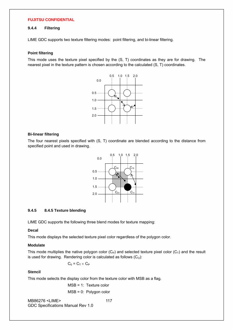
FUJITSU CONFIDENTIAL
MB86276 <LIME> 117 GDC Specifications Manual Rev 1.0
9.4.4 Filtering
LIME GDC supports two texture filtering modes: point filtering, and bi-linear filtering.
Point filtering This mode uses the texture pixel specified by the (S, T) coordinates as they are for drawing. The nearest pixel in the texture pattern is chosen according to the calculated (S, T) coordinates.
Bi-linear filtering The four nearest pixels specified with (S, T) coordinate are blended according to the distance from specified point and used in drawing.
9.4.5 8.4.5 Texture blending
LIME GDC supports the following three blend modes for texture mapping:
Decal This mode displays the selected texture pixel color regardless of the polygon color.
Modulate This mode multiplies the native polygon color (CP) and selected texture pixel color (CT) and the result is used for drawing. Rendering color is calculated as follows (CO):
C0 = CT × CP
Stencil This mode selects the display color from the texture color with MSB as a flag.
MSB = 1: Texture color
MSB = 0: Polygon color
0.0
0.5 1.0 1.5 2.0
0.5
1.0
1.5
2.0
0.0
0.5 1.0 1.5 2.0
0.5
1.0
1.5
2.0
C00 C10
C01 C11

FUJITSU CONFIDENTIAL
MB86276 <LIME> 118 GDC Specifications Manual Rev 1.0
9.5 Rendering 9.5.1 Tiling
Tiling reads the pixel color from the correlated tiling pattern and maps it onto the polygon. The tiling determines the pixel on the pattern read by pixel coordinates to be drawn, irrespective of position and size of primitive. Since the tiling pattern is stored in the texture memory, this function and texture mapping cannot be used at the same time. Also, the tiling pattern size is limited to within 64 × 64 pixels. (at 16-bit color)
Example of Tiling
9.5.2 Alpha blending
Alpha blending blends the drawn in frame buffer to-be-drawn pixel or pixel already according to the alpha value set in the alpha register. This function cannot be used simultaneously with logic operation drawing. It can be used only when the direct color mode (16 bits/pixel) is used. The blended color C is calculated as shown below when the color of the pixel to be drawn is CP, the color of frame buffer is CF, and the alpha value is A:
C = CP × A + (1-A) × CF
The alpha value is specified as 8-bit data. 00h means alpha value 0% and FFh means alpha value 100%. When the texture mapping function is enabled, the following blending modes can be selected:
Normal Blends post texture mapping color with frame buffer color
Stencil Uses MSB of texel color for ON/OFF control:
MSB = 1: Texel color
MSB = 0: Frame buffer color
Stencil alpha Uses MSB of texel color for α/OFF control:
MSB = 1: Alpha blend texel color and current frame buffer color
MSB = 0: Frame buffer color
Note: MSB of frame buffer is drawn MSB of texel in both stencil and stencil alpha mode.
Therefore in case MSB of texel is MSB=0, a color of frame buffer is frame buffer, but MSB of frame buffer is set to 0.

FUJITSU CONFIDENTIAL
MB86276 <LIME> 119 GDC Specifications Manual Rev 1.0
9.5.3 Logic operation
This mode executes a logic operation between the pixel to be drawn and the one already drawn in frame buffer and its result is drawn. Alpha blending cannot be used when this function is specified.
Type ID Operation Type ID Operation CLEAR 0000 0 AND 0001 S & D COPY 0011 S OR 0111 S | D NOP 0101 D NAND 1110 ! (S & D) SET 1111 1 NOR 1000 ! (S | D) COPY INVERTED 1100 !S XOR 0110 S xor D INVERT 1010 !D EQUIV 1001 ! (S xor D) AND REVERSE 0010 S & !D AND INVERTED 0100 !S & D OR REVERSE 1011 S | !D OR INVERTED 1101 !S | D
9.5.4 Hidden plane management (Optional function)
LIME GDC supports the Z buffer for hidden plane management.
This function compares the Z value of a new pixel to be drawn and the existing Z value in the Z buffer. Display/not display is switched according to the Z-compare mode setting. Define the Z-buffer access options in the ZWRITEMASK mode.
The Z compare operation type is determined by the Z compare mode.
Either 16 or 8 bits can be selected for the Z-value.
1 Compare Z values, no Z value write overwrite ZWRITEMASK 0 Compare Z values, Z value write
Z Compare mode Code Condition NEVER 000 Never draw ALWAYS 001 Always draw LESS 010 Draw if pixel Z value < current Z buffer value LEQUAL 011 Draw if pixel Z value ≤ current Z buffer value EQUAL 100 Draw if pixel Z value = current Z buffer value GEQUAL 101 Draw if pixel Z value ≥ current Z buffer value GREATER 110 Draw if pixel Z value > current Z buffer value NOTEQUAL 111 Draw if pixel Z value ! = current Z buffer value

FUJITSU CONFIDENTIAL
MB86276 <LIME> 120 GDC Specifications Manual Rev 1.0
9.6 Drawing Attributes 9.6.1 Line drawing attributes
In drawing lines, the following attributes apply:
Line Drawing Attributes
Drawing Attribute Description
Line width Line width selectable in range of 1 to 32 pixels
Broken line Specify broken line pattern in 32-bit data
Anti-alias Line edge smoothed when anti-aliasing enabled
9.6.2 Triangle drawing attributes
In drawing triangles, the following attributes apply (these attributes are disabled in 2DTriangle with XY setup). Texture mapping and tiling have separated texture attributes:
Triangle Drawing Attributes
Drawing Attribute Description
Shading Gouraud shading or flat shading selectable
Alpha blending Set alpha blending enable/disable per polygon
Alpha blending coefficient Set color blending ratio of alpha blending

FUJITSU CONFIDENTIAL
MB86276 <LIME> 121 GDC Specifications Manual Rev 1.0
9.6.3 Texture attributes
In texture mapping, the following attributes apply:
Texture Attributes
Drawing Attribute Description
Texture mode Select either texture mapping or tiling
Texture filter Select either point sampling or bi-linear filtering
Texture coordinates correction Select either linear or perspective correction
Texture wrap Select either repeat or cramp of texture pattern
Texture blend mode Select either decal or modulate
9.6.4 BLT attributes
In BLT drawing, the following attributes apply:
BLT Attributes
Drawing Attribute Description
Logic operation mode Specify two source logic operation mode
Transparency mode Set transparent copy mode and transparent color
Alpha map mode Blend a color according to alpha map
9.6.5 Character pattern drawing attributes
Character Pattern Drawing
Drawing Attribute Description
Character pattern enlarge/shrink
Vertical and Horizontal × 2, Horizontal × 2, Vertical and Horizontal × 1/2, Horizontal × 1/2
Character pattern color Set character color and background color
Transparency/non-transparency Set background color to transparency/non-transparency

FUJITSU CONFIDENTIAL
MB86276 <LIME> 122 GDC Specifications Manual Rev 1.0
10 DISPLAY LIST 10.1 Overview Display list is a set of display list commands, parameters and pattern data. All display list commands stored in a display list are executed consequently.
The display list is transferred to the display list FIFO by the following method:
Transfer from graphics memory to display FIFO by register setting
Display list Command-1
Data 1-1
Data 1-2
Data 1-3
Display list Command-2
Data 2-1
Data 2-2
Data 2-3
⋅⋅⋅
Display List

FUJITSU CONFIDENTIAL
MB86276 <LIME> 123 GDC Specifications Manual Rev 1.0
10.1.1 Header format
The format of the display list header is shown below.
Format List
Format 31 24 23 16 15 0Format 1 Type Reserved Reserved Format 2 Type Count Address Format 3 Type Reserved Reserved VertexFormat 4 Type Reserved Reserved Flag VertexFormat 5 Type Command Reserved Format 6 Type Command Count Format 7 Type Command Reserved VertexFormat 8 Type Command Reserved Flag VertexFormat 9 Type Reserved Reserved Flag
Format 10 Type Reserved Count Type Reserved Reserved Format 11
Count
Description of Each Field
Type Display list type Command Command Count Count of data excluding header Address Address value used at data transfer Vertex Vertex number Flag Attribute flag peculiar to display list command
Vertex Number Specified in Vertex Code
Vertex Vertex number (Line) Vertex number (Triangle) 00 V0 V0 01 V1 V1 10 Setting prohibited V2 11 Setting prohibited Setting prohibited

FUJITSU CONFIDENTIAL
MB86276 <LIME> 124 GDC Specifications Manual Rev 1.0
10.2 Rendering Command 10.2.1 Command list
The following table lists LIME GDC rendering commands and their command codes.
Type Command Description Nop ⎯ No operation
Interrupt ⎯ Interrupt request to host CPU
Sync ⎯ Synchronization with events
SetRegister ⎯ Sets data to register
Normal Sets data to 2D Triangle with XY setup vertex register
SetVertex2i PolygonBegin Initializes border rectangle calculation of multiple
vertices random shape PolygonEnd Clears polygon flag after drawing polygon
Draw Flush_FB/Z Flushes drawing pipelines
DrawPixel Pixel Draws point
DrawPixelZ PixelZ Draws point with Z
Xvector Draws line (principal axis X)
Yvector Draws line (principal axis Y)
AntiXvector Draws line with anti-alias option (principal axis X) DrawLine
AntiYvector Draws line with anti-alias option (principal axis Y)
ZeroVector Draws 2D Line with XY setup (with vertex 0 as starting point) DrawLine2i
DrawLine2iP OneVector Draws 2D Line with XY setup (with vertex 1 as starting point)
TrapRight Draws right triangle DrawTrap
TrapLeft Draws left triangle
TriangleFan Draws 2D Triangle with XY setup DrawVertex2i
DrawVertex2iP FlagTriangleFan Draws 2D Triangle with XY setup for multiple vertices random shape
BltFill Draws rectangle with single color DrawRectP
ClearPolyFlag Clears polygon flag buffer
BltDraw Draws Blt (16-bit) DrawBitmapP
Bitmap Draws binary bit map (character)
DrawBitmapLargeP BltDraw Draws Blt (32-bit)
TopLeft Blt transfer from top left coordinates
TopRight Blt transfer from top right coordinates
BottomLeft Blt transfer from bottom left coordinates
BltCopyP
BltCopy-
AlternateP BottomRight Blt transfer from bottom right coordinates
LoadTexture Loads texture pattern LoadTextureP
LoadTILE Loads tile pattern
LoadTexture Loads texture pattern from local memory BltTextureP
LoadTILE Loads tile pattern from local memory
BltCopyAlt-
AlphaBlendP ⎯ Alpha blending is supported (see the alpha map).
BltCopyAlternateP

FUJITSU CONFIDENTIAL
MB86276 <LIME> 125 GDC Specifications Manual Rev 1.0
Type Code Table
Type Code
DrawPixel 0000_0000
DrawPixelZ 0000_0001
DrawLine 0000_0010
DrawLine2i 0000_0011
DrawLine2iP 0000_0100
DrawTrap 0000_0101
DrawVertex2i 0000_0110
DrawVertex2iP 0000_0111
DrawRectP 0000_1001
DrawBitmapP 0000_1011
BitCopyP 0000_1101
BitCopyAlternateP 0000_1111
LoadTextureP 0001_0001
BltTextureP 0001_0011
BltCopyAltAlphaBlendP 0001_1111
SetVertex2i 0111_0000
SetVertex2iP 0111_0001
Draw 1111_0000
SetRegister 1111_0001
Sync 1111_1100
Interrupt 1111_1101
Nop 1111_1111
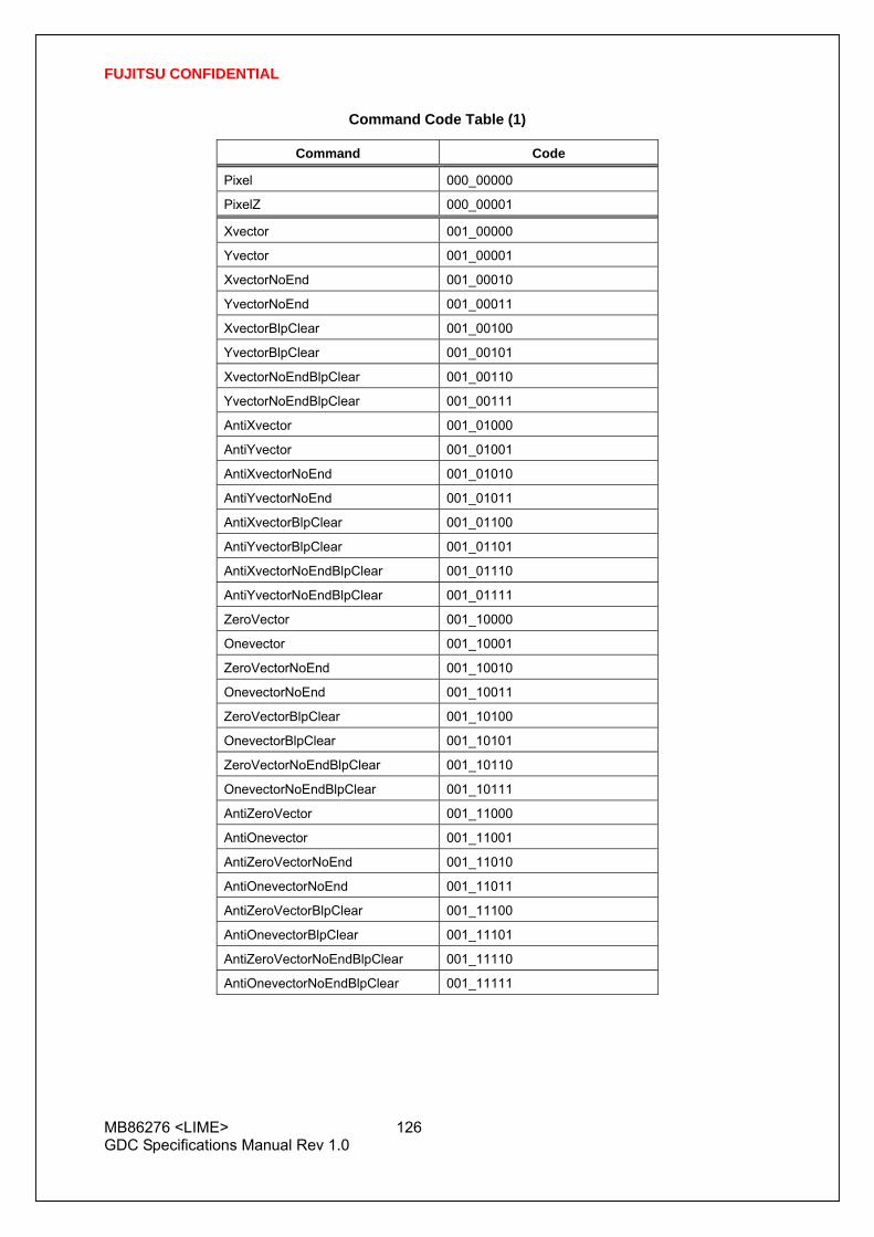
FUJITSU CONFIDENTIAL
MB86276 <LIME> 126 GDC Specifications Manual Rev 1.0
Command Code Table (1)
Command Code
Pixel 000_00000
PixelZ 000_00001
Xvector 001_00000
Yvector 001_00001
XvectorNoEnd 001_00010
YvectorNoEnd 001_00011
XvectorBlpClear 001_00100
YvectorBlpClear 001_00101
XvectorNoEndBlpClear 001_00110
YvectorNoEndBlpClear 001_00111
AntiXvector 001_01000
AntiYvector 001_01001
AntiXvectorNoEnd 001_01010
AntiYvectorNoEnd 001_01011
AntiXvectorBlpClear 001_01100
AntiYvectorBlpClear 001_01101
AntiXvectorNoEndBlpClear 001_01110
AntiYvectorNoEndBlpClear 001_01111
ZeroVector 001_10000
Onevector 001_10001
ZeroVectorNoEnd 001_10010
OnevectorNoEnd 001_10011
ZeroVectorBlpClear 001_10100
OnevectorBlpClear 001_10101
ZeroVectorNoEndBlpClear 001_10110
OnevectorNoEndBlpClear 001_10111
AntiZeroVector 001_11000
AntiOnevector 001_11001
AntiZeroVectorNoEnd 001_11010
AntiOnevectorNoEnd 001_11011
AntiZeroVectorBlpClear 001_11100
AntiOnevectorBlpClear 001_11101
AntiZeroVectorNoEndBlpClear 001_11110
AntiOnevectorNoEndBlpClear 001_11111

FUJITSU CONFIDENTIAL
MB86276 <LIME> 127 GDC Specifications Manual Rev 1.0
Command Code Table (2)
Command Code
BltFill 010_00001
BltDraw 010_00010
Bitmap 010_00011
TopLeft 010_00100
TopRight 010_00101
BottomLeft 010_00110
BottomRight 010_00111
LoadTexture 010_01000
LoadTILE 010_01001
TrapRight 011_00000
TrapLeft 011_00001
TriangleFan 011_00010
FlagTriangleFan 011_00011
Flush_FB 110_00001
Reserved 110_00010
PolygonBegin 111_00000
PolygonEnd 111_00001
ClearPolyFlag 111_00010
Normal 111_11111

FUJITSU CONFIDENTIAL
MB86276 <LIME> 128 GDC Specifications Manual Rev 1.0
10.2.2 Details of rendering commands
All parameters belonging to their command are stored in relevant registers. The definition of each parameter is explained in the section of each command.
Nop (Format1) 31 24 23 16 15 0
Nop Reserved Reserved
No operation
Interrupt (Format1) 31 24 23 16 15 0
Interrupt Reserved Reserved
The Interrupt command generates interrupt request to host CPU.
Sync (Format9) 31 24 23 16 15 4 0
Sleep Reserved Reserved flag
The Sync command suspends all subsequent display list processing until event set in flag detected.
Flag: Bit number 4 3 2 1 0
Bit field name Reserved Reserved Reserved Reserved VBLANK
Bit 0 VBLANK
VBLANK Synchronization
0 No operation
1 Wait for VSYNC detection

FUJITSU CONFIDENTIAL
MB86276 <LIME> 129 GDC Specifications Manual Rev 1.0
SetRegister (Format2) 31 24 23 16 15 0
SetRegister Count Address (Val 0) (Val 1)
⋅⋅⋅ (Val n)
The SetRegister command sets data to sequential registers.
Count: Data word count (in double-word unit)
Address: Register address
Set the value of the address for SetRegister given in the register list. When transferring two or more data, set the starting register address.
SetVertex2i (Format8) 31 24 23 16 15 4 3 2 1 0
SetVertex2i Command Reserved flag vertex Xdc Ydc
The SetVertex2i command sets vertices data for 2D Line with XY setup or 2D Triangle with XY setup to registers.
Commands: Normal Sets vertex data (X, Y).
PolygonBegin Starts calculation of circumscribed rectangle for random shape to be drawn. Calculate vertices of rectangle including all vertices of random shape defined between PolygonBegin and PolygonEnd.
Flag: Not used
SetVertex2iP (Format8) 31 24 23 16 15 4 3 2 1 0
SetVertex2i Command Reserved flag vertex Ydc Xdc
The SetVertex2iP command sets vertices data for 2D Line with XY setup or 2D Triangle with XY setup to registers.
Only the integer (packed format) can be used to specify these vertices.
Commands: Normal Sets vertices data.
PolygonBegin Starts calculation of circumscribed rectangle of random shape to be drawn. Calculate vertices of rectangle including all vertices of random shape defined between PolygonBegin and PolygonEnd.
Flag: Not used

FUJITSU CONFIDENTIAL
MB86276 <LIME> 130 GDC Specifications Manual Rev 1.0
Draw (Format5) 31 24 23 16 15 0
Draw Command Reserved
The Draw command executes drawing command. All parameters required for drawing command execution must be set at their appropriate registers.
Commands: PolygonEnd Draws polygon end.
Fills random shape with color according to flags generated by FlagTriangleFan command and information of circumscribed rectangle generated by PolygonBegin command.
Flush_FB Flushes drawing data in the drawing pipeline into the graphics memory. Place this command at the end of the display list.
Flush_Z Flushes Z value data in the drawing pipeline into the graphics memory. When using the Z buffer, place this command together with the Flush_FB command at the end of the display list.
DrawPixel (Format5) 31 24 23 16 15 0
DeawPixel Command Reserved PXs PYs
The DrawPixel command draws pixel.
Command: Pixel Draws pixel without Z value.
DrawPixelZ (Format5) 31 24 23 16 15 0
DeawPixel Command Reserved PXs PYs PZs
The DrawPixelZ command draws pixel with Z value.
Command: PixelZ Draws pixel with Z value.

FUJITSU CONFIDENTIAL
MB86276 <LIME> 131 GDC Specifications Manual Rev 1.0
DrawLine (Format5) 31 24 23 16 15 0
DrawLine Command Reserved LPN LXs
LXde LYs
LYde
The DrawLine command draws line. It starts drawing after setting all parameters at line draw registers.
Commands: Xvector Draws line (principal axis X).
Yvector Draws line (principal axis Y).
XvectorNoEnd Draws line (principal axis X, and without end point drawing).
YvectorNoEnd Draws line (principal axis Y, and without end point drawing).
XvectorBlpClear Draws line (principal axis X, and prior to drawing, broken line pattern reference position cleared).
YvectorBlpClear Draws line (principal axis Y, and prior to drawing, broken line pattern reference position cleared).
XvectorNoEndBlpClear Draws line (principal axis X, without end point drawing and prior to drawing, broken line pattern reference position cleared).
YvectorNoEndBlpClear Draws line (principal axis Y, without end point drawing and prior to drawing, broken line pattern reference position cleared).
AntiXvector Draws anti-alias line (principal axis X).
AntiYvector Draws anti-alias line (principal axis Y).
AntiXvectorNoEnd Draws anti-alias line (principal axis X, and without end point drawing).
AntiYvectorNoEnd Draws anti-alias line (principal axis Y, and without end point drawing).
AntiXvectorBlpClear Draws anti-alias line (principal axis X and prior to drawing, broken line pattern reference position cleared).
AntiYvectorBlpClear Draws anti-alias line (principal axis Y and prior to drawing, broken line pattern reference position cleared).
AntiXvectorNoEndBlpClear Draws anti-alias line (principal axis X, without end point drawing and prior to drawing, broken line pattern reference position cleared).
AntiYvectorNoEndBlpClear Draws anti-alias line (principal axis Y, without end point drawing and prior to drawing, broken line pattern reference position cleared).
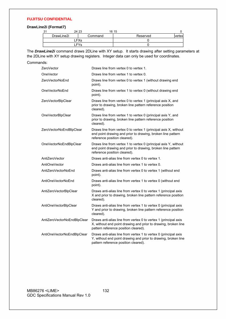
FUJITSU CONFIDENTIAL
MB86276 <LIME> 132 GDC Specifications Manual Rev 1.0
DrawLine2i (Format7) 31 24 23 16 15 0
DrawLine2i Command Reserved vertex LFXs 0 LFYs 0
The DrawLine2i command draws 2DLine with XY setup. It starts drawing after setting parameters at the 2DLine with XY setup drawing registers. Integer data can only be used for coordinates.
Commands: ZeroVector Draws line from vertex 0 to vertex 1.
OneVector Draws line from vertex 1 to vertex 0.
ZeroVectorNoEnd Draws line from vertex 0 to vertex 1 (without drawing end point).
OneVectorNoEnd Draws line from vertex 1 to vertex 0 (without drawing end point).
ZeroVectorBlpClear Draws line from vertex 0 to vertex 1 (principal axis X, and prior to drawing, broken line pattern reference position cleared).
OneVectorBlpClear Draws line from vertex 1 to vertex 0 (principal axis Y, and prior to drawing, broken line pattern reference position cleared).
ZeroVectorNoEndBlpClear Draws line from vertex 0 to vertex 1 (principal axis X, without end point drawing and prior to drawing, broken line pattern reference position cleared).
OneVectorNoEndBlpClear Draws line from vertex 1 to vertex 0 (principal axis Y, without end point drawing and prior to drawing, broken line pattern reference position cleared).
AntiZeroVector Draws anti-alias line from vertex 0 to vertex 1.
AntiOneVector Draws anti-alias line from vertex 1 to vertex 0.
AntiZeroVectorNoEnd Draws anti-alias line from vertex 0 to vertex 1 (without end point).
AntiOneVectorNoEnd Draws anti-alias line from vertex 1 to vertex 0 (without end point).
AntiZeroVectorBlpClear Draws anti-alias line from vertex 0 to vertex 1 (principal axis X and prior to drawing, broken line pattern reference position cleared).
AntiOneVectorBlpClear Draws anti-alias line from vertex 1 to vertex 0 (principal axis Y and prior to drawing, broken line pattern reference position cleared).
AntiZeroVectorNoEndBlpClear Draws anti-alias line from vertex 0 to vertex 1 (principal axis X, without end point drawing and prior to drawing, broken line pattern reference position cleared).
AntiOneVectorNoEndBlpClear Draws anti-alias line from vertex 1 to vertex 0 (principal axis Y, without end point drawing and prior to drawing, broken line pattern reference position cleared).
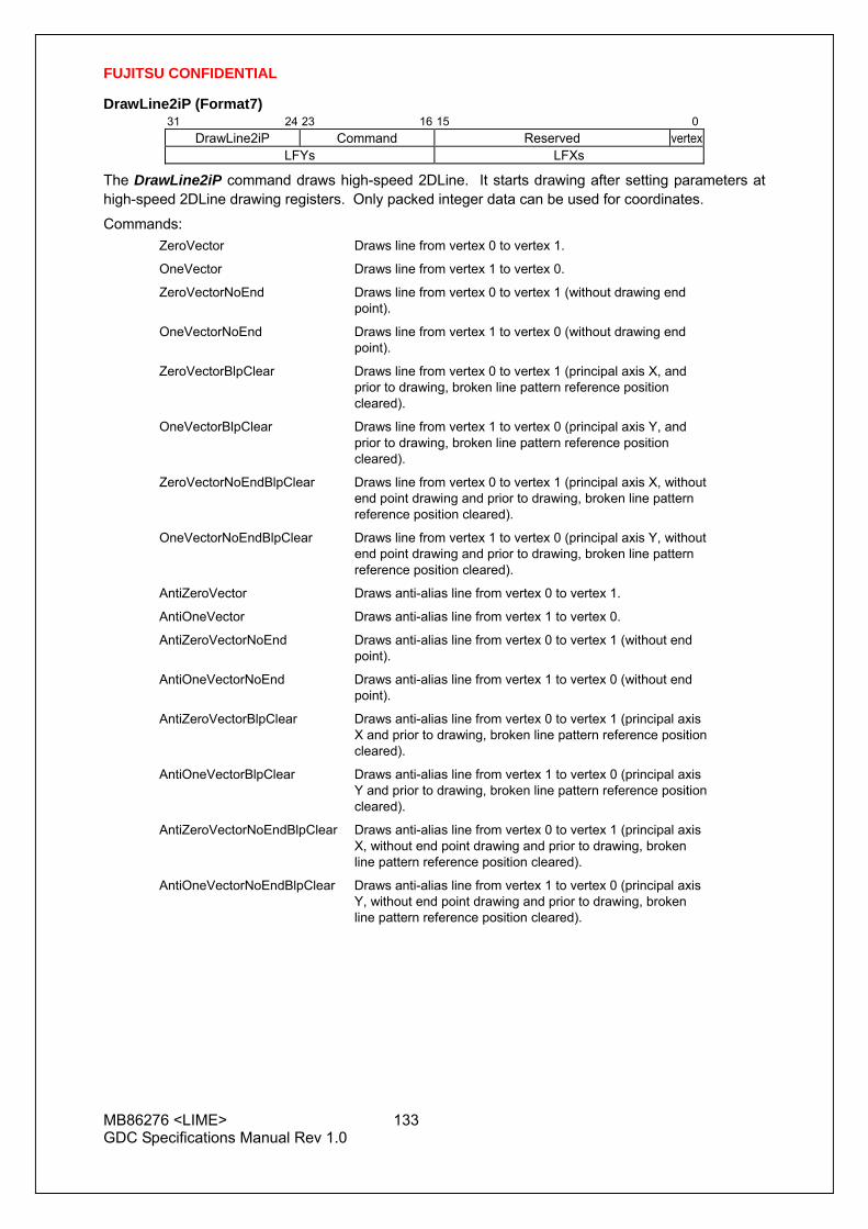
FUJITSU CONFIDENTIAL
MB86276 <LIME> 133 GDC Specifications Manual Rev 1.0
DrawLine2iP (Format7) 31 24 23 16 15 0
DrawLine2iP Command Reserved vertex LFYs LFXs
The DrawLine2iP command draws high-speed 2DLine. It starts drawing after setting parameters at high-speed 2DLine drawing registers. Only packed integer data can be used for coordinates.
Commands: ZeroVector Draws line from vertex 0 to vertex 1.
OneVector Draws line from vertex 1 to vertex 0.
ZeroVectorNoEnd Draws line from vertex 0 to vertex 1 (without drawing end point).
OneVectorNoEnd Draws line from vertex 1 to vertex 0 (without drawing end point).
ZeroVectorBlpClear Draws line from vertex 0 to vertex 1 (principal axis X, and prior to drawing, broken line pattern reference position cleared).
OneVectorBlpClear Draws line from vertex 1 to vertex 0 (principal axis Y, and prior to drawing, broken line pattern reference position cleared).
ZeroVectorNoEndBlpClear Draws line from vertex 0 to vertex 1 (principal axis X, without end point drawing and prior to drawing, broken line pattern reference position cleared).
OneVectorNoEndBlpClear Draws line from vertex 1 to vertex 0 (principal axis Y, without end point drawing and prior to drawing, broken line pattern reference position cleared).
AntiZeroVector Draws anti-alias line from vertex 0 to vertex 1.
AntiOneVector Draws anti-alias line from vertex 1 to vertex 0.
AntiZeroVectorNoEnd Draws anti-alias line from vertex 0 to vertex 1 (without end point).
AntiOneVectorNoEnd Draws anti-alias line from vertex 1 to vertex 0 (without end point).
AntiZeroVectorBlpClear Draws anti-alias line from vertex 0 to vertex 1 (principal axis X and prior to drawing, broken line pattern reference position cleared).
AntiOneVectorBlpClear Draws anti-alias line from vertex 1 to vertex 0 (principal axis Y and prior to drawing, broken line pattern reference position cleared).
AntiZeroVectorNoEndBlpClear Draws anti-alias line from vertex 0 to vertex 1 (principal axis X, without end point drawing and prior to drawing, broken line pattern reference position cleared).
AntiOneVectorNoEndBlpClear Draws anti-alias line from vertex 1 to vertex 0 (principal axis Y, without end point drawing and prior to drawing, broken line pattern reference position cleared).

FUJITSU CONFIDENTIAL
MB86276 <LIME> 134 GDC Specifications Manual Rev 1.0
DrawTrap (Format5) 31 24 23 16 15 0
DrawTrap Command Reserved Ys 0
Xs DXdy XUs
DXUdy XLs
DXLdy USN 0 LSN 0
The DrawTrap command draws Triangle. It starts drawing after setting parameters at the Triangle Drawing registers (coordinates).
Commands: TrapRight Draws right triangle.
TrapLeft Draws left triangle.
DrawVertex2i (Format7) 31 24 23 16 15 0
DrawVertex2i Command Reserved vertex Xdc 0 Ydc 0
The DrawVertex2i command draws 2D Triangle with XY setup
It starts triangle drawing after setting parameters at 2D Triangle Drawing registers.
Commands: TriangleFan Draws 2D Triangle with XY setup.
FlagTriangleFan Draws 2D Triangle with XY setup for polygon drawing in the flag buffer.
DrawVertex2iP (Format7) 31 24 23 16 15 0
DrawVertex2iP Command Reserved vertex Ydc Xdc
The DrawVertex2iP command draws 2D Triangle with XY setup.
It starts drawing after setting parameters at 2D Triangle with XY setup Drawing registers
Only the packed integer format can be used for vertex coordinates.
Commands: TriangleFan Draw 2D Triangle with XY setup.
FlagTriangleFan Draws 2D Triangle with XY setup for polygon drawing in the flag buffer.
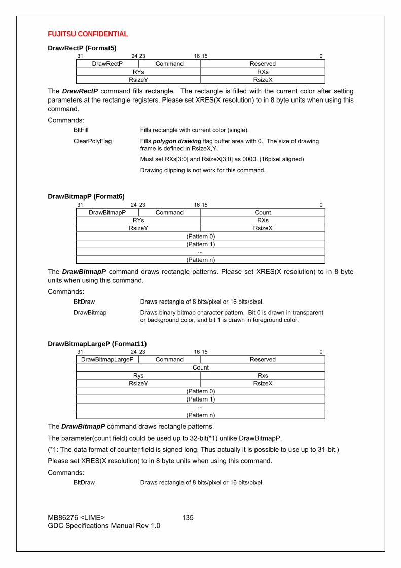
FUJITSU CONFIDENTIAL
MB86276 <LIME> 135 GDC Specifications Manual Rev 1.0
DrawRectP (Format5) 31 24 23 16 15 0
DrawRectP Command Reserved RYs RXs
RsizeY RsizeX
The DrawRectP command fills rectangle. The rectangle is filled with the current color after setting parameters at the rectangle registers. Please set XRES(X resolution) to in 8 byte units when using this command.
Commands: BltFill Fills rectangle with current color (single).
ClearPolyFlag Fills polygon drawing flag buffer area with 0. The size of drawing frame is defined in RsizeX,Y.
Must set RXs[3:0] and RsizeX[3:0] as 0000. (16pixel aligned)
Drawing clipping is not work for this command.
DrawBitmapP (Format6) 31 24 23 16 15 0
DrawBitmapP Command Count RYs RXs
RsizeY RsizeX (Pattern 0) (Pattern 1)
⋅⋅⋅ (Pattern n)
The DrawBitmapP command draws rectangle patterns. Please set XRES(X resolution) to in 8 byte units when using this command.
Commands: BltDraw Draws rectangle of 8 bits/pixel or 16 bits/pixel.
DrawBitmap Draws binary bitmap character pattern. Bit 0 is drawn in transparent or background color, and bit 1 is drawn in foreground color.
DrawBitmapLargeP (Format11) 31 24 23 16 15 0
DrawBitmapLargeP Command Reserved Count
Rys Rxs RsizeY RsizeX
(Pattern 0) (Pattern 1)
⋅⋅⋅ (Pattern n)
The DrawBitmapP command draws rectangle patterns.
The parameter(count field) could be used up to 32-bit(*1) unlike DrawBitmapP.
(*1: The data format of counter field is signed long. Thus actually it is possible to use up to 31-bit.)
Please set XRES(X resolution) to in 8 byte units when using this command.
Commands: BltDraw Draws rectangle of 8 bits/pixel or 16 bits/pixel.

FUJITSU CONFIDENTIAL
MB86276 <LIME> 136 GDC Specifications Manual Rev 1.0
BltCopyP (Format5) 31 24 23 16 15 0
BltCopyP Command Reserved SRYs SRXs DRYs DRXs
BRsizeY BRsizeX
The BltCopyP command copies rectangle pattern within drawing frame. Please set XRES(X resolution) to in 8 byte units when using this command.
Commands: TopLeft Starts BitBlt transfer from top left coordinates.
TopRight Starts BitBlt transfer from top right coordinates.
BottomLeft Starts BitBlt transfer from bottom left coordinates.
BottomRight Starts BitBlt transfer from bottom right coordinates.
BltCopyAlternateP (Format5) 31 24 23 16 15 0
BltCopyAlternateP Command Reserved SADDR SStride
SRYs SRXs DADDR DStride
DRYs DRXs BRsizeY BRsizeX
The BltCopyAlternateP command copies rectangle between two separate drawing frames.
Please set XRES(X resolution) to in 8 byte units when using this command. And please set SStride and DStride to in 8 byte units.
Command: TopLeft Starts BitBlt transfer from top left coordinates.
Drawing clipping is not wok for this command.

FUJITSU CONFIDENTIAL
MB86276 <LIME> 137 GDC Specifications Manual Rev 1.0
BltCopyAltAlphaBlendP (Format5) 31 24 23 16 15 0
BltCopyAlternateP Command Reserved SADDR SStride
SRYs SRXs BlendStride
BlendRYs BlendRXs DRYs DRXs
BRsizeY BRsizeX
The BltCopyAltAlphaBlendP command performs alpha blending for the source (specified using SADDR, SStride, SRXs, SRXy) and the alpha map (specified using ABR (alpha base address), BlendStride, BlendRXs, BlendRYs) and then copies the result of the alpha blending to the destination (specified using FBR (frame buffer base address), XRES (X resolution), DRXs, and DRYs).
Please set XRES(X resolution) to in 8 byte units when using this command. And please set SStride and BlendStride to in 8 byte units.
Command: reserved Set 0000_0000 to maintain future compatibility.

FUJITSU CONFIDENTIAL
MB86276 <LIME> 138 GDC Specifications Manual Rev 1.0
11 GDC Register MAP 11.1 Local memory register list 11.1.1 Host interface register list
Base = HostBase Offset 31 30 29 28 27 26 25 24 23 22 21 20 19 18 17 16 15 14 13 12 11 10 9 8 7 6 5 4 3 2 1 0
IST 0020
IST IST IST
IMASK 0024
IMASK
IMA
SK
IMASK
SRST 002C
SR
ST
CCF 0038
CG
E
CO
T
RSW 005C
RS
W
FRST 00A0
FRS
T
SRBS 00A4
SRBS

FUJITSU CONFIDENTIAL
MB86276 <LIME> 139 GDC Specifications Manual Rev 1.0
IOM
00A8 GIM GD S
ER
RG
B
BE
E
SB
E
TCE
BC
E
EE
E
GD 00AC
GWE GD
SIC 00B0
CK
P
CK
G
CKD DO
E
SD
SP
SL
SID 00B4
FSL
FS
TLS RWD
CID 00F0
CN VER
BSA 8000
SA
BDA 8004
DA
BCR 8008
STR
T
ND
A
NS
A
BSIZE TSIZE
BSR 800C
XC
OR
IMO
DE
TCM
BC
M
EX
TEN
MODE
BER 8010
AB
OR
T
EX
TST
BE
N
BST 8014
TC
BC
TCNT
BCB 8040 …
805C RWDATA * 8

FUJITSU CONFIDENTIAL
MB86276 <LIME> 140 GDC Specifications Manual Rev 1.0
11.1.2 SCI register list
Base = PIOBase Offset 31 30 29 28 27 26 25 24 23 22 21 20 19 18 17 16 15 14 13 12 11 10 9 8 7 6 5 4 3 2 1 0
000 Reserved TMODE
004 TARGET_ADR
008 TRANS_DATA
00C Reserved HLINE_NUM
010 Reserved VLINE_NUM
014 Reserved W_Stride
BL_KICK 018
Reserved K
01C SCI_RD_REG
BL_ST 02C
Reserved ST

FUJITSU CONFIDENTIAL
MB86276 <LIME> 141 GDC Specifications Manual Rev 1.0
11.1.3 I2C interface register list
Base = I2CBase Offset 31 30 29 28 27 26 25 24 23 22 21 20 19 18 17 16 15 14 13 12 11 10 9 8 7 6 5 4 3 2 1 0
000 Reserved BSR
004 Reserved BCR
008 Reserved CCR
00C Reserved ADR
010 Reserved DAR
014 Access Prohibitation
018 Access Prohibitation
01C Access Prohibitation

FUJITSU CONFIDENTIAL
MB86276 <LIME> 142 GDC Specifications Manual Rev 1.0
11.1.4 GPIO register list
Base = PIOBase Offset 31 30 29 28 27 26 25 24 23 22 21 20 19 18 17 16 15 14 13 12 11 10 9 8 7 6 5 4 3 2 1 0
GPIOC1 40
GPIO_is_out GPIO_inout
GPIOC2 44
GPIO_force GPIO_xor
PIC1
4C
OFE
WTO
RTO
S1 GPIO_INT_enable
PIC2 50
GPIO_INT_polarity
PIC3 54
GPIO_INT_mode
PIST 80
OFE
WTO
RTO
S1 GPIO_INT_status
Revision 84
YEAR VERSION Revision
11.1.5 Graphics memory interface register list
Base = HostBase Offset 31 30 29 28 27 26 25 24 23 22 21 20 19 18 17 16 15 14 13 12 11 10 9 8 7 6 5 4 3 2 1 0
DTC FFFC
TWR
ID
TRR
D
TRC TRP
TRAS
TRC
D
LOW
D
RTS SA
W
AS
W
CL

FUJITSU CONFIDENTIAL
MB86276 <LIME> 143 GDC Specifications Manual Rev 1.0
11.1.6 Display controller register list
Base = DisplayBase Offset 31 30 29 28 27 26 25 24 23 22 21 20 19 18 17 16 15 14 13 12 11 10 9 8 7 6 5 4 3 2 1 0
DCM0 (Display Control Mode 0) 000
DE
N
L45E
L23E
L1E
L0E
CK
S
DC
S
SC EE
Q
ED
E
EO
F
EO
D
SF
ES
Y
SYNC
DCM1 (Display Control Mode 1) 100
DE
N
L5E
L4E
L3E
L2E
L1E
L0E
CK
S
DC
S
SC EE
Q
ED
E
EO
F
EO
D
SF
ES
Y
SYNC
DCM2 (Display Control Mode 2) 104
RU
F
RU
M0
DCM3 (Display Control Mode 3) 108
PO
M
DC
Ked
DC
Kin
v
DCKD
004 HTP (H Total Pixels)
008 HDB (H Display Boundary) HDP (H Display Period)
00C VSW HSW HSP (H Sync pulse Position)
010 VTR (V Total Rasters) 014 VDP (V Display Period) VSP (V Sync pulse Position)
018 WY (Window Y) WX (Window X) 01C WH (Window Height) WW (Window Width)

FUJITSU CONFIDENTIAL
MB86276 <LIME> 144 GDC Specifications Manual Rev 1.0
Offset 31 30 29 28 27 26 25 24 23 22 21 20 19 18 17 16 15 14 13 12 11 10 9 8 7 6 5 4 3 2 1 0
L0M (L0 Mode) 020
L0C
L0W (L0 memory Width) L0H (L0 Height)
024 L0OA0 (L0 Origin Address 0) 028 L0DA0 (L0 Display Address 0) 02C L0DY (L0 Display Y) L0DX (L0 Display X)
L0EM (L0 Extend Mode) 110
L0EC L0PB
L0W
P
114 L0WY (L0 Window Y) L0WX (L0 Window X) 118 L0WH (L0 Window Height) L0WW (L0 Window Width)
L1M (L1 Mode) 030
L1C
L1Y
C
L1C
S
L1IM
L1W (L1 memory Width)
034 L1OA0(L1 Origin Address 0) / CBDA0(Capure Buffer Display Address 0) 038 CBDA1 ( Capture Buffer Display Address 1)
L1EM (L1 Extend Mode) 120
L1EC L1C
P
VMAG L1PB
124 L1WY (L1 Window Y) L1WX (L1 Window X)
128 L1WH (L1 Window Height) L1WW (L1 Window Width)
L2M (L2 Mode) 044
L2C
L2FLP
L2W(L2 memory Width) L0H (L0 Height)
044 L2OA0 (L2 Origin Address 0)
048 L2DA0 (L2 Display Address 0)
04C L2OA1 (L2 Origin Address 1)
050 L2DA1 (L2 Display Address 1)
054 L2DY (L2 Display Y) L2DX (L2 Display X) L2EM (L2 Extend Mode)
130 L2EC L2PB L2
OM
L2W
P
134 L2WY (L2 Window Y) L2WX (L2 Window X)
138 L2WH (L2 Window Height) L2WW (L2 Window Width)

FUJITSU CONFIDENTIAL
MB86276 <LIME> 145 GDC Specifications Manual Rev 1.0
Offset 31 30 29 28 27 26 25 24 23 22 21 20 19 18 17 16 15 14 13 12 11 10 9 8 7 6 5 4 3 2 1 0
L3M (L3 Mode) 058
L3C
L3FLP
L3W (L3 memory Width) L3H (L3 Height)
05C L3OA0 (L3 Origin Address 0)
060 L3DA0 (L3 Display Address 0)
064 L3OA1 (L3 Origin Address 1)
068 L3DA1 (L3 Display Address 1)
06C L3DY (L3 Display Y) L3DX (L3 Display X)
L3EM (L3 Extend Mode) 140
L3EC L3PB
L3O
M
L3W
P
144 L3WY (L3 Window Y) L3WX (L3 Window X)
148 L3WH (L3 Window Height) L3WW (L3 Window Width)
L4M (L4 Mode) 070
L4C
L4FLP
L4W (L4 memory Width) L4H (L4 Height)
074 L4OA0 (L4 Origin Address 0)
078 L4DA0 (L4 Display Address 0)
07C L4OA1 (L4 Origin Address 1)
080 L4DA1 (L4 Display Address 1)
084 L4DY (L4 Display Y) L4DX (L4 Display X)
L4EM (L4 Extend Mode) 150
L4EC
L4O
M
L4W
P
154 L4WY (L4 Window Y) L4WX (L4 Window X)
158 L4WH (L4 Window Height) L4WW (L4 Window Width)
L5M (L5 Mode) 088
L5C
L5FLP
L5W (L5 memory Width) L5H (L5 Height)
08C L5OA0 (L5 Origin Address 0)
090 L5DA0 (L5 Display Address 0)
094 L5OA1 (L5 Origin Address 1)
098 L5DA1 (L5 Display Address 1)
09C L5DY (L5 Display Y) L5X (L5 Display X)
L5EM (L5 Extend Mode) 160
L5EC
L5O
M
L5W
P
164 L5WY (L5 Window Y) L5WX (L5 Window X)
168 L5WH (L5 Window Height) L5WW (L5 Window Width)

FUJITSU CONFIDENTIAL
MB86276 <LIME> 146 GDC Specifications Manual Rev 1.0
Offset 31 30 29 28 27 26 25 24 23 22 21 20 19 18 17 16 15 14 13 12 11 10 9 8 7 6 5 4 3 2 1 0
CPM CUTC (Cursor Transparent Control) 0A0
CU
E1
CU
E0
CU
O1
CU
O0
CU
ZT
CUTC
0A4 CUOA0 (CUrsor0 Origin Address)
0A8 CUY0 (Cursor0 Position Y) CUX0 (Cursor0 Position X)
0AC CUOA1 (CUrsor1 Origin Address)
0B0 CUY1 (Cursor1 Position Y) CUX1 (Cursor1 Position X)
MDC (Multi Display Control )
170
MD
en
SC1en SC0en
DLS (Display Layer Select) 180
DLS5 DLS4 DLS3 DLS2 DLS1 DLS0
184 DBGC (Display Back Ground Color)
L0BLD (L0 Blend) 0B4
L0B
E
L0B
S
L0B
I
L0B
P
L0BR
L1BLD (L1 Blend) 188
L1B
E
L1B
S
L1B
I
L1B
P
L1BR
L2BLD (L2 Blend) 18C
L2B
E
L2B
S
L2B
I
L2B
P
L2BR
L3BLD (L3 Blend) 190
L3B
E
L3B
S
L3B
I
L3B
P
L3BR
L4BLD (L4 Blend) 194
L4B
E
L4B
S
L4B
I
L4B
P
L4BR
L5BLD (L5 Blend) 198
L5B
E
L5B
S
L5B
I
L5BR

FUJITSU CONFIDENTIAL
MB86276 <LIME> 147 GDC Specifications Manual Rev 1.0
Offset 31 30 29 28 27 26 25 24 23 22 21 20 19 18 17 16 15 14 13 12 11 10 9 8 7 6 5 4 3 2 1 0
L0TC (L0 Transparent Control) 0BC
L0ZT
L0TC (L0 Transparent Color)
L2TR (L2 Transparent Control) L3TR (L3 Transparent Control) 0C0
L2ZT
L2TC (L2 Transparent Color) L3ZT
L3TR (L3 Transparent Color)
L0TEC (L0 Extend Transparency Control) 1A0
L0E
ZT
L0ETC (L0 Extend Transparent Color)
L1TEC (L1 Transparent Extend Control) 1A4
L1E
ZT
L1ETC (L1 Extend Transparent Color)
L2TEC (L2 Transparent Extend Control) 1A8
L2E
ZT
L2ETC (L2 Extend Transparent Color)
L3TEC (L3 Transparent Extend Control) 1AC
L3E
ZT
L3ETC (L3 Extend Transparent Color)
L4ETC (L4 Extend Transparent Control) 1B0
L4E
ZT
L4ETC (L4 Extend Transparent Color)
L5ETC (L5 Extend Transparent Control) 1B4
L5E
ZT
L5ETC (L5 Extend Transparent Color)
L1YCR0 (L1 YC to Red Coefficient 0) 1E0
a12 a11
L1YCR1 (L1 YC to Red Coefficient 1) 1E4
b1 a13
L1YCG0 (L1 YC to Green Coefficient 0) 1E8
a22 a21
L1YCG1 (L1 YC to Green Coefficient 1) 1EC
b2 a23
L1YCB0 (L1 YC to Blue Coefficient 0) 1F0
a32 a31
L1YCB1 (L1 YC to Blue Coefficient 1) 1F4
b3 a33
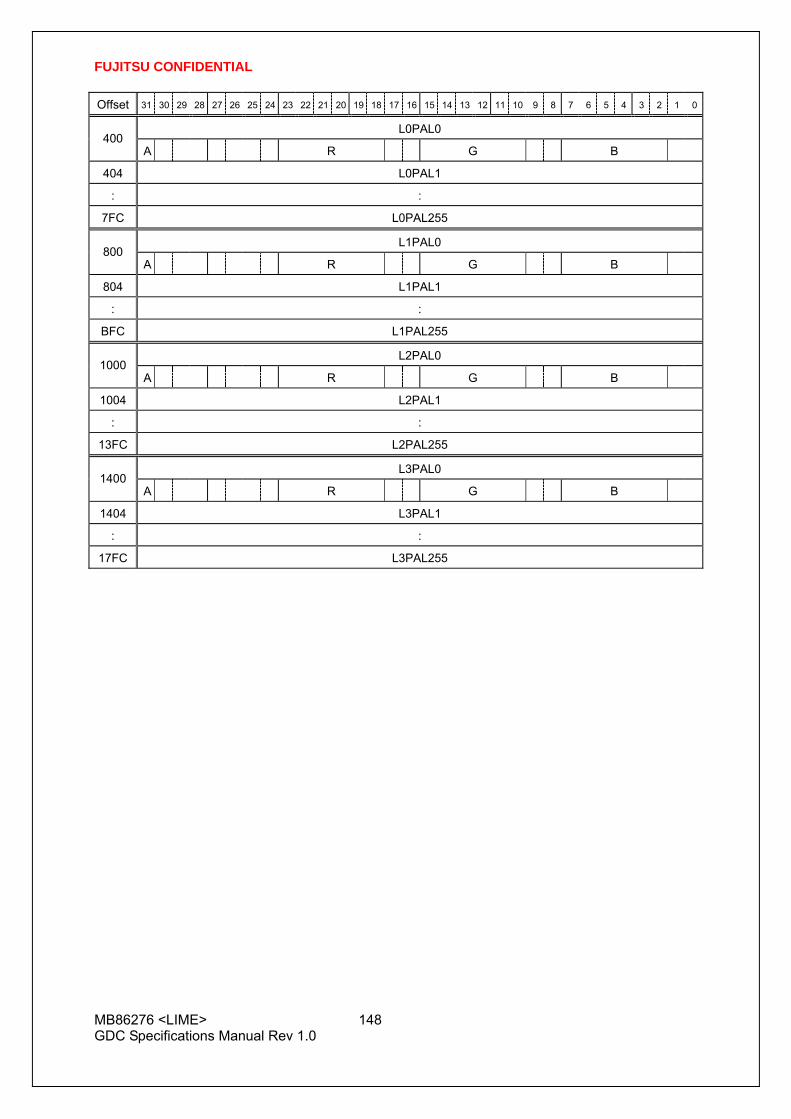
FUJITSU CONFIDENTIAL
MB86276 <LIME> 148 GDC Specifications Manual Rev 1.0
Offset 31 30 29 28 27 26 25 24 23 22 21 20 19 18 17 16 15 14 13 12 11 10 9 8 7 6 5 4 3 2 1 0
L0PAL0 400
A R G B
404 L0PAL1
: :
7FC L0PAL255
L1PAL0 800
A R G B
804 L1PAL1
: :
BFC L1PAL255
L2PAL0 1000
A R G B
1004 L2PAL1
: :
13FC L2PAL255
L3PAL0 1400
A R G B
1404 L3PAL1
: :
17FC L3PAL255

FUJITSU CONFIDENTIAL
MB86276 <LIME> 149 GDC Specifications Manual Rev 1.0
11.1.7 Video capture register list
Base = CaptureBase Offset 31 30 29 28 27 26 25 24 23 22 21 20 19 18 17 16 15 14 13 12 11 10 9 8 7 6 5 4 3 2 1 0
VCM (Video Capture Mode) 000
VIE
VIS
VIC
CM VI
NR
GB
VS
CSC (Capture SCale) 004
VSCI VSCF HSCI HSCF VCS (Video Capture Status)
008 CE
CBM (Capture Buffer Mode) 010
OO
M
SB
UF
CR
GB
CBW (stride)
C24
CB
ST
014 CBOA (Capture Buffer Origin Address) 018 CBLA (Capture Buffer Limit Address) 01C CIVSTR CIHSTR 020 CIVEND CIHEND
CHP (Capture Horizontal Pixel) 028
CHP CVP (Capture Vertical Pixel)
02C CVPP CVPN
CMSS (Capture Magnify Source Size) 048
CMSHP CMSVL CMDS (Capture Magnify Display Size)
04C CMDHP CMDVL
RGBHC(RGB input HSYNC Cycle)/VIN_HSSIZE 080 RGBHC
RGBHEN(RGB input Horizontal Enable Area) 084
RGBHST RGBHEN RGBVEN(RGB input Vertical Enable Area)
088 RGBVST RGBVEN
RGBS(RGB input SYNC) 090
RM
HP
VP
RGBCMY(RGB Color convert Matrix Y coefficient) 0C0
a11 a12 a13 RGBCMCb(RGB Color convert Matrix Cb coefficient)
0C4 a21 a22 a23
RGBCMCr(RGB Color convert Matrix Cr coefficient) 0C8
a31 a32 a33 RGBCMb(RGB Color convert Matrix b coefficient)
0CC b1 b2 b3

FUJITSU CONFIDENTIAL
MB86276 <LIME> 150 GDC Specifications Manual Rev 1.0
Offset 31 30 29 28 27 26 25 24 23 22 21 20 19 18 17 16 15 14 13 12 11 10 9 8 7 6 5 4 3 2 1 0
CDCN(Capture Data Count for NTSC) 4000
BDCN VDCN CDCP(Capture Data Count for PAL)
4004 BDCP VDCP

FUJITSU CONFIDENTIAL
MB86276 <LIME> 151 GDC Specifications Manual Rev 1.0
11.1.8 Drawing engine register list
The parenthesized value in the Offset field denotes the absolute address used by the SetRegister command.
Base = DrawBase Offset 31 30 29 28 27 26 25 24 23 22 21 20 19 18 17 16 15 14 13 12 11 10 9 8 7 6 5 4 3 2 1 0
Ys 000 (000) S S S S Int Frac
Xs 004 (001) S S S S Int Frac
dXdy 008 (002) S S S S Int Frac
XUs 00C (003) S S S S Int Frac
dXUdy 010 (004) S S S S Int Frac
XLs 014 (005) S S S S Int Frac
dXLdy 018 (006) S S S S Int Frac
USN 01C (007) 0 0 0 0 Int 0
LSN 020 (008) 0 0 0 0 Int 0
Rs 040 (010) 0 0 0 0 0 0 0 0 Int Frac
dRdx 044 (011) S S S S S S S S Int Frac
dRdy 048 (012) S S S S S S S S Int Frac
Gs 04C (013) 0 0 0 0 0 0 0 0 Int Frac
dGdx 050 (014) S S S S S S S S Int Frac
dGdy 054 (015) S S S S S S S S Int Frac
Bs 058 (016) 0 0 0 0 0 0 0 0 Int Frac
dBdx 05C (017) S S S S S S S S Int Frac
dBdy 060 (018) S S S S S S S S Int Frac

FUJITSU CONFIDENTIAL
MB86276 <LIME> 152 GDC Specifications Manual Rev 1.0
Offset 31 30 29 28 27 26 25 24 23 22 21 20 19 18 17 16 15 14 13 12 11 10 9 8 7 6 5 4 3 2 1 0
Zs 080 (020) 0 Int Frac
dZdx 084 (021) S Int Frac
dZdy 088 (022) S Int Frac
Ss 0C0 (030) S S S Int Frac
dSdx 0C4 (031) S S S Int Frac
dSdy 0C8 (032) S S S Int Frac
Ts 0CC (033) S S S Int Frac
dTdx 0D0 (034) S S S Int Frac
dTdy 0D4 (035) S S S Int Frac
Qs 0D8 (036) 0 0 0 0 0 0 0 IN
T Frac
dQdx 0DC (037) S S S S S S S IN
T Frac
dQdx 0E0 (038) S S S S S S S IN
T Frac
LPN 140 (050) 0 0 0 0 Int 0
LXs 144 (051) S S S S Int Frac
LXde 148 (052) S S S S S S S S S S S S S S S In
t
Frac
LYs 14C (053) S S S S Int Frac
LYde 150 (054) S S S S S S S S S S S S S S S In
t
Frac
LZs 154 (055) S Int Frac
LZde 158 (056) S Int Frac

FUJITSU CONFIDENTIAL
MB86276 <LIME> 153 GDC Specifications Manual Rev 1.0
Offset 31 30 29 28 27 26 25 24 23 22 21 20 19 18 17 16 15 14 13 12 11 10 9 8 7 6 5 4 3 2 1 0
PXdc 180
(060) S S S S Int Frac
PYdc 184
(061) S S S S Int Frac
PZdc 188
(062) S Int Frac
RXs 200
(080) S S S S Int 0
RYs 204
(081) S S S S Int 0
RsizeX 208
(082) S S S S Int 0
RsizeY 20C
(083) S S S S Int 0
SADDR 240
(090) 0 0 0 0 0 0 0 Address
SStride 244
(091) 0 0 0 0 Int 0
SRXs 248
(092) 0 0 0 0 Int 0
SRYs 24C
(093) 0 0 0 0 Int 0
DADDR 250
(094) 0 0 0 0 0 0 0 Address
DStride 254
(095) 0 0 0 0 Int 0
DRXs 258
(096) 0 0 0 0 Int 0
DRYs 25C
(097) 0 0 0 0 Int 0
BRsizeX 250
(098) 0 0 0 0 Int 0
BRsizeY 254
(099) 0 0 0 0 Int 0
TColor 258
(09A) 0 Color
BLPO 3E0
(0f8) BCR
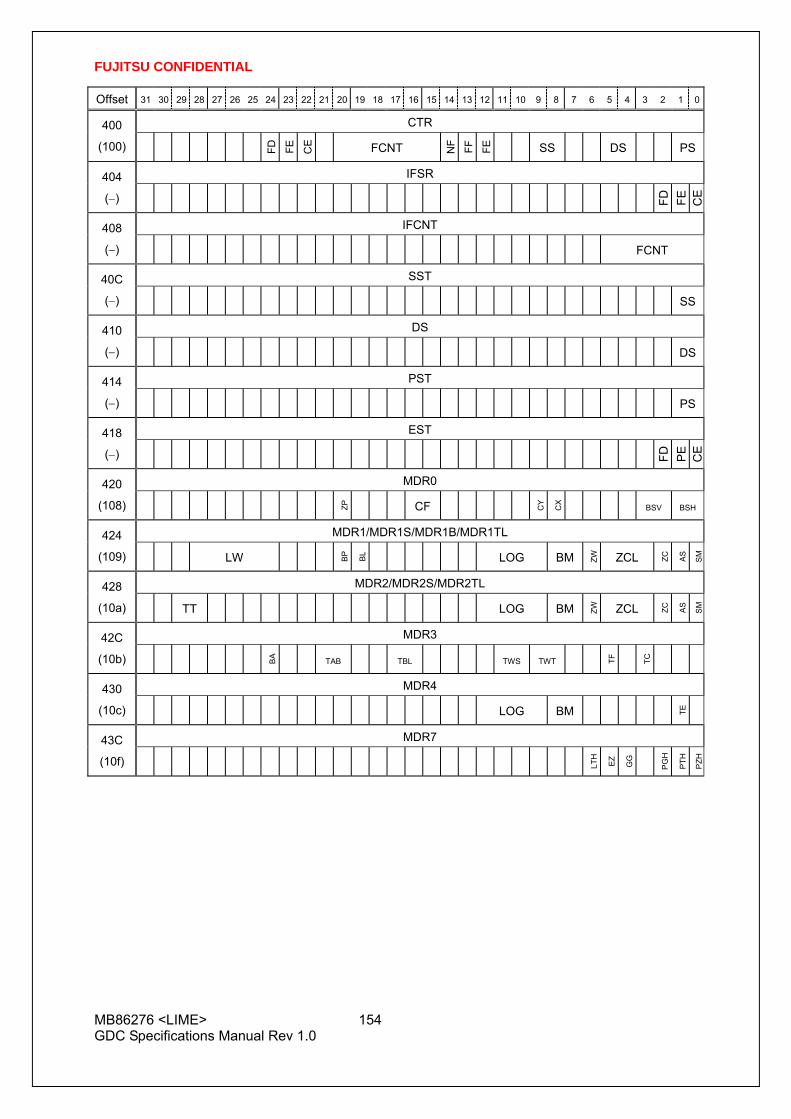
FUJITSU CONFIDENTIAL
MB86276 <LIME> 154 GDC Specifications Manual Rev 1.0
Offset 31 30 29 28 27 26 25 24 23 22 21 20 19 18 17 16 15 14 13 12 11 10 9 8 7 6 5 4 3 2 1 0
CTR 400
(100)
FD
FE
CE
FCNT NF FF
FE
SS DS PS
IFSR 404
(−)
FD
FE
CE
IFCNT 408
(−) FCNT
SST 40C
(−) SS
DS 410
(−) DS
PST 414
(−) PS
EST 418
(−)
FD
PE
C
E
MDR0 420
(108) ZP CF
CY
CX
BSV BSH
MDR1/MDR1S/MDR1B/MDR1TL 424
(109) LW
BP
BL LOG BM ZW
ZCL ZC
AS
SM
MDR2/MDR2S/MDR2TL 428
(10a) TT LOG BM ZW
ZCL ZC
AS
SM
MDR3 42C
(10b)
BA
TAB TBL TWS TWT TF
TC
MDR4 430
(10c) LOG BM TE
MDR7 43C
(10f) LTH
EZ
GG
PG
H
PTH
PZH

FUJITSU CONFIDENTIAL
MB86276 <LIME> 155 GDC Specifications Manual Rev 1.0
Offset 31 30 29 28 27 26 25 24 23 22 21 20 19 18 17 16 15 14 13 12 11 10 9 8 7 6 5 4 3 2 1 0
FBR 440
(110) FBASE
XRES 444
(111) XRES
ZBR 448
(112) ZBASE
TBR 44C
(113) TBASE
PFBR 450
(114) PFBASE
CXMIN 454
(115) CLIPXMIN
CXMAX 458
(116) CLIPXMAX
CYMIN 45C
(117) CLIPYMIN
CYMAX 460
(118) CLIPYMAX
TXS 464
(119) TXSN TXSM
TIS 468
(11a) TISN TISM
TOA 46C
(11b) XBO
SHO 470
(11C) SHOFFS
ABR 474
(11D) ABASE
FC 480
(120) FGC8/16/24
BC 484
(121) BGC8/16/24
ALF 488
(122) A
48C
(123) BLP
TBC 494
(129) BC16/24

FUJITSU CONFIDENTIAL
MB86276 <LIME> 156 GDC Specifications Manual Rev 1.0
Offset 31 30 29 28 27 26 25 24 23 22 21 20 19 18 17 16 15 14 13 12 11 10 9 8 7 6 5 4 3 2 1 0
LX0dc 540
(150) 0 0 0 0 Int 0
LY0dc 544
(151) 0 0 0 0 Int 0
LX1dc 548
(150) 0 0 0 0 Int 0
LY1dc 54C
(151) 0 0 0 0 Int 0
X0dc 580
(160) 0 0 0 0 Int 0
Y0dc 584
(161) 0 0 0 0 Int 0
X1dc 588
(162) 0 0 0 0 Int 0
Y1dc 58C
(163) 0 0 0 0 Int 0
X2dc 590
(164) 0 0 0 0 Int 0
Y2dc 594
(165) 0 0 0 0 Int 0

FUJITSU CONFIDENTIAL
MB86276 <LIME> 157 GDC Specifications Manual Rev 1.0
12 Explanation of GDC Registers
Terms appeared in this chapter are explained below: 1. Register address Indicates address of register 2. Bit number Indicates bit number 3. Bit field name Indicates name of each bit field included in register 4. R/W Indicates access attribute (read/write) of each field Each symbol shown in this section denotes the following:
R0 “0” always read at read. Write access is Don’t care.
W0 Only “0” can be written.
R Read enabled
W Write enabled
RX Read enabled (read values undefined)
RW Read and write enabled
RW0 Read and write 0 enabled 5. Initial value
Indicates initial value of immediately before the reset of each bit field. 6. Handling of reserved bits “0” is recommended for the write value so that compatibility can be maintained with future
products.
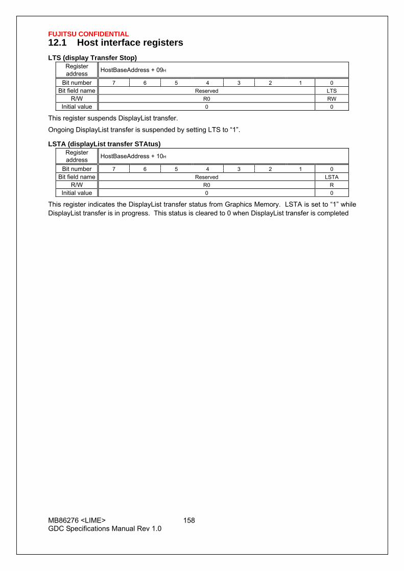
FUJITSU CONFIDENTIAL
MB86276 <LIME> 158 GDC Specifications Manual Rev 1.0
12.1 Host interface registers LTS (display Transfer Stop)
Register address HostBaseAddress + 09H
Bit number 7 6 5 4 3 2 1 0 Bit field name Reserved LTS
R/W R0 RW Initial value 0 0
This register suspends DisplayList transfer.
Ongoing DisplayList transfer is suspended by setting LTS to “1”.
LSTA (displayList transfer STAtus) Register address HostBaseAddress + 10H
Bit number 7 6 5 4 3 2 1 0 Bit field name Reserved LSTA
R/W R0 R Initial value 0 0
This register indicates the DisplayList transfer status from Graphics Memory. LSTA is set to “1” while DisplayList transfer is in progress. This status is cleared to 0 when DisplayList transfer is completed

FUJITSU CONFIDENTIAL
MB86276 <LIME> 159 GDC Specifications Manual Rev 1.0
IST (Interrupt STatus) Register address HostBaseAddress + 20H
Bit number 31 30 29 28 27 26 25 24 23 22 21 20 19 18 17 16 15 14 13 12 11 10 9 8 7 6 5 4 3 2 1 0Bit field name Reserved Resv Reserved IST IST
R/W R0 R0W0 R0 RW0 RW0Initial value 0 0 0 0 0
This register indicates the current interrupt status. It shows that an interrupt request is issued when “1” is set to this register. The interrupt status is cleared by writing “0” to this register.
Bit 0 CERR (Command Error Flag) Indicates drawing command execution error interrupt
Bit 1 CEND (Command END) Indicates drawing command end interrupt
Bit 2 VSYNC (Vertical Sync.) Indicates vertical interrupt synchronization
Bit 3 FSYNC (Frame Sync.) Indicates frame synchronization interrupt
Bit 4 SYNCERR (Sync. Error) Indicates external synchronization error interrupt
Bit 5 REGUD (Register update) Indicates register update interrupt
Bit 17 and 16 Reserved This field is provided for testing. Normally, the read value is “0”, but note that it may be “1” when a drawing command error (Bit 0) has occurred.
IMASK (Interrupt MASK) Register address HostBaseAddress + 24H
Bit number 31 30 29 28 27 26 25 24 23 22 21 20 19 18 17 16 15 14 13 12 11 10 9 8 7 6 5 4 3 2 1 0Bit field name Reserved Resv Reserved IMASK IMASK
R/W R0 R0W0 R0 RW RWInitial value 0 0 0 0 0
This register masks interrupt requests. Even when the interrupt request is issued for the bit to which “0” is written, interrupt signal is not asserted for CPU.
Bit 0 CERRM (Command Error Interrupt Mask)
Masks drawing command execution error interrupt
Bit 1 CENDM (Command Interrupt Mask)
Masks drawing command end interrupt
Bit 2 VSYNCM (Vertical Sync. Interrupt Mask)
Masks vertical synchronization interrupt
Bit 3 FSYNCH (Frame Sync. Interrupt Mask)
Masks frame synchronization interrupt
Bit 4 SYNCERRM (Sync Error Mask)
Masks external synchronization error interrupt
Bit 5 REGUD (Register update)
Masks register update interrupt

FUJITSU CONFIDENTIAL
MB86276 <LIME> 160 GDC Specifications Manual Rev 1.0
SRST (Software ReSeT) Register address HostBaseAddress + 2CH
Bit number 7 6 5 4 3 2 1 0 Bit field name Reserved SRST
R/W R0 W1 Initial value 0 0
This register controls software reset. When “1” is set to this register, a software reset is performed.
CCF (Change of Clock Frequency) Register address HostBaseAddress + 0038H
Bit number 31 30 29 28 27 26 25 24 23 22 21 20 19 18 17 16 15 14 13 12 11 10 9 8 7 6 5 4 3 2 1 0Bit field name Reserved COT Reserved
R/W RW0 RW RW0 Initial value 0 00 0
This register changes the operating frequency.
Bit 17 and 16 COT (Clock select for GDC)
Selects the clock for GDC
11 Reserved
10 Reserved
01 133 MHz
00 100 MHz Notes: 1. Write “0” to the bit field other than the above ([31:18], [15:00]).

FUJITSU CONFIDENTIAL
MB86276 <LIME> 161 GDC Specifications Manual Rev 1.0
LSA (displayList Source Address) Register address HostBaseAddress + 40H
Bit number 31 30 29 28 27 26 25 24 23 22 21 20 19 18 17 16 15 14 13 12 11 10 9 8 7 6 5 4 3 2 1 0Bit field name Reserved LSA
R/W R0 RW R0Initial value 0 Don’t care 0
This register sets the DisplayList transfer source address. When DisplayList is transferred from Graphics Memory, set the transfer start address of DisplayList stored in Graphics Memory. Since the lower two bits of this register are always treated as “0”, DisplayList must be 4-byte aligned. The values set at this register do not change during or after transfer.
LCO (displayList Count) Register address HostBaseAddress + 44H
Bit number 31 30 29 28 27 26 25 24 23 22 21 20 19 18 17 16 15 14 13 12 11 10 9 8 7 6 5 4 3 2 1 0Bit field name Reserved LCO
R/W R0 RW Initial value 0 Don’t care
This register sets the DisplayList transfer count. Set the display list transfer count by the long word. When “1h” is set, 1-word data is transferred. When “0” is set, it is considered to be the maximum count and 16M (16,777,216) words of data are transferred. The values set at this register do not change during or after transfer.
LREQ (displayList transfer REQuest) Register address HostBaseAddress + 48H
Bit number 7 6 5 4 3 2 1 0 Bit field name Reserved LREQ
R/W R0 RW1 Initial value 0 0
This register triggers DisplayList transfer from the Graphics Memory. Transfer is started by setting LREQ to “1”. The DisplayList is transferred from the Graphics Memory to the internal display list FIFO. Access to the display list FIFO by the CPU or DMA is disabled during transfer.
The reserved area in the register area in the host interface excluding the above-mentioned. Please write ALL0 when you write to the Reserved area. Irregularity can be read in case of the read.
DMA_ST_ADR Register address HostBaseAddress + 500H
Bit number 31 30 29 28 27 26 25 24 23 22 21 20 19 18 17 16 15 14 13 12 11 10 9 8 7 6 5 4 3 2 1 0Bit field name DMA_ST_ADR
R/W RW Initial value 26’h3FFFFFF
DMA start address (*address width, 16-bit CPU:[23:0], 32-bit CPU[25:0]) When DMA_ST_ADR≦[input address]≦DMA_ED_ADR, it is DMA transfer. When [input address]>DMA_ST_ADR, it is normal access. DMA_ED_ADR
Register address HostBaseAddress + 504H
Bit number 31 30 29 28 27 26 25 24 23 22 21 20 19 18 17 16 15 14 13 12 11 10 9 8 7 6 5 4 3 2 1 0

FUJITSU CONFIDENTIAL
MB86276 <LIME> 162 GDC Specifications Manual Rev 1.0
Bit field name DMA_ED_ADR R/W RW
Initial value 26’h0 DMA end address (*address width, 16-bit CPU:[23:0], 32-bit CPU[25:0]) When DMA_ST_ADR≦[input address]≦DMA_ED_ADR, it is DMA transfer. When [input address]>DMA_ED_ADR, it is normal access. ERR_ADR
Register address HostBaseAddress + 508H
Bit number 31 30 29 28 27 26 25 24 23 22 21 20 19 18 17 16 15 14 13 12 11 10 9 8 7 6 5 4 3 2 1 0Bit field name ERR_ADR
R/W R Initial value 26’h0
This register keeps the address, when the below interrupt request occurs. It accesses the following order, upper address of 32-bit and lower address of 32-bit in 16-bit CPU mode. It accesses the randam address in 16-bit CPU mode. ERR_DETECT
Register address HostBaseAddress + 50CH
Bit number 31 30 29 28 27 26 25 24 23 22 21 20 19 18 17 16 15 14 13 12 11 10 9 8 7 6 5 4 3 2 1 0Bit field name ● ●
R/W RW RW
Initial value 0 0 Bit0: 16-bit CPU interrupts status register When “1” is set on the bit0, it shows the following interrupt request. It accesses the following order, upper address of 32-bit and lower address of 32-bit in 16-bit CPU mode. It clears the status by writing “0” on the bit0. Bit1: 16-bit CPU interrupts status register When “1” is set on the bit0, it shows the following interrupt request. It accesses the randam address in 16-bit CPU mode. (It accesses the following order, lower address of 32-bit and upper address of 32-bit, but it is not a continuance address.) It clears the status by writing “0” on the bit1. INT_MSK
Register address HostBaseAddress + 510H
Bit number 31 30 29 28 27 26 25 24 23 22 21 20 19 18 17 16 15 14 13 12 11 10 9 8 7 6 5 4 3 2 1 0Bit field name ● ●
R/W RW RW
Initial value 0 0 Bit0: 16-bit CPU interrupts request mask register (It accesses the following order, upper address of 32-bit and lower address of 32-bit in 16-bit CPU mode.) It masks 16-bit CPU interrupts. When “0” is set on the bit0, it does not assert interrupts signal even if the interrupts request occurs. Bit1: 16-bit CPU interrupts request mask register (It accesses a randam address in 16-bit CPU mode.)
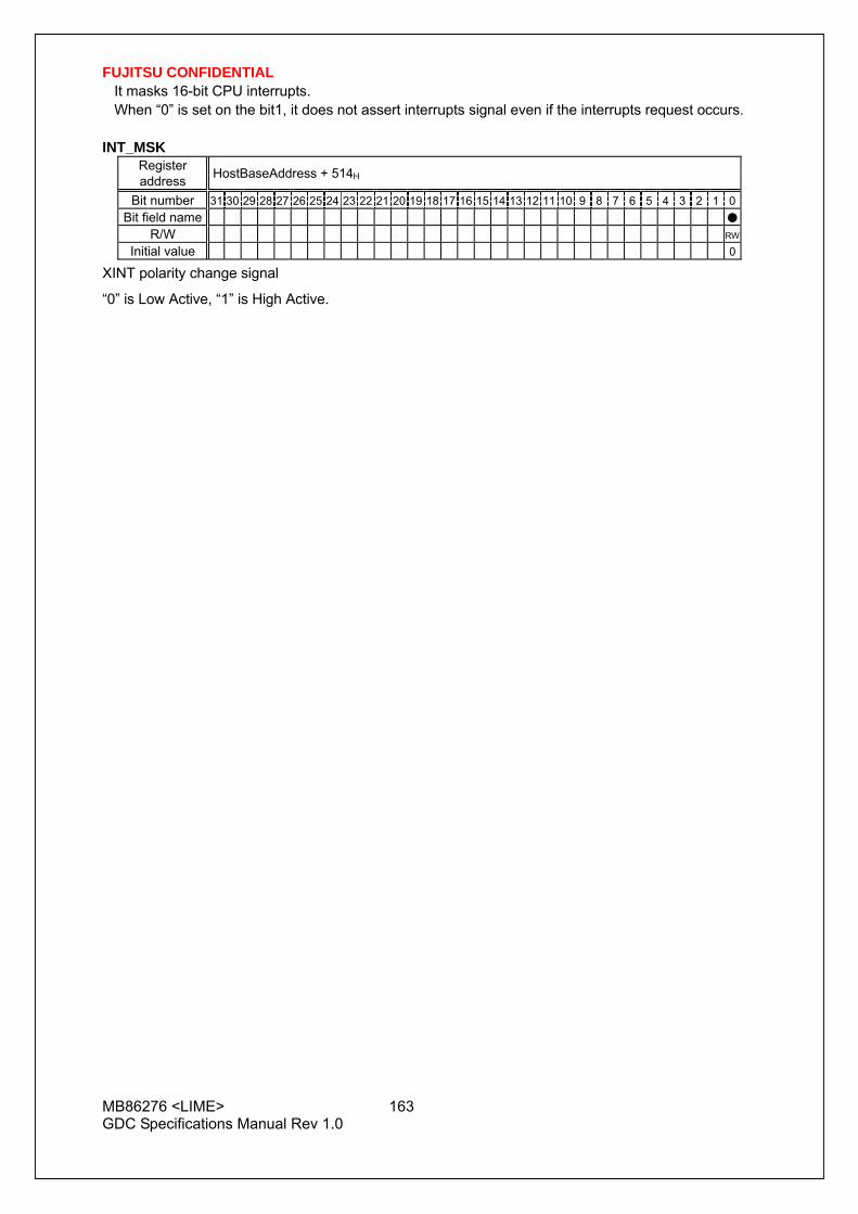
FUJITSU CONFIDENTIAL
MB86276 <LIME> 163 GDC Specifications Manual Rev 1.0
It masks 16-bit CPU interrupts. When “0” is set on the bit1, it does not assert interrupts signal even if the interrupts request occurs. INT_MSK
Register address HostBaseAddress + 514H
Bit number 31 30 29 28 27 26 25 24 23 22 21 20 19 18 17 16 15 14 13 12 11 10 9 8 7 6 5 4 3 2 1 0Bit field name ●
R/W RW
Initial value 0
XINT polarity change signal
“0” is Low Active, “1” is High Active.

FUJITSU CONFIDENTIAL
MB86276 <LIME> 164 GDC Specifications Manual Rev 1.0
12.1.1 SCI registers
TRANS_MODE
Register address PIOBaseAddress+00h Bit number 31 30 29 28 27 26 25 24 23 22 21 20 19 18 17 16 15 14 13 12 11 10 9 8 7 6 5 4 3 2 1 0
Bit field name TMODE R/W RW
Initial value 0
Bit2-0 TMODE (Transfer MODE) This register sets the transfer mode of SCI. 000 SDSA mode
Single data transfer for a single address. 001 MDSA mode
Multiple data transfer for a same single address. 010 MDSA+ mode
Multiple data transfer for an address with post increment (32bit boundary). 011 Line transfer mode
Single data transfer for horizontal line area for any number of times 100 Block transfer mode
Single data transfer for the block area for any number of times 101 Reserved 110 Reaerved 111 Reserved Bit31-3 Reserved
TARGET_ADR
Register address PIOBaseAddress+04h Bit number 31 30 29 28 27 26 25 24 23 22 21 20 19 18 17 16 15 14 13 12 11 10 9 8 7 6 5 4 3 2 1 0
Bit field name TARGET_ADR R/W RW
Initial value 0
Bit31-0 TARGET_ADR This register sets a target address for a transfer with 32bit boundary
TRANS_DATA
Register address PIOBaseAddress+08h Bit number 31 30 29 28 27 26 25 24 23 22 21 20 19 18 17 16 15 14 13 12 11 10 9 8 7 6 5 4 3 2 1 0
Bit field name TRANS_DATA R/W RW
Initial value 0
Bit31-0 TRANS_DATA This register sets data for a transfer with 32bit boundary.

FUJITSU CONFIDENTIAL
MB86276 <LIME> 165 GDC Specifications Manual Rev 1.0
HLINE_NUM
Register address PIOBaseAddress+0Ch Bit number 31 30 29 28 27 26 25 24 23 22 21 20 19 18 17 16 15 14 13 12 11 10 9 8 7 6 5 4 3 2 1 0
Bit field name HLINE_NUM R/W W
Initial value 0
Bit10-0 HLINE_NUM This register sets any number of times with 32bit boundary for the horizontal line area.
It is transferred the number of register value plus 1 times. Please treates 5 bytes transfer when it is Read access, and 6 bytes transfer when it is Write access.
VLINE_NUM
Register address PIOBaseAddress+10h Bit number 31 30 29 28 27 26 25 24 23 22 21 20 19 18 17 16 15 14 13 12 11 10 9 8 7 6 5 4 3 2 1 0
Bit field name VLINE_NUM R/W W
Initial value 0
Bit9-0 VLINE_NUM This register sets any number of times with 32bit boundary for the vertical line area.
It is transferred the number of register value plus 1 times. Please treates 5 bytes transfer when it is Read access, and 6 bytes transfer when it is Write access.
W_Stride
Register address PIOBaseAddress+14h Bit number 31 30 29 28 27 26 25 24 23 22 21 20 19 18 17 16 15 14 13 12 11 10 9 8 7 6 5 4 3 2 1 0
Bit field name W_Stride R/W W
Initial value 0
Bit10-0 W_Stride This register sets a stride size of a window for the block transfer.
Please treates 5 bytes transfer when it is Read access, and 6 bytes transfer when it is Write access.
BL_KICK
Register address PIOBaseAddress+18h Bit number 31 30 29 28 27 26 25 24 23 22 21 20 19 18 17 16 15 14 13 12 11 10 9 8 7 6 5 4 3 2 1 0
Bit field name K R/W W
Initial value 0
Bit0 KICK Please write any data when Block transfer or Line transfer start.

FUJITSU CONFIDENTIAL
MB86276 <LIME> 166 GDC Specifications Manual Rev 1.0
SCI_RD_REG
Register address PIOBaseAddress+1Ch Bit number 31 30 29 28 27 26 25 24 23 22 21 20 19 18 17 16 15 14 13 12 11 10 9 8 7 6 5 4 3 2 1 0
Bit field name SCI_RD_REG R/W W
Initial value 0
Bit15-0 SCI_RD_REG This register sets the target register for read.
Please treates 2 bytes transfer when it is Read access, and 3 bytes transfer when it is Write access. 000 TRANS_MODE 001 TARGET_ADR 010 TRANS_DATA 011 HLINE_NUM 100 VLINE_NUM 101 W_Stride 110 BL_KICK 111 SCI_RD_REG
Reserved registers for debug (PIOBaseAddress + 20h~28h)
Please don’t access this space because those are assigned the registers for debug.
BL_ST
Register address PIOBaseAddress+2Ch Bit number 31 30 29 28 27 26 25 24 23 22 21 20 19 18 17 16 15 14 13 12 11 10 9 8 7 6 5 4 3 2 1 0
Bit field name ST R/W R
Initial value 0
Bit0 BL_ST This register indicates the status of Block transfer or Line transfer.
Please treates 2 bytes transfer when it is Read access. 0 Idle 1 Busy

FUJITSU CONFIDENTIAL
MB86276 <LIME> 167 GDC Specifications Manual Rev 1.0
12.1.2 GPIO control registers
GPIO control 1 (GPIOC1)
Register address PIOBaseAddress+40h Bit number 31 30 29 28 27 26 25 24 23 22 21 20 19 18 17 16 15 14 13 12 11 10 9 8 7 6 5 4 3 2 1 0
Bit field name GPIO_is_out GPIO_inout R/W R0W R/W
Initial value 0000_0000 XXXX_XXXX (*1)
The register controls the GPIO pin. Each set bit can be set corresponding from MSB to LSB by couple 1 in each bit.
(*1)The value of the GPIO pin is reflected longer than the fixed time.
(*2)It takes time more than constancy (system clock cycle order) to mutual reflection with the GPIO pin.
Bit15-0 GPIO_inout (GPIO input/output data ) (*2) The data of the GPIO pin is read and written.
At read The value of external pin GPIO15-0 can be read about the bit to which ‘0’ is set with GPIO_is_out. However, the bit reversing value of external pin GPIO15-0 is read about the bit that GPIOC2.GPIO_xor is set to ‘1’. When GPIOC2.GPIO_force is set to ‘1’, the value in which the write is compulsorily done to GPIO_inout is read as it is (*3). The value in which the write is done to GPIO_inout is read as it is (*3) about the bit to which ‘1’ is set with GPIO_is_out. (*3 The influence of GPIO_xor is not undertaken.) inout (at read) = (is_out || force) ? inout (at write) : (xor ^ GPIO pin)
At write The written value is disregarded about the bit to which ‘0’ is set with GPIO_is_out. The write value is output to external pin GPIO15-0 about the bit to which ‘1’ is set with GPIO_is_out. However, the bit reversing value is output about the bit that GPIOC2.GPIO_xor is set to ‘1’. GPIO pin = (is_out) ? (xor ^ inout (at write)) : Hi-Z
Bit31-16 GPIO_is_out (GPIO direction) The direction of each bit of the terminal GPIO I/O is specified.
At read : 0 is always read. At write : The corresponding bit of ‘1’ is an output of this.
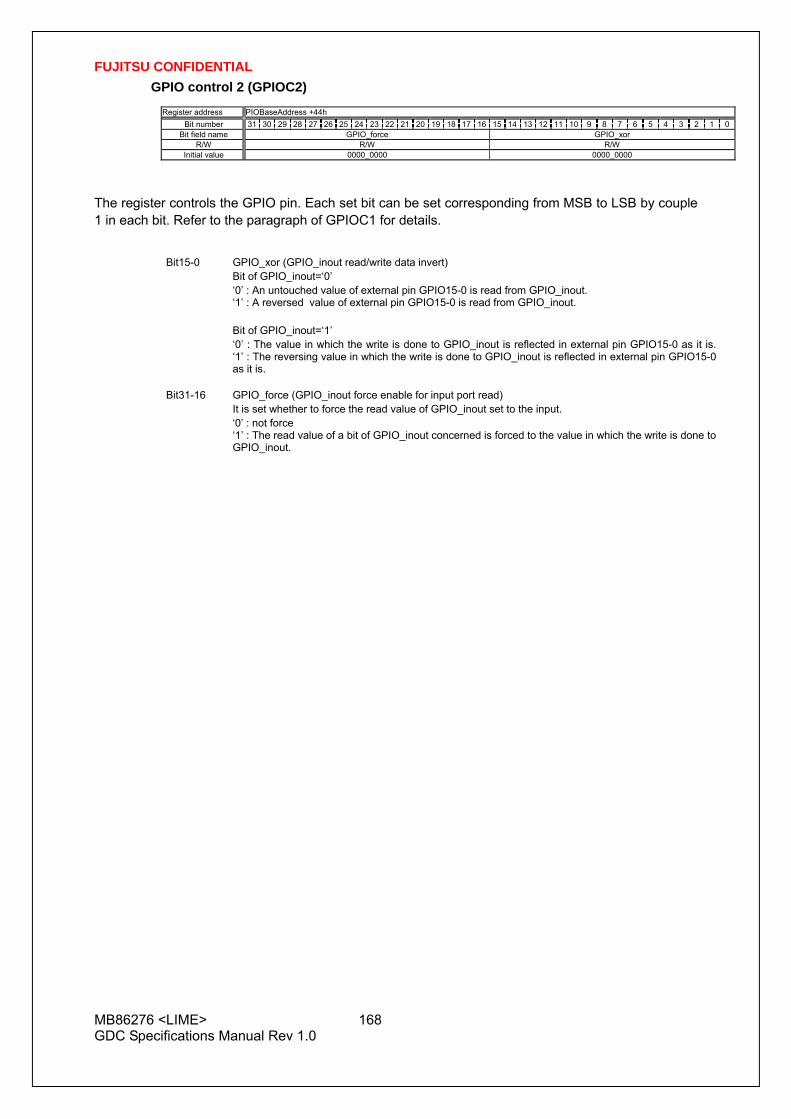
FUJITSU CONFIDENTIAL
MB86276 <LIME> 168 GDC Specifications Manual Rev 1.0
GPIO control 2 (GPIOC2)
Register address PIOBaseAddress +44h Bit number 31 30 29 28 27 26 25 24 23 22 21 20 19 18 17 16 15 14 13 12 11 10 9 8 7 6 5 4 3 2 1 0
Bit field name GPIO_force GPIO_xor R/W R/W R/W
Initial value 0000_0000 0000_0000
The register controls the GPIO pin. Each set bit can be set corresponding from MSB to LSB by couple 1 in each bit. Refer to the paragraph of GPIOC1 for details.
Bit15-0 GPIO_xor (GPIO_inout read/write data invert) Bit of GPIO_inout=‘0’
‘0’ : An untouched value of external pin GPIO15-0 is read from GPIO_inout. ‘1’ : A reversed value of external pin GPIO15-0 is read from GPIO_inout.
Bit of GPIO_inout=‘1’ ‘0’ : The value in which the write is done to GPIO_inout is reflected in external pin GPIO15-0 as it is.
‘1’ : The reversing value in which the write is done to GPIO_inout is reflected in external pin GPIO15-0 as it is.
Bit31-16 GPIO_force (GPIO_inout force enable for input port read) It is set whether to force the read value of GPIO_inout set to the input. ‘0’ : not force
‘1’ : The read value of a bit of GPIO_inout concerned is forced to the value in which the write is done to GPIO_inout.

FUJITSU CONFIDENTIAL
MB86276 <LIME> 169 GDC Specifications Manual Rev 1.0
12.1.3 Peripheral Interrupt related registers
Peripheral Interrupt control1 (PIC1)
Register address PIOBaseAddress +4Ch Bit number 31 30 29 28 27 26 25 24 23 22 21 20 19 18 17 16 15 14 13 12 11 10 9 8 7 6 5 4 3 2 1 0
Bit field name Reserve
OFE
WTO
RTO
S1 GPIO_INT_enable
R/W R0W0
R/W
R/W
R/W
R/W
R/W
Initial value 0000_0000 0 0 0 0 0000_0000
The register controls the interrupt which relates to peripheral logic.
The one of GPIO reacts without regard to input and output in the situation of the setting.
Each set bit can be set corresponding from MSB to LSB by couple 1 in each bit.
Bit15-0 GPIO_INT_enable (GPIO interrupt enable) It is set whether the generation of interrupt of each bit by the value in which external pin GPIO15-0 is
sampled with the internal clock.
Interrupt is not generated for ‘0’. Interrupt is generated for ‘1’ based on the following register setting.
Bit16 S1 (Serial1 Interrupt Enable) Interrupt when data is abandoned is set because of word not read by input FIFO of serial 1CH. 0:Interrupt is not generated.
1:Interrupt is generated. Bit17 RTO (Internal bus timeout interrupt Enable for read) It is specified whether interrupt is generated when input FIFO Read Wait time of an internal bus
becomes more than a set cycle. (This bit does not work if it is not TE bit = 1 of SPC2 registers.) 0:Interrupt is not generated.
1:Interrupt is generated. Bit18 WTO (Internal bus timeout interrupt Enable for write) It is specified whether interrupt is generated when input FIFO Read Wait time of an internal bus
becomes more than a set cycle. (This bit does not work if it is not TE bit = 1 of SPC2 registers.) 0:Interrupt is not generated.
1:Interrupt is generated. Bit19 OFE (Output FIFO empty interrupt Enable) It is specified whether interrupt is generated when output FIFO becomes empty. 0:Interrupt is not generated.
1:Interrupt is generated.

FUJITSU CONFIDENTIAL
MB86276 <LIME> 170 GDC Specifications Manual Rev 1.0
Peripheral Interrupt control2 (PIC2)
Register address PIOBaseAddress +50h Bit number 31 30 29 28 27 26 25 24 23 22 21 20 19 18 17 16 15 14 13 12 11 10 9 8 7 6 5 4 3 2 1 0
Bit field name Reserve GPIO_INT_polarity R/W R0W0 R/W
Initial value 0000_0000 0000_0000
The register controls interrupt concerning GPIO.
It reacts without regard to input and output in the situation of the setting.
Each set bit can be set corresponding from MSB to LSB by couple 1 in each bit.
Bit15-0 GPIO_INT_polarity (GPIO interrupt polarity) Interrupt is generated for the following values. 0: When you detect Level ‘0’ or negative edge (Depend on GPIO_INT_mode)
1: When you detect Level ‘1’ or positive edge (Depend on GPIO_INT_mode)
Peripheral Interrupt control3 (PIC3)
Register address PIOBaseAddress +54h Bit number 31 30 29 28 27 26 25 24 23 22 21 20 19 18 17 16 15 14 13 12 11 10 9 8 7 6 5 4 3 2 1 0
Bit field name Reserve GPIO_INT_mode R/W R0W0 R/W
Initial value 0000_0000 0000_0000
The register controls interrupt concerning GPIO.
It reacts without regard to input and output in the situation of the setting.
Each set bit can be set corresponding from MSB to LSB by couple 1 in each bit.
Bit15-0 GPIO_INT_mode (GPIO interrupt mode) 0: level sensitive (‘0’ or ‘1’ depends on GPIO_INT_polarity) 1: edge sensitive (‘pos’ or ‘neg’ depends on GPIO_INT_polarity)

FUJITSU CONFIDENTIAL
MB86276 <LIME> 171 GDC Specifications Manual Rev 1.0
Peripheral Interrupt Status (PIST)
Register address PIOBaseAddress +80h Bit number 31 30 29 28 27 26 25 24 23 22 21 20 19 18 17 16 15 14 13 12 11 10 9 8 7 6 5 4 3 2 1 0
Bit field name Reserve Reserve
OFE
WTO
RTO
S1 GPIO_INT_status
R/W R0W0 R0W0
R/W
0
R/W
0
R/W
0
R/W
0
R/W0
Initial value 0000_0000 0000_0000 0 0 0 0 0000_0000
The register shows the state of the interrupt which relates to peripheral logic. It clears by 0 Write.
This state is consolidated and it is reflected in bit17 of host interface register IST.
Bit15-0 GPIO_INT_status (GPIO interrupt status) Shows that interrupt is generated by the bit of the correspondence of GPIO.
0: interrupt is not generated 1: interrupt is generated
Bit16 S1 (Serial1 port interrupt status) In Serial1communication, It is shown that interruption which notifies that input data was thrown away
occurred. 0: interrupt is not generated
1: interrupt is generated Bit17 RTO (Internal bus timeout interrupt Status for read) It is shown that interruption when the input FIFO Read Wait time of an internal bus becomes more
than a setting cycle occurred. 0: interrupt is not generated
1: interrupt is generated Bit18 WTO (Internal bus timeout interrupt Status for write) It is shown that interruption when the output FIFO Read Wait time of an internal bus becomes more
than a setting cycle occurred. 0: interrupt is not generated
1: interrupt is generated Bit19 OFE (Output FIFO empty interrupt Status) It is shown that interruption when Output FIFO becomes empty occurred. 0: interrupt is not generated
1: interrupt is generated

FUJITSU CONFIDENTIAL
MB86276 <LIME> 172 GDC Specifications Manual Rev 1.0
Revision
Register address PIOBaseAddress +84h Bit number 31 30 29 28 27 26 25 24 23 22 21 20 19 18 17 16 15 14 13 12 11 10 9 8 7 6 5 4 3 2 1 0
Bit field name YEAR VERSION REVISION
R/W RO
Initial value 0x2005 0x01 0x00
The register shows the chip version.

FUJITSU CONFIDENTIAL
MB86276 <LIME> 173 GDC Specifications Manual Rev 1.0
12.1.4 I2C Interface Registers
BSR (Bus Status Register)
Register address I2C Base Address + 000h
Bit No 7 6 5 4 3 2 1 0
Bit field name BB RSC AL LRB TRX AAS GCA FBT
R/W R R R R R R R R
Default 0 0 0 0 0 0 0 0
All bits on this register are cleared while bit EN on CCR register is “0”.
Bit7 BB (Bus Busy) Indicate state of I2C-bus
0: STOP condition was detected. 1: START condition (The bus is in use.) was detected.
Bit6 RSC (Repeated START Condition) Indicate repeated START condition
This bit is cleared by writing “0” to INT bit, the case of not addressed in a slave mode, the detection of START condition under bus stop, and the detection of STOP condition.0: Repeated START condition was not detected. 1: START condition was detected again while the bus was in use.
Bit5 AL(Arbitration Lost) Detect Arbitration lost
This bit is cleared by writing “0” to INT bit. 0: Arbitration lost was not detected. 1: Arbitration occurred during master transmission, or “1” writing was performed to MSS bit
while other systems were using the bus. Bit4 LRB (Last Received Bit) Store Acknowledge
This bit is cleared by detection of START condition or STOP condition. Bit3 TRX (Transmit / Receive) Indicate data receipt and data transmission.
0: receipt 1: transmission
Bit2 AAS (Address As Slave) Detect addressing
This bit is cleared by detection of START condition or STOP condition. 0: Addressing was not performed in a slave mode. 1: Addressing was performed in a slave mode.
Bit1 GCA (General Call Address) Detect general call address (00h)
This bit is cleared by detection of START condition or STOP condition. 0: General call address was not received in a slave mode. 1: General call address wad received in a slave mode.
Bit0 FBT (First Byte Transfer) Detect the 1st byte
Even if this bit is set to “1” by detection of START condition, it is cleared by writing “0” on INT bit or by not being addressed in a slave mode. 0: Received data is not the 1st byte. 1: Received data is the 1st byte (address data).

FUJITSU CONFIDENTIAL
MB86276 <LIME> 174 GDC Specifications Manual Rev 1.0
BCR (Bus Control Register) Register address I2C Base Address + 0004h
Bit No 7 6 5 4 3 2 1 0
Bit field name BER BEIE SCC MSS ACK GCAA INTE INT
R/W R/W0 R/W R0/W1 R/W R/W R/W R/W R/W
Default 0 0 0 0 0 0 0 0
Bit7 BER (Bus Error) Flag bit for request of bus error interruption
When this bit is set, EN bit on CCR register will be cleared, this module will be in a stop state and data transfer will be discontinued. write case 0: A request of buss error interruption is cleared. 1: Don’t care. read case 0: A bus error was not detected. 1: Undefined START condition or STOP condition was detected while data transfer.
Bit6 BEIE (Bus Error Interruption Enable) Permit bus error interruption
When both this bit and BER bit are “1”, the interruption is generated. 0: Prohibition of bus error interruption 1: Permission of bus error interruption
Bit5 SCC (Start Condition Continue) Generate START condition
write case 0: Don’t care. 1: START condition is generated again at the time of master transmission.
Bit4 MSS (Master Slave Select) Select master / slave mode
When arbitration lost is generated in master transmission, this bit is cleared and this module becomes a slave mode. 0: This module becomes a slave mode after generating STOP condition and completing transfer. 1: This module becomes a master mode, generates START condition and starts transfer.
Bit3 ACK (ACKnowledge) Permit generation of acknowledge at the time of data reception
This bit becomes invalid at the time of address data reception in a slave mode. 0: Acknowledge is not generated. 1: Acknowledge is generated.
Bit2 GCAA(General Call Address Acknowledge) Permit generation of acknowledge at the time of general call address reception
0: Acknowledge is not generated. 1: Acknowledge is generated.
Bit1 INTE (INTerrupt Enable) Permit interruption
When this bit is “1” interruption is generated if INT bit is “1”. 0: Prohibition of interrupt 1: Permission of interrupt
Bit0 INT (INTrrupt) Flag bit for request of interruption for transfer end
When this bit is “1” SCL line is maintained at “L” level. If this bit is cleared by being written “0”, SCL line is released and the following byte transfer is started. Moreover, it is reset to “0” by generating of START condition or STOP condition at the time of a master.

FUJITSU CONFIDENTIAL
MB86276 <LIME> 175 GDC Specifications Manual Rev 1.0
write case 0: The flag is cleared. 1: Don’t care. read case 0: The transfer is not ended. 1: It is set when 1 byte transfer including the acknowledge bit is completed and it corresponds to the following conditions. - It is a bus master. - It is an addressed slave. - It was going to generate START condition while other systems by which arbitration lost happened used the bus.
Competition of SCC, MSS and INT bit Competition of the following byte transfer, generation of START condition and generation of STOP condition happens by the simultaneous writing of SCC, MSS and INT bit. The priority at this case is as follows. 1) The following byte transfer and generation of STOP condition
If “0” is written to INT bit and “0” is written to MSS bit, priority will be given to “0” writing to MSS bit and STOP condition will be generated.
2) The following byte transfer and generation of START condition If “0” is written to INT bit and “1” is written to SCC bit, priority will be given to “1” writing to SCC bit and START condition will be generated.
3) Generation of START condition and STOP condition The simultaneous writing of “1” to SCC bit and “0” to MSS bit is prohibition.

FUJITSU CONFIDENTIAL
MB86276 <LIME> 176 GDC Specifications Manual Rev 1.0
CCR (Clock Control Register) Register address I2C Base Address + 0008h
Bit No 7 6 5 4 3 2 1 0
Bit field name - HSM EN CS4 CS3 CS2 CS1 CS0
R/W R1 R/W R/W R/W R/W R/W R/W R/W
Default 1 0 0 - - - - -
Bit7 Nonuse “1” is always read at read.
Bit6 HSM (High Speed Mode) Select standard-mode / high-speed-mode
0: Standard-mode1: High-speed-mode
Bit5 EN (Enable) Permission of operation
When this bit is “0”, each bit of BSR and BCR register (except BER and BEIE bit) is cleared. This bit is cleared when BER bit is set. 0: Prohibition of operation 1: Permission of operation
Bit4 CS4 - 0 (Clock Period Select4 - 0)
Set up the frequency of a serial transfer clock Frequency fscl of a serial transfer clock is shown as the following formula. Please set up fscl not to exceed the value shown below at the time of master operation. standard-mode: 100KHz high-speed-mode: 400KHz
standard-mode
A fscl = (2 x m)+2
high-speed-mode
A fscl = int(1.5 x m)+2
A: I2C system clock = 16.6MHz <Notes> +2 cycles are minimum overhead to confirm that the output level of SCL terminal changed. When the delay of the positive edge of SCL terminal is large or when the clock is extended by the slave device, it becomes larger than this value. The value of m becomes like the following page to the value of CS 4-0.

FUJITSU CONFIDENTIAL
MB86276 <LIME> 177 GDC Specifications Manual Rev 1.0
m CS4 CS3 CS2 CS1 CS0 standard high-speed
0 0 0 0 0 65 inhibited 0 0 0 0 1 66 inhibited 0 0 0 1 0 67 inhibited 0 0 0 1 1 68 inhibited 0 0 1 0 0 69 inhibited 0 0 1 0 1 70 inhibited 0 0 1 1 0 71 inhibited 0 0 1 1 1 72 inhibited 0 1 0 0 0 73 9 0 1 0 0 1 74 10 0 1 0 1 0 75 11 0 1 0 1 1 76 12 0 1 1 0 0 77 13 0 1 1 0 1 78 14 0 1 1 1 0 79 15 0 1 1 1 1 80 16 1 0 0 0 0 81 17 1 0 0 0 1 82 18 1 0 0 1 0 83 19 1 0 0 1 1 84 20 1 0 1 0 0 85 21 1 0 1 0 1 86 22 1 0 1 1 0 87 23 1 0 1 1 1 88 24 1 1 0 0 0 89 25 1 1 0 0 1 90 26 1 1 0 1 0 91 27 1 1 0 1 1 92 28 1 1 1 0 0 93 29 1 1 1 0 1 94 30 1 1 1 1 0 95 31 1 1 1 1 1 96 32

FUJITSU CONFIDENTIAL
MB86276 <LIME> 178 GDC Specifications Manual Rev 1.0
Address Register(ADR)
Register address I2C Base Address + 000Ch
Bit No 7 6 5 4 3 2 1 0
Bit field name - A6 A5 A4 A3 A2 A1 A0
R/W R1 R/W R/W R/W R/W R/W R/W R/W
Default 1 - - - - - - -
Bit7 Nonuse “1” is always read at read.
Bit6 - 0 A6 - 0 (Address6 - 0) Store slave address
In a slave mode it is compared with DAR register after address data reception, and when in agreement, acknowledge is transmitted to a master.
Data Register(DAR)
Register address I2C Base Address + 0010h
Bit No 7 6 5 4 3 2 1 0
Bit field name D7 D6 D5 D4 D3 D2 D1 D0
R/W R/W R/W R/W R/W R/W R/W R/W R/W
Default - - - - - - - -
Bit7 - 0 D7 - 0 (Data7 - 0) Store serial data
This is a data register for serial data transfer. The data is transferred from MSB. At the time of data reception (TRX=0) the data output is set to “1”. The writing side of this register is a double buffer. When the bus is in use (BB=1), the write data is loaded to the register for serial transfer for every transfer. At the time of read-out, the receiving data is effective only when INT bit is set because the register for serial transfer is read directly at this time.

FUJITSU CONFIDENTIAL
MB86276 <LIME> 179 GDC Specifications Manual Rev 1.0
12.2 Graphics memory interface registers MMR (Memory I/F Mode Register)
Register address HostBaseAddress + FFFCH
Bit number 31 30 29 28 27 26 25 24 23 22 21 20 19 18 17 16 15 14 13 12 11 10 9 8 7 6 5 4 3 2 1 0Bit field name *1 tWR Reserved *1 *1 TRRD TRC TRP TRAS TRCD LOWD RTS SAW ASW CL
R/W RW RW R R1
W0 R RW RW RW RW RW RW RW RW RW RW
Initial value 0 0 Don’t care 1 0 00 0000 00 000 00 00 000 000 0 000
*1: Reserved
This register sets the mode of the graphics memory interface. A value must be written to this register after a reset. (When default setting is performed, a value must also be written to this register.) Only write once to this register; do not change the written value during operation. This register is not initialized at a software reset.
Bit 2 to 0 CL (CAS Latency)
Sets the CAS latency. Write the same value as this field, to the mode register for SDRAM
011 CL3
010 CL2
Other than the above
Setting disabled
Bit 3 ASW (Attached SDRAM bit Width)
Sets the bit width of the data bus (memory bus width mode)
1 Reserved
0 32 bit
Bit 6 to 4 SAW (SDRAM Address Width)
Sets the bit width of the SDRAM address
001 15 bit BANK 2 bit ROW 13 bit COL 9 bit SDRAM
111 14 bit BANK 2 bit ROW 12 bit COL 9 bit SDRAM
110 14 bit BANK 2 bit ROW 12 bit COL 8 bit SDRAM
101 13 bit BANK 2 bit ROW 11 bit COL 8 bit SDRAM
100 12 bit BANK 1 bit ROW 11 bit COL 8 bit FCRAM
Other than the above
Setting disabled
Bit 9 to 7 RTS (Refresh Timing Setting)
Sets the refresh interval
000 Refresh is performed every 384 internal clocks.
111 Refresh is performed every 1552 internal clocks.
001 to 110 Refresh is performed every ‘64 × n’ internal clocks in the 64 to 384 range.

FUJITSU CONFIDENTIAL
MB86276 <LIME> 180 GDC Specifications Manual Rev 1.0
Bit 11 and 10 LOWD
Sets the count of clocks secured for the period from the instant the ending data is output to the instant the write command is issued.
It is able to adjust the internal timing of memory interface by the setting.
11 3 clocks
10 2 clocks
01 1 clocks
Other than the above
Setting disabled
Bit 13 and 12 TRCD
Sets the wait time secured from the bank active to CAS. The clock count is used to express the wait time.
11 3 clocks
10 2 clocks
01 1 clock
00 0 clock
Bit 16 to 14 TRAS
Sets the minimum time for 1 bank active. The clock count is used to express the minimum time.
111 7 clocks
110 6 clocks
101 5 clocks
100 4 clocks
011 3 clocks
010 2 clocks
Other than the above
Setting disabled
Bit 18 and 17 TRP
Sets the wait time secured from the pre-charge to the bank active. The clock count is used to express the wait time.
11 3 clocks
10 2 clocks
01 1 clock
Bit 22 to 19 TRC
This field sets the wait time secured from the refresh to the bank active. The clock count is used to express the wait time.
1010 10 clocks
1001 9 clocks
1000 8 clocks
0111 7 clocks
0110 6 clocks

FUJITSU CONFIDENTIAL
MB86276 <LIME> 181 GDC Specifications Manual Rev 1.0
0101 5 clocks
0100 4 clocks
0011 3 clocks
Other than the above
Setting disabled
Bit 24 and 23 TRRD
Sets the wait time secured from the bank active to the next bank active. The clock count is used to express the wait time.
11 3 clocks
10 2 clocks
Bit 26 Reserved
Always write “0” at write.
“1” is always read at read.
Bit 30 TWR
Sets the write recovery time (the time from the write command to the read or to the pre-charge command).
1 2 clocks
0 1 clock

FUJITSU CONFIDENTIAL
MB86276 <LIME> 182 GDC Specifications Manual Rev 1.0
12.3 Display control registers DCM0/1 (Display Control Mode 0/1)
Register address DisplayBaseAddress + 00H ( DCM0)
Bit number 31 30 29 28 27 26 25 24 23 22 21 20 19 18 17 16 15 14 13 12 11 10 9 8 7 6 5 4 3 2 1 0
Bit field name DE
N
STO
P
Reserve
L45E
L23E
L1E
L0E
CK
S
Resv SC EE
Q
OD
E
Res
v
Res
v
SF
ES
Y
SYNC
R/W RW RW RX RW RW RW RW RW R0 RW RW RW RW R0 RW RW RW
Initial value 0 0 0 0 0 0 0 0 1110 0 0 0 0 0 0 00
Register address DisplayBaseAddress + 100H (DCM1)
Bit number 31 30 29 28 27 26 25 24 23 22 21 20 19 18 17 16 15 14 13 12 11 10 9 8 7 6 5 4 3 2 1 0
Bit field name DE
N
STO
P
Reserve L5E
L4E
L3E
L2E
L1E
L0E
CK
S
Res
v
SC EE
Q
OD
E
Res
v
Res
v
SF
ES
Y
SYNC
R/W RW RW RX RW RW RW RW RW RW RW R0 RW RW RW RW R0 RW RW RW
Initial value 0 0 X 0 0 0 0 0 0 0 0 11101 0 0 0 0 0 0 00
This register controls the display count mode. It is not initialized by a software reset. This register is mapped to two addresses but it is one substance. The differences between the two registers are the format of the frequency division rate setting (SC) and layer enable. The two formats exist to maintain backword compatibility with previous products.
Bit 1 to 0 SYNC (Synchronize)
Set synchronization mode
X0 Non-interlace mode
10 Interlace mode
11 Interlace video mode
Bit 2 ESY (External Synchronize)
Sets external synchronization mode
0: External synchronization disabled
1: External synchronization enabled
Bit 3 SF (Synchronize signal format)
Sets format of synchronization (VSYNC, HSYNC) signals
0: Negative logic
1: Positive logic
Bit 7 EEQ (Enable Equalizing pulse)
Sets CCYNC signal mode
0: Does not insert equalizing pulse into CCYNC signal
1: Inserts equalizing pulse into CCYNC signal
Bit 13 to 8 SC (Scaling)
Divides display reference clock by the preset ratio to generate dot clock
Offset = 0 Offset = 100H
x00000 Frequency not divided 000000 Frequency not divided

FUJITSU CONFIDENTIAL
MB86276 <LIME> 183 GDC Specifications Manual Rev 1.0
x00001 Frequency division rate = 1/4 000001 Frequency division rate = 1/2
x00010 Frequency division rate = 1/6 000010 Frequency division rate = 1/3
X00011 Frequency division rate = 1/8 000011 Frequency division rate = 1/4
: :
x11111 Frequency division rate = 1/64 111111 Frequency division rate = 1/64
When n is set, with Offset = 0, the frequency division rate is 1/(2n + 2).
When m is set, with Offset = 100h, the frequency division rate is 1/(m + 1).
Basically, these are setting parameters with the same function (2n + 2 = m + 1). Because of this, m = 2n + 1 is established. When n is set to the SC field with Offset = 0, 2n + 1 is reflected with Offset = 100h.
Also, when PLL is selected as the reference clock, frequency division rates 1/1 to 1/5 are non-functional even when set; other frequency division rates are assigned.
Bit 15 CKS (Clock Source)
Selects reference clock
0: Internal PLL output clock
1: DCLKI input
Bit 16 L0E (L0 layer Enable)
Enables display of the L0 layer. The L0 layer corresponds to the C layer for previous products.
0: Does not display L0 layer
1: Displays L0 layer
Bit 17 L1E (L1 layer Enable)
Enables display of the L1 layer. The L1 layer corresponds to the W layer for previous products.
0: Does not display L1 layer
1: Displays L1 layer
Bit 18 L23E (L2 & L3 layer Enable) ------ DCM0
Enables simultaneous display of the L2 and L3 layers. These layers correspond to the M layer for previous products.
0: Does not display L2 and L3 layer
1: Displays L2 and L3 layer
L2E (L2 layer Enable) ------ DCM1
Enables L2 layer display
0: Does not display L2 layer
1: Displays L2 layer
Bit 19 L45E (L4 & L5 layer Enable) ------ DCM0
Enables simultaneous display of the L4 and L5 layers. These layers correspond to the B layer for previous products.
0: Does not display L4 and L5 layer
1: Displays L4 and L5 layer

FUJITSU CONFIDENTIAL
MB86276 <LIME> 184 GDC Specifications Manual Rev 1.0
L3E (L3 layer Enable)) ------ DCM1
Enables L3 layer display
0: Does not display L3 layer
1: Displays L3 layer
Bit 20 L4E (L4 layer Enable)
Enables L4 layer display
0: Does not display L4 layer
1: Displays L4 layer
Bit 21 L5E (L5 layer Enable)
Enables L5 layer display
0: Does not display L5 layer
1: Displays L5 layer
Bit 31 DEN (Display Enable)
Enables display
0: Does not output display signal
1: Outputs display signal

FUJITSU CONFIDENTIAL
MB86276 <LIME> 185 GDC Specifications Manual Rev 1.0
DCM2 (Display Control Mode 2) Register address DisplayBaseAddress + 104H
Bit number 31 30 29 28 27 28 17 16 15 14 13 12 11 10 9 8 7 6 5 4 3 2 1 0
Bit field name Reserve Reserv Reserv RUF RUM
R/W R0 R0 R0 RW RW
Initial value 0 0 0 0 0
Bit0 RUM (Register Update Mode)
The mode reflects the register value synchronizing with vertical synchronization is selected.
0: The register update is in real time reflected in the internal control circuit. The display falls into disorder when updating it for the display period.
1: It value of the register spreads to the internal control circuit synchronizing with
vertical synchronization. The simultaneity is controlled with the following RUF flags.
Bit1 RUF (Register Update Flag)
The value is directed to be updated in the following vertical synchronization in writing 1 in this flag. If the update ends, it becomes 0.
0: Initial or update end
1: Vertical synchronous waiting

FUJITSU CONFIDENTIAL
MB86276 <LIME> 186 GDC Specifications Manual Rev 1.0
DCM3 (Display Control Mode 3) Register address DisplayBaseAddress + 108H
Bit number 31 30 29 17 16 15 14 13 12 11 10 9 8 7 6 5 4 3 2 1 0
Bit field name reserve resv POM DCKed DCKinv Reserve DCKD
R/W R0 R0 RW RW RW RW0 R0 RW
Initial value 0 0 0 0 0 0 0 000000
Bit5-0 DCKD ( Display Clock Delay)
This defines additional delay time by internal PLL clock period.
000000 No additional delay
000010 +2 PLL clock
000100 +3 PLL clock
000110 +4 PLL clock
: :
111110 +33 PLL clock
xxxxx1 reserve
Bit8 DCKinv (Display Clock inversion )
0: DCLKO output signal is not inverted
1: DCLKO output signal is inverted.
Bit9 DCKed ( Display clock edge )
This defines which edge mode is used.
0: single edge mode in which positive edge is used for digital RGB output.
1: bi-edge mode in which positive edge and negative edge are used for digital RGB output to identify two data streams.
Bit10 POM (Parallel output Mode)
This defines a way to output two data streams for two display
0: multiplex output mode in which two data streams are multiplexed and goes to the digital RGB output.
1: parallel output mode in which one data stream go to the digital RGB output and another data stream goes to the analog RGB output.
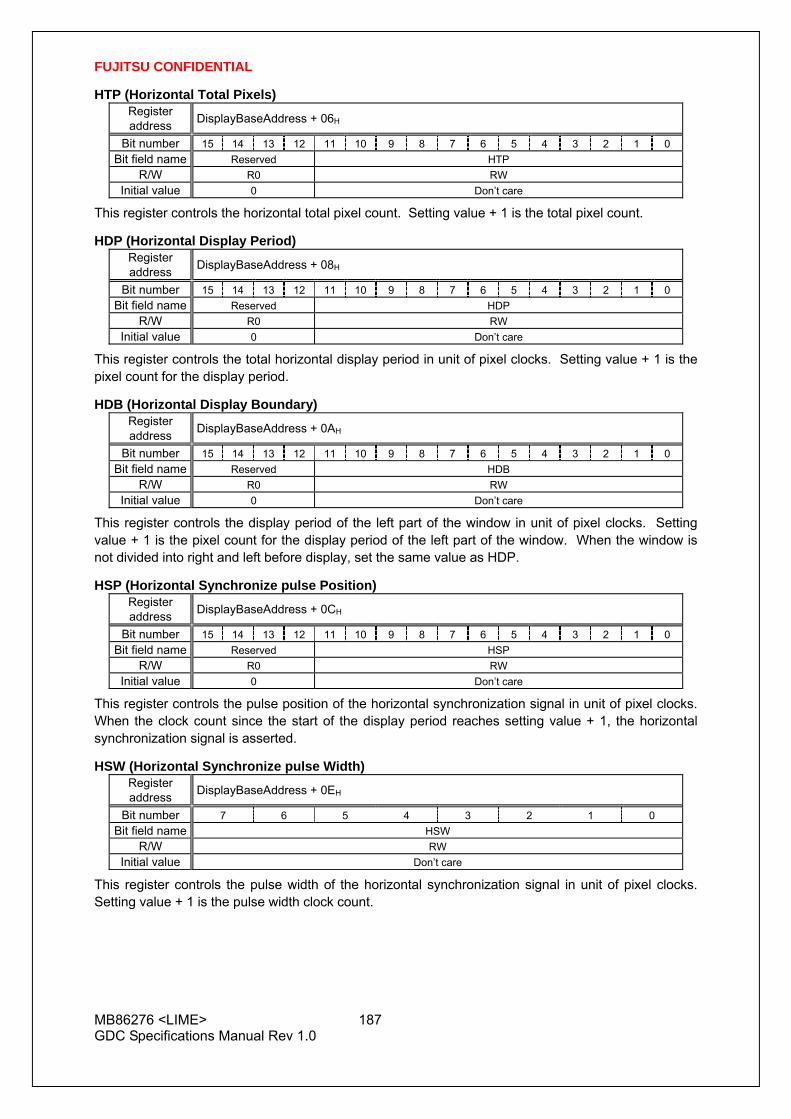
FUJITSU CONFIDENTIAL
MB86276 <LIME> 187 GDC Specifications Manual Rev 1.0
HTP (Horizontal Total Pixels) Register address DisplayBaseAddress + 06H
Bit number 15 14 13 12 11 10 9 8 7 6 5 4 3 2 1 0 Bit field name Reserved HTP
R/W R0 RW Initial value 0 Don’t care
This register controls the horizontal total pixel count. Setting value + 1 is the total pixel count.
HDP (Horizontal Display Period) Register address DisplayBaseAddress + 08H
Bit number 15 14 13 12 11 10 9 8 7 6 5 4 3 2 1 0 Bit field name Reserved HDP
R/W R0 RW Initial value 0 Don’t care
This register controls the total horizontal display period in unit of pixel clocks. Setting value + 1 is the pixel count for the display period.
HDB (Horizontal Display Boundary) Register address DisplayBaseAddress + 0AH
Bit number 15 14 13 12 11 10 9 8 7 6 5 4 3 2 1 0 Bit field name Reserved HDB
R/W R0 RW Initial value 0 Don’t care
This register controls the display period of the left part of the window in unit of pixel clocks. Setting value + 1 is the pixel count for the display period of the left part of the window. When the window is not divided into right and left before display, set the same value as HDP.
HSP (Horizontal Synchronize pulse Position) Register address DisplayBaseAddress + 0CH
Bit number 15 14 13 12 11 10 9 8 7 6 5 4 3 2 1 0 Bit field name Reserved HSP
R/W R0 RW Initial value 0 Don’t care
This register controls the pulse position of the horizontal synchronization signal in unit of pixel clocks. When the clock count since the start of the display period reaches setting value + 1, the horizontal synchronization signal is asserted.
HSW (Horizontal Synchronize pulse Width) Register address DisplayBaseAddress + 0EH
Bit number 7 6 5 4 3 2 1 0 Bit field name HSW
R/W RW Initial value Don’t care
This register controls the pulse width of the horizontal synchronization signal in unit of pixel clocks. Setting value + 1 is the pulse width clock count.

FUJITSU CONFIDENTIAL
MB86276 <LIME> 188 GDC Specifications Manual Rev 1.0
VSW (Vertical Synchronize pulse Width) Register address DisplayBaseAddress + 0FH
Bit number 7 6 5 4 3 2 1 0 Bit field name Reserved VSW
R/W R0 RW Initial value 0 Don’t care
This register controls the pulse width of vertical synchronization signal in unit of raster. Setting value + 1 is the pulse width raster count.
VTR (Vertical Total Rasters) Register address DisplayBaseAddress + 12H
Bit number 15 14 13 12 11 10 9 8 7 6 5 4 3 2 1 0 Bit field name Reserved VTR
R/W R0 RW Initial value 0 Don’t care
This register controls the vertical total raster count. Setting value + 1 is the total raster count. For the interlace display, Setting value + 1.5 is the total raster count for 1 field; 2 × setting value + 3 is the total raster count for 1 frame (see Section 8.3.2).
VSP (Vertical Synchronize pulse Position) Register address DisplayBaseAddress + 14H
Bit number 15 14 13 12 11 10 9 8 7 6 5 4 3 2 1 0 Bit field name Reserved VSP
R/W R0 RW Initial value 0 Don’t care
This register controls the pulse position of vertical synchronization signal in unit of raster. The vertical synchronization pulse is asserted starting at the setting value + 1st raster relative to the display start raster.
VDP (Vertical Display Period) Register address DisplayBaseAddress + 16H
Bit number 15 14 13 12 11 10 9 8 7 6 5 4 3 2 1 0 Bit field name Reserved VDP
R/W R0 RW Initial value 0 Don’t care
This register controls the vertical display period in unit of raster. Setting value + 1 is the count of raster to be displayed.

FUJITSU CONFIDENTIAL
MB86276 <LIME> 189 GDC Specifications Manual Rev 1.0
L0M (L0 layer Mode) Register address DisplayBaseAddress + 20H
Bit number 31 30 29 28 27 26 25 24 23 22 21 20 19 18 17 16 15 14 13 12 11 10 9 8 7 6 5 4 3 2 1 0Bit field name L0C Reserved Reserved CW Reserved CH
R/W RW R0 R0 RW R0 RW Initial value 0 0 0 Don’t care 0 Don’t care
Bit 11 to 0 L0H (L0 layer Height)
Specifies the height of the logic frame of the L0 layer in pixel units. Setting value + 1 is the height
Bit 23 to 16 L0W (L0 layer memory Width)
Sets the memory width (stride) of the logic frame of the L0 layer in 64-byte units
Bit 31 L0C (L0 layer Color mode)
Sets the color mode for L0 layer
0 Indirect color (8 bits/pixel) mode
1 Direct color (16 bits/pixel) mode
L0EM (L0-layer Extended Mode) Register address DisplayBaseAddress + 110H
Bit number 31 30 29 28 27 26 25 24 23 22 21 20 19 18 17 16 15 14 13 12 11 10 ----- 4 3 2 1 0Bit field name L0EC Reserved L0PB Reserved L0WP
R/W RW R0 RW R0 RWInitial value 0 0 0
Bit 0 L0 WP (L0 layer Window Position enable)
Selects the display position of L0 layer
0 Compatibility mode display (C layer supported)
1 Window display
Bit 23 to 20 L0PB (L0 layer Palette Base)
Shows the value added to the index when subtracting palette of L0 layer. 16 times of setting value is added.
Bit 31 and 30 L0EC (L0 layer Extended Color mode)
Sets extended color mode for L0 layer
00 Mode determined by L0C
01 Direct color (24 bits/pixel) mode
1x Reserved

FUJITSU CONFIDENTIAL
MB86276 <LIME> 190 GDC Specifications Manual Rev 1.0
L0OA (L0 layer Origin Address) Register address DisplayBaseAddress + 24H
Bit number 31 30 29 28 27 26 25 24 23 22 21 20 19 18 17 16 15 14 13 12 11 10 9 8 7 6 5 4 3 2 1 0Bit field name Reserved L0OA
R/W R0 RW R0 Initial value 0 Don’t care 0000
This register sets the origin address of the logic frame of the L0 layer. Since lower 4 bits are fixed at “0”, address 16-byte-aligned.
L0DA (L0-layer Display Address) Register address DisplayBaseAddress + 28H
Bit number 31 30 29 28 27 26 25 24 23 22 21 20 19 18 17 16 15 14 13 12 11 10 9 8 7 6 5 4 3 2 1 0Bit field name Reserved L0DA
R/W R0 RW Initial value 0 Don’t care
This register sets the display origin address of the L0 layer. For the direct color mode (16 bits/pixel), the lower 1 bit is “0”, and this address is treated as being aligned in 2 bytes.
L0DX (L0-layer Display position X) Register address DisplayBaseAddress + 2CH
Bit number 15 14 13 12 11 10 9 8 7 6 5 4 3 2 1 0 Bit field name Reserved L0DX
R/W R0 RW Initial value 0 Don’t care
This register sets the display starting position (X coordinates) of the L0 layer on the basis of the origin of the logic frame in pixels.
L0DY (L0-layer Display position Y) Register address DisplayBaseAddress + 2EH
Bit number 15 14 13 12 11 10 9 8 7 6 5 4 3 2 1 0 Bit field name Reserved L0DY
R/W R0 RW Initial value 0 Don’t care
This register sets the display starting position (Y coordinates) of the L0 layer on the basis of the origin of the logic frame in pixels.

FUJITSU CONFIDENTIAL
MB86276 <LIME> 191 GDC Specifications Manual Rev 1.0
L0WX (L0 layer Window position X) Register address DisplayBaseAddress + 114H
Bit number 15 14 13 12 11 10 9 8 7 6 5 4 3 2 1 0 Bit field name Reserved L0WX
R/W R0 RW Initial value 0
This register sets the X coordinates of the display position of the L0 layer window.
L0WY (L0 layer Window position Y) Register address DisplayBaseAddress + 116H
Bit number 15 14 13 12 11 10 9 8 7 6 5 4 3 2 1 0 Bit field name Reserved L0WY
R/W R0 RW Initial value 0
This register sets the Y coordinates of the display position of the L0 layer window.
L0WW (L0 layer Window Width) Register address DisplayBaseAddress + 118H
Bit number 15 14 13 12 11 10 9 8 7 6 5 4 3 2 1 0 Bit field name Reserved L0WW
R/W R0 RW Initial value 0 Don’t care
This register controls the horizontal direction display size (width) of the L0 layer window. Do not specify “0”.
L0WH (L0 layer Window Height) Register address DisplayBaseAddress + 11AH
Bit number 15 14 13 12 11 10 9 8 7 6 5 4 3 2 1 0 Bit field name Reserved L0WH
R/W R0 RW Initial value 0 Don’t care
This register controls the vertical direction display size (height) of the L0 layer window. Setting value + 1 is the height.
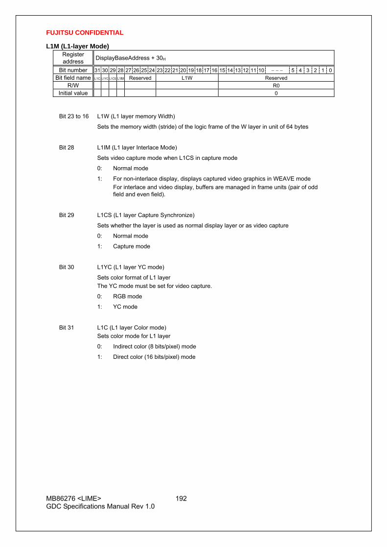
FUJITSU CONFIDENTIAL
MB86276 <LIME> 192 GDC Specifications Manual Rev 1.0
L1M (L1-layer Mode) Register address DisplayBaseAddress + 30H
Bit number 31 30 29 28 27 26 25 24 23 22 21 20 19 18 17 16 15 14 13 12 11 10 − − − 5 4 3 2 1 0Bit field name L1C L1YC L1CS L1IM Reserved L1W Reserved
R/W R0 Initial value 0
Bit 23 to 16 L1W (L1 layer memory Width)
Sets the memory width (stride) of the logic frame of the W layer in unit of 64 bytes
Bit 28 L1IM (L1 layer Interlace Mode)
Sets video capture mode when L1CS in capture mode
0: Normal mode
1: For non-interlace display, displays captured video graphics in WEAVE mode For interlace and video display, buffers are managed in frame units (pair of odd field and even field).
Bit 29 L1CS (L1 layer Capture Synchronize)
Sets whether the layer is used as normal display layer or as video capture
0: Normal mode
1: Capture mode
Bit 30 L1YC (L1 layer YC mode)
Sets color format of L1 layer The YC mode must be set for video capture.
0: RGB mode
1: YC mode
L1C (L1 layer Color mode) Sets color mode for L1 layer
0: Indirect color (8 bits/pixel) mode
Bit 31
1: Direct color (16 bits/pixel) mode

FUJITSU CONFIDENTIAL
MB86276 <LIME> 193 GDC Specifications Manual Rev 1.0
L1EM (L1 layer Extended Mode) Register address DisplayBaseAddress + 120H
Bit number 31 30 29 28 27 26 25 24 23 22 21 20 19 18 17 16 15 14 13 12 11 10 − − − 4 3 2 1 0Bit field name L1EC Reserved DM L1PB Reserved
R/W RW R0 RW R0 Initial value 0 0
Bit 23 to 20 L1PB (L1 layer Palette Base)
Shows the value added to the index when subtracting palette of L1 layer. 16 times of setting value is added.
Bit 25 to 24 L1DM (L1 layer Display Magnify Mode)
00 Normal Mode (no scaling or shrink scaling)
01 Reserved
10 Magnify Scaling
11 Reserved
Bit 31 to 30 L1EC (L1 layer Extended Color mode) Sets extended color mode for L1 layer
00 Mode determined by L1C
01 Direct color (24 bits/pixel) mode
1x Reserved
L1DA (L1 layer Display Address) Register address DisplayBaseAddress + 34H
Bit number 31 30 29 28 27 26 25 24 23 22 21 20 19 18 17 16 15 14 13 12 11 10 9 8 7 6 5 4 3 2 1 0Bit field name Reserved L1DA
R/W R0 RW Initial value 0 Don’t care
This register sets the display origin address of the L1 layer. For the direct color mode (16 bits/pixel), the lower 1 bit is “0”, and this register is treated as being aligned in 2 bytes. Wraparound processing is not performed for the L1 layer, so the frame origin linear address and display position (X coordinates, and Y coordinates) are not specified.
L1WX (L1 layer Window position X) Register address DisplayBaseAddress + 124H (DisplayBaseAddress + 18H)
Bit number 15 14 13 12 11 10 9 8 7 6 5 4 3 2 1 0 Bit field name Reserved L1WX
R/W R0 RW Initial value 0 Don’t care
This register sets the X coordinates of the display position of the L1 layer window. This register is placed in two address spaces. The parenthesized address is the register address to maintain compatibility with previous products. The same applies to L1WY, L1WW, and L1WH.
L1WY (L1 layer Window position Y) Register address DisplayBaseAddress + 126H (DisplayBaseAddress + 1AH)
Bit number 15 14 13 12 11 10 9 8 7 6 5 4 3 2 1 0 Bit field name Reserved L1WY
R/W R0 RW Initial value 0 Don’t care
This register sets the Y coordinates of the display position of the L1 layer window.

FUJITSU CONFIDENTIAL
MB86276 <LIME> 194 GDC Specifications Manual Rev 1.0
L1WW (L1 layer Window Width) Register address DisplayBaseAddress + 128H (DisplayBaseAddress + 1CH)
Bit number 15 14 13 12 11 10 9 8 7 6 5 4 3 2 1 0 Bit field name Reserved L1WW
R/W R0 RW Initial value 0 Don’t care
This register controls the horizontal direction display size (width) of the L1 layer window. Do not specify “0”.
L1WH (L1 layer Window Height) Register address DisplayBaseAddress + 12AH ((DisplayBaseAddress + 1EH)
Bit number 15 14 13 12 11 10 9 8 7 6 5 4 3 2 1 0 Bit field name Reserved L1WH
R/W R0 RW Initial value 0 Don’t care
This register controls the vertical direction display size (height) of the L1 layer window. Setting value + 1 is the height.

FUJITSU CONFIDENTIAL
MB86276 <LIME> 195 GDC Specifications Manual Rev 1.0
L2M (L2 layer Mode) Register address DisplayBaseAddress + 40H
Bit number 31 30 29 28 27 − − 24 23 22 21 20 19 18 17 16 15 14 13 12 11 10 9 8 7 6 5 4 3 2 1 0Bit field name L2C L2FLP Reserved L2W Reserved L2H
R/W RW RW R0 RW R0 RW Initial value 0 Don’t care 0 Don’t care
Bit 11 to 0 L2H (L2 layer Height)
Specifies the height of the logic frame of the L2 layer in pixel units. Setting value + 1 is the height
Bit 23 to 16 L2W (L2 layer memory Width)
Sets the memory width (stride) of the logic frame of the L2 layer in 64-byte units
Bit 30 and 29 L2FLP (L2 layer Flip mode)
Sets flipping mode for L2 layer
00 Displays frame 0
01 Displays frame 1
10 Switches frame 0 and 1 alternately for display
11 Reserved
Bit 31 L2C (L2 layer Color mode)
Sets the color mode for L2 layer
0 Indirect color (8 bits/pixel) mode
1 Direct color (16 bits/pixel) mode

FUJITSU CONFIDENTIAL
MB86276 <LIME> 196 GDC Specifications Manual Rev 1.0
L2EM (L2 layer Extended Mode) Register address DisplayBaseAddress + 130H
Bit number 31 30 29 28 27 26 25 24 23 22 21 20 19 18 17 16 15 14 13 12 11 10 ----- 4 3 2 1 0Bit field name L2EC Reserved L2PB Reserved L2OM L0WP
R/W RW R0 RW R0 RW RWInitial value 00 0 0 0 0 0
Bit 0 L2 WP (L2 layer Window Position enable)
Selects the display position of L2 layer
0 Compatibility mode display (ML layer supported)
1 Window display
Bit 1 L2OM (L2 layer Overlay Mode)
Selects the overlay mode for L2 layer
0 Compatibility mode
1 Extended mode
Bit 23 to 20 L2PB (L2 layer Palette Base)
Shows the value added to the index when subtracting palette of L2 layer. 16 times of setting value is added.
Bit 31 and 30 L2EC (L2 layer Extended Color mode)
Sets extended color mode for L2 layer
00 Mode determined by L2C
01 Direct color (24 bits/pixel) mode
1x Reserved

FUJITSU CONFIDENTIAL
MB86276 <LIME> 197 GDC Specifications Manual Rev 1.0
L2OA0 (L2 layer Origin Address 0) Register address DisplayBaseAddress + 44H
Bit number 31 30 29 28 27 26 25 24 23 22 21 20 19 18 17 16 15 14 13 12 11 10 9 8 7 6 5 4 3 2 1 0Bit field name Reserved L2OA0
R/W R0 RW R0 Initial value 0 Don’t care 0000
This register sets the origin address of the logic frame of the L2 layer in frame 0. Since lower 4 bits are fixed to “0”, this address is 16-byte aligned.
L2DA0 (L2 layer Display Address 0) Register address DisplayBaseAddress + 48H
Bit number 31 30 29 28 27 26 25 24 23 22 21 20 19 18 17 16 15 14 13 12 11 10 9 8 7 6 5 4 3 2 1 0Bit field name Reserved L2DA0
R/W R0 RW Initial value 0 Don’t care
This register sets the origin address of the L2 layer in frame 0. For the direct color mode (16 bits/pixel), the lower 1 bit is “0” and this address is 2-byte aligned.
L2OA1 (L2 layer Origin Address 1) Register address DisplayBaseAddress + 4CH
Bit number 31 30 29 28 27 26 25 24 23 22 21 20 19 18 17 16 15 14 13 12 11 10 9 8 7 6 5 4 3 2 1 0Bit field name Reserved L2OA1
R/W R0 RW R0 Initial value 0 Don’t care 0000
This register sets the origin address of the logic frame of the L2 layer in frame 1. Since lower 4-bits are fixed to “0”, this address is 16-byte aligned.
L2DA1 (L2 layer Display Address 1) Register address DisplayBaseAddress + 50H
Bit number 31 30 29 28 27 26 25 24 23 22 21 20 19 18 17 16 15 14 13 12 11 10 9 8 7 6 5 4 3 2 1 0Bit field name Reserved L2DA1
R/W R0 RW Initial value 0 Don’t care
This register sets the origin address of the L2 layer in frame 1. For the direct color mode (16 bits/pixel), the lower 1 bit is “0” and this address is 2-byte aligned.
L2DX (L2 layer Display position X) Register address DisplayBaseAddress + 54H
Bit number 15 14 13 12 11 10 9 8 7 6 5 4 3 2 1 0 Bit field name Reserved L2DX
R/W R0 RW Initial value 0 Don’t care
This register sets the display starting position (X coordinates) of the L2 layer on the basis of the origin of the logic frame in pixels.

FUJITSU CONFIDENTIAL
MB86276 <LIME> 198 GDC Specifications Manual Rev 1.0
L2DY (L2 layer Display position Y) Register address DisplayBaseAddress + 56H
Bit number 15 14 13 12 11 10 9 8 7 6 5 4 3 2 1 0 Bit field name Reserved L2DY
R/W R0 RW Initial value 0 Don’t care
This register sets the display starting position (Y coordinates) of the L2 layer on the basis of the origin of the logic frame in pixels.
L2WX (L2 layer Window position X) Register address DisplayBaseAddress + 134H
Bit number 15 14 13 12 11 10 9 8 7 6 5 4 3 2 1 0 Bit field name Reserved L2WX
R/W R0 RW Initial value 0 Don’t care
This register sets the X coordinates of the display position of the L2 layer window.
L2WY (L2 layer Window position Y) Register address DisplayBaseAddress + 138H
Bit number 15 14 13 12 11 10 9 8 7 6 5 4 3 2 1 0 Bit field name Reserved L2WY
R/W R0 RW Initial value 0 Don’t care
This register sets the Y coordinates of the display position of the L2 layer window.
L2WW (L2 layer Window Width) Register address DisplayBaseAddress + 13AH
Bit number 15 14 13 12 11 10 9 8 7 6 5 4 3 2 1 0 Bit field name Reserved L2WW
R/W R0 RW Initial value 0 Don’t care
This register controls the horizontal direction display size (width) of the L2 layer window. Do not specify “0”.
L2WH (L2 layer Window Height) Register address DisplayBaseAddress + 13CH
Bit number 15 14 13 12 11 10 9 8 7 6 5 4 3 2 1 0 Bit field name Reserved L2WH
R/W R0 RW Initial value 0 Don’t care
This register controls the vertical direction display size (height) of the L2 layer window. Setting value + 1 is the height.

FUJITSU CONFIDENTIAL
MB86276 <LIME> 199 GDC Specifications Manual Rev 1.0
L3M (L3 layer Mode) Register address DisplayBaseAddress + 58H
Bit number 31 30 29 28 27 26 25 24 23 22 21 20 19 18 17 16 15 14 13 12 11 10 9 8 7 6 5 4 3 2 1 0Bit field name L3C L3FLP Reserved L3W Reserved L3H
R/W RW R0 R0 RW R0 RW Initial value 0 0 0 Don’t care 0 Don’t care
Bit 11 to 0 L3H (L3 layer Height)
Specifies the height of the logic frame of the L3 layer in pixel units. Setting value + 1 is the height
Bit 23 to 16 L3W (L3 layer memory Width)
Sets the memory width (stride) of the logic frame of the L3 layer in 64-byte units
Bit 30 and 29 L3FLP (L3 layer Flip mode)
Sets flipping mode for L3 layer
00 Displays frame 0
01 Displays frame 1
10 Switches frame 0 and 1 alternately for display
11 Reserved
Bit 31 L3C (L3 layer Color mode)
Sets the color mode for L3 layer
0 Indirect color (8 bits/pixel) mode
1 Direct color (16 bits/pixel) mode

FUJITSU CONFIDENTIAL
MB86276 <LIME> 200 GDC Specifications Manual Rev 1.0
L3EM (L3 layer Extended Mode) Register address DisplayBaseAddress + 140H
Bit number 31 30 29 28 27 26 25 24 23 22 21 20 19 18 17 16 15 14 13 12 11 10 − − − 4 3 2 1 0Bit field name L3EC Reserved L3PB Reserved L3OM L3WP
R/W RW R0 RW R0 RW RWInitial value 00 0 0 0 0
Bit 0 L3 WP (L3 layer Window Position enable)
Selects the display position of L3 layer
0 Compatibility mode display (MR layer supported)
1 Window display
Bit 1 L3OM (L3 layer Overlay Mode)
Selects the overlay mode for L3 layer
0 Compatibility mode
1 Extended mode
Bit 23 to 20 L3PB (L3 layer Palette Base)
Shows the value added to the index when subtracting palette of L3 layer. 16 times of setting value is added.
Bit 31 and 30 L3EC (L3 layer Extended Color mode)
Sets extended color mode for L3 layer
00 Mode determined by L3C
01 Direct color (24 bits/pixel) mode
1x Reserved
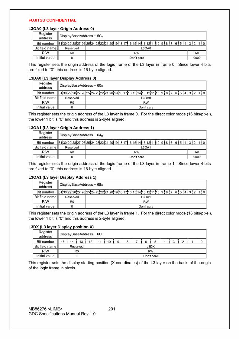
FUJITSU CONFIDENTIAL
MB86276 <LIME> 201 GDC Specifications Manual Rev 1.0
L3OA0 (L3 layer Origin Address 0) Register address DisplayBaseAddress + 5CH
Bit number 31 30 29 28 27 26 25 24 23 22 21 20 19 18 17 16 15 14 13 12 11 10 9 8 7 6 5 4 3 2 1 0Bit field name Reserved L3OA0
R/W R0 RW R0 Initial value 0 Don’t care 0000
This register sets the origin address of the logic frame of the L3 layer in frame 0. Since lower 4 bits are fixed to “0”, this address is 16-byte aligned.
L3DA0 (L3 layer Display Address 0) Register address DisplayBaseAddress + 60H
Bit number 31 30 29 28 27 26 25 24 23 22 21 20 19 18 17 16 15 14 13 12 11 10 9 8 7 6 5 4 3 2 1 0Bit field name Reserved L3DA0
R/W R0 RW Initial value 0 Don’t care
This register sets the origin address of the L3 layer in frame 0. For the direct color mode (16 bits/pixel), the lower 1 bit is “0” and this address is 2-byte aligned.
L3OA1 (L3 layer Origin Address 1) Register address DisplayBaseAddress + 64H
Bit number 31 30 29 28 27 26 25 24 23 22 21 20 19 18 17 16 15 14 13 12 11 10 9 8 7 6 5 4 3 2 1 0Bit field name Reserved L3OA1
R/W R0 RW R0 Initial value 0 Don’t care 0000
This register sets the origin address of the logic frame of the L3 layer in frame 1. Since lower 4-bits are fixed to “0”, this address is 16-byte aligned.
L3OA1 (L3 layer Display Address 1) Register address DisplayBaseAddress + 68H
Bit number 31 30 29 28 27 26 25 24 23 22 21 20 19 18 17 16 15 14 13 12 11 10 9 8 7 6 5 4 3 2 1 0Bit field name Reserved L3DA1
R/W R0 RW Initial value 0 Don’t care
This register sets the origin address of the L3 layer in frame 1. For the direct color mode (16 bits/pixel), the lower 1 bit is “0” and this address is 2-byte aligned.
L3DX (L3 layer Display position X) Register address DisplayBaseAddress + 6CH
Bit number 15 14 13 12 11 10 9 8 7 6 5 4 3 2 1 0 Bit field name Reserved L3DX
R/W R0 RW Initial value 0 Don’t care
This register sets the display starting position (X coordinates) of the L3 layer on the basis of the origin of the logic frame in pixels.
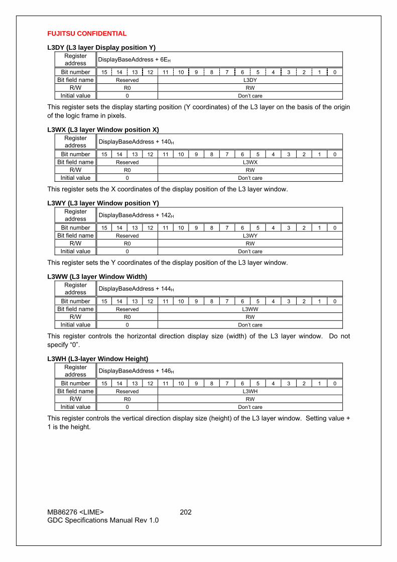
FUJITSU CONFIDENTIAL
MB86276 <LIME> 202 GDC Specifications Manual Rev 1.0
L3DY (L3 layer Display position Y) Register address DisplayBaseAddress + 6EH
Bit number 15 14 13 12 11 10 9 8 7 6 5 4 3 2 1 0 Bit field name Reserved L3DY
R/W R0 RW Initial value 0 Don’t care
This register sets the display starting position (Y coordinates) of the L3 layer on the basis of the origin of the logic frame in pixels.
L3WX (L3 layer Window position X) Register address DisplayBaseAddress + 140H
Bit number 15 14 13 12 11 10 9 8 7 6 5 4 3 2 1 0 Bit field name Reserved L3WX
R/W R0 RW Initial value 0 Don’t care
This register sets the X coordinates of the display position of the L3 layer window.
L3WY (L3 layer Window position Y) Register address DisplayBaseAddress + 142H
Bit number 15 14 13 12 11 10 9 8 7 6 5 4 3 2 1 0 Bit field name Reserved L3WY
R/W R0 RW Initial value 0 Don’t care
This register sets the Y coordinates of the display position of the L3 layer window.
L3WW (L3 layer Window Width) Register address DisplayBaseAddress + 144H
Bit number 15 14 13 12 11 10 9 8 7 6 5 4 3 2 1 0 Bit field name Reserved L3WW
R/W R0 RW Initial value 0 Don’t care
This register controls the horizontal direction display size (width) of the L3 layer window. Do not specify “0”.
L3WH (L3-layer Window Height) Register address DisplayBaseAddress + 146H
Bit number 15 14 13 12 11 10 9 8 7 6 5 4 3 2 1 0 Bit field name Reserved L3WH
R/W R0 RW Initial value 0 Don’t care
This register controls the vertical direction display size (height) of the L3 layer window. Setting value + 1 is the height.

FUJITSU CONFIDENTIAL
MB86276 <LIME> 203 GDC Specifications Manual Rev 1.0
L4M (L4 layer Mode) Register address DisplayBaseAddress + 70H
Bit number 31 30 29 28 27 26 25 24 23 22 21 20 19 18 17 16 15 14 13 12 11 10 9 8 7 6 5 4 3 2 1 0Bit field name L4C L4FLP Reserved L4W Reserved L4H
R/W RW RW R0 RW R0 RW Initial value 0 Don’t care 0 Don’t care
Bit 11 to 0 L4H (L4 layer Height)
Specifies the height of the logic frame of the L4 layer in pixel units. Setting value + 1 is the height
Bit 23 to 16 L4W (L4 layer memory Width)
Sets the memory width (stride) logic frame of the L4 layer in 64-byte units
Bit 30 and 29 L4FLP (L4 layer Flip mode)
Sets flipping mode for L4 layer
00 Displays frame 0
01 Displays frame 1
10 Switches frame 0 and 1 alternately for display
11 Reserved
Bit 31 L4C (L4 layer Color mode)
Sets the color mode for L4 layer
0 Indirect color (8 bits/pixel) mode
1 Direct color (16 bits/pixel) mode

FUJITSU CONFIDENTIAL
MB86276 <LIME> 204 GDC Specifications Manual Rev 1.0
L4EM (L4 layer Extended Mode) Register address DisplayBaseAddress + 150H
Bit number 31 30 29 28 27 26 25 24 23 22 21 20 19 18 17 16 15 14 13 12 11 10 − − − 4 3 2 1 0Bit field name L4EC Reserved L4PB Reserved L4OM L4WP
R/W RW R0 RW R0 RW RWInitial value 00 0 0 0 0
Bit 0 L4 WP (L4 layer Window Position enable)
Selects the display position of L4 layer
0 Compatibility mode display (BL layer supported)
1 Window display
Bit 1 L4OM (L4 layer Overlay Mode)
Selects the overlay mode for L4 layer
0 Compatibility mode
1 Extended mode
Bit 23 to 20 L4PB (L4 layer Palette Base)
Shows the value added to the index when subtracting palette of L4 layer. 16 times of setting value is added.
Bit 31 and 30 L4EC (L4 layer Extended Color mode)
Sets extended color mode for L4 layer
00 Mode determined by L4C
01 Direct color (24 bits/pixel) mode
1x Reserved

FUJITSU CONFIDENTIAL
MB86276 <LIME> 205 GDC Specifications Manual Rev 1.0
L4OA0 (L4 layer Origin Address 0) Register address DisplayBaseAddress + 74H
Bit number 31 30 29 28 27 26 25 24 23 22 21 20 19 18 17 16 15 14 13 12 11 10 9 8 7 6 5 4 3 2 1 0Bit field name Reserved L4OA0
R/W R0 RW R0 Initial value 0 Don’t care 0000
This register sets the origin address of the logic frame of the L4 layer in frame 0. Since lower 4 bits are fixed to “0”, this address is 16-byte aligned.
L4DA0 (L4 layer Display Address 0) Register address DisplayBaseAddress + 78H
Bit number 31 30 29 28 27 26 25 24 23 22 21 20 19 18 17 16 15 14 13 12 11 10 9 8 7 6 5 4 3 2 1 0Bit field name Reserved L4DA0
R/W R0 RW Initial value 0 Don’t care
This register sets the origin address of the L4 layer in frame 0. For the direct color mode (16 bits/pixel), the lower 1 bit is “0” and this address is 2-byte aligned.
L4OA1 (L4 layer Origin Address 1) Register address DisplayBaseAddress + 7CH
Bit number 31 30 29 28 27 26 25 24 23 22 21 20 19 18 17 16 15 14 13 12 11 10 9 8 7 6 5 4 3 2 1 0Bit field name Reserved L4OA1
R/W R0 RW R0 Initial value 0 Don’t care 0000
This register sets the origin address of the logic frame of the L4 layer in frame 1. Since lower 4-bits are fixed to “0”, this address is 16-byte aligned.
L4OA1 (L4 layer Display Address 1) Register address DisplayBaseAddress + 80H
Bit number 31 30 29 28 27 26 25 24 23 22 21 20 19 18 17 16 15 14 13 12 11 10 9 8 7 6 5 4 3 2 1 0Bit field name Reserved L4DA1
R/W R0 RW Initial value 0 Don’t care
This register sets the origin address of the L4 layer in frame 1. For the direct color mode (16 bits/pixel), the lower 1 bit is “0” and this address is 2-byte aligned.
L4DX (L4 layer Display position X) Register address DisplayBaseAddress + 84H
Bit number 15 14 13 12 11 10 9 8 7 6 5 4 3 2 1 0 Bit field name Reserved L4DX
R/W R0 RW Initial value 0 Don’t care
This register sets the display starting position (X coordinates) of the L4 layer on the basis of the origin of the logic frame in pixels.

FUJITSU CONFIDENTIAL
MB86276 <LIME> 206 GDC Specifications Manual Rev 1.0
L4DY (L4 layer Display position Y) Register address DisplayBaseAddress + 86H
Bit number 15 14 13 12 11 10 9 8 7 6 5 4 3 2 1 0 Bit field name Reserved L4DY
R/W R0 RW Initial value 0 Don’t care
This register sets the display starting position (Y coordinates) of the L4 layer on the basis of the origin of the logic frame in pixels.
L4WX (L4 layer Window position X) Register address DisplayBaseAddress + 154H
Bit number 15 14 13 12 11 10 9 8 7 6 5 4 3 2 1 0 Bit field name Reserved L4WX
R/W R0 RW Initial value 0 Don’t care
This register sets the X coordinates of the display position of the L4 layer window.
L4WY (L4 layer Window position Y) Register address DisplayBaseAddress + 156H
Bit number 15 14 13 12 11 10 9 8 7 6 5 4 3 2 1 0 Bit field name Reserved L4WY
R/W R0 RW Initial value 0 Don’t care
This register sets the Y coordinates of the display position of the L4 layer window.
L4WW (L4 layer Window Width) Register address DisplayBaseAddress + 158H
Bit number 15 14 13 12 11 10 9 8 7 6 5 4 3 2 1 0 Bit field name Reserved L4WW
R/W R0 RW Initial value 0 Don’t care
This register controls the horizontal direction display size (width) of the L4 layer window. Do not specify “0”.
L4WH (L4 layer Window Height) Register address DisplayBaseAddress + 15AH
Bit number 15 14 13 12 11 10 9 8 7 6 5 4 3 2 1 0 Bit field name Reserved L4WH
R/W R0 RW Initial value 0 Don’t care
This register controls the vertical direction display size (height) of the L4 layer window. Setting value + 1 is the height.
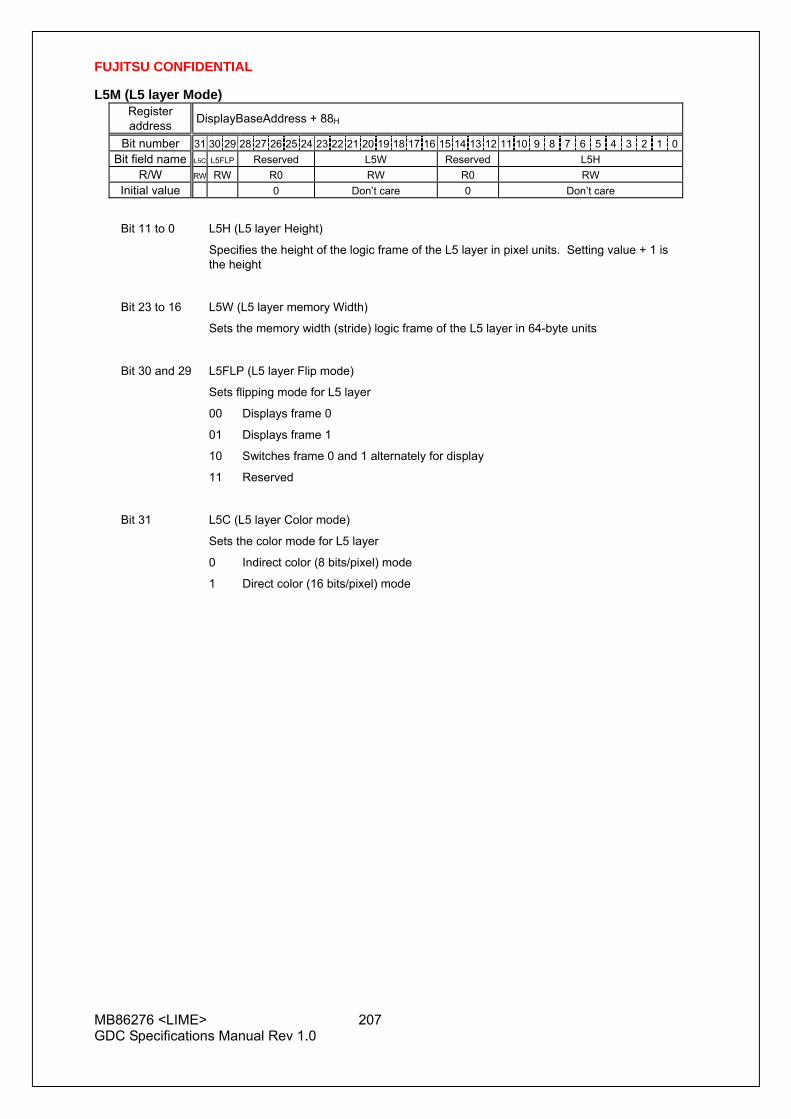
FUJITSU CONFIDENTIAL
MB86276 <LIME> 207 GDC Specifications Manual Rev 1.0
L5M (L5 layer Mode) Register address DisplayBaseAddress + 88H
Bit number 31 30 29 28 27 26 25 24 23 22 21 20 19 18 17 16 15 14 13 12 11 10 9 8 7 6 5 4 3 2 1 0Bit field name L5C L5FLP Reserved L5W Reserved L5H
R/W RW RW R0 RW R0 RW Initial value 0 Don’t care 0 Don’t care
Bit 11 to 0 L5H (L5 layer Height)
Specifies the height of the logic frame of the L5 layer in pixel units. Setting value + 1 is the height
Bit 23 to 16 L5W (L5 layer memory Width)
Sets the memory width (stride) logic frame of the L5 layer in 64-byte units
Bit 30 and 29 L5FLP (L5 layer Flip mode)
Sets flipping mode for L5 layer
00 Displays frame 0
01 Displays frame 1
10 Switches frame 0 and 1 alternately for display
11 Reserved
Bit 31 L5C (L5 layer Color mode)
Sets the color mode for L5 layer
0 Indirect color (8 bits/pixel) mode
1 Direct color (16 bits/pixel) mode

FUJITSU CONFIDENTIAL
MB86276 <LIME> 208 GDC Specifications Manual Rev 1.0
L5EM (L5 layer Extended Mode) Register address DisplayBaseAddress + 110H
Bit number 31 30 29 28 27 26 25 24 23 22 21 20 19 18 17 16 15 14 13 12 11 10 − − − 4 3 2 1 0Bit field name L5EC Reserved L5PB Reserved L5OM L5WP
R/W RW R0 RW R0 RW RWInitial value 00 0 0 0 0
Bit 0 L5 WP (L5 layer Window Position enable)
Selects the display position of L5 layer
0 Compatibility mode display (BR layer supported)
1 Window display
Bit 1 L5OM (L5 layer Overlay Mode)
Selects the overlay mode for L5 layer
0 Compatibility mode
1 Extended mode
Bit 23 to 20 L5PB (L5 layer Palette Base)
Shows the value added to the index when subtracting palette of L5 layer. 16 times of setting value is added.
Bit 31 to 30 L5EC (L5 layer Extended Color mode)
Sets extended color mode for L5 layer
00 Mode determined by L5C
01 Direct color (24 bits/pixel) mode
1x Reserved

FUJITSU CONFIDENTIAL
MB86276 <LIME> 209 GDC Specifications Manual Rev 1.0
L5OA0 (L5 layer Origin Address 0) Register address DisplayBaseAddress + 8CH
Bit number 31 30 29 28 27 26 25 24 23 22 21 20 19 18 17 16 15 14 13 12 11 10 9 8 7 6 5 4 3 2 1 0Bit field name Reserved BROA0
R/W R0 RW R0 Initial value 0 Don’t care 0000
This register sets the origin address of the logic frame of the L5 layer in frame 0. Since lower 4 bits are fixed to “0”, this address is 16-byte aligned.
L5DA0 (L5 layer Display Address 0) Register address DisplayBaseAddress + 90H
Bit number 31 30 29 28 27 26 25 24 23 22 21 20 19 18 17 16 15 14 13 12 11 10 9 8 7 6 5 4 3 2 1 0Bit field name Reserved L5DA0
R/W R0 RW Initial value 0 Don’t care
This register sets the origin address of the L5 layer in frame 0. For the direct color mode (16 bits/pixel), the lower 1 bit is “0” and this address is 2-byte aligned.
L5OA1 (L5 layer Origin Address 1) Register address DisplayBaseAddress + 94H
Bit number 31 30 29 28 27 26 25 24 23 22 21 20 19 18 17 16 15 14 13 12 11 10 9 8 7 6 5 4 3 2 1 0Bit field name Reserved L5OA1
R/W R0 RW R0 Initial value 0 Don’t care 0000
This register sets the origin address of the logic frame of the L5 layer in frame 1. Since lower 4-bits are fixed to “0”, this address is 16-byte aligned.
L5OA1 (L5 layer Display Address 1) Register address DisplayBaseAddress + 98H
Bit number 31 30 29 28 27 26 25 24 23 22 21 20 19 18 17 16 15 14 13 12 11 10 9 8 7 6 5 4 3 2 1 0Bit field name Reserved L5DA1
R/W R0 RW Initial value 0 Don’t care
This register sets the origin address of the L5 layer in frame 1. For the direct color mode (16 bits/pixel), the lower 1 bit is “0” and this address is 2-byte aligned.
L5DX (L5 layer Display position X) Register address DisplayBaseAddress + 9CH
Bit number 15 14 13 12 11 10 9 8 7 6 5 4 3 2 1 0 Bit field name Reserved L5DX
R/W R0 RW Initial value 0 Don’t care
This register sets the display starting position (X coordinates) of the L5 layer on the basis of the origin of the logic frame in pixels.

FUJITSU CONFIDENTIAL
MB86276 <LIME> 210 GDC Specifications Manual Rev 1.0
L5DY (L5 layer Display position Y) Register address DisplayBaseAddress + 9EH
Bit number 15 14 13 12 11 10 9 8 7 6 5 4 3 2 1 0 Bit field name Reserved L5DY
R/W R0 RW Initial value 0 Don’t care
This register sets the display starting position (Y coordinates) of the L5 layer on the basis of the origin of the logic frame in pixels.
L5WX (L5 layer Window position X) Register address DisplayBaseAddress + 164H
Bit number 15 14 13 12 11 10 9 8 7 6 5 4 3 2 1 0 Bit field name Reserved L5WX
R/W R0 RW Initial value 0 Don’t care
This register sets the X coordinates of the display position of the L5 layer window.
L5WY (L5 layer Window position Y) Register address DisplayBaseAddress + 166H
Bit number 15 14 13 12 11 10 9 8 7 6 5 4 3 2 1 0 Bit field name Reserved L5WY
R/W R0 RW Initial value 0 Don’t care
This register sets the Y coordinates of the display position of the L5 layer window.
L5WW (L5 layer Window Width) Register address DisplayBaseAddress + 168H
Bit number 15 14 13 12 11 10 9 8 7 6 5 4 3 2 1 0 Bit field name Reserved L5WW
R/W R0 RW Initial value 0 Don’t care
This register controls the horizontal direction display size (width) of the L5 layer window. Do not specify “0”.
L5WH (L5 layer Window Height) Register address DisplayBaseAddress + 16AH
Bit number 15 14 13 12 11 10 9 8 7 6 5 4 3 2 1 0 Bit field name Reserved L5WH
R/W R0 RW Initial value 0 Don’t care
This register controls the vertical direction display size (height) of the L5 layer window. Setting value + 1 is the height.
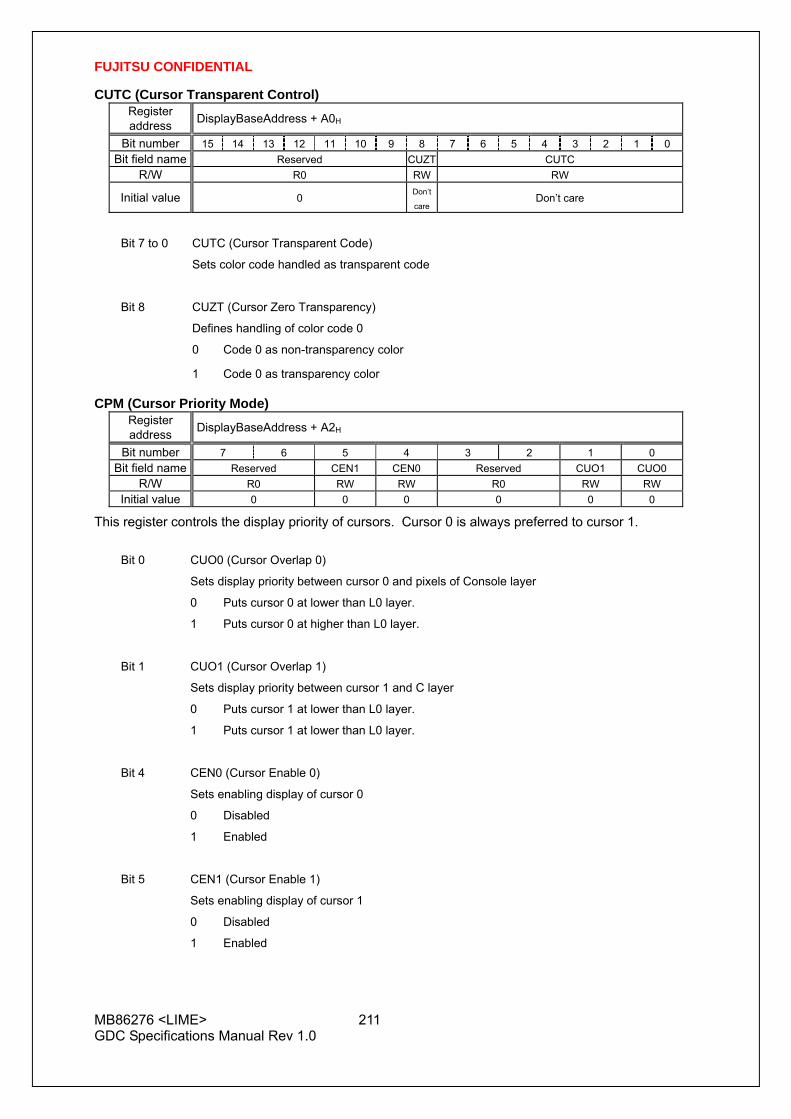
FUJITSU CONFIDENTIAL
MB86276 <LIME> 211 GDC Specifications Manual Rev 1.0
CUTC (Cursor Transparent Control) Register address DisplayBaseAddress + A0H
Bit number 15 14 13 12 11 10 9 8 7 6 5 4 3 2 1 0 Bit field name Reserved CUZT CUTC
R/W R0 RW RW
Initial value 0 Don’t
careDon’t care
Bit 7 to 0 CUTC (Cursor Transparent Code)
Sets color code handled as transparent code
Bit 8 CUZT (Cursor Zero Transparency)
Defines handling of color code 0
0 Code 0 as non-transparency color
1 Code 0 as transparency color
CPM (Cursor Priority Mode) Register address DisplayBaseAddress + A2H
Bit number 7 6 5 4 3 2 1 0 Bit field name Reserved CEN1 CEN0 Reserved CUO1 CUO0
R/W R0 RW RW R0 RW RW Initial value 0 0 0 0 0 0
This register controls the display priority of cursors. Cursor 0 is always preferred to cursor 1.
Bit 0 CUO0 (Cursor Overlap 0)
Sets display priority between cursor 0 and pixels of Console layer
0 Puts cursor 0 at lower than L0 layer.
1 Puts cursor 0 at higher than L0 layer.
Bit 1 CUO1 (Cursor Overlap 1)
Sets display priority between cursor 1 and C layer
0 Puts cursor 1 at lower than L0 layer.
1 Puts cursor 1 at lower than L0 layer.
Bit 4 CEN0 (Cursor Enable 0)
Sets enabling display of cursor 0
0 Disabled
1 Enabled
Bit 5 CEN1 (Cursor Enable 1)
Sets enabling display of cursor 1
0 Disabled
1 Enabled

FUJITSU CONFIDENTIAL
MB86276 <LIME> 212 GDC Specifications Manual Rev 1.0
CUOA0 (Cursor-0 Origin Address) Register address DisplayBaseAddress + A4H
Bit number 31 30 29 28 27 26 25 24 23 22 21 20 19 18 17 16 15 14 13 12 11 10 9 8 7 6 5 4 3 2 1 0Bit field name Reserved CUOA0
R/W R0 RW R0 Initial value 0 Don’t care 0000
This register sets the start address of the cursor 0 pattern. Since lower 4 bits are fixed to “0”, this address is 16-byte aligned.
CUX0 (Cursor-0 X position) Register address DisplayBaseAddress + A8H
Bit number 15 14 13 12 11 10 9 8 7 6 5 4 3 2 1 0 Bit field name Reserved CUX0
R/W R0 RW Initial value 0 Don’t care
This register sets the display position (X coordinates) of the cursor 0 in pixels. The reference position of the coordinates is the top left of the cursor pattern.
CUY0 (Cursor-0 Y position) Register address DisplayBaseAddress + AaH
Bit number 15 14 13 12 11 10 9 8 7 6 5 4 3 2 1 0 Bit field name Reserved CUY0
R/W R0 RW Initial value 0 Don’t care
This register sets the display position (Y coordinates) of the cursor 0 in pixels. The reference position of the coordinates is the top left of the cursor pattern.

FUJITSU CONFIDENTIAL
MB86276 <LIME> 213 GDC Specifications Manual Rev 1.0
CUOA1 (Cursor-1 Origin Address) Register address DisplayBaseAddress + ACH
Bit number 31 30 29 28 27 26 25 24 23 22 21 20 19 18 17 16 15 14 13 12 11 10 9 8 7 6 5 4 3 2 1 0Bit field name Reserved CUOA1
R/W R0 RW R0 Initial value 0 Don’t care 0000
This register sets the start address of the cursor 1 pattern. Since lower 4 bits are fixed to “0”, this address is 16-byte aligned.
CUX1 (Cursor-1 X position) Register address DisplayBaseAddress + B0H
Bit number 15 14 13 12 11 10 9 8 7 6 5 4 3 2 1 0 Bit field name Reserved CUX1
R/W R0 RW Initial value 0 Don’t care
This register sets the display position (X coordinates) of the cursor 1 in pixels. The reference position of the coordinates is the top left of the cursor pattern.
CUY1 (Cursor-1 Y position) Register address DisplayBaseAddress + B2H
Bit number 15 14 13 12 11 10 9 8 7 6 5 4 3 2 1 0 Bit field name Reserved CUY1
R/W R0 RW Initial value 0 Don’t care
This register sets the display position (Y coordinates) of the cursor 1 in pixels. The reference position of the coordinates is the top left of the cursor pattern.

FUJITSU CONFIDENTIAL
MB86276 <LIME> 214 GDC Specifications Manual Rev 1.0
MDC (Multi Display Control) Register address DisplayBaseAddress + 170H
Bit number 31 30 29 28 24 23 21 20 19 18 17 16 15 14 13 12 11 10 9 8 7 6 5 4 3 2 1 0
Bit field name MDen reserve SC1en SC0en
R/W RW R0 RW RW
Initial value 0 0 X X
This register controls dual display mode.
Bit 0 SC0en0 ( screen 0 enable 0)
0: L0 is not included into screen 0
1: L0 is included into screen 0
Bit 1 SC0en1 ( screen 0 enable 1)
0: L1 is not included into screen 0
1: L1 is included into screen 0
Bit 5 SC0en5 ( screen 0 enable 5)
0: L5 is not included into screen 0
1: L5 is included into screen 0
Bit 6 SC0en6 ( screen 0 enable 6)
0: Cursor0 is not included into screen 0
1: Cursor0 is included into screen 0
Bit 7 SC0en7 ( screen 0 enable 7)
0: Cursor1 is not included into screen 0
1: Cursor1 is included into screen 0
Bit 8 SC1en0 ( screen 1 enable 0)
0: L0 is not included into screen 1
1: L0 is included into screen 1
Bit 9 SC1en1 ( screen 1 enable 1)
0: L1 is not included into screen 1
1: L1 is included into screen 1
Bit 13 SC1en5 ( screen 1 enable 5)
0: L5 is not included into screen 1
1: L5 is included into screen 1

FUJITSU CONFIDENTIAL
MB86276 <LIME> 215 GDC Specifications Manual Rev 1.0
Bit 14 SC1en6 ( screen 1 enable 6)
0: Cursor 0 is not included into screen 1
1: Cursor 0 is included into screen 1
Bit 15 SC1en7 ( screen 1 enable 7)
0: Cursor 1 is not included into screen 1
1: Cursor 1 is included into screen 1
Bit 31 MDen ( multi display enable )
This enables multi or dual display mode
0: Single display mode
1: Dual display mode

FUJITSU CONFIDENTIAL
MB86276 <LIME> 216 GDC Specifications Manual Rev 1.0
DLS (Display Layer Select) Register address DisplayBaseAddress + 180H
Bit number 31 30 29 ----- 25 24 23 22 21 20 19 18 17 16 15 14 13 12 11 10 9 8 7 6 5 4 3 2 1 0Bit field name Reserved DLS5 DLS4 DLS3 DLS2 DLS1 DSL0
R/W R0 R0 RW R0 RW R0 RW R0 RW R0 RW R0 RW Initial value 101 100 011 010 001 000
This register defines the blending sequence.
Bit 3 to 0 DSL0 (Display Layer Select 0)
Selects the top layer subjected to blending.
0000 L0 layer
0001 L1 layer
: :
0101 L5 layer
0110 Reserved
: :
0110 Reserved
0111 Not selected
Bit 7 to 4 DSL1 (Display Layer Select 1)
Selects the second layer subjected to blending. The bit values are the same as DSL0.
Bit 11 to 8 DSL2 (Display Layer Select 2)
Selects the third layer subjected to blending. The bit values are the same as DSL0.
Bit 15 to 12 DSL3 (Display Layer Select 3)
Selects the fourth layer subjected to blending. The bit values are the same as DSL0.
Bit 19 to 16 DSL4 (Display Layer Select 4)
Selects the fifth layer subjected to blending. The bit values are the same as DSL0.
Bit 23 to 20 DSL5 (Display Layer Select 5)
Selects the bottom layer subjected to blending. The bit values are the same as DSL0.

FUJITSU CONFIDENTIAL
MB86276 <LIME> 217 GDC Specifications Manual Rev 1.0
DBGC (Display Background Color) Register address DisplayBaseAddress + 184H
Bit number 31 30 29 ----- 25 24 23 22 21 20 19 18 17 16 15 14 13 12 11 10 9 8 7 6 5 4 3 2 1 0Bit field name Reserved DBGR DBGG DBGB
R/W R0 Initial value
This register specifies the color to be displayed in areas outside the display area of each layer on the window.
Bit 7 to 0 DBGB (Display Background Blue)
Specifies the blue level of the background color.
Bit 15 to 8 DBGG (Display Background Green)
Specifies the green level of the background color.
Bit 23 to 16 DBGR (Display Background Red)
Specifies the red level of the background color.

FUJITSU CONFIDENTIAL
MB86276 <LIME> 218 GDC Specifications Manual Rev 1.0
L0BLD (L0 Blend) Register address DisplayBaseAddress + B4H
Bit number 31 30 29 28 ----- 20 19 18 17 16 15 14 13 12 11 10 9 8 7 6 5 4 3 2 1 0Bit field name Reserved L0BE L0BS L0BI L0BP Reserved L0BR
R/W Initial value
This register specifies the blend parameters for the L0 layer. This register corresponds to BRATIO or BMODE for previous products.
Bit 7 to 0 L0BR (L0 layer Blend Ratio)
Sets the blend ratio. Basically, the blend ratio is setting value/256.
Bit 13 L0BP (L0 layer Blend Plane)
Specifies that the L5 layer is the blend plane.
0 Value of L0BR used as blend ratio
1 Pixel of L5 layer used as blend ratio
Bit 14 L0BI (L0 layer Blend Increment)
Selects whether or not 1/256 is added when the blend ratio is not “0”.
0 Blend ratio calculated as is
1 1/256 added when blend ratio ≠ 0
Bit 15 L0BS (L0 layer Blend Select)
Selects the blend calculation expression.
0 Upper image × Blend ratio + Lower image × (1 – Blend ratio)
1 Upper image × (1 – Blend ratio) + Lower image × Blend ratio
Bit 16 L0BE (L0 layer Blend Enable)
This bit enables blending.
0 Overlay via transparent color
1 Overlay via blending
Before blending, the blend mode must be specified using L0BE, and alpha must also be enabled for L0 layer display data. For direct color, alpha is specified using the MSB of data; for indirect color, alpha is specified using the MSB of palette data.

FUJITSU CONFIDENTIAL
MB86276 <LIME> 219 GDC Specifications Manual Rev 1.0
L1BLD (L1 Blend) Register address DisplayBaseAddress + 188H
Bit number 31 30 29 28 ----- 20 19 18 17 16 15 14 13 12 11 10 9 8 7 6 5 4 3 2 1 0Bit field name Reserved L1BE L1BS L1BI L1BP Reserved L1BR
R/W Initial value
This register specifies the blend parameters for the L1 layer.
Bit 7 to 0 L1BR (L1 layer Blend Ratio)
Sets the blend ratio. Basically, the blend ratio is setting value/256.
Bit 13 L1BP (L1 layer Blend Plane)
Specifies that the L5 layer is the blend plane.
0 Value of L1BR used as blend ratio
1 Pixel of L5 layer used as blend ratio
Bit 14 L1BI (L1 layer Blend Increment)
Selects whether or not 1/256 is added when the blend ratio is not “0”.
0 Blend ratio calculated as is
1 1/256 added when blend ratio ≠ 0
Bit 15 L1BS (L1 layer Blend Select)
Selects the blend calculation expression.
0 Upper image × Blend ratio + Lower image × (1 – Blend ratio)
1 Upper image × (1 – Blend ratio) + Lower image × Blend ratio
Bit 16 L1BE (L1 layer Blend Enable)
This bit enables blending.
0 Overlay via transparent color
1 Overlay via blending
Before blending, the blend mode must be specified using L1BE, and alpha must also be enabled for L1 layer display data. For direct color, alpha is specified using the MSB of data; for indirect color, alpha is specified using the MSB of palette data.

FUJITSU CONFIDENTIAL
MB86276 <LIME> 220 GDC Specifications Manual Rev 1.0
L2BLD (L2 Blend) Register address DisplayBaseAddress + 18CH
Bit number 31 30 29 28 ----- 20 19 18 17 16 15 14 13 12 11 10 9 8 7 6 5 4 3 2 1 0Bit field name Reserved L2BE L2BS L2BI L2BP Reserved L2BR
R/W Initial value
This register specifies the blend parameters for the L2 layer.
Bit 7 to 0 L2BR (L2 layer Blend Ratio)
Sets the blend ratio. Basically, the blend ratio is setting value/256.
Bit 13 L2BP (L2 layer Blend Plane)
Specifies that the L5 layer is the blend plane.
0 Value of L2BR used as blend ratio
1 Pixel of L5 layer used as blend ratio
Bit 14 L2BI (L2 layer Blend Increment)
Selects whether or not 1/256 is added when the blend ratio is not “0”.
0 Blend ratio calculated as is
1 1/256 added when blend ratio ≠ 0
Bit 15 L2BS (L2 layer Blend Select)
Selects the blend calculation expression.
0 Upper image × Blend ratio + Lower image × (1 – Blend ratio)
1 Upper image × (1 – Blend ratio) + Lower image × Blend ratio
Bit 16 L2BE (L2 layer Blend Enable)
This bit enables blending.
0 Overlay via transparent color
1 Overlay via blending
Before blending, the blend mode must be specified using L2BE, and alpha must also be enabled for L2 layer display data. For direct color, alpha is specified using the MSB of data; for indirect color, alpha is specified using the MSB of palette data.

FUJITSU CONFIDENTIAL
MB86276 <LIME> 221 GDC Specifications Manual Rev 1.0
L3BLD (L3 Blend) Register address DisplayBaseAddress + 190H
Bit number 31 30 29 28 ----- 20 19 18 17 16 15 14 13 12 11 10 9 8 7 6 5 4 3 2 1 0Bit field name Reserved L3BE L3BS L3BI L3BP Reserved L3BR
R/W Initial value
This register specifies the blend parameters for the L3 layer.
Bit 7 to 0 L3BR (L3 layer Blend Ratio)
Sets the blend ratio. Basically, the blend ratio is setting value/256.
Bit 13 L3BP (L3 layer Blend Plane)
Specifies that the L5 layer is the blend plane.
0 Value of L3BR used as blend ratio
1 Pixel of L5 layer used as blend ratio
Bit 14 L3BI (L3 layer Blend Increment)
Selects whether or not 1/256 is added when the blend ratio is not “0”.
0 Blend ratio calculated as is
1 1/256 added when blend ratio ≠ 0
Bit 15 L3BS (L3 layer Blend Select)
Selects the blend calculation expression.
0 Upper image × Blend ratio + Lower image × (1 – Blend ratio)
1 Upper image × (1 – Blend ratio) + Lower image × Blend ratio
Bit 16 L3BE (L3 layer Blend Enable)
This bit enables blending.
0 Overlay via transparent color
1 Overlay via blending
Before blending, the blend mode must be specified using L3BE, and alpha must also be enabled for L3 layer display data. For direct color, alpha is specified using the MSB of data; for indirect color, alpha is specified using the MSB of palette data.

FUJITSU CONFIDENTIAL
MB86276 <LIME> 222 GDC Specifications Manual Rev 1.0
L4BLD (L4 Blend) Register address DisplayBaseAddress + 194H
Bit number 31 30 29 28 ----- 20 19 18 17 16 15 14 13 12 11 10 9 8 7 6 5 4 3 2 1 0Bit field name Reserved L4BE L4BS L4BI L4BP Reserved L4BR
R/W Initial value
This register specifies the blend parameters for the L4 layer.
Bit 7 to 0 L4BR (L4 layer Blend Ratio)
Sets the blend ratio. Basically, the blend ratio is setting value/256.
Bit 13 L4BP (L4 layer Blend Plane)
Specifies that the L5 layer is the blend plane.
0 Value of L4BR used as blend ratio
1 Pixel of L5 layer used as blend ratio
Bit 14 L4BI (L4 layer Blend Increment)
Selects whether or not 1/256 is added when the blend ratio is not “0”.
0 Blend ratio calculated as is
1 1/256 added when blend ratio ≠ 0
Bit 15 L4BS (L4 layer Blend Select)
Selects the blend calculation expression.
0 Upper image × Blend ratio + Lower image × (1 – Blend ratio)
1 Upper image × (1 – Blend ratio) + Lower image × Blend ratio
Bit 16 L4BE (L4 layer Blend Enable)
This bit enables blending.
0 Overlay via transparent color
1 Overlay via blending
Before blending, the blend mode must be specified using L4BE, and alpha must also be enabled for L4 layer display data. For direct color, alpha is specified using the MSB of data; for indirect color, alpha is specified using the MSB of palette data.
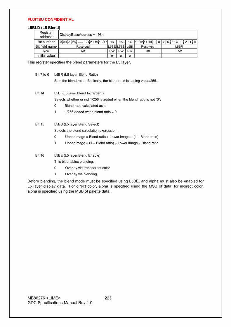
FUJITSU CONFIDENTIAL
MB86276 <LIME> 223 GDC Specifications Manual Rev 1.0
L5BLD (L5 Blend) Register address DisplayBaseAddress + 198h
Bit number 31 30 29 28 ----- 21 20 19 18 17 16 15 14 13 12 11 10 9 8 7 6 5 4 3 2 1 0Bit field name Reserved L5BE L5BS L5BI Reserved L5BR
R/W R0 RW RW RW R0 RW Initial value 0 0 0
This register specifies the blend parameters for the L5 layer.
Bit 7 to 0 L5BR (L5 layer Blend Ratio)
Sets the blend ratio. Basically, the blend ratio is setting value/256.
Bit 14 L5BI (L5 layer Blend Increment)
Selects whether or not 1/256 is added when the blend ratio is not “0”.
0 Blend ratio calculated as is
1 1/256 added when blend ratio ≠ 0
Bit 15 L5BS (L5 layer Blend Select)
Selects the blend calculation expression.
0 Upper image × Blend ratio + Lower image × (1 – Blend ratio)
1 Upper image × (1 – Blend ratio) + Lower image × Blend ratio
Bit 16 L5BE (L5 layer Blend Enable)
This bit enables blending.
0 Overlay via transparent color
1 Overlay via blending
Before blending, the blend mode must be specified using L5BE, and alpha must also be enabled for L5 layer display data. For direct color, alpha is specified using the MSB of data; for indirect color, alpha is specified using the MSB of palette data.

FUJITSU CONFIDENTIAL
MB86276 <LIME> 224 GDC Specifications Manual Rev 1.0
L0TC (L0 layer Transparency Control) Register address DisplayBaseAddress + BCH
Bit number 15 14 13 12 11 10 9 8 7 6 5 4 3 2 1 0 Bit field name L0ZT L0TC
R/W RW RW Initial value 0 Don’t care
This register sets the transparent color for the L0 layer. Color set by this register is transparent in blend mode. When L0TC = 0 and L0ZT = 0, color 0 is displayed in black (transparent).
This register corresponds to the CTC register for previous products.
Bit 14 to 0 L0TC (L0 layer Transparent Color)
Sets transparent color code for the L0 layer. In indirect color mode (8 bits/pixel) bits 7 to 0 are used.
Bit 15 L0ZT (L0 layer Zero Transparency)
Sets handling of color code 0 in L0 layer
0: Code 0 as transparency color
1: Code 0 as non-transparency color
L2TC (L2 layer Transparency Control) Register address DisplayBaseAddress + C2H
Bit number 15 14 13 12 11 10 9 8 7 6 5 4 3 2 1 0 Bit field name L2ZT L2TC
R/W RW RW Initial value 0 Don’t care
This register sets the transparent color for the L2 layer.
When L2TC = 0 and L2ZT = 0, color 0 is displayed in black (transparent).
This register corresponds to the MLTC register for previous products.
Bit 14 to 0 L2TC (L2 layer Transparent Color)
Sets transparent color code for the L2 layer. In indirect color mode (8 bits/pixel) bits 7 to 0 are used.
Bit 15 L2ZT (L2 layer Zero Transparency)
Sets handling of color code 0 in L2 layer
0 Code 0 as transparency color
1 Code 0 as non-transparency color
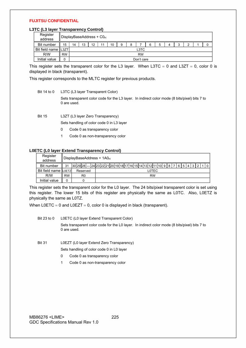
FUJITSU CONFIDENTIAL
MB86276 <LIME> 225 GDC Specifications Manual Rev 1.0
L3TC (L3 layer Transparency Control) Register address DisplayBaseAddress + C0H
Bit number 15 14 13 12 11 10 9 8 7 6 5 4 3 2 1 0 Bit field name L3ZT L3TC
R/W RW RW Initial value 0 Don’t care
This register sets the transparent color for the L3 layer. When L3TC = 0 and L3ZT = 0, color 0 is displayed in black (transparent).
This register corresponds to the MLTC register for previous products.
Bit 14 to 0 L3TC (L3 layer Transparent Color)
Sets transparent color code for the L3 layer. In indirect color mode (8 bits/pixel) bits 7 to 0 are used.
Bit 15 L3ZT (L3 layer Zero Transparency)
Sets handling of color code 0 in L3 layer
0 Code 0 as transparency color
1 Code 0 as non-transparency color
L0ETC (L0 layer Extend Transparency Control) Register address DisplayBaseAddress + 1A0H
Bit number 31 30 29 28 --- 24 23 22 21 20 19 18 17 16 15 14 13 12 11 10 9 8 7 6 5 4 3 2 1 0Bit field name L0ETZ Reserved L0TEC
R/W RW R0 RW Initial value 0 0
This register sets the transparent color for the L0 layer. The 24 bits/pixel transparent color is set using this register. The lower 15 bits of this register are physically the same as L0TC. Also, L0ETZ is physically the same as L0TZ.
When L0ETC = 0 and L0EZT = 0, color 0 is displayed in black (transparent).
Bit 23 to 0 L0ETC (L0 layer Extend Transparent Color)
Sets transparent color code for the L0 layer. In indirect color mode (8 bits/pixel) bits 7 to 0 are used.
Bit 31 L0EZT (L0 layer Extend Zero Transparency)
Sets handling of color code 0 in L0 layer
0 Code 0 as transparency color
1 Code 0 as non-transparency color

FUJITSU CONFIDENTIAL
MB86276 <LIME> 226 GDC Specifications Manual Rev 1.0
L1ETC (L1 layer Extend Transparency Control) Register address DisplayBaseAddress + 1A4H
Bit number 31 30 29 28 --- 24 23 22 21 20 19 18 17 16 15 14 13 12 11 10 9 8 7 6 5 4 3 2 1 0Bit field name L1ETZ Reserved L1TEC
R/W RW R0 RW Initial value
This register sets the transparent color for the L1 layer. When L1ETC = 0 and L1EZT = 0, color 0 is displayed in black (transparent).
For YCbCr display, transparent color checking is not performed; processing is always performed assuming that transparent color is not used.
Bit 23 to 0 L1ETC (L1 layer Extend Transparent Color)
Sets transparent color code for the L1 layer. In indirect color mode (8 bits/pixel) bits 7 to 0 are used.
Bit 31 L1EZT (L1 layer Extend Zero Transparency)
Sets handling of color code 0 in L1 layer
0 Code 0 as transparency color
1 Code 0 as non-transparency color
L2ETC (L2 layer Extend Transparency Control) Register address DisplayBaseAddress + 1A8H
Bit number 31 30 29 28 --- 24 23 22 21 20 19 18 17 16 15 14 13 12 11 10 9 8 7 6 5 4 3 2 1 0Bit field name L2ETZ Reserved L2TEC
R/W RW R0 RW Initial value
This register sets the transparent color for the L2 layer. The 24 bits/pixel transparent color is set using this register. The lower 15 bits of this register are physically the same as L2TC. Also, L2ETZ is physically the same as L2TZ.
When L2ETC = 0 and L2EZT = 0, color 0 is displayed in black (transparent).
Bit 23 to 0 L2ETC (L2 layer Extend Transparent Color)
Sets transparent color code for the L2 layer. In indirect color mode (8 bits/pixel) bits 7 to 0 are used.
Bit 31 L2EZT (L2 layer Extend Zero Transparency)
Sets handling of color code 0 in L2 layer
0 Code 0 as transparency color
1 Code 0 as non-transparency color

FUJITSU CONFIDENTIAL
MB86276 <LIME> 227 GDC Specifications Manual Rev 1.0
L3ETC (L3 layer Extend Transparency Control) Register address DisplayBaseAddress + 1ACH
Bit number 31 30 29 28 --- 24 23 22 21 20 19 18 17 16 15 14 13 12 11 10 9 8 7 6 5 4 3 2 1 0Bit field name L3ETZ Reserved L3TEC
R/W RW R0 RW Initial value 0 0
This register sets the transparent color for the L3 layer. The 24 bits/pixel transparent color is set using this register. The lower 15 bits of this register are physically the same as L3TC. Also, L3ETZ is physically the same as L3TZ.
When L3ETC = 0 and L3EZT = 0, color 0 is displayed in black (transparent).
Bit 23 to 0 L3ETC (L3 layer Extend Transparent Color)
Sets transparent color code for the L3 layer. In indirect color mode (8 bits/pixel) bits 7 to 0 are used.
Bit 31 L3EZT (L3 layer Extend Zero Transparency)
Sets handling of color code 0 in L3 layer
0 Code 0 as transparency color
1 Code 0 as non-transparency color
L4ETC (L4 layer Extend Transparency Control) Register address DisplayBaseAddress + 1B0H
Bit number 31 30 29 28 --- 24 23 22 21 20 19 18 17 16 15 14 13 12 11 10 9 8 7 6 5 4 3 2 1 0Bit field name L4ETZ Reserved L4TEC
R/W RW R0 RW Initial value 0 0
This register sets the transparent color for the L4 layer. This register sets the transparent color for the L4 layer. When L4ETC = 0 and L4EZT = 0, color 0 is displayed in black (transparent).
Bit 23 to 0 L4ETC (L4 layer Extend Transparent Color)
Sets transparent color code for the L4 layer. In indirect color mode (8 bits/pixel) bits 7 to 0 are used.
Bit 31 L4EZT (L4 layer Extend Zero Transparency)
Sets handling of color code 0 in L4 layer
0 Code 0 as transparency color
1 Code 0 as non-transparency color
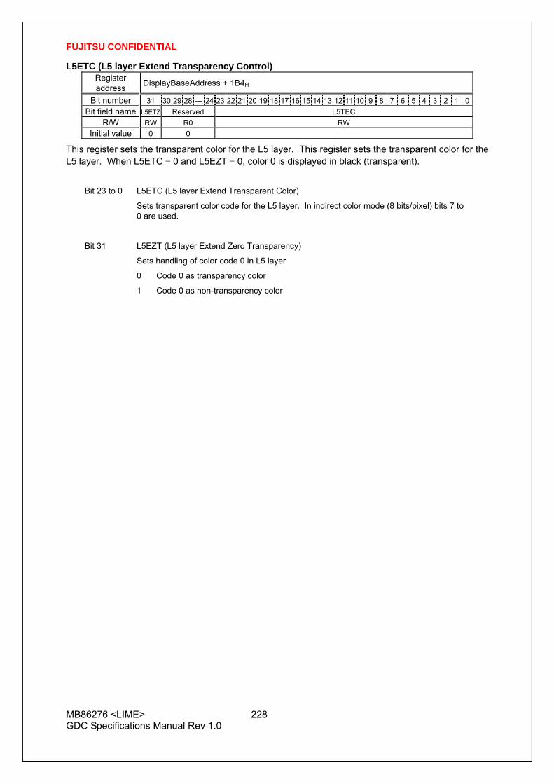
FUJITSU CONFIDENTIAL
MB86276 <LIME> 228 GDC Specifications Manual Rev 1.0
L5ETC (L5 layer Extend Transparency Control) Register address DisplayBaseAddress + 1B4H
Bit number 31 30 29 28 --- 24 23 22 21 20 19 18 17 16 15 14 13 12 11 10 9 8 7 6 5 4 3 2 1 0Bit field name L5ETZ Reserved L5TEC
R/W RW R0 RW Initial value 0 0
This register sets the transparent color for the L5 layer. This register sets the transparent color for the L5 layer. When L5ETC = 0 and L5EZT = 0, color 0 is displayed in black (transparent).
Bit 23 to 0 L5ETC (L5 layer Extend Transparent Color)
Sets transparent color code for the L5 layer. In indirect color mode (8 bits/pixel) bits 7 to 0 are used.
Bit 31 L5EZT (L5 layer Extend Zero Transparency)
Sets handling of color code 0 in L5 layer
0 Code 0 as transparency color
1 Code 0 as non-transparency color

FUJITSU CONFIDENTIAL
MB86276 <LIME> 229 GDC Specifications Manual Rev 1.0
L0PAL0-255 (L0 layer Palette 0-255) Register address DisplayBaseAddress + 400H -- DisplayBaseAddress + 7FFH
Bit number 31 30 29 28 27 26 25 24 23 22 21 20 19 18 17 16 15 14 13 12 11 10 9 8 7 6 5 4 3 2 1 0Bit field name A R G B
R/W RW R0 RW R0 RW R0 RW R0
Initial value Don’t
care 0000000 Don’t care 00 Don’t care 00 Don’t care 00
These are color palette registers for L0 layer and cursors. In the indirect color mode, a color code in the display frame indicates the palette register number, and the color information set in that register is applied as the display color of that pixel. This register corresponds to the CPALn register for previous products.
Bit 7 to 2 B (Blue)
Sets blue color component
Bit 15 to 10 G (Green)
Sets green color component
Bit 23 to 18 R (Red)
Sets red color component
Bit 31 A (Alpha)
Specifies whether or not to perform blending with lower layers when the blending mode is enabled.
0 Blending not performed even when blending mode enabled Overlay is performed via transparent color.
1 Blending performed

FUJITSU CONFIDENTIAL
MB86276 <LIME> 230 GDC Specifications Manual Rev 1.0
L1PAL0-255 (L1 layer Palette 0-255) Register address DisplayBaseAddress + 800H -- DisplayBaseAddress + BFFH
Bit number 31 30 29 28 27 26 25 24 23 22 21 20 19 18 17 16 15 14 13 12 11 10 9 8 7 6 5 4 3 2 1 0Bit field name A R G B
R/W RW R0 RW R0 RW R0 RW R0
Initial value Don’t
care 0000000 Don’t care 00 Don’t care 00 Don’t care 00
These are color palette registers for L1 layer and cursors. In the indirect color mode, a color code in the display frame indicates the palette register number, and the color information set in that register is applied as the display color of that pixel. This register corresponds to the MBPALn register for previous products.
Bit 7 to 2 B (Blue)
Sets blue color component
Bit 15 to 10 G (Green)
Sets green color component
Bit 23 to 18 R (Red)
Sets red color component
Bit 31 A (Alpha)
Specifies whether or not to perform blending with lower layers when the blending mode is enabled.
0 Blending not performed even when blending mode enabled Overlay is performed via transparent color.
1 Blending performed

FUJITSU CONFIDENTIAL
MB86276 <LIME> 231 GDC Specifications Manual Rev 1.0
L2PAL0-255 (L2 layer Palette 0-255) Register address DisplayBaseAddress + 1000H -- DisplayBaseAddress + 13FFH
Bit number 31 30 29 28 27 26 25 24 23 22 21 20 19 18 17 16 15 14 13 12 11 10 9 8 7 6 5 4 3 2 1 0Bit field name A R G B
R/W RW R0 RW R0 RW R0 RW R0
Initial value Don’t
care 0000000 Don’t care 00 Don’t care 00 Don’t care 00
These are color palette registers for L2 layer and cursors. In the indirect color mode, a color code in the display frame indicates the palette register number, and the color information set in that register is applied as the display color of that pixel.
Bit 7 to 2 B (Blue)
Sets blue color component
Bit 15 to 10 G (Green)
Sets green color component
Bit 23 to 18 R (Red)
Sets red color component
Bit 31 A (Alpha)
Specifies whether or not to perform blending with lower layers when the blending mode is enabled.
0 Blending not performed even when blending mode enabled Overlay is performed via transparent color.
1 Blending performed

FUJITSU CONFIDENTIAL
MB86276 <LIME> 232 GDC Specifications Manual Rev 1.0
L3PAL0-255 (L3 layer Palette 0-255) Register address DisplayBaseAddress + 1400H -- DisplayBaseAddress + 17FFH
Bit number 31 30 29 28 27 26 25 24 23 22 21 20 19 18 17 16 15 14 13 12 11 10 9 8 7 6 5 4 3 2 1 0Bit field name A R G B
R/W RW R0 RW R0 RW R0 RW R0
Initial value Don’t
care 0000000 Don’t care 00 Don’t care 00 Don’t care 00
These are color palette registers for L3 layer and cursors. In the indirect color mode, a color code in the display frame indicates the palette register number, and the color information set in that register is applied as the display color of that pixel.
Bit 7 to 2 B (Blue)
Sets blue color component
Bit 15 to 10 G (Green)
Sets green color component
Bit 23 to 18 R (Red)
Sets red color component
Bit 31 A (Alpha)
Specifies whether or not to perform blending with lower layers when the blending mode is enabled.
0 Blending not performed even when blending mode enabled Overlay is performed via transparent color.
1 Blending performed

FUJITSU CONFIDENTIAL
MB86276 <LIME> 233 GDC Specifications Manual Rev 1.0
12.4 Video capture registers
VCM (Video Capture Mode)
Register address CaptureBaseAddress + 00h Bit number 31 30 29 28 27 26 25 24 23 22 21 20 19 18 17 16 15 14 13 12 11 10 9 8 7 6 5 4 3 2 1 0
Bit field name VIE VIS Reserve
VICE
Reserve CM Reserve VI Reserve
NR
GB
VS Rsv
R/W R/W
R/W RX R/
W RX R/W RX R/W RX R/
WR/W RX
Initial value 0 0 X 0 X 00 X 0 X 0 0 X
This register sets the video capture mode. This register is not initialized by software reset.
Bit1 VS (Video Select) NTSC or PAL is selected for the code error detection. (only the RTB656 is input. ) 0 NTSC 1 PAL Bit2 NRGB(Native RGB input on) Native RGB mode is set up.
0 RGB video data is accepted via an internal RGB preprocessor which converts RGB to YUV422
1 Native RGB Bit20 VI (Vertical Interpolation) Sets whether to perform vertical interpolation 0 Performs vertical interpolation. The graphics are enlarged vertically by two times 1 Does not perform vertical interpolation Bit25-24 CM (Capture Mode) Sets video capture mode. To capture vides, set these bits to “11”. 00 Initial value 01 Reserved 10 Reserved 11 Capture Bit28 VICE (Video Input Clock Enable) Capture clock enable 0 Enable 1 Disable Bit30 VIS(Video Input Select) 0 RBT656/601 1 RGB Bit31 VIE (Video Input Enable) Enables video capture function 0 Does not capture video 1 Captures video
-Procedure of video capture clock Stop-
1) 0 is written in bit31 (VIE) of the VCM register, and the video capture function is invalidated.
2) 1 is written in bit28 (VICE) of the VCM register, and Stop does video capture clock.
-Procedure of video capture clock beginning-
1) 0 is written in bit28 (VICE) of the VCM register, and video capture clock is made effective.
2) 1 is written in bit31 (VIE) of the VCM register, and the video capture function is made effective.

FUJITSU CONFIDENTIAL
MB86276 <LIME> 234 GDC Specifications Manual Rev 1.0
CSC (Capture SCale) Register address CaptureBaseAddress + 04h
Bit number 31 30 29 28 27 26 25 24 23 22 21 20 19 18 17 16 15 14 13 12 11 10 9 8 7 6 5 4 3 2 1 0 Bit field name VSCI VSCF HSCI HSCF
R/W R/W R/W R/W R/W Initial value 00001 00000000000 00001 00000000000
This register sets the video capture upscaling/downscaling ratio.
Bit10-0 HSCF (Vertical SCale Fraction) The decimal part of a horizontal upscaling/downscaling ratio is set. Bit15-11 HSCI (Horizontal Scale Integer) The integer part of a horizontal upscaling/downscaling ratio is set. Bit26-16 VSCF (Vertical SCale Fraction) The decimal part of a vertical upscaling/downscaling ratio is set. Bit31-27 VSCI (Vertical SCale Integer) The integer part of a vertical upscaling/downscaling ratio is set.
Note: - Smooth continuation operation to Down Scaling mode and Up Scaling mode cannot be
performed. The picture disorder of some arises at the time of a change. This is the
restrictions for Up Scaling mode and Down Scaling mode using the same interpolate circuit.
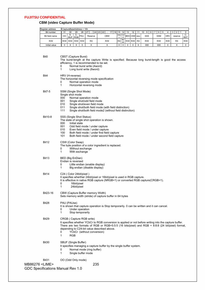
FUJITSU CONFIDENTIAL
MB86276 <LIME> 235 GDC Specifications Manual Rev 1.0
CBM (video Capture Buffer Mode)
Register address CaptureBaseAddress + 10h Bit number 31 30 29 28 27 … 24 23 22 … 17 16 15 14 13 12 11 10 9 8 7 6 5 4 3 2 1 0
Bit field name OO S-BUF
C- RGB PAU Reserve CBW res
vC24 BED CSW resv SSS SSM HRV reserve C-
BST
R/W R/W R/W R/W R/W RX R/W RX R/W R/W R/W RX R/W R/W R/W RX R/W
Initial value 0 X X 0 X X X 0 0 0 X 000 000 0 X 0
Bit0 CBST (Capture Burst) The burst-length at the capture Write is specified. Because long burst-length is good the access efficiency, 1 is recommended to be set. 0 Normal burst write (4word) 1 Long burst write (8word)
Bit4 HRV (H-reverse)
The horizontal reversing mode specification 0 Normal operation mode 1 Horizontal reversing mode
Bit7-5 SSM (Single Shot Mode) Single shot mode 000 Normal operation mode 001 Single shot/odd field mode 010 Single shot/even field mode 011 Single shot/both field mode (with field distinction) 111 Single shot/both field mode2 (without field distinction) Bit10-8 SSS (Single Shot Status) The state of single shot operation is shown. 000 Initial state 001 Odd field mode / under capture 010 Even field mode / under capture 100 Both field mode / under first field capture 101 Both field mode / under second field capture
CSW (Color Swap) Bit12 The byte position of a color ingredient is replaced. 0 Without exchange 1 With exchange
BED (Big EnDian) Bit13 Endian is reversed 0 Little endian (enable display) 1 Big endian (disable display)
Bit14 C24 ( Color 24bit/pixel ) It specifies wherther 24bit/pixel or 16bit/pixel is used in RGB capture.
It is effective in native RGB capture (NRGB=1) or converted RGB capture(CRGB=1). 0 16bit/pixel 1 24bit/pixel Bit23-16 CBW (Capture Buffer memory Width)
Sets memory width (stride) of capture buffer in 64 bytes
PAU (PAUse) Bit28 It is shown that capture operation is Stop temporarily. 0 can be written and it can cancel. 0 Under operation 1 Stop temporarily
Bit29 CRGB ( Capture RGB write) It specifies whether YCbCr to RGB conversion is applied or not before writing into the capture buffer.
There are two formats of RGB or RGB=5:5:5 (16 bits/pixel) and RGB = 8:8:8 (24 bit/pixel) format, depending to C24-bit value described above.
0 YCbCr (without conversion) 1 RGB
Bit30 SBUF (Single Buffer) It specifies managing a capture buffer by the single buffer system. 0 Normal mode (ring buffer) 1 Single buffer mode
Bit31 OO (Odd Only mode)

FUJITSU CONFIDENTIAL
MB86276 <LIME> 236 GDC Specifications Manual Rev 1.0
Specifies whether to capture odd fields only 0 Normal mode 1 Odd only mode
Note: This register is not initialized by soft reset.
CBOA (video Capture Buffer Origin Address)
Register address CaptureBaseAddress + 14h Bit number 31 30 29 28 27 26 25 24 23 22 21 20 19 18 17 16 15 14 13 12 11 10 9 8 7 6 5 4 3 2 1 0
Bit field name Reserved CBOA R/W RX R/W R0
Initial value Don’t care Don’t care 0
This register specifies the starting (origin) address of the video capture buffer.
CBLA (video Capture Buffer Limit Address)
Register address CaptureBaseAddress + 18h Bit number 31 30 29 28 27 26 25 24 23 22 21 20 19 18 17 16 15 14 13 12 11 10 9 8 7 6 5 4 3 2 1 0
Bit field name Reserved CBLA R/W RX R/W R0
Initial value Don’t care Don’t care 0
This register specifies the end (limit) address of the video capture buffer.
CBLA must be larger than CBOA.
CIHSTR (Capture Image Horizontal STaRt)
Register address CaptureBaseAddress + 1Ch
Bit number 15 14 13 12 11 10 9 8 7 6 5 4 3 2 1 0 Bit field name Reserved CIHSTR
R/W RX R/W Initial value Don’t care Don’t care
This register sets the range of the images to be written (captured) to the video capture buffer. Specify the X coordinates located in the top left of the image range as the count of pixels from the top left of the image. For downscaling, apply this setting to the post-reduction image coordinates.
CIVSTR (Capture Image Vertical STaRt)
Register address CaptureBaseAddress + 1Eh
Bit number 15 14 13 12 11 10 9 8 7 6 5 4 3 2 1 0 Bit field name Reserved CIVSTR
R/W RX R/W Initial value Don’t care Don’t care
This register sets the range of the images to be written (captured) to the video capture buffer. Specify the Y coordinates located in the top left of the image range as the count of pixels from the top left of the image. For downscaling, apply this setting to the post-reduction image coordinates.

FUJITSU CONFIDENTIAL
MB86276 <LIME> 237 GDC Specifications Manual Rev 1.0
CIHEND (Capture Image Horizontal END)
Register address CaptureBaseAddress + 20h
Bit number 15 14 13 12 11 10 9 8 7 6 5 4 3 2 1 0 Bit field name Reserved CIHEND
R/W RX R/W Initial value X X
This register sets the range of the images to be written (captured) to the video capture buffer. Specify the X coordinates located in the bottom right of the image range as the count of pixels from the top left of the image. For downscaling, apply this setting to the post-reduction image coordinates.
If the pixel at the right end of the image is not aligned on 64 bits/word boundary, extra data is written before 64 bits/word boundary.
If the width of the input image is less than the range set by this command, data is written only at the size of input image.
CIVEND (Capture Image Vertical END)
Register address CaptureBaseAddress + 22h
Bit number 15 14 13 12 11 10 9 8 7 6 5 4 3 2 1 0 Bit field name Reserved CIVEND
R/W RX R/W Initial value X X
This register sets the range of the images to be written (captured) to the video capture buffer. Specify the Y coordinates located in the bottom right of the image range as the count of pixels from the top left of the original image to be input. For downscaling, apply this setting to the post-reduction image coordinates.
If the count of rasters of the input image is less than the range set by this command, data is written only at the size of the input image.
CVCNT (Capture Vertical Count)
Register address CaptureBaseAddress + 300h Bit number 15 14 13 12 11 10 9 8 7 6 5 4 3 2 1 0
Bit field name Reserved CVCNT R/W R0 R
Initial value 0 Don’t care
Y coordinates of the raster which is carrying out the capture are shown. Only read-out is possible.

FUJITSU CONFIDENTIAL
MB86276 <LIME> 238 GDC Specifications Manual Rev 1.0
CHP (Capture Horizontal Pixel)
Register address CaptureBaseAddress + 28h Bit number 31 30 29 28 27 26 25 24 23 22 21 20 19 18 17 16 15 14 13 12 11 10 9 8 7 6 5 4 3 2 1 0
Bit field name Reserved CHP R/W RX R/W
Initial value X 0x168 (360)
This register sets the count of horizontal pixels of the image output after scaling. Specify the count of horizontal pixels in 2 pixels. Maximum is 840 pixels (setting value is 0x1A4)
CVP (Capture Vertical Pixel) Register address CaptureBaseAddress + 2cH
Bit number 31 30 29 28 27 26 25 24 23 22 21 20 19 18 17 16 15 14 13 12 11 10 9 8 7 6 5 4 3 2 1 0Bit field name Reserved CVPP Reserved CVPN
R/W RX RW RX RW Initial value X 271H (625D) X 20DH (525D)
This register sets the count of vertical pixels of the image output after scaling. The fields to be used depend on the video format to be used.
Bit 25 to 16 CVPP (Capture Vertical Pixel for PAL)
Set count of vertical pixels of output image in PAL format used
Bit 9 to 0 CVPN (Capture Vertical Pixel for NTSC)
Set count of vertical pixels of output image in NTSC format used

FUJITSU CONFIDENTIAL
MB86276 <LIME> 239 GDC Specifications Manual Rev 1.0
CLPF (Capture Low Pass Filter) Register address CaptureBaseAddress + 40h
Bit number 31 30 29 28 27 26 25 24 23 22 21 20 19 18 17 16 15 14 13 12 11 10 9 8 7 6 5 4 3 2 1 0 Bit field name Reserved CVLPF Reserved CHLPF Reserved
R/W RX R/W RX R/W RX Initial value 0 0 0 0 X
This register sets the Low Pass Filter Coefficient. The vertical low pass filter consists of FIR filters of three taps. The horizontal low pass filter consists of FIR filters of five taps. It specifies independently in 2-bit coefficient code with a luminance signal (Y) and a chrominance signal (Cb and Cr) . A low pass filter is OFF (through) in a setup of each coefficient code “00”.
Bit 17 to 16 CHLPF_C (Capture Horizontal LPF coefficient C)
CHLPF_C K0 K1 K2 K3 K4
00 0 0 1 0 0
01 0 1/4 2/4 1/4 0
10 0 3/16 10/16 3/16 0
11 3/32 8/32 10/32 10/32 3/32
Bit 19 to 18 CHLPF_Y (Capture Horizontal LPF coefficient Y)
CHLPF_Y K0 K1 K2 K3 K4
00 0 0 1 0 0
01 0 1/4 2/4 1/4 0
10 0 3/16 10/16 3/16 0
11 3/32 8/32 10/32 10/32 3/32
Bit 25 to 24 CVLPF_C (Capture Vertical LPF coefficient C)
CVLPF_C K0 K1 K2
00 0 1 0
01 1/4 2/4 1/4
10 3/16 10/16 3/16
11 Reserved
Bit 27 to 26 CVLPF_Y (Capture Vertical LPF coefficient Y)
CVLPF_Y K0 K1 K2
00 0 1 0
01 1/4 2/4 1/4
10 3/16 10/16 3/16
11 Reserved
Note:
- In the case of Native RGB mode (NRGB=1), only a setup of CVLPF_Y code becomes effective.

FUJITSU CONFIDENTIAL
MB86276 <LIME> 240 GDC Specifications Manual Rev 1.0
CMSS (Capture Magnify Source Size)
Register address CaptureBaseAddress + 48h Bit number 31 30 29 28 27 26 25 24 23 22 21 20 19 18 17 16 15 14 13 12 11 10 9 8 7 6 5 4 3 2 1 0
Bit field name Reserved CMSHP Reserved CMSVL R/W RX R/W RX R/W
Initial value X X X X
Bit11-0 CMSVL (Capture Magnify Source Vertical Line) This register sets the number of vertical lines of the image input before Magnify scaling. Bit27-16 CMSHP (Capture Magnify Source Horizontal Pixel) This register sets the number of horizontal pixels of the image input before Magnify scaling. Specify the
number of horizontal pixels in 2-pixel units.
CMDS (Capture Magnify Display Size)
Register address CaptureBaseAddress + 4Ch Bit number 31 30 29 28 27 26 25 24 23 22 21 20 19 18 17 16 15 14 13 12 11 10 9 8 7 6 5 4 3 2 1 0
Bit field name Reserved CMDHP Reserved CMDVL R/W RX R/W RX R/W
Initial value X X X X
Bit11-0 CMDVL (Capture Magnify Display Vertical Line) This register sets the number of vertical lines of the image output after Magnify scaling. Bit27-16 CMDHP (Capture Magnify Display Horizontal Pixel) This register sets the number of horizontal pixels of the image output after Magnify scaling. Specify the
number of horizontal pixels in 2-pixel units.

FUJITSU CONFIDENTIAL
MB86276 <LIME> 241 GDC Specifications Manual Rev 1.0
RGBHC(RGB input Hsync Cycle)
Register address CaptureBaseAddress + 80h Bit number 31 30 29 28 27 26 25 24 23 22 21 20 19 18 17 16 15 14 13 12 11 10 9 8 7 6 5 4 3 2 1 0
Bit field name Reserved RGBHC R/W RX R/W
Initial value X X
RGBHC Bit13-0 This register sets number of HSYNC cycles of the RGB input. . It is used when it is made a setup which samples VSYNC. The setting value +1 is a level cycle.
RGBHEN(RGB input Horizontal Enable area)
Register address CaptureBaseAddress + 84h Bit number 31 30 29 28 27 26 25 24 23 22 21 20 19 18 17 16 15 14 13 12 11 10 9 8 7 6 5 4 3 2 1 0
Bit field name Reserved RGBHST Reserved RGBHEN R/W RX R/W RX R/W
Initial value X X X X
It is a parameter for determining effective pixel data.
Bit12-0 RGBHEN(RGB input Horizontal Enable area Size) Effective pixel data size is set up per pixel. Specify the number of horizontal pixels in 2-pixel units Bit25-16 RGBHST(RGB input Horizontal Enable area Start position) The start position of effective pixel data is set up. The setting value -4 is a start position.
Note: - The maximum horizontal enable area size(RGBHEN) which can be captured is 840
pixels. This is the restriction by line buffer size in a video capture module.
RGBVEN(RGB input Vertical Enable area)
Register address CaptureBaseAddress + 88h Bit number 31 30 29 28 27 26 25 24 23 22 21 20 19 18 17 16 15 14 13 12 11 10 9 8 7 6 5 4 3 2 1 0
Bit field name Reserved Reserved RGBVST Reserved RGBVEN
R/W RX R/W R/W RX R/W Initial value X X X X X
It is a parameter for determining effective pixel data.
Bit12-0 RGBVEN(RGB input Vertical Enable area Size)
Set effective line size
Bit25-16 RGBVST(RGB input Vertical Enable area Start position) The start position of effective line is set up. The setting value -1 is a start position.

FUJITSU CONFIDENTIAL
MB86276 <LIME> 242 GDC Specifications Manual Rev 1.0
RGBS (RGB input Sync)
Register address CaptureBaseAddress + 90h Bit number 31 30 29 28 27 26 25 24 23 22 21 20 19 18 17 16 15 14 13 12 11 10 9 8 7 6 5 4 3 2 1 0
Bit field name Reserved RM Reserved HP VP
R/W RX R/W RX R/
WR/W
Initial value X 1 X 0 0
Edge detection of a synchronized signal is set up. It is used at the time of RGB input format.
Bit0 VP (VSYNCI Polarity) 0 Negative edge of VINVSYNC is set to VSYNC. 1 Positive edge of VINVSYNC is set to VSYNC. Bit1 HP (HSYNCI Polarity)
0 Negative edge of VINHSYNC is set to HSYNC. 1 Positive edge of VINHSYNC is set to HSYNC.
RM(RGB Input Mode select) Bit16 Sets Direct RGB input mode
0 reserved 1 RGB666 Direct input Mode

FUJITSU CONFIDENTIAL
MB86276 <LIME> 243 GDC Specifications Manual Rev 1.0
Conversion Operation
RGB data is converted to YUV by the following matrix expression :
Y = a11*R + a12*G + a13*B + b1 Cb= a21*R + a22*G + a23*B + b2 aij 10bit signed real ( lower 8bit is fraction ) Cr= a31*R + a32*G + a33*B + b3 bi 8bit unsigned integer
Each coefficients can be defined by following registers. Cb and Cr components are reduced half after this operation to form the 4:2:2 format.
RGBCMY (RGB Color convert Matrix Y coefficient) Register address CaptureBaseAddress + C0H
Bit number 31 30 29 28 27 26 25 24 23 22 21 20 19 18 17 16 15 14 13 12 11 10 9 8 7 6 5 4 3 2 1 0Bit field name a11 Re a12 Re a13
R/W RW R RW R RW Initial value 0001000010 b 0 0010000000 b 0 0000011001 b
This register sets the RGB color convert matrix coefficient.
Bit 31 to 22 a11
10bit signed real (lower8bit is fraction)
Bit 20 to 11 a12
10bit signed real (lower8bit is fraction)
Bit 9 to 0 a13
10bit signed real (lower8bit is fraction)
RGBCMCb (RGB Color convert Matrix Cb coefficient) Register address CaptureBaseAddress + C4H
Bit number 31 30 29 28 27 26 25 24 23 22 21 20 19 18 17 16 15 14 13 12 11 10 9 8 7 6 5 4 3 2 1 0Bit field name a21 Re a22 Re a23
R/W RW R RW R RW Initial value 1111011010 b 0 1110110110 b 0 0001110000 b
This register sets the RGB color convert matrix coefficient.
Bit 31 to 22 A21
10bit signed real (lower8bit is fraction)
Bit 20 to 11 A22
10bit signed real (lower8bit is fraction)
Bit 9 to 0 A23
10bit signed real (lower8bit is fraction)
RGBCMCr (RGB Color convert Matrix Cr coefficient)

FUJITSU CONFIDENTIAL
MB86276 <LIME> 244 GDC Specifications Manual Rev 1.0
Register address CaptureBaseAddress + C8H
Bit number 31 30 29 28 27 26 25 24 23 22 21 20 19 18 17 16 15 14 13 12 11 10 9 8 7 6 5 4 3 2 1 0Bit field name A31 Re A32 Re A33
R/W RW R RW R RW Initial value 0001110000 b 0 1110100010 b 0 1111101110 b
This register sets the RGB color convert matrix coefficient.
Bit 31 to 22 A31
10bit signed real (lower8bit is fraction)
Bit 20 to 11 A32
10bit signed real (lower8bit is fraction)
Bit 9 to 0 A33
10bit signed real (lower8bit is fraction)
RGBCMb (RGB Color convert Matrix b coefficient) Register address CaptureBaseAddress + CCH
Bit number 31 30 29 28 27 26 25 24 23 22 21 20 19 18 17 16 15 14 13 12 11 10 9 8 7 6 5 4 3 2 1 0Bit field name R B1 Res b2 Res b3
R/W R RW R RW R RW Initial value 0 000010000 b 0 010000000 b 0 010000000 b
This register sets the RGB color convert matrix coefficient.
Bit 30 to 22 B1
9bit unsigned integer
Bit 19 to 11 B2
9bit unsigned integer
Bit 8 to 0 B3
9bit unsigned integer

FUJITSU CONFIDENTIAL
MB86276 <LIME> 245 GDC Specifications Manual Rev 1.0
【656 Code error detect】
< RBT656 format input only> CDCN (Capture Data Count for NTSC)
Register address CaptureBaseAddress + 4000h Bit number 31 30 29 28 27 26 25 24 23 22 21 20 19 18 17 16 15 14 13 12 11 10 9 8 7 6 5 4 3 2 1 0
Bit field name Reserved BDCN Reserved VDCN R/W RX RW RX RW
Initial value X 0x10f(271) X 0x5A3(1443)
This register sets the count of data of the input video stream in NTSC format.
VDCN (Valid Data Count for NTSC) Bit12-0
Sets count of data processed during valid period in NTSC format. The setting value +1 is a data number
Bit28-16 BDCN (Blanking Data Count for NTSC) Sets count of data processed during blanking period in NTSC format. The setting value +1 is a data
number
The range of VDCN and BDCN is shown in the following figure.
SAV: start of active video timing reference code EAV: end of active video timing reference code T: clock period 37 ns nom.
SAVEAV Multiplexed video data
Cb,Y,Cr,Y,Cb,Y,Cr,Y,….. VI[7:0]
4T
H-BLANK 276T [525]
ACTIVE-VIDEO 1440T [525]
EAV
4T
Blanking data
80,10,80,10,80,.
4T
288T [625]
272T(BDCN:271T) 284T(BDCP:283T)
1444T(VDCN:1443T) 1444T(VDCP:1443T)
1440T [625]

FUJITSU CONFIDENTIAL
MB86276 <LIME> 246 GDC Specifications Manual Rev 1.0
CDCP (Capture Data Count for PAL)
Register address CaptureBaseAddress + 4004h Bit number 31 30 29 28 27 26 25 24 23 22 21 20 19 18 17 16 15 14 13 12 11 10 9 8 7 6 5 4 3 2 1 0
Bit field name Reserved BDCP Reserved VDCP R/W RX RW RX RW
Initial value X 0x11B(283) X 0x5A3(1443)
This register sets the count of data of the input video stream in PAL format.
Bit12-0 VDCP (Valid Data Count for PAL) Sets count of data processed during valid period in PAL format. The setting value +1 is a data
number Bit28-16 BDCP (Blanking Data Count for PAL) Sets count of data processed during blanking period in PAL format. The setting value +1 is a data
number

FUJITSU CONFIDENTIAL
MB86276 <LIME> 247 GDC Specifications Manual Rev 1.0
VCS (Video Capture Status)
Register address CaptureBaseAddress + 08h Bit number 31 30 29 28 27 26 25 24 23 22 21 20 19 18 17 16 15 14 13 12 11 10 9 8 7 6 5 4 3 2 1 0
Bit field name Reserve CE R/W RX RW0
Initial value X 00000
This register indicates the ITU-RBT656 SAV and EAV status.
To detect error codes, set NTSC/PAL in the VS bit of VCM. If NTSC is set, reference the number of data in the capture data count register (CDCN). If PAL is set, reference the number of data in the capture data counter register (CDCP). If the reference data does not match the stream data , or undefined Fourth word of SAV/EAV codes are detected, bits 4 to 0 of the video capture status register (VCS) will be values as follows.
Bits 6-0 CE0 (Capture Error 0) Bit0 1 : RBT.656 undefined error (Code Bit7) 0 : true Bit1 1 : RBT.656 undefined error (Code Bit7-4) 0 : true Bit2 1 : RBT.656 undefined error (Code Bit7-0) 0 : true Bit3 1 : RBT.656 long term H code error (SAV) 0 : true Bit4 1 : RBT.656 long term H code error (EAV) 0 : true

FUJITSU CONFIDENTIAL
MB86276 <LIME> 248 GDC Specifications Manual Rev 1.0
12.5 Drawing registers 12.5.1 Drawing control registers
CTR (Control Register) Register address DrawBaseAddress + 400H
Bit number 31 30 29 28 27 26 25 24 23 22 21 20 19 18 17 16 15 14 13 12 11 10 9 8 7 6 5 4 3 2 1 0Bit field name FO CE FCNT NF FF FE SS DS PS
R/W RW RW R R R R R R RInitial value 0 0 011101 0 0 1 00 00 00
This register indicates drawing flags and status information. Bits 24 to 22 are not cleared until 0 is set.
Bit 1 and 0 PS (Pixel engine Status)
Indicate status of pixel engine unit
00 Idle
01 Busy
10 Reserved
11 Reserved
Bit 5 and 4 DS (DDA Status)
Indicate status of DDA
00 Idle
01 Busy
10 Busy
11 Reserved
Bit 9 and 8 SS (Setup Status)
Indicate status of Setup unit
00 Idle
01 Busy
10 Reserved
11 Reserved
Bit 12 FE (FIFO Empty)
Indicates whether data contained or not in display list FIFO
0 Valid data
1 No valid data
Bit 13 FF (FIFO Full)
Indicates whether display list FIFO is full or not
0 Not full
1 Full
Bit 14 NF (FIFO Near Full)
Indicates how empty the display list FIFO is

FUJITSU CONFIDENTIAL
MB86276 <LIME> 249 GDC Specifications Manual Rev 1.0
0 Empty entries equal to or more than half
1 Empty entries less than half
Bit 20 to 15 FCNT (FIFO Counter)
Indicates count of empty entries of display list FIFO (0 to 100000H)
Bit 22 CE (Display List Command Error)
Indicates command error occurrence (Not all error can detect. Need software reset or hardware reset for recovery)
0 Normal
1 Command error detected
Bit 24 FO (FIFO Overflow)
Indicates FIFO overflow occurrence
0 Normal
1 FIFO overflow detected
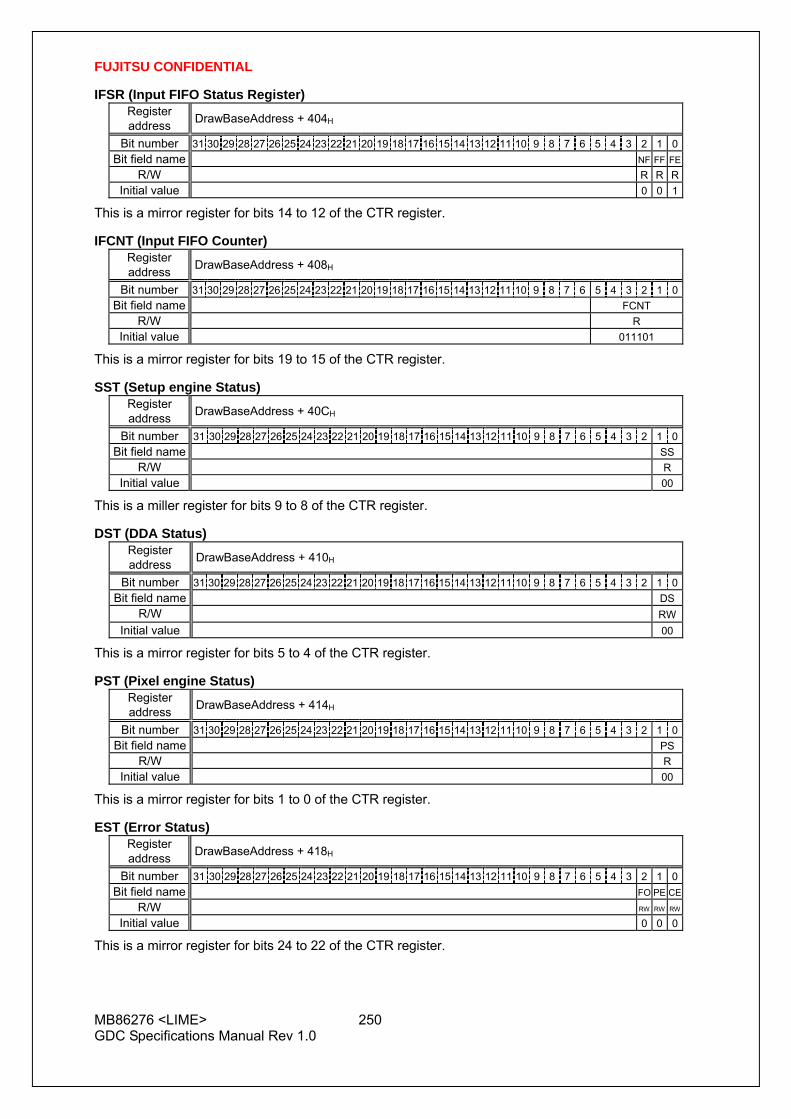
FUJITSU CONFIDENTIAL
MB86276 <LIME> 250 GDC Specifications Manual Rev 1.0
IFSR (Input FIFO Status Register) Register address DrawBaseAddress + 404H
Bit number 31 30 29 28 27 26 25 24 23 22 21 20 19 18 17 16 15 14 13 12 11 10 9 8 7 6 5 4 3 2 1 0Bit field name NF FF FE
R/W R R RInitial value 0 0 1
This is a mirror register for bits 14 to 12 of the CTR register.
IFCNT (Input FIFO Counter) Register address DrawBaseAddress + 408H
Bit number 31 30 29 28 27 26 25 24 23 22 21 20 19 18 17 16 15 14 13 12 11 10 9 8 7 6 5 4 3 2 1 0Bit field name FCNT
R/W R Initial value 011101
This is a mirror register for bits 19 to 15 of the CTR register.
SST (Setup engine Status) Register address DrawBaseAddress + 40CH
Bit number 31 30 29 28 27 26 25 24 23 22 21 20 19 18 17 16 15 14 13 12 11 10 9 8 7 6 5 4 3 2 1 0Bit field name SS
R/W RInitial value 00
This is a miller register for bits 9 to 8 of the CTR register.
DST (DDA Status) Register address DrawBaseAddress + 410H
Bit number 31 30 29 28 27 26 25 24 23 22 21 20 19 18 17 16 15 14 13 12 11 10 9 8 7 6 5 4 3 2 1 0Bit field name DS
R/W RWInitial value 00
This is a mirror register for bits 5 to 4 of the CTR register.
PST (Pixel engine Status) Register address DrawBaseAddress + 414H
Bit number 31 30 29 28 27 26 25 24 23 22 21 20 19 18 17 16 15 14 13 12 11 10 9 8 7 6 5 4 3 2 1 0Bit field name PS
R/W RInitial value 00
This is a mirror register for bits 1 to 0 of the CTR register.
EST (Error Status) Register address DrawBaseAddress + 418H
Bit number 31 30 29 28 27 26 25 24 23 22 21 20 19 18 17 16 15 14 13 12 11 10 9 8 7 6 5 4 3 2 1 0Bit field name FO PE CE
R/W RW RW RW
Initial value 0 0 0
This is a mirror register for bits 24 to 22 of the CTR register.

FUJITSU CONFIDENTIAL
MB86276 <LIME> 251 GDC Specifications Manual Rev 1.0
12.5.2 Drawing mode registers
When write to the registers, use the SetRegister command. The registers cannot be accessed from the CPU.
MDR0 (Mode Register for miscellaneous) Register address DrawBaseAddress + 420H
Bit number 31 30 29 28 27 26 25 24 23 22 21 20 19 18 17 16 15 14 13 12 11 10 9 8 7 6 5 4 3 2 1 0Bit field name ZP CF CY CX BSV BSH
R/W W0 RW W0 RW W0 RW RW W0 RW RWInitial value 0 00 0 0 00 00
Bit 1 to 0 BSH (Bitmap Scale Horizontal) Sets horizontal zoom ratio of bitmap draw 00 x1 01 x2 10 x1/2 01 Reserved Bit 3 to 2 BSV (Bitmap Scale Vertical) Sets vertical zoom ratio of bitmap draw 00 x1 01 x2 10 x1/2 01 Reserved Bit 8 CX (Clip X enable) Sets X coordinates clipping mode 0 Disabled 1 Enabled Bit 9 CY (Clip Y enable) Sets Y coordinates clipping mode 0 Disabled 1 Enabled Bit 16 and 15 CF (Color Format) Sets drawing color format 00 Indirect color mode (8 bits/pixel) 01 Direct color mode (16 bits/pixel) Bit 20 ZP (Z Precision) Sets the precision of the Z value used for erasing hidden planes. 16 bits/pixel 8 bits/pixel

FUJITSU CONFIDENTIAL
MB86276 <LIME> 252 GDC Specifications Manual Rev 1.0
MDR1 (Mode Register for LINE) Register address DrawBaseAddress + 424H
Bit number 31 30 29 28 27 26 25 24 23 22 21 20 19 18 17 16 15 14 13 12 11 10 9 8 7 6 5 4 3 2 1 0Bit field name LW BP BL LOG BM ZW ZCL ZC
R/W RW RW RW RW RW RW RW RW
Initial value 00000 0 0 0011 0 0 0000 0
This register sets the mode of line and pixel drawing.
Please set ZC bit ( bit 2 ) to 0 when draw BltCopyAltAlphaBlendP command.
Bit 2 ZC (Z Compare mode)
Sets Z comparison mode
0 Disabled
1 Enabled
Bit 5 to 3 ZCL (Z Compare Logic)
Selects type of Z comparison
000 NEVER
001 ALWAYS
010 LESS
011 LEQUAL
100 EQUAL
101 GEQUAL
110 GREATER
111 NOTEQUAL
Bit 6 ZW (Z Write mode)
Sets Z write mode
0 Writes Z values.
1 Not write Z values.
Bit 8 to 7 BM (Blend Mode)
Sets blend mode
00 Normal (source copy)
01 Alpha blending
10 Drawing with logic operation
11 Reserved
Bit 12 to 9 LOG (Logical operation)
Sets type of logic operation
0000 CLEAR
0001 AND
0010 AND REVERSE
0011 COPY
0100 AND INVERTED

FUJITSU CONFIDENTIAL
MB86276 <LIME> 253 GDC Specifications Manual Rev 1.0
0101 NOP
0110 XOR
0111 OR
1000 NOR
1001 EQUIV
1010 INVERT
1011 OR REVERSE
1100 COPY INVERTED
1101 OR INVERTED
1110 NAND
1111 SET
Bit 19 BL (Broken Line)
Selects line type
0 Solid line
1 Broken line
Bit 20 BP (Broken line Period)
Selects broken line cycle
0: 32 bits
1: 24 bits
Bit 28 to 24 LW (Line Width)
Sets line width for drawing line
00000 1 pixel
00001 2 pixels
: :
11111 32 pixels

FUJITSU CONFIDENTIAL
MB86276 <LIME> 254 GDC Specifications Manual Rev 1.0
MDR2 (Mode Register for Polygon) Register address DrawBaseAddress + 428H
Bit number 31 30 29 28 27 26 25 24 23 22 21 20 19 18 17 16 15 14 13 12 11 10 9 8 7 6 5 4 3 2 1 0Bit field name TT LOG BM ZW ZCL ZC SM
R/W W0 RW RW RW RW RW RW RW
Initial value 00 0011 0 0 0000 0 0
This register sets the polygon drawing mode.
Bit 0 SM (Shading Mode)
Sets shading mode
0 Flat shading
1 Gouraud shading
Bit 2 ZC (Z Compare mode)
Sets Z comparison mode
0 Disabled
1 Enabled
Bit 5 to 3 ZCL (Z Compare Logic)
Selects type of Z comparison
000 NEVER
001 ALWAYS
010 LESS
011 LEQUAL
100 EQUAL
101 GEQUAL
110 GREATER
111 NOTEQUAL
Bit 6 ZW (Z Write mask)
Sets Z write mode
0 Writes Z values
1 Not write Z values
Bit 8 to 7 BM (Blend Mode)
Sets blend mode
00 Normal (source copy)
01 Alpha blending
10 Drawing with logic operation
11 Reserved
Bit 12 to 9 LOG (Logical operation)
Sets type of logic operation

FUJITSU CONFIDENTIAL
MB86276 <LIME> 255 GDC Specifications Manual Rev 1.0
0000 CLEAR
0001 AND
0010 AND REVERSE
0011 COPY
0100 AND INVERTED
0101 NOP
0110 XOR
0111 OR
1000 NOR
1001 EQUIV
1010 INVERT
1011 OR REVERSE
1100 COPY INVERTED
1101 OR INVERTED
1110 NAND
1111 SET
Bit 29 to 28 TT (Texture-Tile Select)
Selects texture or tile pattern
00 Neither used
01 Enabled tiling
10 Enabled texture
11 Reserved
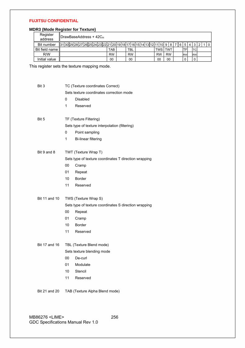
FUJITSU CONFIDENTIAL
MB86276 <LIME> 256 GDC Specifications Manual Rev 1.0
MDR3 (Mode Register for Texture) Register address DrawBaseAddress + 42CH
Bit number 31 30 29 28 27 26 25 24 23 22 21 20 19 18 17 16 15 14 13 12 11 10 9 8 7 6 5 4 3 2 1 0Bit field name TAB TBL TWS TWT TF TC
R/W RW RW RW RW RW RW
Initial value 00 00 00 00 0 0
This register sets the texture mapping mode.
Bit 3 TC (Texture coordinates Correct)
Sets texture coordinates correction mode
0 Disabled
1 Reserved
Bit 5 TF (Texture Filtering)
Sets type of texture interpolation (filtering)
0 Point sampling
1 Bi-linear filtering
Bit 9 and 8 TWT (Texture Wrap T)
Sets type of texture coordinates T direction wrapping
00 Cramp
01 Repeat
10 Border
11 Reserved
Bit 11 and 10 TWS (Texture Wrap S)
Sets type of texture coordinates S direction wrapping
00 Repeat
01 Cramp
10 Border
11 Reserved
Bit 17 and 16 TBL (Texture Blend mode)
Sets texture blending mode
00 De-curl
01 Modulate
10 Stencil
11 Reserved
Bit 21 and 20 TAB (Texture Alpha Blend mode)

FUJITSU CONFIDENTIAL
MB86276 <LIME> 257 GDC Specifications Manual Rev 1.0
Sets texture blending mode The stencil mode and the stencil alpha mode are enabled only when the MDR2 register blend mode (BM) is set to the alpha blending mode. If it is not set to the alpha blending mode, the stencil mode and stencil alpha mode perform the same function as the normal mode.
00 Normal
01 Stencil
10 Stencil alpha
11 Reserved

FUJITSU CONFIDENTIAL
MB86276 <LIME> 258 GDC Specifications Manual Rev 1.0
MDR4 (Mode Register for BLT) Register address DrawBaseAddress + 430H
Bit number 31 30 29 28 27 26 25 24 23 22 21 20 19 18 17 16 15 14 13 12 11 10 9 8 7 6 5 4 3 2 1 0Bit field name LOG BM TE
R/W RW RW RW
Initial value 0011 00 0
This register controls the BLT mode.
Bit 1 TE (Transparent Enable)
Sets transparent mode
0: Not perform transparent processing
1: Not draw pixels that corresponds to set transparent color in BLT (transparancy copy) Note: Set the blend mode (BM) to normal.
Bit 8 to 7 BM (Blend Mode)
Sets blend mode
00 Normal (source copy)
01 Reserved
10 Drawing with logic operation
11 Reserved
Bit 12 to 9 LOG (Logical operation)
Sets logic operation
0000 CLEAR
0001 AND
0010 AND REVERSE
0011 COPY
0100 AND INVERTED
0101 NOP
0110 XOR
0111 OR
1000 NOR
1001 EQUIV
1010 INVERT
1011 OR REVERSE
1100 COPY INVERTED
1101 OR INVERTED
1110 NAND
1111 SET

FUJITSU CONFIDENTIAL
MB86276 <LIME> 259 GDC Specifications Manual Rev 1.0
FBR (Frame buffer Base) Register address DrawBaseAddress + 440H
Bit number 31 30 29 28 27 26 25 24 23 22 21 20 19 18 17 16 15 14 13 12 11 10 9 8 7 6 5 4 3 2 1 0Bit field name FBASE
R/W RW R0 Initial value Don’t care 0
This register stores the base address of the drawing frame.
XRES (X Resolution) Register address DrawBaseAddress + 444H
Bit number 31 30 29 28 27 26 25 24 23 22 21 20 19 18 17 16 15 14 13 12 11 10 9 8 7 6 5 4 3 2 1 0Bit field name XRES
R/W RW Initial value Don’t care
This register sets the drawing frame horizontal resolution.
ZBR (Z buffer Base) Register address DrawBaseAddress + 448H
Bit number 31 30 29 28 27 26 25 24 23 22 21 20 19 18 17 16 15 14 13 12 11 10 9 8 7 6 5 4 3 2 1 0Bit field name ZBASE
R/W RW R0 Initial value Don’t care 0
This register sets the Z buffer base address.
TBR (Texture memory Base) Register address DrawBaseAddress + 44CH
Bit number 31 30 29 28 27 26 25 24 23 22 21 20 19 18 17 16 15 14 13 12 11 10 9 8 7 6 5 4 3 2 1 0Bit field name TBASE
R/W RW R0 Initial value Don’t care 0
This register sets the texture memory base address.
PFBR (2D Polygon Flag-Buffer Base) Register address DrawBaseAddress + 450H
Bit number 31 30 29 28 27 26 25 24 23 22 21 20 19 18 17 16 15 14 13 12 11 10 9 8 7 6 5 4 3 2 1 0
Bit field name PFBASE R/W RW R0
Initial value Don’t care 0
This register sets the polygon flag buffer base address.
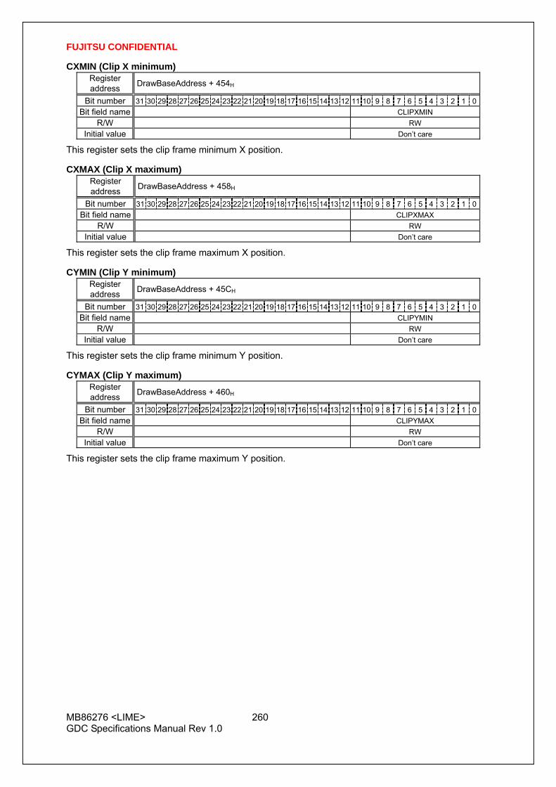
FUJITSU CONFIDENTIAL
MB86276 <LIME> 260 GDC Specifications Manual Rev 1.0
CXMIN (Clip X minimum) Register address DrawBaseAddress + 454H
Bit number 31 30 29 28 27 26 25 24 23 22 21 20 19 18 17 16 15 14 13 12 11 10 9 8 7 6 5 4 3 2 1 0Bit field name CLIPXMIN
R/W RW Initial value Don’t care
This register sets the clip frame minimum X position.
CXMAX (Clip X maximum) Register address DrawBaseAddress + 458H
Bit number 31 30 29 28 27 26 25 24 23 22 21 20 19 18 17 16 15 14 13 12 11 10 9 8 7 6 5 4 3 2 1 0Bit field name CLIPXMAX
R/W RW Initial value Don’t care
This register sets the clip frame maximum X position.
CYMIN (Clip Y minimum) Register address DrawBaseAddress + 45CH
Bit number 31 30 29 28 27 26 25 24 23 22 21 20 19 18 17 16 15 14 13 12 11 10 9 8 7 6 5 4 3 2 1 0Bit field name CLIPYMIN
R/W RW Initial value Don’t care
This register sets the clip frame minimum Y position.
CYMAX (Clip Y maximum) Register address DrawBaseAddress + 460H
Bit number 31 30 29 28 27 26 25 24 23 22 21 20 19 18 17 16 15 14 13 12 11 10 9 8 7 6 5 4 3 2 1 0Bit field name CLIPYMAX
R/W RW Initial value Don’t care
This register sets the clip frame maximum Y position.

FUJITSU CONFIDENTIAL
MB86276 <LIME> 261 GDC Specifications Manual Rev 1.0
TXS (Texture Size) Register address DrawBaseAddress + 464H
Bit number 31 30 29 28 27 26 25 24 23 22 21 20 19 18 17 16 15 14 13 12 11 10 9 8 7 6 5 4 3 2 1 0Bit field name TXSN TXSM
R/W RW RW Initial value 000010000000 000010000000
This register specifies the texture size (m, n).
Bit 12 to 0 TXSM (Texture Size M)
Sets horizontal texture size. Any power of 2 between 4 and 4096 can be used. Values that are not a power of 2 cannot be used.
0_0000_0000_0100 M=4 0_0010_0000_0000 M=512
0_0000_0000_1000 M=8 0_0100_0000_0000 M=1024
0_0000_0001_0000 M=16 0_1000_0000_0000 M=2048
0_0000_0010_0000 M=32 1_0000_0000_0000 M=4096
0_0000_0100_0000 M=64
0_0000_1000_0000 M=128
0_0001_0000_0000 M=256 Other than the above Setting disabled
Bit 28 to 16 TXSN (Texture Size N)
Sets vertical texture size. Any power of 2 between 4 and 4096 can be used. Values that are not a power of 2 cannot be used.
0_0000_0000_0100 N=4 0_0010_0000_0000 N=512
0_0000_0000_1000 N=8 0_0100_0000_0000 N=1024
0_0000_0001_0000 N=16 0_1000_0000_0000 N=2048
0_0000_0010_0000 N=32 1_0000_0000_0000 N=4096
0_0000_0100_0000 N=64
0_0000_1000_0000 N=128
0_0001_0000_0000 N=256 Other than the above Setting disabled
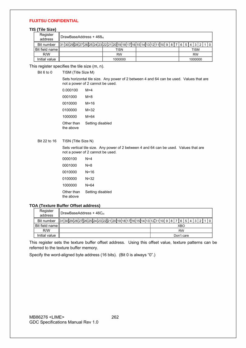
FUJITSU CONFIDENTIAL
MB86276 <LIME> 262 GDC Specifications Manual Rev 1.0
TIS (Tile Size) Register address DrawBaseAddress + 468H
Bit number 31 30 29 28 27 26 25 24 23 22 21 20 19 18 17 16 15 14 13 12 11 10 9 8 7 6 5 4 3 2 1 0Bit field name TISN TISM
R/W RW RW Initial value 1000000 1000000
This register specifies the tile size (m, n). Bit 6 to 0 TISM (Title Size M)
Sets horizontal tile size. Any power of 2 between 4 and 64 can be used. Values that are not a power of 2 cannot be used.
0.000100 M=4
0001000 M=8
0010000 M=16
0100000 M=32
1000000 M=64
Other than the above
Setting disabled
Bit 22 to 16 TISN (Title Size N)
Sets vertical tile size. Any power of 2 between 4 and 64 can be used. Values that are not a power of 2 cannot be used.
0000100 N=4
0001000 N=8
0010000 N=16
0100000 N=32
1000000 N=64
Other than the above
Setting disabled
TOA (Texture Buffer Offset address) Register address DrawBaseAddress + 46CH
Bit number 31 30 29 28 27 26 25 24 23 22 21 20 19 18 17 16 15 14 13 12 11 10 9 8 7 6 5 4 3 2 1 0Bit field name XBO
R/W RW Initial value Don’t care
This register sets the texture buffer offset address. Using this offset value, texture patterns can be referred to the texture buffer memory.
Specify the word-aligned byte address (16 bits). (Bit 0 is always “0”.)

FUJITSU CONFIDENTIAL
MB86276 <LIME> 263 GDC Specifications Manual Rev 1.0
ABR (Alpha map Base) Register address DrawBaseAddress + 474H
Bit number 31 30 29 28 27 26 25 24 23 22 21 20 19 18 17 16 15 14 13 12 11 10 9 8 7 6 5 4 3 2 1 0Bit field name ABASE
R/W RW R0 Initial value Don’t care 0
This register sets the base address of the alpha map.
FC (Foreground Color) Register address DrawBaseAddress + 480H
Bit number 31 30 29 28 27 26 25 24 23 22 21 20 19 18 17 16 15 14 13 12 11 10 9 8 7 6 5 4 3 2 1 0
0
This register sets the drawing foreground color. This color is for the object color for flat shading and foreground color for bitmap drawing and broken line drawing. All bits set to “1” are drawn in the color set at this register.
8 bit color mode: Bit 7 to 0 FGC8 (Foreground 8 bit Color)
Sets the indirect color for the foreground (color index code).
Bit 31 to 8 These bits are not used.
16 bit color mode: Bit 15 to 0 FGC16 (Foreground 16 bit Color)
This field sets the 16-bit direct color for the foreground. Note that the handling of bit 15 is different from that in ORCHID. Up to ORCHID, bit 15 is “0” for other than bit map and rectangular drawing, but starting with LIME GDC, the setting value is reflected in memory as is. This bit is also reflected in bit 15 of the 16-bit color at Gouraud shading.
Bit 31 to 16 These bits are not used.

FUJITSU CONFIDENTIAL
MB86276 <LIME> 264 GDC Specifications Manual Rev 1.0
BC (Background Color) Register address DrawBaseAddress + 484H
Bit number 31 30 29 28 27 26 25 24 23 22 21 20 19 18 17 16 15 14 13 12 11 10 9 8 7 6 5 4 3 2 1 0Bit field name BGC8/16
R/W RW Initial value 0
This register sets the drawing frame background color. This color is used for the background color of bitmap drawing and broken line drawing. At bitmap drawing, all bits set to “0” are drawn in the color set at this register.
BT bit of this register allows the background color of be transparent (no drawing).
8 bit color mode: Bit 7 to 0 BGC8 (Background 8 bit Color)
Sets the indirect color for the background (color index code)
Bit 14 to 8 Not used
Bit 15 BT (Background Transparency)
Sets the transparent mode for the background color
0 Background drawn using color set for BGC field
1 Background not drawn (transparent)
Bit 31 to 16 Not used
16 bit color mode: Bit 14 to 0 BGC16 (Background 16 bit Color)
Sets 16-bit direct color (RGB) for the background
Bit 15 BT (Background Transparency)
Sets the transparent mode for the background color
0 Background drawn using color set for BGC field
1 Background not drawn (transparent)
Bit 31 to 16 Not used

FUJITSU CONFIDENTIAL
MB86276 <LIME> 265 GDC Specifications Manual Rev 1.0
ALF (Alpha Factor) Register address DrawBaseAddress + 488H
Bit number 31 30 29 28 27 26 25 24 23 22 21 20 19 18 17 16 15 14 13 12 11 10 9 8 7 6 5 4 3 2 1 0Bit field name A
R/W RW Initial value 0
This register sets the alpha blending coefficient.
BLP (Broken Line Pattern) Register address DrawBaseAddress + 48CH
Bit number 31 30 29 28 27 26 25 24 23 22 21 20 19 18 17 16 15 14 13 12 11 10 9 8 7 6 5 4 3 2 1 0Bit field name BLP
R/W RW Initial value 0
This register sets the broken-line pattern. The bit 1 set in the broken-line pattern is drawn in the foreground color and bit 0 is drawn in the background color. The line pattern for 1 pixel line is laid out in the direction of MSB to LSB and when it reaches LSB, it goes back to MSB. The BLPO register manages the bit numbers of the broken-line pattern. 32 or 24 bits can be selected as the repetition of the broken-line pattern by the BP bit of the MDR1 register. When 24 bits are selected, bits 23 to 0 of the BLP register are used.
TBC (Texture Border Color) Register address DrawBaseAddress + 494H
Bit number 31 30 29 28 27 26 25 24 23 22 21 20 19 18 17 16 15 14 13 12 11 10 9 8 7 6 5 4 3 2 1 0Bit field name BC8/16
R/W RW Initial value 0
This register sets the border color for texture mapping. 8 bit color mode:
Bit 7 to 0 BC8 (Border Color) Sets the 8-bit direct color for the texture border color
16 bit color mode:
Bit 15 to 0 BC16 (Border Color) Sets the 16-bit direct color for the texture border color Bit15 is used for controlling a stencil and stencil alpha
BLPO (Broken Line Pattern Offset) Register address DrawBaseAddress + 3E0H
Bit number 31 30 29 28 27 26 25 24 23 22 21 20 19 18 17 16 15 14 13 12 11 10 9 8 7 6 5 4 3 2 1 0Bit field name BCR
R/W RW Initial value 11111
This register stores the bit number of the broken-line pattern set to BLP registers, for broken line drawing. This value is decremented at each pixel drawing. Broken line can be drawn starting from any starting position of the specified broken-line pattern by setting any value at this register. When no write is performed, the position of broken-line pattern is sustained.
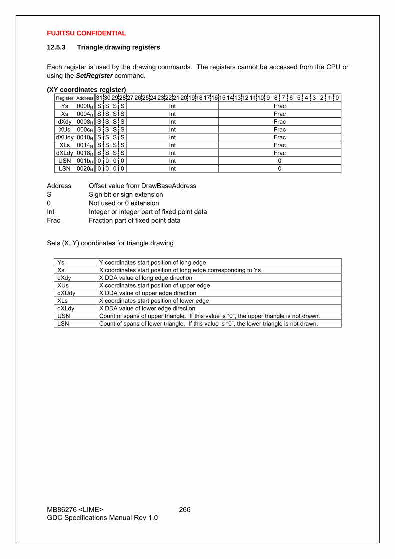
FUJITSU CONFIDENTIAL
MB86276 <LIME> 266 GDC Specifications Manual Rev 1.0
12.5.3 Triangle drawing registers
Each register is used by the drawing commands. The registers cannot be accessed from the CPU or using the SetRegister command.
(XY coordinates register) Register Address 31 30 29 28 27 26 25 24 23 22 21 20 19 18 17 16 15 14 13 12 11 10 9 8 7 6 5 4 3 2 1 0
Ys 0000H S S S S Int Frac Xs 0004H S S S S Int Frac
dXdy 0008H S S S S Int Frac XUs 000cH S S S S Int Frac
dXUdy 0010H S S S S Int Frac XLs 0014H S S S S Int Frac
dXLdy 0018H S S S S Int Frac USN 001bH 0 0 0 0 Int 0 LSN 0020H 0 0 0 0 Int 0
Address Offset value from DrawBaseAddress S Sign bit or sign extension 0 Not used or 0 extension Int Integer or integer part of fixed point data Frac Fraction part of fixed point data
Sets (X, Y) coordinates for triangle drawing
Ys Y coordinates start position of long edge Xs X coordinates start position of long edge corresponding to Ys dXdy X DDA value of long edge direction XUs X coordinates start position of upper edge dXUdy X DDA value of upper edge direction XLs X coordinates start position of lower edge dXLdy X DDA value of lower edge direction USN Count of spans of upper triangle. If this value is “0”, the upper triangle is not drawn. LSN Count of spans of lower triangle. If this value is “0”, the lower triangle is not drawn.

FUJITSU CONFIDENTIAL
MB86276 <LIME> 267 GDC Specifications Manual Rev 1.0
(Color setting register) Register Address 31 30 29 28 27 26 25 24 23 22 21 20 19 18 17 16 15 14 13 12 11 10 9 8 7 6 5 4 3 2 1 0
Rs 0040H 0 0 0 0 0 0 0 0 Int Frac dRdx 0044H S S S S S S S S Int Frac dRdy 0048H S S S S S S S S Int Frac Gs 004CH 0 0 0 0 0 0 0 0 Int Frac
dGdx 0050H S S S S S S S S Int Frac dGdy 0054H S S S S S S S S Int Frac
Bs 0058H 0 0 0 0 0 0 0 0 Int Frac dBdx 005cH S S S S S S S S Int Frac dBdy 0060H S S S S S S S S Int Frac As 0064H 0 0 0 0 0 0 0 0 Int Frac
dAdx 0068H S S S S S S S S Int Frac dAdy 006cH S S S S S S S S Int Frac
Address Offset from DrawBaseAddress S Sign bit or sign extension 0 Not used or 0 extension Int Integer or integer part of fixed point data Frac Fraction part of fixed point data
Sets color parameters for triangle drawing. These parameters are enabled in the Gouraud shading mode.
Rs R value at (Xs, Ys, Zs) of long edge corresponding to Ys dRdx R DDA value of horizontal direction dRdy R DDA value of long edge Gs G value at (Xs, Ys, Zs) of long edge corresponding to Ys dGdx G DDA value of horizontal direction dGdy G DDA value of long edge Bs B value at (Xs, Ys, Zs) of long edge corresponding to Ys dBdx B DDA value of horizontal direction dBdy B DDA value of long edge As Alpha value at (Xs, Ys, Zs) of long edge corresponding to Ys dAdx Alpha DDA value of horizontal direction dAdy Alpha DDA value of long edge
(Z coordinates register) Register Address 31 30 29 28 27 26 25 24 23 22 21 20 19 18 17 16 15 14 13 12 11 10 9 8 7 6 5 4 3 2 1 0
Zs 0080h 0 Int Frac dZdx 0084h S Int Frac dZdy 008ch S Int Frac
Address Offset from DrawBaseAddress S Sign bit or sign extension 0 Not used or 0 extension Int Integer or integer part of fixed point data Frac Fraction part of fixed point data
Sets Z coordinates for 3D triangle drawing
Zs Z coordinate start position of long edge dZdx Z DDA value of horizontal direction dZdy Z DDA value of long edge

FUJITSU CONFIDENTIAL
MB86276 <LIME> 268 GDC Specifications Manual Rev 1.0
(Texture coordinates-setting register) Register Address 31 30 29 28 27 26 25 24 23 22 21 20 19 18 17 16 15 14 13 12 11 10 9 8 7 6 5 4 3 2 1 0
Ss 00c0H S S S Int Frac dSdx 00c4H S S S Int Frac dSdy 00c8H S S S Int Frac
Ts 00ccH S S S Int Frac dTdx 00d0H S S S Int Frac dTdy 00d4H S S S Int Frac Qs 00d8H 0 0 0 0 0 0 0 Int Frac
dQdx 00dcH S S S S S S S Int Frac dQdy 00e0H S S S S S S S Int Frac
Address Offset from DrawBaseAddress S Sign bit or sign extension 0 Not used or 0 extension Int Integer or integer part of fixed point data Frac Fraction part of fixed point data
Sets texture coordinates parameters for triangle drawing
Ss S texture coordinates (Xs, Ys, Zs) of long edge corresponding to Ys dSdx S DDA value of horizontal direction dSdy S DDA value of long edge direction Ts T texture coordinates (Xs, Ys, Zs) of long edge corresponding to Ys dTdx T DDA value of horizontal direction dTdy T DDA value of long edge direction Qs Q (Perspective correction value) of texture at (Xs, Ys, Zs) of long edge corresponding to YsdQdx Q DDA value of horizontal direction dQdy Q DDA value of long edge direction

FUJITSU CONFIDENTIAL
MB86276 <LIME> 269 GDC Specifications Manual Rev 1.0
12.5.4 Line drawing registers
Each register is used by the drawing commands. The registers cannot be accessed from the CPU or by using the SetRegister command.
(Coordinates setting register) Register Address 31 30 29 28 27 26 25 24 23 22 21 20 19 18 17 16 15 14 13 12 11 10 9 8 7 6 5 4 3 2 1 0LPN 0140H 0 0 0 0 Int 0 LXs 0144H S S S S Int Frac
LXde 0148H S S S S S S S S S S S S S S S Int Frac LYs 014cH S S S S Int Frac
LYde 0150H S S S S S S S S S S S S S S S Int Frac LZs 0154H S Int Frac
LZde 0158H S Int Frac Address Offset from DrawBaseAddress S Sign bit or sign extension 0 Not used or 0 extension Int Integer or integer part of fixed point data Frac Fraction part of fixed point data
Sets coordinates parameters for line drawing
LPN Pixel count of principal axis direction
LXs X coordinates start position of draw line (In principal axis X) Integer value of X coordinates rounded off (In principal axis Y) X coordinates in form of fixed point data
LXde Inclination data for X coordinates (In principal axis X) Increment or decrement according to drawing direction (In principal axis Y) Fraction part of DX/DY
LYs Y coordinates start position of draw line (In principal axis X) Y coordinates in form of fixed point data (In principal axis Y) Integer value of Y coordinates rounded off
LYde Inclination data for Y coordinates (In principal axis X) Fraction part of DY/DX (In principal axis Y) Increment or decrement according to drawing direction
LZs Z coordinates start position of line drawing line
LZde Z Inclination

FUJITSU CONFIDENTIAL
MB86276 <LIME> 270 GDC Specifications Manual Rev 1.0
12.5.5 Pixel drawing registers
Each register is used by the drawing commands. The registers cannot be accessed from the CPU or using the SetRegister command.
Register Address 31 30 29 28 27 26 25 24 23 22 21 20 19 18 17 16 15 14 13 12 11 10 9 8 7 6 5 4 3 2 1 0PXdc 0180H 0 0 0 0 Int 0 PYdc 0184H 0 0 0 0 Int 0 PZdc 0188H 0 0 0 0 Int 0
Address Offset from DrawBaseAddress S Sign bit or sign extension 0 Not used or 0 extension Int Integer or integer part of fixed point data Frac Fraction part of fixed point data
Sets coordinates parameter for drawing pixel. The foreground color is used.
PXdc Sets X coordinates position PYdc Sets Y coordinates position PZdc Sets Z coordinates position
12.5.6 Rectangle drawing registers
Each register is used by the drawing commands. The registers cannot be accessed from the CPU or using the SetRegister command.
Register Address 31 30 29 28 27 26 25 24 23 22 21 20 19 18 17 16 15 14 13 12 11 10 9 8 7 6 5 4 3 2 1 0RXs 0200H 0 0 0 0 Int 0 Rys 0204H 0 0 0 0 Int 0
RsizeX 0208H 0 0 0 0 Int 0 RsizeY 020cH 0 0 0 0 Int 0
Address Offset from DrawBaseAddress S Sign bit or sign extension 0 Not used or 0 extension Int Integer or integer part of fixed point data Frac Fraction part of fixed point data
Sets coordinates parameters for rectangle drawing. The foreground color is used.
RXs Sets the X coordinates of top left vertex Rys Sets the Y coordinates of top left vertex RsizeX Sets horizontal size RsizeY Sets vertical size

FUJITSU CONFIDENTIAL
MB86276 <LIME> 271 GDC Specifications Manual Rev 1.0
12.5.7 Blt registers
Sets the parameters of each register as described below:
Set the Tcolor register with the SetRegister command.
Note that the Tcolor register cannot be set at access from the CPU and by drawing commands.
Each register except the Tcolor register is set by executing a drawing command.
Note that access from the CPU and the SetRegister command cannot be used.
Register Address 31 30 29 28 27 26 25 24 23 22 21 20 19 18 17 16 15 14 13 12 11 10 9 8 7 6 5 4 3 2 1 0SADDR 0240H 0 0 0 0 0 0 0 Address SStride 0244H 0 0 0 0 Int 0 SRXs 0248H 0 0 0 0 Int 0 SRYs 024cH 0 0 0 0 Int 0
DADDR 0250H 0 0 0 0 0 0 0 Address DStride 0254H 0 0 0 0 Int 0 DRXs 0258H 0 0 0 0 Int 0 DRYs 025cH 0 0 0 0 Int 0 BRsizeX 0260H 0 0 0 0 Int 0 BRsizeY 0264H 0 0 0 0 Int 0 TColor 0280H 0 Color
Address Offset from DrawBaseAddress S Sign bit or sign extension 0 Not used or 0 extension Int Integer or integer part of fixed point data Frac Fraction part of fixed point data
Sets parameters for Blt operations
SADDR Sets start address of source rectangle area in byte address
SStride Sets stride of source
SRXs Sets X coordinates start position of source rectangle area
SRYs Sets Y coordinates start position of source rectangle area
DADDR Sets start address of destination rectangle area in byte address
DStride Sets stride of destination
DRXs Sets X coordinates start position of destination rectangle area
DRYs Sets Y coordinates start position of destination rectangle area
BRsizeX Sets horizontal size of rectangle
BRsizeY Sets vertical size of rectangle
Tcolor Sets transparent color For indirect color, set a palette code in the lower 8 bits.

FUJITSU CONFIDENTIAL
MB86276 <LIME> 272 GDC Specifications Manual Rev 1.0
12.5.8 2D line with XY setup drawing registers
Each register is used by the drawing commands. The registers cannot be accessed from the CPU.
Register Address 31 30 29 28 27 26 25 24 23 22 21 20 19 18 17 16 15 14 13 12 11 10 9 8 7 6 5 4 3 2 1 0LX0dc 0540H 0 0 0 0 Int 0 LY0dc 0544H 0 0 0 0 Int 0 LX1dc 0548H 0 0 0 0 Int 0 LY1dc 054cH 0 0 0 0 Int 0
Address Offset from DrawBaseAddress S Sign bit or sign extension 0 Not used or 0 extension Int Integer or integer part of fixed point data Frac Fraction part of fixed point data
Sets coordinates of line end points for 2D Line with XY setup drawing
LX0dc Sets X coordinates of vertex V0
LY0dc Sets Y coordinates of vertex V0
LX1dc Sets X coordinates of vertex V1
LY1dc Sets Y coordinates of vertex V1

FUJITSU CONFIDENTIAL
MB86276 <LIME> 273 GDC Specifications Manual Rev 1.0
12.5.9 2D triangle with XY setup drawing registers
Each register is used by the drawing commands. The registers cannot be accessed from the CPU or using the SetRegister command.
Register Address 31 30 29 28 27 26 25 24 23 22 21 20 19 18 17 16 15 14 13 12 11 10 9 8 7 6 5 4 3 2 1 0X0dc 0580h 0 0 0 0 Int 0 Y0dc 0584h 0 0 0 0 Int 0 X1dc 0588h 0 0 0 0 Int 0 Y1dc 058ch 0 0 0 0 Int 0 X2dc 0590h 0 0 0 0 Int 0 Y2dc 0594h 0 0 0 0 Int 0
Address Offset from DrawBaseAddress S Sign bit or sign extension 0 Not used or 0 extension Int Integer or integer part of fixed point data Frac Fraction part of fixed point data
Sets coordinates of three vertices for 2D Triangle with XY setup drawing
X0dc Sets X coordinates of vertex V0
Y0dc Sets Y coordinates of vertex V0
X1dc Sets X coordinates of vertex V1
Y1dc Sets Y coordinates of vertex V1
X2dc Sets X coordinates of vertex V2
Y2dc Sets Y coordinates of vertex V2

FUJITSU CONFIDENTIAL
MB86276 <LIME> 274 GDC Specifications Manual Rev 1.0
12.5.10 Display list FIFO registers
DFIFO (Displaylist FIFO) Register address DrawBaseAddress+ 4A0H
Bit number 31 30 29 28 27 26 25 24 23 22 21 20 19 18 17 16 15 14 13 12 11 10 9 8 7 6 5 4 3 2 1 0Bit field name DFIFO
R/W W Initial value Don’t care
FIFO registers for Display List transfer

FUJITSU CONFIDENTIAL
MB86276 <LIME> 275 GDC Specifications Manual Rev 1.0
13 TIMING DIAGRAM 13.1 Graphics Memory Interface
The LIME GDC access timing and graphics memory access timing are explained here.
13.1.1 Timing of read access to same row address
Timing of Read Access to Same Row Address
The above timing diagram shows that read access is made four times from LIME to the same row address of SDRAM. The ACTV command is issued and then the READ command is issued after TRCD elapses. Then data that is output after the elapse of CL after the READ command is issued is captured into LIME.
MCLKO
CL
TRCD
MA
MWE
MCAS
MRAS
MD
ROW COL
DATA DATA DATA DATA
COL COL COL
ROW: Row Address COL: Column Address DATA: READ DATA
TRCD: RAS to CAS Delay Time CL: CAS Latency
DQM
*Timing when CL2 operating

FUJITSU CONFIDENTIAL
MB86276 <LIME> 276 GDC Specifications Manual Rev 1.0
13.1.2 Timing of read access to different row addresses
Timing of Read Access to Different Row Addresses
The above timing diagram shows that read access is made from LIME to different row addresses of SDRAM. The first and next address to be read fall across an SDRAM page boundary, so the Pre-charge command is issued at the timing satisfying TRAS, and then after the elapse of TRP, the ACTV command is reissued, and then the READ command is issued.
ROW: Row Address COL: Column Address DATA: READ DATA
TRAS: RAS Active Time TRCD: RAS to CAS Delay Time CL: CAS Latency
TRP: RAS Precharge Time
MCLKO
TRAS
CL
TRCD
MA
MWE
MCAS
MRAS
MD
ROW COL
DATA
TRP
ROW COL
TRCD
CL
DATA
DQM
*Timing when CL2 operating

FUJITSU CONFIDENTIAL
MB86276 <LIME> 277 GDC Specifications Manual Rev 1.0
13.1.3 Timing of write access to same row address
Timing of Write Access to Same Row Address
The above timing diagram shows that write access is made form times form LIME to the same row address of SDRAM.
The ACTV command is issued, and then after the elapse of TRCD, the WRITE command is issued to write to SDRAM.
MCLKO
TRCD
MA
MWE
MCAS
MRAS
MD
ROW COL
DATA DATA DATA DATA
COL COL COL
ROW: Row Address COL: Column Address DATA: READ DATA
TRCD: RAS to CAS Delay Time
DQM

FUJITSU CONFIDENTIAL
MB86276 <LIME> 278 GDC Specifications Manual Rev 1.0
13.1.4 Timing of write access to different row addresses
Timing of Write Access to Different Row Addresses
The above timing diagram shows that write access is made from LIME to different row addresses of SDRAM. The first and next address to be write fall across an SDRAM page boundary, so the Pre-charge command is issued at the timing satisfying TRAS, and then after the elapse of TRP, the ACTV command is reissued, and then the WRITE command is issued.
ROW: Row Address COL: Column Address DATA: READ DATA
TRAS: RAS Active Time TRCD: RAS to CAS Delay Time TRP: RAS Precharge Time
MCLKO
TRAS
TRCD
MA
MWE
MCAS
MRAS
MD
ROW COL
DATA
TRP
ROW COL
TRCD
DATA
DQM

FUJITSU CONFIDENTIAL
MB86276 <LIME> 279 GDC Specifications Manual Rev 1.0
13.1.5 Timing of read/write access to same row address
Timing of Read/Write Access to Same Row Address
The above timing diagram shows that write access is made immediately after read access is made from LIME to the same row address of SDRAM.
Read data is output from SDRAM, LOWD elapses, and then the WRITE command is issued.
ROW: Row Address COL: Column Address DATA: READ DATA
TRAS: RAS Active Time TRCD: RAS to CAS Delay Time CL: CAS Latency
TRP: RAS Precharge Time LOWD: Last Output to Write Command Delay
MCLKO
CL
TRCD
MA
MWE
MCAS
MRAS
MD
ROW COL
DATA DATA
DQM
Timing when CL2 operating
LOWD
COL

FUJITSU CONFIDENTIAL
MB86276 <LIME> 280 GDC Specifications Manual Rev 1.0
13.1.6 Delay between ACTV commands
Delay between ACTV Commands
The ACTV command is issued from LIME GDC to the row address of SDRAM after the elapse of TRRD after issuance of the previous ACTV command.
13.1.7 Delay between Refresh command and next ACTV command
Delay between Refresh Command and Next ACTV Command
The ACTV command is issued after the elapse of TRC after issuance of the Refresh command.
ROW: Row Address TRRD: RAS to RAS Bank Active Delay Time
MCLKO
MA
MWE
MCAS
MRAS
ROW ROW
TRRD
ROW: Row Address TRC: RAS Cycle Time
MCLKO
MA
MWE
MCAS
MRAS
ROW
TRC

FUJITSU CONFIDENTIAL
MB86276 <LIME> 281 GDC Specifications Manual Rev 1.0
13.2 Display Timing 13.2.1 Non-interlace mode
Non-interlace Timing
In the above diagram, VTR, HDP, etc., are the setting values of their associated registers.
The VSYNC/frame interrupt is asserted when display of the last raster ends. When updating display parameters, synchronize with the frame interrupt so no display disturbance occurs. Calculation for the next frame is started immediately after the vertical synchronization pulse is asserted, so the parameters must be updated by the time that calculation is started.
VSYNC is output 1 dot clock faster than HSYNC.
VDP+1 rasters
VSYNC
HSYNC
VSP+1 rasters
VTR+1 rasters
VSW+1 rasters
HDP+1 clocks
HSP+1 clocks
HTP+1 clocks
HSW+1 clocks
HSYNC
Ri/Gi/Bi
Assert Frame InterruptAssert Vsync Interrupt
Latency= 13 clocks
DISPE
Ri/Gi/Bi
DISPE
DCLKO
0 1 2 n−1n−2 n=HDP+1
Ri/Gi/Bi

FUJITSU CONFIDENTIAL
MB86276 <LIME> 282 GDC Specifications Manual Rev 1.0
13.2.2 Interlace video mode
Interlace Video Timing
In the above diagram, VTR, HDP, etc., are the setting values of their associated registers.
The interlace mode also operates at the same timing as the interlace video mode. The only difference between the two modes is the output image data.
VDP+1 rasters
VSYNC
HSYNC
VSP+1 rasters
VTR+1 rasters (odd field)
VSW+1 rasters
VTR+1 rasters (even field)VSW+1 rasters
VSYNC
HSYNC
VDP+1 rasters
VSP+1 rasters
Assert Vsync Interrupt
Assert Vsync Interrupt
Assert Frame Interrupt
Ri/Gi/Bi
Ri/Gi/Bi
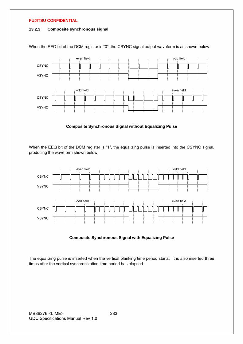
FUJITSU CONFIDENTIAL
MB86276 <LIME> 283 GDC Specifications Manual Rev 1.0
13.2.3 Composite synchronous signal
When the EEQ bit of the DCM register is “0”, the CSYNC signal output waveform is as shown below.
Composite Synchronous Signal without Equalizing Pulse
When the EEQ bit of the DCM register is “1”, the equalizing pulse is inserted into the CSYNC signal, producing the waveform shown below.
Composite Synchronous Signal with Equalizing Pulse
The equalizing pulse is inserted when the vertical blanking time period starts. It is also inserted three times after the vertical synchronization time period has elapsed.
CSYNC
VSYNC
CSYNC
VSYNC
odd field
even field odd field
even field
CSYNC
VSYNC
CSYNC
VSYNC
odd field
even field odd field
even field

FUJITSU CONFIDENTIAL
MB86276 <LIME> 284 GDC Specifications Manual Rev 1.0
13.3 Host interface Timing 13.3.1 CPU read/write timing diagram in SH3 mode (Normally Not Ready Mode)
( MODE[2:0]=000, RDY_MODE=0, BS_MODE=0)
T1: Read/write start cycle (XRDY in wait state)
Tsw*: Software wait insertion cycle (1 cycle setting) Thw*: Hardware wait insertion cycle (XRDY cancels the wait state after the preparations)
T2: Read/write end cycle (XRDY ends in wait state)
Fig. Read/Write Timing Diagram for SH3 (Normally Not Ready Mode)
BCLKI
A[24:2]
XCS
T1 Tsw1 Thw1 T2 T1 Tsw1 Thw1 Thw2 Thw3 T2
XBS
XRD
Hi-Z Hi-ZD[31:0] Valid DataValid Data
Hi-Z
XWE[3:0]
XWAIT
D[31:0]
SoftWait HardWait NotWait
Hi-Z
SoftWait HardWait HardWait HardWait
Valid Data IN Valid Data IN
Hi-Z
: XWAIT sampling in SH3 mode
×: Soft Wait (1 cycle) in SH3 mode
Not Wait
At R
ead
At W
rite

FUJITSU CONFIDENTIAL
MB86276 <LIME> 285 GDC Specifications Manual Rev 1.0
13.3.2 CPU read/write timing diagram in SH3 mode (Normally Ready Mode)
( MODE[2:0]=000, RDY_MODE=1, BS_MODE=0)
T1: Read/write start cycle (XRDY in not wait state)
Tsw*: Software wait insertion cycle (2-cycle setting required)
Thw*: Hardware wait insertion cycle (In hardware state when the immediate accessing is disabled)
T2: Read/write end cycle (XRDY ends in not wait state)
Fig. Read/Write Timing Diagram for SH3 (Normally Ready Mode)
Hi-Z Hi-Z
Hi-Z
BCLKI
A[24:2]
XCS
XBS
XRD
XWE[3:0]
D[31:0]
XWAIT
D[31:0]
: XWAIT sampling in SH3 mode
×: Soft Wait (2 cycles) in SH3 mode
SoftWait SoftWait NotWait
T1 Tsw1 Tsw2 T2 T1 Tsw1 Tsw2 Thw1 Thw2 T2
SoftWait SoftWait HardWait HardWait NotWait
Valid Data IN
Valid Data Valid Data
Valid Data IN
Hi-Z Hi-Z
At W
rite
At R
ead

FUJITSU CONFIDENTIAL
MB86276 <LIME> 286 GDC Specifications Manual Rev 1.0
13.3.3 CPU read/write timing diagram in SH4 mode (Normally Not Ready Mode)
( MODE[2:0]=001, RDY_MODE=0, BS_MODE=0)
T1: Read/write start cycle (XRDY in the not ready state)
Tsw*: Software wait insertion cycle (1 cycle)
Twh*: Hardware wait insertion cycle (XRDY asserts Ready after the preparations)
T2: Read/write end cycle (XRDY ends in not ready state)
Fig. Read/Write Timing Diagram for SH4 Mode (Normally Not Ready Mode)
Hi-Z
Valid Data IN
Valid Data OUT
Hi-Z
BCLKI
A[24:2]
XCS
XBS
XRD
XWE[3:0]
D[31:0]
XRDY
D[31:0]
: XRDY sampling in SH4 mode ×: Soft Wait (1 cycle) in SH4 mode
SoftWaiit HardWait Ready
T1 Tsw1 Thw1 T2 T1 Tsw1 Thw1 Thw2 Thw3 T2
Valid Data OUT
Hi-Z
SoftWait HardWait HardWait HardWait Ready
Valid Data IN
At R
ead
At W
rite

FUJITSU CONFIDENTIAL
MB86276 <LIME> 287 GDC Specifications Manual Rev 1.0
13.3.4 CPU read/write timing diagram in SH4 mode (Normally Ready Mode)
( MODE[2:0]=001, RDY_MODE=1, BS_MODE=0)
T1: Read/write start cycle (XRDY in ready state)
Tsw*: Software wait insertion cycle (2-cycle setting required)
Twh*: Hardware wait insertion cycle (XRDY asserts Ready after the preparations)
T2: Read/write end cycle (XRDY ends in ready state.)
Fig. CPU Read/Write Timing Diagram for SH4 Mode (Normally Ready Mode)
Hi-Z
BCLKI
A[24:2]
XCS
XBS
XRD
XWE[3:0]
D[31:0]
XRDY
D[31:0]
: XRDY sampling in SH4 mode ×: Soft Wait (2 cycles) in SH4 mode
SoftWaiit SoftWait Ready
T1 Tsw1 Tsw2 T2 T1 Tsw1 Tsw2 Thw1 Thw2 T2
SoftWait SoftWait HardWait HardWait Ready
Valid Data OUT Valid Data OUT
Valid Data IN Valid Data IN
Hi-Z Hi-Z
At R
ead
At W
rite

FUJITSU CONFIDENTIAL
MB86276 <LIME> 288 GDC Specifications Manual Rev 1.0
13.3.5 CPU read/write timing diagram in V832 mode (Normally Not Ready Mode)
( MODE[2:0]=010, RDY_MODE=0, BS_MODE=0)
T1: Read/write start cycle (XREADY in not ready state)
Tsw*: Software wait insertion cycle
Twh*: Hardware wait insertion cycle (XREADY asserts Ready after the preparations)
T2: Read/write end cycle (XREADY ends in not ready state)
Notes: 1.The XxxBEN signal is used only for a write from the CPU; it is not used for a read from the CPU.
2.The CPU always inserts one cycle wait after read access.
Fig. Read/Write Timing Diagram in V832 Mode (Normally Not Ready Mode)
BCLKI
A[23:2]
XCS
XB1CYST
XREADY
D[31:0]
: XREADY sampling in V832 mode
×: Soft Wait (1 cycle) in V832 mode
SoftWaiit HardWait Ready
T1 Tsw1 Thw1 T2 T1 Tsw1 Thw1 Thw2 Thw3 T2
SoftWait HardWait HardWait HardWait Ready
Valid Data Valid Data
Valid Data IN
Hi-Z Hi-Z
Valid Data IN
Hi-Z Hi-Z
At R
ead
At W
rite
D[31:0]
XMRD(XIORD)
XMWR(XIOWR)
XXXBEN[3:0]

FUJITSU CONFIDENTIAL
MB86276 <LIME> 289 GDC Specifications Manual Rev 1.0
13.3.6 CPU read/write timing diagram in V832 mode (Normally Ready Mode)
( MODE[2:0]=010, RDY_MODE=1, BS_MODE=0)
T1: Read/write start cycle (XREADY in ready state)
Tsw*: Software wait insertion cycle (2-cycle setting required)
Twh*: Hardware wait insertion cycle (XREADY asserts Ready after the preparations)
T2: Read/write end cycle (XREADY ends in ready state)
Notes: 1.The XxxBEN signal is used only for a write from the CPU; it is not used for a read from the CPU.
2.The CPU always inserts one cycle wait after read access.
Fig. Read/Write Timing Diagram in V832 Mode (Normally Ready Mode)
BCLKI
A[23:2]
XCS
XBCYST
D[31:0]
XREADY
D[31:0]
: XREADY sampling in V832 mode
×: Soft Wait (2 cycles) in V832 mode
SoftWaiit SoftWait Ready
T1 Tsw1 Tsw2 T2 T1 Tsw1 Tsw2 Thw1 Thw2 T2
SoftWait SoftWait HardWait HardWait Ready
Valid Data Valid Data
Valid Data IN
Hi-Z Hi-Z
Valid Data IN
Hi-Z Hi-Z
At R
ead
At W
rite
XMRD(XIORD)
XMWR(XIOWR)
XXXBEN[3:0])

FUJITSU CONFIDENTIAL
MB86276 <LIME> 290 GDC Specifications Manual Rev 1.0
13.3.7 CPU read/write timing diagram in SPARClite (Normally Not Ready Mode)
( MODE[2:0]=011, RDY_MODE=0, BS_MODE=0)
T1: Read/write start cycle (READY# in not ready state)
Tsw*: Software wait insertion cycle
Twh*: Hardware wait insertion cycle (READY# asserts Ready after the preparations)
T2: Read/write end cycle (READY# ends in not ready state)
Note: BE# signal is used only for a write from the CPU; it is not used for a read from the CPU.
Fig. Read/Write Timing Diagram in SPARClite (Normally Not Ready Mode)
Hi-Z
CLKINI
ADR[23:2]
CS#
AS#
D[31:0]
READY#
D[31:0]
: READY# sampling in SPARClite ×: Soft Wait (1 cycle) in SPARClite
SoftWaiit HardWait Ready
T1 Tsw1 Thw1 T2 T1 Tsw1 Thw1 Thw2 Thw3 T2
SoftWait HardWait HardWait HardWait Ready
Valid Data Valid Data
Valid Data IN
Hi-Z Hi-Z
Valid Data IN
Hi-Z Hi-ZRDWR#
RDWR#
BE[3:0]#
At R
ead
At W
rite

FUJITSU CONFIDENTIAL
MB86276 <LIME> 291 GDC Specifications Manual Rev 1.0
13.3.8 CPU read/write timing diagram in SPARClite (Normally Ready Mode)
( MODE[2:0]=011, RDY_MODE=1, BS_MODE=0)
T1: Read/write start cycle (READY# in ready state)
Tsw*: Software wait insertion cycle (2-cycle setting required)
Twh*: Hardware wait insertion cycle (READY# asserts Ready after the preparations)
T2: Read/write end cycle (READY# ends in ready state)
Note: BE# signal is used only for a write from the CPU; it is not used for a read from the CPU.
Fig. Read/Write Timing Diagram in SPARClite (Normally Ready Mode)
Hi-Z
CLKINI
ADR[23:2]
CS#
AS#
D[31:0]
READY#
D[31:0]
: READY# sampling in SPARClite ×: Soft Wait (1 cycle) in SPARClite
SoftWaiit SoftWait Ready
T1 Tsw1 Tsw1 T2 T1 Tsw1 Tsw1 Thw1 Thw2 T2
SoftWait HardWait HardWait HardWait Ready
Valid Data Valid Data
Valid Data IN
Hi-Z Hi-Z
Valid Data IN
Hi-Z Hi-Z
At R
ead
At W
rite
RDWR#
RDWR#
BE#[3:0]

FUJITSU CONFIDENTIAL
MB86276 <LIME> 292 GDC Specifications Manual Rev 1.0
13.3.9 SH4 single-address DMA write (transfer of 1 long word)
: DREQ sampling and channel priority determination for SH mode (DREQ = level detection)
*1: In the cycle steal mode, even when DREQ is already asserted at the 2nd DREQ sampling, the right to use the bus is returned to the CPU temporarily. In the burst mode, DMAC secures the right to use the bus unless DREQ is negated.
Fig. SH4 Single-address DMA Write (Transfer of 1 Long Word)
LIME writes data according to the DTACK assert timing. When data cannot be received, the DREQ signal is automatically negated. And then the DREQ signal is reasserted as soon as data reception is ready.
DMACCPU *1 DMAC CPU *1
BCLKIN
D[31:0]
DREQ
DRACK
DTACK
Acceptance Acceptance Acceptance
Bus cycle
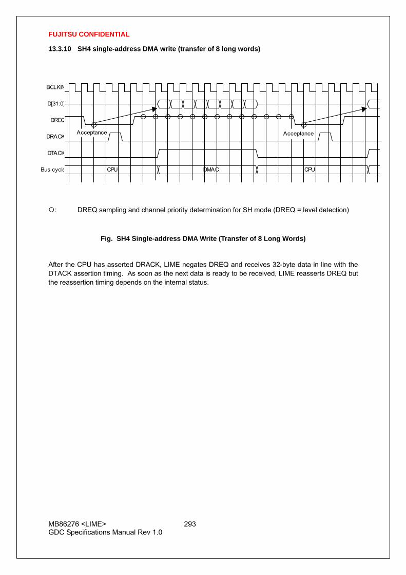
FUJITSU CONFIDENTIAL
MB86276 <LIME> 293 GDC Specifications Manual Rev 1.0
13.3.10 SH4 single-address DMA write (transfer of 8 long words)
: DREQ sampling and channel priority determination for SH mode (DREQ = level detection)
Fig. SH4 Single-address DMA Write (Transfer of 8 Long Words)
After the CPU has asserted DRACK, LIME negates DREQ and receives 32-byte data in line with the DTACK assertion timing. As soon as the next data is ready to be received, LIME reasserts DREQ but the reassertion timing depends on the internal status.
DMAC CPU CPU
BCLKIN
D[31:0]
DREQ
DRACK
DTACK
Acceptance
Bus cycle
Acceptance
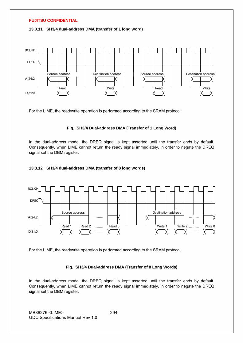
FUJITSU CONFIDENTIAL
MB86276 <LIME> 294 GDC Specifications Manual Rev 1.0
13.3.11 SH3/4 dual-address DMA (transfer of 1 long word)
For the LIME, the read/write operation is performed according to the SRAM protocol.
Fig. SH3/4 Dual-address DMA (Transfer of 1 Long Word)
In the dual-address mode, the DREQ signal is kept asserted until the transfer ends by default. Consequently, when LIME cannot return the ready signal immediately, in order to negate the DREQ signal set the DBM register.
13.3.12 SH3/4 dual-address DMA (transfer of 8 long words)
For the LIME, the read/write operation is performed according to the SRAM protocol.
Fig. SH3/4 Dual-address DMA (Transfer of 8 Long Words)
In the dual-address mode, the DREQ signal is kept asserted until the transfer ends by default. Consequently, when LIME cannot return the ready signal immediately, in order to negate the DREQ signal set the DBM register.
BCLKIN
D[31:0]
A[24:2]
Read
Destination address
Write
Source address
DREQ
Destination addressSource address
Read Write
BCLKIN
D[31:0]
A[24:2]
Read 1
Source address
………
………
………
……… Destination address
……… ………
DREQ
Read 2 Read 8 Write 1 Write 2 Write 8

FUJITSU CONFIDENTIAL
MB86276 <LIME> 295 GDC Specifications Manual Rev 1.0
13.3.13 V832 DMA transfer
For the LIME, the read/write operation is performed according to the SRAM protocol.
Fig. V832 DMA Transfer
In the dual-address mode, the DREQ signal is kept asserted until the transfer ends by default. Consequently, when LIME cannot return the ready signal immediately, in order to negate the DREQ signal set the DBM register.
BCLKIN
D[31:0]
A[23:2]
DMARQ
DMAAK
Read
Destination address
Write
Source address Destination addressSource address
Read Write

FUJITSU CONFIDENTIAL
MB86276 <LIME> 296 GDC Specifications Manual Rev 1.0
13.3.14 SH4 single-address DMA transfer end timing
: DREQ sampling and channel priority determination for SH mode (DREQ = level detection)
Fig. SH4 Single-address DMA Transfer End Timing
DREQ is negated three cycles after DRACK is written as the last data.
13.3.15 SH3/4 dual-address DMA transfer end timing
For the LIME, the read/write operation is performed according to the SRAM protocol.
Fig. SH3/4 Dual-address DMA Transfer End Timing
DREQ is negated three cycles after DRACK is written as the last data.
Note: When the dual address mode (DMA) is used, the DTACK signal is not used.
BCLKIN
D[31:0]
DREQ
DRACK
DTACK
Acceptance
Last data
Acceptance
BCLKIN
D[31:0]
A[24:2]
Read
Destination addressSource address
DREQ
DRACK
DTACK
Write

FUJITSU CONFIDENTIAL
MB86276 <LIME> 297 GDC Specifications Manual Rev 1.0
13.3.16 V832 DMA transfer end timing
For the LIME, the read/write operation is performed according to the SRAM protocol.
Fig. V832 DMA Transfer End Timing
DMMAK and XTC are logic ANDed inside LIME to end DMA.
BCLKIN
D[31:0]
A[24:2]
DMARQ
DMAAK
XTC
Read
Destination address
Write
Source address
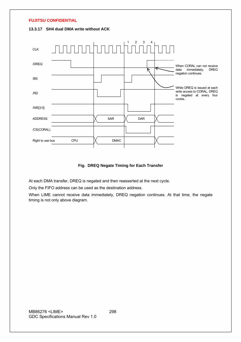
FUJITSU CONFIDENTIAL
MB86276 <LIME> 298 GDC Specifications Manual Rev 1.0
13.3.17 SH4 dual DMA write without ACK
Fig. DREQ Negate Timing for Each Transfer
At each DMA transfer, DREQ is negated and then reasserted at the next cycle.
Only the FIFO address can be used as the destination address.
When LIME cannot receive data immediately, DREQ negation continues. At that time, the negate timing is not only above diagram.
CLK
/DREQ
/BS
/RD
/WE[3:0]
ADDRESS
/CS(CORAL)
Right to use bus
SAR DAR
DMACCPU
1 2 3 4
When CORAL can not receivedata immediately, DREQ negation continues.
While DREQ is issued at each write access to CORAL, DREQ is negated at every four cycles..

FUJITSU CONFIDENTIAL
MB86276 <LIME> 299 GDC Specifications Manual Rev 1.0
13.3.18 Dual-address DMA (without ACK) end timing
Fig. Dual-address DMA (without ACK) End Timing
Example: DMA operation when DMA transfer performed twice
(1) The CPU accesses the DREQ issue register (DRQ) of Lime to issue DREQ.
(2) The right to use bus is transferred from the CPU to the DMAC.
(3) In the first DMAC cycle, write is performed to LIME and DREQ is negated; DREQ is reasserted in the next cycle.
(4) The right to use bus is returned to the CPU and the DREQ edge is detected, so the right to use bus is transferred to the DMAC.
(5) The second write operation is performed and DREQ is negated, but DREQ is reasserted because LIME does not recognize that the transfer has ended.
(6) The right to use bus is transferred to the CPU, so the CPU writes to the DTS register of LIME to negate DREQ.
/DREQ
Right to use bus CPU CPU CPU DMAC DMAC

FUJITSU CONFIDENTIAL
MB86276 <LIME> 300 GDC Specifications Manual Rev 1.0
13.3.19 CPU write timing diagram in 16bit CPU mode (Normally Not Ready Mode)
Val
id D
ata-
1 IN
BC
LKI
A[2
4:1]
XCS
XBS
XWE[
1:0]
XRD
Y
D[1
5:0]
Sof
tWai
itH
ardW
aiR
eady
T1Ts
w1
Tsw
2Th
w1
T1Ts
w1
Thw
2
SoftW
ait
Har
dWai
Har
dWai
Har
dWai
Rea
dy
Valid
Dat
a-2
IN
T2
SoftW
aiit
Sof
tWai
tH
ardW
ai
Tsw
2Th
w1
Thw
3Th
w4
T3
Low
er 1
6bit
data
Upp
er 1
6bit
data
T2
XRD
Y sa
mpl
ing
in 1
6bit
CPU
mod
e ( M
OD
E[2:
0]=1
00 )
T1: R
ead/
writ
e st
art c
ycle
(XR
DY
in th
e no
t rea
dy s
tate
)Ts
w*:
Sof
twar
e w
ait i
nser
tion
cycl
e (2
cyc
le)
Twh*
: Har
dwar
e w
ait i
nser
tion
cycl
e (X
RD
Y as
serts
Rea
dy a
fter t
he p
repa
ratio
ns)
T2: W
rite
end
cycl
e
XRD
Y sa
mpl
ing
in 1
6bit
CPU
mod
e ( M
OD
E[2:
0]=1
00 )
T1: R
ead/
writ
e st
art c
ycle
(XR
DY
in th
e no
t rea
dy s
tate
)Ts
w*:
Sof
twar
e w
ait i
nser
tion
cycl
e (2
cyc
le)
Twh*
: Har
dwar
e w
ait i
nser
tion
cycl
e (X
RD
Y as
serts
Rea
dy a
fter t
he p
repa
ratio
ns)
T3: W
rite
end
cycl
e

FUJITSU CONFIDENTIAL
MB86276 <LIME> 301 GDC Specifications Manual Rev 1.0
13.3.20 CPU read timing diagram in 16bit CPU mode (Normally Not Ready Mode)
BC
LKI
A[2
4:1]
XCS
XBS
XRD
D[1
5:0]
XRD
Y
T1Ts
w1
Thw
2
Valid
Dat
a
SoftW
ait
Har
dWai
Har
dWai
Har
dWai
Rea
dySo
ftWai
tH
ardW
ai
Tsw
2Th
w1
Thw
3Th
w4
T2
XRD
Y sa
mpl
ing
in 1
6bit
CPU
mod
e ( M
OD
E[2:
0]=1
00 )
T1: R
ead/
writ
e st
art c
ycle
(XR
DY
in th
e no
t rea
dy s
tate
)Ts
w*:
Sof
twar
e w
ait i
nser
tion
cycl
e (2
cyc
le)
Twh*
: Har
dwar
e w
ait i
nser
tion
cycl
e (X
RD
Y as
serts
Rea
dy a
fter t
he p
repa
ratio
ns)
T2: R
ead
end
cycl
e
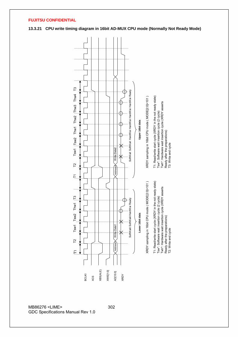
FUJITSU CONFIDENTIAL
MB86276 <LIME> 302 GDC Specifications Manual Rev 1.0
13.3.21 CPU write timing diagram in 16bit AD-MUX CPU mode (Normally Not Ready Mode)
Addr
ess2
Addr
ess1
Writ
e D
ata1
BC
LKI
XCS
XBS
(ALE
)
XWE[
1:0]
XRD
Y
AD
[15:
0]
Sof
tWai
itH
ardW
aiR
eady
T1T2
Tsw
1Th
w1
T1Ts
w1
Thw
2
Sof
tWai
tH
ardW
aiH
ardW
aiH
ardW
aiR
eady
Writ
e D
ata2
T3
Sof
tWai
itS
oftW
ait
Har
dWai
Tsw
2Th
w1
Thw
3Th
w4
T3
Low
er 1
6bit
data
Upp
er 1
6bit
data
Tsw
2T2
XRD
Y sa
mpl
ing
in 1
6bit
CPU
mod
e ( M
OD
E[2:
0]=1
01 )
T1: R
ead/
writ
e st
art c
ycle
(XR
DY
in th
e no
t rea
dy s
tate
)Ts
w*:
Sof
twar
e w
ait i
nser
tion
cycl
e (2
cyc
le)
Twh*
: Har
dwar
e w
ait i
nser
tion
cycl
e (X
RD
Y as
serts
Rea
dy a
fter t
he p
repa
ratio
ns)
T2: W
rite
end
cycl
e
XRD
Y sa
mpl
ing
in 1
6bit
CPU
mod
e ( M
OD
E[2:
0]=1
01 )
T1: R
ead/
writ
e st
art c
ycle
(XR
DY
in th
e no
t rea
dy s
tate
)Ts
w*:
Sof
twar
e w
ait i
nser
tion
cycl
e (2
cyc
le)
Twh*
: Har
dwar
e w
ait i
nser
tion
cycl
e (X
RD
Y as
serts
Rea
dy a
fter t
he p
repa
ratio
ns)
T3: W
rite
end
cycl
e

FUJITSU CONFIDENTIAL
MB86276 <LIME> 303 GDC Specifications Manual Rev 1.0
13.3.22 CPU read timing diagram in 16bit AD-MUX CPU mode (Normally Not Ready Mode)
Addr
ess
BCLK
I
XCS
XBS
(ALE
)
XWE
[1:0
]
AD[1
5:0]
XRD
Y
T1Ts
w1
Thw
2
Val
id D
ata
Sof
tWai
tH
ardW
aiH
ardW
aiH
ardW
aiR
eady
Sof
tWai
tH
ardW
ai
Tsw
2Th
w1
Thw
3Th
w4
T3T2
XRD
Y sa
mpl
ing
in 1
6bit
CPU
mod
e ( M
OD
E[2:
0]=1
01 )
XWE[
1:0]
='H
' mea
ns "R
ead"
cyc
le.
T1: R
ead/
writ
e st
art c
ycle
(XR
DY
in th
e no
t rea
dy s
tate
)Ts
w*:
Sof
twar
e w
ait i
nser
tion
cycl
e (2
cyc
le)
Twh*
: Har
dwar
e w
ait i
nser
tion
cycl
e (X
RD
Y as
serts
Rea
dy a
fter t
he p
repa
ratio
ns)
T2: R
ead
end
cycl
e
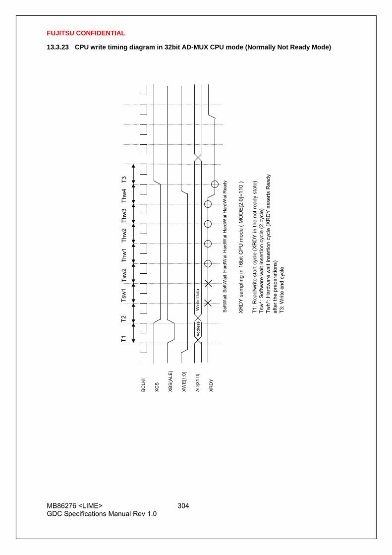
FUJITSU CONFIDENTIAL
MB86276 <LIME> 304 GDC Specifications Manual Rev 1.0
13.3.23 CPU write timing diagram in 32bit AD-MUX CPU mode (Normally Not Ready Mode)
Addr
ess
BC
LKI
XCS
XBS(
ALE
)
XWE[
1:0]
XRD
Y
AD
[31:
0]
T1Ts
w1
Thw
2
Sof
tWai
tH
ardW
aiH
ardW
aiH
ardW
aiR
eady
Writ
e D
ata Sof
tWai
tH
ardW
ai
Tsw
2Th
w1
Thw
3Th
w4
T3T2
XRD
Y sa
mpl
ing
in 1
6bit
CPU
mod
e ( M
OD
E[2:
0]=1
10 )
T1: R
ead/
writ
e st
art c
ycle
(XR
DY
in th
e no
t rea
dy s
tate
)Ts
w*:
Sof
twar
e w
ait i
nser
tion
cycl
e (2
cyc
le)
Twh*
: Har
dwar
e w
ait i
nser
tion
cycl
e (X
RD
Y as
serts
Rea
dyaf
ter t
he p
repa
ratio
ns)
T3: W
rite
end
cycl
e
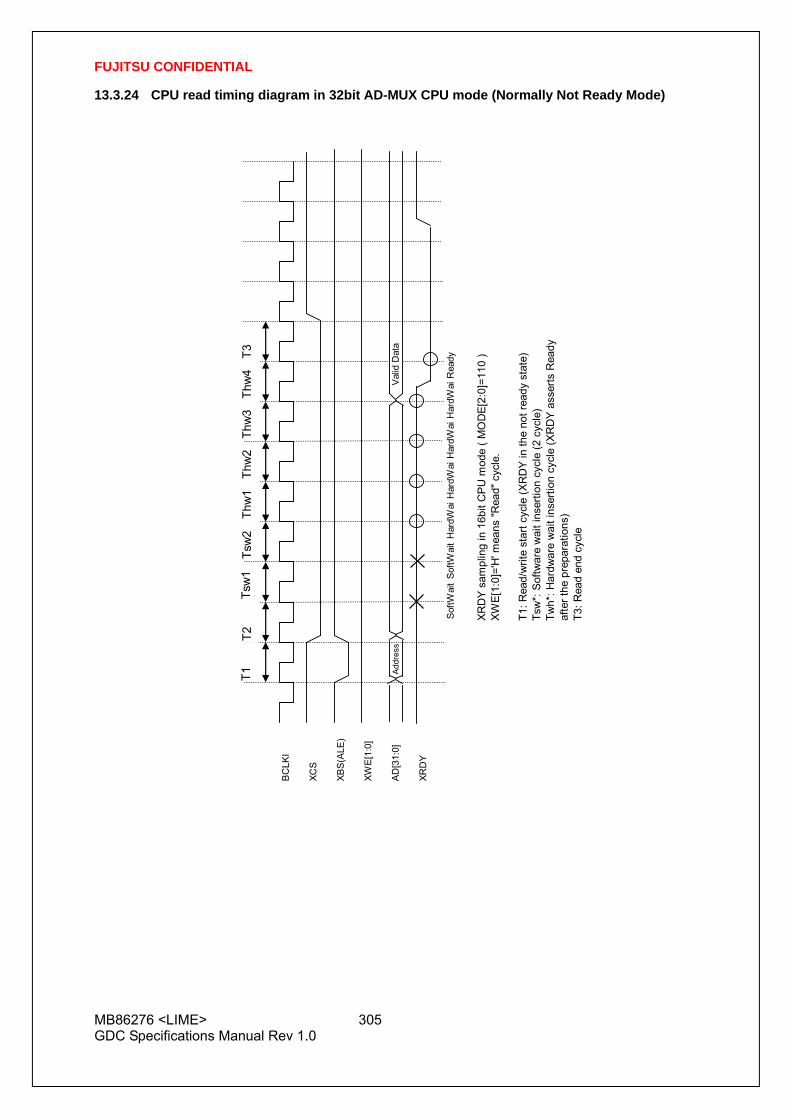
FUJITSU CONFIDENTIAL
MB86276 <LIME> 305 GDC Specifications Manual Rev 1.0
13.3.24 CPU read timing diagram in 32bit AD-MUX CPU mode (Normally Not Ready Mode)
Addr
ess
BC
LKI
XCS
XBS
(ALE
)
XWE
[1:0
]
AD
[31:
0]
XRD
Y
T1Ts
w1
Thw
2
Val
id D
ata
Sof
tWai
tH
ardW
aiH
ardW
aiH
ardW
aiR
eady
Sof
tWai
tH
ardW
ai
Tsw
2Th
w1
Thw
3Th
w4
T3T2
XRD
Y sa
mpl
ing
in 1
6bit
CPU
mod
e ( M
OD
E[2:
0]=1
10 )
XWE[
1:0]
='H
' mea
ns "R
ead"
cyc
le.
T1: R
ead/
writ
e st
art c
ycle
(XR
DY
in th
e no
t rea
dy s
tate
)Ts
w*:
Sof
twar
e w
ait i
nser
tion
cycl
e (2
cyc
le)
Twh*
: Har
dwar
e w
ait i
nser
tion
cycl
e (X
RD
Y as
serts
Rea
dyaf
ter t
he p
repa
ratio
ns)
T3: R
ead
end
cycl
e

FUJITSU CONFIDENTIAL
MB86276 <LIME> 306 GDC Specifications Manual Rev 1.0
14 ELECTRICAL CHARACTERISTICS 14.1 Introduction The values in this chapter are the final specification for LIME.
14.2 Maximum Rating
Maximum Rating
Parameter Symbol Maximum rating Unit
Power supply voltage VDDL *1 VDDH
-0.5 < VDDL < 2.5 -0.5 < VDDH < 4.0 V
Input voltage VI -0.5 < VI < VDDH+0.5 (<4.0) V
Output current IO ±13 mA
Ambient for storage temperature TST -55 < TST < +125 °C
*1 Includes PLL power supply
<Notes>
Semiconductor devices can be permanently damaged by application of stress (voltage, current, temperature, etc) in excess of absolute maximum ratings. Do not exceed these ratings.
Do not directly connect output pins or bidirectional pins of IC products to each other or VDD or VSS to avoid the breakdown of the device. However direct connection of the output pins or bidirectional pins to each other is possible, if the output pins are designed to avoid a conflict in a timing.
Because semiconductor devices are particularly susceptible to damaged by static electricity, you must take the measure like ground all fixtures and instruments.
In CMOS ICs, a latch-up phenomenon is caused when an voltage exceeding Vcc or an voltage below Vss is applied to input or output pins or a voltage exceeding the rating is applied across Vcc and Vss. When a latch-up is caused, the power supply current may be dramatically increased causing resultant thermal break-down of devices. To avoid the latch-up, make sure that the voltage does not exceed the maximum rating.

FUJITSU CONFIDENTIAL
MB86276 <LIME> 307 GDC Specifications Manual Rev 1.0
14.3 Recommended Operating Conditions 14.3.1 Recommended operating conditions
Recommended Operating Conditions
Rating Parameter Symbol
Min. Typ. Max. Unit
Supply voltage VDDL *1 VDDH
1.65
3.0
1.8
3.3
1.95
3.6 V
Input voltage (High level) VIH 2.0 VDDH+0.3 V
Input voltage (low level) VIL −0.3 0.8 V
Ambient temperature for operation TA -40 85 °C
*1 Includes PLL power supply <Note>
Recommended operating conditions are normal operating ranges for the semiconductor device. All the device’s electrical characteristics are warranted when operated within these ranges. Always use semiconductor devices within the recommended operating conditions. Operation outside these ranges may adversely affect reliability and could result in device failure. No warranty is made with respect to uses, operating conditions, or combinations not represented on the manual. Users considering application outside the listed conditions are advised to contact their FUJITSU representative beforehand.

FUJITSU CONFIDENTIAL
MB86276 <LIME> 308 GDC Specifications Manual Rev 1.0
14.3.2 Note at power-on
• There is no restriction on the sequence of power-on/power-off between VDDL and VDDH. However, do not apply only VDDH for more than a few seconds.
• Do not input HSYNC and VSYNC signals when the power supply voltage is not applied. (See the input voltage item in Maximum rating.)
• Immediately after power-on, please reset immediately because CMOS IC is in an unstable state.
1) Immediately after power-on, input the “Low” level to the S and XRST pins.
2) Immediately after power-on, input clock to the BCLKI pin. It is necessary to input 10 clk or more in order that “Low” level signal reach to the whole internal circuit completely.
3) Immediately after power-on, input clock to the CLK pin.
It is necessary to supply the stable clock before S pin is changed “Low” level to “High” level in order that PLL is oscillated stably.
• There is a reset sequences as described below. Immediately after power-on, input the “Low” level to the S and XRST pins. After 500ns or more, input the “High” level to S pin. After the S pin is set to “High” level, input the “Low” level to the XRST pin for 300us or more. Immediately after power-on, input clock to the BCLKI and CLK pins.
Note: Clock shows the image and is not an actual cycle.
There is no restriction on the sequence of power on. The recommendation is the order of VDDL and VDDH.
Please input L level signal in the case of a power on.
Immediately after power-on, please input clock.
System reset starts in 10 cycles.
More than 500ns More than 300us
VDDL
VDDH
BCLKI
CLK
S
XRST
Immediately after power-on, please input clock.
Please input L level signal in the case of a power on.

FUJITSU CONFIDENTIAL
MB86276 <LIME> 309 GDC Specifications Manual Rev 1.0
14.4 DC Characteristics 14.4.1 DC Characteristics
Measuring condition: VDDL = 1.8 ± 1.5 V, VDDH = 3.3 ± 0.3 V, VSS = 0.0 V, Ta = -40 to +85°C
Rating Parameter Symbol Condition Min. Typ. Max.
Unit
Output voltage
(“High” level) VOH IOH=-100uA VDDH-0.2
VDDH V
Output voltage
(“Low” level) VOL IOL=100uA 0.0
0.2 V
Output current
(“High” level) -- VDDH=3.3V±0.3V (*1) mA
Output current
(“Low” level) -- VDDH=3.3V±0.3V (*1) mA
Input leakage current IL ±5 µA
Pin capacitance C 16 pF
*1: Please refer “V-I characteristics diagram”.
L Type: Output characteristics of MD0-31 and MDQM0-3 pins M Type: Output characteristics of pins other than signals indicated by L type and H type H Type: Output characteristics of XINT, DREQ, XRDY pins
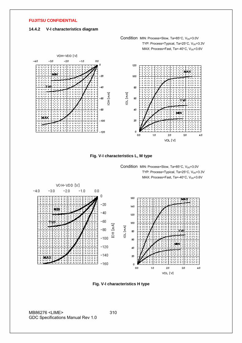
FUJITSU CONFIDENTIAL
MB86276 <LIME> 310 GDC Specifications Manual Rev 1.0
14.4.2 V-I characteristics diagram
Condition MIN: Process=Slow, Ta=85°C, VDD=3.0V TYP: Process=Typical, Ta=25°C, VDD=3.3V MAX: Process=Fast, Ta=-40°C, VDD=3.6V
Fig. V-I characteristics L, M type Condition MIN: Process=Slow, Ta=85°C, VDD=3.0V
TYP: Process=Typical, Ta=25°C, VDD=3.3V MAX: Process=Fast, Ta=-40°C, VDD=3.6V
Fig. V-I characteristics H type
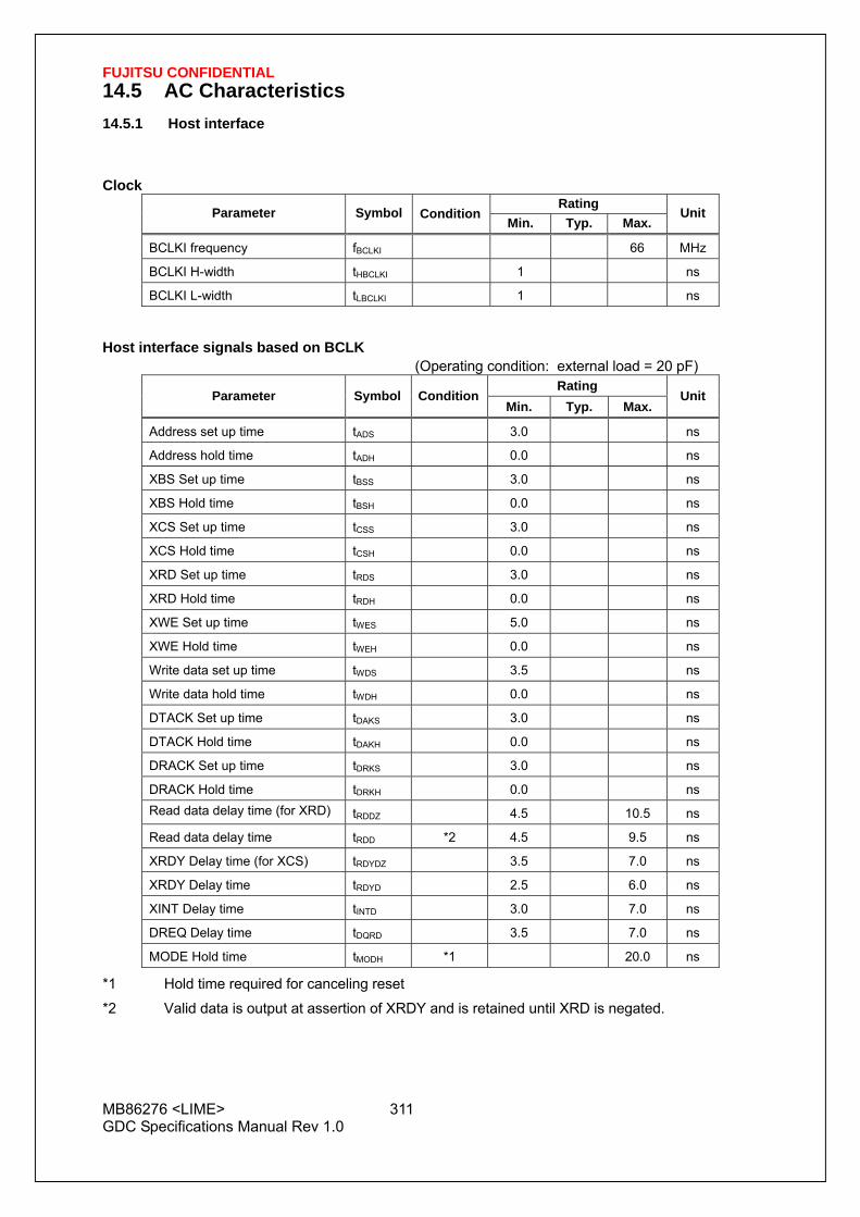
FUJITSU CONFIDENTIAL
MB86276 <LIME> 311 GDC Specifications Manual Rev 1.0
14.5 AC Characteristics 14.5.1 Host interface
Clock Rating
Parameter Symbol ConditionMin. Typ. Max.
Unit
BCLKI frequency fBCLKI 66 MHz
BCLKI H-width tHBCLKI 1 ns
BCLKI L-width tLBCLKI 1 ns
Host interface signals based on BCLK (Operating condition: external load = 20 pF)
Rating Parameter Symbol Condition
Min. Typ. Max. Unit
Address set up time tADS 3.0 ns
Address hold time tADH 0.0 ns
XBS Set up time tBSS 3.0 ns
XBS Hold time tBSH 0.0 ns
XCS Set up time tCSS 3.0 ns
XCS Hold time tCSH 0.0 ns
XRD Set up time tRDS 3.0 ns
XRD Hold time tRDH 0.0 ns
XWE Set up time tWES 5.0 ns
XWE Hold time tWEH 0.0 ns
Write data set up time tWDS 3.5 ns
Write data hold time tWDH 0.0 ns
DTACK Set up time tDAKS 3.0 ns
DTACK Hold time tDAKH 0.0 ns
DRACK Set up time tDRKS 3.0 ns
DRACK Hold time tDRKH 0.0 ns Read data delay time (for XRD) tRDDZ 4.5 10.5 ns
Read data delay time tRDD *2 4.5 9.5 ns
XRDY Delay time (for XCS) tRDYDZ 3.5 7.0 ns
XRDY Delay time tRDYD 2.5 6.0 ns
XINT Delay time tINTD 3.0 7.0 ns
DREQ Delay time tDQRD 3.5 7.0 ns
MODE Hold time tMODH *1 20.0 ns
*1 Hold time required for canceling reset
*2 Valid data is output at assertion of XRDY and is retained until XRD is negated.

FUJITSU CONFIDENTIAL
MB86276 <LIME> 312 GDC Specifications Manual Rev 1.0
Serial Control interface signals TBD

FUJITSU CONFIDENTIAL
MB86276 <LIME> 313 GDC Specifications Manual Rev 1.0
14.5.2 I2C Interface
I2C bus timing
symbol MIN MAX unit standard 250 ns TS2SDAI SDA(I) setup time high-speed 100 ns standard 0 ns TH2SDAI SCL(I) hold time high-speed 0 ns standard 10.0 us TCSCLI SCL(I) cycle time high-speed 2.5 us standard 4.0 us TWHSCLI SCL(I) H period high-speed 0.6 us standard 4.7 us TWLSCLI SCL(I) L period high-speed 1.3 us standard 2*m+2(*2) PCLK*1 TCSCLO SCL(O) cycle time high-speed int(1.5*m)+2(*2) PCLK*1 standard m+2(*2) PCLK*1 TWHSCLO SCL(O) H period high-speed int(0.5*m)+2(*2) PCLK*1 standard m(*2) PCLK*1 TWLSCLO SCL(O) L period high-speed m(*2) PCLK*1 standard 4.0 us TW2SCLI SCL(I) setup time high-speed 0.6 us standard 4.7 us TH2SCLI SCL(I) hold time high-speed 1.3 us standard 4.7 us TWBFI bus free time hirh-speed 1.3 us standard m+2(*2) PCLK*1 TS2SCLO SCL(O) set up time high-speed int(0.5*m)+2(*2) PCLK*1 standard m-2(*2) PCLK*1 TH2SCLO SCL(O) hold time high-speed int(0.5*m)-2(*2) PCLK*1
TH2SDAO SDA(O) hold time 5 PCLK*1 *1 PCLK is an internal clock of I2C module. (16.6MHz) *2 Refer to the clock control register (CCR) for the value of m.

FUJITSU CONFIDENTIAL
MB86276 <LIME> 314 GDC Specifications Manual Rev 1.0
14.5.3 Video interface
(1) Clock Rating
Parameter Symbol ConditionMin. Typ. Max.
Unit
CLK Frequency fCLK 14.318 MHz
CLK H-width tHCLK 25 ns
CLK L-width tLCLK 25 ns
DCLKI Frequency fDCLKI 80 MHz
DCLKI H-width tHDCLKI 5 ns
DCLKI L-width tLDCLKI 5 ns
DCLKO frequency fDCLKO 80 MHz
(2) Input signals Rating
Parameter Symbol ConditionMin. Typ. Max.
Unit
tWHSYNC0 *1 3 clock HSYNC Input pulse width
tWHSYNC1 *2 3 clock
HSYNC Input setup time tSHSYNC *2 6 ns
HSYNC Input hold time tHHSYNC *2 1 ns
VSYNC Input pulse width tWHSYNC1 1 HSYNC1 cycle
*1 Applied only in PLL synchronization mode (CKS=0), reference clock output from internal PLL (cycle = 1/14*fCLK)
*2 Applied only in DCLKI synchronization mode (CKS=1), reference clock = DCLKI
(3) Output signals (standard) This definition is applied for followig mode operations
1) single display & non-inverting DCLKO (MDen=0) & (DCKinv=0)
2) dual display & single-edge & non-inverting DCLKO (MDen=1) & (DCKed=0) & (DCKinv=0)
(Operating condition: external load = 20 pF)
Rating Parameter Symbol Condition
Min. Typ. Max. Unit
RGB Output delay time 1 TRGB1 2 9 ns
DISPE Output delay time 1 tDEO1 2 9 ns
HSYNC Output delay time 1 tDHSYNC1 2 9 ns
VSYNC Output delay time 1 tDVSYNC1 2 9 ns
CSYNC Output delay time 1 tDCSYNC1 2 10 ns
GV Output delay time 1 tDGV1 1.5 9 ns

FUJITSU CONFIDENTIAL
MB86276 <LIME> 315 GDC Specifications Manual Rev 1.0
(4) Output signals (inverting) This definition is applied for followig mode operations
1) single display & inverting DCLKO (MDen=0) & (DCKinv=1)
2) dual display & single-edge & inverting DCLKO (MDen=1) & (DCKed=0) & (DCKinv=1)
(Operating condition: external load = 20 pF)
Rating Parameter Symbol Condition
Min. Typ. Max. Unit
RGB Output delay time 2 TRGB2 2 9 ns
DISPE Output delay time 2 tDEO2 2 9 ns
HSYNC Output delay time 2 tDHSYNC2 2 9 ns
VSYNC Output delay time 2 tDVSYNC2 2 9 ns
CSYNC Output delay time 2 tDCSYNC2 2 10 ns
GV Output delay time 2 tDGV2 1.5 9 ns
(5) Output signals (bi-edge) This definition is applied for followig mode operations
dual display & bi-edge (MDen=1) & (DCKed=1)
(Operating condition: external load = 20 pF)
Rating Parameter Symbol Condition
Min. Typ. Max. Unit
RGB Output delay time 3 TRGB3 1.5 9 ns
DISPE Output delay time 3 tDEO3 1.5 9 ns
HSYNC Output delay time 3 tDHSYNC3 1.5 9 ns
VSYNC Output delay time 3 tDVSYNC3 1.5 9 ns
CSYNC Output delay time 3 tDCSYNC3 1.5 10 ns
GV Output delay time 3 tDGV3 1.5 9 ns
RGB Output delay time 4 TRGB4 1.5 9 ns
DISPE Output delay time 4 tDEO4 1.5 9 ns
HSYNC Output delay time 4 tDHSYNC4 1.5 9 ns
VSYNC Output delay time 4 tDVSYNC4 1.5 9 ns
CSYNC Output delay time 4 tDCSYNC4 1.5 10 ns
GV Output delay time 4 tDGV4 1.5 9 ns
FUJITSU CONFIDENTIAL
MB86276 <LIME> 316 GDC Specifications Manual Rev 1.0
14.5.4 Video capture interface
clock
Rating parameter Symbol Condition
Min. Typ. Max. Unit
CCLK (RGBCLK) frequency fCCLK 27*1 MHz CCLK (RGBCLK) H-width tHCCLKI 5 ns CCLK (RGBCLK) L-width tLCCLKI 5 ns
*1: Max buffer size of horizontal direction is 840.
Input signals
Rating parameter Symbol Condition
Min. Typ. Max. Unit
VI setup time tSVI 6 ns VI hold time tHVI 0 ns HSYNCI setup time tSHSI 6 ns HSYNCI hold time tHHSI 0 ns VSYNCI setup time tSVSI 6 ns VSYNCI hold time tHVSI 0 ns RI setup time tSRI 6 ns RI hold time tHRI 0 ns GI setup time tSGI 6 ns GI hold time tHGI 0 ns BI setup time tSBI 6 ns BI hold time tHBI 0 ns
14.5.5 Graphics memory interface
An assumed external capacitance
An assumed external capacitance Parameter
Min Typ Max
Unit
Board pattern 5.0 15.0 pF
SDRAM (CLK) 2.5 4.0 pF
SDRAM (D) 4.0 6.5 pF
SDRAM (A, DQM) 2.5 5.0 pF
FUJITSU CONFIDENTIAL
MB86276 <LIME> 317 GDC Specifications Manual Rev 1.0
Clock
Rating Parameter Symbol Condition
Min. Typ. Max. Unit
MCLKO Frequency fMCLKO *1 MHz
MCLKO H-width tHMCLKO 1.0 ns
MCLKO L-width tLMCLKO 1.0 ns
MCLKI Frequency fMCLKI *1 MHz
MCLKI H-width tHMCLKI 1.0 ns
MCLKI L-width tLMCLKI 1.0 ns
*1 For the bus-asynchronous mode, the frequency is 1/3 of the oscillation frequency of the internal PLL. For the bus-synchronous mode, the frequency is the same as the frequency of BCLKI.
Input signals
Rating Parameter Symbol Condition
Min. Typ. Max. Unit
MD Input data setup time tMDIDS *2 2.0 ns
MD Input data hold time tMDIDH *2 0.7 ns
*2 It means against MCLKI.

FUJITSU CONFIDENTIAL
MB86276 <LIME> 318 GDC Specifications Manual Rev 1.0
There are some cases regarding AC specifications of output signals.
The following tables shows typical twelve cases of external SDFAM capacitance.
(1) External SDRAM capacitance case 1
External SDRAM capacitance
SDRAM x1 Total capacitance Unit
MCLKO 9.8pF (DRAM CLK 2.5pF, Board pattern 5pF) pF
MA,MRAS,MCAS,MWE 7.5pF (DRAM A.DQM 2.5pF, Board pattern 5pF) pF
MD,DQM 9.0pF (DRAM D 4pF, Board pattern 5pF) pF
Output signals Rating *1
Parameter Symbol ConditionMin. Typ. Max.
Unit
MCLKI signal delay time against MCLKO tDID 0 4.2 ns
MA, MRAS, MCAS, MWE Access time tMAD 1.0 5.0 ns
MDQM Access time tMDQMD 1.1 5.4 ns
MD Output access time tMDOD 1.1 5.4 ns
(2) External SDRAM capacitance case 2
External SDRAM capacitance
SDRAM x1 Total capacitance Unit
MCLKO 24.8pF (DRAM CLK 4.0pF, Board pattern 15pF) pF
MA,MRAS,MCAS,MWE 20.0pF (DRAM A.DQM 5pF, Board pattern 15pF) pF
MD,DQM 21.5pF (DRAM D 6.5pF, Board pattern 15pF) pF
Output signals Rating *1
Parameter Symbol ConditionMin. Typ. Max.
Unit
MCLKI signal delay time against MCLKO tDID 0 3.5 ns
MA, MRAS, MCAS, MWE Access time tMAD 1.0 5.2 ns
MDQM Access time tMDQMD 1.2 5.5 ns
MD Output access time tMDOD 1.2 5.5 ns
FUJITSU CONFIDENTIAL
MB86276 <LIME> 319 GDC Specifications Manual Rev 1.0
(3) External SDRAM capacitance case 3
External SDRAM capacitance
SDRAM x2 Total capacitance Unit
MCLKO 12.3pF (DRAM CLK 2.5pF x2, Board pattern 5pF) pF
MA,MRAS,MCAS,MWE 10.0pF (DRAM A.DQM 2.5pF x2, Board pattern 5pF) pF
MD,DQM 9.0pF (DRAM D 4pF, Board pattern 5pF) pF
Output signals Rating *1
Parameter Symbol ConditionMin. Typ. Max.
Unit
MCLKI signal delay time against MCLKO tDID 0 4.1 ns
MA, MRAS, MCAS, MWE Access time tMAD 1.0 5.0 ns
MDQM Access time tMDQMD 1.1 5.2 ns
MD Output access time tMDOD 1.1 5.2 ns
(4) External SDRAM capacitance case 4
External SDRAM capacitance
SDRAM x2 Total capacitance Unit
MCLKO 28.8pF (DRAM CLK 4.0pF x2, Board pattern 15pF) pF
MA,MRAS,MCAS,MWE 25.0pF (DRAM A.DQM 5pF x2, Board pattern 15pF) pF
MD,DQM 21.5pF (DRAM D 6.5pF, Board pattern 15pF) pF
Output signals Rating *1
Parameter Symbol ConditionMin. Typ. Max.
Unit
MCLKI signal delay time against MCLKO tDID 0 3.4 ns
MA, MRAS, MCAS, MWE Access time tMAD 1.1 5.4 ns
MDQM Access time tMDQMD 1.1 5.5 ns
MD Output access time tMDOD 1.1 5.5 ns
FUJITSU CONFIDENTIAL
MB86276 <LIME> 320 GDC Specifications Manual Rev 1.0
14.5.6 PLL specifications
Parameter Rating Description
Input frequency (typ.) 14.31818 MHz
Output frequency 400.9090 MHz × 28
Duty ratio 101.6 to 93.0% H/L Pulse width ratio of PLL output
Jitter 60 to -60 ps Frequency tolerant of two consecutive clock cycles
CLKSEL1 CLKSEL0 Input frequency Assured operation range (*1) L L 13.5 MHz 13.365 to 13.5 MHz
L H 14.32 MHz 14.177 to 14.32 MHz
H L 17.73 Hz 17.553 to 17.73 MHz
H H 33.33 Hz 32.997 to 33.33 MHz
*1 Assured operation input frequency range: Standard value –1%

FUJITSU CONFIDENTIAL
MB86276 <LIME> 321 GDC Specifications Manual Rev 1.0
14.6 AC Characteristics Measuring Conditions
0.5 V
80 %
20 %
80 %
20 % (V
IH+V
IL)/2
VDD
/2 V DD /2
t r tf
t pHL tpLH
VDD
/2
tpZL tpLZ
VDD
/2
0.5 V
tpHZtpZH
Input
Output
Output disabled ( pull up )
t r, tf ≤ 5 ns : All input signals have to change within 5ns. V IH=2.0 V, V IL = 0.8V (3.3 -V CMOS interface input)
Output disabled ( pull down )
Output enabled (L)
Output enabled (H)

FUJITSU CONFIDENTIAL
MB86276 <LIME> 322 GDC Specifications Manual Rev 1.0
14.7 Timing Diagram 14.7.1 Host interface
Host interface based on BCLKI
(1)Clock
(2)MODE hold time
(3)XINT output delay times
BCLKI
1/fBCLKI
tLBCLKItHBCLKI
XRESET
tMODH
MODE
BCLK
XINT
tINT

FUJITSU CONFIDENTIAL
MB86276 <LIME> 323 GDC Specifications Manual Rev 1.0
(4)Host bus AC timing (Normally Not Ready)
tRDYDZ
tRDDZ
BCLKI
D(output)
tRDDZ
XRD (RDXWR)
Hi-Z
XRDY
tRDYDtRDYD
tRDD
Output dataHi-Z
A
XBS
XCS
XWE (XMWE)
Hi-Z
D(Input)
tRDYDZ
tADH tADS
tBSH tBSS tBSH tBSS
tCSH tCSS
tWES tWEH
tWDS tWDH
tRDS tRDH
tRDYDZ
XWAIT
tRDYDtRDYD
Hi-Z Hi-Z
Hi-Z
T1 Tsw1 Thw1 T2
tRDYDZ

FUJITSU CONFIDENTIAL
MB86276 <LIME> 324 GDC Specifications Manual Rev 1.0
(5)Host bus AC timing (Normally Ready)
BCLKI
A
tADH tADS
tBSH tBSS tBSH tBSS
T1 Tsw1 Tsw2 T2 Thw1
tRDDZ
D(output)
tRDDZ
XRD (RDXWR)
tRDD
Output data Hi-Z
XBS
XCS
XWE (XMWE)
D(Input)
tCSH tCSS
tWES tWEH
tWDS tWDH
tRDS tRDH
XRDY
tRDYD
tRDYD
XWAIT tRDYD
tRDYD
Hi-Z
tRDYDZ
Hi-Z
tRDYDZ
Hi-Z
Hi-Z
tRDYDZ
tRDYDZ
Hi-Z

FUJITSU CONFIDENTIAL
MB86276 <LIME> 325 GDC Specifications Manual Rev 1.0
(6)DMA AC timing
*: The above timing diagram for the D pin is that of when a single DMA is used.
When a dual DMA is used, see the host bus-timing diagram.
BCLKI
D(Input)
DTACK (XTC)
tWDH tWDS
tDAKH tDAKS tDAKH tDAKS
tRRKH tDRKS
tWDH
DREQ
DRACK (DMAAK) tDRQD
tRRKH tDRKS
tDRQD

FUJITSU CONFIDENTIAL
MB86276 <LIME> 326 GDC Specifications Manual Rev 1.0
Serial Control interface
TBD
FUJITSU CONFIDENTIAL
MB86276 <LIME> 327 GDC Specifications Manual Rev 1.0
14.7.2 Video interface
(1) Clock
CLK
1/fCLK
tLCLKtHCLK
VIH
VIL
(2) HSYNC signal setup/hold
DCLKI
tHDCLKI tLDCLKI
1/fDCLKI
tSHSYN tHHSYN
HSYNC (input)
(3) Output signal delay ( standard )
DCLKO
tRGB , tDEO, tDHSYNC,
tDVSYNC, tDCSYNC, tDGV
DR7-2, DG7-2DB7-2HSYNC (output)VSYNC (output)CSYNC, DEGV

FUJITSU CONFIDENTIAL
MB86276 <LIME> 328 GDC Specifications Manual Rev 1.0
(4) Output signal delay ( inverted )
DCLKO
tRGB2 , tDEO2, tDHSYNC2,
tDVSYNC2, tDCSYNC2, tDGV2
DR7-2, DG7-2DB7-2HSYNC (output)VSYNC (output)CSYNC, DEGV
(5) Output signal delay ( bi-edge )
DCLKO
tRGB3 , tDEO3, tDHSYNC3,
tDVSYNC3, tDCSYNC3, tDGV3
DR7-2, DG7-2DB7-2HSYNC (output)VSYNC (output)CSYNC, DEGV
tRGB4, tDEO4, tDHSYNC4,
tDVSYNC4, tDCSYNC4, tDGV4
FUJITSU CONFIDENTIAL
MB86276 <LIME> 329 GDC Specifications Manual Rev 1.0
14.7.3 Video capture interface
clock
Video input
CCLK
tSVI
VI
tSRI
tSVSI
tSGI
tSHSI
tHVI
tHRI
tHVSI
tHGI
tHHSI
RI,GI,BI VSYNCI HSYNCI
tSBI tHBI
RGBCLK
FUJITSU CONFIDENTIAL
MB86276 <LIME> 330 GDC Specifications Manual Rev 1.0
15.7.4 Graphics memory interface
Clock
Input signal setup/hold time
MCLKI signal delay
MCLKO, MCLKI
1/fMCLKO, 1/fMCLKI
tHMCLKO, tHMCLKI tLMCLKO, tLMCLKI
MCLKI
tMDIDS
MD
tMDIDH
Input data
MCLKO
tOID
MCLKI

FUJITSU CONFIDENTIAL
MB86276 <LIME> 331 GDC Specifications Manual Rev 1.0
Output signal delay
MCLKO
tMAD, tMDOD, tMDQMD
MA, MRAS, MCAS, MWE, MD, MDQM