IRS2153(1)D(S)PbF - RS Components
15
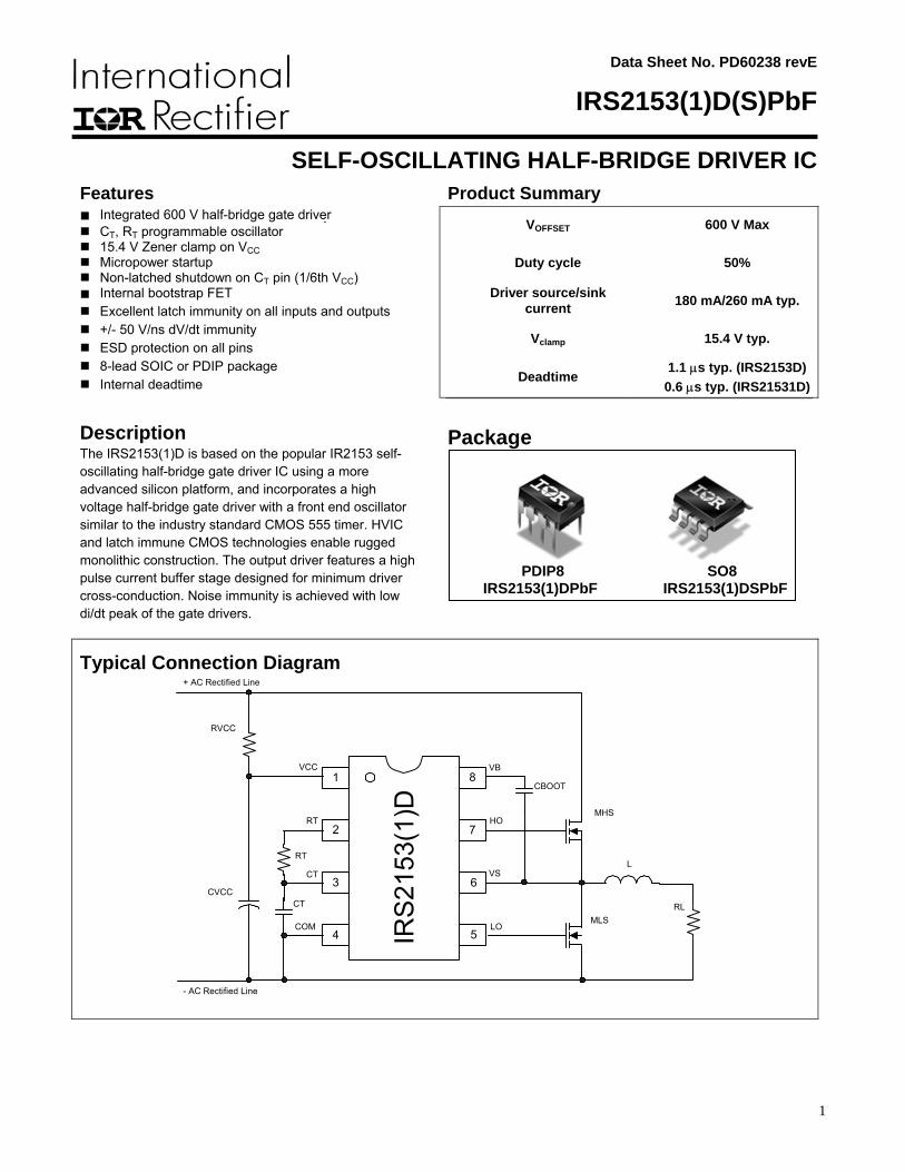
1 Data Sheet No. PD60238 revE IRS2153(1)D(S)PbF SELF-OSCILLATING HALF-BRIDGE DRIVER IC Features Product Summary V OFFSET 600 V Max Duty cycle 50% Driver source/sink current 180 mA/260 mA typ. V clamp 15.4 V typ. Integrated 600 V half-bridge gate driver C T , R T programmable oscillator 15.4 V Zener clamp on V CC Micropower startup Non-latched shutdown on C T pin (1/6th V CC ) Internal bootstrap FET Excellent latch immunity on all inputs and outputs +/- 50 V/ns dV/dt immunity ESD protection on all pins 8-lead SOIC or PDIP package Internal deadtime Deadtime 1.1 µs typ. (IRS2153D) 0.6 µs typ. (IRS21531D) Description The IRS2153(1)D is based on the popular IR2153 self- oscillating half-bridge gate driver IC using a more advanced silicon platform, and incorporates a high voltage half-bridge gate driver with a front end oscillator similar to the industry standard CMOS 555 timer. HVIC and latch immune CMOS technologies enable rugged monolithic construction. The output driver features a high pulse current buffer stage designed for minimum driver cross-conduction. Noise immunity is achieved with low di/dt peak of the gate drivers. Package PDIP8 SO8 IRS2153(1)DPbF IRS2153(1)DSPbF Typical Connection Diagram RT CT COM VCC 1 2 3 4 7 6 5 8 IRS2153(1)D LO VS HO VB CBOOT MHS MLS L RL RVCC RT CT CVCC + AC Rectified Line - AC Rectified Line
-
Upload
khangminh22 -
Category
Documents
-
view
0 -
download
0
Transcript of IRS2153(1)D(S)PbF - RS Components
1
Data Sheet No. PD60238 revE
IRS2153(1)D(S)PbF
SELF-OSCILLATING HALF-BRIDGE DRIVER ICFeatures Product Summary
VOFFSET 600 V Max
Duty cycle 50%
Driver source/sink current 180 mA/260 mA typ.
Vclamp 15.4 V typ.
Integrated 600 V half-bridge gate driver CT, RT programmable oscillator 15.4 V Zener clamp on VCC Micropower startup Non-latched shutdown on CT pin (1/6th VCC) Internal bootstrap FET Excellent latch immunity on all inputs and outputs +/- 50 V/ns dV/dt immunity ESD protection on all pins 8-lead SOIC or PDIP package Internal deadtime Deadtime
1.1 µs typ. (IRS2153D) 0.6 µs typ. (IRS21531D)
Description The IRS2153(1)D is based on the popular IR2153 self-oscillating half-bridge gate driver IC using a more advanced silicon platform, and incorporates a high voltage half-bridge gate driver with a front end oscillator similar to the industry standard CMOS 555 timer. HVIC and latch immune CMOS technologies enable rugged monolithic construction. The output driver features a high pulse current buffer stage designed for minimum driver cross-conduction. Noise immunity is achieved with low di/dt peak of the gate drivers.
Package
PDIP8 SO8
IRS2153(1)DPbF IRS2153(1)DSPbF
Typical Connection Diagram
RT
CT
COM
VCC1
2
3
4
7
6
5
8
IRS2
153(
1)D
LO
VS
HO
VB
CBOOT
MHS
MLS
L
RL
RVCC
RT
CTCVCC
+ AC Rectified Line
- AC Rectified Line
2
IRS2153(1)D
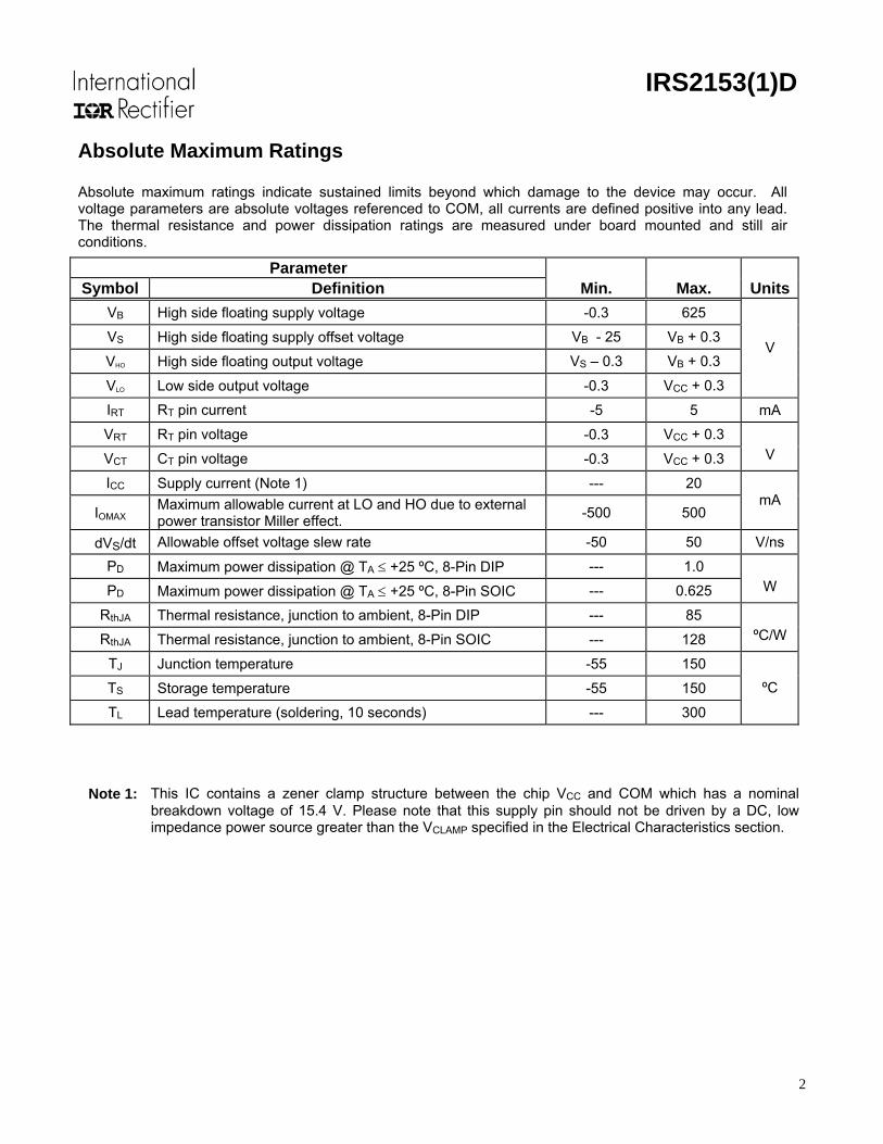
Absolute Maximum Ratings Absolute maximum ratings indicate sustained limits beyond which damage to the device may occur. All voltage parameters are absolute voltages referenced to COM, all currents are defined positive into any lead. The thermal resistance and power dissipation ratings are measured under board mounted and still air conditions.
Parameter Symbol Definition Min. Max. Units
VB High side floating supply voltage -0.3 625
VS High side floating supply offset voltage VB - 25 VB + 0.3
VHO High side floating output voltage VS – 0.3 VB + 0.3
VLO Low side output voltage -0.3 VCC + 0.3
V
IRT RT pin current -5 5 mA
VRT RT pin voltage -0.3 VCC + 0.3
VCT CT pin voltage -0.3 VCC + 0.3
V
ICC Supply current (Note 1) --- 20
IOMAX Maximum allowable current at LO and HO due to external power transistor Miller effect. -500 500
mA
dVS/dt Allowable offset voltage slew rate -50 50 V/ns
PD Maximum power dissipation @ TA ≤ +25 ºC, 8-Pin DIP --- 1.0
PD Maximum power dissipation @ TA ≤ +25 ºC, 8-Pin SOIC --- 0.625
W
RthJA Thermal resistance, junction to ambient, 8-Pin DIP --- 85
RthJA Thermal resistance, junction to ambient, 8-Pin SOIC --- 128
ºC/W
TJ Junction temperature -55 150
TS Storage temperature -55 150
TL Lead temperature (soldering, 10 seconds) --- 300
ºC
Note 1: This IC contains a zener clamp structure between the chip VCC and COM which has a nominal breakdown voltage of 15.4 V. Please note that this supply pin should not be driven by a DC, low impedance power source greater than the VCLAMP specified in the Electrical Characteristics section.
3
IRS2153(1)D
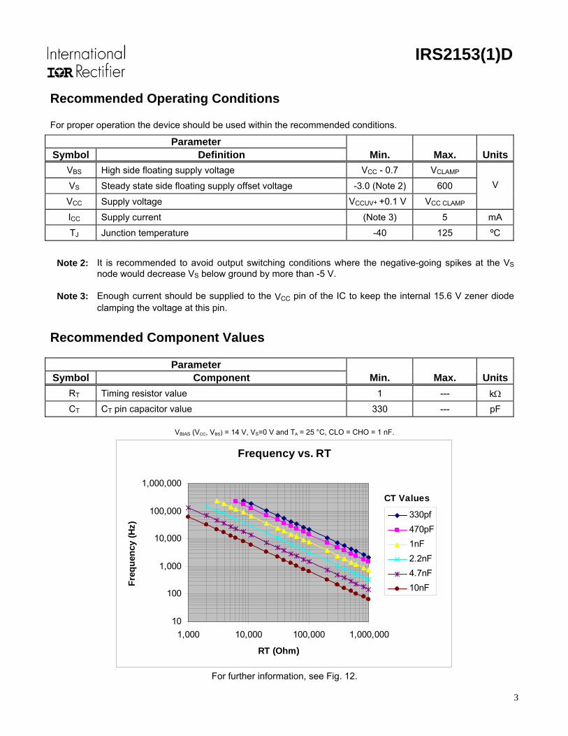
Recommended Operating Conditions For proper operation the device should be used within the recommended conditions.
Parameter Symbol Definition Min. Max. Units
VBS High side floating supply voltage VCC - 0.7 VCLAMP
VS Steady state side floating supply offset voltage -3.0 (Note 2) 600
VCC Supply voltage VCCUV+ +0.1 V VCC CLAMP
V
ICC Supply current (Note 3) 5 mA
TJ Junction temperature -40 125 ºC
Note 2: It is recommended to avoid output switching conditions where the negative-going spikes at the VS node would decrease VS below ground by more than -5 V.
Note 3: Enough current should be supplied to the VCC pin of the IC to keep the internal 15.6 V zener diode clamping the voltage at this pin.
Recommended Component Values
Parameter Symbol Component Min. Max. Units
RT Timing resistor value 1 --- kΩ CT CT pin capacitor value 330 --- pF
VBIAS (VCC, VBS) = 14 V, VS=0 V and TA = 25 °C, CLO = CHO = 1 nF.
Frequency vs. RT
10
100
1,000
10,000
100,000
1,000,000
1,000 10,000 100,000 1,000,000
RT (Ohm)
Freq
uenc
y (H
z)
330pf470pF1nF2.2nF4.7nF10nF
CT Values
For further information, see Fig. 12.
4
IRS2153(1)D
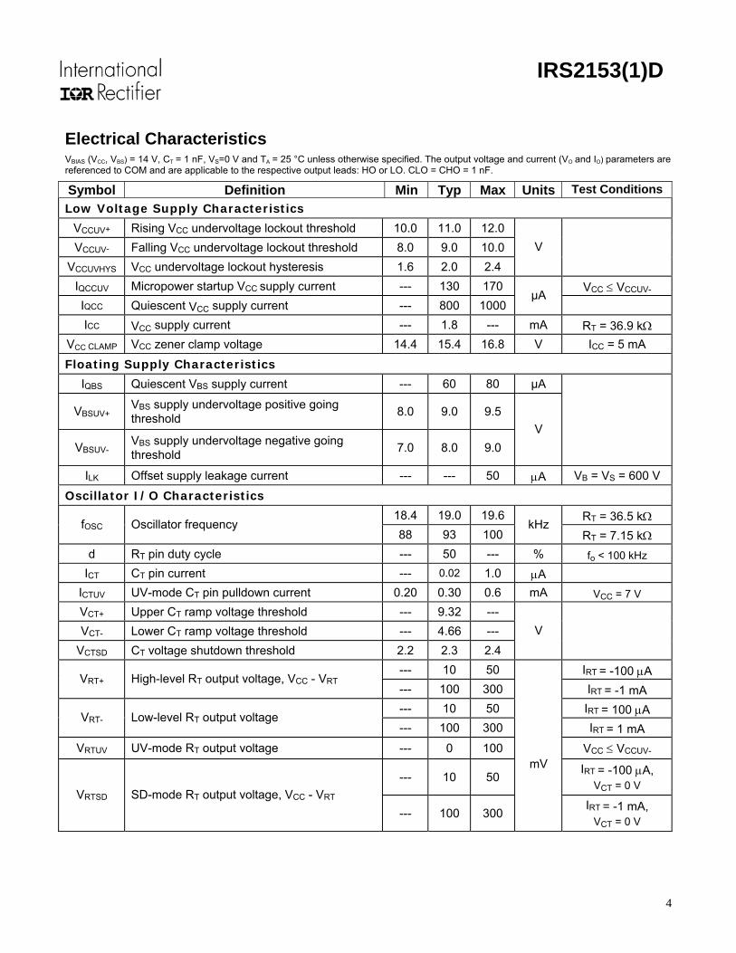
Electrical Characteristics
VBIAS (VCC, VBS) = 14 V, CT = 1 nF, VS=0 V and TA = 25 °C unless otherwise specified. The output voltage and current (VO and IO) parameters are referenced to COM and are applicable to the respective output leads: HO or LO. CLO = CHO = 1 nF.
Symbol Definition Min Typ Max Units Test Conditions Low Voltage Supply Characteristics
VCCUV+ Rising VCC undervoltage lockout threshold 10.0 11.0 12.0 VCCUV- Falling VCC undervoltage lockout threshold 8.0 9.0 10.0
VCCUVHYS VCC undervoltage lockout hysteresis 1.6 2.0 2.4
V
IQCCUV Micropower startup VCC supply current --- 130 170 VCC ≤ VCCUV- IQCC Quiescent VCC supply current --- 800 1000
µA
ICC VCC supply current --- 1.8 --- mA RT = 36.9 kΩ VCC CLAMP VCC zener clamp voltage 14.4 15.4 16.8 V ICC = 5 mA
Floating Supply Characteristics
IQBS Quiescent VBS supply current --- 60 80 µA
VBSUV+ VBS supply undervoltage positive going threshold 8.0 9.0 9.5
VBSUV- VBS supply undervoltage negative going threshold 7.0 8.0 9.0
V
ILK Offset supply leakage current --- --- 50 µA VB = VS = 600 V
Oscillator I/O Characteristics
18.4 19.0 19.6 RT = 36.5 kΩ fOSC Oscillator frequency 88 93 100
kHz RT = 7.15 kΩ
d RT pin duty cycle --- 50 --- % fo < 100 kHz
ICT CT pin current --- 0.02 1.0 µA
ICTUV UV-mode CT pin pulldown current 0.20 0.30 0.6 mA VCC = 7 V
VCT+ Upper CT ramp voltage threshold --- 9.32 --- VCT- Lower CT ramp voltage threshold --- 4.66 ---
VCTSD CT voltage shutdown threshold 2.2 2.3 2.4 V
--- 10 50 IRT = -100 µA VRT+ High-level RT output voltage, VCC - VRT
--- 100 300 IRT = -1 mA
--- 10 50 IRT = 100 µA VRT- Low-level RT output voltage
--- 100 300 IRT = 1 mA
VRTUV UV-mode RT output voltage --- 0 100 VCC ≤ VCCUV-
--- 10 50 IRT = -100 µA,
VCT = 0 V VRTSD SD-mode RT output voltage, VCC - VRT
--- 100 300
mV IRT = -1 mA,
VCT = 0 V
5
IRS2153(1)D
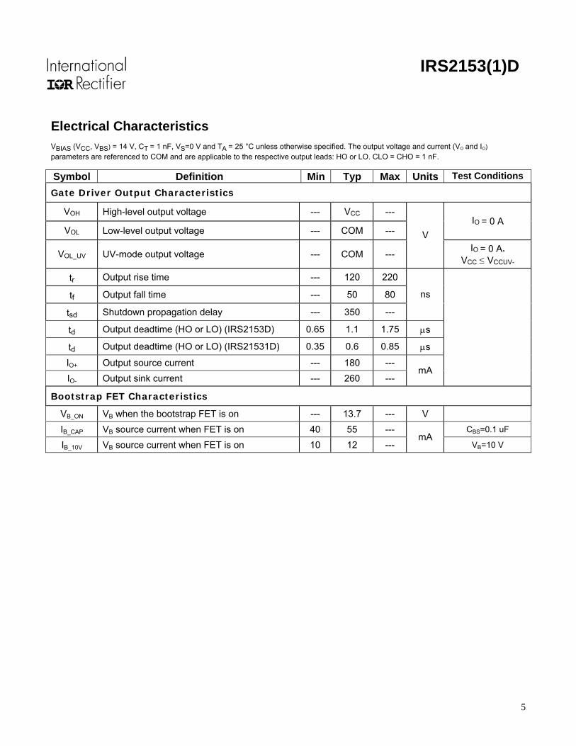
Electrical Characteristics VBIAS (VCC, VBS) = 14 V, CT = 1 nF, VS=0 V and TA = 25 °C unless otherwise specified. The output voltage and current (VO and IO) parameters are referenced to COM and are applicable to the respective output leads: HO or LO. CLO = CHO = 1 nF. Symbol Definition Min Typ Max Units Test Conditions
Gate Driver Output Characteristics
VOH High-level output voltage --- VCC ---
VOL Low-level output voltage --- COM --- IO = 0 A
VOL_UV UV-mode output voltage --- COM ---
V IO = 0 A,
VCC ≤ VCCUV-
tr Output rise time --- 120 220
tf Output fall time --- 50 80
tsd Shutdown propagation delay --- 350 ---
ns
td Output deadtime (HO or LO) (IRS2153D) 0.65 1.1 1.75 µs
td Output deadtime (HO or LO) (IRS21531D) 0.35 0.6 0.85 µs
IO+ Output source current --- 180 --- IO- Output sink current --- 260 ---
mA
Bootstrap FET Characteristics
VB_ON VB when the bootstrap FET is on --- 13.7 --- V
IB_CAP VB source current when FET is on 40 55 --- CBS=0.1 uF
IB_10V VB source current when FET is on 10 12 --- mA
VB=10 V
6
IRS2153(1)D
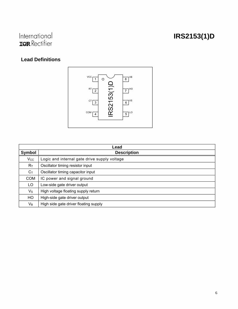
Lead Definitions
RT
CT
COM
VCC1
2
3
4
7
6
5
8
IRS
2153
(1)D
LO
VS
HO
VB
Lead Symbol Description
VCC Logic and internal gate drive supply voltage RT Oscillator timing resistor input CT Oscillator timing capacitor input
COM IC power and signal ground LO Low-side gate driver output VS High voltage floating supply return HO High-side gate driver output VB High side gate driver floating supply
7
IRS2153(1)D
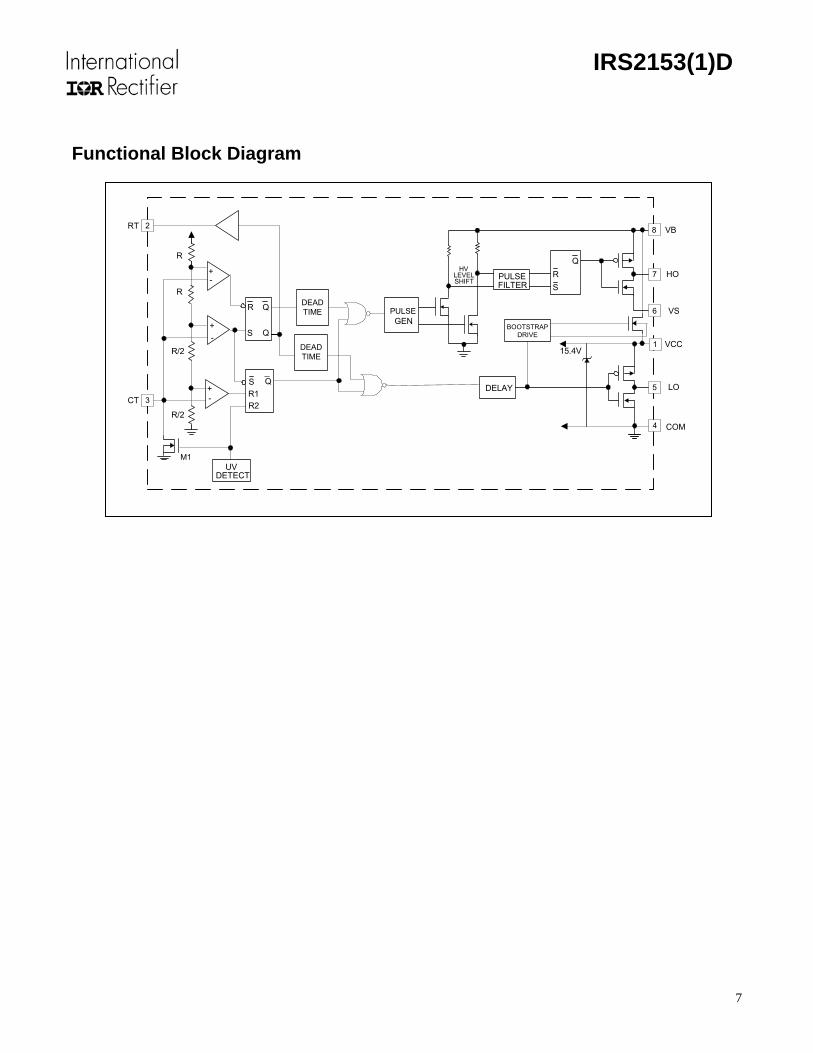
Functional Block Diagram
VB
PULSEGEN
DELAY
HVLEVELSHIFT PULSE
FILTER
LO
VS
RS
Q
CT
RT
R Q
S Q
HO
-
-
-
+
+
+
R
R
R/2
R/2
UVDETECT
DEADTIME
DEADTIME
R1S Q
R2
2
35
6
7
8
COM4
VCC15.4V
1
BOOTSTRAPDRIVE
M1

8
IRS2153(1)D
Timing Diagram Operating Mode
DT
DT
VRTVCC
1/3 VCC
2/3 VCC
VCT
IRT
VCC
VCCUV+
LOVCC
HO
VCC
1/6 VCC
Switching Time Waveform Deadtime Waveform
tr tf
90%
10%HOLO
DTLO
LO
HO
10%
10%
90%
90%
DTHO
Fault Mode: CT <1/6*VCC
9
IRS2153(1)D
Functional Description Under-voltage Lock-Out Mode (UVLO) The under-voltage lockout mode (UVLO) is defined as the state the IC is in when VCC is below the turn-on threshold of the IC. The IRS2153(1)D under voltage lock-out is designed to maintain an ultra low supply current of less than 170 µA, and to guarantee the IC is fully functional before the high and low side output drivers are activated. During under voltage lock-out mode, the high and low-side driver outputs HO and LO are both low. Supply voltage
RT
CT
COM
VCC1
2
3
4
7
6
5
8
IRS2
153(
1)D
LO
VS
HO
VB
CBOOT
MHS
MLS
L
RL
RVCC
RT
CTCVCC
+ AC Rectified Line
- AC Rectified Line
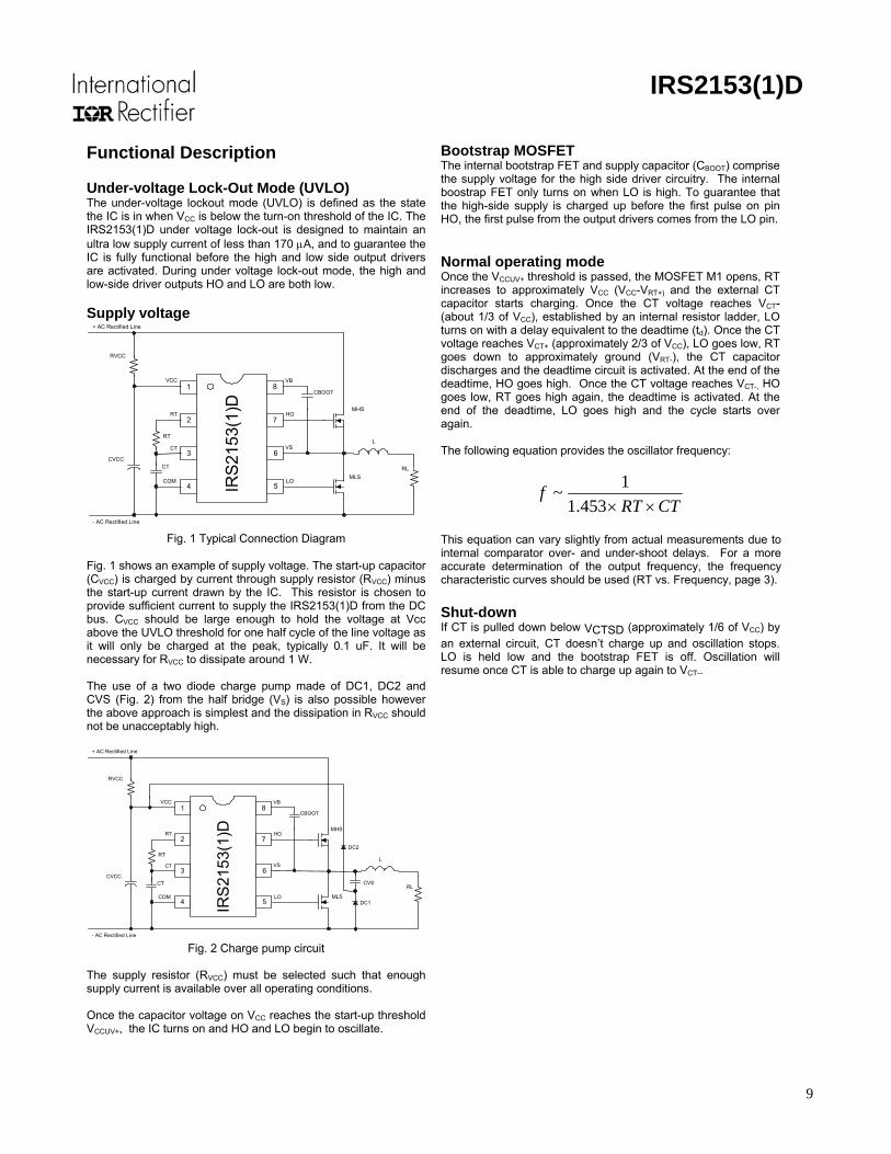
Fig. 1 Typical Connection Diagram Fig. 1 shows an example of supply voltage. The start-up capacitor (CVCC) is charged by current through supply resistor (RVCC) minus the start-up current drawn by the IC. This resistor is chosen to provide sufficient current to supply the IRS2153(1)D from the DC bus. CVCC should be large enough to hold the voltage at Vcc above the UVLO threshold for one half cycle of the line voltage as it will only be charged at the peak, typically 0.1 uF. It will be necessary for RVCC to dissipate around 1 W.
The use of a two diode charge pump made of DC1, DC2 and CVS (Fig. 2) from the half bridge (VS) is also possible however the above approach is simplest and the dissipation in RVCC should not be unacceptably high.
RT
CT
COM
VCC1
2
3
4
7
6
5
8
IRS
2153
(1)D
LO
VS
HO
VB
CBOOT
MHS
MLS
L
RL
RVCC
RT
CTCVCC
+ AC Rectified Line
- AC Rectified Line
DC1
DC2
CVS
Fig. 2 Charge pump circuit
The supply resistor (RVCC) must be selected such that enough supply current is available over all operating conditions. Once the capacitor voltage on VCC reaches the start-up threshold VCCUV+, the IC turns on and HO and LO begin to oscillate.
Bootstrap MOSFET The internal bootstrap FET and supply capacitor (CBOOT) comprise the supply voltage for the high side driver circuitry. The internal boostrap FET only turns on when LO is high. To guarantee that the high-side supply is charged up before the first pulse on pin HO, the first pulse from the output drivers comes from the LO pin.
Normal operating mode Once the VCCUV+ threshold is passed, the MOSFET M1 opens, RT increases to approximately VCC (VCC-VRT+) and the external CT capacitor starts charging. Once the CT voltage reaches VCT- (about 1/3 of VCC), established by an internal resistor ladder, LO turns on with a delay equivalent to the deadtime (td). Once the CT voltage reaches VCT+ (approximately 2/3 of VCC), LO goes low, RT goes down to approximately ground (VRT-), the CT capacitor discharges and the deadtime circuit is activated. At the end of the deadtime, HO goes high. Once the CT voltage reaches VCT-, HO goes low, RT goes high again, the deadtime is activated. At the end of the deadtime, LO goes high and the cycle starts over again. The following equation provides the oscillator frequency:
CTRTf
××453.11~
This equation can vary slightly from actual measurements due to internal comparator over- and under-shoot delays. For a more accurate determination of the output frequency, the frequency characteristic curves should be used (RT vs. Frequency, page 3). Shut-down If CT is pulled down below VCTSD (approximately 1/6 of VCC) by an external circuit, CT doesn’t charge up and oscillation stops. LO is held low and the bootstrap FET is off. Oscillation will resume once CT is able to charge up again to VCT-.
10
IRS2153(1)D
18
18.2
18.4
18.6
18.8
19
11 12 13 14 15 16
VCC(V)
Freq
uenc
y (k
Hz)
FREQ vs VCC
90
92
94
96
98
100
-25 0 25 50 75 100 125
Temperature(C)
Freq
uenc
y (k
Hz)
FREQ vs TEMP
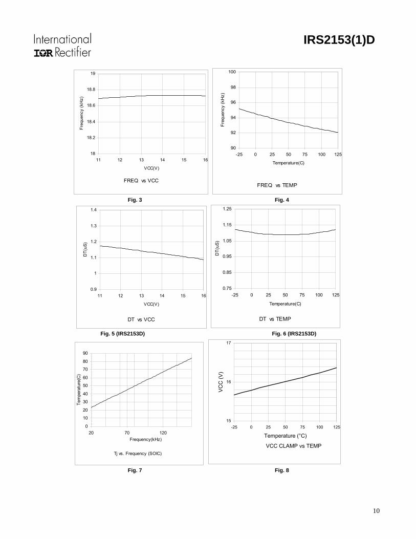
Fig. 3 Fig. 4
0.9
1
1.1
1.2
1.3
1.4
11 12 13 14 15 16
VCC(V)
DT(
uS)
DT vs VCC
0.75
0.85
0.95
1.05
1.15
1.25
-25 0 25 50 75 100 125
Temperature(C)
DT(
uS)
DT vs TEMP
Fig. 5 (IRS2153D) Fig. 6 (IRS2153D)
Tj vs. Frequency (SOIC)
0
10
20
30
40
50
60
70
80
90
20 70 120Frequency(kHz)
Tem
pera
ture
(C)
15
16
17
-25 0 25 50 75 100 125
Temperature (°C)
VC
C (V
)
VCC CLAMP vs TEMP
Fig. 7 Fig. 8
11
IRS2153(1)D
0
50
100
150
200
250
300
-25 0 25 50 75 100 125
Temperature(C)
HO
Cur
rent
(mA)
IsourceHO,IsinkHO vs Temp
IsourceHO
IsinkHO
0
50
100
150
200
250
300
-25 0 25 50 75 100 125
Temperature(C)
LO C
urre
nt (m
A)
IsourceLO,IsinkLO vs Temp
IsourceLO
IsinkHO
Fig. 9 Fig. 10
0
10
20
30
40
50
60
70
80
-25 0 25 50 75 100 125
Temperature(C)
IB_C
AP, I
BS_1
0V (m
A)
IBCAP, IBS10V vs TEMP
IB_CAP
IBS_10V
VOH_HO vs. Frequency
0
2
4
6
8
10
12
14
16
0 50 100 150 200 250 300 350 400
Frequency (kHz)
VO
H_H
O (V
)
With External BS diode No external BS diode
T=25°C, VS=0V, CHO = 1nF
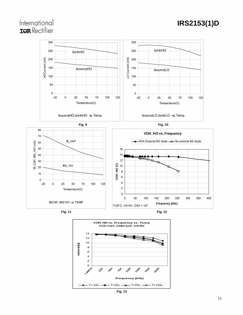
Fig. 11 Fig. 12
VOH_HO vs. Frequency vs. TempVCC=14V, CHO=1nF, VS=0V
0
2
4
6
8
10
12
14
1.46
Khz
20K
50K
75K
100K
125K
150K
200K
Frequency (kHz)
VOH_H
O(V
)
T=-25c T=25c T=75c T=125c
Fig. 13

12
IRS2153(1)D
IRS2153(1)DPbF
IRS2153(1)DSPbF
13
IRS2153(1)D
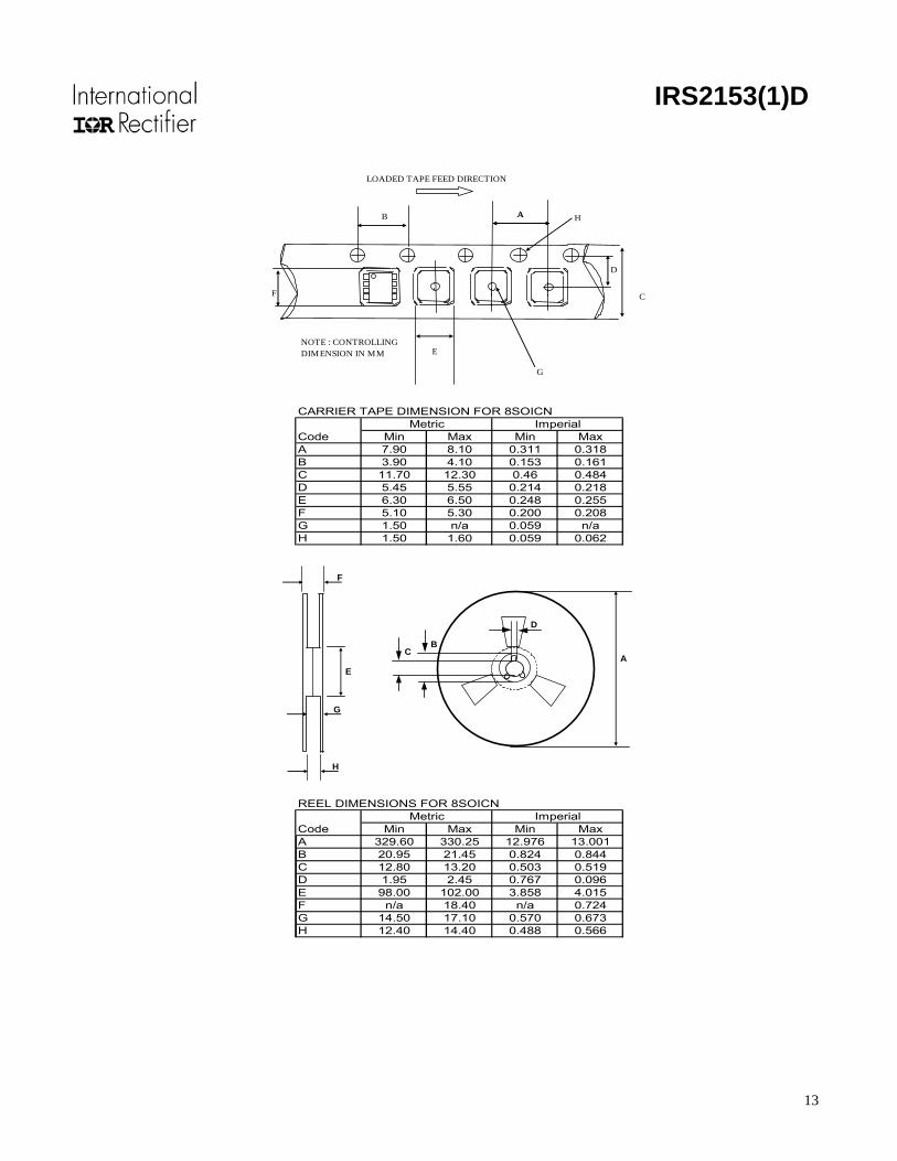
CARRIER TAPE DIMENSION FOR 8SOICN
Code Min Max Min MaxA 7.90 8.10 0.311 0.318B 3.90 4.10 0.153 0.161C 11.70 12.30 0.46 0.484D 5.45 5.55 0.214 0.218E 6.30 6.50 0.248 0.255F 5.10 5.30 0.200 0.208G 1.50 n/a 0.059 n/aH 1.50 1.60 0.059 0.062
Metric Imperial
REEL DIMENSIONS FOR 8SOICN
Code Min Max Min MaxA 329.60 330.25 12.976 13.001B 20.95 21.45 0.824 0.844C 12.80 13.20 0.503 0.519D 1.95 2.45 0.767 0.096E 98.00 102.00 3.858 4.015F n/a 18.40 n/a 0.724G 14.50 17.10 0.570 0.673H 12.40 14.40 0.488 0.566
Metric Imperial
E
F
A
C
D
G
AB H
NOTE : CONTROLLING DIMENSION IN MM
LOADED TAPE FEED DIRECTION
A
H
F
E
G
D
BC

14
IRS2153(1)D
PART MARKING INFORMATION
ORDER INFORMATION
8-Lead PDIP IRS2153DPbF 8-Lead PDIP IRS21531DPbF 8-Lead SOIC IRS2153DSPbF 8-Lead SOIC IRS21531DSPbF
8-Lead SOIC Tape & Reel IRS2153DSTRPbF 8-Lead SOIC Tape & Reel IRS21531DSTRPbF
The SOIC-8 is MSL2 qualified. This product has been designed and qualified for the industrial level.
Qualification standards can be found at www.irf.com <http://www.irf.com> IR WORLD HEADQUARTERS: 233 Kansas St., El Segundo, California 90245, Tel: (310) 252-7105
Data and specifications subject to change without notice. 6/27/2006

15
IRS2153(1)D
REVISION HISTORY
Date Revision Description of Change The following specs have been updated. See PCN S021006
Previous Rev. A
Min Typ Max Min Typ Max
VCCUV+ 10.2 10.8 11.5 10.0 11.0 12.0
2/10/06 A
VCCUV- 8.3 8.8 9.4 8.0 9.0 10.0
3/4/06 B Addition of Fig 12.
5/11/06 C Formatting changes.
6/21/06 D Updated Fig. 12 to add temperature test condition. Addition of Fig. 13. Addition of MSL2 statement.
7/28/06 E Added the specifications for RIS21531D. The only difference between IRS2153D and IRS21531D is the deadtime, 1.1 µs and 0.6 µs respectively (see page 5).