Photogenerated charges and surface potential variations investigated on single Si nanorods by...
8
NANO EXPRESS Open Access Photogenerated charges and surface potential variations investigated on single Si nanorods by electrostatic force microscopy combined with laser irradiation Shan Wu, Zilong Wu, Dongdong Lin, Zhenyang Zhong, Zuimin Jiang and Xinju Yang * Abstract Photogenerated charging properties of single Si nanorods (Si NRs) are investigated by electrostatic force microscopy (EFM) combined with laser irradiation. Under laser irradiation, Si NRs are positively charged. The amount of the charges trapped in single NRs as well as the contact potential difference between the tip and NRs' surface is achieved from an analytical fitting of the phase shift - voltage curve. Both of them significantly vary with the laser intensity and the NR's size and construction. The photogenerated charging and decharging rates are obtained at a timescale of seconds or slower, indicating that the Si NRs are promising candidates in photovoltaic applications. Keywords: Si nanorods; EFM; Photogenerated charging; Surface potential Background One-dimensional silicon nanostructures, such as Si nanowires (NWs), nanorods (NRs), or nanopillar (NPs) have gained particular interests due to their special properties and potential applications in electronic and optoelectronic devices [1-4]. Theoretical and experimen- tal studies have reported that when arranged in a highly ordered fashion, Si NRs or NWs can improve light ab- sorption and charge collection, making it possible to achieve high efficiency in solar cells [5-8]. Therefore, periodic Si NRs (or NWs) arrays have attracted consi- derable attentions in the fields of solar cells. However, despite the huge efforts to control and understand the growth mechanisms underlying the formation of these nanostructures [9,10], some fundamental properties and inside mechanisms are still not well understood. To reveal their properties, the investigation on single NRs is preferred. Recently conductive scanning probe microscopy techniques have been attempted to investi- gate the electrical properties of single NWs/NRs. Among them, electrostatic force microscopy (EFM) can provide direct information of trapped carriers in single nanostructures and has been applied to investigate the charge trapping in single nanostructures, such as carbon nanotubes [11], pentacene monolayer islands [12], CdSe quantum dots (QDs) [13,14], and etc. More recently, photoionization of QDs [15,16] and photo-induced char- ging of photovoltaic films [17-19] have been studied by EFM combined with laser irradiation. But the photogen- erated charging effects have not been concerned on Si NRs or NWs yet. In this letter, EFM measurements com- bined with laser irradiation are applied to investigate the photogenerated charging properties on single vertically aligned Si NRs in periodic arrays. Methods Periodic arrays of Si NRs are fabricated by nanosphere lithography and metal-assisted chemical etching. Three samples (labeled as NR1, NR2, NR3) which contain peri- odic NR arrays with the same diameter of about 300 nm and different length or constructions are prepared. NR1 and NR2 are n-type Si (approximately 1,000 Ω cm) NRs with the length of about 0.5 and 1.0 μm, respectively, while NR3 is Si/SiGe/Si hetero-structural NRs with the length of 1.0 μm, which is fabricated with the same n- type Si substrate but covered with a 5-nm Si 0.55 Ge 0.45 quantum well and a 100-nm intrinsic Si capping layer * Correspondence: [email protected] State Key Laboratory of Surface Physics, Fudan University, Shanghai 200433, China © 2014 Wu et al.; licensee Springer. This is an Open Access article distributed under the terms of the Creative Commons Attribution License (http://creativecommons.org/licenses/by/4.0), which permits unrestricted use, distribution, and reproduction in any medium, provided the original work is properly credited. Wu et al. Nanoscale Research Letters 2014, 9:245 http://www.nanoscalereslett.com/content/9/1/245
-
Upload
independent -
Category
Documents
-
view
1 -
download
0
Transcript of Photogenerated charges and surface potential variations investigated on single Si nanorods by...
Wu et al. Nanoscale Research Letters 2014, 9:245http://www.nanoscalereslett.com/content/9/1/245
NANO EXPRESS Open Access
Photogenerated charges and surface potentialvariations investigated on single Si nanorods byelectrostatic force microscopy combined withlaser irradiationShan Wu, Zilong Wu, Dongdong Lin, Zhenyang Zhong, Zuimin Jiang and Xinju Yang*
Abstract
Photogenerated charging properties of single Si nanorods (Si NRs) are investigated by electrostatic forcemicroscopy (EFM) combined with laser irradiation. Under laser irradiation, Si NRs are positively charged. The amountof the charges trapped in single NRs as well as the contact potential difference between the tip and NRs' surface isachieved from an analytical fitting of the phase shift - voltage curve. Both of them significantly vary with the laserintensity and the NR's size and construction. The photogenerated charging and decharging rates are obtained at atimescale of seconds or slower, indicating that the Si NRs are promising candidates in photovoltaic applications.
Keywords: Si nanorods; EFM; Photogenerated charging; Surface potential
BackgroundOne-dimensional silicon nanostructures, such as Sinanowires (NWs), nanorods (NRs), or nanopillar (NPs)have gained particular interests due to their specialproperties and potential applications in electronic andoptoelectronic devices [1-4]. Theoretical and experimen-tal studies have reported that when arranged in a highlyordered fashion, Si NRs or NWs can improve light ab-sorption and charge collection, making it possible toachieve high efficiency in solar cells [5-8]. Therefore,periodic Si NRs (or NWs) arrays have attracted consi-derable attentions in the fields of solar cells. However,despite the huge efforts to control and understand thegrowth mechanisms underlying the formation of thesenanostructures [9,10], some fundamental properties andinside mechanisms are still not well understood.To reveal their properties, the investigation on single
NRs is preferred. Recently conductive scanning probemicroscopy techniques have been attempted to investi-gate the electrical properties of single NWs/NRs. Amongthem, electrostatic force microscopy (EFM) can providedirect information of trapped carriers in single
* Correspondence: [email protected] Key Laboratory of Surface Physics, Fudan University, Shanghai 200433,China
© 2014 Wu et al.; licensee Springer. This is an OAttribution License (http://creativecommons.orin any medium, provided the original work is p
nanostructures and has been applied to investigate thecharge trapping in single nanostructures, such as carbonnanotubes [11], pentacene monolayer islands [12], CdSequantum dots (QDs) [13,14], and etc. More recently,photoionization of QDs [15,16] and photo-induced char-ging of photovoltaic films [17-19] have been studied byEFM combined with laser irradiation. But the photogen-erated charging effects have not been concerned on SiNRs or NWs yet. In this letter, EFM measurements com-bined with laser irradiation are applied to investigate thephotogenerated charging properties on single verticallyaligned Si NRs in periodic arrays.
MethodsPeriodic arrays of Si NRs are fabricated by nanospherelithography and metal-assisted chemical etching. Threesamples (labeled as NR1, NR2, NR3) which contain peri-odic NR arrays with the same diameter of about 300 nmand different length or constructions are prepared. NR1and NR2 are n-type Si (approximately 1,000 Ω cm) NRswith the length of about 0.5 and 1.0 μm, respectively,while NR3 is Si/SiGe/Si hetero-structural NRs with thelength of 1.0 μm, which is fabricated with the same n-type Si substrate but covered with a 5-nm Si0.55Ge0.45quantum well and a 100-nm intrinsic Si capping layer
pen Access article distributed under the terms of the Creative Commonsg/licenses/by/4.0), which permits unrestricted use, distribution, and reproductionroperly credited.

Wu et al. Nanoscale Research Letters 2014, 9:245 Page 2 of 8http://www.nanoscalereslett.com/content/9/1/245
[20]. The constructions of three types of NRs are givenin Figure 1a, together with the scanning electron micros-copy (SEM) image of NR2. The SEM images of NR1 andNR3 are similar to that of NR2, except the length ofNR1 is smaller than the other two. Figure 1b gives anexperimental schematic diagram of EFM measurementson single Si NRs combined with laser irradiation. Thephase shift vs. voltage (ΔΦ −VEFM) curves are measuredat a lift height on single NRs with SCM-PIT tips. Laser(405 nm) with adjustable power intensity is focused ontothe substrate through a 400-μm fiber, with a spot ofabout 1 mm2 at the area beneath the AFM tip. All mea-surements are operated in a nitrogen flow gas for astable measurement.
Results and discussionsThe ΔΦ − VEFM curves measured at a lift height of140 nm on three samples under different laser intensitiesare shown in Figure 2 as the scattered dots. It can beseen that the curves shift to the negative direction withthe laser intensity, and the shift varies with the type ofthe NRs. In previous literatures, the relation betweenphase shift and electrostatic force has been established,where the tip-sample system is simply treated as planecapacitor [21-23]. When a bias is applied between the
Figure 1 Constructions of NRs and schematic diagram of EFMmeasurements. (a) SEM image of NR2, together with the constructionsof NR1, NR2, and NR3. (b) Schematic diagram of EFM measurements onsingle Si NRs combined with a 405-nm laser irradiation.
tip and the sample, the capacitive electrostatic force gra-dient would cause a phase shift. If there are chargestrapped in the sample, additional phase shift induced bythe coulombic force is generated. Therefore, at the liftedpass where the Van der Waals force can be ignored, theforce on the tip can be written as [11,24,25]:
FElectrostatic ¼ FCapacitive þ FCoulombic ¼ 12∂C∂z
V EFM−VCPDð Þ2
−CQs
4πε0z2V EFM−VCPDð Þ− Q2
s
4πε0z2
ð1ÞWhere C, VEFM, and VCPD are the capacitance, applied
DC voltage, and contact potential difference (CPD)between the tip and sample, respectively. Qs is theamount of charges trapped in the beneath NR, and zis the distance between the trapped charges in NRand image charges in tip. The phase shift detected byEFM is proportional to the gradient of the force,which is as follows:
ΔΦ ¼ −Qk∂F∂z
¼ −Qk ½ 12 ∂2C∂z2
V EFM−VCPDð Þ2
þ Qs
2πε0z2Cz−12∂C∂z
� �V EFM−VCPDð Þ þ Q2
s
2πε0z3�ð2Þ
where Q is the quality factor and k is the spring constantof the probe.From Equation 2, it can be seen, without charges trapped
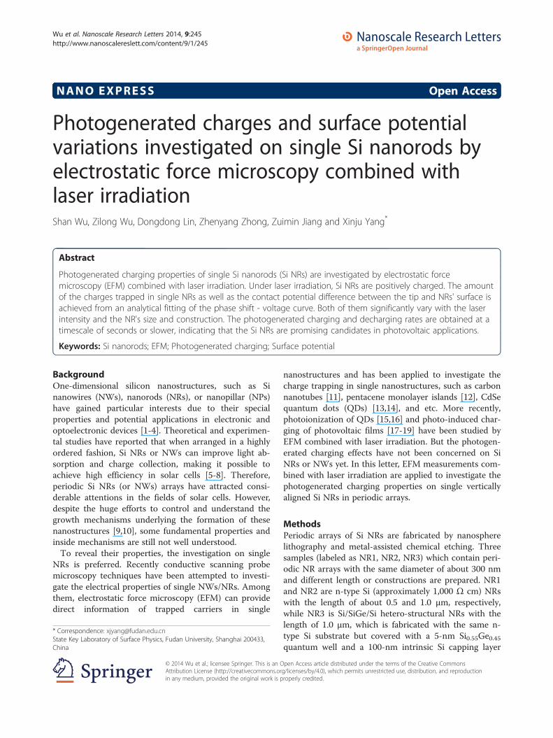
in Si NRs, that the EFM phase shift should be equal to zeroat VEFM =VCPD. In other words, the minimum point of theΔΦ −VEFM curve should be located at zero. In Figure 2,the ΔΦ −VEFM curves of three types of NRs did presenttheir minimum points at almost zero without laser irradi-ation, indicating that the trapped charges can be neglectedin that case. However, with laser irradiation, all ΔΦ−VEFM
curves of the three samples gradually decline to negativesides, suggesting charges are generated by laser irradiationand trapped in Si NRs. From Figure 2, it can also be ob-served that the decline of phase shift increases with thelaser intensity, and the range of decline is significant diffe-rent for the three types of NRs. To achieve the amountof the trapped charges, curve fittings are made by using
Equation 2. Let: A ¼ − Q2k
∂2C∂z2 , B ¼ − Q
kQs
2πε0z2Cz −
12∂C∂z
� �,
and C ¼ − Qk
Q2s
2πε0z3, Equation 2 is simplified to:
ΔΦ ¼ A V EFM−VCPDð Þ2 þ B V EFM−VCPDð Þ þ C ð3ÞBy using Equation 3 and treating A, B, C, and VCPD as
fitting parameters, the ΔΦ −VEFM curves of the threesamples under different laser intensities can be well fit-ted, shown as the lines in Figure 2. A fitting example ofNR1 without laser irradiation is given in the inset of
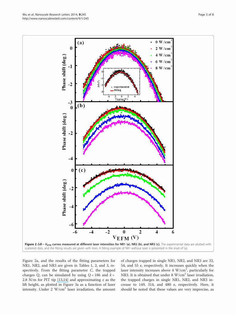
Figure 2 ΔΦ − VEFM curves measured at different laser intensities for NR1 (a), NR2 (b), and NR3 (c). The experimental data are plotted withscattered dots, and the fitting results are given with lines. A fitting example of NR1 without laser is presented in the inset of (a).
Wu et al. Nanoscale Research Letters 2014, 9:245 Page 3 of 8http://www.nanoscalereslett.com/content/9/1/245
Figure 2a, and the results of the fitting parameters forNR1, NR2, and NR3 are given in Tables 1, 2, and 3, re-spectively. From the fitting parameter C, the trappedcharges Qs can be simulated by using Q = 186 and k =2.8 N/m for PIT tip [13,14] and approximating z as thelift height, as plotted in Figure 3a as a function of laserintensity. Under 2 W/cm2 laser irradiation, the amount
of charges trapped in single NR1, NR2, and NR3 are 32,54, and 55 e, respectively. It increases quickly when thelaser intensity increases above 4 W/cm2, particularly forNR3. It is obtained that under 8 W/cm2 laser irradiation,the trapped charges in single NR1, NR2, and NR3 in-crease to 149, 314, and 480 e, respectively. Here, itshould be noted that these values are very imprecise, as
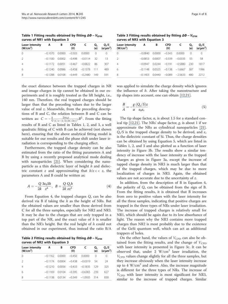
Table 1 Fitting results obtained by fitting ΔΦ − VEFM
curves of NR1 with Equation 3
Laser intensity(W/cm2)
A B CPD(V)
C Qs
(e)Qs/S
(e/μm2)
0 −0.1070 0.0000 −0.503 0.0000 0 0
2 −0.1100 0.0002 −0.498 −0.0114 32 13
4 −0.1172 0.0051 −0.467 −0.0822 86 307
6 −0.1240 0.0086 −0.458 −0.1378 111 489
8 −0.1288 0.0108 −0.449 −0.2480 149 591
Table 3 Fitting results obtained by fitting ΔΦ − VEFM
curves of NR3 with Equation 3
Laser intensity(W/cm2)
A B CPD(V)
C Qs
(e)Qs/S
(e/μm2)
0 −0.0840 0.0000 −0.343 0.0000 0 0
2 −0.0853 0.0007 −0.339 −0.0335 55 58
4 −0.0947 0.0244 −0.191 −0.5880 230 1817
6 −0.1148 0.0325 −0.138 −1.6667 387 1996
8 −0.1403 0.0440 −0.089 −2.5633 480 2212
Wu et al. Nanoscale Research Letters 2014, 9:245 Page 4 of 8http://www.nanoscalereslett.com/content/9/1/245
the exact distance between the trapped charges in NRand image charges in tip cannot be obtained in our ex-periments and it is roughly treated as the lift height, i.e.,140 nm. Therefore, the real trapped charges should belarger than that the preceding values due to the largervalue of real z. Meanwhile, from the preceding descrip-tions of B and C, the relation between B and C can bewritten as: C ¼ − k
Q2πε0z
C=z− 1=2ð Þ ∂C=∂zð Þð Þ2 B2 . From the fitting
results of B and C as listed in Tables 1, 2, and 3, a wellquadratic fitting of C with B can be achieved (not shownhere), ensuring that the above analytical fitting model issuitable for our results and the phase shift under laser ir-radiation is corresponding to the charging effect.Furthermore, the trapped charge density can be also
estimated from the ratio of the fitting parameters A andB by using a recently proposed analytical mode dealingwith nanoparticles [21]. When considering the nano-particle as a thin dielectric layer of height h and dielec-tric constant ε and approximating that h/ε < < z, theparameters A and B could be written as:
A ¼ −Q2k
3ε0Shz4
; B ¼ Q2k
Qshεz3
ð4Þ
From Equation 4, the trapped charges Qs can be alsoderived via B if taking the h as the height of NRs. Butthe obtained values are smaller than those derived fromC for all the three samples, especially for NR2 and NR3.It may be due to the charges that are only trapped in atop part of the NR, and the exact value of h is smallerthan the NR's height. But the real height of h could notobtained in our experiment, thus instead the ratio B/A
Table 2 Fitting results obtained by fitting ΔΦ − VEFM
curves of NR2 with Equation 3
Laser intensity(W/cm2)
A B CPD(V)
C Qs
(e)Qs/S
(e/μm2)
0 −0.1162 0.0000 −0.450 0.0000 0 0
2 −0.1174 0.0004 −0.438 −0.0319 54 24
4 −0.1210 0.0056 −0.433 −0.1835 129 325
6 −0.1169 0.0104 −0.395 −0.6365 239 627
8 −0.1138 0.0134 −0.349 −1.0935 314 830
was applied to simulate the charge density which ignoresthe influence of h. After taking the nanostructure andtip shapes into account, one can obtain [12,21].
BA¼ −
gα
Qs=Sð Þzε0εr
ð5Þ
The tip shape factor, α, is about 1.5 for a standard con-ical tip [12,21]. The NRs' shape factor, g, is about 1 if weapproximate the NRs as cylindrical nanoparticles [21].Qs/S is the trapped charge density to be derived, and εris the dielectric constant of Si. Thus, the charge densitiescan be obtained by using Equation 5, which are listed inTables 1, 2, and 3 and also plotted as a function of laserintensity in Figure 3b. The results show a similar ten-dency of increase with the laser intensity as the trappedcharges as given in Figure 3a, except the increase oftapped charge density in NR3 is much larger than thatof the trapped charges, which may be due to morelocalization of charges in NR3. Again, the obtainedvalues are not accurate due to the uncertainty of z.In addition, from the description of B in Equation 4,
the polarity of Qs can be obtained from the sign of B.From the fitting results, it is obtained that B increasesfrom zero to positive values with the laser intensity forall the three samples, indicating that positive charges aretrapped in the three types of NRs under laser irradiation.The increase of trapped charges is relatively small forNR1, which should be again due to its low absorbance oflight. The reason why the NR3 contains more trappedcharges than NR2 is most probably due to the existenceof the GeSi quantum well, which can act as additionaltrappers of holes.On the other hand, the values of VCPD can also be ob-
tained from the fitting results, and the change of VCPD
with laser intensity is presented in Figure 3c. It can beobserved that, under 2 W/cm2 laser irradiation, theVCPD values change slightly for all the three samples, butthey increase obviously when the laser intensity increaseup to 4 W/cm2 and above. Also, the increase magnitudeis different for the three types of NRs. The increase ofVCPD with laser intensity is most significant for NR3,similar to the increase of trapped charges. Similar

Figure 3 The trapped charges Qs (a), charge density (b) and CPD values (c). Of the three samples as a function of laser intensity.
Wu et al. Nanoscale Research Letters 2014, 9:245 Page 5 of 8http://www.nanoscalereslett.com/content/9/1/245
surface potential variation by photogenerated chargeshas been obtained by Kelvin potential force microscopy(KPFM) [26,27]; it was declared that the positive (nega-tive) shift in surface potential with laser corresponds toan increase in hole (electron) density. Thus, the positiveshift in VCPD with laser intensity in our experiments canalso be attributed to the increase of trapped hole density,which is consistent with the above results of charge
density. As VCPD equals to (ϕtip − ϕsample) / e, the resultsdeclare that the work function of Si NR decrease uponlaser irradiation should be due to the photogeneratedholes trapped in NRs.The reason why positive charging measured on n-type
Si NRs is not very clear, and further studies are requiredto get a clear mechanism. The possible mechanism maybe suggested to the tunneling of photogenerated electrons
Wu et al. Nanoscale Research Letters 2014, 9:245 Page 6 of 8http://www.nanoscalereslett.com/content/9/1/245
to the substrate and trapping the holes in the NRs. In pre-vious studies on the photoionization of an individual CdSenanocrystals [16,28], it was found that a significant frac-tion of nanocrystals was positively charged and it was at-tributed to the tunneling of the excited electrons into thesubstrate. They assumed that the hole tends to be local-ized in the nanocrystal, while the electron is much moredelocalized, with a nonnegligible fraction of the electrondensity outside the nanocrystal. Another possibility arisesfrom that the holes can be captured at Si-Si bonds accor-ding to the reaction ≡ Si-Si ≡ + h→ ≡Si+ + · Si≡, as re-ported in reference [29]. By adopting the above viewpoint,it can be suggested that when Si NRs are irradiated, freecharges are photogenerated after dissociation of the exci-tons. Due to the tunneling of photoelectrons and/orcapture of holes, the Si NRs would be positively charged.To see the dynamics of charging and decharging, the
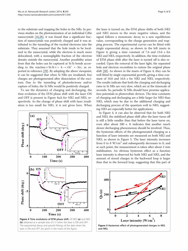
time evolution of the EFM phase shift with the laser ONand OFF is present in Figure 4a,b for NR2 and NR3, re-spectively. As the change of phase shift with laser irradi-ation is too small for NR1, it is not given here. When
Figure 4 Time evolutions of EFM phase shift. Of NR2 (a) and NR3(b) obtained at a sample bias of 2 V when the laser is ON and OFF.The exponential decay and growth fittings of the data when thelaser is ON and OFF are given in the insets of the figure.
the laser is turned on, the EFM phase shifts of both NR2and NR3 moves to the more negative values, and thesignal follows a monotonic decay to a new equilibriumvalue, corresponding to the charge generation and trap-ping process. The experimental curves can be fitted withsingle exponential decay, as shown in the left insets inFigure 4, giving a time constant of 7.6 and 13.6 s forNR2 and NR3, respectively. In addition, the time evolutionof EFM phase shift after the laser is turned off is also re-corded. Upon the removal of the laser light, the separatedhole and electron recombine to restore the original phaseshift [30]. As shown in the insets of Figure 4, they can bewell fitted by single exponential growth, giving a time con-stant of 10.6 and 16.6 s for NR2 and NR3, respectively.The results indicate that both the charging and dechargingrates in Si NRs are very slow, which are at the timescale ofseconds. So, periodic Si NRs should have promise applica-tion potentials in photovoltaic devices. The time constantsof charging and decharging are a little larger for NR3 thanNR2, which may be due to the additional charging anddecharging process of the quantum well in NR3, suggest-ing NR3 are especially better for applications.In Figure 4, it can also be observed that for both NR2
and NR3, the stabilized phase shift after the laser turns offis still a little smaller than that before the laser turns on,even after about 200 s. It indicates that another muchslower decharging phenomenon should be involved. Thus,the hysteresis effects of the photogenerated charging as afunction of laser intensity are measured on both NR2 andNR3, as shown in Figure 5. The laser intensity increasesfrom 0 to 8 W/cm2 and subsequently decreases to 0, andat each point, the measurement is taken after about 2 minstabilization. An obvious hysteresis effect as a functionlaser intensity is observed for both NR2 and NR3, and theamount of stored charges in the backward loop is largerthan that in the forward loop, suggesting that this part of
Figure 5 Hysteresis effect of photogenerated charges in NR2and NR3.

Wu et al. Nanoscale Research Letters 2014, 9:245 Page 7 of 8http://www.nanoscalereslett.com/content/9/1/245
charges decays with a slower time than which needed foreach measurement. These charges are found to bedetrapped after about half an hour. Similar charging hys-teresis effect was observed on Si nanoparticles coveredwith oxide layer by direct charge injection [31], and it wasinterpreted that charges were stored in the oxide layer ofthe nanoparticles. As in our case, the NRs are also coveredwith the native oxide layer; it is also possible that a part ofcharges are trapped in the oxide layer or interface stateswhich decays slower than the time for each measurement,resulting in the hysteresis in trapped charges. Since thistype of charges trapped in NR3 is larger than that in NR2,this difference could be attributed to the existence ofGeSi quantum well which increases the interface states.
ConclusionsIn conclusion, the photogenerated charging and trappingphenomena are directly measured on single Si NRs withoutthe deposition of electrodes by the means of EFM com-bined with laser irradiation. The amounts of photogener-ated charges trapped in single NRs and the CPD values areobtained from the analytical fitting of ΔΦ −VEFM curves.The quantities of charges and CPD values are found to in-crease with the laser intensity and vary with the type ofNRs. Though the exact mechanism for explaining thephotogenerated effects of single Si NRs is not variable atpresent, it is clear that photoexcitation can lead to obviouscharges trapped in Si NRs and hence reduce the work func-tion of NRs. Therefore, EFM can provide an effective wayto gain direct information on the trapped charges and sur-face potential of single nanostructures by combining withlaser irradiation, which should be important for both basicunderstanding and potential applications of nanostructuresin optoelectronics and photovoltaics.
Competing interestsThe authors declare that they have no competing interests.
Authors' contributionsSW carried out the experiments. ZLW prepared the samples. SW and XJYinterpreted the results and wrote the manuscript. DDL participated inmanuscript preparation. ZYZ and ZMJ helped in interpretation anddiscussions. All authors read and approved the final manuscript.
AcknowledgementsThis work was supported by the Major State Basic Research Project of China(No. 2011CB925601), National Natural Science Foundation of China (No.11274072), and Natural Science Foundation of Shanghai (No.12ZR1401300).
Received: 4 March 2014 Accepted: 7 May 2014Published: 20 May 2014
References1. Zhang Z, Zou R, Yu L, Hu J: Recent research on one-dimensional
silicon-based semiconductor nanomaterials: synthesis. Crit Rev Solid State2011, 36:148–173.
2. Barth S, Hernandez-Ramirez F, Holmes JD, Romano-Rodriguez A: Synthesisand applications of one-dimensional semiconductors. Prog Mater Sci2010, 55:563–627.
3. Kenry, Lim CT: Synthesis, optical properties, and chemical-biological sensingapplications of one-dimensional inorganic semiconductor nanowires.Prog Mater Sci 2013, 58:705–748.
4. Hu L, Chen G: Analysis of optical absorption in silicon nanowire arrays forphotovoltaic applications. Nano Lett 2007, 7:3249–3252.
5. Yoo J, Dayeh SA, Tang W, Picraux ST: Epitaxial growth of radial Sip-i-n junctions for photovoltaic applications. Appl Phys Lett 2013,102:093113.
6. Perraud S, Poncet S, Noël S, Levis M, Faucherand P, Rouvière E, Thony P,Jaussaud C, Delsol R: Full process for integrating silicon nanowire arraysinto solar cells. Sol Energ Mater Sol C 2009, 93:1568–71.
7. Tsakalakos L, Balch J, Fronheiser J, Korevaar BA, Sulima O, Rand J:Silicon nanowire solar cells. Appl Phys Lett 2007, 91:233117.
8. Tang H, Zhu L-G, Zhao L, Zhang X, Shan J, Lee S-T: Carrier dynamics in Sinanowires fabricated by metal-assisted chemical etching. Acs Nano 2012,6:7814–7819.
9. Kim J, Rhu H, Lee W: A continuous process for Si nanowires withprescribed lengths. J Mater Chem 2011, 21:15889.
10. Kiraly B, Yang S, Huang TJ: Multifunctional porous silicon nanopillar arrays:antireflection, superhydrophobicity, photoluminescence, and surface-enhanced Raman scattering. Nanotechnology 2013, 24:245704.
11. Jespersen TS, Nygard J: Charge trapping in carbon nanotube loopsdemonstrated by electrostatic force microscopy. Nano Lett 2005, 5:1838–1841.
12. Heim T, Lmimouni K, Vuillaume D: Ambipolar charge injection and transportin a single pentacene monolayer island. Nano Lett 2004, 4:2145–2150.
13. Yalcin SE, Labastide JA, Sowle DL, Barnes MD: Spectral properties ofmultiply charged semiconductor quantum dots. Nano Lett 2011,11:4425–4430.
14. Yalcin SE, Yang B, Labastide JA, Barnes MD: Electrostatic force microscopyand spectral studies of electron attachment to single quantum dots onindium tin oxide substrates. J Phys. Chem C 2012, 116:15847–53.
15. Li S, Steigerwald ML, Brus LE: Surface states in the photoionization ofhigh-quality CdSe core/shell nanocrystals. Acs Nano 2009, 3:1267–1273.
16. Cherniavskaya O, Chen LW, Islam MA, Brus L: Photoionization of individualCdSe/CdS core/shell nanocrystals on silicon with 2-nm oxide dependson surface band bending. Nano Lett 2003, 3:497–501.
17. Groves C, Reid OG, Ginger DS: Heterogeneity in polymer solar cells: localmorphology and performance in organic photovoltaics studied withscanning probe microscopy. Acc Chem Res 2010, 43:612–620.
18. Giridharagopal R, Shao G, Groves C, Ginger DS: New SPM techniques foranalyzing OPV materials. Mater Today 2010, 13:50–56.
19. Coffey DC, Ginger DS: Time-resolved electrostatic force microscopy ofpolymer solar cells. Nat Mater 2006, 5:735–740.
20. Wu Z, Lei H, Zhou T, Fan Y, Zhong Z: Fabrication and characterization ofSiGe coaxial quantum wells on ordered Si nanopillars. Nanotechnology2014, 25:055204.
21. Mélin T, Diesinger H, Deresmes D, Stiévenard D: Electric force microscopyof individually charged nanoparticles on conductors: an analytical modelfor quantitative charge imaging. Phys Rev B 2004, 69:035321.
22. Terris B, Stern J, Rugar D, Mamin H: Contact electrification using forcemicroscopy. Phys Rev Lett 1989, 63:2669–2672.
23. Mélin T, Diesinger H, Deresmes D, Stiévenard D: Probing nanoscale dipole-dipole interactions by electric force microscopy. Phys Rev Lett 2004, 92:166101.
24. Lei CH, Das A, Elliott M, Macdonald JE: Quantitative electrostatic forcemicroscopy-phase measurements. Nanotechnology 2004, 15:627–634.
25. Dokukin M, Olac-Vaw R, Guz N, Mitin V, Sokolov I: Addressable photochargingof single quantum dots assisted with atomic force microscopy probe.Appl Phys Lett 2009, 95:173105.
26. Chiesa M, Burgi L, Kim JS, Shikler R, Friend RH, Sirringhaus H: Correlationbetween surface photovoltage and blend morphology in polyfluorene-based photodiodes. Nano Lett 2005, 5:559–563.
27. Liscio A, Palermo V, Samori P: Nanoscale quantitative measurement of thepotential of charged nanostructures by electrostatic and Kelvin probeforce microscopy: unraveling electronic processes in complex materials.Acc Chem Res 2010, 43:541–550.
28. Krauss TD, Brus LE: Electronic properties of single semiconductornanocrystals: optical and electrostatic force microscopy measurements.Mat Sci Eng B 2000, 69–70:289–294.
29. Kim J-H, Noh H, Khim ZG, Jeon KS, Park YJ, Yoo H, Choi E, Om J: Electrostaticforce microscopy study about the hole trap in thin nitride/oxide/semicon-ductor structure. Appl Phys Lett 2008, 92:132901–3.

Wu et al. Nanoscale Research Letters 2014, 9:245 Page 8 of 8http://www.nanoscalereslett.com/content/9/1/245
30. Liu R: Imaging of photoinduced interfacial charge separation inconjugated polymer/semiconductor nanocomposites. J Phys Chem C2009, 113:9368–9374.
31. Diesinger H, Mélin T, Deresmes D, Stiévenard D, Baron T: Hystereticbehavior of the charge injection in single silicon nanoparticles. Appl PhysLett 2004, 85:3546–3548.
doi:10.1186/1556-276X-9-245Cite this article as: Wu et al.: Photogenerated charges and surfacepotential variations investigated on single Si nanorods by electrostaticforce microscopy combined with laser irradiation. Nanoscale ResearchLetters 2014 9:245.
Submit your manuscript to a journal and benefi t from:
7 Convenient online submission
7 Rigorous peer review
7 Immediate publication on acceptance
7 Open access: articles freely available online
7 High visibility within the fi eld
7 Retaining the copyright to your article
Submit your next manuscript at 7 springeropen.com