Design For Electromagnetic & Electrostatic Transient Immunity-Part1
40
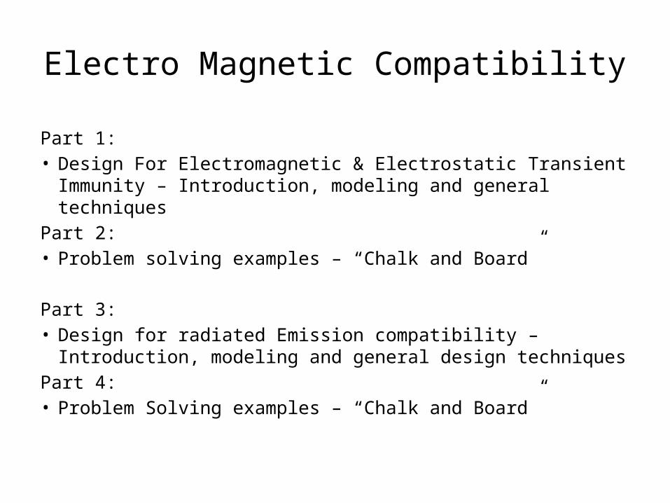
Electro Magnetic Compatibility Part 1: • Design For Electromagnetic & Electrostatic Transient Immunity – Introduction, modeling and general techniques Part 2: • Problem solving examples – “Chalk and Board” Part 3: • Design for radiated Emission compatibility – Introduction, modeling and general design techniques Part 4: • Problem Solving examples – “Chalk and Board”
-
Upload
independent -
Category
Documents
-
view
0 -
download
0
Transcript of Design For Electromagnetic & Electrostatic Transient Immunity-Part1
Electro Magnetic Compatibility
Part 1:• Design For Electromagnetic & Electrostatic Transient Immunity – Introduction, modeling and general techniques
Part 2:• Problem solving examples – “Chalk and Board”
Part 3:• Design for radiated Emission compatibility – Introduction, modeling and general design techniques
Part 4:• Problem Solving examples – “Chalk and Board”
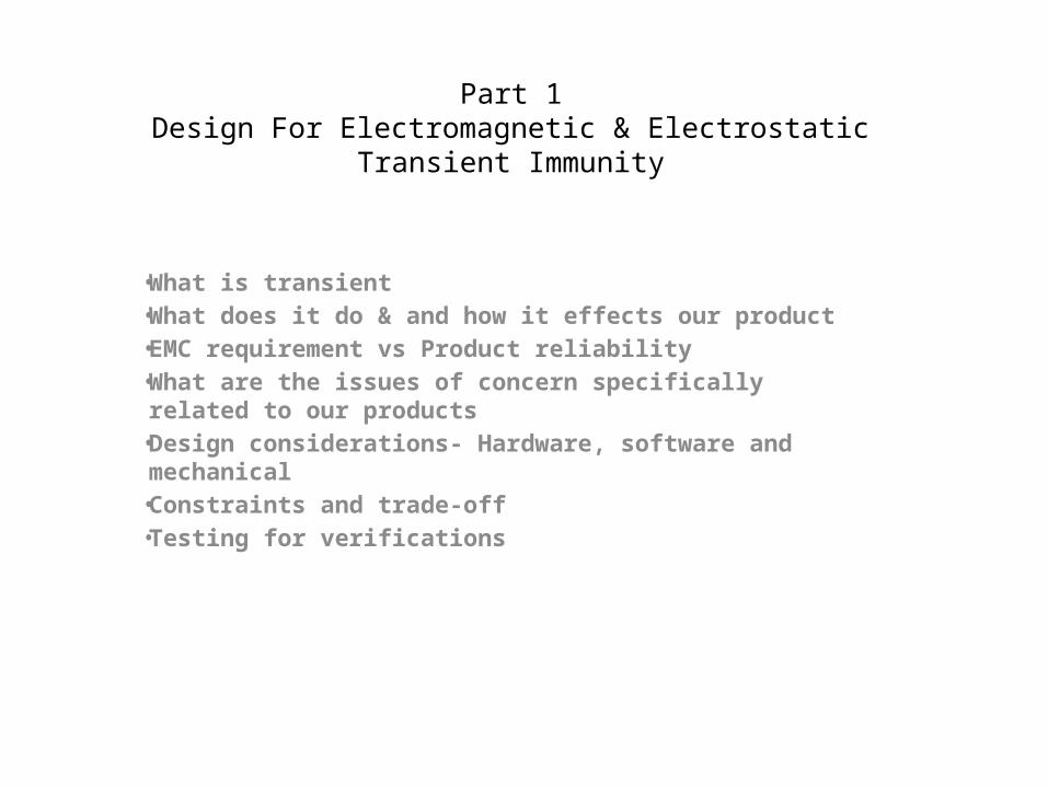
Part 1Design For Electromagnetic & Electrostatic
Transient Immunity
•What is transient•What does it do & and how it effects our product•EMC requirement vs Product reliability•What are the issues of concern specifically related to our products•Design considerations- Hardware, software and mechanical•Constraints and trade-off•Testing for verifications
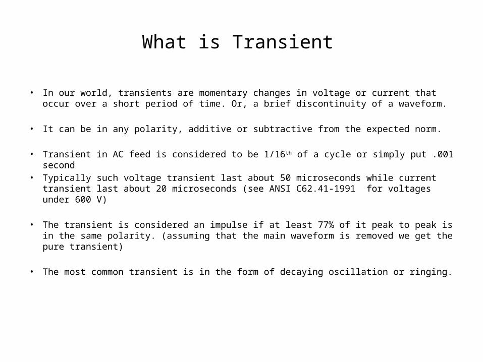
What is Transient
• In our world, transients are momentary changes in voltage or current that occur over a short period of time. Or, a brief discontinuity of a waveform.
• It can be in any polarity, additive or subtractive from the expected norm.
• Transient in AC feed is considered to be 1/16th of a cycle or simply put .001 second
• Typically such voltage transient last about 50 microseconds while current transient last about 20 microseconds (see ANSI C62.41-1991 for voltages under 600 V)
• The transient is considered an impulse if at least 77% of it peak to peak is in the same polarity. (assuming that the main waveform is removed we get the pure transient)
• The most common transient is in the form of decaying oscillation or ringing.
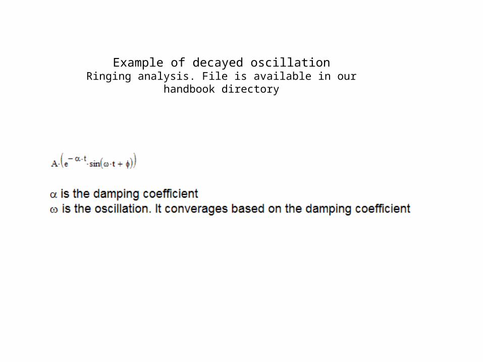
Example of decayed oscillationRinging analysis. File is available in our
handbook directory
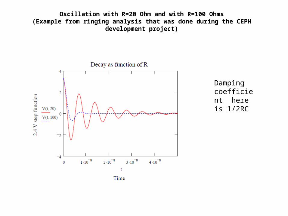
Oscillation with R=20 Ohm and with R=100 Ohms(Example from ringing analysis that was done during the CEPH
development project)
Damping coefficient here is 1/2RC
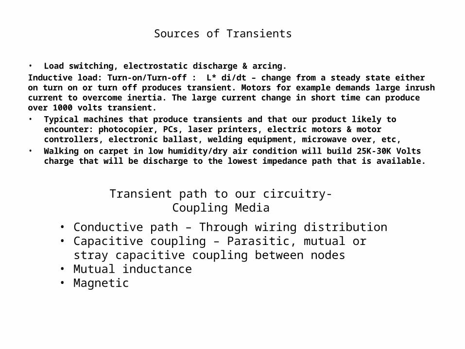
Sources of Transients
• Load switching, electrostatic discharge & arcing.Inductive load: Turn-on/Turn-off : L* di/dt – change from a steady state either on turn on or turn off produces transient. Motors for example demands large inrush current to overcome inertia. The large current change in short time can produce over 1000 volts transient.• Typical machines that produce transients and that our product likely to
encounter: photocopier, PCs, laser printers, electric motors & motor controllers, electronic ballast, welding equipment, microwave over, etc,
• Walking on carpet in low humidity/dry air condition will build 25K-30K Volts charge that will be discharge to the lowest impedance path that is available.
Transient path to our circuitry- Coupling Media
• Conductive path – Through wiring distribution• Capacitive coupling – Parasitic, mutual or
stray capacitive coupling between nodes• Mutual inductance• Magnetic
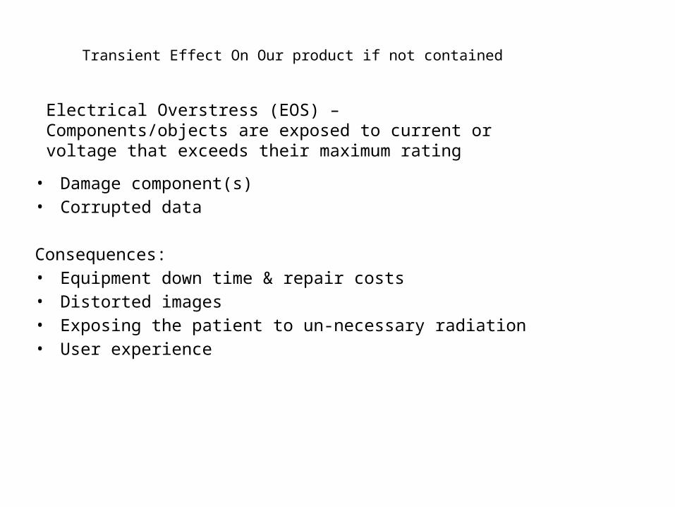
Transient Effect On Our product if not contained
• Damage component(s)• Corrupted data
Consequences:• Equipment down time & repair costs• Distorted images• Exposing the patient to un-necessary radiation• User experience
Electrical Overstress (EOS) – Components/objects are exposed to current or voltage that exceeds their maximum rating
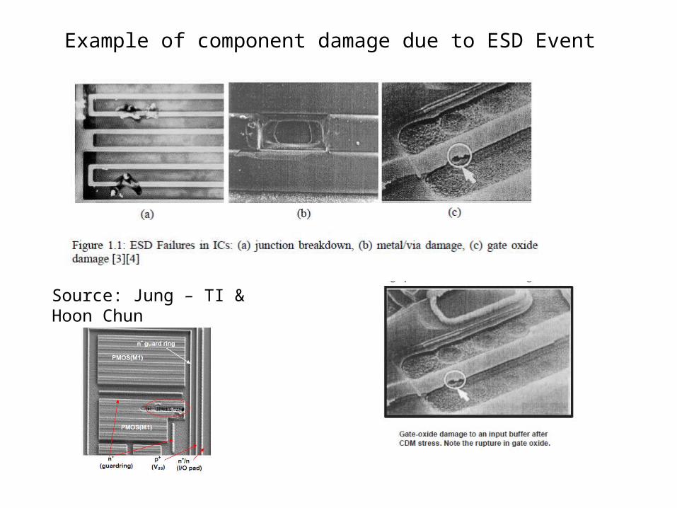
Example of component damage due to ESD Event
Source: Jung – TI & Hoon Chun
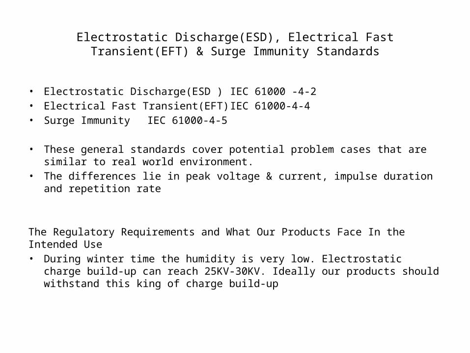
Electrostatic Discharge(ESD), Electrical Fast Transient(EFT) & Surge Immunity Standards
• Electrostatic Discharge(ESD ) IEC 61000 -4-2 • Electrical Fast Transient(EFT)IEC 61000-4-4• Surge Immunity IEC 61000-4-5
• These general standards cover potential problem cases that are similar to real world environment.
• The differences lie in peak voltage & current, impulse duration and repetition rate
The Regulatory Requirements and What Our Products Face In the Intended Use• During winter time the humidity is very low. Electrostatic
charge build-up can reach 25KV-30KV. Ideally our products should withstand this king of charge build-up
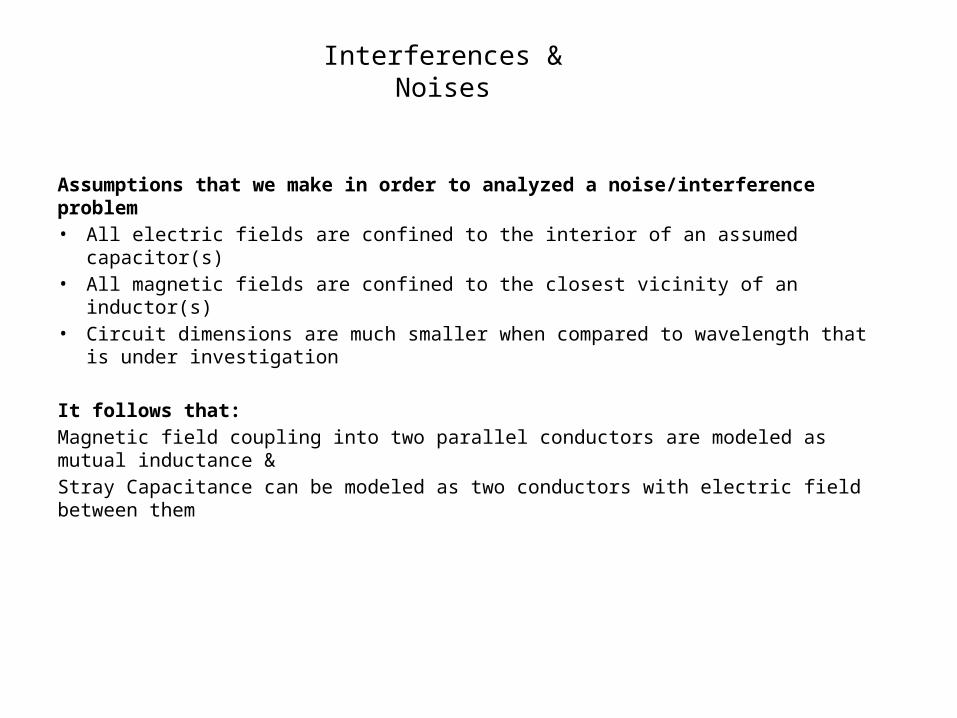
Interferences & Noises
Assumptions that we make in order to analyzed a noise/interference problem• All electric fields are confined to the interior of an assumed
capacitor(s)• All magnetic fields are confined to the closest vicinity of an
inductor(s)• Circuit dimensions are much smaller when compared to wavelength that
is under investigation
It follows that:Magnetic field coupling into two parallel conductors are modeled as mutual inductance &Stray Capacitance can be modeled as two conductors with electric field between them
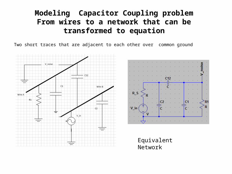
Modeling Capacitor Coupling problemFrom wires to a network that can be
transformed to equationTwo short traces that are adjacent to each other over common ground
Equivalent Network
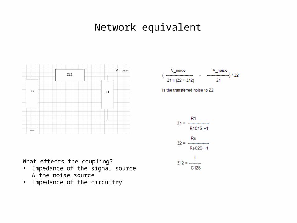
Network equivalent
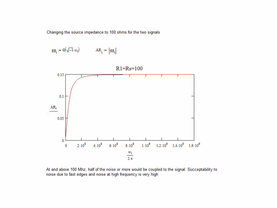
What effects the coupling?• Impedance of the signal source
& the noise source• Impedance of the circuitry
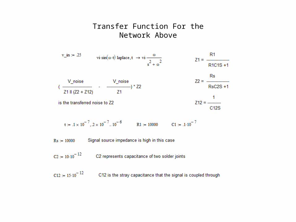
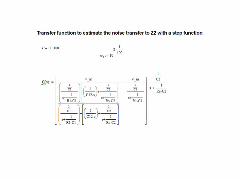
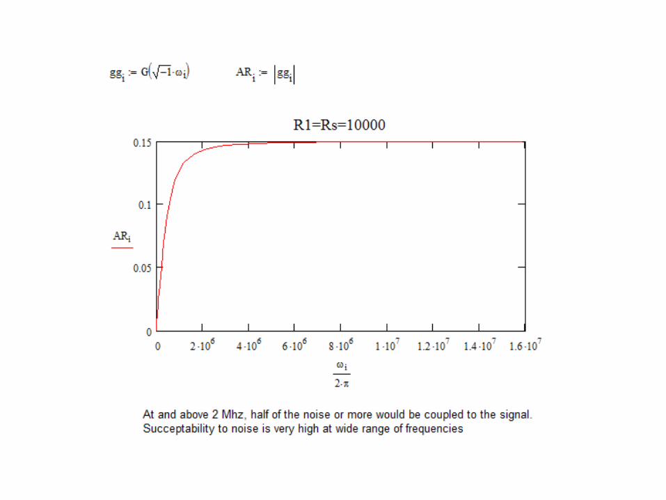
Transfer Function For the Network Above
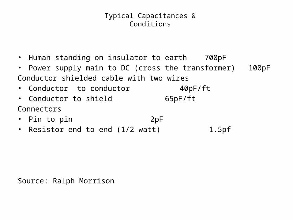
Typical Capacitances & Conditions
• Human standing on insulator to earth 700pF• Power supply main to DC (cross the transformer) 100pFConductor shielded cable with two wires• Conductor to conductor 40pF/ft• Conductor to shield 65pF/ftConnectors• Pin to pin 2pF• Resistor end to end (1/2 watt) 1.5pf
Source: Ralph Morrison
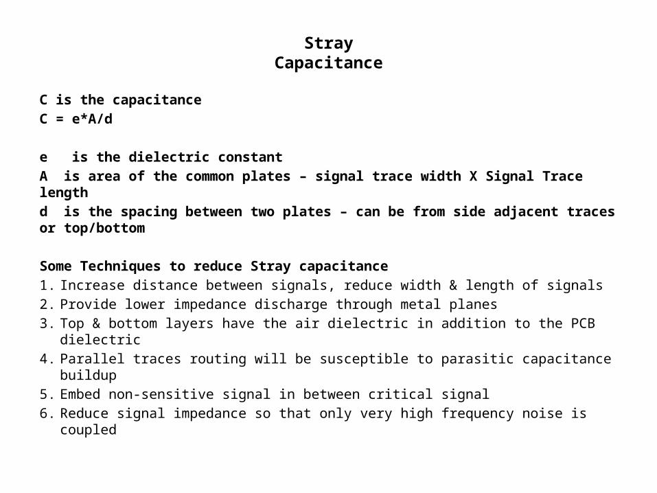
Stray Capacitance
C is the capacitanceC = e*A/d
e is the dielectric constantA is area of the common plates – signal trace width X Signal Trace lengthd is the spacing between two plates – can be from side adjacent traces or top/bottom
Some Techniques to reduce Stray capacitance1. Increase distance between signals, reduce width & length of signals2. Provide lower impedance discharge through metal planes3. Top & bottom layers have the air dielectric in addition to the PCB
dielectric4. Parallel traces routing will be susceptible to parasitic capacitance
buildup 5. Embed non-sensitive signal in between critical signal6. Reduce signal impedance so that only very high frequency noise is
coupled
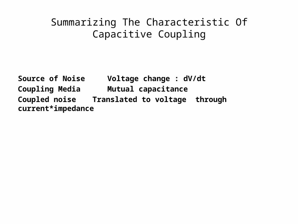
Summarizing The Characteristic Of Capacitive Coupling
Source of Noise Voltage change : dV/dtCoupling Media Mutual capacitanceCoupled noise Translated to voltage through current*impedance
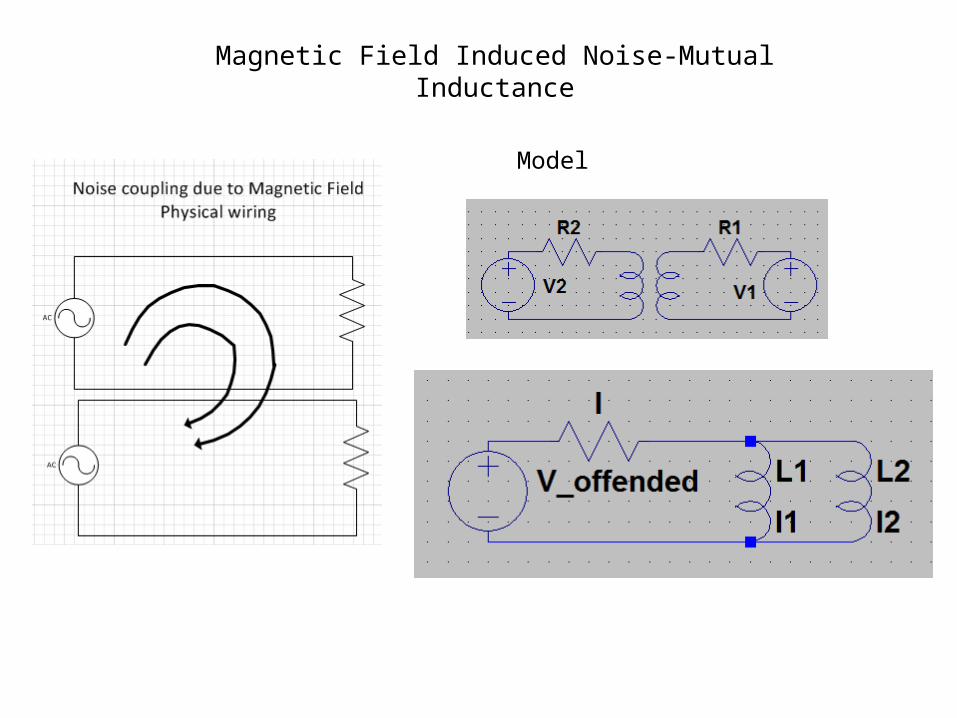
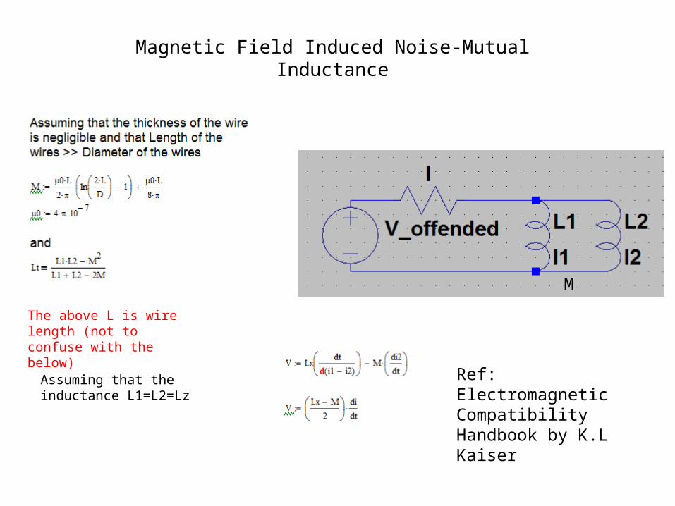
Magnetic Field Induced Noise-Mutual Inductance
Model
M
Magnetic Field Induced Noise-Mutual Inductance
Assuming that the inductance L1=L2=Lz
Ref: Electromagnetic Compatibility Handbook by K.L Kaiser
The above L is wire length (not to confuse with the below)
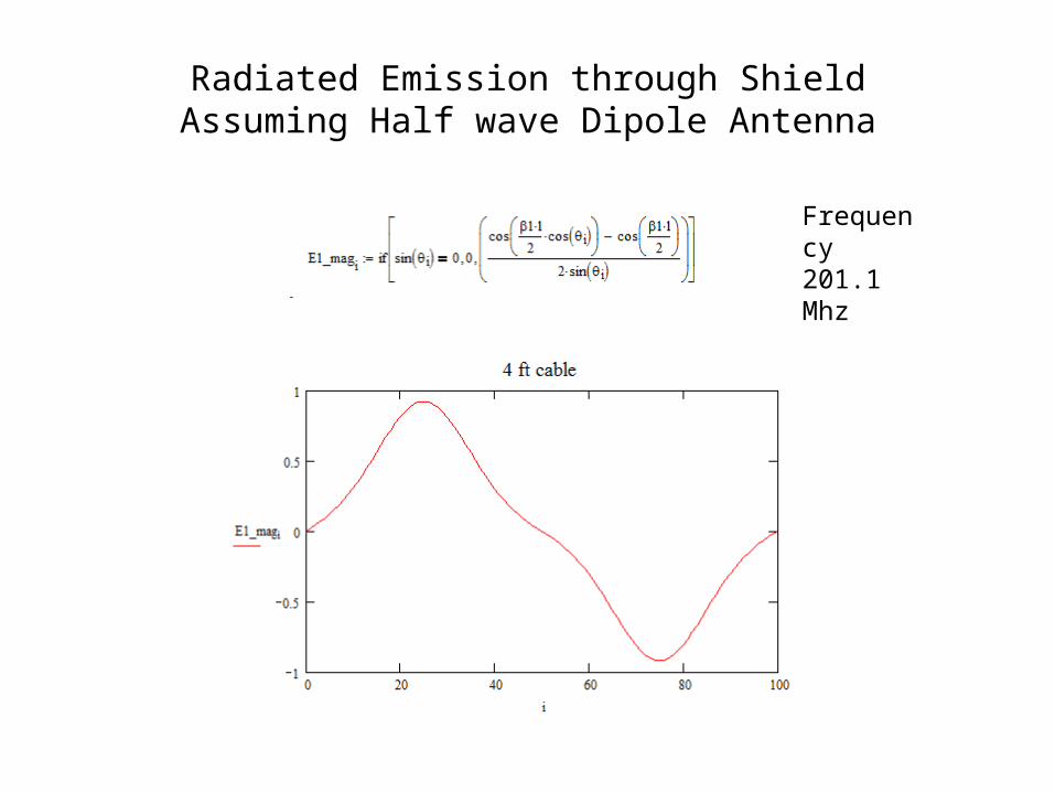
Radiated Emission through ShieldAssuming Half wave Dipole Antenna
Frequency 201.1 Mhz
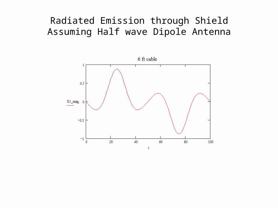
Radiated Emission through ShieldAssuming Half wave Dipole Antenna
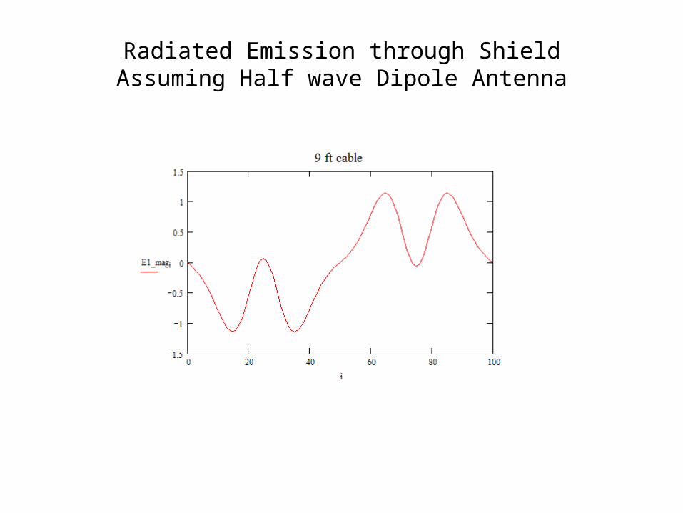
Radiated Emission through ShieldAssuming Half wave Dipole Antenna
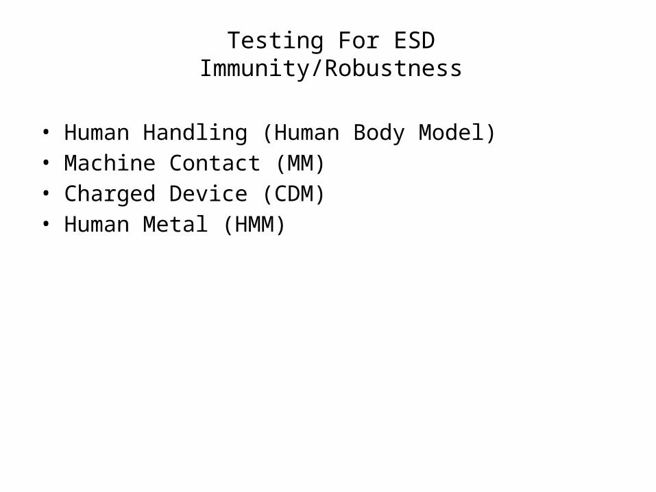
Testing For ESD Immunity/Robustness
• Human Handling (Human Body Model)• Machine Contact (MM)• Charged Device (CDM)• Human Metal (HMM)
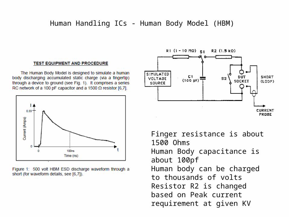
Human Handling ICs - Human Body Model (HBM)
Finger resistance is about 1500 OhmsHuman Body capacitance is about 100pf Human body can be charged to thousands of voltsResistor R2 is changed based on Peak current requirement at given KV
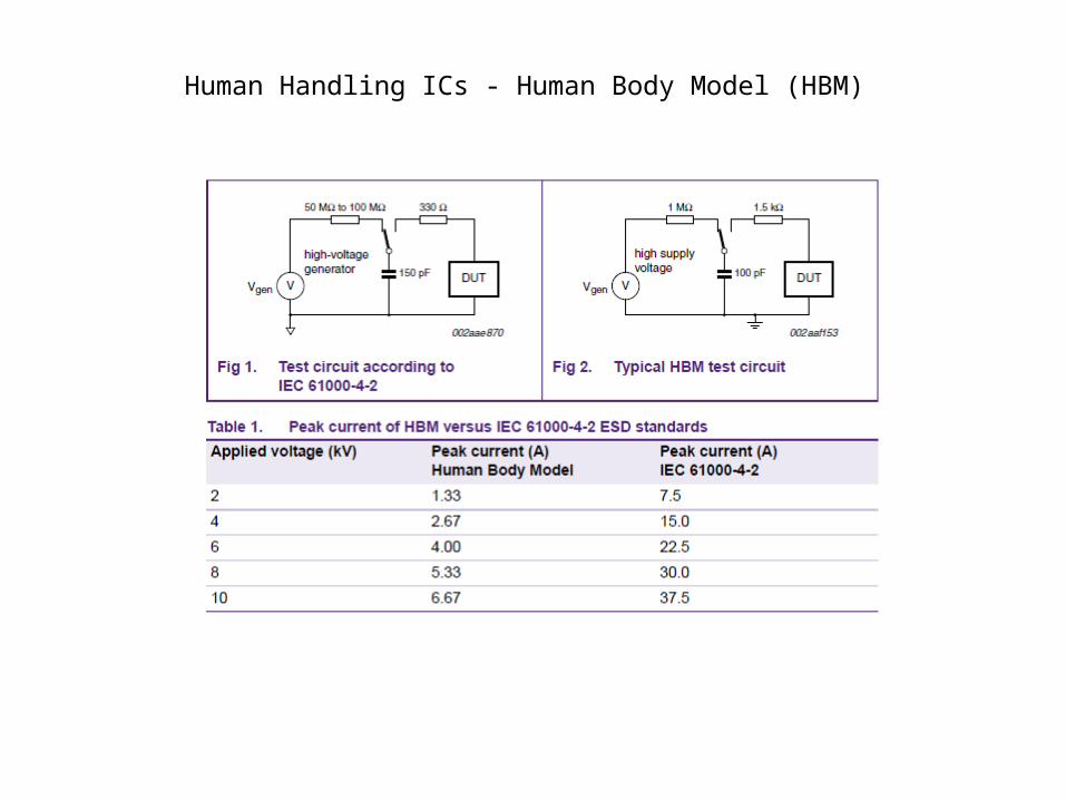
Human Handling ICs - Human Body Model (HBM)
Human Handling ICs - Human Body Model (HBM)
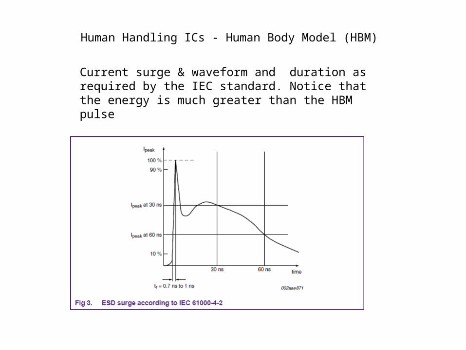
Current surge & waveform and duration as required by the IEC standard. Notice that the energy is much greater than the HBM pulse
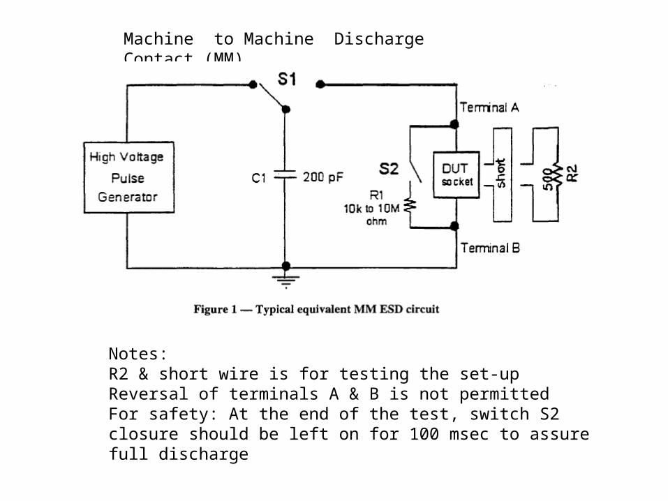
Machine to Machine Discharge Contact (MM)
Notes:R2 & short wire is for testing the set-upReversal of terminals A & B is not permittedFor safety: At the end of the test, switch S2 closure should be left on for 100 msec to assure full discharge
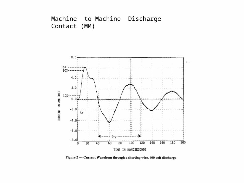
Machine to Machine Discharge Contact (MM)
Machine to Machine Discharge Contact (MM)
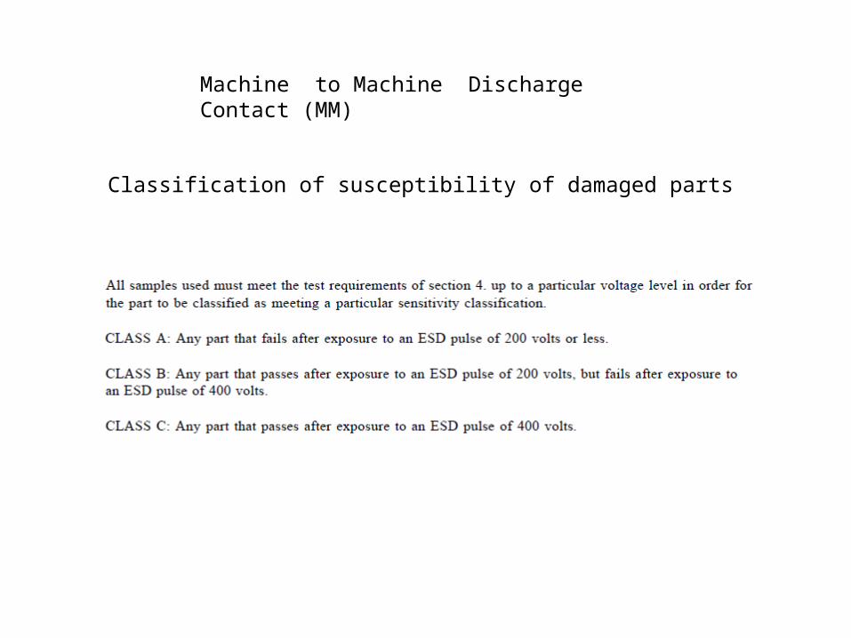
Classification of susceptibility of damaged parts
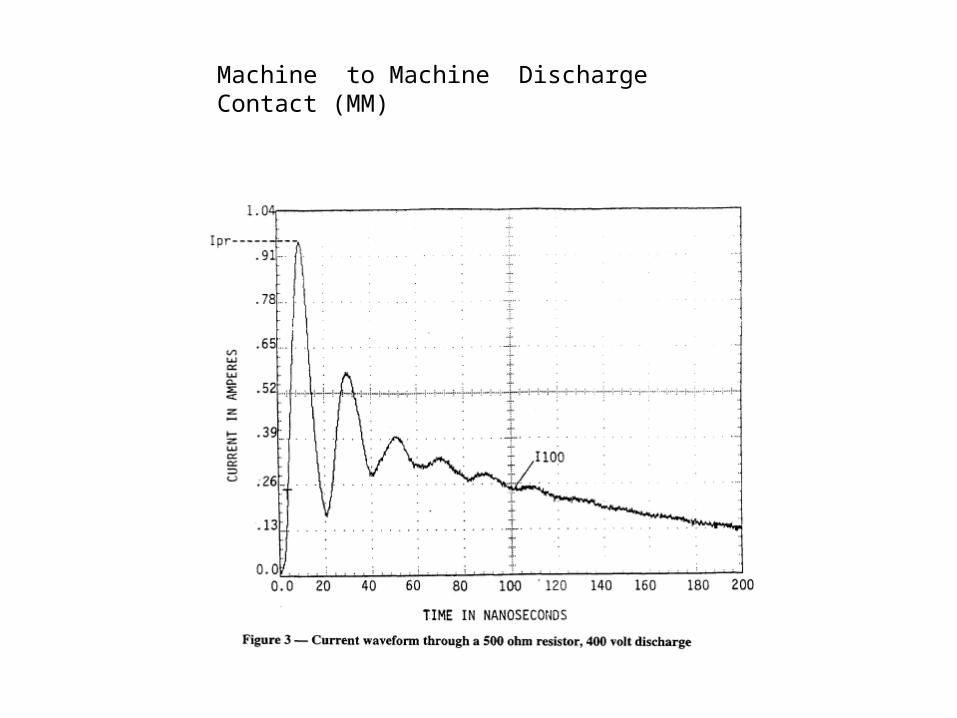
Machine to Machine Discharge Contact (MM)
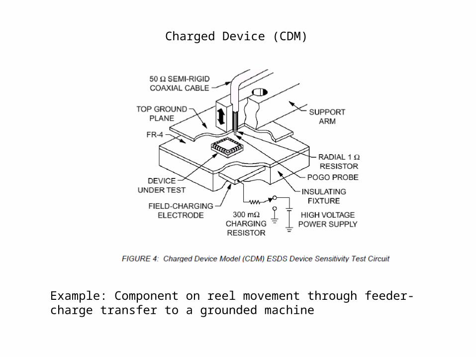
Charged Device (CDM)
Example: Component on reel movement through feeder-charge transfer to a grounded machine
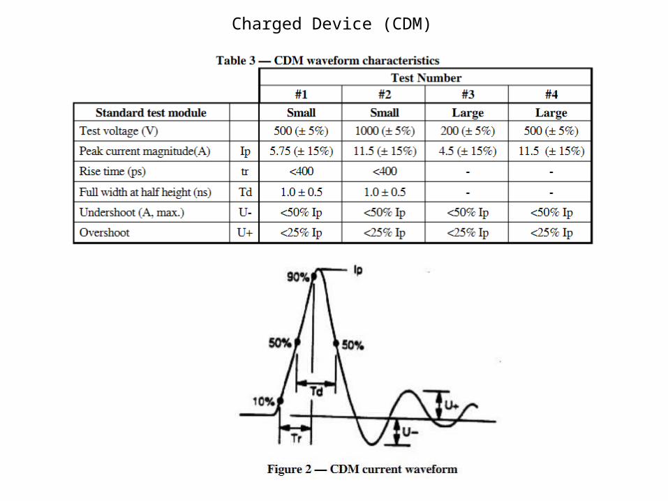
Charged Device (CDM)
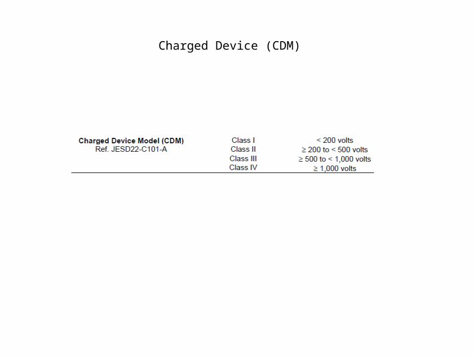
Charged Device (CDM)
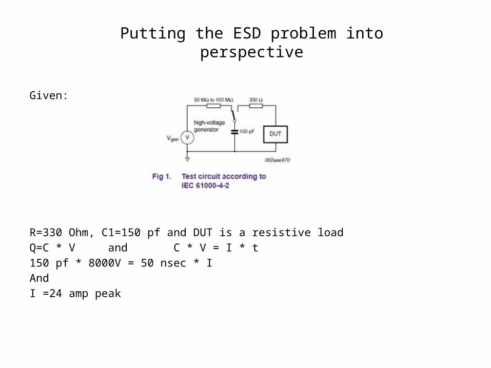
Putting the ESD problem into perspective
Given:
R=330 Ohm, C1=150 pf and DUT is a resistive loadQ=C * V and C * V = I * t150 pf * 8000V = 50 nsec * IAndI =24 amp peak
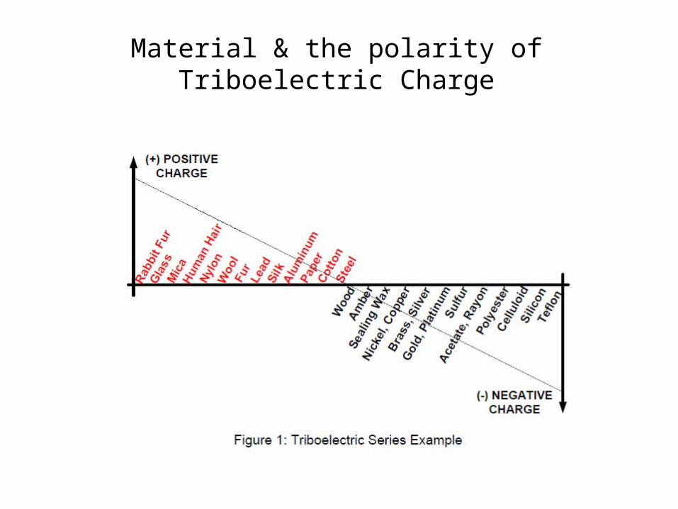
Material & the polarity of Triboelectric Charge
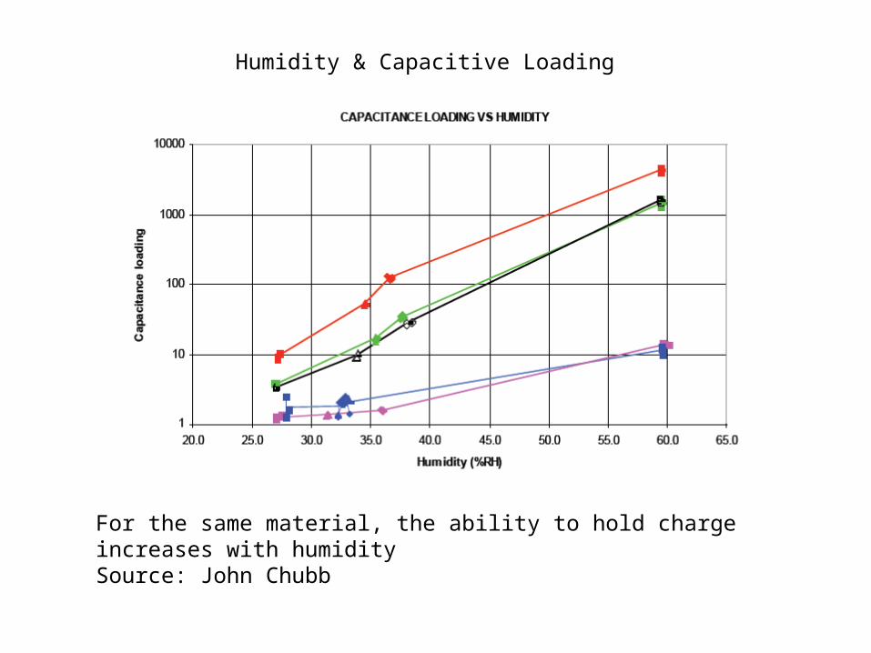
Humidity & Capacitive Loading
For the same material, the ability to hold charge increases with humiditySource: John Chubb
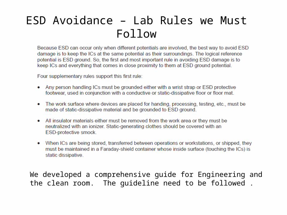
ESD Avoidance – Lab Rules we Must Follow
We developed a comprehensive guide for Engineering and the clean room. The guideline need to be followed .
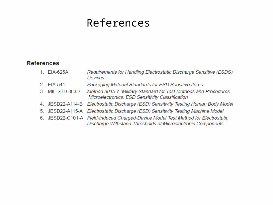
References