PhD Thesis: One and Two-Tip STM Aplications in Mesoscopic Surface Physics
183
O O n n e e a a n n d d T T w w o o - - T T i i p p S S T T M M A A p p l l i i c c a a t t i i o o n n s s i i n n M M e e s s o o s s c c o o p p i i c c S S u u r r f f a a c c e e P P h h y y s s i i c c s s Thesis submitted in partial fulfillment of the requirements for the degree of “DOCTOR OF PHILOSOPHY” by R R a a m m i i D D a a n n a a Submitted to the Senate of Ben-Gurion University of the Negev October 2009
Transcript of PhD Thesis: One and Two-Tip STM Aplications in Mesoscopic Surface Physics

OOnnee aanndd TTwwoo--TTiipp SSTTMM AAppll iiccaattiioonnss iinn MMeessoossccooppiicc
SSuurrffaaccee PPhhyyssiiccss
Thesis submitted in partial fulfillment of the requirements for the degree of
“DOCTOR OF PHILOSOPHY”
by
RRaammii DDaannaa
Submitted to the Senate of Ben-Gurion University of the Negev October 2009

i
Preference
In this Ph.D. the focused was on a mission to construct a dual-tip scanning tunneling
microscope (DTSTM) following a new approach. During the development of the apparatus, the
post deposition fractalization of Si/Si(111)7×7 islands in sub-monolayer was also explored. Some
of the images at a coverage close to θ = 0.5 display an unexpected behavior. As the percolation
threshold was crossed a new morphology, characterized by the islands shape transition to a
ramified structure with a narrow arm width was observed. In this work the conclusions from the
DTSTM project and from modeling of the morphological transition are described. For that reason,
this thesis is assembled from two parts. Part I - 'Morphological Shape Transition of Mesoscopic
Homoepitaxial Island Above Percolation' - describe how strain relaxation due to finite-size misfit
drive the morphological shape transition across the percolation threshold. Part II - 'Towards a
Dual-Tip STM Applications in Mesoscopic Surface Transport' - describe a new approach for a
dual-tip STM that will enables to characterize local electron transport on surfaces.
The work is composed as follows: In the beginning one abstract introduce the entire work;
the work itself is assembled from the above two parts, each with its own introduction, chapters
and conclusions (having their own Equations and Figures numbering); the bibliography is divided
into parts and chapters, but appears at the end; four appendixes, two for each part are also
included.
In each part the introduction and the first three/two (part I/II) chapters give a more general
view on the research field together with the specific theory and relevant practice for the work.
Here, not only the bottom lines of the scientific topics are mentioned, leaving it for the reader to
go through the vast amount of bibliography attached, and instead rather detailed explanations, are
usually included. The rest of the chapters describe the work itself.
Rami.

ii
Table of content
Part I - Morphological Shape Transition of Mesoscopic Homoepitexial
Islands Above Percolation
Introduction for part I
a. Growth modes 1
b. Surface stress and surface energy 2
c. Size dependent strain relaxation 3
d. Scope and composition of Part I of this thesis 4
Chapter 1 - Elastic relaxation and shape transition of epitaxial 2D
islands
1.1 Scope of chapter 1 6
1.2 Elastic relaxation of coherent epitaxial deposits and finite size misfit 6
1.2.1 Basic definitions 7
1.2.2 Epitaxial misfit, finite size misfit 10
1.3 The linear chain model (LCM) 12
Chapter 2 - Percolation and 2D islands system
2.1 Scope of chapter 2 19
2.2 Cluster numbers 19
2.3 Cluster structure 21
2.3.1 Cluster perimeter 21
2.3.2 Cluster radius and fractal dimension 22
Chapter 3 - Experimental & computational techniques
3.1 Scope of chapter 3 27
3.2 Scanning tunneling microscopy (STM) basics and the experimental setup 27
3.2.1 Overview of the scanning tunneling microscope 27
3.2.2 Modes of operation 29
3.2.3 The experimental setup 29
3.3 solid-phase homoepitaxially grown a-Si overlayers on Si(111)-7×7 surfaces 30
3.3.1 Structure of Si(111)7×7 surface 30

iii
3.3.2 Solid-phase epitaxy on Si(111)7×7 surface 31
3.4 Spatial correlations in site-occupations 32
3.5 Image processing and data computation 34
3.5.1 Image processing 34
3.5.2 Data analysis 34
Chapter 4 - STM realization of a strain induced shape transition across
the percolation threshold
4.1 Scope of chapter 4 36
4.2 STM of submonolayer percolating Si/Si(111)7x7 islands 36
4.2.1 Island growth 36
4.2.2 Image acquisition and processing 37
4.2.3 A first insight 38
4.3 Correlations and islands geometry 40
4.4 The islands systems as can be described within the framework of percolation 42
4.5 The shape transition as predicted by the LCM 43
4.5.1 The LCM for 2D ramified islands 44
4.5.2 The shape transition - From compact to ramified to linear chains 45
4.5.3 Energy calculation 47
4.6 The bottom line 48
Chapter 5 - Sub-monolayer homoepitaxial mesoscopic percolating
islands - Discussion
5.1 Scope of chapter 5 50
5.2 The island system as hypothetical medium with short-range correlations 50
5.3 The percolation phase transition and the two typical length scales 52
5.4 Strain forces in homo-epitaxial overlayers 53
5.4.1 The LCM in homoepitaxy 53
5.4.2 The kinetic/thermodynamic/statistical approach 54
5.5 The island system as a periodic domain of alternating-sign steps 54
5.5.1 Spontaneous domain formation and self-organization 54
5.5.2 Step-step interactions 55
5.6 The epitaxial process and the percolation threshold 56
5.7 Review on the LCM applications 57

iv
Conclusions for part I
Part II - Towards a Dual-Tip STM Applications in Mesoscopic Surface
Transport
Introduction for part II
a. Definitions: Characteristic length scales and transport regimes 61
b. Basic phenomenon: Mesoscopic two-terminal transport 62
c. Motivation: Electronic transport at semiconductor surfaces - from point-
contact transistor to micro-four-point probes 64
d. Noise 72
e. Scope and composition of Part II of this thesis 73
Chapter 1 - Review on theoretical aspects of dual-tip STM
1.2 Scope of this chapter 75
1.3 The fundamental work of Niu, Chang and Shih 75
1.4 Two tip configurations from other theoretical works 80
Chapter 2 - Survey on multi-probe STM design and applications
2.1 Scope of this chapter 81
2.2 Examples for multi-probe STM designs 81
2.2.1 Four-probe systems 81
2.2.2 Dual-tip STM 83
2.3 Probe aligning 84
2.4 Multi-probe STM tips 85
2.5 Multi-probe STM data acquisition and control 87
2.6 Multi-probe STM applications 89
2.7 Summery and conclusions 90
Chapter 3 - A new concept for a dual-tip STM
3.1 Scope of this chapter 92
3.2 Motivation and challenges 92
3.3 From a MCBJ to a DTSTM 93
3.3.1 The MCBJ technique 95
3.3.2 From a MCBJ to a DTSTM -The main ideas 97

v
3.3.3 The modified BJ 97
3.3.4 Unisotropialy-etching silicon BJ 97
3.3.5 BJ aligning and breaking 100
3.3.6 Approach mechanism and scanning 101
3.4 Fabrication of EBID nanotips 102
3.4.1 The EBID technique 102
3.4.2 EBID of nanotips for DTSTM applications 104
3.5 Experimental setup data acquisition and control electronics 104
Chapter 4 – Results
4.1 Scope of this chapter 112
4.2 The apparatus and experimental system 112
4.3 Si break-junction design and aligning 115
4.4 EBID of nanotips 116
Conclusions of part II
Appendix A - Computing of the coverage, and of the radius of gyration, area and perimeter (of each island) for a single STM image 125
Appendix B - computing of the site-occupation correlation-function for a
set of STM images from the same experiment (coverage) 134
Appendix C - Two tip configurations from other theoretical works 141
C.1 Probing Spatial Correlations with Nanoscale Two-contact Tunneling 141
C.2 Theory of a scanning tunneling microscope with a two-protrusion tip 142
C.3 Calculation of ballistic conductance through Tamm surface states 143
C.4 Local densities, distribution functions, and wave-function correlations for 146
spatially resolved shot noise at nanocontacts
Appendix D - Multi-probe STM applications
D.1 Four-probe applications 150
• Surface sensitivity versus probe spacing
• Anisotropy in surface conductivity
• Resistance across an atomic step
• Silicide Nanowires and Carbon Nanotubes
D.2 Dual-tip applications 155
• Measuring a carbon nanotube ring transistor

vi
• A method for determining σs by using two STM tips that remains in tunneling
contact
References 160
List of figures and tables for part I
Fig. 0.1 Classification of growth: Frank - van der Merwe, Volmer - Weber, Stranski -
Krastanov
1
Fig. 1.1 Epitaxial striction 10
Fig. 1.2 Schematic of assume crystal shape 13
Fig. 2.1 Percolation on a square lattice 18
Fig. 3.1 STM essential elements 27
Fig. 3.2 The experimental setup 29
Fig. 3.3 Schematic of pair-correlation functions 33
Fig. 4.1 Image processing and the islands border 38
Fig. 4.2 Separation into two phase system 39
Fig. 4.3 STM images from three different coverages 40
Fig. 4.4 STM images of silicon islands on si(111)7×7 and their B&W matrix 41
Fig. 4.5 The site-occupation correlation function 41
Fig. 4.6 The fractal dimension 42
Fig. 4.7 The cluster number exponent τ 43
Fig. 4.8 Perimeter of a ramified object 45
Fig. 4.9 The typical island width w 46
Fig. 5.1 Hypothetical medium with short-range correlations 51
Fig. 5.2 Matching of the target ( )rS2ˆ to the data correlations ( )rC
rδ2
52
Ta. 5.1 gathered the publications I found for the application of the linear chain model 57
List of figures and tables for part II
Fig. 0.1 ‘Onepoint’probes 68
Fig. 0.2 Macroscopic and Microscopic four-point probes 70
Fig. 1.1 Schematic diagram of the double-tip STM 76

vii
Fig. 1.2 Four different probe-sample geometry 80
Ta. 2.1 Different four-point configurations and their measured resistances 81
Fig. 2.1 A monolithic micro-four-point probe 82
Fig. 2.2 Four-tip STM systems 83
Fig. 2.3 Different dual-tip STM systems 84
Fig. 2.4 Two tips aligning and navigation 86
Fig. 2.5 Examples for high-aspect ratio tips in multi-tip STMs 88
Fig. 2.6 A diagram of a preamp for one (current/voltage probe) tip 89
Fig. 3.1 The MCBJ 95
Fig. 3.2 Microfabricated silicon BJ 96
Fig. 3.3 The rotational break-junction 98
Fig. 3.4 The Si BJ 99
Fig. 3.5 Si break junction aligning and breaking 100
Fig. 3.6 Sample approach and scanning 101
Fig. 3.7 An illustration of an ideal EBID process 102
Fig. 3.8 Typical tip growth sequence (from (hfac)CuVTMS on Si, 25 keV, 500 pA) 104
Fig. 3.9 Examples for tip growth control 106
Fig. 3.10 The dumping system 107
Fig. 4.1 The experimental system 112
Fig. 4.2 The DTSTM lower part; the break-junction 113
Fig 4.3 The DTSTM assembled with the upper part 114
Fig. 4.4 Break-junction design 116
Fig. 4.5 Break-junction aligning and tip navigation 117
Fig. 4.6 EBID of carbon tips 118
Fig. 4.7 High aspect ratio WCO6 tips 119
Fig. 4.8 "Free standing" WCO6 fine tips 120
Fig. 4.9 Gold coating 121
List of figures for the appendixes
Fig. C.1 ‘Onepoint’probes 141
Fig. D.1 Macroscopic and Microscopic four-point probes 150
Fig. D.2 Schematic diagram of the double-tip STM 152

viii
Fig. D.3 Four different probe-sample geometry 154
Fig. D.4 A monolithic micro-four-point probe 156
Fig. D.5 Four-tip STM systems 158
List of abbreviations
4PP Four Point Probe SE Secondary Electrons
BEEM
Ballistic Energy Electron
Microscope SEM Scanning Electron Microscope
CNT Carbon Nanotube SK Stranski - Krastanov
DAS Dimer-Adatom-Stacking SPE Solid-Phase Epitaxy
DTSTM Dual-Tip STM SPM Scanning Probe Microscope
EBID
Electron Beam Induced
Deposition STM
Scanning Tunneling
Microscope
FFT Fast-Fourier-Transform TT J. Tersoff and R. M. Tromp
FM Frank - van der Merwe UHV Ultra-High Vacuum
HB P. Hanesch and E. Bertel VW Volmer - Weber
LB Landuer-Büttiker
LCM Linear Chain Model
LDOS Local Density Of States
LEED
Low-Energy Electron
Diffraction
MBE molecular beam epitaxy
MCBJ
Mechanically-Controllable
Break-Junction
ML Monolayer
MPSTM Multi-probe STM
MS
Pierre Müller and Andre´s
Sau´l
RD Random Percolation

ix
Abstract
Usually strain relaxations are predicted on the basis of the macroscopic lattice mismatch
between two materials. In the case of homoepitaxy, according to the classical rule, no difference
between deposited material and substrate has to be made and no effects arise due to a misfit
between substrate and the film. The principal drawback of this approach is that mesoscopic
islands should adopt their intrinsic bond lengths, which can be different from the bond lengths in
bulk. And indeed, it was demonstrated that strain relaxations in homoepitaxy are determined by
the size dependent mesoscopic mismatch. In mesoscopic islands the relaxation of edge atoms can
be the dominating process. These atoms are relaxing in the direction of the center of the island
and take other equilibrium positions with shorter bonds than in macroscopic systems. Therefore,
the mesoscopic mismatch (finite-size misfit) between islands and the substrate in homoepitaxy
exists and can locally affect the growth process.
Transport on surfaces and nanostructures can also be sensitive to the size of the system.
The transport-contextual definition of mesoscopic was originally introduced by van Kampen in
the context of statistical mechanics, where the finite size effect dominates the thermal behavior.
But, microstructures often called mesoscopic when the phase of a single-electron wave function
remains coherent across the system. Coherent means that the phase-coherence length lφ associated
with processes that can change the environment exceeds the system size L.
In this work scanning tunneling microscope (STM) realization of finite-size misfit in
homoepitaxy and a dual-tip STM for the charctarization of mesoscopic transport on surfaces will
be introduced. The finite-size misfit will be used to explain the shape transition of homoepitaxial
silicon islands above the percolation threshold. The motivation to characterize surface transport
on the mesoscale will be in the heart of a new approach for a dual-tip STM.
For the finite size misfit realization - Percolation is a mathematical model, describing a
geometrical phase transition, in infinite disordered systems. By randomly filling sites on an
infinite 2D lattice, the site-percolation threshold pc is defined as the site-occupation probability
where for the first time an infinite island spans the entire system. Percolation was extensively
investigated, both theoretically and experimentally and was implemented in many fields of
research. It is defined for many characteristics like; different connectivity rules and lattice
symmetries, from 1 to n dimensions, for discrete or continuous systems and for random or
correlated occupation probabilities. In percolation, a geometrical correlation length ξ, defined for

x
2D by the mean distance between two sites on the same island, is recognized as the only
characteristic length. Thus, at the critical coverage θc, ξ experience geometrical phase transition
and diverges. Although ξ, and statistical quantities defined by it, are a subject for scaling laws
when p → pc, the morphology of the percolating islands has not been predicted or observed
previously to be affected by this phase transition. In part I of this work, experimental results
showing a strain driven morphological transition associated with the geometrical critical point of
percolation are discussed. The transition is characterized by a reduction of the typical island width
w by a factor of e above the percolation threshold.
The characterization of percolative and ramified geometries in surface over layer systems
is a well established field of research. Specifically, in this work, the appearance of the factor e, led
me to the linear chain model (LCM) first introduced by Tersoff and Tromp (TT). The LCM
describes island formation in strained hetroepitaxial layers, as a mechanism for strain relaxation
without dislocations. TT described the strained islands by applying elastic monopoles at the
border of the deposit. By minimizing the total energy with respect to the island geometry, they
found an optimal island size α02 at the optimal tradeoff between extra surface and interface energy
and the energy gained due to elastic relaxation. They also showed that compact islands are stable
as long as their linear size ≤ eα0. However, once an island grows beyond its optimal area α02 by a
factor of e2, a morphological transition to rectangular shape is observed. The LCM also predicts
an asymptotic convergence to the optimal width α0 as the islands length grows to infinity. This is
a fundamental feature that connects the LCM to percolation. On one hand, percolation is defined
as the coverage where an infinite island is formed. On the other hand, the LCM predicts the
asymptotic island width value as the island length grows to infinity. Thus, when a percolating
island system can be described by the LCM, the asymptotic value is expected to be found when
the percolation threshold is being approached. STM images taken from both sides of the
percolation threshold, (i.e., before and after an infinite island is formed), are consistent with this
prediction. It will be also demonstrated, for the first time, to the best of our knowledge, the
validity of this model for homoepitexial islands. By growing nanoscale Si/Si(111)7x7 islands, it
will be argued that a finite-size misfit, as has been previously recognized (theoretically and
experimentally) as effective also in homoepitaxy, is responsible for the presence of strain forces.
Strain forces are essential in justifying the existence of the shape transition predicted by the LCM.
For the new approach for a DTSTM - The vertical current flowing between a single-tip
scanning tunneling microscope (STM) and a surface can probe static properties of electronic
systems such as local density of states. But, it has already been demonstrated that a significant
lateral surface component is also present. This lateral component carries an extremely

xi
fundamental property of the surface, namely, the electron density of states of the surface at
momentum space (dispersion relations). In order to measure such local dispersion relations, one
has to inject hot ballistic electrons with one electrode and collect them with a second electrode.
As demonstrated by Angle Resolved UV Photoelectron Spectroscopy, the two-dimensional
momentum distributions at the surface are extremely anisotropic. Thus, if a lateral electron beam
that traverses the surface between two biased electrodes can keep its direction and energy over
distances of several nm (as indicated by Ballistic Electron Emission microscopy in 3D), the
dispersion of the electronic structure should give an orientation and position dependence of the
local transconductance current. (However, for the electron to be ballistic, the probe separation
must be very small.) The lateral component of the current can also display mesoscopic transport
phenomena related to characteristic length scales and transport regimes. Some of these
phenomena were verified by the fabrication of artificial structures that generate 3D down to 0D
quantum entities. These patterns serve as fixed experimental setups with a predetermined and
strongly coupled terminal contacts configurations; thus, they lack the capability of performing
local transport measurement on arbitrary systems and especially on surfaces. Transport on
surfaces might be important since, as the conductor’s dimensions become smaller, the surface-to-
volume ratio becomes larger, and transport can be more surface-sensitive (as indicated by 4-probe
measurements). Of all the different possible setups for multi-terminal experiments, the multi-
probe STM (MPSTM) has the following benefits: self and changeable positioning of the leads
with sub-nm precision, small (weakly coupled) point contact or tunneling mode measurements for
high angular resolution, and its nature as a noninvasive technique. Indeed, in the last decade,
various, but not many, attempts to construct MPSTMs were reported. In part II of this work, the
theory for a DTSTM and variety of multi-probe systems, designed in the last eight years, will be
reviewed. Following it, the main challenges and solutions, involved in the design and operation of
a DTSTM that are of fundamental importance will be deduced. From here a new approach for a
dual-tip STM based on the mechanically controllable break-junction (MCBJ) with two electron
beam-induced deposition (EBID) nanotips was developed.
The MCBJ is a novel technique in which a notched-wire/thin-film/lithographically-
designed junction, held at two close points on a bending beam is being broken. By releasing the
pressure (to bend), the two sides of the junction can than be tuned, with extreme precession and
stability, to form atomic point contact. An extension of the MCBJ is what sometimes being called
the MCB-STM. Here a thin piece of piezo material, put between the wire and the bending beam,
enables scanning the two electrodes one in front of the other. Unfortunately, the scanned surfaces
are random and can’t be chosen, and defiantly, scanning a third surface is out of question. In order

xii
to do so, both sides of the junction have to simultaneously face a desired surface (instead of each
other), be aligned in 3D, and have a scanning probe design and capabilities. To meet this
challenge, a DTSTM based on the MCBJ with two fabricated EBID nanotips was developed. The
stability and alignment of the BJ were found as a good starting point for two-electrode system on
a ‘constant’ nanogap separation. The design is a modified version of the MCB-STM. But, unlike
the traditional bending which applies lateral force on the junction, in the new design, the breaking
mechanism applies torque on a virtual axle running through the junction. The rotational
mechanism consists of two tangential springs-hinge that supply the return force and ensure that
the virtual axle keeps its aligning throughout the rotational process. By this manipulation, the two
sides of the junction remain close although a small angle is applied. The angle is necessary in
order to enable tunneling of two nanotips when approaching with macroscopic sample. The
junction is curved in Si wafer by double-sided anisotropic etching to form 30 micron wide bridge
as a base for EBID tips. EBID is the process by which a solid material can be deposited onto a
solid substrate by means of an electron-mediated decomposition of a precursor molecule (a
compound containing the species to be deposited). Nanotips with controlled architecture and from
variety of materials are then being fabricated on each side of the junction to establish a dual-tip
system. Integration of the special characteristics of MCBJ and EBID, leads to a DTSTM capable
of ~50 nm probe separation, as presented in this work. On these scales more local and less
averaged information can be collected; thus, new insight on electron transport phenomena on the
nanoscale will hopefully be gained. The nature of current flow on these scales can be interesting
from both fundamental physics and device application points of views.

PPaarrtt II
MMoorrpphhoollooggiiccaall SShhaappee TTrraannssiittiioonn ooff MMeessoossccooppiicc HHoommooeeppiittaaxxiiaall
IIssllaanndd aabboovvee PPeerrccoollaattiioonn

!
!
!"
#" $
%
" !
# !$!& '()*+),-().

%
!&
! '
( ! )
(
!
* +#,
#, - & -& . / ./!
( 0 0
0! # ! $!! )
#,
01020!3 (
! %
! "
!01040
5-& !
!
5./ !
!
! '
(
!
-
. (
!"
!&

5
!"
!
(
( !
67 8 67
9 657!"
! "
(!.
!
! &
(
:
!
-!
6;7!' 6<=>7
!"
3 &$ $!< ,) 6<7! ? # @ @
&$
6A7 B &
6>7!
($C6<7!
@@$$6D7!"
!

;
. 6E7! ?
,6$7 (
!
!"
! "
% 67! F
! "
6 57! G!/ 6;7
%!
*
! "
!
!"$$G!/6<7
%
!, H 6AE7
@@!
! ?
!
' !
(
! %
! "
!
#
6$7!
/6 7!
-$
<
& "
%., !
! .
%
! "
!
9
!
!"
! '
)!
!
)@, ! )@,
.:.>>
)!! "
. ? ? 657 .?I
"B !'
"!"5
!# ;
!8;
! " <
;
!" !
!

6
Chapter 1
Elastic relaxation and shape transition of epitaxial 2D islands
1.1 Scope of chapter 1
In this chapter some theoretical issues that are essential for later interpretation of the
experimental observation will be reviewed. In section 1.2, an introduction to some basic
definitions in the elastic relaxation of coherent epitaxial deposits will be given. The finite-size
misfit and its contribution, which is crucial to this thesis, will be introduced here. In section 1.3
the linear chain model (LCM) describing the shape transition of hetroepitexial islands will be
reviewed. The LCM will later be used to explain the experimental results in Si/Si(111)7x7
homoepitaxy of mesoscopic islands due to the finite-size misfit.
1.2 Elastic relaxation of coherent epitaxial deposits and finite size misfit
When there is a misfit, the epitaxial contact of two crystals A and B can either be coherent
or not coherent. One recognizes the coherent epitaxial systems where the lattice planes in contact
are in perfect registry over a large domain of intensive parameters (temperature, pressure,
chemical potentials, etc.). During deposition, a transition from this perfect registry to a partial one
occurs at some critical thickness - see for example Ref. [1] - where the introduction of interfacial
dislocations takes place. In this way the deposit abruptly releases strain energy by plasticity. On
the contrary, non-coherent epitaxies are recognized when their contact lattice planes are out of
registry. The periodicities of both lattice planes remain incommensurate, changing continuously
with the intensive parameter changes, although a coherent lock-in may happen but it is weak. The
only way of relaxing such systems is the introduction of explicit dislocations [1] or other linear
defects [2]. This is true for continuous deposits on a semi-infinite substrate. However, when the
deposit grows as three-dimensional (3D) discrete crystals, before any plastic relaxation, an elastic
relaxation is still possible where the interface remains coherent. This elastic relaxation has been
classified as accommodation by misfit strain gradient [3]. This type of relaxation has been
supported experimentally by electron microscopic observations [4-6] of cross-sections. Owing to
their free lateral faces, the 3D crystals relax laterally, but since their base face remains coherent

7
with the substrate they drag the atoms of the contact area, producing a strain field in the bulk of
the substrate. In the following this effect will be called "epitaxial striction". This effect reduces
the total elastic energy stored in the system. A comprehensive account of experimental
observations and theoretical formulations describing this effect can be found in Ref. [7]. Another
trend arose in modeling the coherent elastic relaxation of strained epitaxial films by point forces
acting on the substrate. In a first stage such forces have been assumed to be concentrated at the
film edge [8]. A similar model was made by Tersoff and Tromp (TT) [9] to describe strained
epitaxial islands by applying elastic monopoles at the border of the deposit, or by Duport and
coworkers [10,11] in modeling a coherent epitaxy by a uniform distribution of elastic dipoles or
even a superposition of such. (The formulation by TT will be used in the following).
Nevertheless, Hu [12] stated long before that the concept of such concentrated "edge forces" is
not sound in an epitaxial context. Indeed, if the substrate becomes deformed by such edge-forces
it, in turn, deforms the film above and then leads to a new distribution of forces in the film. Then
the epitaxial force has to be determined by a self-consistent analysis. In their Surface Science
paper "Elastic relaxation of coherent epitaxial deposits" from 1997 [7] R. Kern and P. Müller
(KM) use such a self consistent approach to describe the 3D coherently strained epitaxial
deposits. They used macroscopic linear isotropic elasticity up to monolayer sizes, which is
considered acceptable [13] when the material constants are somewhat adjusted. To introduce
finite size effects properly they also considered surface elasticity, which means they considered
surface stress. They distinguished then between the epitaxial forces and the forces due to surface
stress an island will exert on a substrate, which, in turn, will determine the relaxation of the whole
system. Since they waned to do this analytically they had to limit themselves to the so-called
plane strain case of elasticity. That means they treat a 3D infinite ribbon and not a 3D island.
Despite this restriction, the knowledge they gain makes sense for islands, except for near-corner
effects.
Since finite size misfit is not commonly used as the macroscopic one, in the following,
some basic definitions and the derivation of this quantity are included. Here, KM paper from 1997
and P. Müller and A. Sau´l (MS) Surface Science Reports paper "Elastic effects on surface
physics" [14] from 2004 are being followed.
1.2.1 Basic definitions
• Bulk stress tensor

8
By considering first the case of a homogeneous stressed solid and an elementary
parallelepiped of volume dV = dx1dx2dx3 centered on a pointrr
. The face normal to the k
direction has an area dxi dxj (1 ≤ i ≠ j ≠ k ≤ 3) and is submitted to a force per unit area equal to σ
× k , i.e., the ith component of the force is the element σik of the bulk stress tensor σ.
When an elementary parallelepiped is in mechanical equilibrium, that means when no resultant
force or torque displaces or rotates it, the bulk stress tensor fulfils the following conditions [15]:
0=+∂
∂∑ ext
ijj
ij fx
σ and jiij σσ = in the bulk,
0=−∑ surfijj ij fnσ at the surface, (1)
where extifr
is the external force field per unit volume acting in the bulk (for example gravity),
surfifr
the forces applied at the surface of the body and n the unit vector normal to the surface of
the body directed towards the exterior.
• Bulk strain tensor
The symmetric bulk strain tensor components are defined by
∂
∂+
∂∂
=i
j
j
iij x
u
x
u
21
ε , (2)
where ui are the components of the displacement field [15]. This somehow artificial
symmetrisation of the strain tensor avoids considering a simple rotation as a deformation (in some
cases, for the sake of mathematical simplicity one defines jiij xu ∂∂= /ε . This tensor is called the
unsymmetrised strain tensor). The diagonal components εii describe the elongation parallel to the
i-axis, whereas the off diagonal element εij with i ≠ j is related to the deformation angle measured
between two straight lines initially parallel to the axis xi and xj respectively.
• Hooke’s law

9
In the framework of linear elasticity, the relation between bulk stress and strain tensor can be
written as
∑=kl klijklij C εσ , ∑=
kl klijklij S σε , (3)
where Cijkl and Sijkl are called stiffness and compliance coefficients, respectively. These
coefficients describe the elastic properties of the material.
• Epitaxial striction
For their purpose, KM studied the following minimal geometric model of epitaxy. A 3D
crystal A of simple cubic structure grows with its square (001) face (size l×l, height h), from the
ambient phase, in parallel orientation on a cubic (001) semi-infinite flat substrate of crystal B.
Both crystals are monatomic and do not mix; the (001) faces are F faces, i.e, they grow layer-by-
layer. When these bulk materials are taken separately they have crystallographic parameters a0
and b0 (Fig. l.1 a) and define an epitaxial system of natural misfit m0:
m0 = (b0 – a0)/a0. (4)
(The natural misfit definition ( Eq. (4)) has the opposite sign of that which experimentalists
mostly use. Here KM say that if m0 > 0 the deposit material has to be brought in a state of tensile
strain E0 > 0 in order to become pseudomorphous with the substrate: in this way they preserve the
same sign for misfit and the strain). If one cuts in A a piece hl2 (Fig. 1.1 a) and accommodates it
on the (001) substrate, the in-plane parameter a0 has to be brought to b0 (Fig. 1.1 b), which means
this piece has to be biaxially homogeneously strained. However, this constrained epitaxial system
(Fig. 1.1 b) is not in its elastic equilibrium state and then has to relax (Fig. 1.1 c). It relaxes
elastically since it has free surfaces. During its relaxation it drags the first underlying layer of the
substrate B. This, in turn, produces in the whole substrate, at its surface and in its bulk, even
outside the contact area, an inhomogeneous long range deformation field εB(x,y,z) which they call
the epitaxial striction field. For this elastic problem they have to use the usual second-rank tensors
describing the bulk stress tensor σαβ (with α, β = x,y,z) and the bulk strain tensor εαβ (with α, β =
x,y,z). To these bulk quantities of A and B one has to adjoin the elastic surface quantities. Indeed
since Gibbs, one knows that one has to define for all extensive quantities some surface excess

10
quantities. This is the case for the elastic properties of surfaces and interfaces, where one defines,
for a face parallel to the xy plane in a given material, the so-called surface (or interfacial) stress
tensor sαβ (with α, β = x,y,z) and the so-called surface (or interfacial) strain tensor eαβ (with α, β
= x,y,z) which are conjugated tensors [16]. These tensors are crystal-symmetry-dependent: the sαβ
components have the dimension of a force per unit length, and the eαβ components the dimension
of a length [16]. During a bulk deformation change the surface stress works, per unit area, as dw =
sαβdεαβ (with α, β = x,y). At the same, during a bulk stress change the surface strain works, per
unit area, as dw' = eαβdσαβ (with α, β = x,y). The bulk quantities are connected by the Hooke's
law σαβ = cαγβδεeγδ whereas the surface quantities sαβ and eαβ are bulk-stress and bulk-strain
independent. Therefore, the integral surface work is easy to calculate. KM showed that the surface
stress and surface strain of the deposit are important for defining in a proper way the epitaxial
misfit of a finite crystal. At the same, the interfacial A/B excess quantities are important for
defining their interfacial model.
1.2.2 Epitaxial misfit, finite size misfit
During the process described in Fig. 1.1, the state of strain of A and B have to be defined.
For the infinite crystal A (Fig. 1.1 a) without applied external forces the strain tensor is eαβ = 0;
α, β = x,y,z as reference state. For a finite piece of this cubic material of size l×l×h and with
(001) faces, owing to the surface stress acting on the elastic body the piece becomes biaxially
strained. Bulk strain and stress become size dependent. In Appendix A KM derived some
relations which represent nothing else than the size effect of Laplace's pressure on crystals due to
surface stress. They applied it to their deposited island (Such size effects have to be taken into
account for the study of epitaxy, especially when nano-epitaxial systems are considered). In the
Fig. 1.1 - Epitaxial striction (a) A 3D crystal A, size h0l0
2 is cut in an infinite crystal then put in pseudomorphism (b) with the substrate B by a homogeneous strain. It relaxes in (c) dragging the substrate B.

11
case of Fig. 1.1 a, we have to do with a piece l×l×h of cubic material with (001) faces. They
define the surface stresses sA for the basal faces (area l2) and s'A for the lateral faces (area 4hl), as
well as the normal surface strain e for the basal faces and e' for the lateral faces. Owing to surface
stress, the piece of matter has a crystallographic parameter different from a0. There is an in-plane
3 parameter a|| and a normal parameter a⊥,
( )[ ]lhaa ,10||∗+= ε and ( ) ,,
12
10
−−= ∗
⊥ lhaaA
A εν
ν where
( )
−−
+−
−=∗
A
AAA
A
A
l
s
h
s
Elh
ννν
ε1
31'221, (5)
is the lateral strain εxxA due to finite size as obtained in [7] Appendix A (Eq. (A.3)) with l = lx = ly.
EA and νA are the Young's modulus and Poisson's ratio respectively in the (001) faces of the cubic
crystal. When such a finite size island A has to be rendered pseudomorphous to the substrate B,
instead of a tetragonal deformation 0mAyy
Axx == εε , ( )A
AAzz m ννε −−= 1/20 depending upon the
natural misfit m0 defined by Eq. (4), another state of strain has to be applied where the misfit is
( ) ( ) ( ) ,1// 00000||||0∗∗ +−=−=−= εε mmabmaabm (6)
so that,
( )lhmm ,0∗−≈ ε . (7)
Therefore, we have to distinguish the active misfit m, which is size dependent, from the natural
one m0, which only has a meaning for infinite phases h, l → ∞. They called ε*(h, l) the finite size
misfit, since in the absence of any natural misfit, m0 = 0, the island A has to be tetragonally
strained to become epitaxially pseudomorphous. Even for planar films l = ∞, but of finite
thickness, it is seen from Eqs. (7) and (6) that there is a need to distinguish m and m0, since m =
m0 +[(1 - νA)/EA]2sA/h is thickness dependent. The finite size misfit may be an important
correction term when the natural misfit m0 is small, reversing eventually the sign of the active
misfit during size evolution. By considering |m| < 10-2 as small natural misfits and evaluating the

12
size effect e*(h, l). According to curvature measurements [17], surface stress is usually positive
for a clean surface. It scales with Young's modulus as lxl0-10 < |s/E| < 0.5xl0-9 cm-1. Therefore,
from Eq. (6), there is a misfit correction of ε* ≈ 10 -2 for films of only some atomic layers thick or
islands of nanometric sizes.
Numerical calculations and experimental observation for mesoscopic lattice mismatch in
hetro and homoepitaxial overlayers can be found in the works of J. Kirschner et al. [18-21].
In the following section the 1993 PRL paper [9] by J. Tersoff and R. M. Tromp on the
shape transition in the growth of strained islands will be reviewed. The model that they developed
for hetroepitaxial islands will later be applied to the homoepitaxial mesoscopic islands system.
The above discussion suggests that this adaptation is legitimate.
1.3 The linear chain model (LCM)
Traditionally, in the relaxation of strained epitaxial layers, the focus has been on formation
of dislocations to relieve strain [22, 23]. Yet, it has also been recognized that strained layers are
unstable against shape changes [24-26], while they are metastable against formation of
dislocations (which have large activation energy for formation [27]). Since uniform strained
layers are unstable during growth one would expect immediate formation of strained islands (plus
perhaps an atomically thin wetting layer, [28]). That was observed for example by Eaglesham and
Cerullo [29] for Ge on Si and by Snyder et. al. studying InGaAr on GaAs [30]. In 1993, J. Tersoff
and R. M. Tromp (TT) [9] observed, using low energy electron microscopy, that such islands (Ag
growth on Si(001), as they increase in size, may undergo a shape transition. They also derived an
approximate expression for the energy of such dislocation-free strained islands and found that
small islands have the expected compact shape, but at a critical size the symmetry of the island is
broken. Larger islands become elongated and reach a fixed asymptotic width, so, islands have
widely varying lengths, but similar widths. Their Theory shed light on other experiments [31-34]
of that time as well.
For simplicity, they assume the island to be rectangular in shape, with width s, length t and
height h in the x, y, and z directions respectively. The edges are assumed to be beveled at an angle
θ to the substrate, as illustrated in Fig. l.2 They took as their energy reference the Si substrate,
plus a reservoir of Ge strained to match Si in the x and y directions, and free to relax in the z
direction. Then the island energy can be written E = Es + Er, where Es is the extra surface and
interface energy, and Er is the energy change due to elastic relaxation (any terms corresponding to
the corners have been omitted).

13
The extra surface energy is
( ) ( ) ( )[ ]2/cotcsc2 istestis hhtsstE γγγθθγγγγ −+−×++−+= (8)
where γs, γt and γe are the surface energy (per unit area) of the substrate and of the island's top and
edge facets, respectively, and γi is the island-substrate interface energy.
For the case of coherent Stranski-Krastonow growth, where the strained material wets the surface
before forming islands (as for Ge on Si ([28, 29]), the appropriate reference is not the bare
substrate surface, but the wetted surface. In that case γs = γt and γi = 0, so the surface energy term
becomes
( ) Γ+= htsEs 2 , (9)
were θγθγ cotcsc se −=Γ . This SK growth assumption and its results will be later adapted for
the homoepitaxial system. An island under stress exerts a force on the surface which elastically
distorts the substrate. This lowers the energy or the island at the cost of some strain in the
substrate. To calculate this relaxation energy, they assumed that the strain ε within the island does
not vary in the z direction, 0== yzxz εε . This is an excellent approximation if s >> h and t >> h
and provides a variational upper bound on the relaxed energy in general. Then
( ) ( ) ( )∫ −−= '''21
xfxfxxdxdxE jiijr χ , (10)
where x and x' are two-dimensional (2D) vectors, ijjif σ∂= is the force density at the surface and
z is the elastic Green's function of the surface, which describes the linear response to an applied
force. Here, ( ) ijbij xh δσσ ×= is the 2D island stress tensor, σb is the xx or yy component of the
bulk stress of Ge uniformly strained to the Si x and y lattice constants and allowed to relax in z,
and h(x) is the height (thickness) of the island at position x. The variation off σ as the island
Fig. l.2 - Schematic of assume crystal shape A cross section in xz planes illustrating definitions of width s, height h, and contact angle θ.

14
relaxes (a higher-order effect) was neglected.
Solving Eq. (10), using the surface Green's function χ of an isotropic solid, dropping terms
associated with the corners [35] (consistent with neglecting of corner terms in Es), and expanding
to second order in h/s and h/t, (though the results are expected to be at least semi quantitatively
correct even when h/s and h/t are not small), gives
+
−=
h
st
h
tschEr φφ
lnln2 2 . (11)
Here ( ) πµνσ 2/12 −= bc and ν and µ are the Poisson ratio and shear modulus of the substrate
( θφ cot2/3−= e ). Combining Eqs. (9) and (11), the energy per unit volume of the island can be
written
( )
+
−+Γ= −−−−
h
tt
h
sschts
V
E
φφlnln22 1111 , (12)
where V = sht is the volume. [For the non wetting case (Volmer-Weber growth), using the full
Eq. (8) for Es gives an additional term ( )stih γγγ −+−1 in Eq. (12), and 2Γ
becomes ( ) θγγγθγ cotcsc2 iste −+− ].
Since island growth depends also upon the kinetics, TT incorporates this kinetics by
minimizing the energy with respect to s and t, keeping h fixed. Post deposition kinetics and
dynamics by annealing, like in my experiments, is thus a study-case for the constant-height
assumption. They also assumed for simplicity that θ is also fixed being determined by the
orientation dependence of the surface energy. My 2D islands are again the perfect mach.
By not fixing the total volume of the island, but instead minimizing E/V in Eq. (12) with respect
to s and t TT found s = t = α0 where
chhee /0
Γ= φα . (13)
This size represents the optimal tradeoff between surface energy and strain. The island edges
permit elastic relaxation as the cost of extra surface energy. If the surface energy Γ dominates α0
becomes very large to reduce the edge-to-area ratio. But if the island stress dominates (ch >> Γ),
15
then the minimum energy is obtains with many small islands. In the limit of long, flat islands,
which can be solved exactly for arbitrary density [7], the optimal width α0 is replaced by
( ) chheeff /0 sin/ Γ= φππα , (14)
where f is the coverage fraction (i.e. the ratio of the width s to the center-to-center island spacing).
TT asked for the optimal shape of an island of a given size, assuming sufficient diffusion
to attain this shape. The answer can be obtained directly from Eq. (12). The resulting minimum-
energy values of island width s and length t are shown in Fig. 2 of their paper versus total island
area A = st. For island size s = t < eα0, the square island shape s = t is stable, However, once the
island grows beyond its optimal diameter α0 by a factor of e, the square shape becomes unstable.
There is a transition to a rectangular shape. As the island grows, the aspect ratio t/s becomes ever
larger. In the limit off large islands, the energy is minimized when s equals α0 and t = A/α0. By
achieving the optimal size in one direction the island is guaranteed half its optimal relaxation
energy.
TT have actually observed such behavior using LEEM to watch the growth of Ag islands
on Si(001). At that, time similar behavior, though for less elongated islands, has been seen by
hobbies and enables [33]. At least two groups [32] have observed elongated GaAs islands on Si.
(In that system, nucleation at steps may play an additional role [36].) Also, Mundschau et. al. [37]
observed elongated islands in growth of Au on Mo(111) and on Si(111), and Rousset et. al. [38]
observed elongated islands in growth of Au of Ag(110). While the islands in these examples are
metallic, there is evidence (Mo el al. [31]) that similar behavior may be achievable for Ge on Si
and so presumably for other heteroepitaxial semiconductor systems as well. A full up to date
publications that use the model suggested here will be given in the end of chapter 5.
TT also showed that as the island grows not only does it become elongated, but it becomes
triangular in cross section. They also emphasized that the central conclusions do not depend on
the approximations underlying Eq. (12) and that including island-island interactions have only a
slight effect, even at fairly high island densities. Thus an exact calculation, if possible, would only
shift the sizes at which the two (compact to elongated and trapezoidal to triangular) transitions
occur.
In section 1.2, some basic definitions and concepts as described in two papers; "Elastic
relaxation of coherent epitaxial deposits" by R. Kern and P. Müller [7] and Surface "Elastic
effects on surface physics" by P. Müller and A. Sau´l [14] were discussed.

16
In the first work, Kern and Müller calculated the equilibrium stress and strain σxx and εxx
in a semi-infinite thin film (finite in x and infinite in y) according to Hu [12] but including a
surface stress effect. Then, using the superposition principle, they calculated the equilibrium
stress and strain in an epitaxial ribbon and extend the argument for thick ribbons. They considered
a semi-infinite thin film contiguous to the substrate having a cut at x = 0 along the y axis, z being
normal to the surface, the film being at x > 0, the substrate at z > 0. This is a plane-strain system
where εyy = 0. In the bulk of A, all the quantities are z-independent (thin film approximation).
After they found strain and stress in the deposit and in the substrate for the relaxed system (Fig.
l.1 a), KM were ready to calculate the minimal elastic energy of the epitaxial system. In this
energy enters the variables h, l and the natural misfit m0, all other parameters being in principle,
known characteristics of the system. They arrived to a term that has an analogous form to that
given by Tersoff and Tromp where epitaxy is modeled by elastic point force monopoles acting at
the periphery of the island at the interface level. However, there it was the effect of the surface
stress which produces this elastic energy (striction energy in the substrate) and not the epitaxy
with its natural misfit m0. By letting l become infinite at constant h, in their term, there remains
for the pseudomorphic film the energy density per unit volume:
.4
1min
2
mh
smE A
A
A
l
w +−
=∞→ ν
(15)
Usually, when surface stress is disregarded this energy density is written EAm02/(1 - νA) where m0
is the natural misfit. Now surface stress is included, but also acting is the active misfit m = m0 -
ε* (h, l = ∞) which acts since for surface stress a thin film does not have the same equilibrium
parameter as its infinite corresponding phase. The first term of Eq.(15) describes the elastic
energy stored by the bulk of the deposit, whereas the second term corresponds to the work done
by the two faces of A during the deformation from 0 to m before adhesion.
In the second paper, Müller and Sau´l showed that most of surface defects can be modeled
by using the concept of point forces and emphasized the importance of calculating the
displacement field (and thus the so-stored elastic energy) such point forces induce when applied
at the surface of a semi-infinite medium. They considered the case of 3D epitaxial islands on a
lattice mismatched substrate. Because of the inhomogeneous relaxation of the island, the
calculation of the elastic energy stored in it is very complicated. On the contrary their description
based on point forces located at the island edges allow to calculate more easily the displacement

17
field and the elastic energy in the underlying substrate. They also found equivalent expression as
was first derived by Tersoff and Tromp. Tersoff and Tromp [9] then Duport et al. [39] have
studied the elastic relaxation effect on the equilibrium shape of truncated crystals. For this
purpose they have injected their shape-dependent elastic energy in the free energy of the system.
A further minimization of this energy with respect to the crystal shape (more precisely the aspect
ratio) allowed them to get the equilibrium shape as was reviewed in details before. Müller and
Sau´l comment that Tersoff and Tromp, and Duport have only used approximated expressions for
the elastic energy without considering the elastic energy stored in the island itself. In other words
they have neglected a part of the island contribution to the total elastic energy. This could be a
good approximation for very small and flat islands but cannot be valid for bigger ones [40]. A
discussion on the validity of the point forces model for located monopoles can be found in chapter
6.1.2 of the Müller and Sau´l report.

18
Chapter 2
Percolation and 2D islands system
For a large array of squares as shown in Fig. 2.1, if it is large enough, any effects from its
boundaries can be negligible. By calling it a square lattice each square can be defined as a lattice-
site. One can now randomly fill these sites with some probability p, so a fraction p of these sites will
be occupied wile a fraction 1 – p will be left empty. A cluster can be defined as a group of
neighboring occupied sites where neighbors are 4-directional adjacent squares. Percolation theory
deals with the number and properties of these clusters. At some probability one cluster will extend
from top to bottom and from left to right; it is said that this cluster percolate through the system. The
probability 0.5
size 40
probability 0.
size 40
probability 0.25
size 40
probability 0.59
size 40
Fig. 2.1 - Percolation on a square lattice Red are percolating sites from up and down and blue are the non-percolating occupied sites. Upper left: a finite lattice of square sites. Upper right: randomly filling sites with p = 0.25. Lower left: even at p = 0.5 a percolating cluster is not yet form. Lower right: a percolating cluster sets in at p = pc = 0.59.

19
critical probability where for the first time a percolating cluster is formed is called the percolation
threshold pc. In percolation we thus deal also with the typical phenomena near that concentration.
These aspects are called critical phenomena, and the theory attempting to describe them is the scaling
theory.
2.1 Scope of chapter 2
In this chapter a short introduction to some relevant characteristics of the percolation theory
based on the book by Dietrich Stauffer and Amnon Aharony (SA) [1]; Introduction to Percolation
Theory will be given. In section 2.2, the statistical tool of cluster number and its use will be
explained. In section 2.3, cluster structure will be discussed. Here the issues of the cluster perimeter
(that plays an important roll in my data analysis), cluster radius and fractal dimension will be
addressed including their scaling and correction to scaling.
2.2 Cluster numbers
Percolation is a random process. Therefore, different percolation lattices will contain clusters
of different sizes and shapes. In order to discuss their average properties, one must study the statistics
of these clusters. This is done by studying the number of clusters with s sites per lattice site, ns(p).
For clusters containing s sites, ns is defined as the number off such s-clusters per lattice site.
How large on average is the cluster we are hitting if we point randomly to a lattice site which
is part of a finite cluster? There is a probability nss that an arbitrary site (occupied or not) belongs to
an s-cluster and a probability Σnss that it belongs to any finite cluster. Thus ws = nss/Σnss is the
probability that the cluster to which an arbitrary occupied site belongs contains exactly s sites. The
average cluster size sav which we are measuring in this process of randomly hitting some cluster site
is therefore
∑ ∑∑
==sn
snsws
s
ssav
2
. (all sums exclude the infinite cluster). (16)
The term mean cluster size is in widespread use for sav and SA also showed that sav diverges at the

20
threshold like
γ−−∝ cav pps , (17)
giving the critical exponent γ.
In order to find the asymptotic behavior of the cluster numbers at the threshold, ns(pc). Since,
in Eq. (16) 2sns sav ∝ and the denominator remains finite at the threshold, for p = pc this sum (also
called the second moment of the cluster size distribution) is infinite, whereas for any other p it
remains finite. If ns(pc) decayed exponentially with s, then the mean cluster size sav would remain
finite at p = pc. Thus a power law decay is more plausible and defines the Fisher exponent τ (Fisher
droplet model; Fisher. 1967 [2]) through
( ) τ−∝ spn cs (18)
for large s. An exact solution for the cluster numbers can't be calculated, and instead, a scaling
function valid near pc and large clusters (p → pc, s → ∞) reads
( ) ( )[ ]στ sppfspn cs −= − . (19)
The precise form of the scaling function f = f(z) has to be determined by (computer)
experiments and other numerical methods and is not predicted by the above assumption. However
f(z) nearly always turns out to be a constant value for |z| « 1 (i.e. s « sξ), and to decay rather fast for |z|
» 1. Here ξ is the correlation (or connectivity) length defined as the mean distance between two sites
on the same cluster, and since it is proportional to the mean cluster diameter (as will be shown
ahead), sξ is the cluster size with diameter ξ that diverges as p → pc to become the infinite spanning
cluster. sξ is thus a cutoff for the scaling assumption and a crossover value for the cluster numbers far
from the critical point. Near the critical point sξ scales like
σ
ξ
/1−−∝ cpps . (20)

21
The cluster number away from the critical point scales like
ζsns −∝log (s → ∞, p fixed), then
ζ(p < pc) = 1, ζ(p > pc) = 1 – 1/d . (21)
The critical exponents like γ and τ are important since they are 'universal' i.e. independent of the
lattice structure and dependent only on the dimensionality.
2.3 Cluster structure
So far, we have looked only on the distribution of cluster sizes. We now turn to discuss the
geometry of the clusters. First, fractal relations between the radii of finite clusters at pc and their
masses will be discussed. Scaling arguments are then presented to show that these results also hold
for p ≠ pc, for length scales small compared with the correlation length (For larger length scales one
observes a crossover to different behaviors).
2.3.1 Cluster perimeter
The 'perimeter' t of a cluster, is defined as the number of empty sites neighboring an occupied
cluster sites. We may call the size s of a cluster, the number of occupied sites, the mass of this
cluster; then t is one of the quantities which define the structure of this mass. The word perimeter
suggests that it is some sort of surface, similar to the perimeter of a circle, which is 2π × radius and
thus proportional to the square root of the 'mass' (area) of πr2 of the circle. The infinite cluster for
concentrations p above the percolation threshold pc has some holes in its interior. Each of these holes
gives a contribution to the perimeter. If we have one hole for say every thirty sites we have a
perimeter proportional to the number of sites in the infinite network. For a very large but finite
cluster one may expect the same behavior as for the infinite network and thus also a perimeter
proportional to the number of sites in the cluster. Thus, t ∝ s for s → ∞ seems plausible according to
these arguments. If correct, this quantity t is not a quantity which may be identified directly with a
cluster surface.

22
SA defined the average perimeter ts of a cluster containing s sites as
ζsp
psts const 1
+−
= for (s → ∞). (22)
We see that for sufficiently large clusters the perimeter ts is always proportional to the mass s. Thus,
the perimeter is not a surface in the usual sense. Even deep in the interior of the cluster one has
perimeter sites. Only the second term in Eq. (22) may correspond to a usual surface contribution,
since for p > pc we have ζ = (1 - 1/d), giving a perimeter contribution proportional to the usual
surface.
2.3.2 Cluster radius and fractal dimension
While we have seen that 'surfaces' are difficult to define, the (radius of a complicated object is
much easier to study. Polymer scientists have always had to deal with objects more complicated than
a straight line, a square or a sphere. They usually define a 'radius of gyration' Rs for a complicated
polymer through
2
1
02 ∑ =
−=
s
i
is s
rrR where (23)
∑ ==
s
ii
s
rr
10 (24)
is the position of the centre of mass of the polymer, and r i is the position of the ith atom in the
polymer. The same dentition can be used for our percolation problem, replacing 'polymer' by 'cluster'
and 'atom' by 'occupied site'.
If we average over all clusters having a given size s, the average of the squared radii is denoted as
Rs2. If we turn a two-dimensional cluster around an axis through its centre of mass and perpendicular
to the cluster, then the kinetic energy and angular momentum of this rotation is the same as if all sites
were on a ring of radius R centered about the axis. Therefore, such radii are called gyrations radii. We

23
may also relate Rs to the average distance between two cluster sites:
∑−
=ij
ji
s s
rrR
2
2
22 (25)
as can be derived by putting the origin of the coordinates into the cluster centre-of-mass: r0 = 0.
The correlation function g(r) is the probability that a site at distance r from an occupied site is
also occupied and belongs to the same cluster. The average number of sites to which an occupied site
at the origin is connected is therefore Σg(r), the sum running over all lattice sites r. On the other hand
this average number equals∑s s pns /2 , since nss/p is the probability that an occupied site belongs to
an s-cluster, that is, to a cluster containing mutually connoted sites. Thus, psav = Σs s2ns = pΣr g(r) for
p < pc. The second moment of the cluster size distribution equals the sum over the correlation
function (apart from an uninteresting factor p). Above pc this relation is also valid if the contribution
from the infinite cluster is subtracted. This amounts to replacing g(r) everywhere by g(r) - P2. (The
word connectivity function is also used for g(r)). The correlation or connectivity length ξ is defined
as some average distance of two sites belonging to the same cluster:
( )( )∑
∑=
r
r
rg
rgr 22ξ . (26)
For a given cluster, 2Rs2 is the average squared distance between two cluster sites, and since a site
belongs with probability nss to an s-cluster and it is then connected to s sites, the corresponding
average over 2Rs2 gives the squared correlation length:
∑∑
=s s
s ss
ns
nsR2
222ξ . (27)
Thus, apart from numerical factors, the correlation length is the radius of those clusters which give
the main contribution to the second moment of the cluster size distribution near the percolation
threshold. We expect ξ to diverge as p approaches pc, as

24
νξ
−−∝ cpp . (28)
For two-dimensional percolation plausible but not rigorous arguments give υ = 4/3, in excellent
agreement with numerical results.
Many quantities diverge at the percolation threshold, most of these quantities involve sums over all
cluster sizes s; their main contribution comes from s of the order of |p - pc|-υ. Now we set that the
correlation length, which is also one of these quantities (Eq. (27)), is simply the radius of those
clusters which contribute mainly to the divergences. This effect is the foundation of scaling theory.
There is one and only one length ξ dominating the critical behavior.
We now want to find out how the radius Rs varies with s at the percolation threshold. If we put a
frame of size LxL around an occupied site on a square lattice and count how many sites within this
frame belongs to the same cluster, M(L). We find that M(L) practically grows linearly with the area of
the frame, L2, and we can define the average density of sites connected as P = M(L)/ L2. P is then
independent of L and is monotonically decreasing as p decreases. However the situation is very
different for p close to pc. In that case, the largest cluster is rather ramified, and it has many holes in
it. If one plots logM(L) as a function of logL at pc, one finds that M(L) ∝ L1.9. The exponent 1.9 is
called the 'fractal dimensionality' or 'fractal dimension' D. This concept of 'fractal geometry' was
introduced by Benoit Mandelbrot as a unifying description of natural phenomena which are not
uniform (M ∝ Ld for d the Euclidean dimension) but still obey a simple power lows of the form M
∝ LD with non-integer dimension D. For large L above pc there exist a typical length ξ(p), called the
correlation length, such that M ∝ LD for L < ξ and M ∝ Ld for L > ξ. For L > ξ, ξ is a measure of
the largest hole in the largest cluster.
It is thus natural to assume that also RsD ∝ s, with the same D. This fractal dimension in 2D is 91/48
= 1.986. Thus, the finite clusters at the percolation threshold are fractals in the sense that their fractal
dimension D is smaller than their lattice dimension d.
Many of the results quoted as power laws are only asymptotic (the proportionality factor
instead of equality symbolizes it), i.e. they are valid only for very small (p - pc) or for very large s.
This also applies to RsD ∝ s, which should hold only for s » 1. At finite s there appear corrections to
the asymptotic behavior, and these may involve new exponents:

25
( )scorrectionsmaller 1 ++= Ω−
sDs aRARs . (29)
Usually it is sufficient to consider a single correction term. Normally, relations like RsD ∝ s are
checked for Monte Carlo data on a log-log plot. From Eq. (29), we find
( )Ω−+++= ss aRRDAs 1loglogloglog . (30)
The local slope of this function near a cluster size s, is
Ω−
Ω−
Ω−
Ω−≅+
Ω−= s
s
s
s
aRDaR
aRD
R
s
1logdlogd
. (31)
This local slope may be considered as an effective fractal dimensions Deff. If we measure only over a
finite, narrow range of sizes, the measured local slope may mislead us into identifying a wrong value
Deff for the asymptotic D. A better technique would involve finding the local slope (e.g. by fitting a
straight line to a set of data of width ∆s around s), and then plotting it versus some effective power of
Rs, attempting a few exponents Ω. The correct choice of Ω will yield asymptotically a straight line of
Deff versus Rs-Ω and will have an intercept D. Indeed, this procedure has been applied successfully to
such plots for percolation with rather straight lines when Ω was chosen as l. These simulations then
confirm the above expression for Deff. Similar tricks are useful for other asymptotic power laws.
As noted above, the critical behaviour is dominated by the single diverging length, ξ. From Eq. (27),
ξ represents the radius of the clusters which give the main contribution to the mean cluster size and
similar properties. The size of these clusters is
( ) ( ) σν
ξ ξ/1−−
−∝−∝∝ cD
cD pppps . (32)
This is exactly the cluster size that dominated the moments of the mass distribution. In fact, sξ
appeared as a cutoff on this mass distribution: have the power law behavior ns ∝ s-τ for s « sξ and are
exponentially small for s » sξ. The behavior for s « sξ or for Rs « ξ, is indistinguishable from that at pc.
We can thus identify ξ as the crossover length, separating the 'critical' behavior ns ∝ s-τ and Rs ∝ s1/D

26
from the different behaviors described for cluster numbers away from pc and fractal dimension.
Crossover phenomena are very common in statistical physics. They are always associated with a
length scale, like ξ. For length scales which are much smaller than ξ one may ignore the existence of
a finite ξ and the behavior is the same as that found when ξ is infinite (i.e. p = pc in our example). In
the absence of any basic length scale to use as a 'measuring stick' all the relevant functions becomes
power laws. The power law is the only function that does not require another length.

27
Chapter 3
Experimental & computational techniques
3.1 Scope of chapter 3
In this chapter the experimental work and data analysis methods will be described. In
section 3.2, the field of scanning tunneling microscopy (STM) will be introduced. Here the STM
basics and the experimental setup will be described. In section 3.3 the essentials of solid-phase
homoepitaxially grown amorphous silicon overlayers on Si(111)-7×7 surfaces will be given. The
island system under investigation falls in the category of this later phenomenon. In section 3.4 the
site-occupation correlation-function will be introduced. It will later be used to show the abrupt
shape transition above percolation. Finally in section 3.5 the image processing and the data
computation that followed it, using a costume designed programs, will be introduced.
3.2 Scanning tunneling microscopy (STM) basics and the experimental setup
3.2.1 Overview of the scanning tunneling microscope
STM has its origins in the “topografiner” developed in the early 1970’s (Young et al.,
Fig. 3.1 - STM essential elements The piezoelectric tube here is implementing both the xy scanning and the z height control. The distance control and scanning unit generate the scan, process the tunneling signal and control the tip height by a feedback loop.

28
1972 [1]), which included most of the elements of an STM but operated with a larger tip-to
surface gap (>1 nm, at which distance electron transport occurs via field emission). Deficiencies
in both the mechanical and electrical systems at that time limited the resolution to a few
nanometers vertically and ~0.5 µm laterally. These problems were overcome about ten years later
by Gerd Binnig and Heinrich Rohrer at the IBM Rüschlikon laboratory, who succeeded in
creating an instrument with stable vacuum tunneling and precision scanning capabilities - the
conditions required for atomic resolution imaging - for which they were awarded the 1986 Nobel
Prize in physics (Binnig et al., 1982 [2] ; Binnig et al., 1982 [3]). STM has revolutionized the
study of surfaces and it has led to the development of a host of related techniques, collectively
known as scanning probe microscopies (SPM). SPM enables to characterize and manipulate
surfaces on a large scale of physical and chemical phenomena. Given the many comprehensive
books and review articles about STM that are available [4-15], only the basic concepts essential
for a general understanding of the operation and application of STM are presented here. Figure
3.1 shows The STM essential elements. A probe tip, usually made of W or Pt-Ir alloy, is attached
to a piezodrive, which consists of three mutually perpendicular piezoelectric transducers: x piezo,
y piezo, and z piezo. Upon applying a voltage, a piezoelectric transducer expands or contracts. By
applying a sawtooth voltage on the x piezo and a voltage ramp on the y piezo, the tip scans on the
xy plane. Using the coarse positioner and the z piezo, the tip and the sample are brought to within
a fraction of a nanometer from each other. The electron wavefunctions in the tip overlap electron
wavefunctions in the sample surface. A finite tunneling conductance is generated. By applying a
bias voltage between the tip and the sample, a tunneling current is generated. The most widely
used convention of the polarity of bias voltage is that the tip is virtually grounded. The bias
voltage V is the sample voltage. If V > 0, the electrons are tunneling from the occupied states of
the tip into the empty states of the sample. If V < 0, the electrons are tunneling from the occupied
states of the sample into the empty states of the tip. The tunneling current is converted to a
voltage by the current amplifier, which is then compared with a reference value. The difference is
amplified to drive the z piezo. The phase of the amplifier is chosen to provide a negative
feedback: if the absolute value of the tunneling current is larger than the reference value, then the
voltage applied to the z piezo tends to withdraw the tip from the sample surface, and vice versa.
Therefore, an equilibrium z position is established. As the tip scans over the xy plane, a two-
dimensional array of equilibrium z positions, representing a contour plot of the equal tunneling-
current surface, is obtained, displayed, and stored in the computer memory. The topography of the
surface is displayed on a computer screen. To achieve atomic resolution, vibration isolation is

29
essential. This is achieved by making the STM unit as rigid as possible, and by reducing the
influence of environmental vibration to the STM unit.
3.2.2 Modes of operation
STM has two basic modes of operation. In constant current mode; by using a feedback
loop the tip is vertically adjusted in such a way that the current always stays constant. As the
current is proportional to the local density of states, the tip follows a contour of a constant density
of states during scanning. A kind of a topographic image of the surface is generated by recording
the vertical position of the tip. In constant height mode; the vertical position of the tip is not
changed, equivalent to a slow or disabled feedback. The current as a function of lateral position
represents the surface image. This mode is only appropriate for atomically flat surfaces as
otherwise a tip crash would be inevitable.
3.2.3 The experimental setup
The experimental work was done using a costume made STM shown in Fig. 3.2 (right).
The apparatus is constructed on 8" CF flange that can be mounted onto a UHV camber. The tip is
mounted on a piezoelectric tripod for xy scanning and tip-sample (z) separation control. The
1
2
3
4 5
6
C
E
D
F
A
B
Fig. 3.2 - The experimental setup Left: The UHV chamber: (A) The STM chamber. (B) The sample preparation chamber. (C) The sample replacement chamber. (D) Roughening valve. (E) TSP pump. (F) Optical table (the SIP pump is underneath). Right: The STM. (1) The 8" base flange. (2) The mechanical approach micrometer. (3) Sample holder on coarse approach lever. (4) Piezoelectric tripod for the tip. (5) Tip position. (6) Sample holder support (after leaning on the support, a fine approach is available for the sample).

30
sample can be replaced insitu and it can be mounted on a lever that by a micrometer screw bend
to serves as a coarse approach mechanism. After the lever is brought down, such that the sample
holder rest on a supporting bench, an additional turning of the micrometer screw twist the lever
for a fine tuning of the mechanical approach. The mechanical dumping consists of four optical
legs, and in the chamber; a spring system and viton-tubes array separated by SS plates are used.
The UHV chamber consist of three sub-chambers (see Fig. 3.2 (left)). These are; the STM
chamber, the sample preparation chamber and the sample replacement chamber. The sample
preparation chamber is equipped with an e-beam evaporator and crystal-quartz-monitor for Si
evaporation and layer thickness monitoring. The STM chamber is equipped with low-energy
electron diffraction (LEED) for surface crystallographic characterization. Finally, to achieve a
base pressure of 10-10 Torr, after a rough pumping with a turbo-molecular pump, a sputter-ion and
Titanium-sublimation pumps are used together with Ni cold-trap. To complete the experimental
setup the control-electronics and data-acquisition software were also designed/programmed in our
lab.
3.3 solid-phase homoepitaxially grown a-Si overlayers on Si(111)-7×7 surfaces
A detailed understanding of epitaxial growth processes at the atomistic level is vital for
the precise control of thin film growth. Epitaxial growth requires bulk-like reordering of surface
atoms which often reconstruct in order to minimize the surface free energy. In particular, on a
clean Si(111) surface, the 7×7 dimer–adatom–stacking fault (DAS) reconstruction [16, 17] has to
be resolved before overlayer atoms crystallize epitaxially on the surface. Metastable
reconstructions that appear at the initial stage of epitaxial growth play an essential role in this
reordering process. However, due to the apparent difficulty of the transient behavior, it is not
feasible to investigate these metastable reconstructions in situ in molecular beam epitaxy (MBE).
3.3.1 Structure of Si(111)7×7 surface
Si crystals have a diamond structure and it is stable at room temperature. The diamond
structure consists of a face centred cubic Bravais lattice with a two-atom basis. The coordination
number for an atom in the lattice is four, i.e. each lattice atom is bonded with four others in a
tetrahedral configuration. The lattice constant of silicon is 5.4309 Å. The arrangement of atoms
on a surface differs from the bulk structure. In the bulk of ideal crystal all the bonds of atoms are
saturated. During a process of surface creation, for example a cleaving, the bonds of surface

31
atoms break off. Such a configuration of the surface with dangling bonds is unfavourable and
surface atoms try to overlap their electron shells with neighbouring atoms to minimize the surface
energy via rearrangement of surface atoms to decrease the number of dangling bonds. This leads
to formation of a surface atomic structure, which is called as a superstructure or a surface
reconstruction. Nature and stability of the reconstructed surfaces is very sensitive to the way of
the substrate preparation. Thus, the (111) cleavage plane of Si crystal is reconstructed into the
metastable structure (2×1) [17], which with the careful annealing at 300°C transforms to another
metastable (5×5) structure [18]. The most stable reconstruction of the Si(111) surface is the (7×7)
structure, which can be obtained by the annealing of the cleaved (111) surface or by high
temperature annealing of the mechanically polished surface. At a temperature higher than 850°C
the Si(111) surface has the bulk-like (1×1) surface structure (this is a “bulk termination”, note that
it doesn't mean that the surface is similar to the bulk in all respects, but the average lateral
periodicity is the same as the bulk) [19]. This temperature is the temperature of reversible phase
transition for the surface reconstruction on Si(111) surface..
The (7×7) reconstruction of the Si(111) surface is perhaps the most complex but at the same time
widely studied structure. It is generally accepted that the geometry of this reconstruction is
described by the dimer-adatom-stacking-fault (DAS) model proposed by Takayanagi et al. [23].
The (7×7) structure is one of a family of DAS structures of the form (2n +1)×(2n +1).
3.3.2 Solid-phase epitaxy on Si(111)7×7 surface
The crystallization of amorphous silicon (a-Si) overlayers, prepared by depositing silicon
on room-temperature substrates and post-annealing successively, is an alternative technique to
investigate the initial stage of surface reordering processes, and is sometimes referred to as solid-
phase epitaxy (SPE) [18]. By controlling annealing times and temperatures, this technique enables
to investigate the very initial nucleation stage of the metastable reconstruction separated from the
migration of surface atoms, both of which are simultaneous in MBE. When an a-Si overlayer is
formed on the Si(111)-7×7 surface at room temperature, the stacking-fault layer of the substrate
7×7 reconstruction is preserved between the a-Si and the substrate [19–21]. The buried stacking
fault is resolved by post-annealing above 500°C [22] and the epitaxial crystallization proceeds
across the interface. The buried stacking fault, therefore, is an energetic barrier to epitaxial
crystallization of the overlayer. Reflection high-energy electron diffraction (RHEED) revealed
that the 5×5 DAS reconstruction coexists with the 7×7 reconstruction on an annealed surface for a

32
one-monolayer (ML) thick a-Si overlayer during its crystallization [23], which agrees with recent
scanning tunneling microscopy (STM) studies [24, 35].
In his surface science paper from 1999 [31], Fukuda describe the initial nucleation stage of
surface reconstructions that appear during the homoepitaxial SPE growth on the Si(111)-7×7
surface. Amorphous silicon overlayers 1–6 ML thick (1 ML = 7.86×1014 cm−2) were formed by
vacuum deposition, and they were successively annealed between 250 and 600°C in an ultrahigh
vacuum. Local structures at the initial nucleation stage of surface reconstructions were
investigated by STM with atomic resolution. When the initial a-Si coverage of less than ~4 ML
was annealed at 300°C, the surface exhibited reordered surface atoms. The adatom trimers
confined in half-units of the substrate 7×7 DAS reconstruction and the T4-adatom domains with
2×2 and c(2×4) configurations were stabilized on the surface. However, when greater than ~4 ML
thick a-Si overlayers were annealed, the surface exhibited the reconstructed islands at the initial
nucleation stage of the surface reconstruction, suggesting bulk-like crystallization of underlying
layers.
When the thickness of the a-Si overlayers was below ~2 ML, irregular atomic structures were
occasionally resolved in some of the mounds, but no regular reconstruction was identified,
suggesting amorphous silicon clusters [26]. The cluster formation seems to indicate that
impinging silicon atoms will migrate within the 7×7 half-unit, and will be mixed with surface
adatoms in the 7×7 DAS reconstruction without destroying the DS structure [9-21]. No significant
change was seen on the surfaces annealed below 300°C aside from somewhat reduced surface
roughnesses.
3.4 Spatial correlations in site-occupations
If ( )rnr
denote the occupancy of siterr
, so ( )rnr
= 0 if site rr
is empty, and ( )rnr = 1 if it is
occupied. Then ( )rPr
= ( )rnr
denotes the probability that site rr
is occupied, where ...
denotes an appropriate “ensemble average” over simulations or experiments. By defining the
spatial pair probabilities, ( )21,rrPrr
= ( ) ( )21 , rnrnr
, for finding sites 1rr
and 2rr
both occupied, the
corresponding spatial pair correlations are given by
( ) ( ) ( ) ( ) ( ) ( ) ( ) ( )2121212121 ,, rnrnrnrnrPrPrrPrrCrrrrrrrrrr
−=−= (33)
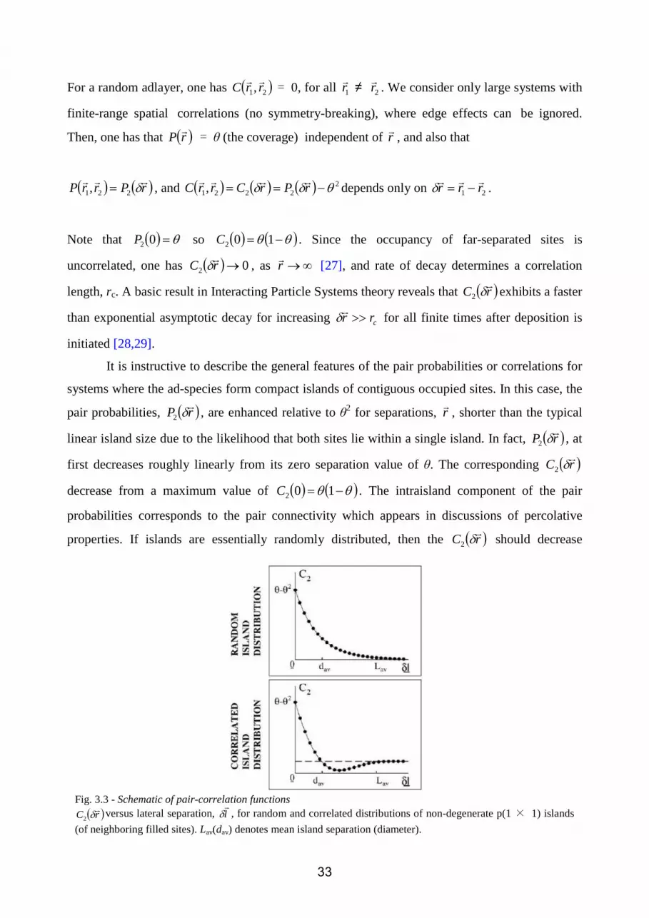
33
For a random adlayer, one has ( )21, rrCrr
= 0, for all 1rr
≠ 2rr
. We consider only large systems with
finite-range spatial correlations (no symmetry-breaking), where edge effects can be ignored.
Then, one has that ( )rPr = θ (the coverage) independent of r
r, and also that
( ) ( )rPrrPrrrδ221, = , and ( ) ( ) ( ) 2
2221, θδδ −== rPrCrrCrrrr
depends only on 21 rrrrrr
−=δ .
Note that ( ) θ=02P so ( ) ( )θθ −= 102C . Since the occupancy of far-separated sites is
uncorrelated, one has ( ) 02 →rCrδ , as ∞→r
r [27], and rate of decay determines a correlation
length, rc. A basic result in Interacting Particle Systems theory reveals that ( )rCrδ2 exhibits a faster
than exponential asymptotic decay for increasing crr >>rδ for all finite times after deposition is
initiated [28,29].
It is instructive to describe the general features of the pair probabilities or correlations for
systems where the ad-species form compact islands of contiguous occupied sites. In this case, the
pair probabilities, ( )rPrδ2 , are enhanced relative to θ2 for separations, r
r, shorter than the typical
linear island size due to the likelihood that both sites lie within a single island. In fact, ( )rPrδ2 , at
first decreases roughly linearly from its zero separation value of θ. The corresponding ( )rCrδ2
decrease from a maximum value of ( ) ( )θθ −= 102C . The intraisland component of the pair
probabilities corresponds to the pair connectivity which appears in discussions of percolative
properties. If islands are essentially randomly distributed, then the ( )rCrδ2 should decrease
Fig. 3.3 - Schematic of pair-correlation functions ( )rCrδ2
versus lateral separation, lrδ , for random and correlated distributions of non-degenerate p(1 × 1) islands
(of neighboring filled sites). Lav(dav) denotes mean island separation (diameter).
34
monotonically to zero. However, if there is a depletion in the population of nearby pairs of
islands, then ( )rCrδ2 will display a negative minimum for separations somewhat larger than an
island diameter. This minimum corresponds to the situation where one site is within an island and
the other is within the surrounding depletion zone. See Fig. 3.3.
3.5 Image processing and data computation
3.5.1 Image processing
The STM images were processed using a costume design IDL program. IDL is an image
analysis platform by ITT Visual Information Solutions. Comprehensive solutions for image and
data analysis typical for STM applications were designed in our lab to accompany the costume
build STMs, control-electronics and data-acquisition software. Among these are included; x and y
plane-subtraction for tilt and thermal drift compensation, median and high/low pass filters and
Fast-Fourier-Transform (FFT) for a frequency-dependent mechanic and electronic noise
elimination.
3.5.2 Data analysis
In this work, a statistical type of information concerning the islands system was under
investigation. Thus, a costume computational programs that will analyze the STM images have to
be designed. In order for a program like that to approach the data, first the STM images, after
being processed for a better 'topographic' precision, had to be digitized. Since the sub-monolayer
islands can be described by a 2D lattice of occupied (island) and un-occupied (vacancy) sites, the
STM images were digitized to binary contrast matrixes of 1 and 0's. Here, 1 denotes an occupied
and 0 denote an un-occupied site in the terminology of percolation. In the terminology of
percolation/simulations 1 belongs to an island and 0 belongs to a vacancy. In the terminology of
epitaxial growth 1 belongs to the deposit and 0 to the substrate. It was easier for the programs to
read a constant-size file and thus, the images were all kept at their original 400x400 matrixes. But,
since the scanning area differ from image to image; a scaling factor had to be attached to every
image so the output will be calibrated to match the shared physical system.
Before any statistics is to be preformed, the islands and their typical geometrical
parameters had to be identified. The first computational program was thus based on a previous

35
Monte-Carlo simulations of the conservative Ising model that was designed to explore the fractal
geometry of the submonolayer islands near p = 0.5 [30]. Here an algorithm that goes over the
lattice, map and list every islands site, served as the source for later analysis. The algorithm was
systematically checking the connectivity to nearest neighboring sites and differentiates between
island, perimeter and vacancy sites. This later analysis includes calculation of the coverage and
computing of the center of mass for every island so the radius of gyration would be established.
The output of the first program is thus the geometrical parameters of; coverage p, area s,
perimeter p and radius of gyration Rs. The routines that establish these quantities can be found in
appendix A.
It is also to be noted that islands that touched the boundary of the image were excluded
from the statistics (except for the coverage), and so are islands that were attached to steps.
The second program was designed for the computation of the circularly-averaged site-
occupation correlation-function. Since here the probability of finding an occupied site a distance
r apart from an already occupied site is the target of computing, the islands have no statistical
meaning, and the only relevant parameter was r. Thus, a different approach was chosen. Here, the
algorithm visit every site in a systematic order and if it was occupied it checked the occupation
probabilities for different distances r on a 'circular' (r2 = x2 + y2) radius. To avoid recounting,
every site that was visited already was excluded for further trials coming from the rest of the sites.
A circularly-average for the different r was then statistically calculated. This program can be seen
in appendix B.
The computations were programmed in FORTRAN90 but some sub-routines called on a
C++ programs. These were responsible for presenting the simulations originally, and later to
display part of the data (for example the center of mass and radius of gyration for each island).
These are not included in the appendixes. Included on the other hand are 'bold' titles that describe
different parts of the program.
The last part of the data analysis involves using the computed data to calculate the
different physical quantities in accordance with the definitions presented in the text. That will be
explained for each quantity at the right place. Since the Si(111) can show domains of different
reconstructions, and so are SPE islands formed on this surface, the results are presented using the
Si(111) lattice units (LU) , for the sake of uniformity. For that, the linear dimensions (Å) were
divided by 3.84 (the (111) inter-atomic spacing) and the spatial dimensions (Å2) were divided by
12.77 (the surface of the (111) unit cell).

36
Chapter 4
STM realization of a strain induced shape transition across the
percolation threshold
4.1 Scope of chapter 4
In this chapter the experimental and computational results will be presented and
interpreted. In the end the strain induced shape transition of homoepitexial 2D islands across the
percolation threshold will be proved. In section 4.2, the STM images will be shown and a primer
insight into their meaning will be suggested. In section 4.3 the site-occupation correlation-
function for the island systems will be presented. The shape transition across pc will be
established here for the first time. Next in section 4.4 the description of the islands systems within
the framework of percolation theory will be examined. The fractal behavior, cluster numbers and
some critical exponents will be calculated here. In section 4.5 the shape transition as can be
predicted by the linear chain model will be described with a quantative prove. To conclude
chapter 4, the bottom line will be expressed.
4.2 STM of submonolayer percolating Si/Si(111)7x7 islands
4.2.1 Island growth
The sample was a Phosphorus-(N-type)-doped Si(orientation: <111> +/- 0.5º) wafer
(single-side polished) of ~300 micron thick and resistance of 0.194 - 0.3 ohm-cm. A pre-cleaning
(rinsing) of the sample was done using a standard procedure; TriChloralEtalon, Acetone, Ethanol
and Double-Distilled-Water. Slabs of 10x3 mm were cut and placed on the sample holder with a
small Si pieces to avoid a contact between the electrical connections and the surface which can
deliver metal atoms during heating. After placed in the UHV chamber a thermal in situ treatment
at a base pressure of 2x10⁻¹⁰ Torr includes: outgassing at ~300°C for 24 hours and removing of
the native oxide at 900°C for 10 min. The DAS of (111)7x7 was then achieved by a subsequent
flashes to 1200°C followed by 5 minutes of annealing at 900°C and slow cooling through the
37
reconstruction transition temperature. The temperature was measured by an infrared pyrometer.
The pyrometer was preliminarily calibrated with a Chromel-Alumel thermocouple attached to the
back of the sample in a low-gradient furnace. The accuracy of the temperature measurements was
estimated as 20°C.
After ~2 hours of waiting the quality of the 7x7 reconstructed surface was verified with
LEED and the sample was ready for Si evaporation. The epitaxial process was preformed in
ambient temperature by heating of Si crystal with an e-beam evaporator. Since the aim was to
study the island system morphology around θ = 0.5, the Si flux had to accurately as possible be
controlled. That was achieved by first attenuating the flux to approx. 1 ML/min and only then
exposing the samples to ~30 sec. The coverage was always verified only after the STM images
were analyzed. A post-deposition typical LEED pictures that was taken in our lab showed a
diffusive background with no spots, confirming that the film was amorphous. STM images at this
stage showed a corrugated surface without atomic resolution which is typical for amorphous a-Si
overlayers. The samples were then annealed to 430°C for 4 min to initialize SPE. Typical LEED
pictures at this point showed weak (111) spots with a delusive background.
STM images reveal that the surface was changed drastically although the annealing temperature
was considerably lower than the reported SPE minimal temperature (the minimal temperature at
which the SPE rate is measurable, is about 550°C [1]. Again at different occasions we saw that
the film is not single crystalline, but consists of (3x3), (5x5), (7x7) and (2x2) reconstructed parts
as expected for SPE growth.
Annealing at 550°C for another 10 min was then took place in order for the system to
reach a metastable thermodynamic state. Further heating up to 700°C, even for times as long as
one hour, did not change the morphology. Hanes, a 'comfortable' thermodynamic range of growth
conditions, which can be reproduced for every sample, could have been established.
4.2.2 Image acquisition and processing
Images from different submonolayer coverages were collected by our custom made UHV-
STM applying a sample bias of +2V and at a constant current of approx 1 nA. The images were
processed first for a better 'topographic' realization and then for two phase system of white
(islands) and black (vacancy). Example for this process is demonstrated in Fig. 4.1 and Fig. 4.2.
The main issue here is how to define the border line between these two phases. Fig. 4.1 (up)
demonstrates the plane-subtraction and noise elimination (by a FFT analysis) and illustrate
(down) the fact that a 'line-scan' across the border line reveals a gradient transition instead of a

38
'step-function'. Fig. 4.2 demonstrates my solution. By identifying an equal 'latitude' lines, the
middle of the 'slop' is chosen for the border line to be coherent with the later definitions of the
width of a trunked island in the LCM.
4.2.3 A first insight
Since it was a 'statistical problem' to deposit submonolayers in the vicinity of the
percolation coverage θc, (and to be able to collect enough data at the same time), three successful
trails will be at the focus of this work. These were the most closest to θc with reasonably amount
of good images. Fig. 4.3 represents STM images at coverage of 0.446 and 0.534 below θc and of
Line scan
Fig. 4.1 - Image processing and the islands border Up: A longitude gradient tone and an oblique 'stripes' noise (left) are eliminated by plane-subtraction and FFT (right). Down: A line scan from enlarged portion of the image (right) shows a gradient transition from the substrate plane to the islands top (left).

39
0.566 above θc. It is to be noted here that percolation defines pc for infinite lattice and STM
images are nothing but the opposite. So, although it is possible to calculate pc out of finite lattice
data, this exact value has no importance for the later arguments, and the percolating state of the
island system (as evidence from many STM images of the same experiment) is satisfying.
In Fig 4.4 black & white images from these coverages are presented. The first insight
regarding the island morphology is as follows. At θ = 0.46 smaller islands or bigger ones that
grew by ripening are compact. Islands that experience coalescence, (and those are naturally
bigger), appears more elongated and some times even ramified. At θ = 0.534 the same behavior is
persevered, and it is just that the portion of the second (elongated/ramified) type is larger due to
the higher coverage. At θ = 0.566 a new behavior emerges. The percolating island system appears
now as a labyrinth type of morphology constitutes from ramified islands with a narrow 'arm-
Fig. 4.2 - Separation into two phase system Up: Equal longitude lines are traced on an enlarge part (right) of the image (left). Down: The middle of the 'slope' is chosen (right) for the border line between the two phases and a binary black and white image (left) is thus defined.

40
width'. That is even more unexpected if we recall that 0.566 is much closer to 0.534 than the later
is to 0.446. A morphological shape transition of the islands system across θc should be considered
here.
4.3 Correlations and islands geometry
In order to get some idea on the abrupt morphology change circular-average of the site-
occupation correlation-function ( )rCr
δ2 for θ = 0.446, 0.534 < θc and θ = 0.566 > θc was
calculated. Fig. 4.5 displays the results for( ) ( )022 CrC −r
δ . Since ( ) ( )θθ −= 102C , by omitting
C2(0) from each coverage, the three data set could be normalized around the x axis. Beyond the
Fig. 4.3 - STM images from three different coverages Up: θ = 0.446. Middle: θ = 0.534. Bottom: θ = 0.566.

41
first secondary maximum, that represents the mean island separation, ( )rCr
δ2 exhibit fluctuations
near 0. Hence, as expected, it is already after one cycle of the oscillatory island-trench
morphology that the system shows no correlations and can be regarded as random. The source for
these fluctuations is the alternating 'step system' of the overlayer islands. For the first zero, that
-0.04
-0.03
-0.02
-0.01
0
0.01
0.02
0.03
0.04
0.05
0 20 40 60 80 100
r (lattice units)
C2(
δδ δδr)
θ = 0.446θ = 0.446θ = 0.446θ = 0.446θ = 0.534θ = 0.534θ = 0.534θ = 0.534θ = 0.566θ = 0.566θ = 0.566θ = 0.566
-0.006
-0.005
-0.004
-0.003
-0.002
-0.001
0
0.001
0.002
0.003
0.004
5 6 7 8 9 10 11 1213 14 15 16 1718 19 20 21 2223 24 25 26 2728 29 30
r (lattice units)
C2(
dr)
θ = 0.446θ = 0.446θ = 0.446θ = 0.446θ = 0.534θ = 0.534θ = 0.534θ = 0.534θ = 0.566θ = 0.566θ = 0.566θ = 0.566
Fig. 4.5 - The site-occupation correlation function Left: ( )rC
rδ2
calculated for θ = 0.446, 0.534 < θc and θ = 0.566 > θc. Right: Beyond the first secondary max.,
( )rCr
δ2is no longer correlated and fluctuate around 0. Right: The first zero gives some evaluation for the typical
width w of the ramified islands and it exhibit dramatic reduction above θc.
Fig. 4.4 - STM images of silicon islands on si(111)7×7 and their B&W matrix (white = occupied). The images are 313×313 lattice units. θ = 0.446 (left) θ = 0.534 (middle) and θ = 0.566 (right). Both the transition to percolation and the transition to lower typical width are evident to the eye.
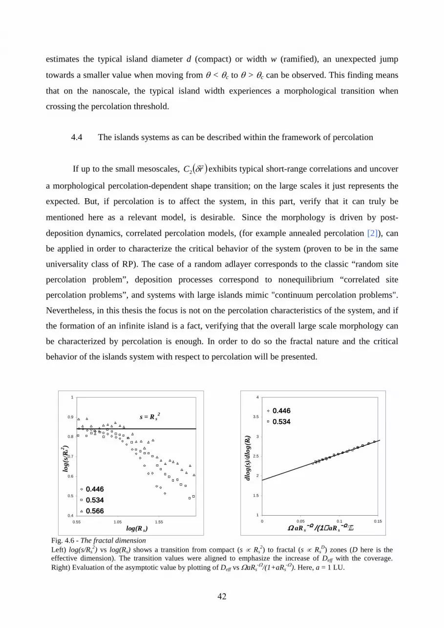
42
estimates the typical island diameter d (compact) or width w (ramified), an unexpected jump
towards a smaller value when moving from θ < θc to θ > θc can be observed. This finding means
that on the nanoscale, the typical island width experiences a morphological transition when
crossing the percolation threshold.
4.4 The islands systems as can be described within the framework of percolation
If up to the small mesoscales, ( )rCr
δ2 exhibits typical short-range correlations and uncover
a morphological percolation-dependent shape transition; on the large scales it just represents the
expected. But, if percolation is to affect the system, in this part, verify that it can truly be
mentioned here as a relevant model, is desirable. Since the morphology is driven by post-
deposition dynamics, correlated percolation models, (for example annealed percolation [2]), can
be applied in order to characterize the critical behavior of the system (proven to be in the same
universality class of RP). The case of a random adlayer corresponds to the classic “random site
percolation problem”, deposition processes correspond to nonequilibrium “correlated site
percolation problems”, and systems with large islands mimic "continuum percolation problems".
Nevertheless, in this thesis the focus is not on the percolation characteristics of the system, and if
the formation of an infinite island is a fact, verifying that the overall large scale morphology can
be characterized by percolation is enough. In order to do so the fractal nature and the critical
behavior of the islands system with respect to percolation will be presented.
s = R s2
0.4
0.5
0.6
0.7
0.8
0.9
1
0.55 1.05 1.55
log(R s)
log(
s/R
s2 )
0.4460.4460.4460.4460.5340.5340.5340.5340.5660.5660.5660.566
1
1.5
2
2.5
3
3.5
4
0 0.05 0.1 0.15
ΩΩΩΩ aR s−Ω−Ω−Ω−Ω /(1+/(1+/(1+/(1+ aR s
−Ω−Ω−Ω−Ω ) ) ) )
dlog
(s)/
dlog
(Rs)
0.4460.4460.4460.4460.5340.5340.5340.534
Fig. 4.6 - The fractal dimension Left) log(s/Rs
2) vs log(Rs) shows a transition from compact (s ∝ Rs2) to fractal (s ∝ Rs
D) zones (D here is the effective dimension). The transition values were aligned to emphasize the increase of Deff with the coverage. Right) Evaluation of the asymptotic value by plotting of Deff vs ΩaRs
-Ω/(1+aRs-Ω). Here, a = 1 LU.

43
Starting with the fractal behavior; Fig. 4.6 (left) is an averaged log-log plot of s/Rs2 vs Rs
with a guide line for s ∝ Rs2. It is apparent that the fractal behavior is restricted to islands above a
crossover value, and it was found at the transition from compact to ramified islands, also
indicated in fig. 4.9. A linear fit of the data at the fractal zone gives higher Deff values with
increasing θ. Corrections to the asymptotic behavior using Ω = 0.55 results in a linear data
collapse, leading to the intersection at D ~ 1.9 for Rs → ∞ (Fig. 4.6 (right)). It is noted here that θ
= 0.566 > θc was omitted from this plot due to the shape transition of the islands and their
tendency towards linear chains as will be proved later. This behavior could not have been
predicted by percolation.
The next behavior that will be verified is that of cluster numbers; Fig. 4.7 is an averaged
log-log plot of ns vs s. For this plot the clusters were grouped in bins of increasing size [2i, 2i + 1 -
1]. The clusters in each bin were counted and the result was divided by the bin size to yield the
average number of clusters for each s in the bin. From each coverage, clusters were collected
from many images. These images were different in size and some times part of the surface/image
was distorted and no data were collected out of it. To normalize the probability per lattice site a
simple trick was used. Dividing the sum of islands areas by the coverage gives an effective lattice
as if the islands were all collected from the same L2eff = ∑s/p image. The values of each average
and normalized ns was presented vs the algebraic mean s in the bin. It is evident that for large s
the exponent τ is being approached asymptotically. Thus, since there are always only two
independent exponents, it is already found that the large scale behavior belongs to the universality
class of RP.
τ = 2.05τ = 2.05τ = 2.05τ = 2.05
-10
-9.5
-9
-8.5
-8
-7.5
-7
-6.5
-6
-5.5
-5
1 2 3 4 5
log(s)
log(
n s)
0.4460.4460.4460.4460.5340.5340.5340.5340.5660.5660.5660.566
Fig. 4.7 - The cluster number exponent τ log(ns) vs log(s) shows a convergence of ns towards sτ for s → ∞.

44
4.5 The shape transition as predicted by the LCM
In the remainder of this chapter, a detailed analysis of the main finding; that the typical
island width is scaled by a factor of e above θc will be presented. At first, the LCM version for
monolayer high 2D ramified islands will be introduced.
4.5.1 The LCM for 2D ramified islands
In order to analyze the driving force leading to the width reduction above percolation, the
LCM calculations for a simple 3D pyramid islands with width w, length t and height h,
experiencing shape transition above a critical area of e2α02, was used. This transition is
represented by wt ≡ eα0 and st = wt2 for the transition values of the width and the area respectively
while w0 ≡ α0. The first experimental verification of this shape transition in the growth of
monolayer high 2D islands was obtained by B. Muller et. al. [3]. For heteroepitaxy of
Cu/Ni(100), they were able to characterize the transition from compact to ramified islands by only
one parameter: the arm width of the ramified islands. In this part their modified LCM model
designed for monolayer high 2D ramified islands will be followed. For h = 1, they used the
following expression for the total normalized energy E:
E = b(w + t) – wln(t) – tln(w), (34)
where the first term represents the elastic energy (b is a constant consisting of elastic constants)
and the other terms represent the surface energy. Since s = wt, Eq. (34) can be rewritten as:
ww
s
w
sw
w
swbE lnln −
−
+= . (35)
Minimizing the energy in Eq. (35) with respect to w, Muller et. al. found two identical solutions
up to the transition value st = exp(4b + 2), and two different solutions when s exceeds this value.
Above st the width w shrinks from wt = exp(b + 2) to w∞ = exp(b + 1) and thus wt/w∞ = e. It is
customary to use a two-point correlation function [4] to characterize the microgeometry of two-
phase systems. Indeed, we have seen before that ( )rCr
δ2 can reflect the basic geometry of the
reducing islands width. But, since ( )rCr
δ2 was circular-averaged and the islands are ramified, the

45
first zero can't be trusted to accurately measure the averaged islands width. In a more reliable
practice, the footsteps of Muller et. al. were followed, and the parameter p vs the island size s was
introduced, because it predicts w when the islands grow to infinity. For a rectangular island the
perimeter is just p = 2(w + t). By replacing t with s/w the dependence of p on s can be obtained:
p = 2s/w + 2w. (36)
This relation correctly describes also ramified islands with a uniform arm width. If an elongated
rectangle is cut into segments and rearranged in a ramified form. If the segments are connected
via their width, the object has the same perimeter as the original rectangle. Since it has the same
area and width as well Eq. (36) also hold for ramified objects. Fig. 4.8 illustrates the fact that in
both cases one finds (n – 1) coupled perimeter sites a width long each.
Muller et al were able to measure wt, but they found it insensitive to the s range above the
transition. They proved the validity of the Tersoff and Tromp model in 2D, but, could not see the
asymptotic value being approached for growing islands. The value of w from the data will be
presented next.
4.5.2 The shape transition - From compact to ramified to linear chains
Fig. 4.9 (left) introduces (averaged) log(p/s0.5) vs log(s) for the three data sets: θ = 0.446,
0.534 < θc and θ = 0.566 > θc. The data shows a first transition from compact (s ∝ p2) to ramified
islands. Beyond an intermediate zone the data align ~parallel to s ∝ p and this behavior can be
modeled by the growth of linear chains with a typical arm width w. Guide lines for the s ∝ p2 and
s ∝ p zones were added to emphasize these transitions. The linear dependence of s on p is a
Fig. 4.8 - Perimeter of a ramified object By rearranging a rectangle into ramified object, with the same arm width, the perimeter is unchanged since the same w(n - 1) (n being the number of segments; 4 in this example) perimeter sites are coupled.

46
familiar characteristic of the infinite island above θc, and therefore, also of the finite but large
islands that forms as θ approaches θc. Thus, it is possible to support the previous finding; that on
the large scales the islands can be described within the framework of RP. In the experiment for θ
< θc the data fall on similar curves and the transitions to compact and LC islands occur
approximately at the same w. For θ > θc the transition occurs much earlier and a parallel curve (to
the θ < θc regime) at the linear chains zone was achieved, indicating the existence of a scale
factor.
Fig. 4.9 (right) displays p vs s in the s ∝ p zone for θ = 0.534 and θ = 0.566. From this
plot, the linear chain coefficients (for s) 2/w (see Eq. (36)) could be calculated, and define these
values at the LC zones by wt, since, the lowest w at the beginning of these zones marks exactly
the transition value. It was found that 2/w = 0.062 or wt = 32.258 LU for θ < θc, and 2/w = 0.169
or wt = 11.834 LU for θ >θc. Thus, wt(θ < θc )/wt(θ > θc) = 2.72 and a factor of e distinguishes
the typical island widths, at the LC zone, from both sides of θc. A more carefully look into these
results and a discussion of their connotation will be given next.
By using the value of 32.258 for wt when (θ < θc ), it was found that log(wt2) = 3.02,
however, from Fig. 4.9 (left) it is apparent that the transition to LC occurs only when log(wt2) =
3.35 or at wt = 47.315 LU. At the same time, if we mark the transition from compact to ramified
islands for θ < θc, by wR, we find log(wR2) = 2.48 or wR = 17.378 LU and thus, wR
2 = wLC2/e2 ≡
w0. This means that the stability of the compact island shape below θc begins to brake at a critical
width w0 = 17.378 LU, but, it is only where wt ≡ ew0 = 47.315 LU, that the islands can be
s = p 2
s = p
(linea
r chain
s)
2.48 3.35 3.02
0.2
0.4
0.6
0.8
1
1.2
1.4
1.5 2 2.5 3 3.5 4 4.5
log(s)
log(
p/s0.
5 )
0.4460.4460.4460.4460.5340.5340.5340.5340.5660.5660.5660.566
p = 0.062s + bp = 0.169s + a
0
200
400
600
800
1000
1200
1400
1600
0 5000 10000 15000 20000 25000
s (lattice units)
p (l
atti
ce u
nits
)
0.5340.5340.5340.5340.5660.5660.5660.566
Fig. 4.9 - The typical island width w Left) log(p/s0.5) vs log(s) shows a transition from compact (s ∝ p2) to LC (s ∝ p) islands. The real 2D transitions at log(w) = 2.48, 3.35 and the 1D theoretical one at log(w) = 3.02 are displayed. Right) p vs s for the s ∝ p zone. The coefficients 2/w for θ = 0.534 and θ = 0.566 are displayed.

47
described as linear chains. Instead of the sharp square-to-rectangular transition found for the 1D
elongation, here, the evolution in 2D from compactness to linear chains is characterized by a
transient ramified zone between s ∝ p2 and s ∝ p.
The value wt = 32.258 LU calculated from the linear chain coefficient 2/w at s ∝ p can
also be found if we extrapolate the linear trend line from the LC zone down to the intersection
with the compact s ∝ p2 line at log(w2) = 3.02. It suggests that this value might refer to the
theoretical value expected for 1D growth without a transition zone. The value wt = 47.315 found
at the transition from ramified to LC islands, refers to the real 2D value. The same 2D effect
repeat itself for θ > θc were the real 2D value seems to be in the vicinity of the θ < θc transition
value from compact to ramified islands: log(w2) = 2.48 or wt = 17.378 LU and the theoretical 1D
value for θ > θc at wt = 11.834 LU. It is remarkable to see, that for wt(θ < θc )/wt(θ > θc) the
theoretical 1D ratio equals the real 2D ratio where 32.258/11.834 = 47.315/17.378 = 2.72 ≈ e.
Together with the w behavior below θc, the general characteristics of the1D LCM; the appearance
of optimal α02 island, the shape transition above a critical e2α0
2 value and the convergence back to
α02 for t → ∞ are reproduced for 2D ramified islands. It means that p/s for 2D ramified structure
constitutes of similar arms is equivalent to p/s for 1D island with the same p & s.
4.5.3 Energy calculation
To confirm the validity of the above results, an energy calculation was made, in order to
estimate the LCM prediction for the optimal island width as discussed in chapter 1:
chhee /0
Γ= φα . (37)
• The exponent of Γ/ch -
According to ΤΤ, the extra surface energy is just 2(w + t)hΓ and thus Γ is just the step
energy per surface area. Here, the results of D. J. Eaglesham et. al. from their "Equilibrium
shape of Si" paper [5] for the step energy obtained from dγ/dθ of ≅140 ± 20 meV/atom on
(111) is quoted. For the atom area, Å2 is being used. Multiplying it by an order of magnitude
for the interatomic spacing squared we get s ≅ 10−19 m2. From here we find Γ ≅ 0.22 J/m2. h ≅
3 Å is the islands height and c = σb2(1 – ν)/2πµ where σb is the xx or yy components of the

48
bulk stress and ν and µ are the Poisson ratio and the shear modulus of the substrate. These
three values are known to be σ = 2.96 J/m2 [6] and so σ b = 0.95⋅10-10 J/m3 , ν = 0.26 and µ =
5.2⋅10-10 N/m2.
From the above exp(Γ/ch) ≅ 0.22.
• Using Φ = e-3/2cotθ
For θ , the contact angle and for the monolayer high islands, by using the half tetrahedral
angle of 54.5° expected for monatomic steps on silicon, the above parameters give α0 ≅ 12
LU, within 2 % of the experimental value.
4.6 The bottom line
The results confirm, for the first time, the validity of the LCM in homoepitaxy. The ability
to model the formation of homoepitaxial silicon islands on Si(111)7x7 with a mechanism for
strain relaxation, originates from the dimension dependence of these forces. Massies and
Grandjean [7] were the first ones to discover this size dependence, measuring in-plane lattice
spacing oscillations (IPLSOs) by using reflection high-energy electron diffraction (RHEED).
Since then, the validity of this finite size phenomenon was established, both theoretically and
experimentally, for heteroepitaxy as well as for homoepitaxy as discussed in chapter 1. In
heteroepitaxy, a natural misfit for semi-infinite cubic phases, an adlayer A and a substrate B,
differ by their crystallographic parameters a0 and b0 is defined by: m0 = (b0 – a0)/a0. However,
because of its broken bonds, a small piece of A may relax to equilibrium showing an effective
lattice parameter of a = a0[1 + ε(h, w, t)] where ε(h, w, t) is the size dependent strain, referred to
as the finite size misfit or mesoscopic mismatch. Thus, a finite crystal grown on a semi-infinite
substrate, has an effective misfit m, distinguished from the natural one as: m ≈ m0 - ε(h, w, t). The
finite size misfit can be dominant also in heteroepitaxy for tiny islands and/or if m0 is sufficiently
small. More important for our discussion, owing to their mesoscopic mismatch, finite size 2D
coherent nano homoepitexial islands for m0 = 0, has to be strained by ε(h, w, t) to be
accommodated on their own substrate. ε(h, w, t) depends only on the surface stress of the lateral
and basal faces of the island, that during relaxation drags the atoms at the contact area to produce
a strain field in the substrate. This strain can be modeled by point forces located at the edges of
the islands on the substrate surface [8, 9]. This method is consistent with the LCM routine where

49
TT modeled this relaxation by elastic point force monopoles acting at the islands periphery. TT
also assumed a coherent Stranski-Krastanov growth with a wetting layer and so the energy of the
substrate and of the islands top was considered to be equal. The homoepitaxial case is a perfect
study case within the framework of this assumption.

50
Chapter 5
Sub-monolayer homoepitaxial mesoscopic percolating islands -
Discussion
5.1 Scope of chapter 5
In this chapter, the outcome of the results as interpreted in chapter 4, will be looked into.
In section 5.2 another view on the correlation will be presented. The hypothetical medium with
short-range correlations will be discussed here. In section 5.3 the shape transition with respect to
the geometrical phase transition of percolation will be discussed. The appearance of two typical
length scales; for the large scale morphology described by percolation and for the small scale
morphology described by the LCM will be suggested. In section 5.4 Strain forces in homo-
epitaxial overlayers; the LCM in homoepitaxy and the coexistence of
kinetic/thermodynamic/statistical approaches will be discussed. In section 5.5 the island system as
a periodic domain will be discussed. Here the formation of Spontaneous domain and step-step
repulsion will be considered. In Section 5.6 the interplay between epitaxial process and the
percolation threshold will be addressed. To conclude in section 5.7 a review of the LCM
applications so far will be given.
5.2 The island system as hypothetical medium with short-range correlations
In Fig. 4.5 the correlations in the islands systems were presented by ( )rCr
δ2 after sampling
the STM images. From that it was concluded that the correlation in the system are short ranged
and do not extend beyond one typical cycle of the island-trench morphology. Long ranged
correlation functions are usually represented by decaying power laws. In order to fit a short-range
correlation function to the images, the hypothetical medium with short-range correlations
function was chosen.
Fluids (gases and liquids) are systems with a high degree of symmetry as they are spatially
homogeneous and rotationally isotropic. Correlations in the fluids are primarily due to short-range
repulsive interactions. In addition to the temperature driven gas-liquid phase transition in which

51
there is no symmetry change, there can be a liquid-solid transition that is mainly determined by
repulsive interactions and hence depends upon density as well. With the increase of liquid
density, depending on interparticle interactions, the system may rearrange itself in a regular,
equilibrium crystalline solid. As an example of a statistical construction, Y. Jiao, F. H. Stillinger
and S. Torquato PRE paper from 2007 will be followed and a two-dimensional, two-phase
hypothetical random medium function will be introduced. Homogeneity and rotational isotropy
are assumed to hold independently of the system density. This is a reasonable assumption for low-
density fluids and amorphous solids which do not have long-range order. The intention is to
construct materials which exhibit a considerable degree of short-range order. A meaningful, yet
nontrivial, two-point correlation function satisfying these conditions is [1]
( ) ( )kr
kreΦΦΦrS rr sinˆ 0/
21212
−+= , (38)
where k = 2π/a0. Here r0 and a0 are two characteristic length scales. The overall exponential
damping is controlled by the correlation length r0, determining the maximum correlations in the
system. The constant a0 determines oscillations in the term sin(kr)/(kr) which also decays with
increasing r, such that a0 can reduce the effective range of r0. In Fig. 5.1 the lattice-point
algorithm is used in the construction of ( )rS2ˆ . At a lower density of the black phase Φ1 = 0.2, a0
is manifested as a characteristic repulsion among different elements with diameter of order a0.
The repulsion vanishes beyond the length scale r0. At a higher density of 0.5, both length scales a0
and r0 are clearly noticeable in the distribution of the black and white phases. The target two-point
correlation function ( )rS2ˆ for Φ1 = 0.2 and ( )rS2
ˆ sampled from the generated structure is shown
Fig. 5.1 - Hypothetical medium with short-range correlations Media with ( )rS2
ˆ given by Eq. (38) generated by the lattice-point algorithm. Left panel: volume fraction of black
pixels Φ1 = 0.2. Middle panel: volume fraction of black pixels Φ1 = 0.5. The linear size of the systems N = 200. Right panel: target two-point correlation function given by Eq. (38) and that of constructed media with volume fraction Φ1 = 0.2.

52
in Fig. 5.1.
An attempt was made to fit ( )rS2ˆ on the correlations of the system as displayed by( )rC
rδ2 .
( )rS2ˆ for θ = 0.534 < θc and θ = 0.566 > θc were calculated and are presented along with ( )rC
rδ2 .
Fig. 5.2 displays the results for ( ) ( )0ˆˆ22 SrS − , and here again, by omitting ( )0ˆ
2S from each
coverage; the two data sets could be normalized around the x axis. The parameters r0 and a0 were
fitted on the correlation data ( )rCr
δ2 in a way that r0 represent the max correlations as the typical
arm width and r0/(r0 + a0) = θ so a0 represent the repulsion as the typical trench width. This choice
gave these parameters a 'physical' meaning with respect to the underline strain driven
phenomenon.
( )rS2ˆ can't predict the morphological shape transition, but it was found that hypothetical
medium with short-range correlations can serve as yet another tool to look into strain-relaxed
sub-monolayer islands systems. By tuning of two parameters r0 and a0 representing correlations
and repulsion respectively, ( )rS2ˆ can construct the systems morphology by for example the
lattice-point algorithm. However the constructed system is uniform wile the island system is not.
5.3 The percolation phase transition and the two typical length scales
The most significant finding as emerges from the data is that the transition to LC islands,
or wt for θ > θc occurs at the same point where the transition from compact to ramified islands, or
w0, occurs for θ < θc. Since for θ < θc this transition occurs where w0 = wt/e, a factor of e
Fig. 5.2 - Matching of the target ( )rS2ˆ to the data correlations ( )rC
rδ2
The parameters r0 and a0 were fitted on the correlation data ( )rCr
δ2 in a way that r0 represent the max correlations
as the typical arm width and r0/(r0 + a0) = θ so a0 represent the repulsion as the typical trench width.
-0.06
-0.04
-0.02
0
0.02
0.04
0.06
0.08
0.1
0 10 20 30 40 50 60 70 80
r (lattice units)
C2(
r)-C
2(0)
& S
2(r)
-S2(
0)
C (0.534)C (0.566)S (0.534)S (0.566)

53
separates the transitions to the LC zone across θc. Thus, analyzing the percolating island
morphology by the LCM ends up with two morphological transitions. The first transition is
related to the optimal tradeoff between surface energy and strain, and it appears in a gradual
transition from compact to LC islands. (This optimal tradeoff freezes the structure detected, at
certain coverage, even if the sample is further heated for longer intervals and at higher T's (up to
700°C)). The second transition is related to the geometrical phase transition of percolation. Once
the percolation threshold is being crossed and an infinite island is formed, wt for θ > θc equals the
infinite w∞ = wt /e = w0 value for θ < θc, and this infinite value becomes the typical length also
for finite islands.
The above nanoscale morphology characterization also suggests the existence of two
typical length scales. A geometric typical length ξ, defined by RP, describes the morphology on
the large scales as θ → θc. An energetic typical length w, defined by the LCM, describes the
effect of strain on small scale morphology. Unfortunately, experimental data with high accuracy
very close to the percolation threshold are very hard to attain. Thus, the measurement to answer
the question of how sharp the transition of w is and how it depends on |θ – θc | might be a very
difficult one. - A crucial question might be; if the elongation of 'individual' islands affects the
percolation transition, or, if crossing the percolation threshold, and the formation of infinite-
island, enhance the elongation of the islands and the convergence to the optimal width. - But, it
should be possible to find out if this behavior can be reproduced on other surfaces, for different
parameters like temperature and coverage, and the role of post-deposition dynamics.
5.4 Strain forces in homo-epitaxial overlayers
5.4.1 The LCM in homoepitaxy
Within the framework of the LCM, in the thermodynamic limit where there are many
islands (though far apart), the islands should "ripen", with the number of islands growing or
shrinking until each island is a square of size α0. This size represents the optimal tradeoff between
surface energy and strain. The island edges permit elastic relaxation as the cost of extra surface
energy. If the surface energy Γ dominates α0 becomes very large to reduce the edge-to-area ratio.
But if the island stress dominates (ch >> Γ), then the minimum energy is obtains with many small
islands.

54
In homoepitaxy we are dealing with finite-size misfit or mesoscopic mismatch. Here the
source of strain is the island size itself. As the island grows, the deposit tends to accommodate on
its own substrate, so, an upper limit on α0 due to vanishing of strain is expected. For elongation
thus to take place when the islands are far apart, we need small surface energy or sustention of
stress up to larger island size. The validity of the LCM for low coverage 'individual isolated
islands' in homoepitaxy was not verified in this work.
5.4.2 The kinetic/thermodynamic/statistical approach
In the experiment the deposit was delivered to the surface at room temperature and thus
kinetic process are not likely to take place before annealing. For high coverage, close to 0.5, by
annealing, nucleation starts immediately and simultaneously everywhere. Here, ripening and
coalescence might even compete for some time and the roll of curvature-dependent diffusion
along the islands is probably a major parameter. The contribution of kinetics and/or
thermodynamics to the 'equilibrium' morphology is thus uncertain. When a percolation transition
is further involved, as appeared from the results, statistical arguments might also come to play.
The mutual relations between these analysis tools are worth a second thought.
Another way to look at the morphology is as a system of islands and trenches that can also
be considered as periodic domain of alternating-sign steps. The possible meaning of this will be
considered in the following.
5.5 The island system as a periodic domain of alternating-sign steps
5.5.1 Spontaneous domain formation and self-organization
In chapter 4, the morphological shape transition of the 2 'phase' (islands and vacancy)
system with strain acting on the periphery of the islands at the interface level, as predicted by the
LCM, was explained. The approach of point forces was at the basis of the TT derivation for the
energy relaxation. In this sub-section, the ability to describe the morphological transition by
Spontaneous domain formation within the framework of that approach will be discussed.
Let us consider the coexistence of two different surface phases. From simple energetic
arguments the two phases are expected to separate neatly, forming two semi-infinite domains in
order to minimize the energy cost related with the formation of the boundaries. However, if the
two phases have different surface stresses, the presence of the boundaries allows the system to

55
efficiently relax elastic energy. First Marchenko [2, 3] and then Alerhand et al. [4] have shown
that, in many cases, the elastic energy relaxation can be large enough to overcome the energy cost
of the domain boundaries, resulting in spontaneous domain formation. The same argument can be
applied to infinite 1D or finite 2D domains, but the 1D case can be treated analytically and that is
way in their Surface Science Reports [5] P. Mu¨ller and A. Sau´l, consider the spontaneous
formation of 1D periodic domains. For a fixed coverage p, the only free parameter is the period
length L. By equating to zero the derivative of the formation energy (they had calculated) with
respect to the period, they found
( ) ( )
−=
22min12
expsin ν
βππ
π
f
E
p
aeL . (39)
Eq. (39) gives the period of the 1D domains as a function of two bulk parameters (the Young’s
modulus E and the Poisson ratio ν) and two surface ones (the net force at the domain boundary f
and the boundary formation energy β). The pre-exponent multiplayer involves coverage
dependence wile the rest of the parameters are the same for different p's. By varying p, a smooth
variation of Lmin is attained. Thus, Spontaneous domain formation can not explain the abrupt L
change with respect to p in my experiment.
5.5.2 Step-step interactions
In chapter 1, the continuous forces approach was also mentioned. I remind here that the
minimal elastic energy of an isolated island relaxed elastically as a coherent epitaxial deposit was
driven from the total elastic energy per unit length of a ribbon. A system of such semi-infinite thin
film ribbons (infinite in y and narrow in x) can also be regarded as an alternating step system. In
this sub-section, a suggestion will be made, that by regarding a system of mesoscopic islands as
alternating-sign step system, updating of the optimal island width for high coverage systems
should be regarded.
The relaxation behavior that is described in [6] is that of an isolated island or ribbon. For
coherent epitaxial a continuous layer is fully strained at its natural misfit m0. So, a collection of
ribbons initially relaxed, when coalescence, have to strain back to m0 at layer completion. This
was first mentioned by Cabrera [7] who said that this proceeds by the overlapping off the
substrate strain fields when the island borders come closer. This overlapping implies that there

56
exists interaction energy of the islands. Such repulsive interactions have been calculated for a pair
of misfitted islands by Stoop and van der Merwe [8] and Stoneham [9].
KM calculated the strain fields for a set of periodic ribbons, l being the island width, L the
periodicity, with L > l and having their borders distant by L - l = D. Since overlap of the substrate
strain fields takes place, they found the following characteristics:
• The strain inside a ribbon is that of the free ribbon where a compression field outside the
ribbon emerges due to the neighboring ribbons.
• For a growing ribbon at a constant thickness h the substrate strain between the ribbons
increases when the borders come closer. Consequently, this increases the strain inside the
ribbons so that at complete coverage L = l (coalescence) the latter tends to the natural
misfit m0 as it should for a continuous layer.
• When the borders come closer there is a back stress effect between the ribbons, or in other
words they communicate "at long distance".
• Just before the completion off the layer, close to coalescence there is a diverging
accumulation of strain in between the ribbons.
As mentioned before, the deposit was delivered to the surface at room temperature. By
annealing, soon after nucleation, a system of islands and trenches that can also be considered as
periodic steps was formed. For coverage l/L close to 0.5, mesoscopic islands are formed and the
interisland spacing was of the order of the islands size. Now, on top of the mesoscopic strain step-
step repulsion might also be present and the 'steps' can "communicate" as mentioned above. This
rationalized stress can be cooperated into the energy expression as suggested by TT. If it is not
negligible it will affect the optimal island size. For the homoepitaxial system when m0 = 0, it
looks like α0 described the optimal island width quit good, but, if m0 ≠ 0 like for hetroepitaxial
systems the step-step interactions might affect α0.
5.6 The epitaxial process and the percolation threshold
In chapter 3 we have seen that when an a-Si overlayer is formed on the Si(111)-7×7
surface at room temperature, the stacking-fault layer of the substrate 7×7 reconstruction is
preserved between the a-Si and the substrate. The buried stacking fault is resolved by post-
annealing above 500°C and the 5×5 DAS reconstruction coexists with the 7×7 reconstruction on

57
an annealed surface for a one-monolayer (ML) thick a-Si overlayer during its crystallization.
What does it means when we try to define the coverage. The STM images truly distinguish
between the overlayer and the substrate, but, the following questions arises:
• If the substrate and the overlayer show different reconstruction, the coverage can no
longer be defined by occupied sites and instead, a fractional coverage with respect to some
mutual area units is needed (this approach was chosen to describe the results in this work).
How can we define the lattice and calculate the threshold in this scenario?
• If the substrate and the overlayer show the same reconstruction, but, we see different
domains, we are dealing with a two phase system problem.
• How the evolution of the overlayer after annealing should be treated? Does the 'coverage'
changes during the SPE growth? If it is we might get into or out of percolation.
• If the overlayer during its crystallization is constructed from an effective monolayer or bi-
layer, is it a 2D problem or qusi-3D problem? Should we define the coverage by the
amount of atoms we need for the crystallization to take place?
5.7 Review on the LCM applications
In table 5.1 I gathered the publications I found for the application of the linear chain model.
Year Title Ref. 1994 Shape Transition in Growth of Strained Islands: Spontaneous Formation of
Quantum Wires [10]
1994 Competing Relaxation Mechanisms in Strained Layers [11] 1995 Shape Transition in the Epitaxial Growth of Gold silicide in Au Thin Films on
Si(111) [12]
1997 Strain Relief via Island Ramification in Submonolayer Heteroepitaxy [13] 1998 Island Shape Transition in Heteroepitaxial Metal Growth on Square Lattices [14] 1998 Stress-Induced Shape Transition of CoSi2 Clusters on Si(100) [15] 2002 Formation of Quasi-One-Dimensional Cu2O Structures by in situ Oxidation of
Cu(100) [16]
2003 Shape Stability of TiSi2 Islands on Si (111) [17] 2004 The Fabrication of Self-Aligned InAs Nanostructures on GaAs(331)A
Substrates [18]
2006 In-Plane and Out-of-Plane Shape Transitions of Heteroepitaxially Self-Assembled Nanostructures
[19]
2007 Mesoscopic Mismatch as a Driving Force for Modified Morphology Above Percolation
[20]
2009 Shape Transitions of Epitaxial Islands during Strained Layer Growth: Anatase TiO2(001) on SrTiO3(001)
[21]

58
Conclusions for part I
In this part, strain effects in homoepitaxy have been demonstrated. By growing of 2D
mesoscopic Si/Si(111)7x7 islands vie SPE a strain driven shape transition due to finite-size misfit
was observed. For coverage close to 0.5 the percolation of the islands system was also identified
as affecting the morphology. The typical islands width appears considerably narrower across pc.
As predicted by the LCM the formation of an infinite island was accompanied by convergence to
a thermodynamic-optimal island width. The following points might be considered for further
investigation:
• In homoepitaxy the source of strain is the island size itself (finite-size misfit), thus, an
upper limit on α0 due to vanishing of strain is expected. Therefore, the validity of the LCM
for low coverage 'individual isolated islands' in homoepitaxy needs to be defined.
• For complex reconstructed surfaces like DAS the percolation definitions of the coverage,
of the lattice and even of the dimension are not trivial. A percolation model that encloses
this complexity might be needed.
• For a system of mesoscopic islands at θ ~ 0.5 the islands might 'communicate' through the
stress they apply on the substrate dragging the underlying layers. The role of this
interaction in homoepitaxial growth is to be identified.
• ( )rS2ˆ can't predict the morphological shape transition, but it was found that hypothetical
medium with short-range correlations can serve as yet another tool to look into strain-
relaxed sub-monolayer islands systems. By tuning of two parameters r0 and a0
representing correlations and repulsion respectively, ( )rS2ˆ can construct the systems
morphology by for example the lattice-point algorithm.
• The morphological shape transition across pc also suggests the existence of two typical
length scales. A geometric typical length ξ, defined by RP, describes the morphology on
the large scales as θ → θc. An energetic typical length w, defined by the LCM, describes
the effect of strain on small scale morphology.
• A crucial question might be; if the elongation of 'individual' islands affects the percolation
transition, or, if crossing the percolation threshold, and the formation of infinite-island,
enhance the elongation of the islands and the convergence to the optimal width. Computer

59
simulations incorporating strain around pc might help here.
Evolution and growth of epitaxial islands from one hand, and percolation on the other
hand are thoroughly investigated. Theoretical models, computer simulations and experimental
evidence can thus be found for these fields of research. However, close to pc, the islands
morphology might be sensitive to the geometrical phase transition as much as the percolation
threshold might be sensitive to the islands morphology. This morphology can be a subject to
different growth conditions that implies thermodynamic or kinetic considerations. Hence, an
interesting coexistence of statistical (percolation), kinetic (evolution) and thermodynamic
(equilibrium) arguments might be considered for submonolayer island growth close to pc. I hope
this thesis demonstrate that.

PPaarrtt IIII
TToowwaarrddss aa DDuuaall--TTiipp SSTTMM AApppplliiccaattiioonnss iinn MMeessoossccooppiicc
SSuurrffaaccee TTrraannssppoorrtt

60
Introduction to part II
To measure the properties of a system it is necessary to couple a measurement apparatus
to the system. To minimize the effect that the presence of the measurement apparatus has on the
properties of the system, it is desirable to have the coupling as weak as possible. Weak coupling
or noninvasive contacts on mesoscopic conductors were already used by Engquist and Anderson
[1] to rederive Landauer’s resistance formula [2] for a small conductor with a scatterer. The
scanning tunneling microscope (STM) is a very powerful experimental realization of a weakly
coupled contact. Due to the fact that the tunneling current to the tip originates only from an
atomically small area on the surface below the tip, it has become the standard tool to measure the
local electronic structure on the surface of conductors. In experiment, it is possible to map the
topography of a surface with atomic resolution [3]. Standing electron wave patterns confined to
quantum corrals [4], which were constructed by manipulation of single atoms, or on carbon
nanotubes serving as a one-dimensional electron box [5] are clearly visible using a low-
temperature STM. In the theoretical description, initially Tersoff and Hamann [6] used the
Bardeen approach to tunneling [7] to relate the tunneling conductance to the local density of states
(LDOS) ν(x) on the surface of the conductor. In 1997, Bracher et al. [8] arrived at the same result
using a propagator theory where the tip was described as a localized source or sink of electrons.
These approaches have been used to interpret many of the features encountered in STM images.
In theory and experiment, the STM has most often been used in a two-terminal configuration, the
two terminals being the tip on one side and the conductor on the other. The current at the tip is
then determined by the two-terminal conductance between tip and surface, and is given by the
Bardeen formula [7], Gts = (e2/h)4π2νtip|t|2ν(x), with the LDOS ν(x) of the sample, νtip of the
tunneling tip, and the coupling energy |t|. The zero-bias conductance thus measures directly the
LDOS ν(x) on the surface of the conductor below the tip.
In this part of this thesis an experimental setup that enables to simultaneously bring two
tunneling 'contacts' with a nanoscale separation onto a conducting surface will be described. As
an introduction, characteristic length scales and transport regimes will be defined. Following it,
the basic theory for mesoscopic two-terminal transport will be given. The main volume will be
devoted to electronic transport at semiconductor surfaces - from point-contact transistor to
micro-four-point probes that will describe experimental challenges to detect surface-state

61
conduction using STM (mostly performed in the group of Shuji Hasegawa at the University of
Tokyo). From here the motivation to construct a multi-probe STM (MPSTM) can be understood.
Some notes on the noise expected in conductance measurements on the mesoscale will be
mentioned and then the Scope and composition of Part II of this thesis will be outlined.
a. Definitions: Characteristic length scales and transport regimes [9]
The transport-contextual definition of mesoscopic was originally introduced by van
Kampen in the context of statistical mechanics, where the finite size effect dominates the thermal
behavior. But, microstructures often called mesoscopic when the phase of a single-electron wave
function (in the independent-particle approximation) remains coherent across the system.
Coherent means that the phase-coherence length lφ associated with processes that can change the
environment exceeds the system size L. various time-scales and length-scales define and
characterize the different regimes of mesoscopic transport and the statistics of the associated
fluctuations in different samples. A canonical example is a disordered degenerate metallic system
at low temperatures. In this system the elastic mean free path le for elastic scattering from a
random impurity potential and the Fermi wavelength λF ≡ (2π/kF) define the dimensionless
disorder parameter (1/kFle) that measures the degree of randomness. The inelastic mean free path
l in due to scattering by phonons, other electrons etc. defines the time scale on which the electron
wave loses its phase coherence τin ≡ l in/vF where vF is the Fermi speed (vF = ħkF/m). In general it
must be replaced by the dephasing time τφ ≡ lφ/vF (lφ being the dephasing length) inasmuch as all
inelastic scattering are not equally effective. The elastic mean free path together with the Fermi
speed defines the diffusion constant De = (1/3)vFle (3D) and together with the inelastic scattering
time they define the Thouless length LT = (De lin) ≡ [(1/3) lin le]1/2. LT is the typical distance
through which the electron diffuses before losing its phase coherence. For a typical mesoscopic
conductor at low temperatures le < LT < l in. In terms of these length scales, three experimentally
regimes for coherent transport (1/kFle << 1) can be defined.
(i) Ballistic (λF < L << le, l in) - The wave propagates through the sample without any elastic or
phase breaking scattering. All the scattering is at the boundary, thus, large statistical fluctuations
are expected if the wavelength or the conductor shape are changed.
(ii) Diffusive weak-localization regime (λF << le << L < LT) - Here the wave transverse the
system coherently, scattering is sample specific and the statistical fluctuations are not suppressed
by self-averaging.

62
(iii) Macroscopic (λF << le << LT << L) - Here the sample effectively breaks up into mesoscopic
subsamples of size LT of the coherently diffusive type (b). But, since there is no phase coherence
between the subsamples, the transport properties are averaged leading to ‘Ohmic’ behavior of the
conductance G (determined entirely by the material conductivity σ and the division of cross-
section by length).
Other two important length scales that there effect will not be treated in this paper are the thermal
lT = (ħDe/kBT) and the magnetic lm = (ħ/eB).
b. Basic phenomenon: Mesoscopic two-terminal transport
• Zero temperature and bias
The resistance of a low dimensional conductor has two corrections to the simple ‘ohmic’
picture: a length-independent resistance associated with the contacts and discrete steps related to
the transverse modes M across the conductor. For a perfectly ballistic conductor (electrons suffer
no scattering inside the conductor), the transition from many transverse modes M in the lead to
few in the conductor, gives rise to contact resistance Gc-1, independent of the conductors length L.
In the zero temperature and bias limit, current flows only down the chemical potential in the
energy range µ1 > E > µ2 that converges to a single energy channel around the Fermi energy EF.
Thus, by assuming a constant number of modes M in the above range and reflectionless contacts
(electrons suffer no reflections escaping into the contacts), we get a finite value for the contact
conductance Gc:
Mh
eGc
=
22. (1)
Hence, for M = 1, (1D conductor), we observe the maximum value of Gc-1 ~ 12.9 kΩ. The source
for the finite conductance was clarified by Imry [10] after earlier notations by Engquist and
Anderson [11]. Since the contact resistance is inversely proportional to the number of modes and
M can be estimated to be equal to Integer[W/(λf/2)], the resistance is raised in discrete steps of
h/2e2 as the conductor width W is being expended. The above two-terminal contact resistance was
observed experimentally, first for metals [12] in the late 1960s and than for semiconductors
[13,14] in 1988. Different modes where observed for example [15] by Topinka et al. (2000/1).

63
A useful approach in describing mesoscopic transport is to express current in terms of the
transmission probability T for electrons to traverse across the conductor. By relating the linear
response conductance (6) to the transmission probability, the Landauer formalism [16] (Landauer
1988) defines the conductance G for a two terminal conductor by:
MTh
eGc
=
22. (2)
For T = 1 the conductor is ballistic and we are left with the contact resistance from (1). For T ≠ 1
it is useful to calculate the actual conductor resistance from a four-terminal Hall-bridge
configuration (see subsection c). The overall resistance G-1 can then be introduced as the contact
resistance in series with the actual device resistance (h/2e2M)(1 – T)/T:
−
+
=−
T
T
Me
h
Me
hG
112
12 22
1 . (3)
• Finite temperature and bias
The Landauer formula (2) is simplified to zero temperature, single energy channel and
unidirectional current. Thus, when the leads are at a different electrochemical potential (µ1 – µ2) =
∆µ we can simply define the current by:
( ) ( ) µµµ
∆=−
= FF EMETh
e
eGI
221 . (4)
But, for finite temperature, transport takes place through multiple energy channels µ1 + few kBT
> E > µ2 - few kBT, each with a possible different T(E) and M(E). In addition, at any energy
channel, current can now flow into the conductor from both leads, proportional to M(E) and the
Fermi distribution fi(E) at the lead. In equilibrium T(E)M(E) is the same in each direction and the
total current is expressed by:
( ) ( ) ( ) ( )[ ]dEEfEfEMETh
eI ∫ −= 21
2. (5)

64
For small deviations from equilibrium (µ1 ≈ µ2), I is proportional to the applied bias and we get
the non-zero temperature linear response formula:
( ) ( ) dEE
fEMET
h
eG ∫
∂∂
−= 02, (6)
where f0 is the Fermi distribution function at zero temperature. Since f0 is a function of (E – EF),
G(E) in (6) leads to thermal smearing [17] of the conductance staircase expected from (1). The
linear response is valid as long as the transmission function is independent of energy and is
unaffected by the bias. Thus, if the bias is small such that ∆µ << εc + few kBT where εc is the
energy range over which T(E) can be assumed uniform (correlation energy), the expression for the
current flowing from lead 1 to lead 2 can be linearized to give:
( )[ ]12212 VVEGI −= → . (7)
The above discussion can be extended for multi-terminal measurements [18] (Büttiker et
al.1988) and then it is referred to as the Landuer-Büttiker (LB) formalism. The LB formalism is
valid as long as transport across the conductor is coherent, that is, only if the probe separation is
much larger then lφ. For non-coherent transport, it is still valid as long as the transport does not
involve flow of electrons between different energy sub bands (transverse modes). If this flow does
exist, it can be neglected if the transmission functions are almost constant over the energy range
where transport occurs.
Since a DPSTM is composed of two probes and a sample, an attempt to measure the
resistance using the LB three-terminal device setup can be made. If the first (1) tip is grounded,
by applying a positive voltage on the sample (S) Vs1 and a higher voltage on the second (2) tip
V21, the surface resistance can be define from R21 = (Vs1/I2).
c. Motivation: Electronic transport at semiconductor surfaces - from point-contact transistor
to micro-four-point probes
Electrical conduction at semiconductor surfaces - The most common way to measure the
electrical conductivity is to use a four-point probe in a Hall-bridge configuration. A current is

65
made to flow through the outer pair of probes, and a voltage drop is measured across the inner
pair of probes, using a voltmeter with such large impedance that it draws hardly any current. As a
result, the measured voltage drop V is predominantly that occurring across the surface due to the
current I flowing through the specimen. The four-point-probe resistance R of the sample is then
obtained by R/V = I (with a geometrical correction factor depending on the shape of specimen and
probe spacing). If the probes have macroscopic spacing (i.e. much larger than the thickness of the
space-charge layer) in most cases, the current flows through three parallel channels [19]:
1. surface-state bands on the topmost atomic layers (when well-ordered surface
superstructures are formed),
2. surface-space–charge layer due to band bending (in which conductivity can be
considerably larger or smaller than in the bulk of the crystal in some cases),
3. unperturbed bulk bands inside the crystal (independent of the surface conditions and
treatments).
The conductivity measured by a four-point probe method contains contributions from all of the
three channels. In general it is very difficult to separate the contributions from each channel. For
measurements made in air, without surface superstructures on the crystal, the measured resistance
is normally interpreted as bulk resistance only. Possible contributions from the surface space-
charge layer and surface-state bands are ignored. This is usually a good approximation, since on
macroscopic scales, the surface-layer contributions are relatively small because a large fraction of
the current tends to flow through the interior of the crystal, far from the surface. Despite this
drawback, it has been possible in careful measurements with macroscopic probes to detect the
effects of conductance through the surface space-charge layer, and in special cases also
conductance directly through surface-state bands. In the early days of surface science, a number
of techniques were reported for measuring the surface conductivity of a semiconductor. In
general, the data were interpreted in terms of conductivity in the surface space-charge layer, due
to band bending, rather than the surface-state conductivity, because the latter was assumed
(without much basis) to be negligible. Brattain and Bardeen [20] found that the band bending
could be varied in a reproducible way by exposing the surface to different gaseous ambients
(Brattain-Bardeen cycle). Since their experiments were not carried out with clean semiconductor
surfaces in UHV environment, the gases adsorb randomly on the outer surface of the oxide film
on the semiconductor in a form of ions, and electric fields due to these ions penetrate into the
space-charge region across the oxide layer. The conductivity actually changed by varying the

66
band bending due to the gas exposures. From the conductivity changes, reversibly, the amounts of
band bending were deduced [21]. Changes in surface conductivity accompanied by conversions of
surface superstructures in a well controlled manner in UHV were first measured by Mönch and
co-workers on clean Si and Ge crystals [22]. Their results showed a strong correlation between
the structural conversion and change in surface conductivity, from which they could deduce a
change in band bending under the surface. The band bending depends on the charge in the surface
states, which redistributes due to the reconstruction of the surface atomic structure. In these
pioneering experiments, the surface-state conductivity was not taken into consideration, because it
was assumed to be negligibly small. The surface-state electrical conduction has been confirmed
first by a macroscopic four-point probe method through a phenomena of carrier doping into a
surface-state band [23], followed by other surfaces with conductive surface-state bands of
metallic nature [24]. Another approach to detect and study the surface-state electronic transport is
miniaturizing the four-point probes. By reducing the probe spacing to a distance similar to the
space-charge layer thickness, a larger fraction of the current flows near the surface because the
current penetrates to an extent similar to the probe spacing. This results in a more surface-
sensitive measurement than with the macroscopic four-point probes [25]. The actual current
distribution in the crystal may not be simple because of a possible Schottky barrier between the
surface states and the underlying bulk states [26] or a possible pn-junction between the surface-
space-charge layer and the interior bulk. But, the simple picture appears to be at least qualitatively
true, as demonstrated in recent measurements [27-29].
The surface-state bands provide a new class of reduced-dimension electron systems,
which may have the following new intrinsic features when compared with the other low-
dimensional electron systems. Three forces described below drive the study of the transport
properties of surface states.
(1) Variety: More than 300 kinds of surface superstructures are found on silicon crystals
with foreign adsorbates of around monolayer coverage [30]. Their surface-state bands are known
to show a rich variety of characters. We can play with them to study almost all kinds of low-
dimensional phenomena just on silicon surfaces. Furthermore, of course, more huge variety of
surface states is also known on surfaces of other materials.
(2) Scales: Some surface-state bands have a nearly 2D free-electron character, which is
quite similar to the conventional 2DEG systems formed at the space-charge layers. One of the
main differences between them, however, is thickness. The surface-state systems are much
thinner, around a monatomic thick, compared with a thickness of around 10 nm for the

67
conventional 2DEG. This results in much larger energy spacing's between the quantized energy
levels in the confinement potential wells normal to the surface. Therefore, we have to consider
only the lowest energy level for the surface states even at room temperature, while the higher-
energy levels are frequently involved in the phenomena at the conventional 2DEG systems even
at low temperatures. Some other surface-state bands consist of 1D atomic-chain only a few atoms
wide, exhibiting some 1D nature. These may be the thinnest quantum wire known so far. Due to
such small dimensions, we can tailor the surface states in a way that quantum effects suitable for
nanometer-scale devices can be expected even for metals having short Fermi wavelengths.
(3) Controllability: The structures on surfaces can be precisely controlled and fabricated
using self-organization phenomena; atoms spontaneously rearrange themselves to make regular
surface superstructures, or using atom/molecule manipulation techniques; atoms are made arrange
one by one with atom tweezers [31]. Surface-state transport may be controlled in a novel way
when combined with such fabrication techniques of atomic-scale structures.
Measuring surface-state transport directly - So far, only indirect measurements of
electron transport through surface states, in particular the signature of metallic surface states
observed by various spectroscopic methods (including STM), have been described. But the
double probes used by Brattain and Bardeen are not common tools in surface science. In this
subsection, experimental techniques, which are natural descendants of the point contact transistor
and which are paving the way for a deeper understanding of transport in surface states are
described.
• ‘One-point’ probes
As described above, four-point probes provide the most accurate and direct way of
measuring surface transport properties. Nevertheless, much has been learned about the transport
with a ‘one-point’ probe; the STM tip. So some of the outstanding results obtained so far with this
technique are considered here.
Hasegawa (Y), Lyo, and Avouris [32] suggested that the electrical conduction through the
dangling-bond surface state on the Si(111)7×7 is detected as an excess leakage current at a
nanometer-scale point contact between the STM tip and the silicon surface. As the radius r of the
contact area is reduced to nanometer scale, the current flowing through the metal/semiconductor
interface at the contact is reduced in proportion to r2, while the leakage current through the
periphery of the contact area is proportional to r. Therefore the leakage dominates at nanometer
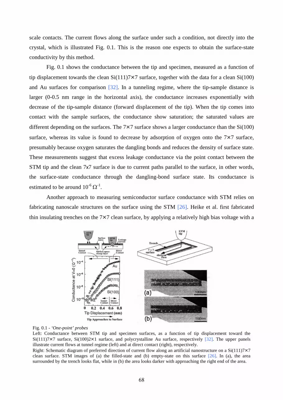
68
scale contacts. The current flows along the surface under such a condition, not directly into the
crystal, which is illustrated Fig. 0.1. This is the reason one expects to obtain the surface-state
conductivity by this method.
Fig. 0.1 shows the conductance between the tip and specimen, measured as a function of
tip displacement towards the clean Si(111)7×7 surface, together with the data for a clean Si(100)
and Au surfaces for comparison [32]. In a tunneling regime, where the tip-sample distance is
larger (0-0.5 nm range in the horizontal axis), the conductance increases exponentially with
decrease of the tip-sample distance (forward displacement of the tip). When the tip comes into
contact with the sample surfaces, the conductance show saturation; the saturated values are
different depending on the surfaces. The 7×7 surface shows a larger conductance than the Si(100)
surface, whereas its value is found to decrease by adsorption of oxygen onto the 7×7 surface,
presumably because oxygen saturates the dangling bonds and reduces the density of surface state.
These measurements suggest that excess leakage conductance via the point contact between the
STM tip and the clean 7x7 surface is due to current paths parallel to the surface, in other words,
the surface-state conductance through the dangling-bond surface state. Its conductance is
estimated to be around 10-6 Ω-1.
Another approach to measuring semiconductor surface conductance with STM relies on
fabricating nanoscale structures on the surface using the STM [26]. Heike et al. first fabricated
thin insulating trenches on the 7×7 clean surface, by applying a relatively high bias voltage with a
Fig. 0.1 - ‘One-point’ probes Left: Conductance between STM tip and specimen surfaces, as a function of tip displacement toward the Si(111)7×7 surface, Si(100)2×1 surface, and polycrystalline Au surface, respectively [32]. The upper panels illustrate current flows at tunnel regime (left) and at direct contact (right), respectively. Right: Schematic diagram of preferred direction of current flow along an artificial nanostructure on a Si(111)7×7 clean surface. STM images of (a) the filled-state and (b) empty-state on this surface [26]. In (a), the area surrounded by the trench looks flat, while in (b) the area looks darker with approaching the right end of the area.

69
high tunneling current in the STM. After that, they observed the structured surface in a
conventional STM mode. Fig. 0.1 Right (a) and (b) shows a half-closed tape-shaped pattern,
surrounded by the insulating trench. The apparent height of the surface area surrounded by the
trench was lower (darker) (by approximately 0.2 nm ) in the empty-state images (b) as the STM
tip approaches to the closed-end of the tape, while the brightness of the whole tape area is
observed to be flat in the filled-state images (a). This result is interpreted as follows: The
electrons tunneling from the tip to the sample flow along the tape through the surface state of only
the region restricted by the trench, when the tip is positioned inside the tape (see the top panel in
Fig. 0.1 Right). This is because a Schottky barrier between the surface state and the bulk state
forces the current to travel along the surface for a while before leaking into the bulk state. Then, a
voltage drop occurs along the tape due to a finite resistance of the surface state. This is a kind of
scanning tunneling potentiometry [33-35]. By comparing the measured voltage drop along the
tape with the calculated one, the conductance of the dangling-bond surface state on the 7×7
surface was deduced to be 8.7x10⁻⁹ Ω-1. This value is much smaller than that obtained by the
point-contact method of Hasegawa (Y) et al. mentioned above. Heike et al. [26] suggest that this
discrepancy arises because the method of Hasegawa (Y) et al. involves the conductance through
the surface space-charge layer as well as through the surface states. It is postulated that tunnel
contact may be a much more effective way to inject carriers into the surface-state bands, whereas
direct contact between the probe and sample surface injects carriers into both of the bulk and
surface bands. However, because all ‘one-point’ measurements are susceptible to resistance
effects at the point of contact, which are difficult to control or calculate multi-probe techniques
are essential to resolve these issues.
• Macroscopic four-point probes
Measurements of surface conductivity using four probes with a macroscopic distance were
performed in situ on silicon surfaces [14, 36]. An example of the sample holder used for such
measurements is illustrated in Fig. 0.2 Left, which is designed for simultaneous metal deposition
and reflection high energy diffraction RHEED observations, to prepare well-defined surface
superstructures on the whole are of surface [36]. After preparing the superstructures, a small
direct current is fed into the specimen crystal through the end clamp electrodes, and the voltage
drop is measured between a pair of thin Ta-wire contacts, the spacing of which is usually as large
as about 5-10 mm. Surface-state electrical conduction can be detected in this configuration only

70
under special conditions, when small amounts (around 0.01 ML) of atoms of monovalent metals
(noble and alkali metals) are deposited on top of the Si(111)√3x√3-Ag surface. These adatoms are
found to enhance the surface conductivity [37]. From photoemission measurements to reveal the
changes in surface electronic states, it has been shown that the adatoms donate their valence
electrons into the 2D-free-electron-like surface-state band S1 of the √3x√3-Ag substrate, thus
enhancing the surface-state conductivity [23, 37]. This is quite similar to in bulk crystals of
semiconductor in which impurity atoms act as donors or acceptors to vary the carrier
concentrations and conductivity. With increasing the coverage of the adatoms up to around 0.15
ML, 2D islands nucleate and arrange to make a new ordered structure with a periodicity [24, 38].
The superstructures made by monovalent-metal-atom adsorptions on the Si(111)√3x√3-Ag
surface have high surface conductivities. This is due to new dispersive metallic surface-state
bands that are created in the superstructures, while the surface-space–charge-layer conductance is
suppressed [39, 40]. In these cases, the surface-state electrical conduction is so large that it can be
detected experimentally using the macroscopic four-probe method. The conductances for these
structures are on the order of 10-4 Ω-1, which is higher than that of the 7x7 clean surface by about
Fig. 0.2 - Macroscopic and Microscopic four-point probes Left: A sample holder for in-situ electrical conductivity measurements in UHV using a ‘‘four-probe’’ method [54]. The inner probe spacing is typically several millimeters. After the surface superstructures are confirmed by using RHEED, the electron beam is always turned off during the subsequent conductivity measurements. A small current is fed through the clamps at both ends, and the voltage drop is measured by a pair of Ta wire contacts. Up: A SEM image of a silicon chip with a micro-four-point-probe array projecting over the chip edge. The probes are made of silicon oxide, coated with metal. Bonding pads on the chip facilitate electrical connections to the probes. An under-etching technique ensures that the probes are not shorted when a metallic layer is evaporated over the whole chip to make the probes conducting. The whole chip is 6 by 4 mm2 and mounted on a ceramic holder for convenience [27]. Down: Scanning electron micrographs showing the micro-four-point probe contacting to a silicon surface for measuring the conductivity in UHV. Slightly brighter bands on the sample surface are step bunches, and wider darker bands are terraces [28].

71
four orders of magnitude.
• Microscopic four-point probes
From the expectation of enhanced surface sensitivity by reducing the probe spacings,
micro-four-point probes with probe spacings down to 2 µm have been developed using silicon-
based micro-fabrication technology [27], one of which is shown in Fig. 0. Up. Such microscopic
probes also enable mapping of the local conductivity distribution on material surfaces [41]. The
micro-four-point probes have been used in UHV to measure the surface conductances of the
Si(111)7×7 clean and -Ag surfaces. Fig. 0.2 Down is a scanning electron micrograph showing a
micro-four-point probe (µ4PP) of 8 µm spacing, contacting to a silicon surface for the electrical
measurements. The resistance measured in this way on the -Ag surface was smaller than that for
the 7×7 clean surface by about two orders of magnitudes. This should be compared with the
result obtained by macroscopic four probes of about 10 mm probe spacing, where the difference
of resistance between the two surfaces was as small as about 10% [42]. These results imply that
reducing the probe spacing makes the measurements more surface sensitive. From a quantitative
analysis, the extremely high conductance of the -Ag surface compared with that of the
Si(111)7×7 surface cannot be explained by the surface-space-charge-layer conductivity. Rather it
must be attributed to the surface-state band inherent in the -Ag superstructure [27]. Although the
surface-state conductivity on this surface had been detected by macroscopic four-probe
measurements as a carrier-doping effect into the surface-state band, as mentioned before, µ4PP
enabled the direct detection of the contribution of the surface-state conductance [27]. Atomic
steps on the surface scatter the surface state electrons and this should cause additional electrical
resistance at steps, which has been measured with the µ4PP. A technique to control the step
configuration on the surface recently has been developed [43], which has been utilized to obtain
almost step-free terraces as wide as the probe spacing. By observing the probes and the sample
surface by scanning electron microscopy in situ, the probes can be positioned on a large flat
terrace, or positioned across a step bunch running between the inner pair of probes. In this way,
the surface area under measurement can be selected by shifting the probe position, so that the
influence of atomic steps upon the surface conductivity can be intentionally avoided or included.
It has been found then that the resistance measured across a step bunch is much larger than that
measured on a step-free terrace. Although this result is intuitively reasonable, it is the first direct

72
transport measurement, confirming that atomic steps on a surface causes an additional resistance
[22].
• Multi-tip STM
In order to measure the local conductivity in smaller areas down to nanometer scales,
several groups have constructed multi-tip STMs in which each probe can be controlled much
more accurately with variable probe spacings, and smaller probe spacings could be achievable.
Prospects for such multi-tip STMs are the measurement of electrical conductivity in a single
domain of a surface superstructure, and the study of ballistic transport as well as other quantum
phenomena that occur only on the nanometer scale. The usefulness of double-tip STM has been
discussed in Ref. [44]. The first trial to make such an STM was done with electrically isolated two
tips mounted on a single scanning head, so that the probe spacing could not be changed [45]. A
machine with independently driven double tips in UHV was later constructed by Aono et al. [46],
in which the tips can be brought together as close as about 100 nm. The macroscopic radius of
each tip determines the minimum distance attainable between the two tips. Such tips can be used
as an emitter and collector, like in the point-contact transistor, with much better control on much
more well-defined surfaces. Fig. 0.2 Right shows SEM images of four STM tips that are driven on
a single stage in UHV [29]. With such a device, the surface conductivities were measured as a
function of probe spacing ranging from 1 mm to 1 µm [29]. The probe-spacing dependences of
the measured resistance for the 7×7 clean surface and the -Ag surface were quite different from
each other, indicating quite different ways of current flowing; the current flows dominantly only
at the surface for the latter superstructure, while the bulk conductivity is dominant for the former
superstructure. Such measurements lead to clarifying the influence of surface defects and intrinsic
nature of surface-state transport in a more detailed way.
d. Noise
At elevated temperature and with an applied bias the fluctuations of the currents can be
divided into two contributions: the thermal noise, which is proportional to the temperature; and an
excess noise, called shot noise, which is only present when the system is biased [47, 48]. The
thermal noise is via a fluctuation-dissipation theorem related to a conductance and does not,
therefore, contain more information about the conductor than can be drawn from measuring

73
conductances. However, the shot noise, which is at zero temperature the only source of
fluctuations, can give more information [47]. For instance, the shot-noise spectrum can be used to
distinguish between different conductance mechanisms, such as ballistic or diffusive conductance
[48]. The low frequency shot noise spectrum has been used to identify the fractional charge of the
quasiparticles in the fractional quantum Hall regime, [49, 50] and, van den Brom and van
Ruitenbeek [51] used combined conductance and shot noise measurements to determine the
detailed mechanism of the electrical conductance through atom-size metallic gold contact. Birk et
al. [52] measured the shot noise at an STM tip. Of particular interest are current-current cross
correlations [53, 47, 54] due to their sensitivity to the statistics of the carriers. Specific predictions
have been made for current correlations of conductors in high quantizing magnetic fields [53, 47,
54], for ballistic conductors [55], for metallic diffusive conductors with massive contacts [56, 57],
for chaotic cavities [58], and for hybrid normal and superconducting systems [59]. Measurements
of current cross-correlations (the electric analog of the Hanburry-Brown-Twiss experiment) have
been reported by Henny et al. [60] for a Hall bar geometry, which permits the separation of
incident and reflected carrier streams as suggested in Ref. [53], and by Oliver et al. [61] for a
conductor that probably exhibits elements both of ballistic electron motion and chaotic electron
motion. More severe tests of our understanding of fluctuations arise from probing exchange
effects in correlations due to the quantum-mechanical indistinguishability of identical particles.
Earlier discussions of exchange effects in cross correlations in mesoscopic conductors can be
found in Refs. [62, 47, 54] and [56-59].
e. Scope and composition of Part II of this thesis
Within the topics mentioned above, part II of this thesis will describe a new approach for a
dual-tip STM. In order to put this work in the right context, with respect to the research fields of
mesoscopic transport and multi-probe STMs (MPSTM), the two first chapters will review the
theoretical and practical aspects of MPSTM. These mini-reviews do not fully describe all that is
mater, but, on the same time they are not composed as summary that leave it for the reader to go
through the referred literature. The choice for a rather comprehensive account of the theoretical
and practical attempts is due to the lack of publication of this kind. The two other chapters of part
II describe in details the work itself. Here the ideas and progress in the construction and operation
of a DTSTM will be discussed.
This part is composed as follows, in chapter 1, a dedicated theory as first suggested by Niu
Chang and shih for a dual-tip STM will be reviewed. Other works that looked at the theoretical

74
aspects of dual-tip measurements will only be mentioned and further reviewed in appendix A. In
chapter 2 a survey on DTSTM design and applications as can be gained from up to date
publications will be given. Some basic designed two and four-probe STM configurations, the
issue of probe aligning and the different choices of probes will be reviewed. Up-to-date
applications of multi-probe techniques will be reviewed in appendix B. In chapter 3, a new
concept for a dual-tip STM will be described. The transition from a mechanically-controllable
break-junction (MCBJ) to a dual-tip STM (DTSTM) will be presented here together with the
fabrication of a two independent nanotips on both sides of the junction using electron-beam
induced deposition (EBID). Different experimental setups that can be preformed will also be
discussed finalizing with a look on the overall system. In the last chapter (4), the preliminary
results of the new dual-tip STM design will be presented. After introducing the constructed
system, the different designs of the junction and its aligning following by the different EBID tip
fabrication and their independent positioning will be presented. The current statues of this project
will be finally stated.

75
Chapter 1
Review on theoretical aspects of dual-tip STM
1.1 Scope of this chapter
In this chapter theoretical works on two tip configurations will be reviewed. In section 1.2,
the first dedicated theory as first suggested by Niu Chang and shih [1] for a dual-tip STM will be
reviewed. Other works that looked at the theoretical aspects of dual-tip measurements will be
mentioned in section 1.3.
1.2 The fundamental work of Niu, Chang and Shih
Because a double-tip STM can probe the all important single-particle Green function of a
sample, it has the potential of becoming an extremely useful new tool in surface analysis. That
was concluded by, Niu, Chang and Shih in their "Duble-tip scanning tunneling microscope for
surface analysis" PRL paper from 1995 [1]. Niu et. al. had identified key experimental parameters
for such measurements and described some basic applications of a double-tip STM: (1) probing
the k-resolved band structure of surface states, as well as the shape of Bloch functions; (2)
measuring scattering phase shifts or amplitude of surface defects; (3) observing transition from
ballistic to diffusive transport to localization; and (4) measuring inelastic mean free paths.
The use of a single-tip STM, described in part I chapter 3, has been limited to probing
static properties of electronic systems such as the local density of states on or near sample
surfaces. In addition, it lacks the k resolution to enable one to determine the energy dispersion in
band structures. Transport properties are also out of reach of the single-tip STM, except for the
ballistic energy electron microscope (BEEM) configuration used to probe ballistic transport
across a metal film [2].
In a typical double-tip experiment, electrons are emitted from one tip, and propagate
through the sample, some of which are picked up by the other tip. Naturally, the propagator or the
Green function of an electron in the sample is involved. Since all single-particle properties of the
system can be derived from the Green function, one expects that a lot more information about the
sample surface and nearby region can be learned from an experiment using a pair of tips than

76
from using a single tip.
Shown in Fig. 1.1 is a schematic
experimental setup. The sample is assumed to
be large enough to have a well-defined
chemical potential µ0. Voltages V1 and V2 are
applied to the tips relative to the sample, and
electric currents I1 and I2 from the tips to the
sample are measured. Like the BEEM, this is a
three-terminal setup [2]. Unlike the BEEM,
here the tip-sample separations, the tip biases
(V1 and V2), and the tip locations (r1 and r2) are
controlled independently. Direct junction
conductance at r1 and r2 are denied as σi =
∂Ii/∂Vi, and are given to leading order in the
tunneling rate as [3]
( )iiii re
µρπ
σ ,2 2
Γ=h
, (8)
where ρ(ri, µi) is the local density of states of the sample at the chemical potential of tip i, and Γi
describes tip-sample couplings as well as the density of states of the tips (which are routinely
measured in single-tip STM experiments). Up to order Γ1 Γ2, there are also processes of coherent
tunneling of an electron from one tip to the other through the sample, which can be measured
through the transconductance defined by σ21 = ∂I2/∂V1. The transition rates can easily be
accounted for by the Fermi golden rule using second-order transition-matrix elements [4] yielding
( )2
121
2
2121 ;,2
µεπ
σ =ΓΓ= rrGe
h, (9)
where G (r1, r2, ε) is the retarded Green function of the sample for non-interacting electrons at
zero temperature.
In the presence of electron-electron and/or electron-phonon interactions in the sample, the Fermi
golden rule gives the same result if µ1 = µ2 and if the sample is nonsuperconducting. For µ1 ≠ µ2,
Fig. 1.1 - Schematic diagram of the double-tip STM experimental setup Tip 1 is biased at F1 and tip 2 at F2 relative to the sample. I1 and I2 are also measured relative to the sample. When µ1 > µ2, I2 contains a transconductance component due to the cotunneling process.

77
four-point Green functions of the sample are involved to account for the inelastic scattering of the
tunneling electrons [5]. For a superconducting sample, Andreev processes can also contribute to a
transconductance within the same order [6]. With the direct conductance and transconductance
measured at µ1 = µ2 = µ, one can thus obtain information about the retarded Green function as
shown below:
( ) ( ) ( )µρµρσσ
σπµε ,,
2;, 21
21
212
2
121 rre
rrGh
== . (10)
Since constant-current STM images trace constant contours of the local density of states, the last
two factors can be treated as normalization constant.
Niu et. al. next identify experimental parameters from which such a measurement can be
realized. As a second-order process, it is clear that σ21 is a weak signal to detect. Taking BEEM as
a reference, for a total tunneling current of 1-10 nA, the detecting limit is about 0.1-1 pA for
ballistically transported electrons, corresponding to a factor of 10-3-10-4. However, it is possible to
utilize a frequency lock-in amplifier to boost this limit to 10-4-10-6. For the sake of argument, they
set a conservative number of 10-4 as a practical detection limit. Considering a symmetric setup
such that σ1 = σ2 = σ, from Eq. (10) one immediately finds that σ21/σ is on the order of (ħ/2πe2)σ,
with additional factors determined by the ratio between the Green function and local density of
states. For a case of ballistic transport through surface states, |G|2/ρ2 is approximately 2π/kr, where
k is the wave number at energy µ, and r is the distance between the tips. The closest tip-to-tip
distance is determined by the radius of curvature and the aspect ratio of the tips. Recent advances
of tip-fabrication techniques can reproducibly make high-aspect-ratio tips with a radius of
curvature on the order of 50-100 Å. It is thus conceivable to consider operating a double-tip STM
in the range of a 300-1000 Å tip-to-tip distance. This gives |G|2/ρ2 on the order of 1%. Since h/e2
= 25 kΩ, one can immediately identify the practical operation range of tunnel junction resistance
to be on the order of 1-10 MΩ. For the case of an anisotropic Fermi surface |G|2/ρ2 is on the order
of unity in the same range of tip to tip distance and the STM junction resistance can be as large as
GΩ. The most advantageous case is for a one-dimensional structure, such as a fullerene nanotube,
for which |G|2/ρ2 does not depend on distance at all and is of order unity.
Niu et. al. described some of the most important applications of the double-tip STM.

78
• Ballistic transport and surface state band structure
For a situation where surface states play a dominant role in electron transport, the
transconductance has overall inverse r dependence like the free-electron case, however, two
interesting new features appear for a crystal: (1) The transconductance is modulated by the
magnitude squared of the Bloch functions. (2) There is also an overall orientational dependence
from the factors involving the partial derivatives of the band energy.
By plotting the transconductance for a square lattice at energy close to a nested-energy
surface, Niu et. al. demonstrate the inverse r dependence and a pronounced anisotropy. They
argued that it is possible to reconstruct the constant energy contour of the surface band structure
for the filled and empty states using the mapped out |G|2/ρ2 and that the oscillatory modulation of
the transconductance should also tell us the shape of the Bloch waves. Another advantage lies
within the sub-mev resolution of the tunneling energy measurement. In comparison, angle-
resolved photoemission spectroscopy (ARPES) can map out the k-dependent band structure only
for the filled states and its resolution is currently limited to about 15 mev.
• Phase shifts from a surface defect
One can move the tips near (but still far compared to the wavelength) to a surface defect
and observe how it scatters the electrons by an interference effect. An electron may propagate
freely from tip 1 to tip 2, or it may propagate to the defect and be scattered to tip 2. The
superposition of these processes can give rise to a modulation of |G|2, when tip 2 is moved around
relative to tip 1 and the defect.
A single-tip STM can only see defects having a substantial disturbance of the local density
of states on a sample surface [7]. The double-tip STM should be able to detect the "mines'' buried
fairly deep under a surface through the "radar'' of scattering interference. Unlike the interference
patterns observed in Eigler's experiments [8], the interference due to an impurity in the bulk is
seen by measuring the transconductance between two tips.
• Transition from ballistic to diffusive transport to localization
In the absence of defects, the transconductance measures ballistic electron transport
between the tips. As seen above, for surface states, this is signified by inverse r dependence,

79
modulated by an angular dependence if the energy surface is not circular. When a defect is
present in the neighborhood of the two tips, scattering interference will occur. The interference
pattern will become more and more complicated if more defects are included in the way between
the tips. When the tips are moved apart by a few elastic mean free paths, diffusive electron
transport should begin to take place. . It can be shown that ( )2
121 ;, µε =rrG measures the time
integral of the probability for a wave packet of energy ε to move from rl to r2 in a given time t [9].
In the diffusive regime the overall trend of this probability goes as
( )
−−
Dt
rDt
21expπ , (11)
where D is the diffusion constant. The average transconductance in this regime should then
behave as
( ) ( )cDtrED /21
1−π , (12)
where E1 is the incomplete Γ function, and tc is a cutoff time beyond which elastic diffusive
behavior creases to occur. In the absence of inelastic scattering, this cutoff time is given by lc2/D,
where lc is the Anderson localization length [10]. It is interesting to see that the transconductance
for r << lc behaves like (πD)-12ln(lc/r). This slow falloff with distance is in sharp contrast with the
behavior in the ballistic regime. When r is beyond the localization length, the Green function and
the transconductance should drop exponentially.
• Inelastic mean free path
Physically, an electron tunneled in from tip 1 may lose energy by exciting electron-hole pairs
or emitting phonons as it travels in the sample, and becomes unable to tunnel out to tip 2. The
typical length scale over which such a process occurs defines the inelastic mean free path, and is
given by the decay length of the Green function. Therefore, the inelastic mean free path and its
energy dependence may be measured by observing how the transconductance decays with tip-tip
distance, and how the decay length varies with µ - µ0.

80
Apart from these applications, Niu et. al. consider applying a magnetic field to observe the
cyclotronic motion of electrons in the semiclassical regime [11], or to possibly probe some
properties of a quantum Hall system in a strong magnetic held [12]. One can also consider
mapping out the quasiparticle band structure of a superconductor through ballistic transport or gap
structure through Andreev reflections as proposed in Ref. 6.
1.3 Two tip configurations from other theoretical works
The section is attached as an appendix C to this work. In the appendix, four different
theoretical probe-sample geometries will be reviewed as can be seen in Fig. 1.2:
• Probing Spatial Correlations with Nanoscale Two-contact Tunneling
• Theory of a scanning tunneling microscope with a two-protrusion tip
• Calculation of ballistic conductance through Tamm surface states
• Local densities, distribution functions, and wave-function correlations for spatially
resolved shot noise at nanocontacts
Fig. 1.2 - Four different probe-sample geometry Up & left) The sample is strongly connected to ground and weakly connected to two localized junctions, at least one of which is mobile. The possibility considered in sub-section 1.3.1 is a 100 Å nanofabricated contact for one localized junction (located at xl) and an STM tip for the other (located at x2). Up & right) Two protrusions on a single STM contact are connected to the same reservoir. Down & left) Double tips on a flat surface. Open and closed circles show the surfaceatoms and the atoms at the apexes of the tips, respectively. Down & right) Experimental setup to measure current correlations. Two STM tips are coupled with strength t at the positions x and x' to the surface of a small wire. The shaded region can be a metallic diffusive or a perfect ballistic wire.

81
Chapter 2
Survey on multi-probe STM design and applications
2.1 Scope of this chapter
A survey on DTSTM design and applications as can be gained from up to date
publications will be given in this chapter. In section 2.2, some basic designed two and four-probe
STM configurations will be reviewed. In section 2.3 the issue of probe aligning will be addressed.
Section 2.4 will look at the different choices of probes. Section 2.5, on up-to-date applications of
multi-probe techniques, will be reviewed in appendix D.
2.2 Examples for multi-probe STM designs
2.2.1 Four-probe systems
A 4PP method is the most direct and common approach to measure the electrical
conductivity of samples. In a 4PP the outer pair of probes is placed in contact with a sample
surface and a voltage is applied between them, a current I flows through the sample. The inner
pair of probes, which are also in contact with the sample, detect a voltage drop V along the
Table 2.1 - Different four-point configurations and their measured resistances

82
surface due to the resistance of the sample. Thus, one can obtain a 4PP resistance R = V/I. Strictly
speaking, the four-point probe measurement is not a direct measurement of the sample resistivity
but depends on the geometry of the sample. The probes can also be arranged in a linear or square
geometry and with a different current and voltage configurations. Analytical expressions
connecting the measured resistance and the resistivity of the sample exist only for a few simple
geometries [1]. Table 2.1 displays 2 and 3D results for different configurations. In these examples
one can correctly measure the resistance of a sample without any influence of contact resistance at
the probe, irrespective of whether the probe contacts are ohmic or Schottky-type. This is because
virtually no current flows through the voltage pick-up contacts; so that no voltage drops occur at
the probe contacts, thus minimizing the contact resistance contribution to the measured signal.
• A fixed µ-4PP
For measuring electrical conductivity with high surface sensitivity, a four-point probe
method with microscopic probe spacing (µ-4PP) is needed. The measuring current fed through a
pair of the four probes penetrates into the specimen as deep as the probe spacing roughly, which
means a relatively higher surface sensitivity as the probe spacing is reduced. A fork-like fixed
configuration has been developed at Mickroelektronik Centret of the Technical University of
Denmark [2], and is also commercially available [3]. Such probes with 4, 8, 10, 20, 30 and 60 µm
probe spaces were made using silicon-based microfabrication technology following a procedure
similar to that used to fabricate micro-cantilevers for atomic-force microscopy. The probes consist
of four sharpened silicon oxide cantilevers, in line and equidistant from each other, extending
from a silicon support chip. The silicon oxide paths on the chip are undercut, so that deposition of
metal onto the chip results in conducting paths that are insulated from the support chip. See fig.
Fig. 2.1 - A monolithic micro-four-point probe Left: A SEM image of the chip. Right: A SEM image of the cantilevers contacting a sample surface.

83
2.1.
• Quadruple-tip STM
To control the setup of a µ-4PP, an apparatus with independently controlled probes is
necessary. Different four-tip STMs were designed in order to face this challenge. These are all
working in scanning electron microscopes in ultrahigh vacuum (UHV), enabling precise probe
positioning on aimed areas on the specimen surface. The four STM probes can be manipulated
independently with subnanometer precision, enabling atomic resolution STM imaging and four-
point electrical transport study of surface electronic systems and nanostructured materials. Some
of theses systems are also equipped with molecular-beam epitaxy chambers, different surface
analytical techniques and integrated heating/cooling capabilities for sample preparation, surface
classification and transport characterization. Two examples are displayed in Fig. 2.2, an
independently driven four-tip probes developed in the University of Tokyo [4], and the
commercial UHV NANOPROBE by Omicron Nanotechnology [5]. Other four-tip STM systems
can be found in the following Ref. [6, 7-10].
2.2.2 Dual-tip STM
In chapter 1 the dual-tip STM theory was discussed. Unlike four-tip STMs, aimed for µ-
4PP setups, dual-tip systems were designed to face the challenges presented in chapter 1. These
are usually simpler and coast-effective designs that do not have the capability of precise probe
positioning on aimed areas under SEM. Instead, different aligning methods were developed for a
coarse approach wile each tip has its individual STM scanning capability as they are all mounted
Fig. 2.2 - Four-tip STM systems Left: Developed in the University of Tokyo and Unisoku Co. [4]. Right: From Omicron Nanotechnology [5].

84
on tube-scanners. Scanning is usually not simultaneous in order to avoid the tips from crashing
into each other. Some designs are displayed in Fig. 2.3.
2.3 Probe aligning
One of the essential requirements of a DTSTM is the capability to position the two tips at
any relative positions including near contact on a sample surface. This requires a position system
of at least 4 degrees of freedom, three for adjusting two tip’s relative coordinates and one for
bringing them to a sample surface. Four-probe STMs are mostly use as micro probe-stations, and
since they are operated under SEM column, the probes are viewed and can be positioned on
(1)
(2)
(4)
(5)
(3)
(8)
(6)
(7)
Fig. 2.3 - Different dual-tip STM systems (1) Ultrahigh vacuum compatible cryogenic (down to 4.2 K) DTSTM with alignment procedure using a specimen made of three mutually nonparallel planes [11]. (2) DTSTM with two orthogonal tips and special designed feedback [12]. (3) A compact DTSTM [14]. (4) DTSTM with multiwall carbon nanotubes as probes and active damper system [13]. (5) Development of probe-to-probe approach method [15]. (6) The tips and sample can be positioned and angled to image the same surface or perpendicular surfaces [16]. (7) A Beetle-Type DTSTM [17]. (8) Ultrahigh vacuum, variable temperature, DTSTM operating under high magnetic field [18].

85
surfaces or nanodevices with high accuracy. The actuation positioning mechanisms are design to
keep the z component fix wile aligning is performed in x and y to avoid crashing (for example
octapole-tube piezo scanner [6]). For dual-tip STMs some kind of 'blind' aligning of the tips has
to take place. Different procedures were developed and three are viewed here.
One - In [11] five linear steppers where employed. The overall configuration is shown in
Fig. 2.3 (1) Three small steppers (x,y,z) are used to adjust relative positions of the two tips and are
supported on a bigger stepper Z, which moves the two tips together along the z direction to
approach or withdraw from the sample surface. A fifth stepper translates the sample along a
horizontal line parallel to its surface. This design, separating tip-tip adjustment from the tips-
sample adjustment, avoids searching and readjusting relative tip positions when the tips are
brought to different points of the sample surface. Together with the embedded position sensor, the
five linear motion, either orthogonal or in parallel, makes navigation of the two tips a well-
controlled process. The position sensors of the liner steppers track the relaive coordinates of the
two tips. This approach, however, requires the accurate determination of the initial coordinates of
the two tips. A method using an alignment sample made of three mutually nonparallel planes for
locating the initial positions of the tips was employed. The basic idea may be seen by imagining
that the two tips are brought to the tunneling range of three orthogonal planes in succession, along
lines normal to each plane. This procedure should provide a complete alignment of the two tips in
x, y, and z coordinates. Three nonparallel planes as shown in Fig. 2.4 (up) are sufficient to achieve
this goal.
Two - In [15] A method of approaching one probe to the other by coarse positioning
motors is composed of two processes. In the first process, the probes are set at initial positions
manually with the aid of a charge-coupled device (CCD) video camera system. The second is a
probe search process, where the positioning motors are automatically operated according to a
computer program. The second processes can be viewed in Fig 2.4 (down).
Three - In [12] a method was developed that uses one tip to search out the end of the other
tip (Fig. 2.4 (right)). The process involves manually arranging the tips into a preliminary ‘‘cross-
swords’’ configuration and then using a computer routine that senses the tip–tip tunneling current
to bring the tips within the same scan range. The computer routine has two variations that differ
depending on whether the sample surface is used as a guide plane. In the first variation the tips
stay in constant tunneling contact with the surface, while the second only checks for the sample
periodically to maintain a constant distance from the surface.
2.4 Multi-probe STM tips

86
The ideal geometric properties for a multiprobe STM tip are that it is long and tapered
with as small a cone angle as is possible, to allow the tips to be used in close proximity. The tip
should be conducting and relatively tough, to withstand physical contact with objects. Finally,
having high symmetry tips is also desirable as this makes it easier to determine the position of
each tip when approaching or making contact with surfaces or objects.
Since the invention of field ion microscope (FIM) by Erwin W. Müller in 1937 [19], the
fabrication techniques of atomically sharp tips have been actively investigated. The invention of
STM has further promoted the investigation. Sharp and hard tips are now an important component
of many of scanning probe microscopes. The size, shape, physical, and chemical identity of the
Fig. 2.4 - Two tips aligning and navigation Up: Three mutually nonparallel planes are used for the dual-tip adjustment process. Two tips approach each plane successively. The first tip approaches using X and Z steppers (see Fig. 2.3 (1)). The second tip approaches using steppers x, y, and z for the planes x, y, and z, respectively. The plane z is the sample itself, while planes x and y are gold evaporated mica planes. Down: Illustration of the approach route of Tip2. Tip2 moves at the speed of 1 µm/s along a route of the solid arrows (like a rectangular wave) on the upper plane, which is ~1.5 µm apart from the sample surface. The route has a wavelength of 2 µm and an amplitude of 25 µm for X and Y directions, respectively. Tip1 and the sample are biased, while Tip2 is grounded. Right: Schematics depicting the two variations of the computer routine used to bring the probes within close proximity. In each cartoon the upper probe is shown on the left (in the -X direction). (A) - (C) display the steps of the first routine that employs the sample surface as a guide. The lower tip moves in -X to come into tunneling with the upper probe. The lower tip then moves around the upper tip until the direction of motion is completely in the -X direction and the tips are aligned. (D) -(F) show the steps of the computer controlled loop when the probes are not in constant tunneling contact with the surface. The lower probe moves in 1X, breaking tunneling contact, and then in 2Z. The probe then moves to the surface and pulls away to maintain a constant distance from the sample. Finally the probe approaches the upper probe until tunneling is reestablished.

87
tip apex, influence not only the resolution of microscopes but also the interpretation of images
and data.
Huge number of works on the fabrication of sharp tips have been performed and several
techniques have been developed, such as grinding [20], cutting [21], mechanical pulling [22],
chemical or electrochemical etching [23], field evaporation or other field-induced methods [24],
beam deposition [25], ion milling [26], and others [27].
Among these methods, the etching technique is most widely used as a fast, cheap,
convenient and reliable method and also as a pre-treatment method for further fine fabrications
such as gluing carbon nanotubes on the metal tip [28]. One of the common and reliable methods
is so called a “drop-off” method, in which etching occurs at the air-electrolyte interface, causing
the portion of wire immersed in the solution to “drop off” when its weight exceeds the tensile
strength of the etched wire metal neck [23, 29].
Tips of different kinds of materials can now be made by the etching methods. Especially,
electrochemical etching of a tungsten wire is widely used for STM tips [29]. Thanks to
contributions from many researchers, sharp tungsten tips having around 20-nm diameter at the
apex can now be acquired routinely [30-32]. Many examples for the above techniques can be
found in [33] and reference therein.
A method to improve the resolution of four-point-probe measurements of two-dimensional
(2D) and quasi-2D systems was also developed [34]. By mapping the conductance on a dense grid
around a target area and postprocessing the data, the resolution was shown to be improved by a
factor of approximately 50 to better than 1/15 of the four-point-probe electrode spacing.
In Fig. 2.5 attempts to use high-aspect ratio tips in multi-tip STMs are shown.
2.5 Multi-probe STM data acquisition and control
Multi-probe apparatus can be configured for a verity of experimental setups. In Table 2.1
Different four-point configurations and their measured resistances where listed. Other three or
two terminal setups can be configured for different physical phenomenon. It is to be noted here
that dual-tip STM is actually a three-terminal setup if we consider the sample to be easier the
source, the sink or the conductor. If the probes are assigned for STM imaging, that for itself
requires STM control electronics that can handle scanning, feedback and data acquisition of multi
tips. If the tip serves as terminals (current or voltage probes) they have to be a part of the suitable
electric circuit. If some of them or all are to be selected for both, the electronics that needs to be
designed get more and more complicated; for example the pre-Amps needs to be biased and

88
relays should be integrated into the circuits. Only recently, commercial control-electronics that
a
h
g
f
e
c
d
b
Fig 2.5 – Examples for high-aspect ratio tips in multi-tip STMs a. SEM image of the tips fabricated by the dynamic etching method [35]. Inset shows the tips made by the static etching. A red circle indicates an accidental contact between the tips. b. A modification of the 'drop-off' process by introducing a magnetic field, along the tip direction was investigated [36]. The resulting tips had a reduction in cone angle of up to 3.5. The white bar represents a length of 1 µm. c. A carbon nanotube (CNT) probe glued on a W tip was wholly coated with a thin PtIr layer 6 nm thick. The current-voltage characteristics of the resultant PtIr-coated CNT tips indicated that the PtIr coating stably reduced the resistance between the CNT tip end and the W supporting tip [37]. d. SEM images of the voltage probes (tips 2, 3) in a four-probe STM with PtIr-coated CNT tips. The minimum probe spacing before the contact was 30 - 20 nm [38]. e. After cleaning of a W tip by annealing at 1000 °C, the tip was cooled down to 600-700 °C and WO2 nanoparticles were evaporated from the W plate heated to 1000 °C under oxygen pressure of 1×10⁻³ Pa resulting in an epitaxial growth of WOx (2 < x < 3) nanorods on the tip surface [39]. f. A SEM image of a micro four-point probe equipped with nanowire nanoelectrodes (single-crystalline silicon nanowires (SiNWs)). Two of the four probes are shown [40]. g. If the beam of a SEM is held at one position for a long time a thin carbon rod grows in the direction of the electron beam (electron beam induced deposition EBID). This technique was used to grow four converging rods at the edge of a microfabricated probe, thus decreasing the overall size of the four-point probe to approximately 1 µm [41]. These probes were rendered conductive by depositing a thin layer of gold with titanium as adhesion layer. h. The EBID tips can be grown in converging direction by tilting and rotating the substrate. Secondary parallel tips can be deposited ending with two nanotips on a nanogap separation [42].

89
can be configured for multi-probe tasks can be found. Generally however, the electronics have to
be custom designed to mach the data collection expected from the experiment.
In Fig. 2.6 example for electronic setups designed to control current/voltage probe in a
multi-probe configurations is displayed.
2.6 Multi-probe STM applications
The section is attached as an appendix D to this work. In the appendix, some applications
demonstrated by multi-probe STMs will be reviewed. These will be divided into two groups of
four-probes and dual-tips.
In the Four-probe applications the following will be reviewed:
• Surface sensitivity versus probe spacing
• Anisotropy in surface conductivity
• Resistance across an atomic step
• Silicide Nanowires and Carbon Nanotubes
Other examples that will not be reviewed
Other applications to nanowires and nanotubes include: "Electrical Characterization of
Metal-Coated Carbon Nanotube Tips" [43], "Intrinsic current-voltage properties of nanowires
Fig. 2.6 - A diagram of a preamp for one (current/voltage probe) tip A low-leakage operational amplifier (op-amp) U1 is used for the case of current probe to measure the tip current and to apply the bias voltage to the tip. Another op-amp U2 is installed in parallel to the signal line for the case of voltage probe to measure the tip voltage and to drive a guard of the signal line. Ultralow-leakage photo-MOS switches Sw1 and Sw2 are inserted in the signal line. The tip can be electrically insulated and work as a voltage probe by opening Sw1. When Sw1 is closed, U1 and U3 measure the tip current, and the tip works as a current probe. Sw2 switches the low- and high-current modes in the current-probe mode. Rf1 is 1-10 GΩ for low current detection, while Rf2 is 1-10 MΩ for high-current detection.

90
with four-probe scanning tunneling microscopy: A conductance transition of ZnO nanowire"
[44], "Four-probe scanning tunnelling microscope with atomic resolution for electrical and
electrooptical property measurements of nanosystems" [45].
In the Dual-tip applications the following will be reviewed:
• Measuring a carbon nanotube ring transistor
• A method for determining σs by using two STM tips that remains in tunneling contact
Other examples that will not be reviewed
Examples for other dual-tip STM setups and results are; three-terminal ballistic electron
emission spectroscopy [46], field-effect-transistor electrical characteristics [47],
2.7 Summery and conclusions
• Aligning and navigation
Multi-probes are design mostly for two kinds of applications; different transport
characterization of surface; transport in nanostructures. In the first case placing of the probes is
less aquatic and it might be satisfying to place it with respect to macroscopic features of the
surface like steps, different reconstruction domains and orientations. In the case of nanostructures
like nano- rods and tubes a high accuracy of the probes contact is essential in order to collect the
proper data. In both cases the ability to perform a series of adjutant measurements in different
configuration is desirable. Thus aligning and navigation of the probes is a fundamental challenge
in multi-probe design. In this chapter we saw that two solutions were applied. Four-probe systems
were all constructed to work under SEM and thus the probes and the surface/nanostructure are
simultaneously being observed. Aligning and navigation is achieved by four independent
translations and/or rotation stages each having a piezo-tube scanner in addition. Careful attention
was devoted for the separation of movement to different axes. The sample is kept fixed. Dual-tip
STMs were mostly designed as 'blind'. It means that after a coarse approach, that some times is
performed under optical microscopes, different aligning and navigation procedures were

91
developed in order for the tips to simultaneously meet the surface and maintain proximity to each
other.
• The probes
According to the desired applications, multi-probe systems needs rigid probes for survival,
conductive probes for tunneling or point contact and high aspect ratio probes for reducible
separation. In this chapter we saw a range of solutions from µ-4PP designed as silicon cantilevers,
through higher aspect ratio electrochemical-etching Tungsten tips to nanorods and nanotubes
attached to conventional tips and some times covered with different metals. EBID tips were also
fabricated to reduce probe separation. Since probe separation is limited by the probe diameter, the
probes can be aligned with a tilt with respect to the surface so the cone at the apex enables a
closer accessibility.
• Control-electronics and experimental setup
Multi-probe systems have to be accompanied with a suitable control-electronics. In this
chapter we saw that it might mean; an independently controllable multi-feedbacks,
synchronization and multi-data acquisition capabilities. The different experimental setups might
also involve; tunneling and point contact capabilities for each probe, switching between
conventional tip-sample to tip-surface-tip circuits using relays and amplification of very low
currents with a good noise reduction.
• Experimental setting
On top of the above, experimental settings like UHV, low and high temperatures, sample
preparation, other surface characterization techniques, in-situ tip/sample replacement and so forth
make the overall design of a multi-probe system ever complicated and expensive.
In the following chapter a new approach for a dual-tip STM will be introduced. Three
issues are taking care of in this new approach. Tip aligning, tip aspect ratio and experimental
setup.

92
Chapter 3
A new concept for a dual-tip STM
3.1 Scope of this chapter
In this chapter a new concept for a dual-tip STM will be described. In section 3.2, the
motivation and challenges that guide this work will be defined. In section 3.3 the transition from a
mechanically-controllable break-junction (MCBJ) to a dual-tip STM (DTSTM) will be presented.
Here after a short introduction to the MCBJ technique, a modified version and its conversion to
DTSTM platform will be explained in details. In section 3.4 the fabrication of a two independent
nanotips on both sides of the junction using electron-beam induced deposition (EBID) will be
reviewed. In section 3.5 the operation; experimental setup and control electronics, will be
described. Here the different experimental setups that can be preformed will be discussed. And at
last the overall system including the dumping system and UHV chamber will be presented.
3.2 Motivation and challenges
In the pervious chapter a variety of multi-probe systems, designed in the last eight years,
were reviewed. Remarkable results were already demonstrated and both academic groups and
commercial companies were involved in the construction of highly reliable multi-probe setups. In
this section the motivation and ideas for a new approach to the design and operation of a dual-tip
STM will be explained. In the summery of chapter II, the main challenges and solution involved
in the design and operation of multi-probe systems were listed. Three of these were found to be of
fundamental importance; aligning of the probes (and navigation); tip aspect ratio (for reduced
separation); experimental setups (the physical information that can be collected). The following
can be deduced from pervious experience:
Alignning - All of the four-probe systems are constructed using complex translation/rotation
stages aligned under high-resolution SEM. That leads to a relatively large apparatus forced to be
mounted in a highly cost dedicated SEM. Most of the dual-tip STMs aligning and navigation
involves the development of some mutual approach procedures. The problem here is how to start

93
from two macroscopic tips (mounted on some aligning/navigation mechanism) that can be viewed
with the bare eyes (or even optical microscope) and end with two nanotips that are aligned in 3D
and brought to tunneling/point-contact with a surface on a desirable location with close proximity.
Tip separation - The tip aspect ratio is fundamental if we want to use the dual-tip STM as a two
terminal experimental setup on the meso- nano-scales. On these scales, transport phenomena that
are more sensitive to surfaces and even to the electron wavelength might be observed.
Experimental setups - All the data acquisition reviewed in chapter II was performed in a static
configuration of the multi-probes. That limited the experimental setups to discrete and very
accurate probe configurations.
The following challenges were found as guidelines for a new approach to a DTSTM:
• To eliminate in situ probe observation for aligning and any aligning procedure.
• To fabricate custom made (shape and material) high aspect ratio nanotips.
• To eliminate the need for accurate and static probe configurations.
The overall motivation was to design a cost effective DTSTM enable of constructing
transconductance maps of surfaces, which are surface structure and defects dependent, on scales
sensitive to the electron wavelength.
In the following sections three ideas will be introduced; 1. Using a modified version of the
MCBJ as a platform for a dual-tip STM. That will eliminate the need for probe aligning. 2.
Fabrication of EBID nanotips for high aspect ratio, custom shape and desirable material probes.
Those will enables to characterize transport at surface on the nanometer scales. 3. A trans-
conductance scanning tunneling microscopy/spectroscopy. That will eliminate the need for
accurate and static probe configurations in order to collect data at specific surface locations or
nanostructures points.
3.3 From a MCBJ to a DTSTM
3.3.1 The MCBJ technique

94
The fundamental application of the STM is the study of surface topography in the non-
contact scanning mode, but it was discovered soon that the probe tip can also be used to modify
the surface or even to build artificial structure of atoms [1]. The mechanical behavior of the
material on such scale has demonstrated several interesting features. For instance, a nanowire can
be pulled out of the sample surface if the tip is intentionally pushed into the sample and thereafter
retracted back. This nanowire becomes narrower and narrower during its elongation, and before
the complete rupture a single atom connects the two sides. The investigation of the mechanical
and electrical properties of such “nanocontacts” has recently become an interesting topic of
nanoscience [2]. As the Fermi wavelength of electrons in a metal is in the order of the interatomic
spacing (≈ 3˚A), these atomic contacts can also be considered as quantum confined systems. In
such nanojunctions the coherent quantum phenomena always interplay with the atomic
granularity of the matter, which makes the understanding of the experimental observations less
straightforward.
One very fine technique to perform point contact measurements is a mechanically
controllable break junction (MCBJ), which was introduced by Muller and co-workers [3]. The
principle of this method is presented in Fig. 3.1 (left). A small piece of a metallic wire is fixed at
two points on a flexible substrate, a so-called bending beam. Between the fixing points the cross
section of the wire is reduced by making a notch. The bending beam is fixed at both ends to the
sample holder. In the middle a vertically moveable axe is pushed to the beam, which can be
precisely positioned with a combination of a differential screw mechanism and a piezo stack. As
the beam is bent, the sample wire starts to elongate between the fixing points, which results in the
reduction of the cross section, and finally the wire completely breaks. Thereafter the contact can
be reestablished by reducing the bending of the beam.
A well established advantage of the break junction technique is the robust mechanical
stability of the system. The electrodes are rigidly fixed to the substrate at a very close separation
(0.5 mm), so the length of the free standing parts is much shorter than in a typical STM setup.
This makes the junction insensitive to mechanical vibrations. Furthermore, due to the mechanical
configuration of the bending beam, the vertical motion of the axe pushing the beam causes only a
highly reduced horizontal displacement of the electrodes (∆x ≈ ∆z/100). This means that any noise
in the position of the axe (due to vibration, thermal expansion or voltage instability on the piezo
element) has only a strongly reduced influence on the junction. This aspect is discussed in detail
in the following references [4].
Beside the important advantages of the MCBJ technique, like the cleanliness and the
stability, the main disadvantage also has to be noted. Due to the uncontrollable details of the

95
breaking process, the exact shape and orientation of the electrodes is always unknown. This is a
crucial point to be mentioned in my modified version ahead.
A different MCBJ instrument (Fig. 3.1 (up)) was developed by van Ruitenbeek et. al. [5].
A notched gold wire is fixed with stainless steel clamps, bridging two bendable metal substrates.
The wire is broken at the notch in a controlled way by mechanically applying pressure from
below onto both substrates. Once broken the bending beams can be relaxed to bring the wire ends
back into contact and atomic-sized contacts can be finely adjusted using a piezoelectric element.
By applying shear piezos, even a small STM can be built with the break junction (see Fig.
3.1 (down)). With this setup the line profile of the electrodes can be traced. The displacement of
the left-hand side shear piezo is continuously varied, while a constant tunnel current is ensured by
a feedback circuit connected to the right hand side shear piezo. The feedback voltage gives an
indication for the shape of the electrodes. It has to be mentioned, that this topography
measurement with two “blunt” and irregular electrodes is rather qualitative. It can easily happen
that the role of the tip is changed between different parts of the electrodes during the sweep.
A microfabrication of a mechanically controllable break junction in silicon was also
demonstrated by Reed et. al. [6] (see Fig. 3.2).
3.3.2 From a MCBJ to a DTSTM -The main ideas
Fig. 3.1 - The MCBJ Left: Schematic drawing of the MCBJ technique [4]. Right: (Up) Another setup - The sample wire is clamped onto two separate bending beams, having a notch at the bridging point, and broken by bending the beams. Contact between the fracture surfaces can be finely adjusted by means of the piezoelectric element [4]. (Down) Modified sample mounting with scanning capabilities. The sample is placed on the top of two shear piezo ceramics [6].

96
As introduced in the pervious sub-section the MCBJ is a
novel technique in which a notched-wire/thin-
film/lithographically-designed junction, held at two close points
on a bending beam is being broken. By releasing the pressure (to
bend), the two sides of the junction can than be tuned, with
extreme precession and stability, to form atomic point contact. An
extension of the MCBJ is what sometimes being called the MCB-
STM [7]. Here a thin piece of piezo material, put between the wire
and the bending beam, enables scanning the two electrodes one in
front of the other. Unfortunately, the scanned surfaces are random
and can’t be chosen, and defiantly, scanning a third surface is out
of question. In order to do so, both sides of the junction have to
simultaneously face a desired surface (instead of each other), be
aligned in 3D, and have a scanning probe design and capabilities.
To meet this challenge, a DTSTM was developed, based on the
MCBJ with two fabricated EBID nanotips. The stability and
alignment of the BJ were found as a good starting point for two-
electrode system on a ‘constant’ nanogap separation. The design is
a modified version of the MCB-STM. But, unlike the traditional bending which applies lateral
force on the junction, in this design, the breaking mechanism applies torque on a virtual axle
running through the junction (see Fig. 3.3). The rotational mechanism consists of two tangential
springs-hinge that supply the return force and insure that the virtual axle keeps its aligning
throughout the rotational process. By this manipulation, the two sides of the junction remain close
although a small angle is applied (see Fig. 3.3 e and f). The angle is necessary in order to enable
tunneling of two nanotips when approaching with macroscopic sample. The junction is curved in
Si wafer by double-sided anisotropic etching to form 30 micron wide bridge as a base for EBID
tips (see Fig. 3.4). Nanotips with controlled architecture and from variety of materials (see ahead)
can then be fabricated on each side, using EBID techniques. The wafer is glued on two piezo-
tubes for xyz aligning of the tips in 3D under the SEM before approaching to tunneling and for
independent z-oscillation of each tip controlled by its own separate feedback. The sample is
mounted on a piezotube for xy scanning and tilts compensation. A piezo-motor will get the
sample into tunneling with the higher tip while the second tip will later approach with its z-piezo.
The approach mechanism consists of eight springs four-hinge system for parallel confinement of
Fig. 3.2 - Microfabricated silicon BJ Up: Two devices suspended above a triangular pit in the Si substrate. Each device shows two SiO2 cantilevers which are covered and bridged by the gold wire. Down: A close-up showing the connecting wire. Before operating the device in the contact or tunnel regime the small connecting wire has to be broken.

97
the sample motion while the motor pushes a reduction lever on an arc path (see Fig. 3.6). After
both tips will be in tunneling, a simultaneous STM images from both tips can be acquired. From
the overlap of the two images, tips spacing and orientation with respect to the surface will be
inferred. The tubes can then be used to nevigate the tips, in order to perform the desired
experiment.
3.3.3 The modified BJ
The Dual tip STM has two major sub-devices; the BJ and the sample approach
mechanisms. The lower device (see Fig. 3.3) is the break junction complex. This complex
includes a base plate with the BJ static part (left) and a rotational part (right). Piezo-tubes are
attached to the static and rotational parts, mounted on height-tunable holders. On top of each tube
a 5° prism is positioned as the base for the silicon BJ. When the silicon is attached (see Fig. 3.5),
the upper part of the static prisms has 5° inclination with respect to the base plate and the rotating
prism is aligned with it (Fig. 3.3 (a) and (e)). When torque is applied on the rotational side the
silicon is breaking and the rotation stops after 10° at a symmetric 5° inclination of the second
prism (Fig 3.3 (b) and (f)). The mutual inclination insures zero extent along the junction while the
etched silicon gives 30 micron width perpendicular to the junction. When tunneling with few
microns long tips, the junction spatial dimensions are critic to avoid tunneling between the sample
and silicon cantilevers. The Junction is keeping its position by two tangential springs-hinge (Fig.
3.3 (c) and (d)). The springs-hinge manipulates a virtual axle (extending through the junction)
around which the rotational side revolves. In order to find the two sides of the broken silicon
bridge at a few micron separation after the revolution, the desired junction have to be placed very
accurately at the revolution axle. A simple aligning part was designed in order to meet this
demand.
By keeping the junction a few microns apart, the path for the fabrication of two
microprobes is open. Two inclining EBID tips, a few microns long and 50-200 nm in diameter,
can now be fabricated on both sides of the junction (see Fig. 3.5).
3.3.4 Unisotropialy-etching silicon BJ
KOH is a wet etch which attacks silicon preferentially in the <100> plane, producing a
characteristic anisotropic V-etch, with sidewalls that form a 54.7° angle with the surface (35.3°

98
from the normal). This etch process is independent of the doping concentration for As, P and Sb.
The KOH process takes typically 1 hour for a 40 µm etch. “30% KOH solution” is made by
mixing 1 part KOH pellets (by weight) with 2 parts DI water and 0.4 part of isopropyl alcohol.
The isopropyl alcohol increases the anisotropy in etch. The KOH etch requires a “hard mask” of
silicon dioxide or silicon nitride ~2000-3000 Å (nitride is preferred since oxide is slowly etched
by KOH).
(a) (b)
(c) (d)
(e) (f)
Fig. 3.3 - The rotational break-junction Left column: Before the rotation. Both the static part (left) and rotational part (right) are aligned 5° above the horizon. Right column: After rotation by 10°. The static part stays in position and the rotational part is now 5° below the horizon. The BJ is now the highest point facing the sample. Up: Overall look. (a) The junction is held aligned for the attachment of the Si BJ. (b) After rotation a mutual inclination (of both BJ sides) towards the horizon is formed. Middle: The virtual axle mechanism. (c) The springs are aligned 90°. (d) After turning round the rotational side by 10°. Down: Enlargement of the BJ. (e) Aligned before breaking. (f) After turning round the BJ is kept at the axle by the springs-hinge mechanism. Green lines illustrates the springs aligning before the revolution.

99
The basic approach is as follows. Start with silicon 1-0-0 polished wafers. Clean wafers
and pattern with photoresist. Use the reactive ion etches (RIE) system to etch the exposed oxide
or nitride surface. Etch until the silicon is exposed (shiny); typically 5 minutes per 1000 Å film.
Rinse the wafer with acetone to remove the remaining photoresist. Rinse with DI water then blow
dry. Put KOH solution in glass container and warm to 80° C on a hot plate. Place patterned wafer
(with patterned hard mask) in the KOH solution. The KOH will bubble at the exposed silicon sites
while etching occurs. The etch rate for 30% KOH at 80°C should be about 1 micron/minute.
Anisotropic wet etching on the front and back sides of a (100) silicon wafer (500 microns
thick) can be applied for the fabrication of a silicon micro break-junction. My desired junction
architecture can be fabricated in two etching processes. The First (a wet each): A low stress SiN
layer is deposited on both sides of the wafer. Cavities are then being patterned on one side with a
first mask. The silicon is etched in a KOH solution, resulting with three v-grooves (see Fig. 3.4
(a)). The two longitudinal ones are etched to 150 micron deep (the depth is preset by the pattern
width) and are 5 mm apart. These will serve to break the connecting-'wings' formed on both sides
after the slab is mounted on the BJ (see Fig. 3.5). Across these two narrow groves a wider one is
(a) (b)
(c) (d)
Fig. 3.4 - The Si BJ (a) The silicon wafer from the bottom. Two v-groves are etched so the connecting-'wings' on both sides can easily be broken living the middle part that is glued to the junction. In the middle the trench with the three cantilevers can be viewed. (b) A top view of the three trapezoidal BJ. (c) Enlargement of one BJ with two Si cantilevers a few microns apart. (d) Illustration of EBID nanotips grown on both sides of the junction. The tips are inclining towards each other in order to close the gap and enable a closer mutual approach.

100
etched through the silicon, living a ~5 micron slit on the other side. This slit determines the gap
between the two sides of the junction. The second (a dry etch): Applied to form six trapezoidal
cantilevers (three junctions) with 100 µm attached to the wafer, 30 µm at the junction, 100 µm
long and 30 µm high (see Fig. 3.4 (b) and (c)).
3.3.5 BJ aligning and breaking
The Si break junction/s is embedding in a 10×10 mm slab. This slab should be mounted
on the BJ mechanism in a way that the upper surface of the cantilevers is leveled with the axle
and the gap is in line with it. If the junction will be above the axle, the two sides will break apart
and become distant as the rotational part will turn around. If it will be below, the two sides will
crush. If it will be leveled but not in line, the two sides will end in a terraced configuration after
turning around. From here, the importance of the junction aligning is withdrawn. In order to make
the alignment simple without using any microscopic help, the two prisms that support the silicon
were pre-aligned, taking in consideration also the thickness of the glue. The prisms embedded the
silicon slab in fix architecture, which can be tuned if necessary, after some experience is gained.
Fig. 3.5 illustrates the placing of the BJ by stages.
3.3.6 Approach mechanism and scanning
Fig. 3.5 - Si break junction aligning and breaking (a) The silicon is glued on both sides of the junction such that the cantilevers are inline with the virtual rotational axle. (b) Side view of the BJ. The cantilevers are also at the axle height. (c) Bottom view showing the v-groves. (d) A press bar is held on top of the Si BJ. A small Teflon stripe with gap at the junction is in touch with the silicon (e) The Si wafer connecting-'wings' are cut at the v-grooves. (f) Two independent sides of a BJ consist of three pairs of aligned cantilevers are ready for EBID of the tips.
(a) (b) (c)
(d) (f) (e)

101
The upper device is a bridge mounted on the base plate for sample approach and scanning
(Fig. 3.6 (c)). The approach mechanism includes an eight-springs four-hinge mechanism, a
translational reduction-lever and a piezo motor (Pico-Motor). The hinge system is organized in a
rectangular symmetry (Fig. 3.6 (a)) with one side (right in the figure) fasten to the bridge wile the
sample is mounted at the opposite side on a piezo-tube scanner. When the motor pushes the lever,
it revolves and torque is applied around the hinges. But, since one side (the two right hinges) can’t
move, the rotation of the lever (for small angles) turns into parallel translation of the sample wile
the rectangular transforms into parallelogram (Fig. 3.6 (b)). The length of the different parts
gives a ~3:1 suppression of the linear motion between the motor and the sample. The motor
(UHV 0.5" Picomotor Actuator Model 8301-UHV by New Focus) has better than 30-nm
resolution with minimal backlash, and can exert a 5-lb (22-N) force. Moreover, it has exceptional
long-term stability and the ability to hold its position with no power applied. Together with the
(c) (d)
(b) (a)
Fig. 3.6 - Sample approach and scanning (a) The parallelogram approach mechanism consists of four virtual axles created by double spring hinges each. The upper part has a cantilever to be pushed by a Pico-Motor. The sample is attached to a piezo-scanner at the left part. (b) When the cantilever is pushed down, the right part is fixed and thus the starting position; rectangular configuration, is turning in to parallelogram. The angle formed by the cantilever is translated to a parallel motion of the left part, keeping the sample aligned with the horizon. (These movements are illustrated with blue lines). The cantilever also reduces the longitudinal motion by a factor of ~3 (see scaling). (c) The sample mounted on top of the BJ. The Pico-Motor is driving a micrometer screw that pushes the cantilever. (d) Enlargement of the sample and BJ. Since both sides of the junction and the sample are mounted on piezo-tubes, three modes of scanning are aloud.

102
mechanical suppression that gives ~10 nm resolution for the
approach mechanism. Finally, the sample is mounted on a piezo-
tube for scanning and tilt compensation. Since the tips are also
mounted on tube-scanners, a multiplicity of scanning
configurations is available. These will be discussed in section 3.5.
3.4 Fabrication of EBID nanotips
3.4.1 The EBID technique
The ability to manipulate and process materials at the
nanoscale with excellent reproducibility is vital to the
advancement of the burgeoning nanotechnology field. This type
of materials processing is becoming increasingly important to the
integrated circuit manufacturing industry, where minimum feature
sizes are approaching current fabrication limits. Although existing
technologies are already capable of extension beyond the sub-35-
nm lithographic node, there are limitations in throughput,
materials compatibility, and cost. Consequently, there has been a
surge in the demand for the improvement of existing processing
techniques as well as for the development of novel fabrication
methods.
One subset of nanofabrication technology that addresses these issues is referred to as
direct-write processes. In direct-write schemes, resists are not necessarily used to transfer
patterns; features are typically defined directly on the substrate, as opposed to being transferred
from a patterned resist. Also fueling current nanofabrication research efforts is the general desire
to reliably manipulate matter and energy at the nanoscale. Nanoscale direct-write processes often
use particle beams such as focused ion and electron beams as the means for materials alteration,
removal, or deposition. The advanced state of current charged particle optics offers the capability
of routinely probing materials on the sub-nanometer scale. For this reason, charged particle beams
have been widely employed to perform direct-write nanofabrication for both application
development and fundamental physical studies.
The earliest reports of EBID were in regard to a common effect in electron microscopy
known as carbon contamination or carbon staining. As an unwanted artifact of electron
Fig. 3.7 - An illustration of an ideal EBID process A precursor vapor is introduced to a substrate (a) and adsorbs to the surface (b). The substrate is exposed to an electron beam in the region of the incident vapor plume, inducing a dissociation reaction (c) and resulting in a solid deposit and a volatile by-product (d).

103
microscopy, Ennos et al. [8] sought to reduce carbon contamination by use of substrate heating
and cold traps. This early work concluded that electron interaction with adsorbed organic species
were responsible for the observed phenomenon. In the same year, Poole [9] observed carbon
contamination on electrodes of electron optical systems; deposition was attributed to dissociation
and polymerization of organic species in the chamber. Poole attributed the carbon deposition to
electron-induced dissociation of organic species. The first intentional use of EBID was performed
by Baker and Morris [10]. In this work, they utilized several organometallic precursor vapors to
deposit large-area, metallic films by EBID. Later, Hart et al. [11] reported that high-energy
electron bombardment of a substrate in the presence of a carbon-containing gas resulted in
contamination of the surface with a carbon film. This original work focused on the effects of
substrate temperature and the residual gas atmosphere and showed that contamination is due to an
electron interaction with the precursor [11]. With these works, the foundation for decades of
EBID-related research was formed.
EBID is the process by which a solid material can be deposited onto a solid substrate by
means of an electron-mediated decomposition of a precursor molecule (a compound containing
the species to be deposited). Typically, the precursor is a vapor, but EBID may also be performed
using a liquid or a viscous solid condensed on a substrate. An ideal EBID process can be
visualized as shown in Fig. 3.7; a precursor vapor is dissociated by an electron beam to produce a
solid deposit on a substrate and a volatile by-product. Probably the most important single factor in
the EBID process is the chemistry of the deposition precursor. The precursor must produce a solid
deposit and volatile by-products as a result of an electron-stimulated dissociation reaction. A wide
array of precursor materials that meet these criteria have already been investigated and found to
be useful in the study of EBID [12].
Perhaps the well-studied EBID deposition material is tungsten, for which there are two main
precursors: W(CO)6 [13] and WF6 [14]. Although both precursors are useful, there is evidence to
suggest that WF6 results in a higher purity tungsten deposit [15]. Although tungsten is certainly a
technologically useful material, it is vital to the success of EBID as a nanofabrication technique to
be able to deposit a wide range of materials. For instance, EBID has been used to deposit metals
such as chromium [14], rhodium [16], iron [17], cobalt [18], platinum [19], copper [20],
palladium [21, 22], aluminum [23], molybdenum [24], osmium [25], nickel [26], rhenium [27],
and ruthenium [25]. In addition to metals, certain nonmetals, semiconductors, and insulators may
also be deposited by EBID. For instance, Fujita et al. reported deposition of carbon from a
phenanthrene precursor [28] as opposed to residual gases in the vacuum chamber. Other non-

104
metals such as gallium arsenide [29], gallium nitride [30], silicon [31], silicon nitride [32], silicon
oxide (SiOx) [33], germanium [34] and titanium oxide (TiOx) [35] have also been reported.
More on the characterization of deposited materials, fundamental studies and process
control, experimental apparatus and EBID setups, associated physics (like; electron-Solid,
electron-vapor and vapor-solid interactions), computer models and deposition simulations and
applications of focused electron-beam-induced deposition can be fond in the following reference
[12] and references therein.
3.4.2 EBID of nanotips for DTSTM applications
Since in this project, probes for STM applications were grown, in this subsection, some
aspects of tips deposits, obtained by keeping the focused electron beam at the same place, are
described. These were investigated in the thesis of Tristan Bret at EPFL [36].
• Growth sequence
A typical tip growth sequence from (hfac)CuVTMS is shown in fig. 3.8. Three growth
modes are observed. The base growth mode showed a hill-like structure with lateral dimensions
similar to that of the primary Gaussian beam. In the cone growth mode, the deposits grew
upwards from a short base. The curvature radius at the top of the cone maintained the same width
as the incoming beam (130 nm). The cone profile was described by a polynomial in which the
main parameters involved were of order 2 and 4. No other fit, including Gaussian functions,
matched the entire cone profile as perfectly. The Gaussian incident beam distribution was not
Fig. 3.8 - Typical tip growth sequence (from (hfac)CuVTMS on Si, 25 keV, 500 pA) a) Superposition of ex-situ SEM pictures (tilt 73°) of deposits obtained from 5 to 120 s deposition times. b) Schematic growth stages: base, cone, and cylinder growth mode.

105
solely responsible for the deposit profile. The third growth mode, or cylinder growth mode,
occurred after a transition from the cone shaped deposit to a cylindrical form topped by a cone
(see fig. 3.8). It started once the cone reached 1.8 µm. The cylindrical part of the deposit grew in
height, even though deposition occurred on the cone-shaped top. The cylinder diameter was 600
nm. Higher deposits were obtained by depositing for longer periods of time. As the deposit height
increased the vertical growth rate decreased. After 10 µm the growth rate was reduced by a factor
of five. The cone-cylinder transition did not have any effect on the growth rate decrease. Similar
reductions were reported in electron-beam contamination and when depositing from
organometallic compounds of Au and Cu [37-39]. Thin layers were also visible around the bases
of the higher tips [40, 41].
The rate at which the tip volume increases per time unit was calculated from the SEM
pictures. Not only did the tip volume increase during cone growth, but also the volume deposited
per time unit, which was maximal when the cone was complete. As the cylinder grew, less and
less volume was deposited per time unit as the vertical growth rate decreased. From a constant
probe current, the incident electrons fixed ~4 times more precursor molecules when impinging on
the complete cone, than on the flat substrate or on the same cone on top of a high cylinder.
• In-situ monitoring
In-situ monitoring of the growth sequence was dune for different parameters like:
1. role of the precursor and focus accuracy,
2. quantitative role of the deposit chemical composition and diameter,
3. role of the substrate for low and high atomic number tips,
4. role of distant obstacles on the substrate and
5. role of the acceleration voltage.
In summary; tip growth occurred through three successive regimes: base, cone, and cylinder. The
monitored sample current and secondary electrons (SE) saturated at the transition between the
cone and cylinder growth modes. The saturation values were more distant from the probe current
when:
a) the tips consisted of heavier elements,

106
b) the cylinder diameters were larger,
c) the substrate was heavier, and
d) when the beam had lower energy.
A physical model incorporating; qualitative tip scattering model for a single electron, physical
effects of the angular electron distribution, derivation of an analytical expression for the forward
scattered electron distribution and calculation of the absorbed sample current can also be found in
[36].
The application in this project dictates several demands from the tips:
• I need tips that extend significantly above the silicon BJ in order for tunneling to accur at
the tips and not at other sight on the BJ;
• they should be STM compatible; strong and conductive;
• they might need to close the Si BJ gap and
• they better be inclined towards each other and with narrow cones for optimal mutual
approach.
The above can be met by: deposition time for variable length, SEM focus for variable
diameters, precursor materials for mechanical and conductivity characteristics, acceleration
voltage for cone angle and scan modes; spot for perpendicular growth; sweep for horizontal
Fig. 3.9 - Examples for tip growth control (a) Length: Cylinder growth mode of tips deposited at increasing intervals (3 to 60 min). (b) Width: Monitoring of deposition with un-focused beams. Increasing defocus from left to right gives higher diameters. (c) Orientation: Rods can be grown horizontally on top of perpendicular tips to deposit a “stool base” (side and top views). In this mode, the rods are narrower than their supporting tips and slightly bent downwards. (d) Cone angle: Higher acceleration voltage gives sharper tips.
(a) (b)
(c) (d)
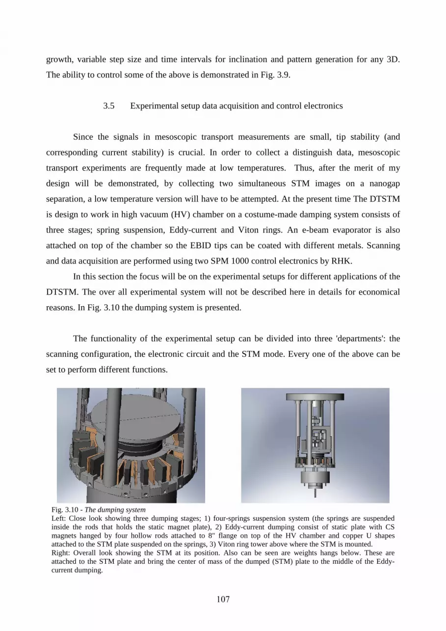
107
growth, variable step size and time intervals for inclination and pattern generation for any 3D.
The ability to control some of the above is demonstrated in Fig. 3.9.
3.5 Experimental setup data acquisition and control electronics
Since the signals in mesoscopic transport measurements are small, tip stability (and
corresponding current stability) is crucial. In order to collect a distinguish data, mesoscopic
transport experiments are frequently made at low temperatures. Thus, after the merit of my
design will be demonstrated, by collecting two simultaneous STM images on a nanogap
separation, a low temperature version will have to be attempted. At the present time The DTSTM
is design to work in high vacuum (HV) chamber on a costume-made damping system consists of
three stages; spring suspension, Eddy-current and Viton rings. An e-beam evaporator is also
attached on top of the chamber so the EBID tips can be coated with different metals. Scanning
and data acquisition are performed using two SPM 1000 control electronics by RHK.
In this section the focus will be on the experimental setups for different applications of the
DTSTM. The over all experimental system will not be described here in details for economical
reasons. In Fig. 3.10 the dumping system is presented.
The functionality of the experimental setup can be divided into three 'departments': the
scanning configuration, the electronic circuit and the STM mode. Every one of the above can be
set to perform different functions.
Fig. 3.10 - The dumping system Left: Close look showing three dumping stages; 1) four-springs suspension system (the springs are suspended inside the rods that holds the static magnet plate), 2) Eddy-current dumping consist of static plate with CS magnets hanged by four hollow rods attached to 8" flange on top of the HV chamber and copper U shapes attached to the STM plate suspended on the springs, 3) Viton ring tower above where the STM is mounted. Right: Overall look showing the STM at its position. Also can be seen are weights hangs below. These are attached to the STM plate and bring the center of mass of the dumped (STM) plate to the middle of the Eddy-current dumping.

108
Scanning configuration - The source for the variable scanning configuration is the three
piezo-tube scanners; one for each tip and one for the sample. Three scanning forms are thus
available. 1. The sample is fixed and both tips are scanning in xyz. 2. The sample is scanning in xy
and the two tips just 'hang on' with their independent z feedbacks. 3. The sample and one tip
stands still wile the second tip is scanning away from the first one.
The first option is natural for DTSTM and most, or all, of the systems that were
constructed so far follow this setup. If the tips are scanning in separate times, a way to make sure
that one will not crash into the other is enough. But, if simultaneous scanning is to be performed,
a synchronized scan generator is needed in order to keep the tips on a 'constant' separation wile
two STM images are acquired. Here, two identical piezo-tubes are a must, but still, to achive two
continuous scanning tips with identical high linearity, stability, repeatability and accuracy is
practically impossible (it might be possible to use two close loop controls that will get the same
scan generation as reference signal but it looks cumbersome with respect to the second option).
The second option, scanning with the sample only, is advantageous if we want to collect
the transconductance current flowing between the tips. For a mechanically stable system (an
essential objective), the tips can keep their relative positioning in xy with respect to the sample
and be driven in z by independent feedback loops (in constant current mode). Electronic noise,
thermal drifts, varying loads or force, hysteresis, creep and so on are always present, also in 'fixed'
multi probe settings configurations.
The third option, scanning with one tip, is a simple STM problem only that here the
second tip can serve as source, drain or gate and together with the sample a three terminal setup
can be formed.
The electronic circuit - Different setups can be found in the literature for fixed multi-probe
measurements. In chapter II, an example (Fig. 2.5) of a preamp designed for one current/voltage
probe tip was given. The idea was to differentiate between voltage and current probes and in the
current probe between high and low currents. The transition among these operational modes is
done using three switches. In the same chapter (fig. 2.10) another example illustrates how σs is
determine by using two STM tips. Here the currents through the STM tips I1 and I2 are measured
with two preamplifiers biased with V1 and V2, respectively. Electrical circuit diagram of the two-
point probe measurement shows that the applied voltage ∆U is composed of the tunneling
voltages UT1 and UT2 and the voltage drop ∆V2PP originating from the sample resistance RS. Tip-

109
to-tip tunneling current calculated using a 2D two-point probe model is also presented in the same
reference.
If the DTSTM is to be used in a static manner, the three terminals (two tips and sample)
can be used as current/voltage probes as desired. A new kind of data collection, can also be
proposed, using the DTSTM to construct conductance maps of surfaces. To describe this
operation we can look at the scanning configuration where the sample is scanning and the two tips
hold constant currents by their independent feedbacks. The conductance map can now be
constructed using two biased preamps and sample-hold procedure. The operational sequence is
divided into two time intervals that complete on cycle (of 0.5 ms). The first time interval is
devoted for STM data acquisition and the second for trans-conductance measurement. In every
time interval the operation is delayed in order for the tunneling junctions (that can be represented
by parallel resistor and capacitor) to unload their charge before moving to the other mode each
time. The time sharing chart for 0.5 ms cycle is illustrated in Table 3.1.
Two STM images interval - In the STM data acquisition we sample the tunneling currents
and adjust tips heights. Here the preamps of each tip are equally biased (-1 V) and the sample is
grounded. Two SPM control electronics are used. The first generates the scan signal for the
sample, controls one tip, collect all the data, control the sample-hold, and as we will see ahead
perform spectroscopic mode measurements. The second electronics control the second tip, get the
sample-hold signals from the first (so the procedure is synchronized) and send the collected
second tip data to the first electronics.
Cycle
STM operetional mode STM STS STM STSOperation of z-piezo feedback Sample Hold Sample Hold
Sample Grounded Floates Grounded Floates
Time (ms) 0 0.25 0.5 0.75 1
Applied bias voltage Tip 1V
1 2
0
-1
0
1
-1
Applied bias voltage Tip 2
Table 3.1 - Time sharing for DTSTM surface conductance mapping Two cycles are shown. The bias is chosen so in the STM mode the tips are biased with -1 V and the sample is grounded (positive sample bias) and in the STS mode the first tip is floating at zero bias wile the second sweep the range from -1 to +1 V.

110
Transconductance current interval - When we hold sampling, relays are operated to move
from STM data acquisition to trans-conductance measurement. Here the sample is floating. The
first tip moves to low current mode and zero bias. Now the important physical process is
executed. The first electronics that controls the sample-hold perform spectroscopic mode
measurements that were predefined to be processed at "every point". But, instead of the familiar
one tip STS, here the voltage is ramped on the second tip wile the current is collected at the first.
What is the physical information that can be drawn from this operation? In the STM
data acquisition two STM images are expected. In the trans-conductance measurement the current
change on the first tip as a function of the voltage change on the second tip is collected. Two
kinds of information are expected here. The first is the surface conductance as suggested by Niu,
Chang and Shih: σs = ∂I1/∂V2 (see chapter I). This value may also show voltage dependence. That
leads to the second information. By plotting of ∂I1/∂V2 as a function of ∂V2 'STS-like' data
emerging from surface states may be found. (For this to happen, the probe separation has to be
small enough with respect to the sample surface). Since the data was collected at each point,
conductance and surface states maps can be constructed. This information can now be compared
with the STM images for further analysis. The effects of tip separation, orientation, bias and
surface defects can be interpreted. I will note here that nanostructures that can be on the surface
will not need to be identified and approached for multi-probe measurements. The conductance
and spectroscopic nature of these will come out from the maps.
Other possibilities -
• Scanning with one tip when the second maintain its position can demonstrate yet another
surface behavior. By using the static one as source and the scanning one as drain, or vice
versa, Friedel oscillations emerging from electron scattering can be observed.
• An attempt to collect the transconductance current can also be made by modulation of the
bias or z position on one tip and using lock-in amplifier to find this signal on the second
tip.

111
• The fixed multi-terminal experiment can also be elaborated. By scanning with two voltage
probes (it can be done again by sample-hold and switching between current and voltage
probes) over a lithographically- or EBID-fabricated multi-terminals setup a map of the
transconductance among the different terminals can be drawn.

112
Chapter 4
Results
4.1 Scope of this chapter
In this chapter the preliminary results of the dual-tip STM design will be reviewed. In
section 4.2, the constructed system will be introduced. In section 4.3, the different designs of the
Fig. 4.1 -The experimental system (a) The BJ lower part of the STM mounted on the dumping system in the evaporation position (older version). A special pipe ensures that the e-beam flux covers a 5 mm diameter layer around the junction. (b) One out of four springs that holds the dumped plate. (c) The HV chamber with the e-beam evaporator on top, sputtering ion pump below and load-lock door on the right. (d) The Eddy-current dumping. A lower static plate is held by four hallow rods and embedded 16 CoS magnets. The dumped plate is hanged by four springs, suspended trough the rods and holds 8 copper U. The plate that holds the DTSTM seats on a 'tower' of Viton rings separated by aluminum rings. (e) Close look on the dumping system inside the HV camber.
(a) (b) (c)
(f) (e)

113
junction and its aligning will be reviewed. In section 4.4 the different EBID tip fabrication and
their independent positioning will be presented. In section 4.5 the two-tip tunneling sequence will
be explained. Finally the current statues of the dual-tip STM will be stated.
4.2 The apparatus and experimental system
The DTSTM is mounted on a dumping system that consist from four springs, Eddy current
dumping and Viton 'tower' where Viton rings are separated be aluminum rings. The system is
hanged from an 8" flange in a six-way cross vacuum chamber. e-beam evaporator (e--flux Mini
Electron Beam Evaporator by tectra GmbH) is mounted on top for metallization of the EBID tips
and is cooled by a chiller. The lower opening is attached on sputtering ion pump (VacIon Plus
After the rotation (4) The rotational part is held from below. (5) Both tubes upper surfaces are horizontally aligned. (6) The left Si BJ is aligned 5° above the horizon and the left one is aligned 5° below the horizon making sample approach safe.
Before the rotation (1) The rotational part is held from above. (2) The left tube upper surface is horizontal and the right tube upper surface is tilted with 10° with respect to the horizon (black). (3) The Si BJ is aligned 5° above the horizon (blue).
(1)
(2)
(3)
(4)
(5)
(6)
Static part
Rotational part
Piezo-tubes
The break-junction
Fig. 4.2 - The DTSTM lower part; the break-junction Up: The lower part after Si chip aligning and breaking of the connecting 'wings'. Down: The lower part after turning of the rotational part by 10°. The different parts are referred to on the images.

114
300 Pump by VARIAN, INC.) where roughening is done using Turbomolecular pump. One of the
four horizontal openings is a load-lock door for quick introduction of the DTSTM into the
chamber. For this reason the base pressure is 10-9 Torr and quick electric connections have to be
made each time the STM is brought in or out. The tunneling signals are transferred with BNC
connectors wile the rest of the signals are transferred with D-type feedthoroughs. Two RHK SPM
1000 control electronics are used for the STM applications and an older SPM 100 is used for the
tip navigation when scanning with the sample. Some features are present in Fig. 4.1.
In the evolution of the DTSTM design, four prototypes were constructed. The first was a
version that applied pooling force on the junction. The second was the first rotational version with
x y and double-z piezo stakes. The third was a rotational version with mechanical aligning for the
junction in addition for a piezo aligning. Here the last version with two piezo-tubes for the tips
and one for the sample is introduced. In fig. 4.2 the lower part before and after the rotation is
displayed and in Fig. 4.3 the assembled DTSTM, lower and upper parts, with focus on the
approach mechanism and the BJ-sample setting are displayed. The functionality of these parts
was explained in chapter III, thus, here the images are just accompanied with titles for the
different parts with no further discussion. The main bodies are made from Titanium, some small
Reduction lever
Scanning tube
Upper bridge
Prism
Approach mechanism
Sample holder
Approach motor
Fig 4.3 - The DTSTM assembled with the upper part Left: The DTSTM lower and upper parts. Up: the approach mechanism. In the circle; adjustable spring to hold the approach mechanism self weight. The cross shows one out of four two-spring-hinge systems that enables parallel approach with the sample. Down: The sample above the junction. The different parts are referred to on the images.

115
parts are made from stainless still and insulating parts are made from Macor. When a conductive
epoxy was needed, H20E (Epoxy Technology) was used and when insulating epoxy was
necessary EP21TCHT-1 (Master Bond) was used. Wiring is made with copper wires coated with
insulating varnish.
4.3 Si break-junction design and aligning
The evolution of the silicon BJ went thorough some stages as well. The first BJ prototype
applied lateral force on the junction. Here, breaking of W wires like in traditional MCBJ was tried
first. These could not have been brought to a reasonable junction that will aloud approaching with
the sample to two electrodes align in 3D. The first Si break junction was designed from a 10×2
mm silicon wafer, 100 µm thick and with a 50 µm trench in the middle (Fig. 4.4 (a)). By placing
the trench at the BJ and breaking, a nice fracture ~ 2 µm wide was formed. The silicon breaks
very uniformly along the junction, but still, approaching to the two micro-long tips with
macroscopic sample can result with tunneling at undesired location for very small angle
mismatches. That provided the motivation to design a special Si BJ. In order to diminish the
junction dimensions, a silicon bridge was designed using anisotropic etching explained in chapter
III. Different designs can be viewed in Fig. 4.4 (b)-(f). These designs reduce the length along the
junction to the designed bridges width. In order to reduce the length perpendicular to the bridge
the rotational mechanism was developed. A 'zero' perpendicular length is achieved in this way
living a 1D ~30 µm wide junction. The V-etch under the junction can result with finite thickens to
be broken or can etch through creating two Si cantilevers with micro-gap separation (Fig. 4.4 (d)
and (e)). For the rotational junction, the two V-shaped cantilevers are preferable since it aloud
approaching up to zero separation wile finite thickness bridge, after the rotation, don't. Later,
three pairs of trapezoidal cantilevers were designed (Fig. 4.4 (f)-(i)). The longer base is attached
to the wafer for extra strength and the narrow one reduces the junction to 30 µm. Since the
etching process is not 100% accurate, three junctions results with higher yield where the best
junction can be chosen for tip fabrication and the rest can carefully be broken or left for future
use. The anisotropic etching is done at Mizur Technology. The finite gap can be aligned as
illustrated in Fig. 4.5. Aligning can be made before or after tip fabrication. The tips can be grown
perpendicular to the junction, or, can be grown across it to 'bridge' or reduce the gap. Tip
fabrication is reviewed in the next section.
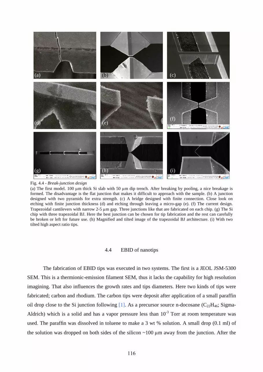
116
4.4 EBID of nanotips
The fabrication of EBID tips was executed in two systems. The first is a JEOL JSM-5300
SEM. This is a thermionic-emission filament SEM, thus it lacks the capability for high resolution
imagining. That also influences the growth rates and tips diameters. Here two kinds of tips were
fabricated; carbon and rhodium. The carbon tips were deposit after application of a small paraffin
oil drop close to the Si junction following [1]. As a precursor source n-docosane (C22H46; Sigma-
Aldrich) which is a solid and has a vapor pressure less than 10-3 Torr at room temperature was
used. The paraffin was dissolved in toluene to make a 3 wt % solution. A small drop (0.1 ml) of
the solution was dropped on both sides of the silicon ~100 µm away from the junction. After the
Fig. 4.4 - Break-junction design (a) The first model. 100 µm thick Si slab with 50 µm dip trench. After breaking by pooling, a nice breakage is formed. The disadvantage is the flat junction that makes it difficult to approach with the sample. (b) A junction designed with two pyramids for extra strength. (c) A bridge designed with finite connection. Close look on etching with finite junction thickness (d) and etching through leaving a micro-gap (e). (f) The current design. Trapezoidal cantilevers with narrow 2-5 µm gap. Three junctions like that are fabricated on each chip. (g) The Si chip with three trapezoidal BJ. Here the best junction can be chosen for tip fabrication and the rest can carefully be broken or left for future use. (h) Magnified and tilted image of the trapezoidal BJ architecture. (i) With two tilted high aspect ratio tips.
(a) (b) (c)
(d) (e) (f)
(h) (i) (g)

117
toluene/paraffin solution evaporated, a film visible by light micro-scope containing the paraffin
was left on the substrate. After the drops were dry, the Si wafer was delivered to the SEM stage
and carbon tips were grown by focusing the electron beam to the desired location (~ 100 µm from
the drop) in spot mode. Line mode was also applied for the growth of horizontal rods and tilted
tips were grown by tilting the SEM stage. These can serve to fabricate a verity of tip shapes as
demonstrated in Fig. 4.6.
Rhodium tips were also attempted from the precursor [RhCl(PF3)2]2. The idea was to
fabricate strong tips that might demonstrate appreciable conductance, enough for STM
applications. For the Rh deposition, the footsteps of P. Hoffman group from EPFL Switzerland
(The precursor was supplied by P. Duppelt - Directeur de Recherche Centre National de la
Recherche Scientifique (CNRS)) were followed. Works on Rh fabrication can be reviewed in the
Ph.D. Thesis by Fabio Cicoira Lausanne, EPFL 2002 and references therein. It will not be
discussed here mainly because it did not have the desired yield and thus, the results of Rh
fabrication are omitted from this work.
(c) (f) (i)
(b) (e) (h)
(d) (g) (a)
Fig. 4.5 - Break-junction aligning and tip navigation Left: aligning of the Si BJ; (a) after breaking, (b) bringing the two sides closer, (c) x aligning. Middle: Tip navigation; (d) After EDID on both sides of the BJ, (e) navigation in y and (f) in x. Right: Tip approach from (g) to (i) for DTSTM scanning on a nano- (~50 nm) gap separation. The tilted high aspect ratio tips enables to rich this goal.

118
The second system was the commercial e-Line by Raith Gmbh. This electron beam
lithography system is also equipped with gas injection system (GIS by Orsay Physics) and is
capable for high resolution deposition of: Carbon, Platinum, Tungsten and Silicon oxide or
selective etching using: Fluorine, Iodine and Oxygen. Water vapors can also be delivered for non-
conducting materials and reducing of Carbon content in the deposit. The tungsten carbonyl WCO6
was used to deposit W tips. It has been reported that deposition from W(CO)6 consists of
tungsten, carbon and Oxygen atoms (for example [2]) and thus after the tips were fabricated, the
Si chip was covered with ~5 nm of Titanium and ~20 nm of gold to ensure the conductance of
both tip and wafer. The EBID process with the e-line is highly reliable and repeatable. Here the
stage can not be tilted due to the special arrangement of the precursor's capillaries. So, the tips
were grown in two modes; spot mode for perpendicular growth, and free standing mode for
vertical and tilted growth.
Fig. 4.7 shows some results for the perpendicular growth. In (a) the experimental setup is
shown. The WCO6 capillary is placed ~350 µm from the Si junction and ~100 µm above. The
WCO6 is heated to ~65° C and the pressure at the SEM chamber when the precursor was applied
(a)
Crane Long cone
(d)
Hook
(c)
Reduced junction
(b)
High aspect ratio tilted tips
(f)
After 90° realigning to Y
(e)
Two hooks aligned in X
Fig. 4.6 – EBID of carbon tips (a) Vertical orientation, with long cone and ‘crane'-shape tips. (b) When the tips are tilted, the gap can be closed and the tips (here ~2.5 micron long and ~200 nm wide) can be brought within proximity less than 100 nm. (c) Reduced junction by two fabricated cantilevers. (d) A ‘Hook like’ tip after working in line mode follows by spot mode. e) Two ‘hook like’ tips aligned in x. (f) After realigning to y, a 90° change of the tip apex orientation is achieved (as indicated by the white circles).

119
was raised from 1.5 to 2×10⁻⁶ mBar. In (b) a 'line-up' of tips with variable length is shown. The
tips were grown using 10 kV and 0.14 nA of the beam energy and current respectively. Growth
rate is rather fast up to this length and it is about 10 nm/sec. Due to the high resolution the tips in
the e-line are 'only' ~50 µm in diameter. That is a good quality if we want to bring tunneling
atoms on two tips as close as possible. But, these high aspect ratio tips might not be strong
(d) (e)
(a)
(c)
(b)
Fig. 4.7 - High aspect ratio WCO6 tips Fine tips growth in high resolution SEM using spot mode. (a) The capillaries setup. Here I used the WCO6 precursor. The inset shows the capillary distance (~350 µm) from the deposition area at the BJ (it is about 100 µm above the surface). Growth took place at a precursor vapor pressure of 2×10⁻⁶ mBar. (b) Very high aspect-ratio tips can easily be grown for increasing times. Inset shows the length for the longest tip. It is also ~50 µm in diameter. (c) Since tips grown with high resolution FE-SEM, might not be strong enough, by working in a higher current mode of 0.208 nA (at 5kV), a ~130 µm in diameter tips can be fabricated. (d) The tip lineup can be used for tip 'replacement'. By the fabrication of three variable-height tips, after crushing with the higher one the next can be brought into tunneling. These can be grown accordingly on both sides of the junction resulting with three sets of dual-tip configurations (e).
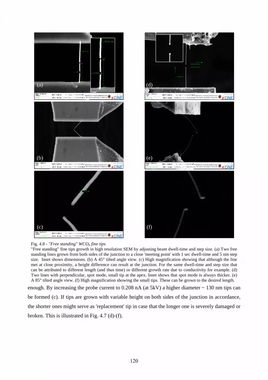
120
enough. By increasing the probe current to 0.208 nA (at 5kV) a higher diameter ~ 130 nm tips can
be formed (c). If tips are grown with variable height on both sides of the junction in accordance,
the shorter ones might serve as 'replacement' tip in case that the longer one is severely damaged or
broken. This is illustrated in Fig. 4.7 (d)-(f).
Fig. 4.8 - "Free standing" WCO6 fine tips "Free standing" fine tips growth in high resolution SEM by adjusting beam dwell-time and step size. (a) Two free standing lines grown from both sides of the junction to a close 'meeting point' with 1 sec dwell-time and 5 nm step size. Inset shows dimensions. (b) A 45° tilted angle view. (c) High magnification showing that although the line met at close proximity, a height difference can result at the junction. For the same dwell-time and step size that can be attributed to different length (and thus time) or different growth rate due to conductivity for example. (d) Two lines with perpendicular, spot mode, small tip at the apex. Inset shows that spot mode is always thicker. (e) A 85° tilted angle view. (f) High magnification showing the small tips. These can be grown to the desired length.
(b) (e)
(d)
(f)
(a)
(c)

121
Fig. 4.8 shows some results for the free standing mode of growth. Here by adjusting of the
beam dwell-time and step size, tilted rods/tips can be grown. Since the deposit growth
perpendicularly at one rate wile the beam is moving laterally at another rate it is, to some extent,
possible to grow at any angle. In (a), two lines were deposit to a 'meeting' point with 1 sec dwell-
time and 5 nm step size leaving a small gap. In (b) and (c) a 45° tilted view shows that although
from above it looks like the tips are almost met, one is actually higher then the other. That can be
attributed to different line length (that means different deposition times), or different growth rate,
for example because of different conductivity. In (d) two free standing tips were grown followed
by two short time perpendicular ones at the apex. It is noticeable that the perpendicular mode
results with higher diameter tips. In (e) and (f) a 85° of the same combined modes is shown. The
two nanotips at the apex and the rounded shape of the supporting tips is noticeable. Here the
supporting tips might have been bent due to the weight of the nanotips. Or else, due to reduction
of conductivity of the tips with length, the perpendicular growth rate is slowing wile the
horizontal translation of the beam is fixed, resulting with this semi-circular growth.
Fig. 4.9 shows some results for gold coating. Here by coating of the entire chip the
conductance to the outside leads is guarantied. In (b) the three double-tip configuration with
decreasing height is shown and in (c) a high magnification of one tip. From (c) it looks like the tip
is fairly covered with gold, or gold clusters, and that is promising for the STM applications.
Fig. 4.9 - Gold coating (a) The chip is coated with ~5 nm of Titanium and then with ~20 nm of Gold. The chip can now be placed on the DTSTM with perfect conductance. A larger image of the three sets of dual-tip configurations coated with gold was presented in Fig 4.8 (e). (b) High magnification of one tip showing that Gold clusters are attached all over. The tip is not as nice as before but it is conducting better for the STM applications.
(b) (a)

122
Conclusions of part II
In chapter 1, we started by quoting from the fundamental theoretical work of Niu, Chang
and Shih that because a double-tip STM can probe the all important single-particle Green
function of a sample, it has the potential of becoming an extremely useful new tool in surface
analysis. In chapter 2, a survey on most of the multi-probe STMs that were already constructed
was conducted and examples for many applications that were already published were reviewed.
From here the motivation was provided and the following challenges were setup as guidelines for
a new approach to a DTSTM:
• To eliminate in situ probe observation for aligning and any aligning procedure.
• To fabricate costume made (shape and material) high aspect ratio nanotips.
• To eliminate the need for accurate and static probe configurations.
The overall motivation was to design a cost effective DTSTM capable of constructing
trance-conductance maps of surfaces, which are dependent on surface structure and defects, on
scales sensitive to the electron wavelength. In chapter 3, three ideas that have the potential to
meet the above challenges were described:
• Using a modified version of the MCBJ where instead of pooling, a torque is applied
around a virtual axle, ending with two mutual tilting Si cantilevers with micro-gap
separation.
• Fabrication of EBID nanotips for high aspect ratio, custom shape and desirable material
probes. Such tips will enable a characterization of transport at surface on the nanometer
scales.
• A trans-conductance scanning tunneling microscopy/spectroscopy. This will eliminate the
need for accurate and static probe configurations in order to collect data at specific surface
locations or nanostructures points.
In chapter 4, the progress of this work was displayed. The following achievements were
presented with respect to the challenges:

123
Rotational BJ instead of probe alignment -
• A rotational BJ system using two-springs-hinge enabled the creation of two Si
cantilevered BJ on a micro-gap separation with no need for probe aligning in 3D with the
sample surface.
• The independence of the two sides of the junction enables a tuning/navigation of the
cantilevers/tips using two piezo-tubes.
• A parallelogram approach mechanism using four two-springs-hinge facilitates tunneling
with the two nanotips at the sample surface.
• The evolution towards a three-pair trapezoidal-BJ using anisotropic etching in silicon
enables a firm support for EBID nanotips.
EBID nanotips instead of W or CNT/nanorods attached tips -
• Fabrication of EBID Carbon tips from paraffin oil (n-docosane C22H46 dissolved in
toluene to make a 3 wt % solution) demonstrates a variety of sizes & shapes for
approaching different surfaces or nanostructures.
• Fabrication of EBID Tungsten tips from W(CO)6 demonstrates high aspect ratio and high
reproducibility and growth control. These can enable tip separations of less then 50 nm.
• Tip 'metalization' by coating with ~5 nm of Titanum followed by ~20 nm of Gold to
ensure probe conductance.
Towards trance-conductance maps of surfaces -
• Three piezo-tube scanners (two for the tips and one for the sample) enables a
configuration of three experimental setups; one tip scanning, two tip scanning and the
sample scanning.
• When one tip is scanning a source-drain-gate setup can enable traces of the Friedel
oscillations emerging from electron scattering with one changeable position (source, drain
or gate) terminal.
• When the sample is scanning a setup with constant dual-probe separation on the nanoscale
can be formed. Using time-sharing by sample-hold of the feedback loops,
transconductance maps and surface-state spectroscopy can be gained by ramping the

124
voltage on one tip and collecting the current on the second. The dependence of the above
on tip separation, electron energy and surface orientation can then be deduced.
• The later can also eliminate the need to place the tips onto desirable nanostructures or
surface defects since the contribution of these will be deduced from the maps.
• The fixed multi-terminal experiment can also be elaborated. By scanning with two voltage
probes (it can be done again by sample-hold and switching between current and voltage
probes) over a lithographically- or EBID-fabricated multi-terminal setup, a map of the
transconductance among the different terminals can be acquired.
The last stage of the DTSTM operation is currently being processed and could not be
included in this thesis. The first tunneling measurements for the EBID nanotips were already
achieved and at the present time scanning of the two tips for simultaneous STM images is
currently being performed. The applications mentioned here are thus still to be tested. From the
progress made so far, the foundations have already been established and the ideas will hopefully
be executed soon.

125
Appendix A - computation of the coverage, and of the radius of gyration, area and perimeter (of each island) for a single STM image program ana_gif ! =============== ! ! implicit none ! ! The_lat is the 2D lattice 1,0 options for the probability coverage. ! character(len=20) :: file_name = ' ', last_file_name = 'bw1512.gif' character(len=20) :: Basic_name, Data_file, Tab_file, Xls_file LOGICAL:: Is_Exists INTEGER:: lat_size, any_row, any_col, any_p, Point_P integer, dimension(:,:), allocatable:: The_Lat integer, dimension(:), allocatable:: The_Vec integer:: vec(4,2), n_boundies real:: s_hist(250000,2), srav, sbouav, the_scale = 1. ! ! Vec is the 4 different directions of the neighbors of an atom. ! vec = 0 vec(1,1) = 1 vec(2,2) = 1 vec(3,1) = -1 vec(4,2) = -1 ! ! Ask the user for the ran parameters. ! 1000 Is_Exists = .FALSE. DO WHILE (.not. Is_Exists) write(*,'(3a)', advance="no") & " Enter the file to start ? <", trim(last_file_name), "> " read(*,'(a)') file_name if (file_name == ' ') file_name = last_file_name if (file_name(1:1) == 'q' .or. file_name(1:1) == 'Q') stop ! ! Make sure the file name include a point. ! Point_P = index(file_name,'.') if (Point_P <= 1) then write(*,'(3a)') & 'The file "', trim(file_name), '" dose not include a point.' else INQUIRE(FILE=file_name, EXIST=Is_Exists) IF (Is_Exists) EXIT write(*,'(3a)') & 'The file "', trim(file_name), '" does not exists!' end if END DO ! ! Ask the scale (calibration from different STM image sizes to one ! gif digitized images size (400x400) contrasted to binary matrix of 0 and 1 for ! computing). !

126
write(*,'(a)', advance="no") " Enter the scale ? " read(*,*) the_scale ! last_file_name = file_name Basic_name = file_name(1:Point_P-1) ! ! Open the out put files. ! Data_file = trim(Basic_name) // '.dat' open(11,file=Data_file, form='formatted', status='unknown') close(11, status='delete') open(11,file=Data_file, form='formatted', status='new') Tab_file = trim(Basic_name) // '.tab' open(12,file=Tab_file, form='formatted', status='unknown',iostat=ios) close(12, status='delete',iostat=ios) open(12,file=Tab_file, form='formatted', status='new',iostat=ios) Xls_file = trim(Basic_name) // '.xls' open(13,file=Xls_file, form='formatted', status='unknown',iostat=ios) close(13, status='delete',iostat=ios) open(13,file=Xls_file, form='formatted', status='new',iostat=ios) ! ! Read the gif file. ! call gif_size(trim(file_name) // CHAR(0), lat_size) print*, " The size of the gif file is:", lat_size, "X", lat_size ! ! Allocate the lat array. ! ALLOCATE(The_Lat(0:lat_size+1, 0:lat_size+1)) ALLOCATE(The_Vec(lat_size*lat_size)) ! ! Read the gif file. ! call read_gif(lat_size, The_Vec) any_p = 1; do any_row = 1, lat_size do any_col = 1, lat_size The_Lat(any_row, any_col) = The_Vec(any_p) any_p = any_p + 1 end do end do ! ! Open the Graphics window (here we show the gif image that we analyze). ! call open_x(file_name) call show_lat(lat_size, The_Lat) call show_lat(lat_size, The_Lat) ! ! Analyze the lattice (here we calculate the coverage, radius of gyration, area ! and perimeter). ! call count_cluster & (lat_size, The_Lat, s_hist,n_boundies,sbouav,srav,vec, the_scale) ! DEALLOCATE(The_Vec, The_Lat) !

127
! Close the output files: ! close(11) close(12) close(13) call system("sort -d -k 3 "//trim(Xls_file)//">aa") call system("mv aa "//trim(Xls_file)) go to 1000 ! end ! subroutine count_cluster& (n, lat, s_hist, n_boundies, sbouav, srav, vec, the_scale) ! ============================================================= ! implicit none ! integer, intent(in) :: n, vec(4,2) integer, intent(out) :: n_boundies integer,intent(inout) :: lat(0:n+1,0:n+1) real, dimension(250000,2), intent(out):: s_hist real :: srav,sbouav, the_scale ! integer lat_size ! ! Local copy of the lattice. ! integer z(0:n+1,0:n+1) real stot1,ntot1 integer s_hist_binned(250) real cm(1:100000,1:3), nr double precision zm,dm integer :: n_cluster, dir_n character:: answer integer:: any_row, any_col, coverage integer max_clust_size,stot,bou ! ! There are maximum of n X n sites possible. ! parameter (max_clust_size= 250000) ! ! A shell site is the list of all sites found. ! integer shell_sites(max_clust_size,2) integer bound(max_clust_size,2) integer cluster_atoms(max_clust_size,2) integer cluster(1:max_clust_size,2) integer hm_in_lists(1:2),i1,i2, any_atom, idm, ns, i_dim integer i,j,j1,j2,actual,next,temp,n_atoms_up,peri,s_binned real center_mas_x, center_mas_y, s1 integer cen_mas_x, cen_mas_y integer pbou(100000),prad(100000) logical :: is_on_bou ! ! End of declartion

128
! -------------------------------------------------- ! !************************************************** ****************** answer = ' ' lat_size = n pbou = 0. prad = 0. n_boundies = 0 ! ! Calculate the coverage. ! coverage = 0 do any_row = 1, lat_size do any_col = 1, lat_size if (Lat(any_row, any_col) == 0) coverage = coverage + 1 end do end do write(11,*) ' The coverarge is :', real(coverage) / (lat_size*lat_size) ! ! Copy the lattice to Z. Make sure that the boundary of Z are all -10, ! so, it stop comparing the atoms in actual-next list out of the lattice, ! when you look for 4 directions of vec. ! z(0,:) = -10 z(n+1,:) = -10 z(:,0) = -10 z(:,n+1) = -10 z(1:n,1:n) = lat(1:n,1:n) ! ! n_cluster count how many clusters we found. ! n_cluster = 0 stot = 0 stot1 = 0 ntot1 =0 !c square lattice ! ! n_atoms_up count how many atoms are in the cluster (here we calculate the area s of each ! island). ! n_atoms_up = 0 row_loop: do j1=1, lat_size col_loop: do j2=1, lat_size ! print *,j1,2,z(i1,i2) is_on_bou = .false. actual = 1 next = 2 ! ! hm_in_lists actaul and next start with 0 ! hm_in_lists = 0 ! ! The spin of this atom is down so start a new list on acual. ! down_if: if (z(j1,j2) == 0) then ! ! Register the location of this atom in Sell sites. !

129
shell_sites(hm_in_lists(actual) + 1,actual) = j1 shell_sites(hm_in_lists(actual) + 2,actual) = j2 ! ! Note the last place we register the actual atoms. ! hm_in_lists(actual) = hm_in_lists(actual) + 2 ! ! Note the value of this atom. ! zm = z(j1,j2) ! ! Resister this atom as one that we already counted. ! z(j1,j2) = z(j1,j2) - 30 end if down_if ! print *,j1,j2,zm, hm_in_lists(actual) n_atoms_up = 0 bou=0 45 continue ! ! Repeat on the following process until hm_in_lists active is 0. ! act_if: do while (hm_in_lists(actual) /= 0) ! ! Start with the last atom in the act_next lists. ! j = shell_sites(hm_in_lists(actual), actual) i = shell_sites(hm_in_lists(actual) - 1,actual) ! ! Now go 2 degree down. ! hm_in_lists(actual) = hm_in_lists(actual) - 2 ! ! The area = how many atoms with their spin are up. ! n_atoms_up = n_atoms_up + 1 ! ! Register the position of this atom into this cluster. ! cluster(n_atoms_up,1)= j cluster(n_atoms_up,2)= i ! ! As long there is a place in cluster sites - Register it. ! if (n_atoms_up < max_clust_size) then cluster_atoms(n_atoms_up,1) = i cluster_atoms(n_atoms_up,2) = j ! write (1,*) i,' ',j ! print *,s,i,j,zm endif vec_loop: do dir_n = 1,4 i1 = i + vec(dir_n,1) i2 = j + vec(dir_n,2) ! ! Flags out any cluster that touch the boundaries (we don’t use islands that are cut in the ! STM image). !

130
if (i1 > n) then i1 = 1 is_on_bou = .true. endif if (i1 < 1) then i1 =n is_on_bou = .true. endif if (i2 > n) then i1=1 is_on_bou = .true. endif if (i2 < 1) then i1 =n is_on_bou = .true. endif ! print *,'scan1',i,j,i1,i2,z(i1,i2) ! ! We find an atom that have the value of zm as the atom above. ! if (z(i1,i2) == zm) then ! print *,'scanin',i1,i2,z(i1,i2) shell_sites(hm_in_lists(next) + 1,next) = i1 shell_sites(hm_in_lists(next) + 2,next) = i2 ! ! Move hm_in_lists next 2 degree upward. ! hm_in_lists(next) = hm_in_lists(next) + 2 z(i1,i2) =z(i1,i2) -30 else if (z(i1,i2) == 1) lat(i,j) = -4 end if end do vec_loop ! ! After we move hm_in_lists -2 and +2 do the whole thing again. ! end do act_if shell_0:& if (hm_in_lists(next) == 0) then ! ! Counts how many atoms are on the boundaries of this cluster? ! bou = 0 do any_atom = 1, n_atoms_up i = cluster_atoms(any_atom,1) j = cluster_atoms(any_atom,2) ! ! Count the number of boundary sites (here we calculate the ! perimeter p of the islands). ! if (lat(i,j) == -4) then bou = bou +1 lat(i,j) = 0 endif end do center_mas_x =0.0 center_mas_y = 0.0 dm = 0.0
131
! ! If we found more then 10 atoms with their spin up, we found one cluster (we ! treat smaller islands as possible noise in the STM image). ! if (n_atoms_up > 10) then n_cluster = n_cluster+1 ! ! Sum the coordinates of the atoms, ! so, we can calculate the center of the mass of this cluster. ! center_mas_x = 0 center_mas_y = 0 do i=1, n_atoms_up center_mas_x = center_mas_x + cluster_atoms(i,1) center_mas_y = center_mas_y + cluster_atoms(i,2) enddo ! ! Compute the center of mass (rcm) of this cluster. ! center_mas_x = center_mas_x / n_atoms_up center_mas_y = center_mas_y / n_atoms_up cen_mas_x = center_mas_x cen_mas_y = center_mas_y !
! Compute the dm - Radius of gyration ( srrRs
i cmig /2
1
2∑ =
−≡ ,
! ∑=
=s
iicm srr
1
/ ) of this cluster.
! do i=1,n_atoms_up dm = dm + (cluster_atoms(i,1)-center_mas_x)**2 dm = dm + (cluster_atoms(i,2)-center_mas_y)**2 end do dm = sqrt(dm/n_atoms_up) i_dim = dm ! ! Draw the center of the cluster. ! if (.not. is_on_bou) then print*, "center no",i,"is at ", cen_mas_x, cen_mas_y call x_set_color(4) call x_draw_line(cen_mas_x-i_dim, cen_mas_y, cen_mas_x+i_dim, cen_mas_y) call x_draw_line(cen_mas_x, cen_mas_y-i_dim, cen_mas_x, cen_mas_y+i_dim) call x_set_color(1) call x_draw_line(cen_mas_x-4, cen_mas_y+4, cen_mas_x+4, cen_mas_y-4) call x_draw_line(cen_mas_x+4, cen_mas_y+4, cen_mas_x-4, cen_mas_y-4) ! call x_draw_point(cen_mas_x, cen_mas_y) ! call x_draw_point(cen_mas_x+1, cen_mas_y+1) ! call x_draw_point(cen_mas_x+1, cen_mas_y-1) ! call x_draw_point(cen_mas_x-1, cen_mas_y+1) ! call x_draw_point(cen_mas_x-1, cen_mas_y-1) CALL X_FLUSH if (answer /= 'r' .and. answer /= 'R') then write(*,'(a)', advance="no") " Enter any key to continue ? " read(*,'(a)') answer if (answer == 'q' .or. answer == 'Q') stop

132
end if end if idm = int(dm*5) + 1 prad(idm) = prad(idm)+1 pbou(bou) = pbou(bou)+1 the_scale2 = the_scale*the_scale if (.not. is_on_bou) then write(12,'(I4,F9.2,f9.2,f9.2)') & n_cluster, dm*the_scale, n_atoms_up*the_scale2, bou*the_scale write(13,'(I4.4,F9.2,f9.2,f9.2,A)') & n_cluster, dm*the_scale, n_atoms_up*the_scale2, bou*the_scale, & char(13) end if ! ! Register this cluster and it's center of mass. ! n_boundies = n_boundies + 1 cm(n_boundies,1) = center_mas_x cm(n_boundies,2) = center_mas_y cm(n_boundies,3) = real(n_atoms_up) ! print *,center_mas_x,center_mas_y,n_atoms_up center_mas_x = 0 center_mas_y = 0 endif if (n_atoms_up > 0) then stot = stot + n_atoms_up s_binned = aint(1.+ 4*alog(real(n_atoms_up))) s_hist_binned(s_binned) = s_hist_binned(s_binned)+1 ! print *,'s=',s if (zm == 0) then s_hist(n_atoms_up,1) =s_hist(n_atoms_up,1) + 1. else s_hist(n_atoms_up,2) =s_hist(n_atoms_up,2) + 1. end if end if n_atoms_up = 0 peri=0 else temp = actual actual =next next = temp ! ! Go back to the beginning and run over the process. ! goto 45 endif shell_0 enddo col_loop enddo row_loop do i=1,100 if (s_hist_binned(i) > 0) then ! write(4,*) 10.**(0.25*(real(i)-1.)),s_hist_binned(i) s_hist_binned(i)=0 endif end do

133
n_boundies= n_cluster ! ! Replace -4 in the lattice with 0 ! where (lat == -4) lat = 0 ns=0 nr =0 sbouav = 0 do i=1,10000 sbouav = sbouav + pbou(i)*real(i) srav = srav + prad(i)*real(i) ns = ns+ pbou(i) nr = nr +prad(i) enddo print *, ns, sbouav sbouav = sbouav/real(ns) srav = srav/real(nr) print *, ns, sbouav print *,'Number of cluster number is:',n_cluster ! end subroutine count_cluster From here as in appendix I.2

134
Appendix B - computation of the site-occupation correlation-function for a set of STM images from the same experiment (coverage). program ana_gif ! =============== ! ! implicit none ! ! The_lat is the 2D lattice 1,0 options for the probability coverage. ! character(len=20) :: file_name = ' ', last_file_name = 'bw1512.gif' character(len=20) :: Basic_name, Data_file, Tab_file, Xls_file character(len=20) :: User_string LOGICAL:: Is_Exists INTEGER:: lat_size, any_row, any_col, any_p, Point_P, N_R_Points INTEGER:: N_files = 0, any_point integer, dimension(:,:), allocatable:: The_Lat, R_Vec integer, dimension(:), allocatable:: The_Vec real:: R_coverage, the_scale = 1. ! ! Ask the user for the ran parameters ! Ask the number of Radius points. ! write(*,'(a)', advance="no") " Enter number of R points ? <700>" read(*,'(a)') User_string if (User_string == ' ') then N_R_Points = 700 else read(User_string,*) N_R_Points endif ! ! Start with 0 at the point's vector. ! It would be updated at each picture. ! ALLOCATE(R_Vec(0:N_R_Points,0:1)) R_Vec = 0 ! ! Let the user add picture after picture (here we load gif images from the ! same experiment). ! 1000 Is_Exists = .FALSE. N_files = N_files + 1 if (N_files > 1 ) last_file_name = "q" ! ! Loop until the user enters a valid gif file. ! DO WHILE (.not. Is_Exists) write(*,'(3a)', advance="no") & " Enter the file to start ? <", trim(last_file_name), "> " read(*,'(a)') file_name if (file_name == ' ') file_name = last_file_name if (file_name(1:1) == 'q' .or. file_name(1:1) == 'Q') stop ! ! Make sure the file name include a point. ! Point_P = index(file_name,'.') if (Point_P <= 1) then write(*,'(3a)') & 'The file "', trim(file_name), '" dose not include a point.'

135
else INQUIRE(FILE=file_name, EXIST=Is_Exists) IF (Is_Exists) EXIT write(*,'(3a)') & 'The file "', trim(file_name), '" does not exists!' end if END DO ! ! Ask the scale (calibration from different STM image sizes to one ! gif digitized images size (400x400) contrasted to binary matrix of 0 and 1 for ! computing). ! write(*,'(a)', advance="no") " Enter the scale ? <1>" read(*,'(a)') User_string if (User_string == ' ') then the_scale = 1 else read(User_string,*) the_scale endif ! ! print *, " the scale is ", the_scale ! last_file_name = file_name Basic_name = file_name(1:Point_P-1) ! ! Open the output files (here 11 is a data file for the coverage and 12 is a ! table file for the correlations, 13 is not in use here). ! Data_file = trim(Basic_name) // '.dat' open(11,file=Data_file, form='formatted', status='unknown') close(11, status='delete') open(11,file=Data_file, form='formatted', status='new') Tab_file = trim(Basic_name) // '.tab' open(12,file=Tab_file, form='formatted', status='unknown',iostat=ios) close(12, status='delete',iostat=ios) open(12,file=Tab_file, form='formatted', status='new',iostat=ios) Xls_file = trim(Basic_name) // '.xls' open(13,file=Xls_file, form='formatted', status='unknown',iostat=ios) close(13, status='delete',iostat=ios) open(13,file=Xls_file, form='formatted', status='new',iostat=ios) ! ! Read the gif file. ! call gif_size(trim(file_name) // CHAR(0), lat_size) print*, " The size of the gif file is:", lat_size, "X", lat_size ! ! Allocate the lat array. ! ALLOCATE(The_Lat(0:lat_size+1, 0:lat_size+1)) ALLOCATE(The_Vec(lat_size*lat_size)) ! ! Read the lattice data. ! call read_gif(lat_size, The_Vec) ! ! Translate from vector to 2D array. any_p = 1; do any_row = 1, lat_size
136
do any_col = 1, lat_size The_Lat(any_row, any_col) = The_Vec(any_p) any_p = any_p + 1 end do end do ! ! Open the Graphics window (here we show the gif image that we analyze). ! call open_x(file_name) ! ! Show the picture. ! call show_lat(lat_size, The_Lat) ! ! Analyze the lattice (here we calculate the coverage and the probability that
! if site i is occupied so is site j ji θθ , ).
! call ana_clusters(lat_size, The_Lat, N_R_Points, R_Vec, R_coverage ) ! ! Write the coverage to the file. ! write(11,*) ' The coverarge is :', R_coverage ! ! Write the table to the file (calculation of the site-occupation correlation-
! function 2, θθθ −ji ).
! do any_point = 0, N_R_Points write(12,'(I4,a,f8.4,2I10,f6.3)') any_point,': ',& any_point*the_scale,& R_Vec(any_point,0)+R_Vec(any_point,1),& R_Vec(any_point,1),& real(R_Vec(any_point,1))/(R_Vec(any_point,0)+R_Vec(any_point,1)) & - R_coverage*R_coverage end do DEALLOCATE(The_Vec, The_Lat, R_Vec) ! ! Close the output files: ! close(11) close(12) close(13) ! call system("sort -d -k 3 "//trim(Xls_file)//">aa") ! call system("mv aa "//trim(Xls_file)) go to 1000 ! end ! subroutine ana_clusters(lat_size, The_Lat, N_R_Points, R_Vec, R_coverage) ! =========================================================== ! implicit none ! integer, intent(in) :: lat_size, N_R_Points integer,intent(inout)::The_Lat(0:lat_size+1,0:lat_size+1) integer, intent(out) :: R_Vec(0:N_R_Points,0:1)

137
real, intent(out) :: R_coverage integer:: any_row, any_col, coverage, any_row_2, any_col_2 integer(KIND=8):: counter real longest_dis, Scale_to_vec integer, dimension(:,:), allocatable:: Dis_Lat integer:: The_dis, row_dif,col_dif, start_col_2 ! ! End of declaration. ! -------------------------------------------------- ! !************************************************** ****************** ! ! Calculate the coverage. ! call show_lat(lat_size, The_Lat) coverage = 0 do any_row = 1, lat_size do any_col = 1, lat_size if (The_Lat(any_row, any_col) == 1) coverage = coverage + 1 end do end do R_coverage = real(coverage) / real(lat_size*lat_size) print *, ' The coverarge is :', R_coverage ! ! Find the longest distance and then the distance scale. ! longest_dis = sqrt(real(2*lat_size*lat_size)) Scale_to_vec = longest_dis / N_R_Points ! print *, ' Longest distance = ', longest_dis print *, ' Dis Scale = ', Scale_to_vec ! ! Compute the distances matrix. ! ALLOCATE(Dis_Lat(0:lat_size+1, 0:lat_size+1)) do any_row = 0, lat_size+1 do any_col = 0, lat_size+1 The_dis = nint(sqrt(real(any_row*any_row + any_col*any_col)) & / Scale_to_vec) if (The_dis > N_R_Points+1 .or. The_dis < 0) then print *, ' The dis is over the lime = ', The_dis The_dis = N_R_Points end if ! print *, ' The dis = ', any_row, any_col, The_dis Dis_Lat(any_row,any_col) = The_dis end do end do ! ! For each point, ! ============== ! counter = 0 do any_row = 1, lat_size print *, 'any_row= ', any_row do any_col = 1, lat_size ! ! If there is no point here - Forget it (we calculate the correlations only for

138
! occupied sites; if site i is occupied…). ! if (The_Lat(any_row,any_col) == 0) cycle ! print *, ' lat = ', any_row, any_col, The_Lat(any_row,any_col) ! ! Run on each other point: ! ! print *, 'any_row, any_col = ', any_col do any_row_2 = any_row, lat_size if (any_row_2 == any_row) then start_col_2 = any_col else start_col_2 = 1 end if do any_col_2 = start_col_2, lat_size ! ! If there is a point here - Add it to the output vector (here we count the ! occupied and unoccupied sites on a radius r from an occupied site in ! order to calculate the probability; …so is site j). ! row_dif = any_row_2-any_row col_dif = abs(any_col_2-any_col) The_dis = Dis_Lat(row_dif,col_dif) if (The_Lat(any_row_2, any_col_2) == 1) then ! if ((The_Lat(any_row_2, any_col_2) == 1) .AND. & ! (The_Lat(any_row,any_col) == 1)) then R_Vec(The_dis,1) = R_Vec(The_dis,1) + 1 else R_Vec(The_dis,0) = R_Vec(The_dis,0) + 1 end if counter = counter + 1 end do end do end do end do ! ! print *, ' counter = ', counter DEALLOCATE(Dis_Lat) ! ! end subroutine ana_clusters subroutine gif_to_lat(lat_size, The_Lat) implicit none integer, intent(in):: lat_size integer, dimension(0:lat_size+1, 0:lat_size+1) :: The_Lat ! ! Local variables: ! integer :: any_row ! open(22,file='temp',status="old") do any_row = 1, lat_size read(22,'(9000I1)') The_Lat(any_row,1:lat_size) end do close(22, status='delete')

139
end subroutine gif_to_lat subroutine swap(i1,i2) integer, intent(inout) :: i1,i2 integer :: temp ! temp = i1 i1 = i2 i2 = temp ! end subroutine swap subroutine show_lat(lat_size, The_Lat) implicit none integer, intent(in) :: lat_size integer, dimension(0:lat_size+1,0:lat_size+1) :: The_Lat ! ! Local variables: ! integer:: i,j, the_color, last_color ! call x_erase_whole_screen last_color = -1 ! DO j = 1, lat_size DO i = 1, lat_size if (The_Lat(i,j) == 1) then the_color = 0 end if if (The_Lat(i,j) == 0) then the_color = 7 end if if (the_color /= last_color) then call x_set_color(the_color) last_color = the_color endif call x_draw_point(i,j) END DO END DO ! end subroutine show_lat subroutine save_lat(n,lat,last_m) implicit none integer n, last_m integer, dimension(0:n+1,0:n+1) :: lat ! ! Local variables: ! character(len=20) :: file_name integer, save :: n_files = 0 ! n_files = n_files + 1 if (mod(n_files,2) == 1) then

140
file_name = "lat_a" else file_name = "lat_b" end if open(23,file=file_name,form="unformatted",status="unknown") rewind(23) write(23) last_m, lat ! end subroutine save_lat

141
Appendix C - Two tip configurations from other theoretical works
In this section, four different theoretical probe-sample geometries will be will be
reviewed. These four configurations can be seen in Fig. 2. The expected experimental
measurements and results will be explained in the following sub-sections. The two lower
examples will be discussed in more details since it is more relevant to a dual-tip STM setup.
C.1 Probing Spatial Correlations with Nanoscale Two-contact Tunneling
In their "Probing Spatial Correlations with Nanoscale Two-contact Tunneling" PRL paper
from 1995 [1], the primary goal of Byers's and Flattè was to offer example of how two-contact
localized spectroscopy can explore the spatial correlation of an uncoupled sample. A conceptually
straightforward, but impractical (in their opinion), two-contact arrangement would consist of two
STM tips which could be placed from 1 to 1000 Å apart, this would allow probing of correlations
with short length scales (1-10 Å), such as Fermi wavelengths in desired directions, medium length
scales (10-100 Å), such as high-Tc superconducting coherence lengths and charge-density wave
Fig. C.1 - Four different probe-sample geometry Up & left) The sample is strongly connected to ground and weakly connected to two localized junctions, at least one of which is mobile. The possibility considered in sub-section 1.3.1 is a 100 Å nanofabricated contact for one localized junction (located at xl) and an STM tip for the other (located at x2) [1]. Up & right) Two protrusions on a single STM contact are connected to the same reservoir (See sub-section C.1) [2]. Down & left) Double tips on a flat surface. Open and closed circles show the surfaceatoms and the atoms at the apexes of the tips, respectively (See sub-section C.2) [3]. Down & right) Experimental setup to measure current correlations (See sub-section C.3). Two STM tips are coupled with strength t at the positions x and x' to the surface of a small wire. The shaded region can be a metallic diffusive or a perfect ballistic wire (See sub-section C.4) [4].

142
oscillations, and long length scales (100-1000 Å), such as mean free paths, transitions from
ballistic to diffusive propagation, low-Tc coherence lengths and angularly anisotropic density-of-
states effects [5].
In this part of my thesis I will show that these measurements are 'practical'.
C.2 Theory of a scanning tunneling microscope with a two-protrusion tip
In their 1996 PRB paper "Theory of a scanning tunneling microscope with a two-
protrusion tip" [2], Michael E. Flatte´ and Jeff M. Byers consider a STM such that tunneling
occurs through two atomically sharp protrusions on its tip. The two protrusions were separated by
at least several atomic spacing and the differential conductance of this STM depends on the
electronic transport in the sample between the protrusions. Such two-protrusion tips commonly
occur during STM tip preparation. They explore possible applications to probing dynamical
impurity potentials on a metallic surface and local transport in an anisotropic superconductor.
Flatte and Byers were motivated by a series of STM experiments on the Cu(111) surface.
Where the local transport properties of electrons in a Shockley surface state were probed through
their influence on the LDOS around an Fe impurity [6] .A similar experiment has been proposed
for measuring the transport properties of a high-temperature superconductor [5]. These
experiments detect the reflection from the impurity of electrons injected by the STM. The spatial
resolution of these experiments is sub-Angstrom. Properties which might be determined from
these types of measurements, but could not be probed by a STM measurement on the
homogeneous sample, include the angularly resolved dispersion relations and mean free path, as
well as the density of states as a function of energy and momentum.
Flatte and Byers suggested an experiment which should provide detailed angular
information about fluctuating impurity potentials and probe transport on a homogeneous sample.
The apparatus, shown schematically in Fig. C.1 (up & right). Here they proposed a tip with two
atomically sharp protrusions, and demonstrated that new information is obtainable when these
protrusions are separated by more than 10 Å. The interference between the two protrusions
influences tunneling conductances at a lower order in the tunneling matrix elements than the two-
contact experiment discussed in sub-section C.1. The two-protrusion experiment, therefore,
should be easier to construct and have greater signal than the two-contact experiment. For
separations of 10 Å - 100 Å a two-protrusion tip would be useful for probing the angular structure
of a free moment. The differential conductivity depends on the angle-resolved amplitude for
electrons to scatter from the impurity. A measurement with a single-protrusion STM tip merely

143
measures backscattering. For an impurity state fixed relative to the lattice orientation by the
crystal field, backscattering is sufficient to determine the impurity’s angular structure; therefore
the single-protrusion measurement provides as much information as the two-protrusion one.
However, for identifying the angular structure of a free moment, the two-protrusion tip is superior
to the single-protrusion tip. A two-contact experiment could in principle measure this angular
structure as well [7] but positioning two tips within 100 Å of each other would be extremely
difficult.
On a homogeneous sample the transport quantities of interest would determine the desired
separation of protrusions on the STM tip. Measurements of quantities with long length scales (100
Å - 1000 Å) such as mean free paths, transitions from ballistic to diffusive propagation, low-Tc
superconductors’ coherence lengths, charge-density-wave correlation lengths, and angularly
anisotropic density-of-states effects [5] would most benefit from the increased signal of the two-
protrusion configuration relative to the two-contact configuration. It is also at these distances that
the overlapping interference of other impurities on a surface would complicate a measurement
performed with a single-protrusion STM around an impurity. However, for electronic quantities
with short length scales, such as Fermi wavelengths, the single-protrusion STM would likely
perform the best of the three.
C.3 Calculation of ballistic conductance through Tamm surface states
In his 2002 PRB paper "Calculation of ballistic conductance through Tamm surface states"
[3], Kobayashi performed a theoretical study on ballistic conduction through Tamm surface
states. He calculated the conductance in systems of STM with double tips as well as a single tip
and found the following. Conductance spectra of flat surfaces containing surface states are
qualitatively proportional to the density of states at the first layer of surfaces if boundary
conditions that allow net current to flow parallel to surfaces are applied. The potential difference
between the first layer and inner layers enhances the conduction through Tamm states. When a
STM tip is put on an island of a surface, the conductance varies as a function of the step height of
the island. The variation is explained by the difference in the step-height dependence between
surface-state and bulk-state conduction. Tunneling between the surface states of islands and
substrates is the main path of the surface-state conduction at low step heights. The study of the
conduction in islands demonstrates the importance of the conduction path in surfaces to
electrodes. The ballistic conductance spectra between two tips in double-tip systems show one-

144
dimensional features, which suggests high conductance when the Fermi energy is located near
band edges of surface states.
One out of three topics in Kobayashi paper was to simulate the conductance measurement
using the double-tip STM. Kobayashi mentioned the electrical conduction of surfaces that was
directly measured using micro-four-point probes [8, 9], where the contribution of surface states to
surface conduction was discussed. The distance between probes in these experiments is of
micrometer order and the electrical conduction is not ballistic. But it is a promising tool for
measuring directly the electrical transport on the nanometer scale, and in the future it may become
possible to study directly the ballistic conduction of surfaces by decreasing the distance between
probes. In his paper he present calculations of ballistic conductance in the double-tip STM and
discussed the role of surface states in the conduction of this system.
Kobayashi discussed the previous theoretical studies on the two-probe measurement mentioned
above, assumed that the conduction between probes and sample surfaces is through tunneling and
derived expressions for tunneling current by using the perturbation theory similar to Bardeen’s
approach. In his paper Kobayashi use the Landauer formula [10] for calculating conductance. The
Landauer formalism allowed him to calculate the ballistic conductance exactly without the
approximation of tunneling and to discuss the surface-state conduction from an atomistic point of
view.
In single-tip systems we assume chemical potentials respective for the tip and sample
surface and consider the situation in which a current flows from the tip to the sample surface by
the difference of the chemical potentials. In double-tip systems we can assume three independent
chemical potentials for the first tip, the second tip, and the sample surface, if we connect the third
electrode to the sample surface. In his paper Kobayashi consider a situation in which the chemical
potential of the first tip is higher than that of the sample surface, and the chemical potential of the
second tip is equal to that of the sample surface. Therefore a part of electrons injected from the
first tip into the sample surface is ejected through the second tip, and the remaining electrons go
out through the electrode contacted with the sample surface. This is similar to the setup assumed
in the earlier theoretical works of two-probe measurements [1, 7] except for the absence of the
bias voltage between the second tip and sample surface. Note that this is different from the setup
for the two-probe measurement where sample surfaces are not connected with the third electrode
and the current flows only between the two probes.
The method of calculation; the tip-sample configurations and the calculation of conductance can
be found in the paper. The main features are as follows.

145
• The surface atoms including the part of the island are arranged in the simple-cubic lattice.
A tight-binding method with only a single s orbital for each atomic site and transfer
energy -tS (tS > 0) between nearest-neighbor atoms was used.
• The apex of the tips was assumed to be a single atom and electrons always pass through
the single apical atom. In such a situation it is expected that the conduction between a tip
and a surface does not depend much on the minute atomic structure of the tip. Therefore,
instead of taking realistic atomic structures of tips into account, a semi-infinite one-
dimensional chain for the structure of the tips was substituted.
• The conductance of systems was calculated from the atomic scale to the nanometer scale
where the electrical transport is ballistic. Therefore the Landauer formula [10] was used
for conductance calculations.
Kobayashi looked at the conductance of a double-tip system as a function of the distance
between the two tips. The surface is a flat surface. The first tip injecting electrons is fixed on the
center atom of the surface. The position of the second tip is changed parallel to an axis of the
simple square lattice. Kobayashi showed the total conductance, surface-state component, bulk-
state component, and conductance for the second tip. Except for the nearest-distance case, the
surface-state component was slightly enhanced in the presence of the second tip. But as a whole
the conductance is not much affected by the second tip. The ballistic current flowing directly to
the second tip is very small. It decreases with increase of the distance between the two tips.
Kobayashi also showed that in the absence of surface states the conductance to the second tip
decreases rapidly with distance. But when surface states exist, the decrease is not so fast; the
conductance is inversely proportional to the distance between the tips. This result reflects the fact
that surface states are two-dimensional states and flux of current conserves. The dependence on
the distance is not changed much when the second tip is moved on the surface along the diagonal
direction of the simple square lattice. This isotropy is due to the fact that in the present case the
energy E is near the bottom of the surface-state band and the energy dispersion is nearly isotropic.
When the energy is near the middle of the surface-state band, the energy band is highly
anisotropic and the conductance between two tips is also anisotropic as shown by Niu, Chang, and
Shih using the effective-mass approximation [7].

146
Kobayashi showed also that the shape of the conductance spectrum between two tips is different
from that of the surface-state component. The latter reflects the two-dimensional DOS of surface
states, but the former is similar to the one-dimensional DOS. Near the bottom energy of the
surface-state band the conductance spectrum between two tips reflects the one-dimensional
feature. This result might be interpreted as that among two-dimensional surface states the one-
dimensional states parallel to the vector connecting the positions of two tips mainly contributes to
the conduction between two tips. The conductance spectra are roughly explained in terms of the
Green’s function of the sample surface. Using a perturbation theory Niu, Chang, and Shih showed
[7] that the conductance between two tips is proportional to the square of the absolute value of the
Green’s function.
Using the Green’s function Kobayashi reproduce well features of the conductance spectra.
The distance between tips is very small in Kobayashi calculations. When the distance is
much greater, the following results are expected. First, since the bulk-state component decreases
with distance more rapidly than the surface state component, most of the double-tip conductance
is the conduction through surface states in the ballistic regime. Second, the shapes of the
conductance spectra do not qualitatively change with the distance. Third, since the ballistic
conductance between two tips decreases inversely proportional to the distance, its magnitude is
very small when the distance between tips is large. But since the conductance spectra diverge near
the bottom or top of the surface-state bands, it is possible that the ballistic conductance between
two tips is high when the Fermi energy is located near band edges.
C.4 Local densities, distribution functions, and wave-function correlations for spatially
resolved shot noise at nanocontacts
This example is brought here since it uses a two tunneling tips and two massive contacts.
This setup can be configured using a dual-tip STM.
In their PRB paper from 1999 "Local densities, distribution functions, and wave-function
correlations for spatially resolved shot noise at nanocontacts" [4], Gramespacher and Büttiker
where interested in weak coupling contacts which are sensitive to the phase of current amplitudes
[11-12], and not only as in the work of Engquist and Anderson and related work [13] to absolute
values of currents. In the paper, they made theoretical predictions for measurements using one (or
two) tunneling tips on mesoscopic phase-coherent multiprobe conductors and analyze the voltage
and the current fluctuations measured at such a contact. The proposed experimental setup for two

147
tips is shown in Fig. C.1. The current at the tips is determined by all conductances between the tip
and the massive contacts of the sample. Applying a bias at the massive contacts of the multiprobe
conductor one can drive a current through it without the presence of the tunneling contacts. This
puts the conductor into a nonequilibrium state. Gramespacher and Büttiker were interested in the
characterization of the transport state. The STM is used to measure the electronic structure on the
surface of the current-carrying sample and they showed that the average current and the current
fluctuation spectrum at a single tunneling tip are determined by an effective local nonequilibrium
distribution function expressed as a function of local partial densities of states (LPDOS) and the
Fermi distribution functions in the electron reservoirs. They were interested in characterizing the
transport state not only locally but also by its spatial and temporal correlations. The measurement
of the correlations of the currents at two different tunneling tips is related to spatially nondiagonal
densities of states and can give information about correlations of wave functions and the phase of
the wave functions.
The terminal arrangement shown in Fig. C.1 is a four-probe experimental setup. A fully
phase-coherent discussion of four-probe resistances measured with weakly coupled contacts has
been presented in Ref. 4. In Gramespacher and Büttiker work and in another work by the two
authors [12] such an approach has been used to investigate the local voltage measurements and
phase-coherent resistance measurements on mesoscopic wires.
Of particular interest is the relationship of the transmission probabilities to densities of
states which characterize the conductor. In the transport problem of interest it was shown [12] that
the densities of states which appear are partial densities of states, called injectivity for
transmission from a contact of the conductor into the tip, and called emissivity for the transmision
from the tip into one of the contacts of the conductor. The transmission probabilities from the
sample into the tip and from the tip into the sample can be viewed as a generalization of the well-
known Bardeen expression for the two-terminal weak coupling contact [12]. The generalized
densities of states, the injectivity and emissivity, play a fundamental role also in the dynamic
conductance of mesoscopic systems [14, 15] and in the nonlinear conductance of mesoscopic
systems [16, 17]. In their work Gramespacher and Büttiker used the same approach but extend the
discussion to treat temporal current and voltage fluctuations and investigate the correlations of
currents measured at two tunneling contacts. These measurements can reveal more information
about the electronic structure than can be found by pure conductance measurements.
In their work Gramespacher and Büttiker made predictions for the cross correlation of the
currents at two contacts. (Before, two groups succeeded in measuring the correlation spectrum of
the current at two different contacts of a multiprobe sample [18, 19]). They consider a mesoscopic
148
wire with two tips weakly coupled at points x and x' as shown in Fig. C.1, zero-temperature limit
and the linear response regime with respect to the applied potentials.
One particularly interesting case is the exchange experiment proposed in Ref. 20 for arbitrary four
terminal conductors. Such an experiment has been performed by Liu et al. [20] on a ballistic
conductor. Theoretical predictions have been made by Blanter and Büttiker [21] and by
Sukhorukov and Loss [22] for metallic diffusive conductors and by van Langen and Büttiker [23]
for chaotic cavities. To identify the exchange contribution in the noise spectrum one performs
three successive experiments. In the first two experiments, called experiments A and B, current is
injected into the system through only one single contact, respectively. In the third experiment,
called experiment C, current is injected through both contacts simultaneously. The correlation
spectrum is always measured at the same two terminals in all three experiments. The current
injection is achieved by raising the potential of the respective contact to the elevated value Vh
keeping the other ones at the equilibrium value V0. In principle, one is free to choose through
which contacts current should be injected and at which two contacts the correlations should be
measured. In Gramespacher and Büttiker system an obvious asymmetry between the two massive
contacts 1 and 2 of the wire and the two tunneling contacts 3 and 4 is obvious.
The second part of Gramespacher and Büttiker's work treats the current correlations in two
tunneling contacts. The correlations are determined by newly defined spatially nondiagonal and
nonlocal densities of states. They used the exchange experiment [24] to investigate the magnitude
of the exchange term in a four-terminal configuration containing two tunneling tips. If current is
injected through the massive contacts of the sample, the correlation spectrum at the tips is given
by the spatially nondiagonal injectivities. If current is injected through the tips, the correlation
spectrum at the massive contacts is given by the nondiagonal emissivities. An exchange term with
a magnitude of the order of the total correlations was found for ballistic conductors and ballistic
conductors with a barrier. The correlations are always negative while the exchange term can have
either sign, depending on the positions of the tips. This can lead to a complete suppression of the
correlations for certain tip positions. Even for the case of measurements on metallic diffusive
conductors an exchange term exists, and its magnitude can be as high as 70% of the total
correlations. In the average over the disorder configurations, the exchange term is always negative
and therefore enhances the correlations. For the example of a mesoscopic ring penetrated by a
magnetic flux, they showed that the current correlations measured in the tips can show a flux
dependence even though the conductances through the ring do not depend on the flux.
Gramespacher and Büttiker's draw the following conclusions from current correlations in
two tunneling contacts: For all the situations investigated here, we could identify an exchange

149
contribution to the cross correlation. In the case of a pure ballistic wire, the exchange contribution
is a purely quantum-mechanical effect which vanishes when averaging is performed (by moving
the tip and averaging the results). As soon as some elastic scattering is present, as in the wire with
a barrier, or in a metallic diffusive wire, the exchange term, in addition to a purely quantum-
mechanical contribution, also contains a ‘‘classical’’ contribution which survives ensemble
averaging. This situation is thus reminiscent of the conductance of a mesoscopic sample which
consists of a classical (Drude-like) conductance and of a small quantum mechanical sample-
specific contribution known as universal conductance fluctuation.
Clearly, the experiments proposed here, if carried out, would permit a detailed
microscopic view of shot noise in mesoscopic conductors.

150
Appendix D - Multi-probe STM applications
In this section, some applications that were demonstrated by multi-probe STMs will be
reviewed. These will be divided into tow groups of four-probes and dual-tips.
D.1 Four-probe applications
• Surface sensitivity versus probe spacing
The effect of probe spacing on surface conductivity measurements, is illustrated by
comparing the results of two typical surface superstructures on a Si(111) crystal. One is
Si(111)7×7 clean surface and another is Si(111)√3×√3-Ag. The latter surface has a two-
dimensional free-electron-like metallic surface-state band, while the former surface has a
localized metallic surface state (dangling-bond state) [1, 2].
Systematic 4PP measurements for these two surfaces on the same crystal by changing the
probe spacing from 1 mm to 1 µm in a linear 4PP arrangement where performed. The result is
shown in Fig. D.1 [3, 4, 5]. The horizontal axis is the probe spacing d (the spacing between
neighboring two probes), and the vertical axis is the differential resistance derived from the I-V
curves around zero-current (the values are without geometrical-factor corrections).
Fig. D.1 - Probe-spacing dependence of the resistance Probe-spacing dependence of the resistance measured on Si crystal at room temperature by the independently
driven four-tip STM prober, for Si(111)7×7 clean surface and Si(111)√3×√3-Ag surface. The insets are schematic illustrations of the current distribution in the sample for the case of the 7×7 surface.
151
The results are qualitatively described by Ohm’s law in classical electromagnetism. If we
assume the sample to be a homogeneous and isotropic semi-infinite three-dimensional resistive
material, the resistance R measured by the linear 4PP method should be
dR
πρ
2= , (D1)
where ρ is its bulk resistivity [Ωcm]. The measured resistance should be inversely proportional to
the probe spacing d. This relation is shown in Fig. D.1 by a shaded band.
The experimental data for the 7×7 surface are consistent with this theoretical prediction only at 10
µm < d < 100 µm, therefore, we can say that the sample crystal (0.4 mm thick) is regarded as a
homogeneous semi-infinite bulk in this region.
When d is much larger (d > 100 µm), on the other hand, the current penetrates deeper in
the crystal and reaches its bottom as shown in an inset (c) of Fig. D.1. The current distribution
may be compressed due to the finite thickness of the sample. This effectively raises the measured
resistance compared with the case of a semi-infinite bulk. The results in the large d regime are
roughly described by a standard form of R = ρL/S, where L is the length of the measured area and
S is the cross section of the sample.
At a smaller d regime (d < 10 µm), which is comparable to the thickness of the surface
space-charge layer (∼ 1 µm), the current mainly flows near the surface as shown in inset (a); the
penetration depth of the current distribution in the sample is similar to the probe spacing in usual
cases. Therefore, the data points at d < 10 µm mean that the resistance at the surface region is
larger than that of the bulk (the surface region has a higher resistance for the 7×7 surface
compared with the bulk region [6, 7]).
In contrast, the d dependence of resistance for the √3×√3-Ag surface does not fit Eq. (D1)
at all. According to Ohm’s law, when the resistance of an infinite two-dimensional sheet is
measured by the linear 4PP with probe spacing d, the measured resistance R is
sRRπ
2ln= , (D2)

152
where Rs is the sheet resistance [Ω] [8]. This means that the measured resistance should be
constant, independent of the probe spacing d. The experimental data points for the √3×√3-Ag
surface in Fig. D.1 roughly follow this tendency. The √3×√3-Ag surface is known to have a two-
dimensional free-electron-like surface-state band which is metallic and conductive. The
contribution from the surface-state band dominates the measured conductance in this case [9] and
therefore, the conduction is two-dimensional, rather than three-dimensional.
In this way, by changing the probe spacing from macroscopic distances to microscopic
ones, one can switch the conductivity measurement from the bulk-sensitive mode to surface-
sensitive one, so that one can clearly distinguish between 2D conduction and 3D conduction.
• Anisotropy in surface conductivity
By placing the micro-4PP at the center of a macroscopic sample surface (~ mm-cm in
size), the sample can be regarded as infinitely large, so that the measured resistance can be
analytically calculated by solving the Poisson equation [10]: Resistances of an infinite 2D
layer/sheet measured with linear 4PP and square 4PP arrangements with equidistant probe
spacing should be
yx
linear IVRσσπ
2ln=∆= , (D3)
Fig. D.2 - Example for Anisotropy in surface conductivity SEM images of rotational square micro-4PP measurements with 60 µm probe spacing, at (a) 30°, (b) 45°, (c) 60°, and (d) 90°. (e) Angle dependence of the measured resistance ∆V /I of the single-domain 4×1-In surface. Experimental data are fitted by Eq. (D4).

153
+=∆=
x
y
yx
square IVRσσ
σσπ1ln
2
1/ , (D4)
respectively. ∆V is voltage drops measured by an inner pair of probes in linear 4PP [11] or by a
pair of any adjacent probes in square 4PP. I is the measuring current flowing through another pair
of probes. σx and σy are conductances along x and y directions, respectively, with the sample
surface being on the xy plane. Then one can notice an important fact from Eqs. (D3) and (D4).
Even if the probes are rotated by 90° with respect to the sample surface having anisotropic
conductance, the linear 4PP measurement gives the same value of resistance; σx and σy are just
exchanged with each other in Eq. (D3). This is true for any angles of rotation of linear 4PP,
meaning that Rlinear always gives a geometric mean of σx and σy only. The square 4PP, however,
gives different values of resistance by exchanging σx and σy in Eq. (D4) when the square is rotated
by 90° or another combination of current and voltage probes is selected. Thus, anisotropy in
conductance of infinite 2D sheets can be measured only by the square 4PP method, and σx and σy
are obtained separately from the two values of measured resistance.
Fig. D.2 shows the first measurements [12] of anisotropic surface-state conductance of a
single-domain Si(111)4×1-In surface.
• Resistance across an atomic step
As described in the previous sections, the µ-4PP methods allow us to detect and measure
the electrical conductivity through the topmost atomic layers on crystal surfaces. However, real
surfaces always have atomic steps, where the topmost layer is broken off, and the electrical
conduction through the layer would be interrupted. But the current flow would not be blocked
completely at the steps; the conduction electrons would pass through the steps with some
probability by some means such as tunneling effect or thermal effect. Therefore, a finite electrical
resistance would be caused by an atomic step. By using four-tip STM and monolithic micro-4PP,
direct measurements of this resistance across the atomic steps were performed [13].
Three different methods where adopted - the first one is a “conventional” method (1 STM
tip) of analyzing Friedel oscillations near step edges in the spectroscopic STM (dI/dV) images,
which enables to obtain the transmission probability of electron wavefunction and the resulting
conductivity across an atomic step from Landauer formula. The second method is direct
measurements of resistance across step-bunched regions where hundreds of monatomic steps are

154
accumulated [14] (monolithic micro-4PP, see Fig. 2.2 part II).The third one is measurements of
anisotropy in surface conductivity of a vicinal crystal surface on which atomic steps are regularly
aligned with almost equal spacing in one direction (four-tip STM, see Fig. D.2). Electron
transport across an atomic step is modeled as a tunneling process through an energy barrier whose
height approximately equals to the work function.
The sample used was the Si(111)√3×√3-Ag surface superstructure, which is produced by
one atomic-layer Ag adsorption on a Si(111) crystal surface. This surface is known to have a
nearly free-electron-like metallic surface-state band [1, 15, 2]. Since the Fermi surface is
completely circular [16], the surface state composes an isotropic two-dimensional metallic
electron system of monatomic-layer thick. Since the surface state is located within the bulk-band
gap, it is electronically isolated from the substrate bulk crystal, so that the carriers in the surface
state are not easily scattered into the substrate.
From the experimental results the authors made an important conclusion. When electrical
current flows through a monatomic step 1 cm, 1 mm, 1 µm, or 1 nm in length, the resistance
across the step should be 0.02, 0.2, 200, and 2×10⁵ Ω, respectively. The resistance is negligible on
a macroscopic scale, but quite large at nanometer-length scales. This means that the step control
is crucial in nanometer-scale electronic devices.
• Silicide Nanowires and Carbon Nanotubes
The four-tip STM is applicable to the conductivity measurements not only for the
surfaces, but also for individual microscopic objects such as silicide nanowires [17, 18] and
carbon nanotubes [19]. Figure D.3 (left) is a SEM image of the four W tips in contact with a
Fig. D.3 - Silicide Nanowires and Carbon Nanotubes Left: SEM image of the four W tips in contact with a Co-slicide (CoSi2) nano-wire on Si(110) substrate [18]. Middle: SEM image of a carbon nanotube bridging between Ta electrode pads (a magnified image of the inset) with the two W tips contacting to the pads. Right: The measured conductance of several carbon nanotubes as a function of the cross-sectional area divided by length [19].

155
cobalt-slicide nanowire on a Si(110) substrate. The typical size is approximately 60 nm wide and
5 µm long. These kinds of nanowires have received much attention recently as promising
elements for future nanoscale devices such as high-performance transistors and interconnect [20].
By putting two or four tips on one of the nanowires, the conductivity of the individual wire was
measured with the two- and four-point probe method with varied tip spacing. When one of the
current-source probes is on the nanowire and the other is on the substrate, the current-voltage
curve shows non-linearity due to a Schottky barrier between the nanowire and substrate. This
means that the nanowire is electrically isolated from the substrate so that the current flowing
through it does not leak into the substrate. This satisfies an important requisite for the device
application. Individual carbon nanotubes were also measured by the four-tip STM [19].
Figure D.3 (middle) shows a SEM image of a multiwalled carbon nanotube bridging
between Ta electrode pads. The two W-tips contact the pad for the two-terminal conductance
measurements. Commercial carbon nanotubes having various diameters (0.05-0.2 µm) were
randomly dispersed on the patterned square Ta pads formed on a SiO2/Si wafer substrate. The
spacing between the pads was 0.8-5 µm so that carbon nanotubes of different lengths were
measured. From the length dependence of resistance, the contact resistance between the carbon
nanotubes and metal electrodes was shown to be sufficiently small. Figure D.3 (right) shows the
measured conductance versus A/L (cross section/length of carbon nanotubes). The data points
show a linear dependence up to A/L ∼ 30 nm, following Ohm’s law G = σ · A/L, where σ is the
conductivity of carbon nanotubes. Arrows indicate the quantum conductance (G0 = 2e2/h); the
measured conductance is not quantized. This indicates the occurrence of diffusive transport
through the multiwalled carbon nanotubes (longer than 0.8 µm) at room temperature. A nonlinear
current-voltage characteristic was found; the conductance increased steeply with current. This can
be interpreted as being due to a change of the current distribution in the cross section of the
nanotubes; the outermost shell mainly contributes to the conduction at lower current, while the
inner shells gradually begin to contribute with increasing current, so that the total conductance
increases with current. A single nanotube could carry a current of more than 0.3 mA.
D.2 Dual-tip applications
• Measuring a carbon nanotube ring transistor
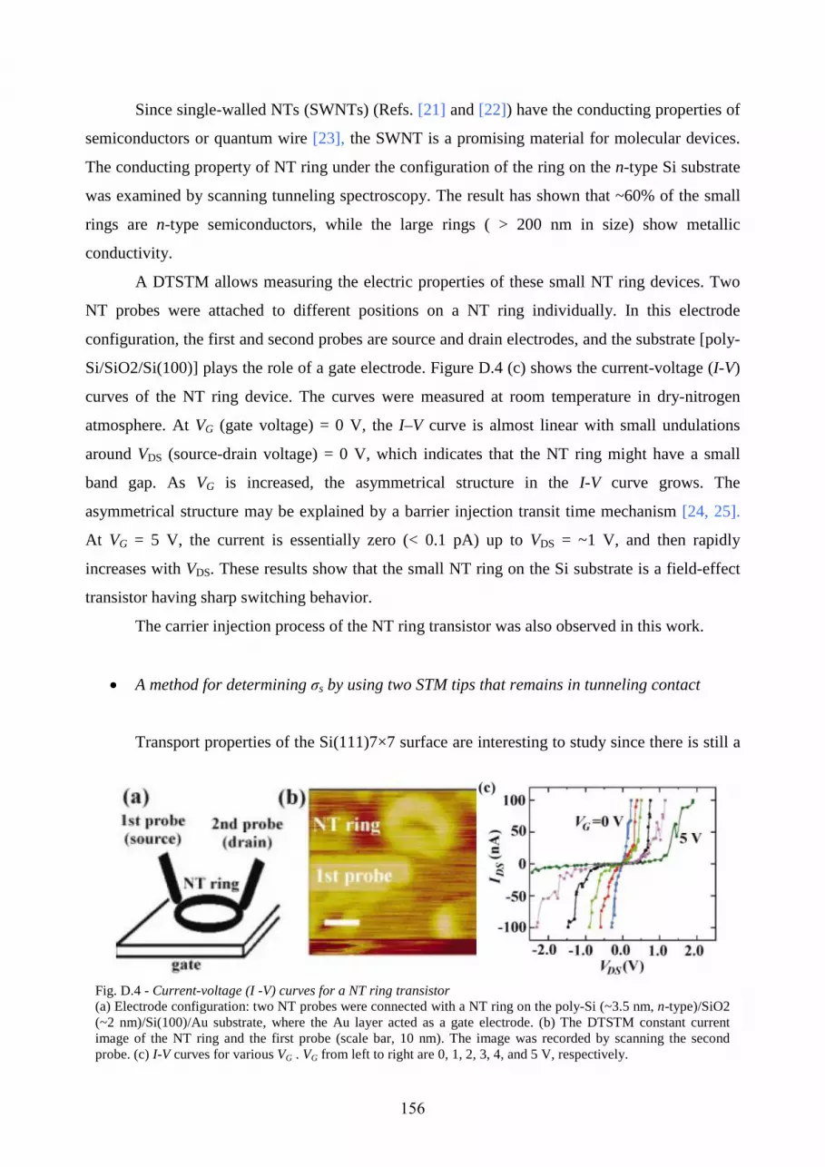
156
Since single-walled NTs (SWNTs) (Refs. [21] and [22]) have the conducting properties of
semiconductors or quantum wire [23], the SWNT is a promising material for molecular devices.
The conducting property of NT ring under the configuration of the ring on the n-type Si substrate
was examined by scanning tunneling spectroscopy. The result has shown that ~60% of the small
rings are n-type semiconductors, while the large rings ( > 200 nm in size) show metallic
conductivity.
A DTSTM allows measuring the electric properties of these small NT ring devices. Two
NT probes were attached to different positions on a NT ring individually. In this electrode
configuration, the first and second probes are source and drain electrodes, and the substrate [poly-
Si/SiO2/Si(100)] plays the role of a gate electrode. Figure D.4 (c) shows the current-voltage (I-V)
curves of the NT ring device. The curves were measured at room temperature in dry-nitrogen
atmosphere. At VG (gate voltage) = 0 V, the I–V curve is almost linear with small undulations
around VDS (source-drain voltage) = 0 V, which indicates that the NT ring might have a small
band gap. As VG is increased, the asymmetrical structure in the I-V curve grows. The
asymmetrical structure may be explained by a barrier injection transit time mechanism [24, 25].
At VG = 5 V, the current is essentially zero (< 0.1 pA) up to VDS = ~1 V, and then rapidly
increases with VDS. These results show that the small NT ring on the Si substrate is a field-effect
transistor having sharp switching behavior.
The carrier injection process of the NT ring transistor was also observed in this work.
• A method for determining σs by using two STM tips that remains in tunneling contact
Transport properties of the Si(111)7×7 surface are interesting to study since there is still a
Fig. D.4 - Current-voltage (I -V) curves for a NT ring transistor (a) Electrode configuration: two NT probes were connected with a NT ring on the poly-Si (~3.5 nm, n-type)/SiO2 (~2 nm)/Si(100)/Au substrate, where the Au layer acted as a gate electrode. (b) The DTSTM constant current image of the NT ring and the first probe (scale bar, 10 nm). The image was recorded by scanning the second probe. (c) I-V curves for various VG . VG from left to right are 0, 1, 2, 3, 4, and 5 V, respectively.

157
debate about its electronic character. It is not clear whether this surface is metallic due to the
uneven number of electrons per unit cell [26, 27] or insulating due to strong correlation effects
[28]. In [30] a method is presented for determining σs of the Si(111)7×7 surface by using two
STM tips that remain in tunneling contact. This method permits distance-dependent charge
transport measurements without the destruction of the STM tips and the surface reconstruction.
Moreover, due to the tunneling contacts the charge carriers are injected completely into the
surface states of the Si(111)7×7 surface [29]. This is not possible by mechanically contacting the
surface because mechanical contacts penetrate the surface and destroy the surface reconstruction.
After checking the Si(111)7×7 reconstruction with one STM tip, the other STM tip was moved to
a certain distance under SEM control. The measurement starts by turning off the feedback loops
of both STMs and by opening the sample-to-ground switch (Fig. D.5). To inject a current into the
surface by one STM tip and collect it with the other STM tip, a voltage of 2 V was applied
between the tips. To change the tunneling resistances between the tips and the surface, both tips
were lowered in three steps (∆z = 2, 3, and 4 Å). During each step the tip-to-tip tunneling current
was measured. The tip-to-tip tunneling current increases as the tips are lowered. This is due to the
fact that the tunneling resistance between the STM tips and the surface decreases as the vacuum
gaps become smaller. The tip-to-tip tunneling current also increases as the probe distance
becomes smaller.
To obtain quantitative information from the measurements in, the authors of Ref. [30] set
up a model of the two-point probe measurement. For the two-point surface resistance the authors
found
( )( ) ( )
−
−=∆
=rDrI
VDR
b
PPDPP
D
111232
3 πσ, (D5)
( ) ( )( )
−=
∆=
r
rD
I
VDR
s
PPDPP
D ln12
222 πσ
, (D6)
for the 3D and 2D cases, respectively. The parameters determining the resistance are the bulk σb
or the surface σs conductivities, the distance of the source and drain areas D, and the effective
radius of the source and drain areas r. In the noncontact setup of this experiment the source and
drain areas represent areas where the charge carriers injected/extracted by tunneling and move

158
ballistically without significant energy losses [31]. In the definitions of Eqs. (D5) and (D6) the
resistance of these areas is implicitly zero.
During the two-point measurement, the surface resistance is in series with two tunneling
resistances of the respective tunneling contacts, see Fig. 2.10. Thus, the current measured in the
two-point measurement is
( )22
1/ TPP
T RRRUI ++∆= . (D7)
To make Eq. (D7) useful for determining σb or σs we have to adopt certain assumptions regarding
RT. RT belongs to a tunneling contact. Thus, in the approximation of small tunneling voltages it is
an exponential function of ∆z [32]. In the experiment, both STM tips are treated equally.
Therefore, we consider
Fig. D.5 - determining σs by using two STM tips Upper left: Schematic drawing of the instrument configuration. The SEM column is in the center and images the two tips of the double-tip STM and the sample surface. The currents through the STM tips I1 and I2 are measured with two preamplifiers biased with V1 and V2, respectively. The master PC controls the STM tip 1, the SEM, and the sample-to-ground connection. The slave PC controls the STM tip 2. To assure a synchronous measurement of STM 1 and STM 2, PCs communicate start and stop signals. Upper right: SEM image of both STM tips in tunneling contact with a Si(111) surface. The visible structures on the surface are bunches of atomic steps formed during heating of the Si sample. Lower left: Electrical circuit diagram of the two-point probe measurement. The applied voltage ∆U is composed of the tunneling voltages UT1 and UT2 and the voltage drop ∆V2PP originating from the sample resistance RS. Lower right: The tip-to-tip tunneling current calculated using the 2D two-point probe model in comparison to the measured data points. The free parameters σs, r, R0, and κ were fitted to obtain the best match with the data points.

159
( )zRRR TT ∆−== κ2exp021 . (D8)
Equation (D7), together with Eqs. (D5) and (D8), for the 3D case or alternatively Eq. (D6) for the
2D case now yield the current (I) as a function of two variables D and ∆z, and four parameters: σb
or σs, r, R0, and κ. The parameters can be obtained by numerical least square fitting of the I(D, ∆z)
dependence to the experimental data points. The results of a fit for the 2D case are shown in Fig.
D.5. The 3D fit reproduces the experimental points comparably well.

160
Bibliography References for part I Introduction [1] N.C. Bartelt, J.L. Goldberg, T.L. Einstein, E.D. Williams, J.C. Heyraud and J.J. Métois, Phys. Rev. Bv48
(1993) 15453; N.C. Bartelt, R.M. Tromp and E.D. Williams, Phys. Rev. Lett. 73 (1994) 1656; A. Pimpinelli, J. Villain, D.E. Wolf, J.J. Métois, J.C. Heyraud, I. Elkinani and G. Uimin, Surf. Sci. 295 (1993) 143; M. Giesen-Seibert, R. Jentjens, M. Poensgen and H. Ibach, Phys. Rev. Lett. 71 (1993) 3521; L. Kuipers, M.S. Hoogeman and J.W.M. Frenken, Phys. Rev. Lett. 71 (1993) 3517.
[2] K. Morgenstern, G. Rosenfeld, B. Poelsema and G. Comsa, Phys. Rev. Lett. 74 (1996) 2058; S.V. Khare and T.L. Einstein, Phys. Rev. B 54 (1996) 11752.
[3] K. Morgenstern, G. Rosenfeld and G. Comsa, Phys. Rev. Lett. 76 (1996) 2113; G. Schultze Icking-Konert, M. Giesen and H. Ibach, Surf. Sci., Phys. Rev. Lett. 83, (1999) 3880.
[4] J.H. van der Merwe, D.L. Tönsing, and P.M. Stoop, Surf. Sci. 312, (1994) 387; J.H. van der Merwe, J. Woltersdorf, and W.A. Jesser, Mater. Sci. Eng. 81, (1986) 1.
[5] D. Sander, C. Schmidthals, A. Enders, and J. Kirschner, Phys. Rev. B 57, (1998) 1406. [6] D. Sander, R. Skomski, C. Schmidthals, A. Enders, and J. Kirschner, Phys. Rev. Lett. 77, (1996) 2566. [7] A. Grossmann, W. Erley, J.B. Hannon, and H. Ibach, Phys. Rev. Lett. 77, (1996) 127. [8] R. Pentcheva and M. Scheffler, Phys. Rev. B 61, (2000) 2211. [9] J. Tersoff and R.M. Tromp, Phys. Rev. Lett. 70, (1993) 2782. [10] B. Müller, L. Nedelmann, B. Fischer, H. Brune, J.V. Barth, and K. Kern, Phys. Rev. Lett. 80, (1998) 2642. [11] R. Kern and P. Müller, Surf. Sci. 392, (1997) 103. [12] J. Fassbender, U. May, B. Schirmer, R.M. Jungblut, B. Hillebrands, and G. Güntherodt, Phys. Rev. Lett. 75,
(1995) 4476. [13] P. Turban, L. Hennet, and S. Andrieu, Surf. Sci. 446, (2000) 241. [14] V. S. Stepanyuk, D. I. Bazhanov, A. N. Baranov, W. Hergert, P. H. Dederichs, and J. Kirschner, Phys. Rev. B
62, (2000) 15398. [15] O.V. Lysenko, V. S. Stepanyuk, W. Hergert, and J. Kirschner, Phys. Rev. Lett. 89, (2002) 126102. [16] M. Giesen, G. Schullze Icking-Konert and H. Ibach, Phys. Rev. Lett., 80 (1998) 552. [17] M. Giesen, G. Schullze Icking-Konert and H. Ibach, Phys. Rev. Lett. 82 (1999) 552. [18] M. Giesen and H. Ibach, Surf. Sci. Lett. 464 (2000) L697. [19] M. Giesen, Prog. Surf. Sci. 68 (2001) 1. [20] S.M. Hu, J. Appl. Phys. 50 (1979) 4661. [21] L.D. Landau and E.M. Lifshitz, Theory of Elasticity, Pergamon Press, Oxford, 1970. [22] J.F. Nye, Physical Properties of Crystals, Oxford, University Press, 1985. [23] D. Stauffer and A. Aharony, Introduction to Percolation theory, Taylor & Francis, Bristol, 1994.
Chapter 1 [1] J.H. Moths, in: F. Nabarro (Ed.), Dislocations in Solids, 1979, Chapter 7, p. 463. [2] F.K. Legoues, M. Copel, R.M. Tromp, Phys. Rev. B 42 (1990) 11690;
F.K, Legoues, MRS Bull., April, 1996, 38. [3] J.H. van der Merwe, W.A. Jesser, J. Appl. Phys. 64 (1988) 4968. [4] R. Hull, A. Fischer-Colbrie, Appl. Phys. Lett. 50 (1987) 851. [5] D.J. Eaglesham, M. Cerullo, Phys. Rev. Lett. 64 (1990) 1943. [6] S. Guha, A. Madhukar, K.C. Raykumar, Appl. Phys. Lett. 57 (1990) 2110. [7] R. Kern, P. Mtiller, Surf. Sci. 392 (1997) 103. [8] S.M. Hu, Appl. Phys. Lett. 32 (1978) 5. [9] J. Tersoff, R.M. Tromp, Phys. Rev. Lett. 70 (1993) 2782;
J. Tersoff, F.K. Legoues, Phys. Rev. Lett. 72 (1994) 3570. [10] Ch. Duport, Ph. Nozières, J. Villain, Phys. Rev. Lett. 74 (1995) 134.

161
[11] Ch. Duport, Ph.D. Thesis, Univ. Ch. Fourier, Grenoble, France, 1996. [12] S.M. Hu, J. Appl. Phys. 50 (1979) 4661. [13] O. Brandt, K. Ploog, R. Bierwolt, M. Hohenstein, Phys. Rev. Lett. 68 (1992) 1339;
J.C. Woicik, J.G. Pellegrino, S.H. Southword, P.S. Shaw, B.A. Karlin, C.E. Bouldin, Phys. Rev. B 52 (1995) R2281.
[14] P. Müller, A. Sau´l, Surf. Sci. Rep. 54 (2004) 157. [15] L.D. Landau, E.M. Lifshitz, Theory of Elasticity, Pergamon Press, Oxford, 1970. [16] R. Shuttleworth, Proc. R. Soc. LXIII, 5 (1949) 444;
A.F. Andreev, Y.A. Kosevitch, Sov. Phys. JETP 54 (1981) 761. P. Nozieres, D.E. Wolf, Z. Phys. B: Condensed Matter 70 (1988) 399.
[17] R.E. Martinez, W.M. Augustyniak, J.A. Golovchenko, Phys. Rev. Lett. 64 (1990) 1035; A.J. SchelI-Sorokin, R.M. Tromp, Phys. Rev. Lett. 64 (1990) 1039.
[18] V. S. Stepanyuk, D. I. Bazhanov, A. N. Baranov, W. Hergert, P. H. Dederichs and J. Kirschner, Phys. Rev. B 62 (2001) 15398.
[19] O.V. Lysenko, V. S. Stepanyuk, W. Hergert and J. Kirschner, Phys. Rev. Lett., 89 (2002) 126102-1. [20] O. Mironets, H. L. Meyerheim, C. Tusche, V. S. Stepanyuk, E. Soyka, P. Zschack, H. Hong, N. Jeutter,
R. Felici, and J. Kirschner, Phys. Rev. Lett., 100 (2008) 096103. [21] O. Mironets, H. L. Meyerheim, C. Tusche, V. S. Stepanyuk, E. Soyka, H. Hong, P. Zschack, N. Jeutter,
R. Felici, and J. Kirschner, Phys. Rev. B 79 (2009) 035406. [22] J . H. van der Merwe, J. Appl. Phys. 34 (1963) 117; 34 (1963) 123. [23] J. W. Matthews and A. E. Blakeslee, J. Cryst. Growth 29 (1975) 273; 32 (l976) 265. [24] M. A. Grinfeld. Dokl. Acad. Nauk SSSR 290 (1986) 1358 [Sov. Phys. Dokl. 31 (1986) 831]. [25] D. Srolovitz. Acta Metall. 37 (1989) 621. [26] B. J. Spencer. P. W. Voorhees and S. H. Davis, Phys. Rev. Lett. 67 (1991) 3696. [27] See, e.g., S. V. Kemat and J. P. Hirth, J. Appl. Phys. 67 (1990) 6844. [28] In equilibrium the substrate is typically wetted, if at all, by a single atomic layer of the strained material; but
thicker wetting layers are possible, see J. Tersoff, Phys. Rev. B 43 (1991) 9377. [29] D. J. Eaglesham and M. Cerullo, Phys. Rev. Leet. 64 (1990) 1943. [30] C.W. Snyder, B.G. Orr, D. Kessler and L.M. Sander, Phys. Rev. Lett., 66 (1991) 3032. [31] Y. -W. Mo, D. E. Savage, B. S. Swartzentruber and M. G. Lagally, Phys. Rev. Lett. 65 (1990) 1020. . [32] F. A. Ponce and C. J. D. Hetherington, in Proceedings of the Forty-Seventh annual Meeting of the Electron
Microscopy Society of America, edited by G. W. Bailey (San Francisco Press San Francisco, CA 1989), p. 586; M. Akiyama, T. Ueda, and S. Onozawa, Matter. Res. Soc. Symp. Proc. 116 (1988) 79.
[33] G. G. Hembree and J. A. Venables. Ultramicroscopy 47 (1992) 109. [34] A. F. Becker, G. Rosenfeld, B. Poelsema, and G. Comsa, Phys. Rev. Lett. 70 (1993) 477. [35] These ''corner'' terms have a somewhat complex form, and depend weakly on the size and shape of the
island. Numerical tests indicate that they are not important in understanding the overall behavior. [36] E. Kaxiras, O. L. Alerhand, J. D. Joannopoulos and G. W. Turner, Phys. Rev. Lett. 62 (1989) 2484. [37] M . Mundschau, E. Bauer. W. Telieps, and W. Swiech, Surf. Sci. 213 (1989) 381. [38] S. Rousset, S. Chiang. D. E. Fowler and D. D. Chambliss, Phys. Rev. Lett. 69 (1992) 3200. [39] C. Duport, C. Priester, J. Villain, in: Z. Zhang, M. Lagally (Eds.), Morphological Organization in Epitaxial
Growth and Removal, World Scientific, 1998, p. 73. [40] P. Müller, R. Kern, Appl. Surf. Sci. 164 (2000) 68.
Chapter 2 [1] D. Stauffer and A. Aharony, Introduction to Percolation theory, Taylor & Francis, Bristol, 1994. [2] M. E. Fisher, Phys. 3 (1967) 255.
Chapter 3 [1] R. Young, J. Ward, F. Scire, Rev. Sci. Instrum. 43 (1972) 999. [2] G. Binnig, H. Rohrer, Ch. Gerber, E. Weibel, Appl. Phys. Lett. 40 (1982) 178. [3] G. Binnig, H. Rohrer, Ch. Gerber, E. Weibel, Physica 109-110 (1982) 2075. [4] G. Binnig, H. Rohrer, Rev. Mod. Phys. 59 (1987) 615. [5] D. A. Bonnell, (Eds.), Scanning Tunneling Microscopy and Spectroscopy: Theory, Techniques, and
Applications, New York: VCH 1993. [6] N. J. DiNardo, N. J., Nanoscale Characterization of Surfaces and Interfaces, New York: VCH 1994.

162
[7] C. Duke, (Ed.), Surface Science: The First Thirty Years, Surf. Sci. 299/300 (1994) 1. [8] H.-J. Güntherodt, R. Wiesendanger, Scanning Tunneling Microscopy I: General Principles and Applications
to Clean and Adsorbate-Covered Surfaces, 2nded., Springer Series in Surface Sciences, Vol. 20. Berlin: Springer-Verlag 1994.
[9] J. A. Kubby, J. J. Boland, Scanning Tunneling Microscopy of Semiconductor Surfaces, Surf. Sci. Rep. 26 (1996) 61.
[10] Y. Kuk, P. J. Silverman, Rev. Sci. Instrum. 60 (1989) 165. [11] s. N. Magonov, Surface Analysis With STM and AFM : Experimental and Theoretical Aspects of Image
Analysis, Weinheim: VCH 1996. [12] J. A. Stroscio, W.J. Kaiser, (Eds.), Scanning Tunneling Microscopy, Boston: Academic 1993. [13] R. Wiesendanger, H.-J. Güntherodt, Scanning Tunneling Microscopy II: Further Applications and Related
Scanning Techniques, 2nded., Springer Series in Surface Sciences, Vol. 28. Berlin: Springer Verlag 1995. [14] R. Wiesendanger, H.-J. Güntherodt, Scanning Tunneling Microscopy III: Theory of STM and Related
Scanning Probe Methods, 2nded., Springer Series in Surface Sciences, Vol. 29. Berlin: Springer-Verlag 1996.
[15] A. Zangwill, Physics at Surfaces, Cambridge: Cambridge University Press. 1988. [16] K. Takayanagi, Y. Tanishiro, S. Takahashi, M. Takahashi, J. Vac. Sci. Technol. A 3 (1985) 1502. [17] K. Takayanagi, Y. Tanishiro, S, Takahashi, M. Takahashi, Surf. Sci. 164 (1985) 367. [18] A.V. Zotov, V.V. Korobtsov, J. Crystal Growth 98 (1989) 519. [19] J.M. Gibson, H.-J. Gossmann, J.C. Bean, R.T. Tung, L.C. Feldman, Phys. Rev. Lett. 56 (1986) 355. [20] I.K. Robinson, W.K. Waskiewicz, R.T. Tung, Phys. Rev. Lett. 57 (1986) 2714. [21] A. Sakai, T. Tatsumi, K. lshida, Surf. Sci. 224 (1989) L956. [22] A. Sakai, T. Tatsumi, I. Hirosawa, H. Ono, K. Ishida, Surf. Sci. 249 (1991) L300. [23] H. Nakahara, A. Ichimiya, J. Crystal Growth 99 (1990) 514. [24] Z. Zhang, M.A. Kulakov, B. Bullermer, Thin Solid Films 294 (1997) 88. [25] Z. Zhang, M.A. Kulakov, B. Bulletmer, Surf. Sci. 375 (1997) 195. [26] H.-J. Grossmann, L.C. Feldman, Phys. Rev. B 32 (1985) 6. [27] H.E. Stanley, Introduction to Phase Transitions and Critical Phenomena, Oxford U.P, Oxford, 1971. [28] T.M. Liggett, Interacting Particle Systems, Springer, Berlin, 1985. [29] J.W. Evans, Rev. Mod. Phys. 63 (1993) 1281. [30] Z. Olami, Y. Manassen, N. R. Rao and R. Dana, Surf. Sci 520 (2002) 35. [31] T. Fukuda, Surf. Sci. 442 (1999) 107.
Chapter 4 [1] G. L. Olson and J. A. Roth, Mater. Sci. Rep. 3 (1988) 1. [2] D. A. Wollman, M. A. Dubson and Qifu Zhu, Phys. Rev. B, 48 (1993) 3713. [3] B. Müller, L. P. Nedelmann, B. Fisscher, H. Brune, J. V. Barth, K. Kern, D. Erdos and J. Wollschlager, Surf.
Rev. Lett., 5 (1998) 769. [4] S. C. Blair, P. A. Berge and J. G. J. Berryman, Geophys. Res., 101 (1996) 20359. [5] D. J. Eaglesham, A. E. White, L. C. Feldman, N. Moriya and D. C. Jacobson, Phys. Rev. Lett., 70 (1993)
1643. [6] R. E. Martinez, W. M. Augustyniak and J. A. Golovchenko, Phys. Rev. Lett., 64 (1990) 1035. [7] J. Massies and N. Grandjean, Phys. Rev. Lett., 71 (1993) 1411. [8] P. Müller, P. Turban, L. Lapena and S. Andrieu, Surf. Sci., 488 (2001) 52. [9] P. Müller, A. Sau´l, Surf. Sci. Rep. 54 (2004) 157.
Chapter 5 [1] Y. Jiao, F. H. Stillinger and S. Torquato, Phys. Rev. E, 76 (2007) 031110. [2] V. Marchenko, JETP 54 (1981) 605. [3] V. Marchenko, JETP 33 (1981) 381. [4] O. Alerhand, D. Vanderbilt, R. Meade, J. Joannopoulos, Phys. Rev. Lett. 61 (1988) 1973. [5] P. Müller, A. Sau´l, Surf. Sci. Rep. 54 (2004) 157. [6] R. Kern and P. Müller, Surf. Sci., 392 (1997) 103. [7] N. Cabrera, Mem. Sci. Rev. Metal. Fr. 62 (1965) 205. [8] L. C. A. Stoop, J. H. van der Merwe, J. Cryst. Growth 24-25 (1974) 289.

163
[9] A.H. Stoneham, Solid State Commun. 24 (1977) 425. [10] J. Tersoff and R. M. Tromp, Phys. Rev. Lett. 70 (1993) 2782. [11] J. Tersoff and F. K. LeGoues, Phys. Rev. Lett. 72 (1994) 3570. [12] K. Sekar, G. Kuri, P. V. Satyam, B. Sundaravel, D. P. Mahapatra and B. N. Dev, Phys. Rev. B 51 (1995)
14330. [13] B. Müller, L. P. Nedelmann, B. Fischer, H. Brune, J. V. Barth, K. Kern, D. Erd Ös , J. Wollschl, Surf.
Rev. and Lett., vol. 5 (1998) 769. [14] B. Müller, L. Nedelmann, B. Fischer, H. Brune, J. V. Barth, and K. Kern, Phys. Rev. Lett., 80 (1998) 2642. [15] S. H. Brongersma, M. R. Castell, D. D. Perovic and M. Zinke-Allmang, Phys. Rev. Lett. 80 (1998) 3795. [16] G. Zhou and J. C. Yang, Phys. Rev. Lett., 89 (2002) 106101-1. [17] W.-C. Yang, H. Ade, and R. J. Nemanich, J. Appl. Phys. 95 (2004) 1572. [18] Z. Gong, Z. D. Fang, X. H. Xu, Z. H. Miao, H. Q. Ni, Z. C. Niu and S. L. Feng, J. Phys.: Condens. Matter,
16 (2004) 29. [19] I. Goldfarb, Surf. Sci. 601 (2007) 2756. [20] R. Dana and Y. Manassen, EuroPhys. Lett. 79 (2007) 16001. [21] M. S. J. Marshall and M. R. Castell, Phys. Rev. Lett., 102 (2009) 146102.
References for part II Introduction [1] H.-L. Engquist and P.W. Anderson, Phys. Rev. B 24 (1981) 1151. [2] R. Landauer, Philos. Mag. 21 (1970) 863; IBM J. Res. Dev. 1 (1957) 223. [3] Ph. Avouris, I.-W. Lyo, and Y. Hasegawa, IBM J. Res. Dev. 39 (1995) 603, and other articles in the same
issue. [4] M.F. Crommie, C.P. Lutz, and D.M. Eigler, Science 262 (1993) 218. [5] L.C. Venema, J.W.G. Wildöer, J.W. Janssen, S.J. Tans, H.L.J. Temminck Tuinstra, L.P. Kouwenhoven, and
C. Dekker, condmat/9811317 (unpublished). [6] J. Tersoff, and D.R. Hamann, Phys. Rev. B 31 (1985) 805. [7] J. Bardeen, Phys. Rev. Lett. 6 (1961) 57. [8] C. Bracher, M. Riza, and M. Kleber, Phys. Rev. B 56 (1997) 7704. [A] P. A. Mello and N. Kumar Ouantum Transport in Mesoscopic Physics, Oxford University Press, 2000. [10] J. Imry, Physics of Mesoscopic Systems, World Scientific Press, Singapore, 1986. [11] H. L. Engquist and P. W. Anderson, Phys. Rev. B 24 (1981) 1151. [12] Yu V. Sharvin. and N. I. Bogatina, Sov. Phys. JETP, 29 (1969) 419. [13] B. J. van Wees, H. van Houten, C.W.J. Beenakker, J. G. Williamson, L. P. Kouwenhoven, D. van der Marel
and C. T. Foxon, Phys. Rev. Lett. 60 (1988) 848. [14] D. A. Wharam, T. J. Thornton, R. Newbury, M. Pepper, H. Ahmed, J.E.F. Frost, D. G. Hasko, D. C.
Peacockt D. A. Ritchie and D. A. C. Jones, J. Phys. C 21 (1988) L209. [15] M. A. Topinka, B. J. LeRoy, S. E. J. Shaw, E. J. Heller, R. M. Westervelt, K. D. Maranowski, K. A. C.
Gossard, Science 289 (2000) 29. [16] R. Landauer, IBM J. Res. Dev., 32 (1988) 306; R. Landauer, Physica Scripta, T42 (1992) 110. [17] A. Kristensen, J. Bo Jensen, M. Zaffalon, C. B. Sørensen, S. M. Reimann, P. E. Lindelof, M. Michel and A.
Forchel, J. Appl. Phys., 83 (1998) 607. [18] M. Büttiker, J. Res. Dev., 32 (1988) 317. [19] M. Henzler, Electronic transport at surfaces, in: J. M. Blakely (Ed.), Surface Physics of Materials I,
Academic Press, New York, 1975, p. 241. [20] W. H. Brattain, J. Bardeen, Bell Syst. Tech. J. 32 (1953) 1. [21] J. Bardeen, S. R. Morrison, Physica 20 (1954) 873. [22] W. Mönch, Surf. Sci. 63 (1977) 79. [23] Y. Nakajima, S. Takeda, T. Nagao, S. Hasegawa, X. Tong, Phys. Rev. B 56 (1997) 6782. [24] For review S. Hasegawa, X. Tong, S. Takeda, N. Sato, T. Nagao, Prog. Surf. Sci. 60 (1999) 89;
S. Hasegawa, J. Phys. C: Condens. Matter 12(2000) R463. [25] S. Hasegawa, Curr Opinion Solid State Mater. Sci. 4 (1999) 429. [26] S. Heike, S. Watanabe, Y. Wada, T. Hashizume, Phys. Rev. Lett. 81 (1998) 890. [27] C. L. Petersen, F. Grey, I. Shiraki, S. Hasegawa, Appl. Phys. Lett. 77 (2000) 3782.

164
Microfour-point probes are now commercially available; http://www.capres.com. [28] I. Shiraki, C. L. Petersen, P. Bøggild, T. M. Hansen, T. Nagao, F. Grey, S. Hasegawa, Surf. Rev. Lett. 7
(2000) 533. [29] I. Shiraki, F. Tanabe, R. Hobara, T. Nagao, S. Hasegawa, Surf. Sci., 493 (2001) 633. [30] V. G. Lifshits, A. A. Saranin, A. V. Zotov, Surface Phases on Silicon, Wiley, Chichester, 1994. [31] D. M. Eigler, E. K. Schweizer, Nature 344 (1990) 524;
J. A. Stroscio, D. M. Eigler, Science 254 (1991) 1319. [32] Y. Hasegawa, I. -W. Lyo, Ph. Avouris, Surf. Sci. 357/358 (1996) 32. [33] J. R. Kirtley, S. Washburn, M. J. Brady, Phys. Rev. Lett. 60 (1988) 1546. [34] A. D. Kent, I. Maggio-Aprile, Ph. Niedermann, O. Fischer, Phys. Rev. B 39 (1989) 12363. [35] P. Muralt, Appl. Phys. Lett. 49 (1986) 1441;
P. Muralt, H. Meier, D. W. Pohl, H. W. M. Salemink, Appl. Phys. Lett. 50 (1987) 1352. [36] S. Hasegawa, S. Ino, Phys. Rev. Lett. 68 (1992) 1192. [37] Y. Nakajima, G. Uchida, T. Nagao, S. Hasegawa, Phys. Rev. B 54 (1996) 14134. [38] S. Hasegawa, K. Tsuchie, K. Toriyama, X. Tong, T. Nagao, Appl. Surf. Sci. 162/163 (2000) 42. [39] X. Tong, C. -S. Jiang, S. Hasegawa, Phys. Rev. B 57 (1998) 9015. [40] X. Tong, C. -S. Jiang, K. Horikoshi, S. Hasegawa, Surf. Sci. 449 (2000) 125. [41] P. Bøggild, T. M. Hanssen, O. Kuhn, F. Grey, T. Junno, L. Montelius, Rev. Sci. Instrum. 71 (2000) 2781;
P. Bøggild, F. Grey, T. Hanssenkam, D. R. Greve, T. Bjornholm, Adv. Mater. 12 (2000) 947. [42] C. -S. Jiang, S. Hasegawa, S. Ino, Phys. Rev. B 54 (1996) 10389. [43] T. Ogino, Surf. Sci. 386 (1997) 137. [44] Q. Niu, M. C. Chang, C. K. Shih, Phys. Rev. B 51(1995) 5502. [45] S. Tsukamoto, B. Siu, N. Nakagiri, Rev. Sci. Instrum. 62 (1991)1767. [46] M. Aono, C.-S. Jiang, T. Nakayama, T. Okuda, S. Qiao, M. Sakurai, C. Thirstrup, Z.-H. Wu, J. Surf. Sci.
Soc. Jpn. 9 (1998) 698, in Japanese. [47] M. Büttiker, Phys. Rev. B 46 (1992) 12485. [48] M. J. M. de Jong and C. W. J. Beenakker, in Mesoscopic Electron Transport, Vol. 345 of NATO Advanced
Study Institute, Series E: Applied Sciences, edited by by L. L. Sohn, L. P. Kouwenhoven, and G. Schön, (Kluwer, Dordrecht, 1997), p. 225.
[49] L. Saminadayar, D. C. Glattli, Y. Jin, and B. Etienne, Phys. Rev. Lett. 79 (1997) 2526. [50] R. de-Picciotto, M. Heiblum, V. Umansky, G. Bunin, and D. Mahalu, Nature (London) 389 (1997) 162. [51] H. E. van den Brom and J. M. van Ruitenbeek, Phys. Rev. Lett. 82 (1999) 1526. [52] H. Birk, M. J. M. de Jong, and C. Schönenberger, Phys. Rev. Lett. 75 (1995) 1610. [53] M. Büttiker, Phys. Rev. Lett. 65 (1990) 2901. [54] M. Büttiker, Phys. Rev. Lett. 68 (1992) 843. [55] Th. Martin and R. Landauer, Phys. Rev. B 45 (1992) 1742. [56] Ya. M. Blanter and M. Büttiker, Phys. Rev. B 56 (1997) 2127. [57] E. V. Sukhorukov and D. Loss, Phys. Rev. Lett. 80 (1998) 4959;
Phys. Rev. B 59 (1999) 13054. [58] S. A. van Langen and M. Büttiker, Phys. Rev. B 56 (1997) R1680. [59] M. P. Anantram and S. Datta, Phys. Rev. B 53 (1996) 16390;
S. Datta, and P. F. Bagwell, and M.P. Anantram, Phys. Low-Dimens. Semicond. Struct. 3, (1996) 1. [60] M. Henny, S. Oberholzer, C. Strunk, and C. Schünenberger, Science 284, (1999);
M. Henny, Ph.D. thesis, University of Basel, 1998. [61] W. D. Oliver, J. Kim, R.C. Liu, and Y. Yamamoto, Science 284 (1999) 299. [62] M. Büttiker, Physica B 175 (1991) 199. [63] Q. Niu, M. C. Chang and C. K. shih, Phys. Rev. B, 51 (1995) 5502.
Chapter 1 [1] Q. Niu, M. C. Chang and C. K. shih, Phys. Rev. B, 51 (1995) 5502. [2] W. J. Kaiser and L. D. Bell, Phys. Rev. Lett. 60 (1988) l406; for a review, see L. D. Bell, W. J. Kaiser, M.
H. Hecht, and L. C. Davis, Scanning tunneling Microscopy, edited by J. A. Stroscio and W. J. Kaiser (Academic New York), 1993, Vol. 27.
[3] J. Tersoff and D. R. Hamann, Phys. Rev. Lett. 50 (1983) 1998; Phys. Rev. B 31 (1985) 805.
[4] R. P. Feynman and A. R. Gibbs, Quantum Mechanics and Path Integrals (McGraw-Hill, New York), 1965, Chap. 6.
[5] M. C. Chang, Q. Niu and C. K. Shih (unpublished).

165
[6] J. M. Byers and M. E. Flatte, Phys. Rev. B 53 (1996) R10536. Their result [Eq. (9)] reduces to Niu et. al. Eq. (2) in the absence of pairing of electrons but their derivation was based on a Hamiltonian that is quadratic in electron creation and attraction operators.
[7] In a recent observation, shallow Si-substituted donors (SiGe) are detected within the top five atomic layers; see J. F. Zheng, X. Liu, N. Newman, E. R. Weber, D. F. Ogletree, and M. Salmeron, Phys. Rev. Lett. 72 (1994) 1490.
[8] M. F. Crommie, C. P. Lutz, and D. M. Eigler: Nature (London) 363 (1993) 524; Science 262 (1993) 218. [9] S. Chakravarty and A. Schmid, Phys. Rep. 10 (1986) 193. [10] A. Lee and T. V. Ramakrishnan, Rev. Mod. Phys. 57 (1985) 287. [11] For recent reviews see A. M. Duif, A. G. M. Jansen and P. Wyder, J. Phys. Condens. Matter 1 (1989) 3157;
C. W. J. Beenakker, H. van Houten, and B. J. van Wees Europhys. Lett. 7 (1988) 359. [12] J. Kinaret, Y. Meir, N. Wingreen, P. A. Lee, and X. G. Wen, Phys. Rev. B 46 (1992) 4681.
Chapter 2 [1] F. M. Smith, Measurement of Sheet Resistivities with Four-Point Probe, The Bell System Technical Journal
May, (1958) 711. [2] C. L. Petersen, F. Grey, I. Shiraki, and S. Hasegawa, Appl. Phys. Lett. 77 (2000) 3782. [3] Monolithic micro-four-point probes are commercially available; http://www.capres.com/ [4] R. Hobara, N. Nagamura, S. Hasegawa, I. Matsuda, Y. Yamamoto, Y. Miyatake and T. Nagamura, Rev. Sci.
Instrum. 78 (2007) 053705. [5] Omicron NanoTechnology GmbH (http://www.omicron.de/). [6] I. Shiraki, F. Tanabe, R. Hobara, T. Nagao, S. Hasegawa, Surf. Sci. 493 (2001) 633. [7] O. Guise, H. Marbach, J. T. Yates, Jr., M.-C. Jung, J. Levy and J. Ahner, Rev. Sci. Instrum. 76 (2005)
045107. [8] X. Lin, X. B. He, T. Z. Yang, W. Guo, D. X. Shi, H.-J. Gaoa, D. D. D. Ma, S. T. Lee, F. Liu and X. C. Xie,
Appl. Phys. Lett. 89 (2006) 043103. [9] T.-H. Kim, Z. Wang, J. F. Wendelken, H. H. Weitering, W. Li and A.-P. Li, Rev. Sci. Instrum. 78 (2007)
123701. [10] Commercial companies: MultiProbe, Inc(http://www.multiprobe.com/), Zyvex Co.
(http://www.zyvex.com/). [11] H. Okamotoa and D. M. Chen, Rev. Sci. Instrum., 72 (2001) 4398. [12] H. Grube, B. C. Harrison, J. Jia and J. J. Boland, Rev. Sci. Instrum., 72 (2001) 4388. [13] H. Watanabe, C. Manabe, T. Shigematsu and M. Shimizu, Appl. Phys. Lett., 78 (2001) 2928. [14] W. Wu, A. Guha, S. Kim and A. de Lozanne, IEEE Transactions on Nanotechnology, 5 (2006) 77. [15] A. Matsui and Y. Shigeta, Rev. Sci. Instrum. 78 (2007) 106107. [16] J. F. Xu, P. M. Thibado, and Z. Ding, Rev. Sci. Instrum. 77 (2006) 093703. [17] P. Jaschinsky, P. Coenen, G. Pirug and B. Voigtländer, Rev. Sci. Instrum. 77 (2006) 093701. [18] W. Cai, F. Pang, J. Wang, H. Liu, X. J. Liang, Q. K. Xue and D. M. Chen, Rev. Sci. Instrum. 78 (2007)
065108. [19] E. W. Müller, Z. Phys. 106 (1937) 132. [20] G. Binnig, H. Rohrer, Helv. Phys. Acta 55 (1982) 726. [21] G. W. Stupian and M. S. Leung, Rev. Sci. Instrum. 60 (1989) 181. [22] G. A. Valaskovic, M. Holton, and G. H. Morrison, Appl. Opt. 34 (1995) 1215. [23] A. J. Melmed, J. Vac. Sci. Technol. B 9 (1991) 601. [24] Hans-Werner Fink, IBM J. Res. Develop. 30 (1986) 460. [25] Y. Akama, E. Nishimura, A. Sakai, H. Murakami, J. Vac. Sci. Technol. A 8 (1990) 429. [26] J. Garnaes, F. Kragh, K. A. Mørch, and A. R. Thölén, J. Vac. Sci. Technol. A 8 (1990) 441. [27] H. -S. Kuo, I. -S. Hwang, T. -Y. FU, and Y. -C. LIN, Jpn. J. Appl. Phys. 45 (2006) 8972. [28] M. Yoshimura, S. Jo, and K. Ueda, Jpn. J. Appl. Phys. 42 (2003) 4841. [29] A. I. Oliva, A. Romero G, J. L. Pena, E. Anguiano, and M. Aguilar, Rev. Sci. Instrum. 67 (1996) 1917. [30] O. L. Guise, J. W. Ahner, M. C. Jung, P. C. Goughnour and J. T. Yates, Jr., Nano Lett. 2 (2002) 191. [31] A. K. Kar, S. Gangopadhyay and B. K. Mathur, Meas. Sci. Technol. 11 (2000) 1426. [32] P. Kim, J. H. Kim, M. S. Jeong, D. -K. Ko, J. Lee and S. Jeong, Rev. Sci. Instrum. 77 (2006) 103706. [33] R. Hobara, S. Yoshimoto and S. Hasegawa, e-J. Surf. Sci. Nanotech. 5 (2007) 94. [34] T. M. Hansen, K. Stokbro, O Hansen, T. Hassenkam, I. Shiraki, S. Hasegawa, P. Bøggild, Rev. Sci.
Instrum., 74 (2003) 3701. [35] R. Hobara, S. Yoshimoto, S. Hasegawa and K. Sakamoto, e-J. Surf. Sci. Nanotech. 5 (2007) 94.

166
[36] J. E. McKendry, C. S. Allen, K. Critchley, M. Ł. Górzny, A. S. Walton and S. D. Evans, Nanotechnology 19 (2008) 085201.
[37] M. Kishida, H. Konishi, Y. Murata, D. Maeda, T. Yasuda, T. Ikuno, S.-i Honda, M. Katayama, S. Yoshimoto, R. Hobara, I. Matsuda and S. Hasegawa, e-J. Surf. Sci. Nanotech., 3 (2005) 417.
[38] S. Yoshimoto, Y. Murata, K. Kubo, K. Tomita, K. Motoyoshi, T. Kimura, H. Okino, R. Hobara, I. Matsuda, S-i Honda, M. Katayama and S. Hasegawa, Nano Lett., 7 (2007) 956.
[39] O. Kubo, Y. Shingaya, M. Nakaya, M. Aono and T. Nakayama, Appl. Phys. Lett. 88 (2006) 254101. [40] R. Lin, P. Bøggild and O. Hansen, J. Appl. Phys., 96 (2004) 2895. [41] Ph.D. Thesis of T. M. Hansen, Mikroelektronik Centret, Bldg. Technical University of Denmark (2003). [42] P Bøggild, T. M. Hansen, C. Tanasa and F. Grey, Nanotechnology 12 (2001) 331. [43] S. Yoshimoto, Y. Murata, R. Hobara, I. Matsuda, M. Kishida, H. Konishi, T. Ikuno, D. Maeda, T. Yasuda,
S.-i. Honda, H. Okado, K. Oura, M. Katayama and S. Hasegawa, Jpn. J. Appl. Phys., 44 (2005) L1563. [44] LIKE [4] X. Lin, X. B. He, T. Z. Yang, W. Guo, D. X. Shi, H.-J. Gaoa, D. D. D. Ma, S. T. Lee, F.
Liu and X. C. Xie, Appl. Phys. Lett. 89 (2006) 043103. [45] X. Lin, X.-B. He, J.-L. Lu, L. Gao, Q. Huan, D.-X. Shi and H.-J. Gao, Chinese Phys. 14 (2005) 1536. [46] W. Yi, I. I. Kaya, I. B. Altfeder, I. Appelbaum, D. M. Chen and V. Narayanamurti, Rev. Sci. Instrum. 76
(2005) 063711. [47] A.-D. Müller, F. Müller, M. Hietschold and Th. Gessner, Appl. Phys. 5 (2005) 629.
Chapter 3 [1] M. F. Crommie, C. P. Lutz and D. M. Eigler, Science, 262 (1993) 218. [2] N. Agrait, A. L. Yeyati, and J. M. van Ruitenbeek, Review article, submitted to Physics Reports (cond-
mat/0208239). [3] C. J. Muller, J. M. van Ruitenbeek, and L. J. de Jongh, Physica C 191 (1992) 485. [4] Ph.D. thesis by András Halbritter, Budapest University of Technology and Economics, 2003. [5] A. I. Mares, A. F. Otte, L. G. Soukiassian, R. H. M. Smit and J. M. van Ruitenbeek, Phys. Rev. B 70 (2004)
073401. [6] C. Zhou, C. J. Muller, M. R. Deshpande, J. W. Sleight and M. A. Reed, Appl. Phys. Lett. 67 (1995) 1160. [7] R. Keijsers, Ph.D. Thesis, University of Nijmegen, 1998. [8] A. E. Ennos, British J. Appl. Phys., 4 (1953) 101. [9] K. M. Poole, Proceedings of the Physical Society, Section B 66 (1953) 542. [10] A. G. Baker and W. C. Morris, Rev. Sci. Instrum., 32, (1961) 458. [11] K. R. Hart, T. F. Kassner and J. K. Maurin, Philos. Mag., 21 (1970) 453. [12] S. J. Randolph, J. D. Fowlkes, and P. D. Rack, Critical Reviews in Solid State and Materials Sciences, 31
(2006) 55. [13] H.W. P. Koops, R.Weiel, D. P. Kern and T. H. Baum, J. Vac. Sci. & Technol., B 6 (1988) 477. [14] S. Matsui and K. Mori, J. Vac. Sci. & Technol., B 4 (1986) 299. [15] K. Gamo, D. Takehara, Y. Hamamura, M. Tomita and S. Namba, Microelectronic Eng., 5 (1986) 163. [16] F. Cicoira, K. Leifer, P. Hoffmann, I. Utke, B. Dwir, D. Laub, P. A. Buffat, E. Kapon and P. Doppelt, J.
Cryst. Growth, 265 (2004) 619. [17] R. R. Kunz, T. E. Allen and T. M. Mayer, J. Vac. Sci. & Technol., B 5 (1987) 1427. [18] Y. M. Lau, P. C. Chee, J. T. L. Thong and V. Ng, J. Vac. Sci. & Technol., A 20 (2002) 1295. [19] S.Wang,Y.-M. Sun, Q.Wang and J. M. White, J. Vac. Sci. & Technol., B 22 (2004) 1803. [20] I. Utke, A. Luisier, P. Hoffmann, D. Laub and P. A. Buffat, Appl. Phys. Lett., 81 (2002) 3245. [21] T. J. Stark, T. M. Mayer, D. P. Griffis and P. E. Russell, J. Vac. Sci. & Technol., B 10 (1992) 2685. [22] T. J. Stark, T. M. Mayer, D. P. Griffis and P. E. Russell, J. Vac. Sci. & Technol., B 9 (1991) 3475. [23] A. Ishibashi, K. Funato and Y. Mori, J. Vac. Sci. & Technol., B 9 (1991) 169. [24] M.Weber, H.W. P. Koops, M. Rudolph, J. Kretz and G. Schmidt, J. Vac. Sci. & Technol., B 13 (1995) 1364. [25] V. Scheurer, H. W. P. Koops and T. Tschudi, Microelectronic Eng., 5 (1986) 423. [26] S. Rubel, M. Trochet, E. E. Ehrichs, W. F. Smith and A. L. d. Lozanne, J. Vac. Sci. & Technol., B 12 (1994)
1894. [27] N. A. Kislov, I. I. Khodos, E. D. Ivanov and J. Barthel, Scanning, 18 (1996) 114. [281] J. Fujita,M.Ishida,T. Ichihashi,Y. Ochiai,T. Kaito and S. Matsui, Journal of J. Vac. Sci. & Technol., B 21
(2003) 2990. [29] T. Takahashi, Y. Arakawa, M. Nishioka and T. Ikoma, Appl. Phys. Lett., 60 (1992) 68. [30] P. A. Crozier, J.Tolle, J.Kouvetakis and C. Ritter, Appl. Phys. Lett., 84 (2004) 3441. [31] S. Matsui and M. Mito, Appl. Phys. Lett., 53 (1988) 1492.

167
[32] B. H. Chin and G. Ehrlich, Appl. Phys. Lett., 38 (1981) 253. [33] S. Lipp, L. Frey, C. Lehrer, B. Frank, E. Demm, S. Pauthner and H. Ryssel, J. Vac. Sci. & Technol., B 14
(1996) 3920. [34] S. Ketharanathan, R. Sharma, P. A. Crozier, and J. Drucker, J. Vac. Sci. & Technol., B: Microelectronics
and Nanometer Structures, 24 (2006) 678. [35] W. J. Mitchell and E. L. Hu, Journal of J. Vac. Sci. & Technol., B 17 (1999) 1622. [36] Ph.D. Thesis by Tristan Bret, Lausanne, EPFL, 2005. [37] K. Kanaya et al., J. Electron. Microsc., 39 (1990) 322. [38] H. W. P. Koops et al., J. Vac. Sci. Technol., B 11 (1993) 2386. [39] A. Luisier et al., J. Electrochem. Soc., 151 (2004) C535-C537. [40] K. Kanaya et al., Micron Microsc. Acta 19 (1988) 163. [41] K. T. Kohlmann-von Platen et al., J. Vac. Sci. Technol., B 11 (1993) 2219.
Chapter 4 [1] W. Ding, D. A. Dikin, X. Chen, R. D. Piner, R. S. Ruoff, E. Zussman, X. Wang and X. Li, . Appl. Phys., 98
(2005) 014905. [2] H. W. P. Koops, R. Weiel and D. P. Kern, J. Vac. Sci.Technol. B 6 (1988) 477.
Appendix C [1] J. M. Byers, M. E. Flatté, Phys. Rev. Lett. 74 (1995) 306. [2] J. M. Byers, M. E. Flatté, Phys. Rev. B 53 (1996) R10 536. [3] K. Kobayashi, Phys. Rev. B 65 (2002) 035419. [4] T. Gramespacher and M. Büttiker, Phys. Rev. B 60 (1999) 2375. [5] J. M. Byers, M. E. Flatté and D. J. Scalapino, Phys. Rev. Lett. 71 (1993) 3363. [6] M.F. Crommie, C.P. Lutz and D.M. Eigler, Nature (London) 363 (1993) 524. Related phenomena were
independently explored on the Au(111) surface @ Y. Hasegawa and P. Avouris, Phys. Rev. Lett. 71 (1993) 1071.
[7] Q. Niu, M.C. Chang and C.K. Shih, Phys. Rev. B 51 (1995) 5502. [8] C. L. Petersen, F. Grey, I. Shiraki and S. Hasegawa, Appl. Phys. Lett. 77 (2000) 3782. [9] I. Shiraki, T. Nagao, S. Hasegawa, C. L. Petersen, P. Boggild, T. M. Hansen and F. Grey, Surf. Rev. Lett. 7
(2000) 533. [10] Y. Imry and R. Landauer, Rev. Mod. Phys. 71 (1999) S306. [11] M. Büttiker, Phys. Rev. Lett. 57 (1986) 1761; IBM J. Res. Dev. 32 (1988) 317. [12] T. Gramespacher and M. Büttiker, Phys. Rev. B 56 13 (1997) 026. [13] Using Fermi golden rule arguments, weak coupling contacts sensitive to currents (but not amplitudes) have
been treated by Y. Imry, in Directions in Condensed Matter Physics, edited by G. Grinstein and G. Mazenko (World Scientific), Singapore, 1986, p. 101.
[14] M. Büttiker, J. Phys.: Condens. Matter 5 (1993) 9361. [15] M. Büttiker and T. Christen, in Quantum Transport in Semiconductor Submicron Structures, Vol. 326 of
NATO Advanced Study Institute, Series B: Physics, edited by B. Kramer (Kluwer, Dordrecht), 1996, p. 263. [16] T. Christen and M. Büttiker, Europhys. Lett. 35 (1996) 523. [17] Z.S. Ma, J. Wang and H. Guo, Phys. Rev. B 57 (1998). [18] M. Henny, S. Oberholzer, C. Strunk, and C. Schönenberger, Science 284, (1999) 296;
M. Henny, Ph.D. thesis, University of Basel, 1998. [19] W.D. Oliver, J. Kim, R.C. Liu and Y. Yamamoto, Science 284, (1999) 299. [20] R.C. Liu, B. Odom, Y. Yamamoto and S. Tarucha, Nature (London) 391 (1998) 263. [21] Ya.M. Blanter and M. Büttiker, Phys. Rev. B 56 (1997) 2127. [22] E.V. Sukhorukov and D. Loss, Phys. Rev. Lett. 80 (1998) 4959; Phys. Rev. B 59 (1999) 13054. [23] S.A. van Langen and M. Büttiker, Phys. Rev. B 56 (1997) R1680. [24] M. Büttiker, Phys. Rev. B 46 (1992) 12485.
Appendix D

168
[1] S. Hasegawa, X. Tong, S. Takeda, N. Sato and T. Nagao, Prog. Surf. Sci. 60 (1999) 89. [2] For review, S. Hasegawa, N. Sato, I. Shiraki, C. L. Petersen, P. Boggild, T. M. Hansen, T. Nagao, F. Grey,
Jpn. J. Appl. Phys. 39 (2000) 3815. [3] S. Hasegawa, I. Shiraki, F. Tanabe, R. Hobara, T. Kanagawa, T. Tanikawa, I. Matsuda, C. L. Petersen, T. M.
Hansen, P. Boggild, F. Grey, Surf. Rev. Lett. 10 (2003) 963. [4] S. Hasegawa, I. Shiraki, T. Tanikawa, C. L. Petersen, T. M. Hansen, P. Goggild and F. Grey, J. Phys.: Cond.
Matters 14 (2002) 8379. [5] I. Shiraki, F. Tanabe, R. Hobara, T. Nagao, S. Hasegawa, Surf. Sci. 493 (2001) 643. [6] F. J. Himpsel, G. Hollinger, R. A. Pollak, Phys. Rev. B 28 (1983) 7014. [7] J.Viernow, M. Henzler,W. L. O’Brien, F. K. Men, F. M. Leibsle, D. Y. Petrovykh, J. L. Lin and F. J.
Himpsel, Phys. Rev B 57 (1998) 2321. [8] F. M. Smits, Bell System Technical Journal 37 (1958) 711. [9] C. L. Petersen, F. Grey, I. Shiraki, S. Hasegawa, Appl. Phys. Lett. 77 (2000) 3782. [10] J. D.Wasscher, Philips Res. Rep. 16 (1961) 301. [11] S. Hasegawa and F. Grey, Surf. Sci. 500 (2002) 84. [12] T. Kanagawa, R. Hobara, I. Matsuda, T. Tanikawa, A. Natori and S. Hasegawa, Phys. Rev. Lett. 91 (2003)
036805-1. [13] I. Matsuda, M. Ueno, T. Hirahara, R. Hobara, H. Morikawa, and S. Hasegawa, Phys. Rev. Lett. 93 (2004)
236801. [14] S. Hasegawa, I. Shiraki, T. Tanikawa, C. L. Petersen, T. M. Hansen, P. Goggild and F. Grey, J. Phys.: Cond.
Matters 14 (2002) 8379. [15] S. Hasegawa, J. Phys.: Cond. Matters 12 (2000) R463. [16] T. Hirahara, I. Matsuda, and S. Hasegawa, e-J. Surf. Sci. Nanotech. 2 (2004) 141. [17] M. Aono, et al., unpublished (http://www.nims.go.jp/nanomat lab/). [18] H. Okino, I. Matsuda, R. Hobara, Y. Hosomura, and S. Hasegawa, P. A. Bennett, Appl. Phys. Lett., 86
(2005) 233108. [19] R. Hobara, S. Yoshimoto, T. Ikuno, M. Katayama, N. Yamauchi, W. Wongwiriyapan, S. Honda, I. Matsuda,
S. Hasegawa and K. Oura, Jpn. J. Appl. Phys. 43 (2004) L1081. [20] Z. Zhong, D. Wang, Y. Cui, M. W. Bockrath and C. M. Lieber, Science 302 (2003) 1377. [21] S. Iijima and T. Ishibashi, Nature (London), 363 (1993) 603. [22] D. S. Bethune, C. H. Kiang, M. S. de Vries, G. Gorman, R. Savoy, J. Vazquez and R. Beyers, Nature
(London), 363 (1993) 605. [23] S. J. Tans, M. H. Devoret, H. Dai, A. Thess, R. E. Smalley, L. J. Geerligs and C. Dekker, Nature (London),
386 (1997) 474. [24] S. M. Sze, Semiconductor Devices-Physics and Technology (Wiley,Toronto, Canada), 1985. [25] S. J. Trans, A. R. M. Verschueren and C. Dekker, Nature (London), 393 (1998) 49. [26] R. Losio, K. N. Altmann, and F. J. Himpsel, Phys. Rev. B 61 (2000) 10845. [27] I. Barke, F. Zheng, A. R. Konicek, R. C. Hatch and F. J. Himpsel, Phys. Rev. Lett., 96 (2006) 216801. [28] D. Fick, C. Bromberger, H. J. Jaensch, O. Kuehlert, R. Schillinger and C. Weindel, Surf. Sci. 600 (2006)
3835. [29] S. Heike, S. Watanabe, Y. Wada and T. Hashizume, Phys. Rev. Lett. 81 (1998) 890. [30] P. Jaschinsky, J. Wensorra, M. Ion Lepsa, J. Mysliveček and Bert Voigtländer, J. Appl. Phys. 104 (2008)
094307. [31] M. Prietsch, Phys. Rep. 253 (1995) 163. [32] C. Julian Chen, Introduction to Scanning Tunneling Microscopy, 2nd ed. (Oxford University Press, New
York), 2007.