Self-organization of mesoscopic silver wires by electrochemical deposition
6
1285 Self-organization of mesoscopic silver wires by electrochemical deposition Sheng Zhong *1,2 , Thomas Koch 1,2 , Stefan Walheim *1,2 , Harald Rösner 3 , Eberhard Nold 4 , Aaron Kobler 2,5 , Torsten Scherer 2,6 , Di Wang 2,6 , Christian Kübel 2,6 , Mu Wang 7 , Horst Hahn 2,5,8,9 and Thomas Schimmel 1,2,9 Full Research Paper Open Access Address: 1 Institute of Applied Physics and Center for Functional Nanostructures (CFN), Karlsruhe Institute of Technology (KIT), 76128 Karlsruhe, Germany, 2 Institute of Nanotechnology (INT), Karlsruhe Institute of Technology (KIT), 76021 Karlsruhe, Germany, 3 Institute of Materials Physics, University of Muenster, 48149 Muenster, Germany, 4 Institute for Materials Research I (IMF I) Karlsruhe Institute of Technology (KIT), 76021 Karlsruhe, Germany, 5 Joint Research Laboratory Nanomaterials (KIT and TUD), Technische Universität Darmstadt (TUD), Petersenstr. 32, 64287 Darmstadt, Germany, 6 Karlsruhe Nano Micro Facility (KNMF), Karlsruhe Institute of Technology (KIT), Hermann-von-Helmholtz-Platz 1, 76344 Eggenstein-Leopoldshafen, Germany, 7 National Laboratory of Solid-State Microstructures, Nanjing University, Nanjing 21009, China, 8 Helmholtz Institute Ulm Electrochemical Energy Storage, Albert-Einstein-Allee 11, 89081 Ulm, Germany and 9 Herbert Gleiter Institute of Nanoscience, NUST, Nanjing 21009, China Email: Sheng Zhong * - [email protected]; Stefan Walheim * - [email protected] * Corresponding author Keywords: crystal growth; electrochemistry; electrodeposition; mesowires; nanoelectrochemistry; nanowires; self-organization; silver nanowires; silver nitrate; stability Beilstein J. Nanotechnol. 2014, 5, 1285–1290. doi:10.3762/bjnano.5.142 Received: 31 October 2013 Accepted: 25 June 2014 Published: 15 August 2014 This article is part of the Thematic Series "Advances in nanomaterials". Guest Editors: H. D. Gleiter and T. Schimmel © 2014 Zhong et al; licensee Beilstein-Institut. License and terms: see end of document. Abstract Long, straight mesoscale silver wires have been fabricated from AgNO 3 electrolyte via electrodeposition without the help of templates, additives, and surfactants. Although the wire growth speed is very fast due to growth under non-equilibrium conditions, the wire morphology is regular and uniform in diameter. Structural studies reveal that the wires are single-crystalline, with the [112] direction as the growth direction. A possible growth mechanism is suggested. Auger depth profile measurements show that the wires are stable against oxidation under ambient conditions. This unique system provides a convenient way for the study of self- organization in electrochemical environments as well as for the fabrication of highly-ordered, single-crystalline metal nanowires. 1285
-
Upload
uni-marburg -
Category
Documents
-
view
0 -
download
0
Transcript of Self-organization of mesoscopic silver wires by electrochemical deposition

1285
Self-organization of mesoscopic silver wiresby electrochemical depositionSheng Zhong*1,2, Thomas Koch1,2, Stefan Walheim*1,2, Harald Rösner3, Eberhard Nold4,Aaron Kobler2,5, Torsten Scherer2,6, Di Wang2,6, Christian Kübel2,6, Mu Wang7,Horst Hahn2,5,8,9 and Thomas Schimmel1,2,9
Full Research Paper Open Access
Address:1Institute of Applied Physics and Center for Functional Nanostructures(CFN), Karlsruhe Institute of Technology (KIT), 76128 Karlsruhe,Germany, 2Institute of Nanotechnology (INT), Karlsruhe Institute ofTechnology (KIT), 76021 Karlsruhe, Germany, 3Institute of MaterialsPhysics, University of Muenster, 48149 Muenster, Germany, 4Institutefor Materials Research I (IMF I) Karlsruhe Institute of Technology(KIT), 76021 Karlsruhe, Germany, 5Joint Research LaboratoryNanomaterials (KIT and TUD), Technische Universität Darmstadt(TUD), Petersenstr. 32, 64287 Darmstadt, Germany, 6Karlsruhe NanoMicro Facility (KNMF), Karlsruhe Institute of Technology (KIT),Hermann-von-Helmholtz-Platz 1, 76344 Eggenstein-Leopoldshafen,Germany, 7National Laboratory of Solid-State Microstructures,Nanjing University, Nanjing 21009, China, 8Helmholtz Institute UlmElectrochemical Energy Storage, Albert-Einstein-Allee 11, 89081 Ulm,Germany and 9Herbert Gleiter Institute of Nanoscience, NUST,Nanjing 21009, China
Email:Sheng Zhong* - [email protected]; Stefan Walheim* [email protected]
* Corresponding author
Keywords:crystal growth; electrochemistry; electrodeposition; mesowires;nanoelectrochemistry; nanowires; self-organization; silver nanowires;silver nitrate; stability
Beilstein J. Nanotechnol. 2014, 5, 1285–1290.doi:10.3762/bjnano.5.142
Received: 31 October 2013Accepted: 25 June 2014Published: 15 August 2014
This article is part of the Thematic Series "Advances in nanomaterials".
Guest Editors: H. D. Gleiter and T. Schimmel
© 2014 Zhong et al; licensee Beilstein-Institut.License and terms: see end of document.
AbstractLong, straight mesoscale silver wires have been fabricated from AgNO3 electrolyte via electrodeposition without the help of
templates, additives, and surfactants. Although the wire growth speed is very fast due to growth under non-equilibrium conditions,
the wire morphology is regular and uniform in diameter. Structural studies reveal that the wires are single-crystalline, with the [112]
direction as the growth direction. A possible growth mechanism is suggested. Auger depth profile measurements show that the
wires are stable against oxidation under ambient conditions. This unique system provides a convenient way for the study of self-
organization in electrochemical environments as well as for the fabrication of highly-ordered, single-crystalline metal nanowires.
1285

Beilstein J. Nanotechnol. 2014, 5, 1285–1290.
1286
Figure 1: Schematic diagrams of the experimental procedure. (a) By slowly freezing the silver nitrate electrolyte a thin aqueous layer of electrolyteforms between the glass slide and the ice. The concentration of electrolyte is higher than the initial concentration due to the segregation effect.(b) Applying a constant voltage across the two electrodes let the silver grow from the cathode into the electrolyte. (c) Cooling is stopped and thetemperature rises after deposition. After melting the ice the silver wires can be taken out of the deposition cell and rinsed with deionized water (d).After drying they are ready for further TEM- and SEM-analysis.
IntroductionNanoscale and mesoscale metal wires have attracted consider-
able attention due to their potential application in new elec-
tronic, sensor, and optical devices [1-10]. Furthermore, metallic
nanowires and -contacts play a key role as leads and contacts
for contacting molecules in the field of molecular electronics
(for a collection of recent work see [11-19]). Silver wires, in
particular have been the focus of research due to their excellent
electric and optical properties [4-6,9,10,20]. For example, itin-
erant electrons in silver wires can strongly interact with inci-
dent electromagnetic waves at specific frequencies and induce a
collective resonant absorption on the surface known as surface
plasmon resonance [21]. Because of this feature, noble metals
can serve as plasmon waveguides [22,23]. Especially, single-
crystalline metallic materials are preferred in order to reduce the
loss in transmitting signals. Therefore, the fabrication of micro-
scopic building blocks, such as single-crystalline silver wires, is
a crucial step towards the implementation of nanodevices and
represents a significant challenge in nanoscale science. There
are various existing methods to fabricate mesoscale metallic
wires: Electron beam lithography is a precise and well-
controlled method, yet for larger numbers of wires rather expen-
sive and time consuming. Electrochemically oxidized anodic
alumina membrane (AAM) templates are also often used to
fabricate metallic nanowires [24]. Yet the AAM-mediated
nanowires are often inhomogeneous in morphology, poly-crys-
talline in structure, and fragile in their mechanical properties.
This is also true for nanowires fabricated with the tip of an
atomic force microscope used as a mechano-electrochemical
pen [25]. As reported recently, this technique allows to fabri-
cate predefined metallic structures on surfaces with nanoscale
resolution, which, however cannot be fabricated as freestanding
wires [25,26].
Here we report a unique method to long, straight, and single-
crystalline mesoscopic silver wires by electrochemical deposi-
tion in the potentiostatic mode without the need to use any
templates, surfactants or additives. At the same time, our
method has the advantages of high deposition rate, low reaction
temperature, and low cost which are traditionally associated
with electrochemical deposition techniques [27].
Results and DiscussionThe fabrication process of the mesoscopic silver wires is
summarized in Figure 1. It is similar to that described in our
previous work [28-31]. Before electrodeposition, the elec-
trolyte in the deposition cell is carefully solidified by lowering
Beilstein J. Nanotechnol. 2014, 5, 1285–1290.
1287
the temperature to a preset value, which is usually just below
the freezing point of the electrolyte. Due to the segregation
effect, AgNO3 is partially expelled from the ice of the elec-
trolyte during solidification [32]. As a consequence, the concen-
tration of aqueous AgNO3 electrolyte in the deposition cell
increases. When equilibrium is reached, a thin layer of concen-
trated AgNO3 electrolyte is formed between frozen electrolyte
and the glass plates of the deposition cell (Figure 1a).
Thereafter, a constant voltage is applied across the two elec-
trodes, and deposits first nucleate from the cathode, grow later-
ally into the aqueous electrolyte, and form aligned wires which
grow towards the anode (Figure 1b). It takes several minutes
before the deposit occupy an area of about 0.5 cm2. When elec-
trodeposition is finished, the temperature is increased to melt
the ice (Figure 1c). The wire deposits stack on the glass sub-
strate and can be easily taken out of the electrodeposition cell
for further examinations (Figure 1d). The thickness of the elec-
trolyte layer can be roughly estimated by two methods: 1. the
thickness of the deposits piled on the substrate [28,31] and 2. by
measuring the electric resistance across the cell [33]. Using
method 2 the authors showed, that the thickness of the CuSO4
electrolyte layer can be tuned from 100 nm to 1.4 µm by
changing the temperature from −8 °C to −1 °C [33]. In the
experiments presented here the thickness of the layer was in the
range of several micrometers based on the observed thickness
of the deposition.
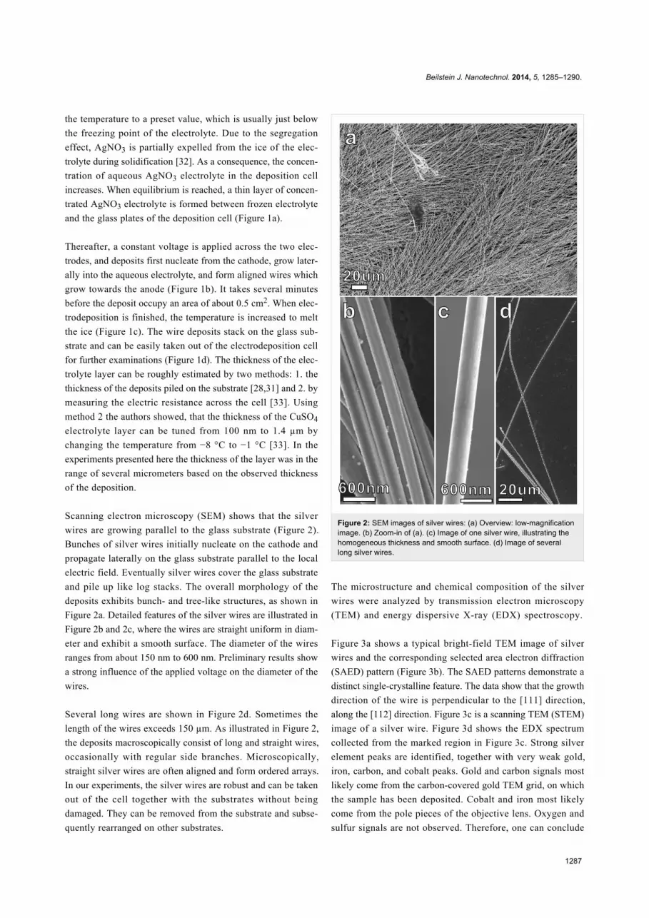
Scanning electron microscopy (SEM) shows that the silver
wires are growing parallel to the glass substrate (Figure 2).
Bunches of silver wires initially nucleate on the cathode and
propagate laterally on the glass substrate parallel to the local
electric field. Eventually silver wires cover the glass substrate
and pile up like log stacks. The overall morphology of the
deposits exhibits bunch- and tree-like structures, as shown in
Figure 2a. Detailed features of the silver wires are illustrated in
Figure 2b and 2c, where the wires are straight uniform in diam-
eter and exhibit a smooth surface. The diameter of the wires
ranges from about 150 nm to 600 nm. Preliminary results show
a strong influence of the applied voltage on the diameter of the
wires.
Several long wires are shown in Figure 2d. Sometimes the
length of the wires exceeds 150 µm. As illustrated in Figure 2,
the deposits macroscopically consist of long and straight wires,
occasionally with regular side branches. Microscopically,
straight silver wires are often aligned and form ordered arrays.
In our experiments, the silver wires are robust and can be taken
out of the cell together with the substrates without being
damaged. They can be removed from the substrate and subse-
quently rearranged on other substrates.
Figure 2: SEM images of silver wires: (a) Overview: low-magnificationimage. (b) Zoom-in of (a). (c) Image of one silver wire, illustrating thehomogeneous thickness and smooth surface. (d) Image of severallong silver wires.
The microstructure and chemical composition of the silver
wires were analyzed by transmission electron microscopy
(TEM) and energy dispersive X-ray (EDX) spectroscopy.
Figure 3a shows a typical bright-field TEM image of silver
wires and the corresponding selected area electron diffraction
(SAED) pattern (Figure 3b). The SAED patterns demonstrate a
distinct single-crystalline feature. The data show that the growth
direction of the wire is perpendicular to the [111] direction,
along the [112] direction. Figure 3c is a scanning TEM (STEM)
image of a silver wire. Figure 3d shows the EDX spectrum
collected from the marked region in Figure 3c. Strong silver
element peaks are identified, together with very weak gold,
iron, carbon, and cobalt peaks. Gold and carbon signals most
likely come from the carbon-covered gold TEM grid, on which
the sample has been deposited. Cobalt and iron most likely
come from the pole pieces of the objective lens. Oxygen and
sulfur signals are not observed. Therefore, one can conclude

Beilstein J. Nanotechnol. 2014, 5, 1285–1290.
1288
Figure 3: TEM analysis of thin silver wires and corresponding EDXinformation. (a) Bright-field image of typical silver wires with the axeswhich should be oriented in [112] direction and (b) the correspondingSAED patterns recorded from the marked region, the growth directionis mostly like [112]. The zone axis is <111>. (c) HAADF-STEM imageof a silver wire and (d) the corresponding EDX spectrum taken at thelabelled position on the wire of Figure 3c. Strong silver element peakscan be identified. Very weak gold, iron, carbon, and cobalt peaks werealso found. Gold and carbon come from the substrate. The cobalt andiron signal comes from the pole pieces of the objective lens; no peakcan be attributed to sulfur, nitrogen or oxygen, the latter demon-strating that the silver wires are not oxidized at ambient conditions inair.
that the silver wires grown in the experiments presented here
are chemically pure.
The application of silver wires as building blocks for microelec-
tronics requires good chemical stability, especially the stability
against oxidation under ambient conditions. For most metallic
microstructures, however, stability against oxidation is a chal-
lenge. The reason is that reducing the length scale means
increasing the surface/volume ratio and thus induces more insta-
bility in comparison with bulk systems. Therefore, the aging of
the silver wires was investigated by scanning Auger micro spec-
troscopy (SAMS).
Figure 4 shows the element depth profiles of silver wires, which
were exposed to ambient conditions for different times. The
profiles are determined by Auger measurements between
several short sputtering steps. The left diagram shows data
obtained from a freshly-prepared sample (exposed to ambient
air for less than one hour) and the right one the data of an aged
sample that had been exposed to ambient conditions for four
months. Comparing the two depth profiles, no significant differ-
ences can be identified. As illustrated in Figure 4, in a depth of
only 5 nm, the concentration of the oxide already virtually
approaches zero. The thickness of the oxide layers did not
change significantly during the aging process and the oxide
layer is not more than approx. 5 nm thick. Therefore, Figure 4
indicates that the silver wires are stable against oxidation under
ambient conditions. Silver typically corrodes under ambient
conditions by silver sulfidation with hydrogen sulfide (H2S)
and/or carbonyl sulfide (OCS) in the atmosphere, with this
phenomenon being amplified by water and oxygen [34]. The
origin of the stability of our structures is the subject of an
ongoing study.
Figure 4: Auger depth profile curves of freshly prepared and agedsilver wires. The full and dotted curves correspond to data obtainedfrom two different wires. The relative atomic concentration is plottedversus the sputter depth; (a) freshly-prepared sample taken out of theelectrodeposition cell and washed by deionized water and immedi-ately investigated by SAMS. (b) Sample aged by exposure to ambientconditions for four months. Freshly-prepared and aged samples showsimilar depth profiles, indicating that the single-crystalline silver wiresare stable under ambient conditions on this time scale.
It is interesting to consider the mechanism for electrochemical
self-organization of such long, smooth silver wires, bearing in
mind, that the growth rate of the wires is of the order of 10 μm/s
in our experiments and that the entropy of interfacial phase tran-
sition for silver is small. The faces tend to be roughened [34]
and the surfaces of the wires are rounded without obvious faces.
This may indicate that the surface is rough on atomic scale. It is
known, that the (112) surface energy is relatively high and that
the growth speed of [112] is faster than that of other facets [35].
Hence elongated silver wires are generated due to the
anisotropy in growth rate. However, anisotropy in growth rate
cannot guarantee for the formation of smooth silver wires with
homogeneous diameter as that shown in Figure 2b,c. The point
is that the side faces of the wires are rough on the atomic scale,
and should possess linear growth kinetics. Thus, any small
driving force should make the side faces to grow. If this would

Beilstein J. Nanotechnol. 2014, 5, 1285–1290.
1289
be the case, then we would observe conical silver wires instead
of iso-diameter ones. We suggest that the formation of uniform
silver wires in our system is due to the unique geometric restric-
tion of the deposition cell and the screening effect in Laplacian
field [36,37]. According to Chazalviel, the cation concentration
behind the growing front decreases dramatically in a two-
dimensional electrodeposition system [37]. Therefore, active
deposition takes place only on the growth front, and growth in
those parts behind the growth front is virtually stopped. In a
thick electrodeposition cell, this condition cannot be realized
easily because of convection and migration of the ions in the
electric field. Our thin film electrodeposition system is closer to
an ideal two-dimensional growth system, which helps to explain
the low diameters of the silver wires.
The growth mechanism of the silver wires can be explained in
the following model: Initial silver wires nucleate on the cathode
and grow towards the anode, presumably with [112] as the
preferred growth direction. Behind the growth front the wires
do not increase their diameter due to the depletion effect. These
two factors allow the wires, once they are initiated along the
direction of local concentration gradient, to develop into homo-
geneous, non-branching wires, as shown in Figure 2b,c.
However, if the axis of the wire deviates from the local concen-
tration gradient, e.g., if in the initial direction of the axis of the
wire is not perpendicular to the cathode (anode), sidebranches
will be triggered. Since the sides of the silver wires are rough,
there is no significant energy barrier to prevent the generation
of sidebranches. When this sidebranching mechanism works,
the sidebranches should develop on only one side of the wires,
that is, from the side facing the cation supply. Indeed such
comb-like structures were observed in our experiments, too. As
illustrated in Figure 5, side branching takes place only on one
side of the wire and forms a 60 degree angle with respect to the
main stem. Electron diffraction indicates that the side branches
maintain the same crystallographic direction.
These observations confirm our understanding of the silver wire
growth and support the nutrient-supply-flux induced side
branching mechanism in silver wire growth. This branching
mechanism is valid when the wire growth has very strong
anisotropy and the side faces of the wire are rough.
ConclusionWe have reported a novel technique for fabricating single-crys-
talline silver wires by electrochemical deposition, without intro-
ducing templates, additives and surfactants. The simple experi-
mental setup and the wide range of control parameters make
this approach a versatile and simple pathway to fabricate metal
meso- and nanostructures. This unique system provides a con-
venient way to investigate fundamental processes of self-orga-
Figure 5: TEM analysis of thin comb-like silver dendrites (dark areasin the image left) and corresponding SAED patterns. Patterns (1)–(5)(right) were recorded at different spots marked by the correspondingnumber in the TEM image (left). The zone axis is <111>. This suggeststhat the comb structure is single-crystalline. All SAED patterns displaythe same hexagonal pattern. This suggests that the comb structure issingle- crystalline. Each branch should grow along one of the <112>directions.
nization in electrochemical environments. Our results are
pointing the way to a controlled fabrication of highly-ordered,
single-crystalline metal nanowires, opening perspectives, e.g.,
for on-chip electrical connectors, sensors as well as photonic
and plasmonic devices.
ExperimentalElectrodeposition was carried out in a cell with two parallel
electrodes made of silver wires (99.99%). The electrolyte solu-
tion was prepared with AgNO3 (99.8%) and deionized water.
The concentration of the solution was 0.05 M.
Scanning electron microscopy (SEM) was performed with a
Gemini 2 system from Zeiss (LEO). The scanning Auger micro
spectroscopy (SAMS) investigations were done with a PHI 680
AUGER NANOPROBE UHV system with 15 nm resolution
and depth profile equipment. Transmission electron microscopy
(TEM) investigations were performed with a Philips Tecnai F20
ST system operated at 200 kV. EDX analyses were carried out
in STEM (scanning transmission electron microscopy) mode in
order to measure nanometer-scale samples (1 nm spot size for
the EDX measurements presented in this article). STEM micro-
graphs were acquired using an HAADF (High-Angle Annular
Dark-Field) detector.

Beilstein J. Nanotechnol. 2014, 5, 1285–1290.
1290
AcknowledgementsWe thank Prof. Cynthia Volkert for stimulating discussions.
This work was financially supported by the DFG-Center for
Functional Nanostructures (CFN) at the Karlsruhe Institute of
Technology and by the Baden-Wuerttemberg Foundation within
the Network of Excellence "Functional Nanostructures".
References1. Lieber, C. M. Sci. Am. 2001, 285, 58–64.
doi:10.1038/scientificamerican0901-582. Chen, J.; Wiley, B. J.; Xia, Y. Langmuir 2007, 23, 4120–4129.
doi:10.1021/la063193y3. Kuchibhatla, S. V. N. T.; Karakoti, A. S.; Bera, D.; Seal, S.
Prog. Mater. Sci. 2007, 52, 699–913.doi:10.1016/j.pmatsci.2006.08.001
4. Rycenga, M.; Cobley, C. M.; Zeng, J.; Li, W.; Moran, C. H.; Zhang, Q.;Qin, D.; Xia, Y. Chem. Rev. 2011, 111, 3669–3712.doi:10.1021/cr100275d
5. Hartland, G. V. Chem. Rev. 2011, 111, 3858–3887.doi:10.1021/cr1002547
6. Dawson, K.; Strutwolf, J.; Rodgers, K. P.; Herzog, G.;Arrigan, D. W. M.; Quinn, A. J.; O’Riordan, A. Anal. Chem. 2011, 83,5535–5540. doi:10.1021/ac2004086
7. Wild, B.; Cao, L.; Sun, Y.; Khanal, B. P.; Zubarev, E. R.; Gray, S. K.;Scherer, N. F.; Pelton, M. ACS Nano 2012, 6, 472–482.doi:10.1021/nn203802e
8. Mann, S. A.; Garnett, E. C. Nano Lett. 2013, 13, 3173–3178.doi:10.1021/nl401179h
9. Garnett, E. C.; Cai, W.; Cha, J. J.; Mahmood, F.; Connor, S. T.;Greyson Christoforo, M.; Cui, Y.; McGehee, M. D.; Brongersma, M. L.Nat. Mater. 2012, 11, 241–249. doi:10.1038/nmat3238
10. van de Groep, J.; Spinelli, P.; Polman, A. Nano Lett. 2012, 12,3138–3144. doi:10.1021/nl301045a
11. May, F.; Wegewijs, M. R.; Hofstetter, W. Beilstein J. Nanotechnol.2011, 2, 693–698. doi:10.3762/bjnano.2.75
12. Hong, W.; Valkenier, H.; Mészáros, G.; Manrique, D. Z.;Mishchenko, A.; Putz, A.; García, P. M.; Lambert, C. J.;Hummelen, J. C.; Wandlowski, T. Beilstein J. Nanotechnol. 2011, 2,699–713. doi:10.3762/bjnano.2.76
13. Perrin, M. L.; Martin, C. A.; Prins, F.; Shaikh, A. J.; Eelkema, R.;van Esch, J. H.; van Ruitenbeek, J. M.; van der Zant, H. S. J.; Dulić, D.Beilstein J. Nanotechnol. 2011, 2, 714–719. doi:10.3762/bjnano.2.77
14. Todorov, T. N.; Dundas, D.; Paxton, A. T.; Horsfield, A. P.Beilstein J. Nanotechnol. 2011, 2, 727–733. doi:10.3762/bjnano.2.79
15. Obermair, C.; Kuhn, H.; Schimmel, T. Beilstein J. Nanotechnol. 2011,2, 740–745. doi:10.3762/bjnano.2.81
16. Strange, M.; Thygesen, K. S. Beilstein J. Nanotechnol. 2011, 2,746–754. doi:10.3762/bjnano.2.82
17. Nakashima, S.; Takahashi, Y.; Kiguchi, M. Beilstein J. Nanotechnol.2011, 2, 755–759. doi:10.3762/bjnano.2.83
18. Lü, J.-T.; Gunst, T.; Hedegård, P.; Brandbyge, M.Beilstein J. Nanotechnol. 2011, 2, 814–823. doi:10.3762/bjnano.2.90
19. Solomon, G. C.; Bergfield, J. P.; Stafford, C. A.; Ratner, M. A.Beilstein J. Nanotechnol. 2011, 2, 862–871. doi:10.3762/bjnano.2.95
20. Gaynor, W.; Burkhard, G. F.; McGehee, M. D.; Peumans, P.Adv. Mater. 2011, 23, 2905–2910. doi:10.1002/adma.201100566
21. El-Sayed, M. A. Acc. Chem. Res. 2001, 34, 257–264.doi:10.1021/ar960016n
22. Barnes, W. L.; Dereux, A.; Ebbesen, T. W. Nature 2003, 424, 824–830.doi:10.1038/nature01937
23. Wang, W.; Yang, Q.; Fan, F.; Xu, H.; Wang, Z. L. Nano Lett. 2011, 11,1603–1608. doi:10.1021/nl104514m
24. Nishizawa, M.; Menon, V. P.; Martin, C. R. Science 1995, 268,700–702. doi:10.1126/science.268.5211.700
25. Obermair, C.; Wagner, A.; Schimmel, T. Beilstein J. Nanotechnol.2011, 2, 659–664. doi:10.3762/bjnano.2.70
26. Obermair, C.; Kress, M.; Wagner, A.; Schimmel, T.Beilstein J. Nanotechnol. 2012, 3, 824–830. doi:10.3762/bjnano.3.92
27. Wang, Z. L. Characterization of nanophase materials; Wiley-VCH:Weinheim, New York, 2000.
28. Wang, M.; Zhong, S.; Yin, X.-B.; Zhu, J.-M.; Peng, R.-W.; Wang, Y.;Zhang, K.-Q.; Ming, N.-B. Phys. Rev. Lett. 2001, 86, 3827.doi:10.1103/PhysRevLett.86.3827
29. Zhong, S.; Koch, T.; Wang, M.; Scherer, T.; Walheim, S.; Hahn, H.;Schimmel, T. Small 2009, 5, 2265–2270. doi:10.1002/smll.200900746
30. Zhong, S.; Wang, D.; Koch, T.; Wang, M.; Walheim, S.; Schimmel, T.Cryst. Growth Des. 2010, 10, 1455–1459. doi:10.1021/cg9012747
31. Zhong, S.; Wang, Y.; Wang, M.; Zhang, M.-Z.; Yin, X.-B.; Peng, R.-W.;Ming, N.-B. Phys. Rev. E 2003, 67, 061601.doi:10.1103/PhysRevE.67.061601
32. Bruinsma, O. S. L.; van der Eerden, J. P. Science and technology ofcrystal growth; Kluwer: Dordrecht, 1995.
33. Weng, Y.-Y.; Si, J.-W.; Gao, W.-T.; Wu, Z.; Wang, M.; Peng, R.-W.;Ming, N.-B. Phys. Rev. E 2006, 73, 051601.doi:10.1103/PhysRevE.73.051601
34. Elechiguerra, J. L.; Larios-Lopez, L.; Liu, C.; Garcia-Gutierrez, D.;Camacho-Bragado, A.; Yacaman, M. J. Chem. Mater. 2005, 17,6042–6052. doi:10.1021/cm051532n
35. Galanakis, I.; Bihlmayer, G.; Bellini, V.; Papanikolaou, N.; Zeller, R.;Blügel, S.; Dederichs, P. H. EPL 2002, 58, 751–757.doi:10.1209/epl/i2002-00413-7
36. Marsili, M. J. Phys. A: Math. Gen. 1992, 25, 3493.doi:10.1088/0305-4470/25/12/011
37. Chazalviel, J.-N. Phys. Rev. A 1990, 42, 7355.doi:10.1103/PhysRevA.42.7355
License and TermsThis is an Open Access article under the terms of the
Creative Commons Attribution License
(http://creativecommons.org/licenses/by/2.0), which
permits unrestricted use, distribution, and reproduction in
any medium, provided the original work is properly cited.
The license is subject to the Beilstein Journal of
Nanotechnology terms and conditions:
(http://www.beilstein-journals.org/bjnano)
The definitive version of this article is the electronic one
which can be found at:
doi:10.3762/bjnano.5.142