P9241-G Tx Reference Design Layout Guide - Renesas
19
P9241-G Tx Reference Design Layout Guide © 2019 Integrated Device Technology, Inc. 1 February 15, 2019 Contents 1. Introduction ...................................................................................................................................................................................................2 2. P9241-G Layout Quick Checklist ..................................................................................................................................................................2 3. Power Circuits ..............................................................................................................................................................................................3 4. Bridge Routing ..............................................................................................................................................................................................5 5. Bootstrap Capacitors ....................................................................................................................................................................................7 6. VCC5V BUCK and LDO Routing ..................................................................................................................................................................8 7. VBRIDGE Step-Down Converter ..................................................................................................................................................................9 8. PCB GND Planes .......................................................................................................................................................................................10 9. Sensitive Circuits ........................................................................................................................................................................................11 10. Current Sense Amplifier Placement and Routing .......................................................................................................................................12 11. Demodulation Filter Components Placement and Routing .........................................................................................................................13 12. Flash IC Placement and Routing ................................................................................................................................................................15 13. External Crystal ..........................................................................................................................................................................................15 14. Non-Sensitive Circuits ................................................................................................................................................................................16 15. Thermal Management ................................................................................................................................................................................16 16. PCB Footprint Design .................................................................................................................................................................................16 17. Revision History..........................................................................................................................................................................................18 List of Figures Figure 1. Power Blocks .......................................................................................................................................................................................3 Figure 2. Bridge Power Stage Schematic Snippet ..............................................................................................................................................4 Figure 3. Half-Bridge FET Bypass Capacitor Placement and Routing Recommendation (Top Layer Only) ......................................................5 Figure 4. Half-Bridge FET Bypass Capacitor Placement and Routing Recommendation (Top Layer Only), Color Coded by Node Name .......6 Figure 5. BRG Components Placed Next to the P9241-G (DRV_VIN, VBRG_IN, BST_BRG1/2 Capacitors), GH/GL Series Resistor Placement, and Routing (Top Layer Only) ..........................................................................................................................................7 Figure 6. Schematic and Trace Snippet of Layout and Placement Recommendation for VCC5V Buck, LDO33, LDO18, and PREG CAP Components ........................................................................................................................................................................................8 Figure 7. Internal and Bottom Layout Recommendation for VCC5V Buck, LDO33, LDO18, and PREG CAP Components ..............................8 Figure 8. VBRG Buck Regulator Schematic Snippet ..........................................................................................................................................9 Figure 9. VBRG Buck Regulator Schematic Snippet ..........................................................................................................................................9 Figure 10. GND Noise Areas and Primary Power Transfer Current Paths .........................................................................................................10 Figure 11. Inner Layers and GND Planes (MID1, MID2, and Bottom Layer) With Key Guidance Points Highlighted ........................................11 Figure 12. BRG Current Sense Resistor – Kelvin Sense Connections (Top Layer) ...........................................................................................12 Figure 13. Voltage and Current Demodulation Filter Schematic.........................................................................................................................13 Figure 14. Voltage Demodulation Diodes to Demodulation Filter Layout ...........................................................................................................14 Figure 15. Flash IC Placement and Layout ........................................................................................................................................................15 Figure 16. External Crystal Placement ...............................................................................................................................................................15 Figure 17. PCB Footprint Design Guidance (All Dimensions in mm)..................................................................................................................17
-
Upload
khangminh22 -
Category
Documents
-
view
0 -
download
0
Transcript of P9241-G Tx Reference Design Layout Guide - Renesas

P9241-G Tx Reference Design Layout Guide
© 2019 Integrated Device Technology, Inc. 1 February 15, 2019
Contents
1. Introduction ...................................................................................................................................................................................................2
2. P9241-G Layout Quick Checklist ..................................................................................................................................................................2
3. Power Circuits ..............................................................................................................................................................................................3
4. Bridge Routing ..............................................................................................................................................................................................5
5. Bootstrap Capacitors ....................................................................................................................................................................................7
6. VCC5V BUCK and LDO Routing ..................................................................................................................................................................8
7. VBRIDGE Step-Down Converter ..................................................................................................................................................................9
8. PCB GND Planes .......................................................................................................................................................................................10
9. Sensitive Circuits ........................................................................................................................................................................................11
10. Current Sense Amplifier Placement and Routing .......................................................................................................................................12
11. Demodulation Filter Components Placement and Routing .........................................................................................................................13
12. Flash IC Placement and Routing ................................................................................................................................................................15
13. External Crystal ..........................................................................................................................................................................................15
14. Non-Sensitive Circuits ................................................................................................................................................................................16
15. Thermal Management ................................................................................................................................................................................16
16. PCB Footprint Design .................................................................................................................................................................................16
17. Revision History ..........................................................................................................................................................................................18
List of Figures
Figure 1. Power Blocks .......................................................................................................................................................................................3
Figure 2. Bridge Power Stage Schematic Snippet ..............................................................................................................................................4
Figure 3. Half-Bridge FET Bypass Capacitor Placement and Routing Recommendation (Top Layer Only) ......................................................5
Figure 4. Half-Bridge FET Bypass Capacitor Placement and Routing Recommendation (Top Layer Only), Color Coded by Node Name .......6
Figure 5. BRG Components Placed Next to the P9241-G (DRV_VIN, VBRG_IN, BST_BRG1/2 Capacitors), GH/GL Series Resistor Placement, and Routing (Top Layer Only) ..........................................................................................................................................7
Figure 6. Schematic and Trace Snippet of Layout and Placement Recommendation for VCC5V Buck, LDO33, LDO18, and PREG CAP Components ........................................................................................................................................................................................8
Figure 7. Internal and Bottom Layout Recommendation for VCC5V Buck, LDO33, LDO18, and PREG CAP Components ..............................8
Figure 8. VBRG Buck Regulator Schematic Snippet ..........................................................................................................................................9
Figure 9. VBRG Buck Regulator Schematic Snippet ..........................................................................................................................................9
Figure 10. GND Noise Areas and Primary Power Transfer Current Paths .........................................................................................................10
Figure 11. Inner Layers and GND Planes (MID1, MID2, and Bottom Layer) With Key Guidance Points Highlighted ........................................11
Figure 12. BRG Current Sense Resistor – Kelvin Sense Connections (Top Layer) ...........................................................................................12
Figure 13. Voltage and Current Demodulation Filter Schematic .........................................................................................................................13
Figure 14. Voltage Demodulation Diodes to Demodulation Filter Layout ...........................................................................................................14
Figure 15. Flash IC Placement and Layout ........................................................................................................................................................15
Figure 16. External Crystal Placement ...............................................................................................................................................................15
Figure 17. PCB Footprint Design Guidance (All Dimensions in mm) ..................................................................................................................17

P9241-G Tx Reference Design Layout Guide
© 2019 Integrated Device Technology, Inc. 2 February 15, 2019
1. Introduction
The P9241-G wireless power transmitter is an Integrated Circuit (IC) consisting of four N-Channel MOSFET gate drivers, an integrated Buck switching regulator, multiple Low Drop Out linear regulators (LDOs), wireless in-band communication demodulator, an ARM CortexTM µProcessor, and General Purpose Inputs/Outputs (GPIOs). These devices use advanced signal processing allowing it to be fully compliant with the Wireless Power Consortium Qi (WPC) Baseline Power Profile (BPP), iOS 7.5W wireless charging for iPhone device, and 10W wireless charging for Android proprietary modes. Considering the integration of power, analog, and digital circuit blocks, the device can achieve optimal operation by following the placement and layout guidance outlined in this document. During placement and routing, there are multiple considerations and tradeoffs associated with managing the critical current paths while implementing the circuit onto a PCB.
To optimize the design, place components based on its circuit function to guarantee best performance when the schematic is implemented into a functional PCB layout. By following the instructions and guidelines in this document, efficient operation can be optimized for each circuit function simultaneously while using minimal amount of PCB area required for safe operation and power transfer. Furthermore, the thermal management of the application is an important aspect of the product’s performance and must be optimized while designing the PCB and routing the connections needed for device operation.
This layout guide is intended to inform the PCB designer to place components in order of functionality and performance priority as well as critical routing connections related to its operation. There are three main categories of circuitry: Power Circuits, Noise Sensitive Circuits, and Non-Sensitive Circuits. The P9241-G PCB is recommended to be routed using at least four copper layers.
2. P9241-G Layout Quick Checklist
Full Bridge FETs are placed near resonance components with bypass capacitors from HS FET drain to LS FET source of eachHalf-Bridge loop area and layer transitions minimized.
Wide routing for power paths (VIN, VBRIDGE, SW_BRG1, SW_BRG2, LC Node, and GND) (50mils, or wider depending on trace length).
The ratio of width to length should be ≥ 1 width unit 8 unit lengths with 1:1 being ideal.
Bridge GND: FET source GND connections are directly connected to local bridge FET bypass capacitors, EMI filters, ZVS caps withconnection to the thermal heat sinking plane at the current sense resistor followed by direct connection on the PGND plane to BUCK.
External Voltage Regulator CIN capacitors are placed first. Use wide VIN, LX, VBRIDGE, and GND routing (75mils, or wider dependingon length).
PREG cap GND must not be shared with the VIN pin bypass cap GND. Place next to IC, routed on component side straddling pins 3and 2.
VIN input bypass capacitors are placed next to the IC, routed on component side straddling pins 4 and 6.
LDO bypass capacitors require direct GND connections to the EPAD using inner or bottom layer.
Use current sense resistor with “kelvin” connections low side current sense amplifier inputs (via appropriate resistors).
Demodulation (Envelope Detect) filter components must be located close to the P9241-G device.
FLASH IC is placed close to the P9241-G, and is an approved part.
The critical components are specified with minimum parameters to comply with the Reference BOM.

P9241-G Tx Reference Design Layout Guide
© 2019 Integrated Device Technology, Inc. 3 February 15, 2019
3. Power Circuits
The main power circuits of the P9241-G wireless power transmitting solution are the step-down converter for VBRIDGE, Bridge Drivers, the external power FETs, resonance tank(s), coil select FETs, and the integrated BUCK Regulator. Secondary power circuits are the LDOs (LDO33, LDO18, PREG), and VDDIO.
Figure 1. Power Blocks

P9241-G Tx Reference Design Layout Guide
© 2019 Integrated Device Technology, Inc. 4 February 15, 2019
First, based on the physical requirements of the system under design, the initial shape of the application PCB must be determined as well as the connection points for the input power supply and transmitter coils. Second, the resonance capacitors and power transfer FETs are placed in close proximity to the coils and near the center of the PCB as possible for heat sinking purposes. Third, with the coils and input power locations determined, the step-down converter power stage relative placement is made and finally, placement of the P9241-G. Orientation of the P9241-G is determined based on the ability to route connections from the Bridge driver pins to the Bridge FETs in a symmetric manner such that the trace lengths from Driver 1 and Driver 2 are similar. Referring to the schematic snippet in Figure 2 from the P9241-G Tx Reference Design Evaluation Kit User Manual, the placement of the components is in the following order of priority:
1. FETs (Q5, Q6, Q7, Q8), VBRIDGE Input capacitors (C31, C32, C33, C55, C56, C57)
2. Bootstrap Capacitors (C38, C46)
3. Zero-Voltage Switching (ZVS) Capacitors and respective resistors (C39, R39, C59, R49)
4. Low-Pass filter components (C30, C34)
5. DRV_VIN bypass capacitors (C34, C35), Signal Resistors (R35, R40, R44, R47).
Figure 2. Bridge Power Stage Schematic Snippet

P9241-G Tx Reference Design Layout Guide
© 2019 Integrated Device Technology, Inc. 5 February 15, 2019
4. Bridge Routing
Focus the key components and layout placement on proper placement and routing of the step-down converter (VBRIDGE, U1) and the ability to route with wide copper traces the connections from the Voltage Regulator output node (V_BRIDGE) to Q5, Q7 (High-side and Low-side Drains) to the current sense resistor and back to the step-down converter. The next priority is for routing the SW_BRG1/SW_BRG2 nodes to the Low-Pass filter, to the resonance tank(s), and coil select circuitry as needed to the current sense resistor (see PCB GND Planes section). Use multiple vias (at least 6 vias with 0.3mm diameter hole size, or larger) for any layer transitions on these nodes to decrease impedance on these paths. These widths will increase heat transfer as well as current carrying capacity while minimizing voltage drops due to conduction. Next, place the V_BRIDGE input capacitors so that they are centered and have minimum trace lengths from each respective capacitor plate to the connecting FET pins.
In the Figure 3, C31, C32, and C33 are placed in close proximity to Q5; while C55, C56, and C57 are placed right next to Q7. The loop area (VBRIDGE_to_drain through decoupling capacitor to BRIDGE_GND_to_source) is minimized on each half-bridge. As an alternative design choice to the P9241-G, the resonant capacitors (C44, C47, C48, and C49) can be replaced with a film capacitor (C52), which is a through-hole component. Both planes beneath the film capacitor should be expanded to allow its placement as shown in Figure 3. Do not place components beneath the film capacitor.
Figure 3. Half-Bridge FET Bypass Capacitor Placement and Routing Recommendation (Top Layer Only)

P9241-G Tx Reference Design Layout Guide
© 2019 Integrated Device Technology, Inc. 6 February 15, 2019
Figure 4 provides color coding and node names to help provide reference for each node to help highlight proper placement and routing.
Figure 4. Half-Bridge FET Bypass Capacitor Placement and Routing Recommendation (Top Layer
Only), Color Coded by Node Name

P9241-G Tx Reference Design Layout Guide
© 2019 Integrated Device Technology, Inc. 7 February 15, 2019
5. Bootstrap Capacitors
Place Bootstrap Capacitors (C38, C46) such that they are near the P9241-G and placed between BST_BRG1 to SW_BRG1 and BST_BRG2 to SW_BRG2, respectively. To optimize performance and continuing to proceed through placement and layout of the PCB, the next step is completing the routing of the BRG switching node (SW_BRG1/2) to the LC tank. The critical components for this portion of the layout is to maximize the copper surface area used for routing to decrease conduction losses (AC losses from skin effect and DC losses from copper foil sheet resistance); therefore, use of copper planes is highly recommended. Figure 4 highlights the recommended routing guidelines by PCB layer.
Another important aspect of the P9241-G solution involves the Zero-Voltage Switching (ZVS) Capacitors and its respective components (C39, R39, C59, and R49). These are used to control the rate of change of the BRIDGE switching nodes (SW_BRG1 and SW_BRG2) during the dead-time (time when both FETs are off and the software state is being changed, such as high-to-low or low-to-high). The dead-time is imperative to prevent shoot-through currents and the ZVS capacitors keep the voltage on those nodes from hard-switching or changing too quickly, which helps reduces EMI to radiate above the CISPR22’s permissible limits. These components should be located next to the corresponding BRIDGE FETs, and have a solid connection to the low-side FET source of each switching node (see ZVS1/2 (colored-coded purple) in Figure 4 found next to BRG FETS Q5 and Q8). The final BRG components that must be placed and routed are all located next to the P9241-G device. These components are: the VBRG_IN bypass capacitors (C30), the Gate driver High and Low (GH_BRG1/2, GL_BRG1/2) series signal resistors (R35, R40, R44, and R47), and the Bootstrap high-side gate driver capacitors (C38 and C46). All of these components should be placed near the P9241-G respective pins as shown in Figure 5.
Figure 5. BRG Components Placed Next to the P9241-G (DRV_VIN, VBRG_IN, BST_BRG1/2 Capacitors),
GH/GL Series Resistor Placement, and Routing (Top Layer Only)
The gate drive signals can be routed with 5-8 mils trace width and should avoid being run in parallel with power switching connections (SW_BRG1/2 and BST_BRG1/2), or should have GND plane isolation from those signals to eliminate any coupling or noise issues.

P9241-G Tx Reference Design Layout Guide
© 2019 Integrated Device Technology, Inc. 8 February 15, 2019
6. VCC5V BUCK and LDO Routing
The internal VCC5V BUCK and LDO components routing are recommended to follow the guidance in placement and routing in Figure 6. Although the current flow can be small, solid wide connections are necessary for the connections. Any heat developed within the IC or on the PCB will be rapidly dissipated.
Figure 6. Schematic and Trace Snippet of Layout and Placement Recommendation for VCC5V Buck,
LDO33, LDO18, and PREG CAP Components
The components listed in Figure 6 are used by the P9241-G for controlling internal bias, digital logic, the micro-processor, and power transfer. Place and route these components as shown in Figure 6. Route the VIN capacitors (C42) and VCC5V output capacitors (C45) GND connections directly to the GND pin. The LDO18 and LDO33 bypass capacitors must have a direct connection from the GND plates of these capacitors to the EPAD. The EPAD is the GND return for the LDOs and the internal micro-processor. Route the SW_S trace as short as possible to the inductor L4 on the next available internal layer adjacent to the P9241-G. This trace can be extended to make room for the more critical VIN capacitors to be placed closer to the respective P9241-G pins. The connections to PREG CAP (C43) should be short and not to be shared with the GND return used for the VIN and VCC5V capacitors. The connections to the PREG CAP (C43) can be fully routed on the P9241-G side of the PCB and should have a good connection to GND (pin 2) pin.
Figure 7. Internal and Bottom Layout Recommendation for VCC5V Buck, LDO33, LDO18, and PREG
CAP Components
ENB1
C43 1uF
C50
1uF
LDO18
C53
1uF
LD
O33
VIN
LDO33
C42
10uF
VCC_5V
LDO33
VCC5V1
P9242-GU3
EN1
GND2
PREG3
VIN4
SW_S5
GND16
LDO337
VIN_LDO8
LDO189
LED110
LED211
VDDIO12
GPIO_B025
GPIO_B126
GPIO_B227
GPIO_B328
GPIO_B429
GH_BRG230
BST_BRG231
SW_BRG232
GL_BRG233
GND234
GL_BRG135
SW_BRG136
EP
49
BS
T_ B
RG
137
GH
_B
RG
138
DR
V_V
IN39
VB
RG
_IN
40
GN
D3
41
RS
V42
QD
EC
43
VD
EM
144
IDE
MI
45
ISN
S_O
UT
46
CS
N47
CS
P48
GP
IO_B
513
GP
IO_B
614
GP
IO_A
015
GP
IO_A
116
GP
IO_A
217
GP
IO_A
318
GP
IO_A
419
GP
IO_A
520
GP
IO_A
621
GP
IO_A
722
GP
IO_B
723
GP
IO_B
824
VCC_5V
LDO18
R41 1K
C45
10uF
L4 4.7uH

P9241-G Tx Reference Design Layout Guide
© 2019 Integrated Device Technology, Inc. 9 February 15, 2019
7. VBRIDGE Step-Down Converter
The VBRG regulator (U1) is the primary power control for wireless power and the voltage level is dynamically controlled by the P9241-G using the GPIO_B7 (pin 23) connection to the feedback node using a low-pass filtered adjustable Pulse Width Modulated (PWM) square wave signal. After connecting to a receiver (Rx), the P9241-G adjusts the transmitted power level by changing VBRIDGE according to the Control Error Packets (CEPs) received by the Rx. The typical step-down converter used as the VBRIDGE control with the P9241-G is the MP2229 as shown in Figure 8.
Figure 8. VBRG Buck Regulator Schematic Snippet
Typically with step-down converter designs, the most important capacitors are the input bypass capacitors (C4 and C5) due to the high (di/dt) change in current pulses. These bypass components must be placed close to MP2229 (U1) to help filter and dampen unwanted AC noise entering into VBRIDGE, which provides the power line for the Switching Nodes. The GND plane is shared in the center for input bypass capacitors and output capacitors. Under the IC layers, L1 and L2 are both kept primarily as solid GND planes to maximize heat dissipation and current condition at minimal impedance, and multiple GND vias are placed next to the MP2229 GND pins. L1 (common mode choke) and L2 (bead) components improve EMI performance.
Figure 9. VBRG Buck Regulator Schematic Snippet

P9241-G Tx Reference Design Layout Guide
© 2019 Integrated Device Technology, Inc. 10 February 15, 2019
8. PCB GND Planes
It is important to properly allow current flow to and from each circuit component of the solution. The primary conduction path is from the main power connector positive terminal, to the VBRIDGE voltage regulator, to the resonance tank and back through GND planes, to each successive current source (GND is referred to as the return current path) when completing each current loop.
It is highly recommended to allocate one complete layer of every PCB design to be a solid GND plane so current flow return to its source is unobstructed from mechanical blocks, such as cut planes in the form of routed traces or slots in the physical PCB. There are two primary GND return loops that exist in the P9241-G:
Tx: VBRG regulator and the WPC resonance tank
Flash IC to P9241-G GND, and other sub-circuits in the Quiet GND area
Figure 10. GND Noise Areas and Primary Power Transfer Current Paths

P9241-G Tx Reference Design Layout Guide
© 2019 Integrated Device Technology, Inc. 11 February 15, 2019
Figure 11. Inner Layers and GND Planes (MID1, MID2, and Bottom Layer) With Key Guidance Points
Highlighted
Some key points regarding the full-board screen captures shown above include:
Use of small internal planes for heat dissipation for connections to the BRG FETs and power inductors (it is recommended to use multiple vias to improve thermal connection and to lower impedance)
Verify that the primary source and return currents have solid copper planes for conduction
Add GND planes on every layer after routing and placement to improve thermal performance of the entire PCB
9. Sensitive Circuits
The sensitive circuits refer to noise sensitive circuits that are placed in an area of the PCB that is not expected to have circulating current flow (VBRG Voltage Regulator, WPC resonance tank noise) and are preferred to be placed away from the primary current paths (Source and Return) in the “Quiet” GND area Figure 10. The following functional circuit blocks should be placed near the P9241-G or in the quiet GND area as possible or have special routing requirements:
Current Sense with kelvin sense connections (4-wire) voltage sensing at current sense resistor (R26)
Used for BRG current sensing for Power loss FOD, OCP, and Demodulation based on coil current variation
Demodulation filter components
VCOIL peak voltage sensing circuitry
Optional: Used for Q measurement, Tx coil OVP, maximum power limiting
Flash IC (must be placed next to P9241-G)
SMD Crystal (Y1)
Inner Layer (L1): Solid GND Plane Inner Layer (L2): - BRG FET PGND vias - P9241-G EPAD thermal vias - GND plane poured after routing
Bottom Layer: - BRG FET thermal plane - P9241-G EPAD thermal vias - GND plane poured after routing

P9241-G Tx Reference Design Layout Guide
© 2019 Integrated Device Technology, Inc. 12 February 15, 2019
10. Current Sense Amplifier Placement and Routing
Place Current Sense Resistor (R26) in close proximity to the BK_VO to VBRIDGE planes. Proceed with the “kelvin” connections by following in equal and parallel distance in its route to CSP (pin 48) and CSN (pin 47). Keep the trace length to minimal to ensure optimal sense points and performance to the amplifier inputs (see Figure 12).
Figure 12. BRG Current Sense Resistor – Kelvin Sense Connections (Top Layer)

P9241-G Tx Reference Design Layout Guide
© 2019 Integrated Device Technology, Inc. 13 February 15, 2019
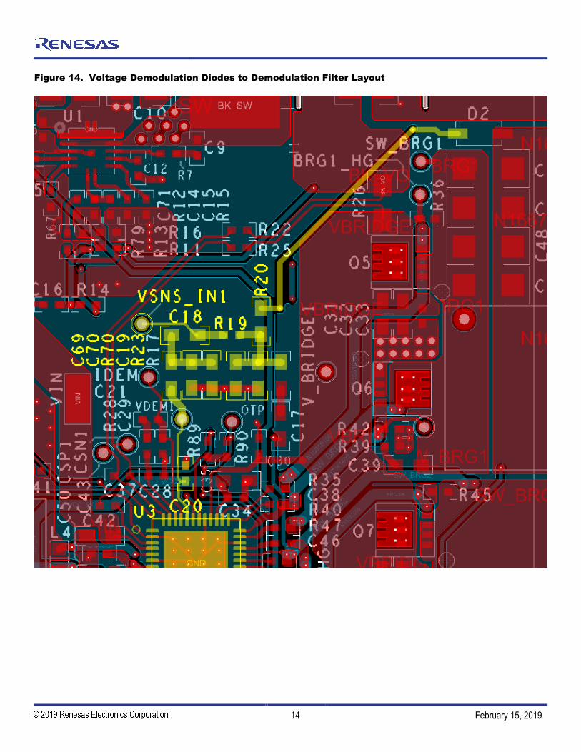
11. Demodulation Filter Components Placement and Routing
When routing the voltage demodulation filter components, it is recommended to place the diode peak detectors (D2) near the LC nodes and route the “DC” peak voltage signals (cathodes from diodes D2) to the remaining DEMOD filter components, which should be placed close to the P9241-G. The following schematic shows the demodulation voltage filter components.
Figure 13. Voltage and Current Demodulation Filter Schematic
Components C20, C69, C70, and R70 should be located near the associated P9241-G pins and be in the “Quiet” GND area.
P9241-G Tx Reference Design Layout Guide
© 2019 Integrated Device Technology, Inc. 14 February 15, 2019
Figure 14. Voltage Demodulation Diodes to Demodulation Filter Layout

P9241-G Tx Reference Design Layout Guide
© 2019 Integrated Device Technology, Inc. 15 February 15, 2019
12. Flash IC Placement and Routing
Due the high data speed of the Flash IC (U7), this component is recommended to be placed next to the P9241-G. Be sure the FLASH IC GND pins to P9241-G EPAD connections are directly connected to each other.
Figure 15. Flash IC Placement and Layout
13. External Crystal
Trace connecting the crystal of the IC (Y1) should be as short and wide as possible to help reduce parasitic inductance. This component is recommended to be placed next to P9241-G and in the “quiet area” as shown in Figure 10.
Figure 16. External Crystal Placement
U7
W25X40CLUXIG
CS#1
DO2
WP#3
GND4
DI5CLK6HLD#7VCC8
EP
AD
9
GPIO_B2GPIO_B1
R57100K
C66
0.1uF
OPTIONAL: FOR DEVELOPMENT ONLY
GPIO_B0
GPIO_B3
LDO33

P9241-G Tx Reference Design Layout Guide
© 2019 Integrated Device Technology, Inc. 16 February 15, 2019
14. Non-Sensitive Circuits
The remaining components and pins that have not been mentioned are regarded as non-sensitive circuits and the placement and routing of these nodes is not considered critical to performance but can be required for functionality. All remaining connections and components do not have placement demands (can be placed anywhere) and they simply need to be connected. In most cases 0.127mm (5mils) wide traces and any method of connectivity will suffice if the circuit is completed according to the schematic.
15. Thermal Management
The thermal management of the P9241-G is of critical importance for successful deployment of the product to reduce heat generation of the total design and to prevent localized heating of any components. To optimize the design, thermally and electrically wide continuous copper planes are highly recommended on every power node. Furthermore, filling all layers of the PCB with copper planes for current conduction and heat dissipation will dramatically improve the thermal performance. Use of multiple vias and EPADs is an effective way to spread localized heating through the PCB. An optimally designed PCB will have even temperature across the board surface. To promote higher heat dissipation, it is recommended to use low DCR, RDSon, and NP0/C0G type capacitors for all components listed in the “Power Circuits” section of this document (following the P9241-G reference components is highly recommended).
For the P9241-G PCB footprint design, an array of GND vias is recommended in the EPAD 4x6 or 6x6 arrays are preferred with 0.3mm (12mil) diameter hole sizes and connections to all PCB layers. It is not recommended to use less than four layers when designing the PCB. Conduct thermal inspection of each design and add additional heat spreading copper planes to spread heat away from higher temperature components to reduce localized heating or prevent components from overheating when used without air conditioning on hot summer days. When designed properly, the PCB solution can operate in up to 105°C ambient air without violating the thermal limits of any components called out in the reference design.
16. PCB Footprint Design
The PCB footprint can have a substantial impact on reliability and production yield. To avoid placement and soldering issues during assembly and product deployment, it is recommended to allow sufficient copper landing pads to be exposed, implement solder mask (2.5 to 3 mils applied between every pin with 1 to 2 mils clearance beyond the exposed copper), and match the pastemask openings to the exposed copper of each pin. To apply a proper amount of solder paste to the IC, fine pitch application lead-free no clean or water soluble solder pastes are recommended and use of stencil thicknesses of approximately 4mils. Furthermore, PCB cleaning is highly recommended after the reflow process is completed.
Reference the P9241-G datasheet during footprint design; Figure 17 can be used for details pertaining to landing pad and solder masking recommendations. The exposed pin (etch) used to solder the IC to the PCB must be at least as large as the physical pin of the package. It is highly recommended to add some additional length extending away from the IC from each pin (~5mils) to promote proper soldering. It is imperative to include soldermask around each pin to eliminate potential solder shorts during assembly and reflow. It is also not suggested to pour continuous copper planes under the pin area, use a short (up to 0.127mm or 5mils) trace matching the pin width to connect pins to the planes beyond the perimeter of the package. The EPAD must contain solderpaste openings for proper electrical and mechanical connection to the PCB and they should be four separated squares approximately 1.5 × 1.5 mm per side with 2.26mm pitch centered within the EPAD.

P9241-G Tx Reference Design Layout Guide
© 2019 Integrated Device Technology, Inc. 17 February 15, 2019
Figure 17. PCB Footprint Design Guidance (All Dimensions in mm)

P9241-G Tx Reference Design Layout Guide
© 2019 Integrated Device Technology, Inc. 18 February 15, 2019
17. Revision History
Revision Date Description of Change
February 15, 2019 Initial release.
Corporate Headquarters
6024 Silver Creek Valley Road San Jose, CA 95138 www.IDT.com
Sales
1-800-345-7015 or 408-284-8200Fax: 408-284-2775www.IDT.com/go/sales
Tech Support
www.IDT.com/go/support
DISCLAIMER Integrated Device Technology, Inc. (IDT) and its affiliated companies (herein referred to as “IDT”) reserve the ri ght to modify the products and/or specifications described herein at any time, without notice, at IDT's sole discretion. Performance specifications and operating parameters of the described products are d etermined in an independent state and are not guaranteed to perform the same way when installed in customer products. The information contained herein is provided without representation or warranty of a ny kind, whether express or implied, including, but not limited to, the suitability of IDT's products for any particular purpose, an implied warranty of merchantability, or non-infringement of the intellectual property rights of others. This document is presented only as a guide and does not convey any license under intellectual property rights of IDT or any thi rd parties.
IDT's products are not intended for use in applications involving extreme environmental conditions or in life support systems or similar devices where the failure or malfunction of an IDT product can be reasonably expected to significantly affect the health or safety of users. Anyone using an IDT product in such a manner does so at their own risk, absent an express, written agreement by IDT.
Integrated Device Technology, IDT and the IDT logo are trademarks or registered trademarks of IDT and i ts subsidiaries in the United States and other countries. Other trademarks used herein are the property of IDT or their respective third party owners. For datasheet type definitions and a glossary of common terms, visit www.idt.com/go/glossary. All contents of this document are copyright of Integrated Device Technology, Inc. All rights reserved.

Corporate HeadquartersTOYOSU FORESIA, 3-2-24 Toyosu,Koto-ku, Tokyo 135-0061, Japanwww.renesas.com
Contact InformationFor further information on a product, technology, the most up-to-date version of a document, or your nearest sales office, please visit:www.renesas.com/contact/
TrademarksRenesas and the Renesas logo are trademarks of Renesas Electronics Corporation. All trademarks and registered trademarks are the property of their respective owners.
IMPORTANT NOTICE AND DISCLAIMER
RENESAS ELECTRONICS CORPORATION AND ITS SUBSIDIARIES (“RENESAS”) PROVIDES TECHNICAL SPECIFICATIONS AND RELIABILITY DATA (INCLUDING DATASHEETS), DESIGN RESOURCES (INCLUDING REFERENCE DESIGNS), APPLICATION OR OTHER DESIGN ADVICE, WEB TOOLS, SAFETY INFORMATION, AND OTHER RESOURCES “AS IS” AND WITH ALL FAULTS, AND DISCLAIMS ALL WARRANTIES, EXPRESS OR IMPLIED, INCLUDING, WITHOUT LIMITATION, ANY IMPLIED WARRANTIES OF MERCHANTABILITY, FITNESS FOR A PARTICULAR PURPOSE, OR NON-INFRINGEMENT OF THIRD PARTY INTELLECTUAL PROPERTY RIGHTS.
These resources are intended for developers skilled in the art designing with Renesas products. You are solely responsible for (1) selecting the appropriate products for your application, (2) designing, validating, and testing your application, and (3) ensuring your application meets applicable standards, and any other safety, security, or other requirements. These resources are subject to change without notice. Renesas grants you permission to use these resources only for development of an application that uses Renesas products. Other reproduction or use of these resources is strictly prohibited. No license is granted to any other Renesas intellectual property or to any third party intellectual property. Renesas disclaims responsibility for, and you will fully indemnify Renesas and its representatives against, any claims, damages, costs, losses, or liabilities arising out of your use of these resources. Renesas' products are provided only subject to Renesas' Terms and Conditions of Sale or other applicable terms agreed to in writing. No use of any Renesas resources expands or otherwise alters any applicable warranties or warranty disclaimers for these products.
(Rev.1.0 Mar 2020)
© 2020 Renesas Electronics Corporation. All rights reserved.