Optical and holographic properties of nano-sized As2S3 films
9
Please cite the paper as J. Dikova, I. Vlaeva, Tz. Babeva, T. Yovcheva and S Sainov, "Optical and holographic properties of nano-sized As 2 S 3 films", Optics and Lasers in Engineering, 50, 838–843, (2012)
-
Upload
uni-plovdiv -
Category
Documents
-
view
3 -
download
0
Transcript of Optical and holographic properties of nano-sized As2S3 films

Please cite the paper as J. Dikova, I. Vlaeva, Tz. Babeva, T. Yovcheva and S Sainov, "Optical and holographic properties of nano-sized As2S3 films", Optics and Lasers in Engineering, 50, 838–843, (2012)
XML-IS
Our reference: OLEN 4041 P-authorquery-vx
AUTHOR QUERY FORM
Journal: OLEN
Please e-mail or fax your responses and any corrections to:
Article Number: 4041
E-mail: [email protected]
Fax: +44 1392 285878
Dear Author,
Please check your proof carefully and mark all corrections at the appropriate place in the proof (e.g., by using on-screenannotation in the PDF file) or compile them in a separate list. Note: if you opt to annotate the file with software other thanAdobe Reader then please also highlight the appropriate place in the PDF file. To ensure fast publication of your paper pleasereturn your corrections within 48 hours.
For correction or revision of any artwork, please consult http://www.elsevier.com/artworkinstructions.
Any queries or remarks that have arisen during the processing of your manuscript are listed below and highlighted by flags in the
proof. Click on the Q link to go to the location in the proof.
Location inarticle
Query / Remark: click on the Q link to go
Please insert your reply or correction at the corresponding line in the proof
Q1 Please confirm that given names and surnames have been identified correctly.
Thank you for your assistance.
1
3
5
7
9
11
13
15
17
19
21Highlights
Contents lists available at SciVerse ScienceDirect
journal homepage: www.elsevier.com/locate/optlaseng
Optics and Lasers in Engineering
Optics and Lasers in Engineering ] (]]]]) ]]]–]]]Optical and holographic properties of nano-sized As2S3 films
J. Dikova a, I. Vlaeva a, T.z. Babeva a, T. Yovcheva b, S. Sainov aQ1
a Institute of Optical Materials and Technologies ‘‘Acad. J. Malinowski’’, Bulgarian Academy of Sciences, Acad. G. Bonchev Str., bl. 109, 1113 Sofia, Bulgariab Department of Experimental Physics, Plovdiv University ‘‘Paissi Hilendarski’’ 24 Tzar Assen Str., 4000 Plovdiv, Bulgaria
c We present the results of holographic recording in nano-sized thin chalcogenide films. c The gratings are produced by the interference between
two surface propagating evanescent waves or plane and evanescent wave.
0143-8166/$ - see front matter & 2012 Published by Elsevier Ltd.
doi:10.1016/j.optlaseng.2012.01.014
Please cite this article as: Dikova J, et al. Optical and holographic properties of nano-sized As2S3 films. Opt Laser Eng (2012),doi:10.1016/j.optlaseng.2012.01.014
Optics and Lasers in Engineering ] (]]]]) ]]]–]]]
xx
Highlight
Please, change it to Tz.
Q1
1
3
5
7
9
11
13
15
17
19
21
23
25
27
29
31
33
35
37
39
41
43
45
47
49
51
53
55
57
59
61
63
65
Optics and Lasers in Engineering ] (]]]]) ]]]–]]]
Contents lists available at SciVerse ScienceDirect
Optics and Lasers in Engineering
0143-81
doi:10.1
n Corr
E-m
Pleasdoi:1
journal homepage: www.elsevier.com/locate/optlaseng
Optical and holographic properties of nano-sized As2S3 films
J. Dikova a, I. Vlaeva a,n, T.z. Babeva a, T. Yovcheva b, S. Sainov a
a Institute of Optical Materials and Technologies ‘‘Acad. J. Malinowski’’, Bulgarian Academy of Sciences, Acad. G. Bonchev Str., bl. 109, 1113 Sofia, Bulgariab Department of Experimental Physics, Plovdiv University ‘‘Paissi Hilendarski’’ 24 Tzar Assen Str., 4000 Plovdiv, Bulgaria
a r t i c l e i n f o
Article history:
Received 16 October 2011
Received in revised form
23 December 2011
Accepted 18 January 2012
Keywords:
Holographic recording
Nano-sized chalcogenide films
Evanescent waves
66/$ - see front matter & 2012 Published by
016/j.optlaseng.2012.01.014
esponding author.
ail address: [email protected] (I. Vlaeva).
e cite this article as: Dikova J, et0.1016/j.optlaseng.2012.01.014
a b s t r a c t
The theoretical background as well as the experimental results of evanescent wave holographic
recording with grating periods of 3.2, 0.88 and 0.37 mm (spatial frequencies of 310 mm�1, 1140 mm�1
and 2700 mm�1) in nano-sized As2S3 films with thicknesses of 29 nm, 15 nm and 10 nm are presented.
The grating recording has been performed using the interference of surface-propagating evanescent
waves, created by total internal light reflection. The maximum diffraction efficiency of 5.6�10�3% has
been achieved for grating period of 0.88 mm and sample thickness of 15 nm. Besides, the optical
characteristics as refractive index n and extinction coefficient k of the films studied have been
determined from spectrophotometric measurements in 250–650 nm wavelength region. Furthermore,
drawing a connection to our previous morphological investigations, the existence of a strong relation-
ship between microstructure, optical and holographic behavior of nano-sized As2S3 films has been
revealed. On this basis the possibility of applying the evanescent – wave holography as a useful nano-
tool for studying structures and different phenomena at nanometer scale has been outlined.
& 2012 Published by Elsevier Ltd.
67
69
71
73
75
77
79
81
83
85
87
89
91
1. Introduction
The holographic recording in very thin photosensitive media isa promising research method for nanoscience and nanotechnol-ogy. The basic problem is the drastic photosensitivity decreaseobserved when the thickness of the samples diminishes thatcould be illustrated with the thickness dependence of the photo-darkening effect in amorphous chalcogenide films. For example,as it is reported in [1] the photoinduced refractive index change(Dn), accompanying the photodarkening, is 0.11 for 1000 nmthick As2S3 film. For sample thickness of 250 nm the holographi-cally measured value for Dn abruptly drops to 0.056 [2]. More-over, Tanaka and co-workers [3] have established that ‘‘nophotodarkening effect occurs for the As2S3 film of 31 nm thick-ness’’. Recently, this result has been confirmed and discussed indetails by Hayashi and Mitsuishi [4]. On this basis it is evidentthat the holographic recording in nano-sized samples by classicalhomogeneous – wave method would be very difficult, even it mayhappen to be impossible. Therefore, a new technique is needed forperforming a nano-dimensional holographic recording.
One possible way to overcome the difficulties, described aboveis to use the interference between inhomogeneous waves. Follow-ing this idea, in 1968, Nassenstein [5] has reported new holo-graphic recording in silver halide emulsions using surface
93
95
Elsevier Ltd.
al. Optical and holographi
propagating evanescent waves. Created by the total internalreflection (TIR), these waves have interfered on the recordingmedium surface thus storing the grating in very thin layer of thismedium. Another TIR application in holography is proposed alittle bit earlier by Stetson [6]. In this case the interference patternis recorded in the photosensitive medium’s volume. Suhara andco-workers [7] have realized recording in 250–800 nm thick As2S3
films, deposited on planar waveguides, using a similar method.Additionally, Min’ko and co-workers [8] reported up to 44%diffraction efficiency (DE) of high spatial frequency holographicgrating, recorded with evanescent waves in 400 nm thick As2S3
films. Recently, the applicability of such kind of holographicrecording has been demonstrated in a sensing device and inter-ference laser lithography [9,10].
During the past years we have performed a series of experi-ments applying evanescent – wave holographic recording innano-sized As2S3 films with thicknesses of 29 and 39 nm[11–13]. Besides, a focal plane quasi-Fourier USAF test targetwas successfully recorded in 20, 15 and 10 nm thick As2S3 films,despite of the relatively low diffraction efficiency [14]. The resultsfrom these studies [11–14] demonstrate the possibilities ofevanescent wave holographic technique for grating and imagerecording in As2S3 films with different thicknesses, laying in thenano-scale. It should be noted however that a full opticalcharacterization of the nano-sized films, which is important forbetter understanding and practical implementation managing ofthis promising holographic method has not been performed.Besides, the grating recordings were realized at one or in a
97
c properties of nano-sized As2S3 films. Opt Laser Eng (2012),
Original Text:
givenname
Original Text:
surname
Original Text:
givenname
Original Text:
surname
Original Text:
givenname
Original Text:
surname
Original Text:
givenname
Original Text:
surname
Original Text:
givenname
Original Text:
surname
Original Text:
‐1
Original Text:
‐1
Original Text:
‐1
Original Text:
1968
Original Text:
250‐800
Original Text:
Min’ko

1
3
5
7
9
11
13
15
17
19
21
23
25
27
29
31
33
35
37
39
41
43
45
47
49
51
53
55
57
59
61
63
65
67
69
71
73
75
77
79
81
83
J. Dikova et al. / Optics and Lasers in Engineering ] (]]]]) ]]]–]]]2
narrow range of spatial frequencies that is not sufficient forobtaining information about maximum possible diffraction effi-ciency, optimal exposure energy, etc.
In the present work the optical and holographic behavior ofnano-sized vacuum deposited As2S3 films with thicknesses of 10,15 and 29 nm has been followed. The optical constants (refractiveindex n and extinction coefficient k) were determined on the basisof spectrophotometric measurements. The holographic recordingwas performed for different grating periods, namely 3.2, 0.88 and0.37 mm (spatial frequencies of 310, 1140 and 2700 mm�1). In thefirst case (3.2 mm grating period) two evanescent waves, propa-gating in one direction were used. For the second grating period(0.88 mm) an evanescent reference wave and a normally incidentobject wave were applied. The holographic recording in the thirdcase (0.37 mm) was implemented by two contra-propagatingevanescent waves. The evolution of the diffraction efficiencywas continuously measured during the recording.
85
87
89
91
93
95
97
99
101
103
105
107
109
111
113
115
119
121
2. Theoretical background
2.1. Interference of two evanescent waves
The intensity interference pattern of two propagating evanes-cent waves (shown in Fig. 1(a) is described by [11,14]:
Ie1,e2 ¼ 2ae1ae2cos n1xð2p=loÞðsinf17sinf2Þ� �
¼ 2ae1ae2cosKx,
ð1Þ
where aei,i ¼ 1,2are the evanescent wave’s intensity, f1,f2 areangles of incidence at the interface between input glass prismwith refractive index n1 and recording medium,9K
!9¼ 2p=L is the
grating vector with L being the grating period:
L¼ lo=½n1ðsinf17sinf2Þ�: ð2Þ
The signs plus and minus are for contra-propagating EW andEW propagating in the same direction. The last case is illustratedin Fig. 1(a). The both angles fi,i¼ 1,2are greater than the criticalone jc, defined by sinfc ¼ n�1
1 and lo is the laser wavelength inthe air.
Usually, the angles ji are relatively close to each other. Wecould introduce the following symbols:
ðf1þf2Þ=2¼f, and ðf1�f2Þ=2¼D where
f1 ¼fþD; f2 ¼f�D: ð3Þ
The interference term (1) now is given by
Ie1,e2 ¼ ½8a2on2
1cos2f=ðn21�1Þ1=2
�expð�z=zoÞcosKx, ð4Þ
with light intensity a2o and evanescent wave penetration depth
zo ¼ lo=½4pðn21sin2f�1Þ1=2
�: ð5Þ
In order to store the obtained interference pattern, part of thewave’s energy has to be absorbed by the photosensitive medium.In this way we have the typical example of the attenuated TIR,discussed in detail by Harrick in his monograph [15], page 50.
Fig. 1. Holographic grating formation in very thin film due to interference of two eva
evanescent waves (in our case fp ¼ 03) (b).
Please cite this article as: Dikova J, et al. Optical and holographidoi:10.1016/j.optlaseng.2012.01.014
When the thickness d of the registration medium is much smallerthan the penetration depth zo, its complex refractive index –n2
*¼n2þ ik does not influence the critical angle value. The condi-
tion for the minimum zo, (j-p/2) is:
dolo=½4pðn21�1Þ1=2
�: ð6Þ
For lo¼488 nm, and n1¼1.5, we obtain do35 nm.
2.2. Plane-evanescent wave’s interference
In this very important for the practical applications case(presented in Fig. 1(b) we have homogeneous (plane) wave,described by
ap ¼ aopexp in1zð2p=loÞcosfp
h i, ð7Þ
where aop is an amplitude and jp is an incidence angle, wherefpofc .
From the relations (1) and (7) the interference term Iep is
Iep ¼ 2aopaeexpð�z=zoÞcosð2p=loÞðn1xsinf1�nzcosfpÞ: ð8Þ
For 2nz=loo1 and aop � ao, we have
Iep ¼ ½8a2ocosf1=ðn
21�1Þ1=2
�cos2ðp n1xsinf1=loÞ: ð9Þ
3. Experimental
3.1. Sample preparation and characterization
The nano-sized As2S3 films were prepared in the Institute ofOptical Materials and Technologies, Bulgarian Academy ofSciences. The samples were obtained by thermal evaporation ofhigh purity As2S3 in a standard vacuum unit maintaining residualpressure in the order of 5�10�4 Pa. A resistively heated Tacrucible with a special design was used as an evaporation source[16]. It allows the sublimation and evaporation of the bulkmaterial without local overheating, thus preventing non-desirableeffects of thermal decomposition. Hence the obtaining of sampleswith composition close to the stoichiometric one could beexpected. The substrates used were pre-cleaned and polishedCa–Na silicate glass plates and fused silica plates, moving plane-tary around the evaporation source thus providing a uniformthickness of the films on the entire substrate surface. Thedeposition rate was about 0.1 nm/s, which is sufficiently lowenabling in situ control of the films’ thickness by a preliminarycalibrated quartz crystal monitor. The calibration was performedboth by a profilograph Talystep, Code 112/1037 M-S, produced byRank Taylor Hobson Ltd. and optical means. The as-depositedAs2S3 films were amorphous as it has been already shown in ourprevious investigation [17] where the same evaporation sourceand vapor deposition conditions were used.
123
125
127
129
131
133nescent waves propagating in one and the same directions (a); homogenous and
c properties of nano-sized As2S3 films. Opt Laser Eng (2012),
Original Text:
a);--
Original Text:
b).--
Original Text:
‐1
Original Text:
a)
Original Text:
2
Original Text:
2
Original Text:
‐4
Original Text:
vapour
xx
Highlight
Please change all 'psi' symbols to 'fai' symbols
xx
Highlight
xx
Highlight
xx
Highlight
1
3
5
7
9
11
13
15
17
19
21
23
25
27
29
31
33
35
37
39
41
43
45
47
49
51
53
55
57
59
61
63
65
67
69
71
73
75
77
79
81
83
85
87
J. Dikova et al. / Optics and Lasers in Engineering ] (]]]]) ]]]–]]] 3
The thickness and optical parameters of the evaporated filmswere determined simultaneously by spectrophotometric mea-surements. Transmittance T, and reflectance R, of the films weremeasured by a high precision Cary 5E spectrophotometer atnormal light incidence in the wavelength region from 250 to1000 nm with an accuracy of 0.1 and 0.5%, respectively. Refractiveindex, n, and thickness, d, of the films were estimated byminimization of the objective function including the sum ofsquared discrepancies between the measured and calculated T
and R spectra [18]. The calculations were performed in thespectral range of negligible absorption (l4540 nm) where thedispersion of n could be described by Wemple–DiDomenico [19]single oscillator model. The initial estimates for the modelparameters were taken from the literature [19] and were variedalong with the thickness until a good fit between the measuredand calculated spectra of T and R was found. Then the values of d
were used as known parameters for recalculating of n andextinction coefficient k in the whole spectral range by the moreaccurate (TR) method [20] using Newton–Raphson iterative algo-rithm [21]. Finally, the maximal absolute errors in n and k arisingfrom experimental inaccuracies in T and R as well as uncertaintiesin d were determined [20].
89
91
93
95
97
99
101
103
105
107
4. Results and discussion
4.1. Optical properties
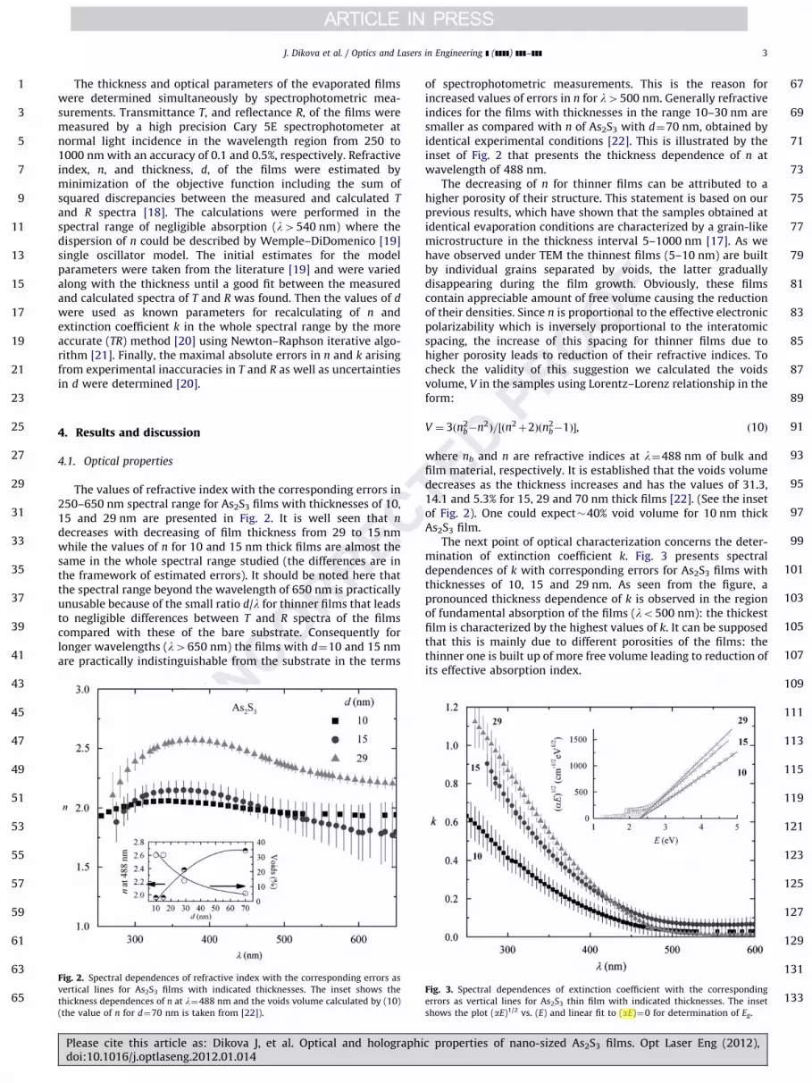
The values of refractive index with the corresponding errors in250–650 nm spectral range for As2S3 films with thicknesses of 10,15 and 29 nm are presented in Fig. 2. It is well seen that n
decreases with decreasing of film thickness from 29 to 15 nmwhile the values of n for 10 and 15 nm thick films are almost thesame in the whole spectral range studied (the differences are inthe framework of estimated errors). It should be noted here thatthe spectral range beyond the wavelength of 650 nm is practicallyunusable because of the small ratio d/l for thinner films that leadsto negligible differences between T and R spectra of the filmscompared with these of the bare substrate. Consequently forlonger wavelengths (l4650 nm) the films with d¼10 and 15 nmare practically indistinguishable from the substrate in the terms
Fig. 2. Spectral dependences of refractive index with the corresponding errors as
vertical lines for As2S3 films with indicated thicknesses. The inset shows the
thickness dependences of n at l¼488 nm and the voids volume calculated by (10)
(the value of n for d¼70 nm is taken from [22]).
Please cite this article as: Dikova J, et al. Optical and holographidoi:10.1016/j.optlaseng.2012.01.014
of spectrophotometric measurements. This is the reason forincreased values of errors in n for l4500 nm. Generally refractiveindices for the films with thicknesses in the range 10–30 nm aresmaller as compared with n of As2S3 with d¼70 nm, obtained byidentical experimental conditions [22]. This is illustrated by theinset of Fig. 2 that presents the thickness dependence of n atwavelength of 488 nm.
The decreasing of n for thinner films can be attributed to ahigher porosity of their structure. This statement is based on ourprevious results, which have shown that the samples obtained atidentical evaporation conditions are characterized by a grain-likemicrostructure in the thickness interval 5–1000 nm [17]. As wehave observed under TEM the thinnest films (5–10 nm) are builtby individual grains separated by voids, the latter graduallydisappearing during the film growth. Obviously, these filmscontain appreciable amount of free volume causing the reductionof their densities. Since n is proportional to the effective electronicpolarizability which is inversely proportional to the interatomicspacing, the increase of this spacing for thinner films due tohigher porosity leads to reduction of their refractive indices. Tocheck the validity of this suggestion we calculated the voidsvolume, V in the samples using Lorentz–Lorenz relationship in theform:
V ¼ 3ðn2b�n2Þ=½ðn2þ2Þðn2
b�1Þ�, ð10Þ
where nb and n are refractive indices at l¼488 nm of bulk andfilm material, respectively. It is established that the voids volumedecreases as the thickness increases and has the values of 31.3,14.1 and 5.3% for 15, 29 and 70 nm thick films [22]. (See the insetof Fig. 2). One could expect�40% void volume for 10 nm thickAs2S3 film.
The next point of optical characterization concerns the deter-mination of extinction coefficient k. Fig. 3 presents spectraldependences of k with corresponding errors for As2S3 films withthicknesses of 10, 15 and 29 nm. As seen from the figure, apronounced thickness dependence of k is observed in the regionof fundamental absorption of the films (lo500 nm): the thickestfilm is characterized by the highest values of k. It can be supposedthat this is mainly due to different porosities of the films: thethinner one is built up of more free volume leading to reduction ofits effective absorption index.
109
111
113
115
119
121
123
125
127
129
131
133Fig. 3. Spectral dependences of extinction coefficient with the corresponding
errors as vertical lines for As2S3 thin film with indicated thicknesses. The inset
shows the plot (aE)1/2 vs. (E) and linear fit to (aE)¼0 for determination of Eg.
c properties of nano-sized As2S3 films. Opt Laser Eng (2012),
xx
Highlight
(aE)^(1/2)
1
3
5
7
9
11
13
15
17
19
21
23
25
27
29
31
33
35
37
39
41
43
45
47
49
51
53
55
57
59
61
63
65
67
69
71
73
75
77
79
81
83
85
87
89
91
93
95
97
99
101
103
105
107
109
111
113
115
119
121
J. Dikova et al. / Optics and Lasers in Engineering ] (]]]]) ]]]–]]]4
Further, the spectral dependences of absorption coefficients, a(a¼4pk/l), were used for estimation of optical band gap energy,Eg by plotting (ahn)1/2 vs. (hn) [23] and extrapolating the linearpart of the experimental points to (ahn)¼0 (see the inset ofFig. 3). The estimated values of Eg are 2.3 eV and are independentof film thicknesses. This give us the reason to assume that theAs2S3 films studied have similar composition and the observeddifferences in n and k are mainly due to variation of the film’sporosity because of thickness change. Simultaneously, the calcu-lated Eg values are a little lower than these for 70 nm thick film(2.34 eV), estimated earlier [22]. In a previous investigation [24]we found a similar trend which could be explained by theincreased structural disorder in the thinnest samples where thegrain-like microstructure is the most pronounced. This suggestionwas confirmed by the established thickness dependence of theUrbah energy values estimated for amorphous As2S3 films withthicknesses between 15 and 70 nm [24].
4.2. Holographic recording
The holographic gratings are recorded by the interferencebetween two evanescent waves and plane and evanescent wavesusing an optical set-up, illustrated in Fig. 4.
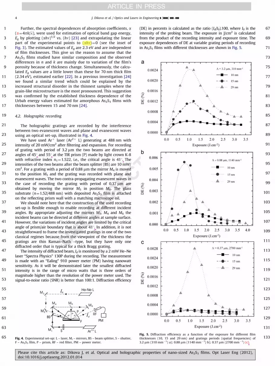
We have used Arþ laser (Ar2þ L) generating at 488 nm withintensity of 20 mW/cm2 after filtering and expansion. For recordingof grating with period of 3.2 mm the two beams are directed atangles of 451 and 551 at the TIR prism (P) made by light crown K-8with refractive index n1¼1.522, i.e., the critical angle is 411. Theintensities of the two beams after the beam splitter (BS) are 10 mW/cm2. For a grating with a period of 0.88 mm the mirror M4 is movedto the position M5 and the grating was recorded with plane andevanescent waves. The two contra-propagating evanescent waves inthe case of recording the grating with period of 0.37 mm areobtained by moving the mirror M5 in position M6. The glasssubstrate (n¼1.52/488 nm) with deposited As2S3 film is attachedon the reflecting prism wall with a matching microscope oil.
We should note here that the construction of the used recordingset-up is flexible enough to enable recording at different incidentangles. By appropriate adjusting the mirrors M1, M4 and M6 theincident beams can be directed at different angles at sample surface.However, the variations of incident angles are limited by the criticalangle of prism/air boundary that is about 411. In addition, it is notstraightforward to frame the investigated gratings in one of the twoclassical regimes because from the viewpoint of the thickness thegratings are thin Raman–Nath –type, but they have only onediffracted order that is typical for a thick Bragg grating.
The intensity of diffracted beam, Id is monitored by a 2 mW He–Nelaser ‘‘Spectra Physics’’ 130P during the recording. The measurementis made with an ‘‘Ealing’’ 910 power meter (PM) having nanowattsensitivity. As it will be demonstrated later the smallest diffractedintensity is in the range of micro watts that is three orders ofmagnitude higher than the resolution of the power meter used. Thesignal-to-noise ratio (SNR) is better than 100:1. Diffraction efficiency
Fig. 4. Experimental set-up: L – laser, Mi – mirrors, BS – beam splitter, S – shutter,
F – As2S3 film, P – prism, RF – red filter, PM – power meter.
Please cite this article as: Dikova J, et al. Optical and holographidoi:10.1016/j.optlaseng.2012.01.014
(DE) in percents is calculated as the ratio (Id/I0).100, where I0 is theintensity of the probing beam. The exposure in J/cm2 is calculatedfrom the product of the recording intensity and exposure time. Theexposure dependences of DE at variable grating periods of recordingin As2S3 films with different thicknesses are shown in Fig. 5.
123
125
127
129
131
133Fig. 5. Diffraction efficiency as a function of the exposure for different film
thicknesses (10, 15 and 29 nm) and gratings periods (spatial frequencies) of
3.2 mm (310 mm�1) a); 0.88 mm (1140 mm�1) b); 0.37 mm (2700 mm�1) (c).
c properties of nano-sized As2S3 films. Opt Laser Eng (2012),
Original Text:
c).--
Original Text:
o
Original Text:
o
Original Text:
o
Original Text:
o
xx
Highlight
(...)^(1/2)
1
3
5
7
9
11
13
15
17
19
21
23
25
27
29
31
33
35
37
39
41
43
45
47
49
51
53
55
57
59
61
63
65
67
69
71
73
75
77
79
81
83
85
87
89
91
93
95
97
99
101
103
105
107
109
111
113
115
119
121
123
125
127
129
131
133
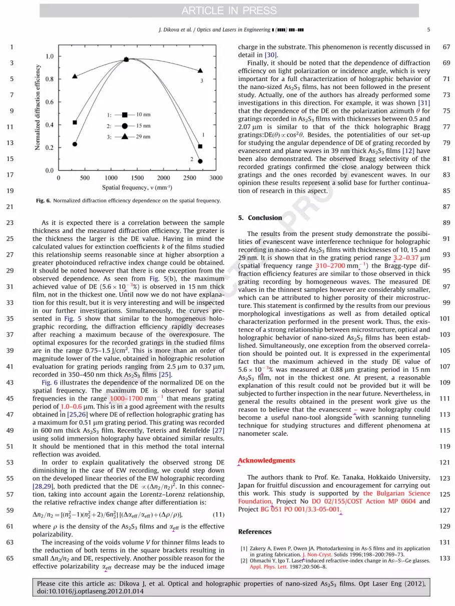
Fig. 6. Normalized diffraction efficiency dependence on the spatial frequency.
J. Dikova et al. / Optics and Lasers in Engineering ] (]]]]) ]]]–]]] 5
As it is expected there is a correlation between the samplethickness and the measured diffraction efficiency. The greater isthe thickness the larger is the DE value. Having in mind thecalculated values for extinction coefficients k of the films studiedthis relationship seems reasonable since at higher absorption agreater photoinduced refractive index change could be obtained.It should be noted however that there is one exception from theobserved dependence. As seen from Fig. 5(b), the maximumachieved value of DE (5.6�10�3%) is observed in 15 nm thickfilm, not in the thickest one. Until now we do not have explana-tion for this result, but it is very interesting and will be inspectedin our further investigations. Simultaneously, the curves pre-sented in Fig. 5 show that similar to the homogeneous holo-graphic recording, the diffraction efficiency rapidly decreasesafter reaching a maximum because of the overexposure. Theoptimal exposures for the recorded gratings in the studied filmsare in the range 0.75–1.5 J/cm2. This is more than an order ofmagnitude lower of the value, obtained in holographic resolutionevaluation for grating periods ranging from 2.5 mm to 0.37 mm,recorded in 350–450 nm thick As2S3 films [25].
Fig. 6 illustrates the dependence of the normalized DE on thespatial frequency. The maximum DE is observed for spatialfrequencies in the range 1000–1700 mm�1 that means gratingperiod of 1.0–0.6 mm. This is in a good agreement with the resultsobtained in [25,26] where DE of reflection holographic grating hasa maximum for 0.51 mm grating period. This grating was recordedin 600 nm thick As2S3 film. Recently, Teteris and Reinfelde [27]using solid immersion holography have obtained similar results.It should be mentioned that in this method the total internalreflection was avoided.
In order to explain qualitatively the observed strong DEdiminishing in the case of EW recording, we could step downon the developed linear theories of the EW holographic recording[28,29], both predicted that the DE pðDn2=n2Þ
2. In this connec-tion, taking into account again the Lorentz–Lorenz relationship,the relative refractive index change after differentiation is:
Dn2=n2 ¼ ½ðn22�1Þðn2
2þ2Þ=6n22� ½ðDaeff=aeff ÞþðDr=rÞ�, ð11Þ
where r is the density of the As2S3 films and aeff is the effectivepolarizability.
The increasing of the voids volume V for thinner films leads tothe reduction of both terms in the square brackets resulting insmall Dn2/n2 and DE, respectively. Another possible reason for theeffective polarizability aeff decrease may be the induced image
Please cite this article as: Dikova J, et al. Optical and holographidoi:10.1016/j.optlaseng.2012.01.014
charge in the substrate. This phenomenon is recently discussed indetail in [30].
Finally, it should be noted that the dependence of diffractionefficiency on light polarization or incidence angle, which is veryimportant for a full characterization of holographic behavior ofthe nano-sized As2S3 films, has not been followed in the presentstudy. Actually, one of the authors has already performed someinvestigations in this direction. For example, it was shown [31]that the dependence of the DE on the polarization azimuth y forgratings recorded in As2S3 films with thicknesses between 0.5 and2.07 mm is similar to that of the thick holographic Bragggratings:DEðyÞpcos2y. Besides, the potentialities of our set-upfor studying the angular dependence of DE of grating recorded byevanescent and plane waves in 39 nm thick As2S3 films [12] havebeen also demonstrated. The observed Bragg selectivity of therecorded gratings confirmed the close analogy between thickgratings and the ones recorded by evanescent waves. In ouropinion these results represent a solid base for further continua-tion of research in this aspect.
5. Conclusion
The results from the present study demonstrate the possibi-lities of evanescent wave interference technique for holographicrecording in nano-sized As2S3 films with thicknesses of 10, 15 and29 nm. It is shown that in the grating period range 3.2–0.37 mm(spatial frequency range 310–2700 mm�1) the Bragg-type dif-fraction efficiency features are similar to those observed in thickgrating recording by homogeneous waves. The measured DEvalues in the thinnest samples however are considerably smaller,which can be attributed to higher porosity of their microstruc-ture. This statement is confirmed by the results from our previousmorphological investigations as well as from detailed opticalcharacterization performed in the present work. Thus, the exis-tence of a strong relationship between microstructure, optical andholographic behavior of nano-sized As2S3 films has been estab-lished. Simultaneously, one exception from the observed correla-tion should be pointed out. It is expressed in the experimentalfact that the maximum achieved in the study DE value of5.6�10�3% was measured at 0.88 mm grating period in 15 nmAs2S3 film, not in the thickest one. At present, a reasonableexplanation of this result could not be provided but it will besubjected to further inspection in the near future. Nevertheless, ingeneral the results obtained in the present work give us thereason to believe that the evanescent – wave holography couldbecome a useful nano-tool alongside with scanning tunnelingtechnique for studying structures and different phenomena atnanometer scale.
Acknowledgments
The authors thank to Prof. Ke. Tanaka, Hokkaido University,Japan for fruitful discussion and encouragement for carrying outthis work. This study is supported by the Bulgarian ScienceFoundation, Project No DO 02/155/COST Action MP 0604 andProject BG 051 PO 001/3.3-05-001.
References
[1] Zakery A, Ewen P, Owen JA. Photodarkening in As-S films and its applicationin grating fabrication. J. Non-Cryst. Solids 1996;198–200:769–73.
[2] Ohmachi Y, Igo T. Laser-induced refractive-index change in As\–S\–Ge glasses.Appl. Phys. Lett. 1987;20:506–8.
c properties of nano-sized As2S3 films. Opt Laser Eng (2012),
Original Text:
‐3
Original Text:
1000
Original Text:
‐1
Original Text:
1.0‐0.6
Original Text:
eff
Original Text:
eff
Original Text:
3.2‐0.37
Original Text:
310‐2700
Original Text:
‐1
Original Text:
‐3
Original Text:
‐
Original Text:
Acknowledgements
Original Text:
the Bulgarian Science Foundation,
Original Text:
BG 051 PO 001macslash3.3‐05‐001.
Original Text:
J Non‐Crys

1
3
5
7
9
11
13
15
17
19
21
23
25
27
29
31
33
35
37
39
41
43
45
47
49
51
53
J. Dikova et al. / Optics and Lasers in Engineering ] (]]]]) ]]]–]]]6
[3] Tanaka K, Kyohya Sh, Odajima A. Anomaly of the thickness dependence ofphotodarkening in amorphous chalcogenide films. Thin Solid Films1984;111:195–200.
[4] Hayashi K, Mitsuishi N. Thickness effect of the photodarkening in amorphouschalcogenide films. J. Non-Cryst. Solids 2002;299–302:949–52.
[5] Nassenstein H. Holographie und interferenzversuche mit inhomogenenOberflachenwellen. Phys. Lett. A 1968;28:249–51.
[6] Stetson K. Holography with total internally reflected light. Appl. Phys. Lett.1967;11:225–6.
[7] Suhara T, Nishihara H, Koyama J. Waveguide holograms. Trans. IECE Jpn1977;60-C(4):197–204.
[8] Min’ko V, Indutnyy I, Shepeliavyi P, Litvin P. Application of amorphouschalcogenide films for recording of high-frequency phase-relief diffractiongratings. J. Optoelectron. Adv. Mater. 2005;7:1429–32.
[9] Tamulevicius T, Tamulevicius S, Andrulevicius M, Griskonis E, PuodziukynasL, Janusas G, Guobien _e A. Formation of periodical micro structures usinginterference lithography. Exp. Tech. 2008;32(4):23–8.
[10] Tamulevicius R, Seperys M, Andrulevicius S. Tamulevicius, Total internalreflection based sub-wavelength grating sensor for the determination ofrefractive index of liquids. Photonics Nanostruct. Fundam. Appl. 2011;9:140–8.
[11] Sainov S, Dikova J, Beev K. Evanescent wave holographic recording innanosize thick chalcogenide glass films. Opt. Commun. 2006;263:163–5.
[12] Sainov S, Stoycheva-Topalova R. Total internal reflection holographic record-ing in very thin films. J. Opt. A: Pure Appl. Opt. 2000;2:117–20.
[13] Sainov S, Dikova J, Stoycheva-Topalova R. Evanescent - wave recording invery thin layers. J. Optoelectron. Adv. Mater. 2001;3:395–8.
[14] Sainov S, Sainov V, Dikova J. Holographic recording in nano-sized As2S3 films.J. Optoelectron. Adv. Mater. 2001;3:399–402.
[15] Harrick N. Internal Reflection Spectroscopy. New York: Interscience; 1967.[16] Mednikarov B. Dependence of the dissolution characteristics of As2S3 as a
photoresist on the condensation rate and evaporation temperature. J. Vac.Sci. Technol., A 1989;B7:561–4.
Please cite this article as: Dikova J, et al. Optical and holographidoi:10.1016/j.optlaseng.2012.01.014
[17] Starbov N, Starbova K, Dikova J. Surface microstructure and growth mor-phology of vacuum deposited a-As2S3 thin films. J. Non-Cryst. Solids1992;139:222–30.
[18] Coleman TF, Li Y. An interior trust region approach for nonlinear minimiza-tion subject to bounds. SIAM J. Optim. 1996;6:418–45.
[19] Wemple S, DiDomenico M. Behavior of the electronic dielectric constant incovalent and ionic materials. Phys. Rev. B 1971;3:1338–51.
[20] Konstantinov I, Babeva Tz, Kitova S. Analysis of errors in thin-film opticalparameters derived from spectrophotometric measurements at normal lightincidence. Appl. Opt. 1998;37:4260–7.
[21] Abeles F, Theye M. Methode de calcul des constantes optiques des couchesminces absorbantes a partir de mesures de reflexion et de transmission. Surf.Sci. 1966;5:325–31.
[22] Dikova J, Babeva Tz, Iliev Tz. Photoinduced optical changes in vacuumdeposited nanocrystalline As2S3 films. J. Optoelectron. Adv. Mater. 2005;7:1281–6.
[23] Tauc J. In: Abeles F, editor. The Optical Properties of Solids; 1970. p. 277–415.[24] Babeva Tz, Dikova J, Rashkova V. Influence of the nanocrystalline structure on
the optival behaviour of vacuum deposited As2S3 films. In: Balabanova,Dragieva, editors. Nanosci. Nanotechnol. Heron Press; 2007. p. 97.
[25] Hou T, Chang M. Holographic evaluation of resolution in amorphouschalcogenide inorganic photoresists. Appl. Opt. 1979;18:1753–6.
[26] Protasova M, Ozols A. Lat. J. Phys. Technol. Sci. 1992;3:38–46.[27] Teteris T, Reinfelde M. Immersion holographic recording of subwavelength
gratings in amorphous chalcogenide thin films. J. Optoelectron. Adv. Mater.2005;7:2581–6.
[28] Lukosz W, Wuthrich A. Holography with evanescent waves. Optik 1974;41:191–211.
[29] Lee W-H, Streifer W. Diffraction efficiency of evanescent- wave holograms,Part I: TE polarization. J. Opt. Soc. Am. A: 1978;68:795–801.
[30] Pinchuk A, Hilger A, Plessen G, Kreibig U. Substrate effect on the opticalresponse of silver nanoparticles. Nanotechnology 2004;15:1890–6.
[31] Beev K, Sainov S, Stoycheva-Topalova R. Total internal reflection holographicrecording in chalcogenide glass films. J. Optoelectron. Adv. Mater. 2007;9:341–3.
55
c properties of nano-sized As2S3 films. Opt Laser Eng (2012),
Original Text:
films
Original Text:
, J Non‐Cryst
Original Text:
Interferenzversuche
Original Text:
Inhomogenen
Original Text:
Total Internally Reflected Light
Original Text:
Appl Phys Lett
Original Text:
Holograms
Original Text:
Trans
Original Text:
of Japan
Original Text:
Min’ko
Original Text:
J Opt Adv Mat
Original Text:
Exp Techn
Original Text:
Photon. Nanostr. – Fundament Appl
Original Text:
Opt Commun
Original Text:
Opt A
Original Text:
Appl Opt
Original Text:
J Opt Adv Mat
Original Text:
Recording
Original Text:
J Vac Sci Technol
Original Text:
J Non‐Cryst
Original Text:
J Optimization
Original Text:
Phys Rev
Original Text:
Appl Opt
Original Text:
Surf Sci
Original Text:
J Opt Adv Mat
Original Text:
Nanoscience & Nanotechnology
Original Text:
Appl Opt
Original Text:
Latvian J Phys Techn Sci
Original Text:
J Optoelectron Adv Mat
Original Text:
J Opt Soc Am
Original Text:
J Opt Adv Mat