
NUCLEAR TECHNIQUES OF ANALYSIS - International ...
259
AU9817094 INSE 10th AUSTRALIAN CONFERENCE ON NUCLEAR TECHNIQUES OF ANALYSIS Australian National University, Canberra, ACT 24-26 November 1997 PROCEEDINGS Sponsored by Australian Institute of Nuclear Science and Engineering Vacuum Society of Australia Australian National University I
-
Upload
khangminh22 -
Category
Documents
-
view
10 -
download
0
Transcript of NUCLEAR TECHNIQUES OF ANALYSIS - International ...

AU9817094
INSE10th AUSTRALIAN CONFERENCE
ON
NUCLEAR TECHNIQUES OF ANALYSIS
Australian National University,Canberra, ACT
24-26 November 1997
PROCEEDINGS
Sponsored by
Australian Institute of Nuclear Science and EngineeringVacuum Society of Australia
Australian National University
I

NTA CONFERENCE ORGANISATION
CONFERENCE CHAIRR.G. Elliman (ANU)
CONFERENCE DEPUTY CHAIRM.C. Ridgway (ANU)
CONFERENCE ADMINISTRATORT.R.Purdy(ANU)
LOCAL ORGANISING COMMITTEEA. Byrne (ANU)
A. Durandet (ANU)R.G. Elliman (ANU)T.R.Purdy(ANU)
M.C. Ridgway (ANU)
NTA PROGRAM COMMITTEED. Cohen (ANSTO)R.G. Elliman (ANU)R. Gammon (AINSE)P. Johnston (RMTT)
M.C. Ridgway (ANU)S. Sie (CSIRO)

ADVERTISERS, SPONSORS ANDEXHIBITORS
Balzers Australia Pty Ltd
Canberra-Packard Pty Ltd
Javac Pty Ltd
John Morris Scientific Pty Ltd
Stanton Scientific
Thermo Optek Pty Ltd
Nanofilm Technologie GmbH
Varian Australia Pty Ltd

PROGRAM

' . . ' . " * . " ' .
• ; / i f , . *
/^»v^?ia*^?=tteii
si ' ' ^ i ^ i f c
Real-time ellipsometricimaging with a very highspatial resolution (repeat-ability for Psi and Delta is0.02°. lateral imagingi evolution is 1 |j,m).Non-destructive analysisand quality control ofsurfaces, thin films and
* SftaBuKisfi ~' • / 1 ' . ' '
, Works on metals, glass,liquids, dielectrics, semi-conductors...
Fully motorized and PCcontrolled for "hands- offoperation.Single wavelength, mul-tiple angle operation.Ellipsometric analysiswithin the image on user-defined region-of-interestovercomes spatial reso-lution limits of conven-tional ellipsometers.
User-friendly Windows95/NT Software.
I l ! " , i i ' J 1 •
'rn^%'®^imf^: '}iy,%^W&i - • • J
i ]

Monday,24 November
8.30-9.30
Session 1:
9.30-9.50
9.50-10.30
10.30-11.00
Session 2:
11.00-11.30
11.30-11.50
11.50-12.10
12.10-12.30
12.30-2.00
Session 3:
2.00-2.20
2.20-2.40
2.40-3.00
3.00-3.20
3.20-3.40
3.40-4.10
Session 4:3.40-5.306.00-7.007.00-9.00
NTA VSA
Late Registration
Opening/PlenaryChair: R.G. EllimanConference Opening
Opening PlenaryD.N. Jamieson PL1Structural and Electrical Characterisation of Semiconductor Materials using a Nuclear Microprobe
Coffee Break Manning Clark Foyer
Ion Beam AnalysisChair: S.H. SieInvitedD.D. Cohen NTA1Atmospheric Aerosol Characterisation at CapeGrim and Global WarmingMX. di Tada NTA2A Biomedical Application of 32Si usingAccelerator Mass SpectrometryK. Prince NTA3Migration of Ions in Cement Paste as Studied bySMS
S.D. Moss NTA4Structural and Superconducting Properties ofLaBaCaCu} O-j System: A Neutron DiffractionStudy
Surface Science 1Chair: D.J. O'ConnorInvitedD.P. Woodruff VSA1Normal Incidence X-ray Standing Wave Studies ofAdsorbate Structures
C.J. Kaalund VSA2Positive-Ion and Electron Emission on CleavageofSiE. Walker VSA3Nobel Gas Core Level Interference inPhotoelectron Spectroscopy of the Valence Bandof Ion-Bombarded SiliconJ.G. Shapter VSA4STM Investigation of Adsorption of anOrganometallic Copper Complex on Si(lll)-7x7
Lunch
Novel Techniques of AnalysisChair: A.P. ByrneE. Bezakova NTA5Amorphization oflnP Studied using PerturbedAngular Correlations
G.D. McOrist NTA6Neutron Activation Analysis - an old techniquebut is it still useful?C. Glover NTA7EXAFS Measurements of Ion Induced StructuralModification of III-VSemiconductorsJ.S. Laird NTA8Single Ion Transient-IBIC Analysis ofSemiconductor Devices using a CryogenicTemperature StageK.K. Lee NTA9Study of Micro-Dosimeter PN Junction using IonBeam Induced Charge
Thin FilmsChair: D.K. SoodA. Merchant VSA5Synthesis and Characterisation of Diamond andCarbon Nitrides Deposited using Hot-filamentand Microwave Plasma Chemical VapourDeposition TechniquesJ. Quintan VSA6PTMS on Iron and Aluminium Oxide Surfaces: aStudy of Damped Adsorption KineticsP.J.K. Paterson VSA7Oxide Growth on Aluminium Alloy 5182 DuringPreheatingK. Gaff VSA8Deposition of High Quality SiO2 Films ontoPlastic Substrates
M. Paterson VSA9The Morphology and Structure of Sol-Gel DerivedZirconia Films on Stainless Steel
Coffee Break Manning Clark Foyer
Poster Session 1: Nuclear Techniques of AnalysisPoster Session, Drinks/Nibblies Manning Clark FoyerRSPhysSE Laboratory ToursBarbeque RSPhysSE Link Bldg. Courtyards

Tuesday,25 November
Session 5:
9.00-9.40
9.40-10.10
10.10-10.30
10.30-11.00
Session 6:
11.00-11.30
11.30-11.50
11.50-12.10
12.10-12.30
12.30-2.001.00-2.00
Session 7:
2.00-2.30
2.30-2.50
2.50-3.10
3.10-3.30
3.30-4.00
Session 8:3.30-5.30
7.30-11.30
NTA VSA
NTA-VSA Joint Plenary SessionChair: B.V.KingPlenaryJ.H. Weaver PL2Visualization of Semiconductor Surface Etching with Scanning Tunneling MicroscopyInvitedM. Sancroti NTA/VSA1High-Temperature Evolution of the Si (111) Surface Investigated by Means of Synchrotron RadiationA. Sakallariou NTA/VSA2Features of Three Dimensional Ion Microtomography
Coffee Break Manning Clark Foyer
Electronic MaterialsChair: J. McCallumInvited NTA10M. PetravicIon Beam Induced Nitridation of Silicon
D.R. McKenzie NTA11The Application ofCar-Parrinello MolecularDynamics to the Study of Doping in AmorphousSemiconductorsS. Fatima NTA12Electrical and Structural Characterisation of theSubthreshold Damage in Ion Implanted p-Si
L. Moipeth NTA13Titanium Sapphire Waveguide Laser Fabricationusing Ion Implantation Techniques
Surface Science IIChair: D.P. WoodruffInvited VSA10U. ValbusaTime Evolution ofAdatom and Vacancy ClustersonAg(U0)V. Chirita VSA11Effects of Vacancies and On-top Adatoms onMobilities of Two-dimensional Pt Clusters onPt(lll)S. Wang VSA12The Chemisorption of Boron on the ClusterModelled Si(lll)dxV3R3ff>-BHydrogenatedSurfaceG.J.Williams VSA13Mechanisms for Sputtering of ZirconiumElucidated from Molecular Dynamics Simulation
LunchVS A Annual General Meeting
High Energy, Heavy Ion Beam AnalysisChair: T.R OphelInvited NTA14L.S. WielunskiMultiple Scattering Effects in Elastic RecoilDetection Depth ResolutionM. Li NTA15Simulation Study of Multiple ScatteringBackground and its Role in the Detection Limit ofHIBSH. Timmers NTA16A Facility for Heavy-Ion Elastic Recoil DetectionAnalysis at the Australian national UniversityN. Dytlewski NTA17Time-of-Flight ERDA of Dual Implanted Metals
Nanometre Science & TechnologyChain D.R. McKenzieInvited VSA14R. LeonDifferent paths to Tunability in Self-formingSemiconductor Quantum DotsD.G. McCullogh VSA15First-principles Quantum Molecular Dynamics ofCrystalline and Amorphous Carbon-Nitrides
M. Samandi VSA16Sintering ofZirconia Toughened Alumina byMM-Wave RadiationY. Chen VSA17Nanostructural Materials Produced by HighEnergy Ball Milling Technique
Coffee Break Manning Clark Foyer
Poster Session II: Vacuum Society of AustraliaPoster Session II, Drinks/Nibblies Manning Clark Foyer
Conference Dinner Canberra Tradies Club

Wednesday,26 November
Session 9:
9.00-9.40
9.40-10.10
10.10-10.30
10.30-11.00
Session 10:
11.00-11.30
11.30-11.50
11.50-12.10
12.10-12.30
12.30-1.30
Session 11:
1.30-2.00
2.00-2.15
2.15-2.30
2.30-2.45
2.45-3.00
3.00-3.15
3.15
NTA VSA
Joint NTA-VSA Plenary SessionChair: D.D.CohenPlenaryM. Vos PL3Materials Research by Electron Momentum SpectroscopyInvitedM. Hoogerland NTA/VSA3Using Atom Lithography to Create Nanoscale StructuresI S . Colligan NTA/VSA4Stoichiometric Carbon Nitride Syntehsized by Ion Beam Sputtering and Post Nitrogen Ion Implantation
Coffee Break Manning Clark Foyer
Optoelectronic MaterialsChair: M.C. RidgwayInvitedJ.C. McCallum NTA18The Kinetics of Solid Phase Epitaxy in As-dopedBuried Amorphous Silicon LayersC. Johnson NTA19Thermal Annealing of Waveguides Formed by IonImplantation ofSilica-on-SiA. Dowd NTA20Nonlinear Optical Properties of SemiconductorNanocrystals in Silica Matrices
J.O. Onva NTA21Carbon Nanoclusters formed by Implanting FusedQuartz and Sapphire with Carbon Ions
Plasma Science and TechnologyChain M. SamandiInvitedA. Durandet VSA18Deposition of Silicon Oxide in Pulsed HeliconAssisted Reactive EvaporationR. Donnan VSA19Multiwavelength Pyrometric Thermometry duringMicrowave Plasma ProcessingK. Ng VSA20Optical Emission Spectroscopy Study of FilteredVacuum Arc Plasmas from Ti, Al and TiAlSourcesG.K. Muralidhar VSA21An Efficient Magnetron Sputtering Source for LowPressure Plasma Deposition
Lunch
New Techniques, Future Needs, Trends and DevelopmentsChair: D.N. JamiesonInvitedS.H. Sie NTA/VSA5AUSTRALIS: A NewMicroanalytical Tool for the GeosciencesM.C. Hotchkis NTA/VSA6The Antinides Beamline on the ANTARES Accelerator Mass Spectrometry FacilityM. Cholewa NTA/VSA7Single Ion Detection Systems and Thin Vacuum WindowsG.C. Ryan NTA/VSA8The New CSIRO/GEMOC Nuclear Microprobe: A New Highly Integrated Design for GeoscienceApplicationsB.V. King NTA/VSA9Laser Postionisation - the Way of the Future
Prizes/Concluding Remarks
Conference Close

SESSION 1(Chair: R.G. Elliman)
OPENING PLENARY

PL1AU9817095
STRUCTURAL AND ELECTRICAL CHARACTERISATION OF SEMICONDUCTORMATERIALS USING A NUCLEAR MICROPROBE
D.N. Jamieson, School of Physics, Microanalytical Research Centre, University of Melbourne,Parkville, 3052, AUSTRALIA.
Abstract
The domain of high-resolution imaging techniques (sub-micron) traditionally belongs to low-energyion beams (keV ion microprobe), electrons (transmission or scanning electron microscopy), light (nearfield microscopy), or all variants of scanning probe microscopies. Now, nuclear techniques ofanalysis, with a nuclear microprobe, have entered this domain, bringing a range of unique techniquesfor making images. In addition to conventional techniques like Rutherford (and non-Rutherford)backscattering spectrometry and particle induced x-ray emission for structural characterisation, newion beam analysis techniques have been developed for electrical characterisation as well. Foremost ofthese new techniques is ion beam induced charge (IBIC) which has seen an explosion of applicationsin the last five years to the study of charge transport properties of a variety of materials includingpolycrystalline diamond and silicon. An additional novel technique is ionoluminescence, which maybe used to image various electronic properties of the material. Presented here are some examples ofthese imaging techniques in a variety of semiconductor materials. In all these examples, thespecimens display structural inhomogeneities on the scale of 10 micrometres, making it essential toemploy a focused beam.
Introduction
More than 40 laboratories worldwide are equipped with nuclear microprobe systems. In theselaboratories, approximately 25% of the work is directed to the study of problems involvingsemiconductor materials [1]. A sequence of reviews of this expanding field is available [2-10] andcomplete details of all analytical techniques discussed here can be found in a recent book [11].
High Beam Current
E Signal Output
Low Beam Current
Depletion region
E Signal Output
2. Ion Beam Induced Charge(With depletion region)
1. ConventionalRBS/PIXE/Channeling/
(NRA)
E Signal Output
3. Ion Beam Induced Charge(Without depletion region)
Figure I: Signals from specimens analysed with high and low beam current techniques.
The techniques applied to the analysis of semiconductors with a nuclear microprobe may be dividedinto two categories: high current techniques and low current techniques on the basis of the source ofthe signal used to make images as shown in Fig. 1. The high current techniques (lOOpA or more) arethose of traditional Ion Beam Analysis: Rutherford Backscattering, Particle induced X-ray Emission,Ion channeling, and, less frequently, Nuclear Reaction Analysis. These traditional ion beam analysistechniques are mainly aimed at analysis of the elemental structure of the sample. Low current

techniques (100 pA or less) employ the specimen itself as the detector so the number of incident beamparticles required to form images is considerably reduced compared to traditional techniques. Thisallows the diameter of the beam collimators to be reduced with a consequent improvement inresolution, often well into the submicron domain. One of the most widely applied is ion beam inducedcharge, where the charged induced in a sample by the beam is collected and regions of differingcollection efficiency form contrast in images. A list of the physical parameters of the Melbounenuclear microprobe system appears in Table 1 below.
Applications I - High Current Techniques
Epitaxial growth of diamond on large area synthetic diamond substrates is important to many potentialapplications in the microelectronics device industry. A method for the production of large area singlecrystal has been devised by Pehrsson et al. [13]. This uses chemical vapour deposition (CVD) to growa homoepitaxial layer on a diamond substrate containing a buried damage layer created by ionimplantation. Chemical etching is used to attack the buried layer resulting in the lift off of a large areaslab. A key question is whether the implantation has an effect on the quality of the homoepitaxiallayer. As shown in Fig. 2, growth defects are evident in the surface of the as-grown layers.Channeling contrast images reveal that, apart from the localised defects, the implantation did notchange the quality of the film. Spectra extracted from the growth defects show no signal from theburied damaged layer suggesting surface dust masked the original implant. The edges of the maskedregion are tilted due to implantation induced swelling and hence nucleated misaligned crystal duringthe CVD growth phase.
Another aspect to the growth of CVD diamond is that it may readily be distinguished from naturaldiamond on the basis of its luminescence spectrum. Electrons (Cathodoluminescence, CL)traditionally excite this spectrum, however ionoluminescence, IL, is a novel technique that can also be
; . • • ; • ! • ; , • • • ; ; • • ^
200 jim -''v"» -' -
t y f Implanted "
Total Yield
D
Figure 2: Channeling contrast microscopy images with photo (top right) and RBS spectra from growthdefects in a homoepitaxial diamond film.
used for this purpose. IL has not been widely used in the past, owing probably to the rapid build-up ofdamage that can change or otherwise degrade the luminescence spectrum. Where this is wellunderstood, IL can be useful, particularly as it has the potential to be used in conjunction withtraditional IBA techniques. For example, Fig. 3 shows IL measurements on a CVD film. The ionbeam is able to penetrate through the thickness of the as-grown CVD film to probe the naturaldiamond substrate beneath. The luminescence from the CVD layer is lower in energy than theluminescence from the substrate owing the fact that the luminescence arises from donor-acceptor pairsthat are further apart in the CVD film.

Figure 3: lonoluminescence spectra from a CVD diamond film on a natural diamond substrate. Forcomparison, the IL spectrum from a bare natural diamond substrate is also shown by comparison.
By use of several beams of differing range, the unique spectrum from the CVDfilm can be identified.
2000F
. 1500 -
3MeVH50 |im
3MeV50 jwn• 3 MeV H+ (no CVD)
• 3 MeV H*
* 2 MeV Hj
Applications II - Low Current Techniques
Here are some examples of electrical characterisation of several different semiconductor materials anddevices. In each case the sample itself is the detector and the microprobe is used to induce chargewhich is then collected by appropriate contacts applied to the device (see Fig. 1).
Polycrystalline silicon in photovoltaic cells offers interesting challenges to nuclear microprobeanalysis [13]. Induced charge is collected owing to the presence of a depletion layer at the p-njunction. Grain boundaries and other defects trap charge reducing the efficiency of the device. Theefficiency of the cell can be imaged with IBIC as shown in Fig. 4. In addition to the obvious grainboundaries, additional structure is visible within individual grains that appears to be correlated withsurface structure visible in SEM images. A potential advantage of this work with MeV ion beams isthat the range of a MeV ion is comparable to longer wavelengths of light in single crystal silicon. Inaddition PIXE has sufficient sensitivity to detect some trace contaminants that perhaps contribute tothe degradation of the charge collection efficiency [14].
Figure 4: IBIC images of grain boundaries in a commercially available poly-silicon solar cell. A2 MeV He* beam was used for these images.
surface
7-

Diamond has been proposed for many possible applications in microelectronic devices, particularly asa radiation detector. High quality polycrystalline diamond films manufactured by the Norton companyhave been the subject of extensive study by IBIC (see list of references in [10]). This work has beendone to investigate the charge transport properties of the material by using the focused ion beam tocreate electron-hole pairs within the material which are then collected by biased electrodes applied tothe diamond surface (the "energy signal"). On average, the diamond films are about 8 % efficient,with localised regions in the centres of grains rising to an efficiency of 24 % [15], or greater. High-resolution IBIC images from within single diamond grains reveal significant structure as shown in Fig.5. Analysis of spectra extracted from these different regions will allow insights to be gained into thecharge collection mechanisms as a function of diamond growth direction. The charge collectionefficiency from the centres of the most efficient grain in this specimen was about 5 times greater thanthe average efficiency of the whole film. The most efficient grain in this specimen appeared to have acharge collection efficiency of close to 100%.
Future of Microbeams
A variety of new techniques are emerging for new imaging methods employing focused MeV ionbeams. One of these exploits the deeply penetration of the beam to form tomographic images ofmicroscopic objects smaller than the range of the ion beam [16]. This provided insights into thegrowth mechanism of the crystal. An extension of this technique involves PIXE tomography [17]where the characteristic x-rays are detected instead of the energy loss of the transmitted ions. Thiswill potentially allow three-dimensional maps of trace elements in microscopic objects to be obtained.
For the future, it would be desirable to have much brighter ion sources to allow smaller probes to beobtained with a similar beam current to those available now. Apart from this, further advances willcome from probe forming lens systems with even greater demagnification compared to the presentsystems that are more closely matched to the characteristics of the ion source and accelerator wherefurther optimisation is possible [18]. At present the main barrier to further reduction in probe sizeappears to be mainly mechanical vibrations and parasitic magnetic fields which limit the resolution to100 run. Also, more sophisticated instrumentation would be valuable to more fully exploit limitedbeam time.
As shown by the many applications here, the ability to make images opens provides a large range ofvaluable information. In fact a key common factor in all of these applications presented here is that
Figure 5: High resolution IBIC images of charge collection efficiency in a Norton polycrystallinediamond. Images made with a 2MeVH beam focused to a sub-micron probe.
225um21
Increasing charge collection efficiency
crucial information about the structure and electrical characteristics of the samples would have been

lost had unfocused beams been employed.
Acknowledgments
The work at Melbourne has been supported by the Australian Research Council and the University ofMelbourne and the Australian Department of Science, Industry and Tourism. I acknowledge usefuldiscussions with Steven Prawer, contributions to Fig. 2 by Steven Prawer and Jim Butler, Fig. 3 byAndrew Bettiol, Fig. 4 by Lachlan Witham and Fig. 5 by Mark Breese.
Table 1; Physical Parameters of the Melbourne microprobe.Accelerator
Object diaphragmAperture diaphragmObject - Aperture distanceAperture- Specimen distanceAperture - Scan coils distanceProbe forming lens system
Lens bore radiusTurns per pole
Lens 1 and 4 length
Lens 2 and 3 lengthLens spacingWorking distance (last lens to specimen), WDDemagnification at shortest WD
X-ray detector (A, d, 6)
Particle detectors (A, n , 9)(Additional forward detectors can be fitted asrequired)Typical parameters for analysisObject diameterAperture diameterBeam convergence angleBeam current for 2 MeV He+
Beam current for 3 MeV IT
NEC 5U pelletron with RF ion source
5 to 200 um diameter50 um to 3 mm diameter7250 mm1200 mm300 mmRussian antisymmetric quadruplet of magnetic quadrupole lenses
6 mm1530 mm
60 mm35 mm150 to 500 mm26Si(Li) 30 mm2,33 msr, 135°PIPS 450 mm', 126 msr, 135°PIPS 100 mm2, 30 msr, 145°Annular 300 mm2, 97 msr, 175°High current techniques
100 um1 mm0.16°200 pA360 pA
Low current techniques
5 |im50 um0.013°~2fA~5fA
References[I] Proc. 5th International Conference on Nuclear Microprobe Technology and Applications, Santa Fe, NM, USA, 1996,Nucl. Instr. and Meth. B131 (1997) to be published.[2] J.S. Williams, J.C. McCallum and R.A. Brow, Nucl. Instr. and MetL B30 (1988) 480.[3] M. Takai, K. Hirai, K. Ishibashi, A. Kinomura and S. Namba, Nucl. Instr. and Meth. B54 (1991) 209.[4] M. Takai, R. Mimura, H. Sawaragi and R. Aihara, Scanning Microscopy 7 (1993) 815.[5] D.N. Jamieson, M.B.H. Breese and A. Saint, Nucl. Instr. and Meth. B85 (1994) 676.[6] M. Takai, Nucl. Instr. and Meth. B85 (1994) 664.[7] D.N. Jamieson, Nucl. Instr. and Meth. B104, (1995) 533.[8] F.Watt and G.W. Grime, Eds, Principles and Applications of High Energy Ion Microbeams, Adam Hilger, Bristol (1987).[9] M. Takai, Nucl. Instr. and Meth. Bl 13 (1996) 330.[10] D.N. Jamieson, in Proc. 5th International Conference on Nuclear Microprobe Technology and Applications, Santa Fe,NM,USA, 1996, Nucl. Instr. and Meth. B131 (1997) to be published.[II] M.B.H. Breese, D.N. Jamieson and P.J.C. King, Materials Analysis mtk a Nuclear Microprobe, Wiley, (1996).[12] P.E. Pehrsson, T. McCormick, W. B. Alexander, M Marchywka, D. Black, J.E. Butler and S. Prawer, Mat Res. Soc.Symp. Proc. 416 (1996) 61[13] C. Donolato, R. Nipoti, D. Govoni, G.P. Egeni, V. Rudello and P. Rossi, Materials Science & Engineering B 42 (1996)306-310.[14]. L.C. Witham, D.N. Jamieson and R.C. Bardos, accepted to appear in proc. IBA-13, Lisbon, Portugal, July 1997, Nucl.Instr. Meth. B.[15] C. Manfredotti, F. Fizzotti, P. Polesello, E. Vittone, M. Jaksic, I. Bogdanovic and S. Fazinic, Mat Res. Soc. Proc. 416(1996)193.[16] S.A. Stuart, M. Cholewa,, A. Saint, S. Prawer,, G.J.F. Legge andD. Weirup, D, Nucl. Inst. and Meth. B77 (1993) 234.[17] A. Saint, M Cholewa and G.J.F. Legge, Nucl. Instr. and Meth. B75 (1993) 504[18] C.G. Ryan, D.N. Jamieson, W.L. Griffin, S.H. Sie, G. Cripps and G.F. Suter, these procedings.

SESSION 2(Chair: S. Sie)
ION-BEAM ANALYSIS

NTA1AU9817096
Atmospheric Aerosol Characterisation at Cape Grim and Global Warming
David D. Cohen. David Garton
Physics Division, Australian nuclear Science and Technology OrganisationPrivate Mail Bag 1, Menai, NSW, Australia, 2234.
IntroductionThe Intergovernmental Panel on Climate Change (IPCC) produced its first report in August 1990 on climateeffects related to increased greenhouse gases such as carbon dioxide in the atmosphere since pre-industrialtimes. However, this report did not find clear evidence that the anthropogenic increase in greenhouse gaseshad led to significant global climate change. Since 1990 there has been the first Earth Summit in Rio deJaneiro in 1992, attended by many key politicians from nations around the world, a second IPCC report in 1995summarising new research [1] and a second Earth Summit of politicians in New York in June 1997. Thesecond IPCC report [1] concluded that "there is now a discernible human influence on global climate change".The current body of evidence is now compelling, both greenhouse gases and fine particle aerosols in theatmosphere affect global warming. Anthropogenic fine particles influence climate change directly, byscattering and absorbing radiation and indirectly by modifying cloud properties. The problem of global climatechange is now well and truly in the politicians court to try and tackle on a global scale.
Methane Concentrationsfrom Antarctic Ice
Carbon Dioxide Concentrations fromAntarctic Ice
1800 1850 1900Year AD
1950 2000 1800 1850 1900 1950Year AD
2000
Fig. 1. Global atmospheric methane concentrations. Fig. 2. Global atmospheric CO2 concentrations.
Research shows[l] that the concentration of gases such as carbon dioxide and methane have been increasingover many decades (see Figs. 1 and 2). Fig. 3 shows the mean adjusted global temperature from 1850 to thepresent, it shows large fluctuations due to several phenomena, including fine particle effects from volcanicaction. It also demonstrates that the increase in greenhouse gases has not been matched by a similar increase inaverage global temperatures over the past 100 years or so.
Gases such as carbon dioxide, methane, halocarbons and tropospheric ozone produce positive climate forcing ofabout 2 to 3 W/m2, whereas atmospheric aerosols from the combustion of fossil fuels and biomass burning,together with stratospheric ozone produce negative climate forcing of a few W/m2. This effect may, to someextent, explain the major differences between global temperature changes and model predictions of globaltemperature change using only greenhouse gas effects [1]. Australia plays a key role in this area, it is currentlythe second largest producer of carbon dioxide gas per capita (see Table 1).
tiI
0.60 •
0.40 •0.20 •0.00 •
-0.20 •-0.40 •-0.60 •
Adjusted
1 ' • ' • 1
Global TemperaturePinatubo
1990 9
ft •!?l*fl U H Chinon
Agung J 1 9 8 1
1850 1900 1950 2000Year
Fig. 3. Global temperature change since 1850 [1].
Country
USAAustraliaJapanEuropean UnionNew ZealandMexicoChinaBrazilIndonesiaIndia
CO2
Emissions(Mtonnes)
4,935266
1,0802,812
24325
2,421202155675
CO2
Emissionsper capita(tonnes)
19168.68.06.73.52.01.20.80.7
Table 1. Major global carbon dioxide emitters.
10
Furthermore, it performs world class global climate research at its key Global Baseline Station in Tasmania,providing vital information for the southern hemisphere. Parameters associated with global atmosphericaerosols are not well known and unlike greenhouse gas concentrations have a low to very low confidenceinterval defining them. This puts large uncertainties into the understanding of climate forcing and into modeltemperature change predictions.
Fine Particle Baseline Sampling at Cape GrimThe Australia Global Baseline monitoring station at Cape Grim in north western Tasmania is operated by theAustralian Bureau of Meteorology. The fine particle Lead Scientist at this station is Dr. John Gras from CSIROAtmospheric Research, Melbourne. ANSTO has been sampling, measuring and characterising fine particles of
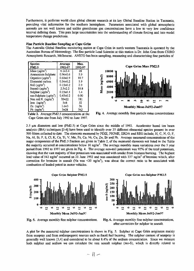
Cape Grim Mass PM2.5SpeciesPM2.5Mass (,ug/m3)Ammonium SulphateOrganics (ug/m3)Elemental carbonSoil (ng/m3)Seasalt (ug/m3)Sulphur (ng/m3)nss-Sulphate (ug/m3)Non soil K (ng/m3)Iron (ng/m3)Zn (ng/m3)Pb (ng/m3)
Average1992-976.1±3.40.96±0.60.61±0.90.34±0.20.15±0.22.5±2.20.23±0.10.45±0.2
35±225±8
1.6±33±28
Max.1992-97
285.910.71.92.910.81.4
0.901815236542
Table 2. Average PM2.5 concentrations at theCape Grim site from July 1992 to June 1997.
Monthly Mean Jul92-Jun97
Fig. 4. Average monthly fine particle mass concentrations
2.5 um diameters and less (PM2.5) at Cape Grim since the middle of 1992. Accelerator based ion beamanalysis (BBA) techniques [2-4] have been used to identify over 25 different elemental species present in over500 filters collected to date. The elements measured by PIXE, PIGME, ERDA and RBS include, H, C, N, O, F,Na, Al, Si, P, S, Cl, K, Ca, Ti, V, Mn, Fe, Co, Ni, Cu, Zn, Br and Pb. Average measured concentrations of themajor components of the PM2.5 fraction are given in Table 2, of the measured elements not listed in the Tablethe majority occurred at concentrations below 10 ng/m3. The average monthly mass variations over the 5 yearperiod from 1992 to 1997 are given in Fig. 4. The average non-soil potassium was 92% of the total potassium,showing that the vast majority of fine potassium was associated with smoke from biomass burning. The highestlead value of 542 ng/m3 occurred on 21 June 1992 and was associated with 337 ng/m3 of bromine which, aftercorrection for bromine in seasalt (Na was <20 ng/m3), was about the correct ratio to be associated withcombustion of leaded petrol in motor vehicles.
Cape Grim Sulphur PM2.5 Cape Grim nss-Sulphur PM2.5
Monthly Mean Jul92-Jun97
Fig. 5. Average monthly fine sulphur concentrations.
N « (H \C
Monthly Mean Jul92-Jun97
Fig. 6. Average monthly fine sulphur concentrations,after correction for sulphur in seasalt.
A plot for the measured sulphur concentrations is shown in Fig. 5. Sulphur at Cape Grim originates mainlyfrom seaspray and from anthropogenic sources such as fossil fuel burning. The sulphur content of seaspray isgenerally well known [3,4] and considered to be about 8.4% of the sodium concentration. Since we measureboth sulphur and sodium we can calculate the non seasalt sulphur (nss-S), which is directly related to

anthropogenic sulphur. This is shown in Fig. 6. The average non-seasalt sulphur was (60±29) % of the totalsulphur measured at Cape Grim over the 5 year period July 1992 to June 1997. Both the total, Fig. 5, and theanthropogenic sulphur, Fig. 6, show strong seasonal variations at Cape Grim, with summer sulphur beinghigher than winter sulphur.
Cape Grim was picked as a Global Baseline Station because for a large fraction of the time strong winds blowfor days from the west and south westerly direction across thousands of miles of ocean. The air sampled fromthis site at these times should therefore be representative of global air and not be too strongly influenced byregional or local anthropogenic sources from continental Australia or the rest of Tasmania to the east.However, we would also expect this global air to contain a high contribution of seasalt particles from the ocean.Dry seasalt is over 90% sodium chloride [4]. Both these elements are well measured by our IBA techniques. Aplot of the measured sodium plus chlorine concentration against 2.54 times the sodium concentration is shownin Fig. 7 for all Cape Grim data between July 1992 and June 1997. A plot of this type should be linear andhave a gradient of 1.0 if there is no chlorine loss and all the sodium is associated with chlorine in seasalt. Thecorrelation was good (R2=0.90) and the gradient of the least squares fit to the data of Fig. 7 was (0.97±0.11),showing that at this site there is very little chlorine loss from the filters and that the majority of sodium wasassociated with chlorine in seasalt. On average seasalt was (42±11)% of the fine particle mass at Cape Grim.
6000 -u
n 5000 • '•E '•"Bb 4000 • :
^ 3000 • \
t 2000 • •
Cape Grim PM2.5
<Na+CIM0-97±0-ll]*(2.54Na)
R2 = 0.90
Average Monthly Percentage SeasaltCape Grim
80 -c Av.=(42±ll)
v© <M va2000 4000
2.5*Na(ng/m3)6000 Month 1992-97
Fig. 7. Plot of (Na+Cl) against 2.54Na for PM2.5.Fig. 8. Plot of monthly percentage seasalt at Cape
Grim for fine particles.
The total sulphur measured at Cape Grim has a natural and an anthropogenic component. Sulphur in seasprayis expected to occur in a relativity fixed ratio to sodium of (S/Na)=0.084 [3,4]. Whereas non seasalt sulphur(nss-S) has anthropogenic origins in fossil fuel burning, mainly originating from non baseline sectors at CapeGrim. In Fig. 9 we show total measured fine sulphur against sodium. The data falls into two clear groups asshown by the open circles and the crosses. The open circles represent data where the (S/Na) ratio falls within±25% of the expected value for seasalt. Whereas the crosses represent excess anthropogenic sulphur notassociated with seaspray. The linear fit to the circle data showed about (5O±3O) ng/m3 of sulphur alwayspresent even in the absence of seaspray (Na=0). This corresponds to about (210±120) ng/m3 of ammonium
sulphate that is always present Cape Grim even fromCape Grim 1992-1996 ^ b a s d i n e ^ ^ whereas the high values of
700 T x^ ^ v n & M | f s excess sulphur shown in Fig. 9 probably originate
600 -Io Seasalt S
Excess S
"SoS
S=(0.08±0.02)Na+<60±40)
• 1 ' ' 1
0 1500 3000Na (ng/m3)
Fig. 9. Sodium versus sulphur at Cape Grim.
4500
from major cities such as Melbourne, Adelaide on themainland and Launceston and Hobart in Tasmania.
This effect is well demonstrated by the plots of Figs.10 and 11. Where we show 24 hour back trajectories,using average hourly wind speed and directions at theCape Grim site. Fig. 10 is for the 28 November 1993which had the highest sodium/ sulphur ratio for thestudy period. The Baseline Sector is defined by 190°to 280°, that is from south to just north of west.Clearly the data for 28 November 1993 originatedfrom this sector and represents baseline air with ahigh seasalt component and a low anthropogenicsulphur component. Fig. 11 shows back trajectories

for a low sodium, high sulphur event on 29 September 1993. This represents data from the Continental Sector280° to 90° and in particular the Urban Sector defined mainly by Melbourne, 330° to 30°. It is low in seasaltsodium but high in anthropogenic sulphur.
High Sodium, Low SulphurBaseline Sector
g
O
I;o
c-300
Gri
m
c ^
©
900 -
600 •
300 •
0 •
-300 •
Low Sodium, High SulphurContinental Sector
'_ S Continental Australia i
\ \ Melbourne^ /
dHHpb; Cape Grid^-——}'• \Ta&pania
• i [ i . i • V - 7 * , , |-700 -400 -100 200 500
East of Cape Grim (km)
Fig. 10. 24 hour back trajectories for 28/11/93
-700 -400 -100 200 500
East of Cape Grim (km)
Fig. 11. 24 hour back trajectories for 29/9/93.
Back trajectory plots of the type shown in Figs. 10 and 11 are interesting because they demonstrate that fineparticles collected at Cape Grim come from hundreds of kilometres away. Indeed this is not unexpected as asteady 20 km/ hr breeze for 24 hours would transport fine particles 480 kilometres, typical of the distancesshown in Figs. 10 and 11.
SummaryClimate change is currently seen as a most important international issue. Millions of people who live on atollsand outcrops barely above sea level may be submerged by rising seas levels, Samoans maybe the first to feelthese effects. In Bangladesh seventeen percent of land may be lost and 6M people affected. The EuropeanUnion wants all developing countries to accept a legally binding 15% reduction in greenhouse emissions by2010 (based on 1990 levels). This would affect Australian aluminium and coal exports considerably.
Of all the atmospheric pollutants, fine particles are the most evident because they affect visibility by changingan otherwise deep blue sky. However, the uncertainty associated with our knowledge of fine atmosphericparticles and their role in global climate change is considerably greater than that related to greenhouse gases.Effects in the southern hemisphere are quite different to the northern hemisphere. It is therefore important toobtain data relevant to our own situation. Fine particle characterisation research is therefore very important.
AcknowledgmentsWe would like to acknowledge the staff of CSIRO Atmospheric Research Division, John Gras, and the staff atthe Cape Grim Baseline Air Pollution Station, Chad Dick, Laurie Porter and Bryan Weymouth for assistance insetting up and obtaining some of the fine particle sampler data. We would like to thank, Grahame Bailey, PhilJohnston, Ed Stelcer, Alex Croal for assistance in data analysis and for operating the 3MV Van de Graaffaccelerator through this work.
References[1] Climate Change 1995; The Science of Climate Change, Report of Working Group I to theIntergovernmental Panel on Climate Change, IPCC-XI, Rome, 11-15 December 1995.[2]. D. D. Cohen, Nucl. Instr. and Meth., B79 (1993) 385-388.[3]. D. D. Cohen, G. M. Bailey and R. Kondepudi, Nucl. Instr. and Methods, B109(1996)218-226.[4] D.D. Cohen, R. Kondepudi, R. Hyde and P. Crisp, Meteorological and Chemical Interpretation of AirPollution by Fine-Aerosol Particles in the Region 200 km Around Sydney. Final Report, NSW EnvironmentalTrust Grant No 1993/RD/G02, March 1995, pl-236.[5] P.K. Hopke, Receptor Modelling for Air Quality Management, Elsevier Science, Amsterdam, (1991).[6] J.G. Watson, N.F. Robinson, J.C. Chow, R.C. Henry, B. Kim, Q.T. Nguyen, E. L. Meyer, T.G. Pace.Receptor model technical series, volume III, CMB7 user's manual, US Environmental Protection Agency,Report EPA-450/4-90-004, January, 1990.

NTA2
111AU9817097
A Biomedical Application Of Si Using AcceleratorMass Spectrometry
M.L.di Tada, L.K.Fifield, Kexin Liu and R.G.CresswellDepartment of Nuclear Physics, RSPhysSE, Australian National University
J.P.Day, C.L.Oldham, J.Popplewell and R.CarlingDepartment of Chemistry, University of Manchester, U.K.
Radioactive isotopic tracers are widely used in biomedical research, but for some elementsof much current interest such as aluminium, silicon and plutonium, suitable isotopes forradioactive decay counting are not available. Each of these elements, however, possesses along-lived isotope which could in principle be used if a suitable atom-counting detectiontechnique were available. Accelerator Mass Spectrometry (AMS) is such a technique.
A significant challenge to the AMS detection of 32Si (T^ = 150 a) is posed by the ubiquityof the stable isobar 32S which leads to prohibitively-high counting rates in a conventionalAMS detector. Consequently, we have recently developed a gas-filled magnet techniquefor measuring 32Si which allows a spatial separation of 32S from 32Si and hence a reductionin the counting rate entering the detector by a factor of 106. The ion-identificationcapability of the detector then provides an additional factor of 106 discrimination againstresidual 32S ions, and permits measurements of the 32Si/Si ratio down to 10"15.
As a first application of this technique to a biomedical project, the first measurement ofsilicon uptake by a human subject has been carried out. The motivation for this study arosefrom the proposition that silicate may be important in human physiology in protectingagainst aluminium toxicity. Indeed, in an earlier study of aluminium uptake, using theisotopic tracer, 26A1, it had been shown that blood-Al levels following Al dosing werelower when the dose was accompanied by dissolved silicate than when it was not [1], andin a recent study we concluded that this effect was largely due to enhanced Al excretionwhen silicate was present [2]. Specifically, in the two subjects studied, the renal clearanceof Al was enhanced nearly twofold for the first 12-24 hours following the Al dose in thecase where the dose was accompanied by silicate, although after this period Al clearancefell to the normal (i.e. non-silicate) level. It was suggested that the concurrent presence ofaluminium and silicate in the blood plasma could lead to an increase in low molecular-weight Al species, more readily eliminated by the kidney than the transferrin-bound Al, ofhigh molecular weight, known to be the dominant plasma-Al species under normalcircumstances.
There is very little quantitative information on the uptake, elimination and retention ofsilicate. However, the credibility of the above Al-silicate binding hypothesis would begreatly enhanced if the kinetics of silicate uptake and elimination were shown to occur on

the same time scale as the enhanced Al elimination, i.e. if it were demonstrated that theenhanced levels of plasma silicate following uptake persisted for no more than 12-24hours. Thus, we set out to determine directly the fraction of silicate absorbed from thegastrointestinal tract, and to quantify the kinetics of renal elimination, using the siliconisotopic tracer, 32Si.
A healthy male volunteer ingested the dose solution which consisted of 53pg of 32Si and 1mg of stable silicon in a form which was expected to be monomeric silicic acid Si(OH)4.Urine collections were made for extending intervals from 2 to 12 hours over 2 daysfollowing ingestion. Silicon was isolated as SiO2 by first co-precipitating calcium silicateand calcium phosphate from the urine samples, and then distilling SiF4 into a solution ofdilute nitric acid where it precipitated as silica gel. After firing and mixing with silverpowder, the 32Si content of the resulting samples was determined by AMS.
The results are shown in figure 1, from which the following can be deduced:a) Uptake appears to have been essentially complete within 2 hours of ingestion, and the
gastrointestinal uptake factor was an unexpectedly large 36%.b) Excretion occurred by two simultaneous first-order processes with half-lives of 2.0 and
8.6 hours, representing 90 and 10%, respectively, of the total output.c) The main body reservoir appears to be the extracellular fluid volume, and there was no
evidence for any specific binding or retention of silicate under these conditions. The10% component may represent intracellular silicate absorption, or may reflect thepresence of a component of oligomeric silicate.
Note that these results for silicon absorption and excretion are in marked contrast to thoseobtained for aluminium, where the uptake factor is typically 0.1%, excretion is an order ofmagnitude slower, and there is good evidence for long-term retention of some of theabsorbed aluminium. Nevertheless, the results of this study are consistent with thehypothesis advanced in our earlier study [2], that the simultaneous ingestion of aluminiumand silicate enhances the rate of aluminium excretion for a period of 12-24 hours, becausethis is just the period when silicate would be present and during which a silicate interactionwould be possible.
1.) J.A. Edwardson, P.B. Moore, I.N. Ferrier, J.S. Lilley, G.W.A. Newton, J. Barker, J.Templar and J.P. Day, Lancet 342 211-212 (1993).
2.) S.J. King, J.P. Day, C. Oldham, J.F. Popplewell, P. Ackrill, P.B. Moore, G.A. Taylor,J.A. Edwardson, L.K. Fifield, K. Liu and R.G. Cresswell, Nuclear Instruments andMethods in Physics Research B 123 254 - 258 (1997).
if-

Figure 1. Urinary 32Si excretion following a single dose: (a) the ordinate is expressed as the
fraction (%) of the ingested dose excreted in each urine collection, or cumulatively (times are
recorded as the mid-point of the relevant intervals); (b) the ordinate is the logarithm (base
10) of the cumulative excretion subtracted from the limiting value estimated from the
cumulative plot in graph (a).
40.00-,
35.00-
0.00
- • - Si32(%dose)•— Cumulative
SD 25
TIME/hours30 35 40
3.0 n
2.5 >
2.0 -
1.5 H
1CD
m
0.5 -
0.0
\
y=-0.1474X+ 2.4873
R2 = 0.9958
\
\\
\\
\\
y=-0.0352x +1.5102R2 = 0.9998
10 15 20 25
TIME/hours
30 35 40 45
NTA3AU9817098
MIGRATION OF IONS IN CEMENT PASTE AS STUDIED BY SIMS
K.E. Prince1, P. Rougeron2, L.P. Aldridge1
Australian Nuclear Science & Technology Organisation, PMB1, Menai, NSW 22342Electricite de France Direction des Etudes et Recherches, Les Renardiers, France
INTRODUCTION
Cement is often used to condition and encapsulate low level radioactive waste before it isdisposed of in a repository. Ground water can attack these waste-forms by transportingaggressive ions into the cement paste and by removing radioactive ions from the paste. Theextent of the attack will be governed by the diffusion of the ions in the cement paste. In thisstudy we examine the migration of aggressive carbonate ions and inactive Cs and Sr throughcement pastes. The use of SIMS for establishing the penetration depths and diffusion profilesfor Cs and Sr in cement will be explored.
Atkinson et al [1,2] have examined the leaching of Cs & Sr from cement and shown that theaddition of a zeolite increases the binding of the Cs and Sr to the cemented matrix. Atkinson[1] measured the penetration profile of Sr and Cs in cement paste and from this calculatedtheir diffusion coefficients. However, the penetration profile in pastes containing zeolites werenot measured. In this paper we examine the penetration profiles of Cs and Sr in a non-zeolitecement paste and compare these to those of a paste made with zeolite.
EXPERIMENTAL
The durability of cement paste in water has previously been studied by Revertegat et al [3]who circulated demineralised water over the paste for extended periods while acids such asCO2 were bubbled through the water. This technique was used to expose samples of cementto carbonated water for 6 weeks. A small sample (20 mm long, 5mm wide, and 2mm thick)was cut from the sample, polished and gold coated. The carbon content of the cement wasmeasured from the leach front to a depth of 5.5 mm into the cement at analysis intervals of1.5mm using SIMS. A lOkV cesium primary ion beam of l-2nA was focussed to a spot ofaround 5[im and rastered over an area of 250um x 250|4.m. Negative secondary ions of *H,12C, 16O, ^ a , 28Si, 32S and 39K were detected. To minimise edge effects only ions from a60um analytical area within the crater were selected for detection.
In another series of experiments the diffusion profiles of Sr and Cs through cement paste weremeasured. Two different cement pastes were prepared one being a normal Portland cementand the other with the addition of 35% Werris Creek zeolite. A solution of 0.6 molar Cs andSr nitrate was allowed to diffuse into cement paste for 27 days. After drying at 60 °C anunpolished slice (6 mm long, 6 mm wide and 1 mm thick) was cut from the paste for study bySIMS. A 12.5kV O" primary ion beam of lOOnA was focussed to a spot of ca 50|im andrastered over an area of 50um x 50(im. Ions from an analytical area of 30|im within thesputtered crater were selected for detection. Moderate energy filtering was utilised as a means
-If-
of suppressing molecular interferences. Positive secondary ions of 27A1, 28Si, ^Ca, 48Ti, 56Fe,Sr and Cs were profiled. One slice of cement was specifically selected in order to assess
the imaging capabilities of the Cameca on this particular substrate. This sample was polishedto diamond grade and gold coated as the previous samples. For the imaging experiments a12.5kV O" primary ion beam was focussed to a small spot of around 5jxm corresponding to aprimary current of ~ 4nA. The instrument was operated at full transmission in order tomaximise detection. Molecular interferences on the peaks of interest were suppressed usingmoderate energy filtering.
RESULTS
The cement paste that was exposed to the carbonated water had an obvious leach front about1.5 mm deep from the surface. Following Glasser [4] we would expect this surface layer toconsist of a silica rich layer from which calcium had been removed. In theory, beneath thislayer the cement should be strongly carbonated. The SIMS analyses confirm thisinterpretation. A maximum carbon concentration was observed at approximately 1.5mm fromthe leach front.
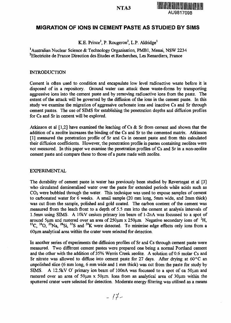
Figure 1 displays the SIMS concentration profiles for Cs and Sr as measured in the Portlandcement paste. The cesium has penetrated the cement to a depth of around 2mm. Thestrontium is not detected by SIMS beyond a distance of approximately lmm.
: 4000-
2000-
Cs (no Zeolite)
70000-
60000-
50000-
40000-
30000-
20000-
10000-
0-
0.S 1.0 1.5
Distance (mm)
Sr (no Zeolite)
0.5 1.0 1.5
Distance (mm)
Figure 1 Concentration profiles for cesium and strontium in Portland Cement as measured by SIMS
Figure 2 displays the SIMS concentration profiles for Cs and Sr as measured in a zeolite-richcement. The strontium has penetrated to a detectable distance of around 1-1.5mm. Theconcentration of cesium from spot to spot is more variable. A general trend similar to thatseen in Figure 1 is observed and a reduction in the number of cesium ions detected is apparent.In the zeolite-rich cement the cesium drops to SIMS detection limits at around 1.5mm.

20000n
• ••
• •
• •
••
0.0 0.S 1.0 t.5
Distance (mm)
Cs (with Zeolite) |
•• • •
2.0 2.5
140000 -
120000 -
100000 -
8 0 0 0 0 -
60000 -
4 0 0 0 0 -
2 0 0 0 0 -
0 -
•
•
0.0
I -•
•• •
•" . •
• • •• • I
0.5 1.0
Distance (mm;
Sr (with Zeolite)
• • • • • • •
1.5 2.0 2.
Figure 2. Concentration profiles for cesium and strontium in a zeolite rich cement
Ion imaging experiments demonstrated the heterogeneous and fine-grained nature of thecement matrix. Images acquired for various species, including Cs and Sr, illustrated thisheterogeneity showing that within a 250um x 250um area there are regions within which bothhigh and low Cs & Sr concentrations occur.
DISCUSSION
The heterogeneous nature of the cement samples was perhaps the most difficult aspect of thestudy to be overcome. The SIMS sampling area was small (50-250um), and imaging andoptical investigations had both clearly indicated that the heterogeneity was on a smaller scalethan this sampling area. The effects of the non-homogeneity was most pronounced in thestudy of the zeolite rich cement where the cesium has preferentially accumulated in the zeolitematerial. When the sampling area intersected a zeolite rich area anomalously high cesiumconcentrations were encountered. This results in the more variable Cs concentrationsobserved in Figure 2.
SEM has also shown that Cs is preferentially adsorbed into the zeolite in a non homogeneousmanner. The Cs concentration is unevenly distributed in the zeolite with some partsapparently being devoid of Cs. This is reflected by the penetration profile of Cs in the zeolitewhere some regions are rich in Cs. When these regions were removed from the profile itcould be fitted to the equation in Atkinson's paper [1] by least squares to give a difiusioncoefficient that was indistinguishable to that fitted to Cs in cement paste. It would appear thatthere is no measurable difference between the diffusion coefficients of Cs in cement paste andin a zeolite cement paste.
REFERENCES
1 A. Atkinson & A.K. Nickerson Nud. Tech. 81 100-113 (1988)2 A. Atkinson, K. Nelson, & T.M. Valentine, Nucl. Chem. Waste. Manage. 6 241-253 (1986)3 E. Revertegat, C. Richer & P. Gegout. Cement & Concrete Research 22 259-272 (1992)4 F.P. Glasser, Adv, Cement. Research. (1990)

NTA4AU9817099
Structural And Superconducting properties of LaCaBaCu3O7-s system:
A Neutron diffraction Study.
V.P.S. Awana1, T.J. Green1, Scott Moss1 SJC. Dou1, S.K. Malik2 and W.B. Yelon3
1 Centre for Superconducting and Electronic Materials, University of Wollongong, Wollongong,
NSW 2522, Australia, 2 Tata Institute of Fundamental Research, Homi Bhabha Road, Bombay-
400005, India,.3 Research Reactor Facility, University of Missouri, Columbia MO 65211, USA.
ABSTRACT
The results on structural aspects and superconductivity of LaBaCaCusO? (La:1113) are
reported. Both X-ray and neutron diffraction studies reveal that the La: 1113 compound
crystallises in P4/mmm tetragonal structure. Our careful and detailed neutron diffraction study
reveals that in this compound the La, Ca and Ba sites are intermixed with each other. Nearly
46% of Ca occupies the usual La-site, while the remaining 54% stays at the Ba-site. In
stoichiometric La: 1113 compound, a corresponding amount of La substitutes at the Ba-site.
These occupancy refinements explain the tejragonal structure of the compound, despite having an
oxygen content close to 7.04. The compound studied presently shows a Tcof 68K.
L INTRODUCTION.
There are several RE (rare earth) based HTSC (High Temperature superconducting)
families such as REBa2Cu3O7(RE:123), REBa2Cu,O8(RE: 124), and RE2Ba,Cu7Oi4(RE:247)
[1,2]. RE based 123, 124, and 247 superconducting families are known for nearly all rare earths
except Ce, Pr and Tb. RE: 123 compounds show superconductivity around 90K with oxygen
content close to 7.0, for all rare earths, except Ce Pr and Tb. While Ce and Tb do not form the
required structure, the case of Pr is unique due to its magnetic interaction with the neighbouring
Cu-0 conduction band [3,4]. The same is true in the case of RE: 124 and 247 compounds [2,5].
Another relatively new RE based HTSC family is called RE: 1113 (REBa2Cu3O7). The
RE: 1113 family is unique in terms of phase formation and crystal structure. Unlike RE: 123 and
124, RE: 1113 compounds form only with heavier rare earths such as La, Pr and Nd [6].
Moreover RE: 1113 compounds crystallise in a tetragonal structure with an oxygen content close
to 7.0 [6,7]. The main aim of the present study is to explore the finer structural details of this
compound by Rietveld analysis of the neutron diffraction patterns of the superconducting (Tc =
68K) LaBaCaCusO? compound. Our results reveal that it is the intermixing of Ba, Ca and La
sites in the parent RE: 123 structure which gives rise to the formation of teragonal RE: 1113
compound with equal occupancies of 0(1) and 0(5) sites in Cu-0 chains.
II. EXPERIMENTAL DETAILS
The presently studied LaBaCaCu3O7 compound is synthesised through solid state
reaction route. The ingredients i.e La2O3, BaCO3, CaCO3 and CuO were mixed in a
stoichiometric ratio and fired at 975 C for several hours. Finally the as formed compound is
annealed in flow of oxygen at 575C for 24 hours and subsequently allowed to cool to room

temperature in the same gas environment over a span of 6 hours. AC magnetic susceptibility
measurements were done using a Quantum Design SQUID magnetometer with an applied r.m.s
field of 0.10 gauss and at 1117 Hertz.. The Neutron diffraction pattern at room temperature was
obtained using the Research Reactor Facility of the University of Missouri. The experimental
details applied are similar to those reported earlier for RE: 123 ceramic samples [8]. In brief, the
samples were contained in a thin walled vanadium can. Neutrons of wavelength 1.4783 A were
selected for the diffraction experiments. The diffraction data were recorded from 10° to 100°,
0.05° intervals, using a 5 element position sensitive array covering 20°.
BDL RESULTS AND DISCUSSION.
AC susceptibility versus temperature plot for the LaBaCaCu3O7 compound is shown
below in Figure 1. The superconducting transition temperature, Tc, is defined as the onset of
diamagnetic transition, which is around 68K with a sharp transition and no visible second step
in the susceptibility down to 4.2 KlxlO"4
0
" ? -lxlO-4
&b -2X10⁻⁴
-3x10-41-4x10"
[TTTrp vi i | i i i'i "j" i"i rr]~TinT"|~rTiT[7 i i i j i i i~rp-r"rrrm=
LaBaCaCu3O7
1 1 1 1 1
10 20 30 40 50 60 70 80 90 100
Temperature (K)
Figure. 1 AC susceptibility versus temperature plot for LaBaCaCu3O7
The neutron diffraction powder data was analysed by the Rietveld refinement procedure using
the Generalised Structural Analysis System (GSAS) program. A typical observed and fitted
neutron diffraction pattern of LaBaCaCu3O7 sample is shown below in Fig.2.
o
•fe °.
1u
o
1 1 r
!,.|.47S3A
1 1- L
1 • i i
I i i
—i 1 1 r-
LaBaCaCu3O7.5
I I I I
0 . 1 0 . 2 0 . 3 0 . 4 0 . S 0 . 6 0 . 7 0 . 8 0 . 9 1 . 0
2 0 ( 1 0 : d e c r e e s )
Figure.2 Fitted and observed neutron diffraction patterns for LaBaCaCu3O7.
It becomes evident from this figure that small peaks, attributed to un-reacted material, are
present, similar to those found in the X-ray diffractograms of this compounds [6,7]. The results
of Rietveld analysis for LaBaCaCu3O7 sample reveal (see Table. 1) that part of the La occupies
the Ba site with a corresponding amount of Ca occupying the nominal RE site. As shown in

Table. 1, 46% of Ca atoms occupies the usual La-site, and the remaining 54% is at the Ba-site.
In the stoichiometric compound subsequently 46% of La occupies the Ba-site in the structure.
This suggests that RE: 1113 compound can form with only the bigger ionic radius members,
which can substitute easily at Ba-site, like as Nd, La and Pr. Also the mixing of Ca, Ba and La in
the structure can bring the 0(1) and 0(5) site occupancies closer to each other giving rise to a
tetragonal system [8,9].
Table.2 Structural parameters for LaBaCaCu3O7.04 (space group P4mmm):
Atomic positions (x, y, z) occupancy and isotropic thermal parameter (UisO).
Atom
Ba
Cu(l)
Cu(2)
0(1)
0(2)
O(4)
Ca@Ba
Ca@La
La@Ba
La@La
Space Group positions
2t
la
2q
le
2s
2q
2t
lh
2t
lh
X
0.5
0
0
0
0.5
0
05
0.5
0.5
0.5
y
0.5
0
0
0
0
0
05
0.5
0.5
0.5
z
0.1849(5)
0
0.3527(5)
0
0.3664(4)
0.1579(9)
0.1849(5)
0.5
0.1849(5)
0.5
Occupancy
0.5x2
l x l
2 x 1
0.72(3) x 2
0.99(2) x 4
0.83(3) x 2
0.27(2) x 2
0.46(5) x 1
0.23(2) x 2
0.54(5) x 1
100 x Ubo (A3)
0.55(19)
1.10(10)
1.10(10)
8.28(69)
0.46(14)
1.73(40)
0.55(19)
0.29(28)
0.229(23)
0.29(28)
The authors at University of Wollongong Australia would like to thank the Australian
Research Council (ARC). Part of this work was supported by the US Department of Energy
Grant No. DE-FE0290ER45427 through the mid-west superconductivity consortium.
REFERENCES
1. H. Oesterreider and M. Smith, Mater. Res. Bull. 22,1709 (1987).
2. L. Soderholm, K. Zhang, D.G. Hinks, J.D. Jorgensen, C.U. Segre, and I.K. Schuller, Nature
328, 604 (1987).
3. J. Herrmann, U.-C. Boehnke, M. Kortzsch, and F. Schlenkrich, Physica C 221, 76 (1994).
4. A. Kebede, C.-S. Jee, J.Schwegler, J.E. Crow, T. Mihalisin, G.H. Myer, R.E. Salomon, P.
Schlottmann, M.V. Kuric, S.H. Bloom, and R.P. Guertin, Phys. Rev. B 40, 4453 (1989).
5. See, for instance, S.K. Malik, and C.V. Tomy, in Physical and Material Properties of High
Temperature Superconductors, edited by S.K. Malik and S.S. Shah (Nova Science, New
York, 1994), p. 283.
6. W.T. Fu, H.W. Zandbergen, and L.J. de Jongh, Physica C 156,133 (1988).
7. J.L. Peng, P. Klavins, R.N. Shelton, H.B. Radousky, P.A. Hahn, L. Bernardez, and M.
Costantino, Phys. Rev. B 39, 9074 (1989).
8. V.P.S. Awana, S.K. Malik, and W.B. Yelon, Physica C 262,272 (1996).
9. V.P.S. Awana, S.K. Malik, and W.B. Yelon, Mod. Phys. Lett. B 10, 845 (1996)

SESSION 3(Chair: A.P. Byrne)
NOVEL TECHNIQUES OFANALYSIS

AU9817100
Amorphization of InP studied using Perturbed Angular Correlations
E. Bezakova1. A.P. Byrne1-2, M. C. Ridgway 3 and C. Glover 3
1 Department of Nuclear Physics, RSPhysSE, Australian National University,ACT 0200, Australia
2 and Department of Physics, The Faculties, Australian National University,ACT 0200, Australia
3 Department of Electronic Materials Engineering, RSPhysSE, Australian NationalUniversity,
ACT 0200, Australia
1. Introduction
The ion beam induced amorphization of InP has been studied using perturbed angu-lar correlation (PAC) technique. The technique uses radioactive atoms as probes andmeasures the hyperfine interaction of these probes with the local fields in the sample.The charge distributions of particular defects induce electric field gradients which coupleto the electric quadrupole moment of the excited state of the radioactive nucleus. Asa result of this interaction the distribution pattern of the emitted radiation is changedas a function of time. Observation of these changes can provide information about thestructure and concentration of defects. More details about the technique can be foundelsewhere [1,2,3].
2. Experimental Methods
a) Production and Implantation of111 In
The radioactive isotope m I n was implanted into InP wafers using a direct productionand recoil-implantation technique. This method uses heavy ion beams from the ANUHUD accelerator to both produce and implant the isotope. The experimental setup isshown in Fig. 1. The following nuclear reactions were used for production of m I n :
103Rh(i2C, p3n)mSn
103Rh(12C, 4n)mSb X ^ i n l u Sn ^ 2 ? m I n
Beam • >
: 'Rh+ :-C=> 1!lSn=> : | :In u Sample
Fig. 1: Experimental setup for production and recoil-implantation of m I n
43-

The energy of carbon beam was 69 MeV. Samples were mounted approximately 2 cmbehind, a thin rhodium target and around 60% of all recoils can be implanted into thesamples (see Fig. 1). The activity of each sample was about 3.3 fiCi corresponding toabout 1.3xlO10 indium ions. TRIM calculations indicate that most of the ions come torest within 1 to 2.5 microns in InP wafers. After radioisotope implantation the sampleswere annealed at 800° C for 10 s (using rapid thermal annealing technique) in order toremove any damage.
b) Amorphization of InP Samples and PAC Measurements
Ion beam amorphization was achieved using Ge beams with dose concentrations between2 x 1012 ions cm"2 and 150 x 1012 ions cm"2. Ion beams of different energies wereused in order to obtain uniform damage from the surface to 2.5 /zm depth. Off-linePAC measurements were performed for each sample using a four detector BaF2 arrayand a ratio function, R(t), was formed from the measured spectra in order to factorout the exponential from the decay curves. This function is equal to the product of thepertubation function and the anisotropy coefficient.
a) b)
-0.150.05
0.00 -
g-0.0505
-0.10 -
-0.15
21 d)
********rI
i I
1 I '
> I i
29.5:;101 J
? -
i t
f)
1 i •
i i i
1 i '
I
i i
i i
i '
i ,
i
19.
i
147.
i
feio12]
-
^2\
mm
-100 200
time (ns)300 400 100 200
time (ns)300 400
Fig. 2 Measured Ratio Function, R-(t), for samples implanted with Germanium ions ofdifferent dose concentrations (1012ions/cm~2)

Results
The ratio functions for 6 of the samples are shown in Fig. 2. They show a smoothtransition from the crystaline (a) to amorphous (f) state as a function of dose. Tworegimes can be observed, one where the probe nucleus sits on a weakly disturbed siteand the other corresponding to a very damaged environment. In order to describe thisbehaviour the spectra were fitted with the "two fraction" pertubation function:
G2(t) = fiG2(a>ut) +/2(?2(w2,t)where fractions, f, correspond to the number of indium nuclei associated
I
100
80
60
40
20
n
-
-
-
-
i
i ' i '
i , i i
• + :
--
i i i i i i
0 10 20 30 40 50dose [10 ions]
Fig. 3: Dependence of the amorphousfraction on the implantation dose
with non-amorphous and amorphous sites in InP samples. Fig. 3 shows the dependenceof the amorphous fraction on the Germanium implantation dose. The portion of thisfraction increases linearly with implantation dose. Rutherford backscattering and X-rayDiffraction measurements have been performed on the equivalent samples and the resultscorrelate well with PAC results.Work is currently under way to calculate the expected pertubation function correspond-ing to particular damage distributions.
References
1. Wichert, T. and Reckangel,E., Microscopic Method's in Metals,Springei Verlag, 19862. Mahnke,H.E., Hyperfine Interactions 49 (1989), 773. Deicher,M., Hyperfine Interactions 79 (1993), 681

NTA6AU9817101
NEUTRON ACTIVATION ANALYSIS - AN OLD TECHNIQUEBUT IS IT STILL USEFUL?
Gordon D. McOristEnvironmental Radiochemistry Group, Environment Division, ANSTO, PMB 1, Menai, 2234.
For over 30 years, neutron activation analysis (NAA) has proven to be a sensitive andaccurate method for determining the concentration of a large number of trace elements in awide variety of samples. More recently, however, other techniques such as ICPMS, ICPOES,XRF and others have replaced NAA as the method preferred by a large number of analyticallaboratories around the world. As the capital cost of these instruments has fallen, anincreasing number of these laboratories have been able to purchase and locate them withintheir own facilities. Since they are now able to quickly analyse samples and determine traceelements at levels similar to NAA, the result appears to be a decline in the number of samplesrequiring analysis by NAA. Therefore, is NAA still useful?
All analytical methods have applications to which they are particularly suited while at thesame time being totally unsuited to others. By changing other characteristics such as samplepreparation protocol, instrument settings and so on, they can now analyse a reasonably widevariety of samples, for most elements, at reasonable levels of detection. However, whencompared with these other analytical techniques, there are certain aspects of NAA whichmake it uniquely suitable to analyse certain types of samples and for particular elements:
1. NAA is a non-destructive technique of analysis making it particularly suitable for valuableor irreplaceable types of sample. We have carried out comprehensive trace elementanalysis on diamonds, black precious opal and ancient fish fossil bones and have beenthen able to return the sample to the client.
2. It is particularly suited to analysing solid samples since no sample dissolution, with itsassociated problems, prior to analysis is necessary.
3. NAA is remarkably free of matrix effects essentially eliminating complex pre-analysisprocedures.
4. Unlike the methods previously mentioned, it is uniquely suited to determining low levelsof certain elements such as Cl, Br and I, particularly in organic samples. Our ability todetermine sub-ppm levels of Cl in transformer oils has greatly assisted in the developmentof a patented method for the destruction of PCB's.
5. It is possible to analyse large samples in order to overcome homogeneity problems, whichis particularly useful in the precious metals industry.
6. Radiochemical NAA enables the determination of very low levels of particular elements(eg Ta) in samples traditionally difficult to dissolve.
It is these and other aspects of NAA which ensure that it is still the preferred method ofanalysis in many instances. As with any other method of analysis NAA has certaindeficiencies, but these are more than outweighed by the benefits derived in the particularapplications described above.

NTA7AU9817102
An EXAFS study of ion-induced structural modification of GaAs.
C J Glover1. M.C. Ridgway1, G J . Foran2 and K.M Yu3
1 Department of Electronic Materials Engineering, Research School of Physical Sciences and Engineering, AustralianNational University, Canberra, ACT 0200.
2 Australian Nuclear Science and Technology Organisation, Menai, Australia.3 Materials Science Division, Lawrence Berkeley National Laboratory, Berkeley, USA.
Ion-induced structural modification of GaAs has been investigated using extended x-ray absorptionfine structure spectroscopy (EXAFS). The local atomic structure has been probed to understand thecharacteristic properties of amorphous GaAs, in particular, the existence of wrong bonds, potentiallythe cause of defective recrystalisation during solid phase epitaxial growth (SPEG). EXAFS, utilising anovel sample fabrication technique, has been utilised to measure the artefact-free structuralparameters of stoichiometric amorphised GaAs for the first time. All experimentally determinedstructural parameters were found to be independent of both implant temperature and incident iondose, and were considered representative of intrinsic amorphous GaAs, as opposed to implantationinduced extrinsic structure. The defective recrystalisation of amorphous GaAs was subsequentlyattributed to this intrinsic disorder as opposed to ion implantation induced specific disorder.
1. Introduction.The low temperature (200°C - 400°C)recrystalisation of amorphised GaAs yieldsdefects in the form of twins and stacking faults[1], as shown in the cross section transmissionelectron micrograph in Fig 1. It has beensuggested that this defective solid-phaseepitaxial growth (SPEG) can be the result oflocalised microscopic non-stoichiometryinduced by ion implantation, the latter requiredto initially amorphise the material. The extentof twinning was expected to be ion dosedependent [2]. Also, theoretical calculations ofthe structure of amorphous GaAs predict theexistence of significant fractions (-12%) oflike-atom bonding (so called wrong bonds) andunder- or over-coordinated atoms (40%) [3],which implies non-equivalent atomicenvironments of Ga and As. Previoustransmission EXAFS studies of amorphousGaAs [4,5] have reported contradictory results,attributed to differences in sample fabricationmethodologies [5]. Both flash evaporation andsputtering have been used in the past, whichhave resulted in non stoichiometric films [4-8].These studies show that the resulting structuraldisorder demonstrates a stoichiometricdependence [7], in agreement with theoreticalresults [10,11]. For this study, extended x-rayabsorption fine structure spectroscopy(EXAFS), has been utilised with a novelsample processing technique, to measure theartefact free structural parameters of
stoichiometric amorphised GaAs for the firsttime.
Figure 1. Micrograph of defective SPEG of GaAsannealed at 260°C. (Courtesy K. Belay).
2. Experimental.Amorphous GaAs samples were prepared by anovel technique based on epitaxial lift-off(ELO) and ion implantation [12]. As can beseen in Fig 2, a 2.5 |J,m GaAs sample layer anda 0.02 (xm AlAs release layer have been grownon a GaAs (100) substrate under lattice-matched conditions. The heterostructures weregrown by metal organic chemical vapourdeposition (MOCVD) at 650°C, and weresubsequently amorphised to a depth of -2.7 |xmby Ga and As co-implantation. Multiple energy/ dose implants at -196°C were utilised toproduce a near constant value of energydeposited in vacancy production as calculatedby the TRIM code [13] and as shownschematically in Fig 3. Equal doses of Ga and

As were implanted to maintain stoichiometry (±<0.01%), ranging two orders of magnitudegreater than the amorphisation threshold [1].The AlAs release layer was preferentiallyetched in a 10% HF solution1 then theamorphised GaAs layer was bonded toadhesive, x-ray transparent, Kapton film.
l.MOCVD growth
2. Ion implantation
3. Etch AlAs layer
4. Bonding to Kapton
c-GaAs
a-GaAs
AlAs
Kflpton film
Figure 2. Schematic diagram of GaAs samplefabrication utilizing selective chemical etching.
3.0x10** I ' • ' ' I ' ' ' ' I ' ' ' ' I ' '
•* 1 MeV• 3 MeV :• ? MeV* sum
0.5 1.0 1.5 2.0Depth (yam)
2.5 3.0
Figure 3. Energy deposited in vacancy productionfollowing a multiple energy, multiple dose Asimplant sequence. The implant energies for the lowermass Ga ions were less than As to maintain localstoichiometry.
The x-ray absorption spectra of Ga and As K-edges, at 10.37 and 11.86 keV respectively,were recorded in transmission geometry at 10Kon beamline 2-3 of the Stanford SynchrotronRadiation Laboratory (SSRL). A Si(220)channel cut crystal monochromator was used,
1 The selectivity of HF for AlAs / GaAs isapproximately 108:l.
with energy resolution estimated to be AE ~ 1eV at 10 keV. Crystalline reference sampleswere prepared from finely crushed powdersmixed with a BN binder. The effective samplethickness, x, was -16 |lm (ie pc ~ 1.5, where fiis the energy dependent absorption coefficient).Amorphous samples were simply stackedtogether to gain this required thickness.Following removal of both the pre-edge andpost-edge background by spline polynomialapproximations, the normalised EXAFS wasFourier transformed over a photoelectronmomentum2 (k) range of 3-18 A and 3-20 A forthe Ga and As K-edges respectively. Thestructural parameters of the first nearestneighbour shell were isolated by inversetransforming over a non-phase corrected radialdistance range of 1.5-2.7 A for both Ga and Asabsorbers. Analysis was performed with theXFTT code [14], in the single scatteringapproximation, with phase and backscatteringamplitude calculated ab initio with the FEFF4.0code [15]. The ratio method [16] was thenutilised for more accurate determination ofsingle shell coordination numbers.
For each K-edge, the amplitude reductionfactor, So, was determined from the crystallinereference sample with the nearest neighbourcoordination number, n, set to 4. This edgespecific value of So
2 was subsequently fixed inthe analysis of amorphous spectra [17]. Thesubsequent refinement of the threshold energy(Eo), nearest neighbour bond length (r), Debye-Waller factor (o2) and n, allowed meaningfulcomparison of implantation induced structuralmodification of the amorphous material tocrystalline GaAs.
3. Results.
Figure 4 shows the EXAFS and Fouriertransforms of the crystalline and amorphoussamples. For the crystalline sample, the detailedstructure apparent in the EXAFS spectrum wasthe result of scattering from first, second andthird nearest neighbours, as can be readily seenfrom the corresponding Fourier transform. Incontrast, the EXAFS of all the amorphous
* = nt(E-E0)n
, where E is the energy of the
incident x-ray photon and Eo is the threshold energyfor removal of the core electron.

samples were composed of a single frequency,indicating scattering from a single shell only.Correspondingly, the Fourier transform showsno evidence of scattering from next nearestneighbours, consistent with the lack of anylong range order and a tetragonal distortion inthe amorphous material.
40
so
BO
IL- 2 0
- 4 0
(a):
crystalline
5 10 15
Photoelectron Momentum (A"1)20
2 3Radial Distance (A)
Figure 4: (a) Spectra of A^-weighted EXAFS as afunction of photoelectron momentum, k and (b) Nonphase corrected Fourier transform as a function ofradial distance of crystalline and amorphous GaAs at10K. Individual spectra have been offset for visualclarity.
Figure 5a shows phase corrected r ofamorphised samples as a function of the energydeposited in vacancy production3 for both Gaand As absorbers. From this it can be seen thation implantation induced amorphisationproduced an increase in nearest neighbour bondlength from 2.445±0.003A for crystalline GaAsto 2.451+0.006A for amorphous GaAs, thelatter being independent of ion dose4. This
3 Energy deposited in vacancy production, Evac, isproportional to total ion dose.4 Though the magnitude of this difference was withinthe bounds of experimental uncertainty, the relative
increase agrees with other EXAFSmeasurements of sputter deposited and flashevaporated amorphous GaAs [5-7].
2-47
J 2.46•O§u 2.45ojasiw>
1 2-44
Z 243
_^ 0.005
o 0.004
£
! 0.003
II
1 0.002
4.4
4.2
4.0
3.8
c3 3-6aa
o
s3.4
3.2
••
3a
i
i
i i1
1
Ga (cryst)As (cryst)
^—i—i | 11 n| 1 i i | 11 n| i—i—i | i 11
GaAs
(c)
i ii
Ga and As (cryst)
10s 10s3 10M 10a
Energy Deposited in Vacancy Prod'n (eV/cm3)
Figure 5: Experimental values of (a) nearestneighbour bond length, (b) relative mean squaredeviation in nearest-neighbour bond length and (c)nearest neighbour coordination number for both Gaand As absorbers as a function of energy depositedin vacancy production. Horizontal lines representuncertainty limits of values measured in crystallinesample at both edges.
From Fig 5b, the o2 values for the amorphisedmaterial were greater than that of thecrystalline, consistent with increased structuraldisorder inherent in an amorphous phase. Asfor r, o2 was independent of the energydeposited in vacancy production (and thus ion
difference was consistently measured over the iondose range examined

dose), although o2 measured at the Ga edge wasconsistently greater than that of the As edge.This is potentially indicative of like atombonding, where Ga-Ga bonding could manifestitself by differences in a2 and/or r, and n.Figure 5c shows nearest neighbourcoordination numbers of both Ga and Asabsorbers, obtained via the ratio method. Theobserved reduction in coordination numberfrom 4 to ~ 3.85 ± 4%5 was also independent ofion dose. This indicates that the majority ofatoms in a-GaAs that were not four-foldcoordinated were under coordinated. Thisagrees well with the theoretical prediction thatthe predominant defect in stoichiometric,amorphous JJI-V semiconductors is a three-foldcoordinated atom [10]. Further, sets of samplesproduced under different implant conditionswere also analysed. Selected a-GaAs sampleswere annealed at 200°C for lhr to investigatepotential structural relaxation in the amorphousphase. Other samples were implanted at 20°Cto investigate a possible implant temperaturedependence of a-GaAs. However, changes in r,(forn were not observed in either case, nor didthey exhibit any ion dose dependence. Giventhis, and the complete lack of ion dosedependence for the structural parameters, it issuggested that the experimentally measuredstructural parameters of ion-implantationinduced amorphous GaAs are representative ofstoichiometric, intrinsic amorphous GaAs. It isfurther suggested that the defectiverecrystalisation observed following SPEG ofamorphous GaAs has not resulted fromextrinsic, ion-implantation induced disorder,but rather the presence of intrinsic disordercharacteristic of amorphous GaAs. This issupported by the observation of defectiveSPEG of stoichiometric, amorphous GaAsproduced by molecular beam epitaxy [18].
4. Conclusions.Transmission EXAFS has been utilised tomeasure the structural parameters ofamorphous GaAs samples, fabricated using anovel, artefact free, preparation methodology.Relative to crystalline GaAs, the nearestneighbour coordination number has decreasedand the nearest neighbour bond lengths and the
5 Again, the relative change in n was consideredexperimentally valid.
Debye-Waller factors have increased, the latterconsistent with structural disorder. Differencesin Debye-Waller factor about the two latticeconstituents were potentially indicative of like-atom bonding. Also, no ion dose dependence ofany of the measured structural parameters wasobserved, and thus the experimental values ofo2, r, and n were considered representative ofthe intrinsic structure of amorphous GaAs , asopposed to implant induced extrinsic structure.It is also proposed that the defectiverecrystalisation of amorphous GaAs occurs dueto the incorporation of intrinsic defects fromthe amorphous phase, and not fromimplantation induced specific disorder.
5. References.[I] M.C Ridgway, K.B Belay et al, Nucl. Instr.
And Meth. In Phys. Res. B 127/128 (1997).[2] G.L Olsen and J.A. Roth in Handbook of
Crystal Growth (Elsevier, Amsterdam 1994)[3] H. Seong and L.J Lewis, Phys.Rev B50,
4371 (1994).[4] J.A Del Cueto and N.J Shevchik, J.Phys.
C:Sol.St.Phys. 11, L829 (1978).[5] M.L. Theye, A Gheorghiu and H. Launois,
J.Phys. C: Sol.St.Phys. 13, 6585 (1980).[6] D. Udron, M.L Theye et al, J.Non-cryst.Sol.
137/138,131 (1991).[7] S.H Baker, M.I Manssor et al, J.Non-
cryst.Sol. 144, 63 (1992).[8] D. Udron, A.M Flank et al, J.Non-cryst.Sol.
150, 361 (1991).[9] A.M Hank, P. Lagarde, D. Udron et al,
J.Non-cryst.Sol. 97/98,435 (1987).[10] E.P O'Reilly, J. Robertson, Phys.Rev.
B34, 8684 (1986).[II] J.P Xanthakis, P.Katsooulakos and D.
Georgiakos, J.Phys: Cond.Mat. 5, 8677.[12] M.C. Ridgway, C.J. Glover et al,
J.Synch.Rad., submitted (1997).[13] J.B. Biersack and L.G. Haggmark,
Nucl.Instrum.Meth 174, 257 (1980).[14] P.J. Ellis and H. Freeman, J.Synch.Rad. 2,
190 (1995).[15] J.J Rehrs and R.C Albers, Phys.Rev. B41,
8139 (1990).[16] E.A. Stern, D.E Sayers and F.W Lytle,
Phys.Rev. B l l , 4836 (1975).[17] E.D Crozier and AJ Seary, Can.J.Phys.
59,876 (1981).[18] J.S Blakemore, J.Appl.Phys 53, R123
(1982) and references therein.

NTA8Il l l l l l l l l l
AU9817103
Single Ion Transient-IBIC Analyses ofSemiconductor Devices using a Cryogenic
Temperature Stage
J.S.Laird, R.Bardos, C.Jagadish* and G.J.F.LeggeMiCTO Analytical Research Centre (MARC),
School of Physics, University of Melbourne, Australia.
* Electronic Materials Engineering (EME),School of Physics, Australian National University,
Canberra, Australia
Abstract:We present here a paper describing the new Transient - IBIC data acquisition and analysis system at
MARC. A discussion on the need for single ion control and temperature control is also given. The newcryostatic temperature control stage is introduced. Data is presented demonstrating the potentialimprovements in spatial resolution in materials of long lifetime by mapping on timing windows aroundthe prompt charge component in the charge transient.
Introduction:Ions traversing a semiconductor material give rise to an e-h plasma whose subsequent interaction with
the local crystal structure and collection via neighboring space-charge regions is the basis of the Ion BeamInduced Charge (IBIC). Transient current techniques using heavy MeV ions have been used for thesimulation of single event process (SEU). IBIC has also been applied to the SEU problem with its mainadvantage over the EBIC and OBIC technique being an energy selectable end of range to probe structureat a particular depth without removal of passivation layers. For a more complete characterization of adevice though, the temporal dependence of the collection process contains more information than theintegrated charge pulse height alone, as typically used in IBIC analysis. Acquisition of the spatio-temporalresponse of the device leads to investigation of time dependent device phenomena such as those associatedwith trapping processes and lifetimes.
Purpose of Single Ion ControlSingle ion control in Transient-IBIC is necessary due to the low transfer rates found with transient
recorders and Digital Storage Oscilloscopes (DSO's). The damage induced from ions striking the deviceduring the transient capture and transfer process degrades the device. Ideally the beam current is matchedto the transient collection rate (typically less than 20Hz). Maintaining such current is difficult since beambunching and timing spread leads to frequency components larger than the steady state required. Minimalbeam is necessary for non-destructive analysis. The second point in favor of single ion control is that ofcontrolling the timing of the ion injection process. The aspect of timing control needs carefulconsideration as the dynamic range in transient widths can be from fractions of (isec's to many msec's inthe case of Scanning Ion-DLTS. At long transient widths pulse pileup in the current transients canintroduce a significant source of error reducing the available timing window. Using a single ion systemenables wider windows in transient widths for a given beam current.
Transient-IBIC System DesignThe single ion system employs rapid electrostatic beam switching after the event detection has
occurred. For Transient-IBIC the recorded signal is used as the event trigger for beam pulsing. Figure 1below schematically illustrates the single ion beam line used for Transient-IBIC analysis.

Scan colls,
device\
Quadrupoles Aperture Slits Object Slits
cryostat Deflector Plates
Lecroy DSO
Figure 1: A schematic of the complete Transient-DBIC analysis system.
The diagrams consists of, going from right to left, a beam pulsing unit for fast timed deflection; themicroprobe object and aperture slits determining the 1st order beam spot size, lenses for beam focusing,ferrite core coils for beam scanning with a transconductance amplifier supplied with scan signals from aPC Lab PC+. The DUT is mounted on an X-Y-Z cryogenic stage with an Amptek A250 chargepreamplifier for charge transient collection.
Scanning System and Beam PulsingThe scanning system comprises a PC running Labview 4.0 equipped with a National Instruments
LabPC+ and GPIB-TNT+ card for both scan generation and lab control. A GPIB-TNT+ card is used forinstrumental control of a 300MHz Lecroy 9361 DSO, Keithley 487 bias supply and Conductus LTC-10temperature controller. Scan generation is achieved by the dual 16-bit DAC's onboard the Lab PC+ carddriving a transconductance amplifier through orthogonal magnetic dipole coils.
The scanning software allows programmed shape scanning with adjustable pixel spacingaccommodates, multiple ions per pixel. Scan rastering is based upon the hardware trigger supplied by theAmptek A250. Upon receiving an event tag, the beam pulsing system blanks the beam, downloads thetransient as captured on the DSO and repositions the beam to the next scan position. Having repositionedthe beam, the BPU receives an ON condition, and the process is repeated over the array. For any givenarray, a Keithley 487 picoammeter Voltage source both monitors the device leakage and sets the operatingbias. Likewise, the temperature for the array can also be set and monitored during an individual pass,although in practice the reduction in the collection rate due to extra instrument calls means the internalscan loop is designed to make no more calls than necessary. Temperature and leakage readings areacquired at the completion of a given scan. The software is written in a modular fashion to accommodatevarious experimental configurations with the optimal collection rate being 18Hz.
Cryogenic Temperature ControlA CTI Cryogenics cryodyne liquid He cryostat and compressor with a Conductus LTC-10 Temperature
Controller are used for device heating and cooling between 30-320K in the microprobe chamber. TheLTC-10 controller incorporates an automated PID feedback system using 2 Si - diode temperature sensorsand a 100Q heater as shown in figure 2. The controller is able to maintain temperature stability of 0.005Kover a broad range of thermal loads. Since typical vacuums in operation are of the order of 10"6-10"7 torrconvective loss is negligible. Radiative losses requires IR shielding. A polished aluminium shroud sittingat 77K acts as a radiative shield in the lower section of the cryostat (1st and 2nd stages ). From the baseof the balanced bellows section and into the target chamber, thin aluminized mila foil covers the copperconduction path providing radiative shielding. The entire cryostatic and interface to the target chamberare mounted on a x-y-z stage for external alignment
Large vibrations from the refrigerator and liquid He compressor require vibrational isolation for thespatial resolution not to be adversely affected. We achieve this using a balanced bellows in the y-directionfor decoupling vibrations along the housing. A Bruel & Kjaar piezoelectric accelerometer and chargesensitive preamplifier connected to the DSO are used to examine the vibrational spectrum using Fourier

decomposition. Both the damping factors and directionnal components can be analyzed. Both STIM andvibrational monitoring point to near complete damping of the vibration along the vacuum housing towithin a nm. Vibrations on the thermal pathway are more difficult to remove primarily becausemechanical interference reduces both conductivity to the sample and introduces thermal leakage. Designis therefore crucial and we have taken the approach of designing a rigid vertical pathway connected to thetarget holder via a series of copper braid wound into springs.
Data and Results:Shown below are the extracted line profiles across the edge of a Au-Si junction collected at 52K. The
profile is produced by integrating the transient in a given timing window and normalizing to the completecharge transient. The images are sensitive to pulse shape and indicate the dependence on diffusion oncarrier velocity and distance of injection point to the Au-Si pad. The Au-Si pad is seen to sharpen inresponse to forming shorter timing windows. Diffusion from outside the pad can be removed as shown infig 2(a). In figure 2(b) the image is most comprised on diffusing charge over longer time intervals.
I"5
1.05
0.95
0.85
0.75
0.65
0.55
0.45
0.35
0.25
sfcesam
f•
B§&—
. . < • .
ti—
25 50 75
distance100
• 0.0-1.0
• 1 .0-2.0
+ 2.0-3.0
O 3.0-4.0
O 4.0-5.0
(a)
O 5.0-6.0
16.0-7.0
(b)
The analysis of the profile has involved electrical characterization over the temperature range of 25-300K using a developed C-V and I-V variable temperature stage incorporating a liquid helium cryostat.Bandwidth limitations have been theoretically calculated for a junction including regions of partialdepletion and compared to the risetime measurement of 60ns.

NTA9 AU9817104
STUDY OF MICRO-DOSIMETER P-N JUNCTIONS USING ION BEAM INDUCEDCHARGE
K.K. Lee, A. Saint, D.N. JamiesonMicroanalytical Research Centre (MARC), School of Physics,The University of Melbourne, Parkville, Vic. 3052, AUSTRALIA
P.D. Bradley, A.B. RosenfeldDepartment of Physics, University of Wollongong,Wollongong NSW 2522, AUSTRALIA
ABSTRACT
Reversed bias p-n junction offered an excellent opportunity to understand the radiobiological effects of BoronNeutron Capture Therapy (BNCT) in tissues and carcinoma cells. Ionising radiation creates electron hole pairs insemiconducting materials. Under an electric field the charge carriers can be tapped externally to produce chargepulses. Therefore the junction can serve as a micro-dosimeter for the detection of charged particles such aslithium and helium ions produced as a by-product of neutron capture by the boron and nitrogen nucleirespectively. By arranging the reverse biased p-n junctions into a two dimensional array, it offers the possibilityof measuring the energy deposition pattern. In this paper, we have used the Ion Beam Induced Charge (IBIC)with a scanned MeV ion microbeam to image and characterise the array of p-n junctions.
INTRODUCTION
Boron neutron capture therapy involves the administration of a suitable boron compound to the lesions followedby thermal neutron irradiation of the target cells. The boron atom captures a neutron, which results in the releaseof highly linear energy transfer (LET) radiations such as alpha and lithium ions that are highly damaging and areusually lethal to carcinoma cells. Traditionally, dosimetry in this area has been difficult. Rosenfeld et al hassuggested the use of array of miniature p-n junctions as microdosimetry detectors to model biological cell underthe influence of neutron beam [1]. The problems associated with the use of silicon diode arrays asmicrodosimetric detectors have been outlined by Bradley et al [2]. The main issue is that silicon is not tissueequivalent. However, it was found by using Monte Carlo simulation to examine the energy deposition, ageometric scaling factor (which is ~ 0.63) is required to convert microdosimetric energy depositionmeasurements performed in silicon to equivalent deposition in tissue [2]. The second issue is the accurateknowledge of the charge collection volume of the reverse biased p-n junction, which will be discussed in thispaper together with the investigation of the spatial response of the microdosimeter similar to the operation of thedetector under high LET radiations.
EXPERIMENTAL
The IBIC experiments were carried out at the Microanalytical Research Centre in the University of Melbourne,which has a NEC 5U Pelletron accelerator. IBIC was performed on the diodes with H \ H2
+ and He+ ion beams.The beam was initially focused to a micron spot size on the target and was further reduced to submicron byreducing the diameter of both the object and collimator diaphragms. The focused beam was rastered across thearray and the IBIC signals were collected by charge sensitive preamplifier, whose output is digitised andrecorded by the data acquisition computer in event-by-event mode.
Fujitsu1 designed the prototype silicon array of p-n diodes. The n-type Si was developed by implantingphosphorus to a dose of 1015 atoms per cm3 at energy of 30keV, while the p-type was fabricated with similardose and energy by implanting boron. A p-type substrate was used. Aluminium contact layer of thickness 0.6 |J.mwas deposited above the p-n junction, and a passivation layer of SiO2 was deposited on top of it. The n-typeregions are interconnected together with aluminium tracks, and the same applied to the p-type regions. Thecapacitance-voltage measurement (CV) shows that the depletion thickness of the diodes at reverse bias diodes of9.3 volts is ~2 (xm. A second similar device except that it has a 2 Jim thick silicon dioxide underneath thedepletion layer was fabricated: silicon on insulator (SOI). The insulating layer acts as a barrier that cutoff charge
1 Fujitsu Pte. Ltd, Japan.

carriers from the substrate diffusing toward the deleption layer. With this it allows varying the collection volumeto simulate different cells thickness by changing the reverse bias voltage.
RESULTS AND DISCUSSION
Figure 1 shows the full IBIC spectrum of the p-n array. An alpha beam of 1.5 MeV was scanned over the deviceto produce this spectrum. Shown in figure 2(a) is the optical micrograph of the device. By gating at variouswindows in the spectrum as indicated in figure 1, we could obtain information indicating where the various IBICsignals came from in figure 2(b). Signals from window 1 is attributed to the charge collection from the p+
regions and the horizontal Al tracks. The p+ was fabricated as an ohmic contact to establish a low resistivityconnection to the p substrate. As expected the charge collection and from the p+ region should be at theminimum as it is the furthest away from the depletion region and only diffusion component contributed to thecollection. It was found that this region is more susceptible to ion beam induced damage as compared to the restof the device. A plot of IBIC signal as a function of dose per area shows that the signals started to shift down inenergy even after a dose of 4 ions per |Jm2, but levelled off at doses around 62 ions per um2. This indicated thatthe ion beam induces defects that allow higher trapping of charge carriers, as a result higher probability of chargerecombination, which leads to lesser charge collected. After doses of 62 ions per \im2 the charge produced at theend of range of the 1.5 MeV alphas contribute little to the charge collection, which explains that no furthervisible shift of the IBIC signals were observed. Similar phenomena were reported by Koehler [3]. He observedthat at large doses to a silicon diode, the charge collected was dramatically reduced, but on subsequent radiationthe changes in the signal was low. IBIC signals from windows 2 and 4 are contributed from the diffusion ofcharge carriers underneath the vertical tracks and from the substrate respectively. In having a thick aluminiumlayer over (0.6(xm) the n+ region, the energy of the alpha particles were reduced, resulting in having the IBICsignal pushed down to window 3 in the IBIC spectrum. Window 5 is the collected charge from within thedepletion region and includes the diffusion of charge carriers from the substrate. Region 6 is rather interestingand cannot be accounted for by using energy loss calculation over the Al cap. It is thought to be attributed toeither the enhanced charge generation mechanism due to a charging effect or the alpha particle glancing throughthe side of the n+ mask resulting in having greater energy reaching the depletion region.
A prime factor involved in the data interpretation of neutron experiments required the knowledge of the averagechord length of the sensitive volume, which in turn required the information on the diffusion length of thematerial. This factor is required for the conversion of charge pulse height spectrum to LET spectrum [4]. Todetermine the diffusion length, proton beams with energies 2 MeV and 3 MeV respectively were rastered overthe device and the result is shown in figure 3. To calculate the diffusion length, the following equation wasapplied:
Ion induced charge pulse height = fZdjZ (eqn. 1)
Where dE/dz is the electronic stoppingpower, Zd is the depth of the deleptionlayer, and L is the diffusion length. The firstterm on the right hand side of the equality isthe contribution from the charge carriersgenerated within the depletion region, whilethe second term refer to the contributionfrom the charge carriers diffusing towardsthe depletion region from the substrate. Afit to equation 1 with diffusion length of 51jj.m is required to produce the solid curveshown in figure 3.
450 650 850 1050 1250
Energy (keV)1450
Figure 1. IBIC spectrum from p-n array.

(a)(3) (2) (4)
Al interconnect High Intensity
15pm
Figure 2. (a) Optical micrograph of the array of p-n cells (b). EBIC map of the same device.
Low Intensity
1200A second device with a 2 ^un SOI was usedto simulate biological cells and wasanalysed with a 3 MeV H2
+ microbeam. Inhere, there is no contribution of chargecarriers from the substrate, instead onlycharge carriers generated from within thedepletion regions and lateral diffusiontowards the depletion regions are detected.Similar to the device without SOI, largerIBIC signals were obtained from the n+
regions than the p+ regions. IBIC signalsextracted from the p+ and n+ cells indicatedthat the diffusion length in this device is 53
1000 1500 2000
Energy (keV)2500 3000
Figure 3. Charge pulse height as a function of proton's energy.
CONCLUSION
In conclusion, a reverse biased p-n array could be used to provide an insight on the energy deposition of alphaand lithium in biological cells. It could provide answers pertaining to the role of boron distribution on the patternof energy disposition at microscopic level, crossfire effect that is the deposition of the alphas and lithiumparticles' energy in nearby neighbouring cells from an irradiated cell and the boron concentration within thenucleus. The present results can be used to assess the sensitivity of the dosimeter to the ionising radiation.
REFERENCES
[1] A. Rosenfeld et al, IEEE Transactions on Nuclear Science, vol. 43, No. 6, (1996).
[2] P.D. Bradley, A. Rosenfeld and B.J. Allen, to be published.
[3] A.M. Koehler, Radiation Research Supplement 7,53 (1967).
[4] Microdosimetry, ICRU Report 36, Issue 31(1983).

SESSION 5(Chair: B.V. King)
JOINT NTA-VSA PLENARYSESSION

P L 2 AU9817105
Visualization of Semiconductor Surface Etching With ScanningTunneling Microscopy
Professor J.H. WeaverDepartment of Chemical Engineering & Materials Science
University of Minnesota
Abstract
Etching, or the process of producing a pattern, is central to a great many technologies. In the worldof thin films and multilayers, etching (material removal) plays a complementary role to growth(material addition), and product fabrication is likely to include both etching and growth. This talkwill review recent progress made in understanding surface etching of semiconductors. Emphasiswill be on atomic-scale changes in surface morphology as revealed through scanning tunnelingmicroscopy. We will consider a specific case, the etching of Si by halogens, where the parametersthat are controlled are the flux and the fluence of the halogen beam and the reaction temperature ofthe substrate. The talk will highlight the kinds of information that can be gained and the newinsights that are provided. Studies such as these are being extended to include the effects of photonirradiation, ion impact, and electron impact, as they pertain to plasma processing ofsemiconductors.
John H. Weaver, Professor and Head, Electronic Materials GroupDept. of Chem. Eng. and Materials Science, University of Minnesota421 Washington Avenue, SE, Minneapolis, Minnesota 55455
www. cems. umn. edu/~weaver/jhw/jhw. htmlVoice: 612-625-6548Fax: 612-625-6043
NTA/VSA1 •IlllllllllllllllHIGH-TEMPERATURE EVOLUTION OF THE Si(lll) SURFACE AU9817106INVESTIGATED BY MEANS OF SYNCHROTRON RADIATION
S. Vandre'(l), A. Goldoni(l,2), V.R. Dhanak(3), A. Santoni(4), and M. Sancrotti(l)
(1) Laboratorio Nazionale TASC-INFM, Padriciano 99, 1-34012 Trieste, Italy(2) Dipartimento di Fisica, Universita' di Trieste, 1-34100 Trieste, Italy(3) Interdisciplinary Research Centre in Surface ScienceThe University of Liverpool, L63 B09 Liverpool, U.K.(4) ENEA-INN, Casaccia, Roma, Italy
Various scenarios have been depicted for the evolution of semiconductorsurfaces as a function of temperature. These include, for example, order-ordertransitions, surface metallization, and incomplete melting. In this context, theSI(lll) surface is an intriguing test-bench for both experiments and theory. The(7x7) to (lxl) transition (about 1140 K) of the Si(lll) surface has been qualified asan order-disorder one. Here, we report on an experimental systematic study ofthe Si(lll) surface as a function of temperature up to the bulk meltingtemperature (about 1683 K). The experiment has been performed at the beamlineTGM3 of the BESSY (Berlin) synchrotron radiation facility.Si 2p core level and angle-integrated valence band photoemission spectra havebeen measured on a wide of selected temperatures.Bulk versus surface electronic structure have been discriminated by exploitingthe synchrotron radiation runability. The unoccupied conduction states havebeen probed by means of Si 2p X-ray absorption spectroscopy. A surface phasetransition is found at about 1550 K which is interpreted in terms of incompletesurface melting.
Contact person:Massimo SancrottiLaboratorio Nazionale TASC-INFMPadriciano 99,1-34012 TriesteItalyPhone +39-40-3756-435FAX +39-40-226767e-mail [email protected]
I would prefer an oral presentation.
SESSION TOPIC Thin Films and Surface Science SS

NTA/VSA2 AU9817107
FEATURES OF THREE DIMENSIONAL ION MICROTOMOGRAPHY
A. SAKELLARIOU. M. CHOLEWA, A. SAINT, G.J.F. LEGGE
School of Physics, Microanalytical Research Centre, University of Melbourne, Parkville,3052, AUSTRALIA
AbstractInteresting features pertaining to three dimensional tomographic ion analysis of micro-samples are presented. The technique is capable of extracting very accurate mass densityand composition information. Information is obtained by performing a tomographic STIMand PIXE experiment on the sample. A priori information about low Z elements are easilyincorporated into this technique.
Introduction
Ion microscopy provides detailed quantitative information about microscopic samples.
The large penetrating distance of ion beams allows information from deep within the
sample to be measured. A particularly useful technique for calculating the internal prop-
erties of a sample is a tomographic experiment. With the use of Scanning Transmission
Ion Microscopy (STIM) and Particle Induced X-Ray Emission (PIXE) data, mass density
and elemental concentrations of a sample can be calculated. Implementation of these two
techniques into a tomographic experiment provides three dimensional distribution maps
of most micro-samples. Ion tomographic experiments involve non-linear processes which
preclude accurate reconstruction of a sample using conventional techniques. The Discrete
Image Space Reconstruction Aigoit thm (DISRA)[1] has been devised to handle the com-
plexities of combined STIM and PIXE three dimensional ion micro-tomography[2]. The
data from a STIM tomography experiment can be very accurately reconstructed and the
accuracy of the solution is dependent only on the precision of the model used to simulate
the experiment. The inherent noise associated with multiple iterations is reduced by a
special discretisation.
The Features
The technique that we use to reconstruct STIM and PIXE tomography data is (DISRA) [1]
and is our extension of the Image Space Reconstruction Algorithm (ISRA)[3]. A technical
account of DISRA can be found in [1]. In summary, the DISRA technique can reconstruct
the density of inhomogeneous samples for which complicated physical phenomena occur
during tomographic experiments. The physical phenomena include: parallel, fan and cone

beam geometries; non-linear probe-sample interactions; and the interactions between the
sample and emission products of probe-sample interactions. This is accomplished whilst
also retaining accurate density information at every voxel. The DISRA technique is iter-
ative and, at every iteration, the approximated density of the sample is used in a simula-
tion of the tomographic experiment. The simulation involves a model of the experiment
incorporating as many significant physical phenomena as possible. The results of the
simulation are used to provide corrections to the density of the sample. Noise is reduced
by constraining the density to discrete bands, the size of which are related to the iteration
number. A STIM and PIXE tomography experiment involves the modelling of numerous
physical phenomena in a simulation. It is possible to choose a few phenomena that are
considered significant and that are not too computationally expensive. Below a list of the
included phenomena are discussed. The stopping power of the ion beam is implemented
and is simply a STIM tomography experiment. The only limitation is that a priori com-
position information is required and consequently the accuracy of the calculated mass
density is critically dependent on the accuracy of the composition information. However,
PIXE information is used to provide this composition information. This is done by per-
forming a full STIM and PIXE tomographic analysis of the sample. The characteristic
x-ray emission calculations consist of two parts. The first part is the calculation of the
x-ray fluorescence yield and x-ray energies. The second part is the calculation- of the pro-
ton induced ionisation cross-section. The x-ray production cross-section is calculated by
multiplying the x-ray fluorescence yield and the proton induced ionisation cross-section.
Most x-rays that are emitted originate from deep within the sample. As a result these
x-rays are absorbed and have a significant effect on the calculated elemental concentra-
tions of a sample. PIXE tomography experiments require good x-ray statistics. To reduce
the experiment time whilst maintaining adequate x-ray statistics, a compromise between
beam current and resolution is required. Also, a large solid angle subtended between the
sample and Si (Li) detector, up to 2?r steradians, can be accommodated into the model.
However, another compromise is necessary because the amount of required computing
resources increases substantially as the size of the solid angle increases. Unfortunately,
low Z elements can not be detected with PIXE analysis. This information can be in-
cluded in the reconstruction problem as a priori elemental composition data. Note that
the quantitative accuracy of the mass density and concentration tomograms will always
be limited by the numerical precision of the expressions that are used to emulate these
physical phenomena. To calculate accurate elemental concentrations, it is important that
the majority of noise in the tomogram results from noise in the measured data, not from

artifacts in the reconstruction technique. Since DISRA has this ability, it is possible to
reconstruct trace amount distributions of non-bulk elements, in samples that have sharp
and/or enclosing structures. Sometimes trace amount distributions of bulk elements can
be measured. These measurements are usually attained after only 10 iterations. However,
a lot of computation time is required to simulate the experiment.
Conclusion
Accurate mass density and elemental concentration tomograms of microscopic samples are
possible. This is because data collected from STIM and PIXE tomography experiments
are processed using the DISRA reconstruction technique. The DISRA technique uses a
simulation of the experiment in which any number of physical phenomena can be modelled.
Incorporating the beam energy dependence of stopping power and x-ray production cross-
section and the attenuation of the x-rays, for any type of detector geometry into the
model results in sufficiently accurate results. Incorporating secondary fluorescence will
improve the accuracy of tomograms for certain combinations of elements in samples but at
the expense of using more computer resources. However, the reconstruction time can be
considerably reduced if the x-ray detector is placed so that the normal of the surface of the
detector is parallel with the axis of sample rotation. This allows attenuation calculations
to be calculated once, independent of the projection angle. Doing this will reduce the
reconstruction time by a factor equal to the number of projections.
References
[1 ] A. Sakellariou, M. Cholewa, A. Saint and G.J.F. Legge. (1997). "An accurate
reconstruction algorithm for tomography experiments that involve complex probe-
sample interactions," Meas. Sci. & Tech. 8, 746-758.
[2 ] A. Sakellariou, M. Cholewa, A. Saint and G.J.F. Legge. To be published. "Advances
in 3D ion micro-tomography."
[3 ] M.E. Daube-Witherspoon and G. Muehllehner. (1986). "An Iterative Image Space
Reconstruction Algorithm suitable for volume ECT," IEEE Trans. Med. Imaging,
MI-5, 61-65.
iff

SESSION 6(Chair: J.C. McCallum)
ELECTRONIC MATERIALS

NTA10Illllllllll
A U 9 8 1 7 1 0 8
ION BEAM INDUCED NITRIDATION OF SILICON
M.Petravic, J.S.Williams and M.Conway
Department of Electronic Materials Engineering, Research School of Physical Sciences and
Engineering, Australian National University, Canberra, ACT 0200, Australia
1. Introduction
High dose ion bombardment of silicon with reactive species, such as oxygen andnitrogen, has attracted considerable interest due to possible applications of beam-inducedchemical compounds with silicon [1]. For example, high energy oxygen bombardment of Si isnow routinely used to form buried oxide layers for device purposes, the so called SIMOXstructures. On the other hand, Si nitrides, formed by low energy (< 1 keV) or high energy(> 100 keV) nitrogen beam bombardment of Si, are attractive as oxidation barriers or gateinsulators, primarily due to the low diffusivity of many species in Si nitrides [1]. However,little data exists on silicon nitride formation during bombardment [2,3] and its angledependence, in particular for N2
+ bombardment in the 10 keV range, which is of interest foranalytical techniques such as SIMS. In SIMS, low energy oxygen ions are more commonlyused as bombarding species, as oxygen provides stable ion yields and enhances the positivesecondary ion yield. Therefore, a large body of data can be found in the literature on oxideformation during low energy oxygen bombardment [4-7].
Nitrogen bombardment of Si may cause similar effects to oxygen bombardment, asnitrogen and oxygen have similar masses and ranges in Si, show similar sputtering effects andboth have the ability to form chemical compounds with Si. In this work we explore thispossibility in some detail. We compare oxide and nitride formation during oxygen and nitrogenion bombardment of Si under similar conditions. Despite the expected similar behaviour, somelarge differences in compound formation were found.
2. Experimental
In this study we used (100) Si wafers of n-type with resistivity of 10 flcm. Oxygen andnitrogen bombardment was carried out either in a Riber MIQ 256 SIMS instrument (in whichthe primary beam energy and angle of incidence can be changed independently) using 6-12 keVO2"1" and N2+ ions at impact angles from 0°-60° or in an ion implanter using 15-40 keV O+ andN+ ions. All samples and SIMS craters, obtained under different conditions (primary beamenergy, angle of incidence and the dose of implanted oxygen or nitrogen), were analysed bySIMS (using Cs+ and O2+ beams) and Rutherford backscattering and channeling (RBS-C)(using 2 MeV He+ ions) to determine the concentration profiles of oxygen and nitrogen and toquantify the influence of primary beam parameters on the formation of surface compounds(oxides and nitrides).
3. Results and discussion
Bombardment of the Si surface with oxygen ions at near-normal incidence eventuallytransforms the surface into a continuous stoichiometric oxide, SiO2. Prior to SiO2 formation,there is a transient region over which the oxygen concentration increases with dose. Fortypical SIMS conditions, the O+ build-up profile changes smoothly, with a rather abruptchange at saturation (for high energy primary ions) [8]. The situation is quite different in thecase of N2
+ bombardment, where the build-up profile of N+ can exhibit several rather intenseoscillations before reaching a constant level. This effect is shown in Fig.la giving thedependence of N+ buildup profiles on the primary beam angle of incidence. As the impact angle
increases, oscillations become less intensive and at about 30° (measured from the normal to thesample surface) they disappear. This behaviour suggests a critical angle of about 30° belowwhich nitride is formed under the bombardment conditions employed in this study.
250 500 750Sputtering time (sec)
6
5332?>- 4•D0)
•^3D
£02
1
0
'-
-
'-
10KeV
. 0°
+ 55°
— Sim of
1. /
N2+
Si3N4
1 1
N
J °i . 1
r
h1 i
b):
-
-
100 150 200Channel
250 300
Fig.l: a) Build-up profiles of N+, measured during nitrogen bombardment at differentimpact angles; b) RBS-C spectra following 10 keV N2+ bombardment of Si during SIMS attwo different angles (the solid curve corresponds to RUMP simulation).
To reveal the nitrogen distribution following 10 keV N2+ bombardment at different
angles of incidence, the craters from Fig.la were analysed by RBS-C. Fig.lb shows RBS-C spectra for two cases of nitrogen bombardment at 0° and 55° to the surface normal.Bombardment at 0° clearly shows a composition close to Si3N,4, while the RUMP simulation(solid curve in Fig.lb) indicates substantial over-stoichiometry of the nitride film. In contrast,bombardment at 55° (Fig.lb) does not result in a surface nitride film, but rather in anamorphous Si layer containing high nitrogen content.
The results on angular dependence are summarised in Fig.2a which reveals apronounced change in nitrogen content at about 30°. For comparison, Fig.2a also shows theangular dependence for oxide formation (normalised to the nitrogen curve), following 10 keV
50
c3
s•3 25'>>T3in
"n
o2 0
1
(
1
?•o
•0
o #
o
I
1• 10
o 8
1
keV N2+
keV O2+
a)
0}
20 40 60Angle to surface normal, 0
80 0.0
2.0
1.5
, 0
0.5
n n
: b)
-
: /
- 10KeV N
y i
2\ 0 = 0°. , . 1 . . ,
' 1 ' ' ' ' 1 '
r /
Position
— Position
Position, i . . . . i .
-
11 S2 i
2J :
200 150 100 50Depth (A)
Fig.2: a) Normalised angular dependencies of oxide and nitride formation; b) RBS-Cnitrogen profiles collected from within SIMS craters labelled with 1, 2 and 3 in Fig.lb.

02+ bombardment. As expected from similar ranges and sputtering rates in Si, both oxygen andnitrogen bombardment exhibit similar angular dependence of compound formation.
To explain the differences between oxygen and nitrogen bombardment, one shouldnotice differences in formation and properties between Si and its oxide and nitride. There is alarge difference in atom density between SiO2 (7.05E22 atoms/cm3) and Si3N4 (1.03E23atoms/cm3). During nitride formation, there is almost no expansion of the Si lattice and thislarge densification may become more important for compound formation than swelling, whichdominates the oxide formation [3]. A consequence of this dramatic densification is a substantialreduction in ion ranges in Si nitride compared with Si, Rp=96A and 150A, respectively for 5keV N+ ions from the TRIM'95 code. Another important feature is the low diffusivity of manyspecies, including nitrogen, in Si nitride [2]. On the other hand, the reaction of N to form N2 ismuch faster than the reaction of O to form O2 (due to the stronger N-N bonds than the O-Obonds) and hence high dose nitrogen implantation (with excess nitrogen) may result information of N2 bubbles [1].
Keeping all this in mind, we propose the following explanation for observed differencesin oxide and nitride formation and segregation of impurities. The initial stage of buried nitrideformation is similar to that of oxide formation: nitrogen is not mobile in disordered Si and thenitrogen concentration below the surface builds up with N dose until a buried nitride layer isformed. With increasing dose, the excess N may be trapped in the Si nitride (low self-diffusionof N in Si nitride and a strong tendency of N to form N2) contributing to the observed over-stoichiometry of the nitride layer. At the same time the surface is being sputtered away, leadingultimately to the formation of a nitride layer continuous to the surface. Now, the range of Nions in the new Si nitride layer will be drastically reduced contributing again to the over-stoichiometry and leading to reduction in the width of the nitride film as sputtering takes place,consistent with a gradual decrease of film thickness shown in Fig.2b. With increasing dose andsputtering, implanted N again reaches the interface and reacts with Si to increase again thenitride layer thickness above the range of N ions. This process repeats itself until a dynamicequilibrium is reached: sputtering reduces the width of the nitride layer to one comparable to therange (plus straggling) of N in Si nitride. This process may contribute to the SIMS oscillationsin N build-up signal, shown in Fig.la.
In conclusion, we have observed some large differences in the ion beam inducedprocesses of nitridation and oxidation of Si. These differences are explained in terms of quitedifferent atomic diffusivities in oxides and nitrides, film structural differences andthermodynamic properties.
References
[1] See, for example, N.Herbots et al., in Low Energy Ion-Surface interactions, edited byJ.W.Rabalais (John Wiley&Sons, Chichester, 1994), pp.389-48O.
[2] J.A.Kilner et al., Nucl.Instrum.Methods B15, (1986) 214.[3] W.De Coster, B.Brijs, H.Bender, J.Alay and W.Vandervorst, Vacuum 45, (1994)
389.[4] N.Menzel and K.Wittmaack, Mat.Sci.Eng. B12, (1992) 91.[5] J.S.Williams, M.Petravic, B.G.Svensson and M.Conway, J.Appl.Phys.76, (1994)
1840.[6] W.De Coster, B.Brijs and W.Vandervorst, Nucl.Instrum.Methods B85, (1994) 911.[7] J.S.Williams, K.T.Short, M.Petravic and B.G.Svensson, Nucl.Instrum. Methods
B121, (1997) 24.[8] C.Tian, G.P.Bayer, W.Vandervorst and J.A.Kilner, in SIMSX, ed. by
A.Benninghoven, B.Hagenhoff and H.W.Werner (John Wiley & Sons, Chichester1997), pp.287-290.

NTA11
AU9817109
The Application of Car-Parrinello Molecular Dynamics tothe Study of Tetrahedral Amorphous Carbon
P. R. McKenzie1. D.G.McCulloch2 and C.M.Goringe2
1. School of Physics, University of Sydney, NSW Australia 2006.2. Key Centre for Microscopy and Microanalysis, University of Sydney, NSW
Australia, 2006.
The Car-Parrinello method for carrying out molecular dynamics enables the forces betweenatoms to be calculated by solving Schrodinger's equation for the valence electrons usingDensity Functional Theory. The method is capable of giving good structural predictions foramorphous network solids by quenching from the melt, even in situations where the bondingchanges from one site to another. In amorphous carbon where, depending on its environment,carbon may show sp2 or sp3 bonds. The method is applied here to the study of network solidsusing the example of tetrahedral amorphous carbon.
INTRODUCTION
Tetrahedral amorphous carbon (ta-C)is a high density amorphous carbon withproperties which reflect its relatively highfraction of tetrahedral bondingfl]. In thispaper, the details of the structure of ta-C areexplored using the Car Parrinello MolecularDynamics method[2j.
Various computer generatedstructures of amorphous carbon are availablein the literature using molecular dynamicstechniques. These are valuable in giving usinsight into the details of the structure, butthe usefulness of the result is dependent onthe accuracy of the method used. Carbon is adifficult atom to describe with an empiricalpotential owing to the possibility of itshybridization states varying between thetrigonal sp2 state and the tetrahedral sp3 state.Consequently, the so called ab initiomethods are the most useful, as they makeno assumptions about the hybridizationstates. This is important since one of theissues we would like to study is the detaileddistribution between these states, including
the degree to which the atoms are separatedinto well defined sp2 and sp3 states.
Marks et al[3] applied the Car-Parrinello method to a carbon network at adensity of 2.9 g/cm3 in a 64 atom simulation.The Car-Parrinello method treats the atom asa positively charged core surrounded by fourvalence electrons whose wavefunction isexpressed in terms of a plane waveexpansion. The atom core is described by apseudopotential and the electrons areassumed to adapt to ionic motion quicklyenough that at each atom configuration theelectrons are in a minimum energy state (theBorn-Oppenheimer approximation). Thesimulation of Marks reveals some expectedand some unexpected features. First, thestructure did have distinct sp2 and sp3 asjudged by their coordination. The sp2 atomsformed into rings containing mostcommonly five members, but withoccasional three and four membered rings.The occurrence of such small rings issurprising at first sight, but their existence innature is already known in such moleculesas cyclopropane and cyclobutane.

COMPUTATIONAL DETAILS
We have now implemented the Car-Parrinello program at the University ofSydney and have repeated the 64 atomcarbon simulation of Marks et al[3]. Theexchange contribution was described by theBecke functional[4] with correlationcontribution described by the functional ofLee, Yang and Parr[5]. Carbon and nitrogenatom cores were described bypseudopotentials due to Goedecker[6]. Thesepseudopotentials have given good agreementwith experimental values of the formationenergies of several compounds.
The simulation was performed bymelting 64 atoms of carbon at a density of2.9 g/cm3 and the equilibrating at 5000 K,followed by quenching to 300 K in 500 fs.This time scale is consistent with an estimateof the quenching time for a thermal spike atincident ion energies used during theformation of ta-C experimentally in avacuum arc.
RESULTS
Figure 1 shows the resulting networkwith atoms coded according to thecoordination. This network is essentially thesame as that of Marks et al[3]. In particular,three and four memebered rings are present.The fraction of sp3 atoms was 59% whichcompares with 65% in the previoussimulation[3].
An alternative way of visualising thestructure is to plot the valence electroncharge density isosurface. This is shown infigure 2. Note that the valence charge densityvanishes at the atom core giving rise to a lowdensity hole (pseudo-core) in the chargedensity.
A valence charge density slicethrough a three memebered ring consistingof sp3 atoms is shown in figure 3. Such ringsare known to exist in such molecules ascyclopropane and therefore their existence inthis network in not unreasonable.
CONCLUSION
We have implemented the CarParrinello molecular dynamics code at theUniversity of Sydney. We have confirmedthat the existence of three and fourmembered rings in dense carbon networks isrobust against the choose of pseudopotentialand exchange correlation functional.
REFERENCES
[1] McKenzie D.R , Muller D.A.,Pailthorpe B.A., Phys. Rev. Lett, 67, 1286(1991).[2] R. Car and M. Parrinello, Phys. Rev.Lett., 55, 2471 (1985).[3] Marks N.A., McKenzie D.R., PailthorpeB.A.,Bernasconi M., and Parrinello M.,Phys. Rev. Lett., 76 ,768 (1996).[4] Becke A.D., Phys. Rev. A, 38, 3098(1988).[5] Lee C , Yang W., Parr R.G., Phys. Rev.5,37,785(1988).[6] Goedecker S. Umrigar CJ., Phys. Rev.5,55,1765(1997).
ACKNOWLEDGMENTS
We wish to thank Professor M.Parrinello and Dr J. Hutter from the Max-Plank Institute, Stuttgart for discussionsabout this work. We also acknowledging thesupport of the New South Wales Centre forParallel Computing in granting use of thePower Challenge facility

• sp• sp
Figure 1 - The 64 atom carbon network calculated using the Car Parrinello moleculardynamics technique.
Figure 2 - The valence charge densityisosurface plot for the 64 atom carbon
network of figure 1 calculated using the CarParrinello molecular dynamics technique.
Figure 3 - Valence charge density slicethrough a three membered ring from the 64
atom carbon network.

AU9817110
Synthesis of Titanium Sapphire by Ion Implantation
LD.MORPETH. J. C. McCALLUM, K .W. NUGENTThe School of Physics, MARC, University of Melbourne, Parkville, Vic 3052
INTRODUCTIONSince laser action was first demonstrated in titanium sapphire (Ti:Al2O3) in 1982 [1], it
has become the most widely used tunable solid state laser source. The development of atitanium sapphire laser in a waveguide geometry would yield an elegant, compact, versatileand highly tunable light source useful for applications in many areas including opticaltelecommunications. We are investigating whether ion implantation techniques can beutilised to produce suitable crystal quality and waveguide geometry for fabrication of aTi:Al2O3 waveguide laser.
The implantation of Ti and O ions into c-axis oriented a-Al2O3 followed by subsequentthermal annealing under various conditions has been investigated as a means of forming thewaveguide and optimising the fraction of Ti ions that have the correct oxidation state requiredfor laser operation. A Raman Microprobe is being used to investigate the photo-luminescenceassociated with Ti3* ion. Initial photoluminescence measurements of ion implanted samplesare encouraging and reveal a broad luminescence profile over a range of ~ .6 to .9 jim,similar to that expected from Ti3+.
Rutherford Backscattering and Ion Channelling analysis have been used to study thecrystal structure of the samples following implantation and annealing. This enablesoptimisation of the implantation parameters and annealing conditions to minimise defectlevels which would otherwise limit the ability of light to propagate in the Ti: A12O3 waveguide.
EXPERIMENTSingle crystals of a-Al2O3 of high quality were obtained from Crystal Systems, Inc.
Disc specimens were annealed at 1400°C in air for 48 hrs to remove any residual defectsinduced by mechanical polishing. The samples were implanted either at room temperature orat liquid nitrogen temperature with 1.0 MeV Ti and 480 keV O ions with doses < 1016
ions/cm2. The ion doses and energies were chosen so that stoichiometric Ti2O3 could beformed over the implant depth range. The samples were tilted 5° from normal incidenceduring implantation to avoid possible ion channelling effects. Following implantation,thermal annealing was carried out at 1100°C for 1,4 or 8 hrs in either air, Ar, O2 or Ar + H.
Photoluminescence measurements were then performed using the Raman Microprobefacility at the University of Melbourne. Finally, 2.8 MeV He+ backscattering and ionchannelling techniques were used to characterise the structural changes in the samples.
A further group of samples were implanted with Ti and O ions at several differentenergies to obtain approximately constant concentration profiles over the depth range 4900 to7600 A. For a concentration of 0.20 wt % Ti the following implant schedule was usedTi (1310 KeV, 6el5) + Ti (910 KeV, 3.1el5) + O (700 KeV, 3.1el5) + O (545 KeV, 1.7el5)+ 0(440 KeV, 1.6el5).

Oxygm
RESULTS AND DISCUSSIONThe propagation characteristics of a waveguide are dependent upon the depth of the
guide [2]. The expected depth profile of the implanted Ti + O ions was calculated using thePROFILE code [3]. This is shown Rg 1.
The Ti ions have been shown topreferentially substitute for Al within the a-AI2O3 lattice structure [4]. In purexperiments, oxygen is also implanted withthe aim to assist the formation of T12O2, andhence the Ti3* ion. This is the active ion inthe TirSapphire laser medium. Using thisimplantation scheme migration of theimplanted species to the surface, as seen inprevious studies, has also been avoided [5].
Dq*h (Aug.)
Fig 1. Ti + 0 implantation profiles for the multiple implant series,calculated using the PROFILE code.
Figure 2 shows typical photoluminescence profiles obtained using the RamanMicroprobe at the University of Melbourne. The 514.5 nm line of the Argon ion laser, whichlies in the absorption band of Ti3* [6] was used in this system to induce luminescence. Theoptics and CCD camera in the Raman microprobe exhibit marked roll-off in detectionefficiency above » 700 nm. We have not attempted to correct for this and consequently theprofiles are skewed towards shorter wavelengths. The small bumps seen on the data are alsoan artefact of the existing data collection system. Previous studies have shown that themobility of Ti in sapphire and the repair rate of damage are dependent on the annealingconditions[8]. Hence, a study was performed with three well-known ambients: argon,forming gas (active component 4% hydrogen ) and oxygen. Typical PL spectra obtained fromsamples annealed in these three ambients are shown in Fig.2. Relative to an un-annealedsample, the luminescence of all samples was about 4 orders of magnitude greater. Theemission band of Ti3* extends from about 600 nm to lOOOnm [7]. Since the PL signalstrength increases dramatically upon thermal annealing, we believe that the observed profilecan be attributed to the presence of Ti3*. However, we are performing further studies usingtechniques including EPR and UV spectroscopy to further demonstrate that Ti3* is indeed
responsible for theobserved signal.The growth of theTi3* PL signal withannealing is incontrast toprevious studiesinvolving just Tiimplantation wherethe Ti wasobserved to shiftpredominantly tothe 4+ oxidationstate uponannealing [8].
45000-
$ 40000-
§ 35000-
2 30000-
•S 25000-
52OOOO-
i 1 5 0 0 ° •= 10000 •
5000-
0 -
Oxygen
I \
j\fHydrogek\
11/ ArgonV. SS
/ \V/ As Implanted X 5 ^ S ^ ^ > s -
\~ i—~ 1 —i ' 1~ - " i 3 *550 600 650 700 750 800 850 900
Wavelength (nm)
Fig 2. Dependence of the PL profiles on annealing ambient. All anneals were carriedout at 1100°Cfor4hrs.

PL spectra for adose series are presented inFig. 3. It can be seen thatfor RT implants, the PLsignal strength grows withincreasing Ti concentrationHowever, ion implantationat liquid nitrogentemperature yieldsluminescence profiles thatare «120% greater than theequivalent roomtemperature luminescenceand hence we believe thatimplants at this temperaturemay yield the best materialfor Ti:sapphire waveguidelaser fabrication.
40000
35000-•
~ 30000-s
£ 25000 • •
1 20000-•
j? 15000 - •
I 10000-•
5000--
0.20%-LN
550 600 650 700 750 800
Wavelength (nm)
850 900
Fig 3. Luminescence profiles for a dose series at room temperatures and acomparison with LN2 temperature implants. Note that oxygen is used as theambient during annealing and all anneals were carried out at 1100°C for4hrs.
CONCLUSIONWe have investigated the implantation of Ti and O ions into a-AbOa as a means of
synthesising Ti:Al2C>3. To our knowledge, this is the first time that co-implantation has beenused to stabilise an implanted species in a particular chemical state in sapphire. Preliminaryresults of PL measurements on annealed samples are encouraging and exhibit a broadluminescence profile in the wavelength range expected for Ti . The role of implantationtemperature is currently being investigated, with preliminary liquid nitrogen implantsproducing significantly higher luminescence yields. High luminescence yields and highcrystal quality should enable propagation of light down the guide. This work represents asignificant step to the realisation of a Ti Sapphire waveguide geometry laser. RBS and ionchannelling are currently being used to characterise our samples and to investigate thereduction of damage during the annealing process.
Once crystal quality and luminescence profiles have been optimised, the propagationcharacteristics of our waveguides shall be investigated via the usual method.
REFERENCES[1] P.F. Moulton, 'Spectroscopic and laser characteristics ofTi:Al2O3', J. Opt. Soc. Am. B, 3,
125-133 (1986)[2] R. Syms, Optical Guided Waves and Devices, McGraw Hill, 1992[3] PROFILE CODE, Implant Sciences Corporation, USA[4] L. M.B. Hickey., E. Martins., J.E. Roman, W.S. Brocklesby, and J.S. Wilkinson,
'Fluorescence ofTi5+ ions thermally diffused into sapphire', Opt. Lett. 1996,21, (8), pp 597-599
[5] H. Naramoto, C.J McHargue, J.M Williams, "Near surface modification of a-Al2O3 by IonImplantation followed by thermal annealing', Nucl. Inst & Meth. 209 ppl 159-1166 (1983)
[6] ibid Hickey[7] Solid-State Laser Engineering, W. Koecher, Springer-Verlag (1992)[[8] A.J Bourdillion, S.J. Bull., PJ . Burnett., and T.F. Page., "The charge state of titanium ions
implanted into sapphire: an EXAFS investigation', J. Mat. Sci. 21 (1986), 1547-1552
S~0

NTA13Hill
AU9817111
Annealing studies of electrically active point defects in ion implanted p-type SiS. Fatima, B.G. Svensson a and C. Jagadish
Department of Electronic Materials Engineering, Research School of Physical Sciences andEngineering, The Australian National University, Canberra, Australia.
a Royal Institute of Technology, Solid State Electronics, P.O. Box E229, S-164 40 Kista-Stockholm, Sweden.
ABSTRACT
Deep level transient spectroscopy (DLTS) is used to monitor the electrically active point defectscreated by low dose ion implantation in Si. P type Si (boron doped) both Fz and Cz samples,having same dopant concentration are implanted with 4 MeV Si. Vacancy (i.e divacancy),interstitial (i.e carbon-oxygen center) related defects are observed in these samples. In addition tothese defects, two more defect levels are seen. They are tentatively identified as defectsinvolving impurities. Dose dependence study for both Cz and Fz samples shows an increase inthe concentration of the implantation-induced defects linearly with dose. Isochronal annealing ofthese defects reveals that their stability depend strongly on dopant concentration and impuritycontent i.e oxygen, carbon and hydrogen present in the as grown crystalline Si to start with.
Introduction:
Characterizing defect and understanding the role played by them in the fabrication of devices isan important area for the microelectronics industry. The realization of the importance of thepoint defect study in Si started when defect is evolved upon annealing of the implantationinduced damage leading to the transient enhanced diffusion (TED) of the dopants1"3 startslimiting the scaling down of the device size. The fundamental defects so called, simple pointdefects resulting from the ion bombardment consist of Frankel pair of Vacancies (V) and Si selfinterstitials (I) which are known to be highly mobile at room temperature (RT). In contrast toMeV electron irradiation, ion implantation generates a non uniform defect distribution, includingV, I and complex defects, peaking at larger depths. In a single collision cascade the probabilityof annihilation of vacancies and interstitials is large, V + I -> 0 and only few percent of theFrankel pairs survive and form stable defects.4
In this study we report on the electrically active point defects in p-type Si. Since low doses areused so that single collision cascades dominate and overlap between different ion tracks is smalland dilute concentration regime is obtained. Except for hydrogen5'6 no level related to theimplanted specie is observed. In Si, evolution of the irradiation-induced defects is stronglyinfluenced by the residual impurities. Besides extensive recombination between vacancies andinterstitials, those which escape are finally trapped by impurities. Some of these impurities areunintentionally introduced during the crystal growth and play a vital role. The commonimpurities are oxygen atom which preferentially occupy the interstitial position (Oj), it isconnected to two Si atoms and is a efficient trap for migrating vacancies. Carbon is at thesubstitutional position (Cs) and is electrically inactive, it captures the self interstitials to produce

Ci. This can be shown as I + Cs -> Q , Q + Oj-^ QOi. A gradual transformation of Q and CiOjwith time takes place and a close one to one correlation is found between loss of Q and growthof QOi7 On the other hand, the presence of hydrogen and copper, incorporated unintentionallyduring the crystal growth or other subsequent processes, decorate the implantation induceddefects.
Experimental :
Float zone (Fz) and Czochralski (Cz) p-type Si(100) having the same dopant concentration areimplanted using the 1.7 MV tandem implanter at the Australian National University. 4 MeV Si isimplanted in to p-type Si, the incident ion beam was scanned over an aperture (2.2 x 4.4 cm 2) toensure the uniformity. The average beam current was 0.2-0.3 nA. Doses in the range of 1O8-1O9
cm'2 are employed. After implantation the samples were chemically cleaned using a standardprocedure which include a final dip in the diluted HF. Immediately after cleaning the sampleswere loaded in to electron-beam system for the deposition of Ti Schottky barrier diodes.Thedeposition was made through a metal mask containing 2mm dots equally spaced. Deep leveltransient spectroscopy (DLTS) and capacitance- voltage measurements were under taken for thesample analysis. Basically the system consists of 1MHz capacitance bridge, a 50 MHz pulsegenerator, a liquid nitrogen bath cryostat with heating stage (77K - 373K) and a chromel alumelthermocouple. The system is controlled by a PC via an interface. The temperature was scannedbetween 77K and 300K. In the DLTS measurement eight traditional spectra with rate windows inthe range of (20 ms)"1 to (2560 ms)'1 were recorded during a single temperature scan. Themeasurements were performed under a reverse bias condition.
Results and Discussion:
Fig.l shows a DLTS spectrum from p-type Si implanted with 4 MeV Si at RT.
8<3
.SP
so
0.0035
0.003
0.0025
0.002
0.0015
0.001
0.0005
E +0.19 eV
50
- - • - - 7 x 1 0 ' o n " 2 , CzFz
100 150Temperature (K)
200 250
Figure 1 DLTS spectra for p-type Si (Fz and Cz)

The major dominating levels are at Ev +0.19 eV above the valance band is attributed to the singlypositive charge state of the divacancy center. Other peak at Ey+0.35 eV originate from thecarbon-oxygen complex. Two other defect levels at Ev+0.48 and Ey+0.53 eV are also observedand they are tentatively identified as related to impurity in the as grown substrate. Fig 1 shows atypical DLTS spectra of p-type Si both (Fz and Cz). The oxygen concentration in Cz is muchhigher then Fz. Thus the mobile interstitial carbon is trapped by an interstitial oxygen atomforming Ev+0.35 eV and hence it is evident from the fig 1 the concentration of CiOi is large.inCz.
Dose Dependence:
Fig. 2 shows the dose dependence of various levels in the Fz p-Si implanted with 4 MeV of Siions. A linear dose dependence is observed for the V2 and QOi, both for Fz and Cz samples,suggesting that they are related to simple point defects. It means that the concentration of theselevels are not high enough to form higher order complex i.e (V2 + V -^ V3).The level at 0.48 eVinitially increases with dose, but it shows that it is exhausted after certain dose, suggesting that itis related to some impurity whose supply is limited.
0.006
0D 0.005s
25J2 0.003o
0.002.2
0.001o
4 MeV Si->p Si
A E T +0.19CVX2
f ET+035 cVBB EVO.48 eV
0 ET+032 eV x 2
210* 4 10s 610s 810*Dose (cm2)
110 9 1.210*
Figure 2 The DLTS amplitude of the levels in p-type Si Fz as a function of implantation dose
Annealing:•
Annealing of these point defects undergo a variety of reactions. Fig.3 shows the isochronalannealing (30 min.) of these traps after irradiation to a dose of 5xlO8 cm'2 Si(Cz). The annealingprocess is complex undergoing dissociation, reconfiguration, diffusion of defects and theirtrapping by other defect and to impurities. After annealing at 150 °C, there is no significantchange in the divacancy peak Two new defect level starts evolving. One of them has anactivation energy of Ev+0.28 eV. It is speculated that Ev+0.28 eV level is hydrogen relatedcomplex, formed only after annealing and it involves hydrogen present in the as grown Si.Presumably hydrogen atoms are released at temperature 150 °C and form new defects as they arefree to interact with the implantation induced defects. Irmscher et al have shown that H-related

0.002
83•is o.ooisCO
sQ•a
0.001
2 0.0005
E+0.19 eV Ev+0.35 eV
As implanted- - iso °c* - - 200 "C•—" 250 "C
50 100 150 200 250
Temperature (K)
Figure 3 Isochronal annealing 30 min in Czochralski Si
300
levels in both n and p type Si at Ec-0.32eV and Ey+0.28eV respectively are present in unannealedsamples in equal concentration, in this respect they are assigned as two charge states of one andthe same H-related defect complex. Hydrogen in Si not only passivate shallow acceptor dopantsbut also vacancy related defects This level anneals out at 250 °C. The level at 0.48 eV is presentin both Fz and Cz samples.Annealing at 200 °C shows a new defect level at 0.24 eV above the valance band. It has beenproposed from the annealing studies of electron irradiated samples that it is due to a gradualtransformation of divacancy to a divacancy-oxygen complex below its dissociation temperature.8
Further work is under way to characterise these defects which evolve after annealing.
Conclusion:
MeV ion implantation in to p-type Si forms vacancy and interstitial related defects.A linear dosedependence holds for the implantation induced defects. Two other defect levels are formed aswell and their identification is tentative at this stage. Annealing study in both Fz and Cz samplesshows the formation of H-related level after annealing, decorating the implantation induceddefects. Further work is under way to characterize other defects in the as implanted and annealedsamples.
References:1. P. A. Stolk, H. J. Gossmann, D. J. Eaglesham, D. C. Jacobson, J.M. Poate, and H. S. Luftman,
Appl. Phys. Lett. 66, 568 (1995).2. H. J. Gossman, C. S. rafferty, H. s. Luftman, F. C. Underwald, T. Boone and J. M. Poate, N.
Appl. Phys. Lett. 63, 639 (1993).3. E. B. Cowem, K. T. F. Janssen, and H. F. F. Jos, J. Appl. Phys. 68, 6191 (1990).4. B.G. Svensson, C. Jagadish, A. Hallen and J. Lalita. Nucl.Instru. and Meth. B 106, 183
(1995).5. K.Irmscher, H. Klose, and K. Maass, J. Phys. C 17, 6317 (1984).6. M. Huppi, J. Appl. Phys. 68,2702 (1990).7. J. Lalita, N. Keskitalo, A. Hallen, C. Jagadish, B. G. Svensson, Nucl. Instr. and Meth. B 120
27(1996).8. M. A. Trauweert, J. Vanhellemont, H.E. Maes, A. M. Van Bavel, G. Langouche, A. Stesmans,
P. Cluws, Mat. Res. Soc. Symp. Proc. Vol. 378, 953 (1995).

SESSION 7(Chair: T.R. Ophel)
HIGH-ENERGY, HEAVY-IONBEAM ANALYSIS

N T A 1 4 AU9817112
Multiple scattering effects in depth resolution of elastic recoil detection 'Leszek S. Wielunski*. Edit Szilagyi** and Geoffrey L. Harding*
* CSIRO, Telecommunications and Industrial Physics, PO Box 218, Lindfield, NSW 2070, Australia**KFKI Research Institute for Particle and Nuclear Physics,
P.O. Box 49, H-1525 Budapest, Hungary
Introduction: Elastic Recoil Detection (ERD) is used to profile hydrogen and other low masselements in thin films at surface and interfaces [1-3] in a similar way that Rutherford BackscatteringSpectroscopy (RBS) is used to detect and profile heavy elements. It is often assumed that the depthresolutions of these two techniques are similar. However, in contrast to typical RBS, the depth resolution ofERD is limited substantially by multiple scattering [4]. In experimental data analysis and/or spectrasimulations of a typical RBS measurement multiple scattering effects are often ignored. Computer programsused in IB A, such as RUMP, HYPRA or RBX do not include multiple scattering effects at all [5-7].
In this paper, using practical thin metal structures with films containing intentionally introducedhydrogen, we demonstrate experimental ERD depth resolution and sensitivity limitations. The effects ofsample material and scattering angle are also discussed.
Multiple scattering effects: There are two effects arising from the statistical nature of the energy lossprocess in material to be considered: the spread in ion energy and that in the ion direction. The direct energyspread, called energy straggling, is often small and it is well described in the literature [8,9]. In the case oftypical RBS the energy straggling is the main process responsible for the reduction of depth resolution,however in the case of ERD the depth resolution is strongly affected by the spread in ion direction due to theangular sensitivity of ERD kinematics.
The spread in ion direction is always accompanied by a lateral displacement from the average path. Inthis way, multiple scattering results in a spread of the detected ion energy by two basically differentmechanisms: i) the angular spread directly changes the scattering /recoil angle and through the kinematics ofthe process it also changes the energy of the detected ions (angular spread), ii) The lateral displacementtransforms into a path length variation, which through the corresponding stopping power causes anotherenergy spread contribution (lateral spread).
For RBS analysis with a scattering angle of ~ 180° the energy of the scattered ion depends onlyslightly on the scattering angle and the final depth resolution changes slightly as a result of the angularspread [10].
In ERD measurement, in contrast to RBS, as a consequence of the scattering kinematics and thegeometry of ERD, multiple scattering effects are rather large. The energy of the recoiled atom, E, stronglydepends on the recoil angle, 0: E = 4EoMiM2(Mi+M2)"
2cos20, where Eo is the ion energy before the reactionevent and Mi, and M2 are the ion and recoil mass, respectively [11]. For nominal recoil angles typical inERD of 0nom = 20° - 30°, the detected ion energy will be strongly affected by changes in the incident and/orrecoil ion direction A<£> (as the recoil angle is 0nOm = 0+A$). Additionally, because of the glancing incidenceand outgoing angles in reflection ERD geometries (both of them are usually less than 15°), the lateral spreadfor both the inward and outward path is also significant.
The FWHM of the angular distribution caused by multiple scattering was estimated using the methodof Sigmund and Winterbon [12,13] and the effective ERD energy and depth resolutions were compared withexperimental results [4]. It was shown that this multiple scattering effect is dominant and limits substantiallythe depth resolution of ERD analysis in all cases, except for surface contamination. This effect is stronger inhigh Z materials as a consequence of larger scattering angles and cross-sections in multiple scattering [4,14].
One of us has developed a computer program, DEPTH, which calculates the energy (depth) resolutionof RBS, ERD and other IBA methods taking into account all the important effects including multiplescattering [15]. The program now has been developed further. It calculates the energy and depth resolutionfor multilayers, and it is also possible to construct and save the simulated energy spectra of ERD [16]. In thesimulation the cross section for the He4(H1,He4)H1 reaction is obtained by fitting Benenson's data [17].
1 The work was partially supported by Hungarian OTKA grant No. F019165.

In this work the new version of DEPTH was used to calculate the energy resolution of ERD in variousmetals (Al, Cr, Zr and W) and for a number of different depths. The results are compared to a simple ERDsimulation using the RBX program without taking into account multiple scattering. In this case only thegeometrical spread and the energy straggling in the sample and absorber foil were considered [7].
Experimental: Four different metals: Al, Cr, W and Zr have been used to produce four specialsamples for ERD depth resolution study. Each sample contains three layers of the same metal deposited bymagnetron sputtering onto typical semiconductor quality silicon wafer. The middle layer containshydrocarbons introduced during deposition [18]. The thicknesses of the different metal films were chosen tobe almost equivalent to each other in ion energy loss for the 2 MeV 4He ions used in RBS, i.e., Al - 370 nm,Cr - 135 nm, Zr - 200 nm and W - 110 nm. The layer structure of each sample was analysed using 2 MeV4He RBS. The RBS results are shown on the bottom parts of Figs 1-4 . ERD spectra of the same samplestaken at 20° and 32° recoil angles are shown in the same figures.The RBS and ERD analysis were performed in the same vacuum chamber at a pressure level of about 0.05mPa. For RBS analysis the samples were first positioned normal to a 2 MeV ^He beam from a tandemaccelerator and the scattered ''He ions were detected by a standard silicon surface barrier detector positionedat a scattering angle of 160°.
3500
3000-
2500-
2000-
| 1500-
1000-
500
• measured-:--• RBX
DEPTH
ERD e=20°
a)
1000 1500 2000 2500
2500-
2000-
, 1500-
' 1000-
500-
measuredRBXDEPTH
ERD 0=32°
b)
2000
S00 1000 1500
Energy [keV)2000
Fig. 1. Experimental 4.5 MeV 4He ERDspectra in a 20° and 32° scattering geometry (a andb) from the Al sample compared to RBX and DEPTHsimulations. The sample structure determined fromthe 2 MeV 4He RBS analysis and RBX simulationshown in part (c); is 370 nm of Al0.975Cu0.015Zn0.01with very small amounts of Pb, Zn and Cu on thesurface. The second layer is a thick Hydrocarbon(CH) layer with a negligible metal content and thethird layer is about the same composition andthickness as the first one. The substrate was silicon.
2500
500 1000 1500 2000
8000-
6000
2.2 4000
2000-
0
measured-RBX
RBS c)Cr
soo 1000 1S00
Energy [keVJ2000
Fig. 2. Experimental 4.5 MeV 4He ERDspectra in a 20° and 32° scattering geometry (a andb) from the Cr sample compared to RBX and DEPTHsimulations. The sample structure determined from 2MeV 4He RBS analysis and RBX simulation shownin part (c); is 135 nm of Cr on uniform Crhydrogenated layer (Cro.1sCo.64Ho.i8) on 135 nm of Cron Si.

In order to perform ERD analysis, the ion energy was increased to 4.5 MeV and the samples wererotated to 75° and 80° from the normal position. The recoiled H atoms were detected by a second surfacebarrier detector positioned alternatively at recoil angle of 32° or 20°. A 24 um thick mylar absorber foilwas mounted in front of this detector to absorb the scattered ^ e ions. Using a standard ion beam analysissystem HYPRA [6] the RBS and ERD spectra were recorded into 512 channels with an energy conversion ofabout 4.37 keV/channel in RBS and 4.6 keV/channel in ERD.
Results: Figs lc, - 4c show the RBS spectra of all samples used in this work. The layer structuresobtained by RBX simulation of the above spectra are indicated in figure captions. In general, all samplescontain a uniform hydrocarbonated metal layer between two reasonably pure metal films.
Two ERD spectra from the Al sample are shown in Figs la and lb. In the same figures, the ERDspectra which were simulated by RBX using the same composition profile as used in RBS simulation forFig. lc are also shown (dashed line). Note, that RBX simulations do not include multiple scattering. Thesolid lines show simulated ERD spectra by DEPTH as described above. The agreement betweenexperimental data and DEPTH simulations is excellent. The difference between these two simulations (RBXand DEPTH) is a measure of multiple scattering effects in this ERD measurement. It is clear, that the depthresolution is better in the 20° scattering geometry.
DEPTH simulations for the Cr sample in Figs 2a and 2b agree very well again with the experimentalERD data. As for Al, the real energy resolution is again strongly limited by multiple scattering (cf. RBXsimulations) and it is better again at 20° recoil angle.
1000-
800-
600-
400-
200
measured•RBX• DEPTH
a)
1500 2000 2500
2000
6000-
measured
•RBXRBS c)
Zr
500 1000 1500
Energy [keV]2000
Fig. 3. Experimental 4.5 MeV 4He ERDspectra in a 20° and 32° scattering geometry (a andb) from the Zr sample compared to RBX and DEPTHsimulations. The sample structure determined from 2MeV 4He RBS analysis and RBX simulation shownin part (c); is 200 nm of Zr on Zr hydrogenated layer(Zr0.i8Co.66Ho.i6) on 200 nm of Zr on Si.
300-
200-
100-
0-
•
ERD
measured H
RBX I a )DEPTH ]
1500 2000 2500
150-
100-
•5
measuredRBXDEPTH
b)
ERD 0=32
500 1000
loooo-
8000-
6000-
4000-
2000
measured
•RBXRBS c)
w •
500 1500 20001000
Energy [keV]
Fig. 4. Experimental 4.5 MeV 4He ERDspectra in a 20° and 32° scattering geometry (a andb) from the W sample compared to RBX and DEPTHsimulations. The sample structure determined from 2MeV 4He RBS analysis and RBX simulation shownin part (c); is 110 nm of W (most likely containing 26at% of C) on uniform W-hydrogenated layer(W0.32C0.63H0.05) on a further 110 nm of W (mostlikely containing 23 at% of C) on Si.
s?-

For the Zr sample, the DEPTH simulation agrees in general with the experimental data in Figs 3a and3b, however, in the case of 20° scattering angle the tails in the low energy region of the experimental data(1000 keV-1500 keV) and also at high energy (about 2000 keV) are not predicted either by DEPTH orRBX. These types of tails were observed previously in ERD experiments and have been explained by doublescattering in the sample material [4].
For the W sample, the DEPTH simulations of ERD spectra in Figs 4a and 4b are in good agreementwith experimental data except for the low energy tails that are even larger now. The sensitivity and theenergy resolution is even more reduced in this case.
Discussion: The width of the H surface peak is about 60 keV (FWHM) and it is a measure of theenergy resolution of the ERD detection system also including the energy spread related to the detector solidangle and the energy straggling in the absorber foil. The H signal from the hydrogenated metal shows asubstantially reduced depth resolution. This depth resolution is well predicted by DEPTH in all the studiedmetals and it is comparable to the individual film thickness used in this work.
In all figures ERD spectra and their simulations, using RBX code, show better agreement for 20°than for 32° scattering angle. This observation can be explained by the very strong kinematic angularenergy dependence: E ~cos20, regardless of the fact that the average multiple scattering angle is of coursehigher for 20° than for 32° (due to longer ion path in the sample material).
Conclusions: Multiple scattering is the major process responsible for this deterioration of the energyresolution in ERD. Reducing the scattering angle helps to improve the ERD depth resolution, but at the sametime, due to an increased double scattering background the sensitivity unfortunately decreases. The ERDdepth resolution is reduced also by increasing the depth and/or the atomic number of sample material.
The results presented in this work agree well with the theoretically predicted multiple scatteringeffects and clearly indicate that the reduced depth resolution of ERD limits its applications, especially in thepractical case of multilayer structures. It must be pointed out that this effect is related to the nature of thesmall angle scattering in a reflection geometry and it can be reduced only in transmission ERD (0° recoils).Unfortunately, in most applications samples cannot be studied in transmission geometry [19].
References:[I] L.S. Wielunski, R.E. Benenson and W.A. Lanford, Nucl. Instr. and Meth. 218 (1983) 120.
[2] A. Turos and O. Meyer, Nucl. Instr. and Meth. B 4 (1984) 92.[3] J. E.E. Baglin, A.J. Kellock, V.R. Deline, M.A. Crockett and A.H. Shih, Nucl. Instr. and Meth. B 64
(1992) 496.[4] L.S. Wielunski, Nuclear Instr. and Meth. Bl 18 (1996) 256.[5] L.R. Doolittle, Nucl. Instr. and Meth. 92 (1971) 481.[6] HYPRA RBS data collection and analysis program, Charles Evans and Associates, Redwood City,
California, USA.[7] E. Kotai, Nucl. Instr. and Meth. B 85 (1996) 588.[8] W.K. Chu, Phys. Rev. 13 (1976) 2057.[9] Q. Yang, D.J. O'Connor and Zhonglie Wang, Nucl. Instr. and Meth. B61 (1991) 149.[10] J.A. Leavitt, L. C. Mclntyre and M.R. Weller in Handbook of Modern Ion Beam Materials Analysis,
eds. J.R. Tesmer and M. Nastasi (Materials Research Society, 1995) p. 39.II1] J. C. Barbour and B.L. Doyle in Handbook of Modern Ion Beam Materials Analysis, eds. J.R. Tesmer
and M. Nastasi (Materials Research Society, 1995) p. 90.[12] J.R. Bird, R.A. Brown, D.D. Cohen and J.S. Williams in Ion Beams for Materials Analysis, eds. J.R.
Bird and J. S. Williams (Academic Press 1989) p. 620.[13] P. Sigmund and K.B. Winterbon, Nucl. Instr. and Meth. 119 (1974) 541.[14] L.S. Wielunski, Mat. Sci. Forum 248-249 (1997) 369.[15] E. Szilagyi, F. Paszti and G. Amsel, Nucl. Instr. and Meth. B 100 (1995) 103.[16] E. Szilagyi, L. S. Wielunski, F. Paszti, IBA-13 Intern. Confer, to be published in NIM-B (1998).[17] R.E. Benenson, L.S. Wielunski and W.A, Lanford, Nucl. Instr. and Meth. B 15 (1986) 453.[18] S. Craig and G.L. Harding, Thin Solid Films 97 (1982) 345.[19] L.Wielunski, R.E. Benenson, K. Horn and W.A. Lanford, Nucl. Instr. and Meth. B15 (1986) 469.

NTA15 AU9817113
The simulation of multiple scattering and its effect on thedetection limit of HIBS
M.M. Li and D.J. O'Connor
Department of Physics, University of Newcastle, Newcastle, NSW 2308, Australia
Abstract
With the development of heavy ion backscattering spectrometry (HIBS) for the detectionof trace impurities, it is necessary to quantify the multiple scattering contributions to thespectral background. In the present work, the Monte Carlo computer simulation programTRIM has been used to study the backscattering spectrum and the multiple scatteringfeatures for heavy ions C, Ne, Si, Ar and Kr impinging on four types of targets: (1) a verythin layer Au with thickness of 10 A, (2) a 10 A Au thin layer covering a 50 A Si thicklayer, (3) a 10 A Au thin layer covering on Si substrate (10000 A), and (4) a thick target ofpure Si with thickness of 10000 A. By fitting the simulation results we have derived theratio of signal from the thin Au layer to the background due to multiple scattering. From thesimulation results, we found that the Si substrate plays a role in generating the low energybackground tail due to ion's multiple scattering in the substrate. Such a background isgenerated neither by the thin Au layer nor by the pure Si substrate independently. Thecorresponding mechanism of multiple scattering in the target can be explained as one large-angle scattering event in Au layer and subsequently several small angle scattering events inthe substrate.
1. Introduction
The heavy ion backscattering spectrometry (HIBS) technique, due to its great sensitivity,has been developed as a useful analysis tool for detecting medium-to-heavy surfaceimpurities [1]. This technique uses a medium energy heavy ion beam for backscatteringanalysis of trace elements. The physical basis for the increased sensitivity lies in the fact thatthe backscattering yield is proportional to the square of the atomic number of the beam andinversely proportional to the square of the energy. Consequently a heavy, medium energybeam produces a much higher yield than that for conventional Rutherford BackscatteringSpectrometry. However, as the signal yield from the impurity of interest increases, the yieldfrom the substrate itself combined with multiple scattering of projectiles in the substrate alsoincreases significantly. This may affect the detection limit of HIBS. Therefore, a detailedsurvey of the effects of multiple scattering and the substrate signal is indispensable.
In the present studies, the Monte Carlo computer simulation TRIM (Version 92) [2] hasbeen used to calculate the backscattering spectra and multiple scattering background featuresfor heavy ions C, Ne, Si, Ar and Kr impinging on four types of targets. The incident energyranges from 10 keV to 100 keV. The targets in this simulation have been chosen tocorrespond to a typical experimental condition, in which the Au element deposited on theclean Si wafer is detected by HIBS spectrometry.

2. Simulation calculations of backscattering spectra and multiplescattering background
In order to treat better the simulated backscattering spectra from different elementcontributions for a two-layer-structure target — a 10 A Au thin layer covered on Si surface,a transformation for rescaling energy is introduced in our studies. The details of treatmentcan be found in reference [4].
We are particularly interested in Has figure of merit (FM), which is defined as the ratio ofsignal backscattered from a thin layer Au to spectral background due to multiple scatteringin the target. We notice that the backscattered signal from a very thin film can be fitted by aGauss distribution, and it is reasonable to assume that the low energy tail background can befitted into a power function [3,4]. We extrapolate the fitted power function to the region ofbackscattering peak. Therefore we have
F — F RS= f Aexp(-(^^-)2)dE , BG= \-§^dE (2.1)
3AE A * AE E-3AE
where S, BG and FM represent the signal of thin layer Au, the background of multiplescattering, and figure of merit respectively, and A, Eo, AE, B, and C are fitting parametersfor a two-segment fit function.
3. Results and Discussion
Fig.l shows a typical simulation of backscattering spectrum for 20 keV Ne ionsimpinging on a thin 10 A Au covering a thick Si surface (10000 A). The spectrum consistsof three parts. (1) A peak between E-^0.50 and 0.72 due to the Au layer. (2) A substratesignal below Ef=0.18 (3) A multiple scattering background from EfO.19 to 0.72. For thespectrum in Fig.l, the values of B and C in eq.(2.1) would be found by fitting to the multiplescattering background between E-^0.19 and 0.49. The value of BG is then found byintegration from EfO.50 to 0.72. Similarly, S is found by fitting the peak to obtain Eo, AEand A, then evaluating eq.(2.1).
Some results for the figure of merit for a 10 A thin layer Au on the thick Si surface(10000 A) are given in Table 1. The FM table is valuable for optimising experimentalparameters. For example, an analysis using 50 keV Ne would give a lower multiplebackscattering background than using 50 keV Ar and so allow smaller gold concentration tobe measured.
•Fig.2 and Fig.3 show the simulated spectra for 50 keV Ar on a target of 10 A thin layergold, and a target of 10 A Au covering 50 A Si, respectively. The multiple scatteringbackground for ET<0.3 is higher in Fig.3. The corresponding scattering mode can beexplained as the incident ion undergoing one large-angle scattering in the Au andsubsequently several small angles scattering in the Si. We know Ar ion can't bebackscattered in Si, but it can be scattered forward by a Si atom, with a maximum scatteringangle 44.3 . Obviously some backscattered ions exit from the target only undergoingmultiple scattering event in the Si.

nts
3O
o
scattering angle
120°<6<150°
• \
\ A
i / \ A / \ A fi
• v _ y {10
a3Ou
I scattering angle
120°<e<150°
I0 0.1 0.2 0.3 0.4 0.5 0.6 0.7 0.8 0.9 ° 0 . 1 0 . 2 0 . 3 0 . 4 0 . 5 0 . 6 0 . 7 0 . 8 0 . 9
E T E / E O
Fig.1 Simulation spectrum for 20 keV Ne impinging on type III target Fig.2 Simulation spectrum for 50 keV Ar impinging on type I target
4J
scattering angle120°<9<150°
0 0 . 1 0 . 2 0 . 3 0 . 4 0 . 5 0 . 6 0 . 7 0 . 8 0 . 9ET
Fig.3 Simulation spectrum for 50 keV Ar impinging on type II target
Table 1. The simulated results of merit of figure for 10 ~100 keV heavy ions incident on a thin layer 10 A Au covering onSi surface. The scattering geometry is set up for normal incidence with a specific range of scattering angle 9 (P=rc-0), with30°<3<60°
Projectile
C
Ne
Si
Ar
Kr
10
5.40
9.10
5.30
4.70
1.14
Energy (keV)
20
12.20
11.49
7.35
4.18
1.74
50
21.16
15.10
6.80
3.53
100
18.9
17.3
5.11
AcknowledgementThe authers would like to thank Dr. B.V.King for helpful discussions.
References
[1] J.A. Knapp and B.L. Doyle, Nucl. Instr. and Meth. B 45 (1990) 143.
[2] J.F. Ziegler, J.P. Biersack and U. Littmark, The Stopping and Range of Ions in Solids(Pergamon, New York, 1985).
[3] A.Weber and H.Mommsen, Nucl. Instru. and Meth. 204, (1983) 204.
[4] M.M.Li and DJ.O'Connor, to be submitted to NIM (B).

NTA16AU9817114
A facility for heavy-ion elastic recoil detectionanalysis at the Australian National University
H. Timmers6, R.G. Elliman0, G.R. Palmer0, T.R. Ophela, D.J. O'Connor6
"RSPHYSSE, Australian National University, Canberra, ACT 0200^Department of Physics, University of Newcastle, Newcastle, NSW 2308
AbstractThe design of a facility at the Australian National University for heavy-ion elastic recoildetection analysis with minimal beam exposure is presented. The system is based on anestablished technique using a position-sensitive gas-ionisation detector with a large ac-ceptance solid angle. The kinematic energy spread of the detected recoil ions is corrected.The capabilities of the system are discussed.
IntroductionHeavy ion elastic recoil detection analysis (HIERDA) of materials has been developed overthe last two decades [1] following initial experiments of L'Ecuyer et al. [2]. HIERDA iscomplementary to Rutherford backscattering spectrometry (RBS) allowing the detectionof light elements in heavy element matrices, which is difficult with RBS. In contrast toRBS, HIERDA yields energy spectra for each chemical element, which can be transformedinto depth-profiles. For heavy projectile ions [Zv > 50) the Rutherford scattering cross-section for light recoil ions {ZT < 50) changes little with ZT, but increases approximatelywith Z*. Consequently, a HIERDA detector operating in this regime has a high anduniform sensitivity to light elements. The scattered projectile ions are confined to anarrow cone about the beam direction, so that for many samples the detection of thoseions can be suppressed by choosing an appropriate detector angle.
A variety of methods including time-of-flight systems [3], magnetic spectrometers [4]and quadrupole mass spectrometers [5] have been applied in HIERDA. These techniquesare often restricted to a small acceptance solid angle. Therefore, in order to obtainreasonable statistics, long exposure times are required, which can cause radiation damageof the sample. The solid angle of the detection system can be greatly increased, by usinga position-sensitive gas-ionisation detector, as shown by W. Assmann et al. [6-8]. Theposition information is used to correct the kinematic energy spread of the recoils over theacceptance angle. Such a gas-ionisation detector has been installed at the NEC 14UDaccelerator of the Australian National University in Canberra [9].
Experimental DetailsA schematic diagram of the ionisation detector in a typical experimental situation is shownin Figure 1. The detector contains the electrode-stack, the pre-amplifiers and a siliconsurface barrier detector to stop He and H recoils. The ionisation gas is Propane, which ispassed through at a constant pressure. The pressure can be varied between 40-130 mbar.The detector is mounted on a movable arm inside a scattering chamber at a distance of25 cm from the sample. The detection angle, relative to the beam direction, can be variedcontinuously between 0 = 10° - 170°.
Ions recoiling from the sample enter the detector through a grid-supported mylarwindow which is 0.5 m thick. The circular window is collimated to provide an aperturewith a diameter of 20 mm. Two movable flaps in front of the detector (not shown in

Figure 1: Schematic Diagram of the HIERDA system indicating typical experimentalparameters.
Figure 1) support another circular collimator of diameter 1.5 mm and a mask with aregular pattern of holes, respectively. They are used for calibration of the detector.
The electrode-stack consists of an anode biased at +150 V, a Frisch-grid at groundpotential and a cathode biased at —400 V. The anode and cathode are 1 cm above and7 cm below the Frisch-grid, respectively. The anode is 7 cm wide and divided into threesections which are labelled in Figure 1 as AEl, AE2 and Residual. The cathode isdivided into a Right and a Left segment. The segments have a saw-tooth geometry andare interdigitated. The three anode-signals are independent of the particle trajectory andcan be combined to yield the total energy of ions which are completely stopped in thesensitive volume. In contrast, the position-dependence of the cathode signals allows thedetermination of the corresponding scattering angle 9 [6-8].
Kinematic Correction and Element SeparationThe energy Er of the recoiling ions varies as a function of detection angle 6 according to
Er = m,.)2] Epcqs2$ (1)
where Ep is the projectile energy and mp and mr are the masses of projectile- and recoil-ion, respectively. When 6 is known, the kinematic energy differences of ions with the sameatomic number can be corrected for, so that
= ErCOS
cos26(2)
where 80 is the nominal scattering angle and E^ the corrected energy. The effect ofthe kinematic correction is illustrated in Figure 2a, which shows the energy spectra withand without kinematic correction for recoil ions from a 200 nm thick Al surface-layer(deposited on Ge) detected at 60 = 45° through the 20 mm aperture. The angle betweenthe sample normal and the beam (Au, Ep = 154 MeV) direction was 112.5°. The relative
1*35
CO
800
400
n
. (a)
•
•
I N :. . . AX'
20 25 30
Energy / MeV
Figure 2: (a) Energy spectrum of recoils from a 200 nm Al surface film, as collected(dotted) and after kinematic correction (solid), (b) The relative energy resolution AE/Efor recoils from the sample surface as a function of acceptance angle half-width A0, with(filled) and without (unfilled) kinematic energy correction. Experimental uncertaintiesare smaller than the symbol size.
energy resolution (FWHM) AE/E for recoil ions from the sample surface has been deter-mined from the high-energy edges of these spectra. In Figure 2b AE/E is displayed as afunction of detector acceptance angle half-width 90 ± Ad. The half-width Ad was variedby software-gating of the position information. Without kinematic correction, the energyresolution deteriorates rapidly with acceptance angle half-width. However, the data showthat the kinematic correction can fully compensate for the effect, so that, independentof acceptance width, AE/E — 1.6 %. This value is the same as that obtained with aphysical aperture with an acceptance angle half-width A6 = 0.15°.
In an initial series of experiments with the new detector a projectile beam of 197Au atEp = 154 MeV was employed. A variety of samples have been analysed. These includesilicon-dioxide layers, optical and infra-red interference-filters, LiF-thermoluminescencedetectors and thin films of Al and Co [10]. Figure 3 shows the two-dimensional, AEversus E spectrum for an infra-red interference filter. This sample consists of stackedTiO2(75 nm)/SiO2(120 nm) double layers with a single layer of SiO2(60 nm) at the surface.The stacking of the Ti and Si layers is obvious in the figure. The three sample elementsTi, Si, O and the C contamination are well separated. This allows the extraction ofelement-specific depth-profiles from the data.
SummaryA system for heavy-ion elastic recoil analysis has been commissioned at the Australian Na-tional University in Canberra. The set-up incorporates a position-sensitive gas-ionisationdetector with large acceptance solid angle. The position information is used to correct thekinematic energy spread of the recoiling ions. The detection angle can be varied between10° to 170° without interupting detector operation. The accuracy of the kinematic energycorrection has been demonstrated. The facility can be used for compositional analysisand depth-profiling of materials with minimal beam exposure.
AcknowledgementsThe authors are grateful to Mr Bernard King for his contribution to the construction

C/3
200
150
50
0
— i i 1 r—
. • * « •
1 1 1 1
~1 1 1—n
* *
R? '" , * '»' •* * "*i
i i i i i
i 1 r -
mmmaeu
* *
W p
1 1
HE
E A r
i i i
sgQ—i r5"J5i * *
Fcr
i i •
— i —
Co
T
-
1 I
1 I
i
-
-
-
0 50 100
AE2 (channels)
150 200
Figure 3: Contour-plot of a typical two-dimensional AE versus total energy spectrum.The sample is an infra-red interference filter. The detector was at 45° and the samplenormal at 112.5° relative to the beam direction.
of the detector. This work has partly been funded through a grant from the AustralianResearch Council.
References[1] W.M. Arnold and F.H.P.M. Habraken, Rep. Prog. Phys. 56 (1993) 859.[2] J. L'Ecuyer, C. Brassard, C. Cardinal, J. Chabbal, L. Deschenes, J.P. Labrie, B.
Terreault, J.G. Martel and R. St. Jacques, J. Appl. Phys. 47 (1976) 381.[3] R. Groleau, S.C. Gujrathi and J.P. Martin, Nucl. Instr. and Meth. 218 (1983) 11.[4] B.L. Doyle, P.S. Peercy, T.J. Gray, C.L. Cocke and E. Justiniano, IEEE Trans.
Nucl. Sci. NS-30 (1983) 1252.[5] C.R. Grosset, Nucl. Instr. and Meth. B 15 (1986) 481.[6] W. Assmann, P. Hartung, H. Huber, P: Staat, H. Steffens and Ch. Steinhausen,
Nucl. Instr. and Meth. B 85 (1994) 726.[7] W. Assmann, H. Huber, Ch. Steinhausen, M. Dobler, H. Gliickler, and A. Wei-
dinger, Nucl. Instr. and Meth. B 89 (1994) 131.[8] J.S. Forster, P.J. Currie, J.A. Davies, R. Siegele, S.G. Wallace and D. Zelenitsky,
Nucl. Instr. and Meth. B 113 (1996) 308.[9] H. Timmers, R.G. Elliman, G.R. Palmer, T.R. Ophel, D.J. O'Connor, Proceedings
of IBA-13, Lisbon, accepted for publication in Nucl. Inst. and Meth. B (1997).. [10] R.G. Elliman, H. Timmers, G.R. Palmer, T.R. Ophel, Proceedings of IBA-13, Lis-
bon, accepted for publication in Nucl. Inst. and Meth. B (1997).

NTA17 AU9817115Time-of-Flight ERDA of Dual Implanted Metals
N. Dytlewski, P.J. Evans, D.B. Garton and J.T. NoormanPhysics Division, ANSTO, PMB 1, Menai, NSW2234, AUSTRALIA
LG. Brown and F. Liu*Lawrence Berkeley Laboratory, Berkeley, CA 94720, USA
" LBL Guest Scientist; permanent address: Institute of Low Energy Nuclear Physics,Beijing Normal University, Beijing 100875, China.
E.M. Oks and G.Y. YushkovHigh Current Electronics Institute, Russian Academy of Sciences, and State Academy of
Control Systems andRaidioelectronics, Tomsk 634050, RUSSIA
AbstractHeavy Ion Time-of-Flight Recoil Spectrometry has been used to measure the implantdistributions and dose in metal surfaces subject to dual ion implantation. Polished specimensof type 304 stainless steel were simultaneously implanted with both metallic and gaseousspecies produced from a modified metal vapour vacuum arc ion source (MEWA). Thecombination of ions used were Al+O, Cr+O, Zr+O and Ti+N. Results show that the retaineddoses differ significantly from the expected applied values, and metal-gas implant ratios. Inparticular, the metal-oxygen systems show an anomalously low retained metal dose.
1. IntroductionA metal vapour vacuum arc (MEWA) ion source developed by Brown and co-workers [1,2]has recently been modified in which gas at low pressure is introduced into the dischargeregion [3,4]. This modification permits co-implantation of a metal and a gaseous ion speciessimultaneously from the one source. This hybrid M E W A source has been used toinvestigate the effects of metal-gas co-implantation on the tribological properties of stainlesssteel [5]. Heavy ion time-of-flight elastic recoil detection analysis (ToF-ERDA) offers aversatile method for probing modified surfaces [6,7], particularly where light elements in aheavier substrate are concerned (eg. Al+O in steel). Initially, the motivation for this workwas to monitor the concentrations of implanted species to confirm they were consistent withapplied doses. However preliminary measurements revealed some significant discrepancieswhich could not be easily explained.
2. ExperimentalPolished disks of type 304L and 316L (Zr+O implant only) stainless steel were implantedwith a hybrid M E W A ion source modified for dual ion generation [4], Details of the ionsource operation and the system for measuring ion beam charge state distributions have beenreported previously [5]. The samples were mounted on a moveable target holder whichcould be interchanged with a Faraday cup to monitor the ion beam current. Al+O wasimplanted into samples with nominal ratios of A1:O of 76:24, 50:50 and 37:54, and Ti+N withTi:N ratios of 100:0, 60:40 and 20:80. Cr+O and Zr+O were also implanted, but only with aratio of 50:50. All samples were implanted to a total applied dose of ixlO17 /cm2 , and at anextraction potential of 50 kV in most runs.
Time-of-Flight ERDA measurements [6] were made on the ANT ARES Tandem Acceleratorusing an 87 MeV I27I beam. This beam was incident at an angle of 15° to the sample's

1500
u 1000-
s.
surface, with the recoiled target atoms being detected at a scattering angle of 45°. A threedimensional view of the data from an Al+O (76:24) implanted steel sample is shown in Fig.l.
Three major curves are seen; theimplanted oxygen, an Al+Si curvewhich has the implanted aluminiumdistribution superimposed on thecontinuous curve for the bulk siliconcontent in the steel (Si < 1%), and the"iron" curve which contains a mixtureof iron, chromium and nickel (approx.72:18:10). A small amount of bulkcarbon and nitrogen is also justdetectable. Using this data, massseparated spectra can be obtained,which can then be integrated, andcorrected using the recoil cross-sectionsto determine the relative implanteddoses. Fig. 1 ToF-ERDA plot for co-implanted Al and O with
implant ratio A1:O of 50:50.
3. Results and DiscussionThe separated depth profiles for theAl+Si and oxygen are shown in Fig. 2.
From a comparison of these profiles,certain observations can be made.There is no correlation between theapplied Al:O implant ratio and therelative retained doses, with theamount of aluminium seen in theimplantation peak being comparable inmagnitude to that of the bulk siliconcontent ( ~ 1%), an anomalous result.In addition, the widths and heights ofthe oxygen distributions are also verysimilar. This low retention ofaluminium was confirmed usingparticle induced gamma ray emission(PIGE) with 2.5 MeV protons.
100
! 100
O24%
2000 3000Energy Channel
1500 2000Eneigy Channel
Fig. 2 Comparison of the Al and O implant distributionsfor the different A1:O ratios.
In view of this result, the performance of the ion source was checked for possible anomalies.A strip of graphite sheet was implanted with A1:O at 50:50. Conventional RBS analysis ofthis sample yielded comparable amounts of both Al and O ions, and retained doses close tothe applied values. The maximum retained dose achievable with relatively dense metals suchas ferrous based alloys is often limited due to sputtering effects [8]. The latter would appearto offer an explanation for the present results. However TRIM-95 calculations of theimplantation profiles of Al and O show significant overlap, and so the sputtering processcannot simply involve the layer by layer removal of the steel substrate, as both implantspecies would be removed in the same proportions. Thus our observations indicate that the

prevailing mechanism is more complex. For instance, the reactive sputtering of Al by O2+ or
O+ at a rate considerably higher than that for either O or the substrate elements could explainthe large differences in retained doses reported above.
Dual implants of Cr+O and Zr+O at the single ion ratio of 50:50 have also been analysed.In the former case, the Cr profile could not be determined due to overlap with contributionsfrom the steel substrate, which includes chromium. However, the oxygen distribution andconcentration was measured and found to be comparable in shape and magnitude to thatobserved for the Al+O system. In contrast, the concentration of oxygen in the Zr+O implantwas found to be approximately twice that in the Al+O implants, a finding in keeping with thedifferent surface colour of this sample after implantation. The total amount of Zr present wasestimated to be -20% of the total oxygen concentration, again anomalously low.
ToF-ERDA measurements were also performed on several samples implanted with Ti+N asdetailed previously. The retained Ti doses measured for these samples were 0.33,0.35 and0.28x1017 /cm2 respectively, with corresponding retained N doses of 0, 0.44 and 0.56x10¹⁷
/cm2. Thus the measured Ti:N dose ratios for the nominal 60:40 and 20:80 samples are 44:56and 35:65 respectively. However, the Ti data are subject to some uncertainty, due to a certaindegree of interference in the ToF-ERDA analysis from the neighbouring Cr signal, whichcould not be readily estimated and corrected for. In contrast to the Al+O case, the Ti dose iscomparable to that of N and furthermore, is similar in magnitude to that of the Ti onlyimplanted sample. This suggests the Ti+N dual implants do not suffer from the sameproblems as metal-oxygen systems despite the lack of good agreement between the nominaland measured ion ratios.
References1. I.G. Brown, J.E. Galvin, B.F. Gavin and R.A. MacGill, Rev. Sci. Instrum. 57 (1986)
1069.2. I.G. Brown, Rev. Sci. Instrum. 65 (1994) 3061.3. P. Spadtke, H. Emig, B.H. Wolf and E.M. Oks, Rev. Sci. Instrum. 65 (1994) 3113.4. E.M. Oks, I.G. Brown, M.R. Dickinson and R.A. MacGill, Rev. Sci. Instrum. 67 (1996)
959.5. E.M. Oks, G.Yu. Yushkov, P.J. Evans, A. Oztarhan, I.G. Brown, M.R. Dickinson, F. Liu,
R.A. MacGill, O.R. Monteiro and Z. Wang, Nucl. Instr. Meth. B, accepted for publication1997.
6. J.W. Martin, D.D. Cohen, N. Dytlewski, D.B. Garton, H.J. Whitlow and G.J. Russell,Nucl. Instr. and Meth. B 94 (1994) 277.
7. Jokinen, J. Keinonen, P. Tikkanen, A. Kuronen, T. Ahlgren and K. Nordlund, Nucl. Instr.and Meth. B 119(1996)533.
8. A.G. Duffy, L. Clapham, J.L. Whitton and M.C. Ridgeway, Nucl. Instr. Meth. B106(1995)504.
9. J.F. Ziegler, J.P.Biersack and U. Littmark, The Stopping and Range of Ions in Solids(Pergamon, New York, 1985).
10. I.G. Brown and X. Godechot, IEEE Trans. Plasma Sci. 19 (1991) 713.

SESSION 9(Chair: D.D. Cohen)
JOINT NTA-VSA PLENARYSESSION

PL3
Materials Research by Electron Momentum Spectroscopy
AU9817116
S.A. Canney, Z. Fang, X. Guo and LE. McCarthyElectronic Structure of Materials Centre, Hinders University of South Australia, GPO Box
2100 Adelaide S.A. 5001.A. S. Kheifets, M. Vos and E. Weigold
Atomic and Molecular Physics Laboratories, Research School of Physical Sciences andEngineering, Australian National University, Canberra, ACT 0200.
IntroductionElectron momentum spectroscopy (EMS, also known as (e,2e) spectroscopy) is a relatively
new technique for the research of materials. It directly determines the electronic structure ofmaterials using binary electron-electron collisions. The measured intensity is proportional tothe energy-momentum density, i.e. the modulus square of the wave function in momentumspace. This intensity is simply the probability of finding an electron in the material with aparticular combination of binding-energy and momentum. In contrast to photoemissionmeasurements, EMS is able to resolve real momentum (rather than crystal-momentum) and themeasured intensity is easily related to the electronic structure itself. The technique ischallenging from an experimental point of view (in particular sample preparation), but theinterpretation of the data is surprisingly direct.
In an EMS experiment an incoming energetic electron (with energy of 20 keV in the caseof the Flinders University spectrometer) impinges on a thin, free-standing film (thickness of
about 100 A) . Some of these electrons will collide with an electron in the solid and transfer asignificant amount of energy and momentum to this electron. This electron will become a free
electron. In the (e,2e) experiment we measure in coincidence the energy and momentum of
20
I2
40
\ .
2 2
Max.
0 2Pm (offset) (au.)
Figure 1 The measured (right side of each pair) and calculated (left side) momentum densitiesof a graphite single crystal film. The sample was aligned so that the momentum was measuredalong the F-M (left pair) and F-K direction (central pair). In the last pair we show thecalculated and measured results after rotation of the slow electron detector. Now themeasured electrons have an additional non-zero fixed momentum component in theperpendicular (horizontal) direction.

both the scattered and ejected electrons. The difference of the energy of the two outgoingelectrons and the incoming electron is the binding energy of the target electron. In the sameway one can infer the momentum of the target electron before the collision from the differencein momentum of the incoming and outgoing electrons. In this way we determine theprobability that a target electron has a certain binding-energy, momentum combination, i.e. theenergy-resolved momentum density of the target (also referred to as spectral momentumdensity).
In this contribution we show some typical results. For a more complete explanation see thereferences. For general introductions to EMS and its relation to solid state physics see1'2.
ExamplesAn example of the type of information that is obtained in the case of single crystals we
show the results for graphite.3 In this experiment we measured the energy resolvedmomentum density of electrons. In fig. 1 we show a grey-scale plot, different shadingscorrespond to different intensities at these energy-momentum values.4 If we choose thegeometry in such a way that we measure the electrons moving perpendicular to the c-axis ofgraphite we observe only one band (the sigma band). The total band width of this band islarger in the F-M direction than in the F-K direction. If we adjust the geometry, so we tune into electrons with a well defined momentum component along the c-axis, we see an additionaldispersive structure, usually referred to as the pi band.
In the graphite measurements we see that the theoretical plots show more contrast than theexperimental ones. This is due to multiple scattering, (i.e. in addition to the (e,2e) collision atleast one of the electrons involved suffered additional scattering). For more isotropic targetslike aluminum it is relatively easy to incorporate these multiple scattering events in thecalculation.5
Energy spectrum near zero momentum
5 10 15 20 25 30 35 _2
Binding Energy (eV)_ a 5 0 a 5 1
Momentum (atomic units)1.5
Figure 2 A comparison between the measured intensity for an aluminum film (error bars),band structure calculations (dashed line) and these calculations convoluted with the results ofa simulation of the multiple scattering effects (solid line). In the left panel we show a spectrumat zero momentum, in the right panel the momentum density near the Fermi level.
In fig. 2 we show for aluminum a plot of a spectrum corresponding to zero momentum andthe momentum density at the Fermi level. Note that these samples were evaporated films, i.e.polycrystalline films without long range order. The dotted line is the result of the band
• i0

structure calculation, and the full line is a calculation including these multiple scatteringeffects. Clearly near the Fermi level the measured intensity is reproduced very well, but atlarger binding energies the measured intensity seems to exceed the calculated ones. This isprobably due to satellites at higher binding energies caused by electron correlation effects notincluded in the one-particle band structure.6
Evaporation of silicon at room temperature is known to result in amorphous films. Nowthere is no periodic structure left. Any resemblance with the silicon crystal occurs only on ascale of a few interatomic distances. Even in these cases there is a clear structure in theenergy-resolved momentum densities as measured by EMS. These are shown in figure 3.7
The measured dispersion is compared to the calculated dispersion for the case ofpolycrystalline film, as the calculations for an amorphous solid are complicated by the absenceof long range order. Surprisingly, the measured dispersion follows the calculated one closely,indicating that the dispersion is mainly determined by short range order.
- i Scale
Momentum (a.u.)
Figure 3 The measured intensity (a) of an amorphous silicon target compared with thecalculation for a polycrystalline solid (b). In (c) we compare the dispersion as determinedfrom (a) (error bars) and (b) (solid line). The agreement is good indicating that the dispersionis mainly caused by short range order.
ConclusionEMS is able to measure energy-resolved momentum densities in all materials, provided that
they can be prepared in the form of ultra-thin free-standing membranes. Currently a new highenergy spectrometer is under construction at the ANU. Its measurements are expected to beless affected by multiple scattering, making a more quantitative interpretation of the datapossible, and it will allow for thicker samples.
1 M. Vos and I.E. McCarthy, Rev. of Mod. Phys. 67,713 (1995).2 M. Vos and I.E. McCarthy, Am. J. of Phys 65,544 (1997).3 M. Vos, Z. Fang, S. Canney, A. Kheifets, IE . McCarthy and E. Weigold, Phys. Rev. B 56,963 (1997).4 Color versions of these and other results can be seen on the web: http://rsphyl.anu.edu.au/~vosl07/ems.html.5 S.A. Canney, M. Vos, A.S. Kheifets, N. Clisby, I.E. McCarthy, and E. Weigold, J. Phys.:Condens. Matter 91931 (1997).6 S. Canney, A. Kheifets, M. Vos and E. Weigold, J. Electron Spectrosc. Relat. phenom., submitted7 M. Vos, P. Storer, Y.Q. Cai, A.S. Kheifets, I.E. McCarthy, and E. Weigold, J. Phys. Condens. Matter 7, 279(1995).
• I I

NTA/VSA3
AU9817117
Using Atom Lithography to Create Nanoscale Structures
M.D.Hoogerland, K.G.H. Baldwin, W. Lu, D. Milic, M. Colla, and S.J. BuckmanResearch School of Physical Sciences and Engineering,
Australian National University, Canberra ACT 0200 Australia
Intense, highly collimated sources of atoms have many potential applications. Brightbeams will be important for competitive high flux and high resolution direct-write techniquesin lithography, with the added advantage of parallel writing through laser manipulation.Intense sources will also be useful in other atom optic devices e.g. for loading atoms intohollow fibre waveguides. In atomic physics, many collision processes can only be measuredwith the sensitivity offered by such high flux sources.
The intense metastable source being developed here uses velocity- and position- selectiveDoppler cooling forces to manipulate the atomic beam. We use these (dissipative) lasercooling forces in a similar scheme to obtain a slow, ultrabright beam of metastable heliumatoms in the 2 3S state.
helium discharge source
laser (4x)
collimator Zeeman slower
a (2x)Compressor
0 50 250 300 2300 2350 2450
axial distance (mm!
Figure 1: The three stages of the intense, slow metastable helium beam source. (1) collimationby effectively curved wavefronts. (2) Zeeman tuned longitudinal Doppler cooling. (3) Twodimensional magneto-optic trap beam compressor.
Helium metastable atoms were chosen because they offer a number of significant advan-tages.
• A very long lifetime (theoretical predictions estimate ~ 8000 s - [1]).
• A number of convenient laser transitions for light force manipulation.
• The highest excitation energy of the metastable rare gases (19.8 eV).
• A high photon recoil velocity. For the transitions at 1083/389 nm, one photon recoilcorresponds to a velocity change of 0.09/0.26 ms"1 .
-Yi

ff/l/f//fl///f!lf/l//HMIf/f
r Si
ISAM of DDT (2-3 nm)
" Ti (5 nm) I Au (50 nm)
As a part of the bright beam source, we have developed a liquid nitrogen cooled metastableatom source which generates very high metastable fluxes, in the range 1014 - 1015 sr~1s~1. Thevelocity distribution is slightly supersonic, with a most probable velocity of ~ 900 ms"1 correspondingto source temperatures of ~ 80 K.
The beam brightening system consists of three stages, as shown in Fig. 1. First, two-dimensional laser cooling is used to collimate the thermal atomic beam. A large fraction of theatoms emerging from the source is captured in a well collimated, large diameter atomic beam.Then the beam is slowed as well as velocity bunched using the Zeeman slowing technique toa velocity tunable from 50-100 ms"1 . As the full beam flux is maintained during the slowingprocess, a large increase in density is obtained.. Finally, the slow beam is compressed usinga two-dimensional magneto-optical trap. The resulting 'bright' beam contains the full atomflux captured in the first section. The final compression stage is currently in a testing stageand is expected to be fully operational this year.
As a first application of the metastablebeam source, we performed a series oflithography experiments using conventionalmasking techniques. The principle is shownin Fig. 2 and is similar to that employedelsewhere [2, 3]. An electron microscopegrid with a wire diameter of 7 microns isused to mask a prepared substrate fromthe incident metastable beam flux. Aself-assembling monolayer (SAM) of dode-canethiol molecules is deposited onto a sil-icon surface coated with 5nm of titaniumand 30nm of gold. Metastable heliumatoms passing through the mask deposittheir excitation energy into the monolayer,disrupting the molecules and exposing thesurface. Wet chemical etching is then usedto remove the gold from the exposed surface[2].
A series of exposures were takenat metastable beam intensities ~ 1011s~1cm~2
at a distance of 0.33 m from the skim-mer which defines the uncollimated beamsource. Typical exposure times ranges from10 to 40 minutes, yielding doses of up to ~0.5 metastable atoms per SAM molecule, inagreement with similar experiments done elsewhere. The new bright atom beam facility isanticipated to reduce this exposure time by two orders of magnitude.
Fig. 3 shows scanning electron microscope (SEM) images of the lithography experiments.At modest magnification, a true image of the mask is found etched in the gold. At highermagnification, we observe that the the resolution is limited to the granularity of the gold onthe surface. Even so, careful analysis shows that the individual grains are neatly cut by theexposure and subsequent etching. The 10-90% definition of the exposures is about 50 nm,in part limited by the thickness of the gold layer. This is much better than achievable with
I
gold/SAM substrate exposed tometastable He* Atoms
mask
exposure to He* damages SAMin localized region
r...,/////////////
Si
1 Etching removes gold in regionswhere SAM was damaged
Figure 2: Principle of the mask lithography ex-periments.
-15

Figure 3: Electron microscope images of the etched silicon substrates. At modest magnifi-cation (left) we observe a true image of the mask over a large area. At high magnification(right) the granularity of the gold limits the resolution.
light lithography. Currently experiments are underway to use the gold pattern as a resist foran anisotropic plasma etch of the silicon substrate.
Throughout the exposure process, care must be taken to avoid contamination. For in-stance pump oil can be polymerised on the surface by the energy impacted by the metastablehelium atoms. This way another, even stronger resist for the wet etching technique is formed.Consequently, the SAM layer under the mask will be removed by prolonged etching, leavinga negative image in the exposed region protected by the contaminant layer. Experimentally,we find 'negative' images for very long exposure times under less clean conditions.
The exposure of SAMs with metastable helium atoms and the subsequent etching hasshown to be a dependable process to transfer existing patterns to a layer of gold on sili-con substrates. Current extensions of the technique include the manipulation of the atomswith standing light waves just before they hit the surface. In a deposition experiment usingchromium atoms elsewhere [4], it has been shown that nanoscopic wires and dots can becreated on a substrate.
References
[1] G.W.F. Drake, Phys. Rev. A 3, pp.908-915, 1971.
[2] K.K. Berggren, A. Bard, J.L. Wilbur, J.D. Gillaspy, A.G. Helg, J.J. McClelland, S.L.Rolston, W.D. Phillips, M. Prentiss, and G.M. Whitesides, Science 269, pp.1255-1257,1995.
[3] T. Pfau, S. Nowak, U. Drodofsky, M. Drewsen and J. Mlynek, proceedings of Optics andInterferometry with Atoms , Elba, June 10 - 12, p.42, 1996.
[4] J.J. McClelland, R.E. Scholten, E.C. Palm, and R.J. Celotta, Science 262, pp.877-879,1993.
TVTnp A f\TQ A A i mini ill win inn urn urn minim
Stoichiometric carbon nitride synthesized by ion beam sputtering and post nitrogen ionimplantation.R. Valizadeh1, I S . Colligon1. I.V. Katardiev2, C.A. Faunce3 and S.E.Donnelly3
1. DMM Institute, University of Salford, Salford M5 4WT, UK.2. Angstrom Laboratory, University of Uppsala, Box 533 Uppsala S-75121, Sweden3. Science Institute, University of Salford, Salford M5 4WT, UK.
Carbon nitride films have been deposited on Si (100) by ion beam sputtering a vitreousgraphite target with nitrogen and argon ions with and without concurrent N2 ionbombardment at room temperature. The sputtering beam energy was 1000 eV and theassisted beam energy was 300 eV with ion / atom arrival ratio ranging from 0.5 to 5. Thecarbon nitride films were deposited both as single layer directly on silicon substrate and asmultilayer between two layers of stoichiometric amorphous silicon nitride andpolycrystalline titanium nitride. The deposited films were implanted ex-situ with 30 keVnitrogen ions with various doses ranging from IE 17 to 4E17 ions.cm"2 and 2 GeV xenonion with a dose of 1E12 ions, cm"2 . The nitrogen concentration of the films was measuredwith Rutherford Backscattering (RBS), Secondary Neutral Mass Spectrometry (SNMS)and Parallel Electron Energy Loss Spectroscopy (PEELS). The nitrogen concentration foras deposited sample was 34 at% and stoichiometric carbon nitride C3N4 was achieved bypost nitrogen implantation of the multi-layered films. Post bombardment of single layercarbon nitride films lead to reduction in the total nitrogen concentration. Carbon K edgestructure obtained from PEELS analysis suggested that the amorphous C3N4 matrix waspredominantly sp2 bonded. This was confirmed by Fourier Transform Infra-RedSpectroscopy (FTIR) analysis of the single CN layer which showed the nitrogen wasmostly bonded with carbon in nitrile (C=N) and inline (C=N) groups. The microstructureof the film was determined by Transmission Electron Microscopy (TEM) which indicatedthat the films were amorphous.
Contact Adress: Prof. I S . ColligonDMM Institute,University of Salford,The Crescent, Salford M5 4WT, UK.Tel: 44-161 745 5247Fax : 44- 161 745 5999E-Mail: [email protected]
To be presented as an Oral presentation in "Thin Films and Surface Science*

SESSION 10(Chair: M.C. Ridgway)
OPTOE LECTRONIC MATERIALS

NTA18AU9817119
THE KINETICS OF SOLID PHASE EPITAXY IN As-DOPED BURIEDAMORPHOUS SILICON LAYERS
J. C. McCALLUMMicroanalytical Research Centre, School of Physics, University of Melbourne, Parkville, Vic-toria 3052, Australia, [email protected]
INTRODUCTIONIon implantation is the principal method used to introduce dopants into silicon for fabricationof semiconductor devices. The damage which accumulates during ion implantation may leadto amorphisation of the silicon over the depth range of the ions. To activate the dopants andmake a useful device the damaged or amorphous material must be crystallised by thermalannealing. In the case of amorphous silicon layers, crystallisation can be achieved by a solid-state process called solid phase epitaxy (SPE) in which the amorphous layer transforms tocrystalline silicon (c-Si) layer by layer using the underlying c-Si as a seed. Unlike liquidphase epitaxy, SPE occurs under conditions where the atomic mobility is comparatively lowand crystallisation occurs by highly localised bond breaking and rearrangement processes.The bond breaking process is thought to be mediated by a defect which is present at theamorphous/crystalline (a/c) interface, however, the exact nature of this defect is unknown.One of the key observations which may lead to identification of the defect is the fact thatmoderate concentrations of dopants enhance the SPE crystallisation rate while the presenceof equal concentrations of an n-type and a p-type dopant (impurity compensation) returnsthe SPE rate to the intrinsic value. This provides crucial evidence that the SPE mechanismis sensitive to the position of the Fermi level in the bandgap of the crystalline and/or theamorphous silicon phases and may lead to identification of an energy level within the bandgapthat can be associated with the defect.
The crystallisation via solid phase epitaxy of a-Si surface layers formed by self-ion im-plantation into single-crystal (c-Si) substrates has been studied extensively [1, 2] and variousmodels have been proposed to explain the SPE growth process and its observed dependence onparameters such as substrate orientation [3], impurity type and concentration [4] and pressure[5]. The studies of dopant-enhanced SPE are of particular importance because they provideinsight into the fundamental mechanism responsible for the crystallisation process [1], Signif-icantly, the experiments of Walser and co-workers showed that for dopant concentrations lessthan ~ 0.1 at.% the SPE rate increases linearly with concentration [6] and several differentmodels of the SPE process that can accommodate this observation have been proposed [5-8].However, Olson and Roth [9] have shown that the SPE rate in thin (< 4000 A) surface a-Silayers like those used by Walser et al. is affected by the presence of hydrogen even when themeasurements are performed in vacuum. They found that H present in the surface oxide infil-trates the a-Si layer during annealing and that for thin layers this results in a nearly constantH concentration of ~ 2 x 1019 cm"3 at the amorphous/crystalline (a/c) interface throughoutthe SPE process, causing retardation of the growth rate. They also showed that the intrin-sic SPE rate can be obtained by using a-Si layers several microns thick and measuring thegrowth rate during the early stages of crystallisation before significant concentrations of Hhave penetrated to the a/c interface [1]. However, thick amorphous surface layers are notvery convenient for studies of dopant-enhanced SPE and the degree of H infiltration mustalways be considered. Recently, we have shown that buried a-Si layers provide an alterna-tive environment in which the intrinsic [10] and dopant-enhanced [11] growth kinetics of a-Sican be studied free from the rate-retarding influence of H and that a two laser time resolvedreflectivity technique can be used to measure the instantaneous crystallisation rates in theselayers. The overlying crystalline Si layer provides a barrier to H infiltration. This paper givesdetails of SPE measurements in As-doped buried a-Si layers and discusses the implications ofthese data for models of the SPE process.

c-Sit
t
ttt*
a-Si
-
c-Si substrate
632.8 nm laservf
500 1000 1500Time (s)
2000
Figure 1: (a) Schematic representation of the reflected signals for the 632.8 nm laser used inthe TRR measurements, (b) TRR trace for crystallisation of a buried a-Si layer at 580°C.
EXPERIMENTFor the dopant-enhanced SPE studies, uniform concentration profiles were produced over thedepth range ~ 0.4-0.7 pm by implantation of As ions at four different energies in the range450-1200 keV with the substrates held at 77 K. Following As implantation, the samples wereannealed at 580° C, 1 hr under UHV conditions in the implantation chamber to fully crystallizethe implanted layer. Buried a-Si layers were then formed using self-ion implantation [10]. TheSPE rates were determined in air by mounting the samples on a resistively heated vacuumchuck and using time resolved reflectivity at wavelengths of A = 1152 nm and A = 632.8 nm tomeasure the a/c interface motion during crystallisation. Further details of the experimentalprocedure are given elsewhere [10, 11].
RESULTSFigure l(a) shows a schematic representation of the laser reflections from the sample interfacesfor the 632.8 nm laser used in the TRR measurements of the SPE rates in the buried a-Silayers. During crystallisation, the front and back a/c interfaces of the buried amorphouslayer approach each other with growth rates represented by Vf and v&. For much of thecrystallisation process, the 632.8 nm reflectivity signal is only sensitive to motion of the fronta/c interface because the laser light is strongly absorbed in the amorphous layer. Figurel(b) shows a typical 632.8 nm TRR trace collected during SPE of a buried a-Si layer at atemperature of 580° C in air. During SPE, the front a/c interface recedes from the surfaceregion and the reflectivity signal exhibits successive interference maxima and minima as thethickness of the crystalline surface layer increases. After ~ 2000 s, the front and back a/cinterfaces meet at a depth of ~ 1.1 y,m below the surface and the TRR trace becomes aflat line. Comparison of the measured reflectivity as a function of time with the theoreticalreflectivity as a function of depth allows the front interface velocity as a function of time ordepth to be determined [10]. The 1152 nm laser signal can be used to monitor the position ofthe back interface of the buried a-Si layer.
SPE rates were measured over the temperature range 480-660° C for buried a-Si layerscontaining ten different As concentrations spanning the range 1-16 xlO19 cm"3. Figure 2shows the dopant-enhanced SPE rates normalized to the intrinsic rate. For clarity, data areshown for just seven of the concentrations. The normalized SPE rates were fitted with theexpression found by Walser and coworkers to describe their data for thin surface a-Si layersdoped with low concentrations of As [12]:
vi = 1 + N/[Noexs>(-AE/kT)] (1)
where Vi is the intrinsic SPE rate, N is the As concentration and No, AE are free parameters.For the ten As concentrations of the present study, the best fit was obtained with values ofNo = 1.20 (±0.03) x 1021 cm"3 and AE = 0.21 (±0.02) eV. The solid lines in Fig. 2 are
Temperature (°C)650 600 550 500
0
8.5el9 As/cmX 6.6el9 As/cm3
6 3.0el9 As/cm3"•it 2.5el9 As/cm3
• 0.9el9 As/cm3
12 13 141/kT (eV1)
15 16
Figure 2: Dopant-enhanced SPE rates for the front a/c interfaces of buried a-Si layers normal-ized to the corresponding intrinsic SPE rate. Data are shown for seven different As concen-trations in the range l-16xlO19 cm"3. The solid lines are plots of Eq. 1 with No = 1.2 x 10²¹
cm"3 and AE = 0.21 eV.
plots of Eq. 1 with these values of No and AE. It can be seen that the equation adequatelydescribes the data over the entire concentration range. It should also be noted that measurableenhancement of the SPE rate is only observed for dopant concentrations greater than ~ 1 x 10¹⁹
cm"3. This contrasts with the results of Walser et al. where rate enhancement with a lineardependence on As concentration was observed for the range 3 x 1018 cm"3 < N < 2.2 x 10¹⁹
cm"3. The presence of H in the thin a-Si layer studies of Walser et al. meant that they werenot measuring the true intrinsic or dopant-enhanced SPE rates.
Several models for SPE have been proposed which correctly predict the observed depen-dence of the growth rate on dopant concentration and temperature. In the fractional ion-ization (FI) model proposed by Walser and Jeon [6] the atomic rearrangements during SPEare thought to be governed by motion of neutral and charged dangling bonds (DB's) at thea/c interface with the intrinsic SPE rate being dominated by the neutral DB's and the rate-enhancement in the presence of dopants arising from the charged dangling bonds having alower activation energy for motion. However, Lu et al.[5] have noted that a key assumptionneeded to derive Eq. 1 within the framework of the FI model is that the fractional ionizationof impurities in the a-Si is independent of the dopant concentration, implying that the law ofmass action is inoperative but there is no justification for assuming this.
In the generalized Fermi level shifting model (GFLS) of Lu et al.[5] which is an extensionof an earlier model by Williams and Elliman [7], SPE is assumed to occur through motion atthe a/c interface of a neutral defect and its negatively and/or positively charged counterpartsand it is assumed that these defects are in thermal and electronic equilibrium, with the latterbeing determined by the band structure and density of states of the crystal. This leads to thefollowing general expression for the normalised SPE rate:
1 +gexp(-
l+£rexp(-(2)
where Ep, EFJ are the Fermi levels in the doped and intrinsic c-Si respectively, and Ej. is anenergy level associated with the defect responsible for SPE and g is its degeneracy. From thisexpression, Lu et al. were able to derive an equation for the normalized SPE rate which is

similar to Eq. 1, however, their derivation depends on expressions for charge neutrality andmass action in a nondegenerate semiconductor whereas, for the As concentrations used in theburied a-Si layer experiments, the c-Si is degenerately doped. We have used a full degeneratesemiconductor statistics treatment, including the temperature dependence of the bandgap andconcentration-dependent bandgap narrowing, to calculate the Fermi level energy as a functionof doping, and find that Eq. 2 can provide equally good fits to the data presented in Fig. 2.The two free parameters in the equation are the degeneracy, g, and energy level, Ed, of thedefect. For sensible values of the degeneracy in the range 0.5 < g < 2, the fits to the datagive values of Ed that lie 0.1-0.18 eV below the conduction band edge but they exhibit alinear dependence on the dopant concentration which suggests that an extra concentration-dependent term is required in Eq. 2 in order to achieve a unique value for Ed. This is underfurther investigation.
We believe that before the energy levels of the defect responsible for the SPE process can beproperly identified and related to the SPE kinetics, it may be necessary to consider the exactnature of the band structure, and in particular the band bending, at the interface betweenthe amorphous and crystalline phases. Certainly, there is adequate knowledge of the bandstructure of the crystalline phase but information on the band structure of the amorphousphase is relatively sparse and details only exist for the intrinsic, case [13]. This informationis sufficient for us to make first-order calculations of the effect of band bending at the a/cinterface [14] but a much better understanding of the band structure of a-Si in the presenceof dopants will be needed before these calculations will provide an adequate representation ofthe semiconductor statistics at the interface. There are many challenges ahead.
CONCLUSIONSThe kinetics of dopant-enhanced solid phase epitaxy (SPE) have been measured in buried a-Silayers doped with As. In the absence of H-retardation effects, the dopant-enhanced SPE rateis observed to depend linearly on the As concentration over the entire range of concentrations,1-16 x 1019 cm"3, covered in the study. These results pose new challenges for models of theSPE process.
REFERENCES[1] For a review, see G. L. Olson and J. A. Roth, Chapter 7: Solid Phase Epitaxy, Handbook
of Crystal Growth 3, 255, ed. D. T. J. Hurle, Elsevier, Amsterdam (1994).[2] O. Hellman, Materials Science and Engineering Reports R16, 1, (1996).[3] F. Spaepen and D. Turnbull, Laser-Solid Interactions and Laser Processing, eds. S. D. Fer-
ris, H. J. Leamy and J. M. Poate, AIP Conf. Proc. No. 50 (New York: AIP), 73 (1979).[4] W. W. Park, M. F. Becker and R. M. Walser, Appl. Phys. Lett. 52, 1517 (1988).[5] G. Q. Lu, E. Nygren and M. J. Aziz, J. Appl. Phys. 70, 5323 (1991).[6] R. M. Walser and Y. J. Jeon, Mater. Res. Soc. Symp. Proc. 205, 27 (1992) and references
therein.[7] J. S. Williams and R. G. Elliman, Phys. Rev. Lett. 51, 1069 (1983).[8] M. Wautelet, Semicond. Sci. Technol. 4, 685 (1989).[9] J. A. Roth, G. L. Olson, D. C. Jacobson, J. M. Poate, and C. Kirschbaum, Mater. Res.
Soc. Symp. Proc. 205, 45 (1992).[10] J. C. McCallum, Appl. Phys. Lett. 69, 925 (1996).[11] J. C. McCallum, Mat. Res. Soc. Symp. Proc. 438/439, 119 (1997) .[12] Y. J. Jeon, M. F. Becker and R. M. Walser, Mater. Res. Soc. Symp. Proc. 157, 745
(1990).[13] P. A. Stolk, F. W. Saris, A. J. M. Berntsen, W. F. van der Weg, L. T. Sealy, R. C. Barklie,
G. Krotz and G. Miiller, J. Appl. Phys. 75, 7266 (1994).[14] P. Gortmaker, Ph.D. Thesis, ANU (1997).

-» ynn A -4 £\ I l l l l l l l I I I I l l l l * IIIKI ! • • • • I1BII ! • • • • ! ! • ! •
NTA19 AU9817120
THERMAL ANNEALING OF WAVEGUIDES FORMED BY ION IMPLANTATIONOFSILICA-ON-SICM. Johnson, M.C. Ridgway, Department of Electronic Materials Engineering, RSPhysSE,Institute of Advanced Studies, Australian National University, Canberra, Australia, 0200; A.Kurver, Department of Communication and Electronic Engineering, Royal Melbourne Instituteof Technology, 3001, Victoria, Australia; P.W. Leech, Telstra Research Laboratories, Clayton,3186, Victoria, Australia; and P.J. Simpson, Department of Physics, The University of WesternOntario, London, Ontario, N6A 3K7 Canada.
Buried channel waveguides were fabricated by ion implantation of PECVD-grownsilica-on-Si. Post-implantation annealing was observed to have a significant influence onwaveguide loss as measured at both 1.3 and 1.5511m. Waveguide loss decreased abruptly froman as-implanted value of ~1 dB/cm to -0.15 dB/cm following a 500°C/l hr annealing cycle.However, annealing at greater temperatures (600°C) yielded a loss value comparable to the as-implanted result (~1 dB/cm). This paper will address the factors that potentially influenced theobserved loss behaviour which included thermally-induced changes to density and refractiveindex, precipitation of the implanted ions (Si) and mode profile spreading and subsequentinteraction with the waveguide surface. Using surface profilometry and variable-energypositron spectroscopy, no significant density or structural changes were observed over thetemperature range of 400-600°C. The refractive index exhibited comparable behaviour asmeasured with prism coupling. The potential influence of precipitation was determined bycomparing Si implantation with dual Si and O implantation, the latter with a dose ratio of 1:2.In addition, waveguides were also fabricated as a function of implantation energy tocharacterise the influence of the surface proximity.
Craig JohnsonDepartment of Electronic Materials EngineeringResearch School of Physical Sciences and EngineeringAustralian National UniversityCanberra AUSTRALIA 0200
Email: cmi [email protected]: 61 6 249 0037Fax: 616 249 0511

NTA20 AU9817121
NONLINEAR OPTICAL PROPERTIES OF SEMICONDUCTORNANOCRYSTALS IN SILICA MATRICES
A. DOWD1, M. SAMOC2, R. G. ELLIMAN1
'Department of Electronic Materials Engineering, and 2Laser Physics Centre,Australian National University, Canberra, Australia
Introduction:
In recent years, there have been many studies into the optical nonlinearities of compositematerials containing metallic and semiconducting nanocrystals. This interest stems from therapid temporal response and large nonlinearity exhibited by these materials, which make thempotential candidates for new technologies based around optical information processing.Several techniques exist for producing such nanocrystals in dielectric matrices includingsputtering1-2, chemical vapour deposition3-4 and ion implantation5-6. This latter technique isattractive because of its simplicity and compatibility with planar waveguide technology.
Previous work has concentrated on metallic nanocrystals. Such systems exhibit resonantabsorption associated with a surface plasmon resonance, at which the nonlinearity is greatlyincreased above the bulk value. However, these samples display relatively long responsetimes in addition to the high absorption at this wavelength, suggesting that they may not bepractical nonlinear materials. On the other hand, semiconductor systems show a much fasterresponse time, much reduced absorption, and nonlinearities of the same magnitude as themetallic nanocrystals. In this letter, we report the measurements of the optical nonlinearitiesof Ge and Si implanted glasses.
Experimental:
The Ge and Si nanocrystals were formed by ion implantation of 1 mm thick fused silicasubstrates followed by thermal annealing. During implantation of Ge ions (1000 keV) or Siions (400 keV) to a dose of 3xlO17 cm'2, the substrate was held at 77 K. Subsequent annealingof the samples was at 1100 °C under a reducing ambient (5% H2, 95% N2) for 60 minutes,during which time the nanocrystals formed.
Analytic techniques employed included Rutherford backscattering (RBS) using 2.0 MeV Heions, optical absorption and transmission electron microscopy (TEM) on a Philips 430operating at 300 keV. Cross sectional samples for TEM were prepared by the usual ion beamthinning method.
Optical nonlinearity measurements were undertaken using time resolved degenerate fourwave mixing technique (DFWM)7. Samples were characterized with 800 nm amplifiedpulses from a mode-locked Ti-sapphire laser to a maximum power of 20 uJ. The profile ofthe beam at the sample surface was analysed using a CCD array and focussed to a spot size of130 um. Measurements were taken at 300 K. The repetition rate was 30 Hz, and the pulsewidth was 600 fs. This low repetition rate forms an important part of this measurement

system because it reduces the effect of beam heating. Nonlinearities reported in the literaturemay be overestimated due to such effects.
Results and Discussion:
A fit to the RBS data showing the distribution of Ge in the sample is shown in figure 1. Thisdistribution is characterized by a Gaussian function, the FWHM of which is -0.5 (am. Figure2 shows a typical cross section view from a Ge implanted sample after annealing. Theaverage nanocrystal size is 3.5 ran in diameter.
PT 51
S 4
3
2
50 rm
Figure 1. Ge profile following 3x10" cm'2 implantderived from RBS measurement.
Figure 2. Cross-sectional TEM image of the matrixexhibiting a large number of Ge nanocrystals in aprecipitation layer.
The presence of the implanted species changed the absorption spectra of the silica matrices(see figure 3). The spectra exhibit a broad featureless absorption in the visible that tails offby 700 nm. This band is quite broad, owing to the inhomogeneity of the particle sizes, so wehave made no attempt to estimate an effective band gap for these samples.
as
: 3'
8<
Q5-
0
Wavelength (m}
Figure 3. Absorption spectra for Ge (solid line) and Si(dotted line) nanocrystals in SiO r
Delay Time (ps)
Figure 4. Nonphase matched DFWM signal for samplesimplanted with Ge (solid line) and Si (dotted line).
Figure 4 shows DFWM signals for the Ge and Si doped samples (at a laser power density of100 GWcm"2. in2i is calculated at maximum peak height using the equation as follows:
n, =SiO2
pm

where In/102! is the nonlinearity of silica (= 2.5xlO'16 cm2W"'); lr is the effective thickness ofsilica sampled (~ 700 |iun); ls is the thickness of the implanted layer; Inpm is the intensity of thenonphase matched signal from the sample and Ipm is the phase matched signal. Thenonlinearities are ln2l = 6.5xl013 and 2.6xl013 cmzW"' for Ge and Si samples respectively.
The nonlinearity for both samples shows rapid relaxation. Over the time range measured, theGe doped glass has two time constants, an instantaneous component (x < 100 fs) and a slowercomponent (T ~ 1 ps). These decay times are approximately an order of magnitude fasterthan those measured for metallic nanocrystals. However, the magnitudes of the nonlinearitiesfor Ge and Si samples are quite different. ln2l for Ge is greater by a factor of approximately 5.Since both glasses were ion implanted to the same high dose, defects due to ion implantationshould be saturated for both8. Thus, the difference in nonlinearity between the two glassesmust be attributed to another mechanism.
Preliminary Z-scan measurements suggest that the nonlinearity is absorptive, and for bulkmaterial the absorption coefficient of Ge at 800 nm is about 50 times larger than that of Si (aphoton of this wavelength is indirectly absorbed in Si; in contrast, it has sufficient energy tobe directly absorbed in Ge). This may explain the difference in nonlinear response of thesematerials. However, quantum confinement causes the indirect energy gaps of the Ge and Sinanocrystals to increase as the particle size decreases and effective mass calculations9 suggestthe energy gap for Ge and Si increases to around 1.55 eV (the photon energy used in DFWMexperiment) for particles of diameter ~ 5-6 nm. Moreover, Si diffuses more slowly in SiO2
than does Ge, leading to smaller nanocrystals. The fraction of nanocrystals with diameter> 6 nm will therefore be less for Si than for Ge. Therefore, a possible explanation of theabsorption difference is that there are a greater number of Ge nanocrystals which absorb aphoton of 1.55 eV than there are Si.
Conclusions:
In conclusion, semiconductor nanocrystals were formed in silica matrices by ion implantationand subsequent annealing. The nonlinearity of each of the two systems was measured at800 nm using DFWM and was found to have values as high as In2l
Ge ~ 7.8xlO~13 and ln2lSi ~
2.6x10"13 cm2W'. It is proposed that this difference is attributable to the difference inabsorption coefficient and this may be exacerbated by quantum confinement effects.
We would like to thank David Llewellyn for his help in the TEM analysis.
1 L. P. Yue and Y. Z. He, / . Appl. Phys. 81, 2910 (1997).2 Y. Maeda, Phys. Rev. B 51,1658 (1995).3 A. Nakajima, Y. Sugita, K. Kawamura, H. Tomita, and N. Yokoyama, J. Appl. Phys. 80,4006 (1996).4 Y. Kanemitsu, S. Okamoto, M. Otobe, and S. Oda, Phys. Rev. B 55, R7375 (1997).5 S. Guha, M. D. Pace, D. N. Dunn, and I. L. Singer, Appl. Phys. Lett. 70, 1207 (1997).6 A. Pifferi, P. Taroni, A. Torricelli, G. Valentini, P. Mutti, G. Ghislotti, and L. Zanghieri, App. Phys.
Lett. 70, 348 (1997).
7 B. Luther-Davies, M. Samoc, A. Samoc, and M. Woodruff, Nonlinear Opt. 14,161 (1995).8 R. A. B. Devine, Nucl. Instrum. Meth. B 91, 378 (1994).9 T. Takagahara and K. Takeda, Phys. Rev. B 46, 15 578 (1992).

NTA21 AU9817122
CARBON NANOCLUSTERS FORMED BY IMPLANTING FUSED QUARTZ ANDSAPPHIRE WITH CARBON IONS
J.O. Orwa*, J.C. McCallum, S. Prawer, K.W. Nugent and D.N. JamiesonSchool of Physics, Microanalytical Research Centre, The University of Melbourne,
Parkville, Victoria 3052, Australia
IntroductionCertain surfaces of diamond have the unusual property of negative electron affinity [1] which makethem ideal as cold cathode devices capable of emitting high electron fluxes at low applied fields.Devices utilizing this technology are currently under investigation for use in high luminosity flatpanel displays. This study aims to investigate the possibility of synthesizing diamond nanocrystals byimplanting fused quartz and sapphire with carbon and annealing in a furnace under forming gas,oxygen and argon ambients. This work is motivated by previous [2,3] successful syntheses of siliconand germanium nanocrystals in both fused quartz and sapphire. In these studies, the nanocrystalswere found to be randomly oriented in the amorphous quartz matrix and oriented with the hostcrystals in sapphire.
Experimental1 MeV carbon ions were implanted into fused quartz and sapphire to doses of 5 x 1017 cm"2 at roomtemperature. The projected range (range straggling) was estimated using Transport of Ions inMatter (TRIM) code [4] as Rp(ARp) = 1.45(±. 12) \xm for quartz and Rp(ARp) = .88(±.08) um forsapphire.
Raman spectra of each sample were taken in the as-implanted state and after thermal annealing at1100°C for 1 hour, 4 hours and 16 hours in forming gas and oxygen ambients. A set of carbonimplanted quartz samples was also annealed for 1 hour and 13.5 hours in argon ambient. The Ramansignal was excited by 2 mW of the 514.5 run line of an argon-ion laser focused to a 1 jam spot anddetected using a DILOR XY Confocal micro-Raman spectrometer with optical multi-channelcollection. The integration time for each spectrum was 300 seconds.
To compare the content and distribution of carbon in the samples, Rutherford BackscatteringSpectrometry (RBS) analysis and Secondary Ion Mass Spectroscopy (SIMS) were performed onselected samples.
Results and DiscussionThe as-implanted samples appeared dark and mostly amorphous carbon-like. After 1 hour annealing
c.2000£
850 1350 1850Raman Shift (cm-1)
Fig. 1 Raman spectra of carbon implantedquartz samples annealed in argon.
850 1350 1850
Raman Shift (cm-1)
Fig. 2 Raman spectra of carbon implanted quartz samplesannealed in forming gas.

in the various environments, the Raman D and G peaks (Fig. 1, 2 and 3) located at 1350 cm"1 and1580 cm'1, respectively, appear, suggesting that the implanted carbon has formed into sp2-bondedstructures. The large Full Width at Half Maximum (FWHM) of the G peaks indicates that the sp2-bonded clusters are small and are not fully ordered. After annealing for 13.5 hours in argon, thequartz sample became optically transparent but nevertheless the Raman data showed the presence ofwell formed sp2 bonding as observed from the narrow FWHM of the G peak in Fig 1. The smallpeak at 1140 cm'1 is associated with micro- and nano-crystalline sp3 bonded carbon clusters [5]which may be present but the signal is swamped by the much higher Raman cross section for sp2-bonded carbon.
The darkening of quartz is attributed to the presence of the carbon and not damage [6]. The fadingof the sample, therefore, suggests loss of carbon. We suggest that interstitial carbon contributes moststrongly to this darkening. Assuming that the carbon is lost by diffusion, the more mobile interstitialsare likely to have all escaped after 13.5 hours of annealing at 1100°C. What is left are carbonclusters which are responsible for the observed D and G peaks but do not cause noticeable darkeningof the quartz. The interstitial carbon is burnt from the surface by traces of oxygen in the argon andescape as carbon dioxide. A parallel process of indiflusion of oxygen and the burning of carboninside the matrix before it escapes as carbon dioxide is also a possibility. We propose that theclusters responsible for the carbon Raman spectra in these 13.5 hours annealed samples are the sameones responsible for the carbon Raman spectra in the 1 hour annealed samples and that the spectraldifferences are due to a change in the background from the interstitials.
The quartz samples annealed in forming gas show similar features across all annealing durations. Itis also noted that no colour change occurred in any of the annealings, indicating that no carbonescaped. This is not unexpected as there is no oxygen to burn the carbon.
35000 3s30000 §
4h -25000 £•• 20000 =g• 15000 2,10000 1?
+ 5000O
35000
850 1350 1850Raman Shift (cm-1)
850 1350 1850
Raman Shift (cm-1)
Fig. 3. Raman spectra of carbon-implantedquartz samples annealed in oxygen.
Fig. 4 Raman spectra of carbon implanted sapphire samplesannealed in forming gas.
Fig. 3 shows Raman spectra of carbon implanted quartz samples annealed in oxygen. The 4 hourannealed sample D and G peaks are more pronounced and symmetrical with the G peak FWHMsmaller than in the sample annealed for 1 hour. This shows that the crystallites are larger and moreordered in the 4 hour annealed sample. The sample annealed for 16 hours turned clear and showed aRaman spectrum that was identical to unimplanted quartz, implying that all the carbon had escapeddue to the longer annealing time and the abundance of oxygen.

Raman experimental results for carbon implanted sapphire (Fig. 4) annealed in forming gas show apossible weak G peak around 1617 cm"1. Two peaks, equally weak in intensity but with a positivecoefficient of annealing duration, are also observed at 1299 cm'1 and 1392 cm'1 superimposed onthe broad weak D peak. We suggest that the two peaks arise from nanocrystalline, hexagonaldiamond in which vibrational mode degeneracy is split into a singlet at 1392 cm"1 and a doublet at1299 cm"1. Formation of hexagonal diamond would be in agreement with previous results [3] inwhich silicon and germanium nanocrystals were found to be three dimensionally oriented with thecrystalline sapphire matrix. By averaging the degeneracy-weighted peak positions we obtain a peakRaman shift of 1330 cm"1, which is very close to the triply degenerate cubic diamond peak shift of1332 cm"1.
To compare the distribution and content of carbon in the samples, SIMS was performed on samplesannealed in argon and RBS on samples annealed in argon and the carbon implanted sapphireannealed in forming gas. The SIMS profiles (not shown) showed that the peak carbon concentrationat the projected end of range decreased as annealing time increased which is consistent with ourearlier explanation of the loss of carbon by diffusion of interstitials. RBS profiles for the samesamples confirmed the SIMS results.
Channeling RBS spectra for carbon implanted sapphire samples showed that the surface region isundamaged. This implies that diffusion inwards or outwards would be unlikely. Consequently, theannealing environment should not matter. The Xmin for the as-implanted sample was close to 100%implying that the end of range is close to amorphization threshold. The 1 hour and 4 hour annealedsamples showed similar yields which means that no significant damage annealing occurs between 1and 4 hours of annealing. Perhaps a higher annealing temperature, closer to the melting point ofsapphire, would make some difference.
ConclusionWe have shown that the darkening of quartz when implanted with carbon is mostly due to interstitialcarbon. It is possible that sp* bonded nanocrystals are formed in the annealed samples along withgraphitic carbon. To confirm the presence of sp3 bonded carbon, it is planned to do TEM and UVRaman analysis on the samples. For carbon implanted sapphire samples, the annealing environmentshould have no effect on the Raman spectra.
References[1] J. Van der Weide, Z. Zhang, P.K. Baumann, M.G. Wensell, J. Benholc and R.J. Nemanich,
Phys.Rev. B 50, 5803 (1994).[2] Jane G. Zhu, C.W. White, J.D. Budai, S.P. Withrow and Y. Chen, Mat. Res. Soc Symp.Proc.
358, 175 (1995).[3] C.W. White, J.D. Budai, S.P. Withrow, S.J. Pennycook, D.M. Hembree Jr., D.S. Zhou, T. Yo-
Dihn, and R.H. Magruder, MatRes. Soc. Symp. Proc. 316,487 (1994).[4] J.F. Ziegler, J.P. Biersack and U. Littmak, The Stopping Powers and Ranges of Ions in Matter,
Permagon Press (1985).[5] W.A. Yarborough and R. Roy, Extended Abstracts. Diamond and Diamond-like Materials
Synthesis, Materials Research Society, Pittsburgh, PA 33 (1988).[6] Steven Prawer, Private Communication (high dose xenon implantation of quartz results in no
darkening).

SESSION 11(Chair: D.N. Jamieson)
NEW TECHNIQUES, FUTURENEEDS, TRENDS ANDDEVELOPMENTS

NTA/VSA5
AUSTRALIS: A New Microanalytical Tool for the Geosciences
S.H. Sie. T.R. Niklaus, G. Suter, F. Bruhn and G. CrippsHeavy Ion Analytical Facility,
CSIRO Exploration and Mining, P.O. Box 136, North Ryde, NSW 2113
IntroductionThe development of the AUSTRALIS (AMS for Ultra-Sensitive TRAce eLement and Isotopic Studies),
a microbeam AMS system at the CSIRO HIAF laboratory commenced in 1994, and has recently beencompleted. The system is specifically designed for geological applications, to enable in-situ microanalysis ofmono-mineralic grains for trace element and isotopic data. The primary microbeam of Cs+ is produced from amodified HICONEX source, augmented with a condenser and a high precision cylindrical lenses to focus thebeam as shown in figure 1. The 'cones', which in the original operation of the HICONEX source is the targetfor secondary ion production, now act as object aperture for the microbeam lens. With a 150 |j.m aperture, a 30urn beam is produced routinely. The beam strikes the sample at 45° incident angle to the target, and thesecondary ions are extracted in the normal direction. Special features arising from these requirements include asample chamber with facility for direct viewing of the sample with high magnification, computer controlledsample stage with 0.5 um positioning precision to facilitate automation. A novel 'screen' electrode in thesecondary ion extraction region allows correction of the primary beam trajectory affected by the extractionfield, to ensure that the beam coincides with the geometrically aligned target spot. An electron flood gun isincorporated into the system for charge compensation during analysis of insulating targets, which comprisemost of geological samples (oxide and silicate minerals).
Modified HICONEX Ion Source
fl
Secondary IonExtraction Region
Figure 1. Details of the ion source showing the modified HICONEX source, augmented with a condenser and a highprecision cylindrical lenses to focus the beam. The electron gun is needed to compensate charge build up during analysisof insulating samples.
The secondary ions are transported through the injector system comprised of a 45° bend electrostaticspherical analyser (ESA), and a 90° bend analysing magnet, both with 30 cm mean radius, 2.5 cm gap andoperated in the double focusing mode. The magnet beam box is floated to allow application of energymodulating voltages, the so-called 'bouncing' voltage. The high energy analysing system consists of a 90°bend, 1.3 radius, 2.5 gap magnet with a beam product of 140 MeV.amu, operated in the double focusing unitymagnification mode and corrected to the 2™ order. Two pairs of electrostatic deflector plates at the entranceand exit ports of the magnet box, deflecting the beam in the orbit plane, comprise the bouncing system for thehigh energy (see accompanying paper []). The magnet is followed by two 3 m radius, 2.5 cm gap, 22.5° bendspherical ESA, separated by a doublet electrostatic quadrupole with 2.5 cm bore. Spatial restriction does notallow the ESA's to be utilised as double focusing device, and hence the quadrupole doublet is used to focus thebeam into the detector chamber at -70 cm away from the exit of the 2nc* ESA. The ions can be detected either

in a Faraday cup, a Frisch gridded gas proportional counter, a surface barrier detector or a bare electronmultiplier acting as an ion counter. With the latter, count rates as high as 2x10^ counts per second can beobtained allowing complete coverage of the whole dynamic range of beam intensity.
Similarly, at the low energy injector, we can use a Faraday cup or the same type electron multiplier todetect the beam. The latter is important in view of the relatively high noise level of the Faraday cup system at~0.1 pA for monitoring weaker peaks from the source.
ResultsFigure 2 shows a mass spectrum obtained using the electron multiplier acting which is set at the image
point of the injector magnet. The sample is aNIST610 standard glass, a cocktail of trace elements at -500 ppmconcentration in a silica glass. The data was obtained with wide open slits except for the magnet analysing slitswhich is set at 0.6 mm. At this setting there is no loss of beam intensity. The obtained mass resolution is ~850,slightly lower than the expected 1000 for the given slit width indicating some aberration effects.
236 240 244 249
Figure 2. A mass spectrum obtained using an electron multiplier acting as an ion detector, from the NIST610 standardglass, a cocktail of trace elements at ~500 ppm concentration in silica glass.
The mass calibration of low energy magnet setting can be carried out readily at such a high resolutionby simply counting the peaks, usually starting from C peak from the carbon coating applied on most (somecoated with Au) samples. The Cn molecules also provide a convenient check for the high mass end of thespectrum, as well as the CsCn molecules. Au target provides another convenient target for mass calibration,being mono-isotopic and prolific negative ion producer both for the low energy and the high energy magnet. Inthe absence of field measuring devices, these targets are the only means to calibrate these magnets, especiallyconsidering the large hysteresis effects at high magnet excitation. We get around the hysteresis problem byobserving a strict protocol for setting the magnet.
Transmission of heavy ions through the accelerator is greatly enhanced after the installation of theterminal pumping system. At 1.5 MV terminal voltage, typical charge multiplication, defined as the (positive)current at the high energy divided by the injected (negative) current, is ~2.5 for Au beam. For ~100 pA injectedAu" beam, typical yield for the 3+,4+,5+ Au ions are 16, 4 and 1 pA respectively. The yield for the 5+ isexpected to almost double, whereas the 3+ yield is relatively flat by increasing the terminal voltage from 1.5 to2 MV. However in terms of particle yield it is more advantageous to use the lower charge state, being the moreprolific one except that there may be limitations due to the analysing magnet field strength, as well as thepossibility of incomplete Coulomb explosion for the lowest charge states. We have used the 4+ ions in mostexperiments to date as a reasonable compromise.
Figure 3 shows the mass spectrum from galena (PbS) in the mass region of interest. The Pb^^S" ionsare strongest peaks carrying the important Pb isotopes. The mass 240 peak corresponds mainly to 208pt,32s,but also contain 206pb>4s and 207pb32sH peaks. This target is also a very convenient target for calibratingthe magnet settings. Figure 4 shows the mass spectrum obtained at the high energy electron multiplier, forvarious injected mass. The high energy magnet is set at a fixed field, and the high energy bouncer scanned todetect the Pb "1" isotopes. The top shows the spectrum when mass 240 is injected, showing mainly the 208pjj4+

The peak is clearly resolved from the 206pt, ancj 207pb peaks, fragments of the interfering molecules. Thelower frames in figure 4 show the spectra corresponding to injected mass of 239,238 and 236, showing the207pb) 206pb a nd 204pt> peaks clearly resolved from any interfering molecules.
The attainable precision in the isotopic ratio measurements depends on many factors, of which thesource and the accelerator stabilities are the most important. Fast bouncing is important for obtaining the highprecision, by cycling through the isotopes at a rate faster than the period of the instabilities. Table 1 shows theresult for the isotopic ratio measured at the low energy end (as ratios of the PbS" ions) and at the high energyend (as Pb^+ ions) from two well characterised galena samples: from Broken Hill and from Lennard Shelf,W.A. The Faraday cup was used at the low energy end, and the ion counters at the high energy end. The lowenergy values have been corrected for the 34s contribution. At slow bouncing rate (few seconds per isotope),the ratios obtained show poor precision and accuracy. With increasing rate, the precision and accuracy areimproved. At the low energy end we can achieve cycling rate of <100 ms per isotope, resulting in better results.At the high energy end, the bouncing rate is still limited to medium speed, but the fast bouncing will beimplemented shortly.
Table 1: Pb isotopic ratios in galena
Sample
Broken Hill
Lennard Shelf
LE
MSLE
HEMS
208pb/206pb
2.28 (0.12)2.25 (0.02)2.13(0.13)2.22862.14 (0.07)2.08 (0.02)2.07 (0.19)2.063
207pb/206pb
0.99 (0.05)0.943(0.009)0.989(0.011)0.96190.86 (0.03)0.83 (0.02)0.91 (0.08)0.823
206pb/204pb
14.3(1.6)14.8(2.3)16.3(1.7)16.00714.0 (6.7)18.5(2.5)20.4(1.2)19.3
Bouncinj
slowmediumfast
slowfastmedium
LE: measured at low energy HE: measured at high energy MS: values measured by conventional mass spectrometry.
ConclusionThe AUSTRALIS system at CSIRO is virtually completed and preliminary results are promising.
Isotopic ratios from galena samples obtained with a microbeam showed that the required precision is attainable.Beams from insulating samples have been produced in trial runs using the charge compensation techniques,paving the way for isotopic ratios and trace element data measurements. Fast bouncing rate is essential forobtaining high precision and accurate data.
References[1] S.H. Sie, T.R. Niklaus and G.F. Suter, Nucl. Instr. Meth.B123 (1997)112, B123 (1997) 558[2] T.R. Niklaus, S.H. Sie and G.F. Suter, these proceedings
i 1 1 1 : 1 1 1 i 1 1 i
Figure 3. The mass spectrum from galena in the massregion of interest showing the Pb32S~ peakscorresponding to the 204,206,207 and 208 Pb isotopes,as well as minor peaks due to the ^S isotope andhydride peaks.
Figure 4. The mass spectrum obtained at the high energydetector, showing the Pb^+ isotopes for various injectedmass.

NTA/VSA6AU9817124
The Actinides Beamline on the ANTARES AcceleratorMass Spectrometry Facility
M.A.C. Hotchkis, D. Fink, G.E. Jacobsen, E.M. Lawson, P.J.Lee, A.M. Smith and C. Tuniz
Australian Nuclear Science and Technology Organisation
PMB l,Menai,NSW 2234
Introduction
Following the Gulf War in Iraq, the International Atomic Energy Agency (IAEA) moved tomake changes to the international nuclear safeguards regime. A programme was initiated,titled "Strengthening the Effectiveness and Improving the Efficiency of the SafeguardsSystem". This process has seen the introduction of an "Additional Safeguards Protocol", towhich Australia became the first signatory on 23 September 1997.
Discussions are continuing in the IAEA concerning further safeguards measures, including thepossibility of using environmental sampling. By analysing environmental samples, such assoil, water or vegetation from around a nuclear facility, it may be possible to monitorcompliance with the safeguards regime. All nuclear facilities release minute quantities ofnuclear materials, through aerial or liquid discharges. The presence and proportion of certainradionuclides would be a signature of the type of nuclear processes in operation at the plant.
ANSTO has participated in an IAEA-sponsored study of the distribution of the fission product129I from the environs of a reprocessing plant. Accelerator Mass Spectrometry (AMS)provides the most sensitive technique for detection of 129I. ANSTO is currently involved infurther assessment of the usefulness of 129I.
The detection of Actinides, particularly the isotopic ratios of uranium and plutonium, providethe clearest signatures for nuclear safeguards purposes. We are currently engaged in a projectto evaluate the application of AMS to the measurement of actinides in environmental samples.
Measurement of 236U is of particular interest as a means of tracing the anthropogeniccomponent of uranium in environmental samples. 236U is expected to be present in naturalsamples at an extremely low level (236U:238U ratio ~10~10). It has recently been demonstrated1
that AMS has sufficient sensitivity to detect 236U at this level. Enrichment and irradiationprocesses that alter uranium isotopic ratios such as the 235U:238U ratio also affect the 236U:238Uratio. 236U is produced from neutron capture by 235U; therefore irradiation of uraniumdramatically changes the 236U:238U ratio from its natural level, and may reach several percent.Measurement of the 236U:238U isotopic ratio of uranium in environmental samples provides ameans for detecting small admixtures of enriched uranium in samples dominated by naturaluranium.
Accelerator Mass Spectrometry
AMS has recently been shown1"2 to hold great promise for improvements to the sensitivitywith which Actinides can be detected. In AMS, charge stripping in the terminal of a Tandemaccelerator dissociates molecules which would otherwise interfere with mass spectrometry.This mechanism is coupled with medium resolving power devices before and after

acceleration. The achievable sensitivity corresponds to less than 106 atoms and is useful bothfor analyses at ultra-trace levels and for measurements of isotopic ratios. In particular, AMShas the unique capability of measuring extremely small isotopic ratios, such as occur forradioisotopes like 129I, 236U and others.
New 90°
ANTARES FNTandem accelerator
Actinidesbeamline
N'»|' m a g n e t
ESQuad
Injectionmagnet
(post-stripper)
\
846B multi-sampleion source
Terminalstripper (gas)
CurrentAMS beamlines
Figure 1. Schematic diagram of the AMS facilities on the ANTARESaccelerator, including the Actinides beamline which is underconstruction. Other beamlines and ion sources are not shown.(ESQuad = electrostatic quadrupole)
The Actinides beamline at ANTARES
At the ANTARES accelerator (see Figure 1) a new beamline is under construction,incorporating new magnetic and electrostatic analysers, to optimise the efficiency forActinides detection through selection of high-yield charge states at up to 8MV accelerationvoltage. The principle components of the new system are:
1. electrostatic quadrupole in the accelerator tank to focus high-mass beams;
2. 12° electrostatic deflector (radius 5m, gap 25mm, E/q = 16MeV);
3. 90° electrostatic analyser (radius 2.5m, gap 25mm, E/q = 8MeV); this component willbe moved from its present location where it has been used for 129I detection;
4. 90° magnet (radius 2m, gap 50mm, ME product = 250).

The principal design considerations which have led to the above choices of specification ofthe electrostatic and magnetic analysers include (1) sufficient bending power to allowselection of charge states close to the peak charge state with argon gas stripping in theaccelerator terminal; (2) energy resolution sufficient to separate molecular interferences suchas 235UH from 236U; (3) matched magnetic deflection, capable of clean resolution ofneighbouring masses at mass ~ 240.
With the new beamline it will be possible to measure a number of isotopes quasi-simultaneously, using the existing isotope cycling system on the injection magnet and an arrayof Faraday cups or detectors after the new magnet. The design also allows for futuredevelopment of a technique proposed by Purser3 where yields are maximised through theselection of the 1+ charge state in the accelerator followed by a post-acceleration stripper formolecular dissociation.
Present status
We have performed ion source tests which demonstrate that our high-intensity Cs sputtersource can generate uranium beams with adequate efficiency. Beams of Uranium oxide andcarbide ions have been extracted, at intensities up to 160nA. A laboratory has beenrefurbished and re-equipped for Actinides and 129I sample preparation.
To exploit the full potential of the resolving powers of the new ESA and magnet, it isnecessary that the accelerator have equivalent or better energy definition. During August1997, a pelletron charging system was installed, to replace the old belt charging system. Thishas led to a 10-fold improvement in terminal voltage stability; it is now approximately ±0.3kVat 6.0MV. The electrostatic quadrupole has been installed and is currently under test. The12° deflector has been constructed in the ANSTO engineering workshop and is being vacuumand voltage tested off-line.
The 90° ESA, manufactured by Danfysik, was delivered to ANSTO in 1996 and has been usedfor 129I measurements; it has been conditioned to beyon order from Bruker, due for delivery early in 1998.for 129I measurements; it has been conditioned to beyond its rated voltage. The 90° magnet is
1 X.-L. Zhao, M.-J. Nadeau, L.R. Kilius and A.E. Litherland, Nucl. Instr. & Meth. B92 (1994)249.2 L.K. Fifield R.G. Cresswell, M.L. di Tada, T.R. Ophel, J.P. Day, A.P. Clacher, S.J. King andN.D. Priest, Nucl. Instr. & Meth. B117,295 (1996).3 K.H. Purser, L.R. Kilius, A.E. Litherland and X.-L. Zhao, Nucl. Instr. & Meth. B113, 445(1996).

NTA/VSA7 AU9817125
Single Ion Detection Systems and Thin Vacuum Windows.
M. Cholewa, A. Saint, S. Prawer, G.J.F. LeggeThe University of Melbourne, School of Physics, Micro AnalyticalResearch Centre, Parkville, Vic. 3052, Australia
T. KamiyaJapanese Atomic Energy Research Institute, Takasaki, Japan
Detection systems with a very high efficiency (close to 100%) has been developedsince the 1970's in many laboratories. For the most recent applications of single ion hitsystems (micromachining, bio-medical studies, etc..) it is becoming very important todesign and construct a single ion detection system with exactly 100% efficiency.
In some recent applications of highly focussed ion microbeams it is necessary to deliverions outside the vacuum system and still maintain a very high beam resolution. It isnecessary to use a very thin (about 1 micron thick) vacuum window is strong enoughto withstand atmospheric pressure. In some of these applications it is also desirablethat the window material (e.g. thin diamond film, etc..) itself can generate a strongenough signal (e.g. secondary electrons, photons, etc..) after interaction with a singleion so that the single ion passage can be detected with a 100% efficiency. Intensivestudies had been performed in this area at MARC.
In this paper we will present data obtained with the use of a thin diamond film thatcould be used as a vacuum window and very efficient detector for single MeV ions.

NTA/VSA8AU9817126
A new highly integrated design and novel lens system for theCSIRO/GEMOC Nuclear Microprobe
C.G. Rvan1'3. D.N. Jamieson2, W.L. Griffin1'3, S.H. Sie1, G. Cripps1 and G.F. Suter1
1 CSIRO Exploration and Mining, North Ryde NSW 2113, Australia.2 School of Physics, Microanalytical Research Centre, University of Melbourne,
Parkville VIC 3052, Australia.3 GEMOC, Macquarie University, Sydney NSW 2109, Australia.
The landscape of microanalysis in the geosciences has changed dramatically in the past fewyears, and with it the role of the Nuclear Microprobe (NMP). Now the routine analysis of sin-gle points on large mineral grains can be handled by laser-ablation ICP/MS; although this tech-nique is destructive, of relatively low resolution (-30 (im) and requires standards, its sensitivi-ty can exceed 0.1 ppm for many elements. This trend shifts the emphasis of NMP applicationsto the advanced complementary techniques of quantitative trace-element imaging, in situ non-destructive fluid and solid inclusion analysis, light element microanalysis using PIGE, latticelocation using ion micro-channeling, and to applications requiring finer spatial resolution.
Recent success of a collaborative ARC bid by the National Key Centre for the GeochemicalEvolution and Metallogeny of Continents (GEMOC) and the CSIRO has enabled the develop-ment of a new Nuclear Microprobe at the CSIRO designed to meet this challenge and to fullyexploit the potential of the NMP in geology.
Nuclear Microprobe Design The new probe uses a highly integrated design approachand a new focusing lens configuration, under construction at the University of Melbourne.The design goal is to optimize beam-optical performance at the same time as maximising de-tection geometry and the provision of high-quality microscope optics and sample manipula-tion (X,Y,Z,9,(t>). This has beenachieved by designing the wholeprobe as a 3D computer modelwhich permits detailed shapingof components to tackle the con-flicting space requirements oflens system, detector system, mi-croscope optics and sample ma-nipulation.
The key to achieving high de-magnification of the lens systemis a small working distance; i.e.to minimise the distance fromthe final quadrupole lens to thetarget, without sacrificing detec-tor and microscope access. Thesolution is illustrated in Figs. 1and 2. The quadrupole yokes areshaped with pole-tip extensionswhich bring the quadrupole
Magnetic quadrupolesinglet lens
Microscope optics mirror
Germaniumdetector
Yoke cutoutsfor detectors X-ray detector Target
Fig. 1 Target chamber layout showing quadrupole yoke cut-outs used to achieve the 80 mm effective working distancewhile providing for normal viewing microscope optics and theprovision for two X-ray detectors at 135° to the beam.

Fig. 2 Final 3 quadruples show-ing yoke cutouts and pole-tip ex-tensions.
fields 30 mm closer to the target. Also, to accommodate un-restricted detector access at 135° to the beam, the yokeshave cutouts between poles for symmetric detector ports.The cutouts permit these ports to fit between coil windings(Fig. 2), and four cutouts are used to maintain four-foldsymmetry. The result is an effective working distance of80 mm.
This working distance allows the use of a conventional 150mm diameter chamber and provides ample space for a mi-croscope mirror for normal viewing of the sample under thebeam.
Ion Beam Focusing System To assess various lens configurations a figure of meritwas devised to reflect optimum beam current into a given spot size under the effects of spheri-cal aberration. Beam current is proportional to the total phase-space accepted by the system:I « (Xo6o)(Yo<])o), in object coordinates. If we assume that spherical aberration cross-terms(i.e. <x|0(j>2>, <yl62<(») are of minor importance, and the image size Xi,Yi is the sum of geo-metric and aberrations terms in quadrature, i.e. Xi2 = (Xo/D)2 + (2<xl03>63)2 and similarly forY, and that for a good focus the geometric term is double the aberration term, then Xo =0.89.Dx.Xi and 90 = 0.61(Xi/<xl63>)1/3, and similarly for Y. It can be shown then that for agiven final spot size (Xi,Yi) optimizing beam current corresponds to optimizing a figure ofmerit Q given by:
Q = (Dx/<xl63>1/3)
A number of possible lens configurations were explored, including the classic 'Russian' quad-ruplet and the Oxford-style high-excitation triplet and two-stage lens systems. The two-stagesystems, such as a separated quadruplet (two quadrupole doublets) produce high demagnifica-tions but at the price of very high spherical aberration coefficients. This approach is difficultto rationalize against our dual needs for high resolution at low beam currents (-100 pA) andminimum beam spot size at high currents (-20 nA). The Russian quadruplet configurationproduces equal demagnification in X and Y but this demagnification is relatively low and fora given bore can be increased only by shortening lens elements and increasing pole-tip fields.The Oxford triplet has some very useful characteristics but typically produces very different X-and Y focusing behaviour.
In exploring the triplet further, it was discovered that by lengthening the first elements manyparameters move in favourable directions: demagnification generally increases, aberrations de-crease and lens excitations decrease slightly. To capitalize on this effect the first 2 elementsof the triplet were split into 2 identical singlets each, thus forming a quintuplet system (Fig.3). Now the spacing of quadrupoles 1,2and 2,3 and 3,4 can be used to simulate ex- 1 9 ^ d s
tended quadrupole lengths. The extra de-grees of freedom that this affords enablesnot only the optimization of beam currentinto a given spot-size but also the approachto equal demagnification in X and Y. Fig.4 shows the effect of varying inter-quadrupole distance for equal separations
—-•3
A+ A- A- B+
Separated quintuplet coupled to form a
A+
Fig. 3distributed triplet lens system. (Beam enters fromleft, target to right.)

500
400
300
S=Si2=S23 with S34=minimum.As S increases Dx and Dy con-verge and the figure of merit Qrises (there is one cross-over inX). Around S=0.45m,IDxl=IDyl~60 and Q approachesa maximum. For larger S thereis a cross-over in the Y-plane aswell, and a similar IDxl=IDyl~88optimum around S=1.0m. Thefirst optimum is preferred as itresults in a shorter overalllength for the quintuplet andless stringent alignment require-ments.
0.2 0.4 0.6 0.8 1.0Inter-quadrupole distance (m)
1.2
Fig. 4 Quintuplet lens system parameters (demagnificationsIDXI and IDyl, spherical aberration coefficients <xl03> and <yl(|>3>estimated using PRAM, and the figure of merit Q) versus inter-quadrupole separation S=Si2=S23 with S34=minimum.
The theoretical performance ofthe quintuplet system is illustrat-ed in Fig. 5 and compared withbeam-spot distributions calculat-ed for the Melbourne MP2 quad-ruplet [1] and Oxford triplet [2]systems. Spherical and chromat-ic aberration were estimated us-
ing the PRAM program [3] and object and divergence apertures optimized for minimum spotsize by iteratively tracing 2000 rays uniformly spread over the available phase-space. Theseresults predict a system with IDxl=IDyl~67,despite its rather short length (4.5m overallfrom ) and suggest that 95% of a 100 pAbeam should be focused into a 0.38 \im spotcompared with 0.71 jim and 0.64 [im for theMP2 and Oxford systems, respectively, atthe same brightness.
Conclusions A new high performancenuclear microprobe is under development atthe CSIRO using a novel quintuplet magnet-ic quadrupole lens system, computer control-led beam-shaping, normal-viewing high-resolution microscope optics and close ge-ometry detector systems. The instrument isexpected to come on-line in mid-1998.
Fig. 5 Calculated beam-spot distributions (urn) forthe quintuplet (CSIRO; Si2=0.45m, S23=0.6m),Melbourne MP2 'Russian' quadruplet and Oxfordtriplet systems using an equal, uniform brightnesssource (B=1.24 pA.u.nrr2.mrad-2.MeV-1) and a beamcurrent of 100 pA.
Contact: Chris Ryanc.ryanOsyd.dem.cs iro.au
[1] D.N. Jamieson, Nucl. Instr. Meth. B104 (1995) 533.[2] D.N. Jamieson, G.W. Grime and F. Watt, Nucl. Instr. Meth. B40/41 (1989) 669.[3]M.B.H. Breese, D.N. Jamieson and PJ.C. King, "Materials Analysis with a Nuclear
Microprobe", Wiley, New York (1996).
Ofp.

NTA/VSA9 AU9817127
LASER IONISATION MASS SPECTROMETRY -THE WAY OF THE FUTURE
B. V. KingPhysics Department, University of Newcastle, Callaghan 2308
The goal of surface analysis is to allow quantitative elemental analysis with extremely high(say ppb) sensitivity, monolayer resolution and micron spatial resolution. Because onetechnique cannot satisfy all the above goals simultaneously, either compromises are made inthe analysis or a range of instruments using complementary techniques is used to solve aparticular materials analysis problem. Laser ionisation mass spectrometry (LIMS) is a versatiletechnique which allows compromises between quantitation, sensitivity and resolution to bemade in one instrument. In the technique, atoms ejected from a surface using laser desorptionor ion sputtering are ionised in an intense resonant or non-resonant laser beam. The ions soformed are then extracted into a conventional mass spectrometer, typically a TOF instrument.
LIMS has two advantages over techniques such as SIMS (secondary ion mass spectrometry) -
(i) the ionisation and ejection processes are decoupled so matrix effects, i.e. the change in ionyield with surface chemistry, are much less important so better quantitation can beobtained. For example, SIMS analysis of metal alloys gives RSFs ranging over 5 orders ofmagnitude whereas the same LIMS analysis gives a factor of 5 change in RSF.
(ii) typically 90-99.99% of desorbed particles are neutral so, since LIMS measures themajority desorbed species, it is capable of high sensitivity.
This sensitivity can be enhanced using resonant ionisation schemes in which tunable UV andvisible light ionises the desorbed particle throughexcited electronic states. For example the schemeshown in fig 1 shows that aluminium, which hasan ionisation potential of 5.99eV, may forexample be ionised non-resonantly using a 157nmphoton from a F2 laser or two 355nm photonsfrom a frequency tripled Nd:YAG laser orresonantly using a single colour scheme using two308.2nm photons from a frequency doubled dyelaser or a two colour scheme using the 616.4nm output from a dye laser together with a308.2nm frequency doubled dye output. Non-resonant ionisation is easier to set up sincemeasurement and control of wavelength are not required. It also allows many elements to bemeasured simultaneously, especially if TOF mass analysis is used. Typical YAG or excimerlasers output photons of 3-8eV which are sufficient to ionise many elements directly. Howeverother elements require 2 or more photons for ionisation. Multiphoton ionisation typicallyrequires high power densities, 1010 W cm"2 or more, to saturate the transition and in many casesleads to backgrounds due to dissociation of clusters. In this case, or for measurement of verysmall concentrations, resonant ionisation is preferred since the excited levels are unique toindividual elements. In theory then only the desired element is ionised so unwanted elementsare automatically discriminated against. Using 2 or 3 colour excitation schemes resonantpostionisation is capable of analysing elements in the top few layers of a surface at the ppb
355nm
I I i
616.4nm
308.2nm 157nm

level. For example, we [1] have shown using 3 colour (613.46nm, 472.39nm and 537nm)resonant laser postionisation that the level of Zr in nominally pure silicon crystals is l±0.6ppb. This measurement which used 3uA 3keV Ar as the sputtering beam, took 1 hour andconsumed the top 4 monolayers of the target. Of the 3xlO12 atoms sputtered, 0.7% or 2x10'°were measured. Of these 20 atoms were Zr90 giving the quoted concentration of lppb. Thismeasurement has implications for the proposed Genesis space mission which will orbit for 2years between the earth and sun collecting solar material for analysis. The goal is to makemuch more precise measurements of isotopic abundances (0.1% compared to the presentuncertainty of 50%) and elemental abundances (which have a present uncertainty >10% basedon meteorites and photospheric absorption). The task is to establish that the collectors aresufficiently pure that contamination does not affect solar wind measurements. For Mg, Al, Si,Ca, Cr and Fe it is known that sufficiently pure collectors exist. The aim of the present workwas to establish whether Si wafers are clean enough to act as collectors for Zr. Fluences of 106-10ls atoms cm'2 are expected for elements in the solar wind. It is also known that solar windenergies can implant ions 10's of nm below the surface. Using the lowest fiuence, andassuming that the Zr is implanted with a straggling of 5nm, we estimate that the peak Zrconcentration in the Si would be about 0.04ppb. If the ion current is increased to lOOuA sucha sensitivity could be achieved in a few hours analysis. However the above measurement ofl±0.6 ppb indicates that either existing Si wafers are not pure enough to use as solar windcollectors for Zr or we have introduced contamination during sample handling or analysis.
A second area of use of LIMS is in quantitativemeasurement of particles ejected from surfaces,which relates to the first advantage discussedabove. For example sputtering of clusters from Caand Sr surfaces [2] have been measured usingnon-resonant single photon laser postionisationusing the 193nm light from a ArF excimer laser.The motivation for this work is that both groundstate Ca2 and Sr2 clusters are both very weaklybound ( about 0.1 eV) and so the clusters would
not be expected to survive sputtering to be measured in a mass spectrometer. It is foundhowever that there is a relatively normal yield of sputtered dimers form Ca and Sr incomparison to other elements. The question is why? The figure opposite shows the relativeyield of Ca and CaO clusters from a Ca surface as a function of adsorbed oxygen on thesurface. It can be seen that the Ca and Ca, signals decrease with oxygen exposure. This is quitedifferent to SIMS where an increase in the ion signal is expected with increasing oxygenconcentrations. Indeed, after correcting for postionisation cross-sections, a calibrated scale canbe obtained for the surface oxygen concentration. This is because the cluster yields can bedirectly related to calcium and oxygen suface concentrations, cs
ca and cs0 e.g. since the yield of
CaO, Ycao is proportional to csca c
s0 and the yield of Ca, Yca, is proportional to cs
ca alone then cs0
= Ycao / Yca. So the concentration of oxygen can be found from atomic and molecule yieldmeasurements.
Calcium oxidises very quickly, so preparation of the sample is difficult. The results show thatthe Ca surface, prior to oxygen adsorption has an oxygen concentration of 0.01. As oxygen isadsorbed, the intensities of the CaO, CaO: and Ca,O2 clusters increases and finally saturatesand the yield of Ca atoms and clusters decreases. It can be seen however that the magnitude of

with respect to Ca is rather constant with cs0 so the relatively large Caj cluster yield is not
influence by surface contamination. It has also been recently shown by resonant postionisationthat the sputtered Caj dimers are also predominately in the ground state so that they are indeedweakly bound. There are indications that dimer ejection involves more than 2 surface layeratoms so that the high dimer concentration may result from decay of larger clusters just abovethe surface.
In conclusion, LIMS is capable of both highly sensitive analysis of surface trace impurities orquantitative analysis of bulk elements, depending on which postionisation schemes are used.The complications inherent in the technique, fragmentation of molecules and poor laserrepetition rates, are being overcome with further developments in laser technology. Theadvantages of LIMS may then truly make it the "way of the future".
[1] C. Hansen, W.Calaway, M.Pellin and B.V. King, to be published[2] C. Hansen, B.V. King, W. Calaway, M.Pellin and A. Wucher, to be published
Of\

NTA POSTER SESSION

Pl.lIlllllillll
AU9817128A Modernised Terminal for the ANU 14UD
D Anderson, A Cooper, K Fifield, G Foote, A Harding, N Lobanov,A Muirhead, H Wallace, D Weisser
Nuclear Physics DepartmentResearch School of Physical Sciences and Engineering
Australian National UniversityCanberra Australia
I. Introduction
The equipment in the 16 MV terminal of the 14UD accelerator has recently been extensivelyupgraded. The main feature of the new installation, is the recirculating gas stripper. This is adifferentially pumped gas canal that provides gas at 20 mtorr pressure, as a medium to stripelectrons from heavy ions traversing it. The resulting multiply charged positive ions, areaccelerated back down to ground potential. The old gas stripper used titanium sublimers topump the gas from the canal. These pumps were difficult to control and the emerging gaswas immediately exposed to the accelerating tube. The consequent rise in pressure in theaccelerating tube, caused charge changing reactions along the tube producing a wide spectrumof ion energies. Such ions were an unacceptable background which interfered withAccelerator Mass Spectrometry, AMS, measurements.
The main feature of the new equipment is that the gas emerging from the canal is pumped bya pair of turbo-molecular pumps which then recirculate the gas back in to the centre of thecanal. The pumping is consistent and is not limited by titanium sublimer lifetime. Additionalion pumps and pumping impedances, isolate the region of gas pumped by the turbos from theaccelerating tubes. The average pressure in the tubes is more than a factor of 10 lower thanwith the old system, thus reducing the background in AMS experiments.
The second feature of the new equipment is the exploitation of several computer controlledpower supplies to serve the turbo pumps, ion pumps, vacuum gauging and the electrostaticquadrupole triplet lens. The use of sophisticated electronics in the terminal has required thedevelopment of devices to protect the equipment from lightning like 16 MV sparks.
The third crucial feature is the invention of a protection scheme for the fibre optic pair whichcommunicate between the ground based computer control system and the device interfaces inthe terminal. This protection eliminates both mechanical damage and spark damage to thefibres
II. The Recirculating Gas Stripper
The gas stripper equipment has been manufactured by National Electrostatics Corporation isshown in the figure. The 15 MeV negative heavy ion beam enters from the top where thevacuum is maintained near 2xl0"8 torr with a 601/s ion pump. The beam then passes throughthe first differential pumping impedance: 8 mm diameter, 42 mm long. The impedance alsoserves as an electron stopper to minimise the production of x-rays. It has a .25 mm thick
\00

tantalum shield covering glassycarbon disks, 16 mm long. All thisis enclosed in a heavy metal x-rayadsorber. The beam then enters the2X10"6 torr chamber pumped by two4001/s Leybold turbos running at80% speed powered by an NECcontroller. The pressure here ismonitored by a Varian 21/s ionpump. The beam now traverses theactual stripping region, a canal 8mm diameter, 852 mm long withthe recirculated gas reinjected at thecentre where the pressure is 2xlO"2
torr. Oxygen stripper gas is addedto the turbo backing line via aGranville Phillips, GP, meteringvalve. The pressure in the centreof the canal is monitored by a GPConvectron gauge.
Another turbo pump at the canalexit is followed by the ANU foilstripper assembly whose isolationvalve provides two impedances,8mm diameter, each 75 mm long.A beryllium electron stopper is nextthen the beam enters the regionpumped by the other ion pump to1 xlO"8 torr.
Beam scattered through smallangles in the foil is focussed by theelectrostatic quadrupole triplet lensand then enters the high energy ac-celerating tube. At the entrance tothis tube, a 12mm diameter alumin-ium electron stopper is installed.The electron stoppers between thefoil stripper and the entrance to thehigh energy accelerating tube havelead sheet wrapped outside thevacuum system to adsorb x-rays.
Ill Spark Protection
When the terminal of the 14UDdischarges, a lightening like surgeof voltage and current will destroy

unprotected electrical devices. Modern developments in shielding from electromagneticpulses have made accessible commercial solutions to these problems. Since thecommissioning of the 14UD in 1973, all but the most robust electrical equipment failed andwas eliminated from the machine. The wiring and voltage doubler power supplies, wereadequately protected by enclosing all wiring in metal pipes or conduit.
To fully exploit the new equipment, sophisticated power supplies and computer control wereessential. The inventory of electronics comprises: the NEC turbo controller, NEC ion pumpcontrollers, 4 Glassman High Voltage supplies for the lens and 1 for the 21/s ion pump, theGP Convectron Gauge, DC supplies, the Group 3 Control Net Device Interfaces, DC valvemotor and read-out. A version of "double shielding" was adopted featuring all equipmentbeing housed in copper plated steel boxes and the Group 3 interfaces separately housed withinthese in a additional RF shielded box. All wiring to and from the Group 3 box does not leavethe outer shielded box and penetrates the Group 3 box via pi-filter feed-throughs. Wiringleaving the outer box is in flexible metal conduit grounded at the box wall and at the loaddevice. The coax in the conduit is grounded only at the power supply and the centreconductor has a spark gap at the load end. The mains power wires from the alternators areattached to MOVs near where they enter the outer shield box. All wire penetrations aretightly grouped at one corner of each box to limit circulating currents in the box walls.Ventilation is provided by RF honey comb units near the tops and bottoms of each box.Temperature monitoring in the Group 3 box has never exceeded 26 degrees Celsius. Theaccess doors are sealed with RF woven wire gaskets and held by 4 quick release clamps. Allelectronic units are mounted on a copper plated frame which hinges in the outer box and isgrounded to it near the penetration window. An RF ground link between the outer boxes andthe 14UD structure is also near the penetration windows.
Spark hardening has also been incorporated in all the power supplies. For the Glassmans,additional copper ground planes under the circuit board have been added. The DC rails andground have been close coupled with capacitors and fast diodes and the voltage monitoringcircuits are protected by transorbs. The NEC turbo pump controller has had its groundsconcentrated on the front panel, a filtered mains socket installed, varistors close coupled atthe output connector and DC rail to ground modifications similar to that on the Glassmansupplies. The NEC ion pump supplies will soon be replaced by Glassmans so the tale ofmodifications will not be listed. All units are voltage controlled by the Group 3 interface andcommunicate by shielded twisted pairs with the shield grounded at the unit.
Since the installation of the new equipment, the 14UD had sparked about 30 times with 60%above 13 MV. There has been no interruption to the computer control let alone any damageto electronic equipment.
IV Fibre Optics Protection.
Fibre communication with the high voltage terminals of accelerators has been successfullyemployed in many accelerators around the world. One still hears of failures even in wellestablished facilities. We sought to incorporate lessons learned in the years of successful useof nylon tubing in the 14UD in the design of a fibre optics protection system.
A long insulator traversing an electric gradient will have charge travelling along its surface.If the insulator is electrically attached to the electrodes at both ends of the gradient region, it

acts like a distributed resistor and the voltage on it varies smoothly from that on theelectrodes. If, however, the contact between the insulator and the electrodes is poor and theinsulator passes through a hole in the electrode, then the charge travelling along the insulatorwill create a voltage difference between the insulator and the electrode. When this voltagedifference gets large enough or if there is spark elsewhere in the structure, there will be adischarge between the electrode and the insulator. This will damage the insulator. The nylontubes in the 14UD are in good contact with the many electrodes they pass through on theirway from ground to 16 MV. The challenge in installing the optical fibres was to achievesimilar contact.
A pair of fibres exposed between for about 470 mm between electrodes are too vulnerable tomechanical damage in the normal maintenance procedures needed in an accelerator. So wecombined the successful aspects of the robust 1/4 inch nylon tubing with the fibres bythreading the fibres through the tubes. A temporary problem was caused by the manufacturerchanging the properties of the previously successful nylon tube that necessitated itsreplacement with perfluoroalkoxy PFA tubing. This material has sufficiently high resistivityto sustain the 1.2 MV over 470 mm between electrodes and low enough resistivity todistribute the gradient along its length.
Although good contact between the tube and electrodes was assured by the old techniques,contact between the plastic optical fibre and the inside of the tube had to be reliably achieved.This was accomplished by causing the tube to abruptly change direction at least every 470mm thus pressing the fibre against the inside of the tube. This had also to be done in thenominally ungraded sections of the machine since during a spark, high gradients penetratetheses regions too.
The bottom 2 units of the MUD were equipped with fibre protected in this way. Lighttransmission measurements confirmed that machine sparks did not alter the performance ofthe fibre. Subsequent extension of this philosophy to the entire machine has resulted introuble free operation.
V Conclusion
The new gas stripper installation in the MUD has successfully achieved the required vacuumperformance reducing the backgrounds in AMS experiments. The spark protection schemehas achieved zero fault operation in a spark plagued period. The innovative fibre opticsprotection system has also demonstrated the desired mechanical and spark robustness.

P1.2
AU9817129
A study of the crystal orientation dependenceof the solid-phase epitaxial growth of amorphized GaAs.
K.B.Belavx. M.C.Ridgwayl and DJXlewellyn 2
1 Department of Electronic Materials Engineering, Research School of Physical Sciences andEngineering, Institute of Advanced Studies, The Australian National University, Canberra, A.C.T.0200, Australia.2 Electron Microscopy Unit, Research School of Biological Sciences, Institute of Advanced Studies,The Australian National University, Canberra, A.C.T. 0200, Australia
In-situ transmission electron microscopy (TEM) has been utilized in conjunction withconventional in-situ time resolved reflectivity (TRR) and ex-situ TEM to study the influenceof substrate orientation on the solid-phase epitaxial growth (SPEG) of amorphized GaAs. Athin amorphous layer was produced on semi-insulating (100), (110) and (111) GaAssubstrates, maintained at liquid nitrogen temperature, by As and Ga co-implantation. Sampleswere annealed at ~260°C in the electron microscope and the dynamic events of therecrystallization process for the different substrates were video-captured. By quantitativelyanalyzing the in-situ TEM data, it has been demonstrated that the non-planarity of theamorphous-crystalline (a/c)-interface was greatest for the (111) and least for the (110)substrate orientations. The roughness was measured in terms of the length of the a/c-interfacein a given window as a function of depth on a frame captured from the video recorded in-situ.This has been further analyzed and substantiated by measuring the size of the angle subtendedby a microtwin with respect to the interface on ex-situ TEM micrographs of each orientation.The angle was both calculated and measured and was the largest in (111) orientation andsmallest in (110) orientation. This has ensured that the a/c-interface was the roughest andmost planar for (111) and (110) orientations, respectively.
1. Introduction.
While introducing a required concentrationof impurities (usually dopants) within amaterial, ion implantation createsundesired damage in the crystallinematerial. The understanding of either theremoval or stabilization of this damage isimportant for the practical application ofthe technique [1, 2]. SPEG is a processthrough which an amorphizedsemiconductor recrystallizes as necessaryfor device applications. Thus, knowledgeof the SPEG of ion implantedsemiconductors is pivotal in makingdevices. A comparative study of interfaceroughness during regrowth in amorphous(a)-GaAs (100), (110) and (111) substrate
orientations has been reported elsewhere[3]. In this report, to obtain directinformation of the dynamic behavior of theregrowth process, in-situ TEM was usedfor the first time, to study the influence ofcrystallographic orientation on the SPEGof a-GaAs
2. Experimental.
Semi-insulating GaAs substrates of (100),(110) and (111) orientation were implantedat a temperature of —196°C with Ga andAs ions both to the same fluence of5el3/cm2 and with energies of 190 and200keV, respectively. These energies werescaled to render a common projected rangeand subsequently the stoichiometry of the
material would be maintained. In-situTRR and TEM were performed on samplesannealed at ~260°C in air and vacuum,respectively. The results obtained werefurther analyzed using ex-situ TEMtechnique. The details of the experimentaltechnique have been discussed elsewhere[4].
3. Results and discussion
The influence of substrate orientation onthe SPEG of a-GaAs, as monitored by in-situ TRR, is demonstrated in Figure-1.When the a/c-interface proceeds towardsthe surface, the intensity of the reflectedlight oscillates due to constructive anddestructive interference. The magnitude ofthe TRR signal (reflectivity) is indicativeof the a/c-interface structure [5]. Theincrease in the roughness of the a/c-interface is evidenced by the decrease inthe intensity of the signal.
0.80
a3 0.70
g 0.60
0.50
;. V>
> . , i i
\
\
\
\
\
1
1
v\
1
1 . . .
— (lOO)GaAs'--(HO)GaAs'- (Ul)GaAs.
\
200 400 600 800Time (s)
Figure-1: In-situ TRR signals during SPEG in(100), (110) and (111) oriented GaAs annealed at atemperature of ~260°C in air.
From Figure-1, it can be inferred that thedegradation of the interfacial planarity orequivalently, the roughness of the a/c-interface, is orientation dependent.
Figure-2: XTEM micrographs for orientations (1)(100), (2) (110) and (3) (111). Each was partiallyannealed at a temperature of ~260°C for -4 min.Arrow indicates surface and letters stand for: a -amorphous, c - crystalline and t - twins.

Comparing the intensities of the (100) and(110) orientations between correspondingtwo adjacent extrema of the reflectivity inFigure-1, in the first two adjacent extrema,the intensity is greater for the (100)orientation, where as, in the second twoadjacent extrema, it is greater for the (110)orientation. This demonstrates that, whileproceeding from the first to the secondmaxima, the a/c-interface transforms fromplanar to non-planar in the (100)orientation and from non-planar to planarin the (110) orientation. In the (111)orientation, however, the intensity of theTRR signal decreases at the fastest rate asthe a/c-interface moves towards thesurface. This indicates that the interface ofthe (111) orientation is the roughest of allthrough out the regrowth process. This isin a good agreement with the resultsreported elsewhere [5,6].
Figure-2 shows the ex-situ XTEMmicrographs of (100), (110) and (111)GaAs substrate orientations annealed at~260°C for ~4 min. The roughness of thea/c-interface was calculated in terms of theangle the microtwins make with respect tothe a/c-interface. Using stereographicprojections [7, 8], the twinningconfiguration that matched with the systememployed in this work was found to berotational [9]. Shown in Table-1, themeasured and calculated values of theangles were in a good agreement within theexperimental error, (±0.5°).
Substratenormal
<100><110><111>
Directionafter
twinning<211><114><115>
Measuredangle
55°35°72°
Calculatedangle
54.7°33.6°70.5°
The (110) orientation, for which the anglebetween the microtwins and a/c-interface issmallest, is the most planar and converselythe (111) orientation, which has the largestangle measured, is the roughest. This isconsistent with the TRR results depicted inFigure-1.
In this report, in-situ TEM [4] was used tostudy the crystallographic dependence ofthe SPEG of a-GaAs as a further step to theconventional techniques. The in-situ dataobtained was quantitatively analyzed.Interfacial roughness as a function of depthwas determined for each orientation.Figure-3 shows the roughness of theinterfaces for (100), (110) and (111)orientations as a function of depth. At adepth of -70 nm, the rate at which theplanarity of a/c-interface for the (111)orientation degraded was four fold that of(110) and (100) orientations. Note that(Figure-3), before recrystallization ceases,the twinning or roughness of the a/c-interface increases and decreases in (100)and (110) orientations, respectively. Thisis quite consistent with the TRR signalshown in Figure-1.
2.0
1.5 -|
o
1.0
• // •
1 1 . , 1
/
/
11
\ *
\\\\\
A
1 ' 1 ' ' '
(lll)GaAs(lOO)GaAs(HO)GaAs
-
\
Table-1: Angles subtended by the microtwins withrespect to the a/c-interface for the differentsubstrate orientations considered.
120 100 80 60 40 20 0Depth of a/c-Interface (nm)
Figure-3: Roughness as function of depth of a/c-interface as obtained from in-situ TEMmeasurements. The a/c-interface starts and endsrelatively planar, during the recrystallizationprocess.

4. Conclusions
In-situ TEM results have shown that thea/c-interface for the (111) orientation wasthe roughest while that of (110) orientationwas stable and smooth. These wereconsistent with the in-situ TRR and ex-situTEM results. The angle the microtwinssubtend with respect to the a/c-interfacewas a measure of the roughness of theinterface. It was demonstrated that the a/c-interface of (111) substrate orientationforms the largest angle with respect to thetwins as compared to the (100) and (110),thus, it is the roughest of allcrystallographic orientations studied.
5. References
New York 1982) p. 88, andreferences therein.
[8] D. B. Williams and C. B. Cater,Transmission electron microscopy:Diffraction II, (Plenum Press, NewYork, 1996) p. 269
[9] F. Phillipp, R. Hoschen, M. Osaki, G.Mobus and M. Ruhle,Ultramicroscopy 56,1 (1994)
[1] L.Csepregi, E.F.Kennedy, J.W.Mayerand T.W.Sigmon, J. Appl. Phys. 49,3906 (1978).
[2] A. Claverie, F. Namavar, Z. Liliental-Weber, P. Dreszer and E. R. Weber,Mat. Sci. Eng. B22, 37 (1993)
[3] C. Locoppe, Y. I. Nissim and P.Henoc, Appl. Phys. Lett. 48, 1441(1986).
[4] K.B.Belay, D.J.Llewellyn andM.C.Ridgway, in CompoundSemiconductor Electronics andPhotonics, Mat. Res. Soc, Symp.Proc. Vol.421, edited by R. J. Shul,S. J. Pearton, F. Ren and C. S. Wu(Mat. Res. Soc., Pittsburgh,Pennsylvania, 1996) p. 221, andreferences therein
[5] C. Licoppe, Y.LNissim, P.Krauz andP.Henoc, Appl. Phys. Lett. 49, (1986)316, and references therein.
[6] R. Drosd and J.Washburn, J. Appl.Phys., 53, (1982) 397
[7] L. C. Feldman, J. W. Mayer and S. T.Picraux, in Materials Analysis by IonChanneling SubmicronCrystallography (Academic Press,
\<n

PI ^AU9817130
IONOLUMINESCENCE (IL) OF SYNTHETIC DIAMONDS.
A. A. Bettiol, K. W. Nugent, D. N. Jamieson and S. Prawer
School of Physics, Microanalytical Research Centre, University of Melbourne, Parkville, 3052,AUSTRALIA.
Introduction
The optical properties of natural and synthetic diamonds have been extensively characterized inthe past by absorption and luminescence. The use of such techniques as cathodoluminescence,photoluminescence, photoluminescence excitation and electron spin and paramagnetic resonancehas resulted in the identification of many impurity and defect related optical centres in diamond[1-2]. Of the impurities found in diamond, nitrogen is by far the most abundant and henceresponsible for most of the optical properties [3]. The development of diamond synthesis methodshas resulted in the discovery of a number of a new optically active impurities and defects whichare introduced during the growth process. These include Si, O, Ni and B [1-2]. In this study weidentify a number of defect and impurity related centres in two commercially produced syntheticdiamond samples by using the novel technique of ionoluminescence (IL) [4].
The first sample characterized is a Norton polycrystalline diamond detector. Signal producedin any charged particle detector is degraded if recombination of the electrons and holes occursbefore the charge can be swept out by the electric field in the detector. In diamonds where theradiative recombination cross-section can be quite high, signal degradation can occur dependingon the optical centres present and their lifetimes. Recombination centres with lifetimes muchlonger than the sweep out time will potentially saturate hence only cause a degradation of signal.Recombination centres with short lifetimes can cause severe signal loss since electron hole pairswill all recombine before they can be swept out by the electric field.
A synthetic diamond sample produced by Sumitomo is also analyzed to look at impurity relatedcentres.
Experiment
A beam of 3 MeV protons was used to analyze the two diamond samples which were cooled downto 30K. To reduce beam damage effects, the beam was focused down to about 5 microns andthen scanned over an area of 200 microns. Light excited by the ion beam was collected by amicroscope mounted at 45 degrees to the beam direction. This light was coupled to an opticalfibre and then diverted to a number of detectors. The first of these is an Ocean Optics SD1000CCD array spectrometer with a 600 I/mm, 500nm blaze grating. The 100 \im core HOH-UVoptical fibre used for light collection provides a 5 nm resolution over a wavelength range of 360 -750 nm. High resolution data is acquired through a 200 ixra core LOH fused silica fibre which isthen coupled to a DILOR xy triple monochromator with an EG& G PARC OMA4 liquid nitrogencooled CCD array detector. A resolution of 0.1 nm can be readily achieved over the visible regionof the spectrum. For imaging the light was diverted to a monochromator coupled to a HamamatsuR943-02 photomultiplier tube. Samples were cooled down to a temperature of 30K by a liquidhelium cryostat. Temperature monitoring is achieved with the aid of two Lakeshore DT-470 silicondiode sensors mounted at the cold head and on the target holder.

Results and Discussion
Two peak are observed in the low resolution spectrum from the Norton polycrystalline diamonddetector sample at low temperature (figure la). The dominant feature is the broad A-bandluminescence in the blue part of the spectrum. This emission has been well studied in the pastand is attributed to donor-acceptor pair recombination [5]. A smaller peak observed at about500 nm is resolved into two components by the high resolution spectrometer (Figure lb). Themost intense of the two peaks is a sharp zero phonon line at 2.462 eV which can be tentativelyattributed to the 3H centre in diamond [6]. The second peak is somewhat broader than the 3Hcentre and has a measured energy of 2.477 eV. Another weak zero phonon line appears at 2.563 eV(not shown), superimposed on the A-band emission. The 2.477 eV and the 2.563 eV are difficult toassign as their positions don't exactly coincide with previously observed CVD diamond emissionlines.
250
(orb
. un
its)
8 8
| i o o
50
•
•
So 2.2 2.4
I
IJ
2.6
/
2.8
\
\
3.0 3.2 3.4Energy <«V>
2.62 2.43 2.44 2.45 2.46 2.47 2.48 2.49
(a) (Fig 1:IL spectra - Norton diamond) (b)
Monochromatic IL images taken at wavelengths corresponding to the A-band (420 nm) and thethree observed emission lines (484 nm, 500 nm, 503.5 nm) do not show any difference in contrast.This indicates that the luminescent regions in the polycrystalline diamond film have identicalproperties. Figure 2 shows monochromatic maps at 420nm and 500nm for a scan size of approxi-mately 800x800 micron (figure 2a) and 200x200 micron (figure 2b). In these maps, white indicateshigh luminescence intensity.
420nm 500nm 420nm 500nm
(a) (Fig 2:IL maps - Norton diamond) (b)
Point spectra were taken from two regions on the Sumitomo synthetic diamond. A low resolutionspectrum of the central region shows a broad band in the green part of the spectrum (figure 3a).In high resolution we find a zero phonon line at 2.464 eV which is attributed to the H3 centre(figure 3b) [7]. The origin of the two other lines which appear in the spectrum is not clear. The2.495 eV line is possibly due to the S3 diamond centre. The presence of a small satellite peak at2.490 eV is however not consistent with the S3 centre.

(a)
(a)
12 2.4 2.6En«rgy («V>
2.46 2.48Enargg C«V)
(Fig 3:IL spectra - Sumitomo diamond) (b)
Z53 2.S4En.rgg (tV>
(Fig 4:IL spectra - Sumitomo diamond) (b)
High resolution analysis performed on the {111} growth sector of the Sumitomo diamond revealeda wealth of structure which can all be attributed to the presence of Ni in the sample. The firstband observed (figure 4a) is made up of five sharp components with zero phonon lines at 2.556eV, 2.557 eV, 2.561 eV, 2.565 eV and 2.570 eV. Associated with these lines are two broad peaks at2.525 eV and 2.537 eV. A zero phonon line doublet, also due to optically active Ni, was observedat 1.401 and 1.404 eV (figure 4b) [8].
Conclusion
A number of optical centres have been identified in two commercially produced synthetic diamondsamples. Future studies on Norton diamond detector samples will attempt to correlate these opti-cal centres with charge collection efficiency which can be measured insitu by the ion beam inducedcharge (IBIC) technique. Results obtained on the Sumitomo diamond sample are consistent withprevious studies which have shown that Ni impurities segregate in {111} growth sectors.
References
[1] J. Walker, Rep. Prog. Phys, 42 (1979) 1605-1659[2] J.E. Field (ed), The properties of Natural and Synthetic Diamond, Academic Press,London, (1992) pp35-79[3] G. Davies and I. Summersgill, Diamond Research 1973 (London: Industrial DiamondInformation Bureau) pp6-15[4] A.A. Bettiol, D.N. Jamieson, S. Prawer and M.G. Allen, Nucl. Instr. Meth B 85(1994) 775-779
[5] P.J. Dean, Phys. Rev. 139 (1965) 588-602[6] A.T. Collins, M. Kamo and Y. Sato, J. Mater. Res, 5 (1990) 2507-2514[7] A.T. Collins, H. Kanda and R.C. Burns, Phil. Mag. B61 (1990) 797-810[8] V.A. Nadolinny, A.P. Yelisseyev, Diamond and Related Materials. 3 (1993) 17-21
(KQ

PI 4AU9817131
Use of the Bochum proton microprobe in isotope stratigraphy andpaleoceanographic studies
Frank Bruhn1'2, Peter Bruckschen1'3, Christoph Korte1, Jan Meijer4, Andreas Stephan4 & JanVeizer1'5
1 Ruhr-Universitat Bochum, Institut fur Geologie, D-44780 Bochum, Germany2 present address: Heavy Ion Analytical Facility, CSIRO Exploration & Mining, PO Box 136,
North Ryde NSW 2113, Australia ([email protected])3 present address: Department of Geology & Geophysics, Texas A&M University, College
Station, TX 77843-3115, U.S.A.4 Ruhr-Universitat Bochum, Institut fur Physik mit Ionenstrahlen, D-44780 Bochum,
Germany5 Ottawa-Carleton Geoscience Centre, University of Ottawa, Ottawa KIN 6N5, Canada
Over the past five years, the proton microprobe at Bochum/Germany has been used as atrace element tool in the context of isotope stratigraphy and paleoceanographic studies. TheSr, O, and C isotopic composition of some biogenic material (e.g. calcitic brachiopod shells,phosphatic conodonts) is widely accepted to mirror, under favourable conditions, the isotopiccomposition of the coeval sea water. The latter, in turn, is a function of a variety of globalprocesses, such as climatic change, volcanic activity, plate tectonics or circulation of oceanwater [1-5]. Thus, on the basis of the isotopic properties of fossil shell material, isotopecurves can be constructed that reflect variations in the above factors over the entirePhanerozoic. However, as a consequence of the long time elapsed since deposition of thefossils, they are prone to chemical and isotopic alteration and may thus yield equivocal oreven irrelevant information if no care is taken to monitor the degree of their diageneticalteration. Trace element composition of the fossil material, combined withcathodoluminescence investigations, is one of the most frequently utilized tools to assess thediagenetic quality of the samples.
For in situ-trace element analyses using PIXE, brachiopod shells from the Carboniferousperiod and Paleozoic and Mesozoic conodonts were mounted on suprapure (<1 ppmcontamination) silica glass backings and subsequently polished. Point analyses as well aslinescans and elemental maps were performed, using a 3 MeV proton beam with a diameter of~10 |j,m. For attenuation of the dominant Ca peak, a 54 |im Al filter and an additional 50 immylar filter in the case of conodonts were used, in addition to the 180 |xm Be detectorwindow. Absolute trace element concentrations were calculated using the GUPIX softwarepackage [6,7]. Repeated measurement of standard materials yielded an accuracy and precisionof ~10 % for a number of elements. Beam current was in the range of a few nA, resulting intypical accumulated charges of 1 to 10 |iC for a single measurement. Detection limits for pointanalyses were between 10 and 30 ppm for Mn, Fe and Sr, but considerably higher (xO toxOO ppm) for the rare earth elements (REE).
Line scans and elemental maps of brachiopod shells revealed chemical inhomogeneity at themicroscale, with low Mn and Fe concentrations and elevated Sr contents mirroring original,unaltered seawater conditions. In contrast, significantly increased Mn and Fe concentrationsand lower Sr values indicate that the material has been precipitated as cement from a diageneticsolution. Consequently, trace element microanalyses as well as bulk chemical analyses (when
\W

sufficient sample material was available) of sample aliquots were routinely performed tofurther monitor the diagenetic quality of the samples and to corroborate the meaningfulness ofthe derived isotope data.
Trace element analyses of conodonts yield a clear evolutionary trend in the conodontgroup. Inhomogenous distribution of Sr and REE, i.e. enrichment of Nd in the vicinity of thebasal cavity and high Sr concentrations in the periphery can be observed in Cambrian samples.In contrast, Triassic conodonts tend to be more homogenous. Frequently observed enrichmentof Mn, Fe, Y and REE at the rims of many samples indicate that post-mortal and/or diageneticelement substitution plays a role in their distribution. However, thorough selection ofconodont material on the basis of their conodont color alteration index (CAI) [8] helps tovirtually rule out diagenetic influences on the Sr isotopic signal.
Proton probe microanalyses of calcitic and phosphatic fossil material can substantiallycontribute to an understanding and quantification of the diagenetic alteration of brachiopodshells and conodonts. This, in turn, is a prerequisite for the use of the isotope compositions ofthese samples as proxies for seawater conditions in isotope stratigraphy andpaleoceanographic studies.
AcknowledgementThese studies were financially supported by the Leibniz Prize of the DeutscheForschungsgemeinschaft to J. Veizer.
Literature[1] Brand, U. & Veizer, J. (1981): Chemical diagenesis in a multicomponent carbonate system
-2: Stable isotopes. - J.SedimentPetrol., 51, 987-998.[2] Veizer, J. (1983): Trace elements and Isotopes in Sedimentary Carbonates: Mineralogy
and Chemistry. - Rev.Min., 11, 265-299.[3] Marshall, J.D. (1992): Climatic and oceanographic isotopic signals from the carbonate
rock record and their preservation. - Geol.Mag., 129,143-160.[4] Schidlowski, M. & Aharon, P. (1992): Carbon Cycle and Carbon Isotope Record:
Geochemical Impact of Life over 3.8 Ga of Earth History. - In: Schidlowski, M. et al.(Eds.): Early Organic Evolution: Implications for Mineral and Energy Resources, 147-175,Springer, Berlin.
[5] McArthur, J.M. (1994): Recent Trends in Strontium Isotope Stratigraphy. -Terra Nova,6, 331-358.
[6] Maxwell, J.A., Campbell, J.L. & Teesdale, W.J. (1989): The Guelph PIXE softwarepackage. - Nucl.Inst.Meth., B43, 218-230.
[7] Maxwell, J.A., Teesdale, W.J. & Campbell, J.L. (1995): The Guelph PIXE softwarepackage II. - Nucl.Inst.Meth., B95,407-421.
[8] Epstein, A.G., Epstein, J.B. & Harris, L.D. (1977): Conodont colour alteration - an indexto organic metamorphism. - U.S.Geol.Surv.Prof.Pap., 995, 27 p.
(12

Fig. 1: A PIXE element map ofa brachiopod shell revealssignificant chemical inhomo-geneity. Original pores (puncae)are now characterized byelevated Mn and Feconcentrations (~3000 ppm)and a decrease in Sr content(~300 ppm), mirroring theprecipitation of diageneticcements. In contrast, thepristine shell yields low Mn andFe concentrations (-30 and-50 ppm, respectively) andhigher Sr contents (-1000 ppm),reflecting growth underunaltered seawater conditions.
Fig. 2: In a PIXE element map, this Cambrian conodont displays inhomogenous distributionof Sr and REE, with Nd enrichment in the vicinity of the basal cavity and Sr enrichment in theperiphery. This pattern is not observed in Triassic conodonts, thus reflecting an evolutionarytrend in the conodont group.
\\l

P1.5 AU9817132
Status of the ADFA/ANU Implanter for Radioactive Ions
A.P. Byrne1-2, D. H. Chaplin 3, J-X. Wei 3 and W. Hutchenson 3
1 Department of Nuclear Physics, RSPhysSE, Australian National University,
ACT 0200, Australia2 and Department of Physics, The Faculties, Australian National University,
ACT 0200, Australia3 Department of Physics, University College, ADFA, University of New South Wales
ACT 0200, Australia
An ion implanter designed for use with radioactive ions is being constructed in the De-partment of Physics, University College ADFA as part of an ANU/ADFA collaboration.The implanter will be used in the first instance to provide controlled implantation ofradioisotopes into material samples to be subsequently studied by hyperfine interactiontechniques. In particular, the ADFA group will be using the NMRON and MAPONtechniques, while the ANU group intends to implant short lived isotopes for PerturbedAngular Correlation studies of semiconductor materials.
The device has been designed to implant all beams up to an energy of 150 keV and isbased on an NEC SNICS II ion source and a p = 0.467m 90° bending magnet. The designof the system follows closely that on the Low Energy Implanter currently in operation
Figure 1: Layout of ADFA/ANU Radioisotope implanter
I if
:£IEMENTS 1 TO Zb6.000 KEVA:197 0:1 XENVECOPE • / " 25.000UM
Figure 2: Beam optics for the ADPA/ANU Radioisotope implanter
in the Department of Electronic Materials Engineering at the ANU (described in thereport by Watt[l]). This compatability allows the matching of implantation depths forradioisotopes for samples prepared by stable ion implantation at the ANU.
The current layout of the system is shown in Figure 1. All components shown in thisfigure are in place and all vacuum components including a UHV target station in thesystem have been installed.
Beam optics calculations have been performed using the program MULE and a typicaloutput is shown in figure 2. The envelope shown corresponds to the most divergentbeam able to be extracted out of the SNICS-II source. The system differs from itsANU sister implanter in the use of a single focussing magnet of larger radius. Doublefocussing characteristics are achieved by the use of magnetic quadrupole singlets mountedeither side of the 90° magnet. A sharp focus at the target position is obtained using anelectrostatic lens.
The present configuration employs a negative ion source, providing the greatest range ofion species, however the system has been designed to allow for operation with positiveions in order to maintain the highest degree of flexibility. The use of the implanter forradioisotopes requires that high efficiency and containment of the source material beimportant design criteria.
Current work is being concentrated on the installation of the high voltage deck with thisplanned to be completed by the end of 1997. Initial beam tests are anticipated for thefirst half of 1998, with the facility expected to be in full operation by the end of 1998.
[1] A. Watt et al. (these proceedings)

P1.6 AU9817133
Using Instrumental Neutron Activation Analysis to study the elementaldistribution in Turangi Swamp, New Zealand
Catherine Chague-Goff1 and Gordon D. McOrist2
'Institute of Geological and Nuclear Sciences Ltd, PO Box 31 312, Lower Hurt, New Zealand2ANSTO, Environment Division, Lucas Heights Research Laboratories, PMB1, Menai, NSW,Australia
ABSTRACT
Peat and sediment samples were collected in Turangi Swamp, North Island, New Zealand, andanalysed by Instrumental Neutron Activation Analysis (INAA) and X-Ray Fluorescence(XRF). Variations in elemental distribution are used to distinguish between a short-termanthropogenic influence and a long-term natural impact. Discharge of sewage effluent hasresulted in elevated zinc concentrations in the surface sediment near the point of effluentinflow into the wetland. Increased arsenic, bromine and antimony concentrations are attributedto seepage of groundwater originating in the nearby Tokaanu-Waihi geothermal field, and arefound in particular on the western side of the wetland. Due to its sensitivity, INAA was usefulto determine the subtle changes in Br and Sb concentrations, which could not be detected byXRF. Analysis of the ashed residue by INAA shows that As and Zn are mostly associatedwith the inorganic fraction, whereas Br has a strong organic affinity.
INTRODUCTION
Turangi Swamp is a deltaic system located on the southern shore of Lake Taupo, NorthIsland, New Zealand (Figure 1), which has been affected by both natural and anthropogenicinfluences. Its proximity to the Tokaanu-Waihi geothermal area has resulted in a long-term
take Taupo
Tokaanu \ \Tallraee Canal -~y
Tokaanu-Waihi ^Geothermal Area Cgw
illNEW ZEALAND | ^ B
^ k . n ' ^Study ^ •Area
0 1km
Bi l l
* II\ \ M _illl;: /S\\lCSEii||l| v
I \Eftfuont
J /i\
jj&iiiiiiiiiiiv
X• core location \
M
^ A
^"" CUnd '\\Treatment \?,Facllliy \
Turangi
Figure 1 : Location map showing Turangi Swamp, which is now divided by the TokaanuTailrace Canal (since the early 1970's), and the core locations.
(fb

geothermal input, whereas sewage effluent from the land treatment facility of the town ofTurangi (average population: 1300) has been discharged in the wetland for the last 30 years.Flooding of the Tongariro River, possibly enhanced by lake level changes in the last 50 yearsand increased sediment loadings, has also led to an increase in inorganic influx, in particularin the area on the west side of the Tokaanu Tailrace Canal (Chague-Goff et al., in press).
Elemental composition of peat and sediment samples collected in the wetland was determinedby Instrumental Neutron Activation Analysis (INAA) and X-Ray Fluorescence (XRF) on adry weight basis, and the ashed residue of selected samples was also analysed by INAA.Selected data are compared and discussed.
METHODS
Eight cores were taken using a stainless-steel McAulay type auger, packed in plastic wrap andchilled at 4°C before analysis. In the laboratory, cores were sliced in 5 cm increments.Samples were dried at 80°C until constant weight and ash yield was determined by ashing theoven-dried samples at 550°C for 16 hours. The top 20 cm of six of the cores weresubsampled into two 10 cm thick samples and analysed for elemental composition by X RayFluorescence (XRF) and Instrumental Neutron Activation Analysis (INAA). A representativesplit was also ashed at 550°C for 16 hours and the ashed residue analysed by INAA. Onecomplete core (C2E taken near the point of inflow of sewage effluent into the wetland) wasalso analysed by INAA and XRF.
RESULTS AND DISCUSSION
Zinc
The highest Zn concentrations occur at site C2E, which is at closest proximity to the pointof inflow of sewage effluent into the wetland, whereas the lowest concentrations are foundat site C1W, on the other side of the Tokaanu Tailrace Canal and at site C6E (Figure 2). Dataobtained by INAA and XRF are fairly similar and variations are attributed to the analyticalerrors of both techniques. Spatial distribution of Zn over the wetland suggests ananthropogenic origin for this element, as a result of sewage effluent discharge. Verticaldistribution in core C2E is also indicative of the recent Zn influx in the wetland, which cannot simply be explained in terms of mineral matter abundance, as ash yield is fairly high inmost of the core (except at the base) (Figure 2). While the high ash yield is probably a resultof frequent flooding in the Tongariro Delta, the increase in Zn concentrations at the top ofthe core is attributed to discharge of sewage effluent in the wetland in the last 30 years. HighZn concentrations in the effluent (as well as Cu, which shows a similar vertical and spatialdistribution; Chague-Goff, in press; Chague-Goff et al., in press) are probably due tocorrosion of industrial and domestic piping.
Zn concentrations are higher in the ashed residue than on a dry weight basis, suggesting thatZn is mostly associated with the inorganic fraction, and thus is concentrated during the ashingprocess. Previous studies show that Zn in soils is mainly associated with hydrous Fe and Aloxides and clay minerals, although soil organic matter can also bind Zn in stable forms(Kabata-Pendias and Pendias, 1992).
\Y\

Zr>(ppm)-XRF0 5001 . i . i . i . i . i
Zn (ppm) - INAA0 300 600
Zn (ppm) in ash0 400 800
1 . 1 . I • I . I • I , I . I . I
> n.d.
Figure 2: Ash yield, Zn concentrations on a dry weight basis (as determined by XRF andINAA), and of the ashed residue (in ash - determined by INAA). Depth in cmis shown on the left hand side.
Antimony, arsenic and bromine
Sb, As and Br exhibit a similar distribution in the wetland, being highest in cores C5E andC1W, and lowest in cores C1E, C2E and C3E (Figure 3). The spatial distribution suggests astrong geothermal input, probably due to seepage of groundwater originating in the Tokaanu-Waihi Geothermal Field to the west (Figure 1). Br was also determined by XRF (data notshown) but concentrations were below the detection limit of the technique for a number ofsamples in core C2E. Sb could not be determined by XRF either.
Analysis of the ashed residue suggests that most of the As is bound with the inorganicfraction, and is therefore concentrated through the ashing process (Figure 3). Adsorption ofAs to clay particles and co-precipitation of As with sulphides and hydrous oxides representthe major mechanisms for As sorption in soil and sediment and removal from aqueoussolutions (e.g. Ferguson and Gavis, 1972). Br concentrations in the ashed residue were mostlybelow detection limit (data not shown). This reflects the affinity of Br for organic matter,which results in loss during the ashing process.
SUMMARY AND CONCLUSIONS
INAA and XRF have been used to determine the elemental composition of peat and sedimentsamples. XRF analysis requires a large sample quantity, but has been used successfully forthe determination of elements present in high concentrations and showing large variationsover the wetland (Chague-Goff et ah, in press). The sensitivity of INAA allows for thedetermination of elements present in low concentrations, such as Br and Sb, which could not
(I?

be detected easily by XRF. This study shows that Zn is brought into the wetland as a resultof discharge of sewage effluent, whereas geothermal activity has led to increasedconcentrations of As, Br and Sb.
Sb (ppm)
I . 1 . I . I40 0
Br (ppm)60 120
As (ppm)300 600
As (ppm) in ash0 400 800
C1E
C2E
C3E
C4E
C6E
20 -J
2 0 -
4 0 -
60-
80-
100-
120-
L3
!
20 J
20 -B
20 J
C1W ° I2 0 -
n.d.
1 1
5130
1850
12700
Figure 3: Sb, Br and As concentrations on a dry weight basis and As concentrations inash (all data determined by INAA). n.d. = not determined. Depth in cm isgiven on the left hand side.
ACKNOWLEDGEMENTS
This study was supported by an Australian Institute of Nuclear Science and Engineering Grant97/164ENV.
REFERENCES
Chague-Goff, C. in press. Peat-water interactions: South Taupo Wetland, New Zealand. InG.B. Arehart (ed.), Proceedings of the Ninth Water-Rock Interaction Meeting, Taupo,New Zealand, 1998.
Chague-Goff C , Rosen, M.R. and Eser, P. in press. Sewage effluent discharge andgeothermal input in a natural wetland, Tongariro Delta, New Zealand. EcologicalEngineering.
Ferguson, J.F. and J. Gavis, 1972. A review of the arsenic cycle in natural waters. WaterResearch, 6: 1259-1274.
Kabata-Pendias, A. and Pendias, H. 1992. Trace elements in soils and plants. 2nd edition,CRC Press, Boca Raton, 365 pp.

P1.7 AU9817134
ROOM TEMPERATURE PHOTOLUMINESCENCE FROM SiNANOCRYSTALS in SiO2
Stephanie Cheylan, Robert G. EllimanDepartment of Electronic Materials Engineering, Australian National University.Canberra, Australia
Neil B. MansonLaser Physics Center, Australian National University, Canberra, Australia
Abstract:The photoluminescence (PL) and optical absorption at room temperature of Si+ implanted into
SiO2 substrates has been studied. The as-implanted samples exhibit a strong PL around 2 eV, due tothe existence of radiation damage in SiO2. After annealing to lOOOC/lh, the emission peak shifts to1.7 eV and has long been believed to result from the quantum confinement of carriers in Sinanocrystals. Alternative theories have recently been proposed, based on the tunneling of excitonsfrom the nanocrystals into the surrounding SiO2, with recombination taking place at luminescentcenters within the SiO2. This study examines the effect of nanocrystal size on PL and opticalabsorption with the aim of understanding the luminescence mechanism.
I INTRODUCTION:
The discovery of room temperature photoluminescence from Porous Silicon hasstimulated a new area of silicon research. Silicon had long been considered unsuitable for thefabrication of optical devices due to its indirect band gap. However, Si nanocrystals producedin SiO2 by ion implantation have exhibited strong room temperature photoluminescence, butits origin has so far been unclear. Nanocrystalline semiconductors are predicted to exhibitmodified optical properties from those of bulk material due to changes in their band structure.For Silicon, the indirect bandgap evolves toward a direct bandgap and the bandgap increaseswith decreasing particle size due to quantum confinement effects. Such effects have beenproposed to explain the existence of strong PL and shifts in the dominant emissionwavelength with processing. However, ion implantation creates defects in the SiO2 substrateand these defects are known to display luminescence at various energies including the visiblerange. This complicates the interpretation of the PL data.
H EXPERIMENTAL PROCEDURE:
Fused silica substrates were implanted with 400 keV Si ions at room temperature todoses ranging from 0.6 to 3el7 at/cm2. Implanted samples were then annealed at 1000C in anAr ambient to cause precipitation of excess Si and nanocrystal formation. Samples werecharacterized by PL using an Ar ion laser (excitation at 488 nm) and a single monochromator,and by optical absorption measurements.
Fig 1 shows typical PL spectra. In the as-implanted sample, the PL emission is peaked at 2 eV(620 nm), which is believed to be due to defects in SiO2 created by ion implantation.Annealing in Ar at lOOOC/lh removes some of these defects and creates Si nanocrystals. ThePL emission shifts to 1.7 eV (730 nm). This PL spectrum is similar to that seen by others [1,2].
inte
nsity
(arb
. uni
t)
9 8
S
§ §
8 8
1.
Room Temperature PhotoluminescenceSi/SiO2,3e17/cm2
annealedas implanted
30 1.40 1.50 1.60 1.70 1.80 1.90 2.00 2.10 2.20 2.30 2.40
energy (eV)
Fig 1: Room temperature PL from Si (400 keV, 3el7 /cm2) implanted fused silica in the as-implanted state and after annealing (lOOOC/lh with Ar)
The average size of the crystallites can be controlled by the annealing time and temperatureand also by the Si concentration. The size of our nanocrystals can be defined by using theTransmission Electron Microscopy technique. In the quantum confinement theory, a decreasein the particle size should lead to an increase in the energy bandgap. Therefore, any variationof these parameters should result in a size dependence of the PL and optical absorption.
Fig. 2 shows the optical absorption spectra for samples annealed at lOOOC/lh. The UV-3101PC Shimadzu scanning spectrophotometer was used to perform these measurements, fora wavelength ranging from 200 nm (UV) up to 3000 nm (IR). The absorption edge shifts tohigher energy (lower wavelength) as the dose (so the size) decreases. These results are inagreement with the quantum confinement theory, although the absorption edge and the PLoccur at significantly different energies, which would imply that the PL does not result fromband edge emission.
4.5-
4 -
3.5-
I 2.5-
« 1.5-
1 -
0.5-
Si (400 keV) implanted Fused Silicaannealed in Ar @ 1000C/1h
3E17/cm2
2E17/cm2
1E17/cm2
6E16/cm2
200 300 400 500wavelength (nm)
Fig 2 Optical absorption for Si (400 keV) implanted fused silica to different doses andannealed at lOOOC/lh in Ar.
Several alternative models have been proposed to account for the observed light emission.These include: exciton production and recombination in the nanocrystals, exciton productionin the nanocrystal and recombination at defects and surface states around the nanocrystal,exciton production in the nanocrystal followed by tunneling into the surrounding SiO2 andrecombination at luminescence centers in the SiO2. Qin and al [5] have argued that the

significance of these processes depends on the nanocrystal size. Experiments are in progressto explore these different mechanisms.
m CONCLUSION:
The formation of Silicon nanocrystallites in SiO2 by ion implantation and annealingresults in a strong visible room temperature PL at around 1.7 eV. Quantum confinementtheories have been proposed to account for such emission but the fact that the opticalabsorption and the PL emission appear in totally different wavelength ranges suggest thatalternative processes may be responsible for light emission. Preliminary results fromexperiments designed to resolve this issue have been presented and more detailedmeasurements are the subject of ongoing work.
References:
1. T. SHIMZU-IWAYANA , J. Phys. Cond. Matter 5 (93) L375-L3802. C.W. WHITE & al , Nuclear Inst.& Methods in Physics Research B 127/1283. Y.KANZAWA & al , Solid State Comm., vol 102 n7 pp 533-537 (1997)4. Y. KANEMTTSU & al , Phys Rev B48 (93) 28275. G. QIN , J. Appl. Phys 82 (5) sept 976 T. SHIMIZU-IWAYAMA , Journal of Non Crystalline Solids 187 (95) 112-1187K.SMIN&al , Appl. Phys. Lett. 69 (14) sept 968 T. SHIMIZU-IWAYAMA , Appl. Phys. Lett. 65 (14) oct 94

P1.8
AU9817135
36C1 in the vadose zone: Matching rainfall to recharge.
Richard Cresswell. Keith Fifield, Kexin Liu, Mariana di Tada, and collaborators from:ANU, AGSO, CSIRO (Adelaide and Melbourne), Flinders University k University of
WollongongDepartment of Nuclear Physics, Research School of Physical Sciences and Engineering,
Australian National University, Canberra, ACT 0200e-mail: [email protected]; fax: (06) 249 0748
36C1 has become a popular tool for hydrogeologists to use when evaluating flow rates,ages and origins of groundwaters, in particular in systems where flow paths are longand/or flow rates are slow. The ratio 36C1/C1 and total chloride are measured in watersamples, and a series of waters can be assessed in light of the different processes actingupon the stable and radioactive isotopes. Thus, figure 1 illustrates trends expected tooccur on a 36C1 vs. Cl~ plot for different processes.
Process effects on Cl-36 and chloride
o
CL-36 PRODUCTION
MIXING?E£rCYCLING
SOURCE CHLORIDE
SO]
DID
DEAD Cl
Cl-36 DECAYPURE WATER
0chloride concentration
Figure 1: Processes affecting 36C1 and chloride levels in groundwaters.
Use of this figure relies on knowledge of the input values for 36C1 and Cl~ to thesystem being studied, or the analysis of a large number of samples from a single aquifer,

or system, to extrapolate to potential end member water bodies. We are attempting tomarry theoretical calculations for the input functions with observed values for rechargewaters in aquifers around Australia.
Following from the work of Key wood et al. (1997, and in press) we can now comparethe theoretical fallout of ^Cl to that observed in rainfall, and then to that seen in shallow,recharge groundwaters, to evaluate the processes involved in the incorporation of chlorideto groundwater systems.
The seminal work by Lai and Peters (1967) still gives the best theoretical estimateof ^Cl fallout, though we should scale their values by a factor of 1.3 in light of theempirical study across western Australia by Keywood et al. (in press). Keywood et al(1997) have also synthesised a comprehensive analysis of the chloride fallout across thewestern half of Australia, permitting an accurate assessment of the expected 36C1/C1ratio to be measured in rainfall. Correspondence with observed values is good, thoughlocal climatic effects are important, and local variability in the chloride fallout outlinesthe difficulty in providing inputs based on theoretical estimates alone.
For Australia, the presence of playa lakes across much of the interior of the continentposes additional constraints. Measurement of brines and salt crusts from playas throughcentral Australia give 36C1/C1 ratios in the relatively restricted range: 30-60xl0"15. Thisis the upper limit to expected steady-state concentrations from neutron-capture on 35C1via neutrons derived from fission of trans-uranic elements in the subsurface (Bentley etal, 1986). Alternatively, it may represent surface re-working of chloride with a mean ageof 500,000a - IMa, depending on rainfall concentrations. The effect of this re-working isevident in recharge waters of the Amadeus and Ngalia Basins, central Northern Terri-tory, where observed values for the 36C1/C1 ratio in recharge waters are 40% lower thanexpected. This can be explained by less than 10% addition of lake salt to rainfall priorto recharge into the aquifers. The critical nature of this mixing, which is dominated bythe high chloride content of the brines and surface salts, means that recharge can onlybe acertained through measurement of shallow bore-waters close to basin margins.
Along the eastern margin of the Australian interior, however, recharge to the GreatArtesian Basin is via a distinct outcropping of sandstones along the Great DividingRange. Shallow bores just inland of this recharge area give 36C1/C1 ratios commensuratewith values estimated from theory and observed at comparable distance from the westerncoast of Austalia. Recharge to the shallow, unconfined aquifers of the Murray Basin insouthern Australia also exhibit ratios that relate well with expected values. In areas wheredischarge of groundwaters predominates, in the lower reaches of the basin, however, therecharge signal is diluted by older emerging salts.
In northern Australia we have observed extreme levels of 36C1 in rainfall that appearto be linked to the tropical monsoon. As yet we cannot fully explain the disrepanciesbetween the observed and estimated values, even if we include scavaging of 36C1 from thestratosphere, and correct for the increased rainfall during this period (Keywood, et al.,in press).
In summary, we now have sufficient coverage of Australia to start speculating on thediscepancies between the observed 36C1/C1 ratios in rainfall and the ratios measured

in shallow, supposedly recharge, waters in groundwater systems. The basic premiseof mixing at the surface and within the vadose (unsaturated) zone of the chloride inprecipitation with remobilised salts from the local environment can now be given someempirical basis.
Salts measured from salt lakes around Australia reveal a restricted range of 36C1/C1suggestive of a dominance of equilibrium concentrations of 36C1 due to neutron captureon 35C1. Our rainfall measurements indicate values closer to those expected on theoreticalgrounds, though there are some complications, particularly where rainfall has a markedseasonality and high intensity. These values are almost always higher than the observedvalues in shallow groundwaters considered to be the recharge waters for major deepgroundwater aquifers. Shallow groundwater aquifers seem to more reasonably reflecttheoretical and rainfall values, though again, weather patterns are important.
References
Bentley, H.W., Phillips, F.M. & Davis, S.N. 1986.Chlorine-36 in the terrestrial environment.pp. 427-475, in Handbook of Environmental Isotope Geochemistry, 2., Fritz, P. & Fontes,J.C. (eds.) Elsevier, Amsterdam.
Keywood, M.D., Fifield, L.K., Chivas, A.R. & Cresswell, R.G. in pressFallout of chlorine-36 to the earth's surface in the southern hemisphere.J. Geophys. Res.
Keywood, M.D., Chivas, A.R., Fifield, L.K., Cresswell, R.G. & Ayers, G. 1997.The accession of chloride to the western half of the Australian continent.Aust. J. Soil Res., 35, 1177-1189.
Lai, D. & Peters, B. 1967.Cosmic-ray produced radioactivity on the earth.Handbuch der physiik, 45_, 551-612.
P1.9 AU9817136
Detection of small lattice strains using beam rocking on a nuclearmicroprobe
D. G. de Kerckhove a*, M. B. H. Breese b, A. J. Wilkinson a, and G. W. Grime a
a Department of Materials, University of Oxford, Parks Road, Oxford, 0X1 3RH, United Kingdomb Centro de Fisica Nuclear, Universidade de Lisboa, Av. Prof. Gatna Pinto 2,1699 Lisboa, Portugal
Abstract
Beam rocking is a new technique in nuclear microscopy which has been developed at the Oxfordnuclear microprobe to produce angle-resolved channelling information from small areas ofcrystalline material without any rotation or translation of the sample. A beam rocking systemwith a focused 3 MeV proton beam has been used to detect and quantify small interface rotationangles in strained Sii.xGex/Si samples with 0.015<x<0.200, where the sample has beenselectively etched to expose the underlying substrate. By eliminating possible rotation errors dueto translation of the sample stage or backlash in the gears of a goniometer, small rotation angleshave been measured, and these are found to be in good agreement with electron back scatterdiffraction (EBSD) results.
Introduction
Angle-resolved channelling analysis is usually performed by measuring the change in yield ofbackscattered ions when a crystalline sample is tilted with respect to an ion beam [1], Recentwork describes computer-controlled raster-scan systems using MeV ions to produce channellingimages in such a manner [2,3]. This requires a high-precision, motorised goniometer, andmodification of the data acquisition system to incorporate software for goniometer control.However, such systems are not ideal for the examination of micron-sized areas, due to the non-eucentric motion which even a high-precision goniometer undergoes, causing the beam toirradiate an area of typically 10|xm/l° of rotation. In addition to this, mechanical error such asbacklash can cause small angular detail to be lost. To overcome this problem, a beam rockingsystem [4] has been developed at the Oxford nuclear microprobe whereby a focused beam ofMeV ions is tilted ("rocked") about a fixed point on a stationary sample. The aim of this work isto examine small areas of crystals (for example, single crystallites in polycrystalline material withgrain sizes <30^m). A complete description of this system, and of the performance of similarsystems on other nuclear microprobes, is given in Ref. [4].
Fig. 1. Angle-resolved channelling image of a Si membrane [001] axis produced bybeam rocking. Angular range=3.15ox0.84°
Current address: School of Physics, Micro-Analytical Research Centre, University of Melbourne, Parkville, Victoria3052, Australia

Beam rocking is achieved by double deflection of an ion beam using two sets of dipole scanningcoils, connected in parallel but with opposite polarities. These coils can either both be placedupstream of the focusing quadrupole lenses, or separated by the lenses. The maximum angularrange achievable in such a system is proportional to the demagnification of the probe formingsystem. An angular range of 3.15° (horizontal tilt) x 0.84° (vertical tilt) is obtained on theOxford system. This range is asymmetric owing to the focusing properties of a high excitationquadrupole triplet [5,6]. Fig. 1 shows a two-dimensional angular channelling scan of a 0.3jj.mthick [001] Si membrane produced by rocking a lOOpA beam of 3MeV protons, withconvergence angle <0.10°. Darker regions are the channelling planes and axis.
Experimental
There are several methods for limiting the displacement of the beam in the sample plane duringrocking, and these are reported on in detail in Ref. [7]. Fig. 2 shows a sequence of threetransmission beam rocking grid patterns which have been obtained by rocking a focused protonbeam on a 12.7pm period Cu grid. Fig. 2a shows the spatial displacement of the beam whenequal dipole fields are used (~100jim x200pm). In Fig. 2b, the horizontal dipole fields have beenunbalanced by 2.93%, and the beam is scanning over a much smaller horizontal range (~6nmx200nm). In Fig. 2c, both horizontal and vertical displacements have been minimised by alsounbalancing the vertical dipole fields by 4.30%. The total beam displacement is now only of±3um horizontally and ±6jwn vertically. In each of these figures, the curvature of the gridpatterns is due to the high spherical aberration suffered by the beam because it travels throughstronger field regions of the quadrupole lenses. Though spherical aberration affects the physicaldisplacement of the beam, for the ranges of dipole fields used in these experiments, it has noeffect on the angular range, which remains linear as shown in Fig.l.
Fig.2: Beam rocking grid patternsfrom a 12.7pm period grid showingdisplacement of the proton beamduring rocking for (a) equal dipolefield strengths (b) horizontal fieldimbalance of 2.93% (c) additionalvertical field imbalance of 4.30%
(a) (b) (c)
Channelling results
By using beam rocking in one direction, and normal spatial scanning in the other, it is possible tooffset the beam vertically, and perform angular line scans horizontally. This method was used tomeasure the angular rotation of the [112] axis of Sii-xGe* epitaxial layers with nominal values0.015<x<0.200. This rotation arises at the interface of the epilayer and substrate due totetragonal distortion of the unit cell caused by lattice mismatch. These samples were selectivelyetched to reveal the Si substrate, so that angular line scans were collected first from the epilayerand the substrate regions without requiring the sample to be rotated or translated between scans.Fig. 3 shows two angular line scans collected in such a fashion for Sio.95Geo.o5/SL
The results of the beam rocking measurements are summarised in Fig. 4, and are in goodagreement with theory (Vegard's Law), and with electron back scatter diffraction (EBSD)measurements, described in Ref. [8], also shown here. The smallest detectable angular shiftusing this method is estimated to be -0.02°, and should allow epitaxial silicon germanium layers
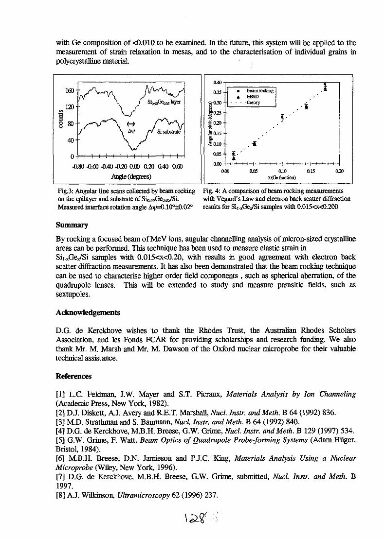
with Ge composition of <0.010 to be examined. In the future, this system will be applied to themeasurement of strain relaxation in mesas, and to the characterisation of individual grains inpolycrystalline material.
i I i i i 1 i i
-0.80 -0.60 -0.40 -0.20 0.00 0.20 0.40 0.60
Angle (degrees)
035 •
•£0.30-
§>0.25-
?0.20-
Ang
ular
sP
P
0.05-
0.00-
A
• ! • '
—1—1—h
beam rockingEBSD
-theory
—1—1—i—1—1—
5- ' '
i—1—1—1—1—1—1—1—1—1—1—
0.00 0.05 0.10x(Ge fraction)
0.15 0.20
Fig.3: Angular line scans collected by beam rocking Fig. 4: A comparison of beam rocking measurementson the epilayer and substrate of Sio.95Geo.o5/Si. with Vegard's Law and electron back scatter diffractionMeasured interface rotation angle A\|/=0.10°±0.02° results for Sii.xGex/Si samples with 0.015<x<0.200
Summary
By rocking a focused beam of MeV ions, angular channelling analysis of micron-sized crystallineareas can be performed. This technique has been used to measure elastic strain inSii-xGex/Si samples with 0.015<x<0.20, with results in good agreement with electron backscatter diffraction measurements. It has also been demonstrated that the beam rocking techniquecan be used to characterise higher order field components , such as spherical aberration, of thequadrupole lenses. This will be extended to study and measure parasitic fields, such assextupoles.
Acknowledgements
D.G. de Kerckhove wishes to thank the Rhodes Trust, the Australian Rhodes ScholarsAssociation, and les Fonds FCAR for providing scholarships and research funding. We alsothank Mr. M. Marsh and Mr. M. Dawson of the Oxford nuclear microprobe for their valuabletechnical assistance.
References
[1] L.C. Feldman, J.W. Mayer and S.T. Picraux, Materials Analysis by Ion Channeling(Academic Press, New York, 1982).[2] D.J. Diskett, A.J. Avery and R.E.T. Marshall, Nucl. Instr. and Meth. B 64 (1992) 836.[3] M.D. Strathman and S. Baumann, Nucl. Instr. andMeth. B 64 (1992) 840.[4] D.G. de Kerckhove, M.B.H. Breese, G.W. Grime, Nucl. Instr. andMeth. B 129 (1997) 534.[5] G.W. Grime, F. Watt, Beam Optics of Quadrupole Probe-forming Systems (Adam Hflger,Bristol, 1984).[6] M.B.H. Breese, D.N. Jamieson and P.J.C. King, Materials Analysis Using a NuclearMicroprobe (Wiley, New York, 1996).[7] D.G. de Kerckhove, M.B.H. Breese, G.W. Grime, submitted, Nucl. Instr. and Meth. B1997.[8] A.J. Wilkinson, Ultramicroscopy 62 (1996) 237.

P1.10minimi
AU9817137PROTON DIFFRACTION
Jacinta L. den Bestena, Les J. Allen and David N. Jamiesona
School of Physics, University of Melbourne, Parkville, 3052, AUSTRALIAa Microanalytical Research Centre
AbstractThe Lindhard theory[l] on ion channeling in crystals has been widely accepted throughout ionbeam analysis for use in simulating such experiments. The simulations use a Monte Carlomethod developed by Barret[2], which utilises the classical 'billiard ball' theory of ions'bouncing' between planes or tubes of atoms in the crystal. This theory is not valid for 'thin'crystals[3] where the planes or strings of atoms can no longer be assumed to be of infiniteproportions. We propose that a theory similar to that used for high energy electron diffractioncan be applied to MeV ions, especially protons, in thin crystals to simulate the intensities oftransmission channeling and of RBS spectra. The diffraction theory is based on a Bloch wavesolution of the Schrbdinger equation[4] for an ion passing through the periodic crystalpotential. The widely used universal potential[5] for proton-nucleus scattering is used toconstruct the crystal potential Absorption due to thermal diffuse scattering[6] is included.Experimental parameters such as convergence angle, beam tilt and scanning directions areconsidered in our calculations. Comparison between theory and experiment is encouraging andsuggests that further work is justified.
IntroductionIn the 1960's a debate was begun about the possibility of proton diffraction in thin crystals andwhether such effects were observable. The debate, led by Chadderton[7], suggested thatdiffraction effects were observable, but ended abruptly when Cowley[8] responded by agreeingthat proton diffraction was possible yet the present technology was unable to observe theseeffects and any calculation performed would be more complicated than for electrons and thatcomputer capacity was limited.
Since the debate, the theory of electron diffraction has been more fully developed[4,6,9] and is implemented in simulating many electron experiments. Rapidly expandingcomputer technology has enabled the large quantum mechanical calculations to be performedquickly and accurately. The introduction of the ion microprobe has enabled a much morecontrolled experimental environment. This means energy spread can be consideredinsignificant, collimation and magnetic lens systems produce the desired amount of divergenceor convergence and data acquisition is much more sophisticated and precise.
So, with today's technology and knowledge, the theory for electrons, we propose, canbe extended to the passage of protons through a crystal. Protons have a large mass incomparison to electrons, so even at MeV energies, they are effectively non-relativistic. Due tothe small de Broglie wavelength of the protons, the classical limit of the quantum mechanicalformulation is being approached. Hence the classical Lindhard derivation utilised with theMonte Carlo method has generally sufficed. The purpose of using diffraction theory is toprovide an insight into physical phenomena fundamentally derived from the quantummechanical point of view.
TheoryThe total crystal potential,
(1)

includes the anomalous absorptionpotential, V'(r), due to thermal diffusescattering (TDS) caused by the thermalvibration of the lattice atoms and V(r) is thecrystal potential. The crystal potential canbe represented as a Fourier series,
(2)
The atom-ion potential uses the universalscreening function,
ae (3)'» 1=1
a, = (0.1818,0.5099,0.2802,0.02817)
Pi =(3.2,0.9423,0.4029,0.2106)
fl = 0.8853as/(Z1°-23+Z20-23)
where r is the atom-ion distance, Zie andZ2e are the charge of the ion and atomrespectively and aB is the Bohr radius.The quantum mechanical formulationmakes use of the Bloch wave, ip(r), todescribe the path of the ions.
(4)
A, are the complex amplitudes, Cg' are theBloch wave coefficients, g is the reciprocallattice vector and k1 is the associatedcomplex wave vectork ' = K + # n , (5)where K is the incident wave vector, Xcontains the absorption coefficients and n isthe unit normal vector to the crystalsurface. By inserting equations 2 and 4 intothe SchrSdinger equation it is possible toobtain results for the complex amplitudes,Bloch wave coefficients and absorptioncoefficients. This then defines the Blochwaves explicitly.
Rutherford Backscattering intensityis then considered as proportional to thedepth averaged probability of the protonbeing present on the lattice sites at aparticular orientation given by:
(6)
where y/ is known by solving theSchrodinger equation and Ims is thecontribution from thermally scatteredcomponent of the beam intensity[10].
TDS incorporates a temperaturedependent calculation by use of the Debye-Waller temperature factor[l 1]
= exp[-2n2{u2)g2], (7)
with <u2>, the mean squared vibrationalamplitude of the lattice atom.
ProgramThe program for simulating channelingphenomena using diffraction theorycurrently includes both transmission andRBS geometry for axial and planarorientations in one or two dimensionalscans. Other features such as the crystal-ionpotential profile and calculation of theDebye temperature and <a2> also provideuseful information on the behaviour of thescattered ion.
Experimental conditions, such as tiltangle from any axis or plane, scan size,angular resolution, beam energy andconvergence, temperature and thickness ofthe sample can be simulated within theprogram. Also the ability to calculate thechanneling pattern for a particular elementor type of lattice atom in a multi-elementalsample is also available.
Results

Preliminary results using the program are encouraging. With fine tuning we hope to produce anaccurate way to determine the channeling patterns of various samples as well as gainingfundamental insight into the scattering process.
The following diagrams are the theoretical simulations of RBS in the <001> orientationfor diamond at room temperature. The figures 1 and 2 are for 500A and 1000A thick samplesrespectively. The scan is over 1.0° with 0.02° resolution and the scattering ion is a 0.5MeV
proton. As is observed, the relative depth and width of the channelsin each figure is representative of any experimental channel pattern ofthis orientation. The shoulder feature of the channel can also be seen,represented by the bright bands bordering the channels indicating ahigher intensity than that of a random orientation. The channelsclearly become thinner with increase in thickness which is alsoexpected experimentally.
Fig. l<001>Di500A
ConclusionMuch work is still to be done in refining our calculations and inunderstanding phenomena such as the effects of temperature, beamenergy, crystal type, thickness and the impact these have on thediffraction of protons within the sample. The model could be used toinvestigate high temperature superconductors through their phasechange and to investigate the magnetic properties of crystals. Theavailability of the nuclear microprobe at the University of Melbourneenables us to perform the simulations according to the experimentalconditions known and consequently the experiments can beperformed in a controlled and optimised situation determined fromthe results of the simulations. It is intended to perform theseexperiments in-house to confirm the simulations, although it is alreadyclear that the simulated channel patterns are remarkably similar to
those observed in RBS axial channeling experiments.
Fig. 2 <001> Di 1000A
References[I] Lindhard J., K Dan Vidensk Selsk Mat-Fys Medd 34 (14) (1965)[2] Barret J H, Phys Rev B 3 (5) 1527 (1971)[3] Neskovic N, Phys Rev B 33 (9) 6030 (1986)[4] Humphries C J, Rep Prog Phys 42 122 (1979)[5]Ziegler J F, Biersack J P and Littmark U, The Stopping and Range of Ions in Solids (Pergamon, New York,1985)[6] Hall C R and Hirsch P B, Proc R Soc London Ser A 286188 (1965)[7] Chadderton L T, Phys Lett 23 (5) 303 (1966)[8] Cowley J M, Phys Lett26A (12) 623 (1968)[9] Pennycook S J and Jesson D E, Ulttamicroscopy 37 14 (1991)[10] Allen L J and Rossouw C J, Phys Rev B 39 (12) 8313 (1989)II1] Butt N M and Bashir J, Acta Cryst A44 396 (1988)
\3\

P I •* -t Illllllllllllllllllllllllllllllfllr i # 1 1 AU9817138
Theoretical limit for the isotopic separation and depth resolutionof heavy elements in ToF-E and AE-E BIERDA
M. El Bouanani. P.N. Johnston,, W.B. Stannard and I.F. BubbDepartment of Applied Physics, Royal Melbourne Institute of Technology,
GPO Box 2476V, Melbourne, Australia
Abstract
Theoretically, the physical principles of Heavy Ion Elastic Recoil Detection Analysis
(HIERDA) do not set any limit to the isotopic separation. The isotopic separation is defined
mainly by the mass or atomic number resolving power of the detection system. In the case of
the ToF-E system, the energy resolution of the Si detector is the main limiting parameter for
isotopic separation. For the AE-E system, the separation depends on the energy resolutions of
both AE and E detectors.
The depth resolution depends on the energy width of the incident ion energy., the geometrical
contribution from the detection solid angle (this contribution may be reduced using a position
sensitive detector), the electronic and nuclear energy loss straggling of both the incident and
the recoiled ions and the energy resolution of the energy or time detector.
The isotopic separation in HIERDA, the achievable depth resolution and the accuracy of the
multi-elemental energy calibration will he. evaluated in both ToF-E and AE-E detection
systems.
Dr. M. El Bouanani E-mail: [email protected] Fax: (03) 9660 3837
132

P1.12i mini in
AU9817139
Advantages of ERDA H profilingusing a new methodology based on AE-E detectionM. El Bouanani, P. N. Johnston, I. F. Bubb, P. Jarosch and R. C. Short
Department of Applied Physics, Royal Melbourne Institute of Technology,GPO Box 2476V, Melbourne, Australia
ERDA is a powerful technique for depth profiling analysis of H in thin films and near thesurface of materials. The use of He incident ions with a stopping filter and a Si energy detector isthe usual analytical methodology because (i) ion beam induced H diffusion is less under He ionirradiation than with heavy ions and (ii) the detection efficiency is 100 %. However, the depthresolution deteriorates due to the straggling in the stopping filter. A nuclear charge dispersivedetection method based on the use of AE-E silicon telescope with AE thickness of 4 um withenhanced depth resolution and accessible depth is proposed. The gains in depth resolution andanalysable depth are demonstrated. Normalisation based on the forward scattered He spectrum isused to offset the uncertainties resulting from the H loss during irradiation of Kapton and Mylarstandards.
1. IntroductionSince its development by L'Ecuyer et al. in 1975 [1] Elastic Recoil Detection Analysis (ERDA)has become a powerful tool for quantitative depth profiling of light elements in the near-surfaceregion of materials. ERDA analysis of H using a low energy He beam was first reported byDoyle and Percy [2]. One of the main advantages of using He incident ions is the minimalradiation damage of the analysed targets. This is very important for accurate measurement of Hwhich is well known for its instability and its loss under ion beam irradiation. Since then,extensive studies aimed mainly at the optimisation of the depth resolution have been undertaken[3-11]. A wide range of combinations including the mass of the incident ions, kinematicconsiderations and different detection approaches [6-9,12] have been used. Considerable efforthas been dedicated to make ERDA depth profiling of H quantitatively accurate. Until recently,the determination of the non Rutherford He - H cross sections [13-15] has been a subject ofdiscrepancies which reflects the difficult problem of H loss under ion beam irradiation.However, quantitative depth profiles of H can be achieved by direct comparison with the Hrecoil spectrum from polymer standards such as Mylar, Kapton or Polystyrene. Accuracyrequires that the target H content does not significantly change during ERDA measurements.The use of light incident ions such as He beams is preferred in order to minimise the effect ofirradiation.Here we describe a new technique based on simultaneous detection of both the recoiled H andforward scattered He using a silicon AE-E telescope. This improves significantly the depthresolution and eliminates the need for H standards for quantitative depth profiling. A newanalysis approach for internal normalisation is described.
2. Experimental set-upThe measurements have been performed at the RMIT 1 MV Tandem accelerator with 2.5 MeV4He++ beam. A glancing incident beam impinged at 75° to the surface sample normal. Thesilicon AE-E telescope was placed at 30° to the incident beam direction. A 1x3 mm2 verticalrectangular slit collimated the AE-E telescope. The AE and E detectors are from ORTEC withthicknesses of respectively 4 um and 500 um. The E and AE detectors were operated in

coincidence mode. The collection of the data use a CAMAC based multi-parameter pulse heightanalysis system controlled by a Macintosh Quadra 900 computer and SPARROW KMAXsoftware with event by event data storage to allow for offline analysis.
3. E and AE calibrationBoth detectors E and AE were calibrated using 0.8 -1.8 MeV H beam scattered on a 20 nm thingold film on silicon substrate in RBS configuration. The AE-E telescope was placed at ascattering angle of 150° relative to the incident H direction. The scattered H peak from the thingold layer is a well defined gaussian with a FWHM of 14 keV. For each incident energy two setsof data collection were performed with and without the AE detector in front the E detector. Thisallows energy and energy loss calibration for both AE and E detectors. For 1.0 MeV H, theenergy widths of the E and AE detectors in this configuration were 14 keV and 40 keV.
4. Results and discussionFigure 2a shows a typical two dimensional spectrum acquired using a 2.5 MeV He-4 beamincident on a Kapton sample. The H and the forward scattered He are both well separated.Figures 2b and 2c show respectively He and H energy projections.
CO
c3 600
400
200
n
' _htL
1 Scottered
" I . I
Helium 1
!i ,
(b)
0 1000 2000 3000 4000Energy Ch.
3000 3500 4000 4500 5000E+AE Ch.
CO
1000 2000Energy Ch.
0 1000 2000
Energy Ch.
FIGURE 2. (a) AE-E two dimensional ERDA spectrum of Kapton sample, (b) Total energy(AE+E) projection of the forward scattered He component, (c) Projected energy spectrum of theH component(d) Energy spectrum with 10 urn Al filter in front of the E detector.
As shown in Figure 2b, the total energy projection of the forward scattered He was obtained byadding both E and AE signals which gives a much better energy resolution. In Figure 2c the Eand AE signals for H are not added because it would not improve the energy resolution. Thesummation of both E and AE signals should be done only in the case where the energy resolution

of the AE detectors is much less than their straggling contribution. The energy resolutioncalculated from figure 2d (ERDA with 10 um Al filter) is 69 keV. The advantages of AE-Emethod are clearly seen in figure 2c. The energy resolution is only 36 keV and the accessibledepth is greater due the reduction of the low energy cutoff. Both He and H spectra were obtainedunder the same experimental conditions. For samples with known composition, auto-normalisation of the forward scattered He energy spectrum in a manner similar to RutherfordBackscattering Spectrometry (RBS) allows inter-normalisation of the H recoil spectrum. Thiseliminates the needs for H standards and consequently the uncertainties related to the H loss inthe commonly used polymers as H references. The accuracy of the absolute H concentrations arethen dependent directly and mainly on both the He-matrix and He-H cross section data. RUMP[16] software can be used for such analysis.The AE detector is not a passive absorber and consequently its thickness is a compromisebetween the minimum acceptable energy loss and the electronic noise of the thin detector andassociated electronics. The use of a 4 (xm AE detector allowed us to obtain good separationbetween the electronic noise level and the AE signal from 1.8 MeV H beam. This means that anenergy of the He beam as high as 3.7 MeV can be used which extends the accessible depth.Otherwise, when using 2.5 MeV He beam, a thickness of less than 3 |j.m can be used for AEdetector which improves further both the depth resolution and the accessible depth.
ConclusionThe use of ERDA low energy He beams and a AE-E silicon detection system with itssimultaneous detection of recoiled H and forward scattered He projectiles have beendemonstrated to:
• improve significantly the depth resolution and extend the analysable depth.• eliminate the need for H standards and their associated uncertainties.
References1. J. L'Ecuyer et al. J. Appl. Phys. 47 (1976) 881.2. B.L. Doyle et al., Appl. Phys. Lett. 34 (1979) 811.3. F. Paszti et al., Nucl. Instr. and Meth. B 54 (1991) 507.4. A. Turos et al., Nucl. Instr. and Meth. B 4 (1984) 92.5. S. Nagata et al., Nucl. Instr. and Meth. B 6 (1985) 533.6. G.G. Ross et al., Nucl. Mater. 128/129 (1978) 730.7. O. Kruse et al., Nucl. Instr. and Meth. B 89 (1994) 191.8. G. Groleau et al., NucL.Instr. and Meth. 218 (1983) 11.9. J.P. Thomas et al., Nucl. Instr. and Meth. 218 (1983) 125.10. O. Benka et al., Nucl. Instr. and Meth. B 85 (1994) 650.11. D.K. Brice et al., Nucl. Instr. and Meth. B 45 (1990) 265.12. U. Kreissig et al., Nucl. Instr. and Meth. B 85 (1994) 71.13. J.E.E. Baglinet al., Nucl. Instr. and Meth. B 64 (1992) 46914. H. Wang et al., Nucl. Instr. and Meth. B 34 (1988) 145.15. R.E. Benenson et al., Nucl. Instr. and Meth. B 15 (1986) 453.16. L.R. Doolittle, Nucl. Instr. and Meth. B 15 (1986) 227.

P1.13Minium
AU9817140
Limitations to Depth Resolution in High-Energy,Heavy-Ion Elastic Recoil Detection Analysis
R.G. Elliman2, H. Timmersb, G.R. Palmer3, T.R. Ophela
"Research School of Physical Sciences and Engineering, Institute of Advanced Studies,Australian National University, Canberra, ACT 0200, Australia, "Department of Physics,
University of Newcastle, Newcastle, NSW 2308, Australia
AbstractThe depth resolution of heavy-ion elastic recoil detection analysis was examined for Al and Cothin films ranging in thickness from 100 to 400 nm. Measurements were performed with 154MeV Au ions as the incident beam, and recoils were detected using a gas ionisation detector.Energy spectra were extracted for the Al and Co recoils and the depth resolution determined asa function of film thickness from the width of the high- and low- energy edges. These resultswere compared with theoretical estimates calculated using the computer program DEPTH.
IntroductionHigh-energy, heavy ions (1-2 MeV/AMU) offer many advantages for elastic recoil detectionanalysis (ERDA) of thin-film materials [1-7]. A wide range of elements can be analysedsimultaneously as long as Z2 < zi, where Zi is the atomic number of the primary ion and Z2 isthe atomic number of the recoil ion. The sensitivity is enhanced due to the ~zi4 dependence ofthe scattering cross-section and the method has approximately equal sensitivity to all lightelements [2< Z2 < 50]. The depth resolution is also improved because of the high stoppingpower of heavy ions and the detection of scattered primary ions is reduced due to the narrowscattering cone of heavy ions scattering from light elements. These advantages have led severalgroups [1-7] to explore applications of heavy ion elastic recoil detection analysis (HERD A).
A large solid-angle, position-sensitive gas-ionisation detector is well suited to HIERDAmeasurements [3-7]. It provides efficient recoil detection and thus minimises exposure of thesample to the ion beam. Such a detector has recently been built and installed at the HUDaccelerator laboratory of the Australian National University in Canberra [7]. This paper reportson preliminary experiments with this system which were carried out to explore the limitationsof depth-profiling with HIERDA.
Experimental DetailsThin films of Co were evaporated onto Si and Ge substrates and thin films of Al wereevaporated onto Ge substrates using either thermal or electron-beam evaporation. Filmthicknesses varied from 100 nm to 400 nm, as indicated by a quartz crystal thickness monitorand verified for selected samples by Rutherford backscattering spectrometry. HIERDAmeasurements were undertaken using 154 MeV 197Au ions with charge state 13+ and a typicalbeam current of 1 nA. The beam had an energy spread of < 50 keV, a maximum angularspread of 0.01° and was collimated to produce a lmm x lmm square spot on the sample.Recoils were detected with a position-sensitive gas-ionisation detector located 300 mm fromthe sample. For these particular measurements, the detector solid angle was limited to 0.02mSr by a 1.5 mm diameter aperture. This obviated the need for kinematic energy correction ofthe data. The scattering angle was fixed at $s = 45° and the incident and exit angles were 22.5°.During analysis, the vacuum pressure inside the scattering chamber was ~10"7 mbar. Furtherdetails of the experimental system are presented in a separate contribution [7].
ISBV

Results and DiscussionThe depth-profiling of individual elements following a HIERDA measurement requires themeasured energy spectrum for each element to be transformed into a concentration versusdepth profile. This requires accurate knowledge of the scattering cross-sections and stoppingpowers of the projectile and recoil ions. Limitations to the depth-resolution include the energyand angular spread of the incident beam, the intrinsic detector resolution, the kinematic energyspread due to the finite size of the beam and detector, the energy stragglmg in the sample andthe detector entrance window, and energy spread due to multiple scattering.
Calculations performed with the computer code DEPTH [8-10], using Bohr straggling withChu correction [8], and assuming an intrinsic detector resolution of 1.2%, show that thesurface energy resolution of the HIERDA measurement is dominated by the intrinsic resolutionof the detector and geometric effects associated with the finite beam size and detector solidangle. As the film thickness increases, the depth resolution deteriorates, largely due to theincreasing contribution of multiple scattering. These results show that the energy (depth)resolution is limited by the detector configuration for film thicknesses < 100 nm but by ion-solid interaction processes for film thicknesses > 100 nm. It is also interesting to note that themain limitation comes from multiple scattering of the primary and recoiled ions, straggling is ofless significance.
Energy-loss (AE) versus total energy (E) spectra were collected for Al and Co films of varyingthicknesses from which energy spectra of Al and Co recoils were extracted. The energy widthof the spectra increased with increasing film thickness, as expected. However, attempts to fitthese recoil spectra with the computer program RUMP [11] highlighted discrepancies betweenthe tabulated and actual stopping powers. For example, the thickness of Co films wasoverestimated by 30%. This was confirmed by calculations using stopping powers fromTRIM'95 [12] and the surface energy approximation [13]. These discrepancies suggests thatthe tabulated stopping powers are lower than the actual values.
The depth resolution of the ERDA measurement was determined experimentally from the high-and low-energy edges of the Al and Co energy spectra. These spectra were fitted with afunction of the form:
Y(E)=(mE+b)[erfc((E-Ef)/8Ef) - erfc((E-Eb)/5Eb)] (1)
where erfc is the complimentary error function, E is the recoil energy and Ef and Eb are thecentroids of the high- and low-energy edges of the spectra, respectively. The factor (mE+b),with fitting parameters m and b, was used to approximate the energy dependence of the yield.The width 8Ef is representative of the energy resolution for surface scattering and 5Eb
represents the energy resolution for recoils coming from the film-substrate interface. The depthresolution was calculated by transforming 5Ef and 5Eb to FWHM values, dividing by theenergy width of the spectrum and multiplying by the nominal film thickness. This assumes thatthe energy width of the spectrum is linearly proportional to the film thickness, a reasonableapproximation for the film thicknesses employed in the present study.
Fig. 1 shows the depth resolution measured for Al and Co films together with the theoreticalpredictions of the computer program DEPTH. For surface scattering, the measured depthresolution for Al (16 nm) and Co (12 nm) films is in excellent agreement with the calculatedvalues. However, with increasing film thickness, the measured values consistently exceed the

predicted resolution. This suggests that either the films have some inherent roughness orinhomogeneity or that the theoretical calculations underestimate the depth resolution.Rutherford backscattering (RBS) analysis of a 200 nm thick Al film showed no evidence forroughness before or after analysis, however, similar analysis of a 200 nm Co film showed thatthis film had an intrinsic roughness of-10 nm and that this increased to -15 nm afterprolonged irradiation with the Au beam. RBS analysis on and off the irradiated spot alsoconfirmed some beam induced oxidation of the Co film. For Co, this roughness is sufficient toaccount for the observed discrepancy between the measured and calculated depth resolution.For Al, the situation is less clear. Stopping power uncertainties clearly affect the calculateddepth resolution. However, as discussed above, the tabulated stopping powers underestimatethe experimental values. Increasing the stopping powers in the DEPTH calculation reduces thecalculated depth resolution, increasing the difference between experiment and theory.
100 200 300Depth (nm)
400 500
100 200 300 400 500Depth (nm)
Figure 1: Comparison of measured (crosses) and calculated (triangles and dashed lines) depthresolution for a) Al and b) Co thin films.

ConclusionsHERD A can provide high-sensitivity, composition-versus-depth analysis of materials. In thisstudy, depth resolution measurements were performed on Al and Co films as a function of filmthickness. The measured values were compared with the theoretical predictions of thecomputer code DEPTH [8-10]. The experimental and theoretical depth resolution showedsimilar trends with increasing film thickness but the experimental data consistently exceededthat predicted by DEPTH. Rutherford backscattering analysis of Co films before and afteranalysis showed that they were intrinsically rough and that exposure to the analysis beamcaused additional beam-induced roughening and beam-induced oxidation. This accounted forthe observed difference between the experimental and theoretical values. Similar analysis of Alfilms showed no such effects. The discrepancy between experiment and theory remainsunresolved in this case.
The observation of beam-induced roughening and beam-induced oxidation of Co filmshighlights the importance of minimising sample exposure to the analysis beam and justifies theuse of a large solid angle, position-sensitive detector for HDERDA analysis [7].
AcknowledgmentsThe authors are grateful to Mr Bernard King for his contribution to the construction of theHIERDA detector and to Mr Alex Boiko for assistance with thin-film deposition. Dr. HeikoTimmers acknowledges financial support from the Australian Research Council.
References[I] W.M.A. Bik and F.H.P.M. Habraken, Rep. Prog. Phys. 56, (1993), 859[2] J.P. Stoquert, G. Guillaume, M. Hage-Ali, J.J. Grob, C. Canter and P. Siffert, Nucl.
Instr. Meth. B44 (1989) 184[3] W. Assmann, P. Hartung, H. Huber, P. Staat, H. Steffens and Ch. Steinhausen, Nucl.
Instr. Meth. B85, (1994), 726[4] W. Assmann, H. Huber, Ch. Steinhausen, M. Dobler, H. Gliickler and A. Weidinger,
Nucl. Instr Meth. B89 (1994) 131[5] J.S. Forster, P.J. Currie, J.A. Davies, R. Siegle, S.G. Wallace and D. Zelenitsky, Nucl.
Instr. Meth. B113 (1996) 308[6] W. Assmann, J.A. Davies, G. Dollinger, J.S. Forster, H. Huber, Th. Reichelt and R.
Siegele, Nucl. Instr. Meth. B118, (1996) 242[7] H. Timmers, R.G. Elliman, G.R. Palmer, T.R. Ophel and D.J. O'Connor, 'The
Development of a Facility for Heavy Ion Elastic Recoil Detection Analysis at theAustralian National University', this proceedings.
[8] E. Szilagyi, F. Paszti and G. Amsel, Nucl. Instr. Meth. B100, (1995) 103[9] F. Paszti, E. Szilagyi and E. Kotai, Nucl. Instr. Meth. B54 (1991) 507[ 10] E. Szilagyi and F. Patzti, Nucl. Instr. Meth B85, (1994) 616[II] J.F. Ziegler, J.P. Biersack and U. Littmark, 'The Stopping of Ions in Solids', Volume
1, ed. J.F. Ziegler. Pergamon Press, New York (1985)[12] RUMP ion scattering analysis package supplied by Computer Graphic Service, Ithaca,
New York. (OS/2 beta-test version supplied by M.O. Thompson, Cornell University.)[13] W.K. Chu, J.W. Mayer and M-A. Nicolet, 'Backscattering Spectrometry\ Academic
Press, New York (1978).

P1.14nun mi
AU9817141
Annealing studies of electrically active point defects in ion implanted p-type Si
S. Fatima, B.G. Svensson a and C. Jagadish
Department of Electronic Materials Engineering, Research School of Physical Sciences andEngineering, The Australian National University, Canberra, Australia.
a Royal Institute of Technology, Solid State Electronics, P.O. Box E229, S-164 40 Kista-Stockholm, Sweden.
ABSTRACT
Deep level transient spectroscopy (DLTS) is used to monitor the electrically active point defectscreated by low dose ion implantation in Si. P type Si (boron doped) both Fz and Cz samples,having same dopant concentration are implanted with 4 MeV Si. Vacancy (i.e divacancy),interstitial (i.e carbon-oxygen center) related defects are observed in these samples. In addition tothese defects, two more defect levels are seen. They are tentatively identified as defectsinvolving impurities. Dose dependence study for both Cz and Fz samples shows an increase inthe concentration of the implantation-induced defects linearly with dose. Isochronal annealing ofthese defects reveals that their stability depend strongly on dopant concentration and impuritycontent i.e oxygen, carbon and hydrogen present in the as grown crystalline Si to start with.
Introduction:
Characterizing defect and understanding the role played by them in the fabrication of devices isan important area for the microelectronics industry. The realization of the importance of thepoint defect study in Si started when defect is evolved upon annealing of the implantationinduced damage leading to the transient enhanced diffusion (TED) of the dopants1'3 startslimiting the scaling down of the device size. The fundamental defects so called, simple pointdefects resulting from the ion bombardment consist of Frankel pair of Vacancies (V) and Si selfinterstitials (I) which are known to be highly mobile at room temperature (RT). In contrast toMeV electron irradiation, ion implantation generates a non uniform defect distribution, includingV, I and complex defects, peaking at larger depths. In a single collision cascade the probabilityof annihilation of vacancies and interstitials is large, V + I -> 0 and only few percent of theFrankel pairs survive and form stable defects.In this study we report on the electrically active point defects in p-type Si. Since low doses areused so that single collision cascades dominate and overlap between different ion tracks is smalland dilute concentration regime is obtained. Except for hydrogen5'6 no level related to theimplanted specie is observed. In Si, evolution of the irradiation-induced defects is stronglyinfluenced by the residual impurities. Besides extensive recombination between vacancies andinterstitials, those which escape are finally trapped by impurities. Some of these impurities areunintentionally introduced during the crystal growth and play a vital role. The commonimpurities are oxygen atom which preferentially occupy the interstitial position (Oi), it isconnected to two Si atoms and is a efficient trap for migrating vacancies. Carbon is at thesubstitutional position (Cs) and is electrically inactive, it captures the self interstitials to produce
f+'O

Ci. This can be shown as I + Cs •> Q , Q + O;-> QOi. A gradual transformation of Q andwith time takes place and a close one to one correlation is found between loss of Q and growthof CjOj7 On the other hand, the presence of hydrogen and copper, incorporated unintentionallyduring the crystal growth or other subsequent processes, decorate the implantation induceddefects. *
Experimental:
Float zone (Fz) and Czochralski (Cz) p-type Si(100) having the same dopant concentration areimplanted using the 1.7 MV tandem implanter at the Australian National University. 4 MeV Si isimplanted in to p-type Si, the incident ion beam was scanned over an aperture (2.2 x 4.4 cm 2) toensure the uniformity. The average beam current was 0.2-0.3 nA. Doses in the range of 1O8-1O9
cm'2 are employed. After implantation the samples were chemically cleaned using a standardprocedure which include a final dip in the diluted HF. Immediately after cleaning the sampleswere loaded in to electron-beam system for the deposition of Ti Schottky barrier diodes.Thedeposition was made through a metal mask containing 2mm dots equally spaced. Deep leveltransient spectroscopy (DLTS) and capacitance- voltage measurements were under taken for thesample analysis. Basically the system consists of 1MHz capacitance bridge, a 50 MHz pulsegenerator, a liquid nitrogen bath cryostat with heating stage (77K - 373K) and a chromel alumelthermocouple. The system is controlled by a PC via an interface. The temperature was scannedbetween 77K and 300K. In the DLTS measurement eight traditional spectra with rate windows inthe range of (20 ms)'1 to (2560 ms)"1 were recorded during a single temperature scan. Themeasurements were performed under a reverse bias condition.
Results and Discussion:
Fig. 1 shows a DLTS spectrum from p-type Si implanted with 4 MeV Si at RT.
0.0035
0.003
0.0025
0.002
0.0015
0.001
0.0005
0
: E +0.19 eV
50
- - • - - 7x10- - - » - - - 7x10
100 150Temperature (K)
200 250
Figure 1 DLTS spectra for p-type Si (Fz and Cz)
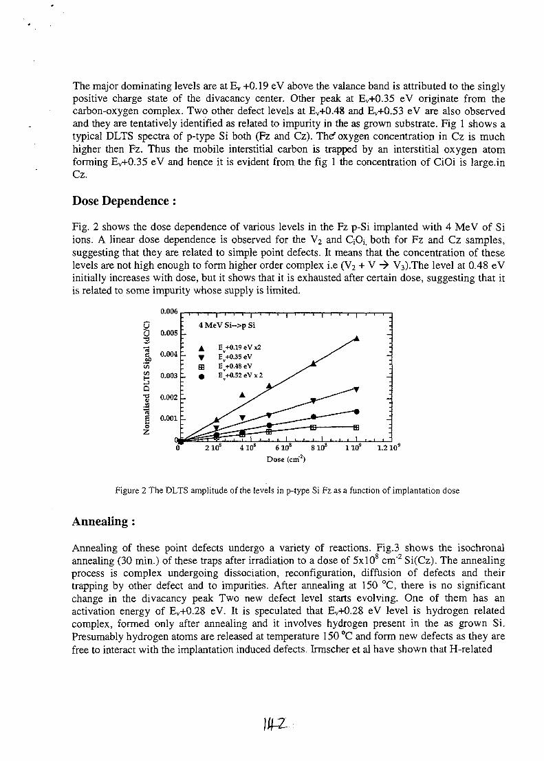
The major dominating levels are at Ey +0.19 eV above the valance band is attributed to the singlypositive charge state of the divacancy center. Other peak at Ev+0.35 eV originate from thecarbon-oxygen complex. Two other defect levels at Ev+0.48 and Ev+0.53 eV are also observedand they are tentatively identified as related to impurity in the as grown substrate. Fig 1 shows atypical DLTS spectra of p-type Si both (Fz and Cz). The* oxygen concentration in Cz is muchhigher then Fz. Thus the mobile interstitial carbon is trapped by an interstitial oxygen atomforming Ev+0.35 eV and hence it is evident from the fig 1 the concentration of CiOi is large.inCz.
Dose Dependence:
Fig. 2 shows the dose dependence of various levels in the Fz p-Si implanted with 4 MeV of Siions. A linear dose dependence is observed for the V2 and QOj, both for Fz and Cz samples,suggesting that they are related to simple point defects. It means that the concentration of theselevels are not high enough to form higher order complex i.e (V2 + V -> V3).The level at 0.48 eVinitially increases with dose, but it shows that it is exhausted after certain dose, suggesting that itis related to some impurity whose supply is limited.
0.006
0U 0.005
P
o
0.004
0.003
0.002
0.001
4 MeV Si~>p Si
A Ey+0.19 eV x2^ E +0.35 eVffl E'+0.48 eV
• EV+0.52 eV x 2
1.2 109
Figure 2 The DLTS amplitude of the levels in p-type Si Fz as a function of implantation dose
Annealing:
Annealing of these point defects undergo a variety of reactions. Fig.3 shows the isochronalannealing (30 min.) of these traps after irradiation to a dose of 5x10 cm"2 Si(Cz). The annealingprocess is complex undergoing dissociation, reconfiguration, diffusion of defects and theirtrapping by other defect and to impurities. After annealing at 150 °C, there is no significantchange in the divacancy peak Two new defect level starts evolving. One of them has anactivation energy of Ev+0.28 eV. It is speculated that Ev+0.28 eV level is hydrogen relatedcomplex, formed only after annealing and it involves hydrogen present in the as grown Si.Presumably hydrogen atoms are released at temperature 150 °C and form new defects as they arefree to interact with the implantation induced defects. Irmscher et al have shown that H-related

0.002
u
50 100 250150 200
Temperature (K)
Figure 3 Isochronal annealing 30 min in Czochralski Si
300
levels in both n and p type Si at Ec-0.32eV and Ev+0.28eV respectively are present in unannealedsamples in equal concentration, in this respect they are assigned as two charge states of one andthe same H-related defect complex. Hydrogen in Si not only passivate shallow acceptor dopantsbut also vacancy related defects This level anneals out at 250 °C. The level at 0.48 eV is presentin both Fz and Cz samples.Annealing at 200 °C shows a new defect level at 0.24 eV above the valance band. It has beenproposed from the annealing studies of electron irradiated samples that it is due to a gradualtransformation of divacancy to a divacancy-oxygen complex below its dissociation temperature.8
Further work is under way to characterise these defects which evolve after annealing.
Conclusion :
MeV ion implantation in to p-type Si forms vacancy and interstitial related defects.A linear dosedependence holds for the implantation induced defects. Two other defect levels are formed aswell and their identification is tentative at this stage. Annealing study in both Fz and Cz samplesshows the formation of H-related level after annealing, decorating the implantation induceddefects. Further work is under way to characterize other defects in the as implanted and annealedsamples.
References :1. P. A. Stolk, H. J. Gossmann, D. J. Eaglesham, D. C. Jacobson, J.M. Poate, and H. S. Luftman,
Appl. Phys. Lett. 66, 568 (1995).2. H. J. Gossman, C. S. rafferty, H. s. Luftman, F. C. Underwald, T. Boone and J. M. Poate, N.
Appl. Phys. Lett. 63, 639 (1993).3. E. B. Cowem, K. T. F. Janssen, and H. F. F. Jos, J. Appl. Phys. 68, 6191 (1990).4. B.G. Svensson, C. Jagadish, A. Hallen and J. Lalita. Nucl.Instru. and Meth. B 106, 183
(1995).5. K.Irmscher, H. Klose, and K. Maass, J. Phys. C 17, 6317 (1984).6. M. Huppi, J. Appl. Phys. 68, 2702 (1990).7. J. Lalita, N. Keskitalo, A. Hallen, C. Jagadish, B. G. Svensson, Nucl. Instr. and Meth. B 120
27(1996).8. M. A. Trauweert, J. Vanhellemont, H.E. Maes, A. M. Van Bavel, G. Langouche, A. Stesmans,
P. Cluws, Mat. Res. Soc. Symp. Proc. Vol. 378,953 (1995).

P1.15 AU9817142
Strain and Defect Microstructure in Ion-Irradiated GeSi/Si StrainedLayers as a Function of Annealing Temperature
J. M. Glasko1, J. Zou2, D. J. H. Cockayne2, J. D. Fitz Gerald3, and R. G. Elliman1
'Department of Electronic Materials Engineering, Research School of Physical Sciences andEngineering, Institute of Advanced Studies, the Australian National University, Canberra, A. C. T.0200, Australia2Australian Key Centre for Microscopy and Microanalysis and Electron Microscope Unit, University ofSydney, Sydney, N. S. W. 2006, Australia3Petrophysics Group, Research School of Earth Sciences, Institute of Advanced Studies, the AustralianNational University, Canberra, A. C. T. 0200, Australia
High energy (1 MeV), ion irradiation of GeSi/Si strained layers at elevatedtemperatures can cause strain relaxation. In this study, the effect of subsequent thermalannealing was investigated. Three distinct annealing stages were identified andcorrelated with the evolution of the defect microstructure. In the temperature rangefrom 350 to 600 °C, a gradual recovery of strain is observed. This is believed to resultfrom the annealing of small defect clusters and the growth of voids. The voids arevisible at annealing temperatures in excess of 600 °C, consistent with an excessvacancy concentration in the irradiated alloy layer. The 600 to 750 °C range is markedby pronounced maximal recovery of strain, and is correlated with the dissolution offaulted loops in the substrate. At temperatures in the range 750-1000 °C, strainrelaxation is observed and is correlated with the growth of intrinsic dislocations withinthe alloy layer. These dislocations nucleate at the alloy-substrate interface and growwithin the alloy layer, towards the surface.
INTRODUCTION
In recent years, attention has focused onthe effect of ion-irradiation on strain levels inGeSi/Si strained layer heterostructures. Bothroom temperature1-4 and elevatedtemperature5*8 ion irradiation have beenshown to modify strain levels in GeSi. Roomtemperature irradiation results in increasedstrain with fluence as does low energyelevated temperature irradiation; both resultsare well-modelled by assuming that the straindistribution reflects the ion damage profile3-4.However, the behaviour of strained layersduring high energy elevated temperatureirradiation is more complicated. Duringelevated temperature irradiation, relaxationof perpendicular lattice strain (£j_) will resultif the irradiating ion projected range (Rp)exceeds the depth of the substrate-epilayerinterface4-8. Observation of extended defectcomplexes in the vicinity of the strainedsubstrate-epilayer interface at elevatedtemperature5"7 suggests the interface causespreferential agglomeration of point defects,and that these defects result in the formationof strain-relieving extended defect complexesat, and/or near the interface. However, a
comprehensive picture of the mechanism andof the evolution of the defect microstructureduring subsequent thermal annealing is as yetunavailable. The purpose of this study is toshed some light on these processes.
Experimental
Strained GexSii-x layers of thickness 145± 3 nm were grown on Si (001) substratesusing molecular beam epitaxy (MBE). Layershad a Ge content of x = 0.072 ± 0.003, andwere grown at temperatures in the range 550- 750 °C. Layers were capped with 5 nm(nominal) of Si to prevent oxidation. Theequilibrium critical thickness9 for thiscomposition range was calculated to be ~56nm, suggesting that both layers aremetastable as grown. Samples were irradiatedat 253 °C with 1 MeV 28Si+ ions (Rp ~ 1.3(im). Ion fluences were in the range 6xlO15 tolxlO17 Si+/cm2, while the ion flux was in therange 1.0 - 5.8 \iAJcm2. Samples were tilted7° with respect to the surface normal duringirradiation to minimise channelling effects,and the base pressure in the implant chamberwas always < 5xl0"7 Torr during irradiation.Subsequent isochronal annealing, at

temperatures in the range 400-1000 °C, wasperformed in a quartz-tube furnace with aflowing Ar ambient. As-irradiated andannealed samples were analysed byRutherford backscattering spectroscopy andchannelling (RBS-C) (2 MeV He+, es=106°),double crystal x-ray diffraction (DCXRD)(40 kV CuKoc x-rays, using the (004)reflection in the 0-29 scattering geometry)and by transmission electron microscopy(TEM) (using a Philips EM430 operating at300 kV and a Philips CM 12 operating at 120kV). Plan-view TEM (PV-TEM) specimenswere prepared using standard chemicaletching techniques while cross-sectional (X-TEM) specimens were prepared bymechanical thinning and ion milling (using 4kVAr).
RESULTS AND DISCUSSION
It has previously been shown7 that theirradiation conditions employed in this studycause strain relief: the perpendicular latticestrain decreases with increasing ion fluence.Where strain relief is significant, (A£JL>10%),a direct backscattering peak is evident inRBS-C spectra at a depth that correspondsapproximately to the alloy-substrateinterface. The defects giving rise to this peakare also evident in X-TEM images, whilelittle other damage is immediately obviouswithin the alloy layer. Closer examination ofthe alloy layer itself reveals a population ofsmall faulted loops, concentrated about thecentre of the alloy and, under sometilt/diffraction conditions, a small populationof linear defect structures is also visiblewithin the alloy layer. High resolution TEM(HR-TEM) reveals that the linear defects lieon {113} habit planes and exhibit behaviourwhich is consistent with that of the {113}rod-like defects (RLDs). Faulted loops arealso visible in the underlying substrate. Theseare noticeably larger than defects in the alloylayer and differ from those in interfaceregion, enabling ready discrimination duringanalysis of plan-view specimens.
PV-TEM micrographs show that thedefects at the interface are irregular in shapeand loop-like in character; some appear asisolated defects while others clearly interact.Detailed analysis shows that the defects havesome segments with a/2<110> Burgersvectors, inclined to the interface plane, whilesegments resulting from interactions are of
edge character, having Burgers vectors ofb=a/2<110> lying in the interface plane.Loops with a/2<110> Burgers vectors caneffect strain relief; however withoutknowledge of the extrinsic/intrinsic nature ofthe defects, or knowledge of their preciselocation with respect to the alloy-substrateinterface, it can only be speculated that theyare responsible for the observed relaxationeffect. The small size of the defects, and thehigh density of defects in the region, makethis determination a non-trivial task.
100
200 400 600 800Anneal Temperature (°C)
1000
Figure 1: Perpendicular strain as a function ofannealing temperature for samples irradiated with 1.0MeV 28Si+ at 253°C. Fluence is indicated in units of1016 Si/cm2.
Figure 1 shows the effect of subsequentannealing on the £j. of an as-grown and ion-irradiated layers. Samples were annealed attemperatures between 350 and 1000 °C.Although the as-grown material is largelyunaffected by thermal treatment to 1000 °C,the behaviour of the ion-irradiated layers isquite complicated. It is best described in 3stages: 1) a gradual 8x recovery stage, fortemperatures up to 600 °C; 2) a pronouncedrecovery stage from 600 to 750 °C, overwhich maximal recovery of as-grown exlevels is observed; and 3) a final relaxationstage between 750 and 1000 °C, where theirradiated layers are seen to relax to varyingdegrees. To gain insight into the strainbehaviour during these stages, the materialwas examined by TEM. Figure 2 shows PV-and X-TEM micrographs of samplesirradiated to 3xl016 Si /cm2 and annealed tothese various stages.
X-TEM analysis of irradiated samplesannealed at 450 and 600 °C shown in figure2a, revealed a microstructure similar to the

as-irradiated samples, although in this case,under similar imaging conditions, the faultcontrast of the substrate loops is not asobvious. In contrast, the microstructure ofirradiated samples annealed to 750 °C, shownin figure 2b, differs significantly. The faultedloops previously visible on the substrate sideof the alloy-substrate interface havedisappeared, and the loop-like defects seenpreviously in the vicinity of the alloy-substrate interface have begun to grow andexpand towards the epilayer-cap interface;and while {113} RLDs are still visible, athrough-focus HRTEM micrograph setreveals small voids (-4 nm in diameter)distributed through the alloy layer and in thesubstrate. Voids are not unexpected as MonteCarlo simulation10 predicts a vacancy excessfrom the surface to a depth of -1.2 Jim, andvoid formation is energetically favoured overvacancy loop formation11. X-TEM analysisof the irradiated material annealed to 900 °C(figure 2c) reveals that the interface defectsnow extend from the region of the alloy-substrate interface to the alloy-cap interface;they do not extend into the Si cap material.Faceted voids (5-6 nm in diameter) arepresent from the surface down to a depth of ~30 nm, with a lower density of larger voids(also faceted but 9-10 nm in diameter)appearing in the substrate material below thealloy-substrate interface; the material in theimmediate vicinity of the loop-like defectsappears void-deficient.
Detailed PV-TEM analysis (see figure2d) of the alloy layer microstructure showsthat the loop-like defects are no longerirregular in shape but consist of straightperfect dislocation segments which lie in thealloy-substrate and alloy-cap interfaces, anddissociated partial dislocation segments thatjoin un-dissociated segments. The defects arefound to have {111} habit planes andBurgers vectors of a/2<110> type (mixedcharacter) or {100} habit planes (normal tothe alloy-substrate interface) and a/2<110>Burgers vectors (edge character). Both typesof loop-like defects were determined12 to beintrinsic in nature (ie-of vacancy-type; theirintrinsic nature suggests that those formedduring ion irradiation are also vacancy-type.
It appears then that the strain behaviourin the first annealing stage (up to 600 °C) isrelated to the annealing of small defectclusters in the irradiated structure and/or thegrowth of voids, which on average, do not
Figure 2: Weak-beam dark-field TEM micrographs ofsamples irradiated to 3xlO16 Si/cm2 at 253 °C afterannealing: a) at 450 and 600 °C, b) at 450, 600 and750 °C, and at 450, 600, 750, and 900 °C in c) and d).Figs a-c) are X-TEM images and d) is imaged in plan-view. Diffraction vectors are displayed in the figuresand arrows indicate the surface and epilayer-substrateinterface.
contribute significantly to the change in £j..The pronounced recovery of as-grown strainwithin the layer during stage 2 (600-750 °C)has been correlated with the disappearance ofthe faulted loops below the alloy-substrateinterface and the growth of voids in theirradiated material. As these loops are likelyto be extrinsic in nature, their presence nearthe alloy-substrate interface would result inlocal swelling of the lattice, and thedisappearance of such defects would be seenas a recovery of ex. In stage 3, the alloylayers relax, and it appears that this resultsfrom the growth of interface loops with apossible contribution from the dissolution of{113} RLDs in the substrate close to thealloy-substrate interface. The extension ofedge segments and edge components of theintrinsic loops in the interface plane during

annealing could in principle be responsiblefor the relaxation, while the reduced voiddensity in the vicinity of these loops suggeststhat their presence promotes the extension ofthe loops towards the surface. It seems likelythat the observed relaxation is a result of thepresence of both voids and loops; detaileddiscussion and a proposed mechanism will bepublished elsewhere13.
CONCLUSIONS
In conclusion, irradiation of the strainedalloy layers at 253 °C with 1 MeV 28Si+ ions(Rp - 1 . 3 |xm) results in relaxation of Ex, asobserved by DCXRD. The relaxationbehaviour appears to result from a complexinterplay between defects in the alloy layer,in the vicinity of the alloy-substrate interface,and the substrate material itself. Threedistinct strain-modifying annealing stageshave been identified and correlated withdefect evolution of the ion-irradiatedstructure: 1) gradual strain recovery fortemperatures up to 600 °C, believed to becorrelated with annealing of small defectclusters and growth of voids; 2) pronouncedstrain recovery for temperatures between 600and 750 °C which coincides with thedissolution of faulted loops below the alloy-substrate interface; and 3) relaxation of strainfor temperatures exceeding 750 °C, which iscorrelated with the growth of intrinsicdislocation structures within the alloy layer.The intrinsic loops have interfacial segmentsin the alloy-substrate and alloy-cap interfaceswith a/2<110> Burgers vectors, which arejoined together by dissociated partialdislocations.
ACKNOWLEDGEMENTS
The authors gratefully acknowledge PerKringh0j and Ame Nylandsted Larsen of theInstitute of Physics and Astronomy at AarhusUniversity, Denmark, for providing theMBE-grown alloy layers used in this study,and the Australian Research Council forfinancial support.
REFERENCES
1 G. Bai and M.-A. Nicolet, J. Appl. Phys. 71, 4227(1992).
2 D. Y. C. Lie, A. Vantomme, F. Eisen, T.
Vreeland, M. A. Nicolet, T. K. Cams, K. L.Wang, and B. Hollander, J. Electron. Mater. 23,369 (1994).
3 J. M. Glasko, R. G. Elliman, J. D. Fitzgerald, andP. Kringhoj, Nucl. Instrum. Methods Phys. Res. B127,397(1997).
4 J. M. Glasko, J. Zou, D. J. H. Cockayne, J. D. FitzGerald, and R. G. Elliman, IEEE. Proc. Conf.Optoelectron. Microelectron. Mat. Devices, 142(1997).
5 W. Jager, B. Kabius, W. Sybertz, S. Mantl, B.Hollander, H. J. Jorke, and E. Kasper, Inst. Phys.Conf. Ser. Proc. No. 100: Sect. 4, 343 (1989).
6 S. Mantl, B. Hollander, W. Jager, B. Kabius, H. J.Jorke, and E. Kasper, Nucl. Instrum. MethodsPhys. Res. B 39,405 (1989).
7 P. Kringh0j, J. M. Glasko, and R. G. Elliman,Nucl. Instrum. Methods Phys. Res. B 96, 276(1995).
8 J. M. Glasko, J. Zou, D. J. H. Cockayne, J. D. FitzGerald, and R. G. Elliman, Mat. Res. Soc. Symp.Proc. 442, 367(1997).
9 D. C. Houghton, D. D. Perovic, J. M. Baribeau,and G. C. Weatherly, J. Appl. Phys. 67, 1850(1990).
10 As simulated using FASTRIM, an in-house MonteCarlo code using the stopping tables of and basedon TRTM95 (JRansport of Ions in Matter, 1995version) by J. P. Biersack, J. F. Ziegler, and G.Cuomo. (See also J. P. Biersack and L. G.Haggmark, Nucl. Instrum. Methods Phys. Res. B174,257(1980)).
1 1 T. Y. Tan, P. Plekhanov, and U. M. Gosele, Appl.Phys. Lett. 70,1715 (1997).
1 2 M. H. Loretto and R. E. Smallman, DefectAnalysis in Electron Microscopy (Chapman andHall, London, 1975).
1 3 J. M. Glasko, R. G. Elliman, J. Zou, D. J. H.Cockayne, and J. D. Fitz Gerald, Appl. Phys. Lett.(To be submitted) (1997).
[H-1

P1.16IIIIIIIIIII
AU9817143
Friction and wear of TiCN coatings deposited by filtered arcS.W. Huang, K. Ng and M. Samandi
Surface Engineering Research Centre(SERC), Department of Materials EngineeringUniversity of Wollongong, NSW 2500, Australia
Abstract
A series of macroparticle-free TiN, TiCN and TiC coatings were deposited on 316 austeniticstainless steel using a titanium target in a filtered arc deposition system and reactive mixtures ofCEU and N2 gases. The microhardness of the coatings were measured by using an Ultra-Microhardness Indentation System (UMIS-2000). The wear and friction of the coatings wereassessed under controlled test conditions in a pin-on-disc tribometer.
The results show a significant increase in microhardness and wear resistance as the CH4 :N2 gasflow rate ratio is increased. At lower load(14N), all coatings exhibited low friction and wear. Athigher load(25N), the higher carbon content TiCN and TiC coatings showed a much lowerfriction and wear compared to TiN and low carbon TiCN. The topographical examination ofcoatings and worn surfaces established that the self-lubricating effect of the carbonaceousparticles condensed from the plasma during the deposition was primarily responsible for thelow friction and wear regime.
1. Introduction
Titanium nitride (TiN) thin films deposited by different PVD technologies are now widelyaccepted in arrange of industrial applications where high wear resistance and good adhesion tothe substrate are critical [1,2]. However, there are mounting evidences that other transition metalnitrides and/or carbides may provide superior performance for some applications, such ascutting tool for interrupted cutting. Titanium carbonitride (TiCN), for instance, is known toperform better than TiN for interrupted cutting [3]. Although TiCN can be reactively depositedby a number of PVD techniques, it is believed that the best results, in terms of adhesion andcoating microstructure, can be obtained by arc evaporation technique[4,5]. The high ionisationrate and high ion energy inherent in arc evaporation provide a wide window of operatingparameters for obtaining the desired stoichiometry in the coating( i.e. C to N ratio) and excellentadhesion. Unfortunately, the presence of macroparticles in arc evaporated films, results inrough surfaces which seriously impair the applicability of these coatings for some applications.We have used a filtered arc source to eliminate the macroparticles and have succeeded indepositing smooth TiCN coatings with different carbon to nitrogen ratio. In this paper theresults of tribological testing conducted on these coatings will be reported.
2. Experimental procedures
Austenitic stainless steel (AISI 316) discs (45mm in diameter and 4mm thick) were ground andpolished to lum finish. The specimens were subsequently degreased and cleaned using DeconNeutracon detergent and distilled water in an ultrasonic bath. The coatings were deposited usingthe filtered arc deposition system (FADS). The coating chamber was pumped down to a basepressure less than 5xl0"5Torr. Prior to coating, the specimens were indirectly heated toapproximately 400-450°C by a resistive heater whilst the temperature was monitored by athermocouple. The specimens were initially sputter cleaned for one and half minutes with thetitanium ion beam using a substrate bias voltage of -500V. To initiate the deposition the biasvoltage was reduced to -100V, and the specimens were coated with Ti for one minute before thereactive gases were introduced into the chamber via mass flow controllers. The depositionpressure was monitored by a capacitance manometer, and maintained at 2 mTorr for alldepositions.

The microhardness of the coatings were measured by using an Ultra-Microhardness IndentationSystem (UMIS-2000) at loads of 20,30 and 50 mN. Wear testing was performed using a pin-on-disc tribometer, a ruby ball (6mm in diameter) served as the pin. Loads of 14N and 25Nwere applied parallel to the axis of rotation of the disc. A fixed linear velocity of 0.3m/s wasused and samples were tested for 800 turns under dry sliding condition at ambient temperatureand humidity. The wear track profiles were measured by an Alpha-step 200 profilometer.
3. Results
Table 1 lists the microhardness of the TiCN coatings obtained by the UMIS. The results showan increase in hardness with increasing carbon content in the coatings, going from pure TiN topure TiC. Similar results have been reported by Randhawa on the cathodic arc plasma depositedfilms[5]
Table 1. The microhardness of the coatings as a function of CH4/N2 mass flow rate ratio.Coatings
(C:N Ratio)Hardness
(Hv)
TiN
2595
TiCN(0.1:1)2628
TiCN(0.15:1)
2661
TiCN(0.3:1)2835
TiCN(0.5:1)2878
TiCN(0.8:1)2884
TiCN(1:1)2892
TiC
2970
Figs. 1.(a) and (b) show the coefficient of friction (|X) of the coatings at 14 and 25N loads,respectively. At lower load, all the coatings irrespective of their carbon content, exhibited lowfriction coefficient (p.=0.015-0.020). At higher load (25N), the value of the coefficient offriction decreased as the carbon content increased from TiN to TiC. It should be pointed outthat uncoated stainless steel substrate exhibited a coefficient of friction of 0.14 , tested undersimilar condition.
(a) (b)0.025
0.000
0.120
•^0.100
1 0.080
"o 0.060c
• | 0.040
Q 0.020
0.000
TiN
YM
0:1 0.1:1 0.15:1 0.3:1 0.5:1 0.8:1 1:1
CH4:N2 Flow Rate Ratio
0:1 0.1:1 0.15:1 0.3:1 0.5:1 0.8:1 1:1
CH4:N2 How Rate Ratio
Fig. 1. The variation in coefficient of friction for TiCN coatings at load: a)14N; b) 25N.
Figs.2 (a) and (b) show the cross-sectional areas of the wear tracks plotted for the coatingswith different carbon content at 14N and 25N, respectively. At low load (14N), all the coatingsexperienced low and almost comparable wear. However, when the load was increased to 25N,the wear resistance was significantly influenced by the C and N ratio in the coating. The bestperformance was displayed by TiC, and the highest wear rate amongst all coatings wasrecorded for the TiN coatings. In other words, the higher the carbon content the better thewear resistance.
4. Discussion
The low friction/wear of TiCN coatings compared to TiN can be partly explained by the higherhardness of these coatings. The addition of carbon to TiN increases the amount of covalency inthe coating and results in higher hardness[6]. The higher hardness, in turn, reduces the extentof plastic deformation at the asperities during sliding contact and therefore reduces thecontribution of ploughing force to the overall friction force. However, reduction in friction

obtained in this work is far greater than that attributed to this effect. Topographical examinationof the coating and worn surfaces indicated that some carbonaceous particles(probablyamorphous carbon) were deposited on the surface. It is not inconceivable that titanium ions inFADS are energetic enough to dissociate methane molecule and the released carbon can becondensed on the surface. The low friction of carbon and the fact that smeared particles reducethe likelihood of adhesive wear, may have resulted in low friction coefficient. Also, asindicated earlier, the addition of C to TiN increases the amount of covalently bonded species onthe surface which also reduces the tendency for adhesion. This reduced tendency would alsoreduce the overall friction force.
150,0
100.0
o2
50.0
0:1 0.1:1 0.15:1 0.3:1 0.5:1 0.8:1 1:1 1:0
CH4:N2 Flow Rate Ratio
(a)
500.0
400.0
300.0
2 200.0
0.0
T-n-r-j-T-i-i-i .
Ui.
•i-t A5» r
Z ill0:1 0.1:1 0.15:1 0.3:1 0.5:1 0.8:1 1:1 1:0
CH4:N2 Flow Rate Ratio
(b)
Fig.2. The results of the cross-sectional area of the wear tracks for the TiCN coatings at twoloads: a) 14N; b) 25N.
4. Conclusions
The following conclusions are derived from this study:
• All the TiCN coatings, irrespective of the actual concentration of carbon, displayed a highermicrohardness values than TiN coating. The highest hardness was achieved for the TiCcoating. The more the carbon content on the coating, the higher the hardness.
• All coatings displayed excellent tribological properties(i.e. low friction and low wear) at lowload. At high load, the friction and wear of TiCN coatings were superior to those of TiN.Generally speaking, the higher carbon content in the coating, the lower the friction and wear.
5. References
[1] M. Y. Al-Jaroudi, H. T. G. Hentzell, S. Gong and A. Bergton, Thin Solid Films,195 (1991) 63.
[2] H. Z. Wu, T. C. Chou, A. Mishra, D. R. Anderson, J. K. Lampert and C.Gujrathi,Thin Solid Films, 191 (1991) 55.
[3] O. Knotek, F. Loffler and G. Kramer, ICMCTF, San Diego, CA, 6 -10, April, 1992.[4] J. Vogel, Proc. 17th Int. Conf. on Metallargical Coating, (1990).[5] H. Randhawa, Thin Solid Films 153 (1987) 290-218.[6] B. E. Jacobson, C. V. Deshpandey, H. J. Doerr, A. A. Karim and R. F. Bunshah. Thin
Solid Films, 118(1984)301.

P1.17AU9817144
MEASUREMENT OF DAMAGE PROFILE IN GERMANIUM IMPLANTED GaAs
R. Imam and M. GalSchool of Physics, University of New South Wales, Sydney, NSW 2052
Hoe Tan, M. Petravic and C.JagadishDepartment of Electronic Materials Engineering, Research School of Physical Sciencesand Engineering, Australian National University, Canberra, ACT 0200
Abstract
Measurement of low levels of damage in ion implanted semiconductors is oftechnological interest. Though deep level transient spectroscopy (DLTS) is a sensitivetechnique for measuring low levels of damage, it cannot be used to profile damage in thenear surface region due to zero band depletion of the diode. We have measured the depthdistribution of damage in 400 keV Ge implanted (100) GaAs, using a sensitive opticaltechnique and compared it with more conventional methods such as RutherfordBackscattering- Channeling (RBS-C). The optical technique is based on differentialreflectance (DR), a form of modulation spectroscopy. The sensitivity of this techniqueallowed us to measure damage profiles over a large range of ion doses. The DR resultscompare favourably with TRIM calculations and show interesting correlation withGermanium profile measured by Secondary Ion Mass Spectrometry (SIMS).
Nuclear Techniques of Analysis NTA
Poster Presentation Preferred
\5\

P1.18AU9817145
SCANNING ION MICRO-BEAM TECHNIQUES FOR MEASURING DIFFUSION INHETEROGENEOUS MATERIALS
P.M.Jenneson and A.S.Clough
School of Physical Sciences, University of Surrey, Guildford, Surrey, GU2 5XH, UK.
A raster scanning MeV micro-beam of 'H+ or 3He+ ions was used to study the diffusion ofsmall molecules in heterogeneous materials. The location of elemental contaminants (heavierthan Lithium) in polymer insulated cables was studied with *H micro-Particle Induced X-rayEmission (jxPIXE). Concentration profiles of a deuterated molecule in a hair fibre weredetermined with 3He micro-Nuclear Reaction Analysis (jxNRA). Chlorine and heavy water(D2O) diffusion into cement pastes were profiled using a combination of 3He p,PIXE anduNRA.
The Ion Beam Analysis laboratory at the University of Surrey consists of a 2 MeV Van deGraaff Accelerator capable of producing 'H"1", 3He+ or 4He+ ions with energies between 0.7 to2 MeV. The facility has three main analysis lines, a channeling/RBS line, an energy lossNRA line, and a scanning micro-beam line. The scanning micro-beam line is shownschematically in figure 1 and the arrangement is described.
Momentum Selecting MagnetAperture
Si(Li) X-ray detector
Focusing Magnets
Storing Plater
Energy Feedback Slits
Liquid N2 coM finger
/
Transputer Controlled
Raster Scanning PlatesProton detector
Translatable Target stage
Fig.l Schematic of the scanning micro-beam line at the University of Surrey, the maincomponents of the line are shown, as is a simplified version of the analysis chamber.
A homogeneous section of the beam is selected by a set of circular apertures of diametersranging from lmm to 25|im. The beam is raster scanned by software and hardware,controlling X-Y electric fields, developed by the Electronic and Electrical EngineeringDepartment at the University of Surrey[l]. This allows the scan position to be correlated toany detected signal. The controlling software allows the scan size, at the sample, to be variedbetween lOOxlOOpm to 2x2mm. The beam then passes through a set of Russian Quadrupletfocusing magnets, which reduce the beam spot size by a factor of five at the focus in theanalysis chamber. The micro-beam analysis chamber consists of a translatable, liquid nitrogencooled, sample stage. There are two thick silicon surface barrier proton detectors, positionedsymmetrically about the beam, and an ATW Si(Li) X-ray detector, all positioned at backwardangles of 145°.
U.PIXE analysis was conducted in the following manner. An X-ray detector was used inconjunction with the raster scanning software to correlate beam position information withdetector output. A JH ion beam is commonly used for PIXE, although a 3He beam can also beused but with a much reduced X-ray yield. Energy ranges from the total spectrum can beselected by the software and counts mapped as a function of position. This allows specificelemental peaks to be spatially correlated and hence two-dimensional maps can be obtained.

By using a reference standard of known concentration and using suitable software, such asPIXAN[2], absolute concentration maps can be obtained.
uPIXE has been used to determine the concentration of elemental intrusions in polymerinsulated high voltage cables, field aged in an aggressive environment. A NIST standard(bituminous coal) was used to construct areal absolute concentration maps of elements such asthe sulphur map shown in figure 2.
(iNRA uses signals from two proton detectors which are summed passively (after gainmatching). Different energy ranges from the spectrum can be mapped versus position,similarly to fxPIXE. The most common type of NRA used at the University of Surrey is,
3He + 2H -> 5Li* -» 4He Q, Q=18.4MeV
3He ions in the beam collide with 2H nuclei and create unstable 5Li* nuclei. The products ofthe decay of the 5Li* nucleus are *H and 4He. As the reaction is exothermic a 2 MeV 3He ionbeam will produce JH and 4He particles having energies distributed around 12 MeV and 1.6MeV respectively. Thus the 4He signal is often masked by the Rutherford backscatters,however the proton signal is completely unambiguous. If the deuterated substance isdispersed in a matrix containing carbon, the protons detected from the 12C(3He,p)14N (whichhave an energy distributed around 5.2 MeV for a 2 MeV beam of 3He ions), can be used tocalculate a ratio of the proton counts from the carbon reaction versus the deuterium reaction.Thus normalisation to the constant concentration of matrix carbon allows the relative amountof deuterium present in different samples of the same material to be quantified.
|j,NRA was used to determine the concentration profiles of a deuterated molecular species inhair fibres[3]. The molecule to be located was synthesised replacing some of the hydrogenatoms with deuterium. The hair fibre was exposed to a solution containing the deuteratedmolecule. The hair fibre was then sectioned radially and exposed to a 2 MeV beam of 3Heions. Hair fibres with different histories were analysed, as well as a hair fibre which had notbeen exposed to the deuterated species, to provide background deuterium levels. The carbonnormalisation method was used to compare the deuterium concentration in each of the hairfibres. A typical deuterium concentration map for a perm damaged hair fibre is shown infigure 3.
Boundary of hair
ConcentrationHigh
Low
Fig.3 Areal map of the relative deuteriumconcentration in a cross section of adamaged hair fibre after exposure to adeuterated species.
200 -400microns
Fig.2 The absolute areal concentrationmap of a sulphur intrusion into highvoltage cable polymer insulation. The greyscale represents the parts per millionconcentration of sulphur.
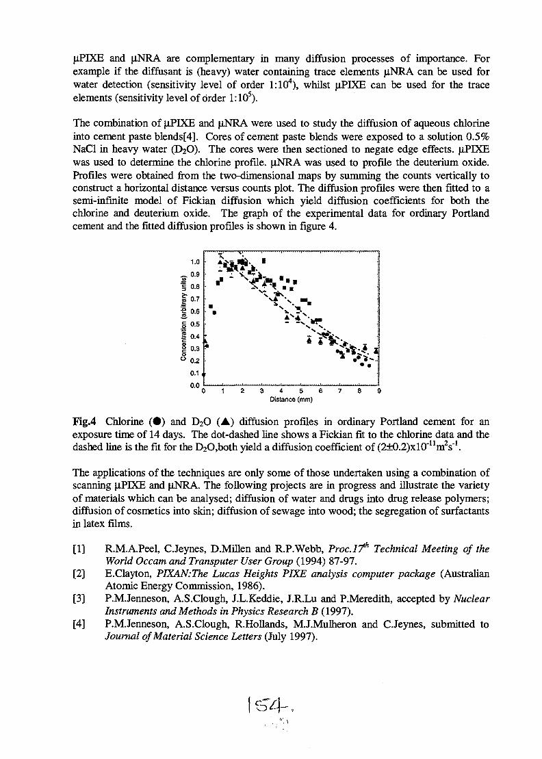
JJPDCE and u,NRA are complementary in many diffusion processes of importance. Forexample if the diffusant is (heavy) water containing trace elements fiNRA can be used forwater detection (sensitivity level of order l:104), whilst fiPIXE can be used for the traceelements (sensitivity level of order l:105).
The combination of jxPIXE and |LLNRA were used to study the diffusion of aqueous chlorineinto cement paste blends[4]. Cores of cement paste blends were exposed to a solution 0.5%NaCl in heavy water (D2O). The cores were then sectioned to negate edge effects. uPIXEwas used to determine the chlorine profile. jxNRA was used to profile the deuterium oxide.Profiles were obtained from the two-dimensional maps by summing the counts vertically toconstruct a horizontal distance versus counts plot. The diffusion profiles were then fitted to asemi-infinite model of Fickian diffusion which yield diffusion coefficients for both thechlorine and deuterium oxide. The graph of the experimental data for ordinary Portlandcement and the fitted diffusion profiles is shown in figure 4.
1 2 3 4 5 6 7 8 9Distance (mm)
Fig.4 Chlorine ( • ) and D2O (A) diffusion profiles in ordinary Portland cement for anexposure time of 14 days. The dot-dashed line shows a Fickian fit to the chlorine data and thedashed line is the fit for the D2O,both yield a diffusion coefficient of (2±0.2)xl0"11m2s1.
The applications of the techniques are only some of those undertaken using a combination ofscanning ^iPIXE and jiNRA. The following projects are in progress and illustrate the varietyof materials which can be analysed; diffusion of water and drugs into drug release polymers;diffusion of cosmetics into skin; diffusion of sewage into wood; the segregation of surfactantsin latex films.
[1] R.M.A.Peel, C.Jeynes, D.Millen and R.P.Webb, Proc.lT"1 Technical Meeting of theWorld Occam and Transputer User Group (1994) 87-97.
[2] E.Clayton, PIXAN.The Lucas Heights PIXE analysis computer package (AustralianAtomic Energy Commission, 1986).
[3] P.M.Jenneson, A.S.Clough, J.L.Keddie, J.R.Lu and P.Meredith, accepted by NuclearInstruments and Methods in Physics Research B (1997).
[4] P.M.Jenneson, A.S.Clough, R.Hollands, MJ.Mulheron and C.Jeynes, submitted toJournal of Material Science Letters (July 1997).

P1.19 AU98I7146
Microstructure of Metal Ion Implanted Ceramics
Huaxia .Ti* P. J. Evans** and M. Samandi*
* Surface Engineering Research Centre, University of Wollongong,Wollongong, NSW 2522, Australia
** Physics Division, ANSTO, Lucas Heights, NSW 2234, Australia
Abstract
Microstructure of alumina and siliconnitride after metal ion implantation has beenstudied. A metal vapour vacuum arc(MEWA) ion source was employed toimplant Ti ions into alumina with 7.6X101
and 3.1xlO17 ions/cm2 at 40W. Ti ions werealso implanted into silicon nitride at a dose of4xlO17 ions/cm2 at 70W. The characterisationof ion implanted ceramics by RutherfordBackscattering Spectrometry (RBS) andcross-sectional transmission electronmicroscopy (XTEM) showed low dose Tiimplantation into alumina resulted in a highlydefective surface layer. At higher dose, T1O2precipitates in an amorphous matrix weredetected. In contrast, Ti implantation intosilicon nitride produced a layered structure.The upper most layer consisted of extremelyfine TiN particles in an amorphous matrix.Underneath this layer, an amorphous layerwas formed.
Introduction
Implantation of ceramics is much morecomplex and less studied than insemiconductors or metals. The defectsproduced by bombarding ions are stronglyassociated with local electrical chargeneutrality, the local stoichiometry and thenature of chemical bonding. Whilst, themicrostructure is considerably sensitive to thechemical and electrical nature of impurities, inaddition to the parameters of implantationfl].
Alumina and silicon nitride arerespectively ionically and covalently bondedceramics used in engineering applications. Inthe case of alumina, no amorphizationoccurred in single crystal substrates eventhough substantial disorder had occurred afterimplantation of Ti to a dosage of 3 x 101
ions/cm2 and energy of 150 keV[2] . Thisindicates that doses above about 1 x 10¹⁷
ions/cm would lead to a softening ofpolycrystalline alumina due to amorphization.According to the previous investigations[3-5],it was found that the covalently bondedceramics were more easily amorphized by ionimplantation than ionic bonded ceramics [6].
Clearly, defects introduced by ionimplantation can result in differentmicrostructural modifications to the substrate.Therefore, it is desirable to characterise suchchanges in ion implanted ceramics in order tounderstand the mechanism of surfacemodification resulting from ion bombardment.In the present study, the microstructure of twoceramic materials (i.e. AI2O3 and Si3N4),implanted with metal ions, have beencharacterised by cross-sectional transmissionelectron microscopy (XTEM) and Rutherfordbackscattering spectrometry (RBS).
Experiments
The ceramic substrates used for metalion implantation were commercially availablehigh purity alumina (OC-AI2O3) andpressureless sintered silicon nitride (Si3N4). Apolished surface sample was obtained bygrinding and polishing to a 1 (im diamondfinish. A metal vapour vacuum arc (MEWA)ion source[7] was used for the implantations.Ti ion implantation on A12O3 was carried outat an extraction voltage of 40kV and doses of7.6xlO16 ions/cm2 and 3.1xlO17 ions/cm2 .Similarly, the polished Si3N4 surface wasimplanted with Ti to a fluence of 4x10ions/cm2 at 70W.
17
Characterisation of the implantedsurfaces was performed using RBS andXTEM. Thin TEM specimens were preparedby ion beam milling and then examined with atransmission electron microscope (JEOL2000) at 200W.

Results
The concentration of implanted Tiretained in A12O3, derived from RBS spectra,was 14at.% for ion fluence at 7.6x10 ions/cm2 and 50at% for 3.1xl017 ions/cm2. Thepeak concentration of Ti was shifted closer tothe surface as the implantation dose increased.Similarly, the Ti concentration was 37at% forSi3N4 at 4xlO17 ions/cm2. A typical TEMmicrograph of AI2O3 implanted with Ti ions at40 keV and 7.6xlOx ions/ cm2 showed anobvious implantation layer in the width ofabout lOOnm (Fig.la). Corresponding nanobeam electron diffraction (NBED) patterns ofTi implantation layer and A12O3 matrix aregiven as inserts in Fig.la. The pattern fromthe Ti implantation layer was identified as the
structure of a- AI2O3 in the direction of[T2Tl], which is consistent with the AI2O3
Fig.l TEM micrographs of A12O3 implantedwith 40keV Ti ions (a) dose at 7.6x10 ions/cm2 showing implanted layer with NBEDpatterns, (b) dose at 3.1xlO17 ions/cm2
showing two distinct sublayers, I and II, withNBED patterns
substrate. It indicates that the implantationlayer was fully monocrystalline. In contrast,an implantation layer of AI2O3 implanted withTi ions at 3.1xl017 ions/cm basicallyconsisted of two sublayers, i.e. outer region(I) and inner region (II), as shown in Fig.lb.The sublayer I was approximately 90 nm thickwhile sublayer II, adjacent to the alumina,was -70 nm thick with a high concentration ofthe defects. The inserted NBED pattern fromthe sublayer I showed crystal diffractionspots which formed a near crystal ringpattern. It indicates that sublayer I was nolonger monocrystalline and consistedpredominantly of numerous fine precipitates,determined as to be TiO2 since the indexeddiffraction pattern was consistent with thestructure of TiC>2. Sublayer II had similarfeatures to the implanted layer produced at thelow Ti dosage. The NBED pattern from thisregion was clearly consistent with that from
the CC-AI2O3 matrix in the direction of [2201 ].Sublayer II remains fully monocrystallinedespite the high concentration of the defectsthat was formed in this region. It is likely thatthe high density of defects promotes thegrowth of precipitates[8].
Analogously, TEM micrograph ofS i 3 N 4 implanted with Ti ions at4xl0 1 7 ions/cm 2 is shown in Fig.2. Theimplantation layer was about 280nm thick andhad two distinct sublayers designated I and HNBED pattern from Si3N4 was determined as
(3-Si3N4 in the direction of [1101 •]. Whilst, thepattern from sublayer I snowed diffractionspots due to the fine precipitation of TiN
Fig.2 TEM micrograph of Si3N4 implantedwith 70keV Ti ions at 4xl01 7 ions/cm2
showing two distinct sublayers, I and II, withcorresponding NBED patterns

superimposed on a diffuse ring patternoriginating from an amorphous matrix.Sublayer II was a fully amorphous band asverified by the sole presence of diffuse rings.Therefore, the implantation layer had anamorphous region and a mixed region ofamorphous and polycrystalline.
Discussion
The experimental results indicate thatlocalised amorphization was caused by Ti ionimplantation. A model which explainsstructural changes by ion implantation isbased on the accumulation of defects [9].During ion implantation, an incident ioncollides with target atoms which in turn causemore displacements. Numerous collisions ofthis type produce a collision cascade resultingin the formation of an extensive network ofdefects, such as vacancies, interstitials andimpurities. These defects will be accumulatedand rearranged into metastable configurationsas the ion fluence is increased. Consequently,the long range order of the crystal lattice isdestroyed and an amorphous state is producedas a critical defect concentration may bereached[6]. The microstructure of implantedmaterials depends upon the damage left afterdynamic recovery processes annihilate mostof the defects produced in the collisioncascade. The depth of amorphization will beassociated with ion incident flux and incidentenergy [7]. Titanium has high affinity foroxygen and preferentially reacts with it toform titanium oxide when AI2O3 is implantedwith Ti ions. The covalently bonded ceramicsappear more easily to be amorphized thanionic bonded ceramics because the covalentbonds are more difficult to recover than ionicbonds. Si3N4 implanted with Ti ions showedthe obvious amorphous band. The formationof new compounds in sublayer I, i.e. outerregion of the implantation layer, indicatesprecipitation from the amorphous layer whenhigh concentrations of metal ions areimplanted.
distinct regions. The one closest to the surfacewas predominantly polycrystalline andcontained precipitates of T1O2. In contrast, thelayer adjacent to the substrate remainedmonocrystalline and corresponded to a- A12O3with a high concentration of defects. Tiimplantation of Si3N4 also resulted in amodified region comprising two layers. Theuppermost layer consisted of a mixture ofpolycrystalline and amorphous material witha. completely amorphous layer underneath. Itis likely that metallic nitride, such as TiN, wasformed in the the layer closest to the surface.
References
1. C. J. McHargue, Nucl. Instr. MethodsPhys. Res., B19/20, p797 (1987)
2. H. Naramoto et al, Nucl. Instr. &Methods, B209/210, pi 159 (1983)
3. C. J. McHargue et al, Mater. Sci.. Eng.,69: pi23 (1985)
4. J. Lankford., W. Wei and R. Kossowsky,3 Mat. Sci., 22, p2069 (1987)
5. F. Halitim et al, Nuc. Inst. & Meth. inPhy. Res., B122, p28 (1997)
6. P. J. Burnett and T. F. Page, J. Mater.Sci., 19, p845 (1984)
7. R. Cornelius, M. Samandi and P. J.Evans, Surface Engineering, 11,pl23 (1995)
8. A. Rahioui and C. Esnouf, Surface &Coating Tech., 45, p23 (1991)
9. R. Kelly, in "Beam Modification ofMaterials 1", ed. O. Auciello and R.Kelly, Elsevier, 1984
Conclusion
The implantation of A12O3 with Ti ionsto a dose of 7.6xlO16 ions/cm2 resulted in amodified layer which was monocrystalline.Implantation at the higher dose of 3.1xlO17
ions/cm2, produced a modified layer with two

P1.20 AU9817147
IMPLANTATION-INDUCED SURFACE AND STRUCTURAL MODIFICATION OFSILICACM. Johnson, M.C. Ridgway, T.D. Thompson, Department of Electronic MaterialsEngineering, RSPhysSE, Institute of Advanced Studies, Australian National University,Canberra, Australia, 0200.
Ion irradiation of silica results in compaction of the substrate over the extent of the ionrange where the resulting increase in refractive index has applications to optical waveguidefabrication. For the present report, several non-conventional analytical techniques have beenutilised to characterise the surface and structural modifications of silica resulting from ionimplantation with the aim of yielding further insight into this technologically-relevant process.Substrates of both fused silica and PECVD-grown silica-on-Si were implanted with Si ions at anenergy of 5 MeV and a temperature of -196°C over a range of ion doses. Compaction of thesubstrate was charcterised as a function of ion dose with both standard profilometry andextended x-ray absorption fine structure (EXAFS). With the former, saturation of thecompaction at an ion dose of lei5 /cm2 was observed. With the latter, complementaryinformation on implantation-induced changes at the atomic scale were determined, specifically,EXAFS was used to differentiate the influences of bond length and bond angle changes in thecompaction process. Furthermore, a novel in-situ photographic technique has been developed torecord the state of the substrate surface, at a temperature of -196°C and under vacuumconditions, during ion implantation. Cracking of the surface, as a means of stress relief, wasobserved at doses less than that required for saturation of the compaction. Crack formation wasstudied as a function of both ion dose and energy, the latter to differentiate the influences ofelectronic and nuclear stopping processes. Thereafter, the evolution of the cracked surface wascharacterised as a function of temperature, pressure and ambient.
Craig JohnsonDepartment of Electronic Materials EngineeringResearch School of Physical Sciences and EngineeringAustralian National UniversityCanberra AUSTRALIA 0200
Email: cmj 109@ rsphvsse.anu.edu.auPhone: 61 6 249 0037Fax: 616 249 0511

PI 11r i * AU9817148
MULTIPLE SCATTERING PROBLEMS INHEAVY ION ELASTIC RECOIL DETECTION ANALYSIS
P.N. Johnston, M. El Bouanani, W.B. Stannard, I.F. Bubb,Department of Applied Physics, Royal Melbourne Institute of Technology, GPO Box 2476V,Melbourne, Australia;D.D. Cohen, N. Dytlewski and R. Siegele,Australian Nuclear Science and Technology Organisation, PMB 1, Menai, Australia
A number of groups use Heavy Ion Elastic Recoil Detection Analysis (HERD A) to studymaterials science problems. Nevertheless, there is no standard methodology for the analysis ofHEERDA spectra. To overcome this deficiency we have been establishing codes for 2-dimensional data analysis. A major problem involves the effects of multiple and pluralscattering which are very significant, even for quite thin (~100 nm) layers of the very heavyelements. To examine the effects of multiple scattering we have made comparisons betweenthe small-angle model of Sigmund et al.1'2 and TRIM3 calculations.
1. IntroductionHERD A with its exceptional and unambiguous multi-elemental depth profiling capabilities is apowerful analysis tool using heavy ion tandem accelerators or cyclotrons with two basicdetector types (i) Time of Flight and Energy (ToF-E) telescopes which are mass resolving and(ii) Energy Loss and Energy (AE-E) telescopes which are nuclear charge resolving. Theimportant capability of the HDERDA method is the quantitative elemental depth profiling ofthin films and the near-surface region of solids. The accuracy of the elemental depth profiles isdependent on the understanding of the underlying physical processes governing ion-matterinteractions and more importantly their adequate modelling.
The main physical considerations in ion-matter interactions are the scattering process, energyloss, energy loss straggling, multiple and large angle plural scattering. In the case of light ions,these are in the main well understood. But for heavy ion-matter interactions where energy lossstraggling and large angle plural scattering are more acute, there is no reliable and satisfactoryunderstanding and modelling. This is a major limitation when dealing with heavy ion IBA. Inthis paper issues regarding multiple scattering in simulation of HERD A data are examined.
2. TheoryThis paper considers the application of multiple scattering slab analysis of BDERDA. Davies etal. have indicated in the Ion Beam Handbook4 that they believe that Multiple scattering canonly be adequately considered through Monte-Carlo simulation using TRIM3. We are reluctantto abandon slab analysis as Monte-Carlo is expensive in computer time for routine usealthough it has been used for some simulations, e.g. Biersack et al.5. Tadic et al.6 haveexamined a similar set of problems for RBS of heavy ions. They used the small angle multiplescattering models of Sigmund and Winterbon1 and Marwick and Sigmund2.
TRIM has been used to model transmission of ions through thin films of Au using typicalion/target combinations. The results of this modelling are compared with the model ofSigmund and Winterbon1 and examined to find ways in which the simulation might proceed.Sigmund and Winterbon have tabulated angular distributions fiyu^a) as functions of
\&\.

Ea- a where a is the total deflection angle
0 ***>
reduced variables x = Tea Nx and a =
and a is the screening radius. The screening radius has been estimated using Meyer's formula7.These distributions are projected onto the scattering plane for application to HEBRDA as smallangular deviations perpendicular to the scattering plane contribute little to the angles involved.
Marwick and Sigmund2 have considered the lateral spread of the beam. This lateral spread isparticularly important in the case of conventional HEERDA in the glancing mode as the lateralspread of the beam has a strong effect on the path length the ion must traverse in passingthrough the layer (Fig. 1).
127i
a
xcosft
Figure 1. Diagram showing the effect of multiple scattering, showing the angular deflection a
and the variation of path length (Al_, A1+) of incident ions through a layer of thickness xcosSj.
3. ResultsFigure 2 shows a comparison of the angular deviation of transmitted 60 MeV 127I ions throughlayers of Au of thicknesses 13 lcosGi nm as a function of incident angle (9i) simulated by TRIMwith 106 ion trajectories so that the undeviated path length is the same for each simulation. Thecurves mostly overlap, with differences when the ion trajectories approach the normal orparallel to the layer boundaries. Changing the angle of incidence has little effect on thedistribution. The angular deviation for an incident ion beam at 67.5° has been compared withthe distribution from the model of Sigmund and Winterbon and they agree well.
1000000 T
10000 --00
o
100 -•
••••••*• . • • • ! • • •• • • • •
\'*AA
-40 40-20 0 20Angular Deviation (degrees)
Figure 2. Angular distribution of transmitted 60 MeV 127I ions through Au of thicknesses 131cos0; nm as a function of incident angle (9;) at 7° (A), 45° ( • ) and 75° ( • ) simulated by TRIM.

Fig. 3 shows the mean energy of transmitted 60 MeV 127I ions through Au of thicknesses of131 cosG; nm as a function of incident angle (0i) simulated by TRIM. At large incident ionangles, the energy distribution becomes very asymmetric which can be partly ascribed to thedifference in path length for ions deviating from the normal. For grazing incidence, it becomesvery clear that the mean energy increases for small deviations toward the normal. The TRIMcalculations show that for ions incident at 75°, the mean energy is highest for a deviation -3°.This is not readily explained by simple path length considerations used by Tadic et al. asshorter path lengths occur for greater deviations but lower mean energies are calculated byTRIM. TRIM simulations of the angular distribution due to multiple scattering as a function oflayer thickness agree with the theory of Sigmund and Winterbon.
600000000 j
• •• • t * A 50000
C A
0) • (
•
A A
• •.
A
.A
A
A
-40 -20 0 20 40Angular deviation (degrees)
Figure 3. Mean energy of transmitted 60 MeV 127I ions through Au of thicknesses 130 cos9jnm as a function of incident angle (9;) of 7° (•) , 45° (A) and 75° ( • ) simulated by TRIM.
ConclusionThe model of Sigmund and TRIM simulations of the angular distribution from multiplescattering are in agreement. However, the energy of ions transmitted in a glancing geometrycannot be adequately estimated by simple path length considerations. These energies calculatedby TRIM will have some uncertainty, but the general behaviour will not change. To quantifymultiple scattering effects, measurements of multiple scattering of heavy ions in situations ofvery heavy targets and where single scattering is excluded have commenced.
AcknowledgmentsThis work is supported by the Australian Institute of Nuclear Science and Engineering.
References1. Sigmund, P. and Winterbon, K.B., Nucl. Instr. and Meth., 119 (1974) 541.2. Marwick, A.D. and Sigmund, P., Nucl. Instr. and Meth., 126 (1975) 317.3. Biersack, J.P. and Littmark, U., 'The Stopping and Range of Ions in Solids', Pergamon,
New York, 1985; Zeigler, J.F., SRM-96 Instruction Manual, IBM-Research, Yorktown.4. Davies, J. A., Lennard, W.N. and Mitchell, I.V., Ch. 12, Handbook of Modern Ion Beam
Materials Analysis, Eds. J.R. Tesmer and M. Nastasi, 1995, MRS, Pittsburgh, p.352.5. Biersack, J.P., Steinbauer, E. and Bauer, P., Nucl. Instr. and Meth. B 61 (1991) 77.6. Tadic, T., Jaksic M. and Dujmic, D., paper 3C-O5, 5th Int. Conf. on Nuclear Microscopy
Techniques and Applications ICNMTA-96, Santa Fe, November 10-15, 1996.7. Meyer, L., Phys. Stat. Sol., 44 (1971) 253.

P 1 - 2 2 AU9817149
COMPLEMENTARY SCATTERED AND RECOILED ION DATA FROM TOF-EHEAVY ION ELASTIC RECOIL DETECTION ANALYSIS
P.N. Johnston, M. El Bouanani, W.B. Stannard, IF . Bubb,Department of Applied Physics, Royal Melbourne Institute of Technology, GPO Box 2476V,Melbourne 3001, AustraliaD.D. Cohen, N. Dytlewski and R. Siegele,Australian Nuclear Science and Technology Organisation, PMB 1, Menai 2234, Australia
The advantage of Time of Flight and Energy (ToF-E) Heavy Ion Elastic Recoil DetectionAnalysis (HIERDA) over Rutherford Backscattering (RBS) analysis is its mass and energydispersive capabilities. The mass resolution of ToF-E HIERDA deteriorates for very heavyelements. The limitation is related to the poor energy resolution of Si detectors for heavy ions.While the energy spectra from ToF-E HIERDA data are normally used to extract depthprofiles, this work discusses the benefits of using the time spectra of both the recoiled and thescattered ions for depth profiling.
1. IntroductionHIERDA using either the mass dispersive ToF-E or the nuclear charge dispersive AE-E(Energy Loss and Energy) detection systems, has been extensively studied during the last fewyears by groups in Sweden [1], Germany [2], Canada [3], France [4], Finland [5] and Australia[6] using (0.2-2 A MeV) heavy ions. The exceptional and unambiguous multi-elemental depthprofiling capabilities of HIERDA are due mainly to its dispersive multi-elemental detectioncharacteristics. Despite the effort devoted to optimising HIERDA, the ability to extract depthprofiles is limited due to: (i) the poor understanding of the transport of heavy ions, and (ii) thepoor energy resolution and stability of Si detectors for heavy ions [7].Limitations of HIERDA are not a result of physical principles but are mainly related to themass or nuclear charge separation performance of the detection system. In the case of the ToF-E detection telescope, this limitation is due to the energy resolution of the Si detector. In aprevious study, the mass resolution of ToF-E HIERDA [8] was determined, showing animprovement with increasing energy and lighter recoils due to the energy response of the Sidetector. For ToF-E detection systems, several data processing methodologies have beendeveloped and used to simulate (ToF, E) data [9] or extract elemental energy spectra [10] todetermine depth profiles. Time spectra have been largely ignored. Also the forward scatteredspectrum is not used even though it contains valuable information.This work demonstrates that: (i) instead of the ToF detector, the Si detector should be used asthe dispersive instrument. The time spectra provide better depth profiling information,improving the depth resolution of HBERDA, and (ii) some difficulties in extracting elementalenergy spectra of the overlapping signals from heavy recoils (Pt-Bi) can be overcome by usingthe complementary time spectra of the recoiled and forward scattered ions.
2. Advantages of Time spectraIn IBA studies, energy spectra are usually measured and used for depth profiling. The ToFdetector in HIERDA is normally only used for mass dispersion as it depends on the flightlength (L). Despite modelling of the ion-matter interactions being defined in terms of energy,there is no need to reformulate the models of ion-matter interactions in terms of the ToFparameter. Experimental time spectra can be directly used for depth profiling. The depthprofiles are extracted using a simulation where each isotopic contribution is calculatedindependently and then summed. This is advantageous for HIERDA as the depth resolution is
\b^

improved and ion damage induced changes in the Si detector pulse height do not affect theanalysis. On the contrary, the time resolution can be well approximated by a constant.Fig. 1 shows the gain in depth resolution when using time spectra for a ferroelectric sample.The energy resolution of the Si detector is so poor that it is difficult to distinguish the highenergy edges of the different elements. On the contrary, the shape of the time spectrum showswell defined high energy edges, demonstrating superior resolution of the ToF detector. Fig. 2shows a comparison between the energy resolutions of the Si and ToF. The energy resolutionof the Si detector is estimated using Amsel's formula [13] fitted to the available experimentaldata for elements up to Br [14]. Amsel's empirical formula is:
AEsi = a + bEm (1)where a and b are constants for a given atomic mass number. The energy E is expressed inkeV. From Hinrichsen's compilation [14] the mass dependence of the parameters a and b isestimated to be:
AEsi = (108.08-3.38 M) + (0.51 M-5.85) E1B (2)where M is the atomic mass of the detected ion.This expression fits experimental data ranging from 12C to 81Br ions with energies below 25MeV and has been extrapolated for 127I ions. A measurement of the energy resolution for 58MeV 127I ions gives 3200 keV including geometrical factors suggesting that the expression (2)is an underestimate. The energy resolution derived from the ToF detector is:
AEToF=2EAt/t (3)where t is the time of flight of the ion. At is the total time resolution of the ToF detectorincluding the intrinsic time resolution, electronic noise, geometrical contributions and sampleroughness. At is 400 ps for scattered 127I ions in this work.The energy resolution of the ToF detector for 127I ions (Fig.2b) is lower than the energyresolution of the Si detector and is at least a factor of 2 better at high energies and a factor of10 better below 20 MeV for L of 0.5 metres and can be improved by a longer L at the expenseof the solid angle.
CO
"c3O200O
100
w 0
3200/-\o
100
n
:, Energy Channel *
• •* .* pt
^ • ^
• Time Channeli , i ,
(a)
(b)
Ta
Figure 1: (a) Energy spectrum of theoverlapped Ta, Pt and Bi recoils detectedat 45° from 97.5 MeV 127I incident ions,and (b) projected time spectrum of thesame recoils. Details of the measurementson the sample of nominal structureSrBi2Ta20<)/Pt/Ti02/Si are given in ref.[6].
o'gLJ<
20 40 60 80Iodine Energy (MeV)
Figure 2: (a) Energy resolutions for bothToF and Si detectors of 127I ions, (b) Theratio of energy resolutions of Si detectorand ToF detector for 127I ion for L of 0.5and 1 m.
\\&

3. Complementary spectra of scattered and recoiled ionsIt is proposed to use the time spectra of both the forward scattered and the recoiled ions asthey contain valuable complementary information. The kinematics governing the scatteringprocess mean that the mass dependencies of the energy transfer to the recoil and the scatteringenergies follow opposite trends when the incident ion is lighter than the analysed ion. Thismeans that the overlapping isotopic contributions from the recoiled ions are completelydifferent for scattering signals (Fig.3). The simulation of both the scattered and recoiled datafrom heavy ions adds extra information for the depth profile extraction.
CO-•—<
co
100
500 1000 1500 2000Time Channel
-
- &£&
Recoiled
, i
•
If*
Bi, Ptja \
i
(a)
Ta
i i-
to•*->
c^600O
400
200
n
••
^ f1 Scattered
i
•
UIodine
i
(b)
Ta*
2000 2500 3000Time Channel
Figure 3: Superposition of experimental and simulated time spectra for (a) overlapped Ta, Ptand Bi recoils (b) forward scattered 127I from Ta, Pt and Bi.
4. ConclusionsWe have demonstrated for HERD A using a ToF-E telescope that the high stability of the ToFsignal which is independent of the mass, atomic number and energy of the detected ions hassignificant advantages over the use of the energy signal from Si detectors. The simulation ofthe complementary scattered and recoiled ion time spectra improves depth profiling andreduces current limitations when dealing with very heavy ions.
AcknowledgmentsThis work is supported by the Australian Institute of Nuclear Science and Engineering.
References1. H.J. Whitlow et al., Nucl. Instr. and Meth. B 63 (1992) 445.2. W. Assmann, et al., Nucl. Instr. and Meth. B 89 (1994) 131.3. R. Siegele, et al., J. Appl. Phys. 76 (1994) 4524.4. J.P. Stoquert, et al., Nucl. Instr. and Meth. B44 (1989) 184.5. J. Jokinen, et al., Nucl. Instr. Meth. B 119 (1996) 533.6. W.B. Stannard, et al., Integ. Ferroelectrics 9 (1995) 243.7. P.N. Johnston, et al., accepted for publication in Vacuum.8. M. Hult, et al., Nucl. Instr. and Meth. B101 (1995)263-266.9. P.N. Johnston, et al., Proc. 14th CAARI'96, Denton, Texas, November 6-9, 1996.10. M. Hult, et al., J.Appl. Phys. 77 (1995) 2435.11. R. Groleau, S.C. Gujrathi, and J.P. Martin, Nucl.Instr. and Meth. 218. (1993) 11.12. J.P. Thomas, et al., Nucl.Instr. and Meth. 218 (1993) 125.13. G. Amsel, C. Cohen and A. L'hoir, in Ion Beam Surface Layer Analysis vol. 2, O. Meyer,
G. Linker and F. Kappeler, eds. (Plenum, New York, 1976).14. P.F. Hinrichsen, et al., Nucl.Instr. and Meth. B45 (1990) 275.

pi 73 iiiiiiiiiiiiiiiiiiiiiiiiiiiiiiiiiiiiiilllllAU9817150
NEUTRON ACTIVATION ANALYSIS TO EXAMINE EFFECTIVENESS OF METALGETTERING TO HYDROGEN-INDUCED CAVITIES IN SILICON
A. Kinomura12, J. S. Williams1, J. Wong-Leung1. M. Petravic1, K. Fujii2, Y. Nakano3 and Y.Hayashi3
1 Department of Electronic Materials Engineering, Research School of Physical Sciences andEngineering, Australian National University, Canberra ACT 0200, Australia
2 Osaka National Research Institute, AIST, 1-8-31 Midorigaoka, Ikeda, Osaka 563, Japan3 Research Reactor Institute, Kyoto Univerisity, Kumatori-cho, Sennan-gun, Osaka 590-04,
Japan
Metal impurities introduced during various fabrication steps are of considerable concern forsilicon device production. We have previously demonstrated the effectiveness of gettering ofvarious implanted metals to cavities in Si by using Rutherford backscattering (RBS) andsecondary ion mass spectrometry (SIMS). However, RBS and SIMS have limited sensitivityand only probe near surfaces. In this study, neutron activation analysis was carried out toexamine the effectiveness of metal gettering to cavities induced by hydrogen implantation insilicon.
After cavity formation by H implantion and annealing at 950 °C for lh, SIMS analyis indicated
that unintentional Cu contamination of the order of 10 cm was introduced. Neutronirradiation was carried out for 225 h in the core irradiation facility of the Kyoto University
1 "
Reactor with a thermal neutron flux of about 3x10 n/cm s. Gamma-rays from the sampleswere measured about 4 days after the end of irradiation by using a pure Ge detector. To detectthe Cu atoms in the samples, gamma-rays of 0.511 MeV from Cu with a half life of 12.7hwere measured. Metal contamination such as Na, Cu, Au, Fe and W was often detected in thesamples with cavities, while non-processed samples (as-received wafer) showed much lowercontamination levels except for Na. The surface of a sample containing a cavity band wasremoved by chemical etching with a solution of HNO3 and HF. The Cu signals considerablyreduced after etching, indicating the cavities successfully trapped Cu atoms unintentionallyintroduced in the wafer.
Under NUCLEAR TECHNIQUES OF ANALYSIS (NTA)

P1.24III
AU9817151Technical Advances at the ANTARES AMS Centre
E.M. Lawson. D. Fink, M.A.C. Hotchkis, Q. Hua, G. Jacobsen, A.M. SmithPhysics Division, ANSTO, PMB 1, Menai, NSW 2234
Accelerator Mass Spectrometry (AMS) began at ANTARES in late 1991.Many technical improvements and upgrades to the AMS measurementsystem have taken place since then. The AMS Centre routinely measures14C (to better than 1% precision), 36C1 and 1291. The capability to measurelOBe and 26A1, and is established although further development is still inprogress. A capability to analyse Actinides is being established and is thesubject of another paper to this conferencel. This paper reviews some of themore recent technical improvements to the facility.
For our 14C analyses a new gas stripper system and high resolution ExBvelocity analyser have been installed and are in routine operation. The gasstripper is also used for most other isotopes. A new 90 degree sphericalESA allows 1291 measurements without the need for time-of-flightanalysis. Installation of a critical insulation flange in the isotope cyclingsytem has permitted ebouncingi of 12C- and the measurement of 13C/12Cratios. A complete set of Dowlish tubes now allows spark free operation to 8MV for our lOBe and 36C1 measurements. The very recent installation ofpelletron chains is being assessed.
1. MAC. Hotchkis et al. The Actinides Beamline on the ANTARESAccelerator Mass Spectrometry Facility.
For POSTER presentation at the Nuclear Techniques of Analysis session
Contact E.M. Lawson Tel: 02 9717 3025Fax: 02 9717 3257Email: [email protected]

P1.25IIII
AU9817152
A PIXE/PIGE STUDY OF LATERITIC GOLD MINERALIZATIONFROM THE REGOLITH OF THE MYSTERY ZONE, MT PERCY,WESTERN AUSTRALIA
Xu Li and J.C. van MoortGeology Department, University of Tasmania, GPO Box 252-79, Hobart, Tasmania 7001
Introduction
Bulk rock chemical analysis by proton-induced X-ray and y-ray emissions (PIXE/PIGE) havebeen used in exploration geochemistry over a decade. Simultaneous analyses are obtained for upto sixty elements, ranging in atomic number for 3Li to ^Pb, typical minimum detection limits(MDL) for trace elements are a few ppm. Similar results may be obtained by XRF spectroscopy,however this method cannot provide information on the concentration of the elements Li, B andF.
PIXE/PIGE have been utilized extensively in the search for gold (van Moort and Hotchkis,1993, Russell, 1995)and volcanic hosted massive sulphide deposits (Pwa, 1996), using rockpowders from relatively fresh rock. The present study uses regolith samples, from whichweathering products (oxides, hydroxides, carbonates, sulphates and clay) have been removed bysequential treatment with aqua regia and sulphuric acid. The samples come from the MysteryZone, Mt Percy, Kalgoorlie, comprising both mineralized and barren samples. The acidinsoluble residue consist essentially of quartz with minor sericite.
The PIXE/PIGE data from the acid insoluble residue shows that the geochemical character of W,Al, K, Ca, V, Ga, Rb, Rb/K and Rb/Al could correctly define the location of underlyingmineralization at depth. The ratio of Ti/Zr remained relatively constant in different geologicalunits and can be used to distinguish lithologies.
Geological setting
Mt. Percy gold mine is located on the north-eastern outskirts of Kalgoorlie, Western Australia.The gold mineralisation at Mt Percy is located in the lower part of the Kalgoorlie sequence.The sequence is crosscut by a series of north-trending, west-dipping dextral faults, includingthe Martiana, Reward, Charlotte and Mystery Faults. In the Mystery Zone, the chlorite talccarbonate rocks of the Hannan's Lake Serpentinite are intruded by porphyries, with strongfuchsite-carbonate alteration occurring at their contacts. Primary gold mineralisation islargely confined to a series of irregular, mostly steeply-dipping lenses within the porphyriesand adjacent fuchsite carbonate alteration zones.
Sampling and sample preparation
One hundred and eighty seven regolith samples from the Mystery Zone, Mt. Percy, Kalgoorliehave been studied by Butt(1991) for gold and associated elements. The present study is an

extension of this important earlier study with the aim to test if the acid insoluble PIXE/PIGEmethod can be used in highly weathered terrain for gold exploration. The section 15850Ncrossing the mineralised zone at the Mt. Percy has been studied.
All samples were riffle split and ground to less than 75 (im using a Mn steel mill (Butt, 1991).The powder samples were then treated with hot aqua regia and then hot sulphuric aicd asdescribed by Xu and van Moort (1997). A 400 mg acid insoluble regolith residue wasmechanically mixed with lOOmg of spectrographically pure graphite in an acrylic vial togetherwith an acrylic ball for ten minutes and pressed into a tablet to be ready for PIXE/PIGEanalysis.
Instrumentaiton, precision, accruacy and detection Limit
PIXE/PIGE analysis were carried out at Lucas Heights, ANSTO, on the 3 MeV Van de Graaffpositive ion accelerator. The proton energy used was 2.5 MeV protons with a beam current ofabout 300 nA. The aperture was set at 1.5 mm with a 3.3 mm steeple. The beam spot sizewas 1.5 mm and run timnes were adjusted so that the total charge collected was 100 (iC.
The reproducibility derived from the NBS obsidian standard SRM 278 and two regolithsamples randomly taken from the study are very good. Normally they ranged from as low as1% for Sr to 20% for Ba." The accuracy ranged from 92-104% for most elements. Only a fewelements (Cu and Zn) with poor accuracy were either present in concentrations at or below theminimum detection limit. The detection limits from most elements were found to range from2 to 30 ppm, except some light elements (e.g. Cl, Mg, Si and Al), which are about 100 ppm to1000 ppm.
Results and disscusion
The distributions for elements W, Al, K, Ca, V, Ga, and Rb are very similar to Au. Thedifference is that gold distribution in fuchsite ultramafic and porphyry units were patchybecause of the weathering process, but the distribution of those elements were more consistantin same geological unit after the acid treatment. They were both absent from biotite talc ultramafic unit. Comparing with the non-acid treatment Al distribution which was enrichedthroughout the whole regolith, particularly over the ultramafic rock, acid insoluble aluminiumcontent show very lower values in talc and biotite ultramafic which is not related to the goldmineralisation. The enrichment of Al and K were more or less related to the alteration. Therubidium distribution was characterised by moderate high value throughout the porphyry andfuchsite rocks from the base to the surface of the profile without a big change. That explainsthe Rb high values (non-acid treatment) occur in saprolite and mottled clays between 385Eand 400E on 15850N due to the weathering products enrichment (Butt, 1991). Zinc wasenriched in the fuchsite ultramafic rocks. It seems to relate to the alteration. Vanadium had avery similar distribution to Au. The difference is its content increasing somewhat towards thesurface. The distribution of chromium was very similar to Al and Rb indicating that they allhost the mineral fuchsite. Probably they host the same minerals. Tungsten and gallium were

consistently enriched throughout the primary mineralisation zone, except that some lowervalues appeared in fuchsite rock.
Zr, Th and Nb are the members of the second and third transition series and have very similarchemical characteristics. They behaved immobile character, with high values near the surface.But it still could be seen the highest value was in the near surface, lateritic duricrust.
Titanium is concentrated in the talc chlorite carbonate ultramafic rocks. Unlike the traditiongeochemistry result in which Ti is strongly concentrated relative to Zr so that lithologicaldiscrimination based on Ti-Zr plots is not possible (Butt, 1991), In this study, the ratio ofTi/Zr remains relatively constant in different geological units even under conditions of intensechemical weathering, except in talc carbonate ultrafafic rocks.
Chromium is concentrated in fuchsite ultramafic rocks (>874 ppm), which confirmed thechromian muscovite is the principal host minerals in the unweathered rocks. Theunweathered porphyry, biotite and talc chlorite ultramafic rocks have much lower Cr content,which is normally less than 189 ppm. Without considering the Cr contents in the lateriticduricrust, which was developed over the ultramafic rocks are unusually low, Cr abundancealone can be used to distinguish lithology.
Copper enriched in the porphyry and mottled and plasmic clay. Pb and Mo, because they arebelow the detection limit, it could not see any relationship with gold mineralisation. Ni and Znwere more enriched in unweathered ultramafic rocks, but depleted in clay saprolite above thebiotite talc ultramafic unit and showed the low values in porphyry. There are no envidence ofthose base metals with the primary Au mineralisation at Mystery Zone.
Rb/Al ratio are more accurately outline the gold mineralisation zone. Rb/K ratio show highvalues near the surface.
Generally, geochemistry character of W, Rb, V, Al, Cu, Pb Ti, and Zr, Rb/K and Rb/Al in theacid insoluble residue by PIXE/PIGE could be correctly define the tenor and location ofunderlying mineralisation at depth.
References
Butt, C. R. M., 1991. Dispersion of gold and associated elements in the lateritic regolith mystery zone, Mt. Percy,Kalgoorlie, Western Australia: Wembley, WA, Division of Exploration Geoscience, CSIRO.
Russell, D.W. 1995, The characterisation of quartz and gold in the Beaconsfield and Letroy areas, NorthernTasmania: Unpub. Ph.D. thesis, University of Tasmania, 300 p.
Pwa, A. 1996, Application of rock geochemistry and electron paramagnetic resonance of rock in mineralexploration, Rosebery mine area, western Tasmania: Unpub. Ph.D. thesis, University of Tasmania, 303 p.
van Moort, J.C. and Hotchkis, M. 1993. Electron paramagnetic resonance (EPR) spectroscopy supported byparticle-induced X-ray emission (PDCE and particle-induced gamma ray emission (PIGME) spectroscopy inmineral Exploration: Proceedings ICAM 93,1993, p. 217-221.
Xu, L. and van Moort, J. C , 1997, EPR characterisation of gold mineralisation in weathered Terrain, Jim's FindSouth, Tanami Desert, NT, Australia: First Asia-Pacific EPR/ESR Symposium, Hong Kong, 1997, ModernApplication of EPR/ESR: From Biophysics to Materials Science. Springer.

P1.26AU9817153
Production of thin carbon stripper foils using heated-substrates in acathodic arc deposition system.
A. R. Merchantd), N. Lobanov(2), R. G. Elliman(2), T. R. Ophel(2), A. Rode(2),D. C. Weisser(2) and R. B. Turkentine(2).
1. Key Centre for Microscopy and Microanalysis, University of Sydney, NSW Australia, 2006.2. Research School of Physical Sciences and Engineering, Australian National University, ACT
Australia.
The lifetime of Carbon stripper foil can have a marked impact on the successful running of a beam line. Standardtechniques for production of carbon stripper foils include evaporation of carbon (ec) and laser-pulsed ablation (Ipa).Recent work by a using Ipa has been successful in substantially increasing the lifetime of a very thin (100A) foil.The suspected mechanism for the increased lifetime of the foil is that the amorphous carbon foil is density-matched tothat of graphite (around 2.26g/cc). hi this work, we attempt to reproduce this result by producing carbon stripperfoils with a mass-density similar to graphite using a cathodic arc deposition system. The cathodic arc is well knownfor the production of tetrahedral amorphous carbon: a high density, high stress form of carbon with over 90% spMikebonds; to reduce the density of the carbon and promote more graphitic structure, a high bias was initially attemptedbut this proved unsuccessful. Another method is to use a heated-substrate holder to reduce compressive stress withinthe deposited film. The performance of the density-matched carbon stripper foils and the implications for futureproduction of high-quality carbon stripper foils in our laboratory will be discussed.
INTRODUCTION
Carbon foils are a vital component of manyaccelerators and are used to remove or stripelectrons from the ion species beingaccelerated. These foils are typically verythin (~200nm). There are several facilites inAustralia which use carbon stripper foilsincluding the National Medical Cyclotron inSydney and the Nuclear Physics Departmentin RSPhySE at ANU.
Because of the different requirements of eachfacility, carbon stripper foils are oftenproduced in-house to meet the necessaryspecifications. There are several techniquesused for regular production of stripper foilsincluding evaporation-condensation (ec) ofcarbon by either resistive heating or e-beam;laser-plasma ablation or glow discharge inethene gas.
The quality of a stripper foil is measured byits lifetime under irradiation, and its beamperformance (angular spread). Under a modelproposed by Dollinger and Maier-Komor [1]
the stripper foils with the longest lifetimesare thin, maximising ion transmission andalso contain isotropically oriented graphiticcrystallites.
Dollinger [2] showed that one way ofproducing a foil with these characteristicswas to use laser-plasma ablation (Ipa) ofsolid graphite targets. Another possible wayof producing a foil with similar attributes toa Ipa foil is to use the cathodic arc depositionsystem. The cathodic arc deposition systemis able to produce highly densifiedamorphous carbon films, commonly calledta-C or tetrahedral amorphous carbon [2].By altering deposition parameters, such asbias or temperature we will investigate theeffect this has on the microstructure of thecarbon foil.
EXPERIMENTALA schematic of a conventional cathodic arc isshown in Figure 1. The filtered cathodic arcis a technique for coating which is low-
lib
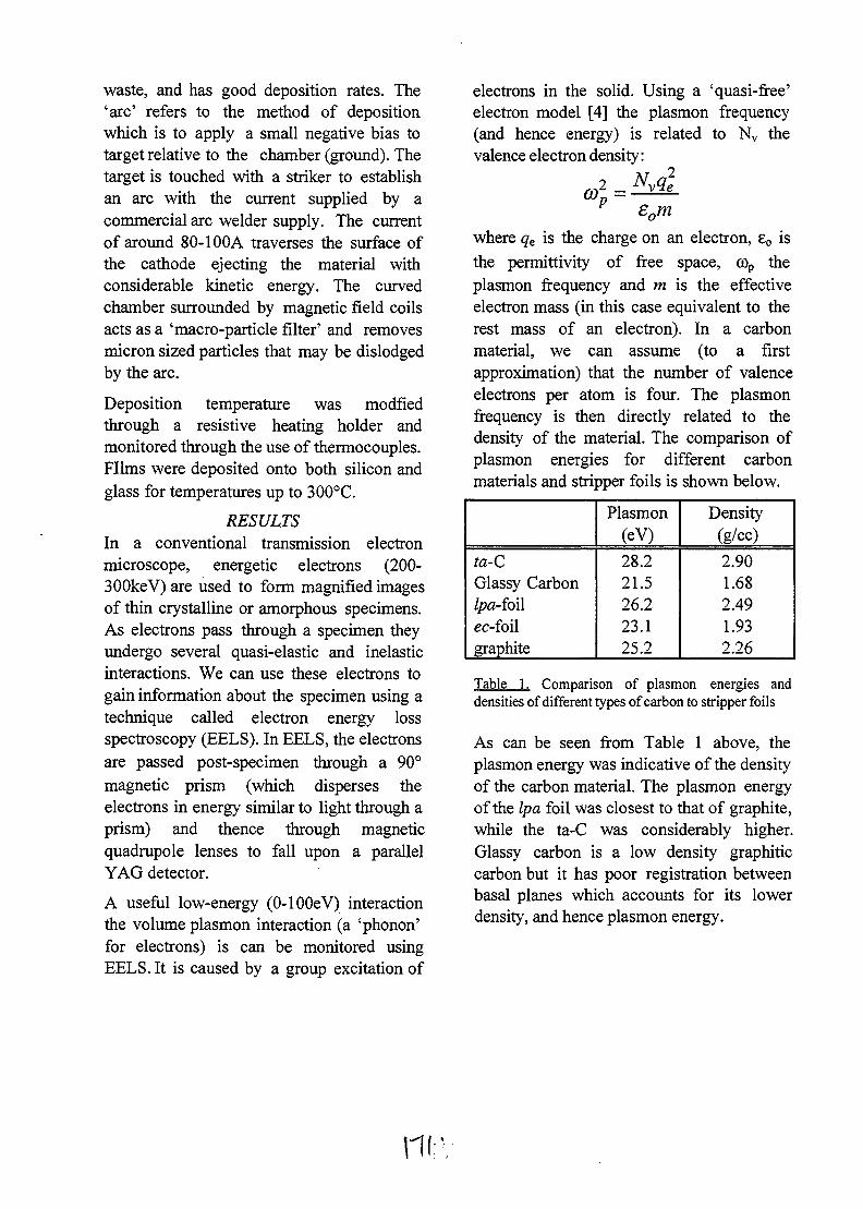
waste, and has good deposition rates. The'arc' refers to the method of depositionwhich is to apply a small negative bias totarget relative to the chamber (ground). Thetarget is touched with a striker to establishan arc with the current supplied by acommercial arc welder supply. The currentof around 80-100A traverses the surface ofthe cathode ejecting the material withconsiderable kinetic energy. The curvedchamber surrounded by magnetic field coilsacts as a 'macro-particle filter' and removesmicron sized particles that may be dislodgedby the arc.
Deposition temperature was modfiedthrough a resistive heating holder andmonitored through the use of thermocouples.Films were deposited onto both silicon andglass for temperatures up to 300°C.
RESULTSIn a conventional transmission electronmicroscope, energetic electrons (200-300keV) are used to form magnified imagesof thin crystalline or amorphous specimens.As electrons pass through a specimen theyundergo several quasi-elastic and inelasticinteractions. We can use these electrons togain information about the specimen using atechnique called electron energy lossspectroscopy (EELS). In EELS, the electronsare passed post-specimen through a 90°magnetic prism (which disperses theelectrons in energy similar to light through aprism) and thence through magneticquadrupole lenses to fall upon a parallelYAG detector.
A useful low-energy (0-100eV) interactionthe volume plasmon interaction (a 'phonon'for electrons) is can be monitored usingEELS. It is caused by a group excitation of
electrons in the solid. Using a 'quasi-free'electron model [4] the plasmon frequency(and hence energy) is related to Nv thevalence electron density:
p £om
where qc is the charge on an electron, 80 isthe permittivity of free space, a>p theplasmon frequency and m is the effectiveelectron mass (in this case equivalent to therest mass of an electron). In a carbonmaterial, we can assume (to a firstapproximation) that the number of valenceelectrons per atom is four. The plasmonfrequency is then directly related to thedensity of the material. The comparison ofplasmon energies for different carbonmaterials and stripper foils is shown below.
ta-CGlassy Carbon/pa-foilec-foilgraphite
Plasmon(eV)
28.221.526.223.125.2
Density(g/cc)
2.901.682.491.932.26
Table 1. Comparison of plasmon energies anddensities of different types of carbon to stripper foils
As can be seen from Table 1 above, theplasmon energy was indicative of the densityof the carbon material. The plasmon energyof the Ipa foil was closest to that of graphite,while the ta-C was considerably higher.Glassy carbon is a low density graphiticcarbon but it has poor registration betweenbasal planes which accounts for its lowerdensity, and hence plasmon energy.
111".

sMagneticFieldCoils
Curved solenoid directsion beam and filtersout macroparticlesand neutral atoms.
EaratronGauge
) 1
lonisationGauge
Our initial results using biased depositionwere promising, but as shown below inTable 2, even at high bias, the plasmon didnot fall below 26.8eV. Although this wasvery close to the Ipa plasmon energy, theresidual compressive stress in the filmdestroyed its structural integrity, making itunusable as a stripper foil.
Bias Plasmon(eV)
Density(g/cc)
-1250-300
0
26.828.328.2
2.602.92.90
Table I. Comparison of plasmon energies anddensities for cathodic arc foils for different bias.
Our initial tests using a heated substrateholder have been moderately successful. Wehave sucessfully deposited amorphouscarbon at temperatures up to 300°C, but wehave experienced problem with delaminationof the film.
CONCLUSIONInitial work has shown we can distinguishbetween different stripper foils by measuringthe volume-plasmon energy. Our work usinga heated substrate holder to deposit graphitefoils is still in progress.
REFERENCES1. Dollinger G. and P.Maier-Komor NIM
B282 (1989) 223-235.2. Dollinger G. and P.Maier-Komor NIM
A303(1991)79.3. McKenzie D. R. et al, Diamond and
Related Materials, 1 (1991), 51.4. D. G. McCulloch and S. Prawer, J. App.
Phys. 78(1995)3040.5. Egerton R. F., Electron Energy Loss
Spectroscopy in the Electron Microscope.(1986) Plenum Press New York.
-it

P127 .'IIIIIIIIIlllEil!AU98V/154
DEVELOPMENT OF AN EXTERNAL BEAM FACILITY FOR PIXE AT RMTT
M. Moserf, I. F. Bubb, P. N. Johnston, M. El Bouanani, W. B. Stannard and R. C. ShortDepartment of Applied Physics, Royal Melbourne Institute of Technology, GPO Box 2476 V,Melbourne, Australiaf on exchange from Technische Universitat Graz, RechbauerstraBe 12, 8010 Graz, Austria
An external Proton Induced X-Ray Emission (PIXE) facility for the 1 MV Tandetronaccelerator based at Royal Melbourne Institute of Technology has been developed. The 0.35mm diameter focused beam of 1.6 MeV protons reaches the target after traversing 8 urnKapton foil coated with gold and 13.5 mm of air. For quantitative analysis, the number ofprotons hitting the target was determined by the number of backscattered protons from theinner layer of gold on the window foil. Radiation damage causes the Kapton window to exhibitincreasing inward diffusion of air. This provides an excellent mechanism for determining theneed to replace the window foil before it ruptures. The facility has been used to make non-destructive measurements of the composition of samples from the Museum of Victoria.
1. IntroductionPIXE analysis in vacuum is a widely used materials analysis technique [1]. The importance ofPIXE is due to its multi-elemental analysis capability, sensitivity, speed and non-destructivenature. Further applications arise when the beam is extracted from vacuum forming an externalbeam. The non-destructive nature of PIXE is enhanced with an external beam allowing a widerrange of analyses for the following reasons:• less size limitation for the samples: This enables the analysis of bulky, bigger items without
having to take them apart or taking samples.• improved heat conduction: Due to the ambient gas atmosphere around the specimen, a less
destructive regime exists for the analysis of samples of organic origin and samples thatdegrade due to the ion heating.
• less charge build-up: The gas atmosphere can provide an electrically conducting path andtherefore simplifies the analysis of insulating materials by reducing sample preparation andelimination of conducting coatings.
• laboratory atmosphere: The higher pressure in non-vacuum systems enables the analysis ofvolatile biological samples and samples that degrade in vacuum.
The technique is used in areas such as biological and medical analysis, atmospheric aerosolanalysis, or applications in earth sciences, art and archaeology, because it enables non-destructive analysis of valuable or fragile specimens.
2. Design of the External PIXE Facility2.1 External PIXE ApparatusThe facility uses a focused beam of 1.6 MeV protons which are generated by the Tandetronaccelerator followed by collimation and focusing in the beamline. The external PIXE apparatuswhich is displayed in a top-view drawing in Figure 1 is mounted on the end of the acceleratorbeamline. Beam collimation takes place in the external PIXE apparatus by its passage througha carbon collimator just before the aperture of the annular backscatter detector which isshielded from the beam. The beam reaches the window with a diameter of not more than 2mm. Final focusing is achieved by observation of beam induced fluorescence from glassmounted on a sample holder inside the external PIXE apparatus. The beam is extracted fromthe vacuum through the Kapton window foil coated with a 20 nm layer of gold on both sides.
VIS'

Preamplifier Input S j ( L j ) x . R g y D e t e c t o r
Position of RBS Sample Holder \ \Crystal
Backscattered Protons
sss^ssssssssssssssssssim^^
Carbon Collimator
Backscatter Detector Energy Loss Foil Window
Figure 1: A top-view drawing of the RMIT external PIXE apparatus.
The design around the exit window can be seen in Figure 2. The exit window foil is mountedon the inner aluminium washer with a Kapton proton absorber on the vacuum side around theexit window. The thickness of the washer around the exit window is reduced to 0.35 mm toimprove the geometry for the backscattered and the incident ions. The aluminium is shielded by
0 1 2 3 4 5
External PIXE ApparatusShell
Inner Washer Outer Washer
Figure 2: Enlargement of the situation around the exit window foil in the external PIXEapparatus
the 120 um thick Kapton foil in order to prevent background y-rays caused by 27Al(p, y)28Sireactions. Radiation damage causes the Kapton vacuum window to show increasing diffusionof air. This provides an excellent mechanism for determining the need to replace the exitwindow foil as an abrupt rupture would allow a rapid pressure increase with the associated riskof sparking in the accelerator column.2.2 Beam NormalisationQuantitative analysis of the samples requires knowledge of the number of incident ionsimpinging on the target. This is monitored using the RBS peak from backscattered protonsfrom the inner layer of gold on the window foil. A foil of 25 um Kapton in front of thebackscatter detector reduces the count rate in that detector. The normal beam energy of 1.6MeV was kept below the non-Rutherford backscattering carbon resonance energy of 1.73MeV [2] to avoid deadtime losses. The thickness of the gold layer on each window foil isdifferent, the number of backscattered protons from the gold layer reaching the backscatterdetector is calibrated using the PIXE signal from a pure nickel standard. The number ofincident protons is a necessary parameter for analysis with the PIXE analysis software packagePIXAN [3]. The system records a PIXE spectrum for a preset number of RBS gold counts.The mean energy of protons reaching the target after traversing 13.5 mm of air was calculatedwith TRIM [4] to be 1.07 MeV.2.3 Detector Efficiency CalibrationThe Si(Li) X-ray detector was calibrated for its absolute full energy peak efficiency using astandardised 241Am X-ray source and by PIXE analysis of Ni, Cu, Ge, CaF2, Si and Snsamples. The efficiency was calculated by using measured X-ray emission probabilities for theNp X-rays [5] and by PIXE analysis using the PIXAN program.
3. ApplicationThe facility has been successfully used to make non-destructive, quantitative measurements [6]of the composition of samples from the Museum of Victoria to enable study of theconservation method and to provide additional data for archaeological analyses.
AcknowledgmentsThe authors would like to thank Alison Wain and Michelle Berry from the Museum of Victoriafor supplying the samples. MM acknowledges the support of the RMIT/TU Graz InternationalExchange Program.
References[1] S. A. E. Johannson, J. L. Campbell and K. G. Malmqvist, Particle Induced X-Ray EmissionSpectrometry (PIXE), John Wiley & Sons, New York 1995[2] J. M. Knox, Non-Rutherford Scattering of Protons by Light Elements-internalreport(unpublished), Physics Dept.-Idaho State University, Pocatello, Idaho, USA[3] E. Clayton, Australian Atomic Energy Commission Report AAEC/- Ml 13 (1986), Nucl.Instr. Meth., B22(1987)64[4] J. F. Ziegler and J. P. Biersack, The Stopping and Range of Ions in Solids, PergamonPress, New York 1985 with Software TRIM 95.9, IBM Research, New York 1995[5] D. D. Cohen, Nucl. Instr. Meth., A267(1988)492[6] M. Moser, Development and Application of an External PIXE Facility, Thesis, RoyalMelbourne Institute of Technology (unpublished), Melbourne 1997

P1.28 AU9817155
APPLICATIONS OF EXTERNAL PIXE TO ANCIENT EGYPTIAN ARTEFACTS
M. Moserf, IF . Bubb, P.N. Johnston, M. El Bouanani, W.B. Stannard and R.C. ShortDepartment of Applied Physics, Royal Melbourne Institute of Technology, GPO Box 2476 V,Melbourne, Australiaf on exchange from Technische Universitat Graz, RechbauerstraBe 12, 8010 Graz, Austria
The external Proton Induced X-Ray Emission (PIXE) facility at Royal Melbourne Institute ofTechnology has been used to analyse ancient Egyptian glass samples, an Egyptian wall paintfragment and soil pigments. External PIXE analysis of two Egyptian glass samples enabled thepartial determination of the colouring transition metals and the manufacturing technique.
1. IntroductionPIXE analysis is a widely used materials analysis technique because of its multi-elementalcapability, high sensitivity, high speed and non-destructive nature [1]. The non-destructivenature of PIXE is enhanced for external PIXE and allows a wider range of analyses including(i) large items without sampling, (ii) some organic samples and samples that degrade due to ionheating, (iii) insulating materials and (iv) samples that degrade in vacuum. External PIXE isused in biological and medical analysis, aerosol analysis, earth sciences, art and archaeology,where it enables analyses of valuable or fragile specimens [2-8]. This paper describes analysesof ancient Egyptian glass samples and Egyptian wall paint as part of a wider study [9].
The external PIXE facility is described in detail elsewhere [9-11]. It uses a 0.35 mm diameterbeam of 1.6 MeV protons which are extracted from the vacuum through an 8 um gold coatedKapton foil. The beam reaches the target with an energy of 1.07 MeV after traversing 13.5 mmin air. Analysis of the spectra was carried out with the analysis package PIXAN [12].
2. Egyptian wall paintA wall paint fragment found during the archaeological excavation of the town of Ismant el-Kharab as part of the Dakhleh Oasis Project in the western desert of Egypt was studied. It isthought to originate from a 1st century AD Roman Egyptian shrine. The aim of the study wasto determine the source of the paint pigment [10]. The paint and soil pigments of similar colourfrom the desert surrounding the site were analysed. The paint has a high As concentration (Fig.1) believed to come from AsO4 [13] used for colouring the paint. The presence of sulphur
1E+4 -
1E+3 -
1E+1 -
1E+0 -
• Sf
S i /
• V; S
• 1 —
V Kf\CI /\ ArJ
-—~—-—-
i Ca
\
— i —
Ti
Fe
/ I FeI 1 AV\
-i '
Cu
—1 •
-Measurement-Background-Fi t
AsA
/ \ A S
J A*M/\6 8
X-Ray Energy [keV]10 12
Figure 1: External PIXE spectrum from the wall paint with clearly visible As peaks.

suggests orpiment AS2S3, which is found in yellow pigment of similar origin [2], however itwas not found with XRD [9]. Exposure of the wall paint to air could allow oxidisation oforpiment to amorphous As2O3 and gaseous SO2 [2]. The As in the pigment provides a meansof obtaining information about the source of the pigment since As is rather unusual in soilpigments. Analysis of 17 soil pigment samples failed to show identifiable As X-ray peaks. Thissuggests that the origin of the colour pigment used lies outside the Dakhleh Oasis.
3. Egyptian Glass SamplesDuring the archaeological excavation two glass pieces, one blue and one of an unusualtransparent red, were collected. Measurements were made to determine the colouring elementsin the glass. PIXE analysis cannot indicate oxidation states of the metals which could be usefulfor identification of the colouring metal oxide. Combinations of metal oxides considerably alterthe colour. An excellent review of ancient glass colouring is Newton & Davison [14].3.1 Red GlassDuring the melting of glass containing Mn and Fe an equilibrium of the different oxidationstates can be found tending toward Fe3+ and Mn2+. Fully reducing conditions result in a brightblue due to Fe2+ and the colourless Mn3+. Oxidising conditions result in brown from Fe andpurple from Mn. Intermediate conditions allow Mn to act as a decolouriser resulting in acolourless glass if the compensation of the Fe yellow due to the Mn purple is right. Imperfectconditions allow many colours such as green, yellow, pink [14]. Fig. 2 shows the spectrumfrom the red glass. The high concentration of Mn and Fe with the transparency of the glasssuggests a decolourising of the Fe influenced by Mn. Light red colouring comes from imperfectcompensation due to this decolouring effect of Mn for Fe with the high Mn concentration.3.2. Blue GlassThe transition metals, Fe, Co and Cu are known to cause blue colouring in glass. Mn incombination with the right manufacturing conditions can cause a decolourising effect of the Fecausing a blue colour. Measurement of the Egyptian blue glass sample resulted in the spectrumin Fig. 3 showing the occurrence of all these metals. The concentration of Mn was not highenough for decolourising the glass. Co and Cu concentrations were too low to be an explicitsource of the blue colouring although they are probably a contributing factor. The main sourcefor the blue colouring is probably the high content of Fe observed in the analysis.
1E+6
1E+4 •:
8
1E+2 -:
1E+0
Ca
-Measurement-Background•Fit
MnFe
X-Ray Energy [keV]
Figure 2: External PIXE spectrum of the red Egyptian glass displaying the high concentrationof Mn and Fe causing the light red colour.
fn.

1E+4 -
f1E+3 -ou
UJ
giE+2 -
1E+1 -
1E+0 -
: Si .: A jA/
—•—h
\
\ Ar C a
\ \ F e
\ " / \ Fe
\ c r Mn / \ / T ° Cu\ ? A7 1/ \ Ni X> J ^ * \ C0/L
1 1 1 1 1 1
-Measurement-Background-Fit
Cu
JA As
4 6X-Ray Energy [keV]
10
Figure 3: The high amount of Fe visible in the external PIXE spectrum of the blue Egyptianglass is the source for the blue colour of this Egyptian glass sample
5. SummaryExternal PIXE analysis of two Egyptian glass samples enabled the determination of thecolouring transition metals showing them to be consistent with 'New Kingdom' glasses.Analysis of Egyptian wall paint and pigments from soils originating from the archaeologicalexcavation of Ismant el-Kharab failed to uncover the origin of the paint pigment.
AcknowledgmentsThe authors would like to thank Alison Wain and Michelle Berry from the Museum of Victoriafor supplying the samples, background knowledge and advice. MM acknowledges the supportof the RMIT/TU Graz International Exchange Program.
References[I] S.A.E. Johannson, J.L. Campbell and K.G. Malmqvist, Particle Induced X-Ray EmissionSpectrometry (PIXE), John Wiley & Sons, New York 1995[2] M. Uda, T. Tsunokami, R. Murai, K. Maeda, I. Harigai, Y. Nakayama, S. Yoshimura, T.Kikuchi, K. Sakurai and Y. Sasa, Nucl. Instr. Meth. B75 (1993) 476[3] P. Del Carmine, F. Lucarelli, P.A. Mando and A. Pecchioli, Nucl.Instr.Meth.B75(1993)480[4] R. Cambria, P. Del Carmine, M. Grange, F. Lucarelli and P.A. Mando, Nucl. Instr. Meth.,B75 (1993) 488[5] C.-M. Fou, IEEE Trans. Nucl. Sci., NS-30 No.2 (1983) 1291[6] S. J. Stuart and C. P. Swann, Nucl. Instr. Meth. A242 (1986) 626[7] S. R. Ryan, H. J. Fischbeck and K. Chesnut, Nucl. Instr. Meth. B10/11 (1985) 645[8] M. Menu, Nucl. Instr. Meth. B75 (1993) 469[9] M. Berry, Preliminary Investigation into the identification and possible provenancing ofpigments from a Roman Egyptian Shrine, in manuscript, Melbourne 1997[10] M. Moser, Thesis, Royal Melbourne Institute of Technology (unpublished), 1997.II1] M. Moser, P.N. Johnston, IF. Bubb, M. El Bouanani, W.B. Stannard and R.C. Short,This proceedings 'Development of an External Beam facility for PIXE at RMIT.[12] E. Clayton, Nucl. Instr. Meth., B22 (1987) 64[13] K. M. Scott, American Mineralogist, 72 (1987) 178[14] R. Newton and S. Davison, Conservation of Glass, Butterworths, London 1989.

P1.29AU9817156
A fast isotope switching system for high energy ions.T.R. Niklaus. S.H. Sie and G.F. Suter,
Heavy Ion Analytical FacilityCSIRO Exploration and Mining, P.O. Box 136, North Ryde, NSW 2113.
Introduction.
In accelerator mass spectrometry (AMS), isotopes to be measured are usually injected sequentially intothe accelerator for each cycle. In order to achieve fast cycling time, the injector magnet field is held constantand the different isotopes are modulated in energy by floating the beam box at appropriate voltages to maintainthe same orbit. This method is commonly known as 'bouncing'. Alternatively, the different isotopes can beinjected simultaneously after suitable attenuation of the more intense isotopes following dispersion with a firstdipole magnet, and recombination in a second dipole in a configuration known as the Brown achromat. Theadvantage of this latter - 'recombinator' method[l] is that the different isotopes can be measuredsimultaneously at the high energy end. In the first method, at the high energy end the different isotopes areeither measured in separate Faraday cups if a broad range magnet is used, or by altering the magnetic field foreach isotope - which can only be carried out slowly, governed by the magnet settling time. The bouncingscheme used at the lower energy side is impractical to use at the high energy end due to the excessively highvoltages required.
The AUSTRALIS (AMS for Ultra Sensitive TRAce eLement and Isotopic Studies) at the CSIRO HIAFlaboratory, a microbeam AMS system [2,3], is aimed for applications in the medium to heavy atomic massregion, for which the recombinator technique is not suitable due to the difficulty in rejecting or attenuatingintense peaks due to the relatively closer spacing of the orbits, and thus the sequential injection method is themore suitable method. At the high energy end, it is desirable to achieve the same fast 'bouncing' rate as thatcan be achieved at the low energy end in order to obtain high precision in the isotopic ratio measurements.
High energy fast bouncing.
We have adapted a technique pioneered by Amsel et al.[4] to achieve the fast bouncing rate at the highenergy. Originally developed as a convenient means of modulating the beam energy over a small relativeinterval in excitation function measurements, the method is readily adaptable as an isotope switcher. In thisscheme, different isotopes of the same energy are deflected off axis in the orbit plane by varying amounts at theentrance to the magnet and returned to the main axis at the exit by another deflection of the same magnitude inthe same plane, as shown schematically in figure 1.
Figure 1. The fast bouncing system at the high energy end consists of pairs of deflector plates at the entrance and at theexit of the high energy magnet, deflecting the beam in the plane of orbit. The voltages are identical for the two sets ofplates.
In the AUSTRALIS system, the high energy mass spectrometer consists of a 1.3 metre radius, 90°double focusing analysing magnet designed to enable analyses of elements up to U at 2.5 MV terminal voltagefor charge state 6+ . The pole gap is 2.5 cm, and tips are 15 cm wide which is sufficient for the application ofthis bouncing method. The magnet is followed by two 3 metre radius, 2.5 cm gap, 22.5° bend, sphericalelectrostatic analysers (ESA's) separated by an electrostatic doublet that focuses the beam at the detectorchamber at ~70 cm from the second ESA. The beam can be measured either in a Faraday Cup, ion counter or agas proportional counter. The electrostatic deflector plates are housed at the entrance and exit ports, and

consist of 20 cm long by 5 cm plates separated by 2.5 cm gap. The voltages are supplied by a fast high voltageamplifier (from TREK Inc.) with 10 kV/ms slew rate, driven by a pulse generator.
Results
The system is tested first with a proton beam where the beam energy is varied while maintaining thesame magnetic field in the analysing magnet. The magnet was operated with 2 mm slit widths and was first setto pass 3 MeV protons at zero deflector voltage. The beam energy was then increased by a small step, and thevoltage on the deflector plates was varied until 100% transmission is restored. The deflector voltage can beapplied in the symmetric mode, where equal but opposite voltages are applied to plates of the same pair, or inthe asymmetric mode where the voltage is applied only to one plate with the other plate held at groundpotential. In figure 2 the beam energy has been converted to the equivalent mass at 3 MeV. Both the symmetricand asymmetric modes gave a linear response over a range of ~3% of relative mass change. A flat toptransmission was obtained with the equivalent mass resolution of 1300 and remain so over the same range(figure 3). At greater deflection voltage the flat top deteriorates indicating loss of resolution. The transmissionefficiency remains flat over the same range, dropping gradually at higher voltages for the symmetric mode(figure 4). The drop is more rapid for the asymmetric mode indicating the lens effect of the deflector plates.The 3% range corresponds to 6 amu range at mass 200, and to ~3 amu at mass 90, which are sufficient for Pb(mass 204 to 208) and Sr isotopes measurements respectively.
Tests with heavy ion beam yielded similar results. Figure 5 shows the 208pb4+ ions detected at thehigh energy from injected 208pb$- ions, at various settings of the magnet as a function of the deflectorvoltage, showing the linearity of the response and constancy of the transmission efficiency, over a rangecorresponding to +/- 3 amu.
While instability can arise from many sources, e.g. accelerator voltage, beam transport elements, one ofthe main causes is the ion source itself. The advantage of fast bouncing is demonstrated in figure 6, showingthe PbS- beam detected at the low energy, as a function of the bouncing speed. The left figures correspond tobouncing cycle of a few seconds whereas the right figures to the order of a second (200 ms per isotope). Theintensity of the 204pt)S- is close to the noise level of the Faraday cup and most of the fluctuations are just thisnoise. But for the more intense peaks (206pt>s-, 207pbs- and 208pb§-) the variation is more gradual withincreasing bouncing speed. The ratios absorb some of the fluctuations, but as can be seen, the faster bouncingspeed improve the constancy of the ratios even more. Variation of less than 1% can be achieved easily withbouncing cycle of ~1 second.
a symmetric steering- asymmetric steering
4 6 8Voltage [kV]
10 12 14
Figure 2. Test of the deflector plates with 3 MeV protons.The proton beam energy variation has been translatedinto the equivalent mass for a 3 Me V beam. Both thesymmetric mode, where the voltages on the pair of platesare equal but opposite, and the anti-symmetric mode,where one of the plates is grounded, give linearresponse.
-5 -4 -3 -2 -1 1
Beam Position [mm]
Figure 3. The beam profile remains flat over asignificant range of deflection and deteriorates at higherdeflection, accompanied by a decrease in transmission.
r/fc.

Conclusion
A fast bouncing system for the high energy end of an AMS system has been devised for theAUSTRALIS system. Based on a method designed for excitation function measurements, the method adaptsreadily as an isotope sequencer for AMS at the high energy side. Synchronised with the low energy sidebouncer, the system will enable isotope ratios measurements with high precision by overcoming drifts in thesource, beam transport and the accelerator itself.
References[1] K.H. Purser et al., Nucl. Instr. Meth. B35 (1988) 284[2] S.H. Sie, T.R. Niklaus and G.F. Suter, Nucl. Instr. Meth. B123 (1997)112-121[3] S.H. Sie, T.R. Niklaus, G.F. Suter, F. Bruhn and G. Cripps, these proceedings[4] G. Amsel, E. D'Artemare and E. Girard, Nucl. Instr. Meth. 205 (1983)5.
0.5asymmetric steeringsymetric steering
15 20Voltage [kV]
Figure 4. The transmission efficiency for the symmetricmode remains flat for a significant range of deflectionvoltage. The more rapid drop in the asymmetric modereflects the lens effect.
Figure 5.208p4 Test energy bouncer using
d 20SPb32S- ions,
50x10 - .
_ .. of the highPb4+ beam from an in
showing a series of bouncer scan. The magnet field isvaried by a given step from 1 to 3; the step is doubledbetween 3 and 6, and doubled again between 6 and 9.The 208pi,4+ jr>ea& appears at different bouncer setting,showing linear correlation with the magnetic fieldsetting but the intensity of the peak remains constantover the range. Traces of^^Pb4^ and 206pfr4+ fi.ominterfering Pb34S~ and Pb32SH~ molecules can be seento be well separated from the 208 peak
o
i
1500 2000
H.E. Bouncer Channel
2500 3000
\i\

AU9817157
COMPARISON OF CARBON STRIPPER FOILS PRODUCED BY ARCDISCHARGE AND LASER ABLATION
T.R.Ophel, A.Rhode, N.Lobanov, D.C.Weisser, R.Turkentine, B.Wolf and R.G.Elliman
Research School of Physical Sciences and Engineering,Institute of Advanced Studies,
Australian National University,Canberra, A.C.T. 0200, Australia.
INTRODUCTION
Thin carbon foils are often used in tandem accelerators for terminal stripping, wherebythe injected negative ion beam is charge-exchanged to multiply-charged positive ions for thesecond stage of acceleration. Alternative use of gas stripping yields a lower mean chargestate, and therefore reduced energies for beams of useful intensity. Less commonly, foils areused as a second stripper, located within the acceleration stage beyond the terminal, toachieve even higher charge states (and thus higher energies again, albeit with reducedintensity), or as a third stripper after acceleration to obtain almost fully-stripped beams toinject into a booster accelerator (usually comprised of super-conducting resonators).
Several essential, though mutually conflicting, factors that determine the thickness ofthe foils can be readily identified. Aside from the practical aspects of handling, the foils mustbe thick enough to achieve near-equilibrium charge exchange, and to have a reasonablelifetime under beam bombardment. On the other hand, the foils need to be sufficiently thin sothat acceptable transmission is not thwarted by excessive multiple scattering in the foil.Multiple scattering becomes important as the mass of the beam increases. With the ANU14 UD accelerator for example, essentially 100% transmission with protons decreases toabout 80% for 12C ions and to about 65% for 35C1. Such transmission is only obtained forchlorine with focussing after the foil, using an electrostatic triplet lens.
Until recently, foils with a thickness of about 5|igm.cm-2 (ie 250A or 25 nm) haveprovided a suitable compromise between the various factors. The foils are prepared at ANUby arc-deposition of carbon onto detergent-coated glass slides; the slides are dipped intocollodion to facilitate.handling before the foils are floated off and mounted on frames. Thecollodion is removed by baking at about 400°C prior to the foils being loaded into the stripperassembly. A capacity of 266 foils has hitherto been adequate, sustaining performance of the14 UD for about six months, with beam species extending to masses of about 60.
However, attempts to accelerate heavier beams, in particular 197Au for a new ElasticRecoil Detection Analysis program, provoked concern about the lifetimes of foils. The use ofdouble stripping to obtain 200 MeV 197Au, with a combination of 10+ and 20+, was quicklyfound to be impractical, since the typical lifetime of a terminal foil was only about 10 minuteswith an injected beam of several hundred nanoamperes. It is to be anticipated that the terminalfoil would be most prone to the effects of bombardment because the beam is well focussed atthe terminal, but less so at the second stripper because of multiple scattering by the terminalfoil. Moreover, the triplet in the terminal provides some degree of charge state selection toreduce still further the beam intensity per unit area at the second foil.
Somewhat serendipitously, a batch of foils, prepared at Munich by the alternativemethod of laser-ablation [1], was available for evaluation. The present work describes a seriesof investigations which compared the arc-deposited foils with those from Munich. It wasfound that the average useful lifetimes of the Munich foils were at least ten times longer thanarc-deposited foils. Furthermore, they maintained a constant beam output during the time inmarked contrast to the arc-deposited foils, for which the output decreased quite rapidly.
The longevity, and no less importantly, the constant beam output of the laser-ablatedfoils have emerged as critical to the continuance of the ERDA program. More significantlythough, such qualities have provoked re-examination of likely energies for heavy beams thatcould be obtained with the Linac booster if foil stripping were used in the 14UD terminal,rather than gas that had previously been considered the only viable option. A program is inprogress to explore the means to produce laser-ablated foils, or their equivalent, locally.

MEASUREMENTS WITH THE 14 UD ACCELERATOR
The first comparison of the two foil types was a perfect "blind" experiment. Deterred bythe short lifetimes, double foil stripping was abandoned; gas at the terminal was tried insteadwith a charge state combination of 7+ and 20+. Though successful, the resulting beamintensities were too low for efficient measurements. Finally, single foil stripping was tested asa means of reducing the amount of beam that needed to be injected, with the expectation ofextending the foil lifetime. The energy obtainable was reduced to 154 MeV using the 13+state (the energy limit is set by the mass-product of the analyzing magnet). Again, foil lifetimelooked to be a problem. With about 100 na being injected, each of the first few foils lasted forno more than an hour. However, the next foil in sequence was still in use when themeasurements were completed nine hours later! Belatedly, because the measurements hadcommanded full attention, both the stamina of this foil and then its origin were appreciated Itwas in fact the first of the laser-ablated foils, that had been included in the foil inventory atintervals.
A more controlled series of measurements demonstrated no less strikingly differencesbetween the two foil types. With an injected beam of 75 na (as read on a Faraday cup at theaccelerator tube entrance - the so-called tank cup), the total stripped output (on the highenergy cup before magnetic analysis) was monitored as a function of time for two arc-deposited foils and one laser-ablated foil. The output from both of the arc-deposited foilsbegan to decrease after several minutes, continuing to do so monotonically to less than 25%of the initial output after 30 minutes (Figure 1). Fluctuations in the output became apparentfor both as the bombardment continued, though one finally ruptured after 35 minutes ofbombardment (with no foil, the high energy cup read -8 na; the same indication obtained forthe ruptured1 foil). The other foil continued to yield a steadily diminishing output, thoughwith increasing fluctuations, for an hour. By comparison, the laser-ablated foil maintained aconstant output after a total bombardment of 38 minutes, until the test was stopped toconserve the foil. For the first 17 minutes of that time, injected beams of 100-300 na had beenused during the beam set-up.
O—D
loo
Figure 1. The total stripped output from the two foil types as a function oftime.
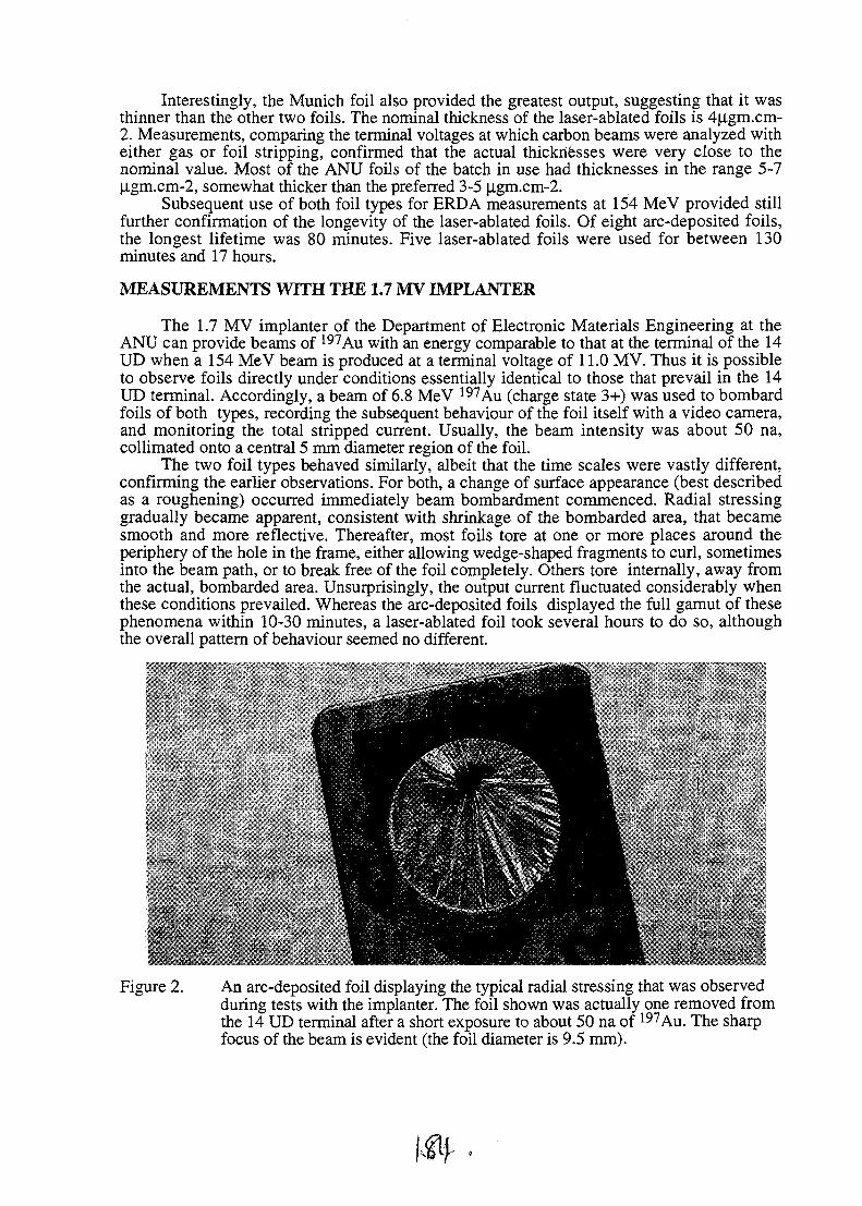
Interestingly, the Munich foil also provided the greatest output, suggesting that it wasthinner than the other two foils. The nominal thickness of the laser-ablated foils is 4jigm.cm-2. Measurements, comparing the terminal voltages at which carbon beams were analyzed witheither gas or foil stripping, confirmed that the actual thicknesses were very close to thenominal value. Most of the ANU foils of the batch in use had thicknesses in the range 5-7|igm.cm-2, somewhat thicker than the preferred 3-5 ji.gm.cm-2.
Subsequent use of both foil types for ERDA measurements at 154 MeV provided stillfurther confirmation of the longevity of the laser-ablated foils. Of eight arc-deposited foils,the longest lifetime was 80 minutes. Five laser-ablated foils were used for between 130minutes and 17 hours.
MEASUREMENTS WITH THE 1.7 MVIMPLANTER
The 1.7 MV implanter of the Department of Electronic Materials Engineering at theANU can provide beams of 197Au with an energy comparable to that at the terminal of the 14UD when a 154 MeV beam is produced at a terminal voltage of 11.0 MV. Thus it is possibleto observe foils directly under conditions essentially identical to those that prevail in the 14UD terminal. Accordingly, a beam of 6.8 MeV 197Au (charge state 3+) was used to bombardfoils of both types, recording the subsequent behaviour of the foil itself with a video camera,and monitoring the total stripped current. Usually, the beam intensity was about 50 na,collimated onto a central 5 mm diameter region of the foil.
The two foil types behaved similarly, albeit that the time scales were vastly different,confirming the earlier observations. For both, a change of surface appearance (best describedas a roughening) occurred immediately beam bombardment commenced. Radial stressinggradually became apparent, consistent with shrinkage of the bombarded area, that becamesmooth and more reflective. Thereafter, most foils tore at one or more places around theperiphery of the hole in the frame, either allowing wedge-shaped fragments to curl, sometimesinto the beam path, or to break free of the foil completely. Others tore internally, away fromthe actual, bombarded area. Unsurprisingly, the output current fluctuated considerably whenthese conditions prevailed. Whereas the arc-deposited foils displayed the full gamut of thesephenomena within 10-30 minutes, a laser-ablated foil took several hours to do so, althoughthe overall pattern of behaviour seemed no different.
Figure 2. An arc-deposited foil displaying the typical radial stressing that was observedduring tests with the implanter. The foil shown was actually one removed fromthe 14 UD terminal after a short exposure to about 50 na of 197Au. The sharpfocus of the beam is evident (the foil diameter is 9.5 mm).
l#
OPTICAL AND ELECTRON SPECTROSCOPY
Both methods indicated that the arc-deposited foils were relatively smooth andamorphous, even at high magnification. The laser-ablated foils appeared to be much morecrystalline, with some features as large as 5jim x 5jim. The Munich group interpreted thisappearance as "quasi-graphitic crystallites, nearly isotropically distributed".
STATUS REPORT
There is some evidence to suggest that the Munich foils mimic the surface structure ofthe release agents (Betaine, NaCl and/or copper) rather than the crystalline appearance beingthe result of the method of deposition. Thus the foils could be postulated to have a "micro-bagginess" which ameliorates the rate at which the foils become stressed under bombardment.
On-going work includes establishment of laser-ablation facilities, and investigation ofthe role, if any, played by the release agents used.
REFERENCE
1. G. Dollinger and P. Maier-Komor, Nucl. Inst. & Meth. B53 (1991) 352

fl AU9817158
Novel Imaging Techniques for the Nuclear Microprobe
A.SaintMicroanaytical Research Centre (MARC), School of Physics, The University of Melbourne, Parkville,
3052, Australia.
Many of the developments of the scanning electron microscope (SEM) have been parrelleled duringthe development of the scanning nuclear microprobe. Secondary electrons were used in the earlydevelopment of both devices to provide specimen imaging [1,2] due to the large numbers of secondariesproduced per incident charged particle. Other imaging contrast techniques have also been developed onboth machines. These include X-ray analysis, scattering contrast, transmission microscopy, channeling,induced charge and others [3]. Techniques on the nuclear microprobe still need to be developed forlive-time imaging of specimens. This aids greatly in specimen positioning and generally makes thedevice more user-friendly.
The "cross-section dependant" imaging techniques such as PIXEj RBS, NRA, etc., rely on the beamcurrent on target for a given resolution. This has prompted research and development of brighter ionsources to maintain probe resolution at high beam current. Higher beam current bring problems withbeam damage to the specimen.
Low beam current techniques [4] however rely on high countrate data collection systems, but thisis only for spectroscopy. To produce an image we can increase beam currents to produce live-timeimages for specimen manipulation and observation.
The work presented here will focus on some developments in live-time imaging with a nuclear micro-probe that have taken place recently at the School of Physics, MARC, University of Melbourne.
1 The Techniques
In STIM imaging the high countrates(100's of kHz) can be used to produce pseudo-live-time imagesbut the response of the detection system is limited by the charge collection time for a single ion andthe system quickly saturates. This paper will investigate other detection systems for the productionof true-live-time images.
Over the last few years PIN photodiodes have been developed that can be used for charged particlespectroscopy and have sufficient resolution to compete with traditional surface barrier detectors. Thebig advantage of PIN diodes is there price, about 103 times less than a surface barrier. This makesthe PIN diode very attractive as a radiation detector. To produce a D.C. signal from a PIN diodefor true live-time imaging we have used the detection system shown in figure 1. This system showsa standard PIN diode (normally used for STIM) that has been covered with a thin (0.5mm) layerof NE109 plastic scintillator. The scintillator has in turn been covered with a thin (1000 angstrom)layer of Al to prevent charging. A beam of 1 - 10 pA is then used in STIM mode to obtain live-timeimages. This beam current is about 3 orders of magnitude greater than standard STIM beams. Thescintillator acts as a charged particle-to-light converter and allows these much greater beam currentsto be used. This means that spectroscopic information is lost, but if only an image is required toposition or view the specimen then the loss of spectroscopic data is irrelevant.
The low current techniques of Ion Beam Induced Charge (IBIC) can be made pseudo-live-time bythe use of a variable persistence ocsilloscope (VPO). The VPO is an ocsilloscope with X-Y display

capability and Z contrast input and a persistence control. This control varies the time that the Zbright-up signal stays bright. Low contrast images can therefore be improved and provide a pseudo-live-time image. This will be discussed in more detail later.
2 Images and Results
Figure 2 shows a STIM image of a 2000 mesh grid taken with the above detection system using a 2MeV proton beam. This provides true live-time imaging that can be viewed using any ocsilloscopewith X-Y capability and Z contrast control.
Figure 3 shows a series of images taken with the above detection system of a piece of 8/im thick Sicrystal with the <100> channeling axis at right-angles to the crystals surface. The beam was ~2 pAof 2 MeV protons and the scan size is about 200 X 200 (tan. The first image (a.) shows the specimen ina random direction (shown in black) close to the <100> axial channel. The specimen issurounded byvacuum where the beam passes directly into the detector to give a white background. In the secondimage (b.) the specimen has been tilted closer to the <100> axis and now more of the beam is passingthrough the sample without being scattered and the specimen is seen to become more white. In thefinal image (c.) the specimen is in a axial channeled orientation and most of the protons pass throughthe specimen without being scattered to produce an all white image (i.e. there is no contrast betweenthe crystal and the vacuum). This type of imaging could be very useful for radiation damage studiesof thin materials.
The IBIC images shown in figure 4. are of true live-time (a.) and pseudo-live-time (b.) images ofa TA 670 CMOS SRAM. This type of imaging can be used to easily position the device for furtherspectroscopic analysis. THe image was taken by connecting a charge sensitive pre-amplifier to VDDI
biasing the device (5V) thru V55 and connecting the output of the charge sensitive pre-amplifier tothe Z contrast of the VPO. The persistence is off in figure 4a. and has been turned up to an arbitraryvalue in figure 4b.
3 References
[1] M. Knoll, Z. Tech. Phys. 16 (1935) 467.
[2] P.A. Younger and J.A. Cookson Nucl. Instr. Meth. 158 (1979) 193-198.
[3] F. Watt and G.W. Grime (eds) "Principles and Applications of High-energy Ion Microbeams",Adam Hilger (1987), chapter 2.
[4] A. Saint, J.S. Laird, R.A. Bardos, G. J.F. Legge, T. Nishijima and H. Sekiguchi, Proceeding of the8th Australian Conference on Nuclear Techniques of Analysis (1993) 21-23.
aluminium
scanning ion beam01
"0
specimen \ t o ocsiUoscope
scintillator
Figure 1 - Detection system
Figure 2 - STIM image of grid
Figure 4 - live-time IBIC image
Figure 3a. - CSTIM image - random
Figure 3b. - CSTIM image - partial channel
Figure 3c. - CSTIM image - channeled

PI \lAU9817159
MODIFICATION OF HIGH TEMPERATURE OXIDATION BEHAVIOUR OFCHROMIA FORMING ALLOYS BY ION IMPLANTATION*
S. Shamsili. D.K. Sood, Microelectronics and Material Technology Centre, Department ofCommunication and Electronic Engineering, Royal Melbourne Institute of Technology, 124La Trobe Street, Melbourne Australia 3001;S.P.S. Badwal, Ceramic Fuel Cells Limited, 170 Browns Road, Noble Park Vic 3174P.J. Evans, ANSTO, Menai NSW 2234
1. Introduction
Fuel cells convert gaseous fuels via an electrochemical process directly into electricity withhigh efficiency (up to 60% electric efficiency and with heat recovery up to 80% systemefficiency) and very low pollution (orders of magnitude reduction in the level of NOX and asignificant reduction in the levels of the greenhouse gas carbon dioxide, and SOX - the cause ofacid rain)[I]. The solid oxide fuel cell is the most versatile of all fuel cell technologiescurrently under development in terms of its high efficiency and fuel flexibility. However, thehigh operating temperature (800-900°C) puts constraints on materials which can be used insolid oxide fuel cells.
In a fuel cell, several single cells are joined together through an interconnect material to forma stack for desired power output. The interconnect also delivers fuel and air to anode andcathode respectively of the fuel cell. The interconnect material is required to meet stringentspecifications of matching thermal expansion coefficient with other fuel cell components, lowmaterial and fabrication costs, high electrical and thermal conductivity, chemical stability withrespect to other fuel cell components, high strength and ductility, and high corrosionresistance.
The high chromium alloy steels, if used as interconnects in solid oxide fuel cells, have thepotential of meeting most of the above criteria. However, low corrosion resistance of thesealloys combined with high volatility of Cr (6+) species from Cr2O3 formed at the surface ofthe alloy are serious problems . With a view to reduce these problems, in this paper the roleof reactive elements such as La, Y and Zr on the high temperature corrosion of stainless steelhas been investigated.
2. Experimental
Ferritic stainless steel TP 446 (72.37% Fe, 26.16% Cr, 0.77% Mn, 0.51% Si) specimens werepolished to 2400 mesh grit SiC paper and thoroughly cleaned. Ions of La, Y, Zr and Cr wereimplanted on steel samples using MEVVA ion implanter at an extraction voltage of 40 kV. Asingle dose of 1 El7 ions/cm was chosen initially for all species at nominal room temperature.This dose was selected as it provides reasonable concentration of the doping ion at the metalsurface. Cr was implanted to observe the self ion damage. After implantation, samples wereheat treated at 800°C for 1 h or at 900°C for 0.5 h in air. Heating rate was 100°C/h. Specimenswere characterised by Rutherford Backscattering Spectrometry (RBS) and optical microscopy.An analysis beam of 2.0-MeV 4He was used for RBS.
* Work supported by an AINSE and an ARC Grant.
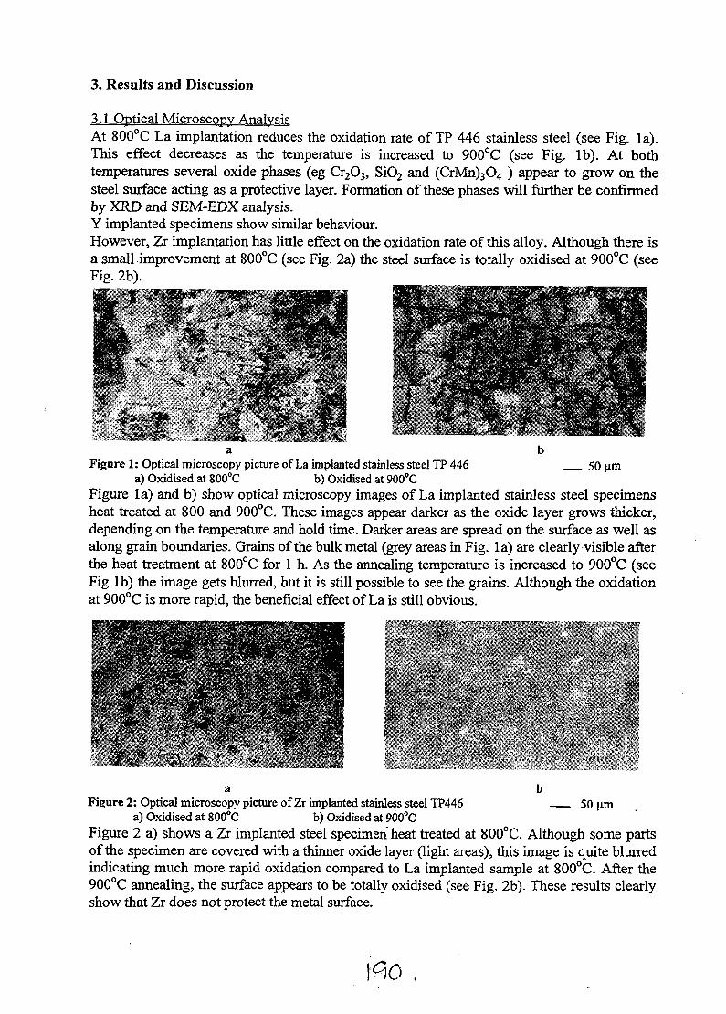
3. Results and Discussion
3.1 Optical Microscopy AnalysisAt 800°C La implantation reduces the oxidation rate of TP 446 stainless steel (see Fig. la).This effect decreases as the temperature is increased to 900°C (see Fig. lb). At bothtemperatures several oxide phases (eg Cr2O3, SiO2 and (CrMn)3O4 ) appear to grow on thesteel surface acting as a protective layer. Formation of these phases will further be confirmedby XRD and SEM-EDX analysis.Y implanted specimens show similar behaviour.However, Zr implantation has little effect on the oxidation rate of this alloy. Although there isa small improvement at 800°C (see Fig. 2a) the steel surface is totally oxidised at 900°C (seeFig. 2b).
v.
Figure 1: Optical microscopy picture of La implanted stainless steel TP 446 _ _ 50 jima) Oxidised at 800°C b) Oxidised at 900°C
Figure la) and b) show optical microscopy images of La implanted stainless steel specimensheat treated at 800 and 900°C. These images appear darker as the oxide layer grows thicker,depending on the temperature and hold time. Darker areas are spread on the surface as well asalong grain boundaries. Grains of the bulk metal (grey areas in Fig. la) are clearly visible afterthe heat treatment at 800°C for 1 h. As the annealing temperature is increased to 900°C (seeFig lb) the image gets blurred, but it is still possible to see the grains. Although the oxidationat 900°C is more rapid, the beneficial effect of La is still obvious.
50
' :>.'
a bFigure 2: Optical microscopy picture of Zr implanted stainless steel TP446
a) Oxidised at 800°C b) Oxidised at 900°CFigure 2 a) shows a Zr implanted steel specimen heat treated at 800°C. Although some partsof the specimen are covered with a thinner oxide layer (light areas), this image is quite blurredindicating much more rapid oxidation compared to La implanted sample at 800°C. After the900°C annealing, the surface appears to be totally oxidised (see Fig. 2b). These results clearlyshow that Zr does not protect the metal surface.

3.2 RBS AnalysisFigure 3 shows RBS spectra of non-oxidised and oxidised (800°C) La implanted steelsamples. In curve 1 (no heat treatment), the La signal has a Gaussian distribution with a peakat 1.774 MeV, while the substrate appears as a step with leading edge at 1.491 MeV. The peakposition of La is at a depth smaller than it's surface edge. Trim calculations give a projectedrange of Rp=175A and a straggling width of ARp=70A, which are consistent with RBSresults. Oxygen can not be observed because of the high background signal from the steelsubstrate. When an implanted sample is heat treated at 800°C (curve 2), La diffuses into thebulk material. La peak is no longer shallow, and is redistributed during oxidation. However,detailed analysis of this curve indicates that there is no loss of La by vaporisation, ALa=4604counts for both oxidised and non-oxidised samples. Oxide film thickness causes a shift in theFe edge by AE=152.8 keV and is increasing with oxidation at higher temperatures, as does theoxide thickness. Cr peak is observed at 1.473 MeV indicating that the oxide formed is mainlyCr2O3. Results at 900°C (not shown) indicate higher penetration of La into the substrate andincreased oxide thickness.Y implanted and oxidised samples show a similar behaviour.
8000
Energy (MeV)
0.4 0.6 0.8 1.0 1.2 1.4 1.6 1.8
2000
— l o implanted sample- -Oxidised sample 800'C
0.4 0.6
6000
5 4000oJ
2000
0
0.8
Energy1.0
v — Zr implonled sompleV - -Oxidised ol 800*C
* t£ Oxidised ot 900'C
?^>-
(MeV)1:2 1.4
^
1.6
\
; \
1/
1.8
-
-
L-If
200 300Chonnel
Figure 3: RBS Energy Spectra, La implantation Figure 4: RBS Energy Spectrum, Zr implantation
Figure 4 shows energy spectra of Zr implanted and oxidised (900°C) samples. Zr is observedat 1.661 MeV. As the temperature is increased Zr diffuses into the bulk. At 900°C, contrary tothe behaviour for La, it is no longer detectable on the surface. It looses it's protective abilityand the sample oxidises rapidly. These observations are consistent with optical microscopyresults.
4. Conclusion
The experimental results show: 1) Oxidation behaviour of TP446 stainless steel improves withimplantation of reactive elements. 2) Implantation with La and Y reduces oxidation rate of thesteel alloy at both temperatures. These elements are more effective at 800°C than they are at900°C. 3) Zr implantation has a little effect on the corrosion rate at 800°C. Specimens that areheat treated at 900°C undergo rapid oxidation.
5. References
1) S.P.S. Badwal, K. Foger and M.J. Murray,"Fuel Cells: Clean Alternative Power GenerationTechnology of 21st Century", Gippsland Basin Symposium, pg.269-278,1992.2) S.P.S. Badwal, R. Deller, K. Foger, Y. Ramprahash and J.P. Zhang, "Interaction BetweenChromia Forming Alloys and Air Electrode of the Solid Oxide Fuel Cell", Solid State Ionics,vol. 99, pg. 297-310,1997.

" AU9817160
ERDA and RBS Measurements on Spark Processed Silicon.
Rainer Siegele, Peter Evans and David CohenAustralian Nuclear Science and Technology Organisation
Private Mail Bag 1, Menai, NSW 2234, Australia
Jinning Yuan and Dan HanemanSchool of Physics, University of New South Wales
Sydney, NSW 5052, Australia
Introduction
Silicon is used almost to the exclusion of all other materials in semiconductor electron-ics. However, it suffers from the limitation that it is an indirect band gap material anddoes not emit light efficiently. Since the advent of fiber-bound data transmission, therehas been considerable interest in the modification of silicon to make it light emitting.
Various ways of modification have been suggested. These include porous silicon andspark processed silicon.1 Both methods are very simple techniques, that produce low di-mensional silicon structures, which are believed to be responsible for the better lightemitting properties. However, because both techniques are carried out in air or in a liquidenvironment, they both change the composition and introduce impurities into the silicon.
Thus it is important to determine the composition of these materials in order to es-tablish whether there is a relationship between composition and light emitting properties.Spark processed silicon, like porous silicon, is very easy to produce but has the advantageover the latter that it is structurally and chemically more stable. Because of this diodescan easily be produced by depositing a conducting layer on top of the spark processedsamples. Diodes produced in this way turn out to have differences in their performancedepending on the material of the conductive layer. Diodes with silver and copper conduct-ing layers were produced and their compositions were measured using ion beam analysis(IBA) techniques.
Exp erimental
Two different types of spark processed silicon samples were prepared. One set waslightly sparked and the other was heavily spark processed. In the lightly sparked materialthe treatment was carried out for about 1-2 seconds per spot compared to 10 secondsfor the heavily processed samples. The spark processing was carried out in air. Afterprocessing one spot, the cathode was was moved approx. 0.2 mm across and the next spotwas processed. In this fashion the cathode was scanned over an area of 5x5 mm, largeenough for ERDA and RBS analysis.
After spark processing one sample of each was coated with a conductive copper or silverlayer. In addition a glass slide was coated with each metal under the same conditions inorder to provide a reference for measurements of the metal layer thickness.

Table 1: Table of the total amount of various elements in the investigated samples.
sparkprocessedlightlyheavilyglass slidelightlyheavilyglass slide
coating
CuCuCuAgAgAg
Cu/Ag layerat/cm2
8.1 x 10¹⁷
7.7 x 10¹⁷
7.8 x 10¹⁷
3.0 x 10¹⁷
3.1 x 10¹⁷
3.0 x 10¹⁷
thicknessnm95.590.892.050.352.550.3
oxygenat/cm2
2.8 x 10¹⁷
1.1 x 10¹⁸
-1.9 x 10¹⁷
1.0 x 10¹⁸
-
carbonat/cm2
3.4 x 10¹⁶
3.2 x 10¹⁶
0.9 x 10¹⁶
1.5 x 10¹⁶
1.6 x 10¹⁶
0.6 x 10¹⁶
nitrogenat/cm2
2.3 x 10¹⁶
5.0 x 10¹⁶
-1.9 x 10¹⁶
5.8 x 10¹⁶
-
The RBS measurements were carried out using 2 MeV He+ in a 169° backscatteringgeometry, while the elastic recoil detection analysis (ERDA) used a 63 MeV Br8+ beam,with recoil particles being detected at 45° with a time-of-fiight spectrometer.2
Results and Discussion
2
1000
800
600
400
200
c oSi
Br
Ag
A typical ERDA 2-dimen-sional coincidence spectrum isshown in fig. 1. Each curve inthe spectrum represents one ofthe elements present in the sam-ple. In all spark processed sam-ples silicon, oxygen, carbon andcopper or silver from the con-ducting layer as well as smallamounts of nitrogen were de-tected. It can be seen from thespectrum in fig. 1 that no otherelements are present in the sam-ples, at concentrations above thedetection limit of ERDA. TheBr in the spectrum is due to Brfrom the ion beam scattered offthe sample.
From the 2-dimensional co-incidence spectra, an energyspectrum for each element canbe extracted. These are shown
in fig 2. The energy spectra of C, N, O, Cu and Ag show peaks close to the surface, whilethe Si spectrum shows that the Si is buried underneath. The slope of Si edge suggeststhat the surface of the spark processed samples is very rough, with the effect being morepronounced in the heavily processed samples.
ERDA and RBS measurements were used to calculate the total amount of O, C, N andAg or Cu in the samples. These result are summarized in tab 1. The Ag and Cu contentare the same for the two sets of samples. The table shows that the total amount of oxygen
200 400 600 800 1000
JSBD
Figure 1: ToF-ERDA spectrum of a spark processed Sisample with a Ag-coating.
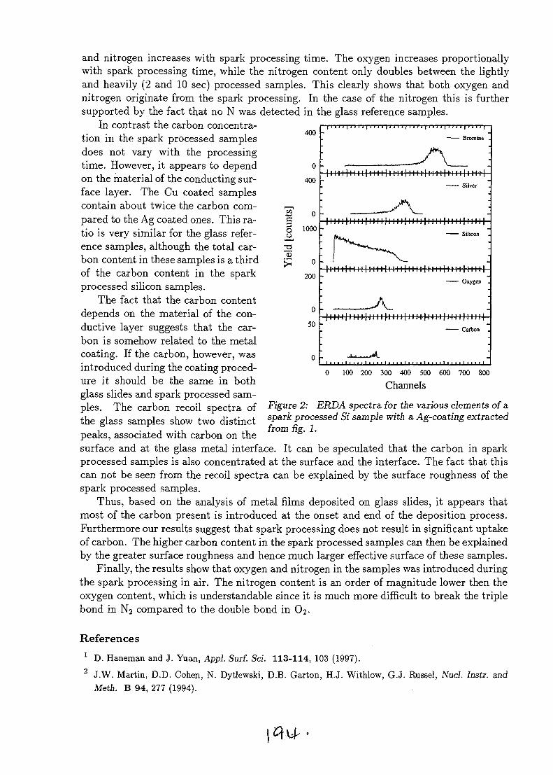
Bromine
1 I I I I [1 I I I | 1111 l l II l[ 1 I II | II l l | l I I I | l I I I |
Silver
and nitrogen increases with spark processing time. The oxygen increases proportionallywith spark processing time, while the nitrogen content only doubles between the lightlyand heavily (2 and 10 sec) processed samples. This clearly shows that both oxygen andnitrogen originate from the spark processing. In the case of the nitrogen this is furthersupported by the fact that no N was detected in the glass reference samples.
In contrast the carbon concentra-tion in the spark processed samplesdoes not vary with the processingtime. However, it appears to dependon the material of the conducting sur-face layer. The Cu coated samplescontain about twice the carbon com-pared to the Ag coated ones. This ra-tio is very similar for the glass refer-ence samples, although the total car-bon content in these samples is a thirdof the carbon content in the sparkprocessed silicon samples.
The fact that the carbon contentdepends on the material of the con-ductive layer suggests that the car-bon is somehow related to the metal
400
400
£3 0s§ 1000o
1 3
200
50
0 -
Silicon
Oxygen
-A.Carbon
•l..i . , . nA.
0 100 200 300 400 500
Channels600 700 800
Figure 2: ERDA spectra for the various elements of aspark processed Si sample with a Ag-coating extractedfrom fig. 1.
coating. If the carbon, however, wasintroduced during the coating proced-ure it should be the same in bothglass slides and spark processed sam-ples. The carbon recoil spectra ofthe glass samples show two distinctpeaks, associated with carbon on thesurface and at the glass metal interface. It can be speculated that the carbon in sparkprocessed samples is also concentrated at the surface and the interface. The fact that thiscan not be seen from the recoil spectra can be explained by the surface roughness of thespark processed samples.
Thus, based on the analysis of metal films deposited on glass slides, it appears thatmost of the carbon present is introduced at the onset and end of the deposition process.Furthermore our results suggest that spark processing does not result in significant uptakeof carbon. The higher carbon content in the spark processed samples can then be explainedby the greater surface roughness and hence much larger effective surface of these samples.
Finally, the results show that oxygen and nitrogen in the samples was introduced duringthe spark processing in air. The nitrogen content is an order of magnitude lower then theoxygen content, which is understandable since it is much more difficult to break the triplebond in N2 compared to the double bond in C>2-
References1 D. Haneman and J. Yuan, Appl. Surf. Sci. 113-114, 103 (1997).2 J.W. Martin, D.D. Cohen, N. Dytlewski, D.B. Garton, H.J. Withlow, G.J. Russel, Nucl. Instr. and
Meth. B 94, 277 (1994).

iinwiDiiiiiiiiiiniiiAU9817161
Diffusion Profiling of Sr in Cement Pastes using the ANSTO
Milliprobe
R. Siegele1, P. Rougeron2, L. Aldridge1, D.D. Cohen1 and E. Stelzer1
1 Australian Nuclear Science and Technology Organisation2 Electricite de France, France
Abstract
The ANSTO milliprobe on the 3 MV Van de Graaff was used to measure thediffusion profiles of Sr and Cs in cement pastes with and without zeolite additionsusing PIXE. The PIXE milliprobe proved to be a suitable tool for Sr profiling, butprovided only semiquantitative information for Cs, because of the poorer detectionlimits for heavier elements.
Introduction
Low radioactive waste is created in many processes in the nuclear fuel circle as well inmedical applications of radio-isotopes. This radioactive waste has to be disposed of. Onecommon technique is the encapsulation of the waste into cement based materials beforedisposal. Since such waste is likely to be transported prior to disposal, it is important toknow how fast the mobile ion will move particularly if the waste package becomes involvedin an accident. Two mobile elements contained in solid waste from nuclear reactors arecesium and strontium.1 The diffusion of these elements is of the order of a few millimetersinto the material, thus ordinary ion beam analysis (IBA) profiling techniques, which givedepth profiles of the order of fxva into the surface can not be used. However, diffusionprofiles can be measured by using small beam spots and scanning across the sample.
Sample Preparation
Cylindrical cement based samples of 40 mm diameter and 60 mm length were prepared.The samples were then placed in a diffusion cell, in which at one end a solution of 0.6 MCsN03 and Sr(N0s)2 was held at a constant concentration by a siphonic system. The otherend was conditioned with a solution, that had been equilibrated with cement. Pastes ofcement and cement zeolite mixtures with exposure times varying from 7 to 47 days wereinvestigated. It is known that zeolite additions to cement paste increase the binding of Srand Cs to the matrix.2 It was therefore of interest to determine if such materials will slowdown the diffusion of these mobile cat-ions.
PIXE Analysis
After exposure to the Sr(NO3)2 and CSNO3 solutions, the samples were cut into thindisks and the Sr profile was measured with PIXE using a small diameter beam. Themeasurements were performed on the ANSTO milliprobe. Spot sizes smaller then 1 mmwere achieved by collimating the focused beam with apertures. A schematic of the setup is

viewer
X-ray Detector
target
aperture aperture
Figure 1: Experimental setup for the PIXE measurements.
shown in fig. 1. After the switching magnet the beam was collimated by a 7 mm aperture,which centers the beam in the quadrupole doublet. Downstream of the quadrupoles a1 mm aperture was used to limit the beam divergence. The beam was set up with a viewerbehind this aperture, by optimising the the quadrupoles until the beam fully illuminatedthe 1 mm aperture. Small apertures (55jum to 500/im) in front of the target were used toselect a small part of the focused beam.
The distance between the 1 mm aperture and the beam defining aperture was 50 cmwhile the distance from this aperture to the target was 10 cm. The position of the beamwas determined using a fiuorescing target, which was monitored using a video cameraattached to a bore-scope. The bore-scope together with the video camera have an overallmagnification of 50, which was sufficient to position the target precisely. A Csl crystalwas used, because it gives bright luminescence even at target currents below 1 nA.
The beam spot size used during this experiment was measured using a thin wire andfound to be 250-300 fan.
Results and Discussion
Energy (keV)15 20 25 30
103 :
A typical PIXE spectrum is shown infig. 2. The spectrum was taken using a1 mm perspex filter in front of the x-ray de-tector. The filter absorbs a large fraction ofthe low energy X-rays, but only very fewof the higher energy ones. This is neces-sary in order to avoid count rate problemsin the detector with characteristic X-raysfrom Ca and Si, the mayor constituents ofcement. The spectrum clearly shows peaksfor Ca, Fe, Sr and Cs. No peak is visible forSi X-rays, because these X-rays are almostcompletely absorbed by the perspex filter.In some cases small peaks of Zn X-rayswere also visible in the spectrum, howeverit is most likely that these were caused by
the scattered beam hitting the chamber rather then the sample. Iron like the calcium wasa constituent of the samples and was visible in all spectra.•< The elements Ca, Fe and Sr yield sufficiently high count rates to allow precise meas-
10°
: Ca
I
•
f
Vl ' f l ' lV l '
be
1 Sr
1
Uvv/vivwyi
.llllilnii
l'JV|'i'l'/i'|MIVf| j
-
Cs :
I :
1 J 1 1 1 U -200 400 600 800 1000 1200
Channels1400 1600 1800 2000
Figure 2: Typica,l PIXE spectrum of one of thesamples, taken with a 1 mm perspex filter.

urements of their content. Because of the lower efficiency of X-ray detectors at energiesabove 30 keV, the low production cross section and the low target current, the Cs countrate was too low to determine a meaningful profile in a realistic time. By increasing themeasurement time it is possible to measure a Cs profile, but it would require many hoursof measurement time under the present conditions.
The total amount of Sr at the beam position can be determined, by comparing theintegral of the peak with a calibration sample. As calibration samples cement pastes withknown Cs and Sr contents were used.
Fig. 3 shows the Sr-diffusion pro-files for samples exposed to Sr-solu-tions for various times. There wereedge effects and it was difficult tojudge where the cement surface began.Therefore the half height of the Caand Fe X-ray signal was used to de-termine the edge of the sample. Theprofiles shown in fig. 3 show an in-crease of the Sr content over the first100-150 jum. This initial increase isan artifact of the measurement caused
10000
8000
6000
"3 4000
2000
• 7 days exposureo 17 days exposure° 47 days exposure
e *
. ,
500 1000 1500
Depth |>m]2000 2500
Figure 3: Sr diffusion profiles for cement sampiesexposed to Sr(NOs)2 solutions for 7, 27 and 47 days.
by the width of the ion beam.The profiles of fig. 3 clearly show
increased Sr uptake with time. Boththe maximum content at the surfaceand the maximum depth of the Sr uptake increase with the diffusion time. The diffusionprofiles after 7, 27 and 47 days of exposure can be fitted by single coefficient diffusionusing least squares routines.
Further the effect of zeolite additions on the Sr diffusion profiles were investigated.Preliminary results show very small differences in the Sr profiles, which suggests thatzeolite additions have very little effect on the Sr diffusion in cement pastes.
Conclusion
The diffusion profiles of Sr were measured by means of an ion beam milliprobe withsufficient accuracy to permit determination of diffusion processes. The Sr profiles werefitted with single coefficient diffusion equations. In principle it should also be possible tomeasure Cs profiles, but this will require a much longer analysis time.
Acknowledgment
We want to thank the 3 M V accelerator staff for their support in running the acceleratoras well as the milliprobe.
References
1 A. Atkinson and A. Nickerson, Nuclear Technology 81, 100 (1988).2 A. Atkinson, K. Nelson, and T.M. Valentine, NucL Chem. Waste Manage. 6, 241 (1886).

P1.35 AU9817162
The ANSTO High Energy Heavy Ion Microprobe
R. Siegele, D.D. Cohen, H. Noorman, D. Garton, and A. Croal
Australian Nuclear Science and Technology OrganisationPrivate Mail Bag 1, Menai, NSW 2234, Australia
Introduction
Ion microprobes have a long tradition at ANSTO as well as in Australia. ANSTO wasamong the first to use micro-sized beams in the 60s. Since then microbeams have developedconsiderably and proton and alpha microprobes are a common sight in IBA laboratoriesaround the world. Ion microbeams allow surface imaging of specimens in addition to thedepth profiling capabilities of macroscopic beams. Nuclear microprobes have significantadvantages in terms of sensitivity for elemental analysis over electron beam microanalysis.
The advantages of ions heavier then helium in nuclear micropobes was first pointed outby Martin1 in the late 1970's. However, very few microbeams employing heavy ions at highenergies have been realized since then, because of the limited availability of high energyaccelerators and the difficulty of the task.
The high energy heavy ion microprobe under construction at ANSTO will be a unique,multi-user facility providing new capabilities for ANSTO and the broader Australian re-search community. It will be used in materials research, environmental research, industrialapplications and for applications in biology, medicine and geology.
Advantages of High Energy Heavy Ion Microbeams
I
u
107
106
105
102
101
10°
! /*/7McV NRBS= j / < / @ 165*
9OMeVIJ5RDA
K x-ray@ 4.5 MeV P
!
—• !
L x-ray Z@ 4.5 MeV P ,
!
-
10 20 30 40 SO 60 70
Target Atomic Number Z2
90
Figure 1: The figure shows the cross sections for varioustechniques.
The ANSTO heavy ion micro-probe will not only provide H andHe ions, but a wide range of ionsat different energies. This results ina number of advantages. The crosssections of most IBA techniques areproportional to the square of the nuc-lear charge of the incident ion, Z2.Higher cross sections mean a highersensitivity or a shorter measurementtime, which gives a heavy ion micro-probe a clear advantage over protonmicroprobes. The higher cross sec-tions are sometimes offset by the factthat the energy also has to be in-creased in order to achieve the same
probing depth or to stay in the Rutherford regime. This, however, is not the case for elasticrecoil detection analysis (ERDA) and PIXE.
The cross sections for various IBA techniques, such as PIXE, RBS and ERDA fordifferent ions and energies are shown in figure 1. The figure shows the higher PIXE cross-sections for oxygen compared to protons as well as the higher ERDA cross sections foriodine compared to Si. It also shows that the cross sections for ERDA using iodine aremuch higher compared to the cross sections of 2 MeV He-RBS. Using heavy ions in PIXEanalysis also reduces the bremsstrahlung of the primary ion thus lowering the background,which results in an even further increase in sensitivity.
/ ' /

Figure 2: Overview of the ANTARES tandem accelerator and beamlines.
Furthermore the use of techniques such heavy ion RBS (HIRBS) and heavy ion ERDAfor microanalysis only becomes possible with a heavy ion microprobe. HIRBS has theadvantage of an enhanced depth and mass resolution over conventional RBS using lightions such as H and He. The cross sections in ERDA increase strongly for heavy ions andin fact ERDA becomes a truly universal technique with heavy ions, allowing the detectionof all elements from hydrogen up to the mass of the ion used in the analysis. In contrast,PIXE is normally limited to target elements heavier then aluminium and gives no depthinformation, while RBS is best suited for the depth profiling of medium to heavy masselements in a light element matrix. The possibility to use ERDA makes a high energy,heavy ion nuclear microprobe a universal tool, that can be used for the depth profiling ofheavy and light elements simultaneously.
ANSTO Microprobe Facility
Figure 2 shows the ANTARES Accelerator with its various beamlines. The tandem ac-celerator together with its various ion sources is located in the tandem hall, while all thebeamlines installed previously are located in the target area. With the ever increasingnumber of beam lines the space in the target hall has became very limited. Since the micro-probe beamline had to be at least 7 m long a location in the tandem hall was chosen. Thislocation also has the advantage that only one deflection magnet is required, which makes iteasier to optimize the beam.
A detailed drawing of the microprobe is shown if figure 3. After the analysing magnetthe ions travel through energy stabilisation slits situated in front of the object slits. Theseslits are also used as collimators to prevent damage to the object slits. A set of quadrupolesand deflectors after the accelerator are used to focus and centre the beam on the objectslits. Faraday cups before and after the slits are used to set up the beam. Additionally abeam profile monitor and viewer allow monitoring the beam shape.
The collimating slits are located 6.10 m from the object slits and and are directlyfollowed by the beam scanning and forming elements. The beam focusing and scanningsystem consists of the OM-55 quadrupole triplet and the OM-25 scanning system fromOxford Microbeams. The OM-55, a modified version of the OM-50, has a smaller polegap

a b c d e
lm
Figure 3: Schematic of the microprobe beamline and target station, a: gate valve, b: Faradaycup, c: beam profile monitor, d: energy stabilisation slits, e: object slits, f: beam viewer, g: pump,h: collimating slits, i: beam scanner, k: quadrupole triplet, 1: target chamber.
of 8 mm and thus permits focusing of ions with a mass energy product of up to 120 MeVamu /q2 .
The stainless steel target chamber has an octagonal design. Each face of the chamberis fitted with two access ports to permit detectors for various applications to be mounted.One of the 135° ports is fitted with a microscope, which will be used for precision placementof the targets and to monitor the focusing of the beam. In the near future on the other 135°port a X-ray detector will be mounted.
At the time of writing of this report the construction of the microprobe beamlime atANSTO as well as target chamber have been completed and we are awaiting the arrival ofthe quadrupoles for installation. The microprobe quadrupole triplet has been completedand is currently undergoing testing by the manufacturer, Oxford Microbeams. Tests by themanufacturer so far have yielded a 0.9 x 1.2 /um spot size for 3 MeV protons.
It is planned to equip the microprobe with various detection systems, that will allow theuse of a variety of IBA techniques. One of the advantages of a heavy ion microprobe, isthe possibility to use heavy ion ERDA. For this purpose the microprobe will be equippedwith a position sensitive large solid angle gas detector.3 Since the target current decreaseswith the beam spot size detectors with large solid angles are required. A gas detector iscurrently under design and construction will commence in the near future. In addition itis planned to equip the microprobe with a Scanning Transmission Ion Microscopy (STIM)capability and a secondary electron detection system.
Acknowledgment
We want to acknowledge the valuable assistance of G. Legge and the Melbourne Mi-croprobe group, as well as A. Dymnikov in the design of the microprobe. We also wantto thank the technical support team of the ANSTO Ion Beam Analysis group for theirassistance.
References1 F.W. Martin, Nucl. Instr. and Meth. 149, 475 (1978).2 J.W. Martin, D.D. Cohen, N. Dytlewski, D.B. Garton, H.J. Withlow, G.J. Russel, Nucl. Instr. and
Meth. B 94, 277 (1994).3 W. Assmann, P. Hartung, H. Huber, P. Staat, H. Steffens, Ch. Steinhausen, Nucl. Instr. and Meth.
B85, 729 (1994).

P1.36 AU9817163
MODIFICATION OF HIGH TEMPERATURE OXIDATION OF CHROMAFORMING STAINLESS STEEL BY DEPOSITION OF TITANIUM DIBORIDE FILMSIMPLANTED WITH TANTALUM IONS.D.K. Sood, S. Mukherjee, G. Katselis, Microelectronics and Materials Technology Centre,Department of Communication and Electronic Engineering, Royal Melbourne Institute ofTechnology, 124 La Trobe Street, Melbourne 3000, Australia;I.G. Brown, Lawrence Berkeley Laboratory, University of California, Berkeley, CA 94720,USA;K.E. Prince, K.T. Short and P.J. Evans, Australian Nuclear Science and TechnologyOrganisation, Lucas Heights Research Laboratory, Private Mail Bag 1, Menai 2234, Australia.
ABSTRACT: Titanium diboride is an attractive material for protective coatings because of itshigh hardness, high electrical and thermal conductivities. However, many of its hightemperature applications are limited because of its poor oxidation behaviour beyond 700 °C.This paper presents a novel approach consisting of doping with implantation of higher valencyatoms, to improve its oxidation resistance up to 900 °C. TiB2 films (nominal thickness 0.5 um)were deposited on polished substrates of Stainless Steel using a RF sputtering depositionsystem. Ions of Ta (as a higher valence dopant species) were implanted using a M E W A ionimplanter at an extraction voltage of 65 kV corresponding to an average energy of 190 keV forTa and 140 keV for Ti ions. Ion doses of 1E15 to 1E17 ions/cm2 (corresponding to dopantconcentrations of about 0.1-10 at.%) were implanted at nominal RT. After implantation, somesamples were vacuum annealed (30 minutes at 900 °C, at 1E-5 Torr) to crystallise the filmsand/or reduce the ion damage. Oxidation of the implanted samples was conducted at 800 and900°C for 1 to 4 hours in air. Analysis was performed by using RBS, SIMS and XRDtechniques. The results show: 1)As-deposited films undergo rapid corrosion and spalling onoxidation, 2)As-implanted films show little improvement and undergo rapid corrosion andspalling on oxidation, 3)When implanted films are first vacuum annealed and then oxidised,they show remarkable improvement in corrosion resistance and do not undergo any spalling. Tais thus an effective dopant for improving oxidation resistance of TiB2 films.
INTRODUCTION: There has been increasing interest in the use of titanium diboride as acoating material because of its desirable properties like high hardness, high melting point,moderate strength, resistance to wear and good thermal and electrical conductivities. Suchproperties make TiB2 an attractive candidate for various applications such as coating for metalcutting tools, as crucibles and electrodes in metal refining equipment such as aluminiumreduction cell. Because of its resistance against chemical attack, it can also be used in catalysissystems, membranes, shut off valves and in medical technology as an implant material. It has agood electrical conductivity at high temperatures - a property not shared by many alternativecoating materials ( such as gold coloured TiN ). Furthermore, TiB2 may be a good candidatematerial for use as protective coating on the metallic interconnect employed in the solid oxidefuel cells (SOFC) being developed as a future technology for clean and efficient powergeneration. This technology requires a coating material which will be resistant to hightemperature oxidation and also be electrically conducting, to allow multiple stacking. This is astringent requirement for industries developing fuel cells for power generationHowever, like other titanium based alloys titanium diboride is also not very stable at elevatedtemperature under oxidising atmosphere. It is well established [1] that the main products oftitanium diboride oxidation in air are B2O3 and TiC>2. The protection of surface of TiB2 duringoxidation is in part dependent on boric oxide(B2Os) which has an appreciable vapour pressure at750°C. This paper presents a novel approach consisting of doping with implantation of highervalency atoms, to improve its oxidation resistance up to 900 °C.

CO
Cou
n
8000
6000
4000
2000
o
0.5JT 1
\
-V
0
1.0
Energy
oo
DO
s9-* (
r
(MeV)
- ^
1.5l
-
A
A
F^ Ta
Fig. 1. RBS spectrafrom an as-polishedSS430 sample (/*), as-deposited TiB2 film(oo) and afteroxidation ( ) of thefilm at 900 °C for 1 hin air.
100 200 300Channel
400
< 38.888 x .' 2thetA y .* 756. Linear 88.888>
Fig.2. XRD results from the same oxidised sample as in Fig. 1. R = Rutile TiO2 , F = Fe2O3
[c/s]
1000 15O0
Time [s]
2000 300 1000 1500 2000 2500 0 10X 20OD 30O0 4000Time [s]
Fig.3. SIMS data form a) an as-deposited film implanted with lE16Ta/ cm2, b) after oxidising a) at 900 °C, lh, andc) a film implanted with lE17Ta/ cm2, vacuum annealed and then oxidised.

EXPERIMENTAL: A chromia forming stainless steel - SS430 [Cr 16%, Si 1%, Mn 1%, C0.12% and Fe balance] was chosen as the substrate. Mirror polished 13 mm square samples wereprepared. TiE^ films (about 500nm thick) were deposited by RF sputtering in Ar at a pressure of6.8 mTorr following a published [2] recipe. Tantalum ion implantation was performed with aMEVVA ion implanter at an extraction voltage of 65 kV corresponding to an average energy of190 keV for Ta and 140 keV for Ti ions. Ion doses of 1E15 to 1E17 ions/cm2 (corresponding todopant concentrations of about 0.1-10 at.%) were implanted at nominal RT. After implantation,some samples were vacuum annealed (30 minutes at 900 °C, at 1E-5 Torr) to crystallise the filmsand/or reduce the ion damage. Oxidation of the implanted samples was conducted at 800 and900°C for 1 to 4 hours in air. Analysis was performed by using RBS, SIMS and glancing angleXRD techniques.
RESULTS AND DISCUSSION: Fig.l shows RBS spectra from an as-deposited film on SS430.The Fe edge (in as polished SS430) is shifted down to ch. 300 by an amount corresponding toTiB2 film thickness of 500 nm, and the Ti edge can be seen at the top surface. XRD (results notshown) on this sample revealed that the films are amorphous since no lines for the TiB2 phasecould be seen. This result is in contrast with earlier report [2] which showed crystalline filmsunder similar conditions of deposition. On oxidation at 900 °C, only Ti and no Cr or Fe are seenat the surface. XRD results (Fig.2) from the same sample show the presence of Fe, Fe2O3 andTiO2 phases. No Cr2O3 phase is seen. Thus the mode of oxidation of SS430 which forms &2O3on oxidation undes similar conditions (data not presented) is altered by te presence of the TiB2coating. B signal is too weak to be seen on the high background in RBS(Fig. 1). SIMSmeasurements show B depth distributions very well, for as-implanted sample (Fig. 3a). Onoxidation at 900 °C for In, a dramatic change occurs (Fig.3b) in the depth profiles of B (showingan almost complete loss of B), Ta (inwards migration of Ta), Fe and Cr (both are at the surfacenow). Results in Figs. 1,2 and 3b are from the same sample. At higher dose of lE17Ta/cm2 , lossof B is contained well and it segregates at the interface between TiB2 film and the substrate (Fig.3 c). This sample was vacuum annealed before oxidation to crystallise the films or annealimplantation damage. Without this pre-annealing, a severe loss of B, Cr, Ti and Ta was observedby SIMS (data not shown) indicative of spalling of the oxide scales.
CONCLUSIONS: From a detailed analysis (not presented here due to shortage of space) ofseveral other samples prepared for a systematic study, we arrive at the following conclusions:1. The as deposited films are "XRD amorphous" and undergo rapid oxidation and spalling at
900 °C2. As implanted films show little or no improvement in oxidation of the steel3. Vacuum annealed (900°C, 30 m) films are still "XRD amorphous" but show remarkable
improvement in oxidation resistance and do not spall off.4. Ta is an effective dopant in T1B2 for improving its oxidation resistance5. Bare SS430 develops a protective Cr2O3 layer6. However, the presence of a coating of TiB2 appears to alter the oxidation mode of the
underlying SS430 and no detectable Cr2O3 is observed at the surface7. A fully crystallised TiB2 film may be needed to achieve further improvement in oxidation
resistance.
REFERENCES:1. A. Kulpa and T. Troczynski, J. Ceram. Soc, 79 (1996) 518.2. W.A. Zdaniewski, J. Wu, S.C. Gujrathi and K. Oxorn, J. Mater. Res., 6 (1991) 1066.
ACKNOWLEDGEMENTS: This work was supported by an AINSE Grant and by a grant underthe National Competitive Grants Scheme at Royal Melbourne Institute of Technology.
pi-37 iiiiiiiniiiiiiAU9817164
CHARACTERISATION OF NdFeB THIN FILMS PREPAREDON (100)Si SUBSTRATES WITH SiO2 BARRIER LAYERS
D.K. SOODAND G.K. MURALIDHAR*MMTC, Department of Communication and Electronic Engineering, *Department ofElectrical Engineering, RMIT, 124, LaTrobe Street, Melbourne 3001 (AUSTRALIA)
ABSTRACT
This work presents a systematic study of the deposition and characterization of NdFeB filmson substrates of Si(100) and of S1O2 layer thermally grown on Si(100) held at RT, 360 °Cor 440 °C. The post-deposition annealing is performed at 600 or 800 °C in vacuum. The filmsare characterised using the analytical techniques of RBS, SIMS, XRD, OM and SEM.Results indicate that SiC>2 is, in deed, an excellent diffusion barrier layer till 600 °C butbecomes relatively less effective at 800 °C. Without this barrier layer, interdiffusion at the Si-NdFeB film interface leads to formation of iron silicides, oc-Fe and B exclusion from thediffusion zone, in competition with the formation of the magnetic NdFeB phase.
INTRODUCTION
Deposition of permanent magnetic thin films on single crystal silicon substrates is anessential requirement for the incorporation of permanent magnet features into some microelectro mechanical systems (MEMS) fabricated by the planar process. However, deposition orannealing at high temperatures is required to grow the magnetic phases; e.g. NdFeB films withgood magnetic properties have been deposited on several substrates (glass, sapphire, quartz,Nb or Ta) by using sputter deposition at substrate temperatures of about 600 °C or postdeposition annealing [1-3]. Our recent work [4] on post deposition annealing of NdFeB filmson Si(100) has shown that a)massive interdiffusion at the interface is a major problem andb)thin layers of SiC>2 can reduce this interdiffusion. Thermally grown SiC>2 which is anintegral part of MEMS processing could therefore make an excellent diffusion barrier. Thiswork presents a systematic study of this hypothesis.
EXPERIMENTAL
NdFeB films (0.1 and 2 |im thick) are sputter deposited using a dc magnetron operating inpure Ar at a pressure of 1 Pa. The target composition was Nd2Fei4B. The substrates of Si(100)and of SiC>2 layer (1.2|im thick) thermally grown on Si(100) are held at RT, 360°C or 440°C.The post-deposition annealing is performed for 20 m at 600 or 800 °C in vacuum ~ 10'5 Pa.The films are characterised using the analytical techniques of RBS, SIMS, XRD and SEM.
RESULTS AND DISCUSSION
Films deposited on Si(100): The nominal composition of the films deposited on Si(100)substrates at RT or 36O°C is estimated from RBS to be Ndi.9Fei3B4. However, RBS analysisof films deposited at 440 °C indicated atomic diffusion at the Si substrate-NdFeB filminterface. The SIMS depth profiles for a film deposited at RT (Fig.la) show B quite well; andthose for a film deposited at 440 °C (Fig. lb) indicate a clear outward migration of B or Ndand inwards migration of Fe. The effect of annealing the NdFeB films deposited on Si (100)

can be seen in Fig. 2 for different deposition temperatures. The films deposited at RT (Fig.2a)undergo considerable interfacial diffusion of Fe and Si, which increases with the annealingtemperature. The XRD shows formation of silicides of Fe. The Nd shows strong surfacesegregation but much weaker inwards diffusion after 800 °C anneal. The anneal behaviour offilms deposited at 360 °C (not shown) is similar. The anneal behaviour of films deposited at440 °C (Fig.2b) shows considerable difference for Nd migration particularly after the 800 °Canneal when it show a double peak formation. It may be noted that there is no evidence of anyoxidation of the film during vacuum annealing. The detailed examination of RBS, SIMS and
10 j
610 i
510 :
&* ,0*1
310 1
210 "
110 •
0
\
\
1
11s
\ -
(a). Ir
r
Nd :Fe ,B :Si .
&A]
••&}
Fig.l. SIMS spectra of films deposited at (a) R.T (b) 440°C
XRD data obtained from the same films indicates- a) the as deposited films at RT and 360 °Care amorphous, b) but those deposited at a temperature of 440 °C and all films after annealingexhibit a massive interdiffusion at the Si-NdFeB film interface leading to formation of ironsilicides,a-Fe and B exclusion from the diffusion zone, in competition with the formation ofthe magnetic NdFeB phase (no lines for NdFeB are seen in XRD). A diffusion barrier layer istherefore required for crystallising the magnetic phase of NdFeB on Silicon.Films deposited on barrier layer of Si<>2: RBS analysis of films deposited on siliconsubstrate with an SiO2 barrier layer didn't show any interdiffusion between the film andsubstrate. The SIMS data (not shown) obtained from the same films confirms the suppressionof B diffusion observed earlier in Fig.lb. The stability of this diffusion barrier action has beenstudied for the annealing temperature of 600 °C (Fig. 3 a) and 800 °C (Fig. 3b). The postdeposition annealing at 600 °C results (Fig.3a) when compared with those in Fig.2 clearlydemonstrate the excellent stability of the SiC>2 as a diffusion barrier. A small amount of Si canbe seen to be present at the surface near the Si edge. This could be due to a small number ofpin holes in SiO2- However, after annealing at 800 °C (Fig.3b), significant changes in the Fe,Nd and Si depth profiles near the film surface can be noticed. Emergence of the new oxygenpeak near the surface edge may arise from formation of surface oxides of Fe or Nd or Si.Silicide formation appears to be absent as deduced from the absence of Fe diffusion into Si.Problems: Thicker films (2 urn) delaminate after undergoing thermal treatment beyond36O°C. This may be due to several reasons - stress relief, mismatch of the thermal expansioncoefficient between SiC>2 or Si and FeNdB phases, formation of silicides or a-Fe at theinterface etc.

«0004000
500
Fig.2. RBS spectra of films (a)Asdeposited at R.T(—) Fig.3.RBS spectra of films depositedannealed at 600°C (•) and 800°C (--) on silicon with SiO2 barrier layer(b) Asdeposited at 440°C(—), annealed at 600°C (•) at R.T(—), 360°C(-),440°C(~)andand (b) 800°C annealed at (a) 600°C and (b) 800°C
Further work is in progress to optimise conditions to overcome this undesirable delaminationeffect for thicker films. Magnetic properties are also under investigation.
CONCLUSIONS
1. Thermally grown S1O2 makes a good diffusion barrier layer up to 600 °C. 2. However someslight surface degradation of the NdFeB films sets in after annealing at 800 °C. Interfacialdiffusion is still minimal. 3. Without the diffusion barrier layer, interdiffusion at the Si-NdFeBinterface leads to the formation of FeSix, oc-Fe phases and exclusion of B from the intermixingzone.
ACKNOWLEDGMENTS
This work is supported by an AINSE Grant # 96/141; and a NEDO(JAPAN) ResearchContract. We thank J. Harding for magnetron sputtering, K. Prince for SIMS, G. Collins forXRD, P. Evans for assistance with RBS and R. Zmood for his support.
REFERENCES
1. FJ.Cadieu, J. Appl. Phys., 61,4105 (1987).2. T.Araki and M.Okabe, Proc. of IEEE 9th Annual Int. workshop on MEMS, 244, (1996)3. K.D.Aylesworth, Z.R.Zhao, D.J.Sellmyer and G.C.Hadjipanayis, J. Magn. Mater., 82, 48(1989).4. G.K.Muralidhar, B.Window, D.K.Sood and R.B.Zmood, J. Mater. Sci. (In press)

AU9817165
Hyperfine Magnetic Fields for 5d Impurities in Iron: Pre-equilibriumeffects, Texture and the Aharoni Effect
A.E. Stuchbery and E. Bezakova
Department of Nuclear Physics, Research School of Physical Sciences and Engineering,Australian National University, Canberra, ACT 0200, Australia
1 IntroductionStatic magnetic hyperfine fields acting on impurities recoil-implanted into ferromag-
netic hosts following heavy-ion induced reactions are being studied with a view to makingmeasurements of the magnetic moments of subnanosecond excited states in neutron-deficient nuclei. These measurements present many experimental challenges, largelybecause the states of interest have subnanosecond lifetimes, which means that a mea-sureable precession can be obtained only by employing the integral perturbed angularcorrelation technique in conjunction with intense hyperfine magnetic fields present atimpurity nuclei implanted into ferromagnetic hosts.
Along with several technical problems (see e.g. Stuchbery et al. 1996), there areseveral problems of condensed matter physics interest inherent in the implantation per-turbed angular correlation (IMPAC) technique. Matters that must be considered include:
(i) corrections for the transient field effect
(ii) whether the hyperfine field is parallel to the applied field
(iii) whether the implanted nuclei all experience the same magnetic interaction
(iv) the time the static field takes to reach equilibrium after implantation
These matters, which in time-integral measurements cannot always be treated in-dependently, are being studied. The focus here is on (i) pre-equilibrium phenomenaassociated with the implantation process and (ii) the direction of the internal magneticfield at implanted impurities after equilibrium is reached.
2 Pre-equilibrium effects following implantationAn interesting outcome of our recent work (Anderssen and Stuchbery 1995, Stuch-
bery, Anderssen and Bezakova 1996) has been the observation that hyperfine fields forthe 5d systems Os, Ir and Pt in iron appear to take about 10 ps to reach equilibriumfollowing implantation.
The effective static field strength, I?IMPAC> c a n be extracted from measured perturbedangular correlations. If we assume that the hyperfine field is zero for a time te afterimplantation, the observed effective field can be parameterized as
BlMPAC = (1 - /o) X -Bmax X e"**^, (1)
where Smax is the field obtained in an NMR or radioactivity measurement with all of thenuclei on full-field sites and r is the mean life of the nuclear probe state. The factor (1 —/o) accounts for the fraction of nuclei that do not reside on full-field sites once equilibriumis established. Alternatively, if the hyperfine field comes to its equilibration value (from
1.0 -
0.5 -
CQ
0.0
" I5i
_ §
i
OsIrPtAuPt
1 i
3--H
afteri i
1 i •
T
P decay1 1 !
0.00 0.02 0.041/t (ps"1)
Fig. 1 Ratio of the static hyperfine fields measured by the IMPAC technique to the 'maximum' fieldsobtained from NMR measurements, plotted versus the inverse lifetime of the probe state used in theIMPAC measurement. The solid line is a fit to eq. (1) while the dashed line is a fit to eq. (2).
zero immediately after implantation) by a relaxation process with characteristic t ime rP,then the effective field is
= (1 - /o) x Bmax x ( \ ) . (2)
As a convenient means of exposing pre-equilibrium effects, we may plotversus the inverse lifetime of the probe state (1/r). The results for 5d impurities neariridium are displayed in Fig. 1. There is a correlation between the lifetime of the probestate and the effective strength of the hyperfine field following implantation. Fits toeq. (1) give te = 11.6 ± 1.4 ps while fits to eq. (2) yield rT = 14.1 ± 1.9 ps. In either casethe hyperfine field takes of the order of 10 ps to reach equilibrium. As the earliest datagave te < 10 ps, it was suggested initially (Anderssen and Stuchbery 1995, Stuchbery,Anderssen and Bezakova 1996) that the static field is quenched altogether for that time,perhaps due to the thermal spike; however the equilibration time of the hyperfine fieldafter implantation will be affected both by the timescale of the atomic rearrangements(thermal spike) and by the equilibration time of the impurity-host spin system.
Alfter et al. (1997) have recently reported much longer equilibration times for Erand Dy (4f) ions recoil-implanted into iron. They suggest that there is a relaxationof the hyperfine field following the thermal spike due to hindered antiferromagneticcoupling between 4f (and also 5d) impurity atoms and the iron host. In principle, thiscan be tested, and the different contributions to the equilibration process investigated,by making precise IMPAC measurements on several ion-host combinations.
3 Misaligned hyperfine fieldsThe first evidence that the internal hyperfine field may not be parallel to the ex-
ternal applied field for impurities implanted into ferromagnetic hosts, even in the casewhere the macroscopic sample is apparently saturated, was presented by Ben-Zvi et al.(1967). To explain the locally misaligned hyperfine fields, Aharoni (1969, 1970) proposeda microscopic mechanism associated with magnetostriction forces on oversize impuritiesin the host matrix. Unfortunately the theory contains many approximations and lackspredictive power.

£7 120 -
Jr4J
9
80
60 Os, Ir and Pt in Fe
0.0 0.1 0.2 0.3 0.4 0.5applied field [T]
Fig. 2 Apparent static hyperfine field as a function of external field for isotopes of Os, Ir and Pt recoil-implanted into iron. The apparent hyperfine field strengths at low external fields are reduced becausethe internal field is no longer parallel to the external field. The behaviour of Pt appears different onlybecause the nuclear lifetimes, and hence the observed precessions, are smaller in that case.
While the data of Ben-Zvi et al. could have a microscopic explanation in the Aharonieffect, similar effects in the perturbed angular correlations could also be produced bymacroscopic domain rotation if the host were not fully saturated. Despite the passing of30 years, this has not been adequately investigated.
We have measured the dependence of the hyperfine fields (static and transient) onthe external, polarizing field for isotopes of Os, Ir and Pt recoil-implanted into polycrys-talline Fe foils, following Coulomb excitation with beams from the ANU 14UD Pelletronaccelerator. Some results are shown in Fig. 2. A detailed account of the measurementsand results will be published in the Proceedings of the Nuclear Methods in MagnetismWorkshop (Stuchbery and Bezakova 1997).
We find that the internal field does become increasingly misaligned with respect tothe external field direction at fields below 0.08 T, but this is associated with incompletesaturation of the foil (domain rotation), not with a microscopic effect like that proposedby Aharoni. Such low field.data are also probably affected by the texture of the iron foils.This is being followed up. In our studies, the implanted osmium nuclei all experiencethe same magnetic interaction (within uncertainties of the order of a few percent).
ReferencesAharoni, A. (1969). Phys. Rev. Lett. 22, 856.Aharoni, A. (1970). Phys. Rev. B2, 3794.Alfter, L, Bodenstedt, E., Knichel, W., Schiith, J., and Grawe, H. (1997). to be pub-lished.Anderssen S.S., and Stuchbery, A.E. (1995). Hyp. Int. 96, 1.Ben-Zvi, I., Gilad, P., Goldring, G., Hillman, P., Schwarzschild, A., and Vager, Z. (1967).Phys. Rev. Lett. 19, 373.Stuchbery, A.E., Anderssen, S.S., and Bezakova, E. (1996). Hyp. Int. 97/98, 479.Stuchbery, A.E., Anderssen, S.S., Byrne, A.P., Davidson, P.M., Dracoulis, G.D., andLane, G.J. (1996). Phys. Rev. Lett. 76, 2246.Stuchbery, A.E., and Bezakova, E. (1997). Australian Journal of Physics, to be pub-lished.

P1.39 AU9817166
The Design and Construction of a Low Eiiergy Ion Implanterand Ion Source Test Facicility
A. J. Watt, A. H. Hayes, B. A. King and R. G. Elliman,Department of Electronic Materials Engineering,
Research School of Physical Sciences and Engineering,ANU, Canberra 0200 (Australia)
D. C. WeisserDepartment of Nuclear Physics,
Research School of Physical Sciences and Engineering,ANU, Canberra 0200 (Australia)
1. Introduction
A low energy (170 KkV) ion implanter has been designed and built by staff from theDepartment of Electronic Materials Engineering, Research School of Physical Sciences andEngineering, at the Australian National University. The instrument compliments the existingNational Electrostatics Corporation (NEC) 1.7 \ W tandem accelerator currently used forhigher energy implants.
The implanter was constructed using components purchased from NEC, components made inthe RSPhySE workshop and existing redundant components from other equipment. The finaldesign is shown in figure 1.
samplechamber
scanner einzellens
double focusingmagnet
accelerator,(bias) tube
extractor &.einzel lens
SNICSn -ion source
;• (toil
Til,
Figure 1. EME Low Energy Implanter

2. Design and Construction
A SNICS II ion source is employed to produce negative ions which are extracted from thesource and injected directly into the accelerator tube. The ions are extracted using an ANUbuilt extractor and einzel lens [1]. The lens electrode is split to provide electrostatic steeringinto the accelerator tube. There is a magnification of around 6 times out of the sourceproducing a beam diameter of 3 mm at the magnet entrance slit.
A double focusing magnet is used for mass analysis of the beam. The magnet has a massenergy product of 22 MeV.amu, enabling implantation of most species up to the maximumenergy, and species like Pt, Au and Pb at energies a little over 100 keV.The bending radius of the magnet is 381 mm giving a resolution of 1 amu at 190 amu(assuming an entrance beam diameter of 3 mm).
The analysed beam is focused onto the target using an einzel lens and is able to be scannedacross a maximum 40 mm x 40 mm area. The einzel lens is positioned to provide unitymagnification of the beam from the magnet exit slits onto the target, giving a final spot size of3 mm.
A combination of basic 1st order ion-optics calculations and computer modelling techniqueswere used to plan the layout of the instrument and to match the available components to thespecifications. A ray tracing diagram of the beam in both the x and y planes is shown in figure2. Ray traces were produced using MULE [2] a computer program that uses transfer matricesto determine ray paths.
<sm«007: DRS/? TO JS 0UA0SA7 -A.7 : EUXENTS 1 10 216.000 KEV A: 197 0:1 X ENVELOPE * / - 36.?20 u u
Figure 2. Beam Envelope for Low Energy Implanter

A SIMION [3] plot for the ANU built extractor/einzel lens arrangement is shown in figure 3.SIMION uses successive approximation methods to determine the electric field around userdefined electrostatic surfaces. Figure 3 shows electric field lines and ray traces for ionsproduced and extracted from the cathode, and focused directly into the entrance of theaccelerator tube.
Figure 3. SIMION Plot of Ion Source to Bias Tube
3. Ion Implanter and Source Testing
The implanter is routinely used for implants at energies between 15 and 150 keV and hascontributed significantly to the research program of the EME department. Absolute doseaccuracy and uniformity have been determined by RBS analysis to be better than 5%.
The instrument is available for ion source testing. An ion source with thermocouple and extraheater power feed throughs is to be built to try to gain more control over cesium flow into thesource.
4. References
[1] Weisser, D. C , Simple Solution to Ion Source Matching (SNEAP 1990)[2] MULE, Beam Optics Modelling Program[3] Dahl, D. A., SIMION, Component Design Program v4, Idaho National
Engineering Lab (1988)

P1.40AU9817167
(p=90° i
Sputtering of Copper {110} by 3 keV Argon — A Computer Simulation
A. Weygandt, B. V. King, Dept. of Physics, The University of Newcastle, NSW 2308
The aims of this study are (i) to investigate the angular distribution of atoms sputtered from{110} surface of a copper monocrystal due to normal incidence 3 keV Argon impact as wellas (ii) to examine the change of sputtering behaviour with temperature from 0 K to 670 K. Wehave used the Molecular Dynamics (MD) code SPUT93M to study sputtering. In MD codesNewton's equations of motion are solved simultanously for all atoms of a crystal. The forcesacting on a particle are found from derivatives of a model potential function^. For the presentstudy an embedded atom method (EAM) potential was used. This potential has previously beenused for MD simulations in copper®.
The crystals contain 1680 atoms ordered in 12 layers. Aplan view of the fcc{110} surface is shown in the diagram.Three major directions with azimuthal angle <f> (0°, 55°, 90°)in the crystal face are marked. The polar angle 9 is defined asthe angle between the surface normal and the direction of thesputtered atoms. One cold crystal (at 0 K) and five differenthot crystals (at 670 K) are used. The rectangle represents theimpact area, which covers four irreduceable symmetry areas,to correctly model the warm crystal. We simulated 1000 ar-gon impacts for each crystal. For the analysis of the resultswe imposed C2v symmetry.
We found a sputter yield of 3.16±0.06. Although this is 33% higher than the experimentalyield of 2.27W, there is considerable uncertainty in the experimental measurements. How-ever, we do reproduce well the ratio of experimental sputtering yields from (110) and (100)surfaces®. We also find that the total yield for the warm crystal (670 K) of 3.13±0.03 is onlyslightly lower, in agreement with experimental results which indicate that the temperature ofthe target has generally very little direct influence on the sputtering yield®.
Since Wehners discovery of predominant sputtering along low index crystal directions, itis known that the angular resolved sputtering yield depends strongly on the structure of thecrystal. These phenomena were first explained with the transport of energy due to correlatedfocused collision cascades of atoms along closed packed directions. For the fee crystal thismeans that preferential emission is predicted in the (110) direction caused by direct focusingcollisions and in the (100) direction caused by assisted focusing collision sequences.
However, preferential ejection is also seen as a result of low energy impact where energy de-position is close to the surface, so that focussed collisions sequences are not formed^7'. Indeed,for sputtering from a Cu{l 10} crystal by 100 eV Ar Johannessent8' correlated such collisionalmechanisms with features in the spot pattern. The mechanisms involve two or three major col-lisions in the first and second layers of the surface appropriate for 100 eV Ar impact. His spotsand mechanisms are shown in the accompanying table. For 500 eV Ar impact he was how-ever not able to correlate the acting mechanisms with the spot pattern because more collisionalmechanisms are possible and the spot pattern features he observed were not detailed enough.In contrast we are able to see distinct spots for sputtering with 3 keV argon, (table and figl).
The mechanisms in the table are parameterised by a combination of the origin of the sput-tered atom, the origin of atoms which strikes the sputtered atom and the crystal direction. TheAn notation denotes that sputtered atom is hit by an atom from n layers below. The crystaldirection identifies which atom in the deeper layer causes the ejection. This notation is onlyrelevant in cases with a well defined final collision leading to ejection. We try to identify these

processes by looking at the direction of the sputtered atom and and compare these with crystaldirections.
Some results of our simulation with a cold target are shown in figure 1 and the peaks inthe angular distribution identified in the accompanying table. It should be noted that figure 1shows the angular distribution of all sputtered atoms whereas some of the peaks in the table arebest identified using layer resolved angular distributions. Three of the peaks may result frommechanisms identified by Johannessen but we find for 3 keV that there are more spots thanfound by Johannessen at 100 eV. We also find that ejection due to collisions between atoms inthe top layers along closed-packed directions become important. From figure 1 we see a largeintensity for normal incidence corresponding to ejection along the (110) direction (0 = 0°).About three quarters of the particles sputtered at normal incidence come from the second layer.This is presumably because second layer atoms are focussed into normal ejection by the toplayer atoms. A possible mechanism for the normal ejection is the A2 processes in the (110)direction.
<f>n/a0°0°0°0°55°55°55°90°90°90°90°90°
60°16°38°37°63°40°60°63°23°27°38°50°60°
possible mechanismA2(110>,(A1)not identified
A2 (100)Ao(HO)
A0(110),A2(114)A3(112),A0(112)
Ax (110), directAj <110), Ao <112)
not identifiednot identifiednot identified
A2(112),A0(100)direct
layer origin2nd, 1st
2nd1st, 2nd '1st, 2nd
1st1st1st1st
2nd3rd2nd1st1st
for 3keVyesyesyes
maybeyesyes
maybeyesyesyesyesyes
maybe
forO.lkeV^nononoyesnonoyesnononononoyes
Furthermore there is an intense spot in the (j> = 0°,6 =38 ° direction. Atoms sputtered in thisdirection come from both the first and the second layer. These atoms could be hit by atoms from2 layers below ( A2 (100)) but then the ejection would be about 45°. Johannessen has a differentmechanism. He identified the spot as due to a Ao (110), which could be likewise possible for3 keV Ar impact. This process could also lead to both first and second layer ejection. So bothmechanisms are possible. We also see a small spot in the 0 = 63° direction due to the first layer.We may classify it as the Ao (110) process. The A2 (114) process seems to be too improbable,because the interaction distants rather long.
In the <f> =55° azimuth two spots are visible which are both caused by atoms from the firstlayer. The more intense spot is the 9 = 40° direction. Atoms from the fourth layer may ejectfirst layer atoms (A3 (112)). This would be a rather unlikely process, because the directionis not closed packed. Another possible explanation for the existence of this spot could bethe Ao (110) mechanism. If we accept this explanation, we should look again in the 0 = 0°direction. These atoms should lead the sputtered atoms with 8 < 40°. However, this effect isnot observed. The second spot in <p = 55° is at 6 = 63°. This ejection may be produced by anearest neighbour Ai (110) mechanism. It could be also due to the Ao (112) mechanism. TheAi (110) mechanism seems to be the most probable, because the ejection direction correspondswith the closed packed direction. This identification would favour the Ao (112) mechanism forthe (f> = 55°, 6 = 40° spot.
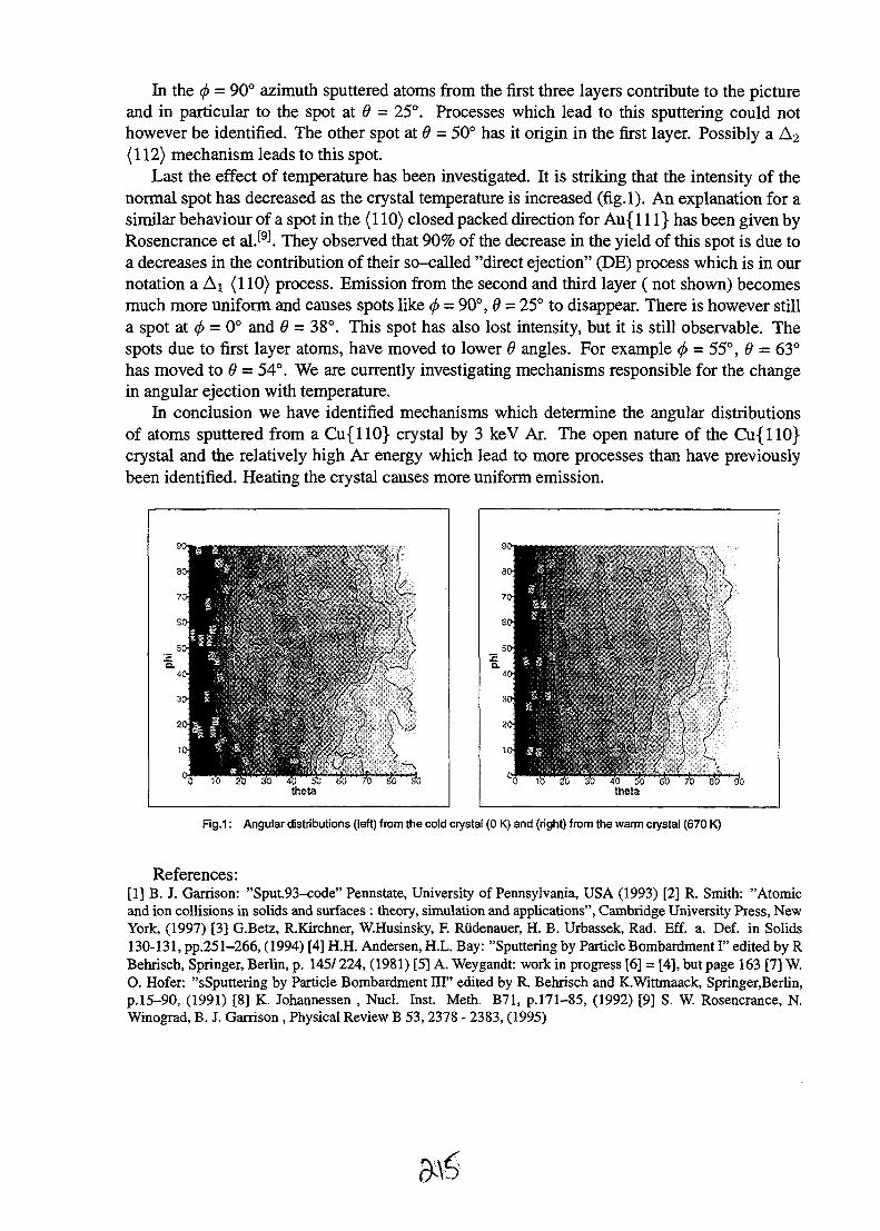
In the <f> = 90° azimuth sputtered atoms from the first three layers contribute to the pictureand in particular to the spot at 8 = 25°. Processes which lead to this sputtering could nothowever be identified. The other spot at 9 = 50° has it origin in the first layer. Possibly a A2
(112) mechanism leads to this spot.Last the effect of temperature has been investigated. It is striking that the intensity of the
normal spot has decreased as the crystal temperature is increased (fig.l). An explanation for asimilar behaviour of a spot in the (110) closed packed direction for Au{ 111} has been given byRosencrance et alJ9l They observed that 90% of the decrease in the yield of this spot is due toa decreases in the contribution of their so-called "direct ejection" (DE) process which is in ournotation a Ai (110) process. Emission from the second and third layer (not shown) becomesmuch more uniform and causes spots like <f> = 90°, 9 = 25° to disappear. There is however stilla spot at <j) = 0° and 8 = 3%°. This spot has also lost intensity, but it is still observable. Thespots due to first layer atoms, have moved to lower 9 angles. For example <j> = 55°, 6 = 63°has moved to 6 = 54°. We are currently investigating mechanisms responsible for the changein angular ejection with temperature.
In conclusion we have identified mechanisms which determine the angular distributionsof atoms sputtered from a Cu{110} crystal by 3 keV Ar. The open nature of the Cu{110}crystal and the relatively high Ar energy which lead to more processes than have previouslybeen identified. Heating the crystal causes more uniform emission.
Kg
3 0 4
7 0 4
604
504
I IAQ-m
11 0 4
T
Ii t
t
i
>
N
• \
theta
)*••
1
j
I
\J
Jss
i1
(
/
\
Fig.1: Angular distributions (left) from the cold crystal (0 K) and (right) from the warm crystal (670 K)
References:[1] B. J. Garrison: "Sput.93-code" Pennstate, University of Pennsylvania, USA (1993) [2] R. Smith: "Atomicand ion collisions in solids and surfaces : theory, simulation and applications", Cambridge University Press, NewYork, (1997) [3] G.Betz, R.Kirchner, W.Husinsky, F. Rudenauer, H. B. Urbassek, Rad. Eff. a. Def. in Solids130-131, pp.251-266, (1994) [4] H.H. Andersen, H.L. Bay: "Sputtering by Particle Bombardment I" edited by RBehrisch, Springer, Berlin, p. 145/ 224, (1981) [5] A. Weygandt: work in progress [6] = [4], but page 163 [7] W.O. Hofer: "sSputtering by Particle Bombardment III" edited by R. Behrisch and K.Wittmaack, Springer,BerIin,p.15-90, (1991) [8] K. Johannessen , Nucl. Inst. Meth. B71, p.171-85, (1992) [9] S. W. Rosencrance, N.Winograd, B. J. Garrison , Physical Review B 53,2378 - 2383, (1995)

P1.41 AU9817168
METHODS OF OPTIMISING ION BEAM INDUCED CHARGE COLLECTIONOF POLYCRYSTALLINE SILICON PHOTOVOLTAIC CELLS
L. C. G. Witham. D. N. Jamieson and R. A. Bardos
School of Physics, Microanalytical Research Centre, University of Me lbourne, Parkville, 3052,AUSTRALIA.
Introduction
Ion Beam Induced Charge (IBIC) is a valuable method for the mapping of charge carrier transportand recombination in silicon solar cells[l]. However performing IBIC analysis of polycrystallinesilicon solar cells is problematic in a manner unlike previous uses of IBIC on silicon-based electronicdevices. Typical solar cells have a surface area of several square centimeters and a p-n junctionthickness of only few microns. This means the cell has a large junction capacitance in the manynanoFarads range which leads to a large amount of noise on the preamplifier inputs which typicallyswamps the transient IBIC signal. The normal method of improving the signal-to-noise (S/N) ratioby biasing the junction is impractical for these cells as the low-quality silicon used leads to a largeleakage current across the device. We present several experimental techniques which improve theS/N ratio which when used together should make IBIC analysis of many low crystalline qualitydevices a viable and reliable procedure.
The Detector and Preamplifier
Solar Cell
Figure 1: Circuit schematic of a solar cell arranged as a charged particle detector in a charge sensitivepreamplifier circuit. Rs and C<j are the series resistance and junction capacitance of the solar cell and isis the small signal current source provided by ionising radiation entering the cell. Cs is the sum of straycapacitances between the detector and preamplifier and CjSS is the input capacitance of the FET. TheA250 is a hybrid charge sensitive preamplifier module made by Amptek Inc.
Data collection for IBIC requires a small transient signal to be collected from a solid-state semi-conductor device and amplified. The circuit most often used for this purpose is the charge sensitivepreamplifier. This mode of preamplification typically gives the best signal to noise ratio for chargedparticle detection with a solid state detector. A schematic for this circuit is shown in figure 1.The solar cell is shown as an equivalent circuit containing a small signal current source is, a seriesresistance Ks and a parallel capacitance C<j. Charge injected into the cell by incident MeV ions
is separated across the p-n junction creating a small transient current (lMeV of energy loss in Sicreates ~0.044pC of charge). The series resistance is largely determined by contributions fromthe bulk resistance of the semiconductor material and contact resistance of the metallic fingers [2,p43]. The space-charge region of the p-n junction has a capacitance Ca which is proportional tothe junction area and inversely proportional to the depletion region width [3,p78]. Other sourcesof capacitance on the preamplifier input are the gate-channel capacitance of the JFET (Qss) andother stray capacitance between the detector and amplifier due to such things as coaxial cabling(Cs). The feedback capacitor C/ controls the voltage gain of the circuit and R/ slowly drains theaccumulated charge off C/ to prevent clipping.
Amplifier Gain and Noise Sources
The output voltage of the above circuit for an input IBIC transient is given by
QVnut — — Cin + (A + \)Ct
where Qn = Cd + Cs + C{SS, Q is the integrated charge of the transient and A is the preamplifiergain. When (Cin + Cf)/Cf « A the output voltage is approximately Vwt = —Q/Cf. Howeveras Cin becomes large the output voltage is significantly reduced and hence the S/N ratio worsens.This effect can be partially offset by using an input FET with a Ciss approximately equal toCd, which will have a larger transconductance gain and hence increase A. Connecting two ormore FETs in parallel can achieve the same effect. In addition to this reduction in sensitivity alarge input capacitance also acts as a significant noise source. This noise is proportional to thecapacitance and must typically be kept below l-2nF to keep the transient signal above the noise.
Results and Discussion
Solar cells typically have junction areas of several cm2 and as such their capacitance is very high.A simple way of reducing this capacitance is to fragment the cell into pieces small enough so thatthe junction capacitance is low enough to see IBIC transients above the noise level. This hasbeen performed successfully as shown in [4]. The same effect may also be achieved by scribinga rectangle on the surface of the cell to cut through the thin n+ layer, hence isolating thep-njunction within the region defined.
A common way of reducing detector capacitance is to reverse bias the p-n junction which increasesthe depletion region width. This is unfortunately impractical for polycrystalline solar cells due tothe large reverse bias leakage current of these devices. This has the effect of dropping much of thesupplied bias voltage across the bias resistor and producing significant Shot noise from the biasresistor.
Figure 2 shows a comparison between a 12mm2 fragment of commercial grade polycrystallinesilicon solar and a 25mm2 p-n junction silicon charged particle detector made from single crystalsilicon. This exemplifies the large capacitance and leakage current even from a small section ofsolar cell by comparing it to a detector for which IBIC S/N ratio is very good.
The purchase of an Amptek A250 hybrid charge sensitive preamplifier has allowed us to fabricatean in-chamber preamplifier module which has significantly improved the S/N ratio by minimisingthe detector to preamplifier distance and hence effectively eliminating the stray capacitance Cs.Another benefit has been the elimination of troublesome ground loop noise sources between the

2000Poly-X Silicon Solar Coll •
Solid State Detector
2.5
1.5
Poly-X Silicon Solar Cell
Solid State Detector
-10bias (V)
-15 -20
Figure 2: Comparison of device capacitance and leakage current as a function of reverse junction biasvoltage for a commercial-grade polycrystalline silicon solar cell and a solid-state crystalline silicon chargedparticle detector. Capacitance and current values for the solid-state detector have been multiplied by afactor of 10 for clarity. Detector surface areas are 12mm2 and 25mm2 respectively.
solar cell detector and preamplifier input.
Future Work and Conclusion
The most effective technique for further improvement of the IBIC S/N ratio is to cool the sample.The leakage current of the cell will halve for approximately every 10°C reduction in temperature.This would allow the junction to be reverse biased and Cd reduced without introducing significantnoise. Simultaneous cooling of the FET reduces its leakage current which will also reduce thenoise. Sample cooling has other beneficial effects such as increasing the diffusion length of thesilicon substrate which improves charge collection of generated charge carriers. Preparation ofan in-chamber liquid nitrogen sample cooling stage for the Melbourne microprobe is currentlyunderway and should allow IBIC on polycrystalline solar cells to be performed with much betterresults.
References
[1] M.B.H. Breese, P.J.C. King, G.W. Grime and F. Watt, "Micro-circuit imaging using an ion-beam-induced charge", Journal of Applied Physics 72 (6), (1992)
[2] S.R. Wenham, M.A. Green and M.E. Watt, Applied Photovoltaics, Centre for PhotovoltaicDevices and Systems, ISBN 0-86758-909-4
[3] S.M. Sze, Physics of Semiconductor Devices, John Wiley & Sons (1981)
[4] L.C.G. Witham, D.N. Jamieson, R.A. Bardos and A. Saint, "Trace elements and charge re-combination in polycrystalline photovoltaic materials", Proceedings of the Thirteenth InternationalConference on Ion Beam Analysis, Lisbon, Portuagal, NIM-B, 1997

P1.42 AU9817169The Fabrication of Quantum Wires in Silicon Utilising the Characteristics of
Solid Phase Epitaxial Regrowth of Crystalline Silicon
A. C. Y. Liu and J. C. McCALLUMMicroanalytical Research Centre, School of Physics, University of Melbourne, Parkville,Victoria 3052, Australia, [email protected]
The process of solid phase epitaxy (SPE) in semiconductor materials is one which hasbeen intensively researched due to possible applications in the semiconductor industry. SPEis a solid phase transformation, in which an amorphous layer can be recrystallized eitherthrough heating or a combination of heating and ion bombardment. The transformation isbelieved to occur exclusively at the interface between the amorphous and crystalline layers,with individual atoms from the amorphous phase being incorporated into the crystallinephase by some point defect mechanism. The process has been observed to follow an Arrheniustemperature dependence,
P
v = voexp{-^}, (1)
where v is the velocity of the moving interface, Ea is a material specific activation energy,often associated with the creation or migration of the defect responsible for the recrystal-lization, and vo is a constant prefactor. Accepted values of these for silicon are found inthe comprehensive review of Olson and Roth, where Ea is empirically determined to be2.7 ± 0.02ey and v0 is cited as 4.64 x 108cm.s"1 [1]. SPE has been observed to proceed lat-erally, if constrained to the plane of the crystal template on which growth occurs. To date,measurements of lateral SPE have involved crystallization radially, outward from a region ofseed crystal. Lateral confinement has been shown to effect the SPE rate in a manner whichis dependent on the direction of the growth. Yamamoto, Ishiwara and Furukawa observethat lateral growth in the [Oil] direction proceeds at a constant rate, while growth in the[010] direction proceeds initially at a faster rate, and then declines to the constant, directionindependent rate. [2].
The prescence of dopants and impurities has been found to influence the rate of SPE.Specifically, amounts of both p and n-type dopants enhance the rate, while equal amountsof both return the rate to the intrinsic rate. This suggests that a modification of the Fermilevel is, in this case important to the defect mechanism responsible for SPE. The prescenceof non-dopant impurities has been found in general to retard the SPE rate. Exceptions tothis are the metals which are fast diffusers in silicon. Gold for example has been found toenhance the SPE rate by as much as 50 times. In an interesting experiment, Jacobson, Poateand Olson monitored the effect of implanted gold in a recrystallizing silicon amorphous layer[3]. They found that the gold is zone refined in the amorphous layer, providing greaterenhancement to the rate as its concentration in the layer increases. This process ceaseswhen the concentration of the gold surpasses the solubility level of gold in silicon, at whichstage the rate is severely retarded, and the gold is precipitated at the interface. Elliman,Gibson, Jacobson, Poate and Williams [4] report similar findings with both gold and copperimplanted amorphous silicon layers, observing the precipitation of these elements with TEM.
The experiment being performed is designed to incorporate lateral SPE and zone refine-ment of fast diffusing metals in the amorphous layer during annealing to create wire likestructures with lateral dimensions in the nanometre regime, and heights of some microns.As shown in Fig. 1 a silicon wafer is subjected to a multi-energy silicon implant througha fine nickel grid to amorphize regions to a depth of 5/Lim creating an array of amorphouswells with diameters of around 1 — 2fxm. Metal impurity atoms are then implanted in theamorphous regions at an energy of 500/ceV with a dose of 5 x 10¹⁴cra~2 calculated from

100keV-8MeV
2x 10A15 /cmA2
500 keV
5x10*14/011*2
multi-energy Siimplant
metal impurityimplant
anneal at around600° C
Figure 1: The Process of Creating a Quantum Wire. The nickel grid used as a mask containsan array of openings of about 1/ira in diameter.
the volume of the intended wire. Annealing then occurs at around 600°C, shrinking theamorphous wells and pushing the metal atoms into the core.
The implantations were conducted using the ion implanter at the Electronic MaterialsEngineering laboratory at ANU. All implants were performed at liquid nitrogen temperaturesto prevent thermal shifting of the nickel grids, and a subsequent widening of the wells.Samples were examined in an optical microscope with a Nomarski attachment to check forthe amorphous regions. The amorphous silicon wells appear as little hillocks due to the factthat amorphous silicon is less dense than crystalline silicon and hence some swelling occurs.An example of this is shown in Fig. 2 which is a photograph of a x40 magnification of thearray of implanted regions. The period of the hillock structure is 12.5^m. It is clear fromthis that due to the implantations there exists a regular array of swollen regions in the siliconwafer, corresponding to expectations. Expectations were again confirmed through the use ofthe Alphastep profiler at RMIT which uses a fine diamond stylus to map the surface featuresof a sample. This provided the information that the burgeoning wells were about 2fxm wideand rose about 0.01/ m above the silicon substrate as can be seen from Fig. 3.
Samples were preannealed at 480°C to relax the interface between amorphous and crys-talline regions, and then annealed at around 600°C for about Ibmins. Anneals were mon-itored using the time resolved reflectivity system at Melbourne University. Although thelaser spot size was much larger than individual wells and the interface was moving, unusu-ally, perpendicular to the incoming beam, the averaged signal was able to be interpretedto the degree that an asymptotic trend could be discerned. This trend existed at all theanneal temperatures used, with higher temperatures resulting in a contracted time scale.The asymptotic behaviour is interpreted as a completion of the recrystallization and precip-

itation process, or an attainment of equilibrium of the system some way from the ideal. Atthis stage, the exact composition and structure of the wires has yet to be determined, andit is possible that a gold and silicon compound is obtained, with the surrounding recrystal-lized silicon containing many defect structures. However, recently acquired RBS data lookspromising and TEM is scheduled to be performed. Both these techniques seem capable ofaugmenting our present knowledge of the process which occurs during the annealing and thestructures which are obtained.
Figure 2: Photograph of Amorphous Wells. The period for the swollen regions is 12.5/zm.
01.04
TIft 3.7O5KR96O. R
LR 80.
firea+4.2098SCRH HEMU 1
2OOO . 2 14OO 1 3
DIR. >STYLUS 5mg
3 ?4un LEUEU
Figure 3: Alphastep Profile of Amorphous Wells
REFERENCES
[1] G. L. Olson and J. A. Roth, Materials Science Reports 3 (1988) 1-78.[2] H. Yamamoto, H. Ishiwara and S. Purukawa, Jap. J. Appl. Phys. 25(5) (1986) 667-672.[3] D. C. Jacobson, J. M. Poate and G. L. Olson, Appl. Phys. Lett. 48(2) (1986) 118-120.[4] R. G. Elliman, J. M. Gibson,D. C. Jacobson, J. M. Poate and J. S. Williams, Appl. Phys. Lett. 46(5)
(1985) 478-480.

P1.43Hill
AU9817170
IN-SITU TRANSMISSION ELECTRON MICROSCOPYOF THE SOLID-PHASE EPITAXIAL GROWTH OF GaAs:
SAMPLE PREPARATION AND ARTIFACT CHARACTERIZATION
D.J. Llewellyna'b, K.B. Belayb and M.C.Ridgwayb
Electron Microscope Unit, Research School of Biological Sciences,The Australian National University, Canberra, Australia.
Department of Electronic Materials Engineering, Research School of PhysicalSciences and Engineering, The Australian National University, Canberra,
Australia
ABSTRACTIn-situ transmission electron microscopy (TEM) has been used to characterize the solid-phase epitaxial growth of amorphized GaAs at a temperature of 260°C. To maximize heattransfer from the heated holder to the sample and minimize electron-irradiation inducedartifacts, non-conventional methodologies were utilized for the preparation of cross-sectionalsamples. GaAs 3x1 mm rectangular wafers were cleaved then glued face-to-face to form awafer stack size of 3x3 mm while maintaining the TEM region at the center. This stack wassubsequently polished on the cross-section to a thickness of ~ 200 Jim. A 3 mm disc wasthen cut perpendicular to the cross-section using a Gatan ultrasonic cutter. The disc waspolished men dimpled on both sides to a thickness of ~ 15 |im. This was ion-beam milled atliquid nitrogen temperature to an electron-transparent layer. From a comparison of in-situ andex-situ measurements of the recrystallization rate, the actual sample temperature during in-situ characterization was estimated to deviate by < 20°C from that of the heated holder. Theinfluence of electron-irradiation was found to be negligible by comparing the recrystallizationrate and microstructure of irradiated and unirradiated regions of comparable thickness.Similarly, the influence of the "thin-foil effect" was found to be negligible by comparing therecrystallization rate and microstructure of thick and thin regions, the former determined afterthe removal of the sample from the microscope and further ion-beam milling of tens ofmicrons of material. In conclusion, the potential influence of artifacts during in-situ TEM canbe minimized by the appropriate choice of sample preparation procedures.
INTRODUCTIONThe solid-phase epitaxial growth (SPEG) of amorphous (a)- GaAs has direct application tothe fabrication of ion-implanted GaAs devices. As a consequence the recrystallization of (a)-GaAs layers produced by ion-implantation has been intensively investigated (Sinclair, 1988).Previously, we have utilized in-situ TEM to compliment conventional techniques tounderstand the regrowth phenomenon of (a)- GaAs during SPEG (Belay, 1996). In thisreport, artifacts associated with in-situ TEM including the electron-beam effect1, the thin-foileffect2 and ion-beam induced heating, resulting from the sample thinning process, have beenstudied.
THE EXPERIMENTAs described below, cross sectional TEM samples were prepared using a non-conventionalmethodology to enhance heat transfer from the heated holder to the sample and to helpminimize electron-beam irradiation induced artifacts. GaAs 3x1 mm rectangular wafers were
1 electron-beam-induced changes in the recrystallization rate.2 differential recrystallization rates as a function of sample thickness.

glued face-to-face to form a bulk sample of size 3x3 mm. This was subsequently polished to athickness of ~ 200 um from which a disc of 3 mm in diameter was cored using an ultrasoniccutter. The disc was polished and dimpled on both sides to a thickness of ~ 15 um. This wasthen ion-beam milled at liquid nitrogen temperature to produce an electron transparent layer.
Imaging was carried out using a JEOL 2000FX TEM fitted with LaB6 emitter and operatingat an accelerating voltage of 200 kV. Beam current was of the order of 18 nA and theresolution of the microscope was better than 0.5 nm.
The potential influence of ion-beam induced heating was characterized by comparingmeasurements of the thickness of an amorphous layer determined from XTEM micrographand Rutherford Backscattering Spectrometry and Channelling (RBS/C) spectrum.
0)oCO
3CO
5 0 nm
( Depth (A)4000 3000 2000 1000 0
0.8 1.0 1.2 1.4 1.6 1.8Energy (MeV)
Figure 1: (a) XTEM Micrograph of Sample after removal from Ion-Beam Thinner, (b) Channeled RBS/CSpectrum for an Amorphous GaAs Layer.
The sample heating was ramped to a temperature of 200°C at the rate of ~ 0.7°C/sec. At thistemperature the regrowth rate is negligible. The temperature was then increased to 260°C atthe rate of l°C/sec. From a comparison of in-situ and ex-situ measurements of therecrystallization rate it was determined that the actual sample temperature during in-situcharacterization was estimated to deviate by < 20°C from that of the heated holder.
Semi-insulating (100) GaAs, as implanted with 200 keV As ions and 190 keV Ga ions to atotal fluence of Iel4/cm2 to form an amorphous surface layer of ~ 160 nm, was partiallyrecrystallized in the TEM at« 260°C for « 10 min.

Electron-beam effect and thin-foil effect were characterized by comparing the recrystallizationrate and microstructure of the irradiated and unirradiated, thick and thin regions of the sample,respectively.
RESULTS and DISCUSSIONFrom Figure 1 it is evident that no material has recrystallized during the sample thinningprocess, due to ion-beam induced heating during sample milling.Figure 2 shows a low magnification image of the sample which was prepared using the non-conventional methodologies, where (A), (B) and (C) are the irradiated3, the unirradiated4 andthe bulk5 parts of the sample.
Figure 2: Disc Sample Showing Regions of Interest.(A) Irradiated Region.(B) Un-Irradiated Region.(C) Bulk Part of Sample.
The extent of the regrown layer and the microstructure of the amorphous/crystalline-interfaceof irradiated, unirradiated and bulk regions of the sample are shown in Figure 3 (I), (ii) and(iii), respectively. The extent of twinning and the depth of the amorphous/crystalline interfaceis the same in all regions of the sample.
3 area of sample irradiated by electron-beam during in-situ heating.4 area of sample not irradiated by electron-beam during in-situ heating.5 thick area of sample not yet thinned to form an electron-transparent region.

surface
Figure 3: Amorphous/Crystalline Interface of:- (i) Irradiated Region, (ii) Un-Irradiated Region.(iii) Bulk Partof Sample
CONCLUSIONThe influence of ion-beam induced heating during the thinning process is insignificant whenthe sample is maintained at liquid nitrogen temperature during the milling process.
The influence of artifacts resulting from the electron-beam and thin-foil effects during in-situTEM can be eliminated by the appropriate choice of sample preparation procedures.
ACKNOWLEDGMENTThe authors wish to acknowledge the Australian Institute of Nuclear Science and Engineeringfor partial financial support and thank the Australian Nuclear Science and TechnologyOrganisation for providing access to the microscopy facilities. The great help of Kath Smith,Mark Blackford and Michael Colella in Advanced Materials, is recognised.Graphics and layout assistance given by Tim Thompson is appreciated.
REFERENCESBELAY K.B, LLEWELLYN D J & RIDGWAY M.C, "Solid-phase epitaxial growth of
amorphized GaAs: The influence of macroscopic nonstoichiometry." Appl. Phys.Lett 69 (17),21(1996).
SINCLAIR R. et al Act Cryst A44, 965-975 (1988) and references there in.

P1.44
AU9817171
Implantation induced optical losses in GaAs/AlGaAs DistributedBragg Mirrors
M. I. Cohen, H. H. Tan and C. Jagadish
Department of Electronic Material EngineeringResearch School of Physical Sciences and EngineeringAustralian National University, Canberra, Australia
1 Introduction
VERTICAL Cavity Surface EmittingLasers, (VCSELs) have attracted intense
research in the past few years. VCSELs arepromising over conventional edge emittinglasers due to their superior beam shape, waferscale processing and the ability to make twodimensional arrays. Hence VCSELs are nowfinding use in short distance optical fiber links,printing and optical signal processing.
The basic structure of an ion implanted VC-SEL is depicted in Figure (1) [1]. The QuantumWell gain medium is sandwiched between twoDistributed Bragg Mirrors (DBRs) forming acavity. In order for the lasing to occur, the op-tical mode must be confined in the transversedimension. This is usually achieved by the im-plantation of the top mirror to isolate the cur-rent into the aperture. The current causes thetemperature to rise in the center of the aper-ture leading to a refractive index change be-tween the center of the aperture and the sides.Thus a graded index lens is formed focusing theoptical mode, this phenomenon is referred to inthe literature as thermal lensing [2].
Hence in ion implanted VCSELs thermallensing is the only mechanism supplying the op-tical confinement necessary. Since the mecha-nism relies on temperature effects, the thermallens is usually destroyed or distorted as higherorder transverse modes appear. This leads tohighly non-linear Light-Current curves whichare non-desirable. Also for device applicationsin Wavelength Division Multiplexing (WDM)networks it is important to suppress transversemodes. There have been numerous attemptsto suppress transverse modes by introducinglosses at the perimeter of the device [3, 4].
ue •
Implanted
p-dopedBragg ReflectorAlo.7Gao.3As/GaAs
7J4 Al0.jGa0,As/GaAs3 InGaAs QWV4 Alo.3Gao.7As/GaAs
n-dopedBragg ReflectorAlo.7Gao.3As/GaAs
n GaAs substrate
Figure 1: A Vertical Cavity Surface EmittingLaser. Lasing action is possible due to the con-finement of the optical mode to the device aper-ture
Even though the study of isolation of GaAsmultilayers by O implantation is very thoroughin the literature [5, 6], it is rare to find workconcerning the effect of O implantation on theoptical characteristics of the material. Also theeffect on resonant structures, such as DBRs isnot well understood. The ion implantation andsubsequent annealing, not only causes a recov-ery of the damage profile but may lead to in-termixing [7] and other effects [8].
Usually the mirrors are implanted using pro-tons, but in this paper we examine the use ofO ions for current confinement of the VCSEL.We show that implantation with high energyO ions leads to a significant amount of opticaldegradation of the mirrors, thus drastically in-creasing loss for higher order transverse modes.This optical degradation is present even afterannealing which demonstrates the stability ofthe O implantation over the proton implanta-tion case.

N type mirror with H implant dose 2
100 •
- , 8 0 •
•> 60
I 40
20
A / M
• ',p V
As grownAs implanted5OOdeg
650 900 950 1000
Wavelength (nm)
N type mirror with H implant dose 3
1050 B50
100
80
60
40
20
n
/it
-: \U' A M1 / \f 1
P type mirror H implant dose 2
A/1 l \ 1
A • N
—; \\r\
\ >! wv
As grownAs implanted500 deg
900 950 1000Wavelength (nm)
P type mirror H implant dose 3
1050
As grownAs implanted400deg
100
40
20
'''I • \ \
VA
As grown
" - • • As implanted
500 dcg
J
800 850 900 950Wavelength (nm)
1000 1050 850 900 950
Wavelength (nm)
1O00
Figure 2: Reflectivity Spectra for proton implanted DBR mirrors, (p type and n type).
2 Experiment
Two mirrors, p-type and n-type, were grownusing low pressure MOCVD. The p type mir-ror was doped with Dimethyle Zinc (DMZn),while the n type mirror was doped using Silane(SiH4). The mirrors consisted of 43.2nm ofAlo.2Gao.8As and 51.3nm of Alo.9Gao.1As, thesewere then separated by a 20nm graded compo-sition layer, with linear grading.
The doping was 5 x 1018cm~3 in the gradedregion with a 5 x 1017cm~3 background dopingmeasured using an ECV profiler.
Both mirrors were implanted with a flat pro-file H implant and a flat profile O implant. Theimplantation scheme is shown in Table (1). Thedoses were chosen to be in close agreement toprevious studies which indicate the carrier re-moval efficiency of 0 ions to be at least an orderof magnitude better than the proton case [5].
H implantEnergy
2550
100150250300350400
Dose1.232.242.632.633.463.833.995.35
O implantEnergy
90300800
1500260038005000
Dose1.01.72.02.52.72.74.0
dose 1 = 1 x 10¹⁴
dose 2 = 5 x 10¹⁴
dose 3 = 1 x 10¹⁵
dose 1 = 1 x 10¹³
dose 2 = 5 X 10¹³
dose 3 = 1 X 10¹⁴
Table 1: Implantation scheme for O and H ions.

N type mirror O implant dose 1 P type mirror O implant dose 1100
I
As grownAs implanted400 deg500 deg
100
80
60
As grownAs implanted500 deg700 deg
800 850 1000900 950
Wavelength (nm)
N type mirror O implant dose 3
1050 900 950 1000
Wavelength (nm)
P type mirror O implant dose 3
1050
100
80
.5" 60>
1I
20
As grownAs implanted400 deg500 deg
60 •
53 40
As grownAs implanted400deg600deg
800 850 950 1000 1050 850 900 950 1000 1050
Wavelength (run) Wavelength (nm)
Figure 3: Reflectivity Spectra for Oxygen implanted DBR mirrors, (p type and n type).
The reflectivity spectra of the proton im-planted n doped mirror is presented in Figure2. For the first dose chosen the reflectivity re-mains virtually unchanged indicating negligibledamage. Dose 2 begins to show some absorp-tion due to damage, particularly in the reducedvisibility of the mirror ripples about 975nm.This damage is quickly annealed though, andannealing at 500°C for 30 seconds is seen tocompletely cure the mirror.
As the dose is increased to Dose 3, the dam-age is much more pronounced. The ripplesabout 975 nm are far less visible in the as im-planted sample. However, the damage is an-nealed efficiently at 400°C and is completelygone at 600°C.
It is very interesting to compare these resultsto the results obtained from the p type mirror.The p-type mirror, shown in Figure 2, displaysa more exaggerated loss for the same doses. Ascan be seen by a direct comparison of the asimplanted case. Again there is negligible dif-ference between the optical reflectivity of dose2 and dose 3 indicating a possible saturationeffect in the implantation induced damage.
Of interest is the significant red shift of the
mirror reflectivity which may be observed forthe as implanted spectra. This may be at-tributed to the increase of the refractive indexof GaAs due to the local amorphization of thematerial [9]. This amorphization may also leadto optical scattering which could account forthe reduced total reflectivity.
When comparing the reflectivities from theH implanted case to the O implanted case, itis easy to see (Figure 3) that O implantationcauses far more pronounced optical loss. Theas implanted case for the lowest dose shows asignificant amount of loss, even more than thehighest dose of protons. However as can beseen a lot of this damage may be annealed atlower temperatures around 400°C-500°C.
When the dose is increased, however, thedamage is much more significant, and it canbe seen that annealing at lower temperaturesis insufficient to remove a significant amount ofthe damage, resulting in highly lossy mirrors.
Contrary to the H implantation case, the p-type material does not exhibit more loss, as canbe seen by Figure 3. The as implanted loss isof the same order of magnitude as in the n typemirror.

Conventionally VCSELs are isolated by pro-ton implantation due to the fact that the stop-ping range of protons in GaAs is much largerthan that of Oxygen. However the damage cre-ated by protons is more susceptible to be an-nealed out during the operation of the deviceleading to device degradation, [10]. Here we seethat the O implanted material displays morethermally stable optical damage than the pro-ton implanted case.
3 Conclusions
In this paper we have compared Oxygen ionimplantation with proton implantation. It wasfound that although proton implantation im-parted significant optical losses to the mate-rial causing a reduction of the reflectivity, thedamage tended to be annealed out at moder-ate temperatures (400°C-600°C). It was foundthat p type mirrors are much more susceptibleto proton implantation leading to severe degra-dation of the reflectivity.
Oxygen implantation was found to be farmore effective in creating optical damage in themirror. The mirror resonance was observed tobe red shifted indicating1 some amorphization ofthe material occurred. Optical damage causedby ion implantation was found to be more ther-mally stable and more significant than in theproton implantation case. It is hence concludedthat O implants are promising for isolation ofVCSELs because the material increases the loss
-of .the transverse modes and the crystal damageis more thermally stable.
impurity-induced disordering. IEEE Photon.Technol. Lett, 7(12):1388-1390, 1995.
[4] Y. A. Wu, G. S. Li, R. F. Nabiev, K. D.Choquette, C. Caneau, and C. J. Changhas-nain. Single-mode, passive antiguide verti-cal cavity surface emitting laser. IEEE Jour-nal of Selected Topics in Quantum Electronics,l(2):629-637, 1995.
[5] S. Gecim, R. J. Sealy, and K. G. Stephens. Car-rier removal profiles from oxygen implantedgaas. Electron. Lett, 14(10):306-308, 1978.
[6] T Henderson, W Liu, and T. S. Kim. Currentconduction in an implant isolated gaas/algaasheterostructure. J. Appl. Phys., 74(11):6571-6575, 1993.
[7] P. J. Hughes, B. L. Weiss, S Tlali, and H. E.Jackson. Oxygen implantation induced inter-diffusion in algaas/gaas quantum well struc-tures. Journal of Vacuum Science & Technol-ogy B, 15(4):845-848, 1997.
[8] S. J. Pearton, F Ren, S N. G. Chu, C. R. Aber-nathy, W. S. Hobson, and R. G. Elliman. De-fects and ion redistribution in implant-isolatedgaas-based device structures. J. Appl. Phys.,74(ll):6580-6586,1993.
[9] K. T. Chan, Y. W. Hui, D. J. Han, and G. H.Li. Modification of refractive index of gaas byion implantation of oxygen. Nuclear Instru-ments & Methods in Physics Research SectionB-Beam Interactions with Materials & Atoms,83(l-2):177-180,1993.
[10] Y. M. Cheng, R. W. Herrick, P. M. Petroff,M. K. Hibbsbrenner, and R. A. Morgan.Degradation studies of proton-implanted verti-cal cavity surface emitting lasers. Appl. Phys.Lett, 67(12):1648-1650, 1995.
References[1] R. S. Geels, S. W. Corzine, and L. A. Coldren.
Ingaas vetrical cavity surface emitting lasers.IEEE J. Quantum Electron., 27(6): 1359-1367,1991.
[2] J. W. Scott, R. S. Geels, S. W. Corzine,and L. A. Coldren. Modeling tempera-ture effects and spatial hole burning to op-timize vertical-cavity surface-emitting laserperformance. IEEE J. Quantum Electron.,29(5):1295-1308, 1993.
[3] P. D. Floyd, M. G. Peters, L. A. Coldren,and J. L. Merz. Suppression of higher-ordertransverse modes in vertical-cavity lasers by
P1.45 AU9817172
URANIUM DOPING AND NEUTRON IRRADIATION OF BI-2223SUPERCONDUCTING TAPES FOR IMPROVED CRITICAL CURRENT DENSITY
S. D. Moss, W.G.Wang, S. X. Dou? R Weinstein+
University of Wollongong, Centre for Superconducting and Electronic Materials, Wollongong, NSW, 2522,AUSTRALIA
+Univeisity of Houston, Texas, USA
ABSTRACTPreliminary data suggests that the combination of uranium doping and neutron irradiationproduces improved flux pinning in Bi-2223 tapes over neutron irradiation alone. Beforeneutron irradiation, uranium doping has no effect on critical current. The uranium appears tobe homogeneously distributed throughout the oxide core of the tape. Finally, the presence of2212 and other secondary phases in the doped tapes suggest further refinement of the sinteringprocedure is necessary.
INTRODUCTIONProgress has been made in understanding the flux pinning behaviour of the Bi-Pb-Sr-Ca-Cu-Osystem. Enhancement of magnetic flux pinning has been attained through neutron irradiation. Anoticeable enhancement in transport Jc in Ag/Bi-based 2223 tapes has been achieved using fastneutron irradiation, which was attributed to an improvement in flux pinning capability [1].Preliminary studies on uranium doping on Bi-2223 powders show a beneficial effect on fluxpinning [2]. Thus it is believed that a combination of neutron irradiation with uranium dopingwould introduce fission tracks throughout a tape which will act as effective pinning centres,leading to a substantial increase in critical current.
EXPERIMENTALShort Ag-clad Bi-2223 tapes, both doped and undoped, were prepared using a standardpowder-in-tube procedure [eg.3]. Commercial Merck powder was used, with doped sampleshaving 0.3%(by weight) uranium oxide added and then ball milled for an extended period oftime. Sintering was performed using a tube furnace with a temperature gradient from one endto the other. A two stage sintering procedure was used. Temperatures were ramped at lC/min,and each stage was held at 840*0.50 for 50 hours. Pressing at lGPa was carried out after thefirst stage. During the final 30 hours of the second stage, temperature was reduced to 820C.Samples were then irradiated with a fluence of 4x10¹⁶ n/cm2 using fast neutrons.
Before irradiation, SEM, DTA and XRD was performed on the tapes. Both before and afterirradiation the trapped maximum magnetic flux was measured at 77K.
RESULTS AND DISCUSSIONEarly results using the standard two stage sintering procedure have generated critical currentsin 0.3% uranium doped Bi-2223 tapes similar to the best undoped tapes (Figure 1). Figure 1shows that the optimum sintering termperature for the doped tapes is 1-2C lower than forundoped tape. XRD shows that the uranium doped tapes contain approximately 20% Bi-2212

Figure 1: Critical Current of Uranium Doped and Undoped Bi-2223 Tapes (1 ji V criterion)
KS7 53B SS8 M« Ml M2
10
undoped samplesU-doped samples
Samples size - 3mm*0.13mmJuly 7.1997
20
1S
to
CSS MO M l
Sintering temperature ( t )
phase and other secondary phases such as (Ca,Sr)CuO, (Ca,Sr)PbO4 and CuO. Undoped tapescontain fewer secondary phases (Figure 2).
Figure 2: XRD of Uranium Doped and Undoped Bi-2223 Tapes after Final Sinter.
- (a) Uranium Doped Bi 2223 tape after 2 sinter- <b) Bi 2223 tape after2 sinter
2-lhete 0
Preliminary SEM suggests that the uranium dispersed throughout the BiSCCO. Having theuranium homogeneously dispersed will result in an isolated U235 fission when neutronirradiated. When the U235 fission occurs there is a back to back emission of fragments whichis thought to produce damage in the form of an isolated column. It is expected then that thetotal damage will appear like a collection of needles of random spacing and orientation. ATEM study is underway to examine the damage due to the fission events.
Some preliminary magnetization results on the neutron irradiation of uranium doped tapes havebeen obtained. Table 1 below compares the maximum trapped magnetic field before and afterneutron irradiation. Unfortunately these results are not reliable due to one of the tapes beingbent, and noise on the gaussmeter on which the measurements were made. The (nowradioaaive) tapes have been sent onto Atomic Institute in Vienna, Austria for analysis byProfessor Weber's group.

Table 1: Maximum Trapped Magnetic Field (BT) Before and After Neutron Irradiation.
with uraniumwith uraniumno uraniumno uranium
Sample NumberU-4U-6Un-1Un-3
BT before (gauss)4.01.53.13.2
BT after (gauss)(0.9)(1)
7.97.511.9
R(2)
—
5.32.43.7
(1) This tape was bent during the neutron irradiation process.® ratio R=(trapped field after irradiation)/(trapped field before irradiation)
The results presented in Table 1, whilst not unreasonable, are to be treated with caution.
CONCLUSIONThe addition of 0.3%(by weight) of uranium oxide into the commercial Merck powder lowersthe optimum sintering temperature by 1-2C. The relatively large amount of 2212 and othersecondary phases in the uranium doped tape suggests the sintering procedure requires furtherrefinement. SEM analysis suggests that the uranium dopant is homogeneously distributedthroughout the Bi2223 grains, possibly substituted into the lattice itself. Neutron irradiation ofuranium doped and undoped tapes has been carried out. Early evidence suggests that thecombined uranium doping/neutron irradiation process produces greater flux pinning thanirradiation alone, however this magnetization data was collected with a noisy gaussmeter andwill need to be verified. A TEM study is underway to examine the structure of the randomcolumnar defects generated by uranium fission events.
[1] Hu, Q.Y., Weber, H.W., Sauerzopf, F.M., Shulz, G.W., Schalk, R.M., Neumuller, H.W.and Dou, S.X, App.Phys.Lett. 29 (1994) 3008[2]Hart, H.R. et.al. IEEE Trans. Magnetics, 27 (1991) 1375[3] S. X. Dou and H. K. Liu, Super. Sci. Tech., 6 (1993) 297

P1.46Hill
AU9817173
Multi-wavelength lasers by ion implantation
H.H. Tan and C. JagadishDepartment of Electronic Materials EngineeringResearch School of Physical Sciences and EngineeringThe Australian National UniversityCanberra, A.C.T. 0200Australia.
Ion implantation is well known technique to induce intermixing in multilayer semiconductors.One major application of this technique is to selectively fine-tune the band structure of quantumwell devices. This effect is achieved by modifying the shape of the quantum well and hence theground state of excitons in the well. Although, ion implantation is not the only techniqueavailable to create intermixing, it has the advantage of reproducibility and the ability to introducea controllable amount of defects to enhance the intermixing process. The introduction of defectsmust be carefully controlled, as they must not degrade the device properties.
In this paper, we will demonstrate the use of proton bombardment to create intermixing in GaAs-AlGaAs quantum well structures. Very large energy shifts (up to 200 meV) are observed fromthese samples by low temperature photoluminescence spectroscopy. This process is thenextended to modify the emission wavelengths of Graded-Index Separate ConfinementHeterostructure (GRINSCH) GaAs quantum well lasers with minimal degradation in the devicecharacteristics. Up to 40 nm shift in wavelength is observed in devices implanted with protons toa dose of 1.5x10 cm". These results demonstrate the viability and usefulness of ionimplantation to fabricate the next generation of wavelength-division-multiplexing (WDM)devices.
Session : Electronic & Optoelectronic MaterialsPresentation : POSTER
•0-

P1.47i mini in
AU9817174Photoreflectance studies of ion implantation-induced intermixing ofAlGaAs/GaAs single quantum well
Xingquan Liua, H. H. Tan,b Shu Yuan", Yong Chang2, S.C. Shena, C. Jagadish"aNational Laboratory for Infrared Physics, Shanghai Institute of Technical Physics,Chinese Academy of Science, Shanghai, 200083, China""Department of Electronic Materials Engineering, Research School of Physical Sciences andEngineering, The Australian National University, Canberra, ACT 0200, Australia
I. Introduction
AlGaAs/GaAs quantum well (QW) structures are one of the most widely usedmaterials for semiconductor lasers. The desired laser wavelength can be convenientlyachieved by adjusting the barrier height and well thickness during epitaxial growth;the so-called "energy band engineering." However, it is also possible to fine-tune thewavelength by post-growth modification of the QW confinement profile usingcontrolled intermixing across the well/barrier interfaces.1 Several methods have beenapplied to create intermixing, such as anodic oxidation,2 rapid thermal annealing(RTA) processes,3 etc. The introduction of either specific impurities or vacancies andtheir thermal diffusion may also achieve intermixing across the QW interfaces. Ionimplantation has been shown to be a very effective method in this regard,4 with up toabout 200meV blue-shift in AlGaAs/GaAs QWs induced by proton irradiation andalso heavier ions such as As.5
The majority of ion implantation-induced intermixing studies of QWs have beenconcerned with the variation of the ground state transition energy using opticaltechniques such as low temperature photoluminescence (PL). However, since theoptical properties such as absorption coefficient and refractive index are determinedby all possible transitions, (i.e. the 11H, 11L, 22H etc. transitions) in the QWs, it isnecessary to study the effect of intermixing on these transitions. It would also beimportant if one would like to know the potential well profile after intermixing. Asuitable technique to measure these transition energies at room temperature wouldthen be required so that these results may be related to actual devices, which normallyoperate at around room temperature.
Photo-modulated reflectance (PR) has been a promising optical technique tocharacterize semiconductor materials, particularly for QW structures because of itshigh sensitivity and spectral resolution at room temperature. In this work, detailedstudy of first and higher order transitions after intermixing induced by proton andarsenic implantation for Alo.54Gao.46As/GaAs/ Alo.54Gao.46As QW was carried out atroom temperature by PR measurements.
II. Experimental details
The sample was grown by low pressure MOCVD on (100) GaAs semi-insulatingsubstrate. After GaAs buffer layer, a 7 nm GaAs quantum well layer sandwiched bytwo 25 nm Alo.54Gao.46As barriers was grown followed by a final GaAs cap layer of 5nm thick. All layers are undoped and grown at 750 °C. Ion implantation was carriedout at room temperature with 40 keV proton or 400 keV arsenic ions. Half of eachsample was masked during implantation for direct comparison with the implanted

16 cm"2 in the case ofhalf. The implantation dose was varied from 5xlO14 to 1x10proton and from 5xl0 n to lxlO13 cm" in the case of arsenic ions. After implantation,the samples (both implanted and masked regions) were annealed under Ar flow in arapid thermal annealer at 900 °C for 30 seconds. Room temperature PR measurementswere taken with 488 Ar+ laser as the modulating source and Xenon-lamp as probebeam in a system consisted of a 1 m monochromator with 1200/mm grating, a Siphoto-detector and a lock-in amplifier.
Ill Results
Fig.l shows the PR results for arsenic and proton implanted samples at variousdoses.
1
1.35 1.40 1.45 1.50 1.55 1.60 1.65 1.70 1.75 1.80 1.85
Energy(eV)
Arsenic-implanted PR Measurement 2 2 H
GaAs I
1.4 1.5 1.6 1.7
Energy(eV)
Fig.l PR measurement of arsenic and proton implanted SQW, M0 is unimplanted but annealed sample.The doses are as follows : 5xlOUAs/cm2 (Ml), lxl012As/cm2 (M2), lxlO13As/cm2 (M4), 3xl014
H/cm2 (M5), 9xlO14 H/cm2 (M6), 2xl015 H/cm2 (M7) and 5xl015 H/cm2 (M8).
From this figure, the following points may be summarised :1. clear blue shifts were observed for all the transitions of QW in both arsenic
and proton implanted samples2. in both cases, the energy shifts of different transitions, i.e. 11H, 11L, 22H,
were different3. in arsenic implanted samples, a saturation effect was observed with increasing
implantation dose but not in the cases of proton implantation4. the signal ratio of 22H/11H for both proton and arsenic implanted samples
increased with increasing dose
IV. Discussion
Fig.2 shows the energy shift for different transitions and both for arsenic andproton implantations. Arsenic implantation was more efficient for intermixing thanproton at all doses. Although the arsenic ion doses used in this work were much lowerthan those of proton, the damage density per ion in the QW region was about a factorof 2000 higher (as calculated by Trim906).

Maximum energy shifts due to arsenic implantations were 60, 38, 21 meV for11H, 11L and 22H transitions, respectively. For protons, these values were 14, 13 and15 meV. The smaller energy shift in proton implanted samples is in contradiction withearlier photoluminescence (PL) studies4'5 which showed large and similar energyshifts in both arsenic and proton implantations. Further experiments are underway toinvestigate this anomaly. However, consistent with earlier studies,4'5 a saturationaffect was observed in the case of arsenic ions while no apparent saturation wasobserved for protons. Also, in arsenic implanted samples, different transitions showeddifferent energy shift with increasing implantation dose. The 11H appeared to shiftfaster than 11L and 22H before saturation occurred. On the other hand, in protonimplanted samples, very little difference was observed in all the three transitions.
With increasing ion dose, the intensity ratio of 22H/11H increased continuouslyfor the arsenic case as illustrated in Fig. 3. However, in the case of protons, the ratiowas fairly constant until a certain critical dose when it started to increase. Theseresults suggest that as the degree of intermixing increases, the initial square QWprofile becomes more diffuse and the overlap between the electron and holewavefunctions of the higher sublevel relative to those of the ground state increases.The difference between arsenic and proton implantations also suggests that the shapesof the QWs after intermixing are different. However, further calculations with propermodels will be required for determining the shape of the QW and understanding of thedynamics of intermixing.
0 10 20 30 43 50
Implantation dose(X10e+11) 0 50 100
Implantation dose(x10e+14)
Fig.2 Energy shift for different transitions of Arsenic and proton implantation at differentimplantation dose.
V. Summary
In this paper, the effects of intermixing for Alo.54Gao.46As/GaAs/ Alo.54Gao.46AsQW induced by arsenic and proton implantations and subsequent annealing had beenstudied by photoreflectance. Comparing with unimplanted samples, obvious blueshifts were observed in both cases. The energy shifts for 11H, 11L and 22Htransitions were quite different for arsenic implantations while for protons, they were

about the same. The results would be useful in determining the shape of the QW afterintermixing and also the mechanism of ion implantation-induced intermixing.
0 10 20 30 40 50
Implantation dose(x10e+11)0 20 40 60 80 100
Implantation dose(x10e+14)
Fig.3 Intensity ratio of 22H by 11H transitions of both arsenic and proton implantation samples atdifferent implantation dose.
Acknowledgement
This research is funded by the Australian Agency for InternationalDevelopment(AusAID) through EDP Education Australia under Australia-ChinaInstitutional Links Program. H.H. Tan acknowledges the Australian Research Councilfor his fellowship.
References
[ 1 ] I. Harrison, J. Mater. Sci. Electron. 4,1 (1993)[2] Shu Yuan, Yong Kim, and C. Jagadish et. al., Appl. Phys. Lett. 70,1269 (1997)[3] P.J. Hughes, E.H. Li, and B.L. Weiss, J. Vac. Sci. Technol. B13, 2276 (1995)[4] H.H. Tan, J.S. Williams, C. Jagadish, P.T. Burke and M. Gal, Appl Phys. Lett.
68,2401(1996)[5] H.H. Tan, J.S. Williams, C. Jagadish, P.T. Burke and M. Gal, Mat. Res. Soc.
Symp. Proc, 396, 823 (1996)[6] J.F. Ziegler, J.P. Biersack, and U. Littmark, "The stopping and range of ions in
solids," edited by J.F. Ziegler, Pergamon Press, New York, 1985.

P1.48lllllllllll
AU9817175
Effect of amorphization by implantation on the existence of nanocavities insilicon
X F Zhu3 J S Williams3 and D J Llewellyn3*"Department of Electronic Materials Engineering, Research School of Physical Science and Engineering, AustralianNational University, Canberra, ACT0200, AustraliabElectron Microscope Unit, Research School of Biological Sciences, Australian National University, Canberra,ACT 0200, Australia
Introduction
Ion beam implantation is an effective technique to induce a crystalline to amorphoustransformation in many materials1-11. In Si, in particular, amorphisation is typicallystraightforward for implantation at liquid nitrogen temperature where implantation-induceddefects are essentially immobile C2]. Such amorphous Si layers(a-Si) can be recrystallizedepitaxially at temperature around 600°C and such experiments have enabled the kinetics ofepitaxial recrystallisation to be measured accurately[2]. Recently, void or nanocavities have beenintroduced into Si by either H[3] or He [4] implantation followed by annealing at typically 850°C.It is interesting to examine the influence of amrophisation and crystallisation on the stability ofcavities. The questions arising are:(l) how are the cavities modified by implantation; (2) whatmaterial transport process occur, and do voids survive amortisation and recrystallisation?Therefore, this kind of research is fundamental but also may find as well techlcal appications forimplantation-induced or porous materials^"61.
From the above considerations, in this paper, the influence of self-implant-inducedamorphorization and its subsequent solid phase epitaxial growth (SPEG) on the stability ofnanocavities in a silicon wafer was investigated. The resultant structures of the as-implanted andthe recrystallised layers were characterised by Rutherford backscattering (RBS) and channellingcombined with cross-sectional transmission electron microscopy (XTEM) observations. Thestructural observations are also correlated with kinetic data from in-situ SPEG measurements tobe reported in another paper[7].
Experimental
N-type, 5-10 Ohm.cm Si(100) wafers were used. The buried nanocavity band located at about5500 A (measured from XTEM observation and RBS measurement) from the wafer surface wascreated by an implantation of 50keV H ions to a dose of 3xl016 cm"2 at room temperaturefollowed by an annealing at 850 °C for 1 hr. A uniform amorphous Si layer of about 10500A inthickness (measured from XTEM observation and RBS measurement was introduced by Si ionself-implantation at three energies at liquid Nitrogen temperature (70keV to a dose lxlO15 cm"2,330 keV to a dose 3xl015cm"2, and 700keV to a dose 5xl015cm"2). To avoid ion channellingeffects, all the implanted samples were titled ~ 7° from the incident beam direction. The a-Silayer was then recrystalized at different temperatures on an in-situ time resolved reflectivity set-up. Au was also introduced into the near surface of both the c-Si sample containing cavities andthe sample that had been subsequently amorphized and then recrystallized. Au was introduced byan 80keV implant to a dose of 4xlO14 cm"2 at room temperature. A furnace annealing at 850°C

for 1 hr in an Argon gas flow was then performed to determine the extent of Au getting to thecavity band region in both cases.
The amorphous layer thickness, the H-implanted damage profile, the crystal quality, and anymovement of Au to cavities were determined with Rutherford backscattering spectrometry andion channeling (RBS-C) using 2.0MeV He ions. The channeling was along the <100> axis(normal to the sample surface). The scattering angle is 168°. The movement of Au and the crystalquality was also examined by XTEM using a Philips 430 microscope operating at 300keV.
Results and Discussion
Fig.l demonstrates the normal gettering of Au to a cavity band in c-Si. Fig. l(a) shows its XTEMmicrograph and Fig.l(b) shows the corresponding RBS random spectrum showing the Auprofile. It is obvious that all the Au implanted at the wafer surface is gettered to the nanocavityband in the c-cav sample after furnace annealing at 850 °C for lhr. However, the same RBSmeasurement in Fig2(b) illustrates that in the amorphized and recrytallized cavity sample, all theAu implanted remains at the wafer surface during annealing. Also, from the XTEM micrographin Fig.2(a), no cavities are observed at the position originally containing a cavity band beforeamorphisation. This is a surprising result since it clearly involves considerable mass transport tofill up the cavities. When do these cavities disappear? Is it during amorphization, or duringSPEG ? It is clearly amazing, regardless of when the cavities are removed, that no trace of themis found in XTEM micrgraphs. From the above analysis, there are two extreme possibilitieswhich can be suggested. That is, the nanocavities are already dissociated (i.e. apprecially filledin) during implantation, leaving smaller vacancy clusters which slightly disturbs but surviveSPEG and are too small to be observed in XTEM. Alternatively the nanocavities remain in theas-implanted amorphous matrix, but are fully filled in by major mass transport during annealingand SPEG process. It is not possible at this stage to resolve this issue.
The detailed mechanisms of the cavity dissociation process are currently under investigation bystudying the effect of pre-amorphous doses on cavity stability both during implantation andduring annealing. It is possible that the nanometer-size of the cavities plays a critical role duringthe implantation and SPEG process. If the size of a cavity exceeds a critical size, it is clear that itmay not disappear during implantation and annealing.
References
[1] P. A. Okamoto and M. Meshii,Science of Advanced Materials, edited by H. Wiedersich and M. Meshii,1990(ASM International: Metals Park, OH) Chap. 2.
[2] G. L. Olson and J. A. Roth, Mater. Sci. Rep. 3,1(1988)[3] C. E. Ascheron, M. Petravic and J. S. Williams, Advanced Materials'93, rWLaser and Ion Beam
Modification of Materials, ed. I. Yamada et. al. Trans. Mat. Res. Soc. Jpn, 17,377(1994)[4] S. M. Myers, D. Follstaedt and D. M. Bishop, Mater. Res. Soc. Symp. Proa, 316, 33(1994)[5] J. S. Williams, D. J. Chivers, R. G. Elliman, S. T. Johnson, E. M. Lawson, I. V. Mitchell, R. G. Orrman-
Rossiter, A. P. Pogany and K. T. Short, Mat. Res. Soc. Symp. Proa, 27, 205(1984)[6] 0 . W. Holland, L. Xie, B. Nielsen and D. S. Zhou, J. of Electronic Mater. 25, 99(1996)[7] X. F. Zhu and J. S. Wallians, et. al., Phys. Rev. Lett., in witting

Au guttered at cavity band attar annealing,
Depth (Angstrom)0.0 0.1 0.2 0 J 0.4 O5 O.ft 0.7 0.8 0.9 1.0 1.1 1.2 1J 1.4
Depth (Angstrom) "°*
Figure 1, gettering results of Sample c-cav: (a) [110]bright-field XTEM image of cavity band at 5500 Awhere all Au is gettered; (b) corresponding RBSrandom spectrum of gettered Au peak at about 5500Afrom wafer surface
Figure 2, gettering results of Sample annl a-cav:(a)[110] bright field XTEM image of recrystallized a-cavity band region where all cavities disappear (b)corresponding RBS random spectrum of allimplanted Au remained at wafer surface;

AUTHOR LIST

NTA AUTHOR LISTPLx - Plenary
PI.xx - NTA Poster PresentationNTAxx - NTA Oral Presentation
NTA/VSAx - Joint NTA-VSA Oral Presentation
Aldridge, L.P.Aldridge, L.P.Allen, L.J.Anderson, D.Awana, V.P.S.Badwal, S.P.S.Baldwin, K.G.H.Bardos, R.R.Bardos, R.R.Belay, K.B.Belay, K.B.Bettiol, A.A.Bezakova, E.Bezakova, E.Bradley, P.D.Breese, M.B.H.Brown, I.G.Brown, I.G.Bruckschen, P.Bruhn, F.Bruhn, F.Bubb, I.F.Bubb, IF .Bubb, IF .Bubb, I.F.Bubb, IF .Bubb, I.F.Buckman, S.J.Byrne, A.P.Byrne, A.P.Canney, S.A.Carling, R.Chague-Goff, C.Chang, Y.Chaplin, D.H.Cheylan, S.Cholewa, M.Cholewa, M.Clough, A.S.Cockayne, D.J.H.Cohen, D.D.
NTA3P1.34PI.10Pl . lNTA4P1.32NTA/VSA3NTA8P1.41P1.2P1.43P1.3NTA5P1.38NTA9P1.9NTA17P1.36P1.4NTA/VSA5P1.4PI.11PI.12P1.21PI.22P1.27PI.28NTA/VSA3NTA5PI.5PL3NTA2P1.6P1.47PI.5P1.7NTA/VSA2NTA/VSA7P1.18PI.15NTA1
Cohen, D.D.Cohen, D.D.Cohen, D.D.Cohen, D.D.Cohen, D.D.Cohen, M.I.Colla, M.Colligon, J.S.Conway, M.Cooper, A.Cresswell, R.G.Cresswell, R.G.Cripps, G.Cripps, G.Croal, A.Day, J.P.de Kerckhove, D.G.den Besten, J.L.Dhanak, V.R.di Tada, MX.di Tada, M.L.Donnelly, S.E.Dou, S.X.Dou, S.X.Dowd, A.Dytlewski, N.Dytlewski, N.Dytlewski, N.El Bouanani, M.El Bouanani, M.El Bouanani, M.El Bouanani, M.El Bouanani, M.El Bouanani, M.Elliman, R.G.Elliman, R.G.Elliman, R.G.Elliman, R.G.Elliman, R.G.Elliman, R.G.Elliman, R.G.
P1.21P1.22P1.33P1.34P1.35PI.44NTA/VSA3NTA/VSA4NTA10Pl. lNTA2P1.8NTA/VSA5NTA/VSA8P1.35NTA2P1.9P1.10NTA/VSA1NTA2P1.8NTA/VSA4NTA4P1.45NTA20NTA17P1.21P1.22PI.11P1.12P1.21PI.22PI.27P1.28NTA16NTA20PI.13PI.15P1.26P1.30P1.39

Elliman, R.G.Evans, P.J.Evans, P.IEvans, P.J.Evans, P.J.Evans, P.J.Fang, Z.Fatima, S.Fatima, S.Faunce, C.A.Fifield, L.K.Fifield, L.K.Fifield, L.K.Fink,D.Fink, D.FitzGerald, J.Foote, G.Foran, G.J.Fujii, K.Gal,M.Garton, D.Garton, D.Garton, D.B.Glasko, J.M.Glover, C.Glover, C.Goldoni, A.Goringe, CM.Green, T.J.Griffin, W.L.Grime, G.W.Guo, X.Haneman, D.Harding, A.Harding, G.L.Hayashi, Y.Hayes, A.Hoogerland, M.D.Hotchkis, M A C .Hotchkis, M.A.C.Hua, Q.Huang, S.W.Hutchenson, W.Iman, R.Jacobsen, G.E.Jacobsen, G.E.Jagadish, C.Jagadish, C.Jagadish, C.
P1.7NTA17PI.19P1.32P1.33P1.36PL3NTA12PI.14NTA/VSA4NTA2Pl. lP1.8NTA/VSA6PI.24PI.15Pl . lNTA7PI.23PI.17NTA1P1.35NTA17PI.15NTA5NTA7NTA/VSA1NTA11NTA4NTA/VSA8P1.9PL3P1.33Pl.lNTA14PI.23P1.39NTA/VSA3NTA/VSA6PI.24PI.24PI.16P1.5PI.17NTA/VSA6PI.24NTA12NTA8PI.14
Jagadish, C.Jagadish, C.Jagadish, C.Jagadish, C.Jamieson, D.N.Jamieson, D.N.Jamieson, D.N.Jamieson, D.N.Jamieson, D.N.Jamieson, D.N.Jamieson, D.N.Jarosh, P.Jenneson, P.M.Ji,H.Johnson, C.Johnson, CM.Johnston, P.N.Johnston, P.N.Johnston, P.N.Johnston, P.N.Johnston, P.N.Johnston, P.N.Kamiya, T.Katardiev, IV.Katselis, G.Kheifets, A.S.King, B.V.King, B.V.King, B.V.Kinomura, A.Korte, CKurver, A.Laird, J.S.Lawson, E.M.Lawson, E.M.Lee, K.K.Lee, P.J.Leech, P.W.Legge, G.J.F.Legge, G.J.F.Legge, G.J.F.Li,M.Li,X.Liu, A.Liu, F.Liu, K.Liu, K.Liu, X.Llewellyn, D.J.
PI.17PI.44PI.46PI.47NTA/VSA8NTA21NTA9PI.10P1.3P1.41PL1PI.12PI.18PI.19PI.20NTA19PI.11PI.12P1.21PI.22PI.27P1.28NTA/VSA7NTA/VSA4P1.36PL3NTA/VSA9P1.39PI.40PI.23P1.4NTA19NTA8NTA/VSA6PI.24NTA9NTA/VSA6NTA19NTA/VSA2NTA/VSA7NTA8NTA15P1.25PI.42NTA17NTA2P1.8PI.47P1.2

Llewellyn, DJ.Llewellyn, DJ .Lobanov, N.Lobanov, N.Lobanov, N.Lu, W.Malik, S.K.Manson, N.McCallum, J.C.McCallum, J.C.McCallum, J.C.McCallum, J.C.McCarthy, I.E.McCulloch, D.G.McKenzie, D.R.McOrist, G.D.McOrist, G.D.Meijer, J.Merchant, A.R.Milic, D.Morpeth, L.D.Moser, M.Moser, M.Moss, S.D.Moss, S.D.Muirhead, A.Mukherjee, S.Muralidhar, G.K.Nakano, Y.Ng,K.Niklaus, T.R.Niklaus, T.R.Noorman, H.Noorman, J.T.Nugent, K.W.Nugent, K.W.Nugent, K.W.O'Connor, D.J.O'Connor, D.J.Oks, E.M.Oldham, C.L.Ophel, T.R.Ophel, T.R.Ophel, T.R.Ophel, T.R.Orwa, JO.Palmer, G.R.Palmer, G.R.Petravic, M.
PI.43P1.48Pl . lP1.26P1.30NTA/VSA3NTA4P1.7NTA13NTA18NTA21PI.42PL3NTA11NT AllNTA6P1.6P1.4PI.26NTA/VSA3NTA13PI.27P1.28NTA4PI.45Pl . lP1.36P1.37P1.23PI.16NTA/VSA5PI.29P1.35NTA17NTA13NTA21P1.3NTA15NTA16NTA17NTA2NTA16PI.13PI.26P1.30NTA21NTA16P1.13NTA10
Petravic, M.Petravic, M.Popplewell, J.Prawer, S.Prawer, S.Prawer, S.Prince, K.Prince, K.Rhode, A.Ridgway, M.C.Ridgway, M.C.Ridgway, M.C.Ridgway, M.C.Ridgway, M.C.Ridgway, M.C.Rode, A.Rosenfeld, A.B.Rougeron, P.Rougeron, P.Ryan, C.G.Saint, A.Saint, A.Saint, A.Saint, A.Sakellariou, A.Samandi, M.Samandi, M.Samoc, M.Sancrotti, M.Santoni, A.Shamsili, S.Shen, S.C.Short, K.T.Short, R.C.Short, R.C.Short, R.C.Sie, S.H.Sie, S.H.Sie, S.H.Siegele, R.Siegele, R.Siegele, R.Siegele, R.Siegele, R.Simpson, PJ.Smith, A.M.Smith, A.M.Sood, D.K.Sood, D.K.
P1.17PI.23NTA2NTA/VSA7NTA21P1.3NT A3P1.36P1.30NTA19NTA5NTA7P1.2PI.20PI.43P1.26NTA9NTA3P1.34NTA/VSA8NTA/VSA2NTA/VSA7NTA9P1.31NTA/VSA2PI.16PI.19NTA20NTA/VSA1NTA/VSA1P1.32PI.47P1.36PI.12PI.27P1.28NTA/VSA5NTA/VSA8PI.29P1.21PI.22P1.33P1.34P1.35NTA19NTA/VSA6PI.24P1.32P1.36

Sood, D.K.Stannard, W.B.Stannard, W.B.Stannard, W.B.Stannard, W.B.Stannard, W.B.Stelzer, E.Stephan, A.Stuchbery, A.E.Suter, G.Suter, G.F.Suter, G.F.Svensson, B.G.Svensson, B.G.Szilagyi, E.Tan, H.H.Tan, H.H.Tan, H.H.Tan, H.H.Thompson, T.D.Timmers, H.Timmers, H.Tuniz, C.Turkentine, R.B.Turkentine, R.B.Valizadeh, R.van Moort, J.C.Vandre, S.Veizer, J.
P1.37PI.11P1.21P1.22PI.27P1.28P1.34P1.4P1.38NTA/VSA5NTA/VSA8P1.29NTA12PI.14NTA14PI.17PI.44PI.46PI.47PI.20NTA16PI.13NTA/VSA6PI.26P1.30NTA/VSA4P1.25NTA/VSA1P1.4
Vos, M.Wallace, H.Wang, W.G.Watt, T.J.Weaver, J.H.Wei, J-XWeigold, E.Weinstein, R.Weisser, D.C.Weisser, D.C.Weisser, D.C.Weisser, D.C.Weygandt, A.Wielunski, L.S.Wilkinson, AJ.Williams, J.S.Williams, J.S.Williams, J.S.Witham, L.C.G.Wolf, B.Wong-Leung, J.Yelon, W.B.Yu, K.M.Yuan, J.Yuan,S.Yushkov, G.Y.Zhu, X.F.Zou, J.
PL3Pl. lPI.45P1.39PL2P1.5PL3P1.45Pl . lPI.26P1.30P1.39PI.40NTA14P1.9NTA10PI.23PI.48P1.41P1.30PI.23NTA4NTA7P1.33PI.47NTA17PI.48PI.15