Novel method of preparation of gold-nanoparticle-doped TiO 2 and SiO 2 plasmonic thin films: Optical...
6
www.afm-journal.de FULL PAPER © 2011 WILEY-VCH Verlag GmbH & Co. KGaA, Weinheim 3502 www.MaterialsViews.com wileyonlinelibrary.com Adv. Funct. Mater. 2011, 21, 3502–3507 Esteban Pedrueza, José L. Valdés, Vladimir Chirvony, Rafael Abargues, Jesús Hernández-Saz, Miriam Herrera, Sergio I. Molina, and Juan P. Martínez-Pastor* 1. Introduction Noble-metal nanoparticles (NPs) are the subject of increasing interest due to the unusual optical and electronic properties that arise from their localized surface-plasmon resonance (LSPR) (surface plasmons are collective excitations of the free electrons at the interface between a metallic structure and a dielectric). Of particular interest is the incorporation of noble-metal NPs into a host-matrix thin film to form a nanocomposite. [1,2] These hybrid materials represent an attractive solution to many present and future tech- nological demands because they combine the promising optical properties of NPs with those of the host matrix. Both poly- mers (such as polyvinyl alcohol, polyvinyl pyrrolidone) [3,4] and metal oxides (such as SiO 2 , TiO 2 , ZnO) [1,5–14] have been widely used as host matrices. Nanocomposite systems based on gold and silver NPs have numerous applications in different fields of nanotechnology such as nonlinear optics, [6–8] catalysis, [9,10] and sensing. [11–14] Along with the above-mentioned applications, thin dielectric films doped with metal NPs may also have photo- voltaic applications: nanoplasmonics is now considered a promising approach for increasing light trapping in Si-based thin-film solar cells. [15,16] To achieve such light-trapping effects, free-standing metal NPs can be deposited on (or close to) the Si surface so that these NPs scatter light preferentially into the dielectric with larger permittivity (silicon). [15] On the other hand, metal-NP-doped thin dielectric layers deposited on sil- icon can not only provide close proximity of NPs to the silicon surface (to increase light trapping), but can also serve as antire- flective coatings, which would allow control over the plasmon- resonance spectral position (by changing the refractive index of the matrix), as well as providing a protective layer against metal NP oxidation. Depending on the final application, metal oxide matrices offer several advantages over organic polymers; e.g., a higher range of refractive indexes and better thermal resistance. An important current problem that prevents the develop- ment of further applications of such plasmonic nanocom- posite films is the lack of a reliable, fast, and simple method of fabrication to provide high homogeneity in the NP distri- bution as well as good reproducibility in their properties. Sev- eral approaches have been suggested to fabricate metal oxide Novel Method of Preparation of Gold-Nanoparticle-Doped TiO 2 and SiO 2 Plasmonic Thin Films: Optical Characterization and Comparison with Maxwell–Garnett Modeling SiO 2 and TiO 2 thin films with gold nanoparticles (NPs) are of particular interest as photovoltaic materials. A novel method for the preparation of spin- coated SiO 2 –Au and TiO 2 –Au nanocomposites is presented. This fast and inexpensive method, which includes three separate stages, is based on the in situ synthesis of both the metal-oxide matrix and the Au NPs during a baking process at relatively low temperature. It allows the formation of nanocom- posite thin films with a higher concentration of Au NPs than other methods. High-resolution transmission electron microscopy studies revealed a homo- geneous distribution of NPs over the film volume along with their narrow size distribution. The optical manifestation of localized surface plasmon resonance was studied in more detail for TiO 2 -based Au-doped nanocom- posite films deposited on glass (in absorption and transmittance) and silicon (in specular reflectance). Maxwell–Garnett effective-medium theory applied to such metal-doped nanocomposite films describes the peculiarities of the experimental spectra, including modification of the antireflective proper- ties of bare TiO 2 films deposited on silicon by varying the concentration of metal NPs. The antireflective capabilities of the film are increased after a wet etching process. DOI: 10.1002/adfm.201101020 E. Pedrueza, Prof. J. L. Valdés, Dr. V. Chirvony, Dr. R. Abargues, Prof. Dr. J. P. Martínez-Pastor UMDO (Unidad Asociada al CSIC-IMM) Instituto de Ciencia de los Materiales, Universidad de Valencia PO Box 22085, 46071 Valencia, Spain E-mail: [email protected] J. Hernández-Saz, Dr. M. Herrera, Prof. Dr. S. I. Molina Departamento de Ciencia de los Materiales e I. M. y Q. I Facultad de Ciencias, Universidad de Cádiz Campus Río San Pedro, s/n, 11510 Puerto Real (Cádiz), Spain
Transcript of Novel method of preparation of gold-nanoparticle-doped TiO 2 and SiO 2 plasmonic thin films: Optical...

www.afm-journal.de
FULL
PAPER
© 2011 WILEY-VCH Verlag GmbH & Co. KGaA, Weinheim3502
www.MaterialsViews.com
wileyonlinelibrary.com Adv. Funct. Mater. 2011, 21, 3502–3507
Esteban Pedrueza , José L. Valdés , Vladimir Chirvony , Rafael Abargues , Jesús Hernández-Saz , Miriam Herrera , Sergio I. Molina , and Juan P. Martínez-Pastor *
1. Introduction Noble-metal nanoparticles (NPs) are the subject of increasing interest due to the unusual optical and electronic properties that arise from their localized surface-plasmon resonance (LSPR) (surface plasmons are collective excitations of the free electrons at the interface between a metallic structure and a dielectric).
Of particular interest is the incorporation of noble-metal NPs into a host-matrix thin fi lm to form a nanocomposite. [ 1 , 2 ] These hybrid materials represent an attractive solution to many present and future tech-nological demands because they combine the promising optical properties of NPs with those of the host matrix. Both poly-mers (such as polyvinyl alcohol, polyvinyl pyrrolidone) [ 3 , 4 ] and metal oxides (such as SiO 2 , TiO 2 , ZnO) [ 1 , 5–14 ] have been widely used as host matrices. Nanocomposite systems based on gold and silver NPs have numerous applications in different fi elds of nanotechnology such as nonlinear optics, [ 6–8 ] catalysis, [ 9 , 10 ] and sensing. [ 11–14 ]
Along with the above-mentioned applications, thin dielectric fi lms doped with metal NPs may also have photo-voltaic applications: nanoplasmonics is now considered a promising approach for increasing light trapping in Si-based thin-fi lm solar cells. [ 15 , 16 ] To achieve such light-trapping effects, free-standing metal NPs can be deposited on (or close to) the
Si surface so that these NPs scatter light preferentially into the dielectric with larger permittivity (silicon). [ 15 ] On the other hand, metal-NP-doped thin dielectric layers deposited on sil-icon can not only provide close proximity of NPs to the silicon surface (to increase light trapping), but can also serve as antire-fl ective coatings, which would allow control over the plasmon-resonance spectral position (by changing the refractive index of the matrix), as well as providing a protective layer against metal NP oxidation. Depending on the fi nal application, metal oxide matrices offer several advantages over organic polymers; e.g., a higher range of refractive indexes and better thermal resistance.
An important current problem that prevents the develop-ment of further applications of such plasmonic nanocom-posite fi lms is the lack of a reliable, fast, and simple method of fabrication to provide high homogeneity in the NP distri-bution as well as good reproducibility in their properties. Sev-eral approaches have been suggested to fabricate metal oxide
Novel Method of Preparation of Gold-Nanoparticle-Doped TiO 2 and SiO 2 Plasmonic Thin Films: Optical Characterization and Comparison with Maxwell–Garnett Modeling
SiO 2 and TiO 2 thin fi lms with gold nanoparticles (NPs) are of particular interest as photovoltaic materials. A novel method for the preparation of spin-coated SiO 2 –Au and TiO 2 –Au nanocomposites is presented. This fast and inexpensive method, which includes three separate stages, is based on the in situ synthesis of both the metal-oxide matrix and the Au NPs during a baking process at relatively low temperature. It allows the formation of nanocom-posite thin fi lms with a higher concentration of Au NPs than other methods. High-resolution transmission electron microscopy studies revealed a homo-geneous distribution of NPs over the fi lm volume along with their narrow size distribution. The optical manifestation of localized surface plasmon resonance was studied in more detail for TiO 2 -based Au-doped nanocom-posite fi lms deposited on glass (in absorption and transmittance) and silicon (in specular refl ectance). Maxwell–Garnett effective-medium theory applied to such metal-doped nanocomposite fi lms describes the peculiarities of the experimental spectra, including modifi cation of the antirefl ective proper-ties of bare TiO 2 fi lms deposited on silicon by varying the concentration of metal NPs. The antirefl ective capabilities of the fi lm are increased after a wet etching process.
DOI: 10.1002/adfm.201101020
E. Pedrueza , Prof. J. L. Valdés , Dr. V. Chirvony , Dr. R. Abargues , Prof. Dr. J. P. Martínez-Pastor UMDO (Unidad Asociada al CSIC-IMM) Instituto de Ciencia de los Materiales, Universidad de ValenciaPO Box 22085, 46071 Valencia, Spain E-mail: [email protected] J. Hernández-Saz , Dr. M. Herrera , Prof. Dr. S. I. Molina Departamento de Ciencia de los Materiales e I. M. y Q. I Facultad de Ciencias, Universidad de Cádiz Campus Río San Pedro, s/n, 11510 Puerto Real (Cádiz), Spain

FULL PA
PER
© 2011 WILEY-VCH Verlag GmbH & Co. KGaA, Weinheim 3503
www.afm-journal.dewww.MaterialsViews.com
wileyonlinelibrary.comAdv. Funct. Mater. 2011, 21, 3502–3507
the application of the present nanocomposites and methods in photovoltaic devices may lead to a net increase in photocurrent due to the increased light trapping through (i) the antirefl ec-tive nature of the nanocomposite thin fi lms, (ii) the increased multi ple and high-angle scattering of light by metal NPs into silicon, [ 15 ] and (iii) enhanced absorption by excitation of the LSPR in metal NPs close to the semiconductor surface. [ 15 ]
2. Results and Discussion Figure 1 a summarizes the overall procedure proposed for obtaining Au NPs embedded in SiO 2 /TiO 2 thin fi lms. Initially, an ethanolic solution of the SiO 2 /TiO 2 precursor and Pluronic P123 is spin coated onto a Si or glass substrate. Then, a solu-tion of HAuCl 4 (0.1 M in ethanol) is deposited dropwise onto the surface and the sample is spun again. Finally, the resulting fi lm is baked at 350 ° C for 5 min. During the bake, a signifi -cant color change takes place because of the incorporation of Au NPs in the host matrix. We observed characteristic purple and blue for the SiO 2 and TiO 2 thin fi lms, respectively.
The formation of the inorganic matrices is based on the acid-catalysed hydrolytic polycondensation of metal alkoxides such as tetraethyl orthosilicate (SiO 2 precursor) and titanium tetrai-sopropoxide (TTIP; TiO 2 precursor) in the presence of Pluronic P123 (poly(ethylene oxide) ! poly(propylene oxide) ! poly(ethylene oxide) (PEO ! PPO ! PEO) triblock copolymer), which is used to achieve homogeneous, mesoporous spin-coated thin fi lms. Moreover, Pluronic P123 plays a key role on the incorporation of the AuCl 4 ! ions (Au–NP precursor) into the host matrix because the PEO in Pluronic P123 can form cavities (pseudo-crown ethers) that bind metal ions very effi ciently. [ 37 ] Furthermore, the PEO and PPO blocks in Pluronic P123 act as reducing agents of AuCl 4 ! for the in situ synthesis of gold NPs. [ 38 ] Additionally, the formation of ethanol and isopropanol as a byproducts of the respective TEOS and TTIP polycondensations may also facili-tate the reduction of Au(III).
Figure 1 b is a transversal SEM image of the nanocomposite thin fi lm formed by the above described method whose surface roughness is around 10–30 nm. This roughness depends on the size of Au NPs produced in the metal oxide matrix, which itself is determined by the concentration of Au(III) in the precursor solution. The presence of crystalline Au NPs is confi rmed by the transverse HRTEM images (Figure 1 c and d). Figure 1 d shows an HRTEM image of the (111) atomic planes of gold with an interplane spacing of around 2.35 Å, which is in agree-ment with other reported values. [ 39 ]
Cross-section (Figure 1 c) and top-view ( Figure 2 a and b) images show that the Au NPs are rather homogeneously distrib-uted in the nanocomposite thin fi lms. As a result, the Au–SiO 2 and Au–TiO 2 fi lms on glass are homogeneous purple and blue, respectively, as shown in the insets of Figure 2 c and d.
UV–vis absorption spectroscopy was used to study the typ-ical LSPRs exhibited by Au NPs. Figure 2 c and d shows the absorbance spectra of the thin fi lms prepared on glass sub-strates from different HAuCl 4 concentrations (0.01, 0.025, and 0.075 M ). The LSPR peak position appears at 540–560 (Figure 2 c) and 610–620 nm (Figure 2 d) for the SiO 2 and TiO 2 -based compos-ites, respectively. This is a consequence of the higher refractive
based nanocomposite fi lms, such as thermal evaporation, [ 17 , 18 ] electrodeposition, [ 19 ] sono- and photochemical approaches, [ 20 ] electrochemical methods, [ 21 ] RF-sputtering, [ 22 ] dip coating, [ 23 ] spin coating, [ 24 ] and others. Spin coating is among the most attractive deposition techniques due to its easy and cheap implementation, its compatibility with other fabrication pro-cesses, and the uniform thickness of the spin-coated fi lm (which is mainly dependent on the viscosity of the sol-gel used and the velocity of the spin). [ 25 ] Many of these techniques rely on sol-gel technology, which is a versatile and low-cost method for producing a wide variety of metal oxide materials. Further-more, sol-gel technology utilizes milder processing tempera-tures than those used in conventional glass technologies. Both ex situ and in situ methods are commonly used to incorporate NPs into metal oxide fi lms. The ex situ approach involves the wet-chemical synthesis of the NPs and their subsequent incor-poration into the host matrix. [ 24 , 26 , 27 ] In the in situ approach, metal NPs are generated inside the host matrix by solid-state chemical reduction of a metallic precursor present in the metal oxide thin fi lm. [ 28–30 ] However, the sol-gel methods reported so far for the preparation of metal oxide layers with embedded Au and Ag metal NPs are rather time-consuming and require strict control of the environmental conditions for many hours or even days. [ 8 , 30–34 ]
In this study, we report a novel method for the fast fabrication of Au-NP-containing thin SiO 2 and TiO 2 fi lms by spin-coating techniques. This method is based on the in situ synthesis of both the metal oxide matrix and the Au NPs by a relatively low-temperature baking process. The novelty of this method is in the incorporation of the Au precursor in the spin-coated metal oxide precursor layer. This allows the formation of homo-geneous nanocomposite thin fi lms with a higher concentration of Au NPs by simply varying the concentration of the Au precursor solution. This variability is very important because it allows the optical properties of the nanocomposite to be tuned over a wide range. Moreover, this method is very fast and inexpensive.
The morphology of the nanocomposite fi lms, including the size, shape, and concentration of the Au NPs in the nanocom-posite, was determined by high-resolution transmission elec-tron microscopy (HRTEM) and high-angle annular dark-fi eld scanning transmission electron microscopy (HAADF-STEM). Larger Au NPs were synthesized (about 40 nm) in the TiO 2 matrix than in SiO 2 ; this may be important for photovoltaic applications because light scattering predominates over light absorption for larger metal NPs. [ 37 , 38 ] As a result, the optical properties of the TiO 2 -based nanocomposite fi lms deposited on glass and silicon were studied experimentally by UV–vis spec-troscopy (transmittance and specular refl ectance, respectively), while peculiarities of the experimental data were accounted for on the basis of theoretical calculations made by using a Maxwell–Garnett effective-medium model (see the Supporting Information). In particular, at wavelengths shorter than LSPR, the Au–TiO 2 coatings on a Si wafer exhibit a higher antirefl ec-tive effect than a bare TiO 2 fi lm with a thickness providing min-imum refl ectivity at around 800 nm. A further decrease in refl ec-tivity in the wavelength range around the LSPR is achieved by a wet-etching treatment of the nanocomposite fi lm with dilute HF, which enables the partial exposure of Au NPs on the sur-face of the Au–TiO 2 fi lm. We suggest that, after optimization,

FULL
PAPER
© 2011 WILEY-VCH Verlag GmbH & Co. KGaA, Weinheim3504
www.afm-journal.dewww.MaterialsViews.com
wileyonlinelibrary.com Adv. Funct. Mater. 2011, 21, 3502–3507
index of TiO 2 ( n " 2.45) relative to that of SiO 2 ( n " 1.45). [ 40 ] The observed spectral shift can be easily accounted for by using the Drude model for the complex dielectric constant of gold and
the Maxwell–Garnett approximation for the effective medium asso-ciated with our composite (see Supporting Information for details).
A slight variation in the LSPR peak wavelength is observed when the concentration of the Au precursor is varied (Figure 2 c and d). This effect can be attributed to changes in the average size of Au NPs rather than to the simultaneous appearance of faceted NPs observed for HAuCl 4 concentrations of 0.025 and 0.075 M ( Figure 3 a and b, respectively). This obser-vation means that control over the size and shape of the gold NPs should be achiev-able by simply changing the concentration of Au(III). As far as the shape is concerned, concentrations below 0.05 M lead mainly to spherical Au NPs (Figure 3 a). Note that the average size of Au NPs (for the same pre-cursor concentration) in TiO 2 is nearly three times larger than in SiO 2 , as shown by the TEM images in Figure 2 a and b. The LSPR peak intensity increases with the metal salt concentration in the precursor (Figure 2 c and d), which refl ects the increase in density of NPs being formed, as also observed in the TEM images of Figure 3 a and b.
We now focus on describing the optical properties of TiO 2 -based nanocomposites because Au NPs synthesized in the TiO 2 matrix are larger (on average 40 nm) than those synthesized in SiO 2 (13 nm), as noted above (Figure 2 a and b). This is important because light scattering begins to domi-nate over absorption as the size of the NPs increases. [ 35 , 36 ] As mentioned above, if such
Figure 1 . a) The three-step process of TiO 2 (SiO 2 ) matrix preparation and in situ synthesis of Au NPs: spin coating of the precursors solutions fol-lowed by thermal annealing at 350 ° C for a few seconds to form the Au NPs and eliminate solvents. b) Scanning electron micrograph (SEM) of the composite, showing the transverse view. c) Low-magnifi cation TEM image of a cross section of the thin fi lm. d) HRTEM image of a single gold NP inside the composite; gold (111) atomic planes are visible.
Figure 2 . Top-view HRTEM images of fl akes scraped off thin fi lms of SiO 2 (a) and TiO 2 (b) matrices containing in situ synthesized Au NPs. Average diameters of Au NPs (13 nm and 40 nm for SiO 2 and TiO 2 matrices, respectively) were determined as the maximum positions in the size distributions. The two bottom panels show absorption spectra of Au NPs in SiO 2 (c) and TiO 2 (d) fi lms deposited on glass. The spectra were measured at three concentrations of the metal salt precursor (0.01, 0.025, and 0.075 M ). Photographs of the corresponding fi lms are shown as insets in c and d.
200 nm100 nm
AverageDiameter
13 nm
AverageDiameter
40 nm
ba
Au-SiO2 Au-TiO2
arb.
uni
ts)
d
arb.
uni
ts)
c
500 600 700 800
Ext
inct
ion
coef
ficie
nt (
a
Wavelength (nm)400 500 600 700 800
Wavelength (nm)
Ext
inct
ion
Coe
ffic
ient
(a
FULL PA
PER
© 2011 WILEY-VCH Verlag GmbH & Co. KGaA, Weinheim 3505
www.afm-journal.dewww.MaterialsViews.com
wileyonlinelibrary.comAdv. Funct. Mater. 2011, 21, 3502–3507
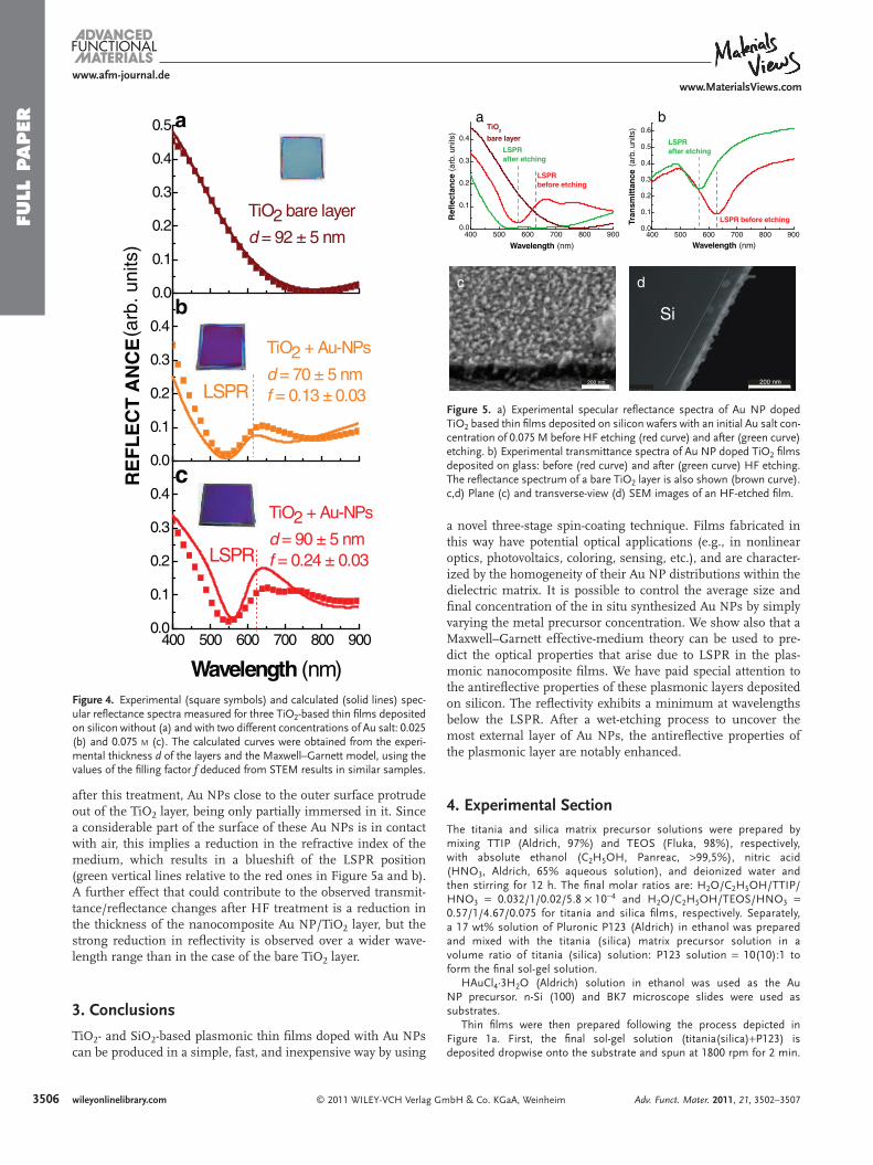
The most important effect associated with the presence of Au NPs is observed in the refl ectivity spectra in the spectral region of their LSPR (see Figure 4 b and c). The LSPR spectral positions, determined by transmit-tance measurements, are shown as ver-tical lines in Figure 4 . The corresponding minima (dips) are blueshifted relative to the LSPR positions, and the shift increases with fi lling factor f . This is a result of the inter-play between the LSPR effect (change in the refractive index of the composite depicted in Figure S1a in the Supporting Informa-tion) and light interference in a thin fi lm, as accounted for by the simulations (see Figure S1c in the Supporting Information). It should be noted that, in general, there is good agreement between the experimental and calculated data shown in Figure 4 . The best (practically ideal) agreement is observed
for the bare TiO 2 layer (Figure 4 a). After TiO 2 fi lm doping with Au NPs, both experiments and calculations show that the refl ectance decreases from the short-wavelength side of the LSPR position and increases from the long-wavelength side. Also, for the case where f = 0.24 (0.075 M HAuCl 4 ) the calcu-lated refl ectance is higher than for f = 0.13 for almost the entire spectrum and, for some spectral regions, higher than for the bare TiO 2 layer. This implies that, at high concentrations, light backscattering by the Au NPs increases, and thus also does the total specular refl ection, even relative to bare TiO 2 fi lm, except for the spectral region around the dip (which is located around 550 nm in case of f = 0.24), which is formed due to refractive-index changes around the LSPR position of the material (see the Supporting Information).
A further observation is that for the Au–TiO 2 layer with the lowest fi lling factor ( f = 0.13), the experimental refl ectivity curve is higher than the calculated one, whereas for the case of f = 0.24, the experimental refl ectivity curve is signifi cantly lower than the calculated one. This is because bigger Au NPs are formed in the case of f = 0.24 and the composite surface roughness is higher. This results in enhanced diffuse (lateral) light scattering, which does not contribute to specular refl ect-ance. Note that if such Au NP doped fi lm were deposited on a silicon surface, its roughness would play a role similar to that of silicon texturing, which is produced to increase light trap-ping in standard silicon solar cells.
The antirefl ective effect of the nanocomposite coatings depos-ited on silicon can be further improved by treating the coating surface with dilute HF, as described in the Experimental Sec-tion. Figure 5 a shows the specular refl ectivity spectra of an Au NP doped TiO 2 fi lm prepared with 0.075 M concentration of the HAuCl 4 , measured before and after additional treatment with dilute ( < 0.001 M ) HF. An appreciable blueshift is observed in the refl ectivity dip of the treated sample relative to the untreated one, while the overall refl ectance drops considerably, enhancing the antirefl ection behavior of the nanocomposite layer. In Figure 5 b, transmittance spectra of nanocomposite fi lms pre-pared in the same manner deposited over glass are shown both before and after HF etching. As can be seen in Figure 5 c and d,
a nanocomposite thin fi lm is deposited onto the surface of a silicon solar cell, the scattering of light by NPs embedded in a fi lm near the surface of the silicon should lead to increased light absorption in silicon.
The use of TiO 2 layers on silicon solar cells as antirefl ective coatings with # /4 thickness to minimize refl ectivity in the near IR is well known. [ 41 ] In view of this our next task is to study the effects of LSPR on the refl ectivity of Au–TiO 2 fi lms deposited on silicon, or in other words, to investigate how the presence of plasmonic NPs modifi es the antirefl ection properties of TiO 2 layers.
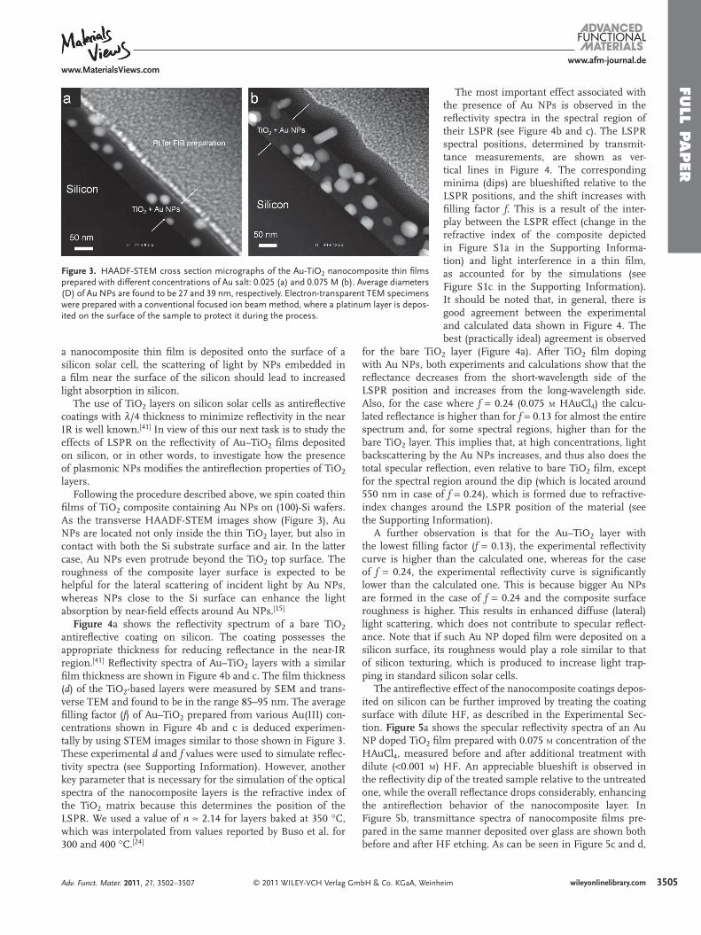
Following the procedure described above, we spin coated thin fi lms of TiO 2 composite containing Au NPs on (100)-Si wafers. As the transverse HAADF-STEM images show (Figure 3 ), Au NPs are located not only inside the thin TiO 2 layer, but also in contact with both the Si substrate surface and air. In the latter case, Au NPs even protrude beyond the TiO 2 top surface. The roughness of the composite layer surface is expected to be helpful for the lateral scattering of incident light by Au NPs, whereas NPs close to the Si surface can enhance the light absorption by near-fi eld effects around Au NPs. [ 15 ]
Figure 4 a shows the refl ectivity spectrum of a bare TiO 2 antirefl ective coating on silicon. The coating possesses the appropriate thickness for reducing refl ectance in the near-IR region. [ 41 ] Refl ectivity spectra of Au–TiO 2 layers with a similar fi lm thickness are shown in Figure 4 b and c. The fi lm thickness ( d ) of the TiO 2 -based layers were measured by SEM and trans-verse TEM and found to be in the range 85–95 nm. The average fi lling factor ( f ) of Au–TiO 2 prepared from various Au(III) con-centrations shown in Figure 4 b and c is deduced experimen-tally by using STEM images similar to those shown in Figure 3 . These experimental d and f values were used to simulate refl ec-tivity spectra (see Supporting Information). However, another key parameter that is necessary for the simulation of the optical spectra of the nanocomposite layers is the refractive index of the TiO 2 matrix because this determines the position of the LSPR. We used a value of n " 2.14 for layers baked at 350 ° C, which was interpolated from values reported by Buso et al. for 300 and 400 ° C. [ 24 ]
Figure 3 . HAADF-STEM cross section micrographs of the Au-TiO 2 nanocomposite thin fi lms prepared with different concentrations of Au salt: 0.025 (a) and 0.075 M (b). Average diameters (D) of Au NPs are found to be 27 and 39 nm, respectively. Electron-transparent TEM specimens were prepared with a conventional focused ion beam method, where a platinum layer is depos-ited on the surface of the sample to protect it during the process.
FULL
PAPER
© 2011 WILEY-VCH Verlag GmbH & Co. KGaA, Weinheim3506
www.afm-journal.dewww.MaterialsViews.com
wileyonlinelibrary.com Adv. Funct. Mater. 2011, 21, 3502–3507
after this treatment, Au NPs close to the outer surface protrude out of the TiO 2 layer, being only partially immersed in it. Since a considerable part of the surface of these Au NPs is in contact with air, this implies a reduction in the refractive index of the medium, which results in a blueshift of the LSPR position (green vertical lines relative to the red ones in Figure 5 a and b). A further effect that could contribute to the observed transmit-tance/refl ectance changes after HF treatment is a reduction in the thickness of the nanocomposite Au NP/TiO 2 layer, but the strong reduction in refl ectivity is observed over a wider wave-length range than in the case of the bare TiO 2 layer.
3. Conclusions TiO 2 - and SiO 2 -based plasmonic thin fi lms doped with Au NPs can be produced in a simple, fast, and inexpensive way by using
a novel three-stage spin-coating technique. Films fabricated in this way have potential optical applications (e.g., in nonlinear optics, photovoltaics, coloring, sensing, etc.), and are character-ized by the homogeneity of their Au NP distributions within the dielectric matrix. It is possible to control the average size and fi nal concentration of the in situ synthesized Au NPs by simply varying the metal precursor concentration. We show also that a Maxwell–Garnett effective-medium theory can be used to pre-dict the optical properties that arise due to LSPR in the plas-monic nanocomposite fi lms. We have paid special attention to the antirefl ective properties of these plasmonic layers deposited on silicon. The refl ectivity exhibits a minimum at wavelengths below the LSPR. After a wet-etching process to uncover the most external layer of Au NPs, the antirefl ective properties of the plasmonic layer are notably enhanced.
4. Experimental Section The titania and silica matrix precursor solutions were prepared by mixing TTIP (Aldrich, 97%) and TEOS (Fluka, 98%), respectively, with absolute ethanol (C 2 H 5 OH, Panreac, > 99,5%), nitric acid (HNO 3 , Aldrich, 65% aqueous solution), and deionized water and then stirring for 12 h. The fi nal molar ratios are: H 2 O/C 2 H 5 OH/TTIP/HNO 3 = 0.032/1/0.02/5.8 ! 10 ! 4 and H 2 O/C 2 H 5 OH/TEOS/HNO 3 = 0.57/1/4.67/0.075 for titania and silica fi lms, respectively. Separately, a 17 wt% solution of Pluronic P123 (Aldrich) in ethanol was prepared and mixed with the titania (silica) matrix precursor solution in a volume ratio of titania (silica) solution: P123 solution = 10(10):1 to form the fi nal sol-gel solution.
HAuCl 4 · 3H 2 O (Aldrich) solution in ethanol was used as the Au NP precursor. n-Si (100) and BK7 microscope slides were used as substrates.
Thin fi lms were then prepared following the process depicted in Figure 1 a. First, the fi nal sol-gel solution (titania(silica) + P123) is deposited dropwise onto the substrate and spun at 1800 rpm for 2 min.
Figure 4 . Experimental (square symbols) and calculated (solid lines) spec-ular refl ectance spectra measured for three TiO 2 -based thin fi lms deposited on silicon without (a) and with two different concentrations of Au salt: 0.025 (b) and 0.075 M (c). The calculated curves were obtained from the experi-mental thickness d of the layers and the Maxwell–Garnett model, using the values of the fi lling factor f deduced from STEM results in similar samples.
0.0
0.1
0.2
0.3
0.4
0.5
0 2
0.3
0.4
TiO2 bare layer
d = 92 ± 5 nm
a
LSPR
TiO2 + Au-NPs
d = 70 ± 5 nmf 0 13 0 03
b
(ar
b. u
nits
)
0.0
0.1
0.2
400 500 600 700 800 9000.0
0.1
0.2
0.3
0.4
LSPR
LSPR f = 0.13 ± 0.03
RE
FLE
CT
AN
CE
TiO2 + Au-NPs
d = 90 ± 5 nmf = 0.24 ± 0.03
c
Wavelength (nm)
Figure 5 . a) Experimental specular refl ectance spectra of Au NP doped TiO 2 based thin fi lms deposited on silicon wafers with an initial Au salt con-centration of 0.075 M before HF etching (red curve) and after (green curve) etching. b) Experimental transmittance spectra of Au NP doped TiO 2 fi lms deposited on glass: before (red curve) and after (green curve) HF etching. The refl ectance spectrum of a bare TiO 2 layer is also shown (brown curve). c,d) Plane (c) and transverse-view (d) SEM images of an HF-etched fi lm.
400 500 600 700 800 9000.0
0.1
0.2
0.3
0.4
0.5
0.6
LSPR after etching
LSPR before etching
Wavelength (nm)
Tran
smitt
ance
(arb
. uni
ts)
b
200 nm 200 nm
Si
dc
400 500 600 700 800 9000.0
0.1
0.2
0.3
0.4TiO
2
bare layerLSPR after etching
LSPR before etching
a
Ref
lect
ance
(ar
b. u
nits
)
Wavelength (nm)

FULL PA
PER
© 2011 WILEY-VCH Verlag GmbH & Co. KGaA, Weinheim 3507
www.afm-journal.dewww.MaterialsViews.com
wileyonlinelibrary.comAdv. Funct. Mater. 2011, 21, 3502–3507
Then, the rotation is stopped and 40 µ L of the Au NPs precursor is added dropwise. The sample is spun again at 1800 rpm for 1 min. Finally, the sample is baked directly on a hot plate at 350 ° C. The entire process is carried out under ambient conditions.
For the etching treatment of TiO 2 /Au NPs thin fi lms, a 0.2 ‰ solution of HF (Fluka, 40%) in water was heated in a bain-marie at 40 ° C. The thin fi lms were immersed in the HF solution under constant agitation for 1 min, and were then washed with deionized water.
For the absorption measurements shown in Figure 2 , a UV–vis–near IR spectrophotometer (UV-2501PC, Shimadzu) was employed. Transmittance and specular refl ectance spectra (Figures 4 and 5 a and b) were measured using a NanoCalc Refl ectometer (Ocean Optics).
To determine the size and shape of the Au NPs, the samples were prepared with a dual-beam FEI Quanta 200 3D FIB instrument following a conventional TEM specimen-preparation method. HRTEM and HAADF-STEM images were taken with a JEOL 2010F working at 200 kV.
Average diameters of Au NPs were determined as the maximum positions of their size distributions calculated by analysis of the micrographs.
Supporting Information Supporting Information is available from the Wiley Online Library or from the author.
Acknowledgements This work was supported through JAE-Predoc grant (CSIC), the Spanish MCINN and Generalitat Valenciana projects Grant Nos. TEC-2008-06756-C03-03 and PROMETEO/2009/074, and FP7 NMP-246331 project NanoPV.
Received: May 7, 2011 Published online: July 29, 2011
[ 1 ] G. Walters , I. P. Parkin , J. Mater. Chem. 2009 , 19 , 574 . [ 2 ] G. V. Ramesh , S. Porel , T. P. Radhakrishnan , Chem. Soc. Rev. 2009 ,
38 , 2646 . [ 3 ] R. Abargues , K. Abderrafi , E. Pedrueza , R. Gradess , J. Marques-Hueso ,
J. L. Valdes , J. P. Martiınez-Pastor , New J. Chem. 2009 , 33 , 1720 . [ 4 ] R. Abargues , J. Marques-Hueso , J. Canet-Ferrer , E. Pedrueza ,
J. L. Valdes , E. Jimenez , J. P. Martinez-Pastor , Nanotechnology 2008 , 19 , 355308 .
[ 5 ] S. K. Medda , S. De , G. De , J. Mater. Chem. 2005 , 15 , 3278 . [ 6 ] H. B. Liao , R. F. Xiao , H. Wang , K. S. Wong , G. K. L. Wong , Appl.
Phys. Lett. 1998 , 72 , 1817 . [ 7 ] F. Cui , Z. Hua , Q. He , J. Li , L. Guo , X. Cui , P. Jiang , C. Wei ,
W. Huang , W. Bu , J. Shi , J. Opt. Soc. Am. B 2009 , 26 , 107 . [ 8 ] C. Zhang , Y. Liu , G. You , B. Li , J. Shi , S. Qian , Physica B 2005 , 357 , 334 . [ 9 ] V. Idakiev , T. Tabakova , Z.-Y. Yuan , B.-L. Su , Appl. Catal. A–Gen.
2004 , 270 , 135 . [ 10 ] E. V. Rebrov , A. Berenguer-Murcia , B. F. G. Johnson , J. C. Schouten ,
Catalysis Today 2008 , 138 , 210 .
[ 11 ] X. D. Hoa , A. G. Kirk , M. Tabrizian , Biosens. Bioelectron. 2007 , 23 , 151 .
[ 12 ] D. Buso , M. Post , C. Cantalini , P. Mulvaney , A. Martucci , Adv. Funct. Mater. 2008 , 18 , 3843 .
[ 13 ] R. Gradess , R. Abargues , A. Habbou , J. Canet-Ferrer , E. Pedrueza , A. Russell , J. L. Valdes , J. P. Martinez-Pastor , J. Mater. Chem. 2009 , 19 , 9233 .
[ 14 ] J. Marques-Hueso , R. Abargues , J. L. Valdes , J. P. Martinez-Pastor , J. Mater. Chem. 2010 , 20 , 7436 .
[ 15 ] H. A. Atwater , A. Polman , Nat. Mater. 2010 , 9 , 205 and references therein.
[ 16 ] V. E. Ferry , J. N. Munday , H. A. Atwater , Adv. Mater. 2010 , 22 , 4794 . [ 17 ] S. Pillai , K. R. Catchpole , T. Trupke , M. A. Green , J. Appl. Phys. 2007 ,
101 , 093105 . [ 18 ] K. Nakayama , K. Tanabe , H. A. Atwater , Appl. Phys. Lett. 2008 , 93 ,
121904 . [ 19 ] M. D. Perez , E. Otal , S. A. Bilmes , G. J. A. A. Soler-Illia ,
E. L. Crepaldi , D. Grosso , C. Sanchez , Langmuir 2004 , 20 , 6879 . [ 20 ] J. C. Yu , X.-C. Wang , L. Wu , W.-K. Ho , L.-Z. Zhang , G.-T. Zhou , Adv.
Funct. Mater. 2004 , 14 , 1178 . [ 21 ] J. Song , U. Lee , H. Lee , M. Suh , Y. Kwon , Thin Solid Films 2009 , 517 ,
5705 . [ 22 ] L. Armelao , D. Barreca , G. Bottaro , A. Gasparotto , E. Tondello ,
M. Ferroni , S. Polizzi , Chem. Mater. 2004 , 16 , 3331 . [ 23 ] Y. Zhang , A. H. Yuwono , J. Li , J. Wag , Microporous Mesoporous Mater.
2008 , 110 , 242 . [ 24 ] D. Buso , J. Pacifi co , A. Martucci , P. Mulvaney , Adv. Funct. Mater.
2007 , 17 , 347 . [ 25 ] D. E. Bornside , C. W. Macosko , L. E. Scriven , J. Imaging Technol.
1987 , 13 , 122 . [ 26 ] Y. Tai , M. Watanabe , J. Murakami , K. Tajiri , J. Mater. Sci. 2007 , 42 ,
1285 . [ 27 ] J. W. M. Chon , C. Bullen , P. Zijlstra , M. Gu , Adv. Funct. Mater. 2007 ,
17 , 875 . [ 28 ] M. Wark , J. Tschirch , O. Bartels , D. Bahnemann , J. Rathousky , Micro-
porous Mesoporous Mater. 2005 , 84 , 247 . [ 29 ] S. De , G. De , J. Mater. Chem. 2006 , 16 , 3193 . [ 30 ] D. Kannaiyan , M.-A. Cha , Y. H. Jang , B.-H. Sohn , J. Nuh , C. Park ,
D. H. Kim , New J. Chem. 2009 , 33 , 2431 . [ 31 ] T. Ung , L. M. Liz-Marzan , P. Mulvaney , Coll. Surf. A 2002 , 202 , 119 . [ 32 ] T. Ung , L. M. Liz-Marzan , P. Mulvaney , J. Phys. Chem. B 2001 , 105 ,
3441 . [ 33 ] M. Kumar , G. B. Reddy , Phys. Stat. Sol. B 2009 , 246 , 2232 . [ 34 ] S. De , G. De , J. Phys. Chem. C 2008 , 112 , 10378 . [ 35 ] Yu. A. Akimov , K. Ostrikov , E. P. Li , Plasmonics 2009 , 4 , 107 . [ 36 ] Yu. A. Akimov , W. S. Koh , K. Ostrikov , Optics Express 2009 , 17 ,
10195 . [ 37 ] A. Warshawsky , R. Kalir , A. Deshe , H. Berkovitz , A. Patchornik , J.
Am. Chem. Soc. 1979 , 101 , 4249 . [ 38 ] T. Sakai , P. Alexandridis , J. Phys. Chem. B 2005 , 109 , 7766 . [ 39 ] W. Wong-Ng , H. F. McMurdie , C. R. Hubbard , A. D. Mighell , J. Res.
Natl. Inst. Stand. Technol. 2001 , 106 , 1013 . [ 40 ] E. György , G. Sauthier , A. Figueras , A. Giannoudakos , M. Kompitsas ,
I. N. Mihailescu , J. Appl. Phys. 2006 , 100 , 114302 . [ 41 ] B. S. Richards , Prog. Photovolt: Res. Appl. 2004 , 12 , 253 .