Volume calculation of subsurface structures and traps in ...

This content has been downloaded from IOPscience. Please scroll down to see the full text.
Download details:
IP Address: 129.6.134.63
This content was downloaded on 04/02/2015 at 15:45
Please note that terms and conditions apply.
New insights into subsurface imaging of carbon nanotubes in polymer composites via
scanning electron microscopy
View the table of contents for this issue, or go to the journal homepage for more
2015 Nanotechnology 26 085703
(http://iopscience.iop.org/0957-4484/26/8/085703)
Home Search Collections Journals About Contact us My IOPscience

New insights into subsurface imaging ofcarbon nanotubes in polymer compositesvia scanning electron microscopy
Minhua Zhao1,7, Bin Ming2, Jae-Woo Kim4, Luke J Gibbons6, Xiaohong Gu3,Tinh Nguyen3, Cheol Park4,5, Peter T Lillehei4, J S Villarrubia2,András E Vladár2 and J Alexander Liddle1
1Center for Nanoscale Science and Technology, National Institute of Standards and Technology,Gaithersburg, USA2 Physical Measurement Lab, National Institute of Standards and Technology, Gaithersburg, USA3Engineering Lab, National Institute of Standards and Technology, Gaithersburg, USA4NASA Langley Research Center, Hampton, USA5Department of Mechanical and Aerospace Engineering, University of Virginia, Charlottesville, USA6Department of Materials Science and Engineering, Virginia Polytechnic Institute and State University,Blacksburg, USA7University of Maryland, Department of Materials Science and Engineering, College Park, USA
E-mail: [email protected] and [email protected]
Received 8 November 2014, revised 30 December 2014Accepted for publication 13 January 2015Published 4 February 2015
AbstractDespite many studies of subsurface imaging of carbon nanotube (CNT)-polymer composites viascanning electron microscopy (SEM), significant controversy exists concerning the imagingdepth and contrast mechanisms. We studied CNT-polyimide composites and, by three-dimensional reconstructions of captured stereo-pair images, determined that the maximum SEMimaging depth was typically hundreds of nanometers. The contrast mechanisms wereinvestigated over a broad range of beam accelerating voltages from 0.3 to 30 kV, and ascribed tomodulation by embedded CNTs of the effective secondary electron (SE) emission yield at thepolymer surface. This modulation of the SE yield is due to non-uniform surface potentialdistribution resulting from current flows due to leakage and electron beam induced current. Theimportance of an external electric field on SEM subsurface imaging was also demonstrated. Theinsights gained from this study can be generally applied to SEM nondestructive subsurfaceimaging of conducting nanostructures embedded in dielectric matrices such as graphene-polymercomposites, silicon-based single electron transistors, high resolution SEM overlay metrology ore-beam lithography, and have significant implications in nanotechnology.
S Online supplementary data available from stacks.iop.org/NANO/26/085703/mmedia
Keywords: scanning electron microscopy, subsurface imaging, carbon nanotube polymercomposites
(Some figures may appear in colour only in the online journal)
1. Introduction
With the increasing deployment of nanocomposite materials,whose properties depend on the state of dispersion of thereinforcing nanomaterial, there is a growing need for high-
resolution subsurface imaging methods that can capture thethree-dimensional (3D) material morphology. For example,understanding the dispersion of carbon nanotubes (CNTs) in apolymer matrix is critical for constructing the process-struc-ture-properties relationships that enable the rational
Nanotechnology
Nanotechnology 26 (2015) 085703 (12pp) doi:10.1088/0957-4484/26/8/085703
0957-4484/15/085703+12$33.00 © 2015 IOP Publishing Ltd Printed in the UK1

improvement of CNT-nanocomposite performance. Electricforce microscopy (EFM), a special type of scanning probemicroscopy (SPM) based on long-range electrostatic interac-tions between a probe and a sample, has been used for sub-surface imaging of CNTs dispersed in polymer composites[1–3]. However, the analysis of the results from this techniquerequires considerable care if quantitative information is to beextracted.
While typically considered to be a surface characteriza-tion technique, scanning electron microscopy (SEM) has alsobeen applied to provide a quantitative assessment of CNTdispersion in a polymer matrix [4]. Interestingly, an imagingdepth up to 1000 nm was calculated using geometric relationsunder different stage tilting angles [4]. While it was generallyagreed that the contrast of subsurface CNTs originated fromvariations in secondary electron (SE) yield due to chargecontrast [4–17], direct SE emission from nanotubes muchbeyond a few 10 nm depth should not be detectable due to theshallow escape depth of SEs [18]. In general, the depth atwhich CNTs can be imaged by SEM in polymer composites isstill a controversial topic, with estimates ranging from lessthan 50 nm [5], to hundreds of nanometers [6] or severalmicrometers [7]. In addition, the reason the contrast of CNTsembedded in polymer composites varies with the primaryelectron beam accelerating voltage is not well understood.SEM contrast here refers to the intensity difference of col-lected SE imaging signals, which is determined by both SEgeneration and collection conditions. The contrast formed byCNTs on insulator surfaces has been ascribed to electronbeam induced current (EBIC) [19, 20] or local potential dif-ferences [21]. There are only a few studies of SEM subsurfaceimaging of CNTs in a polymer matrix based on charge-con-trast imaging [4–7, 15–17]. Loos et al [7] tried to relate thecontrast of CNTs with the depth they were located in com-posites: bright CNTs were closer to the surface than thoseappeared dark, while no quantitative measurement of CNTdepth was attempted. Recently, Li et al [6, 17] did anextensive study on the imaging mechanism, examining theeffect of depth and accelerating beam voltages on the visi-bility of CNTs in an epoxy matrix by SEM. They proposedthat more electrons were trapped at the CNT–epoxy interfaceat high beam voltage resulting in enhanced SE emission at theCNT/epoxy interface which was responsible for the brightcontrast of embedded CNTs, while the dark contrast of CNTsat low beam accelerating voltage was ascribed to lower SEemission at the interface than that of epoxy. On the otherhand, Zhang et al reported SEM subsurface imaging ofconductors embedded in an insulating film by a non-pene-trating low-energy electron beam [13]. The contrast ofembedded structures was attributed to the different SErecapture rate under the surface local electric field, whichreturns more SE to the surface when the local potential is highthan when it is low. Hence, the effect of the SE collectionprocess, such as the SE recapture process during SEM scan-ning, could be important for the interpretation of CNTscontrast, while it was not taken into consideration by Li et al[6, 17]. In summary, some open questions remain for SEMsubsurface imaging of CNTs, including: (i) Does the signal of
subsurface CNTs originate from SEs emitted by the CNTsthemselves or from the near-surface polymer matrix? (ii)Does the electron beam have to reach a given CNT for sub-surface imaging? (iii) What is the maximum SEM imagingdepth for CNT polymer composites? (iv) What is the role ofSE recapture process for SEM subsurface imaging? The mainpurpose of the present work is to clarify these issues and helpestablish SEM subsurface imaging as a useful and facilemethod to provide quantitative information on nanocompositemicrostructure. We present the results obtained by SEMsubsurface imaging of CNTs embedded in polyimide com-posites using beam accelerating voltages in the range of0.3–30 kV. While the CNT contrast is not only dependent onbeam accelerating voltage, but also varies with beam currentand dwell time per pixel, as defined by scanning speed andscanning area [12]. An exhaustive discussion of the effects ofall these parameters is beyond the scope of this work. Here wewill focus on the effect of beam accelerating voltage on theCNT contrast. The SEM subsurface imaging depth is deter-mined by 3D reconstruction of captured stereo-pair images.The influence on subsurface imaging of a polymer-rich layernear the composite surface, revealed by cross-sectional SEMimaging, is discussed. The effect of an external electric fieldon the SEM contrast of CNT polymer composites is alsostudied.
2. Experiments8
Single-wall carbon nanotube (SWCNT)-polyimide nano-composite films were prepared by in situ polymerization asdescribed previously [22]. Two types of SWCNTs wereincorporated into the composites: purified laser-ablated (LA)and high-pressure carbon monoxide decomposition (HiPco)SWCNTs. The polymer matrix was an electroactive poly-imide, 2,6-bis(3-aminophenoxy) benzonitrile/4,4-oxy-diphthalic anhydride ((β-CN)APB/ODPA). As-receivedanhydrous dimethyl formamide was used as a solvent. Aseries of SWCNT-polyimide nanocomposite films withSWCNT concentrations at mass fractions of (0, 0.05, 0.2, 0.5,2 and 10)% were prepared as follows. The SWCNT-poly(amic acid) solution was cast onto a glass plate and dehy-drated in a dry air-flowing chamber. Subsequently, the driedtack-free film was thermally imidized in a nitrogen-circulatingoven to obtain a solvent-free SWCNT-polyimide film havinga thickness between 25 and 65 μm. After removing the filmsfrom the glass plates, the smoother interface side (glass–filminterface) was used for EFM and SEM imaging. This side ofthe film usually displayed a thin surface layer containing fewCNTs due to the wall depletion effect [23].
The details of the EFM setup for subsurface imaging ofCNTs in polymer films has been described previously [1].
8 Certain commercial equipment, instruments, or materials are identified inthis paper to foster understanding. Such identification does not implyrecommendation or endorsement by the National Institute of Standards andTechnology or the National Aeronautics and Space Administration, nor doesit imply that thematerials or equipment identified are necessarily the bestavailable for the purpose.
2
Nanotechnology 26 (2015) 085703 M Zhao et al

Briefly, it is based on a two-pass scanning technique. Duringthe first pass, the topographic image is acquired in normaltapping mode using an atomic force microscope (AFM). Thesecond pass takes place with the conductive AFM proberaised above the sample to a fixed distance. The sample is re-scanned with a bias voltage applied between the probe andAFM stage, following the previously-recorded topography tomaintain a constant tip–sample separation. The dc bias vol-tage applied to the AFM probes ranged from −12 to +12 Vand the sample surface-to-tip distance was maintained at20 nm. Simultaneously, an ac bias voltage was applied to theAFM stage at the same frequency used to drive the AFMcantilever with a peak-to-peak amplitude of 2 V. The EFMimaging was carried out at low humidity (<5% relativehumidity) using the NIST-patented [24] environmentalchamber that was custom-designed and fabricated for theAFM. Both the amplitude and phase of the probe during thesecond pass were recorded as EFM signals.
The SEM study was conducted using a FEI HeliosNanolab 600 focused ion beam (FIB)–SEM system. Thecomposite film was attached to the aluminum sample stub
using conductive carbon tape. No additional sample treat-ment, such as coating with a conductive layer, was used. Thebeam accelerating voltage was varied between 0.3 and 30 kV,while the beam current was maintained at 43 pA. 3D SEMimages were generated by taking stereo pairs at stage tiltingangles of −5° and +5° using 3D reconstruction softwareScandium (Soft Imaging System GmbH, Version 5.0, Build1120). The sample was kept at the eucentric tilting positionfor a 4 mm working distance. A through-lens detector, situ-ated inside the electron optical column, was used to collectthe SE with high efficiency (supplemental figure S1 for proofof SE dominated CNT signal), while excluding most of thebackscattered electrons signals. The SEM images had 1024pixels and 768 pixels in the horizontal and vertical directions,respectively. Unless otherwise noted, a beam dwell time of40 μs was used for each image pixel, while the sample currentduring scanning was recorded simultaneously using apicoammeter. The average values obtained for full-framescanning were reported. Rectangular cross-sections on theCNT-polyimide nanocomposite were produced using FIB bythe staircase method at a gallium (Ga) beam current of 97 pA.
Figure 1. EFM and SEM subsurface imaging at the same location of 0.5% SWCNT(LA)-PI composite. All the fields of view are 10 μm. (a)SPM height image, 50 nm full height scale. (b) EFM phase image, −3 V bias, 20° full phase scale. (c) SEM image at 15 kV beam acceleratingvoltage (d) SEM image at 1 kV beam accelerating voltage.
3
Nanotechnology 26 (2015) 085703 M Zhao et al

The dwell time for each pixel was 1 μs. After FIB milling, thecross-sections were examined in SE mode at 52° tilting angle.Monte Carlo simulation of the electron interaction volume inpolyimide (C22H10N2O5) at various beam voltage was con-ducted using open-source software Casino(v242) [25]. Thenumber of electrons was set to 10 750, equal to the experi-mental electron dose per pixel (43 pA and 40 μs beam dwelltime). The beam radius was set to 1 nm according to the SEMspecification.
3. Results and discussions
3.1. Demonstration of SEM subsurface imaging of CNTsdispersed in a polymer composite
Figure 1 shows EFM and SEM subsurface images of CNT-polyimide composites taken at the same location, relative tothe ‘X’ shaped scratch on the surface as a location mark.While the conventional SPM height image (figure 1(a)) didnot show subsurface CNTs, both EFM (figure 1(b)) and SEM(figures 1(c)–(d)) revealed CNTs under the surface. Increas-ing the SEM acceleration voltage from 1 (figure 1(d)) to15 kV (figure 1(c)), made more subsurface CNTs visible. Inaddition, the contrast of the CNTs inverted, going from darkto bright. Furthermore, it is important to note that the ‘X’mark is still visible in the EFM image (figure 1(b)), while it isnot visible (figure 1(c)) or hardly visible (figure 1(d)) in theSEM images. This indicates that the contrast of the SEMimages is mainly dominated by subsurface features ratherthan surface topography. Furthermore, the features of sub-surface CNTs revealed by EFM (figure 1(b)) and 1 kV SEM(figure 1(d)) is so similar that there could be a common
mechanism at play in both cases, in which the local surfacepotential or electric field may play an important role informing the image contrast during subsurface imaging. Thefollowing studies are carried out to verify this hypothesis aswell as to determine how far below the surface it is possible todetect CNTs using these techniques.
3.2. Effect of beam accelerating voltage on SEM subsurfaceimaging
The changing contrast of the CNTs with respect to accel-erating voltage is shown in figure 2. All the images wereacquired from the same location of SWCNT(LA)-PI film.More intense, broadened, dark CNT signals were apparentfrom 1 to 2 kV. Mixed contrast was observed at 4 and 6 kV,which was similar to the results reported by Loos et al [7]:some CNTs appeared bright, while the others appeared dark.The contrast of the CNTs inverted completely to bright at8 kV. However, one of the concerns regarding SEM imagingin the same location is the possibility for residual chargeaccumulation or other charging history related effects. Toaddress this issue, SEM subsurface imaging was performed ata new location for each beam accelerating voltage from 0.3 to28 kV presented in figure 3(a). Similar trends in image con-trast were observed when compared to imaging at the samelocation in figure 2. Specifically, CNT contrast as a functionof beam accelerating voltage can be divided into three regions(see supplemental figure S2 for full sets of images): (i) RegionI (0.3–0.5 kV): bright CNT contrast. (ii) Region II (0.6–4 kV):dark CNT contrast. (iii) Region III (>6 kV): bright CNTcontrast. Both dark and bright CNT contrast was observed forbeam voltage between 4 and 6 kV, which was ascribed to amixed condition of Regions II and III. Interestingly, three
Figure 2. SEM contrast and imaging depth changes at the same location of 0.5% SWCNT(LA)-PI film revealed by various beam voltages.Scale bar 2 μm.
4
Nanotechnology 26 (2015) 085703 M Zhao et al
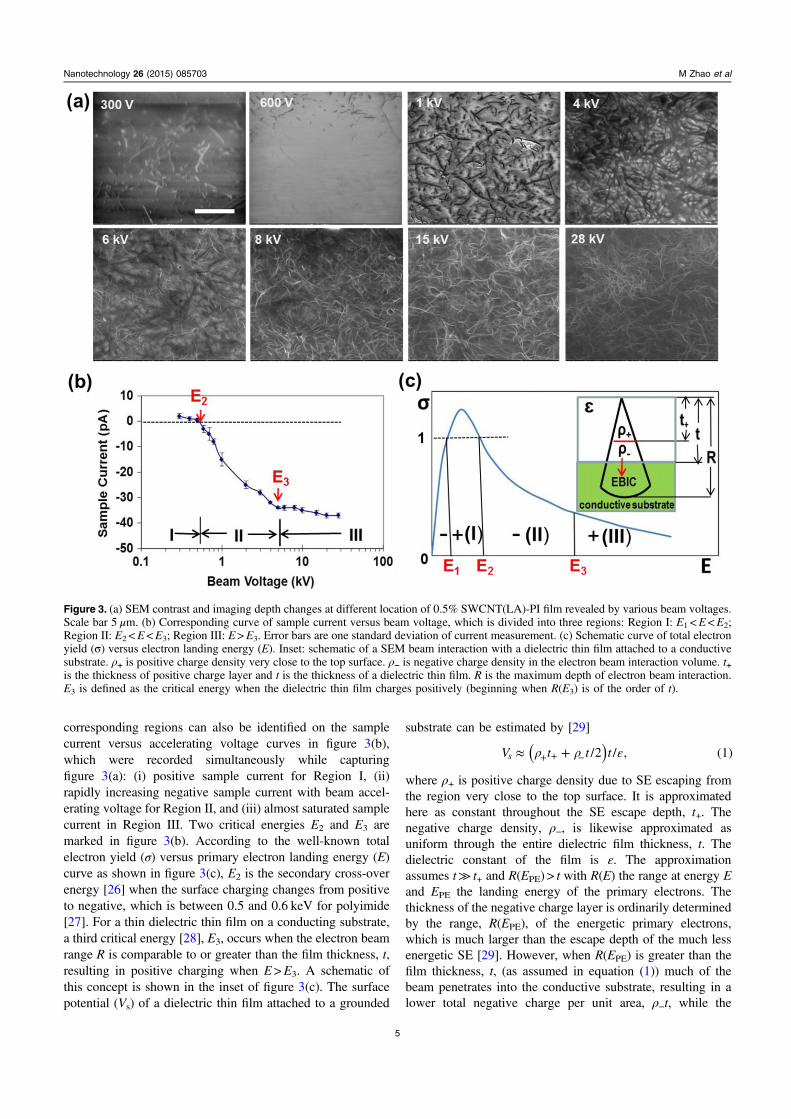
corresponding regions can also be identified on the samplecurrent versus accelerating voltage curves in figure 3(b),which were recorded simultaneously while capturingfigure 3(a): (i) positive sample current for Region I, (ii)rapidly increasing negative sample current with beam accel-erating voltage for Region II, and (iii) almost saturated samplecurrent in Region III. Two critical energies E2 and E3 aremarked in figure 3(b). According to the well-known totalelectron yield (σ) versus primary electron landing energy (E)curve as shown in figure 3(c), E2 is the secondary cross-overenergy [26] when the surface charging changes from positiveto negative, which is between 0.5 and 0.6 keV for polyimide[27]. For a thin dielectric thin film on a conducting substrate,a third critical energy [28], E3, occurs when the electron beamrange R is comparable to or greater than the film thickness, t,resulting in positive charging when E>E3. A schematic ofthis concept is shown in the inset of figure 3(c). The surfacepotential (Vs) of a dielectric thin film attached to a grounded
substrate can be estimated by [29]
ρ ρ ε≈ ++ + −( )V t t t/2 / , (1)s
where ρ+ is positive charge density due to SE escaping fromthe region very close to the top surface. It is approximatedhere as constant throughout the SE escape depth, t+. Thenegative charge density, ρ−, is likewise approximated asuniform through the entire dielectric film thickness, t. Thedielectric constant of the film is ε. The approximationassumes t≫ t+ and R(EPE) > t with R(E) the range at energy Eand EPE the landing energy of the primary electrons. Thethickness of the negative charge layer is ordinarily determinedby the range, R(EPE), of the energetic primary electrons,which is much larger than the escape depth of the much lessenergetic SE [29]. However, when R(EPE) is greater than thefilm thickness, t, (as assumed in equation (1)) much of thebeam penetrates into the conductive substrate, resulting in alower total negative charge per unit area, ρ−t, while the
Figure 3. (a) SEM contrast and imaging depth changes at different location of 0.5% SWCNT(LA)-PI film revealed by various beam voltages.Scale bar 5 μm. (b) Corresponding curve of sample current versus beam voltage, which is divided into three regions: Region I: E1 <E<E2;Region II: E2 <E<E3; Region III: E>E3. Error bars are one standard deviation of current measurement. (c) Schematic curve of total electronyield (σ) versus electron landing energy (E). Inset: schematic of a SEM beam interaction with a dielectric thin film attached to a conductivesubstrate. ρ+ is positive charge density very close to the top surface. ρ− is negative charge density in the electron beam interaction volume. t+is the thickness of positive charge layer and t is the thickness of a dielectric thin film. R is the maximum depth of electron beam interaction.E3 is defined as the critical energy when the dielectric thin film charges positively (beginning when R(E3) is of the order of t).
5
Nanotechnology 26 (2015) 085703 M Zhao et al

positive charge per unit area, ρ+t+, is little changed. Accord-ing to equation (1), when ρ−t gets small enough, eitherbecause the range gets large enough (making ρ− small) or thefilm thickness (t) gets small, there is a point at which Vs
becomes positive. In fact, such results have been reported byboth experiment [30] and simulation [31].
In the meantime, we observed a different E3 value foranother type of SWCNT (Hipco)-PI film as shown in figure 4.The SEM contrast became mixed at 10 kV and changed tofully bright contrast at around 15 kV (only selected SEMimages are shown in figure 4(a). The full sets of SEM imagesare included in supplemental figure S3). The overall pro-gression of image contrast variation, with the similar Regions(I, II and III), can be identified in the sample current versusbeam voltage curve shown in figure 4(b). So why is the E3
different for these two samples with the same polymer matrixand CNT loading? We can find the clues from the cross-sectional SEM images and Monte Carlo simulations. There isa polymer-rich layer very close to the surface for both 0.5%SWCNT(LA)-PI film and 0.5% SWCNT(Hipco)-PI film.
However, its thickness is only 200–300 nm for the former(figure 5(a1)), but 2–3 μm for the latter (figure 5(b1)). Hencemuch higher beam energy is needed for the electrons topenetrate the thicker polymer-rich layer and be dissipated bythe underlying dense, percolated CNT layer. In fact, themaximum electron beam range in polyimide derived from theMonte Carlo simulation is about 300 nm at 4 kV and 2 μm at10 kV respectively, which is a good match to both thethickness of polymer-rich layer and E3 value for the twosamples.
3.3. Estimation of imaging depth for SEM subsurface imaging
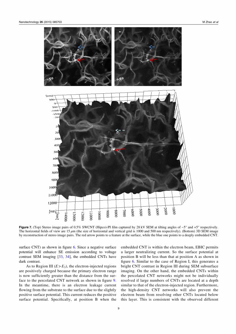
The maximum depth at which embedded CNTs can be dis-tinguished from the surrounding polymer matrix, referred toas the imaging depth, is specific to the sample properties andimaging conditions. The previously reported imaging depthwas derived indirectly by coating a known depth of polymeronto the surface of a CNT polymer composite [6]. Estimationof the imaging depth for a specific CNT nanocomposite basedon geometric relations has also been previously reported [4].In this study, the SEM imaging depth of SWCNTs embeddedin a polyimide matrix was determined by 3D graphs recon-structed from SEM images captured at different tilt angles.Figures 6 and 7 show 3D images of LA and HiPCO SWCNTsembedded in a polyimide matrix respectively. The red arrowspoint to features that had a very intense contrast and wereused as references for the film surfaces. The depth of LA–CNT marked by the blue arrow was measured to be258 nm± 28 nm in figure 6, while it was 728 nm± 56 nm forthe HiPco CNT in figure 7 (the uncertainty number wasestimated from the pixel size and tilting angle from the stereo-pair images). Therefore, the subsurface imaging depth ofSWCNTs embedded in a polyimide matrix is confirmed to beat least hundreds of nanometers, which is consistent with ourprevious results based on geometrical relations [4]. It was alsorevealed that the bundle size of LA–SWCNTs was muchsmaller than that of HiPco–SWCNTs, indicating a betterdispersion of LA–SWCNTs in the polyimide matrix. Thereason why a poorly dispersed sample will have a deeperimaging depth than a better dispersed sample can beaccounted for by referring to CNT dispersions in figure 5. Asshown in figure 5(a1), there are dense and uniform CNTnetworks located near the surface of the film for a betterdispersed sample, this will result in a more uniform surfacepotential, which prevents detection of the more deeplyembedded CNTs.
3.4. Insight of SEM subsurface imaging from FIB cross-sectional measurements
Cross-sectional measurements made on FIB-milled samplesgenerated surprising results. The two interesting points shownin figure 8 were that (i) there were no embedded CNTsobservable at the cross-section cut by the Ga-ion FIB; even atthe side wall; (ii) there was an oval-shaped ring structure withbright contrast surrounding the rectangular FIB cut, underwhich few embedded CNTs were revealed. Both findings can
Figure 4. (a) Selected SEM images at different location of 0.5%SWCNT(Hipco)-PI film revealed by various beam voltages. Scalebar 5 μm. (b) Corresponding curve of sample current versus beamvoltage, which is divided into three regions: Region I: E1 <E<E2;Region II: E2 <E<E3; Region III: E>E3. Error bars are one standarddeviation of current measurement.
6
Nanotechnology 26 (2015) 085703 M Zhao et al

be accounted for if we hypothesize that Ga implantation leadsto locally uniform surface potentials. It is well known that Gaions are implanted into the surface during FIB processing[32]. Some of the Ga ions will also be scattered into thesurrounding areas. That is why an oval-shaped ring structurewas observed at the rectangular FIB cut. During FIB cross-section cutting, so many Ga ions were implanted that a con-ductive layer could form at the cross-section surface or nearbyarea, which would result in a uniform surface potential andthus prevent the observation of subsurface CNTs (see proof ofGa implantation in supplemental figure S4). We will show inthe next section that the observed subsurface imaging andcontrast reversals can be explained by a model in which thecontrast is due to modulation of the surface potential by thepresence or absence of subsurface CNTs. The disappearanceof contrast FIB cross-section results can also be explainedusing the same model.
3.5. Contrast mechanism of SEM subsurface imaging
Based on these observations, a simplified 1D model, sche-matically illustrated in figure 9, is used to account for the
CNT contrast change with respect to the SEM acceleratingvoltage.
In Region I (E1 <E <E2), the surface of the sample ispositively charged. Although the primary electrons may notreach the top layer of CNTs, the positively charged surfacecould attract electrons from the top layer CNTs or underlyinghigh-density CNT networks to the film surface through cur-rent leakage. By current leakage, we refer to the flow ofcharge in the insulator due to the very high (MVm−1) localelectric fields created by charge injection and build up in thematerial. Such leakage is consistent with the observed posi-tive sample current in figure 3(b). In particular, at the locationjust above the embedded CNTs (position B), the leakagecurrent effect is much stronger than in the polymer matrix(position A) due to the proximity of CNTs to the surface.These provide a low-resistance path for electrons. Hence, thepositive surface potential is lower at position B than atposition A, as sketched in figure 9. Since some of the SEs willbe attracted back to the surface by the positive surfacepotential as indicated by the recapture current (IRE) infigure 9, this results in a lower recapture current at position Bthan at position A. In the meantime, the detected SE signal
Figure 5. Thickness of polymer-rich layer for 0.5% SWCNT(LA)-PI films and 0.5% SWCNT(Hipco) film revealed by SEM cross-sectionalimaging of cryo-fractured surface (a1) 0.5% SWCNT (LA)-PI film. (b1) 0.5% SWCNT (Hipco)-PI film. Monte Carlo simulations of electronbeam interaction depths in polyimide and compared to the thickness of the polymer-rich layer in (a1) and (b1) respectively. The scale bar is100 nm for figures (a1)–(a4) and 1 μm for figures (b1)–(b4).
7
Nanotechnology 26 (2015) 085703 M Zhao et al

(IS) is given by
δ α= − = −I I I I (1 ), (2)S SE RE P
where ISE is the emitted SE signal at the polyimide surface, IPis the primary beam current, δ is the SE yield and α is the SErecapture rate. Since the SE yield δ will be little changed fromposition A to B due to their slight potential difference, thedetected SE signal IS will be stronger at position B becauseαB < αA. That is why embedded CNTs show positive contrastin Region I. The imaging contrast of subsurface CNTs arisesfrom the different SE recapture rate at the polyimide surfacedue to non-uniform positive surface potential at positions withand without subsurface CNTs.
In Region II (E2 <E<E3), the electron beam is non-penetrating since primary electrons do not have enoughenergy to reach the embedded conductive CNT networks. Theelectron-injected regions are negatively-charged in general,reversing the situation in Region I. Now electrons are theexcess charge, and it is these that will be conducted awayfrom the surface by the EBIC effect and current leakage asillustrated in figure 9, in agreement with the observed nega-tive sample current shown in figures 3(b) and 4(b). Negativecharges transporting between the electron-injected region andfilm substrate will be readily dissipated by near-surface CNTs(position B), causing a less negative surface potential atposition B than at position A (polymer matrix without near-
Figure 6. (Top) Stereo image pairs of 0.5% SWCNT(LA)-PI film captured by 28 kV SEM at tilting angles of −5° and +5° respectively. Thehorizontal fields of view are 10.6 μm (the size of horizontal and vertical grid is 500 and 100 nm respectively). (Bottom) 3D SEM image of0.5% SWCNT(LA)-PI film by reconstruction of stereo image pairs. The red arrow points to a CNT very close to the surface, while the blueone points to a deeply embedded CNT.
8
Nanotechnology 26 (2015) 085703 M Zhao et al
surface CNT) as shown in figure 6. Since a negative surfacepotential will enhance SE emission according to voltagecontrast SEM imaging [33, 34], the embedded CNTs havedark contrast.
As to Region III (E > E3), the electron-injected regionsare positively charged because the primary electron rangeis now sufficiently greater than the distance from the sur-face to the percolated CNT network as shown in figure 9.In the meantime, there is an electron leakage currentflowing from the substrate to the surface due to the slightlypositive surface potential. This current reduces the positivesurface potential. Specifically, at position B when the
embedded CNT is within the electron beam, EBIC permitsa larger neutralizing current. So the surface potential atposition B will be less than that at position A as shown infigure 6. Similar to the case of Region I, this generates abright CNT contrast in Region III during SEM subsurfaceimaging. On the other hand, the embedded CNTs withinthe percolated CNT networks might not be individuallyresolved if large numbers of CNTs are located at a depthsimilar to that of the electron-injected region. Furthermore,the high-density CNT networks will also prevent theelectron beam from resolving other CNTs located belowthis layer. This is consistent with the observed different
Figure 7. (Top) Stereo image pairs of 0.5% SWCNT (Hipco)-PI film captured by 28 kV SEM at tilting angles of −5° and +5° respectively.The horizontal fields of view are 15 μm (the size of horizontal and vertical grid is 1000 and 500 nm respectively). (Bottom) 3D SEM imageby reconstruction of stereo image pairs. The red arrow points to a feature at the surface, while the blue one points to a deeply embedded CNT.
9
Nanotechnology 26 (2015) 085703 M Zhao et al

imaging depths for the two CNT-polymer composites infigures 6 and 7.
Furthermore, the length and connectivity of CNTs mayalso play an important role in the above contrast mechanism.An isolated short CNT or a small group of connected CNTswith low capacitance would reach its steady-state charge on atime scale (i.e. charging time constant τ =RC) short comparedto the measurement (i.e. pixel dwell time). It would cease tobe a source or sink of charge capable of maintaining a surfacepotential differential during continuing e-beam exposure, so itwould not be visible. CNTs that are part of a large connectednetwork (e.g., connected to ground) can continuously conductthe charge required to maintain surface potential differences.This is partly manifested in figure 4(a): almost all thedetectable embedded CNTs are curved and look like parts ofround-shaped networks, which have larger capacitance andthus a longer time constant for charging. That is to say, not allCNTs located within the electron beam-sample interactionvolume may be visible due to their limited charging-timeconstant. Similar observations were reported by Nagase et al,[35] where it was found that only an embedded nanoscale Sipattern connected to a large area Si plate could be detected bySEM. Compared to the un-connected nanoscale Si pattern, theconnected one has much larger capacitance and thus a longertime constant for charging.
3.6. Effect of external electric field on SEM subsurface imagingof CNT-polymer composites
The effect of an external sample bias on the SEM contrast ofCNT-polymer composites is illustrated in figure 10. A dc biasfrom 2 to 6 V was applied to the SEM sample stage duringscanning. The results for a 2 kV accelerating voltage indicatedthat there was little change in the contrast or brightness withthe variation of bias, as shown in the top row of figure 10. Onthe other hand, image changes were more pronounced withincreasing sample bias at 8 kV accelerating voltage, as shownin the bottom row of figure 10. The average brightnessdecreased as the bias increased, but rather than uniformlydecreasing, the darker areas growed, engulfing an increasing
share of the image. This could be explained by consideringthe energy barrier between the sample and the detector. At0 V bias, the barrier varied, with electrons that escaped fromlocations with low potential energy (high surface potential)facing a higher barrier than those that escaped from regionswith higher potential energy (low surface potential). As dis-cussed above, this was what gave rise to the observed con-trast. When the substrate potential was raised by Vb, allelectrons must overcome an additional barrier, eVb. When thetotal barrier (due to the charging-induced surface variationplus the imposed sample bias) became large enough, none ofthe electrons would have enough energy to overcome thebarrier. Of course, those that originated from low potentialenergy regions (i.e., the darker parts of the image) reachedthis point first. Consequently, one expected the dark regionsto spread as observed in the bottom row of figure 10. In thisrow the landing energy was such that the sample chargedpositively. Escaping electrons already had a barrier to over-come, even before the additional barrier imposed by thesample bias. In the upper row, the landing energy was suchthat the surface potential was negative when there was noadditional imposed bias. Electrons that escaped the immediatevicinity of the surface accelerated away from the surface,arriving at the detector with excess energy. Addition of asmall positive bias initially reduced this excess energy, buthad no effect on electron recapture, because any excess wasenough to avoid recapture. This is why there is little or nochange in the upper row of figure 10. Changing the bias onsample holder is one way to change the extraction field. Ofcourse, the opposite change on the other electrode isequivalent (since only differences in potential are important).The important role of the external electric field on the SEMcontrast opens an opportunity to optimize charge-based SEMsubsurface imaging by tuning the external electric field.
4. Conclusions
Subsurface SEM imaging methods have been successfullyapplied to non-destructively characterize the dispersion ofSWCNTs embedded in polyimide composites. Contrast wasinvestigated over a broad range of beam accelerating voltagesfrom 0.3 to 30 kV and was ascribed to modulation of theeffective SE emission yield (taking into account SE recapture)at the polymer surface because of non-uniform surfacepotential. The non-uniform potential was due to varyingproximity to buried conducting CNTs, to which charge flowsthrough leakage or EBIC. Furthermore, the electron beammight only reveal part of the CNT networks within the beamrange. The maximum SEM subsurface imaging depth forCNT polymer composites is dependent on beam voltages andthe dispersion of CNTs in polymer, with greater imagingdepths for a given CNT loading in samples with poorer dis-persion. SEM subsurface imaging can also be tuned byapplying an external electric field. Finally, the application ofthese techniques is not limited to the subsurface imaging ofCNT-polymer composites. They are generally applicable toconducting nanostructures embedded in a dielectric matrix,
Figure 8. SEM cross-sectional observation of 0.5% LA–SWCNT/PIfilm after Ga FIB cutting. No subsurface CNTs are observed by SEMat FIB cut region observed from 52° tilting angle.
10
Nanotechnology 26 (2015) 085703 M Zhao et al

Figure 10. Stage bias effect on SEM contrast of 0.5% SWCNT(LA)-PI film at different beam accelerating voltages. Top row (a)–(c): 2 kVbeam accelerating voltage. Bottom row (d)–(f): 8 kV beam accelerating voltage.
Figure 9. Schematic of contrast mechanisms for CNTs embedded in polymer composites at various beam accelerating voltages. IP: primarybeam current, IS: detected SE signal, and IRE is the recapture current caused by the local electric field. Point A is the position withoutembedded CNTs in the polymer rich layer. Point B is the position with embedded CNTs. EBIC current is represented by solid lines, whileleakage current is depicted by dotted lines.
11
Nanotechnology 26 (2015) 085703 M Zhao et al

such as graphene polymer composites [36] or integrated cir-cuit conductors covered by a dielectric layer. This may havesignificant implications in non-destructive imaging of siliconnanostructures embedded in silicon oxide for single electrontransistors [35], high resolution SEM overlay metrology [37]or e-beam lithography [30], opening up a broad range ofapplications in nanotechnology. Further optimization of thesetechniques through experiment and Monte Carlo simulation isunderway.
Acknowledgments
The work of Dr Minhua Zhao was supported by NIST-ARRAsenior fellowship award in measurement science and tech-nology and Cooperative Research Program in Nanoscienceand Technology between the University of Maryland andNIST. Luke Gibbons and Cheol Park acknowledge support byNational Science Foundation CMMI-0928839 in part.
References
[1] Zhao M H, Gu X H, Lowther S E, Park C, Jean Y C andNguyen T 2010 Nanotechnology 21 225702
[2] Cadena M J, Misiego R, Smith K C, Avila A, Pipes B,Reifenberger R and Raman A 2013 Nanotechnology 24135706
[3] Thompson H T, Barroso-Bujans F, Herrero J G,Reifenberger R and Raman A 2013 Nanotechnology 23135701
[4] Lillehei P T, Kim J W, Gibbons L J and Park C 2009Nanotechnology 20 325708
[5] Kovacs J Z, Andresen K, Pauls J R, Garcia C P, Schossig M,Schulte K and Bauhofer W 2007 Carbon 45 1279–88
[6] Li W J, Buschhorn S T, Schulte K and Bauhofer W 2011Carbon 49 1955–64
[7] Loos J, Alexeev A, Grossiord N, Koning C E and Regev O2005 Ultramicroscopy 104 160–7
[8] Chung K T, Reisner J H and Campbell E R 1983 J. Appl. Phys.54 6099–112
[9] Zhang R Y, Wei Y, Nagahara L A, Amlani I and Tsui R KNanotechnology 2006 17 272–6
[10] Ura K 1998 J. Electron Microsc. 47 143–7[11] Ura K and Aoyagi S 2000 J. Electron Microsc. 49 157–62[12] Feng R J, Zhang H B and Ura K 2003 J. Electron Microsc. 52
455–8[13] Zhang H B, Feng R J and Ura K 2004 Sci. Prog. 87 249–68
[14] Jbara O, Fakhfakh S, Belhaj M and Rondot S 2004 Microsc.Microanal. 10 697–710
[15] Jesse S, Guillorn M A, Ivanov I N, Puretzky A A, Howe J Y,Britt P F and Geohegan D B 2006 Appl. Phys. Lett. 89013114
[16] Misiego C R and Pipes R B 2013 Compos. Sci. Technol. 8543–9
[17] Li W J and Bauhofer W 2011 Carbon 49 3891–8[18] Goldstein J, Newbury D, Joy D, Lyman C, Echlin P,
Lifshin Sawyer L and Michael J 2003 Scanning ElectronMicroscopy and X-Ray Microanalysis 3rd edn (New York:Springer) pp 91–3
[19] Homma Y, Suzuki S, Kobayashi Y and Nagase M 2004 Appl.Phys. Lett. 84 1750–2
[20] Zhou Y S, Yi K J, Mahjouri-Samani M, Xiong W, Lu Y F andLiou S H 2009 Appl. Surf. Sci. 255 4341–6
[21] Brintlinger T, Chen Y F, Durkop T, Cobas E and Fuhrer M S2002 Appl. Phys. Lett. 81 2454–6
[22] Park C, Ounaies Z, Watson K A, Crooks R E, Smith J,Lowther S E, Connell J W, Siochi E J, Harrison J S andClair T L S 2002 Chem. Phys. Lett. 364 303
[23] Park C, Kang J H, Harrison J S, Costen R C and Lowther S E2008 Adv. Mater. 20 2074
[24] Martin J W, Embree E and VanLandingham M R 2002 USPatent, US 6.490.913 B1
[25] Drouin D, Couture A R, Joly D, Tastet X, Aimez V andGauvin R 2007 Scanning 29 92–101
[26] Joy D C and Joy C S 1999 Micros. Microanal. 4 475–80[27] Nitta K, Hagiwara Y, Takeda Y, Takahashi M and Miyazaki E
2010 24th Int. Symp. on Discharges and ElectricalInsulation in Vacuum (Braunschweig) pp 552–5
[28] Reimer L, Golla U, Bongeler R, Kassens M, Schindler B andSenkel R 1992 Optik 92 14–22
[29] Cazaux J 1986 J. Appl. Phys. 59 1418–30 Our equation (1)corresponds to this reference’s equation (28), albeit withcorrection of a factor of 2 typographical error on thenegative charge density term
[30] Liu W, Ingino J and Pease R F 1995 J. Vac. Sci. Technol. B 131979–83
[31] Li W Q and Zhang H B 2010 Micron 41 416–22[32] Cooper D, Ailliot C, Barnes J P, Hartmann J M, Salles P,
Benassayag G and Dunin-Borkowski R E 2010Ultramicroscopy 110 383–9
[33] Rosenkranz R 2011 J. Mater. Sci., Mater. Electron. 221523–35
[34] Vijayaraghavan A, Marquardt C W, Dehm S, Hennrich F andKrupke R 2010 Carbon 48 494–500
[35] Nagase M, Fujiwara A, Kurihara K and Namatsu H 2003Japan. J. Appl. Phys. 42 318–25
[36] Bernard C, Nguyen T, Pellegrin B, Holbrook R D,Zhao M H and Chin J 2011 J. Phys.: Conf. Ser. 304 012063
[37] Koike T, Ikeda T, Abe H and Komatsu F 1999 Japan. J. Appl.Phys. 38 7159–63
12
Nanotechnology 26 (2015) 085703 M Zhao et al
Copyright © 2022 FDOKUMEN