Multiple-channel optical signal processing with wavelength-waveform conversions, pulsewidth...
14
Multiple-channel optical signal processing with wavelength-waveform conversions, pulsewidth tunability, and signal regeneration Hung Nguyen Tan, 1 Motoharu Matsuura, 2 Tomoya Katafuchi, 1 and Naoto Kishi 1 1 The Department of Information and Communication Engineering, University of Electro-Communications, Tokyo, 182-8585, JAPAN 2 The Center for Frontier Science and Engineering, University of Electro-Communications, Tokyo, 182-8585, JAPAN [email protected] Abstract: A multiple-channel multiple-function optical signal processor (MCMF-OSP) including wavelength-waveform conversions, pulsewidth tunability, and signal regeneration is realized through AND logic gate based on optical parametric processing with a pulsewidth-tunable RZ clock pump. The proposed scheme simultaneously offers four signal processing functions which are useful in wavelength-division multiplexing (WDM) transmission systems, and at network nodes with the necessity for multiple-channel data processing. After the discussions on the concept of MCMF-OSP, a proof-of concept experiment is demonstrated on four 10 Gb/s nonreturn-to-zero (NRZ) data format channels using nonlinearities in semiconductor optical amplifier (SOA) and highly nonlinear fiber (HNLF). A wavelength and waveform conversions to return-to-zero (RZ) modulation format are obtained together with pulsewidth-tunable range from 20% to 80% duty cycles for all input signals. The converted signals inherit the timing and waveform of the RZ clock pump, thus resulting in a time regeneration and large tolerance to narrow-band optical filtering (NAOF) and fiber accumulated chromatic dispersion (CD). © 2009 Optical Society of America OCIS codes: (060.2330) Fiber optics communications; (190.4380) Nonlinear optics, four-wave mixing; (250.4745) Optical processing devices; (250.5980) Semiconductor optical amplifiers. References and links 1. R. J. Manning, A. D. Ellis, A. J. Poustie, and K. J. Blow, “Semiconductor laser amplifier for ultrafast all-optical signal processing,” J. Opt. Soc. Am. B 14, 3204–3216 (1997). 2. S. Bigo, O. Leclerc, and E. Desurvire, “All-optical fiber signal processing and regeneration for soliton commu- nications,” IEEE J. Sel. Top. Quantum Electron. 3, 1208–1223 (1997). 3. A. E. Kelly, I. D. Phillips, R. J. Manning, A. D. Ellis, D. Nesset, D. G. Moodie, and R. Kashyap, “80 Gbit/s all- optical regenerative wavelength conversion using semiconductor optical amplifier based interferometer,” Elec- tron. Lett. 35, 1477–1478 (1999). 4. Y. Ueno, S. Nakamura, and K. Tajima, “Penalty-free error-free all-optical data pulse regeneration at 84 Gb/s by using a symmetric-Mach-Zehnder-type semiconductor regenerator,” IEEE Photon. Technol. Lett. 13, 469–471 (2001). #117263 - $15.00 USD Received 17 Sep 2009; revised 26 Oct 2009; accepted 29 Oct 2009; published 1 Dec 2009 (C) 2009 OSA 7 December 2009 / Vol. 17, No. 25 / OPTICS EXPRESS 22960
-
Upload
independent -
Category
Documents
-
view
1 -
download
0
Transcript of Multiple-channel optical signal processing with wavelength-waveform conversions, pulsewidth...

Multiple-channel optical signalprocessing with wavelength-waveformconversions, pulsewidth tunability, and
signal regeneration
Hung Nguyen Tan,1 Motoharu Matsuura,2 Tomoya Katafuchi,1 andNaoto Kishi1
1The Department of Information and Communication Engineering, University ofElectro-Communications, Tokyo, 182-8585, JAPAN
2The Center for Frontier Science and Engineering, University ofElectro-Communications, Tokyo, 182-8585, JAPAN
Abstract: A multiple-channel multiple-function optical signal processor(MCMF-OSP) including wavelength-waveform conversions, pulsewidthtunability, and signal regeneration is realized through AND logic gatebased on optical parametric processing with a pulsewidth-tunable RZclock pump. The proposed scheme simultaneously offers foursignalprocessing functions which are useful in wavelength-division multiplexing(WDM) transmission systems, and at network nodes with the necessity formultiple-channel data processing. After the discussions on the concept ofMCMF-OSP, a proof-of concept experiment is demonstrated onfour 10Gb/s nonreturn-to-zero (NRZ) data format channels using nonlinearities insemiconductor optical amplifier (SOA) and highly nonlinearfiber (HNLF).A wavelength and waveform conversions to return-to-zero (RZ) modulationformat are obtained together with pulsewidth-tunable range from 20%to 80% duty cycles for all input signals. The converted signals inheritthe timing and waveform of the RZ clock pump, thus resulting in a timeregeneration and large tolerance to narrow-band optical filtering (NAOF)and fiber accumulated chromatic dispersion (CD).
© 2009 Optical Society of America
OCIS codes: (060.2330) Fiber optics communications; (190.4380) Nonlinear optics, four-wavemixing; (250.4745) Optical processing devices; (250.5980) Semiconductor optical amplifiers.
References and links1. R. J. Manning, A. D. Ellis, A. J. Poustie, and K. J. Blow, “Semiconductor laser amplifier for ultrafast all-optical
signal processing,” J. Opt. Soc. Am. B14, 3204–3216 (1997).2. S. Bigo, O. Leclerc, and E. Desurvire, “All-optical fiber signal processing and regeneration for soliton commu-
nications,” IEEE J. Sel. Top. Quantum Electron.3, 1208–1223 (1997).3. A. E. Kelly, I. D. Phillips, R. J. Manning, A. D. Ellis, D. Nesset, D. G. Moodie, and R. Kashyap, “80 Gbit/s all-
optical regenerative wavelength conversion using semiconductor optical amplifier based interferometer,” Elec-tron. Lett.35, 1477–1478 (1999).
4. Y. Ueno, S. Nakamura, and K. Tajima, “Penalty-free error-free all-optical data pulse regeneration at 84 Gb/s byusing a symmetric-Mach-Zehnder-type semiconductor regenerator,” IEEE Photon. Technol. Lett.13, 469–471(2001).
#117263 - $15.00 USD Received 17 Sep 2009; revised 26 Oct 2009; accepted 29 Oct 2009; published 1 Dec 2009
(C) 2009 OSA 7 December 2009 / Vol. 17, No. 25 / OPTICS EXPRESS 22960

5. Y. Liu, E. Tangdiongga, Z. Li, S. Zhang, H. de Waardt, G. D. Khoe, and H. J. S. Dorren, “Error-free all-opticalwavelength conversion at 160 Gb/s using a semiconductor optical amplifier and an optical bandpass filter,” J.Lightwave Technol.24, 230–236 (2006).
6. N. Chi, L. Xu, K. S. Berg, T. Tokle, and P. Jeppesen, “All-optical wavelength conversion and multichannel 2Rregeneration based on highly nonlinear dispersion-imbalanced loop mirror,” IEEE Photon. Technol. Lett.14,469–471 (2002).
7. Y. Huang, I. Glesk, R. Shankar, and P. R. Prucnal, “Simultaneous all-optical 3R regeneration scheme with im-proved scalability using TOAD,” Opt. Express14, 10339-10344 (2006).http://www.opticsinfobase.org/oe/abstract.cfm?URI=oe-14-22-10339.
8. S. Watanabe, S. Takeda, and T. Chikama, “Interband wavelength conversion of 320 Gb/s (32×10 Gb/s) WDMsignal using a polarization-insensitive fiber four-wave mixer,” in Proc. European Conference on Optical Com-munications (ECOC), (1998), 85–86.
9. P. Devgan, R. Tang, V. S. Grigoryan, and P. Kumar, “Highly efficient multichannel wavelength conversion ofDPSK signals,” J. Lightwave Technol.24, 3677–3682 (2006).
10. J. Yamawaku, H. Takara, T. Ohara, K. Sato, A. Takada, T. Morioka, 0. Tadanaga, H. Miyazawa, and M. Asobe,“Inter-band wavelength conversion of 25 GHz-spaced 1.03 Tbit/s (103×10 Gb/s) DWDM signals with smallguard band and low crosstalk in PPLN waveguide,” inProc. Conference on Lasers and Electro-Optics (CLEO),(2003), CThPDB2.
11. E. Yamazaki, A. Takada, J. Yamawaku, and T. Morioka, “Simultaneous and arbitrary wavelength conversionof WDM signals using multiple wavelength quasi phase matched LiNbO3 waveguide,” inProc. Optical FiberCommunication Conference (OFC), (2004), FL6.
12. L. Noel, X. Shan, and A. D. Ellis, “Four WDM channel NRZ to RZ format conversion using a single semicon-ductor laser amplifier,” Electron. Lett.31, 277–278 (1995).
13. H. S. Chung, R. Inohara, K. Nishimura and M. Usami, “All-optical multi-wavelength conversion of 10 Gbit/sNRZ/RZ signals based on SOA-MZI for WDM multicasting,” Electron. Lett.41, 230–232 (2005).
14. C. H. Kwok and C. Lin, “Simultaneous 4×10 Gb/s NRZ-to-RZ modulation format conversion in nonlinear opticalloop mirror with a photonic crystal fiber,” IEEE Photon. Technol. Lett.19, 1825–1827 (2007).
15. M. Vasilyev and T. I. Lakoba, “All-optical multichannel2R regeneration in a fiber-based device,” Opt. Lett.30,1458–1460 (2005).
16. Ch. Kouloumentas, P. Vorreau, L. Provost, P. Petropoulos, W. Freude, J. Leuthold, and I. Tomkos, “All-fiberizeddispersion-managed multichannel regeneration at 43 Gb/s,” IEEE Photon. Technol. Lett.20, 1854–1856 (2008).
17. P. V. Mamyshev, “All-optical data regeneration based onself-phase modulation effect,” inProc. European Con-ference on Optical Communications (ECOC), (1998), 475–476.
18. Y. Yu, X. Zhang, J. B. Rosas-Fernandez, D. Huang, R. V. Pemty, and I. H. White, “Simultaneous multiple DWDMchannel NRZ-to-RZ regenerative format conversion at 10 and20 Gb/s,” Opt. Express17, 3964–3969 (2009).http://www.opticsinfobase.org/oe/abstract.cfm?URI=oe-17-5-3964.
19. Y. Yu, X. Zhang, J. B. Rosas-Fernandez, D. Huang, R. V. Pemty, and I. H. White, “Single SOA based 16 DWDMchannels all-optical NRZ-to-RZ format conversions with different duty cycles,” Opt. Express16, 16166–16171(2008).http://www.opticsinfobase.org/oe/abstract.cfm?URI=oe-16-20-16166.
20. A. Sano, Y. Miyamoto, T. Kataoka, and K. Hagimoto, “Long-span repeaterless transmission systems with opticalamplifiers using pulse width management,” J. Lightwave Technol. 16, 977–985 (1998).
21. L.-S, Yan, S. M. R. Motaghian Nezam, A. B. Sahin, J. E. McGeehan, T. Luo, Q. Yu, and Alan E. Willner,“Performance optimization of RZ data format in WDM systems using tunable pulse-width management at thetransmitter,” J. Lightwave Technol.23, 1063–1067 (2005).
22. M. Matsuura, N. Kishi, and T. Miki, “Performances of a widely pulsewidth-tunable multiwavelength pulsegenerator by a single SOA-based delayed interferometric switch,” Opt. Express13, 10010–10021 (2005).http://www.opticsexpress.org/abstract.cfm?uri=oe-13-25-10010.
23. H. Nguyen Tan, M. Matsuura, and N. Kishi, “Transmission performance of a wavelength and NRZ-to-RZ format conversion with pulsewidth tunability by combination of SOA- and fiber-based switches,” Opt.Express16, 19063–19071 (2008).http://www.opticsinfobase.org/oe/abstract.cfm?URI=oe-16-23-19063.
24. D. Zhou, B. C. Wang, R. J. Runser, I. Glesk, and P. R. Prucnal, “Perfectly synchronized bit-parallel WDM datatransmission over a single optical fiber,” IEEE Photon. Technol. Lett.13, 382–384 (2001).
25. H. J. S. Dorren, M. T. Hill, Y. Liu, N. Calabretta, A. Srivatsa, F. M. Huijskens, H. deWaardt, and G. D. Khoe,“Optical packet switching and buffering by using all-optical signal processing methods,” J. Lightwave Technol.21, 2–12 (2003).
26. K. I. Kang, T. G. Chang, I. Glesk, and P. R. Prucnal, “Comparison of Sagnac and Mach-Zehnder ultrafast all-optical interferometric switches based on a semiconductorresonant optical nonlinearity,” Appl. Opt.35, 417–426(1996).
27. M. Matsuura, and N. Kishi, “All-optical wavelength and pulsewidth conversions with a Sagnac interferometersemiconductor based switch,” Opt. Lett.28, 132–134 (2003).
28. C. Johnson, K. Demarest, C. Allen, R. Hui, K. V. Peddanarappagari, and B. Zhu, “Multiwavelength all-optical
#117263 - $15.00 USD Received 17 Sep 2009; revised 26 Oct 2009; accepted 29 Oct 2009; published 1 Dec 2009
(C) 2009 OSA 7 December 2009 / Vol. 17, No. 25 / OPTICS EXPRESS 22961

clock recovery,” IEEE Photon. Technol. Lett.11, 895–597 (1999).29. V. Mikhailov and P. Bayvel, “All-optical multiwavelength clock recovery using integrated semiconductor ampli-
fier array module,” Electron. Lett.37, 232–234 (2001).30. J. Lasri, P. Devgan, V. S. Grigoryan, P. Kumar, “Multiwavelength NRZ-to-RZ conversion with significant timing-
jitter suppression and SNR improvement,” Opt. Commun.240, 293-298 (2004).31. I. Brener, M. Chou, E. Chaban, K. Parameswaran, M. Fejer,and S. Kosinski, “Polarization-insensitive para-
metric wavelength converter based on cascaded nonlinearities in LiNbO3 waveguides,” inProc. Optical FiberCommunication Conference (OFC), (2000), TuF11.
32. G. W. Lu, L. K. Chen, and C. K. Chan, “Novel NRZ-to-RZ format conversion with tunable pulsewidth usingphase modulator and interleaver,” inProc. Optical Fiber Communication Conference (OFC), (2006), JThB32.
33. H. Nguyen Tan, M. Matsuura, and N. Kishi, “Pulsewidth tunable NRZ-to-RZ data format conversion bycombination of SOA- and fiber-based switches,” inProc. OptoElectronics and Communications Conference(OECC/ACOFT), (2008), TuF-5.
34. M. Vasilyev, I. Tomkos, M. Mehendale, J.-K. Rhee, A. Kobyakov, M. Ajgaonkar, S. Tsuda, and M. Sharma,“Transparent ultra-long-haul DWDM networks with broadcast-and-select OADM/OXC architecture,” J. Light-wave Technol.21, 2661–2672 (2003).
35. C. Caspar, H. M. Foisel, R. Freund, U. Kruger, B. Strebel,“Cascadability of arrayed-waveguide grating(de)multiplexers in transparent optical networks,” inProc. Optical Fiber Communication Conference (OFC),(1997), TuE2.
36. Y. Jiang, X. Tang, J. C. Cartledge, and K. Roberts, “Electronic pre-compensation of narrow optical filtering forOOK, DPSK and DQPSK modulation formats,” J. Lightwave Technol. 27, 3689–3698 (2009).
1. Introduction
Properly utilizing nonlinear effects in highly nonlinear medium such as semiconductor opticalamplifier (SOA) and optical fiber has been recognized as the common techniques in opticalsignal processing due to the ultrafast response and the commercial availability of the devices[1, 2]. The focus of interest in the field has been well on how toboost the line rate as well asimprove the signal quality of a single channel on a separate wavelength [3–5]. Applicationson wavelength-division multiplexing (WDM) communicationsystems and networks, however,need the processing with multiple functions for multiple data channels. Straightforward solu-tions [6, 7] by processing the channels individually and separately adding further functionsafterwards are not practical due to the accumulation of network complexity and cost. As aresult, including many functions in a processing scheme to realize a multiple-channel multiple-function optical signal processor (MCMF-OSP) is apparently a desirable approach for futurephotonic networks.
Multiple-channel but single-function optical processorssuch as wavelength/waveform con-verters or regenerators have been extensively studied for applications on optical switching,transmultiplexing between WDM and optical time-division multiplexing (OTDM), and sig-nal regeneration. Grouped-wavelength or multiple-wavelength conversions have been demon-strated mostly using optical parametric processing (OPP) either in highly nonlinear fiber(HNLF) [8, 9] or periodically-poled lithium-niobate (PPLN) [10, 11]. Whereas, multiple-channel waveform conversions between nonreturn-to-zero (NRZ) and return-to-zero (RZ) for-mats have been developed along with the progress of single-wavelength converters based oncross-phase modulation (XPM) in SOAs or fiber in integrationto interferometric arrangements[12–14]. For researches on regenerations in WDM systems [15–16], the widely-used techniquehas been developed originally from spectrum broadening by self-phase modulation (SPM) andoptical filtering proposed for the first time in Ref. [17]. Although capable of processing formultiple channels, above schemes are limited to single-function demonstrations.
Reference [18] has reported WDM-channel signal regeneration while performing an NRZ-to-RZ format conversion using a phase modulator (PM) and a fiber delay-interferometer (DI).Modulating the phase of the input signals in PM driven by a local RF clock allowed a portion ofmark level passed through the DI, but a small misalignment ofone input NRZ signal with theRF clock would cause degradation on the converted RZ signal.This restriction is the common
#117263 - $15.00 USD Received 17 Sep 2009; revised 26 Oct 2009; accepted 29 Oct 2009; published 1 Dec 2009
(C) 2009 OSA 7 December 2009 / Vol. 17, No. 25 / OPTICS EXPRESS 22962

feature in most of multiple-channel optical processing with necessity of a control signal. It isparticularly difficult to overcome due to the need of simultaneous alignment of all input chan-nels with the control signal. In addition, including pulsewidth tunability in a multiple-channelNRZ-to-RZ format converter has also been proposed by using XPM in a SOA followed by aDI [19]. The pulsewidth tunability is considered to be one ofthe important functions for per-formance improvement in RZ transmission systems over the pulsewidth management [20–23].The pulsewidth tunability in Ref. [19], however, is restricted due to the characteristic of detunedfiltering which determines the output waveform. On top of these, the coupling of wavelengthconversion and waveform conversion with signal regeneration or pulsewidth tunability to formmultiple-channel optical signal processing with more thantwo functions remains a challengein proposed schemes so far.
In this paper, we propose and experimentally demonstrate a multiple-channel multiple-function optical signal processor (MCMF-OSP) including wavelength and NRZ-to-RZ wave-form conversions, pulsewidth tunability, and signal regeneration. Four 10 Gb/s wavelength-division multiplexed NRZ signals are converted in both wavelength and waveform by opticalparametric processing using a pulsewidth-tuned RZ clock pump. The converted signals followthe waveform and timing of the RZ clock pump, resulting in pulsewidth tunability and sig-nal regeneration for output RZ signals. Tuning the pulsewidth of the RZ clock pump allowswide pulsewidth tunability from 20% to 80% duty cycles. The converted RZ signal at differentpulsewidths shows different characteristics to timing jitter. A large tolerance up to± 30 ps tim-ing jitter (± 30% of 10 GHz bit interval) of the input NRZs is obtained as pulsewidth is tunedat 20 ps and 40 ps. Last but not least, the proposed MCMF-OSP also offers a further signalgenerations as input WDM-NRZ signals are distorted by narrow-band optical filtering (NAOF)or fiber accumulated chromatic dispersion (CD).
Following in the content, we first introduce the concept of the MCMF-OSP in Section 2. Thesetup of proof-of-concept experiment is presented in Section 3. Experimental results in termsof wavelength-waveform conversions with pulsewidth tunability, and signal regenerations arethen shown successively in Section 4.
2. Concept of multiple-channel multiple-function optical signal processor (MCMF-OSP)
OPP-based AND logic gate
clock recovery
width-tunable RZ clock
WDM-NRZ signals
WDM-RZ signals
Fig. 1. Concept of the MCMF-OSP with wavelength-waveform conversions, pulsewidthtunability, and signal regeneration. OPP: Optical parametric processing
Figure 1 shows the basic concept of the proposed MCMF-OSP: wavelength-waveform con-versions (function 1, 2), pulsewidth tunability (function3), and signal regeneration (function 4).The MCMF-OSP consists of an AND logic gate based on optical parametric processing (OPP),a pulsewidth tunable RZ clock generator, and a clock recovery. In the AND logic gate, WDM-NRZ signals, which are aligned in time with each other, are OPP interacted with a RZ clockpump created from the pulsewidth tunable RZ clock generator. This clock generator is syn-chronized by an optical clock control whose timing is extracted from the incoming WDM-NRZsignals by the clock recovery scheme. Over the OPP with the RZclock pump, which can be real-
#117263 - $15.00 USD Received 17 Sep 2009; revised 26 Oct 2009; accepted 29 Oct 2009; published 1 Dec 2009
(C) 2009 OSA 7 December 2009 / Vol. 17, No. 25 / OPTICS EXPRESS 22963

t
NRZ with timing jitter
NRZ with distortions
retimed converted RZ
local RZ local RZ
converted RZ
(a) (b)
Fig. 2. Large tolerances to (a) timing jitter, and (b) signaldistortions induced by NAOF orCD based on AND logic function between NRZ data signal and RZ clock.
ized by using either four-wave mixing (FWM) in HNLF [8], or cascaded second-harmonic gen-eration and difference frequency generation (SHG+DFG) in PPLN [10], the multiple-channelwavelength and NRZ-to-RZ waveform conversions (functions1, 2) are performed simultane-ously. The OPP gives the proposed scheme two important advantages. First, it is a data-formatand bit-rate transparent process. Second, as shown in Fig. 2, over the AND logic function be-tween the input WDM-NRZ signals and the RZ clock pump, the converted signals will inheritthe timing and pulse shape of the pump. This in turn leads to the perfect synchronization andthe large tolerance to timing-jitter for all channels afterthe conversion as shown in Fig. 2(a).The perfect synchronization is particularly useful in applications where bit-level synchroniza-tion among WDM channels is required, for example, in bit-parallel WDM data transmissionsystems or in WDM optical packet switching [24, 25]. The timing-jitter tolerance also facil-itates the strict time alignment among input WDM-NRZ signals and with the control clock,which has been a disadvantage in Ref. [18]. Furthermore, it can be seen from Fig. 2(b) thataligning the RZ clock pump to the centre region of NRZ signalsmakes it possible to elim-inate and overcome the signal distortions resulting from narrow-band optical filtering and/orfiber accumulated chromatic dispersion. All of these introduce to the proposed system the sig-nal regenerative function (function 4). As mentioned above, since the converted signals followthe shape of the RZ clock pump, the pulsewidth tunability (function 3) is realized by tuningthe pulsewidth of the RZ clock pump. The width-tunable RZ clock can be created by delayedinterferometric switches, such as Sagnac- or Mach-Zehnder-type interferometer, which usescross-phase modulation (XPM) in SOAs [26, 27]. Adjusting the switching window results inpulsewidth tunability for the output signals.
Various schemes for the clock recovery can be applied for theproposed processor such as all-optical schemes [28–30]. A widely-used electrical configuration consisting of a photodetectorand a phase-lock loop (PLL) is also a suitable solution. In this paper, four WDM-NRZ channelsare input to form the four-channel four-function optical processor. It should be noted that theprocessing of a larger number of input channels is also possible dependently on the conversionefficiency of the OPP. Interband multiple-wavelength conversions with over 30 channels havebeen successfully demonstrated in Ref. [8–11]. Polarization diversity can be introduced to theOPP-based AND logic gate to realize the polarization-independent optical signal processing byusing counter-directional or parallel scheme [8, 31].
#117263 - $15.00 USD Received 17 Sep 2009; revised 26 Oct 2009; accepted 29 Oct 2009; published 1 Dec 2009
(C) 2009 OSA 7 December 2009 / Vol. 17, No. 25 / OPTICS EXPRESS 22964

LNM
PPG
polarizer
circulatorPC
PC
PCPBS
PC
EDFA
EDFA BPF
PC
SOA
highly nonlinear fiber (HNLF)
LD1AWG
EAM
LD4
ECL
ECL
WDM-NRZ transmitter
SOA-based pulsewidth-tunable RZ clock generator
OPP-based AND gate10Gb/s data receiver BERT
10GHz PBS: Polarisation Beam SplitterEAM: Electroabsorption Modulator
AWG: Arrayed Waveguide GratingECL: External-Cavity Laser-Diode
LNM: LiNbO Modulator
PC
PC
tphase shifter
t
PC: Polarisation ControllerBPF: Band Pass Filter
PPG: Pulse Pattern Generator
t
AWG
3
1554.1nm
1556.5nm
1552.1nm
1542.0nm
Fig. 3. Experimental setup of proposed MCMF-OSP using nonlinearities in SOA andHNLF. OPP: Optical parametric processing
3. Proof-of-concept experimental setup
As discussed in Section 2, different schemes can be employedto realize the concept of theproposed MCMF-OSP that is dependent on how to implement the modules in Fig. 1. Figure 3shows the setup of our proof-of-concept experiment which utilizes optical nonlinear effects insemiconductor optical amplifier (SOA) and highly nonlinearfiber (HNLF).
The pulsewidth-tunable RZ clock generator is a delayed Sagnac interferometer using XPMin SOA [27]. The interferometer consists of a polarizer at the output of a nonlinear fiber loopincluding a polarization beam splitter (PBS), a variable delay line (DL), and a SOA placed at anarbitrary position in the loop. A continuous wave (CW) probeat 1552.1 nm from external-cavitylaser-diode (ECL) through a circulator and the PBS are divided into two orthogonally-polarizedwaves propagating in two arms of the loop. The two waves experience the XPM in SOA, whichis excited by a 10 Gb/s local optical RZ clock, at different times which are determined by thedelay line (DL) in the loop. A polarization controller (PC) in the loop is to direct the wavesto the output. The interference of the differential phase modulated waves at the polarizer afterthe loop results in the formation of RZ pulse train with the pulsewidth∆t tuned by the DL,and synchronized with the local clock. Operating principleof the pulsewidth-tunable RZ clockgenerator is similar to SOA-based wavelength converters [27], but instead of the incoming datasignal, an optical clock is used as a control signal. The SOA with carrier recovery time of 100ps is biased by a 200 mA current. The saturated power of SOA is about 10 dBm. The localRZ clock is generated by modulating a CW at 1542.0 nm from ECL in an electroabsorptionmodulator (EAM) driven by a 10 GHz synthesizer. Input powersof the CW probe and the localRZ clock are set at 0 dBm and 2 dBm, respectively.
The OPP-based AND logic gate uses four-wave mixing (FWM) in ahighly nonlinear fiber(HNLF). The HNLF is 500 m long, with nonlinear coefficient (γ) of 12.6 W−1
·km−1, zerodispersion wavelength at 1552 nm, and dispersion slope of 0.032 ps/nm2/km. Input WDM-NRZ channels are FWM interacted and overlapped in time with the pulsewidth-tuned RZ clockas a pump signal. Over the AND logic function of FWM effect, beside converted to differentwavelengths, the FWM products inherit the pulsewidth of thepulsewidth-tuned clock and the
#117263 - $15.00 USD Received 17 Sep 2009; revised 26 Oct 2009; accepted 29 Oct 2009; published 1 Dec 2009
(C) 2009 OSA 7 December 2009 / Vol. 17, No. 25 / OPTICS EXPRESS 22965

data of the input NRZ signals. Therefore, changing the delaytime ∆t in the width-tunable RZclock generator simultaneously results in the pulsewidth tunability of the converted signals atthe output. To generate WDM-NRZ signals, four 100 GHz channel spacing WDM signals withwavelength from 1554.1 nm (ch1) to 1556.5 nm (ch4) are modulated by a LiNbO3 modulator(LNM) with a 10 Gb/s data (PRBS: 231
−1). For a maximum FWM process, the WDM-NRZsignals and the RZ clock pump are controlled to have the same state of polarization by PCs.The power levels prior to the AND logic gate are set to 3 dBm forthe total WDM signal and14 dBm for the width-tuned clock pump by erbium-doped fiber amplifiers (EDFAs). At thereceiver, the converted channels are filtered by a 100 GHz channel spacing arrayed waveguidegrating (AWG), and detected by 10 Gb/s non-preamplifier receiving scheme.
To investigate the timing regeneration, the signal performance is monitored while the width-tunable RZ clock pump is shifted away from the center of the input NRZ signals. To do that, aphase shifter is used on the direct synchronization link between the NRZ signals and the localRZ clock. The demonstration of clock recovery is beyond the scope of this paper.
4. Experimental results and discussions
4.1. Wavelength-waveform conversions and pulsewidth tunability (function 1, 2 and 3)
Due to the close relation among the functions, the wavelength-waveform conversions and thepulsewidth tunability are discussed together in this subsection. Four-wave mixing spectra atthe output of the AND gate is shown in Fig. 4. The input four WDMchannels are converted towavelengths from 1550.1 nm (ch1),..., 1547.7 nm (ch4). Almost the same conversion efficiencyis obtained for all channels. A larger number of channels with wider wavelength conversionrange could be also possible provided a HNLF with higher nonlinear coefficient or polarizationmaintaining is used as demonstrated in Ref. [8]. As seen in Fig. 4, channel order is inverted afterthe FWM. This is common feature in parametric process using asingle pump as seen in Ref. [8–10]. To rearrange the channel order, an additional wavelength conversion stage could be usedafter the present system. This method is, dependently on thesetting of the pump wavelength,able to bring the channels back to the original wavelengths,or to convert the channels to otherwavelength regions for larger wavelength conversion range. Other method is using two-pumpoperating scheme as demonstrated in Ref. [11]. By properly arranging the pump wavelengths, itis possible for multiple-channel wavelength conversion without the inversion of channel order.
-70
-50
-30
-10
10
1546 1548 1550 1552 1554 1556 1558
optical pow
er
(dB
m)
wavelength (nm)
input NRZch1 2 3 4converted RZ
ch1234
RZ clock
Fig. 4. FWM spectrum of RZ clock and NRZ channels (Resolutionbandwidth: 0.2 nm).
Figure 5 shows eye diagrams of the converted signals at all four channels as the delay lineis widely tuned. The NRZ signals are successfully convertedto RZ modulation format, andthe different pulsewidths corresponding to the delay settings ∆t of 20 ps, 40 ps, 60 ps, and
#117263 - $15.00 USD Received 17 Sep 2009; revised 26 Oct 2009; accepted 29 Oct 2009; published 1 Dec 2009
(C) 2009 OSA 7 December 2009 / Vol. 17, No. 25 / OPTICS EXPRESS 22966
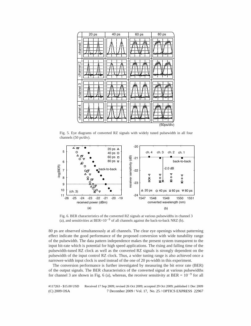
chan
nel 1
chan
nel 2
chan
nel 3
chan
nel 4
(50ps/div)
20 ps 40 ps 60 ps 80 ps
Fig. 5. Eye diagrams of converted RZ signals with widely tuned pulsewidth in all fourchannels (50 ps/div).
5
6
7
8
9 10 11
-26 -25 -24 -23 -22 -21 -20 -19
-log(
BER)
received power (dBm)
20 ps40 ps60 ps80 ps
back-to-back
(a)
back-to-back
-2.0 dB
(b)
-20
-21
-22
-23
-24 1547 1548 1549 1550 1551
rece
iver s
ensit
ivity
(dB)
converted wavelength (nm)
20 ps 40 ps 60 ps 80 ps
ch. 1ch. 2ch. 3ch. 4
(ch. 3)
Fig. 6. BER characteristics of the converted RZ signals at various pulsewidths in channel 3(a), and sensitivities at BER=10−9 of all channels against the back-to-back NRZ (b).
80 ps are observed simultaneously at all channels. The cleareye openings without patterningeffect indicate the good performance of the proposed conversion with wide tunability rangeof the pulsewidth. The data pattern independence makes the present system transparent to theinput bit-rate which is potential for high speed applications. The rising and falling time of thepulsewidth-tuned RZ clock as well as the converted RZ signals is strongly dependent on thepulsewidth of the input control RZ clock. Thus, a wider tuning range is also achieved once anarrower-width input clock is used instead of the one of 20 ps-width in this experiment.
The conversion performance is further investigated by measuring the bit error rate (BER)of the output signals. The BER characteristics of the converted signal at various pulsewidthsfor channel 3 are shown in Fig. 6 (a), whereas, the receiver sensitivity at BER = 10−9 for all
#117263 - $15.00 USD Received 17 Sep 2009; revised 26 Oct 2009; accepted 29 Oct 2009; published 1 Dec 2009
(C) 2009 OSA 7 December 2009 / Vol. 17, No. 25 / OPTICS EXPRESS 22967
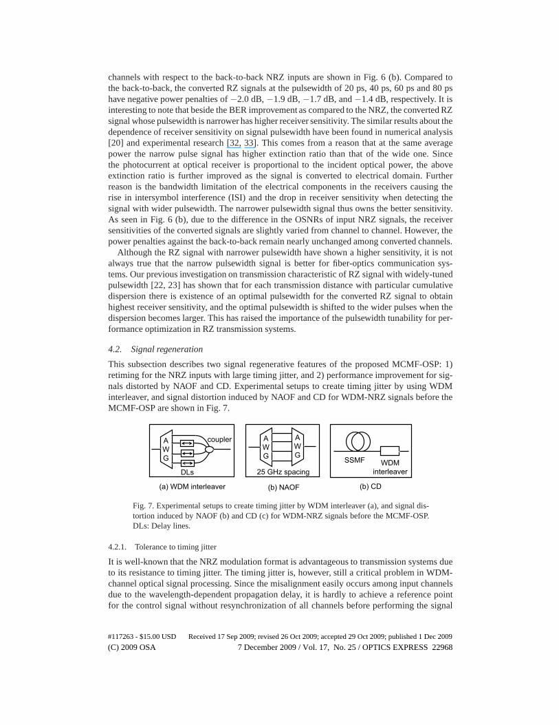
channels with respect to the back-to-back NRZ inputs are shown in Fig. 6 (b). Compared tothe back-to-back, the converted RZ signals at the pulsewidth of 20 ps, 40 ps, 60 ps and 80 pshave negative power penalties of−2.0 dB,−1.9 dB,−1.7 dB, and−1.4 dB, respectively. It isinteresting to note that beside the BER improvement as compared to the NRZ, the converted RZsignal whose pulsewidth is narrower has higher receiver sensitivity. The similar results about thedependence of receiver sensitivity on signal pulsewidth have been found in numerical analysis[20] and experimental research [32, 33]. This comes from a reason that at the same averagepower the narrow pulse signal has higher extinction ratio than that of the wide one. Sincethe photocurrent at optical receiver is proportional to theincident optical power, the aboveextinction ratio is further improved as the signal is converted to electrical domain. Furtherreason is the bandwidth limitation of the electrical components in the receivers causing therise in intersymbol interference (ISI) and the drop in receiver sensitivity when detecting thesignal with wider pulsewidth. The narrower pulsewidth signal thus owns the better sensitivity.As seen in Fig. 6 (b), due to the difference in the OSNRs of input NRZ signals, the receiversensitivities of the converted signals are slightly variedfrom channel to channel. However, thepower penalties against the back-to-back remain nearly unchanged among converted channels.
Although the RZ signal with narrower pulsewidth have shown ahigher sensitivity, it is notalways true that the narrow pulsewidth signal is better for fiber-optics communication sys-tems. Our previous investigation on transmission characteristic of RZ signal with widely-tunedpulsewidth [22, 23] has shown that for each transmission distance with particular cumulativedispersion there is existence of an optimal pulsewidth for the converted RZ signal to obtainhighest receiver sensitivity, and the optimal pulsewidth is shifted to the wider pulses when thedispersion becomes larger. This has raised the importance of the pulsewidth tunability for per-formance optimization in RZ transmission systems.
4.2. Signal regeneration
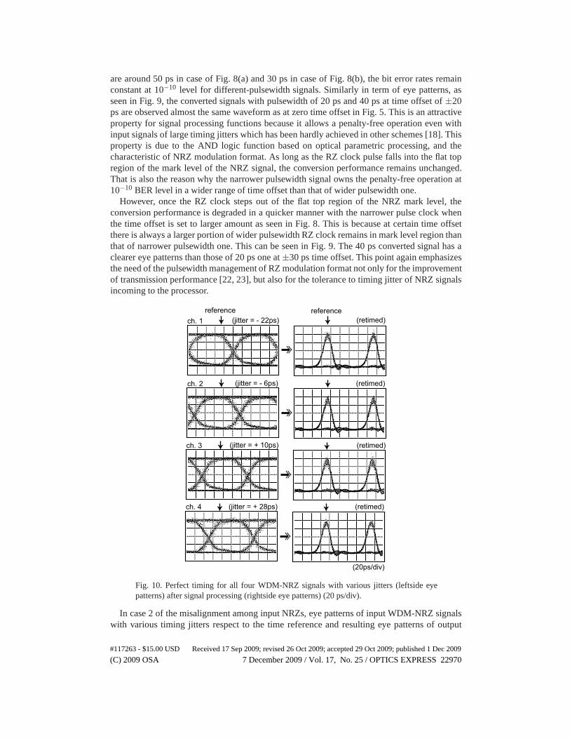
This subsection describes two signal regenerative features of the proposed MCMF-OSP: 1)retiming for the NRZ inputs with large timing jitter, and 2) performance improvement for sig-nals distorted by NAOF and CD. Experimental setups to createtiming jitter by using WDMinterleaver, and signal distortion induced by NAOF and CD for WDM-NRZ signals before theMCMF-OSP are shown in Fig. 7.
AWG
coupler
DLs
(a) WDM interleaver
AWG
AWG
25 GHz spacingWDM
interleaverSSMF
(b) NAOF (b) CD
Fig. 7. Experimental setups to create timing jitter by WDM interleaver (a), and signal dis-tortion induced by NAOF (b) and CD (c) for WDM-NRZ signals before the MCMF-OSP.DLs: Delay lines.
4.2.1. Tolerance to timing jitter
It is well-known that the NRZ modulation format is advantageous to transmission systems dueto its resistance to timing jitter. The timing jitter is, however, still a critical problem in WDM-channel optical signal processing. Since the misalignmenteasily occurs among input channelsdue to the wavelength-dependent propagation delay, it is hardly to achieve a reference pointfor the control signal without resynchronization of all channels before performing the signal
#117263 - $15.00 USD Received 17 Sep 2009; revised 26 Oct 2009; accepted 29 Oct 2009; published 1 Dec 2009
(C) 2009 OSA 7 December 2009 / Vol. 17, No. 25 / OPTICS EXPRESS 22968

3
4
5 6 7 8 9
10 11
-50 -40 -30 -10 0 10 20 30 40 50
-log(
BER)
time offset (ps)
20 ps40 ps
-20
3
4
5 6 7 8 9
10 11
-50 -40 -30 -20 -10 0 10 20 30 40 50
-log(
BER)
time offset (ps)
60 ps80 ps
(a) (b)
60 ps 40 ps
Fig. 8. BER characteristics at channel 2 as a function of timeoffset between NRZs and RZclock as pulsewidth is set at 20 ps, 40 ps (a), and 60 ps, 80 ps (b).
- 30 ps - 20 ps + 20 ps + 30 ps
(20ps/div)
RZ -
20 p
sRZ
- 40
ps
Fig. 9. Changes in eye patterns of 20 ps and 40 ps converted RZ signals as time offset istuned to±20 ps and±30 ps (20 ps/div).
processing. In the best case, where there is no delay among channels, the timing jitter of onechannel becomes double with respect to the other channel of the same jitter.
The investigation on the timing jitter tolerance is done by adjusting the time offset of localRZ clock relative to the center of incoming WDM-NRZ signals.Two cases of setting for timeoffset are considered: input NRZ signals are time aligned incase 1, and misaligned in case 2.The alignment or misalignment among input NRZs is made by using a WDM signal interleavercomprised of an AWG, optical delay lines (DLs), and a WDM coupler as shown in Fig. 7(a).
In case 1, the comparisons in terms of BER variations at channel 2 are shown in Fig. 8(a) for20 ps, 40 ps converted signals, and in Fig. 8(b) for 60 ps and 80ps converted signals as the timeoffset is changed in a wide range. Figure 9, as an example, shows the changes in eye patternsof 20 ps and 40 ps converted signals accordingly with variousvalues of time offset. Since thesignals at different pulsewidths have different receiver sensitivities as seen in Fig. 6, to comparethe BER characteristics among such signals the received power in each case of pulsewidth isadjusted so that its BER reaches the same level of 10−10 at zero time offset.
As seen in Fig. 8, the large timing jitters of±30 ps and±20 ps (±30% and±20% of 10GHz bit period) of input NRZ signal cause the error rates increased by a factor of only 10 forpulsewidths of 20 ps, 40ps, and 60 ps, 80 ps, respectively. Inwide ranges of time offset, which
#117263 - $15.00 USD Received 17 Sep 2009; revised 26 Oct 2009; accepted 29 Oct 2009; published 1 Dec 2009
(C) 2009 OSA 7 December 2009 / Vol. 17, No. 25 / OPTICS EXPRESS 22969
are around 50 ps in case of Fig. 8(a) and 30 ps in case of Fig. 8(b), the bit error rates remainconstant at 10−10 level for different-pulsewidth signals. Similarly in termof eye patterns, asseen in Fig. 9, the converted signals with pulsewidth of 20 psand 40 ps at time offset of±20ps are observed almost the same waveform as at zero time offset in Fig. 5. This is an attractiveproperty for signal processing functions because it allowsa penalty-free operation even withinput signals of large timing jitters which has been hardly achieved in other schemes [18]. Thisproperty is due to the AND logic function based on optical parametric processing, and thecharacteristic of NRZ modulation format. As long as the RZ clock pulse falls into the flat topregion of the mark level of the NRZ signal, the conversion performance remains unchanged.That is also the reason why the narrower pulsewidth signal owns the penalty-free operation at10−10 BER level in a wider range of time offset than that of wider pulsewidth one.
However, once the RZ clock steps out of the flat top region of the NRZ mark level, theconversion performance is degraded in a quicker manner withthe narrower pulse clock whenthe time offset is set to larger amount as seen in Fig. 8. This is because at certain time offsetthere is always a larger portion of wider pulsewidth RZ clockremains in mark level region thanthat of narrower pulsewidth one. This can be seen in Fig. 9. The 40 ps converted signal has aclearer eye patterns than those of 20 ps one at±30 ps time offset. This point again emphasizesthe need of the pulsewidth management of RZ modulation format not only for the improvementof transmission performance [22, 23], but also for the tolerance to timing jitter of NRZ signalsincoming to the processor.
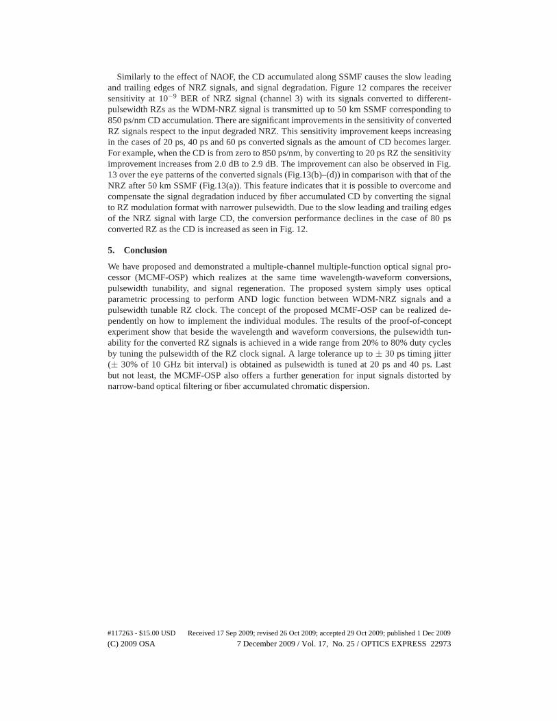
ch. 1 (retimed)(jitter = - 22ps)
(20ps/div)
referencereference
(jitter = - 6ps)
(jitter = + 10ps)
(jitter = + 28ps)
(retimed)
(retimed)
(retimed)
ch. 2
ch. 3
ch. 4
Fig. 10. Perfect timing for all four WDM-NRZ signals with various jitters (leftside eyepatterns) after signal processing (rightside eye patterns) (20 ps/div).
In case 2 of the misalignment among input NRZs, eye patterns of input WDM-NRZ signalswith various timing jitters respect to the time reference and resulting eye patterns of output
#117263 - $15.00 USD Received 17 Sep 2009; revised 26 Oct 2009; accepted 29 Oct 2009; published 1 Dec 2009
(C) 2009 OSA 7 December 2009 / Vol. 17, No. 25 / OPTICS EXPRESS 22970

signals converted to 20 ps RZs are shown in Fig. 10. The time delays within input channelsare set by adjusting DLs in the WDM interleaver, and a time delay of around 50 ps is createdbetween channel 1 and 4 as seen in the leftside eye patterns ofFig. 10. The RZ clock pumpis adjusted to the overlapped point of all input channels, which is the time reference for theretiming. As shown in the resulting eye patterns at the rightside of Fig. 10, the signals with var-ious time jitters are shifted back to the time reference. Thus, a perfect synchronization has beendone for all input data channels. Note here that the acceptable 50 ps delay between channel 1(1554.1 nm) and channel 4 (1556.5 nm) allows a WDM-channel transmission over around 1.2km standard single-mode fiber (SSMF), 17 ps/nm/km dispersion, prior to the MCMF processorwithout resynchronization. Although the bit alignment maycause nonlinear crosstalks in casethe converted WDM signals are propagated on transmission links right after the MCMF proces-sor, the feature of time regeneration of MCMF-OSP is particularly useful in applications wherebit-level synchronization among WDM channels is required,for example, in bit-parallel WDMdata transmission systems or in WDM optical packet switching [24, 25]. It is also necessary tonote that the bit alignment will be no longer a problem in transmissions with chromatic disper-sion due to the wavelength-dependent propagation delay, especially with RZ format signals.
4.2.2. Tolerance to NAOF and CD
Narrow-band optical filtering (NAOF) and fiber chromatic dispersion (CD) are considered twoof the most signal degradation factors in fiber-optics communications. The former factor isapplied to WDM networks with add-drop or routing capabilities in which signal channels arepassed through cascaded optical filters used for multiplexing and demultiplexing [34–36]. Onthe other hand, the latter factor is a critical issue in everyfiber-optic transmission systems. Inthe experiment, two parallel 25 GHz channel-spacing AWGs (0.2 nm) are used as NAOF inFig. 7(b). Various distances of SSMF, on the other hand, is considered CD medium as shown inFig. 7(c). A WDM interleaver is needed after SSMF for the signal alignment at the input of theMCMF-OSP.
4
5
6
7
8 9
10 11
-25 -23 -21 -19 -17
-log(
BER)
received power (dBm)
degraded NRZ
20ps
- 3.9dB
(20ps/div)
(b)
(c)
(d)
(e)
(a)
ch. 2 ch.1
ch. 2
ch. 3
ch. 4
Fig. 11. BER measurements (a) and resulting eye patterns (b–e) of 20 ps converted RZ asinput NRZ signals are degraded by NAOF using two parallel 25GHz spacing AWGs. Insetof (a) shows eye pattern of input NRZ at channel 2 (20ps/div).
#117263 - $15.00 USD Received 17 Sep 2009; revised 26 Oct 2009; accepted 29 Oct 2009; published 1 Dec 2009
(C) 2009 OSA 7 December 2009 / Vol. 17, No. 25 / OPTICS EXPRESS 22971

Experimental results regarding to tolerance to NAOF factorare shown in Fig. 11 when signalsare converted to 20ps RZs. As seen in Fig. 11(a) for channel 2,the NAOF makes slow theleading and trailing edges of the input NRZ (the inset) and the receiver sensitivity inclined by 3dB with a error floor at 10−9 BER level. However, after the signal processing, since the outputconverted signals follow the pulse shape of the RZ clock pump, the signal degraded by NAOFis recovered in terms of BER in Fig. 11(a), and the leading andtrailing edges as seen in Fig.11(b)–(e) for all four channels. For instance, at channel 2,the 20 ps converted RZ signal ownsa better sensitivity by 3.9 dB at BER of 10−9 and a linear BER characteristic than those ofthe degraded and BER-floored NRZ signal. Note here that with anon-degraded NRZ input thesensitivity improvement is only 2 dB as it is converted to 20 ps RZ signal as shown in Fig. 6.These importantly lead to the signal regeneration for the proposed MCMF-OSP.
In the case of SSMF transmission before processing, due to the NRZ signals at differentwavelengths to travel at different velocities over SSMF, itis necessary to align the signals priorto the optical processor by the WDM interleaver as shown in Fig. 7(c). In practical systemsand networks, the time alignment for signals must be controlled by relying on synchronizationinformation of the WDM channels. Thus, it is essential to collect the synchronization fromall input channels. This is easy to achieve once the proposedMCMF-OSP is applied at thenetwork nodes which are the central points of synchronization information due to the necessityfor network control and management. It can also be realized by using multiwavelength clockrecovery schemes as in Ref. [28, 29].
-24
-23
-22
-21
-20
-19
-18
0 10 20 30 40 50 60
rece
iver s
ensit
ivity
(dBm
)
transmission length (km)
2.9dB
2.0dB
20 ps 40 ps60 ps 80 ps
NRZ
Fig. 12. Receiver sensitivities of converted RZs at different pulsewidths as input NRZs areaffected by various amounts of CD on SSMF.
(a) (b) (c) (d)
NRZ after 50 km SSMF RZ - 20 ps
(20ps/div)
RZ - 40 ps RZ - 60 ps
Fig. 13. Eye patterns of NRZ signal after 50 km SSMF (850 ps/nmaccumulated CD) (a)and its converted RZ at 20 ps (b), 40 ps (c), and 60 ps (d) pulsewidths (20 ps/div).
#117263 - $15.00 USD Received 17 Sep 2009; revised 26 Oct 2009; accepted 29 Oct 2009; published 1 Dec 2009
(C) 2009 OSA 7 December 2009 / Vol. 17, No. 25 / OPTICS EXPRESS 22972
Similarly to the effect of NAOF, the CD accumulated along SSMF causes the slow leadingand trailing edges of NRZ signals, and signal degradation. Figure 12 compares the receiversensitivity at 10−9 BER of NRZ signal (channel 3) with its signals converted to different-pulsewidth RZs as the WDM-NRZ signal is transmitted up to 50 km SSMF corresponding to850 ps/nm CD accumulation. There are significant improvements in the sensitivity of convertedRZ signals respect to the input degraded NRZ. This sensitivity improvement keeps increasingin the cases of 20 ps, 40 ps and 60 ps converted signals as the amount of CD becomes larger.For example, when the CD is from zero to 850 ps/nm, by converting to 20 ps RZ the sensitivityimprovement increases from 2.0 dB to 2.9 dB. The improvementcan also be observed in Fig.13 over the eye patterns of the converted signals (Fig.13(b)–(d)) in comparison with that of theNRZ after 50 km SSMF (Fig.13(a)). This feature indicates that it is possible to overcome andcompensate the signal degradation induced by fiber accumulated CD by converting the signalto RZ modulation format with narrower pulsewidth. Due to theslow leading and trailing edgesof the NRZ signal with large CD, the conversion performance declines in the case of 80 psconverted RZ as the CD is increased as seen in Fig. 12.
5. Conclusion
We have proposed and demonstrated a multiple-channel multiple-function optical signal pro-cessor (MCMF-OSP) which realizes at the same time wavelength-waveform conversions,pulsewidth tunability, and signal regeneration. The proposed system simply uses opticalparametric processing to perform AND logic function between WDM-NRZ signals and apulsewidth tunable RZ clock. The concept of the proposed MCMF-OSP can be realized de-pendently on how to implement the individual modules. The results of the proof-of-conceptexperiment show that beside the wavelength and waveform conversions, the pulsewidth tun-ability for the converted RZ signals is achieved in a wide range from 20% to 80% duty cyclesby tuning the pulsewidth of the RZ clock signal. A large tolerance up to± 30 ps timing jitter(± 30% of 10 GHz bit interval) is obtained as pulsewidth is tunedat 20 ps and 40 ps. Lastbut not least, the MCMF-OSP also offers a further generationfor input signals distorted bynarrow-band optical filtering or fiber accumulated chromatic dispersion.
#117263 - $15.00 USD Received 17 Sep 2009; revised 26 Oct 2009; accepted 29 Oct 2009; published 1 Dec 2009
(C) 2009 OSA 7 December 2009 / Vol. 17, No. 25 / OPTICS EXPRESS 22973