Primary Test Manager (PTM) Brochure - Tan Delta – Electric ...
Upload
dsm-academyCategory
view
0download
0

Digital SignalProcessing
Tan: Digital Signaling Processing Perlims Final Proof page 1 23.6.2007 3:30am Compositor Name: MRaja

Tan: Digital Signaling Processing Perlims Final Proof page 2 23.6.2007 3:30am Compositor Name: MRaja
This page intentionally left blank

Digital SignalProcessingFundamentals and
Applications
Li TanDeVry UniversityDecatur, Georgia
AMSTERDAM • BOSTON • HEIDELBERG • LONDONNEW YORK • OXFORD • PARIS • SAN DIEGO
SAN FRANCISCO • SINGAPORE • SYDNEY • TOKYOAcademic Press is an imprint of Elsevier
Tan: Digital Signaling Processing Perlims Final Proof page 3 23.6.2007 3:30am Compositor Name: MRaja

Academic Press is an imprint of Elsevier
30 Corporate Drive, Suite 400, Burlington, MA 01803, USA
525 B Street, Suite 1900, San Diego, California 92101-4495, USA
84 Theobald’s Road, London WC1X 8RR, UK
This book is printed on acid-free paper. 1
Copyright 2008, Elsevier Inc. All rights reserved.
No part of this publication may be reproduced or transmitted in any form or by any means,
electronic or mechanical, including photocopy, recording, or any information storage and
retrieval system, without permission in writing from the publisher.
Permissions may be sought directly from Elsevier’s Science & Technology Rights
Department in Oxford, UK: phone: (þ44) 1865 843830, fax: (þ44) 1865 853333,
E-mail: [email protected]. You may also complete your request on-line via
the Elsevier homepage (http://elsevier.com), by selecting ‘‘Support & Contact’’ then
‘‘Copyright and Permission’’ and then ‘‘Obtaining Permissions.’’
Library of Congress Cataloging-in-Publication Data
Application submitted.
British Library Cataloguing-in-Publication Data
A catalogue record for this book is available from the British Library.
ISBN: 978-0-12-374090-8
For information on all Academic Press publications
visit our Web site at www.books.elsevier.com
Printed in the United States of America
07 08 09 10 11 9 8 7 6 5 4 3 2 1
Tan: Digital Signaling Processing Perlims Final Proof page 4 23.6.2007 3:30am Compositor Name: MRaja

Contents
Preface xiii
About the Author xvii
1 Introduction to Digital Signal Processing 11.1 Basic Concepts of Digital Signal Processing 1
1.2 Basic Digital Signal Processing Examples in Block Diagrams 3
1.2.1 Digital Filtering 3
1.2.2 Signal Frequency (Spectrum) Analysis 4
1.3 Overview of Typical Digital Signal Processing in Real-World
Applications 6
1.3.1 Digital Crossover Audio System 6
1.3.2 Interference Cancellation in Electrocardiography 7
1.3.3 Speech Coding and Compression 7
1.3.4 Compact-Disc Recording System 9
1.3.5 Digital Photo Image Enhancement 10
1.4 Digital Signal Processing Applications 11
1.5 Summary 12
2 Signal Sampling and Quantization 13
2.1 Sampling of Continuous Signal 13
2.2 Signal Reconstruction 20
2.2.1 Practical Considerations for Signal Sampling:
Anti-Aliasing Filtering 25
2.2.2 Practical Considerations for Signal Reconstruction:
Anti-Image Filter and Equalizer 29
2.3 Analog-to-Digital Conversion, Digital-to-Analog
Conversion, and Quantization 35
2.4 Summary 49
2.5 MATLAB Programs 50
2.6 Problems 51
3 Digital Signals and Systems 57
3.1 Digital Signals 57
3.1.1 Common Digital Sequences 58
3.1.2 Generation of Digital Signals 62
Tan: Digital Signaling Processing Perlims Final Proof page 5 23.6.2007 3:30am Compositor Name: MRaja

3.2 Linear Time-Invariant, Causal Systems 64
3.2.1 Linearity 64
3.2.2 Time Invariance 65
3.2.3 Causality 67
3.3 Difference Equations and Impulse Responses 68
3.3.1 Format of Difference Equation 68
3.3.2 System Representation Using Its Impulse Response 69
3.4 Bounded-in-and-Bounded-out Stability 72
3.5 Digital Convolution 74
3.6 Summary 82
3.7 Problems 83
4 Discrete Fourier Transform and Signal Spectrum 87
4.1 Discrete Fourier Transform 87
4.1.1 Fourier Series Coefficients of Periodic Digital Signals 88
4.1.2 Discrete Fourier Transform Formulas 92
4.2 Amplitude Spectrum and Power Spectrum 98
4.3 Spectral Estimation Using Window Functions 110
4.4 Application to Speech Spectral Estimation 117
4.5 Fast Fourier Transform 120
4.5.1 Method of Decimation-in-Frequency 121
4.5.2 Method of Decimation-in-Time 127
4.6 Summary 131
4.7 Problems 131
5 The z-Transform 135
5.1 Definition 135
5.2 Properties of the z-Transform 139
5.3 Inverse z-Transform 142
5.3.1 Partial Fraction Expansion Using MATLAB 148
5.4 Solution of Difference Equations Using the z-Transform 151
5.5 Summary 155
5.6 Problems 156
6 Digital Signal Processing Systems, Basic Filtering Types,
and Digital Filter Realizations 159
6.1 The Difference Equation and Digital Filtering 159
6.2 Difference Equation and Transfer Function 165
6.2.1 Impulse Response, Step Response, and System Response 169
6.3 The z-Plane Pole-Zero Plot and Stability 171
6.4 Digital Filter Frequency Response 179
6.5 Basic Types of Filtering 188
Tan: Digital Signaling Processing Perlims Final Proof page 6 23.6.2007 3:30am Compositor Name: MRaja
vi C O N T E N T S

6.6 Realization of Digital Filters 195
6.6.1 Direct-Form I Realization 195
6.6.2 Direct-Form II Realization 196
6.6.3 Cascade (Series) Realization 197
6.6.4 Parallel Realization 198
6.7 Application: Speech Enhancement and Filtering 202
6.7.1 Pre-Emphasis of Speech 202
6.7.2 Bandpass Filtering of Speech 205
6.8 Summary 208
6.9 Problems 209
7 Finite Impulse Response Filter Design 215
7.1 Finite Impulse Response Filter Format 215
7.2 Fourier Transform Design 217
7.3 Window Method 229
7.4 Applications: Noise Reduction and
Two-Band Digital Crossover 253
7.4.1 Noise Reduction 253
7.4.2 Speech Noise Reduction 255
7.4.3 Two-Band Digital Crossover 256
7.5 Frequency Sampling Design Method 260
7.6 Optimal Design Method 268
7.7 Realization Structures of Finite Impulse Response Filters 280
7.7.1 Transversal Form 280
7.7.2 Linear Phase Form 282
7.8 Coefficient Accuracy Effects on Finite Impulse Response Filters 283
7.9 Summary of Finite Impulse Response (FIR) Design Procedures
and Selection of FIR Filter Design Methods in Practice 287
7.10 Summary 290
7.11 MATLAB Programs 291
7.12 Problems 294
8 Infinite Impulse Response Filter Design 303
8.1 Infinite Impulse Response Filter Format 303
8.2 Bilinear Transformation Design Method 305
8.2.1 Analog Filters Using Lowpass Prototype Transformation 306
8.2.2 Bilinear Transformation and Frequency Warping 310
8.2.3 Bilinear Transformation Design Procedure 317
8.3 Digital Butterworth and Chebyshev Filter Designs 322
8.3.1 Lowpass Prototype Function and Its Order 322
8.3.2 Lowpass and Highpass Filter Design Examples 326
8.3.3 Bandpass and Bandstop Filter Design Examples 336
Tan: Digital Signaling Processing Perlims Final Proof page 7 23.6.2007 3:30am Compositor Name: MRaja
C O N T E N T S vii

8.4 Higher-Order Infinite Impulse Response Filter Design
Using the Cascade Method 343
8.5 Application: Digital Audio Equalizer 346
8.6 Impulse Invariant Design Method 350
8.7 Polo-Zero Placement Method for Simple Infinite Impulse
Response Filters 358
8.7.1 Second-Order Bandpass Filter Design 359
8.7.2 Second-Order Bandstop (Notch) Filter Design 360
8.7.3 First-Order Lowpass Filter Design 362
8.7.4 First-Order Highpass Filter Design 364
8.8 Realization Structures of Infinite Impulse Response Filters 365
8.8.1 Realization of Infinite Impulse Response Filters in
Direct-Form I and Direct-Form II 366
8.8.2 Realization of Higher-Order Infinite Impulse
Response Filters via the Cascade Form 368
8.9 Application: 60-Hz Hum Eliminator and Heart Rate
Detection Using Electrocardiography 370
8.10 Coefficient Accuracy Effects on Infinite Impulse
Response Filters 377
8.11 Application: Generation and Detection of Dual-Tone
Multifrequency Tones Using Goertzel Algorithm 381
8.11.1 Single-Tone Generator 382
8.11.2 Dual-Tone Multifrequency Tone Generator 384
8.11.3 Goertzel Algorithm 386
8.11.4 Dual-Tone Multifrequency Tone Detection
Using the Modified Goertzel Algorithm 391
8.12 Summary of Infinite Impulse Response (IIR) Design
Procedures and Selection of the IIR Filter Design Methods
in Practice 396
8.13 Summary 401
8.14 Problems 402
9 Hardware and Software for Digital Signal Processors 413
9.1 Digital Signal Processor Architecture 413
9.2 Digital Signal Processor Hardware Units 416
9.2.1 Multiplier and Accumulator 416
9.2.2 Shifters 417
9.2.3 Address Generators 418
9.3 Digital Signal Processors and Manufactures 419
9.4 Fixed-Point and Floating-Point Formats 420
9.4.1 Fixed-Point Format 420
9.4.2 Floating-Point Format 429
9.4.3 IEEE Floating-Point Formats 434
Tan: Digital Signaling Processing Perlims Final Proof page 8 23.6.2007 3:30am Compositor Name: MRaja
viii C O N T E N T S

9.4.5 Fixed-Point Digital Signal Processors 437
9.4.6 Floating-Point Processors 439
9.5 Finite Impulse Response and Infinite Impulse Response
Filter Implementation in Fixed-Point Systems 441
9.6 Digital Signal Processing Programming Examples 447
9.6.1 Overview of TMS320C67x DSK 447
9.6.2 Concept of Real-Time Processing 451
9.6.3 Linear Buffering 452
9.6.4 Sample C Programs 455
9.7 Summary 460
9.8 Problems 461
10 Adaptive Filters and Applications 463
10.1 Introduction to Least Mean Square Adaptive Finite
Impulse Response Filters 463
10.2 Basic Wiener Filter Theory and Least Mean Square Algorithm 467
10.3 Applications: Noise Cancellation, System Modeling,
and Line Enhancement 473
10.3.1 Noise Cancellation 473
10.3.2 System Modeling 479
10.3.3 Line Enhancement Using Linear Prediction 484
10.4 Other Application Examples 486
10.4.1 Canceling Periodic Interferences Using
Linear Prediction 487
10.4.2 Electrocardiography Interference Cancellation 488
10.4.3 Echo Cancellation in Long-Distance
Telephone Circuits 489
10.5 Summary 491
10.6 Problems 491
11 Waveform Quantization and Compression 497
11.1 Linear Midtread Quantization 497
11.2 m-law Companding 501
11.2.1 Analog m-Law Companding 501
11.2.2 Digital m-Law Companding 506
11.3 Examples of Differential Pulse Code Modulation (DPCM),
Delta Modulation, and Adaptive DPCM G.721 510
11.3.1 Examples of Differential Pulse Code Modulation
and Delta Modulation 510
11.3.2 Adaptive Differential Pulse Code Modulation G.721 515
11.4 Discrete Cosine Transform, Modified Discrete Cosine
Transform, and Transform Coding in MPEG Audio 522
11.4.1 Discrete Cosine Transform 522
Tan: Digital Signaling Processing Perlims Final Proof page 9 23.6.2007 3:30am Compositor Name: MRaja
C O N T E N T S ix

11.4.2 Modified Discrete Cosine Transform 525
11.4.3 Transform Coding in MPEG Audio 530
11.5 Summary 533
11.6 MATLAB Programs 534
11.7 Problems 550
12 Multirate Digital Signal Processing, Oversampling of
Analog-to-Digital Conversion, and Undersampling of
Bandpass Signals 557
12.1 Multirate Digital Signal Processing Basics 557
12.1.1 Sampling Rate Reduction by an Integer Factor 558
12.1.2 Sampling Rate Increase by an Integer Factor 564
12.1.3 Changing Sampling Rate by a Non-Integer Factor L/M 570
12.1.4 Application: CD Audio Player 575
12.1.5 Multistage Decimation 578
12.2 Polyphase Filter Structure and Implementation 583
12.3 Oversampling of Analog-to-Digital Conversion 589
12.3.1 Oversampling and Analog-to-Digital Conversion
Resolution 590
12.3.2 Sigma-Delta Modulation Analog-to-Digital Conversion 593
12.4 Application Example: CD Player 599
12.5 Undersampling of Bandpass Signals 601
12.6 Summary 609
12.7 Problems 610
13 Image Processing Basics 617
13.1 Image Processing Notation and Data Formats 617
13.1.1 8-Bit Gray Level Images 618
13.1.2 24-Bit Color Images 619
13.1.3 8-Bit Color Images 620
13.1.4 Intensity Images 621
13.1.5 Red, Green, Blue Components and Grayscale
Conversion 622
13.1.6 MATLAB Functions for Format Conversion 624
13.2 Image Histogram and Equalization 625
13.2.1 Grayscale Histogram and Equalization 625
13.2.2 24-Bit Color Image Equalization 632
13.2.3 8-Bit Indexed Color Image Equalization 633
13.2.4 MATLAB Functions for Equalization 636
13.3 Image Level Adjustment and Contrast 637
13.3.1 Linear Level Adjustment 638
13.3.2 Adjusting the Level for Display 641
Tan: Digital Signaling Processing Perlims Final Proof page 10 23.6.2007 3:30am Compositor Name: MRaja
x C O N T E N T S

13.3.3 Matlab Functions for Image Level Adjustment 642
13.4 Image Filtering Enhancement 642
13.4.1 Lowpass Noise Filtering 643
13.4.2 Median Filtering 646
13.4.3 Edge Detection 651
13.4.4 MATLAB Functions for Image Filtering 655
13.5 Image Pseudo-Color Generation and Detection 657
13.6 Image Spectra 661
13.7 Image Compression by Discrete Cosine Transform 664
13.7.1 Two-Dimensional Discrete Cosine Transform 666
13.7.2 Two-Dimensional JPEG Grayscale Image
Compression Example 669
13.7.3 JPEG Color Image Compression 671
13.8 Creating a Video Sequence by Mixing Two Images 677
13.9 Video Signal Basics 677
13.9.1 Analog Video 678
13.9.2 Digital Video 685
13.10 Motion Estimation in Video 687
13.11 Summary 690
13.12 Problems 692
Appendix A Introduction to the MATLAB Environment 699
A.1 Basic Commands and Syntax 699
A.2 MATLAB Array and Indexing 703
A.3 Plot Utilities: Subplot, Plot, Stem, and Stair 704
A.4 MATLAB Script Files 704
A.5 MATLAB Functions 705
Appendix B Review of Analog Signal Processing Basics 709
B.1 Fourier Series and Fourier Transform 709
B.1.1 Sine-Cosine Form 709
B.1.2 Amplitude-Phase Form 710
B.1.3 Complex Exponential Form 711
B.1.4 Spectral Plots 714
B.1.5 Fourier Transform 721
B.2 Laplace Transform 726
B.2.1 Laplace Transform and Its Table 726
B.2.2 Solving Differential Equations Using
Laplace Transform 727
B.2.3 Transfer Function 730
B.3 Poles, Zeros, Stability, Convolution, and Sinusoidal
Steady-State Response 731
Tan: Digital Signaling Processing Perlims Final Proof page 11 23.6.2007 3:30am Compositor Name: MRaja
C O N T E N T S xi

B.3.1 Poles, Zeros, and Stability 731
B.3.2 Convolution 733
B.3.3 Sinusoidal Steady-State Response 735
B.4 Problems 736
Appendix C Normalized Butterworth and Chebyshev Fucntions 741
C.1 Normalized Butterworth Function 741
C.2 Normalized Chebyshev Function 744
Appendix D Sinusoidal Steady-State Response of Digital Filters 749
D.1 Sinusoidal Steady-State Response 749
D.2 Properties of the Sinusoidal Steady-State Response 751
Appendix E Finite Impulse Response Filter Design Equations by the
Frequency Sampling Design Method 753
Appendix F Some Useful Mathematical Formulas 757
Bibliography 761
Answers to Selected Problems 765
Index 791
Tan: Digital Signaling Processing Perlims Final Proof page 12 23.6.2007 3:30am Compositor Name: MRaja
xii C O N T E N T S

Preface
Technologies such as microprocessors, microcontrollers, and digital signal pro-cessors have become so advanced that they have had a dramatic impact on thedisciplines of electronics engineering, computer engineering, and biomedicalengineering. Technologists need to become familiar with digital signals andsystems and basic digital signal processing (DSP) techniques. The objective ofthis book is to introduce students to the fundamental principles of these subjectsand to provide a working knowledge such that they can apply DSP in theirengineering careers.
The book is suitable for a sequence of two-semester courses at the senior levelin undergraduate electronics, computer, and biomedical engineering technologyprograms. Chapters 1 to 8 provide the topics for a one semester course, and asecond course can complete the rest of the chapters. This textbook can also beused in an introductory DSP course at the junior level in undergraduate elec-trical engineering programs at traditional colleges. Additionally, the bookshould be useful as a reference for undergraduate engineering students, sciencestudents, and practicing engineers.
The material has been tested in two consecutive courses in signal processingsequence at DeVry University on the Decatur campus in Georgia. With thebackground established from this book, students can be well prepared to moveforward to take other senior-level courses that deal with digital signals andsystems for communications and controls.
The textbook consists of 13 chapters, organized as follows:
& Chapter 1 introduces concepts of DSP and presents a general DSP block
diagram. Application examples are included.
& Chapter 2 covers the sampling theorem described in time domain and
frequency domain and also covers signal reconstruction. Some practical
considerations for designing analog anti-aliasing lowpass filters and anti-
image lowpass filters are included. The chapter ends with a section dealing
with analog-to-digital conversion (ADC) and digital-to-analog conversion
(DAC), as well as signal quantization and encoding.
& Chapter 3 introduces digital signals, linear time-invariant system concepts,
difference equations, and digital convolutions.
Tan: Digital Signaling Processing Perlims Final Proof page 13 23.6.2007 3:30am Compositor Name: MRaja

& Chapter 4 introduces the discrete Fourier transform (DFT) and digital
signal spectral calculations using the DFT. Applying the DFT to estimate
the speech spectrum is demonstrated. The chapter ends with a section
dedicated to illustrating fast Fourier transform (FFT) algorithms.
& Chapter 5 is devoted to the z-transform and difference equations.
& Chapter 6 covers digital filtering using difference equations, transfer func-
tions, system stability, digital filter frequency responses, and implementa-
tion methods such as the direct form I and direct form II.
& Chapter 7 deals with various methods of finite impulse response (FIR)
filter design, including the Fourier transform method for calculating FIR
filter coefficients, window method, frequency sampling design, and optimal
design. Chapter 7 also includes applications using FIR filters for noise
reduction and digital crossover system design.
& Chapter 8 covers various methods of infinite impulse response (IIR) filter
design, including the bilinear transformation (BLT) design, impulse invari-
ant design, and pole-zero placement design. Applications using IIR filters
include audio equalizer design, biomedical signal enhancement, dual-tone
multifrequency (DTMF) tone generation and detection with the Goertzel
algorithm.
& Chapter 9 introduces DSP architectures, software and hardware, and
fixed-point and floating-point implementations of digital filters.
& Chapter 10 covers adaptive filters with applications such as noise cancel-
lation, system modeling, line enhancement, cancellation of periodic inter-
ferences, echo cancellation, and 60-Hz interference cancellation in
biomedical signals.
& Chapter 11 is devoted to speech quantization and compression, including
pulse code modulation (PCM) coding, mu-law compression, adaptive dif-
ferential pulse code modulation (ADPCM) coding, windowed modified
discrete cosine transform (W-MDCT) coding, and MPEG audio format,
specifically MP3 (MPEG-1, layer 3).
& Chapter 12 covers topics pertaining to multirate DSP and applications, as
well as principles of oversampling ADC, such as sigma-delta modulation.
Undersampling for bandpass signals is also examined.
& Finally, Chapter 13 covers image enhancement using histogram equaliza-
tion and filtering methods, including edge detection. The chapter also
explores pseudo-color image generation and detection, two-dimensional
spectra, JPEG compression using DCT, and the mixing of two images to
Tan: Digital Signaling Processing Perlims Final Proof page 14 23.6.2007 3:30am Compositor Name: MRaja
xiv P R E F A C E

create a video sequence. Finally, motion compensation of the video sequence
is explored, which is a key element of video compression used in MPEG.
MATLAB programs are listed wherever they are possible. Therefore, aMATLAB tutorial should be given to students who are new to the MATLABenvironment.
& Appendix A serves as a MATLAB tutorial.
& Appendix B reviews key fundamentals of analog signal processing. Topics
include Fourier series, Fourier transform, Laplace transform, and analog
system basics.
& Appendixes C, D, and E overview Butterworth and Chebyshev filters,
sinusoidal steady-state responses in digital filters, and derivation of the
FIR filter design equation via the frequency sampling method, respectively.
& Appendix F offers general useful mathematical formulas.
Instructor support, including solutions, can be found at http://textbooks.elsevier.com. MATLAB programs and exercises for students, plus Real-time C programs, can be found at http://books.elsevier.com/companions/9780123740908.
The author wishes to thank Dr. Samuel D. Stearns (professor at the Univer-sity of New Mexico; Sandia National Laboratories, Albuquerque, NM),Dr. Delores M. Etler (professor at the United States Naval Academy atAnnapolis, MD) and Dr. Neeraj Magotra (Texas Instruments, former professorat the University of New Mexico) for inspiration, guidance, and sharing oftheir insight into DSP over the years. A special thanks goes to Dr. Jean Jiang(professor at DeVry University in Decatur) for her encouragement, support,insightful suggestions, and testing of the manuscript in her DSP course.
Special thanks go to Tim Pitts (senior commissioning editor), Rick Adams(senior acquistions editor), and Rachel Roumeliotis (acquisitions editor) and tothe team members at Elsevier Science publishing for their encouragement andguidance in developing the complete manuscript.
I also wish to thank Jamey Stegmaier (publishing project manager) at SPi forcoordinating the copyediting of the manuscript.
Thanks to all the faculty and staff at DeVry University, Decatur, for theirencouragement and support.
The book has benefited from many constructive comments and suggestionsfrom the following reviewers and anonymous reviewers. The author takes thisopportunity to thank them for their significant contributions:
Professor Mateo Aboy, Oregon Institute of Technology, Klamath Falls, OR
Professor Jean Andrian, Florida International University, Miami, FL
Professor Rabah Aoufi, DeVry University, Irving, TX
Professor Larry Bland, John Brown University, Siloam Springs, AR
Tan: Digital Signaling Processing Perlims Final Proof page 15 23.6.2007 3:30am Compositor Name: MRaja
P R E F A C E xv

Professor Phillip L. De Leon, New Mexico State University, Las Cruces, NM
Professor Mohammed Feknous, New Jersey Institute of Technology, Newark, NJ
Professor Richard L. Henderson, DeVry University, Kansas City, MO
Professor Ling Hou, St. Cloud State University, St. Cloud, MN
Professor Robert C. (Rob) Maher, Montana State University, Bozeman, MT
Professor Abdulmagid Omar, DeVry University, Tinley Park, IL
Professor Ravi P. Ramachandran, Rowan University, Glassboro, NJ
Professor William (Bill) Routt, Wake Technical Community College, Raleigh, NC
Professor Samuel D. Stearns, University of New Mexico; Sandia National Laboratories,
Albuquerque, NM
Professor Les Thede, Ohio Northern University, Ada, OH
Professor Igor Tsukerman, University of Akron, Akron, OH
Professor Vijay Vaidyanathan, University of North Texas, Denton, TX
Professor David Waldo, Oklahoma Christian University, Oklahoma City, OK
Finally, I am immensely grateful to my wife, Jean, and my children, Ava,Alex, and Amber, for their extraordinary patience and understanding during theentire preparation of this book.
Li TanDeVry UniversityDecatur, Georgia
May 2007
Tan: Digital Signaling Processing Perlims Final Proof page 16 23.6.2007 3:30am Compositor Name: MRaja
xvi P R E F A C E

About the Author
Dr. Li Tan is a Professor of Electronics Engineering Technology at DeVryUniversity, Decatur, Georgia. He received his M.S. and Ph.D. degrees in Elec-trical Engineering from the University of New Mexico. He has extensivelytaught analog and digital signal processing and analog and digital communica-tions for many years. Before teaching at DeVry University, Dr. Tan worked inthe DSP and communications industry.
Dr. Tan is a senior member of the Institute of Electronic and ElectronicEngineers (IEEE). His principal technical areas include digital signal processing,adaptive signal processing, and digital communications. He has published anumber of papers in these areas.
Tan: Digital Signaling Processing Perlims Final Proof page 17 23.6.2007 3:30am Compositor Name: MRaja

1Introduction to Digital Signal
Processing
Object ives :
This chapter introduces concepts of digital signal processing (DSP) and reviews
an overall picture of its applications. Illustrative application examples include
digital noise filtering, signal frequency analysis, speech and audio compression,
biomedical signal processing such as interference cancellation in electrocardiog-
raphy, compact-disc recording, and image enhancement.
1.1 Basic Concepts of Digi ta l S ignalProcess ing
Digital signal processing (DSP) technology and its advancements have dramat-
ically impacted our modern society everywhere. Without DSP, we would not
have digital/Internet audio or video; digital recording; CD, DVD, and MP3
players; digital cameras; digital and cellular telephones; digital satellite and TV;
or wire and wireless networks. Medical instruments would be less efficient or
unable to provide useful information for precise diagnoses if there were no
digital electrocardiography (ECG) analyzers or digital x-rays and medical
image systems. We would also live in many less efficient ways, since we would
not be equipped with voice recognition systems, speech synthesis systems, and
image and video editing systems. Without DSP, scientists, engineers, and tech-
nologists would have no powerful tools to analyze and visualize data and
perform their design, and so on.
Tan: Digital Signaling Processing 0123740908_chap01 Final Proof page 1 22.6.2007 3:22pm Compositor Name: Mraja

The concept of DSP is illustrated by the simplified block diagram in
Figure 1.1, which consists of an analog filter, an analog-to-digital conversion
(ADC) unit, a digital signal (DS) processor, a digital-to-analog conversion
(DAC) unit, and a reconstruction (anti-image) filter.
As shown in the diagram, the analog input signal, which is continuous in
time and amplitude, is generally encountered in our real life. Examples of such
analog signals include current, voltage, temperature, pressure, and light inten-
sity. Usually a transducer (sensor) is used to convert the nonelectrical signal to
the analog electrical signal (voltage). This analog signal is fed to an analog filter,
which is applied to limit the frequency range of analog signals prior to the
sampling process. The purpose of filtering is to significantly attenuate aliasing
distortion, which will be explained in the next chapter. The band-limited signal
at the output of the analog filter is then sampled and converted via the ADC
unit into the digital signal, which is discrete both in time and in amplitude. The
DS processor then accepts the digital signal and processes the digital data
according to DSP rules such as lowpass, highpass, and bandpass digital filtering,
or other algorithms for different applications. Notice that the DS processor
unit is a special type of digital computer and can be a general-purpose digital
computer, a microprocessor, or an advanced microcontroller; furthermore, DSP
rules can be implemented using software in general.
With the DS processor and corresponding software, a processed digital
output signal is generated. This signal behaves in a manner according to the
specific algorithm used. The next block in Figure 1.1, the DAC unit, converts
the processed digital signal to an analog output signal. As shown, the signal is
continuous in time and discrete in amplitude (usually a sample-and-hold signal,
to be discussed in Chapter 2). The final block in Figure 1.1 is designated as
a function to smooth the DAC output voltage levels back to the analog signal
via a reconstruction (anti-image) filter for real-world applications.
In general, the analog signal process does not require software, an algorithm,
ADC, and DAC. The processing relies wholly on electrical and electronic
devices such as resistors, capacitors, transistors, operational amplifiers, and
integrated circuits (ICs).
DSP systems, on the other hand, use software, digital processing, and algo-
rithms; thus they have a great deal of flexibility, less noise interference, and no
Analog filter
ADCDS
processorDAC
Reconstruction filter
Analog input
Analog output
Band-limited signal
Digital signal
Processed digital signal
Output signal
F IGURE 1.1 A digital signal processing scheme.
Tan: Digital Signaling Processing 0123740908_chap01 Final Proof page 2 22.6.2007 3:22pm Compositor Name: Mraja
2 1 I N T R O D U C T I O N T O D I G I T A L S I G N A L P R O C E S S I N G

signal distortion in various applications. However, as shown in Figure 1.1, DSP
systems still require minimum analog processing such as the anti-aliasing and
reconstruction filters, which are musts for converting real-world information
into digital form and digital form back into real-world information.
Note that there are many real-world DSP applications that do not require
DAC, such as data acquisition and digital information display, speech recogni-
tion, data encoding, and so on. Similarly, DSP applications that need no ADC
include CD players, text-to-speech synthesis, and digital tone generators, among
others. We will review some of them in the following sections.
1.2 Basic Digi ta l S ignal Process ingExamples in Block Diagrams
We first look at digital noise filtering and signal frequency analysis, using block
diagrams.
1.2.1 Digi ta l F i l ter ing
Let us consider the situation shown in Figure 1.2, depicting a digitized noisy
signal obtained from digitizing analog voltages (sensor output) containing
a useful low-frequency signal and noise that occupies all of the frequency
range. After ADC, the digitized noisy signal x(n), where n is the sample number,
can be enhanced using digital filtering.
Since our useful signal contains the low-frequency component, the high-
frequency components above that of our useful signal are considered as noise,
which can be removed by using a digital lowpass filter. We set up the DSP block
in Figure 1.2 to operate as a simple digital lowpass filter. After processing the
digitized noisy signal x(n), the digital lowpass filter produces a clean digital
signal y(n). We can apply the cleaned signal y(n) to another DSP algorithm for a
different application or convert it to the analog signal via DAC and the recon-
struction filter.
The digitized noisy signal and clean digital signal, respectively, are plotted in
Figure 1.3, where the top plot shows the digitized noisy signal, while the bottom
plot demonstrates the clean digital signal obtained by applying the digital low-
pass filter. Typical applications of noise filtering include acquisition of clean
DSP Digital filtering
x (n) y (n)
Digitized noisy input Clean digital signal
F IGURE 1 .2 The simple digital filtering block.
Tan: Digital Signaling Processing 0123740908_chap01 Final Proof page 3 22.6.2007 3:22pm Compositor Name: Mraja
1.2 Basic Digital Signal Processing Examples in Block Diagrams 3

digital audio and biomedical signals and enhancement of speech recording,
among others (Embree, 1995; Rabiner and Schafer, 1978; Webster, 1998).
1.2.2 Signal Frequency (Spectrum) Analys is
As shown in Figure 1.4, certain DSP applications often require that time domain
information and the frequency content of the signal be analyzed. Figure 1.5
shows a digitized audio signal and its calculated signal spectrum (frequency
content), defined as the signal amplitude versus its corresponding frequency for
the time being via a DSP algorithm, called fast Fourier transform (FFT), which
will be studied in Chapter 4. The plot in Figure 1.5 (a) is a time domain display
of the recorded audio signal with a frequency of 1,000 Hz sampled at 16,000
samples per second, while the frequency content display of plot (b) displays the
calculated signal spectrum versus frequencies, in which the peak amplitude is
clearly located at 1,000 Hz. Plot (c) shows a time domain display of an audio
signal consisting of one signal of 1,000 Hz and another of 3,000 Hz sampled at
16,000 samples per second. The frequency content display shown in Plot (d)
0 0.005 0.01 0.015 0.02 0.025 0.03−2
−1
0
1
2Noisy signal
Am
plitu
de
0 0.005 0.01 0.015 0.02 0.025 0.03−2
−1
0
1
2
Am
plitu
de
Time (sec)
Time (sec)
Clean signal
F IGURE 1.3 (Top) Digitized noisy signal. (Bottom) Clean digital signal using the digitallowpass filter.
Tan: Digital Signaling Processing 0123740908_chap01 Final Proof page 4 22.6.2007 3:22pm Compositor Name: Mraja
4 1 I N T R O D U C T I O N T O D I G I T A L S I G N A L P R O C E S S I N G

gives two locations (1,000 Hz and 3,000 Hz) where the peak amplitudes reside,
hence the frequency content display presents clear frequency information of the
recorded audio signal.
As another practical example, we often perform spectral estimation of a
digitally recorded speech or audio (music) waveform using the FFT algorithm
in order to investigate spectral frequency details of speech information. Figure
1.6 shows a speech signal produced by a human in the time domain and
frequency content displays. The top plot shows the digital speech waveform
versus its digitized sample number, while the bottom plot shows the frequency
content information of speech for a range from 0 to 4,000 Hz. We can observe
that there are about ten spectral peaks, called speech formants, in the range
between 0 and 1,500 Hz. Those identified speech formants can be used for
Analog filter
ADCDSP
algorithms
Time domain displayx(n)Analog input
Frequency content display
F IGURE 1 .4 Signal spectral analysis.
0 0.005 0.01−5
0
5
Time (sec)A
C D
B
Sig
nal a
mpl
itude
0 0.005 0.01−10
−5
0
5
10
Time (sec)
Sig
nal a
mpl
itude
0 2000 4000 6000 80000
2
4
6
Frequency (Hz)S
igna
l spe
ctru
m
0 2000 4000 6000 80000
2
4
6
Frequency (Hz)
Sig
nal s
pect
rum
1000 Hz
1000 Hz
3000 Hz
F IGURE 1 .5 Audio signals and their spectrums.
Tan: Digital Signaling Processing 0123740908_chap01 Final Proof page 5 22.6.2007 3:22pm Compositor Name: Mraja
1.2 Basic Digital Signal Processing Examples in Block Diagrams 5

applications such as speech modeling, speech coding, speech feature extraction
for speech synthesis and recognition, and so on (Deller et al., 1993).
1.3 Over view of Typica l Digi ta l S ignalProcess ing in Real-WorldAppl i cat ions
1.3.1 Digi ta l Crossover Audio System
An audio system is required to operate in an entire audible range of frequen-
cies, which may be beyond the capability of any single speaker driver. Several
drivers, such as the speaker cones and horns, each covering a different frequency
range, are used to cover the full audio frequency range.
Figure 1.7 shows a typical two-band digital crossover system consisting of
two speaker drivers: a woofer and a tweeter. The woofer responds to low
frequencies, while the tweeter responds to high frequencies. The incoming digital
audio signal is split into two bands by using a digital lowpass filter and a digital
highpass filter in parallel. Then the separated audio signals are amplified.
Finally, they are sent to their corresponding speaker drivers. Although the
0 0.2 0.4 0.6 0.8 1 1.2 1.4 1.6 1.8 2
104
−2
−1
0
1
2104 Speech data: We lost the golden chain.
Sample number
Spe
ech
ampl
itude
0 500 1000 1500 2000 2500 3000 3500 40000
100
200
300
400
Frequency (Hz)
Am
plitu
de s
pect
rum
F IGURE 1.6 Speech sample and speech spectrum.
Tan: Digital Signaling Processing 0123740908_chap01 Final Proof page 6 22.6.2007 3:22pm Compositor Name: Mraja
6 1 I N T R O D U C T I O N T O D I G I T A L S I G N A L P R O C E S S I N G

traditional crossover systems are designed using the analog circuits, the digital
crossover system offers a cost-effective solution with programmable ability,
flexibility, and high quality. This topic is taken up in Chapter 7.
1.3.2 Inter ference Cancel lat ion inE lec t rocardiography
In ECG recording, there often is unwanted 60-Hz interference in the recorded
data (Webster, 1998). The analysis shows that the interference comes from
the power line and includes magnetic induction, displacement currents in leads
or in the body of the patient, effects from equipment interconnections, and
other imperfections. Although using proper grounding or twisted pairs minim-
izes such 60-Hz effects, another effective choice can be use of a digital notch
filter, which eliminates the 60-Hz interference while keeping all the other useful
information. Figure 1.8 illustrates a 60-Hz interference eliminator using a
digital notch filter. With such enhanced ECG recording, doctors in clinics
can give accurate diagnoses for patients. This technique can also be applied
to remove 60-Hz interferences in audio systems. This topic is explored in depth
in Chapter 8.
1.3.3 Speech Coding and Compress ion
One of the speech coding methods, called waveform coding, is depicted in
Figure 1.9(a), describing the encoding process, while Figure 1.9(b) shows the
decoding process. As shown in Figure 1.9(a), the analog signal is first filtered by
analog lowpass to remove high-frequency noise components and is then passed
through the ADC unit, where the digital values at sampling instants are cap-
tured by the DS processor. Next, the captured data are compressed using data
compression rules to save the storage requirement. Finally, the compressed
digital information is sent to storage media. The compressed digital information
Digital audio x(n)
Digitalhighpass filter
Digital lowpass filter
Gain
Gain Tweeter: The crossover passes
high frequencies
Woofer: The crossover passes
low frequencies
F IGURE 1 .7 Two-band digital crossover.
Tan: Digital Signaling Processing 0123740908_chap01 Final Proof page 7 22.6.2007 3:22pm Compositor Name: Mraja
1.3 Overview of Typical Digital Signal Processing in Real-World Applications 7

can also be transmitted efficiently, since compression reduces the original data
rate. Digital voice recorders, digital audio recorders, and MP3 players are
products that use compression techniques (Deller et al., 1993; Li and Drew,
2004; Pan, 1985).
To retrieve the information, the reverse process is applied. As shown in
Figure 1.9b, the DS processor decompresses the data from the storage media
and sends the recovered digital data to DAC. The analog output is acquired by
filtering the DAC output via the reconstruction filter.
ECG recorder with the removed 60 Hz
interference
ECG preamplifier
60 Hz interference
Digital notch filter for eliminating 60 Hz
interferenceECG signal with 60 Hz
inteference
F IGURE 1.8 Elimination of 60-Hz interference in electrocardiography (ECG).
Analog filter
ADCDSP
compressor
Analog input Storage
media
F IGURE 1.9A Simplified data compressor.
DSP decompressor
DACReconstruction
filter
Analog output
Storage media
F IGURE 1.9B Simplified data expander (decompressor).
Tan: Digital Signaling Processing 0123740908_chap01 Final Proof page 8 22.6.2007 3:22pm Compositor Name: Mraja
8 1 I N T R O D U C T I O N T O D I G I T A L S I G N A L P R O C E S S I N G

1.3.4 Compact-Disc Recording System
A compact-disc (CD) recording system is described in Figure 1.10a. The analog
audio signal is sensed from each microphone and then fed to the anti-aliasing
lowpass filter. Each filtered audio signal is sampled at the industry standard
rate of 44.1 kilo-samples per second, quantized, and coded to 16 bits for each
digital sample in each channel. The two channels are further multiplexed and
encoded, and extra bits are added to provide information such as playing time
and track number for the listener. The encoded data bits are modulated for
storage, and more synchronized bits are added for subsequent recovery of
sampling frequency. The modulated signal is then applied to control a laser
beam that illuminates the photosensitive layer of a rotating glass disc. When
the laser turns on and off, the digital information is etched onto the photosensi-
tive layer as a pattern of pits and lands in a spiral track. This master disc forms
the basis for mass production of the commercial CD from the thermoplastic
material.
During playback, as illustrated in Figure 1.10b, a laser optically scans
the tracks on a CD to produce a digital signal. The digital signal is then
Left mic
Right mic
Anti-aliasing LP filter
Anti-aliasing LP filter
16-bit ADC
16-bit ADC
MultiplexEncoding
Modulation Synchronization
Optics and Recording
F IGURE 1 .10A Simplified encoder of the CD recording system.
CD
Optical pickup Demodulation
Error correction
4 Over-
sampling
14-bit DAC
14-bit DAC
Anti-image LP filter
Anti-image LP filter
Amplifiedleft speaker
Amplified right speaker
F IGURE 1 .10B Simplified decoder of the CD recording system.
Tan: Digital Signaling Processing 0123740908_chap01 Final Proof page 9 22.6.2007 3:22pm Compositor Name: Mraja
1.3 Overview of Typical Digital Signal Processing in Real-World Applications 9

demodulated. The demodulated signal is further oversampled by a factor of
4 to acquire a sampling rate of 176.4 kHz for each channel and is then passed
to the 14-bit DAC unit. For the time being, we can consider the over-
sampling process as interpolation, that is, adding three samples between
every two original samples in this case, as we shall see in Chapter 12. After
DAC, the analog signal is sent to the anti-image analog filter, which is a lowpass
filter to smooth the voltage steps from the DAC unit. The output from each
anti-image filter is fed to its amplifier and loudspeaker. The purpose of the
oversampling is to relieve the higher-filter-order requirement for the anti-
image lowpass filter, making the circuit design much easier and economical
(Ambardar, 1999).
Software audio players that play music from CDs, such as Windows Media
Player and RealPlayer, installed on computer systems, are examples of DSP
applications. The audio player has many advanced features, such as a graphical
equalizer, which allows users to change audio with sound effects such as boost-
ing low-frequency content or emphasizing high-frequency content to make
music sound more entertaining (Ambardar, 1999; Embree, 1995; Ifeachor and
Jervis, 2002).
1.3.5 Digi ta l Photo Image Enhancement
We can look at another example of signal processing in two dimensions. Figure
1.11(a) shows a picture of an outdoor scene taken by a digital camera on a cloudy
day. Due to this weather condition, the image was improperly exposed in natural
light and came out dark. The image processing technique called histogram equal-
ization (Gonzalez and Wintz, 1987) can stretch the light intensity of an
Original image
A B
Enhanced image
F IGURE 1.11 Image enhancement.
Tan: Digital Signaling Processing 0123740908_chap01 Final Proof page 10 22.6.2007 3:22pm Compositor Name: Mraja
10 1 I N T R O D U C T I O N T O D I G I T A L S I G N A L P R O C E S S I N G

image using the digital information (pixels) to increase image contrast so that
detailed information in the image can clearly be seen, as we can see in Figure
1.11(b). We will study this technique in Chapter 13.
1.4 Digi ta l S ignal Process ingAppl i cat ions
Applications of DSP are increasing in many areas where analog electronics are
being replaced by DSP chips, and new applications are depending on DSP
techniques. With the cost of DS processors decreasing and their performance
increasing, DSP will continue to affect engineering design in our modern daily
life. Some application examples using DSP are listed in Table 1.1.
However, the list in the table by no means covers all DSP applications. Many
more areas are increasingly being explored by engineers and scientists. Applica-
tions of DSP techniques will continue to have profound impacts and improve
our lives.
TABLE 1 .1 Applications of digital signal processing.
Digital audio and speech Digital audio coding such as CD players, digital
crossover, digital audio equalizers, digital stereo and
surround sound, noise reduction systems, speech
coding, data compression and encryption, speech
synthesis and speech recognition
Digital telephone Speech recognition, high-speed modems, echo
cancellation, speech synthesizers, DTMF (dual-tone
multifrequency) generation and detection, answering
machines
Automobile industry Active noise control systems, active suspension
systems, digital audio and radio, digital controls
Electronic communications Cellular phones, digital telecommunications,
wireless LAN (local area networking), satellite
communications
Medical imaging equipment ECG analyzers, cardiac monitoring, medical
imaging and image recognition, digital x-rays
and image processing
Multimedia Internet phones, audio, and video; hard disk
drive electronics; digital pictures; digital cameras;
text-to-voice and voice-to-text technologies
Tan: Digital Signaling Processing 0123740908_chap01 Final Proof page 11 22.6.2007 3:22pm Compositor Name: Mraja
1.4 Digital Signal Processing Applications 11

1.5 Summar y
1. An analog signal is continuous in both time and amplitude. Analog signals
in the real world include current, voltage, temperature, pressure, light
intensity, and so on. The digital signal is the digital values converted
from the analog signal at the specified time instants.
2. Analog-to-digital signal conversion requires an ADC unit (hardware) and a
lowpass filter attached ahead of the ADC unit to block the high-frequency
components that ADC cannot handle.
3. The digital signal can be manipulated using arithmetic. The manipulations
may include digital filtering, calculation of signal frequency content, and so
on.
4. The digital signal can be converted back to an analog signal by sending the
digital values to DAC to produce the corresponding voltage levels and
applying a smooth filter (reconstruction filter) to the DAC voltage steps.
5. Digital signal processing finds many applications in the areas of digital speech
and audio, digital and cellular telephones, automobile controls, communica-
tions, biomedical imaging, image/video processing, and multimedia.
ReferencesAmbardar, A. (1999). Analog and Digital Signal Processing, 2nd ed. Pacific Grove, CA:
Brooks/Cole Publishing Company.
Deller, J. R., Proakis, J. G., and Hansen, J. H. L. (1993). Discrete-Time Processing of Speech
Signals. New York: Macmillian Publishing Company.
Embree, P. M. (1995). C Algorithms for Real-Time DSP. Upper Saddle River, NJ:
Prentice Hall.
Gonzalez, R. C., and Wintz, P. (1987). Digital Image Processing, 2nd ed. Reading, MA:
Addison-Wesley Publishing Company.
Ifeachor, E. C., and Jervis, B. W. (2002). Digital Signal Processing: A Practical Approach,
2nd ed. Upper Saddle River, NJ: Prentice Hall.
Li, Z.-N., and Drew, M. S. (2004). Fundamentals of Multimedia. Upper Saddle River, NJ:
Pearson Prentice Hall.
Pan, D. (1995). A tutorial on MPEG/audio compression. IEEE Multimedia, 2, 60–74.
Rabiner, L. R., and Schafer, R. W. (1978). Digital Processing of Speech Signals. Englewood
Cliffs, NJ: Prentice Hall.
Webster, J. G. (1998). Medical Instrumentation: Application and Design, 3rd ed. New York:
John Wiley & Sons, Inc.
Tan: Digital Signaling Processing 0123740908_chap01 Final Proof page 12 22.6.2007 3:22pm Compositor Name: Mraja
12 1 I N T R O D U C T I O N T O D I G I T A L S I G N A L P R O C E S S I N G

2Signal Sampling and Quantization
Object ives :
This chapter investigates the sampling process, sampling theory, and the signalreconstruction process. It also includes practical considerations for anti-aliasingand anti-image filters and signal quantization.
2.1 Sampl ing of Cont inuous Signal
As discussed in Chapter 1, Figure 2.1 describes a simplified block diagram ofa digital signal processing (DSP) system. The analog filter processes theanalog input to obtain the band-limited signal, which is sent to the analog-to-digital conversion (ADC) unit. The ADC unit samples the analog signal,quantizes the sampled signal, and encodes the quantized signal levels to thedigital signal.
Here we first develop concepts of sampling processing in time domain.Figure 2.2 shows an analog (continuous-time) signal (solid line) defined atevery point over the time axis (horizontal line) and amplitude axis (verticalline). Hence, the analog signal contains an infinite number of points.
It is impossible to digitize an infinite number of points. Furthermore, theinfinite points are not appropriate to be processed by the digital signal (DS)processor or computer, since they require infinite amount of memory andinfinite amount of processing power for computations. Sampling can solvesuch a problem by taking samples at the fixed time interval, as shown in Figure2.2 and Figure 2.3, where the time T represents the sampling interval orsampling period in seconds.
Tan: Digital Signaling Processing 0123740908_chap02 Final Proof page 13 21.6.2007 10:57pm Compositor Name: MRaja

As shown in Figure 2.3, each sample maintains its voltage level during thesampling interval T to give the ADC enough time to convert it. This process iscalled sample and hold. Since there exists one amplitude level for each samplinginterval, we can sketch each sample amplitude level at its corresponding sam-pling time instant shown in Figure 2.2, where 14 samples at their sampling timeinstants are plotted, each using a vertical bar with a solid circle at its top.
For a given sampling interval T, which is defined as the time span betweentwo sample points, the sampling rate is therefore given by
fs ¼1
Tsamples per second (Hz):
For example, if a sampling period is T ¼ 125 microseconds, the sampling rate isdetermined as fs ¼ 1=125 s ¼ 8,000 samples per second (Hz).
After the analog signal is sampled, we obtain the sampled signal whoseamplitude values are taken at the sampling instants, thus the processor is ableto handle the sample points. Next, we have to ensure that samples are collectedat a rate high enough that the original analog signal can be reconstructed orrecovered later. In other words, we are looking for a minimum sampling rate toacquire a complete reconstruction of the analog signal from its sampled version.
Analogfilter
ADC DSP DACReconstruction
filter
Analoginput
Analogoutput
band-limitedsignal
Digitalsignal
Processeddigtal signal
Outputsignal
F IGURE 2.1 A digital signal processing scheme.
0 2T 4T−5 nT
6T 8T 10T 12T
Analog signal/continuous-time signal
Signal samplesx (t )
Sampling interval T5
0
F IGURE 2 .2 Display of the analog (continuous) signal and display of digital samplesversus the sampling time instants.
Tan: Digital Signaling Processing 0123740908_chap02 Final Proof page 14 21.6.2007 10:57pm Compositor Name: MRaja
14 2 S I G N A L S A M P L I N G A N D Q U A N T I Z A T I O N

If an analog signal is not appropriately sampled, aliasing will occur, whichcauses unwanted signals in the desired frequency band.
The sampling theorem guarantees that an analog signal can be in theoryperfectly recovered as long as the sampling rate is at least twice as large as thehighest-frequency component of the analog signal to be sampled. The conditionis described as
fs$2fmax,
where fmax is the maximum-frequency component of the analog signal to besampled. For example, to sample a speech signal containing frequencies up to4 kHz, the minimum sampling rate is chosen to be at least 8 kHz, or 8,000samples per second; to sample an audio signal possessing frequencies up to20 kHz, at least 40,000 samples per second, or 40 kHz, of the audio signal arerequired.
Figure 2.4 illustrates sampling of two sinusoids, where the sampling intervalbetween sample points is T ¼ 0:01 second, thus the sampling rate isfs ¼ 100Hz. The first plot in the figure displays a sine wave with a frequencyof 40 Hz and its sampled amplitudes. The sampling theorem condition issatisfied, since 2fmax ¼ 80 Hz < fs. The sampled amplitudes are labeled usingthe circles shown in the first plot. We notice that the 40-Hz signal is adequatelysampled, since the sampled values clearly come from the analog version of the40-Hz sine wave. However, as shown in the second plot, the sine wave with afrequency of 90 Hz is sampled at 100 Hz. Since the sampling rate of 100 Hz isrelatively low compared with the 90-Hz sine wave, the signal is undersampleddue to 2fmax ¼ 180 Hz > fs. Hence, the condition of the sampling theorem isnot satisfied. Based on the sample amplitudes labeled with the circles in thesecond plot, we cannot tell whether the sampled signal comes from sampling a90-Hz sine wave (plotted using the solid line) or from sampling a 10-Hz sinewave (plotted using the dot-dash line). They are not distinguishable. Thus they
x (t )
0 2T 4T
5
−5 nT6T 8T 10T 12T
Analog signal
0
Voltage for ADC
F IGURE 2 .3 Sample-and-hold analog voltage for ADC.
Tan: Digital Signaling Processing 0123740908_chap02 Final Proof page 15 21.6.2007 10:57pm Compositor Name: MRaja
2.1 Sampling of Continuous Signal 15

are aliases of each other. We call the 10-Hz sine wave the aliasing noise in thiscase, since the sampled amplitudes actually come from sampling the 90-Hzsine wave.
Now let us develop the sampling theorem in frequency domain, that is, theminimum sampling rate requirement for an analog signal. As we shall see, inpractice this can help us design the anti-aliasing filter (a lowpass filter that willreject high frequencies that cause aliasing) to be applied before sampling, andthe anti-image filter (a reconstruction lowpass filter that will smooth the recov-ered sample-and-hold voltage levels to an analog signal) to be applied after thedigital-to-analog conversion (DAC).
Figure 2.5 depicts the sampled signal xs(t) obtained by sampling the con-tinuous signal x(t) at a sampling rate of fs samples per second.
Mathematically, this process can be written as the product of the continuoussignal and the sampling pulses (pulse train):
xs(t) ¼ x(t)p(t), (2:1)
0 0.01 0.02 0.03 0.04 0.05 0.06 0.07 0.08 0.09 0.1
−1
0
1
Time (sec)
Vol
tage
Sampling condition is satisfied
0 0.01 0.02 0.03 0.04 0.05 0.06 0.07 0.08 0.09 0.1
−1
0
1
Time (sec)
Vol
tage
Sampling condition is not satisfied
40 Hz
90 Hz 10 Hz
F IGURE 2 .4 Plots of the appropriately sampled signals and nonappropriately sam-pled (aliased) signals.
Tan: Digital Signaling Processing 0123740908_chap02 Final Proof page 16 21.6.2007 10:57pm Compositor Name: MRaja
16 2 S I G N A L S A M P L I N G A N D Q U A N T I Z A T I O N

where p(t) is the pulse train with a period T ¼ 1=fs. From spectral analysis, theoriginal spectrum (frequency components) X( f ) and the sampled signal spec-trum Xs( f ) in terms of Hz are related as
Xs( f ) ¼ 1
T
X1n¼1
X ( f nfs), (2:2)
where X( f ) is assumed to be the original baseband spectrum, while Xs( f ) is itssampled signal spectrum, consisting of the original baseband spectrum X( f ) andits replicas X ( f nfs). Since Equation (2.2) is a well-known formula, thederivation is omitted here and can be found in well-known texts (Ahmed andNatarajan, 1983; Alkin, 1993; Ambardar, 1999; Oppenheim and Schafer, 1975;Proakis and Manolakis, 1996).
Expanding Equation (2.2) leads to the sampled signal spectrum in Equation(2.3):
Xs( f ) ¼ þ 1
TX ( f þ fs)þ
1
TX ( f )þ 1
TX( f fs)þ (2:3)
Equation (2.3) indicates that the sampled signal spectrum is the sum of thescaled original spectrum and copies of its shifted versions, called replicas. Thesketch of Equation (2.3) is given in Figure 2.6, where three possible sketchesare classified. Given the original signal spectrum X( f ) plotted in Figure 2.6(a),the sampled signal spectrum according to Equation (2.3) is plotted in Figure2.6(b), where the replicas, 1
TX( f ), 1
TX( f fs),
1T
X ( f þ fs), . . . , have separationsbetween them. Figure 2.6(c) shows that the baseband spectrum and its replicas,1T
X ( f ), 1T
X ( f fs),1T
X ( f þ fs), . . . , are just connected, and finally, in Figure
x(t )
xs(0)
x(t )
t
tt
p(t )
T
T
1
xs(T )
xs(2T )
ADCencoding
xs(t ) = x(t )p(t )
F IGURE 2 .5 The simplified sampling process.
Tan: Digital Signaling Processing 0123740908_chap02 Final Proof page 17 21.6.2007 10:57pm Compositor Name: MRaja
2.1 Sampling of Continuous Signal 17

2.6(d), the original spectrum 1T
X ( f ) and its replicas 1T
X ( f fs),1T
X ( f þ fs), . . . ,are overlapped; that is, there are many overlapping portions in the sampledsignal spectrum.
From Figure 2.6, it is clear that the sampled signal spectrum consists of thescaled baseband spectrum centered at the origin and its replicas centered at thefrequencies of nfs (multiples of the sampling rate) for each of n ¼ 1,2,3, . . . .
If applying a lowpass reconstruction filter to obtain exact reconstruction ofthe original signal spectrum, the following condition must be satisfied:
fs fmax fmax: (2:4)
Solving Equation (2.4) gives
fs 2fmax: (2:5)
In terms of frequency in radians per second, Equation (2.5) is equivalent to
!s 2!max: (2:6)
B
X (f )
Xs (f )
Xs (f )
Xs (f )
0
f
f
f
f
0
0
0
B
B
B
−B
−B
−B fs
fs
1.0
1T
1T
1T
fs2
B = fmax
Lowpass filter
Folding frequency/Nyquist limit
A
B
C
D
−fs − B
−fs − B−fs − B
−fs − B
fs − B
fs − B
−fs
−fs
fs−fs + B
−fs + B
fs + B
fs + B
fs + B
F IGURE 2.6 Plots of the sampled signal spectrum.
Tan: Digital Signaling Processing 0123740908_chap02 Final Proof page 18 21.6.2007 10:57pm Compositor Name: MRaja
18 2 S I G N A L S A M P L I N G A N D Q U A N T I Z A T I O N

This fundamental conclusion is well known as the Shannon sampling theorem,
which is formally described below:
For a uniformly sampled DSP system, an analog signal can be perfectly recovered aslong as the sampling rate is at least twice as large as the highest-frequency componentof the analog signal to be sampled.
We summarize two key points here.
1. Sampling theorem establishes a minimum sampling rate for a given band-limited analog signal with the highest-frequency component fmax. If thesampling rate satisfies Equation (2.5), then the analog signal can berecovered via its sampled values using the lowpass filter, as described inFigure 2.6(b).
2. Half of the sampling frequency fs=2 is usually called the Nyquist frequency
(Nyquist limit), or folding frequency. The sampling theorem indicates thata DSP system with a sampling rate of fs can ideally sample an analogsignal with its highest frequency up to half of the sampling rate withoutintroducing spectral overlap (aliasing). Hence, the analog signal can beperfectly recovered from its sampled version.
Let us study the following example.
Example 2.1.
Suppose that an analog signal is given as
x(t) ¼ 5 cos (2 1000t), for t 0
and is sampled at the rate of 8,000 Hz.a. Sketch the spectrum for the original signal.
b. Sketch the spectrum for the sampled signal from 0 to 20 kHz.
Solution:
a. Since the analog signal is sinusoid with a peak value of 5 and frequencyof 1,000 Hz, we can write the sine wave using Euler’s identity:
5 cos (2 1000t) ¼ 5 e j21000t þ ej21000t
2
¼ 2:5e j21000t þ 2:5ej21000t,
which is a Fourier series expansion for a continuous periodic signal interms of the exponential form (see Appendix B). We can identify theFourier series coefficients as
c1 ¼ 2:5, and c1 ¼ 2:5:
Tan: Digital Signaling Processing 0123740908_chap02 Final Proof page 19 21.6.2007 10:57pm Compositor Name: MRaja
2.1 Sampling of Continuous Signal 19

Using themagnitudes of the coefficients,we thenplot the two-sided spectrumas
f kHz1−1
X(f )
2.5
F IGURE 2.7A Spectrum of the analog signal in Example 2.1.
b. After the analog signal is sampled at the rate of 8,000 Hz, the sampled signalspectrum and its replicas centered at the frequencies nfs, each with thescaled amplitude being 2.5/T, are as shown in Figure 2.7b:
f kHz
Xs(f )
−8−9 −7 −1
2.5/T
1 7 8 9 15 16 17
F IGURE 2.7B Spectrum of the sampled signal in Example 2.1
Notice that the spectrum of the sampled signal shown in Figure 2.7b containsthe images of the original spectrum shown in Figure 2.7a; that the imagesrepeat at multiples of the sampling frequency fs (for our example, 8 kHz, 16kHz, 24 kHz, . . . ); and that all images must be removed, since they convey noadditional information.
2.2 Signal Reconstruc t ion
In this section, we investigate the recovery of analog signal from its sampledsignal version. Two simplified steps are involved, as described in Figure 2.8.First, the digitally processed data y(n) are converted to the ideal impulse trainys(t), in which each impulse has its amplitude proportional to digital outputy(n), and two consecutive impulses are separated by a sampling period of T;second, the analog reconstruction filter is applied to the ideally recoveredsampled signal ys(t) to obtain the recovered analog signal.
To study the signal reconstruction, we let y(n) ¼ x(n) for the case of no DSP,so that the reconstructed sampled signal and the input sampled signal areensured to be the same; that is, ys(t) ¼ xs(t). Hence, the spectrum of the sampledsignal ys(t) contains the same spectral content as the original spectrum X( f ),
Tan: Digital Signaling Processing 0123740908_chap02 Final Proof page 20 21.6.2007 10:57pm Compositor Name: MRaja
20 2 S I G N A L S A M P L I N G A N D Q U A N T I Z A T I O N

that is, Y ( f ) ¼ X ( f ), with a bandwidth of fmax ¼ B Hz (described in Figure2.8(d) and the images of the original spectrum (scaled and shifted versions). Thefollowing three cases are discussed for recovery of the original signal spectrumX( f ).
Case 1: f s ¼ 2f max
As shown in Figure 2.9, where the Nyquist frequency is equal to the max-imum frequency of the analog signal x(t), an ideal lowpass reconstructionfilter is required to recover the analog signal spectrum. This is an impracticalcase.
t tT
Digital signal
y (n)
y (n)
y (0)
y (f )
y (1)
y (2)
Lowpassreconstruction
filter
n
ys(t ) y(t )
ys(t ) y (t )
ys(0) ys(T )
ys(2T )
DAC
A Digital signal processed B Sampled signal recovered
B0
f
−B
1.0
fmax = B
D Recovered signal spectrum
C Analog signal recovered
F IGURE 2 .8 Signal notations at reconstruction stage.
f
0
Xs(f )
B−B−fs−fs − B fs + B
1T
Ideal lowpass filter
fs
F IGURE 2 .9 Spectrum of the sampled signal when fs ¼ 2fmax.
Tan: Digital Signaling Processing 0123740908_chap02 Final Proof page 21 21.6.2007 10:57pm Compositor Name: MRaja
2.2 Signal Reconstruction 21

Case 2: f s > 2f max
In this case, as shown in Figure 2.10, there is a separation between thehighest-frequency edge of the baseband spectrum and the lower edge of thefirst replica. Therefore, a practical lowpass reconstruction (anti-image) filter canbe designed to reject all the images and achieve the original signal spectrum.
Case 3: f s < 2f max
Case 3 violates the condition of the Shannon sampling theorem. As we cansee, Figure 2.11 depicts the spectral overlapping between the original basebandspectrum and the spectrum of the first replica and so on. Even when we apply anideal lowpass filter to remove these images, in the baseband there is still somefoldover frequency components from the adjacent replica. This is aliasing, wherethe recovered baseband spectrum suffers spectral distortion, that is, contains analiasing noise spectrum; in time domain, the recovered analog signal may consistof the aliasing noise frequency or frequencies. Hence, the recovered analogsignal is incurably distorted.
Note that if an analog signal with a frequency f is undersampled, the aliasingfrequency component falias in the baseband is simply given by the followingexpression:
falias ¼ fs f :
The following examples give a spectrum analysis of the signal recovery.
f
0
Xs(f )
B−B
1T
Practical lowpass filter
−fs−fs − B fs − B−fs + B fs fs + B
F IGURE 2.10 Spectrum of the sampled signal when fs > 2fmax.
1T
Ideal lowpass filter
− fs − B − fs − B fs − B fsB0− fs + B
Xs (f )
fs + Bf
F IGURE 2.11 Spectrum of the sampled signal when fs < 2fmax.
Tan: Digital Signaling Processing 0123740908_chap02 Final Proof page 22 21.6.2007 10:57pm Compositor Name: MRaja
22 2 S I G N A L S A M P L I N G A N D Q U A N T I Z A T I O N

Example 2.2.
Assuming that an analog signal is given by
x(t) ¼ 5 cos (2 2000t)þ 3 cos (2 3000t), for t 0
and it is sampled at the rate of 8,000 Hz,a. Sketch the spectrum of the sampled signal up to 20 kHz.
b. Sketch the recovered analog signal spectrum if an ideal lowpass filter witha cutoff frequency of 4 kHz is used to filter the sampled signal(y nð Þ ¼ xðnÞ in this case) to recover the original signal.
Solution: Using Euler’s identity, we get
x(t) ¼ 3
2ej23000t þ 5
2ej22000t þ 5
2e j22000t þ 3
2e j23000t:
The two-sided amplitude spectrum for the sinusoids is displayed in Figure 2.12:a.
f kHz
Xs (f )
−11 −10 −6 −5 −3 −2 5 62 3
2.5 /T
8 10111314 16 1819
F IGURE 2 .12 Spectrum of the sampled signal in Example 2.2.
b. Based on the spectrum in (a), the sampling theorem condition is satisfied;hence, we can recover the original spectrum using a reconstruction low-pass filter. The recovered spectrum is shown in Figure 2.13:
f kHz2 3
Y(f )
−3−2
F IGURE 2 .13 Spectrum of the recovered signal in Example 2.2.
Tan: Digital Signaling Processing 0123740908_chap02 Final Proof page 23 21.6.2007 10:57pm Compositor Name: MRaja
2.2 Signal Reconstruction 23

Example 2.3.
Given an analog signal
x(t) ¼ 5 cos (2p 2000t)þ 1 cos (2p 5000t), for t$0,
which is sampled at a rate of 8,000 Hz,a. Sketch the spectrum of the sampled signal up to 20 kHz.
b. Sketch the recovered analog signal spectrum if an ideal lowpass filter witha cutoff frequency of 4 kHz is used to recover the original signal(y nð Þ ¼ x nð Þ in this case).
Solution:
a. The spectrum for the sampled signal is sketched in Figure 2.14:
f kHz
Xs (f )
−11 −10 −6 −5 −3 −2 5 62 3
2.5 /T
8 10111314 16 1819
Aliasing noise
F IGURE 2.14 Spectrum of the sampled signal in Example 2.3.
b. Since the maximum frequency of the analog signal is larger than that ofthe Nyquist frequency—that is, twice the maximum frequency of theanalog signal is larger than the sampling rate—the sampling theoremcondition is violated. The recovered spectrum is shown in Figure 2.15,where we see that aliasing noise occurs at 3 kHz.
f kHz2
Y(f )
3−3−2
Aliasing noise
F IGURE 2.15 Spectrum of the recovered signal in Example 2.3.
Tan: Digital Signaling Processing 0123740908_chap02 Final Proof page 24 21.6.2007 10:57pm Compositor Name: MRaja
24 2 S I G N A L S A M P L I N G A N D Q U A N T I Z A T I O N

2.2.1 Pract i ca l Cons iderat ions for S ignalSampl ing: Ant i -Al ias ing Fi l ter ing
In practice, the analog signal to be digitized may contain other frequencycomponents in addition to the folding frequency, such as high-frequencynoise. To satisfy the sampling theorem condition, we apply an anti-aliasingfilter to limit the input analog signal, so that all the frequency components areless than the folding frequency (half of the sampling rate). Considering the worstcase, where the analog signal to be sampled has a flat frequency spectrum,the band-limited spectrum X( f ) and sampled spectrum Xs( f ) are depicted inFigure 2.16, where the shape of each replica in the sampled signal spectrum isthe same as that of the anti-aliasing filter magnitude frequency response.
Due to nonzero attenuation of the magnitude frequency response of the anti-aliasing lowpass filter, the aliasing noise from the adjacent replica still appears inthe baseband. However, the level of the aliasing noise is greatly reduced. We canalso control the aliasing noise level by either using a higher-order lowpass filteror increasing the sampling rate. For illustrative purposes, we use a Butterworthfilter. The method can also be extended to other filter types such as the Cheby-shev filter. The Butterworth magnitude frequency response with an order of n isgiven by
H( f )j j ¼ 1ffiffiffiffiffiffiffiffiffiffiffiffiffiffiffiffiffiffiffiffi1þ f
fc
2nr : (2:7)
For a second-order Butterworth lowpass filter with the unit gain, the transferfunction (which will be discussed in Chapter 8) and its magnitude frequencyresponse are given by
Sample andhold
ADCcoding
Digital value
Xs(f )
f fc
fs − fa2
fsfsfa fcf f
X(f )
Xa
aliasing noise level Xaat fa (image from fs − fa)
Analog signal spectrum(worst case)
Anti-aliasingLP filter
F IGURE 2 .16 Spectrum of the sampled analog signal with a practicalanti-aliasing filter.
Tan: Digital Signaling Processing 0123740908_chap02 Final Proof page 25 21.6.2007 10:57pm Compositor Name: MRaja
2.2 Signal Reconstruction 25

H(s) ¼ 2pfcð Þ2
s2 þ 1:4142 2pfcð Þsþ 2pfcð Þ2(2:8)
and H( f )j j ¼ 1ffiffiffiffiffiffiffiffiffiffiffiffiffiffiffiffiffiffiffi1þ f
fc
4r : (2:9)
A unit gain second-order lowpass filter using a Sallen-Key topology is shown inFigure 2.17. Matching the coefficients of the circuit transfer function to that ofthe second-order Butterworth lowpass transfer function in Equation (2.10) givesthe design formulas shown in Figure 2.17, where for a given cutoff frequency offc in Hz, and a capacitor value of C2, we can determine the other elements usingthe formulas listed in the figure.
1R1R2C1C2
s2 þ 1R1C2þ 1
R2C2
sþ 1
R1R2C1C2
¼ 2pfcð Þ2
s2 þ 1:4142 2pfcð Þsþ 2pfcð Þ2(2:10)
As an example, for a cutoff frequency of 3,400 Hz, and by selecting C2 ¼ 0:01
micro-farad (uF), we can get
R1 ¼ R2 ¼ 6620 V, and C1 ¼ 0:005 uF :
Figure 2.18 shows the magnitude frequency response, where the absolute gain ofthe filter is plotted. As we can see, the absolute attenuation begins at the level of0.7 at 3,400 Hz and reduces to 0.3 at 6,000 Hz. Ideally, we want the gainattenuation to be zero after 4,000 Hz if our sampling rate is 8,000 Hz. Practic-ally speaking, aliasing will occur anyway to some degree. We will study achiev-ing the higher-order analog filter via Butterworth and Chebyshev prototypefunction tables in Chapter 8. More details of the circuit realization for theanalog filter can be found in Chen (1986).
−+
C2
Vo
C1
C1 =
R2R1
R1 = R2 =
Vin
1.4142C2 2pfc
R1R2C2 (2pfc)2
1
Choose C2
F IGURE 2.17 Second-order unit gain Sallen-Key lowpass filter.
Tan: Digital Signaling Processing 0123740908_chap02 Final Proof page 26 21.6.2007 10:57pm Compositor Name: MRaja
26 2 S I G N A L S A M P L I N G A N D Q U A N T I Z A T I O N

According to Figure 2.16, we can derive the percentage of the aliasing noiselevel using the symmetry of the Butterworth magnitude function and its firstreplica. It follows that
aliasing noise level % ¼ Xa
X ( f )jf¼fa
¼H( f )j jf¼fsfa
H( f )j jf¼fa
¼
ffiffiffiffiffiffiffiffiffiffiffiffiffiffiffiffiffiffiffiffiffi1þ fa
fc
2nrffiffiffiffiffiffiffiffiffiffiffiffiffiffiffiffiffiffiffiffiffiffiffiffiffi1þ fsfa
fc
2nr for 0#f #fc: (2:11)
With Equation (2.11), we can estimate the aliasing noise level, or choose ahigher-order anti-aliasing filter to satisfy the requirement for the percentage ofaliasing noise level.
Example 2.4.
Given the DSP system shown in Figures 2.16 to 2.18, where a sampling rateof 8,000 Hz is used and the anti-aliasing filter is a second-order Butterworthlowpass filter with a cutoff frequency of 3.4 kHz,
0 1000 2000 3000 4000 5000 6000 7000 8000 9000 100000.1
0.2
0.3
0.4
0.5
0.6
0.7
0.8
0.9
1
1.1
Frequency (Hz)
Mag
nitu
de r
espo
nse
fc = 3400 Hz
F IGURE 2.18 Magnitude frequency response of the second-order Butterworth low-pass filter.
Tan: Digital Signaling Processing 0123740908_chap02 Final Proof page 27 21.6.2007 10:57pm Compositor Name: MRaja
2.2 Signal Reconstruction 27

a. Determine the percentage of aliasing level at the cutoff frequency.
b. Determine the percentage of aliasing level at the frequency of 1,000 Hz.
Solution:
fs ¼ 8000, fc ¼ 3400, and n ¼ 2:
a. Since fa ¼ fc ¼ 3400Hz, we compute
aliasing noise level % ¼
ffiffiffiffiffiffiffiffiffiffiffiffiffiffiffiffiffiffiffiffiffiffiffi1þ 3:4
3:4
22qffiffiffiffiffiffiffiffiffiffiffiffiffiffiffiffiffiffiffiffiffiffiffiffiffiffiffiffi1þ 83:4
3:4
22q ¼ 1:4142
2:0858¼ 67:8%:
b. With fa ¼ 1000 Hz, we have
aliasing noise level % ¼
ffiffiffiffiffiffiffiffiffiffiffiffiffiffiffiffiffiffiffiffiffiffiffi1þ 1
3:4
22qffiffiffiffiffiffiffiffiffiffiffiffiffiffiffiffiffiffiffiffiffiffiffiffiffi1þ 81
3:4
22q ¼ 1:03007
4:3551¼ 23:05%:
Let us examine another example with an increased sampling rate.
Example 2.5.
a. Given the DSP system shown in Figures 2.16 to 2.18, where a samplingrate of 16,000 Hz is used and the anti-aliasing filter is a second-orderButterworth lowpass filter with a cutoff frequency of 3.4 kHz, determinethe percentage of aliasing level at the cutoff frequency.
Solution:
fs ¼ 16000, fc ¼ 3400, and n ¼ 2:
a. Since fa ¼ fc ¼ 3400 Hz, we have
aliasing noise level % ¼
ffiffiffiffiffiffiffiffiffiffiffiffiffiffiffiffiffiffiffiffiffiffiffi1þ 3:4
3:4
22qffiffiffiffiffiffiffiffiffiffiffiffiffiffiffiffiffiffiffiffiffiffiffiffiffiffiffiffiffi1þ 163:4
3:4
22q ¼ 1:4142
13:7699¼ 10:26%:
As a comparison with the result in Example 2.4, increasing the samplingrate can reduce the aliasing noise level.
The following example shows how to choose the order of the anti-aliasingfilter.
Tan: Digital Signaling Processing 0123740908_chap02 Final Proof page 28 21.6.2007 10:57pm Compositor Name: MRaja
28 2 S I G N A L S A M P L I N G A N D Q U A N T I Z A T I O N

Example 2.6.
a. Given the DSP system shown in Figure 2.16, where a sampling rate of40,000 Hz is used, the anti-aliasing filter is a Butterworth lowpass filterwith a cutoff frequency of 8 kHz, and the percentage of aliasing level at thecutoff frequency is required to be less than 1%, determine the order ofthe anti-aliasing lowpass filter.
Solution:
a. Using fs ¼ 40,000, fc ¼ 8000, and fa ¼ 8000Hz, we try each of thefollowing filters with the increasing number of the filter order.
n ¼ 1, aliasing noise level % ¼
ffiffiffiffiffiffiffiffiffiffiffiffiffiffiffiffiffiffiffiffiffi1þ 8
8
21qffiffiffiffiffiffiffiffiffiffiffiffiffiffiffiffiffiffiffiffiffiffiffiffiffiffiffi1þ 408
8
21q ¼ 1:4142ffiffiffiffiffiffiffiffiffiffiffiffiffiffiffiffi
1þ (4)2q ¼ 34:30%
n ¼ 2, aliasing noise level % ¼ 1:4142ffiffiffiffiffiffiffiffiffiffiffiffiffiffiffiffi1þ (4)4
q ¼ 8:82%
n ¼ 3, aliasing noise level % ¼ 1:4142ffiffiffiffiffiffiffiffiffiffiffiffiffiffiffiffi1þ (4)6
q ¼ 2:21%
n ¼ 4, aliasing noise level % ¼ 1:4142ffiffiffiffiffiffiffiffiffiffiffiffiffiffiffiffi1þ (4)8
q ¼ 0:55 % < 1%
To satisfy 1% aliasing noise level, we choose n ¼ 4.
2.2.2 Pract i ca l Cons iderat ions for S ignalReconstruc t ion: Ant i - Image Fi l terand Equal izer
The analog signal recovery for a practical DSP system is illustrated inFigure 2.19.
As shown in Figure 2.19, the DAC unit converts the processed digital signaly(n) to a sampled signal ys(t), and then the hold circuit produces the sample-and-hold voltage yH(t). The transfer function of the hold circuit can be derived to be
Hh(s) ¼1 esT
s: (2:12)
We can obtain the frequency response of the DAC with the hold circuit bysubstituting s ¼ jv into Equation (2.12). It follows that
Hh(v) ¼ ejvT=2 sin vT=2ð ÞvT=2
: (2:13)
Tan: Digital Signaling Processing 0123740908_chap02 Final Proof page 29 21.6.2007 10:57pm Compositor Name: MRaja
2.2 Signal Reconstruction 29

The magnitude and phase responses are given by
Hh(v)j j ¼ sin vT=2ð ÞvT=2
¼ sin (x)
x
(2:14)
ffHh(v) ¼ vT=2, (2:15)
where x ¼ vT=2. In terms of Hz, we have
Hh( f )j j ¼ sin f Tð Þf T
(2:16)
ffHh( f ) ¼ f T : (2:17)
The plot of the magnitude effect is shown in Figure 2.20.The magnitude frequency response acts like lowpass filtering and shapes
the sampled signal spectrum of Ys( f ). This shaping effect distorts the sampledsignal spectrumYs( f ) in the desired frequency band, as illustrated in Figure 2.21.On the other hand, the spectral images are attenuated due to the lowpass effect ofsin(x)/x. This sample-and-hold effect can help us design the anti-image filter.
As shown in Figure 2.21, the percentage of distortion in the desired fre-quency band is given by
distortion % ¼ 1Hh( f )ð Þ 100%
¼ 1 sin (f T)
f T
100%
(2:18)
t
Digital Signal
y (n)
y (n)
ys(t )
ys(t )
yH (t )
yH (t )
y (t )
y (t )
Anti- image filter
nT
t
HoldCircuit
Equalizer
tT
s
1− e−sTHh(s) =
DAC
A B C D
F IGURE 2 .19 Signal notations at the practical reconstruction stage. (a) Processed digitalsignal. (b) Recovered ideal sampled signal. (c) Recoveredsample-and-hold voltage. (d) Recovered analog signal.
Tan: Digital Signaling Processing 0123740908_chap02 Final Proof page 30 21.6.2007 10:57pm Compositor Name: MRaja
30 2 S I G N A L S A M P L I N G A N D Q U A N T I Z A T I O N

Let us look at Example 2.7.
Example 2.7.
Given a DSP system with a sampling rate of 8,000 Hz and a hold circuit usedafter DAC,
a. Determine the percentage of distortion at the frequency of 3,400 Hz.
b. Determine the percentage of distortion at the frequency of 1,000 Hz.
−20 −15 −10 −5 0 5 10 15 20−0.5
0
0.5
1
x
sin(
x)/x
0 0.5 1 1.5 2 2.5 30
0.2
0.4
0.6
0.8
1
Radians
|Hh(
w)|
F IGURE 2 .20 Sample-and-hold lowpass filtering effect.
f
Y(f ) Y(f − fs) Y(f − 2fs)Ys(f )
Spectral images
sin(x)x
Sample-and-hold effect
0 fs 2fs
F IGURE 2 .21 Sample-and-hold effect and distortion.
Tan: Digital Signaling Processing 0123740908_chap02 Final Proof page 31 21.6.2007 10:57pm Compositor Name: MRaja
2.2 Signal Reconstruction 31

Solution:
a. Since f T ¼ 3400 1=8000 ¼ 0:425,
distortion % ¼ 1 sin (0:425)
0:425
100% ¼ 27:17%:
b. Since f T ¼ 1000 1=8000 ¼ 0:125,
distortion % ¼ 1 sin (0:125)
0:125
100 % ¼ 2:55%:
To overcome the sample-and-hold effect, the following methods can be applied.
1. We can compensate the sample-and-hold shaping effect using an equalizerwhose magnitude response is opposite to the shape of the holdcircuit magnitude frequency response, which is shown as the solid line inFigure 2.22.
2. We can increase the sampling rate using oversampling and interpolationmethods when a higher sampling rate is available at the DAC. Using theinterpolation will increase the sampling rate without affecting the signalbandwidth, so that the baseband spectrum and its images are separatedfarther apart and a lower-order anti-image filter can be used. This subjectwill be discussed in Chapter 12.
3. We can change the DAC configuration and perform digital pre-equaliza-tion using the flexible digital filter whose magnitude frequency response isagainst the spectral shape effect due to the hold circuit. Figure 2.23 showsa possible implementation. In this way, the spectral shape effect can bebalanced before the sampled signal passes through the hold circuit. Fi-nally, the anti-image filter will remove the rest of the images and recoverthe desired analog signal.
The following practical example will illustrate the design of an anti-imagefilter using a higher sampling rate whilemaking use of the sample-and-hold effect.
Example 2.8.
a. Determine the cutoff frequency and the order for the anti-image filtergiven a DSP system with a sampling rate of 16,000 Hz and specificationsfor the anti-image filter as shown in Figure 2.24.
Tan: Digital Signaling Processing 0123740908_chap02 Final Proof page 32 21.6.2007 10:57pm Compositor Name: MRaja
32 2 S I G N A L S A M P L I N G A N D Q U A N T I Z A T I O N

Design requirements:
& Maximum allowable gain variation from 0 to 3,000 Hz ¼ 2 dB
& 33 dB rejection at the frequency of 13,000 Hz
& Butterworth filter assumed for the anti-image filter
Solution:
a. We first determine the spectral shaping effects at f ¼ 3000Hz andf ¼ 13,000Hz; that is,
0 0.2 0.4 0.6 0.8 1 1.2 1.4 1.6
0.7
0.8
0.9
1
1.1
1.2
1.3
1.4
1.5
1.6
Equ
aliz
er g
ain
Radians
F IGURE 2.22 Ideal equalizer magnitude frequency response to overcome the distor-tion introduced by the sample-and-hold process.
Digital signal Anti-imagefilter
HoldDigital equalizer DACy (n)
yeq(n) ys(t )
yH (t )
y (t )
F IGURE 2 .23 Possible implementation using the digital equalizer.
Tan: Digital Signaling Processing 0123740908_chap02 Final Proof page 33 21.6.2007 10:57pm Compositor Name: MRaja
2.2 Signal Reconstruction 33

Digital signal Anti-imagefilter
HoldDACy (n)
ys (t )yH (t )
y (t )
F IGURE 2.24 DSP recovery system for Example 2.8.
f ¼ 3000Hz, f T ¼ 3000 1=16000 ¼ 0:1785
gain ¼ sin (0:1785)
0:1785¼ 0:9484 ¼ 0:46 dB
and
f ¼ 13000Hz, f T ¼ 13000 1=16000 ¼ 0:8125
gain ¼ sin (0:8125)
0:8125¼ 0:2177 13 dB:
This gain would help the attenuation requirement.
f kHz3.2
0.2177
0.9484
1.33 1.6 ..
Ys(f )
0
F IGURE 2.25 Spectral shaping by the sample-and-hold effect in Example 2.8.
Hence, the design requirements for the anti-image filter are:
& Butterworth lowpass filter
& Maximum allowable gain variation from 0 to 3,000 Hz ¼ (2 0:46)
¼ 1:54 dB
& (33 13) ¼ 20 dB rejection at frequency 13,000 Hz.
We set up equations using log operations of the Butterworth magnitudefunction as
20 log 1þ 3000=fcð Þ2n 1=2
#1:54
20 log 1þ 13000=fcð Þ2n 1=2
$20:
From these two equations, we have to satisfy
Tan: Digital Signaling Processing 0123740908_chap02 Final Proof page 34 21.6.2007 10:57pm Compositor Name: MRaja
34 2 S I G N A L S A M P L I N G A N D Q U A N T I Z A T I O N

3000=fcð Þ2n¼ 100:154 1
13000=fcð Þ2n¼ 102 1:
Taking the ratio of these two equations yields
13000
3000
2n
¼ 102 1
100:154 1:
Then n ¼ 1
2log (102 1)=(100:154 1)
= log 13000=3000ð Þ ¼ 1:86 2:
Finally, the cutoff frequency can be computed as
fc ¼13000
102 1ð Þ1=(2n)¼ 13000
102 1ð Þ1=4¼ 4121:30Hz
fc ¼3000
100:154 1ð Þ1=(2n)¼ 3000
100:154 1ð Þ1=4¼ 3714:23 Hz:
We choose the smaller one, that is,
fc ¼ 3714:23Hz:
With the filter order and cutoff frequency, we can realize the anti-image (recon-struction) filter using the second-order unit gain Sallen-Key lowpass filterdescribed in Figure 2.17.
Note that the specifications for anti-aliasing filter designs are similar to thosefor anti-image (reconstruction) filters, except for their stopband edges. The anti-aliasing filter is designed to block the frequency components beyond the foldingfrequency before the ADC operation, while the reconstruction filter is to blockthe frequency components beginning at the lower edge of the first image afterthe DAC.
2.3 Analog-to-Digi ta l Convers ion,Digi ta l - to-Analog Convers ion,and Quant izat ion
During the ADC process, amplitudes of the analog signal to be converted haveinfinite precision. The continuous amplitude must be converted into digital datawith finite precision, which is called the quantization. Figure 2.26 shows thatquantization is a part of ADC.
Tan: Digital Signaling Processing 0123740908_chap02 Final Proof page 35 21.6.2007 10:57pm Compositor Name: MRaja
2.3 Analog-to-Digital Conversion, Digital-to-Analog Conversion, and Quantization 35

There are several ways to implement ADC. The most common ones are
& flash ADC,
& successive approximation ADC, and
& sigma-delta ADC.
In this chapter, we will focus on a simple 2-bit flash ADC unit, described inFigure 2.27, for illustrative purposes. Sigma-delta ADC will be studied inChapter 12.
As shown in Figure 2.27, the 2-bit flash ADC unit consists of a serialreference voltage created by the equal value resistors, a set of comparators,and logic units. As an example, the reference voltages in the figure are 1.25 volts,2.5 volts, 3.75 volts, and 5 volts. If an analog sample-and-hold voltage is Vin ¼ 3
volts, then the lower two comparators will each output logic 1. Through thelogic units, only the line labeled 10 is actively high, and the rest of the lines areactively low. Hence, the encoding logic circuit outputs a 2-bit binary code of 10.
y(t )
x(t ) ADC
Anti-aliasing
filter
Sampleand hold
Quantizationbinary
encoderDAC
Digitalsignal
processor
Zero-orderhold
Anti-imagefilter
F IGURE 2.26 A block diagram for a DSP system.
+
−
+−
+−
R
R
R
R
00
01
10
11 Encodinglogic
3VR
Vin
4= 3.75
VR
VR = 5
2= 2.5
VR
4= 1.25
Comparators
10logic 0
logic 0
logic 0
logic 1
logic 0logic 1
logic 1
logic 1
logic 0
F IGURE 2.27 An example of a 2-bit flash ADC.
Tan: Digital Signaling Processing 0123740908_chap02 Final Proof page 36 21.6.2007 10:57pm Compositor Name: MRaja
36 2 S I G N A L S A M P L I N G A N D Q U A N T I Z A T I O N

Flash ADC offers the advantage of high conversion speed, since all bits areacquired at the same time. Figure 2.28 illustrates a simple 2-bit DAC unit usingan R-2R ladder. The DAC contains the R-2R ladder circuit, a set of single-throw switches, a summer, and a phase shifter. If a bit is logic 0, the switchconnects a 2R resistor to ground. If a bit is logic 1, the corresponding 2Rresistor is connected to the branch to the input of the operational amplifier(summer). When the operational amplifier operates in a linear range, thenegative input is virtually equal to the positive input. The summer adds allthe currents from all branches. The feedback resistor R in the summer providesoverall amplification. The ladder network is equivalent to two 2R resistors inparallel. The entire network has a total current of I ¼ VR
Rusing Ohm’s law,
where VR is the reference voltage, chosen to be 5 volts for our example. Hence,half of the total current flows into the b1 branch, while the other half flowsinto the rest of the network. The halving process repeats for each branchsuccessively to the lower bit branches to get lower bit weights. The secondoperational amplifier acts like a phase shifter to cancel the negative sign of thesummer output. Using the basic electric circuit principle, we can determine theDAC output voltage as
V0 ¼ VR
1
21b1 þ
1
22b0
,
where b1 and b0 are bits in the 2-bit binary code, with b0 as the least significantbit (LSB).
+−
2R
2R
2R
I =VR
V0
VR = 5
RR
R
R
R
R
I / 2
0
0
1
1
I / 4
I / 4+−
Phase shifter
V0 = VR 1
b1 + b02
1
22
b1 = 1
b0 = 0Summer
F IGURE 2 .28 R-2R ladder DAC.
Tan: Digital Signaling Processing 0123740908_chap02 Final Proof page 37 21.6.2007 10:57pm Compositor Name: MRaja
2.3 Analog-to-Digital Conversion, Digital-to-Analog Conversion, and Quantization 37

As an example shown in Figure 2.28, where we set VR ¼ 5 and b1b0 ¼ 10, theADC output is expected to be
V0 ¼ 5 1
21 1þ 1
22 0
¼ 2:5 volts:
As we can see, the recovered voltage of V0 ¼ 2:5 volts introduces voltage erroras compared with Vin ¼ 3, discussed in the ADC stage. This is due to the factthat in the flash ADC unit, we use only four (i.e., finite) voltage levels torepresent continuous (infinitely possible) analog voltage values. The introduc-tion is called quantization error, obtained by subtracting the original analogvoltage from the recovered analog voltage. For our example, we have thequantization error as
V0 Vin ¼ 2:5 3 ¼ 0:5 volts:
Next, we focus on quantization development. The process of converting analogvoltage with infinite precision to finite precision is called the quantization
process. For example, if the digital processor has only a 3-bit word, the ampli-tudes can be converted into eight different levels.
A unipolar quantizer deals with analog signals ranging from 0 volt to apositive reference voltage, and a bipolar quantizer has an analog signal rangefrom a negative reference to a positive reference. The notations and general rulesfor quantization are:
D ¼ (xmax xmin)
L(2:19)
L ¼ 2m (2:20)
i ¼ roundx xmin
D
(2:21)
xq ¼ xmin þ iD, for i ¼ 0, 1, . . . , L 1, (2:22)
where xmax and xmin are the maximum and minimum values, respectively, of theanalog input signal x. The symbol L denotes the number of quantization levels,which is determined by Equation (2.20), where m is the number of bits used inADC. The symbol D is the step size of the quantizer or the ADC resolution.Finally, xq indicates the quantization level, and i is an index corresponding tothe binary code.
Figure 2.29 depicts a 3-bit unipolar quantizer and corresponding binarycodes. From Figure 2.29, we see that xmin ¼ 0, xmax ¼ 8D, and m ¼ 3. ApplyingEquation (2.22) gives each quantization level as follows:xq ¼ 0þ iD, i ¼ 0,1, . . . , L 1, where L ¼ 23 ¼ 8 and i is the integer corre-sponding to the 3-bit binary code. Table 2.1 details quantization for eachinput signal subrange.
Tan: Digital Signaling Processing 0123740908_chap02 Final Proof page 38 21.6.2007 10:57pm Compositor Name: MRaja
38 2 S I G N A L S A M P L I N G A N D Q U A N T I Z A T I O N

Similarly, a 3-bit bipolar quantizer and binary codes are shown inFigure 2.30, where we have xmin ¼ 4D, xmax ¼ 4D, and m ¼ 3. The corre-sponding quantization table is given in Table 2.2.
Example 2.9.
Assuming that a 3-bit ADC channel accepts analog input ranging from 0 to 5volts, determine the following:
a. number of quantization levels
b. step size of the quantizer or resolution
001
011
101
110
111
010
000
eq
x∆ / 2−∆ / 2
x
100
0 ∆ 2∆ 3∆ 4∆ 5∆ 6∆ 7∆ 8∆
∆
7∆
6∆
5∆
4∆
3∆
2∆
xqBinary code
F IGURE 2 .29 Characteristics of the unipolar quantizer.
TABLE 2 .1 Quantization table for the 3-bit unipolar quantizer (stepsize ¼ D ¼ (xmax xmin)=23, xmax ¼maximum voltage, andxmin ¼ 0Þ.
Binary Code Quantization Level xq (V) Input Signal Subrange (V)
0 0 0 0 0#x < 0:5D
0 0 1 D 0:5D#x < 1:5D
0 1 0 2D 1:5D#x < 2:5D
0 1 1 3D 2:5D#x < 3:5D
1 0 0 4D 3:5D#x < 4:5D
1 0 1 5D 4:5D#x < 5:5D
1 1 0 6D 5:5D#x < 6:5D
1 1 1 7D 6:5D#x < 7:5D
Tan: Digital Signaling Processing 0123740908_chap02 Final Proof page 39 21.6.2007 10:57pm Compositor Name: MRaja
2.3 Analog-to-Digital Conversion, Digital-to-Analog Conversion, and Quantization 39

c. quantization level when the analog voltage is 3.2 volts
d. binary code produced by the ADC
Solution:
Since the range is from 0 to 5 volts and the 3-bit ADC is used, we have
xmin ¼ 0 volt, xmax ¼ 5 volts, and m ¼ 3 bits:
a. Using Equation (2.20), we get the number of quantization levels as
TABLE 2 .2 Quantization table for the 3-bit bipolar quantizer (stepsize ¼ D ¼ (xmax xmin)=23, xmax ¼maximum voltage, andxmin ¼ xmax).
Binary Code Quantization Level xq (V) Input Signal Subrange (V)
000 4D 4D#x < 3:5D
001 3D 3:5D#x < 2:5D
010 2D 2:5D#x < 1:5D
011 D 1:5#x < 0:5D
100 0 0:5D#x < 0:5D
101 D 0:5D#x < 1:5D
110 2D 1:5D#x < 2:5D
111 3D 2:5D#x < 3:5D
000
001
011
100
101
110
111
010
eq
∆ / 2−∆ / 2
x
x
xq
∆
3∆
2∆
0−∆−4∆ −2∆−3∆ ∆ 4∆2∆ 3∆
−∆
−2∆
−3∆
−4∆
Binary code
F IGURE 2.30 Characteristics of the bipolar quantizer.
Tan: Digital Signaling Processing 0123740908_chap02 Final Proof page 40 21.6.2007 10:57pm Compositor Name: MRaja
40 2 S I G N A L S A M P L I N G A N D Q U A N T I Z A T I O N

L ¼ 2m ¼ 23 ¼ 8:
b. Applying Equation (2.19) yields
D ¼ 5 0
8¼ 0:625 volt:
c. When x ¼ 3:2 D0:625¼ 5:12D, from Equation (2.21) we get
i ¼ roundx xmin
D
¼ round 5:12ð ) ¼ 5:
From Equation (2.22), we determine the quantization level as
xq ¼ 0þ 5D ¼ 5 0:625 ¼ 3:125 volts:
d. The binary code is determined as 101, from either Figure 2.29 or Table 2.1.
After quantizing the input signal x, the ADC produces binary codes, asillustrated in Figure 2.31.
The DAC process is shown in Figure 2.32. As shown in the figure, the DACunit takes the binary codes from the DS processor. Then it converts the binarycode using the zero-order hold circuit to reproduce the sample-and-hold signal.Assuming that the spectrum distortion due to sample-and-hold effect can beignored for our illustration, the recovered sample-and-hold signal is furtherprocessed using the anti-image filter. Finally, the analog signal is yielded.
x(t )
00001101
00001001
01001011
11010010
Binary code
Anti-aliasing
filter
Sampleand Hold
ADC conversion
Quantizationand coding
F IGURE 2 .31 Typical ADC process.
Tan: Digital Signaling Processing 0123740908_chap02 Final Proof page 41 21.6.2007 10:57pm Compositor Name: MRaja
2.3 Analog-to-Digital Conversion, Digital-to-Analog Conversion, and Quantization 41

When the DAC outputs the analog amplitude xq with finite precision, itintroduces the quantization error, defined as
eq ¼ xq x: (2:23)
The quantization error as shown in Figure 2.29 is bounded by half of the stepsize, that is,
D
2#eq#
D
2, (2:24)
where D is the quantization step size, or the ADC resolution. We also refer to D
as Vmin (minimum detectable voltage) or the LSB value of the ADC.
Example 2.10.
a. Using Example 2.9, determine the quantization error when the analoginput is 3.2 volts.
Solution:
a. Using Equation (2.23), we obtain
eq ¼ xq x ¼ 3:125 3:2 ¼ 0:075 volt:
Note that the quantization error is less than half of the step size, that is,
eq
¼ 0:075 < D=2 ¼ 0:3125 volt:
00001101
00001001
01001011
11010010
DAC conversion
Anti-imagefilter
Analog signal
Digital signal
zero-orderhold
Quantizationand coding
Binary code
F IGURE 2.32 Typical DAC process.
Tan: Digital Signaling Processing 0123740908_chap02 Final Proof page 42 21.6.2007 10:57pm Compositor Name: MRaja
42 2 S I G N A L S A M P L I N G A N D Q U A N T I Z A T I O N

In practice, we can empirically confirm that the quantization error appears inuniform distribution when the step size is much smaller than the dynamic rangeof the signal samples and we have a sufficiently large number of samples. Basedon theory of probability and random variables, the power of quantization noiseis related to the quantization step and given by
E e2q
¼ D2
12, (2:25)
where E() is the expectation operator, which actually averages the squaredvalues of the quantization error (the reader can get more information fromthe texts by Roddy and Coolen (1997); Tomasi (2004); and Stearns and Hush(1990)). The ratio of signal power to quantization noise power (SNR) due toquantization can be expressed as
SNR ¼E x2
E e2q
: (2:26)
If we express the SNR in terms of decibels (dB), we have
SNRdB ¼ 10 log10 (SNR) dB: (2:27)
Substituting Equation (2.25) and E(x2)= xrms into Equation (2.27), we achieve
SNRdB ¼ 10:79þ 20 log10
xrms
D
, (2:28)
where xrms is the RMS (root mean squared) value of the signal to be quantized x.
Practically, the SNR can be calculated using the following formula:
SNR ¼1N
PN1
n¼0
x2(n)
1N
PN1
n¼0
e2q(n)
¼
PN1
n¼0
x2(n)
PN1
n¼0
e2q(n)
, (2:29)
where x(n) is the nth sample amplitude and eq(n) is the quantization error fromquantizing x(n).
Example 2.11.
a. If the analog signal to be quantized is a sinusoidal waveform, that is,
x(t) ¼ A sin (2 1000t),
and if the bipolar quantizer uses m bits, determine the SNR in terms of m
bits.
Tan: Digital Signaling Processing 0123740908_chap02 Final Proof page 43 21.6.2007 10:57pm Compositor Name: MRaja
2.3 Analog-to-Digital Conversion, Digital-to-Analog Conversion, and Quantization 43

Solution:
a. Since xrms ¼ 0:707A and D ¼ 2A=2 m, substituting xrms and D into Equa-tion (2.28) leads to
SNRdB ¼ 10:79þ 20 log10
0:707A
2A=2m
¼ 10:79þ 20 log10 0:707=2ð Þ þ 20m log10 2:
After simplifying the numerical values, we get
SNRdB ¼ 1:76þ 6:02m dB: (2:30)
Example 2.12.
For a speech signal, if a ratio of the RMS value over the absolute maximum value
of the analog signal (Roddy and Coolen, 1997) is given, that is, xrms
xj jmax
, and the
ADC quantizer uses m bits, determine the SNR in terms of m bits.
Solution:
Since
D ¼ xmax xmin
L¼ 2 xj jmax
2m,
substituting D in Equation (2.28) achieves
SNRdB ¼ 10:79þ 20 log10
xrms
2 xj jmax=2m
:
¼ 10:79þ 20 log10
xrms
xj jmax
þ 20m log10 2 20 log10 2:
Thus, after numerical simplification, we have
SNRdB ¼ 4:77þ 20 log10
xrms
xj jmax
þ 6:02m: (2:31)
From Examples 2.11 and 2.12, we observed that increasing 1 bit of the ADCquantizer can improve SNR due to quantization by 6 dB.
Example 2.13.
Given a sinusoidal waveform with a frequency of 100 Hz,
x(t) ¼ 4:5 sin (2 100t),
Tan: Digital Signaling Processing 0123740908_chap02 Final Proof page 44 21.6.2007 10:57pm Compositor Name: MRaja
44 2 S I G N A L S A M P L I N G A N D Q U A N T I Z A T I O N

sampled at 8,000 Hz,
a. Write a MATLAB program to quantize the x(t) using 4 bits to obtain andplot the quantized signal xq, assuming that the signal range is between 5
and 5 volts.
b. Calculate the SNR due to quantization.
Solution:
a. Program 2.1. MATLAB program for Example 2.13.
%Example 2.13
clear all;close all
disp(’Generate 0.02-second sine wave of 100 Hz and Vp¼5’);fs ¼ 8000; % Sampling rate
T ¼ 1=fs; % Sampling interval
t ¼ 0:T:0:02; % Duration of 0.02 second
sig ¼ 4:5 sin(2pi100t); % Generate the sinusoid
bits ¼ input(’input number of bits ¼>’);lg ¼ length(sig); % Length of the signal vector sig
for x ¼ 1:lg
[Index(x)pq]¼biquant(bits,-5,5,sig(x)); %Outputthequantizedindex
end
% transmitted
% received
for x ¼ 1:lg
qsig(x) ¼ biqtdec(bits, -5,5, Index(x)); %Recover the quantized value
end
qerr ¼ qsig-sig; %Calculate the quantized errors
stairs(t,qsig);hold % Plot the signal in a staircase style
plot(t,sig); grid; % Plot the signal
xlabel(’Time (sec.)’);ylabel(’Quantized x(n)’)disp(’Signal to noise power ratio due to quantization’)snr(sig,qsig);
b. Theoretically, applying Equation (2.30) leads to
SNRdB ¼ 1:76þ 6:02 4 ¼ 25:84 dB:
Tan: Digital Signaling Processing 0123740908_chap02 Final Proof page 45 21.6.2007 10:57pm Compositor Name: MRaja
2.3 Analog-to-Digital Conversion, Digital-to-Analog Conversion, and Quantization 45

Practically, using Equation (2.29), the simulated result is obtained as
SNRdB ¼ 25:78 dB:
It is clear from this example that the ratios of signal power to noise power due toquantization achieved from theory and from simulation are very close. Next, welook at an example for quantizing a speech signal.
Example 2.14.
Given a speech signal sampled at 8,000 Hz in the file we.dat,
a. Write a MATLAB program to quantize the x(t) using 4-bit quantizers toobtain the quantized signal xq, assuming that the signal range is from 5
to 5 volts.
b. Plot the original speech, quantized speech, and quantization error,respectively.
c. Calculate the SNR due to quantization using the MATLAB program.
0 0.002 0.004 0.006 0.008 0.01 0.012 0.014 0.016 0.018 0.02−5
−4
−3
−2
−1
0
1
2
3
4
5
Time (sec)
Qua
ntiz
ed x
(n)
F IGURE 2.33 Comparison of the quantized signal and the original signal.
Tan: Digital Signaling Processing 0123740908_chap02 Final Proof page 46 21.6.2007 10:57pm Compositor Name: MRaja
46 2 S I G N A L S A M P L I N G A N D Q U A N T I Z A T I O N

Solution:
a. Program 2.2. MATLAB program for Example 2.14.
%Example 2.14
clear all; close all
disp(’load speech: We’);load we.dat% Load speech data at the current folder
sig ¼ we; % Provided by the instructor
fs¼8000; % Sampling rate
lg¼length(sig); % Length of the signal vector
T¼1/fs; % Sampling period
t ¼ [0:1:1g 1]T; % Time instants in second
sig¼ 4:5sig/max(abs(sig));%Normalizesspeechintherangefrom4:5to4.5Xmax ¼ max(abs(sig)); % Maximum amplitude
Xrms ¼ sqrt( sum(sig . sig) / length(sig)) % RMS valuedisp(’Xrms/Xmax’)k¼Xrms/Xmaxdisp(’20 log10(k) ¼>’);k ¼ 20 log10(k)bits ¼ input(’input number of bits ¼>’);lg ¼ length(sig);
for x ¼ 1:lg
[Index(x)pq]¼ biquant(bits,5,5,sig(x)); %Outputthequantizedindex.
end
% Transmitted
% Received
for x ¼ 1:lg
qsig(x) ¼ biqtdec(bits, 5,5, Index(x)); %Recover the quantized value
end
qerr ¼ sig-qsig; %Calculate the quantized errors
subplot(3,1,1);plot(t,sig);
ylabel(’Original speech’);Title(’we.dat: we’);subplot(3,1,2);stairs(t, qsig);grid
ylabel(’Quantized speech’)subplot(3,1,3);stairs(t, qerr);grid
ylabel(’Quantized error’)xlabel(’Time (sec.)’);axis([0 0.25 1 1]);disp(’signal to noise ratio due to quantization noise’)snr(sig,qsig); % Signal to noise power ratio in dB: sig ¼ signal vector,
% qsig ¼quantized signal vector
Tan: Digital Signaling Processing 0123740908_chap02 Final Proof page 47 21.6.2007 10:57pm Compositor Name: MRaja
2.3 Analog-to-Digital Conversion, Digital-to-Analog Conversion, and Quantization 47

b. In Figure 2.34, the top plot shows the speech wave to be quantized, whilethe middle plot displays the quantized speech signal using 4 bits. Thebottom plot shows the quantization error. It also shows that the absolutevalue of the quantization error is uniformly distributed in a range between0:3125 and 0.3125.
c. From the MATLAB program, we have xrms
xj jmax¼ 0:203. Theoretically, from
Equation (2.31), it follows that
SNRdB ¼ 4:77þ 20 log10
xrms
xj jmax
þ 6:02 4
¼ 4:77þ 20 log10 (0:203)þ 6:02 4 ¼ 15 dB:
On the other hand, the simulated result using Equation (2.29) gives
SNRdB ¼ 15:01 dB:
Results for SNRs from Equations (2.31) and (2.29) are very close in thisexample.
0 0.05 0.1 0.15 0.2 0.25−5
0
5
Orig
inal
spe
ech
we.dat: we
0 0.05 0.1 0.15 0.2 0.25−5
0
5
Qua
ntiz
ed s
peec
h
0 0.05 0.1 0.15 0.2 0.25−1
0
1
Qua
ntiz
ed e
rror
Time (sec)
F IGURE 2.34 Original speech, quantized speech using the 4-bit bipolar quantizer,and quantization error.
Tan: Digital Signaling Processing 0123740908_chap02 Final Proof page 48 21.6.2007 10:57pm Compositor Name: MRaja
48 2 S I G N A L S A M P L I N G A N D Q U A N T I Z A T I O N

2.4 Summar y
1. Analog signal is sampled at a fixed time interval so the ADC will convertthe sampled voltage level to a digital value; this is called the samplingprocess.
2. The fixed time interval between two samples is the sampling period, and thereciprocal of the sampling period is the sampling rate. Half of the samplingrate is the folding frequency (Nyquist limit).
3. The sampling theorem condition that the sampling rate be larger than twicethe highest frequency of the analog signal to be sampled must be met inorder to have the analog signal be recovered.
4. The sampled spectrum is explained using the well-known formula
Xs( f ) ¼ þ 1
TX( f þ fs)þ
1
TX ( f )þ 1
TX ( f fs)þ . . . ,
that is, the sampled signal spectrum is a scaled and shifted version of itsanalog signal spectrum and its replicas centered at the frequencies that aremultiples of the sampling rate.
5. The analog anti-aliasing lowpass filter is used before ADC to removefrequency components having high frequencies larger than the foldingfrequency to avoid aliasing.
6. The reconstruction (analog lowpass) filter is adopted after DAC to removethe spectral images that exist in the sample-and-hold signal and obtain thesmoothed analog signal. The sample-and-hold DAC effect may distort thebaseband spectrum, but it also reduces image spectrum.
7. Quantization means that the ADC unit converts the analog signal ampli-tude with infinite precision to digital data with finite precision (a finitenumber of codes).
8. When the DAC unit converts a digital code to a voltage level, quantizationerror occurs. The quantization error is bounded by half of the quantizationstep size (ADC resolution), which is a ratio of the full range of the signalover the number of the quantization levels (number of the codes).
9. The performance of the quantizer in terms of the signal to quantization noiseratio (SNR), in dB, is related to the number of bits in ADC. Increasing 1 bitused in each ADC code will improve 6 dB SNR due to quantization.
Tan: Digital Signaling Processing 0123740908_chap02 Final Proof page 49 21.6.2007 10:57pm Compositor Name: MRaja
2.4 Summary 49

2.5 MATLAB Programs
Program 2.3. MATLAB function for uniform quantization encoding.
function [ I, pq] ¼ biquant(NoBits, Xmin, Xmax, value)
% function pq ¼ biquant(NoBits, Xmin, Xmax, value)
% This routine is created for simulation of the uniform quantizer.
%
% NoBits: number of bits used in quantization.
% Xmax: overload value.
% Xmin: minimum value
% value: input to be quantized.
% pq: output of the quantized value
% I: coded integer index
L ¼ 2^NoBits;delta¼(Xmax-Xmin)/L;I¼round((value-Xmin)/delta);if ( I¼¼L)I¼I-1;end
if I <0I ¼ 0;
end
pq¼XminþIdelta;
Program 2.4. MATLAB function for uniform quantization decoding.
function pq ¼ biqtdec(NoBits, Xmin, Xmax, I)
% function pq ¼ biqtdec(NoBits, Xmin, Xmax, I)
% This routine recovers the quantized value.
%
% NoBits: number of bits used in quantization.
% Xmax: overload value
% Xmin: minimum value
% pq: output of the quantized value
% I: coded integer index
L¼ 2^NoBits;delta¼(Xmax-Xmin)/L;pq¼XminþIdelta;
Tan: Digital Signaling Processing 0123740908_chap02 Final Proof page 50 21.6.2007 10:57pm Compositor Name: MRaja
50 2 S I G N A L S A M P L I N G A N D Q U A N T I Z A T I O N

Program 2.5. MATLAB function for calculation of signal to quantization noiseratio.
function snr ¼ calcsnr(speech, qspeech)
% function snr ¼ calcsnr(speech, qspeech)
% this routine is created for calculation of SNR
%
% speech: original speech waveform.
% qspeech: quantized speech.
% snr: output SNR in dB.
%
qerr ¼ speech-qspeech;
snr¼ 10 log10(sum(speech.speech)/sum(qerr.qerr))
2.6 Problems
2.1. Given an analog signal
x(t) ¼ 5 cos (2 1500t), for t$0,
sampled at a rate of 8,000 Hz,
a. sketch the spectrum of the original signal;
b. sketch the spectrum of the sampled signal from 0 kHz to 20 kHz.
2.2. Given an analog signal
x(t) ¼ 5 cos (2 2500t)þ 2 cos (2 3200t), for t$0,
sampled at a rate of 8,000 Hz,
a. sketch the spectrum of the sampled signal up to 20 kHz;
b. sketch the recovered analog signal spectrum if an ideal lowpass filterwith a cutoff frequency of 4 kHz is used to filter the sampled signal inorder to recover the original signal.
2.3. Given an analog signal
x(t) ¼ 5 cos (2 2500t)þ 2 cos (2 4500t), for t$0,
sampled at a rate of 8,000 Hz,
a. sketch the spectrum of the sampled signal up to 20 kHz;
Tan: Digital Signaling Processing 0123740908_chap02 Final Proof page 51 21.6.2007 10:57pm Compositor Name: MRaja
2.6 Problems 51

b. sketch the recovered analog signal spectrum if an ideal lowpass filterwith a cutoff frequency of 4 kHz is used to filter the sampled signal inorder to recover the original signal;
c. determine the frequency/frequencies of aliasing noise.
2.4. Assuming a continuous signal is given as
x(t) ¼ 10 cos (2 5500t)þ 5 sin (2 7500t), for t$0,
sampled at a sampling rate of 8,000 Hz,
a. sketch the spectrum of the sampled signal up to 20 kHz;
b. sketch the recovered analog signal spectrum if an ideal lowpass filterwith a cutoff frequency of 4 kHz is used to filter the sampled signal inorder to recover the original signal;
c. determine the frequency/frequencies of aliasing noise.
2.5. Given the following second-order anti-aliasing lowpass filter, which is aButterworth type, determine the values of circuit elements if we want thefilter to have a cutoff frequency of 1,000 Hz.
2.6. From Problem 2.5, determine the percentage of aliasing level at thefrequency of 500 Hz, assuming that the sampling rate is 4,000 Hz.
2.7. Given a DSP system in which a sampling rate of 8,000 Hz is used and theanti-aliasing filter is a second-order Butterworth lowpass filter with acutoff frequency of 3.2 kHz, determine
a. the percentage of aliasing level at the cutoff frequency;
b. the percentage of aliasing level at the frequency of 1,000 Hz.
−+
C2
C1
C1 =
V0Vin R1
R1 = R2 =
R2
1.4142
1C2 2pfc
R1R2C2 (2pfc)2
Choose C2
F IGURE 2.35 Filter circuit in Problem 2.5.
Tan: Digital Signaling Processing 0123740908_chap02 Final Proof page 52 21.6.2007 10:57pm Compositor Name: MRaja
52 2 S I G N A L S A M P L I N G A N D Q U A N T I Z A T I O N

2.8. Given a DSP system in which a sampling rate of 8,000 Hz is used andthe anti-aliasing filter is a Butterworth lowpass filter with a cutofffrequency of 3.2 kHz, determine the order of the Butterworth lowpassfilter for the percentage of aliasing level at the cutoff frequency requiredto be less than 10%.
2.9. Given a DSP system with a sampling rate of 8,000 Hz and assumingthat the hold circuit is used after DAC, determine
a. the percentage of distortion at the frequency of 3,200 Hz;
b. the percentage of distortion at the frequency of 1,500 Hz.
2.10. A DSP system is given with the following specifications:
Design requirements:
& Sampling rate 20,000 Hz
& Maximum allowable gain variation from 0 to 4,000 Hz ¼ 2 dB
DACDigital signal
y (n) y (t)
yH(t)
ys(t)
Anti-imagefilter
Hold
F IGURE 2 .36 Analog signal reconstruction in Problem 2.10.
+−
+−
+−
00
01
10
11 Encodinglogic
3.75=
Comparators
VR = 5 Vin = 2 volts
R
3VR
4
2.5=VR
2
1.25=VR
4
R
R
R
b1b0
F IGURE 2 .37 2-bit flash ADC in Problem 2.11.
Tan: Digital Signaling Processing 0123740908_chap02 Final Proof page 53 21.6.2007 10:57pm Compositor Name: MRaja
2.6 Problems 53

& 40 dB rejection at the frequency of 16,000 Hz
& Butterworth filter assumed
Determine the cutoff frequency and order for the anti-image filter.
2.11. Given the 2-bit flash ADC unit with an analog sample-and-hold voltageof 2 volts shown in Figure 2.37, determine the output bits.
2.12. Given the R-2R DAC unit with a 2-bit value of b1b0 ¼ 01 shown inFigure 2.38, determine the converted voltage.
2.13. Assuming that a 4-bit ADC channel accepts analog input ranging from0 to 5 volts, determine the following:
a. number of quantization levels;
b. step size of the quantizer or resolution;
c. quantization level when the analog voltage is 3.2 volts;
d. binary code produced by the ADC;
e. quantization error.
2.14. Assuming that a 3-bit ADC channel accepts analog input ranging from2:5 to 2.5 volts, determine the following:
a. number of quantization levels;
b. step size of the quantizer or resolution;
+−
VR = 5
V0
0
0
1
1
RR
R
R
R
VRI =I / 2
I / 4
I / 4
2R
2R
2R
R
1
21
1
22
+−
Phase shifter
V0 = VR
b1 = 0
b1 + b0
b0 = 1Summer
F IGURE 2.38 2-bit R-2R DAC in Problem 2.12.
Tan: Digital Signaling Processing 0123740908_chap02 Final Proof page 54 21.6.2007 10:57pm Compositor Name: MRaja
54 2 S I G N A L S A M P L I N G A N D Q U A N T I Z A T I O N

c. quantization level when the analog voltage is 1:2 volts;
d. binary code produced by the ADC;
e. quantization error.
2.15. If the analog signal to be quantized is a sinusoidal waveform, that is,
x(t) ¼ 9:5 sin (2000 t),
and if the bipolar quantizer uses 6 bits, determine
a. number of quantization levels;
b. quantization step size or resolution, D, assuming that the signal rangeis from 10 to 10 volts;
c. the signal power to quantization noise power ratio.
2.16. For a speech signal, if the ratio of the RMS value over the absolutemaximum value of the signal is given, that is, xrms
xj jmax
¼ 0:25, and the
ADC bipolar quantizer uses 6 bits, determine
a. number of quantization levels;
b. quantization step size or resolution, , if the signal range is 5 volts;
c. the signal power to quantization noise power ratio.
Computer Problems with MATLAB: Use the MATLAB programs in Section2.5 to solve the following problems.
2.17. Given a sinusoidal waveform of 100 Hz,
x(t) ¼ 4:5 sin (2 100t)
sample it at 8,000 samples per second and
a. write a MATLAB program to quantize x(t) using a 6-bit bipolarquantizer to obtain the quantized signal xq, assuming the signalrange to be from 5 to 5 volts;
b. plot the original signal and the quantized signal;
c. calculate the SNR due to quantization using the MATLAB program.
Tan: Digital Signaling Processing 0123740908_chap02 Final Proof page 55 21.6.2007 10:57pm Compositor Name: MRaja
2.6 Problems 55

2.18. Given a speech signal sampled at 8,000 Hz, as shown in Example 2.14,
a. write a MATLAB program to quantize x(t) using a 6-bit bipolarquantizer to obtain the quantized signal xq, assuming that the signalrange is from 5 to 5 volts;
b. plot the original speech waveform, quantized speech, and quantiza-tion error;
c. calculate the SNR due to quantization using the MATLAB pro-gram.
ReferencesAhmed, N., and Natarajan, T. (1983). Discrete-Time Signals and Systems. Reston, VA:
Reston Publishing Co.
Alkin, O. (1993). Digital Signal Processing: A Laboratory Approach Using PC-DSP. Engle-
wood Cliffs, NJ: Prentice Hall.
Ambardar, A. (1999). Analog and Digital Signal Processing, 2nd ed. Pacific Grove, CA:
Brooks/Cole Publishing Company.
Chen, W. (1986). Passive and Active Filters: Theory and Implementations. New York: John
Wiley & Sons.
Oppenheim, A. V., and Schafer, R. W. (1975). Discrete-Time Signal Processing. Englewood
Cliffs, NJ: Prentice Hall.
Proakis, J. G., and Manolakis, D. G. (1996). Digital Signal Processing: Principles, Algo-
rithms, and Applications, 3rd ed. Upper Saddle River, NJ: Prentice Hall.
Roddy, D., and Coolen, J. (1997). Electronic Communications, 4th ed. Englewood Cliffs, NJ:
Prentice Hall.
Stearns, S. D., and Hush, D. R. (1990). Digital Signal Analysis, 2nd ed. Englewood Cliffs,
NJ: Prentice Hall.
Tomasi, W. (2004). Electronic Communications Systems: Fundamentals Through Advanced,
5th ed. Upper Saddle River, NJ: Pearson/Prentice Hall.
Tan: Digital Signaling Processing 0123740908_chap02 Final Proof page 56 21.6.2007 10:57pm Compositor Name: MRaja
56 2 S I G N A L S A M P L I N G A N D Q U A N T I Z A T I O N

3Digital Signals and Systems
Object ives :
This chapter introduces notations for digital signals and special digital
sequences that are widely used in this book. The chapter continues to study
some properties of linear systems such as time invariance, BIBO (bounded-
in-and-bounded-out) stability, causality, impulse response, difference equation,
and digital convolution.
3.1 Digi ta l S ignals
In our daily lives, analog signals appear as speech, audio, seismic, biomedical,
and communications signals. To process an analog signal using a digital signal
processor, the analog signal must be converted into a digital signal; that is,
analog-to-digital conversion (ADC) must take place, as discussed in Chapter 2.
Then the digital signal is processed via digital signal processing (DSP) algo-
rithm(s).
A typical digital signal x(n) is shown in Figure 3.1, where both the time and
the amplitude of the digital signal are discrete. Notice that the amplitudes of
digital signal samples are given and sketched only at their corresponding time
indices, where x(n) represents the amplitude of the nth sample and n is the
time index or sample number. From Figure 3.1, we learn that
x(0): zero-th sample amplitude at the sample number n ¼ 0,
x(1): first sample amplitude at the sample number n ¼ 1,
x(2): second sample amplitude at the sample number n ¼ 2,
x(3): third sample amplitude at the sample number n ¼ 3, and so on.
Tan: Digital Signaling Processing 0123740908_chap03 Final Proof page 57 19.6.2007 11:53am Compositor Name: Mraja

Furthermore, Figure 3.2 illustrates the digital samples whose amplitudes are the
discrete encoded values represented in the DS processor. Precision of the data is
based on the number of bits used in the DSP system. The encoded data format
can be either an integer if a fixed-point DS processor is used or a floating-point
number if a floating-point DS processor is used. As shown in Figure 3.2 for the
floating-point DS processor, we can identify the first five sample amplitudes at
their time indices as follows:
x(0) ¼ 2:25
x(1) ¼ 2:0
x(2) ¼ 1:0
x(3) ¼ 1:0
x(4) ¼ 0:0
. . . . . .
Again, note that each sample amplitude is plotted using a vertical bar with
a solid dot. This notation is well accepted in the DSP literature.
3.1.1 Common Digi ta l Sequences
Let us study some special digital sequences that are widely used. We define and
plot each of them as follows:
n
x(n)
0 21
3
4−1−2
x(0) x(1)x(2)
x(3)
......
F IGURE 3.1 Digital signal notation.
n
x(n)
0 21
3
4−1−2
2.252.01.0 ......
0.0
−1.0
F IGURE 3.2 Plot of the digital signal samples.
Tan: Digital Signaling Processing 0123740908_chap03 Final Proof page 58 19.6.2007 11:53am Compositor Name: Mraja
58 3 D I G I T A L S I G N A L S A N D S Y S T E M S

Unit-impulse sequence (digital unit-impulse function):
d(n) ¼ 1 n ¼ 0
0 n 6¼ 0
(3:1)
The plot of the unit-impulse function is given in Figure 3.3. The unit-impulse
function has the unit amplitude at only n ¼ 0 and zero amplitudes at other time
indices.
Unit-step sequence (digital unit-step function):
u(n) ¼ 1 n 0
0 n < 0
(3:2)
The plot is given in Figure 3.4. The unit-step function has the unit amplitude at
n ¼ 0 and for all the positive time indices, and amplitudes of zero for all the
negative time indices.
The shifted unit-impulse and unit-step sequences are displayed in Figure 3.5.
As shown in Figure 3.5, the shifted unit-impulse function d(n 2) is obtained
by shifting the unit-impulse function d(n) to the right by two samples, and the
n0 1 2 3 4−1−2
1d(n)
F IGURE 3 .3 Unit-impulse sequence.
n−1−2
u(n)
1
0 1 2 3 4
F IGURE 3 .4 Unit-step sequence.
n n
1 1
1
n n
1
d(n −2) u(n −2)
u(n+2)d(n+2)
F IGURE 3 .5 Shifted unit-impulse and unit-step sequences.
Tan: Digital Signaling Processing 0123740908_chap03 Final Proof page 59 19.6.2007 11:53am Compositor Name: Mraja
3.1 Digital Signals 59

shifted unit-step function u(n 2) is achieved by shifting the unit-step function
u(n) to the right by two samples; similarly, d(nþ 2) and u(nþ 2) are acquired by
shifting d(n) and u(n) via two samples to the left, respectively.
Sinusoidal and exponential sequences are depicted in Figures 3.6 and 3.7,
respectively.
For the sinusoidal sequence for the case of x(n) ¼ A cos (0:125pn)u(n), and
A ¼ 10, we can calculate the digital values for the first eight samples and list
their values in Table 3.1.
n
x(n)
A
F IGURE 3.6 Plot of samples of the sinusoidal function.
n
x(n)
F IGURE 3.7 Plot of samples of the exponential function.
TABLE 3.1 Sample values calculated from the sinusoidalfunction.
n x(n) ¼ 10 cos (0:125pn)u(n)
0 10.0000
1 9.2388
2 7.0711
3 3.8628
4 0.0000
5 3:8628
6 7:0711
7 9:2388
Tan: Digital Signaling Processing 0123740908_chap03 Final Proof page 60 19.6.2007 11:53am Compositor Name: Mraja
60 3 D I G I T A L S I G N A L S A N D S Y S T E M S

For the exponential sequence for the case of x(n) ¼ A(0:75)nu(n), the
calculated digital values for the first eight samples with A ¼ 10 are listed in
Table 3.2.
Example 3.1.
Given the following,
x(n) ¼ d(nþ 1)þ 0:5d(n 1)þ 2d(n 2),
a. Sketch this sequence.
Solution:
a. According to the shift operation, d(nþ 1) is obtained by shifting d(n) to
the left by one sample, while d(n 1) and d(n 2) are yielded by shifting
d(n) to the right by one sample and two samples, respectively. Using the
amplitude of each impulse function, we yield the following sketch.
x(n)
0 1 2 3−1−2−3
1
2
n
2
1
0.5
F IGURE 3 .8 Plot of digital sequence in Example 3.1.
TABLE 3.2 Sample values calculated from theexponential function.
n 10(0:75)nu(n)
0 10.0000
1 7.5000
2 5.6250
3 4.2188
4 3.1641
5 2.3730
6 1.7798
7 1.3348
Tan: Digital Signaling Processing 0123740908_chap03 Final Proof page 61 19.6.2007 11:53am Compositor Name: Mraja
3.1 Digital Signals 61

3.1.2 Generat ion of Digi ta l S ignals
Given the sampling rate of a DSP system to sample the analytical function of an
analog signal, the corresponding digital function or digital sequence (assuming
its sampled amplitudes are encoded to have finite precision) can be found.
The digital sequence is often used to
1. calculate the encoded sample amplitude for a given sample number n;
2. generate the sampled sequence for simulation.
The procedure to develop the digital sequence from its analog signal function is
as follows. Assuming that an analog signal x(t) is uniformly sampled at the time
interval of Dt ¼ T , where T is the sampling period, the corresponding digital
function (sequence) x(n) gives the instant encoded values of the analog signal x(t)
at all the time instants t ¼ nDt ¼ nT and can be achieved by substituting time
t ¼ nT into the analog signal x(t), that is,
x(n) ¼ x(t)jt¼nT ¼ x(nT): (3:3)
Also notice that for sampling the unit-step function u(t), we have
u(t)jt¼nT ¼ u(nT) ¼ u(n): (3:4)
The following example will demonstrate the use of Equations (3.3) and (3.4).
Example 3.2.
Assuming a DSP system with a sampling time interval of 125 microseconds,
a. Convert each of the following analog signals x(t) to the digital signal
x(n).
1. x(t) ¼ 10e5000tu(t)
2. x(t) ¼ 10 sin (2000pt)u(t)
b. Determine and plot the sample values from each obtained digital function.
Solution:
a. Since T ¼ 0:000125 seconds in Equation (3.3), substituting t ¼ nT ¼n 0:000125 ¼ 0:000125n into the analog signal x(t) expressed in
(a) leads to the digital sequence
1: x(n) ¼ x(nT) ¼ 10e50000:000125nu(nT) ¼ 10e0:625nu(n):
Similarly, the digital sequence for (b) is achieved as follows:
2: x(n)¼ x(nT)¼ 10 sin (2000p 0:000125n)u(nT)¼ 10 sin (0:25pn)u(n):
Tan: Digital Signaling Processing 0123740908_chap03 Final Proof page 62 19.6.2007 11:53am Compositor Name: Mraja
62 3 D I G I T A L S I G N A L S A N D S Y S T E M S

0 1 2 3 4 5
n
5
10
x(n)
10
5.3526
2.86501.5335 0.8208
Sample index
t Micro-seconds (µsec)
0 125 250 375 500 625
T = 125
t = nT
F IGURE 3 .9 Plot of the digital sequence for (1) in Example 3.2.
0 41n
2 3
10
x(n)
5 6 7
−5
−10
0.0 0.0
7.071110.0
7.0711
−7.0711
−10.0
−7.0711
t Micro-seconds (µsec)0 125 250 375 500 625
Sample index
750 875
T = 125
t = nT
F IGURE 3 .10 Plot of the digital sequence for (2) in Example 3.2.
b.1. The first five sample values are calculated below and plotted in Figure 3.9.
x(0) ¼ 10e0:6250u(0) ¼ 10:0
x(1) ¼ 10e0:6251u(1) ¼ 5:3526
x(2) ¼ 10e0:6252u(2) ¼ 2:8650
x(3) ¼ 10e0:6253u(3) ¼ 1:5335
x(4) ¼ 10e0:6254u(4) ¼ 0:8208
2. The first eight amplitudes are computed below and sketched in Figure 3.10.
x(0) ¼ 10 sin (0:25p 0)u(0) ¼ 0
x(1) ¼ 10 sin (0:25p 1)u(1) ¼ 7:0711
x(2) ¼ 10 sin (0:25p 2)u(2) ¼ 10:0
Tan: Digital Signaling Processing 0123740908_chap03 Final Proof page 63 19.6.2007 11:53am Compositor Name: Mraja
3.1 Digital Signals 63

x(3) ¼ 10 sin (0:25p 3)u(3) ¼ 7:0711
x(4) ¼ 10 sin (0:25p 4)u(4) ¼ 0:0
x(5) ¼ 10 sin (0:25p 5)u(5) ¼ 7:0711
x(6) ¼ 10 sin (0:25p 6)u(6) ¼ 10:0
x(7) ¼ 10 sin (0:25p 7)u(7) ¼ 7:0711
3.2 Linear T ime-Invar iant , CausalSystems
In this section, we study linear time-invariant causal systems and focus on
properties such as linearity, time invariance, and causality.
3.2.1 Linear i ty
A linear system is illustrated in Figure 3.11, where y1(n) is the system output
using an input x1(n), and y2(n) is the system output using an input x2(n).
Figure 3.11 illustrates that the system output due to the weighted sum inputs
ax1(n)þ bx2(n) is equal to the same weighted sum of the individual outputs
obtained from their corresponding inputs, that is,
y(n) ¼ ay1(n)þ by2(n), (3:5)
where a and b are constants.
For example, assuming a digital amplifier as y(n) ¼ 10x(n), the input is multi-
plied by 10 to generate the output. The inputs x1(n) ¼ u(n) and x2(n) ¼ d(n)
generate the outputs
y1(n) ¼ 10u(n) and y2(n) ¼ 10d(n), respectively:
If, as described in Figure 3.11, we apply to the system using the combined input
x(n), where the first input is multiplied by a constant 2 while the second input is
multiplied by a constant 4,
x(n) ¼ 2x1(n)þ 4x2(n) ¼ 2u(n)þ 4d(n),
Systemx1(n) y1(n)
y2(n)x2(n)System
Systemax1(n) +bx2(n) ay1(n) +by2(n)
F IGURE 3.11 Digital linear system.
Tan: Digital Signaling Processing 0123740908_chap03 Final Proof page 64 19.6.2007 11:53am Compositor Name: Mraja
64 3 D I G I T A L S I G N A L S A N D S Y S T E M S

then the system output due to the combined input is obtained as
y(n) ¼ 10x(n) ¼ 10 2u(n)þ 4d(n)ð Þ ¼ 20u(n)þ 40d(n): (3:6)
If we verify the weighted sum of the individual outputs, we see
2y1(n)þ 4y2(n) ¼ 20u(n)þ 40d(n): (3:7)
Comparing Equations (3.6) and (3.7) verifies
y(n) ¼ 2y1(n)þ 4y2(n): (3:8)
Hence, the system y(n) ¼ 10x(n) is a linear system. Linearity means that the
system obeys the superposition, as shown in Equation (3.8). Let us verify a
system whose output is a square of its input:
y(n) ¼ x2(n):
Applying to the system with the inputs x1(n) ¼ u(n) and x2(n) ¼ d(n) leads to
y1(n) ¼ u2(n) ¼ u(n) and y2(n) ¼ d2(n) ¼ d(n):
It is very easy to verify that u2(n) ¼ u(n) and d2(n) ¼ d(n).
We can determine the system output using a combined input, which is the
weighed sum of the individual inputs with constants 2 and 4, respectively.
Working on algebra, we see that
y(n) ¼ x2(n) ¼ 4x1(n)þ 2x2(n)ð Þ2
¼ 4u(n)þ 2d(n)ð Þ2¼ 16u2(n)þ 16u(n)d(n)þ 4d2(n)
¼ 16u(n)þ 20d(n):
(3:9)
Note that we use a fact that u(n)d(n) ¼ d(n), which can be easily verified.
Again, we express the weighted sum of the two individual outputs with the
same constants 2 and 4 as
4y1(n)þ 2y2(n) ¼ 4u(n)þ 2d(n): (3:10)
It is obvious that
y(n) 6¼ 4y1(n)þ 2y2(n): (3:11)
Hence, the system is a nonlinear system, since the linear property, superposition,
does not hold, as shown in Equation (3.11).
3.2.2 Time Invar iance
A time-invariant system is illustrated in Figure 3.12, where y1(n) is the system
output for the input x1(n). Let x2(n) ¼ x1(n n0) be the shifted version of x1(n)
Tan: Digital Signaling Processing 0123740908_chap03 Final Proof page 65 19.6.2007 11:53am Compositor Name: Mraja
3.2 Linear Time-Invariant, Causal Systems 65

by n0 samples. The output y2(n) obtained with the shifted input x2(n) ¼ x1(n n0)
is equivalent to the output y2(n) acquired by shifting y1(n) by n0 samples,
y2(n) ¼ y1(n n0).
This can simply be viewed as the following:
If the system is time invariant and y1(n) is the system output due to the input x1(n),then the shifted system input x1(n n0) will produce a shifted system output y1(n n0)by the same amount of time n0.
Example 3.3.
Given the linear systems
a. y(n) ¼ 2x(n 5)
b. y(n) ¼ 2x(3n),
determine whether each of the following systems is time invariant.
Solution:
a. Let the input and output be x1(n) and y1(n), respectively; then the system
output is y1(n) ¼ 2x1(n 5). Again, let x2(n) ¼ x1(n n0) be the shifted
input and y2(n) be the output due to the shifted input. We determine the
system output using the shifted input as
y2(n) ¼ 2x2(n 5) ¼ 2x1(n n0 5):
Meanwhile, shifting y1(n) ¼ 2x1(n 5) by n0 samples leads to
y1(n n0) ¼ 2x1(n 5 n0):
System
x1(n) y1(n)
x2(n) = x1(n − n0) y2(n) = y1(n − n0)
n0 n0Shifted by n0 samples Shifted by n0 samples
n n
nn
F IGURE 3.12 Illustration of the linear time-invariant digital system.
Tan: Digital Signaling Processing 0123740908_chap03 Final Proof page 66 19.6.2007 11:53am Compositor Name: Mraja
66 3 D I G I T A L S I G N A L S A N D S Y S T E M S

We can verify that y2(n) ¼ y1(n n0). Thus the shifted input of n0 samples
causes the system output to be shifted by the same n0 samples, thus the
system is time invariant.
b. Let the input and output be x1(n) and y1(n), respectively; then the system
output is y1(n) ¼ 2x1(3n). Again, let the input and output be x2(n) and
y2(n), where x2(n) ¼ x1(n n0), a shifted version, and the corresponding
output is y2(n). We get the output due to the shifted input
x2(n) ¼ x1(n n0) and note that x2(3n) ¼ x1(3n n0):
y2(n) ¼ 2x2(3n) ¼ 2x1(3n n0):
On the other hand, if we shift y1(n) by n0 samples, which replaces n in
y1(n) ¼ 2x1(3n) by n n0, we yield
y1(n n0) ¼ 2x1(3(n n0)) ¼ 2x1(3n 3n0):
Clearly, we know that y2(n) 6¼ y1(n n0). Since the system output y2(n)
using the input shifted by n0 samples is not equal to the system output
y1(n) shifted by the same n0 samples, the system is not time invariant.
3.2.3 Causal i ty
A causal system is one in which the output y(n) at time n depends only on the
current input x(n) at time n, its past input sample values such as x(n 1),
x(n 2), . . . : Otherwise, if a system output depends on the future input values,
such as x(nþ 1), x(nþ 2), . . . , the system is noncausal. The noncausal system
cannot be realized in real time.
Example 3.4.
Given the following linear systems,
a. y(n) ¼ 0:5x(n)þ 2:5x(n 2), for n 0
b. y(n) ¼ 0:25x(n 1)þ 0:5x(nþ 1) 0:4y(n 1), for n 0,
determine whether each is causal.
Solution:
a. Since for n 0, the output y(n) depends on the current input x(n) and its
past value x(n 2), the system is causal.
b. Since for n 0, the output y(n) depends on the current input x(n) and its
future value x(nþ 2), the system is noncausal.
Tan: Digital Signaling Processing 0123740908_chap03 Final Proof page 67 19.6.2007 11:53am Compositor Name: Mraja
3.3 Difference Equations and Impulse Responses 67

3.3 Dif ference Equat ions and ImpulseResponses
Now we study the difference equation and its impulse response.
3.3.1 Format of Di f ference Equat ion
A causal, linear, time-invariant system can be described by a difference equation
having the following general form:
y(n)þ a1y(n 1)þ . . .þ aNy(nN)
¼ b0x(n)þ b1x(n 1)þ . . .þ bMx(nM), (3:12)
where a1, . . . , aN and b0, b1, . . . , bM are the coefficients of the difference
equation. Equation (3.12) can further be written as
y(n) ¼ a1y(n 1) . . . aNy(nN)
þ b0x(n)þ b1x(n 1)þ . . .þ bMx(nM)(3:13)
or
y(n) ¼ XNi¼1
aiy(n i)þXMj¼0
bjx(n j): (3:14)
Notice that y(n) is the current output, which depends on the past output samples
y(n 1), . . . , y(nN), the current input sample x(n), and the past input sam-
ples, x(n 1), . . . , x(nN).
We will examine the specific difference equations in the following examples.
Example 3.5.
Given the following difference equation:
y(n) ¼ 0:25y(n 1)þ x(n),
a. Identify the nonzero system coefficients.
Solution:
a. Comparison with Equation (3.13) leads to
b0 ¼ 1
a1 ¼ 0:25,
that is, a1 ¼ 0:25.
Tan: Digital Signaling Processing 0123740908_chap03 Final Proof page 68 19.6.2007 11:53am Compositor Name: Mraja
68 3 D I G I T A L S I G N A L S A N D S Y S T E M S

Example 3.6.
Given a linear system described by the difference equation
y(n) ¼ x(n)þ 0:5x(n 1),
a. Determine the nonzero system coefficients.
Solution:
a. By comparing Equation (3.13), we have
b0 ¼ 1, and b1 ¼ 0:5:
3.3.2 System Representat ion Using I ts ImpulseResponse
A linear time-invariant system can be completely described by its unit-impulse
response, which is defined as the system response due to the impulse input d(n)
with zero initial conditions, depicted in Figure 3.13.
With the obtained unit-impulse response h(n), we can represent the linear
time-invariant system in Figure 3.14.
Example 3.7.
Given the linear time-invariant system
y(n) ¼ 0:5x(n)þ 0:25x(n 1) with an initial condition x(1) ¼ 0,
Linear time-invariant systemd (n) h(n)
F IGURE 3 .13 Unit-impulse response of the linear time-invariant system.
y(n)x(n)h(n)
F IGURE 3 .14 Representation of a linear time-invariant system using the impulseresponse.
Tan: Digital Signaling Processing 0123740908_chap03 Final Proof page 69 19.6.2007 11:53am Compositor Name: Mraja
3.3 Difference Equations and Impulse Responses 69

a. Determine the unit-impulse response h(n).
b. Draw the system block diagram.
c. Write the output using the obtained impulse response.
Solution:
a. According to Figure 3.13, let x(n) ¼ d(n), then
h(n) ¼ y(n) ¼ 0:5x(n)þ 0:25x(n 1) ¼ 0:5d(n)þ 0:25d(n 1):
Thus, for this particular linear system, we have
h(n) ¼0:5 n ¼ 0
0:25 n ¼ 1
0 elsewhere
(
b. The block diagram of the linear time-invariant system is shown as
y (n)x(n)h(n) = 0.5d (n) + 0.25d (n−1)
F IGURE 3.15 The system block diagram in Example 3.7.
c. The system output can be rewritten as
y(n) ¼ h(0)x(n)þ h(1)x(n 1):
From this result, it is noted that if the difference equation without the past
output terms, y(n 1), . . . , y(nN), that is, the corresponding coefficients
a1, . . . , aN , are zeros, the impulse response h(n) has a finite number of terms.
We call this a finite impulse response (FIR) system. In general, we can express the
output sequence of a linear time-invariant system from its impulse response and
inputs as
y(n)¼ . . .þ h( 1)x(nþ 1)þ h(0)x(n)þ h(1)x(n 1)þ h(2)x(n 2)þ . . . : (3:15)
Equation (3.15) is called the digital convolution sum, which will be explored in a
later section. We can verify Equation (3.15) by substituting the impulse sequence
x(n) ¼ d(n) to get the impulse response
h(n) ¼ . . .þ h(1)d(nþ 1)þ h(0)d(n)þ h(1)d(n 1)þ h(2)d(n 2)þ . . . ,
Tan: Digital Signaling Processing 0123740908_chap03 Final Proof page 70 19.6.2007 11:53am Compositor Name: Mraja
70 3 D I G I T A L S I G N A L S A N D S Y S T E M S

where . . . h(1), h(0), h(1), h(2). . . are the amplitudes of the impulse response at
the corresponding time indices. Now let us look at another example.
Example 3.8.
Given the difference equation
y(n) ¼ 0:25y(n 1)þ x(n) for n $ 0 and y(1) ¼ 0,
a. Determine the unit-impulse response h(n).
b. Draw the system block diagram.
c. Write the output using the obtained impulse response.
d. For a step input x(n) ¼ u(n), verify and compare the output responses for
the first three output samples using the difference equation and digitial
convolution sum (Equation 3.15).
Solution:
a. Let x(n) ¼ d(n), then
h(n) ¼ 0:25h(n 1)þ d(n):
To solve for h(n), we evaluate
h(0) ¼ 0:25h( 1)þ d(0) ¼ 0:25 0þ 1 ¼ 1
h(1) ¼ 0:25h(0)þ d(1) ¼ 0:25 1þ 0 ¼ 0:25
h(2) ¼ 0:25h(1)þ d(2) ¼ 0:25 0:5þ 0 ¼ 0:0625
. . .
With the calculated results, we can predict the impulse response as
h(n) ¼ 0:25ð Þnu(n) ¼ d(n)þ 0:25d(n 1)þ 0:0625d(n 2)þ . . . :
b. The system block diagram is given in Figure 3.16.
y (n)x (n)
h (n) = d (n) + 0.25d (n − 1) + ...
F IGURE 3 .16 The system block diagram in Example 3.8.
Tan: Digital Signaling Processing 0123740908_chap03 Final Proof page 71 19.6.2007 11:53am Compositor Name: Mraja
3.3 Difference Equations and Impulse Responses 71

c. The output sequence is a sum of infinite terms expressed as
y(n) ¼ h(0)x(n)þ h(1)x(n 1)þ h(2)x(n 2)þ . . .
¼ x(n)þ 0:25x(n 1)þ 0:0625x(n 2)þ . . .
d. From the difference equation and using the zero-initial condition, we have
y(n) ¼ 0:25y(n 1)þ x(n) for n 0 and y( 1) ¼ 0
n ¼ 0, y(0) ¼ 0:25y( 1)þ x(0) ¼ u(0) ¼ 1
n ¼ 1, y(1) ¼ 0:25y(0)þ x(1) ¼ 0:25 u(0)þ u(1) ¼ 1:25
n ¼ 2, y(2) ¼ 0:25y(1)þ x(2) ¼ 0:25 1:25þ u(2) ¼ 1:3125
. . . :
Applying the convolution sum in Equation (3.15) yields
y(n) ¼ x(n)þ 0:25x(n 1)þ 0:0625x(n 2)þ . . .
n ¼ 0, y(0) ¼ x(0)þ 0:25x( 1)þ 0:0625x( 2)þ . . .
¼ u(0)þ 0:25 u( 1)þ 0:125 u( 2)þ . . . ¼ 1
n ¼ 1, y(1) ¼ x(1)þ 0:25x(0)þ 0:0625x( 1)þ . . .
¼ u(1)þ 0:25 u(0)þ 0:125 u( 1)þ . . . ¼ 1:25
n ¼ 2, y(2) ¼ x(2)þ 0:25x(1)þ 0:0625x(0)þ . . .
¼ u(2)þ 0:25 u(1)þ 0:0625 u(0)þ . . . ¼ 1:3125
. . .
Comparing the results, we verify that a linear time-invariant system can be
represented by the convolution sum using its impulse response and input
sequence. Note that we verify only the causal system for simplicity, and the
principle works for both causal and noncausal systems.
Notice that this impulse response h(n) contains an infinite number of terms in
its duration due to the past output term y(n 1). Such a system as described in
the preceding example is called an infinite impulse response (IIR) system, which
will be studied in later chapters.
3.4 Bounded- in-and-Bounded-outStabi l i ty
We are interested in designing and implementing stable linear systems. A stable
system is one for which every bounded input produces a bounded output
Tan: Digital Signaling Processing 0123740908_chap03 Final Proof page 72 19.6.2007 11:53am Compositor Name: Mraja
72 3 D I G I T A L S I G N A L S A N D S Y S T E M S

(BIBO). There are many other stability definitions. To find the stability criter-
ion, consider a linear time-invariant representation with all the inputs reaching
the maximum value M for the worst case. Equation (3.15) becomes
y(n) ¼M . . .þ h( 1)þ h(0)þ h(1)þ h(2)þ . . .ð Þ: (3:16)
Using the absolute values of the impulse response leads to
y(n) < M . . .þ h( 1)j j þ h(0)j j þ h(1)j j þ h(2)j j þ . . .ð Þ: (3:17)
If the absolute sum in Equation (3.17) is a finite number, the product of the
absolute sum and the maximum input value is therefore a finite number. Hence,
we have a bounded input and a bounded output. In terms of the impulse
response, a linear system is stable if the sum of its absolute impulse response
coefficients is a finite number. We can apply Equation (3.18) to determine
whether a linear time-invariant system is stable or not stable, that is,
S ¼X1
k¼1h(k)j j ¼ . . .þ h( 1)j j þ h(0)j j þ h(1)j j þ . . . <1: (3:18)
Figure 3.17 describes a linear stable system, where the impulse response de-
creases to zero in finite amount of time so that the summation of its absolute
impulse response coefficients is guaranteed to be finite.
Example 3.9.
Given the linear system in Example 3.8,
y(n) ¼ 0:25y(n 1)þ x(n) for n $ 0 and y( 1) ¼ 0,
which is described by the unit-impulse response
h(n) ¼ (0:25)nu(n),
a. Determine whether this system is stable or not.
h (n)d (n)
Linear stablesystem
n n
F IGURE 3 .17 Illustration of stability of the digital linear system.
Tan: Digital Signaling Processing 0123740908_chap03 Final Proof page 73 19.6.2007 11:53am Compositor Name: Mraja
3.4 Bounded-in-and-Bounded-out Stability 73

Solution:
a. Using Equation (3.18), we have
S ¼X1
k¼1h(k)j j ¼
X1k¼1
(0:25)ku(k) :
Applying the definition of the unit-step function u(k) ¼ 1 for k $ 0, we have
S ¼X1k¼0
(0:25)k ¼ 1þ 0:25þ 0:252 þ . . . :
Using the formula for a sum of the geometric series (see Appendix F),
X1k¼0
ak ¼ 1
1 a,
where a ¼ 0:25 < 1, we conclude
S ¼ 1þ 0:25þ 0:252 þ . . . ¼ 1
1 0:25¼ 4
3<1:
Since the summation is a finite number, the linear system is stable.
3.5 Digi ta l Convolut ion
Digital convolution plays an important role in digital filtering. As we verify in
the last section, a linear time-invariant system can be represented by using a
digital convolution sum. Given a linear time-invariant system, we can determine
its unit-impulse response h(n), which relates the system input and output. To
find the output sequence y(n) for any input sequence x(n), we write the digital
convolution as shown in Equation (3.15) as:
y(n) ¼X1
k¼1h(k)x(n k)
¼ . . .þ h( 1)x(nþ 1)þ h(0)x(n)þ h(1)x(n 1)þ h(2)x(n 2)þ . . .
(3:19)
The sequences h(k) and x(k) in Equation (3.19) are interchangeable. Hence, we
have an alternative form as
y(n) ¼X1
k¼1x(k)h(n k)
¼ . . .þ x( 1)h(nþ 1)þ x(0)h(n)þ x(1)h(n 1)þ x(2)h(n 2)þ . . .
(3:20)
Tan: Digital Signaling Processing 0123740908_chap03 Final Proof page 74 19.6.2007 11:53am Compositor Name: Mraja
74 3 D I G I T A L S I G N A L S A N D S Y S T E M S

Using a conventional notation, we express the digital convolution as
y(n) ¼ h(n)x(n): (3:21)
Note that for a causal system, which implies its impulse response
h(n) ¼ 0 for n < 0,
the lower limit of the convolution sum begins at 0 instead of1, that is
y(n) ¼X1k¼0
h(k)x(n k) ¼X1k¼0
x(k)h(n k): (3:22)
We will focus on evaluating the convolution sum based on Equation (3.20). Let
us examine first a few outputs from Equation (3.20):
y(0)¼X1
k¼1x(k)h(k)¼ ...þx(1)h(1)þx(0)h(0)þx(1)h(1)þx(2)h(2)þ ...
y(1)¼X1
k¼1x(k)h(1k)¼ ...þx(1)h(2)þx(0)h(1)þx(1)h(0)þx(2)h(1)þ ...
y(2)¼X1
k¼1x(k)h(2k)¼ ...þx(1)h(3)þx(0)h(2)þx(1)h(1)þx(2)h(0)þ ...
...
We see that the convolution sum requires the sequence h(n) to be reversed and
shifted. The graphical, formula, and table methods will be discussed for evalu-
ating the digital convolution via the several examples. To begin with evaluating
the convolution sum graphically, we need to apply the reversed sequence and
shifted sequence. The reversed sequence is defined as follows: If h(n) is the given
sequence, h( n) is the reversed sequence. The reversed sequence is a mirror
image of the original sequence, assuming the vertical axis as the mirror. Let us
study the reversed sequence and shifted sequence via the following example.
Example 3.10.
Given a sequence,
h(k) ¼3, k ¼ 0,1
1, k ¼ 2,3
0 elsewhere
(
where k is the time index or sample number,
a. Sketch the sequence h(k) and reversed sequence h( k).
b. Sketch the shifted sequences h(kþ 3) and h( k 2).
Tan: Digital Signaling Processing 0123740908_chap03 Final Proof page 75 19.6.2007 11:53am Compositor Name: Mraja
3.5 Digital Convolution 75

Solution:
a. Since h(k) is defined, we plot it in Figure 3.18. Next, we need to find the
reversed sequence h( k). We examine the following for
0 1 2 3 4 5k
k
−1
1
2
3
h (k)
h (−k)
0 1−2−3−4−5 −1
1
2
3
F IGURE 3 .18 Plots of the digital sequence and its reversed sequence in Example 3.10.
k > 0, h( k) ¼ 0
k ¼ 0, h( 0) ¼ h(0) ¼ 3
k ¼ 1, h( k) ¼ h( ( 1)) ¼ h(1) ¼ 3
k ¼ 2, h( k) ¼ h( ( 2)) ¼ h(2) ¼ 1
k ¼ 3, h( k) ¼ h( ( 3)) ¼ h(3) ¼ 1
One can verify that k # 4, h( k) ¼ 0. Then the reversed sequence
h( k) is shown as the second plot in Figure 3.18.
As shown in the sketches, h( k) is just a mirror image of the original
sequence h(k).
b. Based on the definition of the original sequence, we know that
h(0) ¼ h(1) ¼ 3, h(2) ¼ h(3) ¼ 1, and the others are zeros. The time in-
dices correspond to the following:
kþ 3 ¼ 0, k ¼ 3
kþ 3 ¼ 1, k ¼ 2
kþ 3 ¼ 2, k ¼ 1
kþ 3 ¼ 3, k ¼ 0:
Thus we can sketch h( kþ 3), as shown in Figure 3.19.
Tan: Digital Signaling Processing 0123740908_chap03 Final Proof page 76 19.6.2007 11:53am Compositor Name: Mraja
76 3 D I G I T A L S I G N A L S A N D S Y S T E M S

0 1−1−2k
2 3 4
1
2
3
h(−k + 3)
F IGURE 3 .19 Plot of the sequence h( kþ 3) in Example 3.10.
Similarly, h( k 2) is yielded in Figure 3.20.
0−2−3−4−5k
−1
1
2
3
−6
h(− k − 2)
F IGURE 3 .20 Plot of the sequence h( k 2) in Example 3.10.
We can get h( kþ 3) by shifting h( k) to the right by three samples, and we
can obtain h( k 2) by shifting h( k) to the left by two samples.
In summary, given h( k), we can obtain h(n k) by shifting h( k) n
samples to the right or the left, depending on whether n is positive or
negative.
Once we understand the shifted sequence and reversed sequence, we can
perform digital convolution of two sequences h(k) and x(k), defined in Equation
(3.20) graphically. From that equation, we see that each convolution value y(n)
is the sum of the products of two sequences x(k) and h(n k), the latter of which
is the shifted version of the reversed sequence h( k) by jnj samples. Hence, we
can summarize the graphical convolution procedure in Table 3.3.
We illustrate digital convolution sum via the following example.
Example 3.11.
Using the following sequences defined in Figure 3.21, evaluate the digital
convolution
y(n) ¼X1
k¼1x(k)h(n k)
Tan: Digital Signaling Processing 0123740908_chap03 Final Proof page 77 19.6.2007 11:53am Compositor Name: Mraja
3.5 Digital Convolution 77

a. By the graphical method.
b. By applying the formula directly.
Solution:
a. To obtain y(0), we need the reversed sequence h( k); and to obtain y(1),
we need the reversed sequence h(1 k), and so on. Using the technique we
have discussed, sequences h( k), h( kþ 1), h( kþ 2), h( kþ 3),
and h( kþ 4) are achieved and plotted in Figure 3.22, respectively.
Again, using the information in Figures 3.21 and 3.22, we can compute
the convolution sum as:
sum of product of x(k) and h( k): y(0) ¼ 3 3 ¼ 9
sum of product of x(k) and h(1 k): y(1) ¼ 1 3þ 3 2 ¼ 9
sum of product of x(k) and h(2 k): y(2) ¼ 2 3þ 1 2þ 3 1 ¼ 11
sum of product of x(k) and h(3 k): y(3) ¼ 2 2þ 1 1 ¼ 5
sum of product of x(k) and h(4 k): y(4) ¼ 2 1 ¼ 2
sum of product of x(k) and h(5 k): y(n) ¼ 0 for n > 4, since sequences x(k) and
h(n k) do not overlap.
Finally, we sketch the output sequence y(n) in Figure 3.23.
b. Applying Equation (3.20) with zero initial conditions leads to
y(n) ¼ x(0)h(n)þ x(1)h(n 1)þ x(2)h(n 2)
TABLE 3.3 Digital convolution using the graphical method.
Step 1. Obtain the reversed sequence h( k).
Step 2. Shift h( k) by jnj samples to get h(n k). If n $ 0, h( k) will be
shifted to the right by n samples; but if n < 0, h( k) will be shifted to the
left by jnj samples.
Step 3. Perform the convolution sum that is the sum of the products of two
sequences x(k) and h(n k) to get y(n).
Step 4. Repeat steps 1 to 3 for the next convolution value y(n).
0 1 2 3k
−1
1
23
h(k) x(k)
0 1 2 3k
−1
1
23
F IGURE 3.21 Plots of digital input sequence and impulse sequence in Example 3.11.
Tan: Digital Signaling Processing 0123740908_chap03 Final Proof page 78 19.6.2007 11:53am Compositor Name: Mraja
78 3 D I G I T A L S I G N A L S A N D S Y S T E M S

n ¼ 0, y(0) ¼ x(0)h(0)þ x(1)h( 1)þ x(2)h( 2) ¼ 3 3þ 1 0þ 2 0 ¼ 9,
n ¼ 1, y(1) ¼ x(0)h(1)þ x(1)h(0)þ x(2)h( 1) ¼ 3 2þ 1 3þ 2 0 ¼ 9,
n ¼ 2, y(2) ¼ x(0)h(2)þ x(1)h(1)þ x(2)h(0) ¼ 3 1þ 1 2þ 2 3 ¼ 11,
n ¼ 3, y(3) ¼ x(0)h(3)þ x(1)h(2)þ x(2)h(1) ¼ 3 0þ 1 1þ 2 2 ¼ 5:
n ¼ 4, y(4) ¼ x(0)h(4)þ x(1)h(3)þ x(2)h(2) ¼ 3 0þ 1 0þ 2 1 ¼ 2,
n 5, y(n) ¼ x(0)h(n)þ x(1)h(n 1)þ x(2)h(n 2) ¼ 3 0þ 1 0þ 2 0 ¼ 0:
0 1−2−3k
−1
123
h(−k)
h(−k + 1)
h(−k + 2)
h(−k + 3)
h(−k + 4)
0 1−2−3
−1 0 1 2−2
−1 0 1 2 3
0 1 2 3 4
k−1
123
k
123
k123
k123
F IGURE 3 .22 Illustration of convolution of two sequences x(k) and h(k) in Example
3.11.
Tan: Digital Signaling Processing 0123740908_chap03 Final Proof page 79 19.6.2007 11:53am Compositor Name: Mraja
3.5 Digital Convolution 79

In simple cases such as Example 3.11, it is not necessary to use the graphical or
formula methods. We can compute the convolution by treating the input
sequence and impulse response as number sequences and sliding the reversed
impulse response past the input sequence, cross-multiplying, and summing the
nonzero overlap terms at each step. The procedure and calculated results are
listed in Table 3.4.
We can see that the calculated results using all the methods are consistent.
The steps using the table method are concluded in Table 3.5.
Example 3.12.
Given the following two rectangular sequences,
x(n) ¼ 1 n ¼ 0,1,2
0 otherwise
nand h(n) ¼
0 n ¼ 0
1 n ¼ 1,2
0 otherwise
(
a. Convolve them using the table method.
Solution:
a. Using Table 3.5 as a guide, we list the operations and calculations in
Table 3.6.
TABLE 3.4 Convolution sum using the table method.
k: 2 1 0 1 2 3 4 5
x(k): 3 1 2
h( k): 1 2 3 y(0) ¼ 3 3 ¼ 9
h(1 k) 1 2 3 y(1) ¼ 3 2þ 1 3 ¼ 9
h(2 k) 1 2 3 y(2) ¼ 3 1þ 1 2þ 2 3 ¼ 11
h(3 k) 1 2 3 y(3) ¼ 1 1þ 2 2 ¼ 5
h(4 k) 1 2 3 y(4) ¼ 2 1 ¼ 2
h(5 k) 1 2 3 y(5) ¼ 0 (no overlap)
0 1 2 3 4 5n
5
10
y(n)
F IGURE 3.23 Plot of the convolution sum in Example 3.11.
Tan: Digital Signaling Processing 0123740908_chap03 Final Proof page 80 19.6.2007 11:53am Compositor Name: Mraja
80 3 D I G I T A L S I G N A L S A N D S Y S T E M S

Note that the output should show the trapezoidal shape.
Let us examine convolving a finite long sequence with an infinite long
sequence.
Example 3.13.
A system representation using the unit-impulse response for the linear system
y(n) ¼ 0:25y(n 1)þ x(n) for n $ 0 and y( 1) ¼ 0
is determined in Example 3.8 as
y(n) ¼X1
k¼1x(k)h(n k),
where h(n) ¼ (0:25)nu(n). For a step input x(n) ¼ u(n),
a. Determine the output response for the first three output samples using the
table method.
Solution:
a. Using Table 3.5 as a guide, we list the operations and calculations in
Table 3.7.
As expected, the output values are the sameas those obtained inExample 3.8.
TABLE 3 .5 Digital convolution steps via the table.
Step 1. List the index k covering a sufficient range.
Step 2. List the input x(k).
Step 3. Obtain the reversed sequence h( k), and align the rightmost element of h(n k)
to the leftmost element of x(k).
Step 4. Cross-multiply and sum the nonzero overlap terms to produce y(n).
Step 5. Slide h(n k) to the right by one position.
Step 6. Repeat step 4; stop if all the output values are zero or if required.
TABLE 3.6 Convolution sum in Example 3.12.
k: 2 1 0 1 2 3 4 5 . . .
x(k): 1 1 1 . . .
h( k): 1 1 0 y(0) ¼ 0 (no overlap)
h(1 k) 1 1 0 y(1) ¼ 1 1 ¼ 1
h(2 k) 1 1 0 y(2) ¼ 1 1þ 1 1 ¼ 2
h(3 k) 1 1 0 y(3) ¼ 1 1þ 1 1 ¼ 2
h(4 k) 1 1 0 y(4) ¼ 1 1 ¼ 1
h(n k) 1 1 0 y(n) ¼ 0, n $ 5 (no overlap)
Stop
Tan: Digital Signaling Processing 0123740908_chap03 Final Proof page 81 19.6.2007 11:53am Compositor Name: Mraja
3.6 Summary 81

3.6 Summar y
1. Digital signal samples are sketched using their encoded amplitudes versus
sample numbers with vertical bars topped by solid circles located at their
sampling instants, respectively. Impulse sequence, unit-step sequence, and
their shifted versions are sketched in this notation.
2. The analog signal function can be sampled to its digital (discrete-time)
version by substituting time t ¼ nT into the analog function, that is,
x(n) ¼ x(t)jt¼nT ¼ x(nT):
The digital function values can be calculated for the given time index (sample
number).
3. The DSP system we wish to design must be a linear, time-invariant, causal
system. Linearity means that the superposition principle exists. Time in-
variance requires that the shifted input generates the corresponding shifted
output with the same amount of time. Causality indicates that the system
output depends on only its current input sample and past input sample(s).
4. The difference equation describing a linear, time-invariant system has a
format such that the current output depends on the current input, past
input(s), and past output(s) in general.
5. The unit-impulse response can be used to fully describe a linear, time-
invariant system. Given the impulse response, the system output is the
sum of the products of the impulse response coefficients and corresponding
input samples, called the digital convolution sum.
6. BIBO is a type of stability in which a bounded input will produce a
bounded output. The condition for a BIBO system requires that the sum
of the absolute impulse response coefficients be a finite number.
TABLE 3.7 Convolution sum in Example 3.13.
k: 2 1 0 1 2 3 . . .
x(k): 1 1 1 1 . . .
h( k): 0.0625 0.25 1 y(0) ¼ 1 1 ¼ 1
h(1 k) 0.0625 0.25 1 y(1) ¼ 1 0:25þ 1 1 ¼ 1:25
h(2 k) 0.0625 0.25 1 y(2) ¼ 1 0:0625þ 1 0:25þ 1 1
¼ 1.3125
Stop as required
Tan: Digital Signaling Processing 0123740908_chap03 Final Proof page 82 19.6.2007 11:53am Compositor Name: Mraja
82 3 D I G I T A L S I G N A L S A N D S Y S T E M S

7. Digital convolution sum, which represents a DSP system, is evaluated in
three ways: the graphical method, evaluation of the formula, and the table
method. The table method is found to be most effective.
3.7 Problems
3.1. Sketch each of the following special digital sequences:
a. 5d(n)
b. 2d(n 5)
c. 5u(n)
d. 5u(n 2)
3.2. Calculate the first eight sample values and sketch each of the following
sequences:
a. x(n) ¼ 0:5nu(n)
b. x(n) ¼ 5 sin (0:2pn)u(n)
c. x(n) ¼ 5 cos (0:1pnþ 300)u(n)
d. x(n) ¼ 5(0:75)n sin (0:1pn)u(n)
3.3. Sketch the following sequences:
a. x(n) ¼ 3d(nþ 2) 0:5d(n)þ 5d(n 1) 4d(n 5)
b. x(n) ¼ d(nþ 1) 2d(n 1)þ 5u(n 4)
3.4. Given the digital signals x(n) in Figures 3.24 and 3.25, write an expression
for each digital signal using the unit-impulse sequence and its shifted
sequences.
3.5. Assuming that a DS processor with a sampling time interval of 0.01
second converts each of the following analog signals x(t) to the digital
signal x(n), determine the digital sequences for each of the following
analog signals.
a. x(t) ¼ e50tu(t)
b. x(t) ¼ 5 sin (20pt)u(t)
Tan: Digital Signaling Processing 0123740908_chap03 Final Proof page 83 19.6.2007 11:53am Compositor Name: Mraja
3.7 Problems 83

c. x(t) ¼ 10 cos (40ptþ 300)u(t)
d. x(t) ¼ 10e100t sin (15pt)u(t)
3.6. Determine which of the following is a linear system.
a. y(n) ¼ 5x(n)þ 2x2(n)
b. y(n) ¼ x (n 1)þ 4x(n)
c. y(n) ¼ 4x3(n 1) 2x(n)
3.7. Given the following linear systems, find which one is time invariant.
a. y(n) ¼ 5x(n 10)
b. y(n) ¼ 4x(n2)
3.8. Determine which of the following linear systems is causal.
a. y(n) ¼ 0:5x(n)þ 100x(n 2) 20x(n 10)
b. y(n) ¼ x(nþ 4)þ 0:5x(n) 2x(n 2)
3.9. Determine the causality for each of the following linear systems.
a. y(n) ¼ 0:5x(n)þ 20x(n 2) 0:1y(n 1)
x(n)
−1 0 1 2 3 4 5
1
2
n
2
1
3
4
1 1
F IGURE 3.24 The first digitial signal in Problem 3.4.
x(n)
3210
1
n4 5
−1
−1
F IGURE 3.25 The second digitial signal in Problem 3.4.
Tan: Digital Signaling Processing 0123740908_chap03 Final Proof page 84 19.6.2007 11:53am Compositor Name: Mraja
84 3 D I G I T A L S I G N A L S A N D S Y S T E M S

b. y(n) ¼ x(nþ 2) 0:4y(n 1)
c. y(n) ¼ x(n 1)þ 0:5y(nþ 2)
3.10. Find the unit-impulse response for each of the following linear systems.
a. y(n) ¼ 0:5x(n) 0:5x(n 2); for n $ 0, x( 2) ¼ 0, x( 1) ¼ 0
b. y(n) ¼ 0:75y(n 1)þ x(n); for n $ 0, y( 1) ¼ 0
c. y(n) ¼ 0:8y(n 1)þ x(n 1); for n $ 0, x( 1) ¼ 0, y( 1) ¼ 0
3.11. For each of the following linear systems, find the unit-impulse response,
and draw the block diagram.
a. y(n) ¼ 5x(n 10)
b. y(n) ¼ x(n)þ 0:5x(n 1)
3.12. Determine the stability for the following linear system.
y(n) ¼ 0:5x(n)þ 100x(n 2) 20x(n 10)
3.13. Determine the stability for each of the following linear systems.
a. y(n) ¼P1k¼0
0:75kx(n k)
b. y(n) ¼P1k¼0
2kx(n k)
3.14. Given the sequence
h(k) ¼2, k ¼ 0,1,2
1, k ¼ 3,4
0 elsewhere,
8<:
where k is the time index or sample number,
a. sketch the sequence h(k) and the reverse sequence h( k);
b. sketch the shifted sequences h( kþ 2) and h( k 3).
3.15. Using the following sequence definitions,
h(k) ¼2, k ¼ 0,1,2
1, k ¼ 3,4
0 elsewhere
(and x(k) ¼
2, k ¼ 0
1, k ¼ 1,2
0 elsewhere,
8<:
Tan: Digital Signaling Processing 0123740908_chap03 Final Proof page 85 19.6.2007 11:53am Compositor Name: Mraja
3.7 Problems 85

evaluate the digital convolution
y(n) ¼X1
k¼1x(k)h(n k)
a. using the graphical method;
b. using the table method;
c. applying the convolution formula directly.
3.16. Using the sequence definitions
x(k) ¼2, k ¼ 0,1,2
1, k ¼ 3,4
0 elsewhere
(and h(k) ¼
2, k ¼ 0
1, k ¼ 1,2
0 elsewhere,
8<:
evaluate the digital convolution
y(n) ¼X1
k¼1h(k)x(n k)
a. using the graphical method;
b. using the table method;
c. applying the convolution formula directly.
3.17. Convolve the following two rectangular sequences:
x(n) ¼ 1 n ¼ 0,1
0 otherwise
nand h(n) ¼
0 n ¼ 0
1 n ¼ 1,2
0 otherwise
(
using the table method.
Tan: Digital Signaling Processing 0123740908_chap03 Final Proof page 86 19.6.2007 11:53am Compositor Name: Mraja
86 3 D I G I T A L S I G N A L S A N D S Y S T E M S

4Discrete Fourier Transform and
Signal Spectrum
Object ives :
This chapter investigates discrete Fourier transform (DFT) and fast Fourier
transform (FFT) and their properties; introduces the DFT/FFT algorithms to
compute signal amplitude spectrum and power spectrum; and uses the window
function to reduce spectral leakage. Finally, the chapter describes the FFT
algorithm and shows how to apply it to estimate a speech spectrum.
4.1 Discrete Four ier Transform
In time domain, representation of digital signals describes the signal amplitude
versus the sampling time instant or the sample number. However, in some
applications, signal frequency content is very useful otherwise than as digital
signal samples. The representation of the digital signal in terms of its frequency
component in a frequency domain, that is, the signal spectrum, needs to be
developed. As an example, Figure 4.1 illustrates the time domain representation
of a 1,000-Hz sinusoid with 32 samples at a sampling rate of 8,000 Hz; the
bottom plot shows the signal spectrum (frequency domain representation),
where we can clearly observe that the amplitude peak is located at the frequency
of 1,000 Hz in the calculated spectrum. Hence, the spectral plot better displays
frequency information of a digital signal.
The algorithm transforming the time domain signal samples to the frequency
domain components is known as the discrete Fourier transform, or DFT. The
DFT also establishes a relationship between the time domain representation and
Tan: Digital Signaling Processing 0123740908_chap04 Final Proof page 87 21.6.2007 10:59pm Compositor Name: Mraja

the frequency domain representation. Therefore, we can apply the DFT to
perform frequency analysis of a time domain sequence. In addition, the DFT
is widely used in many other areas, including spectral analysis, acoustics, im-
aging/video, audio, instrumentation, and communications systems.
To be able to develop the DFT and understand how to use it, we first study
the spectrum of periodic digital signals using the Fourier series. (Detailed
discussion of Fourier series is in Appendix B.)
4.1.1 Four ier Ser ies Coef f i c ients of Per iodicDigi ta l S ignals
Let us look at a process in which we want to estimate the spectrum of a periodic
digital signal x(n) sampled at a rate of fs Hz with the fundamental period
T0 ¼ NT , as shown in Figure 4.2, where there are N samples within the duration
of the fundamental period and T ¼ 1=fs is the sampling period. For the time
being, we assume that the periodic digital signal is band limited to have all
harmonic frequencies less than the folding frequency fs=2 so that aliasing does
not occur.
According to Fourier series analysis (Appendix B), the coefficients of the
Fourier series expansion of a periodic signal x(t) in a complex form is
0 5 10 15 20 25 30−5
0
5
Sample number n
x(n)
0 500 1000 1500 2000 2500 3000 3500 40000
2
4
6
Frequency (Hz)
Sig
nal S
pect
rum
F IGURE 4.1 Example of the digital signal and its amplitude spectrum.
Tan: Digital Signaling Processing 0123740908_chap04 Final Proof page 88 21.6.2007 10:59pm Compositor Name: Mraja
88 4 D I S C R E T E F O U R I E R T R A N S F O R M

ck ¼1
T0
ZT0
x(t)ejkv0tdt 1 < k <1, (4:1)
where k is the number of harmonics corresponding to the harmonic frequency of
kf0 and v0 ¼ 2p=T0 and f0 ¼ 1=T0 are the fundamental frequency in radians
per second and the fundamental frequency in Hz, respectively. To apply Equa-
tion (4.1), we substitute T0 ¼ NT , v0 ¼ 2p=T0 and approximate the integration
over one period using a summation by substituting dt ¼ T and t ¼ nT . We
obtain
ck ¼1
N
XN1
n¼0
x(n)ej2pknN , 1 < k <1: (4:2)
Since the coefficients ck are obtained from the Fourier series expansion in the
complex form, the resultant spectrum ck will have two sides. There is an
important feature of Equation (4.2) in which the Fourier series coefficient ck is
periodic of N. We can verify this as follows
ckþN ¼1
N
XN1
n¼0
x(n)ej2p(kþN)n
N ¼ 1
N
XN1
n¼0
x(n)ej2pknN ej2pn: (4:3)
Since ej2pn ¼ cos (2pn) j sin (2pn) ¼ 1, it follows that
ckþN ¼ ck: (4:4)
Therefore, the two-sided line amplitude spectrum jckj is periodic, as shown in
Figure 4.3.
We note the following points:
a. As displayed in Figure 4.3, only the line spectral portion between the
frequency fs=2 and frequency fs=2 (folding frequency) represents
the frequency information of the periodic signal.
x(n)
n0
x(0)
x(1)
x(N + 1) = x(1)
x(N ) = x(0)T0= NTN
F IGURE 4 .2 Periodic digital signal.
Tan: Digital Signaling Processing 0123740908_chap04 Final Proof page 89 21.6.2007 10:59pm Compositor Name: Mraja
4.1 Discrete Fourier Transform 89

b. Notice that the spectral portion from fs=2 to fs is a copy of the spectrum in
the negative frequency range fromfs=2 to 0 Hz due to the spectrum being
periodic for every Nf0 Hz. Again, the amplitude spectral components
indexed from fs=2 to fs can be folded at the folding frequency fs=2 to
match the amplitude spectral components indexed from 0 to fs=2 in terms
of fs f Hz, where f is in the range from fs=2 to fs. For convenience, we
compute the spectrum over the range from 0 to fs Hz with nonnegative
indices, that is,
ck ¼1
N
XN1
n¼0
x(n)ej2pknN , k ¼ 0,1, . . . , N 1: (4:5)
We can apply Equation (4.4) to find the negative indexed spectral values if
they are required.
c. For the kth harmonic, the frequency is
f ¼ kf0 Hz: (4:6)
The frequency spacing between the consecutive spectral lines, called the
frequency resolution, is f0 Hz.
Example 4.1.
The periodic signal
x(t) ¼ sin (2pt)
is sampled using the rate fs ¼ 4 Hz.
f−fs / 2 fs− f0 fsfs+ f0fs / 2
fs= Nf0
−f0 f0
f0
ck
DC component kf0= 0xf0= 0 Hz1st harmonic kf0= 1xf0= f0 Hz
2nd harmonic kf0= 2xf0= 2f0 Hz
Hz
Other harmonics ...Other harmonics ...
F IGURE 4.3 Amplitude spectrum of the periodic digital signal.
Tan: Digital Signaling Processing 0123740908_chap04 Final Proof page 90 21.6.2007 10:59pm Compositor Name: Mraja
90 4 D I S C R E T E F O U R I E R T R A N S F O R M

a. Compute the spectrum ck using the samples in one period.
b. Plot the two-sided amplitude spectrum jckj over the range from 2 to
2 Hz.
Solution:
a. From the analog signal, we can determine the fundamental frequency
v0 ¼ 2p radians per second and f0 ¼ v0
2p¼ 2p
2p¼ 1Hz, and the fundamental
period T0 ¼ 1 second. Since using the sampling interval T ¼ 1=fs ¼ 0:25
second, we get the sampled signal as
x(n) ¼ x(nT) ¼ sin (2pnT) ¼ sin (0:5pn)
and plot the first eight samples as shown in Figure 4.4.
x (n)x (1)
x (0) x (2)
x (3)
n
N = 4
0
1
F IGURE 4 .4 Periodic digital signal.
Choosing the duration of one period, N ¼ 4, we have the sample values as
follows
x(0) ¼ 0; x(1) ¼ 1; x(2) ¼ 0; and x(3) ¼ 1:
Using Equation (4.5),
c0 ¼1
4
X3
n¼0
x(n) ¼ 1
4x(0)þ x(1)þ x(2)þ x(3)ð Þ ¼ 1
40þ 1þ 0 1ð Þ ¼ 0
c1 ¼1
4
X3
n¼0
x(n)ej2p1n=4 ¼ 1
4x(0)þ x(1)ejp=2 þ x(2)ejp þ x(3)ej3p=2
¼ 1
4x(0) jx(1) x(2)þ jx(3) ¼ 0 j(1) 0þ j( 1)ð Þ ¼ j0:5:
Similarly, we get
c2 ¼1
4
X3
k¼0
x(n)ej2p2n=4 ¼ 0, and c3 ¼1
4
X3
n¼0
x(k)ej2p3n=4 ¼ j0:5:
Tan: Digital Signaling Processing 0123740908_chap04 Final Proof page 91 21.6.2007 10:59pm Compositor Name: Mraja
4.1 Discrete Fourier Transform 91

Using periodicity, it follows that
c1 ¼ c3 ¼ j0:5, and c2 ¼ c2 ¼ 0:
b. The amplitude spectrum for the digital signal is sketched in Figure 4.5.
f Hz1−1
fs / 2 = 2
fs= 4
ck
3
4
5−2−3−4−5
2
0
0.5 0.5 0.5 0.5 0.5 0.5
F IGURE 4.5 Two-sided spectrum for the periodic digital signal in Example 4.1.
As we know, the spectrum in the range of 2 to 2 Hz presents the
information of the sinusoid with a frequency of 1 Hz and a peak value
of 2jc1j ¼ 1, which is converted from two sides to one side by doubling the
spectral value. Note that we do not double the direct-current (DC)
component, that is, c0.
4.1.2 Discrete Four ier Transform Formulas
Now, let us concentrate on development of the DFT. Figure 4.6 shows one way
to obtain the DFT formula.
First, we assume that the process acquires data samples from digitizing the
interested continuous signal for a duration of T seconds. Next, we assume that a
periodic signal x(n) is obtained by copying the acquired N data samples with the
duration of T to itself repetitively. Note that we assume continuity between the N
data sample frames. This is not true in practice. We will tackle this problem in
Section 4.3. We determine the Fourier series coefficients using one-period N data
samples and Equation (4.5). Then we multiply the Fourier series coefficients by a
factor of N to obtain
X (k) ¼ Nck ¼XN1
n¼0
x(n)ej2pknN , k ¼ 0, 1, . . . , N 1,
where X(k) constitutes the DFT coefficients. Notice that the factor of N is a
constant and does not affect the relative magnitudes of the DFT coefficients
X(k). As shown in the last plot, applying DFT with N data samples of x(n)
sampled at a rate of fs (sampling period is T ¼ 1=fs) produces N complex DFT
Tan: Digital Signaling Processing 0123740908_chap04 Final Proof page 92 21.6.2007 10:59pm Compositor Name: Mraja
92 4 D I S C R E T E F O U R I E R T R A N S F O R M

coefficients X(k). The index n is the time index representing the sample number
of the digital sequence, whereas k is the frequency index indicating each
calculated DFT coefficient, and can be further mapped to the corresponding
signal frequency in terms of Hz.
Now let us conclude the DFT definition. Given a sequence x(n),
0 n N 1, its DFT is defined as
X (k) ¼XN1
n¼0
x(n)ej2pkn=N ¼XN1
n¼0
x(n)WknN , for k ¼ 0, 1, . . . , N 1: (4:7)
Equation (4.7) can be expanded as
X(k) ¼ x(0)Wk0N þ x(1) Wk1
N þ x(2)Wk2N þ . . .þ x(N 1)W
k(N1)N ,
for k ¼ 0, 1, . . . , N 1,(4:8)
where the factor WN (called the twiddle factor in some textbooks) is defined as
t
T0= NT0
n
N0
x(N + 1) = x(1)
x(N ) = x(0)
x(t )
x(1)
x(1)
x(0)
x(0)
x(n )
x(n) x(n ) X(k ) = Nck
x(N − 1)
n = 0,1,...,N − 1
t = nT
k = 0,1,...,N − 1
N − 10n
DFT
This portion of the signal is used forDFT and spectrum calculation
f = k∆f
∆f = fs / N
F IGURE 4 .6 Development of DFT formula.
Tan: Digital Signaling Processing 0123740908_chap04 Final Proof page 93 21.6.2007 10:59pm Compositor Name: Mraja
4.1 Discrete Fourier Transform 93

WN ¼ ej2p=N ¼ cos2p
N
j sin
2p
N
: (4:9)
The inverse DFT is given by
x(n) ¼ 1
N
XN1
k¼0
X (k)e j2pkn=N ¼ 1
N
XN1
k¼0
X (k)WknN , for n ¼ 0,1, . . . , N 1: (4:10)
Proof can be found in Ahmed and Natarajan (1983); Proakis and Manolakis
(1996); Oppenheim, Schafer, and Buck (1999); and Stearns and Hush (1990).
Similar to Equation (4.7), the expansion of Equation (4.10) leads to
x(n) ¼ 1
NX (0)W0n
N þ X (1)W1nN þ X (2)W2n
N þ . . .þ X (N 1)W(N1)nN
,
for n ¼ 0, 1, . . . , N 1:
(4:11)
As shown in Figure 4.6, in time domain we use the sample number or time index
n for indexing the digital sample sequence x(n). However, in frequency domain,
we use index k for indexing N calculated DFT coefficients X(k). We also refer to
k as the frequency bin number in Equations (4.7) and (4.8).
We can use MATLAB functions fft() and ifft() to compute the DFT
coefficients and the inverse DFT with the following syntax:
The following examples serve to illustrate the application of DFT and the
inverse of DFT.
Example 4.2.
Given a sequence x(n) for 0 # n # 3, where x(0) ¼ 1, x(1) ¼ 2, x(2) ¼ 3, and
x(3) ¼ 4,
a. Evaluate its DFT X(k).
Solution:
a. Since N ¼ 4 and W4 ¼ ejp2 , using Equation (4.7) we have a simplified
formula,
TABLE 4 .1 MATLAB FFT functions.
X ¼ fft(x) % Calculate DFT coefficients
x ¼ ifft(X) % Inverse DFT
x ¼ input vector
X ¼ DFT coefficient vector
Tan: Digital Signaling Processing 0123740908_chap04 Final Proof page 94 21.6.2007 10:59pm Compositor Name: Mraja
94 4 D I S C R E T E F O U R I E R T R A N S F O R M

X (k) ¼X3
n¼0
x(n)Wkn4 ¼
X3
n¼0
x(n)ejpkn2 :
Thus, for k ¼ 0
X (0) ¼X3
n¼0
x(n)ej0 ¼ x(0)ej0 þ x(1)ej0 þ x(2)ej0 þ x(3)ej0
¼ x(0)þ x(1)þ x(2)þ x(3)
¼ 1þ 2þ 3þ 4 ¼ 10
for k ¼ 1
X (1) ¼X3
n¼0
x(n)ejpn2 ¼ x(0)ej0 þ x(1)ejp
2 þ x(2)ejp þ x(3)ej3p2
¼ x(0) jx(1) x(2)þ jx(3)
¼ 1 j2 3þ j4 ¼ 2þ j2
for k ¼ 2
X (2) ¼X3
n¼0
x(n)ejpn ¼ x(0)ej0 þ x(1)ejp þ x(2)ej2p þ x(3)ej3p
¼ x(0) x(1)þ x(2) x(3)
¼ 1 2þ 3 4 ¼ 2
and for k ¼ 3
X (3) ¼X3
n¼0
x(n)ej3pn2 ¼ x(0)ej0 þ x(1)ej3p
2 þ x(2)ej3p þ x(3)ej9p2
¼ x(0)þ jx(1) x(2) jx(3)
¼ 1þ j2 3 j4 ¼ 2 j2
Let us verify the result using the MATLAB function fft():
X ¼ fft([1 2 3 4])
X ¼ 10:0000 2:0000þ 2:0000i 2:0000 2:0000 2:0000i
Example 4.3.
Using the DFT coefficients X(k) for 0 # k # 3 computed in Example 4.2,
a. Evaluate its inverse DFT to determine the time domain sequence x(n).
Tan: Digital Signaling Processing 0123740908_chap04 Final Proof page 95 21.6.2007 10:59pm Compositor Name: Mraja
4.1 Discrete Fourier Transform 95

Solution:
a. Since N ¼ 4 and W14 ¼ e jp
2 , using Equation (4.10) we achieve a simplified
formula,
x(n) ¼ 1
4
X3
k¼0
X (k)Wnk4 ¼ 1
4
X3
k¼0
X(k)e jpkn2 :
Then for n ¼ 0
x(0) ¼ 1
4
X3
k¼0
X (k)e j0 ¼ 1
4X (0)e j0 þ X (1)e j0 þ X (2)e j0 þ X (3)e j0
¼ 1
410þ ( 2þ j2) 2þ ( 2 j2)ð Þ ¼ 1
for n ¼ 1
x(1) ¼ 1
4
X3
k¼0
X(k)e jkp2 ¼ 1
4X (0)e j0 þ X (1)e jp
2 þ X (2)e jp þ X (3)e j3p2
¼ 1
4X (0)þ jX (1) X (2) jX (3)ð Þ
¼ 1
410þ j( 2þ j2) ( 2) j( 2 j2)ð Þ ¼ 2
for n ¼ 2
x(2) ¼ 1
4
X3
k¼0
X (k)e jkp ¼ 1
4X (0)e j0 þ X(1)e jp þ X(2)e j2p þ X (3)e j3p
¼ 1
4X(0) X (1)þ X (2) X (3)ð Þ
¼ 1
410 ( 2þ j2)þ ( 2) ( 2 j2)ð Þ ¼ 3
and for n ¼ 3
x(3) ¼ 1
4
X3
k¼0
X (k)e jkp32 ¼ 1
4X (0)e j0 þ X(1)e j3p
2 þ X (2)e j3p þ X (3)e j9p2
¼ 1
4X (0) jX (1) X (2)þ jX (3)ð Þ
¼ 1
410 j( 2þ j2) ( 2)þ j( 2 j2)ð Þ ¼ 4
Tan: Digital Signaling Processing 0123740908_chap04 Final Proof page 96 21.6.2007 10:59pm Compositor Name: Mraja
96 4 D I S C R E T E F O U R I E R T R A N S F O R M

This example actually verifies the inverse DFT. Applying the MATLAB func-
tion ifft() achieves:
x ¼ ifft([10 2þ 2j 2 2 2j])
x ¼ 1 2 3 4:
Now we explore the relationship between the frequency bin k and its associated
frequency. Omitting the proof, the calculated N DFT coefficients X(k) represent
the frequency components ranging from 0 Hz (or radians/second) to fs Hz (or vs
radians/second), hence we can map the frequency bin k to its corresponding
frequency as follows:
v ¼ kvs
N(radians per second), (4:12)
or in terms of Hz,
f ¼ kfs
N(Hz), (4:13)
where vs ¼ 2p fs.
We can define the frequency resolution as the frequency step between two
consecutive DFT coefficients to measure how fine the frequency domain pre-
sentation is and achieve
Dv ¼ vs
N(radians per second), (4:14)
or in terms of Hz, it follows that
Df ¼ fs
N(Hz): (4:15)
Let us study the following example.
Example 4.4.
In Example 4.2, given a sequence x(n) for 0 # n # 3, where x(0) ¼ 1, x(1) ¼ 2,
x(2) ¼ 3, and x(3) ¼ 4, we have computed four DFT coefficients X(k) for
0 # k # 3 as X(0) ¼ 10, X (1) ¼ 2þ j2, X (2) ¼ 2, and X (3) ¼ 2 j2. If
the sampling rate is 10 Hz,
a. Determine the sampling period, time index, and sampling time instant for
a digital sample x(3) in time domain.
b. Determine the frequency resolution, frequency bin number, and mapped
frequency for each of the DFT coefficients X(1) and X(3) in frequency
domain.
Tan: Digital Signaling Processing 0123740908_chap04 Final Proof page 97 21.6.2007 10:59pm Compositor Name: Mraja
4.1 Discrete Fourier Transform 97

Solution:
a. In time domain, we have the sampling period calculated as
T ¼ 1=fs ¼ 1=10 ¼ 0:1 second:
For data x(3), the time index is n ¼ 3 and the sampling time instant is
determined by
t ¼ nT ¼ 3 0:1 ¼ 0:3 second:
b. In frequency domain, since the total number of DFT coefficients is four,
the frequency resolution is determined by
Df ¼ fs
N¼ 10
4¼ 2:5Hz:
The frequency bin number for X(1) should be k ¼ 1 and its corresponding
frequency is determined by
f ¼ kfs
N¼ 1 10
4¼ 2:5 Hz:
Similarly, for X(3) and k ¼ 3,
f ¼ kfs
N¼ 3 10
4¼ 7:5 Hz:
Note that from Equation (4.4), k ¼ 3 is equivalent to kN ¼ 3 4 ¼ 1, and
f ¼ 7:5 Hz is also equivalent to the frequency f ¼ ( 1 10)=4 ¼ 2:5Hz,
which corresponds to the negative side spectrum. The amplitude spectrum at
7.5 Hz after folding should match the one at fs f ¼ 10:0 7:5 ¼ 2:5 Hz. We
will apply these developed notations in the next section for amplitude and power
spectral estimation.
4.2 Ampl i tude Spectrum and PowerSpectrum
One of the DFT applications is transformation of a finite-length digital signal
x(n) into the spectrum in frequency domain. Figure 4.7 demonstrates such an
application, where Ak and Pk are the computed amplitude spectrum and the
power spectrum, respectively, using the DFT coefficients X(k).
First, we achieve the digital sequence x(n) by sampling the analog signal x(t)
and truncating the sampled signal with a data window with a length T0 ¼ NT ,
where T is the sampling period and N the number of data points. The time for
data window is
T0 ¼ NT : (4:16)
Tan: Digital Signaling Processing 0123740908_chap04 Final Proof page 98 21.6.2007 10:59pm Compositor Name: Mraja
98 4 D I S C R E T E F O U R I E R T R A N S F O R M

For the truncated sequence x(n) with a range of n ¼ 0, 1, 2, . . . , N 1, we get
x(0), x(1), x(2), . . . , x(N 1): (4:17)
Next, we apply the DFT to the obtained sequence, x(n), to get the N DFT
coefficients
X (k) ¼XN1
n¼0
x(n)WnkN , for k ¼ 0, 1, 2, . . . , N 1: (4:18)
Since each calculated DFT coefficient is a complex number, it is not convenient
to plot it versus its frequency index. Hence, after evaluating Equation (4.18), the
magnitude and phase of each DFT coefficient (we refer to them as the amplitude
spectrum and phase spectrum, respectively) can be determined and plotted
versus its frequency index. We define the amplitude spectrum as
Ak ¼1
NX(k)j j ¼ 1
N
ffiffiffiffiffiffiffiffiffiffiffiffiffiffiffiffiffiffiffiffiffiffiffiffiffiffiffiffiffiffiffiffiffiffiffiffiffiffiffiffiffiffiffiffiffiffiffiffiffiffiffiffiffiffiffiffiffiffiffiffiReal X (k)½ ð Þ2þ Imag X (k)½ ð Þ2
q,
k ¼ 0, 1, 2, . . . , N 1: (4:19)
We can modify the amplitude spectrum to a one-sided amplitude spectrum by
doubling the amplitudes in Equation (4.19), keeping the original DC term at
k ¼ 0. Thus we have
Ak ¼1N
X (0)j j, k ¼ 0
2N
X (k)j j, k ¼ 1, . . . , N=2
(: (4:20)
DSPprocessingDFT or FFT
Powerspectrum oramplitudespectrum
X(k)
x(n)
x (n)
n
T0= NTN − 1
N∆f f = kfs / N
N − 1
Ak or Pk
0
0
T= 1 / fs
∆f = f s / N
N / 2
T
k
F IGURE 4 .7 Applications of DFT/FFT.
Tan: Digital Signaling Processing 0123740908_chap04 Final Proof page 99 21.6.2007 10:59pm Compositor Name: Mraja
4.2 Amplitude Spectrum and Power Spectrum 99
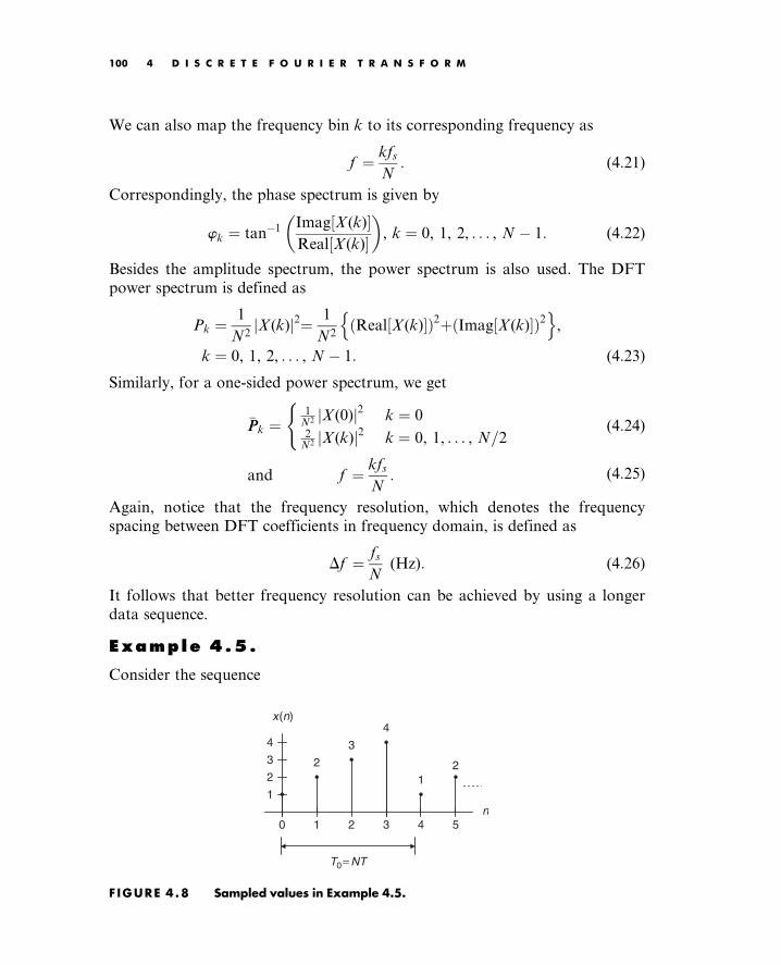
We can also map the frequency bin k to its corresponding frequency as
f ¼ kfs
N: (4:21)
Correspondingly, the phase spectrum is given by
wk ¼ tan1 Imag X (k)½ Real X(k)½
, k ¼ 0, 1, 2, . . . , N 1: (4:22)
Besides the amplitude spectrum, the power spectrum is also used. The DFT
power spectrum is defined as
Pk ¼1
N2X(k)j j2¼ 1
N2Real X(k)½ ð Þ2þ Imag X(k)½ ð Þ2
n o,
k ¼ 0, 1, 2, . . . , N 1: (4:23)
Similarly, for a one-sided power spectrum, we get
PPk ¼1
N2 X (0)j j2 k ¼ 02
N2 X (k)j j2 k ¼ 0, 1, . . . , N=2
((4:24)
and f ¼ kfs
N: (4:25)
Again, notice that the frequency resolution, which denotes the frequency
spacing between DFT coefficients in frequency domain, is defined as
Df ¼ fs
N(Hz): (4:26)
It follows that better frequency resolution can be achieved by using a longer
data sequence.
Example 4.5.
Consider the sequence
x(n)
0 1 2 3
1
2
n
2
1
4 5
3
44
3
2
T0= NT
F IGURE 4.8 Sampled values in Example 4.5.
Tan: Digital Signaling Processing 0123740908_chap04 Final Proof page 100 21.6.2007 10:59pm Compositor Name: Mraja
100 4 D I S C R E T E F O U R I E R T R A N S F O R M

Assuming that fs ¼ 100Hz,
a. Compute the amplitude spectrum, phase spectrum, and power spectrum.
Solution:
a. Since N ¼ 4, and using the DFT shown in Example 4.1, we find the DFT
coefficients to be
X (0) ¼ 10
X (1) ¼ 2þ j2
X (2) ¼ 2
X (3) ¼ 2 j2:
The amplitude spectrum, phase spectrum, and power density spectrum are
computed as follows.
For k ¼ 0, f ¼ k fs=N ¼ 0 100=4 ¼ 0 Hz,
A0 ¼1
4X (0)j j ¼ 2:5, w0 ¼ tan1 Imag X (0)½
Real( X(0)½
¼ 00,
P0 ¼1
42X (0)j j2¼ 6:25:
For k ¼ 1, f ¼ 1 100=4 ¼ 25 Hz,
A1 ¼1
4X (1)j j ¼ 0:7071, w1 ¼ tan1 Imag X (1)½
Real X (1)½
¼ 1350,
P1 ¼1
42X (1)j j2¼ 0:5000:
For k ¼ 2, f ¼ 2 100=4 ¼ 50 Hz,
A2 ¼1
4X (2)j j ¼ 0:5, w2 ¼ tan1 Imag X (2)½
Real X (2)½
¼ 1800,
P2 ¼1
42X (2)j j2¼ 0:2500:
Similarly, for k ¼ 3, f ¼ 3 100=4 ¼ 75 Hz,
A3 ¼1
4X (3)j j ¼ 0:7071, w3 ¼ tan1 Imag X (3)½
Real X(3)½
¼ 1350,
P3 ¼1
42X (3)j j2¼ 0:5000:
Tan: Digital Signaling Processing 0123740908_chap04 Final Proof page 101 21.6.2007 10:59pm Compositor Name: Mraja
4.2 Amplitude Spectrum and Power Spectrum 101

Thus, the sketches for the amplitude spectrum, phase spectrum, and
power spectrum are given in Figure 4.9.
Ak
k0 1 2
2
4
f (Hz)
2.5
0.7071 0.70710.5
0 25 50
3
75
ϕk
k0 1 2−1
2000
00
1800
−1350
1350
1000
−1000
−2000
3
A
F IGURE 4.9A Amplitude spectrum and phase spectrum in Example 4.5.
Pk
0 1 2
4
86.25
0.5 0.50.25
f (Hz)0 25 50 75
3k
B
F IGURE 4.9B Power density spectrum in Example 4.5.
Note that the folding frequency in this example is 50 Hz and the amplitude
and power spectrum values at 75 Hz are each image counterparts (corre-
sponding negative-indexed frequency components). Thus values at 0, 25,
and 50 Hz correspond to the positive-indexed frequency components.
Tan: Digital Signaling Processing 0123740908_chap04 Final Proof page 102 21.6.2007 10:59pm Compositor Name: Mraja
102 4 D I S C R E T E F O U R I E R T R A N S F O R M

We can easily find the one-sided amplitude spectrum and one-sided power
spectrum as
A0 ¼ 2:5, A1 ¼ 1:4141, A2 ¼ 1 and
PP0 ¼ 6:25, PP1 ¼ 2, PP2 ¼ 1:
We plot the one-sided amplitude spectrum for comparison:
Ak
k0 1 2
2
4
f (Hz)
2.51.4141
1
0 25 50
F IGURE 4 .10 One-sided amplitude spectrum in Example 4.5.
Note that in the one-sided amplitude spectrum, the negative-indexed fre-
quency components are added back to the corresponding positive-indexed
frequency components; thus each amplitude value other than the DC term is
doubled. It represents the frequency components up to the folding frequency.
Example 4.6.
Consider a digital sequence sampled at the rate of 10 kHz. If we use a size of
1,024 data points and apply the 1,024-point DFT to compute the spectrum,
a. Determine the frequency resolution.
b. Determine the highest frequency in the spectrum.
Solution:
a. Df ¼ fsN¼ 10000
1024¼ 9:776Hz:
b. The highest frequency is the folding frequency, given by
fmax ¼N
2Df ¼ fs
2
¼ 512 9:776 ¼ 5000 Hz
As shown in Figure 4.7, the DFT coefficients may be computed via a fast
Fourier transform (FFT) algorithm. The FFT is a very efficient algorithm for
Tan: Digital Signaling Processing 0123740908_chap04 Final Proof page 103 21.6.2007 10:59pm Compositor Name: Mraja
4.2 Amplitude Spectrum and Power Spectrum 103

computing DFT coefficients. The FFT algorithm requires the time domain
sequence x(n) to have a length of data points equal to a power of 2; that is, 2m
samples, where m is a positive integer. For example, the number of samples in
x(n) can be N ¼ 2,4,8,16, etc.
In the case of using the FFT algorithm to compute DFT coefficients, where
the length of the available data is not equal to a power of 2 (required by the
FFT), we can pad the data sequence with zeros to create a new sequence with
a larger number of samples, N ¼ 2m > N. The modified data sequence for
applying FFT, therefore, is
xx(n) ¼ x(n) 0 # n # N 1
0 N # n # N 1
n: (4:27)
It is very important to note that the signal spectra obtained via zero-padding the
data sequence in Equation (4.27) does not add any new information and does not
contain more accurate signal spectral presentation. In this situation, the fre-
quency spacing is reduced due to more DFT points, and the achieved spectrum
is an interpolated version with ‘‘better display.’’ We illustrate the zero padding
effect via the following example instead of theoretical analysis. A theoretical
discussion of zero padding in FFT can be found in Proakis and Manolakis (1996).
Figure 4.11a shows the 12 data samples from an analog signal containing
frequencies of 10 Hz and 25 Hz at a sampling rate of 100 Hz, and the amplitude
0 5 10−2
0
2
Orig
inal
dat
a
0
0.5
Am
plitu
de s
pect
rum
0 5 10 15−2
0
2
Pad
ding
4 z
eros
0
0.5
Am
plitu
de s
pect
rum
0 10 20 30−2
0
2
Number of samples
Number of samples
Number of samples
Pad
ding
20
zero
s
0 50 100
0 50 100
0 50 100
0
0.5
Frequency (Hz)
Frequency (Hz)
Frequency (Hz)
Am
plitu
de s
pect
rum
zero padding
zero padding
A
B
C
F IGURE 4.11 Zero padding effect by using FFT.
Tan: Digital Signaling Processing 0123740908_chap04 Final Proof page 104 21.6.2007 10:59pm Compositor Name: Mraja
104 4 D I S C R E T E F O U R I E R T R A N S F O R M

spectrum obtained by applying the DFT. Figure 4.11b displays the signal samples
with padding of four zeros to the original data to make up a data sequence of
16 samples, along with the amplitude spectrum calculated by FFT. The data se-
quence padded with 20 zeros and its calculated amplitude spectrum using FFT are
shown in Figure 4.11c. It is evident that increasing the data length via zero padding
to compute the signal spectrumdoes not add basic information and does not change
the spectral shape but gives the ‘‘interpolated spectrum’’ with the reduced frequency
spacing. We can get a better view of the two spectral peaks described in this case.
The only way to obtain the detailed signal spectrum with a fine frequency
resolution is to apply more available data samples, that is, a longer sequence of
data. Here, we choose to pad the least number of zeros possible to satisfy the
minimum FFT computational requirement. Let us look at another example.
Example 4.7.
We use the DFT to compute the amplitude spectrum of a sampled data sequence
with a sampling rate fs ¼ 10 kHz. Given that it requires the frequency resolution
to be less than 0.5 Hz,
a. Determine the number of data points by using the FFT algorithm, as-
suming that the data samples are available.
Solution:
Df ¼ 0:5 Hz
N ¼ fs
Df¼ 10000
0:5¼ 20000
a. Since we use the FFT to compute the spectrum, the number of the data
points must be a power of 2, that is,
N ¼ 215 ¼ 32768:
And the resulting frequency resolution can be recalculated as
Df ¼ fs
N¼ 10000
32768 ¼ 0:31Hz:
Next, we study a MATLAB example.
Example 4.8.
Given the sinusoid
x(n) ¼ 2 sin 2000pn
8000
Tan: Digital Signaling Processing 0123740908_chap04 Final Proof page 105 21.6.2007 10:59pm Compositor Name: Mraja
4.2 Amplitude Spectrum and Power Spectrum 105

obtained by sampling the analog signal
x(t) ¼ 2 sin 2000ptð Þwith a sampling rate of fs ¼ 8,000 Hz,
a. Use the MATLAB DFT to compute the signal spectrum with the
frequency resolution to be equal to or less than 8 Hz.
b. Use the MATLAB FFT and zero padding to compute the signal spec-
trum, assuming that the data samples are available in (1).
Solution:
a. The number of data points is found to be N ¼ fsDf¼ 8000
8¼ 1000. There is
no zero padding needed if we use the DFT formula. Detailed implemen-
tation is given in Program 4.1. The first and second plots in Figure 4.12
show the two-sided amplitude and power spectra, respectively, using the
DFT, where each frequency counterpart at 7,000 Hz appears. The third
and fourth plots are the one-side amplitude and power spectra, where the
true frequency contents are displayed from 0 Hz to the Nyquist frequency
of 4 kHz (folding frequency).
b. If the FFT is used, the number of data points must be a power of 2.
Hence we choose
N ¼ 210 ¼ 1024:
Assuming there are only 1,000 data samples available in (a), we need to
pad 24 zeros to the original 1,000 data samples before applying the FFT
algorithm, as required. Thus the calculated frequency resolution is
Df ¼ fs=N ¼ 8000=1024 ¼ 7:8125Hz. Note that this is an interpolated
Program 4.1. MATLAB program for Example 4.8
% Example 4.8
close all;clear all
% Generate the sine wave sequence
fs ¼ 8000; %Sampling rate
N ¼ 1000; % Number of data points
x ¼ 2*sin(2000* pi*[0:1:N 1]=fs);% Apply the DFT algorithm
figure(1)
xf ¼ abs(fft(x))=N; %Compute the amplitude spectrum
Tan: Digital Signaling Processing 0123740908_chap04 Final Proof page 106 21.6.2007 10:59pm Compositor Name: Mraja
106 4 D I S C R E T E F O U R I E R T R A N S F O R M

frequency resolution by using zero padding. The zero padding actually
interpolates a signal spectrum and carries no additional frequency infor-
mation. Figure 4.13 shows the spectral plots using FFT. The detailed
implementation is given in Program 4.1.
P ¼ xf:*xf; %Compute the power spectrum
f ¼ [0:1:N 1]*fs=N; %Map the frequency bin to the frequency (Hz)
subplot(2,1,1); plot(f,xf);grid
xlabel(’Frequency (Hz)’); ylabel(’Amplitude spectrum (DFT)’);
subplot(2,1,2);plot(f,P);grid
xlabel(’Frequency (Hz)’); ylabel(’Power spectrum (DFT)’);
figure(2)
% Convert it to one-sided spectrum
xf(2:N) ¼ 2*xf(2:N); % Get the single-sided spectrum
P ¼ xf:*xf; % Calculate the power spectrum
f ¼ [0:1:N=2]*fs=N % Frequencies up to the folding frequency
subplot(2,1,1); plot(f,xf(1:N=2þ 1));gridxlabel(’Frequency (Hz)’); ylabel(’Amplitude spectrum (DFT)’);
subplot(2,1,2);plot(f,P(1:N=2þ 1));gridxlabel(’Frequency (Hz)’); ylabel(’Power spectrum (DFT)’);
figure (3)
% Zero padding to the length of 1024
x ¼ [x, zeros(1,24)];
N ¼ length(x);
xf ¼ abs(fft(x))=N; %Compute the amplitude spectrum with zero padding
P ¼ xf:*xf; %Compute the power spectrum
f ¼ [0:1:N 1]*fs=N; %Map frequency bin to frequency (Hz)
subplot(2,1,1); plot(f,xf);grid
xlabel(’Frequency (Hz)’); ylabel(’Amplitude spectrum (FFT)’);
subplot(2,1,2);plot(f,P);grid
xlabel(’Frequency (Hz)’); ylabel(’Power spectrum (FFT)’);
figure(4)
% Convert it to one-sided spectrum
xf(2:N) ¼ 2*xf(2:N);
P ¼ xf:*xf;
f ¼ [0:1:N=2]*fs=N;
subplot(2,1,1); plot(f,xf(1:N=2þ 1));gridxlabel(’Frequency (Hz)’); ylabel(’Amplitude spectrum (FFT)’);
subplot(2,1,2);plot(f,P(1:N=2þ 1));gridxlabel(’Frequency (Hz)’); ylabel(’Power spectrum (FFT)’);
Tan: Digital Signaling Processing 0123740908_chap04 Final Proof page 107 21.6.2007 10:59pm Compositor Name: Mraja
4.3 Spectral Estimation Using Window Functions 107

0 1000 2000 3000 4000 5000 6000 7000 8000
0 1000 2000 3000 4000 5000 6000 7000 8000
0
0.5
1
Frequency (Hz)
Frequency (Hz)
Frequency (Hz)
Frequency (Hz)
Am
plitu
de s
pect
rum
(D
FT
)
0
0.2
0.4
0.6
0.8
1
Pow
er s
pect
rum
(D
FT
)
0 500 1000 1500 2000 2500 3000 3500 40000
0 500 1000 1500 2000 2500 3000 3500 40000
0.5
1
1.5
2
Am
plitu
de s
pect
rum
(D
FT
)
1
2
3
4
Pow
er s
pect
rum
(D
FT
)
F IGURE 4.12 Amplitude spectrum and power spectrum using DFT for Example 4.8.
Tan: Digital Signaling Processing 0123740908_chap04 Final Proof page 108 21.6.2007 10:59pm Compositor Name: Mraja
108 4 D I S C R E T E F O U R I E R T R A N S F O R M

0 1000 2000 3000 4000 5000 6000 7000 80000
0.5
1
Frequency (Hz)
Am
plitu
de s
pect
rum
(F
FT
)
0 1000 2000 3000 4000 5000 6000 7000 80000
0.2
0.4
0.6
0.8
1
Frequency (Hz)
Pow
er s
pect
rum
(F
FT
)
0 500 1000 1500 2000 2500 3000 3500 40000
0.5
1
1.5
2
Frequency (Hz)
Am
plitu
de s
pect
rum
(F
FT
)
0 500 1000 1500 2000 2500 3000 3500 40000
1
2
3
4
Frequency (Hz)
Pow
er s
pect
rum
(F
FT
)
F IGURE 4 .13 Amplitude spectrum and power spectrum using FFT for Example 4.8.
Tan: Digital Signaling Processing 0123740908_chap04 Final Proof page 109 21.6.2007 10:59pm Compositor Name: Mraja
4.3 Spectral Estimation Using Window Functions 109

4.3 Spectra l Es t imat ion Using WindowFunct ions
When we apply DFT to the sampled data in the previous section, we theoretically
imply the following assumptions: first, that the sampled data are periodic to
themselves (repeat themselves), and second, that the sampled data are continuous
to themselves and band limited to the folding frequency. The second assumption
is often violated, thus the discontinuity produces undesired harmonic frequen-
cies. Consider the pure 1-Hz sine wave with 32 samples shown in Figure 4.14.
As shown in the figure, if we use a window size of N ¼ 16 samples, which is a
multiple of the two waveform cycles, the second window repeats with continu-
ity. However, when the window size is chosen to be 18 samples, which is not a
multiple of the waveform cycles (2.25 cycles), the second window repeats the
first window with discontinuity. It is this discontinuity that produces harmonic
frequencies that are not present in the original signal. Figure 4.15 shows the
spectral plots for both cases using the DFT/FFT directly.
The first spectral plot contains a single frequency, as we expected, while the
second spectrum has the expected frequency component plus many harmonics,
which do not exist in the original signal. We call such an effect spectral leakage.
5 10 15 20 25 300 35−1
−0.5
0
0.5
1
x(n)
Window size: N = 16 (multiple of waveform cycles)
5 10 15 20 25 30 350 40
−0.5
0
0.5
−1
1
Window size: N = 18 (not multiple of waveform cycles)
x(n)
F IGURE 4.14 Sampling a 1-Hz sine wave using (top) 16 samples per cycle and(bottom) 18 samples per cycle.
Tan: Digital Signaling Processing 0123740908_chap04 Final Proof page 110 21.6.2007 10:59pm Compositor Name: Mraja
110 4 D I S C R E T E F O U R I E R T R A N S F O R M

The amount of spectral leakage shown in the second plot is due to amplitude
discontinuity in time domain. The bigger the discontinuity, the more the leak-
age. To reduce the effect of spectral leakage, a window function can be used
whose amplitude tapers smoothly and gradually toward zero at both ends.
Applying the window function w(n) to a data sequence x(n) to obtain a wind-
owed sequence xw(n) is better illustrated in Figure 4.16 using Equation (4.28):
xw(n) ¼ x(n)w(n), for n ¼ 0, 1, . . . , N 1: (4:28)
The top plot is the data sequence x(n); and the middle plot is the window
function w(n): The bottom plot in Figure 4.16 shows that the windowed sequence
xw(n) is tapped down by a window function to zero at both ends such that the
discontinuity is dramatically reduced.
Example 4.9.
In Figure 4.16, given
& x(2) ¼ 1 and w(2) ¼ 0:2265;
& x(5) ¼ 0:7071 and w(5) ¼ 0:7008,
a. Calculate the windowed sequence data points xw(2) and xw(5).
5 100 15−1
−0.5
0
0.5
1
x(n)
Window size: N = 165 100 15
0.2
0.4
0.6
0
0.8
Ak
Window size: N = 16
0 5 10 15−1
−0.5
0
0.5
1
x(n)
Window size: N = 180 5 10 15
0
0.2
0.4
Ak
Window size: N = 18
F IGURE 4 .15 Signal samples and spectra without spectral leakage and with spectralleakage.
Tan: Digital Signaling Processing 0123740908_chap04 Final Proof page 111 21.6.2007 10:59pm Compositor Name: Mraja
4.3 Spectral Estimation Using Window Functions 111

Solution:
a. Applying the window function operation leads to
xw(2) ¼ x(2) w(2) ¼ 1 0:2265 ¼ 0:2265 and
xw(5) ¼ x(5) w(5) ¼ 0:7071 0:7008 ¼ 0:4956,
which agree with the values shown in the bottom plot in the Figure 4.16.
Using the window function shown in Example 4.9, the spectral plot is
reproduced. As a result, spectral leakage is greatly reduced, as shown in
Figure 4.17.
The common window functions are listed as follows.
The rectangular window (no window function):
wR(n) ¼ 1 0 # n # N 1 (4:29)
The triangular window:
wtri(n) ¼ 1 2nN þ 1j jN 1
, 0 # n # N 1 (4:30)
The Hamming window:
whm(n) ¼ 0:54 0:46 cos2pn
N 1
, 0 # n # N 1 (4:31)
0 2 4 6 8 10 12 14 16
0
−1
1
x(n)
0 2 4 6 8 10 12 14 16
0.5
0
1
Win
dow
w(n
)
0 2 4 6 8 10 12 14 16−1
0
1
Win
dow
ed x
w(n
)
Time index n
F IGURE 4.16 Illustration of the window operation.
Tan: Digital Signaling Processing 0123740908_chap04 Final Proof page 112 21.6.2007 10:59pm Compositor Name: Mraja
112 4 D I S C R E T E F O U R I E R T R A N S F O R M

The Hanning window:
whn(n) ¼ 0:5 0:5 cos2pn
N 1
, 0 # n # N 1 (4:32)
Plots for each window function for a size of 20 samples are shown in Figure 4.18.
The following example details each step for computing the spectral informa-
tion using the window functions.
Example 4.10.
Considering the sequence x(0) ¼ 1, x(1) ¼ 2, x(2) ¼ 3, and x(3) ¼ 4, and given
fs ¼ 100Hz, T ¼ 0:01 seconds, compute the amplitude spectrum, phase spec-
trum, and power spectrum
a. Using the triangular window function.
b. Using the Hamming window function.
Solution:
a. Since N ¼ 4, from the triangular window function, we have
0 5 10 15
−0.5
0
0.5
−1
1
x(n)
(or
igin
al s
igna
l)
Time index n
0 5 10 150
0.2
0.4
Ak
Frequency index
0 5 10 15
−0.5
0
0.5
−1
1
Win
dow
ed x
(n)
Time index n
0 5 10 150
0.2
0.4
Win
dow
ed A
k
Frequency index
F IGURE 4 .17 Comparison of spectra calculated without using a window function andusing a window function to reduce spectral leakage.
Tan: Digital Signaling Processing 0123740908_chap04 Final Proof page 113 21.6.2007 10:59pm Compositor Name: Mraja
4.3 Spectral Estimation Using Window Functions 113

wtri(0) ¼ 1 2 0 4þ 1j j4 1
¼ 0
wtri(1) ¼ 1 2 1 4þ 1j j4 1
¼ 0:6667:
Similarly, wtri(2) ¼ 0:6667, wtri(3) ¼ 0. Next, the windowed sequence is
computed as
xw(0) ¼ x(0) wtri(0) ¼ 1 0 ¼ 0
xw(1) ¼ x(1) wtri(1) ¼ 2 0:6667 ¼ 1:3334
xw(2) ¼ x(2) wtri(2) ¼ 3 0:6667 ¼ 2
xw(3) ¼ x(3) wtri(3) ¼ 4 0 ¼ 0:
Applying DFT Equation (4.8) to xw(n) for k ¼ 0, 1, 2, 3, respectively,
X (k) ¼ xw(0)Wk04 þ x(1)Wk1
4 þ x(2)Wk24 þ x(3)Wk3
4 :
We have the following results:
X (0)¼ 3:3334
X (1)¼2 j1:3334
X (2)¼ 0:6666
0 5 10 15 20
0.2
0.4
0.6
0.8
0
1
Rec
tang
ular
win
dow
0 5 10 15 200
0.2
0.4
0.6
0.8
1
Tria
ngul
ar w
indo
w
0 5 10 15 200
0.2
0.4
0.6
0.8
1
Ham
min
g w
indo
w
0 5 10 15 200
0.2
0.4
0.6
0.8
1
Han
ning
win
dow
F IGURE 4.18 Plots of window sequences.
Tan: Digital Signaling Processing 0123740908_chap04 Final Proof page 114 21.6.2007 10:59pm Compositor Name: Mraja
114 4 D I S C R E T E F O U R I E R T R A N S F O R M

X (3)¼2þ j1:3334
Df ¼ 1
NT¼ 1
4 0:01¼ 25Hz
Applying Equations (4.19), (4.22), and (4.23) leads to
A0 ¼1
4X(0)j j ¼ 0:8334, w0 ¼ tan1 0
3:3334
¼ 00,
P0 ¼1
42X (0)j j2¼ 0:6954
A1 ¼1
4X (1)j j ¼ 0:6009, w1 ¼ tan1 1:3334
2
¼ 146:310,
P1 ¼1
42X (1)j j2¼ 0:3611
A2 ¼1
4X (2)j j ¼ 0:1667, w2 ¼ tan1 0
0:6666
¼ 00,
P2 ¼1
42X (2)j j2¼ 0:0278:
Similarly,
A3 ¼1
4X (3)j j ¼ 0:6009, w3 ¼ tan1 1:3334
2
¼ 146:310,
P3 ¼1
42X (3)j j2¼ 0:3611:
b. Since N ¼ 4, from the Hamming window function, we have
whm(0) ¼ 0:54 0:46 cos2p 0
4 1
¼ 0:08
whm(1) ¼ 0:54 0:46 cos2p 1
4 1
¼ 0:77:
Similarly, whm(2) ¼ 0:77, whm(3) ¼ 0:08. Next, the windowed sequence is
computed as
xw(0) ¼ x(0) whm(0) ¼ 1 0:08 ¼ 0:08
xw(1) ¼ x(1) whm(1) ¼ 2 0:77 ¼ 1:54
xw(2) ¼ x(2) whm(2) ¼ 3 0:77 ¼ 2:31
xw(0) ¼ x(3) whm(3) ¼ 4 0:08 ¼ 0:32:
Applying DFT Equation (4.8) to xw(n) for k ¼ 0, 1, 2, 3, respectively,
Tan: Digital Signaling Processing 0123740908_chap04 Final Proof page 115 21.6.2007 10:59pm Compositor Name: Mraja
4.3 Spectral Estimation Using Window Functions 115

X (k) ¼ xw(0)Wk04 þ x(1)Wk1
4 þ x(2)Wk24 þ x(3)Wk3
4 :
We yield the following:
X (0) ¼ 4:25
X (1) ¼ 2:23 j1:22
X (2) ¼ 0:53
X (3) ¼ 2:23þ j1:22
Df ¼ 1
NT¼ 1
4 0:01¼ 25Hz
Using Equations (4.19), (4.22), and (4.23), we achieve
A0 ¼1
4X (0)j j ¼ 1:0625, w0 ¼ tan1 0
4:25
¼ 00,
P0 ¼1
42X (0)j j2¼ 1:1289
A1 ¼1
4X (1)j j ¼ 0:6355, w1 ¼ tan1 1:22
2:23
¼ 151:320,
P1 ¼1
42X (1)j j2¼ 0:4308
A2 ¼1
4X (2)j j ¼ 0:1325, w2 ¼ tan1 0
0:53
¼ 00,
P2 ¼1
42X (2)j j2¼ 0:0176:
Similarly,
A3 ¼1
4X (3)j j ¼ 0:6355, w3 ¼ tan1 1:22
2:23
¼ 151:320,
P3 ¼1
42X (3)j j2¼ 0:4308:
Example 4.11.
Given the sinusoid
x(n) ¼ 2 sin 2000n
8000
obtained by using a sampling rate of fs ¼ 8,000Hz, use the DFT to compute the
spectrum with the following specifications:
Tan: Digital Signaling Processing 0123740908_chap04 Final Proof page 116 21.6.2007 10:59pm Compositor Name: Mraja
116 4 D I S C R E T E F O U R I E R T R A N S F O R M

a. Compute the spectrum of a triangular window function with a window
size ¼ 50.
b. Compute the spectrum of a Hamming window function with a window
size ¼ 100.
c. Compute the spectrum of a Hanning window function with a window
size ¼ 150 and one-sided spectrum.
The MATLAB program is listed in Program 4.2, and the results are plotted in
Figures 4.19 to 4.21. As compared with the no-windowed (rectangular window)
case, all three windows are able to effectively reduce spectral leakage, as shown
in the figures.
0 20 40 60
−1
0
1
−2
2
Time index n
x(n)
0 20 40 60−2
−1
0
1
2
Time index n
Tria
ngul
ar w
indo
wed
x(n
)
0 2000 4000 6000 80000
0.5
1
Frequency (Hz)
Ak
(no
win
dow
)
0 2000 4000 6000 80000
0.2
0.4
0.6
0.8
1
Frequency (Hz)
Tria
ngul
ar w
indo
wed
Ak
F IGURE 4 .19 Comparisonofaspectrumwithoutusingawindowfunctionandaspectrumusing a triangular window of size of 50 samples in Example 4.11.
Program 4.2. MATLAB program for Example 4.11
%Example 4.11
close all;clear all
% Generate the sine wave sequence
fs ¼ 8000; T ¼ 1=fs; % Sampling rate and sampling period
(Continued )
Tan: Digital Signaling Processing 0123740908_chap04 Final Proof page 117 21.6.2007 10:59pm Compositor Name: Mraja
4.4 Application to Speech Spectral Estimation 117

x ¼ 2*sin(2000*pi*[0:1:50]*T); %Generate the 51 2000-Hz samples
% Apply the FFT algorithm
N ¼ length(x);
index t ¼ [0:1:N 1];f ¼ [0:1 1]*8000=N; %Map the frequency bin to the frequency (Hz)
xf¼abs(fft(x))/N; %Calculate the amplitude spectrum
figure(1)
%Using the Bartlett window
x b ¼ x:*bartlett(N)0; %Apply the triangular window function
xf b ¼ abs(fft(x b))=N; %Calculate the amplitude spectrum
subplot(2,2,1);plot(index_t,x);grid
xlabel(’Time index n’); ylabel(’x(n)’);
subplot(2,2,3); plot(index_t,x_b);grid
xlabel(’Time index n’); ylabel(’Triangular windowed x(n)’);
subplot(2,2,2);plot(f,xf);grid;axis([0 8000 0 1]);
xlabel(’Frequency (Hz)’); ylabel(’Ak (no window)’);
subplot(2,2,4); plot(f,xf_b);grid; axis([0 8000 0 1]);
xlabel(’Frequency (Hz)’); ylabel(’Triangular windowed Ak’);
figure(2)
% Generate the sine wave sequence
x ¼ 2*sin(2000*pi*[0:1:100]*T); %Generate the 101 2000-Hz samples.
% Apply the FFT algorithm
N¼length(x);index t ¼ [0:1:N 1];f ¼ [0:1:N 1]*fs=N;
xf ¼ abs(fft(x))/N;
%Using the Hamming window
x hm ¼ x:*hamming(N)0; %Apply the Hamming window function
xf_hm¼abs(fft(x_hm))/N; %Calculate the amplitude spectrum
subplot(2,2,1);plot(index_t,x);grid
xlabel(’Time index n’); ylabel(’x(n)’);
subplot(2,2,3); plot(index_t,x_hm);grid
xlabel(’Time index n’); ylabel(’Hamming windowed x(n)’);
subplot(2,2,2);plot(f,xf);grid;axis([0 fs 0 1]);
xlabel(’Frequency (Hz)’); ylabel(’Ak (no window)’);
subplot(2,2,4); plot(f,xf_hm);grid;axis([0 fs 0 1]);
xlabel(’Frequency (Hz)’); ylabel(’Hamming windowed Ak’);
figure(3)
% Generate the sine wave sequence
x ¼ 2*sin(2000*pi*[0:1:150]*T); % Generate the 151 2-kHz samples
% Apply the FFT algorithm
N¼length(x);
Tan: Digital Signaling Processing 0123740908_chap04 Final Proof page 118 21.6.2007 10:59pm Compositor Name: Mraja
118 4 D I S C R E T E F O U R I E R T R A N S F O R M

index t ¼ [0:1:N 1];f ¼ [0:1:N 1]*fs=N;
xf ¼ 2*abs(fft(x))=N;xf(1) ¼ xf(1)=2; % Single-sided spectrum
%Using the Hanning window
x hn ¼ x:*hanning(N)0;;
xf hn¼2*abs(fft(x hn))=N;xf hn(1)¼xf hn(1)=2; %Single-sided spectrum
subplot(2,2,1);plot(index_t,x);grid
xlabel(’Time index n’); ylabel(’x(n)’);
subplot(2,2,3); plot(index_t,x_hn);grid
xlabel(’Time index n’); ylabel(’Hanning windowed x(n)’);
subplot(2,2,2);plot(f(1:(N-1)/2),xf(1:(N-1)/2));grid;axis([0 fs/2 0 1]);
xlabel(’Frequency (Hz)’); ylabel(’Ak (no window)’);
subplot(2,2,4);plot(f(1:(N-1)/2),xf_hn(1:(N-1)/2));grid;axis([0fs/201]);
xlabel(’Frequency (Hz)’); ylabel(’Hanning windowed Ak’);
0 50 100−2
−1
0
1
2
Time index n
x(n)
0 50 100−2
−1
0
1
2
Time index n
Ham
min
g w
indo
wed
x(n
)
0 2000 4000 6000 80000
0.5
1
Frequency (Hz)
Ak
(no
win
dow
)
0 2000 4000 6000 80000
0.2
0.4
0.6
0.8
1
Frequency (Hz)
Ham
min
g w
indo
wed
Ak
F IGURE 4 .20 Comparison of a spectrum without using a window function anda spectrum using a Hamming window of size of 100 samples inExample 4.11.
Tan: Digital Signaling Processing 0123740908_chap04 Final Proof page 119 21.6.2007 10:59pm Compositor Name: Mraja
4.4 Application to Speech Spectral Estimation 119

4.4 Appl i cat ion to Speech Spectra lEs t imat ion
The following plots show the comparisons of amplitude spectral estimation for
speech data (we.dat) with 2,001 samples and a sampling rate of 8,000 Hz using the
rectangular window (no window) function and the Hamming window function.
As demonstrated in Figure 4.22 (two-sided spectrum) and Figure 4.23 (one-sided
spectrum), there is little difference between the amplitude spectrum using
the Hamming window function and the spectrum without using the window
function. This is due to the fact that when the data length of the sequence
(e.g., 2,001 samples) increases, the frequency resolution will be improved and
spectral leakage will become less significant. However, when data length is short,
reduction of spectral leakage using a window function will come to be prominent.
4.5 Fast Four ier Transform
Now we study FFT in detail. FFT is a very efficient algorithm in computing
DFT coefficients and can reduce a very large amount of computational com-
plexity (multiplications). Without loss of generality, we consider the digital
0 50 100 150−2
−1
0
1
2
Time index n
x(n)
0 50 100 150−2
−1
0
1
2
Time index n
Han
ning
win
dow
ed x
(n)
0 1000 2000 3000 40000
0.5
1
1.5
2
Frequency (Hz)
Ak
(no
win
dow
)0 1000 2000 3000 4000
0
0.5
1
1.5
2
Frequency (Hz)H
anni
ng w
indo
wed
Ak
F IGURE 4.21 Comparison of a one-sided spectrum without using the window functionand a one-sided spectrum using a Hanning window of size of 150samples in Example 4.11.
Tan: Digital Signaling Processing 0123740908_chap04 Final Proof page 120 21.6.2007 10:59pm Compositor Name: Mraja
120 4 D I S C R E T E F O U R I E R T R A N S F O R M

0 500 1000 1500 2000−1
−0.5
0
0.5
13 104
Time index n
x(n)
0 500 1000 1500 2000−5000
0
5000
10000
Time index n
Ham
min
g w
indo
wed
x(n
)0 2000 4000 6000 8000
0
100
200
300
400
Frequency (Hz)
Am
plitu
de s
pect
rum
Ak
0 2000 4000 6000 80000
100
200
300
400
Frequency (Hz)
Ham
min
g w
indo
wed
Ak
F IGURE 4 .22 Comparison of a spectrum without using a window function and aspectrum using the Hamming window for speech data.
0 500 1000 1500 2000−1
−0.5
0
0.5
13 104
Time index n
x(n)
0 500 1000 1500 2000−5000
0
5000
10000
Time index n
Ham
min
g w
indo
wed
x(n
)
0 1000 2000 30000
200
400
600
800
Frequency (Hz)
Am
plitu
de s
pect
rum
Ak
0 1000 2000 30000
200
400
600
800
Frequency (Hz)
Ham
min
g w
indo
wed
Ak
F IGURE 4 .23 Comparison of a one-sided spectrum without using a window functionand a one-sided spectrum using the Hamming window for speech data.
Tan: Digital Signaling Processing 0123740908_chap04 Final Proof page 121 21.6.2007 10:59pm Compositor Name: Mraja
4.5 Fast Fourier Transform 121

sequence x(n) consisting of 2m samples, where m is a positive integer—the
number of samples of the digital sequence x(n) is a power of 2, N ¼ 2, 4, 8,
16, etc. If x(n) does not contain 2m samples, then we simply append it with zeros
until the number of the appended sequence is equal to an integer of a power of 2
data points.
In this section, we focus on two formats. One is called the decimation-
in-frequency algorithm, while the other is the decimation-in-time algorithm.
They are referred to as the radix-2 FFT algorithms. Other types of FFT algorithms
are the radix-4 and the split radix and their advantages can be exploited
(see Proakis and Manolakis, 1996).
4.5.1 Method of Dec imat ion- in-Frequency
We begin with the definition of DFT studied in the opening section of this
chapter as follows:
X (k) ¼XN1
n¼0
x(n)WknN for k ¼ 0, 1, . . . , N 1, (4:33)
where WN ¼ ej2pN is the twiddle factor, and N ¼ 2, 4, 8, 16, . . . Equation (4.33)
can be expanded as
X (k) ¼ x(0)þ x(1)WkN þ . . .þ x(N 1)W
k(N1)N : (4:34)
Again, if we split Equation (4.34) into
X (k) ¼x(0)þ x(1)WkN þ . . .þ x
N
2 1
W
k(N=21)N
þ xN
2
WkN=2 þ . . .þ x(N 1)W
k(N1)N (4:35)
then we can rewrite as a sum of the following two parts
X (k) ¼X(N=2)1
n¼0
x(n)WknN þ
XN1
n¼N=2
x(n)WknN : (4:36)
Modifying the second term in Equation (4.36) yields
X (k) ¼X(N=2)1
n¼0
x(n)WknN þW
(N=2)kN
X(N=2)1
n¼0
x nþN
2
Wkn
N : (4:37)
Recall WN=2N ¼ ej
2p N=2ð ÞN ¼ ejp ¼ 1; then we have
Tan: Digital Signaling Processing 0123740908_chap04 Final Proof page 122 21.6.2007 10:59pm Compositor Name: Mraja
122 4 D I S C R E T E F O U R I E R T R A N S F O R M

X (k) ¼X(N=2)1
n¼0
x(n)þ ( 1)kx nþN
2
Wkn
N : (4:38)
Now letting k ¼ 2m as an even number achieves
X (2m) ¼X(N=2)1
n¼0
x(n)þ x nþN
2
W 2mn
N , (4:39)
while substituting k ¼ 2mþ 1 as an odd number yields
X (2mþ 1) ¼X(N=2)1
n¼0
x(n) x nþN
2
Wn
NW 2mnN : (4:40)
Using the fact that W 2N ¼ ej2p2
N ¼ ej 2p
N=2ð Þ ¼WN=2, it follows that
X (2m) ¼X(N=2)1
n¼0
a(n)WmnN=2 ¼ DFT a(n) with (N=2) pointsf g (4:41)
X (2mþ 1) ¼X(N=2)1
n¼0
b(n)WnNWmn
N=2 ¼ DFT b(n)WnN with (N=2) points
, (4:42)
where a(n) and b(n) are introduced and expressed as
a(n) ¼ x(n)þ x nþN
2
, for n ¼ 0,1 . . . ,
N
2 1 (4:43a)
b(n) ¼ x(n) x nþN
2
, for n ¼ 0,1, . . . ,
N
2 1: (4:43b)
Equations (4.33), (4.41), and (4.42) can be summarized as
DFT x(n) with N pointsf g ¼ DFT a(n) with N=2ð Þ pointsf gDFT b(n)Wn
N with N=2ð Þ points
(4:44)
The computation process can be illustrated in Figure 4.24. As shown in this
figure, there are three graphical operations, which are illustrated in Figure 4.25.
If we continue the process described by Figure 4.24, we obtain the block
diagrams shown in Figures 4.26 and 4.27.
Figure 4.27 illustrates the FFT computation for the eight-point DFT, where
there are 12 complex multiplications. This is a big saving as compared with the
eight-point DFT with 64 complex multiplications. For a data length of N,
the number of complex multiplications for DFT and FFT, respectively, are
determined by
Tan: Digital Signaling Processing 0123740908_chap04 Final Proof page 123 21.6.2007 10:59pm Compositor Name: Mraja
4.5 Fast Fourier Transform 123

Complex multiplications of DFT ¼ N2, and
Complex multiplications of FFT ¼ N
2log2 Nð Þ:
To see the effectiveness of FFT, let us consider a sequence with 1,024 data
points. Applying DFT will require 1,024 1,024 ¼ 1,048,576 complex multipli-
cations; however, applying FFT will need only ð1,024=2Þ log2 (1,024) ¼ 5,120
complex multiplications. Next, the index (bin number) of the eight-point DFT
coefficient X(k) becomes 0, 4, 2, 6, 1, 5, 3, and 7, respectively, which are not in
the natural order. This can be fixed by index matching. Index matching between
the input sequence and the output frequency bin number by applying reversal
bits is described in Table 4.2.
x(0)
x(1)
x(3)
x(4)
x(5)
x(6)
x(7)
x(2)
a(0)
a(1)
a(2)
a(3)
b(0)
b(1)
b(2)
b(3)
WN0
WN1
WN2
WN3
N
2-point
N
2-point
DFT
DFT
−1
−1
−1
−1
X(0)
X(2)
X(4)
X(6)
X(1)
X(3)
X(5)
X(7)
F IGURE 4.24 The first iteration of the eight-point FFT.
x
y
z = x + y
−1
x
yz = x − y
xw
z = wx
F IGURE 4.25 Definitions of the graphical operations.
N
4- point
DFT
−1
−1
−1
−1
−1
−1
−1
−1
x(0)
x(1)
x(3)
x(4)
x(5)
x(6)
x(7)
x(2)
X(0)
X(2)
X(4)
X(6)
X(1)
X(3)
X(5)
X(7)
WN0
WN0
WN1
WN2
WN2
WN0
WN2WN
3
N
4- point
DFT
N
4- point
DFT
N
4- point
DFT
F IGURE 4.26 The second iteration of the eight-point FFT.
Tan: Digital Signaling Processing 0123740908_chap04 Final Proof page 124 21.6.2007 10:59pm Compositor Name: Mraja
124 4 D I S C R E T E F O U R I E R T R A N S F O R M

Figure 4.28 explains the bit reversal process. First, the input data with indices
0, 1, 2, 3, 4, 5, 6, 7 are split into two parts. The first half contains even indices—0,
2, 4, 6—while the second half contains odd indices. The first half with indices 0,
2, 4, 6 at the first iteration continues to be split into even indices 2, 4 and odd
indices 4, 6, as shown in the second iteration. The second half with indices 1, 3, 5,
x(0)
x(1)
x(3)
x(4)
x(5)
x(6)
x(7)
x(2)
X(0)
X(2)
X(4)
X(6)
X(1)
X(3)
X(5)
X(7)
−1
−1
−1
−1
−1
−1 −1
−1
−1
−1
−1
−1WN0
WN0
WN0
WN0
WN0
WN0
WN1
WN2
WN2
WN0
WN2WN
3
F IGURE 4 .27 Block diagram for the eight-point FFT (total twelve multiplications).
TABLE 4 .2 Index mapping for fast Fourier transform.
Input Data Index Bits Reversal Bits Output Data
x(0) 000 000 X(0)
x(1) 001 100 X(4)
x(2) 010 010 X(2)
x(3) 011 110 X(6)
x(4) 100 001 X(1)
x(5) 101 101 X(5)
x(6) 110 011 X(3)
x(7) 111 111 X(7)
2
4
6
0
4
2
6
0
5
3
7
1
4
0
6
2
5
1
7
3
3
5
7
1
1
2
3
0
5
6
7
4
Binary
001
010
011
000
101
110
111
100
Bit reversal
100
010
011
000
101
011
111
001
1st split 2nd split 3rd splitindex
F IGURE 4 .28 Bit reversal process in FFT.
Tan: Digital Signaling Processing 0123740908_chap04 Final Proof page 125 21.6.2007 10:59pm Compositor Name: Mraja
4.5 Fast Fourier Transform 125

7 at the first iteration is split into even indices 1, 5 and odd indices 3, 7 in
the second iteration. The splitting process continues to the end at the third
iteration. The bit patterns of the output data indices are just the respective
reversed bit patterns of the input data indices. Although Figure 4.28 illustrates
the case of an eight-point FFT, this bit reversal process works as long as N is a
power of 2.
The inverse FFT is defined as
x(n) ¼ 1
N
XN1
k¼0
X (k)WknN ¼ 1
N
XN1
k¼0
X(k) ~WWknN , for k ¼ 0, 1, . . . , N 1: (4:45)
Comparing Equation (4.45) with Equation (4.33), we notice the difference as
follows: The twiddle factor WN is changed to be ~WWN ¼W1N , and the sum is
multiplied by a factor of 1/N. Hence, by modifying the FFT block diagram as
shown in Figure 4.27, we achieve the inverse FFT block diagram shown in
Figure 4.29.
Example 4.12.
Given a sequence x(n) for 0 n 3, where x(0) ¼ 1, x(1) ¼ 2, x(2) ¼ 3, and
x(3) ¼ 4,
a. Evaluate its DFT X(k) using the decimation-in-frequency FFT method.
b. Determine the number of complex multiplications.
Solution:
a. Using the FFT block diagram in Figure 4.27, the result is shown in
Figure 4.30.
18
181818181818
18
−1 −1
−1
−1
−1
−1
−1
−1
−1
−1
−1
−1
x(0)
x(1)
x(3)
x(4)
x(5)
x(6)
x(7)
x(2)
X(0)
X(2)
X(4)
X(6)
X(1)
X(3)
X(5)
X(7)
~WN
0
~WN
0
~WN
1
~WN
2
~WN
3
~WN
0
~WN
2
~WN
0
~WN
2
~WN
0
~WN
0
~WN
0
F IGURE 4.29 Block diagram for the inverse of eight-point FFT.
Tan: Digital Signaling Processing 0123740908_chap04 Final Proof page 126 21.6.2007 10:59pm Compositor Name: Mraja
126 4 D I S C R E T E F O U R I E R T R A N S F O R M

b. From Figure 4.30, the number of complex multiplications is four, which
can also be determined by
N
2log2 (N) ¼ 4
2log2 (4) ¼ 4:
Example 4.13.
Given the DFT sequence X(k) for 0 # k # 3 computed in Example 4.12,
a. Evaluate its inverse DFT x(n) using the decimation-in-frequency
FFT method.
Solution:
a. Using the inverse FFT block diagram in Figure 4.28, we have
x (0) = 1x (2) = 3x (1) = 2x (4) = 4
−1
−1
X (0) = 10
X (2) = −2X (1) = −2 + j2
X (3) = −2 − j2−1
−1
14
14
14
14
001001
11
8
−4
12
j4
4
128
16
~W4
0= 1
~W4
0 = 1
~W4
0 = 1~W4
1= j
00011011
Bit index Bit reversal
F IGURE 4 .31 Four-point inverse FFT block diagram in Example 4.13.
4.5.2 Method of Dec imat ion- in-T ime
In this method, we split the input sequence x(n) into the even indexed x(2m) and
x(2mþ 1), each with N data points. Then Equation (4.33) becomes
X (k) ¼X(N=2)1
m¼0
x(2m)W 2mkN þ
X(N=2)1
m¼0
x(2mþ 1)WkNW 2mk
N ,
for k ¼ 0, 1, . . . , N 1: (4:46)
Using the relation W 2N ¼WN=2, it follows that
X(0)
X(1)
X(2)
X(3)
−1
−1
x(0) = 1
x(1) = 2
x(2) = 3
x(3) = 4
W40 = 1
W40 = 1
W40 = 1W4
1 = −j−1
−1
46
−2−2
10
−2−2 + j2−2 − j2
Bit index00011011
Bit reversal00100111
F IGURE 4 .30 Four-point FFT block diagram in Example 4.12.
Tan: Digital Signaling Processing 0123740908_chap04 Final Proof page 127 21.6.2007 10:59pm Compositor Name: Mraja
4.5 Fast Fourier Transform 127

X (k) ¼X(N=2)1
m¼0
x(2m)WmkN=2 þWk
N
X(N=2)1
m¼0
x(2mþ 1)WmkN=2,
for k ¼ 0, 1, . . . , N 1:
(4:47)
Define new functions as
G(k) ¼X(N=2)1
m¼0
x(2m)WmkN=2 ¼ DFT x(2m) with N=2ð ) pointsf g (4:48)
H(k) ¼X(N=2)1
m¼0
x(2mþ 1)WmkN=2 ¼ DFT x(2mþ 1) with N=2ð ) pointsf g: (4:49)
Note that
G(k) ¼ G kþN
2
, for k ¼ 0, 1, . . . ,
N
2 1 (4:50)
H(k) ¼ H kþN
2
, for k ¼ 0, 1, . . . ,
N
2 1: (4:51)
Substituting Equations (4.50) and (4.51) into Equation (4.47) yields the first half
frequency bins
X (k) ¼ G(k)þWkNH(k), for k ¼ 0, 1, . . . ,
N
2 1: (4:52)
Considering the following fact and using Equations (4.50) and (4.51),
W(N=2þk)N ¼ Wk
N : (4:53)
Then the second half of frequency bins can be computed as follows:
XN
2þ k
¼ G(k)Wk
NH(k), for k ¼ 0, 1, . . . ,N
2 1: (4:54)
If we perform backward iterations, we can obtain the FFT algorithm. Procedure
using Equations (4.52) and (4.54) is illustrated in Figure 4.32, the block diagram
for the eight-point FFT algorithm.
From a further iteration, we obtain Figure 4.33. Finally, after three recur-
sions, we end up with the block diagram in Figure 4.34.
The index for each input sequence element can be achieved by bit reversal
of the frequency index in a sequential order. Similar to the method of
decimation-in-frequency, after we change WN to ~WWN in Figure 4.34 and multi-
ply the output sequence by a factor of 1/N, we derive the inverse FFT block
diagram for the eight-point inverse FFT in Figure 4.35.
Tan: Digital Signaling Processing 0123740908_chap04 Final Proof page 128 21.6.2007 10:59pm Compositor Name: Mraja
128 4 D I S C R E T E F O U R I E R T R A N S F O R M

x (0)
x (2)
x (4)
x (6)
x (1)
x (3)
x (5)
x (7)
G (0)
G (1)
G (2)
G (3)
H (0)
H (1)
H (2)
H (3)
WN0
WN1
WN2
WN3
4 - point
4 - point
DFT
DFT
X (0)
X (1)
X (2)
X (3)
X (4)
X (5)
X (6)
X (7)−1
−1
−1
−1
F IGURE 4 .32 The first iteration.
WN0
WN2
WN0
WN0
WN1
WN2
WN3
WN2
2−pointDFT
−1−1
−1
−1
−1
−1
−1
−1
x(0)
x(4)
x(2)
x(6)
x(1)
x(5)
x(3)
x(7)
X(0)
X(1)
X(2)
X(3)
X(4)
X(5)
X(6)
X(7)
2−pointDFT
2−pointDFT
2−pointDFT
F IGURE 4 .33 The second iteration.
W80
W80
W80
W81
W82
W83
W82
W80
W82
W80
W80
W80 −1 −1
−1
−1
−1
−1
−1
−1
−1
−1
−1
−1
x(0)
x(2)
x(4)
x(6)
x(1)
x(3)
x(5)
x(7)
X(0)
X(1)
X(2)
X(3)
X(4)
X(5)
X(6)
X(7)
F IGURE 4.34 The eight-point FFT algorithm using decimation-in-time (twelve complexmultiplications).
Tan: Digital Signaling Processing 0123740908_chap04 Final Proof page 129 21.6.2007 10:59pm Compositor Name: Mraja
4.5 Fast Fourier Transform 129

Example 4.14.
Given a sequence x(n) for 0 n 3, where x(0) ¼ 1, x(1) ¼ 2, x(2) ¼ 3, and
x(3) ¼ 4,
a. Evaluate its DFT X(k) using the decimation-in-time FFT method.
Solution:
a. Using the block diagram in Figure 4.34 leads to
−1
x(0) = 1
x(2) = 3
x(1) = 2
x(3) = 4
X(0)
X(1)
X(2)
X(3)
4
−2
6
−2
10
−2−1−1
−1
− 2 + j2
− 2 − j2
W41= − j
W40= 1
W40= 1
W40= 1
F IGURE 4.36 The four-point FFT using decimation in time.
Example 4.15.
Given the DFT sequence X(k) for 0 # k # 3 computed in Example 4.14,
a. Evaluate its inverse DFT x(n) using the decimation-in-time FFT method.
Solution:
a. Using the block diagram in Figure 4.35 yields
−1
8
12
−4j4
4
8
12
16
1
41
41
41
4
−1 −1
−1
X(0) = 10
X(2) = −2
X(1) = −2 + j2
X(3) = −2 − j2
x(0) = 1
x(1) = 2x(2) = 3
x(3) = 4
W40= 1
W40= 1
~
~
~W4
1= j
W40= 1
~
F IGURE 4.37 The four-point IFFT using decimation in time.
~
~
~
~
~
~
~
18
18181818181818
~W8
0
~W8
2
~W8
0
~W8
0
~W8
0
W80
W81
W82
W83
W80
W80
W82 −1 −1
−1
−1
−1
−1
−1
−1
−1
−1
−1
−1
X (0)
X (4)
X (2)
X (6)
X (1)
X (5)
X (3)
X (7)
x (0)
x (1)
x (2)
x (3)
x (4)
x (5)
x (6)
x (7)
F IGURE 4.35 The eight-point IFFT using decimation-in-time.
Tan: Digital Signaling Processing 0123740908_chap04 Final Proof page 130 21.6.2007 10:59pm Compositor Name: Mraja
130 4 D I S C R E T E F O U R I E R T R A N S F O R M

4.6 Summar y
1. The Fourier series coefficients for a periodic digital signal can be used to
develop the DFT.
2. The DFT transforms a time sequence to the complex DFT coefficients, while
the inverse DFT transforms DFT coefficients back to the time sequence.
3. The frequency bin number is the same as the frequency index. Frequency
resolution is the frequency spacing between two consecutive frequency
indices (two consecutive spectrum components).
4. The DFT coefficients for a given digital signal are applied for computing
the amplitude spectrum, power spectrum, or phase spectrum.
5. The spectrum calculated from all the DFT coefficients represents the
signal frequency range from 0 Hz to the sampling rate. The spectrum
beyond the folding frequency is equivalent to the negative-indexed spec-
trum from the negative folding frequency to 0 Hz. This two-sided
spectrum can be converted into a one-sided spectrum by doubling alter-
nating-current (AC) components from 0 Hz to the folding frequency and
retaining the DC component as it is.
6. To reduce the burden of computing DFT coefficients, the FFT algorithm
is used, which requires the data length to be a power of 2. Sometimes zero
padding is employed to make up the data length. Zero padding actually
does interpolation of the spectrum and does not carry any new informa-
tion about the signal; even the calculated frequency resolution is smaller
due to the zero padded longer length.
7. Applying the window function to the data sequence before DFT reduces
the spectral leakage due to abrupt truncation of the data sequence when
performing spectral calculation for a short sequence.
8. Two radix-2 FFT algorithms—decimation-in-frequency and decimation-
in-time—are developed via the graphical illustrations.
4.7 Problems
4.1. Given a sequence x(n) for 0 # n # 3, where x(0) ¼ 1, x(1) ¼ 1,
x(2) ¼ 1, and x(3) ¼ 0, compute its DFT X(k).
4.2. Given a sequence x(n) for 0 # n # 3, where x(0) ¼ 4, x(1) ¼ 3, x(2) ¼ 2,
and x(3) ¼ 1, evaluate its DFT X(k).
4.3. Given the DFT sequence X(k) for 0 # k # 3 obtained in Problem 4.2,
evaluate its inverse DFT x(n).
Tan: Digital Signaling Processing 0123740908_chap04 Final Proof page 131 21.6.2007 10:59pm Compositor Name: Mraja
4.7 Problems 131

4.4. Given a sequence x(n), where x(0) ¼ 4, x(1) ¼ 3, x(2) ¼ 2, and x(3) ¼ 1
with the last two data zero-padded as x(4) ¼ 0, and x(5) ¼ 0, evaluate its
DFT X(k).
4.5. Using the DFT sequence X(k) for 0 # k # 5 computed in Problem 4.4,
evaluate the inverse DFT x(0) and x(4).
4.6. Consider a digital sequence sampled at the rate of 20,000 Hz. If we use
the 8,000-point DFT to compute the spectrum, determine
a. the frequency resolution
b. the folding frequency in the spectrum.
4.7. We use the DFT to compute the amplitude spectrum of a sampled data
sequence with a sampling rate fs ¼ 2,000 Hz. It requires the frequency
resolution to be less than 0.5 Hz. Determine the number of data points
used by theFFTalgorithmandactual frequency resolution inHz, assuming
that the data samples are available for selecting the number of data points.
4.8. Given the sequence in Figure 4.38
x(n)
0
1
2 3
1
2
n
2
4
4
5
3
44
−1 −1
T0= NT
1
F IGURE 4.38 Data sequence in Problem 4.8.
and assuming that fs ¼ 100Hz, compute the amplitude spectrum, phase spec-
trum, and power spectrum.
4.9. Compute the following window functions for a size of 8:
a. Hamming window function.
b. Hanning window function.
4.10. Given the following data sequence with a length of 6,
x(0) ¼ 0, x(1) ¼ 1, x(2) ¼ 0, x(3) ¼ 1, x(4) ¼ 0, x(5) ¼ 1
compute the windowed sequence xw(n) using the
Tan: Digital Signaling Processing 0123740908_chap04 Final Proof page 132 21.6.2007 10:59pm Compositor Name: Mraja
132 4 D I S C R E T E F O U R I E R T R A N S F O R M

a. triangular window function.
b. Hamming window function.
c. Hanning window function.
4.11. Given the sequence in Figure 4.39
x(n)
0
1
2 3
1
2
n
2
4
4
5
3
44
−1 −1
T0= NT
1
F IGURE 4 .39 Data sequence in Problem 4.11.
where fs ¼ 100Hz and T ¼ 0:01 sec, compute the amplitude spectrum, phase
spectrum, and power spectrum using the
a. triangular window.
b. Hamming window.
c. Hanning window.
4.12. Given the sinusoid
x(n) ¼ 2 sin 2000 2 n
8000
obtained by using the sampling rate at fs ¼ 8,000 Hz, we apply the DFT to
compute the amplitude spectrum.
a. Determine the frequency resolution when the data length is 100
samples. Without using the window function, is there any spectral
leakage in the computed spectrum? Explain.
b. Determine the frequency resolution when the data length is 73
samples. Without using the window function, is there any spectral
leakage in the computed spectrum? Explain.
4.13. Given a sequence x(n) for 0 n 3, where x(0) ¼ 4, x(1) ¼ 3, x(2) ¼ 2,
and x(3) ¼ 1, evaluate its DFT X(k) using the decimation-in-frequency
FFT method, and determine the number of complex multiplications.
Tan: Digital Signaling Processing 0123740908_chap04 Final Proof page 133 21.6.2007 10:59pm Compositor Name: Mraja
4.7 Problems 133

4.14. Given the DFT sequence X(k) for 0 k 3 obtained in Problem 4.13,
evaluate its inverse DFT x(n) using the decimation-in-frequency FFT
method.
4.15. Given a sequence x(n) for 0 n 3, where x(0) ¼ 4, x(1) ¼ 3, x(2) ¼ 2,
and x(3) ¼ 1, evaluate its DFT X(k) using the decimation-in-time FFT
method, and determine the number of complex multiplications.
4.16. Given the DFT sequence X(k) for 0 k 3 computed in Problem 4.15,
evaluate its inverse DFT x(n) using the decimation-in-time FFT method.
4.17 Given three sinusoids with the following amplitude and phases:
x1(t) ¼ 5 cos (2p(500)t)
x2(t) ¼ 5 cos (2p(1200)tþ 0:25p)
x3(t) ¼ 5 cos (2(1800)tþ 0:5p)
a. Create a MATLAB program to sample each sinusoid and generate
a sum of three sinusoids, that is, x(n) ¼ x1(n)þ x2(n)þ x3(n), using
a sampling rate of 8000 Hz, and plot the sum x(n) over a range of
time that will exhibit approximately 0.1 second.
b. Use the MATLAB function fft() to compute DFT coefficients, and
plot and examine the spectrum of the signal x(n).
4.18. Using the sum of sinusoids in Problem 4.17,
a. Generate the sum of sinusoids for 240 samples using a sampling rate
of 8000 Hz.
b. Write a MATLAB program to compute and plot the amplitute
spectrum of the signal x(n) with the FFT and using each of the
following window functions
(1) Rectangular window (no window)
(2) Triangular window
(3) Hamming window
c. Examine the effect of spectral leakage for each window used in (b).
ReferencesAhmed, N., and Natarajan, T. (1983). Discrete-Time Signals and Systems. Reston, VA:
Reston Publishing Co.
Oppenheim, A. V., Schafer, R.W., and Buck, J. R. (1999). Discrete-Time Signal Processing,
2nd ed. Upper Saddle River, NJ: Prentice Hall.
Proakis, J. G., and Manolakis, D. G. (1996). Digital Signal Processing: Principles, Algo-
rithms, and Applications, 3rd ed. Upper Saddle River, NJ: Prentice Hall.
Stearns, S. D., and Hush, D. R. (1990). Digital Signal Analysis, 2nd ed. Englewood Cliffs,
NJ: Prentice Hall.
Tan: Digital Signaling Processing 0123740908_chap04 Final Proof page 134 21.6.2007 10:59pm Compositor Name: Mraja
134 4 D I S C R E T E F O U R I E R T R A N S F O R M

5The z-Transform
Object ives :
This chapter introduces the z-transform and its properties; illustrates how to
determine the inverse z-transform using partial fraction expansion; and applies
the z-transform to solve linear difference equations.
5.1 Def in i t ion
The z-transform is a very important tool in describing and analyzing digital
systems. It also offers the techniques for digital filter design and frequency
analysis of digital signals. We begin with the definition of the z-transform.
The z-transform of a causal sequence x(n), designated by X(z) or Z(x(n)), is
defined as
X (z) ¼ Z(x(n)) ¼X1n¼0
x(n)zn
¼ x(0)z0 þ x(1)z1 þ x(2)z2 þ . . .
(5:1)
where z is the complex variable. Here, the summation taken from n ¼ 0 to
n ¼ 1 is according to the fact that for most situations, the digital signal x(n)
is the causal sequence, that is, x(n) ¼ 0 for n < 0. Thus, the definition in
Equation (5.1) is referred to as a one-sided z-transform or a unilateral transform.
In Equation (5.1), all the values of z that make the summation to exist form a
region of convergence in the z-transform domain, while all other values of z
outside the region of convergence will cause the summation to diverge. The
region of convergence is defined based on the particular sequence x(n) being
Tan: Digital Signaling Processing 0123740908_chap05 Final Proof page 135 19.6.2007 12:06pm Compositor Name: Mraja

applied. Note that we deal with the unilateral z-transform in this book, and
hence when performing inverse z-transform (which we shall study later), we are
restricted to the causal sequence. Now let us study the following typical
examples.
Example 5.1.
Given the sequence
x(n) ¼ u(n),
a. Find the z-transform of x(n).
Solution:
a. From the definition of Equation (5.1), the z-transform is given by
X(z) ¼X1n¼0
u(n)zn ¼X1n¼0
z1 n¼ 1þ z1
þ z1 2þ . . . :
This is an infinite geometric series that converges to
X(z) ¼ z
z 1
with a condition z1 < 1. Note that for an infinite geometric series, we
have 1þ rþ r2 þ . . . ¼ 11r
when rj j < 1. The region of convergence for all
values of z is given as zj j > 1.
Example 5.2.
Considering the exponential sequence
x(n) ¼ anu(n),
a. Find the z-transform of the sequence x(n).
Solution:
a. From the definition of the z-transform in Equation (5.1), it follows that
X (z) ¼X1n¼0
anu(n)zn ¼X1n¼0
az1 n¼ 1þ az1
þ az1 2þ . . . :
Since this is a geometric series which will converge for az1 < 1, it is
further expressed as
X (z) ¼ z
z a, for zj j > aj j:
Tan: Digital Signaling Processing 0123740908_chap05 Final Proof page 136 19.6.2007 12:06pm Compositor Name: Mraja
136 5 T H E Z - T R A N S F O R M

The z-transforms for common sequences are summarized in Table 5.1.
Example 5.3 illustrates finding the z-transform using Table 5.1.
TABLE 5 .1 Table of z-transform pairs.
Line No. x(n), n$0 z-Transform X(z)
Region of
Convergence
1 x(n)X1n¼0
x(n)zn
2 d(n) 1 zj j > 0
3 au(n)az
z 1zj j > 1
4 nu(n)z
(z 1)2zj j > 1
5 n2u(n)z(zþ 1)
(z 1)3zj j > 1
6 anu(n)z
z azj j > aj j
7 enau(n)z
(z ea)zj j > ea
8 nanu(n)az
(z a)2zj j > aj j
9 sin (an)u(n)z sin (a)
z2 2z cos (a)þ 1zj j > 1
10 cos (an)u(n)z[z cos (a)]
z2 2z cos (a)þ 1zj j > 1
11 an sin (bn)u(n)[a sin (b)]z
z2 [2a cos (b)]zþ a2zj j > aj j
12 an cos (bn)u(n)z[z a cos (b)]
z2 [2a cos (b)]zþ a2zj j > aj j
13 ean sin (bn)u(n)[ea sin (b)]z
z2 [2ea cos (b)]zþ e2azj j > ea
14 ean cos (bn)u(n)z[z ea cos (b)]
z2 [2ea cos (b)]zþ e2azj j > ea
15 2 Aj j Pj jn cos nuþ fð )u(n)
where P and A are
complex constants
defined by P ¼ Pj jffu,A ¼ Aj jfff
Az
z Pþ Az
z P
Tan: Digital Signaling Processing 0123740908_chap05 Final Proof page 137 19.6.2007 12:06pm Compositor Name: Mraja
5.1 Definition 137

Example 5.3.
Find the z-transform for each of the following sequences:
a. x(n) ¼ 10u(n)
b. x(n) ¼ 10 sin (0:25pn)u(n)
c. x(n) ¼ (0:5)nu(n)
d. x(n) ¼ (0:5)n sin (0:25pn)u(n)
e. x(n) ¼ e0:1n cos (0:25pn)u(n)
Solution:
a. From Line 3 in Table 5.1, we get
X (z) ¼ Z 10u(n)ð Þ ¼ 10z
z 1:
b. Line 9 in Table 5.1 leads to
X (z) ¼ 10Z sin (0:2pn)u(n)ð Þ
¼ 10 sin (0:25p)z
z2 2z cos (0:25p)þ 1¼ 7:07z
z2 1:414zþ 1:
c. From Line 6 in Table 5.1, we yield
X (z) ¼ Z (0:5)nu(n)ð Þ ¼ z
z 0:5:
d. From Line 11 in Table 5.1, it follows that
X (z) ¼ Z (0:5)n sin (0:25pn)u(n)ð Þ ¼ 0:5 sin (0:25p)z
z2 2 0:5 cos (0:25p)zþ 0:52
¼ 0:3536z
z2 1:4142zþ 0:25:
e. From Line 14 in Table 5.1, it follows that
X (z) ¼ Z e0:1n cos (0:25pn)u(n)
¼ z(z e0:1 cos (0:25p))
z2 2e0:1 cos (0:25p)zþ e0:2
¼ z(z 0:6397)
z2 1:2794zþ 0:8187:
Tan: Digital Signaling Processing 0123740908_chap05 Final Proof page 138 19.6.2007 12:06pm Compositor Name: Mraja
138 5 T H E Z - T R A N S F O R M

5.2 Proper t ies of the z-Transform
In this section, we study some important properties of the z-transform. These
properties are widely used in deriving the z-transform functions of difference
equations and solving the system output responses of linear digital systems with
constant system coefficients, which will be discussed in the next chapter.
Linearity: The z-transform is a linear transformation, which implies
Z ax1(n)þ bx2(n)ð Þ ¼ aZ x1(n)ð Þ þ bZ x2(n)ð Þ, (5:2)
where x1(n) and x2(n) denote the sampled sequences, while a and b are the
arbitrary constants.
Example 5.4.
a. Find the z-transform of the sequence defined by
x(n) ¼ u(n) 0:5ð Þnu(n):
Solution:
a. Applying the linearity of the z-transform previously discussed, we have
X (z) ¼ Z x(n)ð Þ ¼ Z u(n)ð Þ Z 0:5n(n)ð Þ:Using Table 5.1 yields
Z u(n)ð Þ ¼ z
z 1
and Z 0:5nu(n)ð Þ ¼ z
z 0:5:
Substituting these results into X(z) leads to the final solution,
X (z) ¼ z
z 1 z
z 0:5:
Shift theorem: Given X(z), the z-transform of a sequence x(n), the z-transform of
x(nm), the time-shifted sequence, is given by
Z x(nm)ð Þ ¼ zmX (z): (5:3)
Note that if m$0, then x(nm) is obtained by right shifting x(n) by m
samples. Since the shift theorem plays a very important role in developing
the transfer function from a difference equation, we verify the shift theorem
for the causal sequence. Note that the shift thoerem also works for the
noncausal sequence.
Verification: Applying the z-transform to the shifted causal signal x(nm)
leads to
Tan: Digital Signaling Processing 0123740908_chap05 Final Proof page 139 19.6.2007 12:06pm Compositor Name: Mraja
5.2 Properties of the z-Transform 139

Z x(nm)ð Þ ¼X1n¼0
x(nm)zn
¼ x(m)z0 þ . . .þ x( 1)z(m1) þ x(0)zm þ x(1)zm1 þ . . . :
Since x(n) is assumed to be a causal sequence, this means that
x(m) ¼ x(mþ 1) ¼ . . . ¼ x( 1) ¼ 0:
Then we achieve
Z x(nm)ð Þ ¼ x(0)zm þ x(1)zm1 þ x(2)zm2 þ . . . : (5:4)
Factoring zm from Equation (5.4) and applying the definition of z-transform of
X(z), we get
Z x(nm)ð Þ ¼ zm x(0)þ x(1)z1 þ x(2)z2 þ . . .
¼ zmX(z):
Example 5.5.
a. Determine the z-transform of the following sequence:
y(n) ¼ 0:5ð Þ(n5)u(n 5),
where u(n 5) ¼ 1 for n 5 and u(n 5) ¼ 0 for n < 5.
Solution:
a. We first use the shift theorem to have
Y (z) ¼ Z 0:5ð Þn5u(n 5)
h i¼ z5Z 0:5ð Þnu(n)½ :
Using Table 5.1 leads to
Y (z) ¼ z5 z
z 0:5¼ z4
z 0:5:
Convolution: Given two sequences x1(n) and x2(n), their convolution can be
determined as follows:
x(n) ¼ x1(n)x2(n) ¼X1k¼0
x1(n k)x2(k), (5:5)
where designates the linear convolution. In z-transform domain, we have
X (z) ¼ X1(z)X2(z): (5:6)
Here, X (z) ¼ Z(x(n)), X1(z) ¼ Z(x1(n)), and X2(z) ¼ Z(x2(n)).
Tan: Digital Signaling Processing 0123740908_chap05 Final Proof page 140 19.6.2007 12:06pm Compositor Name: Mraja
140 5 T H E Z - T R A N S F O R M

Example 5.6.
a. Verify Equation (5.5) using causal sequences x1(n) and x2(n).
Solution:
a. Taking the z-transform of Equation (5.5) leads to
X(z) ¼X1n¼0
x(n)zn ¼X1n¼0
X1k¼0
x1(n k)x2(k)zn:
This expression can be further modified to
X (z) ¼X1n¼0
X1k¼0
x2(k)zkx1(n k)z(nk):
Now interchanging the order of the previous summation gives
X (z) ¼X1k¼0
x2(k)zkX1n¼0
x1(n k)z(nk):
Now, let m ¼ n k:
X (z) ¼X1k¼0
x2(k)zkX1m¼0
x1(m)zm:
By the definition of Equation (5.1), it follows that
X (z) ¼ X2(z)X1(z) ¼ X1(z)X2(z):
Example 5.7.
Given two sequences,
x1(n) ¼ 3d(n)þ 2d(n 1)
x2(n) ¼ 2d(n) d(n 1),
a. Find the z-transform of their convolution:
X(z) ¼ Z x1(n)x2(n)ð Þ:
b. Determine the convolution sum using the z-transform:
x(n) ¼ x1(n)x2(n) ¼X1k¼0
x1(k)x2(n k):
Tan: Digital Signaling Processing 0123740908_chap05 Final Proof page 141 19.6.2007 12:06pm Compositor Name: Mraja
5.2 Properties of the z-Transform 141

Solution:
a. Applying z-transform to x1(n) and x2(n), respectively, it follows that
X1(z) ¼ 3þ 2z1
X2(z) ¼ 2 z1:
Using the convolution property, we have
X (z) ¼ X1(z)X2(z) ¼ (3þ 2z1)(2 z1)
¼ 6þ z1 2z2:
b. Applying the inverse z-transform and using the shift theorem and line 1 of
Table 5.1 leads to
x(n) ¼ Z1 6þ z1 2z2
¼ 6d(n)þ d(n 1) 2d(n 2):
The properties of the z-transform discussed in this section are listed in Table 5.2.
5.3 Inverse z-Transform
The z-transform of the sequence x(n) and the inverse z-transform of the function
X(z) are defined as, respectively,
X (z) ¼ Z x(n)ð Þ (5:7)
and x(n) ¼ Z1 X (z)ð Þ, (5:8)
where Z( ) is the z-transform operator, while Z1( ) is the inverse z-transform
operator.
The inverse z-transform may be obtained by at least three methods:
1. Partial fraction expansion and look-up table
2. Power series expansion
3. Residue method.
TABLE 5 .2 Properties of z-transform.
Property Time Domain z-Transform
Linearity ax1(n)þ bx2(n) aZ x1(n)ð Þ þ bZ x2(n)ð ÞShift theorem x(nm) zmX (z)
Linear convolution x1(n)x2(n) ¼P1k¼0
x1(n k)x2(k) X1(z)X2(z)
Tan: Digital Signaling Processing 0123740908_chap05 Final Proof page 142 19.6.2007 12:06pm Compositor Name: Mraja
142 5 T H E Z - T R A N S F O R M

The first method is widely utilized, and it is assumed that the reader is well
familiar with the partial fraction expansion method in learning Laplace trans-
form. Therefore, we concentrate on the first method in this book. As for the
power series expansion and residue methods, the interested reader is referred to
the textbook by Oppenheim and Schafer (1975). The key idea of the partial
fraction expansion is that if X(z) is a proper rational function of z, we can
expand it to a sum of the first-order factors or higher-order factors using the
partial fraction expansion that could be inverted by inspecting the z-transform
table. The partial fraction expansion method is illustrated via the following
examples. (For simple z-transform functions, we can directly find the inverse z-
transform using Table 5.1.)
Example 5.8.
Find the inverse z-transform for each of the following functions:
a. X (z) ¼ 2þ 4z
z 1 z
z 0:5
b. X (z) ¼ 5z
(z 1)2 2z
(z 0:5)2
c. X (z) ¼ 10z
z2 zþ 1
d. X (z) ¼ z4
z 1þ z6 þ z3
zþ 0:5
Solution:
a. x(n) ¼ 2Z1 1ð Þ þ 4Z1 z
z 1
Z1 z
z 0:5
:
From Table 5.1, we have
x(n) ¼ 2d(n)þ 4u(n) (0:5)nu(n).
b. x(n) ¼ Z1 5z
(z1)2
Z1 2z
(z0:5)2
¼ 5Z1 z
(z1)2
2
0:5 Z1 0:5z(z0:5)2
.
Then x(n) ¼ 5nu(n) 4n(0:5)nu(n).
c. Since X (z) ¼ 10z
z2 zþ 1¼ 10
sin (a)
sin (a)z
z2 2z cos (a)þ 1,
by coefficient matching, we have
2 cos (a) ¼ 1:
Hence, cos (a) ¼ 0:5, and a ¼ 60. Substituting a ¼ 60 into the sine func-
tion leads to
Tan: Digital Signaling Processing 0123740908_chap05 Final Proof page 143 19.6.2007 12:06pm Compositor Name: Mraja
5.3 Inverse z-Transform 143

sin (a) ¼ sin (60) ¼ 0:866:
Finally, we have
x(n) ¼ 10
sin (a)Z1 sin (a)z
z2 2z cos (a)þ 1
¼ 10
0:866sin (n 600)
¼ 11:547 sin (n 600):
d. Since
x(n) ¼ Z1 z5 z
z 1
þ Z1 z6 1
þ Z1 z4 z
zþ 0:5
,
using Table 5.1 and the shift property, we get
x(n) ¼ u(n 5)þ d(n 6)þ ( 0:5)n4u(n 4):
Now, we are ready to deal with the inverse z-transform using the partial fraction
expansion and look-up table. The general procedure is as follows:
1. Eliminate the negative powers of z for the z-transform function X(z).
2. Determine the rational function X(z)/z (assuming it is proper), and apply
the partial fraction expansion to the determined rational function X(z)/z
using the formula in Table 5.3.
3. Multiply the expanded function X(z)/z by z on both sides of the equation
to obtain X(z).
4. Apply the inverse z-transform using Table 5.1.
The partial fraction format and the formula for calculating the constants are
listed in Table 5.3.
TABLE 5 .3 Partial fraction(s) and formulas for constant(s).
Partial fraction with the first-order real pole:
R
z pR ¼ (z p)
X (z)
z
z¼p
Partial fraction with the first-order complex poles:Az
(z P)þ Az
(z P)A ¼ (z P)
X (z)
z
z¼P
P ¼ complex conjugate of P
A ¼ complex conjugate of A
Partial fraction with mth-order real poles:
Rm
(z p)þ Rm1
(z p)2þ þ R1
(z p)mRk ¼
1
(k 1)!
dk1
dzk1(z p)m
X (z)
z
z¼p
Tan: Digital Signaling Processing 0123740908_chap05 Final Proof page 144 19.6.2007 12:06pm Compositor Name: Mraja
144 5 T H E Z - T R A N S F O R M

Example 5.9 considers the situation of the z-transform function having first-
order poles.
Example 5.9.
a. Find the inverse of the following z-transform:
X (z) ¼ 1
(1 z1)(1 0:5z1):
Solution:
a. Eliminating the negative power of z by multiplying the numerator and
denominator by z2 yields
X(z) ¼ z2
z2(1 z1)(1 0:5z1):
¼ z2
(z 1)(z 0:5)
Dividing both sides by z leads to
X (z)
z¼ z
(z 1)(z 0:5):
Again, we write
X(z)
z¼ A
(z 1)þ B
(z 0:5):
Then A and B are constants found using the formula in Table 5.3, that is,
A ¼ (z 1)X (z)
z
z¼1
¼ z
(z 0:5)
z¼1
¼ 2,
B ¼ (z 0:5)X (z)
z
z¼0:5
¼ z
(z 1)
z¼0:5
¼ 1:
Thus
X(z)
z¼ 2
(z 1)þ 1
(z 0:5):
Multiplying z on both sides gives
X(z) ¼ 2z
(z 1)þ z
(z 0:5):
Using Table 5.1 of the z-transform pairs, it follows that
Tan: Digital Signaling Processing 0123740908_chap05 Final Proof page 145 19.6.2007 12:06pm Compositor Name: Mraja
5.3 Inverse z-Transform 145

x(n) ¼ 2u(n) 0:5ð Þnu(n):
Tabulating this solution in terms of integer values of n, we obtain the
results in Table 5.4.
The following example considers the case where X(z) has first-order complex
poles.
Example 5.10.
a. Find y(n) if Y (z) ¼ z2(zþ 1)
(z 1)(z2 zþ 0:5).
Solution:
a. Dividing Y(z) by z, we have
Y (z)
z¼ z(zþ 1)
(z 1)(z2 zþ 0:5):
Applying the partial fraction expansion leads to
Y (z)
z¼ B
z 1þ A
(z 0:5 j0:5)þ A
(z 0:5þ j0:5):
We first find B:
B ¼ (z 1)Y (z)
z
z¼1
¼ z(zþ 1)
(z2 zþ 0:5)
z¼1
¼ 1 (1þ 1)
(12 1þ 0:5)¼ 4:
Notice that A and A form a complex conjugate pair. We determine A as
follows:
A ¼ (z 0:5 j0:5)Y (z)
z
z¼0:5þj0:5
¼ z(zþ 1)
(z 1)(z 0:5þ j0:5)
z¼0:5þj0:5
A ¼ (0:5þ j0:5)(0:5þ j0:5þ 1)
(0:5þ j0:5 1)(0:5þ j0:5 0:5þ j0:5)¼ (0:5þ j0:5)(1:5þ j0:5)
( 0:5þ j0:5)j:
Using the polar form, we get
A ¼ (0:707ff45)(1:58114ff18:43)
(0:707ff135)(1ff90)¼ 1:58114ff 161:57
A ¼ A¼ 1:58114ff161:57:
TABLE 5 .4 Determined sequence in Example 5.9.
n 0 1 2 3 4 . . . 1x(n) 1.0 1.5 1.75 1.875 1.9375 . . . 2.0
Tan: Digital Signaling Processing 0123740908_chap05 Final Proof page 146 19.6.2007 12:06pm Compositor Name: Mraja
146 5 T H E Z - T R A N S F O R M

Assume that a first-order complex pole has the form
P ¼ 0:5þ 0:5j ¼ Pj jffu ¼ 0:707ff45 and P ¼ Pj jff u ¼ 0:707ff 45:
We have
Y (z) ¼ 4z
z 1þ Az
(z P)þ Az
(z P):
Applying the inverse z-transform from line 15 in Table 5.1 leads to
y(n) ¼ 4Z1 z
z 1
þ Z1 Az
(z P)þ Az
(z P)
:
Using the previous formula, the inversion and subsequent simplification
yield
y(n) ¼ 4u(n)þ 2 Aj j Pj jð Þn cos (nuþ f)u(n)
¼ 4u(n)þ 3:1623(0:7071)n cos (45n 161:57)u(n):
The situation dealing with the real repeated poles is presented in Example 5.11.
Example 5.11.
a. Find x(n) if X(z) ¼ z2
(z 1)(z 0:5)2.
Solution:
a. Dividing both sides of the previous z-transform by z yields
X (z)
z¼ z
(z 1)(z 0:5)2¼ A
z 1þ B
z 0:5þ C
(z 0:5)2,
where A ¼ (z 1)X (z)
z
z¼1
¼ z
(z 0:5)2
z¼1
¼ 4:
Using the formulas for mth-order real poles in Table 5.3, where m ¼ 2 and
p ¼ 0:5, to determine B and C yields
B ¼ R2 ¼1
(2 1)!
d
dz(z 0:5)2
X (z)
z
z¼0:5
¼ d
dz
z
z 1
z¼0:5
¼ 1
(z 1)2
z¼0:5
¼ 4
Tan: Digital Signaling Processing 0123740908_chap05 Final Proof page 147 19.6.2007 12:06pm Compositor Name: Mraja
5.3 Inverse z-Transform 147

C ¼ R1 ¼1
(1 1)!
d0
dz0(z 0:5)2
X (z)
z
z¼0:5
¼ z
z 1
z¼0:5¼ 1:
Then X (z) ¼ 4z
z 1þ 4z
z 0:5þ 1z
(z 0:5)2: (5:9)
The inverse z-transform for each term on the right-hand side of Equation
(5.9) can be achieved by the result listed in Table 5.1, that is,
Z1 z
z 1
n o¼ u(n),
Z1 z
z 0:5
n o¼ 0:5ð Þnu(n),
Z1 z
(z 0:5)2
¼ 2n 0:5ð Þnu(n):
From these results, it follows that
x(n) ¼ 4u(n) 4(0:5)nu(n) 2n(0:5)nu(n):
5.3.1 Par t ia l Frac t ion Expans ion Using MATLAB
The MATLAB function residue( ) can be applied to perform the partial fraction
expansion of a z-transform function X(z)/z. The syntax is given as
[R,P,K] ¼ residue(B,A):
Here, B and A are the vectors consisting of coefficients for the numerator and
denominator polynomials, B(z) and A(z), respectively. Notice that B(z) and A(z)
are the polynomials with increasing positive powers of z.
B(z)
A(z)¼ b0z
M þ b1zM1 þ b2z
M2 þ . . .þ bM
zN þ a1zN1 þ a2z2 þ . . .þ aN
:
The function returns the residues in vector R, corresponding poles in vector P,
and polynomial coefficients (if any) in vector K. The expansion format is
shown as
B(z)
A(z)¼ r1
z p1
þ r2
z p2
þ . . .þ k0 þ k1z1 þ . . . :
Tan: Digital Signaling Processing 0123740908_chap05 Final Proof page 148 19.6.2007 12:06pm Compositor Name: Mraja
148 5 T H E Z - T R A N S F O R M

For a pole pj of multiplicity m, the partial fraction includes the following terms:
B(z)
A(z)¼ . . .þ rj
z pj
þ rjþ1
z pj
2 þ . . .þ rjþm
z pj
m þ . . .þ k0 þ k1z1 þ . . . :
Example 5.12.
Find the partial expansion for each of the following z-transform functions:
a. X (z) ¼ 1
(1 z1)(1 0:5z1)
b. Y (z) ¼ z2(zþ 1)
(z 1)(z2 zþ 0:5)
c. X (z) ¼ z2
(z 1)(z 0:5)2
Solution:
a. From MATLAB, we can show the denominator polynomial as
conv([1 1], [1 0:5])D ¼
1.0000 1:5000 0.5000
This leads to
X (z) ¼ 1
(1 z1)(1 0:5z1)¼ 1
1 1:5z1 þ 0:52¼ z2
z2 1:5zþ 0:5
andX (z)
z¼ z
z2 1:5zþ 0:5:
From MATLAB, we have
[R,P,K] ¼ residue([1 0], [1 1:5 0.5])
R ¼2
1
P ¼1.0000
0.5000
K ¼[]
Tan: Digital Signaling Processing 0123740908_chap05 Final Proof page 149 19.6.2007 12:06pm Compositor Name: Mraja
5.3 Inverse z-Transform 149

Then the expansion is written as
X (z) ¼ 2z
z 1 z
z 0:5:
b. From the MATLAB
N ¼ conv([1 0 0], [1 1])
N ¼1 1 0 0
D ¼ conv([1 1], [1 1 0:5])
D ¼1.0000 2:0000 1.5000 0:5000
we get
Y (z) ¼ z2(zþ 1)
(z 1)(z2 zþ 0:5)¼ z3 þ z2
z3 2z2 þ 1:5z 0:5
andY (z)
z¼ z2 þ z
z3 2z2 þ 1:5z 0:5:
Using the MATLAB residue function yields
[R,P,K] ¼ residue([1 1 0], [1 2 1.5 0:5])R ¼4.0000
1.5000 0.5000i
1.5000 þ 0.5000i
P ¼1.0000
0.5000 þ 0.5000i
0.5000 0.5000i
K ¼[]
Then the expansion is shown as:
X(z) ¼ Bz
z p1
þ Az
z pþ Az
z p,
where B ¼ 4,
p1 ¼ 1,
A ¼ 1:5 0:5j,
p ¼ 0:5þ 0:5j,
A ¼ 1:5þ 0:5j, and
p ¼ 0:5 0:5j:
Tan: Digital Signaling Processing 0123740908_chap05 Final Proof page 150 19.6.2007 12:06pm Compositor Name: Mraja
150 5 T H E Z - T R A N S F O R M

c. Similarly,
D ¼ conv(conv([1 1], [1 0:5]), [1 0:5])
D ¼1:0000 2:0000 1:2500 0:2500
then X (z) ¼ z2
(z 1)(z 0:5)2¼ z2
z3 2z2 þ 1:25z 0:25and
we yieldX(z)
z¼ z
z3 2z2 þ 1:25z 0:25.
From MATLAB, we obtain
[R,P,K] ¼ residue([1 0], [1 2 1:25 0:25])
R ¼4.0000
4.0000
1.0000
P ¼1.0000
0.5000
0.5000
K ¼[]
Using the previous results leads to
X (z) ¼ 4z
z 1 4z
z 0:5 z
z 0:5ð Þ2:
5.4 Solut ion of Di f ference Equat ionsUsing the z-Transform
To solve a difference equation with initial conditions, we have to deal with time-
shifted sequences such as y(n 1), y(n 2), . . . , y(nm), and so on. Let us
examine the z-transform of these terms. Using the definition of the z-transform,
we have
Z y(n 1)ð Þ ¼X1n¼0
y(n 1)zn
¼ y( 1)þ y(0)z1 þ y(1)z2 þ . . .
¼ y( 1)þ z1 y(0)þ y(1)z1 þ y(2)z2 þ . . .
Tan: Digital Signaling Processing 0123740908_chap05 Final Proof page 151 19.6.2007 12:06pm Compositor Name: Mraja
5.4 Solution of Difference Equations Using the z-Transform 151

It holds that
Z y(n 1)ð Þ ¼ y( 1)þ z1Y (z): (5:10)
Similarly, we can have
Z y(n 2)ð Þ ¼X1n¼0
y(n 2)zn
¼ y( 2)þ y( 1)z1 þ y(0)z2 þ y(1)z3 þ . . .
¼ y( 2)þ y( 1)z1 þ z2 y(0)þ y(1)z1 þ y(2)z2 þ . . .
Z y(n 2)ð Þ ¼ y( 2)þ y( 1)z1 þ z2Y (z) (5:11)
Z y(nm)ð Þ ¼ y(m)þ y(mþ 1)z1 þ . . .þ y( 1)z(m1)
þzmY (z), (5:12)
where y(m), y(mþ 1), . . . , y( 1) are the initial conditions. If all initial
conditions are considered to be zero, that is,
y(m) ¼ y(mþ 1) ¼ . . . y( 1) ¼ 0, (5:13)
then Equation (5.12) becomes
Z y(nm)ð Þ ¼ zmY (z), (5:14)
which is the same as the shift theorem in Equation (5.3).
The following two examples serve as illustrations of applying the z-transform
to find the solutions of the difference equations. The procedure is:
1. Apply z-transform to the difference equation.
2. Substitute the initial conditions.
3. Solve for the difference equation in z-transform domain.
4. Find the solution in time domain by applying the inverse z-transform.
Example 5.13.
A digital signal processing (DSP) system is described by the difference equation
y(n) 0:5y(n 1) ¼ 5(0:2)nu (n):
a. Determine the solution when the initial condition is given by y( 1) ¼ 1.
Solution:
a. Applying the z-transform on both sides of the difference equation and
using Equation (5.12), we have
Tan: Digital Signaling Processing 0123740908_chap05 Final Proof page 152 19.6.2007 12:06pm Compositor Name: Mraja
152 5 T H E Z - T R A N S F O R M

Y (z) 0:5 y( 1)þ z1Y (z)
¼ 5Z 0:2nu(n)ð Þ:
Substituting the initial condition and Z(0:2nu(n)) ¼ z=(z 0:2), we achieve
Y (z) 0:5 1þ z1Y (z)
¼ 5z=(z 0:2):
Simplification yields
Y (z) 0:5z1Y (z) ¼ 0:5þ 5z=(z 0:2):
Factoring out Y(z) and combining the right-hand side of the equation, it
follows that
Y (z)(1 0:5z1) ¼ (5:5z 0:1)=(z 0:2):
Then we obtain
Y (z) ¼ (5:5z 0:1)
(1 0:5z1)(z 0:2)¼ z(5:5z 0:1)
(z 0:5)(z 0:2):
Using the partial fraction expansion method leads to
Y (z)
z¼ 5:5z 0:1
(z 0:5)(z 0:2)¼ A
z 0:5þ B
z 0:2,
where
A ¼ (z 0:5)Y (z)
z
z¼0:5
¼ 5:5z 0:1
z 0:2
z¼0:5
¼ 5:5 0:5 0:1
0:5 0:2¼ 8:8333,
B ¼ (z 0:2)Y (z)
z
z¼0:2
¼ 5:5z 0:1
z 0:5
z¼0:2
¼ 5:5 0:2 0:1
0:2 0:5¼ 3:3333:
Thus
Y (z) ¼ 8:8333z
(z 0:5)þ3:3333z
(z 0:2),
which gives the solution as
y(n) ¼ 8:3333(0:5)nu(n) 3:3333(0:2)nu(n):
Example 5.14.
A relaxed (zero initial conditions) DSP system is described by the difference
equation
y(n)þ 0:1y(n 1) 0:2y(n 2) ¼ x(n)þ x(n 1):
Tan: Digital Signaling Processing 0123740908_chap05 Final Proof page 153 19.6.2007 12:06pm Compositor Name: Mraja
5.4 Solution of Difference Equations Using the z-Transform 153

a. Determine the impulse response y(n) due to the impulse sequence
x(n) ¼ d(n)
b. Determine system response y(n) due to the unit step function excitation,
where u(n) ¼ 1 for n$0.
Solution:
a. Applying the z-transform on both sides of the difference equations and
using Equation (5.3) or Equation (5.14), we yield
Y (z)þ 0:1Y (z)z1 0:2Y (z)z2 ¼ X(z)þ X (z)z1: (5:15)
Factoring out Y(z) on the left side and substituting X (z) ¼ Z(d(n)) ¼ 1 to
the right side in Equation (5.15) achieves
Y (z)(1þ 0:1z1 0:2z2) ¼ 1(1þ z1):
Then Y(z) can be expressed as
Y (z) ¼ 1þ z1
1þ 0:1z1 0:2z2:
To obtain the impulse response, which is the inverse z-transform of the
transfer function, we multiply the numerator and denominator by z2.
Thus
Y (z) ¼ z2 þ z
z2 þ 0:1z 0:2¼ z(zþ 1)
(z 0:4)(zþ 0:5):
Using the partial fraction expansion method leads to
Y (z)
z¼ zþ 1
(z 0:4)(zþ 0:5)¼ A
z 0:4þ B
zþ 0:5,
where A ¼ (z 0:4)Y (z)
z
z¼0:4
¼ zþ 1
zþ 0:5
z¼0:4
¼ 0:4þ 1
0:4þ 0:5¼ 1:5556
B ¼ (zþ 0:5)Y (z)
z
z¼0:5
¼ zþ 1
z 0:4
z¼0:5
¼ 0:5þ 1
0:5 0:4¼ 0:5556:
Thus
Y (z) ¼ 1:5556z
(z 0:4)þ0:5556z
(zþ 0:5),
which gives the impulse response:
y(n) ¼ 1:5556(0:4)nu(n) 0:5556( 0:5)nu(n):
Tan: Digital Signaling Processing 0123740908_chap05 Final Proof page 154 19.6.2007 12:06pm Compositor Name: Mraja
154 5 T H E Z - T R A N S F O R M

b. To obtain the response due to a unit step function, the input sequence is
set to be
x(n) ¼ u(n)
and the corresponding z-transform is given by
X (z) ¼ z
z 1,
and notice that
Y (z)þ 0:1Y (z)z1 0:2Y (z)z2 ¼ X (z)þ X (z)z1:
Then the z-transform of the output sequence y(n) can be yielded as
Y (z) ¼ z
z 1
1þ z1
1þ 0:1z1 0:2z2
¼ z2(zþ 1)
(z 1)(z 0:4)(zþ 0:5):
Using the partial fraction expansion method as before gives
Y (z) ¼ 2:2222z
z 1þ1:0370z
z 0:4þ0:1852z
zþ 0:5,
and the system response is found by using Table 5.1:
y(n) ¼ 2:2222u(n) 1:0370(0:4)nu(n) 0:1852( 0:5)nu(n):
5.5 Summar y
1. The one-sided (unilateral) z-transform was defined, which can be used to
transform any causal sequence to the z-transform domain.
2. The look-up table of the z-transform determines the z-transform for a
simple causal sequence, or the causal sequence from a simple z-transform
function.
3. The important properties of the z-transform, such as linearity, shift the-
orem, and convolution, were introduced. The shift theorem can be used to
solve a difference equation. The z-transform of a digital convolution of
two digital sequences is equal to the product of their z-transforms.
4. The method of the inverse z-transform, such as the partial fraction expan-
sion, inverses the complicated z-transform function, which can have first-
order real poles, multiple-order real poles, and first-order complex poles
assuming that the z-transform function is proper. The MATLAB tool was
introduced.
Tan: Digital Signaling Processing 0123740908_chap05 Final Proof page 155 19.6.2007 12:06pm Compositor Name: Mraja
5.5 Summary 155

5. The application of the z-transform solves linear difference equations
with nonzero initial conditions and zero initial conditions.
5.6 Problems
5.1. Find the z-transform for each of the following sequences:
a. x(n) ¼ 4u(n)
b. x(n) ¼ ( 0:7)nu(n)
c. x(n) ¼ 4e2nu(n)
d. x(n) ¼ 4(0:8)n cos (0:1pn)u(n)
e. x(n) ¼ 4e3n sin (0:1pn)u(n).
5.2. Using the properties of the z-transform, find the z-transform for each
of the following sequences:
a. x(n) ¼ u(n)þ (0:5)nu(n)
b. x(n) ¼ e3(n4) cos (0:1p(n 4))u(n 4),
where u(n 4) ¼ 1 for n$4 while u(n 4) ¼ 0 for n < 4.
5.3. Given two sequences,
x1(n) ¼ 5d(n) 2d(n 2) and
x2(n) ¼ 3d(n 3),
a. determine the z-transform of convolution of the two sequences using
the convolution property of z-transform
X (z) ¼ X1(z)X2(z);
b. determine convolution by the inverse z-transform from the result
in (a)
x(n) ¼ Z1 X1(z)X2(z)ð Þ:
5.4. Using Table 5.1 and z-transform properties, find the inverse z-transform
for each of the following functions:
a. X (z) ¼ 4 10z
z 1 z
zþ 0:5
b. X (z) ¼ 5z
(z 1)þ 10z
(z 1)2þ 2z
(z 0:8)2
Tan: Digital Signaling Processing 0123740908_chap05 Final Proof page 156 19.6.2007 12:06pm Compositor Name: Mraja
156 5 T H E Z - T R A N S F O R M

c. X (z) ¼ z
z2 þ 1:2zþ 1
d. X (z) ¼ 4z4
z 1þ z1
(z 1)2þ z8 þ z5
z 0:5
5.5. Using the partial fraction expansion method, find the inverse of the
following z-transforms:
a. X (z) ¼ 1
z2 0:3z 0:04
b. X (z) ¼ z
(z 0:2)(zþ 0:4)
c. X (z) ¼ z
(zþ 0:2)(z2 zþ 0:5)
d. X (z) ¼ z(zþ 0:5)
(z 0:1)2(z 0:6)
5.6. A system is described by the difference equation
y(n)þ 0:5y(n 1) ¼ 2(0:8)nu(n):
Determine the solution when the initial condition is y( 1) ¼ 2.
5.7. A system is described by the difference equation
y(n) 0:5y(n 1)þ 0:06y(n 2) ¼ (0:4)n1u(n 1):
Determine the solution when the initial conditions are y( 1) ¼ 1 and
y( 2) ¼ 2.
5.8. Given the following difference equation with the input-output relation-
ship of a certain initially relaxed system (all initial conditions are zero),
y(n) 0:7y(n 1)þ 0:1y(n 2) ¼ x(n)þ x(n 1),
a. find the impulse response sequence y(n) due to the impulse sequence
d(n);
b. find the output response of the system when the unit step function
u(n) is applied.
Tan: Digital Signaling Processing 0123740908_chap05 Final Proof page 157 19.6.2007 12:06pm Compositor Name: Mraja
5.6 Problems 157

5.9. Given the following difference equation with the input-output relation-
ship of a certain initially relaxed DSP system (all initial conditions are
zero),
y(n) 0:4y(n 1)þ 0:29y(n 2) ¼ x(n)þ 0:5x(n 1),
a. find the impulse response sequence y(n) due to an impulse sequence
d(n);
b. find the output response of the system when a unit step function u(n)
is applied.
Reference
Oppenheim, A. V., and Schafer, R. W. (1975). Discrete-Time Signal Processing. Englewood
Cliffs, NJ: Prentice Hall.
Tan: Digital Signaling Processing 0123740908_chap05 Final Proof page 158 19.6.2007 12:06pm Compositor Name: Mraja
158 5 T H E Z - T R A N S F O R M

6Digital Signal Processing Systems,Basic Filtering Types, and Digital
Filter Realizations
Object ives :
This chapter illustrates digital filtering operations for a given input sequence;
derives transfer functions from the difference equations; analyzes stability of the
linear systems using the z-plane pole-zero plot; and calculates the frequency
responses of digital filters. Then the chapter further investigates realizations of
the digital filters and examines spectral effects by filtering speech data using the
digital filters.
6.1 The Di f ference Equat ion and Digi ta lF i l ter ing
In this chapter, we begin with developing the filtering concept of digital signal
processing (DSP) systems. With the knowledge acquired in Chapter 5, dealing
with the z-transform, we will learn how to describe and analyze linear time-
invariant systems. We also will become familiar with digital filtering types and
their realization structures.A DSP system (digital filter) is described in Figure 6.1.
Let x(n) and y(n) be a DSP system’s input and output, respectively. We can
express the relationship between the input and the output of a DSP system by
the following difference equation:
y(n) ¼b0x(n)þ b1x(n 1)þ þ bMx(nM)
a1y(n 1) aNy(nN), (6:1)
Tan: Digital Signaling Processing 0123740908_chap06 Final Proof page 159 21.6.2007 11:04pm Compositor Name: MRaja

where bi, 0 i M and aj, 1 j N, represent the coefficients of the system
and n is the time index. Equation (6.1) can also be written as
y(n) ¼XMi¼0
bix(n i)XNj¼1
ajy(n j): (6:2)
From Equations (6.1) and (6.2), we observe that the DSP system output is the
weighted summation of the current input value x(n) and its past values:
x(n 1), . . . , x(nM), and past output sequence: y(n 1), . . . , y(nN).
The system can be verified as linear, time invariant, and causal. If the initial
conditions are specified, we can compute system output (time response) y(n)
recursively. This process is referred to as digital filtering. We will illustrate
filtering operations by Examples 6.1 and 6.2.
Example 6.1.
Compute the system output
y(n) ¼ 0:5y(n 2)þ x(n 1)
for the first four samples using the following initial conditions:
a. initial conditions: y( 2) ¼ 1, y( 1) ¼ 0, x( 1) ¼ 1, and input
x(n) ¼ 0:5ð Þnu(n).
b. zero initial conditions: y( 2) ¼ 0, y( 1) ¼ 0, x( 1) ¼ 0, and input
x(n) ¼ 0:5ð Þn u(n).
Solution:
According to Equation (6.1), we identify the system coefficients as
N ¼ 2, M ¼ 1, a1 ¼ 0, a2 ¼ 0:5, b0 ¼ 0, and b1 ¼ 1:
a. Setting n ¼ 0, and using initial conditions, we obtain the input and output
as
x(0) ¼ 0:5ð Þ0u(0) ¼ 1
y(0) ¼ 0:5y( 2)þ x( 1) ¼ 0:5 1þ ( 1) ¼ 0:5:
Digital filter(digital filtering)
Digital inputx(n)
Digital outputy(n)
F IGURE 6.1 DSP system with input and output.
Tan: Digital Signaling Processing 0123740908_chap06 Final Proof page 160 21.6.2007 11:04pm Compositor Name: MRaja
160 6 D I G I T A L S I G N A L P R O C E S S I N G S Y S T E M S

Setting n ¼ 1 and using the initial condition y( 1) ¼ 0, we achieve
x(1) ¼ 0:5ð Þ1 u(1) ¼ 0:5
y(1) ¼ 0:5y( 1)þ x(0) ¼ 0:5 0þ 1 ¼ 1:0:
Similarly, using the past output yð0Þ ¼ 0:5, we get
x(2) ¼ 0:5ð Þ2 u(2) ¼ 0:25
y(2) ¼ 0:5y(0)þ x(1) ¼ 0:5 ( 0:5)þ 0:5 ¼ 0:25
and with y(1)=1.0, we yield
x(3) ¼ 0:5ð Þ3 u(3) ¼ 0:125
y(3) ¼ 0:5y(1)þ x(2) ¼ 0:5 1þ 0:25 ¼ 0:75
. . . . . . . . . . . . . . . ::
Clearly, y(n) can be recursively computed for n > 3.
b. Setting n ¼ 0, we obtain
x(0) ¼ 0:5ð Þ0 u(0) ¼ 1
y(0) ¼ 0:5y( 2)þ x( 1) ¼ 0 1þ 0 ¼ 0:
Setting n ¼ 1, we achieve
x(1) ¼ 0:5ð Þ1 u(1) ¼ 0:5
y(1) ¼ 0:5y( 1)þ x(0) ¼ 0 0þ 1 ¼ 1
Similarly, with the past output y(0) = 0, we determine
x(2) ¼ 0:5ð Þ2 u(2) ¼ 0:25
y(2) ¼ 0:5y(0)þ x(1) ¼ 0:5 0þ 0:5 ¼ 0:5
and with y(1) = 1, we obtain
x(3) ¼ 0:5ð Þ3 u(3) ¼ 0:125
y(3) ¼ 0:5y(1)þ x(2) ¼ 0:5 1þ 0:25 ¼ 0:75
. . . . . . . . . . . . . . . ::
Clearly, y(n) can be recursively computed for n > 3.
Example 6.2.
Given the DSP system
y(n) ¼ 2x(n) 4x(n 1) 0:5y(n 1) y(n 2)
Tan: Digital Signaling Processing 0123740908_chap06 Final Proof page 161 21.6.2007 11:04pm Compositor Name: MRaja
6.1 The Difference Equation and Digital Filtering 161

with initial conditions y( 2) ¼ 1, y( 1) ¼ 0, x( 1) ¼ 1, and the input
x(n) ¼ (0:8)n u(n),
a. Compute the system response y(n) for 20 samples using MATLAB.
Solution:
a. Program 6.1 on the next page lists the MATLAB program for computing
the system response y(n). The top plot in Figure 6.2 shows the input
sequence. The middle plot displays the filtered output using the initial
conditions, and the bottom plot shows the filtered output for zero initial
conditions. As we can see, both system outputs are different at the
beginning portion, while they approach the same value later.
MATLAB function filter(), developed using a direct-form II realization (which
will be discussed in a later section), can be used to operate digital filtering, and
the syntax is
0 2 4 6 8 10 12 14 16 18 200
0.5
1
Inpu
t x(n
)
Sample number
0 2 4 6 8 10 12 14 16 18 20−10
0
10
Number of samples, n; part (a)
Out
put y
(n)
0 2 4 6 8 10 12 14 16 18 20−4
−2
0
2
Number of samples, n; part (b)
Part (a): response with initial conditions;
Part (b): response with zero initial conditions.
Out
put y
(n)
F IGURE 6.2 Plots of the input and system outputs y(n) for Example 6.2.
Tan: Digital Signaling Processing 0123740908_chap06 Final Proof page 162 21.6.2007 11:04pm Compositor Name: MRaja
162 6 D I G I T A L S I G N A L P R O C E S S I N G S Y S T E M S

Program 6.1. MATLAB program for Example 6.2.
% Example 6.2
% Compute y(n) ¼ 2x(n) 4x(n 1) 0:5y(n 1) 0:5y(n 2)%Nonzero initial conditions:
% y( 2) ¼ 1, y( 1) ¼ 0, x( 1) ¼ 1, and x(n) ¼ (0:8)^nu(n)
%
y ¼ zeros(1,20); %Set up a vector to store y(n)
y ¼ [ 1 0 y]; %Set initial conditions of y(2) and y(1)n ¼ 0:1:19; %Compute time indexes
x ¼ (0:8):^n; %Compute 20 input samples of x(n)
x ¼ [0 1 x]; %Set initial conditions of x(2) ¼ 0 and x(1) ¼ 1
for n ¼ 1:20
y(nþ 2) ¼ 2x(nþ 2) 4x(nþ 1) 0:5y(nþ 1) 0:5y(n);%Compute 20 outputsend
n¼ 0:1:19
subplot(3,1,1);stem(n,x(3:22));grid;ylabel(’Input x(n)’);
xlabel (’Sample number’);
subplot(3,1,2); stem(n,y(3:22)),grid;
xlabel(’Number of samples, n; part (a)’);ylabel(’Output y(n)’);
y(3:22) %output y(n)
%Zero- initial conditions:
% y(2) ¼ 0, y(1) ¼ 0, x(1) ¼ 0, and x(n) ¼ 1=(nþ 1)%
y ¼ zeros(1,20); %Set up a vector to store y(n)
y ¼ [ 0 0 y]; %Set zero initial conditions of y(2) and y(1)n¼0:1:19; %Compute time indexes
x ¼ (0:8):^n; %Compute 20 input samples of x(n)
x ¼ [0 0 x]; %Set zero initial conditions of x(2) ¼ 0 and x(1) ¼ 0
for n ¼ 1:20
y(nþ 2) ¼ 2x(nþ 2) 4x(nþ 1) 0:5y(nþ 1) 0:5y(n);%Compute 20 outputsend
n ¼ 0:1:19
subplot(3,1,3);stem(n,y(3:22)),grid;
xlabel(’Number of samples, n; part (b)’);ylabel(’Output y(n)’);
y(3:22)%Output y(n)
Tan: Digital Signaling Processing 0123740908_chap06 Final Proof page 163 21.6.2007 11:04pm Compositor Name: MRaja
6.1 The Difference Equation and Digital Filtering 163

Zi ¼ filtic(B, A,Yi, Xi)
y ¼ filter(B, A, x, Zi),
where B and A are vectors for the coefficients bj and aj, whose formats are
A ¼ [ 1 a1 a2 aN ] and B ¼ [ b0 b1 b2 bM ],
and x and y are the input data vector and the output data vector, respectively.
Note that the filter function filtic() is a MATLAB function used to obtain
initial states required by the MATLAB filter function filter() (requirement by
a direct-form II realization) from initial conditions in the difference equation.
Hence, Zi contains initial states required for operating MATLAB function
filter(), that is,
Zi ¼ [w( 1) w( 2) ],
which can be recovered by the MATLAB function, filtic(). Xi and Yi are initial
conditions with a length of the greater of M or N, given by
Xi ¼ [ x( 1) x( 2) ] and Yi ¼ [ y( 1) y( 2) ]:
Especially for zero initial conditions, the syntax is reduced to
y ¼ filter(B, A, x):
Let us verify the filter operation results in Example 6.1 using the MATLAB
functions. The MATLAB codes and results for Example 6.1 (a) with the non-
zero initial conditions are listed as
B ¼ [0 1]; A ¼ [1 0 0:5];
x ¼ [1 0:5 0:25 0:125];
Xi ¼ [1 0]; Yi ¼ [0 1];
Zi ¼ filtic(B, A, Yi, Xi);
y ¼ filter(B, A, x, Zi)
y ¼0:5000 1:0000 0:2500 0:7500
For the case of zero initial conditions in Example 6.1(b), the MATLAB codes
and results are
Tan: Digital Signaling Processing 0123740908_chap06 Final Proof page 164 21.6.2007 11:04pm Compositor Name: MRaja
164 6 D I G I T A L S I G N A L P R O C E S S I N G S Y S T E M S

B ¼ [0 1];A ¼ [1 0 0:5];
x ¼ [1 0:5 0:25 0:125];
y ¼ filter(B, A, x)
y ¼0 1:0000 0:5000 0:7500
As we expected, the filter outputs match those in Example 6.1.
6.2 Dif ference Equat ion and TransferFunct ion
To proceed in this section, Equation (6.1) is rewritten as
y(n) ¼ b0x(n)þ b1x(n 1)þ þ bMx(nM)
a1y(n 1) aNy(nN):
With an assumption that all initial conditions of this system are zero, and with
X(z) and Y(z) denoting the z-transforms of x(n) and y(n), respectively, taking the
z-transform of Equation (6.1) yields
Y (z) ¼ b0X (z)þ b1X (z)z1 þ þ bMX (z)zM
a1Y (z)z1 aNY (z)zN: (6:3)
Rearranging Equation (6.3), we yield
H(z) ¼ Y (z)
X (z)¼ b0 þ b1z
1 þ þ bMzM
1þ a1z1 þ þ aNzN¼ B(z)
A(z), (6:4)
where H(z) is defined as the transfer function with its numerator and denomin-
ator polynomials defined below:
B(z) ¼ b0 þ b1z1 þ þ bMzM (6:5)
A(z) ¼ 1þ a1z1 þ þ aNzN : (6:6)
Clearly the z-transfer function is defined as
ratio ¼ z-transform of the output
z-transform of the input:
In DSP applications, given the difference equation, we can develop the
z-transfer function and represent the digital filter in the z-domain as shown in
Tan: Digital Signaling Processing 0123740908_chap06 Final Proof page 165 21.6.2007 11:04pm Compositor Name: MRaja
6.2 Difference Equation and Transfer Function 165
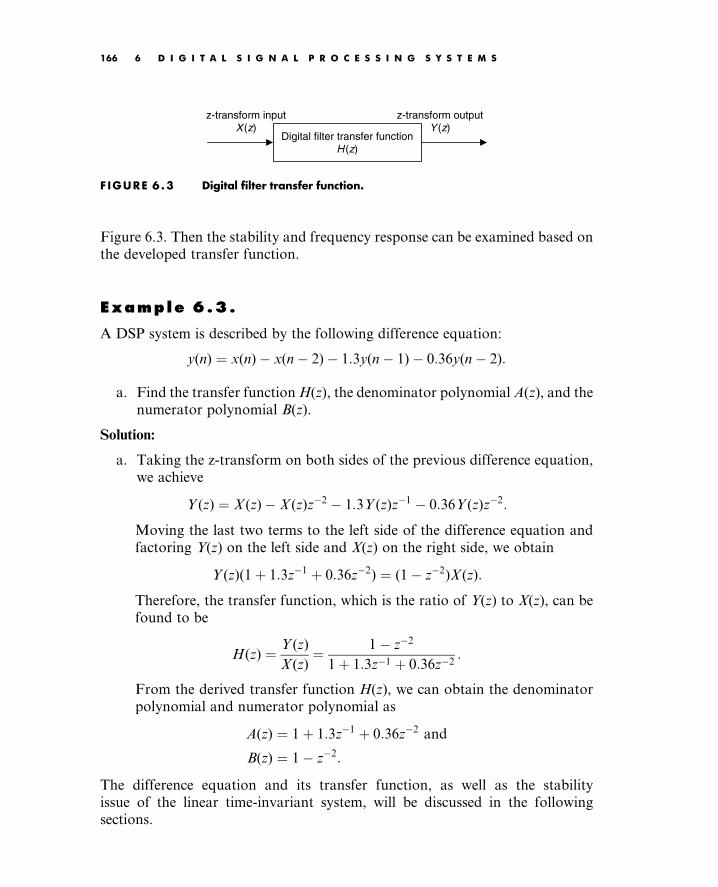
Figure 6.3. Then the stability and frequency response can be examined based on
the developed transfer function.
Example 6.3.
A DSP system is described by the following difference equation:
y(n) ¼ x(n) x(n 2) 1:3y(n 1) 0:36y(n 2):
a. Find the transfer function H(z), the denominator polynomial A(z), and the
numerator polynomial B(z).
Solution:
a. Taking the z-transform on both sides of the previous difference equation,
we achieve
Y (z) ¼ X (z) X (z)z2 1:3Y (z)z1 0:36Y (z)z2:
Moving the last two terms to the left side of the difference equation and
factoring Y(z) on the left side and X(z) on the right side, we obtain
Y (z)(1þ 1:3z1 þ 0:36z2) ¼ (1 z2)X (z):
Therefore, the transfer function, which is the ratio of Y(z) to X(z), can be
found to be
H(z) ¼ Y (z)
X (z)¼ 1 z2
1þ 1:3z1 þ 0:36z2:
From the derived transfer function H(z), we can obtain the denominator
polynomial and numerator polynomial as
A(z) ¼ 1þ 1:3z1 þ 0:36z2 and
B(z) ¼ 1 z2:
The difference equation and its transfer function, as well as the stability
issue of the linear time-invariant system, will be discussed in the following
sections.
z-transform inputX (z)
z-transform outputY (z)
Digital filter transfer functionH (z)
F IGURE 6.3 Digital filter transfer function.
Tan: Digital Signaling Processing 0123740908_chap06 Final Proof page 166 21.6.2007 11:04pm Compositor Name: MRaja
166 6 D I G I T A L S I G N A L P R O C E S S I N G S Y S T E M S

Example 6.4.
A digital system is described by the following difference equation:
y(n) ¼ x(n) 0:5x(n 1)þ 0:36x(n 2):
a. Find the transfer function H(z), the denominator polynomial A(z), and
the numerator polynomial B(z).
Solution:
a. Taking the z-transform on both sides of the previous difference equation,
we achieve
Y (z) ¼ X (z) 0:5X (z)z2 þ 0:36X (z)z2:
Therefore, the transfer function, that is, the ratio of Y(z) to X(z), can be
found as
H(z) ¼ Y (z)
X (z)¼ 1 0:5z1 þ 0:36z2:
From the derived transfer function H(z), it follows that
A(z) ¼ 1
B(z) ¼ 1 0:5z1 þ 0:36z2:
In DSP applications, the given transfer function of a digital system can be
converted into a difference equation for DSP implementation. The following
example illustrates the procedure.
Example 6.5.
Convert each of the following transfer functions into its difference equation.
a. H(z) ¼ z2 1
z2 þ 1:3zþ 0:36
b. H(z) ¼ z2 0:5zþ 0:36
z2
Solution:
a. Dividing the numerator and the denominator by z2 to obtain the transfer
function whose numerator and denominator polynomials have the nega-
tive power of z, it follows that
H(z) ¼ (z2 1)=z2
(z2 þ 1:3zþ 0:36)=z2¼ 1 z2
1þ 1:3z1 þ 0:36z2:
Tan: Digital Signaling Processing 0123740908_chap06 Final Proof page 167 21.6.2007 11:04pm Compositor Name: MRaja
6.2 Difference Equation and Transfer Function 167

We write the transfer function using the ratio of Y(z) to X(z):
Y (z)
X(z)¼ 1 z2
1þ 1:3z1 þ 0:36z2:
Then we have
Y (z)(1þ 1:3z1 þ 0:36z2) ¼ X (z)(1 z2):
By distributing Y(z) and X(z), we yield
Y (z)þ 1:3z1Y (z)þ 0:36z2Y (z) ¼ X (z) z2X(z):
Applying the inverse z-transform and using the shift property in
Equation (5.3) of Chapter 5, we get
y(n)þ 1:3y(n 1)þ 0:36y(n 2) ¼ x(n) x(n 2):
Writing the output y(n) in terms of inputs and past outputs leads to
y(n) ¼ x(n) x(n 2) 1:3y(n 1) 0:36y(n 2):
b. Similarly, dividing the numerator and denominator by z2, we obtain
H(z) ¼ Y (z)
X (z)¼ (z2 0:5zþ 0:36)=z2
z2=z2¼ 1 0:5z1 þ 0:36z2:
Thus, Y (z) ¼ X (z)(1 0:5z1 þ 0:36z2):
By distributing X(z), we yield
Y (z) ¼ X (z) 0:5z1X (z)þ 0:36z2X (z):
Applying the inverse z-transform while using the shift property in Equa-
tion (5.3), we obtain
y(n) ¼ x(n) 0:5x(n 1)þ 0:36x(n 2):
The transfer function H(z) can be factored into the pole-zero form:
H(z) ¼ b0(z z1)(z z2) (z zM)
(z p1)(z p2) (z pN), (6:7)
where the zeros zi can be found by solving for the roots of the numerator
polynomial, while the poles pi can be solved for the roots of the denom-
inator polynomial.
Example 6.6.
Given the following transfer function,
H(z) ¼ 1 z2
1þ 1:3z1 þ 0:36z2
Tan: Digital Signaling Processing 0123740908_chap06 Final Proof page 168 21.6.2007 11:04pm Compositor Name: MRaja
168 6 D I G I T A L S I G N A L P R O C E S S I N G S Y S T E M S

a. Convert it into the pole-zero form.
Solution:
a. We first multiply the numerator and denominator polynomials by z2 to
achieve its advanced form in which both numerator and denominator
polynomials have positive powers of z, that is,
H(z) ¼ (1 z2)z2
(1þ 1:3z1 þ 0:36z2)z2¼ z2 1
z2 þ 1:3zþ 0:36:
Letting z2 1 ¼ 0, we get z ¼ 1 and z ¼ 1. Setting z2 þ 1:3zþ 0:36 ¼ 0
leads to z ¼ 0:4 and z ¼ 0:9. We then can write numerator and de-
nominator polynomials in the factored form to obtain the pole-zero form:
H(z) ¼ (z 1)(zþ 1)
(zþ 0:4)(zþ 0:9):
6.2.1 Impulse Response, Step Response, andSystem Response
The impulse response h(n) of the DSP system H(z) can be obtained by solving its
difference equation using a unit impulse input d(n). With the help of the z-
transform and noticing that X (z) ¼ Zfd(n)g ¼ 1, we yield
h(n) ¼ Z1 H(z)X (z)f g ¼ Z1 H(z)f g: (6:8)
Similarly, for a step input, we can determine step response assuming the zero
initial conditions. Letting
X (z) ¼ Z u(n)½ ¼ z
z 1,
the step response can be found as
y(n) ¼ Z1 H(z)z
z 1
n o: (6:9)
Furthermore, the z-transform of the general system response is given by
Y (z) ¼ H(z)X (z): (6:10)
If we know the transfer function H(z) and the z-transform of the input X(z), we
are able to determine the system response y(n) by finding the inverse z-transform
of the output Y(z):
y(n) ¼ Z1 Y (z)f g: (6:11)
Tan: Digital Signaling Processing 0123740908_chap06 Final Proof page 169 21.6.2007 11:04pm Compositor Name: MRaja
6.2 Difference Equation and Transfer Function 169

Example 6.7.
Given a transfer function depicting a DSP system
H(z) ¼ zþ 1
z 0:5,
Determine
a. the impulse response h(n),
b. the step response y(n), and
c. the system response y(n) if the input is given as x(n) ¼ (0:25)n u(n).
Solution:
a. The transfer function can be rewritten as
H(z)
z¼ zþ 1
z z 0:5ð Þ ¼A
zþ B
z 0:5,
where A ¼ zþ 1
z 0:5ð Þ
z¼0
¼ 2, and B ¼ zþ 1
z
z¼0:5
¼ 3:
Thus we have
H(z)
z¼ 2
zþ 3
z 0:5and
H(z) ¼ 2
zþ 3
z 0:5
z ¼ 2þ 3z
z 0:5:
By taking the inverse z-transform as shown in Equation (6.8), we yield the
impulse response
h(n) ¼ 2d(n)þ 3(0:5)n u(n):
b. For the step input x(n) ¼ u(n) and its z-transform X (z) ¼ z
z 1, we can
determine the z-transform of the step response as
Y (z) ¼ H(z)X (z) ¼ zþ 1
z 0:5
z
z 1:
Applying the partial fraction expansion leads to
Y (z)
z¼ zþ 1
(z 0:5)(z 1)¼ A
z 0:5þ B
z 1,
where
A ¼ zþ 1
z 1
z¼0:5
¼ 3, and B ¼ zþ 1
z 0:5
z¼1
¼ 4:
Tan: Digital Signaling Processing 0123740908_chap06 Final Proof page 170 21.6.2007 11:04pm Compositor Name: MRaja
170 6 D I G I T A L S I G N A L P R O C E S S I N G S Y S T E M S

The z-transform step response is therefore
Y (z) ¼ 3z
z 0:5þ 4z
z 1:
Applying the inverse z-transform yields the step response as
y(n) ¼ 3 0:5ð Þn u(n)þ 4 u(n):
c. To determine the system output response, we first find the z-transform
of the input x(n),
X (z) ¼ Z (0:25)n u(n)f g ¼ z
z 0:25,
then Y(z) can be yielded via Equation (6.10), that is,
Y (z) ¼ H(z)X (z) ¼ zþ 1
z 0:5 z
z 0:25¼ z(zþ 1)
(z 0:5)(z 0:25):
Using the partial fraction expansion, we have
Y (z)
z¼ (zþ 1)
(z 0:5)(z 0:25)¼ A
z 0:5þ B
z 0:25
Y (z) ¼ 6z
z 0:5þ 5z
z 0:25
:
Using Equation (6.11) and Table 5.1 in Chapter 5, we finally yield
y(n) ¼ Z1 Y (z)f g ¼ 6(0:5)n u(n) 5(0:25)n u(n):
The impulse response for (a), the step response for (b), and the system response
for (c) are each plotted in Figure 6.4.
6.3 The z-Plane Pole-Zero Plot andStabi l i ty
A very useful tool to analyze digital systems is the z-plane pole-zero plot. This
graphical technique allows us to investigate characteristics of the digital system
shown in Figure 6.1, including the system stability. In general, a digital transfer
function can be written in the pole-zero form as shown in Equation (6.7), and we
can plot the poles and zeros on the z-plane. The z-plane is depicted in Figure 6.5
and has the following features:
1. The horizontal axis is the real part of the variable z, and the vertical axis
represents the imaginary part of the variable z.
Tan: Digital Signaling Processing 0123740908_chap06 Final Proof page 171 21.6.2007 11:04pm Compositor Name: MRaja
6.3 The z-Plane Pole-Zero Plot and Stability 171

2. The z-plane is divided into two parts by a unit circle.
3. Each pole is marked on the z-plane using the cross symbol , while each
zero is plotted using the small circle symbol .Let’s investigate the z-plane pole-zero plot of a digital filter system via the
following example.
Example 6.8.
Given the digital transfer function
H(z) ¼ z1 0:5z2
1þ 1:2z1 þ 0:45z2,
a. Plot poles and zeros.
Solution:
a. Converting the transfer function to its advanced form by multiplying z2
to both numerator and denominator, it follows that
0 1 2 3 4 5 6 7 8 9 100
1
2
Sample number
Impu
lse
res
pon
se
0 1 2 3 4 5 6 7 8 9 100
2
4
Sample number
Ste
p re
spon
se
0 1 2 3 4 5 6 7 8 9 100
1
2
Sample number
Sys
tem
res
pons
e
A
B
C
F IGURE 6.4 Impulse, step, and system responses in Example 6.7.
Tan: Digital Signaling Processing 0123740908_chap06 Final Proof page 172 21.6.2007 11:04pm Compositor Name: MRaja
172 6 D I G I T A L S I G N A L P R O C E S S I N G S Y S T E M S

H(z) ¼ (z1 0:5z2)z2
(1þ 1:2z1 þ 0:45z2)z2¼ z 0:5
z2 þ 1:2zþ 0:45:
By setting z2 þ 1:2zþ 0:45 ¼ 0 and z 0:5 ¼ 0, we obtain two poles
p1 ¼ 0:6þ j0:3
p2 ¼ p1 ¼ 0:6 j0:3
and a zero z1 ¼ 0:5, which are plotted on the z-plane shown in Figure 6.6.
According to the form of Equation (6.7), we also yield the pole-zero form as
H(z) ¼ z1 0:5z2
1þ 1:2z1 þ 0:45z2¼ (z 0:5)
(zþ 0:6 j0:3)(zþ 0:6þ j0:3):
Re(z)
Outside of unit circle
Inside of unit circle
- zero
× - pole
1
Unit circle
Im(z)
F IGURE 6 .5 z-plane and pole-zero plot.
Im(z)
Re(z)
×
×
10.5−0.6
0.3
−0.3
F IGURE 6 .6 The z-plane pole-zero plot of Example 6.8.
Tan: Digital Signaling Processing 0123740908_chap06 Final Proof page 173 21.6.2007 11:04pm Compositor Name: MRaja
6.3 The z-Plane Pole-Zero Plot and Stability 173

Having zeros and poles plotted on the z-plane, we are able to study the
system stability. We first establish the relationship between the s-plane in
Laplace domain and the z-plane in z-transform domain, as illustrated in
Figure 6.7.
As shown in Figure 6.7, the sampled signal, which is not quantized, with a
sampling period of T is written as
xs(t) ¼X1n¼0
x(nT)d(t nT)
¼ x(0)d(t)þ x(T)d(t T)þ x(2T)d(t 2T)þ . . . : (6:12)
Taking the Laplace transform and using the Laplace shift property as
L d(t nT)ð Þ ¼ enTs (6:13)
leads to
Xs(s) ¼X1n¼0
x(nT)enTs ¼ x(0)e0Ts þ x(T)eTs þ x(2T)e2Ts þ . . . : (6:14)
Comparing Equation (6.14) with the definition of a one-sided z-transform of the
data sequence x(n) from analog-to-digital conversion (ADC):
X (z) ¼ Z x(n)ð Þ ¼X1n¼0
x(n)zn ¼ x(0)z0 þ x(1)z1 þ x(2)z2 þ . . . : (6:15)
Clearly, we see the relationship of the sampled system in Laplace domain and its
digital system in z-transform domain by the following mapping:
z ¼ esT : (6:16)
Z ( )
L ( )
Coding
tt
x(t) xs(t) =Σ x(nT )d(t − nT )n = 0
∞
Xs(s) =Σ x(nT)e −nsT∞
X(z) =Σ x(n)z −n∞
Sampler
n
x(n)
z = esT
n = 0
n = 0
F IGURE 6.7 Relationship between Laplace transform and z-transform.
Tan: Digital Signaling Processing 0123740908_chap06 Final Proof page 174 21.6.2007 11:04pm Compositor Name: MRaja
174 6 D I G I T A L S I G N A L P R O C E S S I N G S Y S T E M S

Substituting s ¼ a jv into Equation (6.16), it follows that z ¼ eaT jvT . In
the polar form, we have
z ¼ eaTff vT : (6:17)
Equations (6.16) and (6.17) give the following important conclusions.
If a > 0, this means jzj ¼ eaT < 1. Then the left-hand half plane (LHHP) of
the s-plane is mapped to the inside of the unit circle of the z-plane. When a ¼ 0,
this causes jzj ¼ eaT ¼ 1. Thus the jv axis of the s-plane is mapped on the unit
circle of the z-plane, as shown in Figure 6.8. Obviously, the right-hand half
plane (RHHP) of the s-plane is mapped to the outside of the unit circle in the z-
plane. A stable system means that for a given bounded input, the system output
must be bounded. Similar to the analog system, the digital system requires that
all poles plotted on the z-plane must be inside the unit circle. We summarize the
rules for determining the stability of a DSP system as follows:
1. If the outermost pole(s) of the z-transfer function H(z) describing the DSP
system is(are) inside the unit circle on the z-plane pole-zero plot, then the
system is stable.
2. If the outermost pole(s) of the z-transfer function H(z) is(are) outside the
unit circle on the z-plane pole-zero plot, the system is unstable.
3. If the outermost pole(s) is(are) first-order pole(s) of the z-transfer function
H(z) and on the unit circle on the z-plane pole-zero plot, then the system is
marginally stable.
4. If the outermost pole(s) is(are) multiple-order pole(s) of the z-transfer
function H(z) and on the unit circle on the z-plane pole-zero plot, then
the system is unstable.
5. The zeros do not affect the system stability.
σ
jw
Re(z )
Im(z)
Stable Region
10 0StableRegion
F IGURE 6 .8 Mapping between s-plane and z-plane.
Tan: Digital Signaling Processing 0123740908_chap06 Final Proof page 175 21.6.2007 11:04pm Compositor Name: MRaja
6.3 The z-Plane Pole-Zero Plot and Stability 175

Notice that the following facts apply to a stable system (bounded-in/bounded-
out [BIBO] stability discussed in Chapter 3):
1. If the input to the system is bounded, then the output of the system will
also be bounded, or the impulse response of the system will go to zero in a
finite number of steps.
2. An unstable system is one in which the output of the system will grow
without bound due to any bounded input, initial condition, or noise, or its
impulse response will grow without bound.
3. The impulse response of a marginally stable system stays at a constant
level or oscillates between two finite values.
Examples illustrating these rules are shown in Figure 6.9.
Example 6.9.
The following transfer functions describe digital systems.
a: H(z) ¼ zþ 0:5
(z 0:5)(z2 þ zþ 0:5)
b: H(z) ¼ z2 þ 0:25
(z 0:5)(z2 þ 3zþ 2:5)
c: H(z) ¼ zþ 0:5
(z 0:5)(z2 þ 1:4141zþ 1)
d: H(z) ¼ z2 þ zþ 0:5
(z 1)2(zþ 1)(z 0:6)
For each, sketch the z-plane pole-zero plot and determine the stability
status for the digital system.
Solution:
a. A zero is found to be z ¼ 0:5.
Poles: z ¼ 0:5, zj j ¼ 0:5 < 1;z ¼ 0:5 j0:5,
zj j ¼ffiffiffiffiffiffiffiffiffiffiffiffiffiffiffiffiffiffiffiffiffiffiffiffiffiffiffiffiffiffiffiffiffiffiffi0:5ð Þ2þ 0:5ð Þ2
q¼ 0:707 < 1:
The plot of poles and a zero is shown in Figure 6.10. Since the outermostpoles are inside the unit circle, the system is stable.
Tan: Digital Signaling Processing 0123740908_chap06 Final Proof page 176 21.6.2007 11:04pm Compositor Name: MRaja
176 6 D I G I T A L S I G N A L P R O C E S S I N G S Y S T E M S

Re(z)
Re(z)
Re(z)
Re(z)
Im(z)y(n) = h(n) = (0.5)nu(n)
y(n) = h(n) = (1.5)nu(n)
y(n) = h(n) = u(n)
y(n) = h(n) = nu(n)
y(n) = h(n) = (−1)nu(n)
n
x(n) = d(n)
x(n) = d(n)
x(n) = d(n)
x(n) = d(n)
x(n) = d(n)
110.5
0.25 0.125n
0 1 2
0 1 2
0 1 2 3 4
0 1 2 3 4
0 1 2 0 1 2 3 4
0 1 2 3 4
Stablesystem
1
Im(z)
Im(z)
Im(z)
Re(z)
Im(z)
n
1
1.51
2.253.375
n
0 1 2
Unstablesystem
1
n
11 11
n
Marginallystable system
Marginallystable system
1
1
n
1
12
4
n0 1 2
Unstablesystem
10
n1 2 3 4
1
−1
1
−1
n0
1
1
y(n) = x(n) + 0.5y(n − 1)
y(n) = x(n) + 1.5y(n − 1)
y(n) = x(n) + y(n − 1)
y(n) = x(n ) − y(n − 1)
y(n) = x(n − 1) + 2y(n − 1) − y(n − 2)
x(n) y(n)
x(n)
x(n)
x(n)
x(n)
y(n)
y(n)
y(n)
y(n)
H(z) = zz − 0.5
H(z) = zz − 1.5
H(z) = zz − 1
H(z) = zz + 1
H(z) = z(z − 1) 2
F IGURE 6 .9 Stability illustrations.
Tan: Digital Signaling Processing 0123740908_chap06 Final Proof page 177 21.6.2007 11:04pm Compositor Name: MRaja
6.3 The z-Plane Pole-Zero Plot and Stability 177

b. Zeros are z ¼ j0:5.
Poles:z¼ 0:5, zj j ¼ 0:5< 1; z¼1:5 j0:5,
zj j ¼ffiffiffiffiffiffiffiffiffiffiffiffiffiffiffiffiffiffiffiffiffiffiffiffiffiffiffiffiffiffiffi1:5ð Þ2þ 0:5ð Þ2
q¼ 1:5811> 1:
The plot of poles and zeros is shown in Figure 6.10. Since we have
two poles at z ¼ 1:5 j0:5, which are outside the unit circle, the
system is unstable.
c. A zero is found to be z ¼ 0:5.
Poles: z ¼ 0:5, zj j ¼ 0:5 < 1; z ¼ 0:707 j0:707,
zj j ¼ffiffiffiffiffiffiffiffiffiffiffiffiffiffiffiffiffiffiffiffiffiffiffiffiffiffiffiffiffiffiffiffiffiffiffiffiffiffiffiffiffi0:707ð Þ2þ 0:707ð Þ2
q¼ 1:
The zero and poles are plotted in Figure 6.10. Since the outermost
poles are first order at z ¼ 0:707 j0:707 and are on the unit circle,
the system is marginally stable.
d. Zeros are z ¼ 0:5 j0:5.
Poles: z ¼ 1, zj j ¼ 1; z ¼ 1, zj j ¼ 1; z ¼ 1, zj j ¼ 1; z ¼ 0:6,
zj j ¼ 0:6 < 1:
Im(z)
Re(z)
Im(z)
Im(z)Im(z)
Re(z)
Re(z) Re(z)
× ×
×
× × ×
×
×
A B
C D
×
×
×
××
F IGURE 6.10 Pole-zero plots for Example 6.9.
Tan: Digital Signaling Processing 0123740908_chap06 Final Proof page 178 21.6.2007 11:04pm Compositor Name: MRaja
178 6 D I G I T A L S I G N A L P R O C E S S I N G S Y S T E M S

The zeros and poles are plotted in Figure 6.10. Since the outermost pole is
multiple order (second order) at z ¼ 1 and is on the unit circle, the system
is unstable.
6.4 Digi ta l F i l ter Frequency Response
From the Laplace transfer function, we can achieve the analog filter steady-state
frequency response H( jv) by substituting s ¼ jv into the transfer function H(s).
That is,
H(s)js¼jv¼ H( jv):
Then we can study the magnitude frequency response jH( jv)j and phase re-
sponse ffH(jv). Similarly, in a DSP system, using the mapping Equation (6.16),
we substitute z ¼ e sTs¼jv¼ e jvT into the z-transfer function H(z) to acquire the
digital frequency response, which is converted into the magnitude frequency
response H(e jvT ) and phase response ff H(e jvT )
. That is,
H(z)jz¼e jvT¼ H(e jvT ) ¼ H(e jvT ) ffH(e jvT ): (6:18)
Let us introduce a normalized digital frequency in radians in digital domain
V ¼ vT : (6:19)
Then the digital frequency response in Equation (6.18) would become
H(e jV) ¼ H(z)jz¼e jV¼ H(e jV) ffH(e jV): (6:20)
The formal derivation for Equation (6.20) can be found in Appendix D.
Now we verify the frequency response via the following simple digital filter.
Consider a digital filter with a sinusoidal input of the amplitude K (Fig. 6.11):
H(z) = 0.5 + 0.5z −1
x(n) = K sin(nΩ)u(n) y(n) = ytr(n) + yss(n)
F IGURE 6 .11 System transient and steady-state frequency responses.
We can determine the system output y(n), which consists of the transient
response ytr(n) and the steady-state response yss(n). We find the z-transform
output as
Y (z) ¼ 0:5zþ 0:5
z
Kz sin V
z2 2z cos Vþ 1: (6:21)
Tan: Digital Signaling Processing 0123740908_chap06 Final Proof page 179 21.6.2007 11:04pm Compositor Name: MRaja
6.4 Digital Filter Frequency Response 179

To perform the inverse z-transform to find the system output, we further rewrite
Equation (6.21) as
Y (z)
z¼ 0:5zþ 0:5
z
K sin V
z e jVð Þ z ejVð Þ ¼A
zþ B
z e jVþ B
z ejV,
where A, B, and the complex conjugate B are the constants for the partial
fractions. Applying the partial fraction expansion leads to
A ¼ 0:5K sin V
B ¼ 0:5zþ 0:5
z
z¼e jV
K
2j¼ H(e jV) e jffH(e jV) K
2j:
Notice that the first part of constant B is a complex function, which is obtained
by substituting z ¼ e jV into the filter z-transfer function. We can also express
the complex function in terms of the polar form:
0:5zþ 0:5
z
z¼e jV
¼ 0:5þ 0:5z1z¼e jV¼ H(z)jz¼e jV¼ H(e jV) ¼ H(e jV)
e jffH(e jV),
where H(e jV) ¼ 0:5þ 0:5ejV, and we call this complex function the steady-
state frequency response. Based on the complex conjugate property, we get
another residue as
B ¼ H(e jV) ejffH(e jV) K
j2:
The z-transform system output is then given by
Y (z) ¼ Aþ Bz
z e jVþ Bz
z ejV:
Taking the inverse z-transform, we achieve the following system transient and
steady-state responses:
y(n)¼0:5K sinVd(n)|fflfflfflfflfflfflfflfflfflfflzfflfflfflfflfflfflfflfflfflfflytr(n)
þ H(ejV) e jffH(ejV)K
j2ejnV u(n)þ H(ejV)
ejffH(ejV) K
j2ejnV u(n)
|fflfflfflfflfflfflfflfflfflfflfflfflfflfflfflfflfflfflfflfflfflfflfflfflfflfflfflfflfflfflfflfflfflfflfflfflfflfflfflfflfflfflfflfflfflfflfflfflfflfflfflfflfflfflfflzfflfflfflfflfflfflfflfflfflfflfflfflfflfflfflfflfflfflfflfflfflfflfflfflfflfflfflfflfflfflfflfflfflfflfflfflfflfflfflfflfflfflfflfflfflfflfflfflfflfflfflfflfflfflfflyss(n)
:
Simplifying the response yields the form
y(n) ¼ 0:5K sin Vd(n)þ H(e jV) K e jnVþjffH(e jV) u(n) ejnVjffH(e jV) u(n)
j2:
Tan: Digital Signaling Processing 0123740908_chap06 Final Proof page 180 21.6.2007 11:04pm Compositor Name: MRaja
180 6 D I G I T A L S I G N A L P R O C E S S I N G S Y S T E M S

We can further combine the last term using Euler’s formula to express the
system response as
y(n)¼ 0:5K sinVd(n)|fflfflfflfflfflfflfflfflfflfflfflzfflfflfflfflfflfflfflfflfflfflfflytr(n) will decay to zero after the first sample
þ H(ejV) K sin nVþffH(ejV)
u(n)|fflfflfflfflfflfflfflfflfflfflfflfflfflfflfflfflfflfflfflfflfflfflfflfflfflfflfflfflfflfflzfflfflfflfflfflfflfflfflfflfflfflfflfflfflfflfflfflfflfflfflfflfflfflfflfflfflfflfflfflffl
yss(n)
:
Finally, the steady-state response is identified as
yss(n) ¼ K H(e jV) sin nVþ ffH(e jV)
u(n):
For this particular filter, the transient response exists for only the first sample in
the system response. By substituting n ¼ 0 into y(n) and after simplifying
algebra, we achieve the response for the first output sample:
y(0) ¼ ytr(0)þ yss(0) ¼ 0:5K sin (V) 0:5K sin (V) ¼ 0:
Note that the first output sample of the transient response cancels the first
output sample of the steady-state response, so the combined first output sample
has a value of zero for this particular filter. The system response reaches
the steady-state response after the first output sample. At this point, we can
conclude:
Steady-state magnitude frequency response
¼ Peak amplitude of steady-state response at V
Peak amplitude of sinusoidal input at V
¼H(e jV) K
K¼ H(e jV)
Steady-state phase frequency response ¼ Phase difference ¼ ffH(e jV):
Figure 6.12 shows the system responses with sinusoidal inputs at
V ¼ 0:25p, V ¼ 0:5p, and V ¼ 0:75p, respectively.
Next, we examine the properties of the filter frequency response H(e jV).
From Euler’s identity and trigonometric identity, we know that
e j(Vþk2p) ¼ cos Vþ k2pð Þ þ j sin Vþ k2pð Þ¼ cos Vþ j sin V ¼ e jV,
where k is an integer taking values of k ¼ 0, 1, 2, . . . ,: Then the frequency
response has the following property (assuming that all input sequences are real):
Tan: Digital Signaling Processing 0123740908_chap06 Final Proof page 181 21.6.2007 11:04pm Compositor Name: MRaja
6.4 Digital Filter Frequency Response 181

1. Periodicity
a. Frequency response: H(e jV) ¼ H(e j(Vþk2p))
b. Magnitude frequency response: H(e jV) ¼ H(e j(Vþk2p))
c. Phase response: ffH(e jV) ¼ ffH(e jVþk2p)
The second property is given without proof (see proof in Appendix D) as shown:
2. Symmetry
a. Magnitude frequency response: H(ejV) ¼ H(e jV)
b. Phase response: ffH(ejV) ¼ ffH(e jV)
Since the maximum frequency in a DSP system is the folding frequency, fs=2,
where fs ¼ 1=T and T designates the sampling period, the corresponding max-
imum normalized frequency can be calculated as
V ¼ vT ¼ 2pfs
2 T ¼ p radians: (6:22)
0 5 10 15 20 25 30 35 40 45 50−2
0
2
Om
ega=
0.25
*pi
0 5 10 15 20 25 30 35 40 45 50−2
0
2
Om
ega=
0.5*
pi
0 5 10 15 20 25 30 35 40 45 50−2
0
2
Om
ega=
0.75
*pi
Sample number
Steady-state response
Steady-state response
Steady-state response
F IGURE 6.12 The digital filter responses to different input sinusoids.
Tan: Digital Signaling Processing 0123740908_chap06 Final Proof page 182 21.6.2007 11:04pm Compositor Name: MRaja
182 6 D I G I T A L S I G N A L P R O C E S S I N G S Y S T E M S

The frequency response H(e jV) for jVj > p consists of the image replicas of
H(e jV) for jVj#p and will be removed via the reconstruction filter later. Hence,
we need to evaluate H(e jV) for only the positive normalized frequency range
from V ¼ 0 to V ¼ p radians. The frequency, in Hz, can be determined by
f ¼ V
2pfs: (6:23)
The magnitude frequency response is often expressed in decibels, defined as
H(e jV)
dB¼ 20 log10 H(e jV)
: (6:24)
The DSP system stability, magnitude response, and phase response are investi-
gated via the following examples.
Example 6.10.
Given the following digital system with a sampling rate of 8,000 Hz,
y(n) ¼ 0:5x(n)þ 0:5x(n 1),
1. Determine the frequency response.
Solution:
1. Taking the z-transform on both sides of the difference equation leads to
Y (z) ¼ 0:5X (z)þ 0:5z1X (z):
Then the transfer function describing the system is easily found to be
H(z) ¼ Y (z)
X (z)¼ 0:5þ 0:5z1:
Substituting z ¼ e jV, we have the frequency response as
H(e jV) ¼ 0:5þ 0:5ejV
¼ 0:5þ 0:5 cos (V) j0:5 sin (V):
Therefore, the magnitude frequency response and phase response are
given by
H(e jV) ¼
ffiffiffiffiffiffiffiffiffiffiffiffiffiffiffiffiffiffiffiffiffiffiffiffiffiffiffiffiffiffiffiffiffiffiffiffiffiffiffiffiffiffiffiffiffiffiffiffiffiffiffiffiffiffiffiffiffiffiffiffiffiffiffiffiffiffiffiffiffiffi(0:5þ 0:5 cos (V))2 þ (0:5 sin (V))2
q
and
ffH(e jV) ¼ tan1 0:5 sin (V)
0:5þ 0:5 cos (V)
:
Tan: Digital Signaling Processing 0123740908_chap06 Final Proof page 183 21.6.2007 11:04pm Compositor Name: MRaja
6.4 Digital Filter Frequency Response 183

Several points for the magnitude response and phase response are calcu-
lated and shown in Table 6.1.
According to data, we plot the magnitude frequency response and phase
response of the DSP system as shown in Figure 6.13.
It is observed that when the frequency increases, the magnitude response
decreases. The DSP system acts like a digital lowpass filter, and its phase
response is linear.
0.5 1 1.5 2 2.50 3−100
−50
0
Frequency (rad)
Pha
se r
espo
nse
(deg
rees
)
0.5 1 1.5 2 2.50 3−40
−30
−20
−10
0
Frequency (rad)
Mag
nitu
de r
espo
nse
(dB
)
F IGURE 6.13 Frequency responses of the digital filter in Example 6.10.
TABLE 6 .1 Frequency response calculations in Example 6.10.
V (radians) f ¼ V2p
fs(Hz) H(ejV) H(ejV)
dB
ffH(ejV)
0 0 1.000 0 dB 080:25p 1000 0.924 0:687 dB 22:5
0:50p 2000 0.707 3:012 dB 45:00
0:75p 3000 0.383 8:336 dB 67:50
1:00p 4000 0.000 1 90
Tan: Digital Signaling Processing 0123740908_chap06 Final Proof page 184 21.6.2007 11:04pm Compositor Name: MRaja
184 6 D I G I T A L S I G N A L P R O C E S S I N G S Y S T E M S

We can also verify the periodicity for jH(e jV)j and ffH(e jV) when
V ¼ 0:25p þ 2p:
H(e j(0:25pþ2p)) ¼
ffiffiffiffiffiffiffiffiffiffiffiffiffiffiffiffiffiffiffiffiffiffiffiffiffiffiffiffiffiffiffiffiffiffiffiffiffiffiffiffiffiffiffiffiffiffiffiffiffiffiffiffiffiffiffiffiffiffiffiffiffiffiffiffiffiffiffiffiffiffiffiffiffiffiffiffiffiffiffiffiffiffiffiffiffiffiffiffiffiffiffiffiffiffiffiffiffiffiffiffiffiffiffiffiffiffiffiffiffi(0:5þ 0:5 cos (0:25p þ 2p))2 þ (0:5 sin (0:25p þ 2p))2
q
¼ 0:924 ¼ H(e j0:25p)
ffH(e j(0:25pþ2p)) ¼ tan1 0:5 sin (0:25p þ 2p)
0:5þ 0:5 cos (0:25p þ 2p)
¼ 22:50 ¼ ffH(e j0:25p):
For V ¼ 0:25p, we can verify the symmetry property as
H(ej0:25p) ¼
ffiffiffiffiffiffiffiffiffiffiffiffiffiffiffiffiffiffiffiffiffiffiffiffiffiffiffiffiffiffiffiffiffiffiffiffiffiffiffiffiffiffiffiffiffiffiffiffiffiffiffiffiffiffiffiffiffiffiffiffiffiffiffiffiffiffiffiffiffiffiffiffiffiffiffiffiffiffiffiffiffiffiffiffiffiffiffiffiffiffiffiffiffiffiffiffi(0:5þ 0:5 cos ( 0:25p))2 þ (0:5 sin ( 0:25p))2
q
¼ 0:924 ¼ H(e j0:25p)
ffH(ej0:25p) ¼ tan1 0:5 sin ( 0:25p)
0:5þ 0:5 cos ( 0:25p)
¼ 22:50 ¼ ffH(e j0:25p):
The properties can be observed in Figure 6.14, where the frequency range
is chosen from V ¼ 2p to V ¼ 4p radians. As shown in the figure, the
magnitude and phase responses are periodic with a period of 2p. For a period
−4 −2 0 2 4 6 8 10−6 120
0.5
1
Frequency (rad)
Mag
nitu
de r
espo
nse
−6 −4 −2 0 2 4 6 8 10 12−100
−50
0
50
100
Frequency (rad)
Pha
se r
espo
nse
(deg
rees
)
F IGURE 6.14 Periodicity of the magnitude response and phase response in Example6.10.
Tan: Digital Signaling Processing 0123740908_chap06 Final Proof page 185 21.6.2007 11:04pm Compositor Name: MRaja
6.4 Digital Filter Frequency Response 185

between V ¼ p to V ¼ p, the magnitude responses for the portion V ¼ p to
V ¼ 0 and the portion V ¼ 0 to V ¼ p are the same, while the phase responses
are opposite. The magnitude and phase responses calculated for the range from
V ¼ 0 to V ¼ p carry all the frequency response information, hence are re-
quired for generating only the frequency response plots.
Again, note that the phase plot shows a sawtooth shape instead of a linear
straight line for this particular filter. This is due to the phase wrapping at
V ¼ 2p radians, since ej(Vþk2p) ¼ e jV is used in the calculation. However, the
phase plot shows that the phase is linear in the useful information range from
V ¼ 0 to V ¼ p radians.
Example 6.11.
Given a digital system with a sampling rate of 8,000 Hz,
y(n) ¼ x(n) 0:5y(n 1),
1. Determine the frequency response.
Solution:
1. Taking the z-transform on both sides of the difference equation leads to
Y (z) ¼ X (z) 0:5z1Y (z):
Then the transfer function describing the system is easily found to be
H(z) ¼ Y (z)
X (z)¼ 1
1þ 0:5z1¼ z
zþ 0:5:
Substituting z ¼ e jV, we have the frequency response as
H(e jV) ¼ 1
1þ 0:5ejV
¼ 1
1þ 0:5 cos (V) j0:5 sin (V):
Therefore, the magnitude frequency response and phase response are
given by
H(e jV) ¼ 1ffiffiffiffiffiffiffiffiffiffiffiffiffiffiffiffiffiffiffiffiffiffiffiffiffiffiffiffiffiffiffiffiffiffiffiffiffiffiffiffiffiffiffiffiffiffiffiffiffiffiffiffiffiffiffiffiffiffiffiffiffiffiffiffiffiffi
(1þ 0:5 cos (V))2 þ (0:5 sin (V))2q
and
ffH(e jV) ¼ tan1 0:5 sin (V)
1þ 0:5 cos (V)
, respectively:
Several points for the magnitude response and phase response are calcu-
lated and shown in Table 6.2.
Tan: Digital Signaling Processing 0123740908_chap06 Final Proof page 186 21.6.2007 11:04pm Compositor Name: MRaja
186 6 D I G I T A L S I G N A L P R O C E S S I N G S Y S T E M S

According to the achieved data, the magnitude response and phase response
of the DSP system are roughly plotted in Figure 6.15.
From Table 6.2 and Figure 6.15, we can see that when the frequency
increases, the magnitude response increases. The DSP system actually performs
digital highpass filtering.
Notice that if all the coefficients ai for i ¼ 0, 1, . . . , M in Equation (6.1) are
zeros, Equation (6.2) is reduced to
y(n) ¼XMi¼0
bix(n i)
¼ b0x(n)þ b1x(n 1)þ þ bKx(nM):
(6:25)
0 0.5 1 1.5 2 2.5 3−10
0
10
20
30
40
Frequency (rad)
Pha
se r
espo
nse
(deg
rees
)
0.5 1 1.5 2 2.50 3−10
−5
0
5
10
Frequency (rad)
Mag
nitu
de r
espo
nse
(dB
)
F IGURE 6 .15 Frequency responses of the digital filter in Example 6.11.
TABLE 6 .2 Frequency response calculations in Example 6.11.
V (radians) f ¼ V2p
fs(Hz) H(ejV) H(ejV)
dB
ffH(ejV)
0 0 0.670 3:479 dB 0
0:25p 1000 0.715 2:914 dB 14:64
0:50p 2000 0.894 0:973 dB 26:57
0:75p 3000 1.357 2.652 dB 28:68
1:00p 4000 2.000 6.021 dB 0
Tan: Digital Signaling Processing 0123740908_chap06 Final Proof page 187 21.6.2007 11:04pm Compositor Name: MRaja
6.4 Digital Filter Frequency Response 187

Notice that bi is the ith impulse response coefficient. Also, since M is a finite
positive integer, bi in this particular case is a finite set, H(z) ¼ B(z); note that the
denominator A(z) ¼ 1. Such systems are called finite impulse response (FIR)
systems. If not all ai in Equation (6.1) are zeros, the impulse response h(i) will
consist of an infinite number of coefficients. Such systems are called infinite
impulse response (IIR) systems. The z-transform of the IIR h(i), in general, is
given by H(z) ¼ B(z)A(z)
, where A(z) 6¼ 1.
6.5 Basic Types of F i l ter ing
The basic filter types can be classified into four categories: lowpass, highpass,
bandpass, and bandstop. Each of them finds a specific application in digital
signal processing. One of the objectives in applications may involve the design
of digital filters. In general, the filter is designed based on specifications primarily
for the passband, stopband, and transition band of the filter frequency response.
The filter passband is the frequency range with the amplitude gain of the filter
response being approximately unity. The filter stopband is defined as the fre-
quency range over which the filter magnitude response is attenuated to eliminate
the input signal whose frequency components are within that range. The transi-
tion band denotes the frequency range between the passband and the stopband.
The design specifications of the lowpass filter are illustrated in Figure 6.16,
where the low-frequency components are passed through the filter while the
high-frequency components are attenuated. As shown in Figure 6.16, Vp and Vs
are the passband cutoff frequency and the stopband cutoff frequency, respect-
ively; dp is the design parameter to specify the ripple (fluctuation) of the
frequency response in the passband, while ds specifies the ripple of the frequency
response in the stopband.
1 + δp
1 − δp
δs
1.0
0 πΩp Ωs
Ω
Passband Transition Stopband
F IGURE 6.16 Magnitude response of the normalized lowpass filter.
Tan: Digital Signaling Processing 0123740908_chap06 Final Proof page 188 21.6.2007 11:04pm Compositor Name: MRaja
188 6 D I G I T A L S I G N A L P R O C E S S I N G S Y S T E M S

The highpass filter, remains high-frequency components and rejects low-
frequency components. The magnitude frequency response for the highpass
filter is demonstrated in Figure 6.17.
The bandpass filter attenuates both low- and high-frequency components
while remaining the middle-frequency component, as shown in Figure 6.18.
As illustrated in Figure 6.18, VpL and VsL are the lower passband cutoff
frequency and the lower stopband cutoff frequency, respectively. VpH and VsH
are the upper passband cutoff frequency and the upper stopband cutoff fre-
quency, respectively. dp is the design parameter to specify the ripple of the
frequency response in the passband, while ds specifies the ripple of the frequency
response in the stopbands.
Finally, the bandstop (band reject or notch) filter, shown in Figure 6.19,
rejects the middle-frequency components and accepts both the low- and the
high-frequency component.
As a matter of fact, all kinds of digital filters are implemented using FIR and
IIR systems. Furthermore, the FIR and IIR systems can each be realized by
1 + δp
1 − δp
δs
1.0
0 πΩpΩsΩ
PassbandTransitionStopband
0
F IGURE 6 .17 Magnitude response of the normalized highpass filter.
1 + δp
1 − δp
δs
1.0
0 πΩ
Passband
Transition
Stopband
0
Stopband
Transition
ΩsL ΩpL ΩpH ΩsH
F IGURE 6 .18 Magnitude response of the normalized bandpass filter.
Tan: Digital Signaling Processing 0123740908_chap06 Final Proof page 189 21.6.2007 11:04pm Compositor Name: MRaja
6.5 Basic Types of Filtering 189

various filter configurations, such as direct forms, cascade forms, and parallel
forms. Such topics will be included in the next section.
Given a transfer function, the MATLAB function freqz() can be used to
determine the frequency response. The syntax is given by
[h, w] ¼ freqz(B, A, N),
whose parameters are defined as:
h ¼ an output vector containing frequency response
w ¼ an output vector containing normalized frequency values distributed
in the range from 0 to p radians.
B ¼ an input vector for numerator coefficients
A ¼ an input vector for denominator coefficients
N ¼ the number of normalized frequency points used for calculating the
frequency response
Let’s consider Example 6.12.
Example 6.12.
Given each of the following digital transfer functions,
a. H(z) ¼ z
z 0:5
b. H(z) ¼ 1 0:5z1
c. H(z) ¼ 0:5z2 0:32
z2 0:5zþ 0:25
d. H(z) ¼ 1 0:9z1 þ 0:81z2
1 0:6z1 þ 0:36z2,
1 + δp
1 − δp
δs
1.0
0 πΩ0
ΩsLΩpL ΩpHΩsH
Passband
Transition
Stopband
Transition
Passband
F IGURE 6.19 Magnitude of the normalized bandstop filter.
Tan: Digital Signaling Processing 0123740908_chap06 Final Proof page 190 21.6.2007 11:04pm Compositor Name: MRaja
190 6 D I G I T A L S I G N A L P R O C E S S I N G S Y S T E M S
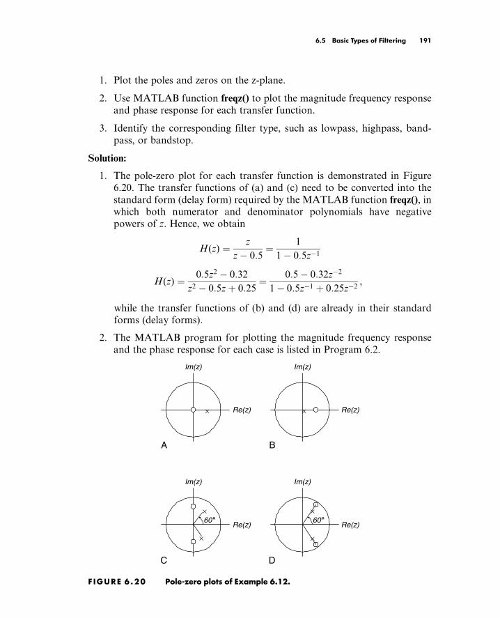
1. Plot the poles and zeros on the z-plane.
2. Use MATLAB function freqz() to plot the magnitude frequency response
and phase response for each transfer function.
3. Identify the corresponding filter type, such as lowpass, highpass, band-
pass, or bandstop.
Solution:
1. The pole-zero plot for each transfer function is demonstrated in Figure
6.20. The transfer functions of (a) and (c) need to be converted into the
standard form (delay form) required by the MATLAB function freqz(), in
which both numerator and denominator polynomials have negative
powers of z. Hence, we obtain
H(z) ¼ z
z 0:5¼ 1
1 0:5z1
H(z) ¼ 0:5z2 0:32
z2 0:5zþ 0:25¼ 0:5 0:32z2
1 0:5z1 þ 0:25z2,
while the transfer functions of (b) and (d) are already in their standard
forms (delay forms).
2. The MATLAB program for plotting the magnitude frequency response
and the phase response for each case is listed in Program 6.2.
Im(z)
Re(z)
Im(z)
Re(z)× ×
A B
Im(z)
Re(z)
×
×
60 8
Im(z)
Re(z)60 8
×
×
C D
F IGURE 6.20 Pole-zero plots of Example 6.12.
Tan: Digital Signaling Processing 0123740908_chap06 Final Proof page 191 21.6.2007 11:04pm Compositor Name: MRaja
6.5 Basic Types of Filtering 191

Program 6.2. MATLAB program for Example 6.12.
% Example 6.12
% Plot the magnitude frequency response and phase response
% Case a
figure (1)
½h w ¼ freqzð½1 ½10:5 1024Þ; % Calculate the frequency response
phi ¼ 180unwrap(angle(h))/pi;
subplot(2,1,1), plot(w,abs(h)),grid;xlabel(’Frequency (radians)’),
ylabel (’Magnitude’)
subplot(2,1,2), plot(w,phi),grid;xlabel(’Frequency (radians)’),
ylabel(’Phase (degrees)’)
% Case b
figure (2)
½h w ¼ freqz(½10:5 ½1 1024); %Calculate the frequency response
phi ¼ 180unwrap(angle(h))/pi;
subplot(2,1,1), plot(w,abs(h)),grid;xlabel(’Frequency (radians)’),
ylabel (’Magnitude’)
subplot(2,1,2), plot(w,phi),grid;xlabel(’Frequency (radians)’),
ylabel(’Phase (degrees)’)
% Case c
figure (3)
½h w ¼ freqz([0.50-0.32],[1-0.50.25],1024);%Calculatethefrequencyresponse
phi ¼ 180unwrap(angle(h))/pi;
subplot(2,1,1), plot(w,abs(h)),grid;xlabel(’Frequency (radians)’),
ylabel(’Magnitude’)
subplot(2,1,2), plot(w,phi),grid;xlabel(’Frequency (radians)’),
ylabel(’Phase (degrees)’)
% Case d
figure (4)
½h w ¼ freqz([1-0.90.81],[1-0.60.36],1024);%Calculatethefrequencyresponse
phi ¼ 180unwrap(angle(h))/pi;
subplot(2,1,1), plot(w,abs(h)),grid;xlabel(’Frequency (radians)’),
ylabel (’Magnitude’)
subplot(2,1,2), plot(w,phi),grid;xlabel(’Frequency (radians)’),
ylabel(’Phase (degrees)’)
%
Tan: Digital Signaling Processing 0123740908_chap06 Final Proof page 192 21.6.2007 11:04pm Compositor Name: MRaja
192 6 D I G I T A L S I G N A L P R O C E S S I N G S Y S T E M S

0.5
1
1.5
2
Frequency (rad)
Mag
nitu
de
0A
0.5 1 1.5 2 2.5 3 3.5
0 0.5 1 1.5 2 2.5 3 3.5
−30
−20
−10
0
Frequency (rad)
Pha
se (
degr
ees)
F IGURE 6 .21A Plots of frequency responses for Example 6.12 for (a).
0 0.5 1 1.5 2 2.5 3 3.50.5
1
1.5
Frequency (rad)
Mag
nitu
de
0B 0.5 1 1.5 2 2.5 3 3.50
10
20
30
Frequency (rad)
Pha
se (
degr
ees)
F IGURE 6 .21B Plots of frequency responses for Example 6.12 for (b).
Tan: Digital Signaling Processing 0123740908_chap06 Final Proof page 193 21.6.2007 11:04pm Compositor Name: MRaja
6.5 Basic Types of Filtering 193

0 0.5 1 1.5 2 2.5 3 3.50
0.5
1
1.5
Frequency (rad)
Mag
nitu
de
0
C0.5 1 1.5 2 2.5 3 3.5
−60
−40
−20
0
20
40
Frequency (rad)
Pha
se (
degr
ees)
F IGURE 6.21C Plots of frequency responses for Example 6.12 for (c).
0 0.5 1 1.5 2 2.5 3 3.50
0.5
1
1.5
Frequency (rad)
Mag
nitu
de
0D
0.5 1 1.5 2 2.5 3 3.5−40
−20
0
20
40
60
Frequency (rad)
Pha
se (
degr
ees)
F IGURE 6.21D Plots of frequency responses for Example 6.12 for (d).
Tan: Digital Signaling Processing 0123740908_chap06 Final Proof page 194 21.6.2007 11:04pm Compositor Name: MRaja
194 6 D I G I T A L S I G N A L P R O C E S S I N G S Y S T E M S

3. From the plots inFigures 6.21a–6.21d ofmagnitude frequency responses for
all cases, we can conclude that case (a) is a lowpass filter, (b) is a highpass
filter, (c) is a bandpass filter, and (d) is a bandstop (band reject) filter.
6.6 Real izat ion of Digi ta l F i l ters
In this section, basic realization methods for digital filters are discussed. Digital
filters described by the transfer function H(z) may be generally realized in the
following forms:
& Direct form I
& Direct form II
& Cascade
& Parallel.
(The reader can explore various lattice realizations in the textbook by Stearns
and Hush [1990].)
6.6.1 Direct -Form I Real izat ion
As we know, a digital filter transfer function, H(z), is given by
H(z) ¼ B(z)
A(z)¼ b0 þ b1z
1 þ þ bMzM
1þ a1z1 þ þ aNzN: (6:26)
Let x(n) and y(n) be the digital filter input and output, respectively. We can
express the relationship in z-transform domain as
Y (z) ¼ H(z)X(z), (6:27)
where X(z) and Y(z) are the z-transforms of x(n) and y(n), respectively. If we
substitute Equation (6.26) into H(z) in Equation (6.27), we have
Y (z) ¼ b0 þ b1z1 þ þ bMzM
1þ a1z1 þ þ aNzN
X (z): (6:28)
Taking the inverse of the z-transform of Equation (6.28), we yield the relation-
ship between input x(n) and output y(n) in time domain, as follows:
y(n) ¼b0x(n)þ b1x(n 1)þ þ bMx(nM)
a1y(n 1) a2y(n 2) aNy(nN):(6:29)
This difference equation thus can be implemented by a direct-form I realiza-
tion shown in Figure 6.22(a). Figure 6.22(b) illustrates the realization of the
second-order IIR filter (M ¼ N ¼ 2). Note that the notation used in Figures
Tan: Digital Signaling Processing 0123740908_chap06 Final Proof page 195 21.6.2007 11:04pm Compositor Name: MRaja
6.6 Realization of Digital Filters 195

6.22(a) and (b) are defined in Figure 6.22(c) and will be applied for discussion of
other realizations.
Also, notice that any of the aj and bi can be zero, thus all the paths are not
required to exist for the realization.
6.6.2 Direct -Form II Real izat ion
Considering Equations (6.26) and (6.27) with N ¼M, we can express
Y (z) ¼ H(z)X(z) ¼ B(z)
A(z)X (z) ¼ B(z)
X (z)
A(z)
¼ b0 þ b1z1 þ þ bMzM
X (z)
1þ a1z1 þ þ aMzM
|fflfflfflfflfflfflfflfflfflfflfflfflfflfflfflfflfflfflfflfflfflfflfflfflfflzfflfflfflfflfflfflfflfflfflfflfflfflfflfflfflfflfflfflfflfflfflfflfflfflffl
W (z)
:(6:30)
Also, defining a new z-transform function as
W (z) ¼ X (z)
1þ a1z1 þ þ aMzM, (6:31)
z −1
z −1z −1
z −1
y(n)b0
b0
b1
b i
b2
b1
bM
−a1
−a2 −a1
−a2−aN
x(n − 1)
x(n − 1)
x(n − 2)
x(n − 1)
y(n − 1)
y(n − 1)
y(n − 2)
y(n − 2)
y(n − N)x(n − M )
+
A B
C
y(n)+
bi . x(n)
This denotes that the output is the productof the weight bi and input x(n); that is, bi
. x(n)
This denotes a unit delay element, whichimplies that the output of this stage is x(n − 1)
x(n)
x(n)
x(n)
x(n)
z −1z −1
z −1
z −1z −1
z −1
z −1
F IGURE 6 .22 (a) Direct-form I realization. (b) Direct-form I realization with M = 2.(c) Notation.
Tan: Digital Signaling Processing 0123740908_chap06 Final Proof page 196 21.6.2007 11:04pm Compositor Name: MRaja
196 6 D I G I T A L S I G N A L P R O C E S S I N G S Y S T E M S

we have
Y (z) ¼ b0 þ b1z1 þ þ bMzM
W (z): (6:32)
The corresponding difference equations for Equations (6.31) and (6.32), respect-
ively, become
w(n) ¼ x(n) a1w(n 1) a2w(n 2) aMw(nM) (6:33)
and
y(n) ¼ b0w(n)þ b1w(n 1)þ . . .þ bMw(nM): (6:34)
Realization of Equations (6.33) and (6.34) becomes another direct-form II
realization, which is demonstrated in Figure 6.23(a). Again, the corresponding
realization of the second-order IIR filter is described in Figure 6.23(b). Note
that in Figure 6.23(a), the variables w(n), w(n 1), w(n 2), . . . , w(nM)
are different from the filter inputs x(n 1), x(n 2), . . . , x(nM).
6.6.3 Cascade (Ser ies) Real izat ion
An alternate way to filter realization is to cascade the factorized H(z) in the
following form:
H(z) ¼ H1(z) H2(z) Hk(z), (6:35)
where Hk(z) is chosen to be the first- or second-order transfer function (section),
which is defined by
Hk(z) ¼bk0 þ bk1z
1
1þ ak1z1(6:36)
b0
b1
b2
b M
A
x (n) y (n)w(n)
w(n −2)
w(n −M )
w(n −1)
−a1
−a2
−aM
z −1
z −1
+ +z −1
B
b0
b1
b2
x (n) y (n)w(n)
w(n −2 )
w(n −1 )
−a1
−a2z −1
+ +
z −1
F IGURE 6 .23 (A) Direct-form II realization. (B) Direct-form II realization with M = 2.
Tan: Digital Signaling Processing 0123740908_chap06 Final Proof page 197 21.6.2007 11:04pm Compositor Name: MRaja
6.6 Realization of Digital Filters 197

or
Hk(z) ¼bk0 þ bk1z
1 þ bk2z2
1þ ak1z1 þ ak2z2, (6:37)
respectively. The block diagram of the cascade, or series, realization is depicted
in Figure 6.24.
6.6.4 Paral le l Real izat ion
Now we convert H(z) into the following form:
H(z) ¼ H1(z)þH2(z)þ þHk(z), (6:38)
where Hk(z) is defined as the first- or second-order transfer function (section)
given by
Hk(z) ¼bk0
1þ ak1z1(6:39)
or
Hk(z) ¼bk0 þ bk1z
1
1þ ak1z1 þ ak2z2, (6:40)
respectively. The resulting parallel realization is illustrated in the block diagram
in Figure 6.25.
Example 6.13.
Given a second-order transfer function
H(z) ¼ 0:5(1 z2)
1þ 1:3z1 þ 0:36z2,
x (n) y (n)H1(z) H2(z) HK(z)
F IGURE 6.24 Cascade realization.
x (n) y (n)
H1(z)
H2(z)
Hk (z)
+
F IGURE 6.25 Parallel realization.
Tan: Digital Signaling Processing 0123740908_chap06 Final Proof page 198 21.6.2007 11:04pm Compositor Name: MRaja
198 6 D I G I T A L S I G N A L P R O C E S S I N G S Y S T E M S

a. Perform the filter realizations and write the difference equations using the
following realizations:
1. direct form I and direct form II
2. cascade form via the first-order sections
3. parallel form via the first-order sections.
Solution:
a. 1. To perform the filter realizations using the direct form I and direct
form II, we rewrite the given second-order transfer function as
H(z) ¼ 0:5 0:5z2
1þ 1:3z1 þ 0:36z2
and identify that
a1 ¼ 1:3, a2 ¼ 0:36, b0 ¼ 0:5, b1 ¼ 0, and b2 ¼ 0:5:
Based on realizations in Figure 6.22, we sketch the direct-form I
realization as Figure 6.26.
The difference equation for the direct-form I realization is given by
y(n) ¼ 0:5x(n) 0:5x(n 2) 1:3y(n 1) 0:36y(n 2):
Using the direct-form II realization shown in Figure 6.23, we have the
realization in Figure 6.27.
0.5
−0.5
−1.3
−0.36
+x (n) y (n)
z −1
z −1
z −1
z −1
F IGURE 6 .26 Direct-form I realization for Example 6.13.
+ +0.5x (n) w (n) y (n)
−0.36 −0.5
−1.3
z −1
z −1
F IGURE 6 .27 Direct-form II realization for Example 6.13.
Tan: Digital Signaling Processing 0123740908_chap06 Final Proof page 199 21.6.2007 11:04pm Compositor Name: MRaja
6.6 Realization of Digital Filters 199

The difference equations for the direct-form II realization are ex-
pressed as
w(n) ¼ x(n) 1:3w(n 1) 0:36w(n 2)
y(n) ¼ 0:5w(n) 0:5w(n 2):
2. To achieve the cascade (series) form realization, we factor H(z) into
two first-order sections to yield
H(z) ¼ 0:5(1 z2)
1þ 1:3z1 þ 0:36z2¼ 0:5 0:5z1
1þ 0:4z1
1þ z1
1þ 0:9z1,
where H1(z) and H2(z) are chosen to be
H1(z) ¼0:5 0:5z1
1þ 0:4z1
H2(z) ¼1þ z1
1þ 0:9z1:
Notice that the obtained H1(z) and H2(z) are not unique selections for
realization. For example, there is another way of choosing
H1(z) ¼ 0:50:5z1
1þ0:9z1 and H2(z) ¼ 1þz1
1þ0:4z1 to yield the same H(z). Using
the H1(z) and H2(z) we have obtained, and with the direct-form II
realization, we achieve the cascade form depicted in Figure 6.28.
The difference equations for the direct-form II realization have two
cascaded sections, expressed as
Section 1:
w1(n) ¼ x(n) 0:4w(n 1)
y1(n) ¼0:5w1(n) 0:5w1(n 1)
Section 2:
w2(n) ¼ y1(n) 0:9w2(n 1)
y(n) ¼ w2(n)þ w2(n 1):
+ +0.5
−0.4 −0.5 −0.9
+ +1
1
x (n) y (n)w1(n) w2(n)y1(n)
z −1 z −1
F IGURE 6.28 Cascade realization for Example 6.13.
Tan: Digital Signaling Processing 0123740908_chap06 Final Proof page 200 21.6.2007 11:04pm Compositor Name: MRaja
200 6 D I G I T A L S I G N A L P R O C E S S I N G S Y S T E M S

3. In order to yield the parallel form of realization, we need to make use of
the partial fraction expansion, and will first let
H(z)
z¼ 0:5(z2 1)
z(zþ 0:4)(zþ 0:9)¼ A
zþ B
zþ 0:4þ C
zþ 0:9,
where
A ¼ z0:5(z2 1)
z(zþ 0:4)(zþ 0:9)
z¼0
¼ 0:5(z2 1)
(zþ 0:4)(zþ 0:9)
z¼0
¼ 1:39
B ¼ (zþ 0:4)0:5(z2 1)
z(zþ 0:4)(zþ 0:9)
z¼0:4
¼ 0:5(z2 1)
z(zþ 0:9)
z¼0:4
¼ 0:21
C ¼ (zþ 0:9)0:5(z2 1)
z(zþ 0:4)(zþ 0:9)
z¼0:9
¼ 0:5(z2 1)
z(zþ 0:4)
z¼0:9
¼ 0:21:
Therefore
H(z) ¼ 1:39þ 2:1z
zþ 0:4þ0:21z
zþ 0:9¼ 1:39þ 2:1
1þ 0:4z1þ 0:21
1þ 0:9z1:
Again, using the direct form II for each section, we obtain the parallel
realization in Figure 6.29.
The difference equations for the direct-form II realization have three
parallel sections, expressed as
y1(n) ¼ 1:39x(n)
w2(n) ¼ x(n) 0:4w2(n 1)
y2(n) ¼ 2:1w2(n)
w3(n) ¼ x(n) 0:9w3(n 1)
y3(n) ¼ 0:21w3(n)
y(n) ¼ y1(n)þ y2(n)þ y3(n):
2.1
–0.21
−0.4
−0.9
−1.39
x (n)
y1(n)
y2(n)
y3(n)
y (n)w2(n)
w3(n)
+
+ +
++
z −1
z −1
F IGURE 6 .29 Parallel realization for Example 6.13.
Tan: Digital Signaling Processing 0123740908_chap06 Final Proof page 201 21.6.2007 11:04pm Compositor Name: MRaja
6.6 Realization of Digital Filters 201

In practice, the second-order filter module using the direct-form I or direct-
form II is used. The high-order filter can be factored in the cascade form
with the first- or second-order sections. In case the first-order filter is
required, we can still modify the second-order filter module by setting the
corresponding filter coefficients to be zero.
6.7 Appl i cat ion: Speech Enhancementand Fi l ter ing
This section investigates applications of speech enhancement using a pre-
emphasis filter and speech filtering using a bandpass filter.
6.7.1 Pre-Emphasis of Speech
A speech signal may have frequency components that fall off at high frequen-
cies. In some applications such as speech coding, to avoid overlooking the
high frequencies, the high-frequency components are compensated using
pre-emphasis filtering. A simple digital filter used for such compensation is
given as:
y(n) ¼ x(n) ax(n 1), (6:41)
where a is the positive parameter to control the degree of pre-emphasis filtering
and usually is chosen to be less than 1. The filter described in Equation (6.41) is
essentially a highpass filter. Applying z-transform on both sides of Equation
(6.41) and solving for the transfer function, we have
H(z) ¼ 1 az1: (6:42)
The magnitude and phase responses adopting the pre-emphasis parameter
a ¼ 0:9 and the sampling rate fs ¼ 8, 000Hz are plotted in Figure 6.30a using
MATLAB.
Figure 6.30b compares the original speech waveform and the pre-emphasized
speech using the filter in Equation (6.42). Again, we apply the fast Fourier
transform (FFT) to estimate the spectrum of the original speech and the
spectrum of the pre-emphasized speech. The plots are displayed in Figure 6.31.
From Figure 6.31, we can conclude that the filter does its job to boost the
high-frequency components and attenuate the low-frequency components. We
can also try this filter with different values of a to examine the degree of the pre-
emphasis filtering of the digitally recorded speech. The MATLAB list is in
Program 6.3.
Tan: Digital Signaling Processing 0123740908_chap06 Final Proof page 202 21.6.2007 11:04pm Compositor Name: MRaja
202 6 D I G I T A L S I G N A L P R O C E S S I N G S Y S T E M S

0A
500 1000 1500 2000 2500 3000 3500 40000
20
40
60
80
Frequency (Hz)
Pha
se (
degr
ees)
0 500 1000 1500 2000 2500 3000 3500 4000−20
−10
0
10
Frequency (Hz)
Mag
nitu
de r
espo
nse
(dB
)
F IGURE 6 .30A Frequency responses of the pre-emphasis filter.
0 0.2 0.4 0.6 0.8 1 1.2 1.4 1.6 1.8 2−2
−1
0
1
2 104
Spe
ech
sam
ples
Speech: We lost the golden chain.
0B 0.2 0.4 0.6 0.8 1 1.2 1.4 1.6 1.8 2−1
−0.5
0
0.5
1
Filt
ered
sam
ples
Number of samples
104
104
104
Pre-emphasized speech
F IGURE 6 .30B Original speech and pre-emphasized speech waveforms.
Tan: Digital Signaling Processing 0123740908_chap06 Final Proof page 203 21.6.2007 11:04pm Compositor Name: MRaja
6.7 Application: Speech Enhancement and Filtering 203

0 500 1000 1500 2000 2500 3000 3500 40000
50
100
150
200
Am
plitu
de s
pect
rum
Ak
Original speech
0 500 1000 1500 2000 2500 3000 3500 40000
20
40
60
Am
plitu
de s
pect
rum
Ak
Frequency (Hz)
Pre-emphasized speech
F IGURE 6 .31 Amplitude spectral plots for the original speech and pre-emphasizedspeech.
Program 6.3. MATLAB program for pre-emphasis of speech.
% Matlab program for Figures 6.30 and 6.31
close all;clear all
fs ¼ 8000; % Sampling rate
alpha ¼ 0:9; % Degree of pre-emphasis
figure(1);
freqz([1–alpha],1,512,fs); % Calculate and display frequency responses
load speech.dat
figure(2);
y ¼ filter([1-alpha],1,speech); % Filtering speech
subplot(2,1,1),plot(speech,’k’);grid;
ylabel(’Speech samples’)
title(’Speech: We lost the golden chain.’)
subplot(2,1,2),plot(y,’k’);grid
Tan: Digital Signaling Processing 0123740908_chap06 Final Proof page 204 21.6.2007 11:04pm Compositor Name: MRaja
204 6 D I G I T A L S I G N A L P R O C E S S I N G S Y S T E M S

6.7.2 Bandpass F i l ter ing of Speech
Bandpass filtering plays an important role in DSP applications. It can be used to
pass the signals according to the specified frequency passband and reject the
frequency other than the passband specification. Then the filtered signal can be
further used for the signal feature extraction. Filtering can also be applied to
perform applications such as noise reduction, frequency boosting, digital audio
equalizing, and digital crossover, among others.
Let us consider the following digital fourth-order bandpass Butterworth
filter with a lower cutoff frequency of 1,000 Hz, an upper cutoff frequency of
1,400 Hz (that is, the bandwidth is 400 Hz), and a sampling rate of 8,000 Hz:
H(z) ¼ 0:0201 0:0402z2 þ 0:0201z4
1 2:1192z1 þ 2:6952z2 1:6924z3 þ 0:6414z4: (6:43)
Converting the z-transfer function into the DSP difference equation yields
y(n) ¼ 0:0201x(n) 0:0402x(n 2)þ 0:0201x(n 4)
þ 2:1192y(n 1) 2:6952y(n 2)þ 1:6924y(n 3) 0:6414y(n 4):
(6:44)
ylabel(’Filtered samples’)
xlabel(’Number of samples’);
title(’Pre-emphasized speech.’)
figure(3);
N ¼ length(speech); % Length of speech
Axk ¼ abs(fft(speech.hamming(N)0))/N; % Two-sided spectrum of speech
Ayk ¼ abs(fft(y. hamming(N)0))/N;% Two-sided spectrum of pre-emphasized speech
f¼[0:N/2]fs/N;Axk(2:N)¼2Axk(2:N); % Get one-sided spectrum of speech
Ayk(2:N)¼ 2Ayk(2:N); % Get one-sided spectrum of filtered speech
subplot(2,1,1),plot(f,Axk(1:N/2þ 1),’k’);grid
ylabel(’Amplitude spectrum Ak’)
title(’Original speech’);
subplot(2,1,2),plot(f,Ayk(1:N/2þ 1),’k’);grid
ylabel(’Amplitude spectrum Ak’)
xlabel(’Frequency (Hz)’);
title(’Preemphasized speech’);
%
Tan: Digital Signaling Processing 0123740908_chap06 Final Proof page 205 21.6.2007 11:04pm Compositor Name: MRaja
6.7 Application: Speech Enhancement and Filtering 205

0A
500 1000 1500 2000 2500 3000 3500 4000−200
−100
0
100
200
Frequency (Hz)
Pha
se (
degr
ees)
0 500 1000 1500 2000 2500 3000 3500 4000−40
−30
−20
−10
0
Frequency (Hz)
Mag
nitu
de r
espo
nse
(dB
)
F IGURE 6.32A Frequency responses of the designed bandpass filter.
0 0.2 0.4 0.6 0.8 1 1.2 1.4 1.6 1.8 2−2
-1
0
1
2 104
104
104
Orig
inal
sam
ples
Speech: We lost the golden chain.
0B 0.2 0.4 0.6 0.8 1 1.2 1.4 1.6 1.8 2−4000
−2000
0
2000
4000
Number of Samples
Filt
ered
sam
ples
Bandpass filtered speech
F IGURE 6.32B Plots of the original speech and filtered speech.
Tan: Digital Signaling Processing 0123740908_chap06 Final Proof page 206 21.6.2007 11:04pm Compositor Name: MRaja
206 6 D I G I T A L S I G N A L P R O C E S S I N G S Y S T E M S

The filter frequency responses are computed and plotted in Figure 6.32(a) with
MATLAB. Figure 6.32(b) shows the original speech and filtered speech, while
Figure 6.32(c) displays the spectral plots for the original speech and filtered
speech.
As shown in Figure 6.32(c), the designed bandpass filter significantly reduces
low-frequency components, which are less than 1,000 Hz, and high-frequency
components, above 1,400 Hz, while letting the signals with the frequencies
0 500 1000 1500 2000 2500 3000 3500 40000
50
100
150
200
Am
plitu
de s
pect
rum
Ak
Original speech
0C
500 1000 1500 2000 2500 3000 3500 40000
10
20
30
Am
plitu
de s
pect
rum
Ak
Frequency (Hz)
Bandpass filtered speech
F IGURE 6 .32C Amplitude spectra of the original speech and bandpass filteredspeech.
Program 6.4. MATLAB program for bandpass filtering of speech.
fs¼8000; % Sampling rate
freqz[(0.02010.000:040200.0201],[12:11922.69521:69240.6414],512,fs);axis([0 fs/240 1]);% Frequency responses of the bandpass filterload speech.dat
y¼filter([0.0201 0.000:0402 0.0201],[12:1192 2.69521:6924 0.6414], speech);subplot(2,1,1),plot(speech);grid; % Filtering speech
ylabel(’Origibal Samples’)(Continued )
Tan: Digital Signaling Processing 0123740908_chap06 Final Proof page 207 21.6.2007 11:04pm Compositor Name: MRaja
6.7 Application: Speech Enhancement and Filtering 207

ranging from 1,000 to 1,400 Hz pass through the filter. Similarly, we can design
and implement other types of filters, such as lowpass, highpass, and band reject
to filter the signals and examine the performances of their designs. MATLAB
implementation detail is given in Program 6.4.
6.8 Summar y
1. The digital filter (DSP system) is represented by a difference equation,
which is linear and time invariant.
2. The filter output depends on the filter current input, past input(s), and
past output(s) in general. Given arbitrary inputs and nonzero or zero
initial conditions, operating the difference equation can generate the filter
output recursively.
3. System responses such as the impulse response and step response can be
determined analytically using the z-transform.
4. The transfer function can be obtained by applying the z-transform to the
difference equation to determine the ratio of the output z-transform over
the input z-transform. A digital filter (DSP system) can be represented by
its transfer function.
title(’Speech: We lost the golden chain.’)
subplot(2,1,2),plot(y);grid
xlabel(’Number of Samples’);ylabel(’Filtered Samples’)
title(’Bandpass filtered speech.’)
figure
N¼length(speech);Axk¼abs(fft(speech.hamming(N)0))/N; % One-sided spectrum of speech
Ayk¼abs(fft(y.hamming(N)0))/N; % One-sided spectrum of filtered speech
f¼[0:N/2]fs/N;Axk(2:N) ¼ 2Axk(2:N);Ayk(2:N) ¼ 2Ayk(2:N); % One-sided spectra
subplot(2,1,1),plot(f,Axk(1:N/2þ 1));grid
ylabel(’Amplitude spectrum Ak’)
title(’Original speech’);
subplot(2,1,2),plot(f,Ayk(1:N/2þ 1),’w’);grid
ylabel(’Amplitude spectrum Ak’);xlabel(’Frequency (Hz)’);
title(’Bandpass filtered speech’);
Tan: Digital Signaling Processing 0123740908_chap06 Final Proof page 208 21.6.2007 11:04pm Compositor Name: MRaja
208 6 D I G I T A L S I G N A L P R O C E S S I N G S Y S T E M S

5. System stability can be studied using a very useful tool, a z-plane pole-zero
plot.
6. The frequency responses of the DSP system were developed and illustrated
to investigate magnitude and phase frequency responses. In addition, the
FIR (finite impulse response) and IIR (infinite impulse response) systems
were defined.
7. Digital filters and their specifications, such as lowpass, highpass, band-
pass, and bandstop, were reviewed.
8. A digital filter can be realized using standard realization methods such as
the direct form I; direct form II; cascade, or series form; and parallel form.
9. Digital processing of speech using the pre-emphasis filter and bandpass
filter was investigated to study spectral effects of the processed digital
speech. The pre-emphasis filter boosts the high-frequency components,
while bandpass filtering keeps the midband frequency components and
rejects other lower- and upper-band frequency components.
6.9 Problems
6.1. Given the difference equation
y(n) ¼ x(n 1) 0:75y(n 1) 0:125y(n 2),
a. calculate the system response y(n) for n ¼ 0, 1, 2, . . . , 4 with the
input x(n) ¼ (0:5)n u(n) and initial conditions: x( 1) ¼ 1,
y( 2) ¼ 2, and y( 1) ¼ 1;
b. calculate the system response y(n) for n ¼ 0, 1, 2, . . . , 4 with the
input x(n) ¼ (0:5)n u(n) and zero initial conditions: x( 1) ¼ 0,
y( 2) ¼ 0, and y( 1) ¼ 0.
6.2. Given the following difference equation,
y(n) ¼ 0:5x(n)þ 0:5x(n 1),
a. find the H(z);
b. determine the impulse response y(n) if the input is x(n) ¼ 4d(n);
c. determine the step response y(n) if the input is x(n) ¼ 10 u(n).
Tan: Digital Signaling Processing 0123740908_chap06 Final Proof page 209 21.6.2007 11:04pm Compositor Name: MRaja
6.9 Problems 209

6.3. Given the following difference equation,
y(n) ¼ x(n) 0:5y(n 1),
a. find the H(z);
b. determine the impulse response y(n) if the input is x(n) ¼ d(n);
c. determine the step response y(n) if the input is x(n) ¼ u(n).
6.4. A digital system is described by the following difference equation:
y(n) ¼ x(n) 0:25x(n 2) 1:1y(n 1) 0:28y(n 2):
a. Find the transfer function H(z), the denominator polynomial A(z),
and the numerator polynomial B(z).
6.5. A digital system is described by the following difference equation:
y(n) ¼ x(n) 0:3x(n 1)þ 0:28x(n 2):
a. Find the transfer function H(z), the denominator polynomial A(z),
and the numerator polynomial B(z).
6.6. Convert each of the following transfer functions into its difference
equation:
a. H(z) ¼ z2 0:25
z2 þ 1:1zþ 0:18
b. H(z) ¼ z2 0:1zþ 0:3
z3
6.7. Convert the following transfer function into its pole-zero form:
a. H(z) ¼ 1 0:16z2
1þ 0:7z1 þ 0:1z2
6.8. A transfer function depicting a digital system is given by
H(z) ¼ 10(zþ 1)
(zþ 0:75):
a. Determine the impulse response h(n) and step response.
b. Determine the system response y(n) if the input is x(n) ¼ (0:25)n u(n).
6.9. Given each of the following transfer functions that describe digital
system transfer functions, sketch the z-plane pole-zero plot and deter-
mine the stability for each digital system.
a. H(z) ¼ z 0:5
(zþ 0:25)(z2 þ zþ 0:8)
Tan: Digital Signaling Processing 0123740908_chap06 Final Proof page 210 21.6.2007 11:04pm Compositor Name: MRaja
210 6 D I G I T A L S I G N A L P R O C E S S I N G S Y S T E M S

b. H(z) ¼ z2 þ 0:25
(z 0:5)(z2 þ 4zþ 7)
c. H(z) ¼ zþ 0:95
(zþ 0:2)(z2 þ 1:414zþ 1)
d. H(z) ¼ z2 þ zþ 0:25
(z 1)(zþ 1)2(z 0:36)
6.10. Given the following digital system with a sampling rate of 8,000 Hz,
y(n) ¼ 0:5x(n)þ 0:5x(n 2),
a. determine the frequency response;
b. calculate and plot the magnitude and phase frequency responses;
c. determine the filter type, based on themagnitude frequency response.
6.11. For the following digital system with a sampling rate of 8,000 Hz,
y(n) ¼ x(n) 0:5y(n 2),
a. determine the frequency response;
b. calculate and plot the magnitude and phase frequency responses;
c. determine the filter type based on the magnitude frequency response.
6.12. Given the following difference equation,
y(n) ¼ x(n) 2 cos (a)x(n 1)þ x(n 2)þ 2g cos (a) g2,
where g ¼ 0:8 and a ¼ 60,
a. find the transfer function H(z);
b. plot the poles and zeros on the z-plane with the unit circle;
c. determine the stability of the system from the pole-zero plot;
d. calculate the amplitude (magnitude) response of H(z);
e. calculate the phase response of H(z).
6.13. For each of the following difference equations,
a. y(n) ¼ 0:5x(n)þ 0:5x(n 1)
Tan: Digital Signaling Processing 0123740908_chap06 Final Proof page 211 21.6.2007 11:04pm Compositor Name: MRaja
6.9 Problems 211

b. y(n) ¼ 0:5x(n) 0:5x(n 1)
c. y(n) ¼ 0:5x(n)þ 0:5x(n 2)
d. y(n) ¼ 0:5x(n) 0:5x(n 2),
1. find H(z);
2. calculate the magnitude response;
3. specify the filter type based on the calculated magnitude response.
6.14. An IIR system is expressed as
y(n) ¼ 0:5x(n)þ 0:2y(n 1), y( 1) ¼ 0:
a. Find H(z).
b. Find the system response y(n) due to the input x(n) ¼ (0:5)n u(n).
6.15. Given the following IIR system with zero initial conditions:
y(n) ¼ 0:5x(n) 0:7y(n 1) 0:1y(n 2),
a. find H(z);
b. find the unit step response.
6.16. Given the first-order IIR system
H(z) ¼ 1þ 2z1
1 0:5z1,
realize H(z) and develop the difference equations using the following
forms:
a. direct-form I
b. direct-form II
6.17. Given the filter
H(z) ¼ 1 0:9z1 0:1z2
1þ 0:3z1 0:04z2,
realize H(z) and develop the difference equations using the following
form:
a. direct-form I
b. direct-form II
Tan: Digital Signaling Processing 0123740908_chap06 Final Proof page 212 21.6.2007 11:04pm Compositor Name: MRaja
212 6 D I G I T A L S I G N A L P R O C E S S I N G S Y S T E M S

c. cascade (series) form via the first-order sections
d. parallel form via the first-order sections
6.18. Given the following pre-emphasis filters:
H(z) ¼ 1 0:5z1
H(z) ¼ 1 0:7z1
H(z) ¼ 1 0:9z1,
a. write the difference equation for each;
b. determine which emphasizes high frequency components most.
MATLAB Problems
6.19. Given a filter
H(z) ¼ 1þ 2z1 þ z2
1 0:5z1 þ 0:25z2,
a. use MATLAB to plot
1. its magnitude frequency response;
2. its phase response.
6.20. Given the difference equation
y(n) ¼ x(n 1) 0:75y(n 1) 0:125y(n 2),
a. use the MATLAB functions filter() and filtic() to calculate the system
response y(n) for n ¼ 0, 1, 2, 3, . . . , 4 with the input of
x(n) ¼ (0:5)n u(n) and initial conditions: x( 1) ¼ 1, y( 2) ¼ 2,
and y( 1) ¼ 1;
b. use the MATLAB function filter() to calculate the system response
y(n) for n ¼ 0, 1, 2, 3, . . . , 4 with the input of x(n) ¼ (0:5)n u(n)
and zero initial conditions: x( 1) ¼ 0, y( 2) ¼ 0, and
y( 1) ¼ 0.
6.21. Given a filter
H(z) ¼ 1 z1 þ z2
1 0:9z1 þ 0:81z2,
Tan: Digital Signaling Processing 0123740908_chap06 Final Proof page 213 21.6.2007 11:04pm Compositor Name: MRaja
6.9 Problems 213

a. plot the magnitude frequency response and phase response using
MATLAB;
b. specify the type of filtering;
c. find the difference equation;
d. perform filtering, that is, calculate y(n) for the first 1,000 samples
for each of the following inputs and plot the filter outputs using
MATLAB, assuming that all initial conditions are zeros and the
sampling rate is 8,000 Hz:
1. x(n) ¼ cos p 103 n8000
2. x(n) ¼ cos 8
3p 103 n
8000
3. x(n) ¼ cos 6p 103 n
8000
;
e. repeat (d) using the MATLAB function filter().
Reference
Stearns, S. D., and Hush, D. R. (1990). Digital Signal Analysis, 2nd ed. Englewood Cliffs,
NJ: Prentice Hall.
Tan: Digital Signaling Processing 0123740908_chap06 Final Proof page 214 21.6.2007 11:04pm Compositor Name: MRaja
214 6 D I G I T A L S I G N A L P R O C E S S I N G S Y S T E M S

7Finite Impulse Response
Filter Design
Object ives :
This chapter introduces principles of the finite impulse response (FIR) filter
design and investigates the design methods such as the Fourier transform
method, window method, frequency sampling method design, and optimal
design method. Then the chapter illustrates how to apply the designed FIR
filters to solve real-world problems such as noise reduction and digital crossover
for audio applications. The major topics discussed in this chapter are included in
the following outline.
7.1 Fini te Impulse Response Fi l ter Format
In this chapter, we describe techniques of designing finite impulse response (FIR)
filters. An FIR filter is completely specified by the following input-output
relationship:
y(n) ¼XKi¼0
bix(n i)
¼ b0 x(n)þ b1x(n 1)þ b2x(n 2)þ þ bKx(n K)
(7:1)
where bi represents FIR filter coefficients and K þ 1 denotes the FIR filter
length. Applying the z-transform on both sides of Equation (7.1) leads to
Y (z) ¼ b0X (z)þ b1z1X(z)þ þ bKzKX(z): (7:2)
Tan: Digital Signaling Processing 0123740908_chap07 Final Proof page 215 21.6.2007 11:05pm Compositor Name: MRaja

Factoring out X(z) on the right-hand side of Equation (7.2) and then dividing
X(z) on both sides, we have the transfer function, which depicts the FIR filter, as
H(z) ¼ Y (z)
X(z)¼ b0 þ b1z
1 þ þ bKzK : (7:3)
The following example serves to illustrate the notations used in Equations (7.1)
and (7.3) numerically.
Example 7.1.
Given the following FIR filter:
y(n) ¼ 0:1x(n)þ 0:25x(n 1)þ 0:2x(n 2),
a. Determine the transfer function, filter length, nonzero coefficients, and
impulse response.
Solution:
a. Applying z-transform on both sides of the difference equation yields
Y (z) ¼ 0:1X (z)þ 0:25X (z)z1 þ 0:2X (z)z2:
Then the transfer function is found to be
H(z) ¼ Y (z)
X (z)¼ 0:1þ 0:25z1 þ 0:2z2:
The filter length is K þ 1 ¼ 3, and the identified coefficients are
b0 ¼ 0:1 b1 ¼ 0:25 and b2 ¼ 0:2:
Taking the inverse z-transform of the transfer function, we have
h(n) ¼ 0:1d(n)þ 0:25d(n 1)þ 0:2d(n 2):
This FIR filter impulse response has only three terms.
The foregoing example is to help us understand the FIR filter format. We
can conclude that
1. The transfer function in Equation (7.3) has a constant term, all the other
terms each have a negative power of z, and all the poles are at the origin
on the z-plane. Hence, the stability of filter is guaranteed. Its impulse
response has only a finite number of terms.
2. The FIR filter operations involve only multiplying the filter inputs by
their corresponding coefficients and accumulating them; the implemen-
tation of this filter type in real time is straightforward.
Tan: Digital Signaling Processing 0123740908_chap07 Final Proof page 216 21.6.2007 11:05pm Compositor Name: MRaja
216 7 F I N I T E I M P U L S E R E S P O N S E F I L T E R D E S I G N

From the FIR filter format, the design objective can be to obtain the FIR filter
bi coefficients such that the magnitude frequency response of the FIR filter H(z)
will approximate the desired magnitude frequency response, such as that of a
lowpass, highpass, bandpass, or bandstop filter. The following sections will
introduce design methods to calculate the FIR filter coefficients.
7.2 Four ier Transform Design
We begin with an ideal lowpass filter with a normalized cutoff frequency Vc,
whose magnitude frequency response in terms of the normalized digital
frequency V is plotted in Figure 7.1 and is characterized by
H(e jV) ¼ 1, 0 jVj Vc
0, Vc jVj p:
(7:4)
Since the frequency response is periodic with a period of V ¼ 2p radians, as we
discussed in Chapter 6, we can extend the frequency response of the ideal filter
H(e jV), as shown in Figure 7.2.
The periodic frequency response can be approximated using a complex
Fourier series expansion (see this topic in Appendix B) in terms of the normal-
ized digital frequency V, that is,
H(e jV) ¼X1
n¼1cnejv0nV, (7:5)
and the Fourier coefficients are given by
cn ¼1
2p
Z p
p
H(e jV)e jv0nVdV for1 < n <1: (7:6)
Notice that we obtain Equations (7.5) and (7.6) simply by treating the Fourier
series expansion in time domain with the time variable t replaced by the normal-
ized digital frequency variable V. The fundamental frequency is easily found to be
v0 ¼ 2p=( period of waveform) ¼ 2p=2p ¼ 1: (7:7)
H(e j Ω)
p-p −Ωc ΩcΩ
F IGURE 7 .1 Frequency response of an ideal lowpass filter.
Tan: Digital Signaling Processing 0123740908_chap07 Final Proof page 217 21.6.2007 11:05pm Compositor Name: MRaja
7.2 Fourier Transform Design 217

Substituting v0 ¼ 1 into Equation (7.6) and introducing h(n) ¼ cn, called the
desired impulse response of the ideal filter, we obtain the Fourier transform
design as
h(n) ¼ 1
2p
Z p
p
H(e jV)e jVndV for1 < n <1: (7:8)
Now, let us look at the possible z-transfer function. If we substitute e jV ¼ z and
v0 ¼ 1 back into Equation (7.5), we yield a z-transfer function in the following
format:
H(z) ¼X1
n¼1h(n)zn
þ h( 2)z2 þ h( 1)z1 þ h(0)þ h(1)z1 þ h(2)z2 þ (7:9)
This is a noncausal FIR filter. We will deal with this later in this section. Using
the Fourier transform design shown in Equation (7.8), the desired impulse
response approximation of the ideal lowpass filter is solved as
h(n) ¼ 1
2p
Z p
p
H(e jV)e jV0dV
For n ¼ 0
¼ 1
2p
Z Vc
Vc
1dV ¼ Vc
p
h(n) ¼ 1
2p
Z p
p
H(e jV)e jVndV ¼ 1
2p
Z Vc
Vc
e jVndV
For n 6¼ 0
¼ e jnV
2pjn
Vc
Vc
¼ 1
pn
e jnVc ejnVc
2j¼ sin (Vcn)
pn: (7:10)
−2pΩc
Ω2p + Ωc
2p−2p − Ωc −2p + Ωc
−p p
− Ωc 2p − Ωc
H (e j Ω)
F IGURE 7.2 Periodicity of the ideal lowpass frequency response.
Tan: Digital Signaling Processing 0123740908_chap07 Final Proof page 218 21.6.2007 11:05pm Compositor Name: MRaja
218 7 F I N I T E I M P U L S E R E S P O N S E F I L T E R D E S I G N

The desired impulse response h(n) is plotted versus the sample number n in
Figure 7.3.
Theoretically, h(n) in Equation (7.10) exists for 1 < n <1 and is
symmetrical about n ¼ 0; that is, h(n) ¼ h( n). The amplitude of the impulse
response sequence h(n) becomes smaller when n increases in both directions. The
FIR filter design must first be completed by truncating the infinite-length
sequence h(n) to achieve the 2M þ 1 dominant coefficients using the coefficient
symmetry, that is,
H(z) ¼ h(M)zM þ þ h(1)z1 þ h(0)þ h(1)z1 þ þ h(M)zM:
The obtained filter is a noncausal z-transfer function of the FIR filter, since the
filter transfer function contains terms with positive powers of z, which in turn
means that the filter output depends on the future filter inputs. To remedy the
noncausal z-transfer function, we delay the truncated impulse response h(n) by
M samples to yield the following causal FIR filter:
H(z) ¼ b0 þ b1z1 þ þ b2M(2M)z2M , (7:11)
where the delay operation is given by
bn ¼ h(nM) for n ¼ 0, 1, . . . , 2M: (7:12)
Similarly, we can obtain the design equations for other types of FIR filters, such
as highpass, bandpass, and bandstop, using their ideal frequency responses and
Equation (7.8). The derivations are omitted here. Table 7.1 gives a summary of
all the formulas for FIR filter coefficient calculations.
The following example illustrates the coefficient calculation for the lowpass
FIR filter.
n
h(n)
0
F IGURE 7 .3 Impulse response of an ideal digital lowpass filter.
Tan: Digital Signaling Processing 0123740908_chap07 Final Proof page 219 21.6.2007 11:05pm Compositor Name: MRaja
7.2 Fourier Transform Design 219

Example 7.2.
a. Calculate the filter coefficients for a 3-tap FIR lowpass filter with a cutoff
frequency of 800 Hz and a sampling rate of 8,000 Hz using the Fourier
transform method.
b. Determine the transfer function and difference equation of the designed
FIR system.
c. Compute and plot the magnitude frequency response for V ¼ 0, p=4,
p=2, 3p=4, and p radians.
Solution:
a. Calculating the normalized cutoff frequency leads to
Vc ¼ 2p fcTs ¼ 2p 800=8000 ¼ 0:2p radians:
Since 2M þ 1 ¼ 3 in this case, using the equation in Table 7.1 results in
h(0) ¼ Vc
pfor n ¼ 0
h(n) ¼ sin (Vcn)
np¼ sin (0:2pn)
np, for n 6¼ 1:
TABLE 7.1 Summary of ideal impulse responses for standard FIR filters.
Filter Type
Ideal Impulse Response
h(n) (noncausal FIR coefficients)
Lowpass: h(n) ¼Vc
pn ¼ 0
sin (Vcn)np
for n 6¼ 0 M n M
(
Highpass: h(n) ¼pVc
pn ¼ 0
sin (Vcn)np
for n 6¼ 0 M n#M
(
Bandpass: h(n) ¼VHVL
pn ¼ 0
sin (VHn)np
sin (VLn)np
for n 6¼ 0 M n M
(
Bandstop: h(n) ¼pVHþVL
pn ¼ 0
sin (VHn)np
þ sin (VLn)np
for n 6¼ 0 M n M
(
Causal FIR filter coefficients: shifting h(n) to the right by M samples.
Transfer function:
H(z) ¼ b0 þ b1z1 þ b2z
2 þ b2Mz2M
where bn ¼ h(nM), n ¼ 0, 1, , 2M
Tan: Digital Signaling Processing 0123740908_chap07 Final Proof page 220 21.6.2007 11:05pm Compositor Name: MRaja
220 7 F I N I T E I M P U L S E R E S P O N S E F I L T E R D E S I G N

The computed filter coefficients via the previous expression are listed as:
h(0) ¼ 0:2p
p¼ 0:2
h(1) ¼ sin [0:2p 1]
1 p¼ 0:1871:
Using the symmetry leads to
h( 1) ¼ h(1) ¼ 0:1871:
Thus delaying h(n) by M ¼ 1 sample using Equation (7.12) gives
b0 ¼ h(0 1) ¼ h( 1) ¼ 0:1871
b1 ¼ h(1 1) ¼ h(0) ¼ 0:2
and b2 ¼ h(2 1) ¼ h(1) ¼ 0:1871:
b. The transfer function is achieved as
H(z) ¼ 0:1871þ 0:2z1 þ 0:1871z2:
Using the technique described in Chapter 6, we have
Y (z)
X (z)¼ H(z) ¼ 0:1871þ 0:2z1 þ 0:1817z2:
Multiplying X(z) leads to
Y (z) ¼ 0:1871X(z)þ 0:2z1X(z)þ 0:1871z2X (z):
Applying the inverse z-transform on both sides, the difference equation is
yielded as
y(n) ¼ 0:1871x(n)þ 0:2x(n 1)þ 0:1871x(n 2):
c. The magnitude frequency response and phase response can be obtained
using the technique introduced in Chapter 6. Substituting z ¼ e jV into
H(z), it follows that
H(e jV) ¼ 0:1871þ 0:2ejV þ 0:1871ej2V:
Factoring the term ejV and using the Euler formula e jx þ ejx ¼ 2 cos (x),
we achieve
H(e jV) ¼ ejV 0:1871e jV þ 0:2þ 0:1871ejV
¼ ejV 0:2þ 0:3742 cos (V)ð Þ:
Tan: Digital Signaling Processing 0123740908_chap07 Final Proof page 221 21.6.2007 11:05pm Compositor Name: MRaja
7.2 Fourier Transform Design 221

Then the magnitude frequency response and phase response are found
to be
H(e jV) ¼ 0:2þ 0:3472 cos Vj j
and ffH(e jV) ¼V if 0:2þ 0:3472 cos V > 0
Vþ p if 0:2þ 0:3472 cos V < 0:
(
Details of the magnitude calculations for several typical normalized
frequencies are listed in Table 7.2.
Due to the symmetry of the coefficients, the obtained FIR filter has a linear phase
response as shown in Figure 7.4. The sawtooth shape is produced by the
contribution of the negative sign of the real magnitude term 0:2þ 0:3742 cos V
in the 3-tap filter frequency response, that is,
H(e jV) ¼ ejV 0:2þ 0:3742 cos Vð Þ:In general, the FIR filter with symmetrical coefficients has a linear phase
response (linear function of V) as follows:
ffH(e jV) ¼ MVþ possible phase of 180: (7:13)
Next, we see that the 3-tap FIR filter does not give an acceptable magnitude
frequency response. To explore this response further, Figure 7.5 displays the
magnitude and phase responses of 3-tap (M ¼ 1) and 17-tap (M ¼ 8) FIR
lowpass filters with a normalized cutoff frequency of Vc ¼ 0:2p radian. The
calculated coefficients for the 17-tap FIR lowpass filter are listed in Table 7.3.
We can make the following observations at this point:
1. The oscillations (ripples) exhibited in the passband (main lobe) and
stopband (side lobes) of the magnitude frequency response constitute
the Gibbs effect. Gibbs oscillatory behavior originates from the abrupt
TABLE 7.2 Frequency response calculation in Example 7.2.
V ffH(e jV)
radians f ¼ Vfs (2p) Hz 0:2þ 0:3742 cos V H(e jV) H(e jV)
dB
dB degree
0 0 0.5742 0.5742 4:82 0
p=4 1000 0.4646 0.4646 6:66 45
p=2 2000 0.2 0.2 14:0 90
3p=4 3000 0:0646 0.0646 23:8 45
p 4000 0:1742 0.1742 15:2 0
Tan: Digital Signaling Processing 0123740908_chap07 Final Proof page 222 21.6.2007 11:05pm Compositor Name: MRaja
222 7 F I N I T E I M P U L S E R E S P O N S E F I L T E R D E S I G N

0 500 1000 1500 2000 2500 3000 3500 4000−80
−60
−40
−20
0
Frequency (Hz)
Mag
nitu
de r
espo
nse
(dB
)
0 500 1000 1500 2000 2500 3000 3500 4000−200
−100
0
100
Frequency (Hz)
Pha
se r
espo
nse
(deg
rees
)
F IGURE 7 .4 Magnitude frequency response in Example 7.2.
0 0.5 1 1.5 2 2.5 3 3.5−80
−60
−40
−20
0
20
Mag
nitu
de R
espo
nse
Frequency (rad)
0 0.5 1 1.5 2 2.5 3 3.5−600
−400
−200
0
200
Frequency (rad)
Pha
se (
degr
ees)
Linear phase responses
Ripples on passband Ripples on stopband(side lobes)
Main lobe
F IGURE 7 .5 Magnitude and phase frequency responses of the lowpass FIR filters with3 coefficients (dash-dotted line) and 17 coefficients (solid line).
Tan: Digital Signaling Processing 0123740908_chap07 Final Proof page 223 21.6.2007 11:05pm Compositor Name: MRaja
7.2 Fourier Transform Design 223

truncation of the infinite impulse response in Equation (7.11). To remedy
this problem, window functions will be used and will be discussed in the
next section.
2. Using a larger number of the filter coefficients will produce the sharp roll-
off characteristic of the transition band but may cause increased time
delay and increased computational complexity for implementing the
designed FIR filter.
3. The phase response is linear in the passband. This is consistent with
Equation (7.13), which means that all frequency components of the filter
input within the passband are subjected to the same amount of time delay
at the filter output. This is a requirement for applications in audio and
speech filtering, where phase distortion needs to be avoided. Note that
we impose the following linear phase requirement, that is, the FIR
coefficients are symmetrical about the middle coefficient, and the
FIR filter order is an odd number. If the design method cannot produce
the symmetric coefficients or can generate anti-symmetric coefficients, the
resultant FIR filter does not have the linear phase property. (Linear
phase even-order FIR filters and FIR filters using the anti-symmetry of
coefficients are discussed in Proakis and Manolakis [1996].)
To further probe the linear phase property, we consider a sinusoidal sequence
x(n) ¼ A sin (nV) as the FIR filter input, with the output expected to be
y(n) ¼ A Hj j sin (nVþ w),
where w ¼ MV. Substituting w ¼ MV into y(n) leads to
y(n) ¼ A Hj j sin [V nMð Þ]:This clearly indicates that within the passband, all frequency components pass-
ing through the FIR filter will have the same constant delay at the output, which
equals M samples. Hence, phase distortion is avoided.
Figure 7.6 verifies the linear phase property using the FIR filter with 17 taps.
Two sinusoids of the normalized digital frequencies 0:05p and 0:15p radian,
respectively, are used as inputs. These two input signals are within passband,
so their magnitudes are not changed. As shown in Figure 7.6, the output
TABLE 7.3 17-tap FIR lowpass filter coefficients in Example 7.2 (M = 8 ).
b0 ¼ b16 ¼ 0:0378 b1 ¼ b15 ¼ 0:0432
b2 ¼ b14 ¼ 0:0312 b3 ¼ b13 ¼ 0:0000
b4 ¼ b12 ¼ 0:0468 b5 ¼ b11 ¼ 0:1009
b6 ¼ b10 ¼ 0:1514 b7 ¼ b9 ¼ 0:1871 b8 ¼ 0:2000
Tan: Digital Signaling Processing 0123740908_chap07 Final Proof page 224 21.6.2007 11:05pm Compositor Name: MRaja
224 7 F I N I T E I M P U L S E R E S P O N S E F I L T E R D E S I G N

beginning the 9th sample matches the input, which is delayed by 8 samples
for each case.
What would happen if the filter phase were nonlinear? This can be illustrated
using the following combined sinusoids as the filter input:
x(n) ¼ x1(n)þ x2(n) ¼ sin 0:05pnð Þu(n) 1
3sin 0:15pnð Þu(n):
The original x(n) is the top plot shown in Figure 7.7. If the linear phase response
of a filter is considered, such as w ¼ MV0, where M ¼ 8 in our illustration, we
have the filtered output as
y1(n) ¼ sin 0:05p(n 8)½ 1
3sin 0:15p(n 8)½ :
The linear phase effect is shown in the middle plot of Figure 7.7. We see that
y1(n) is the 8-sample delayed version of x(n). However, considering a unit gain
filter with a phase delay of 90 degrees for all the frequency components, we have
the filtered output as
y2(n) ¼ sin 0:05pn p=2ð Þ 1
3sin 0:15pn p=2ð Þ,
0 5 10 15 20 25 30 35 40 45 50−2
0
2
x1(n
)=si
n(0.
05*p
i*n)
0 5 10 15 20 25 30 35 40 45 50−2
0
2
y1(n
)
0 5 10 15 20 25 30 35 40 45 50−2
0
2
x2(n
)=si
n(0.
15*p
i*n)
0 5 10 15 20 25 30 35 40 45 50−2
0
2
n
y2(n
)
M = 8 Matching x1(n)
M = 8 Matching x2(n)
F IGURE 7 .6 Illustration of FIR filter linear phase property (constant delay of 8samples).
Tan: Digital Signaling Processing 0123740908_chap07 Final Proof page 225 21.6.2007 11:05pm Compositor Name: MRaja
7.2 Fourier Transform Design 225
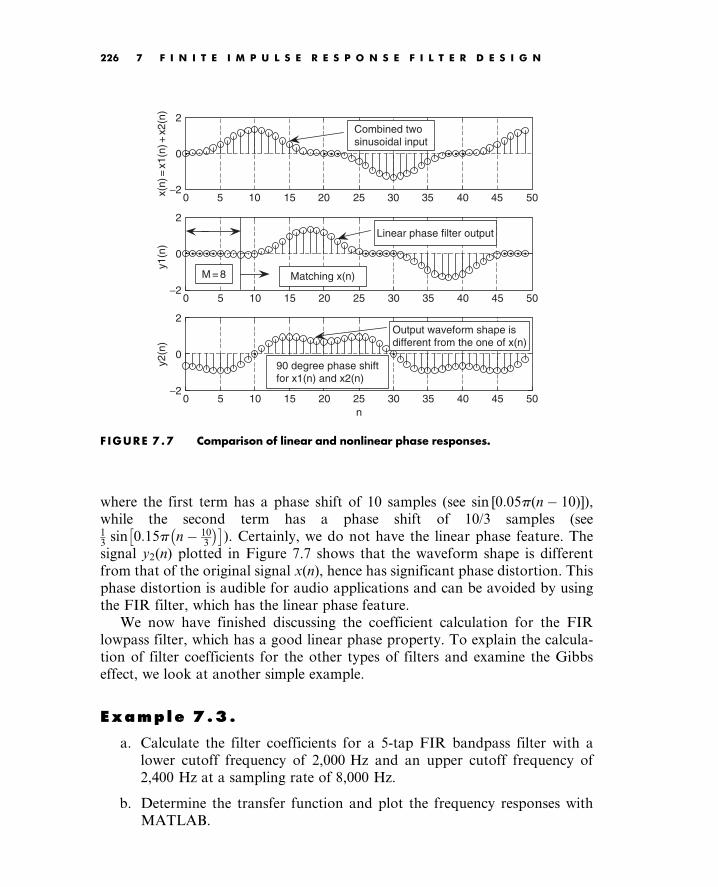
where the first term has a phase shift of 10 samples (see sin [0:05p(n 10)]),
while the second term has a phase shift of 10/3 samples (see13
sin 0:15p n 103
). Certainly, we do not have the linear phase feature. The
signal y2(n) plotted in Figure 7.7 shows that the waveform shape is different
from that of the original signal x(n), hence has significant phase distortion. This
phase distortion is audible for audio applications and can be avoided by using
the FIR filter, which has the linear phase feature.
We now have finished discussing the coefficient calculation for the FIR
lowpass filter, which has a good linear phase property. To explain the calcula-
tion of filter coefficients for the other types of filters and examine the Gibbs
effect, we look at another simple example.
Example 7.3.
a. Calculate the filter coefficients for a 5-tap FIR bandpass filter with a
lower cutoff frequency of 2,000 Hz and an upper cutoff frequency of
2,400 Hz at a sampling rate of 8,000 Hz.
b. Determine the transfer function and plot the frequency responses with
MATLAB.
0 5 10 15 20 25 30 35 40 45 50−2
0
2
x(n)
=x1
(n)+
x2(n
)
0 5 10 15 20 25 30 35 40 45 50−2
0
2
y1(n
)
0 5 10 15 20 25 30 35 40 45 50−2
0
2
n
y2(n
)
M = 8 Matching x(n)
Linear phase filter output
90 degree phase shiftfor x1(n) and x2(n)
Output waveform shape isdifferent from the one of x(n)
Combined twosinusoidal input
F IGURE 7.7 Comparison of linear and nonlinear phase responses.
Tan: Digital Signaling Processing 0123740908_chap07 Final Proof page 226 21.6.2007 11:05pm Compositor Name: MRaja
226 7 F I N I T E I M P U L S E R E S P O N S E F I L T E R D E S I G N

Solution:
a. Calculating the normalized cutoff frequencies leads to
VL ¼ 2pfL=fs ¼ 2p 2000=8000 ¼ 0:5p radians
VH ¼ 2pfH=fs ¼ 2p 2400=8000 ¼ 0:6p radians:
Since 2M þ 1 ¼ 5 in this case, using the equation in Table 7.1 yields
h(n) ¼VHVL
pn ¼ 0
sin (VHn)np
sin (VLn)np
n 6¼ 0 2 n 2
8<: (7:14)
Calculations for noncausal FIR coefficients are listed as
h(0) ¼ VH VL
p¼ 0:6p 0:5p
p¼ 0:1:
The other computed filter coefficients via Equation (7.14) are
h(1) ¼ sin [0:6p 1]
1 p sin [0:5p 1]
1 p¼ 0:01558
h(2) ¼ sin [0:6p 2]
2 p sin [0:5p 2]
2 p¼ 0:09355:
Using the symmetry leads to
h( 1) ¼ h(1) ¼ 0:01558
h( 2) ¼ h(2) ¼ 0:09355:
Thus, delaying h(n) by M ¼ 2 samples gives
b0 ¼ b4 ¼ 0:09355,
b1 ¼ b3 ¼ 0:01558, and b2 ¼ 0:1:
b. The transfer function is achieved as
H(z) ¼ 0:09355 0:01558z1 þ 0:1z2 0:01558z3 0:09355z4:
To complete Example 7.3, the magnitude frequency response plotted in
terms of H(e jV)
dB¼ 20 log10 H(e jV)
using the MATLAB program 7.1
is displayed in Figure 7.8.
Tan: Digital Signaling Processing 0123740908_chap07 Final Proof page 227 21.6.2007 11:05pm Compositor Name: MRaja
7.2 Fourier Transform Design 227

As a summary of Example 7.3, the magnitude frequency response demon-
strates the Gibbs oscillatory behavior existing in the passband and stopband.
The peak of the main lobe in the passband is dropped from 0 dB to
approximately 10 dB, while for the stopband, the lower side lobe in the
magnitude response plot swings approximately between 18 dB and 70 dB,
and the upper side lobe swings between25 dB and68 dB. As we have pointed
out, this is due to the abrupt truncation of the infinite impulse sequence h(n).
0 0.5 1 1.5 2 2.5 3 3.50
100
200
300
Frequency (rad)
Pha
se (
degr
ees)
0 0.5 1 1.5 2 2.5 3 3.5−80
−60
−40
−20
0
Frequency (rad)
Mag
nitu
de r
espo
nse
(dB
)
Side lobe Side lobe
Main lobe
F IGURE 7.8 Frequency responses for Example 7.3.
Program 7.1. MATLAB program for Example 7.3.
% Example 7.3
% MATLAB program to plot frequency responses
%
[hz, w] ¼ freqz([0:093550:015580:10:015580:09355], [1], 512);
phi¼ 180unwrap(angle(hz))/pi;subplot(2,1,1), plot(w,20log10(abs(hz))),grid;xlabel(’Frequency (radians)’);ylabel(’Magnitude Response (dB)’)subplot(2,1,2), plot(w, phi);grid;
xlabel(’Frequency (radians)’);ylabel(’Phase (degrees)’);
Tan: Digital Signaling Processing 0123740908_chap07 Final Proof page 228 21.6.2007 11:05pm Compositor Name: MRaja
228 7 F I N I T E I M P U L S E R E S P O N S E F I L T E R D E S I G N

The oscillations can be reduced by increasing the number of coefficients and
using a window function, which will be studied next.
7.3 Window Method
In this section, the window method (Fourier transform design with window func-
tions) is developed to remedy the undesirable Gibbs oscillations in the passband
and stopband of the designed FIR filter. Recall that Gibbs oscillations originate
from the abrupt truncation of the infinite-length coefficient sequence. Then it is
natural to seek a window function, which is symmetrical and can gradually weight
the designed FIR coefficients down to zeros at both ends for the range of
M n M: Applying the window sequence to the filter coefficients gives
hw(n) ¼ h(n) w(n),
where w(n) designates the window function. Common window functions used in
the FIR filter design are as follows:
1. Rectangular window:
wrec(n) ¼ 1, M n M: (7:15)
2. Triangular (Bartlett) window:
wtri(n) ¼ 1 nj jM
, M n M: (7:16)
3. Hanning window:
whan(n) ¼ 0:5þ 0:5 cosnp
M
, M n M: (7:17)
4. Hamming window:
wham(n) ¼ 0:54þ 0:46 cosnp
M
, M n M: (7:18)
5. Blackman window:
wblack(n) ¼ 0:42þ 0:5 cosnp
M
þ 0:08 cos
2np
M
, M n M: (7:19)
In addition, there is another popular window function, called the Kaiser win-
dow (its detailed information can be found in Oppenheim, Schafer, and Buck
[1999]). As we expected, the rectangular window function has a constant value
of 1 within the window, hence does only truncation. As a comparison, shapes
of the other window functions from Equations (7.16) to (7.19) are plotted in
Figure 7.9 for the case of 2M þ 1 ¼ 81.
Tan: Digital Signaling Processing 0123740908_chap07 Final Proof page 229 21.6.2007 11:05pm Compositor Name: MRaja
7.3 Window Method 229
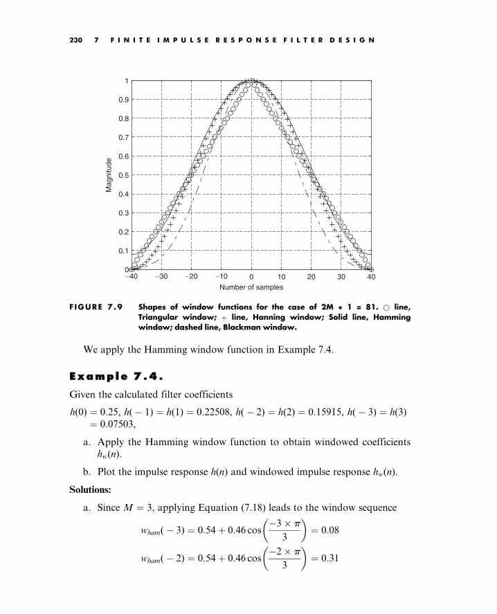
We apply the Hamming window function in Example 7.4.
Example 7.4.
Given the calculated filter coefficients
h(0) ¼ 0:25, h( 1) ¼ h(1) ¼ 0:22508, h( 2) ¼ h(2) ¼ 0:15915, h( 3) ¼ h(3)
¼ 0:07503,
a. Apply the Hamming window function to obtain windowed coefficients
hw(n).
b. Plot the impulse response h(n) and windowed impulse response hw(n).
Solutions:
a. Since M ¼ 3, applying Equation (7.18) leads to the window sequence
wham( 3) ¼ 0:54þ 0:46 cos3 p
3
¼ 0:08
wham( 2) ¼ 0:54þ 0:46 cos2 p
3
¼ 0:31
−40 −30 −20 −10 0 10 20 30 400
0.1
0.2
0.3
0.4
0.5
0.6
0.7
0.8
0.9
1
Number of samples
Mag
nitu
de
F IGURE 7.9 Shapes of window functions for the case of 2M + 1 = 81. * line,Triangular window; þ line, Hanning window; Solid line, Hammingwindow; dashed line, Blackman window.
Tan: Digital Signaling Processing 0123740908_chap07 Final Proof page 230 21.6.2007 11:05pm Compositor Name: MRaja
230 7 F I N I T E I M P U L S E R E S P O N S E F I L T E R D E S I G N

wham( 1) ¼ 0:54þ 0:46 cos1 p
3
¼ 0:77
wham(0) ¼ 0:54þ 0:46 cos0 p
3
¼ 1
wham(1) ¼ 0:54þ 0:46 cos1 p
3
¼ 0:77
wham(2) ¼ 0:54þ 0:46 cos2 p
3
¼ 0:31
wham(3) ¼ 0:54þ 0:46 cos3 p
3
¼ 0:08:
Applying the Hamming window function and its symmetrical property to
the filter coefficients, we get
hw(0) ¼ h(0) wham(0) ¼ 0:25 1 ¼ 0:25
hw(1) ¼ h(1) wham(1) ¼ 0:22508 0:77 ¼ 0:17331 ¼ hw( 1)
hw(2) ¼ h(2) wham(2) ¼ 0:15915 0:31 ¼ 0:04934 ¼ hw( 2)
hw(3) ¼ h(3) wham(3) ¼ 0:07503 0:08 ¼ 0:00600 ¼ hw( 3):
b. Noncausal impulse responses h(n) and hw(n) are plotted in Figure 7.10.
−4 −3 −2 −1 0 1 2 3 40
0.1
0.2
Sample number n
h(n)
−4 −3 −2 −1 0 1 2 3 40
0.1
0.2
Sample number n
hw(n
)
F IGURE 7 .10 Plots of FIR non-causal coefficients and windowed FIR coefficients inExample 7.4.
Tan: Digital Signaling Processing 0123740908_chap07 Final Proof page 231 21.6.2007 11:05pm Compositor Name: MRaja
7.3 Window Method 231

We observe that the Hamming window does its job to weight the FIR filter
coefficients to zero gradually at both ends. Hence, we can expect a reduced
Gibbs effect in the magnitude frequency response.
Now the lowpass FIR filter design via the window method can be therefore
achieved. The design procedure includes three steps. The first step is to obtain
the truncated impulse response h(n), where M n M; then we multiply the
obtained sequence h(n) by the selected window data sequence to yield the
windowed noncausal FIR filter coefficients hw(n); and the final step is to delay
the windowed noncausal sequence hw(n) by M samples to achieve the causal FIR
filter coefficients, bn ¼ hw(nM). The design procedure of the FIR filter via
windowing is summarized as follows:
1. Obtain the FIR filter coefficients h(n) via the Fourier transform method
(Table 7.1).
2. Multiply the generated FIR filter coefficients by the selected window
sequence
hw(n) ¼ h(n)w(n), n ¼ M, . . . 0, 1, . . . , M, (7:20)
where w(n) is chosen to be one of the window functions listed in Equa-
tions (7.15) to (7.19).
3. Delay the windowed impulse sequence hw(n) by M samples to get the
windowed FIR filter coefficients:
bn ¼ hw(nM), for n ¼ 0, 1, . . . , 2M: (7:21)
Let us study the following design examples.
Example 7.5.
a. Design a 3-tap FIR lowpass filter with a cutoff frequency of 800 Hz and a
sampling rate of 8,000 Hz using the Hamming window function.
b. Determine the transfer function and difference equation of the designed
FIR system.
c. Compute and plot the magnitude frequency response for V ¼ 0, p=4,
p=2, 3p=4, and p radians.
Solution:
a. The normalized cutoff frequency is calculated as
Vc ¼ 2pfcTs ¼ 2p 800=8000 ¼ 0:2p radian:
Tan: Digital Signaling Processing 0123740908_chap07 Final Proof page 232 21.6.2007 11:05pm Compositor Name: MRaja
232 7 F I N I T E I M P U L S E R E S P O N S E F I L T E R D E S I G N

Since 2M þ 1 ¼ 3 in this case, FIR coefficients obtained by using the
equation in Table 7.1 are listed as
h(0) ¼ 0:2 and h( 1) ¼ h(1) ¼ 0:1871
(see Example 7.2). Applying the Hamming window function defined in
Equation (7.18), we have
wham(0) ¼ 0:54þ 0:46 cos0p
1
¼ 1
wham(1) ¼ 0:54þ 0:46 cos1 p
1
¼ 0:08:
Using the symmetry of the window function gives
wham( 1) ¼ wham(1) ¼ 0:08:
The windowed impulse response is calculated as
hw(0) ¼ h(0)wham(0) ¼ 0:2 1 ¼ 0:2
hw(1) ¼ h(1)wham(1) ¼ 0:1871 0:08 ¼ 0:01497
hw( 1) ¼ h( 1)wham( 1) ¼ 0:1871 0:08 ¼ 0:01497:
Thus, delaying hw(n) by M ¼ 1 sample gives
b0 ¼ b2 ¼ 0:01496 and b1 ¼ 0:2:
b. The transfer function is achieved as
H(z) ¼ 0:01497þ 0:2z1 þ 0:01497z2:
Using the technique described in Chapter 6, we have
Y (z)
X (z)¼ H(z) ¼ 0:01497þ 0:2z1 þ 0:01497z2:
Multiplying X(z) leads to
Y (z) ¼ 0:01497X(z)þ 0:2z1X(z)þ 0:01497z2X (z):
Applying the inverse z-transform on both sides, the difference equation is
yielded as
y(n) ¼ 0:01497x(n)þ 0:2x(n 1)þ 0:01497x(n 2):
c. The magnitude frequency response and phase response can be obtained
using the technique introduced in Chapter 6. Substituting z ¼ e jV into
H(z), it follows that
H(e jV) ¼ 0:01497þ 0:2ejV þ 0:01497ej2V
¼ ejV 0:01497e jV þ 0:2þ 0:01497ejV
:
Tan: Digital Signaling Processing 0123740908_chap07 Final Proof page 233 21.6.2007 11:05pm Compositor Name: MRaja
7.3 Window Method 233

Using Euler’s formula leads to
H(e jV) ¼ ejV 0:2þ 0:02994 cos Vð Þ:Then themagnitude frequency response andphase response are found tobe
H(e jV) ¼ 0:2þ 0:2994 cos Vj j
and ffH(e jV) ¼ V if 0:2þ 0:02994 cos V > 0
Vþ p if 0:2þ 0:02994 cos V < 0.
The calculation details of the magnitude response for several normalized fre-
quency values are listed in Table 7.4. Figure 7.11 shows the plots of the
frequency responses.
TABLE 7.4 Frequency response calculation in Example 7.5.
V ffH(e jV)
radians f ¼ Vfs=(2p) Hz 0:2þ 0:02994 cos V H(e jV) H(e jV)
dB
dB degree
0 0 0.2299 0.2299 12:77 0
p=4 1000 0.1564 0.2212 13:11 45
p=2 2000 0.2000 0.2000 13:98 90
3p=4 3000 0.1788 0.1788 14:95 135
p 4000 0.1701 0.1701 15:39 180
0 500 1000 1500 2000 2500 3000 3500 4000−30
−20
−10
0
Frequency (Hz)
Mag
nitu
de r
espo
nse
(dB
)
0 500 1000 1500 2000 2500 3000 3500 4000−200
−150
−100
−50
0
50
Frequency (Hz)
Pha
se r
espo
nse
(deg
rees
)
F IGURE 7.11 The frequency responses in Example 7.5.
Tan: Digital Signaling Processing 0123740908_chap07 Final Proof page 234 21.6.2007 11:05pm Compositor Name: MRaja
234 7 F I N I T E I M P U L S E R E S P O N S E F I L T E R D E S I G N

Example 7.6.
a. Design a 5-tap FIR band reject filter with a lower cutoff frequency of
2,000 Hz, an upper cutoff frequency of 2,400 Hz, and a sampling rate
of 8,000 Hz using the Hamming window method.
b. Determine the transfer function.
Solution:
a. Calculating the normalized cutoff frequencies leads to
VL ¼ 2pfLT ¼ 2p 2000=8000 ¼ 0:5p radians
VH ¼ 2pfHT ¼ 2p 2400=8000 ¼ 0:6p radians:
Since 2M þ 1 ¼ 5 in this case, using the equation in Table 7.1 yields
h(n) ¼pVHþVL
pn ¼ 0
sin (VHn)np
þ sin (VLn)np
n 6¼ 0 2 n 2.
(
When n ¼ 0, we have
h(0) ¼ p VH þVL
p¼ p 0:6p þ 0:5p
p¼ 0:9:
The other computed filter coefficients via the previous expression are
listed as
h(1) ¼ sin [0:5p 1]
1 p sin [0:6p 1]
1 p¼ 0:01558
h(2) ¼ sin [0:5p 2]
2 p sin [0:6p 2]
2 p¼ 0:09355:
Using the symmetry leads to
h( 1) ¼ h(1) ¼ 0:01558
h( 2) ¼ h(2) ¼ 0:09355:
Applying the Hamming window function in Equation (7.18), we have
wham(0) ¼ 0:54þ 0:46 cos0 p
2
¼ 1:0
wham(1) ¼ 0:54þ 0:46 cos1 p
2
¼ 0:54
wham(2) ¼ 0:54þ 0:46 cos2 p
2
¼ 0:08:
Using the symmetry of the window function gives
Tan: Digital Signaling Processing 0123740908_chap07 Final Proof page 235 21.6.2007 11:05pm Compositor Name: MRaja
7.3 Window Method 235

wham( 1) ¼ wham(1) ¼ 0:54
wham( 2) ¼ wham(2) ¼ 0:08:
The windowed impulse response is calculated as
hw(0) ¼ h(0)wham(0) ¼ 0:9 1 ¼ 0:9
hw(1) ¼ h(1)wham(1) ¼ 0:01558 0:54 ¼ 0:00841
hw(2) ¼ h(2)wham(2) ¼ 0:09355 0:08 ¼ 0:00748
hw( 1) ¼ h( 1)wham( 1) ¼ 0:00841
hw( 2) ¼ h( 2)wham( 2) ¼ 0:00748:
Thus, delaying hw(n) by M ¼ 2 samples gives
b0 ¼ b4 ¼ 0:00748, b1 ¼ b3 ¼ 0:00841, and b2 ¼ 0:9:
b. The transfer function is achieved as
H(z) ¼ 0:00748þ 0:00841z1 þ 0:9z2 þ 0:00841z3 þ 0:00748z4:
The following design examples are demonstrated using MATLAB programs.
The MATLAB function firwd(N, Ftype, WnL, WnH, Wtype) is listed in the
‘‘MATLAB Programs’’ section at the end of this chapter. Table 7.5 lists com-
ments to show the usage.
TABLE 7.5 Illustration of the MATLAB function for FIR filter design using the windowmethods.
function B ¼ firwd (N, Ftype, WnL, WnH, Wtype)
% B ¼ firwd(N, Ftype, WnL, WnH, Wtype)
% FIR filter design using the window function method.
% Input parameters:
% N: the number of the FIR filter taps.
% Note: It must be an odd number.
% Ftype: the filter type
% 1. Lowpass filter;
% 2. Highpass filter;
% 3. Bandpass filter;
% 4. Band reject filter;
% WnL: lower cutoff frequency in radians. Set WnL ¼ 0 for the highpass filter.
% WnH: upper cutoff frequency in radians. Set WnH ¼ 0 for the lowpass filter.
% Wtypw: window function type
% 1. Rectangular window;
% 2. Triangular window;
% 3. Hanning window;
% 4. Hamming window;
% 5. Blackman window;
Tan: Digital Signaling Processing 0123740908_chap07 Final Proof page 236 21.6.2007 11:05pm Compositor Name: MRaja
236 7 F I N I T E I M P U L S E R E S P O N S E F I L T E R D E S I G N

Example 7.7.
a. Design a lowpass FIR filter with 25 taps using the MATLAB program
listed in the ‘‘MATLAB Programs’’ section at the end of this chapter. The
cutoff frequency of the filter is 2,000 Hz, assuming a sampling frequency
of 8,000 Hz. The rectangular window and Hamming window functions
are used for each design.
b. Plot the frequency responses along with those obtained using the
rectangular window and Hamming window for comparison.
c. List FIR filter coefficients for each window design method.
Solution:
a. With a given sampling rate of 8,000 Hz, the normalized cutoff frequency
can be found as
Vc ¼2000 2p
8000¼ 0:5p radians:
Now we are ready to design FIR filters via the MATLAB program. The
program, firwd(N,Ftype,WnL,WnH,Wtype), listed in the ‘‘MATLAB
Programs’’ section at the end of this chapter, has five input parameters,
which are described as follows:
& ‘‘N’’ is the number of specified filter coefficients (the number of filter
taps).
& ‘‘Ftype’’ denotes the filter type, that is, input ‘‘1’’ for the lowpass filter
design, input ‘‘2’’ for the highpass filter design, input ‘‘3’’ for the
bandpass filter design, and input ‘‘4’’ for the band reject filter design.
& ‘‘WnL’’ and ‘‘WnH’’ are the lower and upper cutoff frequency inputs,
respectively. Note that WnH ¼ 0 when specifying WnL for the lowpass
filter design, while WnL ¼ 0 when specifying WnH for the highpass
filter design.
& ‘‘Wtype’’ specifies the window data sequence to be used in the
design, that is, input ‘‘1’’ for the rectangular window, input ‘‘2’’
for the triangular window, input ‘‘3’’ for the Hanning window, input
‘‘4’’ for the Hamming window, and input ‘‘5’’ for the Blackman
window.
b. The following application program (Program 7.2) is used to generate FIR
filter coefficients using the rectangular window. Its frequency responses
will be plotted together with that obtained using the Hamming window
for comparison, as shown in Program 7.3.
Tan: Digital Signaling Processing 0123740908_chap07 Final Proof page 237 21.6.2007 11:05pm Compositor Name: MRaja
7.3 Window Method 237

Results of the FIR filter design using the Hamming window are illus-
trated in Program 7.3.
As a comparison, the frequency responses achieved from the rectangu-
lar window and the Hamming window are plotted in Figure 7.12, where
the dash-dotted line indicates the frequency response via the rectangular
window, while the solid line indicates the frequency response via the
Hamming window.
c. The FIR filter coefficients for both methods are listed in Table 7.6.
Program 7.2. MATLAB program for Example 7.7.
% Example 7.7
% MATLAB program to generate FIR coefficients
% using the rectangular window.
%
N¼25; Ftype¼1; WnL¼ 0:5pi; WnH¼0; Wtype¼1;B¼firwd(N,Ftype,WnL,WnH,Wtype);
Program 7.3. MATLAB program for Example 7.7.
% Figure 7.12
% MATLAB program to create Figure 7.12
%
N¼25;Ftype¼1;WnL¼ 0:5pi;WnH¼0;Wtype¼1;fs¼8000;%Design using the rectangular window;
Brec¼firwd(N,Ftype,WnL,WnH,Wtype);N¼25;Ftype¼1;WnL¼ 0:5pi;WnH¼0;Wtype¼4;%Design using the Hamming window;
Bham¼firwd(N,Ftype,WnL,WnH,Wtype);[hrec,f]¼freqz(Brec,1,512,fs);[hham,f]¼freqz(Bham,1,512,fs);prec¼ 180unwrap(angle(hrec))/pi;pham¼ 180unwrap(angle(hham))/pisubplot(2,1,1);
plot(f,20log10(abs(hrec)),0-.0,f,20log10(abs(hham)));gridaxis([0 4000 100 10]);xlabel(’Frequency (Hz)’);ylabel(’Magnitude Response (dB)’);subplot(2,1,2);
plot(f,prec,0-.0,f,pham);gridxlabel(’Frequency (Hz)’);ylabel(’Phase (degrees)’);
Tan: Digital Signaling Processing 0123740908_chap07 Final Proof page 238 21.6.2007 11:05pm Compositor Name: MRaja
238 7 F I N I T E I M P U L S E R E S P O N S E F I L T E R D E S I G N

0 500 1000 1500 2000 2500 3000 3500 4000−100
−50
0
Frequency (Hz)
Mag
nitu
de r
espo
nse
(dB
)
0 500 1000 1500 2000 2500 3000 3500 4000−2000
−1500
−1000
−500
0
Frequency (Hz)
Pha
se (
degr
ees)
F IGURE 7 .12 Frequency responses using the rectangular and Hamming windows.
TABLE 7.6 FIR filter coefficients in Example 7.7 (rectangular andHamming windows).
B: FIR Filter Coefficients
(rectangular window)
Bham: FIR Filter Coefficients
(Hamming window)
b0 ¼ b24 ¼ 0:000000 b0 ¼ b24 ¼ 0:000000
b1 ¼ b23 ¼ 0:028937 b1 ¼ b23 ¼ 0:002769
b2 ¼ b22 ¼ 0:000000 b2 ¼ b22 ¼ 0:000000
b3 ¼ b21 ¼ 0:035368 b3 ¼ b21 ¼ 0:007595
b4 ¼ b20 ¼ 0:000000 b4 ¼ b20 ¼ 0:000000
b5 ¼ b19 ¼ 0:045473 b5 ¼ b19 ¼ 0:019142
b6 ¼ b18 ¼ 0:000000 b6 ¼ b18 ¼ 0:000000
b7 ¼ b17 ¼ 0:063662 b7 ¼ b17 ¼ 0:041957
b8 ¼ b16 ¼ 0:000000 b8 ¼ b16 ¼ 0:000000
b9 ¼ b15 ¼ 0:106103 b9 ¼ b15 ¼ 0:091808
b10 ¼ b14 ¼ 0:000000 b10 ¼ b14 ¼ 0:000000
b11 ¼ b13 ¼ 0:318310 b11 ¼ b13 ¼ 0:313321
b12 ¼ 0:500000 b12 ¼ 0:500000
Tan: Digital Signaling Processing 0123740908_chap07 Final Proof page 239 21.6.2007 11:06pm Compositor Name: MRaja
7.3 Window Method 239

For comparison with other window functions, Figure 7.13 shows the magnitude
frequency responses using the Hanning, Hamming, and Blackman windows, with
25 taps and a cutoff frequency of 2,000 Hz. The Blackman window offers the
lowest side lobe, but with an increased width of the main lobe. The Hamming
window and Hanning window have a similar narrow width of the main lobe,
but the Hamming window accommodates a lower side lobe than the Hanning
window. Next, we will study how to choose a window in practice.
Applying the window to remedy the Gibbs effect will change the character-
istics of the magnitude frequency response of the FIR filter, where the width of
the main lobe becomes wider, while more attenuation of side lobes is achieved.
Next, we illustrate the design for customer specifications in practice. Given
the required stopband attenuation and passband ripple specifications shown in
Figure 7.14, where the lowpass filter specifications are given for illustrative
purposes, the appropriate window can be selected based on performances of
the window functions listed in Table 7.7. For example, the Hamming window
offers the passband ripple of 0.0194 dB and stopband attenuation of 53 dB.
With the selected Hamming window and the calculated normalized transition
band defined in Table 7.7,
Df ¼ fstop fpass
=fs, (7:22)
0 500 1000 1500 2000 2500 3000 3500 4000−140
−120
−100
−80
−60
−40
−20
0
20
Mag
nitu
de fr
eque
ncy
resp
onse
s
Frequency (Hz)
Hanning windowPeak of 1st side lobe
Hamming windowPeak of 1st side lobe
Blackman windowPeak of 1st side lobe
F IGURE 7 .13 Comparisons of magnitude frequency responses for the Hanning,Hamming, and Blackman windows.
Tan: Digital Signaling Processing 0123740908_chap07 Final Proof page 240 21.6.2007 11:06pm Compositor Name: MRaja
240 7 F I N I T E I M P U L S E R E S P O N S E F I L T E R D E S I G N

the filter length using the Hamming window can be determined by
N ¼ 3:3
Df: (7:23)
Note that the passband ripple is defined as
dp dB ¼ 20 log10 1þ dp
, (7:24)
while the stopband attenuation is defined as
ds dB ¼ 20 log10 dsð Þ: (7:25)
The cutoff frequency used for the design will be chosen at the middle of the
transition band, as illustrated for the lowpass filter shown in Figure 7.14.
As a rule of thumb, the cutoff frequency used for design is determined by
fc ¼ fpass þ fstop
=2: (7:26)
TABLE 7 .7 FIR filter length estimation using window functions (normalized transitionwidth Df ¼ jfstop fpassj=fs).
Window
Type
Window
Function w(n), M#n#M
Window
Length, N
Passband
Ripple (dB)
Stopband
Attenuation
(dB)
Rectangular 1 N ¼ 0:9=Df 0.7416 21
Hanning 0:5þ 0:5 cos pnM
N ¼ 3:1=Df 0.0546 44
Hamming 0:54þ 0:46 cos pnM
N ¼ 3:3=Df 0.0194 53
Blackman 0:42þ 0:5 cos npM
þ 0:08 cos 2np
M
N ¼ 5:5=Df 0.0017 74
1 + dp
1 − dp
δs
1.0
0 fs / 2fpass fstop
f
Passband Transition Stopband
fc
F IGURE 7 .14 Lowpass filter frequency domain specifications.
Tan: Digital Signaling Processing 0123740908_chap07 Final Proof page 241 21.6.2007 11:06pm Compositor Name: MRaja
7.3 Window Method 241

Note that Equation (7.23) and formulas for other window lengths in Table 7.7
are empirically derived based on the normalized spectral transition width of
each window function. The spectrum of each window function appears to be
a shape like the lowpass filter magnitude frequency response with ripples in
the passband and side lobes in the stopband. The passband frequency edge
of the spectrum is the frequency where the magnitude just begins to drop
below the passband ripple and where the stop frequency edge is at the peak of
the first side lobe in the spectrum. With the passband ripple and stopband
attenuation specified for a particular window, the normalized transition width
of the window is in inverse proportion to the window length N multiplied by a
constant. For example, the normalized spectral transition Df for the Hamming
window is 3.3/N. Hence, matching the FIR filter transition width with the
transition width of the window spectrum gives the filter length estimation listed
in Table 7.7.
The following examples illustrate the determination of each filter length and
cutoff frequency/frequencies for the design of lowpass, highpass, bandpass, and
bandstop filters. Application of each designed filter to the processing of speech
data is included, along with an illustration of filtering effects in both time
domain and frequency domain.
Example 7.8.
A lowpass FIR filter has the following specifications:
Passband ¼ 0 1,850 Hz
Stopband ¼ 2,150 4,000 Hz
Stopband attenuation ¼ 20 dB
Passband ripple ¼ 1 dB
Sampling rate ¼ 8,000Hz
a. Determine the FIR filter length and the cutoff frequency to be used in the
design equation.
Solution:
a. The normalized transition band as defined in Equation (7.22) and
Table 7.7 is given by
Df ¼ 2150 1850j j=8000 ¼ 0:0375:
Again, based on Table 7.7, selecting the rectangular window will result
in a passband ripple of 0.74 dB and a stopband attenuation of 21 dB.
Thus, this window selection would satisfy the design requirement for the
Tan: Digital Signaling Processing 0123740908_chap07 Final Proof page 242 21.6.2007 11:06pm Compositor Name: MRaja
242 7 F I N I T E I M P U L S E R E S P O N S E F I L T E R D E S I G N

passband ripple of 1 dB and stopband attenuation of 20 dB. Next, we
determine the length of the filter as
N ¼ 0:9=Df ¼ 0:9=0:0375 ¼ 24:
We choose the odd number N ¼ 25. The cutoff frequency is determined
by (1850þ 2150)=2 ¼ 2000 Hz. Such a filter has been designed in
Example 7.7, its filter coefficients are listed in Table 7.6, and its fre-
quency responses can be found in Figure 7.12 (dashed lines).
Now we look at the time domain and frequency domain results from filtering
a speech signal by using the lowpass filter we have just designed. Figure 7.15a
shows the original speech and lowpass filtered speech. The spectral comparison
is given in Figure 7.15b, where, as we can see, the frequency components beyond
2 kHz are filtered. The lowpass filtered speech would sound muffled.
We will continue to illustrate the determination of the filter length and cutoff
frequency for other types of filters via the following examples.
0 200 400 600 800 1000 1200 1400 1600 1800 2000−1
−0.5
0
0.5
1 104
Spe
ech
0 200 400 600 800 1000 1200 1400 1600 1800 2000−1
−0.5
0
0.5
1 104
Low
pass
ed s
peec
h
Sample numberA
F IGURE 7 .15A Original speech and processed speech using the lowpass filter.
Tan: Digital Signaling Processing 0123740908_chap07 Final Proof page 243 21.6.2007 11:06pm Compositor Name: MRaja
7.3 Window Method 243

Example 7.9.
a. Design a highpass FIR filter with the following specifications:
Stopband ¼ 0–1,500 Hz
Passband ¼ 2,500–4,000 Hz
Stopband attenuation ¼ 40 dB
Passband ripple ¼ 0.1 dB
Sampling rate ¼ 8,000 Hz
Solution:
a. Based on the specifications, the Hanning window will do the job, since it
has a passband ripple of 0.0546 dB and a stopband attenuation of 44 dB.
Then
Df ¼ 1500 2500j j=8000 ¼ 0:125
N ¼ 3:1=Df ¼ 24:2: Choose N ¼ 25:
0 500 1000 1500 2000 2500 3000 3500 4000
0 500 1000 1500 2000 2500 3000 3500 4000
0
200
400
600
800
Frequency (Hz)
Am
plitu
de |X
(f)|
0
200
400
600
800
Frequency (Hz)
Am
plitu
de |Y
(f)|
B
F IGURE 7 .15B Spectral plots of the original speech and processed speech by thelowpass filter.
Tan: Digital Signaling Processing 0123740908_chap07 Final Proof page 244 21.6.2007 11:06pm Compositor Name: MRaja
244 7 F I N I T E I M P U L S E R E S P O N S E F I L T E R D E S I G N

Hence, we choose 25 filter coefficients using the Hanning window
method. The cutoff frequency is (1500þ 2500)=2 ¼ 2000Hz. The normal-
ized cutoff frequency can be easily found as
Vc ¼2000 2p
8000¼ 0:5p radians:
And notice that 2M þ 1 ¼ 25. The application program and design re-
sults are listed in Program 7.4 and Table 7.8.
The corresponding frequency responses of the designed highpass FIR
filter are displayed in Figure 7.16.
TABLE 7 .8 FIR filter coefficients in Example 7.9 (Hanning window).
Bhan: FIR Filter Coefficients (Hanning window)
b0 ¼ b24 ¼ 0:000000 b1 ¼ b23 ¼ 0:000493
b2 ¼ b22 ¼ 0:000000 b3 ¼ b21 ¼ 0:005179
b4 ¼ b20 ¼ 0:000000 b5 ¼ b19 ¼ 0:016852
b6 ¼ b18 ¼ 0:000000 b7 ¼ b17 ¼ 0:040069
b8 ¼ b16 ¼ 0:0000000 b9 ¼ b15 ¼ 0:090565
b10 ¼ b14 ¼ 0:000000 b11 ¼ b13 ¼ 0:312887
b12 ¼ 0:500000
0 500 1000 1500 2000 2500 3000 3500 4000−1500
−1000
−500
0
500
Frequency (Hz)
Pha
se (
degr
ees)
0 500 1000 1500 2000 2500 3000 3500 4000
−100
−50
0
Frequency (Hz)
Mag
nitu
de r
espo
nse
(dB
)
F IGURE 7.16 Frequency responses of the designed highpass filter using the Hanningwindow.
Tan: Digital Signaling Processing 0123740908_chap07 Final Proof page 245 21.6.2007 11:06pm Compositor Name: MRaja
7.3 Window Method 245

Comparisons are given in Figure 7.17(a), where the original speech and
processed speech using the highpass filter are plotted. The high-frequency com-
ponents of speech generally contain small amounts of energy. Figure 7.17(b)
displays the spectral plots, where clearly the frequency components lower than
1.5 kHz are filtered. The processed speech would sound crisp.
Program 7.4. MATLAB program for Example 7.9.
% Figure 7.16 (Example 7.9)
% MATLAB program to create Figure 7.16
%
N ¼ 25;Ftype ¼ 2;WnL ¼ 0;WnH ¼ 0:5pi;Wtype ¼ 3;fs ¼ 8000;
Bhan¼firwd(N, Ftype, WnL, WnH, Wtype);
freqz(Bhan,1,512,fs);
axis([0 fs/2 120 10]);
0 200 400 600 800 1000 1200 1400 1600 1800 2000−1
−0.5
0
0.5
1 104
104
Spe
ech
0 200 400 600 800 1000 1200 1400 1600 1800 2000−1
−0.5
0
0.5
1
Hig
hpas
sed
spee
ch
Sample numberA
F IGURE 7.17A Original speech and processed speech using the highpass filter.
Tan: Digital Signaling Processing 0123740908_chap07 Final Proof page 246 21.6.2007 11:06pm Compositor Name: MRaja
246 7 F I N I T E I M P U L S E R E S P O N S E F I L T E R D E S I G N

Example 7.10.
a. Design a bandpass FIR filter with the following specifications:
Lower stopband ¼ 0–500 Hz
Passband ¼ 1,600–2,300 Hz
Upper stopband ¼ 3,500–4,000 Hz
Stopband attenuation ¼ 50 dB
Passband ripple ¼ 0.05 dB
Sampling rate ¼ 8,000 Hz
Solution:
a. Df1 ¼ 1600 500j j=8000 ¼ 0:1375 and Df2 ¼ 3500 2300j j=8000 ¼ 0:15
N1 ¼ 3:3=0:1375 ¼ 24 and N2 ¼ 3:3=0:15 ¼ 22
Choosing N ¼ 25 filter coefficients using the Hamming window
method:
f1 ¼ (1600þ 500)=2 ¼ 1050Hz and f2 ¼ (3500þ 2300)=2 ¼ 2900Hz:
0 500 1000 1500 2000 2500 3000 3500 40000
200
400
600
800
Frequency (Hz)
Am
plitu
de |X
(f)|
0 500 1000 1500 2000 2500 3000 3500 40000
10
20
30
Frequency (Hz)
Am
plitu
de |Y
(f)|
B
F IGURE 7.17B Spectral comparison of the original speech and processed speechusing the highpass filter.
Tan: Digital Signaling Processing 0123740908_chap07 Final Proof page 247 21.6.2007 11:06pm Compositor Name: MRaja
7.3 Window Method 247

The normalized lower and upper cutoff frequencies are calculated as:
VL ¼1050 2p
8000¼ 0:2625p radians and
VH ¼2900 2p
8000¼ 0:725p radians,
and N ¼ 2M þ 1 ¼ 25. Using the MATLAB program, design results are
achieved as shown in Program 7.5.
Figure 7.18 depicts the frequency responses of the designed bandpass FIR
filter. Table 7.9 lists the designed FIR filter coefficients.
Program 7.5. MATLAB program for Example 7.10.
% Figure 7.18 (Example 7.10)
% MATLAB program to create Figure 7.18
%
N ¼ 25;Ftype ¼ 3;WnL ¼ 0:2625pi;WnH ¼ 0:725pi;Wtype ¼ 4;fs ¼ 8000;
Bham¼firwd(N,Ftype,WnL,WnH,Wtype);freqz(Bham,1,512,fs);
axis([0 fs/2 130 10]);
0 500 1000 1500 2000 2500 3000 3500 4000−2000
−1500
−1000
−500
0
500
Frequency (Hz)
Pha
se (
degr
ees)
0 500 1000 1500 2000 2500 3000 3500 4000
−100
−50
0
Frequency (Hz)
Mag
nitu
de r
espo
nse
(dB
)
F IGURE 7.18 Frequency responses of the designed bandpass filter using theHamming window.
Tan: Digital Signaling Processing 0123740908_chap07 Final Proof page 248 21.6.2007 11:06pm Compositor Name: MRaja
248 7 F I N I T E I M P U L S E R E S P O N S E F I L T E R D E S I G N

For comparison, the original speech and bandpass filtered speech are
plotted in Figure 7.19a, where the bandpass frequency components contain
a small portion of speech energy. Figure 7.19b shows a comparison indicating
that the low frequency and high frequency are removed by the bandpass
filter.
TABLE 7 .9 FIR filter coefficients in Example 7.10 (Hamming window).
Bham: FIR Filter Coefficients (Hamming window)
b0 ¼ b24 ¼ 0:002680 b1 ¼ b23 ¼ 0:001175
b2 ¼ b22 ¼ 0:007353 b3 ¼ b21 ¼ 0:000674
b4 ¼ b20 ¼ 0:011063 b5 ¼ b19 ¼ 0:004884
b6 ¼ b18 ¼ 0:053382 b7 ¼ b17 ¼ 0:003877
b8 ¼ b16 ¼ 0:028520 b9 ¼ b15 ¼ 0:008868
b10 ¼ b14 ¼ 0:296394 b11 ¼ b13 ¼ 0:008172
b12 ¼ 0:462500
0 200 400 600 800 1000 1200 1400 1600 1800 2000−1
−0.5
0
0.5
1 104
104
Spe
ech
0 200 400 600 800 1000 1200 1400 1600 1800 2000−1
−0.5
0
0.5
1
Ban
dpas
sed
spee
ch
Sample numberA
F IGURE 7 .19A Original speech and processed speech using the bandpass filter.
Tan: Digital Signaling Processing 0123740908_chap07 Final Proof page 249 21.6.2007 11:06pm Compositor Name: MRaja
7.3 Window Method 249

Example 7.11.
a. Design a bandstop FIR filter with the following specifications:
Lower cutoff frequency ¼ 1,250 Hz
Lower transition width ¼ 1,500 Hz
Upper cutoff frequency ¼ 2,850 Hz
Upper transition width ¼ 1,300 Hz
Stopband attenuation ¼ 60 dB
Passband ripple ¼ 0:02 dB
Sampling rate ¼ 8,000 Hz
Solution:
a. We can directly compute the normalized transition widths:
Df1 ¼ 1500=8000 ¼ 0:1875, and Df2 ¼ 1300=8000 ¼ 0:1625:
The filter lengths are determined using the Blackman window as:
N1 ¼ 5:5=0:1875 ¼ 29:33, and N2 ¼ 5:5=0:1625 ¼ 33:8:
0 500 1000 1500 2000 2500 3000 3500 40000
200
400
600
800
Frequency (Hz)
Am
plitu
de |X
(f)|
0 500 1000 1500 2000 2500 3000 3500 40000
10
20
30
40
50
Frequency (Hz)
Am
plitu
de |Y
(f)|
B
F IGURE 7 .19B Spectral comparison of the original speech and processed speechusing the bandpass filter.
Tan: Digital Signaling Processing 0123740908_chap07 Final Proof page 250 21.6.2007 11:06pm Compositor Name: MRaja
250 7 F I N I T E I M P U L S E R E S P O N S E F I L T E R D E S I G N

We choose an odd number N ¼ 35. The normalized lower and upper
cutoff frequencies are calculated as:
VL ¼2p 1250
8000¼ 0:3125p radian and
VH ¼2p 2850
8000¼ 0:7125p radians,
and N ¼ 2M þ 1 ¼ 35. Using MATLAB, the design results are demon-
strated in Program 7.6.
Figure 7.20 shows the plot of the frequency responses of the designed band-
stop filter. The designed filter coefficients are listed in Table 7.10.
Comparisons of filtering effects are illustrated in Figures 7.21a and 7.21b. In
Figure 7.21a, the original speech and the processed speech by the bandstop filter
are plotted. The processed speech contains most of the energy of the original
speech because most of the energy of the speech signal exists in the low-frequency
band. Figure 7.21b verifies the filtering frequency effects. The frequency com-
ponents ranging from 2,000 to 2,200 Hz have been completely removed.
Program 7.6. MATLAB program for Example 7.11.
% Figure 7.20 (Example 7.11)
% MATLAB program to create Figure 7.20
%
N ¼ 35;Ftype ¼ 4;WnL ¼ 0:3125pi;WnH ¼ 0:7125pi;Wtype ¼ 5;fs ¼ 8000;
Bblack ¼ firwd(N,Ftype,WnL,WnH,Wtype);
freqz(Bblack,1,512,fs);
axis([0 fs/2 120 10]);
TABLE 7.10 FIR filter coefficients in Example 7.11 (Blackman window).
Black: FIR Filter Coefficients (Blackman window)
b0 ¼ b34 ¼ 0:000000 b1 ¼ b33 ¼ 0:000059
b2 ¼ b32 ¼ 0:000000 b3 ¼ b31 ¼ 0:000696
b4 ¼ b30 ¼ 0:001317 b5 ¼ b29 ¼ 0:004351
b6 ¼ b28 ¼ 0:002121 b7 ¼ b27 ¼ 0:000000
b8 ¼ b26 ¼ 0:004249 b9 ¼ b25 ¼ 0:027891
b10 ¼ b24 ¼ 0:011476 b11 ¼ b23 ¼ 0:036062
b12 ¼ b22 ¼ 0:000000 b13 ¼ b21 ¼ 0:073630
b14 ¼ b20 ¼ 0:020893 b15 ¼ b19 ¼ 0:285306
b16 ¼ b18 ¼ 0:014486 b17 ¼ 0:600000
Tan: Digital Signaling Processing 0123740908_chap07 Final Proof page 251 21.6.2007 11:06pm Compositor Name: MRaja
7.4 Applications: Noise Reduction and Two-Band Digital Crossover 251

0 500 1000 1500 2000 2500 3000 3500 4000−2500
−2000
−1500
−1000
−500
0
Frequency (Hz)
Pha
se (
degr
ees)
0 500 1000 1500 2000 2500 3000 3500 4000
−100
−50
0
Frequency (Hz)
Mag
nitu
de r
espo
nse
(dB
)
F IGURE 7 .20 Frequency responses of the designed bandstop filter using theBlackman window.
0 200 400 600 800 1000 1200 1400 1600 1800 2000−1
−0.5
0
0.5
1 104
Spe
ech
0 200 400 600 800 1000 1200 1400 1600 1800 2000−1
−0.5
0
0.5
1 104
Ban
d re
ject
ed s
peec
h
Sample numberA
F IGURE 7.21A Original speech and processed speech using the bandstop filter.
Tan: Digital Signaling Processing 0123740908_chap07 Final Proof page 252 21.6.2007 11:06pm Compositor Name: MRaja
252 7 F I N I T E I M P U L S E R E S P O N S E F I L T E R D E S I G N

7.4 Appl i cat ions: Noise Reduct ion andTwo-Band Digi ta l Crossover
In this section, we will investigate noise reduction and digital crossover design
using the FIR filters.
7.4.1 Noise Reduct ion
One of the key digital signal processing (DSP) applications is noise reduction.
In this application, a digital FIR filter removes noise in the signal that is
contaminated by noise existing in the broad frequency range. For example,
such noise often appears during the data acquisition process. In real-world
applications, the desired signal usually occupies a certain frequency range. We
can design a digital filter to remove frequency components other than the
desired frequency range.
In a data acquisition system, we record a 500 Hz sine wave at a sampling rate
of 8,000 Hz. The signal is corrupted by broadband noise v(n):
x(n) ¼ 1:4141 sin (2p 500n=8000)þ v(n):
0 500 1000 1500 2000 2500 3000 3500 40000
200
400
600
800
Frequency (Hz)
Am
plitu
de |X
(f)|
0 500 1000 1500 2000 2500 3000 3500 4000
200
400
0
600
Frequency (Hz)
Am
plitu
de |Y
(f)|
B
F IGURE 7 .21B Spectral comparison of the original speech and the processed speechusing the bandstop filter.
Tan: Digital Signaling Processing 0123740908_chap07 Final Proof page 253 21.6.2007 11:06pm Compositor Name: MRaja
7.4 Applications: Noise Reduction and Two-Band Digital Crossover 253

The 500 Hz signal with noise and its spectrum are plotted in Figure 7.22, from
which it is obvious that the digital sine wave contains noise. The spectrum is also
displayed to give better understanding of the noise frequency level. We can see
that noise is broadband, existing from 0 Hz to the folding frequency of
4,000 Hz. Assuming that the desired signal has a frequency range of only 0 to
800 Hz, we can filter noise from 800 Hz and beyond. A lowpass filter would
complete such a task. Then we develop the filter specifications:
Passband frequency range: 0 Hz to 800 Hz with passband ripple less than
0.02 dB.
Stopband frequency range: 1 kHz to 4 kHz with 50 dB attenuation.
As we will see, lowpass filtering will remove the noise ranging from 1,000 to
4,000 Hz, and hence the signal-to-noise power ratio will be improved.
Based on the specifications, we design the FIR filter with a Hamming
window, a cutoff frequency of 900 Hz, and an estimated filter length of 133
taps. The enhanced signal is depicted in Figure 7.23, where the clean signal can
be observed. The amplitude spectrum for the enhanced signal is also plotted. As
shown in the spectral plot, the noise level is almost neglected between 1 and
4 kHz. Notice that since we use the higher-order FIR filter, the signal experi-
ences a linear phase delay of 66 samples, as is expected. We also see some
transient response effects. However, the transient response effects will be
50 100 150 2000 250
−2
0
2
−4
4
Number of samples
Sam
ple
valu
e
500 1000 1500 2000 2500 3000 35000 4000
0.5
1
0
1.5
Frequency (Hz)
Am
plitu
de |X
(f)|
F IGURE 7.22 Signal with noise and its spectrum.
Tan: Digital Signaling Processing 0123740908_chap07 Final Proof page 254 21.6.2007 11:06pm Compositor Name: MRaja
254 7 F I N I T E I M P U L S E R E S P O N S E F I L T E R D E S I G N

ended totally after the first 132 samples due to the length of the FIR filter.
MATLAB implementation is given in Program 7.7.
7.4.2 Speech Noise Reduct ion
In a speech recording system, we digitally record speech in a noisy environment
at a sampling rate of 8,000 Hz. Assuming that the recorded speech contains
information within 1,800 Hz, we can design a lowpass filter to remove the noise
between 1,800 Hz and the Nyquist limit (the folding frequency of 4,000 Hz).
Therefore, we have the following filter specifications:
Filter type ¼ lowpass FIR
Passband frequency range ¼ 0–1,800 Hz
Passband ripple ¼ 0.02 dB
Stopband frequency range ¼ 2,000–4,000 Hz
Stopband attenuation ¼ 50 dB.
According to these specifications, we can determine the following parameters
for filter design:
Window type ¼ Hamming window
Number of filter taps ¼ 133
Lowpass cutoff frequency ¼ 1,900 Hz.
50 100 150 2000 250
−2
0
2
−4
4
Number of samples
Sam
ple
valu
e
0 500 1000 1500 2000 2500 3000 3500 4000
0.5
1
0
1.5
Frequency (Hz)
Am
plitu
de |Y
(f)|
M = 66
F IGURE 7 .23 The noise-removed clean signal and spectrum.
Tan: Digital Signaling Processing 0123740908_chap07 Final Proof page 255 21.6.2007 11:06pm Compositor Name: MRaja
7.4 Applications: Noise Reduction and Two-Band Digital Crossover 255

Figure 7.24(a) shows the plots of the recorded noisy speech and its spectrum. As
we can see in the noisy spectrum, the noise level is high and broadband. After
applying the designed lowpass filter, we plot the filtered speech and its spectrum
shown in Figure 7.24(b), where the clean speech is clearly identified, while the
spectrum shows that the noise components above 2 kHz have been completely
removed.
7.4.3 Two-Band Digi tal Crossover
In audio systems, there is often a situation where the application requires the
entire audible range of frequencies, but this is beyond the capability of any
single speaker driver. So, we combine several drivers, such as the speaker cones
and horns, each covering different frequency range, to reproduce the full audio
frequency range.
A typical two-band digital crossover can be designed as shown in Figure 7.25.
There are two speaker drivers. The woofer responds to low frequencies, and the
Program 7.7. MATLAB program for the application of noise filtering.
close all; clear all
fs ¼ 8000; % Sampling rate
T ¼ 1=fs; % Sampling period
v¼sqrt(0:1)randn(1,250); % Generate the Gaussian random noise
n ¼ 0:1:249; % Indexes
x ¼ sqrt(2) sin(2pi500nT)þ v; % Generate the 500-Hz sinusoid plus noisesubplot(2,1,1);plot(t,x);
xlabel(’Number of samples’);ylabel(’Sample value’);grid;N¼length(x);f¼[0:N/2]fs/N;Axk¼ 2abs(fft(x))/N;Axk(1)¼Axk(1)/2; % Calculate the single-sided spectrumsubplot(2,1,2);plot(f,Axk(1:N/2þ 1));xlabel(’Frequency (Hz)’);ylabel(’Amplitude (f)j ’);grid;figure
Wnc¼ 2pi900/fs; % Determine the normalized digital cutoff frequency
B¼firwd(133,1,Wnc,0,4); % Design the FIR filter
y¼filter(B,1,x); % Perform digital filtering
Ayk¼ 2abs(fft(y))/N;Ayk(1)¼Ayk(1)/2;% Single-sided spectrum of the filtered datasubplot(2,1,1);plot(t,y);
xlabel(’Number of samples’);ylabel(’Sample value’);grid;subplot(2,1,2);plot(f,Ayk(1:N/2þ 1));axis([0 fs/2 0 1.5]);
xlabel(’Frequency (Hz)’);ylabel(’Amplitude jY(f)j ’);grid;
Tan: Digital Signaling Processing 0123740908_chap07 Final Proof page 256 21.6.2007 11:06pm Compositor Name: MRaja
256 7 F I N I T E I M P U L S E R E S P O N S E F I L T E R D E S I G N

0 0.05 0.1 0.15 0.2 0.25−1
−0.5
0
0.5
1× 10⁴
Number of samples
Sam
ple
valu
e
0A
500 1000 1500 2000 2500 3000 3500 40000
200
400
600
800
Frequency (Hz)
Am
plitu
de |X
(f)|
F IGURE 7 .24A Noisy speech and its spectrum.
0 0.05 0.1 0.15 0.2 0.25−1
−0.5
0
0.5
1× 10⁴
Number of samples
Sam
ple
valu
e
0 500 1000 1500 2000 2500 3000 3500 40000
200
400
600
800
Frequency (Hz)
Am
plitu
de |Y
(f)|
B
F IGURE 7 .24B Enhanced speech and its spectrum.
Tan: Digital Signaling Processing 0123740908_chap07 Final Proof page 257 21.6.2007 11:06pm Compositor Name: MRaja
7.4 Applications: Noise Reduction and Two-Band Digital Crossover 257

tweeter responds to high frequencies. The incoming digital audio signal is split
into two bands by using a lowpass filter and a highpass filter in parallel. We then
amplify the separated audio signals and send them to their respective corre-
sponding speaker drivers. Hence, the objective is to design the lowpass filter and
the highpass filter so that their combined frequency response is flat, while
keeping transition as sharp as possible to prevent audio signal distortion in
the transition frequency range. Although traditional crossover systems are
designed using active circuits (analog systems) or passive circuits, the digital
crossover system provides a cost-effective solution with programmable ability,
flexibility, and high quality.
A crossover system has the following specifications:
Sampling rate ¼ 44,100 Hz
Crossover frequency ¼ 1,000 Hz (cutoff frequency)
Transition band ¼ 600 to 1,400 Hz
Lowpass filter ¼ passband frequency range from 0 to 600 Hz with a ripple of
0.02 dB and stopband edge at 1,400 Hz with attenuation of 50 dB.
Highpass filter ¼ passband frequency range from 1.4 to 44.1 kHz with ripple
of 0.02 dB and stopband edge at 600 Hz with attenuation of 50 dB.
In the design of this crossover system, one possibility is to use an FIR filter,
since it provides a linear phase for the audio system. However, an infinite
impulse response (IIR) filter (which will be discussed in the next chapter) can
be an alternative. Based on the transition band of 800 Hz and the passband
ripple and stopband attenuation requirements, the Hamming window is chosen
for both lowpass and highpass filters. We can determine the number of filter
taps as 183, each with a cutoff frequency of 1,000 Hz.
The frequency responses for the designed lowpass filter and highpass filter
are given in Figure 7.26(a), and for the lowpass filter, highpass filter, and
combined responses in Figure 7.26(b). As we can see, the crossover frequency
Digitalaudio x(n)
Highpass filter
Lowpass filter Gain_L
Gain_H Tweeter:The crossover passes
high frequencies
Woofer:The crossover passes
low frequencies
yH(n)
yL(n)
F IGURE 7.25 Two-band digital crossover.
Tan: Digital Signaling Processing 0123740908_chap07 Final Proof page 258 21.6.2007 11:06pm Compositor Name: MRaja
258 7 F I N I T E I M P U L S E R E S P O N S E F I L T E R D E S I G N

100 101 102 103 104−200
−150
−100
−50
0
Frequency (Hz)
Mag
nitu
de r
espo
nse
(dB
)
100101 102 103 104
−200
−150
−100
−50
0
Frequency (Hz)
Mag
nitu
de r
espo
nse
(dB
)
A
F IGURE 7.26A Magnitude frequency responses for lowpass filter and highpass filter.
100 101 102 103 104−200
−180
−160
−140
−120
−100
−80
−60
−40
−20
0
20
Frequency (Hz)B
Mag
nitu
de r
espo
nse
(dB
)
Combined
LPF HPF
F IGURE 7 .26B Magnitude frequency responses for both lowpass filter and highpassfilter, and the combined magnitude frequency response for the digitalaudio crossover system.
Tan: Digital Signaling Processing 0123740908_chap07 Final Proof page 259 21.6.2007 11:06pm Compositor Name: MRaja
7.4 Applications: Noise Reduction and Two-Band Digital Crossover 259

for both filters is at 1,000 Hz, and the combined frequency response is perfectly
flat. The impulse responses (filter coefficients) for lowpass and highpass filters
are plotted in Figure 7.26(c).
7.5 Frequency Sampl ing Design Method
In addition to methods of Fourier transform design and Fourier transform with
windowing discussed in the previous section, frequency sampling is another
alternative. The key feature of frequency sampling is that the filter coeffi-
cients can be calculated based on the specified magnitudes of the desired filter
frequency response uniformly in frequency domain. Hence, it has design
flexibility.
To begin with development, we let h(n), for n ¼ 0, 1, . . . , N 1, be the
causal impulse response (FIR filter coefficients) that approximates the FIR
filter, and we let H(k), for k ¼ 0, 1, . . . , N 1, represent the corresponding
discrete Fourier transform (DFT) coefficients. We obtain H(k) by sampling
0 20 40 60 80 100 120 140 160 180 200–0.02
0
0.02
0.04
0.06
n
Impu
lse
resp
onse
of L
PF
0 20 40 60 80 100 120 140 160 180 200−0.5
0
0.5
1
nC
Impu
lse
resp
onse
of H
PF
F IGURE 7.26C Impulse responses of both the FIR lowpass filter and the FIR highpassfilter for the digital audio crossover system.
Tan: Digital Signaling Processing 0123740908_chap07 Final Proof page 260 21.6.2007 11:06pm Compositor Name: MRaja
260 7 F I N I T E I M P U L S E R E S P O N S E F I L T E R D E S I G N

the desired frequency filter response H(k) ¼ H(e jV) at equally spaced instants in
frequency domain, as shown in Figure 7.27.
Then, according to the definition of the inverse DFT (IDFT), we can
calculate the FIR coefficients:
h(n) ¼ 1
N
XN1
k¼0
H(k)WknN , for n ¼ 0, 1, . . . , N 1,
where
WN ¼ ej2N ¼ cos
2
N
j sin
2
N
: (7:27)
We assume that the FIR filter has linear phase and the number of taps
N ¼ 2M þ 1. Equation (7.27) can be significantly simplified as
h(n) ¼ 1
2M þ 1H0 þ 2
XMk¼1
Hk cos2pk(nM)
2M þ 1
( ),
for n ¼ 0, 1, . . . , 2M,
(7:28)
where Hk, for k ¼ 0, 1, . . . , 2M, represents the magnitude values specifying the
desired filter frequency response sampled at Vk ¼ 2pk(2Mþ1)
. The derivation is
H(ejW)
H(ejW)
W
π 2p0
Desired filter frequency response
2p
0 1 2 3 4
Desired filter frequency response
Hk= H(k )
k
Wk
5 6 7 8
W0 W1 W2 W3 W4 W5 W6 W7 W8
F IGURE 7.27 Desired filter frequency response and sampled frequency response.
Tan: Digital Signaling Processing 0123740908_chap07 Final Proof page 261 21.6.2007 11:06pm Compositor Name: MRaja
7.5 Frequency Sampling Design Method 261

detailed in Appendix E. The design procedure is therefore simply summarized as
follows:
1. Given the filter length of 2M þ 1, specify the magnitude frequency
response for the normalized frequency range from 0 to p:
Hk at Vk ¼2pk
(2M þ 1)for k ¼ 0, 1, . . . , M: (7:29)
2. Calculate FIR filter coefficients:
h(n) ¼ 1
2M þ 1H0 þ 2
XMk¼1
Hk cos2pk(nM)
2M þ 1
( )
for n ¼ 0, 1, . . . , M:
(7:30)
3. Use the symmetry (linear phase requirement) to determine the rest of the
coefficients:
h(n) ¼ h(2M n) for n ¼M þ 1, . . . , 2M: (7:31)
Example 7.12 illustrates the design procedure.
Example 7.12.
a. Design a linear phase lowpass FIR filter with 7 taps and a cutoff fre-
quency of Vc ¼ 0:3p radian using the frequency sampling method.
Solution:
a. Since N ¼ 2M þ 1 ¼ 7 and M ¼ 3, the sampled frequencies are given by
Vk ¼2p
7k radians, k ¼ 0, 1, 2, 3:
Next we specify the magnitude values Hk at the specified frequencies as
follows:
for V0 ¼ 0 radians, H0 ¼ 1:0
for V1 ¼2
7p radians, H1 ¼ 1:0
for V2 ¼4
7p radians, H2 ¼ 0:0
for V3 ¼6
7p radians, H3 ¼ 0:0:
Figure 7.28 shows the specifications.
Tan: Digital Signaling Processing 0123740908_chap07 Final Proof page 262 21.6.2007 11:06pm Compositor Name: MRaja
262 7 F I N I T E I M P U L S E R E S P O N S E F I L T E R D E S I G N

Using Equation (7.30), we achieve
h(n) ¼ 1
71þ 2
X3
k¼1
Hk cos [2pk(n 3)=7]
( )
¼ 1
71þ 2 cos [2p(n 3)=7]f g
, n ¼ 0, 1, . . . , 3:
Thus, computing the FIR filter coefficients yields
h(0) ¼ 1
71þ 2 cos ( 6p=7)f g ¼ 0:11456
h(1) ¼ 1
71þ 2 cos ( 4p=7)f g ¼ 0:07928
h(2) ¼ 1
71þ 2 cos ( 2p=7)f g ¼ 0:32100
h(3) ¼ 1
71þ 2 cos ( 0 p=7)f g ¼ 0:42857:
By the symmetry, we obtain the rest of the coefficients as follows:
h(4) ¼ h(2) ¼ 0:32100
h(5) ¼ h(1) ¼ 0:07928
h(6) ¼ h(0) ¼ 0:11456:
The following two examples are devoted to illustrating the FIR filter design
using the frequency sampling method. A MATLAB program, firfs(N, Hk), is
provided in the ‘‘MATLAB Programs’’ section at the end of this chapter (see its
usage in Table 7.11) to implement the design in Equation (7.30) with input
parameters of N ¼ 2M þ 1 (number of taps) and a vector Hk containing the
specified magnitude values Hk, k ¼ 0, 1, . . . , M. Finally, the MATLAB func-
tion will return the calculated FIR filter coefficients.
pW
0.5p0
1.0H0 H1
H2 H3
H(ejW )
F IGURE 7 .28 Sampled values of the frequency response in Example 7.12.
Tan: Digital Signaling Processing 0123740908_chap07 Final Proof page 263 21.6.2007 11:06pm Compositor Name: MRaja
7.5 Frequency Sampling Design Method 263

Example 7.13.
a. Design a linear phase lowpass FIR filter with 25 coefficients using the
frequency sampling method. Let the cutoff frequency be 2,000 Hz and
assume a sampling frequency of 8,000 Hz.
b. Plot the frequency responses.
c. List the FIR filter coefficients.
Solution:
a. The normalized cutoff frequency for the lowpass filter is
V ¼ v T ¼ 2p2000=8000 ¼ 0:5p radians, N ¼ 2M þ 1 ¼ 25, and the
specified values of the sampled magnitude frequency response are chosen
to be
Hk ¼ 1 1 1 1 1 1 1 0 0 0 0 0 0½ :MATLAB Program 7.8 produces the design results.
b. The magnitude frequency response plotted using the dash-dotted line is
displayed in Figure 7.29, where it is observed that oscillations (shown as
the dash-dotted line) occur in the passband and stopband of the designed
FIR filter. This is due to the abrupt change of the specification in the
transition band (between the passband and the stopband). To reduce this
ripple effect, the modified specification with a smooth transition band,
Hk, k ¼ 0, 1, . . . , 13, is used:
Hk ¼ 1 1 1 1 1 1 1 0:5 0 0 0 0 0½ :Therefore the improved magnitude frequency response is shown in Figure
7.29 via the solid line.
c. The calculated FIR coefficients for both filters are listed in Table 7.12.
TABLE 7.11 Illustrative usage for MATLAB function firfs(N, Hk).
function B¼firfs(N, Hk)
% B¼firls(N, Hk)
% FIR filter design using the frequency sampling method.
% Input parameters:
% N: the number of filter coefficients.
% Note: N must be an odd number.
% Hk: sampled frequency response for k ¼ 0, 1, 2, . . . , M ¼ (N 1)=2.
% Output:
% B: FIR filter coefficients.
Tan: Digital Signaling Processing 0123740908_chap07 Final Proof page 264 21.6.2007 11:06pm Compositor Name: MRaja
264 7 F I N I T E I M P U L S E R E S P O N S E F I L T E R D E S I G N

0 500 1000 1500 2000 2500 3000 3500 4000−80
−60
−40
−20
0
Frequency (Hz)
Mag
nitu
de r
espo
nse
(dB
)
0 500 1000 1500 2000 2500 3000 3500 4000Frequency (Hz)
−1500
−1000
−500
0
Pha
se (
degr
ees)
F IGURE 7.29 Frequency responses using the frequency sampling method in Example7.13.
Program 7.8. MATLAB program for Example 7.13.
% Figure 7.29 (Example 7.13)
% MATLAB program to create Figure 7.29
fs ¼ 8000; % Sampling frequency
H1 ¼ [1 1 1 1 1 1 1 0 0 0 0 0 0]; % Magnitude specifications
B1¼firfs(25,H1); % Design the filter
[h1,f]¼freqz(B1,1,512,fs); %Calculatethemagnitudefrequencyresponse
H2 ¼ [1 1 1 1 1 1 1 0:5 0 0 0 0 0]; % Magnitude specifications
B2¼firfs(25,H2); % Design the filter
[h2,f]¼freqz(B2,1,512,fs); %Calculatethe magnitudefrequencyresponse
p1 ¼ 180unwrap(angle(h1))/pi;p2 ¼ 180unwrap(angle(h2))/pisubplot(2,1,1);plot(f,20log10(abs(h1)),‘-.’,f,20log10(abs(h2)));gridaxis([0 fs/2 80 10]);
xlabel(’Frequency (Hz)’);ylabel(’Magnitude Response (dB)’);subplot(2,1,2);plot(f,p1,‘-.’,f,p2);grid
xlabel(’Frequency (Hz)’);ylabel(’Phase (degrees)’);
Tan: Digital Signaling Processing 0123740908_chap07 Final Proof page 265 21.6.2007 11:06pm Compositor Name: MRaja
7.5 Frequency Sampling Design Method 265

Example 7.14.
a. Design a linear phase bandpass FIR filter with 25 coefficients using the
frequency sampling method. Let the lower and upper cutoff frequencies
be 1,000 Hz and 3,000 Hz, respectively, and assume a sampling frequency
of 8,000 Hz.
b. List the FIR filter coefficients.
c. Plot the frequency responses.
Solution:
a. First we calculate the normalized lower and upper cutoff frequencies
for the bandpass filter; that is, VL ¼ 2p 1000=8000 ¼ 0:25p radian
and VH ¼ 2p 3000=8000 ¼ 0:75p radians, respectively. The sampled
values of the bandpass frequency response are specified by the following
vector:
Hk ¼ 0 0 0 0 1 1 1 1 1 0 0 0 0½ :
As a comparison, the second specification of Hk with a smooth transition
band is used; that is,
Hk ¼ 0 0 0 0:5 1 1 1 1 1 0:5 0 0 0½ :
b. The MATLAB list is shown in Program 7.9. The generated FIR coeffi-
cients are listed in Table 7.13.
TABLE 7.12 FIR filter coefficients in Example 7.13 (frequency sampling method).
B1: FIR Filter Coefficients B2: FIR Filter Coefficients
b0 ¼ b24 ¼ 0:027436 b0 ¼ b24 ¼ 0:001939
b1 ¼ b23 ¼ 0:031376 b1 ¼ b23 ¼ 0:003676
b2 ¼ b22 ¼ 0:024721 b2 ¼ b22 ¼ 0:012361
b3 ¼ b21 ¼ 0:037326 b3 ¼ b21 ¼ 0:002359
b4 ¼ b20 ¼ 0:022823 b4 ¼ b20 ¼ 0:025335
b5 ¼ b19 ¼ 0:046973 b5 ¼ b19 ¼ 0:008229
b6 ¼ b18 ¼ 0:021511 b6 ¼ b18 ¼ 0:038542
b7 ¼ b17 ¼ 0:064721 b7 ¼ b17 ¼ 0:032361
b8 ¼ b16 ¼ 0:020649 b8 ¼ b16 ¼ 0:049808
b9 ¼ b15 ¼ 0:106734 b9 ¼ b15 ¼ 0:085301
b10 ¼ b14 ¼ 0:020159 b10 ¼ b14 ¼ 0:057350
b11 ¼ b13 ¼ 0:318519 b11 ¼ b13 ¼ 0:311024
b12 ¼ 0:520000 b12 ¼ 0:560000
Tan: Digital Signaling Processing 0123740908_chap07 Final Proof page 266 21.6.2007 11:06pm Compositor Name: MRaja
266 7 F I N I T E I M P U L S E R E S P O N S E F I L T E R D E S I G N

c. Similar to the preceding example, Figure 7.30 shows the frequency
responses. Focusing on the magnitude frequency responses depicted in
Figure 7.30, the dash-dotted line indicates the magnitude frequency
response obtained without specifying the smooth transition band, while
the solid line indicates the magnitude frequency response achieved with
the specification of the smooth transition band, hence resulting in the
reduced ripple effect.
TABLE 7 .13 FIR filter coefficients in Example 7.14 (frequency sampling method).
B1: FIR Filter Coefficients B2: FIR Filter Coefficients
b0 ¼ b24 ¼ 0:055573 b0 ¼ b24 ¼ 0:001351
b1 ¼ b23 ¼ 0:030514 b1 ¼ b23 ¼ 0:008802
b2 ¼ b22 ¼ 0:000000 b2 ¼ b22 ¼ 0:020000
b3 ¼ b21 ¼ 0:027846 b3 ¼ b21 ¼ 0:009718
b4 ¼ b20 ¼ 0:078966 b4 ¼ b20 ¼ 0:011064
b5 ¼ b19 ¼ 0:042044 b5 ¼ b19 ¼ 0:023792
b6 ¼ b18 ¼ 0:063868 b6 ¼ b18 ¼ 0:077806
b7 ¼ b17 ¼ 0:000000 b7 ¼ b17 ¼ 0:020000
b8 ¼ b16 ¼ 0:094541 b8 ¼ b16 ¼ 0:017665
b9 ¼ b15 ¼ 0:038728 b9 ¼ b15 ¼ 0:029173
b10 ¼ b14 ¼ 0:303529 b10 ¼ b14 ¼ 0:308513
b11 ¼ b13 ¼ 0:023558 b11 ¼ b13 ¼ 0:027220
b12 ¼ 0:400000 b12 ¼ 0:480000
Program 7.9. MATLAB program for Example 7.14.
% Figure 7.30 (Example 7.14)
% MATLAB program to create Figure 7.30
%
fs ¼ 8000
H1 ¼ [0 0 0 0 1 1 1 1 1 0 0 0 0]; % Magnitude specifications
B1¼firfs(25,H1); % Design the filter
[h1,f]¼freqz(B1,1,512,fs); %Calculatethemagnitudefrequencyresponse
H2 ¼ [0 0 0 0 0:5 1 1 1 1 0:5 0 0 0]; % Magnitude spectrum
B2¼firfs(25,H2); % Design the filter
[h2,f]¼freqz(B2,1,512,fs); % Calculate the magnitude frequency response
p1 ¼ 180unwrap(angle(h1)0)/pi;p2 ¼ 180unwrap(angle(h2)0)/pisubplot(2,1,1);plot(f,20log10(abs(h1)),0-.0,f,20log10(abs(h2)));gridaxis([0 fs/2 100 10]);xlabel(‘Frequency (Hz)’);ylabel(‘Magnitude Response (dB)’);
subplot(2,1,2); plot(f,p1,0-.0,f,p2);gridxlabel(‘Frequency (Hz)’);ylabel(‘Phase (degrees)’);
Tan: Digital Signaling Processing 0123740908_chap07 Final Proof page 267 21.6.2007 11:06pm Compositor Name: MRaja
7.5 Frequency Sampling Design Method 267
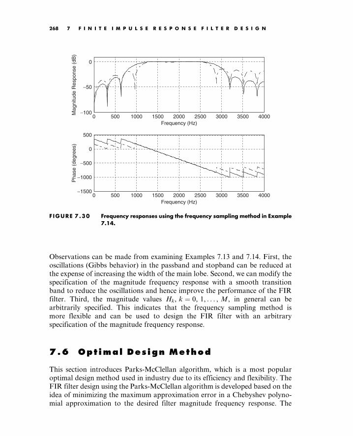
Observations can be made from examining Examples 7.13 and 7.14. First, the
oscillations (Gibbs behavior) in the passband and stopband can be reduced at
the expense of increasing the width of the main lobe. Second, we can modify the
specification of the magnitude frequency response with a smooth transition
band to reduce the oscillations and hence improve the performance of the FIR
filter. Third, the magnitude values Hk, k ¼ 0, 1, . . . , M, in general can be
arbitrarily specified. This indicates that the frequency sampling method is
more flexible and can be used to design the FIR filter with an arbitrary
specification of the magnitude frequency response.
7.6 Opt imal Des ign Method
This section introduces Parks-McClellan algorithm, which is a most popular
optimal design method used in industry due to its efficiency and flexibility. The
FIR filter design using the Parks-McClellan algorithm is developed based on the
idea of minimizing the maximum approximation error in a Chebyshev polyno-
mial approximation to the desired filter magnitude frequency response. The
0 500 1000 1500 2000 2500 3000 3500 4000−100
−50
0
Frequency (Hz)
Mag
nitu
de R
espo
nse
(dB
)
0 500 1000 1500 2000 2500 3000 3500 4000−1500
−1000
−500
0
500
Frequency (Hz)
Pha
se (
degr
ees)
F IGURE 7 .30 Frequency responses using the frequency sampling method in Example7.14.
Tan: Digital Signaling Processing 0123740908_chap07 Final Proof page 268 21.6.2007 11:06pm Compositor Name: MRaja
268 7 F I N I T E I M P U L S E R E S P O N S E F I L T E R D E S I G N

details of this design development are beyond the scope of this text and can be
found in Ambardar (1999) and Porat (1997). We will outline the design criteria
and notation and then focus on the design procedure.
Given an ideal frequency response Hd (ejvT ), the approximation error E(v) is
defined as
E(v) ¼W (v) H(e jvT )Hd(ejvT )
, (7:32)
where H(e jvT ) is the frequency response of the linear phase FIR filter to be
designed, and W (v) is the weight function for emphasizing certain frequency
bands over others during the optimization process. This process is designed to
minimize the error shown in Equation (7.33):
min ( max E(v)j j) (7:33)
over the set of FIR coefficients. With the help of Remez exchange algorithm,
which is also beyond the scope of this book, we can obtain the best FIR filter
whose magnitude response has an equiripple approximation to the ideal
magnitude response. The achieved filters are optimal in the sense that the
algorithms minimize the maximum error between the desired frequency
response and the actual frequency response. These are often called minimax
filters.
Next, we establish notations that will be used in the design procedure.
Figure 7.31 shows the characteristics of the designed FIR filter by Parks-
McClellan and Remez exchange algorithms. As illustrated in the top graph of
Figure 7.31, the passband frequency response and stopband frequency response
have equiripples. dp is used to specify the magnitude ripple in the passband,
while ds specifies the stopband magnitude attenuation. In terms of dB value
specification, we have dp dB ¼ 20 log10 (1þ dp) and ds dB ¼ 20 log10 ds.
The middle graph in Figure 7.31 describes the error between the ideal
frequency response and the actual frequency response. In general, the error
magnitudes in the passband and stopband are different. This makes optimiza-
tion unbalanced, since the optimization process involves an entire band. When
the error magnitude in a band dominates the other(s), the optimization process
may de-emphasize the contribution due to a small magnitude error. To make the
error magnitudes balanced, a weight function can be introduced. The idea is to
weight the band with the bigger magnitude error with a small weight factor and
to weight the band with the smaller magnitude error with a big weight factor.
We use a weight factor Wp for weighting the passband error and Ws for
weighting the stopband error. The bottom graph in Figure 7.31 shows the
weighted error, and clearly, the error magnitudes on both bands are at
the same level. Selection of the weighting factors is further illustrated in the
following design procedure.
Tan: Digital Signaling Processing 0123740908_chap07 Final Proof page 269 21.6.2007 11:06pm Compositor Name: MRaja
7.6 Optimal Design Method 269

Optimal FIR Filter Design Procedure for Parks-McClellan Algorithm
1. Specify the band edge frequencies such as the passband and stopband
frequencies, passband ripple, stopband attenuation, filter order, and
sampling frequency of the DSP system.
2. Normalize band edge frequencies to the Nyquist limit (folding
frequency ¼ fs=2) and specify the ideal magnitudes.
3. Calculate absolute values of the passband ripple and stopband attenu-
ation if they are given in terms of dB values:
dp ¼ 10dp dB
20
1 (7:34)
ds ¼ 10ds dB
20ð Þ: (7:35)
Then calculate the ratio and put it into a fraction form:
dp
ds
¼ fraction form ¼ numerator
denominator¼ Ws
Wp
: (7:36)
1 + dp
1 − dp
1
dp
0
−dp
H(ejwT)
Hd(ejwT)
H(e jwT ) − Hd(e jwT )StopbandPassband0
WP
Ws
Error weight on passband
Error weight on stopband
0
E(w)
ds−ds
ds−ds wpws
w
w
w
F IGURE 7 .31 (Top) Magnitude frequency responses of an ideal lowpass filter and atypical lowpass filter designed using Parks-McClellan algorithm.(Middle) Error between the ideal and practical responses. (Bottom)Weighted error between the ideal and practical responses.
Tan: Digital Signaling Processing 0123740908_chap07 Final Proof page 270 21.6.2007 11:06pm Compositor Name: MRaja
270 7 F I N I T E I M P U L S E R E S P O N S E F I L T E R D E S I G N

Next, set the error weight factors for passband and stopband, respectively:
Wp ¼ denominator
Ws ¼ numerator(7:37)
4. Apply the Remez algorithm to calculate filter coefficients.
5. If the specifications are not met, increase the filter order and repeat steps
1 to 4.
The following examples are given to illustrate the design procedure.
Example 7.15.
a. Design a lowpass filter with the following specifications:
DSP system sampling rate ¼ 8,000 Hz
Passband ¼ 0–800 Hz
Stopband ¼ 1,000–4,000 Hz
Passband ripple ¼ 1 dB
Stopband attenuation ¼ 40 dB
Filter order ¼ 53
Solution:
a. From the specifications, we have two bands: a lowpass band and a
stopband. We perform normalization and specify ideal magnitudes as
follows:
Folding frequency: fs=2 ¼ 8000=2 ¼ 4000Hz
For 0 Hz: 0=4000 ¼ 0, magnitude: 1
For 800 Hz: 800=4000 ¼ 0:2, magnitude: 1
For 1,000 Hz: 1000=4000 ¼ 0:25, magnitude: 0
For 4,000 Hz: 4000=4000 ¼ 1, magnitude: 0
Next, we determine the weights:
dp ¼ 10120ð Þ 1 ¼ 0:1220
ds ¼ 104020ð Þ ¼ 0:01:
Then, applying Equation (7.36) gives
dp
ds
¼ 12:2 12
1¼ Ws
Wp
:
Tan: Digital Signaling Processing 0123740908_chap07 Final Proof page 271 21.6.2007 11:06pm Compositor Name: MRaja
7.6 Optimal Design Method 271

Hence, we have
Ws ¼ 12 and Wp ¼ 1:
Applying remez() routine provided by MATLAB, we list MATLAB
codes in Program 7.10. The filter coefficients are listed in Table 7.14.
Figure 7.32 shows the frequency responses.
Clearly, the stopband attenuation is satisfied. We plot the details for the filter
passband in Figure 7.33.
Program 7.10. MATLAB program for Example 7.15.
% Figure 7.32 (Example 7.15)
% MATLAB program to create Figure 7.32
%
fs ¼ 8000;
f ¼ [0 0:2 0:25 1]; % Edge frequencies
m ¼ [1 1 0 0]; % Ideal magnitudes
w ¼ [1 12]; % Error weight factors
b ¼ remez(53,f,m,w); % (53þ 1)Parks-McClellan algorithm and Remez exchangeformat long
freqz(b,1,512,fs) % Plot the frequency responses
axis([0 fs/2 80 10]);
TABLE 7.14 FIR filter coefficients in Example 7.15.
B: FIR Filter Coefficients (optimal design method)
b0 ¼ b53 ¼ 0:006075 b1 ¼ b52 ¼ 0:00197
b2 ¼ b51 ¼ 0:001277 b3 ¼ b50 ¼ 0:006937
b4 ¼ b49 ¼ 0:013488 b5 ¼ b48 ¼ 0:018457
b6 ¼ b47 ¼ 0:019347 b7 ¼ b46 ¼ 0:014812
b8 ¼ b45 ¼ 0:005568 b9 ¼ b44 ¼ 0:005438
b10 ¼ b43 ¼ 0:013893 b11 ¼ b42 ¼ 0:015887
b12 ¼ b41 ¼ 0:009723 b13 ¼ b40 ¼ 0:002789
b14 ¼ b39 ¼ 0:016564 b15 ¼ b38 ¼ 0:024947
b16 ¼ b37 ¼ 0:022523 b17 ¼ b36 ¼ 0:007886
b18 ¼ b35 ¼ 0:014825 b19 ¼ b34 ¼ 0:036522
b20 ¼ b33 ¼ 0:045964 b21 ¼ b32 ¼ 0:033866
b22 ¼ b31 ¼ 0:003120 b23 ¼ b30 ¼ 0:060244
b24 ¼ b29 ¼ 0:125252 b25 ¼ b28 ¼ 0:181826
b26 ¼ b27 ¼ 0:214670
Tan: Digital Signaling Processing 0123740908_chap07 Final Proof page 272 21.6.2007 11:06pm Compositor Name: MRaja
272 7 F I N I T E I M P U L S E R E S P O N S E F I L T E R D E S I G N

0 500 1000 1500 2000 2500 3000 3500 4000−1500
−1000
−500
0
Frequency (Hz)
Pha
se (
degr
ees)
0 500 1000 1500 2000 2500 3000 3500 4000−80
−60
−40
−20
0
Frequency (Hz)
Mag
nitu
de r
espo
nse
(dB
)
F IGURE 7 .32 Frequency and phase responses for Example 7.15.
0 500 1000 1500 2000 2500 3000 3500 4000−1500
−1000
−500
0
Frequency (Hz)
Ph
ase
(deg
rees
)
0 500 1000 1500 2000 2500 3000 3500 4000−2
−1
0
1
2
Frequency (Hz)
Mag
nitu
de re
spon
se (
dB)
F IGURE 7 .33 Frequency response details for passband in Example 7.15.
Tan: Digital Signaling Processing 0123740908_chap07 Final Proof page 273 21.6.2007 11:06pm Compositor Name: MRaja
7.6 Optimal Design Method 273

As shown in Figure 7.33, the ripples in the passband are between 1 and
1 dB. Hence, all the specifications are met. Note that if a specification is not
satisfied, we will increase the order until the stopband attenuation and passband
ripple are met.
Example 7.16.
This example illustrates the bandpass filter design.
a. Design a bandpass filter with the following specifications:
DSP system sampling rate ¼ 8,000 Hz
Passband ¼ 1,0001,600Hz
Stopband ¼ 0600Hz and 2,000–4,000 Hz
Passband ripple ¼ 1 dB
Stopband attenuation ¼ 30 dB
Filter order ¼ 25
Solution:
a. From the specifications, we have three bands: a passband, a lower stop-
band, and an upper stopband. We perform normalization and specify
ideal magnitudes as follows:
Folding frequency: fs=2 ¼ 8000=2 ¼ 4000Hz
For 0 Hz: 0=4000 ¼ 0, magnitude: 0
For 600 Hz: 600=4000 ¼ 0:15, magnitude: 0
For 1,000 Hz: 1000=4000 ¼ 0:25, magnitude: 1
For 1,600 Hz: 1600=4000 ¼ 0:4, magnitude: 1
For 2,000 Hz: 2000=4000 ¼ 0:5, magnitude: 0
For 4,000 Hz: 4000=4000 ¼ 1, magnitude: 0
Next, let us determine the weights:
dp ¼ 10120ð Þ 1 ¼ 0:1220
ds ¼ 103020ð Þ ¼ 0:0316:
Then, applying Equation (7.36), we get
dp
ds
¼ 3:86 39
10¼ Ws
Wp
:
Hence, we have
Ws ¼ 39 and Wp ¼ 10:
Applying the remez() routine provided by MATLAB and checking per-
formance, we have Program 7.11. Table 7.15 lists the filter coefficients.
Tan: Digital Signaling Processing 0123740908_chap07 Final Proof page 274 21.6.2007 11:06pm Compositor Name: MRaja
274 7 F I N I T E I M P U L S E R E S P O N S E F I L T E R D E S I G N

The frequency responses are depicted in Figure 7.34.
Clearly, the stopband attenuation is satisfied. We also check the details for
the passband as shown in Figure 7.35.
As shown in Figure 7.35, the ripples in the passband between 1,000 and
1,600 Hz are between 1 and 1 dB. Hence, all specifications are satisfied.
Example 7.17.
Now we show how the Remez exchange algorithm in Equation (7.32) is
processed using a linear phase 3-tap FIR filter as
H(z) ¼ b0 þ b1z1 þ b0z
2:
The ideal frequency response specifications are shown in Figure 7.36(a),
where the filter gain increases linearly from the gain of 0.5 at V ¼ 0 radian
to the gain of 1 at V ¼ p=4 radian. The band between V ¼ p=4 radian and
TABLE 7 .15 FIR filter coefficients in Example 7.16.
B: FIR Filter Coefficients (optimal design method)
b0 ¼ b25 ¼ 0:022715 b1 ¼ b24 ¼ 0:012753
b2 ¼ b23 ¼ 0:005310 b3 ¼ b22 ¼ 0:009627
b4 ¼ b21 ¼ 0:004246 b5 ¼ b20 ¼ 0:006211
b6 ¼ b19 ¼ 0:057515 b7 ¼ b18 ¼ 0:076593
b8 ¼ b17 ¼ 0:015655 b9 ¼ b16 ¼ 0:156828
b10 ¼ b15 ¼ 0:170369 b11 ¼ b14 ¼ 0:009447
b12 ¼ b13 ¼ 0:211453
Program 7.11. MATLAB program for Example 7.16.
% Figure 7.34 (Example 7.16)
% MATLAB program to create Figure 7.34
%
fs ¼ 8000;
f ¼ [0 0:15 0:25 0:4 0:5 1]; % Edge frequencies
m ¼ [0 0 1 1 0 0]; % Ideal magnitudes
w ¼ [39 10 39]; % Error weight factors
format long
b ¼ remez(25,f,m,w)%(25þ 1) tapsParks-McClellanalgorithmandRemezexchangefreqz(b,1,512,fs); % Plot the frequency responses
axis([0 fs/2 80 10])
Tan: Digital Signaling Processing 0123740908_chap07 Final Proof page 275 21.6.2007 11:06pm Compositor Name: MRaja
7.6 Optimal Design Method 275

0 500 1000 1500 2000 2500 3000 3500 4000−600
−400
−200
0
200
400
Frequency (Hz)
Pha
se (
degr
ees)
0 500 1000 1500 2000 2500 3000 3500 4000−80
−60
−40
−20
0
Frequency (Hz)
Mag
nitu
de r
espo
nse
(dB
)
F IGURE 7.34 Frequency and phase responses for Example 7.16.
0 500 1000 1500 2000 2500 3000 3500 4000−600
−400
−200
0
200
400
Frequency (Hz)
Pha
se (
degr
ees)
0 500 1000 1500 2000 2500 3000 3500 4000−2
−1
0
1
2
Frequency (Hz)
Mag
nitu
de r
espo
nse
(dB
)
F IGURE 7.35 Frequency response details for passband in Example 7.16.
Tan: Digital Signaling Processing 0123740908_chap07 Final Proof page 276 21.6.2007 11:06pm Compositor Name: MRaja
276 7 F I N I T E I M P U L S E R E S P O N S E F I L T E R D E S I G N

V ¼ p=2 radians is a transition band. Finally, the filter gain decreases
linearly from the gain of 0.75 at V ¼ p=2 radians to the gain of 0 at
V ¼ p radians.
For simplicity, we use all the weight factors as 1, that is, W (V) ¼ 1. Equation
(7.32) is simplified to be
E(V) ¼ H(e jV)Hd(ejV):
Substituting z ¼ e jV to the transfer function H(z) gives
H(e jV) ¼ b0 þ b1ejV þ b0e
j2V:
After simplification using Euler’s identity e jV þ ejV ¼ 2 cos V, the filter fre-
quency response is given by
H(e jV) ¼ ejV b1 þ 2b0 cos Vð Þ:Regardless of the linear phase shift term e jV for the time being, we have a
Chebyshev real magnitude function (there are a few other types as well) as
H(e jV) ¼ b1 þ 2b0 cos V:
1 2 3 400
0.5
1
Normalized frequency
Sel
ecte
d po
ints
on
Hd
0 1 2 3 4
0
−0.4
−0.2
0.2
0.4
Normalized frequency
Em
ax a
t ext
rem
al p
oint
s
0 1 2 3 40
0.2
0.4
0.6
0.8
1
Normalized frequency
Sel
ecte
d po
ints
on
Hd
0 1 2 3 4
−0.2
0
0.2
−0.4
0.4
Normalized frequency
Em
ax a
t ext
rem
al p
oint
s
Will be selected as an extremal point
Equiripples
A B
C D
F IGURE 7.36 Determining the 3-tap FIR filter coefficients using the Remez algorithm inExample 7.17.
Tan: Digital Signaling Processing 0123740908_chap07 Final Proof page 277 21.6.2007 11:06pm Compositor Name: MRaja
7.6 Optimal Design Method 277

The alternation theorem (Ambardar, 1999; Porat, 1997) must be used. The
alternation theorem states that given Chebyshev polynomial H(e jV) to approxi-
mate the ideal magnitude response Hd(ejV), we can find at least M þ 2 (where
M ¼ 1 for our case) frequencies V0, V1, . . . , VMþ1, called the extremal frequen-
cies, so that signs of the error at the extremal frequencies alternate and the
absolute error value at each extremal point reaches the maximum absolute
error, that is,
E Vkð Þ ¼ E Vkþ1ð Þ for V0, V1, . . . VMþ1
and E Vkð Þj j ¼ Emax:
But the alternation theorem does not tell us how to do the algorithm. The
Remez exchange algorithm actually is employed to solve this problem.
The equations and steps (Ambardar, 1999; Porat, 1997) are briefly summarized
for our illustrative example:
1. Given the order of N ¼ 2M þ 1 choose initial extremal frequencies:
V0, V1, . . . , VMþ1 (can be uniformly distributed first).
2. Solve the following equation to satisfy the alternation theorem:
( 1)kE ¼W (Vk)(Hd(ejVk)H(e jVk)) for V0, V1, . . . , VMþ1:
Note that since H(e jV) ¼ b1 þ 2b0 cos V, for example, the solution will
include solving for three unknowns: b0, b1, and Emax.
3. Determine the extremal points including band edges (can be more than
M þ 2 points), and retain M þ 2 extremal points with the largest error
values Emax.
4. Output the coefficients if the extremal frequencies are not changed;
otherwise, go to step 2 using the new set of extremal frequencies.
Now let us apply the Remez exchange algorithm.
First Iteration:
1. We use uniformly distributed extremal points: V0 ¼ 0, V1 ¼ p=2,
V2 ¼ p, whose ideal magnitudes are marked by the symbol ‘‘o’’ in
Figure 7.36(a).
2. The alternation theorem requires:
( 1)kE ¼ Hd(ejV) b1 þ 2b0 cos Vð Þ:
Applying extremal points yields the following three simultaneous equa-
tions with three unknowns, b0, b1, and E:
Tan: Digital Signaling Processing 0123740908_chap07 Final Proof page 278 21.6.2007 11:06pm Compositor Name: MRaja
278 7 F I N I T E I M P U L S E R E S P O N S E F I L T E R D E S I G N

E ¼ 0:5 b1 2b0
E ¼ 0:75 b1
E ¼ 0 b1 þ 2b0
:
8<:
We solve these three equations to get
b0 ¼ 0:125, b1 ¼ 0:5, E ¼ 0:25, H(e jV) ¼ 0:5þ 0:25 cos V:
3. We then determine the extremal points, including at the band edge, with
their error values from Figure 7.36(b) using the following error function:
E Vð Þ ¼ Hd(ejV) 0:5 0:25 cos V:
These extremal points are marked by the symbol ‘‘o’’ and their error
values are listed in Table 7.16.
4. Since the band edge at V ¼ p=4 has an error larger than others, it must be
chosen as the extremal frequency. After deleting the extremal point at
V ¼ p=2, a new set of extremal points are found according the largest
error values as
V0 ¼ 0
V1 ¼ p=4
V2 ¼ p
:
The ideal magnitudes at these three extremal points are given in Figure 7.36(c),
that is, 0.5, 1, 0. Now let us examine the second iteration.
Second Iteration:
Applying the alternation theorem at the new set of extremal points, we have
E ¼ 0:5 b1 2b0
E ¼ 1 b1 1:4142b0
E ¼ 0 b1 þ 2b0
8<: :
Solving these three simultaneous equations leads to
b0 ¼ 0:125, b1 ¼ 0:537, E ¼ 0:287, and H(e jV) ¼ 0:537þ 0:25 cos V:
TABLE 7 .16 Extremal points and band edges with their error values for the firstiteration.
V 0 p=4 p=2 p
Emax 0:25 0.323 0.25 0:25
Tan: Digital Signaling Processing 0123740908_chap07 Final Proof page 279 21.6.2007 11:06pm Compositor Name: MRaja
7.6 Optimal Design Method 279

The determined extremal points and band edge with their error values are listed
in Table 7.17 and shown in Figure 7.36(d), where the determined extremal
points are marked by the symbol ‘‘o.’’
Since the extremal points have their same maximum error value of 0.287,
they are found to be V0 ¼ 0, V1 ¼ p=4, and V2 ¼ p, which are unchanged. Then
we stop the iteration and output the filter transfer function as
H(z) ¼ 0:125þ 0:537z1 þ 0:125z2:
As shown in Figure 7.35(d), we achieve the equiripples of error at the extemal
points: V0 ¼ 0, V1 ¼ p=4, V2 ¼ p; their signs are alternating, and the max-
imum absolute error of 0.287 is obtained at each point. It takes two iterations
to determine the coefficients for this simplified example.
As we mentioned, the Parks-McClellan algorithm is one of the most popular
filter design methods in industry due to its flexibility and performance. How-
ever, there are two disadvantages. The filter length has to be estimated by the
empirical method. Once the frequency edges, magnitudes, and weighting factors
are specified, applying the Remez exchange algorithm cannot control the actual
ripple obtained from the design. We may often need to try a longer length of
filter or different weight factors to remedy the situations where the ripple is
unacceptable.
7.7 Real izat ion Struc tures of F in i teImpulse Response Fi l ters
Using the direct form I (discussed in Chapter 6), we will get a special realization
form, called the transversal form. Using the linear phase property will produce a
linear phase realization structure.
7.7.1 Transversal Form
Given the transfer function of the FIR filter in Equation (7.38),
H(z) ¼ b0 þ b1z1 þ . . .þ bKzK , (7:38)
TABLE 7.17 Error values at extremal frequencies and band edge.
V 0 p=4 p=2 p
Emax 0:287 0.287 0.213 0:287
Tan: Digital Signaling Processing 0123740908_chap07 Final Proof page 280 21.6.2007 11:06pm Compositor Name: MRaja
280 7 F I N I T E I M P U L S E R E S P O N S E F I L T E R D E S I G N

we obtain the difference equation as
y(n) ¼ b0x(n)þ b1x(n 1)þ b2x(n 2)þ . . .þ bKx(n K):
Realization of such a transfer function is the transversal form, displayed in
Figure 7.37.
Example 7.18.
Given the FIR filter transfer function
H(z) ¼ 1þ 1:2z1 þ 0:36z2,
a. Perform the FIR filter realization.
Solution:
a. From the transfer function, we can identify that b0 ¼ 1, b1 ¼ 1:2, and
b2 ¼ 0:36. Using Figure 7.37, we find the FIR realization to be as follows
(Fig. 7.38):
We determine the DSP equation for implementation as
y(n) ¼ x(n)þ 1:2x(n 1)þ 0:36x(n 2):
z−1
z−1
z−1
y(n)b0
b1
bK
+
x(n)
x(n − 1)
x(n − K )
+
F IGURE 7 .37 FIR filter realization (transversal form).
z−1
z−1
y(n)1
1.2
0.36
+
x(n)
x(n − 2)
x(n − 1)
+
F IGURE 7 .38 FIR filter realization for Example 7.18.
Tan: Digital Signaling Processing 0123740908_chap07 Final Proof page 281 21.6.2007 11:06pm Compositor Name: MRaja
7.7 Realization Structures of Finite Impulse Response Filters 281

Program 7.12 (below) shows the MATLAB implementation.
7.7.2 Linear Phase Form
We illustrate the linear phase structure using the following simple example.
Considering the transfer function with 5 taps obtained from the design as
follows,
H(z) ¼ b0 þ b1z1 þ b2z
2 þ b1z3 þ b0z
4, (7:39)
we can see that the coefficients are symmetrical and that the difference
equation is
y(n) ¼ b0x(n)þ b1x(n 1)þ b2x(n 2)þ b1x(n 3)þ b0x(n 4):
This DSP equation can further be combined to be
y(n) ¼ b0 x(n)þ x(n 4)ð Þ þ b1 x(n 1)þ x(n 3)ð Þ þ b2x(n 2):
Then we obtain the realization structure in a linear phase form as follows
(Fig. 7.39):
Program 7.12. MATLAB program for Example 7.18.
%Sample MATLAB code
sample ¼ 1:1:10; %Input test array
x ¼ [0 0 0]; %Input buffer [x(n)x(n 1) . . .]y ¼ [0]; %Output buffer [y(n)y(n 1) . . .]b ¼ [1:0 1:2 0:36]; %FIR filter coefficients [b0 b1...]
KK ¼ length(b);
for n ¼ 1:1:length(sample)% Loop processing
for k ¼ KK:1:2% Shift the input by one sample
x(k) ¼ x(k 1);end
x(1) ¼ sample(n); % Get new sample
y(1) ¼ 0; % Perform FIR filtering
for k ¼ 1:1:KKy(1) ¼ y(1)þ b(k)x(k);end
out(n) ¼ y(1); %Send the filtered sample to the output array
end
out
Tan: Digital Signaling Processing 0123740908_chap07 Final Proof page 282 21.6.2007 11:06pm Compositor Name: MRaja
282 7 F I N I T E I M P U L S E R E S P O N S E F I L T E R D E S I G N

7.8 Coef f i c ient Accuracy Ef fec ts onFin i te Impulse Response Fi l ters
In practical applications, the filter coefficients achieved through high-level
software such as MATLAB must be quantized using finite word length. This
may have two effects. First, the locations of zeros are changed; second, due to
the location change of zeros, the filter frequency response will change corres-
pondingly. In practice, there are two types of digital signal (DS) processors:
fixed-point processors and floating-point processors. The fixed-point DS proces-
sor uses integer arithmetic, and the floating-point processor employs floating-
point arithmetic. Such effects of filter coefficient quantization will be covered in
Chapter 9.
In this section, we study effects of FIR filter coefficient quantization in
general, since during practical filter realization, obtaining filter coefficients
with infinite precision is impossible. Filter coefficients are usually truncated or
rounded off for the application. Assume that the FIR filter transfer function
with infinite precision is given by
H(z) ¼XKn¼0
bnzn ¼ b0 þ b1z
1 þ . . .þ bKzK , (7:40)
where each filter coefficient bn has infinite precision. Now let the quantized FIR
filter transfer function be
Hq(z) ¼XKn¼0
bqnzn ¼ b
q0 þ b
q1z1 þ . . .þ b
qKzK , (7:41)
z−1
z−1
z−1
y(n)b0
b1+
x(n)
x(n − 1)
x(n − 2)
x(n − 3)
x(n − 4)
+
z−1
b2
+
+
F IGURE 7 .39 Linear phase FIR filter realization.
Tan: Digital Signaling Processing 0123740908_chap07 Final Proof page 283 21.6.2007 11:06pm Compositor Name: MRaja
7.8 Coefficient Accuracy Effects on Finite Impulse Response Filters 283

where each filter coefficient bqn is quantized (round-off) using the specified
number of bits. Then the error of the magnitude frequency response can be
bounded as
H(e jV)Hq(e jV) ¼XK
n¼0
(bn bqn)ejnV
<XKn¼0
bn bqn
< (K þ 1) 2B1
(7:42)
where B is the number of bits used to encode each magnitude of the filter
coefficient. Look at Example 7.19.
Example 7.19.
In Example 7.7, a lowpass FIR filter with 25 taps using a Hamming window is
designed, and FIR filter coefficients are listed for comparison in Table 7.18. One
sign bit is used, and 7 bits are used for fractional parts, since all FIR filter
coefficients are less than 1. We would multiply each filter coefficient by a scale
factor of 27 and round off each scaled magnitude to an integer whose magnitude
could be encoded using 7 bits. When the coefficient integer is scaled back,
the coefficient with finite precision (quantized filter coefficient) using 8 bits,
including the sign bit, will be achieved.
TABLE 7 .18 FIR filter coefficients and their quantized filter coefficients in Example7.19 (Hamming window).
Bham: FIR Filter Coefficients BhamQ: FIR Filter Coefficients
b0 ¼ b24 ¼ 0:00000000000000 b0 ¼ b24 ¼ 0:0000000
b1 ¼ b23 ¼ 0:00276854711076 b1 ¼ b23 ¼ 0:0000000
b2 ¼ b22 ¼ 0:00000000000000 b2 ¼ b22 ¼ 0:0000000
b3 ¼ b21 ¼ 0:00759455135346 b3 ¼ b21 ¼ 0:0078125
b4 ¼ b20 ¼ 0:00000000000000 b4 ¼ b20 ¼ 0:0000000
b5 ¼ b19 ¼ 0:01914148493949 b5 ¼ b19 ¼ 0:0156250
b6 ¼ b18 ¼ 0:00000000000000 b6 ¼ b18 ¼ 0:0000000
b7 ¼ b17 ¼ 0:04195685650042 b7 ¼ b17 ¼ 0:0390625
b8 ¼ b16 ¼ 0:00000000000000 b8 ¼ b16 ¼ 0:0000000
b9 ¼ b15 ¼ 0:09180790496577 b9 ¼ b15 ¼ 0:0859375
b10 ¼ b14 ¼ 0:00000000000000 b10 ¼ b14 ¼ 0:0000000
b11 ¼ b13 ¼ 0:31332065886015 b11 ¼ b13 ¼ 0:3125000
b12 ¼ 0:50000000000000 b12 ¼ 0:5000000
Tan: Digital Signaling Processing 0123740908_chap07 Final Proof page 284 21.6.2007 11:06pm Compositor Name: MRaja
284 7 F I N I T E I M P U L S E R E S P O N S E F I L T E R D E S I G N

To see quantization, we take a look at one of the infinite precision coeffi-
cients, Bham(3) ¼ 0:00759455135346, for illustration. The quantization using 7
magnitude bits is shown as:
0:00759455135346 27 ¼ 0:9721 ¼ 1(rounded up to the integer):
Then the quantized filter coefficient is obtained as
BhamQ(3) ¼ 1=27 ¼ 0:0078125:
Since the poles for both FIR filters always reside at origin, we need to
examine only their zeros. The z-plane zero plots for both FIR filters are
shown in Figure 7.40a, where the circles are zeros from the FIR filter with
infinite precision, while the crosses are zeros from the FIR filter with the
quantized coefficients.
Most importantly, Figure 7.40b shows the difference of the frequency
responses for both filters obtained using Program 7.13. In the figure, the solid
line represents the frequency response with infinite filter coefficient precision,
and the dot-dashed line indicates the frequency response with finite filter
coefficients. It is observed that the stopband performance is degraded due
to the filter coefficient quantization. The degradation in the passband is not
severe.
−1 −0.5 0A
0.5 1 1.5 2−1.5
−1
−0.5
0
0.5
1
1.5
F IGURE 7.40A The z-plane zero plots for both FIR filters. The circles are zeros forinfinite precision; the crosses are zeros for rounded-off coefficients.
Tan: Digital Signaling Processing 0123740908_chap07 Final Proof page 285 21.6.2007 11:06pm Compositor Name: MRaja
7.8 Coefficient Accuracy Effects on Finite Impulse Response Filters 285

Using Equation (7.42), the error of the magnitude frequency response due to
quantization is bounded by
H(e jV)Hq(e jV) < 25=256 ¼ 0:0977:
This can be easily verified at the stopband of the magnitude frequency response
for the worst condition as follows:
0 500 1000 1500 2000 2500 3000 3500 4000
−50
−100
0
Frequency (Hz)
Mag
nitu
de r
espo
nse
(dB
)
0 500 1000 1500 2000 2500 3000 3500 4000
−1500
−1000
−500
−2000
0
Frequency (Hz)B
Pha
se (
degr
ees)
F IGURE 7 .40B Frequency responses. The solid line indicates the FIR filter with infiniteprecision; the dashed line indicates the FIR filter with rounded-offcoefficients.
Program 7.13. MATLAB program for Example 7.19.
fs¼8000;[hham,f]¼freqz(Bham,1,512,fs);[hhamQ,f]¼freqz(BhamQ,1,512,fs);p¼ 180unwrap(angle(hham))/pi;pQ¼ 180unwrap(angle(hhamQ))/pisubplot(2,1,1);plot(f,20log10(abs(hham)),f,20log10(abs(hhamQ)),0:0);gridaxis([0 fs/2 100 10]);xlabel(’Frequency (Hz)’);ylabel(’Magnitude Response (dB)’);subplot(2,1,2); plot(f,p,f,pQ,‘:’);grid
xlabel(‘Frequency (Hz)’); ylabel(’Phase (degrees)’);
Tan: Digital Signaling Processing 0123740908_chap07 Final Proof page 286 21.6.2007 11:06pm Compositor Name: MRaja
286 7 F I N I T E I M P U L S E R E S P O N S E F I L T E R D E S I G N

H(e jV)Hq(e jV) ¼ 10100=20 1030=20
¼ 0:032 < 0:0977:
In practical situations, the same procedure can be used to analyze the effects of
filter coefficient quantization to make sure that the designed filter meets the
requirements.
7.9 Summary of Finite Impulse Response(FIR) Design Procedures and Selectionof FIR Filter Design Methods in Practice
In this section, we first summarize the design procedures of the window design,
frequency sampling design, and optimal design methods, and then discuss the
selection of the particular filter for typical applications.
The window method (Fourier transform design using windows):
1. Given the filter frequency specifications, determine the filter order (odd
number used in this book) and the cutoff frequency/frequencies using
Table 7.7 and Equation (7.26).
2. Compute the impulse sequence h(n) via the Fourier transform method
using the appropriate equations (in Table 7.1).
3. Multiply the generated FIR filter coefficients h(n) in (2) by the selected
window sequence using Equation (7.20) to obtain the windowed impulse
sequence hw(n).
4. Delay the windowed impulse sequence hw(n) by M samples to get the causal
windowed FIR filter coefficients bn ¼ hw(nM) using Equation (7.21).
5. Output the transfer function and plot the frequency responses.
6. If the frequency specifications are satisfied, output the difference equa-
tion. If the frequency specifications are not satisfied, increase the filter
order and repeat beginning with step 2.
The frequency sampling method:
1. Given the filter frequency specifications, choose the filter order (odd
number used in the book), and specify the equally spaced magnitudes of
the frequency response for the normalized frequency range from 0 to p
using Equation (7.29).
2. Calculate FIR filter coefficients using Equation (7.30).
3. Use the symmetry, in Equation (7.31), linear phase requirement, to
determine the rest of the coefficients.
Tan: Digital Signaling Processing 0123740908_chap07 Final Proof page 287 21.6.2007 11:06pm Compositor Name: MRaja
7.9 Summary of Finite Impulse Response (FIR) 287

4. Output the transfer function and plot the frequency responses.
5. If the frequency specifications are satisfied, output the difference equa-
tion. If the frequency specifications are not satisfied, increase the filter
order and repeat beginning with step 2.
The optimal design method (Parks-McClellan algorithm):
1. Given the band edge frequencies, choose the filter order, normalize each
band edge frequency to the Nyquist limit (folding frequency ¼ fs=2), and
specify the ideal magnitudes.
2. Calculate absolute values of the passband ripple and stopbandattenuation,
if they are given in terms of dB values, using Equations (7.34) and (7.35).
3. Determine the error weight factors for passband and stopband, respect-
ively, using Equations (7.36) and (7.37).
4. Apply the Remez algorithm to calculate filter coefficients.
5. Output the transfer function and check the frequency responses.
6. If the frequency specifications are satisfied, output the difference equa-
tion. If the frequency specifications are not satisfied, increase the filter
order and repeat beginning with step 4.
Table 7.19 shows the comparisons for the window, frequency sampling, and
optimal methods. The table can be used as a selection guide for each design
method in this book.
Example 7.20 describes the possible selection of the design method by a DSP
engineer to solve a real-world problem.
Example 7.20.
a. Determine the appropriate FIR filter design method for each of the
following DSP applications.
1. A DSP engineer implements a digital two-band crossover system as
described in the section in this book. He selects the FIR filters to
satisfy the following specifications:
Sampling rate ¼ 44, 100Hz
Crossover frequency ¼ 1, 000Hz (cutoff frequency)
Transition band ¼ 600 to 1,400 Hz
Lowpass filter ¼ passband frequency range from 0 to 600 Hz with a
ripple of 0.02 dB and stopband edge at 1,400 Hz with attenuation
of 50 dB.
Tan: Digital Signaling Processing 0123740908_chap07 Final Proof page 288 21.6.2007 11:06pm Compositor Name: MRaja
288 7 F I N I T E I M P U L S E R E S P O N S E F I L T E R D E S I G N

TABLE 7 .19 Comparisons of three design methods.
Design Method Window Method Frequency Sampling Optimal Design
Filter type 1. Lowpass, highpass, bandpass,
bandstop.
1. Any type filter 1. Any type filter
2. Formulas are not valid for arbitrary
frequency selectivity.
2. The formula is valid for
arbitrary frequency selectivity.
2. Valid for arbitrary
frequency selectivity
Linear phase Yes Yes Yes
Ripple and
stopband
specifications
Used for determining the filter order
and cutoff frequency/-cies
Need to be checked after
each design trial
Used in the algorithm; need
to be checked after each
design trial
Algorithm
complexity for
coefficients
Moderate:
1. Impulse sequence calculation
2. Window function weighting
Simple:
Single equation
Complicated:
1. Parks-McClellan algorithm
2. Remez exchange algorithm
Minimal design tool Calculator Calculator Software
Tan:D
igita
lSig
nalin
gPro
cessing
0123740908_ch
ap07
Fin
alPro
of
page
289
21.6
.2007
11:0
6pm
Com
posito
rN
am
e:M
Raja
7.9
Su
mm
ary
of
Fin
iteIm
pu
lseR
esp
on
se(F
IR)
28
9

Highpass filter ¼ passband frequency range from 1.4 to 44.1 kHz with
ripple of 0.02 dB and stopband edge at 600 Hz with attenuation of
50 dB.
The engineer does not have the software routine for the Remez algorithm.
2. An audio engineer tries to equalize the speech signal sampled at
8,000 Hz using a linear phase FIR filter based on the magnitude
specifications in Figure 7.41. The engineer does not have the software
routine for the Remez algorithm.
Solution:
a. 1. The window design method is the first choice, since the window design
formula is in terms of the cutoff frequency (crossover frequency), the
filter order is based on the transient band, and filter types are standard
lowpass and highpass. The ripple and stopband specifications can be
satisfied by selecting the Hamming window. The optimal design method
will also do the job with a challenge to satisfy the combined unit gains at
the crossover frequency of 1,000 Hz if the remez() algorithm is available.
2. Since the magnitude frequency response is not a standard filter type
of lowpass, highpass, bandpass, or band reject, and the remez()
algorithm is not available, the first choice should be the frequency
sampling method.
7.10 Summar y
1. The Fourier transform method is used to compute noncausal FIR filter
coefficients, including those of lowpass, highpass, bandpass, and band-
stop filters.
fs/2 = 4000 Hz
2.0
1.0
0
0.0
Magnitude
F IGURE 7.41 Magnitude frequency response in Example 7.20 (b).
Tan: Digital Signaling Processing 0123740908_chap07 Final Proof page 290 21.6.2007 11:06pm Compositor Name: MRaja
290 7 F I N I T E I M P U L S E R E S P O N S E F I L T E R D E S I G N

2. Converting noncausal FIR filter coefficients to causal FIR filter coeffi-
cients introduces only linear phase, which is a good property for audio
applications. The linear phase filter output has the same amount of delay
for all the input signals whose frequency components are within pass-
band.
3. The causal FIR filter designed using the Fourier transform method
generates ripple oscillations (Gibbs effect) in the passband and stopband
in its filter magnitude frequency response due to abrupt truncation of the
FIR filter coefficient sequence.
4. To reduce the oscillation effect, the window method is introduced to tap
down the coefficient values toward both ends. A substantial improvement
of the magnitude frequency response is achieved.
5. Real-life DSP applications such as noise reduction system and two-band
digital audio crossover system were investigated.
6. Frequency sampling design is feasible for the FIR filter with an arbitrary
magnitude response specification.
7. An optimal design method, Parks-McClellan algorithm using Remez
exchange algorithm, offers the flexibility for filter specifications.
The Remez exchange algorithm was explained using a simplified
example.
8. Realization structures of FIR filters have special forms, such as the
transversal form and the linear phase form.
9. The effect of quantizing FIR filter coefficients for implementation
changes zero locations of the FIR filter. More effects on the stopband
in the magnitude and phase responses are observed.
10. Guidelines for selecting an appropriate design method in practice were
summarized considering the filter type, linear phase, ripple and stopband
specifications, algorithm complexity, and design tools.
7.11 MATLAB Programs
Program 7.14 enables one to design FIR filters via the window method using
functions such as the rectangular window, triangular (Bartlett) window, Han-
ning window, Hamming window, and Blackman window. Filter types of the
design include lowpass, highpass, bandpass, and band reject.
Tan: Digital Signaling Processing 0123740908_chap07 Final Proof page 291 21.6.2007 11:06pm Compositor Name: MRaja
7.11 MATLAB Programs 291

Program 7.14. MATLAB function for FIR filter design using the window
method.
function B ¼ firwd(N, Ftype, WnL, WnH, Wtype)
% B ¼ firwd(N,Ftype,WnL,WnH,Wtype)
% FIR filter design using the window function method.
% Input parameters:
% N: the number of the FIR filter taps.
% Note: It must be an odd number.
% Ftype: the filter type
%1. Lowpass filter;
%2. Highpass filter;
%3. Bandpass filter;
%4. Band reject filter;
% WnL: lower cutoff frequency in radians. Set WnL¼0 for the highpass filter.% WnH: upper cutoff frequency in radians. Set WnH¼0 for the lowpass filter.% Wtypw: window function type
%1. Rectangular window;
%2. Triangular window;
%3. Hanning window;
%4. Hamming window;
%5. Blackman window;
% Output:
% B: FIR filter coefficients.
M ¼ (N 1)=2;hH ¼ sin(WnH[ M:1:1]):=([ M:1:1]pi);hH(Mþ 1) ¼ WnH=pi;hH(Mþ 2:1:N) ¼ hH(M:1:1);hL ¼ sin(WnL[ M:1:1]):=([ M:1:1]pi);hL(Mþ 1) ¼ WnL=pi;hL(Mþ 2:1:N) ¼ hL(M:1:1);if Ftype ¼¼ 1
h(1:N) ¼ hL(1:N);end
if Ftype ¼¼ 2
h(1:N) ¼ hH(1:N);h(Mþ 1) ¼ 1þ h(Mþ 1);end
if Ftype ¼¼3h(1:N) ¼ hH(1:N) hL(1:N);
end
if Ftype ¼¼ 4
h(1:N) ¼ hL(1:N) hH(1:N);h(Mþ 1) ¼ 1þ h(Mþ 1);end
% window functions;
if Wtype ¼¼1w(1:N)¼ones(1,N);
Tan: Digital Signaling Processing 0123740908_chap07 Final Proof page 292 21.6.2007 11:06pm Compositor Name: MRaja
292 7 F I N I T E I M P U L S E R E S P O N S E F I L T E R D E S I G N

Program 7.15 enables one to design FIR filters using the frequency sampling
method. Note that values of the frequency response, which correspond to the
equally spaced DFT frequency components, must be specified for design.
Besides the lowpass, highpass, bandpass, and band reject filter designs, the
method can be used to design FIR filters with an arbitrarily specified magnitude
frequency response.
end
if Wtype ¼¼2w ¼ 1 abs([ M:1:M])=M;end
if Wtype ¼¼3w ¼ 0:5þ 0:5 cos([ M:1:M]pi=M);end
if Wtype ¼¼4w ¼ 0:54þ 0:46 cos([ M:1:M]pi=M);end
if Wtype ¼¼5w ¼ 0:42þ 0:5 cos([ M:1:M]pi=M)þ 0:08 cos(2[ M:1:M]pi=M);end
B ¼ h:w
Program 7.15. MATLAB function for FIR filter design using the frequency
sampling method.
function B¼firfs(N,Hk)% B¼firls(N,Hk)% FIR filter design using the frequency sampling method.
% Input parameters:
% N: the number of filter coefficients.
% note: N must be an odd number.
% Hk: sampled frequency response for k ¼ 0, 1, 2, . . ., M ¼ (N 1)=2.% Output:
% B: FIR filter coefficients.
M ¼ (N 1)=2;for n ¼ 1:1:NB(n) ¼ (1=N)(Hk(1)þ . . .2sum(Hk(2:1:Mþ 1) . . .: cos(2pi([1:1:M])(n 1 M)=N)));end
Tan: Digital Signaling Processing 0123740908_chap07 Final Proof page 293 21.6.2007 11:06pm Compositor Name: MRaja
7.11 MATLAB Programs 293

7.12 Problems
7.1. Design a 3-tap FIR lowpass filter with a cutoff frequency of 1,500 Hz
and a sampling rate of 8,000 Hz using
a. rectangular window function
b. Hamming window function.
Determine the transfer function and difference equation of the designed
FIR system, and compute and plot the magnitude frequency response
for V ¼ 0, p=4, p=2, 3p=4; and p radians.
7.2. Design a 3-tap FIR highpass filter with a cutoff frequency of 1,600 Hz
and a sampling rate of 8,000 Hz using
a. rectangular window function
b. Hamming window function.
Determine the transfer function and difference equation of the designed
FIR system, and compute and plot the magnitude frequency response
for V ¼ 0, p=4, p=2, 3p=4; and p radians.
7.3. Design a 5-tap FIR bandpass filter with a lower cutoff frequency of
1,600 Hz, an upper cutoff frequency of 1,800 Hz, and a sampling rate
of 8,000 Hz using
a. rectangular window function
b. Hamming window function.
Determine the transfer function and difference equation of the designed
FIR system, and compute and plot the magnitude frequency response
for V ¼ 0, p=4, p=2, 3p=4; and p radians.
7.4. Design a 5-tap FIR band reject filter with a lower cutoff frequency of
1,600 Hz, an upper cutoff frequency of 1,800 Hz, and a sampling rate
of 8,000 Hz using
a. rectangular window function
b. Hamming window function.
Determine the transfer function and difference equation of the designed
FIR system, and compute and plot the magnitude frequency response
for V ¼ 0, p=4, p=2, 3p=4; and p radians.
Tan: Digital Signaling Processing 0123740908_chap07 Final Proof page 294 21.6.2007 11:06pm Compositor Name: MRaja
294 7 F I N I T E I M P U L S E R E S P O N S E F I L T E R D E S I G N

7.5. Given an FIR lowpass filter design with the following specifications:
Passband ¼ 0–800 Hz
Stopband ¼ 1,200–4,000 Hz
Passband ripple ¼ 0.1 dB
Stopband attenuation ¼ 40 dB
Sampling rate ¼ 8,000 Hz,
determine the following:
a. window method
b. length of the FIR filter
c. cutoff frequency for the design equation.
7.6. Given an FIR highpass filter design with the following specifications:
Passband ¼ 0–1,500 Hz
Stopband ¼ 2,000–4,000 Hz
Passband ripple ¼ 0.02 dB
Stopband attenuation ¼ 60 dB
Sampling rate ¼ 8,000 Hz,
determine the following:
a. window method
b. length of the FIR filter
c. cutoff frequency for the design equation.
7.7. Given an FIR bandpass filter design with the following specifications:
Lower cutoff frequency ¼ 1,500 Hz
Lower transition width ¼ 600 Hz
Upper cutoff frequency ¼ 2,300 Hz
Upper transition width ¼ 600 Hz
Passband ripple ¼ 0.1 dB
Stopband attenuation ¼ 50 dB
Sampling rate ¼ 8,000 Hz,
determine the following:
a. window method
b. length of the FIR filter
c. cutoff frequencies for the design equation.
Tan: Digital Signaling Processing 0123740908_chap07 Final Proof page 295 21.6.2007 11:06pm Compositor Name: MRaja
7.12 Problems 295

7.8. Given an FIR bandstop filter design with the following specifications:
Lower passband ¼ 0–1,200 Hz
Stopband ¼ 1,600–2,000 Hz
Upper passband ¼ 2,400–4,000 Hz
Passband ripple ¼ 0.05 dB
Stopband attenuation ¼ 60 dB
Sampling rate ¼ 8,000 Hz,
determine the following:
a. window method
b. length of the FIR filter
c. cutoff frequencies for the design equation.
7.9. Given an FIR system
H(z) ¼ 0:25 0:5z1 þ 0:25z2,
realize H(z) using each of the following specified methods:
a. transversal form, and write the difference equation for implemen-
tation
b. linear phase form, and write the difference equation for implementa-
tion.
7.10. Given an FIR filter transfer function
H(z) ¼ 0:2þ 0:5z1 0:3z2 þ 0:5z3 þ 0:2z4,
perform the linear phase FIR filter realization, and write the difference
equation for implementation.
7.11. Determine the transfer function for a 5-tap FIR lowpass filter with a
lower cutoff frequency of 2,000 Hz and a sampling rate of 8,000 Hz
using the frequency sampling method.
7.12. Determine the transfer function for a 5-tap FIR highpass filter with a
lower cutoff frequency of 3,000 Hz and a sampling rate of 8,000 Hz
using the frequency sampling method.
7.13. Given the following specifications:
& a 7-tap FIR bandpass filter
& a lower cutoff frequency of 1,500 Hz and an upper cutoff frequency
of 3,000 Hz
Tan: Digital Signaling Processing 0123740908_chap07 Final Proof page 296 21.6.2007 11:06pm Compositor Name: MRaja
296 7 F I N I T E I M P U L S E R E S P O N S E F I L T E R D E S I G N

& a sampling rate of 8,000 Hz
& the frequency sampling design method,
determine the transfer function.
7.14. Given the following specifications:
& a 7-tap FIR band reject filter
& a lower cutoff frequency of 1,500 Hz and an upper cutoff frequency
of 3,000 Hz
& a sampling rate of 8,000 Hz
& the frequency sampling design method,
determine the transfer function.
7.15. In a speech recording system with a sampling rate of 10,000 Hz, the
speech is corrupted by broadband random noise. To remove the
random noise while preserving speech information, the following spe-
cifications are given:
Speech frequency range ¼ 0–3,000 kHz
Stopband range ¼ 4,000–5,000 Hz
Passband ripple ¼ 0.1 dB
Stopband attenuation ¼ 45 dB
FIR filter with Hamming window.
Determine the FIR filter length (number of taps) and the cutoff
frequency; use MATLAB to design the filter; and plot the frequency
response.
7.16. Given a speech equalizer shown in Figure 7.42 to compensate mid-
range frequency loss of hearing:
Sampling rate ¼ 8,000 Hz
Bandpass FIR filter with Hamming window
Frequency range to be emphasized ¼ 1,500–2,000 Hz
Lower stopband ¼ 0–1,000 Hz
Upper stopband ¼ 2,500–4,000 Hz
Digitalinput x(n)
Digitaloutput y(n)
+Bandpassfilter
5
Gain
F IGURE 7 .42 Speech equalizer in Problem 7.16.
Tan: Digital Signaling Processing 0123740908_chap07 Final Proof page 297 21.6.2007 11:06pm Compositor Name: MRaja
7.12 Problems 297

Passband ripple ¼ 0.1 dB
Stopband attenuation ¼ 45 dB,
determine the filter length and the lower and upper cutoff frequencies.
7.17. A digital crossover can be designed as shown in Figure 7.43.
Digitalaudio x(n)
Highpassfilter
Lowpassfilter Gain_L
Gain_H Tweeter:The crossover passes
high frequencies
Woofer:The crossover passes
low frequencies
yH(n)
yL(n)
F IGURE 7.43 Two-band digital crossover in Problem 7.17.
Given the following audio specifications:
Sampling rate ¼ 44,100 Hz
Crossover frequency ¼ 2,000 Hz
Transition band range ¼ 1,600 Hz
Passband ripple ¼ 0.1 dB
Stopband attenuation ¼ 50 dB
Filter type ¼ FIR,
determine the following for each filter:
a. window function
b. filter length
c. cutoff frequency.
Use MATLAB to design and plot frequency responses for both
filters.
Computer Problems with MATLAB
Use the MATLAB programs in Section 7.11 to design the following FIR filters.
7.18. Design a 41-tap lowpass FIR filter whose cutoff frequency is 1,600 Hz
using the following window functions. Assume that the sampling
frequency is 8,000 Hz.
Tan: Digital Signaling Processing 0123740908_chap07 Final Proof page 298 21.6.2007 11:06pm Compositor Name: MRaja
298 7 F I N I T E I M P U L S E R E S P O N S E F I L T E R D E S I G N

a. rectangular window function
b. triangular window function
c. Hanning window function
d. Hamming window function
e. Blackman window function.
List the FIR filter coefficients and plot the frequency responses for
each case.
7.19. Design a lowpass FIR filter whose cutoff frequency is 1,000 Hz using
the Hamming window function for the following specified filter
lengths. Assume that the sampling frequency is 8,000 Hz.
a. 21 filter coefficients
b. 31 filter coefficients
c. 41 filter coefficients.
List FIR filter coefficients for each design and compare the magnitude
frequency responses.
7.20. Design a 31-tap highpass FIR filter whose cutoff frequency is
2,500 Hz using the following window functions. Assume that the
sampling frequency is 8,000 Hz.
a. Hanning window function
b. Hamming window function
c. Blackman window function.
List the FIR filter coefficients and plot the frequency responses for
each design.
7.21. Design a 41-tap bandpass FIR filter with the lower and upper cutoff
frequencies being 2,500 Hz and 3,000 Hz, respectively, using the fol-
lowing window functions. Assume a sampling frequency of 8,000 Hz.
a. Hanning window function
b. Blackman window function.
List the FIR filter coefficients and plot the frequency responses for
each design.
7.22. Design a 41-tap band reject FIR filter with frequencies 2,500 Hz and
3,000 Hz, respectively, using the Hamming window function. Assume
Tan: Digital Signaling Processing 0123740908_chap07 Final Proof page 299 21.6.2007 11:06pm Compositor Name: MRaja
7.12 Problems 299

a sampling frequency of 8,000 Hz. List the FIR filter coefficients and
plot the frequency responses for each design.
7.23. Use the frequency sampling method to design a linear phase lowpass
FIR filter with 17 coefficients. Let the cutoff frequency be 2,000 Hz
and assume a sampling frequency of 8,000 Hz. List FIR filter coeffi-
cients and plot the frequency responses.
7.24. Use the frequency sampling method to design a linear phase bandpass
FIR filter with 21 coefficients. Let the lower and upper cutoff frequen-
cies be 2,000 Hz and 2,500 Hz, respectively, and assume a sampling
frequency of 8,000 Hz. List the FIR filter coefficients and plot the
frequency responses.
7.25. Given an input data sequence:
x(n) ¼ 1:2 sin 2(1000)n=8000)ð Þ 1:5 cos 2(2800)n=8000ð Þ,assuming a sampling frequency of 8,000 Hz, use the designed FIR
filter with Hamming window in Problem 7.18 to filter 400 data points
of x(n), and plot the 400 samples of the input and output data.
7.26. Design a lowpass FIR filter with the following specifications:
Design method: Parks-McClellan algorithm
Sampling rate: 8000 Hz
Passband: 0 – 1200 Hz
Stopband 1500 – 4000 Hz
Passband ripple: 1 dB
Stopband attenuation: 40 dB
List the filter coefficients and plot the frequency responses.
7.27. Design a bandpass FIR filter with the following specifications:
Design method: Parks-McClellan algorithm
Sampling rate: 8000 Hz
Passband: 1200 – 1600 Hz
Lower stopband 0 – 800 Hz
Upper stopband 2000 – 4000 Hz
Passband ripple: 1 dB
Stopband attenuation: 40 dB
List the filter coefficients and plot the frequency responses.
Tan: Digital Signaling Processing 0123740908_chap07 Final Proof page 300 21.6.2007 11:06pm Compositor Name: MRaja
300 7 F I N I T E I M P U L S E R E S P O N S E F I L T E R D E S I G N

References
Ambardar, A. (1999). Analog and Digital Signal Processing, 2nd ed. Pacific Grove, CA:
Brooks/Cole Publishing Company.
Oppenheim, A. V., Schafer, R. W., and Buck, J. R. (1999). Discrete-Time Signal Processing,
2nd ed. Upper Saddle River, NJ: Prentice Hall.
Porat, B. (1997). A Course in Digital Signal Processing. New York: John Wiley & Sons.
Proakis, J. G., and Manolakis, D. G. (1996). Digital Signal Processing: Principles, Algo-
rithms, and Applications, 3rd ed. Upper Saddle River, NJ: Prentice Hall.
Tan: Digital Signaling Processing 0123740908_chap07 Final Proof page 301 21.6.2007 11:06pm Compositor Name: MRaja
References 301

Tan: Digital Signaling Processing 0123740908_chap07 Final Proof page 302 21.6.2007 11:06pm Compositor Name: MRaja
This page intentionally left blank

8Infinite Impulse Response
Filter Design
Object ives :
This chapter investigates a bilinear transformation method for infinite impulse
response (IIR) filter design and develops a procedure to design digital Butter-
worth and Chebyshev filters. The chapter also investigates other IIR filter
design methods, such as impulse invariant design and pole-zero placement
design. Finally, the chapter illustrates how to apply the designed IIR filters to
solve real-world problems such as digital audio equalization, 60-Hz interference
cancellation in audio and electrocardiography signals, dual-tone multifrequency
tone generation, and detection using the Goertzel algorithm.
8.1 Inf in i te Impulse Response Fi l terFormat
In this chapter, we will study several methods for infinite impulse response (IIR)
filter design. An IIR filter is described using the difference equation, as discussed
in Chapter 6:
y(n) ¼ b0x(n)þ b1x(n 1)þ þ bMx(nM)
a1y(n 1) aNy(nN):
Chapter 6 also gives the IIR filter transfer function as
H(z) ¼ Y (z)
X(z)¼ b0 þ b1z
1 þ þ bMzM
1þ a1z1 þ þ aNzN,
Tan: Digital Signaling Processing 0123740908_chap08 Final Proof page 303 22.6.2007 6:21pm Compositor Name: MRaja

where bi and ai are the (M þ 1) numerator and N denominator coefficients,
respectively. Y(z) and X(z) are the z-transform functions of the filter input x(n)
and filter output y(n). To become familiar with the form of the IIR filter, let us
look at the following example.
Example 8.1.
Given the following IIR filter:
y(n) ¼ 0:2x(n)þ 0:4x(n 1)þ 0:5y(n 1),
a. Determine the transfer function, nonzero coefficients, and impulse re-
sponse.
Solution:
a. Applying the z-transform and solving for a ratio of the z-transform
output over input, we have
H(z) ¼ Y (z)
X (z)¼ 0:2þ 0:4z1
1 0:5z1:
We also identify the nonzero numerator coefficients and denominator
coefficient as
b0 ¼ 0:2, b1 ¼ 0:4, and a1 ¼ 0:5:
To solve the impulse response, we rewrite the transfer function as
H(z) ¼ 0:2
1 0:5z1þ 0:4z1
1 0:5z1:
Using the inverse z-transform and shift theorem, we obtain the impulse
response as
h(n) ¼ 0:2 0:5ð Þnu(n)þ 0:4 0:5ð Þn1u(n 1):
The obtained impulse response has an infinite number of terms, where the
first several terms are calculated as
h(0) ¼ 0:2, h(1) ¼ 0:7, h(2) ¼ 0:25, . . . :
At this point, we can make the following remarks:
1. The IIR filter output y(n) depends not only on the current input x(n) and
past inputs x(n 1), . . . , but also on the past output(s) y(n 1), . . .(recursive terms). Its transfer function is a ratio of the numerator poly-
nomial over the denominator polynomial, and its impulse response has an
infinite number of terms.
Tan: Digital Signaling Processing 0123740908_chap08 Final Proof page 304 22.6.2007 6:21pm Compositor Name: MRaja
304 8 I N F I N I T E I M P U L S E R E S P O N S E F I L T E R D E S I G N

2. Since the transfer function has the denominator polynomial, the pole(s)
of a designed IIR filter must be inside the unit circle on the z-plane to
ensure its stability.
3. Compared with the finite impulse response (FIR) filter (see Chapter 7),
the IIR filter offers a much smaller filter size. Hence, the filter operation
requires a fewer number of computations, but the linear phase is not
easily obtained. The IIR filter is thus preferred when a small filter size is
called for but the application does not require a linear phase.
The objective of IIR filter design is to determine the filter numerator and
denominator coefficients to satisfy filter specifications such as passband gain
and stopband attenuation, as well as cutoff frequency/frequencies for the low-
pass, highpass, bandpass, and bandstop filters.
We first focus on the bilinear transformation (BLT) design method. Then we
introduce other design methods such as the impulse invariant design and the
pole-zero placement design.
8.2 Bi l inear Transformat ion DesignMethod
Figure 8.1 illustrates a flow chart of the BLT design used in this book. The
design procedure includes the following steps: (1) transforming digital filter
specifications into analog filter specifications, (2) performing analog filter
design, and (3) applying bilinear transformation (which will be introduced in
the next section) and verifying its frequency response.
Digital filter specifications
Analog filter specifications
Analog filter transfer function
Digital filter transfer function and frequency response verification
1. Transformation with frequency warping
2. Transformation by lowpass prototype filter
3. Bilinear transformation
F IGURE 8 .1 General procedure for IIR filter design using bilinear transformation.
Tan: Digital Signaling Processing 0123740908_chap08 Final Proof page 305 22.6.2007 6:21pm Compositor Name: MRaja
8.2 Bilinear Transformation Design Method 305

8.2.1 Analog Fi l ters Us ing Lowpass PrototypeTransformation
Before we begin to develop the BLT design, let us review analog filter design
using lowpass prototype transformation. This method converts the analog low-
pass filter with a cutoff frequency of 1 radian per second, called the lowpass
prototype, into practical analog lowpass, highpass, bandpass, and bandstop
filters with their frequency specifications.
Letting Hp(s) be a transfer function of the lowpass prototype, the transform-
ation of the lowpass prototype into a lowpass filter is given in Figure 8.2.
As shown in Figure 8.2, HLP(s) designates the analog lowpass filter with a
cutoff frequency of vc radians/second. The lowpass-prototype to lowpass-filter
transformation substitutes s in the lowpass prototype function HP(s) with s=vc,
where v is the normalized frequency of the lowpass prototype and vc is the
cutoff frequency of the lowpass filter to be designed. Let us consider the
following first-order lowpass prototype:
HP(s) ¼ 1
sþ 1: (8:1)
Its frequency response is obtained by substituting s ¼ jv into Equation (8.1),
that is,
HP( jn) ¼ 1
jvþ 1
with the magnitude gain given in Equation (8.2):
HP( jn)j j ¼ 1ffiffiffiffiffiffiffiffiffiffiffiffiffi1þ n2p : (8:2)
HLP (s) = HP (s) s = s / wc
1 n ω
HP (jv) HLP ( jw)
s = s
00
wc
wc
F IGURE 8.2 Analog lowpass prototype transformation into a lowpass filter.
Tan: Digital Signaling Processing 0123740908_chap08 Final Proof page 306 22.6.2007 6:21pm Compositor Name: MRaja
306 8 I N F I N I T E I M P U L S E R E S P O N S E F I L T E R D E S I G N

We compute the gains at v ¼ 0, v ¼ 1, v ¼ 100, v ¼ 10,000 to obtain 1, 1=ffiffiffi2p
,
0.0995, and 0.01, respectively. The cutoff frequency gain at v ¼ 1 equals 1=ffiffiffi2p
,
which is equivalent to 3 dB, and the direct-current (DC) gain is 1. The gain
approaches zero when the frequency goes to v ¼ þ1. This verifies that the
lowpass prototype is a normalized lowpass filter with a normalized cutoff
frequency of 1. Applying the prototype transformation s=vc in Figure 8.2, we
get an analog lowpass filter with a cutoff frequency of vc as
H(s) ¼ 1
s=vc þ 1¼ vc
sþ vc
: (8:3)
We can obtain the analog frequency response by substituting s ¼ jv into
Equation (8.3), that is,
H( jv) ¼ 1
jv=vc þ 1:
The magnitude response is determined by
H( jv)j j ¼ 1ffiffiffiffiffiffiffiffiffiffiffiffiffiffiffiffiffiffiffiffi1þ v
vc
2r : (8:4)
Similarly, we verify the gains at v ¼ 0, v ¼ vc, v ¼ 100vc, v ¼ 10,000vc to be
1, 1=ffiffiffi2p
, 0.0995, and 0.01, respectively. The filter gain at the cutoff frequency vc
equals 1=ffiffiffi2p
, and the DC gain is 1. The gain approaches zero when v ¼ þ1.
We notice that filter gains do not change but that the filter frequency is scaled
up by a factor of vc. This verifies that the prototype transformation converts
the lowpass prototype to the analog lowpass filter with the specified cutoff
frequency of vc without an effect on the filter gain.
This first-order prototype function is used here for an illustrative purpose.
We will obtain general functions for Butterworth and Chebyshev lowpass
prototypes in a later section.
The highpass, bandpass, and bandstop filters using the specified lowpass
prototype transformation can be easily verified. We review them in Figures
8.3, 8.4, and 8.5, respectively. The transformation from the lowpass prototype
to the highpass filter HHP(s) with a cutoff frequency vc radians/second is
given in Figure 8.3, where s ¼ vc=s in the lowpass prototype transformation.
The transformation of the lowpass prototype function to a bandpass filter
with a center frequency v0, a lower cutoff frequency vl, and an upper cutoff
frequency vh in the passband is depicted in Figure 8.4, where s ¼ (s2 þ v02)=(sW )
is substituted into the lowpass prototype.
Tan: Digital Signaling Processing 0123740908_chap08 Final Proof page 307 22.6.2007 6:21pm Compositor Name: MRaja
8.2 Bilinear Transformation Design Method 307

As shown in Figure 8.4, v0 is the geometric center frequency, which is defined
as v0 ¼ffiffiffiffiffiffiffiffiffiffivlvhp
, while the passband bandwidth is given by W ¼ vh vl. Simi-
larly, the transformation from the lowpass prototype to a bandstop (band reject)
filter is illustrated in Figure 8.5, with s ¼ sW=(s2 þ v02) substituted into the
lowpass prototype.
Finally, the lowpass prototype transformations are summarized in Table 8.1.
MATLAB function freqs() can be used to plot analog filter frequency
responses for verification with the following syntax:
H ¼ freqs(B, A, W)
B ¼ the vector containing the numerator coefficients
A ¼ the vector containing the denominator coefficients
W¼ the vector containing the specified analog frequency points (radians
per second)
H ¼ the vector containing the frequency response.
The following example verifies the lowpass prototype transformation.
HHP (s) = HP (s) s = wc /s
1 n ω00
HP (jv ) HHP ( jw)
s =swc
wc
F IGURE 8.3 Analog lowpass prototype transformation to the highpass filter.
1 n ω
HP ( jv ) HBP ( jw)
s =sW
s2 + w02
00
W
W = wh − wl
wI w 0
w 0 = wl wh
wh
HBP (s) = HP (s) s2 + w02
s = sW
F IGURE 8.4 Analog lowpass prototype transformation to the bandpass filter.
Tan: Digital Signaling Processing 0123740908_chap08 Final Proof page 308 22.6.2007 6:21pm Compositor Name: MRaja
308 8 I N F I N I T E I M P U L S E R E S P O N S E F I L T E R D E S I G N
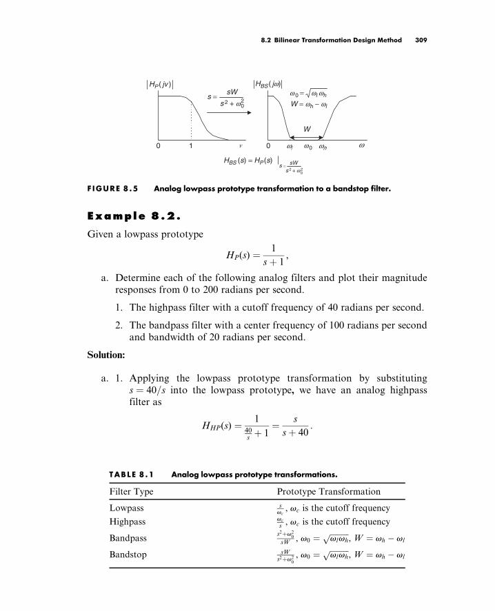
Example 8.2.
Given a lowpass prototype
HP(s) ¼ 1
sþ 1,
a. Determine each of the following analog filters and plot their magnitude
responses from 0 to 200 radians per second.
1. The highpass filter with a cutoff frequency of 40 radians per second.
2. The bandpass filter with a center frequency of 100 radians per second
and bandwidth of 20 radians per second.
Solution:
a. 1. Applying the lowpass prototype transformation by substituting
s ¼ 40=s into the lowpass prototype, we have an analog highpass
filter as
HHP(s) ¼ 140sþ 1¼ s
sþ 40:
1 n ω
HP ( jv ) HBS ( jw)
s = sW
s 2 + w02
00 ωl ωh
W
w 0 = wl wh
W = wh − wl
HBS (s) = HP (s)s =
s 2 + w02
sW
w0
F IGURE 8 .5 Analog lowpass prototype transformation to a bandstop filter.
TABLE 8 .1 Analog lowpass prototype transformations.
Filter Type Prototype Transformation
Lowpass svc
, vc is the cutoff frequency
Highpass vc
s, vc is the cutoff frequency
Bandpasss2þv2
0
sW, v0 ¼
ffiffiffiffiffiffiffiffiffiffivlvhp
, W ¼ vh vl
Bandstop sWs2þv2
0
, v0 ¼ffiffiffiffiffiffiffiffiffiffivlvhp
, W ¼ vh vl
Tan: Digital Signaling Processing 0123740908_chap08 Final Proof page 309 22.6.2007 6:21pm Compositor Name: MRaja
8.2 Bilinear Transformation Design Method 309

2. Similarly, substituting the lowpass-to-bandpass transformation
s ¼ (s2 þ 100)=(20s) into the lowpass prototype leads to
HBP(s) ¼ 1s2þ100
20sþ 1¼ 20s
s2 þ 20sþ 100:
The program for plotting the magnitude responses for highpass and bandpass
filters is shown in Program 8.1, and Figure 8.6 displays the magnitude responses
for the highpass filter and bandpass filter, respectively.
Program 8.1. MATLAB program in Example 8.2.
W ¼ 0:1:200; %Analog frequency points for computing the filter gains
Ha ¼ freqs([1 0],[1 40],W); % Frequency response for the highpass filter
Hb ¼ freqs([20 0],[1 20100],W); % Frequency response for the bandpassfilter
subplot(2,1,1);plot(W,abs(Ha),’k’);grid%Filtergainplotforthehighpassfilterxlabel(’(a) Frequency (radians per second)’)ylabel(’Absolute filter gain’);subplot(2,1,2);plot(W,abs(Hb),’k’);grid%Filtergainplotforthebandpassfilterxlabel(’(b) Frequency (radians per second)’)ylabel(’Absolute filter gain’);
Figure 8.6 confirms the lowpass prototype transformation into a highpass
filter and a bandpass filter, respectively. To obtain the transfer function of
an analog filter, we always begin with a lowpass prototype and apply the
corresponding lowpass prototype transformation. To transfer from a lowpass
prototype to a bandpass or bandstop filter, the resultant order of the analog
filter is twice that of the lowpass prototype order.
8.2.2 Bi l inear Transformat ion and FrequencyWarping
In this subsection, we develop the BLT, which converts an analog filter into a
digital filter. We begin by finding the area under a curve using the integration of
calculus and the numerical recursive method. The area under the curve is a
common problem in early calculus courses. As shown in Figure 8.7, the area
under the curve can be determined using the following integration:
y(t) ¼Z t
0
x(t)dt, (8:5)
Tan: Digital Signaling Processing 0123740908_chap08 Final Proof page 310 22.6.2007 6:21pm Compositor Name: MRaja
310 8 I N F I N I T E I M P U L S E R E S P O N S E F I L T E R D E S I G N

where y(t) (area under the curve) and x(t) (curve function) are the output and
input of the analog integrator, respectively, and t is the upper limit of the
integration.
Applying Laplace transform on Equation (8.5), we have
Y (s) ¼ X (s)
s(8:6)
and find the Laplace transfer function as
20 40 60 80 100 120 140 160 1800 2000
0.5
1
Frequency (rad/sec)
Abs
olut
e fil
ter
gain
20 40 60 80 100 120 140 160 1800 2000
0.5
1
Frequency (rad/sec)
Abs
olut
e fil
ter
gain
A
B
F IGURE 8 .6 Magnitude responses for the analog highpass filter and bandpass filter inExample 8.2.
t
x (n − 1)x (n)
(n − 1)T nT
T
0
x(t )
y (n)
y (n − 1)
F IGURE 8.7 Digital integration method to calculate the area under the curve.
Tan: Digital Signaling Processing 0123740908_chap08 Final Proof page 311 22.6.2007 6:21pm Compositor Name: MRaja
8.2 Bilinear Transformation Design Method 311

G(s) ¼ Y (s)
X (s)¼ 1
s: (8:7)
Now we examine the numerical integration method shown in Figure 8.7 to
approximate the integration of Equation (8.5) using the following difference
equation:
y(n) ¼ y(n 1)þ x(n)þ x(n 1)
2T , (8:8)
where T denotes the sampling period. y(n) ¼ y(nT) is the output sample that is
the whole area under the curve, while y(n 1) ¼ y(nT T) is the previous
output sample from the integrator indicating the previously computed area
under the curve (the shaded area in Figure 8.7). Notice that x(n) ¼ x(nT) and
x(n 1) ¼ x(nT T), sample amplitudes from the curve, are the current
input sample and the previous input sample in Equation (8.8). Applying the
z-transform on both sides of Equation (8.8) leads to
Y (z) ¼ z1Y (z)þ T
2X (z)þ z1X(z)
:
Solving for the ratio Y(z) / X(z), we achieve the z-transfer function as
H(z) ¼ Y (z)
X(z)¼ T
2
1þ z1
1 z1: (8:9)
Next, comparing Equation (8.9) with Equation (8.7), it follows that
1
s¼ T
2
1þ z1
1 z1¼ T
2
zþ 1
z 1: (8:10)
Solving for s in Equation (8.10) gives the bilinear transformation
s ¼ 2
T
z 1
zþ 1: (8:11)
The BLT method is a mapping or transformation of points from the s-plane to
the z-plane. Equation (8.11) can be alternatively written as
z ¼ 1þ sT=2
1 sT=2: (8:12)
The general mapping properties are summarized as following:
1. The left-half s-plane is mapped onto the inside of the unit circle of the
z-plane.
Tan: Digital Signaling Processing 0123740908_chap08 Final Proof page 312 22.6.2007 6:21pm Compositor Name: MRaja
312 8 I N F I N I T E I M P U L S E R E S P O N S E F I L T E R D E S I G N

2. The right-half s-plane is mapped onto the outside of the unit circle of the
z-plane.
3. The positive jv axis portion in the s-plane is mapped onto the positive
half circle (the dashed-line arrow in Figure 8.8) on the unit circle, while
the negative jv axis is mapped onto the negative half circle (the dotted-
line arrow in Figure 8.8) on the unit circle.
To verify these features, let us look at the following illustrative example:
Example 8.3.
Assuming that T ¼ 2 seconds in Equation (8.12), and given the following
points:
1. s ¼ 1þ j, on the left half of the s-plane
2. s ¼ 1 j, on the right half of the s-plane
3. s ¼ j, on the positive jv on the s-plane
4. s ¼ j, on the negative jv on the s-plane,
a. Convert each of the points in the s-plane to the z-plane, and verify the
mapping properties (1) to (3).
Solution:
a. Substituting T ¼ 2 into Equation (8.12) leads to
z ¼ 1þ s
1 s:
s
jw
Re(z)
Im(z)
Stable Region
Stable Region
10 0
F IGURE 8 .8 Mapping between the s-plane and the z-plane by the bilineartransformation.
Tan: Digital Signaling Processing 0123740908_chap08 Final Proof page 313 22.6.2007 6:21pm Compositor Name: MRaja
8.2 Bilinear Transformation Design Method 313

We can carry out mapping for each point as follows:
1. z ¼ 1þ ( 1þ j)
1 ( 1þ j)¼ j
2 j¼ 1ff90ffiffiffi
5pff 26:57
¼ 0:4472ff116:570,
since jzj ¼ 0:4472 < 1, which is inside the unit circle on the z-plane.
2. z ¼ 1þ (1 j)
1 (1 j)¼ 2 j
j¼
ffiffiffi5pff 26:57
1ff90¼ 2:2361ff 116:57,
since jzj ¼ 2:2361 > 1, which is outside the unit circle on the z-plane.
3. z ¼ 1þ j
1 j¼
ffiffiffi2pff45ffiffiffi
2pff 45
¼ 1ff90,
since jzj ¼ 1 and u ¼ 90, which is on the positive half circle on the
unit circle on the z-plane.
4. z ¼ 1 j
1 ( j)¼ 1 j
1þ j¼
ffiffiffi2pff 45ffiffiffi2pff45
¼ 1ff 90,
since jzj ¼ 1 and u ¼ 90, which is on the negative half circle on the
unit circle on the z-plane.
As shown in Example 8.3, the BLT offers conversion of an analog transfer
function to a digital transfer function. Example 8.4 shows how to perform
the BLT.
Example 8.4.
Given an analog filter whose transfer function is
H(s) ¼ 10
sþ 10,
a. Convert it to the digital filter transfer function and difference
equation, respectively, when a sampling period is given as T ¼ 0:01
second.
Solution:
a. Applying the BLT, we have
H(z) ¼ H(s)js¼2T
z1zþ1¼ 10
sþ 10
s¼2
Tz1zþ1
:
Tan: Digital Signaling Processing 0123740908_chap08 Final Proof page 314 22.6.2007 6:21pm Compositor Name: MRaja
314 8 I N F I N I T E I M P U L S E R E S P O N S E F I L T E R D E S I G N

Substituting T ¼ 0:01, it follows that
H(z) ¼ 10200(z1)
zþ1þ 10
¼ 0:05z1zþ1þ 0:05
¼ 0:05(zþ 1)
z 1þ 0:05(zþ 1)¼ 0:05zþ 0:05
1:05z 0:95:
Finally, we get
H(z) ¼ (0:05zþ 0:05)=(1:05z)
(1:05z 0:95)=(1:05z)¼ 0:0476þ 0:0476z1
1 0:9048z1:
Applying the technique in Chapter 6, we yield the difference equation as
y(n) ¼ 0:0476x(n)þ 0:0476x(n 1)þ 0:9048y(n 1):
Next, we examine frequency mapping between the s-plane and the z-plane. As
illustrated in Figure 8.9, the analog frequency va is marked on the jv axis on the
s-plane, whereas vd is the digital frequency labeled on the unit circle in the
z-plane.
We substitute s ¼ jva and z ¼ e jvdT into the BLT in Equation (8.11) to get
jva ¼2
T
e jvdT 1
e jvdT þ 1: (8:13)
Simplifying Equation (8.13) leads to
va ¼2
Ttan
vdT
2
: (8:14)
σ
jw
Re(z)
Im(z)
10
••
z = 1
0
wa wdT
F IGURE 8 .9 Frequency mapping from the analog domain to the digital domain.
Tan: Digital Signaling Processing 0123740908_chap08 Final Proof page 315 22.6.2007 6:21pm Compositor Name: MRaja
8.2 Bilinear Transformation Design Method 315

Equation (8.14) explores the relation between the analog frequency on the jv
axis and the corresponding digital frequency vd on the unit circle. We can also
write its inverse as
vd ¼2
Ttan1 vaT
2
: (8:15)
The range of the digital frequency vd is from 0 radian per second to the folding
frequency vs=2 radians per second, where vs is the sampling frequency in
radians per second. We make a plot of Equation (8.14) in Figure 8.10.
From Figure 8.10 when the digital frequency range 0 vd 0:25vs is
mapped to the analog frequency range 0 va 0:32vs, the transformation
appears to be linear; however, when the digital frequency range 0:25vs vd 0:5vs
is mapped to the analog frequency range for va > 0:32vs, the transformation is
nonlinear. The analog frequency range for va > 0:32vs is compressed into the
digital frequency range 0:25vs vd 0:5vs. This nonlinear frequency mapping effect
is called frequency warping. We must incorporate the frequency warping into the
IIR filter design. The following example will illustrate the frequency warping effect
in the BLT.
Example 8.5.
Assume the following analog frequencies:
va ¼ 10 radians per second
va ¼ vs=4 ¼ 50p ¼ 157 radians per second
va ¼ vs=2 ¼ 100p ¼ 314 radians per second.
a. Find their digital frequencies using the BLT with a sampling period of
0.01 second, given the analog filter in Example 8.4 and the developed
digital filter.
0wa (r /s)
wd (r /s)
0.5ws
0.4ws
0.25ws
0.32ws ws
F IGURE 8.10 Frequency warping from bilinear transformation.
Tan: Digital Signaling Processing 0123740908_chap08 Final Proof page 316 22.6.2007 6:21pm Compositor Name: MRaja
316 8 I N F I N I T E I M P U L S E R E S P O N S E F I L T E R D E S I G N

Solution:
a. From Equation (8.15), we can calculate digital frequency vd as follows:
When va ¼ 10 radians=sec and T ¼ 0:01 second,
vd ¼2
Ttan1 vaT
2
¼ 2
0:01tan1 10 0:01
2
¼ 9:99 rad=sec,
which is close to the analog frequency of 10 radians per second. When
va ¼ 157 rad=sec and T ¼ 0:01 second,
vd ¼2
0:01tan1 157 0:01
2
¼ 133:11 rad=sec,
which has an error as compared with the desired value 157. When
va ¼ 314 rad=sec and T ¼ 0:01 second,
vd ¼2
0:01tan1 314 0:01
2
¼ 252:5 rad=sec,
which gives a bigger error compared with the digital folding frequency of
314 radians per second.
Figure 8.11 shows how to correct the frequency warping error. First, given
the digital frequency specification, we prewarp the digital frequency specifica-
tion to the analog frequency specification by Equation (8.14).
Second, we obtain the analog lowpass filter H(s) using the prewarped analog
frequency va and the lowpass prototype. For the lowpass analog filter, we have
H(s) ¼ HP(s)js¼ sva
¼ HP
s
va
: (8:16)
Finally, substituting BLT Equation (8.11) into Equation (8.16) yields the digital
filter as
H(z) ¼ H sð Þjs¼2
Tz1zþ1
: (8:17)
This approach can be extended to the other type of filter design similarly.
8.2.3 Bi l inear Transformat ion Design Procedure
Now we can summarize the BLT design procedure.
1. Given the digital filter frequency specifications, prewarp the digital fre-
quency specifications to the analog frequency specifications.
Tan: Digital Signaling Processing 0123740908_chap08 Final Proof page 317 22.6.2007 6:21pm Compositor Name: MRaja
8.2 Bilinear Transformation Design Method 317

For the lowpass filter and highpass filter:
va ¼2
Ttan
vdT
2
: (8:18)
For the bandpass filter and bandstop filter:
val ¼2
Ttan
vlT
2
, vah ¼
2
Ttan
vhT
2
, (8:19)
where
v0 ¼ffiffiffiffiffiffiffiffiffiffiffiffiffivalvah
p, W ¼ vah val
2. Perform the prototype transformation using the lowpass prototype
Hp(s).
From lowpass to lowpass: H(s) ¼ HP(s)js¼ sva
(8:20)
0
0.5w s
Digital lowpass filter specification
Analog lowpass filter specification
T
2
2( )tan
Frequency prewarping
n1
H (z)
H (s)
HP (s)s = s / wa
s =T z + 1
z − 12
Analog lowpass prototype
Step 1
Step 3
Step 2
Bilinear transformation
wd (r /s )
wa (r /s )
wd
wa
wdTwa =
F IGURE 8.11 Graphical representation of IIR filter design using the bilineartransformation.
Tan: Digital Signaling Processing 0123740908_chap08 Final Proof page 318 22.6.2007 6:21pm Compositor Name: MRaja
318 8 I N F I N I T E I M P U L S E R E S P O N S E F I L T E R D E S I G N
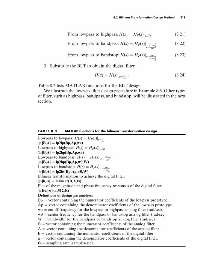
From lowpass to highpass: H(s) ¼ HP(s)js¼vas
(8:21)
From lowpass to bandpass: H(s) ¼ HP(s)js¼
s2þv20
sW
(8:22)
From lowpass to bandstop: H(s) ¼ HP(s)js¼ sW
s2þv20
(8:23)
3. Substitute the BLT to obtain the digital filter
H(z) ¼ H(s)js¼2T
z1zþ1: (8:24)
Table 8.2 lists MATLAB functions for the BLT design.
We illustrate the lowpass filter design procedure in Example 8.6. Other types
of filter, such as highpass, bandpass, and bandstop, will be illustrated in the next
section.
TABLE 8 .2 MATLAB functions for the bilinear transformation design.
Lowpass to lowpass: H(s) ¼ HP(s)js¼ sva[B,A] ¼ lp2lp(Bp,Ap,wa)
Lowpass to highpass: H(s) ¼ HP(s)js¼vas[B,A] ¼ lp2hp(Bp,Ap,wa)
Lowpass to bandpass: H(s) ¼ HP(s)js ¼ s2þv20
sW[B,A] ¼ lp2bp(Bp,Ap,w0,W)
Lowpass to bandstop: H(s) ¼ HP(s)js¼ sW
s2þv20[B,A] ¼ lp2bs(Bp,Ap,w0,W)
Bilinear transformation to achieve the digital filter:
[b, a] ¼ bilinear(B,A,fs)
Plot of the magnitude and phase frequency responses of the digital filter:
freqz(b,a,512,fs)
Definitions of design parameters:
Bp ¼ vector containing the numerator coefficients of the lowpass prototype.
Ap ¼ vector containing the denominator coefficients of the lowpass prototype.
wa ¼ cutoff frequency for the lowpass or highpass analog filter (rad/sec).
w0 ¼ center frequency for the bandpass or bandstop analog filter (rad/sec).
W ¼ bandwidth for the bandpass or bandstop analog filter (rad/sec).
B ¼ vector containing the numerator coefficients of the analog filter.
A ¼ vector containing the denominator coefficients of the analog filter.
b ¼ vector containing the numerator coefficients of the digital filter.
a ¼ vector containing the denominator coefficients of the digital filter.
fs ¼ sampling rate (samples/sec).
Tan: Digital Signaling Processing 0123740908_chap08 Final Proof page 319 22.6.2007 6:21pm Compositor Name: MRaja
8.2 Bilinear Transformation Design Method 319

Example 8.6.
The normalized lowpass filter with a cutoff frequency of 1 rad/sec is given as:
HP(s) ¼ 1
sþ 1:
a. Use the given Hp(s) and the BLT to design a corresponding digital IIR
lowpass filter with a cutoff frequency of 15 Hz and a sampling rate of
90 Hz.
b. Use MATLAB to plot the magnitude response and phase response of
H(z).
Solution:
a. First, we obtain the digital frequency as
vd ¼ 2pf ¼ 2p(15) ¼ 30p rad=sec , and T ¼ 1=fs ¼ 1=90 sec:
We then follow the design procedure:
1. First calculate the prewarped analog frequency as
va ¼2
Ttan
vdT
2
¼ 2
1=90tan
30p=90
2
,
that is, va ¼ 180 tan (p=6) ¼ 180 tan (30) ¼ 103.92 rad/sec.
2. Then perform the prototype transformation (lowpass to lowpass) as
follows:
H(s) ¼ HP sð Þs¼ sva
¼ 1s
vaþ 1¼ va
sþ va
,
which yields an analog filter:
H(s) ¼ 103:92
sþ 103:92:
3. Apply the BLT, which yields
H(z) ¼ 103:92
sþ 103:92
s¼2
Tz1zþ1
:
We simplify the algebra by dividing both the numerator and the
denominator by 180:
H(z) ¼ 103:92
180 z1zþ1þ 103:92
¼ 103:92=180z1zþ1þ 103:92=180
¼ 0:5773z1zþ1þ 0:5773
:
Tan: Digital Signaling Processing 0123740908_chap08 Final Proof page 320 22.6.2007 6:21pm Compositor Name: MRaja
320 8 I N F I N I T E I M P U L S E R E S P O N S E F I L T E R D E S I G N

Then we multiply both numerator and denominator by (zþ 1) to
obtain
H(z) ¼ 0:5773(zþ 1)
z1zþ1þ 0:5773
(zþ 1)
¼ 0:5773zþ 0:5773
(z 1)þ 0:5773(zþ 1)
¼ 0:5773zþ 0:5773
1:5773z 0:4227:
Finally, we divide both numerator and denominator by 1.5773z to get
the transfer function in the standard format:
H(z) ¼ (0:5773zþ 0:5773)=(1:5773z)
(1:5773z 0:4227)=(1:5773z)¼ 0:3660þ 0:3660z1
1 0:2679z1:
b. The corresponding MATLAB design is listed in Program 8.2. Figure 8.12
shows the magnitude and phase frequency responses.
0 5 10 15 20 25 30 35 40 450
0.5
1
Frequency (Hz)
Mag
nitu
de re
spon
se
0 5 10 15 20 25 30 35 40 45−100
−80
−60
−40
−20
0
Frequency (Hz)
Ph
ase
(deg
rees
)
F IGURE 8 .12 Frequency responses of the designed digital filter for Example 8.6.
Tan: Digital Signaling Processing 0123740908_chap08 Final Proof page 321 22.6.2007 6:21pm Compositor Name: MRaja
8.2 Bilinear Transformation Design Method 321

Program 8.2. MATLAB program for Example 8.6.
%Example 8.6
% Plot the magnitude and phase responses
fs ¼ 90;% Sampling rate (Hz)
[B, A] ¼ lp2lp([1],[1 1],103.92);
[b, a] ¼ bilinear(B, A, fs)
%b ¼ [0.3660 0.3660] numerator coefficients of the digital filter from MATLAB
%a ¼ [10:2679]denominator coefficients of the digital filter from MATLAB[hz,f] ¼ freqz([0.36600.3660],[10:2679],512,fs);%thefrequencyresponsephi ¼ 180unwrap(angle(hz))/pi;subplot(2,1,1), plot(f, abs(hz)),grid;
axis([0 fs/2 0 1]);
xlabel(’Frequency (Hz)’); ylabel(’Magnitude Response’)subplot(2,1,2), plot(f, phi); grid;
axis([0 fs/2 100 0]);xlabel(’Frequency (Hz)’); ylabel(’Phase (degrees)’)
8.3 Digi ta l But terwor th and ChebyshevFi l ter Des igns
In this section, we design various types of digital Butterworth and Chebyshev
filters using the BLT design method developed in the previous section.
8.3.1 Lowpass Prototype Funct ion and I tsOrder
As described in the Section 8.2.3 (Bilinear Transformation Design Procedure),
BLT design requires obtaining the analog filter with prewarped frequency
specifications. These analog filter design requirements include the ripple speci-
fication at the passband frequency edge, the attenuation specification at the
stopband frequency edge, and the type of lowpass prototype (which we shall
discuss) and its order.
Table 8.3 lists the Butterworth prototype functions with 3 dB passband
ripple specification. Tables 8.4 and 8.5 contain the Chebyshev prototype func-
tions (type I) with 1 dB and 0.5 dB passband ripple specifications, respectively.
Other lowpass prototypes with different ripple specifications and order can be
computed using the methods described in Appendix C.
In this section, we will focus on the Chebyshev type I filter. The Chebyshev
type II filter design can be found in Proakis and Manolakis (1996) and Porat
(1997).
Tan: Digital Signaling Processing 0123740908_chap08 Final Proof page 322 22.6.2007 6:21pm Compositor Name: MRaja
322 8 I N F I N I T E I M P U L S E R E S P O N S E F I L T E R D E S I G N

The magnitude response function of the Butterworth lowpass prototype with
an order of n is shown in Figure 8.13, where the magnitude response jHp(v)jversus the normalized frequency v is given by Equation (8.25):
HP(v)j j ¼ 1ffiffiffiffiffiffiffiffiffiffiffiffiffiffiffiffiffiffiffi1þ «2v2np (8:25)
With the given passband ripple Ap dB at the normalized passband frequency
edge vp ¼ 1, and the stopband attenuation As dB at the normalized stopband
TABLE 8.3 3 dB Butterworth lowpass prototypetransfer functions (« ¼ 1)
n HP(s)
1 1sþ1
2 1s2þ1:4142sþ1
3 1s3þ2s2þ2sþ1
4 1s4þ2:6131s3þ3:4142s2þ2:6131sþ1
5 1s5þ3:2361s4þ5:2361s3þ5:2361s2þ3:2361sþ1
6 1s6þ3:8637s5þ7:4641s4þ9:1416s3þ7:4641s2þ3:8637sþ1
TABLE 8.4 Chebyshev lowpass prototype transferfunctions with 0.5 dB ripple (« ¼ 0.3493)
n HP(s)
1 2:8628sþ2:8628
2 1:4314s2þ1:4256sþ1:5162
3 0:7157s3þ1:2529s2þ1:5349sþ0:7157
4 0:3579s4þ1:1974s3þ1:7169s2þ1:0255sþ0:3791
5 0:1789s5þ1:1725s4þ1:9374s3þ1:3096s2þ0:7525sþ0:1789
6 0:0895s6þ1:1592s5þ2:1718s4þ1:5898s3þ1:1719s2þ0:4324sþ0:0948
TABLE 8.5 Chebyshev lowpass prototype transferfunctions with 1 dB ripple (« ¼ 0.5088)
n HP(s)
1 1:9652sþ1:9652
2 0:9826s2þ1:0977sþ1:1025
3 0:4913s3þ0:9883s2þ1:2384sþ0:4913
4 0:2456s4þ0:9528s3þ1:4539s2þ0:7426sþ0:2756
5 0:1228s5þ0:9368s4þ1:6888s3þ0:9744s2þ0:5805sþ0:1228
6 0:0614s6þ0:9283s5þ1:9308s4þ1:20121s3þ0:9393s2þ0:3071sþ0:0689
Tan: Digital Signaling Processing 0123740908_chap08 Final Proof page 323 22.6.2007 6:21pm Compositor Name: MRaja
8.3 Digital Butterworth and Chebyshev Filter Designs 323

frequency edge vs, the following two equations must be satisfied to determine the
prototype filter order:
AP dB ¼ 20 log10
1ffiffiffiffiffiffiffiffiffiffiffiffiffi1þ «2p
(8:26)
As dB ¼ 20 log10
1ffiffiffiffiffiffiffiffiffiffiffiffiffiffiffiffiffiffiffi1þ «2v2n
s
p !
: (8:27)
Solving Equations (8.26) and (8.27), we determine the lowpass prototype order
as
«2 ¼ 100:1Ap 1 (8:28)
n log10
100:1As1«2
2 log10 (vs)½ , (8:29)
where « is the absolute ripple specification.
The magnitude response function of the Chebyshev lowpass prototype with
an order of n is shown in Figure 8.14, where the magnitude response jHp(v)jversus the normalized frequency v is given by
HP(v)j j ¼ 1ffiffiffiffiffiffiffiffiffiffiffiffiffiffiffiffiffiffiffiffiffiffiffiffi1þ «2C2
n(v)p (8:30)
v
1 + e2v2n
1 + e2
n = 2n = 1
n = 30
1
vsvp = 1
As
Hp(v )
Hp(v )
=11
F IGURE 8.13 Normalized Butterworth magnitude response function.
1
v
n (odd) n (even)1
[[
]]
Cn (v) =v ≤ 1
v > 1
Hp(v )Hp(v )
1+e2
1
0 vsvp = 1As
1 + e2C2n(v)
cos ncos−1(v)
cosh ncosh−1(v)
=
F IGURE 8.14 Normalized Chebyshev magnitude response function.
Tan: Digital Signaling Processing 0123740908_chap08 Final Proof page 324 22.6.2007 6:21pm Compositor Name: MRaja
324 8 I N F I N I T E I M P U L S E R E S P O N S E F I L T E R D E S I G N

where
Cn(vs) ¼ cosh n cosh1 (vs)
(8:31)
cosh1 (vs) ¼ ln (vs þffiffiffiffiffiffiffiffiffiffiffiffiffiv2s 1
q) (8:32)
As shown in Figure 8.14, the magnitude response for the Chebyshev lowpass
prototype with the order of an odd number begins with the filter DC gain of 1.
In the case of a Chebyshev lowpass prototype with the order of an even number,
the magnitude starts at the filter DC gain of 1=ffiffiffiffiffiffiffiffiffiffiffiffiffi1þ «2p
. For both cases, the filter
gain at the normalized cutoff frequency vp ¼ 1 is 1=ffiffiffiffiffiffiffiffiffiffiffiffiffi1þ «2p
.
Similarly, Equations (8.33) and (8.34) must be satisfied:
AP dB ¼ 20 log10
1ffiffiffiffiffiffiffiffiffiffiffiffiffi1þ «2p
(8:33)
As dB ¼ 20 log10
1ffiffiffiffiffiffiffiffiffiffiffiffiffiffiffiffiffiffiffiffiffiffiffiffiffi1þ «2C2
n (vs)p
!: (8:34)
The lowpass prototype order can be solved in Equation (8.35b):
«2 ¼ 100:1Ap 1 (8:35a)
n cosh1 100:1As1
"2
0:5
cosh1 vsð Þ, (8:35b)
where cosh1 (x) ¼ ln (xþffiffiffiffiffiffiffiffiffiffiffiffiffix2 1p
), « is the absolute ripple parameter.
The normalized stopband frequency vs can be determined from the frequency
specifications of an analog filter in Table 8.6. Then the order of the lowpass
TABLE 8 .6 Conversion from analog filter specifications to lowpass prototypespecifications.
Analog Filter Specifications Lowpass Prototype Specifications
Lowpass: vap, vas vp ¼ 1, vs ¼ vas=vap
Highpass: vap, vas vp ¼ 1, vs ¼ vap=vas
Bandpass: vapl , vaph, vasl , vash
v0 ¼ffiffiffiffiffiffiffiffiffiffiffiffiffiffiffiffiffivaplvaphp
, v0 ¼ffiffiffiffiffiffiffiffiffiffiffiffiffiffiffiffivaslvashp vp ¼ 1,vs ¼ vashvasl
vaphvapl
Bandstop: vapl , vaph, vasl , vash
v0 ¼ffiffiffiffiffiffiffiffiffiffiffiffiffiffiffiffiffivaplvaphp
, v0 ¼ffiffiffiffiffiffiffiffiffiffiffiffiffiffiffiffivaslvashp vp ¼ 1,vs ¼ vaphvapl
vashvasl
vap, passband frequency edge; vas, stopband frequency edge; vapl , lower cutoff frequency in
passband; vaph, upper cutoff frequency in passband; vasl , lower cutoff frequency in stopband;
vash, upper cutoff frequency in stopband; vo, geometric center frequency.
Tan: Digital Signaling Processing 0123740908_chap08 Final Proof page 325 22.6.2007 6:21pm Compositor Name: MRaja
8.3 Digital Butterworth and Chebyshev Filter Designs 325

prototype can be determined by Equation (8.29) for the Butterworth function and
Equation (8.35b) for the Chebyshev function. Figure 8.15 gives frequency edge
notations for analog lowpass and bandpass filters. The notations for analog high-
pass and bandstop filters can be defined correspondingly.
8.3.2 Lowpass and Highpass F i l ter DesignExamples
The following examples illustrate various designs for the Butterworth and
Chebyshev lowpass and highpass filters.
Example 8.7.
a. Design a digital lowpass Butterworth filter with the following
specifications:
1. 3 dB attenuation at the passband frequency of 1.5 kHz
2. 10 dB stopband attenuation at the frequency of 3 kHz
3. Sampling frequency of 8,000 Hz.
b. Use MATLAB to plot the magnitude and phase responses.
Solution:
a. First, we obtain the digital frequencies in radians per second:
vdp ¼ 2p f ¼ 2p(1500) ¼ 3000p rad=sec
vds ¼ 2p f ¼ 2p(3000) ¼ 6000p rad=sec
T ¼ 1= fs ¼ 1=8000 sec
wap waswasl wapl
wapl waph
waph − wapl
waph wash ww0
w0 =
w
HLP( jω) HBP( jω)
00
W
W =
As
Ap
As
Ap
Lowpass filter Bandpass filter
F IGURE 8.15 Specifications for analog lowpass and bandpass filters.
Tan: Digital Signaling Processing 0123740908_chap08 Final Proof page 326 22.6.2007 6:21pm Compositor Name: MRaja
326 8 I N F I N I T E I M P U L S E R E S P O N S E F I L T E R D E S I G N

Following the steps of the design procedure,
1. We apply the warping equation as
vap¼2
Ttan
vdT
2
¼16000tan
3000p=8000
2
¼1:0691104rad=sec:
vas¼2
Ttan
vdT
2
¼16000tan
6000p=8000
2
¼3:8627104rad=sec:
We then find the lowpass prototype specifications using Table 8.6 as
follows:
vs ¼ vas=vap ¼ 3:8627 104= 1:0691 104
¼ 3:6130 rad=sec and As ¼ 10 dB:
The filter order is computed as
«2 ¼ 100:13 1 ¼ 1
n ¼ log10 (100:110 1)
2 log10 (3:6130)¼ 0:8553 :
2. Rounding n up, we choose n ¼ 1 for the lowpass prototype. From
Table 8.3, we have
HP(s) ¼ 1
sþ 1:
Applying the prototype transformation (lowpass to lowpass) yields
the analog filter
H(s) ¼ HP(s)j svap
¼ 1s
vapþ 1¼ vap
sþ vap
¼ 1:0691 104
sþ 1:0691 104:
3. Finally, using the BLT, we have
H(z) ¼ 1:0691 104
sþ 1:0691 104
s¼16000(z1)=(zþ1)
:
Substituting the BLT leads to
H(z) ¼ 1:0691 104
16000 z1zþ1
þ 1:0691 104
:
Tan: Digital Signaling Processing 0123740908_chap08 Final Proof page 327 22.6.2007 6:21pm Compositor Name: MRaja
8.3 Digital Butterworth and Chebyshev Filter Designs 327

To simplify the algebra, we divide both numerator and denominator
by 16000 to get
H(z) ¼ 0:6682
z1zþ1
þ 0:6682
:
Then multiplying (zþ 1) to both numerator and denominator leads to
H(z) ¼ 0:6682 zþ 1ð Þz 1ð Þ þ 0:6682 zþ 1ð Þ ¼
0:6682zþ 0:6682
1:6682z 0:3318:
Dividing both numerator and denominator by (1:6682 z) leads to
H(z) ¼ 0:4006þ 0:4006z1
1 0:1989z1:
b. Steps 2 and 3 can be carried out using MATLAB Program 8.3, as shown
in the first three lines of the MATLAB codes. Figure 8.16 describes the
filter frequency responses.
0 500 1000 1500 2000 2500 3000 3500 4000−100
−80
−60
−40
−20
0
Frequency (Hz)
Pha
se (
degr
ees)
0 500 1000 1500 2000 2500 3000 3500 4000−20
−15
−10
−5
0
Frequency (Hz)
Mag
nitu
de r
espo
nse
(dB
)
F IGURE 8.16 Frequency responses of the designed digital filter for Example 8.7.
Tan: Digital Signaling Processing 0123740908_chap08 Final Proof page 328 22.6.2007 6:21pm Compositor Name: MRaja
328 8 I N F I N I T E I M P U L S E R E S P O N S E F I L T E R D E S I G N

Program 8.3. MATLAB program for Example 8.7.
%Example 8.7
% Design of the digital lowpass Butterworth filter
format long
fs¼8000;% Sampling rate
[B A]¼lp2lp([1],[1 1], 1:069110^4)% Complete step 2
[b a]¼bilinear(B,A,fs) % Complete step 3
% Plot the magnitude and phase responses
%b¼[0.4005 0.4005]; numerator coefficients from MATLAB
%a¼ [10:1989]; denominator coefficients from MATLAB
freqz(b,a,512,fs);
axis([0 fs/2 -20 1])
Example 8.8.
a. Design a first-order digital highpass Chebyshev filter with a cutoff fre-
quency of 3 kHz and 1 dB ripple on passband using a sampling frequency
of 8,000 Hz.
b. Use MATLAB to plot the magnitude and phase responses.
Solution:
a. First, we obtain the digital frequency in radians per second:
vd ¼ 2p f ¼ 2p(3000) ¼ 6000p rad=sec, and T ¼ 1= fs ¼ 1=8000 sec:
Following the steps of the design procedure, we have
1. va ¼ 2T
tan vdT2
¼ 16000 tan
6000p=80002
¼ 3:8627 104 rad=sec:
2. Since the filter order is given as 1, we select the first-order lowpass
prototype from Table 8.5 as
HP(s) ¼ 1:9652
sþ 1:9625:
Applying the prototype transformation (lowpass to highpass), we
yield
H(s) ¼ HP(s)jvas¼ 1:9652
va
sþ 1:9652
¼ 1:9652s
1:9652sþ 3:8627 104:
Tan: Digital Signaling Processing 0123740908_chap08 Final Proof page 329 22.6.2007 6:21pm Compositor Name: MRaja
8.3 Digital Butterworth and Chebyshev Filter Designs 329

Dividing both numerator and denominator by 1.9652 gives
H(s) ¼ s
sþ 1:9656 104:
3. Using the BLT, we have
H(z) ¼ s
sþ 1:9656 104
s¼16000(z1)=(zþ1)
:
Algebra work is demonstrated as follows:
H(z) ¼16000 z1
zþ1
16000 z1zþ1þ 1:9656 104
:
Simplifying the transfer function yields
H(z) ¼ 0:4487 0:4487z1
1þ 0:1025z1:
b. Steps 2 and 3 and the frequency response plots shown in Figure 8.17 can
be carried out using MATLAB Program 8.4.
0 500 1000 1500 2000 2500 3000 3500 40000
50
100
Frequency (Hz)
Pha
se (
degr
ees)
0 500 1000 1500 2000 2500 3000 3500 4000−40
−30
−20
−10
0
Frequency (Hz)
Mag
nitu
de r
espo
nse
(dB
)
F IGURE 8.17 Frequency responses of the designed digital filter for Example 8.8.
Tan: Digital Signaling Processing 0123740908_chap08 Final Proof page 330 22.6.2007 6:21pm Compositor Name: MRaja
330 8 I N F I N I T E I M P U L S E R E S P O N S E F I L T E R D E S I G N

Program 8.4. MATLAB program for Example 8.8
%Example 8.8
% Design of the digital highpass Butterworth filter
format long
fs¼8000; % Sampling rate
[B A]¼lp2hp([1.9652],[1 1.9652], 3:862710^4) % Complete step 2
[b a]¼bilinear(B,A,fs)% Complete step 3
% Plot the magnitude and phase responses
%b ¼ [0:4487 0:4487]; numerator coefficients from MATLAB
%a¼[1 0.1025]; denominator coefficients from MATLAB
freqz(b,a,512,fs);
axis([0 fs/2 -40 2])
Example 8.9.
a. Design a second-order digital lowpass Butterworth filter with a cutoff
frequency of 3.4 kHz at a sampling frequency of 8,000 Hz.
b. Use MATLAB to plot the magnitude and phase responses.
Solution:
a. First, we obtain the digital frequency in radians per second:
vd ¼ 2p f ¼ 2p(3400) ¼ 6800p rad=sec, and T ¼ 1= fs ¼ 1=8000 sec:
Following the steps of the design procedure, we compute the prewarped
analog frequency as
1. va ¼ 2T
tan vdT2
¼ 16000 tan
6800p=80002
¼ 6:6645 104 rad=sec.
2. Since the order of 2 is given in the specification, we directly pick the
second-order lowpass prototype from Table 8.3:
HP(s) ¼ 1
s2 þ 1:4142sþ 1:
After applying the prototype transformation (lowpass to lowpass), we
have
H(s) ¼ HP(s)j sva
¼ 4:4416 109
s2 þ 9:4249 104sþ 4:4416 109:
3. Carrying out the BLT yields
H(z) ¼ 4:4416 109
s2 þ 9:4249 104sþ 4:4416 109
s¼16000(z1)=(zþ1)
:
Tan: Digital Signaling Processing 0123740908_chap08 Final Proof page 331 22.6.2007 6:21pm Compositor Name: MRaja
8.3 Digital Butterworth and Chebyshev Filter Designs 331

Let us work on algebra:
H(z) ¼ 4:4416 109
16000 z1zþ1
2
þ9:4249 104 16000 z1zþ1
þ 4:4416 109
:
To simplify, we divide both numerator and denominator by (16000)2
to get
H(z) ¼ 17:35
z1zþ1
2
þ5:8906 z1zþ1
þ 17:35
:
Then multiplying both numerator and denominator by (zþ 1)2 leads to
H(z) ¼ 17:35 zþ 1ð Þ2
z 1ð Þ2þ5:8906 z 1ð Þ zþ 1ð Þ þ 17:35 zþ 1ð Þ2:
Using identities, we have
H(z) ¼17:35 z2 þ 2zþ 1
z2 2zþ 1ð Þ þ 5:8906 z2 1ð Þ þ 17:35 z2 þ 2zþ 1ð Þ
¼ 17:35z2 þ 34:7zþ 17:35
24:2406z2 þ 32:7zþ 12:4594:
Dividing both numerator and denominator by (24:2406z2) leads to
H(z) ¼ 0:7157þ 1:4314z1 þ 0:7151z2
1þ 1:3490z1 þ 0:5140z2:
b. Steps 2 and 3 require a certain amount of algebra work and can be
verified using MATLAB Program 8.5, as shown in the first three lines.
Figure 8.18 plots the filter magnitude and phase frequency responses.
Program 8.5. MATLAB program for Example 8.9.
%Example 8.9
% Design of the digital lowpass Butterworth filter
format long
fs ¼ 8000; % Sampling rate
[B A] ¼ lp2lp([1],[1 1.4142 1], 6:664510 ^ 4) % Complete step 2
[b a] ¼ bilinear(B,A,fs)% Complete step 3
% Plot the magnitude and phase responses
%b ¼ [0.7157 1.4315 0.7157]; numerator coefficients from MATLAB
%a ¼ [1 1.3490 0.5140]; denominator coefficients from MATLAB
freqz(b,a,512,fs);
axis([0 fs/2 -40 10])
Tan: Digital Signaling Processing 0123740908_chap08 Final Proof page 332 22.6.2007 6:21pm Compositor Name: MRaja
332 8 I N F I N I T E I M P U L S E R E S P O N S E F I L T E R D E S I G N

Example 8.10.
a. Design a digital highpass Chebyshev filter with the following specifi-
cations:
1. 0.5 dB ripple on passband at the frequency of 3,000 Hz
2. 25 dB attenuation at the frequency of 1,000 Hz
3. Sampling frequency of 8,000 Hz.
b. Use MATLAB to plot the magnitude and phase responses.
Solution:
a. From the specifications, the digital frequencies are
vdp ¼ 2p f ¼ 2p(3000) ¼ 6000p rad=sec
vds ¼ 2p f ¼ 2p(1000) ¼ 2000p rad=sec
T ¼ 1= fs ¼ 1=8000 sec.
0 500 1000 1500 2000 2500 3000 3500 4000−200
−150
−100
−50
0
Frequency (Hz)
Pha
se (
degr
ees)
0 500 1000 1500 2000 2500 3000 3500 4000−40
−30
−20
−10
0
10
Frequency (Hz)
Mag
nitu
de r
espo
nse
(dB
)
F IGURE 8 .18 Frequency responses of the designed digital filter for Example 8.9.
Tan: Digital Signaling Processing 0123740908_chap08 Final Proof page 333 22.6.2007 6:21pm Compositor Name: MRaja
8.3 Digital Butterworth and Chebyshev Filter Designs 333

Using the design procedure, it follows that
vap¼2
Ttan
vdpT
2
¼ 16000 tan
6000p=8000
2
¼ 3:8627104 rad=sec
vas¼ 16000 tanvdsT
2
¼ 16000 tan
2000p=8000
2
¼ 6:6274103 rad=sec
We find the lowpass prototype specifications using Table 8.6 as follows:
vs ¼ vps=vsp ¼ 3:8627 104=6:6274 103 ¼ 5:8284 rad=s and As ¼ 25dB,
then the filter order is computed as
«2 ¼ 100:10:5 1 ¼ 0:1220
(100:125 1)=0:1220 ¼ 2583:8341
n ¼cosh1 2583:8341ð Þ0:5
h icosh1 (5:8284)
¼ ln (50:8314þffiffiffiffiffiffiffiffiffiffiffiffiffiffiffiffiffiffiffiffiffiffiffiffiffiffi50:83142 1p
)
ln (5:8284þffiffiffiffiffiffiffiffiffiffiffiffiffiffiffiffiffiffiffiffiffiffiffiffi5:82842 1p
)¼ 1:8875:
We select n ¼ 2 for the lowpass prototype function. Following the steps
of the design procedure, it follows that
1. vp ¼ 3:8627 104 rad=sec.
2. Performing the prototype transformation (lowpass to lowpass) using
the prototype filter in Table 8.4, we have
HP(s) ¼ 1:4314
s2 þ 1:4256sþ 1:5162and
H(s) ¼ HP(s)j sva
¼ 1:4314vp
s
2þ1:4256vp
s
þ 1:5162
¼ 0:9441s2
s2 þ 3:6319 104sþ 9:8407 108:
3. Hence, applying the BLT, we convert the analog filter to a digital filter
as
H(z) ¼ 0:9441s2
s2 þ 3:6319 104sþ 9:8407 108
s¼16000(z1)=(zþ1)
:
Tan: Digital Signaling Processing 0123740908_chap08 Final Proof page 334 22.6.2007 6:21pm Compositor Name: MRaja
334 8 I N F I N I T E I M P U L S E R E S P O N S E F I L T E R D E S I G N

After algebra simplification, it follows that
H(z) ¼ 0:1327 0:2654z1 þ 0:1327z2
1þ 0:7996z1 þ 0:3618z2:
b. MATLAB Program 8.6 is listed for this example, and the frequency
responses are given in Figure 8.19.
Program 8.6. MATLAB program for Example 8.10.
%Example 8.10
% Design of the digital lowpass Chebyshev filter
format long
fs ¼ 8000; % Sampling rate
% BLT design
[B A] ¼ lp2hp([1.4314],[1 1.4256 1.5162], 3:862710 ^ 4) % Complete step 2
[b a] ¼ bilinear(B,A,fs)% Complete step 3
% Plot the magnitude and phase responses
%b ¼ [0:1327 0:2654 0:1327]; numerator coefficients from MATLAB
%a ¼ [1 0:7996 0:3618];denominator coefficients from MATLAB
freqz(b,a,512,fs);
axis([0 fs=2 40 10])
0 500 1000 1500 2000 2500 3000 3500 40000
50
100
150
200
Frequency (Hz)
Pha
se (
degr
ees)
0 500 1000 1500 2000 2500 3000 3500 4000−40
−30
−20
−10
0
10
Frequency (Hz)
Mag
nitu
de r
espo
nse
(dB
)
F IGURE 8 .19 Frequency responses of the designed digital filter for Example 8.10.
Tan: Digital Signaling Processing 0123740908_chap08 Final Proof page 335 22.6.2007 6:21pm Compositor Name: MRaja
8.3 Digital Butterworth and Chebyshev Filter Designs 335
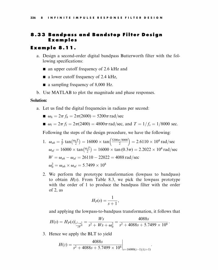
8.33 Bandpass and Bandstop Fi l ter DesignExamples
Example 8.11.
a. Design a second-order digital bandpass Butterworth filter with the fol-
lowing specifications:
& an upper cutoff frequency of 2.6 kHz and
& a lower cutoff frequency of 2.4 kHz,
& a sampling frequency of 8,000 Hz.
b. Use MATLAB to plot the magnitude and phase responses.
Solution:
a. Let us find the digital frequencies in radians per second:
& vh ¼ 2p fh ¼ 2p(2600) ¼ 5200p rad=sec
& vl ¼ 2p fl ¼ 2p(2400) ¼ 4800p rad=sec, and T ¼ 1= fs ¼ 1=8000 sec.
Following the steps of the design procedure, we have the following:
1. vah ¼ 2T
tan vhT2
¼ 16000 tan
5200p=80002
¼ 2:6110 104 rad=sec
val ¼ 16000 tan vlT2
¼ 16000 tan (0:3p) ¼ 2:2022 104 rad=sec
W ¼ vah val ¼ 26110 22022 ¼ 4088 rad=sec
v20 ¼ vah val ¼ 5:7499 108
2. We perform the prototype transformation (lowpass to bandpass)
to obtain H(s). From Table 8.3, we pick the lowpass prototype
with the order of 1 to produce the bandpass filter with the order
of 2, as
HP(s) ¼ 1
sþ 1,
and applying the lowpass-to-bandpass transformation, it follows that
H(s) ¼ HP(s)js2þv20
sW
¼ Ws
s2 þWsþ v20
¼ 4088s
s2 þ 4088sþ 5:7499 108:
3. Hence we apply the BLT to yield
H(z) ¼ 4088s
s2 þ 4088sþ 5:7499 108
s¼16000(z1)=(zþ1)
:
Tan: Digital Signaling Processing 0123740908_chap08 Final Proof page 336 22.6.2007 6:21pm Compositor Name: MRaja
336 8 I N F I N I T E I M P U L S E R E S P O N S E F I L T E R D E S I G N

Via algebra work, we obtain the digital filter as
H(z) ¼ 0:0730 0:0730z2
1þ 0:7117z1 þ 0:8541z2:
b. MATLAB Program 8.7 is given for this example, and the corresponding
frequency response plots are illustrated in Figure 8.20.
Program 8.7. MATLAB program for Example 8.11.
%Example 8.11
% Design of the digital bandpass Butterworth filter
format long
fs ¼ 8000;
[B A] ¼ lp2bp([1],[1 1],sqrt(5:749910 ^ 8),4088)% Complete step 2
[b a] ¼ bilinear(B,A,fs) % Complete step 3
% Plot the magnitude and phase responses
%b ¼ [0:0730 0:0730]; numerator coefficients from MATLAB
%a ¼ [1 0:7117 0:8541]; denominator coefficients from MATLAB
freqz(b, a,512,fs);
axis([0 fs=240 10])
0 500 1000 1500 2000 2500 3000 3500 4000−100
−50
0
50
100
Frequency (Hz)
Pha
se (
degr
ees)
0 500 1000 1500 2000 2500 3000 3500 4000−40
−30
−20
−10
0
10
Frequency (Hz)
Mag
nitu
de r
espo
nse
(dB
)
F IGURE 8 .20 Frequency responses of the designed digital filter for Example 8.11.
Tan: Digital Signaling Processing 0123740908_chap08 Final Proof page 337 22.6.2007 6:21pm Compositor Name: MRaja
8.3 Digital Butterworth and Chebyshev Filter Designs 337

Example 8.12.
Now let us examine the bandstop Butterworth filter design.
a. Design a digital bandstop Butterworth filter with the following specifica-
tions:
& Center frequency of 2.5 kHz
& Passband width of 200 Hz and ripple of 3 dB
& Stopband width of 50 Hz and attenuation of 10 dB
& Sampling frequency of 8,000 Hz.
b. Use MATLAB to plot the magnitude and phase responses.
Solution:
a. The digital frequencies of the digital filter are
vh ¼ 2p fh ¼ 2p(2600) ¼ 5200p rad=sec,
vl ¼ 2p fl ¼ 2p(2400) ¼ 4800p rad=sec,
vd0 ¼ 2p f0 ¼ 2p(2500) ¼ 5000p rad=sec, and T ¼ 1=fs ¼ 1=8000 sec:
Applying the three steps of the IIR fitter design approach, it follows
that
1. vah ¼ 2T
tan vhT2
¼ 16000 tan
5200p=8000
2
¼ 2:6110 104 rad=sec
val ¼ 16000 tan vlT2
¼ 16000 tan (0:3p) ¼ 2:2022 104 rad=sec
v0 ¼ 16000 tan vd0T2
¼ 16000 tan (0:3125p) ¼ 2:3946 104 rad=sec
vsh ¼ 2T
tan25252p=8000
2
¼ 16000 tan (56:81250) ¼ 2:4462 104 rad=sec
vsl ¼16000tan24752p=8000
2
¼16000tan(55:68750)¼2:3444104 rad=sec:
To adjust the unit passband gain at the center frequency of 2,500 Hz,
we perform the following:
Fixing val ¼ 2:2022 104, we compute vah ¼ v20=val ¼ (2:3946104)2
2:2022104 ¼2:6037 104 and the passband bandwidth: W ¼ vah val ¼ 4015
fixing vsl ¼ 2:3444 104, vsh ¼ v20=vsl ¼ (2:3946104)2
2:3444104 ¼ 2:4459 104
and the stopband bandwidth: Ws ¼ vsh vsl ¼ 1015
Again, fixing vah ¼ 2:6110 104, we got val ¼ v20=vah ¼ (2:3946104)2
2:6110104 ¼2:1961 104 and the passband bandwidth: W ¼ vah val ¼ 4149
Tan: Digital Signaling Processing 0123740908_chap08 Final Proof page 338 22.6.2007 6:21pm Compositor Name: MRaja
338 8 I N F I N I T E I M P U L S E R E S P O N S E F I L T E R D E S I G N

Fixing vsh ¼ 2:4462 104, vsl ¼ v20=vsh ¼ (2:3946104)2
2:4462104 ¼ 2:3441 104
and the stopband bandwidth: Ws ¼ vsh vsl ¼ 1021
For an aggressive bandstop design, we choose val ¼ 2:6110 104,
vah ¼ 2:1961 104, vsl ¼ 2:3441 104, vsh ¼ 2:4462 104, and
v0 ¼ 2:3946 104 to satisfy a larger bandwidth.
Thus, we develop the prototype specification
vs ¼ 26110 21916ð Þ= 24462 23441ð Þ ¼ 4:0177
n ¼ log10 (100:110 1)
2 log10 (4:0177)
¼ 0:7899, choose n ¼ 1:
W ¼ vah val ¼ 26110 21961 ¼ 4149 rad= sec , v20 ¼ 5:7341 108:
2. Then, carrying out the prototype transformation (lowpass to band-
stop) using the first-order lowpass prototype filter given by
HP(s) ¼ 1
sþ 1,
it follows that
H(s) ¼ HP(s)j sW
s2þv20
¼s2 þ v2
0
s2 þWsþ v2
0
:
Substituting the values of v20 and W yields
H(s) ¼ s2 þ 5:7341 108
s2 þ 4149sþ 5:7341 108:
3. Hence, applying the BLT leads to
H(z) ¼ s2 þ 5:7341 108
s2 þ 4149sþ 5:73411 108
s¼16000(z1)=(zþ1)
:
After algebra, we get
H(z) ¼ 0:9259þ 0:7078z1 þ 0:9259z2
1þ 0:7078z1 þ 0:8518z2:
b. MATLAB Program 8.8 includes the design steps. Figure 8.21 shows the
filter frequency responses.
Tan: Digital Signaling Processing 0123740908_chap08 Final Proof page 339 22.6.2007 6:21pm Compositor Name: MRaja
8.3 Digital Butterworth and Chebyshev Filter Designs 339

Program 8.8. MATLAB program for Example 8.12.
%Example 8.12
% Design of the digital bandstop Butterworth filter
format long
fs ¼ 8000; % Sampling rate
[B A] ¼ lp2bs([1],[1 1],sqrt(5:734110^8),4149)% Complete step 2
[b a] ¼ bilinear(B,A,fs)% Complete step 3
% Plot the magnitude and phase responses
%b ¼ [0:9259 0:7078 0:9259]; numerator coefficients from MATLAB
%a ¼ [1 0:7078 0:8518]; denominator coefficients from MATLAB
freqz(b,a,512,fs);
axis([0 fs=2 40 10])
Example 8.13.
a. Design a digital bandpass Chebyshev filter with the following specifications:
& Center frequency of 2.5 kHz
& Passband bandwidth of 200 Hz, 0.5 dB ripple on passband
& Lower stop frequency of 1.5 kHz, upper stop frequency of 3.5 kHz
0 500 1000 1500 2000 2500 3000 3500 4000−100
−50
0
50
100
Frequency (Hz)
Pha
se (
degr
ees)
500 1000 1500 2000 2500 3000 35000 4000−40
−30
−20
−10
0
10
Frequency (Hz)
Mag
nitu
de r
espo
nse
(dB
)
F IGURE 8.21 Frequency responses of the designed digital filter for Example 8.12.
Tan: Digital Signaling Processing 0123740908_chap08 Final Proof page 340 22.6.2007 6:21pm Compositor Name: MRaja
340 8 I N F I N I T E I M P U L S E R E S P O N S E F I L T E R D E S I G N

& Stopband attenuation of 10 dB
& Sampling frequency of 8,000 Hz.
b. Use MATLAB to plot the magnitude and phase responses.
Solution:
a. The digital frequencies are given as:
vdph ¼ 2p fdph ¼ 2p(2600) ¼ 5200p rad=sec,
vdpl ¼ 2p fdpl ¼ 2p(2400) ¼ 4800p rad=sec,
vd0 ¼ 2p f0 ¼ 2p(2500) ¼ 5000p rad=sec, and T ¼ 1=fs ¼ 1=8000 sec :
Applying the frequency prewarping equation, it follows that
vaph¼2
Ttan
vdphT
2
¼ 16000 tan
5200p=8000
2
¼ 2:6110104 rad=sec
vapl¼ 16000 tanvdplT
2
¼ 16000 tan(0:3p)¼ 2:2022104 rad=sec
v0¼ 16000 tanvd0T
2
¼ 16000 tan(0:3125p)¼ 2:3946104 rad=sec
vash¼ 16000 tan35002p=8000
2
¼ 16000 tan(78:750)¼ 8:0437104 rad=sec
vasl¼ 16000 tan15002p=8000
2
¼ 1:0691104 rad=sec :
Now, adjusting the unit gain for the center frequency of 2,500 Hz leads to
the following:
Fixing vapl ¼ 2:2022 104, we have vaph ¼v2
0
vapl¼ (2:3946104)2
2:2022104 ¼2:6038 104 and the passband bandwidth: W ¼ vaph vapl ¼ 4016
Fixing vasl ¼ 1:0691 104, vash ¼v2
0
vasl¼ (2:3946104)2
2:10691104 ¼ 5:3635 104 and
the stopband bandwidth: Ws ¼ vash vasl ¼ 42944
Again, fixing vaph ¼ 2:6110 104, we have vapl ¼v2
0
vaph¼ (2:3946104)2
2:6110104 ¼2:1961 104 and the passband bandwidth: W ¼ vaph vapl ¼ 4149
Fixing vash ¼ 8:0437 104, vasl ¼v2
0
vash¼ (2:3946104)2
8:0437104 ¼ 0:7137 104 and
the stopband bandwidth: Ws ¼ vash vasl ¼ 73300
For an aggressive bandpass design, we select vapl ¼ 2:2022 104,
vaph ¼ 2:6038 104, vasl ¼ 1:0691 104, vash ¼ 5:3635 104, and for a
smaller bandwidth for passband.
Thus, we obtain the prototype specifications:
vs ¼ (53635 10691)= 26038 22022ð Þ ¼ 10:6932
«2 ¼ 100:10:5 1 ¼ 0:1220
Tan: Digital Signaling Processing 0123740908_chap08 Final Proof page 341 22.6.2007 6:21pm Compositor Name: MRaja
8.3 Digital Butterworth and Chebyshev Filter Designs 341

(100:110 1)=0:1220 ¼ 73:7705
n ¼cosh1 73:7705ð Þ0:5
h icosh1 (10:6932)
¼ ln (8:5890þffiffiffiffiffiffiffiffiffiffiffiffiffiffiffiffiffiffiffiffiffiffiffiffi8:58902 1p
)
ln (10:6932þffiffiffiffiffiffiffiffiffiffiffiffiffiffiffiffiffiffiffiffiffiffiffiffiffiffi10:69322 1p
)¼ 0:9280;
rounding up n leads to n ¼ 1.
Applying the design steps leads to:
1. vaph ¼ 2:6038 104 rad=sec, vapl ¼ 2:2022 104 rad=sec,W ¼ 4016 rad=sec, v2
0 ¼ 5:7341 108
2. Performing the prototype transformation (lowpass to bandpass), we
obtain
HP(s) ¼ 2:8628
sþ 2:8628
and
H(s) ¼ HP(s)js¼
s2þv20
sW
¼ 2:8628Ws
s2 þ 2:8628Wsþ v20
¼ 1:1497 104 s
s2 þ 1:1497 104 sþ 5:7341 108:
3. Applying the BLT, the analog filter is converted into a digital filter as
follows:
H(z) ¼ 1:1497 104s
s2 þ 1:1497 104sþ 5:7341 108
s¼16000(z1)=(zþ1)
,
which is simplified and arranged to be
H(z) ¼ 0:1815 0:1815z2
1þ 0:6264z1 þ 0:6369z2:
b. Program 8.9 lists the MATLAB details. Figure 8.22 displays the fre-
quency responses.
Program 8.9. MATLAB program for Example 8.13.
%Example 8.13
% Design of the digital bandpass Chebyshev filter
format long
fs ¼ 8000;
[B A] ¼ lp2bp([2.8628],[1 2.8628],sqrt(5:734110^8),4016) % Complete step 2[b a] ¼ bilinear(B,A,fs) % Complete step 3
% Plot the magnitude and phase responses
% b ¼ [0:1815 0:0 0:1815]; numerator coefficients from MATLAB
% a ¼ [1 0:6264 0:6369]; denominator coefficients from MATLAB
freqz(b,a,512,fs);
axis([0 fs=240 10])
Tan: Digital Signaling Processing 0123740908_chap08 Final Proof page 342 22.6.2007 6:21pm Compositor Name: MRaja
342 8 I N F I N I T E I M P U L S E R E S P O N S E F I L T E R D E S I G N

8.4 Higher-Order Inf in i te ImpulseResponse Fi l ter Design Using theCascade Method
For the higher-order IIR filter design, use of a cascade transfer function is
preferred. The factored forms for the lowpass prototype transfer functions for
Butterworth and Chebyshev filters are given in Tables 8.7, 8.8, and 8.9. The
Butterworth filter design example will be provided next. A similar procedure can
be adopted for the Chebyshev filters.
Example 8.14.
a. Design a fourth-order digital lowpass Butterworth filter with a cutoff
frequency of 2.5 kHz at a sampling frequency of 8,000 Hz.
b. Use MATLAB to plot the magnitude and phase responses.
Solution:
a. First, we obtain the digital frequency in radians per second:
vd ¼ 2p f ¼ 2p(2500) ¼ 5000p rad=sec, and T ¼ 1=fs ¼ 1=8000 sec:
0 500 1000 1500 2000 2500 3000 3500 4000−100
−50
0
50
100
Frequency (Hz)
Pha
se (
degr
ees)
0 500 1000 1500 2000 2500 3000 3500 4000−40
−30
−20
−10
0
10
Frequency (Hz)
Mag
nitu
de r
espo
nse
(dB
)
F IGURE 8 .22 Frequency responses of the designed digital filter for Example 8.13.
Tan: Digital Signaling Processing 0123740908_chap08 Final Proof page 343 22.6.2007 6:21pm Compositor Name: MRaja
8.4 Higher-Order Infinite Impulse Response Filter Design Using the Cascade Method 343

Following the design steps, we compute the specifications for the analog
filter.
1. va ¼ 2T
tan vdT2
¼ 16000 tan
5000p=80002
¼ 2:3946 104 rad=sec:
2. From Table 8.7, we have the fourth-order factored prototype transfer
function as
HP(s) ¼ 1
(s2 þ 0:7654sþ 1)(s2 þ 1:8478sþ 1):
Applying the prototype transformation, we yield
H(s) ¼ HP(s)j sva
¼ v2a v2
a
(s2 þ 0:7654vasþ v2a)(s
2 þ 1:8478vasþ v2a):
TABLE 8.7 3 dB Butterworth prototype functions in the cascade form.
n HP(s)
3 1(sþ 1)(s2 þ sþ 1)
4 1(s2 þ 0:7654sþ 1)(s2 þ 1:8478sþ 1)
5 1(sþ 1)(s2 þ 0:6180sþ 1)(s2 þ 1:6180sþ 1)
6 1(s2 þ 0:5176sþ 1)(s2 þ 1:4142sþ 1)(s2 þ 1:9319sþ 1)
TABLE 8 .8 Chebyshev prototype functions in the cascade form with 0.5 dBripple (« ¼ 0.3493)
n HP(s) 0:5 dB Ripple (« ¼ 0:3493)
3 0:7157(sþ 0:6265)(s2 þ 0:6265sþ 1:1425)
4 0:3579(s2 þ 0:3507sþ 1:0635)(s2 þ 0:8467sþ 0:3564)
5 0:1789(sþ 0:3623)(s2 þ 0:2239sþ 1:0358)(s2 þ 0:5862sþ 0:4768)
6 0:0895(s2 þ 0:1553sþ 1:0230)(s2 þ 0:4243sþ 0:5900)(s2 þ 0:5796sþ 0:1570)
TABLE 8.9 Chebyshev prototype functions in the cascade form with 1 dBripple (« ¼ 0.5088).
n HP(s) 1 dB Ripple (« ¼ 0:5088)
3 0:4913(sþ 0:4942)(s2 þ 0:4942sþ 0:9942)
4 0:2456(s2 þ 0:2791sþ 0:9865)(s2 þ 0:6737sþ 0:2794)
5 0:1228(sþ 0:2895)(s2 þ 0:1789sþ 0:9883)(s2 þ 0:4684sþ 0:4293)
6 0:0614(s2 þ 0:1244sþ 0:9907)(s2 þ 0:3398sþ 0:5577)(s2 þ 0:4641sþ 0:1247)
Tan: Digital Signaling Processing 0123740908_chap08 Final Proof page 344 22.6.2007 6:21pm Compositor Name: MRaja
344 8 I N F I N I T E I M P U L S E R E S P O N S E F I L T E R D E S I G N

Substituting va ¼ 2:3946 104 rad=sec yields
H(s) ¼ (5:7340 108) (5:7340 108)
(s2 þ 1:8328sþ 5:7340 108)(s2 þ 4:4247 104sþ 5:7340 108):
3. Hence, after applying BLT, we have
H(z)¼ (5:7340108) (5:7340108)
(s2þ1:8328sþ5:7340108)(s2þ4:4247104sþ5:7340108)
s¼16000(z1)=(zþ1)
:
Simplifying algebra, we have the digital filter as
H(z)¼ 0:5108þ 1:0215z1þ 0:5108z2
1þ 0:5654z1þ 0:4776z2 0:3730þ 0:7460z1þ 0:3730z2
1þ 0:4129z1þ 0:0790z2:
b. A MATLAB program is better to use to carry out algebra and is listed
in Program 8.10. Figure 8.23 shows the filter magnitude and phase
frequency responses.
0 500 1000 1500 2000 2500 3000 3500 4000−400
−300
−200
−100
0
Frequency (Hz)
Pha
se (
degr
ees)
0 500 1000 1500 2000 2500 3000 3500 4000−40
−30
−20
−10
0
10
Frequency (Hz)
Mag
nitu
de r
espo
nse
(dB
)
F IGURE 8 .23 Frequency responses of the designed digital filter for Example 8.14.
Tan: Digital Signaling Processing 0123740908_chap08 Final Proof page 345 22.6.2007 6:21pm Compositor Name: MRaja
8.4 Higher-Order Infinite Impulse Response Filter Design Using the Cascade Method 345

Program 8.10. MATLAB program for Example 8.14.
%Example 8.14
% Design of the fourth-order digital lowpass Butterworth filter
% in the cascade form
format long
fs ¼ 8000; % Sampling rate
[B1 A1] ¼ lp2lp([1],[1 0.7654 1], 2:394610^4)% Complete step 2
[b1 a1] ¼ bilinear(B1,A1,fs)% Complete step 3
[B2 A2] ¼ lp2lp([1],[1 1.8478 1], 2:394610^4)% Complete step 2
[b2 a2] ¼ bilinear(B2,A2,fs)% Complete step 3
% Plot the magnitude and phase responses
% b1 ¼ [0.5108 1.0215 0.5108];a1 ¼ [1 0.5654 0.4776]; coefficients from MATLAB
% b2 ¼ [0.3730 0.7460 0.3730];a2 ¼ [1 0.4129 0.0790]; coefficients from MATLAB
freqz(conv(b1,b2),conv(a1,a2),512,fs);% Combined filter responses
axis([0 fs=240 10]);
The higher-order bandpass, highpass, and bandstop filters using the cascade
form can be designed similarly.
8.5 Appl i cat ion: Digi ta l Audio Equal izer
In this section, the design of a digital audio equalizer is introduced. For an audio
application such as the CD player, the digital audio equalizer is used to make the
sound as one desires by changing filter gains for different audio frequency bands.
Other applications include adjusting the sound source to take room acoustics
into account, removing undesired noise, and boosting the desired signal in the
specified passband. The simulation is based on the consumer digital audio
processor—such as a CD player—handling the 16-bit digital samples with a
sampling rate of 44.1 kHz and an audio signal bandwidth at 22.05 kHz. A block
diagram of the digital audio equalizer is depicted in Figure 8.24.
A seven-band audio equalizer is adopted for discussion. The center frequen-
cies are listed in Table 8.10. The 3 dB bandwidth for each bandpass filter is
chosen to be 50% of the center frequency. As shown in Figure 8.24, g0 through
g6 are the digital gains for each bandpass filter output and can be adjusted to
make sound effects, while y0(n) through y6(n) are the digital amplified bandpass
filter outputs. Finally, the equalized signal is the sum of the amplified bandpass
filter outputs and itself. By changing the digital gains of the equalizer, many
sound effects can be produced.
To complete the design and simulation, second-order IIR bandpass Butter-
worth filters are chosen for the audio equalizer. The coefficients are achieved
using the BLT method, and are given in Table 8.11.
Tan: Digital Signaling Processing 0123740908_chap08 Final Proof page 346 22.6.2007 6:21pm Compositor Name: MRaja
346 8 I N F I N I T E I M P U L S E R E S P O N S E F I L T E R D E S I G N

The magnitude response for each filter bank is plotted in Figure 8.25 for
design verification. As shown in the figure, after careful examination, the
magnitude response of each filter band meets the design specification. We will
perform simulation next.
Simulation in the MATLAB environment is based on the following setting.
The audio test signal having frequency components of 100 Hz, 200 Hz, 400 Hz,
1,000 Hz, 2,500 Hz, 6,000 Hz, and 15,000 Hz is generated from Equation (8.36):
+x(n)
g0
g1
g6
Bandpass filter
Bandpass filter
Bandpass filter
x(n)
y(n)
y0(n)
y1(n)
y6(n)
F IGURE 8 .24 Simplified block diagram of the audio equalizer.
TABLE 8.10 Specifications for an audio equalizer to be designed.
Center frequency (Hz) 100 200 400 1000 2500 6000 15000
Bandwidth (Hz) 50 100 200 500 1250 3000 7500
TABLE 8 .11 Designed filter banks.
Filter Banks Coefficients for the Numerator Coefficients for the Denominator
Bandpass filter 0 0.0031954934, 0, 0:0031954934 1, 1:9934066716, 0.9936090132
Bandpass filter 1 0.0063708102, 0, 0:0063708102 1, 1:9864516324, 0.9872583796
Bandpass filter 2 0.0126623878, 0, 0:0126623878 1, 1:9714693192, 0.9746752244
Bandpass filter 3 0.0310900413, 0, 0:0310900413 1, 1:9181849043, 0.9378199174
Bandpass filter 4 0.0746111954, 0, 0:0746111954 1, 1:7346085867, 0.8507776092
Bandpass filter 5 0.1663862883, 0, 0:1663862884 1, 1:0942477187, 0.6672274233
Bandpass filter 6 0.3354404899, 0, 0:3354404899 1, 0.7131366534, 0.3291190202
Tan: Digital Signaling Processing 0123740908_chap08 Final Proof page 347 22.6.2007 6:21pm Compositor Name: MRaja
8.5 Application: Digital Audio Equalizer 347

x(n) ¼ sin (200n=44100)þ sin (400n=44100þ =14)
þ sin (800n=44100þ =7)þ sin (2000n=44100þ 3=14)
þ sin (5000n=44100þ 2=7)þ sin (12000n=44100þ 5=14)
þ sin (30000n=44100þ 3=7) (8:36)
The gains set for the filter banks are:
g0 ¼ 10; g1 ¼ 10; g2 ¼ 0; g3 ¼ 0; g4 ¼ 0; g5 ¼ 10; g6 ¼ 10:
After simulation, we notice that the frequency components at 100 Hz, 200 Hz,
6,000 Hz, and 15,000 Hz will be boosted by 20 log10 10 ¼ 20 dB. The top plot
in Figure 8.26 shows the spectrum for the audio test signal, while the bottom
plot depicts the spectrum for the equalized audio test signal. As shown in the
plots, before audio digital equalization, the spectral peaks at all bands are at the
same level; after audio digital equalization, the frequency components at bank 0,
bank 1, bank 5, and bank 6 are amplified. Therefore, as we expected, the
operation of the digital equalizer boosts the low frequency components and
the high frequency components. The MATLAB list for the simulation is shown
in Program 8.11.
101 102 103 104 105
10−5
10−4
10−3
10−2
10−1
10−6
100
Frequency (Hz)
Filt
er g
ain
F IGURE 8.25 Magnitude frequency responses for the audio equalizer.
Tan: Digital Signaling Processing 0123740908_chap08 Final Proof page 348 22.6.2007 6:21pm Compositor Name: MRaja
348 8 I N F I N I T E I M P U L S E R E S P O N S E F I L T E R D E S I G N

Program 8.11. MATLAB program for the digital audio equalizer.
close all; clear all
% Filter coefficients (Butterworth type designed using the BLT)
B0 ¼ [0.0031954934 00:0031954934]; A0 ¼ [1.00000000001:9934066716 0.9936090132];B1 ¼ [0.0063708102 00:0063708102]; A1 ¼ [1.00000000001:9864516324 0.9872583796];B2 ¼ [0.0126623878 0 0:0126623878]; A2 ¼ [1.0000000000 1:9714693192 0.9746752244];B3 ¼ [0.0310900413 00:0310900413]; A3 ¼ [ 1.00000000001:9181849043 0.9378199174];B4 ¼ [ 0.0746111954 0.000000000 0:0746111954];A4 ¼ [1.0000000000 1:7346085867 0.8507776092];B5 ¼ [0.1663862883 0.0000000000 0:1663862884];A5 ¼ [1.0000000000 1:0942477187 0.6672274233];B6 ¼ [0.3354404899 0.0000000000 0:3354404899];A6 ¼ [1.0000000000 0.7131366534 0.3291190202];
[h0,f] ¼ freqz(B0,A0,2048,44100);
[h1,f] ¼ freqz(B1,A1,2048,44100);
[h2,f] ¼ freqz(B2,A2,2048,44100);
[h3,f] ¼ freqz(B3,A3,2048,44100);
[h4,f] ¼ freqz(B4,A4,2048,44100);
101 102 103 104 105
100
Audio spectrum
101 102 103 104 105
100
Frequency (Hz)
Equalized audio spectrum
F IGURE 8 .26 Audio spectrum and equalized audio spectrum.
(Continued )
Tan: Digital Signaling Processing 0123740908_chap08 Final Proof page 349 22.6.2007 6:21pm Compositor Name: MRaja
8.5 Application: Digital Audio Equalizer 349

[h5,f] ¼ freqz(B5,A5,2048,44100);
[h6,f] ¼ freqz(B6,A6,2048,44100);
loglog(f,abs(h0),f,abs(h1), f,abs(h2), ...
f,abs(h3),f,abs(h4),f,abs(h5),f,abs(h6));
xlabel(’Frequency (Hz)’);ylabel(’Filter Gain’);gridaxis([10 10^5 10^( 6) 1]);
figure(2)
g0 ¼ 10;g1 ¼ 10;g2 ¼ 0;g3 ¼ 0;g4 ¼ 0;g5 ¼ 10;g6 ¼ 10;
p0 ¼ 0;p1 ¼ pi=14;p2 ¼ 2p1;p3 ¼ 3p1;p4 ¼ 4p1;p5 ¼ 5p1;p6 ¼ 6p1;n ¼ 0:1:20480; % Indices of samples
fs ¼ 44100; % Sampling rate
x ¼ sin(2pi100n=fs)þ sin(2pi200n=fsþ p1)þ . . .sin(2pi400n=fsþ p2)þ sin(2pi1000n=fsþ p3)þ . . .sin(2pi2500n=fsþ p4)þ sin(2pi6000n=fsþ p5)þ . . .sin(2pi15000n=fsþ p6); % Generate test audio signals
y0 ¼ filter(B0,A0,x); % Bandpass filter 0
y1 ¼ filter(B1,A1,x); % Bandpass filter 1
y2 ¼ filter(B2,A2,x); % Bandpass filter 2
y3 ¼ filter(B3,A3,x); % Bandpass filter 3
y4 ¼ filter(B4,A4,x); % Bandpass filter 4
y5 ¼ filter(B5,A5,x); % Bandpass filter 5
y6 ¼ filter(B6,A6,x); % Bandpass filter 6
y ¼ g0:y0þ g1:y1þ g2:y2þ g3:y3þ g4:y4þ g5:y5þ g6:y6þ x; % Equalizer outputN ¼ length(x);
Axk ¼ 2*abs(fft(x))/N;Axk(1) ¼ Axk(1)/2; % One-sided amplitude spectrum of the input
f ¼ [0:N=2]fs=N;subplot(2,1,1);loglog(f,Axk(1:N/2þ 1));title(’Audio spectrum’);axis([10 100000 0.00001 100]);grid;
Ayk ¼ 2abs(fft(y))/N;Ayk(1) ¼ Ayk(1)/2;%One-sidedamplitudespectrumoftheoutput
subplot(2,1,2);loglog(f,Ayk(1:N/2þ1));xlabel(’Frequency (Hz)’);title(’Equalized audio spectrum’);axis([10 100000 0.00001 100]);grid;
8.6 Impulse Invar iant Des ign Method
We illustrate the concept of the impulse invariant design in Figure 8.27. Given
the transfer function of a designed analog filter, an analog impulse response can
be easily found by the inverse Laplace transform of the transfer function.
To replace the analog filter by the equivalent digital filter, we apply an approxi-
mation in time domain in which the digital impulse response must be equivalent
to the analog impulse response. Therefore, we can sample the analog impulse
Tan: Digital Signaling Processing 0123740908_chap08 Final Proof page 350 22.6.2007 6:21pm Compositor Name: MRaja
350 8 I N F I N I T E I M P U L S E R E S P O N S E F I L T E R D E S I G N

response to get the digital impulse response and take the z-transform of the
sampled analog impulse response to obtain the transfer function of the digital
filter.
The analog impulse response can be achieved by taking the inverse Laplace
transform of the analog filter H(s), that is,
h(t) ¼ L1 H(s)ð Þ: (8:37)
Now, if we sample the analog impulse response with a sampling interval of T
and use T as a scale factor, it follows that
T h(n) ¼ T h(t)jt¼nT , n 0: (8:38)
Taking the z-transform on both sides of Equation (8.38) yields the digital
filter as
H(z) ¼ Z T h(n)½ : (8:39)
The effect of the scale factor T in Equation (8.38) can be explained as follows.
We approximate the area under the curve specified by the analog impulse
function h(t) using a digital sum given by
area ¼Z 1
0
h(t)dt T h(0)þ T h(1)þ T h(2)þ : (8:40)
Note that the area under the curve indicates the DC gain of the analog filter
while the digital sum in Equation (8.40) is the DC gain of the digital filter.
The rectangular approximation is used, since each sample amplitude is
multiplied by the sampling interval T. Due to the interval size for approximation
in practice, we cannot guarantee that the digital sum has exactly the same value
ADC
n
t t
n
X(s ) = 1
h(t ) = L−1 (H(s ))
T.h(n ) = T.h(t ) t = nt
H(s )
H(z )X(z ) = 1
H(z ) = Z(Th(n))
d(t )
d(n )
h(t )
h(n)
F IGURE 8 .27 Impulse invariant design method.
Tan: Digital Signaling Processing 0123740908_chap08 Final Proof page 351 22.6.2007 6:21pm Compositor Name: MRaja
8.6 Impulse Invariant Design Method 351

as the one from the integration unless the sampling interval T in Equation (8.40)
approaches zero. This means that the higher the sampling rate—that is, the
smaller the sampling interval—the more accurately the digital filter gain
matches the analog filter gain. Hence, in practice, we need to further apply
gain scaling for adjustment if it is a requirement. We look at the following
examples.
Example 8.15.
Consider the following Laplace transfer function:
H(s) ¼ 2
sþ 2:
a. Determine H(z) using the impulse invariant method if the sampling rate
fs ¼ 10Hz.
b. Use MATLAB to plot
1. the magnitude response jH( f )j and the phase response w( f ) with
respect to H(s) for the frequency range from 0 to fs=2Hz.
2. the magnitude response jH(e jV)j ¼ jH(e j2pfT )j and the phase response
w( f ) with respect to H(z) for the frequency range from 0 to fs=2 Hz.
Solution:
a. Taking the inverse Laplace transform of the analog transfer function, the
impulse response is found to be
h(t) ¼ L1 2
sþ 2
¼ 2e2tu(t):
Sampling the impulse response h(t) with T ¼ 1=fs ¼ 0:1 second, we
have
Th(n) ¼ T2e2nTu(n) ¼ 0:2e0:2nu(n):
Using the z-transform table in Chapter 5, we yield
Z eanu(n)½ ¼ z
z ea:
And noting that ea ¼ e0:2 ¼ 0:8187, the digital filter transfer function
H(z) is finally given by
H(z) ¼ 0:2z
z 0:8187¼ 0:2
1 0:8187z1:
Tan: Digital Signaling Processing 0123740908_chap08 Final Proof page 352 22.6.2007 6:21pm Compositor Name: MRaja
352 8 I N F I N I T E I M P U L S E R E S P O N S E F I L T E R D E S I G N

b. The MATLAB list is Program 8.12. The first and third plots in Figure
8.28 show comparisons of the magnitude and phase frequency responses.
The shape of the magnitude response (first plot) closely matches that of
the analog filter, while the phase response (third plot) differs from the
analog phase response in this example.
Program 8.12. MATLAB program for Example 8.15.
%Example 8.15.
% Plot the magnitude responses jH(s)j and jH(z)j% For the Laplace transfer function H(s)
f ¼ 0:0:1:5=0:1%Frequency range and sampling interval
w ¼ 2 pi f; %Frequency range in rad/sec
hs ¼ freqs([2], [1 2],w); % Analog frequency response
phis ¼ 180angle(hs)/pi;% For the z-transfer function H(z)
hz ¼ freqz([0.2],[1 0:8187],length(w)); % Digital frequency responsehzscale ¼ freqz([0.1813],[1 0:8187],length(w)); % Scaled digital mag. responsephiz ¼ 180angle(hz)/pi;%Plot magnitude and phase responses.
subplot(3,1,1), plot(f,abs(hs), ’kx’,f, abs(hz), ’k-’),grid;axis([0 5 0 1.2]);xlabel(’Frequency (Hz)’);ylabel(’Mag. Responses’)subplot(3,1,2), plot(f,abs(hs),’kx’,f, abs(hz_scale),’k-’),grid;axis([0 5 0 1.2]);xlabel(’Frequency (Hz)’);ylabel(’Scaled Mag. Responses’)subplot(3,1,3), plot(f,phis,’kx’,f, phiz, ’k-’);grid;xlabel(’Frequency (Hz)’);ylabel(’Phases (deg.)’);
The filter DC gain is given by
H(e jV)V¼0¼ H(1) ¼ 1:1031:
We can further scale the filter to have a unit gain of
H(z) ¼ 1
1:1031
0:2
1 0:8187z1¼ 0:1813
1 0:8187z1:
The scaled magnitude frequency response is shown in the middle plot along with
that of the analog filter in Figure 8.28, where the magnitudes are matched very
well below 1.8 Hz.
Example 8.15 demonstrates the design procedure using the impulse invariant
design. The filter performance depends on the sampling interval (Lynn and
Fuerst, 1999). As shown in Figure 8.27, the analog impulse response h(t) is
not a band-limited signal whose frequency components generally are larger than
the Nyquist limit (folding frequency); hence, sampling h(t) could cause aliasing.
Tan: Digital Signaling Processing 0123740908_chap08 Final Proof page 353 22.6.2007 6:21pm Compositor Name: MRaja
8.6 Impulse Invariant Design Method 353

Figure 8.29(a) shows the analog impulse response Th(t) in Example 8.15 and its
sampled version Th(nT), where the sampling interval is 0.125 second. The
analog filter and digital filter magnitude responses are plotted in Figure
8.29(b). Aliasing occurs, since the impulse response contains the frequency
components beyond the Nyquist limit, that is, 4 Hz, in this case. Furthermore,
using the lower sampling rate of 8 Hz causes less accuracy in the digital filter
magnitude response, so that more aliasing develops.
Figure 8.29(c) shows the analog impulse response and its sampled version
using a higher sampling rate of 16 Hz. Figure 8.29(d) displays the more accurate
magnitude response of the digital filter. Hence, we can obtain the reduced
aliasing level. Note that aliasing cannot be avoided, due to sampling of the
analog impulse response. The only way to reduce the aliasing is to use a higher
sampling frequency or design a filter with a very low cutoff frequency to reduce
the aliasing to a minimum level.
Investigation of the sampling interval effect leads us to the following con-
clusions. Note that the analog impulse response for the highpass filter or band
reject filter contains frequency components at the maximum level at the Nyquist
limit (folding frequency), even assuming that the sampling rate is much higher
than the cutoff frequency of a highpass filter or the upper cutoff frequency of a
0 0.5 1 1.5 2 2.5 3 3.5 4 4.5 50
0.5
1
Frequency (Hz)
0 0.5 1 1.5 2 2.5 3 3.5 4 4.5 5Frequency (Hz)
0 0.5 1 1.5 2 2.5 3 3.5 4 4.5 5Frequency (Hz)
Mag
. res
pons
es
0
0.5
1
Sca
led
Mag
. res
pons
es
−100
−50
0
Pha
ses
(deg
.)
F IGURE 8 .28 Frequency responses. Line of x’s, frequency responses of the analogfilter; solid line, frequency responses of the designed digital filter.
Tan: Digital Signaling Processing 0123740908_chap08 Final Proof page 354 22.6.2007 6:21pm Compositor Name: MRaja
354 8 I N F I N I T E I M P U L S E R E S P O N S E F I L T E R D E S I G N

band reject filter. Hence, sampling the analog impulse response always produces
the maximum aliasing level. Without using an additional anti-aliasing filter, the
impulse invariant method alone cannot be used for designing the highpass filter
or band reject filter.
Instead, in practice, we should apply the BLT design method. The impulse
invariant design method is only appropriate for designing a lowpass filter or
bandpass filter with a sampling rate much larger than the cutoff frequency of the
lowpass filter or the upper cutoff frequency of the bandpass filter.
Next, let us focus on the second-order filter design via Example 8.16.
Example 8.16.
Consider the following Laplace transfer function:
H(s) ¼ s
s2 þ 2sþ 5:
0
A B
C D
5 10 15 200
0.1
0.2
0.3
0.4
Time (sec)
h(t)
and
h(n
T)
Sample rate fs = 8 Hz
0 2 4 6 80
0.5
1
1.5
Frequency (Hz)
Mag
. res
pons
es:H
(s)
and
H(z
)
0 10 20 30 400
0.05
0.1
0.15
0.2
Time (sec)
h(t)
and
h(n
T)
Sample rate fs = 16 Hz
0 5 10 150
0.5
1
1.5
Frequency (Hz)
Mag
. res
pons
es:H
(s)
and
H(z
)
Digitalfilter
Analogfilter
Aliasing
Digitalfilter
Analogfilter
Aliasing
F IGURE 8 .29 Sampling interval effect in the impulse invariant IIR filter design.
Tan: Digital Signaling Processing 0123740908_chap08 Final Proof page 355 22.6.2007 6:21pm Compositor Name: MRaja
8.6 Impulse Invariant Design Method 355

a. Determine H(z) using the impulse invariant method if the sampling rate
fs ¼ 10Hz.
b. Use MATLAB to plot:
1. the magnitude response jH( f )j and the phase response w( f ) with
respect to H(s) for the frequency range from 0 to fs=2Hz.
2. the magnitude response jH(e jV)j ¼ jH(e j2pfT )j and the phase response
w( f ) with respect to H(z) for the frequency range from 0 to fs=2Hz.
Solution:
a. Since H(s) has complex poles located at s ¼ 1 2j, we can write it in a
quadratic form as
H(s) ¼ s
s2 þ 2sþ 5¼ s
(sþ 1)2 þ 22:
We can further write the transfer function as
H(s) ¼ (sþ 1) 1
(sþ 1)2 þ 22¼ (sþ 1)
(sþ 1)2 þ 22 0:5 2
(sþ 1)2 þ 22:
From the Laplace transform table (Appendix B), the analog impulse
response can easily be found as
h(t) ¼ et cos (2t)u(t) 0:5et sin (2t)u(t):
Sampling the impulse response h(t) using a sampling interval T ¼ 0:1 and
using the scale factor of T ¼ 0:1, we have
Th(n) ¼ Th(t)jt¼nT ¼ 0:1e0:1n cos (0:2n)u(n) 0:05e0:1n sin (0:2n)u(n):
Applying the z-transform (Chapter 5) leads to
H(z) ¼ Z 0:1e0:1n cos (0:2n)u(n) 0:05e0:1n sin (0:2n)u(n)
¼ 0:1z(z e0:1 cos (0:2))
z2 2e0:1 cos (0:2)zþ e0:2 0:05e0:1 sin (0:2)z
z2 2e0:1 cos (0:2)zþ e0:2:
After algebra simplification, we obtain the second-order digital filter as
H(z) ¼ 0:1 0:09767z1
1 1:7735z1 þ 0:8187z2:
b. The magnitude and phase frequency responses are shown in Figure
8.30, and MATLAB Program 8.13 is given. The passband gain of the
digital filter is higher than that of the analog filter, but their shapes are
the same.
Tan: Digital Signaling Processing 0123740908_chap08 Final Proof page 356 22.6.2007 6:21pm Compositor Name: MRaja
356 8 I N F I N I T E I M P U L S E R E S P O N S E F I L T E R D E S I G N

Program 8.13. MATLAB program for Example 8.16.
%Example 8.16
% Plot the magnitude responses jH(s)j and jH(z)j% For the Laplace transfer function H(s)
f ¼ 0:0.1:5;T ¼ 0.1; % Initialize analog frequency range in Hz and sampling interval
w ¼ 2 pi f; % Convert the frequency range to radians/second
hs ¼ freqs([1 0], [1 2 5],w); % Calculate analog filter frequency responses
phis ¼ 180angle(hs)/pi;% For the z-transfer function H(z)
% Calculate digital filter frequency responses
hz ¼ freqz([0.1 0:09766],[1 1:7735 0.8187],length(w));phiz ¼ 180angle(hz)/pi;% Plot magnitude and phase responses
subplot(2,1,1), plot(f,abs(hs),’x’,f, abs(hz),’-’),grid;xlabel(’Frequency (Hz)’);ylabel(’Magnitude Responses’)subplot(2,1,2), plot(f,phis, ’x’,f, phiz,’-’);grid;xlabel(’Frequency (Hz)’);ylabel(’Phases (degrees)’)
0
0.2
0.4
0.6
0.8
Mag
nitu
de r
espo
nses
0 0.5 1 1.5 2 2.5 3 3.5 4 4.5 5−100
−50
0
50
100
Frequency (Hz)
0 0.5 1 1.5 2 2.5 3 3.5 4 4.5 5
Frequency (Hz)
Pha
ses
(deg
rees
)
F IGURE 8.30 Frequency responses. Line of x’s, frequency responses of the analogfilter; solid line, frequency responses of the designed digital filter.
Tan: Digital Signaling Processing 0123740908_chap08 Final Proof page 357 22.6.2007 6:21pm Compositor Name: MRaja
8.7 Pole-Zero Placement Method for Simple Infinite Impulse Response Filters 357

8.7 Pole-Zero Placement Method forSimple Inf in i te Impulse ResponseFi l ters
This section introduces a pole-zero placement method for a simple IIR filter
design. Let us first examine effects of the pole-zero placement on the magnitude
response in the z-plane shown in Figure 8.31.
In the z-plane, when we place a pair of complex conjugate zeros at a given
point on the unit circle with an angle u (usually we do), we will have a numerator
factor of (z e ju)(z eju) in the transfer function. Its magnitude contribution to
the frequency response at z ¼ e jV is (e jV e ju)(e jV eju). When V ¼ u, the
magnitude will reach zero, since the first factor (e ju e ju) ¼ 0 gives a zero
magnitude. When a pair of complex conjugate poles are placed at a given point
within the unit circle, we have a denominator factor of (z re ju)(z reju), where
r is the radius chosen to be less than and close to 1 to place the poles inside the unit
circle. The magnitude contribution to the frequency response at V ¼ u will rise to
a large magnitude, since the first factor (e ju re ju) ¼ (1 r)e ju gives a small
magnitude of 1 r, which is the length between the pole and the unit circle at
the angle V ¼ u. Note that the magnitude of e ju is 1.
Therefore, we can reduce the magnitude response using zero placement,
while we increase the magnitude response using pole placement. Placing a
combination of poles and zeros will result in different frequency responses,
θ
0
r
θ
0
fs / 2
fs / 2
r
Factor in denominator = (z − re j q)(z − re −j q)
Magnitude response in denominator at z = e j q
= (e j Ω − re j q)(e j Ω − re −j q) = (1 − r )(e j q − re −j q)
Factor in numerator = (z − e j q)(z − e −j q)
Magnitude response in numerator at z = e j θ
= (e j Ω − e j q)(e j Ω − e −j q) = 0
z = e j Ω
z = e j Ω
F IGURE 8.31 Effects of pole-zero placement on the magnitude response.
Tan: Digital Signaling Processing 0123740908_chap08 Final Proof page 358 22.6.2007 6:21pm Compositor Name: MRaja
358 8 I N F I N I T E I M P U L S E R E S P O N S E F I L T E R D E S I G N

such as lowpass, highpass, bandpass, and bandstop. The method is intuitive and
approximate. However, it is easy to compute filter coefficients for simple IIR
filters. Here, we describe the design procedures for second-order bandpass and
bandstop filters, as well as first-order lowpass and highpass filters. (For details
of derivations, readers are referred to Lynn and Fuerst [1999]). Practically, the
pole-zero placement method has good performance when the bandpass and
bandstop filters have very narrow bandwidth requirements and the lowpass
and highpass filters have either very low cutoff frequencies close to the DC or
very high cutoff frequencies close to the folding frequency (the Nyquist limit).
8.7.1 Second-Order Bandpass F i l ter Design
Typical pairs of poles and zeros for a bandpass filter are placed in Figure 8.32.
Poles are complex conjugate, with the magnitude r controlling the bandwidth
and the angle u controlling the center frequency. The zeros are placed at z ¼ 1,
corresponding to DC, and z ¼ 1, corresponding to the folding frequency.
The poles will raise the magnitude response at the center frequency while the
zeros will cause zero gains at DC (zero frequency) and at the folding frequency.
The following equations give the bandpass filter design formulas using pole-
zero placement:
r 1 BW3dB =fsð Þ p, good for 0:9 # r < 1 (8:41)
u ¼ f0
fs
3600 (8:42)
H(z) ¼ K(z 1)(zþ 1)
(z re ju)(z reju)¼ K(z2 1)
(z2 2rz cos uþ r2), (8:43)
0 f 0
θ
0
( )
fs / 2
fs / 2
f
r
00 180θ
H (e j Ω)
× 360f0fs
Im(z )
Re(z )
q =
F IGURE 8 .32 Pole-zero placement for a second-order narrow bandpass filter.
Tan: Digital Signaling Processing 0123740908_chap08 Final Proof page 359 22.6.2007 6:21pm Compositor Name: MRaja
8.7 Pole-Zero Placement Method for Simple Infinite Impulse Response Filters 359

where K is a scale factor to adjust the bandpass filter to have a unit passband
gain given by
K ¼ 1 rð Þffiffiffiffiffiffiffiffiffiffiffiffiffiffiffiffiffiffiffiffiffiffiffiffiffiffiffiffiffiffiffiffiffiffiffiffi1 2r cos 2uþ r2p
2 sin uj j : (8:44)
Example 8.17.
A second-order bandpass filter is required to satisfy the following specifications:
& Sampling rate ¼ 8,000Hz
& 3 dB bandwidth: BW ¼ 200Hz
& Narrow passband centered at f0 ¼ 1,000 Hz
& Zero gain at 0 Hz and 4,000 Hz.
a. Find the transfer function using the pole-zero placement method.
Solution:
a. First, we calculate the required magnitude of the poles.
r ¼ 1 200=8000ð Þp ¼ 0:9215,
which is a good approximation. Use the center frequency to obtain the
angle of the pole location:
u ¼ 1000
8000
360 ¼ 450:
Compute the unit-gain scale factor as
K ¼ 1 0:9215ð Þffiffiffiffiffiffiffiffiffiffiffiffiffiffiffiffiffiffiffiffiffiffiffiffiffiffiffiffiffiffiffiffiffiffiffiffiffiffiffiffiffiffiffiffiffiffiffiffiffiffiffiffiffiffiffiffiffiffiffiffiffiffiffiffiffiffiffiffiffiffiffiffiffiffiffiffiffiffiffi1 2 0:9215 cos 2 450 þ 0:92152p
2 sin 450j j ¼ 0:0755:
Finally, the transfer function is given by
H(z)¼ 0:0755(z2 1)
(z2 2 0:9215z cos450þ 0:92152)¼ 0:0755 0:0755z2
1 1:3031z1þ 0:8491z2:
8.7.2 Second-Order Bandstop (Notch) F i l terDes ign
For this type of filter, the pole placement is the same as the bandpass filter
(Fig. 8.33). The zeros are placed on the unit circle with the same angles with
respect to the poles. This will improve passband performance. The magnitude
Tan: Digital Signaling Processing 0123740908_chap08 Final Proof page 360 22.6.2007 6:21pm Compositor Name: MRaja
360 8 I N F I N I T E I M P U L S E R E S P O N S E F I L T E R D E S I G N

and the angle of the complex conjugate poles determine the 3 dB bandwidth and
the center frequency, respectively.
Design formulas for bandstop filters are given in the following equations:
r 1 BW3dB=fsð Þ p, good for 0:9 r < 1 (8:45)
u ¼ f0
fs
3600 (8:46)
H(z) ¼ K(z e ju)(zþ eju)
(z re ju)(z reju)¼ K(z2 2z cos uþ 1)
(z2 2rz cos uþ r2): (8:47)
The scale factor to adjust the bandstop filter to have a unit passband gain is
given by
K ¼1 2r cos uþ r2
2 2 cos uð Þ : (8:48)
Example 8.18.
A second-order notch filter is required to satisfy the following specifications:
& Sampling rate ¼ 8,000 Hz
& 3 dB bandwidth: BW ¼ 100Hz
& Narrow passband centered at f0 ¼ 1,500 Hz:
a. Find the transfer function using the pole-zero placement approach.
Solution:
a. We first calculate the required magnitude of the poles:
r 1 100=8000ð Þ p ¼ 0:9607,
0
θ
0
f
r
f 0
fs /2
fs /2
F IGURE 8 .33 Pole-zero placement for a second-order notch filter.
Tan: Digital Signaling Processing 0123740908_chap08 Final Proof page 361 22.6.2007 6:21pm Compositor Name: MRaja
8.7 Pole-Zero Placement Method for Simple Infinite Impulse Response Filters 361

which is a good approximation. We use the center frequency to obtain the
angle of the pole location:
u ¼ 1500
8000
3600 ¼ 67:50:
The unit-gain scale factor is calculated as
K ¼1 2 0:9607 cos 67:50 þ 0:96072
2 2 cos 67:50ð Þ ¼ 0:9620:
Finally, we obtain the transfer function:
H(z) ¼ 0:9620(z2 2z cos 67:50 þ 1)
(z2 2 0:9607z cos 67:50 þ 0:96072)
¼ 0:9620 0:7363z1 þ 0:9620z2
1 0:7353z1 þ 0:9229:
8.7.3 Firs t -Order Lowpass Fi l ter Design
The first-order pole-zero placement can be operated in two cases. The first
situation is when the cutoff frequency is less than fs=4. Then the pole-zero
placement is shown in Figure 8.34.
As shown in Figure 8.34, the pole z ¼ a is placed in the real axis. The zero is
placed at z ¼ 1 to ensure zero gain at the folding frequency (Nyquist limit).
When the cutoff frequency is above fs=4, the pole-zero placement is adopted as
shown in Figure 8.35.
Design formulas for lowpass filters using the pole-zero placement are given
in the following equations:
When fc < fs=4, a 1 2 fc=fsð Þ p, good for 0:9 r< 1: (8:49)
When fc > fs=4, a 1pþ 2 fc=fsð Þ pð Þ, good for 1< r0:9: (8:50)
0
0f
α
f c
fs /2
fs /2
F IGURE 8.34 Pole-zero placement for the first-order lowpass filter with fc < fs/4.
Tan: Digital Signaling Processing 0123740908_chap08 Final Proof page 362 22.6.2007 6:21pm Compositor Name: MRaja
362 8 I N F I N I T E I M P U L S E R E S P O N S E F I L T E R D E S I G N

The transfer function is
H(z) ¼ K(zþ 1)
(z a), (8:51)
and the unit passband gain scale factor is given by
K ¼ 1 að Þ2
: (8:52)
Example 8.19.
A first-order lowpass filter is required to satisfy the following specifications:
& Sampling rate ¼ 8,000 Hz
& 3 dB cutoff frequency: fc ¼ 100Hz
& Zero gain at 4,000 Hz.
a. Find the transfer function using the pole-zero placement method.
Solution:
a. Since the cutoff frequency of 100 Hz is much less than fs=4 ¼ 2,000 Hz,
we determine the pole as
a 1 2 100=8000ð Þ p ¼ 0:9215,
which is above 0.9. Hence, we have a good approximation. The unit-gain
scale factor is calculated by
K ¼ 1 0:9215ð Þ2
¼ 0:03925:
Last, we can develop the transfer function as
H(z) ¼ 0:03925(zþ 1)
(z 0:9215)¼ 0:03925þ 0:03925z1
1 0:9215z1:
0
0f
α
f c
fs / 2
fs / 2
F IGURE 8 .35 Pole-zero placement for the first-order lowpass filter with fc > fs/4.
Tan: Digital Signaling Processing 0123740908_chap08 Final Proof page 363 22.6.2007 6:21pm Compositor Name: MRaja
8.7 Pole-Zero Placement Method for Simple Infinite Impulse Response Filters 363

Note that we can also determine the unit-gain factor K by substituting
z ¼ e j0 ¼ 1 to the transfer function H(z) ¼ (zþ1)(za)
, then find a DC gain. Set
the scale factor to be a reciprocal of the DC gain. This can be easily done,
that is,
DC gain ¼ zþ 1
z 0:9215
z¼1
¼ 1þ 1
1 0:9215¼ 25:4777:
Hence, K ¼ 1=25:4777 ¼ 0:03925.
8.7.4 Firs t -Order Highpass F i l ter Design
Similar to the lowpass filter design, the pole-zero placements for first-order
highpass filters in two cases are shown in Figures 8.36a and 8.36b.
Formulas for designing highpass filters using the pole-zero placement are
listed in the following equations:
When fc < fs=4, a 1 2 fc=fsð Þ p, good for 0:9 r< 1: (8:53)
When fc > fs=4, a 1 þ 2 fc=fsð Þ pð Þ, good for 1< r0:9 (8:54)
H(z) ¼ K(z 1)
(z a)(8:55)
K ¼ 1þ að Þ2
: (8:56)
0A
0f
α
f c
fs / 2
fs / 2
F IGURE 8.36A Pole-zero placement for the first-order highpass filter with fc < fs/4.
0
B
0f
α
f c
fs / 2
fs / 2
F IGURE 8.36B Pole-zero placement for the first-order highpass filter with fc > fs/4.
Tan: Digital Signaling Processing 0123740908_chap08 Final Proof page 364 22.6.2007 6:21pm Compositor Name: MRaja
364 8 I N F I N I T E I M P U L S E R E S P O N S E F I L T E R D E S I G N

Example 8.20.
A first-order highpass filter is required to satisfy the following specifications:
& Sampling rate ¼ 8,000 Hz
& 3 dB cutoff frequency: fc ¼ 3,800Hz
& Zero gain at 0 Hz.
a. Find the transfer function using the pole-zero placement method.
Solution:
a. Since the cutoff frequency of 3,800 Hz is much larger than
fs=4 ¼ 2,000 Hz, we determine the pole as
a 1 p þ 2 3800=8000ð Þ pð Þ ¼ 0:8429,
The unit-gain scale factor and transfer functions are obtained as
K ¼ 1 0:8429ð Þ2
¼ 0:07854
H(z) ¼ 0:07854(z 1)
(zþ 0:8429)¼ 0:07854 0:07854z1
1þ 0:8429z1:
Note that we can also determine the unit-gain scale factor K by substi-
tuting z ¼ e j1808 ¼ 1 into the transfer function H(z) ¼ (z1)(za)
, finding a
passband gain at the Nyquist limit fs=2 ¼ 4,000Hz. We then set the scale
factor to be a reciprocal of the passband gain. That is,
passband gain ¼ z 1
zþ 0:8429
z¼1
¼ 1 1
1þ 0:8429¼ 12:7307:
Hence, K ¼ 1=12:7307 ¼ 0:07854.
8.8 Real izat ion Struc tures of Inf in i teImpulse Response Fi l ters
In this section, we will realize the designed IIR filter using direct form I and
direct form II. We will then realize a higher-order IIR filter using a cascade
form.
Tan: Digital Signaling Processing 0123740908_chap08 Final Proof page 365 22.6.2007 6:21pm Compositor Name: MRaja
8.8 Realization Structures of Infinite Impulse Response Filters 365

8.8.1 Real izat ion of Inf in i te Impulse ResponseFi l ters in Direc t -Form I and Direct -Form I I
Example 8.21.
a. Realize the first-order digital highpass Butterworth filter
H(z) ¼ 0:1936 0:1936z1
1þ 0:6128z1
using a direct form I.
Solution:
a. From the transfer function, we can identify
b0 ¼ 0:1936, b1 ¼ 0:1936, and a1 ¼ 0:6128:
Applying the direct form I developed in Chapter 6 results in the diagram
in Figure 8.37.
The digital signal processing (DSP) equation for implementation is
then given by
y(n) ¼ 0:6128y(n 1)þ 0:1936x(n) 0:1936x(n 1):
Program 8.14 lists the MATLAB implementation.
Program 8.14. m-File for Example 8.21.
%Sample MATLAB code
sample ¼ 2:2:20; %Input test array
x ¼ [0 0]; % Input buffer [x(n) x(n 1) . . .]y ¼ [0 0]; % Output buffer [y(n)y(n 1) . . .]b ¼ [0:19360:1936]; % Numerator coefficients [b0 b1 . . .]a ¼ [1 0:6128]; % Denominator coefficients [1 a0 a1 . . .]for n ¼ 1:1:length(sample)% Processing loop
for k ¼ 2:1:2x(k) ¼ x(k 1); % Shift the input by one sample
y(k) ¼ y(k 1); % Shift the output by one sample
end
x(1) ¼ sample(n); % Get new sample
y(1) ¼ 0; % Digital filtering
for k ¼ 1:1:2y(1) ¼ y(1)þ x(k)b(k);end
for k ¼ 2:2y(1) ¼ y(1) a(k)y(k);end
out(n) ¼ y(1); %Output the filtered sample to the output array
end
out
Tan: Digital Signaling Processing 0123740908_chap08 Final Proof page 366 22.6.2007 6:21pm Compositor Name: MRaja
366 8 I N F I N I T E I M P U L S E R E S P O N S E F I L T E R D E S I G N

Example 8.22.
a. Realize the following digital filter using a direct form II:
H(z) ¼ 0:7157þ 1:4314z1 þ 0:7151z2
1þ 1:3490z1 þ 0:5140z2:
Solution:
a. First, we can identify
b0 ¼ 0:7157, b1 ¼ 1:4314, b2 ¼ 0:7151
and a1 ¼ 1:3490, a2 ¼ 0:5140:
Applying the direct form II developed in Chapter 6 leads to Figure 8.38.
There are two difference equations required for implementation:
w(n) ¼x(n) 1:3490w(n 1) 0:5140w(n 2) and
y(n) ¼0:7157w(n)þ 1:4314w(n 1)þ 0:7157w(n 2):
The MATLAB implementation is listed in Program 8.15.
z−1 z−1
y(n )0.1936
−0.1936 −0.6128
+
x (n )
x (n − 1 ) y (n − 1 )
+
F IGURE 8 .37 Realization of IIR filter in Example 8.21 in direct form I.
z−1
z−1
y(n)0.7157
1.4314
−0.514
−1.349
0.7157
x (n ) w (n )
w (n − 1)
w (n − 2)
++
F IGURE 8 .38 Realization of IIR filter in Example 8.22 in direct form II.
Tan: Digital Signaling Processing 0123740908_chap08 Final Proof page 367 22.6.2007 6:21pm Compositor Name: MRaja
8.8 Realization Structures of Infinite Impulse Response Filters 367

Program 8.15. m-File for Example 8.22.
%Sample MATLAB code
sample ¼ 2:2:20; % Input test array
x ¼ [0]; %Input buffer [x(n) ]
y ¼ [0]; %Output buffer [y(n)]
w ¼ [0 0 0]; % Buffer for w(n) [w(n)w(n 1) . . .]b ¼ [0:7157 1:4314 0:7157]; % Numerator coefficients [b0 b1 . . .]a ¼ [1 1:3490 0:5140]; % Denominator coefficients [1 a1 a2 . . .]for n ¼ 1:1:length(sample)% Processing loop
for k ¼ 3:1:2w(k) ¼ w(k 1); %Shift w(n) by one sample
end
x(1) ¼ sample(n); % Get new sample
w(1) ¼ x(1); % Perform IIR filtering
for k ¼ 2:1:3w(1) ¼ w(1) a(k)w(k);end
y(1) ¼ 0; % Perform FIR filtering
for k ¼ 1:1:3y(1) ¼ y(1)þ b(k)w(k);end
out(n) ¼ y(1); % Send the filtered sample to the output array
end
out
8.8.2 Real izat ion of Higher-Order Inf in i teImpulse Response Fi l ters via theCascade Form
Example 8.23.
Given a fourth-order filter transfer function designed as
H(z) ¼ 0:5108z2 þ 1:0215zþ 0:5108
z2 þ 0:5654zþ 0:4776 0:3730z2 þ 0:7460zþ 0:3730
z2 þ 0:4129zþ 0:0790,
a. Realize the digital filter using the cascade (series) form via second-order
sections.
Solution:
a. Since the filter is designed using the cascade form, we have two sections of
the second-order filters, whose transfers are
H1(z)¼0:5108z2þ1:0215zþ0:5108
z2þ0:5654zþ0:4776¼0:5180þ1:0215z1þ0:5108z2
1þ0:5654z1þ0:4776z2
Tan: Digital Signaling Processing 0123740908_chap08 Final Proof page 368 22.6.2007 6:21pm Compositor Name: MRaja
368 8 I N F I N I T E I M P U L S E R E S P O N S E F I L T E R D E S I G N

and
H2(z) ¼0:3730z2 þ 0:7460zþ 0:3730
z2 þ 0:4129zþ 0:0790¼ 0:3730þ 0:7460z1 þ 0:3730z2
1þ 0:4129z1 þ 0:0790z2:
Each filter section is developed using the direct form I, shown in Figure
8.39.
There are two sets of DSP equations for implementation of the first
and second sections, respectively.
First section:
y1(n) ¼ 0:5654y1(n 1) 0:4776y1(n 2)
þ 0:5108x(n)þ 1:0215x(n 1)þ 0:5108x(n 2)
Second section:
y(n) ¼ 0:4129y(n 1) 0:0790y(n 2)
þ 0:3730y1(n)þ 0:7460y1(n 1)þ 0:3730y1(n 2):
Again, after we use the direct form II for realizing each second-order
filter, the realization shown in Figure 8.40 is developed.
The difference equations for the implementation of the first section
are:
w1(n) ¼ x(n) 0:5654w1(n 1) 0:4776w1(n 2)
y1(n) ¼ 0:5108w1(n)þ 1:0215w1(n 1)þ 0:5108w1(n 2):
z−1
z−1
z−1
z−1
z−1
z−1
z−1
z−1
y(n)0.5108
1.0215 −0.5654
0.5108 −0.4776
0.7460 −0.4129
0.3730 −0.0790
x (n ) 0.3730y1 (n )+ +
F IGURE 8 .39 Cascade realization of IIR filter in Example 8.23 in direct form I.
z−1
z−1
z−1
z−1
y1(n) y(n)0.5108
1.0215
0.5108
−0.5654
−0.4776
0.7460
0.3730
−0.4129
−0.0790
x (n ) w1 (n ) 0.3730w2 (n )+ + + +
F IGURE 8 .40 Cascade realization of IIR filter in Example 8.23 in direct form II.
Tan: Digital Signaling Processing 0123740908_chap08 Final Proof page 369 22.6.2007 6:21pm Compositor Name: MRaja
8.8 Realization Structures of Infinite Impulse Response Filters 369

The difference equations for the implementation of the second section
are:
w2(n) ¼ y1(n) 0:4129w2(n 1) 0:0790w2(n 2)
y(n) ¼ 0:3730w2(n)þ 0:7460w2(n 1)þ 0:3730w2(n 2):
Note that for both direct form I and direct form II, the output from the
first filter section becomes the input for the second filter section.
8.9 Appl i cat ion: 60-Hz Hum El iminatorand Hear t Rate Detect ion UsingElec t rocardiography
Hum noise created by poor power supplies, transformers, or electromagnetic
interference sourced by a main power supply is characterized by a frequency of
60 Hz and its harmonics. If this noise interferes with a desired audio or bio-
medical signal (e.g., in electrocardiography [ECG]), the desired signal could be
corrupted. The corrupted signal is useless without signal processing. It is suffi-
cient to eliminate the 60-Hz hum frequency with its second and third harmonics
in most practical applications. We can complete this by cascading with notch
filters having notch frequencies of 60 Hz, 120 Hz, and 180 Hz, respectively.
Figure 8.41 depicts the functional block diagram.
Notch filter60 Hz
Notch filter120 Hz
Notch filter180 Hz
Digital signalinput
Digital signaloutput
60 120 180
0
−30
−60
Gain (dB)
ƒ Hz
ƒ Hz60 120 180
60-Hz Hum120-Hz Harmonic180-Hz Harmonic
Input signalspectrum
F IGURE 8.41 (Top) 60-Hz hum eliminator; (middle) the filter frequency response ofthe eliminator; (bottom) the input signal spectrum corrupted by the 60-Hz hum and its second and third harmonics.
Tan: Digital Signaling Processing 0123740908_chap08 Final Proof page 370 22.6.2007 6:21pm Compositor Name: MRaja
370 8 I N F I N I T E I M P U L S E R E S P O N S E F I L T E R D E S I G N

Now let us apply the 60-Hz hum eliminator to an ECG recording system. ECG
is a small electrical signal captured from an ECG sensor. The ECG signal is
produced by the activity of the human heart, thus can be used for heart rate
detection, fetal monitoring, and diagnostic purposes. The single pulse of the ECG
is depicted in Figure 8.42, which shows that the ECG signal is characterized by five
peaks and valleys, labeled P, Q, R, S, and T. The highest positive wave is the R
wave. Shortly before and after the R wave are negative waves called Q wave and S
wave. The P wave comes before the Q wave, while the T wave comes after the S
wave. The Q, R, and S waves together are called the QRS complex.
The properties of the QRS complex, with its rate of occurrence and times,
highs, and widths, provide information to cardiologists concerning various
pathological conditions of the heart. The reciprocal of the time period between
R wave peaks (in milliseconds) multiplied by 60,000 gives the instantaneous
heart rate in beats per minute. On a modern ECG monitor, the acquired ECG
signal is displayed for diagnostic purposes.
However, a major source of frequent interference is the electric-power sys-
tem. Such interference appears on the recorded ECG data due to electric-field
coupling between the power lines and the electrocardiograph or patient, which
is the cause of the electrical field surrounding mains power lines. Another cause
is magnetic induction in the power line, whereby current in the power line
0 50 100 150 200 250 300 350 400 450 500−0.6
−0.4
−0.2
0
0.2
0.4
0.6
0.8
EC
G s
igna
l am
plitu
de
n
P
Q
R
S
T
F IGURE 8 .42 The characteristics of the ECG pulse.
Tan: Digital Signaling Processing 0123740908_chap08 Final Proof page 371 22.6.2007 6:21pm Compositor Name: MRaja
8.9 Application: 60-Hz Hum Eliminator and Heart Rate Detection Using Electrocardiography 371

generates a magnetic field around the line. Sometimes, the harmonics of
60-Hz hum exist due to nonlinear sensor and signal amplifier effects. If such
interference is severe, the recorded ECG data become useless.
In this application, we focus on ECG enhancement for heart rate detection.
To significantly reduce 60-Hz interference, we apply signal enhancement to the
ECG recording system, as shown in Figure 8.43.
The 60-Hz hum eliminator removes the 60-Hz interference and has the
capability to reduce its second harmonic of 120 Hz and its third harmonic of
180 Hz. The next objective is to detect the heart rate using the enhanced ECG
signal. We need to remove DC drift and to filter muscle noise, which may occur
at approximately 40 Hz or more. If we consider the lowest heart rate as 30 beats
per minute, the corresponding frequency is 30=60 ¼ 0:5 Hz. Choosing the lower
cutoff frequency of 0.25 Hz should be reasonable.
Thus, a bandpass filter with a passband from 0.25 to 40 Hz (range 0.67–
40 Hz, discussed in Webster [1998]), either FIR or IIR type, can be designed to
reduce such effects. The resultant ECG signal is valid only for the detection of
heart rate. Notice that the ECG signal after bandpass filtering with a passband
from 0.25 to 40 Hz is no longer valid for general ECG applications, since the
original ECG signal occupies the frequency range from 0.01 to 250 Hz (diag-
nostic-quality ECG), as discussed in Carr and Brown (2001) and Webster
(1998). The enhanced ECG signal from the 60-Hz hum eliminator can serve
for general ECG signal analysis (which is beyond the scope of this book). We
summarize the design specifications for the heart rate detection application as:
System outputs: Enhanced ECG signal with 60-Hz elimination
Processed ECG signal for heart rate detection
60 Hz eliminator:
Harmonics to be removed: 60 Hz (fundamental)
120 Hz (second harmonic)
180 Hz (third harmonic)
3 dB bandwidth for each filter: 4 Hz
Sampling rate: 600 Hz
Notch filter type: Second-order IIR
Design method: Pole-zero placement
Bandpass filter:
60-Hz eliminatorBandpass filtering
passband:0.25 Hz to 40 Hz
Input ECGsignal
Enhanced ECG signal Signal forheart ratedetection
F IGURE 8.43 ECG signal enhancement system.
Tan: Digital Signaling Processing 0123740908_chap08 Final Proof page 372 22.6.2007 6:21pm Compositor Name: MRaja
372 8 I N F I N I T E I M P U L S E R E S P O N S E F I L T E R D E S I G N

Passband frequency range: 0.25–40 Hz
Passband ripple: 0.5 dB
Filter type: Chebyshev fourth order
Design method: Bilinear transformation
DSP sampling rate: 600 Hz
Let us carry out the 60-Hz eliminator design and determine the transfer
function and difference equation for each notch filter and bandpass filter. For
the first section with the notch frequency of 60 Hz, applying Equations (8.45) to
(8.48) leads to
r ¼ 1 4=600ð Þ p ¼ 0:9791
¼ 60
600
3600 ¼ 360:
We calculate 2 cos (36) ¼ 1:6180, 2r cos (36) ¼ 1:5842, and
K ¼1 2r cos þ r2
2 2 cos ð Þ ¼ 0:9803:
Hence it follows that
H1(z) ¼0:9803 1:5862z1 þ 0:9803z2
1 1:5842z1 þ 0:9586z2
y1(n) ¼ 0:9803x(n) 1:5862x(n 1)þ 0:9802x(n 2)
þ 1:5842y1(n 1) 0:9586y1(n 2):
Similarly, we yield the transfer functions and difference equations for the second
and third sections as:
Second section:
H2(z) ¼0:9794 0:6053z1 þ 0:9794z2
1 0:6051z1 þ 0:9586z2
y2(n) ¼ 0:9794y1(n) 0:6053y1(n 1)þ 0:9794y1(n 2)
þ 0:6051y2(n 1) 0:9586y2(n 2)
Third section:
H3(z) ¼0:9793þ 0:6052z1 þ 0:9793z2
1þ 0:6051z1 þ 0:9586z2
y3(n) ¼ 0:9793y2(n)þ 0:6052y2(n 1)þ 0:9793y2
(n 2) 0:6051y3(n 1) 0:9586y3(n 2):
Tan: Digital Signaling Processing 0123740908_chap08 Final Proof page 373 22.6.2007 6:21pm Compositor Name: MRaja
8.9 Application: 60-Hz Hum Eliminator and Heart Rate Detection Using Electrocardiography 373

The cascaded frequency responses are plotted in Figure 8.44. As we can see, the
rejection for each notch frequency is below 50 dB.
The second-stage design using the BLT gives the bandpass filter transfer
function and difference equation
H4(z) ¼0:0464 0:0927z2 þ 0:0464z4
1 3:3523z1 þ 4:2557z2 2:4540z3 þ 0:5506z4
y4(n) ¼ 0:046361y3(n) 0:092722y3(n 2)þ 0:046361y3(n 4)
þ 03:352292y4(n 1) 4:255671y4(n 2)
þ 2:453965y4(n 3) 0:550587y4(n 4):
Figure 8.45 depicts the processed results at each stage. In Figure 8.45, plot (a)
shows the initial corrupted ECG data, which include 60 Hz interference and its
120 and 180 Hz harmonics, along with muscle noise. Plot (b) shows that the
interferences of 60 Hz and its harmonics of 120 and 180 Hz have been removed.
Finally, plot (c) displays the result after the bandpass filter. As we expected, the
muscle noise has been removed; and the enhanced ECG signal is observed. The
MATLAB simulation is listed in Program 8.16.
With the processed ECG signal, a simple zero-cross algorithm can be
designed to detect the heart rate. Based on plot (c) in Figure 8.45, we use a
0 50 100 150 200 250 300−100
−50
0
50
100
Frequency (Hz)
Pha
se (
degr
ees)
0 50 100 150 200 250 300−100
−50
0
50
Frequency (Hz)
Mag
nitu
de r
espo
nse
(dB
)
F IGURE 8.44 Frequency responses of three cascaded notch filters.
Tan: Digital Signaling Processing 0123740908_chap08 Final Proof page 374 22.6.2007 6:21pm Compositor Name: MRaja
374 8 I N F I N I T E I M P U L S E R E S P O N S E F I L T E R D E S I G N

threshold value of 0.5 and continuously compare each of two consecutive
samples with the threshold. If both results are opposite, then a zero crossing is
detected. Each zero-crossing measure is given by
zero crossing ¼ cur sign pre signj j2
,
where cur _ sign and pre _ sign are determined based on the current input x(n),
the past input x(n 1), and the threshold value, given as
if x(n) threshold cur sign ¼ 1 else cur sign ¼ 1
if x(n 1) threshold pre sign ¼ 1 else pre sign ¼ 1:
Figure 8.46 summarizes the algorithm.
After detecting the total number of zero crossings, the number of the peaks
will be half the number of the zero crossings. The heart rate in terms of pulses
per minute can be determined by
Heart rate ¼ 60
Number of enhanced ECG datafs
zero-crossing number
2
:
0 0.5 1 1.5 2 2.5−1
0
1
0 0.5 1 1.5 2 2.5−1
0
1
0 0.5 1 1.5 2 2.5−1
0
1
Time (sec)
A
B
C
F IGURE 8.45 Results of ECG signal processing. (a) Initial corrupted ECG data; (b) ECGdata enhanced by removing 60 Hz; (c) ECG data with DC blocking andnoise removal for heart rate detection.
Tan: Digital Signaling Processing 0123740908_chap08 Final Proof page 375 22.6.2007 6:21pm Compositor Name: MRaja
8.9 Application: 60-Hz Hum Eliminator and Heart Rate Detection Using Electrocardiography 375

In our simulation, we have detected 6 zero-crossing points using 1,500 captured
data at a sampling rate of 600 samples per second. Hence,
Heart rate ¼ 601500600
6
2
¼ 72 pulses per minute:
The MATLAB implementation of the zero-crossing detection can be found in
the last part in Program 8.16.
Program 8.16. MATLAB program for heart rate detection using an ECG signal.
load ecgbn.dat; % Load noisy ECG recording
b1 ¼ [0:98031:5862 0:9803]; %Notch filter with a notch frequency of 60 Hz
a1 ¼ [11:5842 0:9586];b2 ¼ [0:97940:6053 0:9794]; % Notch filter with a notch frequency of 120 Hz
a2 ¼ [10:6051 0:9586];b3 ¼ [0:9793 0:6052 0:9793]; % Notch filter with a notch frequency of 180 Hz
a3 ¼ [1 0.6051 0.9586];
y1 ¼ filter(b1,a1,ecgbn); % First section filtering
y2 ¼ filter(b2,a2,y1); % Second section filtering
y3 ¼ filter(b3,a3,y2); % Third section filtering
%bandpass filter
fs ¼ 600; % Sampling rate
threshold = 0.5zero crossing = 0
Get enhanced ECG data array x(n)with N data
pre_sign = −1 and cur_sign = −1get x(n) and x(n − 1)
if x(n − 1)) > threshold then pre_sign = 1if x(n) > threshold then cur_sign = 1
zero crossing = zero crossing+abs(cur_sign-pre_sign)/2
n = n + 1is n = N?
No
Yes
Start
Stop
F IGURE 8.46 A simple zero-cross algorithm.
Tan: Digital Signaling Processing 0123740908_chap08 Final Proof page 376 22.6.2007 6:21pm Compositor Name: MRaja
376 8 I N F I N I T E I M P U L S E R E S P O N S E F I L T E R D E S I G N

T ¼ 1/600; % Sampling interval
% BLT design
wd1 ¼ 2pi0:25;wd2 ¼ 2pi40;wa1 ¼ (2=T) tan(wd1T=2);wa2 ¼ (2=T) tan(wd2T=2);[B,A] ¼ lp2bp([1.4314], [1 1.4652 1.5162],sqrt(wa1wa2),wa2-wa1);[b,a] ¼ bilinear(B,A,fs);
%b ¼ [ 0.046361 0 0:092722 0 0.046361] numerator coefficients from MATLAB%a ¼ [13:352292 4:2556712:453965 0:550587] denominator coefficients from MATLAB
y4 ¼ filter(b,a,y3); %Bandpass filtering
t ¼ 0:T:1499T; % Recover time
subplot(3,1,1);plot(t,ecgbn);grid;ylabel(’(a)’);subplot(3,1,2);plot(t,y3);grid;ylabel(’(b)’);subplot(3,1,3);plot(t,y4);grid;ylabel(’(c)’);xlabel(’Time (sec.)’);%Zero crossing algorithm
zcross ¼ 0.0;threshold ¼ 0.5
for n ¼ 2:length(y4)
pre_sign ¼ 1;cur_sign ¼ 1;if y4(n 1) >thresholdpre_sign ¼ 1;
end
if y4(n)>thresholdcur_sign ¼ 1;
end
zcross ¼ zcrossþabs(cur_sign-pre_sign)/2;end
zcross % Output the number of zero crossings
rate ¼ 60zcross/(2length(y4)/600) % Output the heart rate
8.10 Coef f i c ient Accuracy Ef fec ts onInf in i te Impulse Response Fi l ters
In practical applications, the IIR filter coefficients with infinite precision may be
quantized due to the finite word length. Quantization of infinite precision filter
coefficients changes the locations of the zeros and poles of the designed filter
transfer function, hence changes the filter frequency responses. Since analysis of
filter coefficient quantization for the IIR filter is very complicated and beyond
the scope of this textbook, we pick only a couple of simple cases for discussion.
Filter coefficient quantization for specific processors such as the fixed-point
DSP processor and floating-point processor will be included in Chapter 9. To
illustrate this effect, we look at the following first-order IIR filter transfer
function having filter coefficients with infinite precision,
Tan: Digital Signaling Processing 0123740908_chap08 Final Proof page 377 22.6.2007 6:21pm Compositor Name: MRaja
8.10 Coefficient Accuracy Effects on Infinite Impulse Response Filters 377

H(z) ¼ b0 þ b1z1
1þ a1z1: (8:57)
After filter coefficient quantization, we have the quantized digital IIR filter
transfer function
Hq(z) ¼ bq0 þ b
q1z1
1þ aq1z1
: (8:58)
Solving for pole and zero, we achieve
p1 ¼ aq1 (8:59)
z1 ¼ b
q1
bq0
: (8:60)
Now considering a second-order IIR filter transfer function as
H(z) ¼ b0 þ b1z1 þ b2z
2
1þ a1z1 þ a2z2, (8:61)
and its quantized IIR filter transfer function
Hq(z) ¼ bq0 þ b
q1z1 þ b
q2z2
1þ aq1z1 þ a
q2z2
, (8:62)
solving for poles and zeros finds:
p1, 2 ¼ 0:5 aq1 j a
q2 0:25 a
q1
2 12
(8:63)
z1, 2 ¼ 0:5 bq1
bq0
jb
q2
bq0
0:25 bq1
bq0
2 !1
2
: (8:64)
With the developed Equations (8.59) and (8.60) for the first-order IIR filter, and
Equations (8.63) and (8.64) for the second-order IIR filter, we can study the
effects of the location changes of the poles and zeros, and the frequency
responses due to filter coefficient quantization.
Example 8.24.
Given the following first-order IIR filter,
H(z) ¼ 1:2341þ 0:2126z1
1 0:5126z1,
and assuming that we use 1 sign bit and 6 bits for encoding the magnitude of the
filter coefficients,
a. Find the quantized transfer function and pole-zero locations.
Tan: Digital Signaling Processing 0123740908_chap08 Final Proof page 378 22.6.2007 6:21pm Compositor Name: MRaja
378 8 I N F I N I T E I M P U L S E R E S P O N S E F I L T E R D E S I G N

Solution:
a. Let us find the pole and zero for infinite precision filter coefficients:
Solving 1:2341zþ 0:2126 ¼ 0 leads to a zero location z1 ¼ 0:17227.
Solving z 0:5126 ¼ 0 gives a pole location p1 ¼ 0:5126.
Now let us quantize the filter coefficients. Quantizing 1.2341 can be
illustrated as
1:2341 25 ¼ 39:4912 ¼ 39 (rounded to integer):
Since the maximum magnitude of the filter coefficients is 1.2341, which is
between 1 and 2, we scale all coefficient magnitudes by a factor of 25 and
round off each value to an integer whose magnitude is encoded using 6
bits. As shown in the quantization, 6 bits are required to encode the
integer 39. When the coefficient integer is scaled back by the same scale
factor, the corresponding quantized coefficient with finite precision (7
bits, including the sign bit) is found to be
bq0 ¼ 39=25 ¼ 1:21875:
Following the same procedure, we can obtain
bq1 ¼ 0:1875
anda
q1 ¼ 0:5:
Thus we achieve the quantized transfer function
Hq(z) ¼ 1:21875þ 0:1875z1
1 0:5z1:
Solving for pole and zero leads to
p1 ¼ 0:5
and
z1 ¼ 0:1538:
It is clear that the pole and zero locations change after the filter coefficients are
quantized. This effect can change the frequency responses of the designed filter
as well. In Example 8.25, we study quantization of the filter coefficients for the
second-order IIR filter and examine the pole/zero location changes and magni-
tude/phase frequency responses.
Example 8.25.
A second-order digital lowpass Chebyshev filter with a cutoff frequency of 3.4
kHz and 0.5 dB ripple on passband at a sampling frequency at 8,000 Hz is
Tan: Digital Signaling Processing 0123740908_chap08 Final Proof page 379 22.6.2007 6:21pm Compositor Name: MRaja
8.10 Coefficient Accuracy Effects on Infinite Impulse Response Filters 379

designed. Assume that we use 1 sign bit and 7 bits for encoding the magnitude of
each filter coefficient. The z-transfer function is given by
H(z) ¼ 0:7434þ 1:4865z1 þ 0:7434z2
1þ 1:5149z1 þ 0:6346z2:
a. Find the quantized transfer function and pole and zero locations.
b. Plot the magnitude and phase responses, respectively.
Solution:
a. Since the maximum magnitude of the filter coefficients is between 1 and 2,
the scale factor for quantization is chosen to be 26, so that the coefficient
integer can be encoded using 7 bits.
After performing filter coefficient encoding, we have
Hq(z) ¼ 0:7500þ 1:484375z1 þ 0:7500z2
1þ 1:515625z1 þ 0:640625z2:
For comparison, the uncoded zeros and encoded zeros of the transfer
function H(z) are
Uncoded zeros: 1, 1;
Coded zeros: 0:9896þ 0:1440 i, 0:9896 0:1440 i.
Similarly, the uncoded poles and coded poles of the transfer function
Hq(z) are
Uncoded poles: 0:7574þ 0:2467 i, 0:7574 0:2467 i;
Coded poles: 0:7578þ 0:2569 i, 0:7578 0:2569 i.
b. The comparisons for the magnitude responses and phase responses are
listed in Program 8.17 and plotted in Figure 8.47.
Program 8.17. MATLAB m-file for Example 8.25.
% Example 8.25
% Plot the magnitude and phase responses
fs ¼ 8000; % Sampling rate
B ¼ [0.7434 1.4868 0.7434];
A ¼ [1 1.5149 0.6346];
[hz,f] ¼ freqz(B,A,512,fs); % Calculate reponses without coefficient quantization
phi ¼ 180unwrap(angle(hz))/pi;Bq ¼ [0.750 1.4834375 0.75000];
Aq ¼ [1 1.515625 0.640625];
[hzq,f] ¼ freqz(Bq,Aq,512,fs); % Calculate responses with coefficient quantization
phiq ¼ 180unwrap(angle(hzq))/pi;subplot(2,1,1),plot(f,20log10(abs(hz)),f,20log10(abs(hzq)), ’-.’);grid;
Tan: Digital Signaling Processing 0123740908_chap08 Final Proof page 380 22.6.2007 6:21pm Compositor Name: MRaja
380 8 I N F I N I T E I M P U L S E R E S P O N S E F I L T E R D E S I G N

axis([0 fs/2 10 2])
xlabel(’Frequency (Hz)’);ylabel(’Magnitude Response (dB)’);subplot(2,1,2), plot(f, phi, f, phiq, ’-.’);grid;xlabel(’Frequency (Hz)’);ylabel(’Phase (degrees)’);
From Figure 8.47, we observe that the quantization of IIR filter coefficients
has more effect on magnitude response and less effect on the phase response in
the passband. In practice, one needs to verify this effect to make sure that the
magnitude frequency response meets the filter specifications.
8.11 Appl i cat ion: Generat ion andDetect ion of Dual-ToneMult i f requency Tones Using theGoer tze l Algori thm
In this section, we study an application of the digital filters to the generation and
detection of dual-tone multifrequency (DTMF) signals used for telephone touch
0 500 1000 1500 2000 2500 3000 3500 4000−10
−5
0
Frequency (Hz)
Mag
nitu
de r
espo
nse
(dB
)
0 500 1000 1500 2000 2500 3000 3500 4000−200
−150
−100
−50
0
50
Frequency (Hz)
Pha
se (
degr
ees)
F IGURE 8 .47 Frequency responses (dash-dotted line, quantized coefficients; solidline, unquantized coefficients).
Tan: Digital Signaling Processing 0123740908_chap08 Final Proof page 381 22.6.2007 6:21pm Compositor Name: MRaja
8.11 Generation and Detection of Dual-Tone Multifrequency Tones Using the Goertzel Algorithm 381

keypads. In our daily life, DTMF touch tones produced by telephone keypads
on handsets are applied to dial telephone numbers routed to telephone com-
panies, where the DTMF tones are digitized and processed and the detected
dialed telephone digits are used for the telephone switching system to ring the
party being called. A telephone touch keypad is shown in Figure 8.48, where
each key is represented by two tones with their specified frequencies. For
example, if the key ‘‘7’’ is pressed, the DTMF signal with the designated
frequencies of 852 Hz and 1,209 Hz is generated, which is sent to the central
office at the telephone company for processing. At the central office, the
received DTMF tones are detected through the digital filters and some logic
operations to decode the dialed signal consisting of 852 Hz and 1,209 Hz to be
key ‘‘7.’’ The frequencies defined for each key are in Figure 8.48.
8.11.1 Single-Tone Generator
Now, let us look at a digital tone generator whose transfer function is obtained
from the z-transform function of a sinusoidal sequence sin (nV0) as
1 2 3
4 5
8
6
7 9
0 #
1209 Hz 1336 Hz 1477 Hz
697 Hz
770 Hz
852 Hz
941 Hz *
F IGURE 8.48 DTMF tone specifications.
Tan: Digital Signaling Processing 0123740908_chap08 Final Proof page 382 22.6.2007 6:21pm Compositor Name: MRaja
382 8 I N F I N I T E I M P U L S E R E S P O N S E F I L T E R D E S I G N

H(z) ¼ z sin V0
z2 2z cos V0 þ 1¼ z1 sin V0
1 2z1 cos V0 þ z2, (8:65)
where V0 is the normalized digital frequency. Given the sampling rate of the
DSP system and the frequency of the tone to be generated, we have the
relationship
V0 ¼ 2pf0=fs: (8:66)
Applying the inverse z-transform to the transfer function leads to the difference
equation
y(n) ¼ sin V0x(n 1)þ 2 cos V0y(n 1) y(n 2), (8:67)
since
Z1 H(z)ð Þ ¼ Z1 z sin V0
z2 2z cos V0 þ 1
¼ sin (V0n) ¼ sin (2pf0n=fs),
which is the impulse response. Hence, to generate a pure tone with the amplitude
of A, an impulse function x(n) ¼ Ad(n) must be used as an input to the digital
filter, as illustrated in Figure 8.49.
Now, we illustrate implementation. Assuming that the sampling rate of the
DSP system is 8,000 Hz, we need to generate a digital tone of 1 kHz. Then we
compute
V0 ¼ 2p 1000=8000 ¼ p=4, sin V0 ¼ 0:707107, and 2 cos V0 ¼ 1:414214:
The required filter transfer function is determined as
H(z) ¼ 0:707107z1
1 1:414214z1 þ z2:
The MATLAB simulation using the input x(n) ¼ d(n) is displayed in Figure 8.50,
where the top plot is the generated 1 kHz tone, and the bottom plot shows its
spectrum. The corresponding MATLAB list is in Program 8.18.
Note that if we replace the filter H(z) with the z-transform of other se-
quences such as a cosine function and use the impulse sequence as the filter
input, the filter will generate the corresponding digital wave such as the digital
cosine wave.
H (z) = z −1 sinΩ0
1 − 2z −1 cosΩ0 + z−2
x(n) = Ad (n)Tone
y(n) = A sin(2πƒ0n /ƒs)u (n)
F IGURE 8 .49 Single-tone generator.
Tan: Digital Signaling Processing 0123740908_chap08 Final Proof page 383 22.6.2007 6:21pm Compositor Name: MRaja
8.11 Generation and Detection of Dual-Tone Multifrequency Tones Using the Goertzel Algorithm 383

Program 8.18. MATLAB program for generating a sinusoid.
fs ¼ 8000; % Sampling rate
t ¼ 0:1=fs:1; % Time vector for 1 second
x ¼zeros(1,length(t)); % Initialize input to be zero
x(1) ¼ 1; % Set up impulse function
y ¼ filter([0 0:707107],[11:414214 1],x); % Perform filtering
subplot(2,1,1);plot(t(1:400),y(1:400));grid
ylabel(’y(n) 1 kHz tone’);xlabel(’time (second)’)Ak ¼ 2abs(fft(y))/length(y);Ak(1) ¼ Ak(1)=2; % One-sided amplitude spectrumf ¼ [0:1:(length(y)1)=2]fs=length(y); % Indices to frequencies (Hz) for plotsubplot(2,1,2);plot(f,Ak(1:(length(y)þ1)/2));gridylabel(’Spectrum for y(n)’);xlabel(’frequency (Hz)’)
8.11.2 Dual-Tone Mult i f requency ToneGenerator
Now that the principle of a single-tone generator has been illustrated, we can
extend it to develop the DTMF tone generator using two digital filters in
parallel. The DTMF tone generator for key ‘‘7’’ is depicted in Figure 8.51.
0 0.005 0.01 0.015 0.02 0.025 0.03 0.035 0.04 0.045 0.05−2
−1
0
1
2
y(n)
1 K
Hz
tone
Time (sec)
0 500 1000 1500 2000 2500 3000 3500 40000
0.2
0.4
0.6
0.8
1
Spe
ctru
m fo
r y(
n)
Frequency (Hz)
F IGURE 8.50 Plots of a generated single tone of 1,000 Hz and its spectrum.
Tan: Digital Signaling Processing 0123740908_chap08 Final Proof page 384 22.6.2007 6:21pm Compositor Name: MRaja
384 8 I N F I N I T E I M P U L S E R E S P O N S E F I L T E R D E S I G N

Here we generate the DTMF tone for key ‘‘7’’ for a duration of one second,
assuming the sampling rate of 8,000 Hz. The generated tone and its spectrum
are plotted in Figure 8.52 for verification, while the MATLAB implementation
is given in Program 8.19.
z −1 sinΩL
z −1 sinΩH
+DTMF Tones
7
y7(n)
ΩL = 2p × 852/fs
HL(z) =
HH(z) =
1−2z −1 cosΩL+ z −2
1−2z −1 cosΩH + z −2
Ad(n)
ΩH = 2p × 1209/fs
F IGURE 8.51 Digital DTMF tone generator for the keypad digit ‘‘7.’’
0 0.005 0.01 0.015 0.02 0.025 0.03 0.035 0.04 0.045 0.05−2
−1
0
1
2
y(n)
DT
MF
: num
ber
7
Time (sec)
0 500 1000 1500 2000 2500 3000 3500 4000
0.2
0.4
0.6
0.8
0
1
Spe
ctru
m fo
r y7
(n)
Frequency (Hz)
F IGURE 8.52 Plots of the generated DTMF tone ‘‘7’’ and its spectrum.
Tan: Digital Signaling Processing 0123740908_chap08 Final Proof page 385 22.6.2007 6:21pm Compositor Name: MRaja
8.11 Generation and Detection of Dual-Tone Multifrequency Tones Using the Goertzel Algorithm 385

Program 8.19. MATLAB program for DTMF tone generation.
close all; clear all
fs ¼ 8000; % Sampling rate
t ¼ 0:1=fs:1; % 1-second time vector
x ¼ zeros(1,length(t)); % Initialize the input to be zero
x(1) ¼ 1; % Set up the impulse function
% generate the 852-Hz tone
y852 ¼ filter([0sin(2pi852=fs)],[12 cos(2pi852=fs)1],x);% generate the 1209-Hz tone
y1209 ¼ filter([0sin(2pi1209=fs)],[1 2 cos(2pi1209=fs) 1],x); % Filtering
y7 ¼ y852þ y1209; % Generate the DTMF tone
subplot(2,1,1);plot(t(1:400),y7(1:400));grid
ylabel(’y(n) DTMF: number 7’);xlabel(’time (second)’)Ak ¼ 2abs(fft(y7))/length(y7);Ak(1)¼Ak(1)/2; % One-sided amplitude spectrumf ¼ [0:1:(length(y7) 1)=2]fs=length(y7); % Map indices to frequencies (Hz)subplot(2,1,2);plot(f,Ak(1:(length(y7)þ1)/2));gridylabel(’Spectrum for y7(n)’);xlabel(’frequency (Hz)’);
8.11.3 Goer tzel Algor i thm
In practice, the DTMF tone detector is designed to use the Goertzel algorithm.
This is a special and powerful algorithm used for computing discrete Fourier
transform (DFT) coefficients and signal spectra using a digital filtering method.
The modified Goertzel algorithm can be used for computing signal spectra
without involving complex algebra like the DFT algorithm.
Specifically, the Goertzel algorithm is a filtering method for computing the
DFT coefficient X(k) at the specified frequency bin k with the given N digital
data x(0), x(1), . . . , x(N 1). We can begin to illustrate the Goertzel algorithm
using the second-order IIR digital Goertzel filter, whose transfer function is
given by
Hk(z) ¼Yk(z)
X (z)¼ 1Wk
Nz1
1 2 cos 2pkN
z1 þ z2
, (8:68)
with the input data x(n) for n ¼ 0, 1, . . . , N 1, and the last element set to be
x(N) ¼ 0. Notice that WkN ¼ e
2pkN . We will process the data sequence N þ 1
times to achieve the filter output as yk(n) for n ¼ 0, 1, . . . , N, where k is the
frequency index (bin number) of interest. The DFT coefficient X(k) is the last
datum from the Goertzel filter, that is,
Tan: Digital Signaling Processing 0123740908_chap08 Final Proof page 386 22.6.2007 6:21pm Compositor Name: MRaja
386 8 I N F I N I T E I M P U L S E R E S P O N S E F I L T E R D E S I G N

X (k) ¼ yk(N): (8:69)
The implementation of the Goertzel filter is presented by direct-form II realiza-
tion in Figure 8.53.
According to the direct-form II realization, we can write the Goertzel algo-
rithm as
x(N) ¼ 0, (8:70)
for n ¼ 0, 1, . . . , N
vk(n) ¼ 2 cos2pk
N
vk(n 1) vk(n 2)þ x(n) (8:71)
yk(n) ¼ vk(n)WkNvk(n 1) (8:72)
with initial conditions: vk( 2) ¼ 0, vk( 1) ¼ 0:
Then the DFT coefficient X(k) is given as
X (k) ¼ yk(N): (8:73)
The squared magnitude of x(k) is computed as
X (k)j j2¼ v2k(N)þ v2
k(N 1) 2 cos2pk
N
vk(NÞvk(N 1): (8:74)
We show the derivation of Equation (8.74) as follows. Note that Equation (8.72)
involves complex algebra, since the equation contains only one complex num-
ber, a factor
WkN ¼ ej2pk
N ¼ cos2pk
N
j sin
2pk
N
discussed in Chapter 4. If our objective is to compute the spectral value, we can
substitute n ¼ N into Equation (8.72) to obtain X(k) and multiply X(k) by its
z−1
+
1
−WNk
2 cos( )2pkN
x(n) vk(n)
vk(n−1)
vk(n−2)
yk(n)
−1
+
z−1
F IGURE 8 .53 Second-order Goertzel IIR filter.
Tan: Digital Signaling Processing 0123740908_chap08 Final Proof page 387 22.6.2007 6:21pm Compositor Name: MRaja
8.11 Generation and Detection of Dual-Tone Multifrequency Tones Using the Goertzel Algorithm 387

complex conjugate X(k) to achieve the squared magnitude of the DFT coeffi-
cient. It follows (Ifeachor and Jervis, 2002) that
X (k)j j2¼ X (k)X(k)
SinceX (k) ¼ vk(N)Wk
Nvk(N 1)
X(k) ¼ vk(N)WkN vk(N 1)
then
X (k)j j2 ¼ vk(N)WkNvk(N 1)
vk(N)Wk
N vk(N 1)
¼ v2k(N)þ v2
k(N 1) WkN þWk
N
vk(N)vk(N 1):
(8:75)
Using Euler’s identity yields
WkN þWk
N ¼ ej2pN
k þ e j2pN
k ¼ 2 cos2pk
N
: (8:76)
Substituting Equation (8.76) into Equation (8.75) leads to Equation (8.74).
We can see that the DSP equation for vk(k) and computation of the squared
magnitude of the DFT coefficient jX(k)j2 do not involve any complex algebra.
Hence, we will use this advantage for later development. To illustrate the
algorithm, let us consider Example 8.26.
Example 8.26.
Given the digital data sequence of length 4 as x(0) ¼ 1, x(1) ¼ 2, x(2) ¼ 3, and
x(3) ¼ 4,
a. Use the Goertzel algorithm to compute DFT coefficient X(1) and the
corresponding spectral amplitude at the frequency bin k ¼ 1.
Solution:
a. We have k ¼ 1, N ¼ 4, x(0) ¼ 1, x(1) ¼ 2, x(2) ¼ 3, and x(3) ¼ 4. Note
that
2 cos2p
4
¼ 0 and W 1
4 ¼ ej2p14 ¼ cos
p
2
j sin
p
2
¼ j:
We first write the simplified difference equations:
x(4) ¼ 0
for n ¼ 0, 1, . . . , 4
v1(n) ¼ v1(n 2)þ x(n)
y1(n) ¼ v1(n)þ jv1(n 1)
Tan: Digital Signaling Processing 0123740908_chap08 Final Proof page 388 22.6.2007 6:21pm Compositor Name: MRaja
388 8 I N F I N I T E I M P U L S E R E S P O N S E F I L T E R D E S I G N

then
X (1) ¼ y1(4)
X (1)j j2 ¼ v21(4)þ v2
1(3):
The digital filter process is demonstrated in the following:
v1(0) ¼ v1( 2)þ x(0) ¼ 0þ 1 ¼ 1
y1(0) ¼ v1(0)þ jv1( 1) ¼ 1þ j 0 ¼ 1
v1(1) ¼ v1( 1)þ x(1) ¼ 0þ 2 ¼ 2
y1(1) ¼ v1(1)þ jv1(0) ¼ 2þ j 1 ¼ 2þ j
v1(2) ¼ v1(0)þ x(2) ¼ 1þ 3 ¼ 2
y1(2) ¼ v1(2)þ jv1(1) ¼ 2þ j 2 ¼ 2þ j2
v1(3) ¼ v1(1)þ x(3) ¼ 2þ 4 ¼ 2
y1(3) ¼ v1(3)þ jv1(2) ¼ 2þ j 2 ¼ 2þ j2
v1(4) ¼ v1(2)þ x(4) ¼ 2þ 0 ¼ 2
y1(4) ¼ v1(4)þ jv1(3) ¼ 2þ j 2 ¼ 2þ j2:
Then the DFT coefficient and its squared magnitude are determined as
X (1) ¼ y1(4) ¼ 2þ j2
X (1)j j2 ¼ v21(4)þ v2
1(3) ¼ ( 2)2 þ (2)2 ¼ 8:
Thus, the two-sided amplitude spectrum is computed as
A1 ¼1
4
ffiffiffiffiffiffiffiffiffiffiffiffiffiffiffiffiffiffiffiffiX (1)j j2
r¼ 0:7071
and the corresponding single-sided amplitude spectrum is
A1 ¼ 2 0:707 ¼ 1:4141.
From this simple illustrative example, we see that the Goertzel algo-
rithm has the following advantages:
1. We can apply the algorithm for computing the DFT coefficient X(k) for a
specified frequency bin k; unlike the fast Fourier transform (FFT) algo-
rithm, all the DFT coefficients are computed once it is applied.
2. If we want to compute the spectrum at frequency bin k, that is, jX (k)j,Equation (8.71) shows that we need to process only vk(n) for N þ 1 times
and then compute jX(k)j2. The operations avoid complex algebra.
Tan: Digital Signaling Processing 0123740908_chap08 Final Proof page 389 22.6.2007 6:21pm Compositor Name: MRaja
8.11 Generation and Detection of Dual-Tone Multifrequency Tones Using the Goertzel Algorithm 389

If we use the modified Goertzel filter in Figure 8.54, then the corresponding
transfer function is given by
Gk(z) ¼Vk(z)
X (z)¼ 1
1 2 cos 2pkN
z1 þ z2
: (8:77)
The modified Goertzel algorithm becomes
x(N) ¼ 0
for n ¼ 0, 1, . . . , N
vk(n) ¼ 2 cos 2pkN
vk(n 1) vk(n 2)þ x(n)
with initial conditions: vk( 2) ¼ 0, and vk( 1) ¼ 0
then the squared magnitude of the DFT coefficient is given by
X (k)j j2¼ v2k(N)þ v2
k(N 1) 2 cos2pk
N
vk(N)vk(N 1)
Example 8.27.
Given the digital data sequence of length 4 as x(0) ¼ 1, x(1) ¼ 2, x(2) ¼ 3, and
x(3) ¼ 4,
a. Use the Goertzel algorithm to compute the spectral amplitude at the
frequency bin k ¼ 0.
Solution:
k ¼ 0, N ¼ 4, x(0) ¼ 1, x(1) ¼ 2, x(2) ¼ 3, and x(3) ¼ 4:
a. Using the modified Goertzel algorithm and noting that
2 cos 2p4 0
¼ 2, we get the simplified difference equations as:
x(4) ¼ 0
for n ¼ 0, 1, . . . , 4
v0(n) ¼ 2v0(n 1) v0(n 2)þ x(n)
then X (0)j j2 ¼ v20(4)þ v2
0(3) 2v0(4Þv0(3):
+
2 cosN
2pk
x(n) vk(n)
vk(n −1)
vk(n −2)−1
z −1
z −1
F IGURE 8.54 Modified second-order Goertzel IIR filter.
Tan: Digital Signaling Processing 0123740908_chap08 Final Proof page 390 22.6.2007 6:21pm Compositor Name: MRaja
390 8 I N F I N I T E I M P U L S E R E S P O N S E F I L T E R D E S I G N

The digital filtering is performed as:
v0(0) ¼ 2v0( 1) v0( 2)þ x(0) ¼ 0þ 0þ 1 ¼ 1
v0(1) ¼ 2v0(0) v0( 1)þ x(1) ¼ 2 1þ 0þ 2 ¼ 4
v0(2) ¼ 2v0(1) v0(0)þ x(2) ¼ 2 4 1þ 3 ¼ 10
v0(3) ¼ 2v0(2) v0(1)þ x(3) ¼ 2 10 4þ 4 ¼ 20
v0(4) ¼ 2v0(3) v0(2)þ x(4) ¼ 2 20 10þ 0 ¼ 30:
Then the squared magnitude is determined by
X(0)j j2¼ v20(4)þ v2
0(3) 2v0(4)v0(3) ¼ (30)2 þ (20)2 2 30 20 ¼ 100:
Thus, the amplitude spectrum is computed as
A0 ¼1
4
ffiffiffiffiffiffiffiffiffiffiffiffiffiffiffiffiffiffiffiffiX (0)j j2
r¼ 2:5:
8.11.4 Dual-Tone Mult i f requency ToneDetect ion Using the Modi f ied Goer tze lAlgor i thm
Based on the specified frequencies of each DTMF tone shown in Figure 8.48
and the modified Goertzel algorithm, we can develop the following design
principles for DTMF tone detection:
1. When the digitized DTMF tone x(n) is received, it has two nonzero
frequency components from the following seven: 679, 770, 852, 941,
1209, 1336, and 1477 Hz.
2. We can apply the modified Goertzel algorithm to compute seven spectral
values, which correspond to the seven frequencies in (1). The single-sided
amplitude spectrum is computed as
Ak ¼2
N
ffiffiffiffiffiffiffiffiffiffiffiffiffiffiffiX (k)j j2
q: (8:78)
3. Since the modified Goertzel algorithm is used, there is no complex
algebra involved. Ideally, there are two nonzero spectral components.
We will use these two nonzero spectral components to determine which
key is pressed.
4. The frequency bin number (frequency index) can be determined based on
the sampling rate fs, and the data size of N via the following relation:
k ¼ f
fsN (rounded off to an integer): (8:79)
Tan: Digital Signaling Processing 0123740908_chap08 Final Proof page 391 22.6.2007 6:21pm Compositor Name: MRaja
8.11 Generation and Detection of Dual-Tone Multifrequency Tones Using the Goertzel Algorithm 391

Given the key frequency specification in Table 8.12, we can determine the
frequency bin k for each DTMF frequency with fs ¼ 8; 000Hz and
N ¼ 205. The results are summarized in Table 8.12.
The DTMF detector block diagram is shown in Figure 8.55.
5. The threshold value can be the sum of all seven spectral values divided by
a factor of 4. Note that there are only two nonzero spectral values, hence
the threshold value should ideally be half of the individual nonzero
spectral value. If the spectral value is larger than the threshold value,
then the logic operation outputs logic 1; otherwise, it outputs logic 0.
Finally, the logic operation at the last stage decodes the key information
based on the 7-bit binary pattern.
H18(z)
H20(z)
H22(z)
H24(z)
H31(z)
H34(z)
x (n) = y7(n)
DTMF Tone
A18
A20
A22
A24
A31
A34
A38
= (A18+ A20+ A22+ A24+ A31+ A34+ A38)/4Threshold
logic
logic
logic
logic
logic
logic
logic
logic
7
1
0
0
0
1
0
0
ν18(n)
ν20(n)
ν22(n)
ν24(n)
ν31(n)
ν34(n)
ν38(n)H38(z)
F IGURE 8.55 DTMF detector using the Goertzel algorithm.
TABLE 8 .12 DTMF frequencies and their frequency bins.
DTMF Frequency (Hz) Frequency Bin: k ¼ ffsN
697 18
770 20
852 22
941 24
1209 31
1336 34
1477 38
Tan: Digital Signaling Processing 0123740908_chap08 Final Proof page 392 22.6.2007 6:21pm Compositor Name: MRaja
392 8 I N F I N I T E I M P U L S E R E S P O N S E F I L T E R D E S I G N
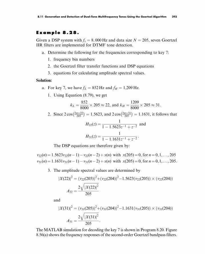
Example 8.28.
Given a DSP system with fs ¼ 8; 000Hz and data size N ¼ 205, seven Goertzel
IIR filters are implemented for DTMF tone detection.
a. Determine the following for the frequencies corresponding to key 7:
1. frequency bin numbers
2. the Goertzel filter transfer functions and DSP equations
3. equations for calculating amplitude spectral values.
Solution:
a. For key 7, we have fL ¼ 852Hz and fH ¼ 1,209Hz.
1. Using Equation (8.79), we get
kL ¼852
8000 205 22, and kH ¼
1209
8000 205 31:
2. Since 2 cos 2p22205
¼ 1:5623, and 2 cos 2p31
205
¼ 1:1631, it follows that
H22(z) ¼1
1 1:5623z1 þ z2and
H31(z) ¼1
1 1:1631z1 þ z2:
The DSP equations are therefore given by:
v22(n)¼ 1:5623v22(n1) v22(n2)þx(n) with x(205)¼ 0, for n¼ 0,1, . . . , 205
v31(n)¼ 1:1631v31(n1) v31(n2)þx(n) with x(205)¼ 0, for n¼ 0,1, . . . , 205:
3. The amplitude spectral values are determined by
X (22)j j2 ¼ v22(205)ð Þ2þ v22(204)ð Þ21:5623 v22(205)ð Þ v22(204)ð Þ
A22 ¼2
ffiffiffiffiffiffiffiffiffiffiffiffiffiffiffiffiffiX(22)j j2
q205
and
X (31)j j2 ¼ v31(205)ð Þ2þ v31(204)ð Þ21:1631 v31(205)ð Þ v31(204)ð Þ
A31 ¼2
ffiffiffiffiffiffiffiffiffiffiffiffiffiffiffiffiffiX(31)j j2
q205
:
The MATLAB simulation for decoding the key 7 is shown in Program 8.20. Figure
8.56(a) shows the frequency responses of the second-order Goertzel bandpass filters.
Tan: Digital Signaling Processing 0123740908_chap08 Final Proof page 393 22.6.2007 6:21pm Compositor Name: MRaja
8.11 Generation and Detection of Dual-Tone Multifrequency Tones Using the Goertzel Algorithm 393

The input is generated as shown in Figure 8.52. After filtering, the calculated spectral
values and threshold value for decoding key 7 are displayed in Figure 8.56(b), where
only two spectral values corresponding to the frequencies of 770 Hz and 1,209 Hz
are above the threshold, andare encodedas logic 1.According to thekey information
in Figure 8.55, the final logic operation decodes the key as 7.
Program 8.20. DTMF detection using the Goertzel algoritm.
close all;clear all;
% DTMF tone generator
N¼205;fs¼8000;t¼[0:1:N-1]/fs; % Sampling rate and time vector
x¼zeros(1,length(t));x(1)¼1; % Generate the imupse function
%generation of tones
y697¼filter([0 sin(2*pi*697/fs)],[1 2*cos(2*pi*697/fs) 1],x);
y770¼filter([0 sin(2*pi*770/fs)],[1 2*cos(2*pi*770/fs) 1],x);
y852¼filter([0 sin(2*pi*852/fs)],[1 2*cos(2*pi*852/fs) 1],x);
y941¼filter([0 sin(2*pi*941/fs)],[1 2*cos(2*pi*941/fs) 1],x);
y1209¼filter([0 sin(2*pi*1209/fs)],[1 2*cos(2*pi*1209/fs) 1],x);y1336¼filter([0 sin(2*pi*1336/fs)],[1 2*cos(2*pi*1336/fs) 1],x);y1477¼filter([0 sin(2*pi*1477/fs)],[1 2*cos(2*pi*1477/fs) 1],x);key¼input(‘input of the following keys: 1,2,3,4,5,6,7,8,9,*,0,#¼>’,‘s’);yDTMF¼[];
0 500 1000 1500 2000 2500 3000 3500 40000
500
1000
1500
2000
Frequency (Hz)
Filt
er b
ank
freq
. res
pons
es
0 500 1000 1500 2000 2500 3000 3500 40000
0.5
1
1.5
Frequency (Hz)
Spe
ctra
l val
ues
A
B
F IGURE 8.56 (a) Goertzel filter bank frequency responses; (b) display of spectralvalues and threshold for key 7.
Tan: Digital Signaling Processing 0123740908_chap08 Final Proof page 394 22.6.2007 6:21pm Compositor Name: MRaja
394 8 I N F I N I T E I M P U L S E R E S P O N S E F I L T E R D E S I G N

if key¼¼‘1’yDTMF¼y697þy1209;endif key¼¼‘2’yDTMF¼y697þy1336;endif key¼¼‘3’yDTMF¼y697þy1477;endif key¼¼‘4’yDTMF¼y770þy1209;endif key¼¼‘5’yDTMF¼y770þy1336;endif key¼¼‘6’yDTMF¼y770þy1477;endif key¼¼‘7’yDTMF¼y852þy1209;endif key¼¼‘8’yDTMF¼y852þy1336;endif key¼¼‘9’yDTMF¼y852þy1477;endif key¼¼‘*’yDTMF¼y941þy1209;endif key¼¼‘0’yDTMF¼y941þy1336;endif key¼¼‘#’yDTMF¼y941þy1477;endif size(yDTMF)¼¼0 disp(‘Invalid input key’);return;endyDTMF¼[yDTMF 0]; % DTMF signal appended with a zero
% DTMF detector (use Goertzel algorithm)
a697¼[1 2*cos(2*pi*18/N) 1];a770¼[1 2*cos(2*pi*20/N) 1];a852¼[1 2*cos(2*pi*22/N) 1];a941¼[1 2*cos(2*pi*24/N) 1];a1209¼[1 2*cos(2*pi*31/N) 1];a1336¼[1 2*cos(2*pi*34/N) 1];a1477¼[1 2*cos(2*pi*38/N) 1];% Filter bank frequency responses
[w1, f]¼freqz(1,a697,512,fs);[w2, f]¼freqz(1,a770,512,fs);[w3, f]¼freqz(1,a852,512,fs);[w4, f]¼freqz(1,a941,512,fs);[w5, f]¼freqz(1,a1209,512,fs);[w6, f]¼freqz(1,a1336,512,fs);[w7, f]¼freqz(1,a1477,512,fs);subplot(2,1,1);plot(f,abs(w1),f,abs(w2),f,abs(w3), ...
f,abs(w4),f,abs(w5),f,abs(w6),f,abs(w7));grid
xlabel(‘Frequency (Hz)’);ylabel(‘(a) Filter bank freq. responses’);
% filter bank bandpass filtering
y697¼filter(1,a697,yDTMF);y770¼filter(1,a770,yDTMF);y852¼filter(1,a852,yDTMF);y941¼filter(1,a941,yDTMF);y1209¼filter(1,a1209,yDTMF);y1336¼filter(1,a1336,yDTMF);y1477¼filter(1,a1477,yDTMF);% Determine the absolute magnitudes of DFT coefficents
m(1)¼sqrt(y697(206)^2þy697(205)^2- ...
2*cos(2*pi*18/205)*y697(206)*y697(205));
m(2)¼sqrt(y770(206)^2þy770(205)^2- ...
2*cos(2*pi*20/205)*y770(206)*y770(205));
m(3)¼sqrt(y852(206)^2þy852(205)^2- ...
2*cos(2*pi*22/205)*y852(206)*y852(205));
m(4)¼sqrt(y941(206)^2þy941(205)^2- ...
2*cos(2*pi*24/205)*y941(206)*y941(205));
Tan: Digital Signaling Processing 0123740908_chap08 Final Proof page 395 22.6.2007 6:21pm Compositor Name: MRaja
8.11 Generation and Detection of Dual-Tone Multifrequency Tones Using the Goertzel Algorithm 395

m(5)¼sqrt(y1209(206)^2þy1209(205)^2- ...
2*cos(2*pi*31/205)*y1209(206)*y1209(205));
m(6)¼sqrt(y1336(206)^2þy1336(205)^2- ...
2*cos(2*pi*34/205)*y1336(206)*y1336(205));
m(7)¼sqrt(y1477(206)^2þy1477(205)^2- ...
2*cos(2*pi*38/205)*y1477(206)*y1477(205));
% Convert the magnitudes of DFT coefficients to the single-side spectrum
m¼2*m/205;% Determine the threshold
th¼sum(m)/4;% Plot the DTMF spectrum with the threshold
f¼[697 770 852 941 1209 1336 1477];
f1¼[0 fs/2];th¼[ th th];subplot(2,1,2);stem(f,m);grid;hold;plot(f1,th);
xlabel(‘Frequency (Hz)’);ylabel(‘ (b) Spectral values’);
m¼round(m); % Round to the binary pattern
if m¼¼ [1 0 0 0 1 0 0] disp(‘Detected Key 1’);end
if m¼¼ [1 0 0 0 0 1 0] disp(‘Detected Key 2’);end
if m¼¼ [1 0 0 0 0 0 1] disp(‘Detected Key 3’);end
if m¼¼ [0 1 0 0 1 0 0] disp(‘Detected Key 4’);end
if m¼¼ [0 1 0 0 0 1 0] disp(‘Detected Key 5’);end
if m¼¼ [0 1 0 0 0 0 1] disp(‘Detected Key 6’);end
if m¼¼ [0 0 1 0 1 0 0] disp(‘Detected Key 7’);end
if m¼¼ [0 0 1 0 0 1 0] disp(‘Detected Key 8’);end
if m¼¼ [0 0 1 0 0 0 1] disp(‘Detected Key 9’);end
if m¼¼ [0 0 0 1 1 0 0] disp(‘Detected Key *’);end
if m¼¼ [0 0 0 1 0 1 0] disp(‘Detected Key 0’);end
if m¼¼ [0 0 0 1 0 0 1] disp(‘Detected Key #’);end
The principle can easily be extended to transmit the ASCII (American
Standard Code for Information Interchange) code or other types of code
using the parallel Goertzel filter bank. If the calculated spectral value is larger
than the threshold value, then the logic operation outputs logic 1; otherwise, it
outputs logic 0. Finally, the logic operation at the last stage decodes the key
information based on the 7-bit binary pattern.
8.12 Summar y of Inf in i te ImpulseResponse ( I IR) Des ign Proceduresand Selec t ion of the I IR F i l terDesign Methods in Pract i ce
In this section, we first summarize the design procedures of the BLT design,
impulse invariant design, and pole-zero placement design methods, and then
discuss the selection of the particular filter for typical applications.
Tan: Digital Signaling Processing 0123740908_chap08 Final Proof page 396 22.6.2007 6:21pm Compositor Name: MRaja
396 8 I N F I N I T E I M P U L S E R E S P O N S E F I L T E R D E S I G N

The BLT design method:
1. Given the digital filter frequency specifications, prewarp each digital fre-
quency edge to the analog frequency edge using Equations (8.18) and (8.19).
2. Determine the prototype filter order using Equation (8.29) for the Butter-
worth filter or Equation (8.35b) for the Chebyshev filter, and perform
lowpass prototype transformation using the lowpass prototype in Table
8.3 (Butterworth function) or Tables 8.4 and 8.5 (Chebyshev functions)
using Equations (8.20) to (8.23).
3. Apply the BLT to the analog filter using Equation (8.24) and output the
transfer function.
4. Verify the frequency responses, and output the difference equation.
The impulse invariant design method:
1. Given the lowpass or bandpass filter frequency specifications, perform
analog filter design. For the highpass or bandstop filter design, quit this
method and use the BLT.
a. Determine the prototype filter order using Equation (8.29) for the
Butterworth filter or Equation (8.35b) for the Chebyshev filter.
b. Perform lowpass prototype transformation using the lowpass proto-
type in Table 8.3 (Butterworth function) or Tables 8.4 and 8.5 (Cheby-
shev functions) using Equations (8.20) to (8.23).
c. Skip step 1 if the analog filter transfer function is given to begin with.
2. Determine the impulse response by applying the partial fraction expan-
sion technique to the analog transfer function and inverse Laplace trans-
form using Equation (8.37).
3. Sample the analog impulse response using Equation (8.38) and apply the
z-transform to the digital impulse function to obtain the digital filter
transfer function.
4. Verify the frequency responses, and output the difference equation. If the
frequency specifications are not met, quit the design method and use the
BLT.
The pole-zero placement design method:
1. Given the filter cutoff frequency specifications, determine the pole-zero
locations using the corresponding equations:
a. Second-order bandpass filter: Equations (8.41) and (8.42)
Tan: Digital Signaling Processing 0123740908_chap08 Final Proof page 397 22.6.2007 6:21pm Compositor Name: MRaja
8.12 Summary of IIR Design Procedures and Selection of the IIR Filter Design Methods in Practice 397

b. Second-order notch filter: Equations (8.45) and (8.46)
c. First-order lowpass filter: Equation (8.49) or (8.50)
d. First-order highpass filter: Equation (8.53) or (8.54).
2. Apply the corresponding equation and scale factor to obtain the digital
filter transfer function:
a. Second-order bandpass filter: Equations (8.43) and (8.44)
b. Second-order notch filter: Equations (8.47) and (8.48)
c. First-order lowpass filter: Equations (8.51) and (8.52)
d. First-order highpass filter: Equations (8.55) and (8.56).
3. Verify the frequency responses, and output the difference equation. If the
frequency specifications are not met, quit the design method and use
the BLT.
Table 8.13 compares the design parameters of the three design methods.
Performance comparisons using the three methods are given in Figure 8.57,
where the bandpass filter is designed using the following specifications:
Passband ripple ¼ 3 dB
Center frequency ¼ 400 Hz
Bandwidth ¼ 200 Hz
Sampling rate ¼ 2,000 Hz
Butterworth IIR filter ¼ second-order
As we expected, the BLT method satisfies the design requirement, and the
pole-zero placement method has little performance degradation because
r ¼ 1 (f0=fs)p ¼ 0:6858 < 0:9, and this effect will also cause the center fre-
quency to be shifted. For the bandpass filter designed using the impulse invari-
ant method, the gain at the center frequency is scaled to 1 for a frequency
response shape comparison. The performance of the impulse invariant method
is satisfied in passband. However, it has significant performance degradation in
stopband when compared with the other two methods. This is due to aliasing
when sampling the analog impulse response in time domain.
Improvement in using the pole-zero placement and impulse invariant
methods can be achieved by using a very high sampling rate. Example 8.29
describes the possible selection of the design method by a DSP engineer to solve
a real-world problem.
Tan: Digital Signaling Processing 0123740908_chap08 Final Proof page 398 22.6.2007 6:21pm Compositor Name: MRaja
398 8 I N F I N I T E I M P U L S E R E S P O N S E F I L T E R D E S I G N

TABLE 8 .13 Comparisons of three IIR design methods.
Design Method
BLT Impulse Invariant Pole-Zero Placement
Filter type Lowpass, highpass, bandpass,
bandstop
Appropriate for lowpass and
bandpass
2nd-order for bandpass and
bandstop; 1st-order for
lowpass and highpass
Linear phase No No No
Ripple and stopband
specifications
Used for determining the filter
order
Used for determining the filter
order
Not required; 3 dB on
passband offered.
Special requirement None Very high sampling relative to the
cutoff frequency (LPF) or to
upper cutoff frequency for (BPF)
Narrow band for BPF or
notch filter; lower cutoff
frequency or higher cutoff
frequency for LPF or HPF.
Algorithm complexity High: Frequency prewarping,
analog filter design, BLT
Moderate: Analog filter design
determining digital impulse re-
sponse. Apply z-transform
Simple design equations
Minimum design tool Calculator, algebra Calculator, algebra Calculator
BLT ¼ bilinear transformation; LPF ¼ lowpass filter; BPF ¼ bandpass filter; HPF ¼ highpass filter.
Tan:D
igita
lSig
nalin
gPro
cessing
0123740908_ch
ap08
Fin
alPro
of
page
399
22.6
.2007
6:2
1pm
Com
posito
rN
am
e:M
Raja
8.1
2Su
mm
ary
of
IIRD
esig
nP
roce
du
res
an
dSele
ction
of
the
IIRFilte
rD
esig
nM
eth
od
sin
Pra
ctice3
99

Example 8.29.
1. Determine an appropriate IIR filter design method for each of the fol-
lowing DSP applications. As described in a previous section, we apply a
notch filter to remove 60 Hz interference and cascade a bandpass filter to
remove noise in an ECG signal for heart rate detection. The following
specifications are required:
Notch filter:
Harmonic to be removed ¼ 60Hz
3 dB bandwidth for the notch filter ¼ 4 Hz
Bandpass filter:
Passband frequency range ¼ 0.25 to 40 Hz
Passband ripple ¼ 0.5 dB
Sampling rate ¼ 600 Hz.
The pole-zero placement method is the best choice, since the notch filter to be
designed has a very narrow 3 dB bandwidth of 4 Hz. This simple design gives a
quick solution. Since the bandpass filter requires a passband ripple of 0.5 dB
from 0.25 to 40 Hz, the BLT can also be an appropriate choice. Even though the
0 100 200 300 400 500 600 700 800 900 1000−20
−18
−16
−14
−12
−10
−8
−6
−4
−2
0
2
Frequency (Hz)
Mag
nitu
de r
espo
nses
(dB
)
Bilineartransformationmethod
Pole-zeroplacementmethod
Impulse invariantmethod
F IGURE 8.57 Performance comparisons for the BLT, pole-zero placement, andimpulse invariant methods.
Tan: Digital Signaling Processing 0123740908_chap08 Final Proof page 400 22.6.2007 6:21pm Compositor Name: MRaja
400 8 I N F I N I T E I M P U L S E R E S P O N S E F I L T E R D E S I G N

impulse invariant method could work for this case, since the sampling rate of
600 Hz is much larger than 40 Hz, aliasing cannot be prevented completely.
Hence, the BLT is a preferred design method for the bandpass filter.
8.13 Summar y
1. The BLT method is able to transform the transfer function of an analog
filter to the transfer function of the corresponding digital filter in general.
2. The BLT maps the left half of an s-plane to the inside unit circle of the
z-plane. Stability of mapping is guaranteed.
3. The BLT causes analog frequency warping. The analog frequency range
from 0 Hz to infinity is warped to a digital frequency range from 0 Hz to
the folding frequency.
4. Given the digital frequency specifications, analog filter frequency speci-
fications must be developed using the frequency warping equation before
designing the corresponding analog filter and applying the BLT.
5. An analog filter transfer function can be obtained by lowpass prototype,
which can be selected from the Butterworth and Chebyshev functions.
6. The higher-order IIR filter can be designed using a cascade form.
7. The impulse invariant design method maps the analog impulse response
to the digital equivalent impulse response. The method works for the
lowpass and bandpass filter design with a very high sampling rate. It is
not appropriate for the highpass and bandstop filter design.
8. The pole-zero placement method can be applied for a simple IIR filter
design such as the second-order bandpass and bandstop filters with
narrow band specifications, first-order lowpass and highpass filters with
cutoff frequencies close to either DC or the folding frequency.
9. Quantizing IIR filter coefficients explores the fact that the quantization
of the filter coefficients has more effect on the magnitude frequency
response than on the phase frequency response. It may cause the quant-
ized IIR filter to be unstable.
10. A simple audio equalizer uses bandpass IIR filter banks to create sound
effects.
11. The 60-Hz interference eliminator is designed to enhance biomedical
ECG signals for heart rate detection. It can also be adapted for audio
humming noise elimination.
Tan: Digital Signaling Processing 0123740908_chap08 Final Proof page 401 22.6.2007 6:21pm Compositor Name: MRaja
8.13 Summary 401

12. A single tone or a DTMF tone can be generated using the IIR filter with
the impulse sequence as the filter input.
13. The Goertzel algorithm is applied for DTMF tone detection. This is an
important application in the telecommunications industry.
14. The procedures for the BLT, impulse invariant, and pole-zero placement
design methods were summarized, and their design feasibilities were
compared, including the filter type, linear phase, ripple and stopband
specifications, special requirements, algorithm complexity, design tool(s).
8.14 Problems
8.1. Given an analog filter with the transfer function
H(s) ¼ 1000
sþ 1000,
convert it to the digital filter transfer function and difference equation
using the BLT if the DSP system has a sampling period of T ¼ 0:001
second.
8.2. The lowpass filter with a cutoff frequency of 1 rad/sec is given as
HP(s) ¼ 1
sþ 1:
a. Use Hp(s) and the BLT to obtain a corresponding IIR digital low-
pass filter with a cutoff frequency of 30 Hz, assuming a sampling
rate of 200 Hz.
b. Use MATLAB to plot the magnitude and phase frequency re-
sponses of H(z).
8.3. The normalized lowpass filter with a cutoff frequency of 1 rad/sec is
given as
HP(s) ¼ 1
sþ 1:
a. Use Hp(s) and the BLT to obtain a corresponding IIR digital high-
pass filter with a cutoff frequency of 30 Hz, assuming a sampling
rate of 200 Hz.
b. Use MATLAB to plot the magnitude and phase frequency
responses of H(z).
Tan: Digital Signaling Processing 0123740908_chap08 Final Proof page 402 22.6.2007 6:21pm Compositor Name: MRaja
402 8 I N F I N I T E I M P U L S E R E S P O N S E F I L T E R D E S I G N

8.4. Consider the normalized lowpass filter with a cutoff frequency of 1 rad/
sec:
HP(s) ¼ 1
sþ 1:
a. Use Hp(s) and the BLT to design a corresponding IIR digital notch
(bandstop) filter with a lower cutoff frequency of 20 Hz, an upper
cutoff frequency of 40 Hz, and a sampling rate of 120 Hz.
b. Use MATLAB to plot the magnitude and phase frequency
responses of H(z).
8.5. Consider the following normalized lowpass filter with a cutoff fre-
quency of 1 rad/sec:
HP(s) ¼ 1
sþ 1:
a. Use Hp(s) and the BLT to design a corresponding IIR digital band-
pass filter with a lower cutoff frequency of 15 Hz, an upper cutoff
frequency of 25 Hz, and a sampling rate of 120 Hz.
b. Use MATLAB to plot the magnitude and phase frequency
responses of H(z).
8.6. Design a first-order digital lowpass Butterworth filter with a cutoff
frequency of 1.5 kHz and a passband ripple of 3 dB at a sampling
frequency of 8,000 Hz.
a. Determine the transfer function and difference equation.
b. Use MATLAB to plot the magnitude and phase frequency
responses.
8.7. Design a second-order digital lowpass Butterworth filter with a cutoff
frequency of 1.5 kHz and a passband ripple of 3 dB at a sampling
frequency of 8,000 Hz.
a. Determine the transfer function and difference equation.
b. Use MATLAB to plot the magnitude and phase frequency
responses.
8.8. Design a third-order digital highpass Butterworth filter with a cutoff
frequency of 2 kHz and a passband ripple of 3 dB at a sampling
frequency of 8,000 Hz.
a. Determine the transfer function and difference equation.
Tan: Digital Signaling Processing 0123740908_chap08 Final Proof page 403 22.6.2007 6:21pm Compositor Name: MRaja
8.14 Problems 403

b. Use MATLAB to plot the magnitude and phase frequency
responses.
8.9. Design a second-order digital bandpass Butterworth filter with a lower
cutoff frequency of 1.9 kHz, an upper cutoff frequency of 2.1 kHz, and
a passband ripple of 3 dB at a sampling frequency of 8,000 Hz.
a. Determine the transfer function and difference equation.
b. Use MATLAB to plot the magnitude and phase frequency
responses.
8.10. Design a second-order digital bandstop Butterworth filter with a center
frequency of 1.8 kHz, a bandwidth of 200 Hz, and a passband ripple of
3 dB at a sampling frequency of 8,000 Hz.
a. Determine the transfer function and difference equation.
b. Use MATLAB to plot the magnitude and phase frequency
responses.
8.11. Design a first-order digital lowpass Chebyshev filter with a cutoff
frequency of 1.5 kHz and 1 dB ripple on passband at a sampling
frequency of 8,000 Hz.
a. Determine the transfer function and difference equation.
b. Use MATLAB to plot the magnitude and phase frequency
responses.
8.12. Design a second-order digital lowpass Chebyshev filter with a cutoff
frequency of 1.5 kHz and 0.5 dB ripple on passband at a sampling
frequency of 8,000 Hz. Use MATLAB to plot the magnitude and
phase frequency responses.
8.13. Design a third-order digital highpass Chebyshev filter with a cutoff
frequency of 2 kHz and 1 dB ripple on the passband at a sampling
frequency of 8,000 Hz.
a. Determine the transfer function and difference equation.
b. Use MATLAB to plot the magnitude and phase frequency
responses.
8.14. Design a second-order digital bandpass Chebyshev filter with the fol-
lowing specifications:
Tan: Digital Signaling Processing 0123740908_chap08 Final Proof page 404 22.6.2007 6:21pm Compositor Name: MRaja
404 8 I N F I N I T E I M P U L S E R E S P O N S E F I L T E R D E S I G N

Center frequency of 1.5 kHz
Bandwidth of 200 Hz
0.5 dB ripple on passband
Sampling frequency of 8,000 Hz.
a. Determine the transfer function and difference equation.
b. Use MATLAB to plot the magnitude and phase frequency
responses.
8.15. Design a second-order bandstop digital Chebyshev filter with the
following specifications:
Center frequency of 2.5 kHz
Bandwidth of 200 Hz
1 dB ripple on stopband
Sampling frequency of 8,000 Hz.
a. Determine the transfer function and difference equation.
b. Use MATLAB to plot the magnitude and phase frequency
responses.
8.16. Design a fourth-order digital lowpass Butterworth filter with a cutoff
frequency of 2 kHz and a passband ripple of 3 dB at a sampling
frequency of 8,000 Hz.
a. Determine the transfer function and difference equation.
b. Use MATLAB to plot the magnitude and phase frequency
responses.
8.17. Design a fourth-order digital lowpass Chebyshev filter with a cutoff
frequency of 1.5 kHz and a 0.5 dB ripple at a sampling frequency of
8,000 Hz.
a. Determine the transfer function and difference equation.
b. Use MATLAB to plot the magnitude and phase frequency
responses.
8.18. Design a fourth-order digital bandpass Chebyshev filter with a center
frequency of 1.5 kHz, a bandwidth of 200 Hz, and a 0.5 dB ripple at a
sampling frequency of 8,000 Hz.
a. Determine the transfer function and difference equation.
b. Use MATLAB to plot the magnitude and phase frequency
responses.
Tan: Digital Signaling Processing 0123740908_chap08 Final Proof page 405 22.6.2007 6:21pm Compositor Name: MRaja
8.14 Problems 405

8.19. Consider the following Laplace transfer function:
H(s) ¼ 10
sþ 10:
a. Determine H(z) and the difference equation using the impulse in-
variant method if the sampling rate fs ¼ 10 Hz.
b. Use MATLAB to plot the magnitude frequency response jH( f )jand the phase frequency response w( f ) with respect to H(s) for the
frequency range from 0 to fs=2 Hz.
c. Use MATLAB to plot the magnitude frequency response
jH(e jV)j ¼ jH(e j2pfT )j and the phase frequency response w( f ) with
respect to H(z) for the frequency range from 0 to fs=2 Hz.
8.20. Consider the following Laplace transfer function:
H(s) ¼ 1
s2 þ 3sþ 2:
a. Determine H(z) and the difference equation using the impulse in-
variant method if the sampling rate fs ¼ 10 Hz.
b. Use MATLAB to plot the magnitude frequency response jH( f )j and
the phase frequency response w( f ) with respect to H(s) for the
frequency range from 0 to fs=2 Hz.
c. Use MATLAB to plot the magnitude frequency response
jH(e jV)j ¼ jH(e j2pfT )j and the phase frequency response w( f ) with
respect to H(z) for the frequency range from 0 to fs=2 Hz.
8.21. Consider the following Laplace transfer function:
H(s) ¼ s
s2 þ 4sþ 5:
a. Determine H(z) and the difference equation using the impulse
invariant method if the sampling rate fs ¼ 10 Hz.
b. Use MATLAB to plot the magnitude frequency response jH( f )j and
the phase frequency response w( f ) with respect to H(s) for the
frequency range from 0 to fs=2 Hz.
c. Use MATLAB to plot the magnitude frequency response
jH(e jV)j ¼ jH(e j2pfT )j and the phase frequency response w( f ) with
respect to H(z) for the frequency range from 0 to fs=2 Hz.
Tan: Digital Signaling Processing 0123740908_chap08 Final Proof page 406 22.6.2007 6:21pm Compositor Name: MRaja
406 8 I N F I N I T E I M P U L S E R E S P O N S E F I L T E R D E S I G N

8.22. A second-order bandpass filter is required to satisfy the following
specifications:
Sampling rate ¼ 8,000Hz
3 dB bandwidth: BW ¼ 100Hz
Narrow passband centered at f0 ¼ 2,000Hz
Zero gain at 0 Hz and 4,000 Hz.
Find the transfer function and difference equation by the pole-zero
placement method.
8.23. A second-order notch filter is required to satisfy the following specifi-
cations:
Sampling rate ¼ 8,000Hz
3 dB bandwidth: BW ¼ 200Hz
Narrow passband centered at f0 ¼ 1,000Hz.
Find the transfer function and difference equation by the pole-zero
placement method.
8.24. A first-order lowpass filter is required to satisfy the following specifi-
cations:
Sampling rate ¼ 8,000Hz
3 dB cutoff frequency: fc ¼ 200Hz
Zero gain at 4,000 Hz.
Find the transfer function and difference equation using the pole-zero
placement method.
8.25. A first-order lowpass filter is required to satisfy the following specifi-
cations:
Sampling rate ¼ 8,000Hz
3 dB cutoff frequency: fc ¼ 3,800 Hz
Zero gain at 4,000 Hz.
Find the transfer function and difference equation by the pole-zero
placement method.
8.26. A first-order highpass filter is required to satisfy the following specifi-
cations:
Sampling rate ¼ 8,000Hz
3 dB cutoff frequency: fc ¼ 3; 850Hz
Zero gain at 0 Hz.
Find the transfer function and difference equation by the pole-zero
placement method.
Tan: Digital Signaling Processing 0123740908_chap08 Final Proof page 407 22.6.2007 6:21pm Compositor Name: MRaja
8.14 Problems 407

8.27. A first-order highpass filter is required to satisfy the following specifi-
cations:
Sampling rate ¼ 8,000 Hz
3 dB cutoff frequency: fc ¼ 100Hz
Zero gain at 0 Hz.
Find the transfer function and difference equation by the pole-zero
placement method.
8.28. Given a filter transfer function,
H(z) ¼ 0:3430z2 þ 0:6859zþ 0:3430
z2 þ 0:7075zþ 0:7313,
a. realize the digital filter using direct form I and using direct form II;
b. determine the difference equations for each implementation.
8.29. Given a fourth-order filter transfer function,
H(z) ¼ 0:3430z2 þ 0:6859zþ 0:3430
z2 þ 0:7075zþ 0:7313 0:4371z2 þ 0:8742zþ 0:4371
z2 0:1316zþ 0:1733,
a. realize the digital filter using the cascade (series) form via second-
order sections using the direct form II;
b. determine the difference equations for implementation.
Use MATLAB to solve problems 8.30 to 8.36.
8.30. A speech sampled at 8,000 Hz is corrupted by a sine wave of 360 Hz.
Design a notch filter to remove the noise with the following specifica-
tions:
Chebyshev notch filter
Center frequency: 360 Hz
Bandwidth: 60 Hz
Passband and ripple: 0.5 dB
Stopband attenuation: 5 dB at 355 Hz and 365 Hz, respectively.
Determine the transfer function and difference equation.
8.31. In Problem 8.30, if the speech is corrupted by a sine wave of 360 Hz and
its third harmonic, cascading two notch filters can be applied to remove
noise signals. The possible specifications are given as:
Chebyshev notch filter 1
Center frequency: 360 Hz
Tan: Digital Signaling Processing 0123740908_chap08 Final Proof page 408 22.6.2007 6:21pm Compositor Name: MRaja
408 8 I N F I N I T E I M P U L S E R E S P O N S E F I L T E R D E S I G N

Bandwidth: 60 Hz
Passband and ripple: 0.5 dB
Stopband attenuation: 5 dB at 355 Hz and 365 Hz, respectively.
Chebyshev notch filter 2
Center frequency: 1,080 Hz
Bandwidth: 60 Hz
Passband and ripple: 0.5 dB
Stopband attenuation: 5 dB at 1,075 Hz 1,085 Hz, respectively.
Determine the transfer function and difference equation for each filter
(Fig. 8.58).
8.32. In a speech recording system with a sampling frequency of 10,000 Hz,
the speech is corrupted by random noise. To remove the random noise
while preserving speech information, the following specifications are
given:
Speech frequency range: 0–3,000 kHz
Stopband range: 4,000–5,000 Hz
Passband ripple: 3 dB
Stopband attenuation: 25 dB
Butterworth IIR filter.
Determine the filter order and transfer function.
8.33. In Problem 8.32, if we use a Chebyshev IIR filter with the following
specifications:
Speech frequency range: 0–3,000 Hz
Stopband range: 4,000–5,000 Hz
Passband ripple: 1 dB
Stopband attenuation: 35 dB
Chebyshev IIR filter,
determine the filter order and transfer function.
8.34. Given a speech equalizer to compensate midrange frequency loss of
hearing (Fig. 8.59) and the following specifications:
Sampling rate: 8,000 Hz
Second-order bandpass IIR filter
Notch filterat 360 Hz
Notch filterat 1080 Hz
Digitalinput x(n)
Digitaloutput y(n)
F IGURE 8 .58. Cascaded notch filter in Problem 8.31.
Tan: Digital Signaling Processing 0123740908_chap08 Final Proof page 409 22.6.2007 6:21pm Compositor Name: MRaja
8.14 Problems 409

Frequency range to be emphasized: 1,500–2,000 Hz
Passband ripple: 3 dB
Pole-zero placement design method,
determine the transfer function.
8.35. In Problem 8.34, if we use an IIR filter with the following specifications:
Sampling rate: 8,000 Hz
Butterworth IIR filter
Frequency range to be emphasized: 1,500–2,000 Hz
Lower stop band: 0–1,000 Hz
Upper stop band: 2,500–4,000 Hz
Passband ripple: 3 dB
Stopband attenuation: 20 dB,
determine the filter order and filter transfer function.
8.36. A digital crossover can be designed as shown in Figure 8.60. Given
audio specifications as:
Sampling rate: 44,100 Hz
Crossover frequency: 1,000 Hz
Highpass filter: third-order Butterworth type at a cutoff frequency of
1,000 Hz
Lowpass filter: third-order Butterworth type at a cutoff frequency of
1,000 Hz,
use the MATLAB BLT design method to determine:
a. the transfer functions and difference equations for the highpass and
lowpass filters
b. frequency responses for the highpass filter and the lowpass filter
c. combined frequency response for both filters.
Digitalinput x(n)
Digitaloutput y(n)
+Bandpassfilter 5
Gain
F IGURE 8.59 . Speech equalizer in Problem 8.34.
Tan: Digital Signaling Processing 0123740908_chap08 Final Proof page 410 22.6.2007 6:21pm Compositor Name: MRaja
410 8 I N F I N I T E I M P U L S E R E S P O N S E F I L T E R D E S I G N

8.37. Given a DSP system with a sampling rate set up to be 8,000 Hz, develop
an 800 Hz single-tone generator using a digital IIR filter by completing
the following steps:
a. Determine the digital IIR filter transfer function.
b. Determine the DSP equation (difference equation).
c. Write a MATLAB program using the MATLAB function filter() to
generate and plot the 800-Hz tone for a duration of 0.01 sec.
8.38. Given a DSP system with a sampling rate set up to be 8,000 Hz, develop
a DTMF tone generator for key ‘‘5’’ using digital IIR filters by com-
pleting the following steps:
a. Determine the digital IIR filter transfer functions.
b. Determine the DSP equations (difference equation).
c. Write a MATLAB program using the MATLAB function filter() to
generate and plot the DTMF tone for key 5 for 205 samples.
8.39. Given x(0) ¼ 1, x(1) ¼ 1, x(2) ¼ 0, x(3) ¼ 1, use the Goertzel algo-
rithm to compute the following DFT coefficients and their amplitude
spectra:
a. X(0)
b. X (0)j j2
c. A0 (single sided)
d. X(1)
e. X (1)j j2
f. A1 (single sided)
Digitalaudio x(n)
Highpassfilter
Lowpassfilter
Gain_L
Gain_H Tweeter:The crossover passes
high frequencies
Woofer:The crossover passes
low frequencies
yH(n)
yL(n)
F IGURE 8 .60. Two-band digital crossover system in Problem 8.36.
Tan: Digital Signaling Processing 0123740908_chap08 Final Proof page 411 22.6.2007 6:21pm Compositor Name: MRaja
8.14 Problems 411

8.40. Given a DSP system with a sampling rate set up to be 8,000 Hz and a
data size of 205 (N ¼ 205), seven Goertzel IIR filters are implemented
for DTMF tone detection. For the frequencies corresponding to key 5,
determine:
a. the modified Goertzel filter transfer functions
b. the filter DSP equations for vk(n)
c. the DSP equations for the squared magnitudes
X (k)j j2¼ yk(205)j j2
d. Using the data generated in Problem 8.38 (c), write a program using
the MATLAB function filter() and Goertzel algorithm to detect the
spectral values of the DTMF tone for key 5.
8.41. Given an input data sequence:
x(n) ¼ 1:2 sin (2p(1000)n=10000) ) 1:5 cos (2p(4000)n=10000)
assuming a sampling frequency of 10 kHz, implement the designed IIR
filter in Problem 8.33 to filter 500 data points of x(n) with the following
specified method, and plot the 500 samples of the input and output
data.
a. Direct-form I implementation
b. Direct-form II implementation
References
Carr, J. J., and Brown, J. M. (2001). Introduction to Biomedical Equipment Technology, 4th
ed. Upper Saddle River, NJ: Prentice Hall.
Ifeachor, E. C., and Jervis, B. W. (2002). Digital Signal Processing: A Practical Approach,
2nd ed. Upper Saddle River, NJ: Prentice Hall.
Lynn, P. A., and Fuerst, W. (1999). Introductory Digital Signal Processing with Computer
Applications, 2nd ed. Chichester and New York: John Wiley & Sons.
Porat, B. (1997). A Course in Digital Signal Processing. New York: John Wiley & Sons.
Proakis, J. G., and Manolakis, D. G. (1996). Digital Signal Processing: Principles, Algo-
rithms, and Applications, 3rd ed. Upper Saddle River, NJ: Prentice Hall.
Webster, J. G. (1998). Medical Instrumentation: Application and Design, 3rd ed. New York:
John Wiley & Sons, Inc.
Tan: Digital Signaling Processing 0123740908_chap08 Final Proof page 412 22.6.2007 6:21pm Compositor Name: MRaja
412 8 I N F I N I T E I M P U L S E R E S P O N S E F I L T E R D E S I G N

9Hardware and Software for
Digital Signal Processors
Object ives :
This chapter introduces basics of digital signal processors such as processor
architectures and hardware units, investigates fixed-point and floating-point
formats, and illustrates the implementation of digital filters in real time.
9.1 Digi ta l S ignal Processor Archi tec ture
Unlike microprocessors and microcontrollers, digital signal (DS) processors
have special features that require operations such as fast Fourier transform
(FFT), filtering, convolution and correlation, and real-time sample-based and
block-based processing. Therefore, DS processors use a different dedicated
hardware architecture.
We first compare the architecture of the general microprocessor with that of
the DS processor. The design of general microprocessors and microcontrollers is
based on the Von Neumann architecture, which was developed from a research
paper written by John von Neumann and others in 1946. Von Neumann
suggested that computer instructions, as we shall discuss, be numerical codes
instead of special wiring. Figure 9.1 shows the Von Neumann architecture.
As shown in Figure 9.1, a Von Neumann processor contains a single, shared
memory for programs and data, a single bus for memory access, an arithmetic
unit, and a program control unit. The processor proceeds in a serial fashion in
terms of fetching and execution cycles. This means that the central processing
unit (CPU) fetches an instruction from memory and decodes it to figure out
Tan: Digital Signaling Processing 0123740908_chap09 Final Proof page 413 21.6.2007 11:11pm Compositor Name: MRaja

what operation to do, then executes the instruction. The instruction (in machine
code) has two parts: the opcode and the operand. The opcode specifies what the
operation is, that is, tells the CPU what to do. The operand informs the CPU
what data to operate on. These instructions will modify memory, or input and
output (I/O). After an instruction is completed, the cycles will resume for the
next instruction. One an instruction or piece of data can be retrieved at a time.
Since the processor proceeds in a serial fashion, it causes most units to stay in a
wait state.
As noted, the Von Neumann architecture operates the cycles of fetching and
execution by fetching an instruction from memory, decoding it via the program
control unit, and finally executing the instruction. When execution requires data
movement—that is, data to be read from or written to memory—the next
instruction will be fetched after the current instruction is completed. The Von
Neumann–based processor has this bottleneck mainly due to the use of a single,
shared memory for both program instructions and data. Increasing the speed
of the bus, memory, and computational units can improve speed, but not
significantly.
To accelerate the execution speed of digital signal processing, DS processors
are designed based on the Harvard architecture, which originated from the
Mark 1 relay-based computers built by IBM in 1944 at Harvard University.
This computer stored its instructions on punched tape and data using relay
latches. Figure 9.2 shows today’s Harvard architecture. As depicted, the DS
processor has two separate memory spaces. One is dedicated to the program
code, while the other is employed for data. Hence, to accommodate two
memory spaces, two corresponding address buses and two data buses are
used. In this way, the program memory and data memory have their own
Program anddata memory
Address bus
Data bus
Input/outputdevices
Addressgenerator
Programcontrol unit
Arithmeticunit
F IGURE 9.1 General microprocessor based on Von Neumann architecture.
Tan: Digital Signaling Processing 0123740908_chap09 Final Proof page 414 21.6.2007 11:11pm Compositor Name: MRaja
414 9 D I G I T A L S I G N A L P R O C E S S O R S

connections to the program memory bus and data memory bus, respectively.
This means that the Harvard processor can fetch the program instruction and
data in parallel at the same time, the former via the program memory bus and
the latter via the data memory bus. There is an additional unit called a multiplier
and accumulator (MAC), which is the dedicated hardware used for the digital
filtering operation. The last additional unit, the shift unit, is used for the scaling
operation for fixed-point implementation when the processor performs digital
filtering.
Let us compare the executions of the two architectures. The Von Neumann
architecture generally has the execution cycles described in Figure 9.3. The
fetch cycle obtains the opcode from the memory, and the control unit will
decode the instruction to determine the operation. Next is the execute cycle.
Based on the decoded information, execution will modify the content of
the register or the memory. Once this is completed, the process will fetch
the next instruction and continue. The processor operates one instruction at a
time in a serial fashion.
To improve the speed of the processor operation, the Harvard architecture
takes advantage of a common DS processor, in which one register holds the
filter coefficient while the other register holds the data to be processed, as
depicted in Figure 9.4.
Programmemory
Program memory data bus
Input/outputdevices
Addressgenerator
Programcontrol unit
Arithmeticlogic unit
Program memory address bus
Data memory address bus
Data memory data bus
Datamemory
Multiplier/accumulator
Shift unit
F IGURE 9 .2 Digital signal processors based on the Harvard architecture.
Tan: Digital Signaling Processing 0123740908_chap09 Final Proof page 415 21.6.2007 11:11pm Compositor Name: MRaja
9.1 Digital Signal Processor Architecture 415

As shown in Figure 9.4, the execute and fetch cycles are overlapped. We call
this the pipelining operation. The DS processor performs one execution cycle
while also fetching the next instruction to be executed. Hence, the processing
speed is dramatically increased.
The Harvard architecture is preferred for all DS processors due to the
requirements of most DSP algorithms, such as filtering, convolution, and
FFT, which need repetitive arithmetic operations, including multiplications,
additions, memory access, and heavy data flow through the CPU.
For other applications, such as those dependent on simple microcontrollers
with less of a timing requirement, the Von Neumann architecture may be a
better choice, since it offers much less silica area and is thus less expansive.
9.2 Digi ta l S ignal Processor HardwareUni ts
In this section, we will briefly discuss special DS processor hardware units.
9.2.1 Mult ip l ier and Accumulator
As compared with the general microprocessors based on the Von Neumann
architecture, the DS processor uses the MAC, a special hardware unit for
Fetch Execute
Fetch
Fetch
Execute
Execute
F IGURE 9.3 Execution cycle based on the Von Neumann architecture.
Execute
Execute
Execute
Fetch
Fetch
Fetch
F IGURE 9.4 Execution cycle based on the Harvard architecture.
Tan: Digital Signaling Processing 0123740908_chap09 Final Proof page 416 21.6.2007 11:11pm Compositor Name: MRaja
416 9 D I G I T A L S I G N A L P R O C E S S O R S

enhancing the speed of digital filtering. This is dedicated hardware, and the
corresponding instruction is generally referred to as MAC operation. The basic
structure of the MAC is shown in Figure 9.5.
As shown in Figure 9.5, in a typical hardware MAC, the multiplier has a
pair of input registers, each holding the 16-bit input to the multiplier. The
result of the multiplication is accumulated in a 32-bit accumulator unit.
The result register holds the double precision data from the accumulator.
9.2.2 Shi f ters
In digital filtering, to prevent overflow, a scaling operation is required.
A simple scaling-down operation shifts data to the right, while a scaling-up
operation shifts data to the left. Shifting data to the right is the same as
dividing the data by 2 and truncating the fraction part; shifting data to the
left is equivalent to multiplying the data by 2. As an example, for a 3-bit data
word 0112 ¼ 310, shifting 011 to the right gives 0012 ¼ 1, that is, 3=2 ¼ 1:5, and
truncating 1.5 results in 1. Shifting the same number to the left, we have
1102 ¼ 610, that is, 3 2 ¼ 6. The DS processor often shifts data by several
bits for each data word. To speed up such operation, the special hardware
shift unit is designed to accommodate the scaling operation, as depicted in
Figure 9.2.
X Register Y Register
Multiplier
Accumulator
ResultRegister
Operand Operand
1616
32
32
F IGURE 9 .5 The multiplier and accumulator (MAC) dedicated to DSP.
Tan: Digital Signaling Processing 0123740908_chap09 Final Proof page 417 21.6.2007 11:11pm Compositor Name: MRaja
9.2 Digital Signal Processor Hardware Units 417

9.2.3 Address Generators
The DS processor generates the addresses for each datum on the data buffer to
be processed. A special hardware unit for circular buffering is used (see the
address generator in Figure 9.2). Figure 9.6 describes the basic mechanism of
circular buffering for a buffer having eight data samples.
In circular buffering, a pointer is used and always points to the newest data
sample, as shown in the figure. After the next sample is obtained from analog-
to-digital conversion (ADC), the data will be placed at the location of x(n 7),
and the oldest sample is pushed out. Thus, the location for x(n 7) becomes the
location for the current sample. The original location for x(n) becomes a
location for the past sample of x(n 1). The process continues according to
the mechanism just described. For each new data sample, only one location on
the circular buffer needs to be updated.
The circular buffer acts like a first-in/first-out (FIFO) buffer, but each datum
on the buffer does not have to be moved. Figure 9.7 gives a simple illustration of
the 2-bit circular buffer. In the figure, there is data flow to the ADC (a, b, c, d, e,
f, g, . . . ) and a circular buffer initially containing a, b, c, and d. The pointer
specifies the current data of d, and the equivalent FIFO buffer is shown on the
right side with a current data of d at the top of the memory. When e comes in, as
shown in the middle drawing in Figure 9.7, the circular buffer will change the
pointer to the next position and update old a with a new datum e. It costs the
pointer only one movement to update one datum in one step. However, on the
right side, the FIFO has to move each of the other data down to let in the new
x(n )
x(n − 1)
x(n − 2)
x(n − 3)x(n − 4)
x(n − 5)
x(n − 6)
x(n − 7)
Data point
F IGURE 9.6 Illustration of circular buffering.
Tan: Digital Signaling Processing 0123740908_chap09 Final Proof page 418 21.6.2007 11:11pm Compositor Name: MRaja
418 9 D I G I T A L S I G N A L P R O C E S S O R S

datum e at the top. For this FIFO, it takes four data movements. In the bottom
drawing in Figure 9.7, the incoming datum f for both the circular buffer and the
FIFO buffer continues to confirm our observations.
Like finite impulse response (FIR) filtering, the data buffer size can reach
several hundreds. Hence, using the circular buffer will significantly enhance the
processing speed.
9.3 Digi ta l S ignal Processors andManufacturers
DS processors are classified for general DSP and special DSP. The general-DSP
processor is designed and optimized for applications such as digital filtering,
correlation, convolution, and FFT. In addition to these applications, the
special-DSP processor has features that are optimized for unique applications
d
Data flow: a, b, c, d, e, f, g, ...
c
ba
PointerPast data
a
b
c
dCurrent data
FIFO
d
bePointer
Past data
b
c
d
eCurrent data
d
fe
Pointer
Past data
c
d
e
fCurrent data
FIFO
FIFO
Equivalent to
Equivalent to
Equivalent to
Data
Data
c
c
F IGURE 9 .7 Circular buffer and equivalent FIFO.
Tan: Digital Signaling Processing 0123740908_chap09 Final Proof page 419 21.6.2007 11:11pm Compositor Name: MRaja
9.3 Digital Signal Processors and Manufacturers 419
such as audio processing, compression, echo cancellation, and adaptive filtering.
Here, we will focus on the general-DSP processor.
The major manufacturers in the DSP industry are Texas Instruments
(TI), Analog Devices, and Motorola. TI and Analog Devices offer both fixed-
point DSP families and floating-point DSP families, while Motorola offers
fixed-point DSP families. We will concentrate on TI families, review their
architectures, and study real-time implementation using the fixed- and
floating-point formats.
9.4 Fixed-Point and Float ing-PointFormats
In order to process real-world data, we need to select an appropriate DS
processor, as well as a DSP algorithm or algorithms for a certain application.
Whether a DS processor uses a fixed- or floating-point method depends on how
the processor’s CPU performs arithmetic. A fixed-point DS processor represents
data in 2’s complement integer format and manipulates data using integer
arithmetic, while a floating-point processor represents numbers using a mantissa
(fractional part) and an exponent in addition to the integer format and operates
data using floating-point arithmetic (discussed in a later section).
Since the fixed-point DS processor operates using the integer format, which
represents only a very narrow dynamic range of the integer number, a problem
such as overflow of data manipulation may occur. Hence, we need to spend
much more coding effort to deal with such a problem. As we shall see, we may
use floating-point DS processors, which offer a wider dynamic range of data, so
that coding becomes much easier. However, the floating-point DS processor
contains more hardware units to handle the integer arithmetic and the floating-
point arithmetic, hence is more expensive and slower than fixed-point processors
in terms of instruction cycles. It is usually a choice for prototyping or proof-of-
concept development.
When it is time to make the DSP an application-specific integrated circuit
(ASIC), a chip designed for a particular application, a dedicated hand-coded
fixed-point implementation can be the best choice in terms of performance and
small silica area.
The formats used by DSP implementation can be classified as fixed or
floating point.
9.4.1 Fixed-Point Format
We begin with 2’s complement representation. Considering a 3-bit 2’s
complement, we can represent all the decimal numbers shown in Table 9.1.
Tan: Digital Signaling Processing 0123740908_chap09 Final Proof page 420 21.6.2007 11:11pm Compositor Name: MRaja
420 9 D I G I T A L S I G N A L P R O C E S S O R S

Let us review the 2’s complement number system using Table 9.1. Converting
a decimal number to its 2’s complement requires the following steps:
1. Convert the magnitude in the decimal to its binary number using the
required number of bits.
2. If the decimal number is positive, its binary number is its 2’s complement
representation; if the decimal number is negative, perform the 2’s com-
plement operation, where we negate the binary number by changing the
logic 1’s to logic 0’s and logic 0’s to logic 1’s and then add a logic 1 to the
data. For example, a decimal number of 3 is converted to its 3-bit 2’s
complement as 011; however, for converting a decimal number of 3, we
first get a 3-bit binary number for the magnitude in the decimal, that is,
011. Next, negating the binary number 011 yields the binary number 100.
Finally, adding a binary logic 1 achieves the 3-bit 2’s complement repre-
sentation of 3, that is, 100þ 1 ¼ 101, as shown in Table 9.1.
As we see, a 3-bit 2’s complement number system has a dynamic range from 4
to 3, which is very narrow. Since the basic DSP operations include multiplica-
tions and additions, results of operation can cause overflow problems. Let us
examine the multiplications in Example 9.1.
Example 9.1.
Given
1. 2 ( 1)
2. 2 ( 3),
a. Operate each using its 2’s complement.
TABLE 9.1 A 3-bit 2’s complement number representation.
Decimal Number 2’s Complement
3 011
2 010
1 001
0 000
1 111
2 110
3 101
4 100
Tan: Digital Signaling Processing 0123740908_chap09 Final Proof page 421 21.6.2007 11:11pm Compositor Name: MRaja
9.4 Fixed-Point and Floating-Point Formats 421

a. 1. 010
001
010
000
þ 000
00010
and 2’s complement of 00010 ¼ 11110. Removing two extended sign bits
gives 110.
The answer is 110 (2), which is within the system.
2. 010
011
010
010
þ 000
00110
and 2’s complement of 00110 ¼ 11010. Removing two extended sign bits
achieves 010.
Since the binary number 010 is 2, which is not (6) as we expect, overflow
occurs; that is, the result of the multiplication (6) is out of our dynamic
range (4 to 3).
Let us design a system treating all the decimal values as fractional numbers,
so that we obtain the fractional binary 2’s complement system shown in
Table 9.2.
To become familiar with the fractional binary 2’s complement system, let us
convert a positive fraction number 34
and a negative fraction number 14
in
decimals to their 2’s complements. Since
3
4¼ 0 20 þ 1 21 þ 1 22,
its 2’s complement is 011. Note that we did not mark the binary point for clarity.
Again, since
1
4¼ 0 20 þ 0 21 þ 1 22,
Tan: Digital Signaling Processing 0123740908_chap09 Final Proof page 422 21.6.2007 11:11pm Compositor Name: MRaja
422 9 D I G I T A L S I G N A L P R O C E S S O R S
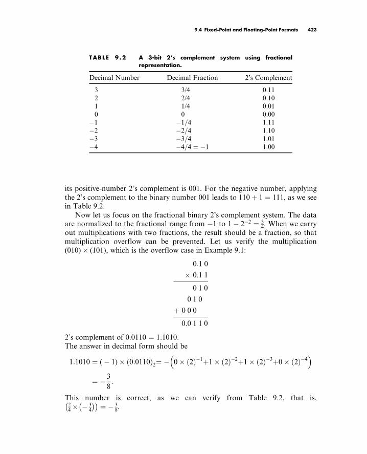
its positive-number 2’s complement is 001. For the negative number, applying
the 2’s complement to the binary number 001 leads to 110þ 1 ¼ 111, as we see
in Table 9.2.
Now let us focus on the fractional binary 2’s complement system. The data
are normalized to the fractional range from 1 to 1 22 ¼ 34. When we carry
out multiplications with two fractions, the result should be a fraction, so that
multiplication overflow can be prevented. Let us verify the multiplication
(010) (101), which is the overflow case in Example 9.1:
0:1 0
0:1 1
0 1 0
0 1 0
þ 0 0 0
0:0 1 1 0
2’s complement of 0.0110 ¼ 1.1010.
The answer in decimal form should be
1:1010 ¼ ( 1) 0:0110ð Þ2¼ 0 2ð Þ1þ1 2ð Þ2þ1 2ð Þ3þ0 2ð Þ4
¼ 3
8:
This number is correct, as we can verify from Table 9.2, that is,24 3
4
¼ 3
8.
TABLE 9.2 A 3-bit 2’s complement system using fractionalrepresentation.
Decimal Number Decimal Fraction 2’s Complement
3 3/4 0.11
2 2/4 0.10
1 1/4 0.01
0 0 0.00
1 1=4 1.11
2 2=4 1.10
3 3=4 1.01
4 4=4 ¼ 1 1.00
Tan: Digital Signaling Processing 0123740908_chap09 Final Proof page 423 21.6.2007 11:11pm Compositor Name: MRaja
9.4 Fixed-Point and Floating-Point Formats 423

If we truncate the last two least-significant bits to keep the 3-bit binary
number, we have an approximated answer as
1:10 ¼ ( 1) 0:10ð Þ2¼ 1 2ð Þ1þ 0 2ð Þ2
¼ 1
2:
The truncation error occurs. The error should be bounded by 22 ¼ 14. We can
verify that
1=2 ( 3=8)j j ¼ 1=8 < 1=4:
To use such a scheme, we can avoid the overflow due to multiplications but
cannot prevent the additional overflow. In the following addition example,
0:11
þ 0:01
1:00
where the result 1.00 is a negative number.
Adding two positive fractional numbers yields a negative number. Hence,
overflow occurs. We see that this signed fractional number scheme partially
solves the overflow in multiplications. Such fractional number format is called
the signed Q-2 format, where there are 2 magnitude bits plus one sign bit. The
additional overflow will be tackled using a scaling method discussed in a later
section.
Q-format number representation is the most common one used in fixed-point
DSP implementation. It is defined in Figure 9.8.
As indicated in Figure 9.8, Q-15 means that the data are in a sign magnitude
form in which there are 15 bits for magnitude and one bit for sign. Note that
after the sign bit, the dot shown in Figure 9.8 implies the binary point. The
number is normalized to the fractional range from 1 to 1. The range is divided
into 216 intervals, each with a size of 215. The most negative number is 1,
while the most positive number is 1 215. Any result from multiplication is
within the fractional range of 1 to 1. Let us study the following examples to
become familiar with Q-format number representation.
Q-15•−20 2−1 2−2 2−3 2−4 2−5 2−6 2−7 2−8 2−9 2−10 2−11 2−12 2−13 2−14 2−15
Implied binary point
F IGURE 9.8 Q-15 (fixed-point) format.
Tan: Digital Signaling Processing 0123740908_chap09 Final Proof page 424 21.6.2007 11:11pm Compositor Name: MRaja
424 9 D I G I T A L S I G N A L P R O C E S S O R S

Example 9.2.
a. Find the signed Q-15 representation for the decimal number 0.560123.
Solution:
a. The conversion process is illustrated using Table 9.3. For a positive
fractional number, we multiply the number by 2 if the product is larger
than 1, carry bit 1 as a most-significant bit (MSB), and copy the fractional
part to the next line for the next multiplication by 2; if the product is less
than 1, we carry bit 0 to MSB. The procedure continues to collect all 15
magnitude bits.
We yield the Q-15 format representation as
0:100011110110010:
Since we use only 16 bits to represent the number, we may lose accuracy
after conversion. Like quantization, the truncation error is introduced.
However, this error should be less than the interval size, in this
case, 215 ¼ 0:000030517. We shall verify this in Example 9.5. An alterna-
tive way of conversion is to convert a fraction, let’s say 34, to Q-2 format,
multiply it by 22, and then convert the truncated integer to its binary, that
is,
(3=4) 22 ¼ 3 ¼ 0112:
TABLE 9 .3 Conversion process of Q-15 representation.
Number Product Carry
0:560123 2 1.120246 1 (MSB)
0:120246 2 0.240492 0
0:240492 2 0.480984 0
0:480984 2 0.961968 0
0:961968 2 1.923936 1
0:923936 2 1.847872 1
0:847872 2 1.695744 1
0:695744 2 1.391488 1
0:391488 2 0.782976 0
0:782976 2 1.565952 1
0:565952 2 1.131904 1
0:131904 2 0.263808 0
0:263808 2 0.527616 0
0:527616 2 1.055232 1
0:055232 2 0.110464 0 (LSB)
MSB, most-significant bit; LSB, least-significant bit.
Tan: Digital Signaling Processing 0123740908_chap09 Final Proof page 425 21.6.2007 11:11pm Compositor Name: MRaja
9.4 Fixed-Point and Floating-Point Formats 425

In this way, it follows that
0:560123ð Þ 215 ¼ 18354:
Converting 18354 to its binary representation will achieve the same
answer. The next example illustrates the signed Q-15 representation for
a negative number.
Example 9.3.
a. Find the signed Q-15 representation for the decimal number 0:160123.
Solution:
a. Converting the Q-15 format for the corresponding positive number with
the same magnitude using the procedure described in Example 9.2, we
have
0:160123 ¼ 0:001010001111110:
Then, after applying 2’s complement, the Q-15 format becomes
0:160123 ¼ 1:110101110000010:
Alternative way: Since (0:160123) 215 ¼ 5246:9, converting the truncated
number 5246 to its 16-bit 2’s complement yields 1110101110000010.
Example 9.4.
a. Convert the Q-15 signed number 1.110101110000010 to the decimal
number.
Solution:
a. Since the number is negative, applying the 2’s complement yields
0:001010001111110:
Then the decimal number is
(23 þ 25 þ 29 þ 210 þ 211 þ 212 þ 213 þ 214) ¼ 0:160095:
Example 9.5.
a. Convert the Q-15 signed number 0.100011110110010 to the decimal
number.
Tan: Digital Signaling Processing 0123740908_chap09 Final Proof page 426 21.6.2007 11:11pm Compositor Name: MRaja
426 9 D I G I T A L S I G N A L P R O C E S S O R S

Solution:
a. The decimal number is
21 þ 25 þ 26 þ 27 þ 28 þ 210 þ 211 þ 214 ¼ 0:560120:
As we know, the truncation error in Example 9.2 is less than
215 ¼ 0:000030517. We verify that the truncation error is bounded by
0:560120 0:560123j j ¼ 0:000003 < 0:000030517:
Note that the larger the number of bits used, the smaller the round-off
error that may accompany it.
Examples 9.6 and 9.7 are devoted to illustrating data manipulations in the
Q-15 format.
Example 9.6.
a. Add the two numbers in Examples 9.4 and 9.5 in Q-15 format.
Solution:
a. Binary addition is carried out as follows:
1: 1 1 0 1 0 1 1 1 0 0 0 0 0 1 0
þ 0: 1 0 0 0 1 1 1 1 0 1 1 0 0 1 0
1 0: 0 1 1 0 0 1 1 0 0 1 1 0 1 0 0:
Then the result is
0: 0 1 1 0 0 1 1 0 0 1 1 0 1 0 0:
This number in the decimal form can be found to be
22 þ 23 þ 26 þ 27 þ 210 þ 211 þ 213 ¼ 0:400024:
Example 9.7.
This is a simple illustration of fixed-point multiplication.
a. Determine the fixed-point multiplication of 0.25 and 0.5 in Q-3 fixed-
point 2’s complement format.
Tan: Digital Signaling Processing 0123740908_chap09 Final Proof page 427 21.6.2007 11:11pm Compositor Name: MRaja
9.4 Fixed-Point and Floating-Point Formats 427

Solution:
a. Since 0:25 ¼ 0:010 and 0:5 ¼ 0:100, we carry out binary multiplication as
follows:
0:010
0:100
0 000
00 00
001 0
þ 0 000
0:001 000
Truncating the least-significant bits to convert the result to Q-3 format,
we have
0:010 0:100 ¼ 0:001:
Note that 0:001 ¼ 23 ¼ 0:125. We can also verify that
0:25 0:5 ¼ 0:125.
As a result, the Q-format number representation is a better choice than the
2’s complement integer representation. But we need to be concerned with the
following problems.
1. Converting a decimal number to its Q-N format, where N denotes the
number of magnitude bits, we may lose accuracy due to the truncation
error, which is bounded by the size of the interval, that is, 2N .
2. Addition and subtraction may cause overflow, where adding two positive
numbers leads to a negative number, or adding two negative numbers
yields a positive number; similarly, subtracting a positive number from a
negative number gives a positive number, while subtracting a negative
number from a positive number results in a negative number.
3. Multiplying two numbers in Q-15 format will lead to a Q-30 format,
which has 31 bits in total. As in Example 9.7, the multiplication of Q-3
yields a Q-6 format, that is, 6 magnitude bits and a sign bit. In practice, it
is common for a DS processor to hold the multiplication result using a
double word size such as MAC operation, as shown in Figure 9.9 for
multiplying two numbers in Q-15 format. In Q-30 format, there is one
sign-extended bit. We may get rid of it by shifting left by one bit to obtain
Q-31 format and maintaining the Q-31 format for each MAC operation.
Tan: Digital Signaling Processing 0123740908_chap09 Final Proof page 428 21.6.2007 11:11pm Compositor Name: MRaja
428 9 D I G I T A L S I G N A L P R O C E S S O R S

Sometimes, the number in Q-31 format needs to be converted to Q-15; for
example, the 32-bit data in the accumulator needs to be sent for 16-bit
digital-to-analog conversion (DAC), where the upper most-significant 16
bits in the Q-31 format must be used to maintain accuracy. We can shift
the number in Q-30 to the right by 15 bits or shift the Q-31 number to the
right by 16 bits. The useful result is stored in the lower 16-bit memory
location. Note that after truncation, the maximum error is bounded by the
interval size of 215, which satisfies most applications. In using the Q-
format in the fixed-point DS processor, it is costive to maintain the
accuracy of data manipulation.
4. Underflow can happen when the result of multiplication is too small to be
represented in the Q-format. As an example, in the Q-2 system shown in
Table 9.2, multiplying 0:01 0:01 leads to 0.0001. To keep the result in
Q-2, we truncate the last two bits of 0.0001 to achieve 0.00, which is zero.
Hence, underflow occurs.
9.4.2 Float ing-Point Format
To increase the dynamic range of number representation, a floating-point
format, which is similar to scientific notation, is used. The general format for
floating-point number representation is given by
x ¼M 2E , (9:1)
where M is the mantissa, or fractional part, in Q format, and E is the exponent.
The mantissa and exponent are signed numbers. If we assign 12 bits for the
mantissa and 4 bits for the exponent, the format looks like Figure 9.10.
Since the 12-bit mantissa has limits between 1 andþ1, the dynamic range is
controlled by the number of bits assigned to the exponent. The bigger the
number of bits assigned to the exponent, the larger the dynamic range. The
number of bits for the mantissa defines the interval in the normalized range; as
shown in Figure 9.10, the interval size is 211 in the normalized range, which is
smaller than the Q-15. However, when more mantissa bits are used, the smaller
interval size will be achieved. Using the format in Figure 9.10, we can determine
the most negative and most positive numbers as:
Q-30
15 magnitude bitsS
30 magnitude bitsS S
15 magnitude bits SSQ-15 Q-15
F IGURE 9 .9 Sign bit extended Q-30 format.
Tan: Digital Signaling Processing 0123740908_chap09 Final Proof page 429 21.6.2007 11:11pm Compositor Name: MRaja
9.4 Fixed-Point and Floating-Point Formats 429

Most negative number ¼ 1:00000000000ð Þ2201112 ¼ 1ð Þ 27 ¼ 128:0
Most positive number ¼ 0:11111111111ð Þ2201112 ¼ 1 211
27 ¼ 127:9375:
The smallest positive number is given by
Smallest positive number ¼ 0:00000000001ð Þ2210002 ¼ 211
28 ¼ 219:
As we can see, the exponent acts like a scale factor to increase the dynamic range
of the number representation. We study the floating-point format in the follow-
ing example.
Example 9.8.
a. Convert each of the following decimal numbers to the floating-point
number using the format specified in Figure 9.10.
1. 0.1601230
2. 20:430527
Solution:
a. 1. We first scale the number 0:1601230 to 0:160123=22 ¼ 0:640492 with
an exponent of 2 (other choices could be 0 or 1) to get
0:160123 ¼ 0:640492 22. Using 2’s complement, we have
2 ¼ 1110. Now we convert the value 0.640492 using Q-11 format
to get 010100011111. Cascading the exponent bits and the mantissa
bits yields
1110010100011111:
2. Since 20:430527=25 ¼ 0:638454, we can convert it into the frac-
tional part and exponent part as 20:430527 ¼ 0:638454 25.
Note that this conversion is not particularly unique; the forms
20:430527 ¼ 0:319227 26 and
20:430527 ¼ 0:1596135 27 . . . are still valid choices. Let us keep
what we have now. Therefore, the exponent bits should be 0101. Con-
verting the number 0.638454 using Q-11 format gives:
010100011011:
−23 −2022 21 20 2−1 2−2 2−3 2−4 2−5 2−6 2−7 2−8 2−9 2−10 2−11
12 bit mantissa4 bit exponent
F IGURE 9.10 Floating-point format.
Tan: Digital Signaling Processing 0123740908_chap09 Final Proof page 430 21.6.2007 11:11pm Compositor Name: MRaja
430 9 D I G I T A L S I G N A L P R O C E S S O R S

Using 2’s complement, we obtain the representation for the decimal number
0:638454 as
101011100101:
Cascading the exponent bits and mantissa bits, we achieve
0101101011100101:
The floating arithmetic is more complicated. We must obey the rules for manipu-
lating two floating-point numbers. Rules for arithmetic addition are given as:
x1 ¼M12E1
x2 ¼M22E2:
The floating-point sum is performed as follows:
x1 þ x2 ¼M1 þM2 2 E1E2ð Þ
2E1 , if E1 $ E2
M1 2 E2E1ð Þ þM2
2E2 if E1 < E2
As a multiplication rule, given two properly normalized floating-point numbers:
x1 ¼M12E1
x2 ¼M22E2 ,
where 0:5 jM1j < 1 and 0:5 jM2j < 1. Then multiplication can be per-
formed as follows:
x1 x2 ¼ M1 M2ð Þ 2E1þE2 ¼M 2E :
That is, the mantissas are multiplied while the exponents are added:
M ¼M1 M2
E ¼ E1 þ E2:
Examples 9.9 and 9.10 serve to illustrate manipulators.
Example 9.9.
a. Add two floating-point numbers achieved in Example 9.8:
1110 010100011111 ¼ 0:640136718 22
0101 101011100101 ¼ 0:638183593 25:
Solution:
a. Before addition, we change the first number to have the same exponent as
the second number, that is,
0101 000000001010 ¼ 0:005001068 25:
Tan: Digital Signaling Processing 0123740908_chap09 Final Proof page 431 21.6.2007 11:11pm Compositor Name: MRaja
9.4 Fixed-Point and Floating-Point Formats 431

Then we add two mantissa numbers:
0: 0 0 0 0 0 0 0 1 0 1 0
þ 1: 0 1 0 1 1 1 0 0 1 0 1
1: 0 1 0 1 1 1 0 1 1 1 1
and we get the floating number as
0101 101011101111:
We can verify the result by the following:
0101 101011101111 ¼ 21 þ 23 þ 27 þ 211
25
¼ 0:633300781 25 ¼ 20:265625:
Example 9.10.
a. Multiply two floating-point numbers achieved in Example 9.8:
1110 010100011111 ¼ 0:640136718 22
0101 101011100101 ¼ 0:638183593 25:
Solution:
a. From the results in Example 9.8, we have the bit patterns for these two
numbers as
E1 ¼ 1110,E2 ¼ 0101,M1 ¼ 010100011111, M2 ¼ 101011100101:
Adding two exponents in 2’s complement form leads to
E ¼ E1 þ E2 ¼ 1110þ 0101 ¼ 0011,
which is þ3, as we expected, since in decimal domain ( 2)þ 5 ¼ 3.
As previously shown in the multiplication rule, when multiplying two
mantissas, we need to apply their corresponding positive values. If the
sign for the final value is negative, then we convert it to its 2’s comple-
ment form. In our example, M1 ¼ 010100011111 is a positive mantissa.
However, M2 ¼ 101011100101 is a negative mantissa, since the MSB is 1.
To perform multiplication, we use 2’s complement to convert M2 to its
positive value, 010100011011, and note that the multiplication result is
negative. We multiply two positive mantissas and truncate the result to 12
bits to give
010100011111 010100011011 ¼ 001101000100:
Tan: Digital Signaling Processing 0123740908_chap09 Final Proof page 432 21.6.2007 11:11pm Compositor Name: MRaja
432 9 D I G I T A L S I G N A L P R O C E S S O R S

Now we need to add a negative sign to the multiplication result with 2’s
complement operation. Taking 2’s complement, we have
M ¼ 110010111100:
Hence, the product is achieved by cascading the 4-bit exponent and 12-
bit mantissa as:
0011 110010111100:
converting this number back to the decimal number, we verify the result
to be 0:408203125 23 ¼ 3:265625 :
Next, we examine overflow and underflow in the floating-point number system.
Over f low
During operation, overflow will occur when a number is too large to be
represented in the floating-point number system. Adding two mantissa numbers
may lead to a number larger than 1 or less than 1; and multiplying two
numbers causes the addition of their two exponents, so that the sum of the
two exponents could overflow. Consider the following overflow cases.
Case 1. Add the following two floating-point numbers:
0111 011000000000þ 0111 010000000000:
Note that two exponents are the same and they are the biggest positive
number in 4-bit 2’s complement representation. We add two positive
mantissa numbers as
0: 1 1 0 0 0 0 0 0 0 0 0
þ 0: 1 0 0 0 0 0 0 0 0 0 0
1: 0 1 0 0 0 0 0 0 0 0 0:
The result for adding mantissa numbers is negative. Hence, the over-
flow occurs.
Case 2. Multiply the following two numbers:
0111 011000000000 0111 011000000000:
Adding two positive exponents gives
0111þ 0111 ¼ 1000 (negative; the overflow occurs):
Multiplying two mantissa numbers gives:
0:11000000000 0:11000000000 ¼ 0:10010000000 (OK!):
Tan: Digital Signaling Processing 0123740908_chap09 Final Proof page 433 21.6.2007 11:11pm Compositor Name: MRaja
9.4 Fixed-Point and Floating-Point Formats 433

Under f low
As we discussed before, underflow will occur when a number is too small to be
represented in the number system. Let us divide the following two floating-point
numbers:
1001 001000000000 0111 010000000000:
First, subtracting two exponents leads to
1001 (negative) 0111 (positive) ¼ 1001þ 1001
¼ 0010 (positive; the underflow occurs):
Then, dividing two mantissa numbers, it follows that
0:01000000000 0:10000000000 ¼ 0:10000000000 (OK!):
However, in this case, the expected resulting exponent is 14 in decimal, which
is too small to be presented in the 4-bit 2’s complement system. Hence the
underflow occurs.
Understanding basic principles of the floating-point formats, we can next
examine two floating-point formats of the Institute of Electrical and Electronics
Engineers (IEEE).
9.4.3 IEEE F loat ing-Point Formats
Single Prec is ion Format
IEEE floating-point formats are widely used in many modern DS processors.
There are two types of IEEE floating-point formats (IEEE 754 standard). One is
the IEEE single precision format, and the other is the IEEE double precision
format. The single precision format is described in Figure 9.11.
The format of IEEE single precision floating-point standard representation
requires 23 fraction bits F, 8 exponent bits E, and 1 sign bit S, with a total of 32
bits for each word. F is the mantissa in 2’s complement positive binary fraction
represented from bit 0 to bit 22. The mantissa is within the normalized range
limits between þ1 and þ2. The sign bit S is employed to indicate the sign of the
number, where when S ¼ 1 the number is negative, and when S ¼ 0 the number
is positive. The exponent E is in excess 127 form. The value of 127 is the offset
from the 8-bit exponent range from 0 to 255, so that E-127 will have a range
from127 toþ128. The formula shown in Figure 9.11 can be applied to convert
the IEEE 754 standard (single precision) to the decimal number. The following
simple examples also illustrate this conversion:
Tan: Digital Signaling Processing 0123740908_chap09 Final Proof page 434 21.6.2007 11:11pm Compositor Name: MRaja
434 9 D I G I T A L S I G N A L P R O C E S S O R S

0 10000000 00000000000000000000000 ¼ ( 1)0 1:02ð Þ 2128127 ¼ 2:0
0 10000001 10100000000000000000000 ¼ ( 1)0 1:1012ð Þ 2129127 ¼ 6:51
1 10000001 10100000000000000000000 ¼ ( 1)1 1:1012ð Þ 2129127 ¼ 6:5:
Let us look at Example 9.11 for more explanation.
Example 9.11.
a. Convert the following number in the IEEE single precision format to the
decimal format:
110000000:010 . . . 0000:
Solution:
a. From the bit pattern in Figure 9.11, we can identify the sign bit, exponent,
and fractional as:
s ¼ 1,E ¼ 27 ¼ 128
1:F ¼ 1:012 ¼ (2)0 þ (2)2 ¼ 1:25:
Then, applying the conversion formula leads to
x ¼ ( 1)1(1:25) 2128127 ¼ 1:25 21 ¼ 2:5:
In conclusion, the value x represented by the word can be determined
based on the following rules, including all the exceptional cases:
& If E ¼ 255 and F is nonzero, then x ¼ NaN (‘‘Not a number’’).
& If E ¼ 255, F is zero, and S is 1, then x ¼ Infinity.
& If E ¼ 255, F is zero, and S is 0, then x ¼ þInfinity.
& If 0 < E < 255, then x ¼ ( 1)s (1:F ) 2E127, where 1.F repre-
sents the binary number created by prefixing F with an implicit
leading 1 and a binary point.
fractionexponent
x = (−1)s (1.F ) 2E−127
s031 30 23 22
F IGURE 9 .11 IEEE single precision floating-point format.
Tan: Digital Signaling Processing 0123740908_chap09 Final Proof page 435 21.6.2007 11:11pm Compositor Name: MRaja
9.4 Fixed-Point and Floating-Point Formats 435

& If E ¼ 0 and F is nonzero, then x ¼ ( 1)s (0:F) 2126. This is
an ‘‘unnormalized’’ value.
& If E ¼ 0, F is zero, and S is 1, then x ¼ 0.
& If E ¼ 0, F is zero, and S is 0, then x ¼ 0.
Typical and exceptional examples are shown as follows:
0 00000000 00000000000000000000000 ¼ 0
1 00000000 00000000000000000000000 ¼ 0
0 11111111 00000000000000000000000 ¼ Infinity
1 11111111 00000000000000000000000 ¼ Infinity
0 11111111 00000100000000000000000 ¼ NaN
1 11111111 00100010001001010101010 ¼ NaN
0 00000001 00000000000000000000000¼ (1)0 1:02ð Þ21127¼ 2126
0 00000000 10000000000000000000000¼ (1)0 0:12ð Þ20126¼ 2127
0 00000000 00000000000000000000001¼(1)0 0:000000000000000000000012ð Þ20126¼ 2149(smallest positive value)
Double Prec is ion Format
The IEEE double precision format is described in Figure 9.12.
The IEEE double precision floating-point standard representation requires a
64-bit word, which may be numbered from 0 to 63, left to right. The first bit is
the sign bit S, the next eleven bits are the exponent bits E, and the final 52 bits
are the fraction bits F. The IEEE floating-point format in double precision
significantly increases the dynamic range of number representation, since there
are eleven exponent bits; the double precision format also reduces the interval
size in the mantissa normalized range of þ1 to þ2, since there are 52 mantissa
bits as compared with the single precision case of 23 bits. Applying the conver-
sion formula shown in Figure 9.12 is similar to the single precision case.
s exponent fraction fraction
0031 3130 1920
odd register even register
x = (−1)s (1.F ) 2E−1023
F IGURE 9.12 IEEE double precision floating-point format.
Tan: Digital Signaling Processing 0123740908_chap09 Final Proof page 436 21.6.2007 11:11pm Compositor Name: MRaja
436 9 D I G I T A L S I G N A L P R O C E S S O R S

Example 9.12.
a. Convert the following number in IEEE double precision format to the
decimal format:
001000 . . . 0:110 . . . 0000
Solution:
b. Using the bit pattern in Figure 9.12, we have
s ¼ 0,E ¼ 29 ¼ 512 and
1:F ¼ 1:112 ¼ (2)0 þ (2)1 þ (2)2 ¼ 1:75:
Then, applying the double precision formula yields
x ¼ ( 1)0(1:75) 25121023 ¼ 1:75 2511 ¼ 2:6104 10154:
For purposes of completeness, rules for determining the value x represented by
the double precision word are listed as follows:
& If E ¼ 2047 and F is nonzero, then x ¼ NaN (‘‘Not a number’’)
& If E ¼ 2047, F is zero, and S is 1, then x ¼ Infinity
& If E ¼ 2047, F is zero, and S is 0, then x ¼ þInfinity
& If 0 < E < 2047, then x ¼ ( 1)s (1:F) 2E1023, where 1.F is intended
to represent the binary number created by prefixing F with an implicit
leading 1 and a binary point
& If E ¼ 0 and F is nonzero, then x ¼ ( 1)s (0:F) 21022. This is an
‘‘unnormalized’’ value
& If E ¼ 0, F is zero, and S is 1, then x ¼ 0
& If E ¼ 0, F is zero, and S is 0, then x ¼ 0
9.4.5 Fixed-Point Digi ta l S ignal Processors
Analog Device, Texas Instruments, and Motorola all manufacture fixed-point
DS processors. Analog Devices offers a fixed-point DSP family such as
ADSP21xx. Texas Instruments provides various generations of fixed-point
DSP processors based on historical development, architectural features, and
computational performance. Some of the most common ones are TMS320C1x
(first generation), TMS320C2x, TMS320C5x, and TMS320C62x. Motorola
manufactures varieties of fixed-point processors, such as the DSP5600x family.
The new families of fixed-point DS processors are expected to continue to grow.
Tan: Digital Signaling Processing 0123740908_chap09 Final Proof page 437 21.6.2007 11:11pm Compositor Name: MRaja
9.4 Fixed-Point and Floating-Point Formats 437

Since they share some basic common features such as program memory and data
memory with associated address buses, arithmetic logic units (ALUs), program
control units, MACs, shift units, and address generators, here we focus on an
overview of the TMS320C54x processor. The typical TMS320C54x fixed-point
DSP architecture appears in Figure 9.13.
The fixed-point TMS320C54x families supporting 16-bit data have on-chip
program memory and data memory in various sizes and configurations. They
include data RAM (random access memory) and program ROM (read-only
memory) used for program code, instruction, and data. Four data buses and
four address buses are accommodated to work with the data memories and
program memories. The program memory address bus and program memory
data bus are responsible for fetching the program instruction. As shown in
Figure 9.13, the C and D data memory address buses and the C and D data
Programmemory
Program memory data bus
Input/outputdevices
Arithmeticlogic unit
D data memory address bus
E data memory address bus
C data memory data bus
Datamemory
Multiplier/accumulator
Shift unit
Program memory address bus
C data memory address bus
D data memory data bus
E data memory data bus
Data addressgenerator
Programaddress
generator
Programcontrol unit
F IGURE 9.13 Basic architecture of TMS320C54x family.
Tan: Digital Signaling Processing 0123740908_chap09 Final Proof page 438 21.6.2007 11:11pm Compositor Name: MRaja
438 9 D I G I T A L S I G N A L P R O C E S S O R S

memory data buses deal with fetching data from the data memory, while the E
data memory address bus and the E data memory data bus are dedicated to
moving data into data memory. In addition, the E memory data bus can access
the I/O devices.
Computational units consist of an ALU, an MAC, and a shift unit. For
TMS320C54x families, the ALU can fetch data from the C, D, and program
memory data buses and access the E memory data bus. It has two independent
40-bit accumulators, which are able to operate 40-bit addition. The multiplier,
which can fetch data from C and D memory data buses and write data via the E
memory data bus, is capable of operating 17-bit 17-bit multiplications. The
40-bit shifter has the same capability of bus access as the MAC, allowing all
possible shifts for scaling and fractional arithmetic such as we have discussed for
the Q-format.
The program control unit fetches instructions via the program memory data
bus. Again, in order to speed up memory access, there are two address generators
available: one responsible for program addresses and one for data addresses.
Advanced Harvard architecture is employed, where several instructions
operate at the same time for a given single instruction cycle. Processing per-
formance offers 40 MIPS (million instruction sets per second). To further
explore this subject, the reader is referred to Dahnoun (2000), Embree (1995),
Ifeachor and Jervis (2002), and Van der Vegte (2002), as well as the website for
Texas Instruments (www.ti.com).
9.4.6 Float ing-Point Processors
Floating-point DS processors perform DSP operations using floating-point
arithmetic, as we discussed before. The advantages of using the floating-point
processor include getting rid of finite word length effects such as overflows,
round-off errors, truncation errors, and coefficient quantization errors. Hence,
in terms of coding, we do not need to do scaling input samples to avoid
overflow, shift the accumulator result to fit the DAC word size, scale the filter
coefficients, or apply Q-format arithmetic. The floating-point DS processor
with high-performance speed and calculation precision facilitates a friendly
environment to develop and implement DSP algorithms.
Analog Devices provides floating-point DSP families such as ADSP210xx
and TigerSHARC. Texas Instruments offers a wide range of floating-point DSP
families, in which the TMS320C3x is the first generation, followed by the
TMS320C4x and TMS320C67x families. Since the first generation of a float-
ing-point DS processor is less complicated than later generations but still has the
common basic features, we overview the first-generation architecture first.
Figure 9.14 shows the typical architecture of Texas Instruments’
TMS320C3x families. We discuss some key features briefly. Further detail can
Tan: Digital Signaling Processing 0123740908_chap09 Final Proof page 439 21.6.2007 11:11pm Compositor Name: MRaja
9.4 Fixed-Point and Floating-Point Formats 439

be found in the TMS320C3x User’s Guide (Texas Instruments, 1991), the
TMS320C6x CPU and Instruction Set Reference Guide (Texas Instruments,
1998), and other studies (Dahnoun, 2000; Embree, 1995; Ifeachor and Jervis,
2002; Kehtarnavaz and Simsek, 2000; Sorensen and Chen, 1997; van der Vegte,
2002). The TMS320C3x family consists of 32-bit single chip floating-point
processors that support both integer and floating-point operations.
The processor has a large memory space and is equipped with dual-access
on-chip memories. A program cache is employed to enhance the execution of
commonly used codes. Similar to the fixed-point processor, it uses the Harvard
architecture, in which there are separate buses used for program and data so
that instructions can be fetched at the same time that data are being accessed.
There also exist memory buses and data buses for direct-memory access (DMA)
for concurrent I/O and CPU operations, and peripheral access such as serial
ports, I/O ports, memory expansion, and an external clock.
The C3x CPU contains the floating-point/integer multiplier; an ALU, which
is capable of operating both integer and floating-point arithmetic; a 32-bit barrel
shifter; internal buses; a CPU register file; and dedicated auxiliary register
arithmetic units (ARAUs). The multiplier operates single-cycle multiplications
on 24-bit integers and on 32-bit floating-point values. Using parallel instructions
to perform a multiplication, an ALU will cost a single cycle, which means that a
multiplication and an addition are equally fast. The ARAUs support addressing
RAMblock 1
(1K 32)
Programcache
(64 32)
RAMblock 0
(1K 32)
ROMblock 0(4Kx32)
DMA
Address generators
Control registers
CPU
Integer/Floating-point
Multiplier
Integer/Floating-point
ALU
8 Extended-precisionregisters
Addressgenerator 0
Addressgenerator 1
8 Auxilliary registers
12 Control registers
Data busC
ontr
olle
r
Per
iphe
ral b
us
Serialport 0
Serialport 1
Timer 0
Timer 1
XR/W
XD 31 − 0
XA12 − 0
MSTRB
IOSTRB
XRDY
XR/W
XD 31 − 0
XA12 − 0
MSTRB
IOSTRB
XRDY
IACKXF 1 − 0
MCBL/MPX1
INT 3 − 0
RDY
SHZ
VSS
VDD
X2/CLKIN
F IGURE 9.14 The typical TMS320C3x floating-point DS processor.
Tan: Digital Signaling Processing 0123740908_chap09 Final Proof page 440 21.6.2007 11:11pm Compositor Name: MRaja
440 9 D I G I T A L S I G N A L P R O C E S S O R S

modes, in which some of them are specific to DSP such as circular buffering and
bit-reversal addressing (digital filtering and FFT operations). The CPU register
file offers 28 registers, which can be operated on by the multiplier and ALU. The
special functions of the registers include eight extended 40-bit precision registers
for maintaining accuracy of the floating-point results. Eight auxiliary registers
can be used for addressing and for integer arithmetic. These registers provide
internal temporary storage of internal variables instead of external memory
storage, to allow performance of arithmetic between registers. In this way,
program efficiency is greatly increased.
The prominent feature of C3x is its floating-point capability, allowing oper-
ation of numbers with a very large dynamic range. It offers implementation of
the DSP algorithm without worrying about problems such as overflows and
coefficient quantization. Three floating-point formats are supported. A short
16-bit floating-point format has 4 exponent bits, 1 sign bit, and 11 mantissa bits.
A 32-bit single precision format has 8 exponent bits, 1 sign bit, and 23 fraction
bits. A 40-bit extended precision format contains 8 exponent bits, 1 sign bit, and
31 fraction bits. Although the formats are slightly different from the IEEE 754
standard, conversions are available between these formats.
The TMS320C30 offers high-speed performance with 60-nanosecond single-
cycle instruction execution time, which is equivalent to 16.7 MIPS. For speech-
quality applications with an 8 kHz sampling rate, it can handle over 2,000
single-cycle instructions between two samples (125 microseconds). With instruc-
tion enhancement such as pipelines executing each instruction in a single cycle
(four cycles required from fetch to execution by the instruction itself) and a
multiple interrupt structure, this high-speed processor validates implementation
of real-time applications in floating-point arithmetic.
9.5 Fini te Impulse Response andInf in i te Impulse Response Fi l terImplementat ions in Fixed-PointSystems
With knowledge of the IEEE formats and of filter realization structures such as
the direct form I, direct form II, and parallel and cascade forms (Chapter 6), we
can study digital filter implementation in the fixed-point processor. In the fixed-
point system, where only integer arithmetic is used, we prefer input data, filter
coefficients, and processed output data to be in the Q-format. In this way, we
avoid overflow due to multiplications and can prevent overflow due to addition
by scaling input data. When the filter coefficients are out of the Q-format
range, coefficient scaling must be taken into account to maintain the
Q-format. We develop FIR filter implementation in Q-format first, and then
Tan: Digital Signaling Processing 0123740908_chap09 Final Proof page 441 21.6.2007 11:11pm Compositor Name: MRaja
9.5 Filter Implementations in Fixed-Point Systems 441

infinite impulse response (IIR) filter implementation next. In addition, we
assume that with a given input range in Q-format, the filter output is always
in Q-format even if the filter passband gain is larger than 1.
First, to avoid overflow for an adder, we can scale the input down by a scale
factor S, which can be safely determined by the equation
S ¼ Imax X1k¼0
h(k)j j ¼Imax h(0)j j þ h(1)j j þ h(2)j j þ ð Þ, (9:2)
where h(k) is the impulse response of the adder output and Imax the maximum
amplitude of the input in Q-format. Note that this is not an optimal factor in
terms of reduced signal-to-noise ratio. However, it shall prevent the overflow.
Equation (9.2) means that the adder output can actually be expressed as a
convolution output:
adder output ¼ h(0)x(n)þ h(1)x(n 1)þ h(2)x(n 2)þ :
Assuming the worst condition, that is, that all the inputs x(n) reach a maximum
value of Imax and all the impulse coefficients are positive, the sum of the adder
gives the most conservative scale factor, as shown in Equation (9.2). Hence,
scaling down of the input by a factor of S will guarantee that the output of the
adder is in Q-format.
When some of the FIR coefficients are larger than 1, which is beyond the
range of Q-format representation, coefficient scaling is required. The idea is that
scaling down the coefficients will make them less than 1, and later the filtered
output will be scaled up by the same amount before it is sent to DAC.
Figure 9.15 describes the implementation.
In the figure, the scale factor B makes the coefficients bk=B convertible to the
Q-format. The scale factors of S and B are usually chosen to be a power of 2, so
the simple shift operation can be used in the coding process. Let us implement
an FIR filter containing filter coefficients larger than 1 in the fixed-point
implementation.
z−1
z−1
z−1
b0/B
b1/B
bK/B
+
x(n ) xs(n ) ys(n ) y(n )+
B
1/S
S
F IGURE 9.15 Direct-form I implementation of the FIR filter.
Tan: Digital Signaling Processing 0123740908_chap09 Final Proof page 442 21.6.2007 11:11pm Compositor Name: MRaja
442 9 D I G I T A L S I G N A L P R O C E S S O R S

Example 9.13.
Given the FIR filter
y(n) ¼ 0:9x(n)þ 3x(n 1) 0:9x(n 2),
with a passband gain of 4, and assuming that the input range occupies only 1/4
of the full range for a particular application,
a. Develop the DSP implementation equations in the Q-15 fixed-point
system.
Solution:
a. The adder may cause overflow if the input data exist for 14
of a full
dynamic range. The scale factor is determined using the impulse response,
which consists of the FIR filter coefficients, as discussed in Chapter 3.
S ¼ 1
4h(0)j j þ h(1)j j þ h(2)j jð Þ ¼ 1
40:9þ 3þ 0:9ð Þ ¼ 1:2:
Overflow may occur. Hence, we select S ¼ 2 (a power of 2). We choose
B ¼ 4 to scale all the coefficients to be less than 1, so the Q-15 format can
be used. According to Figure 9.15, the developed difference equations are
given by
xs(n) ¼ x(n)
2
ys(n) ¼ 0:225xs(n)þ 0:75xs(n 1) 0:225xs(n 2)
y(n) ¼ 8ys(n)
Next, the direct-form I implementation of the IIR filter is illustrated in
Figure 9.16.
As shown in Figure 9.16, the purpose of a scale factor C is to scale down the
original filter coefficients to the Q-format. The factor C is usually chosen to be a
power of 2 for using a simple shift operation in DSP.
z−1
z−1
z−1
z−1
z−1
z−1
b0/C
b1/C −a1/C
−a2/C
−aN/CbM/C
x(n)y(n)
1/S C S+
xs(n ) ys(n ) yf(n )
F IGURE 9 .16 Direct-form I implementation of the IIR filter.
Tan: Digital Signaling Processing 0123740908_chap09 Final Proof page 443 21.6.2007 11:11pm Compositor Name: MRaja
9.5 Filter Implementations in Fixed-Point Systems 443

Example 9.14.
The following IIR filter,
y(n) ¼ 2x(n)þ 0:5y(n 1),
uses the direct form I, and for a particular application, the maximum input is
Imax ¼ 0:010 . . . 02 ¼ 0:25.
a. Develop the DSP implementation equations in the Q-15 fixed-point
system.
Solution:
a. This is an IIR filter whose transfer function is
H(z) ¼ 2
1 0:5z1¼ 2z
z 0:5:
Applying the inverse z-transform, we have the impulse response
h(n) ¼ 2 (0:5)nu(n):
To prevent overflow in the adder, we can compute the S factor with the
help of the Maclaurin series or approximate Equation (9.2) numerically.
We get
S ¼ 0:25 2 0:5ð Þ0þ2 0:5ð Þ1þ2 0:5ð Þ2þ
¼ 0:25 2 1
1 0:5¼ 1:
MATLAB function impz() can also be applied to find the impulse response and
the S factor:
h ¼ impz(2,[10:5]); % Find the impulse response sf ¼ 0:25 sum(abs(h)) % Determine the sum of absolute values of h(k)
sf ¼ 1
Hence, we do not need to perform input scaling. However, we need to
scale down all the coefficients to use the Q-15 format. A factor of C ¼ 4 is
selected. From Figure 9.16, we get the difference equations as
xs(n) ¼ x(n)
ys(n) ¼ 0:5xs(n)þ 0:125yf (n 1)
yf (n) ¼ 4ys(n)
y(n) ¼ yf (n):
We can develop these equations directly. First, we divide the original
difference equation by a factor of 4 to scale down all the coefficients to be
less than 1, that is,
Tan: Digital Signaling Processing 0123740908_chap09 Final Proof page 444 21.6.2007 11:11pm Compositor Name: MRaja
444 9 D I G I T A L S I G N A L P R O C E S S O R S

1
4yf (n) ¼
1
4 2xs(n)þ 1
4 0:5yf (n 1),
and define a scaled output
ys(n) ¼ 1
4yf (n):
Finally, substituting ys(n) to the left side of the scaled equation and
rescaling up the filter output as yf (n) ¼ 4ys(n) we have the same results
we got before.
The fixed-point implementation for the direct form II is more complicated.
The developed direct-form II implementation of the IIR filter is illustrated in
Figure 9.17.
As shown in Figure 9.17, two scale factors A and B are designated to scale
denominator coefficients and numerator coefficients to their Q-format repre-
sentations, respectively. Here S is a special factor to scale down the input sample
so that the numerical overflow in the first sum in Figure 9.17 can be prevented.
The difference equations are given in Chapter 6 and listed here:
w(n) ¼ x(n) a1w(n 1) a2w(n 2) aMw(nM)
y(n) ¼ b0w(n)þ b1w(n 1)þ þ bMw(nM):
The first equation is scaled down by the factor A to ensure that all the denom-
inator coefficients are less than 1, that is,
ws(n) ¼1
Aw(n) ¼ 1
Ax(n) 1
Aa1w(n 1) 1
Aa2w(n 2) 1
AaMw(nM)
w(n) ¼ A ws(n):
Similarly, scaling the second equation yields
z−1
z−1
z−1
b1/B
b0 / B
b2 /B
bM /B
−a1/A
−a2 /A
−aM / A
x (n ) y (n )ys (n ) Bws (n ) A w (n )
w (n−1 )
w (n−2 )
w (n−M )
1/S 1/A
S+ +
F IGURE 9 .17 Direct-form II implementation of the IIR filter.
Tan: Digital Signaling Processing 0123740908_chap09 Final Proof page 445 21.6.2007 11:11pm Compositor Name: MRaja
9.5 Filter Implementations in Fixed-Point Systems 445

ys(n) ¼ 1
By(n) ¼ 1
Bb0w(n)þ 1
Bb1w(n 1)þ þ 1
BbMw(nM)
andy(n) ¼ B ys(n)
To avoid the first adder overflow (first equation), the scale factor S can be
safely determined by Equation (9.3):
S ¼ Imax h(0)j j þ h(1)j j þ h(2)j j þ ð Þ, (9:3)
where h(k) is the impulse response of the filter whose transfer function is the
reciprocal of the denominator polynomial, where the poles can cause a larger
value to the first sum:
h(n) ¼ Z1 1
1þ a1z1 þ þ azM
: (9:4)
All the scale factors A, B, and S are usually chosen to be a power of 2,
respectively, so that the shift operations can be used in the coding process.
Example 9.15 serves for illustration.
Example 9.15.
Given the following IIR filter:
y(n) ¼ 0:75x(n)þ 1:49x(n 1)þ 0:75x(n 2) 1:52y(n 1) 0:64y(n 2),
with a passband gain of 1 and a full range of input,
a. Use the direct-form II implementation to develop the DSP implementa-
tion equations in the Q-15 fixed-point system.
Solution:
a. The difference equations without scaling in the direct-form II implemen-
tation are given by
w(n) ¼ x(n) 1:52w(n 1) 0:64w(n 2)
y(n) ¼ 0:75w(n)þ 1:49w(n 1)þ 0:75w(n 2):
To prevent overflow in the first adder, we have the reciprocal of the
denominator polynomial as
A(z) ¼ 1
1þ 1:52z1 þ 0:64z2:
Using MATLAB function leads to
h ¼ impz(1,[1 1:52 0:64]); sf ¼ sum(abs(h))
sf ¼ 10:4093.
Tan: Digital Signaling Processing 0123740908_chap09 Final Proof page 446 21.6.2007 11:11pm Compositor Name: MRaja
446 9 D I G I T A L S I G N A L P R O C E S S O R S

We choose the S factor as S ¼ 16 and we choose A ¼ 2 to scale down the
denominator coefficients by half. Since the second adder output after
scaling is
ys(n) ¼ 0:75
Bw(n)þ 1:49
Bw(n 1)þ 0:75
Bw(n 2),
we have to ensure that each coefficient is less than 1, as well as the sum of
the absolute values
0:75
Bþ 1:49
Bþ 0:75
B< 1
to avoid second adder overflow. Hence B ¼ 4 is selected. We develop the
DSP equations as
xs(n) ¼ x(n)=16
ws(n) ¼ 0:5xs(n) 0:76w(n 1) 0:32w(n 2)
w(n) ¼ 2ws(n)
ys(n) ¼ 0:1875w(n)þ 0:3725w(n 1)þ 0:1875w(n 2)
y(n) ¼ (B S)ys(n) ¼ 64ys(n)
:
The implementation for cascading the second-order section filters can be found
in Ifeachor and Jervis (2002).
A practical example will be presented in the next section. Note that if a
floating-point DS processor is used, all the scaling concerns should be ignored,
since the floating-point format offers a large dynamic range, so that overflow
hardly ever happens.
9.6 Digi ta l S ignal Process ingProgramming Examples
In this section, we first review the TMS320C67x DSK (DSP Starter Kit), which
offers floating-point and fixed-point arithmetic. We will then investigate real-
time implementation of digital filters.
9.6.1 Over view of TMS320C67x DSK
In this section, a Texas Instruments TMS320C67x DSK is chosen for demon-
stration in Figure 9.18. This DSK board (Kehtarnavaz and Simsek, 2001; Texas
Instruments, 1998) consists of the TMS320C67x chip, SDRAM (synchronous
dynamic random access memory) and ROM for storing program code and data,
and an ADC535 chip performing 16-bit ADC and DAC operations. The gain of
Tan: Digital Signaling Processing 0123740908_chap09 Final Proof page 447 21.6.2007 11:11pm Compositor Name: MRaja
9.6 Digital Signal Processing Programming Examples 447

the ADC channel is programmable to provide microphone or other line inputs,
such as from the function generator or other sensors. The DAC channel is also
programmable to deliver the power gain to drive a speaker or other devices. The
ADC535 chip sets a fixed sampling rate of 8 kHz for speech applications. The
on-board daughter card connections facilitate the external units for advanced
applications. For example, a daughter card designed using PCM3001/3 offers a
variable high sampling rate, such as 44.1 kHz, and its own programmable ADC
and DAC for CD-quality audio applications. The parallel port is used for
connection between the DSK board and the host computer, where the user
program is developed, compiled, and downloaded to the DSK for real-time
applications using the user-friendly software called the Code Composer Studio,
which we shall discuss later.
The TMS320C67x operates at a high clock rate of 300 MHz. Combining
with high speed and multiple units operating at the same time has pushed its
performance up to 2,400 MIPS at 300 MHz. Using this number, the C67x can
handle 0.3 MIPS between two speech samples at a sampling rate of 8 kHz and
can handle over 54,000 instructions between two audio samples with a sampling
rate of 44.1 kHz. Hence, the C67x offers great flexibility for real-time applica-
tions with a high-level C language.
Figure 9.19 shows a C67x architecture overview, while Figure 9.20 displays a
more detailed block diagram. C67x contains three main parts, which are the
CPU, the memories, and the peripherals. As shown in Figure 9.19, these three
main parts are joined by an external memory interface (EMIF) interconnected
TMS320 C6711DSP
Line level I/O microphoneLine level I/O speaker
Reset pushbutton
PC parallel portinterface
Power jack
TLC320AD53516 bit
AD535
SDRAM (2)128 K × 8 bitFlash ROM
Daughter card I/F
Daughter card I/F
User optionDip switches
TI 1.8 V power supply
TI 3.3 V power supply
EmulationJTAG controller
JTAG header
F IGURE 9.18 C6711 DSK board.
Tan: Digital Signaling Processing 0123740908_chap09 Final Proof page 448 21.6.2007 11:11pm Compositor Name: MRaja
448 9 D I G I T A L S I G N A L P R O C E S S O R S

DataRAM
ProgramRAM
.D1
Control registers
Internal buses
Serialport
Hostport
Bootload
Timers
Data
EMIF
DMA
Powerdown
CPU
Registers (B
0-B15)
Registers (A
0-A15)
.D2
.M1 .M2
.L1 .L2
.S1 .S2
F IGURE 9 .19 Block diagram of TMS320C67x floating-point DSP.
Additionalperipherals:
Timers,Serial ports
etc.
DMAEMIF
Program cache/program memory32-bit address256-bit data
Program fetch
Instruction dispatch
Instruction decode
Data cache/data memory32 bit address
6-, 16-, 32-bit data
Controlregisters
Data path A Data path B
Register file A Register file B
Controllogic
Test
Emulation
Interrupts
.L1 .D2.D1.M1.S1 .M2 .S2 .L2
F IGURE 9 .20 Registers of the TMS320C67x floating-point DSP.
Tan: Digital Signaling Processing 0123740908_chap09 Final Proof page 449 21.6.2007 11:11pm Compositor Name: MRaja
9.6 Digital Signal Processing Programming Examples 449

by internal buses to facilitate interface with common memory devices; DMA; a
serial port; and a host port interface (HPI).
Since this section is devoted to showing DSP coding examples, C67x key
features and references are briefly listed here:
1. Architecture: The system uses Texas Instruments Veloci2 architecture,
which is an enhancement of the VLIW (very long instruction word
architecture) (Dahnoun, 2000; Ifeachor and Jervis, 2002; Kehtarnavaz
and Simsek, 2000).
2. CPU: As shown in Figure 9.20, the CPU has eight functional units
divided into two sides A and B, each consisting of units .D, .M, .L, and
.S. For each side, an .M unit is used for multiplication operations, an .L
unit is used for logical and arithmetic operations, and a .D unit is used for
loading/storing and arithmetic operations. Each side of the C67x CPU
has sixteen 32-bit registers that the CPU must go through for interface.
More detail can be found in Appendix D (Texas Instruments, 1991), as
well as in Kehtarnavaz and Simsek (2000) and Texas Instruments (1998).
3. Memory and internal buses: Memory space is divided into internal pro-
gram memory, internal data memory, and internal peripheral and external
memory space. The internal buses include a 32-bit program address bus, a
256-bit program data bus to carry out eight 32-bit instructions (VLIW),
two 32-bit data address buses, two 64-bit load data buses, two 64-bit store
data buses, two 32-bit DMA buses, and two 32-bit DMA address buses
responsible for reading and writing. There also exist a 22-bit address bus
and a 32-bit data bus for accessing off-chip or external memory.
4. Peripherals:
a. EMIF, which provides the required timing for accessing external
memory
b. DMA, which moves data from one memory location to another
without interfering with the CPU operations
c. Multichannel buffered serial port (McBSP) with a high-speed multi-
channel serial communication link
d. HPI, which lets a host access internal memory
e. Boot loader for loading code from off-chip memory or the HPI to
internal memory
f. Timers (two 32-bit counters)
g. Power-down units for saving power for periods when the CPU is
inactive.
Tan: Digital Signaling Processing 0123740908_chap09 Final Proof page 450 21.6.2007 11:11pm Compositor Name: MRaja
450 9 D I G I T A L S I G N A L P R O C E S S O R S

The software tool for the C67x is the Code Composer Studio (CCS) provided by
TI. It allows the user to build and debug programs from a user-friendly graph-
ical user interface (GUI) and extends the capabilities of code development tools
to include real-time analysis. Installation, tutorial, coding, and debugging can
be found in the CCS Getting Started Guide (Texas Instruments, 2001) and in
Kehtarnavaz and Simsek (2000).
9.6.2 Concept of Real-T ime Process ing
We illustrate real-time implementation in Figure 9.21, where the sampling rate is
8,000 samples per second; that is, the sampling period T ¼ 1=fs ¼ 125 micro-
seconds, which is the time between two samples.
As shown in Figure 9.21, the required timing includes an input sample clock
and an output sample clock. The input sample clock maintains the accuracy of
sampling time for each ADC operation, while the output sample clock keeps the
accuracy of time instant for each DAC operation. Time between the input
sample clock n and the output sample clock n consists of the ADC operation,
algorithm processing, and the wait for the next ADC operation. The numbers of
instructions for ADC and DSP algorithms must be estimated and verified to
ensure that all instructions have been completed before the DAC begins. Simi-
larly, the number of instructions for DAC must be verified so that DAC
instructions will be finished between the output sample clock n and the next
input sample clock nþ 1. Timing usually is set up using the DSP interrupts (we
will not pursue the interrupt setup here).
T = 125ms
T = 125ms T = 125ms
T = 125msT = 125ms
AD
C x
(n)
Pro
cess
ing
DS
Pal
gorit
hm y
(n)
Wai
ting
time
DA
C y
(n)
AD
C x
(n)
Pro
cess
ing
DS
Pal
gorit
hm y
(n)
Wai
ting
time
DA
C y
(n)
Input sample n Input sample n + 1 Input sample n + 2
Output sample n Output sample n + 1
F IGURE 9 .21 Concept of real-time processing.
Tan: Digital Signaling Processing 0123740908_chap09 Final Proof page 451 21.6.2007 11:11pm Compositor Name: MRaja
9.6 Digital Signal Processing Programming Examples 451

Next, we focus on the implementation of the DSP algorithm in the floating-
point system for simplicity.
9.6.3 Linear Buf fer ing
During DSP such as digital filtering, past inputs and past outputs are required
to be buffered and updated for processing the next input sample. Let us first
study the FIR filter implementation.
F in i te Impulse Response Fi l ter ing
Consider implementation for the following 3-tap FIR filter:
y(n) ¼ 0:5x(n)þ 0:2x(n 1)þ 0:5x(n 2):
The buffer requirements are shown in Figure 9.22. The coefficient buffer b[3]
contains 3 FIR coefficients, and the coefficient buffer is fixed during the process.
The input buffer x[3], which holds the current and past inputs, is required to be
updated. The FIFO update is adopted here with the segment of codes shown in
Figure 9.22. For each input sample, we update the input buffer using FIFO,
which begins at the end of the data buffer; the oldest sampled is kicked out first
from the buffer and updated with the value from the upper location. When the
FIFO completes, the first memory location x[0] will be free to be used to
store the current input sample. The segment of code in Figure 9.22 explains
implementation.
Note that in the code segment, x[0] holds the current input sample x(n), while
b[0] is the corresponding coefficient; x[1] and x[2] hold the past input samples
x(n 1) and x(n 2), respectively; similarly, b[1] and b[2] are the corresponding
coefficients.
Again, note that using the array and loop structures in the code segment is
for simplicity in notations and assumes that the reader is not familiar with the C
pointers in C-language. This concern for simplicity has to do mainly with the
DSP algorithm. More coding efficiency can be achieved using the C pointers
and circular buffer. The DSP-oriented coding implementation can be found in
Kehtarnavaz and Simsek (2000).
In f in i te Impulse Response Fi l ter ing
Similarly, we can implement an IIR filter. It requires an input buffer, which
holds the current and past inputs; an output buffer, which holds the past
outputs; a numerator coefficient buffer; and a denominator coefficient buffer.
Considering the following IIR filter for implementation,
y(n) ¼ 0:5x(n)þ 0:7x(n 1) 0:5x(n 2) 0:4y(n 1)þ 0:6y(n 2),
Tan: Digital Signaling Processing 0123740908_chap09 Final Proof page 452 21.6.2007 11:11pm Compositor Name: MRaja
452 9 D I G I T A L S I G N A L P R O C E S S O R S

we accommodate the numerator coefficient buffer b[3], the denominator
coefficient buffer a[3], the input buffer x[3], and the output buffer y[3]
shown in Figure 9.23. The buffer updates for input x[3] and output y[3] are
FIFO. The implementation is illustrated in the segment of code listed in
Figure 9.23.
Again, note that in the code segment, x[0] holds the current input sample,
while y[0] holds the current processed output, which will be sent to the DAC unit
for conversion. The coefficient a[0] is never modified in the code. We keep that
for a purpose of notation simplicity and consistency during the programming
process.
Coefficient buffer b[3]
Update of inputbuffer x[3]
(FIFO)
b[0]
b[1]
b[2]
0.5
0.5
0.2
x[0]
x[1]
x[2]
x(n)
x(n − 1)
x(n − 2)
New input x(n)
kicked outFirst step
Free for new sample
volatile int sample;
float x[3]¼0.0, 0.0, 0.0;float b[3]¼0.5, 0.2, 0.5;float y[1]¼0.0;interrupt void AtoD()
int i;
sample ¼ mcbsp0_read(); /ADC=
for(i ¼ 2; i > 0; i--)= Update the input buffer x[3] =
x[i] ¼ x[i 1];
x[0]¼(float) sample;y[0]¼0;for(i ¼ 0; i < 3; iþþ)
y[0] ¼ y[0]þ b[i]x[i];
sample ¼ (int) y[0]; = The processed sample will be sent to DAC =
F IGURE 9 .22 Example of FIR filtering with linear buffer update.
Tan: Digital Signaling Processing 0123740908_chap09 Final Proof page 453 21.6.2007 11:11pm Compositor Name: MRaja
9.6 Digital Signal Processing Programming Examples 453

Digi ta l Osc i l la t ion with Inf in i te Impulse ResponseFi l ter ing
The principle for generating digital oscillation is described in Chapter 8, where
the input to the digital filter is the impulse sequence, and the transfer function
is obtained by applying the z-transform of the digital sinusoidal function.
Coefficients b[3] Coefficients a[3]
Update of inputbuffer x[3]
(FIFO)
b[0]
b[1]
b[2]
0.5
− 0.5
0.7
a[0]
a[1]
a[2]
x[0]
x[1]
x[2]
1
0.4
− 0.6
x(n)
x(n − 1)
x(n − 2)
New input x(n)
Kicked outFirst step
Free for new sample
Update of outputbuffer y[3]
(FIFO)
y[0]
y[1]
y[2]
y(n)
y(n − 1)
y(n − 2)
Kicked outFirst step
Free for output sample
volatile int sample;
float b[3]¼0.5, 0.7, 0:5;float a[3]¼1, 0.4, 0:6;float x[3]¼0.0, 0.0, 0.0;
float y[3]¼0.0, 0.0, 0.0;
interrupt void AtoD()
int i;
sample¼mcbsp0_read(); = ADC =for(i ¼ 2; i > 0; i--) = Update the input buffer =
x[i] ¼ x[i 1];
x[0]¼ (float) sample;
for (i ¼ 2;i > 0;i--)/ Update the output buffer /
y[i]¼y[i – 1];
y[0] ¼ b[0]x[0]þ b[1]x[1]þ b[2]x[2]-a[1]y[1]-a[2]y[2];sample¼ (int) y[0]; = the processed sample will be sent to DAC =
F IGURE 9.23 Example of IIR filtering using linear buffer update.
Tan: Digital Signaling Processing 0123740908_chap09 Final Proof page 454 21.6.2007 11:11pm Compositor Name: MRaja
454 9 D I G I T A L S I G N A L P R O C E S S O R S

Applications can be found in dual-tone multifrequency (DTMF) tone gener-
ation, digital carrier generation for communications, and so on. Hence, we can
modify the implementation of IIR filtering for tone generation with the input
generated internally instead of by using the ADC channel.
Let us generate an 800 Hz tone with a digital amplitude of 5,000. According
to the section in Chapter 8 (‘‘Applications: Generation and Detection of DTMF
Tones Using the Goertzel Algorithm’’), the transfer function, difference equa-
tion, and impulse input sequence are found to be, respectively,
H(z) ¼ 0:587785z1
1 1:618034z1 þ z2
y(n) ¼ 0:587785x(n 1)þ 1:618034y(n 1) y(n 2)
x(n) ¼ 5000d(n):
We define the numerator coefficient buffer b[2], the denominator coefficient
buffer a[3], the input buffer x[2], and the output buffer y[3], shown in Figure
9.24, which also shows the modified implementation for the tone generation.
Initially, we set x[0] ¼ 5000. Then it will be updated with x[0] ¼ 0 for each
current processed output sample y[0].
9.6.4 Sample C Programs
F loat ing-Point Implementat ion Example
Real-time DSP implementation using the floating-point processor is easy to
program. The overflow problem hardly ever occurs. Therefore, we do not
need to consider scaling factors, as described in the last section. The code
segment shown in Figure 9.25 demonstrates the simplicity of coding the float-
ing-point IIR filter using the direct-form I structure.
F ixed-Point Implementat ion Example
Where execution time is critical, fixed-point implementation is preferred in a
floating-point processor. We implement the following IIR filter with a unit
passband gain in direct form II:
H(z)¼ 0:02010:0402z2þ0:0201z4
12:1192z1þ2:6952z21:6924z3þ0:6414z4
w(n)¼ x(n)þ2:1192w(n1)2:6952w(n2)þ1:6924w(n3)0:6414w(n4)
y(n)¼ 0:0201w(n)0:0402w(n2)þ0:0201w(n4):
Tan: Digital Signaling Processing 0123740908_chap09 Final Proof page 455 21.6.2007 11:11pm Compositor Name: MRaja
9.6 Digital Signal Processing Programming Examples 455

Coefficients b[2] Coefficients a[3]
Update of inputbuffer x[2]
(FIFO)New input x(n) = 0
b[0]
b[1]
0.0
0.587785
a[0]
a[1]
a[2]
x[0]
x[1]
1.0
− 1.618034
1.0
5000
x(n − 1)
Kicked outFirst step
Free for new sample
Update of outputbuffer y[3]
(FIFO)
y[0]
y[1]
y[2]
y(n)
y(n − 1)
y(n − 2)
Kicked outFirst step
Free for output sample
volatile int sample;
float b[2]¼ f0:0,0:587785g;float a[3]¼ f1,1:618034,1g;float x[2]¼ f5000,0:0g; =Set up the input as an impulse function /float y[3]¼ f0:0,0:0,0:0g;interrupt void AtoD()
int i;
sample ¼ mcbsp0_read(); =ADC =y[0] ¼ b[0]x[0]þ b[1]x[1]-a[1]y[1]-a[2]y[2];sample¼ (int) y[0]; /The processed sample will be sent to DAC /for(i ¼ 1; i > 0; i--)/Update the input buffer /
x[i] ¼ x[i-1];
x[0] ¼ 0;
for(i ¼ 2 > 0;i--)/ Update the output buffer /
y[i] ¼ y[i – 1];
F IGURE 9 .24 Example of IIR filtering using linear buffer update and the impulsesequence input.
Tan: Digital Signaling Processing 0123740908_chap09 Final Proof page 456 21.6.2007 11:11pm Compositor Name: MRaja
456 9 D I G I T A L S I G N A L P R O C E S S O R S

volatile int sample;
float a[5] ¼ f1:00,2:1192, 2:6952,1:6924, 0:6414g;float b[5] ¼ f0:0201,0:00,0:0402, 0:00, 0:0201g;float x[5] ¼ f0:0, 0:0, 0:0, 0:0, 0:0g;float y[5] ¼ f0:0, 0:0, 0:0, 0:0, 0:0g;/******************************************************************/
/ AtoD() Interrupt Service Routine (ISR)–> interrupt 12 defined in IST
of vectors.asm (read McBSP) //******************************************************************/
interrupt void AtoD()
int i;
float temp, sum;
sample ¼ mcbsp0_read(); = ADC ///Insert DSP Algorithm Here ()
temp ¼ (float) sample;
for(i ¼ 4; i > 0; i--)
x[i] ¼ x[i-1];
x[0] ¼ temp;
for(i ¼ 4; i > 0; i--)
y[i] ¼ y[i – 1];
sum¼b[0]x[0]þb[1]x[1]þb[2]x[2]þb[3]x[3]þb[4]x[4]-a[1]y[1]-a[2]
y[2]-a[3]y[3]-a[4]y[4];
y[0] ¼ sum;
sample ¼ sum;
/******************************************************************/
/* DtoA() Interrupt Service Routine (ISR)–> interrupt 11 defined in IST
of vectors.asm (write to McBSP)*/
/******************************************************************/
interrupt void DtoA()
sample ¼ sample & 0xfffe; / set LSB to 0 for primary communication/mcbsp0_write(sample); /DAC /
F IGURE 9 .25 Sample C code for IIR filtering (float-point implementation).
Tan: Digital Signaling Processing 0123740908_chap09 Final Proof page 457 21.6.2007 11:11pm Compositor Name: MRaja
9.6 Digital Signal Processing Programming Examples 457

Using MATLAB to calculate the scale factor S, it follows that
h ¼ impz([1],[12:1192 2:6952 1:6924 0:6414]);
sf ¼ sum(abs(h))
sf ¼ 28:2196
Hence we choose S ¼ 32. To scale the filter coefficients in the Q-15 format, we
use the factors A ¼ 4 and B ¼ 1. Then the developed DSP equations are
xs(n) ¼ x(n)=32
ws(n) ¼ 0:25xs(n)þ 0:5298ws(n 1) 0:6738ws(n 2)þ 0:4231ws(n 3)
þ 0:4231ws(n 3)þ 0:16035ws(n 4)
w(n) ¼ 4ws(n)
ys(n) ¼ 0:0201w(n) 0:0402w(n 2)þ 0:0201w(n 4)
y(n) ¼ 32ys(n):
Using themethod described in Section 9.5,we can convert filter coefficients into the
Q-15 format; each coefficient is listed in Table 9.4.
The list of codes for the fixed-point implementation is displayed in Figure
9.26, and some coding notations are given in Figure 9.27.
Note that this chapter has provided only basic concepts and an introduction
to real-time DSP implementation. The coding detail and real-time DSP appli-
cations will be treated in a separate DSP course, which deals with real-time
implementations.
TABLE 9.4 Filter coefficients in Q-15 format.
IIR Filter Filter Coefficients Q-15 Format (Hex)
a1 0.5298 0x43D0
a2 0:6738 0xA9C1
a3 0.4230 0x3628
a4 0:16035 0xEB7A
b0 0.0201 0 0293
b1 0.0000 0 0000
b2 0:0402 0 FADB
b3 0.0000 0 000
b4 0.0201 0 0293
Tan: Digital Signaling Processing 0123740908_chap09 Final Proof page 458 21.6.2007 11:11pm Compositor Name: MRaja
458 9 D I G I T A L S I G N A L P R O C E S S O R S

volatile int sample;
= float a[5]¼ f1.00, 2.1192, 2.6952, 1.6924, 0.6414g;float b[5]¼ f0.0201, 0.00, 0.0402, 0.00, 0.0201g;*/shorta[5]¼f02000, 043D0, 0A9C1, 03628, 0EB7Ag;= coefficientsinQ-15format =short b[5] ¼ f0 0293, 0 0000, 0 FADB, 0 0000, 0 0293g;int w[5]¼0, 0, 0, 0, 0;
interrupt void AtoD()
int i, sum¼0;sample¼mcbsp0_read(); = ADC =//Insert DSP Algorithm Here ()
sample ¼ (sample 16);= Move to high 16 bits =sample ¼ (sample 5);= Scaled down by 32 to avoid overflow =for (i ¼ 4;i > 0;i--)
w[i] ¼ w[i 1];
sum ¼ (sample 2); = Scaled down by 4 to use Q 15=for (i ¼ 1;i < 5;iþþ)
sum þ ¼ (_mpyhl(w[i],a[i])) 1;
sum ¼ (sum 2);= scaled up by 4 =w[0] ¼sum;sum ¼0;for (i ¼ 0;i < 5;iþþ)
sum þ ¼ (_mpyhl(w[i],b[i])) 1;
sum ¼ (sum 5); = Scaled up by 32 to get y(n) =sample ¼ (sum 16); = Move to low 16 bits =
==
= DtoA() Interrupt Service Routine (ISR)–> interrupt 11 defined in IST of
vectors.asm(write to McBSP) ===
interrupt void DtoA()
sample ¼ sample & 0xfffe; = set LSB to 0 for primary communication=mcbsp0_write(sample); = DAC =
F IGURE 9 .26 Sample C code for IIR filtering (fixed-point implementation).
Tan: Digital Signaling Processing 0123740908_chap09 Final Proof page 459 21.6.2007 11:11pm Compositor Name: MRaja
9.6 Digital Signal Processing Programming Examples 459

9.7 Summar y
1. The Von Neumann architecture consists of a single, shared memory for
programs and data, a single bus for memory access, an arithmetic unit,
and a program control unit. The Von Neumann processor operates
fetching and execution cycles in series.
2. The Harvard architecture has two separate memory spaces dedicated to
program code and to data, respectively, two corresponding address buses,
and two data buses for accessing two memory spaces. The Harvard
processor offers fetching and execution cycles in parallel.
3. The DSP special hardware units include an MAC dedicated to DSP
filtering operations, a shifter unit for scaling, and address generators for
circular buffering.
4. The fixed-point DS processor uses integer arithmetic. The data format Q-
15 for the fixed-point system is preferred to avoid overflows.
5. The floating-point processor uses floating-point arithmetic. The standard
floating-point formats include the IEEE single precision and double
precision formats.
6. The architectures and features of fixed-point processors and floating-
point processors were briefly reviewed.
short coefficient; declaration of 16 bit signed integer
int sample, result; declaration of 32 bit signed integer
MPYHL assembly instruction (signed multiply high low 16 MSB × 16 LSB)
result = (_mpyhl(sample, coefficient) ) <<1;
sample must be shifted left by 16 bits to be stored in the high 16 MSB.
coefficient is the 16 bit data to be stored in the low 16 LSB.
result is shifted left by one bit to get rid of the extended sign bit, and high 16
MSB’s are designated for the processed data.
Final result will be shifted down to right by 16 bits before DAC conversion.
sample = (result>>16);
F IGURE 9.27 Some coding notations for the Q-15 fixed-point implementation.
Tan: Digital Signaling Processing 0123740908_chap09 Final Proof page 460 21.6.2007 11:11pm Compositor Name: MRaja
460 9 D I G I T A L S I G N A L P R O C E S S O R S

7. Implementing digital filters in the fixed-point DSP system requires scaling
filter coefficients so that the filters are in Q-15 format, and input scaling for
the adder so that overflow during the MAC operations can be avoided.
8. The floating-point processor is easy to code using floating-point arith-
metic and develops the prototype quickly. However, it is not efficient in
terms of the number of instructions it has to complete compared with the
fixed-point processor.
9. The fixed-point processor using fixed-point arithmetic takes much effort
to code. But it offers the least number of instructions for the CPU to
execute.
9.8 Problems
9.1. Find the signed Q-15 representation for the decimal number 0.2560123.
9.2. Find the signed Q-15 representation for the decimal number
0:2160123.
9.3. Convert the Q-15 signed number ¼ 1.010101110100010 to the decimal.
9.4. Convert the Q-15 signed number ¼ 0.001000111101110 to the decimal
number.
9.5. Add the following two Q-15 numbers:
1: 10 1 0 1 0 1 1 1 0 0 0 0 0 1þ 0: 01 0 0 0 1 1 1 1 0 1 1 0 1 0
9.6. Convert each of the following decimal numbers to the floating-point
number using the format specified in Figure 9.10.
a. 0.1101235
b. 10:430527
9.7. Add the following floating-point numbers whose formats are defined in
Figure 9.10, and determine the sum in decimal format.
1101 011100011011þ 0100 101111100101:
9.8. Convert the following number in IEEE single precision format to the
decimal format:
110100000:010 . . . 0000:
9.9. Convert the following number in IEEE double precision format to the
decimal format:
011000 . . . 0:1010 . . . 000
Tan: Digital Signaling Processing 0123740908_chap09 Final Proof page 461 21.6.2007 11:11pm Compositor Name: MRaja
9.8 Problems 461

9.10. Given the following FIR filter:
y(n) ¼ 0:36x(n)þ 1:6x(n 1)þ 0:36x(n 2),
with a passband gain of 2 and the input being half of range, develop
the DSP implementation equations in the Q-15 fixed-point system.
9.11. Given the following IIR filter:
y(n) ¼ 1:35x(n)þ 0:3y(n 1),
with a passband gain of 2 and the input being half of range, use the
direct-form I method to develop the DSP implementation equations in
the Q-15 fixed-point system.
9.12. Given the following IIR filter:
y(n) ¼ 0:72x(n)þ 1:42x(n 2)þ 0:72x(n 2)
1:35y(n 1) 0:5y(n 2),
with a passband gain of 1 and a full range of input, use the direct-form
II method to develop the DSP implementation equations in the Q-15
fixed-point system.
References
Dahnoun, N. (2000). Digital Signal Processing Implementation Using the TMS320C6000TM
DSP Platform. Englewood Cliffs, NJ: Prentice Hall.
Embree, P. M. (1995). C Algorithms for Real-Time DSP. Upper Saddle River, NJ: Prentice
Hall.
Ifeachor, E. C., and Jervis, B. W. (2002). Digital Signal Processing: A Practical Approach,
2nd ed. Upper Saddle River, NJ: Prentice Hall.
Kehtarnavaz, N., and Simsek, B. (2000). C6X-Based Digital Signal Processing. Upper Saddle
River, NJ: Prentice Hall.
Sorensen, H. V., and Chen, J. P. (1997). A Digital Signal Processing Laboratory Using
TMS320C30. Upper Saddle River, NJ: Prentice Hall.
Texas Instruments. (1991). TMS320C3x User’s Guide. Dallas, TX: Author.
———. (1998). TMS320C6x CPU and Instruction Set Reference Guide, Literature ID#
SPRU 189C. Dallas, TX: Author.
———. (2001). Code Composer Studio: Getting Started Guide. Dallas, TX: Author.
van der Vegte, J. (2002). Fundamentals of Digital Signal Processing. Upper Saddle River, NJ:
Prentice Hall.
Wikipedia. (2007). Harvard Mark I. Retrieved March 14, 2007, from http://en.wikipedia.org/
wiki/Harvard_Mark_I
Tan: Digital Signaling Processing 0123740908_chap09 Final Proof page 462 21.6.2007 11:11pm Compositor Name: MRaja
462 9 D I G I T A L S I G N A L P R O C E S S O R S

10Adaptive Filters and Applications
Object ives :
This chapter introduces principles of adaptive filters and adaptive least mean
square algorithm and illustrates how to apply the adaptive filters to solve real-
world application problems such as adaptive noise cancellation, system model-
ing, adaptive line enhancement, and telephone echo cancellation.
10.1 Introduct ion to Least Mean SquareAdapt ive Fin i te Impulse ResponseFi l ters
An adaptive filter is a digital filter that has self-adjusting characteristics. It is
capable of adjusting its filter coefficients automatically to adapt the input signal
via an adaptive algorithm. Adaptive filters play an important role in modern
digital signal processing (DSP) products in areas such as telephone echo can-
cellation, noise cancellation, equalization of communications channels, biomed-
ical signal enhancement, active noise control, and adaptive control systems.
Adaptive filters work generally for adaptation of signal-changing environments,
spectral overlap between noise and signal, and unknown, or time-varying, noise.
For example, when interference noise is strong and its spectrum overlaps that of
the desired signal, the conventional approach will fail to preserve the desired
signal spectrum while removing the interference using a traditional filter, such as
a notch filter with the fixed filter coefficients, as shown in Figure 10.1.
However, an adaptive filter will do the job. Note that adaptive filtering, with
its applications, has existed for more than two decades in the research community
and is still active there. This chapter can only introduce some fundaments of the
Tan: Digital Signaling Processing 0123740908_chap10 Final Proof page 463 22.6.2007 12:16am Compositor Name: MRaja

subject, that is, adaptive finite impulse response (FIR) filters with a simple and
popular least mean square (LMS) algorithm. Further exploration into adaptive
infinite impulse response (IIR) filters, adaptive lattice filters, their associated
algorithms and applications, and so on can be found in comprehensive texts by
Haykin (1991), Stearns (2003), and Widrow and Stearns (1985).
To get the concept of adaptive filtering, we will first look at an illustrative
example of the simplest noise canceler to see how it works before diving into
detail. The block diagram for such a noise canceler is shown in Figure 10.2.
As shown in Figure 10.2, first, the DSP system consists of two analog-to-
digital conversion (ADC) channels. The first microphone with ADC is used to
capture the desired speech s(n). However, due to a noisy environment, the signal
is contaminated and the ADC channel produces a signal with the noise; that is,
d(n) ¼ s(n)þ n(n). The second microphone is placed where only noise is picked
up and the second ADC channel captures noise x(n), which is fed to the
adaptive filter.
Note that the corrupting noise n(n) in the first channel is uncorrelated to the
desired signal s(n), so that separation between them is possible. The noise signal
x(n) from the second channel is correlated to the corrupting noise n(n) in the first
f
SpectrumNoise spectum
Desired signal spectrum
F IGURE 10 .1 Spectrum illustration for using adaptive filters.
y (n) = wnx(n)Adaptive filter
+
y (n)
d(n ) = s(n) + n(n)
x (n)
e(n) = d(n) − y(n) = s(n)~
wn + 1= wn+ 0.01e(n)x(n)
+
−
ADC
ADC
DAC
LMS algorithm
Noise
Signal and noise Error signal
F IGURE 10 .2 Simplest noise canceler using a one-tap adaptive filter.
Tan: Digital Signaling Processing 0123740908_chap10 Final Proof page 464 22.6.2007 12:16am Compositor Name: MRaja
464 10 A D A P T I V E F I L T E R S A N D A P P L I C A T I O N S

channel, since both come from the same noise source. Similarly, the noise signal
x(n) is not correlated to the desired speech signal s(n).
We assume that the corrupting noise in the first channel is a linear filtered
version of the second-channel noise, since it has a different physical path from
the second-channel noise, and the noise source is time varying, so that we can
estimate the corrupting noise n(n) using an adaptive filter. The adaptive filter
contains a digital filter with adjustable coefficient(s) and the LMS algorithm to
modify the value(s) of the coefficient(s) for filtering each sample. The adaptive
filter then produces an estimate of noise y(n), which will be subtracted from the
corrupted signal d(n) ¼ s(n)þ n(n). When the noise estimate y(n) equals or
approximates the noise n(n) in the corrupted signal, that is, y(n) n(n), the
error signal e(n) ¼ s(n)þ n(n) y(n) ~ss(n) will approximate the clean speech
signal s(n). Hence, the noise is canceled.
In our illustrative numerical example, the adaptive filter is set to be a one-tap
FIR filter to simplify numerical algebra. The filter adjustable coefficient wn is
adjusted based on the LMS algorithm (discussed later in detail) in the following:
wnþ1 ¼ wn þ 0:01 e(n) x(n),
where wn is the coefficient used currently, while wnþ1 is the coefficient obtained
from the LMS algorithm and will be used for the next coming input sample. The
value of 0.01 controls the speed of the coefficient change. To illustrate the
concept of the adaptive filter in Figure 10.2, the LMS algorithm has the initial
coefficient set to be w0 ¼ 0:3 and leads to:
y(n) ¼ wnx(n)
e(n) ¼ d(n) y(n)
wnþ1 ¼ wn þ 0:01e(n)x(n):
The corrupted signal is generated by adding noise to a sine wave. The corrupted
signal and noise reference are shown in Figure 10.3, and their first 16 values are
listed in Table 10.1.
Let us perform adaptive filtering for several samples using the values for the
corrupted signal and reference noise in Table 10.1. We see that
n ¼ 0, y(0) ¼ w0x(0) ¼ 0:3 ( 0:5893) ¼ 0:1768
e(0) ¼ d(0) y(0) ¼ 0:2947 0:1768ð Þ ¼ 0:1179 ¼ ~ss(0)
w1 ¼ w0 þ 0:01e(0)x(0) ¼ 0:3þ 0:01 0:1179ð Þ 0:5893ð Þ ¼ 0:3007
n ¼ 1, y(1) ¼ w1x(1) ¼ 0:3007 0:5893 ¼ 0:1772
e(1) ¼ d(1) y(1) ¼ 1:0017 0:1772 ¼ 0:8245 ¼ ~ss(1)
w2 ¼ w1 þ 0:01e(1)x(1) ¼ 0:3007þ 0:01 0:8245 0:5893 ¼ 0:3056
n ¼ 2, y(2) ¼ w2x(2) ¼ 0:3056 3:1654 ¼ 0:9673
Tan: Digital Signaling Processing 0123740908_chap10 Final Proof page 465 22.6.2007 12:16am Compositor Name: MRaja
10.1 Introduction to Least Mean Square Adaptive Finite Impulse Response Filters 465

e(2) ¼ d(2) y(2) ¼ 2:5827 0:9673 ¼ 1:6155 ¼ ~ss(2)
w3 ¼ w2 þ 0:01e(2)x(2) ¼ 0:3056þ 0:01 1:6155 3:1654 ¼ 0:3567
n ¼ 3, For comparison, results of the first 16 processed output samples, original
samples, and filter coefficient values are also included in Table 10.1. Figure
10.3 also shows the original signal samples, reference noise samples corrupted
signal samples, enhanced signal samples, and filter coefficient values for each
incoming sample, respectively.
As shown in Figure 10.3, after 7 adaptations, the adaptive filter learns noise
characteristics and cancels the noise in the corrupted signal. The adaptive coef-
ficient is close to the optimal value of 0.5. The processed output is close to the
original signal. The first 16 processed values for the corrupted signal, reference
noise, clean signal, original signal, and adaptive filter coefficient used at each step
are listed in Table 10.1.
Clearly, the enhanced signal samples look much like the sinusoidal input
samples. Now our simplest one-tap adaptive filter works for this particular case.
In general, the FIR filter with multiple-taps is used and has the following format:
y(n) ¼XN1
i¼0
wn(i)x(n i)
¼ wn(0)x(n)þ wn(1)x(n 1)þ þ wn (N 1)x(nN þ 1):
(10:1)
The LMS algorithm for the adaptive FIR filter will be developed next.
TABLE 10 .1 Adaptive filtering results for the simplest noise canceler example.
n d(n) x(n) ~ss(n) ¼ e(n) Original s(n) wnþ1
0 0:2947 0:5893 0:1179 0 0.3000
1 1.0017 0.5893 0.8245 0.7071 0.3007
2 2.5827 3.1654 1.6155 1.0000 0.3056
3 1:6019 4:6179 0.0453 0.7071 0.3567
4 0.5622 1.1244 0.1635 0.0000 0.3546
5 0.4456 2.3054 0:3761 0:7071 0.3564
6 4:2674 6:5348 1:9948 1:0000 0.3478
7 0:8418 0:2694 0:7130 0:7071 0.4781
8 0:3862 0:7724 0:0154 0:0000 0.4800
9 1.2274 1.0406 0.7278 0.7071 0.4802
10 0.6021 0:7958 0.9902 1.0000 0.4877
11 1.1647 0.9152 0.7255 0.7071 0.4799
12 0.9630 1.9260 0.0260 0.0000 0.4865
13 1:5065 1:5988 0:7279 0:7071 0.4870
14 0:1329 1.7342 0:9976 1:0000 0.4986
15 0.8146 3.0434 0:6503 0:7071 0.4813
Tan: Digital Signaling Processing 0123740908_chap10 Final Proof page 466 22.6.2007 12:16am Compositor Name: MRaja
466 10 A D A P T I V E F I L T E R S A N D A P P L I C A T I O N S

10.2 Basic Wiener Fi l ter Theor y and LeastMean Square Algor i thm
Many adaptive algorithms can be viewed as approximations of the discrete
Wiener filter shown in Figure 10.4.
The Wiener filter adjusts its weight(s) to produce filter output y(n), which
would be as close as the noise n(n) contained in the corrupted signal d(n). Hence,
at the subtracted output, the noise is canceled, and the output e(n) contains
clean signal.
0 5 10 15 20 25 30−5
0
5
d(n)
0 5 10 15 20 25 30
−505
x(n)
0 5 10 15 20 25 30−2
0
2
e(n)
0 5 10 15 20 25 30−2
0
2
s(n)
0 5 10 15 20 25 300
0.5
1
wn
Sample number n
Converges
F IGURE 10.3 Original signal, reference noise, corrupted signal, enhanced signal, andadaptive coefficient in the noise cancellation.
++
−
y(n)Wiener filter
Outpute(n)
Noisex(n)
Signal and noised(n) = s(n) + n(n)
F IGURE 10.4 Wiener filter for noise cancellation.
Tan: Digital Signaling Processing 0123740908_chap10 Final Proof page 467 22.6.2007 12:16am Compositor Name: MRaja
10.2 Basic Wiener Filter Theory and Least Mean Square Algorithm 467

Consider a single-weight case of y(n) ¼ wx(n), and note that the error signal
e(n) is given by
e(n) ¼ d(n) wx(n): (10:2)
Now let us solve the best weight w. Taking the square of the output error leads
to
e2(n) ¼ d(n) wx(n)ð Þ2¼ d2(n) 2d(n)wx(n)þ w2x2(n): (10:3)
Taking the statistical expectation of Equation (10.3), we have
E e2(n)
¼ E d2(n)
2wE d(n)x(n)ð Þ þ w2E x2(n)
: (10:4)
Using the notations in statistics, we define
J ¼ E(e2(n)) ¼MSE (mean squared error)
s2 ¼ E(d2(n)) ¼ power of corrupted signal
P ¼ E(d(n)x(n)) ¼ cross-correlation between d(n) and x(n)
R ¼ E(x2(n)) ¼ autocorrelation
We can view the statistical expectation as an average of the N signal terms, each
being a product of two individual signal samples:
E e2(n)
¼ e2(0)þ e2(1)þ þ e2(N 1)
N
or
E d(n)x(n)ð Þ ¼ d(0)x(0)þ d(1)x(1)þ þ d(N 1)x(N 1)
N
for a sufficiently large sample number of N. We can write Equation (10.4) as
J ¼ s2 2wPþ w2R: (10:5)
Since s2, P, and R are constants, J is a quadratic function of w that may be
plotted in Figure 10.5.
J
ww *
Jmin
F IGURE 10 .5 Mean square error quadratic function.
Tan: Digital Signaling Processing 0123740908_chap10 Final Proof page 468 22.6.2007 12:16am Compositor Name: MRaja
468 10 A D A P T I V E F I L T E R S A N D A P P L I C A T I O N S

The best weight (optimal) w is at the location where the minimum MSE Jmin
is achieved. To obtain w, taking a derivative of J and setting it to zero leads to
dJ
dw¼ 2Pþ 2wR ¼ 0: (10:6)
Solving Equation 10.6, we get the best weight solution as
w ¼ R1P: (10:7)
Example 10.1.
Given a quadratic MSE function for the Wiener filter:
J ¼ 40 20wþ 10w2,
a. Find the optimal solution for w to achieve the minimum MSE Jmin and
determine Jmin.
Solution:
a. Taking a derivative of the MSE function and setting it to zero, we have
dJ
dw¼ 20þ 10 2w ¼ 0:
Solving the equation leads to
w ¼ 1:
Finally, substituting w ¼ 1 into the MSE function, we get the minimum
Jmin as
Jmin ¼ Jjw¼w ¼ 40 20wþ 10w2jw¼1 ¼ 40 20 1þ 10 12 ¼ 30:
Notice that a few points need to be clarified for Equation (10.7):
1. Optimal coefficient(s) can be different for every block of data, since the
corrupted signal and reference signal are unknown. The autocorrelation
and cross-correlation may vary.
2. If a larger number of coefficients (weights) are used, the inverse matrix of
R1 may require a larger number of computations and may come to be ill-
conditioned. This will make real-time implementation impossible.
3. The optimal solution is based on the statistics, assuming that the size of
the data block, N, is sufficiently long. This will cause a long processing
delay that will make real-time implementation impossible.
Tan: Digital Signaling Processing 0123740908_chap10 Final Proof page 469 22.6.2007 12:16am Compositor Name: MRaja
10.2 Basic Wiener Filter Theory and Least Mean Square Algorithm 469

As we pointed out, solving the Wiener solution Equation (10.7) requires a lot of
computations, including matrix inversion for a general multiple-taps FIR filter.
The well-known textbook by Widrow and Stearns (1985) describes a powerful
LMS algorithm by using the steepest descent algorithm to minimize the MSE
sample by sample and locate the filter coefficient(s). We first study the steepest
descent algorithm as illustrated in Equation (10.8):
wnþ1 ¼ wn mdJ
dw(10:8)
where m ¼ constant controlling speed of convergence.
The illustration of the steepest descent algorithm for solving the optimal
coefficient(s) is described in Figure 10.6.
As shown in the first plot in Figure 10.6, if dJdw< 0, notice that m dJ
dw> 0. The
new coefficient wnþ1 will be increased to approach the optimal value w by
Equation (10.8). On the other hand, if dJdw> 0, as shown in the second plot in
Figure 10.6, we see that m dJdw< 0. The new coefficient wnþ1 will be decreased to
approach the optimal value w. When dJdw¼ 0, the best coefficient wnþ1 is reached.
w * wwn +1wn
Jmin Jmin
Jn Jn
Jn + 1 Jn + 1
J
w * wwn +1 wn
J
CasedJdw
dJdw
> 0< 0 and − m CasedJdw
dJdw
< 0> 0 and − m
F IGURE 10 .6 Illustration of the steepest descent algorithm.
Example 10.2.
Given a quadratic MSE function for the Wiener filter:
J ¼ 40 20wþ 10w2,
a. Use the steepest descent method with an initial guess as w0 ¼ 0 and
m ¼ 0:04 to find the optimal solution for w and determine Jmin by
iterating three times.
Solution:
a. Taking the derivative of the MSE function, we have
dJ
dw¼ 20þ 10 2wn:
Tan: Digital Signaling Processing 0123740908_chap10 Final Proof page 470 22.6.2007 12:16am Compositor Name: MRaja
470 10 A D A P T I V E F I L T E R S A N D A P P L I C A T I O N S

When n ¼ 0, we calculate
mdJ
dw¼ 0:04 20þ 10 2w0ð Þjw0¼0 ¼ 0:8:
Applying the steepest descent algorithm, it follows that
w1 ¼ w0 mdJ
dw¼ 0 0:8ð Þ ¼ 0:8:
Similarly for n ¼ 1, we get
mdJ
dw¼ 0:04 20þ 10 2w1ð Þjw1¼0:8 ¼ 0:16
w2 ¼ w1 mdJ
dw¼ 0:8 0:16ð Þ ¼ 0:96,
and for n ¼ 2, it follows that
mdJ
dw¼ 0:04 20þ 10 2w2ð Þjw2¼0:96 ¼ 0:032
w3 ¼ w2 mdJ
dw¼ 0:96 0:032ð Þ ¼ 0:992:
Finally, substituting w w3 ¼ 0:992 into the MSE function, we get the
minimum Jmin as
Jmin 40 20wþ 10w2jw¼0:992 ¼ 40 20 0:992þ 10 0:9922 ¼ 30:0006:
As we can see, after three iterations, the filter coefficient and minimum
MSE values are very close to the theoretical values obtained in Example
10.1.
Application of the steepest descent algorithm still needs an estimation of the
derivative of the MSE function that could include statistical calculation of a
block of data. To change the algorithm to do sample-based processing, an LMS
algorithm must be used. To develop the LMS algorithm in terms of sample-
based processing, we take the statistical expectation out of J and then take the
derivative to obtain an approximate of dJdw
, that is,
J ¼ e2(n) ¼ d(n) wx(n)ð Þ2 (10:9)
dJ
dw¼ 2 d(n) wx(n)ð Þ d d(n) wx(n)ð Þ
dw¼ 2e(n)x(n): (10:10)
Substituting dJdw
into the steepest descent algorithm in Equation (10.8), we
achieve the LMS algorithm for updating a single-weight case as
wnþ1 ¼ wn þ 2me(n)x(n), (10:11)
Tan: Digital Signaling Processing 0123740908_chap10 Final Proof page 471 22.6.2007 12:16am Compositor Name: MRaja
10.2 Basic Wiener Filter Theory and Least Mean Square Algorithm 471

where m is the convergence parameter controlling speed of convergence. For
example, let us choose 2m ¼ 0:01. In general, with an adaptive FIR filter of
length N, we extend the single-tap LMS algorithm without going through
derivation, as shown in the following equations:
y(n) ¼ wn(0)x(n)þ wn(1)x(n 1)þ þ wn(N 1)x(nN þ 1) (10:12)
for i ¼ 0, . . . , N 1
wnþ1(i) ¼ wn(i)þ 2me(n)x(n i): (10:13)
The convergence factor is chosen to be
0 < m <1
NPx
, (10:14)
where Px is the input signal power. In practice, if the ADC has 16-bit data, the
maximum signal amplitude should be A ¼ 215. Then the maximum input power
must be less than
Px < 215 2¼ 230:
Hence, we may make a selection of the convergence parameter as
m ¼ 1
N 230 9:3 1010
N: (10:15)
We further neglect time index for wn(i) and use the notation w(i) ¼ wn(i), since
only the currently updated coefficients are needed for the next sample adapta-
tion. We conclude the implementation of the LMS algorithm by the following
steps:
1. Initialize w(0), w(1), . . . , w(N 1) to arbitrary values.
2. Read d(n), x(n), and perform digital filtering:
y(n) ¼ w(0)x(n)þ w(1)x(n 1)þ þ w(N 1)x(nN þ 1):
3. Compute the output error:
e(n) ¼ d(n) y(n):
4. Update each filter coefficient using the LMS algorithm:
for i ¼ 0, . . . , N 1
w(i) ¼ w(i)þ 2me(n)x(n i):
We will apply the adaptive filter to solve real-world problems in the next
section.
Tan: Digital Signaling Processing 0123740908_chap10 Final Proof page 472 22.6.2007 12:16am Compositor Name: MRaja
472 10 A D A P T I V E F I L T E R S A N D A P P L I C A T I O N S

10.3 Appl i cat ions: Noise Cancel lat ion,System Model ing, and LineEnhancement
We now examine several applications of the LMS algorithm, such as noise
cancellation, system modeling, and line enhancement via application examples.
First, we begin with the noise cancellation problem to illustrate operations of
the LMS adaptive FIR filter.
10.3.1 Noise Cancel lat ion
The concept of noise cancellation was introduced in the previous section.
Figure 10.7 shows the main idea.
The DSP system consists of two ADC channels. The first microphone with
ADC captures the noisy speech, d(n) ¼ s(n)þ n(n), which contains the clean
speech s(n) andnoise n(n) due to a noisy environment, while the second microphone
with ADC resides where it picks up only the correlated noise and feeds the noise
reference x(n) to the adaptive filter. The adaptive filter uses the LMS algorithm to
adjust its coefficients to produce the best estimate of noise y(n) n(n), which will
be subtracted from the corrupted signal d(n) ¼ s(n)þ (n). The output of the error
signal e(n) ¼ s(n)þ n(n) y(n) ~ss(n) is expected to be a best estimate of the clean
speech signal. Through digital-to-analog conversion (DAC), the cleaned digital
speech becomes analog voltage, which drives the speaker.
We first study the noise cancellation problem using a simple two-tap adap-
tive filter via Example 10.3 and assumed data. The purpose of doing so is to
become familiar with the setup and operations of the adaptive filter and LMS
algorithm. The simulation for real adaptive noise cancellation follows.
+
y (n)x (n)
+
−
ADC
ADC
DAC
Adaptive filter
LMS algorithm
Noise
Signal and noise Error signald(n) = s(n) + n(n) e(n) = d(n) − y (n) = s(n)~
F IGURE 10.7 Simplest noise canceler using a one-tap adaptive filter.
Tan: Digital Signaling Processing 0123740908_chap10 Final Proof page 473 22.6.2007 12:16am Compositor Name: MRaja
10.3 Applications: Noise Cancellation, System Modeling, and Line Enhancement 473

Example 10.3.
Given the DSP system for the noise cancellation application using an adaptive
filter with two coefficients shown in Figure 10.8,
a. Set up the LMS algorithm for the adaptive filter.
b. Perform adaptive filtering to obtain outputs e(n) ¼ n ¼ 0, 1, 2 given the
following inputs and outputs:
x(0) ¼ 1, x(1) ¼ 1x(2) ¼ 1, d(0) ¼ 2, d(1) ¼ 1, d(2) ¼ 2
and initial weights:
w(0) ¼ w(1) ¼ 0,
convergence factor is set to be m ¼ 0:1:
Solution:
a. The adaptive LMS algorithm is set up as:
Initialization: w(0) ¼ 0, w(1) ¼ 0
Digital filtering: y(n) ¼ w(0)x(n)þ w(1)x(n 1)
Computing the output error ¼ output: e(n) ¼ d(n) y(n).
Updating each weight for the next coming sample:
w(i) ¼ w(i)þ 2me(n)x(n i), for i ¼ 0, 1
or
w(0) ¼ w(0)þ 2me(n)x(n)
w(1) ¼ w(1)þ 2me(n)x(n 1):
++
−
x (n) y(n)
Adaptive filtery(n) = w(0)x(n) + w(1)x(n − 1)
Outpute(n)
Noise
Signal and noised (n) = s (n) + n (n)
F IGURE 10 .8 Noise cancellation in Example 10.3.
Tan: Digital Signaling Processing 0123740908_chap10 Final Proof page 474 22.6.2007 12:16am Compositor Name: MRaja
474 10 A D A P T I V E F I L T E R S A N D A P P L I C A T I O N S

b. We can see the adaptive filtering operations as follows:
a. For n ¼ 0
Digital filtering:
y(0) ¼ w(0)x(0)þ w(1)x( 1) ¼ 0 1þ 0 0 ¼ 0
Computing the output:
e(0) ¼ d(0) y(0) ¼ 2 0 ¼ 2
Updating coefficients:
w(0) ¼ w(0)þ 2 0:1 e(0)x(0) ¼ 0þ 2 0:1 2 1 ¼ 0:4
w(1) ¼ w(1)þ 2 0:1 e(0)x( 1) ¼ 0þ 2 0:1 2 0 ¼ 0:0
For n ¼ 1
Digital filtering:
y(1) ¼ w(0)x(1)þ w(1)x(0) ¼ 0:4 1þ 0 1 ¼ 0:4
Computing the output:
e(1) ¼ d(1) y(1) ¼ 1 0:4 ¼ 0:6
Updating coefficients:
w(0) ¼ w(0)þ 2 0:1 e(1)x(1) ¼ 0:4þ 2 0:1 0:6 1 ¼ 0:52
w(1) ¼ w(1)þ 2 0:1 e(1)x(0) ¼ 0þ 2 0:1 0:6 1 ¼ 0:12
For n ¼ 2
Digital filtering:
y(2) ¼ w(0)x(2)þ w(1)x(1) ¼ 0:52 ( 1)þ 0:12 1 ¼ 0:4
Computing the output:
e(2) ¼ d(2) y(2) ¼ 2 ( 0:4) ¼ 1:6
Updating coefficients:
w(0)¼w(0)þ20:1e(2)x(2)¼0:52þ20:1 (1:6) (1)¼0:84
w(1)¼w(1)þ20:1e(2)x(1)¼0:12þ20:1 (1:6)1¼0:2:
Hence, the adaptive filter outputs for the first three samples are listed as
e(0) ¼ 2, e(1) ¼ 0:6, e(2) ¼ 1:6:
Tan: Digital Signaling Processing 0123740908_chap10 Final Proof page 475 22.6.2007 12:16am Compositor Name: MRaja
10.3 Applications: Noise Cancellation, System Modeling, and Line Enhancement 475

Next we examine the MSE function assuming the following statistical data:
s2 ¼ E d2(n)
¼ 4, E x2(n)
¼ E x2(n 1)
¼ 1, E x(n)x(n 1)½ ¼ 0
E d(n)x(n)½ ¼ 1, and E d(n)x(n 1)½ ¼ 1
for the two-tap adaptive filter y(n) ¼ w(0)x(n)þ w(1)x(n 1). We follow Equa-
tions (10.2) to (10.5) to achieve the minimum MSE function in two dimensions as
J ¼ 4þ w2(0)þ w2(1) 2w(0)þ 2w(1):
Figure 10.9 shows the MSE function versus the weights, where the optimal
weights and the minimum MSE are w(0) ¼ 1, w(1) ¼ 1, and Jmin ¼ 2. If
the adaptive filter continues to process the data, it will converge to the optimal
weights, which locate the minimum MSE. The plot also indicates that the
function is quadratic and that there exists only one minimum of the MSE
surface.
Next, a simulation example is given to illustrate this idea and its results. The
noise cancellation system is assumed to have the following specifications:
& Sample rate ¼ 8,000 Hz
& Original speech data: wen.dat
−4−2
02
4
−4
−2
0
2
40
10
20
30
40
50
60
w(1)w(0)
MS
E
w*(0) = 1, w*(1) = −1MSEmin = 2
F IGURE 10 .9 Plot of the MSE function versus two weights.
Tan: Digital Signaling Processing 0123740908_chap10 Final Proof page 476 22.6.2007 12:16am Compositor Name: MRaja
476 10 A D A P T I V E F I L T E R S A N D A P P L I C A T I O N S

& Speech corrupted by Gaussian noise with a power of 1 delayed by 5 samples
from the noise reference
& Noise reference containing Gaussian noise with a power of 1
& Adaptive FIR filter used to remove the noise
& Number of FIR filter taps ¼ 21
& Convergence factor for the LMS algorithm chosen to be 0:01(<1=21).
The speech waveforms and spectral plots for the original, corrupted, and
reference noise and for the cleaned speech are plotted in Figures 10.10a and
10.10b. From the figures, it is observed that the enhanced speech waveform and
spectrum are very close to the original ones. The LMS algorithm converges after
approximately 400 iterations. The method is a very effective approach for noise
canceling. MATLAB implementation is detailed in Program 10.1.
Program 10.1. MATLAB program for adaptive noise cancellation.
close all; clear all
load wen.dat % Given by the instructor
fs¼8000; % Sampling rate
t¼0:1:length(wen)-1; % Create the index array
t¼t/fs; % Convert indices to time instants
x¼randn(1,length(wen)); % Generate the random noise
n¼filter([ 0 0 0 0 0 0.5 ],1,x); % Generate the corruption noise
d¼wenþn; % Generate the signal plus noise
mu¼0.01; % Initialize the step size
w¼zeros(1,21); % Initialize the adaptive filter coefficients
y¼zeros(1,length(t)); % Initialize the adaptive filter output array
e¼y; % Initialize the output array
% Adaptive filtering using the LMS algorithm
for m¼22:1:length(t)-1sum¼0;for i¼1:1:21sum ¼ sumþ w(i)x(m i);end
y(m)¼sum;e(m)¼d(m)-y(m);for i¼1:1:21w(i) ¼ w(i)þ 2mue(m)x(m i);end
end
(Continued )
Tan: Digital Signaling Processing 0123740908_chap10 Final Proof page 477 22.6.2007 12:16am Compositor Name: MRaja
10.3 Applications: Noise Cancellation, System Modeling, and Line Enhancement 477

% Calculate the single-sided amplitude spectrum for the original signal
WEN ¼ 2abs(fft(wen))/length(wen);WEN(1)¼WEN(1)/2;% Calculate the single-sided amplitude spectrum for the corrupted signal
D ¼ 2abs(fft(d))/length(d);D(1)¼D(1)/2;f¼[0:1:length(wen)/2]fs/length(wen);% Calculate the single-sided spectrum for the noise-canceled signal
E ¼ 2abs(fft(e))/length(e);E(1)¼E(1)/2;% Plot signals and spectra
subplot(4,1,1), plot(wen);grid;ylabel(‘Orig. speech’);
subplot(4,1,2),plot(d);grid;ylabel(‘Corrupt. speech’)
subplot(4,1,3),plot(x);grid;ylabel(‘Ref. noise’);
subplot(4,1,4),plot(e);grid;ylabel(‘Clean speech’);
xlabel(‘Number of samples’);
figure
subplot(3,1,1),plot(f,WEN(1:length(f)));grid
ylabel(‘Orig. spectrum’)
subplot(3,1,2),plot(f,D(1:length(f)));grid;ylabel(‘Corrupt.spectrum’)
subplot(3,1,3),plot(f,E(1:length(f)));grid
ylabel(‘Clean spectrum’);xlabel(‘Frequency (Hz)’);
0 200 400 600 800 1000 1200 1400 1600 1800 2000
0 200 400 600 800 1000 1200 1400 1600 1800 2000
0 200 400 600 800 1000 1200 1400 1600 1800 2000
0 200 400 600 800 1000 1200 1400 1600 1800 2000
−1
0
1
Orig
. spe
ech
−5
0
5
Cor
rupt
. spe
ech
−5
0
5
Ref
. noi
se
−1
0
1
Cle
an s
peec
h
Number of samplesA
F IGURE 10.10A Waveforms for original speech, corrupted speech, reference noise,and clean speech.
Tan: Digital Signaling Processing 0123740908_chap10 Final Proof page 478 22.6.2007 12:16am Compositor Name: MRaja
478 10 A D A P T I V E F I L T E R S A N D A P P L I C A T I O N S

Other interference cancellations include that of 60 Hz interference in elec-
trocardiography (ECG) (Chapter 8) and echo cancellation in long-distance
telephone circuits, which will be described in a later section.
10.3.2 System Model ing
Another application of the adaptive filter is system modeling. The adaptive filter
can keep tracking the behavior of an unknown system by using the unknown
system’s input and output, as depicted in Figure 10.11.
0 500 1000 1500 2000 2500 3000 3500 4000
0 500 1000 1500 2000 2500 3000 3500 4000
0 500 1000 1500 2000 2500 3000 3500 4000
0
0.05
0.1
Orig
. spe
ctru
m
0
0.05
0.1
0.15
Cor
rupt
. spe
ctru
m
0
0.05
0.1
0.15
Cle
an s
pect
rum
Frequency (Hz)B
F IGURE 10.10B Spectrum for original speech, corrupted speech, and clean speech.
+
+
−x (n)
d (n)
y (n)
e (n)
Unknown system
AdaptiveFIR filter
Input
Output
F IGURE 10.11 Adaptive filter for system modeling.
Tan: Digital Signaling Processing 0123740908_chap10 Final Proof page 479 22.6.2007 12:16am Compositor Name: MRaja
10.3 Applications: Noise Cancellation, System Modeling, and Line Enhancement 479

As shown in the figure, y(n) is going to be as close as the unknown system’s
output. Since both the unknown system and the adaptive filter use the same
input, the transfer function of the adaptive filter will approximate that of the
unknown system.
Example 10.4.
Given the system modeling described and using the single-weight adaptive filter
y(n) ¼ wx(n) to perform the system modeling task,
a. Set up the LMS algorithm to implement the adaptive filter, assuming that
the initial w ¼ 0 and m ¼ 0:5.
b. Perform adaptive filtering to obtain y(0), y(1), y(2), and y(3) given
d(0) ¼ 1, d(1) ¼ 2, d(2) ¼ 2, d(3) ¼ 2,
x(0) ¼ 0:5, x(1) ¼ 1, x(2) ¼ 1, x(3) ¼ 1:
Solution:
a. Adaptive filtering equations are set up as
w ¼ 0 and 2m ¼ 2 0:5 ¼ 1
y(n) ¼ wx(n)
e(n) ¼ d(n) y(n)
w ¼ wþ e(n)x(n)
b. Adaptive filtering:
n ¼ 0, y(0) ¼ wx(0) ¼ 0 0:5 ¼ 0
e(0) ¼ d(0) y(0) ¼ 1 0 ¼ 1
w ¼ wþ e(0)x(0) ¼ 0þ 1 0:5 ¼ 0:5
n ¼ 1, y(1) ¼ wx(1) ¼ 0:5 1 ¼ 0:5
e(1) ¼ d(1) y(1) ¼ 2 0:5 ¼ 1:5
w ¼ wþ e(1)x(1) ¼ 0:5þ 1:5 1 ¼ 2:0
n ¼ 2, y(2) ¼ wx(2) ¼ 2 ( 1) ¼ 2
e(2) ¼ d(2) y(2) ¼ 2 ( 2) ¼ 0
w ¼ wþ e(2)x(2) ¼ 2þ 0 ( 1) ¼ 2
n ¼ 3, y(3) ¼ wx(3) ¼ 2 1 ¼ 2
e(3) ¼ d(3) y(3) ¼ 2 2 ¼ 0
w ¼ wþ e(3)x(3) ¼ 2þ 0 1 ¼ 2
For this particular case, the system is actually a digital amplifier with a
gain of 2.
Tan: Digital Signaling Processing 0123740908_chap10 Final Proof page 480 22.6.2007 12:16am Compositor Name: MRaja
480 10 A D A P T I V E F I L T E R S A N D A P P L I C A T I O N S

Next, we assume that the unknown system is a fourth-order bandpass IIR
filter whose 3 dB lower and upper cutoff frequencies are 1,400 Hz and 1,600 Hz
operating at 8,000 Hz. We use an input consisting of tones of 500, 1,500, and
2,500 Hz. The unknown system’s frequency responses are shown in Figure 10.12.
The input waveform x(n) with three tones is shown as the first plot in Figure
10.13. We can predict that the output of the unknown system will contain a
1,500 Hz tone only, since the other two tones are rejected by the unknown
system. Now, let us look at adaptive filter results. We use an adaptive FIR filter
with the number of taps being 21, and a convergence factor set to be 0.01. In
time domain, the output waveforms of the unknown system d(n) and adaptive
filter output y(n) are almost identical after 70 samples when the LMS algorithm
converges. The error signal e(n) is also plotted to show that the adaptive filter
keeps tracking the unknown system’s output with no difference after the first 50
samples.
Figure 10.14 depicts the frequency domain comparisons. The first plot
displays the frequency components of the input signal, which clearly shows
500, 1,500, and 2,500 Hz. The second plot shows the unknown system’s output
spectrum, which contains only a 1,500 Hz tone, while the third plot displays the
spectrum of the adaptive filter output. As we can see, in frequency domain, the
0 500 1000 1500 2000 2500 3000 3500 4000−200
−100
0
100
200
Frequency (Hz)
Pha
se (
degr
ees)
0 500 1000 1500 2000 2500 3000 3500 4000−80
−60
−40
−20
0
Frequency (Hz)
Mag
nitu
de r
espo
nse
(dB
)
F IGURE 10.12 The unknown system’s frequency responses.
Tan: Digital Signaling Processing 0123740908_chap10 Final Proof page 481 22.6.2007 12:16am Compositor Name: MRaja
10.3 Applications: Noise Cancellation, System Modeling, and Line Enhancement 481

0 100 200 300 400 500 600 700 800
0 100 200 300 400 500 600 700 800
0 100 200 300 400 500 600 700 800
0 100 200 300 400 500 600 700 800
−2
0
2
Sys
tem
inpu
t
−1
0
1
Sys
tem
out
put
−1
0
1
AD
F o
utpu
t
−1
0
1
Err
or
Number of samples
F IGURE 10 .13 The waveforms for the unknown system’s output, adaptive filteroutput, and error output.
0 500 1000 1500 2000 2500 3000 3500 4000
0 500 1000 1500 2000 2500 3000 3500 4000
0 500 1000 1500 2000 2500 3000 3500 4000
0
0.5
1
Sys
t. in
put s
pect
.
0
0.5
1
Sys
t. ou
tput
spe
ct.
0
0.5
1
AD
F o
utpu
t spe
ct.
Frequency (Hz)
F IGURE 10.14 Spectrum for the input signal, unknown system output, and adaptivefilter output.
Tan: Digital Signaling Processing 0123740908_chap10 Final Proof page 482 22.6.2007 12:16am Compositor Name: MRaja
482 10 A D A P T I V E F I L T E R S A N D A P P L I C A T I O N S

adaptive filter tracks the characteristics of the unknown system. The MATLAB
implementation is given in Program 10.2.
Program 10.2. MATLAB program for adaptive system identification.
close all; clear all
%Design unknown system
fs ¼ 8000; T ¼ 1=fs; % Sampling rate and sampling period
% Bandpass filter design
%for the assumed unknown system using the bilinear transformation
%(BLT) method (see Chapter 8)
wd1 ¼ 14002pi;wd2 ¼ 16002pi;wa1 ¼ (2=T) tan(wd1T=2);wa2 ¼ (2=T) tan(wd2T=2);BW¼wa2-wa1;w0 ¼ sqrt(wa2wa1);[B,A]¼1p2bp([1],[1 1.4141 1],w0,BW);
[b,a]¼bilinear(B,A,fs);freqz1(b,a,512,fs); axis([0 fs/2 -80 1]); % Frequency response plots
figure
t¼0:T:0.1; % Generate the time vector
x ¼ cos(2pi500t)þ sin(2pi1500t)þ cos(2pi2500tþ pi=4);d¼filter(b,a,x); % Produce the unknown system output
mu¼ 0:01; % Convergence factor
w¼zeros(1,21);y¼zeros(1,length(t));%Initializethecoefficientsandoutpute¼y;% initialize the error vector% Perform adaptive filtering using the LMS algorithm
for m¼22:1:length(t)-1sum¼0;for i¼1:1:21sum ¼ sumþ w(i)x(m i);end
y(m)¼sum;e(m) ¼ d(m)-y(m);
for i¼1:1:21w(i) ¼ w(i)þ 2mue(m)x(m-i);end
end
% Calculate the single-sided amplitude spectrum for the input
X ¼ 2abs(fft(x))/length(x);X(1)¼X(1)/2;% Calculate the single-sided amplitude spectrum for the unknown system output
D ¼ 2*abs(fft(d))/length(d);D(1)¼D(1)/2;% Calculate the single-sided amplitude spectrum for the adaptive filter output
Y ¼ 2*abs(fft(y))/length(y);Y(1)¼Y(1)/2;% Map the frequency index to its frequency in Hz
f¼[0:1:length(x)/2]*fs/length(x);(Continued )
Tan: Digital Signaling Processing 0123740908_chap10 Final Proof page 483 22.6.2007 12:16am Compositor Name: MRaja
10.3 Applications: Noise Cancellation, System Modeling, and Line Enhancement 483

% Plot signals and spectra
subplot(4,1,1), plot(x);grid;axis([0 length(x) 3 3]);ylabel(‘System input’);
subplot(4,1,2), plot(d);grid;axis([0 length(x) 1:5 1.5]);ylabel(‘System output’);
subplot(4,1,3),plot(y);grid;axis([0 length(y) 1:5 1.5]);ylabel(‘ADF output’)
subplot(4,1,4),plot(e);grid;axis([0 length(e) 1:5 1.5]);ylabel(‘Error’); xlabel(‘Number of samples’)
figure
subplot(3,1,1),plot(f,X(1:length(f)));grid;ylabel(‘Syst. input spect.’)
subplot(3,1,2),plot(f,D(1:length(f)));grid;ylabel(‘Syst. output spect.’)
subplot(3,1,3),plot(f,Y(1:length(f)));grid
ylabel(‘ADF output spect.’);xlabel(‘Frequency (Hz)’);
10.3.3 Line Enhancement Using LinearPredic t ion
We study adaptive filtering via another application example of line enhancement.
If a signal frequency content is very narrow compared with the bandwidth and
changes with time, then the signal can efficiently be enhanced by the adaptive
filter, which is line enhancement. Figure 10.15 shows line enhancement using the
adaptive filter where the LMS algorithm is used. As illustrated in the figure, the
signal d(n) is the corrupted sine wave signal by the white Gaussian noise n(n).
The enhanced line consists of the delay element to delay the corrupted signal by
D samples to produce an input to the adaptive filter. The adaptive filter is
actually a linear predictor of the desired narrow band signal. A two-tap adaptive
FIR filter can predict one sinusoid (proof is beyond the scope of this text). The
value of D is usually determined by experiments or experience in practice to
achieve the best enhanced signal.
+
+
−
d (n) = A cos(2pfn / f s) + n (n)
y (n)
e (n)z −∆
x (n)
AdaptiveFIR filter Enhanced
output
F IGURE 10 .15 Line enhancement using an adaptive filter.
Tan: Digital Signaling Processing 0123740908_chap10 Final Proof page 484 22.6.2007 12:16am Compositor Name: MRaja
484 10 A D A P T I V E F I L T E R S A N D A P P L I C A T I O N S

Our simulation example has the following specifications:
& Sampling rate ¼ 8,000 Hz
& Corrupted signal ¼ 500 Hz tone with unit amplitude added with white
Gaussian noise
& Adaptive filter ¼ FIR type, 21 taps
& Convergence factor ¼ 0.001
& Delay value D ¼ 7
& LMS algorithm applied
Figure 10.16 shows time domain results. The first plot is the noisy signal, while the
second plot clearly demonstrates the enhanced signal. Figure 10.17 describes the
frequency domain point of view. The spectrum of the noisy signal is shown in
the top plot, where we can see that white noise is populated over the
entire bandwidth. The bottom plot is the enhanced signal spectrum. Since the
method is adaptive, it is especially effective when the enhanced signal frequency
is changing with time. Program 10.3 lists the MATLAB program for this
simulation.
0 100 200 300 400 500 600 700 800
0 100 200 300 400 500 600 700 800
−2
−1
0
1
2
Noi
sy s
igna
l
−2
−1
0
1
2
AD
F o
utpu
t (en
hanc
ed s
igna
l)
Number of samples
F IGURE 10.16 Noisy signal and enhanced signal.
Tan: Digital Signaling Processing 0123740908_chap10 Final Proof page 485 22.6.2007 12:16am Compositor Name: MRaja
10.3 Applications: Noise Cancellation, System Modeling, and Line Enhancement 485

Program 10.3. MATLAB program for adaptive line enhancement.
close all; clear all
fs ¼ 8000; T ¼ 1=fs; % Sampling rate and sampling period
t ¼ 0:T:0.1; % 1 second time instants
n ¼randn(1,length(t)); % Generate the Gaussian random noise
d ¼ cos(2pi500t)þ n; % Generate the 500-Hz tone plus noise
x ¼ filter([0 0 0 0 0 0 0 1], 1, d); %Delay filter
mu ¼ 0:001; % Initialize the step size for the LMS algorithms
w ¼ zeros(1, 21); % Initialize the adaptive filter coefficients
y ¼ zeros(1,length(t)); % Initialize the adaptive filter output
e ¼ y; % Initialize the error vector
%Perform adaptive filtering using the LMS algorithm
for m ¼ 22:1:length(t)-1
sum ¼ 0;
for i ¼ 1:1:21
sum ¼ sumþ w(i)*x(m i);end
y(m) ¼ sum;
e(m) ¼ d(m)-y(m);
for i ¼ 1:1:21w(i) ¼ w(i)þ 2*mu*e(m)*x(m-i);end
end
% Calculate the single-sided amplitude spectrum for the corrupted signal
D ¼ 2*abs(fft(d))/length(d);D(1) ¼ D(1)=2;% Calculate the single-sided amplitude spectrum for the enhanced signal
Y ¼ 2*abs(fft(y))/length(y);Y(1) ¼ Y(1)=2;% Map the frequency index to its frequency in Hz
f¼[0:1:length(x)/2]*8000/length(x);% Plot the signals and spectra
subplot(2,1,1),plot(d);grid;axis([0length(x)-2.52.5]);ylabel(‘Noisysignal’);
subplot(2,1,2),plot(y);grid;axis([0 length(y) 2:52:5]);ylabel(‘ADF output (enhanced signal)’);xlabel(‘Number of samples’)
figure
subplot(2,1,1),plot(f,D(1:length(f)));grid;axis([0 fs/2 0 1.5]);
ylabel(‘Noisy signal spectrum’)
subplot(2,1,2),plot(f,Y(1:length(f)));grid;axis([0 fs/2 0 1.5]);
ylabel(‘ADF output spectrum’);xlabel(‘Frequency (Hz)’);
10.4 Other Appl i cat ion Examples
This section continues to explore other adaptive filter applications briefly,
without showing computer simulations. The topics include periodic interference
cancellation, ECG interference cancellation, and echo cancellation in long-distance
Tan: Digital Signaling Processing 0123740908_chap10 Final Proof page 486 22.6.2007 12:16am Compositor Name: MRaja
486 10 A D A P T I V E F I L T E R S A N D A P P L I C A T I O N S

telephone circuits. Detailed information can also be explored in Haykin (1991),
Ifeachor and Jervis (2002), Stearns (2003), and Widrow and Stearns (1985).
10.4.1 Cancel ing Per iodic Inter ferencesUsing Linear Predic t ion
An audio signal may be corrupted by periodic interference and no noise refer-
ence is available. Such examples include the playback of speech or music with
the interference of tape hum, turntable rumble, or vehicle engine or power line
interference. We can use the modified line enhancement structure as shown in
Figure 10.18.
The adaptive filter uses the delayed version of the corrupted signal x(n) to
predict the periodic interference. The number of delayed samples is selected by
the experiment of the adaptive filter performance. Note that a two-tap adaptive
FIR filter can predict a one sinusoid, as noted earlier. After convergence, the
adaptive filter would predict the interference as
y(n) ¼XN1
i¼0
w(i)x(n i) A cos 2pfn=fsð Þ: (10:16)
0 500 1000 1500 2000 2500 3000 3500 4000
0 500 1000 1500 2000 2500 3000 3500 4000
0
0.5
1
1.5
Noi
sy s
igna
l spe
ctru
m
0
0.5
1
1.5
AD
F o
utpu
t spe
ctru
m
Frequency (Hz)
F IGURE 10.17 Spectrum plots for the noisy signal and enhanced signal.
Tan: Digital Signaling Processing 0123740908_chap10 Final Proof page 487 22.6.2007 12:16am Compositor Name: MRaja
10.4 Other Application Examples 487

Therefore, the error signal contains only the desired audio signal
e(n) s(n): (10:17)
10.4.2 Electrocardiography Inter ferenceCancel lat ion
As we discussed in Chapters 1 and 8, in recording of electrocardiograms, there
often exists unwanted 60-Hz interference, along with its harmonics, in the
recorded data. This interference comes from the power line, including effects
from magnetic induction, displacement currents in leads or in the body of the
patient, and equipment interconnections and imperfections.
Figure 10.19 illustrates the application of adaptive noise canceling in ECG.
The primary input is taken from the ECG preamplifier, while a 60-Hz reference
+
+
−y (n)
e (n) = s (n)z −∆
x (n)
AdaptiveFIR filter
Enhancedaudio
Audio and periodic interference d (n) = s (n) + A cos (2pfn / fs)
F IGURE 10 .18 Canceling periodic interference using the adaptive filter.
ECG recorder withthe removed 60-Hz
interference
ECGpreamplifier
and ADC
60 Hzinterference
To 60-Hzwall outlet
Referenceinput and
ADC
AdaptiveFIR filter
Primary signalwith the
interference
x (n)
d (n) = s (n) + n (n)
y (n)
+
+−
F IGURE 10 .19 Illustration of canceling 60-Hz interference in ECG.
Tan: Digital Signaling Processing 0123740908_chap10 Final Proof page 488 22.6.2007 12:16am Compositor Name: MRaja
488 10 A D A P T I V E F I L T E R S A N D A P P L I C A T I O N S

input is taken from a wall outlet with proper attenuation. After proper signal
conditioning, the digital interference x(n) is acquired by the digital signal (DS)
processor. The digital adaptive filter uses this reference input signal to produce
an estimate, which approximates the 60-Hz interference n(n) sensed from the
ECG amplifier:
y(n) n(n): (10:18)
Here, an FIR adaptive filter with N taps and the LMS algorithm can be used for
this application:
y(n) ¼ w(0)x(n)þ w(1)x(n 1)þ þ w(N 1)x(nN þ 1): (10:19)
Then after convergence of the adaptive filter, the estimated interference is
subtracted from the primary signal of the ECG preamplifier to produce the
output signal e(n), in which the 60-Hz interference is canceled:
e(n) ¼ d(n) y(n) ¼ s(n)þ n(n) x(n) s(n): (10:20)
With enhanced ECG recording, doctors in clinics can give more accurate
diagnoses for patients.
10.4.3 Echo Cancel lat ion in Long-Dis tanceTelephone Circu i ts
Long-distance telephone transmission often suffers from impedance mismatches.
This occurs primarily at the hybrid circuit interface. Balancing electric networks
within the hybrid can never perfectly match the hybrid to the subscriber loop due
to temperature variations, degradation of the transmission line, and so on. As a
result, a small portion of the received signal is leaked for transmission. For
example, in Figure 10.20a, if speaker B talks, the speech indicated as xB(n) will
pass the transmission line to reach user A, and a portion of xB(n) at site A is
leaked and transmitted back to the user B, forcing caller B to hear his or her own
Centraloffice
Centraloffice
RepeatersLocal 2-wire
customer loopxA(n)
Local 2-wirecustomer loop
xB(n)
4-wire trunk
A
F IGURE 10.20A Simplified long-distance circuit.
Tan: Digital Signaling Processing 0123740908_chap10 Final Proof page 489 22.6.2007 12:16am Compositor Name: MRaja
10.4 Other Application Examples 489

voice. This is known as an echo for speaker B. A similar echo illustration can be
conducted for speaker A. When the telephone call is made over a long distance
(more than 1,000 miles, such as with geostationary satellites), the echo can be
delayed by as much as 540 ms. The echo impairment can be annoying to the
customer and increases with the distance.
To circumvent the problem of echo in long-distance communications, an
adaptive filter is applied at each end of the communication system, as shown in
Figure 10.20b. Let us examine the adaptive filter installed at the speaker A site.
The incoming signal is xB(n) from speaker B, while the outgoing signal contains
the speech from speaker A and a portion of leakage from the hybrid circuit
dA(n) ¼ xA(n)þ xxB(n). If the leakage xxB(n) returns back to speaker B, it becomes
an annoying echo. To prevent the echo, the adaptive filter at the speaker A site
uses the incoming signal from speaker B as an input and makes its output
approximate to the leaked speaker B signal by adjusting its filter coefficients;
that is,
yA(n) ¼XN1
i¼0
w(i)xB(n i) xxB(n): (10:21)
As shown in Figure 10.20(b), the estimated echo yA(n) xxB(n) is subtracted
from the outgoing signal, thus producing the signal that contains only speech A;
that is, eA(n) xA(n). As a result, the echo of speaker B is removed. We can
illustrate similar operations for the adaptive filter used at the speaker B site. In
practice, the FIR adaptive filter with several hundred coefficients or more is
Hybrid HybridADF ADF
Channel
Channel
+
+
+
+
−
−
yA(n)
dA(n) = xA(n) + xB(n)
dB(n) = xA(n) + xB(n)
eA(n) ≈ xA(n)
eB(n) ≈ xB(n)
xA(n) xB(n)
yB(n)
Echo of speaker B
Echo of speaker A
xB(n)
xA(n)Local 2-wirecustomer loop
Local 2-wirecustomer loop
4-wire trunk
Receiving site
Transmitting site
Receiving site
Transmitting site
B
F IGURE 10 .20B Adaptive echo cancelers.
Tan: Digital Signaling Processing 0123740908_chap10 Final Proof page 490 22.6.2007 12:16am Compositor Name: MRaja
490 10 A D A P T I V E F I L T E R S A N D A P P L I C A T I O N S

commonly used to effectively cancel the echo. If nonlinearities are concerned in
the echo path, a corresponding nonlinear adaptive canceler can be used to
improve the performance of the echo cancellation.
Other forms of adaptive filters and other applications are beyond the scope
of this book. The reader is referred to the references for further development.
10.5 Summar y
1. Adaptive filters can be applied to signal-changing environments, spectral
overlap between noise and signal, and unknown, or time-varying, noises.
2. Wiener filter theory provides optimal weight solutions based on statistics.
It involves collection of a large block of data, calculation of an auto-
correlation matrix and a cross-correlation matrix, and inversion of a large
size of the autocorrelation matrix.
3. The steepest descent algorithm can find the optimal weight solution using
an iterative method, so a large matrix inversion is not needed. But it still
requires calculating an autocorrelation and cross-correlation matrix.
4. The LMS is a sample-based algorithm, which does not need collection of
data or computation of statistics and does not involve matrix inversion.
5. The convergence factor for the LMS algorithm is bounded by the recip-
rocal of the product of the number of filter coefficients and input signal
power.
6. The LMS adaptive FIR filter can be effectively applied for noise cancel-
lation, system modeling, and line enhancement.
7. Further exploration includes other applications such as cancellation of
periodic interference, biomedical ECG signal enhancement, and adaptive
telephone echo cancellation.
10.6 Problems
10.1. Given a quadratic MSE function for the Wiener filter:
J ¼ 50 40wþ 10w2,
find the optimal solution for w to achieve the minimum MSE Jmin and
determine Jmin.
Tan: Digital Signaling Processing 0123740908_chap10 Final Proof page 491 22.6.2007 12:16am Compositor Name: MRaja
10.6 Problems 491

10.2. Given a quadratic MSE function for the Wiener filter:
J ¼ 15þ 20wþ 10w2,
find the optimal solution for w to achieve the minimum MSE Jmin and
determine Jmin.
10.3. Given a quadratic MSE function for the Wiener filter:
J ¼ 50 40wþ 10w2,
use the steepest descent method with an initial guess as w0 ¼ 0 and the
convergence factor m ¼ 0:04 to find the optimal solution for w and
determine Jmin by iterating three times.
10.4. Given a quadratic MSE function for the Wiener filter:
J ¼ 15þ 20wþ 10w2,
use the steepest descent method with an initial guess as w0 ¼ 0 and the
convergence factor m ¼ 0:04 to find the optimal solution for w and
determine Jmin by iterating three times.
10.5. Given the following adaptive filter used for noise cancellation appli-
cation (Fig. 10.21), in which d(0) ¼ 3, d(1) ¼ 2, d(2) ¼ 1, x(0) ¼ 3,
x(1) ¼ 1, x(2) ¼ 2, and an adaptive filter with two taps:
y(n) ¼ w(0)x(n)þ w(1)x(n 1) with initial values w(0) ¼ 0, w(1) ¼ 1,
and m ¼ 0:1,
a. determine the LMS algorithm equations
y(n) ¼e(n) ¼w(0) ¼w(1) ¼
b. perform adaptive filtering for each of n ¼ 0, 1, 2.
+
+
−
d(n)
y (n)AdaptiveFIR filter
Inputx(n)
Outpute(n)
F IGURE 10 .21. Noise cancellation in Problem 10.5.
Tan: Digital Signaling Processing 0123740908_chap10 Final Proof page 492 22.6.2007 12:16am Compositor Name: MRaja
492 10 A D A P T I V E F I L T E R S A N D A P P L I C A T I O N S

10.6. Given a DSP system with a sampling rate set up to be 8,000 samples
per second, implement an adaptive filter with 5 taps for system mod-
eling.
As shown in Figure 10.22, assume that the unknown system transfer
function is
H(z) ¼ 0:25þ 0:25z1
1 0:5z1:
Determine the DSP equations using the LMS algorithm
y(n) ¼e(n) ¼w(i) ¼
for i ¼ 0, 1, 2, 3, 4; that is, write the equations for all adaptive coef-
ficients:
w(0) ¼w(1) ¼w(2) ¼w(3) ¼w(4) ¼
10.7. Given a DSP system for noise cancellation application with a sampling
rate set up to be 8,000 Hz, as shown in Figure 10.23, the desired signal
of a 1,000 Hz tone is generated internally via a tone generator; and the
generated tone is corrupted by the noise captured from a microphone.
An adaptive FIR filter with 25 taps is applied to reduce the noise in the
corrupted tone.
+
+
−
H(z) =0.25 + 0.25z−1
1− 0.5z−1
d (n)
y (n)
Inputx (n)
Outpute (n)
AdaptiveFIR filter
Unknown system
F IGURE 10.22 . System modeling in Program 10.6.
Tan: Digital Signaling Processing 0123740908_chap10 Final Proof page 493 22.6.2007 12:16am Compositor Name: MRaja
10.6 Problems 493

a. Determine the DSP equation for the channel noise n(n).
b. Determine the DSP equation for signal tone yy(n).
c. Determine the DSP equation for the corrupted tone d(n).
d. Set up the LMS algorithm for the adaptive FIR filter.
10.8. An audio playback application is described in Figure 10.24.
Due to the interference environment, the audio is corrupted by 15
different periodic interferences. The DSP engineer uses an FIR adap-
tive filter to remove such interferences, as shown in Figure 10.24.
What is the minimum number of filter coefficients?
10.9. In a noisy ECG acquisition environment, the DSP engineer uses an
adaptive FIR filter with 20 coefficients to remove 60 Hz interferences.
The system is set up as shown in Figure 10.19, where the corrupted
ECG and enhanced ECG signals are represented as d(n) and e(n),
respectively; x(n) is the captured reference signal from the 60-Hz
interference; and y(n) is the adaptive filter output. Determine all
difference equations to implement the adaptive filter.
x(n)
xx(n) = 5000 × d(n)+
d(n)
0.5
yy(n)
n(n)Noise channel
Gain
Delay for 5 samples
Sine wave generator1000 Hz
Noise from line in
+e(n)
Adaptivefilter
y(n) −
+
Cleansignal
F IGURE 10 .23. Noise cancellation in Problem 10.7.
+
+
−
z−∆
AdaptiveFIR filter
Enhancedaudio
Audio and periodic interferences
F IGURE 10 .24. Interference cancellation in Problem 10.8.
Tan: Digital Signaling Processing 0123740908_chap10 Final Proof page 494 22.6.2007 12:16am Compositor Name: MRaja
494 10 A D A P T I V E F I L T E R S A N D A P P L I C A T I O N S

10.10. Given an application of the echo cancellation shown in Figure
10.20b,
a. explain the concepts and benefits of using the echo canceler;
b. explain the operations of the adaptive filter at the speaker B site;
c. determine all difference equations to implement the adaptive filter
at the speaker A site.
MATLAB Problems
10.11. Write a MATLAB program for minimizing the two-weight MSE
(mean squared error) function
J ¼ 100þ 100w21 þ 4w2
2 100w1 þ 8w2 þ 10w1w2
by applying the steepest descent algorithm for 500 iterations.
The derivatives are derived as
dJ
dw1
¼ 200w1 100þ 10w2 anddJ
dw2
¼ 8w2 8þ 10w1
and the initial weights are assumed as w1(0) ¼ 0, w2(0) ¼ 0, m ¼ 0:001.
Plot w1(k), w2(k), and J(k) versus the number of iterations, respect-
ively. Summarize your results.
10.12. In Problem 10.6, the unknown system is assumed as a fourth-order
Butterworth bandpass filter with a lower cut-off frequency of 700 Hz
and an upper cut-off frequency of 900 Hz. Design the bandpass filter
by the bilinear transformation method for simulating the unknown
system with a sampling rate of 8,000 Hz.
a. Generate the input signal for 0.1 second using a sum of three
sinusoids having 100 Hz, 800 Hz, and 1500 Hz with a sampling
rate of 8,000 Hz.
b. Use the generated input as the unknown system input to produce
the system output.
The adaptive FIR filter is then applied to model the designed band-
pass filter. The following parameters are assumed:
Adaptive FIR filter
Number of taps: 15 coefficients
Algorithm: LMS algorithm
Convergence factor: 0.01
Tan: Digital Signaling Processing 0123740908_chap10 Final Proof page 495 22.6.2007 12:16am Compositor Name: MRaja
10.6 Problems 495
c. Implement the adaptive FIR filter, plot the system input, system
output, adaptive filter output, and error signal, respectively.
d. Plot the input spectrum, system output spectrum, and adaptive
filter output spectrum, respectively.
10.13. Use the following MATLAB code to generate the reference noise and
the signal of 300 Hz corrupted by the noise with a sampling rate of
8000 Hz.
fs¼8000; T¼1/fs; % Sampling rate and sampling period
t¼0:T:1; % Create time instants
x¼randn(1,length(t)); % Generate the reference noise
n¼filter([ 0 0 0 0 0 0 0 0 0 0.8 ],1,x); % Generate the corrupting noised¼sin(2*pi*300*t)þn; % Generate the signal plus noise
a. Implement an adaptive FIR filter to remove the noise. The adap-
tive filter specifications are as follows:
Sample rate ¼ 8,000 Hz
Signal corrupted by Gaussian noise delayed by 9 samples from the
reference noise as shown in above MATLAB code.
Reference noise: Gaussian noise with a power of 1
Number of FIR filter tap:16
Convergence factor for the LMS algorithm: 0.01
b. Plot the corrupted signal, reference noise, and enhanced signal,
respectively.
c. Compare the spectral plots for the corrupted signal, and enhanced
signal, respectively.
ReferencesHaykin, S. (1991). Adaptive Filter Theory, 2nd ed. Englewood Cliffs, NJ: Prentice Hall.
Ifeachor, E. C., and Jervis, B. W. (2002). Digital Signal Processing: A Practical Approach,
2nd ed. Upper Saddle River, NJ: Prentice Hall.
Stearns, S. D. (2003). Digital Signal Processing with Examples in MATLAB. Boca Raton,
FL: CRC Press LLC.
Widrow, B., and Stearns, S. (1985). Adaptive Signal Processing. Upper Saddle River, NJ:
Prentice Hall.
Tan: Digital Signaling Processing 0123740908_chap10 Final Proof page 496 22.6.2007 12:16am Compositor Name: MRaja
496 10 A D A P T I V E F I L T E R S A N D A P P L I C A T I O N S

11Waveform Quantization
and Compression
Object ives :
This chapter studies speech quantization and compression techniques such as
signal companding, differential pulse code modulation, and adaptive differential
pulse code modulation. The chapter continues to explore the discrete-cosine
transform (DCT) and modified DCT and shows how to apply the developed
concepts to understand the MP3 audio format. The chapter also introduces
industry standards that are widely used in the digital signal processing field.
11.1 Linear Midtread Quant izat ion
As we discussed in Chapter 2, in the digital signal processing (DSP) system, the
first step is to sample and quantize the continuous signal. Quantization is the
process of rounding off the sampled signal voltage to the predetermined levels
that will be encoded by analog-to-digital conversion (ADC). We have described
the quantization process in Chapter 2, in which we studied unipolar and bipolar
linear quantizers in detail. In this section, we focus on a linear midtread
quantizer, which is used in digital communications (Roddy and Coolen, 1997;
Tomasi, 2004), and its use to quantize speech waveform. The linear midtread
quantizer is similar to the bipolar linear quantizer discussed in Chapter 2 except
that the midtread quantizer offers the same decoded magnitude range for both
positive and negative voltages.
Let us look at a midtread quantizer. The characteristics and binary codes for
a 3-bit midtread quantizer are depicted in Figure 11.1, where the code is in a sign
Tan: Digital Signaling Processing 0123740908_chap11 Final Proof page 497 21.6.2007 11:15pm Compositor Name: NNiranchana

magnitude format. Positive voltage is coded using a sign bit of logic 1, while
negative voltage is coded by a sign bit of logic 0; the next two bits are the
magnitude bits. The key feature of the linear midtread quantizer is noted as
follows: When 0 x < D=2, the binary code of 100 is produced; when
D=2 x < 0, the binary code of 000 is generated, where D is the quantization
step size. However, the quantized values for both codes of 100 and 000 are the
same and equal to xq ¼ 0. We can also see details in Table 11.1. For the 3-bit
midtread quantizer, we expect 7 quantized values instead of 8; that is, there are
2n 1 quantization levels for the n-bit midtread quantizer. Notice that quant-
ization signal range is ð2n 1ÞD and the magnitudes of the quantized values are
symmetric, as shown in Table 11.1. We apply the midtread quantizer particu-
larly for speech waveform coding.
The following example serves to illustrate coding principles of the 3-bit
midtread quantizer.
Example 11.1.
For the 3-bit midtread quantizer described in Figure 11.1 and the analog signal
with a range from 5 to 5 volts,
a. Determine the quantization step size.
b. Determine the binary codes, recovered voltages, and quantization errors
when the input is 3:6 volts and 0.5 volt, respectively.
Solution:
a. The quantization step size is calculated as
D ¼ 5 ( 5)
23 1¼ 1:43 volts:
001
011
100/000
101
110
111
010
eq∆/2
−∆/2x
x
xq
∆
3∆
2∆
0 ∆ 2∆ 3∆ 4∆−∆−2∆−3∆−4∆−∆
−2∆
−3∆
Binary code
F IGURE 11 .1 Characteristics of a 3-bit midtread quantizer.
Tan: Digital Signaling Processing 0123740908_chap11 Final Proof page 498 21.6.2007 11:15pm Compositor Name: NNiranchana
498 11 W A V E F O R M Q U A N T I Z A T I O N A N D C O M P R E S S I O N

b. For x ¼ 3:6 volts, we have x ¼ 3:61:43
D ¼ 2:52D. From quantization
characteristics, it follows that the binary code ¼ 011 and the recovered
voltage is xq ¼ 3D ¼ 4:29 volts. Thus the quantization error is
computed as
eq ¼ xq x ¼ 4:28 ( 3:6) ¼ 0:69 volt:
For x ¼ 0:5 ¼ 0:51:43
D ¼ 0:35D, we get a binary code ¼ 100. Based on
Figure 11.1 or Table 11.1, the recovered voltage and quantization error
are found to be
xq ¼ 0 and eq ¼ 0 0:5 ¼ 0:5 volt:
As discussed in Chapter 2, the linear midtread quantizer introduces the quant-
ization noise, as shown in Figure 11.1; and the signal-to-noise power ratio
(SNR) is given by
SNR ¼ 10:79þ 20 log10
xrms
D
dB, (11:1)
where xrms designates the root mean squared value of the speech data to be
quantized. The practical equation for estimating the SNR for the speech data
sequence x(n) of N data points is written as:
SNR ¼
PN1
n¼0
x2(n)
PN1
n¼0
xq(n) x(n) 2
0BBB@
1CCCA (11:2)
SNR dB ¼ 10 log10 SNRð Þ dB: (11:3)
TABLE 11.1 Quantization table for the 3-bit midtread quantizer.
Binary Code Quantization Level xq (V) Input Signal Subrange (V)
0 1 1 3D 3:5D x < 2:5D
0 1 0 2D 2:5D x < 1:5D
0 0 1 D 1:5D x < 0:5D
0 0 0 0 0:5 x < 0
1 0 0 0 0 x < 0:5D
1 0 1 D 0:5D x < 1:5D
1 1 0 2D 1:5D x < 2:5D
1 1 1 3D 2:5D x < 3:5D
(Note that: step size ¼ D ¼ xmax xmin=23 1; xmax ¼ maximum voltage; and xmin ¼ xmax; and
coding format: a. Sign bit: 1 ¼ plus; 0 ¼ minus; b. 2 magnitude bits)
Tan: Digital Signaling Processing 0123740908_chap11 Final Proof page 499 21.6.2007 11:15pm Compositor Name: NNiranchana
11.1 Linear Midtread Quantization 499

Notice that x(n) and xq(n) are the speech data to be quantized and the quantized
speech data, respectively. Equation (11.2) gives the absolute SNR, and Equation
(11.3) produces the SNR in terms of decibel (dB). Quantization error is the
difference between the quantized speech data (or quantized voltage level) and
speech data (or analog voltage), that is xq(n) x(n). Also note that from
Equation (11.1), increasing 1 bit to the linear quantizer would improve SNR
by approximately 6 dB. Let us examine performance of the 5-bit linear midtread
quantizer.
In the following simulation, we use a 5-bit midtread quantizer to quantize the
speech data. The original speech, quantized speech, and quantized error after
quantization are plotted in Figure 11.2. Since the program calculates
xrms=xmax ¼ 0:203, we yield xrms as xrms ¼ 0:203 xmax ¼ 0:0203 5 ¼ 1:015
and D ¼ 10=(25 1) ¼ 0:3226. Applying Equation (11.1) gives SNR ¼21:02 dB. The SNR using Equations (11.2) and (11.3) is approximately 21.6 dB.
The first plot in Figure 11.2 is the original speech, and the second plot shows
the quantized speech. Quantization error is displayed in the third plot, where the
error amplitude interval is uniformly distributed between 0:1613 and 0.1613,
indicating the bounds of the quantized error (D=2). The details of the MATLAB
implementation are given in Program 11.1.
0 200 400 600 800 1000 1200 1400 1600 1800 2000
0
−5
5
Spe
ech
0 200 400 600 800 1000 1200 1400 1600 1800 2000
0
−5
5
Qua
ntiz
ed s
peec
h
0 200 400 600 800 1000 1200 1400 1600 1800 2000
0
−0.5
0.5
Qua
ntiz
ed e
rror
Sample number
F IGURE 11 .2 Plots of original speech, quantized speech, and quantization error.
Tan: Digital Signaling Processing 0123740908_chap11 Final Proof page 500 21.6.2007 11:15pm Compositor Name: NNiranchana
500 11 W A V E F O R M Q U A N T I Z A T I O N A N D C O M P R E S S I O N

To improve the SNR, the number of bits must be increased. However,
increasing the number of encoding bits will cost an expansive ADC device,
larger storage media for storing the speech data, and a larger bandwidth for
transmitting the digital data. To gain a more efficient quantization approach, we
will study the m-law companding in the next section.
11.2 m-Law Companding
In this section, we will study analog m-law companding, which takes analog
input signal; and digital m-law companding, which deals with linear pulse code
modulation (PCM) codes.
11.2.1 Analog m-Law Companding
To save the number of bits to encode each speech datum, m-law companding,
called log-PCM coding, is applied. m-Law Companding (Roddy and Coolen,
1997; Tomasi, 2004) was first used in the United States and Japan in the
telephone industry (G.711 standard). m-Law companding is a compression
process. It explores the principle that the higher amplitudes of analog signals
are compressed before ADC while expanded after digital-to-analog conversion
(DAC). As studied in the linear quantizer, the quantization error is uniformly
distributed. This means that the maximum quantization error stays the same no
matter how much bigger or smaller the speech samples are. m-Law companding
can be employed to make the quantization error smaller when the sample
amplitude is smaller and to make the quantization error bigger when the sample
amplitude is bigger, using the same number of bits per sample. It is described in
Figure 11.3.
As shown in Figure 11.3, x is the original speech sample, which is the input to
the compressor, while y is the output from the m-law compressor; then the
output y is uniformly quantized. Assuming that the quantized sample yq is
encoded and sent to the m-law expander, the expander will perform the
reverse process to obtain the quantized speech sample xq. The compression
and decompression processes cause the maximum quantization error
µ-lawcompressor
Uniformquantizer
µ-lawexpander
x y yq xq
F IGURE 11.3 Block diagram for m-law compressor and m-law expander.
Tan: Digital Signaling Processing 0123740908_chap11 Final Proof page 501 21.6.2007 11:15pm Compositor Name: NNiranchana
11.2 m-Law Companding 501

jxq xjmax to be small for the smaller sample amplitudes and large for the larger
sample amplitudes.
The equation for the m-law compressor is given by
y ¼ sign(x)ln 1þ xj j
xj jmax
ln 1þ ð Þ , (11:4)
where jxjmax is the maximum amplitude of the inputs, while m is the positive
parameter to control the degree of the compression. m ¼ 0 corresponds to no
compression, while m ¼ 255 is adopted in the industry. The compression curve
with m ¼ 255 is plotted in Figure 11.4. And note that the sign function sign(x) in
Equation (11.4) is defined as
sign(x) ¼ 1 x 0
1 x < 0.
(11:5)
Solving Equation (11.4) by substituting the quantized value, that is, y ¼ yq we
achieve the expander equation as
xq ¼ xj jmaxsign( yq)1þ ð Þ yqj j1
: (11:6)
−1 −0.8 −0.6 −0.4 −0.2 0 0.2 0.4 0.6 0.8 1−1
−0.8
−0.6
−0.4
−0.2
0
0.2
0.4
0.6
0.8
1
x/|x|max
u-law compressor
y
F IGURE 11 .4 Characteristics for the m-law compander.
Tan: Digital Signaling Processing 0123740908_chap11 Final Proof page 502 21.6.2007 11:15pm Compositor Name: NNiranchana
502 11 W A V E F O R M Q U A N T I Z A T I O N A N D C O M P R E S S I O N

For the case of m ¼ 255, the expander curve is plotted in Figure 11.5.
Let’s look at Example 11.2 for m-law compression.
Example 11.2.
For the m-law compression and expansion process shown in Figure 11.3, with
m ¼ 255, the 3-bit midtread quantizer described in Figure 11.1, and an analog
signal ranging from 5 to 5 volts,
a. Determine the binary codes, recovered voltages, and quantization errors
when the input for each is 3:6 volts and 0.5 volt.
Solution:
a. For m-law compression and x ¼ 3:6 volts, we can determine the quant-
ization input as
y ¼ sign(3:6)ln 1þ 255
3:6j j5j jmax
ln (1þ 255)
¼ 0:94:
−1 −0.8 −0.6 −0.4 −0.2 0 0.2 0.4 0.6 0.8 1−1
−0.8
−0.6
−0.4
−0.2
0
0.2
0.4
0.6
0.8
1
yq
xq/|x
|max
u-law expander
F IGURE 11.5 Characteristics for the m-law expander.
Tan: Digital Signaling Processing 0123740908_chap11 Final Proof page 503 21.6.2007 11:15pm Compositor Name: NNiranchana
11.2 m-Law Companding 503

As shown in Figure 11.4, the range of y is 2, thus the quantization step
size is calculated as
D ¼ 2
23 1¼ 0:286 and y ¼ 0:94
0:286D ¼ 3:28D:
From quantization characteristics, it follows that the binary code ¼ 011
and the recovered signal is yq ¼ 3D ¼ 0:858.
Applying the m-law expander leads to
xq ¼ 5j jmaxsign( 0:858)1þ 255ð Þ 0:858j j1
255¼ 2:264:
Thus the quantization error is computed as
eq ¼ xq x ¼ 2:264 ( 3:6) ¼ 1:336 volts:
Similarly, for x ¼ 0:5, we get
y ¼ sign(0:5)ln 1þ 255
0:5j j5j jmax
ln 1þ 255ð Þ ¼ 0:591:
In terms of the quantization step, we get
y ¼ 0:519
0:286D ¼ 2:1D and binary code ¼ 110:
Based on Figure 11.1, the recovered signal is
yq ¼ 2D ¼ 0:572
and the expander gives
xq ¼ 5j jmaxsign(0:572)1þ 255ð Þ 0:572j j1
255¼ 0:448 volt:
Finally, the quantization error is given by
eq ¼ 0:448 0:5 ¼ 0:052 volt:
As we can see, with 3 bits per sample, the strong signal is encoded with bigger
quantization error, while the weak signal is quantized with smaller quantization
error.
In the following simulation, we apply a 5-bit m-law compander with m ¼ 255
in order to quantize and encode the speech data used in the last section. Figure
11.6 is a block diagram of compression and decompression.
Figure 11.7 shows the original speech data, the quantized speech data using
m-law compression, and the quantization error for comparisons. The quantized
speech wave is very close to the original speech wave. From the plots in Figure
11.7, we can observe that the amplitude of the quantization error changes
Tan: Digital Signaling Processing 0123740908_chap11 Final Proof page 504 21.6.2007 11:15pm Compositor Name: NNiranchana
504 11 W A V E F O R M Q U A N T I Z A T I O N A N D C O M P R E S S I O N

according to the amplitude of the speech being quantized. The bigger quantiza-
tion error is introduced when the amplitude of speech data is larger; on the other
hand, the smaller quantization error is produced when the amplitude of speech
data is smaller.
Compared with the quantized speech using the linear quantizer shown in
Figure 11.2, the decompressed signal using the m-law compander looks and
sounds much better, since the quantized signal can better keep tracking the
original larger amplitude signal and original small amplitude signal as well.
MATLAB implementation is shown in Program 11.2.
µ-lawcompressor
µ= 255
5-bit codemidtreadquantizer
µ-lawexpander
µ= 255
x y yq xq
F IGURE 11.6 The 5-bit midtread uniform quantizer with m=255 used for simulation.
0 200 400 600 800 1000 1200 1400 1600 1800 2000−5
0
5
Spe
ech
0 200 400 600 800 1000 1200 1400 1600 1800 2000−5
0
5
Qua
ntiz
ed s
peec
h
0 200 400 600 800 1000 1200 1400 1600 1800 2000−1
0
1
Qua
ntiz
ed e
rror
Sample number
F IGURE 11 .7 Plots of the original speech, quantized speech, and quantization errorwith the m-law compressor and expander.
Tan: Digital Signaling Processing 0123740908_chap11 Final Proof page 505 21.6.2007 11:15pm Compositor Name: NNiranchana
11.2 m-Law Companding 505

11.2.2 Digi ta l m-Law Companding
In many multimedia applications, the analog signal is first sampled and then it is
digitized into a linear PCM code with a larger number of bits per sample. Digital
m-law companding further compresses the linear PCM code using the com-
pressed PCM code with a smaller number of bits per sample without losing
sound quality. The block diagram of a digital m-law compressor and expander is
shown in Figure 11.8.
The typical digital m-law companding system compresses a 12-bit linear
PCM code to an 8-bit compressed code. This companding characteristics is
depicted in Figure 11.9, where it closely resembles an analog compression
curve with m ¼ 255 by approximating the curve using a set of 8 straight-line
segments. The slope of each successive segment is exactly one-half that of the
previous segment. Figure 11.9 shows the 12-bit to 8-bit digital companding
curve for the positive portion only. There are 16 segments, accounting for
both positive and negative portions.
However, like the midtread quantizer discussed in the first section of this
chapter, only 13 segments are used, since segments þ0, 0,þ 1, and 1 form a
straight line with a constant slope and are considered as one segment. As shown
in Figure 11.9, when the relative input is very small, such as in segment 0 or
segment 1, there is no compression, while when the relative input is getting
bigger such that it is in segment 3 or segment 4, the compression occurs with the
compression ratios of 2:1 and 4:1, respectively. The format of the 12-bit linear
PCM code is in sign-magnitude form with the most significant bit (MSB) as the
sign bit (1 ¼ positive value and 0 ¼ negative value) plus 11 magnitude bits. The
compressed 8-bit code has a format shown in Table 11.2, where it consists of a
sign bit, a 3-bit segment identifier, and a 4-bit quantization interval within the
specified segment. Encoding and decoding procedures are very simple, as illus-
trated in Tables 11.3 and 11.4, respectively.
As shown in those two tables, the prefix ‘‘S’’ is used to indicate the sign bit,
which could be either 1 or 0; A, B, C, and D are transmitted bits; and the bit
position with an ‘‘X’’ is the truncated bit during compression and hence would
be lost during decompression. For the 8-bit compressed PCM code in Table
11.3, the 3 bits between ‘‘S’’ and ‘‘ABCD’’ indicate the segment number that is
obtained by subtracting the number of consecutive zeros (less than or equal to 7)
after the ‘‘S’’ bit in the original 12-bit PCM code from 7. Similarly, to recover
Linear PCMDecoded
linear PCMDigital µ-lawcompressor
Digital µ-lawexpander
CompressedPCM
F IGURE 11 .8 The block diagram for m-law compressor and expander.
Tan: Digital Signaling Processing 0123740908_chap11 Final Proof page 506 21.6.2007 11:15pm Compositor Name: NNiranchana
506 11 W A V E F O R M Q U A N T I Z A T I O N A N D C O M P R E S S I O N

the 12-bit linear code in Table 11.4, the number of consecutive zeros after the
"S" bit can be determined by subtracting the segment number in the 8-bit
compressed code from 7. We illustrate the encoding and decoding processes in
Examples 11.3 and 11.4.
Example 11.3.
a. In a digital companding system, encode each of the following 12-bit linear
PCM codes into 8-bit compressed PCM codes.
1. 1 0 0 0 0 0 0 0 0 1 0 1
2. 0 0 0 0 1 1 1 0 1 0 1 0
Solution:
a. 1. Based on Table 11.3, we identify the 12-bit PCM code as:
S ¼ 1, A ¼ 0, B ¼ 1, C ¼ 0, and D ¼ 1, which is in segment 0. From
the fourth column in Table 11.3, we get the 8-bit compressed code as
10000101:
1.0
1.0
0.0
Segment +0 1:1 no compression
Segment +1 1:1 no compression
Segment +2 2:1 compression ratio
Segment +3 4:1 compression ratio
Segment +4 8:1 compression ratio
Segment +5 16:1 compression ratio
Segment +6 32:1 compression ratio
Segment +7 64:1 compression ratio
Relative input amplitude
Rel
ativ
e ou
tput
am
plitu
de
F IGURE 11.9 m=255 compression characteristics (for positive portion only).
TABLE 11.2 The format of 8-bit compressed PCM code.
Sign Bit 3-Bit 4-Bit
1 ¼ þ0 ¼
Segment
identifier
000 to 111
Quantization
interval
A B C D
0000 to 111
Tan: Digital Signaling Processing 0123740908_chap11 Final Proof page 507 21.6.2007 11:15pm Compositor Name: NNiranchana
11.2 m-Law Companding 507

2. For the second 12-bit PCM code, we note that S ¼ 0, A ¼ 1,
B ¼ 1, C ¼ 0, D ¼ 1, and XXX ¼ 010, and the code belongs to segment
4. Thus, from the fourth column in Table 11.3, we have
01001101:
Example 11.4.
a. In a digital companding system, decode each of the following 8-bit
compressed PCM codes into 12-bit linear PCM code.
1. 1 0 0 0 0 1 0 1
2. 0 1 0 0 1 1 0 1
Solution:
a. 1. Using the decoding Table 11.4, we notice that S ¼ 1, A ¼ 0, B ¼ 1,
C ¼ 0, and D ¼ 1, and the code is in segment 0. Decoding leads to
100000000101,
TABLE 11.3 m=255 encoding table.
Segment 12-Bit Linear Code
12-Bit Amplitude
Range in Decimal
8-Bit Compressed
Code
0 S0000000ABCD 0 to 15 S000ABCD
1 S0000001ABCD 16 to 31 S001ABCD
2 S000001ABCDX 32 to 63 S010ABCD
3 S00001ABCDXX 64 to 127 S011ABCD
4 S0001ABCDXXX 128 to 255 S100ABCD
5 S001ABCDXXXX 256 to 511 S101ABCD
6 S01ABCDXXXXX 512 to 1023 S110ABCD
7 S1ABCDXXXXXX 1023 to 2047 S111ABCD
TABLE 11.4 m=255 decoding table.
8-Bit Compressed
Code
8-Bit Amplitude
Range in Decimal Segment 12-Bit Linear Code
S000ABCD 0 to 15 0 S0000000ABCD
S001ABCD 16 to 31 1 S0000001ABCD
S010ABCD 32 to 47 2 S000001ABCD1
S011ABCD 48 to 63 3 S00001ABCD10
S100ABCD 64 to 79 4 S0001ABCD100
S101ABCD 80 to 95 5 S001ABCD1000
S110ABCD 96 to 111 6 S01ABCD10000
S111ABCD 112 to 127 7 S1ABCD100000
Tan: Digital Signaling Processing 0123740908_chap11 Final Proof page 508 21.6.2007 11:15pm Compositor Name: NNiranchana
508 11 W A V E F O R M Q U A N T I Z A T I O N A N D C O M P R E S S I O N

which is identical to the 12-bit PCM code in (1) in Example 11.3. We
expect this result, since there is no compression for segment 0 and
segment 1.
2. Applying Table 11.4, it follows that S ¼ 0, A ¼ 1, B ¼ 1, C ¼ 0, and
D ¼ 1, and the code resides in segment 4. Decoding achieves
000011101100:
As expected, this code is an approximation of the code in (2) in Example 11.3.
Since segment 4 has compression, the last 3 bits in the original 12-bit linear code,
that is, XXX ¼ 010 ¼ 2 in decimal, are discarded during transmission or stor-
age. When we recover these three bits, the best guess should be the middle value,
XXX ¼ 100 ¼ 4 in decimal for the 3-bit coding range from 0 to 7.
Now we apply the m ¼ 255 compander to compress the 12-bit speech data
as shown in Figure 11.10(a). The 8-bit compressed code is plotted in Figure
11.10(b). Plots (c) and (d) in the figure show the 12-bit speech after decoding and
quantization error, respectively. We can see that the quantization error follows
the amplitude of speech data relatively. The decoded speech sounds no different
when compared with the original speech. Programs 11.8 to 11.10 show the detail
of the MATLAB implementation.
0 200 400 600 800 1000 1200 1400 1600 1800 2000−1000
0
1000
A
0 200 400 600 800 1000 1200 1400 1600 1800 2000−100
0
100
B
0 200 400 600 800 1000 1200 1400 1600 1800 2000−1000
0
1000
C
0 200 400 600 800 1000 1200 1400 1600 1800 2000−40−20
02040
DSample number
F IGURE 11.10 The m=255 compressor and expander: (a) 12-bit speech data; (b) 8-bitcompressed data; (c) 12-bit decoded speech; (d) quantization error.
Tan: Digital Signaling Processing 0123740908_chap11 Final Proof page 509 21.6.2007 11:15pm Compositor Name: NNiranchana
11.2 m-Law Companding 509

11.3 Examples of Di f ferent ia l PulseCode Modulat ion (DPCM), Del taModulat ion, and Adapt ive DPCMG.721
Data compression can be further achieved using differential pulse code modula-
tion (DPCM). The general idea is to use past recovered values as the basis to
predict the current input data and to then encode the difference between the
current input and the predicted input. Since the difference has a significantly
reduced signal dynamic range, it can be encoded with fewer bits per sample.
Therefore, we obtain data compression. First, we study the principles of the
DPCM concept that will help us understand adaptive DPCM in the next
subsection.
11.3.1 Examples of Di f ferent ia l Pulse CodeModulat ion and Del ta Modulat ion
Figure 11.11 shows a schematic diagram for the DPCM encoder and decoder.
We denote the original signal x(n); the predicted signal ~xx(n); the quantized, or
recovered signal xx(n); the difference signal to be quantized d(n); and the quant-
ized difference signal dq(n). The quantizer can be chosen as a uniform quantizer,
a midtread quantizer (e.g., see Table 11.5), or others available. The encoding
block produces binary bit stream in the DPCM encoding. The predictor uses the
past predicted signal and quantized difference signal to predict the current input
+
+
+
−+
+
Quantizer
Predictor
Encoding
Binary stream
x(n)
~x(n)
x(n)~
d(n) dq (n)
dq (n)x(n)
A
B
++
+ Predictor
Decoding
Binary stream
dq(n)
~x(n)
Recovered
ˆ
x(n)ˆ
F IGURE 11 .11 DPCM block diagram: (a) encoder; (b) decoder.
Tan: Digital Signaling Processing 0123740908_chap11 Final Proof page 510 21.6.2007 11:15pm Compositor Name: NNiranchana
510 11 W A V E F O R M Q U A N T I Z A T I O N A N D C O M P R E S S I O N

value x(n) as close as possible. The digital filter or adaptive filter can serve as the
predictor. On the other hand, the decoder recovers the quantized difference
signal, which can be added to the predictor output signal to produce the
quantized and recovered signal, as shown in Figure 11.11(b).
In Example 11.5, we examine a simple DPCM coding system via the process
of encoding and decoding numerical actual data.
Example 11.5.
A DPCM system has the following specifications:
Encoder scheme: ~xx(n) ¼ xx(n 1); predictor
d(n) ¼ x(n) ~xx(n)
dq(n) ¼ Q d(n)½ ¼ quantizer in Table 11:5
xx(n) ¼ ~xx(n)þ dq(n)
Decoder scheme: ~xx(n) ¼ xx(n 1); predictor
dq(n) ¼ quantizer in Table 11:5
xx(n) ¼ ~xx(n)þ dq(n)
5-bit input data: x(0) ¼ 6, x(1) ¼ 8, x(2) ¼ 13.
a. Perform DPCM encoding to produce the binary code for each input
datum.
b. Perform DPCM decoding to recover the data using the binary code in (1).
Solution:
a. Let us perform encoding according to the encoding scheme.
For n ¼ 0, we have
TABLE 11.5 Quantization table for the 3-bit quantizer in Example 11.5.
Binary Code Quantization Value dq(n) Subrange in d(n)
0 1 1 11 15 d(n) < 7
0 1 0 5 7 d(n) < 3
0 0 1 2 3 d(n) < 1
0 0 0 0 1 d(n) < 0
1 0 0 0 0 d(n) 1
1 0 1 2 1 < d(n) 3
1 1 0 5 3 < d(n) 7
1 1 1 11 7 < d(n) 15
Tan: Digital Signaling Processing 0123740908_chap11 Final Proof page 511 21.6.2007 11:15pm Compositor Name: NNiranchana
11.3 Examples of Differential Pulse Code Modulation (DPCM), Delta Modulation 511

~xx(0) ¼ xx( 1) ¼ 0
d(0) ¼ x(0) ~xx(0) ¼ 6 0 ¼ 6
dq(0) ¼ Q[d(0)] ¼ 5
xx(0) ¼ ~xx(0)þ dq(0) ¼ 0þ 5 ¼ 5
Binary code ¼ 110:
For n ¼ 1, it follows that
~xx(1) ¼ xx(0) ¼ 5
d(1) ¼ x(1) ~xx(1) ¼ 8 5 ¼ 3
dq(1) ¼ Q[d(1)] ¼ 2
xx(1) ¼ ~xx(1)þ dq(1) ¼ 5þ 2 ¼ 7
Binary code ¼ 101:
For n ¼ 2, results are
~xx(2) ¼ xx(1) ¼ 7
d(2) ¼ x(2) ~xx(2) ¼ 13 7 ¼ 6
dq(2) ¼ Q[d(2)] ¼ 5
xx(2) ¼ ~xx(2)þ dq(2) ¼ 7þ 5 ¼ 12
Binary code ¼ 110:
b. We conduct the decoding scheme as follows.
For n ¼ 0, we get:
Binary code ¼ 110
dq(0) ¼ 5; from Table 11:5
~xx(0) ¼ xx( 1) ¼ 0
xx(0) ¼ ~xx(0)þ dq(0) ¼ 0þ 5 ¼ 5 (recovered):
For n ¼ 1, decoding shows:
Binary code ¼ 101
dq(1) ¼ 2; from Table 11:5
~xx(1) ¼ xx(0) ¼ 5
xx(1) ¼ ~xx(1)þ dq(1) ¼ 5þ 2 ¼ 7 (recovered):
For n ¼ 2, we have:
Binary code ¼ 110
dq(2) ¼ 5; from Table 11:5
Tan: Digital Signaling Processing 0123740908_chap11 Final Proof page 512 21.6.2007 11:15pm Compositor Name: NNiranchana
512 11 W A V E F O R M Q U A N T I Z A T I O N A N D C O M P R E S S I O N

~xx(2) ¼ xx(1) ¼ 7
xx(2) ¼ ~xx(2)þ dq(2) ¼ 7þ 5 ¼ 12 (recovered):
From this example, we can verify that the 5-bit code is compressed to the 3-bit
code. However, we can see that each recovered data has a quantization error.
Hence, the DPCM is a lossy data compression scheme.
DPCM for which a single bit is used in the quantization table becomes delta
modulation (DM). The quantization table contains two quantized values, A and
A, quantization step size. Delta modulation quantizes the difference of the
current input sample and the previous input sample using a 1-bit code word.
To conclude the idea, we list the equations for encoding and decoding as
follows:
Encoder scheme: ~xx(n) ¼ xx(n 1); predictor
d(n) ¼ x(n) ~xx(n)
dq(n) ¼þA dq(n) 0, output bit: 1
A dq(n) < 0, output bit: 0
xx(n) ¼ ~xx(n)þ dq(n)
Decoder scheme: ~xx(n) ¼ xx(n 1); predictor
dq(n) ¼þA input bit: 1
A input bit: 0
xx(n) ¼ ~xx(n)þ dq(n):
Note that the predictor has a sample delay.
Example 11.6.
For a DM system with 5-bit input data
x(0) ¼ 6, x(1) ¼ 8, x(2) ¼ 13
and the quantized constant as A ¼ 7,
a. Perform the DM encoding to produce the binary code for each input
datum.
b. Perform the DM decoding to recover the data using the binary code in
(a).
Solution:
a. Applying encoding accordingly, we have:
For n ¼ 0,
Tan: Digital Signaling Processing 0123740908_chap11 Final Proof page 513 21.6.2007 11:15pm Compositor Name: NNiranchana
11.3 Examples of Differential Pulse Code Modulation (DPCM), Delta Modulation 513

~xx(0) ¼ xx(1) ¼ 0, d(0) ¼ x(0) ~xx(0) ¼ 6 0 ¼ 6
dq(0) ¼ 7, xx(0) ¼ ~xx(0)þ dq(0) ¼ 0þ 7 ¼ 7
Binary code ¼ 1:
For n ¼ 1,
~xx(1) ¼ xx(0) ¼ 7, d(1) ¼ x(1) ~xx(1) ¼ 8 7 ¼ 1
dq(1) ¼ 7, xx(1) ¼ ~xx(1)þ dq(1) ¼ 7þ 7 ¼ 14
Binary code ¼ 1:
For n ¼ 2,
~xx(2) ¼ xx(1) ¼ 14, d(2) ¼ x(2) ~xx(2) ¼ 13 14 ¼ 1
dq(2) ¼ 7, xx(2) ¼ ~xx(2)þ dq(2) ¼ 14 7 ¼ 7
Binary code ¼ 0:
b. Applying the decoding scheme leads to:
For n ¼ 0,
Binary code ¼ 1
dq(0) ¼ 7, ~xx(0) ¼ xx( 1) ¼ 0
xx(0) ¼ ~xx(0)þ dq(0) ¼ 0þ 7 ¼ 7 (recovered):
For n ¼ 1,
Binary code ¼ 1
dq(1) ¼ 7, ~xx(1) ¼ xx(0) ¼ 7
xx(1) ¼ ~xx(1)þ dq(1) ¼ 7þ 7 ¼ 14 (recovered):
For n ¼ 2,
Binary code ¼ 0
dq(2) ¼ 7, ~xx(2) ¼ xx(1) ¼ 14
xx(2) ¼ ~xx(2)þ dq(2) ¼ 14 7 ¼ 7 (recovered):
We can see that the coding causes a larger quantization error for each recovered
sample. In practice, this can be solved using a very high sampling rate (much
larger than the Nyquist rate) and making the quantization step size A adaptive.
The quantization step size increases by a factor when the slope magnitude of the
input sample curve becomes bigger, that is, the condition in which the encoder
produces continuous logic 1’s or generates continuous logic 0’s in the coded bit
stream. Similarly, the quantization step decreases by a factor when the encoder
generates logic 1 and logic 0 alternately. Hence, the resultant DM is called
Tan: Digital Signaling Processing 0123740908_chap11 Final Proof page 514 21.6.2007 11:15pm Compositor Name: NNiranchana
514 11 W A V E F O R M Q U A N T I Z A T I O N A N D C O M P R E S S I O N

adaptive DM. In practice, the DM chip replaces the predictor, feedback path,
and summer (see Fig. 11.11) with an integrator for both the encoder and the
decoder. Detailed information can be found in Li and Drew (2004), Roddy and
Coolen (1997), and Tomasi (2004).
11.3.2 Adapt ive Di f ferent ia l Pulse CodeModulat ion G.721
In this subsection, an efficient compression technique for speech waveform is
described, that is, adaptive DPCM (ADPCM), per recommendation G.721 of
the CCITT (the Comite Consultatif International Telephonique et Telegraphi-
que). General discussion can be found in Li and Drew (2004), Roddy and
Coolen (1997), and Tomasi (2004). The simplified block diagrams of the
ADPCM encoder and decoder are shown in Figures 11.12a and 11.12b.
As shown in Figure 11.12a for the ADPCM encoder, first a difference signal
d(n) is obtained, by subtracting an estimate of the input signal ~xx(n) from the input
signal x(n). An adaptive 16-level quantizer is used to assign four binary digits I(n) to
the value of the difference signal for transmission to the decoder. An inverse
quantizer produces a quantized difference signal dq(n) from the same four binary
digits I(n). The adaptive quantizer and inverse quantizer operate based on the
quantization table and the scale factor obtained from the quantizer adaptation to
keep tracking the energy change of the difference signal to be quantized. The input
signal estimate is then added to this quantized difference signal to produce
the reconstructed version of the input xx(n). Both the reconstructed signal and the
quantized difference signal are operated on by an adaptive predictor, which
16-level adaptivequantizer
Encoder
AdaptivepredictorB(z)/A(z) +
+
−
x(n) d(n)
~x(n)
dq(n)
x(n)
Quantizeradaptation
16-level inverseadaptivequantizer
+
+
+
I(n)
ˆ
A
F IGURE 11.12A The ADPCM encoder.
Tan: Digital Signaling Processing 0123740908_chap11 Final Proof page 515 21.6.2007 11:15pm Compositor Name: NNiranchana
11.3 Examples of Differential Pulse Code Modulation (DPCM), Delta Modulation 515

generates the estimate of the next input signal, thereby completing the feedback
loop.
The decoder shown in Figure 11.12b includes a structure identical to the
feedback part of the encoder as depicted in Figure 11.12a. It first converts the
received 4-bit data I(n) to the quantized difference signal dq(n) using the adap-
tive quantizer. Then, at the second stage, the adaptive predictor uses the recov-
ered quantized difference signal dq(n) and recovered current output ~xx(n) to
generate the next output. Notice that the adaptive predictors of both the
encoder and the decoder change correspondingly based on the signal to be
quantized. The details of the adaptive predictor will be discussed.
Now, let us examine the ADPCM encoder principles. As shown in Figure
11.12a, the difference signal is computed as
d(n) ¼ x(n) ~xx(n): (11:7)
A 16-level non-uniform adaptive quantizer is used to quantize the difference
signal d(n). Before quantization, d(n) is converted to a base-2 logarithmic
representation and scaled by y(n), which is computed by the scale factor algo-
rithm. Four binary codes I(n) are used to specify the quantized signal level
representing dq(n), and the quantized difference dq(n) is also fed to the inverse
adaptive quantizer. Table 11.6 shows the quantizer normalized input and output
characteristics.
The scaling factor for the quantizer and the inverse quantizer y(n) is com-
puted according to the 4-bit quantizer output I(n) and the adaptation speed
control parameter al(n), the fast (unlocked) scale factor yu(n), the slow (locked)
scale factor yl(n), and the discrete function W(I), defined in Table 11.7:
yu(n) ¼ (1 25)y(n)þ 25W (I(n)), (11:8)
where 1:06 yu(n) 10:00.
16-level Inverseadaptivequantizer
AdaptivepredictorB(z)/A(z)
+
I(n) ~x(n)
Quantizeradaptation
+
+dq(n)
B
F IGURE 11 .12B The ADPCM decoder.
Tan: Digital Signaling Processing 0123740908_chap11 Final Proof page 516 21.6.2007 11:15pm Compositor Name: NNiranchana
516 11 W A V E F O R M Q U A N T I Z A T I O N A N D C O M P R E S S I O N

The slow scale factor yl(n) is derived from the fast scale factor yu(n) using a
lowpass filter as follows:
yl(n) ¼ (1 26)yl(n 1)þ 26yu(n): (11:9)
The fast and slow scale factors are then combined to compute the scale factor
y(n) ¼ al(n)yu(n 1)þ (1 al(n))yl(n 1), 0 al(n) 1: (11:10)
Next the controlling parameter 0 al(n) 1 tends toward unity for speech
signals and toward zero for voice band data signals and tones. It is updated
based on the following parameters: dms(n), which is the relatively short term
average of F(I(n)); dml(n), which is the relatively long term average of F(I(n));
and the variable ap(n), where F(I(n)) is defined as in Table 11.8.
Hence, we have
dms(n) ¼ (1 25)dms(n 1)þ 25F(I(n)) (11:11)
and
dml(n) ¼ (1 27)dml(n 1)þ 27F(I(n)), (11:12)
TABLE 11.6 Quantizer normalized input and output characteristics.
Normalized Quantizer Input
Range: log2 d(n)j j y(n) Magnitude: I(n)j j
Normalized
Quantizer Output:
log2 dq(n) y(n)
[3:12,þ1) 7 3.32
[2.72, 3.12) 6 2.91
[2.34, 2.72) 5 2.52
[1.91, 2.34) 4 2.13
[1.38, 1.91) 3 1.66
[0.62, 1.38) 2 1.05
[0:98, 0.62) 1 0.031
(1, 0:98) 0 1
TABLE 11 .7 Discrete function W(I ).
I(n)j j 7 6 5 4 3 2 1 0
W(I) 70.13 22.19 12.38 7.00 4.0 2.56 1.13 0:75
TABLE 11.8 Discrete function F (I (n)).
I(n)j j 7 6 5 4 3 2 1 0
F(I(n)) 7 3 1 1 1 0 0 0
Tan: Digital Signaling Processing 0123740908_chap11 Final Proof page 517 21.6.2007 11:15pm Compositor Name: NNiranchana
11.3 Examples of Differential Pulse Code Modulation (DPCM), Delta Modulation 517

while the variable ap(n) is given by
ap(n) ¼
(1 24)ap(n 1)þ 23 if dms(n) dml(n)j j 23dml(n)
(1 24)ap(n 1)þ 23 if y(n) < 3
(1 24)ap(n)þ 23 if td(n) ¼ 1
1 if tr(n) ¼ 1
(1 24)ap(n) otherwise
8>>>>>>><>>>>>>>:
(11:13)
ap approaches the value of 2 when the difference between dms(n) and dml is large
and the value of 0 when the difference is small. Also, ap(n) approaches 2 for an
idle channel (indicated by y(n) < 3) or partial band signals (indicated by
td(n) ¼ 1). Finally, ap(n) is set to 1 when the partial band signal transition is
detected (tr(n) ¼ 1).
al used in Equation (11.10) is defined as
Finally, al(n) ¼ 1 ap(n 1) > 1
ap(n 1) ap(n 1) 1:
(11:14)
The partial band signal (tone) td (n) and the partial band signal transition tr(n) in
Equation (11.13) will be discussed later.
The predictor is to compute the signal estimate ~xx(n) from the quantized
difference signal dq(n). The predictor z-transfer function, which is effectively
suitable for a variety of input signals, is given by
B(z)
A(z)¼ b0 þ b1z
1 þ b2z2 þ b3z
3 þ b4z4 þ b5z
5
1 a1z1 a2z2: (11:15)
It consists of a sixth-order portion that models the zeros and a second-order
portion that models poles of the input signals. The input signal estimate is
expressed in terms of the processed signal xx(n) and the signal xz(n) processed
by the finite impulse response (FIR) filter as follows:
~xx(n) ¼ a1(n)xx(n 1)þ a2(n)xx(n 2)þ xz(n), (11:16)
where
xx(n i) ¼ ~xx(n i)þ dq(n i) (11:17)
xz(n) ¼X5
i¼0
bi(n)dq(n i): (11:18)
Both sets of predictor coefficients are updated using a simplified gradient
algorithm:
a1(n) ¼ (1 28)a1(n 1)þ 3 28signn( p(n))sign( p(n 1)) (11:19)
Tan: Digital Signaling Processing 0123740908_chap11 Final Proof page 518 21.6.2007 11:15pm Compositor Name: NNiranchana
518 11 W A V E F O R M Q U A N T I Z A T I O N A N D C O M P R E S S I O N

a2(n) ¼ (1 27)a2(n 1)þ 27signn( p(n))sign( p(n 2))
f (a1(n 1))signn( p(n))sign( p(n 1)),
(11:20)
where p(n) ¼ dq(n)þ xz(n) and
f (a1(n)) ¼ 4a1(n) a1(n)j j 21
2sign(a1(n)) a1(n)j j > 21,
(11:21)
Note that the function sign(x) is defined in Equation(11.5) and signn(x)¼ 1
when x > 0; signn(x)¼ 0 when x = 0; signn(x)¼ 1 when x<0 with stability
constraints as
a2(n)j j 0:75 and a1(n)j j 1 24 a2(n) (11:22)
a1(n) ¼ a2(n) ¼ 0 if tr(n) ¼ 1: (11:23)
Also, the equations for updating the coefficients for the zero-order portion are
given by
bi(n) ¼ (1 28)bi(n 1)þ 27signn(dq(n))sign(dq(n i))
for i ¼ 0, 1, 2, . . . , 5(11:24)
with the following constraints:
b0(n) ¼ b1(n) ¼ b2(n) ¼ b3(n) ¼ b4(n) ¼ b5(n) ¼ 0 if tr(n) ¼ 1: (11:25)
td(n) ¼ 1 a2(n) < 0:71875
0 otherwise
(11:26)
tr(n) ¼ 1 a2(n) < 0:71875 and dq(n) > 24 2yl :
0 otherwise
(11:27)
td(n) is the indicator of detecting a partial band signal (tone). If a tone is detected
ðtd(n) ¼ 1Þ; Equation (11.13) is invoked to drive the quantizer into the fast mode
of adaptation. tr(n) is the indicator for a transition from a partial band signal. If
it is detected (tr(n) ¼ 1), setting the predictor coefficients to be zero as shown in
Equations (11.23) and (11.25) will force the quantizer into the fast mode of
adaptation.
Simulat ion Example
To illustrate the performance, we apply the ADPCM encoder to the speech data
used in Section 11.1 and then operate the ADPCM decoder to recover the
speech signal. As described, the ADPCM uses 4 bits to encode each speech
sample. The MATLAB implementations for the encoder and decoder are listed
Tan: Digital Signaling Processing 0123740908_chap11 Final Proof page 519 21.6.2007 11:15pm Compositor Name: NNiranchana
11.3 Examples of Differential Pulse Code Modulation (DPCM), Delta Modulation 519

in Programs 11.11 to 11.13. Figure 11.13 plots the original speech samples,
decoded speech samples, and quantization errors. From the figure, we see
that the decoded speech data are very close to the original speech data; the
quantization error is very small as compared with the speech sample, and its
amplitude follows the change in amplitude of the speech data. In practice, we
cannot tell the difference between the original speech and the decoded speech by
listening to them. However, ADPCM encodes each speech sample using 4 bits
per sample, while the original data are presented using 16 bits, thus the com-
pression ratio (CR) of 4:1 is achieved.
In practical applications, data compression can reduce the storage media and
bit rate for efficient digital transmission. To measure performance of data
compression, we use
& the data CR, which is the ratio of the original data file size to the com-
pressed data file size, or the ratio of the original code size in bits to the
compressed code size in bits for the fixed length coding, and
& the bit rate, which is in terms of bits per second (bps) and can be
calculated by:
bitrate ¼ m fs (bps), (11:28)
0 200 400 600 800 1000 1200 1400 1600 1800 2000
−5000
0
5000
Spe
ech
0 200 400 600 800 1000 1200 1400 1600 1800 2000
−5000
0
5000
Qua
ntiz
ed s
peec
h
0 200 400 600 800 1000 1200 1400 1600 1800 2000
−1000
0
1000
Qua
ntiz
ed e
rror
Sample number
F IGURE 11.13 Original speech, quantized speech, and quantization error usingADPCM.
Tan: Digital Signaling Processing 0123740908_chap11 Final Proof page 520 21.6.2007 11:15pm Compositor Name: NNiranchana
520 11 W A V E F O R M Q U A N T I Z A T I O N A N D C O M P R E S S I O N

where m ¼ number of bits per sample (bits) and fs ¼ sampling rate (samples
per second). Now let us look at an application example.
Example 11.7.
Speech is sampled at 8 kHz and each sample is encoded by 12 bits per sample.
Using the following encoding methods:
1. noncompression
2. standard m-law compression
3. standard ADPCM encoding (4 bits per sample),
a. Determine the CR and the bit rate for each of the encoders and
decoders.
b. Determine the number of channels that the phone company can carry
if a telephone system can transport a digital voice channel over a
digital link having a capacity of 1.536 Mbps.
Solution:
a.1. For noncompression:
CR ¼ 1: 1
Bit rate ¼ 12bits
sample 8000
samples
second¼ 96(kbps):
b.1. Number of channels ¼ 1:53696
MBPSKBPS
¼ 16.
a.2. For the standard m-law compression, each sample is encoded using 8
bits per sample. Hence, we have
CR ¼ 12
8
bits=sample
bits=sample¼ 1:5: 1
Bit rate ¼ 8bits
sample 8000
samples
second¼ 64 (kbps):
b.2. Number of channels ¼ 1:53664
MBPSKBPS
¼ 24:
a.3. For standard ADPCM with 4 bits per sample, it follows that
CR ¼ 12
4
bits=sample
bits=sample¼ 3: 1
Bit rate ¼ 4bits
sample 8000
samples
second¼ 32 (kbps):
b.3. Number of channels ¼ 1:53632
MBPSKBPS
¼ 48:
Tan: Digital Signaling Processing 0123740908_chap11 Final Proof page 521 21.6.2007 11:15pm Compositor Name: NNiranchana
11.3 Examples of Differential Pulse Code Modulation (DPCM), Delta Modulation 521

11.4 Discrete Cos ine Transform, Modi f iedDiscrete Cos ine Transform, andTransform Coding in MPEG Audio
This section introduces discrete cosine transform (DCT) and explains how to
apply it in transform coding. The section will also show how to remove the
block effects in transform coding using a modified DCT (MDCT). Finally, we
will examine how the MDCT coding is used in MPEG (Motion Picture Experts
Group) audio format, which is used as part of MPEG audio, such as in MP3
(MPEG-1 layer 3).
11.4.1 Discrete Cos ine Transform
Given N data samples, we define the one-dimensional (1D) DCT pair given:
Forward transform:
XDCT (k) ¼ffiffiffiffiffi2
N
rC(k)
XN1
n¼0
x(n) cos2nþ 1ð Þkp
2N
, k ¼ 0, 1, . . . , N 1 (11:29)
Inverse transform:
x(n) ¼ffiffiffiffiffi2
N
r XN1
k¼0
C(k)XDCT (k) cos2nþ 1ð Þkp
2N
, n ¼ 0, 1, . . . , N 1 (11:30)
C(k) ¼ffiffi2p
2k ¼ 0
1 otherwise,
(11:31)
where x(n) is the input data sample and XDCT (k) is the DCT coefficient. The
DCT transforms the time domain signal to frequency domain coefficients.
However, unlike the discrete Fourier transform (DFT), there is no complex
number operations for both forward and inverse transforms. Both forward and
inverse transforms use the same scale factor:ffiffiffiffiffi2
N
rC(k):
In terms of transform coding, the DCT decomposes a block of data into the
direct-current (DC) coefficient corresponding to the average of the data sam-
ples and the alternating-current (AC) coefficients, each corresponding to the
frequency component (fluctuation). The terms ‘‘DC’’ and ‘‘AC’’ come from
basic electrical engineering. In transform coding, we can quantize the DCT
coefficients and encode them into binary information. The inverse DCT can
transform the DCT coefficients back to the input data. Let us proceed to
Examples 11.8 and 11.9.
Tan: Digital Signaling Processing 0123740908_chap11 Final Proof page 522 21.6.2007 11:15pm Compositor Name: NNiranchana
522 11 W A V E F O R M Q U A N T I Z A T I O N A N D C O M P R E S S I O N

Example 11.8.
Assuming that the following input data each can be encoded by 5 bits, including
a sign bit:
x(0) ¼ 10, x(1) ¼ 8, x(2) ¼ 10, and x(3) ¼ 12,
a. Determine the DCT coefficients.
b. Use the MATLAB function dct() to verify all the DCT coefficients.
Solution:
a. Using Equation (11.29) leads to
XDCT (k) ¼ffiffiffi1
2
rC(k)
x(0) cos
pk
8
þ x(1) cos
3pk
8
þ x(2) cos
5pk
8
þ x(3) cos7pk
8
:
When k ¼ 0, we see that the DC component is calculated as
XDCT (0) ¼ffiffiffi1
2
rC (0) x(0) cos
p 0
8
þ x(1) cos
3p 0
8
þ x(2) cos
5p 0
8
þ x(3) cos7p 0
8
:
¼ffiffiffi1
2
r
ffiffiffi2
2
r½x(0)þ x(1)þ x(2)þ x(3) ¼ 1
210þ 8þ 10þ 12ð Þ ¼ 20:
We clearly see that the first DCT coefficient is a scaled average value.
For k ¼ 1,
XDCT (1) ¼ffiffiffi1
2
rC(1)
x(0) cos
p 1
8
þ x(1) cos
3p 1
8
þ x(2) cos
5p 1
8
þ x(3) cos7p 1
8
:
¼ffiffiffi1
2
r 1
10 cos
p
8
þ 8 cos
3p
8
þ 10 cos5p
8
þ 12 cos
7p
8
¼ 1:8478
Tan: Digital Signaling Processing 0123740908_chap11 Final Proof page 523 21.6.2007 11:15pm Compositor Name: NNiranchana
11.4 Discrete Cosine Transform, Modified Discrete Cosine Transform 523

Similarly, we have the rest as
XDCT (2) ¼ 2 and XDCT (3) ¼ 0:7654:
b. Using the MATLAB 1D-DCT function dct(), we can verify that
dct([10 8 10 12])
ans ¼ 20:0000 1:8478 2:0000 0:7654:
Example 11.9.
Assuming the following DCT coefficients:
XDCT (0) ¼ 20, XDCT (1) ¼ 1:8478, XDCT (0) ¼ 2, and XDCT (0) ¼ 0:7654,
a. Determine x(0).
b. Use the MATLAB function idct() to verify all the recovered data samples.
Solution:
a. Applying Equations (11.30) and (11.31), we have
x(0) ¼ffiffiffi1
2
rC(0)XDCT (0) cos
p
8
þ C(1)XDCT (1) cos
3p
8
þC(2)XDCT (2) cos5p
8
þ C(3)XDCT (3) cos
7p
8
¼ffiffiffi1
2
r ffiffiffi2p
2 20 cos
p
8
þ 1 1:8478ð Þ cos
3p
8
"
þ1 2 cos5p
8
þ 1 0:7654 cos
7p
8
¼ 10:
b. With the MATLAB 1D inverse DCT function idct(), we obtain
idct([201:8478 2 0:7654])
ans ¼ 10:0000 8:0000 10:0000 12:0000:
We verify that the input data samples are as the ones in Example 11.8.
In Example 11.9, we can get an exact recovery of the input data from the
DCT coefficients, since infinite precision of each DCT coefficient is pre-
served. However, in transform coding, each DCT coefficient is quantized
using the number of bits per sample assigned by a bit allocation scheme.
Usually the DC coefficient requires a larger number of bits to encode, since
it carries more energy of the signal, while each AC coefficient requires a
Tan: Digital Signaling Processing 0123740908_chap11 Final Proof page 524 21.6.2007 11:15pm Compositor Name: NNiranchana
524 11 W A V E F O R M Q U A N T I Z A T I O N A N D C O M P R E S S I O N

smaller number of bits to encode. Hence, the quantized DCT coefficients
approximate the DCT coefficients in infinite precision, and the recovered
input data with the quantized DCT coefficients will certainly have quantiza-
tion errors.
Example 11.10.
Assuming the following DCT coefficients in infinite precision:
XDCT (0) ¼ 20, XDCT (1) ¼ 1:8478, XDCT (2) ¼ 2, and XDCT (3) ¼ 0:7654,
we had exact recovered data as: 10, 8, 10, 12, verified in Example 11.9. If a bit
allocation scheme quantizes the DCT coefficients using a scale factor of 4 in the
following form:
XDCT (0) ¼ 4 5 ¼ 20, XDCT (1) ¼ 4 ( 0) ¼ 0, XDCT (2) ¼ 4 1
¼ 4, and XDCT (3) ¼ 4 0 ¼ 0,
We can code the scale factor of 4 by 3 bits (magnitude bits only), the scaled DC
coefficient of 5 by 4 bits (including a sign bit), and scaled AC coefficients of 0, 1,
0 using 2 bits each. 13 bits in total are required.
a. Use the MATLAB function idct() to recover the input data samples.
Solution:
a. Using the MATLAB function idct() and the quantized DCT coefficients,
it follows that
idct([20 0 4 0])
ans ¼ 12 8 8 12 :
As we see, the original sample requires 5 bits (4 magnitude bits and 1 sign bit) to
encode each of 10, 8, 10, and 12 with a total of 20 bits. Hence, 7 bits are saved
for coding this data block using the DCT. We expect many more bits to be saved
in practice, in which a longer frame of the correlated data samples is used.
However, quantization errors are introduced.
For comprehensive coverage of the topics on DCT, see Li and Drew (2004),
Nelson (1992), Sayood (2000), and Stearns (2003).
11.4.2 Modi f ied Discrete Cos ine Transform
In the previous section, we have seen how a 1D-DCT is adopted for coding a
block of data. When we apply the 1D-DCT to audio coding, we first divide the
audio samples into blocks and then transform each block of data with DCT.
Tan: Digital Signaling Processing 0123740908_chap11 Final Proof page 525 21.6.2007 11:15pm Compositor Name: NNiranchana
11.4 Discrete Cosine Transform, Modified Discrete Cosine Transform 525

The DCT coefficients for each block are quantized according to the bit alloca-
tion scheme. However, when we decode DCT blocks back, we encounter edge
artifacts at boundaries of the recovered DCT blocks, since the DCT coding is
block based. This effect of edge artifacts produces periodic noise and is annoy-
ing in the decoded audio. To solve for such a problem, the windowed MDCT
has been developed (described in Pan, 1995; Princen and Bradley, 1986). The
principles are illustrated in Figure 11.14. As we shall see, the windowed MDCT
is used in MPEG-1 MP3 audio coding.
We describe and discuss only the main steps for coding data blocks using the
windowed MDCT (W-MDCT) based on Figure 11.14.
Encoding stage:
1. Divide data samples into blocks that each have N (must be an even
number) samples, and further divide each block into two subblocks,
each with N/2 samples for the data overlap purpose.
2. Apply the window function for the overlapped blocks. As shown in
Figure 11.14, if one block contains the subblocks A and B, the next one
N
N
N/2 N/2 N/2
A C
C
A
B
B
A
B
50% overlapwith window h(n)
CW-MDCTW-MDCT
W-MDCT
A_MDCT B_MDCT C_MDCT
A
A B
B
W-IMDCTW-IMDCT
W-IMDCT 50% overlapwith window f(n)
50%overlap
add
50%overlap
add
50%overlap
add
Recoverd A Recoverd B Recoverd C
Encodingstage
Decodingstage
F IGURE 11 .14 Modified discrete cosine transform (MDCT).
Tan: Digital Signaling Processing 0123740908_chap11 Final Proof page 526 21.6.2007 11:15pm Compositor Name: NNiranchana
526 11 W A V E F O R M Q U A N T I Z A T I O N A N D C O M P R E S S I O N

would consist of subblocks B and C. The subblock B is the overlapped
block. This procedure continues. A window function h(n) is applied to
each N sample block to reduce the possible edge effects. Next, the W-
MDCT is applied. The W-MDCT is given by:
XMDCT (k) ¼ 2XN1
n¼0
x(n)h(n) cos2p
Nnþ 0:5þN=4ð Þ kþ 0:5ð Þ
for k ¼ 0, 1, . . . , N=2 1: (11:32)
Note that we need to compute and encode only half of the MDCT coeffi-
cients (since the other half can be reconstructed based on the first half of the
MDCT coefficients).
3. Quantize and encode the MDCT coefficients.
Decoding stage:
1. Receive the N/2 MDCT coefficients, and use Equation (11.33) to recover
the second half of the coefficients:
XMDCT (k) ¼ ( 1)N2þ1XMDCT (N 1 k),
for k ¼ N=2, N=2þ 1, . . . , N 1: (11:33)
2. Apply the windowed inverse MDCT (W-IMDCT) to each N MDCT
coefficient block using Equation (11.34) and then apply a decoding
window function f(n) to reduce the artifacts at the block edges:
x(n)¼ 1
Nf (n)
XN1
k¼0
XMDCT (k) cos2p
Nnþ 0:5þN=4ð Þ kþ 0:5ð Þ
for n¼ 0, 1, . . . , N 1: (11:34)
Note that the recovered sequence contains the overlap portion. As shown
in Figure 11.14, if a decoded block has the decoded subblocks A and B,
the next one would have subblocks B and C, where the subblock B is an
overlapped block. The procedure continues.
3. Reconstruct the subblock B using the overlap and add operation, as
shown in Figure 11.14, where two subblocks labeled B are overlapped
and added to generate the recovered subblock B. Note that the first
subblock B comes from the recovered N sample block containing A and
B, while the second subblock B belongs to the next recovered N sample
block with B and C.
In order to obtain the perfect reconstruction, that is, all aliasing introduced by
the MDCT being fully canceled, the following two conditions must be met for
Tan: Digital Signaling Processing 0123740908_chap11 Final Proof page 527 21.6.2007 11:15pm Compositor Name: NNiranchana
11.4 Discrete Cosine Transform, Modified Discrete Cosine Transform 527

selecting the window functions, in which one is used for encoding while the other
is used for decoding (Princen and Bradley, 1986):
f nþN
2
h nþN
2
þ f nð Þh nð Þ ¼ 1 (11:35)
f nþN
2
h N n 1ð Þ f nð Þh N
2 n 1
¼ 0: (11:36)
Here, we choose the following simple function for the W-MDCT given by
f (n) ¼ h(n) ¼ sinp
Nnþ 0:5ð Þ
: (11:37)
Equation (11.37) must satisfy the conditions described in Equations (11.35) and
(11.36). This will be left for an exercise in the Problems section at the end of this
chapter. The MATLAB functions wmdct() and wimdct() are written for use and
listed in the MATLAB Programs section at the end of the chapter. Now, let us
examine the W-MDCT in Example 11.11.
Example 11.11.
Given the data 1, 2, 3, 4, 5, 6, 4, 5 . . . ,
a. Determine the W-MDCT coefficients for the first three blocks using a
block size of 4.
b. Determine the first two overlapped subblocks, and compare the results
with the original data sequence using the W-MDCT coefficients in (1).
Solution:
a. We divided the first two data blocks using the overlapping of two sam-
ples:
First data block: 1 2 3 4
Second data block: 3 4 5 6
Third data block: 5 6 4 5
We apply the W-MDCT to get
wmdct([1 2 3 4])
ans ¼ 1.1716 3.6569
wmdct([3 4 5 6])
ans ¼ 8:0000 7.1716
wmdct([5 6 4 5])
ans ¼ 4:6569 18:0711.
Tan: Digital Signaling Processing 0123740908_chap11 Final Proof page 528 21.6.2007 11:15pm Compositor Name: NNiranchana
528 11 W A V E F O R M Q U A N T I Z A T I O N A N D C O M P R E S S I O N

b. We show the results from W-IMDCT as:
x1¼wimdct([1.1716 3.6569])
x1 ¼ 0:5607 1.3536 1:1465 0:4749
x2¼wimdct([8:0000 7.1716])
x2 ¼ 1:8536 4.4749 2.1464 0.8891
x3¼wimdct([4:6569 18:0711])
x3 ¼ 2:8536 6:8891 5.1820 2.1465.
Applying the overlap and add operation, we have
[x1 0 0 0 0]þ [0 0 x2 0 0 ]þ [ 0 0 0 0 x3]
ans¼ 0:5607 1.3536 3:0000 4.0000 5.0000 6:0000 5.1820 2.1465.
The recovered first two subblocks have values of 3, 4, 5, 6, which are
consistent with the input data.
Figure 11.15 shows coding of speech data we.dat using the DCT transform
and W-MDCT transform. To be able to see the block edge artifacts, the
following parameters are used for both DCT and W-MDCT transform coding:
Speech data: 16 bits per sample, 8,000 samples per second
Block size: 16 samples
Scale factor: 2-bit nonlinear quantizer
Coefficients: 3-bit linear quantizer
0 200 400 600 800 1000 1200 1400 1600 1800 2000−1
0
1 104
Orig
inal
sig
nal
0 200 400 600 800 1000 1200 1400 1600 1800 2000−1
0
1 104
DC
T c
odin
g
0 200 400 600 800 1000 1200 1400 1600 1800 2000−1
0
1 104
W-M
DC
T c
odin
g
Sample number
Block edge artifacts
F IGURE 11.15 Waveform coding using DCT and W-MDCT.
Tan: Digital Signaling Processing 0123740908_chap11 Final Proof page 529 21.6.2007 11:15pm Compositor Name: NNiranchana
11.4 Discrete Cosine Transform, Modified Discrete Cosine Transform 529

Note that we assume a lossless scheme will further compress the quantized
scale factors and coefficients. This stage does not affect the simulation results.
We use a 2-bit nonlinear quantizer with four levels to select the scale factor so
that the block artifacts can be clearly displayed in Figure 11.15. We also apply a
3-bit linear quantizer to the scaled coefficients for both DCT and W-MDCT
coding. As shown in Figure 11.15, the W-MDCT demonstrates significant
improvement in smoothing out the block edge artifacts. The MATLAB simu-
lation list is given in Programs 14 to 16, where Program 11.6 is the main
program.
11.4.3 Transform Coding in MPEG Audio
With the DCT and MDCT concepts developed, we now explore the MPEG
audio data format, where the DCT plays a key role. MPEG was established in
1988 to develop a standard for delivery of digital video and audio. Since MPEG
audio compression contains so many topics, we focus here on examining its data
format briefly, using the basic concepts developed in this book. Readers can
further explore this subject by reading Pan’s (1985) tutorial on MPEG audio
compression, as well as Li and Drew (2004).
Figure 11.16 shows the MPEG audio frame. First, the input PCM samples—
with a possible selection of sampling rates of 32 kHz, 44.1 kHz, and 48 kHz—are
divided into 32 frequency subbands. All the subbands have equal bandwidths.
The sum of their bandwidths covers up to the folding frequency, that is, fs=2,
which is the Nyquist limit in the DSP system. The subband filters are designed to
minimize aliasing in frequency domain. Each subband filter outputs one sample
for every 32 input PCM samples continuously, and forms a data segment for
PCMsamples
Subband filter 0
Subband filter 1
Subband filter 31
12samples
12samples
12samples
12samples
12samples
12samples
12samples
12samples
12samples
Layer 1frame
Layer 2 frame, layer 3 frame
F IGURE 11 .16 MPEG audio frame size.
Tan: Digital Signaling Processing 0123740908_chap11 Final Proof page 530 21.6.2007 11:15pm Compositor Name: NNiranchana
530 11 W A V E F O R M Q U A N T I Z A T I O N A N D C O M P R E S S I O N

every 12 output samples. The purpose of the filter banks is to separate the data
into different frequency bands so that the psycho-acoustic model of the human
auditory system (Yost, 1994) can be applied to activate the bit allocation scheme
for a particular subband. The data frames are formed before quantization.
There are three types of data frames, as shown in Figure 11.16. Layer 1
contains 32 data segments, each coming from one subband with 12 samples, so
the total frame has 384 data samples. As we see, layer 2 and layer 3 have the
same size data frame, consisting of 96 data segments, where each filter outputs 3
data segments of 12 samples. Hence, layer 2 and layer 3 each have 1,152 data
samples.
Next, let us examine briefly the content of each data frame, as shown in
Figure 11.17. Layer 1 contains 384 audio samples from 32 subbands, each
having 12 samples. It begins with a header followed by a cyclic redundancy
check (CRC) code. The numbers within parentheses indicate the possible
number of bits to encode each field. The bit allocation informs the decoder
of the number of bits used for each encoded sample in the specific band. Bit
allocation can also be set to zero number of bits for a particular subband if
analysis of the psycho-acoustic model finds that the data in the band can be
discarded without affecting audio quality. In this way, the encoder can achieve
more data compression. Each scale factor is encoded with 6 bits. The decoder
will multiply the scale factor by the decoded quantizer output to get the
quantized subband value. Using the scale factor can make use of the full
range of the quantizer. The field ‘‘ancillary data’’ is reserved for ‘‘extra’’
information.
The layer 2 encoder takes 1,152 samples per frame, with each subband
channel having 3 data segments of 12 samples. These 3 data segments may
have a bit allocation and up to three scale factors. Using one scale factor for 3
data segments would be called for when values of the scale factors per subband
are sufficiently close and the encoder applies temporal noise masking (a type of
Header(32)
CRC(0,16)
Bit allocation(128-256)
Scale factors(0-384)
SamplesAncillary
data
Header(32)
CRC(0,16)
Bit allocation(26-256)
Scale factors(0-1080)
SamplesAncillary
dataSCFSI(0-60)
Header(32)
CRC(0,16)
Side information(136-256)
Main data; not necessarylined to this frame.
Layer 1
Layer 2
Layer 3
A
B
C
F IGURE 11.17 MPEG audio frame formats.
Tan: Digital Signaling Processing 0123740908_chap11 Final Proof page 531 21.6.2007 11:15pm Compositor Name: NNiranchana
11.4 Discrete Cosine Transform, Modified Discrete Cosine Transform 531

noise masking by the human auditory system) to hide any distortion. In
Figure 11.17, the field ‘‘SCFSI’’ (scale-factor selection information) contains
the information to inform the decoder. A different scale factor is used for each
subband channel when avoidance of audio distortion is required. The bit
allocation can also provide a possible single compact code word to represent
three consecutive quantized values.
The layer 3 frame contains side information and main data that come from
Huffman encoding (lossless coding having an exact recovery) of the W-MDCT
coefficients to gain improvement over layer 1 and layer 2.
Figure 11.18 shows the MPEG-1 layers 1 and 2 encoder and the layer
3 encoder. For the MPEG-1 layer 1 and layer 2, the encoder examines the
audio input samples using a 1,024-point fast Fourier transform (FFT). The
psycho-acoustic model is analyzed based on the FFT coefficients. This includes
possible frequency masking (hiding noise in frequency domain) and noise tem-
poral masking (hiding noise in time domain). The result of the analysis of the
psycho-acoustic model instructs the bit allocation scheme.
The major difference in layer 3, called MP3 (the most popular format in the
multimedia industry), is that it adopts the MDCT. First, the encoder can gain
further data compression by transforming the data segments using DCT from
each subband channel and then quantizing the DCT coefficients, which, again,
are losslessly compressed using Huffman coding. As shown in Examples 11.8 to
11.11, since the DCT is block-based processing, it produces block edge effects,
where the beginning samples and ending samples show discontinuity and cause
Layer I, or layer IIframe formatting
PCMsamples
A
B
Filter banks:32 subbands
1024-pointFFT
Linearquantizer
Psycho acousticmodel
Side-informationcoding
Bit stream
Non-uniformquantizer
PCMsamples
Filter banks:32 subbands
1024-pointFFT
M-DCT
Psycho acousticmodel
Side-informationcoding
Bit stream
Huffman coding
Layer IIIframe formatting
Layer 1 and Layer 2
Layer 3
F IGURE 11 .18 Encoder block diagrams for layers 1 and 2 and for layer 3.
Tan: Digital Signaling Processing 0123740908_chap11 Final Proof page 532 21.6.2007 11:15pm Compositor Name: NNiranchana
532 11 W A V E F O R M Q U A N T I Z A T I O N A N D C O M P R E S S I O N
audible periodic noise. This periodic edge noise can be alleviated, as discussed in
the previous section, by using the W-MDCT, in which there is 50% overlap
between successive transform windows.
There are two sizes of windows. One has 36 samples and the other 12 samples
used in MPEG-1 layer 3 (MP3) audio. The larger block length offers better
frequency resolution for low-frequency tonelike signals, hence it is used for the
lowest two subbands. For the rest of the subbands, the shorter block is used,
since it allows better time resolution for noiselike transient signals. Other
improvements of MP3 over layers 1 and 2 include use of the scale-factor
band, where the W-MDCT coefficients are regrouped from the original 32
uniformly divided subbands into 25 actual critical bands based on the human
auditory system. Then the corresponding scale factors are assigned, and a non-
linear quantizer is used.
Finally, Huffman coding is applied to the quantizer outputs to obtain more
compression. Particularly in CD-quality audio, MP3 (MPEG-1 layer 3) can
achieve CRs varying from 12:1 to 8:1, corresponding to the bit rates from 128
kbps to 192 kbps. Besides the use of DCT in MP3, MPEG-2 audio coding
methods such as AC-2, AC-3, ATRAC, and PAC/MPAC also use W-MDCT
coding. Readers can further explore these subjects in Brandenburg (1997) and Li
and Drew (2004).
11.5 Summar y
1. The linear midtread quantizer used in PCM coding has an odd number of
quantization levels, that is, 2n 1. It accommodates the same decoded
magnitude range for quantizing the positive and negative voltages.
2. The analog and digital m-law compressions improve coding efficiency.
The 8-bit m-law compression of speech is equivalent to 12-bit linear PCM
coding, with no difference in the sound quality. These methods are widely
used in the telecommunications industry and multimedia system applica-
tions.
3. DPCM encodes the difference between the input sample and the pre-
dicted sample using a predictor to achieve coding efficiency.
4. DM coding is essentially a 1-bit DPCM.
5. ADPCM is similar to DPCM except that the predictor transfer function
has six zeros and two poles and is an adaptive filter. ADPCM is superior
to 8-bit m-law compression, since it provides the same sound quality with
only 4 bits per code.
Tan: Digital Signaling Processing 0123740908_chap11 Final Proof page 533 21.6.2007 11:15pm Compositor Name: NNiranchana
11.5 Summary 533

6. Data compression performance is measured in terms of the data com-
pression ratio and the bit rate.
7. The DCT decomposes a block of data to the DC coefficient (average)
and AC coefficients (fluctuation) so that different numbers of bits are
assigned to encode DC coefficients and AC coefficients to achieve data
compression.
8. W-MDCT alleviates the block effects introduced by the DCT.
9. The MPEG-1 audio formats such as MP3 (MPEG-1, layer 3) include W-
MDCT, filter banks, a psycho-acoustic model, bit allocation, a nonlinear
quantizer, and Huffman lossless coding.
11.6 MATLAB Programs
Program 11.1. MATLAB program for the linear midtread quantizer
clear all;close all
disp(’load speech: We’);load we.dat; % Provided by your instructor
sig ¼ we;
lg¼length(sig); % Length of the speech data
t¼[0:1:lg-1]; % Time index
sig ¼ 5sig=max(abs(sig)); % Normalize signal to the range between -5 to 5
Emax ¼ max(abs(sig));
Erms ¼ sqrt( sum(sig : sig) / length(sig))k¼Erms/Emaxdisp(’20log10(k)¼>’);k ¼ 20 log10(k)bits ¼ input(’input number of bits ¼>’);lg ¼ length(sig);
% Encoding
for x¼1:lg[indx(x) qy] ¼ mtrdenc(bits, 5, sig(x));
end
disp(’Finished and transmitted’);% Decoding
for x¼1:lgqsig(x) ¼ mtrddec(bits, 5, indx(x));
end
disp(’decoding finished’);qerr ¼ sig-qsig; % Calculate quantization errors
subplot(3,1,1);plot(t, sig);grid
ylabel(’Speech’);axis([0 lg -5 5]);
Tan: Digital Signaling Processing 0123740908_chap11 Final Proof page 534 21.6.2007 11:15pm Compositor Name: NNiranchana
534 11 W A V E F O R M Q U A N T I Z A T I O N A N D C O M P R E S S I O N

subplot(3,1,2);plot(t, qsig);grid
ylabel(’Quantized speech’);axis([0 2000 -5 5]);
subplot(3,1,3);plot(qerr);grid
axis([0 lg -0.5 0.5]);
ylabel(’Qunatized error’);xlabel(’Sample number’);disp(’signal to noise ratio due to quantization noise’)snr(sig,qsig); % Calculate signal to noise ratio due to quantization
Program 11.2. MATLAB program for m-law encoding and decoding
close all; clear all
disp(’load speech file’);load we.dat; % Provided by your instructor
lg¼length(we); % Length of the speech data
we¼ 5we/max(abs(we)); % Normalize the speech data
we_nor¼we/max(abs(we)); % Normalization
t¼[0:1:lg-1]; % Time indices
disp(’mu-law companding’)mu¼input(’input mu ¼>’);for x¼1:lgymu(x)¼ mu-law(we_nor(x),1,mu);
end
disp(’finished mu-law companding’);disp(’start to quantization’)bits ¼ input(’input bits¼>’);% Midtread quantization and encoding
for x¼1:lg[indx(x) qy] ¼ mtrdenc(bits, 1, ymu(x));
end
disp(’finished and transmitted’);%
% Midtread decoding
for x¼1:lgqymu(x) ¼ mtrddec(bits, 1, indx(x));
end
disp(’expander’);for x¼1:lgdymu(x)¼ muexpand(qymu(x),1,mu)5;end
disp(’finished’)qerr ¼ dymu-we; % Quantization error
subplot(3,1,1);plot(we);grid
ylabel(’Speech’);axis([0 lg -5 5]);
subplot(3,1,2);plot(dymu);grid
ylabel(’recovered speech’);axis([0 lg -5 5]);
(Continued )
Tan: Digital Signaling Processing 0123740908_chap11 Final Proof page 535 21.6.2007 11:15pm Compositor Name: NNiranchana
11.6 MATLAB Programs 535

subplot(3,1,3);plot(qerr);grid
ylabel(’Quantized error’);xlabel(’Sample number’);axis([0 lg -1 1]);
snr(we,dymu); % Calculate signal to noise ratio due to quantization
Program 11.3. MATLAB function for m-law companding
function qvalue ¼ mu law(vin, vmax, mu)
% This function performs mulaw companding
% Usage:
% function qvalue ¼ mu law(vin, vmax, mu)
% vin ¼ input value
% vmax ¼ input value
% mu ¼ parameter for controlling the degree of compression
% qvalue ¼ output value from the mu-law compander
% as the mu-law expander
%
vin ¼ vin/vmax; % Normalization
% mu-law companding formula
qvalue ¼ vmaxsign(vin) log(1þ muabs(vin))=log(1þ mu);
Program 11.4. MATLAB program for m-law expanding
function rvalue ¼ muexpand(y,vmax, mu)
% This function performs mu-law expanding
% usage:
% function rvalue ¼ muexpand(y,vmax, mu)
% y ¼ input signal
% vmax ¼ maximum amplitude
% mu ¼ parameter for controlling the degree of compression
% rvalue ¼ output value from the mu-law expander
%
y¼y/vmax; % Normalization
% mu-law expanding
rvalue ¼ sign(y)(vmax=mu)((1þ mu)^abs(y) 1);
Tan: Digital Signaling Processing 0123740908_chap11 Final Proof page 536 21.6.2007 11:15pm Compositor Name: NNiranchana
536 11 W A V E F O R M Q U A N T I Z A T I O N A N D C O M P R E S S I O N

Program 11.5. MATLAB function for midtread quantizer encoding
function [indx, pq ] ¼ mtrdenc(NoBits,Xmax,value)
% function pq ¼ mtrdenc(NoBits, Xmax, value)
% This routine is created for simulation of the midtread uniform quantizer.
%
% NoBits: number of bits used in quantization.
% Xmax: overload value.
% value: input to be quantized.
% pq: output of the quantized value
% indx: integer index
%
% Note: the midtread method is used in this quantizer.
%
if NoBits ¼¼ 0
pq ¼ 0;
indx¼0;else
delta ¼ 2abs(Xmax)=(2^NoBits 1);Xrmax ¼ delta(2^NoBits=2 1);if abs(value) >¼ Xrmax
tmp ¼ Xrmax;
else
tmp ¼ abs(value);
end
indx¼round(tmp/delta);pq ¼ indxdelta;if value < 0
pq ¼ pq;indx ¼ indx;end
end
Program 11.6. MATLAB function for midtread quantizer decoding
function pq ¼ mtrddec(NoBits,Xmax,indx)
% function pq ¼ mtrddec(NoBits, Xmax, value)
% This routine is the dequantizer.
%
% NoBits: number of bits used in quantization.
% Xmax: overload value.
% pq: output of the quantized value
(Continued )
Tan: Digital Signaling Processing 0123740908_chap11 Final Proof page 537 21.6.2007 11:15pm Compositor Name: NNiranchana
11.6 MATLAB Programs 537

% indx: integer index
%
% Note: the midtread method is used in this quantizer.
%
delta ¼ 2abs(Xmax)=(2^NoBits 1);pq ¼ indxdelta;
Program 11.7. MATLAB function for calculation of signal to quantization
noise ratio (SNR)
function snr ¼ calcsnr(speech, qspeech)
% function snr ¼ calcsnr(speech, qspeech)
% This routine is created for calculation of SNR
%
% speech: original speech waveform.
% qspeech: quantized speech.
% snr: output SNR in dB.
%
qerr ¼ speech-qspeech;
snr ¼ 10 log10(sum(speech:speech)=sum(qerr:qerr))
Program 11.8. Main program for digital m-law encoding and decoding
load we12b.dat
for i¼1:1:length(we12b)code8b(i)¼dmuenc(12, we12b(i)); % Encoding
qwe12b(i)¼dmudec(code8b(i)); % Decoding
end
subplot(4,1,1),plot(we12b);grid
ylabel(’a’);axis([0 length(we12b) 1024 1024]);
subplot(4,1,2),plot(code8b);grid
ylabel(’b’);axis([0 length(we12b) 128 128]);subplot(4,1,3),plot(qwe12b);grid
ylabel(’c’);axis([0 length(we12b) 1024 1024]);
subplot(4,1,4),plot(qwe12b-we12b);grid
ylabel(’d’);xlabel(’Sample number’);axis([0 length(we12b) 40 40]);
Tan: Digital Signaling Processing 0123740908_chap11 Final Proof page 538 21.6.2007 11:15pm Compositor Name: NNiranchana
538 11 W A V E F O R M Q U A N T I Z A T I O N A N D C O M P R E S S I O N

Program 11.9. The digital m-law compressor
function [cmp_code ] ¼ dmuenc(NoBits, value)
% This routine is created for simulation of 8-bit mu-law compression.
% function [cmp_code ] ¼ dmuenc(NoBits, value)
% NoBits ¼ number of bits for the data
% value ¼ input value
% cmp_code ¼ output code
%
scale ¼ NoBits-12;
value ¼ value2^( scale); % Scale to 12 bit
if (abs(value) >¼0) & (abs(value)<16)cmp_code¼value;
end
if (abs(value) >¼16) & (abs(value)<32)cmp code ¼sgn(value)(16þ fix(abs(value)16));end
if (abs(value) >¼32) & (abs(value)<64)cmp code ¼sgn(value)(32þ fix((abs(value)32)=2));
end
if (abs(value) >¼64) & (abs(value)<128)cmp code ¼sgn(value)(48þ fix((abs(value)64)=4));
end
if (abs(value) >¼128) & (abs(value)<256)cmp code ¼sgn(value)(64þ fix((abs(value)128)=8));
end
if (abs(value) >¼256) & (abs(value)<512)cmp code ¼sgn(value)(80þ fix((abs(value)256)=16));
end
if (abs(value) >¼512) & (abs(value)<1024)cmp code¼sgn(value)(96þ fix((abs(value)512)=32));
end
if (abs(value) >¼1024) & (abs(value)<2048)cmp code¼sgn(value)(112þ fix((abs(value)1024)=64));
end
Program 11.10. The digital m-law expander
function [value ] ¼ dmudec(cmp_code)
% This routine is created for simulation of 8-bit mu-law decoding.
% Usage:
% function [value ] ¼ dmudec(cmp_code)
(Continued )
Tan: Digital Signaling Processing 0123740908_chap11 Final Proof page 539 21.6.2007 11:15pm Compositor Name: NNiranchana
11.6 MATLAB Programs 539

% cmp_code ¼ input mu-law encoded code
% value ¼ recovered output value
%
if (abs(cmp code) >¼0) & (abs(cmp code) <16)value ¼cmp code;
end
if (abs(cmp code) >¼16) & (abs(cmp code) <32)value¼sgn(cmp code)(16þ (abs(cmp code) 16));
end
if (abs(cmp code) >¼32) & (abs(cmp code) <48)value ¼sgn(cmp code)(32þ (abs(cmp code) 32)2þ 1);
end
if (abs(cmp code) >¼48) & (abs(cmp code) <64)value¼sgn(cmp code)(64þ (abs(cmp code) 48)4þ 2);
end
if (abs(cmp code) >¼64) & (abs(cmp code) <80)value¼sgn(cmp code)(128þ (abs(cmp code) 64)8þ 4);
end
if (abs(cmp code) >¼ 80) & (abs(cmp code) < 96)
value¼sgn(cmp code)(256þ (abs(cmp code) 80)16þ 8);end
if (abs(cmp_code) >¼96) & (abs(cmp_code)<112)value¼sgn(cmp_code)(512þ(abs(cmp_code)-96)32þ 16);
end
if (abs(cmp_code) >¼112) & (abs(cmp_code)<128)value¼sgn(cmp_code)(1024þ(abs(cmp_code)-112)64þ 32);
end
Program 11.11. Main program for ADPCM coding
% This program is written for offline simulation
clear all; close all
load we.dat % Provided by the instructor
speech¼we;desig¼ speech;
lg¼length(desig); % Length of speech data
enc ¼ adpcmenc(desig); % ADPCM encoding
%ADPCM finished
dec ¼ adpcmdec(enc); % ADPCM decoding
snrvalue¼ snr(desig,dec)%Calculatesignaltonoiseratioduetoquantizationsubplot(3,1,1);plot(desig);grid;
ylabel(’Speech’);axis([0 lg 8000 8000]);subplot(3,1,2);plot(dec);grid;
ylabel(’Quantized speech’);axis([0 lg 8000 8000]);
Tan: Digital Signaling Processing 0123740908_chap11 Final Proof page 540 21.6.2007 11:15pm Compositor Name: NNiranchana
540 11 W A V E F O R M Q U A N T I Z A T I O N A N D C O M P R E S S I O N

subplot(3,1,3);plot(desig-dec);grid
ylabel(’Quantized error’);xlabel(’Sample number’);axis([0 lg 1200 1200]);
Program 11.12. MATLAB function for ADPCM encoding
function iiout ¼ adpcmenc(input)
% This function performs ADPCM encoding
% function iiout ¼ adpcmenc(input)
% Usage:
% input ¼ input value
% iiout ¼ output index
%
% Quantization tables
fitable ¼ [0 0 0 1 1 1 1 3 7];
witable ¼ [0:75 1.13 2.56 4.00 7.00 12.38 22.19 70.13 ];
qtable ¼ [0:98 0.62 1.38 1.91 2.34 2.72 3.12];
invqtable ¼ [0.031 1.05 1.66 2.13 2.52 2.91 3.32];
lgth ¼ length(input);
sr ¼ zeros(1,2);pk ¼ zeros(1,2);
a ¼ zeros(1,2);b ¼ zeros(1,6);
dq ¼ zeros(1,6);ii¼ zeros(1,lgth);
y ¼ 0; ap ¼ 0;al ¼ 0;yu ¼ 0;yl ¼ 0;dms ¼ 0;dml ¼ 0;tr ¼ 0;td ¼ 0;
for k ¼ 1:lgth
sl ¼ input(k);
%
sez ¼ b(1)dq(1);for i ¼ 2:6sez ¼ sez þ b(i)dq(i);end
se ¼ a(1)sr(1)þa(2)sr(2)þ sez;
d ¼ sl - se;
%
% Perform quantization
%
dqq ¼ log10(abs(d))/log10(2.0)-y;
ik ¼ 0;
for i ¼ 1:7if dqq > qtable(i)
ik ¼ i;
end
end
(Continued )
Tan: Digital Signaling Processing 0123740908_chap11 Final Proof page 541 21.6.2007 11:15pm Compositor Name: NNiranchana
11.6 MATLAB Programs 541

if d < 0
ik ¼ -ik;
end
ii(k) ¼ ik;
yu ¼ (31.0/32.0)yþ witable(abs(ik)þ1)/32.0;if yu > 10:0yu ¼ 10.0;
end
if yu < 1:06yu ¼ 1:06;end
yl ¼ (63.0/64.0)ylþyu/64.0;%
%Inverse quantization
%
if ik ¼¼ 0
dqq ¼ 2^( y);else
dqq ¼ 2^(invqtable(abs(ik))þy);end
if ik < 0
dqq ¼ dqq;end
srr ¼ se þ dqq;
dqsez ¼ srrþsez-se;%
% Update state
%
pk1 ¼ dqsez;
%
% Obtain adaptive predictor coefficients
%
if tr ¼¼ 1
a ¼ zeros(1,2);b ¼ zeros(1,6);
tr ¼ 0;
td ¼ 0; %Set for the time being
else
% Update predictor poles
% Update a2 first
a2p ¼ (127.0/128.0)a(2);if abs(a(1)) <¼ 0:5fa1 ¼ 4.0a(1);
else
fa1 ¼ 2:0sgn(a(1));end
a2p ¼ a2pþ(sign(pk1)sgn(pk(2))-fa1sign(pk1)sgn(pk(1)))/128.0;if abs(a2p) > 0:75a2p ¼ 0:75sgn(a2p);
end
Tan: Digital Signaling Processing 0123740908_chap11 Final Proof page 542 21.6.2007 11:15pm Compositor Name: NNiranchana
542 11 W A V E F O R M Q U A N T I Z A T I O N A N D C O M P R E S S I O N

a(2) ¼ a2p;
%
% Update a1
a1p ¼ (255.0/256.0)a(1);a1p ¼ a1p þ3:0sign(pk1)sgn(pk(1))/256.0;
if abs(a1p) > 15.0/16.0a2pa1p ¼ 15.0/16.0a2p;
end
a(1) ¼ a1p;
%
% Update b coefficients
%
for i ¼ 1:6b(i) ¼ (255.0/256.0)b(i)þsign(dqq)sgn(dq(i))/128.0;end
if a2p < 0:7185td ¼ 1;
else
td ¼ 0;
end
if a2p < 0:7185 & abs(dq(6)) > 24:02^(yl)tr ¼ 1;
else
tr ¼ 0;
end
for i ¼ 6:1:2dq(i) ¼ dq(i-1);
end
dq(1) ¼ dqq;pk(2) ¼ pk(1);pk(1) ¼ pk1;sr(2) ¼ sr(1);sr(1) ¼ srr;
%
% Adaptive speed control
%
dms ¼ (31.0/32.0)dms; dms ¼ dms þ fitable(abs(ik)þ1)/32.0;dml ¼ (127.0/128.0)dml; dml ¼ dml þ fitable(abs(ik)þ1)/128.0;if ap > 1:0al ¼ 1:0;else
al ¼ ap;
end
ap ¼ (15.0/16.0)ap;if abs(dmsdml) >¼ dml=8:0ap ¼ apþ 1=8:0;end
if y < 3
ap ¼ apþ 1=8:0;end
if td ¼¼ 1
ap ¼ apþ 1=8:0;(Continued )
Tan: Digital Signaling Processing 0123740908_chap11 Final Proof page 543 21.6.2007 11:15pm Compositor Name: NNiranchana
11.6 MATLAB Programs 543

end
if tr ¼¼ 1
ap ¼ 1:0;end
y ¼ alyuþ (1.0-al)yl;end
end
iiout ¼ ii;
Program 11.13. MATLAB function for ADPCM decoding
function iiout ¼ adpcmdec(ii)
% This function performs ADPCM decoding
% function iiout ¼ adpcmdec(ii)
% Usage:
% ii ¼ input ADPCM index
% iiout ¼ decoded output value
%
% Quantization tables:
fitable ¼ [0 0 0 1 1 1 1 3 7];
witable ¼ [0:75 1.13 2.56 4.00 7.00 12.38 22.19 70.13 ];
qtable ¼ [ 0:98 0.62 1.38 1.91 2.34 2.72 3.12 ];
invqtable ¼ [0.031 1.05 1.66 2.13 2.52 2.91 3.32 ];
lgth ¼ length(ii);
sr ¼ zeros(1,2);pk ¼ zeros(1,2);
a ¼ zeros(1,2);b ¼ zeros(1,6);
dq ¼ zeros(1,6);out¼ zeros(1,lgth);
y ¼ 0;ap ¼ 0;al ¼ 0;yu ¼ 0;yl ¼ 0;dms ¼ 0;dml ¼ 0;tr ¼ 0;td ¼ 0;
for k ¼ 1:lgth
%
sez ¼ b(1)dq(1);for i ¼ 2:6
sez ¼ sez þ b(i)dq(i);end
se ¼ a(1)sr(1)þ a(2)sr(2)þ sez;%
%Inverse quantization
%
ik ¼ ii(k);
yu ¼ (31.0/32.0)y þ witable(abs(ik)þ1)/32.0;if yu > 10.0
yu ¼ 10.0;
end
if yu < 1.06
yu ¼ 1.06;
end
Tan: Digital Signaling Processing 0123740908_chap11 Final Proof page 544 21.6.2007 11:15pm Compositor Name: NNiranchana
544 11 W A V E F O R M Q U A N T I Z A T I O N A N D C O M P R E S S I O N

yl ¼ (63:0=64:0)ylþ yu=64:0;if ik ¼¼ 0
dqq ¼ 2^( y);else
dqq ¼ 2^(invqtable(abs(ik))þy);end
if ik < 0
dqq ¼ dqq;end
srr ¼ se þ dqq;
dqsez ¼ srrþsez-se;out(k) ¼srr;%
% Update state
%
pk1 ¼ dqsez;
%
% Obtain adaptive predictor coefficients
%
if tr ¼¼ 1
a ¼ zeros(1,2);
b ¼ zeros(1,6);
tr ¼ 0;
td ¼ 0; %set for the time being
else
% Update predictor poles
% Update a2 first;
a2p ¼ (127:0=128:0)a(2);if abs(a(1)) <¼ 0:5fa1 ¼ 4:0a(1);
else
fa1 ¼ 2:0sgn(a(1));end
a2p¼a2pþ(sign(pk1)sgn(pk(2))-fa1sign(pk1)sgn(pk(1)))/128.0;if abs(a2p) > 0.75
a2p ¼ 0:75sgn(a2p);end
a(2) ¼ a2p;
%
% Update a1
a1p ¼ (255.0/256.0)a(1);a1p ¼ a1p þ3:0sign(pk1)sgn(pk(1))/256.0;
if abs(a1p) > 15.0/16.0-a2p
a1p ¼ 15.0/16.0-a2p;
end
a(1) ¼ a1p;
(Continued )
Tan: Digital Signaling Processing 0123740908_chap11 Final Proof page 545 21.6.2007 11:15pm Compositor Name: NNiranchana
11.6 MATLAB Programs 545

%
% Update b coefficients
%
for i¼ 1: 6
b(i) ¼ (255.0/256.0)b(i)þsign(dqq)sgn(dq(i))/128.0;end
if a2p < 0:7185td ¼ 1;
else
td ¼ 0;
end
if a2p < 0:7185 & abs(dq(6)) > 24:02^(yl)tr ¼ 1;
else
tr ¼ 0;
end
for i¼6:-1:2dq(i) ¼ dq(i-1);
end
dq(1) ¼ dqq; pk(2) ¼ pk(1); pk(1) ¼ pk1; sr(2) ¼ sr(1); sr(1) ¼ srr;
%
% Adaptive speed control
%
dms ¼ (31.0/32.0)dms;dms ¼ dms þ fitable(abs(ik)þ1)/32.0;dml ¼ (127.0/128.0)dml;dml ¼ dml þ fitable(abs(ik)þ1)/128.0;if ap > 1.0
al ¼ 1.0;
else
al ¼ ap;
end
ap ¼ (15.0/16.0)ap;if abs(dms-dml) >¼ dml/8.0
ap ¼ ap þ 1/8.0;
end
if y < 3
ap ¼ ap þ 1/8.0;
end
if td ¼¼ 1
ap ¼ ap þ 1/8.0;
end
if tr ¼¼ 1
ap ¼ 1:0;end
y ¼ alyuþ (1.0-al)yl;end
end
iiout ¼ out;
Tan: Digital Signaling Processing 0123740908_chap11 Final Proof page 546 21.6.2007 11:15pm Compositor Name: NNiranchana
546 11 W A V E F O R M Q U A N T I Z A T I O N A N D C O M P R E S S I O N

Program 11.14. W-MDCT function
function [ tdac_coef ] ¼ wmdct(ipsig)
%
% This function transforms the signal vector using the W-MDCT
% Usage:
% ipsig: input signal block of N samples (N¼even number)% tdac_coe: W-MDCT coefficients (N/2 coefficients)
%
N ¼ length(ipsig);
NN ¼N;for i ¼ 1:NN
h(i) ¼ sin((pi/NN)(i 1þ 0:5));end
for k ¼ 1:N/2
tdac_coef(k) ¼ 0:0;for n ¼ 1:N
tdac_coef(k) ¼ tdac_coef(k) þ . . .h(n)ipsig(n)cos((2pi/N)(k1þ 0:5)(n1þ 0:5þ N=4));end
end
tdac_coef¼ 2tdac_coef;
Program 11.15. Inverse W-MDCT function
function [ opsig ] ¼ wimdct(tdac_coef)
%
% This function transforms the W-MDCT coefficients back to the signal
% Usage:
% tdac_coeff: N/2 W-MDCT coefficients
% opsig: output signal block with N samples
%
N ¼ length(tdac_coef);
tmp_coef ¼ (( 1)^(Nþ 1))tdac_coef(N:-1:1);tdac_coef ¼ [ tdac_coef tmp_coef];
N ¼ length(tdac_coef);
NN ¼N;for i ¼ 1:NN
f(i) ¼ sin((pi/NN)(i 1þ 0:5));end
for n ¼ 1:N
opsig(n) ¼ 0:0;for k ¼ 1:N
(Continued )
Tan: Digital Signaling Processing 0123740908_chap11 Final Proof page 547 21.6.2007 11:15pm Compositor Name: NNiranchana
11.6 MATLAB Programs 547

opsig(n) ¼ opsig(n) þ . . .tdac_coef(k)cos((2pi/N)(k 1þ 0:5)(n 1þ 0:5þ N=4));end
opsig(n) ¼ opsig(n)f(n)/N;end
Program 11.16. Waveform coding using DCT and W-MDCT
% Waveform coding using DCT and MDCT for a block size of 16 samples
% Main program
close all; clear all
load we.dat% Provided by the instructor
% Create scale factors
N¼16 %Blocksize
scalef4bits¼sqrt (2*N)*[1 2 4 8 16 32 64 128...
256 512 1024 2048 4096 8192 16384 32768];
scalef3bits¼sqrt(2*N)*[256 512 1024 2048 4096 8192 16384 32768];
scalef2bits¼sqrt(2*N)*[4096 8192 16384 32768];
scalef1bit¼sqrt(2*N)*[16384 32768];scalef¼scalef2bits;nbits ¼3;% Ensure the block size to be 16 samples.
x¼[we zeros(1,16-mod(length(we),16))];Nblock¼length(x)/16;DCT_code¼[]; scale_code¼[];% DCT transform coding
% Encoder
for i¼1:Nblockxblock DCT¼dct(x((i 1)16þ 1:i16));diff¼(scalef-(max(abs(xblock_DCT))));iscale(i)¼min(find(diff¼¼min(diff(find(diff>¼0))))); %Find a scale factorxblock_DCT¼xblock_DCT/scalef(iscale(i)); % Scale the input vector
for j¼1:16[DCT_coeff(j) pp]¼biquant(nbits,1,1,xblock_DCT(j));%biquant(): Program 2.4end
DCT_code¼[DCT_code DCT_coeff ];
end
%Decoder
Nblock¼length(DCT_code)/16;xx¼[];for i¼1:NblockDCT_coefR¼DCT_code((i 1)16þ 1:i16);for j¼1:16xrblock_DCT(j)¼biqtdec(nbits,1,1,DCT_coefR(j));%bigtdet():Program2.5
Tan: Digital Signaling Processing 0123740908_chap11 Final Proof page 548 21.6.2007 11:15pm Compositor Name: NNiranchana
548 11 W A V E F O R M Q U A N T I Z A T I O N A N D C O M P R E S S I O N

end
xrblock¼idct(xrblock_DCT.scalef(iscale(i)));xx¼[xx xrblock];end
% Transform coding using the MDCT
xm¼[zeros(1,8) we zeros(1,8-mod(length(we),8)), zeros(1,8)];
Nsubblock¼length(x)/8;MDCT_code¼[];% Encoder
for i¼1:Nsubblockxsubblock_DCT ¼ wmdct(xm((i 1)8þ 1:(iþ 1)8));diff¼(scalef-max(abs(xsubblock_DCT)));iscale(i)¼min(find(diff¼¼min(diff(find (diff>=0))))); %Find a scale factorxsubblock_DCT¼xsubblock_DCT/scalef(iscale(i)); %Scale the input vector
for j¼1:8[MDCT_coeff(j) pp]¼biquant(nbits,1,1,xsubblock_DCT(j));end
MDCT_code¼[MDCT_code MDCT_coeff];end
%Decoder
% Recover the first subblock
Nsubblock¼length(MDCT_code)/8;xxm¼[];MDCT_coeffR¼MDCT_code(1:8);for j¼1:8xmrblock_DCT(j)¼biqtdec(nbits,1,1,MDCT_coeffR(j));end
xmrblock¼wimdct(xmrblock_DCTscalef(iscale(1)));xxr_pre¼xmrblock(9:16) % recovered first block for overlap and add
for i¼2:NsubblockMDCT coeffR ¼ MDCT code((i 1)8þ 1:i8);for j¼1:8xmrblock_DCT(j)¼biqtdec(nbits,1,1,MDCT_coeffR(j));end
xmrblock¼wimdct(xmrblock_DCTscalef(iscale(i)));xxr_cur¼xxr_preþxmrblock(1:8);% overlap and addxxm¼[xxm xxr_cur];
xxr_pre¼xmrblock(9:16);% set for the next overlap
end
subplot(3,1,1);plot(x);grid; axis([0 length(x) 10000 10000])ylabel(’Original signal’);subplot(3,1,2);plot(xx);grid;axis([0 length(xx) 10000 10000]);ylabel(’DCT coding’)subplot(3,1,3);plot(xxm);grid;axis([0 length(xxm) 10000 10000]);ylabel(’W-MDCT coding’);xlabel(’Sample number’);
Tan: Digital Signaling Processing 0123740908_chap11 Final Proof page 549 21.6.2007 11:15pm Compositor Name: NNiranchana
11.6 MATLAB Programs 549

Program 11.17. Sign function
function sgn ¼ sgn(sgninp)
%
% sign function
% if sginp >¼0 then sgn¼1% else sgn ¼ 1%
if sgninp >¼0opt ¼ 1;
else
opt ¼ 1;end
sgn ¼ opt;
11.7 Problems
11.1. For the 3-bit midtread quantizer described in Figure 11.1, and the
analog signal range from 2:5 to 2.5 volts, determine
a. the quantization step size
b. the binary codes, recovered voltages, and quantization errors
when each input is 1.6 volts and 0:2 volt.
11.2. For the 3-bit midtread quantizer described in Figure 11.1, and the
analog signal range from 4 to 4 volts, determine
a. the quantization step size
b. the binary codes, recovered voltages, and quantization errors
when each input is 2:6 volts and 0.1 volt.
11.3. For the m-law compression and expanding process shown in
Figure 11.3 with m ¼ 255 and the 3-bit midtread quantizer described
in Figure 11.1, with analog signal range from 2:5 to 2.5 volts,
determine the binary codes, recovered voltages, and quantization
errors when each input is 1.6 volts and 0:2 volt.
11.4. For the m-law compression and expanding process shown in Figure
11.3 with m ¼ 255 and the 3-bit midtread quantizer described in
Figure 11.1, with the analog signal range from 4 to 4 volts, deter-
mine the binary codes, recovered voltages, and quantization errors
when each input is 2:6 volts and 0.1 volt.
Tan: Digital Signaling Processing 0123740908_chap11 Final Proof page 550 21.6.2007 11:15pm Compositor Name: NNiranchana
550 11 W A V E F O R M Q U A N T I Z A T I O N A N D C O M P R E S S I O N
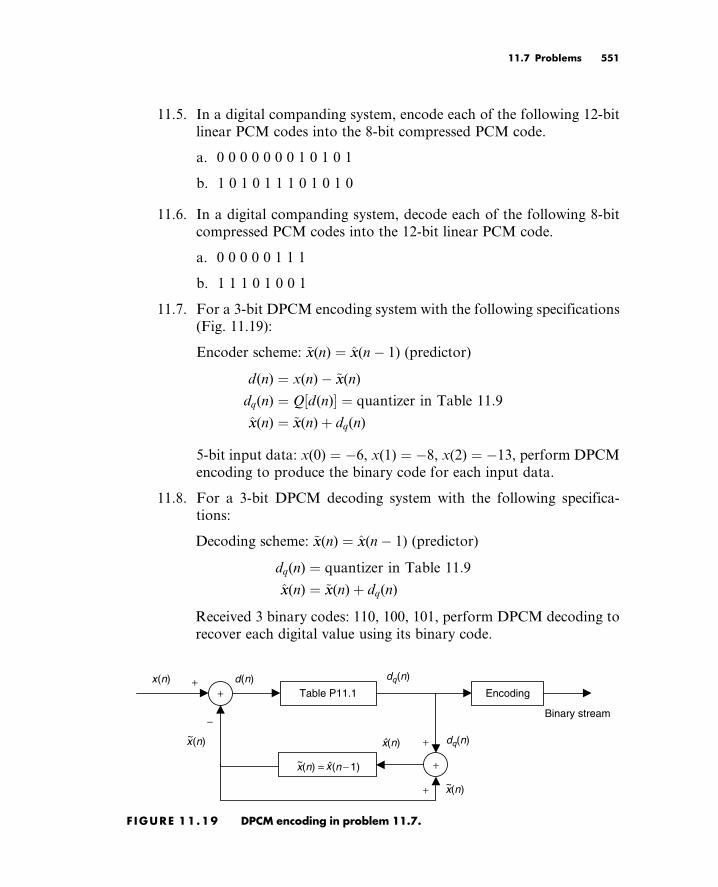
11.5. In a digital companding system, encode each of the following 12-bit
linear PCM codes into the 8-bit compressed PCM code.
a. 0 0 0 0 0 0 0 1 0 1 0 1
b. 1 0 1 0 1 1 1 0 1 0 1 0
11.6. In a digital companding system, decode each of the following 8-bit
compressed PCM codes into the 12-bit linear PCM code.
a. 0 0 0 0 0 1 1 1
b. 1 1 1 0 1 0 0 1
11.7. For a 3-bit DPCM encoding system with the following specifications
(Fig. 11.19):
Encoder scheme: ~xx(n) ¼ xx(n 1) (predictor)
d(n) ¼ x(n) ~xx(n)
dq(n) ¼ Q d(n)½ ¼ quantizer in Table 11:9
xx(n) ¼ ~xx(n)þ dq(n)
5-bit input data: x(0) ¼ 6, x(1) ¼ 8, x(2) ¼ 13, perform DPCM
encoding to produce the binary code for each input data.
11.8. For a 3-bit DPCM decoding system with the following specifica-
tions:
Decoding scheme: ~xx(n) ¼ xx(n 1) (predictor)
dq(n) ¼ quantizer in Table 11:9
xx(n) ¼ ~xx(n)þ dq(n)
Received 3 binary codes: 110, 100, 101, perform DPCM decoding to
recover each digital value using its binary code.
+
+
+
−
+
+
Table P11.1 Encoding
Binary stream
x(n)
~x(n)
~x(n)
d(n) dq(n)
dq(n)
~x(n) = (n − 1)
x(n)ˆ
x
F IGURE 11.19 DPCM encoding in problem 11.7.
Tan: Digital Signaling Processing 0123740908_chap11 Final Proof page 551 21.6.2007 11:15pm Compositor Name: NNiranchana
11.7 Problems 551

11.9. Assuming that a speech waveform is sampled at 8 kHz and each
sample is encoded by 16 bits, determine the compression ratio for
each of the encoding methods.
a. noncompression
b. standard m-law compression (8 bits per sample)
c. standard ADPCM encoding (4 bits per sample).
11.10. Suppose that a speech waveform is sampled at 8 kHz into 16 bits per
sample. Determine the bit rate for each of the following encoding
methods:
a. noncompression
b. standard m-law companding (8 bits per sample)
c. standard ADPCM encoding (4 bits per sample).
11.11. Speech is sampled at 8 kHz and each sample is encoded by 16 bits.
The telephone system can transport the digital voice channel over a
digital link having a capacity of 1.536 Mbps. Determine the number
of channels that the phone company can carry for each of the
following encoding methods:
TABLE 11 .9 Quantization table for the 3-bit quantizer in Problem 11.7.
Binary Code Quantization Value dq(n) Subrange in d(n)
0 1 1 11 15 d(n) < 7
0 1 0 5 7 d(n) < 3
0 0 1 2 3 d(n) < 1
0 0 0 0 1 d(n) < 0
1 0 0 0 0 d(n) 1
1 0 1 2 1 < d(n) 3
1 1 0 5 3 < d(n) 7
1 1 1 11 7 < d(n) 15
+
+
+
Decoding usingTable 11.9
Binary stream
dq(n)
~x(n)
Recovered~x(n) = (n − 1)
x(n)ˆ
x
F IGURE 11 .20. DPCM decoding in problem 11.8.
Tan: Digital Signaling Processing 0123740908_chap11 Final Proof page 552 21.6.2007 11:15pm Compositor Name: NNiranchana
552 11 W A V E F O R M Q U A N T I Z A T I O N A N D C O M P R E S S I O N
a. noncompression
b. standard m-law companding (8 bits per sample)
c. standard ADPCM encoding (4 bits per sample).
11.12. Given the following input data:
x(0) ¼ 25, x(1) ¼ 30, x(2) ¼ 28, and x(3) ¼ 25,
determine the DCT coefficients.
11.13. Assuming the following DCT coefficients with infinite precision:
XDCT (0) ¼ 14, XDCT (1) ¼ 6, XDCT (3) ¼ 6, and XDCT (0) ¼ 8,
a. determine the input data using the MATLAB function idct();
b. recover the input data samples using the MATLAB function
idct() if a bit allocation scheme quantizes the DCT coefficients
as follows: 2 magnitude bits plus 1 sign bit (3 bits) for the DC
coefficient, 1 magnitude bit plus 1 sign bit (2 bits) for each AC
coefficient and a scale factor of 8, that is,
XDCT (0) ¼ 8 2 ¼ 16, XDCT (1) ¼ 8 1 ¼ 8, XDCT (2) ¼ 8 ( 1)
¼ 8, and XDCT (3) ¼ 8 1 ¼ 8;
c. compute the quantized error in part b. of this question.
11.14. a. Verify the window functions
f (n) ¼ h(n) ¼ sinp
Nnþ 0:5ð Þ
used in MDCT that are satisfied with Equations (11.35) and
(11.36).
b. Verify W-MDCT coefficients
XMDCT (k) ¼ ( 1)N2þ1XMDCT (N 1 k) for k ¼ N=2, N=2þ 1, . . . , N 1:
11.15. Given data 1, 2, 3, 4, 5, 4, 3, 2, . . . ,
a. determine the W-MDCT coefficients for the first three blocks
using a block size of 4;
b. determine the first two overlapped subblocks and compare the
results with the original data sequence using the W-MDCT coef-
ficients in part (a) of Problem 11.15.
Tan: Digital Signaling Processing 0123740908_chap11 Final Proof page 553 21.6.2007 11:15pm Compositor Name: NNiranchana
11.7 Problems 553

Computer Problems with MATLAB
Use the MATLAB programs in the program section for Problems 11.16 to
11.18.
11.16. Given the data file ‘‘speech.dat’’ with 16 bits per sample and a
sampling rate of 8 kHz,
a. Use the PCM coding (midtrad quantizer) to perform compres-
sion and decompression and apply the MATLAB function
sound() to evaluate the sound quality in terms of ‘‘excellent,’’
‘‘good,’’ ‘‘intelligent,’’ and ‘‘unacceptable’’ for the following bit
rates:
1. 4 bits/sample (32 Kbits per second)
2. 6 bits/sample (48 Kbits per second)
3. 8 bits/sample (64 Kbits per second)
b. Use the m-law PCM coding to perform compression and decom-
pression and apply the MATLAB function sound() to evaluate
the sound quality.
1. 4 bits/sample (32 Kbits per second)
2. 6 bits/sample (48 Kbits per second)
3. 8 bits/sample (64 Kbits per second)
11.17. Given the data file ‘‘speech.dat’’ with 16 bits per sample, a sampling
rate of 8 kHz, and ADCPM coding, perform compression, and
decompression and apply the MATLAB function sound() to evalu-
ate the sound quality.
11.18. Given the data file ‘‘speech.dat’’ with 16 bits per sample, a sampling
rate of 8 kHz, and DCT and M-DCT coding in the program section,
perform compression and decompression using the following speci-
fied parameters in Program 11.16 to compare the sound quality.
a. nbits¼ 3, scalef¼ scalef2bits
b. nbits¼ 3, scalef¼ scalef3bits
c. nbits¼ 4, scalef¼ scalef2bits
d. nbits¼ 4, scalef¼ scalef3bits
Tan: Digital Signaling Processing 0123740908_chap11 Final Proof page 554 21.6.2007 11:15pm Compositor Name: NNiranchana
554 11 W A V E F O R M Q U A N T I Z A T I O N A N D C O M P R E S S I O N

References
Brandenburg, K. (1997). Overview of MPEG audio: Current and future standards for low-
bit-rate audio coding. Journal of the Audio Engineering Society, 45 (1/2).
Li, Z.-N., and Drew, M. S. (2004). Fundamentals of Multimedia. Upper Saddle River, NJ:
Pearson/Prentice Hall.
Nelson, M. (1992). The Data Compression Book. Redwood City, CA: M&T Publishing.
Pan, D. (1995). A tutorial on MPEG/audio compression. IEEE Multimedia, 2: 60–74.
Princen, J., and Bradley, A. B. (1986). Analysis/synthesis filter bank design based on time
domain aliasing cancellation. IEEE Transactions on Acoustics, Speech, and Signal Pro-
cessing, ASSP 34 (5).
Roddy, D., and Coolen, J. (1997). Electronic Communications, 4th ed. Englewood Cliffs, NJ:
Prentice Hall.
Sayood, K. (2000). Introduction to Data Compression, 2nd ed. San Francisco: Morgan
Kaufmann Publishers.
Stearns, S. D. (2003). Digital Signal Processing with Examples in MATLAB. Boca Raton,
FL: CRC Press LLC.
Tomasi, W. (2004). Electronic Communications Systems: Fundamentals Through Advanced,
5th ed. Upper Saddle River, NJ: Pearson/Prentice Hall.
Yost, W. A. (1994). Fundamentals of Hearing: An Introduction, 3rd ed. San Diego: Academic
Press.
Tan: Digital Signaling Processing 0123740908_chap11 Final Proof page 555 21.6.2007 11:15pm Compositor Name: NNiranchana
References 555

Tan: Digital Signaling Processing 0123740908_chap11 Final Proof page 556 21.6.2007 11:15pm Compositor Name: NNiranchana
This page intentionally left blank

12Multirate Digital Signal Processing,Oversampling of Analog-to-DigitalConversion, and Undersampling of
Bandpass Signals
Object ives :
This chapter investigates basics of multirate digital signal processing, illus-
trates how to change a sampling rate for speech and audio signals, and
describes the polyphase implementation for the decimation filter and inter-
polation filter. Next, the chapter introduces the advanced analog-to-digital
conversion system with the oversampling technique and sigma-delta modula-
tion. Finally, the chapter explores the principles of undersampling of
bandpass signals.
12.1 Mult i rate Digi ta l S ignalProcess ing Basics
In many areas of digital signal processing (DSP) applications—such as commu-
nications, speech, and audio processing—rising or lowering of a sampling rate is
required. The principle that deals with changing the sampling rate belongs
essentially to multirate signal processing (Ifeachor and Jervis, 2002; Porat,
1997; Proakis and Manolakis, 1996; Sorensen and Chen, 1997). As an introduc-
tion, we will focus on sampling rate conversion; that is, sampling rate reduction
or increase.
Tan: Digital Signaling Processing 0123740908_chap12 Final Proof page 557 22.6.2007 12:18am Compositor Name: Mraja

12.1.1 Sampl ing Rate Reduct ion by anInteger Factor
The process of reducing a sampling rate by an integer factor is referred to as
downsampling of a data sequence. We also refer to downsampling as ‘‘decimation’’
(not taking one of ten). The term ‘‘decimation’’ used for the downsampling process
has been accepted and used in many textbooks and fields. To downsample a data
sequence x(n) by an integer factor of M, we use the following notation:
y(m) ¼ x(mM), (12:1)
where y(m) is the downsampled sequence, obtained by taking a sample from the
data sequence x(n) for every M samples (discarding M 1 samples for every
M samples). As an example, if the original sequence with a sampling period
T ¼ 0:1 second (sampling rate ¼ 10 samples per sec) is given by
x(n): 8 7 4 8 9 6 4 2 2 5 7 7 6 4 . . .
and we downsample the data sequence by a factor of 3, we obtain the down-
sampled sequence as
y(m): 8 8 4 5 6 . . . ,
with the resultant sampling period T ¼ 3 0:1 ¼ 0:3 second (the sampling rate
now is 3.33 samples per second). Although the example is straightforward, there
is a requirement to avoid aliasing noise. We will illustrate this next.
From the Nyquist sampling theorem, it is known that aliasing can occur in
the downsampled signal due to the reduced sampling rate. After downsampling
by a factor of M, the new sampling period becomes MT, and therefore the new
sampling frequency is
fsM ¼1
MT¼ fs
M, (12:2)
where fs is the original sampling rate.
Hence, the folding frequency after downsampling becomes
fsM=2 ¼fs
2M: (12:3)
This tells us that after downsampling by a factor of M, the new folding
frequency will be decreased M times. If the signal to be downsampled has
frequency components larger than the new folding frequency, f > fs=(2M),
aliasing noise will be introduced into the downsampled data.
To overcome this problem, it is required that the original signal x(n) be
processed by a lowpass filter H(z) before downsampling, which should have a
stop frequency edge at fs=(2M) (Hz). The corresponding normalized stop fre-
quency edge is then converted to be
Tan: Digital Signaling Processing 0123740908_chap12 Final Proof page 558 22.6.2007 12:18am Compositor Name: Mraja
558 12 M U L T I R A T E D I G I T A L S I G N A L P R O C E S S I N G

Vstop ¼ 2pfs
2MT ¼ p
Mradians: (12:4)
In this way, before downsampling, we can guarantee that the maximum
frequency of the filtered signal satisfies
fmax <fs
2M, (12:5)
such that no aliasing noise is introduced after downsampling. A general block
diagram of decimation is given in Figure 12.1, where the filtered output in terms
of the z-transform can be written as
W (z) ¼ H(z)X (z), (12:6)
where X(z) is the z-transform of the sequence to be decimated, x(n), and H(z) is
the lowpass filter transfer function. After anti-aliasing filtering, the down-
sampled signal y(m) takes its value from the filter output as:
y(m) ¼ w(mM): (12:7)
Anti-aliasingfilter H(z)
x (n)
x (n)
w (n)
w (n) y (m)
y (m)
n
n
m
0 2 4 6 8 10 12 14 16
0 2
1 2 3 4
4 6 8 10 12 14 16
0 5
fs fsfsM
↓M
F IGURE 12.1 Block diagram of the downsampling process with M ¼ 3:
Tan: Digital Signaling Processing 0123740908_chap12 Final Proof page 559 22.6.2007 12:18am Compositor Name: Mraja
12.1 Multirate Digital Signal Processing Basics 55912.1 Multirate Digital Signal Processing Basics 559

The process of reducing the sampling rate by a factor of 3 is shown in
Figure 12.1. The corresponding spectral plots for x(n), w(n), and y(m) in general
are shown in Figure 12.2.
To verify this principle, let us consider a signal x(n) generated by the
following:
x(n) ¼ 5 sin2p 1000n
8000
þ cos
2p 2500n
8000
, (12:8)
with a sampling rate of fs ¼ 8,000Hz, the spectrum of x(n) is plotted in the first
graph in Figure 12.3a, where we observe that the signal has components at
frequencies of 1,000 and 2,500 Hz. Now we downsample x(n) by a factor of 2,
0
0
1
0−2f sM f sM 2 f sM
Anti-aliasingfilter H(z)
↓M
fs
− f s
− f s
− f s / 2
− f s / 2
f s / 2
f s / 2
fs
f s
f s
f sM =
f sM = f s / M
f s
M
x (n)
X (f )
W (f )
Y (f )
H (f )
w (n) y (m)
f (Hz )
f (Hz )
f (Hz )
f (Hz )
−2
f sM
2f sM
0− f s − f s / 2 f s / 2 f s
−f sM
2f sM
2f sM
2f sM−
2f sM−
F IGURE 12 .2 Spectrum after downsampling.
Tan: Digital Signaling Processing 0123740908_chap12 Final Proof page 560 22.6.2007 12:18am Compositor Name: Mraja
560 12 M U L T I R A T E D I G I T A L S I G N A L P R O C E S S I N G

that is, M ¼ 2. According to Equation (12.3), we know that the new folding
frequency is 4000=2 ¼ 2000 Hz. Hence, without using the anti-aliasing
lowpass filter, the spectrum would contain the aliasing frequency of
4 kHz 2:5 kHz ¼ 1:5 kHz introduced by 2.5 kHz, plotted in the second
graph in Figure 12.3a.
Now we apply a finite impulse response (FIR) lowpass filter designed with a
filter length of N ¼ 27 and a cutoff frequency of 1.5 kHz to remove the 2.5-kHz
signal before downsampling to avoid aliasing. How to obtain such specifications
will be discussed in a later example. The normalized cutoff frequency used for
design is given by
Vc ¼ 2p 1500 (1=8000) ¼ 0:375p:
Thus, the aliasing noise is avoided. The spectral plots are given in Figure 12.3b,
where the first plot shows the spectrum of w(n) after anti-aliasing filtering,
while the second plot describes the spectrum of y(m) after downsampling.
Clearly, we prevent aliasing noise in the downsampled data by sacrificing
the original 2.5-kHz signal. Program 12.1 gives the detail of MATLAB imple-
mentation.
0 500 1000 1500 2000 2500 3000 3500 40000
2
4
6
Frequency (Hz)
0 200 400 600 800 1000 1200 1400 1600 1800 20000
2
4
6
Frequency (Hz)A
F IGURE 12.3A Spectrum before downsampling and spectrum after downsamplingwithout using the anti-aliasing filter.
Tan: Digital Signaling Processing 0123740908_chap12 Final Proof page 561 22.6.2007 12:18am Compositor Name: Mraja
12.1 Multirate Digital Signal Processing Basics 56112.1 Multirate Digital Signal Processing Basics 561

Program 12.1. MATLAB program for decimation.
close all;clear all;
% Downsampling filter (see Chapter 7 for FIR filter design)
B¼[0.00074961181416 0.00247663033476 0.00146938649416 0.00440446121505...0.00910635730662 0.00000000000000 0.02035676831506 0.02233710562885...
0.01712963672810 0.06376620649567 0.03590670035210 0.10660980550088...
0.29014909103794 0.37500000000000 0.29014909103794 0.10660980550088...
0.03590670035210 0.06376620649567 0.01712963672810 0.02233710562885...
0.02035676831506 0.00000000000000 0.00910635730662 0.00440446121505...0.00146938649416 0.00247663033476 0.00074961181416];
% Generate the 2048 samples
fs¼8000; % Sampling rate
N¼2048; % Number of samples
M¼2; % Downsample factor
n¼0:1:N-1;x ¼ 5sin(npi/4)þcos(5npi/8);% Compute the single-sided amplitude spectrum
% AC component will be doubled, and DC component will be kept the same value
X ¼ 2abs(fft(x,N))/N;X(1)¼X(1)/2;
0 500 1000 1500 2000 2500 3000 3500 40000
2
4
6
Frequency (Hz)
0 200 400 600 800 1000 1200 1400 1600 1800 20000
2
4
6
Frequency (Hz)B
F IGURE 12.3B Spectrum before downsampling and spectrum after downsamplingusing the anti-aliasing filter.
Tan: Digital Signaling Processing 0123740908_chap12 Final Proof page 562 22.6.2007 12:18am Compositor Name: Mraja
562 12 M U L T I R A T E D I G I T A L S I G N A L P R O C E S S I N G

% Map the frequency index up to the folding frequency in Hz
f¼[0:1:N/2-1]fs/N;%Downsampling
y¼x(1:M:N);NM¼length(y); % Length of the downsampled data
% Compute the single-sided amplitude spectrum for the downsampled signal
Y ¼ 2abs(fft(y,NM))/length(y);Y(1)¼Y(1)/2;% Map the frequency index to the frequency in Hz
fsM¼[0:1:NM/2-1](fs/M)/NM;subplot(2,1,1);plot(f,X(1:1:N/2));grid;xlabel(‘Frequency (Hz)’);
subplot(2,1,2);plot(fsM,Y(1:1:NM/2));grid;xlabel(‘Frequency (Hz)’);
figure
w¼filter(B,1,x); % Anti-aliasing filtering
% Compute the single-sided amplitude spectrum for the filtered signal
W ¼ 2abs(fft(w,N))/N;W(1)¼W(1)/2;% Downsampling
y¼w(1:M:N);NM¼length(y);% Compute the single-sided amplitude spectrum for the downsampled signal
Y ¼ 2abs(fft(y,NM))/NM;Y(1)¼Y(1)/2;% plot spectra
subplot(2,1,1);plot(f,W(1:1:N/2));grid;xlabel(‘Frequency (Hz)’);
subplot(2,1,2);plot(fsM,Y(1:1:NM/2));grid;xlabel(‘Frequency (Hz)’);
Now we focus on how to design the anti-aliasing FIR filter, or decimation
filter. We will discuss this topic via the following example.
Example 12.1.
Given a DSP downsampling system with the following specifications:
Sampling rate ¼ 6,000 Hz
Input audio frequency range ¼ 0–800 Hz
Passband ripple ¼ 0.02 dB
Stopband attenuation ¼ 50 dB
Downsample factor M ¼ 3,
a. Determine the FIR filter length, cutoff frequency, and window type if the
window method is used.
Solution:
a. Specifications are reorganized as:
Anti-aliasing filter operating at the sampling rate ¼ 6000 Hz
Passband frequency range ¼ 0–800 Hz
Tan: Digital Signaling Processing 0123740908_chap12 Final Proof page 563 22.6.2007 12:18am Compositor Name: Mraja
12.1 Multirate Digital Signal Processing Basics 56312.1 Multirate Digital Signal Processing Basics 563

Stopband frequency range ¼ 1–3 kHz
Passband ripple ¼ 0.02 dB
Stopband attenuation ¼ 50 dB
Filter type ¼ FIR.
The block diagram and specifications are depicted in Figure 12.4.
The Hamming window is selected, since it provides 0.019 dB ripple
and 53 dB stopband attenuation. The normalized transition band is
given by
Df ¼ fstop fpass
fs¼ 1000 800
6000¼ 0:033:
The length of the filter and the cutoff frequency can be determined by
N ¼ 3:3
Df¼ 3:3
0:033¼ 100:
We choose the odd number, that is, N ¼ 101, and
fc ¼fpass þ fstop
2¼ 800þ 1000
2¼ 900Hz:
12.1.2 Sampl ing Rate Increase by an IntegerFactor
Increasing a sampling rate is a process of upsampling by an integer factor of L.
This process is described as follows:
y(m) ¼ x mL
m ¼ nL
0 otherwise
, (12:9)
Anti-aliasing filter H(z)
x(n) w(n) y(m)
↓3
6kHz 6kHz 2kHz
3f kHz
210.80
F IGURE 12 .4 Filter specifications for Example 12.1.
Tan: Digital Signaling Processing 0123740908_chap12 Final Proof page 564 22.6.2007 12:18am Compositor Name: Mraja
564 12 M U L T I R A T E D I G I T A L S I G N A L P R O C E S S I N G

where n ¼ 0, 1, 2, . . . , x(n) is the sequence to be upsampled by a factor of L, and
y(m) is the upsampled sequence. As an example, suppose that the data sequence
is given as follows:
x(n): 8 8 4 5 6 . . . :
After upsampling the data sequence x(n) by a factor of 3 (adding L 1 zeros for
each sample), we have the upsampled data sequence w(m) as:
w(m): 8 0 0 8 0 0 4 0 0 5 0 0 6 0 0 . . . :
The next step is to smooth the upsampled data sequence via an interpolation
filter. The process is illustrated in Figure 12.5a.
Similar to the downsampling case, assuming that the data sequence has the
current sampling period of T, the Nyquist frequency is given by fmax ¼ fs=2.
After upsampling by a factor of L, the new sampling period becomes T / L, thus
the new sampling frequency is changed to be
fsL ¼ Lfs: (12:10)
This indicates that after upsampling, the spectral replicas originally centered at
fs, 2fs, . . . are included in the frequency range from 0 Hz to the new Nyquist
limit Lfs=2 Hz, as shown in Figure 12.5b. To remove those included spectral
replicas, an interpolation filter with a stop frequency edge of fs=2 in Hz must be
attached, and the normalized stop frequency edge is given by
Vstop ¼ 2pfs
2
T
L
¼ p
Lradians: (12:11)
After filtering via the interpolation filter, we will achieve the desired spectrum
for y(n), as shown in Figure 12.5b. Note that since the interpolation is to remove
the high-frequency images that are aliased by the upsampling operation, it is
essentially an anti-aliasing lowpass filter.
To verify the upsampling principle, we generate the signal x(n) with 1 kHz
and 2.5 kHz as follows:
x(n) ¼ 5 sin2p 1000n
8000
þ cos
2p 2500n
8000
,
with a sampling rate of fs ¼ 8,000Hz. The spectrum of x(n) is plotted in Figure
12.6. Now we upsample x(n) by a factor of 3, that is, L ¼ 3. We know that the
sampling rate is increased to be 3 8000 ¼ 24,000Hz. Hence, without using the
interpolation filter, the spectrum would contain the image frequencies originally
centered at the multiple frequencies of 8 kHz. The top plot in Figure 12.6 shows
Tan: Digital Signaling Processing 0123740908_chap12 Final Proof page 565 22.6.2007 12:18am Compositor Name: Mraja
12.1 Multirate Digital Signal Processing Basics 56512.1 Multirate Digital Signal Processing Basics 565

the spectrum for the sequence after upsampling and before applying the inter-
polation filter.
Now we apply an FIR lowpass filter designed with a length of 53, a cutoff
frequency of 3,250 Hz, and a new sampling rate of 24,000 Hz as the interpol-
ation filter, whose normalized frequency should be
Vc ¼ 2p 3250 1
24000
¼ 0:2708p:
The bottom plot in Figure 12.6 shows the spectrum for y(m) after applying the
interpolation filter, where only the original signals with frequencies of 1 kHz
and 2.5 kHz are presented. Program 12.2 shows the implementation detail in
MATLAB.
Now let us study how to design the interpolation filter via Example 12.2.
m
m
n
0 2 4 6 8 10 12 14 16
0 2 4 6 8 10 12 14 16
0 1 2 3 4
Interpolation filter H(z)
x(n)
x(n)
w(m)
w(m)
y(m)
y(m)
↑L
5
f s Lf s Lf s
A
F IGURE 12 .5A Block diagram for the upsampling process with L ¼ 3.
Tan: Digital Signaling Processing 0123740908_chap12 Final Proof page 566 22.6.2007 12:18am Compositor Name: Mraja
566 12 M U L T I R A T E D I G I T A L S I G N A L P R O C E S S I N G

Example 12.2.
Given a DSP upsampling system with the following specifications:
Sampling rate ¼ 6,000 Hz
Input audio frequency range ¼ 0---800Hz
Passband ripple ¼ 0:02 dB
Stopband attenuation ¼ 50 dB
Upsample factor L ¼ 3,
a. Determine the FIR filter length, cutoff frequency, and window type if the
window design method is used.
(Continued on page 569)
0
1
0
0
Interpolation filter H(z)
↑L
x(n)
X(f )
H(f )
Y(f )
W(f )
w(m) y(m)
f s Lfs f sL = Lf s
− Lf s f sL = Lf s
− f s − f s / 2 f s / 2 f s
0− f s − f s / 2
− f s − f s / 2
− f s / 2 f sL / 2− f sL / 2
f s / 2
f s / 2
f s / 2
f s
f s f sL
f sL
− f sL
− f sL
f (Hz )
f (Hz )
f (Hz )
f (Hz )
B
F IGURE 12.5B Spectra before and after upsampling.
Tan: Digital Signaling Processing 0123740908_chap12 Final Proof page 567 22.6.2007 12:18am Compositor Name: Mraja
12.1 Multirate Digital Signal Processing Basics 56712.1 Multirate Digital Signal Processing Basics 567

Program 12.2. MATLAB program for interpolation.
close all; clear all
%Upsampling filter (see Chapter 7 for FIR filter design)
B¼[0.00012783931504 0.00069976044649 0.00123831516738 0.00100277549136...
0.00025059018468 0.00203448515158 0.00300830295487 0.00174101657599...0.00188598835011 0.00578414933758 0.00649330625041 0.00177982369523...
0.00670672686935 0.01319379342716 0.01116855281442 0.00123034314117...
0.01775600060894 0.02614700427364 0.01594155162392 0.01235169936557...0.04334322148505 0.05244745563466 0.01951094855292 0.05718573279009...
0.15568416401644 0.23851539047347 0.27083333333333 0.23851539047347...
0.15568416401644 0.05718573279009 0.01951094855292 0.05244745563466...0.04334322148505 0.01235169936557 0.01594155162392 0.02614700427364...
0.01775600060894 0.00123034314117 0.01116855281442 0.01319379342716...0.00670672686935 0.00177982369523 0.00649330625041 0.00578414933758...
0.00188598835011 0.00174101657599 0.00300830295487 0.00203448515158...0.00025059018468 0.00100277549136 0.00123831516738 0.00069976044649...
0.00012783931504];% Generate the 2048 samples with fs ¼ 8000Hz
fs ¼ 8000; % Sampling rate
0 2000 4000 6000 8000 10000 120000
0.5
1
1.5
2
Frequency (Hz)
0 2000 4000 6000 8000 10000 120000
0.5
1
1.5
2
Frequency (Hz)
F IGURE 12.6 (Top) The spectrum after upsampling and before applying theinterpolation filter; (bottom) the spectrum after applying theinterpolation filter.
Tan: Digital Signaling Processing 0123740908_chap12 Final Proof page 568 22.6.2007 12:18am Compositor Name: Mraja
568 12 M U L T I R A T E D I G I T A L S I G N A L P R O C E S S I N G

N ¼ 2048; % Number of samples
L ¼ 3; % Upsampling factor
n¼0:1:N-1;x ¼ 5 sin(npi=4)þ cos(5npi=8);% Upsampling by a factor of L
w¼zeros(1,LN);for n¼0:1:N-1w(Lnþ 1) ¼ x(nþ 1);end
NL ¼ length(w); % Length of the upsampled data
W ¼ 2abs(fft(w,NL))/NL;W(1)¼W(1)/2;%Computetheone-sidedamplitudespectrumf¼[0:1:NL/2-1]fsL/NL; % Map the frequency index to the frequency (Hz)
%Interpolation
y¼filter(B,1,w); % Apply the interpolation filter
Y ¼ 2abs(fft(y,NL))/NL;Y(1)¼Y(1)/2;%Computetheone-sidedamplitudespectrumfsL¼[0:1:NL/2-1]fsL/NL; % Map the frequency index to the frequency (Hz)
subplot(2,1,1);plot(f,W(1:1:NL/2));grid;xlabel(‘Frequency (Hz)’);
subplot(2,1,2);plot(fsL,Y(1:1:NL/2));grid;xlabel(‘Frequency (Hz)’);
Solution:
a. The specifications are reorganized as follows:
Interpolation filter operating at the sampling rate ¼ 18,000Hz
Passband frequency range ¼ 0---800 Hz
Stopband frequency range ¼ 3---9 kHz
Passband ripple ¼ 0:02 dB
Stopband attenuation ¼ 50 dB
Filter type ¼ FIR.
The block diagram and filter frequency specifications are given in Figure
12.7.
We choose the Hamming window for this application. The normalized
transition band is
Df ¼ fstop fpass
fsL¼ 3000 800
18000¼ 0:1222:
The length of the filter and the cutoff frequency can be determined by
N ¼ 3:3
Df¼ 3:3
0:1222¼ 27,
and the cutoff frequency is given by
fc ¼fpass þ fstop
2¼ 3000þ 800
2¼ 1900Hz:
Tan: Digital Signaling Processing 0123740908_chap12 Final Proof page 569 22.6.2007 12:18am Compositor Name: Mraja
12.1 Multirate Digital Signal Processing Basics 56912.1 Multirate Digital Signal Processing Basics 569

12.1.3 Changing Sampl ing Rate by aNon-Integer Factor L/M
With an understanding of the downsampling and upsampling processes, we now
study the sampling rate conversion by a non-integer factor of L/M. This can be
viewed as two sampling conversion processes. In step 1, we perform the upsam-
pling process by a factor of integer L following application of an interpolation
filter H1(z); in step 2, we continue filtering the output from the interpolation
filter via an anti-aliasing filter H2(z), and finally operate downsampling. The
entire process is illustrated in Figure 12.8.
Since the interpolation and anti-aliasing filters are in a cascaded form and
operate at the same rate, we can select one of them. We choose the one with the
lower stop frequency edge and choose the most demanding requirement for
passband gain and stopband attenuation for the filter design. A lot of compu-
tational saving can be achieved by using one lowpass filter. We illustrate the
procedure via the following simulation. Let us generate the signal x(n) by:
x(n) ¼ 5 sin2p 1000n
8000
þ cos
2p 2500n
8000
,
with a sampling rate of fs ¼ 8,000Hz and frequencies of 1 kHz and 2.5 kHz.
Now we resample x(n) to 3,000 Hz by a non-integer factor of 0.375, that is,
L
M
¼ 0:375 ¼ 3
8:
Upsampling is at a factor of L ¼ 3 and the upsampled sequence is filtered by an
FIR lowpass filter designed with the filter length N ¼ 53 and a cutoff frequency
of 3,250 Hz at the sampling rate of 3 8000 ¼ 24,000Hz. The spectrum for the
upsampled sequence and the spectrum after application of the interpolation
filter are plotted in Figure 12.9a.
Anti-image filter H(z)
↑3
6kHz 18kHz 18kHz
9
f kHz
630 .80
x(n) w(m) y(m)
F IGURE 12 .7 Filter frequency specifications for Example 12.2.
Tan: Digital Signaling Processing 0123740908_chap12 Final Proof page 570 22.6.2007 12:18am Compositor Name: Mraja
570 12 M U L T I R A T E D I G I T A L S I G N A L P R O C E S S I N G

The sequence from step 1 can be filtered via another FIR lowpass filter
designed with the filter length N ¼ 159 and a cutoff frequency of 1,250 Hz,
followed by downsampling by a factor of M ¼ 8. The spectrum after the anti-
aliasing filter and the spectrum for the final output y(m) are plotted in
Figure 12.9b. Note that the anti-aliasing filter removes the frequency compon-
ent of 2.5 kHz to avoid aliasing. This is because after downsampling, the
Nyquist limit is 1.5 kHz. As we discussed previously, we can select one filter
for implementation. We choose the FIR lowpass with N ¼ 159 and a cutoff
frequency of 1,250 Hz because its bandwidth is smaller than that of the inter-
polation filter. The MATLAB implementation is listed in Program 12.3.
Program 12.3. MATLAB program for changing sampling rate with a non-
integer factor.
close all; clear all;clc;
% Downsampling filter
Bdown¼firwd(159,1,2pi1250/24000,0,4);% Generate the 2048 samples with fs ¼ 8000Hz
fs ¼ 8000; % Original sampling rate
N ¼ 2048; % The number of samples
L ¼ 3; % Upsampling factor
M ¼ 8; % Downsampling factor
n ¼ 0:1:N-1; % Generate the time index
x ¼ 5 sin(npi=4)þ cos(5npi=8); % Generate the test signal
% upsampling by a factor of L
w1¼zeros(1,LN);for n ¼ 0:1:N-1
w1(Lnþ 1) ¼ x(nþ 1);end
NL¼ length(w1); % Length of the upsampled data
W1 ¼ 2abs(fft(w1,NL))/NL;W1(1) ¼ W1(1)/2;%Computetheone-sidedamplitudespectrum
f ¼ [0:1:NL=2-1]fsL=NL; %MapfrequencyindextoitsfrequencyinHz
subplot(3,1,1);plot(f,W1(1:1:NL/2));grid
xlabel(‘Frequency (Hz)’);
w2 ¼ filter(Bdown,1,w1); % Perform the combined anti-aliasing filter
Interpolationfilter H1(z)
y (m)
↑LAnti-aliasingfilter H2(z) ↓M
H(z)
x(n)
F IGURE 12 .8 Block diagram for sampling rate conversion.
(Continued )
Tan: Digital Signaling Processing 0123740908_chap12 Final Proof page 571 22.6.2007 12:18am Compositor Name: Mraja
12.1 Multirate Digital Signal Processing Basics 57112.1 Multirate Digital Signal Processing Basics 571

W2 ¼ 2abs(fft(w2,NL))/NL;W2(1) ¼ W2(1)=2;%Computetheone-sidedamplitudespectrum
y2¼w2(1:M:NL);NM¼length(y2); % Length of the downsampled data
Y2 ¼ 2abs(fft(y2,NM))/NM;Y2(1) ¼ Y2(1)=2;% Compute the one-sidedamplitudespectrum
% Map frequency index to its frequency in Hz before downsampling
fbar ¼ [0:1:NL=2-1]24000=NL;% Map frequency index to its frequency in Hz
fsM ¼ [0:1:NM=2-1](fsL=M)=NM;subplot(3,1,2);plot(f,W2(1:1:NL/2));grid;xlabel(‘Frequency (Hz)’);
subplot(3,1,3);plot(fsM,Y2(1:1:NM/2));grid;xlabel(‘Frequency (Hz)’);
Therefore, three steps are required to accomplish the process:
1. Upsampling by a factor of L ¼ 3
2. Filtering the upsampled sequence by an FIR lowpass filter designed with
the filter length N ¼ 159 and a cutoff frequency of 1,250 Hz at the
sampling rate of 3 8000 ¼ 24,000Hz
3. Downsampling by a factor of M ¼ 8.
0 2000 4000 6000 8000 10000 120000
0.5
1
1.5
2
0 2000 4000 6000 8000 10000 120000
0.5
1
1.5
2
Frequency (Hz)
Frequency (Hz)
A
F IGURE 12.9A (Top) Spectrum after upsampling and (bottom) spectrum afterinterpolation filtering.
Tan: Digital Signaling Processing 0123740908_chap12 Final Proof page 572 22.6.2007 12:18am Compositor Name: Mraja
572 12 M U L T I R A T E D I G I T A L S I G N A L P R O C E S S I N G

Example 12.3.
Given a sampling conversion DSP system with the following specifications:
Interpolation filter H1(z)
x(n) y(m)
H(z)↑3
Anti-aliasing filter H2(z) ↓2
A
Audio input x(n) is sampled at the rate of 6,000 Hz,
Audio output y(m) is operated at the rate of 9,000 Hz.
F IGURE 12.10A Sampling conversion in Example 12.3.
a. Determine the filter length and cutoff frequency for the combined anti-
aliasing filter H(z), and window types, respectively, if the window design
method is used.
0 2000 4000 6000 8000 10000 120000
0.5
1
1.5
2
Frequency (Hz)
0 500 1000 15000
0.5
1
1.5
2
Frequency (Hz)B
F IGURE 12.9B (Top) Spectrum after anti-aliasing filtering and (bottom) spectrumafter downsampling.
Tan: Digital Signaling Processing 0123740908_chap12 Final Proof page 573 22.6.2007 12:18am Compositor Name: Mraja
12.1 Multirate Digital Signal Processing Basics 57312.1 Multirate Digital Signal Processing Basics 573

Solution:
a. The filter frequency specifications and corresponding block diagram are
developed in Figure 12.10b.
Specifications for the interpolation filter H1(z):
Passband frequency range ¼ 0---2500Hz
Passband ripples for H1(z) ¼ 0:04 dB
Stopband frequency range ¼ 3000---9000Hz
Stopband attenuation ¼ 42 dB
Specifications for the anti-aliasing filter H2(z):
Passband frequency range ¼ 0---2500Hz
Passband ripples for H2(z) ¼ 0:02 dB
Stopband frequency range ¼ 4500---9000Hz
Stopband attenuation ¼ 46 dB
Combined specifications H(z):
Passband frequency range ¼ 0---2500Hz
Passband ripples for H(z) ¼ 0:02 dB
Stopband frequency range ¼ 3000---9000Hz
Stopband attenuation ¼ 46 dB.
We use the FIR filter with the Hamming window. Since
Df ¼ fstop fpass
fsL¼ 3000 2500
18000¼ 0:0278,
the length of the filter and the cutoff frequency can be determined by
Interpolation filter H1(z)
x(n)
H(z)
H1(z) H2(z)
y(m)
↑3 Anti-aliasing filter H2(z)
↓2
9
f kHz f kHz
632 .5B0 4 .52 .50 96
F IGURE 12 .10B Filter frequency specifications for Example 12.3.
Tan: Digital Signaling Processing 0123740908_chap12 Final Proof page 574 22.6.2007 12:18am Compositor Name: Mraja
574 12 M U L T I R A T E D I G I T A L S I G N A L P R O C E S S I N G

N ¼ 3:3
Df¼ 3:3
0:0278¼ 118:8:
We choose N ¼ 119, and
fc ¼fpass þ fstop
2¼ 3000þ 2500
2¼ 2750 Hz:
12.1.4 Appl i cat ion: CD Audio Player
In this application example, we will discuss principles of the upsampling and
interpolation-filter processes used in the CD audio system to help the recon-
struction filter design.
Each raw digital sample recorded on the CD audio system contains 16 bits
and is sampled at the rate of 44.1 kHz. Figure 12.11 describes a portion of one
channel of the CD player in terms of a simplified block diagram.
Let us consider the situation without upsampling and application of a digital
interpolation filter. We know that the audio signal has a bandwidth of 22.05 kHz,
that is, the Nyquist frequency, and digital-to-analog conversion (DAC) produces
the sample-and-hold signals that contain the desired audio band and images
thereof. To achieve the audio band signal, we need to apply a reconstruction filter
(also called a smooth filter or anti-image filter) to remove all image frequencies
beyond the Nyquist frequency of 22.05 kHz. Due to the requirement of the sharp
transition band, a higher-order analog filter design becomes a requirement.
The design of the higher-order analog filter is complex and expensive to
implement. In order to relieve such design constraints, as shown in Figure 12.11,
we can add the upsampling process before DAC, followed by application of the
digital interpolation filter (assume L ¼ 4). Certainly, the interpolation filter
design must satisfy the specifications studied in the previous section on increas-
ing the sampling rate by an integer factor. Again, after digital interpolation, the
audio band is kept the same, while the sampling frequency is increased fourfold
(L ¼ 4), that is, 44:1 4 ¼ 176:4 kHz.
Since the audio band of 22.05 kHz is now relatively low compared with the
new folding frequency (176:4=2 ¼ 88:2 kHz), the use of a simple first-order or
second-order analog anti-image filter may be sufficient. Let us look at the
following simulation.
A test audio signal with a frequency of 16 kHz and a sampling rate of
44.1 kHz is generated using the formula
x(n) ¼ sin2p 16000n
441000
:
If we use an upsampling factor of 4, then the bandwidth would increase
to 88.2 kHz. Based on the audio frequency of 16 kHz, the original Nyquist
Tan: Digital Signaling Processing 0123740908_chap12 Final Proof page 575 22.6.2007 12:18am Compositor Name: Mraja
12.1 Multirate Digital Signal Processing Basics 57512.1 Multirate Digital Signal Processing Basics 575

frequency of 22.05 kHz, and the new sampling rate of 176.4 kHz, we can
determine the filter length as
Df ¼ 22:05 16
176:4¼ 0:0343:
Using the Hamming window for FIR filter design leads to
N ¼ 3:3
Df¼ 96:2:
We choose N ¼ 97. The cutoff frequency therefore is
fc ¼16þ 22:05
2¼ 19:025 kHz:
Interpolation filter H(z)
x(n) w(m) y(m) y(t )
↑LCD
Player
Analog reconstruction
filter H(s)DAC
f s Lfs Lfs
F IGURE 12 .11 Sample rate conversion in the CD audio player system.
0 10 20 30 40 50 60 70 800
0.5
1
1.5
2
Frequency (KHz)
0 10 20 30 40 50 60 70 800
0.5
1
1.5
2
Frequency (KHz)
F IGURE 12.12 (Top) The spectrum after upsampling and (bottom) the spectrum afterapplying the interpolation filter.
Tan: Digital Signaling Processing 0123740908_chap12 Final Proof page 576 22.6.2007 12:18am Compositor Name: Mraja
576 12 M U L T I R A T E D I G I T A L S I G N A L P R O C E S S I N G

The spectrum of the interpolated audio test signal is shown in Figure 12.12,
where the top plot illustrates that after upsampling, the audio test signal has the
frequency of 16 kHz, along with image frequencies coming from
44:1 kHz 16 ¼ 28:1 kHz, 44:1þ 16 ¼ 60:1 kHz, 88:2 16 ¼ 72:2 kHz, and so
on. The bottom graph describes the spectrum after the interpolation filter. From
lowpass FIR filtering, the interpolated audio signal with a frequency of 16 kHz
is observed.
Let us examine the corresponding process in time domain, as shown in
Figure 12.13. The upper left plot shows the original samples. The upper right
plot describes the upsampled signals. The lower left plot shows the signals
after the upsampling process and digital interpolation filtering. Finally,
the lower right plot shows the sample-and-hold signals after DAC. Clearly,
we can easily design a reconstruction filter to smooth the sample-
and-hold signals and obtain the original audio test signal. The advantage of
reducing hardware is illustrated. The MATLAB implementation can be seen in
Program 12.4.
0 5 10−5
0
5
Number of Samples
x(n)
0 10 20 30 40−5
0
5
Number of Samples
w(n
)
0 10 20 30 40−2
−1
0
1
2
Number of Samples
y(n)
0.4 0.5 0.6−2
−1
0
1
2
Time (ms)
y(t)
F IGURE 12.13 Plots of signals at each stage according to the block diagram in Figure12.11.
Tan: Digital Signaling Processing 0123740908_chap12 Final Proof page 577 22.6.2007 12:18am Compositor Name: Mraja
12.1 Multirate Digital Signal Processing Basics 57712.1 Multirate Digital Signal Processing Basics 577

Program 12.4. MATLAB program for CD player example.
close all; clear all; clc
% Generate the 2048 samples with fs ¼ 44100Hz
fs ¼ 44100; % Original sampling rate
T ¼ 1=fs; % Sampling period
N ¼ 2048; % Number of samples
L ¼ 4;
fsL ¼ fsL; % Upsampling rate
%Upsampling filter (see Chapter 7 for FIR filter design)
Bup ¼ firwd(97,1,219025pi=fsL,0,4);n ¼ 0:1:N-1; % Generate the time indices
x ¼ 5 sin(2pi16000nT); % Generate the test signal
% Upsampling by a factor of L
w ¼ zeros(1,LN);for n ¼ 0:1:N-1w(Lnþ 1) ¼ x(nþ 1);end
NL¼length(w); % Number of the upsampled data
W ¼ 2 abs(fft(w,NL))/NL;W(1)¼W(1)/2; % Compute the one-sided amplitude spectrumf¼[0:1:NL=2-1]fsL=NL; % Map the frequency index to its frequency in Hz
f¼f/1000; % Convert to kHz
%Interpolation
y¼filter(Bup,1,w); % Perform the interpolation filter
Y¼2abs(fft(y,NL))/NL;Y(1)¼Y(1)/2; % Compute the one-sided amplitude spectrumsubplot(2,1,1);plot(f,W(1:1:NL/2));grid;
xlabel(‘Frequency (kHz)’); axis([0 f(length(f)) 0 2]);
subplot(2,1,2);plot(f,Y(1:1:NL/2));grid;
xlabel(‘Frequency (kHz)’);axis([0 f(length(f)) 0 2]);
figure
subplot(2,2,1);stem(x(21:30));grid
xlabel(‘Number of Samples’);ylabel(‘x(n)’);
subplot(2,2,2);stem(w(81:120));grid
xlabel(‘Number of Samples’); ylabel(‘w(n)’);
subplot(2,2,3);stem(y(81:120));grid
xlabel(‘Number of Samples’); ylabel(‘y(n)’)
subplot(2,2,4);stairs([80:1:119]1000T,y(81:120));gridxlabel(‘Time (ms)’); ylabel(‘y(t)’)
12.1.5 Mult i s tage Decimat ion
The multistage approach for downsampling rate conversion can be used to
dramatically reduce the anti-aliasing filter length. Figure 12.14 describes a
two-stage decimator.
Tan: Digital Signaling Processing 0123740908_chap12 Final Proof page 578 22.6.2007 12:18am Compositor Name: Mraja
578 12 M U L T I R A T E D I G I T A L S I G N A L P R O C E S S I N G

As shown in Figure 12.14, a total decimation factor is M ¼M1 M2. Here,
even though we develop a procedure for a two-stage case, a similar principle can
be applied to general multistage cases.
Using the two-stage decimation in Figure 12.15, the final Nyquist limit is
fs=2M after final downsampling. So our useful information bandwidth should
stop at the frequency edge of fs=2M. Next, we need to determine the stop
frequency edge for the anti-aliasing lowpass filter at stage 1 before the first
decimation process begins. This stop frequency edge is actually the lower
frequency edge of the first image replica centered at the sampling frequency of
fs=M1 after the stage 1 decimation. This lower frequency edge of the first image
replica is then determined by
fs
M1
fs
2M,
After downsampling, we expect that some frequency components from fsM1
– fs2M
to fsM1
to be folded over to the frequency band between fs2M
and fs2M1
. However,
these aliased frequency components do not affect the final useful band between
0 Hz to fs2M
and will be removed by the anti-aliasing filter(s) in the future stage(s).
As illustrated in Figure 12.15, any frequency components beyond the edgefs
M1 fs
2Mcan fold over into the final useful information band to create aliasing
distortion. Therefore, we can use this frequency as the lower stop frequency edge
of the anti-aliasing filter to prevent the aliasing distortion at the final stage. The
upper stopband edge (Nyquist limit) for the anti-image filter at stage 1 is clearlyfs2, since the filter operates at fs samples per second. So the stopband frequency
range at stage 1 is from fsM1 fs
2Mto fs
2. The aliasing distortion, introduced into the
frequency band from fs2M
to fs2M1
, will be filtered out after future decimation
stage(s).
Similarly, for stage 2, the lower frequency edge of the first image developed
after stage 2 downsampling is
fs
M1M2
fs
2M¼ fs
2M:
x(n)y(m)Anti-aliasing
filter H2(z) ↓M2↓M1Anti-aliasing filter H1(z)
fsfs
M1
fs
M1M2
fs
M=
Stage 1 Stage 2
F IGURE 12.14 Multistage decimation.
Tan: Digital Signaling Processing 0123740908_chap12 Final Proof page 579 22.6.2007 12:18am Compositor Name: Mraja
12.1 Multirate Digital Signal Processing Basics 57912.1 Multirate Digital Signal Processing Basics 579

As is evident in our two-stage scheme, the stopband frequency range for the
second anti-aliasing filter at stage 2 should be from fs2M
to fs2M1
.
We summarize specifications for the two-stage decimation as follows:
Filter requirements for stage 1:
& Passband frequency range ¼ 0 to fp
& Stopband frequency range ¼ fsM1 fs
2Mto fs
2
& Passband ripple ¼ dp=2, where dp is the combined absolute ripple on
passband
& Stopband attenuation ¼ ds
Filter requirements for stage 2:
& Passband frequency range ¼ 0 to fp
& Stopband frequency range ¼ fsM1M2
fs2M
to fs2M1
& Passband ripple ¼ dp=2, where dp is the combined absolute ripple on
passband
& Stopband attenuation ¼ ds.
Example 12.4 illustrates the two-stage decimator design.
2M fs
M1
f (Hz)
f s
M1
fs
2M−
Final stopband frequency edge
Image after decimation at
stage 1
f s
fs
Anti-aliasing filter at stage 1 operating at
the sampling rate of fsImage before decimation at
stage 1
Stopband frequency edge at stage 1
f s / 2
Removed by H1(z)
Prevented by H1(z)
Removed in future stage(s)
F IGURE 12.15 Stopband frequency edge for the anti-aliasing filter at stage 1 fortwo-stage decimation.
Tan: Digital Signaling Processing 0123740908_chap12 Final Proof page 580 22.6.2007 12:18am Compositor Name: Mraja
580 12 M U L T I R A T E D I G I T A L S I G N A L P R O C E S S I N G

Example 12.4.
a. Determine the anti-aliasing FIR filter lengths and cutoff frequencies for
the two-stage decimator with the following specifications and block
diagram:
Original sampling rate: fs ¼ 240 kHz
Audio frequency range: 0–3,400 Hz
Passband ripple: dp ¼ 0:05 (absolute)
Stopband attenuation: ds ¼ 0:005 ðabsoluteÞFIR filter design using the window method
New sampling rate: fsM ¼ 8 kHz
Solution:
a. M ¼ 240 kHz8 kHz
¼ 30 ¼ 10 3
We choose M1 ¼ 10 and M2 ¼ 3; there could be other choices. Figure
12.16b shows the block diagram and filter frequency specifications.
Filter specification for H1(z):
Passband frequency range: 0–3,400 Hz
Passband ripples: 0:05=2 ¼ 0:025 (ds dB ¼ 20log10(1þ dp) ¼ 0:212dB)
Stopband frequency range: 20,000–120,000 Hz
Stopband attenuation: 0.005, ds dB ¼ 20 log10 dsð Þ ¼ 46 dB
Filter type: FIR, Hamming window.
Note that the lower stopband edge can be determined as
fstop ¼fs
M1
fs
2M¼ 240000
10 240000
2 30¼ 20000Hz
Df ¼ fstop fpass
fs¼ 20000 3400
240000¼ 0:06917:
The length of the filter and the cutoff frequency can be determined by
N ¼ 3:3
Df¼ 47:7:
We choose N ¼ 49, and
fc ¼fpass þ fstop
2¼ 20000þ 3400
2¼ 11700Hz:
Filter specification for H2(z):
Passband frequency range: 0–3,400 Hz
Passband ripples: 0:05=2 ¼ 0:025 (0.212 dB)
Stopband frequency range: 4,000–12,000 Hz
Tan: Digital Signaling Processing 0123740908_chap12 Final Proof page 581 22.6.2007 12:18am Compositor Name: Mraja
12.1 Multirate Digital Signal Processing Basics 58112.1 Multirate Digital Signal Processing Basics 581

Stopband attenuation: 0.005, ds dB ¼ 46 dB
Filter type: FIR, Hamming window
Note that
Df ¼ fstop fpass
fsM1
¼ 4000 3400
24000¼ 0:025:
The length of the filter and the cutoff frequency can be determined by
N ¼ 3:3
Df¼ 132:
We choose N ¼ 133, and
fc ¼fpass þ fstop
2¼ 4000þ 3400
2¼ 3700Hz:
The reader can verify for the case by using only one stage with a decimation
factor of M ¼ 30. Using the Hamming window for the FIR filter, the resulting
number of taps is 1,321, and the cutoff frequency is 3,700 Hz. Thus, such a filter
requires a huge number of computations and causes a large delay during
implementation compared with the two-stage case.
x(n)y (m)
240kHz 24kHz 8kHz
Stage 1 Stage 2
Anti-aliasingfilter H2(z)
↓M2↓M1Anti-aliasingfilter H1(z)
A
F IGURE 12 .16A Multistage decimation in Example 12.4.
x(n)Anti-aliasingfilter H2(z)
y (m)
↓3
f kHz f kHz1208040200
H1(z) H2(z)
40 128
Anti-aliasingfilter H1(z)
↓10
B
F IGURE 12 .16B Filter frequency specifications for Example 12.4.
Tan: Digital Signaling Processing 0123740908_chap12 Final Proof page 582 22.6.2007 12:18am Compositor Name: Mraja
582 12 M U L T I R A T E D I G I T A L S I G N A L P R O C E S S I N G

The multistage scheme is very helpful for sampling rate conversion between
audio systems. For example, to convert the CD audio at the sampling rate of
44.1 kHz to the MP3 or digital audio type system (professional audio rate), in
which the sampling rate of 48 kHz is used, the conversion factor
L=M ¼ 48=44:1 ¼ 160=147 is required. Using the single-stage scheme may
cause impractical FIR filter sizes for interpolation and downsampling. How-
ever, since L=M ¼ 160=147 ¼ (4=3)(8=7)(5=7), we may design an efficient three-
stage system, in which stages 1, 2, and 3 use the conversion factors
L=M ¼ 8=7,L=M ¼ 5=7, and L=M ¼ 4=3, respectively.
12.2 Polyphase Fi l ter Struc ture andImplementat ion
Due to the nature of the decimation and interpolation processes, polyphase
filter structures can be developed to efficiently implement the decimation and
interpolation filters (using fewer numbers of multiplications and additions).
As we will explain, these filters are all-pass filters with different phase shifts
(Proakis and Manolakis, 1996), thus we call them polyphase filters.
Here, we skip their derivations and illustrate implementations of decimation
and interpolation using simple examples. Consider the interpolation process
shown in Figure 12.17, where L ¼ 2. We assume that the FIR interpolation
filter has four taps, shown as:
H(z) ¼ h(0)þ h(1)z1 þ h(2)z2 þ h(3)z3
and the filter output is
y(m) ¼ h(0)w(m)þ h(1)w(m 1)þ h(2)w(m 2)þ h(3)w(m 3):
For the purpose of comparison, the direct interpolation process shown in Figure
12.17 is summarized in Table 12.1, where w(m) is the upsampled signal and y(m)
the interpolated output. Processing each input sample x(n) requires applying the
difference equation twice to obtain y(0) and y(1). Hence, for this example, we
need eight multiplications and six additions.
The output results in Table 12.1 can be easily obtained by using the poly-
phase filters shown in Figure 12.18.
x(n)↑2 H(z)
w(m) y(m)
F IGURE 12.17 Upsampling by a factor of 2 and a four-tap interpolation filter.
Tan: Digital Signaling Processing 0123740908_chap12 Final Proof page 583 22.6.2007 12:18am Compositor Name: Mraja
12.2 Polyphase Filter Structure and Implementation 58312.2 Polyphase Filter Structure and Implementation 583

In general, there are L polyphase filters. Having the designed interpolation
filter H(z) of the N taps, we can determine each bank of filter coefficients as
follows:
rk(n) ¼ h(kþ nL) for k ¼ 0, 1, . . . , L 1 and n ¼ 0, 1, . . . ,N
L 1: (12:12)
For our example L ¼ 2 and N ¼ 4, we have L 1 ¼ 1, and N=L 1 ¼ 1,
respectively. Hence, there are two filter banks, r0(z) and r1(z), each having a
length of 2, as illustrated in Figure 12.18. When k ¼ 0 and n ¼ 1, the upper limit
of time index required for h(kþ nL) is kþ nL ¼ 0þ 1 2 ¼ 2. When k ¼ 1 and
n ¼ 1, the upper limit of the time index for h(kþ nL) is 3. Hence, the first filter
r0(z) has the coefficients h(0) and h(2). Similarly, the second filter r1(z) has
coefficients h(1) and h(3). In fact, the filter coefficients of r0(z) are a decimated
version of h(n) starting at k ¼ 0, while the filter coefficients of r1(z) are a
decimated version of h(n) starting at k ¼ 1, and so on.
As shown in Figure 12.18, we can reduce the computational complexity from
eight multiplications and six additions down to four multiplications and four
additions for processing each input sample x(n). Generally, the computation can
be reduced by a factor of L as compared with the direct process.
The commutative model for the polyphase interpolation filter is given in
Figure 12.19.
TABLE 12 .1 Results of the direct interpolation process in Figure 12.17(8 multiplications and 6 additions for processing each input samplex(n)).
n x(n) m w(m) y(m)
n ¼ 0 x(0) m ¼ 0 w(0) ¼ x(0) y(0) ¼ h(0)x(0)
m ¼ 1 w(1) ¼ 0 y(1) ¼ h(1)x(0)
n ¼ 1 x(1) m ¼ 2 w(2) ¼ x(1) y(2) ¼ h(0)x(1)þ h(2)x(0)
m ¼ 3 w(3) ¼ 0 y(3) ¼ h(1)x(1)þ h(3)x(0)
n ¼ 2 x(2) m ¼ 4 w(4) ¼ x(2) y(4) ¼ h(0)x(2)þ h(2)x(1)
m ¼ 5 w(5) ¼ 0 y(5) ¼ h(1)x(2)þ h(3)x(1)
. . . . . . . . . . . . . . .
↑2
↑2
+r0(z) = h(0)+h(2)z −1
r1(z) = h(1)+h(3)z −1
x(n) y0(m)
y1(m)z −1
y(m)
fs L ⋅ fs
w0(n)
w1(n)
F IGURE 12.18 Polyphase filter implementation for the interpolation in Figure 12.17(4 multiplications and 4 additions for processing each input samplex(n)).
Tan: Digital Signaling Processing 0123740908_chap12 Final Proof page 584 22.6.2007 12:18am Compositor Name: Mraja
584 12 M U L T I R A T E D I G I T A L S I G N A L P R O C E S S I N G

Example 12.5.
a. Verify y(1) in Table 12.1 using the polyphase filter implementation in
Figures 12.18 and 12.19, respectively.
Solution:
a. Applying the polyphase interpolation filter as shown in Figure 12.18
leads to
w0(n) ¼ h(0)x(n)þ h(2)x(n 1)
w1(n) ¼ h(1)x(n)þ h(3)x(n 1);
when n ¼ 0,
w0(0) ¼ h(0)x(0)
w1(0) ¼ h(1)x(0):
After interpolation, we have
y0(m): w0(0) 0 . . .
and
y1(m): 0 w1(0) 0 . . .
Note: there is a unit delay for the second filter bank. Hence
m ¼ 0, y0(0) ¼ h(0)x(0), y1(0) ¼ 0
m ¼ 1, y0(1) ¼ 0, y1(1) ¼ h(1)x(0):
Combining two channels, we finally get
m ¼ 0, y(0) ¼ y0(0)þ y1(0) ¼ h(0)x(0),
m ¼ 1, y(1) ¼ y0(1)þ y1(1) ¼ h(1)x(0):
Therefore, y(1) matches that in the direct interpolation process given in
Table 12.1.
Applying the polyphase interpolation filter using the commutative model
in Figure 12.19, we have
y0(n) ¼ h(0)x(n)þ h(2)x(n 1)
y1(n) ¼ h(1)x(n)þ h(3)x(n 1);
when n ¼ 0,
m ¼ 0, y(0) ¼ y0(0) ¼ h(0)x(0)þ h(2)x( 1) ¼ h(0)x(0)
m ¼ 1, y(1) ¼ y1(0) ¼ h(1)x(0)þ h(3)x( 1) ¼ h(1)x(0):
Tan: Digital Signaling Processing 0123740908_chap12 Final Proof page 585 22.6.2007 12:18am Compositor Name: Mraja
12.2 Polyphase Filter Structure and Implementation 58512.2 Polyphase Filter Structure and Implementation 585

Clearly, y(1) ¼ h(1)x(0) matches the y(1) result in Table 12.1.
Next, we will explain the properties of polyphase filters (all-pass gain and
possible different phases). Each polyphase filter rk(n) operating at the original
sampling rate fs (assuming 8 kHz) is a downsampled version of the interpolation
filter h(n) operating at the upsampling rate Lfs (32 kHz, assuming an interpol-
ation factor of L ¼ 4). Considering that the designed interpolation FIR filter
coefficients h(n) are the impulse response sequence having a flat frequency
spectrum up to a bandwidth of fs=2 (assume a bandwidth of 4 kHz with a
perfect flat frequency magnitude response, theoretically) at the sampling rate
of Lfs (32 kHz), we then downsample h(n) to obtain polyphase filters by a factor
of L ¼ 4 and operate them at a sampling rate of fs (8 kHz).
The Nyquist frequency after downsampling should be (Lfs=2)=L ¼ fs=2(4 kHz); at the same time, each downsampled sequence rk(n) operating at fs(8 kHz) has a flat spectrum up to fs=2 (4 kHz) due to the fs=2 (4 kHz) band-
limited sequence of h(n) at the sampling rate of fs (32 kHz). Hence, all of the
polyphase filters are all-pass filters. Since each polyphase rk(n) filter has differ-
ent coefficients, each may have a different phase. Therefore, these polyphase
filters are the all-pass filters having possible different phases, theoretically.
Next, consider the following decimation process in Figure 12.20.
x(n)H(z)
w(n) y(m)↓2
F IGURE 12 .20 Decimation by a factor of 2 and a three-tap anti-aliasing filter.
Assuming a three-tap decimation filter, we have
H(z) ¼ h(0)þ h(1)z1 þ h(2)z2
w(n) ¼ h(0)x(n)þ h(1)x(n 1)þ h(2)x(n 2):
x(n) y0(n)
y1(n)
y(m)fs
L ⋅ fs
Switchr0(z) = h(0)+h(2)z −1
r1(z) = h(1)+h(3)z −1
F IGURE 12 .19 Commutative model for the polyphase interpolation filter.
Tan: Digital Signaling Processing 0123740908_chap12 Final Proof page 586 22.6.2007 12:18am Compositor Name: Mraja
586 12 M U L T I R A T E D I G I T A L S I G N A L P R O C E S S I N G

The direct decimation process is shown in Table 12.2 for the purpose of
comparison. Obtaining each output y(m) requires processing filter difference
equations twice, resulting in six multiplications and four additions for this
particular example.
The efficient way to implement a polyphase filter is given in Figure 12.21.
Similarly, there are M polyphase filters. With the designed decimation filter
H(z) of the N taps, we can obtain filter bank coefficients by
rk(n) ¼ h(kþ nM)
for k ¼ 0, 1, . . . , M 1 and n ¼ 0, 1, . . . ,N
M 1:
(12:13)
For our example, we see that M 1 ¼ 1 and N=M 1 ¼ 1 (rounded up). Thus
we have two filter banks. Since k ¼ 0 and n ¼ 1, kþ nM ¼ 0þ 1 2 ¼ 2. The
time index upper limit required for h(kþ nM) is 2 for the first filter bank r0(z).
Hence r0(z) has filter coefficients h(0) and h(2).
However, when k ¼ 1 and n ¼ 1, kþ nM ¼ 1þ 1 2 ¼ 3, the time index
upper limit required for h(kþ nM) is 3 for the second filter bank, and the
corresponding filter coefficients are required to be h(1) and h(3). Since our direct
decimation filter h(n) does not contain the coefficient h(3), we set h(3) ¼ 0 to get
the second filter bank with one tap only, as shown in Figure 12.21. Also as
shown in that figure, achieving each y(m) needs three multiplications and one
addition. In general, the number of multiplications can be reduced by a
factor of M.
The commutative model for the polyphase decimator is shown in
Figure 12.22.
TABLE 12 .2 Results of direct decimation process in Figure 12.20 (6 multiplications and4 additions for obtaining each output y (m)).
n x(n) w(n) m y(m)
n ¼ 0 x(0) w(0) ¼ h(0)x(0) m ¼ 0 y(0) ¼ h(0)x(0)
n ¼ 1 x(1) w(1) ¼ h(0)x(1)þ h(1)x(0) discard
n ¼ 2 x(2) w(2) ¼ h(0)x(2)þ h(1)x(1)þ h(2)x(0) m ¼ 1 y(1) ¼ h(0)x(2) þn ¼ 3 x(3) w(3) ¼ h(0)x(3)þ h(1)x(2)þ h(2)x(1) discard h(1)x(1) þ
h(2)x(0)
n ¼ 4 x(5) w(4) ¼ h(0)x(4)þ h(1)x(3)þ h(2)x(2) m ¼ 2 y(2) ¼ h(0)x(4) þn ¼ 5 x(6) w(5) ¼ h(0)x(5)þ h(1)x(4)þ h(2)x(3) discard h(1)x(3) þ
h(2)x(2)
. . . . . . . . . . . . . . .
Tan: Digital Signaling Processing 0123740908_chap12 Final Proof page 587 22.6.2007 12:18am Compositor Name: Mraja
12.2 Polyphase Filter Structure and Implementation 58712.2 Polyphase Filter Structure and Implementation 587

Example 12.6.
a. Verify y(1) in Table 12.2 using the polyphase decimation filter implemen-
tation in Figure 12.21.
Solution:
a. Using Figure 12.21, we write the difference equations as
y0(m) ¼ h(0)w0(m)þ h(2)w0(m 1)
y1(m) ¼ h(1)w1(m):
Assuming n ¼ 0, n ¼ 1, n ¼ 2, and n ¼ 3, we have the inputs x(0), x(1),
x(2), and x(3), and
w0(m): x(0) x(2) . . . :
Delaying x(n) by one sample and decimating it by a factor of 2 leads to
w1(m): 0 x(1) x(3) . . . :
Hence, applying the filter banks yields the following:
m ¼ 0, we have inputs for each filter as
w0(0) ¼ x(0) and w1(0) ¼ 0
theny0(0) ¼ h(0)w0(0)þ h(2)w0( 1) ¼ h(0)x(0)
y1(0) ¼ h(1)w1(0) ¼ h(1) 0 ¼ 0:
Combining two channels, we obtain
y(1) ¼ y0(1)þ y1(1) ¼ h(0)x(0)þ 0 ¼ h(0)x(0)
m ¼ 1, we get inputs for each filter as
w0(1) ¼ x(2) and w1(1) ¼ x(1),
theny0(1) ¼ h(0)w0(1)þ h(2)w0(0) ¼ h(0)x(2)þ h(2)x(0)
y1(1) ¼ h(1)w1(1) ¼ h(1)x(1):
+x(n) y0(m)
y1(m)z −1
y(m)
fs fsM
w0(m)
w1(m)
r0(z) = h(0)+h(2)z −1
r1(z) = h(1)
↓2
↓2
F IGURE 12.21 Polyphase filter implementation for the decimation in Figure 12.20(3 multiplications and 1 addition for obtaining each output y (m)).
Tan: Digital Signaling Processing 0123740908_chap12 Final Proof page 588 22.6.2007 12:18am Compositor Name: Mraja
588 12 M U L T I R A T E D I G I T A L S I G N A L P R O C E S S I N G

Combining two channels leads to
y(1) ¼ y0(1)þ y1(1) ¼ h(0)x(2)þ h(2)x(0)þ h(1)x(1):
We note that y(1) is the same as that shown in Table 12.2. Similar analysis can
be done for the commutative model shown in Figure 12.22.
Note that wavelet transform and subband coding are also in the area of
multirate signal processing. We do not pursue these subjects in this book.
The reader can find useful fundamental information in Akansu and Haddad
(1992), Stearns (2003), Van der Vegte (2002), and Vetterli and Kovacevic
(1995).
12.3 Oversampl ing of Analog-to-Digi ta lConvers ion
Oversampling of the analog signal has become popular in DSP industry to
improve resolution of analog-to-digital conversion (ADC). Oversampling uses
a sampling rate, which is much higher than the Nyquist rate. We can define an
oversampling ratio as
fs
2fmax
1: (12:14)
The benefits from an oversampling ADC include:
1. helping to design a simple analog anti-aliasing filter before ADC, and
2. reducing the ADC noise floor with possible noise shaping so that a low-
resolution ADC can be used.
Switch+
bank 0
bank 1
x(n)
y0(m)
y1(m)
y(m)
fsfsM
w0(m)
w1(m)
r0(z) = h(0)+h(2)z −1
r1(z) = h(1)
F IGURE 12.22 Commutative model for the polyphase decimation filter.
Tan: Digital Signaling Processing 0123740908_chap12 Final Proof page 589 22.6.2007 12:18am Compositor Name: Mraja
12.3 Oversampling of Analog-to-Digital Conversion 58912.3 Oversampling of Analog-to-Digital Conversion 589

12.3.1 Oversampl ing and Analog-to-Digi ta lConvers ion Resolut ion
To begin with developing the relation between oversampling and ADC reso-
lution, we first summarize the regular ADC and some useful definitions dis-
cussed in Chapter 2:
Quantization noise power ¼ s2q ¼
D2
12(12:15)
Quantization step ¼ D ¼ A
2n(12:16)
A ¼ full range of the analog signal to be digitized
n ¼ number of bits per sample (ADC resolution ):
Substituting Equation (12.16) into Equation (12.15), we have:
Quantization noise power ¼ s2q ¼
A2
12 22n: (12:17)
The power spectral density of the quantization noise with an assumption of
uniform probability distribution is shown in Figure 12.23. Note that this as-
sumption is true for quantizing a uniformly distributed signal in a full range
with a sufficiently long duration. It is not generally true in practice. See research
papers by Lipshitz et al. (1992) and Maher (1992). However, using the assump-
tion will guide us for some useful results for oversampling systems.
The quantization noise power is the area obtained from integrating the power
spectral density function in the range of fs=2 to fs=2. Now let us examine the
oversampling ADC, where the sampling rate is much bigger than that of the
regular ADC; that is fs 2fmax. The scheme is shown in Figure 12.24.
As we can see, oversampling can reduce the level of noise power spectral
density. After the decimation process with the decimation filter, only a portion
of quantization noise power in the range from fmax to fmax is kept in the DSP
system. We call this an in-band frequency range.
In Figure 12.24, the shaded area, which is the quantization noise power, is
given by
quantization noise power ¼Z 11
P( f )df ¼ 2fmax
fs s2
q
¼ 2fmax
fs A
2
12 22m: (12:18)
Assuming that the regular ADC shown in Figure 12.23 and the oversampling
ADC shown in Figure 12.24 are equivalent, we set their quantization noise
powers to be the same to obtain
Tan: Digital Signaling Processing 0123740908_chap12 Final Proof page 590 22.6.2007 12:18am Compositor Name: Mraja
590 12 M U L T I R A T E D I G I T A L S I G N A L P R O C E S S I N G

A2
12 22n ¼ 2fmax
fs A
2
12 22m: (12:19)
Equation (12.19) leads to two useful equations for applications:
n ¼ mþ 0:5 log2
fs
2fmax
and (12:20)
fs ¼ 2fmax 22 nmð Þ, (12:21)
where
fs ¼ sampling rate in the oversampling DSP system
fmax ¼ maximum frequency of the analog signal
P(f )
f (Hz)
sq2
sq2
sq2 =
fs
fs2
− fs2
P(f )df = area =fs−∞
∞
fs
n-bit ADC
× (fs)∫
F IGURE 12.23 Regular ADC system.
P(f )
f (Hz)
fs
fsfmax−
fs fs = 2fmax
2
fs2
−fmax
m-bit ADCoversampling
Decimator
Oversampling rate Minimum sampling rate
In-band noise
↓MAnti-aliasing LPF
sq2
F IGURE 12 .24 Oversampling ADC system.
Tan: Digital Signaling Processing 0123740908_chap12 Final Proof page 591 22.6.2007 12:18am Compositor Name: Mraja
12.3 Oversampling of Analog-to-Digital Conversion 59112.3 Oversampling of Analog-to-Digital Conversion 591

m ¼ number of bits per sample in the oversampling DSP system
n ¼ number of bits per sample in the regular DSP system using the minimum
sampling rate
From Equation (12.20) and given the number of bits (m) used in the over-
sampling scheme, we can determine the number of bits per sample equivalent
to the regular ADC. On the other hand, given the number of bits in the over-
sampling ADC, we can determine the required oversampling rate so that the
oversampling ADC is equivalent to the regular ADC with the larger number of
bits per sample (n). Let us look at the following examples.
Example 12.7.
Given an oversampling audio DSP system with maximum audio input fre-
quency of 20 kHz and ADC resolution of 14 bits,
a. Determine the oversampling rate to improve the ADC to 16-bit reso-
lution.
Solution:
a. Based on the specifications, we have
fmax ¼ 20 kHz, m ¼ 14 bits, and n ¼ 16 bits:
Using Equation (12.21) leads to
fs ¼ 2fmax 22(nm) ¼ 2 20 22(1614) ¼ 640 kHz:
Since fs2fmax¼ 24, we see that each doubling of the minimum sampling rate
(2fmax ¼ 40 kHz) will increase the resolution by a half bit.
Example 12.8.
Given an oversampling audio DSP system with
Maximum audio input frequency ¼ 4 kHz
ADC resolution ¼ 8 bits
Sampling rate ¼ 80 MHz,
a. Determine the equivalent ADC resolution.
Solution:
a. Since fmax ¼ 4 kHz, fs ¼ 80 kHz, and m ¼ 8 bits, applying Equation
(12.20) yields
Tan: Digital Signaling Processing 0123740908_chap12 Final Proof page 592 22.6.2007 12:18am Compositor Name: Mraja
592 12 M U L T I R A T E D I G I T A L S I G N A L P R O C E S S I N G

n ¼ mþ 0:5 log2
fs
2fmax
¼ 8þ 0:5 log2
80000kHz
2 4 kHz
15 bits:
12.3.2 Sigma-Del ta Modulat ionAnalog-to-Digi ta l Convers ion
To further improve ADC resolution, sigma-delta modulation (SDM) ADC is
used. The principles of the first-order SDM are described in Figure 12.25.
First, the analog signal is sampled to obtain the discrete-time signal x(n).
This discrete-time signal is subtracted by the analog output from the m-bit
DAC, converting the m bit oversampled digital signal y(n). Then the difference
is sent to the discrete-time analog integrator, which is implemented by the
switched-capacitor technique, for example. The output from the discrete-time
analog integrator is converted using an m-bit ADC to produce the oversampled
digital signal. Finally, the decimation filter removes outband quantization noise.
Further decimation process can change the oversampling rate back to the
desired sampling rate for the output digital signal w(m).
To examine the SDM, we need to develop a DSP model for the discrete-time
analog filter described in Figure 12.26.
As shown in Figure 12.26, the input signal c(n) designates the amplitude at
time instant n, while the output d(n) is the area under the curve at time instant n,
which can be expressed as a sum of the area under the curve at time instant n 1
and area increment:
d(n) ¼ d(n 1)þ area incremental: (12:22)
Using the extrapolation method, we have
d(n) ¼ d(n 1)þ 1 c(n): (12:23)
Applying the z-transform to Equation (12.23) leads to a transfer function of the
discrete-time analog filter as
x (t )+
−
x(n) Discrete-timeanalog
integrator
m-bitADC
m-bitDAC
S/H
y(n) w(m)
Analogsignal
Decimator
↓MAnti-aliasing LPF
F IGURE 12.25 Block diagram of SDM ADC.
Tan: Digital Signaling Processing 0123740908_chap12 Final Proof page 593 22.6.2007 12:18am Compositor Name: Mraja
12.3 Oversampling of Analog-to-Digital Conversion 59312.3 Oversampling of Analog-to-Digital Conversion 593

H(z) ¼ D(z)
C(z)¼ 1
1 z1: (12:24)
Again, considering that the m-bit quantization requires one sample delay, we get
the DSP model for the first-order SDM depicted in Figure 12.27, where y(n) is
the oversampling data encoded by m bits each, and e(n) represents quantization
error.
The SDM DSP model represents a feedback control system. Applying the z-
transform leads to
Y (z) ¼ 1
1 z1X(z) z1Y (z)
þ E(z): (12:25)
After simple algebra, we have
Y (z) ¼ X(z)|fflzfflOriginal
digital signal
transform
þ 1 z1 |fflfflfflfflfflfflzfflfflfflfflfflfflHighpass
filter
E(z)|fflzfflQuantization
error
transform
: (12:26)
In Equation (12.26), the indicated highpass filter pushes quantization noise to
the high-frequency range, where later the quantization noise can be removed by
the decimation filter. Thus we call this highpass filter (1 z1) the noise shaping
filter, illustrated in Figure 12.28.
Shaped-in-band noise power after use of the decimation filter can be esti-
mated by the solid area under the curve. We have
Shaped-in-band noise power ¼Z Vmax
Vmax
s2q
2p1 ejV 2dV: (12:27)
Using the Maclaurin series expansion and neglecting the higher-order term due
to the small value of Vmax, we yield
Discrete-timeanalog
integrator
c(n) d(n)
n
c(n)d (n−1)=area under the curve at n−1
d (n)=area under the curve at n
nn−10 1 2
c(0)
c(1)c(2)
c(n−1) c(n)
area increment =1×c(n)
F IGURE 12.26 Illustration of discrete-time analog integrator.
Tan: Digital Signaling Processing 0123740908_chap12 Final Proof page 594 22.6.2007 12:18am Compositor Name: Mraja
594 12 M U L T I R A T E D I G I T A L S I G N A L P R O C E S S I N G
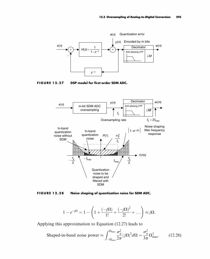
1 ejV ¼ 1 1þ jVð Þ1!þ jVð Þ2
2!þ . . .
! jV:
Applying this approximation to Equation (12.27) leads to
Shaped-in-band noise power Z Vmax
Vmax
s2q
2pjVj j2dV ¼
s2q
3pV3
max: (12:28)
x(n)y(n)
w(n)H(z) =
11−z −1
z −1
+
e(n) Quantization error
+
−
Decimator
↓MAnti-aliasing LPF
Encoded by m bits
F IGURE 12.27 DSP model for first-order SDM ADC.
In-bandquantization
noise
In-bandquantizationnoise without
SDM
Quantizationnoise to beshaped andfiltered with
SDM
Noise shapingfilter frequency
response1−e−jΩ
m-bit SDM ADCoversampling
Oversampling rate
Decimator
↓MAnti-aliasing LPFx(n)
y(n) w(m)
fmax
fs
fs = 2fmax
P(f )
fs
sq2
−fs2
− fmax fs2
f (Hz)
F IGURE 12.28 Noise shaping of quantization noise for SDM ADC.
Tan: Digital Signaling Processing 0123740908_chap12 Final Proof page 595 22.6.2007 12:18am Compositor Name: Mraja
12.3 Oversampling of Analog-to-Digital Conversion 59512.3 Oversampling of Analog-to-Digital Conversion 595

After simple algebra, we have
Shaped-in-band noise power p2s2
q
3
2fmax
fs
3
¼ p2
3 A
222m
12
2fmax
fs
3
:
(12:29)
If we let the shaped-in-band noise power equal the quantization noise power
from the regular ADC using a minimum sampling rate, we have
p2
3 A
222m
12
2fmax
fs
3
¼ A2
12 22n: (12:30)
We modify Equation (12.30) into the following useful formats for applications:
n ¼ mþ 1:5 log2
fs
2fmax
0:86 (12:31)
fs
2fmax
3
¼ p2
3 22 nmð Þ: (12:32)
Example 12.9.
Given the following DSP system specifications:
Oversampling rate system
First-order SDM with 2-bit ADC
Sampling rate ¼ 4 MHz
Maximum audio input frequency ¼ 4 kHz,
a. Determine the equivalent ADC resolution.
Solution:
a. Since m ¼ 2 bits, and
fs
2fmax
¼ 4000 kHz
2 4 kHz¼ 500:
we calculate
n ¼ mþ 1:5 log2
fs
2fmax
0:86
¼ 2þ 1:5 log2 500ð Þ 0:86 15 bits:
Tan: Digital Signaling Processing 0123740908_chap12 Final Proof page 596 22.6.2007 12:18am Compositor Name: Mraja
596 12 M U L T I R A T E D I G I T A L S I G N A L P R O C E S S I N G

We can also extend the first-order SDM DSP model to the second-order
SDM DSP model by cascading one section of the first-order discrete-time
analog filter, as depicted in Figure 12.29.
Similarly to the first-order SDM DSP model, applying the z-transform leads
to the following relationship:
Y (z) ¼ X(z)|fflzfflOriginal
digital signal
transform
þ 1 z1 2|fflfflfflfflfflfflfflzfflfflfflfflfflfflfflHighpass
noise shaping
filter
E(z)|fflzfflQuantization
error
transform
: (12:33)
Notice that the noise shaping filter becomes a second-order highpass filter;
hence, the more quantization noise is pushed to the high-frequency range, the
better ADC resolution is expected to be. In a similar analysis to the first-order
SDM, we get the following useful formulas:
n ¼ mþ 2:5 log2
fs
2fmax
2:14 (12:34)
fs
2fmax
5
¼ p4
5 22 nmð Þ: (12:35)
In general, the Kth-order SDM DSP model and ADC resolution formulas are
given as:
Y (z) ¼ X(z)|fflzfflOriginal
digital signal
transform
þ 1 z1 K|fflfflfflfflfflfflfflzfflfflfflfflfflfflfflHighpass
noise shaping
filter
E(z)|fflzfflQuantization
error
transform
(12:36)
+−
++
− ↓M
x(n)H(z)=
11−z −1
1H(z)=
1−z −1
z −1
DecimatorAnti-aliasing LPF
y(n)w (n)
e(n) Quantization error
Encoded by m bits
F IGURE 12.29 DSP model for the second-order SDM ADC.
Tan: Digital Signaling Processing 0123740908_chap12 Final Proof page 597 22.6.2007 12:18am Compositor Name: Mraja
12.3 Oversampling of Analog-to-Digital Conversion 59712.3 Oversampling of Analog-to-Digital Conversion 597

n ¼ mþ 0:5 2K þ 1ð Þ log2
fs
2fmax
0:5 log2
p2K
2K þ 1
(12:37)
fs
2fmax
2Kþ1
¼ p2K
2K þ 1 22 nmð Þ: (12:38)
Example 12.10.
Given the oversampling rate DSP system with the following specifications:
Second-order SDM ¼ 1-bit ADC
Sampling rate ¼ 1 MHz
Maximum audio input frequency ¼ 4 kHz,
a. Determine the effective ADC resolution.
Solution:
a. n ¼ 1þ 2:5 log21000 kHz24 kHz
2:14 16 bits.
Next, we review the application of the oversampling ADC used in industry.
Figure 12.30 illustrates a function diagram for the MAX1402 low-power, multi-
channel oversampling sigma-delta analog-to-digital converter used in industry.
It applies a sigma-delta modulator with a digital decimation filter to achieve
16-bit accuracy. The device offers three fully differential input channels, which
can be independently programmed. It can also be configured as five pseudo-
differential input channels. It comprises two chopper buffer amplifiers and a
programmable gain amplifier, a DAC unit with predicted input subtracted from
the analog input to acquire the differential signal, and a second-order switched-
capacitor sigma-delta modulator.
The chip produces a 1-bit data stream, which will be filtered by the integrated
digital filter to complete ADC. The digital filter’s user-selectable decimation
factor offers flexibility for conversion resolution to be reduced in exchange for a
higher data rate, or vice versa. The integrated digital lowpass filter is first-order
or third-order Sinc infinite impulse response. Such a filter offers notches corre-
sponding to its output data rate and its frequency harmonics, so it can effect-
ively reduce the developed image noises in the frequency domain. (The Sinc filter
is beyond the scope of our discussion.) The MAX1402 can provide 16-bit
accuracy at 480 samples per second and 12-bit accuracy at 4,800 samples
per second. The chip finds wide application in sensors and instrumentation.
Its detailed features can be found in the MAX1402 data sheet (Maxim Inte-
grated Products, 2007).
Tan: Digital Signaling Processing 0123740908_chap12 Final Proof page 598 22.6.2007 12:18am Compositor Name: Mraja
598 12 M U L T I R A T E D I G I T A L S I G N A L P R O C E S S I N G

12.4 Appl i cat ion Example: CD Player
Figure 12.31 illustrates a CD playback system, also described earlier in this
chapter. A laser optically scans the tracks on a CD to produce a digital signal.
The digital signal is then demodulated, and parity bits are used to detect bit
errors due to manufacturing defects, dust, and so on and to correct them. The
demodulated signal is again oversampled by a factor of 4 and hence the sam-
pling rate is increased to 176.4 kHz for each channel. Each digital sample then
passes through a 14-bit DAC, which produces the sample-and-hold voltage
signals that pass the anti-image lowpass filter. The output from each analog
filter is fed to its corresponding loudspeaker. Oversampling relaxes the design
requirements of the analog anti-image lowpass filter, which is used to smooth
out the voltage steps.
The earliest system used a third-order Bessel filter with a 3 dB passband at
30 kHz. Notice that the first-order sigma-delta modulation (first-order SDM) is
added to the 14-bit DAC unit to further improve the 14-bit DAC to 16-bit
DAC.
Let us examine the single-channel DSP portion shown in Figure 12.32.
CLKINCLOCKGEN
DIVIDER
DIGITALFILTERMODULATORPGA
DAC
AGND
REFIN+REFIN−
CALOFF+
AIN1
OUT1
OUT2
AIN2AIN3AIN4AIN5AIN6
CALGAIN−
CALOFF+CALGAIN−
INTERFACEAND CONTROL
V+
V+
BUFFER
BUFFER
SWITCHINGNETWORK
CLKOUT
DGND
AGND
SCLK
DIN
DOUT
INT
CS
DS1
DS0
RESET
V+
VDD
MAXIMMAX1402
F IGURE 12.30 Functional diagram for the sigma-delta ADC.
Tan: Digital Signaling Processing 0123740908_chap12 Final Proof page 599 22.6.2007 12:18am Compositor Name: Mraja
12.4 Application Example: CD Player 59912.4 Application Example: CD Player 599

The spectral plots for the oversampled and interpolated signal xx(n), the 14-
bit SDM output y(n), and the final analog output audio signal are given in
Figure 12.33. As we can see in plot (a) in the figure, the quantization noise is
uniformly distributed, and only in-band quantization noise (0 to 22.05 kHz) is
expected. Again, 14 bits for each sample are kept after oversampling. Without
using the first-order SDM, we expect the effective ADC resolution due to
oversampling to be
n ¼ 14þ 0:5 log2
176:4
44:1
¼ 15 bits,
which is fewer than 16 bits. To improve quality further, the first-order SDM is
used. The in-band quantization noise is then shaped. The first-SDM pushes
CD
Optical pickupDemodulation
Error correction
4×Oversampling
14-bitDAC
1st-order SDM
14-bitDAC
1st-order SDM
Anti-imageLP filter
Amplifiedleft speaker
Amplifiedright speaker
Anti-imageLP filter
F IGURE 12 .31 Simplified decoder of a CD recording system.
AnalogLPF
y(m)
K1 − z −1
z −1
+
e (m) Quantizationerror
+
−
Oversampling by 4
1st-order SDMm=14 bits
f s = 44.1kHz
n = 16 bits
fs = 4 × 44.1 = 176.4 kHz
x(m)x(n)
↑4Anti-image LPF
F IGURE 12 .32 Illustration of oversampling and SDM ADC used in the decoder of a CDrecording system.
Tan: Digital Signaling Processing 0123740908_chap12 Final Proof page 600 22.6.2007 12:18am Compositor Name: Mraja
600 12 M U L T I R A T E D I G I T A L S I G N A L P R O C E S S I N G

quantization noise to the high-frequency range, as illustrated in plot (b) in
Figure 12.33. The effective ADC resolution now becomes
n ¼ 14þ 1:5 log2
176:4
44:1
0:86 16 bits:
Hence, 16-bit ADC audio quality is preserved. On the other hand, from plot (c)
in Figure 12.33, the audio occupies a frequency range up to 22.05 kHz, while the
DSP Nyquist limit is 88.2, so the low-order analog anti-image filter can satisfy
the design requirement.
12.5 Undersampl ing of BandpassSignals
As we discussed in Chapter 2, the sampling theorem requires that the sampling
rate be twice as large as the highest frequency of the analog signal to be sampled.
The sampling theorem ensures the complete reconstruction of the analog signal
X(f ) 14-bit in-bandquantization
noise
Y(f ) 14-bit in-bandshaped noisewith the SDM
f (kHz )
f (kHz )
f (kHz )
44.10 88.2 132.322.05 176.4
44.10 88.2 132.322.05 176.4
44.10 88.2 132.322.05 176.4
14-bit in-bandshaped noisewith the SDM
Analog LPFBest audio
A
C
B
F IGURE 12.33 Spectral illustrations for oversampling and SDM ADC used in thedecoder of a CD recording system.
Tan: Digital Signaling Processing 0123740908_chap12 Final Proof page 601 22.6.2007 12:18am Compositor Name: Mraja
12.5 Undersampling of Bandpass Signals 60112.5 Undersampling of Bandpass Signals 601
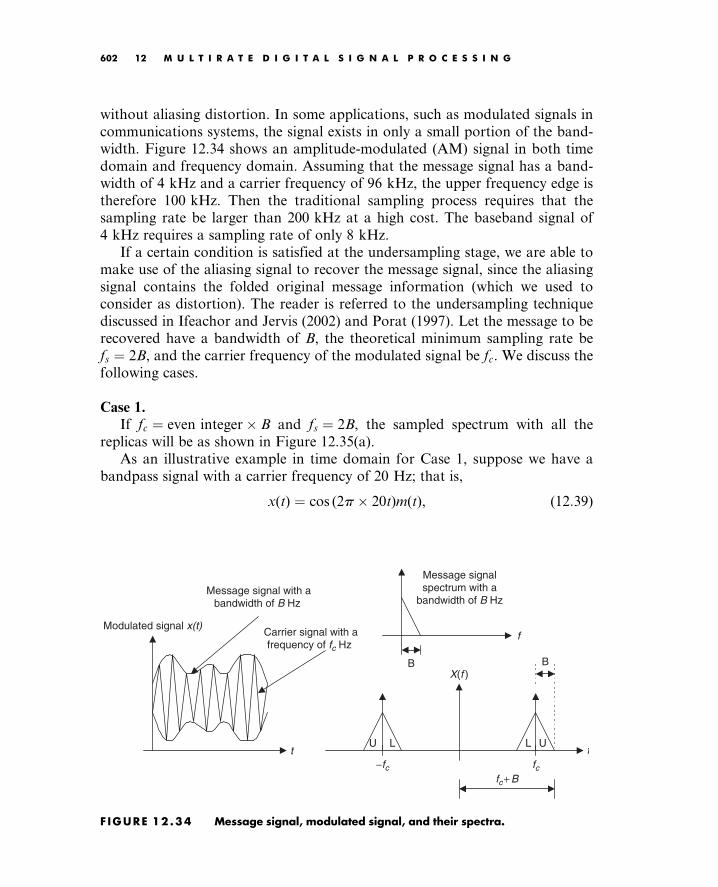
without aliasing distortion. In some applications, such as modulated signals in
communications systems, the signal exists in only a small portion of the band-
width. Figure 12.34 shows an amplitude-modulated (AM) signal in both time
domain and frequency domain. Assuming that the message signal has a band-
width of 4 kHz and a carrier frequency of 96 kHz, the upper frequency edge is
therefore 100 kHz. Then the traditional sampling process requires that the
sampling rate be larger than 200 kHz at a high cost. The baseband signal of
4 kHz requires a sampling rate of only 8 kHz.
If a certain condition is satisfied at the undersampling stage, we are able to
make use of the aliasing signal to recover the message signal, since the aliasing
signal contains the folded original message information (which we used to
consider as distortion). The reader is referred to the undersampling technique
discussed in Ifeachor and Jervis (2002) and Porat (1997). Let the message to be
recovered have a bandwidth of B, the theoretical minimum sampling rate be
fs ¼ 2B, and the carrier frequency of the modulated signal be fc. We discuss the
following cases.
Case 1.
If fc ¼ even integer B and fs ¼ 2B, the sampled spectrum with all the
replicas will be as shown in Figure 12.35(a).
As an illustrative example in time domain for Case 1, suppose we have a
bandpass signal with a carrier frequency of 20 Hz; that is,
x(t) ¼ cos (2p 20t)m(t), (12:39)
t
Message signal with abandwidth of B Hz
Carrier signal with afrequency of fc Hz
Modulated signal x(t)
f
X(f )
f
−fc fc
UU L
B
fc+ B
B
Message signalspectrum with a
bandwidth of B Hz
L
F IGURE 12 .34 Message signal, modulated signal, and their spectra.
Tan: Digital Signaling Processing 0123740908_chap12 Final Proof page 602 22.6.2007 12:18am Compositor Name: Mraja
602 12 M U L T I R A T E D I G I T A L S I G N A L P R O C E S S I N G

where m(t) is the message signal with a bandwidth of 2 Hz. Using a sampling
rate of 4 Hz by substituting t ¼ nT , where T ¼ 1=fs into Equation (12.39), we
get the sampled signal as
x(nT) ¼ cos (2p 20t)m(t)jt¼nT¼ cos (2p 20n=4)m(nT): (12:40)
Since 10np ¼ 5n(2p) is the multiple of 2p,
cos (2p 20n=4) ¼ cos (10pn) ¼ 1, (12:41)
we obtained the undersampled signal as
x(nT) ¼ cos (2p 20n=4)m(nT) ¼ m(nT), (12:42)
which is a perfect digital message signal. Figure 12.36 shows the bandpass signal
and its sampled signal when the message signal is 1 Hz, given as
m(t) ¼ cos (2pt): (12:43)
Case 2.
If fc ¼ odd integer B and fs ¼ 2B, the sampled spectrum with all the
replicas will be as shown in Figure 12.35(b), where the spectral portion L and
U are reversed. Hence, frequency reversal will occur. Then a further digital
modulation in which the signal is multiplied by the digital oscillator with a
frequency of B Hz can be used to adjust the spectrum to be the same as that in
Case 1.
Bandpass filter ADCx(t )
fs
UL
x(n)
ULU ULUf
UL ULU ULUf
Spectrum for x(n) forfs = even integer x B Hz
Spectrum for x(n) forfs = odd integer x B Hz
A
B
L L
L L
F IGURE 12.35 Spectrum of the undersampled signal.
Tan: Digital Signaling Processing 0123740908_chap12 Final Proof page 603 22.6.2007 12:18am Compositor Name: Mraja
12.5 Undersampling of Bandpass Signals 60312.5 Undersampling of Bandpass Signals 603

As another illustrative example for Case 2, let us sample the following
bandpass signal with a carrier frequency of 22 Hz, given by
x(t) ¼ cos (2p 22t)m(t): (12:44)
Applying undersampling using a sampling rate of 4 Hz, it follows that
x(nT) ¼ cos (2p 22n=4)m(nT) ¼ cos (11np)m(nT): (12:45)
Since 11np can be either an odd or an even integer multiple of p, we have
cos (11pn) ¼ 1 n = odd
1 n = even.
n(12:46)
We see that Equation (12.46) causes the message samples to change sign alter-
nately with a carrier frequency of 22 Hz, which is the odd integer multiple of the
message bandwidth of 2 Hz. This in fact will reverse the baseband message
spectrum. To correct the spectrum reversal, we multiply an oscillator with a
frequency of B ¼ 2 Hz by the bandpass signal, that is
x(t) cos (2p 2t) ¼ cos (2p 22t)m(t) cos (2p 2t): (12:47)
0.2 0.4 0.6 0.8 1 1.2 1.4 1.6 1.80 2
−0.8
−0.6
−0.4
−0.2
0
0.2
0.4
0.6
0.8
−1
1
x(t)
, and
x(n
T)
Case 1 fc = even number × 2 Hz = 20 Hz, fs = 4 Hz
Time (sec.)
Bandpasssignal
Sampledsignal
F IGURE 12 .36 Plots of the bandpass signal and sampled signal for Case 1.
Tan: Digital Signaling Processing 0123740908_chap12 Final Proof page 604 22.6.2007 12:18am Compositor Name: Mraja
604 12 M U L T I R A T E D I G I T A L S I G N A L P R O C E S S I N G

Then the undersampled signal is given by
x(nT) cos (2p 2n=4) ¼ cos (2p 22n=4)m(nT) cos (2p 2n=4)
¼ cos (11np)m(nT) cos (np)(12:48)
Since cos (11pn) cos (pn) ¼ 1, it follows that (12:49)
x(nT) cos (2p 2n=4) ¼ cos (p 11n)m(nT) cos (p n) ¼ m(nT), (12:50)
which is the recovered message signal. Figure 12.37 shows the sampled bandpass
signals with the reversed message spectrum and the corrected message spectrum,
respectively, for a message signal having a frequency of 0.5 Hz; that is,
m(t) ¼ cos (2p 0:5t): (12:51)
Case 3.
If fc ¼ non-integer B, we can extend the bandwidth B toB such that
fc ¼ integerB and fs ¼ 2B: (12:52)
Then we can apply Case 1 or Case 2. An illustration of Case 3 is included in the
following example.
0 0.2 0.4 0.6 0.8 1 1.2 1.4 1.6 1.8 2−1
−0.5
0
0.5
1
Time (sec)
x(t)
and
x(n
T)
Case 2: fc= odd number × B = 22 Hz, fs= 2B = 4 Hz
0 0.2 0.4 0.6 0.8 1 1.2 1.4 1.6 1.8 2−1
−0.5
0
0.5
1
Time (sec)
Case 2: fc= odd number × B = 22 Hz, fs= 2B = 4 Hz, with B = 2 Hz oscillator
x(t)
*cos
(2*p
i*2*
t) a
nd m
(nT
)
Phase distortion
Message signal
F IGURE 12.37 Plots of the bandpass signals and sampled signals for Case 2.
Tan: Digital Signaling Processing 0123740908_chap12 Final Proof page 605 22.6.2007 12:18am Compositor Name: Mraja
12.5 Undersampling of Bandpass Signals 60512.5 Undersampling of Bandpass Signals 605

Example 12.11.
Given a bandpass signal with the spectrum and the carry frequency fc shown in
Figure 12.38(a), 12.38(b), and 12.38(c), respectively, and assuming the baseband
bandwidth B ¼ 4 kHz,
a. Select the sampling rate and sketch the sampled spectrum ranging from
0 Hz to the carrier frequency for each of the following carrier frequencies:
1. fc ¼ 16 kHz
2. fc ¼ 12 kHz
3. fc ¼ 18 kHz
Solution:
a. 1. Since fc=B ¼ 4 is an even number, which is Case 1, we select fs ¼ 8 kHz
and sketch the sampled spectrum shown in Figure 12.38a.
2. Since fc=B ¼ 3 is an odd number, we select fs ¼ 8 kHz and sketch the
sampled spectrum shown in Figure 12.38b.
A
0 10 2016
20100
Bandpass signal withbaseband
bandwidth B = 4 kHz
Bandpass signalsampled at fs= 8 kHz
15 17
7 9 15 171
f kHz
f kHz
F IGURE 12 .38A Sampled signal spectrum for fc ¼ 16 kHz.
B
0 10 2012
20100
Bandpass signal withbaseband
bandwidth B = 4 kHz
Bandpass signalsampled at fs= 8 kHz
3 5
1311
11 13 19
f kHz
f kHz
F IGURE 12 .38B Sampled signal spectrum for fc ¼ 12 kHz.
Tan: Digital Signaling Processing 0123740908_chap12 Final Proof page 606 22.6.2007 12:18am Compositor Name: Mraja
606 12 M U L T I R A T E D I G I T A L S I G N A L P R O C E S S I N G

3. Now, fc=B ¼ 4:5, which is a non-integer. We extend the bandwidth
B ¼ 4:5 kHz, so fc=B ¼ 4 and fs ¼ 2B ¼ 9 kHz. Then the sketched
spectrum is shown in Figure 12.38c.
Simulat ion Example
An AM with a 1-kHz message signal is given as:
x(t) ¼ 1þ 0:8 sin (2p 1000t)½ cos (2p fct): (12:53)
Assuming a message bandwidth of 4 kHz, determine the sampling rate, use
MATLAB to sample the AM signal, and sketch the sampled spectrum up to
the sampling frequency for each the following carrier frequencies:
1. fc ¼ 96 kHz
2. fc ¼ 100 kHz
3. fc ¼ 99 kHz
1. For this case, fc=B ¼ 24 is an even number. We select fs ¼ 8 kHz. Figure
12.39a describes the simulation, where the upper left plot is the AM
signal, the upper right plot is the spectrum of the AM signal, the lower
left plot is the undersampled signal, and the lower right plot is the
spectrum of the undersampled signal displayed from 0 to 8 kHz.
2. fc=B ¼ 25 is an odd number, so we choose fs ¼ 8 kHz, and a further
process is needed. We can multiply the undersampled signal by a digital
oscillator with a frequency of B ¼ 4 kHz to achieve the 1-kHz baseband
signal. The plots of the AM signal spectrum, the undersampled signal
spectrum, and the oscillator mixed signal and its spectrum are shown in
Figure 12.39b.
3. For fc ¼ 99 kHz, fc=B ¼ 24:75. We extend the bandwidth toB ¼ 4:125 so
that fc=B ¼ 24. Hence, the undersampling rate is used as fs ¼ 8:25 kHz.
f kHz
f kHz
C
0 10 2019
20100
Bandpass signal withbaseband
bandwidth B = 4.5 kHz
Bandpass signalsampled at fs= 9 kHz
1
1817
17 198
F IGURE 12.38C Sampled signal spectrum for fc ¼ 18 kHz.
Tan: Digital Signaling Processing 0123740908_chap12 Final Proof page 607 22.6.2007 12:18am Compositor Name: Mraja
12.5 Undersampling of Bandpass Signals 60712.5 Undersampling of Bandpass Signals 607

0 0.005 0.01−2
−1
0
1
2
Time (sec)
AM
sig
nal
0.9 0.95 1 1.05 1.1
× 105
0
0.5
1
Frequency (Hz)
Spe
ctru
m o
f x(t
)
0A
0.005 0.010
0.5
1
1.5
2
m(n
)
Time (sec)0 2000 4000 6000 8000
0
0.5
1
Frequency (Hz)
Spe
ctru
m o
f x(n
)
F IGURE 12 .39A Sampled AM signal and spectrum for fc ¼ 96 kHz.
0.9 0.95 1 1.05 1.1
× 105
0
0.5
1
Frequency (Hz)
Spe
ctru
m o
f x(t
)
0 2000 4000 6000 80000
0.5
1
Frequency (Hz)Spe
ctru
m fo
r x(
n)=
cos(
2*π*
B*n
/fs)
0 0.005 0.010
B
0.5
1
1.5
2
Time (sec)
x(n)
=co
s(2*
π*B
*n/fs
)
0 2000 4000 6000 80000
0.2
0.4
0.6
0.8
Frequency (Hz)
Spe
ctru
m o
f x(n
)
F IGURE 12 .39B Sampled AM signal and spectrum for fc ¼ 100 kHz.
Tan: Digital Signaling Processing 0123740908_chap12 Final Proof page 608 22.6.2007 12:18am Compositor Name: Mraja
608 12 M U L T I R A T E D I G I T A L S I G N A L P R O C E S S I N G

Figure 12.39c shows the plots for the AM signal, the AM signal spectrum,
the undersampled signal based on the extended baseband width, and the
sampled signal spectrum ranging from 0 to 8.25 kHz, respectively.
This example verifies principles of undersampling of bandpass signals.
12.6 Summar y
1. Downsampling (decimation) by an integer factor of M means taking one
sample from the data sequence x(n) for every M sample and discarding
the last M 1 sample.
2. Upsampling (interpolation) by an integer factor of L means inserting
L 1 zeros for every sample in the data sequence x(n).
3. Downsampling requires a decimation (anti-aliasing) filter to avoid fre-
quency aliasing before downsampling.
4. Upsampling requires an interpolation (anti-image) filter to remove the
images after interpolation.
0 0.005 0.01−2
−1
0
1
2
Time (sec)
AM
sig
nal
0.9 0.95 1 1.05 1.1
105
0
0.5
1
Frquency (Hz)
Spe
ctru
m o
f x(t
)
0C
0.005 0.010
0.5
1
1.5
2
m(n
)
Time (sec)0 5000 10000
0
0.5
1
Frequency (Hz)
Spe
ctru
m o
f x(n
)
F IGURE 12.39C Sampled AM signal and spectrum for fc ¼ 99 kHz.
Tan: Digital Signaling Processing 0123740908_chap12 Final Proof page 609 22.6.2007 12:18am Compositor Name: Mraja
12.6 Summary 60912.6 Summary 609

5. Changing the sampling rate by a non-integer factor of L/M requires two
stages: an interpolation stage and a downsampling stage.
6. Two-stage decimation can dramatically reduce the anti-aliasing filter
length.
7. Polyphase implementations of the decimation filter and interpolation
filter can reduce complexity of the filter operations, that is, fewer multi-
plications and additions.
8. Using oversampling can improve the regular ADC resolution. Sigma-
delta modulation ADC can achieve even higher ADC resolution, using
noise shaping effect for further reduction of quantization noise.
9. The audio CD player uses multirate signal processing and oversampling.
10. Undersampling can be used to sample the bandpass signal, and finds its
application in communications.
12.7 Problems
12.1. For a single-stage decimator with the following specifications:
Original sampling rate ¼ 8 kHz
Decimation factor M ¼ 4
Frequency of interest ¼ 0800Hz
Passband ripple ¼ 0:02 dB
Stopband attenuation ¼ 46 dB,
a. draw the block diagram for the decimator;
b. determine the window type, filter length, and cutoff frequency if the
window method is used for the anti-aliasing FIR filter design.
12.2. For a single-stage interpolator with the following specifications:
Original sampling rate ¼ 8 kHz
Interpolation factor L ¼ 3
Frequency of interest ¼ 03,400 Hz
Passband ripple ¼ 0:02 dB
Stopband attenuation ¼ 46 dB,
a. draw the block diagram for the interpolator;
b. determine the window type, filter length, and cutoff frequency if the
window method is used for the anti-image FIR filter design.
Tan: Digital Signaling Processing 0123740908_chap12 Final Proof page 610 22.6.2007 12:18am Compositor Name: Mraja
610 12 M U L T I R A T E D I G I T A L S I G N A L P R O C E S S I N G

12.3. For the sampling conversion from 6 kHz to 8 kHz with the following
specifications:
Original sampling rate¼ 6 kHz
Interpolation factor L ¼ 4
Decimation factor M ¼ 3
Frequency of interest ¼ 02,400 Hz
Passband ripple ¼ 0:02 dB
Stopband attenuation ¼ 46 dB,
a. draw the block diagram for the processor;
b. determine the window type, filter length, and cutoff frequency if the
window method is used for the combined FIR filter H(z).
12.4. For the design of a two-stage decimator with the following specifica-
tions:
Original sampling rate¼ 320 kHz
Frequency of interest ¼ 03,400 Hz
Passband ripple ¼ 0:05 (absolute)
Stopband attenuation ¼ 0:005 (absolute)
Final sampling rate ¼ 8,000Hz,
a. draw the decimation block diagram;
b. specify the sampling rate for each stage;
c. determine the window type, filter length, and cutoff frequency for
the first stage if the window method is used for the anti-aliasing FIR
filter design (H1(z));
d. determine the window type, filter length, and cutoff frequency for
the second stage if the window method is used for the anti-aliasing
FIR filter design (H2(z)).
12.5.
a. Given an interpolator filter as
H(z) ¼ 0:25þ 0:4z1 þ 0:5z2,
draw the block diagram for interpolation polyphase filter imple-
mentation for the case of L ¼ 2.
b. Given a decimation filter as
H(z) ¼ 0:25þ 0:4z1 þ 0:5z2 þ 0:6z3,
Tan: Digital Signaling Processing 0123740908_chap12 Final Proof page 611 22.6.2007 12:18am Compositor Name: Mraja
12.7 Problems 61112.7 Problems 611

draw the block diagram for decimation polyphase filter implemen-
tation for the case of M ¼ 2.
12.6. Using the commutative models for the polyphase interpolation and
decimation filters,
a. draw the block diagram for interpolation polyphase filter implemen-
tation for the case of L ¼ 2, and H(z) ¼ 0:25þ 0:4z1þ 0:5z2;
b. draw the block diagram for decimation polyphase filter implementation
for the case of M ¼ 2, and H(z) ¼ 0:25þ 0:4z1 þ 0:5z2þ 0:6z3.
12.7. Given the audio system with the following specifications:
Audio input frequency range: 0 15 kHz
ADC resolution ¼ 16 bits
Current sampling rate ¼ 30 kHz,
a. determine the oversampling rate if the 12-bit ADC chip is used to
replace the audio system;
b. draw the block diagram.
12.8. Given the audio system with the following specifications:
Audio input frequency range: 0 15 kHz
ADC resolution ¼ 6 bits
Oversampling rate ¼ 45 MHz,
a. draw the block diagram;
b. determine the actual effective ADC resolution (number of bits per
sample).
12.9. Given the following specifications of an oversampling DSP system:
Audio input frequency range: 0 4 kHz
First-order SDM with a sampling rate of 128 kHz
ADC resolution in SDM ¼ 1 bit,
a. draw the block diagram using the DSP model;
b. determine the equivalent (effective) ADC resolution.
12.10. Given the following specifications of an oversampling DSP system:
Audio input frequency range: 0 20 kHz
Second-order SDM with a sampling rate of 160 kHz
ADC resolution in SDM ¼ 10 bits,
Tan: Digital Signaling Processing 0123740908_chap12 Final Proof page 612 22.6.2007 12:18am Compositor Name: Mraja
612 12 M U L T I R A T E D I G I T A L S I G N A L P R O C E S S I N G

a. draw the block diagram using the DSP model;
b. determine the equivalent (effective) ADC resolution.
12.11. Given a bandpass signal with its spectrum shown in Figure 12.40, and
assuming the bandwidth B ¼ 5 kHz, select the sampling rate and
sketch the sampled spectrum ranging from 0 Hz to the carrier fre-
quency for each of the following carrier frequencies:
a. fc ¼ 30 kHz
b. fc ¼ 25 kHz
c. fc ¼ 33 kHz
MATLAB Problems
Use MATLAB to solve Problems 12.12 to 12.16
12.12. Generate a sinusoid with a 1000 Hz for 0.05 sec using a sampling rate
of 8 kHz,
a. Design a decimator to change the sampling rate to 4 kHz with
specifications below:
Signal frequency range: 0–1800 Hz
Hamming window required for FIR filter design
b. Write a MATLAB program to implement the downsampling
scheme, and plot the original signal and the downsampled signal
versus the sample number, respectively.
f kHz
0 fc
Bandpass signal withbaseband
bandwidth B=5kHz
fc − 2fc − 5 fc + 5fc + 2
F IGURE 12.40 Spectrum of the bandpass signal in Problem 12.11.
Tan: Digital Signaling Processing 0123740908_chap12 Final Proof page 613 22.6.2007 12:18am Compositor Name: Mraja
MATLAB Problems 613MATLAB Problems 613

12.13. Generate a sinusoid with a 1000 Hz for 0.05 sec using a sampling rate
of 8 kHz,
a. Design an interpolator to change the sampling rate to 16 kHz with
following specifications:
Signal frequency range: 0 – 3600 Hz
Hamming window required for FIR filter design
b. Write a MATLAB program to implement the upsampling scheme,
and plot the original signal and the downsampled signal versus the
sample number, respectively.
12.14. Generate a sinusoid with a frequency of 500 Hz for 0.1 sec using a
sampling rate of 8 kHz,
a. design an interpolation and decimation processing algorithm to
change the sampling rate to 22 kHz
Signal frequency range: 0 – 3400 Hz
Hamming window required for FIR filter design
b. Write a MATLAB program to implement the scheme, and plot the
original signal and the sampled signal at the rate of 22 kHz versus
the sample number, respectively.
12.15. Repeat Problem 12.12 using the polyphase form for the decimator.
12.16. Repeat Problem 21.13 using the polyphase form for the interpolator.
References
Akansu, A. N., and Haddad, R. A. (1992). Multiresolution Signal Decomposition: Trans-
forms, Subbands, and Wavelets. Boston: Academic Press.
Ifeachor, E. C., and Jervis, B. W. (2002). Digital Signal Processing: A Practical Approach,
2nd ed. Upper Saddle River, NJ: Prentice Hall.
Lipshitz, S. P., Wannamaker, R. A., and Vanderkooy, J. (1992). Quantization and dither:
A theoretical survey. Journal of the Audio Engineering Society, 40 (5): 355–375.
Maher, R. C. (1992). On the nature of granulation noise in uniform quantization systems.
Journal of the Audio Engineering Society, 40 (1/2): 12–20.
Maxim Integrated Products. (2007). MAXIM þ5V , 18-Bit, Low-Power, Multichannel, Over-
sampling (Sigma-Delta) ADC. Retrieved March 3, 2007, from http://datasheets.maxim-
ic.com/en/ds/MAX1402.pdf
Porat, B. (1997). A Course in Digital Signal Processing. New York: John Wiley & Sons.
Tan: Digital Signaling Processing 0123740908_chap12 Final Proof page 614 22.6.2007 12:18am Compositor Name: Mraja
614 12 M U L T I R A T E D I G I T A L S I G N A L P R O C E S S I N G

Proakis, J. G., and Manolakis, D. G. (1996). Digital Signal Processing: Principles, Algo-
rithms, and Applications, 3rd ed. Upper Saddle River, NJ: Prentice Hall.
Sorensen, H. V., and Chen, J. P. (1997). A Digital Signal Processing Laboratory Using
TMS320C30. Upper Saddle River, NJ: Prentice Hall.
Stearns, S. D. (2003). Digital Signal Processing with Examples in MATLAB. Boca Raton,
FL: CRC Press LLC.
van der Vegte, J. (2002). Fundamentals of Digital Signal Processing. Upper Saddle River, NJ:
Prentice Hall.
Vetterli, M., and Kovacevic, J. (1995). Wavelets and Subband Coding. Englewood Cliffs, NJ:
Prentice Hall.
Tan: Digital Signaling Processing 0123740908_chap12 Final Proof page 615 22.6.2007 12:18am Compositor Name: Mraja
References 615References 615

Tan: Digital Signaling Processing 0123740908_chap12 Final Proof page 616 22.6.2007 12:18am Compositor Name: Mraja
This page intentionally left blank

13Image Processing Basics
Objectives: In today’s modern computers, media information such as audio,
images, and video have come to be necessary for daily business operations and
entertainment. In this chapter, we will study the digital image and its processing
techniques. This chapter introduces the basics of image processing, including
image enhancement using histogram equalization and filtering methods, and
proceeds to study pseudo-color generation for object detection and recognition.
Finally, the chapter investigates image compression techniques and basics of
video signals.
13.1 Image Process ing Notat ion andData Formats
The digital image is picture information in digital form. The image can be
filtered to remove noise and obtain enhancement. It can also be transformed
to extract features for pattern recognition. The image can be compressed for
storage and retrieval, as well as transmitted via a computer network or a
communication system.
The digital image consists of pixels. The position of each pixel is specified in
terms of an index for the number of columns and another for the number of
rows. Figure 13.1 shows that the pixel p(2, 8) has a level of 86 and is located in
the second row, eighth column. We express it in notation as
p(2, 8) ¼ 86: (13:1)
The number of pixels in the presentation of a digital image is its spatial
resolution, which relates to the image quality. The higher the spacial resolution,
Tan: Digital Signaling Processing 0123740908_chap13 Final Proof page 617 22.6.2007 3:23pm Compositor Name: MRaja

the better quality the image has. The spacial resolution can be fairly high,
for instance, as high as 1600 1200 (1,920,000 pixels ¼ 1:92 megapixels), or as
low as 320 200 (64,000 pixels ¼ 64 kilopixels). In notation, the number to the
left of the multiplication symbol represents the width, and that to the right of the
symbol represents the height. Image quality also depends on the numbers of bits
used in encoding each pixel level, which will be discussed in the next section.
13.1.1 8-Bi t Gray Level Images
If a pixel is encoded on a gray scale from 0 to 255, where 0 ¼ black and
255 ¼ white, the numbers in between represent levels of gray forming a gray-
scale image. For a 640 480 8-bit image, 307.2 kilobytes are required for
storage. Figure 13.2 shows a grayscale image format. As shown in the figure,
the pixel indicated in the box has an 8-bit value of 25.
The image of a cruise ship with spatial resolution of 320 240 in an 8-bit
grayscale level is shown in Figure 13.3.
m
n
(m, n)
p(m, n)
00 1 2 3 4 5 6 7 8 9 10 11
1
2
3
4
5
6
7
86
F IGURE 13 .1 Image pixel notation.
0
0
n
m
25
Pixel value
F IGURE 13 .2 Grayscale image format.
Tan: Digital Signaling Processing 0123740908_chap13 Final Proof page 618 22.6.2007 3:23pm Compositor Name: MRaja
618 13 I M A G E P R O C E S S I N G B A S I C S

13.1.2 24-Bi t Color Images
In a 24-bit color image representation, each pixel is recoded with red, green,
and blue (RGB) components. With each component value encoded in 8 bits,
resulting in 24 bits in total, we achieve a full color RGB image. With such
an image, we can have 224 ¼ 16:777216 106 different colors. A 640 480
24-bit color image requires 921.6 kilobytes for storage. Figure 13.4 shows the
format for the 24-bit color image where the indicated pixel has 8-bit RGB
components.
Figure 13.5 shows a 24-bit color image of the Grand Canyon, along with its
grayscale displays for the 8-bit RGB component images. The full color picture
at the upper left is included in the color insert.
F IGURE 13.3 Grayscale image (8-bit 320 3 240).
0
0 n
m
R=66G=132B=34
Pixel value
F IGURE 13.4 The 24-bit color image format.
Tan: Digital Signaling Processing 0123740908_chap13 Final Proof page 619 22.6.2007 3:23pm Compositor Name: MRaja
13.1 Image Processing Notation and Data Formats 619

13.1.3 8-Bi t Color Images
The 8-bit color image is also a popular image format. Its pixel value is a color
index that points to a color look-up table containing RGB components. We call
this a color indexed image, and its format is shown in Figure 13.6. As an example
in the figure, the color indexed image has a pixel index value of 5, which is the
index for the entry of the color table, called the color map. At the index of
location 5, there are three color components with RGB values of 66, 132, and
34, respectively. Each color component is encoded in 8 bits. There are only 256
different colors in the image. A 640 480 8-bit color image requires memory
of 307.2 kilobytes for data storage and 3 256 ¼ 768 bytes for color map
storage. The 8-bit color image for the cruise ship shown in Figure 13.3 is
displayed in Figure 13.7.
F IGURE 13.5 The 24-bit color image and its respective RGB components. (See colorinsert.)
Tan: Digital Signaling Processing 0123740908_chap13 Final Proof page 620 22.6.2007 3:23pm Compositor Name: MRaja
620 13 I M A G E P R O C E S S I N G B A S I C S

13.1.4 Intens i ty Images
As we noted in the first section, the grayscale image uses a pixel value ranging
from 0 to 255 to present luminance, or the light intensity. A pixel value of 0
designates black, and a value 255 encodes for white.
In some processing environments such as MATLAB (matrix laboratory),
floating-point operations are used. The grayscale image has an intensity value
that is normalized to be in the range from 0 to 1.0, where 0 represents black and
1 represents white. We often change the pixel value to the normalized range to
0
0
n
m
0
0 n
m
R BG
01000010
5
Index value
0
5
255
10000100 00100010
R=66G=132B=34
Pixel value
Index
F IGURE 13.6 The 8-bit color indexed image format.
F IGURE 13.7 The 8-bit color indexed image. (See color insert.)
Tan: Digital Signaling Processing 0123740908_chap13 Final Proof page 621 22.6.2007 3:23pm Compositor Name: MRaja
13.1 Image Processing Notation and Data Formats 621

get the grayscale intensity image before processing it, then scale it back to the
standard 8-bit range after processing for display. With the intensity image in the
floating-point format, the digital filter implementation can be easily applied.
Figure 13.8 shows the format of the grayscale intensity image, where the
indicated pixel shows the intensity value of 0.5988.
13.1.5 Red, Green, Blue Components andGrayscale Convers ion
In some applications, we need to convert a color image to a grayscale image so
that storage space can be saved. As an example, the fingerprint image is stored
in the grayscale format in the database system. In color image compression, as
another example, the transformation converts the RGB color space to YIQ
color space (Li and Drew, 2004; Rabbani and Jones, 1991), where Y is the
luminance (Y) channel representing light intensity and the I (in-phase) and Q
(quadrature) chrominance channels represent color details.
The luminance Y(m, n) carries grayscale information with most of the signal
energy (as much as 93%), and the chrominance channels I(m, n) and Q(m, n)
carry color information with much less energy (as little as 7%). The transform-
ation in terms of the standard matrix notion is given by
Y (m, n)
I(m, n)
Q(m, n)
24
35 ¼
0:299 0:587 0:114
0:596 0:274 0:322
0:212 0:523 0:311
24
35 R(m, n)
G(m, n)
B(m, n)
24
35: (13:2)
As an example of data compression, after transformation, we can encode Y(m,n)
with a higher resolution using a larger number of bits, since it contains most of
the signal energy, while we encode chrominance channels I(m,n) and Q(m,n)
with less resolution using a smaller number of bits. Inverse transformation can
be solved as
R(m, n)
G(m, n)
B(m, n)
24
35 ¼
1:000 0:956 0:621
1:000 0:272 0:647
1:000 1:106 1:703
24
35 Y (m, n)
I(m, n)
Q(m, n)
24
35: (13:3)
0
0 n
m
0.5988
Pixel value
Floatingpoint
operation
F IGURE 13 .8 The grayscale intensity image format.
Tan: Digital Signaling Processing 0123740908_chap13 Final Proof page 622 22.6.2007 3:23pm Compositor Name: MRaja
622 13 I M A G E P R O C E S S I N G B A S I C S

To obtain the grayscale image, we simply convert each RGB pixel to a YIQ pixel
and then keep its luminance channel and discard its IQ chrominance channels.
Hence, the conversion formula is given by
Y (m, n) ¼ 0:299 R(m, n)þ 0:587 G(m, n)þ 0:114 B(m, n): (13:4)
Note that Y(m, n), I(m, n), and Q(m, n) can be matrices that represent the
luminance image and two color component images, respectively. Similarly,
R(m, n), G(m, n), and B(m, n) can be matrices for the RGB component images.
Example 13.1.
Given a pixel in an RGB image as follows:
R ¼ 200, G ¼ 10, B ¼ 100,
a. Convert the pixel values to the YIQ values.
Solution:
a. Applying Equation (13.2), it follows that
Y
I
Q
24
35 ¼
0:299 0:587 0:114
0:596 0:274 0:322
0:212 0:523 0:311
24
35 200
10
100
24
35:
Carrying out the matrix operations leads to
Y
I
Q
24
35 ¼
0:299 200 0:587 10 0:114 100
0:596 200 0:274 10 0:322 100
0:212 200 0:523 10 0:311 100
24
35 ¼
77:07
84:26
68:27
24
35:
Rounding the values to integers, we have
Y
I
Q
24
35 ¼ round
77:07
84:26
68:27
24
35 ¼
77
84
68
24
35:
Now let us study the following example to convert the YIQ values back to the
RGB values.
Example 13.2.
Given a pixel of an image in the YIQ color format as follows:
Y ¼ 77, I ¼ 84, Q ¼ 68,
a. Convert the pixel values back to the RGB values.
Tan: Digital Signaling Processing 0123740908_chap13 Final Proof page 623 22.6.2007 3:23pm Compositor Name: MRaja
13.1 Image Processing Notation and Data Formats 623

Solution:
a. Applying Equation (13.3) yields
R
G
B
264
375 ¼
1:000 0:956 0:621
1:000 0:272 0:647
1:000 1:106 1:703
264
375
77
84
68
264
375 ¼
199:53
10:16
99:90
264
375:
After rounding, it follows that
R
G
B
264
375 ¼ round
199:53
10:16
99:9
264
375 ¼
200
10
100
264
375:
Example 13.3.
Given the following 2 2 RGB image,
R ¼ 100 50
200 150
G ¼ 10 25
20 50
B ¼ 10 5
20 15
,
a. Convert the RGB color image into a grayscale image.
Solution:
a. Since only Y components are kept in the grayscale image, we apply
Equation (13.4) to each pixel in the 2 2 image and round the results
to integers as follows:
Y ¼ 0:299 100 50
200 150
þ 0:587 10 25
20 50
þ 0:114 10 5
20 15
¼ 37 30
74 76
:
Figure 13.9 shows the grayscale image converted from the 24-bit full color image
in Figure 13.5 using the RGB-to-YIQ transformation, where only the luminance
information is retained.
13.1.6 MATLAB Funct ions for FormatConvers ion
The following list summarizes MATLAB functions for image format conversion:
imread ¼ read image data file with the specified format
X ¼ 8-bit grayscale image, 8-bit indexed image, or 24-bit RGB color image
map ¼ color map table for the indexed image (256 entries)
imshow(X,map) ¼ 8-bit image display
Tan: Digital Signaling Processing 0123740908_chap13 Final Proof page 624 22.6.2007 3:23pm Compositor Name: MRaja
624 13 I M A G E P R O C E S S I N G B A S I C S

imshow(X) ¼ 24-bit RGB color image display if image X is in a 24-bit RGB
color format; grayscale image display if image X is in an 8-bit grayscale format
ind2gray ¼ 8-bit indexed color image to 8-bit grayscale image conversion
ind2rgb ¼ 8-bit indexed color image to 24-bit RGB color image conversion
rgb2ind ¼ 24-bit RGB color image to 8-bit indexed color image conversion
rgb2gray ¼ 24-bit RGB color image to 8-bit grayscale image conversion
im2double ¼ 8-bit image to intensity image conversion
mat2gray ¼ image data to intensity image conversion
im2uint8 ¼ intensity image to 8-bit grayscale image conversion
Figure 13.10 on the next page outlines the applications of image format con-
versions.
13.2 Image His togram and Equal izat ion
An image histogram is a graph to show how many pixels are at each scale level,
or at each index for the indexed color image. The histogram contains informa-
tion needed for image equalization, where the image pixels are stretched to give
a reasonable contrast.
13.2.1 Grayscale His togram and Equal izat ion
We can obtain a grayscale histogram by plotting pixel value distribution over
the full grayscale range.
F IGURE 13.9 Grayscale image converted from the 24-bit color image in Figure 13.5using RGB-to-YIQ transformation.
Tan: Digital Signaling Processing 0123740908_chap13 Final Proof page 625 22.6.2007 3:23pm Compositor Name: MRaja
13.2 Image Histogram and Equalization 625

Example 13.4.
a. Produce a histogram given the following image (a matrix filled with
integers) with the grayscale value ranging from 0 to 7, that is, with each
pixel encoded into 3 bits.
0 1 2 2 62 1 1 2 11 3 4 3 30 2 5 1 1
264
375
Image Format and Conversion
Indexed color image1) pixel value is an index; there are256 indices2) each index points to a color mapentry with three values: Red, Greenand Blue.
R G B01
255
1
RGB color image1) each pixel has three values:Red, Green, and Blue2) Three are red image, blueimage, and green imagecomponents
BGR
Gray scale image1) each pixel has a value witha range of 0 to 255
Grayscale intensity image1) pixel value is normalized tothe range from 0 to 1.02) the filter could be applied inthe float format.[X, map]=imread('file name','format')
X=imread('file name','format'); imshow(X)
X=ind2rgb(X,map) [X,map]=rgb2ind(X,256)X=ind2gray(X,map)
X=rgb2gray(X)
I=im2double(X) X=mat2gray(I)X=im2uint8(X)
imshow(X, map)
imshow(X)
F IGURE 13 .10 Image format conversions.
Tan: Digital Signaling Processing 0123740908_chap13 Final Proof page 626 22.6.2007 3:23pm Compositor Name: MRaja
626 13 I M A G E P R O C E S S I N G B A S I C S

Solution:
a. Since the image is encoded using 3 bits for each pixel, we have the pixel
value ranging from 0 to 7. The count for each grayscale is listed in Table
13.1.
Based on the grayscale distribution counts, the histogram is created as
shown in Figure 13.11.
As we can see, the image has pixels whose levels are more concentrated
in the dark scale in this example.
TABLE 13.1 Pixel counts distribution.
Pixel p(m, n) Level Number of Pixels
0 2
1 7
2 5
3 3
4 1
5 1
6 1
7 0
0 1 2 3 4 5 6 70
1
2
3
4
5
6
7
8
Num
ber
of p
ixel
s
Scale level
F IGURE 13.11 Histogram in Example 13.4.
Tan: Digital Signaling Processing 0123740908_chap13 Final Proof page 627 22.6.2007 3:23pm Compositor Name: MRaja
13.2 Image Histogram and Equalization 627

With the histogram, the equalization technique can be developed. Equalization
stretches the scale range of the pixel levels to the full range to give an improved
contrast for the given image. To do so, the equalized new pixel value is redefined as
peq(m, n)¼Number of pixels with scale level#p(m, n)
Total number of pixels maximum scale levelð Þ
(13:5)
The new pixel value is reassigned using the value obtained by multiplying
the maximum scale level by the scaled ratio of the accumulative counts up to the
current image pixel value over the total number of the pixels. Clearly, since the
accumulate counts can range from 0 up to the total number of pixels, then
the equalized pixel value can vary from 0 to the maximum scale level. It is due
to the accumulation, the pixel values are spread over the whole range from 0 to the
maximum scale level (255). Let us look at a simplified equalization example.
Example 13.5.
Given the following image (matrix filled with integers) with a grayscale value
ranging from 0 to 7, that is, with each pixel encoded in 3 bits,
0 1 2 2 62 1 1 2 11 3 4 3 30 2 5 1 1
264
375,
a. Perform equalization using the histogram in Example 13.4, and plot the
histogram for the equalized image.
Solution:
a. Using the histogram result in Table 13.1, we can compute an accumula-
tive count for each grayscale level as shown in Table 13.2. The equalized
pixel level using Equation (13.5) is given in the last column.
To see how the old pixel level p(m, n) ¼ 4 is equalized to the new pixel
level peq(m, n) ¼ 6, we apply Equation (13.5):
peq(m, n) ¼ round18
20 7
¼ 6:
The equalized image using Table 13.2 is finally obtained by replacing each
old pixel value in the old image with its corresponding equalized new pixel
value and given by
1 3 5 5 75 3 3 5 33 6 6 6 61 5 7 3 3
264
375:
Tan: Digital Signaling Processing 0123740908_chap13 Final Proof page 628 22.6.2007 3:23pm Compositor Name: MRaja
628 13 I M A G E P R O C E S S I N G B A S I C S

To see how the histogram is changed, we compute the pixel level counts
according to the equalized image. The result is given in Table 13.3, and
Figure 13.12 shows the new histogram for the equalized image.
As we can see, the pixel levels in the equalized image are stretched to the
larger scale levels. This technique woks for underexposed images.
Next, we apply the image histogram equalization to enhance a biomedical
image of a human neck in Figure 13.13a, while Figure 13.13b shows the original
image histogram. (The purpose of the arrow in Figure 13.13a will be explained
later.) We see that there are many pixel counts residing at the lower scales in the
histogram. Hence, the image looks rather dark and may be underexposed.
Figures 13.14a and 13.14b show the equalized grayscale image using the
histogram method and its histogram, respectively. As shown in the histogram,
the equalized pixels reside more on the larger scale, and hence the equalized
image has improved contrast.
TABLE 13.2 Image equalization in Example 13.5.
Pixel p(m, n)
Level Number of Pixels
Number of Pixels
#p(m, n) Equalized Pixel Level
0 2 2 1
1 7 9 3
2 5 14 5
3 3 17 6
4 1 18 6
5 1 19 7
6 1 20 7
7 0 20 7
TABLE 13.3 Pixel level distribution counts of theequalized image in Example 13.5.
Pixel p(m, n) Level Number of Pixels
0 0
1 2
2 0
3 6
4 0
5 5
6 4
7 2
Tan: Digital Signaling Processing 0123740908_chap13 Final Proof page 629 22.6.2007 3:23pm Compositor Name: MRaja
13.2 Image Histogram and Equalization 629

0 1 2 3 4 5 6 70
1
2
3
4
5
6
7
8
Scale level
Num
ber
of p
ixel
s
F IGURE 13 .12 Histogram for the equalized image in Example 13.5.
F IGURE 13 .13A Original grayscale image.
Tan: Digital Signaling Processing 0123740908_chap13 Final Proof page 630 22.6.2007 3:23pm Compositor Name: MRaja
630 13 I M A G E P R O C E S S I N G B A S I C S

0 50 100 150 200 250
0
500
1000
1500
2000
F IGURE 13.13B Histogram for the original grayscale image.
F IGURE 13.14A Grayscale equalized image.
Tan: Digital Signaling Processing 0123740908_chap13 Final Proof page 631 22.6.2007 3:23pm Compositor Name: MRaja
13.2 Image Histogram and Equalization 631

13.2.2 24-Bi t Color Image Equal izat ion
For equalizing the RGB image, we first transform RGB values to YIQ values,
since the Y channel contains most of the signal energy, about 93%. Then the Y
channel is equalized just like the grayscale image equalization to enhance the
luminance. We leave the I and Q channels as they are, since these contain color
information only and we do not equalize them. Next, we can repack the equal-
ized Y channel back into the YIQ format. Finally, the YIQ values are trans-
formed back to the RGB values for display. Figure 13.15 shows the procedure.
Figure 13.16a shows an original RGB color outdoors scene that is under-
exposed. Figure 13.16b shows the equalized RGB image using the method for
equalizing the Y channel only. We can verify significant improvement with the
equalized image showing much detailed information. The color print of the
image is included in the color insert.
We can also use the histogram equalization method to equalize each of the R,
G, and B channels, or their possible combinations. Figure 13.17 illustrates such
a procedure.
Some color effects can be observed. Equalization of the R channel only
would make the image look more red, since the red pixel values are stretched
out to the full range. Similar observations can be made for equalizing the G
channel or the B channel only. The equalized images for the R, G, and B
0 50 100 150 200 250
0
500
1000
1500
2000
2500
F IGURE 13 .14B Histogram for the grayscale equalized image.
Tan: Digital Signaling Processing 0123740908_chap13 Final Proof page 632 22.6.2007 3:23pm Compositor Name: MRaja
632 13 I M A G E P R O C E S S I N G B A S I C S

channels, respectively, are shown in Figure 13.18. The image from equalizing the
R, G, and B channels simultaneously is shown in the upper left corner, which
offers improved image contrast.
13.2.3 8-Bi t Indexed Color Image Equal izat ion
Equalization of the 8-bit color indexed image is more complicated. This is due to
the fact that the pixel value is the index for color map entries, and there are three
RGB YIQ Grayscaleequalization
Yeq
Pack YIQEqualized
RGB
F IGURE 13.15 Color image equalization.
F IGURE 13 .16A Original RGB color image. (See color insert.)
Tan: Digital Signaling Processing 0123740908_chap13 Final Proof page 633 22.6.2007 3:23pm Compositor Name: MRaja
13.2 Image Histogram and Equalization 633

RGB color components for each entry. We expect that after equalization, the
index for each pixel will not change from its location on the color map table.
Instead, the RGB components in the color map are equalized and changed. The
procedure is described and is shown in Figure 13.19.
F IGURE 13 .16B Equalized RGB color image. (See color insert.)
RGB
Equalizing R channel
EqualizedRGBEqualizing G channel
Equalizing B channel
F IGURE 13 .17 Equalizing RGB channels.
Tan: Digital Signaling Processing 0123740908_chap13 Final Proof page 634 22.6.2007 3:23pm Compositor Name: MRaja
634 13 I M A G E P R O C E S S I N G B A S I C S

Step 1. The RGB color map is converted to the YIQ color map. Note that
there are only 256 color table entries. Since the image contains the index
values, which point to locations on the color table containing RGB compon-
ents, it is natural to convert the RGB color table to the YIQ color table.
Step 2. The grayscale image is generated using the Y channel value, so that
grayscale equalization can be performed.
Step 3. Grayscale equalization is executed.
Step 4. The equalized 256 Y values are divided by their corresponding old Y
values to obtain the relative luminance scale factors.
Step 5. Finally, the R, G, and B values are each scaled in the old RGB color
table with the corresponding relative luminance scale factor and are normal-
ized as new RGB channels in the color table in the correct range. Then the new
RGB color map is the output.
Note that original index values are not changed; only the color map content is.
Using the previous outdoors picture for the condition of underexposure,
Figure 13.20 shows the equalized indexed color image. We see that the equalized
image displays much more detail. Its color version is reprinted in the color
insert.
F IGURE 13.18 Equalization effects for RGB channels. (See color insert.)
Tan: Digital Signaling Processing 0123740908_chap13 Final Proof page 635 22.6.2007 3:23pm Compositor Name: MRaja
13.2 Image Histogram and Equalization 635

13.2.4 MATLAB Funct ions for Equal izat ion
Figure 13.21 lists MATLAB functions for performing equalization for the
different image formats. The MATLAB functions are explained as follows:
histeq ¼ grayscale histogram equalization, or 8-bit indexed color histogram
equalization
imhist ¼ histogram display
rgb2ntsc ¼ 24-bit RGB color image to 24-bit YIQ color image conversion
ntsc2rgb ¼ 24-bit YIQ color image to 24-bit RGB color image conversion
Examples using the MATLAB functions for image format conversion and
equalization are given in Program 13.1.
0
0
n
m
R G B
01000010
5
Index value
0
5
255
10000100 00010010
Index
Y I Q
00010000
0
5
255
10110100 00010110
Index
0
0
n
m
16
Gray scale
0
0
n
m
32
Gray scale
Grayscale equalization
Yeq
00100000
Index0
5
255
Relativeluminancescale factor
Yeq/Y
00000010
Multiply R, G, B by thescale factor and rescale
them to the correct rangewith their maximum scalelevels from R's, G's, B's,
respectively.
Req Geq Beq
Step 1
Step 2
Step 3
Step 4
Step 5
F IGURE 13 .19 Equalization of 8-bit indexed color image.
Tan: Digital Signaling Processing 0123740908_chap13 Final Proof page 636 22.6.2007 3:23pm Compositor Name: MRaja
636 13 I M A G E P R O C E S S I N G B A S I C S

Program 13.1. Examples of image format conversion and equalization.
disp(’Read the rgb image’);XX¼imread(’trees’,’JPEG’); % Provided by the instructor
figure, imshow(XX); title(’24-bit color’);disp(’the grayscale image and histogram’);Y¼rgb2gray(XX); %RGB to grayscale conversion
figure, subplot(1, 2, 1);imshow(Y);
title(’original’);subplot(1, 2, 2);imhist(Y, 256);disp(’Equalization in grayscale domain’);Y¼histeq(Y);figure, subplot(1, 2, 1);imshow(Y);
title(’EQ in grayscale-domain’);subplot(1, 2, 2);imhist(Y, 256);
disp(’Equalization of Y channel for RGB color image’);figure
subplot(1, 2, 1);imshow(XX);
title(’EQ in RGB color’);subplot(1, 2, 2);imhist(rgb2gray(XX), 256);
Z1¼rgb2ntsc(XX); % Conversion from RGB to YIQ
Z1(:,:,1)¼histeq(Z1(:,:,1)); %Equalizing Y channel
ZZ¼ntsc2rgb(Z1); %Conversion from YIQ to RGB
figure
subplot(1, 2, 1);imshow(ZZ);
title(’EQ for Y channel for RGB color image’);subplot(1, 2, 2);imhist(im2uint8(rgb2gray(ZZ)), 256);
ZZZ¼XX;ZZZ(:,:,1)¼histeq(ZZZ(:,:,1)); %Equalizing R channel
ZZZ(:,:,2)¼histeq(ZZZ(:,:,2)); %Equalizing G channel
ZZZ(:,:,3)¼histeq(ZZZ(:,:,3)); %Equalizing B channel
figure
subplot(1, 2, 1);imshow(ZZZ);
title(’EQ for RGB channels’);subplot(1, 2, 2);imhist(im2uint8(rgb2gray(ZZZ)), 256);
disp(’Eqlization in 8-bit indexd color’);[Xind, map]¼rgb2ind(XX, 256); % RGB to 8-bit index image conversion
newmap¼histeq(Xind, map);figure
subplot(1, 2, 1);imshow(Xind,newmap);
title(’EQ in 8-bit indexed color’);subplot(1, 2, 2);imhist(ind2gray(Xind,newmap), 256);
13.3 Image Level Adjustment and Contrast
Image level adjustment can be used to linearly stretch the pixel level in an image
to increase contrast and shift the pixel level to change viewing effects. Image
Tan: Digital Signaling Processing 0123740908_chap13 Final Proof page 637 22.6.2007 3:23pm Compositor Name: MRaja
13.3 Image Level Adjustment and Contrast 637

level adjustment is also a requirement for modifying results from image filtering
or other operations to an appropriate range for display. We will study this
technique in the following subsections.
13.3.1 Linear Level Adjustment
Sometimes, if the pixel range in an image is small, we can adjust the image pixel
level to make use of a full pixel range. Hence, contrast of the image is enhanced.
Figure 13.22 illustrates linear level adjustment.
The linear level adjustment is given by the following formula:
padjust(m, n) ¼ Bottomþ p(m, n) L
H L Top - Bottomð Þ, (13:6)
where p(m, n) ¼ original image pixel
padjust(m, n) ¼ desired image pixel
H ¼ maximum pixel level in the original image
L ¼ minimum pixel level in the original image
Top ¼ maximum pixel level in the desired image
Bottom ¼ minimum pixel level in the desired image
Besides adjusting the image level to a full range, we can also apply the method to
shift the image pixel levels up or down.
F IGURE 13 .20 Equalized indexed 8-bit color image. (See color insert.)
Tan: Digital Signaling Processing 0123740908_chap13 Final Proof page 638 22.6.2007 3:23pm Compositor Name: MRaja
638 13 I M A G E P R O C E S S I N G B A S I C S

Example 13.6.
Given the following image (matrix filled with integers) with a grayscale value
ranging from 0 to 7, that is, with each pixel encoded in 3 bits,
3 4 4 5
5 3 3 3
4 4 4 5
3 5 3 4
2664
3775,
Indexed color image1) pixel value is an index; there are256 indices2) each index points to a color mapentry with three values: Red, Greenand Blue
R G B01
255
1
RGB color image1) each pixel has three values:Red, Green, and Blue2) Three are red image, greenimage, and blue imagecomponents
BGR
Grayscale image1) each pixel has a value witha range of 0 to 255
Equalization1) In grayscale domainY=histeq(X)imhist(Y,256)2) In 8-bit color domain, find a newcolormapnewmap=histeq(X,map)imhist(ind2gray(X,newmap),256)3) In RGB color domain (a) transform RGB domain to YIQdomain; equalize Y, and transformYIQ domain back to RGB domain Z=rgb2ntsc(X); Z(:,:,1)=histeq(Z(:,:,1)); X=ntsc2rgb(Z); (b) Equalize R, G, B, respectively. X(:,:,1)=histeq(X(:,:,1)); X(:,:,2)=histeq(X(:,:,2)); X(:,:,3)=histeq(X(:,:,3));
[X, map]=imread('file name','format');
X=imread('file name','format');
X=ind2rgb(X,map) [X,map]=rgb2ind(X,256)
X=ind2gray(X,map)
X=rgb2gray(X)
Image HistogramEqualization
F IGURE 13.21 MATLAB functions for image equalization.
Tan: Digital Signaling Processing 0123740908_chap13 Final Proof page 639 22.6.2007 3:23pm Compositor Name: MRaja
13.3 Image Level Adjustment and Contrast 639

a. Perform level adjustment to a full range.
b. Shift the level to the range from 3 to 7.
c. Shift the level to the range from 0 to 3.
Solution:
a. From the given image, we set the following for level adjustment to the full
range:
H ¼ 5, L ¼ 3, Top ¼ 23 7, Bottom ¼ 0:
Applying Equation (13.6) yields the second column in Table 13.4.
b. For the shift-up operation, it follows that
H ¼ 5, L ¼ 3, Top ¼ 7, Bottom ¼ 3:
c. For the shift-down operation, we set
H ¼ 5, L ¼ 3, Top ¼ 3, Bottom ¼ 0:
The results for (b) and (c) are listed in the third and fourth columns,
respectively, of Table 13.4.
According to Table 13.4, we have three images:
0 4 4 77 0 0 04 4 4 70 7 0 4
264
375
3 5 5 77 3 3 35 5 5 73 7 3 5
264
375
0 2 2 33 0 0 02 2 2 30 3 0 2
264
375
TABLE 13.4 Image adjustment results in Example 13.6.
Pixel p(m, n) Level Full Range Range [3–7] Range [0–3]
3 0 3 0
4 4 5 2
5 7 7 3
L
H
Bottom
Top
p(m,n)padjust(m,n)
F IGURE 13 .22 Linear level adjustment.
Tan: Digital Signaling Processing 0123740908_chap13 Final Proof page 640 22.6.2007 3:23pm Compositor Name: MRaja
640 13 I M A G E P R O C E S S I N G B A S I C S

Next, applying the level adjustment for the neck image of Figure 13.13(a), we get
results as shown in Figure 13.23: the original image, the full-range stretched
image, the level shift-up image, and the level shift-down image. As we can see,
the stretching operation increases image contrast while the shift-up operation
lightens the image and the shift-down operation darkens the image.
13.3.2 Adjust ing the Level for Disp lay
When two 8-bit images are added together or undergo other mathematical
operations, the sum of two pixel values can be as low as 0 and as high as 510.
We can apply the linear adjustment to scale the range back to 0–255 for display.
The following addition of two 8-bit images:
30 25 5 170
70 210 250 30
225 125 50 70
28 100 30 50
2664
3775þ
30 255 50 70
70 3 30 30
50 200 50 70
30 70 30 50
2664
3775 ¼
60 280 55 240
140 213 280 60
275 325 100 140
58 179 60 100
2664
3775
F IGURE 13.23 Image level adjustment.
Tan: Digital Signaling Processing 0123740908_chap13 Final Proof page 641 22.6.2007 3:23pm Compositor Name: MRaja
13.3 Image Level Adjustment and Contrast 641

yields a sum that is out of the 8-bit range. To scale the combined image, modify
Equation (13.6) as
pscaled(m, n) ¼ p(m, n)Minimum
MaximumMinimum Maximum scale levelð Þ: (13:7)
Note that in the image to be scaled,
Maximum ¼ 325
Minimum ¼ 55
Maximum scale level ¼ 255,
we have after scaling:
5 213 0 175
80 149 213 5
208 255 43 80
3 109 5 43
2664
3775:
13.3.3 Mat lab Funct ions for Image LevelAdjustment
Figure 13.24 lists applications of the MATLAB level adjustment function,
which is defined as:
J ¼ imajust(I, [bottom level, top level], [adjusted bottom, adjusted top], gamma)
I ¼ input intensity image
J ¼ output intensity image
gamma ¼ 1 (linear interpolation function as we discussed in the text)
0 < gamma < 1 lightens image; and gamma > 1 darkens image.
13.4 Image Fi l ter ing Enhancement
As with one-dimensional digital signal processing, we can design a digital image
filter such as lowpass, highpass, bandpass, and notch to process the image to
obtain the desired effect. In this section, we discuss the most common ones:
lowpass filters to remove noise, median filters to remove impulse noise, and edge
detection filters to gain the boundaries of objects in the images. More advanced
treatment of this subject can be explored in the well-known text by Gonzalez
and Wintz (1987).
Tan: Digital Signaling Processing 0123740908_chap13 Final Proof page 642 22.6.2007 3:23pm Compositor Name: MRaja
642 13 I M A G E P R O C E S S I N G B A S I C S

13.4.1 Lowpass Noise Fi l ter ing
One of the simplest lowpass filters is the average filter. The noisy image is
filtered using the average convolution kernel with a size 3 3 block, 4 4
block, 8 8 block, and so on, in which the elements in the block have the
same filter coefficients. The 3 3, 4 4, and 8 8 average kernels are
as follows:
Level adjustment1) stretch the pixel range2) shift and scale the pixel range3) darken or lighten the pixel level
X=ind2gray(X,map)
I=im2double(X) X=im2uint8(X)to display
%J=imadjust(I,[low,high],[bot,top],gamma);% gamma=1.5 darker, gamm=0.5 lighterJ1=imadjust(I,[0,.5],[0,1],1);J2=imadjust(I,[0,1],[.5,1],1);J3=imadjust(I,[0,1],[0,0.5],1);
Image Level Adjustment
Indexed color image1) pixel value is an index; there are256 indices2) each index points to a color mapentry with three values: Red, Greenand Blue
R G B01
255
1
RGB color image1) each pixel has three values:Red, Green, and Blue2) Three are red image, greenimage, and blue imagecomponents
BGR
Grayscale image1) each pixel has a value witha range of 0 to 255
[X, map]=imread('file name','format');
X=imread('file name','format');
X=ind2rgb(X,map) [X,map]=rgb2ind(X,256)
X=rgb2gray(X)
F IGURE 13.24 MATLAB functions for image level adjustment.
Tan: Digital Signaling Processing 0123740908_chap13 Final Proof page 643 22.6.2007 3:23pm Compositor Name: MRaja
13.4 Image Filtering Enhancement 643

3 3 average kernel:
1
9
1 1 1
1 1 1
1 1 1
24
35 (13:8)
4 4 average kernel:
1
16
1 1 1 1
1 1 1 1
1 1 1 1
1 1 1 1
26664
37775 (13:9)
8 8 average kernel:
1
64
1 1 1 1 1 1 1 1
1 1 1 1 1 1 1 1
1 1 1 1 1 1 1 1
1 1 1 1 1 1 1 1
1 1 1 1 1 1 1 1
1 1 1 1 1 1 1 1
1 1 1 1 1 1 1 1
1 1 1 1 1 1 1 1
266666666666664
377777777777775
(13:10)
Each of the elements in the average kernel is 1, and the scale factor is the
reciprocal of the total number of elements in the kernel. The convolution
operates to modify each pixel in the image as follows. By passing the center of
a convolution kernel through each pixel in the noisy image, we can sum each
product of the kernel element and the corresponding image pixel value and
multiply the sum by the scale factor to get the processed pixel. To understand
the filter operation with the convolution kernel, let us study the following
example.
Example 13.7.
a. Perform digital filtering on the noisy image using 2 2 convolutional
average kernel, and compare the enhanced image with the original
one given the following 8-bit grayscale original and corrupted (noisy)
images.
Tan: Digital Signaling Processing 0123740908_chap13 Final Proof page 644 22.6.2007 3:23pm Compositor Name: MRaja
644 13 I M A G E P R O C E S S I N G B A S I C S

4 4 original image:
100 100 100 100
100 100 100 100
100 100 100 100
100 100 100 100
26664
37775
4 4 corrupted image:
99 107 113 96
92 116 84 107
103 93 86 108
87 109 106 107
26664
37775
2 2 average kernel:1
4
1 1
1 1
:
Solution:
a. In the following diagram, we pad edges with zeros in the last row and
column before processing at the point where the first kernel and the last
kernel are shown in dotted-line boxes, respectively.
To process the first element, we know that the first kernel covers the
image elements as99 107
92 116
. Summing each product of the kernel
element and the corresponding image pixel value, multiplying a scale
factor of 1⁄4 , and rounding the result, it follows that
1
499 1þ 107 1þ 92 1þ 116 1ð Þ ¼ 103:5
round(103:5) ¼ 104:
In the processing of the second element, the kernel covers107 113
116 84
.
Similarly, we have
1
4107 1þ 113 1þ 116 1þ 84 1ð Þ ¼ 105
round(105) ¼ 105:
The process continues for the rest of the image pixels. To process the last
element of the first row, 96, since the kernel covers only96 0
107 0
, we
assume that the last two elements are zeros. Then:
Tan: Digital Signaling Processing 0123740908_chap13 Final Proof page 645 22.6.2007 3:23pm Compositor Name: MRaja
13.4 Image Filtering Enhancement 645

1
496 1þ 107 1þ 0 1þ 0 1ð Þ ¼ 50:75
round(50:75) ¼ 51:
Finally, we yield the following filtered image:
104 105 100 51
101 95 96 54
98 98 102 54
49 54 53 27
2664
3775:
As we know, due to zero padding for boundaries, the last-row and last-column
values are in error. However, for a large image, these errors at boundaries can be
neglected without affecting image quality. The first 3 3 elements in the pro-
cessed image have values that are close to those of the original image. Hence, the
image is enhanced.
Figure 13.25 shows the noisy image and enhanced images using the
3 3, 4 4, and 8 8 average lowpass filter kernels, respectively. The average
kernel removes noise. However, it also blurs the image. When using a large-sized
kernel, the quality of the processed image becomes unacceptable.
The sophisticated large-size kernels are used for noise filtering. Although it is
beyond the scope of this text, the Gaussian filter kernel with the standard
deviation s¼ 0.9, for instance, is given by the following:
1
25
0 2 4 2 0
2 15 27 15 2
4 27 50 27 4
2 15 27 15 2
0 2 4 2 0
266664
377775: (13:11)
This kernel weights the center pixel to be processed most and weights less and less
to the pixels away from the center pixel. In this way, the blurring effect can be
reduced when filtering the noise. The plot of kernel values in the spacial domain
looks like the bell-shape. The steepness of shape is controlled by the standard
deviation of the Gaussian distribution function, in which the larger the stand-
ard deviation, the flatter the kernel; hence, the more blurring effect will occur.
Figure 13.26a shows the noisy image, while Figure 13.26b shows the en-
hanced image using the 5 5 Gaussian filter kernel. Clearly, the majority of the
noise has been filtered, while the blurring effect is significantly reduced.
13.4.2 Median Fi l ter ing
The median filter is one type of nonlinear filters. It is very effective at removing
impulse noise, the ‘‘pepper and salt’’ noise, in the image. The principle of the
median filter is to replace the gray level of each pixel by the median of the gray
Tan: Digital Signaling Processing 0123740908_chap13 Final Proof page 646 22.6.2007 3:23pm Compositor Name: MRaja
646 13 I M A G E P R O C E S S I N G B A S I C S

F IGURE 13.25 Noise filtering using the lowpass average kernels.
levels in a neighborhood of the pixel, instead of using the average operation.
For median filtering, we specify the kernel size, list the pixel values covered by
the kernel, and determine the median level. If the kernel covers an even number
of pixels, the average of two median values is used. Before beginning median
filtering, zeros must be padded around the row edge and the column edge. Hence,
edge distortion is introduced at the image boundary. Let us look at Example 13.8.
Example 13.8.
Given a 3 3 median filter kernel and the following 8-bit grayscale original and
corrupted (noisy) images,
4 4 original image:
100 100 100 100
100 100 100 100
100 100 100 100
100 100 100 100
26664
37775
Tan: Digital Signaling Processing 0123740908_chap13 Final Proof page 647 22.6.2007 3:23pm Compositor Name: MRaja
13.4 Image Filtering Enhancement 647

F IGURE 13 .26A Noisy image of a human neck.
F IGURE 13 .26B Enhanced image using Gaussian lowpass filter.
Tan: Digital Signaling Processing 0123740908_chap13 Final Proof page 648 22.6.2007 3:23pm Compositor Name: MRaja
648 13 I M A G E P R O C E S S I N G B A S I C S

4 4 corrupted image by impulse noise:
100 255 100 100
100 255 100 100
255 100 100 0
100 100 100 100
26664
37775
3 3 median filter kernel:
24
35
33
a. Perform digital filtering, and compare the filtered image with the
original one.
Solution:
a. Step 1: The 3 3 kernel requires zero padding 3=2 ¼ 1 column of zeros
at the left and right edges and 3=2 ¼ 1 row of zeros at the upper and
bottom edges:
Step 2: To process the first element, we cover the 3 3 kernel with the
center pointing to the first element to be processed. The sorted data
within the kernel are listed in terms of their values as
0, 0, 0, 0, 0, 100, 100, 255, 255:
The median value ¼ median(0, 0, 0, 0, 0, 100, 100, 255, 255) ¼ 0. Zero
will replace 100.
Step 3: Continue for each element until the last is replaced. Let us see
the element at the location (1, 1):
The values covered by the kernel are:
100, 100, 100, 100, 100, 100, 255, 255, 255:
Tan: Digital Signaling Processing 0123740908_chap13 Final Proof page 649 22.6.2007 3:23pm Compositor Name: MRaja
13.4 Image Filtering Enhancement 649

The median value ¼ median(100, 100, 100, 100, 100, 100, 255, 255, 255)
¼ 100. The final processed image is
0 100 100 0
100 100 100 100
0 100 100 0
100 100 100 100
2664
3775:
Some boundary pixels are distorted due to zero padding effect. However,
for a large image, the distortion can be omitted versus the overall quality
of the image. The 2 2 middle portion matches the original image
exactly. The effectiveness of the median filter is verified via this example.
The image in Figure 13.27a is corrupted by ‘‘pepper and salt’’ noise. The
median filter with a 3 3 kernel is used to filter this impulse noise. The
enhanced image in Figure 13.27b has a significant quality improvement. Note
that a larger size kernel is not appropriate for median filtering, because for a
larger set of pixels the median value deviates from the desired pixel value.
F IGURE 13 .27A Noisy image (corrupted by ‘‘pepper and salt’’ noise).
Tan: Digital Signaling Processing 0123740908_chap13 Final Proof page 650 22.6.2007 3:23pm Compositor Name: MRaja
650 13 I M A G E P R O C E S S I N G B A S I C S

13.4.3 Edge Detect ion
In many applications, such as pattern recognition and fingerprint and iris
biometric identification, image edge information is required. To obtain the
edge information, a differential convolution kernel is used. Of these kernels,
Sobel convolution kernels are used for horizontal and vertical edge detection.
They are listed below:
Horizontal Sobel edge detector:
1 2 1
0 0 0
1 2 1
24
35: (13:12)
The kernel subtracts the first row in the kernel from the third row to detect the
horizontal difference.
Vertical Sobel edge detector:
1 0 1
2 0 2
1 0 1
24
35: (13:13)
The kernel subtracts the first column in the kernel from the third column to
detect the vertical difference.
F IGURE 13.27B The enhanced image using the 3 X 3 median filter.
Tan: Digital Signaling Processing 0123740908_chap13 Final Proof page 651 22.6.2007 3:23pm Compositor Name: MRaja
13.4 Image Filtering Enhancement 651

A Laplacian edge detector is devised to tackle both vertical and horizontal
edges. It is listed as follows:
Laplacian edge detector:
0 1 0
1 4 1
0 1 0
24
35: (13:14)
Example 13.9.
Given the following 8-bit grayscale image,
5 4 original image:
100 100 100 100110 110 110 110100 100 100 100100 100 100 100100 100 100 100
26664
37775,
a. Use the Sobel horizontal edge detector to detect horizontal edges.
Solution:
a. We pad the image with zeros before processing as follows:
After processing using the Sobel horizontal edge detector, we have:
330 440 440 330
0 0 0 0
30 40 40 30
0 0 0 0
300 400 400 300
266664
377775:
Adjusting the scale level leads to
222 255 255 222
121 121 121 121
112 109 109 112
121 121 121 121
30 0 0 30
266664
377775:
Tan: Digital Signaling Processing 0123740908_chap13 Final Proof page 652 22.6.2007 3:23pm Compositor Name: MRaja
652 13 I M A G E P R O C E S S I N G B A S I C S

Disregarding the first row and first column and the last row and last
column, since they are at image boundaries, we identify a horizontal line
of 109 in the third row.
Figure 13.28 shows the results from edge detection.
Figure 13.29 shows the edge detection for the grayscale image of the cruise
ship in Figure 13.3. Sobel edge detection can tackle only the horizontal edge or
the vertical edge, as shown in Figure 13.29, where the edges of the image have
both horizontal and vertical features. We can simply combine two horizontal
and vertical edge-detected images and then rescale the resultant image in the full
range. Figure 13.29(c) shows that the edge detection result is equivalent to that
of the Laplacian edge detector.
Next, we apply a more sophisticated Laplacian of Gaussian filter for edge
detection, which is a combined Gaussian lowpass filter and Laplacian derivative
operator (highpass filter). The filter smoothes the image to suppress noise using
the Gaussian lowpass filter, then performs Laplacian derivative operation for
F IGURE 13 .28 Image edge detection. (Upper left) Original image; (upper right) resultfrom Sobel horizontal edge detector; (lower left) result from Sobelvertical edge detector; (lower right) result from Laplacian edge detector.
Tan: Digital Signaling Processing 0123740908_chap13 Final Proof page 653 22.6.2007 3:23pm Compositor Name: MRaja
13.4 Image Filtering Enhancement 653
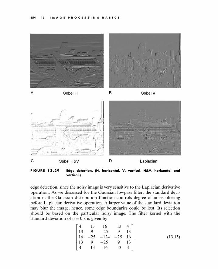
edge detection, since the noisy image is very sensitive to the Laplacian derivative
operation. As we discussed for the Gaussian lowpass filter, the standard devi-
ation in the Gaussian distribution function controls degree of noise filtering
before Laplacian derivative operation. A larger value of the standard deviation
may blur the image; hence, some edge boundaries could be lost. Its selection
should be based on the particular noisy image. The filter kernel with the
standard deviation of s¼ 0.8 is given by
4 13 16 13 4
13 9 25 9 13
16 25 124 25 16
13 9 25 9 13
4 13 16 13 4
266664
377775: (13:15)
F IGURE 13 .29 Edge detection. (H, horizontal, V, vertical, H&V, horizontal andvertical.)
Tan: Digital Signaling Processing 0123740908_chap13 Final Proof page 654 22.6.2007 3:23pm Compositor Name: MRaja
654 13 I M A G E P R O C E S S I N G B A S I C S

The processed edge detection using the Laplacian of Gaussian filter in Equation
(13.15) is shown in Figure 13.30. We can further use a threshold value to convert
the processed image to a black and white image, where the contours of objects
can be clearly displayed.
13.4.4 MATLAB Funct ions for Image Fi l ter ing
MATLAB image filter design and implementation functions are summarized in
Figure 13.31. MATLAB functions are explained as:
X ¼ image to be processed
fspecial(’filter type’, kernel size, parameter)¼ convolution kernel generationH ¼ FSPECIAL(’gaussian’,HSIZE,SIGMA) returns a rotationally
symmetric Gaussian lowpass filter of size HSIZE with standard deviation SIGMA (positive).
H ¼ FSPECIAL(’log’,HSIZE,SIGMA) returns a rotationally symmetric
Laplacian of Gaussian filter of size HSIZE with standard deviation SIGMA (positive).
filter([convolution kernel], X) ¼ two-dimensional filter using the convolution kernel
medfilt2(X, [row size, column size]) ¼ two-dimensional median filter
Program 13.2 lists the sample MATLAB codes for filtering applications. Figure
13.31 outlines the applications of the MATLAB functions.
F IGURE 13.30 Image edge detection using Laplacian of Gaussian filter.
Tan: Digital Signaling Processing 0123740908_chap13 Final Proof page 655 22.6.2007 3:24pm Compositor Name: MRaja
13.4 Image Filtering Enhancement 655

Program 13.2. Examples of Gaussian filtering, median filtering, and Laplacian
of Gaussian filtering.
close all;clear all; clc;
X¼imread(’cruise’,’jpeg’); % Provided by the instructor
Y¼rgb2gray(X); % Convert the rgb image to the grayscale image
I¼im2double(Y); % Get the intensity image
image1_g¼imnoise(I,’gaussian’); % Add random noise to the intensity image
ng¼mat2gray(image1_g); %Adjust the range
ng¼im2uint8(ng); % 8-bit corrupted image
%Linear Filtering
K_size¼ 5; % Kernel size ¼ 5 5sigma ¼0.8; % sigma: the bigger, the smoother the processed image
h¼fspecial(’gaussian’,K_size,sigma);%DetermineGaussianfiltercoefficients%This command will construct a Gaussian filter
%of size 5x5 with a mainlobe width of 0.8.
image1_out¼filter2(h,image1_g); % Perform filtering
image1_out¼mat2gray(image1_out); % Adjust the range
image1_out¼im2uint8(image1_out); % Get the 8-bit image
subplot(1, 2, 1);imshow(ng),title(’Noisy image’);subplot(1, 2, 2);imshow(image1_out);
title(’5 5 Gaussian kernel’);%Median Filtering
image1_s¼imnoise(I,’salt&pepper’);%Add‘‘pepperandsalt’’noisetotheimagemn¼mat2gray(image1_s); % Adjust the range
mn¼im2uint8(mn); % Get the 8-bit image
K_size¼3; % kernel size
image1_m¼medfilt2(image1_s, [K_size, K_size]); % Perform median filteringimage1_m¼mat2gray(image1_m); % Adjust range
image1_m¼im2uint8(image1_m); % Get the 8-bit image
figure, subplot(1, 2, 1);imshow(mn)
title(’Median noisy’);subplot(1, 2, 2);imshow(image1_m);
title(’3 3 median kernel’);%Laplacian of Gaussian filtering
K_size ¼5; % Kernel size
sigma ¼0.9; % Sigma parameter
h¼fspecial(’log’, K_size, sigma); % Determine the Laplacian of Gaussian filter kernelimage1_out¼filter2(h,I); % Perform filtering
image1_out¼mat2gray(image1_out); % Adjust the range
image1_out¼im2uint8(image1_out); % Get the 8-bit image
figure,subplot(1, 2, 1);imshow(Y)
title(’Original’);subplot(1,2,2);imshow(image1_out);
title(’Laplacian filter 5 5 kernel’);
Tan: Digital Signaling Processing 0123740908_chap13 Final Proof page 656 22.6.2007 3:24pm Compositor Name: MRaja
656 13 I M A G E P R O C E S S I N G B A S I C S

13.5 Image Pseudo-Color Generat ionand Detect ion
We can apply certain transformations to the grayscale image so that it becomes
a color image, and a wider range of pseudo-color enhancement can be obtained.
In object detection, pseudo-color generation can produce the specific color for
Filter operations:1) Gaussian Lowpass filter:remove noise, but the image isblurred2) median filter:effectively remove "salt andpepper" type noise3) Laplacian of Gaussian filter:(log filter)find the segments of image orboundariesh=fspecial('gaussian',5,0.8);image1_out=filter2(h,image1_g);image1_m=medfilt2(image1_s,[3 3]);
h=fspecial('log',5,0.9);image1_out=filter2(h,image1);
X=ind2gray(X,map)
I=im2double(X) X=mat2gray(J)X=im2uint8(X)
to display
Image Filtering
Indexed color image1) pixel value is an index; there are256 indices2) each index points to a color mapentry with three values: Red, Greenand Blue
R G B01
255
1
RGB color image1) each pixel has three values:Red, Green, and Blue2) Three are red image, greenimage, and blue imagecomponents
BGR
Grayscale image1) each pixel has a value witha range of 0 to 255
[X, map]=imread('file name','format');
X=imread('file name','format');
X=ind2rgb(X,map) [X,map]=rgb2ind(X,256)
X=rgb2gray(X)
F IGURE 13.31 MATLAB functions for filter design and implementation.
Tan: Digital Signaling Processing 0123740908_chap13 Final Proof page 657 22.6.2007 3:24pm Compositor Name: MRaja
13.5 Image Pseudo-Color Generation and Detection 657

the object that is to be detected, say, red. This would significantly increase
accuracy of the identification. To do so, we choose three transformations of
the grayscale level to the RGB components, as shown in Figure 13.32.
As a simple choice, we choose three sine functions for RGB transformations,
as shown in Figure 13.33(a). Changing the phase and period of one sine function
can be easily done so that the grayscale pixel level of the object to be detected is
aligned to the desired color with its component value as large as possible, while
the other two functions transform the same grayscale level to have their color
component values as small as possible. Hence, the single specified color object
can be displayed in the image for identification. By carefully choosing the phase
and period of each sine function, certain object(s) can be transformed to red,
green, or blue with a favorable choice.
Example 13.10.
In the grayscale image in Figure 13.13a, the area pointed to by the arrow has a
grayscale value approximately equal to 60. The background has a pixel value
approximately equal to 10.
a. Generate the background to be as close to blue as possible, and make the
area pointed to by the arrow as close to red as possible.
Solution:
a. The transformation functions are chosen as shown in Figure 13.33a,
where the red value is largest at 60 and the blue and green values
approach zero. At the grayscale of 10, the blue value is dominant. Figure
13.33b shows the processed pseudo-color image; it is included in the color
insert.
Figure 13.34 illustrates the pseudo-color generation procedure.
8-bit grayscalepixel p(m,n)
8-bit red pixel
8-bit green pixel
8-bit blue pixel
Redtransformation
Greentransformation
Bluetransformation
F IGURE 13 .32 Block diagram for transforming a grayscale pixel to a pseudo-colorpixel.
Tan: Digital Signaling Processing 0123740908_chap13 Final Proof page 658 22.6.2007 3:24pm Compositor Name: MRaja
658 13 I M A G E P R O C E S S I N G B A S I C S

0
0.5
1
R v
alue
0 50 100 150 200 250 300
0 50 100 150 200 250 300
0 50 100 150 200 250 300
0
0.5
1
G v
alue
0
0.5
1
B v
alue
6010
F IGURE 13.33A Three sine functions for grayscale transformation.
F IGURE 13.33B The pseudo-color image. (See color insert.)
Tan: Digital Signaling Processing 0123740908_chap13 Final Proof page 659 22.6.2007 3:24pm Compositor Name: MRaja
13.5 Image Pseudo-Color Generation and Detection 659

Pseudo color generation
1) Gray to Red transformationusing a sine function2) Gray to Green transformationusing a sine function3) Gray to Blue transformationusing a sine function
Note the phases are different
Image Pseudo-colorGeneration for Detection
R
G
B
0
0
0 255
255
255100 110
Pixel valuebetween 100 and110 will look like
green
X=ind2gray(X,map)
Indexed color image1) pixel value is an index; there are256 indices2) each index points to a color mapentry with three values: Red, Greenand Blue
R G B01
255
1
RGB color image1) each pixel has three values:Red, Green, and Blue2) Three are red image, greenimage, and blue imagecomponents
BGR
Grayscale image1) each pixel has a value witha range of 0 to 255
[X, map]=imread('file name','format');
X=imread('file name','format');
X=ind2rgb(X,map) [X,map]=rgb2ind(X,256)
X=rgb2gray(X)
F IGURE 13 .34 Illustrative procedure for pseudo-color generation.
Tan: Digital Signaling Processing 0123740908_chap13 Final Proof page 660 22.6.2007 3:24pm Compositor Name: MRaja
660 13 I M A G E P R O C E S S I N G B A S I C S

Program 13.3 lists the sample MATLAB codes for pseudo-color generation
for a grayscale image.
Program 13.3. Program examples for pseudo-color generation.
close all; clear all;clc
disp(’Convert the grayscale image to the pseudo-color image1’);[X,map]¼imread(’clipim2’,’gif’);%Read8-bitindeximage,providedbytheinstructorY¼ind2gray(X,map); % 8-bit color image to the grayscale conversion
%Apply pseudo color functions using sinusoids
C_r ¼304; % Cycle change for the red channel
P_r¼0; % Phase change for the red channel
C_b¼804; % Cycle change for the blue channel
P_b¼60; % Phase change for the blue channel
C_g¼304; % Cycle change for the green channel
P_g¼60; % Phase change for the green channel
r¼abs(sin(2*pi*[-P_r:255-P_r]/C_r));g¼abs(sin(2*pi*[P_b:255P_b]/C_b));b¼abs(sin(2*pi*[P_g:255P_g]/C_g));figure, subplot(3, 1, 1);plot(r,’r’);grid;ylabel(’R value’)subplot(3, 1, 2);plot(g,’g’);grid;ylabel(’G value’);subplot(3, 1, 3);plot(b,’b’);grid;ylabel(’B value’);figure, imshow(Y);
map¼[r;g;b;]’; % Construct the color map
figure, imshow(Y, map); % Display the pseudo-color image
13.6 Image Spectra
In one-dimensional digital signal processing such as for speech and other audio,
we need to examine the frequency contents, check filtering effects, and
perform feature extraction. Image processing is similar. However, we need
to apply a two-dimensional discrete Fourier transform (2D-DFT) instead of a
one-dimensional (1D) DFT. The spectrum including the magnitude and phase is
also in two dimensions. The equations of the 2D-DFT are given by:
X(u,v) ¼XM1
m¼0
XN1
n¼0
p(m, n)WumM Wvn
N , (13:16)
where WM ¼ ej2pM and WN ¼ ej2p
N ,
m and n ¼ pixel locations
u and v ¼ frequency indices.
Tan: Digital Signaling Processing 0123740908_chap13 Final Proof page 661 22.6.2007 3:24pm Compositor Name: MRaja
13.6 Image Spectra 661

Taking the absolute value of the 2D-DFT coefficients X(u,v) and dividing the
absolute value by (M N), we get the magnitude spectrum as
A(u,v) ¼ 1
N Mð Þ X (u,v)j j: (13:17)
Instead of going through the details of the 2D-DFT, we focus on application
results via examples.
Example 13.11.
a. Determine the 2D-DFT coefficients and magnitude spectrum for the
following 2 2 image:
100 50
100 10
:
Solution:
a. Since M ¼ N ¼ 2, applying Equation (13.16) leads to
X (u, v) ¼ p(0, 0)ej2pu02 ej2pv0
2 þ p(0, 1)ej2pu02 ej2pv1
2
þ p(1, 0)ej2pu12 ej2pv0
2 þ p(1, 1)ej2pu12 ej2pv1
2
:
For u ¼ 0 and v ¼ 0, we have
X (0, 0) ¼ 100ej0 ej0 þ 50ej0 ej0 þ 100ej0 ej0 10ej0 ej0
:
¼ 100þ 50þ 100 10 ¼ 240
For u ¼ 0 and v ¼ 1, we have
X(0, 1) ¼ 100ej0 ej0 þ 50ej0 ejp þ 100ej0 ej0 10ej0 ejp
:
¼ 100þ 50 ( 1)þ 100 10 ( 1) ¼ 160
Following similar operations,
X (1, 0) ¼ 60 and X (1, 1) ¼ 60:
Thus, we have DFT coefficients as
X(u, v) ¼ 240 160
60 60
:
Tan: Digital Signaling Processing 0123740908_chap13 Final Proof page 662 22.6.2007 3:24pm Compositor Name: MRaja
662 13 I M A G E P R O C E S S I N G B A S I C S

Using Equation (13.17), we can calculate the magnitude spectrum as
A(u,v) ¼ 60 40
15 15
:
We can use the MATLAB function fft2() to verify the calculated DFT
coefficients:
X ¼ fft2([100 50;100 10])
X ¼240 160
60 60:
Example 13.12.
Given the following 200 200 grayscale image with a white rectangle (11 3
pixels) at its center and a black background, shown in Figure 13.35(a), we can
compute the image’s amplitude spectrum whose magnitudes are scaled in the
range from 0 to 255. We can display the spectrum in terms of the grayscale.
Figure 13.35(b) shows the spectrum image.
The displayed spectrum has four quarters. The left upper quarter corresponds
to the frequency components, and the other three quarters are the image coun-
terparts. From the spectrum image, the area of the upper left corner is white and
hence has the higher scale value. So, the image signal has low-frequency dominant
components. The first horizontal null line can be estimated as 200=11 ¼ 18, while
the first vertical null line happens at 200=3 ¼ 67. Next, let us apply the 2D
spectrum to understand image filtering effects in image enhancement.
F IGURE 13.35A A square image.
Tan: Digital Signaling Processing 0123740908_chap13 Final Proof page 663 22.6.2007 3:24pm Compositor Name: MRaja
13.6 Image Spectra 663

Example 13.13.
Figure 13.36(a) is a biomedical image corrupted by random noise. Before we
apply lowpass filtering, its 2D-DFT coefficients are calculated. We then com-
pute its magnitude spectrum and scale it to the range of 0 to 255. To see noise
spectral components, the spectral magnitude is further multiplied by a factor of
100. Once the spectral value is larger than 255, it is clipped to 255. The resultant
spectrum is displayed in Figure 13.36(b), where we can see that noise occupies
the entirety of the image.
To enhance the image, we apply a Gaussian lowpass filter. The enhanced
image is shown in Figure 13.36(c), in which the enhancement is easily observed.
Figure 13.36(d) displays the spectra for the enhanced image with the same
scaling process as described. As we can see, the noise is significantly reduced
compared with Figure 13.36(b).
13.7 Image Compress ion by DiscreteCos ine Transform
Image compression is a must in our modern media systems, such as digital still
and video cameras and computer systems. The purpose of compression is to
reduce information storage or transmission bandwidth without losing image
Frequency information
Image replicas
F IGURE 13 .35B Magnitude spectrum for the square image.
Tan: Digital Signaling Processing 0123740908_chap13 Final Proof page 664 22.6.2007 3:24pm Compositor Name: MRaja
664 13 I M A G E P R O C E S S I N G B A S I C S

quality or at least without losing it significantly. Image compression can be
classified as lossless compression or lossy compression. Here we focus on lossy
compression using discrete cosine transform (DCT).
The DCT is a core compression technology used in the industry standards
JPEG (Joint Photographic Experts Group) for still-image compression and
MPEG (Motion Picture Experts Group) for video compression, achieving com-
pression ratios of 20:1 without noticeable quality degradation. JPEG standard
image compression is used every day in real life.
The principle of the DCT is to transform the original image pixels to their
DCT coefficients with the same number of the original image pixels, where the
DCT coefficients have non-uniform distribution of direct-current (DC) terms
F IGURE 13.36 Magnitude spectrum plots for the noisy image and the noise-filteredimage. (a) The noisy image, (b) magnitude spectrum of the noisyimage, (c) noise-filtered image, (d) magnitude spectrum of the noise-filtered image.
Tan: Digital Signaling Processing 0123740908_chap13 Final Proof page 665 22.6.2007 3:24pm Compositor Name: MRaja
13.7 Image Compression by Discrete Cosine Transform 665

representing the average values, and alternate-current (AC) terms representing
fluctuations. The compression is achieved by applying the advantages of
encoding DC terms (of a large dynamic range) with a larger number of bits and
low-frequency AC terms (a few, with a reduced dynamic range) with a reduced
number of bits, and neglecting some high-frequency AC terms having small
dynamic ranges (most of which do not affect the visual quality of the picture).
13.7.1 Two-Dimensional Discrete CosineTransform
Image compression uses 2D-DCT, whose transform pairs are defined as:
Forward DCT:
F (u, v) ¼ 2C(u)C(v)ffiffiffiffiffiffiffiffiffiMNp
XM1
i¼0
XN1
j¼0
p(i, j) cos2i þ 1ð Þup
2M
cos
2j þ 1ð Þvp
2N
(13:18)
Inverse DCT:
p(i, j) ¼XM1
u¼0
XN1
v¼0
2C(u)C(v)ffiffiffiffiffiffiffiffiffiMNp F(u, v) cos
2i þ 1ð Þup
2M
cos
2j þ 1ð Þvp
2N
(13:19)
where
C(m) ¼
ffiffiffi2p
2if m ¼ 0
1 otherwise
8<: (13:20)
p(i, j) ¼ pixel level at the location (i, j)
F(u, v) ¼ DCT coefficient at the frequency indices (u,v).
JPEG divides an image into 8 8 image subblocks and applies DCT for each
subblock individually. Hence, we simplify the general 2D-DCT in terms of 8 8
size. The equation for 2D 8 8 DCT is modified as:
F (u, v) ¼ C(u)C(v)
4
X7
i¼0
X7
j¼0
p(i, j) cos2i þ 1ð Þup
16
cos
2j þ 1ð Þvp
16
: (13:21)
The inverse of 2D 8 8 DCT is expressed as:
p(i, j) ¼X7
u¼0
X7
v¼0
C(u)C(v)
4F (u, v) cos
2i þ 1ð Þup
16
cos
2j þ 1ð Þvp
16
: (13:22)
To become familiar with the 2D-DCT formulas, we study Example 13.14.
Tan: Digital Signaling Processing 0123740908_chap13 Final Proof page 666 22.6.2007 3:24pm Compositor Name: MRaja
666 13 I M A G E P R O C E S S I N G B A S I C S

Example 13.14.
a. Determine the 2D-DCT coefficients for the following image:
100 50
100 10
:
Solution:
a. Applying N ¼ 2 and M ¼ 2 to Equation (13.18) yields
F(u, v) ¼ 2C(u)C(v)ffiffiffiffiffiffiffiffiffiffiffi2 2p
X1
i¼0
X1
j¼0
p(i, j) cos2i þ 1ð Þup
4
cos
2j þ 1ð Þvp
4
:
For u ¼ 0 and v ¼ 0, we achieve:
F (0, 0) ¼ c(0)c(0)X1
i¼0
X1
j¼0
p(i, j) cos 0ð Þ cos 0ð Þ
¼ffiffiffi2p
2
!2
p(0, 0)þ p(0, 1)þ p(1, 0)þ p(1, 1)½
¼ 1
2100þ 50þ 100 10ð Þ ¼ 120
For u ¼ 0 and v ¼ 1, we achieve:
F (0,1)¼c(0)c(1)X1
i¼0
X1
j¼0
p(i, j)cos 0ð Þcos(2jþ1)p
4
¼ffiffiffi2p
2
!1 p(0, 0)cos
p
4þp(0, 1)cos
3p
4þp(1, 0)cos
p
4þp(1, 1)cos
3p
4
¼ffiffiffi2p
2100
ffiffiffi2p
2þ50
ffiffiffi2p
2
!þ100
ffiffiffi2p
210
ffiffiffi2p
2
! !¼80
Similarly,
F (1, 0) ¼ 30 and F(1, 1) ¼ 30:
Finally, we get
F (u, v) ¼ 120 80
30 30
:
Tan: Digital Signaling Processing 0123740908_chap13 Final Proof page 667 22.6.2007 3:24pm Compositor Name: MRaja
13.7 Image Compression by Discrete Cosine Transform 667

Applying the MATLAB function dct2() verifies the DCT coefficients as
follows:
F ¼ dct2([100 50;100 10])
F ¼120:0000 80:0000
30:0000 30:0000:
Example 13.15.
Given the following DCT coefficients from a 2 2 image:
F(u, v) ¼ 120 80
30 30
,
a. Determine the pixel p(0, 0).
Solution:
a. Applying Equation (13.19) of the inverse 2D-DCT with N ¼M ¼ 2,
i ¼ 0, and j ¼ 0, it follows that
p(0,0) ¼X1
u¼0
X1
v¼0
c(u)c(v)F (u, v) cosup
4
cos
vp
4
¼ffiffiffi2p
2
!
ffiffiffi2p
2
! F (0, 0)þ
ffiffiffi2p
2
! F (0, 1)
ffiffiffi2p
2
!
þffiffiffi2p
2
! F (1, 0)
ffiffiffi2p
2
!þ F (0, 1)
ffiffiffi2p
2
!
ffiffiffi2p
2
!
¼ 1
2 120þ 1
2 80þ 1
2 30þ 1
2( 30) ¼ 100
We apply the MATLAB function idct2() to verify the inverse DCT to get
the pixel values as follows:
p ¼ idct2([120 80; 30 30])
p ¼100:0000 50:0000
100:0000 10:0000:
Tan: Digital Signaling Processing 0123740908_chap13 Final Proof page 668 22.6.2007 3:24pm Compositor Name: MRaja
668 13 I M A G E P R O C E S S I N G B A S I C S

13.7.2 Two-Dimensional JPEG Grayscale ImageCompress ion Example
To understand JPEG image compression, we examine the 8 8 grayscale
subblock. Table 13.5 shows a subblock of the grayscale image shown in
Figure 13.37 to be compressed.
Applying 2D-DCT leads to Table 13.6.These DCT coefficients have a big DC component of 1198 but small AC
component values. These coefficients are further normalized (quantized) with a
quality factor Q, defined in Table 13.7.
TABLE 13.5 8 8 subblock.
150 148 140 132 150 155 155 151
155 152 143 136 152 155 155 153
154 149 141 135 150 150 150 150
156 150 143 139 154 152 152 155
156 151 145 140 154 152 152 155
154 152 146 139 151 149 150 151
156 156 151 142 154 154 154 154
151 154 149 139 151 153 154 153
TABLE 13.6 DCT coefficients for the subblock image in Table 13.5.
1198 10 26 24 5 16 0 12
8 6 3 8 0 0 0 0
0 3 0 0 8 0 0 0
0 0 0 0 0 0 0 0
0 4 0 0 0 0 0 0
0 0 1 0 0 0 0 0
10 1 0 0 0 0 0 0
0 0 0 0 0 0 0 0
TABLE 13.7 The quality factor.
16 11 10 16 24 40 51 61
12 12 14 19 26 58 60 55
14 13 16 24 40 57 69 56
14 17 22 29 51 87 80 62
18 22 37 56 68 109 103 77
24 35 55 64 81 104 113 92
49 64 78 87 103 121 120 101
72 92 95 98 112 100 103 99
Tan: Digital Signaling Processing 0123740908_chap13 Final Proof page 669 22.6.2007 3:24pm Compositor Name: MRaja
13.7 Image Compression by Discrete Cosine Transform 669

After normalization, as shown in Table 13.8, the DC coefficient is reduced to
75, and a few small AC coefficients exist, while most are zero. We can encode
and transmit only nonzero DCT coefficients and omit transmitting zeros, since
they do not carry any information. They can be easily recovered by resetting
coefficients to zero during decoding. By this principle we achieve data compres-
sion.
As shown in Table 13.8, most nonzero coefficients reside at the upper left
corner. Hence, the order of encoding for each value is based on the zigzag path
in which the order is numbered, as in Table 13.9.
According to the order, we record the nonzero DCT coefficients as a JPEG
vector, shown as:
JPEG vector: [ 75 1 1 0 1 3 2 EOB ]:
where ‘‘EOB’’ ¼ end of block coding. The JPEG vector can further be com-
pressed by encoding the difference of DC values between subblocks, in differ-
ential pulse code modulation (DPCM), as discussed in Chapter 11, as well as by
run-length coding of AC values and Huffman coding, which both belong to
lossless compression techniques. We will pursue this in the next section.
TABLE 13 .8 Normalized DCT coefficients.
75 1 3 2 0 0 0 0
1 1 0 0 0 0 0 0
0 0 0 0 0 0 0 0
0 0 0 0 0 0 0 0
0 0 0 0 0 0 0 0
0 0 0 0 0 0 0 0
0 0 0 0 0 0 0 0
0 0 0 0 0 0 0 0
TABLE 13 .9 The order to scan DCT coefficients.
0 1 5 6 14 15 27 28
2 4 7 13 16 26 29 42
3 8 12 17 25 30 41 43
9 11 18 24 31 40 44 53
10 19 23 32 39 45 52 54
20 22 33 38 46 51 55 60
21 34 37 47 50 56 59 61
35 36 48 49 57 58 62 63
Tan: Digital Signaling Processing 0123740908_chap13 Final Proof page 670 22.6.2007 3:24pm Compositor Name: MRaja
670 13 I M A G E P R O C E S S I N G B A S I C S

During the decoding stage, the JPEG vector is recovered first. Then the
quantized DCT coefficients are recovered according to the zigzag path. Next,
the recovered DCT coefficients are multiplied by a quality factor to obtain
the estimate of the original DCT coefficients. Finally, we apply the inverse
DCT to achieve the recovered image subblock, the recovered subblock of
which is shown in Table 13.10.
For comparison, the errors between the recovered image and the original
image are calculated and listed in Table 13.11.
The original and compressed images are displayed in Figures 13.37 and
13.38, respectively. We do not see any noticeable difference between these two
grayscale images.
13.7.3 JPEG Color Image Compress ion
This section is devoted to reviewing JPEG standard compression and examines
the steps briefly. We focus on the encoder, since decoding is just the reverse
process of encoding. The block diagram for the JPEG encoder is in Figure 13.39.
The JPEG encoder has the following main steps:
1. Transform RGB to YIQ or YUV (U and V ¼ chrominance components).
2. Perform DCT on blocks.
TABLE 13.10 The recovered image subblock.
153 145 138 139 147 154 155 153
153 145 138 139 147 154 155 153
155 147 139 140 148 154 155 153
157 148 141 141 148 155 155 152
159 150 142 142 149 155 155 152
161 152 143 143 149 155 155 152
162 153 144 144 150 155 154 151
163 154 145 144 150 155 154 151
TABLE 13 .11 The coding error of the image subblock.
3 3 2 7 3 1 0 2
2 7 5 3 5 1 0 0
1 2 2 5 2 4 5 3
1 2 2 2 6 3 3 3
3 1 3 2 5 3 3 3
7 0 3 4 2 6 5 1
6 3 7 2 4 1 0 3
12 0 4 5 1 2 0 2
Tan: Digital Signaling Processing 0123740908_chap13 Final Proof page 671 22.6.2007 3:24pm Compositor Name: MRaja
13.7 Image Compression by Discrete Cosine Transform 671

3. Perform quantization.
4. Perform zigzag ordering, DPCM, and run-length encoding.
5. Perform entropy encoding (Huffman coding).
F IGURE 13 .37 Original image.
F IGURE 13 .38 JPEG compressed image.
Tan: Digital Signaling Processing 0123740908_chap13 Final Proof page 672 22.6.2007 3:24pm Compositor Name: MRaja
672 13 I M A G E P R O C E S S I N G B A S I C S

RGB to YIQ Transformat ion
The first transformation is of the RGB image to a YIQ or YUV image.
Transformation from RGB to YIQ has previously been discussed. The principle
is that in YIQ format, the luminance channel carries more signal energy, up to
93%, while the chrominance channels carry up to only 7% of signal energy. After
transformation, more effort can be spent on coding the luminance channel.
DCT on Image Blocks
Each image is divided into 8 8 blocks. 2D-DCT is applied to each block to
obtain the 8 8 DCT coefficient block. Note that there are three blocks: Y, I,
and Q.
Quant izat ion
Quantization is operated using the 8 8 quantization matrix. Each DCT coef-
ficient is quantized, divided by the corresponding value given in the quantiza-
tion matrix. In this way, a smaller number of bits can be used for encoding the
DCT coefficients. There are two different quantization tables, one for lumi-
nance (which is the same as the one in the last section and is listed here again for
comparison) and the other for chrominance.
We can see that the chrominance table has numbers with larger values, so
that small values of DCT coefficients will result and hence a smaller number of
bits are required for encoding each DCT coefficient. Zigzag ordering to produce
the JPEG vector is similar to the grayscale case, except that there are three
JPEG vectors.
RGB YIQ or YUV
DCT Quantization
Quantizationtables
8x8
P (i,j ) F (u,v )
8x8 8x8
Zigzag
DC
AC
DPCM
RLC
CodingTables
Entropycoding
Header
Tables
Data
F IGURE 13.39 Block diagram for JPEG encoder.
Tan: Digital Signaling Processing 0123740908_chap13 Final Proof page 673 22.6.2007 3:24pm Compositor Name: MRaja
13.7 Image Compression by Discrete Cosine Transform 673

Dif ferent ia l Pulse Code Modulat ion onDirec t -Current Coef f i c ients
Since each 8 8 image block has only one DC coefficient, which can be a very
large number and varies slowly, we make use of DPCM for coding DC coeffi-
cients. As an example for the first five image blocks, DC coefficients are 200,
190, 180, 160, and 170. DPCM with a coding rule of d(n) ¼ DC(n)DC(n 1)
with initial condition d(0) ¼ DC(0) produces a DPCM sequence as
200,10,10,20, 10:
Hence, the reduced signal range of these values is feasible for entropy coding.
Run-Length Coding on Al ternat ing-CurrentCoef f i c ients
The run-length method encodes the pair of
& the number of zeros to skip and
& the next nonzero value.
The zigzag scan of the 8 8 matrix makes up a vector of 64 values with a long
run of zeros. For example, the quantized DCT coefficients are scanned as
TABLE 13 .12 The quality factor for luminance.
16 11 10 16 24 40 51 61
12 12 14 19 26 58 60 55
14 13 16 24 40 57 69 56
14 17 22 29 51 87 80 62
18 22 37 56 68 109 103 77
24 35 55 64 81 104 113 92
49 64 78 87 103 121 120 101
72 92 95 98 112 100 103 99
TABLE 13 .13 The quality factor for chrominance.
17 18 24 47 99 99 99 99
18 21 26 66 99 99 99 99
24 26 56 99 99 99 99 99
47 66 99 99 99 99 99 99
99 99 99 99 99 99 99 99
99 99 99 99 99 99 99 99
99 99 99 99 99 99 99 99
99 99 99 99 99 99 99 99
Tan: Digital Signaling Processing 0123740908_chap13 Final Proof page 674 22.6.2007 3:24pm Compositor Name: MRaja
674 13 I M A G E P R O C E S S I N G B A S I C S

[75, 1, 0 1, 0, 0, 1, 3, 0, 0, 0, 2, 0, 0, . . . , 0],
with one run, two runs, and three runs of zeros in the middle and 52 extra zeros
toward the end. The run-length method encodes AC coefficients by producing a
pair (run length, value), where the run length is the number of zeros in the run,
while the value is the next nonzero coefficient. A special pair (0, 0) indicates
EOB. Here is the result from a run-length encoding of AC coefficients:
(0, 1), (1, 1), (2, 1), (0,3), (3,2), (0,0):
Loss less Entropy Coding
The DC and AC coefficients are further compressed using entropy coding.
JPEG allows Huffman coding and arithmetic coding. We focus on Huffman
coding here.
Coding DC Coef f i c ients
Each DPCM-coded DC coefficient is encoded by a pair of symbols (size,
amplitude) with the size (4-bit code) designating the number of bits for the
coefficient as shown in Table 13.14, while the amplitude is encoded by the actual
bits. For the negative number of the amplitude, 1’s complement is used.
For example, we can code the DPCM-coded DC coefficients 200, 10, 10,
20, 10 as
(8, 11001000), (4, 0101), (4, 0101), (5, 01011), (4, 1010):
Since there needs to be 4 bits for encoding each size, we can use 45 bits in total
for encoding the DC coefficients for these five subblocks.
TABLE 13.14 Huffman coding table.
Size Amplitude
1 1, 1
2 3, 2, 2, 3
3 7, . . . , 4, 4, . . . , 7
4 15, . . . , 8, 8, . . . , 15
5 31, . . . , 16, 16, . . . , 31
. .
. .
. .
10 1023, . . . , 512, 512, . . . , 1023
Tan: Digital Signaling Processing 0123740908_chap13 Final Proof page 675 22.6.2007 3:24pm Compositor Name: MRaja
13.7 Image Compression by Discrete Cosine Transform 675

Coding AC Coef f i c ients
The run-length AC coefficients have the format (run length, value). The value
can be further compressed using the Huffman coding method, similar to coding
the DPCM-coded DC coefficients. The run length and the size are each encoded
by 4 bits and packed into a byte.
Symbol 1: (run length, size)
Symbol 2: (amplitude):
The 4-bit run length can tackle only the number of runs of zeros from one to
fifteen. If the run length of zeros is longer than fifteen, then a special code (15, 0)
is used for Symbol 1. Symbol 2 is the amplitude in Huffman coding as shown in
Table 13.14, while the encoded Symbol 1 is kept in its format:
(run length, size, amplitude):
Let us code the following run-length code of AC coefficients:
(0, 1), (1, 1), (2, 1), (0, 3), (3, 2), (0, 0):
We can produce a bit stream for AC coefficients as:
(0000, 0001, 0), (0001, 0001, 0), (0010, 0001, 0),
(0000, 0010, 11), (0011, 0010, 10), (0000, 0000):
There are 55 bits in total. Figure 13.40 shows a JPEG compressed color image
(included in the color insert). The decompressed image is indistinguishable from
the original image after comparison.
F IGURE 13 .40 JPEG compressed color image. (See color insert.)
Tan: Digital Signaling Processing 0123740908_chap13 Final Proof page 676 22.6.2007 3:24pm Compositor Name: MRaja
676 13 I M A G E P R O C E S S I N G B A S I C S

13.8 Creat ing a Video Sequence byMixing Two Images
In this section, we introduce a method to mix two images to generate an image
(video) sequence. Applications of mixing two images may include fading in and
fading out images, blending two images, or overlaying text on an image.
In mixing two images in a video sequence, a smooth transition is required
from fading out one image of interest to fading in another image of interest. We
want to fade out the first image and gradually fade in the second. This cross-
fade scheme is implemented using the following operation:
Mixed image ¼ (1 a) image1 þ a image2, (13:23)
where a ¼ fading in proportionally to the weight of the second image (value
between 0 and 1), and (1 a) ¼ fading out proportionally to the weight of the
second image.
The video sequence in Figure 13.41a, b consisting of six frames is generated
using a ¼ 0:0, a ¼ 0:2, a ¼ 0:4, a ¼ 0:6, a ¼ 0:8, and a ¼ 1:0, respectively,
for two images. The equations for generating these frames are listed as follows:
Mixed image1 ¼ 1:0 image1 þ 0:0 image2
Mixed image2 ¼ 0:8 image1 þ 0:2 image2
Mixed image3 ¼ 0:6 image1 þ 0:4 image2
Mixed image4 ¼ 0:4 image1 þ 0:6 image2
Mixed image5 ¼ 0:2 image1 þ 0:8 image2
Mixed image6 ¼ 0:0 image1 þ 1:0 image2:
The sequence begins with the Grand Canyon image and fades in with the cruise
ship image. At frame 4, 60% of the cruise ship is faded in, and the image begins
to be discernible as such. The sequence ends with the cruise ship in 100% fade-in.
Figure 13.41a displays the generated grayscale sequence. Figure 13.41b shows
the color RGB video sequence (also given in the color insert).
13.9 Video Signal Bas ics
Video signals generally can be classified as component video, composite video,
and S-video. In component video, three video signals—such as the red, green, and
blue channels or the Y, I, and Q channels—are used. Three wires are required
for connection to a camera or TV. Most computer systems use component video
signals. Composite video has intensity (luminance) and two-color (chrominance)
components that modulate the carrier wave. This signal is used in broadcast
Tan: Digital Signaling Processing 0123740908_chap13 Final Proof page 677 22.6.2007 3:24pm Compositor Name: MRaja
13.9 Video Signal Basics 677
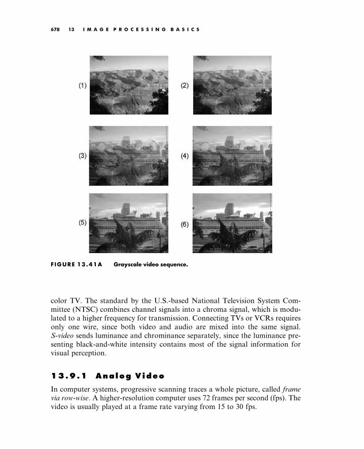
color TV. The standard by the U.S.-based National Television System Com-
mittee (NTSC) combines channel signals into a chroma signal, which is modu-
lated to a higher frequency for transmission. Connecting TVs or VCRs requires
only one wire, since both video and audio are mixed into the same signal.
S-video sends luminance and chrominance separately, since the luminance pre-
senting black-and-white intensity contains most of the signal information for
visual perception.
13.9.1 Analog Video
In computer systems, progressive scanning traces a whole picture, called frame
via row-wise. A higher-resolution computer uses 72 frames per second (fps). The
video is usually played at a frame rate varying from 15 to 30 fps.
F IGURE 13 .41A Grayscale video sequence.
Tan: Digital Signaling Processing 0123740908_chap13 Final Proof page 678 22.6.2007 3:24pm Compositor Name: MRaja
678 13 I M A G E P R O C E S S I N G B A S I C S

In TV reception and some monitors, interlaced scanning is used in a cathode-
ray tube display, or raster. The odd-numbered lines are traced first, and the
even-numbered lines are traced next. We then get the odd-field and even-field
scans per frame. The interlaced scheme is illustrated in Figure 13.42, where the
odd lines are traced, such as A to B, then C to D, and so on, ending in the middle
at E. The even field begins at F in the middle of the first line of the even field and
ends at G. The purpose of using interlaced scanning is to transmit a full frame
quickly to reduce flicker. Trace jumping from B to C is called horizontal retrace,
while trace jumping from E to F or G to A is called vertical retrace.
The video signal is amplitude modulated. The modulation levels for NTSC
video are shown in Figure 13.43. In the United States, negative modulation is
used, considering that less amplitude comes from a brighter scene, while more
amplitude comes from a darker one. This is due to the fact that most pictures
contain more white than black levels. With negative modulation, possible power
F IGURE 13.41B Color RGB video sequence. (See color insert.)
Tan: Digital Signaling Processing 0123740908_chap13 Final Proof page 679 22.6.2007 3:24pm Compositor Name: MRaja
13.9 Video Signal Basics 679

efficiency can be achieved for transmission. The reverse process will apply for
display at the receiver.
The horizontal synchronizing pulse controls the timing for the horizontal
retrace. The blanking levels are used for synchronizing as well. The ‘‘back
porch’’ (Figure 13.43) of the blanking also contains the color subcarrier burst
for color demodulation.
A
BC
D
E
F
G
F IGURE 13 .42 Interlaced raster scanning.
63.5 µs
10.9 µs 52.7 us
t
Video signal
Video
"Back porch"blanking level
"Front porch"blanking level
Horizontalsynchronizing pulse
100%
75%70%
12.5%
F IGURE 13 .43 Video-modulated waveform.
Tan: Digital Signaling Processing 0123740908_chap13 Final Proof page 680 22.6.2007 3:24pm Compositor Name: MRaja
680 13 I M A G E P R O C E S S I N G B A S I C S

The demodulated electrical signal can be seen in Figure 13.44, where a typical
electronic signal for one scan line is depicted. The white intensity has a peak value
of 0.714 volt, and the black has a voltage level of 0.055 volt, which is close to zero.
The blank corresponds to zero voltage, and the synchronizing pulse is at the level
of0:286 volt. The time duration for synchronizing is 10.9 microseconds; that of
the video occupies 52.7 microseconds; and that of one entire scan line occupies
63.6 microseconds. Hence, the line scan rate can be determined as 15.75 kHz.
Figure 13.45 describes vertical synchronization. A pulse train is generated at
the end of each field. The pulse train contains 6 equalizing pulses, 6 vertical
synchronizing pulses, and another 6 equalizing pulses at the rate of twice the size
of the line scan rate (31.5 kHz), so that the timing for sweeping half the width of
the field is feasible. In NTSC, vertical retrace takes the time interval of 20
horizontal lines designated for control information at the beginning of each
field. The 18 pulses of the vertical blanking occupy the time interval that is
equivalent to 9 lines. This leaves lines 10 to 20 for other uses.
A color subcarrier resides at the back porch, as shown in Figure 13.45. The 8
cycles of the color subcarrier are recovered via a delayed gating circuit triggered
by the horizontal sync pulse. Synchronization includes the color burst frequency
and phase information. The color subcarrier is then applied to demodulate the
color (chrominance).
Let us summarize NTSC video signals. The NTSC TV standard uses an
aspect ratio of 4:3 (ratio of picture width to height), and 525 scan lines per frame
at 30 fps. Each frame has an odd field and an even field. So there are
525=2 ¼ 262:5 lines per field. NTSC actually uses 29.97 fps. The horizontal
sweep frequency is 525 29:97 ¼ 15,734 lines per second, and each line takes
1=15,734 ¼ 63:6 msec. Horizontal retrace takes 10:9 msec, while the line signal
takes 52:7 msec for one line of image display. Vertical retrace and sync are
also needed so that the first 20 lines for each field are reserved to be used. The
active video lines per frame are 485. The layout of the video data, retrace, and
sync data is shown in Figure 13.46.
63.6 µs
10.9 µs 52.7 us
White (0.714 V)
Black (0.055 V)Blank (0V)
Sync(-0.286 V)
t
F IGURE 13.44 The demodulated signal level for one NTSC scan line.
Tan: Digital Signaling Processing 0123740908_chap13 Final Proof page 681 22.6.2007 3:24pm Compositor Name: MRaja
13.9 Video Signal Basics 681

Blanking regions can be used for V-chip information, stereo audio channel
data, and subtitles in various languages. The active line is then sampled for
display. A pixel clock divides each horizontal line of video into samples. For
example, vertical helical scan (VHS) uses 240 samples per line; Super VHS,
400–425 samples per line.
Figure 13.47 shows the NTSC video signal spectra. The NTSC standard
assigns a bandwidth of 4.2 MHz for luminance Y, 1.6 MHz for I, and 0.6 for Q,
due to human perception of color information. Since the human eye has higher
resolution to the I color component than to the Q color component, the wider
bandwidth for I is allowed.
H H/2 H
Equalizing pulses Verticalsynchronizing
pulses
Equalizing pulses
Vertical blanking
H/2
Equalizing pulses Verticalsynchronizing
pulses
Equalizing pulses
Vertical blanking
Front porchHorizontal blanking
Horizontal syn. pulse
Back porchHorizontal blanking
8 cycles color subcarrier burstColor subcarrier
Odd field
Even field
F IGURE 13 .45 Vertical synchronization for each field and the color subcarrierburst.
Tan: Digital Signaling Processing 0123740908_chap13 Final Proof page 682 22.6.2007 3:24pm Compositor Name: MRaja
682 13 I M A G E P R O C E S S I N G B A S I C S

Image data
Vertcal retrace and synchronizing
Hor
izon
tal r
etra
ce a
nd s
ynch
roni
zing
F IGURE 13.46 Video data, retrace, and sync layout.
Pic
ture
car
rier
Aud
io c
arrie
r
1.25 MHz 45 MHz.
1 MHz1.48 MHz
3.579545 MHz
6 MHz
Y Luminance signal
f (MHz)
I signalQ signal
Color subcarrier
1.48MHz
1 MHz
I signal
Q signal
LSB
LSB
USB
USB
LSB LSB USBVSB
0.75 MHz
F IGURE 13.47 NTSC Y, I, and Q spectra.
Tan: Digital Signaling Processing 0123740908_chap13 Final Proof page 683 22.6.2007 3:24pm Compositor Name: MRaja
13.9 Video Signal Basics 683

As shown in Figure 13.47, vestigial sideband modulation (VSB) is employed
for the luminance, with a picture carrier of 1.25 MHz relative to the VSB
left edge. The space between the picture carrier and the audio carrier is
4.5 MHz.
The audio signal containing the frequency range from 50 Hz to 15 kHz is
stereo frequency modulated (FM), using a peak frequency deviation of 25 kHz.
Therefore, the stereo FM audio requires a transmission bandwidth of 80 kHz,
with an audio carrier located at 4.5 MHz relative to the picture carrier.
The color burst carrier is centered at 3.58 MHz above the picture carrier. The
two color components I and Q undergo quadrature amplitude modulation
(QAM) with modulated component I output, which is VSB filtered to remove
two-thirds of the upper sideband, so that all chroma signals fall within a
4.2 MHz video bandwidth. The color burst carrier of 3.58 MHz is chosen
such that the chroma signal and luminance are interleaved in the frequency
domain to reduce interference between them.
Generating a chroma signal with QAM gives
C ¼ I cos 2pfsctð Þ þQ sin 2pfsctð Þ, (13:24)
where C ¼ chroma component and fsc ¼ color subcarrier ¼ 3:58MHz. The
NTSC signal is further combined into a composite signal:
Composite ¼ Y þ C ¼ Y þ I cos 2pfsctð Þ þQ sin 2fsctð Þ: (13:25)
At decoding, the chroma signal is obtained by separating Y and C first. Gen-
erally, the lowpass filters located at the lower end of the channel can be used to
extract Y. The comb filters may be employed to cancel interferences between the
modulated luminance signal and the chroma signal (Li and Drew, 2004). Then
we perform demodulation for I and Q as follows:
C 2 cos 2pfsctð Þ ¼ I2 cos2 2pfsctð Þ þQ 2 sin 2pfsctð Þ cos 2pfsctð Þ¼ I þ I cos 2 2pfsctð Þ þQ sin 2 2pfsctð Þ:
(13:26)
Applying a lowpass filter yields the I component. Similar operation by applying
a carrier signal of 2 sin (2pfsct) for demodulation recovers the Q component.
PAL Video
The phase alternative line (PAL) system uses 625 scan lines per frame at 25 fps,
with an aspect ratio of 4:3. It is widely used in western Europe, China, and
India. PAL uses the YUV color model, with an 8-MHz channel in which Y has
5.5 MHz and U and V each have 1.8 MHz with the color subcarrier frequency
of 4.43 MHz relative to the picture carrier. The U and V are the color difference
signals (chroma signals) of the B-Y signal and R-Y signal, respectively. The
chroma signals have alternate signs (e:g:;þ V and V) in successive scan lines.
Tan: Digital Signaling Processing 0123740908_chap13 Final Proof page 684 22.6.2007 3:24pm Compositor Name: MRaja
684 13 I M A G E P R O C E S S I N G B A S I C S

Hence, the signal and its sign reversed one in the consecutive lines are averaged
to cancel out the phase errors that could be displayed as the color errors.
SECAM Video
The SECAM (Sequentiel Couleur a Memoire) system uses 625 scan lines per
frame at 25 fps, with an aspect ratio of 4:3 and interlaced fields. The YUV color
model is employed, and U and V signals are modulated using separate color
subcarriers of 4.25 and 4.41 MHz, respectively. The U and V signals are sent on
each line alternatively. In this way, the quadrature multiplexing and the possible
cross-coupling of color signals could be avoided by halving the color resolution
in the vertical dimension.
13.9.2 Digi ta l Video
Digital video has become dominant over the long-standing analog method
in modern systems and devices because it offers high image quality; flexibility
of storage, retrieval, and editing capabilities; digital enhancement of video im-
ages; encryption; channel noise tolerance; and multimedia system applications.
Digital video formats are developed by the Consultative Committee for
International Radio (CCIR). A most important standard is CCIR-601, which
became ITU-R-601, an international standard for professional video applications.
In CCIR-601, chroma subsampling is carried for digital video. Each pixel is
in YCbCr color space, where Y is the luminance, and Cb and Cr are the
chrominance. Subsampling schemes include 4:4:4 (no chroma subsampling),
4:2:2, 4:1:1, and 4:2:0, as illustrated in Figure 13.48.
In a 4:4:4 video format in each frame, the number of values for each
chrominance component, Cb or Cr, is the same as that for luminance, Y, both
horizontally and vertically. This format finds applications in computer graphics,
in which the chrominance resolution is required for both horizontal and vertical
dimensions. The format is not widely used in video applications due to a huge
storage requirement.
TABLE 13.15 Analog broadband TV systems.
TV System
Frame
Rate (fps)
Number
of Scan
Lines
Total
Bandwidth
(MHz)
Y Bandwidth
(MHz)
U or I
Bandwidth
(MHz)
V or Q
Bandwidth
(MHz)
NTSC 29.97 525 6.0 4.2 1.6 0.6
PAL 25 625 8.0 5.5 1.8 1.8
SECAM 25 625 8.0 6.0 2.0 2.0
Source: Li and Drew, 2004.
Tan: Digital Signaling Processing 0123740908_chap13 Final Proof page 685 22.6.2007 3:24pm Compositor Name: MRaja
13.9 Video Signal Basics 685

As shown in Figure 13.48, for each frame in the 4:2:2 video format, the
number of chrominance components for Cr or Cb is half the number of
luminance components for Y. The resolution is full vertically, and the horizontal
resolution is downsampled by a factor of 2. Considering the first line of
six pixels, transmission occurs in the following form: (Y0, Cb0), (Y1, Cr0),
(Y2, Cb2), (Y3, Cr2), (Y4, Cb4), (Y5, Cr4), and so on. Six Y values are sent
for every two Cb and Cr values that are sent.
In the 4:2:0 video format, the number of values for each chrominance Cb and
Cr is half the number of luminance Y for both horizontal and vertical directions.
That is, the chroma is downsampled horizontally and vertically by a factor of 2.
The location for both Cb and Cr is shown in Figure 13.48. Digital video
specifications are given in Table 13.16.
Y Cr,Cb480
720
480
720
YCr,Cb
480
720
480
360
4:4:4
4:2:2
YCr,Cb
480
720
240
360
4:2:0
=Y value =Cr and Cb values =Y, Cr, and Cb values
F IGURE 13 .48 Chroma subsampling.
Tan: Digital Signaling Processing 0123740908_chap13 Final Proof page 686 22.6.2007 3:24pm Compositor Name: MRaja
686 13 I M A G E P R O C E S S I N G B A S I C S

CIF was specified by the Comite Consultatif International Telephonique et
Telegraphique (CCITT), which is now the International Telecommunications
Union (ITU). CIF produces a low bit rate video and supports a progressive
scan. QCIF achieves an even lower bit rate video. Neither format supports the
interlaced scan mode.
Table 13.17 outlines the high-definition TV (HDTV) formats supported by
the Advanced Television System Committee (ATSC), where ‘‘I’’ means inter-
laced scan and ‘‘P’’ indicates progressive scan. MPEG compressions of video
and audio are employed.
13.10 Motion Est imat ion in Video
In this section, we study motion estimation, since this technique is widely used in
the MPEG video compression. A video contains a time-ordered sequence of
frames. Each frame consists of image data. When the objects in an image are
still, the pixel values do not change under constant lighting conditions. Hence,
TABLE 13.16 Digital video specifications.
CCIR-601
525/60 NTSC
CCR-601 625/50
PAL/SECAM CIF QCIF
Luminance resolution 720 480 720 576 352 288 176 144
Chrominance resolution 360 480 360 576 176 144 88 72
Color subsampling 4:2:2 4:2:2 4:2:0 4:2:0
Aspect ratio 4:3 4:3 4:3 4:3
Fields/sec 60 50 30 30
Interlaced Yes Yes No No
Source: Li and Drew, 2004. CCR, comparison category rating; CIF, common intermediate
format; QCIF, quarter-CIF.
TABLE 13 .17 High-definition TV (HDTV) formats.
Number of
Active Pixels
per Line
Number of
Active Lines
Aspect
Ratio
Picture
Rate
1920 1080 16:9 60I 30P 24P
1280 720 16:9 60P 30P 24 P
704 480 16:9 and 4:3 60I 60P 30P 24P
640 480 4:3 60I 60P 30P 24P
Source: Li and Drew, 2004.
Tan: Digital Signaling Processing 0123740908_chap13 Final Proof page 687 22.6.2007 3:24pm Compositor Name: MRaja
13.10 Motion Estimation in Video 687

there is no motion between the frames. However, if the objects are moving, then
the pixels are moved. If we can find the motions, which are the pixel displace-
ments, with motion vectors, the frame data can be recovered from the reference
frame by copying and pasting at locations specified by the motion vectors. To
explore such an idea, let us look at Figure 13.49.
As shown in Figure 13.49, the reference frame is displayed first, and the next
frame is the target frame containing a moving object. The image in the target
frame is divided into N N macroblocks (20 macroblocks). A macroblock
match is searched within the search window in the reference frame to find the
closest match between a macroblock under consideration in the target frame
and the macroblock in the reference frame. The differences between two loca-
tions (motion vectors) for the matched macroblocks are encoded.
The criteria for searching the best matching can be chosen using the mean
absolute difference (MAD) between the reference frame and the target frame:
MAD(i, j) ¼ 1
N2
XN1
k¼0
XN1
l¼0
T(mþ k, nþ l) R(mþ kþ i, nþ l þ j)j j (13:27)
u ¼ i, v ¼ j for MAD(i, j) ¼ minimum, and p i, j p: (13:28)
There are many search methods for finding motion vectors, including
optimal sequential, or brute force, searches; and suboptimal searches such as
2D-logarithmic and hierarchical searches. Here we examine the sequential
search to understand the basic idea.
The sequential search for finding motion vectors employs methodical ‘‘brute
force’’ to search the entire (2pþ 1) (2pþ 1) search window in the reference
frame. The macrobock in the target frame compares each macroblock centered
at each pixel in the search window of the reference frame. Comparison proceeds
pixel by pixel to find the best match in which the vector (i, j) produces the
Reference frame Target frame
(m,n)
(m,n)
(m +u,n +v)
N
N
Macroblock
Macroblock
Search window
MV
2p+
1
2p+1
F IGURE 13.49 Macroblocks and motion vectors in the reference frame and targetframe.
Tan: Digital Signaling Processing 0123740908_chap13 Final Proof page 688 22.6.2007 3:24pm Compositor Name: MRaja
688 13 I M A G E P R O C E S S I N G B A S I C S

smallest MAD. Then the motion vector (MV(u,v)) is found to be u ¼ i, and
v ¼ j. The algorithm is described as:
min_MAD¼large valuefor i ¼ p, . . ., p
for j ¼ p, . . ., p
cur_MAD¼MDA(i, j);
if cur_MAD < min_MAD
min_MAD¼cur_MAD;u ¼ i;
v ¼ j;
end
end
end
The sequential search provides the best matching with the least MAD. However,
it requires a huge amount of computations. Other suboptimal search methods
can be employed to reduce the computational requirement, but with sacrifices of
image quality. These topics are beyond our scope.
Example 13.16
The 80 80 reference frame, target frame, and their difference are displayed in
Figure 13.50. The macroblock with a size of 16 16 is used, and the search
window has a size of 32 32. The target frame is obtained by moving the
reference frame to the right by 6 pixels and to the bottom by 4 pixels. The
sequential search method is applied to find all the motion vectors. The recon-
structed target frame using the motion vectors and reference image is given in
Figure 13.50.
Since 80 80=(16 16) ¼ 25, there are 25 macroblocks in the target frame
and 25 motion vectors in total. The motion vectors are found to be:
Horizontal direction ¼6 6 6 6 6 6 6 6 6 6 6 6 6 6
6 6 6 6 6 6 6 6 6 6 6 (13:29)
Vertical direction ¼4 4 4 4 4 4 4 4 4 4 4 4 4 4 4
4 4 4 4 4 4 4 4 4 4 (13:30)
The motion vector comprises the pixel displacements from the target frame to the
reference frame. Hence, given the reference frame, directions specified in the
motion vector should be switched to indicate the motion towards the target
Tan: Digital Signaling Processing 0123740908_chap13 Final Proof page 689 22.6.2007 3:24pm Compositor Name: MRaja
13.10 Motion Estimation in Video 689

frame. As indicated by the obtained motion vectors, the target image is the version
of the reference image moving to the right by 6 pixels and down by 4 pixels.
Summar y
1. A digital image consists of pixels. For a grayscale image, each pixel is
assigned a grayscale level that presents the luminance of the pixel. For
an RGB color image, each pixel is assigned a red component, a green
component, and a blue component. For an indexed color image, each
pixel is assigned an address that is the location of the color table (map)
made up of the red, green, and blue components.
2. Common image data formats are 8-bit grayscale, 24-bit color, and 8-bit
indexed color.
3. The larger the number of pixels in an image, or the larger the numbers
of the RGB components, the finer is the spatial resolution in the image.
Similarly, the more scale levels used for each pixel, the better the scale-
level image resolution. The more pixels and more bits used for the scale
levels in the image, the more storage is required.
F IGURE 13.50 Reference frame, target frame, their difference, and the reconstructedframe by the motion vectors.
Tan: Digital Signaling Processing 0123740908_chap13 Final Proof page 690 22.6.2007 3:24pm Compositor Name: MRaja
690 13 I M A G E P R O C E S S I N G B A S I C S

4. The RGB color pixels can be converted to YIQ color pixels. Y
component is the luminance occupying 93% of the signal energy,
while the I and Q components represent the color information of the
image, occupying the remainder of the energy.
5. The histogram for a grayscale image shows the number of pixels at each
grayscale level. The histogram can be modified to enhance the image.
Image equalization using the histogram can improve the image con-
trast and effectively enhances contrast for image underexposure. Color
image equalization can be done only in the luminance channel or RGB
channels.
6. Image enhancement techniques such as average lowpass filtering can
filter out random noise in the image; however, it also blurs the image.
The degree of blurring depends on the kernel size. The bigger the kernel
size, the more blurring occurs.
7. Median filtering effectively removes the ‘‘pepper and salt’’ noise in an
image.
8. The edge detection filter with Sobel convolution, Laplacian, and Lapla-
cian of Gaussian kernels can detect the image boundaries.
9. The grayscale image can be made into a facsimile of the color image by
pseudo-color image generation, using the red, green, and blue trans-
formation functions.
10. RGB-to-YIQ transformation is used to obtain the color image in
YIQ space, or vice versa. It can also be used for color-to-grayscale
conversion, that is, keeping only the luminance channel after the trans-
formation.
11. 2D spectra can be calculated and are used to examine filtering effects.
12. JPEG compression uses the 2D-DCT transform for both grayscale and
color images in YIQ color space. JPEG uses different quality factors to
normalize DCT coefficients for the luminance (Y) channel and the
chrominance (IQ) channels.
13. The mixing of two images, in which two pixels are linearly interpolated
using the weights 1 a and a, can produce video sequences that have
effects such as fading in and fading out of images, blending of two
images, and overlaying of text on an image.
14. Analog video uses interlaced scanning. A video frame contains odd
and even fields. Analog video standards include NTSC, PAL, and
SECAM.
Tan: Digital Signaling Processing 0123740908_chap13 Final Proof page 691 22.6.2007 3:24pm Compositor Name: MRaja
Summary 691
15. Digital video carries the modulated information for each pixel in YCbCr
color space, where Y is the luminance and Cb and Cr are the chromin-
ance. Chroma subsampling creates various digital video formats. The
industrial standards include CCIR-601, CCR-601, CIF, and QCIF.
16. The motion compensation of the video sequence produces motion vec-
tors for all the image blocks in the target video frame, which contain
displacements of these image blocks relative to the reference video
frame. Recovering the target frame involves simply copying each
image block of the reference frame to the target frame at the location
specified in the motion vector. Motion compensation is a key element in
MPEG video.
13.12 Problems
13.1. Determine the memory storage requirement for each of the following
images:
a. 320 240 8-bit grayscale
b. 640 480 24-bit color image
c. 1600 1200 8-bit indexed image
13.2. Determine the number of colors for each of the following images:
a. 320 240 16-bit indexed image
b. 200 100 24-bit color image
13.3. Given a pixel in an RGB image as follows:
R ¼ 200, G ¼ 120, B ¼ 100,
convert the RGB values to the YIQ values.
13.4. Given a pixel of an image in YIQ color format as follows:
Y ¼ 141, I ¼ 46, Q ¼ 5,
convert the YIQ values back to RGB values.
13.5. Given the following 2 2 RGB image,
R ¼ 100 50
100 50
G ¼ 20 40
10 30
B ¼ 100 50
200 150
,
convert the image into grayscale.
Tan: Digital Signaling Processing 0123740908_chap13 Final Proof page 692 22.6.2007 3:24pm Compositor Name: MRaja
692 13 I M A G E P R O C E S S I N G B A S I C S

13.6. Produce a histogram of the following image, which has a grayscale
value ranging from 0 to 7, that is, each pixel is encoded in 3 bits.
0 1 2 2 0
2 1 1 2 1
1 1 4 2 3
0 2 5 6 1
2664
3775
13.7. Given the following image with a grayscale value ranging from 0 to 7,
that is, each pixel being encoded in 3 bits,
0 1 2 2 0
2 1 1 2 1
1 1 4 2 3
0 2 5 6 1
2664
3775,
perform equalization using the histogram in Problem 13.6, and plot the histo-
gram for the equalized image.
13.8. Given the following image with a grayscale value ranging from 0 to 7,
that is, each pixel being encoded in 3 bits,
2 4 4 22 3 3 34 4 4 23 2 3 4
264
375,
perform level adjustment to the full range, shift the level to the range from 3 to
7, and shift the level to the range from 0 to 3.
13.9. Given the following 8-bit grayscale original and noisy images, and
2 2 convolution average kernel,
4 4 original image:
100 100 100 100
100 100 100 100
100 100 100 100
100 100 100 100
26664
37775
4 4 corrupted image:
93 116 109 96
92 107 103 108
84 107 86 107
87 113 106 99
26664
37775
2 2 average kernel: 14
1 1
1 1
,
perform digital filtering on the noisy image, and compare the enhanced image
with the original image.
Tan: Digital Signaling Processing 0123740908_chap13 Final Proof page 693 22.6.2007 3:24pm Compositor Name: MRaja
13.12 Problems 693

13.10. Given the following 8-bit grayscale original and noisy images, and
3 3 median filter kernel,
4 4 original image:
100 100 100 100
100 100 100 100
100 100 100 100
100 100 100 100
266664
377775
4 4 corrupted image by impulse noise:
100 255 100 100
0 255 255 100
100 0 100 0
100 255 100 100
266664
377775
3 3 average kernel:
264
375,
perform digital filtering, and compare the filtered image with the original image.
13.11. Given the following 8-bit 5 4 original grayscale image,
110 110 110 110
110 100 100 110
110 100 100 110
110 110 110 110
110 110 110 110
266664
377775,
apply the following edge detectors to the image:
a. Sobel vertical edge detector
b. Laplacian edge detector,
and scale the resultant image pixel value to the range of 0 to 255.
13.12. In Example 13.10, if we switch the transformation functions between
the red function and the green function, what is the expected color for
the area pointed to by the arrow, and what is the expected back-
ground color?
13.13. In Example 13.10, if we switch the transformation functions between
the red function and the blue function, what is the expected color for
the area pointed to by the arrow, and what is the expected back-
ground color?
Tan: Digital Signaling Processing 0123740908_chap13 Final Proof page 694 22.6.2007 3:24pm Compositor Name: MRaja
694 13 I M A G E P R O C E S S I N G B A S I C S

13.14. Given the following grayscale image p(i, j):
100 50 10
100 80 100
50 50 40
24
35,
determine the 2D-DFT coefficient X(1,2) and the magnitude spectrum A(1, 2).
13.15. Given the following grayscale image p(i, j):
10 100
200 150
,
determine the 2D-DFT coefficients X(u,v) and magnitude A(u, v).
13.16. Given the following grayscale image p(i, j):
10 100
200 150
,
apply the 2D-DCT to determine the DCT coefficients.
13.17. Given the following DCT coefficients F(u, v):
200 10
10 0
,
apply the inverse 2D-DCT to determine 2D data.
13.18. In JPEG compression, DCT DC coefficients from several blocks are
400, 390, 350, 360, and 370. Use DPCM to produce the DPCM
sequence, and use the Huffman table to encode the DPCM sequence.
13.19. In JPEG compression, DCT coefficients from an image subblock are
[175, 2, 0, 0, 0, 4, 0, 0, 3, 7, 0, 0, 0, 0, 2, 0, 0, . . . , 0]:
a. Generate the run-length codes for AC coefficients.
b. Perform entropy coding for the run-length codes using the Huff-
man table.
13.20. Explain the difference between horizontal retrace and vertical retrace.
Which one would take more time?
13.21. What is the purpose of using interlaced scanning in the traditional
NTSC TV system?
13.22. What is the bandwidth in the traditional NTSC TV broadcast sys-
tem? What is the bandwidth to transmit luminance Y, and what are the
required bandwidths to transmit Q and I channels, respectively?
Tan: Digital Signaling Processing 0123740908_chap13 Final Proof page 695 22.6.2007 3:24pm Compositor Name: MRaja
13.12 Problems 695

13.23. What type of modulation is used for transmitting audio signals in the
NTSC TV system?
13.24. Given the composite NTSC signal
Composite ¼ Y þ C ¼ Y þ I cos 2pfsctð Þ þQ sin 2pfsctð Þ,show demodulation for the Q channel.
13.25. Where does the color subcarrier burst reside? What is the frequency
of the color subcarrier, and how many cycles does the color burst
have?
13.26. Compare differences among the NTSC, PAL, and SECAM video
systems in terms of the number of scan lines, frame rates, and total
bandwidths required for transmission.
13.27. In the NTSC TV system, what is the horizontal line scan rate? What
is the vertical synchronizing pulse rate?
13.28. Explain which of the following digital video formats achieves the
most data transmission efficiency.
a. 4:4:4
b. 4:2:2
c. 4:2:0
13.29. What is the difference between an interlaced scan and a progressive
scan? Which of the following video systems uses the progressive scan?
a. CCIR-601
b. CIF
13.30. In motion compensation, which of the following would require more
computation? Explain.
a. Finding the motion vector using a sequential search
b. Recovering the target frame with the motion vectors and refer-
ence frame
13.31. Given a reference frame and target frame of size 80 80, a macro-
block size of 16 16, and a search window size of 32 32, estimate
the number of subtraction, absolute value, and addition operations
for searching all the motion vectors using the sequential search
method.
Tan: Digital Signaling Processing 0123740908_chap13 Final Proof page 696 22.6.2007 3:24pm Compositor Name: MRaja
696 13 I M A G E P R O C E S S I N G B A S I C S

MATLAB Problems
Use MATLAB to solve Problems 13.32 to 13.37.
13.32. Given the image data ‘‘trees.jpg,’’ use MATLAB functions to per-
form each of the following processing:
a. Use MATLAB to read and display the image.
b. Convert the image to the grayscale image.
c. Perform histogram equalization for the grayscale image in (b) and
display the histogram plots for both original grayscale image and
equalized grayscale image.
d. Perform histogram equalization for the color image in (a) and
display the histogram plots of Y channel for both original color
image and equalized color image.
13.33. Given the image data ‘‘cruise.jpg,’’ perform the following linear
filtering:
a. Convert the image to grayscale image and then create the 8-bit
noisy image by adding Gaussian noise using the following code:
noise_image¼imnoise(I,‘gaussian’);
where I is the intensity image obtained from normalizing the
grayscale image.
b. Process the noisy image using the Gaussian filter with the follow-
ing parameters: the convolution kernel size ¼ 4, SIGMA ¼ 0.8,
and compare the filtered image with the noisy image.
13.34. Given the image data ‘‘cruise.jpg,’’ perform the following filtering
process:
a. Convert the image to grayscale image and then create the 8-bit
noisy image by adding ‘‘pepper and salt’’ noise using the following
code:
noise_image¼imnoise(I,‘salt & pepper’);
where I is the intensity image obtained from normalizing the
grayscale image.
b. Process the noisy image using the median filtering with a convo-
lution kernel size of 44.
Tan: Digital Signaling Processing 0123740908_chap13 Final Proof page 697 22.6.2007 3:24pm Compositor Name: MRaja
MATLAB Problems 697

13.35. Given the image data ‘‘cruise.jpg,’’ convert the image to the grayscale
image and detect the image boundaries using Laplacian of Gaussian
filtering with the following parameters:
a. Kernel size ¼ 4 and SIGMA ¼ 0.9
b. Kernel size ¼ 10 and SIGMA ¼ 10
Compare the results.
13.36. Given the image data ‘‘clipim2.gif,’’ perform the following process:
a. Convert the indexed image to the grayscale image.
b. Adjust the color transformation functions (sine functions) to
make the object indicated by the arrow in the image to be red
and the background color to be green.
13.37. Given the image data ‘‘cruiseorg.tiff,’’ perform JPEG compression by
completing the following steps:
a. Convert the image to grayscale image.
b. Write a MATLAB program for encoding: (1) Dividing the image
into 8x8 blocks. (2) Transforming each block using the discrete-
cosine transform. (3) Scaling and rounding DCT coefficients with
the standard quality factor. Note that lossless-compressing the
quantized DCT coefficients is omitted here for a simple simulation.
c. Continue to write the MALAB program for decoding: (1) inversing
the scaling process for quantized DCT coefficients. (2) Performing
the inverse DCT for each 8 X 8 image block. (3) Recovering the
image.
d. Run the developed MATLAB program to examine the image
quality using
I. The quality factor
II. The quality factor X 5
III. The quality factor X 10
References
Gonzalez, R. C., and Wintz, P. (1987). Digital Image Processing, 2nd ed. Reading, MA:
Addison-Wesley Publishing Company.
Li, Z.-N., and Drew, M. S. (2004). Fundamentals of Multimedia. Upper Saddle River, NJ:
Pearson Prentice Hall.
Rabbani, M., and Jones, P. W. (1991). Digital Image Compression Techniques. Presentation
to the Society of Photo-Optical Instrumentation Engineers (SPIE), Bellingham, Washington.
Tan: Digital Signaling Processing 0123740908_chap13 Final Proof page 698 22.6.2007 3:24pm Compositor Name: MRaja
698 13 I M A G E P R O C E S S I N G B A S I C S

AIntroduction to the MATLAB
Environment
Matrix Laboratory (MATLAB) is used extensively in this book for simulations.
The goal here is to help students acquire familiarity with MATLAB and build
basic skills in the MATLAB environment. Hence, Appendix A serves the
following objectives:
1. Learn to use the help system to study basic MATLAB command and
syntax
2. Learn array indexing
3. Learn basic plotting utilities
4. Learn to write script m-files
5. Learn to write functions in MATLAB.
A.1 Basic Commands and Syntax
MATLAB has an accessible help system by the help command. By issuing the
MATLAB help command following the topic or function (routine), MATLAB
will return the text information of the topic and show how to use the function.
For example, by entering help on the MATLAB prompt to question a function
Tan: Digital Signaling Processing 0123740908_appA Final Proof page 699 21.6.2007 3:44pm Compositor Name: Mraja

sum( ), we see the text information (listed partially here) to show how to use the
MATLAB function sum( ).
» help sum
SUM Sum of the elements.
For vectors, SUM(X) is the sum of the elements of X.
For matrices, SUM(X) is a row vector with the sum over
each column.
»
The following examples are given to demonstrate the usage:
» x ¼ [1 2 3 1:5 1:5 2]; %Initialize an array
» sum(x) %Call MATLAB function sum
ans ¼4 %Display the result
»
» x ¼ [1 2 3;1:5 1:5 2:5;4 5 6] %Initialize the 3 3 matrixx ¼ %Display the contents of the 3 3 matrix
1.0000 2.0000 3.0000
1:5000 1.5000 2.5000
4.0000 5.0000 6.0000
» sum(x) %Call MATLAB function sum
ans ¼3.5000 8.5000 11.5000 %Display the results
»
MATLAB can be used like a calculator to work with numbers, variables,
and expressions in the command window. The following are the basic syntax
examples:
» sin(pi/4)
ans ¼0.7071
» pi*4
ans ¼12.5664
Tan: Digital Signaling Processing 0123740908_appA Final Proof page 700 21.6.2007 3:44pm Compositor Name: Mraja
700 A I N T R O D U C T I O N T O T H E M A T L A B E N V I R O N M E N T

In MATLAB, variable names can store values, vectors, and matrices. See the
following examples.
» x ¼ cos(pi=8)x ¼0.9239
» y ¼ sqrt(x) 2 ^ 2y ¼3:0388
» z ¼ [12 1 2]
z ¼1 2 1 2
» zz¼[1 2 3; 4 5 6]
zz ¼1 2 3
4 5 6
Complex numbers are natural in MATLAB. See the following examples.
» z ¼ 3þ 4i % Complex number
z ¼3:0000þ 4:0000i
» conj(z) % Complex conjugate of z
ans ¼3:0000 4:0000i
» abs(z) % Magnitude of z
ans ¼5
» angle(z) % Angle of z (radians)
ans ¼0.9273
» real(z) % Real part of a complex number z
ans ¼3
» imag(z) % Imaginary part of a complex number z
ans ¼4
» exp(j*pi=4) % Polar form of a complex number
ans ¼0:7071þ 0:7071i
The following shows examples of array operations. Krauss, Shure, and Little
(1994) and Stearns (2003) give the detailed explanation for each operation.
Tan: Digital Signaling Processing 0123740908_appA Final Proof page 701 21.6.2007 3:44pm Compositor Name: Mraja
A.1 Basic Commands and Syntax 701

» x ¼ [1 2;3 4] %Initialize a 2 2 matrixx ¼1 23 4
» y ¼ [4 3;2 1]y ¼4 32 1
» xþy % Add two matricesans ¼3 51 5
» x*y % Matrix productans ¼8 520 13
» x.*y % Array element productans ¼4 66 4» x0 % Matrix transpose
ans ¼1 32 4» 2: ^ x % Exponentiation: matrix x contains each exponent.ans ¼2 48 16» x: ^ 3 % Exponentiation: power of 3 for each element in matrix xans ¼1 827 64» y: ^ x % Exponentiation: each element in y has a power
% specified by a corresponding element in matrix xans ¼4 98 1» x ¼ [0 1 2 3 4 5 6] % Initialize a row vectorx ¼0 1 2 3 4 5 6
» y ¼ x:*x 2*x % Use array element product to compute a quadratic functiony ¼0 1 0 3 8 15 24
»» z ¼ [1 3]0 % Initialize a column vectorz ¼13»w ¼ xnz % Inverse matrix x, then multiply it by the column vector zw ¼10
Tan: Digital Signaling Processing 0123740908_appA Final Proof page 702 21.6.2007 3:44pm Compositor Name: Mraja
702 A I N T R O D U C T I O N T O T H E M A T L A B E N V I R O N M E N T

A.2 MATLAB Array and Indexing
Let us look at the syntax to create an array as follows:
Basic syntax: x ¼ begin : step : end
An array x is created with the first element value of begin. The value increases by
a value of step for each next element in the array and stops when the next
stepped value is beyond the specified end value of end. In simulation, we may
use this operation to create the sample indices or array of time instants for
digital signals. The values begin, step, and end can be assigned to be integers or
floating-point numbers.
The following examples are given for illustrations:
» n¼1:3:8 % Create a vector containing n¼[1 4 7]n ¼1 4 7
» m ¼ 9:1:2 % Create a vector m¼[9 8 7 6 5 4 3 2 ]
m ¼9 8 7 6 5 4 3 2
» x¼2:(1/4):4 % Create x¼[2 2.25 2.5 2.75 3 3.25 3.5 3.75 4]
x ¼Columns 1 through 7
2.0000 2.2500 2.5000 2.7500 3.0000 3.2500 3.5000
Columns 8 through 9
3.7500 4.0000
» y ¼ 2:0:5:1 % Create y ¼ [2 1:5 1 0:5 0 0:5 1]y ¼2.0000 1.5000 1.0000 0.5000 0 0:5000 1:0000
Next, we examine creating a vector and extracting numbers in a vector:
» xx ¼ [12345 [5:1:1]] % create xx¼[ 1 2 3 4 5 5 4 3 2 1]xx ¼1 2 3 4 5 5 4 3 2 1
» xx(3:7) % Show [3 4 5 5 4]
ans ¼3 4 5 5 4
» length(xx) % Return of the number of elements in vector xx
ans ¼10
» yy¼xx(2:2:length(xx)) % Display even indexed numbers in array xx
yy ¼2 4 5 3 1
Tan: Digital Signaling Processing 0123740908_appA Final Proof page 703 21.6.2007 3:44pm Compositor Name: Mraja
A.2 MATLAB Array and Indexing 703

A.3 Plot Ut i l i t ies : Subplot , P lot , Stem,and Stair
The following are common MATLAB plot functions for digital signal process-
ing (DSP) simulation:
subplot opens subplot windows for plotting.
plot produces an x-y plot. It can also create multiple plots.
stem produces discrete-time signals.
stair produces staircase (sample-and-hold) signals.
The following program contains different MATLAB plot functions:
t¼0:0.01:0.4; %Create time vector for time instants from 0 to 0.4 second
xx ¼ 4:5*sin(2*pi*10*tþ pi=4); % Calculate a sine function with the frequency 10 Hzyy ¼ 4:5*cos(2*pi*5*t pi=3);%Calculateacosfunctionwiththefrequency5 Hzsubplot(4,1,1), plot(t,xx);grid % Plot a sine function in window 1
subplot(4,1,2),plot(t,xx,t,yy,’-.’);grid;%Plotsineandcosfunctionsinwindow2
subplot(4,1,3),stem(t,xx);grid%Plotasinefunctioninthediscrete-timeform
subplot(4,1,4),stairs(t,yy);grid%Plotacosfunctioninthesample-and-holdform
xlabel(‘Time (sec.)’);
Each plot is shown in Figure A.1. Notice that dropping the semicolon at the end
of the MATLAB syntax will display values on the MATLAB prompt.
A.4 MATLAB Scr ipt F i les
We can create a MATLAB script file using the built-in MATLAB editor (or
Windows Notepad) to write MATLAB source code. The script file is named
‘‘filename.m’’ and can be run by typing the file name at the MATLAB prompt
and hitting the return key. The following script file called test.m containing the
MATLAB code is listed here for illustration.
At the MATLAB prompt, run the program
which test % show the folder where test.m resides
Go to the folder that contains test.m, and run your script from MATLAB.
test % run the test.m
type test % display the contents of test.m
Tan: Digital Signaling Processing 0123740908_appA Final Proof page 704 21.6.2007 3:44pm Compositor Name: Mraja
704 A I N T R O D U C T I O N T O T H E M A T L A B E N V I R O N M E N T

test.m
t¼0:0.01:1;x ¼ sin(2*pi*2*t);
y ¼ 0:5*cos(2*pi*5*t pi=4);plot(t,x), grid on
title(‘Test plots of sinusoids’)
ylabel(‘Signal amplitudes’);
xlabel(‘Time (sec.)’);hold on
plot(t,y,’-.’);
A.5 MATLAB Funct ions
A MATLAB function is often used for replacing the repetitive portions of the
MATLAB codes. It is created using the MATLAB script file. However, the code
begins with the key word function, following the function declaration, comments
for the help system, and program codes. A function sumsub.m that computes the
addition and subtraction of two numbers is listed here for illustration.
0 0.05 0.1 0.15 0.2 0.25 0.3 0.35 0.4−5
0
5
0 0.05 0.1 0.15 0.2 0.25 0.3 0.35 0.4−5
0
5
0 0.05 0.1 0.15 0.2 0.25 0.3 0.35 0.4−5
0
5
0 0.05 0.1 0.15 0.2 0.25 0.3 0.35 0.4−5
0
5
Time (sec)
F IGURE A.1 Illustration of MATLAB plot functions.
Tan: Digital Signaling Processing 0123740908_appA Final Proof page 705 21.6.2007 3:44pm Compositor Name: Mraja
A.5 MATLAB Functions 705

sumsub.m
function [sum, sub]¼sumsub(x1,x2)%sumsub: Function to add and subtract two numbers
% Usage:
% [sum, sub] ¼ sumsub(x1, x2)
% x1 ¼ the first number
% x2¼ the second number
% sum ¼ x1þ x2;% sub ¼ x1 x2sum ¼ x1þ x2; %Add two numbers
sub¼ x1 x2; %Subtract x2 from x1
To use the MATLAB function, go to the folder that contains sumsub.m. At
the MATLAB prompt, try the following:
0 0.1 0.2 0.3 0.4 0.5 0.6 0.7 0.8 0.9 1−1
−0.8
−0.6
−0.4
−0.2
0
0.2
0.4
0.6
0.8
1
Sig
nal a
mpl
itude
s
Time (sec)
Test plots of sinusoids
F IGURE A.2 Illustration for the MATLAB script file test.m.
Tan: Digital Signaling Processing 0123740908_appA Final Proof page 706 21.6.2007 3:44pm Compositor Name: Mraja
706 A I N T R O D U C T I O N T O T H E M A T L A B E N V I R O N M E N T

»help sumsub % Display usage information on MATLAB prompt
sumsub: Function to add and subtract two numbers
Usage:
[sum, sub] ¼ sumsub(x1, x2)
x1 ¼ the first number
x2¼ the second number
sum ¼ x1þ x2;sub ¼ x1 x2
Run the function as follows:
» [x1, x2]¼sumsub(3, 4-3i); % Call function sumsub
» x1 %Display the result of sum
x1 ¼7.0000 3.0000i» x2 %Display the result of subtraction
x2 ¼1:0000þ 3:0000i
The MATLAB function can also be used inside the m-file. More MATLAB
exercises for introduction to DSP can be explored in McClellan, Schafer, and
Yoder (1998) and Stearns (2003).
References
Krauss, T. P., Shure, L., and Little, J. N. (1994). Signal Processing TOOLBOX for Use with
MATLAB. Natick, MA: The MathWorks Inc.
McClellan, J. H., Schafer, R. W., and Yoder, M. A. (1998). DSP First—A Multimedia
Approach. Upper Saddle River, NJ: Prentice Hall.
Stearns, S. D. (2003). Digital Signal Processing with Examples in MATLAB. Boca Raton,
FL: CRC Press LLC.
Tan: Digital Signaling Processing 0123740908_appA Final Proof page 707 21.6.2007 3:44pm Compositor Name: Mraja
References 707

Tan: Digital Signaling Processing 0123740908_appA Final Proof page 708 21.6.2007 3:44pm Compositor Name: Mraja
This page intentionally left blank

BReview of Analog Signal
Processing Basics
B.1 Four ier Ser ies and Four ier Transform
In electronics applications, we have been familiar with some periodic signals
such as the square wave, rectangular wave, triangular wave, sinusoid, sawtooth
wave, and so on. These periodic signals can be analyzed in frequency domain
with the help of the Fourier series expansion. According to Fourier theory, a
periodic signal can be represented by a Fourier series that contains the sum of a
series of sine and/or cosine functions (harmonics) plus a direct-current (DC)
term. There are three forms of Fourier series: (1) sine-cosine, (2) amplitude-
phase, and (3) complex exponential. We will review each of them individually in
the following text. Comprehensive treatments can be found in Ambardar (1999),
Soliman and Srinath (1998), and Stanley (2003).
B.1.1 Sine-Cos ine Form
The Fourier series expansion of a periodic signal x(t) with a period of T via the
sine-cosine form is given by
x(t) ¼ a0 þX1n¼1
an cos (nv0t)þX1n¼1
bn sin (nv0t), (B:1)
whereas v0 ¼ 2p=T0 is the fundamental angular frequency in radians
per second, while the fundamental frequency in terms of Hz is f0 ¼ 1=T0. The
Tan: Digital Signaling Processing 0123740908_appB Final Proof page 709 20.6.2007 6:11pm Compositor Name: Mraja

Fourier coefficients of a0, an, and bn may be found according to the following
integral equations:
a0 ¼1
T0
ðT0
x(t)dt (B:2)
an ¼2
T0
ðT0
x(t) cos (nv0t)dt (B:3)
bn ¼2
T0
ðT0
x(t) sin (nv0t)dt: (B:4)
Notice that the integral is performed over one period of the signal to be
expanded. From Equation (B.1), the signal x(t) consists of a DC term and
sums of sine and cosine functions with their corresponding harmonic frequen-
cies. Again, note that nv0 is the nth harmonic frequency.
B.1.2 Ampl i tude-Phase Form
From the sine-cosine form, we notice that there is a sum of two terms with the
same frequency and that one from the first sum is an cos (nv0t) and the other is
bn sin (nv0t). We can combine these two terms and modify the sine-cosine form
into the amplitude-phase form:
x(t) ¼ A0 þX1n¼1
An cos (nv0tþ fn): (B:5)
The DC term is the same as before; that is,
A0 ¼ a0, (B:6)
and the amplitude and phase are given by
An ¼ffiffiffiffiffiffiffiffiffiffiffiffiffiffiffia2
n þ b2n
q(B:7)
fn ¼ tan1 bn
an
, (B:8)
respectively. The amplitude-phase form provides very useful information for
spectral analysis. With the calculated amplitude and phase for each harmonic
frequency, we can create the spectral plots. One depicts a plot of the amplitude
versus its corresponding harmonic frequency, called the amplitude spectrum,
while the other plot shows each phase versus its harmonic frequency, called the
phase spectrum. Note that the spectral plots are one-sided, since amplitudes and
phases are plotted versus the positive harmonic frequencies. We will illustrate
these via Example B.1.
Tan: Digital Signaling Processing 0123740908_appB Final Proof page 710 20.6.2007 6:11pm Compositor Name: Mraja
710 B R E V I E W O F A N A L O G S I G N A L P R O C E S S I N G B A S I C S

B.1.3 Complex Exponent ia l Form
The complex exponential form is developed based on expanding sine and cosine
functions in the sine-cosine form into their exponential expressions using Euler’s
formula and regrouping these exponential terms. Euler’s formula is given by
e jx ¼ cos (x) j sin (x),
which can be written as two separate forms:
cos (x) ¼ e jx þ ejx
2
sin (x) ¼ e jx ejx
2j:
We will focus on the interpretation and application rather than its derivation.
Thus the complex exponential form is expressed as
x(t) ¼X1
n¼1cne
jnv0t, (B:9)
where cn represents the complex Fourier coefficients, which may be found from
cn ¼1
T0
ðT0
x(t)ejnv0tdt: (B:10)
The relationship between the complex Fourier coefficients cn and the coefficients
of the sine-cosine form are
c0 ¼ a0 (B:11)
cn ¼an jbn
2, for n > 0: (B:12)
for n < 0, and cn is equal to the complex conjugate of ccn for n > 0. It follows
that
cn ¼ ccn ¼an þ jbn
2, for n > 0: (B:13)
Since cn is a complex value, which can be further written in the magnitude-phase
form, we obtain
cn ¼ cnj jfffn, (B:14)
where jcnj is the magnitude and wn is the phase of the complex Fourier coeffi-
cient. Similar to the amplitude-phase form, we can create the spectral plots for
jcnj and wn. Since the frequency index n goes from 1 to 1, the plots of
resultant spectra are two-sided.
Tan: Digital Signaling Processing 0123740908_appB Final Proof page 711 20.6.2007 6:11pm Compositor Name: Mraja
B.1 Fourier Series and Fourier Transform 711
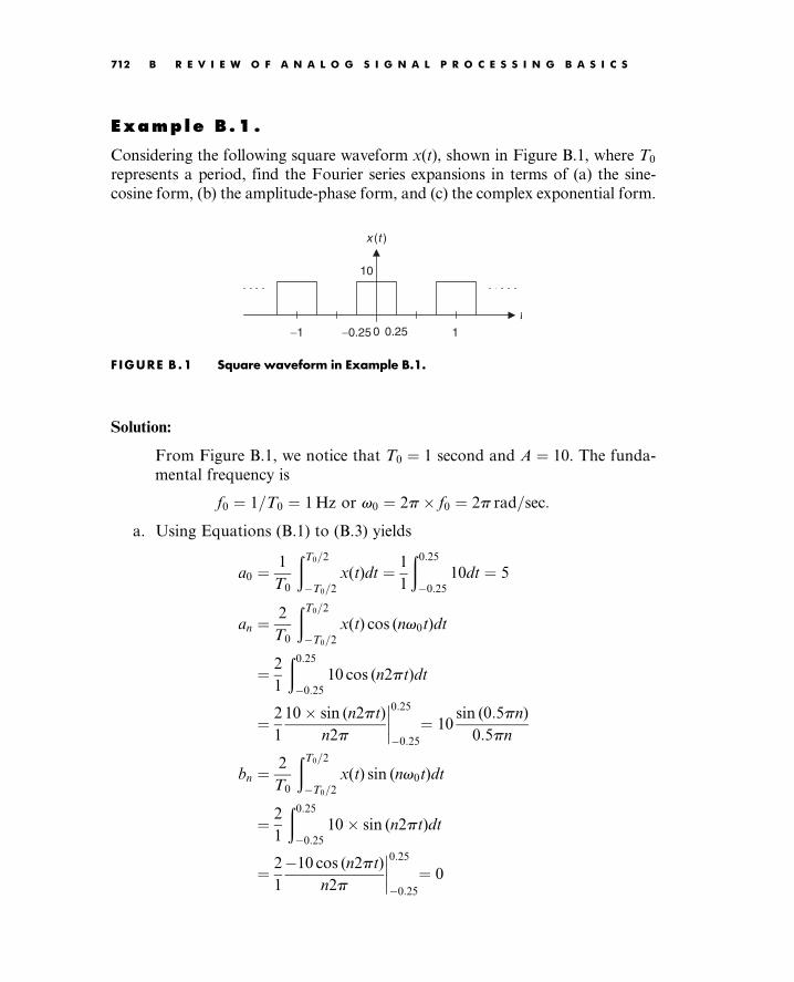
Example B.1.
Considering the following square waveform x(t), shown in Figure B.1, where T0
represents a period, find the Fourier series expansions in terms of (a) the sine-
cosine form, (b) the amplitude-phase form, and (c) the complex exponential form.
t
x (t )
10
0.250−0.25−1 1
F IGURE B.1 Square waveform in Example B.1.
Solution:
From Figure B.1, we notice that T0 ¼ 1 second and A ¼ 10. The funda-
mental frequency is
f0 ¼ 1=T0 ¼ 1Hz or v0 ¼ 2p f0 ¼ 2p rad=sec:
a. Using Equations (B.1) to (B.3) yields
a0 ¼1
T0
ðT0=2
T0=2
x(t)dt ¼ 1
1
ð0:25
0:25
10dt ¼ 5
an ¼2
T0
ðT0=2
T0=2
x(t) cos (nv0t)dt
¼ 2
1
ð0:25
0:25
10 cos (n2pt)dt
¼ 2
1
10 sin (n2pt)
n2p
0:25
0:25
¼ 10sin (0:5pn)
0:5pn
bn ¼2
T0
ðT0=2
T0=2
x(t) sin (nv0t)dt
¼ 2
1
ð0:25
0:25
10 sin (n2pt)dt
¼ 2
1
10 cos (n2pt)
n2p
0:25
0:25
¼ 0
Tan: Digital Signaling Processing 0123740908_appB Final Proof page 712 20.6.2007 6:11pm Compositor Name: Mraja
712 B R E V I E W O F A N A L O G S I G N A L P R O C E S S I N G B A S I C S

Thus, the Fourier series expansion in terms of the sine-cosine form is
written as
x(t)¼ 5þX1n¼1
10sin (0:5pn)
0:5pncos (n2pt)
¼ 5þ 20
pcos (2pt) 20
3pcos (6pt)þ 4
pcos (10pt) 20
7pcos (14pt)þ . . .
b. Making use of the relations between the sine-cosine form and the ampli-
tude-phase form, we obtain
A0 ¼ a0 ¼ 5
An ¼ffiffiffiffiffiffiffiffiffiffiffiffiffiffiffia2
n þ b2n
q¼ anj j ¼ 10 sin (0:5pn)
0:5pn
:
Again, noting that cos (x) ¼ cos (xþ 180), the Fourier series expan-
sion in terms of the amplitude-phase form is
x(t) ¼ 5þ 20
pcos (2pt)þ 20
3pcos (6ptþ 180)þ 4
pcos (10pt)
þ 20
7pcos (14ptþ 180)þ . . .
c. First let us find the complex Fourier coefficients using the formula, that
is,
cn ¼1
T0
ðT0=2
T0=2
x(t)ejnv0tdt
¼ 1
1
ð0:25
0:25
Aejn2ptdt
¼ 10 ejn2pt
jn2p
0:25
0:25
¼ 10 (ej0:5pn e j0:5pn)
jn2p
Applying Euler’s formula yields
cn ¼ 10 cos 0:5pn j sin (0:5pn) [ cos (0:5pn)þ j sin (0:5pn)]
jn2p
¼ 5sin (0:5pn)
0:5pn:
Second, using the relationship between the sine-cosine form and the
complex exponential form, it follows that
Tan: Digital Signaling Processing 0123740908_appB Final Proof page 713 20.6.2007 6:11pm Compositor Name: Mraja
B.1 Fourier Series and Fourier Transform 713

cn ¼an jbn
2¼ an
2¼ 5
sin (0:5np)
(0:5np):
Certainly, the result is identical to that obtained directly from the for-
mula. Note that c0 cannot be evaluated directly by substituting n ¼ 0,
since we have the indeterminate term 00. Using L’Hospital’s rule, described
in Appendix F, leads to
c0 ¼ limn!0
5sin (0:5np)
(0:5np)¼ lim
n!05
d sin (0:5np)ð Þdn
d 0:5npð Þdn
¼ limn!0
50:5p cos (0:5np)
0:5p¼ 5
Finally, the Fourier expansion in terms of the complex exponential form
is shown as follows:
x(t) ¼ . . .þ 10
pej2pt þ 5þ 10
pe j2pt 10
3pe j6pt þ 2
pe j10pt 10
7pe j14pt þ . . .
B.1.4 Spectra l P lots
As previously discussed, the amplitude-phase form can provide information
to create a one-sided spectral plot. The amplitude spectrum is obtained by
plotting An versus the harmonic frequency nv0, and the phase spectrum is
obtained by plotting wn versus nv0, both for n $ 0. Similarly, if the complex
exponential form is used, the two-sided amplitude and phase spectral plots of jcnjand wn versus nv0 for 1 < n <1 can each be achieved, respectively.
We illustrate this by the following example.
Example B.2.
a. Plot the amplitude spectrum of Example B.1 for a one-sided amplitude
spectrum and a two-sided amplitude spectrum, respectively.
Solution:
a. Based on the solution of An, the one-sided amplitude spectrum is shown
as follows:
Tan: Digital Signaling Processing 0123740908_appB Final Proof page 714 20.6.2007 6:11pm Compositor Name: Mraja
714 B R E V I E W O F A N A L O G S I G N A L P R O C E S S I N G B A S I C S

5
0 2p 4p 6p 8p 10p
20/(5p)20/(3p)
An20/p
w rads/sec
F IGURE B.2 One-sided spectrum of the square waveform in Example B.2.
According to the solution of the complex exponential form, the two-
sided amplitude spectrum is demonstrated as follows:
−2p−4p−6p−8p−10p 10p8p6p4p2p0
5
10/(3p) 10/(3p)
10/p 10/p
2/p 20/p
Cn
w rads/sec.
F IGURE B.3 Two-sided spectrum of the square waveform in Example B.2.
A general pulse train x(t) with a period T0 seconds and a pulse width t
seconds is shown in Figure B.4.
x(t)
A
t−T0 −T0−t / 2 0 t / 2
F IGURE B.4 Rectangular waveform (pulse train).
The Fourier series expansions for sine-cosine and complex exponential
forms can be derived similarly and are given on the next page.
Tan: Digital Signaling Processing 0123740908_appB Final Proof page 715 20.6.2007 6:11pm Compositor Name: Mraja
B.1 Fourier Series and Fourier Transform 715

Sine-cosine form:
x(t) ¼ tA
T0
þ 2tA
T0
sin (v0t=2)
(v0t=2)cos (v0t)þ
sin (2v0t=2)
(2v0t=2)cos (2v0t)
þ sin (3v0t=2)
(3v0t=2)cos (3v0t)þ . . .
! (B:15)
Complex exponential form:
x(t) ¼ . . .þ tA
T0
sin (v0t=2)
(v0t=2)ejv0t þ tA
T0
þ tA
T0
sin (v0t=2)
(v0t=2)e jv0t
þ tA
T0
sin (2v0t=2)
(2v0t=2)e j2v0t þ . . . ,
(B:16)
where v0 ¼ 2pf0 ¼ 2p=T0 is the fundamental angle frequency of the
periodic waveform. The reader can derive the one-sided amplitude spec-
trum An and the two-sided amplitude spectrum jcnj. The expressions for
one-sided amplitude and two-sided amplitude spectra are given by the
following:
A0 ¼t
T0
A (B:17)
An ¼2t
T0
Asin (nv0t=2)
(nv0t=2)
, for n ¼ 1, 2, 3 . . . (B:18)
cnj j ¼t
T0
Asin (nv0t=2)
(nv0t=2)
,1 < n <1: (B:19)
Example B.3.
a. In Figure B.4, if T0 ¼ 1ms, t ¼ 0:2 ms, and A ¼ 10, use Equations (B.17)
to (B.19) to derive the amplitude one-sided spectrum and two-sided
spectrum for each of the first four harmonic frequency components.
Solution:
a. The fundamental frequency is
v0 ¼ 2pf0 ¼ 2p (1=0:001) ¼ 2000p rad=sec:
Using Equations (B.17) and (B.18) yields the one-sided spectrum as
A0 ¼t
T0
A ¼ 0:0002
0:001 10 ¼ 2, for n ¼ 0, nv0 ¼ 0:
Tan: Digital Signaling Processing 0123740908_appB Final Proof page 716 20.6.2007 6:11pm Compositor Name: Mraja
716 B R E V I E W O F A N A L O G S I G N A L P R O C E S S I N G B A S I C S

For n ¼ 1, nv0 ¼ 2000p rad=sec:
A1 ¼2 0:0002
0:001 10 sin (1 2000p 0:0002=2)
(1 2000p 0:0002=2)
¼ 4
sin (0:2p)
(0:2p)¼ 3:7420,
for n ¼ 2, nv0 ¼ 4000p rad=sec:
A2 ¼2 0:0002
0:001 10 sin (2 2000p 0:0002=2)
(2 2000p 0:0002=2)
¼ 4
sin (0:4p)
(0:4p)¼ 3:0273,
for n ¼ 3, nv0 ¼ 6000p rad=sec:
A3 ¼2 0:0002
0:001 10 sin (3 2000p 0:0002=2)
(3 2000p 0:0002=2)
¼ 4
sin (0:6p)
(0:6p)¼ 2:0182,
for n ¼ 4, nv0 ¼ 8000p rad=sec:
A4 ¼2 0:0002
0:001 10 sin (4 2000p 0:0002=2)
(4 2000p 0:0002=2)
¼ 4
sin (0:8p)
(0:8p)¼ 0:9355:
The one-sided amplitude spectrum is plotted in Figure B.5.
0
3.7420
2.0
3.02732.0182
0.9355
2000p 4000p 6000p 8000p
An
w rads/sec.
F IGURE B.5 One-sided spectrum in Example B.3.
Similarly, applying Equation (B.19) leads to
c0j j ¼0:0002
0:001 10 lim
n!0
sin (n 2000p 0:0002=2)
(n 2000p 0:0002=2)
¼ 2 1j j ¼ 2:
Note: we use the fact limx!0
sin (x)x¼ 1:0 (see L’Hospital’s rule in Appendix F)
c1j j ¼ c1j j ¼ 0:0002
0:00110 sin(12000p0:0002=2)
(12000p0:0002=2)
¼ 2 sin(0:2p)
0:2p
¼ 1:8710
c2j j ¼ c2j j ¼ 0:0002
0:00110 sin(22000p0:0002=2)
(22000p0:0002=2)
¼ 2 sin(0:4p)
0:4p
¼ 1:5137
c3j j ¼ c3j j ¼ 0:0002
0:00110 sin(32000p0:0002=2)
(32000p0:0002=2)
¼ 2 sin(0:6p)
0:6p
¼ 1:0091
c4j j ¼ c4j j ¼ 0:0002
0:00110 sin(42000p0:0002=2)
(42000p0:0002=2)
¼ 2 sin(0:8p)
0:8p
¼ 0:4677
Tan: Digital Signaling Processing 0123740908_appB Final Proof page 717 20.6.2007 6:11pm Compositor Name: Mraja
B.1 Fourier Series and Fourier Transform 717

Figure B.6 shows the two-sided amplitude spectral plot.
.
1.87101.87102.0
1.51371.5137
1.00911.0091
0.46770.4677
8000p6000p4000p2000p−2000p−4000p−6000p−8000p 0
Cn
w rads/sec
F IGURE B.6 Two-sided spectrum in Example B.3.
The following example illustrates the use of table information to determine
the Fourier series expansion of the periodic waveform. Table B.1 consists of the
Fourier series expansions for common periodic signals in the sine-cosine form
while Table B.2 shows the expansions in the complex exponential form.
Example B.4.
In the sawtooth waveform shown in Table B.1, if T0 ¼ 1 ms and A ¼ 10, use the
formula in the table to determine the Fourier series expansion in amplitude-
phase form, and determine the frequency f3 and amplitude value of A3 for the
third harmonic.
a. Write the Fourier series expansion also in a complex exponential form,
and determine jc3j and jc3j for the third harmonic.
A = 10
−10
t
1 ms
F IGURE B.7 Sawtooth waveform in Example B.4.
Solution:
a. Based on the information in Table B.1, we have
x(t) ¼ 2A
psin v0t
1
2sin 2v0tþ
1
3sin 3v0t
1
4sin 4v0tþ . . .
:
Tan: Digital Signaling Processing 0123740908_appB Final Proof page 718 20.6.2007 6:11pm Compositor Name: Mraja
718 B R E V I E W O F A N A L O G S I G N A L P R O C E S S I N G B A S I C S

TABLE B .1 Fourier series expansions for some common waveform signals in the sine-cosine form.
Time domain signal x(t) Fourier series expansion
Positive square wave
A
T0
t
x(t) ¼ A
2þ 2A
psin v0tþ
1
3sin 3v0t
þ 1
5sin 5v0tþ
1
7sin 7v0tþ
Square wave
A
−A
t
T0
x(t) ¼ 4A
pcos v0t
1
3cos 3v0t
þ 1
5cos 5v0t
1
7cos 7v0tþ
Triangular wave
A
−A
t
T0
x(t) ¼ 8A
p2cos v0tþ
1
9cos 3v0t
þ 1
25cos 5v0tþ
1
49cos 7v0tþ
Sawtooth wave
A
−A
t
T0
x(t) ¼ 2A
psin v0t
1
2sin 2v0t
þ 1
3sin 3v0t
1
4sin 4v0tþ
Rectangular wave (Pulse train)
A
tt
t
T0
T0
Duty cycle = d =
x(t) ¼ Ad þ 2Adsin pd
pd
cos v0t
þ2Adsin 2pd
2pd
cos 2v0t
þ2Adsin 3pd
3pd
cos 3v0tþ
Ideal impulse train
T0t
1
x(t) ¼ 1
T0
þ 2
T0
cos v0tþ cos 2v0tð
þ cos 3v0tþ cos 4v0tþ )
Tan: Digital Signaling Processing 0123740908_appB Final Proof page 719 20.6.2007 6:11pm Compositor Name: Mraja
B.1 Fourier Series and Fourier Transform 719

TABLE B .2 Fourier series expansions for some common waveform signals in thecomplex exponential form.
Time domain signal x(t) Fourier series expansion
Positive square wave
A
T0
t
x(t) ¼ A
j3pej3v0t A
jpejv0t þ A
2
þ A
jpejv0t þ A
j3pe j3v0t þ A
j5pe j5v0t þ )
Square wave
A
−A
t
T0
x(t) ¼ 2A
p þ 1
5ej5v0t 1
3ej3v0t þ ejv0t
þe jv0t 1
3e j3v0t þ 1
5e j5v0t
Triangular wave
A
−A
t
T0
x(t) ¼ 4A
p2 þ 1
25e j5v0t þ 1
9ej3v0t
þejv0t þ e jv0t þ 1
9e j3v0t þ 1
25e j5v0t þ
Sawtooth wave
A
−A
t
T0
x(t) ¼ A
jp 1
3ej3v0t þ 1
2ej2v0t ejv0t
þejv0t 1
2ej2v0t þ 1
3ej3v0t þ
Rectangular wave (Pulse train)
A
tt
t
T0
T0
Duty cycle = d =
x(t) ¼ þ Adsin pd
pd
ejv0t þ Ad
þAdsin pd
pd
e jv0t þ Ad
sin 2pd
2pd
e j2v0t
þAdsin 3pd
3pd
e j3v0t þ
Ideal impulse train
T0t
1
x(t) ¼ 1
T0
þ ej3v0t þ ej2v0t þ ejv0t þ 1
þe jv0t þ e j2v0t þ e j3v0t þ )
Tan: Digital Signaling Processing 0123740908_appB Final Proof page 720 20.6.2007 6:11pm Compositor Name: Mraja
720 B R E V I E W O F A N A L O G S I G N A L P R O C E S S I N G B A S I C S

Since T0 ¼ 1ms, the fundamental frequency is
f0 ¼ 1=T0 ¼ 1000Hz, and v0 ¼ 2pf0 ¼ 2000p rad=sec:
Then, the expansion is determined as
x(t) ¼ 2 10
psin 2000pt 1
2sin 4000ptþ 1
3sin 6000pt
1
4sin 8000ptþ . . .
:
Using trigonometric identities:
sinx ¼ cos (x 90) and sin x ¼ cos (xþ 90),
and simple algebra, we finally obtain
x(t) ¼ 20
pcos 2000pt 90ð Þ þ 10
pcos 4000ptþ 90ð Þ
þ 20
3pcos 6000pt 90ð Þ þ 5
pcos 8000ptþ 90ð Þ þ . . . :
From the amplitude-phase form, we then determine f3 and A3 as follows:
f3 ¼ 3 f0 ¼ 3000Hz, and A3 ¼20
3p¼ 2:1221:
b. From Table B.2, the complex exponential form is
x(t) ¼ 10
jp. . . 1
3ej6000pt þ 1
2ej4000pt ej2000pt þ e j2000pt
1
2e j4000pt þ 1
3e j6000pt þ . . .
:
From the expression, we have
c3j j ¼10
jp 1
3
¼ 1:061
j
¼ 1:061 and
c3j j ¼ 10
jp 1
3
¼ 1:061
j
¼ 1:061:
B.1.5 Four ier Transform
Fourier transform is a mathematical function that provides the frequency spec-
tral analysis for a nonperiodic signal. The Fourier transform pair is defined as
Fourier transform: X (v) ¼ð11
x(t)ejvtdt (B:20)
Tan: Digital Signaling Processing 0123740908_appB Final Proof page 721 20.6.2007 6:11pm Compositor Name: Mraja
B.1 Fourier Series and Fourier Transform 721

Inverse Fourier transform: x(t) ¼ 1
2p
ð11
X (v)e jvtdv, (B:21)
where x(t) is a nonperiodic signal and X (v) is a two-sided continuous
spectrum versus the continuous frequency variable v, where 1 < v <1.
Again, the spectrum is a complex function that can be further written as
X(v) ¼ X (v)j jfff(v), (B:22)
where jX (v)j is the continuous amplitude spectrum, while fff(v) designates the
continuous phase spectrum.
Example B.5.
Let x(t) be a single rectangular pulse, shown in Figure B.8, where the pulse
width is t ¼ 0:5 second.
a. Find its Fourier transform and sketch the amplitude spectrum.
t
x(t)
10
−0.25 0.250
t
F IGURE B.8 Rectangular pulse in Example B.5.
Solution:
a. Applying Equation (B.21) and using Euler’s formula, we have
X (v) ¼ð11
x(t)ejvtdt ¼ð0:25
0:25
10ejvdt
¼ 10ejvt
jv
0:25
0:25
¼ 10 (ej0:25v e j0:25v)
jv
¼ 10 cos (0:25v) j sin (0:25v) [ cos (0:25v)þ j sin (0:25v)]
jv
¼ 5sin (0:25v)
0:25v
where the amplitude spectrum is expressed as
X (v)j j ¼ 5 sin (0:25v)
0:25v
:
Tan: Digital Signaling Processing 0123740908_appB Final Proof page 722 20.6.2007 6:11pm Compositor Name: Mraja
722 B R E V I E W O F A N A L O G S I G N A L P R O C E S S I N G B A S I C S

Or using v ¼ 2pf , we can express the spectrum in terms of Hz as
X ( f )j j ¼ 5 sin (0:5pf )
0:5pf
:
The amplitude spectrum is shown in Figure B.9. Note that the first null
point is at v ¼ 2p=0:5 ¼ 4p rad=sec, and the spectrum is symmetric.
X(w)
ω
0 2p 4p 6p 10p−2p−4p−6p−10p
5
F IGURE B.9 Amplitude spectrum in Example B.5.
Example B.6.
Let x(t) be an exponential function given by
x(t) ¼ 10e2tu(t) ¼ 10e2t t$0
0 t < 0
:
a. Find its Fourier transform.
Solution:
a. According to the definition of the Fourier transform,
X(v) ¼ð1
0
10e2tu(t)ejvtdt ¼ð1
0
10e(2þjv)tdt
¼ 10e(2þjv)t
(2þ jv)
1
0
¼ 10
2þ jv
X (v) ¼ 10ffiffiffiffiffiffiffiffiffiffiffiffiffiffiffiffi22 þ v2p ff tan1 v
2
Using v ¼ 2pf , we get
X ( f ) ¼ 10
2þ j2pf¼ 10ffiffiffiffiffiffiffiffiffiffiffiffiffiffiffiffiffiffiffiffiffiffiffiffi
22 þ 2pfð Þ2q ff tan1 pfð Þ:
The Fourier transforms for some common signals are listed in Table B.3.
Some useful properties of the Fourier transform are summarized in
Table B.4.
Tan: Digital Signaling Processing 0123740908_appB Final Proof page 723 20.6.2007 6:11pm Compositor Name: Mraja
B.1 Fourier Series and Fourier Transform 723

TABLE B .3 Fourier transforms for some common signals.
Time domain signal x(t) Fourier spectrum X(f)
Rectangular pulse
A
t
−2t
2t
X ( f ) ¼ Atsin pf t
pf t
Triangular pulse
A
t−t t
X ( f ) ¼ Atsin pf t
pf t
2
Cosine pulse
A
t
−2t
2t
X ( f ) ¼ 2Atp
cos pf t
14f 2t2
Sawtooth pulse
tt
A
X ( f ) ¼ jA2pf
sin pf t
pf tejpf t 1
Exponential function a ¼ 1t
t
A
X ( f ) ¼ Aaþj2pf
Impulse function
AX ( f ) ¼ A
Tan: Digital Signaling Processing 0123740908_appB Final Proof page 724 20.6.2007 6:11pm Compositor Name: Mraja
724 B R E V I E W O F A N A L O G S I G N A L P R O C E S S I N G B A S I C S

Example B.7.
Find the Fourier transforms of the following functions:
a. x(t) ¼ d(t), where d(t) is an impulse function defined by
d(t) ¼ 6¼ 0 t ¼ 0
0 elsewhere
n
with a property given as
ð11
f (t)d(t t)dt ¼ f (t)
b. x(t) ¼ d(t t)
Solution:
a. We first use the Fourier transform definition and then apply the delta
function property,
X (v) ¼ð11
d(t)ejvtdt ¼ ejvtt¼0¼ 1:
b. Similar to (a), we obtain
X (v) ¼ð11
d(t t)ejvtdt ¼ ejvtt¼t¼ ejvt:
Example B.8 shows how to use the table information to determine the Fourier
transform of the nonperiodic signal.
TABLE B .4 Properties of Fourier transform.
Line Time Function Fourier Transform
1 ax1(t)þ bx2(t) aX1( f )þ bX2( f )
2 dx(t)dt
j2pfX ( f )
3R t
1 x(t)dtX (f )j2pf
4 x(t t) ej2pf tX ( f )
5 e j2pf0tx(t) X (f f0)
6 x(at) 1aX f
a
Tan: Digital Signaling Processing 0123740908_appB Final Proof page 725 20.6.2007 6:11pm Compositor Name: Mraja
B.1 Fourier Series and Fourier Transform 725

Example B.8.
a. Use Table B.3 to determine the Fourier transform of the following cosine
pulse.
10
t1ms−1ms
F IGURE B.10 Cosine pulse in Example B.8.
Solution:
a. According to the graph, we can identify
t
2¼ 1ms, and A ¼ 1:
t is given by
t ¼ 2 1 ms ¼ 0:002 second:
Applying the formula from Table B.3 gives
X ( f ) ¼ 2 10 0:002
p
cos pf 0:002
1 4f 20:0022
¼ 0:04
p
cos 0:002pf
1 4 0:0022f 2
:
B.2 Laplace Transform
In this section, we will review Laplace transform and its applications.
B.2.1 Laplace Transform and Its Table
Laplace transform plays an important role in analysis of continuous signals and
systems. We define Laplace transform pairs as
X (s) ¼ L x(t)f g ¼ð1
0
x(t)estdt (B:23)
x(t) ¼ L1 X (s)f g ¼ 1
2pj
ðgþj1
gj1X (s)estds: (B:24)
Notice that the symbol L denotes the forward Laplace operation, while the
symbol L1fg indicates the inverse Laplace operation. Some common Laplace
transform pairs are listed in Table B.5.
In Examples B.9, we examine Laplace transform in light of its definition.
Tan: Digital Signaling Processing 0123740908_appB Final Proof page 726 20.6.2007 6:11pm Compositor Name: Mraja
726 B R E V I E W O F A N A L O G S I G N A L P R O C E S S I N G B A S I C S

Example B.9.
a. Derive the Laplace transform of the unit step function.
Solution:
a. By the definition in Equation (B.23),
X (s) ¼ð1
0
u(t)estdt
¼ð1
0
estdt ¼ est
s
1
0
¼ e1
s e0
s¼ 1
s:
The answer is consistent with the result listed in Table B.5. Now we use the
results in Table B.5 to find the Laplace transform of a function.
Example B.10.
Perform the Laplace transform for each of the following functions.
a. x(t) ¼ 5 sin (2t)u(t)
b. x(t) ¼ 5e3t cos (2t)u(t).
Solution:
a. Using line 5 in Table B.5 and noting that v ¼ 2, the Laplace transform
immediately follows that
X (s) ¼ 5L 2 sin (2t)u(t)f g
¼ 5 2
s2 þ 22¼ 10
s2 þ 4:
b. Applying line 9 in Table B.5 with v ¼ 2 and a ¼ 3 yields
X (s) ¼ 5L e3t cos (2t)u(t)
¼ 5(sþ 3)
(sþ 3)2 þ 22¼ 5(sþ 3)
(sþ 3)2 þ 4:
B.2.2 Solving Di f ferent ia l Equat ions UsingLaplace Transform
One of the important applications of Laplace transform is to solve the differ-
ential equation. Using the differential property in Table B.5, we can transform
the differential equation from the time domain to the Laplace domain. This will
change the differential equation into an algebraic equation, and we then solve
Tan: Digital Signaling Processing 0123740908_appB Final Proof page 727 20.6.2007 6:11pm Compositor Name: Mraja
B.2 Laplace Transform 727

TABLE B .5 Laplace transform table.
Line Time Function x(t) Laplace Transform
X (s) ¼ L x(t)ð Þ
1 d(t) 1
2 1 or u(t) 1s
3 tu(t) 1s2
4 eatu(t) 1sþa
5 sin (vt)u(t)v
s2 þ v2
6 cos (vt)u(t)s
s2 þ v2
7 sin (vtþ u)u(t)s sin (u)þ v cos (u)
s2 þ v2
8 eat sin (vt)u(t)v
(sþ a)2 þ v2
9 eat cos (vt)u(t) sþa
(sþa)2þv2
10 A cos (vt)þ BaAv
sin (vt)
eatu(t)Asþ B
(sþ a)2 þ v2
11a tnu(t) n!snþ1
11b 1(n1)! t
n1u(t)1
sn
12a eattnu(t)n!
(sþ a)nþ1
12b 1(n1)! e
attn1u(t) 1(sþa)n
13 2Real(A) cos (vt) 2Imag(A) sin (vt)ð Þ A
sþ a jvþ A
sþ aþ jv
14 dx(t)dt
sX (s) x(0)
15R t
0x(t)dt
X (s)
s
16 x(t a)u(t a) easX (s)
17 eatx(t)u(t) X (sþ a)
Tan: Digital Signaling Processing 0123740908_appB Final Proof page 728 20.6.2007 6:11pm Compositor Name: Mraja
728 B R E V I E W O F A N A L O G S I G N A L P R O C E S S I N G B A S I C S

the algebraic equation. Finally, the inverse Laplace transform is processed to
yield the time domain solution.
Example B.11.
a. Solve the following differential equation using Laplace transform:
dy(t)
dtþ 10y(t) ¼ x(t) with an initial condition: y(0) ¼ 0,
where the input is x(t) ¼ 5u(t).
Solution:
a. Applying the Laplace transform on both sides of the differential equation
and using the differential property (line 14 in Table B.5), we get
sY (s) y(0)þ 10Y (s) ¼ X (s):
Note that
X (s) ¼ L 5u(t)f g ¼ 5
s:
Substituting the initial condition yields
Y (s) ¼ 5
s(sþ 10):
Then we use a partial fraction expansion by writing
Y (s) ¼ A
sþ B
sþ 10
where A ¼ sY (s)js¼0¼5
sþ 10
s¼0
¼ 0:5
and B ¼ (sþ 10)Y (s)js¼10¼5
s
s¼10
¼ 0:5:
Hence,
Y (s) ¼ 0:5
s 0:5
sþ 10:
y(t) ¼ L1 0:5
s
L1 0:5
sþ 10
:
Finally, applying the inverse Laplace transform leads to using the results
listed in Table B.5, we obtain the time domain solution as
y(t) ¼ 0:5u(t) 0:5e10tu(t):
Tan: Digital Signaling Processing 0123740908_appB Final Proof page 729 20.6.2007 6:11pm Compositor Name: Mraja
B.2 Laplace Transform 729

B.2.3 Transfer Funct ion
The linear analog system can be described using the Laplace transfer function.
The transfer function relating the input and output of the linear system is
depicted as
Y (s) ¼ H(s)X (s), (B:25)
where X(s) and Y(s) are the system input and response (output), respectively, in
the Laplace domain, and the transfer function is defined as a ratio of the
Laplace response of the system to the Laplace input given by
H(s) ¼ Y (s)
X (s): (B:26)
The transfer function will allow us to study the system behavior. Considering an
impulse function as the input to a linear system, that is, x(t) ¼ d(t), whose
Laplace transform is X (s) ¼ 1, we then find the system output due to the
impulse function to be
Y (s) ¼ H(s)X (s) ¼ H(s): (B:27)
Therefore, the response in time domain y(t) is called the impulse response of the
system and can be expressed as
h(t) ¼ L1 H(s)f g: (B:28)
The analog impulse response can be sampled and transformed to obtain a digital
filter transfer function as one of the applications. This topic is covered inChapter 8.
Example B.12.
Consider a linear system described by the differential equation shown in
Example B.11. x(t) and y(t) designate the system input and system output,
respectively.
a. Derive the transfer function and the impulse response of the system.
Solution:
a. Tacking the Laplace transform on both sides of the differential equation
yields
Ldy(t)
dt
þ L 10y(t)f g ¼ L x(t)f g:
Applying the differential property and substituting the initial condition,
we have
Y (s)(sþ 10) ¼ X (s):
Tan: Digital Signaling Processing 0123740908_appB Final Proof page 730 20.6.2007 6:11pm Compositor Name: Mraja
730 B R E V I E W O F A N A L O G S I G N A L P R O C E S S I N G B A S I C S

Thus, the transfer function is given by
H(s) ¼ Y (s)
X(s)¼ 1
sþ 10:
The impulse response can be found by taking the inverse Laplace trans-
form as
h(t) ¼ L1 1
sþ 10
¼ e10tu(t):
B.3 Poles , Zeros, S tabi l i ty, Convolut ion,and Sinusoidal Steady-StateResponse
This section is a review of analog system analysis.
B.3.1 Poles , Zeros, and Stabi l i ty
To study the system behavior, the transfer function is written in a general form,
given by
H(s) ¼ N(s)
D(s)¼ bmsm þ bm1s
m1 þ . . .þ b0
ansn þ an1sn1 þ . . .þ a0
: (B:29)
It is a ratio of the numerator polynomial of degree of m to the denominator
polynomial of degree n. The numerator polynomial is expressed as
N(s) ¼ bmsm þ bm1sm1 þ . . .þ b0, (B:30)
while the denominator polynomial is given by
D(s) ¼ ansn þ an1s
n1 þ . . .þ a0: (B:31)
Again, the roots of N(s) are called zeros, while the roots of D(s) are called poles
of the transfer function H(s). Notice that zeros and poles can be real numbers or
complex numbers.
Given a system transfer function, the poles and zeros can be found. Further,
a pole-zero plot can be created on the s-plane. Having the pole-zero plot, the
stability of the system is determined by the following rules:
1. The linear system is stable if the rightmost pole(s) is(are) on the left-hand
half plane (LHHP) on the s-plane.
2. The linear system is marginally stable if the rightmost pole(s) is(are) simple
order (first order) on the jv axis, including the origin on the s-plane.
Tan: Digital Signaling Processing 0123740908_appB Final Proof page 731 20.6.2007 6:11pm Compositor Name: Mraja
B.3 Poles, Zeros, Stability, Convolution, and Sinusoidal Steady-State Response 731

3. The linear system is unstable if the rightmost pole(s) is(are) on the right-
hand half plane (RHHP) of the s-plane or if the rightmost pole(s) is(are)
multiple order on the jv axis on the s-plane.
4. Zeros do not affect the system stability.
Example B.13.
Determine whether each of the following transfer functions is stable, marginally
stable, or unstable.
a. H(s) ¼ sþ 1
(sþ 1:5)(s2 þ 2sþ 5)
b. H(s) ¼ (sþ 1)
(sþ 2)(s2 þ 4)
c. H(s) ¼ sþ 1
(s 1)(s2 þ 2sþ 5)
Solution:
a. A zero is found to be s ¼ 1.
The poles are calculated as s ¼ 1:5, s ¼ 1þ j2, s ¼ 1 j2.
The pole-zero plot is shown in Figure B.11a. Since all the poles are
located on the LHHP, the system is stable.
b. A zero is found to be s ¼ 1.
The poles are calculated as s ¼ 2, s ¼ j2, s ¼ j2.
The pole-zero plot is shown in Figure B.11b. Since the first-order poles
s ¼ j2 are located on the jv axis, the system is marginally stable.
c. A zero is found to be s ¼ 1.
The poles are calculated as s ¼ 1, s ¼ 1þ j2, s ¼ 1 j2.
The pole-zero plot is shown in Figure B.11c. Since there is a pole s ¼ 1
located on the RHHP, the system is unstable.
σ
jw
0
A
j
1
j 2
−1
−j
−2
−j 2
2
F IGURE B.11A Pole-zero plot for (a).
Tan: Digital Signaling Processing 0123740908_appB Final Proof page 732 20.6.2007 6:11pm Compositor Name: Mraja
732 B R E V I E W O F A N A L O G S I G N A L P R O C E S S I N G B A S I C S

σ
jw
0
B
j
1
j 2
−1
−j
−2
−j 2
2
F IGURE B.11B Pole-zero plot for (b).
σ
jw
0
C
j
1
j 2
−1
−j
−2
−j 2
2
F IGURE B.11C Pole-zero plot for (c).
B.3.2 Convolut ion
As we discussed before, the input and output relationship of a linear system in
Laplace domain is shown as
Y (s) ¼ H(s)X (s): (B:32)
It is apparent that in Laplace domain, the system output is the product of the
Laplace input and transfer function. But in time domain, the system output is
given as
y(t) ¼ h(t)x(t), (B:33)
where denotes linear convolution of the system impulse response h(t) and the
system input x(t). The linear convolution is further expressed as
y(t) ¼ð1
0
h(t)x(t t)dt: (B:34)
Tan: Digital Signaling Processing 0123740908_appB Final Proof page 733 20.6.2007 6:11pm Compositor Name: Mraja
B.3 Poles, Zeros, Stability, Convolution, and Sinusoidal Steady-State Response 733

Example B.14.
As you have seen in Examples B.11 and B.12, for a linear system, the impulse
response and the input are given, respectively, by
h(t) ¼ e10tu(t) and x(t) ¼ 5u(t):
a. Determine the system response y(t) using the convolution method.
Solution:
a. Two signals h(t) and x(t) that are involved in the convolution integration
are displayed in Figure B.12. To evaluate the convolution, the time-
reversed signal x( t) and the shifted signal x(t t) are also plotted for
reference. Figure B.12 shows an overlap of h(t) and x(t t). According
to the overlapped (shaded) area, the lower limit and the upper limit of the
convolution integral are determined to be 0 and t, respectively. Hence,
y(t) ¼ðt
0
e10t 5dt ¼ 5
10e10t
t
0
¼ 0:5e10t ( 0:5e100):
Finally, the system response is found to be
y(t) ¼ 0:5u(t) 0:5e10tu(t):
τ τ00
h(t) x(t)
1
5
e−10τ
τ0
5
x(−t)
τ
x(t − t)
0
5
t
0τ
t
h (t ) = e−10t
x (t − t ) = 5u (t − t)
F IGURE B.12 Convolution illustration for Example B.14.
Tan: Digital Signaling Processing 0123740908_appB Final Proof page 734 20.6.2007 6:11pm Compositor Name: Mraja
734 B R E V I E W O F A N A L O G S I G N A L P R O C E S S I N G B A S I C S

The solution is the same as that obtained using the Laplace transform method
described in Example B.11.
B.3.3 Sinusoidal Steady-State Response
For linear analog systems, if the input to system is a sinusoid of radian
frequency v, the steady-state response of the system will also be a sinusoid
of the same frequency. Therefore, the transfer function, which provides the
relationship between a sinusoidal input and a sinusoidal output, is called the
steady-state transfer function. The steady-state transfer function is obtained
from the Laplace transfer function by substituting s ¼ jv, as shown in the
following:
H( jv) ¼ H(s)js¼jv: (B:35)
Thus we have a system relationship in a sinusoidal steady state as
Y ( jv) ¼ H(jv)X (jv): (B:36)
Since H( jv) is a complex function, we may write it in a phasor form:
H( jv) ¼ A(v)ffb(v), (B:37)
where the quantity A(v) is the amplitude response of the system defined as
A(v) ¼ H(jv)j j, (B:38)
and the phase angle b(v) is the phase response of the system. The following
example is presented to illustrate the application.
Example B.15.
Consider a linear system described by the differential equation shown in Ex-
ample B.12, where x(t) and y(t) designate the system input and system output,
respectively. The transfer function has been derived as
H(s) ¼ 10
sþ 10:
a. Derive the steady-state transfer function.
b. Derive the amplitude response and phase response.
c. If the input is given as a sinusoid, that is, x(t) ¼ 5 sin (10tþ 30)u(t), find
the steady-state response yss(t).
Tan: Digital Signaling Processing 0123740908_appB Final Proof page 735 20.6.2007 6:11pm Compositor Name: Mraja
B.3 Poles, Zeros, Stability, Convolution, and Sinusoidal Steady-State Response 735

Solution:
a. By substituting s ¼ jv into the transfer function in terms of a suitable
form, we get the steady-state transfer function as
H( jv) ¼ 1s10þ 1¼ 1
jv10þ 1
:
b. The amplitude response and phase response are found to be
A(v) ¼ 1ffiffiffiffiffiffiffiffiffiffiffiffiffiffiffiffiv10
2þ1
q
b(v) ¼ ff tan1 v
10
:
c. When v ¼ 10 rad=sec, the input sinusoid can be written in terms of the
phasor form as
X ( j10) ¼ 5ff308:
For the amplitude and phase of the steady-state transfer function at
v ¼ 10, we have
A(10) ¼ 1ffiffiffiffiffiffiffiffiffiffiffiffiffiffiffiffi1010
2þ1
q ¼ 0:7071
b(10) ¼ tan1 10
10
¼ 458:
Hence, we yield
H( j10) ¼ 0:7071ff 458:
Using Equation (B.36), the system output in the phasor form is obtained as:
Y ( j10) ¼ H( j10)X ( j10) ¼ 1:4141ff 458ð ) 5ff308ð )
Y ( j10) ¼ 3:5355ff 158:
Converting the output in the phasor form back to the time domain results
in the steady-state system output as
yss(t) ¼ 3:5355 sin (10t 158)u(t):
B.4 Problems
B.1. Develop equations for the amplitude spectra, that is, An (one sided) and
jcnj (two sided), of the following pulse train x(t).
Tan: Digital Signaling Processing 0123740908_appB Final Proof page 736 20.6.2007 6:11pm Compositor Name: Mraja
736 B R E V I E W O F A N A L O G S I G N A L P R O C E S S I N G B A S I C S

x(t )
5
τ
T0= 125
0t (msecs)
F IGURE B.13 Pulse train in problem B.1.
where t ¼ 10 m sec.
a. Plot and label the one-sided amplitude spectrum up to 4 harmonic
frequencies including DC.
b. Plot and label the two-sided amplitude spectrum up to 4 harmonic
frequencies including DC.
B.2. In the waveform shown in Figure B.14, T0 ¼ 1 ms and A ¼ 10. Use the
formula in Table B.1 to write a Fourier series expansion in magnitude-
phase form. Determine the frequency f3 and amplitude value of A3 for
the third harmonic.
10
x(t )
−10 1 ms
t
F IGURE B.14 Square wave in problem B.2.
B.3. In the waveform shown in Figure B.15, T0 ¼ 1ms, t ¼ 0:2 ms, and
A ¼ 10.
a. Use the formula in Table B.1 to write a Fourier series expansion in
magnitude-phase form.
b. Determine the frequency f2 and amplitude value of A2 for the
second harmonic.
x(t )
10
t
1ms0.2 ms
F IGURE B.15 Rectangular wave in problem B.3.
Tan: Digital Signaling Processing 0123740908_appB Final Proof page 737 20.6.2007 6:11pm Compositor Name: Mraja
B.4 Problems 737

B.4. Find the Fourier transform X(v) and sketch the amplitude spectrum
for the following rectangular pulse x(t).
x(t )
5
0t (msecs)
5−5
F IGURE B.16 Rectangular pulse in problem B.4.
B.5. Use Table B.3 to determine the Fourier transform of the following pulse.
x(t )
5
t1−1
F IGURE B.17 Triangular pulse in problem B.5.
B.6. Use Table B.3 to determine the Fourier transform of the following pulse.
x(t )5
t0.5−0.5
F IGURE B.18 Rectangular pulse in problem B.6.
B.7. Determine the Laplace transform X(s) for each of the following time
domain functions using the Laplace transform in Table B.5.
a. x(t) ¼ 10d(t)
b. x(t) ¼ 100tu(t)
c. x(t) ¼ 10e2tu(t)
d. x(t) ¼ 2u(t 5)
e. x(t) ¼ 10 cos (3t)u(t)
f. x(t) ¼ 10 sin (2tþ 45o)u(t)
g. x(t) ¼ 3e2t cos (3t)u(t)
h. x(t) ¼ 10t5u(t)
Tan: Digital Signaling Processing 0123740908_appB Final Proof page 738 20.6.2007 6:11pm Compositor Name: Mraja
738 B R E V I E W O F A N A L O G S I G N A L P R O C E S S I N G B A S I C S

B.8. Determine the inverse Laplace transform of analog signal x(t) for each
of the following given functions using Table B.5 and partial fraction
expansion.
a. X (s) ¼ 10
sþ 2
b. X (s) ¼ 100
(sþ 2)(sþ 3)
c. X(s) ¼ 100s
s2 þ 7sþ 10
d. X (s) ¼ 25
s2 þ 4sþ 29
B.9. Solve the following differential equation using the Laplace transform
method.
2dx(t)
dtþ 3x(t) ¼ 15u(t) with x(0) ¼ 0
a. Determine X(s).
b. Determine the continuous signal x(t) by taking the inverse Laplace
transform of X(s).
B.10. Solve the following differential equation using the Laplace transform
method.
d2x(t)
dt2þ 3
dx(t)
dtþ 2x(t) ¼ 10u(t) with x0(0) ¼ 0 and x(0) ¼ 0
a. Determine X(s).
b. Determine x(t) by taking the inverse Laplace transform of X(s).
B.11. Determine the locations of all finite zeros and poles. In each case, make
an s-plane plot of the poles and zeros, and determine whether the given
transfer function is stable, unstable, or marginally stable.
a. H(s) ¼ (s 3)
(s2 þ 4sþ 4)
b. H(s) ¼ s(s2 þ 5)
(s2 þ 9)(s2 þ 2sþ 4)
c. H(s) ¼ (s2 þ 1)(sþ 1)
s(s2 þ 7s 8)(sþ 3)(sþ 4)
Tan: Digital Signaling Processing 0123740908_appB Final Proof page 739 20.6.2007 6:11pm Compositor Name: Mraja
B.4 Problems 739
B.12. Given the transfer function of a system as
H(s) ¼ 5
sþ 5,
and the input x(t) ¼ u(t),
a. determine the system impulse response h(t);
b. determine the system Laplace output based on Y (s) ¼ H(s)X (s);
c. determine the system response y(t) in time domain by taking the
inverse Laplace transform of Y(s).
B.13. Given the transfer function of a system as
H(s) ¼ 5
sþ 5,
a. determine the steady-state transfer function;
b. determine the amplitude response and phase response in terms of
the frequency v;
c. determine the steady-state response of the system output yss(t) in
time domain using the results that you obtained in (b), given an
input to the system of x(t) ¼ 5 sin (2t)u(t).
B.14. Given the transfer function of a system as
H(s) ¼ 5
sþ 5,
and the input x(t) ¼ u(t), determine the system output y(t) using the
convolution method; that is, y(t) ¼ h(t)x(t).
References
Ambardar, A. (1999). Analog and Digital Signal Processing, 2nd ed. Pacific Grove, CA:
Brooks/Cole Publishing Company.
Soliman, S. S., and Srinath, M. D. (1998). Continuous and Discrete Signals and Systems.
Upper Saddle River, NJ: Prentice Hall.
Stanley, W. D. (2003). Network Analysis with Applications, 4th ed. Upper Saddle River, NJ:
Prentice Hall.
Tan: Digital Signaling Processing 0123740908_appB Final Proof page 740 20.6.2007 6:11pm Compositor Name: Mraja
740 B R E V I E W O F A N A L O G S I G N A L P R O C E S S I N G B A S I C S

CNormalized Butterworth and
Chebyshev Functions
C.1 Normal ized But terwor th Funct ion
The normalized Butterworth squared magnitude function is given by
Pn(v)j j2¼ 1
1þ «2(v)2n, (C:1)
where n is the order and « is the specified ripple on filter passband. The specified
ripple in dB is expressed as «dB ¼ 20 log10
ffiffiffiffiffiffiffiffiffiffiffiffiffi1þ «2p
dB.
To develop the transfer function Pn(s), we first let s ¼ jv and then substitute
v2 ¼ s2 into Equation (C.1) to obtain
Pn(s)Pn( s) ¼ 1
1þ «2( s2)n: (C:2)
Equation (C.2) has 2n poles, and Pn(s) has n poles on the left-hand half plane
(LHHP) on the s-plane, while Pn( s) has n poles on the right-hand half
plane (RHHP) on the s-plane. Solving for poles leads to
(1)ns2n ¼ 1=«2: (C:3)
If n is an odd number, Equation (C.3) becomes
s2n ¼ 1=«2
Tan: Digital Signaling Processing 0123740908_appC Final Proof page 741 18.6.2007 1:49pm Compositor Name: Mraja

and the corresponding poles are solved as
pk ¼ «1=ne j2pk2n ¼ «1=n cos (2pk=2n)þ j sin (2pk=2n)½ , (C:4)
where k ¼ 0, 1, . . . , 2n 1. Thus in the phasor form, we have
r ¼ «1=n, and uk ¼ 2pk=(2n) for k ¼ 0, 1, , 2n 1: (C:5)
When n is an even number, it follows that
s2n ¼ 1=«2
pk ¼ «1=ne j2pkþp2n ¼ «1=n cos (2pkþ p)=2nð Þ þ j sin (2pkþ p)=2nð Þ½ , (C:6)
where k ¼ 0, 1, . . . , 2n 1. Similarly, the phasor form is given by
r ¼ «1=n, and uk ¼ (2pkþ p)=(2n) for k ¼ 0, 1, , 2n 1: (C:7)
When n is an odd number, we can identify the poles on the LHHP as
pk ¼ r, k ¼ 0 and
pk ¼ r cos (uk)þ jr sin (uk), k ¼ 1, , (n 1)=2: (C:8)
Using complex conjugate pairs, we have
pk* ¼ r cos (uk) jr sin (uk):
Notice that
(s pk)(s pk*) ¼ s2 þ 2r cos (uk)ð Þsþ r2,
and from a factor from the real pole (sþ r), it follows that
Pn(s) ¼K
(sþ r)Q(n1)=2
k¼1
(s2 þ 2r cos (uk)ð Þsþ r2)
(C:9)
and
uk ¼ 2pk=(2n) for k ¼ 1, , (n 1)=2:
Setting Pn(0) ¼ 1 for the unit passband gain leads to
K ¼ r n ¼ 1=«:
When n is an even number, we can identify the poles on the LHHP as
pk ¼ r cos (uk)þ jr sin (uk), k ¼ 0, 1, , n=2 1: (C:10)
Using complex conjugate pairs, we have
pk* ¼ r cos (uk) jr sin (uk):
Tan: Digital Signaling Processing 0123740908_appC Final Proof page 742 18.6.2007 1:49pm Compositor Name: Mraja
742 C N O R M A L I Z E D B U T T E R W O R T H
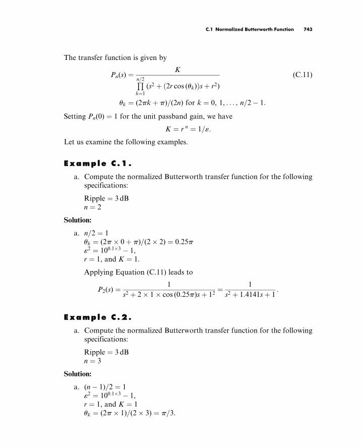
The transfer function is given by
Pn(s) ¼K
Qn=2k¼1
(s2 þ 2r cos (uk)ð Þsþ r2)
(C:11)
uk ¼ (2pkþ p)=(2n) for k ¼ 0, 1, , n=2 1:
Setting Pn(0) ¼ 1 for the unit passband gain, we have
K ¼ r n ¼ 1=«:
Let us examine the following examples.
Example C.1.
a. Compute the normalized Butterworth transfer function for the following
specifications:
Ripple ¼ 3 dB
n ¼ 2
Solution:
a. n=2 ¼ 1
uk ¼ (2p 0þ p)=(2 2) ¼ 0:25p
«2 ¼ 100:13 1,
r ¼ 1, and K ¼ 1.
Applying Equation (C.11) leads to
P2(s) ¼1
s2 þ 2 1 cos (0:25p)sþ 12¼ 1
s2 þ 1:4141sþ 1:
Example C.2.
a. Compute the normalized Butterworth transfer function for the following
specifications:
Ripple ¼ 3 dB
n ¼ 3
Solution:
a. (n 1)=2 ¼ 1
«2 ¼ 100:13 1,
r ¼ 1, and K ¼ 1
uk ¼ (2p 1)=(2 3) ¼ p=3.
Tan: Digital Signaling Processing 0123740908_appC Final Proof page 743 18.6.2007 1:49pm Compositor Name: Mraja
C.1 Normalized Butterworth Function 743

From Equation (C.9), we have
P3(s) ¼1
(sþ 1)(s2 þ 2 1 cos (p=3)sþ 12)
¼ 1
(sþ 1)(s2 þ sþ 1)
:
For the unfactored form, we can carry out
P3(s) ¼1
s3 þ 2s2 þ 2sþ 1:
Example C.3.
a. Compute the normalized Butterworth transfer function for the following
specifications:
Ripple ¼ 1:5 dB
n ¼ 3
Solution:
a. (n 1)=2 ¼ 1
«2 ¼ 100:11:5 1,
r ¼ 1:1590, and K ¼ 1:5569
uk ¼ (2p 1)=(2 3) ¼ p=3.
Applying Equation (C.9), we achieve the normalized Butterworth transfer
function as
P3(s) ¼1
(sþ 1:1590)(s2 þ 2 1:1590 cos (p=3)sþ 1:15902Þ
¼ 1
(sþ 1)(s2 þ 1:1590sþ 1:3433):
For the unfactored form, we can carry out
P3(s) ¼1:5569
s3 þ 2:3180s2 þ 2:6866sþ 1:5569):
C.2 Normal ized Chebyshev Funct ion
Similar to analog Butterworth filter design, the transfer function is derived from
the normalized Chebyshev function, and the result is usually listed in the table
for design reference. The Chebyshev magnitude response function with an order
of n and the normalized cutoff frequency v ¼ 1 radian per second is given by
Tan: Digital Signaling Processing 0123740908_appC Final Proof page 744 18.6.2007 1:49pm Compositor Name: Mraja
744 C N O R M A L I Z E D B U T T E R W O R T H

Bn(v)j j ¼ 1ffiffiffiffiffiffiffiffiffiffiffiffiffiffiffiffiffiffiffiffiffiffiffiffiffi1þ «2C2
n (v)p , n 1, (C:12)
where the function Cn(v) is defined as
Cn(v) ¼ cos (n cos1 (v)) v 1
cosh (n cosh1 (v)) v > 1,
(C:13)
and « is the ripple specification on the filter passband. Notice that
cosh1 (x) ¼ ln (xþffiffiffiffiffiffiffiffiffiffiffiffiffix2 1p
): (C:14)
To develop the transfer function Bn(s), we let s ¼ jv and substitute v2 ¼ s2
into Equation (C.12) to obtain
Bn(s)Bn( s) ¼ 1
1þ «2C2n(s=j)
: (C:15)
The poles can be found from
1þ «2C2n(s=j) ¼ 0
or
Cn(s=j) ¼ cos n cos1 (s=j)
¼ j1=«: (C:16)
Introducing a complex variable v ¼ aþ jb such that
v ¼ aþ jb ¼ cos1 (s=j), (C:17)
we can then write
s ¼ j cos (v): (C:18)
Substituting Equation (C.17) into Equation (C.16) and using trigonometric
identities, it follows that
Cn(s=j) ¼ cos n cos1 (s=j)
¼ cos (nv) ¼ cos (naþ jnb)
¼ cos (na) cosh (nb) j sin (na) sinh (nb) ¼ j1=«:
(C:19)
To solve Equation (C.19), the following conditions must be satisfied:
cos (na) cosh (nb) ¼ 0 (C:20)
sin (na) sinh (nb) ¼ 1=«: (C:21)
Since cosh(nb) 1 in Equation (C.20), we must let
cos (na) ¼ 0, (C:22)
Tan: Digital Signaling Processing 0123740908_appC Final Proof page 745 18.6.2007 1:49pm Compositor Name: Mraja
C.2 Normalized Chebyshev Function 745

which therefore leads to
ak ¼ (2kþ 1)p=(2n), k ¼ 0, 1, 2, , 2n 1: (C:23)
With Equation (C.23), we have sin (nak) ¼ 1. Then Equation (C.21) becomes
sinh (nb) ¼ 1=«: (C:24)
Solving Equation (C.24) gives
b ¼ sinh1 (1=«)=n: (C:25)
Again from Equation (C.18),
s ¼ j cos (v) ¼ j cos (ak) cosh (b) j sin (ak) sinh (b)½ (C:26)
for k ¼ 0, 1, , 2n 1:
The poles can be found from Equation (C.26):
pk ¼ sin (ak) sinh (b)þ j cos (ak) cosh (b) (C:27)
for k ¼ 0, 1, , 2n 1:
Using Equation (C.27), if n is an odd number, the poles on the left side are
solved to be
pk ¼ sin (ak) sinh (b)þ j cos (ak) cosh (b), k¼ 0, 1, , (n 1)=2 1: (C:28)
Using complex conjugate pairs, we have
pk* ¼ sin (ak) sinh (b) j cos (ak) cosh (b) (C:29)
and a real pole
pk ¼ sinh (b), k ¼ (n 1)=2: (C:30)
Notice that
(s pk)(s pk*) ¼ s2 þ bksþ ck (C:31)
and a factor from the real pole [sþ sinh (b)], it follows that
Bn(s) ¼K
sþ sinh (b)½ Q(n1)=21
k¼0
(s2 þ bksþ ck)
, (C:32)
where ak ¼ (2kþ 1)p=(2n) for k ¼ 0, 1, , (n 1)=2 1 (C:33)
bk ¼ 2 sin (ak) sinh (b) (C:34)
ck ¼ sin (ak) sinh (b)½ 2þ cos (ak) cosh (b)½ 2: (C:35)
Tan: Digital Signaling Processing 0123740908_appC Final Proof page 746 18.6.2007 1:49pm Compositor Name: Mraja
746 C N O R M A L I Z E D B U T T E R W O R T H

For the unit passband gain and the filter order as an odd number, we set
Bn(0) ¼ 1. Then
K ¼ sinh (b)Y(n1)=21
k¼0
ck (C:36)
b ¼ sinh1 (1=«)=n (C:37)
sinh1 (x) ¼ ln (xþffiffiffiffiffiffiffiffiffiffiffiffiffix2 þ 1
p): (C:38)
Following a similar procedure for the even number of n, we have
Bn(s) ¼K
Qn=21
k¼0
(s2 þ bksþ ck)
(C:39)
where ak ¼ (2kþ 1)p=(2n) for k ¼ 0, 1, , n=2 1 (C:40)
bk ¼ 2 sin (ak) sinh (b) (C:41)
ck ¼ sin (ak) sinh (b)½ 2þ cos (ak) cosh (b)½ 2: (C:42)
For the unit passband gain and the filter order as an even number, we require
that Bn(0) ¼ 1=ffiffiffiffiffiffiffiffiffiffiffiffiffi1þ «2p
, so that the maximum magnitude of the ripple on
passband equals 1. Then we have
K ¼Yn=21
k¼0
ck=ffiffiffiffiffiffiffiffiffiffiffiffiffi1þ «2
p(C:43)
b ¼ sinh1 (1=«)=n (C:44)
sinh1 (x) ¼ ln (xþffiffiffiffiffiffiffiffiffiffiffiffiffix2 þ 1
p): (C:45)
Equations (C.32) to (C.45) are applied to compute the normalized Chebyshev
transfer function. Now let us look at the following illustrative examples.
Example C.4.
a. Compute the normalized Chebyshev transfer function for the following
specifications:
Ripple ¼ 0:5 dB
n ¼ 2
Solution:
a. n=2 ¼ 1.
Tan: Digital Signaling Processing 0123740908_appC Final Proof page 747 18.6.2007 1:49pm Compositor Name: Mraja
C.2 Normalized Chebyshev Function 747

Applying Equations (C.39) to (C.45), we obtain
a0 ¼ (2 0þ 1)p=(2 2) ¼ 0:25p
«2 ¼ 100:10:5 1 ¼ 0:1220, 1=« ¼ 2:8630
b ¼ sinh1 (2:8630)=n ¼ ln (2:8630þffiffiffiffiffiffiffiffiffiffiffiffiffiffiffiffiffiffiffiffiffiffiffiffi2:86302 þ 1
p)=2 ¼ 0:8871
b0 ¼ 2 sin (0:25p) sinh (0:8871) ¼ 1:4256
c0 ¼ sin (0:25p) sinh (0:8871)½ 2þ cos (0:25p) cosh (0:8871)½ 2¼ 1:5162
K ¼ 1:5162=ffiffiffiffiffiffiffiffiffiffiffiffiffiffiffiffiffiffiffiffiffiffi1þ 0:1220p
¼ 1:4314:
Finally, the transfer function is derived as
B2(s) ¼1:4314
s2 þ 1:4256sþ 1:5162:
Example C.5.
a. Compute the normalized Chebyshev transfer function for the following
specifications:
Ripple ¼ 1 dB
n ¼ 3
Solution:
a. (n 1)=2 ¼ 1.
Applying Equations (C.32) to (C.38) leads to
a0 ¼ (2 0þ 1)p=(2 3) ¼ p=6
«2 ¼ 100:11 1 ¼ 0:2589, 1=« ¼ 1:9653
b ¼ sinh1 (1:9653)=n ¼ ln (1:9653þffiffiffiffiffiffiffiffiffiffiffiffiffiffiffiffiffiffiffiffiffiffiffiffi1:96532 þ 1
p)=3 ¼ 0:4760
b0 ¼ 2 sin (p=6) sinh (0:4760) ¼ 0:4942
c0 ¼ sin (p=6) sinh (0:4760)½ 2þ cos (p=6) cosh (0:4760)½ 2¼ 0:9942
sinh (b) ¼ sinh (0:4760) ¼ 0:4942
K ¼ 0:4942 0:9942 ¼ 0:4913:
We can conclude the transfer function as
B3(s) ¼0:4913
(sþ 0:4942)(s2 þ 0:4942sþ 0:9942):
Finally, the unfactored form is found to be
B3(s) ¼0:4913
s3 þ 0:9883s2 þ 1:2384sþ 0:4913:
Tan: Digital Signaling Processing 0123740908_appC Final Proof page 748 18.6.2007 1:49pm Compositor Name: Mraja
748 C N O R M A L I Z E D B U T T E R W O R T H

DSinusoidal Steady-State Response
of Digital Filters
D.1 Sinusoidal Steady-State Response
Analysis of the sinusoidal steady-state response of digital filters will lead to the
development of the magnitude and phase responses of digital filters. Let us look
at the following digital filter with a digital transfer function H(z) and a complex
sinusoidal input
x(n) ¼ Ve j(Vnþwx), (D:1)
where V ¼ vT is the normalized digital frequency, while T is the sampling
period and y(n) denotes the digital output, as shown in Figure D.1.
The z-transform output from the digital filter is then given by
Y (z) ¼ H(z)X (z): (D:2)
Since X (z) ¼ Ve jwx zze jV , we have
Y (z) ¼ Ve jwxz
z ejVH(z): (D:3)
Based on the partial fraction expansion, Y(z)/z can be expanded as the
following form:
Y (z)
z¼ Ve jwx
z e jVH(z) ¼ R
z ejVþ sum of the rest of partial fractions: (D:4)
Tan: Digital Signaling Processing 0123740908_appD Final Proof page 749 18.6.2007 1:50pm Compositor Name: Mraja

H(z )x(n) = Ve j Ωn + j ϕx y (n) = yss(n) + ytr (n)
X(z ) Y (z )
F IGURE D.1 Steady-state response of the digital filter.
Multiplying the factor (z e jV) on both sides of Equation (D.4) yields
Ve jfxH(z) ¼ Rþ z e jV
(sum of the rest of partial fractions): (D:5)
Substituting z ¼ e jV, we get the residue as
R ¼ Ve jfxH(e jV):
Then substituting R ¼ Ve jw H(e jV) back into Equation (D.4) results in
Y (z)
z¼ Ve jwxH(e jV)
z e jVþ sum of the rest of partial fractions, (D:6)
and multiplying z on both sides of Equation (D.6) leads to
Y (z) ¼ Ve jwxH(e jV)z
ðz e jV)þ z sum of the rest of partial fractions: (D:7)
Taking the inverse z-transform leads to two parts of the solution:
y(n) ¼ Ve jwxH(e jV)e jVn þZ1 z sum of the rest of partial fractionsð Þ: (D:8)
From Equation (D.8), we have the steady-state response
yss(n) ¼ Ve jwxH(e jV)e jVn (D:9)
and the transient response
ytr(n) ¼ Z1 z sum of the rest of partial fractionsð Þ: (D:10)
Note that since the digital filter is a stable system, and the locations of its
poles must be inside the unit circle on the z-plane, the transient response will be
settled to zero eventually. To develop filter magnitude and phase responses, we
write the digital steady-state response as
yss(n) ¼ V H(e jV) e jVþjwxþffH(e jV): (D:11)
Comparing Equation (D.11) and Equation (D.1), it follows that
Magnitude response ¼ Amplitude of the steady-state output
Amplitude of the sinusoidal input
¼ V jH(e jV)jV
¼ jH(e jV)j(D:12)
Tan: Digital Signaling Processing 0123740908_appD Final Proof page 750 18.6.2007 1:50pm Compositor Name: Mraja
750 D R E S P O N S E O F D I G I T A L F I L T E R S

Phase response ¼ e jwx þffH(e jV)
e jwx¼ e jffH(e jV) ¼ ffH(e jV): (D:13)
Thus we conclude that
Frequency response ¼ H(e jV) ¼ H(z)jz¼e jV : (D:14)
Since H(e jV) ¼ H(e jV) ffH(e jV)
Magnitude response ¼ H(e jV) (D:15)
Phase response ¼ ffH(e jV): (D:16)
D.2 Proper t ies of the SinusoidalSteady-State Response
From Euler’s identity and trigonometric identity, we know that
e j(Vþk2p) ¼ cos Vþ k2pð Þ þ j sin Vþ k2pð Þ¼ cos Vþ j sin V ¼ e jV,
(D:17)
where k is an integer taking values of k ¼ 0, 1, 2, . . . : Then:
Frequency response: H(e jV) ¼ H(e j(Vþk2p)) (D:18)
Magnitude frequency response: H(e jV) ¼ H(e j(Vþk2p))
(D:19)
Phase response: ffH(e jV) ¼ ffH(e jVþ2kp): (D:20)
Clearly, the frequency response is periodical, with a period of 2p. Next, let us
develop the symmetric properties. Since the transfer function is written as
H(z) ¼ Y (z)
X(z)¼ b0 þ b1z
1 þ . . .þ bMzM
1þ a1z1 þ . . .þ aNzN, (D:21)
substituting z ¼ e jV into Equation (D.21) yields
H(e jV) ¼ b0 þ b1ejV þ . . .þ bMe jMV
1þ a1e jV þ . . .þ aNe jNV: (D:22)
Using Euler’s identity, e jV ¼ cos V j sin V, we have
H(e jV) ¼ b0 þ b1 cos Vþ . . .þ bM cosMVð Þ j b1 sin Vþ . . .þ bM sin MVð Þ1þ a1 cos Vþ . . .þ aN cos NVð Þ j a1 sin Vþ . . .þ aN sinNVð Þ :
(D:23)
Tan: Digital Signaling Processing 0123740908_appD Final Proof page 751 18.6.2007 1:50pm Compositor Name: Mraja
D.2 Properties of the Sinusoidal Steady-State Response 751

Similarly,
H(e jV) ¼ b0 þ b1 cos Vþ . . .þ bM cos MVð Þ þ j b1 sin Vþ . . .þ bM sin MVð Þ1þ a1 cos Vþ . . .þ aN cos NVð Þ þ j a1 sin Vþ . . .þ aN sin NVð Þ :
(D:24)
Then the magnitude response and phase response can be expressed as
H(e jV) ¼
ffiffiffiffiffiffiffiffiffiffiffiffiffiffiffiffiffiffiffiffiffiffiffiffiffiffiffiffiffiffiffiffiffiffiffiffiffiffiffiffiffiffiffiffiffiffiffiffiffiffiffiffiffiffiffiffiffiffiffiffiffiffiffiffiffiffiffiffiffiffiffiffiffiffiffiffiffiffiffiffiffiffiffiffiffiffiffiffiffiffiffiffiffiffiffiffiffiffiffiffiffiffiffiffiffiffiffiffiffiffiffiffiffiffiffiffiffiffiffiffiffiffiffiffiffiffiffiffiffiffiffiffiffiffiffib0 þ b1 cos Vþ . . .þ bM cosMVð Þ2þ b1 sin Vþ . . .þ bM sinMVð Þ2
qffiffiffiffiffiffiffiffiffiffiffiffiffiffiffiffiffiffiffiffiffiffiffiffiffiffiffiffiffiffiffiffiffiffiffiffiffiffiffiffiffiffiffiffiffiffiffiffiffiffiffiffiffiffiffiffiffiffiffiffiffiffiffiffiffiffiffiffiffiffiffiffiffiffiffiffiffiffiffiffiffiffiffiffiffiffiffiffiffiffiffiffiffiffiffiffiffiffiffiffiffiffiffiffiffiffiffiffiffiffiffiffiffiffiffiffiffiffiffiffiffiffiffiffiffiffiffiffiffiffi1þ a1 cos Vþ . . .þ aN cosNVð Þ2þ a1 sin Vþ . . .þ aN sinNVð Þ2
q(D:25)
ffH(e jV) ¼ tan1 (b1 sin Vþ . . .þ bM sinMV)
b0 þ b1 cos Vþ . . .þ bM cos MV
tan1 (a1 sin Vþ . . .þ aN sin NV)
1þ a1 cos Vþ . . .þ aN cos NVÞ: (D:26)
Based on Equation (D.24), we also have the magnitude and phase response
for H(e jV) as
H(ejV) ¼
ffiffiffiffiffiffiffiffiffiffiffiffiffiffiffiffiffiffiffiffiffiffiffiffiffiffiffiffiffiffiffiffiffiffiffiffiffiffiffiffiffiffiffiffiffiffiffiffiffiffiffiffiffiffiffiffiffiffiffiffiffiffiffiffiffiffiffiffiffiffiffiffiffiffiffiffiffiffiffiffiffiffiffiffiffiffiffiffiffiffiffiffiffiffiffiffiffiffiffiffiffiffiffiffiffiffiffiffiffiffiffiffiffiffiffiffiffiffiffiffiffiffiffiffiffiffiffiffiffiffiffiffib0þ b1 cosVþ . . .þ bM cosMVð Þ2þ b1 sinVþ . . .þ bM sinMVð Þ2
qffiffiffiffiffiffiffiffiffiffiffiffiffiffiffiffiffiffiffiffiffiffiffiffiffiffiffiffiffiffiffiffiffiffiffiffiffiffiffiffiffiffiffiffiffiffiffiffiffiffiffiffiffiffiffiffiffiffiffiffiffiffiffiffiffiffiffiffiffiffiffiffiffiffiffiffiffiffiffiffiffiffiffiffiffiffiffiffiffiffiffiffiffiffiffiffiffiffiffiffiffiffiffiffiffiffiffiffiffiffiffiffiffiffiffiffiffiffiffiffiffiffiffiffiffiffiffi1þ a1 cosVþ . . .þ aN cosNVð Þ2þ a1 sinVþ . . .þ aN sinNVð Þ2
q(D:27)
ffH(e jV) ¼ tan1 b1 sin Vþ . . .þ bM sin MV
b0 þ b1 cos Vþ . . .þ bM cos MV
tan1 a1 sin Vþ . . .þ aN sinNV
1þ a1 cos Vþ . . .þ aN cos NV
:
(D:28)
Comparing (D.25) with (D.27) and (D.26) with (D.28), respectively, we con-
clude the symmetric properties as
H(e jV) ¼ H(e jV)
(D:29)
ffH(e jV) ¼ ffH(e jV): (D:30)
Tan: Digital Signaling Processing 0123740908_appD Final Proof page 752 18.6.2007 1:50pm Compositor Name: Mraja
752 D R E S P O N S E O F D I G I T A L F I L T E R S

EFinite Impulse Response Filter
Design Equations by the FrequencySampling Design Method
Recall from Section 7.5 in Chapter 7 on the ‘‘Frequency Sampling Design
Method’’:
h(n) ¼ 1
N
XN1
k¼0
H(k)WknN , (E:1)
where h(n), 0 # n # N 1, is the causal impulse response that approximates the
finite impulse response (FIR) filter, and H(k), 0 # k # N 1, represents the
corresponding coefficients of the discrete Fourier transform (DFT), and
WN ¼ ej2pN . We further write DFT coefficients H(k), 0 # k # N 1, into the
polar form:
H(k) ¼ Hkejwk , 0 # k # N 1, (E:2)
where Hk and wk are the kth magnitude and the phase angle, respectively. The
frequency response of the FIR filter is expressed as
H(e jV) ¼XN1
n¼0
h(n)ejnV: (E:3)
Substituting (E.1) into (E.3) yields
H(e jV) ¼XN1
n¼0
1
N
XN1
k¼0
H(k)WknN ejVn: (E:4)
Tan: Digital Signaling Processing 0123740908_appE Final Proof page 753 18.6.2007 1:51pm Compositor Name: Mraja

Interchanging the order of the summation in Equation (E.4) leads to
H(e jV) ¼ 1
N
XN1
k¼0
H(k)XN1
n¼0
WkN ejV
n: (E:5)
Since WkN ejV ¼ ej2p=N
k
ejV ¼ e(jV2pk=N),
and using the identityXN1
n¼0
rn ¼ 1þ rþ r2 þ þ rN1 ¼ 1 rN
1 r,
we can write the second summation in Equation (E.5) as
XN1
n¼0
WkN ejV
n ¼ 1 ej(V2pk=N)N
1 ej(V2pk=N): (E:6)
Using the Euler formula leads Equation (E.6) to
XN1
n¼0
WkN ejV
n ¼ ejN(V2pk=N)=2(e jN(V2pk=N)=2 ejN(V2pk=N)=2)=2j
ej(V2pk=N)=2(e j(V2pk=N)=2 ej(V2pk=N)=2)=2j
¼ ejN(V2pk=N)=2 sin [N(V 2pk=N)=2]
ej(V2pk=N)=2 sin [(V 2pk=N)=2]:
(E:7)
Substituting Equation (E.7) into Equation (E.5) leads to
H(e jV) ¼ 1
Nej(N1)V=2
XN1
k¼0
H(k)e j(N1)kp=N sin [N(V 2pk=N)=2]
sin [(V 2pk=N)=2)]: (E:8)
Let V ¼ Vm ¼ 2pmN
, and substituting it into Equation (E.8) we get
H(e jVm) ¼ 1
Nej(N1)2pm=(2N)
XN1
k¼0
H(k)e j(N1)kp=N sin [N(2pm=N 2pk=N)=2]
sin [(2pm=N 2pk=N)=2)]:
(E:9)
Clearly, when m 6¼ k, the last term of the summation in Equation (E.9) becomes
sin [N(2pm=N 2pk=N)=2]
sin [(2pm=N 2pk=N)=2)]¼ sin p(m k)ð Þ
sin p(m k)=Nð Þ ¼0
sin p(m k)=Nð Þ ¼ 0:
When m ¼ k, and using L’Hospital’s rule, we have
sin [N(2pm=N 2pk=N)=2]
sin [(2pm=N 2pk=N)=2)]¼ sin Np(m k)=Nð Þ
sin p(m k)=Nð Þ ¼ limx!0
sin (Nx)
sin (x)¼ N:
Tan: Digital Signaling Processing 0123740908_appE Final Proof page 754 18.6.2007 1:51pm Compositor Name: Mraja
754 E F R E Q U E N C Y S A M P L I N G D E S I G N M E T H O D

Then Equation (E.9) is simplified to
H(e jVk) ¼ 1
Nej(N1)pk=NH(k)e j(N1)kp=NN ¼ H(k):
That is, H(e jVk) ¼ H(k), 0 # k # N 1, (E:10)
where Vk ¼ 2pkN
, corresponding to the kth DFT frequency component. The fact
is that if we specify the desired frequency response, H(e jVk), 0 # k # N 1, at
the equally spaced sampling frequency determined by Vk ¼ 2pkN
, they are actually
the DFT coefficients; that is, H(k), 0 # k # N 1, via Equation (E.10), and
furthermore, the inverse DFT of (E.10) will give the desired impulse response,
h(n), 0 # n # N 1.
To devise the design procedure, we substitute Equation (E.2) into Equation
(E.8) to obtain
H(e jV) ¼ 1
Nej(N1)V=2
XN1
k¼0
Hkejwkþj(N1)kp=N sin [N(V 2pk=N)=2]
sin [(V 2pk=N)=2)]: (E:11)
It is required that the frequency response of the designed FIR filter expressed in
Equation (E.11) be a linear phase. This can easily be accomplished by setting
wk þ (N 1)kp=N ¼ 0, 0 # k # N 1 (E:12)
in Equation (E.11) so that the summation part becomes a real value, thus
resulting in the linear phase of H(e jV), since only one complex term,
ej(N1)V=2, is left, which presents the constant time delay of the transfer func-
tion. Second, the sequence h(n) must be real. To proceed, let N ¼ 2M þ 1, and
due to the properties of DFT coefficients, we have
HH(k) ¼ H(N k), 1 # k # M, (E:13)
where the bar indicates complex conjugate. Note the fact that
WWkN ¼W
(Nk)N , 1 # k # M: (E:14)
From Equation (E.1), we write
h(n) ¼ 1
NH(0)þ
XMk¼1
H(k)WknN þ
X2M
k¼Mþ1
H(k)WknN
!: (E:15)
Equation (E.15) is equivalent to
h(n) ¼ 1
NH(0)þ
XMk¼1
H(k)WknN þ
XMk¼1
H(N k)W(Nk)nN
!:
Tan: Digital Signaling Processing 0123740908_appE Final Proof page 755 18.6.2007 1:51pm Compositor Name: Mraja
Frequency Sampling Design Method 755

Using Equations (E.13) and (E.14) in the last summation term leads to
h(n) ¼ 1
NH(0)þ
XMk¼1
H(k)WknN þ
XMk¼1
HH(k) WWknN
!
¼ 1
2M þ 1H(0)þ
XMk¼1
H(k)WknN þ HH(k) WWkn
N
!:
Combining the last two summation terms, we achieve
h(n) ¼ 1
2M þ 1H(0)þ 2Re
XMk¼1
H(k)WknN
!( ), 0 # n # N 1: (E:16)
Solving Equation (E.12) gives
wk ¼ (N 1)kp=N, 0 # k # N 1: (E:17)
Again, note that Equation (E.13) is equivalent to
Hkejwk ¼ HNke
jwNk , 1 # k # M: (E:18)
Substituting (E.17) into (E.18) yields
Hkej(N1)kp=N ¼ HNke
j(N1)(Nk)p=N , 1 # k # M: (E:19)
Simplification of Equation (E.19) leads to the following result:
Hk ¼ HNkej(N1)p ¼ 1ð ÞN1
HNk, 1 # k # M: (E:20)
Since we constrain the filter length to be N ¼ 2M þ 1, Equation (E.20) can be
further reduced to
Hk ¼ 1ð Þ2MH2Mþ1k ¼ H2Mþ1k, 1 # k # M: (E:21)
Finally, by substituting (E.21) and (E.17) into (E.16), we obtain a very simple
design equation:
h(n) ¼ 1
2M þ 1H0 þ 2
XMk¼1
Hk cos2pk(nM)
2M þ 1
( ), 0 # n # 2M: (E:22)
Thus the design procedure is simply summarized as follows: Given the filter
length, 2M þ 1, and the specified frequency response, Hk at Vk ¼ 2pk(2Mþ1)
for
k ¼ 0, 1, . . . ; M, FIR filter coefficients can be calculated via Equation (E.22).
Tan: Digital Signaling Processing 0123740908_appE Final Proof page 756 18.6.2007 1:51pm Compositor Name: Mraja
756 E F R E Q U E N C Y S A M P L I N G D E S I G N M E T H O D

FSome Useful Mathematical Formulas
Form of a complex number:
Rectangular form: aþ jb, where j ¼ffiffiffiffiffiffiffi1p
(F:1)
Polar form: Ae ju (F:2)
Euler formula: e jx ¼ cos x j sin x (F:3)
Conversion from the polar form to the rectangular form:
Ae ju ¼ A cos uþ jA sin u ¼ aþ jb,
where a ¼ A cos u, and b ¼ A sin u:(F:4)
Conversion from the rectangular form to the polar form:
aþ jb ¼ Ae ju,
where A ¼ffiffiffiffiffiffiffiffiffiffiffiffiffiffiffia2 þ b2
p:
(F:5)
We usually specify the principal value of the angle such that 180 < u 180.The angle value can be determined as:
u ¼ tan1 b
a
if a 0
(that is, the complex number is in the first or fourth quadrant in the rectangular
coordinate system);
u ¼ 180 þ tan1 b
a
if a < 0 and b 0
Tan: Digital Signaling Processing 0123740908_appF Final Proof page 757 18.6.2007 1:52pm Compositor Name: Mraja

(that is, the complex number is in the second quadrant in the rectangular
coordinate system); and
u ¼ 180 þ tan1 b
a
if a < 0 and b 0
(that is, the complex number is in the third quadrant in the rectangular coord-
inate system). Note that
u radian ¼ u degree
180 p
u degree ¼ u radian
p 180:
Complex numbers:
e jp=2 ¼ j (F:6)
e j2np ¼ 1 (F:7)
e j(2nþ1)p ¼ 1 (F:8)
Complex conjugate of aþ jb:
(aþ jb)* ¼ conj(aþ jb) ¼ a jb (F:9)
Complex conjugate of Ae ju:
(Ae ju)* ¼ conj(Ae ju) ¼ Aeju (F:10)
Complex number addition and subtraction:
(a1 þ jb1) (a2 þ jb2) ¼ (a1 a2)þ j(b1 b2) (F:11)
Complex number multiplication:
Rectangular form:
(a1 þ jb1) (a2 þ jb2) ¼ a1a2 b1b2 þ j(a1b2 þ a2b1) (F:12)
(aþ jb) conj(aþ jb) ¼ (aþ jb)(a jb) ¼ a2 þ b2 (F:13)
Polar form:
A1eju1A2e
ju2 ¼ A1A2ej(u1þu2) (F:14)
Complex number division:
Rectangular form:
a1 þ jb1
a2 þ jb2
¼ (a1 þ jb1)(a2 jb2)
(a2 þ jb2)(a2 jb2)
¼ (a1a2 þ b1b2)þ j(a2b1 a1b2)
(a2)2 þ (b2)
2
(F:15)
Tan: Digital Signaling Processing 0123740908_appF Final Proof page 758 18.6.2007 1:52pm Compositor Name: Mraja
758 F S O M E U S E F U L M A T H E M A T I C A L F O R M U L A S

Polar form:
A1eju1
A2e ju2¼ A1
A2
e j(u1u2) (F:16)
Trigonometric identities:
sinx ¼ e jx ejx
2j(F:17)
cosx ¼ e jx þ ejx
2(F:18)
sin (x 90) ¼ cos x (F:19)
cos (x 90) ¼ sin x (F:20)
sinx cos x ¼ 1
2sin 2x (F:21)
sin2 xþ cos2 x ¼ 1 (F:22)
sin2 x ¼ 1
2(1 cos 2x) (E:23)
cos2 x ¼ 1
2(1þ cos 2x) (F:24)
sin (x y) ¼ sin x cos y cos x sin y (F:25)
cos (x y) ¼ cos x cos y sinx sin y (F:26)
sinx cos y ¼ 1
2sin (xþ y)þ sin (x y))ð (F:27)
sin x sin y ¼ 1
2cos (x y) cos (xþ y))ð (F:28)
cos x cos y ¼ 1
2cos (x y)þ cos (xþ y))ð (F:29)
Series of exponentials:
XN1
k¼0
ak ¼ 1 aN
1 a, a 6¼ 1 (F:30)
X1k¼0
ak ¼ 1
1 a, aj j < 1 (F:31)
X1k¼0
kak ¼ 1
(1 a)2, aj j < 1 (F:32)
XN1
k¼0
e j2pnkNð Þ ¼ 0 1#n#N 1
N n ¼ 0,N
(F:33)
Tan: Digital Signaling Processing 0123740908_appF Final Proof page 759 18.6.2007 1:52pm Compositor Name: Mraja
Some Useful Mathematical Formulas 759

L’Hospital’s rule:
If limx!a
f (x)
g(x)results in the undetermined form
0
0or11 , then
limx!a
f (x)
g(x)¼ lim
x!a
f 0(x)
g0(x)
where f 0(x) ¼ df (x)
dxand g0(x) ¼ dg(x)
dx:
(F:34)
Solution of the quadratic equation:
For a quadratic equation expressed as
ax2 þ bxþ c ¼ 0, (F:35)
the solution is given by
x ¼ bffiffiffiffiffiffiffiffiffiffiffiffiffiffiffiffiffiffib2 4acp
2a: (F:36)
Tan: Digital Signaling Processing 0123740908_appF Final Proof page 760 18.6.2007 1:52pm Compositor Name: Mraja
760 F S O M E U S E F U L M A T H E M A T I C A L F O R M U L A S

Bibliography
Ahmed, N., and Natarajan, T. (1983). Discrete-Time Signals and Systems. Reston, VA:
Reston Publishing Co.
Akansu, A. N., and Haddad, R. A. (1992). Multiresolution Signal Decomposition: Transforms,
Subbands, and Wavelets. Boston: Academic Press.
Alkin, O. (1993). Digital Signal Processing: A Laboratory Approach Using PC-DSP. Engle-
wood Cliffs, NJ: Prentice Hall.
Ambardar, A. (1999). Analog and Digital Signal Processing, 2nd ed. Pacific Grove, CA:
Brooks/Cole Publishing Company.
Brandenburg, K. (1997). Overview of MPEG audio: Current and future standards for
low-bit-rate audio coding. Journal of Audio Engineering Society, 45 (1/2).
Carr, J. J., and Brown, J. M. (2001). Introduction to Biomedical Equipment Technology,
4th ed. Upper Saddle River, NJ: Prentice Hall.
Chen, W. (1986). Passive and Active Filters: Theory and Implementations. New York: John
Wiley & Sons.
Dahnoun, N. (2000). Digital Signal Processing Implementation Using the TMS320C6000TM
DSP Platform. Englewood Cliffs, NJ: Prentice Hall.
Deller, J. R., Proakis, J. G., and Hansen, J. H. L., Discrete-Time Processing of Speech
Signals, Macmillian Publishing Company, 1993.
El-Sharkawy, M. (1996). Digital Signal Processing Applications with Motorola’s DSP56002
Processor. Upper Saddle River, NJ: Prentice Hall.
Embree, P. M. (1995). C Algorithms for Real-Time DSP. Upper Saddle River, NJ: Prentice
Hall.
Gonzalez, R. C., and Wintz, P. (1987). Digital Image Processing, 2nd ed. Reading, MA:
Addison-Wesley Publishing Company.
Grover, D., and Deller, J. R. (1998). Digital Signal Processing and the Microcontroller.
Upper Saddle River, NJ: Prentice-Hall.
Haykin, S. (1991). Adaptive Filter Theory, 2nd ed. Englewood Cliffs, NJ: Prentice Hall.
Tan: Digital Signaling Processing 0123740908_Biblio Final Proof page 761 18.6.2007 1:52pm Compositor Name: Mraja

Ifeachor, E. C., and Jervis, B. W. (2002). Digital Signal Processing: A Practical Approach,
2nd ed. Upper Saddle River, NJ: Prentice Hall.
Kehtarnavaz, N., and Simsek, B. (2000). C6X-Based Digital Signal Processing. Upper Saddle
River, NJ: Prentice Hall.
Krauss, T. P., Shure, L., and Little, J. N. (1994). Signal Processing TOOLBOX for Use with
MATLAB. Natick, MA: The MathWorks, Inc.
Li, Z.-N., and Drew, M. S. (2004). Fundamentals of Multimedia. Upper Saddle River, NJ:
Pearson Prentice Hall.
Lipshitz, S. P., Wannamaker, R. A., and Vanderkooy, J. (1992). Quantization and dither:
A theoretical survey. Journal of the Audio Engineering Society, 40 (5): 355–375.
Lynn, P. A., and Fuerst, W. (1999). Introductory Digital Signal Processing with Computer
Applications, 2nd ed. Chichester and New York: John Wiley & Sons.
Maher, Robert C. (1992). On the nature of granulation noise in uniform quantization
systems. Journal of the Audio Engineering Society, 40 (1/2): 12–20.
McClellan, J. H., Oppenheim, A. V., Schafer, R. W., Burrus, C. S., Parks, T. W., and
Schuessler, H. (1998). Computer Based Exercises for Signal Processing Using MATLAB 5.
Upper Saddle River, NJ: Prentice Hall.
McClellan, J. H., Schafer, R. W., and Yoder, M. A. (1998). DSP First—A Multimedia
Approach. Upper Saddle River, NJ: Prentice Hall.
Nelson, M. (1992). The Data Compression Book. Redwood City, CA: M&T Publishing.
Oppenheim, A. V., and Schafer, R. W. (1975). Discrete-Time Signal Processing. Englewood
Cliffs, NJ: Prentice Hall.
Oppenheim, A. V., Schafer, R. W., and Buck, J. R. (1999). Discrete-Time Signal Processing,
2nd ed. Upper Saddle River, NJ: Prentice Hall.
Pan, D. (1995). A tutorial on MPEG/audio compression. IEEE Multimedia, 2: 60–74.
Phillips, C. L., and Harbor, R. D. (1991). Feedback Control Systems, 2nd ed. Englewood
Cliffs, NJ: Prentice Hall.
Phillips, C. L., and Nagle, H. T. (1995). Digital Control System Analysis and Design. Engle-
wood Cliffs, NJ: Prentice Hall.
Porat, B. (1997). A Course in Digital Signal Processing. New York: John Wiley & Sons.
Princen, J., and Bradley, A. B. (1986). Analysis/synthesis filter bank design based on time
domain aliasing cancellation. IEEE Transactions on Acoustics, Speech, and Signal Pro-
cessing, ASSP 34 (5).
Proakis, J. G., and Manolakis, D. G. (1996). Digital Signal Processing: Principles, Algo-
rithms, and Applications, 3rd ed. Upper Saddle River, NJ: Prentice Hall.
Rabbani, M., and Jones, P. W. (1991). Digital Image Compression Techniques. Presentation to
the Society of Photo-Optical Instrumentation Engineers (SPIE), Bellingham, Washington.
Rabiner, L. R., and Schafer, R. W. (1978). Digital Processing of Speech Signals. Englewood
Cliffs, NJ: Prentice Hall.
Roddy, D., and Coolen, J. (1997). Electronic Communications, 4th ed. Englewood Cliffs, NJ:
Prentice Hall.
Sayood, K. (2000). Introduction to Data Compression, 2nd ed. San Francisco: Morgan
Kaufmann Publishers.
Soliman, S. S., and Srinath, M. D. (1998). Continuous and Discrete Signals and Systems,
2nd ed. Upper Saddle River, NJ: Prentice Hall.
Tan: Digital Signaling Processing 0123740908_Biblio Final Proof page 762 18.6.2007 1:52pm Compositor Name: Mraja
762 B I B L I O G R A P H Y

Sorensen, H. V., and Chen, J. P. (1997). A Digital Signal Processing Laboratory Using
TMS320C30. Upper Saddle River, NJ: Prentice Hall.
Stanley, W. D. (2003). Network Analysis with Applications, 4th ed. Upper Saddle River, NJ:
Prentice Hall.
Stearns, S. D. (2003). Digital Signal Processing with Examples in MATLAB. Boca Raton,
FL: CRC Press LLC.
Stearns, S. D., and David, R. A. (1996). Signal Processing Algorithms in MATLAB. Upper
Saddle River, NJ: Prentice Hall.
Stearns, S. D., and Hush, D. R. (1990). Digital Signal Analysis, 2nd ed. Englewood Cliffs,
NJ: Prentice Hall.
Texas Instruments. (1991). TMS320C3x User’s Guide, Dallas, TX: Author.
Texas Instruments. (1998). TMS320C6x CPU and Instruction Set Reference Guide, Literature
ID# SPRU 189C, Dallas, TX: Author.
Texas Instruments. (2001). Code Composer Studio: Getting Started Guide. Dallas, TX:
Author.
Tomasi, W. (2004). Electronic Communications Systems: Fundamentals Through Advanced,
5th ed. Upper Saddle River, NJ: Pearson Prentice Hall.
Van der Vegte, J. (2002). Fundamentals of Digital Signal Processing. Upper Saddle River, NJ:
Prentice Hall.
Vetterli, M., and Kovacevic, J. (1995). Wavelets and Subband Coding. Englewood Cliffs, NJ:
Prentice Hall.
Webster, J. G. (1998). Medical Instrumentation: Application and Design, 3rd ed. New York:
John Wiley & Sons, Inc.
Yost, W. A. (1994). Fundamentals of Hearing: An Introduction, 3rd ed. San Diego: Academic
Press.
Tan: Digital Signaling Processing 0123740908_Biblio Final Proof page 763 18.6.2007 1:52pm Compositor Name: Mraja
Bibliography 763

Tan: Digital Signaling Processing 0123740908_Biblio Final Proof page 764 18.6.2007 1:52pm Compositor Name: Mraja
This page intentionally left blank

Answers to Selected Problems
Chapter 2
2.1.
5 cos (2p 1000t) ¼ 5 e j2p1500t þ ej2p1000t
2
¼ 2:5e j2p1500t þ 2:5ej2p1500t
c1 ¼ 2:5 and c1 ¼ 2:5
a.
f kHz1.5−1.5
X(f )
2.5
b.
f kHz
Xs(f )
−8 8 9.5 17.5161.5−1.5 6.5 14.5−9.5 −6.5
2.5/T
Tan: Digital Signaling Processing 0123740908_Answers Final Proof page 765 18.6.2007 1:41pm Compositor Name: Mraja

2.3.
x(t) ¼ ej2p4500t þ 2:5ej2p2500t þ 2:5e j2p2500t þ e j2p4500t
a.
f kHz
Xs(f )
8 16−2.5 5.5 10.5 13.5 18.5−10.5 −5.5
2.5/T
2.5−11.5 −4.5 −3.5 3.5 4.5 11.5 12.5 19.5
Aliasing noise
b.
f kHz2.5−2.5
Y(f )
3.5−3.5
Aliasing noise
c. the aliasing frequency ¼ 3:5 kHz
2.5.
+−
Vin Vo2.25 K
0.1 uF
0.05 uF
2.25 K
2.7.
a. % aliasing noise level ¼ 57.44%
b. % aliasing noise level ¼ 20.55%
2.9.
a. % distortion ¼ 24.32%
b. % distortion ¼ 5.68%
2.11.
b1b0 ¼ 01
Tan: Digital Signaling Processing 0123740908_Answers Final Proof page 766 18.6.2007 1:41pm Compositor Name: Mraja
766 A N S W E R S T O S E L E C T E D P R O B L E M S

2.13.
a. L ¼ 24 ¼ 16 levels
b. D ¼ xmax xmin
L¼ 5
16¼ 0:3125
c. xq ¼ 3:125
d. binary code ¼ 1010
e. eq ¼ 0:075
2.15.
a. L ¼ 26 ¼ 64 levels
b. D ¼ xmaxxmin
L¼ 20
64¼ 0:3125
c. SNRdB ¼ 1:76þ 6:02 6 ¼ 37:88 dB
Chapter 3
3.1.
−5 0 50
2
4
6
A
C
B
D
n−5 0 5 10
−2
−1.5
−1
−0.5
0
n
−5 0 5 10−6
−4
−2
0
n−5 0 5 10
0
2
4
6
n
Tan: Digital Signaling Processing 0123740908_Answers Final Proof page 767 18.6.2007 1:41pm Compositor Name: Mraja
Answers to Selected Problems 767

3.3.
−8 −6 −4 −2 0 2 4 6 8−5
0
5
10
A
B
n
−8 −6 −4 −2 0 2 4 6 8−2
0
2
4
6
n
3.5.
a. x(n) ¼ e0:5nu(n) ¼ (0:6065)nu(n)
b. x(n) ¼ 5 sin (0:2pn)u(n)
c. x(n) ¼ 10 cos (0:4pnþ p=6)u(n)
d. x(n) ¼ 10en sin (0:15pn)u(n) ¼ 10(0:3679)n sin (0:15pn)u(n)
3.7.
a. time invariant.
b. time variant.
3.9.
a. causal system
b. noncausal system
c. causal system
3.10.
a. h(n) ¼ 0:5d(n) 0:5d(n 2)
b. h(n) ¼ (0:75)n; n$0
c. h(n) ¼ 1:25d(n) 1:25( 0:8)n; n$0
Tan: Digital Signaling Processing 0123740908_Answers Final Proof page 768 18.6.2007 1:41pm Compositor Name: Mraja
768 A N S W E R S T O S E L E C T E D P R O B L E M S

3.11.
a. h(n) ¼ 5d(n 10)
b. h(n) ¼ d(n)þ 0:5d(n 1)
3.13.
a. stable
b. unstable
3.15.
y(0) ¼ 4, y(1) ¼ 6, y(2) ¼ 8, y(3) ¼ 6, y(4) ¼ 5, y(5) ¼ 2, y(6) ¼ 1,
y(n) ¼ 0 for n$7
3.17.
y(0) ¼ 0, y(1) ¼ 1, y(2) ¼ 2, y(3) ¼ 1, y(4) ¼ 0
y(n) ¼ 0 for n$4
Chapter 4
4.1.
X (0) ¼ 1, X (1) ¼ 2 j, X (2) ¼ 1, X (3) ¼ 2þ j
4.3.
From 4.2: X (0) ¼ 10, X (1) ¼ 2 2j, X (2) ¼ 2, X (3) ¼ 2þ 2j
Ans: x(0) ¼ 4, x(1) ¼ 3, x(2) ¼ 2, x(3) ¼ 1
4.5.
From 4.4: X (0) ¼ 10, X (1) ¼ 3:5 4:3301j, X (2) ¼ 2:5 0:8660j,
X (3) ¼ 2, X (3) ¼ 2:5þ 0:8660j, X (3) ¼ 3:5þ 4:3301j
Ans: x(0) ¼ 4, x(4) ¼ 0
4.7.
N ¼ 4096, Df ¼ 0:488Hz
4.9.
a. w ¼ [0:0800 0:2532 0:6424 0:9544 0:9544 0:6424 0:2532 0:0800]
b. w ¼ [0:1170 0:4132 0:7500 0:9698 0:9698 0:7500 0:4132 0:1170]
Tan: Digital Signaling Processing 0123740908_Answers Final Proof page 769 18.6.2007 1:41pm Compositor Name: Mraja
Answers to Selected Problems 769

4.11.
a. A0 ¼ 0:1667, A1 ¼ 0:3727, A2 ¼ 0:5, A3 ¼ 0:3727
w0 ¼ 00, w1 ¼ 154:430, w2 ¼ 00, w3 ¼ 154:430
P0 ¼ 0:0278, P1 ¼ 0:1389, P2 ¼ 0:25, P3 ¼ 0:1389
b. A0 ¼ 0:2925, A1 ¼ 0:3717, A2 ¼ 0:6375, A3 ¼ 0:3717
w0 ¼ 00, w1 ¼ 145:130, w2 ¼ 00, w3 ¼ 145:130
P0 ¼ 0:0586, P1 ¼ 0:1382, P2 ¼ 0:4064, P3 ¼ 0:1382
c. A0 ¼ 0:6580, A1 ¼ 0:3302, A2 ¼ 0:9375, A3 ¼ 0:3302
w0 ¼ 00, w1 ¼ 108:860, w2 ¼ 00, w3 ¼ 108:860
P0 ¼ 0:4330, P1 ¼ 0:1091, P2 ¼ 0:8789, P3 ¼ 0:1091
4.13. Hint:
X (0) ¼ 10, X (1) ¼ 2 2j, X (2) ¼ 2, X (3) ¼ 2þ 2j, 4 complex multi-
plications
4.15.
X (0) ¼ 10, Hint: X (1) ¼ 2 2j, X (2) ¼ 2, X (3) ¼ 2þ 2j, 4 complex
multiplications
Chapter 5
5.1.
a. X (z) ¼ 4z
z 1
b. X (z) ¼ z
zþ 0:7
c. X (z) ¼ 4z
z e2¼ 4z
z 0:1353
d. X (z) ¼ 4z[z 0:8 cos (0:1p)]
z2 [2 0:8z cos (0:1p)]þ 0:82¼ 4z(z 0:7608)
z2 1:5217zþ 0:64
e. X (z) ¼ 4e3 sin (0:1p)z
z2 2e3z cos (0:1p)þ e6¼ 0:06154z
z2 0:0947zþ 0:00248
Tan: Digital Signaling Processing 0123740908_Answers Final Proof page 770 18.6.2007 1:41pm Compositor Name: Mraja
770 A N S W E R S T O S E L E C T E D P R O B L E M S

5.3.
a. X(z) ¼ 15z3 6z5
b. x(n) ¼ 15d(n 3) 6d(n 5)
5.5.
a. X(z) ¼ 25þ 5z
z 0:4þ 20z
zþ 0:1,
x(n) ¼ 25d(n)þ 5(0:4)nu(n)þ 20( 0:1)nu(n)
b. X(z)¼1:6667z
z0:21:6667z
zþ0:4, x(n)¼1:6667(0:2)nu(n)1:6667(0:4)nu(n)
c. X(z) ¼ 1:3514z
zþ 0:2þ Az
zPþ Az
zP,
where P = 0.5 + 0.5j = 0.707ff45, and A ¼ 1:1625ff 125:54
x(n) ¼ 1:3514(0:2)nu(n)þ 2:325(0:707)n cos (45 n 125:54)
d. X(z) ¼ 4:4z
z 0:6þ 0:4z
z 0:1þ 1:2z
(z 0:1)2,
x(n) ¼ 4:4(0:6)nu(n) 0:4(0:1)nu(n) 12n(0:1)nu(n)
5.7.
Y (z) ¼ 9:84z
z 0:2þ29:46z
z 0:3þ 20z
z 0:4
y(n) ¼ 9:84(0:2)nu(n) 29:46(0:3)nu(n)þ 20(0:4)nu(n)
5.9.
a. Y (z) ¼ Az
z Pþ Az
z P,
P ¼ 0:2þ 0:5j ¼ 0:5385ff68:20, A ¼ 0:8602ff 54:46
y(n) ¼ 1:7204 0:5382ð Þn cos (n 68:20 54:46)
b. Y (z) ¼ 1:6854z
z 1þ Az
z Pþ Az
z P,
where P ¼ 0:2þ 0:5j ¼ 0:5385ff68:20, A ¼ 0:4910ff 136:25
y(n) ¼ 1:6845u(n)þ 0:982 0:5382ð Þn cos (n 68:20 136:25)
Tan: Digital Signaling Processing 0123740908_Answers Final Proof page 771 18.6.2007 1:41pm Compositor Name: Mraja
Answers to Selected Problems 771

Chapter 6
6.1.
a. y(0) ¼ 2, y(1) ¼ 2:3750, y(2) ¼ 1:0312,
y(3) ¼ 0:7266, y(4) ¼ 0:2910
b. y(0) ¼ 0, y(1) ¼ 1, y(2) ¼ 0:2500, y(3) ¼ 0:3152, y(4) ¼ 0:0781
6.2.
a. H(z) ¼ (0:5þ 0:5z1,
b. y(n) ¼ 2d(n)þ 2d(n 1), y(n)
c. y(n) ¼ 5d(n)þ 10u(n)
6.3.
a. H(z) ¼ 1
1þ 0:5z1,
b. y(n) ¼ ( 0:5)nu(n),
c. y(n) ¼ 0:6667u(n)þ 0:3333( 0:5)nu(n)
6.5.
H(z) ¼ 1 0:3z1 þ 0:28z2, A(z) ¼ 1, B(z) ¼ 1 0:3z1 þ 0:28z2
6.7.
H(z) ¼ (zþ 0:4)(z 0:4)
(zþ 0:2)(zþ 0:5)
6.9. Hint:
a. zero: z ¼ 0:5,
poles: z¼0:25 ( zj j ¼ 0:25), z¼0:5 0:7416j ( zj j ¼ 0:8944), stable
b. zeros: z ¼ 0:5j,poles: z ¼ 0:5 ( zj j ¼ 0:5), z ¼ 2 1:7321j ( zj j ¼ 2:6458), unstable
c. zero: z ¼ 0:95,
poles: z ¼ 0:2 ( zj j ¼ 0:2), z ¼ 0:7071 0:7071j ( zj j ¼ 1),
marginally stable
d. zeros: z ¼ 0:5, z ¼ 0:5, poles: z ¼ 1 ( zj j ¼ 1),
z ¼ 1, z ¼ 1( zj j ¼ 1), z ¼ 0:36 ( zj j ¼ 0:36), unstable
6.11.
a. H(z) ¼ 1
1þ 0:5z2
Tan: Digital Signaling Processing 0123740908_Answers Final Proof page 772 18.6.2007 1:41pm Compositor Name: Mraja
772 A N S W E R S T O S E L E C T E D P R O B L E M S

b. Hint: H(e jV) ¼ 1
1þ 0:5ej2V
c. bandpass filter H(e jV) ¼ 1ffiffiffiffiffiffiffiffiffiffiffiffiffiffiffiffiffiffiffiffiffiffiffiffiffiffiffiffiffiffiffiffiffiffiffiffiffiffiffiffiffiffiffiffiffiffiffiffiffiffiffiffiffiffiffiffiffiffiffiffiffiffiffiffiffi
(1þ 0:5 cos 2V)2 þ (0:5 sin 2V)2q ,
ffH(e jV) ¼ tan1 0:5 sin 2V
1þ 0:5 cos 2V
6.13.
a. (1) H(z) ¼ 0:5þ 0:5z1
(2) H(z) ¼ 0:5 0:5z1
(3) H(z) ¼ 0:5þ 0:5z2
(4) H(z) ¼ 0:5 0:5z2
b. Hint:
(1) H(e jV) ¼ 0:5þ 0:5ejV
(2) H(e jV) ¼ 0:5 0:5ejV
(3) H(e jV) ¼ 0:5þ 0:5ej2V
(4) H(e jV) ¼ 0:5 0:5ej2V
(1) H(e jV) ¼
ffiffiffiffiffiffiffiffiffiffiffiffiffiffiffiffiffiffiffiffiffiffiffiffiffiffiffiffiffiffiffiffiffiffiffiffiffiffiffiffiffiffiffiffiffiffiffiffiffiffiffiffiffiffiffiffiffiffiffiffiffiffiffiffiffi(0:5þ 0:5 cos V)2 þ (0:5 sin V)2
q,
ffH(e jV) ¼ tan1 0:5 sin V
0:5þ 0:5 cos V
(2) H(e jV) ¼
ffiffiffiffiffiffiffiffiffiffiffiffiffiffiffiffiffiffiffiffiffiffiffiffiffiffiffiffiffiffiffiffiffiffiffiffiffiffiffiffiffiffiffiffiffiffiffiffiffiffiffiffiffiffiffiffiffiffiffiffiffiffiffiffi(0:5 0:5 cos V)2 þ (0:5 sin V)2
q,
ffH(e jV) ¼ tan1 0:5 sin V
0:5 0:5 cos V
(3) H(e jV) ¼
ffiffiffiffiffiffiffiffiffiffiffiffiffiffiffiffiffiffiffiffiffiffiffiffiffiffiffiffiffiffiffiffiffiffiffiffiffiffiffiffiffiffiffiffiffiffiffiffiffiffiffiffiffiffiffiffiffiffiffiffiffiffiffiffiffiffiffiffiffi(0:5þ 0:5 cos 2V)2 þ (0:5 sin 2V)2
q,
ffH(e jV) ¼ tan1 0:5 sin 2V
0:5þ 0:5 cos 2V
(4) H(e jV) ¼
ffiffiffiffiffiffiffiffiffiffiffiffiffiffiffiffiffiffiffiffiffiffiffiffiffiffiffiffiffiffiffiffiffiffiffiffiffiffiffiffiffiffiffiffiffiffiffiffiffiffiffiffiffiffiffiffiffiffiffiffiffiffiffiffiffiffiffiffiffi(0:5 0:5 cos 2V)2 þ (0:5 sin 2V)2
q,
ffH(e jV) ¼ tan1 0:5 sin 2V
0:5 0:5 cos 2V
Tan: Digital Signaling Processing 0123740908_Answers Final Proof page 773 18.6.2007 1:41pm Compositor Name: Mraja
Answers to Selected Problems 773

c. (1) lowpass
(2) highpass
(3) bandstop
(4) bandpass
6.15.
a. H(z) ¼ 0:5
1þ 0:7z1 þ 0:1z2
b. y(n) ¼ 0:5556u(n) 0:111( 0:2)nu(n)þ 0:5556( 0:5)nu(n)
6.17.
a. Hint: y(n)¼x(n)0:9x(n1)0:1x(n2)0:3y(n1)þ0:04y(n2)
b. Hint: w(n) ¼ x(n) 0:3w(n 1)þ 0:04w(n 2)
y(n) ¼ w(n) 0:9w(n 1) 0:1w(n 2)
c. Hint: H(z) ¼ (z 1)(zþ 0:1)
(zþ 0:4)(z 0:1)
w1(n) ¼ x(n) 0:4w1(n 1)
y1(n) ¼ w1(n) w1(n 1)
w2(n) ¼ y1(n)þ 0:1w2(n 1)
y(n) ¼ w2(n)þ 0:1w2(n 1)
d. Hint: H(z) ¼ 2:5þ 2:1z
zþ 0:4 3:6z
z 0:1
y1(n) ¼ 2:5x(n)
w2(n) ¼ x(n) 0:4w2(n 1)
y2(n) ¼ 2:1w2(n)
w3(n) ¼ x(n)þ 0:1w3(n 1)
y3(n) ¼ 3:6w3(n)
y(n) ¼ y1(n)þ y2(n)þ y3(n)
6.18.
a. y(n) ¼ x(n) 0:5x(n 1)
y(n) ¼ x(n) 0:7x(n 1)
y(n) ¼ x(n) 0:9x(n 1)
b. Filter H(z)¼ 1 0:9z1 emphasizes high frequency components most.
Tan: Digital Signaling Processing 0123740908_Answers Final Proof page 774 18.6.2007 1:41pm Compositor Name: Mraja
774 A N S W E R S T O S E L E C T E D P R O B L E M S

Chapter 7
7.1. Hint:
a. H(z) ¼ 0:2941þ 0:3750z1 þ 0:2941z2
b. H(z) ¼ 0:0235þ 0:3750z1 þ 0:0235z2
7.3. Hint:
a. H(z) ¼ 0:0444þ 0:0117z1 þ 0:0500z2 þ 0:0117z3 0:0444z4
b. H(z) ¼ 0:0035þ 0:0063z1 þ 0:0500z2 þ 0:0063z3 0:0035z4
7.5.
a. Hanning window
b. filter length ¼ 63
c. cutoff frequency ¼ 1000 Hz
7.7.
a. Hamming window
b. filter length ¼ 45
c. lower cutoff frequency¼ 1,500 Hz, upper cutoff frequency¼ 2,300 Hz
7.9.
a. y(n) ¼ 0:25x(n) 0:5x(n 1)þ 0:25x(n 2)
z−1
z−1
y(n)0.25
−0.5
0.25
x(n)
x(n − 1)
x(n − 2)
+
b. y(n) ¼ 0:25[x(n)þ x(n 2)] 0:5x(n 1)
z−1
z−1
y(n)0.25
−0.5
x(n)
x(n − 1)
x(n − 2)
++
Tan: Digital Signaling Processing 0123740908_Answers Final Proof page 775 18.6.2007 1:41pm Compositor Name: Mraja
Answers to Selected Problems 775

7.11.
H(z) ¼ 0:1236þ 0:3236z1 þ 0:6z2 þ 0:3236z3 0:1236z4
7.13.
H(z) ¼ 0:1718 0:2574z1 0:0636z2 þ 0:2857z3
0:0636z4 0:2574z5 þ 0:1781z6
7.15. Hint:
Hamming window, filter length¼ 33, lower cutoff frequency¼ 3,500 Hz.
7.16.
Hamming window, filter length¼ 53. Lower cutoff frequency¼1,250 Hz;
upper cutoff frequency ¼ 2,250 Hz.
7.17.
a. Lowpass filter: Hamming window
Highpass filter: Hamming window
b.
lowpass: Filter length ¼ 91
highpass: Filter length ¼ 91
c.
lowpass: Cutoff frequency ¼ 2,000 Hz
highpass: Cutoff frequency ¼ 2,000 Hz
Chapter 8
8.1. H(z) ¼ 0:3333þ 0:3333z1
1 0:3333z1
y(n) ¼ 0:3333x(n)þ 0:3333x(n 1)þ 0:3333y(n 1)
8.3.
a. H(z) ¼ 0:6625 0:6625z1
1 0:3249z1
y(n) ¼ 0:6225x(n) 0:6225x(n 1)þ 0:3249y(n 1)
Tan: Digital Signaling Processing 0123740908_Answers Final Proof page 776 18.6.2007 1:41pm Compositor Name: Mraja
776 A N S W E R S T O S E L E C T E D P R O B L E M S

8.5.
a. H(z) ¼ 0:2113 0:2113z2
1 0:8165z1 þ 0:5774z2
y(n) ¼ 0:2113x(n) 0:2113x(n 2)þ 08165y(n 1)
0:5774y(n 2)
8.7.
a. H(z) ¼ 0:1867þ 0:3734z1 þ 0:1867z2
1 0:4629z1 þ 0:2097z2
y(n) ¼ 0:1867x(n)þ 0:3734x(n 1)
þ0:1867x(n 2)þ 0:4629y(n 1) 0:2097y(n 2)
8.9.
a. H(z) ¼ 0:0730 0:0730z2
1þ 0:8541z2
y(n) ¼ 0:0730x(n) 0:0730x(n 2) 0:8541y(n 2)
8.11.
a. H(z) ¼ 0:5677þ 0:5677z1
1þ 0:1354z1
y(n) ¼ 0:5677x(n)þ 0:5677x(n 1) 0:1354y(n 2)
8.13.
a. H(z) ¼ 0:1321 0:3964z1 þ 0:3964z2 0:1321z3
1þ 0:3432z1 þ 0:6044z2 þ 0:2041z3
y(n)¼0:1321x(n)0:3964x(n1)þ0:3964x(n2)0:1321x(n3)
0:3432y(n1)0:6044y(n2)0:2041y(n3)8.15.
a. H(z) ¼ 0:9609þ 0:7354z1 þ 0:9609z2
1þ 0:7354z1 þ 0:9217z2
y(n) ¼ 0:9609x(n)þ 0:7354x(n 1)þ 0:9609x(n 2)
0:7354y(n 1) 0:9217y(n 2)
8.17.
a. H(z) ¼ 0:0242þ 0:0968z1 þ 0:1452z2 þ 0:0968z3 þ 0:0242z4
1 1:5895z1 þ 1:6690z2 0:9190z3 þ 0:2497z4
y(n) ¼ 0:0242x(n)þ 0:0968x(n 1)þ 0:1452x(n 2)
þ0:0968x(n 3)þ 0:0242x(n 4)
þ1:5895y(n 1) 1:6690y(n 2)þ 0:9190y(n 3)
0:2497y(n 4)
Tan: Digital Signaling Processing 0123740908_Answers Final Proof page 777 18.6.2007 1:41pm Compositor Name: Mraja
Answers to Selected Problems 777

8.19.
a. H(z) ¼ 1
1 0:3679z1
y(n) ¼ x(n)þ 0:3679y(n 1)
8.21.
a. H(z) ¼ 0:1 0:09781z1
1 1:6293z1 þ 0:6703z2
y(n) ¼ 0:1x(n) 0:0978x(n 1)þ 1:6293y(n 1) 0:6703y(n 2)
8.23.
H(z) ¼ 0:9320 1:3180z1 þ 0:9320z2
1 1:3032z1 þ 0:8492
y(n) ¼ 0:9320x(n) 1:3180x(n 1)þ 0:9329x(n 2)
þ1:3032y(n 1) 0:8492y(n 2)
8.25.
H(z) ¼ 0:9215þ 0:9215z1
1þ 0:8429z1
y(n) ¼ 0:9215x(n)þ 0:9215x(n 1) 0:8429y(n 1)
8.27.
H(z) ¼ 0:9607 0:9607z1
1 0:9215z1
y(n) ¼ 0:9607x(n) 0:9607x(n 1)þ 0:9215y(n 1)
8.29.
b. for section 1: w1(n) ¼ x(n) 0:7075w1(n 1) 0:7313w1(n 2)
y1(n) ¼ 0:3430w1(n)þ 0:6859w1(n 1)
þ 0:3430w1(n 2)
for section 2: w2(n) ¼ y1(n)þ 0:1316w2(n 1) 0:1733w2(n 2)
y2(n) ¼ 0:4371w2(n)þ 0:8742w2(n 1)þ 0:4371w2(n 2)
8.31.
Chebyshev notch filter 1: order ¼ 2
H(z) ¼ 0:9915 1:9042z1 þ 0:9915z2
1:0000 1:9042z1 þ 0:9830z2
Chebyshev notch filter 2: order ¼ 2
H(z) ¼ 0:9917 1:3117z1 þ 0:9917z2
1:0000 1:3117z1 þ 0:9835z2
Tan: Digital Signaling Processing 0123740908_Answers Final Proof page 778 18.6.2007 1:41pm Compositor Name: Mraja
778 A N S W E R S T O S E L E C T E D P R O B L E M S

8.33.
Filter order ¼ 4;
H(z) ¼ 0:1103þ 0:4412z1 þ 0:6618z2 þ 0:4412z3 þ 0:1103z4
1:0000þ 0:1509z1 þ 0:8041z2 0:1619z3 þ 0:1872z4
8.35.
Filter order ¼ 4;
H(z) ¼ 0:0300 0:0599z2 þ 0:0300z4
1:0000 0:6871z1 þ 1:5741z2 0:5176z3 þ 0:5741z4
8.37.
a. H(z) ¼ 0:5878z1
1 1:6180z1 þ z2
b. y(n) ¼ 0:5878x(n 1)þ 1:6180y(n 1) y(n 2)
8.39.
a. X(0) ¼ 1
b. X (0)j j2¼ 1
c. A0 ¼ 0:25
d. X(1) ¼ 1 j2
e. X (1)j j2¼ 5
f. A1 ¼ 1:12
Chapter 9
9.1.
0:2560123 (decimal) ¼ 0:0 1 0 0 0 0 0 1 1 0 0 0 1 0 1 (Q-15)
9.3.
1:0 1 0 1 0 1 1 1 0 1 0 0 0 1 0 (Q-15) ¼ 0:6591186
9.5.
1:1 0 1 0 1 0 1 1 1 0 0 0 0 0 1þ 0:0 1 0 0 0 1 1 1 1 0 1 1 0 1 0
¼ 1:1 1 1 1 0 0 1 1 0 0 1 1 0 1 1
Tan: Digital Signaling Processing 0123740908_Answers Final Proof page 779 18.6.2007 1:41pm Compositor Name: Mraja
Answers to Selected Problems 779

9.7.
1101 011100011011(floating) ¼ 0:8881835 23 (decimal)
0100 101111100101(floating) ¼ 0:5131835 24 (decimal)
0:8881835 23 (decimal)
¼ 0:0069389 24 (decimal) ¼ 0100 000000001110 (floating)
0100 101111100101 (floating)þ 0100 000000001110 (floating)
¼ 0100 101111110010 (floating) ¼ 8:1094 (decimal)
9.9.
(1)0 1:625 215361023 ¼ 4:3575 10154
9.11.
C ¼ 2, S ¼ 1
xs(n)¼x(n), ys(n)¼0:675xs(n)þ0:15yf (n1), yf (n)¼2ys(n), y(n)¼yf (n)
9.12.
S ¼ 8, A ¼ 2, B ¼ 4
xs(n) ¼ x(n)=8, ws(n) ¼ 0:5xs(n)0:675w(n 1) 0:25w(n 2),
w(n) ¼ 2ws(n)
ys(n) ¼ 0:18w(n)þ 0:355w(n 1)þ 0:18w(n 2), y(n) ¼ 32ys(n)
Chapter 10
10.1.
w ¼ 2, and Jmin ¼ 10
10.3.
w w2 ¼ 1:984, and Jmin ¼ 10:0026
10.5.
a. y(n) ¼ w(0)x(n)þ w(1)x(n 1)
e(n) ¼ d(n) y(n)
w(0) ¼ w(0)þ 0:2 e(n)x(n)
w(1) ¼ w(1)þ 0:2 e(n)x(n 1)
Tan: Digital Signaling Processing 0123740908_Answers Final Proof page 780 18.6.2007 1:41pm Compositor Name: Mraja
780 A N S W E R S T O S E L E C T E D P R O B L E M S

b. for n ¼ 0
y(0) ¼ 0
e(0) ¼ 3
w(0) ¼ 1:8
w(1) ¼ 1
for n ¼ 1
y(1) ¼ 1:2
e(1) ¼ 3:2
w(0) ¼ 2:44
w(1) ¼ 0:92
for n ¼ 2
y(2) ¼ 5:8
e(2) ¼ 4:8
w(0) ¼ 0:52
w(1) ¼ 0:04
10.7.
a. n(n) ¼ 0:5 x(n 5)
b. xx(n) ¼ 5000 d(n),
yy(n) ¼ 0:7071xx(n 1)þ 1:4141yy(n 1) yy(n 2)
c. d(n) ¼ yy(n) n(n)
d. for i ¼ 0, . . . , 24, w(i) ¼ 0
y(n) ¼X24
i¼0
w(i)x(n i)
e(n) ¼ d(n) y(n)
for i ¼ 0, . . . , 24
w(i) ¼ w(i)þ 2me(n)x(n i)
10.8.
30 coefficients
Tan: Digital Signaling Processing 0123740908_Answers Final Proof page 781 18.6.2007 1:41pm Compositor Name: Mraja
Answers to Selected Problems 781

10.9.
For i ¼ 0, . . . , 19, w(i) ¼ 0
y(n) ¼X19
i¼0
w(i)x(n i)
e(n) ¼ d(n) y(n)
For i ¼ 0, . . . , 19
w(i) ¼ w(i)þ 2me(n)x(n i)
Chapter 11
11.1.
a. D ¼ 0:714
b. for x ¼ 1:6 volts, binary code ¼ 110, xq ¼ 1:428 volts, and
eq ¼ 0:172 volts
for x ¼ 0:2 volt, binary code ¼ 000, xq ¼ 0 volts, and eq ¼ 0:2 volt
11.3.
For x ¼ 1:6 volts, binary code ¼ 111, xq ¼ 1:132 volts, and
eq ¼ 0:468 volt
For x ¼ 0:2 volt, binary code ¼ 010, xq ¼ 0:224 volt, and
eq ¼ 0:024 volt
11.5.
a. 0 0 0 1 0 1 0 1
b. 1 1 1 0 0 1 1 1
11.7.
010, 001, 010
11.9.
a. 1 :1
b. 2:1
c. 4:1
11.10.
a. 128 kilo bits per sample (kbps)
b. 64 kbps
c. 32 kbps
Tan: Digital Signaling Processing 0123740908_Answers Final Proof page 782 18.6.2007 1:41pm Compositor Name: Mraja
782 A N S W E R S T O S E L E C T E D P R O B L E M S

11.11.
a. 12 channels
b. 24 channels
c. 48 channels
11.13.
a. inverse DCT: 10.0845 6.3973 13.6027 2:0845
b. Quantized DCT coefficients: 16, 8, 8, 8
recovered inverse DCT: 11.3910 8.9385 15.0615 3:3910
c. quantization error: 1.3066 2.5412 1.4588 1:3066
11.15.
a. 9:0711 0:5858
13:3137 0:0000
7:8995 0:5858
b. 3, 4, 5, 4
Same as the original data
Chapter 12
12.1.
a.
Anti-aliasing filter H(z)
x(n) w(n) y(m)
fs = 8000 Hz fs = 8000 Hz fsM = 2000 Hz
↓3
b. Hamming window, N ¼ 133, fc ¼ 900Hz
12.3.a.
Interpolation andantialiasing filter H(z)
x (n)
↑4
y (m)
↓3
b. Combined filter H(z): Hamming window, N ¼ 133, fc ¼ 2700Hz
Tan: Digital Signaling Processing 0123740908_Answers Final Proof page 783 18.6.2007 1:41pm Compositor Name: Mraja
Answers to Selected Problems 783

12.5.
a.
↑2
↑2
+r0(z) = 0.25 + 0.5z−1
r1(z) = 0.4
x(n)
z−1
fs 2 . fs
w0 (n) y0 (m) y (m)
y1 (m)w1 (n)
b.
↓2
↓2
+x(n)
z−1fsfs2
r0(z) = 0.25 + 0.5z−1
r1(z) = 0.4 + 0.6z−1
w0 (m)
w1 (m)
y0 (m) y (m)
y1 (m)
12.7.
a. fs ¼ 2fmax22(nm) ¼ 2 15 22(1612) ¼ 7680 RHz
b.
12-bit ADC Over sampling
fs = 7680 KHz
Decimator
Over sampling rate
f s = 2fmax
Minimum sampling rate
12.9.
a.
+−
x(n)
y(n)
e(n)
w(n)Decimation filter
H(z) =1
1−z−1
z−1
+
Quantization error
encoded by m bits
b. n ¼ 1þ 1:5 log212824
0:86 6 bits
Tan: Digital Signaling Processing 0123740908_Answers Final Proof page 784 18.6.2007 1:41pm Compositor Name: Mraja
784 A N S W E R S T O S E L E C T E D P R O B L E M S

12.11.
a. fc=B ¼ 6 ¼ even number, which is the case 1, fs ¼ 10 kHz
f kHz
0 25 4030
f kHz40200
Bandpass signal withbaseband bandwidth
B = 5 kHz
Bandpass signalsampled at fs = 10 kHz
3520
10 30
28 32
2
b. fc=B ¼ 5 ¼ odd number, which is case 2, fs ¼ 10 kHz
f kHz
0 25 4030
f kHz
40200
Bandpass signal withbaseband bandwidth
B = 5 kHz
Bandpass signalsampled at fs = 10 kHz
3520
10 30
23 27
3
c. fc=B ¼ 6:6 ¼ non integer: Extended band width B ¼ 5:5 kHz,
fc=B ¼ 6 and fs ¼ 2B ¼ 11 kHz:
f kHz
0 31 4030
f kHz40200
Bandpass signal withbaseband bandwidth
B = 5.5 kHz
Bandpass signalsampled at fs = 11 kHz
3520
10 30
33
2
Tan: Digital Signaling Processing 0123740908_Answers Final Proof page 785 18.6.2007 1:41pm Compositor Name: Mraja
Answers to Selected Problems 785

Chapter 13
13.1.
a. 76.8 Kbytes
b. 921.6 Kbytes
c. 1920.768 Kbytes
13.3.
Y ¼ 142, I ¼ 54, Q ¼ 11
13.5.
53 44
59 50
13.7.
1 4 6 6 1
6 4 4 6 4
4 4 6 6 6
1 6 7 7 4
2664
3775
0 1 2 3 4 5 6 70
1
2
3
4
5
6
7
8
13.9. Hint:
102 109 104 51
98 101 101 54
98 103 100 51
50 55 51 25
2664
3775
Tan: Digital Signaling Processing 0123740908_Answers Final Proof page 786 18.6.2007 1:41pm Compositor Name: Mraja
786 A N S W E R S T O S E L E C T E D P R O B L E M S

13.10. Hint:
0 100 100 0
0 100 100 100
0 100 100 100
0 100 0 0
2664
3775
13.11.
a.
225 125 130 33
249 119 136 6
249 119 136 6
255 125 130 0
255 128 128 30
266664
377775
b.
0 106 106 0
106 255 255 106
106 255 255 106
117 223 223 117
0 117 117 0
266664
377775
13.13.
Blue color is dominant in the area pointed to by the arrow; red color is
dominant in the background.
13.15.
X (u, v) ¼ 460 40
240 140
and A(u, v) ¼ 115 10
60 35
13.16.
Forward DCT: F (u, v) ¼ 230 20
120 70
13.17.
Inverse DCT: p(i, j) ¼ 110 100
100 90
13.19.
a. (0, 2), (3, 4), (2, 3), (0, 7), (4, 2), (0, 0)
b. (0000, 0010, 01), (0011, 0011, 100), (0010, 0010, 00),
(0000, 0011, 111), (0100, 0010, 01), (0000, 0000)
13.21.
The interlaced scanning contains the odd field and even field per frame.
The purpose of using the interlaced scanning is to transmit a full frame
quickly to reduce flicker. See Section 13.9.1.
Tan: Digital Signaling Processing 0123740908_Answers Final Proof page 787 18.6.2007 1:41pm Compositor Name: Mraja
Answers to Selected Problems 787

13.23.
Frequency modulated (FM) using a peak frequency deviation of
25 kHz. Assuming the audio baseband bandwidth is 15 kHz, the stereo
FM audio requires a transmission bandwidth of 80 kHz with an audio
carrier located at 4.5 MHz relative to the picture carrier. FM (fre-
quency modulation). See Section 13.9.1.
13.24.
Hint:
Composite 2 sin 2pfsctð ) ¼ Y 2 sin 2pfsctð )
þI cos 2pfsctð ) 2 sin 2pfsctð Þ þQ 2 sin2 2pfsctð )
¼ Y 2 sin 2pfsctð )þ I sin 2 2pfsctð Þ þQQ cos 2 2pfsctð )
Then apply lowpass filtering
13.25.
The back porch of the blanking contains the color sub-carrier burst for
the color demodulation. The color burst carrier is centered at 3.58 MHz
above the picture carrier and has the 8 cycles. See Section 13.9.1.
13.27.
The scan line rate 525 lines per frame 30 frames per second ¼15.75 kHz
The vertical synchronizing pulse rate (used with equalization pulses to
provide timing) ¼ 31.5 kHz. See Section 13.9.1.
13.29.
The progressive scanning traces a whole picture which is called the
frame via row-wise, the interlaced scanning retraces the odd field and
even field in each frame alternatively. CIF uses the progressive scan. See
Section 13.9.2.
13.31.
80 80
16 16162 322 3
) ¼ 19:661 106 operations
Tan: Digital Signaling Processing 0123740908_Answers Final Proof page 788 18.6.2007 1:41pm Compositor Name: Mraja
788 A N S W E R S T O S E L E C T E D P R O B L E M S

Appendix B
B.1. Hint:
A0 ¼ 0:4, A1 ¼ 0:7916, A2 ¼ 0:7667, A3 ¼ 0:7263, A4 ¼ 0:6719
c0j j ¼ 0:4, c1j j ¼ c1j j ¼ 0:3958,
c2j j ¼ c2j j ¼ 0:3834, c3j j ¼ c3j j ¼ 0:3632, c4j j ¼ c4j j ¼ 0:3359
B.3.
a. x(t) ¼ 2þ 3:7420 cos 2000ptð )þ 3:0273 cos 4000ptð )
þ2:0182 cos 6000ptð )þ 0:9355 cos 8000ptð )þ
b. f2 ¼ 2000Hz, A2 ¼ 3:0273
B.5.
X ( f ) ¼ 5sin pf
pf
2
B.7.
a. X(s) ¼ 10
b. X(s) ¼ 100=s2
c. X(s) ¼ 10
sþ 2
d. X(s) ¼ 2e5s
s
e. X(s) ¼ 10s
s2 þ 9
f. X (s) ¼ 14:14þ 7:07s
s2 þ 9
g. X(s) ¼ 3(sþ 2)
(sþ 2)2 þ 9
h. X(s) ¼ 12000
s6
B.9.
a. X(s) ¼ 7:5
s(sþ 1:5)
b. x(t) ¼ 5u(t) 5e1:5tu(t)
Tan: Digital Signaling Processing 0123740908_Answers Final Proof page 789 18.6.2007 1:41pm Compositor Name: Mraja
Answers to Selected Problems 789

B.11.
a. Zero: s ¼ 3, poles: s ¼ 2, s ¼ 2, stable
b. Zeros: s ¼ 0, s ¼ 2:236j,
poles: s ¼ 3j, s ¼ 1 1:732j, marginally stable
c. Zeros: s ¼ j, s ¼ 1,
poles: s ¼ 0, s ¼ 3, s ¼ 4, s ¼ 8, s ¼ 1, unstable
B.13.
a. H( jv) ¼ 1
jv
5þ 1
b. A(v) ¼ 1ffiffiffiffiffiffiffiffiffiffiffiffiffiffiffiffiffiffiffiffi1þ v
5
2r b(v) ¼ ff tan
v
5
c. Y ( j2) ¼ 4:6424ff 21:800 that is, yss(t) ¼ 4:6424 sin (2t 21:800)u(t)
Tan: Digital Signaling Processing 0123740908_Answers Final Proof page 790 18.6.2007 1:41pm Compositor Name: Mraja
790 A N S W E R S T O S E L E C T E D P R O B L E M S

Index
AC. See Alternating current
AC-2 coding, 533
AC-3 coding, 533
Acoustics, audio equalizer and, 346
Active noise control, 463
Active suspension systems, 11t
Adaptive DM, 515
Adaptive DPCM (ADPCM), 515, 537
decoding, 526f
MATLAB function for, 536–544
encoding, 510f
MATLAB function for, 536–544
original speech and, 520f
quantization error and, 520f
quantized speech and, 520f
quantizer and, 532t
scale factor and, 515
Adaptive filter, 463–496
for ECG interference cancellation, 490–491
line enhancement with, 473–491, 484f
LMS for, 484
for noise cancellation, 473–494
one-tap, 464f
output from
spectrum for, 479f
waveform for, 478f
periodic interference cancellation with,
486–494, 488f
for system modeling, 479–493, 479f
for telephone echo cancellation, 463–491
Wiener filter, 467–492
ADC. See Analog-to-digital conversion
Address generators, 418, 438–440, 460
Adjustable filter coefficients, 463
ADPCM. See Adaptive DPCM
Advanced Television System Committee
(ATSC), 687
Aliasing, 15–16, 19, 354. See also Anti-aliasing
distortion from, 3, 9–16, 579
Alternating current (AC), 131, 522
coding coefficients for, 675
DCT and, 522–554
run-length coding and, 674–676
Alternation theorem, 278–279
ALUs. See Arithmetic logic units
AM. See Amplitude-modulated
Amplifier, 2, 37
chopper buffer, 598
gain, 598
Amplitude, of impulse response, 219
Amplitude spectrum, 6f, 87–133
computation of, 123
with DFT, 87–131, 108f
Hamming window function and, 119f,
121f
one-sided, 99–100, 103–121, 120f–121f
of periodic digital signal, 90f
window functions and, 117, 119f, 121f
Amplitude-modulated (AM), 602
spectrum for, 608f, 609f
video signal as, 679
Analog broadband TV systems, 685t
Analog Devices, 420, 437, 439
Analog domain, mapping from, 315f
Analog filter, 2
to lowpass prototype, 323t
with lowpass prototype transformation,
306–310
Analog signal
conversion of, 57
sampling of, 98
Analog video, 678–685, 691
PAL and, 685–687
SECAM and, 685
Analog-to-digital conversion (ADC), 2, 35
adaptive filters and, 463
flash, 36–37
oversampling of, 557, 589–614, 595f
Tan: Digital Signaling Processing Index Page Proof page 791 20.6.2007 3:28pm Compositor Name: MRaja

Analog-to-digital conversion (ADC) (Cont’d )
power gain of, 448
process of, 41f
quantization and, 497
real-time processing and, 451
resolution, 593–597
sampling and, 25–47
SDM in, 593
sigma-delta, 36
successive approximation, 36
traditional, 591f
z-transform and, 174
Answering machines, 11t
Anti-aliasing, 25–29
in CD recording, 9
decimation and, 588f
downsampling and, 558, 560f–562f
Nyquist sampling theorem and, 558
spectrum after, 573f
stopband frequency edge for, 580f
Anti-image filter, 22. See also Reconstruction
filter
design of, 32–33
interpolation and, 614
signal reconstruction and, 20, 53f
upsampling and, 609
Application-specific integrated circuit (ASIC),
420
ARAUs. See Auxiliary register arithmetic units
Arithmetic logic units (ALUs), 438, 439
ASIC. See Application-specific integrated
circuit
ATRAC, 533
ATSC. See Advanced Television System
Committee
Audio crossover system
frequency response for, 259f
impulse response for, 260f
Audio equalizer
acoustics and, 346
bandpass filter and, 346, 397
Butterworth bandpass filter and, 346
center frequency and, 346
filter gain and, 346
frequency boosting and, 346
IIR and, 303
magnitude frequency response for, 348f
MATLAB function for, 347–348
noise and, 346
specifications for, 347t
Audio recorders, compression in, 8
Audio signals, spectrums of, 4
Autocorrelation, 469
Auxiliary register arithmetic units (ARAUs),
440
Average lowpass filter, image enhancement
and, 691
Back porch, 680, 681
Band edges, 278–280, 279t, 288
Band reject filter, 290, 291
original speech and, 253f
Bandpass digital Butterworth filter, 346
Bandpass digital Chebyshev filter, 340–342
Bandpass filter, 2, 189, 294. See also
Butterworth bandpass filter;
Second-order bandpass filter
amplitude spectral plots for, 204f
audio equalizer and, 346, 401
BLT and, 374
crossover audio systems and, 205
cutoff frequency for, 242, 305
ECG and, 370
equalizing and, 205
filter length for, 242
folding frequency for, 274
frequency boosting and, 205
frequency response of, 207, 248f
frequency warping and, 316
Hamming window function and, 248f
linear phase, 266, 399t
lowpass prototype transformation and, 306f
magnitude frequency response for, 290
magnitude response of, 189f
MATLAB for, 207
multirate digital signal processing and, 557,
589
noise reduction and, 205
original speech and, 250f
passband ripple for, 274
speech enhancement and, 202
stopband attenuation for, 274
Bandpass signals
plots of, 604, 605f
undersampling of, 557, 601–610
Bandstop filter, 189
Butterworth, 336–338
cutoff frequency for, 242
Tan: Digital Signaling Processing Index Page Proof page 792 20.6.2007 3:28pm Compositor Name: MRaja
792 I N D E X

filter length for, 242
frequency warping and, 316
lowpass prototype transformation and, 307,
308f
magnitude response of, 189f
Bartlett window function. See Triangular
window function
begin function, in MATLAB array indexing,
699
Bessel filter, 599
BIBO. See Bounded-in-and-bounded out
stability
Bilinear transformation (BLT)
bandpass filter and, 372
frequency warping and, 310–317, 401
for IIR, 303, 305f
vs. impulse invariant design, 400f
Laplace transfer function and, 353
mapping and, 313f
MATLAB and, 319
vs. pole-zero placement, 400f
procedure for, 317–322
s-plane and, 312
z-plane and, 312
Biomedical signal enhancement, 463
Bipolar quantizer, 497
characteristics of, 40f
Bit reversal process, 125, 125f, 441
Blackman window function, 229, 291
filter length and, 250
FIR filter coefficients for, 251t
frequency response for, 240f, 252f
Blanking levels, 680
Block edge artifacts, 530
BLT. See Bilinear transformation
Blue component
equalization and, 632–635
in image processing, 622–627
Blurring, 691
Bounded-in-and-bounded out stability
(BIBO), 72–82, 176
Buffering. See also Linear buffering
circular, 418, 418f, 419f, 460
FIR and, 419
Buses, 450
Butterworth bandpass filter, 346
Butterworth bandstop filter, 338–340
for frequency response, 340f
Butterworth filter, 25, 33, 54, 205
bandpass filter design, 326, 336
bandstop filter design, 326, 336
filter order for, 397
lowpass filter and, 326, 398
lowpass prototype function and, 322–326
magnitude frequency response of, 27f
second-order bandpass, 336–338
second-order lowpass, 331
Butterworth fourth-order lowpass filter,
343–345
frequency response for, 345f
Butterworth lowpass prototype, 307, 322, 323t
Butterworth prototype functions, in cascade
form, 344t
Butterworth transfer function, normalized,
743–744
Cameras, 1, 11t
Capacitors, 2
Cardiac monitoring, 11t
Carrier wave, 677
Cascade realization, 195, 197–198, 198f, 200f
in higher-order IIR design, 365–368
of IIR direct form I, 367f
of IIR direct form II, 367f
Cathode-ray tube display, 679
Causal sequence, 135
z-transform and, 135
Causality, linear time-invariant causal systems
and, 64
CCIR. See Consultative Committee for
International Radio
CCITT. See Comite Consultatif International
Telephonique et Telegraphique
CCS. See Code Composer Studio
CD. See Compact-disc
Cellular telephones, 1, 11t
Center frequency, 338, 398
audio equalizer and, 346
for Chebyshev bandpass filter, 342
Central processing unit (CPU), 413–414, 448
of TMS320C67x, 448
Chebyshev bandpass filter
passband width for, 338
stopband attenuation for, 338
Chebyshev filter, 25, 26, 268
bandpass filter design, 340–342
bandstop filter design, 340
filter order for, 397
Tan: Digital Signaling Processing Index Page Proof page 793 20.6.2007 3:28pm Compositor Name: MRaja
I N D E X 793

Chebyshev filter (Cont’d )
highpass filter and, 326–329
lowpass filter and, 326–329, 398
lowpass prototype function and, 322–325,
397
Chebyshev function, normalized, 744–747
Chebyshev lowpass filter, 379–397
MATLAB for, 380
second-order, 379
Chebyshev lowpass prototype, 307, 323t,
324–326
Chebyshev prototype functions, 322
in cascade form, 344t
Chebyshev transfer function, 747–748
Chopper buffer amplifier, 598
Chrominance
in composite video, 677
demodulation of, 680
S-video and, 677
in YCbCr color space, 685–692
CIF, 687, 692
Circular addressing, 441
Circular buffering, 418, 418f, 460
C-language, 452
Clean speech
spectrum for, 479f
waveform for, 478f
Code Composer Studio (CCS), 451
Coding. See also Decoding; Encoding;
Waveform
of AC coefficients, 675
AC-2, 533
AC-3, 533
of DC coefficients, 522–525
with DCT, 529f
EOB, 670
lossless entropy, 675
in MPEG, 530–534
run-length, 674–676
of speech, 7, 11t
with W-MDCT, 529f
Coefficient accuracy effects, on FIR, 283
Coefficient quantization effects, 377–380
Color burst frequency, 681
Color demodulation, 680
Color image, equalization of, 632–633, 633f
Color indexed image, 620
Color subcarrier burst, 680
vertical synchronization and, 682f
Comite Consultatif International
Telephonique et Telegraphique (CCITT),
515, 687
Commutative model, for polyphase
interpolation filter, 588, 589f
Compact-disc (CD), 1, 11t, 346
decoder for, 601f
Hamming window function and, 576
interpolation and, 578–586
MATLAB function for, 578
multi-rate signal processing and, 557
Nyquist frequency and, 586
oversampling in, 591f
recording system for, 9
SDM and, 599–612
upsampling and, 577–583
Complement integer format, 420
Complex numbers, 99, 757–758
Component video, 677
Composite video, 677
Compression, 497–552. See also
Decompression; Waveform
in audio recorders, 8
of data, 7–8, 8f, 11t, 534
DCT and, 522–530
DPCM and, 510–516
lossless, 665
MDCT and, 527–533
m-law, 505f
analog, 533
digital, 533
m-law companding and, 501–506
in MP3, 8
of MPEG, 687
of speech, 501–554
two-dimensional JPEG grayscale,
669–671
in voice recorders, 8
Compression ratio (CR), 520–521
Cone speakers, 256
Constant system coefficients, 139
Consultative Committee for International
Radio (CCIR), 685, 692.
Continuous-time. See Analog
Contrast
image level adjustment and, 637–643
improvement in, 632
pixels and, 637
Convergence factor, 491
Tan: Digital Signaling Processing Index Page Proof page 794 20.6.2007 3:28pm Compositor Name: MRaja
794 I N D E X

Conversion. See also Analog-to-digital
conversion; Digital-to-analog conversion;
Grayscale conversion
of analog signal, 62
of image format, 624–626, 626f
from RGB to grayscale, 622–625
Convolution, 74–82, 140–142, 155, 442,
731–740
formula method for, 80
graphical method for, 78, 78t, 83
in image processing, 644
of sequences, 79f
steps of, 81t
trapezoidal shape and, 81
z-transform, 139–143, 142t
Convolution sum, 70
plot of, 80f
Corrupted image, 647
Corrupted signal, 370, 473
in noise cancellation, 467f
Corrupted speech
spectrum for, 479f
waveform for, 478f
Cosine pulse, 726f, 724t
CPU. See Central processing unit
CR. See Compression ratio
CRC. See Cyclic redundancy check
Crossover audio systems, 6, 11t
bandpass filtering and, 205
Cutoff frequency, 28–29, 35, 188, 242, 287
for bandpass filter, 242, 307, 483
for bandstop filter, 242
calculation of, 219, 234
downsampling and, 565
FIR and, 215
for first-order lowpass filter, 359
for Hanning window function, 244
for highpass digital processing, 242
for highpass filter, 307
for lowpass filter, 242, 264, 306, 320
for multistage decimation, 578
for noise reduction, 253
for second-order bandpass digital
Butterworth filter, 336–337
for speech noise reduction, 255
Cyclic redundancy check (CRC), 531
DAC. See Digital-to-analog conversion
Data
compression of, 7–8, 8f 11t, 534
decompression of, 8, 8f
encoding of, 3
encryption of, 11t
frames, 531
Daughter cards, 448
DC. See Direct current
DCT. See Discrete cosine transform
dct2() function, 668
dct() function, 526–527
Debugging, 451
Decimation, 614. See also Downsampling
anti-aliasing and, 591f
MATLAB function for, 566–571
multistage, 579–583
polyphase filter for, 588f
z-transform and, 559
Decimation-in-frequency, 122–126
Decimation-in-time, 122, 127–130
eight-point FFT and, 129f
eight-point IFFT and, 130f
first iteration with, 129f
four-point FFT and, 130f
four-point IFFT and, 130f
input sequences and, 127
second iteration with, 129f
Decoding
ADPCM, 516f
in CD recording, 9f, 600f, 601f
MDCT, 526–534
midtread quantizer, MATLAB function for,
537
Decompression
of data, 8, 8f
m-law companding and, 505–506
Delta modulation (DM), 513–515, 533
Demodulation, 680
of chrominance, 681
of color, 680
for NTSC scan line, 681f
Desired impulse response, 218
Determined sequence, 146t
DFT. See Discrete Fourier transform
Difference equations, 294–296, 444
coefficients for, 68
DSP and, 152–153
filtering and, 159–165
format for, 68
transfer function and, 165–169
Tan: Digital Signaling Processing Index Page Proof page 795 20.6.2007 3:28pm Compositor Name: MRaja
I N D E X 795

Difference equations (Cont’d )
with z-transform, 151–155
Differential equations, Laplace transform and,
727–731
Differential pulse code modulation (DPCM),
510–515, 670
DC and, 674
decoder of, 510f
encoder of, 510f
Digital domain, mapping to, 315f
Digital filter. See Filter(s)
Digital integration method, 311f
Digital linear system, 64f
stability of, 72–74, 73f
Digital sequences, 122
plot of, 61f, 63f
Digital signal(s)
BIBO with, 72–73
common digital sequences in, 58–62
difference equations with, 68–69
digital convolution and, 74–82
generation of, 62–64
impulse responses with, 68–69
linear time-invariant causal systems and,
67–69
notation for, 57, 58f
periodic, 90f
systems and, 57–82
Digital signal processing (DSP), 1
applications of, 11t
difference equations and, 152–153
filtering and, 159–209
hardware for, 416–460
multirate, 557–610
software for, 416–460
Digital signal (DS) processor, 13
fixed-point, 437–439
floating-point, 58
manufacturers of, 419–420
Digital video, 685–687
Digital-to-analog conversion (DAC), 2
power gain of, 448
process of, 42f
real-time processing and, 451
sampling and, 16, 31–45
Direct current (DC), 92, 99, 103, 131, 307, 325,
534
coding coefficients for, 674
DCT and, 526, 665
DPCM and, 674
Fourier series coefficients and, 709
Direct form I
cascade realization of, 369f
of FIR, 442f
of IIR, 443f
realization in, 195–196, 196f, 199f,
365–366
Direct form II
cascade realization of, 369f
Goertzel algorithm and, 387
of IIR, 443f
realization in, 195–197, 197f, 199f,
365–366
Discontinuity, 110, 111
Discrete cosine transform (DCT), 497,
522–530, 665
AC and, 666
DC and, 666
Image compression and, 664–675
JPEG color image compression and,
670–675
quantization with, 525–531, 673
two-dimensional, 666–669
two-dimensional JPEG grayscale
compression and, 669–671
Discrete Fourier transform (DFT), 87–131,
260, 522
amplitude spectrum and, 98–113,
108f–109f
applications of, 99f
FFT algorithms for, 103–104
formulas for, 92–96, 93f
Fourier series coefficients and, 88–92
Goertzel algorithm and, 386–391
one-dimensional, 661
power spectrum and, 98–109, 108f–109f
spectral estimation and, 110–121
speech spectral estimation and, 121
two-dimensional, 661
window functions and, 110–117
Discrete-time analog integrator, 593
Displacement currents, 488
Display
adjusting level for, 641
cathode-ray tube, 679
Distortion, 30
from aliasing, 579
sample-and-hold effect and, 31f
Tan: Digital Signaling Processing Index Page Proof page 796 20.6.2007 3:28pm Compositor Name: MRaja
796 I N D E X
DM. See Delta modulation
DMA, 450
Domain sequence, 88, 95
Double precision format, 436–437
Downsampling, 558–563, 613
anti-aliasing and, 559, 561f–562f
cutoff frequency and, 561
FIR and, 561
folding frequency and, 558
lowpass filter and, 565
multistage decimation and, 578–582
Nyquist sampling theorem and, 579
spectrum after, 560f–562f, 568f
spectrum before, 561f–562f, 568f
DPCM. See Differential pulse code
modulation
DS. See Digital signal processor
DSP. See Digital signal processing
DTMF. See Dual-tone multifrequency
Dual-tone multifrequency (DTMF), 11t
detector, 392f
frequency bins and, 392t
Goertzel algorithm and, 381–391, 392f
IIR and, 303
MATLAB and, 385
modified Goertzel algorithm and,
386–391
oscillation and, 454
single-tone generator and, 382–402
tone generator, 384–385
tone specifications for, 382f
DVD’s, 1
ECG. See Electrocardiography
Echo cancellation, 11t, 463
in telephones, 489–491
Edge detection, 651–655, 653f, 654f
8-bit color images, 620–621
8-bit color indexed image, 623f
equalization of, 633–637
format for, 622f
8-bit compressed code, 509
format for, 507t
8-bit gray level images, 618, 618f, 690
Eight-point FFT, 126f
decimation-in-time and, 129f
first iteration of, 124f
inverse of, 126f
second iteration of, 129f
Eight-point IFFT, decimation-in-time and, 129f
Electrocardiography (ECG), 1, 11t
60 Hz interference in, 479
bandpass filter and, 372
heart rate detection with, 370–377
IIR and, 303, 365–377
interference cancellation in, 7, 8f, 488–491
LMS and, 491
pulse characteristics in, 371f
signal enhancement system, 372f
60 Hz hum eliminator with, 370–376
60 Hz hum with, 370–376, 488f
EMIF. See External memory interface
Encoding
ADPCM, 515f
in CD recording, 9f
end function, in MATLAB array indexing, 703
End of block coding (EOB), 670
Enhancement. See also Line enhancement
adaptive filter and, 484–486, 484f
of biomedical signal, 463
of ECG, 372f
of image, 648f
average lowpass filtering and, 691
by Gaussian filter kernel, 648f
by median filter, 651
photographic, 10
of signal, 372f, 466, 485f
of speech, 202–207
EOB. See End of block coding
Equalization. See also Histogram
of eight8-bit indexed color image, 633
of color image, 633–636, 634f
of grayscale histogram, 625–632
MATLAB function for, 636–637, 639f
of RGB, 632–636, 635f
Equalized image
color, 634f
grayscale, 631f
histogram for, 632f
indexed 8-bit color, 638f
Equalizer, 11t. See also Audio equalizer
bandpass filtering and, 205
in communication channels, 463
graphical, 10
IIR and, 346
implementation of, 33f
signal reconstruction and, 29–35
for speech signal, 290
Tan: Digital Signaling Processing Index Page Proof page 797 20.6.2007 3:28pm Compositor Name: MRaja
I N D E X 797

Equalizer magnitude frequency, sample-
and-hold effect and, 33f
Equiripples, 280
Error output, waveform for, 482f
Euler’s identity, 23, 181, 221, 234, 388
in Fourier complex exponential form, 711
Execution cycle, 415
on Harvard architecture, 416f
on Von Neumann architecture, 416f
Expectation operator, 43
Exponential function, 60, 723
plot of, 60f
sample values from, 60f
Exponential sequence, 136
External memory interface (EMIF), 448–449,
450
Extremal frequencies, 278
Extremal points, 278, 279, 279f, 280
Fast Fourier transform (FFT), 4, 87, 121–129
applications of, 99f
bit reversal process in, 125, 125f
decimation-in-frequency and, 122–127
decimation-in-time and, 127–130, 129f, 130f
for DFT coefficients, 103–104
eight-point, 124f, 126f
four-point, 127
functions of, 94t
index mapping for, 125f
MPEG and, 532
pre-emphasis filter and, 202
pre-emphasized speech and, 202
radix-2 algorithms, 122
radix-4 algorithms, 122
split radix algorithms, 122
Fetch cycle, 415
FFT. See Fast Fourier transform
FIFO. See First-in/first-out
Filter(s), 3–4. See also Adaptive filter;
Bandpass filter; Bandstop filter;
Butterworth filter; Chebyshev filter; Finite
impulse response filter; Highpass filter;
Infinite impulse response filter; Lowpass
filter; Polyphase filter
average lowpass, 691
band reject, 290, 291
original speech and, 253f
Bessel, 599
cascade, 195
coefficients with
in adaptive filters, 463
adjustable, 465
in Q-15 format, 458t
design of, MATLAB function for, 657f
difference equations and, 159–169
digital convolution and, 74
direct form I, 195
direct form II, 195
in DSP systems, 159–169
frequency response and, 179–188
impulse response and, 169–171
input and, 160f
lowpass, 188
output and, 160f
parallel, 195
realization of, 195–202
Sallen-Key lowpass, 26
sinusoidal steady-state response of, 749–751,
750f
speech enhancement and, 202–207
stability and, 171–177
steady-state frequency response of, 179f
step response and, 169–171
system response and, 169–171
transfer function of, 166f
types of, 188–194
z-plane pole-zero plot and, 171–179
Filter gain, 277–307
audio equalizer and, 346
Filter length, 216
for bandpass filter, 242
for bandstop filter, 242
Blackman window function and, 250
for highpass digital processing, 242
for lowpass filter, 242
for noise reduction, 253
Filter order, 35, 287, 288
for Butterworth filter, 397
for Chebyshev filter, 397
filter() function, 162–165
filtic() function, 164
Finite impulse response (FIR) filter, 70, 188,
189, 209, 215–293
adaptive filters, 464–466
Blackman window function and, 251t
buffering and, 419
coefficients accuracy effects on, 283–285
coefficients of, 231f, 239t, 245t, 248
Tan: Digital Signaling Processing Index Page Proof page 798 20.6.2007 3:28pm Compositor Name: MRaja
798 I N D E X

direct-form I of, 442f
downsampling and, 563
filter format, 215–217
in fixed-point processor, 441–447
Fourier transform, 217–228
frequency sampling and, 260–268, 753–756
ideal impulse response for, 220t
linear buffering in, 452–456
linear phase property of, 225f
MATLAB and, 236t
noise reduction and, 253–260
optimal design method, 268–280
realization structures of, 280–283
17-tap, 224, 224t
speech noise reduction, 255–256
transfer function and, 216
two-band digital crossover, 256–259
window method, 229–253, 231f
FIR. See Finite impulse response filter firfs
function, 263
illustrative usage for, 264t
First-in/first-out (FIFO), 418–419
First-order complex poles, 146–147, 175
First-order highpass filter, 364–365
pole-zero placement for, 364f
First-order lowpass filter
folding frequency for, 362
pole-zero placement for, 362, 362f
First-order lowpass prototype, 306–307, 339
firwd function, 236, 238
5-bit midtread uniform quantizer, 505f
Fixed-point format, 420–429
Fixed-point processor, 283, 420–429, 437–439
by Analog Devices, 420, 437
FIR in, 441–447
IIR in, 441–447
by Motorola, 420, 437
sample C programs with, 455–460
by TI, 420
Flash ADC, 36–37
Floating point format, 429–434, 430t
double precision format, 436–437
IEEE and, 434–436
multiplication rule for, 431–432
overflow with, 433, 447
underflow with, 434
Floating point numbers, 58, 283
Floating point processor, 429–434, 439–441
by Analog Devices, 420
IEEE, 434–439
sample C programs with, 455
by TI, 420
FM. See Frequency modulated
Folding frequency, 19, 89, 103, 106, 353
for bandpass filter, 274
downsampling and, 558
for first-order lowpass filter, 359
for lowpass filter, 271
For speech noise reduction, lowpass filter and,
255
Formula method, for digital convolution,
80
4-bit bipolar quantizer, quantization error and,
48
Fourier series coefficients, 19–20
amplitude-phase form, 712
for common waveforms, 720t
complex exponential form, 711–716
DC and, 709
harmonic frequency and, 710
for ideal impulse train, 720t
for positive square waveform, 720t
for rectangular waveform, 720t
for sawtooth waveform, 720t
sine-cosine form, 709–710
for square waveform, 720t
for triangular waveform, 720t
Fourier transform, See also 721–726
Discrete Fourier transform; Fast
Fourier transform
for common signals, 724t
for cosine pulse, 726f, 724t
for exponential function, 724t
FIR and, 217–228
for impulse function, 724t
properties of, 725t
for rectangular pulse, 724t
for sawtooth pulse, 724t
for triangular pulse, 724t
window functions and, 287
Four-point FFT, 127f
decimation-in-time and, 130f
Four-point IFFT, decimation-in-time and,
130f
Fourth-order bandpass IIR filter, 481
Fourth-order lowpass Butterworth filter,
343–345
fps. See Frames per second
Tan: Digital Signaling Processing Index Page Proof page 799 20.6.2007 3:28pm Compositor Name: MRaja
I N D E X 799

Frame via row-wise, 678
Frames per second (fps), 678
freqs() function, 308
Frequency. See also Cutoff frequency;
Dual-tone multifrequency; Folding
frequency; Frequency response;
Nyquist frequency
boosting of
audio equalizer and, 346
bandpass filtering and, 205
domain representation, 87–88, 97–98, 243,
481
index, 99, 131
resolution, 90, 97, 103, 105, 131
spectral leakage and, 121
sampling of
FIR and, 260–268, 753–756
frequency responses for, 265f, 268f
MATLAB functions and, 293
spacing, 90, 100, 131
warping
bandpass filter and, 318
bandstop filter and, 318
bilinear transformation and, 305–319
BLT and, 305–319, 399
lowpass filter and, 317
Frequency bins, 131
DTMF and, 392t
Frequency mapping. See Mapping
Frequency modulated (FM), 684
Frequency response, 228f, 273f, 276f. See also
Magnitude frequency response; Steady-
state frequency response
for audio crossover system, 260f
of bandpass filter, 205
for Blackman window function, 240f,
252f
for Butterworth fourth-order lowpass filter,
345
calculations of, 184t, 187t, 222t, 234t
of cascade notched filters, 374f
for Chebyshev bandpass filter, 340
for Chebyshev lowpass filter, 335
for frequency sampling, 265f, 268f
for Goertzel filter bank, 394f
for Hamming window function, 239f, 240f,
248f
for Hanning window function, 240f, 245f
for highpass filter, 245f, 259, 260f
for lowpass filter, 218f, 259, 260f, 270f
magnitude, 223f
MATLAB function for, 191
with Parks-McClellan algorithm, 270f
for passband ripple, 273f, 276f
periodicity of, 182
phase, 223f, 319
plots of, 193f–194f
pole-zero placement and, 358f
of pre-emphasis filter, 203f
for rectangular window function, 239f
for sampling rate, 205
for second-order bandpass digital
Butterworth filter, 337
for second-order lowpass Chebyshev filter,
335
symmetry of, 182
system transient, 179f, 180–181
for unknown system, 482f
freqz() function, 190–191
Fundamental frequency, 91
Gain amplifier, 598
Gaussian filter kernel, 646
enhanced image by, 648f
Gaussian noise, 477
Gibbs effect, 222, 226, 228, 268, 291
Hamming window function and, 232
windows functions and, 240
Goertzel algorithm, 381–391, 396 See also
Modified Goertzel algorithm
DFT and, 386–391
direct form II and, 387
DTMF and, 381–392, 392f
second-order, 387f
Goertzel filter bank, frequency response for,
394f
Graphical equalizer, 10
Graphical method, for digital convolution,
78, 78t, 80
Graphical user interface (GUI), 451
Grayscale conversion
image of, 626f
in image processing, 626
Grayscale equalized image, 631f
histogram for, 631f, 636
Grayscale histogram equalization, 626–639
Grayscale image, 626f, 636f
format for, 619f
Tan: Digital Signaling Processing Index Page Proof page 800 20.6.2007 3:28pm Compositor Name: MRaja
800 I N D E X

histogram for, 631f
pixels and, 660
Grayscale intensity image, format for, 626f
Grayscale transformation, three sine functions
for, 659f
Green component
equalization and, 633–636
in image processing, 622–624
GUI. See Graphical user interface
Halfing process, 37
Hamming window function, 113, 114, 115,
229, 230–232, 235, 248, 284t, 290
amplitude spectrum and, 118, 120f
bandpass filter and, 248f
CD and, 575–576
computation of, 117
FIR filter coefficients for, 241t, 245t
frequency response for, 239f, 240f, 248f
Gibbs effect and, 232
for highpass filter, 258
interpolation and, 573
for lowpass filter, 258, 284
for multistage decimation, 578–583
noise reduction and, 253
one-sided amplitude spectrum and, 121f
for speech data, 120f
for speech noise reduction, 255
for two-band digital crossover, 256
Hanning window function, 113, 229, 291
computation of, 117
cutoff frequency for, 245
FIR filter coefficients for, 245t
frequency response for, 240f
highpass digital processing and, 245f
one-sided amplitude spectrum and, 120f
Hard disk drives, 11t
Hardware
address generators, 418
DS processors, 419–420
for DSP, 413–462
fixed-point processors, 420–429, 437–439
floating-point processors, 429–434, 439–441
MAC, 416–417
shifters, 417
Texas Instruments, 447–451
TMS320C67X DSK, 447–451
Harmonic frequency, 89, 110
of 60 Hz, 370, 370f
Fourier series coefficients and, 709
SDM and, 601
Harvard architecture, 414–416, 439, 460
DSP with, 416
execution cycle on, 416f
Heart rate detection, 370–377. See also
Electrocardiography
High-definition TV (HDTV), 689
Higher-order design, 343–346
cascade realization in, 369
Highpass digital processing, 2, 187
in audio system, 6
cutoff frequency for, 242
filter length for, 242
Hanning window function and, 245f
magnitude response of, 189f
original speech and, 247f
Highpass filter, 291
Chebyshev filter and, 327, 330–333
cutoff frequency with, 309
first-order, 362–364
frequency response for, 258, 260f
Hamming window function for, 258
impulse response for, 260f
lowpass filter with, 258
lowpass prototype transformation and, 305,
306f
magnitude frequency response for, 309
for noise shaping, 600
two-band digital crossover and, 258
Histogram
equalization of, 10–11, 633–639
of color image, 639
8-bit indexed color image equalization
and, 639
grayscale, 626–633
for equalized image, 633f
for grayscale equalized image, 631f
for original grayscale image, 631f
pixels and, 626
Horizontal retrace, 683
Horizontal Sobel edge detector,
653–654, 653f
Horizontal synchronizing pulse, 680
Horns (speakers), 256
Host port interface (HPI), 450
HPI. See Host port interface
Huffman coding, 532–534, 675t, 676
Tan: Digital Signaling Processing Index Page Proof page 801 20.6.2007 3:28pm Compositor Name: MRaja
I N D E X 801

I channel. See In-phase
IBM, 414
IC. See Integrated circuits
idct2() function, 668
idct() function, 524–525
Ideal impulse train, 720t
IDFT. See Inverse of DFT
IEEE. See Institute of Electrical and
Electronics Engineers
IEEE floating-point format, 434, 437, 460
double precision format, 436–437, 436f
single precision format, 434–436
IEEE single precision floating-point standard,
434–435, 435f, 461
IFFT function, 97
IIR. See Infinite impulse response
Image. See also Equalized image; Grayscale
image
color indexed, 620
compression of, DCT and, 664–676
8-bit color, 620–621
8-bit color indexed, 623f
equalization of, 633–637
format for, 622f
8-bit gray level, 618, 618f, 690
enhancement of, 10–11, 642–657
average lowpass filtering and, 691
edge detection in, 651–655
lowpass noise filtering in, 643–646
median filtering in, 646–651
filtering of, MATLAB functions for,
655–657
format conversion for, 626f
MATLAB function for, 624–625
from RGB to grayscale, 622–624
level adjustment of, 641f
for display, 641–642
linear level adjustment in, 638–641
MATLAB function for, 642, 643f
mixing of, 677
processing of, 11t, 617–698
analog video and, 678–685
blue component in, 622–624
color equalization and, 632–636
compression in, 664–676
contrast and, 637–642
convolution in, 644
data formats for, 617–625
DCT and, 665–674
digital video and, 685–687
edge detection in, 651–655
8-bit color images, 620–621
8-bit gray images, 618
8-bit indexed color image equalization
and, 633–637
grayscale conversion in, 622–624
green component in, 622–624
histogram equalization for, 625–637
image filtering enhancement and, 642–657
image level adjustment and, 637–642
image pseudo-color generation and
detection in, 657–661
image spectra in, 661–664
intensity images, 621–622
level adjustment for display and, 637–642
linear level adjustment in, 638–641
lowpass noise filtering in, 643–646
median filtering in, 646–651
by mixing two images, 677
motion estimation in, 687–690
notation for, 617–625
PAL and, 684–685
red component in, 622–624
scale factor in, 644
SECAM and, 685
24-bit color images, 619–620
zero padding effect in, 646
spectra of, 661–644
Image pseudo-color generation and detection,
657–661
imdctf() function, 528
Impulse input sequence, 455
IIR with, 456f
Impulse invariant design, 350–357, 351f, 397
vs. BLT, 400f
vs. pole-zero placement, 400f
sampling interval effect in, 355f
Impulse response, 154, 172f
amplitude of, 219
for audio crossover system, 259f
desired, 218
filtering and, 169–171
for FIR, 219, 236t
for highpass filter, 258f
for lowpass filter, 219f, 260f
system representation and, 69–73
impz() function, 444
imshow() function, 624
Tan: Digital Signaling Processing Index Page Proof page 802 20.6.2007 3:28pm Compositor Name: MRaja
802 I N D E X

In-band frequency range, 590
Index mapping, for FFT, 125f
Index matching, 124
Indexed 8-bit color image, 638f
Infinite impulse response (IIR) filter, 72, 188,
209, 303–396
adaptive filters, 466
analog filters and, 306–309
audio equalizer, 346–348
bilinear transformation and, 303–322
Butterworth filter design, 326–343
cascade realization in, 369f,
Chebyshev filter design and, 322–343
coefficient quantization effects on,
377–380
design methods, 399f
design selection, 396–398
direct form I of, 364–366, 367f, 443f
direct form II of, 365–367, 369f, 445f
DTMF and, 381–391
ECG and, 370–374
first-order highpass filter, 362–364
in fixed-point processor, 337–441
format for, 303
Goertzel algorithm and, 381–396
heart rate detection, 370–377
higher-order design, 343–346, 368–370
with impulse input sequence, 456f
impulse invariant design, 350–357
linear buffering in, 452–455, 453f, 454f
modified Goertzel algorithm and, 386–391
oscillation with, 454–455
pole-zero form and, 358–365
realization structures of, 365–370, 367f, 369f
second-order bandpass filter, 359–360
second-order bandstop filter, 360–362
60 Hz hum eliminator, 370–377
60 Hz interference cancellation in, 303
two-band digital crossover and, 253
Information display, 3
In-phase (I channel), 624
Input, 160f, 304
FIR and, 215–217
plots of, 162f
Input and output (I/O), 414
Input sequences
decimation-in-time and, 127
index matching with, 124
plot of, 78f
Input signal, spectrum for, 482f
Instant encoded values, 62
Institute of Electrical and Electronics
Engineers (IEEE), 434–437, 460
Integer factor, sampling rate and, 564–575
Integrated circuits (IC), 2
Intensity image, 621–622
format for, 622f
Interference cancellation, in ECG, 7, 8f,
488–489
Interlaced scanning, 679, 691
raster, 680f
Internal buses, 450
of TMS320C67x, 448
International Telecommunications Union
(ITU), 687
Internet phones, 11t
Interpolated spectrum, 105
Interpolation, 577. See also Upsampling
anti-image filters and, 609
CD and, 575–583
and Hamming window function, 574
MATLAB function for, 568–571
polyphase filter for, 586f
spectrum after, 572f, 576f
spectrum before, 572f
Interrupt service thread (IST), 457
Inverse of DFT (IDFT), 261
Inverse z-transform, 140–151, 233, 444
I/O. See Input and output
IST. See Interrupt service thread
ITU. See International Telecommunications
Union
ITU-R-601, 685
Joint Photographic Experts Group. See JPEG
JPEG (Joint Photographic Experts Group),
665
color image compression, 671–676,
676f
quantization with, 673
compressed image, 674f, 672f
two-dimensional grayscale compression,
669–671
Kaiser window function, 229
Kernel, 643–647, 691
Gaussian filter, 646, 655f
lowpass average, 647f
Tan: Digital Signaling Processing Index Page Proof page 803 20.6.2007 3:28pm Compositor Name: MRaja
I N D E X 803

Laplace domain, 733
Laplace shift property, 174
Laplace transfer function, 179, 311, 352,
353–355, 730
BLT and, 397
MATLAB for, 352
Laplace transform, 143, 174, 311, 726–731
differential equations and, 727–729
inverse of, 350, 351, 397
table of, 728t
unit step function of, 727
z-transform and, 174f
Laplacian edge detector, 652–655, 655f, 656,
657f
Law of probability, 43
Least mean square (LMS) algorithm, 464–466,
489
for adaptive filter, 484
for ECG interference cancellation, 489
line enhancement and, 484
noise cancellation and, 473–479
Least-significant bit (LSB), 42, 425t
Left-hand half plane (LHHP), 175
of s-plane, 731–732, 741
LHHP. See Left-hand half plane
L’Hospital’s rule, 714, 760
Line enhancement, 484–486
with adaptive filter, 484f
enhanced signal and, 485f
LMS and, 484
MATLAB function for, 486
noisy signal and, 487f
Linear buffering
in FIR filtering, 452–453, 453f
in IIR filtering, 452–453, 454f
Linear convolution. See Convolution
Linear level adjustment, 638–641, 641f
Linear midtread quantizer, MATLAB function
for, 534
Linear phase bandpass filter, 266, 399
Linear phase delay, 254
Linear phase property, 224, 280
of FIR, 225f
Linear phase realization structure, 280,
282–283, 283f
Linear phase requirement, 262, 287
Linear phase response, 226f
Linear prediction
with line enhancement, 484–486
periodic interference cancellation with,
486–491
Linear time-invariant causal system, 64–67,
159, 160
causality and, 64
illustration of, 66f
linearity and, 64
time invariance and, 65–67
unit-impulse response and, 69–73
unit-impulse sequence of, 69f
Linearity
linear time-invariant causal systems and, 64
z-transform and, 142t
LMS. See Least mean square algorithm
Log-PCM coding, 501
Long-distance telephone, echo cancellation in,
489–491
Lossless compression, 665
Lossless entropy coding, 675
Lowpass average kernels, noise filtering by,
647f
Lowpass filter, 3, 25, 184, 241f, 292
in audio system, 6
Butterworth filter and, 322–335
in CD recording, 9
Chebyshev filter and, 322–335
coefficient calculation for, 219–220
cutoff frequency for, 242, 262, 305, 320
downsampling and, 562, 565
effect, 31f
filter length for, 241
folding frequency for, 271
frequency response for, 217f, 259, 270f
frequency warping and, 316
with Hamming window function, 258, 284
with highpass filter, 258
impulse response for, 219f, 260f
lowpass prototype transformation into,
306f
magnitude response of, 188f
of noise, 646–649
noise reduction and, 253
original speech and, 243f, 244f
passband ripple for, 271
periodicity of, 218f
stopband attenuation for, 271
two-band digital crossover and, 256
upsampling and, 575
Lowpass prototype
Tan: Digital Signaling Processing Index Page Proof page 804 20.6.2007 3:28pm Compositor Name: MRaja
804 I N D E X

analog filters to, 325t
Butterworth filter and, 326, 329, 397
Chebyshev filter and, 222–223, 397
transformation of
analog filters with, 305–306
to highpass filter, 307, 308f
into lowpass filter, 306f
Lowpass reconstruction filters, 21
LSB. See Least-significant bit
Luminance (Y Channel), 622, 632, 685
in composite video, 677
pixels and, 690
S-video and, 677
VSB for, 684
m bits, 43–44, 594–597
MAC. See Multiplier and accumulator
Maclaurin series, 444, 594
Macroblocks, 688–689
in reference frame, 688f
in target frame, 688f
MAD. See Mean absolute difference
Magnetic induction, 488
Magnitude bits, 424
Magnitude frequency response, 223f, 299
for audio equalizer, 347f
for bandpass filter, 292
for highpass filter, 290
for second-order lowpass digital
Butterworth filter, 331
Magnitude response, 183–189
of bandpass filter, 189f
of bandstop filter, 190f
of highpass digital processing, 189f
of lowpass filter, 188f
periodicity of, 185f
pole-zero placement and, 400f
Magnitude spectrum
for noise-filtered image, 665f
for noisy image, 665f
for square image, 664f
Mantissa, 420, 429
Mapped frequencies, 97
Mapping
from analog domain, 315f
to digital domain, 315f
of s-plane, 312
of z-plane, 285f
Mark 1 relay-based computers, 414
MATLAB (Matrix Laboratory) function, 45,
94, 105–106, 117, 134, 148–151, 202, 238,
246, 251, 265, 267, 272, 319, 326, 328, 330,
703–707
for adaptive line enhancement, 486
for adaptive noise cancellation, 473, 477
for adaptive system identification, 483
for ADPCM decoding, 540, 544
for ADPCM encoding, 552–553
array indexing in, 699
for audio equalizer, 346–349
for bandpass filtering, 207
begin in, 705
BLT and, 319t
for Butterworth bandstop filter, 336
for Butterworth fourth-order lowpass filter,
343
for CD, 583
for Chebyshev bandpass filter, 340
for Chebyshev lowpass filter, 379
dct2() function, 668
dct() function, 526–527
for decimation, 562–563
for DTMF tone generation, 386
end function, 705
for equalization, 636–637, 639f
fft() function, 94t
for filter design, 657f
filter() function, 162, 164
filttic () function, 164–165
for FIR, 236t, 291–293
firfs function of, 263, 264t
firwd function, 236
freqs() function, 308
for frequency response, 191, 226–228
frequency sampling and, 293
freqz() function, 190–191
for generating sinusoid, 384
help in, 700
histeq function, 637
idct2() function, 668
idct() function, 524–525
ifft() function, 94t, 97
for IIR direct-form II representation, 445
illustrative usage for, 264t
for image filtering, 655–656
for image format conversion, 624–625
for image level adjustment, 642, 643f
imdctf() function, 528
Tan: Digital Signaling Processing Index Page Proof page 805 20.6.2007 3:28pm Compositor Name: MRaja
I N D E X 805

MATLAB (Matrix Laboratory) function
(Cont’d)
impz() function, 444
for interpolation, 572–573
for Laplace transfer function, 352, 355
mdcth() function, 528
for midtread quantizer, 499–500, 505f,
537
for midtread quantizer decoding, 537
for midtread quantizer encoding, 537
for m-law companding, 536
for m-law decoding, 539
for m-law encoding, 535, 538
for noise filtering, 256
with non-integer factor, 570
partial fractions with, 148–149
phase response and, 191
plot functions in, 704–705
for pre-emphasis speech, 204
for pseudo-color generation, 661
for realization of IIR direct form I, 367f, 366
for realization of IIR direct form II, 365,
367f
remez() function, 272, 274, 290
residue function, 150
for sampling rate change, 575
script files in, 704
for second-order bandpass digital
Butterworth filter, 336
for second-order lowpass Chebyshev filter,
379
for signal to quantization noise ratio, 51
SNR and, 46–47, 538, 540
stair function, 704
stem function, 704
step in, 703
subplot function, 704
sum function, 700
sumsub.m function, 705–706
for system response, 162
test.m function, 705, 706f
for uniform quantization coding, 50
for uniform quantization decoding, 50
zero-crossing and, 375
z-transform and, 148–149, 155
Matrix Laboratory. See MATLAB
MAX1402, 599
Maxim Integrated Products, 598
McBSP. See Multichannel buffered serial port
mdcth() function, 528
Mean absolute difference (MAD), 688
Mean square between (MSB), 499
Mean square error (MSE), 468f
minimization of, 470
noise cancellation and, 474, 474f
for Wiener filter, 470
Media Player, 10
Median filter, 646–647
enhanced imaging by, 651f
Memory, of TMS320C67x, 448
Midtread quantizer, 449–450, 537
MATLAB function for, 537
3-bit, 498f, 499t
Midtread quantizer decoding, MATLAB
function for, 537
Midtread quantizer encoding, MATLAB
function for, 537
Million instruction sets per second (MIPS),
439
Minimax filters, 269
Minimum detectable voltage, 42
MIPS. See Million instruction sets per second
Mixing two video images, 677, 691
m¼ 255
12-bit decoded speech, 509f
compression characteristics, 507f
compressors, 509f
decoding table, 508t
8-bit compressed data, 509f
encoding table, 508t
expanders, 509f
quantization error, 509f
12-bit speech data, 509f
m-law companding
analog, 501
characteristics of, 507f
digital, 506–508
MATLAB function for, 536–538
m-law compression, 505f
analog, 533
digital, 538
original speech with, 505f
quantization error with, 505f
quantized speech, 505f
m-law decoding, MATLAB function for, 539
m-law encoding, MATLAB function for, 535,
538
m-law expander, 505f
Tan: Digital Signaling Processing Index Page Proof page 806 20.6.2007 3:28pm Compositor Name: MRaja
806 I N D E X

characteristics of, 507f
original speech with, 505f
quantization error with, 505f
quantized speech with, 505f
Modems, high speed, 11t
Modified discrete cosine transform (MDCT),
522
Modified Goertzel algorithm, 390–391
second-order, 390f
Modulation. See also Amplitude-modulated;
Demodulation; Sigma-delta modulation
DM, 517–518, 533
FM, 684
negative, 679
QAM, 684
spectrum of, 606f
VSB, 684
Most-significant bit (MSB), 425, 425t
Motion compensation, 692
Motion estimation, 687–689
Motion Picture Experts Group. See MPEG
Motion vectors, 688, 688f, 690f, 690
in reference frame, 688f
in target frame, 688f
Motorola, 420, 437
MP3 (MPEG-1 layer 3), 1, 497, 526, 534
compression in, 8
MDCT and, 529, 534
MPEG (Motion Picture Experts Group), 526,
534
audio frame formats of, 531f
audio frame size of, 530f
compression of, 687
FFT and, 532
MDCT and, 529
Nyquist frequency and, 530
transform coding in, 530
MPEG-1 layer 3. See MP3
MPEG-2, 533
MSB. See Mean square between;
Most-significant bit
MSE. See Mean square error
Multichannel buffered serial port (McBSP),
450
Multiple-order poles, 175
Multiplication rule, for floating point format,
431–432
Multiplier and accumulator (MAC), 415,
416–417, 417f, 438, 439
Multirate digital signal processing, 557
ADC, 595–601
bandpass filters and, 606–614
CD and, 610
decimation and, 580–588
downsampling and, 558–563
integer factor and, 570–571, 575
non-integer factor and, 570
oversampling and, 590–601
polyphase filters, 587–589
sampling rate and, 568–572
undersampling and, 604, 607, 609, 610
Multistage decimation, 578, 582f
passband ripple for, 580–581
plot of, 577f
stopband attenuation for, 581, 582
National Television System Committee
(NTSC), 678, 695
Negative modulation, 679
Negative-indexed frequency components, 102
Noise. See also Signal-to-noise
adaptive filters and, 465
audio equalizer and, 346
filtering of, 647f
Gaussian, 477
in image, 643–644
lowpass filter of, 643–648
pepper and salt, 646, 650, 691
reference, 478f
signal with, 254t, 487f
vehicle, 487
Noise cancellation, 463
adaptive filter for, 466t, 475–477
corrupted signal in, 467f
LMS and, 473–474
MATLAB function for, 479–480, 477, 483
MSE and, 476, 476f
one-tap adaptive filter for, 473f
reference noise in, 467f
Wiener filter for, 469
Noise filtering, for MATLAB function, 256
Noise reduction, 11t
for speech, 255–256
bandpass filtering and, 205
cutoff frequency for, 254
filter length for, 254
FIR and, 253–256
Hamming window function and, 254
Tan: Digital Signaling Processing Index Page Proof page 807 20.6.2007 3:28pm Compositor Name: MRaja
I N D E X 807

Noise reduction (Cont’d )
lowpass filter and, 254
passband ripple, 255
stopband attenuation for, 255
two-band digital crossover and, 253, 256
Noise shaping filter, 597
for quantization noise, 601f
Noise shaping, highpass filter for, 597
Noise-filtered image, magnitude spectrum for,
665f
Noisy image, 648f, 650f
magnitude spectrum for, 665f
Noncausal sequence, 139
Non-integer factor MATLAB function with,
577
sampling rate and, 575–576, 614
Nonlinear phase response, 226f
Nonzero attenuation, 25
Nonzero coefficients, 68–69, 216
Normalized Butterworth function, 744
Normalized Chebyshev function, 748
Notch filter. See Second-order bandstop filter
NTSC. See National Television System
Committee
Nyquist frequency, 19, 21, 24, 255, 288, 353
CD and, 599
for first-order lowpass filter, 359
MPEG and, 533–534
polyphase filter and, 587
reconstruction filter and, 577
upsampling and, 569
Nyquist sampling theorem anti-aliasing and,
561
downsampling and, 561
Ohm’s law, 37
1D-DFT. See One-dimensional discrete
Fourier transform
1-Hz sine wave, sampling of, 110
One-dimensional discrete Fourier transform
(1D-DFT), 663
One-sided amplitude spectrum, 99–100, 103,
103f, 117
Hamming window function and, 121f
Hanning window function and, 120f
window functions and, 120f, 121f
One-sided z-transform, 135
One-tap adaptive filter, 464f
for noise cancellation, 474f
Opcode, 414
Operand, 414
Original RGB color image, 633f
Original signal, quantized signal and, 46f
Original speech ADPCM and, 520f
amplitude spectral plots for, 204f, 207
band reject filter and, 252f
bandpass filter and, 250f
highpass digital processing and, 247f
lowpass filter and, 243f, 244f
with m-law compressor, 506f
with m-law expander, 506f
plots of, 206f, 504, 505f
pre-emphasis speech and, 203f
pre-emphasized speech and, 203f
quantized speech and, 48f
spectrum for, 479f
waveform for, 482f
Oscillation (ripple), 222, 291
DTMF and, 455
with IIR, 455–456
Remez exchange algorithm and, 280
for two-band digital crossover, 256
Output, 160f, 300
for adaptive filter, 484f
FIR and, 215–216
plots of, 162f
Output frequency, index matching with, 124
Output sequence, 155
Overflow, 422–423, 442
with floating-point format, 433–434, 447
Q-15 format and, 460
Oversampling, 32
of ADC, 589–593, 595f
ADC resolution and, 595–599
in CD recording system, 600f, 601f
PAL. See Phase alternative line
Parallel realization, 198, 201, 198f, 201f
partial fraction expansion and, 201
Parks-McClellan algorithm, 268, 288
design procedure for, 270
frequency response with, 270f
popularity of, 280
with Remez exchange algorithm, 291
Partial fraction expansion, 155, 171, 397
with MATLAB, 148–151
parallel realization and, 201
z-transform and, 142–144, 142t
Tan: Digital Signaling Processing Index Page Proof page 808 20.6.2007 3:28pm Compositor Name: MRaja
808 I N D E X

Passband frequency edge, 322
in multistage decimation, 578
Passband gain, 338, 356, 365, 455
Passband ripple, 240, 242, 243, 270, 271, 322,
323, 398. See also Oscillation
for bandpass filter, 274
frequency response for, 273f, 276f,
277f
for lowpass filter, 271
for multistage decimation, 578
for speech noise reduction, 255
Passband width
for Butterworth bandstop filter, 336
for Chebyshev bandpass filter, 338
Pepper and salt noise, 646, 650, 691
periodic digital signal, 88–92, 89f
two-sided spectrum for, 92f
Periodic interference cancellation
with adaptive filter, 488f
with linear prediction, 487
Periodicity
of frequency response, 179–180
of lowpass filter, 217f
of magnitude response, 185f
of phase response, 185f
Phase alternative line (PAL), 684, 696
Phase distortion, 224
Phase frequency response, 223f, 319
Phase response, 185–186, 273f, 276f
linear, 226f
MATLAB and, 191
periodicity of, 185f
for second-order lowpass digital
Butterworth filter, 326
Phase spectrum, 99, 100
computation of, 105
Photo image enhancement, 10
Pipelining, 416
Pixels, 617–618
contrast and, 637
counts distributions of, 627t, 629t, 631t
grayscale image and, 690
histograms and, 625
notation for, 618f
resolution and, 690
stretching of, 641
zero padding effect and, 650
Plot functions, in MATLAB, 704–705
Poles, 731–732
pole-zero form, 169
first-order highpass filter, 364–365
IIR and, 358–359
plots of, 178f, 191f
second-order bandpass filter and, 359–360,
359f
Pole-zero placement, 396
vs. BLT, 400f
for first-order highpass filter, 364f
for first-order lowpass filter, 359, 362f
frequency response and, 354f
impulse invariant design vs., 400f
magnitude response and, 358f
second-order bandpass filter and, 359f, 398
second-order bandstop filter and, 359f, 398
Polyphase filter, 583–588, 612
commutative model for, 587
implementation of, 588f
for interpolation, 584f, 586f
Nyquist frequency and, 586
Positive-indexed frequency components, 102
Power gain
of ADC, 447
of DAC, 448
Power lines, 371
interference from, 488
Power spectrum, 87
computation of, 105
DFT and, 98–101, 108f
Power-down units, 450
Pre-emphasis filter
FFT and, 202
frequency response of, 203f
of speech, 202–205
Pre-emphasis speech
amplitude spectral plots for, 204f
MATLAB for, 202, 204
original speech and, 203f
Probability, 43
Pseudo-color generation, 657
illustrative procedure for, 660f
MATLAB function for, 661
Pseudo-color image, 659f
Psycho-acoustic mode, 534
Pulse train, 16
Q channel. See Quadrature
Q-15 format
coding notations for, 460f
Tan: Digital Signaling Processing Index Page Proof page 809 20.6.2007 3:28pm Compositor Name: MRaja
I N D E X 809

Q-15 format (Contd )
filter coefficients in, 459t
overflow and, 460
QAM. See Quadrature amplitude modulation
QCIF, 692
Q-format number representation, 424, 428,
439, 441–442
Q-15 format, 424f, 425t
QRS complex, 371
Quadratic equations, 760
Quadrature (Q channel), 624. See also
Chrominance
Quadrature amplitude modulation (QAM),
686
Quantization, 35, 401, 497–501
ADC and, 501
DCT and, 522–526, 674
DPCM and, 510–511
of infinite precision filter coefficients, 377
with JPEG color image compression, 673
MDCT and, 529–533
sampling and, 32, 49
of signals, 13–50
Quantization error, 38, 43, 501, 509
ADPCM and, 520f
4-bit bipolar quantizer and, 48f
m ¼ 255, 513f
with m-law compressor, 506f
with mlaw expander, 506f
plots of, 504
sample-and-hold effect and, 504
Quantization noise, 594
noise shaping filter for, 595f
Quantization step size, 504
Quantized signal, original signal and, 46
Quantized speech
ADPCM and, 520f
with m-law compressor, 506f
with m-law expander, 506f
original speech and, 48f
plots of, 504, 505f
Quantizer. See also Midtread quantizer
ADPCM and, 521t
bipolar, 40f, 497
5-bit midtread uniform, 505f
4-bit bipolar, 48f
3-bit bipolar, 39, 40t
3-bit midtread, 498f, 499t
unipolar, 38, 39f, 497
R-2R ladder, 37, 37f
Radix-2 FFT algorithms, 122, 131
Radix-4 FFT algorithms, 122
RAM. See Random access memory
Random access memory (RAM), 438
Random variables, 43
Read-only memory (ROM), 438
Realization. See also Cascade realization
in direct form I, 195–196, 196f, 199f,
365–366
in direct form II, 195–197, 197f, 199f,
365–366
of filtering, 202
FIR and, 280–282f
IIR and, 367f
parallel, 195, 198–199, 198f, 201f
series, 197–198
Realization structures
of IIR, 365
linear phase, 282–283, 283f
RealPlayer, 10
Real-time processing, 451, 451f
Reconstruction filter, 2–3, 8
CD and, 575
Nyquist frequency and, 575
sample-and-hold effect and, 577
Recovery system, 34f
Rectangular waveform, 715f, 720t
Rectangular window function, 117, 229, 291
FIR filter coefficients for, 239t
frequency response with, 239f
Red component
equalization and, 632–635
in image processing, 619–623
Red, green, and blue (RGB), 633f
in component video, 677
equalization of, 635f, 636f
24-bit color image and, 620f
YIQ and, 69
Reference frame, 688–690, 690f
macroblocks in, 688f
motion vectors in, 688f
in target frame, 688f
Reference noise
in noise cancellation, 467f
waveform for, 478f
Region of convergence, 135, 136
Rejection band, 337
Relay latches, 414
Tan: Digital Signaling Processing Index Page Proof page 810 20.6.2007 3:28pm Compositor Name: MRaja
810 I N D E X

Remez exchange algorithm, 269, 271, 275, 278,
288, 290
with Parks-McClellan algorithm, 291
ripples and, 275
3-tap FIR filter coefficients with, 277f
Remez() function, 272, 274, 290
Replicas, 17
Residue function, 150, 180
Resistors, 2
Resolution, 617–618. See also Frequency
pixels and, 691
Retracing, 681
RHHP. See Right-hand half plane
Right-hand half plane (RHHP), 175
of s-plane, 731, 741
Ripple. See Oscillation
RMS. See Root mean squared
ROM. See Read-only memory
Root mean squared (RMS), 43
Round-off error, 427
Run-length coding, 674–676
Sallen-Key lowpass filter, 26, 26f, 35
Sample C programs
fixed-point implementation, 455, 458
floating-point implementation, 455, 460
Sample number, 87
Sample-and-hold effect, 16, 15f, 30f
distortion and, 31f
equalizer magnitude frequency and, 33f
overcoming of, 32
quantization error and, 504
reconstruction filter and, 577
spectral shaping and, 34f
Sampled signal spectrum, 17–18, 18f, 606f, 607f
for AM, 608f, 609f
plots of, 607, 605f
Sampling, 13–50. See also
Downsampling; 13–50
Frequency; Oversampling; Upsampling
ADC and, 35–42, 44, 49
of analog signal, 98
DAC and, 16, 35–49
multivariate signal processing and, 557
of 1-Hz sine wave, 110
quantization and, 35–48
signal reconstruction and, 20–21
spectral leakage and, 111f
Sampling frequency, 336
for Chebyshev bandpass filter, 338
Sampling interval effect, 355f
Sampling period, 98
Sampling rate, 10, 398
in CD, 576f
frequency response for, 207
integer factor and, 564, 570, 575
MATLAB function for, 575
non-integer factor and, 570, 607, 610, 614
sampling theorem and minimum, 19
Sampling theorem, 15
minimum sampling rate in, 19
violations of, 24
Sampling time constant, 87
Satellite, 1, 11t
Sawtooth waveform, 186, 719, 719f, 720t
Scale factor, 430
ADPCM and, 520
in image processing, 644
Scale-factor selection information (SCFSI),
532
SCFSI. See Scale-factor selection information
Script files, in MATLAB, 704
SDM. See Sigma-delta modulation
SDRAM. See Synchronous dynamic random
access memory
SECAM. See Sequentiel Couleur a Memoire
Second-order bandpass Butterworth filter,
336
Second-order bandpass filter, 359
butterworth, 331–332
IIR filter, 358–359
pole-zero form and, 358, 357f
pole-zero placement and, 359f, 397
Second-order bandstop filter, 359–360
IIR filter, 358–359
pole-zero placement and, 359f, 397
Second-order filter module, 202
Second-order Goertzel IIR filter, 387f
Second-order lowpass Butterworth filter, 331
Second-order lowpass Chebyshev filter,
MATLAB and, 379
Second-order unit gain, 35
Sensors, 2
Sequence, output, 155
Sequences. See also Digital sequences; Input
sequences
causal, 135, 155
convolution of, 79f
Tan: Digital Signaling Processing Index Page Proof page 811 20.6.2007 3:28pm Compositor Name: MRaja
I N D E X 811

Sequences. See also Digital sequences; Input
sequences (Cont’d )
determined, 146t
domain, 94–95
exponential, 136
impulse input, 454, 556f
noncausal, 139
plot of, 77f, 78f
reversal of, 75–76, 76f
shifted, 75, 77
unit impulse, 59, 59f, 69f
unit step, 59, 59f
video, 677
window, 114f
window impulse, 287
Sequentiel Couleur a Memoire (SECAM), 685,
696
Series realization, 197–198
Shannon sampling theorem, 19
violations of, 22
Shaped-in-band noise power, 596
Shift operation, 61
Shift theorem, 139–140
z-transform and, 139–140, 142t
Shift unit, 438, 439, 460
Shift-down operation, 640
Shifters, 417
Shift-up operation, 640
Sigma-delta ADC, 36
CD and, 599
diagram for, 599
Sigma-delta modulation (SDM)
in ADC conversion, 597, 41
for CD recording, 599, 600f, 601f
first-order, 595f
harmonic frequency and, 598
second-order, 598
z-transform for, 597
Sign bit extended Q-30 format, 429f
Signal(s). See also Bandpass signals; Digital
signals; Periodic digital signal
analog, 62, 98
audio, 4
corrupted, 370, 370f, 469
enhancement of, 372f, 463, 484f 487f
Fourier transform for common, 725t
with noise, 254f
original, 46
quantization of, 13, 35–50
reconstruction and, 20–23
quantized, 46
reconstruction of, 20–23
anti-image filters and, 30, 33–35
equalizer and, 29–35
sampling of, 13–50
anti-aliasing filters and, 25–29
reconstruction and, 20–23
spectrum for, 482f
speech, equalizer for, 290
undersampling of, 557, 610
video, as amplitude modulated, 679
Signal frequency analysis, 4–6
Signal (DS) processor, 2
Signal-to-noise (SNR), 43, 499
MATLAB function for, 46–47, 541–544
Sine-cosine form, 715–716
Single precision format, 434–436
Single-tone generator, 382, 383f
Sinusoidal function, 179, 454
sample values from, 60f
transfer function with, 735–736
z-transform of, 382–383
Sinusoidal steady-state response, 735
of filters, 753, 755–756
properties of, 755
Sinusoidal waveform, 43, 44, 60
plot of, 60f
60 Hz hum, 400
with ECG, 370–375, 479, 481, 488f, 490f
harmonic frequency of, 370, 370f
60 Hz hum eliminator, 370–376, 370f
60 Hz interference cancellation, IIR and,
303
Smooth filter. See Reconstruction filter
SNR. See Signal-to-noise
Sobel edge detector, 651–653, 653f
Software
CCS, 451
for DSP, 413–462
Spatial resolution, 617–618
Speakers, drivers for, 256, 258
Spectral estimation, with window functions,
110–117
Spectral leakage, 87, 111
frequency resolution and, 119
sampling and, 110f
window functions and, 113f, 119
Spectral overlap, 19, 491
Tan: Digital Signaling Processing Index Page Proof page 812 20.6.2007 3:28pm Compositor Name: MRaja
812 I N D E X

Spectral shaping, sample-and-hold effect and,
34f
Spectrum. See also Amplitude spectrum;
Onesided amplitude spectrum; Power
spectrum; Sampled signal spectrum
for adaptive filter output, 482f
for amplitude-modulated, 612f, 613f
after anti-aliasing, 573f
of audio signals, 4
for clean/corrupted speech, 479f
after downsampling, 560–562f, 573f
before downsampling, 561f–562f
image, 661–666
for input signal, 482f
after interpolation, 572f,
before interpolation, 568f
magnitude, 664f, 665f,
of modulated signal, 602f
one-sided, 715f, 717f
for original speech, 479f
phase, 99, 100, 101
two-sided, 92f, 106, 121, 718f
of undersampled signal, 607
for unknown system, 482f
after upsampling, 568f, 572f, 576f,
before upsampling, 571f, 572f
for YIQ, 682
Spectrum analysis, 4–6
speech and, 257f, 479f
Speech. See also Original speech; Quantized
speech
clean
spectrum for, 482f
waveform for, 482f
coding of, 7, 11t
compression of, 501–554
corrupted
spectrum for, 482f
waveform for, 482f
enhancement of, 202–207
filtering and, 202–207
pre-emphasis and, 202–204
formants, 5
pre-emphasis of, 202–204
spectrum analysis and, 257f
synthesis of, 11t
Speech noise reduction
bandpass filtering and, 205
cutoff frequency for, 255
filter length for, 254
FIR and, 251–256
Hamming window function for, 254
lowpass filter and, 254
passband ripple for, 255
stopband attenuation for, 255
two-band digital crossover and, 253–259
Speech recognition, 3, 11t
Speech signal, equalizer for, 290
Speech spectral estimation, 121
S-plane
BLT and, 310
LHHP of, 732, 742, 745
mapping of, 311f
RHHP of, 732, 741
z-plane and, 175f
Split radix FFT algorithms, 122
Square image, 663f
magnitude spectrum for, 664f
Square waveform, 712, 715f, 720t
Stability, 731–735
BIBO, 72–73, 176
of digital linear system, 73f
filtering and, 171–179
illustrations of, 177f
stair function, 704
Steady-state frequency response, 179f,
180–181
of filters, 754f
properties of, 751–752
Steady-state transfer function, 735–736
Steepest descent algorithm, 470–471, 470f, 493,
495
stem function, 704
step function, 703
Step response, 169–171, 172f
filtering and, 169–171
Step size, 504
Stereo, 11t
in TV, 681
Stop frequency edge, 565
Stopband attenuation, 240, 242, 243, 270, 272,
275
for bandpass filter, 274
for Chebyshev bandpass filter, 340
for lowpass filter, 271
for multistage decimation, 578
for speech noise reduction, 255
for two-band digital crossover, 256
Tan: Digital Signaling Processing Index Page Proof page 813 20.6.2007 3:28pm Compositor Name: MRaja
I N D E X 813

Stopband frequency edge, for anti-aliasing
filter, 580f
Stopband width, 338
subplot function, 704
Successive approximation ADC, 36
sum function, 700
Summers, 37
sumsub.m function, 705–707
Super VHS (S-VHS), 682
Surround sound, 11t
S-VHS. See Super VHS
S-video, 677
Symmetry, 221–222, 233, 235, 262
of frequency response, 181–182
Synchronizing pulse, 680, 681
Synchronous dynamic random access memory
(SDRAM), 447
System input. See Input
System modeling, adaptive filter for, 479–478,
479f
System output. See Output
System representation
impulse response and, 68–72
with unit-impulse response, 82
System response, 154, 172f
filtering and, 169–171
System transient frequency response, 179f,
180–181
Tape hum, 487
Taps, 481, 587
Target frame, 688–690, 690f
motion vectors in, 690f
reference frame in, 690f
Telephones
cellular, 1, 11t
echo cancellation in, 463, 489–491, 490f,
492f
internet, 11t
long-distance, 489–490
touchpads for, 381–382
Television (TV), 1
aspect ratio of, 681
high-definition, 687
stereo in, 684
test.m function, 704, 706f
Texas Instruments (TI), 420, 437, 439, 447–451
Veloci architecture of, 450
website for, 439
Text-to-voice technologies, 11t
Three sine functions, for grayscale
transformation, 659f
3-bit 2’s complement system
with fractional representation, 423t
with number representation, 421t
3-bit bipolar quantizer, 39
quantization table for, 39f, 40f
3-bit midtread quantizer, 499f
quantization table for, 499f
3-bit quantizer, quantization table for, 511t
TI. See Texas Instruments
TigerSHARC, 439
Time domain representation, 87–88, 243
CD and, 578
Time invariance, linear time-invariant causal
systems and, 65–67
TMS320C30 processor, 440f, 441
TMS320C54x processor, 438–439
architecture of, 438f
TMS320C67x, 447–448
diagram of, 449f
registers of, 449f
Tone specifications, for DTMF, 382f
Touchpads, 382
Trace jumping, 679
Transducers, 2
Transfer function, 455. See also Laplace
transfer function
Butterworth, 743–744
Chebyshev, 747–748
difference equations and, 165–169
of filter, 166f
FIR and, 216
with sinusoidal function, 735
steady-state, 735–736
Transient response effects, 254
Transistors, 2
Transversal form, 280, 281f
Trapezoidal shape, 81
Triangular waveform, 720t
Triangular window function, 113, 117f, 229,
291
computation of, 121
Trigonometric identity, 181, 745, 759
Turntable rumble, 487
TV. See Television
Tweeters, 258
12-bit linear code, 507
Tan: Digital Signaling Processing Index Page Proof page 814 20.6.2007 3:28pm Compositor Name: MRaja
814 I N D E X

24-bit color image, 619–620, 692
format for, 621f
RGB components and, 620f
Twiddle factor, 93, 122
2-bit circular buffer, 418f
2-bit flash ADC, 36f
Two-band digital crossover, 7f, 258f
FIR and, 253–256
Hamming window function for, 258
highpass filter and, 258
HR and, 258
lowpass filter and, 258
noise reduction and, 253–255
ripple for, 258
stopband attenuation for, 258
D-DFT. See Two-dimensional discrete Fourier
transform
Two-dimensional discrete cosine transform
(2D-DCT), 666
Two-dimensional discrete Fourier transform
(2D-DFT), 661
Two-dimensional JPEG grayscale
compression, 669
Two’s complement number system, 420–423
Two-sided spectrum, 121, 718f
for periodic digital signal, 92f
Underflow, 429, 434
Undersampling, 610
of bandpass signals, 557, 601–613
spectrum of, 607
Unilateral transform, 135
Unipolar quantizer, 38, 497
characteristics of, 39f
Unit impulse response, linear time-invariant
causal systems and, 64–67
Unit impulse sequence, 59
of linear time-invariant system, 69f
shifted, 59f
Unit step function, 154
of Laplace transform, 726
Unit step sequences, 59
shifted, 59f
Unknown system
frequency response for, 481f
spectrum for, 482f
waveform for, 482f
Unnormalized value, 436
Upsampling, 564–572, 572f, 609
anti-image filters and, 610
CD and, 575–578
lowpass filter and, 572
Nyquist frequency and, 575
spectrum after, 572f, 573f, 576f
spectrum before, 568f
V-chip, 682
Vehicle noise, 487
Veloci architecture, 450
Vertical helical scan (VHS), 682
Vertical retrace, 681
Vertical Sobel edge detector, 651–653, 653f
Vertical synchronization, 681
color subcarrier burst and, 682f
Very long instruction word architecture
(VLIW), 450
Vestigial sideband modulation (VSB), 684
VHS. See Vertical helical scan
Video. See also Analog video
component, 677
composite, 677
digital, 685–687
sequence, by mixing two images, 677
signal, as amplitude modulated, 679
S-video, 678
Video-modulated waveform, 680f
VLIW. See Very long instruction word
architecture
Voice recorders, compression in, 8
Voice-to-text technologies, 11t
Von Neumann architecture, 413–414, 460
execution cycle on, 416f
von Neumann, John, 413
VSB. See Vestigial sideband modulation
Waveform
for adaptive filter output, 484f
for clean speech, 479f
coding of, 6–7
with DCT, 533
with W-MDCT, 533
compression of, 501–554
DCT and, 525–529
DPCM and, 533
MCDT and, 527–528
for corrupted speech, 479f
for error output, 482f
Fourier series coefficients for, 720t
Tan: Digital Signaling Processing Index Page Proof page 815 20.6.2007 3:28pm Compositor Name: MRaja
I N D E X 815

Waveform (Cont’d )
for original speech, 479f
quantization of, 501–554
DCT and, 525–529, 674
DPCM and, 533
MCDT and, 527–528
rectangular, 717, 709, 720t
for reference noise, 478f
sawtooth, 186, 719, 719f
sinusoidal, 43, 44, 60, 60f
triangular, 724t
for unknown system, 482f
Weight function, 269, 272, 288
in Wiener filter, 469–470
Wiener filter, 469–470, 492
MSE for, 471
for noise cancellation, 473
Window functions, 224. See also Blackman
window function; Hamming window
function; Hanning window function;
Rectangular window function;
Triangular window function
amplitude spectrum and, 113, 120f, 121f
Fourier transform and, 287
illustration of, 112f
Kaiser, 229
one-sided amplitude spectrum and, 120f,
121f
shapes of, 230f
spectral estimation with, 110–117
spectral leakage and, 113f, 117
Window impulse sequence, 287
Window sequences, 114f
Windowed MDCT (W-MDCT), 526–533
Windows Media Player, 10
Wireless local area networking, 11t
W-MDCT. See Windowed MDCT
Woofers, 256
X-rays, 1, 11t
Y channel. See Luminance
YCbCr color space, 685, 692
YIQ color space, 622–635
RGB and, 692
YUV color model, 684–685
Zero padding effect, 104, 104f, 106, 107, 131
in image processing, 647
pixels and, 650
Zero-crossing, 374
MATLAB and, 374
Zero-initial condition, 72, 153
Zeros, 731–735
Z-plane
BLT and, 310
mapping of, 313f
s-plane and, 175f
zeros in, 352
Z-plane pole-zero plot, 173f
filtering and, 187–188
Z-transform, 135–155, 304, 310, 312, 395,
397
ADC and, 174
causal sequence and, 155
convolution and, 140–142, 142t
decimation and, 563
definition of, 135–136
difference equations with, 151–155
FIR and, 215–216
inverse z-transform and, 142–148, 233,
444
Laplace transform and, 174f
MATLAB and, 148–151, 155
pairs of, 137t
partial fractions and, 143–144, 144t, 148–149
properties of, 139–142, 142t
for SDM, 600
shift theorem and, 139–140, 142t
of sinusoidal function, 382
Tan: Digital Signaling Processing Index Page Proof page 816 20.6.2007 3:28pm Compositor Name: MRaja
816 I N D E X

F IGURE 13.5 The 24-bit color image.
F IGURE 13.7 The 8-bit color indexed image.
Tan: Digital Signaling Processing 0123740908_colorplates Final Proof page 1 22.6.2007 3:25pm Compositor Name: Mraja

F IGURE 13 .16A OriginalRGB colorimage.
F IGURE 13 .16B EqualizedRGB colorimage.
F IGURE 13 .18 Equalization effects for RGB channels.
Tan: Digital Signaling Processing 0123740908_colorplates Final Proof page 2 22.6.2007 3:25pm Compositor Name: Mraja

F IGURE 13.20 Equalized indexed 8-bit color image.
F IGURE 13.33B The pseudo-color image.
Tan: Digital Signaling Processing 0123740908_colorplates Final Proof page 3 22.6.2007 3:25pm Compositor Name: Mraja

F IGURE 13 .40 JPEG compressed color image.
F IGURE 13 .41B The RGB color video sequence.
Tan: Digital Signaling Processing 0123740908_colorplates Final Proof page 4 22.6.2007 3:25pm Compositor Name: Mraja
Copyright © 2022 FDOKUMEN


![Characterization of Li-rich xLi2MnO3·(1−x)Li[MnyNizCo1−y−z]O2ascathode active materials for Li-ion batteries](https://static.fdokumen.com/doc/165x107/6333ab67ce61be0ae50ec31e/characterization-of-li-rich-xli2mno31xlimnynizco1yzo2ascathode-active.jpg)