
MPS USER'S HANDBOOK
169
DEC-08-UMPHA-A-D MPS SERIES USER'S HANDBOOK
-
Upload
khangminh22 -
Category
Documents
-
view
3 -
download
0
Transcript of MPS USER'S HANDBOOK
DEC-08-UMPHA-A-D
MPS
MICROP~ROCESSOR SERIES USER'S HANDBOOK

1st Edition, July 1974 2nd Printing (Rev), November 1974
Copyright © 1974 by Digital Equipment Corporation
The material in this manual is for informational purposes and is subject to change without notice.
Digital Equipment Corporation assumes no responsibility for any errors which may appear in this manual.
Printed in U.S.A.
The following are trademarks of Digital Equipment
Corporation, Maynard, Massachusetts:
DEC
FLIP CHIP
DIGITAL
PDP
FOCAL
COMPUTER LAB
CHAPTER 1
1.1 1.2 1.3 1.3.1 1.3.2 1.4 1.4.1 1.4.2 1.4.3 1.4.4
CHAPTlER 2
2.1 2.2 2.2.1 2.2.2 2.2.3 2.2.4 2.2.5 2.2.6 2.2.7 2.3 2.3.1 2.3.2 2.3.3 2.4 2.4.1 2.4.2 2.5 2.5.1 2.5.2 2.5.3 2.5.4 2.6 2.6.1 2.6.2 2.6.3
CHAPTER 3
3.1 3.2 3.3 3.3.1 3.3.2 3.3.3 3.3.4
CONTENTS
OPERATING CHARACTERISTICS
INTRODUCTION ...... . GENERAL DESCRIPTION FUNCTIONAL DESCRIPTION
Microprocessor Series Modules MPSST Software Tools Package
SPECIFICATIONS ...... . Performance Specifications Electrical Specifiica tions Mechanical Specifications Environmental Specifications (all modules)
FUNCTIONAL DESCRIPTION
INTRODUCTION ..... . PROCESSOR MODULE ... .
Processor Modul,e Timing Processor Module Instruction Cycle Input Data Paths . Output Data Paths ........ . Control Logic .......... . Asynchronous Communications Receiver/Transmitter Logic Interrupt Control ..... .
READ/WRITE MEMORY MODULE Memory Read Tiiming Memory Write Timing Address Decoding
PROGRAMMABLE READ-ONLY MEMORY MODULE Memory Organization ........ . Address and Control Decoding .. . . .
EXTERNAL EVENT DETECTION MODULE Priority Arbitration Logic Start Circuit ...... ... . Power Failure Detection Circuit Stop Function ........ .
MONITOR/CONTROL PANEL Monitor/Control Panel Cable Connections Monitor/Control Panel Functions Resident Memory ........... .
MICROPROCESSOR SERIES INSTRUCTION SET
INTRODUCTION .............. . INSTRUCTION FUNCTIONS AND FORMATS .. INDEX REGISTER INSTRUCTIONS ...... .
Loading Data into Index Registers or Memory Loading Data Immediate .. . . Incrementing an Index Register Decrementing an Index Register
iii
Page
1-1 1-1 1-1 1-1 1-4 1-5 1-5 1-8 1-8 1-9
2-1 2-1 2-1 2-4 2-4 2-5 2-5 2-5 2-6 2-7 2-7 2-8 2-8 2-9 2-9 2-9
2-11 2-11 2-13 2-13 2-14 2-14 2-14 2-14 2-20
3-1 3-1 3-3 3-3 3-4 3-4 3-4

3.4 3.4.1 3.4.2 3.4.3 3.4.4 3.5 3.5.1 3.5.2 3.5.3 3.6 3.6.1 3.6.2 3.6.3 3.7 3.7.1 3.7.2 3.7.3
CHAPTER 4
4.1 4.2 4.2.1 4.2.2 4.2.3 4.2.4 4.2.5 4.3 4.3.1 4.3.2 4.3.3 4.3.4 4.3.5 4.3.6 4.3.7 4.3.8
CHAPTER 5
5.1 5.2 5.2.1 5.2.2 5.2.3 5.3 5.4 5.4.1 5.4.2 5.4.3
CONTENTS (Cont)
ACCUMULATOR INSTRUCTIONS Index Register Instructions Operations With Memory Immediate Instructions Rotate Instructions
PROGRAM COUNTER AND STACK CONTROL INSTRUCTIONS Jump Instructions Call Instructions Return Instructions
INPUT /OUTPUT INSTRUCTIONS Input Instruction . . . . . . Output Instruction . . . . . Reserved INP and OUT Instructions
MACHINE INSTRUCTIONS Halt Instruction Restart Instruction ........ . Interrupt Enable and Disable Instructions
THE PDP-8 HOST ENVIRONMENT
INTRODUCTION TO THE PDP-8 . PDP-8 HARDWARE ENVIRONMENT
Central Processing Unit (CPU) Programmer's Console ..... Keyboard/Printer Terminal Low-Speed Paper-Tape Reader/punch High-Speed Paper-Tape Reader/punch
PDP-8 SOFTWARE ENVIRONMENT The RIM Loader ......... . The Microprocessor Host Loader . . The Microprocessor Language Editor The Microprocessor Language Assembler Master Tape Duplicator IV erifier . Microprocessor ROM Programmer Microprocessor Debugging Program Microprocessor Program Loader
MICROPROCESSOR LANGUAGE EDITOR
INTRODUCTION TO THE EDITOR OVERVIEW OF EDITOR COMMANDS
General Editor Syntax ..... Errors in Specifying Commands Line Numbering ....... .
EDITOR MODES OF OPERATION . SPECIAL CHARACTERS AND FUNCTIONS
RETURN: Terminating a Line CTRL/U: Erasing a Line .... RUBOUT: Erasing A Character
iv
Page
34 3-5 3-7 3-8
· 3-10 · 3-11 · 3-12
3-13 3-14 3-16 3-16 3-16 3-16 3-17 3-17
· 3-17 · 3-17
4-1 4-1 4-1 4-1 4-5 4-6 4-8 4-9
· 4-10 · 4-11 · 4-11 · 4-11 · 4-13 · 4-14
.. 4-14 · 4-14
5-1 5-1 5-1 5-1 5-2 5-3 5-3 5-3 5-3 5-4

5.4.4 5.4.5 5.4.6 5.4.7 5.4.8 5.4.9 5.4.10 5.4.11 5.4.12 5.4.13 5.4.14 5.5 5.6 5.6.1 5.6.2 5.6.3 5.7 5.7.1 5.7.2 5.7.3 5.7.4 5.7.5 5.8 5.8.l 5.8.2 5.8.3 5.8.4 5.8.5 5.8.6 5.9 5.9.1 5.9.2 5.9.3 5.9.4 5.9.5 5.9.6 5.10
CHAPTER 6
6.1 6.2 6.3 6.3.1 6.3.2 6.3.3 6.3.4 6.4
CONTENTS (Cont)
CTRL/L: Entering A Form Feed Dot (.): Identifying the Current Line Slash (/): Identifying the Last Line LINE FEED: Identifying the Next Line ALT MODE: Incrementing the CUrrent Line Right Angle Bracket (»: Identif)'jing the Next Line Left Angle Bracket «): Identifying the Previous Line Equal Sign (=): Requesting a Value ........ . Colon (:): Requesting a Value ........... . Blank Tape and Leader/Trailer Tape: Processing Paper Tape CTRL/I: Tabbing Editor Output
SWITCH REGISTER OPTIONS INPUT COMMANDS . . . . . . . .
R: Reading Paper Tape A: Appending Terminal Text I: Inserting Text in the Buffer
OUTPUT COMMANDS ..... . L: Listing on the Terminal Printer P: Punching Out Paper Tape . .. . F: Punching a Form Feed ..... T: Punching a Paper Tape Trailer . N: Combining P, F, K, and R Corrimands .
EDITING COMMANDS .......•.. C: Changing Lines in the Text Burfer D: Deleting Lines of Text G: Getting a Tagged Line K: Killing the Text Buffer M: Moving Text in the Buffer S: Searching the Text Buffer
EDITOR OPERATING PROCEDURES , Loading the Editor into Core Generating a Symbolic Program Off-Line Loading a Symbolic Tape Using the Editor Restarting the Editor . . . . . . • . . Editing the Source Program ...... . Punching the Corrected Symbolic Tape
EDITING EXAMPLE ............. .
MICROPROCESSOR LANGUAGE ASS£MBLER
INTRODUCTION TO THE ASSEMBLER OVERVIEW OF THIS CHAPTER BASIC CHARACTER SET . . . .
Legal Source T~~xt Characters Format Control ..... Construction of Numbers Construction of Symbols
STATEMENT SYNTAX ...
v
Page
54 54 5-5 5·5 5·5 5·5 5-5 5·5 5-5 5·5 5·5 5·6 5-6 5-7 5-8 5-8 5-9 5-9 5-9
5·10 5-10 5-11 5-11 5-11
. 5·12 5-13
· . 5-13 · . 5-13 · . 5-14
5·16 5-16 5-16 5·16 5·16
. 5·17 · . 5·18 · . 5-18
6·1 6·1 6-1 6·2 6-2 6·2 6-3 6-3
6.4.1 6.4.2 6.4.3 6.4.4 6.5 6.6 6.6.1 6.6.2 6.6.3 6.6.4 6.6.5 6.7 6.8 6.9 6.10 6.10.1 6.10.2 6.10.3 6.10.4 6.10.5 6.10.6 6.10.7 6.10.8 6.10.9 6.10.10 6.11 6.11.1 6.11.2 6.11.3 6.11.4 6.11.5 6.11.6 6.11.7 6.12 6.12.1 6.12.2
CHAPTER 7
7.1 7.2 7.3 7.4
CHAPTER 8
8.1 8.2 8.3 8.4
CONTENTS (Cont)
Construction of a Label Construction of an Instruction Construction of an Operand Construction of a Comment .
THE LOCATION COUNTER EXPRESSIONS AND OPERATORS
Expression Evaluation ..... Replacement and Arithmetic Operators Logical Opera tors ..... High Byte-Selection Operator Block-Offset Operator
THE MEMORY MAP ..... . ASSEMBLER SYMBOL TABLES MLA INSTRUCTION SET . . . . PSEUDO-INSTRUCTIONS
$: Indicating End of Program PAUSE: Pausing During Assembly *: Specifying an Origin ..... OCT, HEX, and DEC: Specifying Radix Control EXPUNGE: Deleting the Instruction Symbol Table OPDEF: Specifying User-Defined Instructions DATA: Assigning a Value to Storage BLOCK: Assigning a Block of Data . TEXT: Spt~cifying a Character String ADDR: Generating an Address
ASSEMBLER OPERATING PROCEDURES Loading the Assembler into Core Preparation of Input . Starting the Assembler Assembler Output Symbol Table Format Binary Output Format Output Listing Format
ASSEMBLER DIAGNOSTIC MESSAGES Error Types ..... . Summary of Diagnostics ..... .
MICROPROCESSOR PROGRAM LOADER
OPERATING ENVIRONMENT LOADING A BINARY TAPE REST ARTING THE LOADER MCPMEMORY ...... .
MICROPROCESSOR DEBUGGING PROGRAM
INTRODUCTION TO MDP OPERATING ENVIRONMENT BASIC CHARACTER SET . ADDRESS SPECIFICATION
vi
Page
~-4 6-4 p-5 6-5 6-5 6-5 f)-6 6-6 6-6 6-6 6-6 6-7 6-8 6-8 6-8 6-8 6-8 ,6-9 6-9 ,6-9 6-9
· 6-10 · 6-10 · 6-10 · 6,-11 · 6-11 · 6-11 · 6-11 · 6-11 · 6-12 · 6-12 · q-14 · 6-14 · 6-15 · 6-15 · 6-15
,7-1 7-1 7-1 7-2
8-1 8-1
,8-1 8-2

8.5 8.6 8.7 8.7.1 8.7.2 8.8 8.8.1 8.8.2 8.8.3 8.8.4 8.9 8.9.1 8.9.2 8.9.3 8.9.4 8.9.5 8.10 8.10.1 8.10.2 8.10.3 8.11 8.11.1 8.11.2 8.11.3
CHAPTER 9
9.1 9.2 9.2.1 9.2.2 9.3 9.4 9.5 9.6 9.7 9.8 9.9 9.9.1 9.9.2 9.10 9.10.1 9.10.2 9.10.3 9.10.4 9.10.5 9.11 9.11.1 9.11.2 9.11.3
CONTENTS (Cont)
OVERVIEW OF MDP COMMANDS ... ERRORS IN SPECIFYING COMMANDS SPECIAL FUNCTION KEYS ..... .
RUBOUT: Deleting a Digit .... . Control C: Aborting MDP Operati<!>n
INPUT /OUTPUT COMMANDS R: Reading Paper Tape ..... . P: Punching Paper Tape ...... . T: Punching Leader and Trailer Tape E: Punching an End Block on Tape
LOCATION-EXAMINATION COMMANDS /: Opening a Memory Location Carriage Return: Closing an Open Location Line Feed: Opening the Next Location .: Reopening the Current Location t: Opening the' Previous Location
DISPLAY COMMANDS ...... . D: Dumping Address Contents S: Displaying Status Flip-Flops X: Displaying an Index Register
CONTROL COMMAJ~S G: Executing the Program .... B: Setting a Breakpoint L: Loading Memory with a Constant
MICROPROCESSOR ROM PROGRAMMER
INTRODUCTION TO MPR HARDWARE ENVIRONMENT
MR873 Hardware Assembly PROM Assemblly and Manipulation
OPERATING ENVIRONMENT SWITCH REGISTER OPTIONS BASIC CHARACTER SET . . . ADDRESS SPECIFICATION OVERVIEW OF MRlP COMMANDS MRPERRORS ........ . SPECIAL FUNCTION KEYS
RUBOUT: Deleting a Digit Control C: Aborting MRP Operation
PAPER TAPE I/O COMMANDS ... . R: Reading Paper Tape .... . Q: Reading Additional Paper Tape P: Punching Paper Tape .... , T: Punching Leader and Trailer Tape E: Punching an End Block on Tape
PROM I/O COMMANDS . F: Reading a PROM C: Checking a PROM W: Writing a PROM
vii
Page
8-2 8-3 8-3 8-3 8-4 8-4 8-4 8-5 8-5 8-6 8-6 8-6 8-7 8-7 8-7 8-7 8-7 8-8 8-8 8-9 8-9
· 8-10 · 8-10 · 8-11
9-1 9-1 9-1 9-2 9-3 9-3 9-4 9-5 9-5 9-5 9-6 9-6 9-6 9-6 9-7 9-8 9-9
· 9-10 · 9-11 · 9-11 · 9-11 · 9-12
.. 9-13

9.11.4 9.12 9.12.1 9.12.2 9.12.3 9.12.4 9.12.5 9.13 9.13.1 9.14 9.14.1
CONTENTS (Cont)
V: Verifying a PROM ....... . LOCATION-EXAMINATION COMMANDS
/: Opening a Memory Location Carriage Return: Closing an Open Location Line Feed: Opening the Next Location .. .: Reopening the Current Location t: Opening the Previous Location
DISPLAY COMMAND . . . . . . . . . . . D: Dumping Address Contents
CONTROL COMMAND ........ . L: Loading Memory with a Constant
CHAPTER 10 SAMPLE PROGRAMS
10.1 10.2 10.3
LOADING REGISTER IN RAM READING A BLOCK OF DATA CONVERSION/PRINT SUBROUTINES
APPENDIX A SUMMARY OF EDITOR (MLE) COMMANDS
APPENDIX B SUMMARY OF ASSEMBLER (MLA) INSTRUCTIONS
APPENDIX C SUMMARY OF ASSEMBLER PSEUDO-INSTRUCTIONS
APPENDIX D SUMMARY OF MICROPROCESSOR DEBUGGING PROGRAM (MDP) COMMANDS
APPENDIX E SUMMARY OF MICROPROCESSOR ROM PROGRAMMER (MRP) COMMANDS
APPENDIX F BLOCK-OFFSET TO OCTAL CONVERSION
APPENDIX G 7-BIT ASCII CODE
ILLUSTRATIONS
Figure No.
1-1 1-2 1-3 1-4 1-5 2-1 2-2 2·3 2-4 2-5 2-6
Processor Module ....... . Read/Write Module ...... . Programmable Read-Only Module External Event Detection Module Monitor/Control Panel .. . PM Block Diagram .... . Instruction Execution States Time State Flow Diagram I/O Timing Diagram M7344 Block Diagram . Memory Timing Diagram
Title
viii
Page
· . 9·14 . 9-15
· . 9-15 · . 9·15 · . 9·15 · . 9·16 · . 9·16 · . 9-16 · . 9·16
. 9·17 · . 9·17
10·1 10·2 10·3
Page
1-2 1·3 1·3 1-3 1·5 2·2 2-3 2-3 2·6 2-7 2·8

Figure No.
2-7 2-8 2-9 2-10 2-11 2-12 2-13 2-14 4-1 4-2 4-3 44 4-5 4-6 4-7 4-8 4-9 4-10 4-11 5-1 5-2 5-3 54 9-1 9-2 9-3
Table No.
3-1 4-1 4-2 4-3 4-4 5-1 5-2 5-3 54 5-5 5-6 5-7 5-8 5-9 5-10 6-1 6-2
ILLUSTRATIONS (Cont)
Title
M7345 Block Diagram ....... . . . . . . Physical Location and Octal Address of M7345 PROMs Memory Timing Diagram M7346 Logic Diagram MCP Cable Connections MCP Front Panel ..... MCP Block Diagram MCP Resident Memory Block Diagram PDP-8E Programmer's Console LT33 Teletype Console Teletype Keyboard ASCII Format RIM Format BIN Format High-Speed Paper-Tape Reader/punch Loading the RIM Loader ...... . Checking the RIM Loader ..... . Loading the Microprocessor Host Loader Loading a Binary Tape Using MHL . . . Loading the Editor into Core ......... . Generating a Symbolic Program Off-Line Loading a Symbolic Tape Using the Editor Generating a Symbolic Tape Using the Editor PDP-8 I/O Bus .............. . MR873 ROM Programmer ........ . Y168 Socket Module (with PROM inserted)
TABLES
Title
Instruction Set Notation ..... Programmer's Console Control and Indicator Functions Special Key board Functions PDP-8 System Programs RIM Loader Programs. Editor Command Options Switch Register Options Input Commands . LIST Commands .... PUNCH Commands NEXT Command Functions CHANGE Commands DELETE Commands SEARCH Commands SEARCH Options Switch Register Settings Switch Register'Options
ix
Page
2-10 2-10 2-11 2-12 2-15 2-16 2-17 2-21
4-2 4-5 4-6 4-7 4-8 4-8 4-8
. ... 4-10 · . 4-11
· 4-12 · . 4-12 · . 5-16
5-17 5-17 5-18 9-2 9-3 9-3
Page
3-2 4-2 4-6 4-9
· 4-10 5-2 5-6 5-7 5-9 5-9
5-11 5-11 5-12
· 5-14 5-15 6-12
· 6-13

Table No.
6-3 8-1 8-2 8-3 8-4 9-1 9-2 9-3 9-4 9-5
TABLES (Cont)
Tide
Assem bIer Diagnostics ..... . Input/Output Commands Location-Examination Commands Display Commands . . . . . . . . Control Commands ...... . Socket Positions for PROM Commands Switch Register Options Paper Tape I/O Commands . . . . . PROM I/O Commands ..... . Location-Examination Commands
x
Page
. 6~16 8-4 8~6 8~8
8-10 9~3
94 9;7
9·11 9·15
PREFACE
The user's handbook provides a detailed range of hardware and software information pertinent to the operation of Microprocessor Series (MPS) modules. This information is presented in ten chapters:
Chapter 1
Chapter 2
Chapter 3
Chapter 4
Chapter 5
provides an overview of the functions performed by the MPS modules and the programming routines
presents a functional description of each MPS module based on detail block diagrams
consists of a detailed presentation of the Processor Module instruction repertoire
describes, in detail, the PDP-8 host environment as it applies to the use of the applicable program in the software package supplied by Digital to support use r-development of MPS system programs
provides the application programmer wi th the detailed information necessary to the use of the Microprocessor Language Editor (MLE)
Chapter 6
Chapter 7
Chapter 8
Chapter 9
Chapter 10
describes, in Microprocessor (MLA)
detail, the use of the Language Assembler
summarizes the operation of the Microprocessor Program Loader (MPL)
presents instructions for utilizing the Microprocessor Debugging Program (MDP) which facilitates analysis and alteration of binary programs
provides operating instructions for reading and writing data and instruction bits into programmable read-only memory (PROM) circuits using the M icrop rocessor Read-Only Memory Programmer (MRP)
contains sample programs which might be useful to the user as a reference aid
· " .' • • • · ,,' · " • ,',>
~ ... '"., ..• '.," .. "'.",""/~ '". "'
- ~, '
·'····""".M~
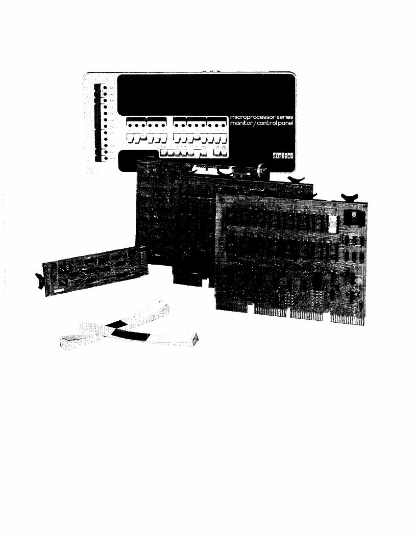
1.1 INTRODUCTION Digital Equipment Corporation's Microprocessor Series (MPS) consists of a group of four M Seriles modules and an optional operator's control panel, designed to efficiently perform a range of process control and decision-making functions that were previously uneconomic subjects for automation. When used together, these modules can form low-cost digital control systems that exhibit the characteristics normally attributed to more costly minicomputer-based systems. With this capability, systems structured from MPS modules can perform the functions of dedicated controllers, operate as a Central Processor Unit (CPU) in intelligent terminals, perform data aquisition and analysis tasks in the laboratory, and automate a host of industrial processes.
1.2 GENERAL DESCRIPTION The Microprocessor Series is listed below by model number and name:
• M7341 Processor Module
•
•
•
M7344-Y A 1 K Read/Write Memory Module M7344-YB 2K Read/Write Memory Module M7344-YC 4K Read/Write Memory Module
M7345 Programmable Read-Only Memory Module
M7346 External Event Detection Module
• KC341 Monitor/Control Panel
In a systems context, the M7341 Processor Module (PM) acts as the central processor unit with the remaining
1-1
CHAPTER 1 OPERATING
CHARACTERISTICS
modules performing supporting functions. Activity in a given system, then, is directed by a unique stored program contained in a read/write and/or a programmable read-only memory and executed by the PM. A major factor in the structuring of an MPS system for a specific application is the development of this unique system program by the user. To support user development of application software, Digital provides the Microprocessor Series Software Tools (MPSST) package that includes the following routines:
• Microprocessor Language Editor (MLE)
• Microprocessor Language Assembler (MLA)
• M i c r 0 processor Read-Only Memory Programmer (MRP)
• Microprocessor Host Loader (MHL)
• Microprocessor Debugging Program (MDP)
• Master Tape Duplicator (MTD)
In addition, the Microprocessor Program Loader (MPL) is available to users of the optional KC341 Monitor Control Panel.
1.3 FUNCTIONAL DESCRIPTION
1.3.1 Microprocessor Series Modules The discussions that follow present brief descriptions of the functions performed by each module within the context of a generalized MPS system structure.

Figure 1-1 Processor Module
Processor Atlodule (Figure 1-1) The M734I Processor Module performs the functions of a CPU in a system structured from MPS modules. The module consists of solid-state integrated circuits with input and output lines that are TTL-compatible; its major CPU functions are executed by a single-chip, large-scale, integrated (LSI) microprocessor. Supportive functions such as timing, data and address busing, input multiplexing, gating, buffering, storage and external communication are performed by the remaining logic population on the board.
The processor chip is a parallel, 8-bit control processor unit configured as a single metal oxide silicon circuit packaged in an l8-pin dual in-line package. Through the supportive logic in the M734I module, the processor can communicate the consequences of program execution with all other MPS modules.
LSI processor internal logic includes an accumulator, two memory address registers, six general-purpose registers, four condition flip-flops, complete instruction control and decoding logic, and a stack. All communication between internal registers and logic and other MPS modules and peripheral devices is conducted through an 8-bit bidirectional data port integral to the processor chip. The internal stack contains the 14-bit program counter and seven other 14-bit registers for nesting up to seven levels of subroutines. This I4-bit addressing capability permits accessing up to 16K memory locations that can be any mixture of RAM or ROM.
1-2
The instruction control and decoding logic implement a set of 48 register transfer, arithmetic, control, and 10gJlcal instructions which are speCifically optimized for the process control environment. The processor chip is also equipped with an interrupt line under control of supporting PM logic which allows the enabling or disabling of interrupts. Input to this interrupt recognition logic is generated by the external event detection module which implements the detection of, and response to, application-defined events or power failure conditions. Enabling and disabling interrupts is performed under program control.
Serial communication between the processor and external equipment is furnished by a universal asynchronous receiver /transmitter which is also part of the PM supportive logic. Through this interface, programs can be loaded from an external peripheral device such as a paper-tape loader and MPS systems communicating directly with external data bases.
Read/Write and Programmable Read-Only Memories (Figures 1-2 and 1-3) These two MPS memory modules provide the user with a wide range of options with respect to the mixing of RAM and ROM memory within a system. The read/write memory module is available in three versions: a IK module, a 2K module, and a 4K module. All memory circuits in a programma ble re ad-only memory module are socket-mounted so that the storage capacity of a given module can be expanded to 4K by adding memory circuits.
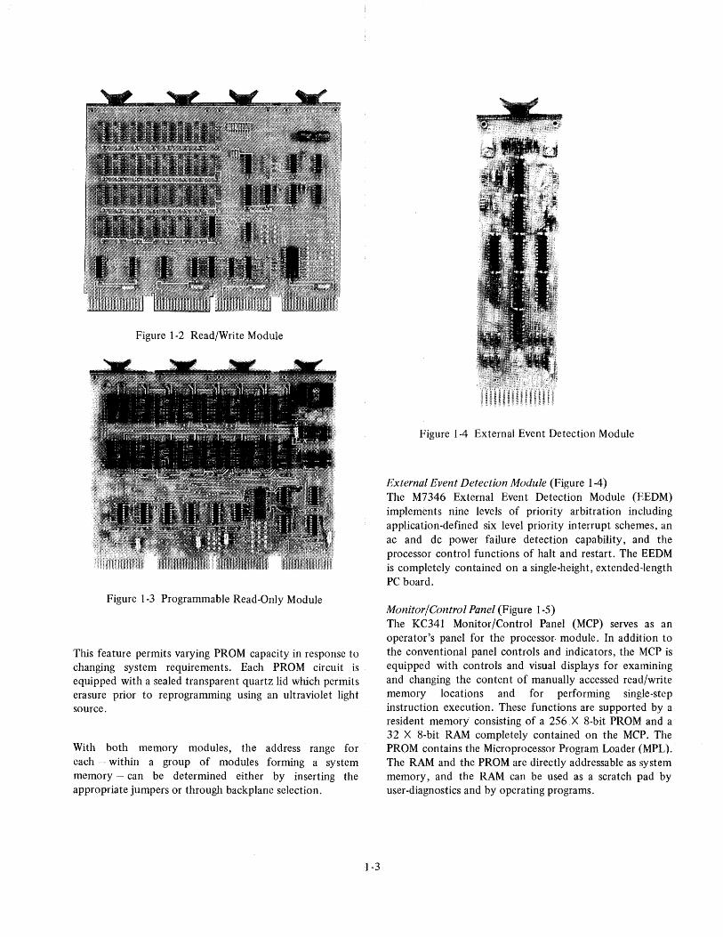
Figure 1-2 Read/Write Module
Figure 1-3 Programmable Read-Only Module
This feature permits varying PROM capacity in response to changing system requirements. Each PROM circuit is equipped with a sealed transparent quartz lid which permits erasure prior to reprogramming using an ultraviolet light source.
With both memory modules, the address range for each - within a group of modules forming a system memory- can be determined either by inserting the appropriate jumpers or through backplane selection.
1-3
Figure 1-4 External Event Detection Module
External Event Detection Module (Figure 1-4) The M7346 External Event Detection Module (EEDM) implements nine levels of priority arbitration including application-defined six level priority interrupt schemes, an ac and dc power failure detection capability, and the processor control functions of halt and restart. The EEDM is completely contained on a single-height, extended-length PC board.
Monitor/Control Panel (Figure 1-5) The KC341 Monitor/Control Panel (MCP) serves as an operator's panel for the processor· module. In addition to the conventional panel controls and indicators, the MCP is equipped with controls and visual displays for examining and changing the content of manually accessed read/write memory locations and for performing single-step instruction execution. These functions are supported by a resident memory consisting of a 256. X 8-bit PROM and a 32 X 8-bit RAM completely contained on the MCP. The PROM contains the Microprocessor Program Loader (MPL). The RAM and the PROM are directly addressable as system memory, and the RAM can be used as a scratch pad by user-diagnostics and by operating programs.
The MCP .interfaces with the processor module through a dedicated cable of up to 8 feet. Although normally configured for table mounting, the MCP can be panelmounted in a standard EIA rack panel fitted with a suitable bezel.
1.3.2 MPSST Software Tools Package This software package (supplied by Digital) aids the user in developing application programs. The support functions performed by each of these routines are presented in the following paragraphs.
Microprocessor Language Assembler (MLA) MLA is a three-pass symbolic assembler that operates on a PDP-8 to produce either a listing or a binary punched paper tape of an MPS object program from punched paper tape source code. This program has been designed to conform generally to the operational characteristics of other PDP-8 assemblers. Assembled code is generated in punched paper tape form or as a printed listing at the option of the user. Diagnostic messages are also printed out to designate syntax errors and to indicate warnings or actions taken by the assembler.
~Microprocessor Language Editor (MLE) MLE is an on-line symbolic editor that operates on the PDP-8 to create and modify MPS source program punched paper tapes. This editor implements both program entry and on-line program editing. Source text can be entered from a keyboard or from a punched paper-tape reader. After editing, the user may produce a source paper tape ready for input to MLA and/or a source text listing. Listings and tapes of source text can be made in whole or in part as required by the user.
Microprocessor Host Loader (MHL) MHL is a utility program loaded into core to read binary-coded data from paper tape and to store it in core memory, and used primarily to load system binary object programs.
1-4
Microprocessor Read-Only Memory Programmer (MRP) MRP operates on an MR873 PROM writer in cdnjunction with a PDP-8/E, /F, or 1M to set data and instruction bits into ultra-violet light erasable PROM circuits using object tapes produced by MLA.
Microprocessor Debugging Program (MDP) MDP operates on the processor module in conjunction with the Monitor/Control Panel from either PROM or RAM memory. This octal debugger permits the following diagnostic actions under control of the MCP panel as directed by an operator:
• •
•
Reads and punches paper tape
Opens specified memory locations for modifications and allows the previous, current, and next locations to be opened, displayed, and closed
Dumps the contents of program addresses, status flip-flops, and index registers on the Teletype printer
• Allows a program segment to execute for test purposes under MDP control
• Specifies a breakpoint location for program execution
• Loads specified locations in memory with a constant value
Microprocessor Program Loader (MPL) MPL is a binary paper-tape loader that operates on the processor module and resides in the Monitor/Control Panel PROM memory. This program provides for the loading of a binary punched tape from an external paper-tape reader through the universal asynchronous receiver/transmitter integral to the PM. Operation of MPL is performed from the MCP control panel.

Figure 1-5 Monitor/Control Panel
1.4 SPECIFICATIONS
1.4.1 Performance Specifications
M7341 Processor Module
Operating Speed @ 500 kHz Two-phase clock period Time state Instruction time
Word Size Data Instruction Address
1-5
2 J1S 4 J1S 12 to 44 J.Ls
8-bit word 1, 2, or 3 8-bit words 14 bits

Input Data Ports Memory data Peripheral data Power fail/stop I/O Interrupt/start
Input/Output Lines Memory data Memory address Peripheral data Peripheral address Communication Lines Baud rate
With internal clock With external clock
Instruction Repertoire Forty-eight basic instructions Instruction Categories
Register Operation Accumulator Operation PC and Stack Control I/O Machine
KC341 Monitor/Control Panel
Controls Switch register
ADDRLOAD
STRT
CONT
EXM
DEP
SING CYCLE
DISP DATA
DISP ADDR
1-6
8 bitS} 8 bits 8 bits 8 bits
Multiplexed
8 bits bidirectional 14 bits, output only 8 bits input and output 5 bits, output only (may be expanded) 2; 20 rnA current loop, active or passive
110 baud (1.76 kHz) 9600 baud (153.6 kHz) maximum (TTL)
14-switch manual input register
Load address from switch register with PM halted
Start Processor Module
Execute one machine cycle if in single cycle mode, or continue program execution at machine speed if not in single cycle mode
Display content of memory location addressed by either switch register content or incremented switch register content
Deposit content of switch register into a memory location accessed by a previously loaded address
Enter single cycle mode
Display data contained in location being examined
Display address loaded from switch register or address of location being examined

Indicators
RUN
HALT
WAIT
PCI, PCW, PCR, PCC
1> 2, 1>1, SYNC
RDY
INTR
Mep-PM Interface
Cable length (max) @ PM clock rate of 500 kHz/phase
Connector /plug types Cable type
M7344-Y A, -VB, -YC Read/Write Memory Modules
Memory type Data word size Address word size
Number of words Memory read or write cycle time
M7345 Programmable Read-Only Memory Module
Memory type Data word size Address word size Number of words Cycle time Erasure method
Program write time
1-7
Lights when processor module is operating
Lights when processor module is in the stopped state
Lights when processor module is in wait state
Each indicator lights when the processor module is executing the corresponding machine cycle
These indicators light to designate the operation of the corresponding processor module timing signal
Lights when the processor module Ready line is asserted true
Lights when the processor module Interrupt line is asserted true
8 [t. (204m)
50-pin PC board connector /header 50-conductor, flat, shielded
Static MOS 8 bits 14 bits, expandable to 16 bits plus address expansion line 1024, 2048, or 4096 1.15 J1S
Static MOS PROM 8 bits 14 bits, expandable to 16 bits plus selection line Up to 4K (multiples of 256) 1.0 J1S Ultraviolet light; 256 words erased per circuit exposed 2 minutes, typical per 256 words

M7346 External Event Detection Module
Number of event detection input lines Priority encoded
External event response time Power failure response time Input polarity Ou tpu t polarity Power fail sense input
1.4.2 Electrical Specifications
Power supply (all modules) Input Logic Levels (all modules)
TTL Logical Low TTL Logical High
Output Logic Levels (all modules) TTL Logical Low TTL Logical High
Power Consumption Processor Module Monitor/Control Panel Read/Write Memory, M7344-YA
M7344-YB M7344-YC
Programmable Read-Only Memory, 1 K 2K 4K
External Event Detection Module
1.4.3 Mechanical Specifications
M7341 Processor Module
Board type Dimensions
KC341-B Monitor and Control Panel
Overall panel dimensions Width Height Depth
1 -8
9 1, lowest 9, highest 12 to 44 J.Ls 21 ms (from ac loss to power-fail request) Zero volts true Zero volts true 6.3 Vac
+5 Vdc, -15 Vdc, ±5%
0.0 to 0.8 Vdc 2.0 to 3.6 Vdc
0.0 to 0.4 Vdc 2.4 to 3.6 Vdc
1.62 A @+5 V, 150 rnA @-15 V, 10.25 W 2.43 A @ +5 V, 60 rnA @-15 V, 12 W 1.2 A @ +5 V, 6.0 W 1.5 A @ +5 V, 7.5 W 2.2 A @ +5 V, 11.0 W 490 rnA @ +5 V, 300 rnA @ -15 V; 6.0 W 630 rnA @ +5 V, 530 rnA @ -15 V; 11.0 W 900 mA@+5 V, 1.0 A@-15 V; 19.5 W 250 rnA @ +5 V, 50 rnA @6.3 Vac, 1.5 W
Quad-height, extended-length, single width 10.436 X 8.50 X 0.50 in. (26.5 X 21.6 X 1.27 cm)
18 in. (45.7 cm) 8.75 in. (22.2 cm) 1.75 in. (4.4 cm) excluding switches 2.50 in. (6.35 cm) including switches
M7344 Read/Write Memory Module Board type Dimensions
M7345 Programmable Read-Only Memory Module Board type Dimensions
M7346 External Event Detection Module Board type Dimensions
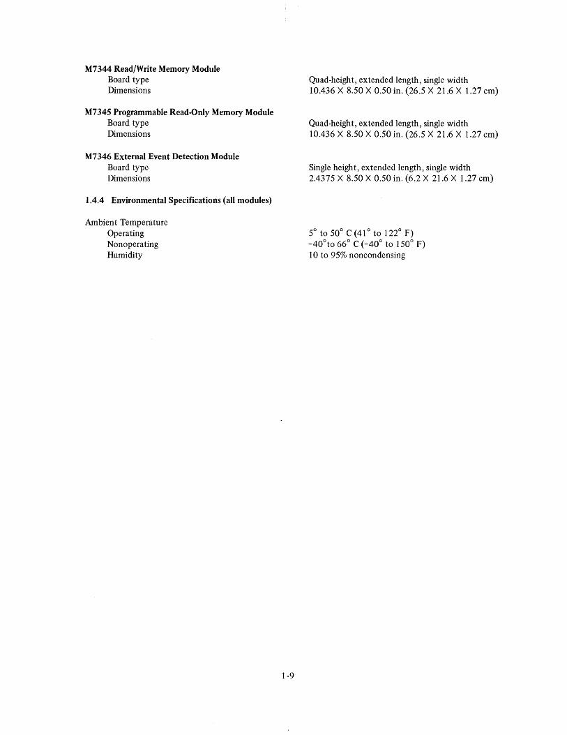
1.4.4 Environmental Specifications (all modules)
Ambient Temperature Operating Nonoperating Humidity
1-9
Quad-height, extended length, single width 10.436 X 8.50 X 0.50 in. (26.5 X 21.6 X 1.27 em)
Quad-height, extended length, single width 10.436 X 8.50 X 0.50 in. (26.5 X 2l.6 X l.27 em)
Single height, extended length, single width 2.4375 X 8.50 X 0.50 in. (6.2 X 21.6 X 1.27 em)
5° to 50° C (41 ° to 122° F) -400 to 66° C (-40° to 150° F) 10 to 95% noneondensing

CHAPTER 2 FUNCTIONAL DESCRIPTION
2.1 INTRODUCTION This chapter presents a detailed functionall description of each Microprocessor Series module and the operator's monitor/control panel. The discussion conveying these descriptions is based on comprehensive block diagrams which relate input and output signals andl internal signal flow to the event sequence within each module.
Each of the detailed block diagrams supporting these discussions graphically represents module throughput as logic circuit blocks that are functional1y cohesive. For example, registers, multiplexers, gating networks, clocks, and various control logic are depicted as functional blocks. Data and address buses, control and enabling lines, and interna11y generated signals are shown as they affect the pertinent functional blocks. The discussions supported by these block diagrams deal with the effect of inputs on the function of throughput, how functional blocks interrelate to implement throughput, and what actions result from outputs. A more comprehensive technical description including pinouts, input and output loading, signal descriptions, and jumper selections is contained in the respective data sheet supplied with each module.
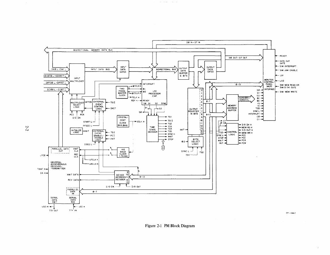
2.2 PROCESSOR MODULE The M7341 Processor Module (PM) contains a single chip MOS/LSI microprocessor along with the ilntegrated logic ,md control circuitry necessary to operate as a para11el 8-bit central processing unit. This microprocessor support logic consists of an adjustable 500 kHz variable clock; a four channel input multiplexer; data, memory, and address bus gating; I/O control logic; interrupt recognition logic; and a universal asynchronous receiver/transmitter driven by an integral 844.8 kHz clock. The relationships of the supporting] ogic to the processor chip are shown in Figure 2-1.
2-1
The single chip microprocessor contains a bidirectional data port, complete instruction decoding logic, an arithmetic unit, a state counter, an accumulator, an address stack, six general registers, and memory and I/O timing and control logic.
2.2.1 Processor Module Timing The basic timing signals shown in Figure 2-1, for the PM are produced by the two-phase clock. These signals, labeled ¢1 and ¢2, are symmetrical, nonoverlapping positive-going clock pulses which drive the processor chip state counter. This state counter controls all activity internal to the processor chip and produces the output signals SO, S 1, S2, and SYNC. The timing signals available for external use are ¢ICLK H, ¢2CLK H, and SYNC H. The SYNC H signal, along with SO, SI, and S2 defines processor module instruction execution states.
A typical PM machine cycle involves five sequential time states: TS1, TS2, TS3, TS4, and TSS (Figure 2-2). During time states TS 1 and TS2, system memory is addressed by a lower and an upper address byte respectively to form a 14-bit address; during TS 1 the program counter (PC) is incremented. In time state TS3 the instruction addressed during TS 1 and TS2 is fetched, and during TS4, or TS4 and TSS, the fetched instruction is executed. The flow chart of time state transitions is shown in Figure 2-3 which Simplifies the progression through time states during a machine cycle.
If an interrupt is initiated by an external event, control does not return to TS 1 after completing instruction execution but instead reverts to time state TSII which replaces TS!. During TSII, the external event is recognized, an interrupt is generated, and incrementing of the PC is suppressed to permit execution of a one-byte instruction generated by the external event.
N N
BIDIRECTIONAL MEMORY DATA BUS
DM0 L -DM7 L INPUT DATA BUS
DIosrp L-DIOST7 L
DPFS(Il L -DPFS7 L r-------------I-IINTERRUPT
: PARALLEL DATA; XMIT lOUT : CLK L __________ ...1
UPOE-I REC
CLK Il~UTCLKH UNIVERSAL ASYNCHRONOUS URCLK H RECEIVER I
TBMT H-..l TRANSMITTER
DA H XMIT DATA
RCV DATA
r-------
) PA~~iALEL 0-7 L __ ~N ___
USI H
TTY OUT TTY IN
TSI1
INIT
TS2
PCI
INiT
I/O IN
<l>ICLK H
TWO I. -I ¢>1
PHASE 'L -, ¢>2 MASTER ¢>2 CLK H CLOCK
'SCLK H
ROY H
50
ucu, H
9-13
I/O OUT
LSI PROCESSOR
CHIP
TiME STATE
DECODER
TSI
TSII
TS2 TS3 TS4 TS5 SYNC H WAiT STOP
INIT
r;; i V
11 12
:3 14
:5 OUTPUT I 6
REGISTER I 7 16 BITS iii
:9 rIO
:11 112
~1~ 14 15
Figure 2-1 PM Block Diagram
00 OUT- 07 OUT
0-13
110 IN H MEM RO H lIO OUT H
MEM WR H
PCI PCC PCR pew
INTERFACE
Cl
READY
DATA OUT GATE
SIM INTERRUPT
SIM JAM ENABLE
LAI
LA2
SIM MEM READ OR SIM 0 (N) GATE
ISO. MEM WRITE
I
cp- 0987

+1 ---.lLJLJl .., I- 500n5
+ 2 .J1--fl.--Jl- I I I I
SYNC ,.... 4fLS --, :
(INTERRUPT, WAIT JLJl rI rI i rltf1--f1---\ AND STOPPED STATES . ~ ~~ _ ~ ___ Lf:
SHOWN) 1 TS11 I TS2 1 WAIT I TS3, ISTOPP 01 TS4 1 TS5 1
(NORMAL
TS2 TS3 I TS4 I TS5 I TS1
Figure 2-2 Instruction Execution States
Figure 2-3 Time State Flow Diagram
S2 SI
1 1
0 1
1 0
0 0
0 0
0 1
1 1
1 0
SO STATE
0 TSII (INTERRUPT)
0 TSI
0 TS2
0 WAIT
1 TS3
1 STOPPED
1 TS4
1 TS5
CP-0985
YES
CP -0984
At the completion of time state TS2, the processor checks the state of the READY line. If this line is true (High), time state TS3 is entered; if not true (Low), the Wait state is entered. Time state TS3 is entered from the Wait state when the READY line is asserted again. The state of the READY line is available for external use through the signal RDYH.
If the instruction fetched during time state TS3 is a Halt, the processor stops operation at the end of that time state. The processor remains halted until the START line is asserted forcing entry into time state TSlI and execution of a jammed one-byte instruction which can be supplied by the External Event Detection Module. When the PM is operating (STOP H not asserted) the RUN indicator is lit; when the Stop state is entered (STOP H asserted), this indicator will be extinguished.
2.2.2 Processor Module Instruction Cycle Figure 2-3 shows that a machine cycle can be completed at the end of time states TS3, TS4 or TSS. The instruction cye1e for instructions in the PM repertoire is variable depending on the class and function of the speCific instruction executed and can consist of one, two, or three machine cycles. The completion point within a machine cycle is also instruction-dependent so that the number of time states encompassed by PM instructions can range from a minimum of three to a maximum of eleven.
The processor module executes four types of machine cydes which are listed and defined below:
PCI Cycle - This is always the first cycle of every PM instruction and initiates an instruction fetch. The two bytes which address memory during this cycle are always taken from the PC.
PCR Cycle - This cycle initiates the addreSSing of memory by the incremented PC to retrieve a subs.equent byte of a two- or three-byte instruction, or to retrieve a data byte addressed by the contents of registers Hand L.
pcC Cycle - This cycle initiates the set-up and execution of I/O instructions by placing the address of the peripheral device to be accessed and the content of the accumulator onto the memory address bus and retrieving and/or storing the data at the pertinent peripheral.
pew Cycle - This cycle initiates the addreSSing of memory by the content of the Hand L registers and implementing the writing of data into that location.
2-4
As shown in Figure 2-1, a corresponding signal for each of these machine cycles is available as output from the processor. At time state TS2, the specific signal corresponding to the machine cycle being executed is asserted and latched for external use. These signals are derived from the states of the two high-order bits of the high address byte and are decoded and gated out for external use during time state TS3.
2.2.3 Input Data Paths The processor chip is equipped with a single time-shared 8-bit bidirectional data port to permit memory addressing,. instruction fetching, and data input and output. This port connects to the bidirectional data bus on the processor module. As shown in Figure 2-1, input data in the form of an 8-bit byte is gated onto this internal bidirectional bus from the unidirectional input data bus. Data is multiplexed and gated onto the input data bus from four input ports which are selected as a function of the machine cycle currently being executed.
When a PCI or PCR machine cycle is in process, time state TS3 selects the bidirectional memory port DMO L to DM7 L to fetch the instruction or data word addressed dl,uing TSI and TS2 of that cycle from memory. During a PCC cycle the signal I/O IN, asserted by the control logic, selects the peripheral data-in port DIO L to DI7 L to retrieve data from the addressed peripheral device as specified by the read I/O instruction being executed.
At start-up or restart time, or in response to an external event, one of the signals START L or 10EE L is asserted to select the I/O start port DIOSTO L to DIOST7 L for external instruction input.
Figure 2-3 illustrates that when an interrupt occurs in response to an external event, time state TSlI is entered so that normal incrementing of the PC is inhibited.
As a consequence of selecting the I/O start port, an externally supplied one-byte instruction is automatically fetched. This instruction is executed during time states TS4 and TSS. Note that when 10EE L is asserted, the external event recognition logic must be enabled under program control in order for the I/O start port to be selected as a response to an external event. The signal START L, when asserted, bypasses the event recognition to select the I/O start port regardless of program-enabling action.
The signal PFSEE L can be asserted by a system start-stop switch, by a power-fail sensing circuit, or by some other
external logic. A power-fail circuit or external logic connected to the power-fail/stop port DPFSO L to DPFS7 L can jam a one-byte RST instruction (see section 3.7.2) into this port upon detection of a power failure or in reaction to some external event. This instruction would then be executed to initiate a service routine or sequence.
Activating an external system stop switch would also select the power-fail/stop port; however, in this case, all the data lines into this port would normally be High . which is equivalent to a Halt instruction. When the signal PFSEE L is asserted, the power-fail stop port is selected at time state TS3 following entry into time state TSlI which, as shown in Figure 2-3, occurs in the same manner as with a normal interrupt. During time state TS3, the instruction at this port is fetched by the processor for execution.
2.2.4 Output Data Paths Processor Module output can be in the form of memory addresses, memory and I/O control information, I/O device addresses, data output to memory, and data output to peripherals. With the exception of data output to memory, aU of these addresses and data are stored for output in the 16-bit multipurpose output register. Data words are latched into the register by the data selection logic during time states TSI and TS2 (Figure 2-1).
Memory addresses are issued as two separate words to form a 14-bit address word during machine cycles PCI, PCR, and PCW - the lower word at time state TSI and the upper byte at TS2 of these cycles. During each one of these time states the corresponding memory address word is loaded into the 16-bit output register by the address selection logic. At the end of time state TS2, the current memory address is present at the output side of the output register. These output lines are buffered to drive the address/data lines ADRDOO L to ADRD 13 L which can be bused out to the Microprocessor Series ROMs, RAMs, and I/O devices.
During a PCC cycle, the contents of the accumulator and the instruction register are stored in output register bits 0 through 13 for use as peripheral device output data and address. At time state TSI of a PCC cycle the content of the accumulator (Register A), which is the data to be output to the addressed peripheral device, is placed in the output register bit positions 0 to 7.
At time state TS2, the content of the instruction register is transferred to output register bit positions 8 through 15, with bits 9 through 13 containing the address of the peripheral device being accessed during the PCC cycle. Once
stored in the output register, these address and data fields are available to external peripheral devices over the lines ADRDOO L to ADRD 13 L. This device address field permits the addressing of up to eight input devices and 24 output devices.
Data to be written in read/write memory is gated onto the bidirectional memory bus DMO L to DM7 L during time states TSI and TS2 of a PCW cycle. Data must be accepted by the memory during time state TS3 of that cycle.
2.2.5 Control Logic The control logic (Figure 2-1) provides the various control signals necessary to memory accessing and to the performance of input/output operations with associated peripherals. Input to the control logic is the state of bits 14 and 15 of the output register.
During time state TS3 of every machine cycle, the control signals pertinent to the machine cycle currently being executed are asserted. For example, during PCI and PCR cycles where memory is addressed to fetch an instruction or data, the signal MEM RD H is asserted at the end of time state TS2 and throughout TS3. As shown in Figure 2-4, this signal controls the reading of data from that memory location addressed during the pertinent machine cycle.
For a PCC cycle, the signals I/O IN H or I/O OUT Hare asserted during time state TS3 to control the storage and retrieval of data at external peripheral devices. When data is to be written into an addressed memory location during a PCW cycle, the signal MEM WR H is asserted by the control logic during time state TS3 of that machine cyc1e.
In addition to these signals, the control logic also asserts one of the signals PCI L, PCC L, PCR L, or PCW L during time state TS3 of the corresponding machine cyc1e.
2.2.6 Asynchronous Communications Receiver/ Transmitter Logic The PM is equipped with a full duplex communication receiver/transmitter implemented by a Universal Asynchronous Receiver/Transmitter (UART). A 1.76 kHz clock, ,driven by an 844.8 kHz crystal-controlled clock integral to the PM, is input to this device to produce a 110
. baud data transfer rate. The UART is addressed during time state TS3 by bits 9 to 13 of the output register. Data is transmitted and received at the module over 20 mA current loop or TTL-compatible lines (USI Hand usa H) to interface with Teletype-like lines or to telephone lines
. through a modem.
2-5
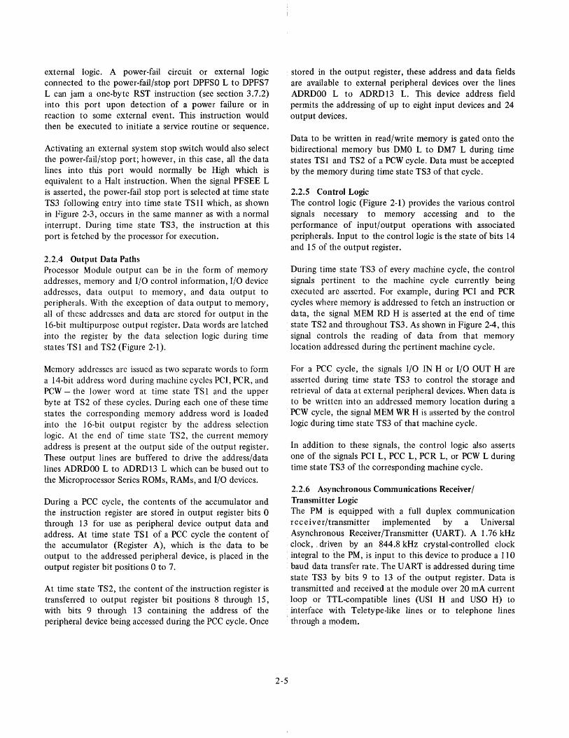
TS2~-----------------TS3--------------------~·~I·~TS4---
TIME STATES ~ I ~---
MEMORY IDEVICE X ADDRESS I
I
F MEMORY READ -I 125 ns OR IIO IN
I
"'-DATA READ
MEMORY WRITE _____________________ ~~oons--l OR IIO OUT ..... ____ _
* At a 500 KHz clock rote. DATA READY FOR OUTPUT
CP·0988
Figure 24 I/O Timing Diagram
Higher baud rates can be obtained by using an external clock input (URCLK or UTCLK) that can be derived from external logic which divides the basic crystal clock frequency. The maximum data transfer rate is 9600 baud for TTL lines and 4800 baud for current loop lines (at limited lengths). Interna1 switches on the PM permit selection of operation under external clock control; the number of stop bits used (one or two) can be selected through switch action. Active or passive operation of current loop lines is jumper-selectable.
Odd parity, even parity, or no parity is selected by the PM input line UPOE. Also, the number of data bits in a word can be selected to vary from five to eight bits. Both TBMT (Transmitter Buffer Empty) and DA (Data Available) are available for external interrupt drive capability.
When an input instruction is being executed, the signal I/O IN H is asserted by the control logic. This signal and the receiver/transmitter device receive address are decoded to gate data from the device onto peripheral bus lines DIO L to DI7 L and into the peripheral data-in port.
Data for transmission is written from the output register into the UART transmission buffer during time state TS3 of a PCC cycle when the signal I/O OUT H is asserted (Figure 24). This signal and the transmit data address are decoded to strobe data from the PM output register into lhe transmission buffer.
2-6
Status information, which includes receiver/transmitter error conditions and transmit and receive buffer status, is retrievable through execution of an input instructi<on with the assigned status device address. As with readihg data from the receiver/transmitter, the signal I/O IN H is asserted as a result of a PCC cycle execution. This ~ignall is gated with the device address to, in turn, gate device status into the peripheral data-in port DIO L through DI7 L.
2.2.7 Interrupt Control The interrupt control logic drives the input data multiplexer to select one of two input ports. If the interrupt results from a power failure or a stop command, the power-fail/stop port DPFSO L to DPFS7 L is selected. Similar1y, if the 10EE L line or the system START ~ line is asserted, the I/O start port DIOSTO L to DIOST7 L is selected. The instruction jammed into these ports as a consequence of a power failure or an I/O or. restart interrupt is furnished by the External Event Detection Module or external logic as determined by the specific application.
I/O interrupts can be enabled or disabled under program control by the PM external event enable/disable logic. Interrupts are disabled by executing the instruction IOF and enabled by executing ION (paragraph 3.7.3).
Since interrupts will be enabled or disabled one instruction time after execution of an ION or 10F, one instruction can
be executed after ION or IOF before interrupts are actually enabled or disabled. The external event recognition logic is automatically disabled after every interrupt.
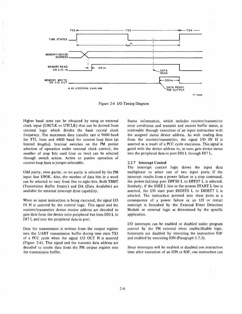
2.3 READ/WRITE MEMORY MODULE The M7344 Read/Write Memory Module provides a IK, 2K, or 4K X 8-bit random access memory capacity along with all necessary timing, control, and decoding logic (Figure 2-5). This module is completely contained on a single quad extended-length board. The module memory matrix is formed by up to 32 1024 X I-bit static MOS MSI memory circuits. The nature of these MOS circuits precludes the need for external refresh logic.
The M7344 Read/Write Memory Module is available in three versions to satisfy varying mem~)fy capacity requirements. Model numbers identifying these memory versions are listed below:
• M7344-Y A IK X 8-bit capacity • M7344-YB 2K X 8-bit capacity • M7344-YC 4K X 8-bit capacity
All versions of the M7344 can be accessed by up to 16-bits of address data and are equipped with an address expansion line to implement multi-module memory systems having potential capacities of up to 128K 8-bit words. M7344 Read/Write Memory Modules also contain a jumper network which can be configured to permit assignment of a module within an application-defined address space.
Operation of each memory circuit in either the read mode or write mode is determined by a read/write (R/W) linc. Each of the 32 MSI circuits in the memory matrix connect to a data input line' and a data output line with the significance of the line corresponding to the position of a circuit with a IK X 8-bit group. Data input lines are wire-ORed to each memory circuit from the data input register. Similarly, data output lines are wire-ORed to the data output gates from each memory circuit.
2.3.1 Memory Read Timing The timing and control logic (Figure 2-5) furnishes the signals necessary to time memory read and write operations. The processor module asserts the level MEM RD H after providing the address of the memory location to be
I BIDIRECTIONAL MEMORY DATA BUS
...-_----""-1'\'\ A D~RESC~ ~:: r--V' DEggPc
E CE3
CE1; .A ) A Y
~ ~ DATA '\ 1Kx8-BIT ,'\r----., ~ INPUT
CE4
ADR/DAT! STROBE H
J ... MEMORY ADRD10-ADRD15
'---------" ADDRESS MEMORY ADDRESS IN) REGI STEI~
y ADRD00-· I-------~ ADRD15 ADRD00-ADRD09
ADR IDATA tSTROBE H
MEM RD H .........
MEM WR H .........
-ADR/DATA STROBE H TIMING
CO~~~OL -DATA ENABLE L
LOGIC -WRITE PULSE L
- / MATRIX " REGISTER'_ IV ----. B-BITS • ~
WRITE !ULSE L
C;2 A
/ ~ 1K x 8-BIT '-., ..... ,,',......., .,.......,...---, r-vI MATRIX ~
'----r----'-
WR ITE ;ULSE L
C;3
~ 1K x 8- BIT K ..... ~ ____ --, .,/ MATRIX ~
~ 1 K x 8 -BIT K,r---r---r------' L- / MATRIX ~ Lo.....-_ .... "-"
ADRJDATA STROBE H
DATA OUTPUT GATES
---v ) L--t..--J-------v.... '---'f----'
WRITE PULSE L DATA ENABLE L
Figure 2-5 M7344 Block Diagram
2-7
'P-0988

read. At the read/write memory module, the signaJ MEM RD H generates the internal signaJs ADR/DATA STROBE H and DATA ENABLE L.
The signal ADR/DATA STROBE clocks the memory address register to store the address currently on the memory address bus ADRDOO L to ADRD15 L. This action initiates address decoding which enables assertion of DATA ENABLE L along with addressing of the memory location being read. DATA ENABLE L, when asserted, enables the output gating network to place the data from the addressed location onto the bidirectionaJ memory data bus DMO L to DM7 L. Figure 2-6 shows that data becomes vaJid on this bus 1.15 JiS after the assertion of MEM RD H.
2.3.2 Memory Write Timing For a write operation, the address of the memory location to be written into is placed on the address bus and must be stable for at least 150 ns prior to the assertion of MEM WR H. Data to be written into the addressed location is placed on the bidirectional memory data bus coincident with the signal MEM WR H.
~--
M7341 ~ TI ME STATES...J
As shown in Figure 2-6, the signal MEM WR H has a minimum period of 250 ns and is asserted by the processor module. Pulse-stretching circuitry in the M7344 control logic uses the leading edge of MEM WR H to set a latch to store the signal. Approximately 200 ns after the receipt of MEM WR H, this signal is ANDed with the decoded address to generate the internaJ 1 /J.S signal WRITE PULSE L. This pulse then enables the data stored in the data input register by the assertion of ADR/DAT A STROBE to be written into the addressed memory location.
2.3.3 Address Decoding Input to the memory address decoding logic is an address loaded into the memory address register from the address bus by the assertion of ADR/DATA STROBE. Both the address bus and the memory address register can accommodate a 16-bit address to permit memory system capacities up to 64K.
As shown in Figure 2-5, the 10 low-order bits (ADRDOO to ADRD09) of the memory address access the same location in each of the four 1 K memory segments. The next high-order two bits (ADRDIO and ADRDll) define the
TS3 ----------.-jo-I .. - TS4 -
READ CYCLE
READADDRESS~ _______________________ ~ I I 1 ~I _______________________ ~
MEM RD H -1 \ I-- ~ 150 ns ----:....-.1d--t_ ---1.15/oL5----------.l1 1
I I
~~~~ __________ D_A_TA_IN_V_AL_I_D ______ .....JX DATA VALID FOR READIN~
WRITE CYCLE
~~ WRITE ADDRESS ~ ___________________________ ~
I I -"1 ~~ 150n5
14"-=::J ~ 250n5 MEM WR H ------H-{ L.. __________________ ~
J+-.--.---- 1.15 fL5 -------..t--t
WRITE DATA _____ ,=><~ ______________ ,.:-------~ :- DATA
WRITTEN CP-0981
Figure 2-6 Memory Timing Diagram
2-8

final magnitude of the addressed location and are decoded by the segment address decoding logic to assert one of the four signals CE1, CE2, CE3, or CE4. These signals enable the 1K segment, which contains the location pointed to by the low-order 12 bits of a 14-bit address. Note that each of the signals CE1, CE2, CE3, and CE4 is jumpered to permit a module to contain multiples of 1K memory locations within the total memory system address space.
A 16-bit address field, all of decoded states of bits ADRD13 L to ADRD15 L, can be jumper-configured. As a consequence, each 4K module in a. multiple module memory system can be uniquely jumpered to be assigned as a given set of 4K memory locations within a.consecutive set of up to 16K locations.
This jumper network is configured to permit allocation of address space in 1K intervals within an address range of 4K to 8K formed by either one or two M7344 modules. In addition, each module can be assigned an address space of up to 4K within a total 64K address set. Each side of this jumper network is also brought out to the module edge fingers to permit address space allocation to be supplemented by wire wrap on the connl~ctor block.
Since the M7344 Read/Write Memory is electrically and logically compatible with the M7345 Programmable Read-Only Memory, these modules can be used together to form a contiguous RAM-PROM memory space.
2.4 PROGRAMMABLE READ-ONLY MEM ORY MODULE The M7345 Programmable Read-Only Memory (PROM) Module provides a variable read-only data storage capacity for systems structured from modules in this family. The functional logic blocks comprising this module (Figure 2-7) consist of plug-in socket space for up to four 1K memory matrices, an address buffer, address and control decoding logic, and an output gating network. Each of these functional blocks is discussed in terms of functions performed and how these functions intl~rrelate. Figure 2-7 also provides a graphic reference for data and signal flow within the module.
2.4.1 Memory Organization The M7345 PROM module is an 8-bit electrically programmable and erasable read-only memory contained on a single quad board. Maximum PROM capacity is formed by 16 MSI memory circuits mounted in plug-in sockets and organized as 16 separate matrices each containing 256 8-bit . words (Figure 2-8). As a consequence l, memory capacity can range from 256 to 4K words in 256 word increments.
2-9
PROM circuits can be removed at will to satisfy changing system requirements and for erasure and reprogramming (Chapter 9).
A transparent quartz lid on each PROM circuit permits exposure to an ultraviolet light source for erasing an existing bit pattern. Then a new bit pattern can be electrically written.
2.4.2 Address and Control Decoding Address input to the PROM module consists of the fuB 16 bits of the address bus (ADRDOO L to ADRD15 L) with 14 of these bits (ADRDOO L to ADRD13 L) relevant to the PM. The remaining two bits provide for memory address expansion. As shown in Figure 2-7, the low-order eight bits directly address each PROM circuit in the memory matrix through the address buffer. The remaining bits on the address bus, ADRD08 to ADRD 1 5, are input to the address and control decoding logic which is enabled by the signal MEM RD 1. This signal is asserted by the processor module during time state TS3 of a PCI or PCR machine cycle.
Address bits ADRD10 and ADRD11 are decoded to determine the 1 K group associated with an addressed location within a 4K group, and bits ADRD08 and ADRD09 are decoded to point to the 256 X 8-bit PROM circuit within that 1K group containing the location being accessed. The result of this decoding is the assertion of one of 16 chip enable signals which causes the addressed PROM circuit to output data from the addressed location within 1.1 5 J.1s after the assertion of MEM RD H (Figure 2-9). This data is present at the data output gates. An chip enable signals are wire-ORed to assert the internal signal DATA ENABLE which gates the data at the output data gates onto the bidirectional memory data bus DMO L to DM7 1. This same logic also asserts the external synchronizing signals MEM SYNC L and DATA READY 1.
Bus address bits ADRDl2 and ADRDl3 are decoded to implement the addreSSing of multiple module PROM systems having up to 16K locations. Address bits ADRD14 and ADRD15 are decoded to permit expansion of multiple module PROM systems beyond 16K locations up to 64K locations.
Each of the 16 chip enable signals derived as a consequence of decoding address bits ADRD08 through ADRD 11 are jumper-connected for assertion to permit depopulation of a given PROM module down to 256 locations by multiples of 256. In addition, the results of decoding address bits ADRD12 and ADRD13 can be jumper-configured to permit the selection of 1 K contiguous addresses of PROM memory

MEM RD L
PROM E27 3400
TO 3777
PROM E26 4000
TO 4377
ADDRESS DECODING
LOGIC
PROM E24
3000 TO
3377
PROM E23
4400 TO
4777
ICEI
ICE2
lCE3
lCE4
2CEI
2CE2
2CE3
2CE4
3CEI
3(:E2
3CE3
3CE4
4CEI
4CE2
4CE3
4CE4
_DATA ENABLE
BI DIRECTIONAL MEMORY DATA BUS
lCE' ICE2 ICE3
lCE4
4 256
X 8-BIT PROMS
2CE2 2CE3 2CEI 2CE4
4 256
X 8-BIT PROMS
3CE2 3CE3 3CEI 3CE4
4 256
X 8-BIT
PROMS
4CE2 4CE3 4CEI 4CE4
4 256
X 8-BIT
PROMS
Figure 2-7 M7345 Block Diagram
PROM E21 2400 TO
2777
PROM E20
5000 TO
5377
PROM E18
2000 TO
2377
PROM EI7
5400 TO
5777
1
PROM E15 1400 TO
1777
PROM EI4
6000 TO
6377
EDGE CONNECTOR
PROM E12
1000 TO
1377
PROM Ell
6400 TO
6777
Figure 2-8 Physical Location and Octal Address of M7345 PROMs
2-10
DATA ENABLE
PROM E9
400 TO
777
PROM E8
7000 TO
7377
CP-09B2
PROM E6 o
TO 377
PROM E5
7400 TO
7777
CP-0983
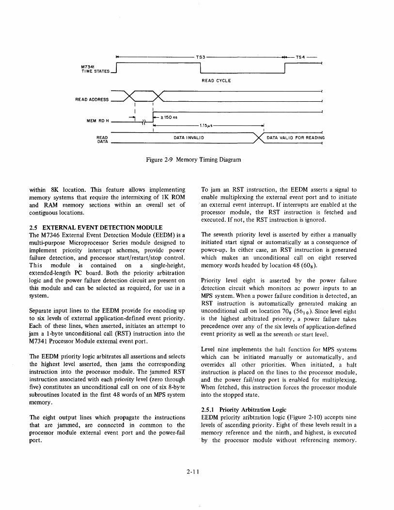
~~---------------------TS3--------------------~·.I·~TS4---
~iJ:1STATES J READ CYCLE
READADDRESS~~ ____________________________________________ ~ I I I rl ----------------______________________________ ~
-, \ J-~150nS MEM RD H -----....:..--Itr- 10--. __________ _
~ 1.15p.s ------------..1,1 I I
~~~~ ___________________ DA_T_A_I_N_VA_L_ID ______________ ..JX DATA VALID FOR READIN~
Figure 2-9 Memory Timing Diagram
within 8K location. This feature allows implementing memory systems that require the intermixing of lK ROM and RAM memory sections within an overall set of contiguous locations.
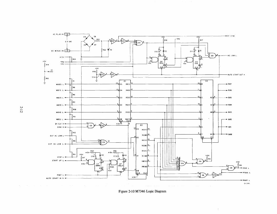
2.S EXTERNAL EVENT DETECTION MODULE The M7346 External Event Detection Module (EEDM) is a mUlti-purpose Microprocessor Series modul,e designed to implement priority interrupt schemes, provide power failure detection, and processor start/restart/stop control. This module is contained on a single-height, extended-length PC board. Both the priority arbitration logic and the power failure detection circuit are present on this module and can be selected as required, for use in a system.
Separate input lines to the EEDM provide for encoding up to six levels of external application-defined event priority. Each of these lines, when asserted, initiates an attempt to jam a I-byte unconditional call (RST) instruction into the M7341 Processor Module external event port.
The EEDM priority logic arbitrates all assertions and selects the highest level asserted, then jams the corresponding instruction into the processor module. The jammed RST instruction associated with each priority level (zero through five) constitutes an unconditional calion one of six 8-byte subroutines located in the first 48 words of a.n MPS system memory.
The eight output lines which propagate the instructions that are jammed, are connected in common to the processor module external event port and the power-fail port.
2-11
To jam an RST instruction, the EEDM asserts a signal to enable multiplexing the external event port and to initiate an external event interrupt. If interrupts are enabled at the processor module, the RST instruction is fetched and executed. If not, the RST instruction is ignored.
The seventh priority level is asserted by either a manually initiated start signal or automatically as a consequence of power-up. In either case, an RST instruction is generated which makes an unconditional calIon eight reserved memory words headed by location 48 (60s).
Priority level eight is asserted by the power failure . detection circuit which monitors ac power inputs to an MPS system. When a power failure condition is detected, an RST instruction is automatically generated making an unconditional call on location 70s (5610 ), Since level eight is the highest arbitrated priority, a power failure takes precedence over any of the six levels of application-defined event priority as well as the seventh or start level.
Level nine implements the halt function for MPS systems which can be initiated manua]]y or automatical1y, and overrides all other priorities. When initiated, a halt instruction is placed on the lines to the processor module, and the power fail/stop port is enabled for multiplexing. When fetched, this instruction forces the processor module into the stopped state.
2.5.1 Priority Arbitration Logic EEDM priority aribtration logic (Figure 2-10) accepts nine levels of ascending priority. Eight of these levels result in a memory reference and the ninth, and highest, is executed by the processor module without referencing memory.
t;> ...... N
1 1 AC PLUS IN Dy
'" I ('~' :;", +5V
RIS
AC MINUS IN
+ 5Y
+5V TP2
~ TPI
C I +3V
1'" M005 l
M015 l
M025 l
M035 l
M045 l
M055 l
01 ClK H
SYNC H
EXT AC lOW l
EXT OC lOW l
STOP l
START UP l
PINIT l
AUTO START IN H
I l....£.J I " f'" 1" r CI2[.: 02
l 9~~ 7
~RI3 L
-=} I V' ~ 10 E6
I +3V 35ms 5
I
0
T 12
+5V
R16 I
E5 2 3 E5 4
C141+ I
~RI -=- EI 14
05 R5(\) 15
lRS 13 04 R4(!) 12
lR9 II
03 R3(1) 10
nR2
6 02 R2(f) 7
lRI0 4 01 R HI) 5
lR3 3 D0 R0(I 2
ClR ClK 2...-- + 3Y.Y
' 9
3J ES I 9 E5
8 E2
'203 R3(1l ~
lR'2 R3(0) ~
lR51
~02 13 ___
12 R2(O ~ 2 E9 I -....-
R2(f)) ..!..!...-
I '" RI9 RHI) L +5V +5Y
1 .. T ":U" CI3U03 ~ 01 R 1(0) 6
R? 6 1 9~ 5
14 1513
I~ r.=- rL ,~ I~ ~ I~ R0 (1)
+3V E7 2 E7 50MS ~~ 50p.S R0(0) 2
0~ R20 0~ 4 :r-r=- +5V 4 00 -or ClR ClK
+3VJI r
Figure 2-10 M7346 Logic Diagram
"--"--"'- .-+5V
r TP3 RI?
I
I CII~ 01
I ~1513 ~ 4 6 AC lOW l 5 E9./
I D ,,<--
E6 +3'.' 5m. 13
0~ 'r-AUTO START OU T H
I
E3
10 0 ~B07
II 1 r---- 806
12 2 A2 6 805
13 3 AI 1 B04
I 4 A0 9 B03
I 2
5 r--- B02
3 6 >--r----- Btll
4 1 GS B00
E0 EI
I
~ 3
~ ~8
ES 10 ~ 8 +5V
\I ~ -6 6 R6 5 ~ES
4 4 - IOEE l
12 10
E8 13 II E5
II
PFSEE l
-- - START L

Levels 0 through 5, designated by the input signal lines MOOS L, M015 L, M025 L, M035 L, M045 L, and MOSS L, constitute the six lowest priority levels. These lines are reserved for implementing six levels of application-defined interrupt priority arbitration.
The seventh level is reserved for the automatic and manual restart function, and the eighth and highest arbitrated level, for power failure detection. The ninth, and highest absolute level is reserved for the stop function which automatically jams an HLT instruction into the processor module to stop operation.
EEDM priority arbitration logic is formed by the nine-stage external event storage latch E1 and E2 and the octal encoder E3. Assertions of any of the nin€~ levels are stored during the combined periods of the processor module synchronous timing sig"nals SYNC Hand <j>lCLCK H. These signals are ANDed to strobe the external event storage latch E1 and E2 once during each processor time state (every 4 p.s) to store asserted events. The output of the first eight stages of the external event storage latch are input to the octal priority encoder E3. These eight input lines are ORed by E3 to enable the encoder. The outputs of the encoder, EO and GS, are wired to assert the code for an RST instruction on module output lines BOO to B02 and B06 and B07. The octal number corresponding to the external event input line asserted is simultaneously placed in the address field (B03 to B05) of the RST instruction generated by encoder E3.
In parallel with the generation of the RST instruction, the outputs of the first eight stages of latch E1, E2 are ORed by E3 to assert the signal IOEE L at the processor module. This signal, when asserted, generates an interrupt if interrupts are enabled, and initiates multiplexing of the RST instruction on EEDM output lines BOO to B07 at the processor module external event port DIOSTO L to DIOST7 L for fetching.
The octal number placed in the address field of the RST instruction genera ted is in the range 0 to 7. By decoding this instruction, this value is mapped to address one of the eight locations 10,20,30,40,50,60, and 70 (decimal 0,8, 16, 24, 32, 40, 48, and 56 respectively) in an MPS system memory. The result is a correspondence between a given external event input line and an unconditional call on a dedicated memory location. Through this mechanism, application-defined routines can be developed to implement priority interrupt schemes, start-up routines, and powerfailure handling routines.
2-13
2.5.2 Start Circuit Th e start function can be initiated in two ways: automatically by an integral EEDM circuit, or manually by an external switch. The automatic start output signal AUTO START OUT H is generated by the RC circuit R16, C14, and E5 when +5 V power is turned on and is maintained high as long as +5 V is maintained. The output of this circuit also clears the two monostable multivibrators E6 in the power failure detection circuit. This automatically-generated start signal, when fed back to the EEDM,becomes the input signal AUTO START IN H. When asserted, this signal triggers the monostable multivibrator E7 to produce a 50 p.s signal at pin 4. This signal is stored in the seventh stage of the exter~al event latch E1, E2 on the next assertion of ¢lCLK H and SYNC H from the processor module. As a consequence, an RST instruction making an unconditional calion memory location 60 (4810) is generated and placed on output lines BOO to B07. Simultaneously, the signal START L is asserted at the processor module to initiate a demand interrupt and to multiplex the RST instruction into the external event port DIOSTO L to DIOST7 L for fetching. Manual restarts are implemented through the EEDM input signal START L which can be derived from an external switch. This signal is debounced by the monostable multivibrator E7 which produces a 50 ms negative-going debouncing level at pin 5 for input to E7 at pin 1. From this point, the circuit path is exactly the same as with an automatic restart. Both automatic and manual start signals take priority over all other external events except power failure detection and stop functions.
2.5.3 Power Failure Detection Circuit The EEDM contains a complete ac power failure detection circuit (Figure 2-10) which samples a 6.3 V, 50 or 60 Hz, ac input derived from the local Hne voltage by an external transformer. This sampled qC voltage, which is received through two F ASTON tabs on the handle end of the module, is rectified by a full-wave diode bridge to produce a signal having a frequency twice that of the ac input frequency. This signal is input to the frequency integrators E5, E9, and E6 which detect the absence of line voltage for two complete cycles. The signal period triggered by a power failure is approximately 35 ms and is determined by the value of capacitor C12 which, together with R18, forms the RC for the monostable multivibrator E6 at pins 6 and 7. Note that C 12 is connected to the circuit with split lugs. This manner of connection permits the value of C 12 to be changed to accommodate different application requiremen ts.
When an absence of two or more ac cycles is detected, the multivibrator E6 is triggered at pin 1 to assert a 5 ms signal to be gated out by E9 at pin 6. This period is determined by the RC circuit R17, C 11 when~ capacitor C 11 is connected to the circuit with split lugs to allow the value of C11 to be changed to accommodate different application requirements. The 5 ms output signal from the frequency integrator is ORed with the externally generated signals AC
. LOW L and DC LOW L for input to level seven of the ,external event storage latch El, E2. This input is stored in the latch on the assertion of the processor module signals SYNC Hand 1> 1 CLK H. Since both of these signals are continuous regardless of processor state, storage of a power failure detection signal for fetching by the processor is assured even when the processor is in the Wait state.
The external inputs AC LOW L and DC LOW L a]]ow use of application-defined power failure detection circuitry whose outputs are TTL levels.
NOTE Many commercially available power supplies provide such output signals.
Power failure detection by the integral EEDM circuit or assertion of one .of these external signals takes priority over all external events except assertion of the external signal STOP L.
A detection of power failure results in the automatic generation of an RST instruction which makes an unconditional calIon memory location 48 (60s ). Simultaneously, the signal PFSEE L is asserted by E8, pin 13 of the priority arbitration logic to generate a mandatory interrupt at the processor module and to enable multiplexing of the RST instruction in to the power-fail port DPFSO L to DPFS7 L for fetching ..
2.5.4 Stop Function A halt instruction is generated by the EEDM when the input signal STOP L is asserted. When this occurs, the signal is stored in the ninth stage of the external event latch E 1, E2 in the same manner as other external events. This stage disables encoder E3 to generate and place a halt instruction (HLT) on the lines BOO to B07.
As with detection of a power failure, the signal PFSEE L is asserted at the processor module power fail/stop port by the EEDM to initiate multiplexing and fetching of the halt instruction.
2-14
2.6 MONITOR/CONTROL PANEL The KC341 Monitor/Control Panel (MCP) interfaces directly with the processor module (PM) over a 50-wire dedicated interface cable to provide an on-line control and program diagnostic capability for systems configured from Microprocessor Series modules. Specifically, the KC341 MCP serves as an address and data input station for .the PM to provide a visual display of data as we]] as display of machine states and PM operating status. The MCP also contains a resident memory formed by a random access scratch pad memory and a programmable read-only memory. Together, these memories provide for program loading as well as other application-defined requirements.
2.6.1 Monitor/Control Panel Cable Connections
Data/Control Interface Cable (BC05-W) Connect the flat Data/Control Cable between the 50-pin connector on the MCP and the 50-pin connector on side 1 (component side) of the M7341 Processor Module as shown in Figure 2-11. Be sure that the flat cable is not twisted between the two units.
Power Cable (BC05- Y) The power cable connections to the MCP must be made to the appropriate FASTON tabs as listed below:
Black Blue Red
Ground -15 V +5V
2.6.2 Monitor/Control Panel Functions The discussion that follows relates the functions performed by the MCP to data, address, and signal flow, both within the module and between the MCP and the PM. This discussion is centered on two categories: panel functions and diagnostic memory. Discussions of MC pane] functions and the diagnostic memory are based on the detailed block diagrams which graphically depict data address and signal flow as related to the functional logic blocks comprising the monitor/control panel.
In Figure 2-12 the MCP consists of a 14-bit switch register for entry of addresses and data with corresponding display ligh ts, nine function switches, and 12 signal, status and condition display lights. The switch register, together with corresponding bit display lights, is marked off for qUick visual observation of octal as well as address blocking notation. The line of function switches located below the switch register is divided into two groups with one group containing seven switches and the other containing two switches. The seven-switch group provides the mechanism
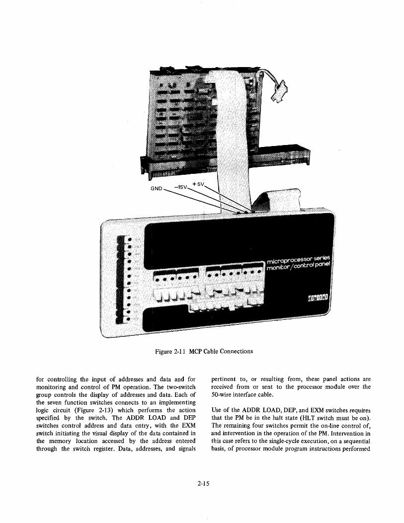
Figure 2-11 MCP Cable Connections
for controHing the input of addresses and data and for monitoring and control of PM operation. The two-switch group controls the display of addresses and data. Each of the seven function switches connects to an implementing logic circuit (Figure 2-13) which performs the action speCified by the switch. The ADDR LOAD and DEP switches control address and data entry, with the EXM switch initiating the visual display of the data contained in the memory location accessed by the address entered through the switch register. Data, addresses, and signals
2-15
pertinent to, or resulting from, these panel actions are received from or sent to the processor module over the 50-wire interface cable.
Use of the ADDR LOAD, DEP, and EXM switches requires that the PM be in the halt state (HLT switch must be on). The remaining four switches permit the on-line control of, and intervention in the operation of the PM. Intervention in this case refers to the single-cycle execution, on a sequential basis, of processor module program instructions performed
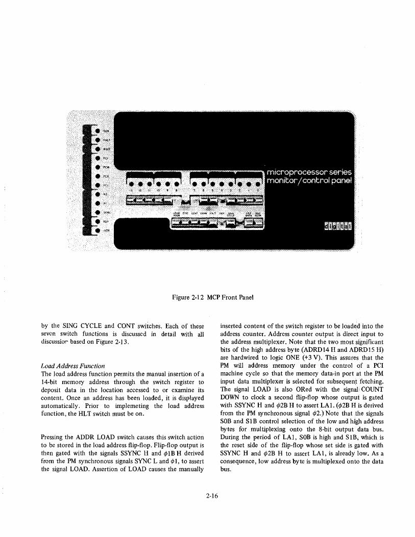
Figure 2-12 MCP Front Panel
by the SING CYCLE and CONT switches. Each of these seven switch functions is discussed in detail with all discussior based on Figure 2-13.
Load Address Function The load address function permits the manual insertion of a 14-bit memory address through the switch register to deposit data in the location accessed to or examine its content. Once an address has been loaded, it is displayed automatically. Prior to implemeting the load address function, the HLT switch must be on.
Pressing the ADDR LOAD switch causes this switch action to be stored in the load address flip-flop. Flip-flop output is then gated with the signals SSYNC Hand ¢IB H derived from the PM synchronous signals SYNC Land ¢ I, to assert the signal LOAD. Assertion of LOAD causes the manually
2-16
inserted content of the switch register to be loaded into the address counter. Address counter output is direct input to the address multiplexer. Note that the two most significant bits of the high address byte (ADRDI4 Hand ADRDl5 H) are hardwired to logic ONE (+3 V). This assures that the PM will address memory under the control of a PCI machine cycle so that the memory data-in port at the PM input data multiplexer is selected for subsequent fetching. The signal LOAD is also ORed with the signal~ COUNT DOWN to clock a second flip-flop whose output is gated with SSYNC Hand ¢2B H to assert LAL (¢2B H is derived from the PM synchronous signal ¢2.) Note that the signals SOB and SIB control selection of the low and high address bytes for multiplexing onto the 8-bit output· data bus. During the period of LAI, SOB is high and SIB, which is the reset side of the flip-flop whose set side is gated with SSYNC Hand ¢2B H to assert LAI, is already low. As a consequence, low address byte is multiplexed onto the data bus.

t;-J --...l
~2BH
~1BH ~'--.L-.&..,
RESET
SIM JAM ENABLE
LA1
LA2
T3L
START / HALT MUX
• SELECT COUNTER I
SSYNC H
~IBH
~2BH
JMP INST.
HALT INST.
SIM INTERRUPT
SIM SIM MEM JAM
WRITE ENABLE
DATA OUT GATE
SIM MEM READ AND
SIM D( N) GATE
ADDRESS BUS
HALT/
,,',!;!,,~ I SYNCL ROY INTR
~ START LINE
-""1 A B ENA.I I , r f
co C1
RUN HALT WAIT
T3L
SO S1 S 2
CP-0989
Figure 2-13 MCP Block Diagram

At the PM, LAlloads this low address byte into the output register (Figure 2-1) as though processor time state TSI had commenced.
The trailing edge of LA1, as determined by (j>2B H, clocks a third flip-flop causing SOB to go low along with SIB so that the high address byte is multiplexed onto the output data bus. The set side of this flip-flop is gated with (j>2B H to assert LA2. At the PM, LA2 causes the high address byte to be loaded into the output register as though the processor time state TS2 had commenced. The assertion of LA2 also initiates a reset cycle to prepare this condition-sensitive logic for the next load address cycle.
At this point, the output register at the PM contains a 14-bit address and this address is present on the address bus to system memory.
Deposit Function The deposit function permits an 8-bit data byte to be written into the memory location currently accessed by a 14-bit address inserted into the switch register and placed on the PM memory bus by pressing the ADDR LOAD switch. Each data byte inserted into the switch register for deposit can be displayed after being deposited by pressing the DISP DATA button.
Since the content of the address counter is incremented after each deposit, and this new address is placed on the PM memory bus, sets of data bytes can be deposited into consecutive memory locations of ascending magnitude merely by inserting and depositing each byte. The data byte to be deposited is inserted into the eight least significant switches (labeled 0 to 7).
Pressing the DEP switch causes the switch action to be stored by the two deposit flip-flops which are configured to form a two-phase selector. During the first phase, which is selected by the initial pressing of the DEP switch, the resulting signal is stored in an associated flip-flop, then gated with the AND of signals SSYNC H and (j> 1 B H. The result of this gating is then stored in a second associated flip-flop to assert the simultaneous signals S21 and DATA OUT GATE. Data inserted into the eight least significant positions of the switch register, in addition to being the low address input to the address multiplexer, is also input to the data out gates.
The assertion of S21, then, gates the 8-bit data byte to be deposited out of the switch register onto the output data bus and to the PM. At the same time, DATA OUT GATE enables the output data gates at the PM to gate this data onto the bidirectional memory data bus.
2-18
The assertion of S21 and DATA OUT GATE is gated with the next (j>2B H pulse to assert SIM MEM WRITE at the PM. As shown in Figure 2-1, this signal activates the PM control logic to assert MEM WR H causing the data on the bidirectional memory bus to be written into memory. [f a new address were loaded at this point, the two-phase selector would be reset and the next pressing of the DEP switch would cause the deposit cycle, just discussed, to be repeated.
When the DEP switch is pressed a second time with no intervening address loading or examining, the second phase of the two-phase selector is entered causing assertion of the signal COUNT DOWN. This signal updates the. address counter by one and is ORed with the signal LOAD to initiate the load address sequence as described in the discussion under Load Address Function. After a 200 ns delay, to permit gating of the incremented address.onto the PM memory bus, a deposit cycle is initiated to· write the new data inserted in the switch register into the memory location accessed by the incremented address.
Examine Function The examine function, as the name implies, permits the examination of the content of that location access~d by the current content of the PM address bus. The content of this location is automatically displayed in the Address/Data display as a resul t of pressing the EXM switch. The address currently being examined can be displayed by pressing the DISP ADDR button. As with the Load Address and Deposit functions, the processor module must be in the Halt state prior to examining a memory location.
If a sequential set of addresses of ascending magnitude jis to be examined, only the starting address need be erttered into the MCP switch register. With each subsequent pressing of the EXM switch following the first pressing, the initial address is incremented by one to access the next sequential location for examination.
After an address has been loaded, pressing the EXM switch causes the switch action to be stored by the two examine flip-flops which are configured to form a two-phase selector. During the first phase, which is selected by the initial pressing of the EXM switch, the resulting signal is stored in a third flip-flop to assert the simultaneous signals SIM MEM READ and SIM D (N) GATE at the PM. SIM MEM READ is input to the PM control logic causing that logic to assert the PM signal MEM RD H. As a consequence, the data contained in the location accessed by the MCP (see discussion of Load Address Function) is placed on the memory bus as input to the PM input multiplexer memory
data port DMO L to DM7 L. Since this port is always selected when the PM is halted, the content of the addressed location is present at the PM input data gates.
These gates are enabled by the signal SIM D (N) GATE placing the data on the input data bus and hence onto the dedicated bidirectional data Hnes to the MCP. At the MCP, this 8-bit data byte to be examined is input to the eight low-order positions of the Address/Data display. The display is enabled along with the assertion of SIM MEM READ and SIM D (N) GATE, thereby automatica11y displaying the retrieved data for examination.
When the EXAMINE switch is pressed a second time, the second phase of the two-phase examine selector is entered. During this phase, which is maintained until a new address is manually entered into the switch register, each pressing of the EXM switch asserts the COUNT DOWN signa1. The assertion of COUNT DOWN updates the MCP address counter by one, placing the next sequential address to be examined as input to the address multiplexer. COUNT DOWN is also ORed with LOAD to initiate the load address sequence. The load address sequence generates a 200 ns delay to inhibit the examine sequence until the incremented address has been gated onto the data output bus and placed on the PM memory address bus. At the end of this 200 ns delay, the examine sequence is initiated to read and display the data contained in the memory location accessed by the incremented address.
When a new address is entered into the switch register following an examine sequence, the resulting load address sequence wil1 reset an condition-sensitive examine logic including the two-phase selector in the same manner as with the Deposit function.
Single Cycle and Continue Function The switches implementing these functions, the SING CYCLE and CONT switches, permit the examination on a cycle-by-cyc1e basis of the PM memory address bus and the bidirectional data port content. Pressing the SING CYCLE switch serves to pull the RDY (Ready) Hne to the PM to ground causing the processor to enter the Wait state. Entrance into the Wait state by the PM is designated when the WAIT indicator lights. With the proce8sor in the Wait state, each pressing of the CONT switch clocks the continue flip-flop to assert the RDY line at +3 volts causing the PM to escape the Wait state and begin execution starting at time state TS3.
2·19
As soon as time state TS3 begins, the states of SO, S 1, and S2 at the MCP assert the internal signal T3L. This signal then resets the Continue flip-flop pu1ling the RDY line back to ground within a time frame which assures that the PM wil1 enter the Wait state fo11owing execution of the next time state TS2.
As a consequence each time the CONT switch is pressed, the machine cycle, which is the current constituent of the instruction under execution, is performed starting at PM time state TS3, continues into the next constituent machine cycle, and stops in the Wait state. At that point, the identity of the next machine cycle to be executed will be displayed by the pertinent indicator (PCI, PCC, PCR, or PCW). In addition, the address of the locations containing the bytes constituting the instruction being executed is automatically displayed as each byte is accessed. The actual content of each address can be displayed by pressing the DISP DATA button.
Start Function The Start function permits an operator to begin executing a program at any location within that program merely by inserting the address of the desired memory location into the MCP switch register and pressing the STRT switch. This address could be, for example, the starting location of the bootstrap routine contained in the MCP PROM resident memory.
Pressing the STRT switch wil1Hght the RUN indicator. Use of the Start function is always based on the processor module initially in the halted state. The MCP HALT switch must be in the off position (down) to initiate the Start Function.
Pressing the STRT switch stores the switch action in the start flip-flop causing the output of that flip-flop to assert SIM INTERRUPT at the PM which interrupts the processor. As a result, the processor enteres time state TS 11 after completing the current machine cycle. At the start of the next time state TS3 fo11owing TS 11, the PM asserts the signa1 TUB to the MCP which is gated with the start flip-flop to enable the 2-bit Start/Halt multiplexer select counter and to assert the signa1 SIM JAM ENABLE to the PM. The signal TUB represents the first occurrence of time state TS3 at the PM following entry into time state TSII. The signal SIM JAM ENABLE inhibits the PM input data gates to prevent any extraneous data out of the input data multiplexer from entering the PM bidirectional data port. (Figure 2-1). On the first assertion of TS3 during a start sequence, the initial byte of a JMP Gump unconditiona11y)
instruction, which is hardwired at the MCP, is selected. This Hrst byte is multiplexed onto the MCl' output bus to the PM and directly into the PM data port simultaneously with the assertion of SIM JAM ENABLE. On the second assertion of TS3, the Jow byte of the jump address «B2» previously inserted into the switch register is multiplexed and gated onto the output data bus and into the PM. On the third assertion of TS3, the high byte of the jump address ( <B3> ) is multiplexed and gated in the same manner. The next instruction executed, which would be the first instruction of a start-up routine, would be fetched from this address. During the jamming of this 3-byte JMP instruction, all system memories including the MCP resident memory are disabled until the jammed instruction has been fetched by the PM.
Halt Function The Halt function permits a user to arbitrarily halt operation of the processor module through a single switch action. When using one of the panel functions such as load a.ddress, examine, or deposit, this switch must be actuated to perform any of these operations.
When the HLT switch is actuated, this action is stored in the Halt flip-flop. The output of this flip-flop then asserts the signal SIM INTERRUPT to the PM thereby interrupting the PM and causing the INTR indicator att the MCP to light. As a consequence of the interrupt, a PCI machine cycle is initiated and TUB is issued by the PM to set the Start/Halt multiplexer select counter to a zero count thereby selecting the hardwired halt instruction for gating onto the output data bus. Simultaneously, TUB is gated with start flip-flop output to enable the Start/Halt multiplexer, placing the HLT instruction at the PM data port to be fetched and executed. At that point, the RUN indicator will be extinguished and the HLT indicator will light. AIl condition-sensitive circuits in the Start/Halt logic are also n~set.
2.6.3 Resident Memory lhe MCP Resident memory is a semiconductor memory matrix formed by a fully decoded bipolar 32-word X 8-bit random access scratch pad memory (RAM) and an MOS 256-word X 8-bit programmable read-only memory (PROM). In all systems configured from Microprocessor Series modules, this memory occupies the last 288 memory locations within a 16K address set regardless of actual system memory size. The octal address set 37340 to 37777
2-20
is hardwired-dedicated to the MCP resident memory. The resident memory may be removed from a system and this address space used by a system memory by cutting jumper WI and installing a soldered wire connection between the adjoining split lugs. Resident memory is discussed under the two memory categories - the RAM and the PROM. Each discussion is based on the block diagram shown in Figure 2-14.
Resident RAM The Resident RAM is configured for addressing as 16 upper words and 16 lower words. To access this memory, the address decoding logic decodes the state of bus address lines ADRD04 H through ADRD 13 H to determine that the current address is in the range 373408 to 373578 (Iower words) or 373608 to 373778 (upper words).
When one of the lower bytes is addressed, the signal SELECT LOWER RAM is asserted to select the lower word locations for accessing. Similarly, when one of the upper words is addressed, the signal SELECT UPPER RAM is asserted to select upper word locations for accessing. The lines ADRDOO H through ADRD03 H are the four low-order address bits in the 14-bit address and are wire-ORed to all 32 memory locations to address one of 16 locations in both the upper and lower memory word locations. Resident memory timing is performed by the signals MEMORY READ and MEMORY WRITEln conjunction with the signals SYNC Land </>2 from; the PM and T3L as derived at the MCP. Both signals, MEMORY READ and MEMORY WRITE, are derived by the MCP from the signals CO and C 1 from the PM. These signals are asserted simultaneously with the corresponding PM signals MEM RD Hand MEM WR H and are, therefore, equivalent.
Two memory-enabling signals are associated with each select signal to implement reading and writing operations. These are: ME UPPER, ME LOWER, WE UPPER and WE LOWER. The signals ME UPPER and ME LOWER aTe asserted in parallel with the corresponding select sigrral to initiate a memory-read operation. However, for a write operation, the pertinent select signal is gated with MEMORY WRITE to enable the addressed location for writing of data present on the MCP input data bus. During a read operation, data from the addressed location is gated onto the bidirectional data bus by the signal MEMORY READ.

DATA IN DATA OUT ... f"" . ~
SELECT UPPER RAM
1 ME UPPER
1 WE UPPER ~.
A1 ADRD00H ~ A2 UPPER
ADDRESS
Q? ADRD 01 H r-----' - A3 RAM ADRD02H 1 .. A4
DECODE ~ 16 -WORDS RAM -ADRD03H L ' r OUT A1 -LOGIC LOWER GATES ... - A2
ADRD00H TOADRD13~ A3 RAM
1 A4 r
16-WORDS .. t r r
MEMORY SELECT LOWER RAM READ
ME LOWER WE LOWER
r---- MEMORY WRITE .. PROM
ADRD00H TO ADRD07H) 256-WORDS .. ENABLE - MEMORY READ f
r---- MEMORY READ
CO
MEMORY TlMI~ C1
LOGIC cZl2 SYNC L T3 L
-.J SIM MEM WRITE SIM MEM READ C.P 0990
Figure 2-14 MCP Resident Memory Block Diagram
Resident PROM The Resident PROM (Figure 2-14) is a 256 word X 8-bit electrically programmable and, ultra violet erasable read-only memory accessed by octal addresses in the range 37400 to 37777. The signal MEMORY READ is gated with address bits ADRD09 H through ADRD 13 H when the magnitude of these bits is decoded to be equal to or greater than 374008 to enable the PROM for reading. The content of the location accessed by the eight low-order bits of an
2-21
asserted address (ADRDOO H to ADRD07 H) is placed on the MCP output data bus as a direct consequence of addressing.
Note that the resident PROM is formed by a single socket mounted dual in-line integrated circuit which contains the Microprocessor Program Loader (MPL). MPL is a bootstrap loader which permits the user to read in object paper tapes from a Teletype.


CHAPTER 3
MICROPROCESSOR SERIES
3.1 INTRODUCTION This chapter defines the instruction set for the Microprocessor Series (MPS) M7341 Processor Module, the central control element of the system described in this manual. This instruction set is highly optimized for process control applications. Chapter 3 and Chapter 6 are intended to be used together by system users who develop application programs. Chapter 3 presents the instruction set itself in terms of its graphic and mnemonic representation, the number of bytes in the instruction, the number of time states, the types of machine cycles executed, and examples of program usage. Chapter 6 describes the Microprocessor Language Assembler (MLA) (which assembles the instructions defined in Chapter 3), presents the MLA character set and syntax, describes pseudo-instructions defined for MPS, and summarizes operating procedures and possible error messages.
3.2 INSTRUCTION FUNCTIONS AND FORMATS Instructions are presented in this chapter :in five functional categories:
• Index register instructions
• Accumulator (arithmetic/logical) instructions
• Program counter and stack control instructions
• Input/output instructions
• Machine instructions
3 ·1
INSTRUCTION SET
Table 3-1 summarizes the conventions used in describing the instruction set, and translates terms used frequently as shorthand descriptions of individual instructions.
The following list of registers and codes applies both to source and destintion registers:
A B C D E H L
Register
M (memory addressed by Hand L)
Code
000 001 010 011 100 101 110 111
Data is stored and handled in the form of 8-bit words; all data transfers between registers and memory occur in this format. The instruction syntax shown in the paragraphs which follow includes the number of machine states executed by the instruction. To obtain the amount of time in seconds, use the follOWing computation:
1 seconds = * 2 * state times executed
clock frequency
where clock frequency is expressed as Hz. If the frequency is given in megacycles, the result will be expressed in microseconds.
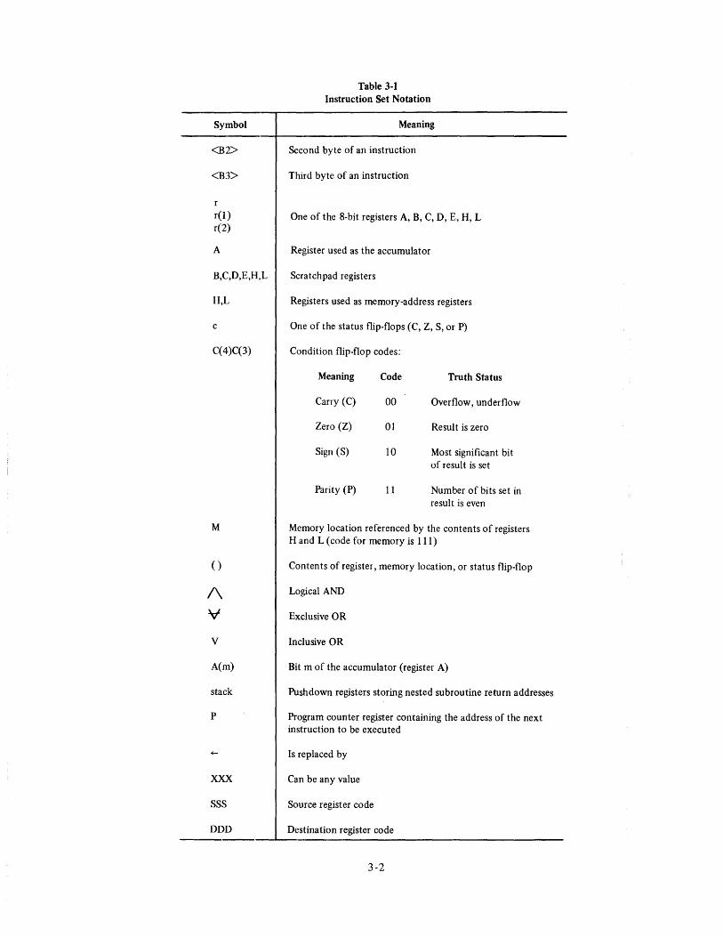
Symbol
<82>
<83>
r(1) r(2)
A
B,C,D,E,H,L
H,L
c
C(4)C(3)
M
()
1\ V
v
A(m)
stack
P
xxx
SSS
DDD
Table 3-1 Instruction Set Notation
Meaning
Second byte of an instruction
Third byte of an instruction
One of the 8-bit registers A, B, C, D, E, H, L
Register used as the accumulator
Scratch pad registers
Registers used as memory-address registers
One of the status flip-flops (C, Z, S, or P)
Condition flip-flop codes:
Meaning Code Truth Status
Carry (C) 00 Overflow, underflow
Zero (Z) 01 Result is zero
Sign (S) 10 Most significant bit of result is set
Parity (P) 11 Number of bits set in result is even
Memory location referenced by the contents of registers Hand L (code for memory is 111)
Contents of register, memory location, or status flip-flop
Logical AND
Exclusive OR
Inclusive OR
Bit m of the accumulator (register A)
Pushdown registers storing nested subroutine return addresses
Program counter register containing the address of the next instruction to be executed
Is replaced by
Can be any value
Source register code
Destination register code
3-2

3.3 INDEX REGISTER INSTRUCTIONS Index register instructions have been :implemented to perform the following functions:
• •
Load data into index registers or memory
Load constant immediately after the instruction into index registers or memory
• Increment an index register
• Decrement an index register
The registers maniplulated by these instructions include the following:
• • • •
Accumulator or A register
Scratchpad registers B, C, D, and E
Memory address registers Hand L
Any addressable read/write or read-only memory location
3.3.1 Loading Data into Index Registers or Memory Data can be loaded into any of the index or memory registers or can be moved among these registers. Loads of this kind are one-byte instructions, and their execution does not affect the condition flip-flops in any way. Data can be loaded in any of the following ways:
• Load a register with the contents of another register
•
•
Load a register with the contents of a memory location
Load a memory location with the contents of a register
In all of these instructions, data is loaded from a source (SSS) to a destination (DDD) register; the source register remains in tact.
3-3
The format for loading a register with the contents of another register is:
Form
Examples
Time States/
Lr(l)r(2) 11 DDD SSS r(l)+-r(2)
LAB LDE
Machine Cycles 5,PCI
The contents of r(2), the source register, are transferred to r(l), the destination register. The contents of r(2) remain unchanged. If the source and destination registers are the same, this is considered a NOP (no operation) instruction.
To load a register with the contents of a memory location, the following is issued:
Form
Examples
Time States/
LrM 11 DDD 111 (r)+-(M)
LAM LDM
Machine Cycles 8,PCI,PCR
The contents of a memory location (M), addressed by registers Hand L, are transferred to r, the destination register. If the code of the destination register is 111, an HLT instruction is executed.
To load a memory location with the contents of a register, use the following instruction:
Form LMr 11 111 SSS (M)+-(r)
Examples LMA LMC
Time States/ Machine Cycles 7,PCI,PCW
The contents of r, the source register, are transferred to a memory location (M), addressed by registers Hand L. The contents of r remain unchanged. If the code of the source register is 111, an HLT instruction is executed.
3.3.2 Loading Data Immediate These instructions are executed to load the byte of data immediately following the instruction into a register or memory location. Condition flip-flops are not affected. Loads of this kind are two-byte instructions. Data can be loaded as follows:
• Load data into a register
• Load data into a memory location
To load byte two of an instruction into a register, use the follOwing format:
Form
Examples
Time States/
Lrl 00 DDD 110
<B2> (r)+-<B2>
LAIA+B LLI340
Machine Cycles 8,PCI,PCR
The data contained in byte two of this instruction will be loaded immediately into r, the destination register.
To load byte two of an instruction into a memory location addressed by the contents of registers Hand L, use the following:
Form
Example
Time States/
LMI 00111110 <B2> (M)+-<B2>
LMI104
Machine Cycles 9,PCI,PCR,PCW
The data contained .in byte two of this instruction will be loaded immediately into M, the memory location addressed by registers Hand L.
3-4
3.3.3 Incrementing an Index Register The one-byte instruction is used to increment an index register by one. All condition flip-flops are affected except the carry. Registers B, C, D, E, H, and L can be incremented, but the accumulator (register A) and memory cannot. The instruction format is:
Form
Examples
Time States/
INr OODDDOOO (r)~r)+l
INB INL
Machine Cycles 5,PCI
The contents of r, the destination register, are incremented by one, and the result is stored in r. If the code of the destination register is 000, an HLT instruction is executed.
3.3.4 Decrementing an Index Register An index register can be decremented by one by means of the one-byte instruction. All condition flip-flops are affected except the carry. Registers B, C, D, E,H, and L can be decremented, but the accumulator and memory cannot. The instruction format is:
Form DCr 00 DDD 001 (r)~r)-l
Examples DCB DCC
Time States/ Machine Cycles 5,PCI
The contents of r, the destination register, are decreme:nted by one, and the result is stored in r. If the code of the destination register is 000, an HLT instruction is executed.
3.4 ACCUMULATOR INSTRUCTIONS The instructions summarized in this paragraph are used to perform arithmetic, logical, and rotation operations usually between the accumulator and a register or memory location. Accumulator instructions can be divided into the following areas:
• Arithmetic/logical index register instructions
• Arithmetic/logical operations with memory

• Arithmetic/logical immediate instructions
• Rotate instructions
These instructions use the contents of the accumulator as one argument, and an index register, a memory location, or the second byte of the instruction as the other argument. Instructions in this category affect the condition flip-flops in a variety of ways:
1.
2.
3.
4.
If a carry or borrow is generated by the instruction, the carry flip-flop (C) is set to one; if no carry or borrow is generated, the carry flip-flop is set to zero.
If the result of a comparison with the accumulator is zero, the zero flip-flop (Z) is set to one; if the result of the comparison is nonzero, the zero flip-flop is set to zero.
If bit 7 of a result is one, the sign flip-flop (S) is set to one; if bit 7 is not one, the sign flip-flop is set to zero.
If a result contains an even number of ones, the parity flip-flop (P) is set to one; if the result contains an odd number of ones, the parity fli p-flop is set to zero.
Depending on the specific instruction being executed, one or more of the condition flip-flops Gan be set as a consequence of instruction execution.
Multiple-precision binary arithmetic is performed using the carry flip-flop; logical operations always reset the carry flip-flop to zero. Rotate instructions affect only the carry flip-flop leaving other condition flip-flops unchanged. Subsequent paragraphs define flip-flop consequences of executing other instructions.
3.4.1 Index Register Instructions The eight instructions described in this paragraph are used to perform arithmetic and logical operations between the accumulator (register A) and the contents of one of the index registers. The results of the operations affect the accumulator but do not change the contents of any other index register (SSS in boxes below). All of the operations described are one-byte instructions.
3-5
To add the contents of a register to the contents of the accumulator, use the following:
Form
Examples
Time States/
ADr 10000 SSS (A)~(A)+(r )
ADC ADD
Machine Cycles 5,PCI
The contents of r, the source register, are added to the contents of the accumulator and the sum is stored in the accumulator. The result of executing this instruction can affect any of the condition flip-flops.
To add the contents of a register and the carry flip-flop to the accumulator, issue the following:
Form
Examples
Time States/
ACr 10001 SSS (A)~(A)+(r )+( carry)
ACB ACD
Machine Cycles 5,PCI
The contents of the source register (r) and the carry flip-flop are added to the contents of the accumulator and the sum is stored in the accumulator. When used in conjunction with the ADr instruction, this instruction facilitates multiple-precision addition of register and accumulator data. Any of the condition flip-flops can be affected by executing this instruction.
To subtract the contents of a register from the contents of the accumulator, use the following:
Form SUr 10010 SSS (A)+-{A)-(r)
Examples SUB SUE
Time States/ Machine Cycles 5,PCI

The contents of r, the source register~1 are subtracted from the contents of the accumulator and the difference is stored in the accumulator. Subtraction is performed using two's complement arithmetic. Any of the condition flip-flops can be affected by executing this instruction.
To subtract and borrow use the following:
Form SBr 10011 SSS (A)+-( A)-( r )-( carry)
Examples SBB SBD
Time States/ Machine Cycles 5,PCI
The contents of the source register (r) and the carry flip-flop are subtracted from the contents of the accumulator and the difference is stored in the accumulator. Subtraction is performed using two's complement arithmetic. When used in conjunction with the SUr instruction, this instruction facilitates multiple-precision subtraction. Any of the condition flip-flops can be affected by executing this instruction.
To perform a logical AND operation on the contents of the accumulator and a register, use the following:
Form
Examples
Time States/
NDr 10 100 SSS (A)+-(A) 1\ (r)
NDB NDD
Machine Cycles 5,PCI
Each bit of r, the source register, is ANDed with each bit of the accumulator. The logical product is stored in the accumulator .
3-6
To perform an exclusive OR operation on the contents of the accumulator and a register, use the following:
Form XRr 10 101 SSS (A)+-(A) ¥ (r)
Examples XRA XRD
Time States/ Machine Cycles 5,PCI
The contents of r, the source register, are exclusively ORed with the contents of the accumulator. The result is stored in the accumulator.
To perform an inclusive OR operation on the contents of the accumulator and a register, use the following:
Form ORr 10 110 SSS (A)~(A) V (r)
Examples ORA ORB
Time States/ Machine Cycles 5,PCI
Each bit of r, the source register, is ORed with each bit of the accumulator. The result is stored in the accumulator.
To compare the contents of a register with the contents of the accumulator, use the following:
Form
Examples
Time States/
CPr 10 111 SSS (A)-(r)
CPB CPD
Machine Cycles 5,PCI

The contents of r, the source register, are compared with the contents of the accumulator. The accumulator remains unchanged. After the instruction has been executed, if the contents of r are greater than the contents of the accumulator, the carry flip-flop is set to one; if not, it is reset to zero. If the two values are tht~ same, the zero flip-flop is set to one; if not, it is reset to zero. The sign and parity flip-flops are set as if the subtraction had actually occurred.
3.4.2 Operations With Memory The eight instructions described in this paragraph are used to perform arithmetic and logical operations between the accumulator (register A) and the memory byte of data addressed by the contents of registers Hand L. The results of the operations affect the accumulator but do not change the contents of the memory location (M in all models below). All of the operations described are one-byte instructions.
To add the contents of a memory location to the contents of the accumulator, use the following:
Form ADM 10000 111 (A)~A)+(M)
Example ADM
Time States/ Machine Cycles 8,PCI,PCR
The contents of M are added to the contents of the accumulator and the sum is stored in the accumulator. Any of the condition flip-flops can be affected by executing this instruction.
To add the contents of a memory location and the carry flip-flop to the contents of the accumulator, use the following:
Form ACM 10001 111 (A)~ A)+(M)+( carry)
Example ACM
Time States/ Maehine Cycles 8,PCI,PCR
3-7
The contents of the specified memory location and the carry flip-flop are added to the contents of the accumulator; the sum is stored in the accumulator (A). When used in conjunction with the ADM instruction, this instruction facilitates multiple-precision addition of memory and accumulator data. Any of the condition flip-flops can be affected by executing this instruction.
To subtract the memory location from the contents of the accumulator, use the following:
Form SUM 10010111 (A)~A)-(M)
Example SUM
Time States/ Machine Cycles 8,PCI,PCR
The contents of the specified memory location are subtracted from the accumulator and the difference is stored in the accumulator. Subtraction is performed using two's complement arithmetic. Any of the condition flip-flops can be affected by executing this instruction.
To subtract the contents of a memory location and the carry flip-flop from the contents of the accumulator, usc the following:
Form SBM 10011111 (A)~A)-(M)-( carry)
Example SBM
Time States/ Machine Cycles 8,PCI,PCR
The contents of the specified memory location and the carry flip-flop are subtracted from the contents of the accumulator. Subtraction is performed using two's complement arithmetic. When used in conjunction with the SUM instruction, this instruction facilitates multiple-precision subtraction. Any of the condition flip-flops can be affected by executing this instruction.
To perform a logical AND operation on the contents of the accumulator and the memory location use the following:
Form
Example
Time States/
NDM 10100111 (A)+-(A) 1\ (M)
NDM
Machine Cycles 8,PCI,PCR
Each bit of the memory location is ANDed with each bit of the accumulator. The logical product is stored in the accumulator.
To perform an exclusive OR operation on the contents of the accumulator and the memory location, use the following:
Form XRM 10101111 (A)+-(A) V (M)
Example XRM
Time States/ Machine Cycles 8,PCI,PCR
The contents of M are exclusively ORed with the contents of the accumulator and the result is stored in the accumulator.
For an inclusive OR operation on the contents of the accumulator and the memory location, issue the following:
Form ORM 10110111 (A)~A) V (M)
Example ORM
Time States/ Machine Cycles 8,PCI,PCR
The contents of M are inclusively ORed with the contents of the accumulator and the result is stored in the accumulator.
3-8
To compare the contents of the memory byte with the contents of the accumulator, use the following:
Form
Example
Time States/
CPM 10111111 (A)-(M)
CPM
Machine Cycles 8,PCI,PCR
The contents of M are compared with the contents of the accumulator; the accumulator remains unchanged. After the instruction has been executed, if the contents of Mare greater than the contents of the accumulator, the cafl('Y flip-flop is set to one; if not, it is reset to zero. If the two values are equal, the zero flip-flop is set to one; if not, it is reset to zero. The sign and parity flip-flops are set as if the subtraction had actually occurred.
3.4.3 Immediate Instructions The eight instructions described in the paragraph are used to perform arithmetic and logical operations between the accumulator and the byte of data immediately following the instruction. The results of the operations described below affect the accumulator but do not change the contents of the immediate byte. All of the operations described are two-byte instructions.
To add the contents of byte two to the contents of the accumulator, use the following:
Form
Example
Time States/
ADI 00000 100 <82> (A)~(A)+<82>
ADI2
Machine Cycles 8,PCI,PCR
The second byte of this instruction, <82>, is added to the contents of the accumulator and the sum is stored in the accumulator. Any of the condition flip-flops can be affected by executing this instruction.

To add byte two and the carry flip-flop to the contents of the accumulator, issue the following:
Form
Example
Time States/
ACI 00001 100 <B2> (A)~A)+<B 2>+( carry)
ACI104
Machine Cycles 8,PCI,PCR
The second byte of this instruction (<B2» and the carry flip-flop are added to the contents of the accumulator and the sum is stored in the accumulator. In conjunction with the ADI instruction this instruction facillitates multipleprecision addition of instruction and accumulator data. Any of the condition flip-flops can be affected by executing this instruction.
To subtract byte two from the contents of the accumulator, use the following:
Form
Example
Time States/
SUI 00010 100 <B2> (A)~A)-<B2>
SUI 1
Machine Cycles 8,PCI,PCR
The second byte of this instruction, <B2>, is subtracted from the contents of the accumulator and the difference is stored in the accumulator. Subtraction is performed using two's complement arithmetic. Any of the condition flipflops can be affected by executing this instruction.
To subtract byte two and the carry flip-flop from the accumulator, use the following:
Form SBI 00011 100 <B2> (A)~ A)-<B 2>-( carry)
Example SBI6
Time States/ Machine Cycles 8,PCI,PCR
3-9
The second byte of this instruction, (<B2», and the carry flip-flop are subtracted from the contents of the accumulator and the difference is stored in the accumulator. Subtraction is performed using two's complement arithmetic. In conjunction with the SUI instruction, this instruction facilitates multiple-precision subtraction.
To perform a logical AND operation on the contents of the accumulator and byte two, use the following:
Form NDI 00 100 100 <B2> (A)~(A) 1\ <B2>
Example NDI 100
Time States/ Machine Cycles 8,PCI,PCR
The second byte of this instruction, <B2>, is ANDed with the contents of th~ accumulator. The logical product is stored in the accumulator.
To perform an exclusive OR operation on the contents of the accumulator and byte two, use the following:
Form
Example
Time States/
XRI 00 101 100 <B2> (A)~(A) V- <B2>
XRI340
Machine Cycles 8,PCI,PCR
The second byte of the instruction, <B2>, is exclusively ORed with the contents of the accumulator and the result is stored in the accumulator.
For an inclusive OR operation on the contents of the accumulator and byte two, issue the following:
Form ORI 00 110 100 <B2> (A)~A) V <B2>
Example ORI 102
Time States/ Machine Cycles 8,PCI,PCR

The second byte of the instruction, <B2>, is inclusively ORed with the contents of the accumulator and the result is stored in the accumulator.
To compare the contents of byte two with the contents of the accumulator, use the following:
Form
Example
Time States/
CPI 00 111 100 <132> (A)-<B2>
CPI4
Machine Cycles 8,PCI,PCR
The second byte of the instruction, <B2>, is compared with the contents of the accumulator; the accumulator remains unchanged. After the instruction has been executed, if the contents of <B2> are greater than the contents of the accumulator, the carry flip-flop is set to one; if not, it is reset to zero. If the two values are the same, the zero flip-flop is set to one; if not, it is reset to zero. The sign and parity flip-flops are set as if the subtraction had actually occurred.
3.4.4 Rotate Instructions The four instructions described in this paragraph are used to rotate the contents of the accumulator, one bit per instruction execution, in one of the following ways:
• Left and into the carry flip-flop
• Right and into the carry flip-flop
• Left and through the carry flip-flop
• Right and through the carry flip-flop
These instructions affect only the carry flip-flop; all other condition flip-flops remain unchanged. All rotates described are one-byte instructions.
3-10
To rotate the contents of the accumulator one bit to the left and into the carry flip-flop, use the following:
Form
Example
Time States/
RLC 00 000 010 A(m+1)+-A(m) A(0)+-A(7) ( carry)+-A( 7)
RLC
Machine Cycles 5,PCI
The contents of the accumulator are rotated to the left by one bit. Bit 7 is moved to the bit position of bit 0, and bits o through 6 are moved to bit positions 1 through 7. Bit 7 is also stored in the carry flip-flop. The following diagrams show the bit positions before and after the rotate. The original contents of the accumulator are as follows:
7 6 5 4 3 2 a
After the rotate, the following is the case:
a a a a o
carry 7 6 5 4 3 2 o
To rotate the contents of the accumulator one hit to the right and into the carry flip-flop, use the following:
Form RRC 00 001 010 A(m)+-A(m+1) A(7)+-A(0) (carry)+-A( 0)
Example RRC
Time States/ Machine Cycles 5,PCI

The contents of the accumulator are rotated to the right by one bit. Bit 0 is moved to the bit position of bit 7, and bits 7 through 1 are moved to bit positions 6 through O. Bit 0 is also stored jin the carry flip-flop. The original position is:
~[O I 0 o o o
7 6 5 4 3 2 o
The next diagram represents the contents of the accumulator after an RRC:
carry 7 6 5 4 3 2 o
To rotate the contents of the accumulator one bit to the left and through the carry flip-flop, use the following:
Form RAL 00010010 A(m+ 1)+-A(m) A( O)+-( carry) ( carry)+-A( 7)
Example RAL
Time States/ Machine Cycles 5 ,PC I
The contents of the accumulator are rotated to the left by one bit. Bit 7 is stored in the carry flip-flop; the contents of the carry flip-flop are stored in A(O). Bits 0 through 6 are moved to bit positions 1 through 7. The original contents of the accumulator and the carry flip-flop an~:
G ~ 0 0 0 0 o
To rotate the contents of the accumulator one bit to the right and through the carry flip-flop, use the following:
Form
Example
Time States/
RAR 00011 010 A(m)+-A(m+ 1) A(7)+-( carry) (carry)+-A(O)
RAR
Machine Cycles 5,PCI
The contents of the accumulator are rotated to the right by one bit. Bit 0 is stored in the carry flip-flop; the contents of the carry flip-flop are stored in bit 7. Bits 7 through 1 are moved to bit positions 6 through O. The original contents of the accumulator and the carry flip-flop are:
G 10
10 o o o
carry 7 6 5 4 3 2 o
After the rotate, the following is the case:
0 10 I 0 0 0 0
carry 7 6 5 4 3 2 o
3.5 PROGRAM COUNTER AND STACK CONTROL INSTRUCTIONS The instructions summarized in this paragraph are used to transfer control from one address to another. These instructions are divided into three categories:
• Jump instructions • Call instructions
• Return instructions
carry '7 6 5 4
Mter the rotate, the contents are:
G @] 0 0 0
3 2
0
o All of these instructions make use of the processor stack and/or program counter. The stack is a set of eight 14-bit registers. Seven of these registers are organized as a last-in first-out (LIFO) pushdown stack which is used to store nested subroutine addresses. The eighth register serves as the current program counter (P) and always contains the
carry 7 6 5 4 3 2 o address of the next instruction to be fetched.
3 -11

Each of the three instruction types described uses the stack or program counter in a different way. The second and third bytes, <82> and <83>, of each jump instruction
. (.IMP, JFc, JTc) contain an address. This address points to the memory location from which the next instruction is to be fetched if the jump is an unconditional one or if the conditions of the jump are satisfied. The address contained in the jump instruction is stored in the program counter (P) for use during execution. <82> and <B3> are 8-bit bytes which form the 14-bit address to be stored. <82> contains the eight low-order bits of the address, ilnd <83> contains the six high-order bits. Bits 6 and 7 of <B3> are not used.
Subroutine call instructions (CAL, CFc, CTc) store the current program counter (P) in the pushdown stack and then store the starting address of the subroutine to be called in the program counter. This address is contained in the second and third bytes of the call instruction. Calls can be performed unconditionally in a CAL instruction, or conditionally in the case of CFc and CTc.
Subroutine return instructions (RET, RFc, RTc) cause the current program counter to be replaced by the last inserted address in the stack, and for all remaining addresses in the stack to be "popped up" one level. These actions can be performed unconditionally in the case of a RET instruction, or conditionally in the case of RFc and RTc. Because the stack is an eight-register LIFO pushdown stack, is popped up one level at a time, and has a program counter as its eighth register, subroutines can be nested to seven levels.
With conditional jumps, calls, and returns, any of the four condition flip-flops (carry, zero, sign, and parity) can be tested to determine the condition on which the instruction will be executed.
Each of the instruction groups introduced is explained in detail. The following example shows a call to a subroutine, a conditional jump, and an unconditional return.
NXTBLK, CAL GETBYT
3.5.1 Jump Instructions Jump instructions are three-byte instructions which are used to alter the normal flow of a program by branching conditionally or unconditionally to another location. The address to which control is passed is specified by bytes two and three of the jump instruction. Byte two (<82» contains the eight low-order bits of the address and byte three (<83» contains the six high-order bits. Because the processor uses a 14-bit address, bits six and seven of <83> are ignored. There are three jump instructions:
• Jump unconditionally
• Jump if condlllon is false
• Jump if condition is true
To perform an unconditional jump, issue the following:
Form JMP 01 XXX 100
<82> <83>
(P)~3><B2>
Examples JMP CKDONE JMPAL
Time States/ Machine Cycles 11 ,PC I ,PCR,PCR
<82> and <83> make up a 14-bit address which is stored in the program counter to initiate an unconditional transfer of program control to that address. <82> and <83> therefore represent the next instruction to be executed after the JMP.
/SUBROUTINE TO GET ONE BYTE OF DATA FROM PAPER TAPE / AND UPDATE CHECKSUM GETBYT, INPI
NDI JTZ TI'IPO LEA ADD IDA LAE RET
40 GETBYT
3 -12
/INPUT STATUS /MASK "DA" (IGNORE ERRORS) /WAIT FOR "DA" /GET CHAR /SAVE CHAR / ADD CHECKSUM TO INPUT BYTE /SA VE NEW CHECKSUM /RESTORE CHAR /RETURN UNCONDITIONALLY

To jump on a false condition use the following:
Form
Examples
Time States/ Machine Cycles
JFc
01 OC(4)C(3) 000 <82> <B3>
If (c)=O (P)+-<B3><B2>
Otherwise (P)=(P)+3
JFZ NXTBLK JFP B2
If (c)=O 11,PCI,PCR,PCR
Otherwise 9,PCI,PCR,PCR
If the condition flip-flop represented by c is false (reset to zero), the address specified by <B3> <Bl> is stored in the program counter and the next instruction to be executed is fetched from this address. If the relevant status flip-flop is true (set to one), the program counter is incremented by three and the branch is not taken. In this case, time states T4 and TS of the second PCR cycle are skipped. For example, if instruction JFC is executed, a branch will occur if the carry condition flip-flop is zero.
To jump on a true condition, use the instruction following:
Form
Examples
Time States/ Machine Cycles
JTc
01 lC(4)C(3) 000 <B2> <83>
If (c)=1 (P)+-<B3> <B 2>
Otherwise (P)=(P)+3
JTSER JTC DONE
If (c)=1 II,PCI,PCR,PCR
Otherwise 9,PCI,PCR,PCR
3 -13
If the condition flip-flop represented by c is true (set to one), the address specified by <83> <81> is stored in the program counter and the next instruction to be executed is fetched from this address. If the relevant condition flip-flop is false (reset to zero), the program counter is incremented by three and the branch is not taken. In this case, time states T4 and TS of the second PCR cycle are skipped. For example, if instruction JTP is executed, a branch will occur if the parity condition flip-flop is set.
3.5.2 Call Instructions Call instructions are three-byte instructions which are used to alter the normal flow of a program by branching conditionally or unconditionally to a subroutine. Subroutine calls may be nested to seven levels. Byte two (<82» contains the low-order eight bits of the address, and byte three (<83» contains the high-order six bits. Bits six and seven of byte three are ignored. A call causes <B3> <82> to be stored in the curren t program counter (P) an d for the previous contents of P to be inserted at the top of the pushdown stack. There are three call instructions:
• Call unconditionally • Call if condition is false • Call if condition is true
To perform an unconditional call to a subroutine, issue the following:
Form
Examples
Time States/
CAL 01 XXX 110
<82> <83>
(stack)+-(P) (P)+- <83> <B2>
CALGETBYT CAL DOAI
Machine Cycles II,PCI,PCR,PCR
The contents of P are shifted into the stack and the starting address of the subroutine, <83> <B2>, is stored in the program counter. This causes the next instruction executed to be the starting address of the subroutine whose name is included in the CAL.

To perform a call on a false condition, use the instruction following:
Form
Examples
Time States/ Machine Cycles
CFc
01 OC(4)C(3) 010 <82> <83>
If (c)==O (stack)'*iP) (P)~:- <83> <B 2>
Otherwise (P)=(P)+3
CFZALL CFP ADDUP
If (c}=O II,PCI,PCR,PCR
Otherwise 9 ,PCI ,PCR,PCR
If the condition flip-flop represented by c is false (reset to zero), the address specified by <83> <B2> is stored in the program counter and the next instruction to be executed is fetched from this address. If the relevant condition flip-flop is true (set to one), the program counter is incremented by three and the subroutine is not called. In this case, time states T4 and TS of the second PCR cycle are skipped. For example, if instruction CFS is executed, a subroutine call will be issued if the sign condition flip-flop is not set.
To call a subroutine on a true condition, issue the following:
Form
Examples
Time States/ Machine Cycles
CTc
01IC(4)C(3) 010 <82> <B3>
If (c)=1 (stack)'*iP) (P)~ <83> <82>
Otherwise (P)=(P)+3
CTS CKDONE CTCCX
If (c)=1 11 ,PCI,PCR,PCR
Otherwise 9,PCI,PCR,PCR
If the condition flip-flop represented by c is true (set to one), the address specified by <B3> <82> is stored in the program counter and the next instruction to be executed is fetched from this address. If ~he relevant condition flip-flop is false (reset to zero), the program counter is incremented by three and the subroutine is not called. In this case, time states T4 and TS of the second PCR cycle are skipped. For example, if instruction CTZ is executed, a subroutine caUl will be issued if the zero condition flip-flop is set.
3.5.3 Return Instructions The instructions described in this section are one-byte instructions which are used to exit unconditionally or conditionally from a subroutine entered via a call instruction and to return to the next sequential instruction. after the call. Returns cause the pushdown stack to be popped up one level at a time. The popped entry in the pushdown stack is stored in the program counter (P). The following example illustrates both an unconditional and a conditional subroutine return:
3-14

CAL INCHL
INCHL, INL RFZ INH RET
/INCREMENT LOW BYTE OF MEMORY ADDRESS /RETURN IF NO OVERFLOW /OVERFLOW-INCREMENT HIGH BYTE /RETURN
To perform an unconditional return from a called subroutine, issue the following:
Form RET
00 XXX 111
(P)+{ stack)
Example RET
Time States/ Machine Cycles 5,PCI
The stack is popped up one level and the popped entry in the pushdown stack is stored in the program counter. P now points to the next instruction after the call.
To perform a return on a false condition, use the following:
Form RFc
OOOC(4)C(3) 011
If (c)=O (P)+-(stack)
Otherwise (P)=(P)+1
Example RFZ
Time States/ If (c )=0; 5,PCI Machine Cycles Otherwise; 3,PCI
3 -15
If the condition flip-flop represented by c is false (reset to zero), the stack is popped up one level and the popped entry in the pushdown stack is stored in the program counter. P now points to the next instruction after the call. If the relevant condition flip-flop is true (set to one), the program counter is incremented by one and the return is not performed. In this case, time states T4 and T5 are skipped. For example, if instruction RFP is executed, a return will be issued if the parity condition flip-flop is not set.
To return on a true condition, issue the following:
Form RTc
00 lC(4)C(3) 011
If (c)=1 (P)+-(stack)
Otherwise (P)=(P)+1
Example RTS
Time States/ If (c)=I; 5,PCI Machine Cycles Otherwise; 3,PCI
If the condition flip-flop represented by c is true (set to one), the stack is popped up one level and the popped entry in the pushdown stack is stored in the program counter. P now points to the next instruction after the call. If the relevant condition flip-flop is false (reset to zero), the program counter is incremented by one and the return is not performed. In this case, time states T4 and T5 are skipped. For example, if instruction RTZ is executed, a return will be issued if the zero condition flip-flop is set.

3.6 INPUT/OUTPUT INSTRUCTIONS The one-byte instructions described in this section are used to perform input or output operations. With these instructions, data can be transferred between the accumulator (register A) of the Processor Module and any peripheral device associated with the system. The data transfer is performed in 8-bit bytes at the rate of one byte per I/O instruction executed. It is possible to access eight different input devices by specifying the appropriate address field in the INP instruction. By supplying the proper address in an OUT instruction, 24 different output devices can be accessed.
The states of the condition flip-flops are not affected by executing the I/O instructions described. Because INP moves data into the accumulator from an input device and OUT moves data from the accumulator to an output device, it is the programmer's responsibility to load data into register A before issuing an OUT instruction, and to extract data from A after executing an INP.
3.6.1 Input Instruction To read one byte of data into the accumulator (register A) from an input device, use the following:
Form INP
01 OOM MMI
(A)~input data lines)
Example INP + 10*
Time States/ Machine Cycles 8,PCI,PCC
The contents of the accumulator are~ placed on the peripheral device input bus during time state Tl of the PCC cycle. The device address field, represented by MMM, is placed on the device address bus to select the appropriate device during time state T2 of that cycle. During time state T3 of the PCC cycle, data contents from the selected device are removed from the input bus and loaded into the accumulator.
*Where lOs represents input device 4 multiplied by 2. **Where 60s represents output device 30 multiplied by 2.
[:r Data Data Trans-
over- Avail· mit
run able buffer empty
7 6 5 4
3 -16
Eight input devices may be referenced by the INP instruction. The contents of the accumulator is latched during time state Tl of the PCC cycle to facilitate expansion of the number of input-only devices that can be connected to an MPS system.
3.6.2 Output Instruction To write data to an output device from the accumulator, use the following:
Form OUT
01 RRM MMI (RR=O)
(output data line )~A)
Example OUT + 60**
Time States/ Machine Cycles 6,PCI,PCR
The contents of the accumulator are placed on the peripheral device output bus at time state Tl of the PCC cycle. The device address field, represented by RRMMM, is placed on the device bus at time state T2 of the same cycle. RRMMM must be a nonzero number in the range 1 0 (octal) through 37 (octal).
OUT can reference 24 output devices.
3.6.3 Reserved INP and OUT Instructions Three input/output instructions are reserved for UART (Universal Asynchronous Receiver/Transmitter) control on the Processor Module. The UART is an I/O interface on th(~ Processor Module which handles data from a serial port. Control of the UART is accomplished as follows:
Instruction
INPO 01 000001 OUTO 01 010001 INPI 01 000011
Function
Read data from UART Output data to UART Read status from UART
The status register looks like the following:
3 2 o

3.7 MACHINE INSTRUCTIONS The four instructions in this category perform the basic machine control functions halt, restart, interrupt enable, and interrupt disable. All four of these instructions have a one-byte format.
3.7.1 Halt Instruction The halt instruction is issued by the following:
Form HLT
00 000 OOX or
11111111
Example HLT
Time States/ Machine Cycles 4,PCI
When the HLT is executed, the proc1essor enters the stopped state after completion of time state T3. The program counter is incremented by one, and the contents of all condition flip-flops, registers, and memory are unchanged.
3.7.2 Restart Instruction The restart instruction can be used as a one-byte unconditional call to any of eight specified locations in the first 64 words of memory. The called addresses are the following octal locations:
o 10 20 30 40 50 60 70
Each of these eight locations can be use:d as the starting address of an eight-word subroutine.
The restart is a one-byte instruction which is issued by the following:
Form RST
00 AAA 101
(stack)+-(P) (P)+-(OOOOOO OOAAAOOO)
Example RST + aO*
Time States/ Machine Cycles 5,PCI
The contents of the program counter, P, are shifted into the top entry of the pushdown stack. Bits 3-5 of the instruction, AAA in the model, are moved into positions 3-5 of P. All other bit positions of the program counter arc zeroed.
The restart is sometimes used in place of a call instruction because it is at least twice as fast and uses only one-third as much memory. For example, instead of issuing a CAL INCHL directly in the assembly language code, the programmer might place the INCHL subroutine in low memory to be called with an RST.
NOTE Users may employ OPDEF (Paragraph 6.10.6) to define their specific instructions involving RST, INP, and OUT.
3.7.3 Interrupt Enable and Disable Instructions The interrupt enable (ION) and interrupt disable (lOF) instructions are specialized input/output instructions which are defined as machine instructions because of the interrupt control functions performed.
*Where a represents an octal digit from 0 to 7
3·17

To enable external events to interrupt normal program sequence, issue the following:
Form ION
01 010011
Enable external event interrupt
Example ION
Time States/ Machine Cycles 8,PCI,PCC
To disable external events from in terru pting, issue the following:
Form IOF
01 010 101
Disable external event interrupt
Example IOF
Time States/ Machine Cycles 6,PCI,PCC
External event control is similar to iIiterrupt control, but the condition flip-flops cannot be saved and restored, and the registers cannot be saved and restored with sufficient generality. The STRT switch on the programmable module performs a simulated interrupt and jumps to the address set in the Monitor/Control Panel (MCP) Switch Register. As.in an actual interrupt, the interrupt recognition logic is automatically disabled after every interrupt. Therefore, if a program is to recognize interrupts, an ION instruction must be issued in the initialization routine. After the ION is executed, one more instruction can be executed before interrupts are enabled. The ION instruction should be the last executable instruction before the RET command in an interrupt service routine.
The IOF instruction is used to disable interrupts from external events excluding power fail. This instruction should therefore be used with extreme caution. Typically it is used when a particular operation is being performed and it is not appropriate to allow interrupts for the duration of the operation.
A typical program sequence is shown on the opposite page.
3-18

DOFF,
PFR,
*50 JMPDOFF
*70 JMPPFR
*100 XRA
ION JMP.
ION RET
HLT
/ASSUMlE DOFF IS CONNECTED TO PIN 11
/ ASSUME POWER FAIL CONNECTED TO Ul
/CLEAR STATUS FLIP-FLOPS AND AC /OTHER INITIALIZATION CODE
/ENABLEINTERRUPTS /LOOP HERE UNTIL INTERRUPT OCCURS lOR COULD BE VERY LOW PRIORITY /ROUTINES
/DOFF INTERRUPT SERVICE ROUTINE /CLEAR DOFF INTERRUPT FLAG
/ENABLE INTERRUPT /RETURN TO PROGRAM SEQUENCE BEFORE /INTER*UPT OCCURRED
/ROUTINE TO SHUT DOWN OR STABILIZE /SYSTEM BEFORE ALL POWER IS LOST. /AFTERPOWER IS RESTORED, SYSTEM /SHOULb BE RESTARTED AT THE BEGINNING
3-19


CHAPTER 4 1'HE PDR-8 HOST ENVIRONMENT
The Digital Equipment Corporation PDP-8 computer system has been selected as the host machine for preparing and processing programs designed for Microprocessor Series (MPS) use. This chapter describes the hardware and software environment in which programs wHl be developed and assembled, defines both minimum operational requirements and expanded capabilities and options, and outlines the characteristics and use of major PDP-8 hardware and software modules, some of which are described in far greater functional detail in subsequent chapters of this handbook.
4.1 INTRODUCTION TO THE PDP-8 The PDP-8 is a small, economical, and efficient computer designed for effective program development, assembly, and execution. It is a single-address parallel machine which operates on 12-bit binary numbers using two's complement arithmetic. An effective PDP-8 can function with only 4K of core memory and no peripheral devices whatsoever . Yet this minimum configuration can expand to support as much as 32K of core and a variety of devices. PDP-8 users of Microprocessor Series Modules are assumed to possess only the minimum hardware configuration described in the next paragraph. They will receive a set of system programs in paper tape form, sufficient to load and copy paper tapes and to edit and assemble programs developed for the Processor Module. This software system will be described in detail in subsequent paragraphs of this chapter.
4.2 PDP-8 HARDWARE ENVIRONMENT The minimum configuration of PDP-8 equipment for support of the software defined for this product consists of the following:
• PDP-8 central processing unit, programmer's console, and 4K (4096 decimal words) of core memory
• Keyboard/printer terminal, often a Teletype ®
®Teletype is a registered trademark of the n~letype Corporation.
• Low-speed (associated with the Teletype) paper-tape reader/punch
• If Teletype is not the terminal device, high-speed paper-tape reader/punch
Other peripheral devices may be supported by an installa-, tion's PDP-8 configuration~ these will normally" be ignored
while processing MPS programs. The only exception occurs when both high-speed and low-speed paper-tape readerl punches are availabe. With most programs, the user must specify which paper tape unit is available by setting a switch on the PDP-8 console. One variety of paper tape unit is a necessary component of the PDP-8 minimum configuration, but both are supported by the system and described in this chapter. The following paragraphs describe the usc of each hardware module just defined.
4.2.1 Central Processing Unit (CPU) The PDP-8 computer system is available in many models and configurations. The CPU most frequently utilized by MPS users is the PDP-8/E. In many of the paragraphs which follow, specific references to switches or keys may be most relevant to the PDP-8/E. However, users of other PDP-8 computer models (e.g., PDP-8/F, PDP-8/I, PDP-8/L, PDP-81M) normally can use the software supplied with this system with equal facility.
4.2.2 Programmer's Console The PDP-8 programmer's console provides switches and indicator lamps, facilia ting manual control of the computer by allowing a programmer to examine or alter the contents of memory locations and to determine the status of a program in execution. In Figure 4-1 you can see a photograph of a PDP-8/E console. Table 4-1 summarizes the functions of all switches and indicators on this console. Note that some of these functions are specific to the PDP-8/E and may not be relevant to all user machines.

aM -.1: SiWC Q,.t:;M: ~ DV
'.='1iJM @ill. -
Figure 4-1 PDP-8E Programmer's Console
Table 4-1 Programmer's Console Control and Indicator Functions
Control or Indicator
OFF /POWER/PANEL LOCK
SW
SWITCH REGISTER
ADDR LOAD
EXTD ADDR LOAD
Function
In the counter-clockwise, or OFF position, this key-operated switch disconnects all primary power to the computer. In the POWER, or vertical position, it applies power to the computer and all manual controls. In the PANEL LOCK, or clockwise position, it applies power to the computer, the Switch Register and the RUN light only. In this position, a running program is protected from inadvertent switch operation.
When this switch is up, the OMNIBUS SW line is high (logical 1). When it is down, the SW line is low. This switch is used by special peripheral routines.
The Switch Register (SR) may be loaded with a 12-bit binary number by setting each of the twelve switches either up for aI, or down for a O.
Pressing the ADDRess LOAD switch loads the contents of the SR into the central processor MA register and forces the processor to enter a fetch state. This causes the contents of the core memory location designated by the SR to be loaded into the MB register.
Pressing the EXTendeD ADDRess LOAD switch loads the contents of SR bits 6-8 into the instruction field register and the contents of SR bits 9-11 into the data field register.
4-2

Control or Indicator
CLEAR
CONT
EXAM
HALT
SING STEP
DEP
EMA
MEMORY ADDRESS
RUN
Indicator Selector Switch
Setting this knob to:
BUS
Table 4-11 (Cont) Programmer's Console Control and Indicator Functions
Function
Pressing the CLEAR switch loads a binary 0 into bits 0-11 of the accumulator, the link~ all I/O device flag registers, and the interrupt request flag register. This is equivalent to executing a CAF (Clear All FI,ags) instruction.
Pn~ssing the CONTinue switch sets the run flip-flop and issues a memory start to begin program execution at the address specified by the current contents of the central processor MA register.
Pressing the EXAMine switch loads the contents of core memory at the address specified by the MA register into the MB register and then increments the MA register and the PC. Repeated operation of this switch permits the contents of sequential core memory locations to be examined.
Pressing HALT clears; the run flip-flop and causes the computer to stop at the beginning of the next fetch state. Operating the computer with HALT depressed causes on¢ complete instruction to be executed whenever the CONTinue switch is pressed.
Pressing SINGle STEP clears the run flip-flop and causes the computer to halt at the next machine cycle. Operating the computer with the SINGle STEP switch depressed causes only one machine cycle to be executed whenever the CONTinue switch is pressed.
Lifting the DEPosit switch loads the contents of the SR into the MB register and into core memory at the address specified by the current contents of the central processor MA register, then increments the PC and the MA registers. This facilitates manual storage of information in sequential core memory locations.
The 3-bit Extended, Memory Address register displays the memory field d~~signation of the memory field currently being accessed.
The MEMORY ADI!>RESS register displays the contents of the central processor MA regist~r. It combines with the EMA register to provide the IS-bit address of the next core location to be accessed.
The RUN indicator is lit whenever all machine timing circuits are activated and capable of executing instructions.
This six-position rotary knob designates which of six possible registers (or combinations of registers) is to be loaded into the adjacent 12-bit display.
Displays the logical state of the data gating lines which connect the major registers.
4-3
Control or Indicator
MQ
MD
AC
STATUS
Table 4-1 (Cont) Programmer's Console Control and Indicator Functions
Function
Displays the contents of the multiplier quotient register.
Displays the contents of the MB register. This indicates the last information read from or written into core memory.
Displays the contents of the accumulator.
Each display light is turned on to indicate the designated condition:
Indicator Light/Bit Position Turned On to Indicate
o 1 2 3
4 5 6-8 9-11
STATE
The link contains a binary 1. The Greater Than Flag (GTF) is raised. The interrupt request line is asserted. A processor condition, which prevents program interrupts, has been initiated by software.
The interrupt enable flip-flop is on. The user mode line is asserted. Displays the contents of the instruction field register. Displays the contents of the data field register.
With the Indicator Selector knob in the STATE position, each display light is turned on to indicate the following condition:
Indicator Light/Bit Position Turned On to Indicate
o 1 2 3-5 6 7 8 9 10 11
Currently in fetch state. Currently in defer state. Currently in execute state. Displays the contents of the instruction register. The MD DIR line is asserted. The BREAK DATA CONT line is asserted. The SW line is asserted. The PAUSE I/O line is asserted. The BREAK IN PROG line is asserted. The BREAK CYCLE line is asserted.
NOTE The function of the various transmission lines cited and their associated control logic is documented in Digital's Small Computer Handbook.
4-4

4.2.3 Keyboard/Printer Terminal The PDP-8 user interacts with many of the system programs described in this chapter in a command-oril~nted way using a terminal as the input/output device. The following terminals may be used with the PDP-8 system described.
• • •
LT33 Teletype VT05 Display Terminal LA30 DECwriter Data Terminal
The VT05 and LA30 are much faster than the Teletype, which prints at a maximum rate of ten characters per second; but the Teletype offers the advantage of a built-in low-speed paper-tape reader/punch unit. The VTOS has a video display screen; the other two terminals supply hard copy. Figure 4-2 is an illustration of the LT33 Teletype, the basic I/O device assumed for users of the system.
OFF
REL.
B.SP.
ON
STOP ----,~.:.
Certain specialized Teletype knobs and keys require some clarification. The control knob of the LT33 Teletype has the following three positions:
Position
LINE
Meaning
The Teletype console is energized and connected to the computer as an input/output device under computer control.
OFF The Teletype console is de-energized.
LOCAL The Teletype console is energized for offline operation under control of the Teletype keyboard and switches exclusively.
These three positions will be referenced in this and subsequent chapters when discussing the handling of paper tape functions.
LINEO LOCAL
2428-1
Figure 4-2 LT33 Teletype Console
4-5

The Teletype keyboard shown in Figure 4-3 combines standard typewriter characters with special functions which are summarized in Table 4-2.
4.2.4 Low-Speed Paper-Tape Reader/Punch The Teletype paper-tape reader (also called the low-speed reader) is used to read data punched on paper tape into core memory. The data is read from an eight-channel, perforated paper tape at a maximum rate of ten characters per second. Operation is controlled by a three-position switch, shown in Figure 4-2.
Setting
START
STOP
FREE
Meaning
Activates the reader; reader sprocket wheel is engaged and operative.
De-activates the reader; reader sprocket wheel is engaged but not operative.
De-activates the reader; reader sprocket wheel is disengaged.
The paper-tape punch is used to perforate eight-channel, rolled, oiled paper tape at a maximum rate of ten characters
O()C)C)OC)G)C)OQC)O® A(\(\~~~OO~Af'®\t::;\R\ ~ \.V \V \V \.:,J '-V y u \V \.V \..:..) \:.:!Y \:::Y
eOG)G)G)6)OOCDe?o@ee 80000.0000008
Figure 4-3 Teletype Keyboard
per second. The punch controls are shown in Figure 4-2 and described below:
Setting
REL.
B.SP.
Meaning
Disengages the tape to allow tape removal or loading.
Backspaces the tape one space for each firm depression of the B.SP. button.
ON Activates the paper-tape punch.
OFF De-activates the paper-tape punch.
Table 4-2
Key
SPACE
RETURN
HERE IS
RUBOUT
CTRL/SHIFT / REPT/P
LINE FEED
SHIFT
Special Keyboard Functions
Function
Space
Carriage Return
Blank Tape
Rubout
Code 200
Line Feed
Use
Used to combine and delimit symbols or numbers in a symbolic program.
Used to terminate a line of input.
Used to generate leader/trailer tape. Effective in LOCAL control mode only.
Used for deleting erroneous characters. Punches all eight channels.
Used for leader/trailer on BIN format tapes. Keys must be released in reverse order: P, REPT, SHIFT, CTRL.
Follows carriage return to advance terminal printer one line.
Used to type the characters and symbols which appear on the upper portion of certain keys.
4-6
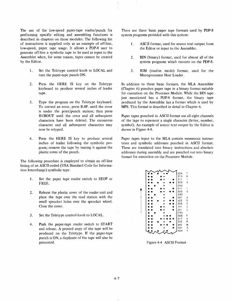
The use of the low-speed paper-tape reader/punch for performing specific editing and assembling functions is described in chapters on those modules. The following list of instructions is supplied only as an example of off-line, low-speed, paper tape usage. It allows a PDP-8 user to generate off-line a symbolic tape to be used as input to the Assembler when, for some reason, tapes cannot be created by the Editor.
1.
2.
3.
4.
Set the Teletype control knob to LOCAL and turn the paper-tape punch ON.
Press the HERE IS key on the Teletype keyboard to produce several inches of leader tape.
Type the program on the Teletype keyboard. To correct an error, press B.SP'. until the error is under the print/punch station; then press RUBOUT until the error and all subsequent characters have been deleted. The erroneous character and all subsequent characters may now be retyped.
Press the HERE IS key to produce several inches of trailer following the symbolic program; remove the tape by tearing it against the plastic cover of the punch.
The following procedure is employed to obtain an off-line listing of an ASCII-coded (USA Standard Code for Informa-tion Interchange) symbolic tape:
l. Set the paper tape reader switch to STOP or FREE.
2. Release the plastic cover of the reader unit and place the tape over the read station with the small sprocket holes over the sprocket wheel. Close the cover.
3. Set the Teletype control kno b to LOCAL.
4. Push the paper-tape reader switch to START and release. A printed copy of the tape will be produced on the Teletype. If the paper-tape punch is ON, a duplicate of the tape will also be generated.
4-7
There are three basic paper tape formats used by PDP-8 system programs provided with this system:
1. ASCII format, used for source text output from the Editor or input to the Assembler.
2. BIN (binary) format, used for almost all of the system programs which execute on the PDP-8.
3. RIM (read-in mode) format, used for the Microprocessor Host Loader.
In addition to these basic formats, the MLA Assembler (Chapter 6) punches paper tape in a binary format suitable for execution on the Processor Module. While the BIN tape just mentioned has a PDP-8 format, the binary tape produced by the Assembler has a format which is used by MPS. This format is described in detail in Chapter 6.
Paper tapes punched in ASCII format use all eight channels of the tape to represent a single character (letter, number, symbol). An example of source text output by the Editor is shown in Figure 44.
Paper tapes input to the MLA contain mnemonic instructions and symbolic addresses punched in ASCII format. These are translated into binary instructions and absolute addresses during assembly and are punched out into binary format for execution on the Processor Module.
• • • • • 324 T
• • • • 310 H
• • • • • 311 I
• • • • • 323 S
• • 240
• • • • • 311 I
• • • • • • 323 S
• • 240
• • • 301 A
• • • • • 323 S
• • • • 303 c • • • • • 311
• • • • • 311
• • 240
• • • • • 306 F
• • • • • • • 317 0
• • • • 322 R
• • • • • • 315 M
• 301 A 324 T
Figure 44 ASCII Format
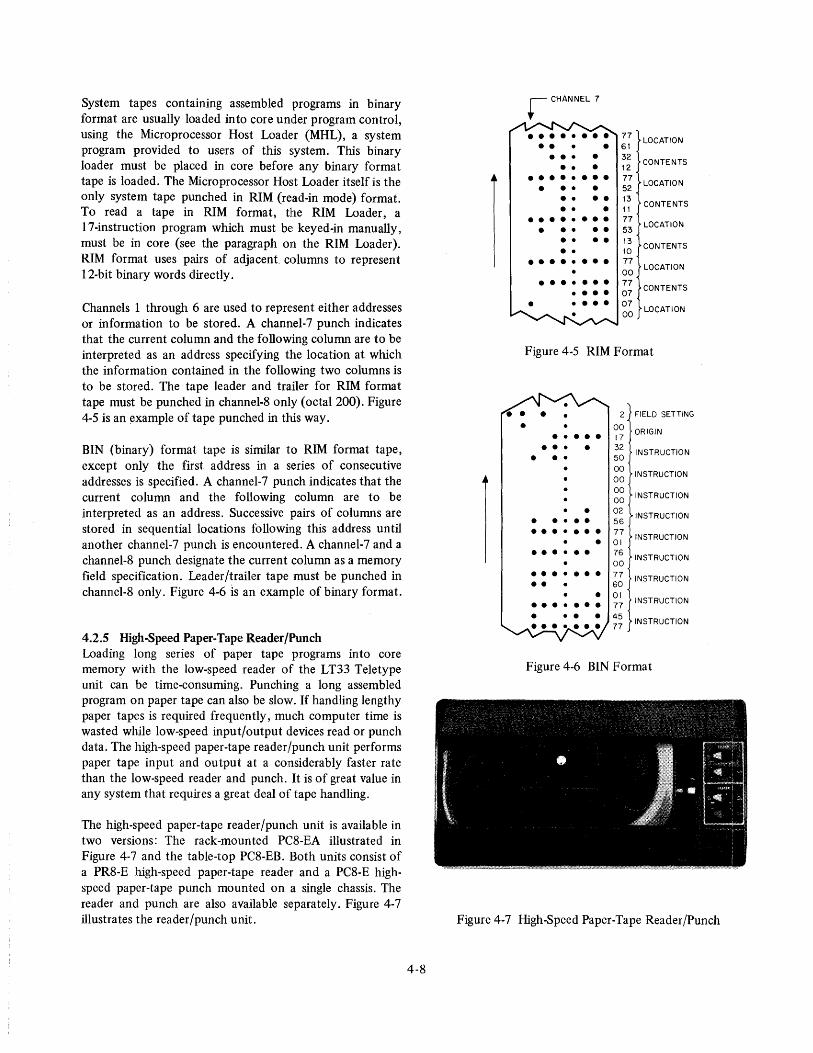
System tapes containing assembled programs in binary format are usually loaded into core under program control, using the Microprocessor Host Loader (MHL) , a system program provided to users of this system. This binary loader must be placed in core before any binary format tape is loaded. The Microprocessor Host Loader itself is the only system tape punched in RIM (read-in mode) format. To read a tape in RIM format, the RIM Loader, a 17-instruction program which must be keyed-in manually, must be in core (see the paragraph on the RIM Loader). RIM format uses pairs of adjacent columns to represent 12-bit binary words directly.
Channels 1 through 6 are used to represent either addresses or information to be stored. A channel-7 punch indicates that the current column and the following column are to be interpreted as an address specifying the location at which the information contained in the following two columns is to be stored. The tape leader and trailer for RIM format tape must be punched in channel-8 only (octal 200). Figure 4-5 is an ~xample of tape punched in this way.
BIN (binary) format tape is similar to RIM format tape, except only the first address in a series of consecutive addresses is specified. A channel-7 punch indicates that the current column and the following column are to be interpreted as an address. Successive pairs of columns are stored in sequential locations following this address until another channel-7 punch is encounten:d. A channel-7 and a channel-8 punch designate the current column as a memory field specification. Leader/trailer tape must be punched in channel-8 only. Figure 4-6 IS an example of binary format.
4.2.5 High-Speed Paper-Tape Reader/Punch Loading long series of paper tape programs into core memory with the low-speed reader of the LT33 Teletype unit can be time-consuming. Punching a long assembled program on paper tape can also be slow. If handling lengthy paper tapes is required frequently, much computer time is wasted while low-speed input/output devices read or punch data. The high-speed paper-tape reader/punch unit performs paper tape input and output at a considerably faster rate than the low-speed reader and punch. It is of great value in any system that requires a great deal of tape handling.
The high-speed paper-tape reader/punch unit is available in two versions: The rack-mounted PC8-EA illustrated in Figure 4-7 and the table-top PC8-EB. Both units consist of a PR8-E high-speed paper-tape reader and a PC8-E highspeed paper-tape punch mounted on a single chassis. The reader and punch are also available separately. Figure 4-7 illustrates the reader/punch unit.
4-8
r CHANNEL 7
77 LOCATION • • • 61
••• • 32
• • • 12 CONTENTS
• • • • • • • • 77 LOCATION • • • • 52
• • • • 13 CONTENTS • • • 11
• ••••••• 77 LOCATION • • • • • 53
• • • • 13
• • 10 CONTENTS
• • • • • • • • 77 LOCATION • 00
• • • • • • • 77 CONTENTS
• • • • 07
• • • • • 07 00
LOCATION
Figure 4-5 RIM Format
• 2 FIELD SETTING
• 00
• • • • • 17 ORIGIN
• • • • 32 INSTRUCTION • • • 50
• 00 INSTRUCTION
00 00
INSTRUCTION 00
• 02 INSTRUCTION • • • • • 56
• •••••• 77 INSTRUCTION • 01
• ••••• 76 INSTRUCTION
00
• •••••• 77 INSTRUCTION •• 60
• 01
• •••••• 77 INSTRUCTION
• • • • 45 INSTRUCTION
77
Figure 4-6 BIN Format
Figure 4-7 High-Speed Paper-Tape Reader/Punch

The high-speed reader accepts input data from eightchannel, fan-folded, non-oiled paper tape alt a maximum rate of 300 characters per second, or thirty times the LT33 maximum input rate. The high-speed punch records output data at a maximum rate of 50 characters per second.
The reader and punch are each supplied with an ON/OFF rocker switch which applies power to the respective units in the ON position and disconnects power in the OFF position. Each device is also provided with a FEED switch which advances the tape without reading, in the case of the reader, or advances tape with only the feed holes punched, in the case of the punch unit. The reader is supplied with a control knob which may be turned clockwise to raise the tape retaining lever and free the tape, or counter-clockwise to lower this lever ang engage the sprocket wheel.
The following procedure is employed to position tapes in the high-speed reader:
1. Turn the control knob to raise the tape retaining lever.
2. Place a fan-folded tape in the right-hand bin.
3. Place several folds of leader in the left-hand bin and position the tape so that the sprocket wheel engages the feed holes.
4. Turn the control knob to lower the tape retaining lever.
5. Press the FEED switch briefly to ensure that the tape is properly positioned.
6. Tape is advanced and read during program execution.
4.3 PDP-8 SOFTWARE ENVIRONMENT The minimum software environment required for convenient and efficient program development, assembly, and duplication is quite limited. The few necessary system programs are designed to be used with ease, and are documented in full detail in this and subsequent chapters. These programs are grouped together in kit form, designated Microprocessor Series Software Tools (MPSST), DEC No. QF500-AB. All software components of MPSST will be provided in the form of binary paper tapes ready to be loaded on the user's PDP-8. Table 4-3 summarizes the binary tapes which compose the minimum necessary PDP-8 software system.
Table 4-3
Program
Microprocessor Host Loader (MHL)
Microprocessor Language Editor (MLE)
Microprocessor Language Assembler (MLA)
Master Tape Duplicator/ Verifier (MTD)
Microprocessor ROM Programmer (MRP)
PDP-8 System Programs
Function DEC Number
Loads binary-coded tapes DEC-08-UMPLA-A-PM
Modifies or generates DEC-08-UMPEA-A-PB source text from Teletype commands by reading and writing paper tapes
Assembles source text DEC-08-UMPAA-A-PB into binary format by reading and writing paper tapes and listing at user's option
Copies paper tapes and DEC-08-UMPDA-A-PB verifies their contents
Copies and modifies paper DEC-08-UMPP A-A-PB tapes and PROMs
4-9

These system programs run on the PDP-8 and are described in greater detail below. Two other programs, the Microprocessor Debugging Program (MDP) (DEC-08-UMPMA-A-PB), and the Microprocessor Program Loader (MPL) are supplied for use on the Processor Module itself and will be described here. MDP is provided in paper tape form; MPL is supplied as part of the MPS hardware. An additional component, the RIM Loader, is also described; thjs Loader is not a binary tape but a series of instructions to be entered manually into the PDP-8 before any of the system paper tapes can be used.
4.3.1 The RIM Loader The RIM (Read-In-Mode) Loader is used to load into core programs punched in RIM format. For purposes of this system, the only program entered in this format is the Microprocessor Host Loader, described here. Unless the PDP-8 being used has a PDP-8/E Hardware Bootstrap Option, the RIM loader must be loaded manually ("toggled"), using the switches located on the programmer's console.
There are two versions of the RIM Loader: one program is designed to be used when tapes are to be loaded from the low-speed (Teletype) paper-tape reader, and the other is intended for input from the high-speed reader. Table 4-4 lists the octal instructions for these programs. The loading and verifying procedures are detailed in the flowcharts in the two figures which follow. After loading RIM, it is good programming practice to verify that all instructions have been entered properly.
Loc ation
56 57 60 61 62 63
77 77 77 77 77 77 7-J 164 77 77 77 77 77 77 77 77 77 77
65 66 67 70 71 72 73 74 75 76
Table 44 RIM Loader Programs
Instruction Low-Speed High-Speed
Reader Reader
6032 6014 6031 6011 5357 5357 6036 6016 7106 7106 7006 7006 7510 7510 5357 5374 7006 7006 6031 6011 5367 5367 6034 6016 7420 7420 3776 3776 3376 3376 5356 5357 0000 0000
4-10
When loaded, the RIM loader occupies absolute locations 7756 through 7776. The following procedures are used to load. (Figure 4-8)
*DECTAPE USERS SHOULD LOAD RIM INTO FIELD 0
SET SWITCHES 6-8 TO DESIRED
INSTRUCTION FIELD*
Figure 4-8 Loading the RIM Loader
To ensure that the load has been successful, follow the steps shown in Figure 4-9.

SET SWITCHES 6-8 TO FIELD IN WHICH RIM HAS BEEN LOADED
Figure 4-9 Checking the RIM Loader
4.3.2 The Microprocessor Host Loader The Microprocessor Host Loader (MHL) is a utility program which is loaded into core to read binary-coded data on paper tape and store it in core memory. MHL is used primarily to load system binary programs.
MHL is stored on punched paper tape in RIM-coded format; therefore, RIM must be in core before MHL can be loaded. When loading MHL, the input device (low-speed or high-speed reader) must be the same as that selected when loading RIM, and RIM and MHL must be loaded into the same field.
Once stored in core, MHL resides on the last page of core, occupying absolute locations 7625 through 7752 and 7777 of the field in which it was loaded. The programmer must be aware that if he writes a program that uses the last page of core, MHL will be destroyed when the program is run,
4-11
and both RIM and MHL will require reloading before another program can be loaded. Figure 4-10 details the method of loading MHL.
The programmer is now able to load binary tapes using the method described in Figure 4-11.
4.3.3 The Microprocessor Language Editor The Microprocessor Language Editor (MLE) provided with this system is a paper tape-oriented source text editor with which the user modifies source program tapes by submitting commands from the Teletype keyboard. Using MLE alleviates the tedious task of preparing source program tapes off-line. This program is described in detail in Chapter 5.
The Microprocessor Language Editor is provided to users of this system in the form of a binary tape which is loaded into core by means of the Microprocessor Host Loader, using either the low-speed or high-speed paper-tape reader. The unit is selected at the time MLE is loaded, as shown in Figure 4-11. MLE itself uses either the low-speed or high-speed paper tape reader/punch for I/O. Text to be modified may be entered into core using either the Teletype or the paper-tape reader. The modified source text may be punched-out using the paper-tape punch. Switch Register bits are set to indicate high-speed input and output (low-speed tape is the default).
4.3.4 The Microprocessor Language Assembler The Microprocessor Language Assembler (MLA) offers a complete instruction set and group of pseudo-instructions for straightforward development and processing of assembly language programs for the Processor Module. For consistency of use and ease of training, the Assembler's character set, available operators, and construction of sta tements, symbols, and expressions conform in many ways to other standard PDP-8 Assemblers. This program is described in detail in Chapter 6.
The Assembler is provided to users of this system in the form of binary tape which is loaded into core by means of the Microprocessor Host Loader, using either the low-speed or high-speed paper-tape reader. The unit is selected at the time MLA is loaded, as shown in Figure 4-11.
The Assembler itself is oriented to the use of paper tape, and uses either the low-speed or high-speed paper-tape reader /punch for I/O. The source program to be assembled is usually prepared using the Microprocessor Language Editor (but can be generated off-line) and is read by the available paper-tape reader. The assembly itself is performed in three passes, each of which produces certain
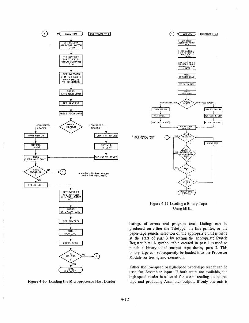
---"T"'""--"
SET SWITCHES 6-8 TO FIELD
WHICH CONTAINS RIM
SET SWITCHES 9-11 TO FIELD IN
WHICH MHL IS TO BE LOADED
---~ SEE FIGURE 4- 81
* = WITH LEADER/TRAILER OVER THE READ HEAD
~L9 SET SWITCHES 6-8 TO FIELD
M H L WAS LOADED INTO
Figure 4-10 Loading the Microprocessor Host Loader
4-12
* . WITH LEADER/TRAILER OVER THE READ HEAD
_-=..;:,---'--../ ----I SEE FIGURE 4-10 I
Figure 4-11 Loading a Binary Tape Using MHL
listings of errors and program text. Listings can be produced on either the Teletype, the line printer, or the paper-tape punch; selection of the appropriate unit is made at the start of pass 3 by setting the appropriate Switch Register bits. A symbol table created in pass 1 is used to
punch a binary-coded output tape during pass 2. This binary tape can subsequently be loaded into the Processor Module for testing and execution.
Either the low-speed or high-speed paper-tape reade'r can be used for Assembler input. If both units are available, the high -speed reader is selected for use in reading the source tape and producing Assembler output. If only one unit is

available, the Assembler will dynamically determine which type of paper-tape reader is to be used. Switch Register bits are set to determine which unit is to be used for punching purposes.
4.3.5 Master Tape DuplicatorNerifier The Master Tape Duplicator/Verifier (MTD) is a system program used to copy and check eight-channel paper tapes using the high-speed paper-tape reader and punch. Installations with a low-speed (Teletype) punch can perform the same function by simply copying and listing off-line, as outlined in the paragraph on the low-speed paper-tape reader /punch.
MTD is provided to users of this system in the form of a binary tape which is loaded into core by means of the Microprocessor Host Loader. Since only installations with a high-speed paper-tape reader punch will be using MTD, the high-speed device will normally be selected at the time the system program is loaded. Once in core, MTD uses all but the last page of memory as a buffer.
Paper tapes are duplicated and verified in three passes as described below:
Pass
1 2 3
Function
Production of the master tape Duplication of the master tape Verification of the duplicated tape
After MTD has been loaded into core, the user performs the following initial procedures:
1. Set the Switch Register to 0200.
2.
3.
4.
Press the ADDR LOAD and START keys; the computer will halt.
Set the Switch Register to 4000.
Place the paper tape to be duplicated in the high-speed paper-tape reader.
5. Turn the paper-tape punch on and feed paper through the punch unit for approximately one length of a fold.
6. Press the CONTinue key.
4:-13
After these procedures have been completed, pass 1 begins. The input tape is read and an output master tape is punched. Because the paper-tape reader is faster than the punch, the reader stops occasionally to allow the punch to catch up. After punching is complete, the following message will be displayed on the terminal:
MASTER CREATED
During pass 1, two types of checksums are accumulated:
1. The number of nonzero characters on the tape.
2. The sum of characters on the tape.
Both sums are computed module 4096 and are punched-out at the end of the master tape.
To begin pass 2, remove the punched master tape from the punch unit and place it in the reader. Prepare the punch unit for another copy by feeding blank tape. Set the Switch Register to 2000 and press the CONTinue key. During this pass, the master tape will be duplicated and a new set of checksums will be accumulated. After the master tape has been duplicated, the following message will be displayed on the terminal:
SET SWITCHES TO NUMBER OF COPIES TO BE MADE - PRESS CONTINUE
If the user wants to generate one master and four copies of his input tape, now he will set the Switch Register to 0003, turn the punch on, ready tape, and press the CONTinue key. After the next copy has been duplicated, MTD will feed several folds of blank tape and then output the following message on the terminal:
PRESS CONTINUE
The user presses CONTinue. MTD produces another copy, feeds several folds of blank tape, and displays the following message:
PRESS CONTINUE
The user presses the CONTinue key. MTD produces another copy and displays the following message:
DUPLICATION OK

Mter all copies have been produced, pass 3 can begin. During this pass, the tape copies are verified by comparing checksums. The user places the "master" tape in the reader, sets the Switch Register to 1000, and presses CONTinue. The master tape will be read and the following message displayed:
0001 VERIFY OK
Next, the user loads the first duplicate tape in the reader and presses CONTinue. After reading the tape, MTD will display the following:
0002 VERIFY OK
The next three duplicate tapes are loaded and verified in turn. The following messages are displayed - one for each tape:
0003 VERIFY OK 0004 VERIFY OK 0005 VERIFY OK
MTD uses the PDP-B program interrupt facility to keep both the paper-tape reader and punch operating at maximum speed. A buffer is filled by the reader and emptied by the punch. Never remove a paper tape from the reader until all punching has stopped or valuable data may be lost from the tape.
The Duplicator does not currently check for extra blank frames in the duplicate tape. If this presents a problem for users of the program, another program can be used for secondary verification. User tapes that are too long for the space left in core should be broken into two or more shorter tapes for this operation. The alternate binary tape and documentation may be ordered from the DECUS Program Library, numbered DIGITAL·5-10-S-BIN.
4.3.6 Microprocessor ROM Programmer The Microprocessor ROM Programmer (MRP) is used to read, write, and verify programmable read-only memory (PROM) chips for use on the MPS modules. PROMs can be
4-14
copied to or from paper tape, and memory locations can be examined, modified, zeroed, or listed. This program is described in detail in Chapter 9.
MRP is provided to users of this system in the form of binary tape which is loaded into core by means of the Microprocessor Host Loader, using either the low-speed or high-speed paper-tape reader: The unit is selected at the time MRP is loaded, as shown in Figure 4-11. Switch Register bits can be set to send selective output to the line printer or to choose the high-speed or low-speed paper-tape punch as the punch unit.
4.3.7 Microprocessor Debugging Program The Microprocessor Debugging Program (MDP) is a debugging aid which runs on the Processor Module, not on the PDP-B. It enables the user to read, modify, and rewrite binary programs in paper tape form. MDP capabilities include the ability to examine memory locations, condition flip-flops, and index registers, to set a breakpoint, and to allow a program segment to execute to that breakpoint. Binary code can be examined, tested, and modified without requiring reassembly on the PDP-B. This program is described in detail in Chapter B.
MDP is provided to users of MPS in the form of an MPS binary tape. It is loaded into module memory by means of the Microprocessor Program Loader (MPL). Input to MDP is normally an MPS binary tape produced by the Microprocessor Language Assembler. MDP produces paper tape and Teletype printer listings as output.
4.3.8 Microprocessor Program Loader The Microprocessor Program Loader (MPL) is a loader which is supplied as part of the Microprocessor Series hardware and is available to users of the KC341 MPS Monitor/Control Panel (MCP). It allows programs to be loaded into MPS memory from paper tape for execution on the module. A paper-tape reader must be available for use with MPL, as well as the MPS Universal Asynchronous Receiver/Transmitter (UART) interface, and read-only and random-access MPS memory. Operation of the loader is described in detail in Chapter 7.

5.1 INTRODUCTION TO THE EDITOR The Microprocessor Language Editor (MLE) provided to users of this system is a PDP-8 based Editor oriented to paper tape usage. I t is interactive and offers an extensive set of commands which can be entered from the Teletype or other terminal keyboard. Primarily it is used as an on-line tool for creating and modifying source program tapes.
The Editor facilitates both program entry and program correction. Source text is either entered directly from the keyboard or read into core using the low-speed (Teletype) or high-speed paper-tape reader. Once in core, the program text can be changed freely, expanded, deleted, or reformatted. At any point, all or some of the source text can be listed on the terminal printer or punched out using one of the paper-tape punches.
MLE is supplied in the form of a paper tape which is loaded into core using the Microprocessor Host Loader (MHL). Precise instructions for loading the Editor are supplied in Paragraph 5.9 of this chapter. The Editor occupies about 1000 locations of core and reserves all but the last page of core for source program use. In a 4K machine, this provides room for approximately 4200 decimal characters; that is about 60 lines of heavily commented text or about 340 lines of text without comments. When the core area (text buffer area) used by the source program is full, the Editor causes the Teletype bell to ring or an audible signal to be produced on another terminal. The buffer may then be enlarged, as described in the Operating Procedures, or the buffer may be dumped by punching it out onto paper tape. After punching, the Editor can be restarted and can continue with a clear text buffer area. If this occurs, it is recommended that the remainder of the source program be placed in Gore and punched out, so that the entire source program is on a single paper tape.
5.2 OVERVIEW OF EDITOR COMMANDS This paragraph summarizes general syntax and err ordetection characteristics of the Microprocessor Language Editor.
5 ·1
CHAPTER 5 MICROPROCESSOR
LANGUAGE EDITOR
5.2.1 General Editor Syntax MLE commands are . entered from the keyboard in the following way:
Form [[m,] n [$j]] command<cr>
The command is a one-character function that directs the Editor to perform a particular operation; commands are preceded by zero, one, two, or three arguments. These arguments, represented by m, n, and j in the syntax, are digits or expressions that specify line numbers in the source text which are affected by the particular MLE function. The , (comma) and $ (dollar sign) symbols in this form represent argument delimiters, and <cr> is the command terminator - usually a carriage return. The user typical1y types the carriage return, and MLE inserts an automatic line feed character. Arguments enclosed in brackets are normally optional, but specific usage depends on the syntax of particular commands.
Table 5-1 provides examples of different forms of Editor commands.
5.2.2 Errors in Specifying Commands A question mark (?) followed by a carriage return/line feed will be displayed on the terminal printer if the user does any of the following:
1. Specifies a nonexistent command; for example, the following is an error:
H ?
because H is not an MLE command.
2. Requests nonexistent information; for example, if the user requests a listing by typing L, and the text buffer is empty, the following will occur:
L ?

3.
4.
Similarly, if certain lines not in the buffer are requested or if negative line numbers are supplied, a question mark will be disp1ayed.
Includes too few arguments; for example, if the user wants to move the first 17 lines of text in the buffer to precede line 100, and types the following:
17$100M ?
the question mark will be printed, because a MOVE command requires two arguments before $, and only one is supplied. The correct format is:
1,17$100M
SpeCifies line numbers in incorrect order; in form:
m,ncommand
m must be less than n; thf:refore the fol1owing specification results in an error condition:
7,5L ?
Whenever a question mark is displayed in this way, the command speCification in which the error occurred is ignored, and the user is free to re-enter the command.
There is one kind of command "error" which does not cause the question mark to be displayed and the command to be ignored. This is the case in which one or more arguments may be supplied for a command which requires no arguments; the following illustrates this incorrect usage:
1,15A
Because the APPEND command takes no arguments, the 1,15 specification will simply be ignored, and the text will be appended as usual.
5.2.3 Line Numbering All lines in the text buffer area are assigned implicit decimal line numbers starting with I. This implicit numbering scheme causes line numbers to be continua11y updated by the Editor to account for line insertions, moves, and deletions. This implies that the line numbers on the following original lines of text may be changed during the editing process.
Implicit Line Number Text
I 2 3 4
AAA BBB DDD EEE
For example, if the following two commands are performed to delete line 4 and insert a new line between 2 and. 3
4D 31 eee
Table 5-1 Editor Command Options
Type of Command Format Example Meaning
No Argument A A Append incoming text to buffer.
One Argument nl 841 Insert incoming text before Hne number 84.
Two Arguments m,nL I,IOOL List text buffer lines I through 100.
Three Arguments m,n$jM 12,20$96M Move lines 12 through 20 to before 1ine number 96.
5-2
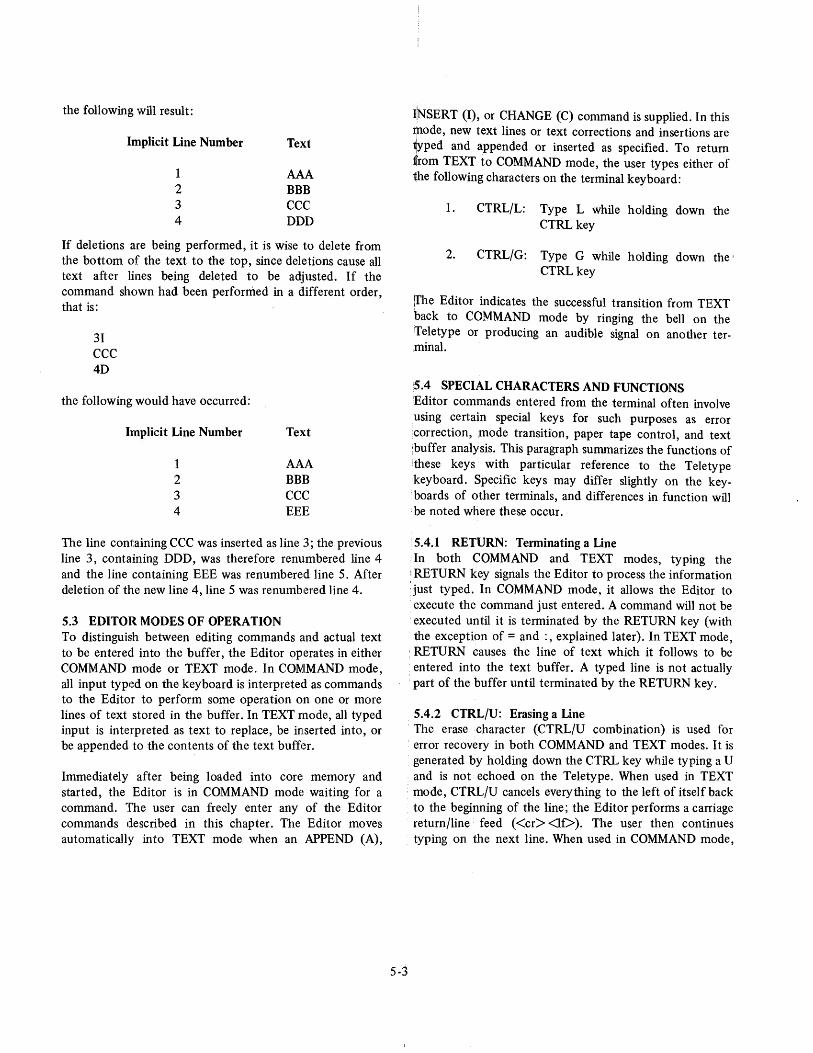
the following will result:
Implicit Line Number
1 2 3 4
Text
AAA BBB CCC DDD
If deletions are being performed, it is wise to delete from the bottom of the text to the top, since deletions cause all text after lines being deleted to be adjusted. If the command shown had been performed in a different order, that is:
31 CCC 4D
the follOWing would have occurred:
Implicit Line Number
1 2 3 4
Text
AAA BBB CCC EEE
The line containing CCC was inserted as line 3; the previous line 3, containing DDD, was therefore renumbered line 4 and the line containing EEE was renumbered line 5. After deletion of the new line 4, line 5 was renumblered line 4.
5.3 EDITOR MODES OF OPERATION To distinguish between editing commands and actual text to be entered into the buffer, the Editor operates in either COMMAND mode or TEXT mode. In COMMAND mode, all input typed on the keyboard is interpreted as commands to the Editor to perform some operation on one or more lines of text stored in the buffer. In TEXT mode, all typed input is interpreted as text to replace, be inserted into, or be appended to the contents of the text buffl~r.
Immediately after being loaded into core: memory and started, the Editor is in COMMAND mode waiting for a command. The user can freely enter any of the Editor commands described in this chapter. The Editor moves automatically into TEXT mode when an APPEND (A),
5-3
INSERT (I), or CHANGE (C) command is supplied. In this t11ode, new text lines or text corrections and insertions are -qyped and appended or inserted as specified. To return £rom TEXT to COMMAND mode, the user types either of the following characters on the terminal keyboard:
1. CTRL/L: Type L while holding down the CTRL key
2. CTRL/G: Type G while holding down the' CTRLkey
[The Editor indicates the successful transition from TEXT back to COMMAND mode by ringing the bell on the ;Teletype or producing an audible signal on another terminal.
:S.4 SPECIAL CHARACTERS AND FUNCTIONS :Editor commands entered from the terminal often involve using certain special keys for such purposes as error correction, mode transition, paper tape control, and text :buffer analysis. This paragraph summarizes the functions of :these keys with particular reference to the Teletype keyboard. Specific keys may differ slightly on the keyboards of other terminals, and differences in function will be noted where these occur.
.5.4.1 RETURN: Terminating a Line ; In both COMMAND and TEXT modes, typing the ; RETURN key signals the Editor to process the information 'just typed. In COMMAND mode, it allows the Editor to . execute the command just entered. A command will not be . executed until it is terminated by the RETURN key (with the exception of = and:, explained later). In TEXT mode, RETURN causes the line of text which it follows to be entered into the text buffer. A typed line is not actually part of the buffer until terminated by the RETURN key.
5.4.2 CTRL/U: Erasing a Line The erase character (CTRL/U combination) is used for error recovery in both COMMAND and TEXT modes. It is generated by holding down the CTRL key while typing a U and is not echoed on the Teletype. When used in TEXT mode, CTRL/U cancels everything to the left of itself back to the beginning of the line; the Editor performs a carriage return/line feed «cr> <If». The user then continues typing on the next line. When used in COMMAND mode,
CTRL/U cancels the entire command; MLE prints a ? and performs a <cr> <If>. The erase character cannot cancel past a <cr> <1£> in either COMMAND or TEXT mode. For example, in COMMAND mode, the CTRL/U character after the A cancels the append command.
A?
In TEXT mode, the CTRL/U is pressed after "THIS" and results in a carriage return. The line containing "THIS" will not be entered in the text buffer.
THIS HERE IS A TEXT MODE EXAMPLE
5.4.3 RUBOUT: Erasing A Character RUBOUT is used for error recovery in both COMMAND and TEXT modes with one exception. When executing a READ command (explained later) from the paper-tape reader, RUBOUTs are ignored completely and are not entered in the buffer. It is necessary for the READ command to disable the RUBOUT function because a1J tab characters on paper tape are, for timing purposes, fo11owed by RUBOUTs; recognition of these characters would cause the tabs to be ignored. RUBOUTs are not stored in the text buffer but are inserted by the Editor fo]]owing a]] tab characters on the output tape.
At any other time, typing the RUBOUT key in TEXT mode echoes a backslash (\) and deletes the last typed character. Repeated RUBOUTs delete from right to left up to but not including the <cr> <If>, which separates the current line from the previous one. For example:
THE QUUICK\ \ \ \ICK BROWN FOX
will be entered in the buffer as:
THE QUICK BROWN FOX
When used in COMMAND mode, RUB OUT is equivalent to CTRL/U and cancels the entire command; the Editor then prints a ?, performs a <cr> <If>, and waits for the user to type another command.
5.4.4 CTRL/L: Entering A Form Feed The form feed character signals the Editor to return to COMMAND mode. A character of this kind is generated by typing L while holding down the CTRL key. This combination is typed while in TEXT mode to indicate that the
5-4
desired text has been entered and that the Editor should now return to COMMAND mode. The Editor rings the Teletype bell or produces an audible signal on another terminal in response to a CTRL/L to indicate that it is back in COMMAND mode. If the Editor is already in COMMAND mode when CTRL/L is typed, no be1J or signal wi11 sound. CTRL/G is equivalent to CTRL/L (except in the case of a SEARCH command, as explained later).
5.4.5 Dot (.): Identifying the Current Line The Editor keeps track of the implicit decimal numbe:r of the line on which it is currently operating. At any given time, the dot, which is produced by typing the period key, represents this number and may be used as an argument in a command. For example:
.L
means list the current line, and
.-I,.+IL
means list the line preceding the current line, the current line, and the line following it; then update the current line counter to the decimal number of the last line printed. The current line counter, represented by the dot, is genera]]y updated as follows:
1.
2.
3.
4.
5.
6.
7.
After a READ or APPEND command, dot is equal to the number of the last line in the buffer.
After an INSERT or CHANGE command, dot is equal to the number of the last line entered.
After a LIST or SEARCH command, dot is equal to the number of the last line listed.
After a DELETE command, dot is equal to the number of the line immediately after the deletion.
After a KILL command, dot is equal to zero.
After a GET command, dot is equal to the number of the Hne printed by the GET.
After a MOVE command, dot is not updated and remains whatever it was before the command.

5.4.6 Slash (/): Identifying the Last Line The slash (/) symbol has a value equal to the decimal number of the last line in the text buffer. It may also be used as an argument in a command. For example:
10,/L
means list from line 10 to the end of the buffer.
5.4.7 LINE FEED: Identifying the Next Une Commands and lines of text are terminated by the RETURN key which generates a carriage return/line feed combination. LINE FEED characters are completely ignored when input is on paper tape. During output, the Editor automatically punches a LINE FEED following each carriage return.
Typing the LINE FEED while in COMMAND mode is equivalent to typing:
. +lL
and will cause the Editor to print the line following the current one and to increment the value of the current line counter (.) by one.
5.4.8 ALT MODE: Incrementing the Curre:nt Line Typing the ALT MODE key while in COMMAND mode will cause the line following the current line to be printed and the current line counter (.) to be incremented by one. If the current line is also the last line in the buffer, typing either ALT MODE or LINE FEED will cause a ? to be typed by the Editor to indicate that there is no n{~xt line. (Some Teletypes and most other terminals have an escape key (ESC) in place of the ALT MODE; the function is identical for both ESCape and ALT MODE.)
5.4.9 Right Angle Bracket (»: Identifying the Next Line Typing the right angle bracket (» while in COMMAND mode is equivalent to typing:
.+lL
and will cause the Editor to echo > and then print the line following the current line. The value of the current line counter is incremented by one so that it refers to the last line printed.
, 5.4.10 Left Angle Bracket «): Identifying the Previous Line Typing the left angle bracket «) while in COMMAND mode is equivalent to typing:
.-lL
and will cause the Editor to echo < and then print the line preceding the current line. The value of the current line counter is decremented by one so that it refers to the last line printed.
5.4.11 Equal Sign (=): Requesting a Value The equal sign is used in conjunction with the line
: indicators dot (.) or slash (/). When typed in COMMAND mode it causes the Editor to print the decimal value of the argument preceding it. In this way the number of the current line may be found (.=xxx), or the total number of 1ines in the buffer (/=xxx) or the number of some particular 1ine (/-8=xxx) may be determined without counting from the beginning .
5.4.12 Colon (:): Requesting a Value Colon is a lower-case character with exactly the same function as the equal sign (=).
5.4.13 Blank Tape and Leader/Trailer Tape: Processing : Paper Tape , Both blank tape and leader/trailer (octal code 200) tape are : completely ignored on an input tape, as are line feed : characters and RUBOUTs. Line feeds and RUBOUTs are : automatically replaced wherever necessary on output, but , blank tape and leader/trailer are not. The production and
processing of paper tape at the terminal is, of course, specific to the Teletype.
5.4.14 CTRL/I: Tabbing Editor Output The Editor simulates tab stops at eight-space intervals across the Teletype paper. The user can tabulate by typing I while holding down the CTRL key. A tabulation consists of from one to eight spaces, depending on the number needed to bring the carriage to the next tab stop. This feature
, facilitates the production of neat columns on output copy.
The tab function is used in conjunction with two Switch Register bits set to allow the user to produce and control tabulations in the text buffer during input and output
, operations (see Paragraph 5.5). On input (under a READ command), the Editor can replace a group of two or more spaces with a tabulation if the user chooses to set bit 0 on.
5-5

On output, it will produce either a tab character followed by a RUBOUT (for timing purposes) or enough spaces to reach a tab stop, depending on the setting of bit L The Editor cannot output tab characters unless tabulations have been entered in the buffer either from the keyboard or by setting bit 0 on input.
NOTE Location 0002 contains the negative (two's complement) of the number of spaces used to simulate tab stops. To change the tabulation, simply change the constant in location 0002 after loading the Editor.
5.5 SWITCH REGISTER OPTIONS The Editor uses five Switch Register bits in conjunction with input and output commands to control the reading and punching of paper tape. Switch Register bits may be set for a variety of reasons including the fo11owing:
1.
2.
To select the low-speed (Teletype) or highspeed paper-tape reader or paper-tape punch
To suppress output operations
3. To select celiain interpretations for tabulation
The selection of the paper tape unit is probablY the most critical of these functions. Natural1y, if a PDP-8 configuration has a terminal device other thlm the Teletype, it is necessary to select the high-speed paper-tape reader and punch. If both high- and low-speed devices are supported, the decision might be more complex. Setting Switch Register options allows the user to select one unit for reading and the other for punching.
It is often desirable to be able to interrupt a command before it finishes. For example, if the user mistakenly supplied a LIST command instead of a PUNCH, he may not want to wait for the terminal to list a large amount of text. Setting bit 2 on the console Switch Register allows the user to interrupt any output command and to return immediately to COMMAND mode. Table 5~2 lists options for all relevant Switch Register bits.
5.6 INPUT COMMANDS Input commands allow source text to be entered into the text buffer area, either from one of the paper-tape readers or from the terminal keyboard. Available input commands are listed in Table 5-3.
5-6
Bit
o
2
10
Table 5-2 Switch Register Options
Setting Meaning
o Read the input tape exactly as is.
o
o
o
Read the input tape and keep track of spaces. Each time two or more successive spaces are found, substitute in the buffer a tabulation for that whole group of spaces; this option affects only the READ command.
On punching (or listing) text from the buffer, interpret tabulations as an appropriate number of spaces.
Interpret tabulations as a tab character followed by a rubout (Teletype codes 211 and 377).
Normal operation; a11 output commands completed as specified.
Suppress list, punch, or si~arch
operation. If at any time during execution of an output command this bit is set to 1, output will cease and the Editor will return immediately to COMMAND mode; if this occurs while a line is being searched, any modifications to the line made during that search will be disregarded; the current line counter (.) will be equal to the number of the line being printed or punched at that time. Until the bit is set to 0, any further output command will be ignored.
Low-speed output; a]] punching will be performed on the Teletype punch.
High-speed output; all punehing will be performed on the high-speed punch.
Bit
11
Table 5-2 (Cont) Switch Register Options
Setting Meaning
o Low-speed input; the READ command expects the source tape to be in the Teletype reader. Do not use the APPEND command to read tapes.
High-speed input; the source tape will be read from the high -speed reader.
Table 5-3 Input Commands
Command Meaning
R
A
nl
Read a page of text and append it to the text buffer using the paper tape unit defined by Switch Register bit 11.
Append text entered from the terminal to the text buffer.
Insert text entered from the terminal before line 1 of the text buffer.
Insert text entered from the terminal before line n of the text buffer.
For all input commands, the Editor is assumed to be in TEXT mode until a form feed characte~r (CTRL/L) is encountered. If CTRL/L is typed or if a full buffer condition occurs, the Editor returns to COMMAND mode.
NOTE In these commands, the Editor ignores ASCII codes 340 through 376. These cod,es include the codes for the lower-case alphabet (ASCII 341-372).
5.6.1 R: Reading Paper Tape The READ command is issued as follows:
Form R
5-7
It is used. to read a page of text from the paper-tape reader. Depending on the position of Switch Register bit 11, reading will be performed on the high-speed (one) or low-speed (zero) reader. MLE will read the input tape until fl form feed character (CTRL/L key combination) is detected or until the Editor senses a text buffer full ,condition. All incoming text except the form feed is :appended to the end of the text buffer. Information :already in the buffer remains there.
.In the case of input from the high-speed reader, the end of ,the tape will be interpreted as a form feed if an actual form Jeed character does not appear on the tape; the Editor will return to COMMAND mode. In the case of input from the ilow-speed reader, a form feed must be entered from the · keyboard to return the Editor to COMMAND mode if an actual form feed character does not appear on the tape. If
'this is not done, the READ command remains in effect, and all subsequent commands will be interpreted erroneously as
· text and appended to the text just read from tape.
· Any RUBOUT encountered during a READ command will be ignored; as described in the discussion of the special Teletype keys.
The appropriate paper-tape reader unit must be turned on and positioned to read at the time the READ command is issued. For the low-speed reader, do the folloWing:
1.
2.
Set the paper-tape reader switch to STOP or FREE.
Release the plastic cover of the reader unit and place the tape over the read station with the small sprocket holes over the sprocket wheel. Close the cover.
3. Push the paper-tape reader switch to START and release.
For the high-speed reader, do the folloWing:
1.
2.
Turn the reader unit on.
Turn the control knob to raise the tape retaining lever.
3. Place a fan-folded tape in the right-hand bin.
4. Place several folds of leader in the left-hand bin and position the tape so that the sprocket wheel engages the feed holes.

5.
6.
Turn the control knob to lower the tape retaining lever.
Press the FEED switch briefly to ensure that the tape is properly positioned.
5.6.2 A: Appending Terminal Text The APPEND command is issued as follows:
Form A
It signals the Editor that the text which is entered next from the terminal keyboard is to be appended to the text already in the buffer. If the buffer is e'mpty at the time the command is issued, a new me is created. This effectively generates a symbolic program on-line by accepting program text from the keyboard. On receiving the APPEND command, MLE enters TEXT mode to accept as much text as the user enters (until the buffer area is ful1). To return to COMMAND mode, a form feed (CTRL/L key combination) is typed.
A RUBOUT character encountered during execution of an APPEND command (i.e., while program text is being entered) will delete the last typed character. Repeated RUBOUTs will delete from right to left up to but not beyond the beginning of the current line.
5.6.3 I: Inserting Text in the Buffer The INSERT command causes text to be read from the terminal keyboard and inserted into the buffer in the specified position. It is issued as follows:
Form [n] I
If a command of the form nl is entered, text from the keyboard will be inserted in the buffer just before the Jine implicitly numbered n. If a simple I command is typed, text will be inserted at the very beginning of the text buffer, just before line 1.
The Editor enters TEXT mode to accept input, and the first line typed becomes the new line n. Both the line count and the numbers of all lines following the insertion are increased by the number of lines inserted; the value of the current line counter (.) is equal to the number of the last line inserted using the I command. To re-enter COMMAND mode, the form feed (CTRL/L combination) must be typed
5-8
terminating TEXT mode. If CTRL/L is not typed, all subsequent commands will be interpreted erroneously as text and entered in the program immediately after the intended insertion. The follOWing example illustrates the use of the INSERT command. The text buffer is assumed to contain the following:
Implicit Line Number
2 3
Text
AAA BBB CCC
The following command is given
31 ABA BAA BAB
To insert text before line 3 and cause the following:
Implicit Line Number Text
1 AAA 2 BBB 3 ABA 4 BAA 5 BAB 6 CCC
Next, the following command causes two lines of text to be inserted before the old line 1:
I AAO AOA
Implicit Line Number
1 2 3 4 5 6 7 8
Text
AAO AOA AAA BBB ABA BAA BAB CCC

5.7 OUTPUT COMMANDS Output commands are available for both listing and punching purposes. Both kinds of commands provide for the output of part or a11 of the contents of the text buffer. LIST commands facilitate examining the text by producing output on the terminal keyboard. PUNCH commands output leader and trailer tape, form feeds, corrected text, or duplication of pages of an input tape on the paper-tape punch. Neither LIST nor PUNCH commands affect the contents of the buffer in any way. All listing opera tions can be interrupted by setting Switch Register bit 2 on.
5.7.1 L: Listing on the Terminal Printer The LIST command causes part or all of the contents of the text buffer to be listed on the terminal. A LIST command is constructed as follows:
Form [[m,] n] L
where m and n are optional arguments as defined in Table 5-4, which summarizes different forms of the LIST command:
Command
L
nL
m,nL
Table 5-4 LIST Commands
Meaning
List the entire page; this causes the Editor to list the entire contents of the text buffer on the terminal.
List line n; this line will be printed followed by a carriage return and a line feed.
List lines m through n inclusive (m must be less than n); lines m through n will be printed on the terminal.
The Editor remains in COMMAND mode after a LIST command and the value of the current line counter is updated to be equal to the number of the last line printed. Some examples of the LIST command might be helpful. The contents of the text buffer at the time the commands are issued as follows:
Implicit Line Number
1 2 3 4
Text
AAA BBB CCC DDD
5-9
The following illustrates interspersed command input and text output as in actual terminal interactions:
2L BBB 1,3L AAA BBB CCC L AAA BBB CCC DDD
5.7.2 P: Punching Out Paper Tape The PUNCH command causes part or all of the contents of the text buffer to be punched-out using either the low-speed or high-speed paper-tape punch. The device selection depends on the setting of Switch Register bit 10 at the time the PUNCH is issued. If bit lOis set on, the high-speed device is used; otherwise the Teletype punch is selected.
The PUNCH command is constructed as follows:
Form [[m,]n]P
where m and n are optional arguments as defined in Table 5-5, which summarizes different forms of the PUNCH command. This table also illustrates utility commands used for punching purposes.
Command
P
nP
m,nP
F
T
Table 5-5 PUNCH Commands
Meaning
Punch the entire contents of the text buffer using the punch unit defined by Switch Register bit 10.
Punch line n only.
Punch lines m through n inclusive (where m must be less than n).
Punch four blanks, a form feed character, and approximately two inches of leader /trailer tape.
Punch four inches of leader/trailer tape.

Table 5-5 (Cont) PUNCH Commands
Command Meaning
N Punch the entire contents of the text buffer, issue a FORM FEED command, erase the contents of the text buffer, and read a new page of text into the text buffer using the appropriate paper-tape reader unit (perform P, F,K,and R).
nN Perform P, F, K, and R n times in sequence.
Because the appropriate paper-tape punch unit must be readied before tape is punched, the Editor will cause the computer to be temporarily halted when a PUNCH is supplied. After the unit has been readied, the user should press the CONTinue key on the console to cause punching to begin.
To position tape in the low-speed punch, do the fol1owing:
1. Turn the Teletype control knob to LOCAL.
2. Turn the punch unit on.
3. Press the HERE IS key on the Teletype to p~oduce several inches of reader tape.
4. Turn the punch off.
5. Turn the Teletype control knob to LINE.
6. Turn the punch unit on.
For the high-speed punch, do the following:
1. Turn the punch unit on.
2. Press the FEED switch briefly to ensure that the tape is properly positioned; this switch will advance the tape with only its feed holes punched.
5-10
The Editor remains in COMMAND mode after a punching operation, and the value of the current line counter is updated to be equal to the number of the last line punched. PUNCH commands do not cause a form feed character to be output following the text. An explicit form feed' must be supplied using the F command.
MLE is designed to minimize the possibility of illegal or meaningless characters being punched into a source tape; therefore the illegal codes 340-376 and 140-177 and most illegal control characters will not be punched. This provides a means of correcting a tape containing illegal characters by simply reading this tape using the Editor and by subsequently punching it out.
5.7.3 F: Punching a Form Feed The FORM FEED command is issued as follows:
Form F
and is used to punch the following on a paper tape, using either the high-speed or low-speed unit.
1. Four blanks.
2. A form feed character.
3. Approximately two inches of blank tape.
The Editor does not cause the computer to halt when a FORM FEED command is encountered. To avoid the insertion of extraneous characters on the paper tape when the low-speed paper-tape punch has been selected, the user should follow this sequence when issuing a FORM FEED command:
1 . Turn the punch off.
2. Type F followed by RETURN.
3. Turn the punch on.
5.7.4 T: Punching a Paper Tape Trailer The TRAILER command is issued as follows:
Form T
and is used to punch a paper-tape trailer consisting of approximately four inches of blank tape on either the high-speed or low-speed unit.

The Editor does not cause the computer to halt when a TRAILER command is encountered. To avoid inserting extraneous characters on the paper tape when the lowspeed paper-tape punch has been selected, the user should follow this sequence when issuing a TRAILER command:
1. Turn the punch off.
2. Type T followed by RETURN.
3. Turn the punch on.
5.7.5 N: Combining P, F, K, and R Commands The NEXT command is a utility command which is used to read in the next page of text from paper tape one or more times by combining the functions of four distinct MLE commands. It is issued as follows:
Form nN
and performs the functions of the four commands in Table 5-6 in sequence.
Command
PUNCH
FORM FEED
KILL
READ
Table 5-6 NEXT Command Functions
Function
Punch the entire contemts of the text buffer using the punch unit defined by Switch Register bit 10.
Punch four blanks, a form feed character, and approximately two inches of blank tape.
Erase the contents of the text buffer.
Read a page of text into the text buffer using the reader unit defined by Switch Register bit 11.
If a simple N command is given, this sequence will be performed only once. If nN is supplied, the sequence will be performed n times.
Because the appropriate paper-tape punch unit must be readied before tape is punched, MLE will cause the computer to be temporarily halted when a NEXT is supplied. After the unit has been readied, as just described,
the user should press the CONTinue key on the console. If !an nN command is given, the halt will occur only before the !first cycle. If n is greater than the number of pages of input tape, the commands will proceed in the speCified sequence until the end of the input tape is read. The Editor will then return to COMMAND mode if the unit being used is the high-speed punch. If the Teletype unit has been selected, the user must type CTRL/L to return to COMMAND mode when the tape runs out.
· 5.8 EDITING COMMANDS Editing commands allow source text to be deleted,
· changed, moved, and expanded in the text buffer. In · addition to standard replacement and deletion features, the 'Editor described in this chapter facilitates such advanced
5 -11
editing features as moving a block of text from one part of the buffer to another or searching the text buffer for specific characters or for lines containing tags.
5.8.1 C: Changing Lines in the Text Buffer The CHANGE command allows the user to replace one or more lines in the buffer with text entered on the terminal keyboard. It is issued as follows:
Form [m,] nC
where m is optional and n is a required argument, supplied as shown in Table 5-7.
Command
nC
m,nC
Table 5-7 CHANGE Commands
Meaning
Delete line n and replace it with the line(s) that follow.
Delete lines m through n and replace them with the lines that follow (m must be less than n).
When the Editor receives a CHANGE command, it deletes the speCified lines and then enters TEXT mode to accept text typed by the user to replace the deleted line(s).
Once in TEXT mode, RUBOUTs can be used to erase characters in the inserted text. It is not necessary to replace the changed text with the same number of lines that were deleted. Since lines are automatically renumbered, the user may enter any number of new lines to replace the old. The

line count will automatically be updated. In addition, after a CHANGE has been performed, the value of the current line counter (.) is equal to the number of the last line of the inserted text.
An example of changing text in the buffer might be helpful. If the contents of the buffer are as follows:
Implicit Line Number Text
1 2 3 4
typing the command:
2C Bll B22 B33
will result in the following:
Implicit Line Number
The next command:
4,6C BBB
causes the following:
1 2 3 4 5 6
Implicit Line Number
2 3
4
AAA BBB CCC DDD
Text
AAA Bl1 B22 B33 CCC ODD
Text
AAA B11 B22 BBB
To return to COMMAND mode after replacing text with the CHANGE command, the user types a form feed (CTRL/L) to terminate input from the keyboard.
5 -12
5.8.2 D: Deleting Lines of Text The DELETE command causes the deletion of one or more lines of text in the buffer. It is issued as follow~:
Form [m,]nD
where m is optional, and n is a required argument, supplied as shown in Table 5-8.
Command
nD
m,nD
Table 5-8 DELETE Commands
Meaning
Delete line n.
Delete lines m through n (m must be less than n).
When the Editor has performed the specified deletion, it automatically renumbers all succeeding lines reducing their implicit numbers by the number of lines deleted. When a command of the form
m,nD
is performed, the line following n becomes the new line m, and the rest of the lines are renumbered accordingly.
FollOWing is an example of deletion of text in the buffer:
Implicit Line Number Text
1 AAA 2 BBB 3 CCC 4 DDD
The command:
2,3D
changes the text buffer to the following:
Implicit Line Number Text
1 2
AAA DDD

5.8.3 G: Getting a Tagged Line The GET command is used to locate the next line in the text buffer with a tag associated with it. It is issued as follows:
Form [nl G
If a simple G command is supplied, the Editor begins the search for the next tagged line with the line following the current line (the value of the current line counter). If the optional argument precedes the G, the search begins at line n, testing it and each succeeding line. The line which first passes the test will be printed on the terminal by the Editor.
A tagged line is defined as one which does not begin with a tab, slash, or space character. Usually such lines begin with tags or labels, but lines not indented will also pass the test. For example:
Sample GET commands, with the initial line counter at line 5, are given below:
IG VERI, LMA G VER2, JFZ VERI G ?
5.8.4 K: Killing the Text Buffer The KILL command causes the entire page in the text buffer to be erased. It is issued as follows:
Form K
The values of special characters / (last line in buffer) and. (current line counter) are set to zero. The Editor remains in COMMAND mode after the buffer has been erased.
LAB This is the current line. INP2
/THIS IS A COMMENT HERE, LMA This line will be printed by GET.
RAR JFZ HERE
*20#377 This line will be printed next if another GET is entered.
If the GET command succeeds in finding a tagged line, the current line counter is updated. However, if the GET reaches the end of the buffer without finding a tagged line, the current line counter (i.e., the value of the line counter before the GET was issued) is preserved. A question mark (?) is typed on the terminal to indicate that tests were not successful. The Editor remains in COMMAND mode after all GET operations.
The following is the current text -buffer:
Implicit Line Number Text
I LAB 2 INP2 3 /OLD VERS][ON 4 VERI, LMA 5 RAR 6 VER2, JFZ VERI 7 HLT
5 -13
5.8.5 M: Moving Text in the Buffer The MOVE command is used to move a line or lines from one location in the text buffer to another. It is issued as follows:
Form m,n$jM
where m, n, and j are all required arguments. The MOVE command causes text buffer lines m through n inclusive to be moved to the position just before line j. The user must ensure that m is less than n. After the MOVE is complete, lines are renumbered but the value of the current line counter (.) is not changed.
The following example:
I,IO$20M
causes lines I through 10 to be moved to just before line 20. If the user wishes to move a single line to a new
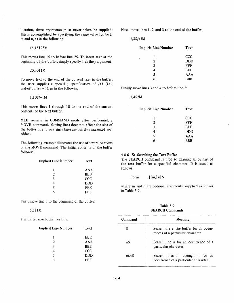
location, three arguments must nevertheless be supplied; this is accomplished by specifying the same value for both m and n, as in the following:
15,15$25M
lbis moves line 15 to before line 25. To insert text at the beginning of the buffer, simply specify 1 as the j argument:
20,30$IM
To move text to the end of the current text in the buffer, the user supplies a special j specification of /+1 (i.e., cnd-of-buffer + 1), as in the following:
1,10$/+IM
This moves lines 1 through 10 to the end of the current contents of the text buffer.
MLE remains in COMMAND mode after performing a MOVE command. Moving lines does not affect the size of the buffer in any way since lines are merely rearranged, not added.
The following example illustrates the use of several vers:ions of the MOVE command. The initial contents of the buffer follows:
lmplicit Line Number Text
1 AAA 2 BBB 3 CCC 4 DDD 5 EEE 6 FFF
First, move line 5 to the beginning of the buffer:
5,5$IM
The buffer now looks like this:
Implicit Line Number Text
1 EEE 2 AAA 3 BBB 4 CCC 5 DDD 6 FFF
5-14
Next, move lines 1, 2, and 3 to the end of the buffer:
1,3$/+IM
Implicit Line Number Text
1 CCC 2 DDD 3 FFF 4 EEE 5 AAA 6 BBB
Finally move lines 3 and 4 to before line 2:
3,4$2M
Implicit Line Number Text
1 CCC 2 FFF 3 EEE 4 DDD 5 AAA 6 BBB
5.8.6 S: Searching the Text Buffer The SEARCH command is used to examine all or part of the text buffer for a specified character. It is issued as follows:
Form [[m,] n] S
where m and n are optional arguments, supplied as shown in Table 5-9.
Command
S
nS
m,nS
Table 5-9 SEARCH Commands
Meaning
Search the entire buffer for all oceurrences of a particular character.
Search line n for an occurrence of a particular character.
Search lines m through n for an occurrence of a particular character.

The SEARCH command is very different from the MLE commands already discussed in this manual. It is far more interactive and therefore facilitates far more complex editing operations.
The SEARCH command string itself does not specify the character for which the Editor is to search. That character must be entered after the command, terminated by a RETURN key, has been typed. No searc:h operations will begin until a character is typed; MLE will simply halt waiting for input. The user is expected to type a single character as the object of the search, but the typed character will not be echoed. Instead, the Editor will respond either by typing a question mark (?) to indicate that the desired character cannot be found in the speCified line or lines, or by supplying part of the first line encoun tered which contains the specified character, from the first character in the line to the position where the specified character occurred.
An example may be helpful. Assume that line 10 contains AB**N&&:
lOS AB*
In this example, the user requested a search of line 10 for the asterisk character (*) entered in the place where A appears. The * is not echoed, but the Editor locates that character in line 10 and types out line 10 from the beginning to the position in which * occurs. At this point, the user may choose one of many options which affect the selected line or the text in the rest of the buffer. These options are listed in Table 5-10.
The options shown in Table 5-10 apply particularly to the nS form of the SEARCH command. In almost all cases, however, they are applicable to the other command formats as well. If the follOWing form:
m,nS
is used, indicating a search in lines m through n inclusive, one major difference occurs. If RETURN is typed in . response to the Editor's display of the search character line, . the entire unprinted portion of the line is deleted and the line is terminated. However, the search will continue on the next line.
By typing CTRL/G to change search characters, all editing of a single line may be performed in one pass. Typing CTRL/G twice will cause the search to terminate since the search character will now be BELL, which is not stored in the buffer.
5 -15
Option
CTRL/U
RETURN
RUBOUT (\)
character( s)
LINE FEED
CTRL/L
CTRL/G character
Table 5-10 SEARCH Options
Action
Delete the entire printed portion of the line with the CTRL/U (erase) character. This preserves the unprinted portion of the line. A carriage return/ line feed character is automatically generated.
Delete the entire unprinted portion of the line, and terminate the search. MLE resumes in COMMAND mode.
Delete one character from right to left for each RUBOUT typed; only printed characters are affected.
Insert typed character(s) after the last printed character.
Insert a carriage return/line feed character between the printed and unprinted portions of the line.
Continue the search to the next occurrence of the specified character; when the next line portion has been printed, all options are available again.
Change the search character to character and continue the search to the first occurrence of this character.
Specifying a simple S command causes the entire buffer to be searched for occurrences of a single search character. It should be remembered, however, that as with CHANGE, every SEARCH command uses additional buffer space for storage of the new line. This is necessary, since the program can have no prior knowledge of whether the size of the line will be . less than, greater than, or equal to that of the old line, and it must therefore assume that it will be greater. The entire text buffer is searched and a new image of this text is created in core; it is guaranteed to occupy the same space as before, or somewhat less, since all deleted spaces have been removed. The only prerequisite to condensing the text image is that there be enough core space left to contain another image of the edited text. The options available in a simple S specification are exactly the same as those for the m,nS version of the command.
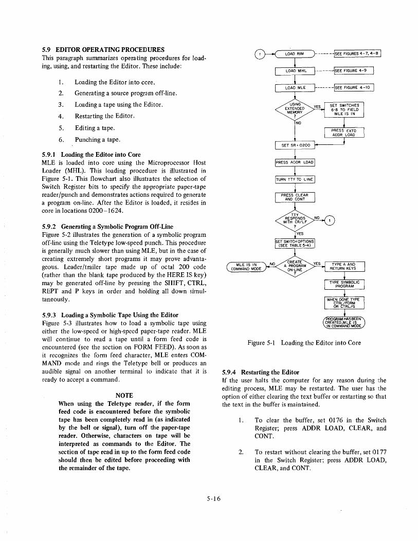
5.9 EDITOR OPERATING PROCEDURES This paragraph summarizes operating procedures for loading, using, and restarting the Editor. These include:
1.
2.
Loading the Editor into core.
Generating a source program off-line.
3. Loading a tape using the Editor.
4. Restarting the Editor.
5. Editing a tape.
6. Punching a tape.
5.9.1 Loading the Editor into Core MLE is loaded into core using the Microprocessor Host Loader (MHL). This loading procedure is illustrated in Figure 5-1. This flowchart also illustrates the selection of Switch Register bits to specify the appropriate paper-tape reader/punch and demonstrates actiom; required to generate a program on-line. After the Editor is, loaded, it resides in core in locations 0200-1624.
5.9.2 Generating a Symbolic Program Off-Line Figure 5-2 illustrates the generation of a symbolic program off-line using the Teletype low-speed punch. This procedure is generally much slower than using MLE, but in the case of creating extremely short programs it may prove advantageous. Leader/trailer tape made up of octal 200 code (rather than the blank tape produced by the HERE IS key) may be generated off-line by pressing the SHIFT, CTRL, REPT and P keys in order and holding all down simultaneously.
5.9.3 Loading a Symbolic Tape Using the Editor Figure 5-3 illustrates how to load a symbolic tape using either the low-speed or high-speed paper-tape reader. MLE will continue to read a tape until a form feed code is encountered (see the section on FORM FEED). As soon as it recognizes the form feed character, MLE enters COMMAND mode and rings the Teletype bell or produces an audible signal on another terminal to indicate that it is ready to accept a command.
NOTE When using the Teletype reader, if the form feed code is encountered before the symbolic tape has been completely read in (as indicated by the bell or signal), turn off the paper-tape reader. Otherwise, characters on tape will be interpreted as commands to the Editor. The section of tape read in up to the form feed code should then be edited before proceeding with the remainder of the tape.
5 -16
MLE IS IN COMMAND MODE
'-------r----'
'------r----'
-----1SEE FIGURES 4-7. 4-~
------1SEE FIGURE 4-9 ]
un - -1 SEE FIGURE 4 -IC~
Figure 5-1 Loading the Editor into Core
5.9.4 Restarting the Editor If the user halts the computer for any reason during the editing process, MLE may be restarted. The user has the option of either clearing the text buffer or restarting SOl that the text in the buffer is maintained.
1. To clear the buffer, set 0176 in the Switch Register; press ADDR LOAD, CLEAR, and CaNT.
2. To restart without clearing the buffer, set 0177 in the Switch Register; press ADDR LOAD, CLEAR, and CaNT.

Figure 5-2 Generating a Symbolic Program Off-Line
3. Set 0200 in the Switch Register.
4. Press ADDR LOAD, CLEAR, and CONT.
This has the effect of restarting the Editor in COMMAND mode.
5.9.5 Editing the Source Program Actual editing procedures depend, of course, on the particular programs being created or modified. A general approach is illustrated in the example presented in Paragraph 5.10. For input, editing, and output commands to the Editor, refer to the specific paragraphs just discussed. Also observe the following operating notes and precautions:
1. Terminate each command to the Editor by typing the RETURN key. This directs MLE to execute the command.
5~1 7
NO TAPE READS IN
?
'------;;----" -------1SEE FIGURE 5-11
Figure 5-3 Loading a Symbolic Tape Using the Editor
2.
3.
After a command to insert, change, or append text to a symbolic program has been executed, MLE remains in TEXT mode until the operator types CTRL/L on the terminal. This genera tes the form feed code, which tells the Editor to return to COMMAND mode.
The Editor senses a buffer full condition (buffer capacity is approximately 60 lines of commented text or 340 lines of uncommented text) when, after completing input of a text line, it finds that characters have been packed in the last 128 locations in the text buffer. When this condition occurs, MLE rings the Teletype bell or produces an audible signal on another terminal five times and exits to COMMAND mode. The user then has a choice of deleting text and continuing editing as usual, or attempting to input more than 200 additional characters. After each line, the buffer full alarm will precede a return to COMMAND mode. When no more characters can be packed, the Editor will again output the alarm five times and will exit from the input routine. Any further attempts to input text will be answered in the same manner until deletions have made room for text input. Although characters are received through the input device, they probably will not be appended as text.
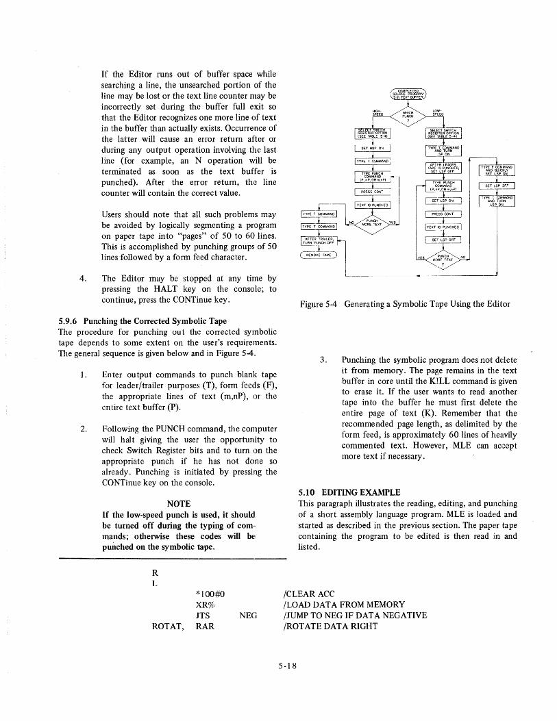
4.
If the Editor runs out of buffer space while searching a line, the unsearched portion of the line may be lost or the text line counter may be incorrectly set during the buffer full exit so that the Editor recognizes one more line of text in the buffer than actually exists. Occurrence of the latter will cause an error return after or during any output operation involving the last line (for example, an N operation will be terminated as soon as the text buffer is punched). After the enor return, th,~ line counter will contain the correct value.
Users should note that all such problems may be avoided by logically segmenting a program on paper tape into "pages" of 50 to 60 lines. This is accomplished by punching groups of 50 lines followed by a form feed character.
The Editor may be stopped at any time by pressing the HALT key on the console; to continue, press the CONTinue key.
5.9.6 Punching the Corrected Symbolic Tape The procedure for punching out the corrected symbolic tape depends to some extent on the user's requirements. The general sequence is given below and in Figure 5-4.
1. Enter output commands to punch blank tape for leader/trailer purposes (T), form feeds (F), the appropriate lines of text (m,nP), or the entire text buffer (P).
2. Following the PUNCH command, the computer will halt giving the user the opportunity to check Switch Register bits and to turn on the appropriate punch if he has not done so already. Punching is initiated by pressing the CONTinue key on the console.
NOTE If the low-speed punch is used, it should! be turned off during the typing of com·· mands; otherwise these codes will bf! punched on the symbolic tape.
R L
*100#0 XR% JTS NEG
ROTAT, RAR
L TYPE F COMMAND
AND QUICKLY SET LSP ON
r: ~LSP~
1::: I TYPE T eo'UMAND
ANCI TunN LSP ot!
Figure 5-4 Generating a Symbolic Tape Using the Editor
3. Punching the symbolic program does not ddete it from memory. The page remains in the text buffer in core until the KILL command is given to erase it. If the user wants to read another tape into the buffer he must first delete the entire page of text (K). Remember that the recommended page length, as delimited by the form feed, is approximately 60 lines of heavily commented text. However, MLE can ac,~ept
more text if necessary.
5.10 EDITING EXAMPLE This paragraph illustrates the reading, editing, and punching of a short assembly language program. MLE is loaded and started as described in the previous section. The paper tape containing the program to be edited is then read :in and listed.
/CLEAR ACC /LOAD DATA FROM MEMORY /JUMP TO NEG IF DATA NEGATIVE /ROTATE DATA RIGHT
5 -18
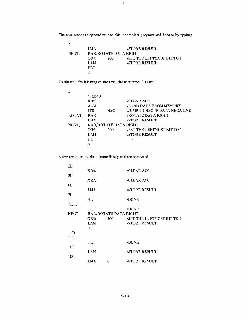
The user wishes to append text to this incomplete program and does so by typing:
A LMA /STORE RESULT
NEGT, RAR/ROTATE DATA RIGHT OR% 200 /SET THE LEFTMOST BIT TO 1 LAM /STORE RESULT HLT $
To obtain a fresh listing of the text, the user types L again:
L *100#0 XR% /CLEAR ACC ADM /LOAD DATA FROM MEMORY JTS NEG /JUMP TO NEG IF DATA NEGATIVE
ROTAT, RAR /ROTATE DATA RIGHT LMA /STORE RESULT
NEGT, RAR/ROTATE DATA RIGHT OR% 200 /SET THE LEFTMOST BIT TO 1 LAM /STORE RESULT HLT $
A few errors are noticed immediately and are corrected.
2L
2C
6L
71
7,l1L
NEGT,
lID 111
10L
10C
XR% /CLEARACC
XRA /CLEAR ACC
LMA /STORE RESULT
HLT /DONE
HLT /DONE RAR/ROTATE DATA RIGHT OR% 200 /SET THE LEFTMOST BIT TO 1 LAM /STORE RESULT HLT
HLT /DONE
LAM /STORE RESULT
LMA 0 /STORE RESULT
5-19
The user decides that the program is ready for assembly and formats the output tape in the following way:
P F T
This produces the text of the program followed by a form feed, followed by a trailer. The computer halts after the PUNCH command is issued and wa.its for the paper-tape unit to be readied. When this has been performed, the CONTinue key on the console must be pressed.
Message Statement
AD AT 00 000 *100#0
IC 245 AT 00 010 OR%
OA AT 00 011 LMAO
US NEG AT 00 002
The first assembly of this program produces the following error messages on pass 1. See Chapter 6 for detailed descriptions of all statement syntax and errors.
AD IC 245 OA US NEG
AT 00 000 AT 00 010 AT 01 011 AT 00 002
Addresses in AT specifications are given in octal offsets within blocks. These messages can be matched to source statements as follows:
Meaning
Address specified in origin is out of range. Maximum block-offset is 77#377; origin is set to zero so the addresses in the rest of the program are not affected.
Illegal character (%) is not recognized by the Assembler. ASCII representation of % (245) is supplied; ORI was simply misspelled.
Operand error; LMA load instruction does not take an operand and 0 is supplied.
Undefined address. No NEG label can be found in the program; statement with label NEGT is probably in erroT.
The program can now be corrected as follows:
lL *100#0
IC *35#40
G ROTAT, RAR 6G
/ROTATE DATA RIGHT
NEGT, RAR/ROTATE DATA RIGHT
8 8C NEG, 1,12S
9 9C
RAR
OR%
ORI
/ROTATE DATA RIGHT
200 /SET THE LEFTMOST BIT TO 1
200 /SET THE LEFTMOST BIT TO 1
5-20

A few commands require explanation. The interaction:
1,12S OR%
does not show the typing of the search character, the %. The user types % right after the carriage return following
L *35·#40 XRA ADM JTS NEG
ROTAT, RAR LMA HLT
NEG, RAR ORI 200 LMA HLT $
The program is then punched-out for assembly and the text buffer cleared for subsequent use.
P F T K
1,12S, but this character is not echoed. To return to COMMAND mode after the line is found and the string OR% printed, the user types CTRL/L. The .t: command requests, in two cases, that the decimal number of the current line be printed so that it can be changed. Then, the user verifies that all corrections have been made by listing the entire program.
/CLEAR ACC /LOAD DATA FROM MEMORY /JUMP TO NEG IF DATA NEGATIVE /ROTATE DATA RIGHT /STORE RESULT /DONE /ROT ATE DATA RIGHT /SET THE LEFTMOST BIT TO 1 /STORE RESULT /DONE
5-21


6.1 INTRODUCTION TO THE ASSEMBLER The Microprocessor Language Assembler (MLA) is a powerful paper tape-oriented system program which is used to assemble source code on the PDP-8 into binary output which is loaded and executed on the Processor Module. Input to the Assembler is usually prepared with the aid of the PDP-8 Microprocessor Language Editor (MLE) described in Chapter 5; it can also be generated off-line. The Assembler expects all input to be in paper tape form, and reads input tapes, dynamically' selecting the high-speed paper-tape reader. If a high-speed device is not part of the system configuration, the Assembler reads from the low-speed reader associated with the Teletype. At the user's option, assembled code can be output in punched paper tape form or can be listed on the terminal printer. Diagnostic messages are displayed to indicate errors in syntax, warnings, or actions taken by the Assembler.
The Assembler operates in three passes to produce binary code suitable for testing and executing on the Microprocessor Series, and outputs a variety of program, diagnostic, and symbol table listings. The lPDP-8 therefore serves as the host computer for the preparation and development of executable code. In an effort to aid those who have used other PDP-8 Assemblers, such as PAL III, MLA has been designed to conform to such existing Assemblers in terms of its character set, error messages, available operators, and construction of statements, symbols, and expressions whenever possible.
6.2 OVERVIEW OF THIS CHAPTER Information necessary for developing and assembling programs for the Microprocessor Series is presented in this chapter and structured as a series of seven major topics:
1. Character set, including use of numbers and symbols.
6-1
CHAPTER 6
MICROPROCESSOR
LANGUAGE ASSEMBLER
2. Language syntax, focusing on construction of statements and use of instructions, operators, and expressions.
3. Internal Assembler characteristics, including mapping of memory and use of tables.
4. Instruction set comprising index register, accumulator, program-counter, stack-control, input/output, and machine instructions.
5. Pseudo-instructions used to assign values to storage, to indicate end of program or tape, to define operation codes, and to perform other Assembler functions.
6. Operating instructions necessary to load the Assembler and the source program, to run and restart the Assembler, and to define desired output.
7. Error messages produced during assembly, with suggested possible reasons for occurrence.
This information, when supplemented by specific details of Editor (Chapter 5) and Loader (Chapter 7) usage, should provide the necessary background for developing source programs and preparing them for execution on the target module.
6.3 BASIC CHARACTER SET This paragraph defines the set of characters allowed in Assembler input, defines special characters used for paper tape or listing control, and describes construction of numbers and symbols.
6.3.1 Legal Source Text Characters The following list summarizes all characters that may be included in a source program and are accepted by the Assembler:
• Alphabetic characters A through Z
• Numeric characters 0 through 9
• Selected special (printing) ,;haracters, such as:
Character Meaning
•
•
Space +
Space Plus Minus
&
t
$
/ < > * #
Label terminator Is replaced by Logical AND Logical OR High byte-selection operator Data separator End of source program Current value of location counter Comment initiator
{Used to enclose numeric representation of ASCII character Used to reset location counter Block-offset operator
Selected special (nonprinting) characters, such as:
TAB Carriage return Form feed
Ignored characters, often produced by the editor, such as:
Blank tape RUBOUT Leader /trailer (octal code 200) Line feed
Characters other than those listed above may be included in an assembly language source program only when included after a comment character (/) or within a TEXT literal. The presence of an illegal character in A8sembler code causes
6-2
the following message to be displayed during Assembler pass 1:
IC xxx AT yy zzz
where IC identifies this as an illegal character message, xxx is the ASCII value of the illegal character, and yy zzz is the address at which the error was encountered, in block-off~,et notation. This message causes the illegal character and the rest of the current line to be ignored while assembly proceeds. If an illegal character is detected in a symbol, however, the symbol is assumed to terminate at the position where the illegal character occurred.
6.3.2 Format Control Certain keys on the terminal may be used to affect the format of an Assembler listing by skipping to the next line or by inserting blank lines or spaces. These spedal characters include the following:
Character
Form feed
TAB
Carriage return
Meaning
Assembler outputs 12 blank lines in the output listing when form teed (CTRL/L on the terminal) is entered. It is used to begin a new page of text and has no effect on the binary output.
Assembler outputs between on,e and eight spaces in the output listing line if bit 10 is set in the Switch Register; total number of characters in inserted spaces and prior symbols equals eight. It is also used to line up column:; of code (symbols, comments, etc.) in the listing.
Terminates a line in the source program and output listing; used to separate one statement from th(~ next.
6.3.3 Construction of Numbers The Assembler recognizes numbers in octal, hexadecimal, and decimal form. In all cases, a number must be represented by a string which begins with a digit (0-9). Therefore, hexadecimal A2 is constructed as OA2.

6.3.4 Construction of Symbols The user can construct symbols to represent labels in the assembly language program by combining legal letters and digits in a string. Rules for user-defined symbols follow:
1. A symbol must begin with an alphabetic character (A-Z).
2. A symbol may contain any number of letters (A-Z) and digits (0-9), but only the first six characters are recognized.
3. A symbol must be terminated by a comma.
4. The space character is used to delimit a field and may not be embedded in a symbol.
Any of the following are legal symbolic labels:
TOTAL, NEG, PROD!, HALT!O, AIB2C3D4E5, (only Al B2C3 is recognized).
NEG, RAR ORI lMA HLT
The following are examples of illegal labels which do not fit the definition of a symbol:
Label
lADDUP SET%X ADD UP SET*X NEG
Reason
First character (1) not alphabetic lllegal character Embedded space Legal but nonalphanumeric character Not terminated directly by comma (spaces not allowed)
6.4 STATEMENT SYNTAX An assembly language statement consists of a maximum of four fields and is constructed as follows:
Form [label,] [instruction] [operand] [lcomment]
All four fields are optional under different circumstances. The instruction is normally a required item in every statement. In many cases an operand field must be included as well. A label is only necessary to identify the object of a branch, but if it is included, the label must be separated from the rest of the statement by a comma (,). The comment field is optional in all cases; if included, the comment must be preceded by a slash (/). Comments may be entered on a line without any other text, as in the following:
/FOLLOWING IS A /COMMENT
In this case, the instruction field need not be included.
The order of the fields shown in this form must be preserved, but the particular placement of individual fields is not significant. Spacing is specified to give the impression of tabbing throughout this chapter, but tabbing is, of course, optional, and both of the follOWing examples are interpreted identically by the Assembler. First, with tabbing to columns 1, 9, 17, and 25 for labels, instructions, operands, and comments respectively:
/ROTATE DATA RIGHT 200 /SET THE LEFTMOST BIT TO 1
/STORE RESULT
6-3
/DONE
Next, with free-form specification of fields:
NEG,RAR/ROTATE DATA RIGHT ORI 200 /SET THE LEFTMOST BIT TO 1 LMA/STORE RESULT HLT/DONE
The use of standard tabbing does improve the readability of a source listing and is recommended for that reason. But a certain delimiting of fields is necessary whether or not tabbing is performed. Fields must be separated by:
1. A label from an instruction by a comma (followed by as many spaces as desired),
2.
3.
An instruction from an operand by at least one space or tab, or
An instruction or an operand from a comment by a slash (preceded and followed by as many spaces as desired).
To facilitate a clear and easy-to-read program listing, the following coding practices are recommended. Use of these practices is also recommended to improve the ease of sharing programs among different programmers.
l.
2.
3.
4.
5.
If a title or introductory program comment is included, begin the line with a slash and regard the entire line as a comment.
Begin all statement labels at the left margin and tab once to the sta tement's instruction field.
Tab once from the margin before typing an unlabeled instruction or pseudO-instruction to align this field with labeled instructions.
If an operand is included in the statement, tab twice from the margin before typing it.
If a comment is included, tab once from the operand field, twice from the instruction field (if an operand is not required), or three times from the margin (if the comment is effectively continued from the previous line) to line up all comment fields. It is legal to include a full-line comment and to specify a slash as thE: first character of the line; this is useful in delineating parts of the program.
The four components of a statement are described in greater detail in the paragraphs which follow.
6.4.1 Construction of a Label A statement label is used to tag an assembly language statement and thereby identify its, location so other statements can branch to it or reference it during execution. A label must be a legal symbol, as just defined, and must be immediately followed by a comma, as In the following examples:
END1, NEG, STORE,
HLT LMA ORI 200
If a label is included, it must be the first field in a statement preceding the instruction, operand, and comment fields.
6-4
All statement labels referenced in an assembly language program must appear in that program. For example, in the following routine:
NEGT,
1#200 XRA ADM JTS RAR LMA HLT RAR ORI LMA HLT $
NEG
200
The JTS jump instruction references label NEG which d.oes not appear in the program (in actual practice, this may indicate a simple misspelling, as suggested). At the end of Assembler pass 1, the symbol NEG will be undefined and the follOWing message will be printed
US NEG AT 01 202
where US identifies this as an undefined symbol message, NEG is the symbol used but not defined, and 01 202 is the current location at the time the undefined symbol was first specified (the JTS instruction).
A different error message will be output if the same symbol is used as a label more than once in a single program. In this case, the following message will be printed
DT xxxx AT yy zzz
where DT identifies this as a duplicate tag message, xxxx is the duplicate symbol, and yy zzz is the location of the second occurrence of the label in block-offset notation. The symbol will not be redefined.
6.4.2 Construction of an Instruction The instruction field in a statement must be occupied by one of the following:
• • •
Mnemonic MLA instruction
MLA pseudo-instruction
User-defined instruction

Assembler instructions and pseudo-instructions are implemented as reserved words and are described in detail in subsequent paragraphs. These words may not be selected as user-defined symbols or used in any other part of a statement except in the comment field, as follows:
ENDL, HLT /HLT INDICATES END PROGRAM
User-defined instructions can be used only after they have been explicitly defined in the user program. Some instructions and pseudo-instructions require the inclusion of operands. If an operand is specified as the object of an instruction, at least one space must separat1e the two fields. If an operand is not included, the comment field (if specified) must be preceded by a slash. If an instruction is labeled, a comma must separate the label and the instruction.
6.4.3 Construction of an Operand The inclusion of an operand is required after many Assembler instructions and pseudO-instructions. After an instruction, the operand is usually an octal, hexadecimal, or decimal address, a symbol representing the data to be manipulated, or the address to be refere:nced when the instruction is executed. An operand is usually included after a pseudo-instruction as the argument of that pseudo-instruction. At least one space must separate the instruction field from the operand field of a statement. A slash must separate the operand from a comment (if included).
6.4.4 Construction of a Comment Comments can be included in an assembly language program to annotate the functions of particular statements or to document complicated logic for future ease of debugging or recoding. In processing input statements, the Assembler ignores everything from the slash, used to denote the beginning of a comment, to the next carriage return. This means that the comment field must be the last or the only field in a statement. Some examples follow:
/THIS IS A SAMPLE PROGRAM /
NEG,
*1#200 XRA ADM JTS RAR LMA HLT
NEG
MLA allows lines to be inserted in the text of a program as shown in the third line of the previous example.
6.S THE LOCATION COUNTER The location counter is a special Assembler pointer which is constantly updated during program execution to keep track of the current address. The user ordinarily sets the location counter at the beginning of the program with the origin (*) pseudo-instruction to indicate the address at which execution is to begin. Subsequently, the location counter can be referenced as an operand to set a value or to specity a jump to a location relative to the counter. In the following code
*1#200 INPI NDI JFZ
200 .-3
/GET STATUS /MASK BIT 7 /LOOP UNTIL BIT IS SET
* 1 #200 sets the counter initially at block 1 offset 200, and JFZ .- 3 indicates a conditional jump to the current location minus 3.
Because MLA is a symbolic Assembler capable of setting the location counter and performing all other operations based on symbolic assignments like
*A#B
the extensive use of the . to set the location counter is not recommended. Symbolic addresses and values should be used to avoid rewriting the entire program if the program is moved in core and specific locations have been represented throughout the source text. Relative addressing with . should be used only if available symbol table space is very tight.
6.6 EXPRESSIONS AND OPERATORS This paragraph describes legal operators in the MLA assembly language and discusses the construction and evaluation of expressions.
/CLEAR ACCUMULATOR /LOAD DATA FROM MEMORY /JUMP TO NEG IF DATA NEGATIVE /ROTATE DATA RIGHT /STORE RESULT /DONE
6-5

There are five different kinds of operators available to MLA users:
• Replacement operator =
• Arithmetic operators + and-·
• Logical operators & and !
• High byte-selection operator t
• Block-offset operator #
6.6.1 Expression Evaluation Expressions are evaluated by the MLA from left to right without pre(;edence in signed 23-bit arithmetic. Parentheses are not legal characters and cannot be used to impose precedence on an expression; the components must simply be ordered appropriately.
6.6.2 Replacement and Arithmetic Opelrators Replacement and arithmetic operators are used in arithmetic expressions to indicate two's complement addition (+), subtraction (-), and replacement (=). Following are two examples of arithmetic expressions:
D=A-B+3 C=.+2
Arithmetic is carried out on signed 23-bit numbers. Only the lower 14 bits are used as an address in a jump or call instruction. If the high-order bits are set, an error message of the following kind will result
AD AT yy zzz
where AD identifies this as an address out-of-range message and yy zzz is the value of the location counter when the address was specified in block-offset notation.
6.6.3 Logical Operators Two logical opera tors have been implemented for use with the Assembler. These are &, indicating a logical AND operation, and !, indicating a logical OR operation. Logical operators are used in logical expressions of the following forms:
A&B X!Y!Z A&B!X&Z X+Y&Z-A!B
Logical and arithmetic operations can be mixed as just shown in the fourth example.
6-6
6.6.4 High Byte-Selection Operator The high byte-selection operator t (up arrow) is a post-operator used to indicate selection of the high byte of the entire expression (from the beginning) which the t follows. For example,
LHI A+Bt
indicates a load immediate of the high byte of expression A+B to register H. The example below, on the other hand, indicates a load immediate of the low byte of value A to register L.
LLI A
By selecting the high byte, this operator performs: an effective signed divide by 256. For example, if the follOWing assignments have been made
A = 0400 B = 0377
the expression
A+B+I0t+l
resul ts in 0003.
6.6.5 Block-Offset Operator The block-offset operator # is used to indicate an address in terms of its block number and an offset within that block. For example, an origin (*) pseudo-instruction of the form
*2#200
sets the location counter to location 200 within block 2 (octal 1200). The example
JMP 35#377
sets the location counter to block 35 offset 377 (octal 16777).
The conversion from block-offset to octal notation proceeds as in the following. The bit pattern of 35#377 can be represented by:
011 101 11 3 5 3
111 111 7 7

The effect of the # operator is to shift block number 35 to the right causing the following displacements and conversion:
01 1
110 111 6 7
111 111 7 7
Appendix F serves as a conversion table for block-offset to octal notation.
6.7 THE MEMORY MAP The memory map of the M7341 module is relevant to the user's understanding of the instruction set described in Chapter 3. The map consists of a string of 8-bit bytes as shown:
Bytes
n n-l
2 1 o
7
7
H
6 5
o
Bits
Byte 1
H H H H H
4 3 2 o
6-7
Bytes go from low (0) to high (n) in increments of 1. Within each byte, bits are numbered from right (0) to left (7). Bit 7 is the most significant bit.
Addresses in memory are 14 bits long and consist of one 8-bit byte plus the low six bits of the next byte, as shown:
n n-l
Bytes
"-
_. 2 ,-1 H H H H H H 0 L L L L L L L L __
7 6 5 4 3 2 o
Bits
Bit 5 of byte 1 above is therefore the most significant bit of the 14-bit address stored in bytes 0 and 1, as shown below:
Byte 0
L L L L L L L L
7 6 5 4 3 2 o
6.8 ASSEMBLER SYMBOL TABLES Symbols that appear in assembly language statements are stored in one of the following three symbol tables:
1. Pseudo-instruction symbol tables
2. Instruction symbol table
3. User symbol table
When searching for a symbol defined in the instruction field (or OP code field) of a statement, the search precedence is:
• Pseudo-instruction symbol table
• Instruction symbol table
When searching for a symbol defined in the operand field, the precedence is:
• User symbol table
• Instruction symbol table
If an operand of a three-byte ("type 2") instruction (e.g., CAL or JM!» is found in the instruction symbol table, this operand is assumed to be a two-byte address. The following warning message will be given
AW xxxx AT yy zzz
where A W identifies this as an address warning message, xxxx is the address (label) found in the instruction symbol table, and yy zzz is the current location counter at the time the label was processed, in block-offset notation. This message applies only to three-byte instruction entries and it is only a warning - the code is generated from the instruction symbol table.
The instruction symbol table is often called the OP Code Table, and the pseudo-instruction symbol table the Pseudo-OP Code Table.
6.9 MLA INSTRUCTION SET The MPS instruction set is described fully in Chapter 3 in terms of components, number of bytes and time states, types of machine cycles executed, and examples of program usage. The following list summarizes classes of instructions:
• Index register instructions
• Accumulator (arithmetic/logical) instructions
6-8
• Program counter and stack control instructions
• Input/output instructions
• Machine instructions
Legal instructions in each of these categories are descIibed in detail in Chapter 3 and are sununarized in Appendix B.
6.1 0 PSEUDO-INSTRUCTIONS The MLA pseudo-instructions documented in this section have been implemented to supplement the capabillitiles offered by the instruction set itself. Pseudo-instructions a.re referenced in the pseudo-instruction symbol table (also called the pseudo-OP table).
6.10.1 $: Indicating End of Program The $ (dollar sign) pseudo-instruction is used to indicate the end of an assembly language program as follows:
Form $
The $ is a required part of every program and causes the current pass to be terminated. A carriage return must terminate the $ or the program will not execute.
The following is a legitimate end to an assembly language program:
LMA HLT $
/STORE RESULT /DONE
6.10.2 PAUSE: Pausing During Assembly The PAUSE pseudo-instruction causes a pause in the Assembler processing and is issued as follows:
Form PAUSE
A carriage return must be typed after the PAUSE. The Assembler stops processing the paper tape being read at the time the PAUSE is encountered, but the current pass on the tape is not terminated. Processing continues when the user presses the CONTinue switch on the PDP-8 console.
PAUSE is nonnally used only at the end of a physical tape when the program being processed is stored on more than one tape. When the Assembler PAUSEs, it resets the input buffer pointer and waits for the operator to resume. He is expected to position the next tape segme:nt of the program in the reader and, when the tape has been readied, to press the CONTinue switch.
6.10.3 *: Specifying an Origin The * (asterisk) pseudo-instruction is used to specify the origin of the program and to set the initial program location counter as follows:
Form *expression
where ex.pression is any legal Assembler expression as defined in previous paragraphs. The origin is assumed to be the value of expression and the location counter is set to this initial value. The value of the expressilon must be in the range bloGk 0 offset 0 through block 77 offset 377 (octal 0 through 37777) respectively. If a valm~ larger than the maximum value or smaller than zero is specified, the error message given in the following example is printed:
*177#000 AD AT 77 000
AD identifies this as an out-of-range addlress message, and 77 000 is the value of the current location counter. To avoid genera ting needless errors in the assembly, the out-of-range expression included in the origin statement will be truncated to 14 bits before the location counter is set. A symbolic origin can be specified" but any symbol must be defined before the origin pseudo-instruction is given. The following shows an example of such a specification:
ST ART=04#200 *START
6.10.4 OCT, HEX, and DEC: Specifying: Radix Control Three pseudo-instructions have been impilemented to allow the user to set the radix for numbers interpreted in the assembly language program. The octal base is assumed by default and must be explicitly overridd,en by one of the following pseudo-instructions:
Forms HEX DEC
6-9
All numbers appearing after the new declaration are interpreted in the new base. To resume octal interpretation, the following specification must be given:
Form OCT
These pseudo-instructions set the radix as follows:
Pseudo-Instruction
HEX DEC OCT
Meaning
Set radix to base 16 Set radix to base 10 Set radix to base 8
6.10.5 EXPUNGE: Deleting the Instruction Symbol Table The EXPUNGE pseudo-instruction is used to delete the entire instruction symbol table and is issued as follows:
Form EXPUNGE
EXPUNGE is used to give the assembly language programmer more core storage for his own user-defined symbols. It is recognized by the Assembler during pass 1 and is ignored during pass 2 and pass 3.
EXPUNGE deletes only the instruction symbol table and has no effect on the pseudo-instruction table. To define a new instruction symbol table, OPDEF must be invoked before any definitions are supplied. EXPUNGE must also be used before the space allocated for the user symbol table is used.
6.10.6 OPDEF: Specifying User-Defined Instructions The OPDEF pseudo-instruction allows the assembly ·language programmer to define his own instructions with the following format:
Form OPDEF mnemonic;value;type
The mnemonic represents the user-defined operation and value is the value generated by that operation. The type represents the type of instruction genera ted and must be one of the following:
Type
o 1 2
Meaning
One-byte instruction Two-byte instruction Three-byte instruction
Type 0 instructions require no operands but both type 1 and type 2 instructions do require operands.
OPDEF must be issued before the space allocated for the user symbol table is used.

6.10.7 DATA: Assigning a Value to Storage The DATA pseudo-instruction is used to assign one or more values to specific memory locations. It is included in a statement in the following way
Form label, DATA nO;nl ~n2; ... nm
where each n is a value, variable, or expression constructed as described in the paragraphs above. Entries are separated by semicolons (;). The numerical values of the expressions are assigned in sequence to memory locations beginning at the value of the current location counter.
For example, in the following exampl,e
*70#370 DATA 5;6;7
the current location counter is set at block 70, offset 370 (octal 34370) by the origin (*) pseudo-instruction. Values 5, 6, and 7 are assigned in sequence to memory IOf:!ations 70 370, 70 371, and 70 372. The current location counter is then reset at 70 372. Inclusion of a label in the DATA statement is optional.
6.10.8 BLOCK: Assigning a Block of Data The BLOCK pseudo-instruction is used to assign a block of core by placing in it a fixed value or by filling it with values with fixed increments or decrements. A BLOCK statement is constructed as follows
Form label, BLOCK size [; initial [; increment] ]
where a block of the size specified is assigned values. If the following example is evaluated
*1=1/=0 BLOCK 10;1 ;1
a block of size 1 0 (octal) is filled as follows with an initial value of 1 and a fixed increment of 1.
Address
400 401 402
407 (octal)
Value
1 2 3
10
6-10
If a simple BLOCK 10 speCification is supplied, the entire block will be filled with zeros. If BLOCK 10;4 is given., the entire block will be filled with 4 'so A label can be included optionally in the BLOCK statement.
6.10.9 TEXT: Specifying a Character String The TEXT pseudO-instruction is used to specify the inclusion of an ASCII character string in an assembly language program. It is issued as follows
Form label, TEXT \7 literal \7 ...
where \J represents a delimiter and ... indicates that the literal specification can be repeated. An example of a TEXT statement follows
TXOUT, TEXT /HI THERE/ <215> <0>
where HI THERE will be output followed by a carriage return (ASCII code 215) and a null (ASCII code 0).
Rules for the construction of literals in TEXT statements are summarized below:
1.
2.
The literal is delimited by a pair of any printing ASCII characters with the exception of a left angle bracket (<).
Right and left angle brackets « and » are used to enclose a numeric representation of an ASCII character. For example, <215> is used to represent a carriage return and might often be included after a text string to force a n:turn before processing the next statement. ASCII codes are evaluated according to the current radix, set by OCT, DEC, or HEX.
3. There is no limit on the number of literals or ASCII representations that may appear in a TEXT statement, but the entire text string may not exceed the length of a line.
The TEXT statement may be labeled and commented, as shown in the following:
QUERY, TEXT /pRESS RETURN TO CONTINUE/<211> <207> /TAB AND RING BELL
In this example, a pair of slashes is used to delimit the text string itself and a space followed by a slash indicates the beginning of the comment field in the conventional way.
6.10.10 .ADDR: Generating an Address The ADDR pseudo-instruction is used to generate address constants in the following way
Form label, ADDR aO;al ;a2; ... ;am
where each a is an argument that generates a two-byte (lowand high-byte) address, and a's are separated by semicolons (;). The addresses are stored low-byte, high-byte, in sequence, in locations beginning at the current location counter. If a label is given, it refers to the low-byte of the first address.
The high two bits of an address are regarded as "don't care" bits by the Assembler and can be used as "flags."
6.11 ASSEMBLER OPERATING PROCJEDURES This paragraph summarizes Assembler inputs and outputs and describes procedures for loading and operating the Microprocessor Language Assembler.
6.11.1 Loading the Assembler into Core MLA is supplied in the form of a paper tape, punched in binary-coded format. This tape is loaded into core by means of the Microprocessor Host Loader (MHL), using either the low-speed or high-speed paper-tape reader. Selection of the reading unit and other load procedures are shown in Figure 4-11.
6.11.2 Preparation of Input Input to the Assembler consists of 3l source program punched in ASCII code on eight-channel paper tape. The tape can be prepared in one of two ways:
1. It can be punched by the user with an off-line Teletype (Model LT33), or
2. I t can be punched by the Microprocessor Language Editor (MLE) (see Chapter 5).
6-11
In either case, the paper tape should begin with leader code which may be any of the following:
• Blank paper tape
• Code 200
• RUBOUT characters
The source program tape is read by the high-speed paper-tape reader or, if the high -speed device is not available, the low-speed reader associated with the Teletype. The input tape should be positioned in the appropriate reader after the Assembler itself is in core.
6.11.3 Starting the Assembler The procedures outlined below should be followed in operating the Assembler.
1. Load the Assembler into core.
2.
3.
4.
Set 0200 in the Switch Register and press ADDRLOAD.
Position the input tape in the paper-tape reader and turn on the appropriate reader and punch.
Set bits 0 and 1 of the Switch Register to indicate the pass and bits 2, 9, 10 and 11 as appropriate, to select output options (Tables 6-1 and 6-2).
5. Press CLEAR and CONTinue to begin pass 1.
6. The Assembler halts at the end of pass 1; set bits 0 and 1, position the source tape again, and press CONTinue to begin pass 2. Do the same for pass 3.
The Assembler will dynamically select the high-speed reader for input; if the high-speed unit is not available, MLA will select the low-speed reader.

Bits 0 and 1 of the Switch Register are set to indicate the current pass. The proper settings are listed in Table 6-1.
Pass
2 3
Table 6-1 Switch Register Setltings
Bit 0
o
Bit 1
1 o
6.11.4 Assembler Output Output from an assembly consists of a binary tape containing the object text punched by the Assembler and a listing of the source program and symbol table. These are produced as follows:
1. The symbol table is printed or punched by Assembler pass 1.
2. The object tape is punched by Assembler pass 2.
3. The listing and symbol table are printed or punched by Assembler pass 3.
The user has extensive control over the production of these outputs. By means of the Switch Register settings just mentioned, pass 2 (punching the binary tape) or pass 3 (listing the source text) can be entirely omitted. Switch Register bits 2, 9, 10 and 11 can also be set as shown in Table 6-2, to select or suppress certain Assembler outputs. The following can be controlled:
1. The listing of the symbol table can be produced or suppressed.
2. If produced, the symbol table can be punched on the high-speed device, printed on the line printer, or punched and listed on the Teletype.
6-12
3.
4.
5.
6.
The program listing can be produced or suppressed.
If produced, the program Itsting can be punched on the high-speed device, printed on the line printer, or listed on the Teletype.
The binary tape can be produced or suppressed.
If produced, the binary tape can be punche:d on the high-speed device or on the low-speed punch associated with the Teletype.
Combinations of bits can be set in such a way that any or all of these outputs can be produced on the desired media. Bit 2 can be set on to indicate suppression of the symbol table listing during passes 1 and 3. Bit 9 can be set during passes 1 and 3 to select the line printer for symbol table, program listing, or error message output. When bit 9 is set, bit lOis automatically set on as well. Bit lOis set during pass 3 to choose a particular tabbing convention for listing output. Bit 11 is used to select the appropriate device for symbol table, binary tape, and listing output. Table 6-2 summarizes all bit options.
If both bit 9 and bit 11 are set on during pass 3, bit 11 will take precedence and the program will be punched using the high-speed unit.
6.11.5 Symbol Table Format During pass 1 the Assembler defines all user symbols and creates the symbol table. If the user chooses, this table is printed or punched at the end of pass 1 and repeated during pass 3. It is produced in alphabetical order showing both symbols and addresses at which they are referenced. If any symbols remain undefined, the US undefined symbol diagnostic is printed during the pass. Following i:;; an example of the beginning of a symbol table listing:
Al Q WHAT
45 100 45 177 45 105
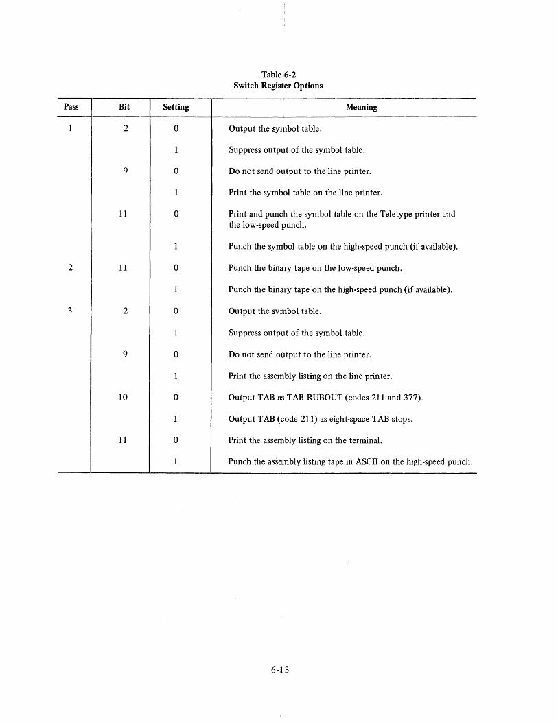
Pass Bit Setting
1 2 0
1
9 0
1
11 0
1
2 11 0
1
3 2 0
1
9 0
1
10 0
1
11 0
1
Table 6-2 Switch Register Options
Output the symbol table.
Meaning
Suppress output of the symbol table.
Do not send oliltput to the line printer.
Print the symbol table on the line printer.
Print and punch the symbol table on the Teletype printer and the low-speed punch.
Punch the symbol table on the high-speed punch (if available).
Punch the binary tape on the low-speed punch.
Punch the binary tape on the high-speed punch (if available).
Output the symbol table.
Suppress output of the symbol table.
Do not send output to the line printer.
Print the assembly listing on the line printer.
Output TAB as TAB RUBOUT (codes 211 and 377).
Output TAB (code 211) as eight-space TAB stops.
Print the assembly listing on the terminal.
Punch the assembly listing tape in ASCII on the high-speed punch.
6-13
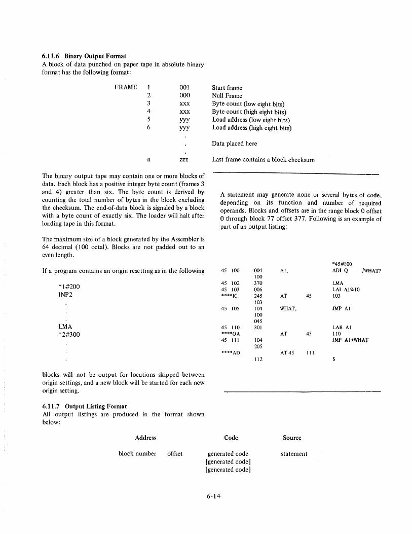
6.11.6 Binary Output Format A block of data punched on paper tape in absolute binary format has the following format:
FRAME 1 001 2 000 3 xxx 4 xxx 5 yyy 6 yyy
n zzz
The binary output tape may contain one or more blocks of data. Each block has a positive integer byte count (frames 3 and 4) greater than ·six. The byte count is derived by counting the total number of bytes in the block excluding the checksum. The end-of-data block is signaled by a block with a byte count of exactly six. The loader will halt after loading tape in this format.
The maximum size of a block generated by the Assembler is 64 decimal (100 octal). Blocks are not padded out to an even length.
If a program contains an origin resetting as in the following
*1#200 INP2
LMA *2#300
blocks will not be output for locations skipped between origin settings, and a new block will be started for each new origin setting.
6.11.7 Output Listing Format All output listings are produced in the format :;;hown below:
Address
block number offset
Start frame Null Frame Byte count (low eight bits) Byte count (high eight bits) Load address (low eight bits) Load address (high eight bits)
Data placed here
Last frame contains a block checksum
A statement may generate none or several bytes of code, depending on its function and number of required operands. Blocks and offsets are in the range block 0 offset o through block 77 offset 377. Following is an example of part of an output listing:
45 100
45 102 45 103 ****IC
45 lOS
45 110 ****OA 45 III
****AD
Code
generated code [generated code] [generated code]
6-14
004 100 370 006 245 103 104 100 045 301
104 205
112
*45#100 AI, ADI Q l,mAT?
LMA LAI AI%IO
AT 45 103
WHAT, lMP Al
LAB Al AT 45 110
lMP AI+WHAT
AT 45 III $
Source
statement

6.12 ASSEMBLER DIAGNOSTIC.MESSAGES Errors or warnings encountered during assembly are output on the terminal or line printer; selection of the device depends on the setting of Switch Register bit 9.
Pass
3
Errors
Messages output on terminal or line printer, noting illegal values and addresses where errors occurred.
Listing of program output on terminal or line printer, with error messages following sta tements to which they apply.
The total number of errors encountered is always output on the terminal at the end of each pass regardless of the setting of bit 9. Following is an example of pass 1 output:
IC 245 AT 45 103 OA AT 45 110 AD AT 45 111
Al 45 100 US AlIO AT 45 103 US Q AT 45 100 WHAT 45 105
005 ERRORS
An example of pass 3 output is included in the previous section.
6.12.1 Error Types Three types of error messages have been implemented for Assembler use and are described below. The syntax of an error message follows:
error code [symbol ] ASCII representation
address
When an illegal symbol or unidentified address of some kind is found in an Assembler statement, a type 1 error message of the following kind is produced
US Q AT 45 100
6-15
where US indicates an undefined symbol message, Q is the address symbol which caused the error, and 45 100 is the location at which the error occurred, in block-offset notation. The listing of the statement which caused this error follows:
45 100 004 AI, ADIQ
In type 2 error messages, the illegal symbol cannot be printed because the character that caused the error is not recognized by the Assembler. Thus the following might be produced
IC 245 AT 45 103
where IC indicates an illegal character message, 245 is the ASCII representation for % - the illegal character encountered but not recognized by the Assembler -- and 45 102 is the address at which the character was found. Following is the statement which produced this error:
45 102 006 LAI Al%10 /ADD Al AND 10 103
Type 3 error messages report on errors in which a symbol has not caused the error. These are errors in which an address is out of range or an operand is missing. For example, the statement:
45110 301 LAB Al
causes an error because the LAB instruction does not take an operand. The following error message is produced
OA AT 45 110
where OA indicates an operand error message and 45 110 is the address at which the error occurred.
6.12.2 Summary of Diagnostics Table 6-3 summarizes all error messages that may be produced by the Assembler. These messages may be printed out during pass 1 and again during pass 3 to correspond to the statement listing produced during that pass. The type column identifies the message as a type 1, type 2, or type 3 diagnostic in accordance with the syntax specifications just given. In all of the messages, the address specification
AT yy zzz
indicates that the described error was encountered at block yy offset zzz.

Type Message
AW xxxx ATyy ZZZ
DT xxxx AT yy zzz
ID xxxx AT yy zzz
RD xxxx AT yy lZZ
us xxxx AT yy zzz
UO xxxx AT yy lZZ
2 IC xxx AT yy zzz
3 AD ATyy ZZZ
3 IN AT yy ZZZ
3 OA ATyy ZZZ
3 OV ATyy zzz
3 ST AT yy zzz
3 PE AT yy zzz
2 PO xxx AT yy 'ZZl
2 PU xxx AT yy ZZl
Table 6-3 Assembler Diagnostics
Meaning
Address warning message; instruction xxxx found in the operand field as in JMP lMP.
Duplicate tag message; label xxxx (symbol ending with a comma) is repeated. Previous value of the symbol is retained, and the label is not redefined.
Illegal definition message; instruction or pseudo-instruction xxxx used illegally (EXPUNGE not given) as in A=LAB.
Redefinition by parameter assignment warning message; symbol xxxx is redefined (see DT for illegal definition of label fields).
Undefined symbol message; xxxx is a symbol used in the program but not defined, as in US Q AT 45 100.
Undefined operation code message; xxxx is a symbol used in the instruction field of a statement but is not a legal instruction, as in AI, A2.
IUegal character message; xxx is the ASCII representation of the illegal character encountered, as in IC 245 AT 45 102. The portion of the line following the illegal character is ignored.
Address out of range message. The illegal address was speCified in an origin (*), a JMP, or in some other instruction, as in AD AT 45 111 for statement JMP Al+WHAT; when the error occurs in an origin, the current location counter is not set to the out-of-range value but to that value truncated to 14 bits.
megal numeric constant message; a specified number was unacceptable to the Assembler (e.g., 123K).
Operand error message; operand missing from a statement that requires one (e.g., JMP), or operand included in a statement that does not require one (e.g., LAB AI).
Input buffer overflow message; will happen only in the unlikely event that a simple input statement exceeds 126 characters in length.
Symbol table overflow message; will happen only if a large number of symbols defined (number of symbols allowed is approximately 200). Assembler halts and must be restarted.
Pseudo-instruction parameter error message; illegal parameter specified, as in OPDEF JUMP;I04;3, where 3 is an illegal assignment for the instruction type.
Pushdown list overflow message; xxx is the list location. This is a fatal error.
Pushdown list underflow message; xxx is the list location. This is a fatal error.
6-16

This chapter summarizes the operation of the Microprocessor Program Loader (MPL) provided to MPS Monitor/Control Panel (MCP) users. Binary program tapes, normally produced by the Assembler described in Chapter 6, can be loaded into MPS memory by means of the Microprocessor Program Loader. The Loader is intended to be used extensively on the MCP for debugging and generation purposes.
7.1 OPERATING ENVIRONMENT The Loader requires the following hardware to be available:
1.
2.
The Microprocessor Series Monitor/Control Panel (MCP)
A paper-tape reader (the low-speed device associated with the Teletype).
The paper··tape reader must be interfaced to the Processor Module.
7.2 LOADING A BINARY TAPE Input to the Loader consists of a paper tape in MPS binary format usually produced as output from an MLA assembly on the PDP-B. To load the binary program into the module, follow the procedure outlined below:
I . Set the starting address on the MCP Switch Register to block 77 offset 0 (octal 37400).
2. Position the binary tape in the paper-tape reader and ready the device.
7-1
3.
4.
CHAPTER 7
MICROPROCESSOR
PROGRAM LOADER
Press the ADDR LOAD and STRT keys on the MCP.
Turn the paper-tape reader on. Low-speed tape will be read until the process is stopped manually by pressing the STOP switch on the reader. High-speed tape will stop automatically.
A binary program can have blocks of almost any length (the maximum is a block of 214 bytes. If binary output is generated in the normal way by the Assembler, 64-byte (decimal) blocks are output.
If the MPL load is successful, the Loader will halt at block 77 offset 141. If a checksum error occurs during the loading procedure, the load will not succeed and MPL wil1 halt at block 77 offset 124 (octal 37524).
7.3 RESTARTING THE LOADER It is possible to restart the loader after saving the contents of all but two of the module's registers. If the user presses ADDR LOAD and STRT at block 77 offset 200, the following registers will be saved:
Register Block and Octal Displacement Equivalent
A 76 340 37340 B 76 341 37341 C 76 342 37342 H 76 343 37343 L 76 344 37344

If the user presses ADDR LOAD and STRT at block 77 offset 202, the following registers will be saved:
Register Block and Octal Displacement Equivalent
A 76 340 37340 B 76 341 37341 C 76 342 37342 D 76 343 37343 E 76 344 37344
MPL will halt at block 77 offset 217.
7.4 MCP MEMORY The Loader reserves two areas of Monitor/Control Panel (MCP) memory for its own use:
7-2
1. Random-Access Memory (RAM) (32 decimal words)
2. Read-Only Memory (ROM) (256 decimal words)
The RAM begins at block 76 and offsets 340 through 377 (octal 37340 through 37377). The ROM begins at block 77 and offsets 0 through 377 (octal 37400 through 37777). These addresses are used by the MCP and should not be accessed by the user.
8.1 INTRODUCTION TO MDP The Micr.oprocess.or Debugging Program (MDP) is a software tool which runs .on the Processor Module and facilitates analysis and alteration of binary programs. These programs are normally produced by the Assembler (see Chapter 6).
MDP provides the following capabilities:
1. Reads and punches paper tape,
2.
3.
4.
5.
6.
Opens specified mem.ory locations for modification and allows the previous, current, and next locations to be opened, displayed, and closed,
Dumps the c.ontents .of program addresses, status flip-flops, and index registers on the Teletype printer,
Allows a program segment to execute for test purposes under MDP control,
Specifies a breakpoint location for program execution, and
L()ads specified locations in memory with a constant value.
The major advantage of using a debugging package such as MDP is that the binary code itself can be examined and modified, allowing the program to be tested and corrected without requiring reassembly. This is an especially useful capability in the environment in which Microprocessor Series programs are typically developed.
8-1
CHAPTER 8 MICROPROCESSOR
DEBUGGING PROGRAM
8.2 OPERATING ENVIRONMENT MDP is supplied in the form of a binary paper tape. To use the program, read the tape int.o memory using the standard Microprocessor Program Loader (MPL). After l.oading the tape set the starting address for MDP on the Monitor/Control Panel, raise the HLT switch, and press STRT. If the Teletype control knob is turned to LINE, MDP will respond by typing the MDP prompting character (*) .on the Teletype printer. The starting address for MDP is block 0 offset 1 00 (octal 0100). All bits are zero except low bit 6.
The minimum memory requirement for running MDP is 1 K of Random Access Memory (RAM) on a Microprocessor Series module. A Teletype must be interfaced with the M7341 m.odule for MDP command input from the keyb.oard and the display .of memory locations on the printer.
The low-speed paper-tape punch associated with the Teletype is used in conjunction with the R, P, T, and E c.ommands to read the binary program tape into memory and to punch out a corrected version.
Input to MDP is usually a binary paper tape produced by the Assembler described in Chapter 6. The listing produced during pass 3 of the assembly is necessary for determining addresses to be examined and modified.
8.3 BASIC CHARACTER SET The following list summarizes all ASCII characters that may be included in MDP command input and are rec.ognized by the debugging program:
• Alphabetic characters B, D, E, G, L, P, R, S, T, X
• Numeric characters 0 through 7
• Selected special (printing) characters.
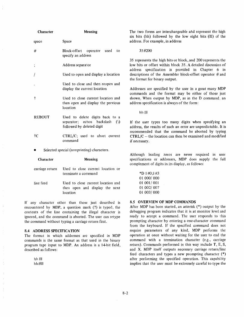
Character
space
#
t
RUB OUT
tc
Meaning
Space
Block-offset operator used to specify an address
Address separator
Used to open and display a location
Used to close and then reopen and display the current location
Used to close current location and then open and display the previous location
Used to delete digits back to a separator; echos backslash (\) followed by deleted digit
CTRL/C; used to abort current command
• Selected special (nonprinting) characters.
Character Meaning
carriage return Used to close current location or terminate a command
line feed Used to close current location and then open and display the next location
If any character other than those just describecl is encountered by MDP, a question mark (?) is typed, the contents of the line containing the illegal character is ignored, and the command is aborted. The user can retype the command without typing a carriage return first.
8.4 ADDRESS SPECIFICATION The format in which addresses are specified in MOP commands is the same format as that used in the binary program tape input to MOP. An address is a 14-bit fjeld, described as follows:
hh 111 hh#l1l
8-2
The two forms are interchangeable and represent the high six bits (hh) followed by the low eight bits (111) of the address. For example, in address
35#200
35 represents the high bits or block, and 200 represents the low bits or offset within block 35. A detailed discussion of address specification is provided in Chapter 6 in descriptions of the Assembler block-offset operator # and the format for binary output.
Addresses are specified by the user in a great many MOP commands and the format may be either of those just shown: When output by MOP, as in the D command" an address specification is always of the form:
hh 11l
If the user types too many digits when specifying an address, the results of such an error are unpredictable. It is recommended that the command be aborted by typing CTRL/C - the location can then be examined and modified if necessary.
Although leading zeros are never required in user speCifications or addresses, MOP does supply the full complement of digits in its display, as follows:
*D 1#0;1#3 01 000/000 01 001/001 01 002/007 01 003/000
8.S OVERVIEW OF MDP COMMANDS After MOP has been started, an asterisk (*) output by the debugging program indicates that it is at monitor level and ready to accept a command. The user responds to this prompting character by entering a one-character command from the keyboard. If the specified command does not require parameters of any kind, MOP performs the operation at once without waiting for the user to end the command with a termination character (e.g., carriage return). Commands performed in this way include T, E, S, and X. MOP itself outputs necessary carriage return/line feed characters and types a new prompting character (*) after performing the speCified operation. This capability implies that the user must be extremely careful to type the

correct characters. A paper tape read is performed as soon as the R command is typed, but MDP halts after reading tape and then waits to be restarted.
All other MDP commands require that parameters be included in the command line. After the user types one of the commands P, D, G, B, or L, MDP inserts a space after the one-character command and waits for necessary parameters to be typed by the user. The user must indicate that the command line is complete by typing a carriage return to terminate the command. MDP automatically inserts a line feed, performs the desired operation, and indicates a return of control to MDP monitor level by displaying an asterisk (*) on the Teletype printer. In the syntactic models shown in subsequent paragraphs, a carriage return/line feed combination, in which the user must supply the carriage return, is represented by <cr>. An explicit line feed character is represented by <If>. Terminators output solely by MDP (as in SorT, for example) are not shown.
8.6 ERRORS IN SPECIFYING COMMANDS A question mark (?) will be displayed on the Teletype printer if the user does any of the following:
1.
2.
3.
Uses a character not in the basic MDP character set; for example, the following is an error:
*D 1#0,
because comma (,) is not a legal MDP character.
Specifies a nonexistent command, for example:
*A
A is not a valid MDP command"
Specifies an address with alphabetic or special characters or with illegal numeric characters; either of the following causes an error:
*46#20A *1 379
After displaying the ? character, MDP ignores the current line and aborts the command. If the user omits parameters from a command line and types a carriage return to terminate this line, MDP will wait and will not return to monitor level until the parameters are typed or CTRL/C is issued.
8·3
8.7 SPECIAL FUNCTION KEYS The following two paragraphs detail the operation of two special functions used to correct errors and to abort MDP activity.
8.7.1 RUBOUT: Deleting a Digit The RUBOUT key on the Teletype keyboard is used for error correction when entering MDP parameters. Each RUB OUT causes the deletion of one digit, from right to left, beginning with the digit just to the left of the first RUBOUT and ending with the digit just to the right of the first separator encountered in the scan. Separators include the following:
Character
space
#
Meaning
Space output by MDP following a command or used as a block-offset operator
Block-offset operator used to separate the high and low bits of an address
Semicolon used to separate starting and ending address specifications
carriage return Terminator typed after a command or used to close the current location in an examination command
line feed Inserted by MDP after carriage return following a command or used to open the next location in an examination command
Open location or may be used as ;
RUBOUT echoes a backslash followed by the digit it deletes back to the most recent separator. Thus in the following command
*77#177\7\7\1277
the address originally specified
*77#177
is corrected and respecified as 77#277. The sequence \7\7\1 simply represents the digits 177 rubbed out, and 277 represents the new offset. RUBOUT of a digit causes a backslash, followed by the deleted digit, to be echoed on
the Teletype printer. If digits typed beyond the most recent separator must be deleted, the user must abort (Paragraph 8.7.2) and retype the entire command. An attempt to rub out digits beyond the separator causes zeros to be typed for these digits as in the following:
* 72#123\3\2\1 \0\0\0
In this command line, the user successfully rubbed out the digits 123; an attempt to delete the separator and block 72, however, failed, resulting in the printing of \0\0\0.
8.7.2 Control C: Aborting MDP Operation A control C character can be issued at any time to return control to MDP monitor level. This function is useful to correct the ~mtry of an invalid command or to terminate long input or output operations. It is recommended that this character be typed to abort a command when the user has made more than one or two errors when entering this command. Retyping the command is often a more straightforward and reliable method of correction than mbbing out and retyping multiple digits in an invalid line. To enter control C, type C while holding down the CTRL key. When CtRL/C is typed, the command being typed or executed is aborted, and the character is echoed as:
tc
Control then returns to MDP, a new prompting character is output, and a new command is expected. The following is an example of the use of CTRL/C when terminating and address dump:
*D 45#100;47#377 45 100/000 45 101/000 45 102/377 45 tc *
8.8 INPUT/OUTPUT COMMANDS The user can read and punch binary paper tapes by means of the MDP commands listed in Table 8-1.
8-4
Table 8-1 Input/Output Commands
Command Meaning
R
P
T
E
Read paper tape from low-speed paper-tape reader.
Punch paper tape for address range specified on low-speed punch.
Punch leader or trailer tape.
Punch end block and trailer.
These are described in more detail in Paragraph 8.8.1.
8.8.1 R: Reading Paper Tape The R command is used to read the contents of a binary paper tape into memory. It is issued in the following way:
Form R
This command does not require the user to type a carriage return. As soon as the character R is typed, the paper tape loaded in the low-speed tape reader associated with the Teletype is read into the memory addresses specified on the binary tape. This implies that the paper tape to be read must be properly positioned in the reader at the time the command
*R
is given.
The following sequence of steps should be used when loading paper tape into the reader:
1.
2.
Set the paper-tape reader switch to STOP or FREE.
Release the plastic cover of the reader unit and place the program tape over the read station with the small sprocket holes over the sprocket wheel. Close the cover.
3. Type R
4. Push the paper-tape reader switch to START and release.
After the entire program tape has been read into memory and an end block has been encountered, MDP halts. It can be restarted by setting the starting address (0 100) again, raising the HLT switch, and pressing STRT. To determine whether or not the read has been successfuL, the user should examine the accumulator (register A) after MDP has been restarted. If the contents of A are zero, reading has been successfully performed.
8.8.2 P: Punching Paper Tape The P command facilitates the following operations:
• Punching selected program or other memory locations on paper tape.
• Punching an entire program tape by dumping the contents of part or all of memory.
All punching is performed on the low-speed paper-tape punch associated with the Teletype. The command is supplied as follows:
Form
Where
P addrl ;addr2<cr > addrl is the starting memory location in block-offset notation addr2 is the ending memory location in block-offset notation
Example *p 45#100;47#377
In this example, memory locations from block 45, offset 100 through block 47, and offset 377 are punched out on paper tape using the low-speed paper-tape punch. This command does not automatically punch leader tape and an end block so it should be used in conjunction with the T and E commands.
The addr2 parameter is not optional. If only one address is to be punched, the user must nevertheless supply starting and ending range speCifications. In this case, both are identical, as in the following:
*p 11 #300 ;11 #300
The paper-tape punch must be readied at the time the command is issued. To position tape in the low-speed punch, do the following:
1.
2.
Turn the Teletype punch unit off.
Type the P command on the Teletype keyboard but do not type a carriage return.
8-5
3. Turn the punch unit on.
4. Type a carriage return to initiate punching.
It is important to follow this sequence to avoid punching command input on the program tape output by the punch.
It is a relatively easy matter to use MDP as a tool in generating paper tapes for use on the Microprocessor Series. Read a binary tape into memory and punch it out again using the following commands. This example assumes that program locations include blocks 15 through 1 7 and that all appropriate actions are taken to avoid punching unwanted characters on the output tape.
*R *T *p 15#0;17#377 *E *
Read paper tape into memory Punch header tape Punch blocks 15 through 1 7 Punch end block and trailer tape Return to MDP
8.8.3 T: Punching Leader and Trailer Tape The T command uses the low-speed Teletype punch to produce either leader or trailer tape. Both leader and trailer tape have exactly the same format and consist of approximately four inches of tape punched with octal code 200. The command is issued as follows:
Form T
This command does not require that the user type a carriage return. As soon as the character T is typed, header or trailer tape is produced. MDP then inserts an automatic carriage return/line feed to return control to MDP monitor level.
If the punch is turned on at the time T is typed, the command character, as well as the carriage return/line feed inserted by MDP, will be output on the tape but ignored when the program is loaded. If the user wishes to exclude these extraneous characters from the program tape, he/she should follow certain procedures when producing header or trailer tape:
1. Turn the punch off.
2. Type the T command after the prompting character:
*T

3.
4.
Turn the punch on immediately after typing the T command.
Turn the punch off after header or trailer tape has been produced.
Control returns automatically to MOP. Because the punch is not turned on until after T begins operation, a small amount of trailer tape might be lost.
8.8.4 E: Punching an End Block on Tape The E command punches the end block, followed by approximately four inches of octal code 200 trailer tape, using the low-speed paper-tape punch. It is issued as follows:
Form E
This command does not require that the user type a carriage return. As soon as the character E is typed, end block and trailer tape are produced. MOP then inserts an automatic carriage return/line feed to return control to MOP monitor level.
An end block punched by MOP has the same format as that produced by the MLA Assembler. In this format, e:ach block of data has a byte count of greater than six. The end block contains no data and therefore has a byte count of exactly six. The sequence of steps shown for the T command could be followed to prevent the E character from being punched out on paper tape. However, it is a more serious matter to lose part of the end block than to lose part of the leader/trailer tape. Therefore, it is usually preferable to leave the punch on while typing E and to rely on these command characters being ignored when the program tape is loaded.
Note that E implies automatic execution of the T command so trailer tape need not be explicitly requested.
8.9 LOCATION-EXAMINATION COMMANDS MOP commands have been implement(~d to facilitate the examination and modification of memory locations. All commands .in this category primarily consist of special Teletype keyboard characters as shown in Table 8-2.
8.9.1 /: Opening a Memory Location The / command allows the user to specify that a particular memory location is to be opened and the contents of this
8-6
Table 8-2 Loca tion-Examination Commands
Command Meaning
o pens specified location for modification
carriage return Closes current location
line feed
t
Closes current location and opens next location
Closes current location and reopen s it
Closes current location and opens previous location
location displayed. These contents can subsequently be changed. The command is issued in the following way:
Form addr/
Where addr is the location to be examined :In block-offset notation
Example *45#100/001
In response to the prompting character, the user types the address to be examined and follows it with a slash (/) character. MOP automatically inserts a space after the sJa:;h and prints out the contents of the examined location in three-digit octal form. The user can then modify the contents of the location by typing the new value to replace the value displayed as follows:
*45#100/001 111
The space between the old and new values is also output by MOP.
To terminate the command line, to return control to MOP, or to examine another location, the user types carriage return, line feed, period, or up-arrow. The different characteristics of these Teletype keys are presented in the following paragraphs.

8.9.2 Canriage Return: Closing an Open Location In addition to its typical function as a stat~~ment terminator (for example, in Band P commands), the RETURN key can be used to close an open location which is being examined. A carriage return is typed at the end of the following command
*12#141/000 111 <cr>
to indicate that the specified change in contents is to be made, and the location at block 12, offset 141 is to be closed. After the RETURN key has been pressed, control returns to MDP and the prompting asterisk is displayed. No further locations are opened until explieitly directed by another command.
8.9.3 Line Feed: Opening the Next Location The line feed character can be typed instead of the carriage return to perform three distinct actions:
1. Close the location being examined.
2. Open the next location and display its contents.
3. Allow modification of the displayed location.
Use of the line feed in terminating the command
*27#0/377<It>
causes the location at block 27 offset 0 to be closed and the location at block 27 offset 1 to be opened automatically. The full interaction looks like
*27#0/377<It> 27001/001
where the user types only the initial 27#0/ specification.
The long form of this function requires that the user issue two separate examination commands:
*27#O/377<cr> *27#1/001
8.9.4 .: Reopening the Current Location The period (.) is used to perform the following functions:
1. Close the location being examined.
8-7'
2. Reopen the same location and display its contents.
3. Allow modification of the displayed location.
Use of the period is valuable when correcting an incorrectly altered location or when verifying that a change has been made. For example, in the following
*45#10/000 770\0\7\326\61 \171. 45 010/271
the use of RUBOUT characters, echoing deleted characters, has made the modification of location 45#10 difficult to read. The period is used to verify that the desired correction has been made. Note that rubbing out 770 has indicated that 770 was truncated to 370, since MPS addresses can include offsets of only eight bits.
8.9.5 t: Opening the Previous Location Use of the up-arrow (t) character complements the use of the line feed. While line feed allows the user to view the next location, up-arrow causes the previous location to be opened. The following functions are performed:
1.
2.
3.
Close the location being examined.
Open the previous location and display its contents.
Allow modification of the displayed location.
Use of t in the followil1g commands
*22#0/001 t 21 377/ 377 ooot 21 376/001
allows the user to view the contents of the location before 22#0, 21 #377 (377) and to modify that location. t is used again to view the contents oflocation 21#376 (001).
8.10 DISPLAY COMMANDS A variety of commands have been implemented to allow a range of addresses or certain key locations to be displayed on the Teletype printer. Some commands allow modification of the contents of these locations; others do not. Table 8-3 lists the commands in this category.
Command
Table 8-3 Display Commands
Meaning
D Dump the contents of a range of specified addf{~sses on the Teletype printer.
S Display the contents of the condition flip-flops and allow modification.
X Display the contents of the accumulator and allow modification.
These are more fully described in subst~quent paragraphs.
8.10.1 D: Dumping Address Contents The D (dump) command allows the user to obtain a listing on the Teletype printer of all or some of the binary program in memory. It is issued as follows:
Form
Where
D addrl ;addr2<cr>
addrl is the starting memory location in block-offset notation addr2 is the ending memory 10caHon in block-offset notation
Example *D 1#0;1#377
The user terminates the command by typing a carriage return; MDP inserts a line feed and proceeds to type out the desired listing in the following format:
*D addrl ;addr2<cr> addrl/ contents addra/ contents addrb/ contents addre/ contents addrd/ contents
addr2/ contents
*
8-8
An example is included below:
*D 1#0;1#377 01 000/ 000 01 001/ 000 01 002/ 001 01 003/ 002 01 004/ 077
01 377/000
*
If the user decides that he need not view the entire dump, the listing can be terminated by typing CTRL/C on the Teletype keyboard.
The addr2 parameter is not optional. If only one address is to be dumped, the user must nevertheless supply starting and ending range specifications. In this case both are identical, as in the following:
*D 36#0;36#0
8.10.2 S: DisplayingStatus Flip-Flops The S (status) command allows the user to examine and modify the contents of the status register which contains the following condition flip-flops:
Bit Meaning
7 Sign 2 Parity
Zero a Carry
The status register has an organization as shown below:
STATUS REGISTER
sign unused parity zero carry
~ 7 6 5 4 3 2 a
The unused bits are always considered to be zeroed. Sign, parity, zero, and carry are normally set to one or reset to zero depending on the results of instmction execution. MDP allows the user to set these bits explicitly by means of the S command.
If the sign bit is set to one and all other bits are zero, the status register has contents of 200, as shown below:
10000000 2 0 0
If the padty, zero, and carry bits are set to one and the sign bit is zero, the status register will have contents of 007, as follows:
00000 111 o 0 7
If only the zero bit is set, the following will be the case:
00000010 o 0 2
The S command is entered in the following way:
Form S
This command does not require that the user type a carriage return. As soon as the character S is typed, MDP itself inserts a carriage return/line feed and produces status bits in the following form on the Teletype printer:
addr / contents
An example follows:
*S 20 105/ 200
The address returned by MDP is the address in which the status register is found. In the example just shown, the sign bit is set and all other bits are zero. To modify status bits, simply type new contents as in the following:
*S 20 105/ 200005
Here the space between the old and new contents is output by MDP. The user changes the contents so that the parity and carry bits are set.
8-9
8.1 0.3 X: Displaying an Index Register The X (index) command is used to examine and modify the index registers. The accumulator (register A) is accessed in the following way:
Form X
This command does not require that the user type a carriage return. As soon as the character X is typed, MDP itself inserts a carriage return/line feed and displays the contents of the accumulator in the following form on the Teletype printer:
addr/ contents
An example follows:
20 111/000
The address returned by MDP is the address of the accumulator storage location on the user's machine and is not necessarily the one just shown. The contents of this address can be modified by typing in a new value, as follows:
*X 20 111/000377
To examine and modify subsequent registers (B, C, H, L), the user terminates this and succeeding lines with an explicit line feed. For example:
*X 20 111/ 000377 < If > 20 112/ 001 < If > 20 113/ 000 < If > 20 114/007 < If > 20115/377000<cr>
<If> indicates a line feed entered by the user, <cr> a carriage return. This sequence allows the user to examine all index register storage locations.
8.11 CONTROL COMMANDS Commands used to set breakpoints, begin test execution, and clear memory locations can be categorized as control commands. Table 84 summarizes the functions of these commands.

Table 84 Control Commands
----~----------------------------
Command
G
B
L
Meaning
Start execution of binary program at specified address.
Set breakpoint at specified address in binary program.
Set range of .addresses to specified constant.
These commands are described in greater detail in the paragraphs that follow.
8.11.1 G: Executing the Program The G (go) command is used to execute a binary program or part of the program. Often it is used in conjunction with the B (breakpoint) command to test part or all of the binary program read in to memory. G is issued in the following way:
Form
Where
G addr<cr>
addr is the first address to be executed in block-offset notation
Example *G 10#121
The user types a carriage return to terminate the G command, and MDP inserts an automatic line feed. The status bits and registers saved when MDP was loaded are restored, and the program segment beginning at addr is executed. For test purposes, the user can set initial conditions before beginning program execution by modifying the status bits and index register storage locations as previously indicated.
8.11.2 B: Setting a Breakpoint The B command provides one of the most useful fe,atures available through MDP. It is used to specify a location to be used as a breakpoint in the binary program currently in
8-10
memory. When the program encounters this location during execution, it returns control to MDP. The B command is issued as follows:
Form B addr<cr>
Where addr is the address to be used as a breakpoint in block-offset notation.
Example *B 37#0
The user types a carriage return to terminate the B command, and MDP inserts an automatic line feed.
The B eommand modifies the location specified and the two following locations; therefore, care must be used when placing breakpoints due to the variable length instructions. It specifies the address to be treated as a breakpoint location when the program is exe<;uted. Thus B is used in conjunction with G to test segments of a program" When the specified address is executed, the following actions occur:
1. The binary program stops.
2. Registers A, B, C, H, L, and the status bits are saved.
3. Control returns to MDP and the following is printed on the Teletype
B
*
to indicate that the breakpoint has been reached.
The saved registers and status bits can now be examined and modified if necessary.
The breakpoint does not normally remain in the binary program; it is removed under any of the folltowing circumstances:
1. The specified address is executed.
2. MDP is restarted.
3. A special version of the B command is entered:
The expliCllt B reset command has the following form:
Form B R
This command does not require that the user conclude with a carriage return. As soon as the B R combination is typed, MDP itself inserts a carriage return/line feed. The space between Band R is also output by MDP. After B R is typed, MDP returns to monitor level, removes the breakpoint from the binary program, and outputs a new prompting character.
8.11.3 L: Loading Memo.ry with a Constant The L command is used to load a segment of memory with a specified constant. It is issued in the following way:
Form
Where
L addrl ;addr2;[ constant] <cr>
addrl is the s1tarting memory location in block-offset notation addr2 is the ending memory location in block-offset notation constant is optional and represents the value to be inserted in the memory locations
8-11
Examples *L 76#340;76#377;77<cr> *L 76#343;76#362;<cr>
The user terminates the command with a carriage return and MDP inserts an automatic line feed. The addr2 parameter is not optional. If only one address is to be cleared, the user must nevertheless supply starting and ending range specifications. In this case, both are identical, as in the following:
*L 1#0;1#0;
L is often used to clear memory locations; if constant is omitted from the command, zero is the default, and the memory range specified is zeroed. The semicolon following addr2 must be supplied, even if constant is omitted from the command. After the operation defined in L is performed, MDP returns to monitor level and outputs a new prompting character.

9.1 INTRODUCTION TO MPR The Microprocessor Read-Only Memory (ROM) Programmer (MRP) is a PDP-8 system program used to read and write programmable read-only memory (PROM) circuits for use on the M7345 PROM Module. The write function performed by MRP can also be called programming a PROM. A special hardware assembly is required to implement the functions supported by MRP, since PROMs, the I/O medium used by this program, are not a standard device supported by a PDP-8 interface. The particular hardware environment in which MRP functions, is described in detail in the next paragraph.
MRP provides the following capabilities:
1. Reads and punches paper tape using the high-speed or low-speed unit
2. Reads, writes, and verifies PROMs
3.
4.
5.
Opens specified memory locations for modification and allows the previous, current, and next locations to be opened, displayed, and closed
Dumps the contents of memory locations on the Teletype or line printer
Loads specified locations in memory with a constant value
MRP permits examination and modifkation of PROM locations read into memory, and provides a facility for obtaining both Teletype and line printer listings of programs stored in paper tape or PROM form.
9.2 HARDWARE ENVIRONMENT This paragraph describes the characteristics and use of the special hardware used by MRP.
9-1
CHAPTER 9 MICROPROCESSOR
ROM PROGRAMMER
9.2.1 MR873 Hardware Assembly Using the MRP on the PDP-8 requires a special hardware assembly to be placed on the machine's I/O bus. Only those PDP-8 models with OMNIBUS construction can support this assembly; thus MRP can run on PDP-8/E, PDP-8/F, and PDP-8/M models, but not normally on the PDP-8/1, PDP-8/L, or PDP-8/S.* The special hardware used by MRP consists of one basic unit, the MR873, which holds PROM circuits and is attached to the I/O bus as shown in Figure 9-1.
Any other devices supported by a particular PDP-8 configuration can also be conveniently added to the bus. Often a high-speed paper-tape reader/punch and a line printer are supported.
The MR873 consists of the following:
1. Main rack-mountable or bench top MR873 hardware assembly
2. One M1703 input interface module which plugs directly into the PDP-8 OMNIBUS
3. One M1705 output interface module which plugs directly into the PDP-8 OMNIBUS
4. Two Y168 zero-insertion force socket modules
When these components are unpacked at the user's installation they should be inspected for any obvious signs of damage that may have occurred during shipping.
*It is possible to use a special hardware interface to facilitate MRP
use on the PDP-B/I, PDP-8/S, and PDP-BIL. Users of these CPU's
should contact Logic Products Applications Engineering at Digital
for information.

~]-----I ~---1 TELETYPE I
Figure 9-1 PDP-B I/O Bus
Protruding from the rear of the MRB73 unit are three flat gray cables and one standard power cord. When the BCOBR-6 cables, used to connect the MRB73 to the OMNIBUS, are unrolled the user will find a sticker attached to each cable at the plug end. This sticker identifies each cable and identifies its terminus as follows:
1. From 11 - MRB73 to 11 M:l703 2. From J2 - MRB73 to 11 M1705 3. From J3 - MRB73 to J2 MJl705
The user should connect these cables in the way described, ensuring that the letters on the plug housing match the letters on the top of the board-mounted jack. Then the MI703 and MI705 modules can b,~ installed in any convenient position on the OMNIBUS of the PDP··B/E, PDP-B/F, or PDP-B/M.
Next, the user should install the two YI6B modules that are designed to hold the PROMs. Plug one module into the slot labeled CHECK, VERIFY, FETCH, and the other into the slot labeled WRITE. After the line cord has been connected to any nearby 115 Vac 60-cyc1e outlet, the MRB73 is ready for operation under MRP.
9.2.2 PROM Assembly and Manipulation The YI6B modules are designed to hold PROM packages and to facilitate easy movement of these packages from one module socket to another. There are three sockets mounted on the front panel of the MRB73 assembly labeled from left to right:
1 . SIMULATE (RTM ONLY) 2. CHECK, FETCH, VERIFY 3. WRITE
These sockets have the following functions:
1. The socket labeled SIMULATE is not relevant to MRP and should be disregarded by the user.
9-2
2. The socket labeled CHECK, FETCH, VERIFY can be used only to read PROM data during check, fetch, or verify MRP operations.
3. The socket labeled WRITE can be used only to load PROM data during write MRP operations.
Only 1702A ultraviolet-erasable PROMs can be used with the MRB73 and MRP. PROMs of this kind can be writiten in approximately two minutes.
WARNING When PROMs are being written by the MRB73, high voltage pulses (60 Vdc) are generated; the user should therefore be careful not to handle the PROM or MRB73 assembly during this process. The vol tage level generated can be dangerous and is present on both the PROM and the etch of the Y168 module into which the PROM is plugged while being written.
If it is ever necessary to remove or touch a PROM before writing has been completed, the user should stop the process either by pressing the HALT switch on the PDP-B console or by typing CTRL/C on the Teletype keyboard.
Before a PROM is written, it should be completely erased by exposing it to ultraviolet light for five to ten minutes. The user should be sure to protect his eyes from the ultraviolet light.
PROMs must be inserted in the socket in the proper way, as shown in Figure 9-2.
If the user inserts the PROM into the module incorrectly, the chip may be destroyed. With the locking lever in the raised position, insert the PROM in the socket with the: dot on the PROM in the position shown in Figure 9-3. Thien lock it in by pushing the lever all the way down.
The following example illustrates a sequence in which a segment of the PDP-B memory data buffer is loaded into a PROM and then verified. It is assumed that PDP-B memory contains the desired data.

1. Install a clear PROM in the socket labeled CHECK, FETCH, VERIFY, and check that the PROM is clear by issuing a C (check) command from MRP.
2. Move the PROM to the socket labeled WRITE and load it with data by issuing a W (write) MRP command.
3. Move the PROM back to the socket labeled CHECK, FETCH, VERIFY and verify that the PROM was loaded correctly by issuing a V (verify) command from MRP.
Figure 9-2 MR873 ROM Programmer
Figure 9-3 Y168 Socket Module (with PROM inserted)
Table 9-1 summarizes the correct location of the PROM during various MRP PROM I/O commands.
Table 9-1 Socket Positions for PROM Commands
Command
WRITE CHECK FETCH VERIFY
Socket Labeled WRITE
X
Socket Labeled CHECK FETCH
VERIFY
x X X
To fetch data from a PROM, the user positions the PROM in the socket labeled CHECK, FETCH, VERIFY, and issues an F (fetch) command from MRP. Before performing this or any PROM operation, ensure that the PROM is securely locked in place with the socket lever.
9.3 OPERA TING ENVIRONMENT MRP is provided to users of this system in the form of a binary paper tape which is loaded into core by means of the Microprocessor Host Loader (MHL) using either the low-speed or high-speed paper-tape reader. Selection of the reading unit and other load procedures performed at this time are illustrated in Figure 4-11. To start the program, set the starting address 02008 in the Switch Register and press the ADDR LOAD and START keys on the PDP-8 console. If the Teletype control knob is turned to LINE, MRP will respond by typing the prompting character (*) on the Teletype printer.
The minimum memory and peripheral device requirements are the same as those described in Chapter 4. Input to MRP usually consists of a binary paper tape produced by the MLA Assembler and/or a previously programmed PROM. Output can be a punched binary tape, a programmed PROM, and/or a listing on the Teletype or line printer.
9.4 SWITCH REGISTER OPTIONS Alternate output devices may be selected for use by MRP by setting the appropriate PDP-8 Switch Register bits before output is directed to these devices. Table 9-2 summarizes selection of the printing and punching units.
Bit 9 is set to indicate that the line printer is the primary output device. Error messages are always displayed on the terminal; if bit 9 is set they will also appear on the line printer, but they will never only appear on the line printer.

Table 9-2 Switch Register Options
Bit Setting Meaning
9 0
11 o
Print output on the Teletype printer.
Print output on the line printer.
Punch tape on the low-speed paper-tape punch associated with the Teletype.
Punch tape on the high-speed punch (if available ).
Although output will be printed on the specified device if the setting of bit 9 is established before the command that produces output is typed, it is possible for output to be sent to both devices. If bit 9 is set 0 when the initial character of the MRP command is typed, the user can set the bit on after MRP outputs the space following that character. Then, when output is produced, it will appear on both the Teletype printer and the line printer. If the following command is typed
*D 21#O;21#27<cr>
and bit 9 is set after the MRP space and before <cr>, locations 21 #0 through 21 #27 will be dumped on both output devices.
If bit 9 is set but a line printer is not part of the PDP-8 configuration, the system will wait 150 milliseconds for the line printer to be attached and will then assume that the Teletype is the primary output device.
9.5 BASIC CHARACTER SET The following list summarizes all ASCII characters that may be included in MRP command input and are recognized by the blasting program:
•
•
Alphabetic characters C, D, E, F, L, P, Q, R, T, V,W
Numeric characters 0 through 7
9-4
• Selected special (printing) characters, as follows:
Character Meaning
space
#
t
Space
Block-offset operator used to specify an address
Address Separator
Used to open and display a location
Used to close and then reopen and display the current location
Used to close current location and then open and display the previous location
RUBOUT Used to delete digits back to a separator; echoes backslash (\) followed by deleted character
tc
•
CTRL/C; used to abort current command
Selected special (nonprinting) characters, as follows:
Character Meaning
carriage return Used to close current location or terminate a command
line feed Used to close current location and then open and display the next location
If any character other than those just described is encountered by MRP, a question mark (?) is typed, the contents of the line containing the illegal character is ignored, and the command is aborted. The user can retype the command without typing a carriage return first.

9.6 ADDRESS SPECIFICATION The format in which addresses are specified in MRP commands is the same format as that used in the Microprocessor Debugging Program (MDP) (Chapter 8) or in the binary program tape input to MRP. An address is a 14-bit field, described as follows:
hhlll hh#l11
The two forms are interchangeable and represent the high six bits (hh) followed by the low eight bits (111) of the address. For example, in address
23#0
23 represents the high bits or block, and 0 represents the low bits or offset within block 23. A detailc~d discussion of address specification is provided in Chapter 6 in descriptions of the Assembler block-offset operator # and the format for binary output.
Addresses are specified by the user in a great many MRP commands and the format may be either of those just shown. When output by MRP, as in the D command, an address specification is always of the form:
hhlll
If the user types too many digits when specifying an address, the results of such an error are unpredictable. It is recommended that the command be aborted by typing CTRL/C. The location can then be examined and modified if necessary,
Although leading zeros are never required in user specifications or addresses, MRP does supply the full complement of digits in its display as follows:
*D 1#0;1#3 01 000/000 01 001/001 01 002/007 01 003/000
9.7 OVERVIEW OF MRP COMMANDS After MRP has been started, an asterisk (*) output by the program indicates that it is at monitor level and ready to accept a command. The user responds to this prompting character by entering a one-character command from the keyboard. If the specified command does not require parameters of any kind, MRP performs the operation at
9-5
once without waiting for the user to end the command with a termination character (e.g., carriage return). Commands performed in this way include R, Q, T, E, and C. MRP itself outputs necessary carriage return/line feed characters and types a new prompting character (*) after performing the specified operation. This capability implies that the user must be extremely careful to type the correct characters. If an incorrect character is typed, the user can type CTRL/C to cancel the incorrect character. RUBOUT does not erase command characters - only digits in addresses.
All other MRP commands require that parameters be included in the command line. After the user types one of the commands P, F, W, V, D, or L, MRP inserts a space after the one-character command and waits for necessary parameters to be typed by the user. The user must indicate that the command line is complete by typing a carriage return to terminate the command. MRP automatically inserts a line feed, performs the desired operation, and indicates a return of control to MRP monitor level by displaying an asterisk on the Teletype printer. In the syntactic models shown in subsequent paragraphs, a carriage return/line feed combination, in which the user must supply the carriage return, is represented by <cr>. An explicit line feed character is represented by <It>. Terminators output solely by MRP (as in R or T, for example) are not shown.
9.8 MRP ERRORS There are two kinds of errors that are recognized by MRP. Command errors cause a question mark (?) followed by a carriage return/line feed to be displayed on the Teletype printer (and also on the line printer, if bit 9 is set). Execution errors cause a question mark followed by a message and a carriage return/line feed to be displayed.
Command errors occur when the user specifies a nonexistent command, as in the following:
*z
A question mark and error message will be displayed when invalid characters are included in the command:
*F A ? ILLEGAL CHARACTER
Execution errors occur when an invalid or out-of-range address specification is included in a command, when a checksum error occurs during a read, or when an illegal address separator is specified. Error and warning messages are discussed in detail in the paragraphs on specific MRP commands which produce these messages.
9.9 SPECIAL FUNCTION KEYS The following two paragraphs detail the operation of two special functions used to correct errors and to abort MRP activity.
9.9.1 RUBOUT: Deleting a Digit The RUBOUT key on the Teletype keyboard is used for error correction in entering MRP parameters. Each RUBOUT causes the deletion of one digit, from right to left, beginning with the digit just to the left of the first RUBOUT and ending with the digit just to the right of the first separator encountered in the scan. Separators include the following:
Character
space
#
Meaning
Space output by MRP following a command, or used as a block-offset operator
Block-offset operator used to separate high and low bits of an address
Semicolon used to separate starting and ending address specifications
carriage return Terminator typed after a command, or used to close the current loca tion in an examination command
line feed Inserted by MRP after carriage return following a command or used to open the next location in an examination command
RUBOUT echoes a backslash followed by the digit it deletes back to the most recent separator. Thus in the following command
*77#177\7\7\1277
the address originally specified
*77#177
is corrected and respecified as 77*,1:277. The sequence \7\7\1 represents the digits 177 rubbed out and 277 represents the new offset. RUBOUT of a digit causes a backslash, followed by the deleted digit, to be echoed on
9-6
the Teletype printer. If digits typed beyond the most recent separator must be deleted, the user must abort (ParagJaph 9.9.2) and retype the entire command. An attempt to rub out digits beyond the separator causes zeros to be typed for these digits, as in the following.
*72#123\3\2\1 \0\0\0
In this command line, the user successfully rubbed out the digits 123; an attempt to delete the separator and block 72, however, failed, resulting in the printing of \0\0\0.
9.9.2 Control C: Aborting MRP Operation A control C character can be issued at any time to return control to MRP monitor level. This function is useful to correct the entry of an invalid command, or to terminate long input or output operations. It is recommended [hat this character be typed to abort a command when the user has made more than one or two errors when entering this command. Retyping the command is often a lTlore straightforward and reliable method of correction than rubbing out and retyping multiple characters in a command line. To enter control C, type C while holding down the CTRL key. When CTRL/C is typed, the command being typed or executed is aborted, and the character is e,choed as:
tc
Control returns to MRP, a new prompting character is output, and a new command is expected. Following i~. an example of the use of CTRL/C in terminating an address dump:
*D 45#100;47#377 45 100/000 45101/000 45 102/377 45 tc *
There is one case in which CTRL/C cannot be used to terminate an I/O operation. If the low-speed papeJr-tape reader is in the process of reading a program tape, CTRL/C will not terminate the input operation. The computer must be halted and the program restarted to return control to MRP monitor level. Set 0200 in the Switch Register and press the ADDR LOAD and START keys to restart.
9.10 PAPER TAPE I/O COMMANDS The user can read and punch binary paper tapes by means of the MRP commands listed in Table 9-3.
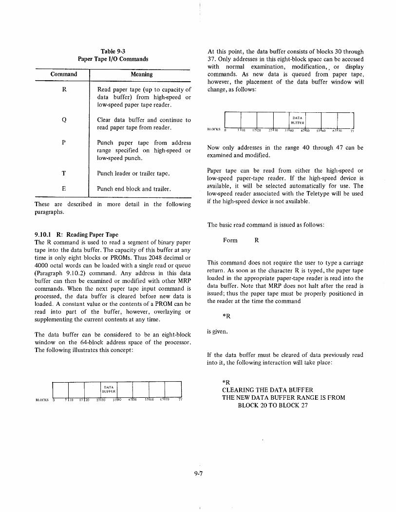
Table 9-3 Paper Tape I/O Commands
Command Meaning
R Read paper tape (up to capacity of data buffer) from high-speed or low-speed paper tape reader.
Q Clear data buffer and continue to read paper tape from reader.
P Punch paper tape from address range specified on high-speed or low-speed punch.
T Punch leader or trailer tape.
E Punch end block and trailer.
These are described in more detail in the following paragraphs.
9.10.1 R: Reading Paper Tape The R command is used to read a segment of binary paper tape into the data buffer. The capacity of this buffer at any time is only eight blocks or PROMs. Thus 2048 decimal or 4000 octal words can be loaded with a single read or queue (Paragraph 9.1 0.2) command. Any address in this data buffer can then be examined or modified with other MRP commands. When the next paper tape input command is processed, the data buffer is cleared before new data is loaded. A constant value or the contents of a PROM can be read into part of the buffer, however, overlaying or supplementing the current contents at any time.
The data buffer can be considered to be an eight-block window on the 64-block address space of the processor. The following illustrates this concept:
DATA BUFFER
7 10 17 20 27 30 3740 4750 57
[ BLOCKS 0
9-7
At this point, the data buffer consists of blocks 30 through 37. Only addresses in this eight-block space can be accessed with normal examination, modification" or display commands. As new data is queued from· paper tape, however, the placement of the data buffer window will change, as follows:
BLOCKS 1 ,1 "I" I nm I BUFFER
37 40 47 50
Now only addresses in the range 40 through 47 can be examined and modified.
Paper tape can be read from either the high-speed or low-speed paper-tape reader. If the high-speed device is available, it will be selected automatically for use. The low-speed reader associated with the Teletype will be used if the high-speed device is not available.
The basic read command is issued as follows:
Form R
This command does not require the user to type a carriage return. As soon as the character R is typed, the paper tape loaded in the appropriate paper-tape reader is read into the data buffer. Note that MRP does not halt after the read is issued; thus the paper tape must be properly positioned in the reader at the time the command
*R
is given.
If the data buffer must be cleared of data previously read into it, the following interaction will take place:
*R CLEARING THE DATA BUFFER THE NEW DATA BUFFER RANG E IS FROM
BLOCK 20 TO BLOCK 27

As the tape is read into blocks 20 through 27, the following messages will be output:
ST ARTING AT 20 000 LOADING BLOCK 20 LOADING BLOCK 21 LOADING BLOCK 22 LOADING BLOCK 23 LOADING BLOCK 24 LOADING BLOCK 25 LOADING BLOCK 26 LOADING BLOCK 27 STOPPED AT 27 377
If the tape end block is encountered before the end of the current data buffer, the following messages might be displayed:
*R STARTING AT 20 000 LOADING BLOCK 20 LOADING BLOCK 21 STOPPED at 21 305 END-OF-DATA BLOCK WAS SEEN
If there is nothing in the segment of tape being read, the following will be displayed:
*R STARTING AT 20000 STOPPED AT 20 000 END-OF-DATA BLOCK WAS SEEN
If this occurs, nothing will be loaded into the data buffer.
If an error occurs while performing the read, the following message might be output:
*R ST ARTING AT 20 000 LOADING BLOCK 20 ? CHECKSUM ERROR
If the high-speed paper-tape reader is used, the following sequence of steps should be followed to position tape in the reader:
1. Turn the control knob to raise the tape retaining lever.
9-8
2. Place a fan-folded tape in the right-hand bin.
3. Place several folds of leader in the left-hand bin and position the tape so that the sprocket wheel engages the feed holes.
4. Turn the control knob to lower the tape retaining lever.
5. Press the FEED switch briefly to ensure that the tape is properly positioned.
6. Issue R command.
The sequence of steps below should be followed if the low-speed reader is selected:
1. Set the paper-tape reader switch to STOP or FREE.
2. Release the plastic cover of the reader unit and place the program tape over the read station with the small sprocket holes over the sproGket wheel. Close the cover.
3. Issue R command.
4. Push the paper-tape reader switch to START and release.
9.10.2 Q: Reading Additional Paper Tape The Q (queue) command is used to clear the data buffer if it currently contains data and to read the next segment of paper tape. It is issued as follows:
Form Q
This command does not require that the user type a carriage return. As soon as the character Q is typed, the next segment of the paper tape loaded in the paper-tape reader used by the previous read command is read.
Q is used in conjunction with a paper tape whose addresses span more than eight consecutive blocks. It can also be used to reset the data buffer at any time. The R command is issued to read the first eight blocks of the new tape positioned in the high-speed or low-speed paper-tape reader. Q is used to clear the buffer of the data just read and 10
load the next address section(s).

If the data buffer must be cleared of data previously read into it, the following interaction might take place:
*Q CLEARING THE DATA BUFFER THE NEW DATA BUFFER IS FROM
BLOCK 30 TO BLOCK 37
As the tape is read into blocks 30 through 37, the following messages will be output:
STARTING AT 30 000 LOADING BLOCK 30 LOADING BLOCK 31 LOADING BLOCK 32 LOADING BLOCK 33 LOADING BLOCK 34 LOADING BLOCK 35 LOADING BLOCK 36 LOADING BLOCK 37 STOPPED AT 37 377
If the tape end block is encountered before the end of the current data buffer, the following messages might be displayed:
*Q CLEARING THE DATA BUFFER THE NEW DATA BUFFER IS FROM
BLOCK 30 to BLOCK 37 ST ARTING AT 30 000 LOADING BLOCK 30 LOADING BLOCK 31 LOADING BLOCK 32 STOPPED AT 32 377 END-OF-DATA BLOCK WAS SEEN
If an error occurs while performing thle queue, the following message might be output:
*Q CLEARING THE DATA BUFFER THE NEW DATA BUFFER IS FROM
BLOCK 30 TO BLOCK 37 STARTING AT 30 000 LOADING BLOCK 30 ? CHECKSUM ERROR
9-9
If an R command has not preceded the Q or if the read encountered a checksum error or an end-of-data block, the following warning message will be displayed:
*Q % ILLEGAL USE OF Q % READ COMMAND ASSUMED *R
After Q has been typed, enabling of the low-speed paper-tape reader can be performed at any time; MRP will wait until the reader is ready. The high-speed reader must be readied at the time the command is issued.
9.10.3 P: Punching Paper Tape The P command facilitates the following operations:
1. Punching selected locations from paper tape, PROM, or the data buffer on paper tape.
2. Duplicating a paper tape by punching segments of the binary program stored in the data buffer.
3. Duplicating a PROM by writing out the contents of the data buffer.
4. Backing up a PROM on paper tape, or paper tape on one or more PROMs.
Punching is performed on either the high-speed or low-speed paper-tape punch, depending on the setting of Switch Register bit 11. If the bit is on, the high-speed punch is selected; otherwise, the low-speed device associated with the Teletype is used.
The P command is issued as follows:
Form
Where
Example
P addrl ;addr2<cr>
addr 1 is the starting memory location in block-offset notation addr2 is the ending memory location in block-offset notation
*p 45#100;47#377

In tius example, memory locations from block 45, offset 100 through block 47, offset 377 are punched out on paper tape using the appropriate paper-tape punch. This command does not automatically punch leader tape and an end block so it should be used in conjunction with the T and E commands.
The addr2 parameter is not optional. If only one address is to be punched, the user must nevertheless supply starting and ending range specifications. In this case, both are identical, as in the following:
*p 11 #300 ;11 #300
There are several error messages whieh may be produced because of errors in address specifications. If an alphabetic or special character is supplied in an address of if an invalid address separator is typed, the following message will be displayed:
*p 30:#0;37#37 A ? ILLEGAL CHARACTER
If the starting block is greater than the ending block in the address specification, the following message will be displayed:
*p 7#0;0#377 ? ADDRESS SPECIFICATION ERROR:
BLOCK 1 > BLOCK 2
If the starting offset is greater than the ending offset in the address specification, the following message will be displayed:
*p 20#377;20#0 ?LOW BYTES OF THE ADDRESS
SPECIFICATION ARE REVERSED
This message only occurs when the starting and ending block specifications are the same.
The paper-tape punch must be readied at the time the command is issued. No special action need be taken to position paper tape for punching on the high-speed device. To ready tape for the low-speed punch, do the following:
1. Turn the Teletype punch unit off.
9-10
2.
3.
4.
Type the P command on the Teletype keyboard but do not type a carriage return.
Turn the punch unit on.
Type carriage return to initiate punching.
It is important to follow this sequence in order to avoid punching command input on the program tape outpUll by the punch.
It is a relatively easy matter to use MRP as a tool to facilitate high-speed or low-speed on-line tape duplication. Read a binary tape into memory and punch it out again using the following commands. This example assumes that program locations include blocks 15 through 17 and that all appropriate actions are taken to avoid punching unwanted characters on the output tape. Remember that the tapes will not be exact copies since MRP inserts a few sptxial control characters.
*R *T *p 15#0;17#377 *E *
Read paper tape into memory Punch header tape Punch blocks 15 through 17 Punch end block and trailer tape Return to MRP
9.10.4 T: Punching Leader and Trailer Tape The T command uses the high-speed or low-speed Teletype punch to produce either leader or trailer tape. Both leader and trailer tape have exactly the same format and consist of approximately four inches of tape punched with octal code 200. Selection of the punching unit depends on the s,etting of Switch Register bit 11. The command is issued as follows:
Form T
This command does not require the user to type a carriage return. As soon as the character T is typed, header or trailer tape is produced. MRP then inserts an automatic carriage return/line feed to return control to MRP monitor lev,el.
If the punch is turned on at the time T is typed, the command character, as well as the carriage return/line feed inserted by MRP, will be output on the tape but ignored when the program is loaded. If the user wishes to exclude these extraneous characters from the program tape~ he should follow certain procedures when producing header or trailer tape.

1.
2.
3.
4.
Turn the punch off.
Type the T command after the prompting character:
*T
Turn the punch on immedia.tely after typing the T command.
Turn the punch off after header or trailer tape has been produced.
Control returns automatically to MRP. Because the punch is not turned on until after T begins operation, a small amount of trailer tape might be lost.
9.10.5 E: Punching an End Block on Tape The E command punches the end block, followed by approximately four inches of octal code 200 trailer tape, using the high-speed or low-speed paper-tape punch. Selection of the punching unit depends on the setting of Switch Register bit 11. It is issued as follows:
Form E
This command does not require the user to type a carriage return. As soon as the character E is typed, end block and trailer tape are produced. MRP then inserts an automatic carriage return/line feed to return controll to MRP monitor level.
An end block punched by MRP has the same format as that produced by the MLA Assembler. In this format, each block of data has a byte count of greater than six. The end block contains no data and therefore has a byte count of exactly six. The sequence of steps shown for the T command could be followed to prevent the E character from being punched out on paper tape. However, it is a far more serious matter to lose part of the e,nd block than to lose part ot the leader/trailer tape. It is therefore preferable to leave the punch on while typing E and to rely on these command characters being ignored when the program tape is loaded.
Note that E implies automatic execution of the T command, so trailer tape need not be explicitly requested.
9.11 PROM I/O COMMANDS A variety of input/output commands have been implemented to allow the MRP user to read, check, write, and verify PROMs. These commands are listed in Table 9-4.
9·11
Command
F
C
W
V
Table 94 PROM I/O Commands
Meaning
Read or fetch contents of PROM in read socket, copying it into data buffer.
Check contents of PROM in read socket to ensure that all locations are clear.
Write specified address range onto PROM in write socket.
Verify that contents of PROM in write socket correspond to specified addresses in data buffer.
These are described in greater detail in the following paragraphs.
9.11.1 F: Reading a PROM The F (fetch) command is used to read the contents of a PROM into the data buffer. The PROM must be in the read socket on the MR873 assembly. This command is issued as follows:
Form
Where
Example
F addrl ;addr2<cr>
addr 1 is the starting memory location in block-offset notation addr2 is the ending memory location in block-offset notation
*F 30#0;30#377
In this command, addr 1 and addr2 reference memory locations in the data buffer in which the contents of the PROM will be loaded.
There are several error messages which may be produced because of errors in address specifications. If an alphabetic or special character is supplied in an address or if an invalid address separator is typed, the following message will be displayed:
*F 30#0;30#37% ? ILLEGAL CHARACTER

If the starting offset is greater than the ending offset in the address specification, the following message will be displayed:
*F 20#377 ;20#0 ?LOW BYTES OF THE ADDRESS
SPECIFICATION ARE REVERSED
Because the capacity of a PROM is only 256 decimal or 400 octal words, the address range cannot exceed one block and cannot cross a block boundary. All of the following are therefore invalid:
*F 1#0;7#377 *F 30#377;31#123 *F 47#200 ;50#1 77
If the block numbers of the starting and ending range specifications are not the same, the following will occur:
*F 1 #0;7#377 ?HIGH BYTES OF THE ADDRESS
SPECIFICATION MUST BE THE SAME
Careful placement of PROM data is essential when copying from PROM to paper tape. The following illustrates concatenation of three PROMS onto paper tape. This example assumes that a new PROM is inserted in the read socket for each fetch.
*1' Punch header tape
*F 10#0;10#377 Fetch data from PROM and copy to data buffer
*F 11#0;11#377 Fetch data from PROM and copy to data buffer
*F 12#0;12#377 Fetch data from PROM and copy to data buffer
*L 13#0;17#377 Clear remaining locations in data buffer
*£1 10#0;1 2#377 Punch blocks 10 through 12
*E Punch end block and trailer tape
* Return to MRP
The user types a carriage return to conclude the F command. MRP inserts an automatic line feed, performs the fetch, and returns to monitor level.
9-12
The fetch command is a very powerful one, since it can be used to redefme the current window on the data buffer. If the data buffer is defined as extending from 10#0 thTOugh 17#377 and the following command is issued
*F 37#16;37#377
MRP will display the following message:
CLEARING THE DATA BUFFER THE NEW DATA BUFFER RANGE IS FROM
BLOCK 30 TO BLOCK 37
The user has the option of electing not to redefine 1th(~ data buffer at this time. If an error has been made or if ya]uable information is still in the current data buffer, the us{:r can simply type CTRL/C at any time while the message is being displayed. After the message has been typed completely, the data buffer will be redefmed as extending from 30#0 through 37#377.
9.11.2 C: Checking a PROM The C (check) command examines every location of a PROM to ensure that the entire PROM is clear before the user attempts to write on it. The PROM must be in 1the read socket in the MR873 assembly at the time the command is given. The user types the follOWing:
Form C
It is not necessary to terminate this command with a carriage return. As soon as the character C is typed, MRP begins to examine PROM locations.
Each location is checked to ensure that it is clear. [f the entire PROM is clear, the following message will be displayed:
*C PROM IS CLEAR
If any locations in the PROM have invalid contents, MRP will display both address and contents in a formatted list. Following is an example:
*C ADRSPROM 003001 127010 322072 376077 377 177
* Because a PROM consists of one complete block (400 octal words) of data, it is not necessary for MRP to supply the

block numbers of addresses with invalid contents. The three octal digits displayed beneath the ADRS label represent offsets within the block.
MRP automatically outputs a carriage~ return/line feed combination at the end of each line printed; it returns automatiGally to the monitor when all relevant addresses and contents have been printed.
9.11.3 W: Writing a PROM The W (write) command is used to load (or program) a PROM with the contents of specified addresses in the data buffer. The PROM to be used for output must have been checked for clear contents and must be iln the write socket on the MR873. The W command is issued as follows:
Form
Where
Example
W addrl ;addr2<cr>
addr 1 is the starting memory location in block-offset notation addr2 is the ending memory location in block-offset notation
*W 1#0;1#377
The user types a carriage return to conclude this command. MRP inserts an automatic line feed and displays the following message:
WAIT FOR BELL
The PROM will now be programmed. By watching the lights on the PDP-8 console panel, the Ulser can determine when the PROM has been loaded. During the loading process, the MQ register displays the binary representation of all characters loaded. When the panel Hghts stabilize, the PROM has been loaded. At this time, MRP causes the Teletype bell to ring or the audible signal on another terminal to be produced. A carriage return/line feed is output and MRP returns to monitor level.
There are several error messages that may be produced because of errors in address specifications. If an alphabetic or special character is supplied in an address or if an invalid address separator is typed, the following message will be displayed:
*W ? ILLEGAL CHARACTER
9-13
If the starting offset is greater than the ending offset in the address speCification, the following message will be displayed:
*W 20#377;20#0 ?LOW BYTES OF THE ADDRESS
SPECIFICATION ARE REVERSED
Because the capacity of a PROM is only one block, the address range cannot exceed one block and cannot cross a block boundary. The following are therefore invalid:
*W 20#0;27#377 *W 50#377;51#10
If the block numbers of the starting and ending range speCifications are not the same, the following will occur:
*W 20#0;27#377 ?HIGH BYTES OF THE ADDRESS
SPECIFICATION MUST BE THE SAME
MRP can be used to duplicate PROMs in a straightforward on-line way. Read a PROM into the data buffer and write it out again using the following commands. This example assumes that program locations comprise block 36.
*C PROM IS CLEAR
*F 36#0;36#377
*W 36#0;36#377
WAIT FOR BELL
*V 36#0;36#377 PROM VERIFIED OK
*
Check that PROM is clear
Fetch data from PROM and copy it into data buffer
Write PROM from data buffer
Verify contents of PROM
Return to MRP
MRP can also be used to copy PROM-to-tape or tape-to-PROM. Remember, however, that the capacity of paper tape is much larger than that of a PROM, so care must be used when specifying addresses to be copied.
9.11.4 V: Verifying a PROM The V (verify) command compares specified addresses in the data buffer with addresses of the PROM in the read socket on the MR873 assembly. It is issued in the following way:
Form
Where
Example
V addrl ;addr2<cr>
addr 1 is the starting memory location in block-offset notation addr2 is the ending memory location in block-offset notation
*V 74#100;74#277
The user types a carriage return to conclude this command. MRP inserts an automatic line feed, performs the verification operation, and returns to monitor level.
There are several error messages that may be produced because of errors in address speCifications. If an alphabetic or special character is supplied in an address of if an invalid address separator is typed, the following message will be displayed:
*V 30#0;30#37 A ? ILLEGAL CHARACTER
If the starting offset is greater than the ending offset in the address specification, the following message wHl be displayed:
*V 20#377;20#0 ?LOW BYTES OF THE ADDRESS SPECIFICATION
ARE REVERSED
This message only occurs when the starting and ending block specifications are the same.
Because the capacity of a PROM is only one block, the address range cannot exceed one block and cannot cross a block boundary. The following are therefore invalid:
*V 70#0;75#377 *V 60#377;61#2
9-14
If the block numbers of the starting and ending range speCifications are not the same, the following will occur:
*V 20#0;27#377 ?HIGH BYTES OF THE ADDRESS SPECIFICATION
MUST BE THE SAME
If the specifications are outside the range of the current data buffer, the message shown below will be displayed. The current data buffer is assumed to include blocks 20 through 27.
*V 70#0;70#377 ?HIGH BYTE OF THE ADDRESS SPECIFICA llION
OUTSIDE THE RANGE OF THE CURRENT DATA BUFFER
The contents of each PROM location is compared to the contents of the corresponding data buffer address. If the address contents are all the same, the following message will be displayed:
PROM VERIFIED OK
If any locations do not correspond, MRP will display both addresses and contents in a formatted list. Following i:; an example:
*V 36#0;36#377 ADRS BUF PROM 305001 210 375 007010
*
Because a PROM consists of one complete block of data, it is not necessary for MRP to supply the block numbers of addresses that cannot be verified. The three octal digits displayed beneath the ADRS label represent offsets within the block. The digits that appear beneath the BUF labe)l are the contents of the specified offset in the data buffer; the digits beneath PROM are the contents of the PROM at that offset.
MRP automatically outputs a carriage return/line feed combination at the end of each line printed. It returns automatically to the montior level when all rE:levant addresses and contents have been printed.
9.12 LOCATION-EXAMINATION COMMANDS MRP commands have been implemented to facilitate the examination and modification of memory locations. All commands in this category consist primarily of special Teletype keyboard characters as shown in Table 9-5.
Table 9-5 Location-Examination Commands
Command Meaning
/ 0 pens specified location for modification
carriage return Closes current location
line feed
t
Closes current location and opens next location
Closes current location and reopens it
Closes current location and opens previous location
9.12.1 /: Opening a Memory Location The / command allows the user to specify that a particular data buffer location is to be opened and the contents of this location displayed. These contents can subsequently be changed. The command is issued in the following way:
Form
Where
Example
addr/
addr is the location to be examined in block-offset notation
*45#100/001
In response to the prompting character, the user types the address to be examined and follows it with a slash (/) character. MRP automatically inserts a space after the slash and prints out the contents of the examined location in three-digit octal form. The user can then modify the contents of the location by typing the new value to replace the value displayed, as follows:
*45#100/001 111
9-15
The space between the old and new values is also output by MRP.
To terminate the command line, returning control to MRP or examining another location, carriage return, line feed, period, or up-arrow can be typed. The different characteristics of these Teletype keys are presented in the following paragraphs.
9.12.2 Carriage Return: Closing an Open Location In addition to its typical function as a statement terminator (for example, in F and P commands), the RETURN key can be used to close an open location that is being examined. A carriage return is typed at the end of the following command
*12#141/000 111 <cr>
to indicate that the specified change in contents is to be made, and the location at block 12, offset 141 is to be closed. After the RETURN key is pressed, control returns to MRP and the prompting asterisk is displayed. No further locations are opened until explicitly directed by another command.
9.12.3 Line Feed: Opening the Next Location The line feed character instead of the carriage return can be typed to perform three distinct actions:
1. Close the location being examined.
2. Open the next location and display its contents.
3. Allow modification of the displayed location.
Use of the line feed in terminating the following command
*27#O/377<If>
causes the location at block 27 offset 0 to be closed and the location at block 27 offset 1 to be opened automatically. The full interaction looks like
*27#O/377<If> 27001/001
where the user types only the initial 27#0/ specification.

The long form of this function requin~s that the user issue two separate examination commands, as follows:
*27#O/377<cr> *27#1/001
9.12.4 .: Reopening the Current Location The'period (.) is used to perform the following functions:
1.
2.
3.
Close the location being examined.
Reopen the same location and display its contents.
Allow modification of the displayed location.
Use of the period is valuable when correcting an incorrectly altered location or when verifying th,at a change has. been made. For example, in the following:
*45#10/000 770\0\7\326\671. 45010/271
the use of RUBOUT characters, echoing deleted characters, has made the modification of location 45#10 difficult to read. The period is used to verify that the desired correction has been made. Note that rubbing out 770 has indicated that 770 was truncated to 370, since MPS addresses can include offsets of only eight bits.
9.12.5 t: Opening the Previous Location Use of the up-arrow (t) character complements the use of line feed. While line feed allows the user to view the next location, up-arrow causes the previous location to be opened. The following functions are performed:
1.
2.
Close the location being examined.
Open the previous location and display its contents.
3. Allow modification of the displayed location.
Use of the t in the following commands
*22:f.!:01 001 t 21 3771 177 ooot 21 376/001
9-16
allows the user to view the contents of the location before 22:#0, 21 #377 (177) and to modify that location; t is used again to view the contents oflocation 21#376 (001).
9.13 DISPLAY COMMAND The D command has been implemented to allow the MRP user to obtain listings of part or all of the data buffer on the Teletype or the line printer.
9.13.1 D: Dumping Address Contents The D (dump) command allows the user to obtain a listing on the Teletype or line printer of a range of memory addresses in the data buffer. It is issued as follows:
Form
Where
Example
D addrl ;addr2<cr>
addr 1 is the starting memory location in block-offset notation addr2 is the ending memory location in block-offset notation
*D 1 :#0;7#377
There are several error messages that may be produced because of errors in address specifications. If an alphabetic or special character is supplied in an address or if an invalid address separator is typed, the following message wiU be displayed:
*D 30#O;37#37N ? ILLEGAL CHARACTER
If the starting block is greater than the ending block in the address specification, the following message wHl be displayed:
*D 7:#0;0#377 ? ADDRESS SPECIFICATION ERROR:
BLOCK 1 > BLOCK 2
If the starting offset is greater than the ending offset in the address specification, the following message wiJI be displayed:
*D 20#377;20:#0 ?LOW BYTES OF THE ADDRESS SPECIFICATION
ARE REVERSED

This message occurs only when the starting and ending block specifications are the same.
A dump command can access only the current data buffer. If the buffer is assumed to include blocks 0 through 7, the following are illegal specifications:
*D 1 #0;36#377 *D 27#377;30#0 *D 70#0;70#377
The following interaction will take place:
*D 1#0;36#377 ?HIGH BYTE OF ADDRESS SPECIFICATION
IS OUTSIDE THE RANGE OF THE CURRENT DATA BUFFER
The user terminates the D command by typing a carriage return; MRP inserts a line feed and proceeds to type out the desired listing in the following format:
*D addrl; addr2<cr> addr 1 / contents addra/ contents addrb/ contents addre/ contents addrd/ contents
addr2/ contents
*
An example is included below:
*D 1 #0;7#377 01 000/ 000 01 001/001 01 002/ 007 01 003/000 01 004/070
07377/ 000
*
If the user decides that he need not view the entire dump, or if the Teletype or line printer requires maintenance of any kind, the listing can be terminated by typing CTRL/C on the Teletype keyboard.
9-17
The addr2 parameter is not optional. If only one address is to be dumped the user must nevertheless supply starting and ending range specifications. In this case, both are identical, as in the following:
*D 36#0;36#0
9.14 CONTROL COMMAND One MRP command has been implemented to allow the user to clear memory locations or to fill specified addresses with a constant.
9.14.1 L: Loading Memory with a Constant The L command is used to load a segment of memory with a specified constant. It is issued in the follOWing way:
Form
Where
Examples
L addrl ;addr2;[constant] <cr>
addr 1 is the starting memory location in block-offset notation addr2 is the ending memory location in block-offset notation constant is optional and represents the value to be inserted in the memory location
*L 76#340;76#352;7 *L 20#343;27#377;
The user terminates the command with a carriage return, and MRP inserts an automatic line feed. The addr2 parameter is not optional. If only one address is to be cleared the user must nevertheless supply starting and ending range specifications. In this case, both are identicaL as in the following:
*L 70#0;70#0;
L is often used to clear memory locations; if constant is omitted from the command, zero is the default, and the memory range specified is zeroed. The semicolon following addr2 must be supplied, even if constant is omitted from the command.
There are several error messages that may be produced because of errors in address specifications. If an alphabetic or special character is supplied in an address or if an invalid address separator is typed, the following message will be displayed:
*L 30#O;37#37Q ? ILLEGAL CHARACTER

If the starting block is greater than the ending block in the address specification, the following message will be displayed:
*L 7#0;0#377; ? ADDRESS SPECIFICATION ERROR:
BLOCK 1 > BWCK 2
If the starting offset is greater than the ending offset in the address specification, the following message will be displayed:
*L 20#377;20#0; ?LOW BYTES OF THE ADDRESS SPECIFICATIONS
ARE REVERSED
This message only occurs when the starting and ending block specifications are the same.
The load command can be used to redefine the current window on the data buffer. If the buffer is defined as extending from 20#0 through 27#377 and the following command is issued:
*L 72#0;73#377;
9-18
MRP will display the following message:
CLEARING THE DATA BUFFER THE NEW DATA BUFFER IS FROM
BLOCK 70 TO BLOCK 77
The user has the option of electing not to redefine the data buffer at this time. If an error has been made or if valuable information is still in the current data buffer, the user can simply type CTRL/C at any time while the message is being displayed. After the message has been typed completely, the data buffer will be redefined as extending from 70#0 through 77#377.
Although the data buffer can be redefined by specifying an address range in the new data buffer, a load cannot actually cross the boundary of a data buffer. Therefore, if the current data buffer extends from 20#0 through 27#377, the following is legal:
*L 70#0;77#377;
but the following example is illegal and results in the message displayed:
*L 26#0;32#377; ?HIGH BYTE OF ADDRESS SPECIFICATION
IS OUTSIDE THE RANGE OF THE CURRENT DATA BUFFER

This chapter contains a series of sample programs that might be useful as a reference when the user begins to construct programs based on the syntax described in Chapter 6. This sample code is heavily commented and is included in the form of assembly listings.. Symbol table listings are included when indicated by the setting of the PDP-8 Switch Register.
10.1 LOADING REGISTER IN RAM The following example illustrates suppression of symbol table output during assembly.
*77#200 RAM = 76#340
CHAPTER 10 SAMPLE PROGRAMS
/OPERATION = LOAD ADDRESS OR JUMP TO 77#200 77 200 335 SA VEHL, LDH /pUT REGISTER H IN REGISTER D 77 201 346 LEL /PUT REG ISTER L IN REG ISTER E
/OPERATION = LOAD ADDRESS OR JUMP TO 77#202 77 202 066 SAVREG, LLI RAMt /SAVE REGISTERS A-E
340 77 204 056 LHI RAM /IN LOCATION 76#340 (37340)
076 77 206 370 LMA /STORE A 77 207 060 INL /B 77 2]0 371 LMB 77 211 060 INL /C 77 212 372 LMC 77 213 060 INL /D 77 214 373 LMD 77 215 060 INL /ANDE 77 216 374 LME 77 217 000 HLT /HALT
$ 000 ERRORS
10-1

10.2 READING A BLOCK OF DATA
/READ IN A BLOCK OF DATA OF 10 (OCTAL)
OPDEF INPUT;INP;O /DEFINE OPCODE INPUT OPDEF CALL~106;2 /DEFINE OPCODE CALL START = 04#200 * START
04 200 056 LHI BLKt /LOAD ADDRESS BLOCK TO HAND L REGS 004
04 202 066 LLI ELK 230
04 204 016 LBI 10 /SET COUNT TO 10 010
04 206 106 AGAIN, CALL READIN /READ A BYTE OF DATA 220 004
04 211 370 LMA /STORE IT IN BLOCK 04 212 060 INL /INCREMENT POINTER IN BLOCK 04 213 011 DCB /DECREMENT COUNTER 04 214 110 JFZ AGAIN /IF NOT DONE, GO BACK FOR NEXT
206 004
04 217 000 HLT
04 220 103 READIN, INPI /INPUT STATUS 04 221 044 NDI 40 /MASK "DA" (IGNORE ERRORS)
040 04 223 150 JTZ READIN /WAIT FOR "DA"
220 004
04 226 101 INPUT /GET A BYTE OF DATA 04 227 007 RET /RETURN
04 230 000 BLK, BLOCK 10 000 000 000 000 000 000 000
$ AGAIN 04 206 ELK 04 230 READIN 04 220 START 04 200
000 ERRORS
10-2
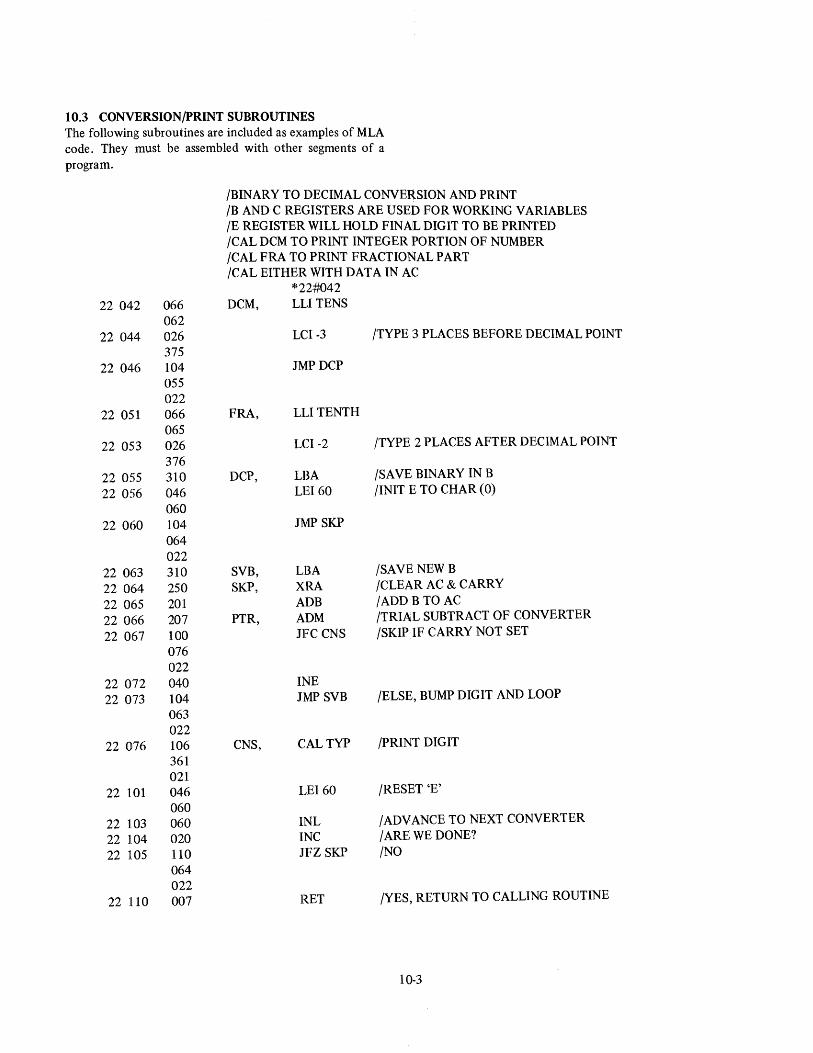
10.3 CONVERSION/pRINT SUBROUTINES The following subroutines are included as examples of MLA code. They must be assembled with other segments of a program.
IBINARY TO DECIMAL CONVERSION AND PRINT IB AND C REGISTERS ARE USED FOR WORKING VARIABLES IE REGISTER WILL HOLD FINAL DIGIT TO BE PRINTED ICAL DCM TO PRINT INTEGER PORTION OF NUMBER ICAL FRA TO PRINT FRACTIONAL PART ICAL EITHER WITH DATA IN AC
*22#042 22 042 066 DCM, LLITENS
062 22 044 026 LCI -3 ITYPE 3 PLACES BEFORE DECIMAL POINT
375 22 046 104 JMP DCP
055 022
22 051 066 FRA, LLITENTH
065 22 053 026 LeI -2 ITYPE 2 PLACES AFTER DECIMAL POINT
376 22 055 310 DCP, LBA ISAVE BINARY IN B
22 056 046 LEI 60 IINIT E TO CHAR (0) 060
22 060 104 JMPSKP
064 022
22 063 310 SVB, LBA ISAVE NEW B
22 064 250 SKP, XRA ICLEAR AC & CARRY
22 065 201 ADB IADDB TO AC
22 066 207 PTR, ADM ITRIAL SUBTRACT OF CONVERTER
22 067 100 J1FC CNS /SKIP IF CARRY NOT SET
076 022
22 072 040 INE
22 073 104 IMP SVB /ELSE, BUMP DIGIT AND LOOP
063 022
22 076 106 CNS, CALTYP /PRINT DIGIT
361 021
22 101 046 LEI 60 IRESET 'E'
060 22 103 060 INL I ADVANCE TO NEXT CONVERTER
22 104 020 INC IARE WE DONE?
22 105 110 JFZ SKP INO 064 022
22 110 007 RET IYES, RETURN TO CALLING ROUTINE
10-3
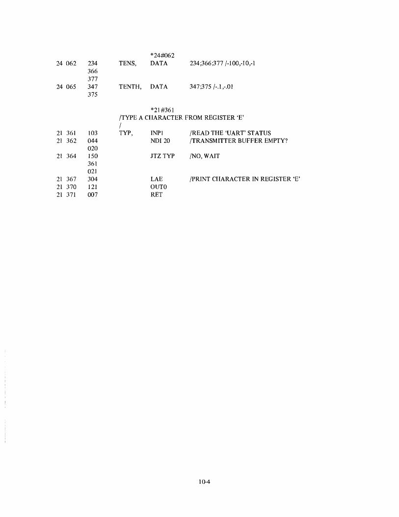
*24#062 24 062 234 TENS, DATA 234;366;377 1-100,-10,-1
366 377
24 065 347 TENTH, DATA 347;375/-.1,-.01 375
*21#361 ITYPE A CHARACTER FROM REGISTER 'E'
I 21 361 103 TYP, INPI IREAD THE 'UART' STATUS 21 362 044 NDI20 ITRANSMITTER BUFFER EMPTY?
020 21 364 ]50 JTZ TYP INa, WAIT
361 021
21 367 304 LAE IPRINT CHARACTER IN REGISTER 'E' 21 370 121 aUTO 21 371 007 RET
10-4

Category
READ
APPEND
INSERT
LIST
PUNCH
FORM FEED
APPENDIX A SUMMA~RY OF EDITOR (MLE) COMMANDS
Command Example
R R
A A
nl 31
L L
nL 100L
m,nL 1,50L
P P
nP 6P
m,nP 100,120
F F
Function
Read text from paper-tape reader and append it to text buffer.
Read text from terminal and append it to text buffer.
Insert text from terminal before line 1 in text buffer.
Insert text from terminal before line n in text buffer.
List the contents of the text buffer on the terminal.
List line n of the text buffer on the terminal.
List lines m through n of the text buffer on the terminal.
Punch the contents of the text buffer on the high- or low-speed paper-tape punch (selection depends on setting of Switch Register bit 10).
Punch line n of the text buffer on the paper-tape punch.
Punch lines m through n of the text buffer on the paper-tape punch.
Punch a form feed (four blanks, a form feed character, and approximately two inches of blank tape) on the paper-tape punch.
A·l
Reference
5.6.1
5.6.2
5.6.3
5.6.3
5.7.1
5.7.1
5.7.1
5.7.2
5.7.2
5.7.2
5.7.3

CategOlY Command Example
TRAILER T T
NEXT N N
nN ION
CHANGE nC IOOC
m,nC I,IOC
DELETE nO 420
m,nD 12,200
GET G G
nG 15G
KILL K K
MOVE m,n$jM 1,10$20M
SEARCH S S
nS lOS
m,nS I,IOS
Function
Punch a trailer (approximately four inches of blank tape) on the paper-tape punch.
Perform the functions of P, F, K, and R respectively.
Perform the functions of P, F, K, and R respectively, n times in sequence.
Delete line n of the text buffer and replace it with the text entered from the terminal.
Delete lines m through n of the text buffer and replace them with the text en tered from the terminal.
Delete line n from the text buffer.
Delete lines m through n from the text buffer.
Output the first tagged (labeled) line after the current location in the text buffer on the terminal.
Output the first tagged line after line n in the text buffer on the terminal.
Kill (erase) the entire contents of the text buffer.
Move lines m through n in the text buffer to the location just before line j.
Search the entire text buffer for all occurrences of the character entered from the terminal, but not echoed, after the carriage return.
Search line n for occurrences of the character entered from the terminal and then allow command modification.
Search lines m through n for occurrences of the character entered from the terminal and then allow command modification.
A-2
Reference
5.7.4
5.7.5
5.7.6
5.8.1
5.8.1
5.8.2
5.8.2
5.8.3
5.8.3
5.8.4
5.8.4
5.8.6
5.8.6
5.8.7

APPENDIX B SUMMARY OF AS~SEMBLER (MLA) INSTRUCTIONS
Instruction Example
Lr(1)r(2) LAB
LrM LDM
LMr LMA
Lrl LAIA+B
LMI LMII04
1m INL
DCr DCB
ADr ADD
ACr ACB
SUr SUB
SBr SBD
NDr NDB
XRr XRA
ORr ORB
CPr CPB
ADM ADM
Function
Load register 1 with the contents of register 2.
Load a register with the contents of memory.
Load memory with the contents of a register.
Load a register with the byte of data immediately following the instruction.
Load memory with the byte of data immediately following the instruction.
Increment a register.
Decrement a register.
Add the contents of a register to the accumulator.
Add the contents of a register and the carry flip-flop to the accumulator .
Subtract the contents of a register from the accumulator.
Subtract the con~ents of a register and the carry flip-flop from the accumulator.
Logical AND the contents of register with the accumulator.
Exclusively OR the contents of a register with the accumulator.
Inclusively OR the contents of a register with the accumulator.
Compare the contents of a register with the accumulator and set the status ,flip-flops.
Add the contents of memory to the accumulator.
B-1
Reference
3.3.1
3.3.1
3.3.1
3.3.2
3.3.2
3.3.3
3.3.4
3.4.1
3.4.1
3.4.1
3.4.1
3.4.1
3.4.1
3.4.1
3.4.1
3.4.2

Instnlction Example
ACM ACM
SUM SUM
SBM SBM
NDM NDM
XRM XRM
ORM ORM
CPM CPM
ADI ADI2
ACI ACI104
SUI SUI 1
SBI SBI6
NDI NDI100
XRI XRI340
ORI ORI 102
CPI CPI4
RLC RLC
RRC RRC
Function
Add the contents of memory and the carry flip-flop to the accumulator .
Subtract the contents of memory from the accumulator.
Subtract the contents of memory and the carry flip-flop from the accumulator.
Logical AND the contents of memory with the accumulator.
Exclusively OR the contents of memory with the accumulator.
Inclusively OR the contents of memory with the accumulator.
Compare the contents of memory with the accumulator and set the status flip-flops.
Add the byte of data immediately following the instruction to the accumulator.
Add the byte of data immediately following the instruction and the carry flip-flop to the accumulator.
Subtract the byte of data immediately following the instruction from the accumulator.
Subtract the byte of data immediately following the instruction and the carry flip-flop from the accumulator.
Logical AND the byte of data immediately following the instruction with the accumulator.
Exclusively OR the byte of data immediately following the instruction with the accumulator.
Inclusively OR the byte of data immediately following the instruction with the accumulator.
Compare the byte of data immediately following the instruction with the accumulator and set the status flip-flops.
Rotate the contents of the accumulator one bit to the left and into the carry flip-flop.
Rotate the contents of the accumulator one bit to the right and into the carry flip-flop.
B-2
Referenc(~
3.4.2
3.4.2
3.4.2
3.4.2
3.4.2
3.4.2
3.4.2
3.4.3
3.4.3
3.4.3
3.4.3
3.4.3
3.4.3
3.4.3
3.4.3
3.4.4
3.4.4
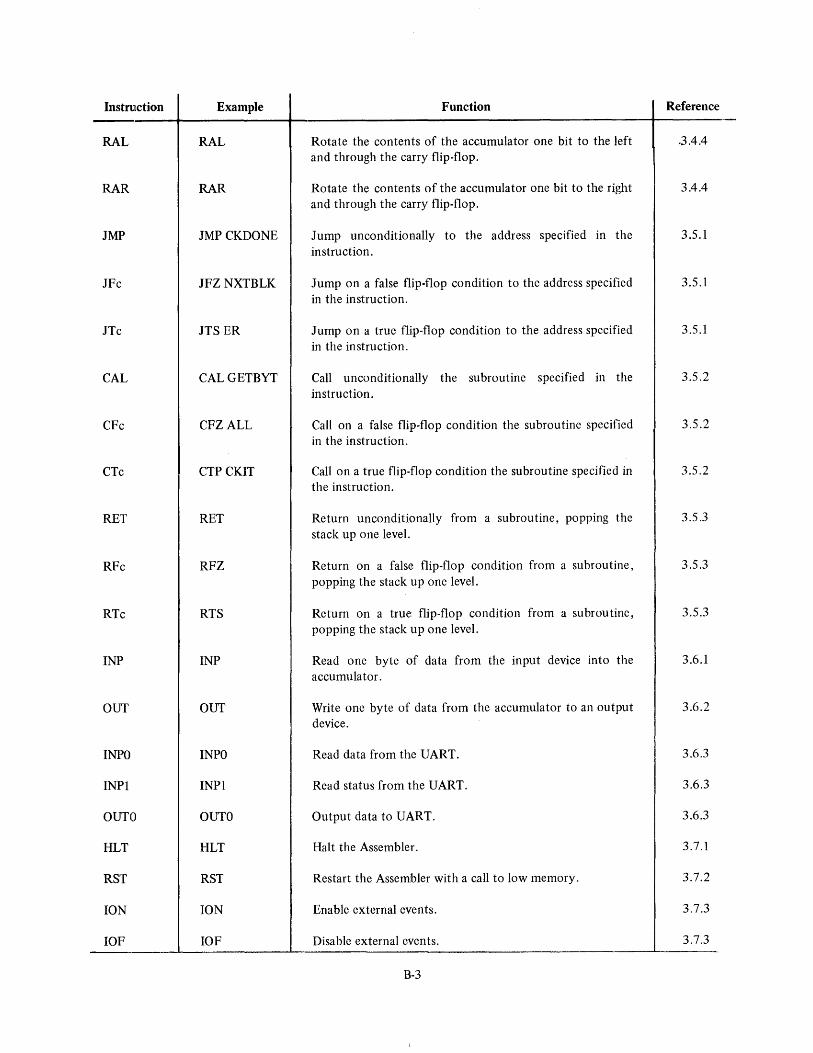
Instruction Example
RAL RAL
RAR RAR
JMP JMPCKDONE
JFc JFZ NXTBLK
JTc JTSER
CAL CALGETBYT
CFc CFZ ALL
CTc CTP CKIT
RET RET
RFc RFZ
RTc RTS
INP INP
OUT OUT
INPO INPO
INPI INPI
aUTO aUTO
HLT HLT
RST RST
ION ION
IOF IOF
Function
Rotate the contents of the accumulator one bit to the left and through the carry flip-flop.
Rotate the contents of the accumulator one bit to the right and through the carry flip-flop.
Jump unconditionally to the address specified in the instruction.
Jump on a false flip-flop condition to the address specified in the instruction.
Jump on a true flip-flop condition to the address specified in the instruction.
Call unconditionally the subroutine specified in the instruction.
Call on a false flip-flop condition the subroutine specified in the instruction.
Call on a true flip-flop condition the subroutine specified in the instruction.
Return unconditionally from a subroutine, popping the stack up one level.
Return on a false flip-flop condition from a subroutine, popping the stack up one level.
Return on a true flip-flop condition from a subroutine, popping the stack up one level.
Read one byte of data from the input device into the accumulator.
Write one byte of data from the accumulator to an output device.
Read data from the UART.
Read status from the UART.
Output data to UART.
Halt the Assembler.
Restart the Assembler with a call to low memory.
Enable external events.
Disable external events.
B-3
Reference
.3.4.4
3.4.4
3.5.1
3.5.1
3.5.1
3.5.2
3.5.2
3.5.2
3.5.3
3.5.3
3.5.3
3.6.1
3.6.2
3.6.3
3.6.3
3.6.3
3.7.1
3.7.2
3.7.3
3.7.3

APPENDIX C SUMMARY OF
ASSEMBLER PSEUDO-INSTRUCTIONS
Pseudo-Instruction
$
PAUSE
*expression
OCT
HEX
DEC
EXPUNGE
OPDEF mnemonic ;value ;type
label, DATA nO;nl ;n2;nm
label, BLOCK size [;initial [;increment] ]
label, TEXT? literal 'V
label, ADDR aO;al ;a2; ... ;am
Function
Signals end of assembly language program.
Causes pause in Assembler processing until CONTinue switch is pressed.
Specifies initial program location counter and can be used to reset current location counter.
Sets radix for subsequent numbers in program to octal (base 8).
Sets radix for subsequent numbers in program to hexadecimal (base 16).
Sets radix for subsequent numbers in program to decimal (base 10).
Deletes instruction symbol table.
Allows programmer to define own instructions according to value and type given.
Assigns values to incremental memory locations.
Assigns a block of memory of the size given with values of zero, an initial value, or a set of increments.
Specifies ASCII character strings and/or numeric representations of ASCII characters to be included in a program.
Assigns address constants to memory locations.
C-l
Reference
6.10.1
6.10.2
6.10.3
6.10.4
6.10.4
6.10.4
6.10.5
6.10.6
6.10.7
6.10.8
6.10.9
6.10.10

APPENDIX D E,UMMARY OF MICROPROCESSOR
DEBUGGIJNG PROGRAM (MDP) COMMANDS
Command Example
R R
P addr 1 ;addr2 P 41#0;41#377
T T
E E
addr/ 1#0/
D addrl ;addr2 D 1#0;1#377
s s
x x
G addr G 10#121
Function
Read paper tape from low-speed reader.
Punch out an address range on low-speed punch.
Produce leader or trailer tape (octal code 200) on low-speed punch.
Punch end block and trailer tape on low speed punch.
Open specified location for examination or modification; specific line terminators may cause additional locations to be examined:
Reference
8.8.1
8.8.2
8.8.3
8.8.4
8.9.1
<cr> close location. 8.9.2
D-1
<If> close location and open next 8.9.3 one. close location and reopen it. 8.9.4
t close location and open 8.9.5 previous one.
Dump specified address range on Teletype printer.
Display and allow modification of status register contents.
Display and allow modification of index register contents.
Execute program to breakpoint location.
8.10.1
8.1 0.2
8.10.3
8.11.1

Command Example
B addr B 37#0
L addrl flddr2;[constant] L 76#340;76#377;7
D-2
Function
Set program breakpoint at specified location.
Load a segment of memory with a specified constant.
Referenc~~
8.11.2
8.11.3
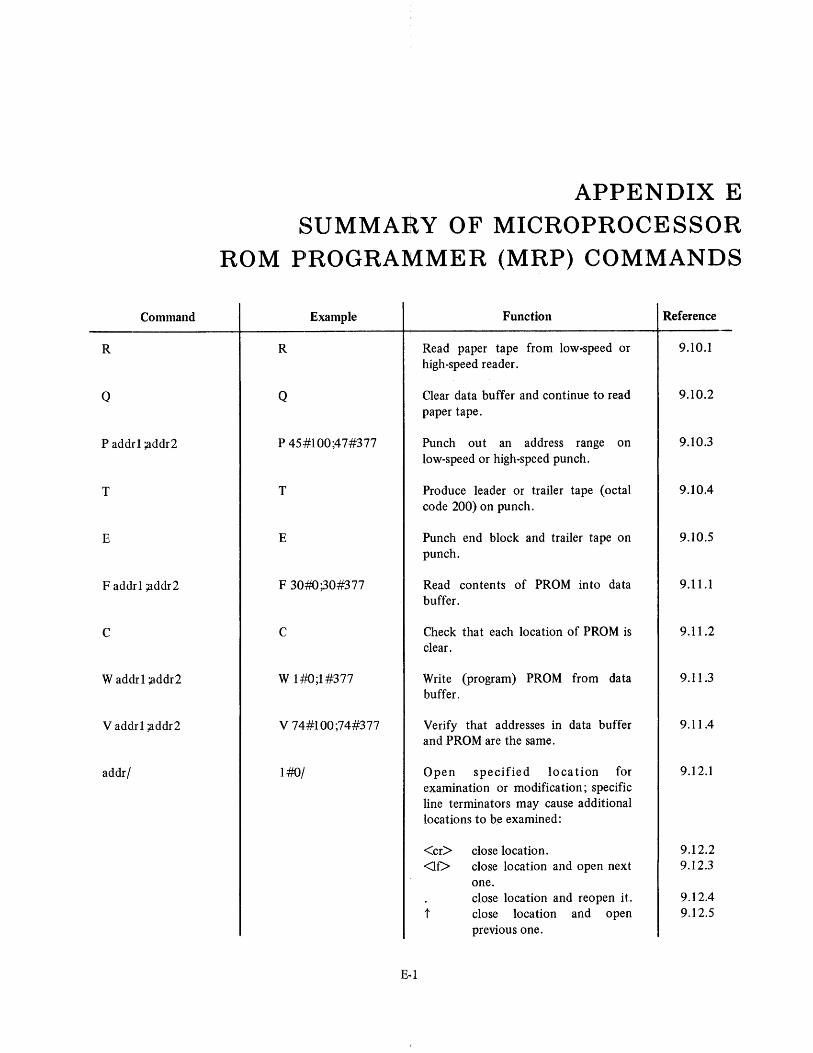
Command
R
Q
P addrl ;addr2
T
E
F addrl ;addr2
C
W addrl ;addr2
V addrl ;addr2
addr/
APPENDIX E ~3UMMARY OF MICROPROCESSOR
ROM P~ROGRAMMER (MRP) COMMANDS
Example
R
Q
P 45#100;47#377
T
E
F 30#0 ;30#377
C
W 1#0;1#377
V 74#100;74#377
1#0/
Function
Read paper tape from low-speed or high-speed reader.
Clear data buffer and continue to read paper tape.
Punch out an address range on low-speed or high-speed punch.
Produce leader or trailer tape (octal code 200) on punch.
Punch end block and trailer tape on punch.
Read contents of PROM into data buffer.
Check that each location of PROM is clear.
Write (program) PROM from data buffer.
Verify that addresses in data buffer and PROM are the same.
Open specified location for examination or modification; specific line terminators may cause additional locations to be examined:
<cr> close location. <If> close location and open next
one. close location and reopen it.
t close location and open previous one.
Reference
9.10.1
9.10.2
9.10.3
9.10.4
9.10.5
9.11.1
9.11.2
9.11.3
9.11.4
9.12.1
9.12.2 9.12.3
9.12.4 9.12.5
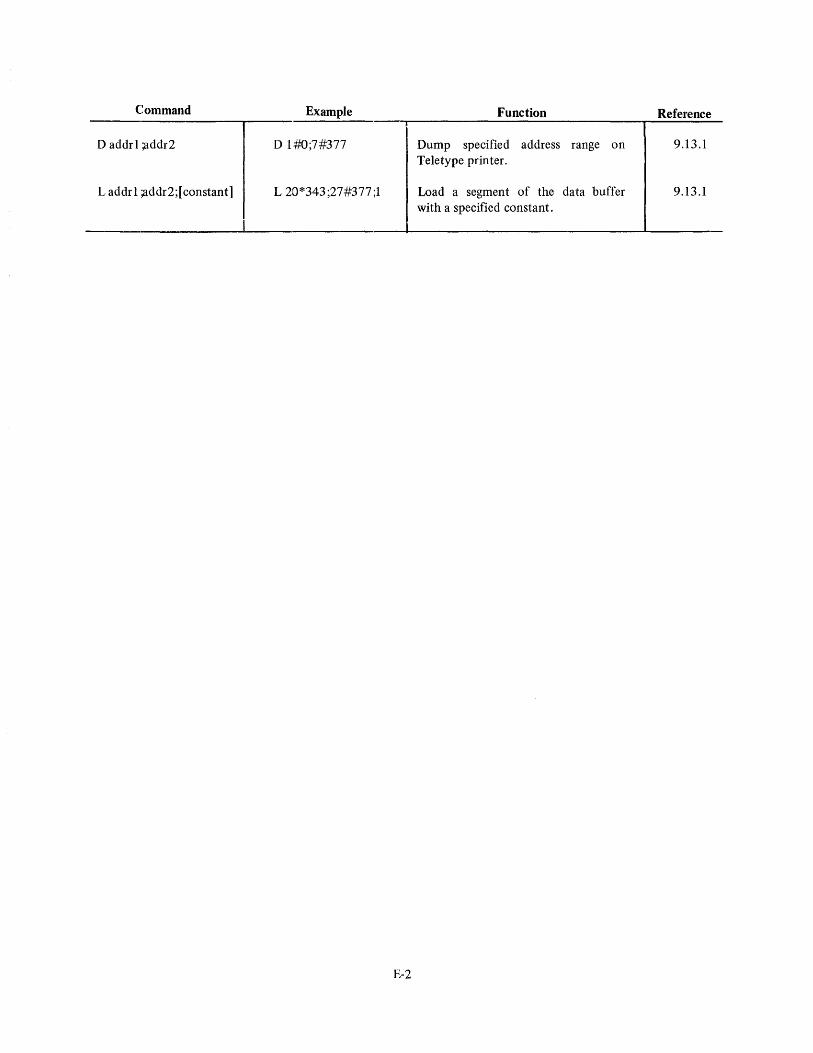
Command Example
D addr 1 ;addr2 D 1#0;7#377
L addrl ;addr2;[ constant] L 20*343;27#377;1
E-2
Function
Dump specified address range on Teletype printer.
Load a segment of the data buffer with a specified constant.
Reference
9.13.1
9.13.1

APPENDIX F
BLOCK··OFFSET TO OCTAL CONVERSION
This appendix can be used if it is ever necessary to convert the block-offset notation in assembly language programs and output to octal notation. Only the first and last conversions are given for each block. To convert an offset within a given block, simply add the offset to the starting octal location in the block. For example:
Block Offset Octal
11 o 4400
11 377 4777
To convert block 11 offset 227 to octal, simply add 227 to 4400. The correct octal equivalent is thus 4627.
Block
1 2
2 3
3 4
4
Offset
o
377 o
377 o
377 o
377
Octal
0400
0777 1000
1377 1400
1777 2000
2377
Decimal
0256
0511 0512
0767 0768
1023 0124
1279
F-l
Block
5
5 6
6 7
7 10
10
Offset
o
377 o
377 o
377 o
377
Octal
2400
2777 3000
3377 3400
3777 4000
4377
Decimal
1280
1535 1536
1791 1792
2047 2048
2303

Block
11
11 12
12 13
13 14
14 15
15 16
16 17
17 20
20 21
21 22
22
Offset Octal
o 4400
377 4777 o 5000
377 5377 o 5400
377 5777 o 6000
377 6377 o 6400
377 6777 o 7000
377 7377 o 7400
377 7777 o 10000
377 10377 o 10400
377 10777 o 11000
377 11377
Decimal
2304
2559 2560
2815 2816
3071 3072
3327 3328
3583 3584
3839 3840
4095 4096
4351 4352
4607 4608
4863
F-2
Block
23
23 24
24 25
25 26
26 27
27 30
30 31
31 32
32 33
33 34
34
Offset
o
377 o
377 o
377 o
377 o
377 o
377 o
377 o
377 o
377 o
377
Octal
11400
11777 12000
12377 12400
12777 13000
13377 13400
13777 14000
14377 14400
14777 15000
15377 ]5400
15777 16000
16377
Decimal
4864
5119 5120
5375 5376
5631 5632
5887 5888
6143 6144
6399 6400
6655 6656
6911 6912
7167 7168
7423

Block
35
35 36
36 37
37 40
40 41
41 42
42 43
43 44
44 45
45 46
46
Offset Octal
o 16400
377 16777 o 17000
377 17377 o 17400
377 17777 o 20000
377 20377 o 20400
377 20777 o 21000
377 21377 o 21400
377 21777 o 22000
377 22377 o 22400
377 22777 o 23000
377 23377
Decimal
7424
7679 7680
7935 7936
8191 8192
8447 8448
8703 8704
8959 8960
9215 9216
9471 9472
9727 9728
9983
F-3
Block
47
47 50
50 51
51 52
52 53
53 54
54 55
55 56
56 57
57 60
60
Offset Octal Decimal
o 23400 9984
377 23777 10239 o 24000 10240
377 24377 10495 o 24400 10496
377 24777 10751 o 25000 10752
377 25377 11007 o 25400 11008
377 25777 11263 o 26000 11264
377 26377 11519 o 26400 11 520
377 26777 11775 o 27000 11776
377 27377 12031 o 27400 12032
377 27777 12287 o 30000 12288
377 30377 12543
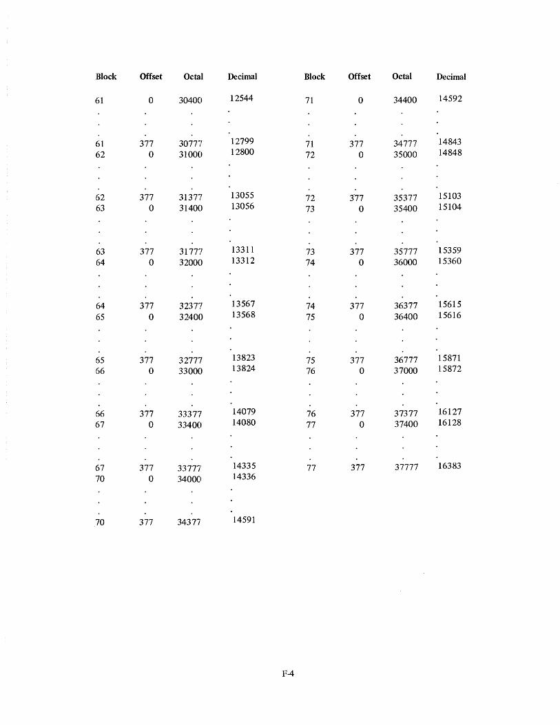
Hlock
61
61 62
62 63
63 64
64 65
65 66
66 67
67 70
70
Offset Octal
o 30400
377 30777 o 31000
377 31377 o 31400
377 31777 o 32000
377 32377 o 32400
377 32777 o 33000
377 33377 o 33400
377 33777 o 34000
377 34377
DecimaJ
12544
12799 12800
13055 13056
13311 13312
13567 13568
l3823 13824
14079 14080
14335 14336
14591
F-4
Block
71
71 72
72 73
73 74
74 75
75 76
76 77
77
Offset
o
377 o
377 o
377 o
377 o
377 o
377
Octal
34400
34777 35000
35377 35400
35777 36000
36377 36400
36777 37000
37377 37400
37777
Decimal
14592
14843 14848
15103 15104
15359 15360
15615 15616
15871 15872
16127 16128
16383
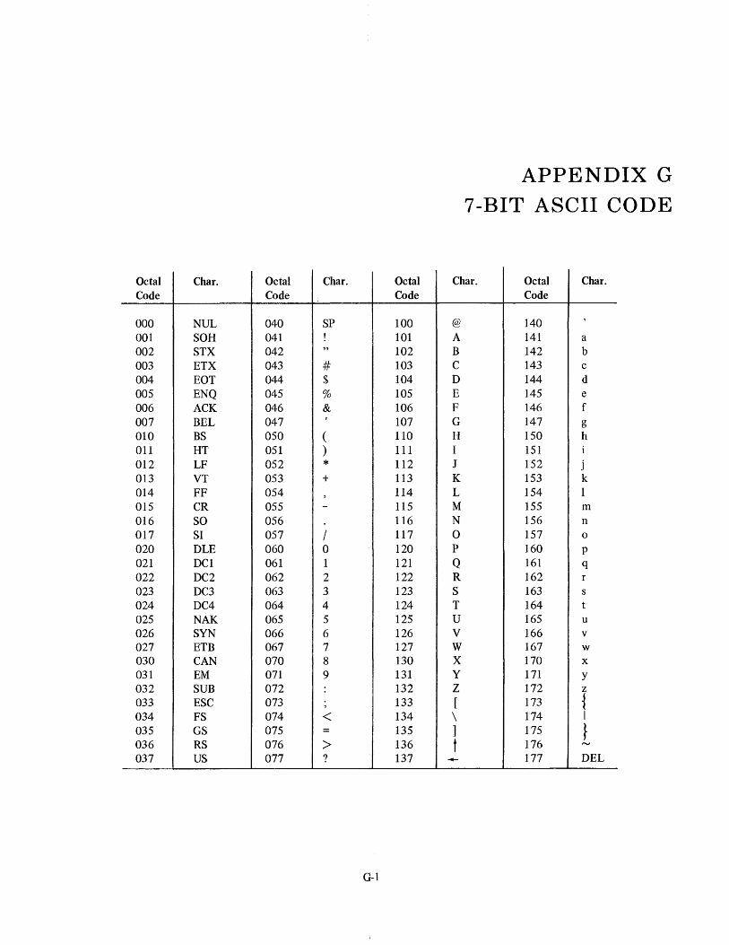
Octal Char. Octal Char. Code Code
000 NUL 040 SP 001 SOH 041 ! 002 STX 042 " 003 ETX 043 # 004 EOT 044 $ 005 ENQ 045 % 006 ACK 046 & 007 BEL 047
,
010 BS 050 ( 011 HT 051 ) 012 LF 052 * 013 VT 053 + 014 FF 054 , 015 CR 055 -
016 SO 056 017 SI 057 / 020 DLE 060 0 021 DCl 061 1 022 DC2 062 2 023 DC3 063 3 024 DC4 064 4 025 NAK 065 5 026 SYN 066 6 027 ETB 067 7 030 CAN 070 8 031 EM 071 9 032 SUB 072 033 ESC 073 , 034 FS 074 < 035 GS 075 = 036 RS 076 > 037 US 077 ?
G-1
Octal Code
100 101 102 103 104 105 106 107 110 111 112 113 114 115 116 117 120 121 122 123 124 125 126 127 130 131 132 133 134 135 136 137
APPENDIX G
7 -BIT ASCII CODE
Char. Octal Char. Code
@ 140 ,
A 141 a B 142 b C 143 c D 144 d E 145 e F 146 f G 147 g
H 150 h I 151 i J 152 j K 153 k L 154 1 M 155 m N 156 n 0 157 0
P 160 P Q 161 q R 162 r
S 163 s T 164 t
U 165 u
V 166 v W 167 w X 170 x Y 171 y Z 172 z [ 173 { \ 174 I ] 175 } t 176 ,..."
-- 177 DEL

NORTHEAST REGIONAL OFFICE: 235 Wyman Street. WHitham, Mass. 02154 Telephone: (617)-890-0330/0310 Dataphone: 617-890-3012 or 3013
CONNECTICUT Meriden 240 Pomeroy Ave., Morlden. Conn. 06540 Telephone, (203)-237-844117466 Detaphone 203-237-8205 Fairfield 1275 Post Road, Fairfield. Conn. 06430 Telephone, (203)-255-0-991
NEW YORK Rochester 130 Aliens Creek Road. Rochester. New York Telephone, (716)-481-1700 Dataphone, 716-244-1680 Syracuse 6700 Thompson Road. Syracuse, New York 13211 Telephone, (315)-437-159317085 Dataphone, 315-454-4152
MASSACHUSETTS Marlborough One Iron Way Marlborough, Mass. 01752 Telephone, (617)-481-7400 Tele" 710-347-0348
MID-ATLANTIC REGIONAL OFFICE: U.S. Route 1. Prlncetcn, New Jersey 08540 Telephone, (609)-452-2940 FLORIDA Orlando Suite 130. 7001 Lake Ellener Drive, Orlando, Florida 32809 Telephone, (305)-851-4450 Dataphone, 305-859-2360
GEORGIA Atlanta 2815 Clearvlew Piece. Suite 100 Atlante, Georgie 03040 Telephone, (404)-451-7411 Detaphone, 305-859-2360
NORTH CAROLINA Durhem/Chapel HIli Executive Park 3700 Chepel HIli Blvd. Durham. North Carolina 27707 Telephone, (919)-489-3347 Dataphone, 919-489-7832
NEW JERSEY Fairfield 253 Passaic Ave .. Fairfield, N~w Jersey 07006 Telephon., (201)-227-9280 Dataphone, 201-227-9290 Metuchen 95 Main Street. Metuchen, New Jersey 08840 Telephone, (201)-549-4100/2000 Dataphone, 201-548-0144
EUROPEAN HEADQUARTERS Digital Equipment Corporation International Europe 81 route de I' Alre 1211 Geneva 26, Switzerland Telephone, 42 79 50 Tele., 22 663
FRANCE Digital Equipment France Centre Sllie - Cldex L 225 94533 Rungls, France Telephone: 687·23·33 Telex 26840 GRENOBLE Digital Equipment France Tour Mangin 16 Rue Du Gal Mangin 38100 Grenoble. France Telephone, (76)-87-56-01 Tele., 212-32882
GERMAN FEDERAL REPUBLIC Dlgltel Equipment GmbH MUNICH 8 Muenchen 13. Wallenstelnplatz 2 Telephone, 0811-35031 Tele" 524-226 COLOGNE 5 Koeln 41. Aachener Strass9 311 Telephone, 0221-<\4-40·95 Tele" 888-2269 Telegram: Flip Chip Koeln
FRANKFURT 6078 Neu·lsenburg 2 Am Foretau8 Gravebrllch 5-7 Telephone, 06102-5526 Tel • ., 41-78-82 HANNOVER 3 Hannover, PodbrelsJ.:lstraase 102 Telephone, 0511-69-70·95 T.le., 922-952 STUTTGART 0·7301 Kemnat, Stuttgart Marco·Polo·Strasse 1 Telephone, (0771)-45-50-65 Telex, 841-722-393
AUSTRIA Digital Equipment Corporation Ges,m.b.H. VIENNA Marlahllferstrasse 136. 1150 Vienna 15. Austria Telephone, 88 51 88
UNITED KINGDOM Digital Equipment Co. Ltd, U.K. HEADQUARTERS Fountain House. Butts Centre Re.dlng RGI 7QN. Eogland
Telephone, (0734)-5835'>5 Tele" 8483278 BIRMINGHAM Maney Buildings 29/31 Birmingham Rd .. Sutton Coldfleld Warwlckahlre. England Telephone· 021-355-5501 Tele" 337-080 BRISTOL Fish Ponds Road. Fish Ponds Bristol. Englend BS163HQ Telephone: Bristol 651·431 EAL/NG Bilton House. Uxbridge Road. Eallng. London W.5. Telephone, 01-579-2334 Telo" 22371 EDINBURGH Shiel House, Cralgshill. Livingston. West Lothian. Scotland Telephone: 32705 Telex: 727113
LONDON Management House 43 Parker St.. Holborn. London WC 2B 5PT. Englend Telephone: 01·405-261~114067 Telex' 27560 MANCHESTER Arndale House Chester Road. Stretford. Manchester M32 9BH Telephone, (061)-885-7011 Tele" 668866
~D~DD~D DIGITAL EQUIPMENT CORPORATION
WORLDWIDE SALES OFFICES COMPONENTS GROt;JP HEADQUARTERS ONE IRON WAY. MARLBOROUGH. MASSACHUSETTS 01752
(617) 4817400 TWX 710·34J.0348 For detaIled l%rmahor aboulproducls and polICIes. call800·225-9480 loll·/ree (USA only). Massachusellsresldents call (617)481-7400
OOMESTIC
MID-ATLANTIC (cont.) Princeton U.S. Route 1. Princeton. New Jersey 08540 Telephone, (609)-452-2!14O Detephone, 609-452-2940
NEW YORK Long Island 1 Huntington Quadrangle Suite 1507 Huntington Station. New York 11746 Telephone, (516)-694-4131. (212)-895-6095 Detaphone, 516-293-56H3 Manhattan 810 7th Ave .. 22nd Floor New York. N.Y. 10019 Telephone, (212)-562-1:300
PENNSYLVANIA Philadelphl. Digital Hall 1740 Walton Road, Blue Bell. Pennsylvania 19422 Telephone, (215)-825-4200
TENNESSEE Knoxville 6311 Kingston Pike, Suite 21E Knoxville. Tennessee 37919 Telephone, (615)-588-6S71 Dataphone, 615-584,0571
WASHINGTON D.C. Lanham 30 Office Building 4900 Princess Garden Parkway. Lanham. Maryland Telephone, (301)-459-7.00 Dataphone, 301-459-7900 X53
CENTRAL REGIONAL OFFICE: 1850 Frontage Road. N,orthbrook. Illinois 60062 Telephone, (312)-498-2!OO Detephone, 312-498-2500
INDIANA Indianapolis 21 Beachway Drive. S'.ute G Indianapolis. Indiana 46224
Ex. 78
Telephone, (317)-243-8:141 Dataphone, 317-247-1212
ILLINOIS Chicago 1850 Frontage Road Northbrook. illinois 80062 Dataphone, 312-498-2500
LOUISIANA New Orleans 3100 Rldgel.ke Drive. Suite 108 Metairie. Louisiana 70002 Telephone, (504)-837-02'57 Dataphone, 504-633-2800
CENTRAL (cont.) MICHIGAN Ann Arbor 230 Huron View Boulevard. Ann Arbor, Michigan 48103 Telephone, (313)-761-1150 Dataphone, 313-769-9863 Detroit 23777 Greenfield Road Suite 189 Southfield. Michigan 48075 Dataphone, 313-557-3063 MINNESOTA Minneapolis 8030 Cedar Ave. South, Minneapolis, Minnesota 55420 Telephone, (612)-854-6562-3-4-5 Detaphone, 612-654-1410 MISSOURI Kensaa City 12401 East 43rd Street. Independence, Missouri 64055 Telephone, (816)-252-2300 Dataphone, 816-481-3100 St. Louis Suite 110. 115 Progress Parkway Maryland Heights. Missouri 63043 T.'ephone, (314)-878-4310 Datephone, 816-481-3100 OHIO Cleveland 2500 Euclid Avenue. Euclid. Ohio 44117 Telephone, (216)-948-8484 Dataphone, 216-948-8477 Dayton 3101 Kettering Boulevard Dayton. Ohio 45439 Telephone, (513)-294-3323 Dataphone, 513-298-4724 OKLAHOMA Tulsa 3140 S. Wlneton Winston Sq. Bldg., Suite 4, Tulsa. Oklahoma 74135 Telephone, (918)-749~4476 Detephone, 918-749-2714 PENNSYLVANIA Pittsburgh 400 Penn. Center Boulevard. Pittsburgh. PennsylvanIa 15235 Telephone, (412)-243-9404 Dataphone, 412-824-9730 TEXAS Dallas Plaza North. Suite 513 2880 LBJ Freeway, Dallas. Texas 75234 Telephone, (214)-620-2051 Datephone, 214-620-2061 HOUSTON 6656 Hornwood Drive Monterey Park, Houston. Texas 77036 Telephone, (713)-777-3471 Dataphone, 713-777-1071 WISCONSIN Milwaukee 8531 West Capitol Drive. Milwaukee. Wisconsin 53222 Telephone, (414)-483-9110 Detephone, 414-463-9115
UNITED KINGDOM (cont.) READING
INTERNATIONAL
ISRAEL
Fountain House. Butta Centre Reading RGI 7QN. En'lland Telephone, (0734)-5635S5 Tele" 8463278
NETHERLANDS Dlgltel Equipment N.V. THE HAGUE Sir Winston Churchillian 370 RIjswijk/The Hague. Netherlands Telephone, 94 9220 Tele" 32533
BELGIUM Dlgltel Equipment N.V'/S.A. BRUSSELS 108 Rue D'Arlon 1040 Brussels. Belgium Telephone, 02-139258 Tele" 25297
SWEDEN Dlgltel Equipment AB STOCKHOLM Englundavagen 7. 171 411 So Ina. Sweden Telephone, 98 1390 Telex, 170 50 Cable, Dlgltel Stockholm
NORWAY Digital Equipment Cor,p_ A/S OSLO Trondhelmsvelen 47 0.10 5. Norway Telephone, 02/6834 40 Tele" 19079 DEC N
DENMARK Digital Equipment Aktfebolag COPENHAGEN Hellerupveg 66 2900 Hellerup. Denmark
FINLAND Dlgltel Equipment AB HELSINKI Tltlsmaantle 6 SF-00710 HelSinki 71 Telephone, (090) 370133 Ceble, Dlgltel HelSinki
SWITZERLAND Digital Equipment Corporation S.A. GENEVA 20. Qual Ernest Anserrnet Boite Postale 23, 1211 Geneva 8. SWitzerland Telephone No. 022/204020 and 2058 93 and 20 68 93 Tele" 289201
ZURICH Digital Equipment Corp. AG SchaHhauserstr.315 CH-8050 Zurich. SWitzerland Telephone: 01·46-41-91 Telex: 56059
ITALY Digital Equipment S.p.A. MILAN Corso Garibaldi 49. 20121 Milano. Italy Telephone, (02)-879-051/2/3/4/5 Tele" 643-33815
SPAIN Digital Equipment Corporation Ltd. MADRID Atalo IngenleroB S.A .. Enrique Larreta 12. Madrid 16 Telephone, 215 35 43 Tele" 27249
BARCELONA Atelo Ingenleroe S.A .. Granduxer 76. Barcelona 6 Telephone, 221 44 66
DEC Systems Computers Ltd. TEL AVIV Suite 103. Southern Habakuk Street Tel Aviv, Israel Telephone, (03) 443114/440763 Tele" 922-33-3163
OANADA Digital Equipment of Caneda. Ltd. CANADIAN HEADQUARTERS P.O. Box 11500 Ottawa. OntariO. Canada K2H aK8 Telephone, (613)-592-5111 TWX, 610-562-8732
TORONTO 2550 Goldenrldge Road, Mississauga. OntariO Telephone, (416)-270-9400 TWX, 610-492-7118
MONTREAL 9045 Cote De Uease Dorval. Quebec. Canada H9P 2M9 Telephone· (514)-638-9393 Tele" 610-422-4124
CALGARY/Edmonton Suite 140. 6940 Fisher Road S.E. Calgary. Alberta. Canada Telephone, (403)·435-4661 TWX, 403-255-7408
VANCOUVER Suite 202 644 S.W. Marine Dr .. Vancouver British Columbia. Canada VBP 5Y1 Telephone, (604)-325-3231 Tele" 610-929-2006
GENERAL INTERNATIONAL SALES REGIONAL OFFICE 146 Main Street. Maynard. Massachusetts 01754 Telephone, (617) 697-5111
From Metropolitan Boston, 646--8600 TWX, 710-347-0217/0212 Ceble, DIGITAL MAYN Tele" 94-8457
AUSTRALIA Digital Equipment Australia Ply. Ltd. ADELAIDE 6 Montrose Avenue Norwood. South Australia 5067 Telephone, (08)-42-1339 Telex, 790-82825
BRISBANE 133 Lelchhardt Street Spring Hili Brisbane. Queensland. Australia 4000 Telephone, (072)-293088 Tele" 790-40816
CANBERRA 21 Collie St. Fyshwlck. A.C.T. 2609 Australia T.'ephone, (062)-959073
MELBOURNE 60 Park Street. South Melbourne. Victoria 3205 Australia Telephone, (03)-699-2888 Tele" 790-30700
PERTH 643 Murray Street West Perth. Western Australia 6005 Telephone, (092)-21-4993 Telex, 790-92140
SYDNEY P.O. Box 491. Crows Nest N.S.w. Auatralle 2065 r.lephone, (02)-439-2566 Tele" 790-20740
NEW ZEALAND Digital Equipment CorporatIon Ltd. AUCKLAND Hilton House. 430 Queen Street. Box 2471 Auckland. New Zealand Telephone, 75533
WEST REGIONAL OFFICE: 310 Soquel Way. Sunnyvale, California 9<4086 Telephone, (408)-735-9200 Detephone, 403-735-1820
ARIZONA Phoenix 4358 EaBt Broadway Road. Phoenix. Arizona 85040 Telephone, (802)-268-3488 Dataphone 602-268-7371
CALIFORNIA Santa Ana 2110 S. Anne Street. Santa Ana. CalifornIa 92704 Telephone, (714)-979-2460 Dataphono, 714-979-7650 San Diego 6154 Mission Gorge Road Suite 110. San ~iego. Celifornle Telephone, (714)-290-788017970 Dataphone, 714-280-7825 Sen Francisco 1400 Terra Bella. Mountain View. CalifornIa 94040 Telephone, (415)-964-6200 Dataphone, 415-964-1438 Oakland 7850 Edgewater Drive. Oakland. California 94621 Telephone, (415)-635-545317930 Datephone, 415-562-7180 West Los Angeles 1510 Cotner Avenue. LOB Angeles. California 90025 Telephone, (213)-479-3791/4318 Dataphone, 213-478-5626 COLORADO 7901 E. Bellevue Avenue Suite 5. Englewood. Colorado 80110 Telephone, (303)-770-6150 Dataphone, 303-770-6628
NEW MEXICO Albuquerque 10200 Menual N.E .. Albuquerque. New Maxlco 87112 Telephone, (505)-296-50411/5426 Dataphone, 505-294-2330
OREGON Portland Suite 188 5319 S.W. Westgate Drive, Portland. Oregon 97221 Telephone, (503)-297-3761/3765
UTAH Salt Lake City 429 Lewn Dale Drive. Salt Leke City. Utah 84115 Telephone (901)-467-4869 Detephone, 801-467-0535
WASHINGTON Bellevue 13401 N_E. Bellevue. Redmond Road. Suite 111 Bellevue. Washington 98005 Telephone, (206)-545-4056/455-5404 Detaphone, 206-747-3754
JAPAN Digital Equipment Corporation International Kowa Building No. 18 - Annex. Firat Floor 9·20 Akaseka 1-Chome Minato-Ku, Tokyo 107, Japan Telephone, 588-2771 Tole" J-26428 Rlkei Trading Co .• Ltd. (s.le. only) Kozato·Kalkan Bldg. No. 1S-14 Nlahiehlmbashl 1-Chome Mlnato·Ku, Tokyo. Japan Telephone: 5915246 Telex: 781·4208
PUERTO RICO Digital Equipment Corporation De Puerto RICO 407 del Parque Street Senturce. Puarto Rico 00912 Telephone, (809)-723-8069/67 Tel." 385~9056
ARGENTINA BUENOS AIRES Coesln S.A. Vlrrey del Pino. 4071. Buenos Aires Telephone' 52-3185 Telex: 012·2284
BRAZIL RIO DE JANEIRO - GB Ambrlex S.A. Rua CearA. 104. 2 e 3 andares ZC - 29 Rio De Janeiro - GB Telephone, 264-7408/046117825
SAO PAULO Ambrlex S.A. Rua Tupl. 535 Sao Paulo - SP Telephone, 52-7808/1870. 51-0912
PORTO ALEGRE - RS Rua Coronel Vicente 421/101 Porto Alegre --- RS Telephone, 24-7411
CHILE SANTIAGO Coasln Chile Ltda. (sales only) CasUla 14588. Correo 15. Telephone, 396713 Cable, COACHIL
INDIA BOMBAY Hlndltron Computers Pvt. Ltd. 69/ A. L. Jsgmohandas Marg. Bombay~6 (WB) Indle Telephone, 38-1615,38-5344 T.le" 011-2594 Plenty Cable, TEKHIND
MEXICO MEXICO CITY Mexltek. S.A. Eugenia 408 Deptos. 1 Apdo. Postal 12-1012 MexiCO 12. D.F. Telephone, (905) 536~09-10
PHILIPPINES MANILA Stanford Computer Corporation P.O. Box t808 416 D8smarlnas St .• Manila Telephone, 49-68-96 Tele" 742-0352
VENEZUELA CARACAS Coesln. C.A. Apartado 50939 Sabane Grande No.1. Caracas 105 Telephone, 72-8662, 72-9637 C.ble, INSTAUVEN

~DmDDmD COMPONENTS
GROUP DIGITAL EQUIPMENT CORPORATION. COMPONENTS GROUP. ONE IRON WAY. MARLBOROUGH. MASSACHUSETTS 017e,2
(617) 481-7400 TWX 710-347-0348
~RINTED IN U.S.A. 11174 531009/04/14 20