
MP2671 - MPS
11
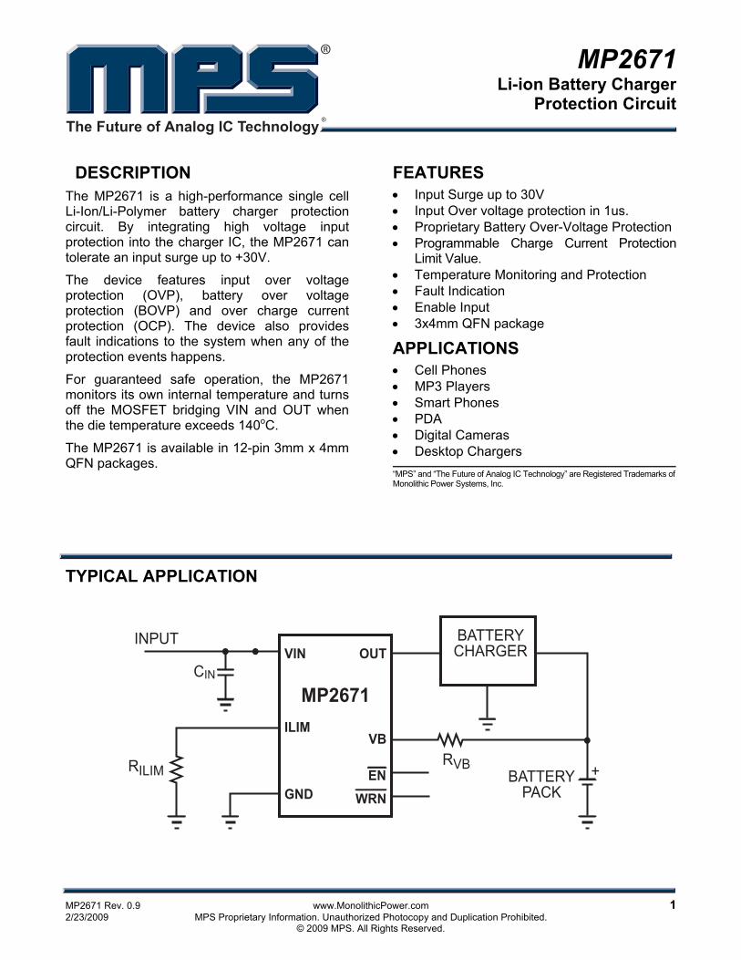
MP2671 Li-ion Battery Charger Protection Circuit MP2671 Rev. 0.9 www.MonolithicPower.com 1 2/23/2009 MPS Proprietary Information. Unauthorized Photocopy and Duplication Prohibited. © 2009 MPS. All Rights Reserved. The Future of Analog IC Technology DESCRIPTION The MP2671 is a high-performance single cell Li-Ion/Li-Polymer battery charger protection circuit. By integrating high voltage input protection into the charger IC, the MP2671 can tolerate an input surge up to +30V. The device features input over voltage protection (OVP), battery over voltage protection (BOVP) and over charge current protection (OCP). The device also provides fault indications to the system when any of the protection events happens. For guaranteed safe operation, the MP2671 monitors its own internal temperature and turns off the MOSFET bridging VIN and OUT when the die temperature exceeds 140 o C. The MP2671 is available in 12-pin 3mm x 4mm QFN packages. FEATURES • Input Surge up to 30V • Input Over voltage protection in 1us. • Proprietary Battery Over-Voltage Protection • Programmable Charge Current Protection Limit Value. • Temperature Monitoring and Protection • Fault Indication • Enable Input • 3x4mm QFN package APPLICATIONS • Cell Phones • MP3 Players • Smart Phones • PDA • Digital Cameras • Desktop Chargers “MPS” and “The Future of Analog IC Technology” are Registered Trademarks of Monolithic Power Systems, Inc. TYPICAL APPLICATION MP2671 VIN OUT VB EN WRN ILIM GND INPUT BATTERY CHARGER BATTERY PACK C IN R ILIM R VB +
-
Upload
khangminh22 -
Category
Documents
-
view
1 -
download
0
Transcript of MP2671 - MPS
MP2671 Li-ion Battery Charger
Protection Circuit
MP2671 Rev. 0.9 www.MonolithicPower.com 1 2/23/2009 MPS Proprietary Information. Unauthorized Photocopy and Duplication Prohibited. © 2009 MPS. All Rights Reserved.
The Future of Analog IC Technology
DESCRIPTION The MP2671 is a high-performance single cell Li-Ion/Li-Polymer battery charger protection circuit. By integrating high voltage input protection into the charger IC, the MP2671 can tolerate an input surge up to +30V.
The device features input over voltage protection (OVP), battery over voltage protection (BOVP) and over charge current protection (OCP). The device also provides fault indications to the system when any of the protection events happens.
For guaranteed safe operation, the MP2671 monitors its own internal temperature and turns off the MOSFET bridging VIN and OUT when the die temperature exceeds 140oC.
The MP2671 is available in 12-pin 3mm x 4mm QFN packages.
FEATURES • Input Surge up to 30V • Input Over voltage protection in 1us. • Proprietary Battery Over-Voltage Protection • Programmable Charge Current Protection
Limit Value. • Temperature Monitoring and Protection • Fault Indication • Enable Input • 3x4mm QFN package
APPLICATIONS • Cell Phones • MP3 Players • Smart Phones • PDA • Digital Cameras • Desktop Chargers “MPS” and “The Future of Analog IC Technology” are Registered Trademarks of Monolithic Power Systems, Inc.
TYPICAL APPLICATION
MP2671
VIN OUT
VB
ENWRN
ILIM
GND
INPUT BATTERYCHARGER
BATTERYPACK
CIN
RILIMRVB +
MP2671 – CHARGE SYSTEM PROTECTION CIRCUIT
MP2671 Rev. 0.9 www.MonolithicPower.com 2 2/23/2009 MPS Proprietary Information. Unauthorized Photocopy and Duplication Prohibited. © 2009 MPS. All Rights Reserved.
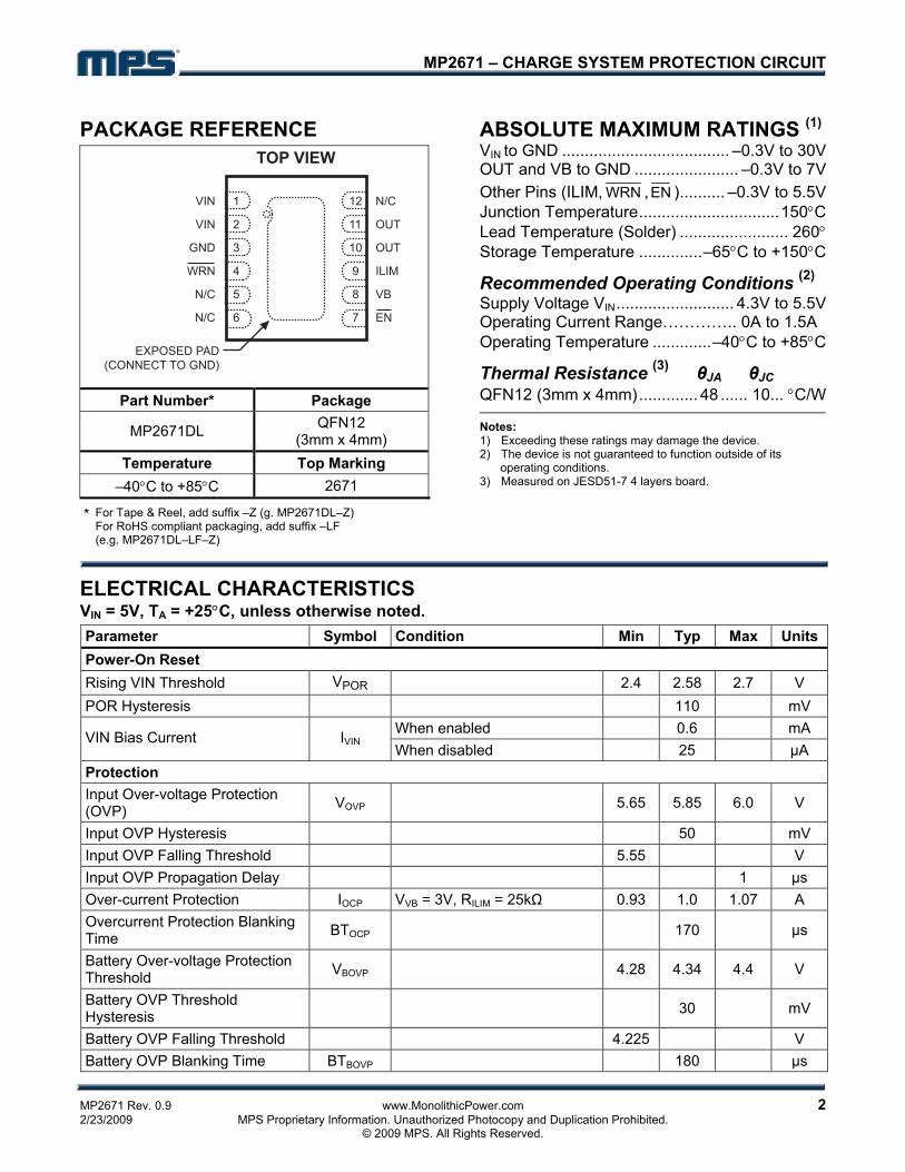
PACKAGE REFERENCE TOP VIEW
VIN
VIN
GND
WRN
N/C
N/C
1
2
3
4
5
6
N/C
OUT
OUT
ILIM
VB
EN
12
11
10
9
8
7
EXPOSED PAD(CONNECT TO GND)
Part Number* Package
MP2671DL QFN12 (3mm x 4mm)
Temperature Top Marking –40°C to +85°C 2671
* For Tape & Reel, add suffix –Z (g. MP2671DL–Z) For RoHS compliant packaging, add suffix –LF (e.g. MP2671DL–LF–Z)
ABSOLUTE MAXIMUM RATINGS (1) VIN to GND ..................................... –0.3V to 30V OUT and VB to GND ....................... –0.3V to 7V Other Pins (ILIM, WRN ,EN ).......... –0.3V to 5.5V Junction Temperature...............................150°C Lead Temperature (Solder) ........................ 260° Storage Temperature ..............–65°C to +150°C
Recommended Operating Conditions (2) Supply Voltage VIN.......................... 4.3V to 5.5V Operating Current Range………….. 0A to 1.5A Operating Temperature .............–40°C to +85°C
Thermal Resistance (3) θJA θJC QFN12 (3mm x 4mm)............. 48 ...... 10... °C/W
Notes: 1) Exceeding these ratings may damage the device. 2) The device is not guaranteed to function outside of its
operating conditions. 3) Measured on JESD51-7 4 layers board.
ELECTRICAL CHARACTERISTICS VIN = 5V, TA = +25°C, unless otherwise noted. Parameter Symbol Condition Min Typ Max Units Power-On Reset Rising VIN Threshold VPOR 2.4 2.58 2.7 V POR Hysteresis 110 mV
When enabled 0.6 mA VIN Bias Current IVIN When disabled 25 µA
Protection Input Over-voltage Protection (OVP) VOVP 5.65 5.85 6.0 V
Input OVP Hysteresis 50 mV Input OVP Falling Threshold 5.55 V Input OVP Propagation Delay 1 µs Over-current Protection IOCP VVB = 3V, RILIM = 25kΩ 0.93 1.0 1.07 A Overcurrent Protection Blanking Time BTOCP 170 µs
Battery Over-voltage Protection Threshold VBOVP 4.28 4.34 4.4 V
Battery OVP Threshold Hysteresis 30 mV
Battery OVP Falling Threshold 4.225 V Battery OVP Blanking Time BTBOVP 180 µs

MP2671 – CHARGE SYSTEM PROTECTION CIRCUIT
MP2671 Rev. 0.9 www.MonolithicPower.com 3 2/23/2009 MPS Proprietary Information. Unauthorized Photocopy and Duplication Prohibited. © 2009 MPS. All Rights Reserved.
ELECTRICAL CHARACTERISTICS (continued) VIN = 5V, TA = +25°C, unless otherwise noted. Parameter Symbol Condition Min Typ Max Units VB Pin Leakage Current VVB = 4.4V 20 nA Over Temperature Protection Rising Threshold 140 °C
Over Temperature Protection Falling Threshold 90 °C
Logic
EN Input Logic HIGH 1.5 V
EN Input Logic LOW 0.4 V
EN Internal Series Resistor 100 200 400 kΩ WRN Output Logic Low Sink 5mA current 0.35 0.8 V WRN Output Logic High Leakage Current 1 µA
Power MOSFET
On Resistance RDS(ON) Measured at 500mA, 4.3<VIN<5.5V 170 280 mΩ
PIN FUNCTIONS 12-pin QFN Name Description
1,2 VIN Input Power Source. VIN can withstand 30V input.
3 GND,
Exposed Pad
System Ground. Exposed pad and GND pin must be connected to the same ground plane.
4 WRN Open-Drain Logic Output. This pin turns LOW when any protection event occurs. 5,6 NC No Connect. Keep it floating.
7 EN Enable. Leave this pin floating or pull it below 0.4V to enable the IC. Drive this pin higher than 1.5V to disable the IC.
8 VB Battery Voltage Monitoring Input. Connect this pin to the battery pack positive terminal via an isolation resistor.
9 ILIM Over-current Protection Threshold Setting. Connect a resistor between this pin and GND to set the OCP threshold.
10,11 OUT Output pin and input pin of the protected charger. 12 NC No Connect. Keep it floating.

MP2671 – CHARGE SYSTEM PROTECTION CIRCUIT
MP2671 Rev. 0.9 www.MonolithicPower.com 4 2/23/2009 MPS Proprietary Information. Unauthorized Photocopy and Duplication Prohibited. © 2009 MPS. All Rights Reserved.
TYPICAL PERFORMANCE CHARACTERISTICS VIN= 5V, RILM= 25kΩ, CIN= 1uF, RVB= 200kΩ, TA = +25ºC, unless otherwise noted.
Input StepsFrom 0V to 9V Waveform
Battery Overvoltage ProtectionThe IC is latched off after 16 counts of protection, VB voltage varies between 4.3V to 4.5V
Input StepsFrom 5.5V to 9.5V Waveform
Input Gradually Rises tothe Input OVP Threshold Waveform
Input StepsFrom 6.5V to 5.5V Waveform
4ms/div
4ms/div
400ms/div
10s/div
WRN (5V/DIV)
OUT (2V/DIV)
VIN (2V/DIV)
WRN (5V/DIV)
WRN (5V/DIV)
WRN (5V/DIV)
ILIM (1V/DIV)
OUT (1V/DIV)
OUT (2V/DIV)
OUT (2V/DIV)
VB (1V/DIV)
VIN (1V/DIV)
OUT (1V/DIV)
WRN (5V/DIV)
LOAD CURRENT(200mA/DIV)
VIN (1V/DIV)
VIN (2V/DIV)
VIN (2V/DIV)
Zoom In View of Power-up Waveform when Outputis Short-circuitGreen: Load Current; Blue: Output Voltage
Power-up Waveform when Output is Short-circuit
200ms/div 10ms/div
LOAD CURRENT(500mA/DIV)
LOAD CURRENT(500mA/DIV)
VIN (1V/DIV)
WRN (5V/DIV)
OUT (1V/DIV)
WRN (5V/DIV)
VIN (1V/DIV)
OUT (1V/DIV)
VIN (2V/DIV)
OUT (2V/DIV)

MP2671 – CHARGE SYSTEM PROTECTION CIRCUIT
MP2671 Rev. 0.9 www.MonolithicPower.com 5 2/23/2009 MPS Proprietary Information. Unauthorized Photocopy and Duplication Prohibited. © 2009 MPS. All Rights Reserved.
TYPICAL PERFORMANCE CHARACTERISTICS (continued) VIN= 5V, RILM= 25kΩ, CIN= 1uF, RVB= 200kΩ, TA = +25ºC, unless otherwise noted.
Input Bias Current vs. Input Voltage when Enabled and Disabled
Input Bias Current when Enabled and Disabled vs. Temperature
VPOR vs. Temperature
Input Overvoltage Protection Threshold vs. Temperature
Overcurrent Protection Threshold vs. Temperature
Overcurrent ProtectionBlanking Time vs. Temperature
Battery Voltage OVP Threshold vs. Temperature
VB Pin Leakage Current vs. Temperature
EN Input Threshold vs. Temperature
0
100
200
300
400
500
600
0 5 10 15 20 25 30 35Input Voltage (V)
Enabled
Disabled
0100200300400500600700800900
1000
-50 -20 10 40 70 100 130
-50 -20 10 40 70 100 130 -50 -20 10 40 70 100 130
-50 -20 10 40 70 100 130
-50 -20 10 40 70 100 130
-50 -20 10 40 70 100 130
-50 -20 10 40 70 100 130
Enabled
Disabled2.612.642.67
2.72.732.762.792.822.852.882.912.94
VP
OR(V
)
VO
VP(V
)
I OC
P(m
A)
5.70
5.72
5.74
5.76
5.78
5.80
5.82
5.84
5.86
Rising Threshold
Falling Threshold
970
980
990
1000
1010
1020
1030
1040Current Limit =1A
150155160165170175180185190195200
4.2804.2904.3004.3104.3204.3304.3404.3504.3604.3704.3804.390
-60 -40 -20 0 20 40 60 80 100120140
VB
(V)
Rising Max
Falling Min
0.0
2.0
4.0
6.0
8.0
10.0
12.0
14.0
16.0
18.0
VB P
in L
eaka
ge C
urre
nt (n
A) Tested at 5V
0.00.20.40.60.81.01.21.41.61.82.0
EN
Thr
esho
ld (V
)
Rising Threshold
Falling Threshold
Rising Threshold
Falling Threshold

MP2671 – CHARGE SYSTEM PROTECTION CIRCUIT
MP2671 Rev. 0.9 www.MonolithicPower.com 6 2/23/2009 MPS Proprietary Information. Unauthorized Photocopy and Duplication Prohibited. © 2009 MPS. All Rights Reserved.
TYPICAL PERFORMANCE CHARACTERISTICS (continued) VIN= 5V, RILM= 25kΩ, CIN= 1uF, RVB= 200kΩ, TA = +25ºC, unless otherwise noted.
EN Pin InternalPull-down Resistance vs. Temperature
On-Resistancevs. Temperature
150160170180190200210220230240250
-50 -20 10 40 70 100 130 -50 -20 10 40 70 100 130
0
50
100
150
200
250
300

MP2671 – CHARGE SYSTEM PROTECTION CIRCUIT
MP2671 Rev. 0.9 www.MonolithicPower.com 7 2/23/2009 MPS Proprietary Information. Unauthorized Photocopy and Duplication Prohibited. © 2009 MPS. All Rights Reserved.
BLOCK DIAGRAM
CP11.2V
0.8V
R2
R1
INPUTVIN
Q4
R
Q1
Q2Q3 ILIM
VB RVB
OUT
RILIM
Q5
WRN GND
--
+
CP3
--
+
CP2
--+
EA--+
LOGIC
FETDRIVER
PORPRE-REG
REF
LINEARBATTERYCHARGER
+
EN
Figure 1—Functional Block Diagram

MP2671 – CHARGE SYSTEM PROTECTION CIRCUIT
MP2671 Rev. 0.9 www.MonolithicPower.com 8 2/23/2009 MPS Proprietary Information. Unauthorized Photocopy and Duplication Prohibited. © 2009 MPS. All Rights Reserved.
OPERATION The MP2671 is designed to provide a redundant safety protection to a Li-Ion battery from failures of the charging system. The IC continuously monitors the input voltage, the battery voltage, and the charge current. When any of the above three parameters exceeds its limit, the IC turns off an internal N-channel MOSFET to remove the power from the charging system. The threshold of charge current protection is user-programmable. Additionally, the IC also monitors its own die temperature and turns off the N-channel MOSFET if the temperature exceeds 140°C. Together with the battery charging IC and the protection module in a battery pack, the charging system has triple-level protection from over-charging the Li-Ion battery and is two–fault tolerant. The MP2671 protects up to 30V input voltage.
Power Up The MP2671 has a power-on reset (POR) threshold of 2.6V with a built-in hysteresis of 110mV. When the input voltage is below the POR threshold, the internal power FET is off. The IC resets itself and waits for approximately 10ms after the input voltage exceeds the POR threshold, then, if the input voltage and battery voltage are safe, the IC begins to soft-start the internal power FET. The 10ms delay allows any transient at the input during a hot insertion of the power supply to settle down before the IC stars to operate. The soft-start slowly turns on the power FET to reduce the inrush current as well as the input voltage drop during the transition.
Input Over-voltage Protection (OVP) The input voltage is continuously monitored by the comparator CP1 in the Block Diagram (Figure 1). The OVP threshold is set by a resistive divider consisting of R1 and R2 and an accurate reference generated by the IC itself. The protection threshold is set to 5.8V. When the input voltage exceeds the threshold, the CP1 outputs a logic signal to turn off the power FET within 1µs to prevent the high input voltage from damaging the electronics in the handheld system. The hysteresis for the input OVP threshold is given in the Electrical Specification.
When the input over-voltage condition is removed, the power FET is turned on again by running through the soft-start. Because of the 10ms second delay before the soft-start, the output is never enabled if the input rises above the OVP threshold quickly.
Over-current Protection (OCP) The current in the power FET is limited to prevent charging the battery with an excessive current. The current is sensed using the voltage drop across the power FET after the FET is turned on. The reference of the OCP is generated using a sensing FET Q2, as shown in Figure 1. The current in the sensing FET is forced to a value which can be programmed by an external resistor connected to the ILIM pin. The size of the power FET Q1 is 31,250 times the size of the sensing FET Q2. Therefore, when the current in the power FET is 31,250 times the current in the sensing FET, the drain voltage of the power FET falls below that of the sensing FET. The comparator CP2 then outputs a signal to turn off the power FET. The OCP threshold can be programmed using the following formula:
ILIMILIMLIM RR
VI 25000312508.0=⋅=
The OCP comparator CP2 has a built-in 170µs delay to prevent false triggering by transient signals. When OCP happened, Vo shuts down for about 40ms and take 10ms delay to soft start as the OCP condition is removed. The OCP function also has a 4-bit binary counter that accumulates during an OCP event. When the total count reaches 16, the power PFET is turned off permanently unless the input power is recycled or the enable pin is toggled.

MP2671 – CHARGE SYSTEM PROTECTION CIRCUIT
MP2671 Rev. 0.9 www.MonolithicPower.com 9 2/23/2009 MPS Proprietary Information. Unauthorized Photocopy and Duplication Prohibited. © 2009 MPS. All Rights Reserved.
Battery Over-voltage Protection (BOVP) The battery voltage OVP threshold is internally set to 4.34V. The threshold has 30mV built-in hysteresis. The comparator CP3, as shown in Figure 1, monitors the VB pin and issues an over-voltage signal to turn off the internal power FET when the battery voltage exceeds the battery OVP threshold. The comparator CP3 has a built-in 180µs blanking time to prevent any transient voltage from triggering the OVP. If the OVP situation still exists after the blanking time, the power FET is turned off. There is an internal 4-bit binary counter monitoring the occurrences of the battery over-voltage event. If the battery over-voltage occurs 16 times, the power FET is turned off permanently. Recycling the input power or toggling the enable ( EN ) input will reset the counter and restart the MP2671.
The resistor between the VB pin and the battery, RVB, as shown in the Typical Applications circuit, is an important component. This resistor provides a current limit in case the VB pin is shorted to the input voltage under a failure mode. The VB pin leakage current under normal operation is negligible to allow a resistance of 200kΩ to 1MΩ be used.
Thermal Protection The MP2671 monitors its own die temperature to prevent thermal failures. When the internal temperature reaches 140°C, the internal N-channel power MOSFET is turned off. The IC does not resume operation until the internal temperature drops below 90°C.
External Enable Function The MP2671 offers an enable (EN ) input which can be used to enable or disable the IC. When the EN pin is pulled to logic HIGH, the protection IC is shut down. The internal control circuit as well as the power FET is turned off. Both 4-bit binary counters for the battery OVP and the OCP are reset to zero when the IC is re-enabled. The EN pin has an internal 200kΩ pull-down resistor. Leaving the EN pin floating or driving it to below 0.4V enables the IC.
Warning Indication Output The WRN pin is an open-drain output that indicates a LOW signal when any of the three protection events happens. To pull the WRN pin voltage low when fault, a 1k Ω resistor should used as the pull up resistor.

MP2671 – CHARGE SYSTEM PROTECTION CIRCUIT
MP2671 Rev. 0.9 www.MonolithicPower.com 10 2/23/2009 MPS Proprietary Information. Unauthorized Photocopy and Duplication Prohibited. © 2009 MPS. All Rights Reserved.
APPLICATION INFORMATION For safe and effective charging, some strict requirements have to be satisfied during charging Li-Ion batteries such as high precise power source for charging (4.2V±50mV), the accuracy should be higher than 1%. For highly used capacity, the voltage of the battery should be charged to the value (4.2V) as possible as could. Otherwise, the performance and the life of the battery suffers overcharge. Additionally, the pre-charge for depleted batteries, charging voltage, charging current, as well as the temperature detection and protection, are required for linear battery chargers. The output of any MP2602 family chargers has a typical I-V curve and provides overcharge, input over voltage, over temperature protection. The function of the MP2671 is to add a redundant protection layer such that, under any fault condition, the charging system output does not exceed the I-V limits that the battery required. Additionally, MP2671 provides full protection for these chargers whose protection function is not so complete especially those without input surge voltage sustain. MP2671 guarantees the safety of the charge system with its perfect 4 protection functions: OVP, BOVP, OCP and OTP
The MP2671 is a simple device that requires few external components, in addition to the MP2602 charger circuit as shown in the Typical Application Circuit. The selection of MP2671’s external components is shown as follow, and the selection of the current limit resistor RILIM has been introduced in the Over-current Protection section.
CIN and COUT Selection The input capacitor (CIN) is for decoupling. Higher value of CIN reduces the voltage drop or the over shoot during transients. The AC adapter is inserted live (hot insertion) and sudden step down of the current in the power FET will cause the input voltage overshoot.
During an input OVP, the FET is turned off in less than 1µs and can lead to significant over shoot. Higher capacitance of CIN reduces this type of over shoot. However, the over shoot caused by a hot insertion is not very dependent on the decoupling capacitance value. Usually,
the input decoupling capacitor is recommended to use a dielectric ceramic capacitor with a value between 1µF to 4.7µF. The output of the MP2671 and the input of the charging circuit typically share one decoupling capacitor. The selection of that capacitor is mainly determined by the requirement of the charging circuit. When using the MP2602 family chargers, a 1µF to 4.7uF ceramic capacitor is recommended.
RVB Selection RVB limits the current from the VB pin to the battery terminal in case the MP2671 fails. The recommended value is between 200kΩ to 1MΩ. With 200kΩ resistance, during the failure operation, assuming the VB pin voltage is 30V and the battery voltage is 4.2V. The worst case the current flowing from the VB pin to the charger output is,
(30V - 4.2V)/200kΩ = 130µA,
Such small current can be easily absorbed by the bias current of other components. Increasing the RVB value reduces the worst case current, but at the same time increases the error for the 4.4V battery OVP threshold.
As the typical VB pin leakage current is 20nA, the error of the battery OVP threshold can be calculated as 4.4V+20nAxRVB. With the 200kΩ resistor, the worst-case additional error is 4mV and with a 1MΩ resistor, the worst-case additional error is 20mV.
.

MP2671 – CHARGE SYSTEM PROTECTION CIRCUIT
NOTICE: The information in this document is subject to change without notice. Users should warrant and guarantee that third party Intellectual Property rights are not infringed upon when integrating MPS products into any application. MPS will not assume any legal responsibility for any said applications.
MP2671 Rev. 0.9 www.MonolithicPower.com 11 2/23/2009 MPS Proprietary Information. Unauthorized Photocopy and Duplication Prohibited. © 2009 MPS. All Rights Reserved.
PACKAGE INFORMATION
QFN12 (3mmx4mm)
SIDE VIEW
TOP VIEW
112
7 6
BOTTOM VIEW
2.903.10
1.601.80
3.904.10
3.203.40
0.50BSC
0.180.30
0.801.00
0.000.05
0.20 REF
PIN 1 IDMARKING
1.70
0.50
0.25
RECOMMENDED LAND PATTERN
2.90NOTE:
1) ALL DIMENSIONS ARE IN MILLIMETERS. 2) EXPOSED PADDLE SIZE DOES NOT INCLUDE MOLD FLASH. 3) LEAD COPLANARITY SHALL BE 0.10 MILLIMETER MAX. 4) DRAWING CONFORMS TO JEDEC MO-229, VARIATION VGED-4. 5) DRAWING IS NOT TO SCALE.
PIN 1 IDSEE DETAIL A
3.30
0.70
PIN 1 ID OPTION BR0.20 TYP.
PIN 1 ID OPTION A0.30x45º TYP.
DETAIL A
0.300.50
PIN 1 IDINDEX AREA