Modelling of Electromagnetic Response of Cubical Cavities
44
Modelling of Electromagnetic Response of Cubical Cavities by Jens Bröder Bachelor Thesis in Physics Fakultät für Mathematik, Informatik und Naturwissenschaften der Rheinisch-Westfälischen Technischen Hochschule Aachen August 2013 at the Institute for Quantum Information (IQI) under supervision of Prof. Dr. David P. DiVincenzo
-
Upload
khangminh22 -
Category
Documents
-
view
1 -
download
0
Transcript of Modelling of Electromagnetic Response of Cubical Cavities
Modelling
of Electromagnetic Response
of Cubical Cavities
by
Jens Bröder
Bachelor Thesis in Physics
Fakultät für Mathematik, Informatik und Naturwissenschaftender Rheinisch-Westfälischen Technischen Hochschule Aachen
August 2013
at the
Institute for Quantum Information (IQI)
under supervision of
Prof. Dr. David P. DiVincenzo

Contents
1 Introduction 1
1.1 A Model for 4-Qubit Parity Check Measurements . . . . . . . . . . . . . . . . . . 2
2 Theoretical Background 3
2.1 RLC Circuit Representation . . . . . . . . . . . . . . . . . . . . . . . . . . . . . . . 3
2.1.1 Circuit Model for three Cavity Modes . . . . . . . . . . . . . . . . . . . . . 4
2.1.2 S-Parameters . . . . . . . . . . . . . . . . . . . . . . . . . . . . . . . . . . . 4
2.1.3 Q Factor . . . . . . . . . . . . . . . . . . . . . . . . . . . . . . . . . . . . . . 5
2.2 Electromagnetic Cavities . . . . . . . . . . . . . . . . . . . . . . . . . . . . . . . . . 6
2.2.1 The Rectangular Cavity . . . . . . . . . . . . . . . . . . . . . . . . . . . . . 6
3 About the Program XFdtd 7 9
3.1 General Informaton . . . . . . . . . . . . . . . . . . . . . . . . . . . . . . . . . . . 9
3.1.1 FDTD Method . . . . . . . . . . . . . . . . . . . . . . . . . . . . . . . . . . . 9
3.1.2 The Mesh . . . . . . . . . . . . . . . . . . . . . . . . . . . . . . . . . . . . . . 10
3.2 Important Simulation Criteria . . . . . . . . . . . . . . . . . . . . . . . . . . . . . 11
3.2.1 Convergence of Fields . . . . . . . . . . . . . . . . . . . . . . . . . . . . . . 11
3.2.2 Running Time and Timescales . . . . . . . . . . . . . . . . . . . . . . . . . 11
3.2.3 Broadband versus Single Frequency Excitation . . . . . . . . . . . . . . . 12
4 Simulation Setup and S11-Data 13
4.1 Rectangular Cavity with Antenna in [111] Direction . . . . . . . . . . . . . . . . . 13
4.1.1 CAD Model of a Cavity . . . . . . . . . . . . . . . . . . . . . . . . . . . . . . 13
4.1.2 Simulation 1: Varying the Antenna Length . . . . . . . . . . . . . . . . . . 14
4.1.3 S11 Parameter Data . . . . . . . . . . . . . . . . . . . . . . . . . . . . . . . . 15
4.1.4 Electromagnetic Fields . . . . . . . . . . . . . . . . . . . . . . . . . . . . . . 20
4.2 Other Simulations done . . . . . . . . . . . . . . . . . . . . . . . . . . . . . . . . . 22
iii
Contents
5 Results and Discussion 23
5.1 Analysis of the Circuit Model . . . . . . . . . . . . . . . . . . . . . . . . . . . . . . 23
5.2 Results of Simulation and Shifts . . . . . . . . . . . . . . . . . . . . . . . . . . . . 26
5.3 Comparing the Circuit Model to S11-Data . . . . . . . . . . . . . . . . . . . . . . 27
6 Conclusions and Outlook 31
Acknowledgements VII
iv

CHAPTER 1
Introduction
In the field of quantum information theory multi qubit parity check measurements are the
central part for quantum error correction (QEC)[1]. Therefore, a good implementation of
parity checks is a very important step towards a quantum memory and hence ultimately for
building a good quantum computer in the future. Over the last years superconducting solid
state qubits[2], like the transmon[3], improved a lot. Coupling qubits to cavities proved to
be a good way to archive better coherence times. 1D, 2D cavities were widely implemented
and their circuit quantum electro dynamics (c-QED)[4][5] is quit well understood. The cou-
pling and distortion of 3D cavities are current research[6] and are believed to be a promising
technique for archiving further progress. Partly because they could be used for non demoli-
tion measurements[7] and have very high Q-factors[8]. However, there are still many open
questions and challenges relating to them. In the framework of this thesis a possible physical
model consisting of 3D cavity with antennas is examined. In the future it might be build to
do 4-qubit parity check measurements and implement quantum error correction. The model
was proposed in a paper from Professor DiVincenzo and Firat Solgun[7] in March 2013. The
aim of this thesis is finding out if the elemental RLC circuit parameters of the model fall in a
usable range. This is important, because it will allow a better understanding on how 3D cavity
modes are disturbed by antennas, couple to qubits and ultimately provide important informa-
tion for an experimental implementation and further simulations. Therefore, it contributes to
a better overall understanding of 3D Cavities in general. EM Simulation with a software called
XFdtd are done on one cell of the model. Some important background information about
the software is in chapter 3. The Simulations are presented in chapter 4. S-Parameters are
calculated and EM fields of modes, inside the rectangular cavity are also shown in chapter 4.
In chapter 5 the S-Parameters are compared and per hand adjusted to a RLC circuit model.
1
Chapter 1: Introduction
1.1 A Model for 4-Qubit Parity Check Measurements
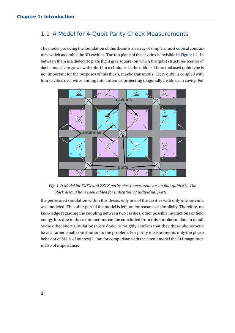
The model providing the foundation of this thesis is an array of simple almost cubical conduc-
tors, which assemble the 3D cavities. The top plane of the cavities is invisible in Figure 1.1. In
between them is a dielectric plate (light gray square) on which the qubit structures (center of
dark crosses) are grown with thin-film techniques in the middle. The actual used qubit type is
not important for the purposes of this thesis, maybe transmons. Every qubit is coupled with
four cavities over wires ending into antennas projecting diagonally inside each cavity. For
cavities
antennas
qubits
Fig. 1.1: Model for XXXX and ZZZZ parity check measurements on four qubits[7]. The
black arrows have been added for indication of individual parts.
the performed simulation within this thesis, only one of the cavities with only one antenna
was modeled. The other part of the model is left out for reasons of simplicity. Therefore, no
knowledge regarding the coupling between two cavities, other possible interactions or field
energy loss due to these interactions can be concluded from this simulation data in detail.
Some other short simulations were done, to roughly confirm that they these phenomena
have a rather small contribution to the problem. For parity measurements only the phase
behavior of S11 is of interest[7], but for comparison with the circuit model the S11 magnitude
is also of importance.
2
CHAPTER 2
Theoretical Background
2.1 RLC Circuit Representation
In frequency ranges of kHz to MHz the meaning of terms as circuit, wire, inductance, capaci-
tance, voltage and so on were originally developed. An easy engineered LC-circuit consists
out of a capacitor with capacitance C, wires and a coil with inductance of L. These elements
are well separated in space. In order to move to higher frequencies of GHz (the microwave
region), the whole circuit could simply be made smaller. However, this is highly impractical as
other important properties, for instance energy stored without breakdown decreases. In this
frequency region engineering of circuits is different. A simple hollow metallic cylinder, with
exact right dimensions is now the simple model for an ’LC-circuit’. As a result the meaning of
all terms mentioned above is more abstract and unclear. The shapes of resonant circuits in
the microwave region have two characteristic features. First, a physical size is comparable
with the wavelength involved and second, electromagnetic fields are totally confined within
conducting walls, except if they are designed to radiate energy into space. In order to un-
derstand the electrical properties of such structures, direct analysis of the electromagnetic
fields have to be performed. This is in general far from trivial. Nevertheless the LC and
other parameters of a representative circuit model for such structures can be determine from
EM-simulation. Certainly, these representative models can probably not be implemented as
they are, as it would possible in the lower frequency range[9].
3
Chapter 2: Theoretical Background
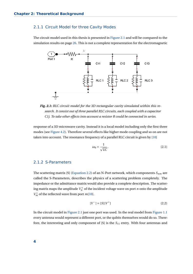
2.1.1 Circuit Model for three Cavity Modes
The circuit model used in this thesis is presented in Figure 2.1 and will be compared to the
simulation results on page 26. This is not a complete representation for the electromagnetic
Fig. 2.1: RLC circuit model for the 3D rectangular cavity simulated within this re-
search. It consist out of three parallel RLC circuits, each coupled with a capacitor
C1j. To take other effects into account a resistor R could be connected in series.
response of a 3D microwave cavity. Instead it is a local model including only the first three
modes (see Figure 4.2). Therefore several effects like higher mode coupling and so on are not
taken into account. The resonance frequency of a parallel RLC circuit is given by [10]
ω0 = 1pLC
. (2.1)
2.1.2 S-Parameters
The scattering matrix [S] (Equation 2.2) of an N-Port network, which components Snm are
called the S-Parameters, describes the physics of a scattering problem completely. The
impedance or the admittance matrix would also provide a complete description. The scatter-
ing matrix maps the amplitude V +n of the incident voltage wave on port n onto the amplitude
V +m of the reflected wave from port m[10].
[V −] = [S][V +] (2.2)
In the circuit model in Figure 2.1 just one port was used. In the real model from Figure 1.1
every antenna would represent a different port, or the qubits themselves would do so. There-
fore, the interesting and only component of [S] is the S11 entry. With four antennas and
4

2.1 RLC Circuit Representation
consequently four ports, [S] is a 4x4 matrix. In this problem S11 is found to be the reflection
coefficient and therefore given by[10]
S11 =V −
1
V +1
∣∣∣∣V +
2 =0
= Γ(1)∣∣V +
2 =0 = Z (1)i n −Z0
Z (1)i n +Z0
∣∣∣∣∣Z0 on por t 2
. (2.3)
The impedance Z0 is by convention 50 Ohm. For the theoretical circuit model in Figure 2.1
Z (1)i n from Equation 2.3 is
Z (1)i n = ZR + 1
(ZC 11 +ZRLC 1)−1 + (ZC 12 +ZRLC 2)−1 + (ZC 13 +ZRLC 3)−1 (2.4)
with ZC 1 j = (iωC 1 j )−1 and where
ZRLC j = 1
R−1j + (iωL j )−1 + (iωC j )
(2.5)
is the impedance of one of the three parallel RLC-circuits[10]. Plots of the magnitude and
phase of S11 are shown in chapter 5.
2.1.3 Q Factor
The quality factor or short Q factor is a dimensionless parameter, which is a measure for the
’quality’ of a resonance. It is related to the damping of a resonator, as indicated in Equation 2.6
and Equation 2.8. Per definition it is just the resonant frequency w0 divided by the bandwidth
∆ω as seen in Equation 2.7.
Q =ω (aver ag e stor ed ener g y)
(ener g y loss per second)(2.6)
Q = ω0
∆ω(2.7)
The Q factor of a parallel RLC circuit is given by Equation 2.8 and is for usual electric circuits
O (100)[10].
Q = R ·√
C
L. (2.8)
5
Chapter 2: Theoretical Background
2.2 Electromagnetic Cavities
An electromagnetic cavity or resonator is a metallic enclosure in which modes of free oscilla-
tion can exist at an infinite number of discrete frequencies. Only TE and TM, no TEM modes
can exist in hollow cavities. This is conform to a usual hollow waveguide. Cavities are very
interesting to study because they can have very high Q factors, as large as 104 or even higher.
The behavior is described by the solution of the general formulation of the dyadic Greens’s
function for a cavity[8]. Cavities are usual excited by some waveguide or some other feed.
Everything inside a cavity distorts the fields and modes in some way. Cavities perturbation
theory[11] provides tools for gaining better understanding on phenomena as modes shifts in
frequency or Q factor changes.
2.2.1 The Rectangular Cavity
For the model a usual rectangular box cavity was used. It is excited by a coaxial cable, with
inner conductor reaching inside the cavity. The mode frequencies are calculated by[10]
fmnl =c
2pµr εr
√(m
a
)2+
(n
b
)2+
(l
d
)2
(2.9)
where by convention a = side length of x, b = side length of y, d = side length of z and
b < a < d . C in Equation 2.9 is the speed of light, with µr and εr being material constants
of material inside the cavity at the resonance. For the cavities of interest for this thesis, the
resonant frequencies in GHz calculated with Equation 2.9 are shown in Table 2.1.
Mode rectangular Cavity cubical Cavity
T E101 6.752629228 7.066176000
T E011 7.173150496 7.066176000
T M110 7.469064856 7.066176000
T E111 8.741825306 8.654262816
Tab. 2.1: Resonant frequencies in GHz for a rectangular cavity with dimensions of
30x27x33 mm and a cubical cavity with dimensions of 30x30x30 mm. The inside
of both cavities is filled with air.
6
2.2 Electromagnetic Cavities
The EM fields inside a cavity can be solved. For example the EM field solution for a T E10`
mode inside a rectangular cavity is described by[10]
Ey = E0 sin(πx
a
)sin
(`πz
d
), (2.10)
Hx = − j E0
ZT Esin
(πx
a
)cos
(`πz
d
), (2.11)
Hz = jπE0
kηacos
(πx
a
)sin
(`πz
d
), (2.12)
with η= ε/µ, a material constant and k = 2πλr . A picture of a nearly perfect T E101 mode is
shown in Figure 4.11a. All modes of a box cavity are not shown in this paper but can be found
on the web1. The characteristic of Equation 2.2.1 are examined in Figure 4.9 and used to
confirm the mode structure in the simulation results. The Q factor is defined by Equation 2.6,
but specific calculations can be very tricky for some cases. For example, the unloaded Q of
a box cavity, with lossy conducting walls and a lossless dielectric inside, of a simple T E10`
resonant mode is:
Qc = 2ω0We
Pc= (kad)3bη
2π2Rs
1
(2`2a3b +2bd 3 +`2a3d +ad 3)(2.13)
Where in Equation 2.13 and Equation 2.14 Rs =√ωµ0/2σ is the surface resistivity of the
metallic walls and Pc is the power loss in the conducting walls given by
Pc = Rs
2
∫w all s
|Ht |2d s. (2.14)
We is the stored electric energy given by[10]
We = ε
4
∫V
Ey E∗y dν. (2.15)
1http://www.falstad.com/embox/
7

CHAPTER 3
About the Program XFdtd 7
3.1 General Informaton
XFdtd 7 from Remcom1 is a program which uses the finite differential time domain method
FDTD, (see subsection 3.1.1) to solve Maxwell’s equations in time. It has an inbuilt CAD
modeling system and libraries with all standard materials. It supports GPU networks with
CUDA on board, meaning most NVIDIA boards. The recommend system requirements
are devices with a NVIDIA Tesla K10 or better 2. The usual CPU and RAM of a computer
can also be used for computation. All simulations in this thesis are done on a 2.4 GHz
Duo-core processor and 4GB RAM, which capacity sets the most limitations. Alternative
suitable commercial software would be HFSS from Ansys or CST Microwave Studio with a
fundamental license prize around 1300 Euro per Year.
3.1.1 FDTD Method
The FDTD method[12][13][14] is a widely used method to solve Maxwell’s equations, because
it is capable of dealing with very complex geometries and applicable to a wide range of prob-
lems. The necessary computational power is nowadays available. The algorithm divides the
whole simulation space into so called Yee cells. It then solves a discrete version of Maxwell’s
equation for every of the Yee cells. Only the scattered field is determined computationally, the
incident field is specified analytically. The algorithms is linear in problem size (number of Yee
1www.remcom.com2http://www.remcom.com/xf7-system-requirements/
9
Chapter 3: About the Program XFdtd 7
cells). The number of cells in a cube scales with side length to the power of 3. If XAct-mesh is
used, it even scales to the power of 4. One important parameter for resolution is the size of a
base mesh cell[12][13].
3.1.2 The Mesh
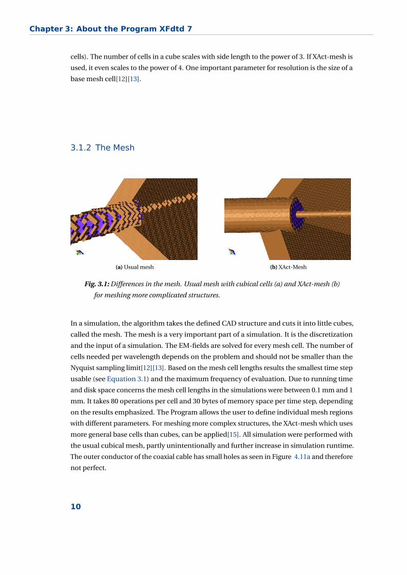
(a) Usual mesh (b) XAct-Mesh
Fig. 3.1: Differences in the mesh. Usual mesh with cubical cells (a) and XAct-mesh (b)
for meshing more complicated structures.
In a simulation, the algorithm takes the defined CAD structure and cuts it into little cubes,
called the mesh. The mesh is a very important part of a simulation. It is the discretization
and the input of a simulation. The EM-fields are solved for every mesh cell. The number of
cells needed per wavelength depends on the problem and should not be smaller than the
Nyquist sampling limit[12][13]. Based on the mesh cell lengths results the smallest time step
usable (see Equation 3.1) and the maximum frequency of evaluation. Due to running time
and disk space concerns the mesh cell lengths in the simulations were between 0.1 mm and 1
mm. It takes 80 operations per cell and 30 bytes of memory space per time step, depending
on the results emphasized. The Program allows the user to define individual mesh regions
with different parameters. For meshing more complex structures, the XAct-mesh which uses
more general base cells than cubes, can be applied[15]. All simulation were performed with
the usual cubical mesh, partly unintentionally and further increase in simulation runtime.
The outer conductor of the coaxial cable has small holes as seen in Figure 4.11a and therefore
not perfect.
10
3.2 Important Simulation Criteria
3.2 Important Simulation Criteria
3.2.1 Convergence of Fields
Once a simulation is started it runs until either one of two things occurs: First, the maximum
anticipated simulation time is reached, for example to simulate exactly one second in a
run. Second, the EM-fields converge below a selected relative value to the starting fields, for
example −50 dB. Convergence means that either all fields within the simulation space decay
under this value or the derivation of the mean field in every cell becomes smaller than this
value. That way a standing wave inside a structure would be perfectly converged[15].
3.2.2 Running Time and Timescales
The maximum simulated time can be chosen to be any multiple of the minimum time step.
The minimum time step possible is given by
∆t ≤ 1
c
√1
(∆x)2 + 1
(∆y)2 + 1
(∆z)2 . (3.1)
In Equation 3.1 c is the speed of light or the speed limit of propagation in the material.
∆x,∆y ,∆z are the cell side lengths of the 3D rectangular grid. Ideally the user strives to
use a time step according the current problem and simulate until convergence is reached.
If computational resources available were less then recommended, this procedure would
sometimes not be practical with a to long simulation runtime.
11
Chapter 3: About the Program XFdtd 7
3.2.3 Broadband versus Single Frequency Excitation
Since XFdtd uses a time-domain solver, it is capable of running single frequency calculations
or multiple-frequency (referred to as broadband) calculations for a given excitation pulse in a
single run. Due to running time concerns mainly broadband calculations were performed.
Single frequency calculations were done to save the EM fields at certain frequency points.
For broadband simulations, a maximum resolution in frequency of 247.602 kHz could be
used. Within single frequency evaluations, an accuracy of 10 kHz can be reached. If there is
no other way to increase the resolution, this will limit the maximum Q factor the program is
able to resolve. If ten data points are required for properly resolving a resonance at 10 GHz,
the maximum Q will be approximately 4000 with broadband and around 100000 with single
frequency evaluations.
12
CHAPTER 4
Simulation Setup and S11-Data
4.1 Rectangular Cavity with Antenna in [111] Direction
4.1.1 CAD Model of a Cavity
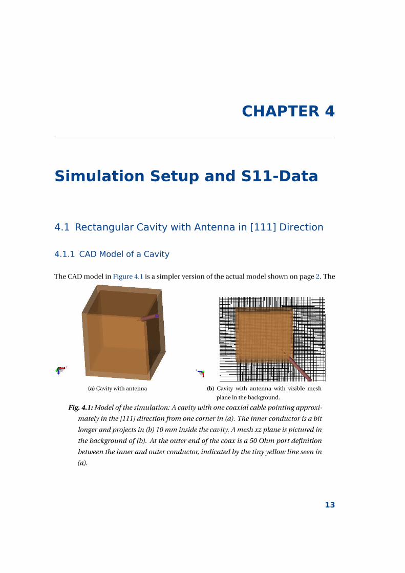
The CAD model in Figure 4.1 is a simpler version of the actual model shown on page 2. The
(a) Cavity with antenna (b) Cavity with antenna with visible mesh
plane in the background.
Fig. 4.1: Model of the simulation: A cavity with one coaxial cable pointing approxi-
mately in the [111] direction from one corner in (a). The inner conductor is a bit
longer and projects in (b) 10 mm inside the cavity. A mesh xz plane is pictured in
the background of (b). At the outer end of the coax is a 50 Ohm port definition
between the inner and outer conductor, indicated by the tiny yellow line seen in
(a).
13

Chapter 4: Simulation Setup and S11-Data
cuboid has dimensions of 30x27x33 mm and the antenna is pointing from one corner into
the [111] direction of the cuboid. The coaxial cable is 26.75 mm long, with a discrete port
between the inner and outer conductor defined at its end, indicated by a tiny yellow line.
The port is a 50 Ohm feed on which two defined waveforms with an amplitude of 1 Volt are
applied: A broadband pulse for S-Parameter calculations and sinusoidal waves with certain
frequencies in other simulation runs. The inner conductor has a radius of 0.25 mm, as has
the shell of the outer conductor. The dielectric shell (blue part in Figure 4.1) is made out of
Polyethylene and has a thickness of 0.75 mm. The material of the cavity walls can be copper
with a conductivity of 5.98 ·107 S/m. The theoretical resonance mode frequencies for a pure
cavity are presented in Table 2.1. The mesh cell size in the cuboid, the cuboids walls and
around the coaxial cable is 0.25 mm. A xz mesh plane can be seen in Figure 4.1b. Around the
cuboid, the mesh cells have a side length of 1 mm. Ten cells are meshed around the cube until
the outer absorbing PML boundary with seven layers is reached. Based on this mesh choice,
it results that over 6 million cells have to be calculated in every time step. These values were
selected due to the limitations of the computational power used and because the resulting
maximum simulation frequency is around 30 GHz. The so called ’Ftt size’ is always set to a
maximum of 23, resulting in frequency steps of approximately 247.602 kHz.
4.1.2 Simulation 1: Varying the Antenna Length
The length of the inner conductor in the cuboid was changed from 0 to 15 mm. For the first
10 mm, a broadband simulation of 15 nanoseconds was performed in 1 mm steps and after
10 mm in 0.5 mm steps. Furthermore discrete frequencies of 3, 6.75, 7.17, 7.47, 8, 8.74 GHz
are evaluated. EM fields for these frequencies were saved and are partly shown below in
subsection 4.1.4. The conductance value of all the conducting walls and the coax conductor
material is set down to 5.98 ·104 S/m. The intension was to put more loss into the system
and therefore receive a lower Q factor and also a faster convergence. The convergence of
every run is written in Table 4.1. The table suggests a careful interpretation of the simulation
output, as the EM fields inside the cavity did not reach convergence. Time shortage permitted
the run of a second longer simulation on this scale with better converged results. Instead a
longer single run for 100 nanoseconds with an antenna length of 10 mm was done (referred
to as simu1.1). The convergence reached in simu1.1 was −12.91 dB and the circuit model was
compared to this data.
14
4.1 Antenna in [111]
Antenna length [mm] Convergence [dB]
1 -22.83
2 -13.39
3 -7.34
4 -3.15
5 -1.02
6 -0.3
7-15 0
Tab. 4.1: Convergence results for each run of the simulation.
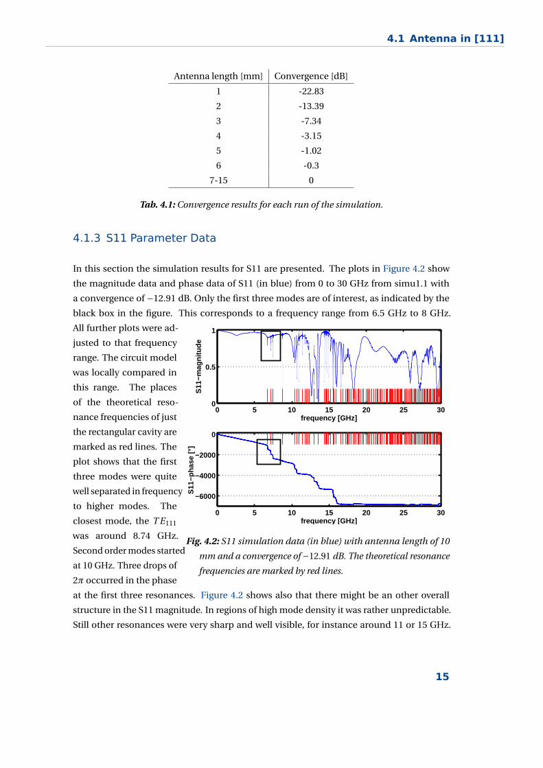
4.1.3 S11 Parameter Data
In this section the simulation results for S11 are presented. The plots in Figure 4.2 show
the magnitude data and phase data of S11 (in blue) from 0 to 30 GHz from simu1.1 with
a convergence of −12.91 dB. Only the first three modes are of interest, as indicated by the
black box in the figure. This corresponds to a frequency range from 6.5 GHz to 8 GHz.
0 5 10 15 20 25 30
−6000
−4000
−2000
0
frequency [GHz]
S11
−pha
se [°
]
0 5 10 15 20 25 300
0.5
1
frequency [GHz]
S11
−mag
nitu
de
Fig. 4.2: S11 simulation data (in blue) with antenna length of 10
mm and a convergence of −12.91 dB. The theoretical resonance
frequencies are marked by red lines.
All further plots were ad-
justed to that frequency
range. The circuit model
was locally compared in
this range. The places
of the theoretical reso-
nance frequencies of just
the rectangular cavity are
marked as red lines. The
plot shows that the first
three modes were quite
well separated in frequency
to higher modes. The
closest mode, the T E111
was around 8.74 GHz.
Second order modes started
at 10 GHz. Three drops of
2π occurred in the phase
at the first three resonances. Figure 4.2 shows also that there might be an other overall
structure in the S11 magnitude. In regions of high mode density it was rather unpredictable.
Still other resonances were very sharp and well visible, for instance around 11 or 15 GHz.
15

Chapter 4: Simulation Setup and S11-Data
Figure 4.3 shows a detailed view of the first three modes. The resonances were clearly vis-
ible in the structure of the S11 magnitude and each of them comes with a 2π change in
the continuous S11 phase. The phase offset is readjusted in this plot. Figure 4.3 reveals
6.6 6.8 7 7.2 7.4 7.6−1500
−1000
−500
0
frequency [GHz]
S11
−pha
se [°
]
6.6 6.8 7 7.2 7.4 7.6
0.6
0.8
1
1.2
frequency [GHz]
S11
−mag
nitu
de
Fig. 4.3: The black box from Figure 4.2 with simulation S11 data (blue) with red lines
at the theoretical resonances is visualized here.
slight shift in frequency for all modes. The shifts of their lowest data points compared to the
pure cavity frequencies was calculated to be −3.783 MHz for the T E101 mode, 2.558 MHz
for the T E011 mode and 2.031 MHz for the T M110 mode. Since the discretization is 0.248
MHz, the uncertainties of these shift values were at least ±0.072 MHz. The smallest data
points in the minima of the magnitude were 0.7934 for the first mode, 0.7244 for the second
mode and 0.6329 for the third mode. There were about 50 to 90 data points around each
minimum. From looking at the plot ∆ω was 8 to 15 MHz and first rough estimations for the Q
factor of the modes were between 400 to 900. There were other larger uncertainties due to
convergence. In Figure 4.3, small unphysical oscillation pattern in the absolute value of S11
were observed due to convergence. In the plots in Figure 4.4 and in Figure 4.5 two specific
datasets from the large simulation are pictured. No convergence was reached in these two
runs. The oscillation background pattern in the magnitude was stronger in both figures than
in the better converged run, presented in Figure 4.3. The phase structure of the run at 10 mm
antenna length differed from Figure 4.3 and had also a smaller oscillation pattern between
the resonances. No smooth 2π changes were visible. Instead at every resonance some other
phase structure was visible. At an antenna length of 15 mm the S11 phase did 2π cycles.
16

4.1 Antenna in [111]
6.5 7 7.5 8
−200
−100
0
100
frequency [GHz]
S11
−pha
se [°
]
6.5 7 7.5 80
0.5
1
frequency [GHz]
S11
−mag
nitu
de
Fig. 4.4: S11 data for an antenna length of 10 mm with low convergence. The red lines
are the theoretical mode frequencies of a pure cavity from Table 2.1.
6.5 7 7.5 8
−1500
−1000
−500
0
frequency [GHz]
S11
−pha
se [°
]
6.5 7 7.5 80
0.5
1
frequency [GHz]
S11
−mag
nitu
de
Fig. 4.5: S11 data for an antenna length of 15 mm with low convergence. The red lines
are the theoretical mode frequencies of a pure cavity from Table 2.1.
17
Chapter 4: Simulation Setup and S11-Data
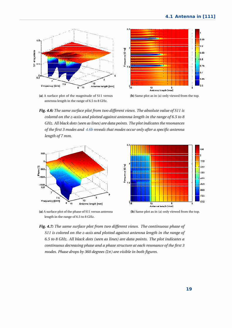
In Figure 4.6, the complete results of all runs for the magnitude of S11 is shown. It is a 3D
surface plot with the antenna length given in mm on the right axis in the same frequency in-
terval of 6.5 to 8 GHz. All the black spots represent simulation data points. Several indications
can be drawn from these results: First, the antenna should be at least 7 mm long to excite
the cavity modes. Second, the third mode is already excited at shorter antenna lengths. This
could be due to different coupling strengths for the modes. This maybe explained by a lack
of perfect adjustment of the antenna in the [111] direction. The different side lengths of the
cuboid might also result in varied coupling in different directions. With further simulation
this may be possible to falsify. Close observations revealed background oscillations with a
rather large magnitude and S11 magnitude values greater than 1. Figure 5.3a shows how
the oscillations become stronger with occurrence of a resonance and a lower convergence
value (referred to in Table 4.1). The running time was constant for each run. Therefore the
uncertainties in this data are unknown. The small resonance features at short antenna lengths
are because all fields get reflected back into the coaxial cable or stay around the antenna.
In Figure 4.7 the phase of S11 is presented. A overall background decrease in the phase
can be realized. The occurrence of the modes was also reflected in the phase structure. At
antenna length from 7 mm to 10 mm (see Figure 4.4), a little ’wiggle’ in the phase developed
at existence of a mode. At a longer antenna length, a decrease of 360 degrees, respectively of
2π, occurred at a resonance.
18
4.1 Antenna in [111]
(a) A surface plot of the magnitude of S11 versus
antenna length in the range of 6.5 to 8 GHz.
(b) Same plot as in (a) only viewed from the top.
Fig. 4.6: The same surface plot from two different views. The absolute value of S11 is
colored on the z-axis and plotted against antenna length in the range of 6.5 to 8
GHz. All black dots (seen as lines) are data points. The plot indicates the resonances
of the first 3 modes and 4.6b reveals that modes occur only after a specific antenna
length of 7 mm.
(a) A surface plot of the phase of S11 versus antenna
length in the range of 6.5 to 8 GHz.
(b) Same plot as in (a) only viewed from the top.
Fig. 4.7: The same surface plot from two different views. The continuous phase of
S11 is colored on the z-axis and plotted against antenna length in the range of
6.5 to 8 GHz. All black dots (seen as lines) are data points. The plot indicates a
continuous decreasing phase and a phase structure at each resonance of the first 3
modes. Phase drops by 360 degrees (2π) are visible in both figures.
19
Chapter 4: Simulation Setup and S11-Data
4.1.4 Electromagnetic Fields
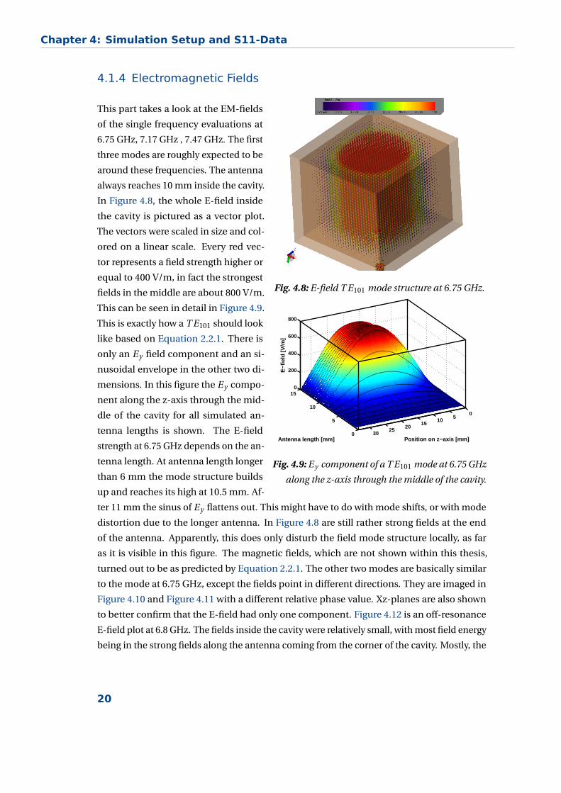
Fig. 4.8: E-field T E101 mode structure at 6.75 GHz.
0
5
10
15
05
1015
2025
30
0
200
400
600
800
Position on z−axis [mm]Antenna length [mm]
E−f
ield
[V/m
]
Fig. 4.9: Ey component of a T E101 mode at 6.75 GHz
along the z-axis through the middle of the cavity.
This part takes a look at the EM-fields
of the single frequency evaluations at
6.75 GHz, 7.17 GHz , 7.47 GHz. The first
three modes are roughly expected to be
around these frequencies. The antenna
always reaches 10 mm inside the cavity.
In Figure 4.8, the whole E-field inside
the cavity is pictured as a vector plot.
The vectors were scaled in size and col-
ored on a linear scale. Every red vec-
tor represents a field strength higher or
equal to 400 V/m, in fact the strongest
fields in the middle are about 800 V/m.
This can be seen in detail in Figure 4.9.
This is exactly how a T E101 should look
like based on Equation 2.2.1. There is
only an Ey field component and an si-
nusoidal envelope in the other two di-
mensions. In this figure the Ey compo-
nent along the z-axis through the mid-
dle of the cavity for all simulated an-
tenna lengths is shown. The E-field
strength at 6.75 GHz depends on the an-
tenna length. At antenna length longer
than 6 mm the mode structure builds
up and reaches its high at 10.5 mm. Af-
ter 11 mm the sinus of Ey flattens out. This might have to do with mode shifts, or with mode
distortion due to the longer antenna. In Figure 4.8 are still rather strong fields at the end
of the antenna. Apparently, this does only disturb the field mode structure locally, as far
as it is visible in this figure. The magnetic fields, which are not shown within this thesis,
turned out to be as predicted by Equation 2.2.1. The other two modes are basically similar
to the mode at 6.75 GHz, except the fields point in different directions. They are imaged in
Figure 4.10 and Figure 4.11 with a different relative phase value. Xz-planes are also shown
to better confirm that the E-field had only one component. Figure 4.12 is an off-resonance
E-field plot at 6.8 GHz. The fields inside the cavity were relatively small, with most field energy
being in the strong fields along the antenna coming from the corner of the cavity. Mostly, the
20
4.1 Antenna in [111]
off-resonance fields observed inside the cavity were smaller than in this plot.
(a) view 1 (b) ZX plane
Fig. 4.10: E-field T E101 mode structure at 7.17 GHz the relative phase is set to 40.
(a) view 1 (b) ZX plane.
Fig. 4.11: E-field T E101 mode structure at 7.47 GHz, the relative phase is set to 100.
Fig. 4.12: E-vectorfield at 6.8 GHz, the relative phase is set to 100
21
Chapter 4: Simulation Setup and S11-Data
4.2 Other Simulations done
During the three month period, other simulations were performed, mainly with the purpose
of getting to know the program and to check basic assumptions. First, only a floating antenna
inside the cavity was used instead of the coaxial cable. It was possible to see mode structures
in the S11 magnitude, but no 2π change in the phase was observed. In retrospect, this was
probably due to the short length of the antenna, with 2 mm. Simulations with different
orientations of the antenna were also tried out. In one of them, the coaxial cable connected
to the cavity in the center of the xy-plane and the antenna was pointing in the z-direction.
These results confirmed that not all modes were excited. This was used for checking if the
antenna orientation had a direct impact on the coupling to the modes. Furthermore, small
other simulations were done for checking basic things of the original model with 4 antennas
per cavity and several cavities close to each other. In one cavity 4 antennas, placed as in the
original model with a length of 10 mm, were used. It could be confirmed that the magnitude
of S12, S13, S14 is smaller than 0.005 in the frequency range from 3 to 10 GHz, indicating
they are at least 40 dB lower then the S11 magnitude. An other simulation included a square
of 9 cavities with a wall thickness of 2 mm each and one antenna exciting the cavity in the
middle. This confirmed that field energy loss into nearby cavities is a rather small problem,
as the EM-field strength were smaller than -60 dB. In one simulation the conductance of the
conductor material of the cavity and the coaxial cable was varied.
22

CHAPTER 5
Results and Discussion
5.1 Analysis of the Circuit Model
Since the simulation output has been presented, a feeling should developed of how the S11
of the circuit model in Figure 2.1, behaves in theory. In Figure 5.1, the S11 magnitude of
just a single parallel RLC circuit with a coupling capacitor C was plotted. Since the reso-
nance frequency ω0 = 6.752629228 GHz and Q = 300 were hold constant, because these
two parameters can be read out of S11 simulation data. It results from Equation 2.8 and
Equation 2.1 that L is given by L = R/(ω0 ·Q) and C1 of the RLC is given by C 1 =Q/(ω0 ·R).
(a) S11-magnitude with single resonance (b) View from he top of plot (a)
Fig. 5.1: The influence of a coupling capacitor on the S11 magnitude of a parallel RLC
with constant Q of 300 and ω0 of 6.752629228 GHz.
23
Chapter 5: Results and Discussion
Fig. 5.2: S11 Phase relationship of the coupling
capacitance of a single C coupled RLC.
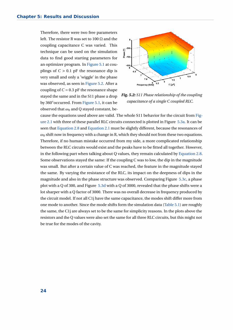
Therefore, there were two free parameters
left. The resistor R was set to 100Ω and the
coupling capacitance C was varied. This
technique can be used on the simulation
data to find good starting parameters for
an optimizer program. In Figure 5.1 at cou-
plings of C > 0.1 pF the resonance dip is
very small and only a ’wiggle’ in the phase
was observed, as seen in Figure 5.2. After a
coupling of C = 0.3 pF the resonance shape
stayed the same and in the S11 phase a drop
by 360occurred. From Figure 5.1, it can be
observed that ω0 and Q stayed constant, be-
cause the equations used above are valid. The whole S11 behavior for the circuit from Fig-
ure 2.1 with three of these parallel RLC circuits connected is plotted in Figure 5.3a. It can be
seen that Equation 2.8 and Equation 2.1 must be slightly different, because the resonances of
ω0 shift now in frequency with a change in R, which they should not from these two equations.
Therefore, if no human mistake occurred from my side, a more complicated relationship
between the RLC circuits would exist and the peaks have to be fitted all together. However,
in the following part when talking about Q values, they remain calculated by Equation 2.8.
Some observations stayed the same: If the coupling C was to low, the dip in the magnitude
was small. But after a certain value of C was reached, the feature in the magnitude stayed
the same. By varying the resistance of the RLC, its impact on the deepness of dips in the
magnitude and also in the phase structure was observed. Comparing Figure 5.3c, a phase
plot with a Q of 300, and Figure 5.3d with a Q of 3000, revealed that the phase shifts were a
lot sharper with a Q factor of 3000. There was no overall decrease in frequency produced by
the circuit model. If not all C1j have the same capacitance, the modes shift differ more from
one mode to another. Since the mode shifts form the simulation data (Table 5.1) are roughly
the same, the C1j are always set to be the same for simplicity reasons. In the plots above the
resistors and the Q values were also set the same for all three RLC circuits, but this might not
be true for the modes of the cavity.
24
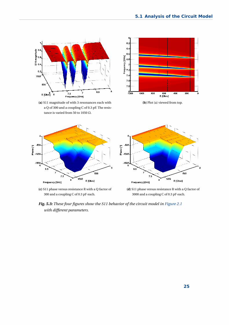
5.1 Analysis of the Circuit Model
(a) S11 magnitude of with 3 resonances each with
a Q of 300 and a coupling C of 0.3 pF. The resis-
tance is varied from 50 to 1050Ω.
(b) Plot (a) viewed from top.
(c) S11 phase versus resistance R with a Q factor of
300 and a coupling C of 0.3 pF each.
(d) S11 phase versus resistance R with a Q factor of
3000 and a coupling C of 0.3 pF each.
Fig. 5.3: These four figures show the S11 behavior of the circuit model in Figure 2.1
with different parameters.
25

Chapter 5: Results and Discussion
5.2 Results of Simulation and Shifts
Table 5.1 shows the frequency differences from the lowest data points from the simulation to
the theoretical pure cavity modes. The uncertainty on these numbers is at least ±0.072 MHz
due to discretization in frequency. Withing this uncertainty a trend might be seen in the data:
the longer the antenna the greater is the mode shift and the mode shifts of the 3 modes differ,
meaning the coupling is slightly different. The variation of the values at an antenna length of
10 mm suggest that there have to be other quite big uncertainties, because of convergence
compared to the discretization one. Or differences due to different simulation time. In order
to really confirm the trend suspected in the data, a better converged simulation is needed.
The oscillations in the magnitude had an amplitude of approximately 0.05 to 0.1. This could
be used as an other uncertainty on the data for the minimum in the magnitude.
Antenna T E101 T E101 T E011 T E011 T M110 T M110
length [mm] shift [MHz] min shift [MHz] min shift [MHz] min
8 -1.555 0.8558 -1.155 0.6745 -1.435 0.5792
9 -3.536 0.5998 -0.412 0.3149 0.050 0.3936
10 -3.288 0.0486 3.302 0.1396 1.536 0.3170
10 (Simu1.1) -3.782 0.7934 2.558 0.7244 2.031 0.6329
10.5 -0.069 0.2652 4.539 0.1502 2.031 0.2946
11 4.388 0.3110 5.529 0.1798 2.774 0.2714
11.5 7.111 0.2616 6.025 0.2023 3.022 0.2478
12 8.844 0.1783 6.521 0.2150 3.517 0.215
12.5 9.835 0.1055 6.767 0.2200 3.764 0.1784
13 10.330 0.0446 7.016 0.2120 4.012 0.1316
13.5 10.825 0.0102 7.262 0.1958 4.012 0.0699
14 11.073 0.0324 7.262 0.1711 3.764 0.0108
14.5 11.568 0.0361 7.262 0.1336 3.517 0.0884
15 11.815 0.0235 7.262 0.0925 3.269 0.1537
Tab. 5.1: Frequency shifts of the modes and the S11 magnitude minimum from simu-
lation in subsection 4.1.2.
26

5.3 Comparing the Circuit Model to S11-Data
5.3 Comparing the Circuit Model to S11-Data
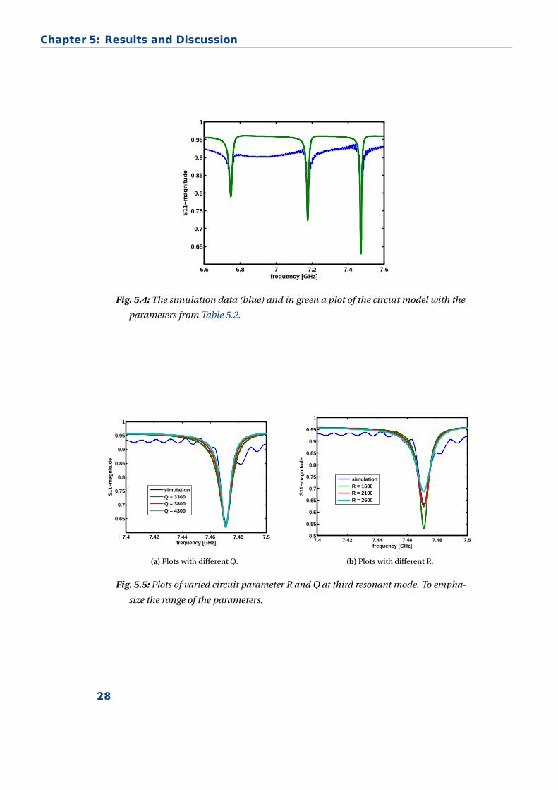
In this section the theoretical circuit model is compared to the response of the rectangular
cavity resonator. Figure 5.4 shows a plot with possible reasonable parameters in green and
the simulation data in blue from the better converged run (simu1.1) with an antenna length
of 10 mm. Since it was not managed to fit the model in Matlab to the simulation data,
circuit part value
R 1.3Ω
C11 0.3 pF
C12 0.3 pF
C13 0.3 pF
R1 5500Ω
L1 38.9941 pH
C1 14.0379 pF
R2 3400Ω
L2 19.7573 pH
C2 24.6795 pF
R3 2100Ω
L3 11.7398 pH
C3 38.4405 pF
Tab. 5.2: Circuit parameters form the plot in
green from Figure 5.4
a variation of the model parameters was
done by hand. The results are presented
in Table 5.2. There was a background in
the magnitude as can be seen in Figure
5.7d, which is not explained by the circuit
model. The resistor R was chosen to be 1.3
Ω to account for the offset in the magnitude
through a wide frequency range. First Q and
ω0 were hold constant whereas C1j and Rj
were varied. The three C1j were set to the
most suitable value of 0.3 pF. Then a linear
correction from the fit results of a first order
polynomial to the S11 phase simulation data
was adjusted to the circuit model data. This
led to an increase in the values of Q and R as
seen in Figure 5.6. These results should only
be seen as a rough estimate. The three cou-
pling capacitors C1j are probably not smaller
then 0.1 pF, because then the resistors of the RLC circuits would have to become very large.
Otherwise the phase has small wiggles instead of 2π drops. All three resonances are presented
in closeup view in Figure 5.7.By observation of the steepness of the S11 phase without cor-
rection (Figure 5.6) the Q factor can be estimated to be around 400. If the linear background
was subtracted, the new Q values would be Q1 = 3300 and Q2,Q3 = 3800. The differences
from simulation values to theoretical resonance frequencies were ∆ω1 =−807 KHz for the
first mode, ∆ω2 =−248.5 KHz for the second and ∆ω3 =−95.8 KHz for the third mode. To get
an idea regarding the range that might be suitable for R and Q, the plots in Figure 5.5 were
produced. The uncertainties of the R values were roughly ±100 Ω. The Q value estimated
from the phase was in the range of ±500.
27
Chapter 5: Results and Discussion
6.6 6.8 7 7.2 7.4 7.6
0.65
0.7
0.75
0.8
0.85
0.9
0.95
1
frequency [GHz]
S11
−mag
nitu
de
Fig. 5.4: The simulation data (blue) and in green a plot of the circuit model with the
parameters from Table 5.2.
7.4 7.42 7.44 7.46 7.48 7.5
0.65
0.7
0.75
0.8
0.85
0.9
0.95
1
frequency [GHz]
S11
−mag
nitu
de
simulationQ = 3300Q = 3800Q = 4300
(a) Plots with different Q.
7.4 7.42 7.44 7.46 7.48 7.50.5
0.55
0.6
0.65
0.7
0.75
0.8
0.85
0.9
0.95
1
frequency [GHz]
S11
−mag
nitu
de
simulationR = 1600R = 2100R = 2600
(b) Plots with different R.
Fig. 5.5: Plots of varied circuit parameter R and Q at third resonant mode. To empha-
size the range of the parameters.
28

5.3 Comparing the Circuit Model to S11-Data
6.6 6.8 7 7.2 7.4 7.6−1800
−1600
−1400
−1200
−1000
−800
−600
−400
−200
frequency [GHz]
S11
−pha
se [°
]
(a) Phase with correction.
6.6 6.8 7 7.2 7.4 7.6−1800
−1600
−1400
−1200
−1000
−800
−600
−400
−200
0
frequency [GHz]
S11
−pha
se [°
]
(b) Phase without correction.
Fig. 5.6: The S11 phase simulation data in blue and the adjusted model in green with
the parameters from Table 5.2 is plotted in (b). In (a) a plot with a phase correction
of the linear background in the simulation data to the circuit model is shown.
6.7 6.72 6.74 6.76 6.78 6.80.75
0.8
0.85
0.9
0.95
1
frequency [GHz]
S11
−mag
nitu
de
(a) First resonance.
7.14 7.15 7.16 7.17 7.18 7.19 7.20.7
0.75
0.8
0.85
0.9
0.95
1
frequency [GHz]
S11
−mag
nitu
de
(b) Second resonance.
7.4 7.42 7.44 7.46 7.48 7.5
0.65
0.7
0.75
0.8
0.85
0.9
0.95
1
frequency [GHz]
S11
−mag
nitu
de
(c) Third resonance.
4 4.5 5 5.5 6 6.5 7 7.5 8
0.65
0.7
0.75
0.8
0.85
0.9
0.95
1
frequency [GHz]
S11
−mag
nitu
de
(d) Plot from a frequency range of 4 to 8
GHz.
Fig. 5.7: Detailed view of the matched data at the three resonances in (a),(b) and
(c). In (d) a zoomed out version is shown to justify the offset and see the possible
background structure.
29

CHAPTER 6
Conclusions and Outlook
The results from the simulation with the variable antenna length suggest that the real excita-
tion of cavity modes starts after an antenna length of 7 mm. Their E-field strength shows also
a strong dependence on the antenna length. The theoretical EM field structure of a T E101,
T E011 and T M110 mode of a rectangular cavity could be confirmed within the simulations.
The disturbance of the fields due to the antenna turns out to be rather small at antenna
lengths until 15 mm. There might be a flatten out of the E-field mode structure at antenna
lengths longer than 10 mm. This should be investigated in more detail through further simu-
lation.
The frequency shifts of modes with antenna compared to the pure cavity modes are in a range
of 0 to 11 MHz changing with the antenna length. Without knowing the uncertainties due to
convergence in detail a good statement about the trend that larger mode shifts correspond to
longer antennas can not be made. With small uncertainties on such data, differences in the
coupling capacitors could be examined. The assumption of the model seems to be valid that
coupling to other cavities and other antennas plays a rather smaller role.
The per hand roughly estimated parameter for the circuit model were surprising, because the
resistances for the modes differ a lot from 5500Ω for the first over 3400Ω for the second and
2100Ω for the third mode. The coupling capacitors with 300 f F are quite high compared to
the 0−50 f F coupling capacitors region in the 2D case[16]. The Q factors result to be 3300 for
the first and 3800 for the other two modes. The impact of the imperfect coaxial cable on the
simulation results is unknown. However, there were no strong fields on the outside of the
coaxial cable observed during any simulation. For future simulations the XAct-mesh might
be a more suitable choice.
The radiation from a qubit will probably not be a simple sine wave, but in a broadband pulse
31
Chapter 6: Conclusions and Outlook
might be some other physics, like different decay times of modes. In an detailed analysis the
outcome of the broadband and a lot of single frequency evaluations should be compared.
If one would find out how the program calculates the results in the frequency domain, some
assumptions could be made, for example, uncertainties due to a Fourier transformation. In
general, more detailed single frequency simulations with a good convergence are necessary
to confirm these results and to provide better data for optimization in a tool which is able to
handle models of these order of complexity. The circuit model might be incomplete, because
it can not explain the background decrease in S11 phase and the background structure in S11
magnitude.
On a more powerful computer the EM fields can be observed in time and might lead to a
better understanding how the mode structure develops and decays within the simulation
time. More detailed information about how exactly a mode is disturbed can be made available
by visualizing the resulting EM fields in an external program like Matlab and then subtract
perfect cavity modes. With the numerical integration of such fields an other way to extract
the capacitance might be used. For further understanding of the model, the exact model
should be designed with wires and connections between the cavities for simulation. The
model should include several cavities and the parameters as they suit for the use of 4 qubit
parity check measurements should be adjusted. Other methods for extracting capacitances,
as evaluating the CAD model with a long antenna through an algorithm like fastcap and EM
field energy integration, might be helpful to test results of the circuit elements.
In the framework of this thesis it was shown that XFdtd 7 might be a program capable of deal-
ing with a more realistic model as long as Q factors are smaller than 100000 and therefore help
achieving a higher level of understanding of the coupling and EM response of 3D cavities.
32

List of Figures
1.1 Model for 4-qubit parity check measurements. . . . . . . . . . . . . . . . . . . . 2
2.1 RLC circuit model for describing 3 cavity modes. . . . . . . . . . . . . . . . . . . 4
3.1 Different types of mesh in XFdtd. . . . . . . . . . . . . . . . . . . . . . . . . . . . . 10
4.1 Simulation model of for a cavity with one antenna in 111 direction. . . . . . . . 13
4.2 S11 simulation data for the whole frequency range. . . . . . . . . . . . . . . . . . 15
4.3 Good S11 data for an antenna length of 10 mm. . . . . . . . . . . . . . . . . . . . 16
4.4 S11 data for an antenna length of 10 mm. . . . . . . . . . . . . . . . . . . . . . . . 17
4.5 S11 data for an antenna length of 15 mm. . . . . . . . . . . . . . . . . . . . . . . . 17
4.6 Simulation 1 total results of the S11 magnitude. . . . . . . . . . . . . . . . . . . . 19
4.7 Simulation 1 total results of the S11 phase. . . . . . . . . . . . . . . . . . . . . . . 19
4.8 E-field T E101 mode structure at 6.75 GHz. . . . . . . . . . . . . . . . . . . . . . . 20
4.9 Ey component of a T E101 mode at 6.75 GHz along the z-axis through the middle
of the cavity. . . . . . . . . . . . . . . . . . . . . . . . . . . . . . . . . . . . . . . . . 20
4.10 E-field T E101 mode structure at 7.17 GHz the relative phase is set to 40. . . . . 21
4.11 E-field T E101 mode structure at 7.47 GHz, the relative phase is set to 100. . . . 21
4.12 E-vectorfield at 6.8 GHz, the relative phase is set to 100 . . . . . . . . . . . . . . 21
5.1 S11 magnitude of a single C coupled RLC circuit. . . . . . . . . . . . . . . . . . . 23
5.2 S11 phase of single C coupled RLC circuit. . . . . . . . . . . . . . . . . . . . . . . 24
5.3 S11 magnitude and phase behavior of the circuit model. . . . . . . . . . . . . . . 25
5.4 Circuit model match to the magnitude of S11 . . . . . . . . . . . . . . . . . . . . 28
5.5 Plots of varied circuit parameter R and Q at third resonant mode. . . . . . . . . 28
5.6 S11 Phase plots of the Data and circuit model. . . . . . . . . . . . . . . . . . . . . 29
5.7 Detailed view of the matched data at the resonances. . . . . . . . . . . . . . . . . 29
I


List of Tables
2.1 First four cavity resonance frequencies. . . . . . . . . . . . . . . . . . . . . . . . . 6
4.1 Convergence data from simulation 1. . . . . . . . . . . . . . . . . . . . . . . . . . 15
5.1 Resonance shifts and magnitude low from simulation 1 data. . . . . . . . . . . . 26
5.2 Parameters of the circuit model which match to simulation. . . . . . . . . . . . . 27
III

Bibliography
[1] Simon J. Devitt, Kae Nemoto, and William J. Munro. “Quantum Error Correction for
Beginners”. In: Rep. Prog. Phys. 76 (2013), p. 076001. URL: http://arxiv.org/
abs/0905.2794 (cit. on p. 1).
[2] D. Ristè et al. “Initialization by measurement of a two-qubit superconducting circuit”.
In: Phys. Rev. Lett. 109 (2012), p. 050507. URL: http://arxiv.org/abs/1204.
2479 (cit. on p. 1).
[3] Jens Koch et al. “Charge-insensitive qubit design derived from the Cooper pair box”.
In: Phys. Rev. A 76 (4 2007), p. 042319. DOI: 10.1103/PhysRevA.76.042319. URL:
http://link.aps.org/doi/10.1103/PhysRevA.76.042319 (cit. on p. 1).
[4] T. Niemczyk et al. “Circuit quantum electrodynamics in the ultrastrong-coupling
regime”. In: Nat Phys 6.10 (2010). 10.1038/nphys1730, pp. 772–776. ISSN: 1745-2473.
DOI: http://dx.doi.org/10.1038/nphys1730 (cit. on p. 1).
[5] J. Bourassa et al. “Ultrastrong coupling regime of cavity QED with phase-biased flux
qubits”. In: Phys. Rev. A 80 (3 2009), p. 032109. DOI: 10.1103/PhysRevA.80.
032109. URL: http://link.aps.org/doi/10.1103/PhysRevA.80.
032109 (cit. on p. 1).
[6] Simon E. Nigg et al. “Black-box superconducting circuit quantization”. In: Phys. Rev.
Lett. 108 (2012), p. 240502. URL: http://arxiv.org/abs/1204.0587 (cit. on
p. 1).
[7] David P. DiVincenzo and Firat Solgun. Multi-qubit parity measurement in circuit quan-
tum electrodynamics. 03/2013. URL: http://arxiv.org/abs/1205.1910 (cit.
on pp. 1, 2).
[8] Robert E. Collin. Foundations for Microwave Engineering. 2nd ed.,Revised. Vol. Vol.
11. The IEEE/OUP Series on Electromagnetic Wave Theory (Formerly IEEE Only),
Series Editor Ser. Hoboken: John Wiley & Sons, Incorporated. electronic text. ISBN:
978-0-7803-6031-0 (cit. on pp. 1, 6).
V

Bibliography
[9] Carol G. Montgomery, Robert Henry Dicke, and Edward Mills Purcell. Principles of
microwave circuits. Vol. 25. IEE electromagnetic waves series. London: P: Peregrinus,
op. 1987. xvi, 486. ISBN: 0863411002 (cit. on p. 3).
[10] David M. Pozar. Microwave engineering. 4th ed. Hoboken and NJ: Wiley, 2012. xvii, 732.
ISBN: 978-0-470-63155-3 (cit. on pp. 4–7).
[11] Robert E. Collin. Field theory of guided waves. 2nd ed. New York: IEEE Press, 1991. xii,
851. ISBN: 0-87942-237-8 (cit. on p. 6).
[12] Stephen Douglas Gedney. Introduction to the finite-difference time-domain (FDTD)
method for electromagnetics. Vol. # 27. Synthesis lectures on computational electro-
magnetics. San Rafael et al.: Morgan & Claypool, 2011. 1 online resource (xiv, 236. ISBN:
9781608455225 (cit. on pp. 9, 10).
[13] Karl S. Kunz and Raymond J. Luebbers. The finite difference time domain method for
electromagnetics. Boca Raton: CRC Press, 1993. 448 pp. ISBN: 0-8493-8657-8 (cit. on
pp. 9, 10).
[14] David B. Davidson. Computational electromagnetics for RF and microwave engineering.
2nd ed. Cambridge and New York: Cambridge University Press, 2011. xxii, 505. ISBN:
978-0-521-51891-8 (cit. on p. 9).
[15] REMCOM. XFdtd Reference Manual. Ed. by REMCOM. Version 7.3.1. 04/01/2013 (cit. on
pp. 10, 11).
[16] M. Goppl et al. “Coplanar waveguide resonators for circuit quantum electrodynamics”.
In: Journal of Applied Physics 104.11, 113904 (2008), p. 113904. DOI: 10.1063/1.
3010859. URL: http://link.aip.org/link/?JAP/104/113904/1 (cit. on
p. 31).
VI
Acknowledgements
A special thanks to my supervisor Prof. Dr. David P. DiVincenzo for his time, patience and
guidance throughout the whole project.
I also thank Prof. Dr. Barbara M. Terhal for being the second assessor of my thesis.
Big thanks to Bernhard Dielhenn, who let me use the computational power of his computer
for simulation purposes and all other people who supported me during the project.
Furthermore to my family for their support throughout the whole bachelor. All my friends
and people who gave me hints and spend their time for stimulating discussions. Especially to
Jana, a wonderful girlfriend who never gets tired of listening to me talking about this stuff.
VII

Hiermit versichere ich, dass ich die vorliegende Arbeit selbstständig verfasst und nur die
angegebenen Quellen und Hilfsmittel benutzt habe.
Aachen, den 31. August 2013