Engineering Design Handbook. Electromagnetic Compatibility
704
DARCOM PAMPHLET -DARCOM-P 706-410 b6 I ENGINEERING DESIGN II HANDBOOK ,II I... ELECTROMAGNETICj COMPATIBILITY .M * I .: H S ERIEEVEETADREAINES CMDEMACHG97 HANBOO [;T ~ Downloaded from http://www.everyspec.com
-
Upload
khangminh22 -
Category
Documents
-
view
2 -
download
0
Transcript of Engineering Design Handbook. Electromagnetic Compatibility

DARCOM PAMPHLET -DARCOM-P 706-410
b6 IENGINEERING DESIGN
II HANDBOOK
,III...
ELECTROMAGNETICj
COMPATIBILITY
.M
* I .:
H S ERIEEVEETADREAINES CMDEMACHG97
HANBOO
[;T ~
Downloaded from http://www.everyspec.com

BestAvailable
Copy
Downloaded from http://www.everyspec.com

DARCOM-P 706410
DEPARTMENT OF THE ARMYHEADQUARTERS US ARMY MATERIEL DEVELOPMENT AND READINESS COMMAND
5001 EIsenhower AvenueAlexandria. VA 22333
This handbook con tafbu covYrifhted matr.DARCOM PAMPHLET 1 March 1977INo. 706410
ENGINEERING DESIGN HANDBOOKELECTROMAGNETIC COMPATIBILITY
TABLE OF CONTENTS
Paragraph PageLIST OF ILLUSTRATIONS ........................................................ xixLIST O F TA BLES ................................................................... xxiABBREVIATIONS FOR NONTECHNICAL TERMS ............... , .,........ xxxvABRVIATONSN TECHNICALTEMABBREVIATIONS FOR UNITS TERMS......... ........ xxxviiPR EFA CE ..................................................................... .... xxxix
CHAPTER 1INTRODUCTION
1-1 BACKGROUND INFORMATION ................................................ I-i1-2 THE SIGNAL CONCEPT OF EMC ................................................. 1-21-3 ELECTROMAGNETIC INTERFERENCE CONTROL ............................. 1-21-4 PURPOSE OF HANDBOOK ............................... . ................. 1-21-5 SCOPE OF HANDBOOK ........................................................... 1-31-6 ORGANIZATION AND USE .................................................. 1-31-6.1 O RG AN IZATION ................................................................ 1.31-6.2 USEOF HANDBOOK ............................................................ 1-4
REFEREN CES ........................................... . . ................. 1-4
CHAPTER 2EMC/EMI REQUIREMENTS AND PROCEDURES
2-1 INTRODUCTION ................................................... ...... 2-12-2 THE ELECTROMAGNETIC ENVIRONMENT .................................. 2-12-2.1 THE NATURAL RADIO-NOISE ENVIRONMENT ....................... 2-12-2.2 THE MAN-MADE NOISE ENVIRONMENT ..................................... 2.12.2.2.1 N oise Levels ..................................................................... 2-12-2.2.2 Intrasystem and Intersystem Compatibility ........................................ 2-12-2.3 THE SIGNAL ENVIRONMENT ................................................ 2-32-2.3.1 Nonmilitary Signal Environments ................................................. 2-42-2.3.2 M ilitary Environments .......................................................... 2-52-2.3.2.1 G round Stations ................................................................ 2-52-2.3.2.2 Battlefield .5...................................................2-52-2.3.2.3 Ship and A ircraft ................................................................ 2-52-2.3.2.4 M issile .......................................................................... 2-5
,. ; . - ...
Downloaded from http://www.everyspec.com

[- - DARCOWP- 70410
TABLE OF CONTENTS (con'd)"
Paragraph Page
2-2.3.2.5 Equipm ent ...................................................................... 2.52-2.3.2.6 O ther C ategories ................................................................ 2-62-3 SPECTRUM ENGINEERING .............. ............................ 2-62-4 ACHIEVING ELECTROMAGNETIC COMPATIBILITY ........................... 2-72-4.1 THE SYSTEM APPROACH ....................................... 2-72-4.2 REVIEW OF APPROACHES TO EMC .......................................... 2-72-4.2.1 The Federal Communications Commission ........................................ 2-82-4.2.1.1 Incidental Radiation Device ..................................................... 2-82-4.2.1.2 Restricted Radiation Device ................................................... 2-102-4.2.1.3 Radio Receivers ................................................................. 2-122-4.2.1.4 Low Power Communication Devices ............................................. 2-122-4.2.1.5 Industrial, Scientific, and Medical Equipment (SMI) ........................ 2-1224 .2.1.6 Licensing of Test Facilities ....................................................... 2-1224 .2.2 Industry Standards ............................................................... 2.1324.2.3 Department of Defense EMC Program .......................................... 2-142-4.2.4 Department of the Army EMC Program .................................... ..... 2-142-5 THE EMC PROGRAM REQUIREMENTS ......................................... 2-142-5.1 EMC PROGRAM GOALS ........................................................ 2-142-5.2 EMC PROGRAM RESPONSIBILITIES ............................... 2-162-.5.3 PROGRAM ORGANIZATION ................................................. 2462-5.4 DETAILED REQUIREMENTS ........ ....... ............................. 2-172-6 EMC PROGRAM PLANNING ..................................................... 2-172-6.1 EMC PROGRAM PLAN ......................................................... 2-172-6.2 CONTRO L PLAN ................................................................ 2-172-6.2.1 G eneral .......................................................................... 2-172-6.2.2 D esign Instructions ............................................................... 2-172-6.3 T EST PLA N S ..................................................................... 2.242-6.4 FREQUENCY ALLOCATIONS .................................................. 2-262-.6.4.1 Initiating the RF Allocation Request ............. .......................... 2-262-6.4.2 Request Processing ............................................................... 2-262-6.4.3 DCSOPS Partial Function Summary ............................................. 2.262-6.4.4 SPS Partial Function Summary ................................................... 2-262-6.4.5 IRAC Function Summary ........................................................ 2-262-6.4.6 OTP Function Summ ary .......................................................... 2-272-6.5 INTERFERENCE PREDICTION ............................................... 2-282-6.5.1 A nalysis Procedures ............................................................. 2-282-6.5.2 Applications of Interference Prediction ............................................ 2-282-6.6 COST-EFFECTIVENESS CONSIDERATIONS .................................. 2-282-7 EMC PROGRAM IMPLEMENTATION ............. ......................... 2-302-7.1 EMC DECISIONS DURING SYSTEM LIFE CYCLE ............................. 2-302-7.1.1 Conceptual Phase ................................................................ 2-302-7.1.2 Validation Phase ................................................................. 2-332-7.1.3 Full-scale Development.Phase .................................................... 2-332-7.1.4 Production and Deployment Phase ................................................ 2.342-7.1.5 Sum m ary ........................................................................ 2-342-7.2 GUIDANCE CATEGORIES ....................................................... 2-342-7.2.1 Program M ilestones .............................................................. 2-35 ,2-7.2.2 EM C G uidance Categories ........................................................ 2-362-7.2.3 D epth of G uidance 2........................................................... 2-36
ii
.} ........
- ' . , ,. - :. "+, + "_, r ,- ',... :. ,.; , , i w _; ., . • . ' ,
Downloaded from http://www.everyspec.com
F4
... DARCOM4P 706.410
TABLE OF CONTENTS (coat'd)
Paragraph Page
2-7.2.4 EM C Selection Factors ........................................................... 2-372-7.2.4.1 Factor A, Functions of the C-E Portion of a System (func) ......................... 2-372-7.2.4.2 Factor B, System Type ........................................................... 2-382-7.2.4.3 Factor C, Basis of Issue (BOI), Site Selection, and Development ................... 2.392-7,2.4.4 Factor D, Evolutionary vs Technologically New Development (evol/new) .......... 2-392-7.3 PROGRAM DOCUMENTATION ................................................ 2.39
REFERENCES ........ ....... ........................................... 2-40APPENDIX A. OUTLINE OF CONTENT OF EMC PROGRAM PLAN ............. A-1APPENDIX B. CONTENT FOR EMI CONTROL PLAN ....... ..................... B-iAPPENDIX C. CONTENT FOR EMI TEST PLAN ............................ C -I
CHAPTER 3
EMC PHENOMENA3-0 LIST OF SYM BOLS ..................................... .......................... 3-13-1 SOU RCE M O DELS ................................................................. 3-43-m1. GENERAL COMMENTS ........................................................ 343-1.2 NATURAL NOISE SOURCES ................................................... 3-43.1.2.1 Electronic Noise ............... .......................................... 3-43-1.2.1.1 Sources of Electronic Noise ......... ......... *...... ............ 3-4-
,A 3-1.2.1.2 Levels and Power Spectral Density of Electronic Noise ............................ 3-53-1,2.1.3 Noise Figure and Noise Temperature ............................................ 3-6
;. 3.1.2.2 A tmospheric N oise .............................................................. 3-73.1.2.2.1 O rigin ............................................ . .. .................... 3-73-1.2.2.2 Probability Distribution of Envelope ............................................ 3-73.1.2.2.3 Spatial and Temporal Variations - Long Term Properties ........................ 3-73-1,2.2.4 Atmospheric Pulse Properties - Lightning ....................................... 3-123-1.2.2.5 Antenna and Brightness Temperatures ........................................... 3.133-1.2.2.6 Temperature of Earth, Sea, and Atmosphere ..................................... 3.143-1.2.3 Extraterrestrial N oise ............................................................. 3-173-1.2.3.1 C osm ic N oi.e ................................................................... 3.183-1.2.3.2 Solar N oise ..................................................................... 3-183-1.2.4 Other Natural N oise M echanics ................................................... 3-183-1.2.4.1 Triboelectric N oise .............................................................. 3-183-1.2.4.2 Precipitation Static .............................................................. 3-203-1.3 MAN-MADE NOISE ............................................. 3-203-1.3.1 C W Sources ...................................................................... 3-213-1.3.1,1 T ransm itters .................................................................... 3-213-1.3.1.2 ISM D evices ................................................................... 3-233-1,3.1.3 Local Oscillator Em issions ....................................................... 3-233-1.3.2 Switching Transients ............................................................. 3-233-1.3.2.1 Sw itching Action ................................................................ 3-263-1.3.2.2 Arcing Phenom ena .............................................................. 3-213-1.3,2.3 Repetitive Sw itching ............................................................. 3-333-1.3.2.3, I Rotating M achines .............................................. .............. 3-333-1.3.2.3,2 Gaseous Discharge Lamps ...................................................... 3-333-1.3.2.4 Automotive Ignition .......................................................... . 3-373-1.3.2.5 Semiconductor Switching ..................................................... 3.393-1.3.2.6 High-voltage Power Lines ...................................................... 3-39~iii
. " " °'. ' ..,,, , - ',!i.,
Downloaded from http://www.everyspec.com

TABLE OF CONTENTS (cant'd)
Paragraph Page3-1.3.3 Nonlinear Phenomena .3-440
3-1.3.3.1 Power Frequency Harmonic Generation ............................ 3433-1.3.3.1.1 R ectifiers ...................................................................... 3-4 33-1.3.3.1.2 Transformers and Inductors ................................................... 3-453-1.3.3.2 External Mechanisms and Interference Generation ................................ 3-413.2 SUSCEPTIBILITY ....................................... . . ................. 3.483-2.1 MASKING AND ERROR INDUCTION ......................................... 3-483-2.1.1 Speech Systems ................................................................. 3-48
f 3-2.1.2 Visual Display Systems .......................... ......... ...... ........... 3-503-2.1.3 D igital System s ................................................................... 3-523-2.1.4 Acceptance Ratios ......................................... . . .............. 3-563-2.1.5 Synchronization Error ............................................................ 3-573-2.2 ADMISSION MECHANICS .............. . ...................... 3-583-2.2.1 Linear Intrusion ............................................ . ........... 3.613-2.2.1.1 Broadband N oise .............................................................. 3-613.2.2.1.2 Interference from Sources Intended as Generators ....................... 3-623-2.2,1.2.1 Co-channel Interference ........................................................ 3-623-2.2.1.2.2 Receiver IF Channel Interference ................................ 3-62
- 3-2.2.1.2,3 Adjacent-channel Interference .................................................. 3-623-2.2.1 Nonlinear Intrusion ............................................................ 3-643-2.2.2.1 Spurious Responses .. ... ..............-..... 3-64
3-2.2.2.2 Intermodulation and Cross-modulation .......................................... 3-683-2.2.2.3 D esensitization ......................................... . . ................ 3-703-3 COUPLING PHENOMENA ...................................................... 3-74
41 3-3.1 INDUCTION FIELD COUPLING........................ ........... .. 3-763-3.1.1 Magnetic Field Coupling ....................................... 3-773-3.1.1.1 Magnetic Fields from Devices or Cabinets . ................................... 3-773-3.1.1.1.1 Dipole Properties .......................................... 3-773-3.1.1.1.2 Fiux Density from a Loop .......... . ........................... 3-773-3.1.1.1.3 Experim ental D ata ............................................................. 3-783-3.1.1.2 Magnetic Fields from Wires and Cables .......................................... 3-833-3.1.1.2.1 Parallel-wire Line (Low Frequencies) ............................................ 3-853-3.1.1.2,2 Coaxial Cables ................................................................ 3-853-3.1.1.2.3 Twisted-pair Cables ......................................................... 3.853-3.1.1.2.4 Common-mode Generation of Magnetic Fields .................................. 3-853-3.1.1.2.5 Leakage Fields of High Frequency .......... ....... I ...................... 3-893-3.1.1.2.5.1 Solid C ables ................................................................. 3-893-3.1.1.2.5.2 Leakage from Braided Shields ..... ................................ 3.903-3.1.1.2.5.3 Induced Fields ................................................................ 3-903-3.1.1.2.5,4 Radiation from Cables of Finite Length ........................................ 3.913-3.1.1.3 Magnetic Induction Susceptibility .............................................. 3-913-3.1.2 Electric Coupling .............................................................. 3.923-3.1.3 Combined Electric and Magnetic Coupling, Low Frequency Case ................... 3-933-3.1,4 Solutions at Higher Frequencies .................................................. 3--953-3.1,5 Multiconductor Coupling ..................................... ............. 3.953-3.2 RADIATION FIELD COUPLING ................................................ 3-953-3.2,1 The Elementary Dipoles .......... ....... . . ......................... 3-1003-3.2,1.1 The M agnetic D ipole ............................................................ 3-100 0 .3-3,2.1.2 The Electric Dipole .3-103(3-3.2.2 A ntenna G ain .................................................................... 3- 103
iv
Downloaded from http://www.everyspec.com

DARCOU-P 706410
k TABLE OF CONTENTS (cunt'd)
Paragraph page
3-3.2.3 Characteristics of Simple Antennas ......................................... 3-1043-3.2.4 Field Suscteptibility ............ ......... ................ .3104'I3-3.2.4.1 Propagation Effects.................................. I.................. 3'1053.3.2.4.2 Transmission Within Line of Sight......................................... 3-1053-3.2.4.3 Miscellaneous Effects ................................................... 3.1073-3.2.5 Tropospheric Transmission Beyond Line of Sight ............................. 3-1103-3.2.5.1 Refraction .. ......................................................... 3-1103-3.2.5.2 Diffraction Over a Smooth Spherical Earth and Ridges........................ 3.1103-3..5. Efectz ofNeaby H lls- Prticlary o Sh rt Pths ....................... 3413-3.2.5.4 Effects of Buildings and Tr-s ............................................. 3-1153-3.2.6 Medium. and Low-frequency Ground Wave Transmission ..................... 3-11l3-3.3 CONDUCTIVE COUPLING............................................. 3-1183-3.3.1 Introduction ........................................................... 3-1183-3.3.2 Powerline Coupling.......................................... ........... 3-1193-3.3.2.1 Source and Line Models................................................. 3-1203-3.3.2.1.1 Two-terminsal Representation............................................ 3-1203-3.3.2.1.2 Statistical Approach.................................................... 3.1213-3.3.2.1.3 Resistan:e Distribution................................................. 3-121
j13-3.3.12.1.4 Roc~ne ...bulo .... ;.......... ....... ........... .......... 3,1 1-3-3,3.2.2 Typical Characteristics ................................................. 3-1233-3.3.2.2.1 .5-30 ilfH ............................................................. 3-1233-3.3.2.2.2 0.4-4.9 Ml~z:........................................................ 3-1233-3.3.2.2.3 50 kI~z to 200 kHz........................ ............................. 3-123
A3-3.3.3 The Common-mode Concept.. ............ ............................. 3-1243-3.4 GROUNDING.......................................................... 3-1283-3.4.1 General................................ .............................. 3.1283-3.4.2 Static and Structural Grounds ............................................. 3-1283-3.4.3 Power System Ground ................................................... 3.1293-3.4.4 C-round Planes ......................................................... 3-1303-3.4.4.1 Floating Ground System ......... I........... I........ .................. 3-1313-3.4.4.2 Single-point System........ .............................................. 31313-3.4.4.3 Multipoint System ..................................................... 3-1313-3.4.4.4 Balanced Coupling Circuits............................. ............. 3-1343-3.4.4.5 Ground Loops ............................................... ......... 3-135
*REFERENCES ........................................... ............. 3-135
CHAPTER 4EMC DESIGN TECHNIQUES
4-0 LISTOF SYMBOLS....................................................... 4-14-1 EMISSION CONTROL ...................................... ............. 4-34-1.1 SIGNAL DESIGN ....................................................... 4-34-1.2 MECHANICAL SWITCHES.............................................. 4-44-1.3 DIODES............................................ ................... 4-44-1.4 TUNNEL DIODES...................................................... 4-444 1 TRIODES AND TRANSISTORS.............................4-44-1.6 POWER AMPLIFIER DESIGN ................... ........................ 4-44-1.1 LINEARIZATION TECHNIQUES ........................................ 4-54-1.8 BALANCED CIRCUITS .............................................. 4-6
v
j, 4
Downloaded from http://www.everyspec.com

DARCOM-P 706-410
vITABLE OF CONTENTS (coent'd)
Paragraph Page
4-2 SUSCEPTIBILITY CONTROL ..................................................... 4.64 2.1 SELECTIVITY ................................................................... 4-84-2.2 LIM ITIN G ....................................................................... 4-84-2.3 COHERENT AND MATCHED FILTER DETECTION ........................... 4-84-3 COUPLING CONTROL ............................................................ 4-84-3.1 CONDUCTIVE COUPLING ..................................................... 4-84.3.1.1 D ecoupling ...................................................................... 4-84-3.1.1.1 Power Output Stages ............................................................ 4-84-3.1.1.2 Tuned C ircuits .................................................................. 4-94-3.1.1.3 Em itter Followers ............................................................... 4-9I 4-3.1.1.4 Interstage Decoupling ........................................................... 4-94-3.1.1.5 Flip-Flops ...................................................................... 4-10
4-3.1.1.6 Swit 3 Power Supplies ........................................................ 4-104-3.1.1.7 Sen. Audio Amplifiers ........ ...................................... 4-104-3.2, INDUC tIVE COUPLING ........................................... 4-104-3.2.1 M utual Im pedance .................. e ............................................. 4-114-3.2.2 Transient Coupling ............................................................. 4.114-3.2.3 Constant Magnetic Field ............................................ 4-124-3.3 RADIATIVE COUPLING ........................................................ 4124-4 WIRING AND CABLING .......................................................... 4-124-4.1 INTRODUCTION .......................... ............................ 4-124-4.2 DESIGN CONSIDERATIONS ................................................... 4-124-4.3 WIRES OVER A GROUND PLANE .............................................. 412 .k4-4.3.1 M agnetic Coupling ............................................................... 4-124-4.3.2 Electric Coupling ................................................................. 4-144-4.3.3 High Frequency Considerations ...................................... 4-144-4,4 TW ISTED PAIRS ................................................................ 4-154-4.5 POWER WIRING ............................................................... 4-154-4.5.1 Separation of Motor Loads from Signal Equipment Loads .......................... 4-164-4.5.2 Separation of Utility Lines from Equipment Loads ................................. 4-164-4.5.3 Placement of Conduit and Wireways .............................................. 4-164-4.6 CA BLE TYPES ................................................................... 4-164-4.7 CONNECTORS .................................................................. 4-174-4.8 CABLE APPLICATION .......................................................... 4-184-4.8.1 G eneral .......................................................................... 4-184-4.8.2 Multiconductor Cables ............................................ 4-194-4.9 SHIELD GROUNDING .......................................................... 4-204-4.10 CONNECTOR GROUNDING ...................................... 4-214-4.11 CABLE SEGREGATION AND HARNESSING ............ .............. 4-234-5 FILTERS ........................................................................... 4-254-5,1 INTRODUCTION ............................................................... 4-254-5.2 LUMPED ELEMENT FILTERS .................................................. 4-294-5.2.1 Low-pass Filters ................................................................. 4-294-5.2.1.1 Shunt Capacitor Filters and General Capacitor Characteristics .................... 4-294-5.2.1.2 Series Inductor Filters and General Inductor Characteristics ....................... 4-314-5.2.1.3 Low-pass L-Section Filters ....................................................... .4-314-5.2.1.4 i.Section Filter ................................................................. 4-324-5.2.1.5 T-Section Filters ................................................ 4-324-5.2.1.6 M ultiple Section Filters ......................................................... 4.34
.. ... ..
Downloaded from http://www.everyspec.com

DARCOMP 7056410
"ABLE OF CONTENTS (cout'd)
Paragraph Page4-5.2.1.7 Effects of Filter Terminations ........................................ ........... 4-344-5.2.1.8 Lossy Filters ............................................................ ....... 4-344-5.2.2 High-pass Filters ................................................................. 4-354-5.2.3 Bandpass Filters ................................................................ 4-374-5..34 Band-rejection Filters ........................................................... 4-404-5.3 ACTIVE FILTERS ............................................................... 4-404-5.4 MICROWAVE FILTERS ......................................................... 4-42 Y4-5.4.1 Stripline Filters ................................................................... 4-424-5.4.2 W av uide Filters ................................................................ 4-444-5.4.2.1 Wide-band Reflective Waveguid Filters .......................................... 4-45
4-5.4.2.2 Reactive M ode Devices .......................................................... 4-454-5.4.2.3 Tuned Cavities .................................................................. 4-464-5.4.2.4 Ferrite Filters ................................................................... 4-464-5.4.2.5 Absorbing M ode Filters ......................................................... 4-474-5.5 FILTER INSTALLATION AND MOUNTING TECHNIQUES ................... 4-474-5.5.1 G eneral .......................................................................... 4-474-5.5.2 Chassis M ounting ................................................................ 4-484.5.5.3 Connector M ounting ............................................................. 4-504-6 SH IELD IN G ....................................................................... 4-51
-4-6.1 INTRODUCTION .............................................. 4-514-6.2 THEORETICAL CONSIDERATIONS ................................ 4-514-6.3 DESIGN DATA .................................................................. 4-644-6.3.1 Absorption Loss ................................................................. 4-644-6.3.2 Reflection Loss ................................................................... 4-654-6.3.3 Com bined Losses ................................................................. 4-654-6.3.4 Re-reflection Losses .............................................................. 4-684-6.3.5 Examples of Shielding Effectiveness Calculations ................................... 4-684-6.4 MULTIPLE SHIELDING ......................................... 4-69
V 4-6.4.1 General ..................................................... 4-694-6.4.2 M ultiple Shielding Applications ................................................... 4-714-6.5 IMPERFECTIONS IN SHIELDS ................................................ 4-724-6.5.1 A pertures ........................................................................ 4-734-6.5.1.1 Formulas for Shielding Effectiveness ............................................. 4-734-6.5.1.2 Shielding Effectiveness Formula Derivations ...................................... 4-764-6.5.2 Aperture Screening ............................................................... 4-804-6.5.2.1 Screening ....................................................................... 4-824-6.5.2.2 Waveguide-below-cutoff Devices ................................................. 4-904-6.5.3 Enclosure Seam Design ........................................................... 4964-6.5.4 Joints in Shields .......... .............................................. 4-984-6.5.4.1 G eneral ......................................................................... 4-984-6.5.4.2 Groove G askets ................................................................. 4-984-6.5.4.3 Flat G askets .................................................................... 4-984-6.5.4,4 Resiliency ....................................................................... 4-984-6.5,4.5 Joint Classification .............................................................. 4-1004-6.5.4.6 Insertion Loss ................................................................... 4-1014-6.5.4.7 Gasket Characteristics .......................................... 41014-6.5.4.8 Qualification of Gasket Material ................................................. 4-1054-6.5.4.9 Panels .......................................................................... 4-1054-6.5.4.10 Connectors ..................................................................... 4-105
vii
N1 - ?
Downloaded from http://www.everyspec.com

OA .M P MO410-
TABLE OF CONTENTS (cet'd)
Paragraph Page
4-6.5.4.11 Pressure Seats ................................................................... 4-1074-6.5.5 Cable Shielding .................................................................. 4-1074-6.6 MAGNETIC SHIELDING TECHNIQUES . 4-1! I4-6.6.1 M aterials ........................................................................ 4-1114-6.6.2 Structures ........................................................................ 4- 1124-6.7 SHIELD PENETRATIONS ....................................................... 4-1144-6.7.1 Direct-view Storage Tubes ........................................................ 4-1154-6.7.2 Cathode-ray Tubes ............................................................. 4-1164-6.7.3 Indicating and Elapsed Time Meters ............................................... 4-116
* 4-6.7.4 Fuse Holder and Indicator Lamp Openings ........................................ 4-1164-6.7.5 Switching Devices ................................................................ 4-1164-6.7.6 Cables ........................................................................... 4-1164-6.7.7 Conductive Surface Coatings ...................................................... 4-1184-7 GROUNDING AND BONDING ................................................... 4-1184-7.1 GROUNDING ................................................................... 4-1184-7.1.1 Grounding Connections .......................................................... 4-1184-7,1.2 Chassis Grounds ................................................................. 4-1204-7,1.2.1 Distribution of Chassis Potential ................................................ 4-1204-7.1.2.2 Circuit Considerations ........................................... 4-1204-7.1.2.3 Shield Grounds ....................... 4-1204-7.1.2.4 Printed Circuit Boards .......................................................... 4-1234-7.1.3 Cable Grounding ................................................................ 4-1234-7.1.4 Static Grounds ................................................................... 4-1244-7.1.5 Power Supplies ................................................................... 4-1244-7.1.5.1 G eneral ......................................................................... 4-1244-7.1.5.2 Separation of AC Neutral from Frame Ground ................................... 4-1244-7.1.5.3 Marine Craft Bonding and Grounding Methods .................................. 4-1254-7.1.5.4 Ground Studs ........ ....... ......................................... 4-1254-7.1.6 Earth G round .................................................................... 4-1254-7.1.6.1 G eneral .. ...................................................................... 4-1254-7.1.6.2 Grounding in Subzero Weather .................................................. 4-1264-7.2 BON DING ....................................................................... 4-1264-7.2.1 G eneral .......................................................................... 4-1264-7.2.2 Types of Bonds ................................................... ................ 4-1264-7.2.2.1 Direct Bonds .................................................. 4-126,4-7.2.2.2 Indirect Bonds ......................................................... 4-1274-7.2.3 Bonding Impedance .............................................................. 4-127 S4-7.2.4 Bond M easurements .............................................................. 4-1284-7.2.5 Bond Design ..................................................................... 4-1284-7.2.5.1 Physical Requirements .......................................................... 4-1284-7.2.5.2 Choice of M aterials ............................................................. 4-1294-7.2.5.3 Conductive Adhesives ........................................................... 4-1314-7.2.5.4 Conductive Pastes ............................................................... 4-1324-7.2.6 Bonding Applications ............................................................ 4-1324-7.2.6.1 Shock M ounts .................................................................. 4-1324-7.2.6.2 Rotating Joints ................................................................. 4.1334-7.2.6.3 Tubing Conduit ................................................................. 4.1334-7.2.6.4 H inges .......................................................................... 4- 135 (4-7.2.6.5 Cable Trays ..................................................................... 4-135 x
REFERENCES ................................................... 4-135
viii
Downloaded from http://www.everyspec.com

TABLE OF CONTENTS (cont'd)
Paragraph Page~CHAPTER S
. .. APPLICATIONS TO SPECIFIC DEVICES
5-0 LIST OF SYMBOLS ................................................................ 5-15-1 ROTATING ELECTRICAL MACHINES ........................................... 5-35-1.1 BRUSH PHENOMENA .......................................................... 5-35-1.2 COMMUTATION ................................................................ 5-35-1.2.1 Design Considerations ............................................................ 5-35-1.2.2 Suppression ...................................................................... 5-65-1.3 ALTERNATORS AND SYNCHRONOUS MOTORS ............................. 5-65-1.3.1 Design Considerations ......................................... ............... 5-65-1.3.2 Suppression ...................................................................... 5-85-1.4 INDUCTION MOTORS .......................................................... 5-85-1.5 PORTABLE FRACTIONAL-HORSEPOWER MACHINES ....................... 5-85-1.6 SPECIAL-PURPOSE MACHINES ................................................ 5-85-1.6.1 Rotary Inverter ........................................................ ......... 5-85-1.6.2 Dynam otor ...................................................................... 5-95-1.6%3 Electric Arc Generators ........................................................... 5-95-2 POWER DISTRIBUTION .......................................................... 5-95-2.lI LOW VOLTAGE DISTRIBUTION ................................... 5-105-2.1.1 Direct Voltage Distribution ....................................................... 5-105-2.1.1.1 Conductive Coupling ....................... ........... 5-105-2.1.1.2 Inductive Coupling ................................................... .......... 5-115-2.1.2 Alternating Voltage Distribution .................................................. 5-115-2.1.3 Switching Transients ............................................. 5-Il5-2.2 HIGH VOLTAGE LINES ......................................................... 5-125-2.3 RADIO-NOISE FROM HIGH VOLTAGE TRANSMISSION LINES .............. 5-125-2.4 GAP TYPE DISCHARGES ....................................................... 5-225-2.4.1 Propagation of Interference ...................................................... 5-225-2.4.2 Passive Interference .............................................................. 5-225-2.5 INTERFERENCE LEVEL AND QUALITY OF RECEPTION .................... 5-255-3 POWER CONTROL ................................................................ 5-255-3.1 SWITCH POWER CONTROL .................................................... 5-255-3.1 Interference Generation .................................................... 5-255-3.1.2 Interference Reduction ............................................ 5-275-3.1.2.1 Use of Diodes and Varistors ..................................................... 5-295-3.1.2.2 Interference Reduction Circuits .................................................. 5-315-3.1.2.3 Sum m ary ....................................................................... 5-345-3.2 CONTINUOUS POWER CONTROL ............................................. 5-365-3.2.1 D istortion Levels .............................................. .................. 5-415-3.2.2 Effects on Connected Apparatus ................................................. 5-425-3.2.3 Susceptibility of SCR Circuits ..................................................... 5-425-4 LIG H TIN G ......................................................................... 5-435-4.1 INTRODUCTION ................................................................ 5-435-4.2 FLUORESCENT LAMPS ........................................................ 5-435-4.2.1 Em ission Levels ................................................................. 5-4454.2.2 Interference Reduction ........................................................... 5-475-4.2.2.1 R adiation ....................................................................... 5-4 75-4.2.2.2 Conduction ..................................................................... 5-495-5 ELECTRONIC POWER SUPPLIES ................................................. 5-495-5.1 INTRODUCTION ................................................................ 5-49
ix
. -- .. .
!
.. . . . . . .. . . . . . . .. . . . . ..
Downloaded from http://www.everyspec.com

DARcoM-P 706410
TABLE OF CONTENTS (eott'd)
Paragraph Page
5-5.2 CIRCUIT ARRANGEMENTS ................................................... 5-535-5.3 COMPONENTS ............................................ 5-535-5.3.1 Vacuum and Gas Tubes ........................................................... 5-535-5.3.2 Radio Frequency Components .................................................... 5-535.5.3.3 Semiconductor Generated EMI .................................................. 5-535-5.3.3.1 G eneral ......................................................................... 5-535-5.3.3.2 Diode Recovery Time .......................................................... 5-535-5.3.3.3 Forward Recovery .............................................................. 5-53
5-5.3.3.4 SCR Recovery ................................................................ 5-535-5.3.3.5 SCR Turn O n ................................................................... 5-555-5.3.4 Transformers .................................................................... 5-555-5.3.4.1 Electrostatic Shielding of Transformers ........................................... 5-555-5.3.4.2 Electromagnetic Shielding of Transformers ....................................... 5-555-3.3.5 R elays ........................................................................... 5-565$6.4 SUPPLY LINE HARMONICS .................................................... 5-565-54.1 Single-Phase Power Supply Rectifier Circuits ...................................... 5-565-5.4.1.1 Half-wave Rectifiers ............................................................. 5595-3.4.1.2 Full-wave Rectifiers ............................................................. 5-59
-- 5-5.4.1.3 Bridge Rectifiers ................................. .. ................ 5-595-5.4.2 Multiphase Rectifier Circuits ...................................................... 5-595-5.4.2.1 Harmonic Content of Multiphase Rectifier Circuits ........... ............. 5-595.5.4.2.2 Multiphase Rectifier Designs .................................................... 5-595-5.5 INTERFERENCE CONTROL METHODS ....................................... 5-595-5.5.1 Filtering ......................................................................... 5-5955.5.1.1 Conventional L-C Filters ........................................................ 5-595-5.5.1.2 Compatible Lossy Filters ........................................................ 5-625-5.5.1.3 Common-mode Filtering..... : ..................................... 5-625-5.5.1.4 Filter Installation ............................................................... 5-685.5.5.2 Shielding ..................................................... 5-685-5.5.3 Relay Transient Suppression ...................................................... 5-695-5.5.4 Voltage Regulators ............................................................... 5-695-5.5.4.1 Linear Voltage Regulators ....................................................... 5-695-5.5;4.2 Prevention of Oscillation ........................................................ 5-705.5.5.4.3 Switching Regulators ............................................................ 5-705-5.5.4.4 Applications .................................................................... 5-715-3.5.4.5 Transient Suppression ........................................................... 5-715-6 VEHICLES AND OTHER ENGINE DRIVEN EQUIPMENT ....................... 5-745-6.1 INTRODUCTION ................................................................ 5-745-6.2 INTERFERENCE GENERATION ............................................... 5-745-6.3 SUPPRESSION AND CONTROL TECHNIQUES ................................ 5-745-6.3.1 Noniinition Equipment ......................................................... 5-745-6.3.1.1 Rotating M achinery ............................................................. 5-765-6.3.1.2 Switching Devices .............................................................. 5-765-6.3.1.3 Static Electric Discharges ........................................................ 5-775-6.3.2 Ignition System Suppression ..................................................... 5-775-6.3.7.1 Resistor Suppression ............................................................ 5.805-6.3.2.2 Shielding ....................................................................... 5-835-6.4 MISCELLANEOUS ENGINE-DRIVEN EQUIPMENT ........................... 5-85 -
5-6.4.1 Truck Suppression ............................................................... 5-885.6.4.2 M aterial Handling Crane ......................................................... 5-88
x
Q A__ _
Downloaded from http://www.everyspec.com

... DAReOM-P 706410 1
TABLE OF CONTENTS (cont'd) DA-MP761
Paregraph Page
5-7 R EC E IV ER S ....................................................................... 5-885-7.1 INTRODUCTION ............................................................... 5-885-7.2 EM ISSIO N ...................................................................... 5-885-7.3 SU SCEPTIBILITY .................................................. ........... 5-895-7.3.1 Admission Ports 5-895-7.3.2 N onantenna Inputs ............................................................... 5-895-7.3.3 A ntenna Inputs ............................................... ... ... ..........5-7.4 INTERFERENCE REDUCTION TECHNIQUES ............................. 5-925-7.5 MILLIMETER WAVE RECEIVERS ............................................. 5-935-7.6 INTERFERENCE EFFECT IN DIGITAL RECEIVERS ....................... 5-945-8 TRAN SM ITTERS ...................................................... ........... 5-965-8.1 INTRODUCTION .............................. ................- 965-8.2 POWER AND BANDWIDTH LIMITING ....................................... 5-975-8.3 DESIGN CONSIDERATIONS .................................................. 5-995-8.4 SIDEBAND SPLATTER AND ITS SUPPRESSION .............................. 5-1025-8.4.1 M echanism ...................................................................... 5-1025-8.4.2 Control of Sideband Splatter ...................................................... 5-1035-8.5 HARMONIC GENERATION AND SUPPRESSION ............................ 5-1035-8.5.1 Balanced M odular ................................................................ 1055-8.5.2 Amplifier Linearity Control ....................................................... 5-1065-8.5.3 M icrowave Circuit Design ........................................................ 5-107 i5-8.6 TRANSMITTER INTERFERENCE ...................... ... i...1... -I5-8.7 INTERMODULATION AND CROSS-MODULATION ............ ........ 5-1125-8.8 OTHER SPURIOUS OUTPUTS .................................................. 5-1I125-9 RADAR EQUIPM ENT ............................................................ 5-1125-9.1 INTRODUCTION ............................................................... 5-1125-9.2 RADAR EMISSION CHARACTERISTICS ...................................... 5-1135-9.2.1 Frequency Band Utilization ....................................................... 5-1135-9.2.2 Time-Frequency Characteristics of Radar Pulse Waveforms ........................ 5-1135-9.2.3 Spurious Em issions ............................................................... 5-1165-9.2.3.1 H arm onics ...................................................................... 5-1175-9.2.3.2 Adjacent Band Spurious Noise ................................................... 5-1185-9.2.3.3 Transmitter Stability Considerations ............................................. 5-I 185-9.3 RADAR SUSCEPTIBILITY ..................................................... 5-1185-9.3.1 Effects of Interfering Signals ...................................................... 5-1185-9.3.2 Sources of Interfering Signals ..................................................... 5-1205-9.3.2.1 The Radar's Own Transmitter ................................................. 5-1205-9.3.2.2 U ndesired Echoes ............................................................... 5-1205-9.3.2.3 Environm ental Fields ............................................................ 5-1205-9.3.2.4 N atural Sources ................................................................. 5-1215-9.3.2.5 Communication and Navigational Signals ........................................ 5-1215-9.3.2.6 O ther Radars ................................................................... 5-1215-9.3.2.7 Electronic Countermeasures (ECM) ...................................... 5-1215-9.4 INTERFERENCE CONTROL .................................... ............ 5-1215-9.4.1 D irectional Selectivity ............................................................ 5-1215-9.4.2 Tim e Selectivity .................................................................. 5-1215-9.4.3 Frequency Selectivity ............................................................. 5-1225-9,4.4 A m plitude Selectivity ............................................................. 5-122 15-9.4.5 W aveform Selectivity ............................................................. 5.122
:. : ,4o
Downloaded from http://www.everyspec.com

DARCOIP 70.10
$. TABLE OF CONTENTS (cont'd)
Paragaph Page
5-10 ANTENNA INTERACTION CONTROL ................................ 51235.10.1 INTRODUCTION ................................................................ 5.1235-10.2 INTERACTION COMPUTATIONS .................................. 51235-10.3 ANTENNA PARAMETERS ...................................................... 5-1245-10.4 PRESENTLY AVAILABLE PERFORMANCE DATA ............................ 5-1245-10.4,1 Thin D ipoles ..................................................................... 5-1245-10.4.2 D ipole A rrays .................................................................... 5-1295- 10.4.3 Disc-cone Antennas 9..........................................-95-10.4.4 Exponential Horns .............................................................. 5-1295-10.4.5 H orn Parabola ................................................................... 5.1355-10.5 DESIGN IMPROVEMENTS ..................................................... 5-1355-10.5.1 Thin Dipoles and Disc-cones ...................................................... 5-1355-10.5.2 Dipole Arrays and Aperture Antennas ............................................. 5-1355-10.6 GAIN CHARACTERISTICS OF APERTURE ANTENNAS ................. 5-1355-10.6.1 Statistical Description ........................................................... 5-1355-10.6.2 1 ear Field Considerations ........................................................ 5-1405-10.6.3 Design Considerations ............................................................ 5-1405-11 INFRARED EQUIPMENT ......................................................... 5144511.1 INTRODUCTION ................................................................ 5-1445-11.2 EQUIPMENTTYPES ............................................................ 5-1455-11.3 EMISSION CHARACTERISTICS ................................................ 5-1455-11.4 SUSCEPTIBILITY ............................................................... 5.146.411.5 CONTROL AND SUPPRESSION TECHNIQUES ............................... 51475-11.6 INTERFERENCE CRITERIA ...................................................... 5-1485-12 A IRC R A FT ........................................................................ 5-1495.12.1 INTRODUCTION ................................................................ 5-1495.12.2 EMISSION CHARACTERISTICS ................................................ $-1505-12.2.1 Power System s .................................. ................................ 5.-1505-12.2.2 Radio System s ................................................................... 5-1535.12.2.3 Environmental EM I .............................................................. 5-1535-12.3 SUSCEPTIBILITY ............................................................... 5-1555-12.3.1 G eneral .......................................................................... 5-1555-12,3.2 Exam ples ........................................................................ 5.1555-12.4 INTERFERENCE SUPPRESSION ............................................... 5-1555-12.4.1 Program Organization ............................................................ 5-1565-12.4.2 Design Criteria ................................................................... 5-1565-12.5 INERTIAL NAVIGATION EQUIPMENT ........................................ 5-1565-12.5.1 Introduction ..................................................................... 5-1565-12.5.2 System Description ............................................................... 5-1565-125.3 Em issions ....................................................................... 5.1565-12.5.4 Susceptibility ..................................................................... 5-1575-12.5.5 Interference Control .............................................................. 5-1575-12.6 FLIGHT CONTROL EQUIPMENT .............................................. 5-1585-12.6.1 Introduction ..................................................................... 5-1585-12.6.2 Sensors .......................................................................... 5-15854 2.6.3 A ctuation ....................................................................... . 1585-12.6.4 Em ission ........... ............................................... 5.1605.12.6.5 Susceptibility........................................................... 5.1605-12.6.6 Control Techniques .... ........... .............................................. 5-1605-12.6.6.1 U se of Fiber O ptics .............................................................. 5.160
xii
Downloaded from http://www.everyspec.com

-- OM4P 706410
PaTABLE OF CONTENTS (eont'd)
' -Paragrdp ... Page
5-13 AEROSPACE GROUND EQUIPMENT (AGE) ..................................... 5-1615.13.1 INTRODUCTION ................................................................ 5-1615.13.2 EMISSION CHARACTERISTICS .................................... 5-1615-13.3 SUSCEPTIBILITY ............................................................... 5-1615-13.4 EM C CONTROL ................................................................. 5-1625-14 SPECIAL CIRCUIT CONSIDERATIONS .......................................... 5-1625-14.1 INTEGRATED CIRCUITS ....................................................... 5-1625.14.1.1 Em ission ......................................................................... 51625-14.1.2 Susceptibility ..................................................................... 5-1635-14.2 ANALOG CIRCUITS AND DEVICES ............................................ 5-1635.14.2.1 Electronic Instruments ........... ............................... 5-1635.14.2.1.1 Em ission ....................................................................... 5-1635-13.2.1.2 Susceptibility ................................................................... 5-1635-15.2.1.2.1 Input and Signal Circuits ..................................... 5-1635.14.2.1.2.2 Other Circuits .................................................................. 5-1665-14.2.2 Synchros ..................................... . . ....................... 5-1665-14.2.3 Analog Computers .............................................................. 54 665-14.3 DIGITAL DATA SYSTEMS ...................................................... 5-1665-14.3.1 Introduction ..................................................................... 5-1665-14.3.2 Em ission ......................................................................... 5-1665-14.3.3 Susceptibility .............................................. 5-1675-14.3.3.1 Susceptibility Mechanisms ..................................... 51675-14.3.3.2 Measured Susceptibfiity Levels ................................................. 5:1695.14.3.4 Interference Reduction .......................................................... 5-1695-14.3.5 Logic D esign ..................................................................... 5-1705-14.4 MICROWAVE CIRCUITS ...................................................... 51705-14.4.1 Em ission ......................................................................... 5-1705-14.4.1.1 Tunnel D iode .................... ............................................. 5.1705-14.4.2 Susceptibility .................................................................... 5-1725.14.4.2.1 M asers ......................................................................... 5-1725-14.4.2.2 Parametric Amplifiers ........................................................... 5.1765-14.4.2.3 Tunnel D iodes .................................................................. 5-1765-14.4.3 Compatibility Control .......................................... ............ 5.1765-14.4.3.1 Transmission Lines ............................................................. 51765-14.4.3.2 Filters .......................................................................... 5 -1815-15 TELEM ETERING .................................................................. 5-1815-15.1 INTRODUCTION , .............................................................. 5-1815-15,2 INTERFERENCE SOURCES .................................................... 5-1835.15.3 SUSCEPTIBILITY ............................................................... 5-1865-13.4 CONTROL TECHNIQUES ....................................................... 5-186
REFEREN CES ..................................................................... 5-187
(CHAPTER (FSYSTEMATIC PREDICTION
6-0 LIST OF SYM BOLS ................ ............................................... 6-16-1 INTRODUCTION ................................. 6-46-2 PROCEDURES .................................................................... 6.46-2.1 G EN ERA L ..................................................................... 6.46-2.2 INTRASYSTEM vs INTERSYSTEM EVALUATION ............................. 6-5
xiii
Downloaded from http://www.everyspec.com

4-
TABLE OF CONTENTS (cont'd)
Paragraph Page
6-2.3 NONLINEAR MODELING ...................................................... 6-56-2.4 STATISTICAL CONSIDERATIONS ............................................. 6-56-3 D ATA FILES ....................................................................... 6-56-3.1 U SA M SSA ....................................................................... 6-56-3.2 EC A C ........................................................................... 6-66.4 DESCRIPTION OF PROGRAMS ................................................... 6106-4.1 INTRODUCTION ................................................................ 6-10
6-4.2 THE ALLEN MODEL ............................................................ 6-116-4.2.1 Power Level in Receiver .......................................................... 6-1i6-4.2.2 Expected Values .................................................................. 6-136-4.2.3 Receiver M odel .................................................................. 6- 136-4.2.4 Frequency Spectrum Model ....................................................... 6-156-4.2.5 Propagation Loss M odel .......................................................... 6-1564.2.6 Antenna Gain ................................................................... 6-156-4.2.7 M ethod of Analysis ............................................................... 6-156-4.2.8 A vailability ...................................................................... 6-186-4.3 EMETF/IPM ................................................. 6186-4.3.1 Introduction ..................................................................... 6-186-4.3.2 Operational Concept .......................................................... 6.18-6-4.3;3 Electromagnetic Compatibility Analysis , .... ....... 6-19 -64.3.4 Computational Procedure .......................... 6-206-4.3.5 Availability ........................................................ . . ........ 6.216-4.4 ELECTROMAGNETIC COMPATIBILITY ANALYSIS CENTER (ECAC) ....... 6-226-4.4.1 G eneral .......................................................................... 6-226-4.4.2 Spectrum Utilization ............................................................. 6-226-4.4.3 System EM C Analyses ............................................................ 6-246-4.4.4 EMC Consultation and Guidance to Research, Development, and Engineering ...... 6-246-4.4.5 Model B....................................................6246-4.4.5.1 Environment File Processing ..................................................... 6-256-4.4.5.2 Analysis M odels ............................................................... 6256-4.4.5.2.1 Transmitter Power ............................................................ 6-256-4.4.5.2.2 Transmitter and Receiver Antenna Gain ......................................... 6-256-4.4.5.2.3 Propagation Path Loss ....... 6-276-4.4.5.2.3.1 Smooth Earth Path Loss Model ................................................ 6-276-4.4.5.2.3.2 Rough Earth Path Loss Modei ................................................. 6-276-4.4.5.2.4 Off-Frequency Rejection ...................................................... 6-276-4.4.5.2.5 Receiver Sensitivity ............................................................. 6-276-4.4.6 Availability ..................................................................... 6. 276-4.5 INTERFERENCE PREDICTION PROCESS NUMBER 1 ......................... 6-2764 .5.1 Introduction ................. .................................................. 6.2764.5.2 Analysis Process ............................................... 62764.5.3 Data Outputs .................................................................. 6.286-4.5.4 A vailability ...................................................................... 6-2864.6 COSITE ANALYSIS MODEL .................................................... 6.2864 .6.1 Introduction ..................................................................... 6-2864.6.2 Program M odels ................................................................ 6-31 I64.6.2.1 Adjacent Signal M odel .......................................................... 6-316-4.6.2.2 Noise Model.......................................................... 6.3164.6.2.3 Spurious Emission and Response ................................................. 6-31 I6-4.6.2.4 Intermodulation (,-31
xiv I
Downloaded from http://www.everyspec.com

PARCOM"-P 0101
F TABLE OF CONTENTS (cont'd)
Paragraph Page6-4.6.3 Scoring Techniques .............................................. 6.316-4.6.4 Comparison of Measurements and Predictions ............................ 6-326-4.6.5 A vailability ...................................................................... 6-346-4.7 SHIPBOARD ELECTROMAGNETIC COMPABILITY ANALYSIS AND
SHIPBOARD ELECTROMAGNETIC COMPATIBILITYANALYSIS MICROWAVE (NAVSEA) ......................................... 6-35
6-4.8 SPECIFICATION AND ELECTROMAGNETIC COMPATIBILITYANALYSIS PROGRAM ......................................................... 6-37
6-4.8.1 Coupling M odels ................................................................. 6-376-4.8.1.1 W ire-to-W ire Coupling .......................................................... 6.376.4.8.1. 1. 1 Capacitive Transfer ............................................. 6376-4.8,1.1.1.1 Unshielded W ires ........................................................... 6-376-4.8,1.1.1.2 Two-W ire Circuits ............................................................ 6-376-4.8.1.1.1.3 Shielded W ires ............................................................... 6-406-4.8.1'.1.2 Inductive Transfer ............................................. 6-406-4.8.1.1.2.1 Shielded Wires ............................................... 6-406-4.8.1.1.2.2 Twisted W ires ................................................. . . ......... 6416-4.8.1.2 Field Coupling .................................................................. 6-426-4.8.1.2.1 G enerator Fields ............................................................... 6-42I-6-4.8,1.2.1.1 Conversion of Voltage to E-Field .............................................. 6-426-4.8.1.2.1.2 Conversion of Current to H-Field ............................................. 6-43 -6-4.8.1.2.2 Field Reception M odels ........................................................ 6-436-4.8.1.2.2.1 E-Field Transfer Function ..................................................... 6-43
6-4.8.1.2.2.2 H-Field Transfer Function .................................................... 6-446.4.8.2 M odel U tilization ................................................................ 6-456-4.8.2.1 Compatibility Analysis ......................................................... 6.456-4.8.2.2 Specification Development ...................................................... 6-466-4.8.2.2.1 Generation Specification Routine ............................................... 6-486-4 .8.2.2.2 Susceptibility Lim its ............................................................ 6-486-4.8.2.3 W aiver Evaluation .............................................................. 6-486.4.8.2.4 Use and Insertion of Test Data ................................................... 6-506-4.8.2.5 Program O utput ................................................................ 6-506-4.8.2.6 Program Availability .............. ................................ 6-506-4.9 ISCAP ....................................................... 6-526-4.9.1 G eneral D escription ..................... ........................................ 6-526-4.9.2 D ata Base ....................................................................... 6-526-4.9.3 Military Standavds Check ........................................... 6-526-4,9.4 Analysis of Transmitter Fundamental, Harmonic, and Spurious Emissions ......... 6-536-4.9.5 Receiver Spurious Responses, Intermodulation, and Cross-modulation ............. 6-556-4.9.5.1 Description of Analysis Routine ................................................. 6-556-4.9.5.2 Results of Receiver Analysis Routine Operation .................................. 6-596-4.9.6 Description of Local Oscillator Radiation ......................................... 6-596-4.9.7 Analysis of Cable, Case, and Antenna Coupling ................................ 6-596-4.9.8 Im plem entation .................................................................. 6-646-4.10 INTRASYSTEM ELECTROMAGNETIC COMPATIBILITY
ANALYSIS PROGRAM (IEMCAP) ............................................. 6-646-4.10.1 Introduction ..................................................................... 6-646-4 .10.2 M odels .......................................................................... 6-64
( 6-4.10.2.1 Em itters ........................................................................ 6-646-4.10.2.2 Susceptors ...................................................................... 6- 64
xv
:i'e . ,- L.*_Mk "
Downloaded from http://www.everyspec.com

TABLE OF CONTENTS (cont'd)Paragraph Page
6-4.10.2.3 Transfer M odels ............................................................... 6656-4.10,2.3.1 Filter M odels .................................................................. 6-65 -6-4,10.2.3.2 Antenna Models .............................................. 6.656-4.10.2.3.3 Field-to-Wire Compatibility Analysis ........................................... 6-656-4.10.2.3.4 W ire-to-W ire Coupling ......................................................... 6-656-4.10.3 Basic Analysis Approach ......................................................... 6-65 T6-4.10.4 Spectrum Representation .................................. ...................... 6.666 4.10.5 Logic Flow ....................................................................... 6-676-4.10.6 System/Subsytem Specification Generation ........... ................... 6.696-4.10.7 O utputs .......................................................................... 6.696-4.10.8 A ,' ilability ..................................................................... 6.71
6-4.11 S.'.iNCAP I .................................................... 6-716-4 .11.1 O bjectives ........................................................................ 6.716-4.11.2 D ata Inputs ...................................................................... 6-716-4.11.3 A nalysis Process .................................................................. 6-716.4.11.4 Data Outputs .................................................. 6-716-4.11.5 A vailability ....................................................................... 6-71
REFEREN CES ..................................................................... (?13
CHAPTER 7MEASUREMENTS
7-0 LIST Of SYM BO LS ................................................................ 7-I7-I IN TRO DU CTION .................................................................. 7-27-2 TEST REQUIREM ENTS ........................................................... 7-27-2.1 DEVELOPMENT TESTING ...................................................... 7-27.2.2 VALIDATION TESTING ........................................................ 7-27-3 IN STRUM ENTATION ............................................................. 7-37-3.1 M EASURING SYSTEM .......................................................... 7-37-3.1.1 M easurement Functions .......................................................... 7-47-3.1.2 Detector Functions .............................................................. 7-57-3.1.2.1 Peak D etectors ................................................... . . ......... 7-57-3.1.2.2 A verage D etector .............................................................. 7.67-3.1.2.3 R M S D etectors ................................................................. 7-67-3.1.3 Calibrations and M ethods of Use ................................................. 7-77-3.1.4 Sum m ary ........................................................................ 7-87-3.2 WAVE AND SPECTRUM ANALYZERS ......................................... 7-107-3.2.1 W ave A nalyzers .................................................................. 7-107-3.2.2 Spectrum Analyzers .............................................................. 7-117-3.3 ANTENNAS AND PROBES ......................................... .... ..... 7-147-3.3.1 Conductive M easurement Sensors ................................................. 7-147-3.3.1.1 Impedance Standardization .................................................. .7-147-3.3.1.2 The Current Probe .............................................................. 7-157-3.3.2 A ntennas ....................................................................... 7-177-3.3.2.1 Electric D ipole ................................................................. 7.177-3.3.2.2 M agnetic A ntennas .............................................................. 7-187-3.3.2.2.1 Loop Antennas ............................................................. 7-187-3,3.2.2.2 H all Effect Sensor .............................................................. 7-187-3.3.2.2.3 Variable-m u Sensor ............................................................ 7-197-3.3.2.3 H alf-w ave D ipole ............................................................... 7,20
xvi
.... . . . u, -, - - ; .- - -._ - __ - - i' _ _ . : ' " 7- -
, - -- : 'T .. ... : :_ t__ - -.. .
Downloaded from http://www.everyspec.com

DAPCOMP 706-410
- TABLE OF CONTENTS (cont'd)
Paragraph Page
7-3.3.2.4 Broadband Antennas ............................................................ 7 207-3.3.3 C alibration ...................................................................... 7-237-3.4 AUTOMATIC INSTRUMENT SYSTEMS ........................................ 7-247-4 TEST FACILITIES ................................................ 7-257-4.1 GROUND PLAN ES .............................................................. 7-257-4.2 SHIELDED ENCLOSURES ...................................................... 7-267-4.2,1 A ttenuation ...................................................................... 7-287.4.2.2 Construction ................................................... 7-283, 7-4.2.3 Arrangements for Testing ....................................................... 7.287-4.2.4 Radiated Emission Testing ........................................................ 7-297-4.2.5 Recommended Arrangements .................................................... 7-297-4.2.6 The Anechoic Enclosure .......................................................... 7-297-4.2.7 Antenna Pattern Synthesis ........................................................ 7-297-4.3 OPEN FIELD TESTS ............................................................. 7-307-4.4 ELECTRO-OPTICAL TECHNIQUES ............................................ 7-307-5 MEASUREMENT TECHNIQUES .................................................. 7-307-5. 1 INTRODUCTION ........................................... .................... 7-307-5.2 MEASUREMENT ACCURACY ................................................ 7-317-5.3 TEST EQUIPM ENT ................................................... .......... 7 327-5.4 LABORATORY TYPE MEASUREMENTS ............................. 7-327-5.4.1 Probe Measurements ............................................. 7-327-5.4.2 Filter M easurem ents .............................................................. 7 33
4 7-5.4.3 Shielding Effectiveness ........................................................... 7-337-5.4.4 Articulation Measurements ......................................... 7.347.5.5 EMISSION CHARACTERISTICS ............................................... 7-347-5.5.1 Conducted M easurenients .............................................. ......... 7-347-5.5.1.1 Power Line M easurements ....................................................... 7-347-5,5.1.2 Signal Lines ..................................................................... 7-35
z7-5.5.1.3 A ntenna Term inals .............................................................. 7 357-5.5.2 Radiation Measurements ................................ .................... 7-357-5.5.2.1 M agnetic Field ......................................................... ........ 7-377-5.5.2.2 Electric Field .................................................................... 7-387-5.5.2,2.1 Nonantenna Emitted ..................................... .-- ''7-387-5.5.2,2.2 Antenna Radiated Emissions ................................................. 7.387-5.6 SU SCEPTIBILITY ............................................................... 7-387-5.6 1 Conducted Susceptibility ......................................................... 7-447-5.6.1.1 Power Line Susceptibility .................................... ................... 7-447-5.6,1.2 Interm odulation ................................................................ 7-457-5.6,1.3 C ross-m odulation ............................................................... 7-467-5.6.1.4 Spurious Response and Desensitization ........................................... 7-477-5.6.2 Radiated Susceptibility .......................................................... 7.477-5.6.2.1 M agnetic Field ..................... ................................. .......... 7-477-5.6.2.2 Electric Field ................................................................... 7.477-5,6.2.3 Transmission Line Technique .................................................... 7-477-5.7 SITE SU RVEY S .................................................................. 7-487-5.7.1 Frequency Range ................................................ ....... 7-487-5.7.2 Sensitivity ........................................................................ 7-497-5.7.3 A ntennas ..................................................................... . 7-497-5.7.4 Location of Antennas ............................................................. 7-49
xvii
Downloaded from http://www.everyspec.com

.-
. TABLE OF CONTENTS (cont'd) .
Paragraph Page7-5.7.5 Data Recording ................................................................. 7.497-3.7.6 C alibration ...................................................................... 7.50I 7.6 EMC TEST FACILITIES ........................................ 7-5076.1 ARM Y FACILITIES ............................................................. 7-517-6.1.1 Electromagnetic Interference Test Facilities ..................................... 7-517-6.1.2 M ateriel Testing Directorate ....................................... .............. 7517-6.1.3 Electromagnetic Environmental Test Facility .......................... 7-5i7-6.1.4 Electromagnetic Radiation Effects Test Facility .................................. 7-17-6.1.5 Missile Electromagnetic Effects Test Facility ...................................... 7-517-6.2 NAVAL FACILITIES ......................................... 7.537-6.2.1 Naval Air Test Center (NATC) ................................................... 7.53"-6.2.2 Naval Surface Weapons Center ................................... 7-51,-6,2.3 Naval Electronic Laboratory Center (NELC) ...................................... 7-537-6.2.4 Naval Electronic Laboratory Center (NELC, Technical and
Environmental Evaluation Division .............................................. 7-537-6.2.5 US Naval Research Laboratory .................................. 7-537-6.2.6 Naval Avionics Facility ............ ............ ......... ................. 7-547-6.2.7 Naval Ship Engineering Center, Norfolk Division .................................. 7-5476.2.8 Naval Electronics Systems Test and Evaluation Facility (NESTEF) ............. 7-547-6.2.9 Naval Underwater Systems Center (NUSC) ........................... 7-547-6.3 AIR FORCE FACILITIES ....................................................... 7-547-6.31 Electromagnetic Interference and Compatibility Branch . ...... . ........ -7-547-6.3.2 Antenna Proving Range ........................................................ 7-54 .7-6.3.3 Electromagnetic Test Facility ........................................ 7-547-6.3.4 Electromagnetic Interference and Analysis Facility ................................. 7-547-6.3.5 Air Force Communication Service (AFCS) ....................................... 7.54
V REFERENCES ................. ........................................ 7-54
G LO SSA R Y ........................................................... ............
IN D E X ............................................................................. I-I
xviii
4i
Downloaded from http://www.everyspec.com

DARCOM-P 706-410
LIST OF ILLUSTRATIONSFigure No. Title Page
1-1 Forms of Interference Coupling ...................................................... 1-11-2 Communication System and Its Environment ....................................... 1-22-1 Estimates of Median Values of Man-Made Noise Expected at Typical Locations ........ 2-22-2 M odel of System and Its Environment ................................................ 2-32-3 Field Strength as a Function of Distance of Transmitter ................................ 2-42-4 Typical EM C Functional Interfaces .................................................. 2-252-5 Authority and Processing of RF Spectrum Applications ................................ 2-272-6 Cost-Effectiveness Model for Selecting a Configuration ................................ 2-292-7 EM C Decision Process ............................................................... 2-302-8 Flow Chart - EMC Decisions/Actions in the LCSMM for Major Systems ............. 2-312-9 Flow Chart - EMC Decisions/Actions in the LCSMM for Nonmajor Systems ......... 2-32B-I Sample Frequency M atrix ............................................................ B-33-1 Noise Source Equivalent Circuits of a Resistor ........................................ 3-53-2 Amplitude Probability Distribution of the Noise Envelope ............................. 3-83-3 Conversion of Vd in One Bandwidth to Vd in Another Bandwidth ..................... 3-93-4 Noise Variability (Summer: 0000-0400 h) ....................................... 3-103.5 Expected Values of Atmospheric Radio Noise F,,, dB Above kTb at I MHz .......... 3-113-6 Variation of Radio Noise W ith Frequency ............................................ 3-123-i'; Waveform of Effective Radiated-Electric Field .................................. 3-13
Ii 3-8 Lightning Stroke, Complete Discharge Current ....................................... 3-13. 3-9 Cumulative Distribution of the Number of Current Peaks in an Individual
Lightning D ischarge ................................................................ 3-143-10 Probability Density of the Time Between Pulses of the Atmospheric
N oise Envelope ..................................................................... 3-143-11 Increment of Solid Angle Measured at the Observer's Position .......................... 3-153-12 Brightness Temperature Distributions, Frequency 3 GHz ......... ....... ....... 3-163-13 Antenna Temperatures Due to Oxygen and Water Vapor
(Standard Summer Atmosphere) .................................................... 3-173-14 Basic Parts of CW Transmittar ......................................... 3-233-15 Typical Transmitter Output Spectra .................................................. 3-233-16 Typical Conducted Narrowband Emissions ........................................... 3-243-17 Typical Narrowband Electric Field Levels ............................................ 3-253-1 Sim plified Switching C ircuit ......................................................... 3-263-19 A U nit Step at t = t, ................................................................ 3-273.20 Interference Level for a I-V. I-Ats Trapezoidal Pulse and I-V Unit Step
(0.1 ,s rise tim e) ......................................................... ... ...... 3-273-21 Contact Arc Suppression ............................................................ 3-283-22 Typical Switching Transients ......................................................... 3-293-23 Make Contact Conducted EM I Associated With Current Magnitudes in an
Electromagnetic Relay Contact Circuit .............................................. 3-303-24 Break Contact Conducted EM ! Associated With Current Magnitudes in an
Electromagnetic Relay Contact Circuit .............................................. 3-313-25 EMI Radiated from a Conventional Electromagnetic Relay Coil ....................... 3-323-26 Conducted Noise Voltage from a 0.5-kW dc Generator at Full Load ................ 3-343-27 Resistive and Reactive Components of EMI Source Impedance of0.5-kW dc
Generator Showing Variation With dc Load Current ................................ 3-353-28 Dynamotor (14 V dc-250 V dc) Cooducted EMI Voltage Line to Ground ................ 3-363-29 EM I Source Voltage of Fluorescent Lamp ........................... .............. 3-37
xix
'."•~ ~ ~ ~ ~ ~ ~ ~ ~ ~~~~~~ U- 1 . ."'-:,' ,;:,-;.-
Downloaded from http://www.everyspec.com
DA-coMP 70541O
LIST OF ILLUSTRATIONS (cont'd) JAFigure No. Title Page3-30 Source Impedance of the Fluorescent Lamp Fixture ................................... 3-383-31 Broadband Radiated Interference (Peak) .............................................. 3-393-32 Spark Current Generation and Current Spectra ........................................ 340
.- 3-33 Individual Vehicle Electromagnetic Radiations ........................................ 3-41
3-34 Average Probability Distributions for Freeway Traffic, 24.11 MHz ............... 3-423-35 Oscillograms of Reverse Current Transients for 1 N435 Diode at 880-mA dc Load ....... 3-433-36 Radiated EMI from High-voltage Power Lines ....................................... 3-443-37 Waveforms Resulting from Switch-type Nonlinearities ................................. 3-493-38 Waveforms Resulting from Saturating Nonlinearities .................................. 3-453-39 Ideal Half- and Full-wave Rectifiers .................................. 3-463-40 Generation of Harmonics in Magnetic Materials ........................ 3-473-41 Plot, on a Spectrum Level Basis, of(l) the Speech Area for a Man Talking in a
3 Raised Voice; (2) the Region of "Overload" of the Ear of an Average MaleListener; and (3) the Threshold of Audibility for Young Ears ........... ....... 3-49
3-42 Several Experimental Relations Between Articulation Index and Speech
Intelligibility ............................................................ 3-503-43 Relation Between Signal-to-Noise Ratio and Mean Opinion on a 6-point Scale ........ 3-513.44 Interference Conditions on PPI Display ..................... ................ 3-533-45 Search Radar Detection Range vs Interference Level ........................ 3-543-46 Binary Error Probability vs CNR - Coherent Detection ............................... 3.55-347 Error Rates for Several Binary Systems ................................. 3-57
3-48 Block Diagram of Bas-- Receiver Elements .......................... ............... 3-613-49 Interference Produced by a Signal in an Adjacent Channel ............................. 3-613-50 Unwanted Signal Spectrum and the Receiver Bandpass Characteristic .................. 3-633 -51 Possible Spurious Responses in a High-frequency Receiver With Local Oscillator
Freqioencyf. Set 30 MHz Below Desired Frequency ................................... 3-68 " "3-52 Relative Signal-to-Interference Response for Eq'ial Outputs ............................ 3-683-53 Waveform Diagram for Desensitization Signals ....................................... 3-723-54 Spectra of Undesired and Desired Signals ............................................. 3-723-55 Desensitization Curve ............................................... . ........... 3-733-56 Tests Results of Conversion Loss in a Crystal Mixer ................................... 3-743-57 Mutual Conductive Coupling .................... . . ........................ 3-753-58 M utual Inductance Coupling ......................................................... 3-763-59 M utual Capacitance Coupling ........................................................ 3-763-60 Coordinate System for Magnetic Source .............................................. 3-783-61 Magnetic Field Strength from Circular Current Loop on Axis and in Plane
of Loop ........................................................................ ... 3-793-62 Normalized Magnetic Field Intensity from Circular Current Loop on Axis and in
Plane of Loop ...................................................................... 3-803-63 Maximum Flux Density from a Circular Loop ......................................... 3-8I3-64 Magnetic rne:'_ Strength of 500-W Transformer ....................................... 3-823-65 Dipole Strength vs Frequency ........................................................ 3-833-66 Flux Density from Parallel Conductors ............................................. 3-863-67 Spacing of Conductors in the Equivalent Two-wire Line as a Function of
Frequency for Different Cables ...................................................... 3-873-68 Correction Factor for Estimating Field from Twisted Wire Pair ........................ 3-883-69 Coaxial Cable Geometry and Parameters ............................... 3-893-70 Plot Showing Frequency Dependence of Normalized Surface Transfer Impedance
?, for Solid Shields ...................... ............................................. 3-903-71 Surface Transfer Impedance ......................................................... 3-913-72 Dimensional Notation for Braided Shield ............................................ 3-92
xx
Downloaded from http://www.everyspec.com

-- ~~- _PK 0410-I- --D--Q!& i7OS41
LIST OF ILLUSTRATIONS (cont'd)Figure No. Title Page
3-73 Surface Transfer Impedance of RG-58 C/U Cable ..................................... 3-933-74 Surface Transfer Impedance of RG 223/U, Formerly RG-55/U, Cable .............. 3-943-75 Surface Transfer Impedance of RG-213/U, Formerly RG-SA/U, Cable ................ 3-953-76 Transfer Impedance vs Frequency. RG-62B/U, Formerly RG-I 3A/U ................ 3-963-77 Transfer Impedance vs Frequency, RG-216/U ........................................ 3-963-78 Transfer Impedance vs Frequency, RG-58 A/U Triax .................................. 3-973-79 Transfer Impedance vs Frequency, RG-12/U Armored (armor floating) ............. 3-973480 Transfer Impedance vs Frequency, RG 12/U Armored (armor bonded to cable
shield at ends) ...................................................................... 3-983-81 Patterns for Field from Leakage Currents ............................................. 3-983-82 Cable and Loop Susceptibility ........................................................ 3.993-83 M odel for Electric Coupling .......................................................... 3-1003-84 Frequency Dependence of Voltage Ratio for Electric Coupling ......................... 3-100 43-85 Circuit and Equations Representing Electric Coupling and Magnetic Coupling
Between Parallel Lines .............................................................. 3-1013-86 Approximate Signal Coupling in Wiring ............ ...................... 3-1023-87 Free Space Transmission ............................................................ 3-105 33-88 Values of R and p as Functions of tan# ............................................... 3-1063-89 Transmission Loss Over Plane Earth .................................................. 3-1083-90 Minimum Effective Antenna Height .................................................. 3-1093-91 .... Diffraction LossArounda Perfect Sphere ..-. ;......... -...... .-. ............. 34 11-
Diffraction Loss Relative to Free Space Transmission at All Locations Beyond, Line-of-sight Over a Smooth Sphere ................................................. 3-112
i] 3-93 Knife-edge Diffraction Loss Relative to Free Space .................................... 3-113' ' 3-94 Transmission Loss vs'Clearance ...................................................... 3-114
3-95 Field Intensity for Vertical Polarization Over Sea Water for I kW-Radiated Powerfrom a Grounded Whip Antenna as a Function of Roughness of Terrain ............... 3-115
3-96 Field Intensity for Vertical Polarization Over Poor Soil for l-kW Radiated Power/:from a Grounded W hip Antenna ............................................... ..... 3-117
3-97 Field Intensity for Vertical Polarization Over Sea Water for l-kW RadiatedPower from a Grounded Whip Antenna .............................................. 3-117
3-98 Antenna Height Gain Factor for Vertical Polarization Over Poor Soil ............. 3-1183-99 Antenna Height Gain Factor for Vertical Polarization Over Sea Water .............. 3-1183-100 Power Line Conducted Interference Model ................................ 3-19' 3-101 Model of Interference Source and Its Load ....... ............................... 3-119
3-102 Two-terminal Representation ........................................................ 3-1203-103 Impedance Between Live and Earth Connections at Ring Main Sockets in
ER A Laboratory ................................................................... 3-1223-104 Gamma Probability Density for Several Parameter Values ............................. 3-1233-105 Comparison of Uniform and Gaussian Probability Density Functiors With Samre
M ean and Standard Deviation ....................................................... 3-1233-106 Distribution of VL/IM, 5- to 30-MHz Typical Power Lines ............................. 3-1253-107 Distribution of V /I m, Typical Power Line ........................................... 3-126
3-108 Distribution of VL/iM 50-, 100-, and 200-kHz Typical Power Lines ..................... 3-1273-109 Com mon-mode M odel ............................................................... 3-1283-110 Common-mode Impedance of Receiver Bonded to Ground Plane ....................... 3-1293-111 Common-mode Impedance of Receiver Grounded by Means of 3-ft Coaxial
A ntenna C ables ................................................................... 3-1303-112 Phase Angle of Common-mode Impedance of Receiver Connected as for
F ig. 3-111 ................................................................... ..... 3-131
xxi
7 k' " ''"' ' ' : '
Downloaded from http://www.everyspec.com

DARCOM-P 706-410
LIST OF ILLUSTRATIONS (cont'd) .Figure No. Title Page
3-113 Impedance Magnitude and Phase vs Frequency; BS-348, Common Mode GroundedShielded Enclosure Test Bench ...................................................... 3-132
3-114 Impedance Magnitude and Phase vs Frequency; Common-mode -Receiver Ungrounded .............................................. 3133
3-115 Floating G round Plane ............................................................... 3-1343-116 Single-point G round System .......................................................... 3-1343 1C7 M ultipoint G round System ........................................................... 3.-1343-11M M ultipoint G round Detail ............................................................ 3-1353-119 Balanced Coupling Circuit ........................................................... 3.1354-1 Interference Levels for Eight Common Pulses ........................................ 4-3
I:4-2 Feedback N etw ork .................................................. ................ 45
Otu-3 Feedback Around Modulator ............................................. 4-5T4-4 Predistortion Block Diagram ......................................................... 4.6
!=4-5 Circuits for Controlling Common-mode Currents ..................................... 4-74-6 O utput Stage Decoupling ............................................................ 4-8
i 4-7 Tuned Output Stage Decoupling ...................................................... 49
4-8 Emitter-Fdllower Decoupling ........................................................ 4-94-9 Interstage D ecoupling ................................... ............................ 4-104-10 Typical Final Power Supply Configuration ............................................ 4-104-11 Mutual Inductance BetweenTwo Wires Overa Ground Plane .......................... 4-1 1
A_4.12 Capacity per Inch of Two-wire Line With Various Wire Diameters as a Function of
Spacing ............................................................................ 4-11
4-13 Inductance of a Wire Over a Ground Plane ............................................ 4-144-14 AC Inductive and Shield Attenuation Factors ......................................... 4-154-15 Transient Inductive and Shield Attenuation Factors ........................... 4-164-16 Shield Termination for Connectors ................................................... 4-194-17 Triaxial Cable Application ........................................................... 4-20418 Continuous Equipment Enclosure Shield .................................. 4-214-19 Incorrect Method of Introducing Shielded Cable ....................................... 4-224.20 Correct Method of Introducing Shielded Cable ........................................ 4-224-21 Connector With Shielding Shell Enclosure for Connecting Points ....................... 4-224.22 Connector Backshell Arrangement for Terminating Cable Shields ...................... 4-234-23 Backshell Arrangement for Terminating Cable Shields ................................. 4-244-24 C able Shield Bonding ................................................................. 4-244-25 Poor Cable Bonding ........... ..................................... 4-254-26 Typical Cable M ethods .............................................................. 4-264-27 Linear Two Port M odel of Filter ...................................................... 4-274-28 Filter Attenuation as a Function of Frequency ......................................... 4-284-29 Capacitor Low-pass Filter ............................................................ 4-294-30 M etalized Capacitor Equivalent Circuit .............................................. 4-294-31 Insertion Loss of a 0.05-,uF Aluminum Foil Capacitor ................................. 4-304-32 Three-term inal C apacitor ............................................................ 4-304-33 Typical Feedthrough Capacitor Construction ........................................ 4-314-34 Inductor Low-pass Filter ............................................................. 4-314-35 Low-pass L-Section Filter ............................................................ 4-324-36 Response M odes of Filters ........................................................... 4-334-37 Low-pass r-Filter .................................................................... 4-334-38 Low-pass T-Filter .................................................................... 4-334-39 Insertion Loss for Mismatched Filters ............ . ........................ 4-354-40 Insertion Loss of a Ferrite Tube Low-pass EMI Filter .......................... 4-364-41 Typical Low-pass Filter Loss Characteristics, Low-pass Filter Only ..................... 4-36 ;k.
~xxii
I !' -. -_=7::==_-=-: _: ..... - - 7 '" -, :- 7 -L, :- -. -_447
Downloaded from http://www.everyspec.com

LIST OF ILLUSTRATIONS (cont'd)Figure No. Title Page4-42 Typical Low-pass Filter Plus Lossy Filter Section ...................................... 4-364-43 Typical Characteristics of Lossy Connector ................................. 4374-44 Typical Characteristics of Lossy Line Suppressant Tubing .............................. 4-384-45 Low-pass to High-pass Transformation .................................. .......... 4-394-46 Example of Bandpass Filter Design ................................................... 4-404-47 Band-reject Filter Configurations ..................................................... 4-414-48 Twin-T N otch Filter ........................................... ..................... 4-4 14-49 Twin-T Network W ith K I ......................................................... 4-414-50 Twin-T Network with K = 0.5 ........................................................ 4-414-5I Twin-T Network W ith K 2 ......................................................... 4-424-52 Active Filter for Power Line Interference .............................................. 4-434-53 Strip Transmission Line Construction ..................................... .......... 4-444-54 Shorted Shunt Line Construction ..................................................... 4-45I 4-55 Symmetrical T-Section Filter and Equivalent Network ................................. 4-454-56 Low-pass Filter and Equivalent Network .............................................. 4-464-57 Linear Taper M atching of Strip Lines ................................................. 4-464-58 W affle-iron W aveguide Filter ......................................................... 4-464-59 Characteristics of Waffle-iron Waveguide Filter ....................................... 4-4/4-60 Septum Section ...................................................................... 4-484-61 Rod and Bullet Septa ................................................................ 4-484-62 Tuned Cavity Section ................................................................ 4-48-4-63 Narrow Wall Mode Absorber Strips ..................................... 4-484-64 Effect of a Poor RF Ground Bond on Filter Effectiveness .............................. 4-494-65 Typical Filter M ounting Techniques .................................................. 4-494-66 Filter Installation ................................................. .................. 4-494-67 Incorreet Filter M ounting M ethods ................................................... 4-504-68 Installation of Power Line Filters ..................................................... 4-504-69 M etal Shielding Effectiveness ......................................................... 4-5I4-70 Reflection Loss for Low-impedance Source ........................................... 4-534-71 Reflection Loss to a Plane-wave ........................................ 4-544-72 Reflection Loss for Fligh-impedance Source ........................................... 4-554-73 A bsorption-loss Curve ............................................................... 4-564-74 Correction Factor in Correction Term for Internal Reflections .................... 4-584-75 A bsorption Loss A .................................................................. 4-594-76 M agnetic Field Reflection Loss RM ................................................... 4-604-77 Electric Field Reflection Loss R. ............ . ............................ 4-614-78 Plane W ave Reflection LossR ....................................................... 4-624-79 Chart for Computing K for Magnetic Field Secondary Reflection Loss .............. 4-634-80 Chart for Computing Secondary Losses for Magnetic Fields ............................ 4-644-81 Shielding Effectiveness in Electric, Magnetic, and Plane Wave Fields of Solid
Copper and Iron Shields (for Signal Source 12 in. from Shield at 100 Hz to10 G H z) ............................................................................ 4-67
4-82 Absorption Loss for Copper and Iron, dB per mil ...................................... 4-684-83 Shielding Effectiveness in Electric, Magnetic, and Plane Wave Fields of Copper
Shield (7-rail Thickness) for Signal Sources 165 ft from the Shield ...................... 4-704-84 Shielding Effectiveness in Electric, Magnetic, and Plane Wave Fields of Steel Shield
(r-mil Thickness) for Signal Sources 165 ft from the Shield) ........................... 4-714-85 Shielding Effectiveness in Electric, Magnetic, and Plane Wave Fields of Steel Shield48(50-mil Thickness) for Signal Sources 165 ft from the Shield ........................... 4-724-86 Total Reflection Loss at Both Surfaces of a Solid Steel Shield ........................... 4-764-87 Total Reflection Loss at Both Surfaces of a Solid Copper Shield ........................ 4-77
xxiii
-.... r.." •: ,
Downloaded from http://www.everyspec.com

JARCOM-P 706-410
LIST OF ILLUSTRATIONS (cont'd)i:"Figure No. Title Pag........47e "
I 4-88 Absorption Loss for Steel and Copper Shields at 30 Hz to 10,000 MHz..........47r 4-89 M ultiple Shielding Applications a..................................................... 4-82
4-90 Currents Induced on Perforated Metal Sheet .......................................... 4-824-91 Typical Welded Screen Installation Over a Ventilation Aperture ........................ 4-834-92 Typical Clamped Screen Installation Over a Ventilation Aperture ...................... 4-834-93 Shielding Effectiveness of Various Copper Screens ..................................... 4-844.94 Shielding Effectiveness of Various Galvanized Steel Screens ............................ 4-85
4-95 Comparison of the Shielding Effectiveness of Single and Double 18 Mesh CopperScree ning .......................................................................... 4-86
4-96 Comparison of the Shielding Effectiveness of Single and Double 40 Mesh CopperScreening .................... ..................................................... 4-87I 4-97 Comparison of the Shielding Effectiveness of Single and Double 69 Mesh CopperScreening .......................................................................... 4-88
4-98 Comparison of the Shielding Effectiveness of Single and Double 8 Mesh GalvanizedSteel Screening ..................................................................... 4-89
4-99 Attenuation vs Frequency Curves for Various Screens ................................. 4-914-100 Attenuation vs Frequency Curves for Various Screens and Honeycomb ................ 4-92
4-101 Minimum Shielding Effectiveness of Copper and Bronze Screening in a MagneticField .......................................................................... ... 4-93
4-102 Minimum Shielding Effectiveness of Steel Screening in a Magnetic Field ................ 4-944-103 Honeycomb Type Ventilation Panel .................................................. 4-954-104 Air Impedance of Perforated Metal and Honeycomb ................................... 4-954105 - Air Impedance-of Coper and-Nickel-Mesh .................... .......... 4-95 . .4-106 Attenuation - Rectangular Waveguide ............................ ................ 4-964-107 Attenuation - Circular Waveguide ................................................... 4-974-108 Shaft Arrangements .................................................................. 4-974-109 Seam Design for Minimum Interference ............................................... 4-994-110 Vertical Expansion Joint, an Example of a Complex Seam .............................. 4-1004-111 Improper Gasket Application ......................................................... 4-1014-112 Recommended Screw Spacing To Cause a Minimum of Buckling of the Metal .......... 4-1024-113 Flat-flange Type Joint With Groove Gasket ........................................... 4-1034-114 Typical Conductive Gasket Applications - Flat Plate and Ridged Plate
Configurations ..................................................................... 4-1034-115 Typical Conductive Gasket Applications .............................................. 4-1034-116 Types of "Flat" G askets ............................................................. 4-1044-117 Typical Gasket Mounting Methods ................................................. 4-1044-118 Sample Gaskets in Simulated Joints ................................................... 4-1044-119 Insertion Loss vs Pressure for Resilient Metal Gasket ................................. 4-1054-120 Technique for Measurement of Insertion Lc3s of Resilient Metal Gasket ................ 4-106
4-121 Metal-to-Metal Contact Techniques of Cover and Case for Interference Shields ......... 4-1084-122 Typical Conductive Gasketing Application ............................................ 4-1104-123 Combination Pressure and Interference Seals .......................................... 4-1104-124 Raintight Conductive Gasket Seal .................................................... 4-1104-125 Comparison of Shielding Effectiveness vs Frequency for the Various 1/32-in. Thick
Shield C ans ........................................................................ 4-1124-126 Typical Curves Showing Effects of Magnetic Saturation on Permeability of
Various M aterials .................................................................. 4-1 !34-127 Effect of Joint Orientation on Flux Paths .............................................. 4- 1144-128 Shield Econom ies .................................................................... 4-1144-129 M eter Shielding and Isolation ........................................................ 4-115 .
4-130 Treatment of Cathode-ray Tube Openings ............................................. 4-117 1 -
xxiv
. . ... . ...
Downloaded from http://www.everyspec.com

DARCOM-P 706410
LIST OF ILLUSTRATIONS (cot'd)Figure No. Title Page
4-131 Shielding Cable With Four Bands of Foil ................ .................. 4- 11844132 Typical Conductive Caulking Applications.....................................4-119 y4-133 Ground Lug Connection and Equivalent Circuit ....................................... 4-1204-134 G rounding M ethods ................................................................. 4-1214-135 Typical Ground Potential Graph at a Specific Frequency ............................... 4-1224-136 Example of Intercircuit Coupling ..................................................... 4-1224-137 Effect of Circulating Currents on a Typical Circuit .................................... 4-122 A4-138 Isolation Transformer Technique for Minimizing Ground Potential .................... 4-1234-139 Single-point Ground Bus Arrangement ............................................... 4-1234-140 Direct Use of Chassis for Good Ground .................................. 4.1234-141 Variation of Soil Resistance With Temperature ........................................ 4-1264-142 Bonding Strap Impedance Characteristics ............................................. 4-128 .j4-143 Skin Depth in Copper, and Resistance and Reactance Variation With Frequency
for Conductors of Circular Cross Section ............................................ 4-1294-144 Inductive Reactances of Bond Strap and a Bond Jumper Having Constant Cross-
Sectional A rea ...................................................................... 4-1304-145 Recommended Bond Strap Bolting Installation ........................................ 4-131 K4-146 Fault Current vs Maximum Allowed Resistance for Bonding Between Equipment
and Structure ........................................................ . . .......... 4-1314-147 Typical Shock M ount Bond .......................................................... 4-1334-148 Bonded Engine Shock Mount - Front .................. ................. 4-134.4-149 Bonded Engine Shock Mount -- Rear ................................... 4-1344-150 Cable and Conduit Bonding .......................................... 4134 74-151 Bonding of H inges ................................................................... 4-1354-152 Cable Tray Section Bonding .......................................................... 4-1354-153 Equipment Cabinets Bonded to Cable Tray ........................................... 4-1355-1 Installation of By-pass Capacitors .................................................... 5-45-2 Commutation of an Armature Coil by Laminated Brushes ............................. 5-65-3 M ornting of By-Pass Capacitors ...................................................... 5-75-4 Interference Reduction Design Technique for Rotary Inverter ........................ 5-95-5 Interference Reduction Design Technique for a Dynamotor ............................ 5-105-6 Power Line Transient Distribution of Amplitude ...................................... 5-125-7 Power Line Transient Distribution of Duration ........................................ 5-135-8 Power Line Transient Distribution of Rise Time ....................................... 5-145-9 Triangular Pulse Spectrum ........................................................... 5-155-10 Power Cable Degradation of Rise Time and Fall Time ................................. 5-165-11 Transfer Function-Frequency Domain ................................................ 5-175-12 Typical Multiwire in Conduit Transfer Function ....................................... 5-185-13 Predicted Radio Interference Profile for 225-kV Power Lin(; ............................ 5-195-14 Predicted Radio Interference Profile for 750-kV Power Line ............................ 5-205-15 Typical Frequency Spectra of the Interference Fields of High Voltage Power Lines ...... 5-215-16 Radio Noise Level vs Maximum Gradient ............................................. 5-235-17 Relative Current Spectrum of Corona and of a Gap Discharge ......................... 5-245-18 Relative Interference Field Strength as a Function of the Distance from the Line ........ 5-255-19 Reflection Loss and Phase of a Three-conductor Bundle as a Function of the
D irection of Reflection .............................................................. 5-265-20 Spectra of Switching Interference Phenomena ......................................... 5-285-21 DC Switching Interference Reduction by Load-Shunt Diode ..................... 5-295-22 DC Switching Interference Reduction by Switch Shunt Diode .................... 5-305-23 Current vs Voltage Characteristic of Two Bck-to-Back Zener Diodes ................. 5-305-24 AC Switching Interference Reduction by Two D:odes .................................. 5-31 '
. .. .. ~ . . . . . . ,xxv
Downloaded from http://www.everyspec.com

r
DARCOM-P 706410
LIST OF ILLUSTRATIONS (cont'd) N.Figure No, Title Page
5.25 Series Capacitor and Resistor Circuit to Reduce Contact Erosion ..... ............. 5-315-26 Interference Reduction by Series Capacitor and Nonlinear Resistance .................. 5-325-27 Interference Reduction by Series Resistance and Parallel Capacitance ................... 5-325-28 Interference Reduction by Coupled Coils.............................................. 5-335-29 1 nterference Reduction by Coupled Coil With Diode ................................... 5345-30 Interference Reduction Circuits Employing Bias Batteries .............................. 5-355-31 Composite Interference Reduction Components ....................................... 5-365-32 Typical Power Control W aveforms .................................................. 5-405-33 Objectionability of Lamp Flicker as a Function of Frequency ....................... 5-415-34 Typical Equivalent Circuit for a Power Source 3t Low Frequencies ..................... 5-425-15 Harmonic Content vs Function of Firing An~te (Unsymmetrical Phase Control) ........ 5-435-36 Harmonic Content vs Firing Angle (Symmetrical Phase Control) ....................... 5-445-37 Conducted Interference for Light Dimmer ............................................ 5-455-38 Conducted RFI Suppression With RF Ground Inaccessible ............................ 5-465-39 Conducted RFI Suppression With RF Ground Accessible .............................. 5-465-40 Decoupling Against Supply Transients ............................................... 5.475-41 Fluorescent Lamp Circuits ........................................................... 5-485-42 Dual Lamp Fluorescent Fixture ..................................................... 5-495-43 Conducted Interference from Fluorescent Lamps ..................................... 5-505-44 Conducted Interference from Three-lamp Fluorescent Fixture, With and
Without Filter ................................................... 5-5I5-45 M utual Interference Coupling ........................................................ 5-525-4 6 Power Supply Filtering ............................................................... 5-545-47 Power Supply Isolatior .............................................................. 5-555-48 Current Spectrum for Single-phase Rectifiers .......................................... 5-575-49 Current Spectrum for Single-phase Rectifiers Under Different Load Conditions ........ 5-585-50 Waveforms in the Half-wave Rectifier Circuit ......................................... 5-605-51 Single-phase R ectifiers ............................................................... 5-615-52 Six-phase Rectifiers .................................................................. 5-645-53 Three-phase Rectifiers ............................................................... 5-655-54 Pow er-line Filters .................................................................... 5-665-55 Effect of Different Load and Source Impedances on Insertion Loss .................... 5-675.56 Common Mode Filtering ............................................. 5-685-57 Line-to-ground Filtering ............................................................. 5-695-58 Magnetic Shielding Effectiveness for (A) a Single Thickness, and (B) a Double
Thickness of Material W ith High Permeability ....................................... 5-705-59 Series Regulator Block Diagram ...................................................... 5-705-60 Shunt Regulator Block Diagram .......... ........................................ 5-705-61 Switching Regulator Block Diagram ............. ..................................... 5-715-62 L-C Transient Filter ................................................................ 5-725-63 Balanced L-C Transient Filter ........................................................ 5-725-64 Bifilar Transient Filter ............................................................. 5-725-65 Transient Suppression Circuits ........ ................................. 5-735-66 Typical Vehicular Alternator Schematic ............................................... 5-765-67 Vibrating Type Voltage Regulator .................................................... 5-775-68 Suppression Applied to a Voltage Regulator ........................................... 5-785-69 Bonding of Shock-mounted Engine Rear Mount ...................................... 5-795-70 Battery Spark Ignition System ........................................................ 5-805-71 Emission from a Commercial Truck Having a Semiconductor Ignition System .......... 5-815-72 Emission from a Commercial Truck Having a Breaker-point Ignition System .......... 5-825-73 Integrally Shielded and Suppressed Spark Plug ........................................ 5-83
xxvi
Downloaded from http://www.everyspec.com

___DARCOM-P 706410
F LIST OF ILLUSTRATIONS (cont'd)Figure No. Title Page
5-74 Integrally Suppressed and Shielded Coil and Distributor (Ignitor) .... .................. 5-865-75 Waterproof Spark Plug Lead and Conduit Assembly .......................... 5855-76 Emission from a Commercial Truck Having Semiconductor Ignition ..... .............. 5-865-77 Schematic Diagram of a Typical Suppression System for Tactical Vehicles .............. 5-875-78 Receiver Power Line Susceptibility .................................................... 5-905-79 Receiver Block Diagram ..................... .................................. 5-915-80 Spurious Responses of Receiver Tuned to 3.0 MHz .................................. 5-935-81 RF Amplifier Characteristic, f, - 70 M Hz ............................................ 5-945-82 Comparison of Third Order Distortion of a Microwave Amplifier vs a High Power
M illim eter A m plifier ................................................................ 5-955-83 Susceptibility of 40 DPSK to Antenna-coupled Interference ....................... ... 5-965-84 Probability of Bit Errors for PCM-FM With Continuous Antenna-coitpled
Cochannel Interference (Af - 0.24) .................................................. 5-97 !5-85 Successive N yquist Pulses ............................................................ 5-985-86 Spectrum of Nyquist Pulse Showing Constancy of Repeated Spectrum .................. 5-995-87 Spectrum of Unfiltered Data Sequence ......................................... 5-1005-88 Spectrum of Filtered Data Sequence .......................................... 5-101 •5-89 Basic Elements of Product M odulators ............................................... 5-1025-90 Calculated and Measured Results of the Typical Spectrum Distribution of
Sidebands Produced by Amplitude Modulated Transmitters ...................... 5-1045-91 Schematic Diagram of a Balanced M0iilfr _................ .......... 5105 T
5-92 Cosinusoidal Cap Waveform .............................................. 5-1065-93 Relative Intensity of Harmonics for Two Pulse Shapes as a Function of Conduction
A ngle .......................................... . . ........................ 5-107 j
5-94 Typical Values of Harmonic Emissions Determined from Measurements on 14R adio T ransm itters ................................................... ............ 5-108
5-95 Harmonic Output as a Function of Beam Voltage for VA 87-B Klystron ................ 5-1095-96 Single Carrier Power Transmission Characteristic and AM-PM Conversion Factor
for a Typical TWT ............................................... 5-1105.97 Diagram of Two Short-Circuited Stubs (Each 1/4 wavelength long and spaced I/8
wavelength at the fundamental frequency) Arranged to Attenuate the SecondHarmonic ................................................................. 5-110
5-98 Diagram Illustrating the Use of a Circulator to Separate Harmonics .................... 5-Ill5-99 Measured Vauns of the Sideband Noise Level of Unmodulated 45- and 160-M Hz
Transmitters as a Function of Frequency Separation from the Carrier Frequency ....... 5-1 I5-100 Measured Characteristics of Typical Radars ........................................... 5-1195-101 Impedance of Center-fed Dipole ...................................................... 5-1255-102 (A) Far-field Radiation Patterns of Thin Dipoles (l/ = 0 to 1.5) ........................... 5-1265.102 (B) Far-field Radiation Patterns of Thin Dipoles (1/X .75 to 5) .......................... 5-1275-103 G ain of Center-fed Dipole ........................................................... 5-1285-104 Direction of Maximum Radiation Intensity for Center-fed Dipole and for Solid
Cone Over Hemispherical G roud ................................................... 5-1305-105 Gain of 47-deg Solid Cone Above a Hemispherical Ground ............................ 5-1315-106 Far-field Radiation Patterns of Conical Antennas Above Infinite and Hemispherical
G ro und ............................................................................ 5-1325-107 VSW R of D isc-cone Antennas ........................................................ 5-1335-108 Gain and VSWR of Horn Antenna With Transducer ................................... 5-1345-109 (A) Exponential Horn Azimuth Patterns, Vertical Polarization ............................. 5-1365-109 (B) Exponential Horn Azimuth Patterns. Horizontal Polarization ............. 5-1375-110 Horn Patterns as Function of Frequency and Excitation Mode ........ ........... 5-1385-Ill Measured Pattern in dB of Horn Parabola Antenna at 3.74 GHz .................. 5-139
xxvii
Downloaded from http://www.everyspec.com

DARCO M-P 706.410
LIST OF ILLUSTRATIONS (cont'd)Figure No. Title Page5-112 Typical Directional Antenna Pattern .................................................. 5-1415-113 Pattern Distribution Function for Typical Antenna .................................... 5-1425-114 Three-sector Representation of Antenna Pattern ....................................... 5-1435-115 Fresnel Region Gain Correction for Uniform Illumination ............................. 5-1445-116 Fresnel Region Gain Correction for Cosine Illumination ............................... 5-1455-117 Fresnel Region Gain Correction for Cosine Squared Illumination ...................... 5-1463-118 Fresnel Region Gain Correction for Cosine Cubed Illumination ..................... 5-1475-119 Fresael Region Gain Correction for Cosine Fourth Illumination ....................... 5-1485-120 Simplified Aperture Antenna Geometry ............................................... 5-149
5-121 Infrared Search System and Its Interconnections With the Aircraft ...................... 5-1505-122 Typical Component Locations and Major Wire Runs .................................. 5-151
5-123 Typical Frequency Ranges of Communication and Associated ElectronicEquipm ent ......................................................................... 5-152
5-124 Typical Aircraft Power Unit .......................................................... 5-1545-125 Block Diagram of an Aircraft Inertial Navigator ....................................... 5-1575-126 Flight Control System Overall Block Diagram ......................................... 5-1585-127 Typical Pitch-axis Augmentation Function ............................................ 5-159
... 5-128 Displacement Follow-up A bsolute-pressure Transducer ................................ 5-160
5-129 Amplifier Integrated Circuit CW Susceptibility ........................................ 5-1645-130 Digital-Integrated Circuit CW Susceptibility-(Predicted)........ .......... ..... 5-1655.131 Composite CW Radiated Interference Spectra .................................. 5-1685-132 Susceptibility Comparison of Vacuum Tube and Solid-state Computer ............. 5-171 5-133 Fundamental Frequency vs Bias Voltage of Tunnel Diode for Tunnel-diode
Al Oscillator ................................................ 5-1725-134 Total Output Power vs Bias Voltage of Tunnel Diode for Tunnel-diode
O scillator ........................................................................ . 5-1735-135 Ratio of Second-harmonic Power to Fundamental Power vs Bias Voltage of
Tunnel D iode ..................................................................... 5-1745-136 Gain Saturation as a Function of Duty Cycle ............................ 5-1755-137 Saturation Characteristic of Microwave Parametric Amplifier .......................... 5.1775-138 Cross-modulation Measurements ..................................................... 5-1775-139 Cross-modulation vs Input Power .................................................... 5.1785-140 Small Signal Gain vs Interfering Input Power ......................................... 5-1785-141 Reduction of Gain as a Function of Interfering Power and Frequency ................... 5-1795-142 Block Diagram of Tunnel-diode Amplifier ........................................... 51795.143 Method for Extending Tunnel-diode Dynamic Range Using Inverted Pairs .............. 5-1805.144 Saturation Characteristics of Tunnel-diode Amplifiers ................................. 5-1805-145 Desensitization Characteristics of Tunnel-diode Amplifiers ............................ 5.1815-146 Cross-modulation Characteristics of Tunnel-diode Amplifier ........................... 5-1825-147 Summary of Interference Characteristics of Tunnel-diode Amplifier .................... 5-1835-148 Crosstalk Constants as a Function of Line Spacing ................................... 5-1845-149 FM -FM Telemetry System ........................................................... 5-1856-1 The Allen Model for the Synthesis and Analysis of Electromagnetic Compatibility
Problem s ........................................................................... 6-176-2 Typical MLS Antenna Pattern Synthesis ............................................. 6-266-3 Frequency Cull Steps of Interference Prediction ....................................... 6-296-4 Coordinate System for Installing a Transmitter ....................................... 6-306-5 Upper Performance Score (UPS) .................................................... 6-326-6 System Performance Score (SPS) ..................................................... 6-326-7 Cumulative Probability Distribution of SK - ................................... 6-336-8 Cumulative Probability Distribution of- I - $P$,I . ... . 6-34
xxviii
i. 'A
Downloaded from http://www.everyspec.com

F.I DARCOM-P 706-410
LIST OF ILLUSTRATIONS (eout'd)Figure No, Title Page6-9 Sam ple O utput ............................ .. ........................... 6-366-10 Transfer Function ................................................................... 6-386-I Close-coupled Capacitive Transfer Models ........................................... 6-396-12 Close-coupled Inductive Transfer Model for Unshielded Wires ......................... 6.416-13 Simplified Equivalent Lumped Circuit of Twisted Susceptor Wires ..................... 6-426-14 Equivalent Circuit for E-Field Wire Reception Model .................................. 6-446-15 SEMCAP Compatibility Analysis ................................... 6-466-16 Interference Received by a Typical Suseeptor ..................... 6476-17 Interference Specification Limits Program .............................. 6496-18 Susceptibility Limit Development ......... ............ .............. 6-506-19 Sample SEMCA P Output Sheet ...................................................... 6-516-20 Simple System Organization ......................... .............. 6 6-536-21 Simplified Logic for Spectrum Overlap and Interference Potential Check ................ 6.546-22 Rcpresentation of Mean and Mean + 26 Path Loss Model (Modified EPM-l) ...... 6-566-23 Harmonic-Spurious Overlap Amplitude Check Output Format ........... ......... 6-576-24 Simplified Logic for Receiver Analysis Checks ......................................... 6.586-25 Output Format for Receiver Characteristic Analysis Routine ........ ......... .. 6-606-26 Output Format for Local Oscillator Analysis Routine .................................. 6-616.27 Simplified Block Diagram for Close-coupled Routine ................................ 6-626-28 Output Format for Close-coupled Analysis Routine ................................... 6-636.29 IEM CAP Functional Flow ................. ............ .......................... 6-686-30 Sample Output - SGR Adjusted Emitter Spectra ................................... 6.706-31 Sample Output- SGR Unresolved Interference ................. ......... -12
7-2 Block Diagram of an EMI Measuring System ..................... 7-47-3 Detector Circuits .............................................. 7.57-4 Simplified Schematic of an Impulse Generator ......................... . .... 7-8
a 7-5 Simplified Schematic of a Random Noise Source .................................. 7.87.6 Basic Constituents of W ave Analyzer ................................................. 7-10
7-7 Basic Consfitutents of Heterodyne Wave Analyzer .................................... 7.107-8 Basic Elements of Spectrum Analyzer ................................... . ........ 7- I7-9 Response of a Spectrum Analyzer to a Sinusold .......................... 7-127-10 Normalized Resolution vs Sweep Rate ................ ................. 7. 137.Il Current Probe ............................................... 7-157-12 Transfer Impedance Characteristics of a Current Probe ................................ 7.167.13 Equivalent Circuit of a Current Probe ................................................ 7-167-14 Equivalent Circuit of a Transformer Probe With Impedances Reflected to
Primary Side........................................................... 7.177-15 Schematic View of a Hall Effect Sensor ................................................ 7-197-16 Basic Structure of Variable-mu Sensor ................................. 7207.17 Antenna Factor for Biconical Antenna With Bifnlar Balun .............................. 7-217-18 Antenna Factor for Log Spiral Antenna ... ........................................... 7-227-19 Setup for Measuring Antenna Factor .............. ................. 7.247-20 Block Diagram of Automatic Measuring Equipment ................................... 7-257-21 Resistance Between Two Circular Electrodes on 0.25-mm Copper Ground Plane ........ 7.277-22 Effect of Ground Plane on Field from Horizontal Dipole .............................. 7-287-23 Measurement of Interference Current With IO-pF Capacitor .......................... 7.357-24 Insertion Loss of 10-gsF Feedthrough Capacitors ...................................... 7-367-25 Line Impedance Stabilization Networks .............................................. 7-377-26 Typical Test Setup for Radiated Measurements on Portable Equipment ................. 7-397-27 Typical Test Setup for Radiated Measurements ....................................... 7-40
• xxix
.4 : . , . -
"" '-.. '" " • " - '- ' :" "
Downloaded from http://www.everyspec.com

7DARCO*P1O06410 -
LIST OF ILLUSTRATIONS (cont'd)Figure No. Title Page
7-28 Typical Case Radiation Test Setup (Whip Antenna) ................................... 7-417-29 Typical Case Radiation Test Setup (Biconical Antenna) ................................ 7-42
7-30 Special-purpose Test Setup (Crane Motor) ........................................... 7-43
7-31 Strike C haracteristics .......................................... .................... 7-44
7-32 Power Line Conducted Susceptibility Tests Using LISN ................................ 7-457-33 Intermodulation M easurements ...................................................... 7-46
7-34 Long-wire Transm ission Line ......................................................... 7-48
7-35 Parallel Strip Line for Radiated Susceptibility Tests (Top and Side View) ................ 7-49
7-36 Enclosed Parallel Plate Line .......................................................... 7-50
xt
+C
- ...... , --, .- - - --,- - - - : :. . +. - -- . ..,+- .
_ + ,.. . . .. . . . . .,.. . .. . . . . -.4 . ,1 + -
Downloaded from http://www.everyspec.com

DARCMU 706410
LIST OF TABLES
Table No. Title Page
2-I Important Contributors to Various Electromagnetic Environments ................ 2-62-2 Examples of Electronic Devices Regulated by FCC Rules Parts 15 and 18 ............... 2-82-3 Technical Requirements for Part 15 (Incidental and Restricted Radiation) Devices ...... 2-92.4 Frequencies for Industrial, Scientific, and Medical (ISM) Equipment for Which No
Radiation Limits Are Specified ...................................................... 2-102-5 Technical Specifications for Part 18 (ISM) Devices ..................................... 2-112-6 Army Regulations and DA Pamphlets Containing EMC Guidance ................ 2.152-7 EMC and Related Specifications ...M ..Milestone............. .............. 2-182-8 EMC Decisions in Relation to LCSMM Milestones ................................... 2-352-9 EMC Guidance Categories That May Be Required for EMC Decision/Actions ......... 2-372-10 Relation of System Types to System Function and Composition ........................ 2-382-11 EMC Guidance Category Information Required for the Principal Materiel
Development Documents .............. . .............................. 2-40C-I Sample Test Matrix ............... . ................................ C-23-I Solar Brightness Temperature ........................................................ 3-183-2 Solar Em issions ...................................... . .. ....................... 3-193.3 Typical Man-made Interference Sources ......................................... 3-21-.3-4 Typical Bandwidth Requirements ..................................................... 3-223-5 ....... EMiFrequecy-Spct-ra 6f Ele-fomehaiiiial Switch-es-..-. I ..-.. -; .... ....3-33-3-6 Articulation as Function of Signal-to-Noise Level ............................ 3-503-7 Cochannel Acceptance Ratio .................................................... 3-593-8 Low-frequency Magnetic Fields from Wires and Cahles .............................. 3.843-9 Characteristics of Simple Antennas ................................................... 3-1043-10 Typical Mean and Standard Deviation of Impedances, 5-50 MHz ....................... 3-1244-1 Summary of Open Wire and Shielded Wire Induced Interference ....................... 4-134-2 Spacings and Pitch Distances for Cables ............................................... 4-174-3 Connector Application Summary ..................................................... 4-184-4 Circuits and W ire Classes ............................................................ 4-274-5 Absorption Loss of M etals at 150 kHz ...................................... ........ 4-574-6 Absorption Loss of Solid Copper, Aluminum, and Iron Shields at 60 Hz to
10,000 M H z ................................................ ............... .... 4-654-7 Reflection Loss ................................................. . . ............. 4-654-8 Shielding Effectiveness in Magnetic Field (wave impedance much smaller than 377 t)
of Solid Copper, Aluminum, and iron Shields for Signal Source 12 in. from theShield at150 kHz to100 MHz ............................................ 4-66
4-9 Shield'ng Effectiveness in Plane Wave Field (wave impedance equal to 377 fl)ofSolid Copper and Iron Shields for Signal Source Greater than 2X from the Shield atSO kH zto 100 M H z ................................................................ 4-66
4-10 Shielding Effectiveness in Electric Field (wave impedance much greater than 377 0)of Solid Copper, Aluminum, and Iron Shields for Signal Source 12 in. from theShield at 0.15 M Hzto 100 M Hz ..................................................... 4-66
4-11 B-Factors in Electric, Magnetic, and Plane Wave Fields of Solid Copper and IronShields ................ ....................................................... 4-69
4-12 Shielding Effectiveness in Electric, Magnetic, and Plane Wave Fields of CopperShield (7-mil thickness) for Signal Source 165 ft from the Shield at 30 Hz to10 G H z ............................................................................ 4-73
xxxi
Downloaded from http://www.everyspec.com

I-4]DARCOM4P 706-410
LIST OF TABLES (cont'd)Table No. otle Page
4-13 Shielding Effectiveness in Electric, Magnetic, and Plane Wave Fields of Steel Shield(1-mil thickness) for Signal Source 165 ft from the Shield at 30 Hz to 10 GHz......... 4-73
4.14 Shielding Effectiveness in Electric, Magnetic, and Plane Wave Fields of Steel Shield(50-mil thickness) for Signal Source 165 ft from the Shield at 30 Hz to 10 GHz ........ 4-73
4.15 Total Reflection Loss in Electric Field (wave impedance much greater than 377 0)1at Both Surfaces of Solid Steel and Copper Shields ............................. 4-74
4-16 Total Reflection Loss in Magnetic Field (wave impedance much smaller than 377 fQ)at Both Surfaces of Solid Steel and Copper Shields .................................. 474
4-17 Total Reflection Loss in Plane Wave Field (wave impedance equals 377 l) at BothSurfaces of Solid Steel and Copper Shields ........................................... 4.75
4-18 Absorption Loss of Steel and Copper Shields at 30 Hz to 10 GHz ....................... 4-784.19 Calculated B-Factors for Steel and Copper Shields for Sigaial Sources 165 ft from the
Shield ............................................ .......................... 4.804-20 Examples for Calculating Shielding Effectiveness of Solid-metal Shield ................. 4-814.21 Mesh, Wire, and Aperture Sizes for Typical Screening Materials ........ ......... 4.904-22 Mesh, Wire, and Aperture Sizes for Screening Materials Tested ........................ 4-904-23 Copper, Bronze, and Steel Screening Used in Magnetic Field Shielding Effectiveness
Test Measurements .................. ......................... 4-954-24 Characteristics of Conductive Gaset.ng .. . .. ............................ 4.107 ......4-25 Guide to Choice of Type of RF Gasket Based on Mechanical Suitability ................ 4109i 4-26 Gasket Mechanical Test Requirements ................................................ 4-110
4-27 Microwave and Optical Properties of Semitransparent Shielding Materials .............. 41154.28 Conductive Surface Applications ..................................................... 4-119
J 4.29 Soil Classification Chart ................................................ 4-125 A4-30 Effect of Moisture Content on Soil Resistance ...... ............................ 4-1264-31 Electromotive Force Series of Commonly Used Metals ................................. 4-1324-32 Metal Connections ............................................ 41335-1 Reception Quality as a Function of Signal-to-Noise Ratio .............................. 5-275-2 Comparison of Interference Reduction Components ................................... 5-375-3 General Interference Reduction Characteristics of Components ........................ 5-385-4 Determination of Component Values .................. .............. 5-395-5 Single-phase Rectifiers ......................................... . ... ........... 5-565-6 Three-phase Rectifiers .............................................................. 5-625.7 Line Current Harmonics in Multiphase Rectifiers ...................................... 5-635-8 Typical Elements of Military Electrical Systems ..................................... 5-755-9 Radar Frequency Bands ............................................................. 5-1 135.10 Four Representative W aveforms .................................................... 5-.1155.Il Energy (Effective) and Moment Bandwidths of Representative Waveforms .............. 5-I 165-12 Frequency Bandwidth Characteristics for Representative Waveforms, Normalized
W ith Respect to Duration Parameter r ............................................... 5-1175-13 Frequency Bandwidth Characteristics for Representative Waveforms, Normalized
to 3-dB Bandw idths ................................................................. 5-1 185-14 Summary of Radar Harmonic Levels ................................................ 5-1185-15 Horn Parabola Characteristics ........................................................ 5.1405-16 List of Typical Aircraft Equipments .................................. 5-1535-17 Active and Passive Transducers .................................................. 5-1866-I Description of Environmental Data Supplies .......................................... 6-86-2 Organization and Platform Allowance Files .......................................... 6-106-3 International Source Documents ..................................................... 6-116-4 National Source Documents ........................................................ 6-126.5 US M ilitary Source Documents ....................................................... 6-14 ' '
xxxii
Downloaded from http://www.everyspec.com

DARCOM-P "06410
LIST OF TABLES (cont'd)- ~ k- Table No. Title page
6-6 Comparison of Intrasystemn Programs .......................................... 6 16-6-7 Listing of ECAC Models .................................................... 6-23
6-8 Data Base Select Capabilities................................................. 6-246-9 Equipment Characteristics ................................................... 6-306-10 Port Emission and Susceptibility Test and Froquency Ranges ...................... 6-67
-,7.1 Readings of RFI Meter Calibrated To Read the RMS Value of an Input Sine Wave ...... 7-77-2 Typical Instrument Sensitivities ............................................... 7.97-3 List of MIL-STD-462 EMI Measurement. Tests .................................. 7.317.4 Test Frequency Relationships vs Modulation Order............................... 7-46
-- 7-5 Point-of-Contact List ......................... ....... ...................... 7-52
-J,
Downloaded from http://www.everyspec.com

DAR-MP 706410
ABBREVIATIONS FOR NONTECHNICAL, TERMS1 AAWS air-to-air weapon system FM Field Manual
AGE aerospace ground equipment FS frequency supportability
AR Army Regulation ING International Notification Group (IRAC)ASARC Army Systems Acquisition Review 1OC initial operational capability
Council IP initial productionASWS air-to-surface weapon system IPR in-process reviewB01 basis of issue IRAC lnterdepartment Radio AdvisoryBOIP basis-of-issue plan CommitteeC-E communication-electronic ISM Industrial, Scientific, and Medical
CFP oncpt ormtionpacageJCS Joint Chiefs of StaffCM/CB counter mortar-counterbattery system J/FP Joint Frequency Panel (MCEB)COMM communications system LCMM see: LCSMM MCONUS continental U.S. LCSMM Life Cycle System Management ModelCSTA combat surveillance and target acquisition (formerly LCMM)
system MCEB Military-Communications ElectronicsCTP coordinated test program BoardCRDA Chief, Research, Development, and Ac- MIJI meaconing. intrusion: jamming. and inter-
quisition (DA) ferenceC/S Chief of Staff MIL-STD Milltary Standard . -.. .
K DA Department of the Army OSD Office of the Secretary of DefenseDCP development concept paper OT operational test, Office of Tele-DCSOPS Deputy Chief of Styfff, Operations and communicationsDoD Plans (DA) I OTP Office of Telecommunications PolicyDoD Department of Defepse Pam pamphletDoDD Department of Defense Directive PM program memorandum- project/productDP development plan managerDPM defense program memorandum QQPRI qualitative and quantitative personnel re-DSARC Defense Systems Acquisition Review quirements Information
Council R&D research and developmentDT development test R FI radio frequency interference
* ECAC Electromagnetic Compatibility Analysis SAWS surface-to-air weapon systemCenter(DoD) SIGSEC signalsecurity
ECM electronic countermeasures SPS Spectrum Planning SubcommitteeEM electromagnetic (IRAC)EMC electromagnetic compatibility SSWS surface-to-surface weapon systemEMCAB EMC Advisory Board TDS tactical data systemEMCP electromagnetic compatibility program T&E test and evaluationEMI electromagnetic interference TOE table of organization and equipmentEWS electronic warfare system TSC Technical Subcommittee ( RAC)FAS Frequency Assignment Subcommittee USACC US Army Communications Command
(IRAC) (formerly USASTRATCOM)FCC Federal Communications Commission VT variable time (fuze)
xxxv
-..
Downloaded from http://www.everyspec.com

~-- - -. -DAROOM-P M"10U
ABBREVIATIONS FOR UNITS AND TECHNICAL TERMS
A ampere log logarithn, Aac alternating current In logarithm, naturalAGC automatic gain control LF low frequencyAM amplitude modulation MF medium frequencyC coulomb MHz megahertzCW continuous wave MV megavoltcm centimeter m meter I A
dB decibel mA milliamperedBm dB with reference to I milliwatt rnH millihenrydBW dB with reference to I watt ms milliseconddB[ ] decibel with reference to the quantity in mV millivolt
brackets mW milliwattdc direct current fl ohmdeg degree pF picofaradEM F electromotive force PRF pulse repetition frequencyEI-F extremely high frequency PRR pulse repetition rateELF extremely low frequency rad radianft foot RF radio frequency
- F -farad . .. . rms _root.mean square.. . .* FM frequency modulation s second
GHz gigahertz sr steradiani "' H henry T tesla
HF high frequency UHF ultra-high frequencyHz hertz V volt
IF intermediate frequency VHF very high frequencyJ joule VLF very low frequency
- K Kelvin VSWR voltage standing wave ratiokHz kilohertz VTVM vacuum-tube voltmeterkm kilometer W wattkV kilovolt Wb WeberkW kilowatt
* (xxxvii
-Vn
: :J
Downloaded from http://www.everyspec.com

DARCOM-P 706-410
PREFACEThe Engineering Design Handbook Series of the US Army Materiel Development
and Readiness Command is a coordinated series containing basic information andfundamental data useful in the design and development of Army materiel aadsystems. The handbooks are authoritative reference books of practical informati3nand quantitative facts helpful in the design and development of Army materiel. Thepurpose of this particular Handbook is to take the wealth of information ac-cumulated by the Army over a period of years on the subject of electromagneticcompatibility and make this information available to the designer.
In support of the design information, the Handbook contains discussion of elec-tromagnetic field coupling mechanisms, nonlinear circuit effects, and statistical con-cepts necessary to an understanding of the phenomena involved. To some extent theHandbook can be considered to be an update of the Interference Reduction Guideprepared by Filtron Co., Inc., in 1964 for the US Army Electronics Laboratories.Much of that material which in of current value has been retained in this documentalthough rearranged in many places and extensively edited.
The Handbook on Electromagnetic Compatibility was prepared at the Universityof Pennsylvania, Philadelphia, PA, for the Engineering Hundbook Office, ResearchTriangle Institute, Research Triangle Park, NC. Contributing authors included: R.M. Showers, F. Haber, R. S. Berkowitz, J. B. Butler, and L. Forrest, Jr. Sachs-Freeman Associates, Hyattsville, MD, assisted with Chapter 6. Technical guidance-was provided- by a committee with- representatives-from the US Army ElectronicsCommand, Ft. Monmouth, NJ; US Army Aviation Systems Command, St. Louis,MO; Picatinny Arsenal, Dover, NJ; US Army Tank-Automotive Command,
I' " Warren, MI; and US Army Missile Command, Redstone Arsenal, AL. Members ofthis committee were: Mr. J.J. O'Neil, Chairman; Mr. John Snyder; Mr. A. Grinoch.Mr. Benjamin Ciocan; Mr. Leon Riley; and Mr. Basil L. DeNardi.
The Engineering Design Handbooks fall into two basic categories, those approvedfor release and sale, and those classified for security reasons. The US Army MaterielDevelopment and Readiness Command policy is to release these Engineering DesignHandbooks in accordance with current DOD Directive 7230.7, dated 18 September1973, All unclassified Handbooks can be obtained from the National Technical In-formation Service (NTIS). Procedures for acquiring these Handbooks follow:
a. All Department of Army activities having need for the Handbooks must sub-mit their request on an official requisition form (DA Form 17, dated Jan 70) directlyto:
CommanderLetterkenny Army DepotATTN: AMXLE-ATDChambersburg, PA 17201
(Requests for classified documents must be submitted, with appropriate "Need toKnow" justification, to Letterkenny Army Depot.) DA activities will not requisitionHandbooks for further free distribution.
b. All other requestors, DOD, Navy, Air Force, Marine Corps, nonmilitaryGovernment agencies, contractors, private industry, individuals, universities, andothers must purchase these Handbooks from:
National Technical Information Service( Department of Commerce
Springfield, VA 22151
-xxxix
- 4J
Downloaded from http://www.everyspec.com

........... A c:* 7-6i-
-
Classified documents may be released on a "Need to Know" basis verified by an of-ficial Department of Army representative and processed from Defense Documenta-tion Center (DDC), ATTN: DDC-TSR, Cameron Station, Alexandria, VA 22314.
Comments and suggestions on this Handbook are welcome and should be ad-dressed to:
CommanderUS Army Materiel Development and
Readiness CommandAlexandria, VA 22333
(DA Forms 2028, Recommended Changes to Publications, which are availablethrough normal publications supply channels, may be used for comments/suggestions,)
X1.
-ti
4 i ....- Ii: + , . ' , . .--.. , - ," "* . . .K : ;.
Downloaded from http://www.everyspec.com

DARCO*-P 706410
CHAPTER I
INTRODUCTION
1-1 BACKGROUND INFORMATION In some cases the causes of system degradation canThe development of devices utilizing electrical or be recognized and distinguished readily as in the case
electromagnetic phenomena in their operation has of ignition or continuous wave interference with am.. been so extensive that few components or systems plitude modulated radio or television transmissions.used for military or civilian purposes exist that do not In other cases, such as in control circuits, it may bedepend upon them. However, the very nature of the much more difficult to identify the cause of a systemproperties associated with the phenomena which en- failure.able them to perform their purposes may also pro- Electromagnetic Compatibility (EMC) is the abili-
duce undesired effects on other equipment having dif- ty of C-E equipments, subsystems, and systems toferent purposes. Thus, radio signal F (see Fig. 1-1) operate in their intended operational environmentswhich serves to provide communications to receiver without suffering or causing unacceptable degrada-R, is quite capable of degrading the response of re- tion because of unintentional electromagnetic radia-
ceiver R 2 to signal F2. In a similar way, electrical cir- tion or response._.. cuits in industrial applications W may degrade near- Electromagnetic Interference (EMI) is the phe-
by receivers either -irectly by radiation B, B, by .nomenon. resulting when ..... eictromagnetic. energy.conduction along a common power line I, or by orn- causes unacceptable or undesirable responses, mal-bined conduction and then radiation E3 . Magnetic in- function, degradation, or interruption of the in-ductive coupling between a signal line and a power tended operation of electronic equipment, subsystemline is represented by H. Other examples are: or system. The term radio noise is reserved for
a. Effects produced by an electrical system of a ye- emanations other than signals.hidle on nearby communications and in the same ye- The rapid advance of technology has increased nothicle only the number of electrical equipments, but also
b. Mutual interaction of two geographically close their complexity. Thus, the effectiveness of per.radars forming almost any single ultimate function is now
c. Undesired interaction of receivers and trans- usually dependent on the efficient performance ofmitters due to spurious outputs or responses many other functions. Increasing density of equip-
d. Failure of computer or control equipment be- ments to perform these functions greatly increases thecause of power line harmonics or switching tran- possibility of degradation in performance by un-sients. desired electromagnetic interactions.
Then undesired interactions can take place at all Examples of recent technological developmentslevels; i.e., between systems, between subsystems of which have increased the ,,ossibility of interactionsthe same system, between equipments in the same include:subsystem and between components in the same a. Miniature and integrated circuits which result inu"black box", high component packing densitiesb. Increased cimponent susceptibility because of
higher sensitivityc. Use of wider bandwidths in equipment design.
V Possible consequences of performance degrada-
~ ii tions caused by electromagnetic interference include:, - - ... - a. Mission abort
b. Message inaccuracies\ * /" .~c. Message refeats or delays
- 1FLPOWER d. Navigational errorsS,( e. Failure of logistic support
f. Reduction of system availabilityg. Movement surveillance under combat con-
Figure 1-1. Forms of lterference Coapling ditions.
- . "-: ... ,:-- :.- . ),,- ," ,-" .. .-" •-: .. ,- U- . - . ,
Downloaded from http://www.everyspec.com

2. ,.."
DARCOM-P 706-410 V
1-2 THE SIGNAL CONCEPT selves are relatively easy to understand when the con-
OF EMC figurations are simple and all the parameters areOne can consider that all instances of electomag- known. However, configurations are seldom simple
netic iaicompatibility result in the degradation of t and, as a result, the interactions are usually quiteability of a system to transmit information from one complex. Furthermore, analysis often must be car-intended poaint to another as shown on Fig. -2. An ried out under conditions in which there is consider-
information source generates a message which is then able uncertainty as to the values of the various para-transmssion meters involved.encoded in some convenient form for transmission eces oe
through a suitable medium. After transmission, the Techniques for dealing with these interactions havesignal is received at some other point where the mes- been studied explicitly 7for more than 35 yr. Data have
sage is decoded and forwarded to the end user which been compiled on emmission characteristics of
may be either a human being or some device. This various equipments capable of producing inter-
representation is characteristic of the usual corn- ference voltages, on the susceptibility of sensit;ve
munication system in which the signal channel is equipments, and on the coupling factors between
either a path through which a radio wave propagates them. Methods of controlling these interactions by
- such as the troposphere or ionosphere surround- (a) suppression of interference generating mecha-
ing the earth, or a pair of wires such as in telephone nisms at the source, (b) reduction of coupling by elec-
transmission, or a coaxial cable as in closed circuit tri!al filtering, shielding, circuit separation, and othertelevision - normally is the place at which inter- iring techniques, and (c) reduction of susceptibility
ference is coupled into the system. Also shown is how by circuit linearization, filtering, and circuit designtechniqu- s have been documented. Methods of ef-interference can enterinto thesystemat other places ficienty examfinig ptentially interfefring situations -
such as at the information source, the encoder, or y exdming putertalsi staiondecoder - depending on the nature of the inter- by modeling and computer analysis also have beenference source and its location. Fig. 1-2 also can developed. In recent years it has been clear that a
represent a control system except that a feedback need exists for bringing most of this information to-loop (not shown) from debtination to information gether and organizing it to make it readily accessiblesource is required. to the design engineer and others concerned with
electromagnetic compatibility problems.
1-3 ELECTROMAGNETIC 1-4 PURPOSE OF HANDBOOKINTERFERENCE CONTROL The purpose of this handbook is to assemble in-
In order to contiol electromagnetic interference, formation pertinent to the establishment of a condi-the various possible electromagnetic interactions tion of electromagnetic compatibility for any equip-must be clearly understood. As previously illustrat- ment or system, with itself, and with the environ-ed, the "coupling" may be by way of many different ment in which it is to be placed when performing itspaths and include such phenomena as conduction, in- designated function, and to define procedures to as-duction, and radiation. These phenomena them- sure that an optimum design is obtained. The major
S *(W) *(t)Mt S(t) CORRUPTED CORRUPTED
SIGNAL MESSAGER
INFORMATION ENrCODER- SEGTINATOONSOURCE TRANSMI TTER CANLRECEIVERDETNIO
-I -- -- TERFERENC£ E
Figure 1-2. Comunalcatlin System awd Its Enviroaeent
1-2
; . . ... ... . ., ---. •- ..- , --
-4 I
Downloaded from http://www.everyspec.com

-P 706.410
-mphasis is, on those aspects of the problem of in- b. Approaches used by various organizationsterest to the equipment design engineer and the c, Specificationssystem engineer. Special attention is paid to the early d. EMC program organization.stages of development when EMI problems can be Chapter 3-EMC Phenomena and Analysis. A de-solved in an efficient way. tailed discussion of the various elements that enter
'The handbook also will lie of use to engineers con- into the analysis of electromagnetic compatibility in-cerned with assuring the compatibility of equipment teractions is presented. This chapter gives informa-with its environment after installation lion on the basic phenomena involved in such form
that quantitative analysis can be carried out with the1-5 SCOPE OF HANDBOOK highest possible accuracy. Included are:
Material included in this handbook is of general a. Source models:and specific interest to the US Army. It pertains to (1) Conducted and radatedArmy equipments used in the active battlefield areas (2) Narrowband and broadbandas well as in support areas in an otherwise civilian en- b. Source characteristics:vironment. The treatment includes a review of funda- (I) Naturalmental electrical science and engineering phenom- (2) Man-madeI ena, an understanding of which is required for appli- c. Susceptibility:cation of design processes for achieving electromag- (1) Admission mechanismsnetic compatibility. The interactions involved are (2) Masking and error inductionthose which can result in either temporary or per- d. Coupling phenomena:manent degradation of performance of such equip- (1) Induction fieldmeat. Ha-tards resulting from exposure of biological (2) Radiation fieldmateriials i id of munitions to electromagnetic radia- (3) Conductiontion are tr,ted Qlsewhere (Ref. 1) as are effects of the (4) Grounding. .electromagnetic pulse (EMP) (Refs. 2. 3. and 4). Chapter 4-EMC/EMI Design Techniques. Practical
The major effort is directed toward the eqiipment aspects of EMC/EMI control are treated in detailand subsystem level, i.e.. the design and installation with quantitative data on the various methods of re-of equipment or subsystem to perform specific func- ducing interactions. The chapter makes reference totions within systems and which must be compatible basic models and data given in Chapter 3. Topicswith themselves as well as compatible with nearby to- considered are:cated equipment, subsystems, or systems. a. Emission control
Interactions will be considered that occur between b. Susceptibility controlequipments and subsystems which are located no c. Coupling controlfurther apart than several miles. The frequency range d. Filterscovered is from 30 Hz to 30 GHz, although in some e. Wiring and cablingcases the effects of constant magnetic fields will be f. Shieldingconsidered. g. Grounding and bonding.
Chapter 5-Applications to Specific Devices. Electro-1-6 ORGANIZATION AN!) USE magnetic interference and control characteristics ofspecific equipments in electrical and electronic cate-1-6.1 ORGANIZATION gories are discussed, In the power category emission
The material in this handbook is organized in ac- is emphasized, while electronic equipments are dis-cordance with the outline that follows. For details, cussed both from an emission and susceptibilityconsult the table of contents. standpoint. Cross-references are made to earlier por-
Chapter I-Introduction lions of the handbook. Paragraph headings include:Chapter 2-EMC/EA. Requirements and Proce- a. Rotating electrical machines
dures. General background information is supplied b. Power distributionon the philosophy of EMC control procedures as c. Power corntrolthey have been developed in the past, with emphasis d. Electronic power suppliesupon the particular characteristics of specific en- e. Vehicles and other engine driven equipmentvironments. Methods of implementing various types f. Receiversof FMC control programs are discussed. Specific g. Transmitterstopics include: h. Radar equipment
a. Signal environment classification i. Antenna interaction control
1-3
" . , . . ' . .,
Downloaded from http://www.everyspec.com

DARC~f 06-10.
j. Infrared equipment The index at the end of the handbook provides im-k. Aircraft mediate identification of all elements in the hand.I. Aerospace ground equipment book which pertain to particular compatibility prob-
m. Special circuit considerations lems.n. Telemetering, Other general and specific handbooks and mranuals IChapter 6-Systematic Prediction and Analysis. This are available which the reader may find useful in cer-
chapter presents a discussion of analysis and EMC tain applications. These are Refs. 5 to 12..prediction techniques with particular reference to REFERENCESlarge and complex configurations. The evaluation of F Ethe wide variety of possible interactions, and the ef- I. AMCP 706-235, Engineering Design Handbook,fects on circuits of multiple parameter %ariations, Hardening Weapon Systems Against RF Energy.generally requires the use of a large scale digital com- 2. AMCP 706-335 through -338, Engineering De-puter. The chapter describes how methods used can sign Handbook, Design Engineers' Nuclearbe classified and presents a description of the major Effects Manual (DENEM), Vols. I through IV,models. The information is presented in a fashion to (SRD).enable the user to select the appropriate method. 3. DASA EMP (Electromagnetic Pulse) Handbook,Included are: DASA 2114.1 and classified supplement 2114-2.
a. Intrasystem vs intersystem evaluation 4. DASA TREE (Transient Radiation Effects onb. Data files Electronics), DASA 1420 and classified supple-c. Application of data files and models ment 1420-1.d. Description of programs 5. Interference Reduction Guide for Design l.e. Model utilization. gineers, Vols. I and 2, Filtron Co., Inc., NY"Chapter 7-Measurements. The applications of var- 1964. AD-619 666.
ious types 'of measurement equipment and as- 6. NASA SP-3067, Radio Frequency Interferencesociated test techniques to achieve EMC are dis- Handbook. 1971, edited by Ralph E. Taylor,
J cussed. Limitations due to uncertainty factors in ap- NASA Goddard Space Flight Center, Greenbelt,plications are described. Techniques which will find MD.general usefulness in the laboratory in the early stages 7. NAVAIR 5335. Electromagnetic Compatibilityof equipment development are covered, along with Manual, Chapters 1-18, & Appendices A-G (2techniques specially designed for measurements ac- vols.), published by Naval Air Systems Com-cording to specifications. Included are: mand.
a. Test requirements 8. Handbook on Frequency Management Principles,b. Instrumentation Spectrum Engineering Measurements, 6050.23,c. Test facilities Dept. of Transportation, FAA, May 29, 1969,d. Measurement techniques 9, Electromagnetic Compatibility Principles ande. EMC test facilities. Practices, NHB 5320-3, Apollo Program, NASA,
Washington, DC 20546.I-6.2 USE OF HANDBOOK 10. AFSC Design Handbook, DH 1-4. Electro.
This handbook is organized for use by engineers magnetic Compatibility, lst Edition 10 Jan. 1969,representing a wide variety of technical experience. Air Force Systems Command, Andrews AFB,Generally, it assumes the reader has, as a minimum, Washington, DC 20331.the equivalent of a Bachelor's degree in Electrical En- 11. Naval Shore Electronics Criteria, Electromagneticgineering, but other persons with experience in Compatibility and Electromagnetic Radiationspecialized aspects of EMC will find it useful. Hazards, NAVELEX 0101, 106, August 1971,
If one is specifically concerned with a given type of and Naval Shore Electronics Criteria, HF Radioequipment, it is best to start with the appropriate dis. Propagation and Facility Site Selection, Junecussion in Chapter 5. The engineer concerned with 1970, Dept. of the Navy, Naval Electroniccircuit development will find Chapter 4 the most use- Systems Command, Washington, DC 20360.ful, while one concerned with early development 12, Interference Notebook. Vols. I and 2, RADC-stages of a given equipment or system should make TR-66-1, June 1966, Rome Air Developmentextensive reference to Chapter 2. Center, Griffiss AFB, NY 13440.
1.4
Downloaded from http://www.everyspec.com

OARCOMIN IMFC-
i : CHAPTER 2
EMC/EMI REQUIREMENTS & PROCEDURES
F 2-1 INTRODUCTION 2-2.2.2 Intrasystem andThis chaper is concerned with the general concepts Intersystem Compatibility
underlying the procedures for controlling electro- A special type of man-made noise environment ismagnetic interference and achieving electromagnetic that created by various parts of a single electroniccompatibility in Department of the Army and re- system. As discussed in Chapter 1, in most electricallated programs, and provides detailed information on and electronic systems, one part of a system mayprocedures to be used. The importance of the system create a "hostile" environment for another part. Thisviewpoint is emphasized, but the viewpoint or the concept of intrasystem compatibility can be dis-subsystem/equipment designer is treated also. tinguished clearly from intersystem compatibility in-
volving interactions between antennas of systems2-2 THE ELECTROMAGNETIC widely separated geographically.
ENVIRONMENT In many cases the distinction is not so clear cut, es-Ct tepecially where different systems are located close to-
gether physically, and indeed where such systems -can be divided into three main classes: (1) natural such as radar, navigatiwm,. and. communication.....radio noise, (2) signals which are generated pur- can be considered to be parts of a larger system, eg,posely to-convey -information-and (3) spectral cam -an aircraft which -carries-these systems;-The relation--.ponents generated incidentally to the functioning of ships are illustrated on Fig. 2-2 in which intersystemvarious electrical and electronic devices, and general- interactions are illustrated with solid lines, while In.ly classed as man-made noise. trasystem interactions are shown dotted, At the
higher "system" levels undesired coupling usually in.ENVIRONMENT volves a highly sensitive antenna or transmission line
Niaand the coupling is by radiation. At the lower intra-Natural radio noise originates in atmospheric dis- system levels the coupling is between cabinets orturbances and varies with location on the surface of cp.bles, or indeed between circuit elements by con-the earth, time of day, and time of year. Usually the duction or induction,
level varies only slowly with position in a given geo- At the lowest circuit levels, relatively simple func.graphical area, and at frequencies in the VHF range tions are performed, Criteria for determining the ef-and below it provides a background level which sets fectiveness with which the interactions take place arethe maximum useful sensitivity of a receiver. Meth- relatively easy to establish in terms of subsystemods of estimating the expected lev..! are discussed in operational requirements. As one moves up thepar. 3-1.2.2. system "hierarchy", it becomes more difficult to es-
2-2.2 THE MAN-MADE NOISE tablish firm criteria for performance because theENVIRONMENT function performed becomes more complex and itbecomes increasingly difficult to control, or even to
2-2.2.1 Noise Levels predict, the significant environmental conditions.Individual contributors to man-made (incidental) At the equipment level and below, usually it is pos-
noise are discussed in detail in Chapter 3. Since most sible to Isolate any device from uncontrollable factorssources are significant only in their immediate vi. of the environment. This renders the design problemcinity, this environmental It-vel can ba expected to essentially deterministic; it is that of providing the re-vary rapidly with distance. 1However, studies have quired number of noninteracting (intrasystem cam-shown that the expected level can be related to the patible) communication paths of adequate relia-population density in the surrounding area. Fig. 2-1 bility, and doing so at a minimum cost, Trade-offsshows levels published by the Department of Com can be definitive, and results can be evaluated reason-merce (Ref. 1) which show a difference between ur- ably well. At the upper levels, one must consider theban and rural areas of about 18 dB. The quantity F, natural and signal environments in which the systemcalled the noise factor, is defined by Eq. 3-19. operates which are less controllable, so that it is
2.1
• ..... .. ...- i.....Ap. . ..- 5
Downloaded from http://www.everyspec.com

DARCOMP 706410
........ .I
CDI
4Ai
IV A.. - -I
LA_
/ I
£~CY
/C/D C 1("
P J19
.1 1 V...I
Downloaded from http://www.everyspec.com
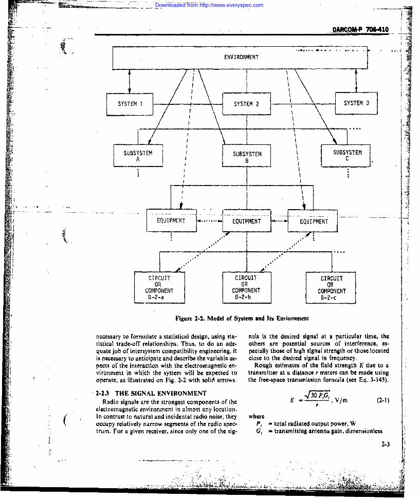
C.706410
EQUIPMENT EVIPMENT ' EQPEN
EOUPONENT CO....ONENT COMNENT
OR OR ORCOMPONENT COMPONENT COMPONENTB-2-a B-2-h B-2-C
Figure 2-2. Model of System and Its Enviornment
necessary to formulate a statistical design, using sta- nals is the desired signal at a particular time, thetistical trade-off relationships. Thus, to do an ade- others are potential sources of interference, es-quate job of intersystem compatibility engineering, it pecially those of high signal strength or those locatedis necessary to anticipate and describe the variable as- close to the desired signal in frequency.pects of the interaction with the electromagnetic en- Rough estimates of the field strength E due to avironment in which the system will be expected to transmitter at a distance r meters can be made usingoperate, as illustrated on Fig. 2.2 with solid arrows. the free-space transmission formula (see Eq. 3-145).
2-2.3 THE SIGNAL ENVIRONMENT - I3f P,Radio signals are the strongest components of the E V/m (21)
electromagnetic environment in almost any location,I In contrast to natural and incidental radio noise, they where
occupy relatively narrow segments of the radio spec- P, = total radiated output power, Wtrum. For a given receiver, since only one of the sig- G, transmitting antenna gain. dimensionless
2-3
• , ... ." . • * " i-4
Downloaded from http://www.everyspec.com

DAAM-P 706"410r n . ' .. ... I.. .I n
Fig. 2-3 shows the variation of field strength with r cation to another, characteristics change gradually.for constant values of PG,. However enough areas can b. classified distinctly as
In using Eq. 2.1, the reader is cautioned that the one type or another to make classification useful. Inrate of fall-off of E with distance may be greater or this category we classify environments as rural, resi-less depending on propagation conditions, see par. 3- dential, commercial, industrial, and urban on the pre-3.2. sumption that man-made radio noise levels will in-
The signal environment in which military equip- crease significantly as we pass from one to the other.ment and systems operate consists of two major ele- Rural areas can be considered to have a popula-ments, the military part and the nonmilitary part. tion density less than 500 persons per square mileThe military part is created by the overall military and, except for isolated instances, are at least 25 milessystem and thus can be controlled to a large extent. from fixed transmitters having more than a kilowattThe nonmilitary is characteristic of the area and only of output power. They have no substantial industriallimited control may be exercised over it. activity. Radio-noise levels are determined by at-
mospheric noise levels except in the immediate vi-2-2.3.1 Nonmilitary Signal cinity of high voltage power lines, electric fences, or
Environments heavily travelled roads, Radio signals of all kinds areAny environmental classification scheme must be at relatively low levels and the ability to receive de-
considered to be partially conceptual, rather than ab- sired signals generally Is limited more by low signalsolute, since as one moves physically from one 1o- strengths than by interference from undesired signals.
-- Pt -,--total-. radi ated--output-powar-,-W ..... .
Gt transmitting antenna gain, dmls
so-.-
igr
4istanc Fro Sorer'ii
201--l
60 T- i-,...
-40 --- !
1.0 10 100 I k 10 k .
Distance From Source P, m
Figure 2-3. Field Strengt~h as a Function of Distance of Transmitter
.... 2-4
. T U. ...
Downloaded from http://www.everyspec.com

DARCOM.P 706410
At the other extreme, urban areas are characterized it e0sential that incidental equipment noise be as lowby high population densities, which may range from as possible in order to enhance transmission quality
I 15,000 to more than 70,000 persons per square mile, and minimize adjacent channel and other spuriousand relatively high ambient noise levels due to nu- emision interference.merous industrial and commercial area as well as The heavy demand for radio frequencies makes itdensely populated residential areas. In the VHF and necessary to use the same frequency simultaneouslyUHF bands, local ignition interference can be of con- in various nets. To prevent co-channel and adjacentsiderable importance. Broadcast signals, because of channel interference, a trained frequency manage-their local origin, are usually relatively strong and the ment officer assigns frequencies on a priority basis,signal strengths in the vicinity of the antenna towers utilizing data on geography, restrictions on timecan be very large. In the VHF and UHF bands, how- usage, power, bandwidths, and types of antennas.ever, the effects of tall buildings may cause serious re- (See DA Pamphlet No. 105.2* and ST 24.2-1 forflections which will degrade performance locally and details, Ref. 2).distort normal field strength contours.2 . Ms2-2.3.23 Ship and Aircraft2-2.3.2 Military Enwironments In many respects these environments are similar to
This classification includes environments which are that of the ground station. A principal difference ischaracteristic of peace-time operations as well as one of scale. Although very large ships can be con-operations which are likely to be found only under sidered to be a complete ground station on a mobileconditions of conflict, platform, the largest Army watercraft are likely to
carry typical radar and communications equipment.2-2,3.2.1 Ground Station Since antennas and various items of electrical equip-
This classification includes a typical Army post. It ment are in. permanent locations, to some extent.theusually includes an array of transmitters having a installation can be designed to optimize the compati-wide range of output power and corresponding -bility situation. How-u-,the- fle-x-bility-availiibllisreceivers, In some cases, particularly at HF where small and the consequences of any signal de-high power may be used, receiving antennas are sepa- gradation whatsoever are likely to be serious. Belowrated from transmitting antennas by distances of the steel decks or within an aircraft fuselage, one hasorder of miles in order to avoid interaction, good examples of what are usually defined as intra-
At VHF and UHF, line-of-sight multichannel links system compatibility problems. In these locations po-use low power (a few watts) and may use the same re- tentially interacting equipments and their cables mayflector for transmission and reception, and reflectors be in close proximity, and antenna coupling is almostfor separate links may be mounted on the same nonexistent, Above deckg or external to the fuselage,tower. Troposcatter links use high power with a high- both types of interaction are possible.ly directional antenna which may be used for bothtransmitting and receiving. Furthermore, high pow- 2-2.3.2,4 Missileered radars rmay be located on the site. Frequently This item is placed in a unique classificationsuch sites have industrial types of equipment in use. because of the fact that it must operate with high re-
liability through rapidly changing external environ-2-2.3,2.2 Battlefield ments. At low altitudes it may pass quite close to ur-
In the battlefield environment, radio communi- ban areas containing relatively high-powered trans-cations provide the principal means of exercising mitters of both military and broadcast types. At highcommand and control. At the same time, radar, altitudes the missile is within line of sight of largespecial weapons systems, and telemetry units are ex- areas of the earth and, therefore, large numbers ofpected to function with a high degree of reliability, signals have the potential of affecting it. In addition,
A theater army area of operations may have tens of because of the high density of electronic compo-thousands of emitters of electromagnetic energy or- nents, its intrasystem environment is especiallyganized into many radio nets. The tactical situation severedetermines the land mass occupied by this army, and 2-2.3.2.5 Equipmentexpansion or contraction of the area will increase ordecrease the interference level together with the de- This is the environment that can be found within asired signal strength. typical cabinet or metallic eniclosure of some device,
The relatively dense concentration of emitters, as ODA Pamphlet% and AR's referred to in this paragraph are dewell as the possibility of intentional jamming, makes scribed in Table 2-6,
2-!
Downloaded from http://www.everyspec.com

DARtCOM-P 706-410
It is an extreme example of an intrasystem environ- where some of the major types of source of inter.ment. Frequently, such an enclosure contains many ference contribute most importantly in each of thesepaate electrical and electronic parts which must in- major types of environment. Also, reference is madeteract in a specified way in order to perform the use- to paragraphs in Chapter 3 which give quantitativeful function for which the equipment was designed. information of use in a system or equipment analy-At the same time, these components may interact in sis. Clearly, before such an analysis can be carriedways that are not intended, and the unintended inter- through, the design engineer must have familiarityactions may be caused by emission levels introduced with the theory andjnactice of EMC/EMI tn-into the inside of the equipment by the penetration of gineering. Further discussion of prediction techni-external fields or currents through the walls of the ques is given in Chapter 6.container. By proper design, such penetration phe-nomena can be controlled. 2-3 SPECTRUM ENGINEERING
At the component level, environment can he con-trolled frequently by proper physical placement of The radio spectrum is a limited resource (Ref. 3).
components or by the use of filters and shields to iso- The uses of the spectrum are expanding and, at any
late them from undesired interactions with other given time, the demand exceeds the supply. Further-"components. In other cases specific circuit designs more, some services are best carried out in certain fre.can be used to reduce their susceptibility to local quency ranges and demand in these ranges continues
fields or to reduce the fields which they generate, to grow. By international agreement, and by, de- I"cisions of national regulatory bodies, parts of the
22.3.2.6 Other Categories.. . .. pectrumare allocated to particular services. These
Other categories which are not explicitly covered are further subdivided into channels whose width is-may-be- considered to-be-combinations -of the pre.- sufficient-to accommodatethe signals-typical-of-theceding. An example is the airport which may be com- service. Thus a principal microwave radio relay al-pared with a military ground station. It has re- location is a band between 37U0 MHz and 4200 MHzceivers, transmitters, radars,. and, at least in civilian subdivided into 24 channels with adjacent channels •airports, is usually surrounded by commercial and in- separated by 20 MHz. Each channel is, in turn, ab!e K
& i dustrial areas with high radio noise levels. to accommodate 600 multiplexed voice channels. '"
The environmental characteristics discussed in this Electromagnetic compatibility requires a minimalparagraph are produced by electromnagnetic phe- geographic spacing between users assigned to thenomena which are analyzed explicitly in later same channel, and also between users assigned to ad-chapters, In the treatment, methods of determining jacent channels. In order to fit as many microwave re-steps to be taken to avoid a particular effect or to re- lay users as poss'ble into a geographical region, ad-
* duce interactions that are experienced will be in- vantage is taken of the rejection afforded to un-cluded. For reference puepohes. Table 2-1 shows wanted signals by antenna directivity, and also by the
TABLE 2-1. IMPORTANT CONTRIBUTORS TO VARIOUS ELECTROMAGNETICENVIRONMENTS
___Noise Type of Environment This HandbookSource I Paragraph
Rural Urban Intersystem Intrasystem Equipment References,Atmospheric X x 31.2.2
Transmitters ISM X X X X 3-1,3.1.2
Spurious RFGeneration X X X 3-1.3,3.3
Ignition X X X 3-1.3.2.4.5 " . .. 3-1.3.2 . :
Switching Transients X X 3-1.3.3.2(
Powerine Harmonics X X [ 13-33.1
2-6
...' ...
Downloaded from http://www.everyspec.com

DARCOM-P 06410
. use of orthogonal polarizations. Allocations 'are specification (see par. 2-5.2). The latter establishessometimes shared by different services where theex- equipment limits which will effectively "control" thepectation of mutual interference is small. Channel cquipment contribution to environmental levels. The Vassignments sometimes are made with-the provision K-, "system" specification establishes system perform-that no interference shall result to other users who"* ance requirements which in turn require a design that
I.' have priority, or that transmission will occur during e directly controls interactions between individualspecified time only. . components of equipments.
The process by which assignments are made takesaccount of the need for the channel; the.. umber' tfchannels available; -the noise level, both nat ral andman-made; the characteristics of receiversi.tht range 24.1 THE SYSTEM APPROACH
I and area to be-covered; the location, whefher fixed or The main fact to be recognized in system design ismobile; the kind of signal ito be Used (the'inodulation that each system is unique and therefore EMC re-
: 0and bandwidth); and the time during which it is re- quirements are likely to be unique. It is the overallquired. An assignment specifies the allowable trans- system requirements that determine what the corn-mitted power, the limits of spatial coverage by the an- ponent equipment EMC requirements are and the ex-tenna, as well as frequency, time, and place. tent to which standard requirements will be suitable.
Frequency allocations are made internationally Just as with equipment design, these requirementsthrough the International Telecommunications must be determined initially before manufacture.L Union and, in the USA. by the Federal Com- Thus one must obtain, early in the design and de-munications Commission and the Office of Telecom- velopment stages, an adequate description of the ulti-munications Management. Because of the shortage of mate circumstances under which a specific system issplectr . space, no development of Department of used. Then it is possible to initiate design of theA.my equipment requiring spectrum space can be in-- system-components in accordance with the deriveditiated without a formal action regarding frequency requirements. To do this, the designer must have a re-allocation (see AR 705-16). liable interference prediction process readily avail-
Intrasystem compatibility problems usually are ig- able. This means having adequate models of emitters,nored in frequency allocation procedures, it being as- susceptors, and the couplings between them. Thesumed that by proper design techniques system de. engineer also must have the same type of in.
,. dgradation due to this cause can be avoided. To the formation pertinent to equipment design includingdesigner, however - especially where systems are co- data on interference reduction circuith and tech-located, such as on a vehicle or at a command post - niques and on cost effectivencss trade-offs.the considerations for dealing with intrasystem and In practice the entire process is usually not as com-intersystem compatibility may be quite similar. plicated as this description might lead one to believe.
It is probable that only a limited number of para-2-4 ACHIEVING meters involved in the system design will exhibitELECTROMAGNETIC critical cost-effectiveness trade-offs. Many of the pos-
LCOMPATIBILITY sible interactions can be controlled effectively by de-sign techniques which do not, in themselves, in-
Achieving electromagnetic compatibility can be herently lead to very high costs. The system designerapproached from the concept of either (i) a detailed must be able to identify those elements of the systemevaluation of interactions between the elements, which are critical with regard to cost and perform-emitters and susceptors, on a pair by pair basis; or (2) ance, and must deal with these in a first-orderfrom general requirements. In the latter case the de- analysis with properly assigned priorities.signer attempts to define a so-called "typical" or"nominal" environment, and then designs his equip-ment so as to neither degrade the environment byraising levels of radio noise above the "nominal" 24.2 REVIEW OF APPROACHES TO EMClevel (at a specified distance from the equipment) nor Different approaches to EMC control are exempli-to be susceptible to those levels. In general, neither of fled by those used by the Federal Communicationsthese two approaches can be used in isolation. Commission industry, and the Department of De-
To some extent these approaches can be as- fense, Since the technologies involved are inter-sociated with two of the basic types of specification, related, the discussion is relevant to a variety ofi.e., the "system" specification and the "equipment" typical EMC problem areas.
2-7
1, X. W A -bt
Downloaded from http://www.everyspec.com

2 -4.2.1 The Federal Communications Commission be located are permitted to radiate more energy than
In carrying out its responsibilities for regulating those which appear in homes near receivers orradio communication, the Federal Communications receiver ariternnas. Also taken into consideration arcCommission has been faced with the very practical such factors as whether danger to life is involved,question of how to write the rules so that they can economic aspects (which are a function of the state ofprotect effectively the various services under its the art), and the possibilities of alternate means ofcognizance, while at the same time not unduly burden obtaining the same type of service. In many respectsthose who provide the services. To assure this, the the rule-making procedure is a way of establishing aCommi!sion makes effective use of the public hearing de facto cost-effectiveness trade-off relationship.
procedure. In this procedure, the Commission In other cases, the Commission adopts an equip-publishes a notice of proposed rule-making and in- ment interaction approach in that it establishesvites comments from those involved in providing the standards for various types of transmitting equip.service, the public at large making use of the service, ment and allocates frequencies based upon the as-and industry which manufactures the equipment sumption that the equipment meets those standards.which will have to meet the requirements. After some For example, transmitter harmonic levels are con-study, a set of limits is proposed. These limits are trolled along with antenna patterns. A person ap-then discussed at great length. After duly taking into plying for a transmitter license must show that hisaccount all the evidence before it, the Commission equipment will not produce interference with otherfinally issues specific rules and regulations. In doing services already established in the same area.this, the Commission makes use of both the system In order to simplify FCC rule-making procedures,approach and the environmental approach. unintentional emitters have been classified in three
.................... Thenvirpmctal_ approah-can. be illustrated by general cat¢ories JRefs, 5). Exa mplls are ghyen in.the method used to control interference to radio Table 2-2. The major features of the regulations arebroadcasting. Here, one can look upon the pro- summarized in Tables 2-3, 2-4, and 2-5.cedure as protecting a defined field strength at aspecified distance from an interference source. The 24.2.1.1 Incidental Radiation Devicefield strength is a function of the service involved, A device that radiates radio frequency energywhile the distance at which protection is to be ob- during the course of its operation, even though thetained is a function of the source, and where it is device is not intentionally designed to generate radioused. For example, sources arising in industrial en. frequency energy, is classified as an incidental radia-vironments where receiver antennas are not likely to tion device (Ref. 4, part 15).
TABLE 2-2. EXAMPLES OF ELECTRONIC DEVICES REGULATED BYFCC RULES PARTS 15 AND 18
Regulated by Part 15 Regulated by Part 18Restricted Radiation Devices Incidental Radiation Devices Industrial. Scientific, and
RF Energy RF Energy MedicalPurposely Generated Unintentionally Generated
I. Radio Receivers I . Fluorescent Lights I . Industrial Heatersa. Induction, Carrier Current Systems 2. Electric Appliances b. Dielectric
a. "Campus"b. Telephone 3. Electric Motors 2. Medical Diathermyc. Industrial 4. Electric Shavers 3. Miscellaneous
3. Low-power Communications 5. Ignition Systems a. Epilatorsa. Wireless Microphones 6. Defective Insulators b. Ultrasonicb. Garage Door Openers c. Microwave Ovensc. Phonograph Oscillators d. RF Neon Signs
4. Field Disturbance Sensors
5. Class I TV Devices ___
2-8
Downloaded from http://www.everyspec.com

TABLE 2-3TECHNICAL REQUIREMENTS FOR PART 15
(INCIDENTAL AND RESTRICTED RADIATION) DEVICES
TYPE OF EQUIPMENT FREQUENCY OF FIELD STRENGTH ADDITIONAL REQUIREMENTS REFER TORADIATION, MHz LIMIT. MV/nt SECTION"
Incidental Radiation Any frequency None In the event that harmful interference is caused. 15.31Device* the operator shall promptly take steps to elimi-(Subpart B) nato the harmf'ul interference.
Radio Receivers(30-890 MHz)(Subpart C)TV broadcast 0.45-25 None Power line RF voltage limitation: 100 1V/m 15.63
-*.All other 0.45-9 None Power line RF voltage limitation: lO0siV/m 15.63
9-10 None Power line RIF voltage limitation: 100-I00D iLY/rn 15.63
10-25 None Power line RF voltage limitation: IOD m/ni 15.63
25-70 32 at 1000 ft Applicable to All Receivers (30-890 MI-z)70-130 50 at 1000 ft Certification required for each model receiver, 15.69
Identify each certified receiver with seal or 15.70130-174 so.I so at lO00 ft label. 15.71
Any measurement procedure acceptable to the 05174-260 IS0 at 1000 ft FCC may be used. The following standards are
-. - -------......------- ~~~ ------------ cndeesepae----- - - - -
Power line RF voltage: IEEE STD 213260.470 130-500at 1000 ft Radiation: IEEE STD 187: also IEC
l~b/l0ba and EL6S RS 378470-1000 M00(350 for TV rcvr.
see Sec. 15.63) at TV sensitivity: IEEE STD 1901000 ft
Door Openers 25-70 32(receivers) Measuremqvnts scc-ordlng to FCC document
70-200 so T700 I
200-1500 50-500
over 1500 S0oo__________________ ____
Low Power Communi-cation (Subpart E) Max. Input to Final. W Max. Antenna Length, fOperation Under 0. 16-0. 19 None 1.0 SO* 15.203Antenna, and Power 0.51-1.6 None 0.1 100 15.204Limitations 26.97-27.27 None 0.1 5 15.205
0.010-0.490 2.4/f(ln MHz) 15.202Operation under at 1000 ftField Strength 0.510-1.6 2.4/f(ln MHz) 15.202Limitation at 1000 ft
70- 1000 receiver radiation Limit operation automatically to I s on followed 15.211limit applies by 30 a off
above 1000 500 at 100 ft Limit operation automatically to I a on followed~ !5.211_____________by 30 a off ____
Telemetering andWireless Microphone 88-1O8 50 at S0 rt in Channel width is limited to 200 kl~z. 15.212
200 kHz band40 at 10 ft
outside of band'. * including transmission line
(. (ont') ~ References are to Part 15 or Part 1IS as applicable, of the FCC Rules and Regulations.
2-9
4. .. . . . . . . .
Downloaded from http://www.everyspec.com

DARCOM.P 706-410A
TABLE 2-3 (cont'd) #
TYPEOF EQUIPMENT FREQUENCY OF FIELDSTRENUTH ADDITIONAL REQUIREMENTS REFERTORADIATION. MHz LIMIT,ssV/m SECTION"
BiomedicalTelemetering 174-216 150 at 100 ft Limit applies only to the fundamental frequency. 15.215SDevices Harmonic and other spurious emissions outside
of 174-216 MHz shall be suppressed by at least20 dB (subject to change in Docket 10846).
Door Openers(transmitters) 70-130 125 at 100 ft The emission permitted on 73.75.4. 108-118, 15.215
121.4-121.6, 242.8-243.2. 265-285. 328.6-335.4,406-410.608-6l4.9W0-2l5 (allin M[W)and otherbands.SeeSee. 15.21S.
Field DisturbanceSensors (Subpart F) Any Frequency 15at 157/Ain MHz)ft Limit applies to the fundamental, any harmonic. 15-.305
and other spurious frequencies.
915 50,0W at l00 ft Band limited to *:13 MHz 15.3071, 0.309
2450 50,0W at 100 ft Band limited to hI5 MHz 15.307,15.3095800 50,000 at 1OOft Band limited to * 15 MHz 15.307,15,309
10525 250.000 at 100 ft Band limited to*25 MHz ' .. 15.307.15.309
- - 24125- -250.,0at-l00ft- -Band limited to*+50 MHz _ _ 15.307.15.309
Applicable to All Field Disturbance Sensors 15.303. 15.317CertificationMeasurement
1 References are to Part 15 or Part 18, as applicable, of the FCC Rules and Regulations.
TABLE 2-4. FREQUENCIES FOR INDUSTRIAL. SCIENTIFIC, ANDMEDICAL (ISM) EQUIPMENT FOR WHICH NO RADIATION
LIMITS ARE SPECIFIED
Frequency, kHz Tolerance, kHz Frequency, MHz Tolerance, MHz
13,560 ± 6.78 915 ± 1327,120 ± 160 2,450 ± 5040.680 ± 20 5.800 1 75
24.125 + 125
There are no regulations specifying constraints on To control interference from restricted radiationradiation from devices in this category other than it devices, unless otherwise stated, the limit fieldharmful interference does occur, immediate steps strength is 15pV/m at a distance of X/(2wr) where X ismust be taken to eiminate it. (This latter regulation is the wavelength corresponding to the operating fre-applied to all incidental device categories.) quency. The design must be in accordance with the
best engineering practice, and operate with the mini.mum power required to produce the desired result. It
2-4,2.1.2 Restricted Radiation Device may be noted that the distance of X/(21r) is the dis-A restricted radiation device is one in which the tance from a dipole at which the variation in field
generation of small amounts of RF energy is in- strength with distance changes from an inverse cubetentionally incorporated into the design, but does not relationship (induction field) to an inverse first po;verrequire licensing. relationihip (radiation field). Also at a fixed distance
2.10
Downloaded from http://www.everyspec.com

4 -QF > DARCOM-P 706410~jj 4.~TABLE 2-5. TECHNICAL SPECIFICATIONS FOR PART 18
(INDUSTRIAL, SCIENTIFIC, AND MEDICAL SERVICES) DEVICES
TYPE OF EQUIPMENT FUNDAMENTAL FIELD STRENGTH ADDITIONAL REQUIREMENTS REETOFREQUENCY OF LIMIT OUTSIDESETNRADIATION, MHz OF ISM BANDS SCIN
Medical Diathermy 13.56, 27.12, 14.68 .25 1&V/m at lODO ft 1.4
(Subpart E) 915.2450.580D.24135 Reduce radiation to Reduce bandwidth of emissions to the greatest 18.142greatest extent extent practicable
________________practicable, _____________________ ______
Any Other Frequency 15 itV/mat 100) ft l5pif at 1000-ft limit also applies to radiation 18.142at the fundamentalApjplicabie to All Medical Diathermy Equipment
Use FCC radiation measurement procedure. 18.143Certification or Type Approval. 18.14Certificate must be renewed every 3 yr. 18.1 41Equipment operated on off- ISM frequencies re- 18.142quires a rectified and filtered power supply.
Ultrasonic Up to 0.490 24/f(in MHz) gaY/r In predominantly residential areas and on fre- 18.72(Subpart CQ at 1000 ft quencies below 0.490 MHz the radiation limit
may be increased as the square of the generated-- -- power to 500 W. The limit, however, is not Per-
_________W~ ifte~ xcftd10,V/m atl mi-.-
0.490-1.6 24/f (ini MHz) jnt/ Applicable to All Ultrasonic Equipmentat 100 ft Use FCC radiation measurement procedure. 18.78
Power line RF voltage:b-low 0.49 MHz-10ODpV 18.72(c)
Ove 1. I~Y/mtlOftabove 0.49 M Hz-200gA F
Certification. 18810____________________________________ or Type Approval. 18.13
Industrial Heating Below 5725 l0jiV/m at I mu Power line radiation limit; 10 gaV/m at 50 it at 18.102(Subpart CQ points I mi or more from the equipment.
Use FCC radiation mncasureaner.t. procediure. 19.107Above 5725 Reduce radiation to Applicable To All Industrial Heaters
greatest extent Operation not permitted on; 19.102(b)4practicable. 0.490-0.510 MHz. 2.170-2.194 MHz. aaid
8.354-8.374 MHzCertification. 18.113
__________ ________________________ Periodic Inspection. 18.101.
RE Stabilized Any Frequency lOsaV/M at I mi Power line radiation limit: 10 gaV/m at 50 ft at 18.5Arc Welders points I mu or more from the equipment.
(Subpart F) Use FCC radiation measurement procedures. 18.107Measure quasi-peak using an instrument equiva- 18.18)lent to ANSI specifications C63.2 to C63.4Certification. 19.192
___________________________________or Type Approval. 18.181
Miscellaneous These rules apply to ISM equipment other than medical diathermy, industrial heating, ultrasonic(Subpart H) and RF Stabilized tire welders in which RF energy is appi to raurials to produce physical.
biological, or chemical effects such as microwave ovens, ionization of gases, mechanical vibra-tions, hair removal, and acceleration of charge particles which do not involve the use of radioreceiving equipment.
Requirements are the samei as for medical diathermy except that for equipment other than thatsed in predominantly residential areas, the radiation limit may be increased as the square root
? Iof the generated power to S00 W. The limit, however, is not permitted to exceed IG gay/r at I mi.
References art to Part 18 of the FCC Rules and Regulations.
2-i 1
Downloaded from http://www.everyspec.com

.1. ..- , -.
DAR "M-P70 iO...
this limit decreases with frequency, which cor- be suppressed at least 20 d8 below the level of the un- '
responds to the behavior of atmospheric radio noise modulated carrier. An additional design limitationlevels, prohibits class B operation.
Field disturbance sensors are classed as restricted2-4.2.1.3 Radio Receivers radiation devices but, because of their special func-
Radio receivers, including television broadcast tion, have special limits assigned in the GHz rangereceivers, are treated as a special case of restricted and above.radiation devices.
For frequencies above 25 MHz the radiation frpm 2-4.2.1.5 lndustrial, Scientific, andthese devices is limited to specific field strengths Medical Equipment (ISM)measured at specific disances. The limit increases The ISM category of equipment (Ref. 5) includessomewhat with frequency corresponding partly with devices which use radio waves for industrial, scien-state of the art, and partly with incrbasing cosmic tific, medical, or other purposes which are neithernoise levels. At 25 MHz and below, a limit is placed used or intended to be used for communicaton.on voltages conducted to the power lines since this is Operating frequencies have been allecated, andconsidered to be the most likyly source of coupling allowable tolerances established for which there arefrom such devices, no radiation limits (Table 2-4). Operation is per-
mitted at other frequencies but radiated emissions are2-4.2.1.4 Low Power Communication Devices limited (Table 2-5). These limits are defined in terms
A low power communication device is a restricted of radiated field strength at a specified distance, andradiation device (Ref. 4) exclusive of those em- apply to radiated harmonics oawel as. -spurious.ploying conducted- or -guided-- radio- frequency tech-.- radiation. In addition, conducted emission limitsniqups used for transmission of signs, signals (in- have boten established for ultrasonic- equipment. -cluding control signals), writing, images, and sounds Medical diathermy equipment, when operated onor intelligence of any nature by radiation of electro- frequencies other than those assigned for ISM opera-i magnetic energy (e.g., wireless microphone, phone tion. are subject to a radiated emission limitation inoscillators, garage door openers, radio control terms of a maximum field strength measured at amodels), specified distance. There are, as well, some design re-
The design and operation of low power communi- quirements which will suppress spurious and har-cation devices are more closely regulated than are monic frequency radiation: for example, a rectifiedthose of the previously discussed devices. The general and filtered plate voltage must be used.rule requiring the immediate elimination of harmful Industrial heating equipment is subject to a limita-interference applies here as in all other categories. tion as to its radiated field strength at a specified dis-Allowed bands of operation have been established tance when operated below 5725 MHz and on any(see Table 2-3) and, in the case of telemetry trans- frequency other than those established for ISMmitters and wireless microphones, maximum channel equipment. Above 5725 MHz the regulations onlywidths have been established. Limits of radiated specify that radiation must be suppressed as much asenergy, in-band and out-of-band, and within-channel possible. Though there are no specific limits to con-and out-of-channel, have been established for all but ducted emissions to the power lines from industrialone band. A limit to the energy which may be con- heating equipment, it is required that sufficient filter-ducted to the power line has been establishd in the ing be provided to limit radiation from power lines. A510 - 1600 kHz bands. In the 26.97 - 27.27 MHz band limit to power line radiation is provided in terms ofwhere no radiation limit has been directly es- radiated field strength at a distance. These limitstablished and as an alternative method in the 160 - represent compromises between practical state-of-190 kHz and 510 - 1600 kHz bands, device design the-art considerations and use in specialized areas.limits are used which effectively serve to limit the de-vice radiation. An upper limit is set for input power 24.2.1.6 Licensing of Test Facilitiesto the final amplifier and the length of the antenna (5 Unless a Government agency assumes responsi-ft for the 26.97 - 27.27 MHz band) or the combined bility for running tests, test facilities set up by con-length of the antenna and its associated transmission tractors require FCC licenses or at least temporaryline. In addition, the level of power input to the final authorization if substantial radiation may occur,amplifier lying outside of the band of operation (e.g., either in connection with scientific studies or for test-if operation is on the 160 - 190 kHz band, for all ing of communication equipment including trans-frequencies above 190 kHz or below 160 kHz) must mitters and antennas. Requirements are covered in
2-12
..-.-.. ~~~~ka ai . • • .,,..,..,,,, .. .:_., . . ... ..- . ..,
Downloaded from http://www.everyspec.com

FA-AKCM-P 706410
Parts 5 (Ref. 9) and 15 (Ref. 4) of the Rules and trol. In many instances the interference from par-Regulations. At frequencies below about 10 MHz the ticular devices is controlled in accordance with limitscriterion for obtaining FCC approval is considered to established by individual companies. In those cases inbe whether emission levels will exceed 15 pV/m at a which the interactions have been sufficiently signifi-distance of X,/(2T) where X is the wavelength of the cant to justify a joint industry effort, standards haveradiation, been published. These limits generally are based upon
In the usual case, a contractor will not require a a carefully examined cost-effectiveness trade-off. Pri-formal radio station license (Ref. 9, par. 5.52) but will mary concern has been with interference to radio andbe able to qualify for a special temporary authori- television broadcasting, although recently there haszation (par. 5.56) as an experimental radio service been a growing concern about establishing electro-(Research or Developmental) (par. 5.2). magnetic compatibility between industria! and com-
Informal applications for special temporary autho- mercial use devices. Industry has devoted most of itsrizations for Government contractors thould: efforts to establishing measurement techniques and
a. Be prepared as a letter, in duplicate with the instrumentation, as exemplified by the followingI. original signed and sent to the Federal Com- standards published by the American National.munications Commission, Washington, DC 20554. Standards Institute-
b. Contain the following information: a. C63.2-1963, Radio-Noise and Field-Strength(I) Name and address Meters, 0.015 to 30 Megacycles/Second, Specifi-(2) Need for special action cations for.(3) Type of operation to be conducted b. C63.3-1964, Radio-Noise and Field-Strength( (4) Purpose of operation Meters, 20 to 1000 Megacycles/Second, Specirt-(5) Time and date of proposed operation cations for.(6) Class -f station, call sign of station, and c. C63.4-1963, Radio-Noise Voltage and Radio-
nature of servi-e .... Noise-Field Strength, 0.015 to 25 Megacycles! Sc-._(7) Location of proposed operation cond, Low-Voltage Electric Equipment, and Non-(8) Equipment to be used, including name of electric Equipment, Methods of Measurement of.
manufacturer, model, and number of units. Industry groups have established voluntary limitsI!' (9) Frequency(s) desired as follows:(10) Plate power input to final radio frequency a. Society of Automotive Engineers, Inc.: J551,
stage "Measurement of Electromagnetic Radiation from(1l) Type of emission Motor Vehicles (20-1000 MHz)."(12) Antenna height (FCC Form 401-A if par. b. National Electr; Manufacturers Associa-
5.55 so requires) tion: "Semiconducto )immers for Incandescent(13) Full particulars as to the purpose of the Lamps," WD2-197
request. c. Radio Techni. 'ornmittee for Aeronautics.c. Include: DO-138, "Environment.. -onditions and Test Pro-
(1) FCC Form 44A in triplicate "Supplemental cedures for Airborne Eh. conic/Electrical Equip-Information for Applications in the Experimental ment and Instrument."Radio Service Involving Government Contracts". d. International Special Committee on Radio
(2) If the application involves communications Interference (CISPR):essential to a research project: (I) Publication 11: "Limits and methods of
(a) A description of the nature of the re- measurement of radio interference characteristics ofsearch project being conducted industrial, scientific and medical (ISM) radio-
(b) A showing that communication facil- frequency equipment (excluding surgical diathermyities are necessary for the research project involved apparatus)," 1st edition, 1975.
(c) A showing that existing communication (2) Publication 12: "Limits and methods offacilities are inadequate, measurement of radio interference characteristics of
If a Government agency assumes test responsibili- ignition systems of motor vehicles and other de-ty, it must obtain permission from the Interdepart- vices," 1st edition, 1975.ment Radio Advisory Committee (see par. 2-6.4.5). (3) Publication 13: "Limits and methods of
measurement of radio interference characteristics of2-4.2.2 Industry Standards sound and television receivers," Ist edition, 1975.
Industry in the United States is well aware of EMI (4) Publication 14: "Limits and methods ofphenomena and has devoted much effort to its con- measurement of radio interference characteristics of
2-13
Downloaded from http://www.everyspec.com

- tARCOM-P 706-410
household electrical appliances, portable tools and opment, cost production, and deployment) of thea. similar electrical apparatus," 1st edition, 1975. Life Cycle System Management Model (LCSMM)(5) Publication 15, "Limits and methods of (par. 2-7), and recognizes three principal factors
measurement of radio interference characteristics of which must be addressed by the EMC Program:
fluorescent lamps and luminaires," Ist edition, 1975. i. Environmental Geometry: The identification ofall emitters and receptors, the spatial relationships
2-4.2.3 Department of Defense among the emitters and receptors, and the partic-EMC Program ulars regarding terrain and propagation
The Department of Defense has established an in- 2. C-E Materiel Characteristics: All features whichtegrated Electromagnetic Compatibility • Program influence the degree of performance achievable under(EMCP) to ensure electromagnetic compatibility of given electromagnetic environmental operating con-all military communication-electronic (C-E) equip- ditionsments, subsystems, and systems during conceptual, 3. Frequency Assignments: The distribution ofdesign, acquisition, and operational phases (see DoD available spectrum resources.Directive 3222.3). Its objectives are to: (a) achieve A number of regulations and pamphlets, as shown
compatibility of all equipments, (b) to obtain built-in in Table 2-6, describe policies and procedures relateddesign compatibility rather than remedies added after to matters of direct concern in EMC programs re-the fact, and (c) use common approaches and lated to Army materiel procurements.techniques in C-E material programs. To accomplishthis it directs action and assigns responsibility in thefollowing EMC program areas: Standards and Speci- 2 5 THE EMC PROGRAMfications, Measurement Techniques and Instrumen- REQUIREMENTS.ation, Education for EMC, Data Base and Analysis MIL-HDBK-237 (Ref. 6) provides criteria for es-Capability, Design, concepis and Doctrine, Opera. tablishing, managing, and evaluating an EMC pro-
tional Problems and Test and Validation. gram for electronic, electrical, and clectromechani-DoD recognizes that frequency management has a cal equipments, subsystems, and systems. It provides
strong influence on compatibility and has assigned EMC guidance to those responsible for the programresponsibilities for the use of the radio frequency so as to increase the probability of achieving intra-spectrum. Specific spectrum management functions system and intersystem compatibility.are delegated to individual departments. Depart-mental membership in the Interdepartmental Radio 2-.1 EMC PROGRAM GOALSAdvisory Committee (IRAC) and liaison with FCC In broad terms, the goals of any EMC program areprovides interdepartment, international, and national (Ref. 6):(non-Government) coordination. DoD directives ad- a. Assure efficient integration of engineering,dress themselves to spectrum management, and EMC management, and quality assurance tasks, as relatedprograms and equipment. Typical examples are: to EMC.
a. DoDD 4630.1, Programming of Major Tele- b. Assure the efficient integration of EMC with allcommunications Requirements other system performance factors and disciplines
b. DoDD 4630.5, Compatibility and Common- affecting system effectiveness and cost, such asality of Equipment for Tactical Command and Con- reliability, maintainability, vulnerability, and safety.trol and Communications c. Assure the integration of the engineering func-
c. DoDD 4650.1, Management and Use of the tions - such as design, development, and test - asRadio Frequency Spectrum related to EMC.
d. DoDD 5000.3, Test and Evaluation d. Assure intrasystem and intersystem design ande. DoDD 5100.35, Military Communications- operational electromagnetic compatibility.
Electronics Board (MCEB). e. Assure continuous traceability of EMC re-quirements and design alternatives throughout the
24.2.4 Department of The Army program, so that the soutces and impact of designEMC Program changes and deficiencies in equipment and sub-
The Department of the Army has established an systems, and the impact of contractual performanceEMC Program consistent with the Department of requirements are promptly determined, accuratelyDefense EMC Program. It directs that electromag- identified, and properly communicated. , ,netic compatibility of materiel be controlled through- f. Permit timely and optimum redefinition ofout each phase (concept, validation, full-scale devel- EMC requirements in response to changes dimcted
2-14
Downloaded from http://www.everyspec.com

DARCOM-P 706410
A, TABLE 2.6. ARMY REGULATIONS AND DA PAMPHLETS CONTAINING EMC GUIDANCE
NO. TITLE PURPOSE EMC PROVISIONS RELATION TOOTHERDIRECTIVES
10-5 Organizations and func- Provides specific responsi- Responsibilities for the Implemented in AR's I I-Il3ions. Dept. of the Army bilities of the general and EMCP frequency manage- 15-14, 70-1, 70-27, 105-3.
special staff ment and, commonality of etc.C-E eqmt
11.13 Army Electromagnetic Provides policies and pro. Policy guidance for EMCP Implements DoDD 3222.3Compatibility Program cedures for the EMCP and program or aetlvitles as- and AR 10-5 for EMC. Re.
sociated with the LCSMM lutes to AR's 105-16, 105-2,_ 105.3,105-16, 105-24
DA Pam Army Electromagnetic To assiit developers In clec. Describes the processes nec. Supplements AR 11-13 with11-13 Compatibility Program tromagnetic compatibility essary to comply with AR emphasis on intersystem
Guide considerations and frequen. 11-13: indicates sources of EMC decisions/actonscy supportability during life EMC analytic support incycle system management areas of analysis, test. and
measurement
DA Pam LifeCycle Systems Privides step by step pro- Check lists for IPR and implements AR's 1000-1,11-25 Management Models for cedures for systems acquisi- ASARC reviews include I15-14, and 11-25
Army Systems tion process EM requirements15-14 Systems Acquisition Re- Provides procedures for Responsibilities for ASARC Implement, AR 1000-1
view Council Procedures ASARC reviews review process. Check listsfor each ASARC includeEM considerations,
-701 , Army Research.-Dcvelop, Establishs rcaponsibilties, Responsibilities to R&D. Cites AR's 11-13 andr, Jto&,'afd'Aiqts1uo"iy. l i4 d joieral Moce- "Need -to -iordnate AF X C-16
dures for Army R&D spectrum and EM require,ments as early as possible,
70-10 Test Evaluation during Describes objectives, con- Provision for EMC testing Implements DoDD 5000.5,Development and Acquisi- .cepts, responsibilities, poit- In DT and OT. and outline and AR's i000-1 and 70-1,
_... .__ sion of M aterIel .. es for T&E test plans for CTP Relates to AR 713
70-27 Outline Developmrnt Plan/ Prescribes procedures for EMC considerations are Implements AR's 1000-IDevelopment Concept preparation and content of provided in outline for Sys- and 0.14Paper/Progratm Memo- DP/DCP/PM tems Summary in App. B.random
711- ArmyCombat Develop. Establishes policy and pro. Responsibilities for combat Implements AR 1000-I inments cedures for combat devel- development and EM con the area of combat develop-
opment activities including siderations in OCO's and ments and provides guid.guidance for preparation of requirement operational unce for AR 71-3future requirements characteristics
71-2 Basisof Issue Plans Establishes policy and pro. Establishes coordination re- Relatesto AR's 11-25,71-1.codures for basis uf issue quirements for EMC. 31t)-31plans for new equipment
-..3 UserTesting Prescribes policies and pro. EMC content of operation- Implements AR I1.8 andcedures for operational test- al tests DODD 5000.3In& I
DA Pam Management of the Electro- Provides information back- Spectrum management Implements and provides105-2 magnetic Spectrum ground on spectrum man- aspects of EMC background for AR's 105-
agement at the internation- If, 105-24. 105-63, andal, national, and DOD Icv- 105-67cis and a description or theArmy EMC program
105-3 (C) Reporting Meaconing, Establishes procedures for MIJI reporting concerned Responds to JC taklt.g inIntrusion. Jamming, and reporting and evaluating in- with electromagnetic emis- SM528-70Interference (MIJI) of Elec- formation concerning inci- sione. Responsibilities aretromagnetic Syrtems dents of MIJI of US mii- assigned, procedures de-
tary electromagnetic equip- crlbed. and format pre.merit sr Aystems sented.
(cont'd)2-11
_-_ _. . .. . . , .' .__ _.. , . , - :. .. ' ' " , " - : ,>1.. :,.- " . , .€e . , ' ' i ". -" " - '. . .:
Downloaded from http://www.everyspec.com

, -J - w xn--- -*-innn_ _- .... . L .. .
D2ARCOM*P161
TABLE 2-6 (cost'd) CNO. TITLE PURPOSE EMC PROVISIONS RELATION TO OTHER
DIRECTIVES
105-16 Radio Frequency Alloca. Prescribes procedures for EMC considerations associ- Relates to AR's II-i3, 105.tions for Equipments under obtaining RF spectrum &I. ated with spectrum alloca. 24, 105-63, 105.67; and DADevelopment, Production, locations tion PAM 105-2and Procurement
105-22 Telecommunications Re. Prescribes policies, respon. Specifies responsibilities for Relates to AR's 11-13, 105-quirements Planning, De. sibilities, and procedures compliance with the EMCP i, 530.2. and 330-4veloping, and Processing for telecommunications re. and makes special provi- J
qulrements within DA sions for Inclusion of
SIOSEC requirements105-24 Radio Frequency and Call Assigns responsibilities and EMC considerations associ- Relates to AR 105-16 and
Sign Assignments for Army establishes procedures fot %ted with frequency assign. DA PAM 105-2
Activities within the Conti. frequency assignments In manianental United States CONUS _
105.63 Army Electromagnetic Provides instructions for re- Provides data for RF utili. Rielates to AR's 105.16 andSpectrum Usage Program porting usage of assigned zation file 105-24, DA PAM 105.2
frequencies in 4-30 MHzband-:
105-.67 Electrumagnetic Compati. Prescribes reporting of C-E Provide data for ECAC file Joint regulation implement.bility Program - Report. equipment in CONUS to Ing part of DODD 3222.3,ing of US Military Else- ECAC EM environment file Relates to AR's 11-13, to$-tronic Equipment Environ. _16._05_-15and _DA-PAM -.. ..
1000-1 basi Policies for Systems Prescribes basis policies and None s rcifcally Implements DODD 5000.1Acquisition by the Depart. goals for systems acquisl. Provides guldance for allment of Army tion regulations and directives -'
governing R&D and sys-.. ....... __ tems acquisition
by the procuring authority, or problems identified level testing activity such as qualification acceptancethrough performance measurements, if required. and compliance.
g. Provide inputs to, and assure compatibility d. Require EMC representation during the variouswith, all interfacing management and information program reviews and design reviews. If the review issystems employed in the project. performed by a designated team, one of the team
members will be an EMC engineer.2-5.2 EMC PROGRAM RESPONSIBILITIES a. Designate responsibility for preparation, ap-
In order to meet EMC program goals, the EMC proval, and submission of all requests for deviationprogram must (Ref. 7, par 15.1,2): from EMC requirements or specifications,
a. Establish a single, authoritative coordinatedorganization responsible for all EMC program 2.5.3 PROGRAM ORGANIZATIONmatters. In establishing a suitable program, the following
b. Designate specific responsibility for the pre- nust be considered:paration of EMC control plans, test plans, reports 1a. Possible conflicts in requirements betweenproduction specifications, and other associated docu- EMC documents and other applicable standards andmentation. The relationship of other organizational specifications for the specific procurement involved.elements which provide inputs for these documents to b. Requirements for establishing an EMC ad-the organization of primary EMC responsibility must visury boardbe clearly defined. c. Requirements for !peciflc EMC analyses
c, Designate responsibility for EMC testing at all d, Coordination of EMC requirements with otherlevels. This should include all equipment/subsystem engineering requirements such as those associated A'level testing activity - such as development, with electromagnetic hazards, electronic warfare,qualification, and engineering - as well as systems security compromising by electromagnetic emissions,
2-16
-" . . - .. . . .. '" • - ,,
Downloaded from http://www.everyspec.com

-.... .. ARCOM 701M50_
' :"susceptibility to electromagnetic pulse, meas- 2-6.2 CONTROL PLANurements, lightning and static protection 2.6.2.1 General
e. System EMC requirements The EMC control plan, sometimes referred to as
Ne orsyst adisabilityof taiin lnds for raEMI control plan or EMC development plan, is thetibility control ,key EMC technical document in the system pro.g. Need or advisability of tailoring EMC limits for gram It is prepared as early as possible after initia-
specific application. tion of a project and is the source f6r all EMC tech-nical information, and defines or refers to all of the
2-5.4 DETAILED REQUIREMENTS requirements, directives, and control mechanisms, in.
In addition to the broadly applicable requirements cluding organization, specification, design criteria,
already mentioned, materiel programs are bounded and test plans.and defined by requirements initiating the program. A control plan is required by MIL-STD461, MIL-
E-6051 and is listed in AR 70-27, Research andAs the program progresses, the initial requirements, Development Plan/ Development Concept Paper/Pro-as well as additional standard and tailored require-mats, are used to regulate program activities, gram Memorandum. The content for the EM I controlDocumentation placing mandatory requirements plan is shown in Appendix B.
It is sometimes desirable to modify the completelyon program management includes general military integrated control plan approach by generatingstandards and specifications (systems and equip- andaresern n Es: documents ser aMment) as well as requirements specific to EMC/EM!. separate supplemental EMC documents such asThe most important documents are identified in specifications, design criteria, and various test plans,Table 2-7. and referencing these documents in the master EMC
Control plan. In this way it is possible to make
changes to, and reissue, the supplemental documents
26 EMC -PROGRAM PLANNING without changing the entire control plan.- -
EMC programs should be directed by a System,j' Program Plan which in turn usually contains the
following EMC plans (Ref. 6):a, EMC Program Plan 26.2.2 Design Instructionsb. EMC Control Plan In any materiel design program it is necessary toc. EMC Test Plan. issue instructions to the design groups in the first
It should be noted that, for the purpose of as- stages of work. These instructions should take thetablishing suitable programs, systems have been form of a separate design instruction document or adivided into two classes, major systems and non- preliminary control plan embodying mechanical,major systems (see par. 2-7). Generally, the detail wiring, and circuit design instructions. The use ofdescribed in the paragraphs that follow for these design instructions (in the form of specificationsthree plans can be considered to apply to the first when available) will assure meeting all requirementsclass. Certain details can be omitted in a system of the and promoting uniformity of design. Early issuance issecond class. especially important, since early design decisions can
commit the program to poor EMC practices. Asdesign, analysis, production, and development testing
2-6,1 EMC PROGRAM PLAN progress, the design instructions must be modified,To achieve the greatest EMC engineering benofits, amplified, and reissued. Some of the EMC areas
management and engineering personnel must es- which should be covered by initial design instruc-tablish the necessary EMC program early in the pro- tions include:gram life cycle. The EMC program plan, which is a. Mechanical design: including choice of metalsusually prepared as a separate part of a proposal or and hardware, corrosion control procedures. andcontract work statement, documents clearly defined types of constructiontasks and milestones, and is made completely com- b. Electrical bonding and grounding: electrical in-patible with the overall program plan. Appendix A terraces with other equipment, subsystems, or otheroutlines the contents of a typical EMC program plan. systems, electrical power returns, and conductorFig. 2-4 (Ref. 7) shows typical interfaces in an EMC shieldsprogram between various appropriate documents c. Shielding: encompassing equipment and sub-and functions. system case shielding, shielding provision of the
2-17.
.... .......... ... ............ ..................
Downloaded from http://www.everyspec.com

.1..
DARCOM4P 706-410
TABLE 2.7, EMC AND RELATED SPECIFICATIONS
NUMBER TITLE SCOPE
MIL-STD-188 Military Communications Overall technical design standards for militarySSystem Technical Standards communication systems. it is used in the develop-ment of new equipment and the procurement of
" production models of standard equipment. The
objective is to enable the design, installation, andoperation of military systems to be accomplishedwith a minirnum of equipment interface problemsof system/equipment incompatibility.The broad areas included are overall tactical sys-tern planning, tactical transmission systems,switching systems, and instruments, telegraph anddata transmission, interface standards, and meth-ods of measurement. The general requirement forEMC, specifically MIL-ST0-461, is cited. Excep-tions to MIL-STD-461 do exist in this standard.I_ MIL-STD-202 Test Methods for Electronics & Uniform methods for testing electronic and elec-
, Electrical Component Parts trical component parts. including basic environ-
S.mental tests to determine resistance to deleteriouseffects of natural elements and condttions sur--rounding military operations. and physical and jelectrical tests. This standard applies only to smallparts weighing up to 300 lb or having an rms test .2voltage up to 50,000 V unless otherwise specified. ....
MIL-STD-220 Methods of Insertion Loss A method of measuring, in a 50-ohm system, theMeasurement insertion loss of single- and multiple-circuit radio-
frequency filters at frequencies up to I GHz
MIL-STD-285 Attenuation Measurements for A method of measuring the attenuation character-Enclosure, Electromagnetic istics of electromagnetic shielding enclosures usedShielding, for Electronic Test for electronic test purposesPurposes, Method of
MIL-STD-449 Radio Frequency Spectrum Uniform measurement techniques that are appli-Characteristics, Measurement of cable to the d.terminatioa of the spectral charac-
teristics of transmitters, receivers, antennas, andsystem couplers
MIL-STD-454 General Requirements for Components and construction details for the de-Electronic Equipment sign and construction of electronic equipment for
the Department of Defense. It includes in one doc-ument, under suitable subject headings, the funda-mental design requirements of 13 general electron-ic specifications. It is updated biannually throughthe cooperative efforts of Government and indus-try. It references MIL-STD-461,462, and 469.
MIL-STD-461 EMI Characteristics, Require- Requirements and test limits for the measurementments for Equipment and determination of the emission and susceptibil-
ity characteristics of electronic, electrical, and elec-tromechanical equipment and subsystems which
(cont'd)
2.18I '!
.... -.,., , . . . , ;: ,,.,.:, . ,-
Downloaded from http://www.everyspec.com

AL DAR4OMP 706410
I < " - :TABLE 2-7 (cont'd)
NUMBER TITLE SCOPE
are used independently or become part of othersubsystems or systems. The requirements and testlimzits are applicable, to the extent specified, in theindividual equipment ot subsystem specificationcontract. Accordingly, when invoking this stan-dard, the requirements and limits it contains mustbe analyzed to verify its suitability and applicabil-ity for the specific procurement. When it is knownthat the equipment or subsystem will encounterworst case operational conditions which are moreor less severe than the levels jontained in this stan-davd, the individual specifications may modify thelimits in this standard.
MIL-STD-462 EM I Characteristics, Measure- Meastirement techniques to determine emissionment of and susceptibility characteristics of electrical, elec-
tronic, and the electromechanical equipment, asrequired by MIL-STD-461. Setups for each testare given ,in block diagram form, along with de-tails on'conducting each measurement.
MIL-STD-463 Definitions'and Systems of Units,, Abbreviations, multiplying symbols, frequencyEMIlTechnology .. spectrum designations, and definitions of terms...... . ... ....... plcable to-EMT along with their approved sym-
MIL-STD-469 Radar Engineering Design Engineering design requirements to control theRequirements, EMC spectral characteristics of all new radar systems
operating between 100 MHz and 40,000 MHz inan effort to achieve EMC and to conserve the fre-quency spectrum available to military radar sys.tems. The design requirements and criteria are notintended to inhibit the free and unrestricted ap-proach to research related to the development ofnew radar systems which promise an increase in ef-fectiveness. It is recognized that certain require-ments stated in this document are not applicableto all types of radar systems. Where this is true. theintent of the requirements shall be applied with thebest engineering judgment and approval by the
_ _ _ _ _ _ procuring agency.
MIL-STD-633 Mobile Electric Power Engine Detailed information on the physical and electricalGenerator Standard Family characteristics and logistical data on the DoD ap.Characteristics Data Sheets proved family of mobile electric power engine gen-
erator sets.
MIL-STD-704 Electric Power, Aircraft, CI-arac- Characteristics of electric power supplied to air-teristics and Utilization of borne equipment at the equipment terminals and
the requirements for the utilization of such electricpower by airborne e4uipment.
MIL-STD-831 7"est Reports. Preparation of Format and content criteria to be used in the preparation of test reports covering tests on systems,subsystems, equipments, components, and parts.
(cont'd)
.&
Downloaded from http://www.everyspec.com

- ~ ~DARCOM.* 70" 10..... -.; . ....
TABLE2-7 (cont'd)
NUMBER TITLE SCOPE1 " MIL-STD-833 Minimization of Hazards of Criteria to be applied to the design of electroexplo-Electromagnetic Radiation to sive devices (EED's) and their application in sys-
.** Electroexplosive Devices tems. The purpose of this standard is to minimizethe hazard& of electromagnetic radiation to EED's.Applies to the design, selection, and application ofEED's and their fring circuits for all new develop-ment programs of systems that use EED's.
MtL-STD-1275 Electrical Circuit, 28 Volt DC Limits of transient voltage characteristics andTransient Characteristics for steady state limits of the 28 V dc electric power cir-Military Vehicles cuits of military vehicles:
MIL-STD-1310 Shipboard Bonding and Ground- Shipboard construction and equipm'ent installa-ing Methods for Electromagnetic tion requirements .and the practices necessiry to .0Compatibility minimize the electromagnetic interference (EMI)
environment aboard Naval ships.
MIL-STD-1337 General Suppression System Electromagnetic interference design requirementsDesign Requirements for Porta- for portable electric hand topls (rhetal or iisulated.ble Electric Hand Tools encasements or a combination thereof) having
functional or double insulation.
MIL-STD-1377 Effectiveness of Cable, Connect- Provides a weapon developer or designer with- .or, and Weapon. Enclosure Shield- shielding knd filter effectiveness test methods foring and Filters in Precluding Haz- determing whether the particular weapon designaids of Electromagnetic Radia- requirements of MIL-P-24014 have been properlytion to Ordnance; Measurement implemented. It is not intended to be a substituteof for full-scale electromagnetic hazards evaluation
tests of the weapon system, but rather an aid in de-II veloping a weapon system with a high probability
of successfully passing such environmental tests.
MIL-STD-1385 Preclusion of Ordnance Hazards General requirements to preclude hazards result-in Electromagnetic Fields; Gener- ing from ordnance having EED's when exposed toal Requirements for electromagnetic fields. The nominal frequency
range covered by this standard is from 10 kHz to40GHz.
MIL-STD-1512 Electroexplasive Subsystems, Uniform design and qualification requirementsElectrically Initiated Design and test methods for the design, development, andRequirements and Test Methods acceptance of all electroexplosive subsystems and
components.
MIL-B-5423 Boots, Dust and Water Seal (for General requirements for molded silicone-rubberToggle and Push-Button Switches boots for use on toggle and push-button switchesand Rotary-Activated Parts), and rotary-actuated parts such as rotary switches,General variable resistance, capacitors, inductors, and
transformers. The boots protect the switch-actuat-ing mechanism from sand, dust, water and othercontaminants, and seal the panel on which theswitches are mounted.
MIL-C-5 Capacitors, Fixed, Mica-Dielec- General requirements for molded, dipped, andtric, General Specification for potted mica dielectric, fixed capacitors intended
(cont'd) primarily for use in high-stability, low-loss radio-
2-20
,$..
Downloaded from http://www.everyspec.com

DARCOM*P 70(-410,a
TABLE 2-7 (coo%
NUMBER TITLE SCOPE
frequency applications such as tuned circuits. Thisis a graded specification covering ranges in tern-perature coefficient, capacitance, tolerance tem-perature, and vibration.
MIL-C-7078 Cable, Electric, Aerospace Vehi. Electric cable for use in aerospace vehicles andcle, General Specification for other applications for which its performance char-
acteristics are suitable. The types of cables coveredare unshielded-unjacketed, jacketed, shielded, andand shielded and jacketed.
MIL-C-I1693 Capacitors, Feedthrough, Radio General requirements for established reliabilityInterference, Reduction, AC & (ER) and non-ER capacitors designed for opera-DC (Hermetically Sealed in Me- tion with alternating current (ac) and direct cur-tallic Cases), General Specifica- rent (dc), paper, metallized paper, and metallizedtion for plastic dielectric radio-interference reduction,
feedthrough capacitors, hermetically sealed inmetal cases, for use primarily in broadband, radio-
-------.. . .. interference suppression application. CapacitorsSmeetting- the -established- reliability x~equ meats.specified herein have a maximum failure rate of1%/1000 h. This failure rate is established with a90% confidence limit based on the life test param-eters specified, and are maintained at a 10% pro-ducer's risk. An acceleration factor of 5:1 has beenused to relate the life test data obtained at 140% ofrated voltage (ac or dc) at the applicable high testtemperature to the rated voltage at the applicablehigh test temperature. Styles CZ20, CZ25, CZ32,and CZ33 contained herein are of a metallizedconstruction and should be used only in circuitryin 'which high values of insulation resistance arenot essential, and in which occasional momentarybreakdowns can be tolerated.
MIL-C-12889 Capacitors, Bypass, Radio Inter- Performance and general material requirementsrerence Reduction, Paper Dielec- for bypass radio-interference reduction, alternat-tric, AC and DC (Hermetically ing current (ac) and direct current (dc), paper-di-Sealed in Metallic Cases), Gener- electric capacitors, hermetically sealed in metallical Specifications for cases, for use primarily in broadband, radio-inter-
ference suppression application. In addition, thisspecification indicates the ambient test conditionswithin which the capacitors must operate satis-factorily and reliably. These capacitors are suit-able for operation over a temperature range of-55* to +85°C.
MIL-C-13909 Conduit, Metal, Flexible; Shielded, electrical, flexible metal conduit. TheElectrical, Shielded conduit consists of a core or flexible metal tubing
with a covering of wire braid for use in military ap-plications.
-( (cont'd)
2-21
. . . .. . . ...- .. . . -... . . -- ' .-- '.- :::: ;: :" ,, - ,. t . - . ; ;, :.:. .... ..
Downloaded from http://www.everyspec.com

DAN=., 706410
TABLE 2-7 (cont'd)
NUMBER TITLE SCOPE
MIL-C-25200 Cable Assemblies, Special Weap- Detailed requirements for the design, manufac-ons, Electrical, General Require- ture, and testing of Air Force special weapons ca-meants for ble assemblies, including interconnecting cables.
MIL-C-45662 Calibration of Standards Establishment and maintenance of a calibrationsystem to control the accuracy of the measuringand test equipment used to assure that suppliesand services presented to the Government for ac-ceptance are in conformance with prescribed tech-
nical requirements.
MIL-E-605l System EMC Requirements Owrall EMC requirements for systems, includingcontrol of the system electromagnetic environ-ment, lightning protection, static electricity, bond-ing, and grounding. It is applicable to completesystems, including all associated subsystems andequipments. Requirements for the overall integra-ted EMC program for the system. This includes
Sthe necessary approach, planning, technical criter-. ------------------ ia,--and-management- controls,-and-is-based-on the -------
requirements in this specification, other specifica-tions, statement of work, auid other applicablecontract documents.
MIL-E-7080 Electric Equipment, Aircraft, Requirements for the installation and selection of
Selection and Installation of electric equipment in pilotei aircraft. Electric ,equipment includes electric power generation andutilization equipment, and control and protectivedevices.
M IL-E-45782 Electrical Wiring, Procedures for Fabrication and termination of shielded electricalharness and cable assemblies and the wiring ofelectrical and electronic circuits of subassembliesuscid in missile systems.
MIL-F-15733 Filters, Radio Interference, General requirements for current-carrying filters,General Specifications for ac and dc, for use primarily in the reduction of ra-
dio noise.
MIL-F-18327 Filters: High Pass, Low Pass, General requirements for passive frequency-selec-Band Suppression, and Dual tive networks over the frequency range of 0 to 50Functioning. General Specifiea- MHz for use in electronic and communicationtions for equipment. It does not cover filters weighing more
than 50 lb or requiring rms test voltage ratingsgreater than 3000 V. Also, it does not cover inter-ference reduction, brute-force filters; pulse-form-ing or resistive-capacitance networks; IF and RFtransformers and coils.
MIL-F-19207 Fuseholders, Extractor Pose Enclosed, panel mounted, extractor post type clec-Type, Blown Fuse, Indicating trical fuseholders, both blown fuse indicating andand Nonindicating, General nonindicating.Specifications for "
(cont'd) A-
2-22
Downloaded from http://www.everyspec.com

__ --.--.-- ~ -. ~AR0*P706410.
. .. ... TABLE 2-7 (cont'd)
I NUMBER TITLE SCOPE
MIL-1-6181 Interference Control Require. Design requirements, interference test procedures.ments, Aircraft Equipment and limits for electrical and electronic aeronautical
equipment to be installed or in closely associatedwith aircraft. The types of tests are:
a. Interference tests; measurement of conductedand radiated emissions
b. Susceptibility tests.
MIL-R-9673 Radiation Limits, Microwave Requirements for the preparation and submissionand X-radiation. Generated by by a contractor of data describing and defining ra-Ground Electronic Equipment dio-frequency power density and X-ray character-(as Related to Personnel Safety) istics for ground electronic systems, subsystems,
equipments, components, and end items procuredby USAF. Furnishes guidance regarding permissi-ble levels of exposure to X ray and provides forsubmission of da.a.
MIL-W-6858 Welding. Resistance: Aluminum, Requirements for resistance spot and seam weld.Magnesium, Nonhardening ing d the following nonhardening materials:
SSteels-r Alloys, Nickel Alloys, Group (a) - Aluminum, aluminum alloys, and....... ...... . Lreisting Alloys, and Titan -magnesiumnalloys_
ium Alloys: SpondfSe'ai " Group (h)'- Stels, austenitic and ferritic andprecipitation hardening steels, nick-el and cobalt base alloys
Group (c) - Titanium and titanium alloys.
MIL-HDBK-162 United States Radar Equipment Technical and functional descriptions, installationconsiderations, and reference data for operationalground, airborne, and shipborne radar equipmentused within the Department of Defense. Radarequipment described is limited to the "radar set"or "end item" level. The Joint Electronics TypeDesignation System (JETDS) was used as a guideto select the type of radar equipment. With a fewexceptions, only "P' and "S" "Type of" Equip-ment" indicator letter codes are included.
MS-25384 Plug, Fuel Nozzle, Grounding Details the design of electrostatic discharger jump-er, fuel nozzle-to-aircraft.
MS-33645 Receptacle Installation, Fuel Details the method of installing the grounding re-Nozzle Jumper, Aircraft ceptacle to be used with the electrostatic discharg-
erjumper described in MS-25384.
SAE-ARP-936 Ten-#F Capacitor Requirements of a special purpose 10-tF feed-through capacitor to be used in series with thepower line to an electrical or electronic device dur-ing EMI tests.
SAE-ARP-958 Measurement of Antenna Method and technique for the checkout and cali-Factors bration of electromagnetic interference measure-
, -ment antennas. This applies to conical logarithmic
' . (cont'd)
2-23
.... . "
Downloaded from http://www.everyspec.com

DARCOM-P 706-410
TABLE 2-7 (cont'd)
NUMBER TITLE SCOPE
spiral antennas as described in USAF drawings:62J4040 200 to 1000 MHz6214041 I to 10GHz
SAE-J551 Measurement of Electromagnetic Test procedures for the measurement of electro-Radiation from Motor Vehicles magnetic radiation from motor vehicles and limits,
(20 to 1000 MHz) to insure that their operation does not seriously in-terfere with radio communications and other elec-tronic equipment. This covers all emissions fromall sources, except short duty cycle equipment inthe frequency range 20-1000 MHz.
ANSI C I National Electrical Code Electric conductors and equipment installed withinor on public and private buildings or other struc-tures, industrial substations, mobile homes, recre-ational vehicles, and other premises: conductorsthat connect the installations to a supply of elec-tricity; and other outside conductors on the prem-i .. .. .. . .. ises. -
system structure, shielding and twisting of conduc- supplements to the EMC Control Plan or as part of -
tors, anticipated electromagnetic and electrostatic en- the plan itself.vironments Separation into supplements is often desirable,
d. Circuit design for transient control: encom- since many of the groups having primary interest inpassing suppression of transients from inductive testing - i.e., quality assurance, system test, produc-sources, suppression of contactor transients, and tion test - are not associated organizationally withsurge limiting within the system power profile. design engineering, and may have no need for the
e. Circuit design for radiated signal control: en- overall program documents. In addit.on, the final testcompassing spurious signals from intentional radia- plan usually cannot be defined until design andtion sources, unintentional radiation sources, control analysis have progre-:etd to the point where firmof response to radiated signals, projected intentional equipment designs are called out to allow exact testsradiated environment created by the system including to be specified.frequency allocation, antenna location, antenna In drawing up plans for tests it should be recog-patterns, and signal levels. nized that they can be conducted at three levels of
f. Interference susceptibility prediction methods system development as follows:g. Cable and/or conductor routing configuration, a. Subsystem level. Tests are required to demon.
which should encompass conductor separation and strate that subsystems (power supplies, transmitters,isolation, and location of equipments and subsystems receivers, elect, generators, vehicles, etc.) meet
h. Any special system EMC considerations which criteria given in MIL-STD-461.bear upon design. b. System level. 1tsts are required in accordance
with MIL-E-6051 to d,'monstrate that the system willoperate without EMI.
c. Intersystem level. Tests are required to demon-2-6.3 TEST PLANS strate that the system wilV operate with other military
Test plans may include facilities and instrumenta- and civilian systems without EMI during training andtion required, description of test samples. test proce- battlefield operations. General requirements aredures, test reports, and enumeration of tests such as called out in AR 11-13, and detailed requirementsequipment, subsystem, development, production, may be obtained from the system project manager,and operational tests. Test plans may be issued as from the US Army Training and Doctrine Command
2-24
..... --. ._ -- .: 6
Downloaded from http://www.everyspec.com

DARcoM-P 706410
'M14
'1* U
2-25
-P I- I .
Downloaded from http://www.everyspec.com

DAR M-P 706410
(TRADOC), or from other Department vi'the Army b. Advising on frequency matters during all stagesagencies. of Army materiel development
The content of an EMI test plan is shown in c. Department of the Army staff management ofAppendix C. For further details, see Ref. 6 and AR the use of the electromagnetic spectrum70-10. d. Coordination and processing of Army RF
allocations with the Joint Frequency Panel of theMilitary Communications-Electronics Board
2-6,4 FREQUENCY ALLOCATIONS (MCEB)One of the most important program life cycle ac- e. Management of the Army Electromagnetic
tivities of communication-electronic materiel devel- Compatibility Program.opment programs is the requesting and obtaining of Further details may be found in AR 105-16.frequency allocations and assignments.
2-64.1 Initiating the RF Allocmion Request 2.6AA SPS Partial Fmic&to Summary
for C-E equipments "Application for RF Allo- The SPS is responsible for carrying out those func-
cation" form DD 1494 must be submiLtcd at soecific tions that relate to planning for the use of the elec-life cycle management model (LCSMM) phases ( tromagnetic spectrum in the national interest, in-fpar. 2-7) as follows: ecluding the apportionment of spectrum space for the
support of established or anticipated radio services,Phase Action Required as well as the apportionment of spectrum space
Conceptual Apply for experimental RF betweeft or among Go'ernment and non-Govern-
spectrum allocation ment activities.Validation- Apply for developmental RF The SPS consists of a representative appointed by
' spectrum allocation - each of the following member departments and agen-Full-scale Apply for frequency assignments cies: ...
development Agriculture
(See AR 15-14. AR 71-1 for details.) Air ForceArmy (
2-6.4.2 Reqest Processing Atomic Energy CommissionIn the Department of the Army (DA) the requests Coast Guard
follow the flow shown in Fig. 2-5. Form DD 1494 Commercegoes via appropriate command channels to the Depu- Federal Aviation Admin.ty Chief of Staff for Operations and Plans (DCSOPS) General Services Admin.who either processes the request at that level or Health. Education & Welfarepasses it on to the Spectrum Planning Subcommittee Interior
(SPS) of the !ntcrdepartment Radio Advisory Corn- Justicemittee (IRAC) for action. (See AR 105-16 for de- National Aeronautics & Space Admin.tails.) Navy
The Federal Communications Commission (FCC) Statefrequency planning is shown on the right side of Fig. Treasury2-5. FCC line responsibility is to Congress, while United States Information ServiceDepartment of Defense (DoD) is to the President, Liaison between the SPS and the FCC is effectedand liaison between DoD spectrum management and by a representative appointed by the Commission tothe non-Government spectrum management (FCC) is serve in that capacity.via FCC representation of IRAC.
2-6.4.5 IRAC Fwiaion Summary2-6.4.3 DCSOPS Partial Function Sainmaa IRAC reports to the Assistant Director for Fre-
In accordance with AR 10-5, the Deputy Chief of quency Management. OTP. it consists of a repre-Staff for Operations and Plans (DCSOPS) has Army sentative appointed by each of the departments andGeneral Staff responsibility for radio frequency man- agencies listed in par. 2-6.4.4, except Commerce, Itsagement throughout the Department of the Army, as mission is to assist the Director of OTP in the dis-follows: charge of his responsibilities pertaining to the use of
a. Army policy and procedures for processing RF the electromagnetic spectrum, especially in assigningallocation requests frequencies to US Government radio stations and in
2-26
_-.. . .. , - ,,-" , . - ,-- ). : .- .- ,
Downloaded from http://www.everyspec.com

DARCOM-P 706-410
President Congessj
Office of Tele-convnunicationsPolicy (OTP)
Interdepartment RadioAdvisory Committee (IRAC) JLaSn
Subcommittees[ jFrequency Assignment (FAS)FeraTechnical (TSC)Couni-International Notification ionscaGroup (ING) Cotion
___________Secretariat Cmiso
Joit FequncySpectrum Planning (SPS) (FCC)Panel, Military______ _______
Communications-Electronics Deputy Chief of Staff 1
ABoard (MCEB)- __.... or.Operations and Plans --
boo-Directive (DA) (DCSOPS)A5100.35A
Area Application for plcto oFre1 ~Apllocation fDor 144Ro-G rmnFreuenc~y I Allocation forCoranaor..- for Amy Use JUse
Command j.FrequencyManager 1-Line of authority
----- _.Appl ication process----Advice
Figure 2.5. Authority and Processing of RF Spectrum Applications.
developing and executing policies, programs. proce- 2-6.4.6 OTP Function Summarydures, and technical criteria pertaining to th alloca-tion, management, and use of the spectrum. In addi- Subject to the authority and control of the Presi-tion to the SPS. thi- IRAC's substructure consists of dent, the Director of OTP developti and sets forththe Frequency Assignment Subcommittee (FAS), the plans, policies, and programs with respect to tele-Technical Subcommittee (TSC), the International communications that promote the public interest,Notification Group (ING). and the Secretariat. support national security, sustain and contribute to
2-27
A -a...
Downloaded from http://www.everyspec.com

DARCOM-P 706410 .
R"A the full development of the economy and world trade, Testing and analysis in the later phases of the pro-strengthen the position and serve the best interests of gram should verify and expand the prior analysis andthe U.S. in negotiations with foreign nations, and corrections. If an unforeseen interference occurs oncepromote effective and innovative use of telecom- a system has been deployed, sufficient analytical andmunication technology, resources, and services, test data should be available from the developmentAgencies iconsult with the Director or OTP to ensure program to pinpoint quickly the source of troublethat their conduct of telecommunication activities is and allow remedies to be applied offering the best '
consistent with the Director's policies and standards. trade-off between cost and effectiveness.
The application and frequency of use of predictiontechniques, and the resulting decisions regarding cor-
2-6.5 rections, are important program management func-, An integral part of materiel system planning is ap- tions directly involving systecrr cost effectiveness.
propriate scheduling of interference prediction. Ser- Programs which do not fit" the system life cycleous interference possibilities must be foreseen and management model, such as research programs orpredicted as early as possible in a system life cycle, beyond the state-of-the-art developments, alsoThe EMC Control Plan defines and schedules the benefit from the use of EMI prediction techniques.prediction work, and funds must be budgeted for The impact of the EMI environment on such an ad-analysis and prediction. vanced program, the impact of the program on po--. l odtential susceptors, as well as the normal internal pro-
gram EMI problems should be analyzed andInterference possibilities are predicted and described. Advanced programs that have been appro-
described by modeling emitters and susceptors, iden- priately analyzed, and for which prediction, correc-tifying the coupling modes, and calculating the trans- tion, and test data are available - when converted tomission. Although the process is not difficult for a- operational hardware through the system life cycle-single iource and receiver, it becomes geometrically tend to maintan a hgh system effectveness and x-
-i'! more difficult as sources and receivers increase in perience few expensive EMI fixes. . "
number. Typical procedures may include:a. Theoretical analysis- < 1
(1) Model the system (see Chapters 3, 4, and 5 2-6.6 COST-EFFECTIVENESSfor emitter, susceptor, and coupling data). CONSIDERATIONS
(2) Analyze the system using: Cost-effectiveness considerations must be part of(a) Rule of thumb or comparison with every program decision at every phase in the systemI
other systems cycle, In order to maintain a proper balance between(b) Hand calculation the most elegant design and the greatest ease of fabri-(c) Computer analysis (see Chapter 6). cation, between meeting a high standard of perform-
b. Simulate all or parts of the system. ance on the one hand and maintaining a frugal andc. Measure each piece of the system, and do a easily fabricated design on the other, it is necessary to
semitheoretical analysis based on measured results. seek a reasonable trade-off between program costd. Observe the actua' system during operation. and program performance. The third variable of thee. Use combination of two or more of the pre- program triumvirate, time, customarily is converted
ceding techniques. to dollars and included in the cost element, Fig. 2-6f. Recommend corrections (see Chapter 4). shows typical relationshps in a cost-effectiveness
model.2-6.5.2 Applications of Interference Prediction EMC control decisions are particularly susceptible
Each phase of a system life cycle requires appro- to the influence of cost-effectiveness trade-offs.priate analysis and prediction. Concept formulation Analysis, tests, and corrections account for con-activity must not only predict problems to be en- siderable program expenses, and every effort must becountered in later phases, but must use analytical expended to apply the exact amount of expensetechniques to effect a judicious balancing and modi- needed to achieve an appropriate measure of EMC.fication of system design, operating environment, Typical elements of the use of cost effectiveness in-and system requirements. Succeeding phases must in- elude:clude analysis leading to prediction of the expected a. Setting the "tightness" of requirements beyondEM I status of the next phase as well as the identifica- those which are mandatory in designated specifics-tion of correction measures, if required. tions and standards, par. 2-5.4.
2-28
g 5 ,
Downloaded from http://www.everyspec.com

DARCOM* 706-410
La..
L-0
qqU
U..
t33
LUU
0 L0
Lu I--
W .nu- 0. 0 -j
ui
LLxUc2-
Downloaded from http://www.everyspec.com

DARCOM.P 706.410
b. Establishing the size of the EMC program with- 2-7 EMC PROGRAMin the system program IMPLEMENTATIONc, Selecting EMC design criteria Major and nonmajor system life cycles require that A
actions be carried out, decisions made, documenta-analysis methodanalyis mthodtion prepared, and program milestones met. EMC ac-
c. Selecting the best solution (design, component,manufacturing. installation) to an EMI problem.' tivities and decisions are important life cycle func-
To establish the risk of EMI failure in terms of tions. Specific EMC decisions to be made during thedollars, it is necessary to do a risk analysis which will LCSMM phases must be identified, described, andstablish potential EM! failure modes, cost penalty of scheduled to meet the over-all program require.ments. EMC decision points may be selected and
the failure, and the probability of failure, Once the definedanalysis is complete and an appropriate matrix pre- shown by systematically analyzing the program as
pared, the cost penalty multiplied by the probability EMC Decisiogd process is give nn Ref. 8.
of failure will give the dollar risk for the potentialfailure.
The task of establishing EMC program costs is not C IN Sdifficult when costs are limited to such readily 2-7.1 EMC DECISIONS DURING SYSTEMmeasurable items as engineering labor, technician LIFE CYCLE (REF. 81labor, consultants, test time, equipment, facility The discussion of life cycle actions and EMCcosts, and overhead. However, costs must also be decisions which follows takes up each LCSMM phaseestimated and included for such induced expenses as: in turn as shown in Figs. 2-8 and 2.9. The distinction
si a. Labor applied by engineering, test, and quality between major and nonmajor systems is made whereassurance personnel, other-than EMC- personnel; to - an important difference -exists,.................. .EMC activities.
b. Impact of EMC plans and reports on other pro.gram costs 2-7.1.1 Conceptual Phase ..
c. Design review time devoted to EMC The conceptual phase of the LCSMM begins withd, Impact of EMC tests on other program costs. approval of a required operational capability byMathematically. the trade-off point exists when the Headquarters, Department of the Army (AR 15-14,
incremental risk cost equals the incremental EMC AR 71-1).program cost. However, in the face of the many un- For all tactical comand, control, and communica-predictable program elements, the trade-off should tion equipments. DoD Directive 4630.5 requires thatbe taken only as a guide, and the final decision DA coordinate the requirement with the other ser-regarding the magnitude of the EMC program should vices and provide a record of this coordination to thebe made by the Program Manager. Joint Chiefs of Staff (JCS).
EMC DECISIONS(Par. 2-7.2)
Documentation Program Milestones Application of EMCRequirements Requirements Gui dance Categories(Par. 2-7.3) (Par. 2-7.2.1) (Par. 2-7.2.2)
Analysis of Depth Examination ofof Guidance EMC Selection
(Par. 2-7.2.3) Factors(Par. 2-7.2.4)
Figure 2-7. EMC Decision Process
2-30
S..- - - - -.- ------ --
Downloaded from http://www.everyspec.com

DARCOM-P 706-410
-4
Laii
c.~4.
LAJ
SQ 4..Zul
G e-
.1 .4
kA) 44 I
00
2-31
Downloaded from http://www.everyspec.com

DARCOM4P 706-410
~~4b
-~ I. k*
01-1
a %j
00 -
___ a- -- 4 Vt
ujAuj
4J
~ ~cm-Ljg
LL
E)E)4
LiL
a .4
a ~ . ,c
bu-iICL
4 j 4.
W4 4 4
2M
2-32,
Downloaded from http://www.everyspec.com

DARCOM-P 706-410
In the case of major programs, and if the program opment - for nonmajor systems after the feasibility" requires Office of Secretary of Defense (OSD) ap- IPR.
proval. the principal action required during the con- Principal activities during this phase include com-L ceptual phase is the preparation of a Development pletion of the development plan (DP) (if major
Concept Paper (DCP); otherwise a Program Memor- system), prototype development, first developmentandum (PM) (AR 15-14) is required. The DCP or test (DT-l), the initial operational test (OT-i), and thePM, prepared by a special task force convened at the validation IPR (nonmajor systems) or ASARC-1Idirection of the Chief of Staff, must define mission (major systems).profiles and bands of performance and identify Major milestones include award of the prototypecritical issues associated with EMC. The DCP or PM development contract; preparation, coordination,is used as the basis for the first Army Systems and approval of test plans for DT-I and OT-1; reviewAcquisition Review Council review (ASARC-l) (and of test reports, and ASARC/DSARC review (IPRthe first Defense Systems Acquisition Review Coun- for nonmajor systems) of the prototype developmentcil review (DSARC-l), if required), which terminates program to determine whether to proveed with full.the conceptual phase of the LCSMM. scale engineering development.
For nonmajor systems the principal action EMC considerations or actions during the valida.[ required is preparation of the Development Plan tion phase include preparing the EMC-related por-(DP) by the materiel developer to include system and tion of the equipment performance specifications forsubsystem characteristics and a specific paragraph on the prototype equipments, developing plans for theEMC which requires quantitative statements of EMC EMC portion of development and operational tests,requirements and plans for achieving these require- reviewing results of EMC tesiing as part of DT-I andments (AR 70-27). This action occurs later in the OT-1, and verifying that potential EMC problemLCSMM for major systems. The conceptual phase have been averted or can be expected to be resolved
.. . for nonmajor systems terminates with the feasibility during engineering development. Prior to ASARC,in process review (IPR). II/DSARC-II, the application for a developmcnta
The major milestones in the conceptual phase for frequency allocation must be made. Thus, threeC-E equipments which are designed to use the elec- critical EMC decisions are required in the validatiortromagnetic spectrim are preliminary selection of the phase:frequency band, including frequency supportability 3. Determine prototype equipment specificationsconsiderations; type of modulation, channelization, 4. Verify prototype equipment performance.and other principal characteristics of the system; and 5. Apply for developmcntal RF spectrum allocasubmission of an application for an experimental RF tion (see par. 2-1.1).spectrum allocation. These actions are required forevaluation of EMC feasibility for the IPR, ASARC, 2-7.1.3 Full-scale Development Phaseor DSARC review and to satisfy DoD Directive The full-scale development phase begins after ai. 4630.5 on compatibility and commonality of equip- ASARC-II/DSARC-ll or validation IPR decision timent. enter into full-scale development. Principal activitieFor non-C-E systems and C-E systems which are in this phase are the engineering development of thnot designed to utilize the radio frequency spectrum, system or equipment, development testing (DT-U'a determination of system technical characteristics is operational testing (OT-Il) and, for majorequired to a level of detail adequate to permit systems/programs, ASARC-lla!DSARC-ila, fcevaluation of potential unintentional receptor sus- nonmajor systems, development acceptance IPiceptibility or unintentional radiation interference, low-rate initial production (IP), development testin
Thus, in the conceptual phase, there are two DT-ll, operational testing (OT-Ill), and finally prccritical EMC decisions: duction approval by ASARC-III/DSARC-II! or
, *I. Select preliminary equipment characteristics production validation IPR.and ascertain frequency supportability. Major milestones include award of the enginecrir
2. Apply for experimental RF spectrum allocation development contract, approval of test plans for DI(see par. 2-1.1). I! and OT-l1, review of test reports for DT-1I an
OT-Il, approval for initial production by ASAR(2-7.1.2 Validation Phase Ila/DSARC-Ila or development acceptance IPIThe validation phase begins for major programs award of IP contract, approval of test plans for D"
after ASARC-I approval to begin prototype devel- Ill and OT-I1l, review of DT-111 and OT-1ll te*Numbers correspond to EMC Decisions. Tables 2-7 and 2-8. reports, and approval of full-scale production
2-.
I .'" ". 4
- - - -,- -. " .:.; -
Downloaded from http://www.everyspec.com

DARCOM-P 706-410
ASARC-III/DSARC-Ill or production validation of the system or equipment into the field; unit train-IPR. ing: operational use of the system or equipment; and
EMC considerations and a.tions include preparing finally disposal.EMC portions of equipment development specifica- Major milestones include award of the productiontions, preparing EMC portions of test plans for DT- contract; publication of FM. TM, and TOE; achiev-11 and OT-I1, reviewing EMC test results, verifying ing initial operational capability (IOC); identifying athat EMC performance of developmental equipment requirement for a new or revised system of equip-is satisfactory, preparing EMC portions of equip- ment; and finally replacement or disposal.ment specifications for initial production, preparing EMC considerations and actions include preparingEMC test requirements for DT-III and OT-Ill, EM portions of the production equipment specifica-reviewing DT-111 and OT-ill test results, and tions and verifying performance by review of opera-r verifying that the system or equipment is ready for tional performance reports and reports of inter-production from an EMC viewpoint, ference or electronic warfare (meaconing, intrusion,
During the initial production (IP) phase of the pro- jamming, interference: MIJI).gram, applications must be made for operational RF The following are the critical EMC decisions in thespectrum allocations based on previously ascertained production and deployment phasa of the LCSMM:FS data. Prior to DSARC-1I, which authorizes full- 13. Determine production equipment specifica-scale production, DA approval of organization- tions.equipment authorization document and training 14. Verify operational equipment performance.material - including table of organization andequipment (TOE), technical manuals (TM), and 2-7.1.5 Summary
- - - -field manuals (FM) -- is required in order-to provide _ Of the fourteen EMC decisions/actions identifiedtime for publication and use prior to introduction of as critical, it is clearthat all of them apply to-both C- .
the equipment to the field. E and non-C-E equipment with the exception ofApplication for frequency assignments, also keyed those concerned with radio frequency spectrum
to current inputs on FS feasibility, should be made allocation and frequency assignment.immediately after ASARC-III/DSARC-Ill or the Timing of the decisions has not been fixed precise-production validation IPR. ly; in fact, the timing will vary and must be es-
Thus, there are seven critical EMC decisions/ac- tablished as a part of the development plan. Thus, intiuns in the full-scale development phase of the the conceptual phase, selection of preliminary equip-LCSMM: ment characteristics will be made on the basis of per-
*6. Determine developmental equipment specifi- formance requirements stated in the requiredcations. operational requirements and must be made prior to
7. Verify developmental equipment perfot'mance. the determination of feasibility in ASARC-8. Apply' for operational RF spectrum alloca- l/DSARC-I or the feasibility IPR. EM decisions on
tions. equipment specifications must be made prior to9. Determine IP equipment sncifications. award of prototype, development, initial produc-
10. Approve TOE and training material. tion, or production contract bid solicitation. Ob-11, Verify IP equipment performance, taining FS supporting data for experimental,12. Apply for frequency assignments. developmental, and operational RF spectrum
allocations must be accomplished early enough topermit timely applications, planning for tests, and to
2-7.1.4 Production and Deployment Phase be considered as a factor in equipment parameterThe production and deployment phase of the selection. Verification of equipment performance inTpthe validation, full-scale development, and produc-
LCSMM begins after ASARC-III/DSARC-II or tion and deployment phases of the LCSMM dependsproduction validation IPR decision to enter into full- upon and o et esofts an d ean-scale production. upon DT and OT test results and must be ac-
Principal activities in this phase include the pro- complished prior to ASARC or IPR action,
duction of the system or equipment; publication of 2-7.2 GUIDANCE CATEGORIESfield manuals, technical mafuals, tables of organiza- EMC decisions during the LCSMM are deter-tion and equipment: r~sideit training; introduction mined by analysis of program milestones and pro-______ gram document requirements, as well as by an
., *Numbers corrcsp.)nd to FMC Dvisios. Tables 2-7 and 2-8. evaluation of a group of EMC guidance categories
2-34
-- - . - ... o, ___.__,. ___'" ___. ,, . _
Downloaded from http://www.everyspec.com

I- 0.
which serve as a standard grouping of EMC informa- 2-7.2.1 Program Milesteaestion (see Fig. 2-7). The information in the guidancecategories is based upon EMC selection factors which A typical relationship between EMC decisions,make use of comparisons of similar programs and LCSMM phase, and LCSMM program milestones isupon evaluations of depth of guidance required. shown in Table 2-8. It is apparent that EMC
TABLE 2-8. EMC DECISIONS IN R.,LATION TO LCSMM MILESTONES
LCMM PHASE LCMM MILESTONES EMC DECISIONS
Conceptual Future Requirements Approval I. Select preliminary equipment charac.teristics and ascertain frequency sup-portability.
ASARC-.I, Feasibilitv IPR 2. *Apply for experimental RF spec-trum allocation.
Validation Prototype Contract 3. Determine prototype equipment. .DT-I )
., OT-1
4. Verify prototype equipment perform-
5. *Apply for developmental RF spec-trum allocation.
ASARC-II, Validation IPR
44 Full-scale 6. Determine developmental equipmentDevelopment Development Contract specifications.
4 DT-11OT-11
7. Verify development equipment per-formance.
ASARC-tla, Development AcceptanceIPR
8. *Apply for operational RF spectrumallocation.
, 9. Determine IP equipment specifica-tions.
IP Contract10. Approve TOE and training material.
DT-IllOT-Ill
I1. Verify IP equipment performance.ASARC-I1 Production Validation IPR
12. *Apply for frequency assignments.Production and 13. Deterrmtine production specifications.Deployment Production Contract
Publication of FM, TM, TOEInitial Operational Capability
14..'Verify operational equipment per-• formanc.
Requirement for new/modified materiel
____________ Disposal __________________
*Not required for non-C-E equipment: frequency assignment must be obtained for all eqi.ipment which requires an RF allocation beforeany radiation is permitted.
2-3V4
Downloaded from http://www.everyspec.com

=:DARM 706-410
decisions must be made in the proper time sequence 11. Measures of System Effectiveness. Determina-to support LCSMM activities primarily associated tion of how well a specified combination of equip-with EMC. It is not so apparent that other system ments, links, or networks provides a system functiondecisions, such as system power levels. are not pri- for C-E support of deployed forces.marily EMC oriented but may be influenced heavily 12. Site Surwy and Selection. Electrical, physical,by EMC decisions and therefore must be considered and topographic characteristics of one or more sites, in the decision process. 13. EMC Training Data. Technical data, designs
of training equipment, analysis techniques, com-putational aids, and curricula to ensure properly
2-7.2.2 EMC Guidence Categories balanced emphasis on EMC in all formal trainingFourteen categories of EMC information have courses on concept, doctrine, operation, and main-
been identified to assist in EMC program decisions. tenance of C-E equipment subsystems, and systems,These guidance categories are: including preparation and evaluation of MIJI re-
I. C-E System Feasibility and Performance Re- ports.quirements. Supports preliminary evaluations and 14. MII Report Analysis. This category of EMCanalyses of the ability of candidate C-E equipment guidance information consists of evaluations of theand system concepts to achieve the system perform- sources and types of reported interference.ance specified by requirements, such as required Table 2-9 shows EMC guidance categories beingoperation characteristics, within given technical, mis- used to select and define EMC decision points in asion, and environmental constraints, typical program.
2. Command and Organizational Principles.--- Assessments of-the impact-of EMC factors on the
development of organization and command prvn- 24-.2,3 Depth of Guidace ...ciples of a combat force. Preparation of material for each EMC guidance
3. System Operational Factors. Equipment and category entails gathering information, and the effortsystem EMC performance data to assist in evaluating needed in each case depends on a number of circum-system operational performance. stances and requirements. The depth of EMC (
4. Economic Assessment. Cost comparisons, life guidance required in the various guidance cate-cycle costing analyses, cost-benefit analyses, and gories, in terms of needed effort and resulting infor-similar economic assessments in connection with mation, can be characterized by:equipment or system development, a. Total time and resources expended.
5. Electromagnetic Environment Evaluation. b. Complexity of required imput parameters andAvailable frequency spectrum resources and RF associated analytic techniques employed.power flux densities and/or EM field distributions as c. Level of detail of EMC information obtained.functions of frequency, time, and space coordinates. d. Resolution and accuracy of EMC information
6. Natural Environment Evaluation. Terrain, obtained.meteorological, and other physical factors which can The following circumstances must be considered:affect the performance of C-E equipment. a. State of finalization of C-E system parameters
7. Hazard Evaluation. Potential hazards to elec- and of input datatrical equipment, munitions, electroexplosive devises, b. Detail, resolution, and accuracy demanded bypersonnel, and ecology due to specified electromag- the documentation, decision, or action that the EMCnetic emissions. guidance information is intended to support
8. Equipment and Performance Characteristics. c. Availability of prior substantiating or relatedCircuit, equipment, and subsystem performance pa- EMC guidance informationrameters. d. Confidence in the available analytic techniques,
9. Conformance to or Waivers of EMC Standards in terms of the intended application. For example,or Specifications. Determination that equipments or the accuracy with which the characteristics of the EMequipment designs conform or do not conform to the environment are determined has a different payoffEMC portions of military standards or specifica- for a hazard investigation than for a computer-tions; and determination of whether to request simulated EMC study.waivers of specific equipment requirements. e. Ready availability of inexpensive analytic tech-
10. Spectrum Signatures. Time and frequency- niques. For example, a developer may use adependent amplitude response and phase character- computer-aided EMC analysis methodology whichistics of an electromagnetic emitter. provides much greater accuracy and detail than he
2-36
, . 4 . A, . * - . . . . . . -7
Downloaded from http://www.everyspec.com

TABLE 2-9. EMC GUIDANCE CATEGORIES THAT MAY BE REQUIRED FOR
EMC DECISIONS/ACTIONS
EMC DECISIONS/ACTIONS WITHIN LCSMM PHAS EMC GUIDANCE CATEGORIES__112 314 5 67 99110 11 12 13 14Conceptual 2hase:1. Select preliminary equipment characteristics
and ascertain frequency supportability XXXXXX X X2. Apply for experimental RF spectrum allocation X X X X X X X
Validation phase:3. Determine prototype equipment/specification X X X X X X4. Verify prototype equipment performance X X X X X X X5. Apply for developmental RF spectrum allocation X X X X X X X
Full scale development phase:6. Determine developmental equipment specifications X X X X X7. Verify development equipment performance X X X X X X X8. Apply for operational RF spectrum allocation X X X X X9. Determine IP equipment specifications X X X X
10. Approve TOE and training material X11. Verify lP equipment performance X X X X X X X X
-12. Apply-for frquencyassignments X X X X
Production and deployment phase:13. Determine production specifications X X X X14. Verify operational equipment performance X X X X X X X X X
requires, when the model is readily available and of detail of the information required within acosts less than simpler analytic techniques. guidance category. They are judgment aids rather
Within the preceding rationale, the depths of than precise rules for determining the required EMCguidance will, in general, increase with succeeding guidance information. The four EMC selection fac-LCSMM phases. The three depths of guidance are tors are:somewhat arbitrarily defined as follows: A, Functions of the C-E portion of a system (func)
a. Basic. Guidance is needed to select tentative C- B. System typeE equipment characteristics. Application of planning C. Basis of issue (BOI), site selection, and deploy-factors and rules of thumb is sufficient. The EMC mentguidance information provided to the developer is D. Evolutionary versus technologically newexpressed in broad, tentative, and general terms. development (evol/new).
b. Detailed. Guidance is needed for firmer dei- Each factor is described in the paragraphs thatsions on C-E equipment characteristics. Prototypes follow.or development models are available. Theoreticaldata are validated with the use of computer-aidedtechniques or measurements on simplified develop- 1-7.2.4.1 Factor A, Fuactions of the C-E Portion of ament models. System (fuc)
c. Very Detailed. Guidance is needed to aid in This EMC selection factor is concerned with themaking final decisions concerning equipment pa- overall functions of the system under development,rameters, BOI, and operational use. Precise analytic and particularly the functions of its C-E portions.techniques are required including comprehensive and The following fourteen C-E system functions are es-detailed error and sensitivity analyses. tablished, with abbreviations as indicated:
1. Surface-to-surface weapon system (SSWS)2-7.2.4 EMC Selection Factors 2. Surface-to-air weapon system (SAWS)
EMC selection f-" rs are used to influence the 3. Air-to-surface weapon system (ASWS)selection of EMC rdancc categories and the depth 4. Air-to-air weapon system (AAWS)
2-37
.. . . . . . .-- ,...-.--,- -.. '.-- - -:. , .-
Downloaded from http://www.everyspec.com

VAN"-1OM.,7064%0
5. Counter mortar-counterbattery system (CM/ this function. Prior Army developments of C-ECB) equipments with the same function have patterns of
6. Communication system (comm) EMC support in the various EMC guidance cate-7. Electronic warfare system (EW) gories that can be used as a checklist.8. Tactical data system (TDS)9. Navigation and IFF system (nav/IFF)
10. Simple combat surveillance and target acquisi- -7..41 Factor B Systeu Typetion system (simple CSTA) 2& 11. Variable time fuzes (VT fuze) The systems involved in the 14 system functions
12. Complex combat surveillance and target listed under EMC selection Factor A can be classifiedacquisition system (complex CSTA) into five distinctive types. Each of these types in-
13. Unintended C-E or non-C-E receptor unit (un- cludes system functions that are technically similar.int rec) The relationships between these system types and the
14. Unintended C-E or non-C-E emitter (unint previously defined functions are shown in Table 2-10.emit). along with descriptions of the major composition ofThe application of Factor A (func) is primarily to each system type in terms of system subfunctions.
establish the over-all general pattern of EMC support The usefulness of these broad definitions of systemrequirements, rather than for specifying the detailed types is that the developer can now rapidly establish adata to be obtained in each EMC guidance category. framework within which to specify detailed EMCThe general pattern of EMC support requirements guidance requirements in terms of technical systemfor a development that involves one of the first 12 characteristics. From prior experience with thesesystem functions should be in line with that of system types, the significance of high emitted powerprevious experience with developments that involve requirements, directional versus omnidirectional
TABLE 2-10. RELATION OF SYSTEM TYPES TO SYSTEM FUNCTIONAND COMPOSITION
SYSTEM TYPE SYSTEM FUNCTION SYSTEM COMPOSITION
(a) SSWS j Weapons(b) SAWS Sensors(c) ASWS J Transmission/reception(d) AAWSI Processors
I1 (e) Comm(f) CM/CB (Baseband generator(g) EW Data entry (modulation)(h) TDS Transmission/reception(i) Nav/IFF Demodulation() Simple CSTA Display/readout(k) VT fuze
III () Complex CSTAI Complex platform with sensors,communications, processors(multiple site)
IV (m.n: non-C-E) MunitionsUnint tee/emit } HumansAnimals
Ecological systemsOther non-C-E systems
V (m.n: C-E)Unintended emission)Unintended receptionj {C-E systemSpurious emanation )
2-38
. . . .. .. -. .A- . -. ~" t . - -
Downloaded from http://www.everyspec.com

- DARCOR~ 706410
antenna, high versus low information rate require- case, some EMC information categories may eitherments, high versus low operating duty cycles, recep- be omitted entirely, or may be broad and general.tion requiring high signal/noise contrast ratios, elec- Hazard evaluations and economic assessments aretroexplosive devices and other power-density sen- examples of categories which may be omitted orsitive components, etc., can be readily recognized, receive more general treatment if the radiators haveThe technical characteristics and performance re- modest BO's and emit low powers.quirements can then be reflected in narrowing theselection of guidance categories and determining thedepths of guidance required -as an input for EMCdecisions. 2-7.2.4.4 Factor D, Evolutionary vs Teehaslogically
Systems in the same type classification generally New Development (evol/mew)share the need for the application of similar planning, An equipment or a system development may beanalysis. measurement, and test methodologies, even evolutionary, i.e.. it may involve only changes inif the data resulting from other EMC support ac- equipment characteristics such as weight and cube, ortivities are not directly applicable to the developer's reliability and ease of operation and maintenance.needs. This can offer the developer broader insights Operational changes may consist of modest im-into the applicability of available techniques, and provements in communication or radar ranges, quali-their payoffs and costs than can reference to the more ty or resolution of received signals, or more suitablerestricted rznge of choices available through selection pulse repetition frequencies. In contrast to such evo-Factor A. iutionary development, a development may be tech-i ~nologically new. A technologically new development ,.
may result in the capabifity to satisfy a new missionrequirement, or it may include radical innovations in
--circuit design of components which result in sub-2-7.2.4.3 Factor C, Basis of Issue (BOI), stantial improvements in performance.
Site S lf a, and Deployment In the case of an evolutionary development, thereThe BOI. site selection, and deployment determine may be relatively minor and predictable EMC prob-
the impact that an equipment will have on the EM lems, requiring only a few EMC guidance informa-environment in the field army. A sufficiently large tion categories. Opportunities for using the results ofnumber of equipments densely deployed in the mis- previously conducted EMC analyses may be con-sion area tend to be self-jamming. The actual de- siderable if the changes incorporated in the newployment and use of the equipment, as specified by equipment are primarily internal upgradings todoctrine reflected in TOE unit organization descrip- reflect improved component technology. However,tions and DA field manuals, also impact on EMC for a technologically new development, the effects ofanalysis requirements. EMC guidance requirements must be assessed in-
The BOI, site selection, and deployment factor has dividually for each information category. The oppor-a major impact on planning for the use of inter- tunities for use of the prior EMC analytical results onference models and may he summarized in terms of similar systems, as in the case of Factors A and B,the complexity with which the various EMC analysis will be substantially fewer than for evolutionary Jtechniques are employed. When a subttantial number development cases.of C-E radiators or receivers are deployed in the mis-sion area, and their performance may be affected bymany friendly or hostile equipments in the same area,the developer must consider the use of analytical 2-73 PROGRAM DOCUMENTATIONtechniques which will take these wide-area effects LCSMM flow charts, Figs. 2-8 and 2-9, show theinto account. The need for a full computerized simu- time phasing for the preparation of typical materiallation of the field army and the hostile threat is not development documents. In order to have the appro-necessarily implied by this requirement, for rules of priate EMC data available for the documents, EMCthumb or planning factors may be applicable to this decision points must have been achieved, and appro-case, depending upon circumstances considered in priate EMC guidance category information collectedpar. 2-7.2.3. "'Depth of Guidance". on schedule. Table 2-Il shows the EMC guidance
However, the BOl for a new C-E equipment may category information required for the principalresult in a sparse distribution compared to other material development documents of a typical pro-radiators which already have been fielded. In this gram.
2-39
... .. ... ....• -- ... ..: ... -- , , g : .... .-,- .. . ..: .. , , ... ., ..1
Downloaded from http://www.everyspec.com

- - DAROD-P 706410
TABLE 2-11. EMC GUIDANCE CATEGORY INFORMATION REQUIRED FOR THE PRINCIPAL.MATERIEL DEVELOPMENT DOCUMENTS
MATERIEL DEVELOPMENT DUO MENTS
EMC GUIDANCE CATEGORY SpectrumDP BR* DCP CF' BOIP CTP QQPRI Alloc. FM TM
Request1. C-E system feasibility and per-
formance requirements x x x x x x
2. Command and organizationalprinciples x x x x x x x x x
3. System operational factors x x x x x x x x x4. Economic assessment x x x
5. Electromagnetic environmentevaluation x a x x x x x x
6. Natural environment evaluation ax x x x x7. Hazard evaluation x x x x x x
8. Equipment and performancecharacteristics x x x x x x x x
9. Conformance to or waivers ofEMC standards or specifica-
10. Spectrum signatures a x xIt. Measures of system --
effectiveness x x x x12. Site survey and selection x x x
13. EMC training data x x x x14. MIJI report analysis x x x x
*BR - basic requirements such as operational capability, materiel development objectives, requirement operational character-istics.
REFERENCES 5. Rules and Regulations, Vol. 11, Part 18, FederalCommunications Commission, Washington, DC,1972.
1. Man-Made Radio Noise, Part 1: Estimates for 6. MIL-HDBK-237, Electromagnetic Compatibil-Business, Residential and Rural Areas. OT Report ity/Interference Program Requirements, 20 April74-38, US Dept. of Commerce, Office of Tele- 1973communications, June 1974. 7. Electromagnetic Compatibility Principles and Prac-
2. Radio Frequency Management, ST 24-2-1, I May tices. NHB 5320.3, October 1965, NASA Office of1965, US Army. Manned Space Flight (Apollo Program).
3. Spectrum Engineering - The Key to Progress, 8. Department of the Army Pamphlet No. 11-13,Supplement 8, Sec. VI, Institute of Electrical & Army Electromagnetic Compatibility ProgramElectronic Engineers, Inc. NY, 1968. Guide, March 1975.
4. Rules and Regulations. Vol. II, Part 15, Federal 9. Rules and Regulations. Vol. 11, Part 5. FederalCommunications Commission, Washington, DC. Communications Commission, Washington, DC,1972. 1972.
2-40
:: . • : .. ;.- -------.-------..---- •-.---,,----.-..--",----:---.
Downloaded from http://www.everyspec.com
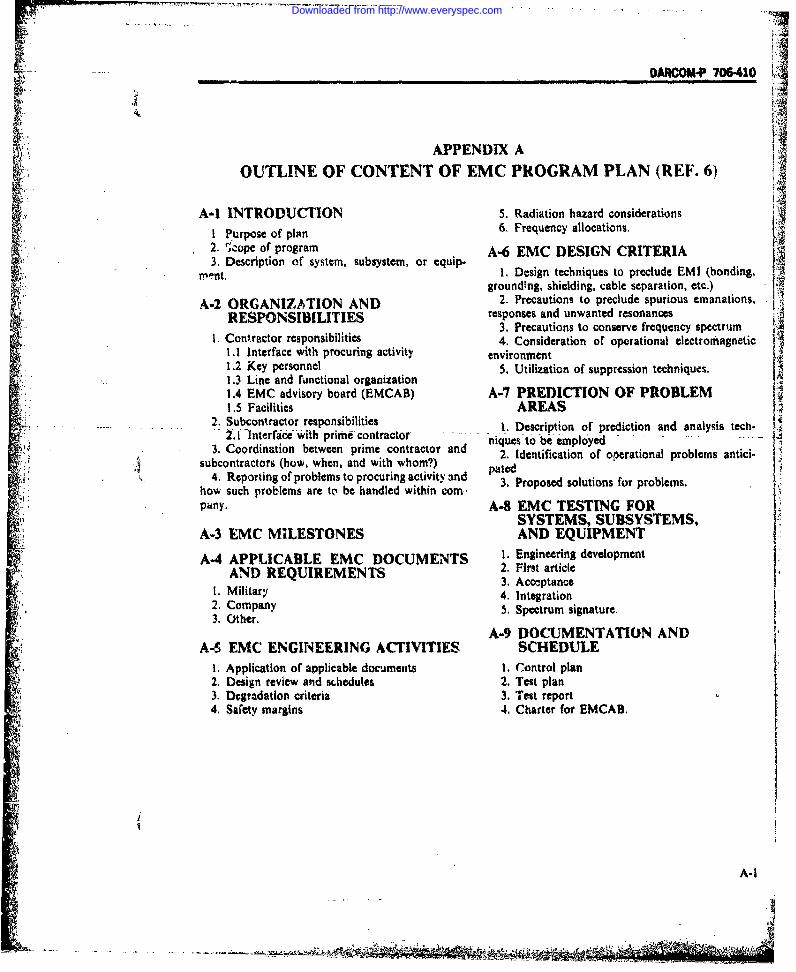
DARCOM-P 706410
APPENDIX A AOUTLINE OF CONTENT OF EMC PROGRAM PLAN (REF. 6)
A-1 INTRODUCTION 5. Radiation hazard considerationsPurpose of plin 6. Frequency allocations.
2. 1,cope of program . A-6 EMC DESIGN CRITERIA3. Description of system, subsystem, or equip-
!r, ont. 1. Design techniques to preclude EM! (bonding,grounding, shielding, cable separation, etc.)
i A-2 ORGANIZATION AND 2. Precautions to preclude spurious emanations,
RESPONSIBILITIES responses and unwanted resonances La3. Precautions to conserve frequency spectrumI . Cont ractor responsibilities 4. Consideration of operational electromagnetic ]'
I.1 Interface with procuring activity environment1,2 Key personnel 5. Utilization of suppression techniques.
i! .: " 1.3 Line and functional organization ,]!i":1.4 EMC advisory board (EMCAB) A-7 PREDICTION OF PROBLEM [
1.5 Facilities AREAS" 2. Subcontractor responsibilities...s
2. ubcntrcto reponibiitis . Description of prediction and analysis tech-2.1 Interface with prime contractor . ..... to be .employe
3. Coordination between prime contractor and . tiisubcontractors (how, when, and with whom?) ated o
V 4. Reporting of problems to procuring activity and 1.how such problems are to be handled within comPi
pany. A-8 EMC TESTING FOR'i? SYSTEMS, SUBSYSTEMS,
A-3 EMC MILESTONES AND EQUIPMENTA-4 APPLICABLE EMC DOCUMENTS T Engineering development E
AND REQUIREMENTS 2. First article3. Acceptance
-I. Military 4. Integration2. Company 5. Spectrum signature.3. Other.
A-9 DOCUMENTATION ANDA-5 EMC ENGINEERING ACTIVITIES SCHEDULE
I. Application of applicable documents 1. Control plan2. Design review and shedules 2. Test plan3. Degradation criteria 3. Te-st report4. Safety margins 4. Charter for EMCAB.
A-I
Downloaded from http://www.everyspec.com

MRO* 70640
-W
APPENDIX B
I CONTENT FOR EMI CONTROL PLAN (REF. 6)
B-I MANAGEMENT B-4 ELECTRICAL AND ELECTRONICThe EMI Control plan shall include the specific or- WIRING DESIGN
ganizational responsibilities, lines of authority and The proposed electrical and electronic wiringcontrol, and the implementation plan. including mile- design, cable separation, and routing to minimizestones and schedules. In addition, the detailed EMI emission and susceptibilities shall be described in ac-and EMC requirements to be imposed on associated cordance with the classification procedure requiredsuppliers and subcontractors for vendor items, test by the contract. Grounding philosophy shall berequirements to be placed on independent testing described in detail and methods of shielding andlaboratories, a complete listing of all EMI and EMC routing of cables shall be enumerated. Equipments orrequirements in supplier's procurement documenta- subsystems, consisting of a number of black boxestion, and additional requirements for GFE shall be shall have interconnecting cabling diagrams supplied.
B-5 ELECTRICAL AND ELECTRONIC
B-2 SPECTRUM CONSERVATION CIRCUIT DESIGN
The program is employed to minimize emission The EMI control and suppression techniquesspectrum and receiver bandwidths and to control os. which will b. applied to all parts and circuitry,cillator frequencies, pulse rise times, harmonics, side whether capable of generating undesirable emana-bands, and duty cycles within the constraints of the tions or suspected of being susceptible to the fields iequipment or subsystem. Specified design parame- and voltage levels specified by the contract, shall bet b de odescribed fully. The specifically required design data=: ters shall be defined. A completed copy of DD Form shall include but not be limited to the following:1494, shall be included for information purposes on- sly, a. Choice of parts and circuitry, the criteria for use
of standard parts and circuitry, and bonding ardgrounding techniques
B-3 EMI MECHANICAL DESIGN b. Justification of selected filter characteristics in-clding type and attenation, technical reasons forThe control plan shall describe the material and selecting types of filters (for example, absorptive ver-
construction to be used to provide the inherent at- sus nonabsorptive filters) and specific circuit appli-tenuation to electromagnetic emissions and suscepti- cationsbilities while still meeting the contract end item speci- c. Part location and separation based on orienta- Ification requirements. Specific data shall include but tion of EM fields for reduction of emissions, suscep-need not be limited to the following: tibility, or both
a. Type of metals, castings, finishes, and hard- d. Indicate valid technical reasons for selection ofware employed in the design pulse shape. Pulse shapes utilized shall minimize the
b. Type of construction, such as compartmental- 'electromagnetic spectrum employed consistent withizing, filter mounting and isolation of other parts, achieving design performance.type and characteristics of filtering used on openings e. Location of critical circuits and decouplingincluding ventilation parts, access hatches, windows, techniques employed for eachmeter faces and control shafts, and type of attenua- f. Shielding and isolation of critical circuits.tion characteristics of RF gaskets used on all internaland exteral mating surfaces 0-6 ANALYSIS
Shielding and design practices employed for:termining shielding effectiveness Prediction or analysis techniques employed tod. Currosion control procedures. determine adequacy of supplier's conclusions shall be
SB-I
Downloaded from http://www.everyspec.com

DARCOM-P 706410
included. Specific aspects of the mechanical, electri- c. Worst case analysis of multivibrators, switch- (.cal, and electronic design to be included are as ing (single and repetitive) and logic circuits, and clockfollows: and strobe signals.
a. Adequacy of mechanical construction, and an d. Analysis of circuitry, subassemblies, and totalanalysis of the shielding afforded by the proposed equipment, or subsystem, including cabling and loadsdesigns over the specified frequency range and energy for:level (1) The prediction of susceptibility to internally
b. Complete frequency matrix of all frequencies and externally generated fields and voltages, whetherassociated with receivers and transmitters (see Fig. B- below or above the limits specified in the contract1), expected spurious responses of receivers at input (2) The prediction of emissions, whether belowsignal levels and at frequency range(s) specified in the or above the limits specified in the contract.contract, and expected spurious outputs of items such e. Subsystem analysis for mobile or fixed installa-as transmitters, local oscillators, and frequency syn- tions with two or more antennas shall include athesizers. Spurious responses f, will be determined description of radiation characteristics from antennasby use of the following equation: including fundamental and spurious energy, and dis-
cuss minimizing antenna coupling and isolation-f q (-l) achieved by placement and location of antennas.,~ q
whereB-7 PROBLEM AREAS'i where
p all integers; including zero, representing Plans for potential EMI and EMC interface prob-harmonics of the local oscillator (lo) lems shall- be -psefited, including theprocedures for -
q - all integers, except zero, representing defining problems, formulating solutions, imple-harmnicsof te surios sinalmenting and testing the solutions. and documenta-
H! - local oscillator frequency tion procedures.f - intermediate frequency
The frequency matrix is to used to formulate a sub-system test matrix of source and victim equipments.The test matrix will be included in the subsystem test The method of updating the control plan shall beplan. indicated.
II
B-2
Downloaded from http://www.everyspec.com

DARCOMP 706-410
4t 'I II 1I
-H - :11 1 - i -.- 1- 4 ~ -1.
:T iTL.
-4)W-
u -i LiiItll
j- +11
Downloaded from http://www.everyspec.com

DARCOM-P 706410
APPENDIX C
CONTENT FOR EMI TEST PLAN (REF. 6)
C-I INTRODUCTION OR SCOPE C-5 TEST SAMPLE SET-UPThe following Fhall be included: A description of the test sample shall include thea. An opening statement indicating the purpose of actual physical layout of equipment under test, de-
the plan and its relationship to the overall EMC pro- picting position of test sample and feedthroughgram for the equipment and subsystem capacitors or line impedance stabilization networks
b. A table listing all the tests to be performed, the on the ground plane, lead dress, bond straps, real orparagraph number of the plan, and the correspond- simulated loads, electrical or mechanical, and anying test method of the basic standard. test sets employed in the test. (Notes may be used to
indicate height above ground plane for leads).C-2 APPLICABLE DOCUMENTS
Documents shall be l.sted as follows: C-6 TEST SAMPLE OPERATIONa. Military (standards, specifications, etc.) a. Modes of operation for each test and operatingb. Company (any in-house documents for calibra- frequency
-tion-or-qualiy assurance) ......... b.- List of -controi settings on the test sample ..c. Other documents (Society of Automotive Engi- c. List of control settings on any test sets employed
J neers procedures, drawings, etc.) or characteristics of input signalsJEI d. Test frequencies at which oscillators, clocks,
C-1 Td T SITE and similar equipment may be expected to approach
The following shall be included: test limitsa. Description of test facity. shielded enclosure e. Performance checks iitiated to designate the
(size, power availability, filters, attenuation charac- equipment as meeting min,mal working standard re-teristics of room to electric, magnetic, and plane quirementswaves) f. Circuits, outputs, or displays to be monitored
b. Descr'ption of ground plz ne (size and type) and during susceptibility testing shall be enumerated, asmethods of grounding or bonding test sample to the well as the criteria for monitoring for degradation ofground plane in order to simulate actual equipment performanceiastallation g. Normal, malfunction, and degradation of per-
c. Spot check measurements of the ambient elec- formance criteria (i.e., change in output spectrum,tromagnetic emission profile of the test facility, both change in (S + N)/N ratio, loss of synchronization,ra&ited and conducted, to determine ambient suita. change in output waveform) for susceptibility testingbility. shall be described.
C4 TEST INSTRUMENTATION C-7 TEST PROCEDUREInstrumentation to Wa used shall be dscribed as Test procedures to be employed to demonstrate
follows: compliance with the contractual requirements shall
a. When matching transformers or band-reject be fully described as a minimum and the followingfilters are used, their characteristics must be shall be include:described, a, Block diagram depicting test setup for each test
b. Bandwidth of the measurement instrumenta- method
tion shall be specified. b. Test equipment used in performance of the testc. List of test equipm~ent. and methods of grounding, bonding or achievingd. Scanning speed used to drive EMI measuring isolation for the measurement in!.rumentation
equipment. c. Detailed step-by-step procedures enumeratinge. Monitoring equipment utilized during measure- probing of the test sample. placement and orienta-
ments, tion of probes and antennas. frequency range of test.
C.1
~ - * dw
Downloaded from http://www.everyspec.com

. . . ....... ....- -. . ....-
CANCOM-P 706-410
selection of measurement frequencies, detector func- b. Transmitter to receiver interactionstions used, data to be racorded, frequency of record- c. Transmitter to active and passive devicesing data, and the units of recorded data (magnetic devices).
d. During susceptibility testing, the actual modu-Llation characteristics of the interfering signal (ampli-tude, type, degree, weveform) shall be specified. C-9 DATA TO BE RECORDED
C-8 SUBSYSTEM TESTS The data to be recorded shall be outlined as
The test matrix similar to Table C-I shall be in- follows:cluded in subsystem test plans and enumerate poten- a. Sample data sheettial: b. Sample test log
a. Receiver to receiver interactions c. Sample graphs. A
TABLE C-i. SAMPLE TEST MATRIX (Ref. 6)
I. Receiver-to-receiver interaction:
Source VictimSource Victim - receiver receiver --Test-receiver receiver frequency, frequency, frequency, Interaction
AN/AR-100B AN/ARC-0 .MHz MHz MHz 1____forcitici
AN/ARC-IOOBX AN/ARC-1000 230.00 17.1 17.1 1 st LO of Source with VictimAN/ARC-00BX AN/ARC-1000 '238,80 25.1 25.1 1st LO oi Source with Victim
, I1. Transmitter-to-receiver interaction:
Source VictimSource Victim transmitter receiver Test
transmitter receiver frequency, frequency, frequency, Interaction-__MHz MHz MHz
AN/ARC-1000 AN/ARC-IOOBX 3.85 225.95 3.85 Source frequency with 2nd IFof victim
AN/ARC. 1000 AN/ARC-100BX 22,500 232.50 22.500 Source frequency with IF ofvictim
AN/ARC-1000 AN/ARN-! 15E 22.000 110.00 110.00 5x source frequency withvictim
AN/ARC-1000 AN/ARN-i 15E 29.000 116.000 116.00 4x source frequency withvictim
C-2
iAl*
Downloaded from http://www.everyspec.com

CHAPTER 3
EMC PHENOMENAI In this chapter models are developed for repre- B = wide bandwidth, Hz
senting electromagnetic phenomena which are funda- B3 = 3-dB bandwidth, Hzmental to electromagnetic compatibility. The parame- 86 - 6-dH bandwidth, Hzters of the equivalent circuits of sources and suscepiors b = e/(kT) (40 V- at 300 K); height toare all functions of frequency over the range from below ground plane, m; interference amplitude;the power frequency to about .30 GHz. Because it is a magnitude of output currem at saturation,practical impossibility to identify details completely. Ae.g.. of impedances over this range, actual data on bn = constants in Fourier series expansionspecific devices are limited. bf = bandwidth constant
Furthermore, many EMC phenomena vary more or C -capacitance. Fless randomly from moment to moment, or from fre- C, - stray capacitance (between wires), Fquency to frequency (in the case of broadband phe- CNR = carrier-to-noise ratio, dimensionlessnomena). It is practical to describe these variatic.ns CIR - carrier-to-interference ratio,only in a statistical sense by using appropriate distribu- dimensionlesstion functions or their parameters such as means. c, = speed of light, 3.00 x 10V m/svariances, or other measures. D = desired component at the output of a
3-0 LIST OF SYMBOLS miler V ditancebetween wirs.In,;mantenna diameter. mn
A articulation index; effective area of circuit, D,, ratio of upper docile to median value F,,,... M 2; attenuation factor (plane earth or sur. dimensionless
face wave), dimensionless; local oscillator D, - ratio of median value F,,,, to lower docile,frequency, Hz; amplitude, dimensionless; dimensionlessamplitude, V or A; area of a loop, m2 d - duration, s; diameter of conductor, in.;
Aw = effective aperture, m2 distance of separation of parallel wires;A, effective area of receiving antenna, ml loop diameter, m; helix diameter, mA, = effective area of transmitting antenna, m' dB( ) = level in decibels expressed with respect to
dA, = incremental area of the source, m quantity in parenthesesa = loop radius, n; bandwidth constant; satu- E - voltage; electric field strength, V/rn
4. ration voltage magnitude; radius of earth, Ei = interfering voltage, Vm k - generated noise, V
af = bandwidth constant EA - peak voltage, Va,, - constants in power series expansion; con- Es - Thevenin equivalent sour-e voltage
stants in Fourier series expansion Ell, a voltage at saturation, Va,, - fraction of output current resulting from e = electronic charge, 1.602 x 10-' C;
saturation, dimensionless induced el: ctromotive force, V; naperianB magnetic flux density. T; bandwidth, Hz base
AS - bandwidth of an ideal bandpass filter; Co- peak value of output voltage, Vbandwidth over which radio noise power e2 = electromotive force induced in circuit 2 byis uniformly distributed, Hz circuit 1, V
= 2 lf)1 erfc = complementary error function,( L - df. effective noise power F = noise figure, dimensionless
J 0 bandwidth cf a network, T = average noise figure, dimensionless
Hz F(f) - spot noise fi6ure, dimensionless
81 J 1(1) tF, - noise figure (isothernil), dB-" f df effective impulse band- F mei ue of k ).dB. , B1=J U0 width of a network, Hr F, - nitdian value of F,,. dB abovekT)*
f frequency, Hz
B - narrow bandwidth, Hz Af Dopp;er frequency shift, Hz
3.1
-l $$ ~. *~h
Downloaded from http://www.everyspec.com

f (u) ormalized surface transformer imped- it)= desked compunent located on canter fte-aace function, dimensionless queucy, A
f(x) pretability distribution it load current, AfI fa f~tU~ucy of desired signal, Hz = line current, A' fruency of interfering signal, Hz i. = noise current, AL fundamental frequency, Hz. center fre- i,=,- rms current, A; rrns spectrum amplitude,
quency; reference fmqmncy, Hz A/HZ'Pf = signal ewtier frequecy. Hz = current in circuit 1. A
A - desiredigvml frequency. Hz - integers designating various signals; -=Tfs = interfering signal frequency, Hz K - votage amplification of inturfering signalG - power gabL dimensionless retutive to thinA of desired signal. dimen-
G(f) a-vailable power gain, dinamsiouless; sionless; ratio of gains from receiver inputtrasskr function, dimensionless to mixer input at the undesired signal fre-
G(0, o) - gain pattern of antenna, dimensionless quency and the desired signal frequency,G, = veceiving antenna gain. diamsionless dimensionlessG, - transmiting aatenna gaim, dimincsiuwlas k - Boltzmann constant 1.38 x 10- 21 J/K
g(t) = transc.nductance (timc varying), mbo k, = modified earth radius, mg cotersion transcondactrancc, mho k2, &3 - parameter In coaxial cable leakageW = transconductance, mho equation
u - i order converion transconductaicc, L = inductance, H. luminance, W/(s'mc'H z);
imho length of cable, m; loss associatod with dis-N - magnetic riW stegth, A/w tance, dB
l1(f)-- clcarance.-vaage orcurrentu iAnsfer - L(f) ff cable i oire figure, dimensionlessI) ~ ~ ~ iiricion, diincnskeness C=m lengh of cible, [t; iterisries epn
H. = nth Fresihel zone clearance, m sion; dipole length , iii, = cotVpocuat of magnetic field in rdirec- M = mutual irductance, H
tion, /'/m m, - magnetic dipole strength, Aml;-i/ component of magnetic field in 0-dirc- . = integer in serits expanuon
tion, A/m - mean of'xH.(f) - relative response, ditnensionless N number of turns (loop or indictor)
H,1 -Hankel functiot of the kth kind, order n N( f) - noise power specral density per unit solidh - antenna height (distance to ground plaac) angle and pzr unit area at sourze,
m: Planck's constant 6.62C x 10-" J-; W/(srn'Hz)height above ground, in.; height uf ob- N,(f) - equivalent noise power spectral density atstruction. ft the input contributed by the network.
h() - impulse response, s-' VI/Hzk = minimum effective antenna height, m N,f) - power spectral density (mean square perI - undesired or interfering comcponent, V: unit bandwidth) of shot noise curr at.
* current, A A2/HzA(n) - current at harmonic n, A V, - powev spectral density of white noise,1(t) = interference V2iH;6
c - common-mode current, A NJ (f) - power spectral density (mean square perID = differential-mode current, A unit bardwidth) of 'he noise voltageid, - direct curr%.nt, A across a resistor. V/Hz1, - equivalent leakage radation current, A N1(f ) - -siablka input noist power spectralIL - current in loop (antenna); iterfernce desm at 4*equencyf, VW/L
cmeA. A e N(f) - avaiug mntput noise power spectralI" - mcsuad current, A densi y0ilrequencyf, V2/Hz
1 A) - Oth Oer Bessel function of the first kind n - o, rder a fdarbonic; integer in series expan-L peak cument, A sili; a fMe" of bradeA strands; ratio of
I,,, - rMs value of curren at anenna tUmsinals, propaluisi c*ants, dimensionless
-. rernw &rzticn -.urftnt, AP-poe
t - knuat~os cumtnt lesaL. A -x 4wu~ativjdisribtftu of x3-2
. . . . 6. . - .. , . , .;
Downloaded from http://www.everyspec.com

DARCOM-P 706410
P, - average desired signal power, W or dB T, = equivalent temperature of source, K;Pb = average interfering signal power, W or dB reference temperature, K-. t -- time, S
PD power density, Poynting vector, W/ml r, - time at saturation, sP, = power of an unmodulated interfering V = voltage, usually fixed, V
signal, W or dB K f) = voltage Fourier Transform, VsP= received power expected in free space., ~ )=vlaeFuirTasom -PO received power e V> - peak amplitude of the desired signal at theP, = radiated power, W receiver input, V
P, =raditedpowe, W d =ratio of the rms voltage to the averagep = helix pitch (twisted pair), m; order of local voltage of the noise envelope, droscillator harmonic V otan value o ve , dB
p(x) - probability density function of x Vd = median value of d , dBq = ird/p. helix parameter, dimensionless; Vd -- V d for narrow bandwidth, dB
order of signal harmonic V, = Vd for wide bandwidth, dB .R = reciprocity; resistance, fl; earth's reflec- V = peak amplitude of the interfering (unde-sired) signal at the receiver input,V
tion coefficient, dimensionlessR(t) = bipolar rectangular waveform, A VL = ioad voltage, V
*;. Ra = radiation resistance of antenna. .p voltage, VR, = contact resistance, a =. voltage , Vi~iR L - loa reisto, fl, . Vsf r = voltage at saturation, VRL =load resistor, Q.. Vs 0 = peak amplitudes 9 f the envelope of theR. = dc resistance per unit length of outer con- desired signal at mixer input, V
r ductor (coaxial cable), 2/m "Vs, = peak amplitude of the envelope of ther = distance, cm or m; true radius of earth, n; undesired signal at mixer input, V
................. ...........loopradius, em;. distpce..frum axis of.. Vu . . . .helix, m".
S = signal level, V VS WR = voltage standing wave ratio,S(f) - spectrum amplitude; s, V-s, orl's dimensionless
S(r) = signal input tothe phae dtector; unit v = applied voltage, Vamplitude sampling waveform, Y (t) = time varying vol:age, Vdimensionless v. noise.voltage, V
d$ noise power spectral density per unit area vt),(A random noise voltage, Vat the observer, W/(m2 'Hz) v., amplifier output voltage. V
SE= equivalent surface transfer impedance, 1 v,,,. = rms voltage, V: rms spectrum ampaitude,S, = power spectral density of an interfering VALE,/,
signal v,(t) = signal amplitude modulation fu-iction, VSp = unit voltage pulse spectrum amplitude, W, = articulation index parameter
V's x = input to nonlinear deviceS,. = init voltage step spectrum amplitude, V-s x(!) = signal voltage waveform, V
S "S/ - signal-to-interference ratio, dimensionless x(t) oscillator voltage, V(S/N). = ratio of the rms spectral density of average x(t) = signal voltage, V
speech to rms spectral cionsity of the noise Y(f)= admittanceat the output in the ath band, d.1 y = output of nonlinear device, frequency
T- absolute temperature, K; thicknass of integration variableouter conductor, m; length, s; period of yt) = interference signalwaveform, s y interference cross-modulation compo-
71 T(9, p) = brightness temperaturv. K nent, AT. - antenna temperatuie, K y= dtsired cross-modulation component, A
equivalent network temperature, K Z(f) 7 impedance. ilTo = thermal temperature of the earth. K: 4 = load impedance, 0; line impedance. U
rererence temperature, K Zt - measured load impedance, 0T, - system temperalturc. K; sky temperature, Z, - Thtvenin equivalent source impedance, 12: '
: l K. solar noise temp-erature, K generatur iir')edance, G7 - system temperature referenced to receiver Z, - surface tra~nsfer impedance, /m
iaput. K Z, - impedance of frt: space, 377 Q
3-3
i . . . . .. .. . . . .. . .* . , " ' '
Downloaded from http://www.everyspec.com

DARCOM-P 706410
z z-coordinate; polarization constant; d1a - increment of solid angle, radmutual impedance, 11 ( ) mea value ,
- parameter of cable braid (coaxial cable),dimensionless; earth's absorption coeffi-cient, dimensionless 3-1 SOURCE MODELSphase constant, 2r/X, m-1 GENERAL COMMENTS
e propagation constant, m;carrier-to- For the purpose of simplifying analysis and pre-noise ratio, dimensionless diction it is convenient to use "'linear" mathematical
A envelope of filtered random noise divided models for representing various circuit elements. This['i by the rms value of the envelope, dB; "
by he/r) valuenofthnlope ,is so in spite of the fact that nonlinear mechanisms-depthofpdimenionlesin deptare frequently responsible for interference generation= depth of penetration (skin depth), m;~ and susceptibility. The usual procedure is to use the
phase difference, rad linear model and modify it as necessary to account= error; permittivitty, F/r for observed phenomena. Thus a typical source of= permittivity of free space, conducted interference is represented as an electro-
8.5 elaiv dlectc cmotive force of specified value in series with a definedt, = relative dielectric constant, dimensionlessimpedance. Although it should be recognized that
x= displacement of the center conductor of a such a representation is an approximation to the truecoaxial cable from the true center model, fortunately it does appear to have general
n = wave impedance = 4jt , ' validity.
no = .'/4, characteristic impedance of free Emitters usually are identified as narrowband ors- pace,fl- . .. . broadband, in accordance with the nature of the
=co-latitude angle in spherical coordinate spectrum of-the-emitted- energy- Since --these~aresystem, rad; angle between reflected wave relative terms, the dividing line between them is notand ground level, rad sharp; one of the best bases for distinction is the
. = wavelength, m; random phase angle, deg acceptance bandwidth of any susceptible device (sus- 4 -
u = permeability, H/m ceptor) whose operation may be degraded by the < ,
,o = permeabil'ty of free space, emission. If the bandwidth of the dominant energy is4ir x 10' H/m less than that of the susceptor, the emission is
i - standard deviation; conductivity, mhos/m "narrow-band". otherwise it is "broadband". Emis-47 2, mean square value of noise, V2 sion arising from modulated sine wave oscillations= variance ox are usually narrow-band, while those arising from
Y - time constant, s; deviation from unper- switching action are usually broadband.turbed zero crossing time, s, switching 3-1.2 NATURAL NOISE SOURCEStime, s; duration of noasaturationinterval, s Sources of natural noise include thermal noise of
P - longitude angle in spherical coordinate resistors and warm body radiators, shot noise in dec-system, rad; phase angle, rad tronic devices, atmospheric noise, cosmic noise
v(f) = phase vs frequency characteristic of IF emanating from the sun and from sources in outeramplifier, rad space, and triboelectric (frictional charging and dis-
€, = phase angle, tad charging) noise. The statistical properties of noise0 = power spectral density of an interfering from these sources range widely from spectrally flat
signal. W/kHz Gaussian noise, to sporadically impulsive noise. in= grazing angle with respect to the earth's some cases the statistical parameters remain essen-
surface tially constant in time. In instances where they arew = angular frequency, rad/s not constant, variations with time of day, season, and
wir - intermediate angular frequency, rad/s year may be given.w, = local oscillator angular frequency, rad/sa, - angular frequency of signal carrier, rad/s 3-1.2.1 Electronic Noise
'sD - desired angular frequency, rad/s 3-1.2.1.1 Sources of Electronic Noiseangular frequency of ui|dwird signnl, Associated with the real part of the impedance seenrad/s at a pair of terminals of a passive electrical network,
il solid angle. sr: pointing angle, sr is a Gaussian noise process called thermal or Johnson -
3-
-W . , - . .. ? . .-
Downloaded from http://www.everyspec.com
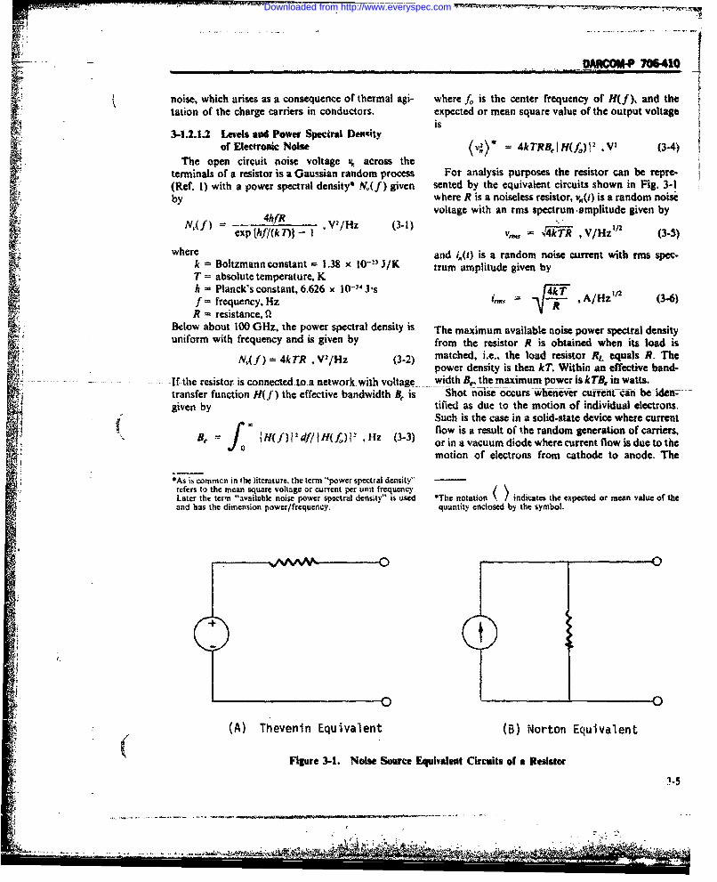
7 _0__ARC0M# 706410 fk noise, which arises as a consequence of thermal agi- where fo is the center frequency of H(f), and the
tation of the charge carriers in conductors. expected or mean square value of the output voltage
3-1.2.1.2 Levels and Power Spectral Densiity isof Electronic Noise = 4kTRBHIn(fo)1 ,V 1 (3-4)
The open circuit noise voltage %. across theterminals of a resistor is a Gaussian random process For analysis purposes the resistor can be repre.(Ref. I) with a power spectral density* N !(f) given sented by the equivalent circuits shown in Fig. 3-1by where R is a noiseless resistor, v(1) is a random noise
voltage with an rms spectrum, amplitude given by
! exp [hf/(k T)] - I ,V./Hz (3.1) V,,-t V/Hz", (3-5)
where and i(t) is a random noise current with rms spec-k - Boltzmann constant 1 1.38 x 10-" J/K trum amplitude given byT = absolute temperature. K
h T Planck's constant, 6.626 x 10--' JS A/H. 2 (3-6)f - frequency. Hz - , z
R = resistance, QBelow about 100 GHz, the power spectral density is The maximum available noise power spectral densityuniform with frequency and is given by from the resistor R is obtained when its load is
N,(f) = 4kTR , V2/Hz (3-2) matched, i.e.. the load resistor RL equals R. Thepower density is then kT. Within an effective band-
- - - If the resistor is connected to a network with voltage width B, the maximum power is kT, in watts.transfer function H(f) the effective bandwidth B is Shot noise occurs whenever current-cabe- iden-given by tified as due to the motion of individual electrons.i-Such is the case in a solid-state device where current
flow is a result of the random generation of carriers,eH(f) I df/ I H(f ) I Hz (3-3) or in a vacuum diode where current flow is due to thefo
motion of electrons from cathode to anode. The
*As is comnmcn in the literature, the term "power spectral density"refers to the mean square voltage or current per unit frequency. /Later the term "available noise power spectral density" is used *The notation indicates the expected or mean value of theand has the dimension power/frequency. quantity enclosed by the symbol.
A +t
(A) Thevenin Equivalent (B) Norton Equivalent
Figure 3-1. Noise Source Equivalent Circuits of a Resistor
3-5
i. i
Downloaded from http://www.everyspec.com

DARCCM-P 706-410
current is comprised of a collection of pulses, each figure. If it varies significantly with the frequency onehaving an area equal to the electronic charge. A uses the average noise figure F given bycurrent so constituted will have a randomly fluc-tuating component with a power spectral densityNA f) given by J N2(f df
Nj(f 2e1 , -A/Hz (3-7) , d'less (3-10)
where Nj(f)G(f)df
e - electronic charge = 1.6 x 10⁻¹, C
V -- = average (or direct) current of the pulses, A Or, using Eq. 3-9Eq. 3-7 is correct at frequencies which are low relativeto the reciprocal of the pulse widths. f
If such a current source feeds a noiseless network N j Ff) N(f) G(f)dfwith a current transfer function, H(f), the output =,d'less (3-11)mean square value isf
('<) = ,/' 2 Id H(f)i 2 df The noise figure F12(f) of a cascade of two net-
works in which the individual networks have noise
= 2e1d&BtH(f)t2 ,A2/Hz (3-8) figures F and F2, and available power gains G1(f)
and G2(f), respectively, can be written
where the effective bandwidth 3, is defined in Eq. 3-3. F = F2(f) + . . . ...
G(f)(,d'less (3-12,3-1.2.1.3 Noise Figure and Noise Temperature Defining T, T-, and ,2 as temperatures €orre.
The noisiness of active and passive networks due toshot, thermal, and other noise sources, usually is sponding to F(ff), F2(f), aad F(f),measured by the noise figure F(f) of the network, Te2defined by T + K (3-13)
N( f) N( f )F(f) = + N Frequently, the first network in a system is a lead-
N(f) G(f) N,(f) in cable which is somewhat lossy. It can be shown7T, + T, that for a matched cable
- , d'less (3-9)T, input power = L(f) > I , d'less (3-14)
output powerwhereN2(f) = available noise power spectral density at the where L(f) is the noise figure of the cable. The over-
network output at frequencyf, V/Hz all noise figure of the cable plus the rest of the systemN(f) = av.ailable power spectral density at the net- (assumed to be the second network) is
work input at frequencyf = kTI, V/HzG(f) = available power gain of the network, F 2(f) = L(f) + L(f)[F 2(f) - II
dimensionless = L(f)F2(f) .d'less (3-15)
N(f) - equivalent noise power spectral density atthe input contributed by the network Or, in terms of temperature with T. = T,
= k T, V2/Hzk = Boltzmann constant = 1.38 x 10- ', J/KT, = equivalent temperature of the source, K T, L(f) 2L(f)T,T, = network equivalent temperature, K = [L(f) - 1]T, + L(f)[F2(f)- I]T, -r4
The noise figure as written if Eq. 3-9 is a functionof frequency, and is sometimes called the shot noise = [L(f)F 2(f) - iIT, K (3-16)
3-6
, .-fi:...-. ... ,,--..-,-.. • ... : - , ' .. - -" : o . ,
Downloaded from http://www.everyspec.com

DARCOMP 706410
Eq. 3-15 shows that the cable attenuation is reflected 3-1.2.2.2 Probability DistrUitIon of Eavelope" directly as a proportional increase in the noise figure. The first order probability distribution of the enve-
In receiver applications, the first element in the lope in a 200-Hz bandwidth is shown on Fig. 3-2system is an antenna which is immersed in a noise (Ref. 3). Because the noise is non-Gaussian, the shapeemitting environment. The noise may arise from the of the probability distribution depends on the re-natural sources - atmospheric, terrestrial, and cos- ceiver bandwidth. Empirical techniques for convert-mic - or it may arise from the man-made causes to ing these results to other bandwidths are shown inbe discussed in par. 3-1.3. The noise entering the Fig. 3-3.system may be accounted for through an antenna The distribution depends on a parameter given bytemperature T. The overall system temperature of a the ratio of the rms value to the average value of thereceiver connected to a transmission line and antenna envelope, and denoted V1. For Gaussian noise, theis obtained by augmenting Eq. 3-16 by T. That is, the instartaneous value of the envelope has a Rayleighsystem temperature T, referred to the input of the probability density, and V is equal to 1.05 dB. Fig. 3-transmission line, is 2 shows the probability distribution of the instanta-
neous noise envelope normalized to the rms value of11 T, = T + [L(f) - liT1 + L(f)Te2 ,K (3-17) the envelope (denoted 4) for various Vd.Predictions of the value of V are also available in
CCIR Report 322 (Ref. 3), and a typical estimate isThe system behaves as would one in which the anten- shown in Fig. 3-4. The estimate is of a quantityna radiation resistance was at temperature T1, and the designated Vtm, where the subscript m signifies medi-
:system was otherwise noiseless. Sometimes it is an value, i.e.. this is the value estimated to bepreferable to reference the temperature to the receiver exceeded half the time. Generally, V falls off with
input. In this case the system temperature is denoted increasing frequency, suggesting that at higher fre--- ,, and it is given by Eq. 3-17 divided by L(f), or, quencies the noise as seen in the 200-Hz receiver band
... becomes -more nearly-Gaussian Examination -of the--T r . range of estimated median values of V, shows it to be+/
T Lr-f- I -1- IT + T~,2 K (3-18) from around 2 to 14 over all frequencies below 20" ,L. )L Lcj JMHz, and for its entire time history.
Conversions to other bandwidths using Fig. 3-3 areThe system behaves as would one in which the illustrated by example. Suppose an estimate of theresistance looking toward the transmission line from envelope distribution is sought at I MHz in a band ofthe receiver input terminals was at temperature T,, 2 kHz for the time block and season appropriate toand the system was otherwise noiseless. Fig. 3-4; the median value of V1' is about 7 in a 200-
lHz bandwidth. In a bandwidth of 2 kHz, implying a
3-1.2.2 Atmospheric Noise bandwidth ratio of 10 (B.,18, in Fig. 3-3), the value of
3-1 . OrnVd in the wide bandwidth (Vd, in Fig. 3-3) is obtainedby reading the ordin.te corresponding to the inter-
At frequencies below 20 MHz, the natural elec- section of B,&,/B, = 10 and the curve labeled VAtrical noise associated with thunderstorm activity (subscript n stands for narrow) = 7. A value of V,,throughout the world plays a dominant role in radio (subscript w stands for wide) = 16 is obtained. Thecommunication. Often, noise of this origin is great proper probability distribution curve for this case ;senough to make all other sources of noise negligible, the one marked Vd = 16 in Fig. 3-2.
1infortunately, atmospheric noise is highly change- Note the following in Fig. 3-3: (1) if V is 1.05 dB inable ,vith time and place, and in its short term prop- any noninfinitesimal bandwidth, the input noise iserties may not be represented by any simple random Gaussian and Vd is 1.05 for any bandwidth, and (2) asprocess. One model of atmospheric noise suggested bandwidth is decreased, Vd decreases, tending toby physical phenomena is a low level Gaussian noise approach 1.05 dB; i.e., decreasing bandwidth makesrepresenting distant effects, plus a high level impulse the noise more nearly Gaussian.process to represent local effects. However, simpleimpulse processes, such as the Poisson process inwhich pulses occur at random, do not accurately 3-1.2.2.3 Spatial and Temporal Variations -represent the local activity. The actual phenomena Long Term Propertiesoccur in bursts, so that there is interdependence The distributions discussed in par. 3-1.2.2.2 areamong adjacent impulses. determined from the instantaneous noise voltages
3-7
Downloaded from http://www.everyspec.com

L- -IOARCOM-P 706&410
60
3s0-eisLnaeusevlp ffleenos28raizdb-h m vleo h
14 1 O L06 0 09
12 A is ercestntaneueoe of filtsEx eed ed
F -ur no. p ie , obali d tibutono the Noisve Eeof te I3-8
.................- .
Downloaded from http://www.everyspec.com

ARC-MP 706410." -
~~28 ,-"-'
0* =
C . 2",
0i0Is',-O " 24 . , -
'.. ~...u o ....10 4, ,0 , :
0 'y'0 4 18
~~1 5 0 0 50 10 0 50 00
(0 b 12
+- OF
I1 2 5 10 20 so 100 20 500 1000Bandwidth Ratio-B/B , dimensionless -
Corresponding values of and Vdn are read
along the appropriate line for the bandwidthratio.
B = the wider bandwidthB = the narrower bandwidthn
Figure 3-3. Conversion of Vd In One Bandwidth to Vd in Another Pandwidth
measured over relatively short intervals of time, F can be converted to field strength in a l-kHz band-typically about 0.25 h. The atmospheric noise intensi- width byty exhibits important long term variations, and vari-ations with location. To represent these variations, E F0 - 655 + 20 logf(MHZ), dB( V/m) (3-20)Fig. 3-5 shows isothermal lines, or lines of equal noise CCIR Report 322 (Ref. 3) contains 24 figures such astemperature, covering the earth, The isothermals are Fig. 3-5, each for a specified 3-month season, and forgiven in terms of a noise figure F, a 4-h block in each day of the season. Fig. 3-5, for
.- 10 log (Ta/T) (3-19) example, gives the noise temperature in the hours0000-0400, during the months of June, July, and
where August, in the Northern Hemisphere, and during the
- antenna temperature of a short vertical an- months of December, January, and February, in the
tenna above a highly conductive earth, K dB ( ) - level in decibels expressed with respect to the quantityT, - reference temperature, 288 K in parentheses in this case. microvolt per meter.
3-9
....... " .. .
Downloaded from http://www.everyspec.com

DARCOM-P 706410
3-10
Downloaded from http://www.everyspec.com

DARCOM-P 706-410
. '"Ir . . " , W IV . rII
.~-46 54 .. " -"
_ , ~ ... .6 .. - . .7: --- -43 4
i ~ ~Longi :tu de
i Figure 3-5. Expected Values of Atmospheric Radio Noise F~m dB Above k T,2 b at~1 MHz (Summer: 0000-0400 h)
K Southern Hemisphere. By organizing the blocks in estimate of noise figure at any frequency below aboutthis fashion, the variations within a time block are 20 MI-l. For example, if one requires the estimated
i~i kept low. Within each time block, there are about 90 noise figure at the time applicable to these figures at
days per yr, and about 360 h. The predictions shown 100 kHz, and at 60° N. Lat., 450 E. Long., one first,i in Fig. 3.5 are based on measurements of Fo over a enters Fig. 3-5 at the proper position, and finds the: 0.25-h interval in each hour. The value plotted is F4,,, noise figure at 1 MHz to be about S0 dB. Then one
L where in implies the median value of the observed enters the S0-dB curve on Fig. 3-6 and reads 105 dB• data over the time block, Other parameters of the em- at !00 kl-z. Note that , i a measure of power spec-
' - pirical distributions of F, such as the upper and tral density. and for moderate bandwidths is notlower deciles, are given in CCIR Report 322, but are dependent on bandwidth. Fig. 3-6 is plotted only tonot reproduced here. The F0 statistics are short term 10 kHz at the low end. Atmosphen ic noise levels tendaverages, as are the Vd statistics mentioned earlier, to peak in this region, usually around 2 to 5 kllz.
T~he datai of F~g. 3-5 apply at a frequency o1f I More detailed information on atmospheric noise in,, MHz. The results vary with frequency, and to repre- this range of frequencies may be found in Watt and
sent this we show Fig. 3-6 abstracted from CCIR Maxwell (Ref. 4).Report 322. Fig. 3-6 is used with Fig. 3-5 to obtain an Fig. 3-6 also shows estimates of man-madc noise in
3-11
Jv % -, f. - ,
60.
ii i i
Downloaded from http://www.everyspec.com

IDARCOM-P 706-410
I-)
~0
so
em 020 a U?,,01] 1 0. 3 I U 3 5 T 10 20 50 50 TO 100
Frequency f, MHz
Expected Values of Atmosmheric Noise
- -Expected Values of Man-nde Noise at a
Quiet Receiving Location
-------------- Expected Values of Galactic Noise L
Figure 3-6. Variation of Radio Noise With Frequency (Summer: 0000-0400 h)
relatively quiet areas, as well as galactic noise. From design level. By this means it will be possible tothese it is seen that below about 10 MHz, atmos- guarantee satisfactory operation for a specified frac-pheric noise will predominate at virtuaily all loca- tion of time. When there are thunderstorms in the im-tions on earth. Galactic noise becomes most signifi- mediate vicinity of the receiver, however, the im-cant above 20 MHz. Man-made noise does not plusive fields generated by lightning will exceed anyappear to be significant here, but that is only because reasonable quality design level.the curve shown applies to quiet locations. In areas of Lightning discharges may take place betweenindustrial concentration and much auto traffic, man- clouds, within clouds, and from cloud to ground. Themade noise may be as much as 20 dB greater. Typical latter is the most significant. Watt (Ref. 5, pp. 454-5)levels are shown on Fig. 2-1. makes a distinction between short discharges, in
which a single stroke occurs lasting perhaps 4 ms, and3-1.2.2.4 Atmospheric Pulse Properties - long discharges in which there are multiple strokes
Lightning each lasting about 100 ms, with a stroke separation ofCommunication systems operating in the HF range about 40 ms, Between strokes there is a small but . .
will - by choice of signal power level, and by circuit continuing trickle of charge. Typical measurement :design - be tolerant of atmospheric noise up to some results are shown in Fig. 3-7 (Refs. 4 and 6). Field
3-12
Downloaded from http://www.everyspec.com

DARCOMP 706-410 f
strengths of more than 70 V/m occur with a dura- the HF band, with a bandwidth from several hundredtion of the high amplitude part of about 200 1s at I to several thousand Hertz, to recover to a quiescentmi from the discharge. state. The pulses will appear as separate discharges,
The multiple stroke phenomena are typified by the though there may be overlap between discharges oc-current waveform shown in Fig. 3-8 (Ref. 7). Shown curring simultaneously at different places in thethere is a succession of 5 strokes, with a.; average thunderstorm. The phenomenon, as seen at a receiverseparation of about 70 ms. The distribution of the output, will then appear to be a quasi-random succs-number of peaks in a discharge is shown in Fig. 3-9 sion of pulses with random amplitudes. Because of(Ref. 8), the clustering nature of the pulses, the process is not
The pulse separations between strokes are seen to of the nature of Poisson noise where pulses occurbe sufficiently long to allow a typical receiver used in totally at random. The probability density of the time
between pulses of atmospheric noise is found to be ofthe form shown in Fig. 3-10 (Ref. 5). It shows a
Actual measurements made at tendency for the time spacing to be around 20 ms. A20 km by H. Norinder Poisson process shows a smooth decrease as time
rZ
4- t spacing increases.3-1.2.2.5 Antenna and Brightnes Temperature
The noise power spectral density N(f) per unitI VG~ - solid angle, and per unit area at the source (Fig. 3-li).ii -® 2~ is given by Planck's radiation law
l eN(f) , v{ephf(kT)] -1' W(sr-m',Hz)
(3-21)Figure 3-7. Waveform of Effective Radiated
Electric Field (Refs. 4 and 6) where c, is the speed of light, or by its approximate
14,000 14,500
M 10,000 - 11,000
2,000 1t L 100 500 0 500 0 500 0 500 0 500
EXPANDED TIME, s
Ii i II I i
0 .084 .169 .226 .285 .286 .40 .50 .60
TIME AND STROKE COMMENCEMENTSAND END OF DISCHARGE. s
Figure 3-8. Lightning Stroke, Complete Discharge Current (Ref. 7)
3-13
-, . ,.
Downloaded from http://www.everyspec.com

DARCOM-P 706410
------- - - The luminance L is defined as
= dS 2kTS - L =- - W/(sr'm"Hz) (3-24)> S_. 20 •-
S -Z- - -As the pointing angle f? changes, the brightness, L5 W- I --I-- varies so that
. . ,o 2k T(O, ip)0 -- L(O, €)= v) (3-25)
*a0 S... o 2 where
d $a -- T(,) -brightness temperature, K
a.a....--- Q" - Is - o and 0 and fp are the angular dimensions in a sphericalNumber of current peaks coordinate system, 0 measures the co-latitude angle
and o measures the longitude angle.I Figure 3-9. Cumulative Distribution of the Number An antenna with gain pattern G(O,(p) will have an
of Current Peaks in an Individual Lightning antenna temperature T given byDischarge (Ref. 8) T1 1 f G(0, o) 7"(0, p) sinO dodO , K
Boulder, CO--Oct. 19, 1955--0043 M.S.T. (3-2K(3-26)i 1.4 Freq. = 2kHz, Bandwidth - 1170 Hz._
and the available output noise power spectral density. 2 _ - - of the antenna is.KT,_ . ... ... .
I. 1 VIf the antenna has an impulse pattern at the point(00, \vo) then, since by defnition,
A'T f
t- 0 .. G(O. 0) sinO dodO I10.4
2 T = T(Oo. o) , K (3-27)2 0.2" - -
0 _ 1 0 i.e., the antenna temperature is the same as the source0.1 10 100 1,000 10,000 temperature at the point at which the antenna is
Time t, ms aimed. Eq. 3-26 is therefore an average temperature
of the source, weighted by the antenna gain pattern.Figure 3-10. Probability Density of the Time The brightness temperature has become a stand-
Between Pulses of the Atmospheric Noise Envelope ard for quantifying the emissive properties of radiat-ing noise sources, whether or not they satisfy the radi-ation laws Eqs. 3-21 or 3-22. For real sources the
version at low frequencies, known as the Rayleigh- brightness temperature will vary with frequency asJeans law well as with angular position.2k T ,f kT (-2)
N(f) = - , (322) 3-1.2.2.6 Temperature of Earth, Sea,and Atmosphere
where X is the wavelength. One component of the radiation received by anIn an increment of solid angle d0, measured at the antenna arises from the electromagnetic emissions of
observer's position as seen in Fig. 3-11, the area at the hot bodies. Fig. 3-12 (Ref. 9) shows a polar plot ofsource is rdfl = dA,, so that the received power spec- brightness temperature as a function of angle relativetral density per unit solid angle due to dA, is Nr2dO in to the vertical at 3 GHz for various conditions. If theW/(sriHz). The noise power spectral density dS per antenna is above typical ground with vegetation, the "unit area at the observer arising from dA, is .14_
If the antenna is movable the gain pattern is a function of anten-dS = Nd, W/(ml.Hz) (3-23) na position.
3-14
*. , .*. .,
Downloaded from http://www.everyspec.com

rDARCOti-P 706410
Source
Observer's Posit on
-,-xY
Figure 3-11. Increment of Solid Angle Measured at the Observer's Position
applicable parts of the figure are the part labeled T a(8) = earth's absorption coefficient, dimension-(representing sky temperature) and the dotted curve lessC. The curves T and B apply if the antenna is above R(6) = earth's reflection coefficient, dimension-calm sea. Finally, if the earth is a hypothetically lessperfect reflector, the appropriate curves are T and A. When -3r/2 < 0 < r/2, the antenna sees only theIf 0 is the angle from the vertical, the antenna tern- emissive sources above earth. These may be extrater-perature of a sharply directed beam antenna is restrial sources such as the sun and the stars. T(6)
arises from the process of energy absorption and re-radiation by components of the atmosphere. In the
T(O) = () T0 + R() T,( - 0),- < 0 < 3- radio frequencies, oxygen and water vapor are the'2 2 main absorbers, with water vapor being predom-
(3-28) inant. Fig. 3-13 (Ref. 9) shows a typical set of curves
S"( r < of antenna temperature for various angles 0. relativeT- -< 0 < to the vertical, as a function of frequency. The peaks2 2 are due to the effects of water vapor. The variation
(3-2'9) with 0 comes about because for small values of 0, thea(8) + R(9) = I (3-30) antenna looks into a thickness of atmosphere equal
only to the height of the atmosphere (effectivelywhere about 10,000 ft), while at 0 = ir/2 the antenna looksT,(O) = sky temperature, K along the horizon seeing a much greater depth of at-T, = thermal temperature of the earth, K mosphere. At VHF and below, the contribution due
3-15
L " • -
Downloaded from http://www.everyspec.com

DARCOM-P 706410
Brightness Temperature T(6),°K
so o
Y s o
220
990
A, A -..PE RF E C R EFL ECTO R )0 0
'SEA WATER-IS
S170 co PERFECT ABSORBER
Fiure 3-12. irghtas Tepeamture Dtributlis, Frewncy-3 GHz (Ref. 9)
to these causes is negligible in nearly all applications. 3-12. Because the sea is a poor absorber la(0) 0.51,When the antenna looks at the earth itself, it sees the brightness temperature seen by the antenna is
the sky sources pirtly reflected from the earth with much less. If the earth were a perfect reflector, thecoretribution R(O)T(t - 8), and a part of the tern- brightness temperature seen by the antenna lookingperature of the earth a(O)T3, Because a(#) is close to at the earth would be a mirror image of the sky tern- .'unity over earth with vegetation, the brightness, tern- perature. An antenna which in omnidirectional, orperature seen by the antenna is very nearly the ther- which sees symmetrically above and below the hori.mal temperature of the earth, as is indicated by Fig. zon, will. over ground, see a temperature of about
3-16
Downloaded from http://www.everyspec.com

[ -- ~ WOO *P
GALAXYNOISE
0,0
4-)
4 0.
0.T IS J1 to
Frequency fGHz
Figure 3-13. Antenna Temperatures Due to Oxygen and Water Vapor (Standard Summer Atmosphere)
5150 deg. This is a consequence of the antenna seeing par. 3-1.2.2.5. The sun and stars are the primarythe ground in half of its pattern and the sky in the sources, with a minor contribution from nonemittersother half. that act as reflectors. The temperature of the
receiving antenna is given by Eq. 3-26, where thebrightness temperature 710.tp) is the temperature seen
341.2.3 Extraterrestrial Nolse by an ideal antenna, with an impulse pattern in the41A receiving antenna on earth will be exposed to direction (8,,p). The brightness temperature deter-radiation emanating from sources outside the earth, mined in this manner by an antenna on earth will in-as well as from the terrestrial sources discussed in clude the effect of absorption in the atmosphere, and
3-17
Downloaded from http://www.everyspec.com

DARCOM-P 706-410F iiwill, at some frequencies, poorly represent the source disc) will have a temperature contribution due totemperature. solar noise given by3-1.23.1 Cosmic Noise 6x 1-
Cosmic nois refers to the electromagnetic emis- T. = ') G ) T K (3-31)sions from bodies outside our own solar system. =(While some individual radio stars such as Cassiopeia where T, is the solar noise temperature as given inA and Taurus are observable, the largest emissions Table 3-1. At 1000 MHz, for instance, with G(O.come from our own galaxy. Fig. 3-12 shows the ap- o) = 1000(30 dB) the antenna temperature arisingproximate brightness temperature estimated by Hogg from this source alone would be 1800 K. If a side lobe(Ref. 9) looking into the center of our galaxy, for fre- of 20 dB below the main lobe were pointing at thequencies beyond 100 kHz. Fig. 3-6 shows the noise sun, a contribution of 18 K would be made to thelevel estimated in CCIR Report 322 (Ref. 3) (refer to antenna temperature.par. 3-1.3.2.3 for conversion from antenna noise During periods of high solar activity temperaturefigure to antenna temperature). These curves do not increases of 10 to 20 dB may be found. (See. forexactly correspond if they are linearly extrapolated; example, Ref. 2, p. 27-4 Fig. 4 which shows such anhowever, they are both based on an inverse square re- increase when measurements are made with a dipolelationship between temperature and frequency. The antenna.) Intense activity takes place at isolatedcurves show that significant effects due to cosmic regions on the solar disc, so that the brightness tern-noise are to be expected in the frequency range from perature within these regions is even greater. Theabout 20 MHz to about 500 MHz, with atmospheric regions of intense activity have varying lifetimes,noise dominating below 20 MHz, and various other change in size, and move. While the steady solar
- noise sources such- as--thermal- emission from the - noise is unpolarized, the short intense bursts give ris.earth, and receiver noise, dominating above 500 to circularly polarized waves. Table 3-2 classifies theMHz. When the antenna points away from the galac- observed phenomena and their properties.tic center, the noise level falls off, and at the galacticpoles might be 20d13 less. ' [
3-1.2.4.1 Triboeleetric Noise3-1.23.2 Solar Noise Triboelectric noise is noise generated as a conse-
The sun is a significant contributor to receiver quence of frictional separation of charge. Noise im-system noise, particularly when the antenna main pulses are generated when the charges separate, andlobe is directed close to or at the sun. A substantial when the accumulated charge on a body leaks off.contribution will occur, at times, even when side or Categorizing this kind of noise under natural phe-
4 back lobes are aimed at the sun. A table of the quiet nomena is somewhat arbitrary, since the importantsun brightness temperatures is given in Table 3-I manifestations of such noise are in applications in-abstracted from Panter (Ref. 10). Because the solar volving machinery.disc subtends a solid angle of about 6 x 10- 'sf on Frictional noise may occur between metals, be-earth (about 0.5 deg across the face of the disc), a tween a metal and a nonmetal, or between non-receiving antenna with gain G across the disc metals. The degre- of seriousness is determined by(assumed to be approximately constant across the the amount of friction encountered. It may occur
between any two moving surfaces or the contactpoints of two charged surfaces. Examples of these
TABLE 3-1 phenomena are:SOLAR BRIGHTNESS TEMPERATURE a. Belt noise. A charge between a dielectric (non-tRef. 10) conducting) belt and its pulleys
b. Bearing noise. Occurs between bearings andFrequencyf MHz Brightness Temperature T,, K their lubricant or housing
100 106 c. Th,'re and track noise. Appears between the tires200 9 X 10' or tracks of moving vehicles or tanks and the road300 7 X 10' d. Gear noise. Results from two gears moving600 4.6 X 10' against each other.
1,000 3.6 X 10' Static charges on belts are a common occurrence in3,000 6.5 X 10' industry. The charges develop on both power-trans-
10,000 1.1 >' 10, mission and conveyor belts. Low temperatures
3-18
Downloaded from http://www.everyspec.com

5,,& DARCOM.P 706410
TABLE 3-2. SOLAR EMISSIONS
Class Basic Slowly Short Term Unpolarized BurstCharacteristic Component Varying Interference Outburst Isolated
t (Thermal) Component. Burst
Wavelength Unlimited 3-60cm 1-15 m I cm-15 m 50cm-50m_ ~range .I
Duration Weeks or Hours or Minutes Secondsatmonths days
Polarization Random : Trace of Strongly Random Random. .. Rcircular circular
Place of Whole Number Small Small area Small areaorigin sun of small area above rapid move-
_ _ _ _ _ areas sunspot ment
Associated Sunspots Large Flare Unknownoptical and sunspotsfeatures others
Remarks Constant 27-day With or No certain No certainover component without distinc- distinc-years numerous tion tioli
bursts
appear to be more favorable for the accumulation of flying. The type of particle present controls thecharge, although the effect may become serious in dry resulting polarity of charge, to some extent.atmospheres at any temperature. Noise arising f, -m Dry snow impinging upon aircraft almost alwaysvehicular tires is quite evident in mobile trans- produces a negative charge, as has been demon-mitters, and is very pronounced when a vehicle is strated in the laboratory as well as in flight. Air tern-traveling on paved roads. When two gears made of perature controls the rate of charge, with the ratesimilar metals mesh, little noise is generated; when becoming maximum at about - 10C. Snow con-two gears of dissimilar metals mesh, noise in the form ditions prevail in any weather at intermediate alti-of pulses at the beginning of motion appear. The dcec- tudes, to produce severe interference. Fine ice crystalstiolytic action between two different metals causes encountered at high altitudes, or the form describedan electrical discharge to occur as the gears mesh. as ice spicules composing cirrus clouds, occurring
Frictional (Ref. 1I) charge separation is en- generally above 30,000 ft, produce equally severe in.countered in aircraft. It occurs between the aircraft terference at all seasons.and particlus in the air, or between the aircraft and Sand, dust, smoke, and exhaust particles generatenonconductive liquids such as fuel flowing into the charges, but the polarity depends upon aircraft finishtanks of the aircraft. The phenomenon is of impor, air temperatures, and atmospheric charge centerstance in dry weather, when considerable charge can The most commonly used aircraft paints and waxebe accumulated without the opportunity to dissipate lead to a negative charge on the aircraft at air temitself slowly through leakage. Large amplitude noise peratures between -5* and -15C. On the otheis generated when a substantial charge is accumu- hand, a finish using titanium dioxide (Tiq) or a pijlated, giving rise to high field intensities at sharp ment of colloidal silica in cellulose nitrate. general<points on the aircraft exterior, and attendant corona a positive charge on the aircraft at air temperatundischarge. between 0* and - 10C. The polarities cannot t
Frictional charging can take place on the ground. predicted reliably at temperatures higher or low,for instance in a dust storm, or in the air under a than those indicated. Experience has shown thvariety of coniditions. The particles involved include clean bare aluminum is the most neutral Matedsnow, ice crystals, sand, dust, smoke, and exhaust over the widest tempernture range for all types of pisystem particles from lead aircraft in tight formation ticles encountered. Even nonconductive surfaces su
3.
Downloaded from http://www.everyspec.com

SARCOM-P 706-410
as radomes develop a local charge accompanied by a and the surface density of charge are parameters thattype of discharge known as streamering, unless they inflwuncc the breakdown potential gradient. Air den-are protected with a thin, somewhat conductive sity obviously decreases as the altitude above sea levelcoating, that is properly grounded to the aircraft increases. It also becomes less at high-lift areas, suchmetal structure, as along the upper surface of wings and at propeller
Helicopters, while hovering in snow. sand, or dust, blades. Surface density of charge depends upon themay experience frictional charging. Potentials from geometry of the material immersed in the field.- 200,000 V to + 60,000 V have been recorded on Once breakdown has occurred, a discharge willdifferent occasions which - depending upon the type follow. Impulsive and continuing discharges, rich inof aircraft, the windborne particle material, and the both AM and FM compornents and their harmonics,atmospheric field gradients - can reach 5.000 V/m are generated in the 0.1- to 400-MHz range, and oc-or more causing incipient lightning conditions. To casionally beyond. Direct pickup by a receivingneutralize these potentials, active static discharges in antenna may result in a received level as high as 100the form of high voltage power supplies capable of jAV /kHz: indirect pickup by way of the conduction ofdelivering at least 100 MA at either polarity as the oc- interference from the source to receivers via anten-casion demands have been installed in helicopters. nas. power lines, or other electric circuits in the air.
craft may also result in significant effects. Special3..4.2 Precipitation Static consideration is required for communication and
Closely related to the frictional charge separation navigation equipment in the low-frequency (LF) andon aircraft discussed previously, is the phenomena of medium-frequency (MF) bands because of their par-precipitation static-also referred to as p-stat- ticular susceptibility to p-static interference. Foric-which arises in wet weather conditions. Two manned aircraft, the problem is especially severedifferent kinds of phenomena are encountered which because this type of interference occurs during timesgive rise to charge separation and discharge. These of low visibility, when the pilot must fly by instru-are: ments, using voice communication and radio naviga-
a. Frictional charge separation as the aircraft tion aids.passes through uncharged raindrops, leaving the A number of remedies for reducing p-static haveraindrop positively charged and the aircraft nega- been developed. One obvious method is to minimizetively charged. The rate of charge accumulation corona by avoiding sharp points. Another method isdepends here on the density of raindrops, being to shield and ground sufficiently to minimize pickup.
L directly proportional to the weight of material struck. A third method is to use static dischargers, active orb. Charge induction in the airframe arising when passive.
the aircraft passes through the electric field of Further information on triboclectric noise and p-weather makers. It has been explained that, as a rain- static will be found in Refs. 12 through 14.[drop falls through the air, the friction between the airand the raindrop causes a physical separation of a 3-1.3 MAN-MADE SOURCESnegatively charged mist, which remains hanging in Man-made sources of electromagnetic energy maythe cloud, thus leaving the falling drops positively be intentional, such as radio transmitters, or inciden-charged, This is the fundamental mechanism whereby tal. as in the case of ignition noise or local oscillatorclouds are said to acquire charge. When the aircraft radiation, In considering levels of electromagneticpasses through the field between these regions. charge energy at a given location, it is important to recognizereorientation takes place on the aircraft by the the fact that, while an incidental emitter can be amechanism of static induction. Corona discharges ;ignificant source, intentional radiation can be equal-into the air occur at sharp points of the airframe, and ly or more important.into dielectrics which are part of the airframe. This is A breakdown of man-made sources, listing exam-a consequence of the large fields that build up at pies of both broadband and narrowband types, issharp points on the surface of a charged conductor, given in Table 3-3 (Ref. 15). It has been further sub-Furthermore, different parts of a cloud, and different divided to give a general indication of whether eachclouds, carry different amounts of charge: hence, source is active for lotig periods of time (continuous).fields exist within and between them and induce for short periods (intermittent), or for very short andcharge on the airframe,
While the breakdown potential gradient at sea level I'hik description k not cntirc| consitent %ith that l FCCmay be 30,000 V/cm, its value may be reduced to "cid lac r ticn 1devi c into mo %d r aratv cLics ox. in-
lower values at higher altitudes. Both the air density chapter 2
3-20
Downloaded from http://www.everyspec.com
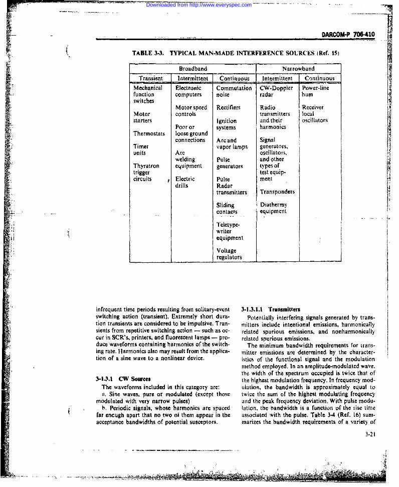
DARCOM-P 706410
F 4. TABLE 3-3. TYPICAL MAN-MADE INTERFERENCE SOURCES (Ref. 15)
Broadband Narrowband
Transient Intermittent Continuous Intermittent . ContinuousMechanical Electronic Commutation CW.Doppler Power-linefunction computers noise radar humswitches
Motor speed Rectifiers Radio ReceiverMotor controls transmitters localstarters Ignition and their oscillators
Poor or systems harmonicsThermostats loose ground
connections Arc and SignalTimer vapor lamps generators, 4+
units Arc oscillators, 11welding Pulse and other
Thyratron equipment generators types oftrigger test equip-circuits Electric Pulse ment f
drills Radartransmitters Transponders
Sliding Diathermycontacts equipment
Teletype-iwriter
+ equipment
Voltageregulators_
infrequent time periods resulting from solitary-event 3-1.3.1.1 Transmittersswitching action (transient), Extremely short dura- Potentially interfering signals generated by trans-tion transients are considered to be impulsive. Tran- mitters include intentional emissions, harmonicallysients from repetitive switching action - such as oc- related spurious emissions, and nonharmonicallycur in SCR's, printers, and fluorescent lamps - pro- related spurious emissions.duce waveforms containing harmonics of the switch- The minimum bandwidth requirements for trans-ing rate. Harmonics also may result from the applica- mitter emissions are determined by the character-tion of a sine wave to a nonlinear device. istics of the functional signal and the modulation
method employed. In an amplitude-modulated wave.the width of the spectrum occupied is twice that of
3-1.3.1 CW Sources the highest modulation frequency. In frequency mod-The waveforms included in this category are: ulation, the bandwidth is approximately equal toa. Sine waves, pure or modulated (except those twice the sum of the highest modulating frequency
modulated with very narrow pulses) and the peak frequency deviation. With pulse modu.h. Periodic signals, whose harmonics are spaced lation, the bandwidth is a function of the rise time
far encugh apart that no two of them appear in the associated with the pulse. Table 3-4 (Ref. 16) sum-acceptance bandwidths of potential susceptors. marizes the bandwidth requirements of a variety of
3-21
............................ ...... ....................... . ._ ........, , + + -+ . +
Downloaded from http://www.everyspec.com

DARCOM-P 706-410 9TABLE 3-4. TYPICAL BANDWIDTH REQUIREMENTS (Ref. 16)
Narrowband WidebandInformation Single- FM FM
Transmission Bandwidth, AM, sideband, (mi > 0.5), (m = 10).Hz Hz Hz Hz Hz
TelegraphMorse Code 10 wordsper min 0-120 240 120 240 2,400
SpeechHigh fidelity 40-15,000 30,000 15,000 30,000 300.000Typical broadcastprogram 100-500 10.000 5,000 10,000 100,000
Long distance tele-phone quality 250-3500 7,000 3,500 7,000 70,000Intelligible butpoor quality 500-2000 4,000 2.000 4.000 40,000
TelevisionStandard 525-linepicture interlaced,30-cycle repeti-tion rate 60-4.5 X 1( 9 X 10" 4.5 X 10⁶ 9 X 10 90 X 10
Pulsel"pslong 0-I X On 2 X 10_ I X 10' 2x 10" 20 X 10"
typical signals for each of the applicable types of output tube is shown in Fig. 3-15(C). In this spec-modulation, trum, in addition to the harmonics of the funda-
Spurious emissions are signals emitted at fre- mental, there appear additional spurious outputs thatquencies outside the "necessary" bandwidth of the do not bear any definite frequency relationship to thegenerating source, the levels cf which may be reduced fundamental or to each other. These are usually at-without affecting the quality of the intentional trans- tributed to multimoding phenomena associated withmission. Spurious emissions include: the multiple-cavity resonator that is used in the
a. Harmonics of the transmitter fundamental fre- device. Although measures are taken to suppress thequencyj, undesired modes, it is not possible to eliminate them
h. Nonharmonically-related outputs completely.c. Sideband splatter and noise. Sideband splatter occurs in amplitude-modulated
Fig. 3-14 shows a simplified block diagram of a com- transmitters when the modulation exceeds 100 per-munication transmitter that uses conventional vac- cent, and when the carrier is cut off on the negativeuum tubes, a master oscillator, and a multiplication modulation peaks. In single-sideband transmitters,scheme to generate the fundamental output. A typical splatter is caused most often by overdriving theoutput spectrum is shown in Fig. 3-15 (Ref. 16). In power amplifier, so that it operates in a nonlinearaddition to the normal harmonic outputs, there are region. With frequency-modulated transmitters.outputs that occur at a multiple of a frequency lower over-modulation causes the frequency swing to ex-than the fundamental. These outputs usually are har- ceed the design maximum system deviation. Trans-monics of the master oscillator used to generate the mitters also radiate broadband noise. Although thetransmitter carrier frequency, level is quite low, it is sometimes high enough to pro-
Fig. 3-15(B) shows the output spectrum that may duce interference with colocated receivers.be obtained from a system that uses a klystron for the The emissions which have been discussed can befinal power amplifier. In this case, the output spec- radiated not only from the antenna but also from thetrum consists only of the fundamental, and har- transmitter equipment cabinet itself, and also can be "monics of the fundamental. The output spectrum conducted along any signal or power lines connectedfrom a typical radar transmitter with a magnetron to the cabinet.
3-22
4. i 4a .
Downloaded from http://www.everyspec.com

DARCOM-P 706-410
F Mas ter requencyOsila JMuti ie ........ (Power) Amp Load
Figure 3-14. Basic Parts of CW Transmitter
-~ 3-1.3.1.2 ISM DevicesA class of equipment that generates RF energy for
Z .o noncommunication purposes but ior which the levelscan be as large as, or larger than, those used for corn-
s. munications is known as "Industrial, Scientific, and,,- Medical" (ISM) equipment. ISM equipment gener-ILLT ates sine wave signals at frequencies in the range from
T T T T 10 kHz to 30 GHz, usually for the purposes of clean.Frequency-.- ing, heating, or plasma stabilization. Equipment
(A) Typical communication Transmitter Spectra designed for civilian use is subject to special limita.tions on emissions by Part 18 of FCC Rules andRegulations as described in Table 2-5.
Considerable data extist on measured emissionlevels from such devices. Pearce and Bull (Ref. 17)measured levels of emissions from wood gluers,
94 plastic welders, and preheaters which appear at nu-merous frequencies between 30 MHz and I GHz. At-,
I c'.ja distance of 1000 ft the levels varied from 0 to aboutT~60 dB (,iV/m).
Garlan and Whipple (Ref. 18) measured emissionsFrequency- from arc welders, also at 1000 ft. In this case the(8) lystron Transmitter Output Spectra emissions are broadband, but on any one emitter
vary considerably with frequency over the range from0,5 MHz to 30 MHz. Levels varied from -5 to about
2 38 dB[Iu//(mkkHz)].
3-1.3.1.3 Local Oscillator Emissions' . :Local oscillators, used for heterodyning or detec-
J T tion in receivers, are potential sources of emissionsS via conduction on the power line or radiation eitherdirectly from the chassis or via a connected antenna.
Frequency- In digital computers, clock oscillators are used to) Mgenerate repetitive pulses to trigger logic circuits in(C) Magnetron Transmitter Output Spectra synchronism. The associated emissions can be rich in
Figure 3-15. Typical Transmitter Output Spectra harmonics, and can be radiated and/or conducted.Some typical conducted and radiated narrowband
emissions from receivers, transmitters, and a com-When the transmitter cabinet is located close to the puter are shown in Figs. 3-16 and 3-17 (Refs. 19 and
radiating antenna, direct leakage from the cabinet 20). The emissions shown below 10 kHz in Fig. 3-16may be no more troublesome than that from the are power frequency harmonics, not related to localantenna. When the transmitter is in a shielded enclo- or clock oscillator emissions.sure or a metallic building which offers shieldingfrom the antenna, direct leakage from the trans- 3-1.3.2 Switching Transients-nitter cabinet may be the primary source of inter- Transients occur whenever electrical power sud.terence and must be controlled where sensitive equip- denly is applied to or removed from a load. Thtment is present in the enclosure, power may be direct or alternating and the switching
3-2:
Downloaded from http://www.everyspec.com

DARCOM.P 706410
01200
Narrowiband Limit
x x
o SingleFrequencye f. iieItI
0mparg Receivere~ W.o'vr
Raderute
1 0
00- X XXciie Tarow~ iitP~i
x MIL-STO-461
xV20 -
xX
10kIM Frequency f. Hiz IOM 10OO1
Figure 3-16. Typical Conducted Nanrowband EwivAsom (Re(. 19)
3.24
- - -r--f
Downloaded from http://www.everyspec.com

DAR"O* 706410
*z c
j*
++0Na 0 0I0
*0' -4) k
- 0
L4 IA= 2 - 0
C S 'B
44:
NW/At -3~jfoS wojj W L 44BUBJIS PLO A3.25
1'N
Downloaded from http://www.everyspec.com

AROM-P- 706410
action may be intentional, as in the case of a me- should be raised 20 dB. By changing the ordinate ' ..chanical or electronic switch; or it may be uninten- dimensions to dB (MA/MHz), the same figure can beI tional, as in the case of intermittent contact due to a used for a current step.faulty mechanical connection between two parts of a An actual switch and circuit differs from the idealcircuit. The prototype switching action is to initiate prototype in that the current or voltage is not im.or interrupt a steady current or voltage. A simplified mediately initiated or interrupted due to imperfectcircuit is shown in Fig. 3-18. In this figure, Z switching action, or because the circuit in which therepresents the generator impedance, and ZL the load contact is placed may have reactive or unmatchedimpedance. At high frequencies the lengths of the loads, Frequently the equivalent load or the connect-lines connecting the switch S to the source and the ing transmission line may be considered to contain anload are important. equivalent series inductance.
On closing such a circuit, the voltage v(i) across the3-1.3.2.1 Switching Action load resistor rises exponentially according to the rel-
At low frequencies if the impedances are purely tionresistive, the switch can be considered to function in-stantly, to establish (upon closing) a voltage across v(t) = VI - exp (- t/r)] , V (3-36)the load 'impedance or a current through it. Themathematical model for this action is the unit step where(see Fig. 3-19) which has a spectrum amplitude S(f) = LIR, s
L inductance, HS(f) I(Wf) , s (3-32) R resistance, 1
V = final voltage, VFor a step of amplitude A (A nondimensional) I = time, s
The spectrum amplitude is given by the expressionS(f) A/(irf) , s (3-33)1V
For a stop or amplitude V volts or I amperes, the SU) : -f[(23:f :'::!])1spectrum amplitude is r[(1fl+Q,
Note that at frequencies for which 27rfT -c 1, the
S(f) V/(f) V's (3-34) spectrum is identical to that of the step. For somepurposes, this spectrum can be approximated by that
or of a linear rise of voltage to the maximum value V. Itis given by the expression for S shown on Fig. 3-20
TeS(f) I/(lrf) , A's (3-35) (Ref. 15). Its envelope (substitute I for sin rfr) isplotted for t - 0.1 As. A = V = I V. Note that for
The spectrum for step S, of one volt is plotted on frequencies above I/(rt), the spectrum amplitudeFig. 3-20, Also shown on this figure are formulas falls off as I/f rather than I If, and that in this range,showing how this spectrum is modified for an ampli- it is 6 dB above that for an exponential rise withtude of A volts, i.e., for a 10-V step the line shown r t 0.1 s
'12Switch S
''I Source Impedance Z
Load Impedance zL
Sourceof
Power
Figure 3-18. Simplified Switching Circuit
3-26
| , -- . ,, .U a ',
" ' :: "V: " ' - I.. 4. :
Downloaded from http://www.everyspec.com

DARC:M.P 706410
time t.anddurtio d s sownon Fig. 3-20 (see for-mul an plt fr S,).In heportion of the spectrumwhee te apliudevares s IIf, the spectrum of the
unit step is 6 dB below that of the unit amplitudepulse. The dependence on the rise time for both issimilar, but the pulse spectrum levels off at fre-quencies below I /(rd).
Time 3.1.3.2.2 Arcing PhenomenaWhen a switch opens, the current tends to change
rapidly from a finite value to zero, and the largeFilgure 3-19. A Unit Step at: i resulting dildt can produce a large instantaneous
t 0.1 x10⁻⁶ s
S140- A
1j.~- 120 a
100 1000
8rqunc f, Mr fz
Onl Lnvetipe value artho
Refer to formulas for other shapes (different t, A, or d).
Flgure 3.20. Initerference teiel for a INV, I-us Trapezoidal Pulse and INV Unit Step (04 ,us rise time) (Ref. VI
3-
Downloaded from http://www.everyspec.com
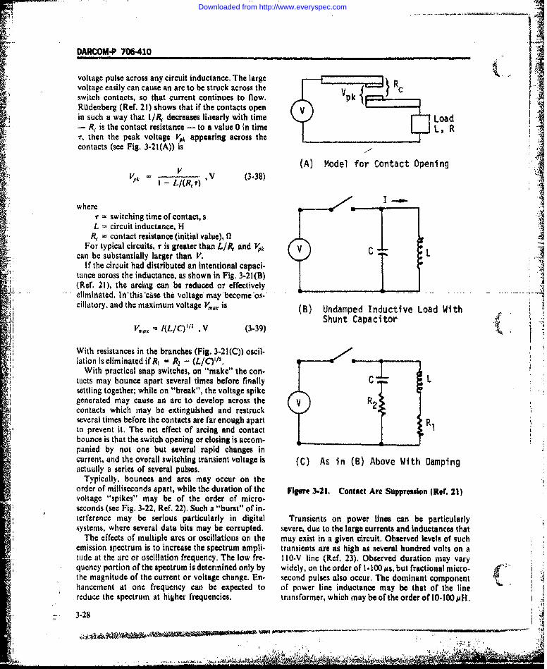
DARCOM-P 706410
voltage pulse across any circuit inductance. The largevoltage easily can cause an arc to be struck across the _Iiswitch contacts, so that current continues to flow. pRtldenberg (Ref. 21) shows that if the contacts open Vin such a way that l/IR decreases linearly with time Load
R,. is the contact resistance - to a value 0 in time L, R-r then the peak voltage Vpk appearing across thecontacts (see Fig. 3-21(A)) is
V (A) Model for Contact OpeningL/(Ro) ,V (3.38)
r= switching time of contact, sL circuit inductance, H a / n kT
R, contact resistance (initial value), PFor typical circuits, r is greater than L/I& and Vk VC L.ican be substantially larger than V. L
If the circuit had distributed an intentional capaci.tance across the inductance, as shown in Fig. 3-21(B)(Ref. 21), the arcing can be reduced or effectively . ..... ..........___
eliminated. In-this-case the voltage may become-os--cillatory. and the maximum voltage V,,, is (B) Undamped Inductive Load With
Shunt CapacitorIV,.I - IeL/ V (3-39)
With resistances in the branches (Fig. 3-21(C)) oscil-lation is eliminated if R, - (L/CV/.
With practical snap switches, on "make" the con-tacts may bounce apart several times before finally C Lsettling together; while on "break", the voltage spikegenerated may cause an arc to develop across the v R2contacts which may be extinguished and restruckseveral times before the contacts are far enough apart Rto prevent it. The net effect of arcing and contactbounce is that the switch opening or closing is accom-panied by not one but several rapid changes incurrent, and the overall switching transient voltage is (C) As in (B) Above With Dampingactually a series of several pulses.
Typically, bounces and arcs may occur on theorder of milliseconds apart, while the duration of the Figure M-21. Contact Are Suppression (Ref. 21)voltage "spikes" may be of the order of micro.seconds (see Fig, 3-22, Ref. 22). Such a "burst" of in-terference may be serious particularly in digital Transients on power lines can be particularlysystems, where several data bits may be corrupted. severe, due to the large currents and Inductances that
The effects of multiple arcs or oscillations on the may exist in a given circuit. Observed levels of suchemission spectrum is to increase the spectrum ampli- transients are as high as several hundred volts on atude at the arc or oscillation frequency. The low fre- I 10-V line (Ref. 23). Observed duration may varyquency portion of the spectrum is determined only by widely, on the order of i-100 js. but fractional micro-the magnitude of the current or voltage change. En- second pulses also occur. The dominant componenthancement at one frequency can be expected to of power line inductance may be that of the linereduce the spectrum at higher frequencies. transformer, which may be of the order of 10-100 pH.
3-28
• . ---..." .'".. ... ... . 7 :. - "' 7' " " -3 .Wa1"3 'a 4 vi'w-. ."i
Downloaded from http://www.everyspec.com

DARCOM-P 706410
(A) EMI* Created by Toggle Switch
400 V Peak to Peak
inductivepulse
50 idsH
400 VPeak to Peak
50 Ps;i, arcing200 Ws 400 )is
(B) EMI Generated by Electronic Switch (C) EMI Generated by Six Pole Relay Opening
*EMT * electromagnetic interference
Figure 3-22. Typical Switching Transients (Ref. 22)
Although spikes on power lines usually are generated Representative spectra are shown on Figs. 3-23 andby the switching of differential mode current, they 3-24 (Ref. 24). On Fig. 3-23, peak conducted EMImay be coupled readily into common mode or levels measured in a circuit containing a relay coil areground loop circuits, thereby considerably increasing shown as a function of the magnitude of steadythe effectivness of the power line as a radiator. This current after contact. The levels are seen to be a func-situation is discussed further in par. 3-3.3,3. tion of the current level and indeed, except at very
Transients are generated in circuits containing low currents, directly proportional to the current. Atrelays both by opening and closing of the contacts of high currents, the rate of fall off of spectrum is ap-the relay itself, and by operation of the activator coil, proximately inversely proportional to frequency. inusually by other contacts. Transients also appear in accordance with theory, as is its magnitude (see Fig.circuits containing solenoid valves. The rlay coil or 3-20). At lower currents the increase in spectrum levelsolenoid, as an inductance, generates a voixage spike with frequency is not understood, but may be caused%hen deactivated. Although the current in the coil by decreased damping of the circuit inductance by in-may be small compared with that switched by the creased load resistance.-'ontacts of the relay, the voltage spike generated by Fig. 3.24 shows corresponding results for contactthe coil circuit mpy be comparable in level, due to the "break", Note that here the spectrum is beterlarge inductance bf the coil compared with power cir- behaved, probably because the load resistance hascuit inductance. Tvnsients associated with relay or less effect in an open circuit.solenoid operation, other than those caused by the Measured levels of EMI radiated from the circuitcoil, are similar to those associated with mechani- containing the relay coil are shown on Fig. 3-25 (Ref.cally operated switch circuits. 24). No attempt is made to provide a radiation model
3-29
Downloaded from http://www.everyspec.com

DARCOM-P 706410
100,000 -______ _ _ _ _4-
0O.5 AO------O110 mA
0-------o 4 mA
1000 0
88ooc
10
1.0
0.1
Frequency f. MHz
Figure 3-23. Make Contact Conducted EMI Associated With Current MagnitudesIn an Electromagetic: Relay Contact Circuit
V = 6.0OV d; 4 - R) (Ref. 24)
* 3-30
Downloaded from http://www.everyspec.com

DARCOMP 70-41
io~OA COC URRENT
o---o0.5 Ao-----.110 mA
0.---- 4 mA
10 ,000C- - 50p
1000
10
1.0
0.1
Frequency f,, MHz
Figure 3-24. Break Contact Conducted EMI Associated With Current Magnitudes- I in an Electromagetic Relay Contact Circuit(Va 6.OV dc; 7jw R) (Ref. 24)
3-31
- -- ----
Downloaded from http://www.everyspec.com

t - .llI lII . . . -. .. , I I I-
100,000
10.000 MAKE CONTACT
/ ----- BREAV ,.)NTACT
1000 1wO0 00
4A
k^
1.0
0.1 .1
Frequency , Hz
Figure 3-25. EMI Radiated from a Convenional Electromagnetie Relay Coil (no relay cover) (Ref. 24)
3-32
.L:..'.. - .- - - - - - ---. , • .. .. , : ;, . -
_ ........... ,,. ...... I. . . . . -, I: -.. . ....- . .: . . .
Downloaded from http://www.everyspec.com

DARCOM-P 706410
here because of uncertainty as to the actual con- Fig. 3-27 shows that on the basis of open circuit volt-figuration of the test circuit. Other data on conducted age and impedance measurements, the output noiseand radiated spuctra from various relays or solenoid level from this device can be predicted with reason-operated devices are shown in Table 3-5 (Ref. 22). able accuracy for any load. Similar results are ob-
The principles of switching transients just dis- tained for ac generators measured as noise sources.cussed apply in alternating as well as direct current Fig. 3-28 (Ref. 26) shows conducted noise voltagecircuits. but in alternating current circuits the magni- measured an a dynamotor in the frequency range 150
tude of the transient and contact arcing is very much kHz to 15 MHz.a function of the time during a cycle that circuit inter-ruption begins. The magnitude of the expected tran. 3-1.3.23.2 Gases Discharge Lampssient is of the same order for equal maximum voltage Gsosdshrelmsoeaeo h rnilequl axiumGaseous discharge lamps operate on theprnilor current. However, the transient itself may be of an arc breakdown, a phenomenon that occursaffected significantly by saturation effects in mag- twice during each ac cycle.netic circuits caused by large inrush currents. Ref. 21 Fig. 3-29 (Ref. 27) shows the electromagnetic inter-should be consulted for details. ference (EMI) voltage from a fluorescent lamp in a
3-1.3,1.3 Relmititie Switching limited frequency range, measured directly across the. e Slamp terminal. Fig, 3-30 (Ref. 27) shows, however,
3-1.3.2.3.1 Rotating Mahinmes that the impedance of the lamp (including its ballast)Because a commutator is, effectively, a device is so large that very little conducted noise voltage
which performs an automatic and repetitive switch- results. However, in the frequency region of imped-.ing function in which one of the principal elements is ance resonance, the lamp exhibits fairly sustained os-the inductance of the machine windings, it can be cillations (in the neighborhood of 12 kHz). This os-expected to generate EMI in the same way. Actually. cillation might create serious radiated EMI in somethe brush used in commutation acts as a varying con- circumstances.::-! tact resistance in a way corresponding to the dis- Radiated EMI measurements on a different flu0-- .
cussion leading up to Eq. 3-1. rescent lamp in a higher frequency range are shownFig. 3-26 (Ref. 25)'shows experimental data for a on Fig. 3-31 (Ref. 28). In making these measure-
commutator type of generator. ments. the electric antenna was placed 3 ft from theFig. 3-27 (Ref. 25) hows that the effective ac im- lamp. Electric fields from fluorescent lamps usually
p, dancc of the equivalent noise source for a dc can be eliminated entirely by using glass with a con-generator is independent of the load, although it ductive coating and whose surface is electricallyvaries rapidly with frequency. The dotted curve on bonded to an otherwise complete metal enclosure.
TABLE 3-5. EMI FREQUENCY SPECTRA OFELECTROMECHANICAL SWITCHES (Ref. 22)
Switch Type EMI Frequency Spectra
Latching power relay 15 kHz to 400 MHz radiatedI MHz to 25 MHz conducted (coil lines)30 kHz to 25 MHz conducted (contact lines)
Power transfer relay 15 kHz to 150 kHz, 25 MHz to 400 MHz radiated150 kHz to 25 MHz conducted
Switching relay 130 kHz to 60 MHz radiated600 kHz to 12 MHz oscillation conducted on coil lines87 to 150 kHz oscillation conducted on coil lines
Solenoid-operated valves I to 8 kHz conducted
Power contactors 150 kHz to 25 M Hz conducted
Coil-operated coaxial 1 50 kHz oscillation conducted on coil linesswitch .. 33
3-33
JPI[
Downloaded from http://www.everyspec.com

DARCOM.P 706-410V
2
~---N--predicted
S6-
4.3
10, - - -
<II
Frequency fkHz
Figure 3-26. Conducted Noise Voltage from a O.5-kW dc Generator at Full Load(1725 rpm. 115 V dec, 4.35 A, R 2.76 Q) I Ref. 25)
3-34
Downloaded from http://www.everyspec.com
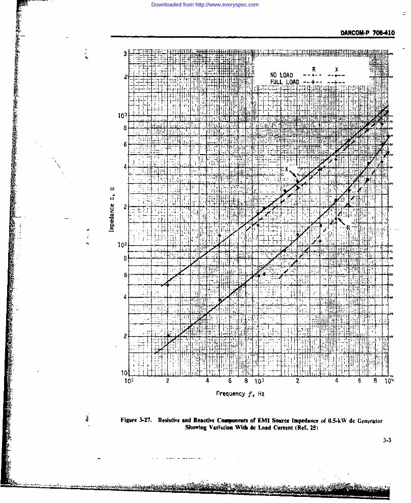
01 i- DARCOM-P 706410
t- . - + .4L-. * -4 ~ 1-4,4
- - -, - z : I 1 1; ; : R2~ "i i NO LOAD---
A7~i~ ~4 FULL LOAD + +
6 J1 4 i .
t K -r
IAI{I
10-
L -r
6 V
4-4
I. I ;M I. Il
i~ 1P.4.
102 2 6 BO 2 - 8O
6 t: .7!.. .V'4.. .... . ..
Downloaded from http://www.everyspec.com

DARCOM*P 706-410
J..
4 4
anI [4IC) I
14-1 4 __4- c7r T.T TI7
04
RIF u!.I
m .
-P! -V
A ~ ~ IJ 1~~O 1W
3-36
Downloaded from http://www.everyspec.com

DARCOM01W4HI
SEE~~~ NOT -----
4; -0~ - , ; '.-
2 -. -..
NOTE: DUE TO VARIATIONS IN THE FREQUENCY4 MODULATION EFFECTS. THE EMI VOLTAGE BETWEEN
8 AND 13 kHz VARIES IN MAGNITUDE BUT DOES NUTEXCEED 0.8 V RMS.
2,t I1F
89 10 11 12 13 14 is
Frequency f, kHz
Figure 3-29. EMI Source Voltage of Fluorescent Lamp (Rel. 27)
3-1.3.2.4 Automotive Inition Fig. 3-33 (Ref. 3 1) shows the range of field strengthData on a number of incidental radiating devices (both horizontal and vertical polarization) as a func.
have been summarized by Myers (Ref. 29). He tion of frequency for 21 vehicles and also shows thereports the work of Newell on a simulated ignition limits of SAE Standard J551. These data were takensystem as shown here in Fig. 3-32 (Ref. 30). 1 he corn- in 1969 at a distance of 10 m.parison between measured and theoretical current When vehicles are moving, a spread in levels evenspectra shows remarkable agreement, the peak at larger than shown on Fig. 3.33 will be experienced. Iabout 20 MHz being dtie to a resonance in the Fig. 3-34 (Ref. 32) shows the distribution function forsystem. The extension of this model to predict radi- vehicles on a 7-lane freeway when measured by ansled values is almost impossible, because of the ex- antenna 51 ft from the nearest lane of traffic. In thistrenie dependence on the amount or shielding contri- case a power measurement was made. Although thebuted by the metal body of the vehicle, average value of measured power was only 18 dB
3-37
Downloaded from http://www.everyspec.com
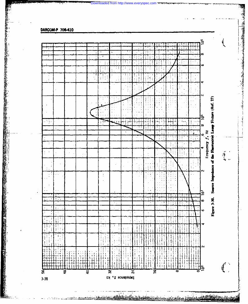
DARCOM-P 706-410
. ..........
- -~ -- r~- ~-~r ~ 7T~T 9-'--r
- - - - - ~ - - - .-.- . .... ...-- ~".
4114
4--m
3-38 u)N 'z aouepadl
-7i;4....
Downloaded from http://www.everyspec.com

N MetalX grille
EZ 10 removed
i!iende
Cx
I+
44
0.0 ., O 0 ~ +
++ Frequency f, MHz 'Figure 331. Broadband Radiated Interference (Peak) (Ref. 28)
above kT,,B, the value exceeded 1% or the time was 3-1.3.2.5 Semlcouc~tor Switching*about 50 dB above k7oB, Fig. 3-35 shows a source of interference arising
Military vehicles for tactical use are suppressed to from a switching transient (Ref. I13) in a semi~on-; - lower levels than SAE Standard .1551 (see par. 5- ductor diode. The source of interference is a pulse
i ,6.3.2). This is because they frequently carry corn- generated at diode turnoff by stored carriers in then, unications equipment which must be usable white junction.the vehicle is moving or standing with engine oper-ating. Furthermore, because equipment mounted onthe vehicle or connected to its power supply is po- 3-1.3.2.6 High-voltage Power Limettentially susceptible, levels of conducted interference EMI generated by power lines is of two types,
+ . must be controlled. Even if tactical vehicles do not namely: {carry communication equipment, they must be sup- a. That due to various forms of corona whichpressed because they can be located close to cor- generally has a random waveoerm, but which is mod.munication installations. ulated at the power frequency or multiples of it. This
. F-39 b s
Downloaded from http://www.everyspec.com

F DARCOM-P 706410
'R. Spark Gap
R- L
Contact Brae 41
(A) Simplified Circuit of Ignition System
10NN
Frqunc 10M- Frqecyf ~-1 "w 0 4... .. ... "J -
0- __ _ _20__ _ __ _
i f -30 - 30 -
5 -40 -: -40 "!
1.O 0 1001'0 1.0 10 10:Frequency ,MHz Frequency 2,MHz _
(B) Spectrum of Spark Current for (C) Spectrum of Spark Current forDistributor and Plugs at At- Distributor and Plugs at 75 psi
mospheric Pressure Pressure (gage)
------Theoretical
- Measured
Figure 3-32. Spark Current Generation and Current Spectra (Ref. 30)
source has a high duty cycle and is usually not impor- distances from the line, under fair weather con-tant at frequencies above 100 MHz. ditions. In fog, mist, or rain, levels may be !0 to 20
b. That due to localized static discharges across in- dB higher.sulators or other forms of line hardware which ismorc Impulsive in character. This type of inter- 3-1.3.3 Nonlinear Phenomenaference has substantial components at frequencies of The term nonlinear phenomena could be inter-the order of 100 MHz and does not propagate on the preted to include almost any mechanism of EMIline. generation. For example, almost all switching in- (
Measured data compiled by Skomal (Ref. 33) are volves some nonlinear action in the arcing that mustshown on Fig. 3-36, for a variety of line voltages and always occur. Here the term is reserved for those
3-40
Downloaded from http://www.everyspec.com

DARCOM-P _70k410 *
SAE J551A
801
70 Vert. Only
,. = 60
x: Vert. & Hor..
qnf50
Vert. 0ny 1
20 100 1.000
i Frequency fMHz ,
(Range of Radiation from Individual VehiclesMeasurement Distance 10 m)
Figure 3-33. Indiwldual Vehicle Electromagnetic Radiation (Ref. 31)
devices in which there is a relatively well defined non- mixers, and frequency multipliers - or they may
linear relation between current and voltage. The arise unintentionally, as in the case of saturation indevices or major interest are those in which ac (sine electronic tubes, transistors, and magnetic materials.waves) or periodic pulses are applied, A nonlinear device excited by a single-frequency
Nonlinear impedances appear in electric circuits by sine wave signal will produce harmonics of that sineseveral mechanisms. They may be intentionally in- wave. If the nonlinearity is quite severe, the signalcluded in the circuit - as in the case of rectifiers, produced may be characterized by abrupt changes in
3-41
.............. ......... .. . ,, .: , . .,. . ... . .. . _ .,
Downloaded from http://www.everyspec.com

DARCOM-P 706410
FAR FROM FREEWAY NEAR FREEWAY
:0 \I..
1 29
50 a
2 30
... itit
20
10
d) 0 t I
T 20 1 -
40
062 PS 08323 PST
30
20
10
0a
0.001 0.1 1 6 10 20 50 70 80 9095 98 99 0.0010.1 1 5 10 20 5C 70 80 9096 98 9ijPERCENT OF IM PERCENT OF TIME
ORDINATE IS EXCEEDED ORDINATE IS EXCEEDED
Figure 3-34, Average Probability Dibutions for Freeway Traffic, 24.1 Mi-t (Re(. 32)
3.42
Downloaded from http://www.everyspec.com

DARCOMP 706.410
level, and may appear as a succession of switchingtransients rather than a sine wave corrupted by har-monics. These concepts are illustrated in Figs. 3-37and 3-38. The nonlinearities represented in Figs. 3.37(A) and (B) are typical of the "switching" type ofnonlinearity, i.e., the slope of the output-input curve
-,-. I I+ I I I I I I increases as input increases in magnitude (althoughnot necessarily symmetrically as shown). The outputsof such nonlinearities are quite rich in harmonics; in-deed, in the extreme case of Fig. 3-37(C) the level ofthe harmonics can be constant up to quite high fre-quencies. Examples of devices having this kind of
Peak nonlinearity to a lesser or greater degree are mixers.2.25 A detectors, rectifiers, magnetic core inductors, anddevices utilizing gas discharges, such as fluorescent
(A) Current Wave: Four Conducting Cycles lamps. Another type of nonlinearity is the "satu-rating" type shown in Fig. 3-38. In this type of non-
linearity, the output waveform is "clipped" and in theextreme case, represented in Fig. 3-38(B), becomes a
2:; square wave with fundamental frequency equal to the *.
frequency of the sine wave input. The harmonics of asquare wave fall off inversely with frequency. Anexample of a device with saturating nonlinearity Is .i
AA/ ,the linear amplifier when operated at too-high an in-I ..... .... . . ... . . . ..put level;. .11
Harmonic generation by nonlinear phenomenaalso creates problems due to the mixing of signalspresented to the nonlinear device. Sometimes this isIntentional, as in mixers, converters, and detectors.But intermodulation and crossmodulation are un-
desired phenomena in circuits designed to be linear. .
t ~primarily radio frequency atrplifiers.(B) Same as (A) With Sweep Rate Increasedprmilrdofeqnyapiirs,
to 10 Ws/cm 3-1.3.3.1 Power Fre4uency Harmonc GenerationThe primary sources of har,nonics in ac electric
power lines and distribution systems are rectifiers andmagnetic saturation in transformers.
3-1.3.M.1.1 RectifiersThe load and line currents for ideal singleophase.
_____-______unfiltered half-wave and full-wave rectifiers areshown in Fig. 3-39. For the half-wave rectifier themagnitudes of the harmonic currents 1(n) for both .line and load are given by
f ' ' . A (3-40)2'
(C) Same as (A) With Sweep Rate Increased I(n) -to I Uslcm 2
t1 cr(n - IXn + I) ,ncven ,A (3.41)
Figure 3-35. Ouctllograms of Reverse Current whereTransients for a IN345 Diode at 880-mA dc Load /A = peak value of current, A
(Ref. 20) n - order of harmonic
3-43
................... ..... .. ..... ...
Downloaded from http://www.everyspec.com

PARCOM-P 706-410
~180-160 / Bond
S120- '>{4. Hinrma 1S100- Hinchman j (0) B=103 Hz
0 - H ich a 1n4 ) ( 0
0- Buehler 5)ha 132).20-- (285-345)' 35
(132) (35,(7)Gbealnpitlctos eet odco,( 5f ateally, fro lie,
(o1 00,35)(7) ftbla ervaon oin01ft lats erallyhfronduline 0 25 ft laterally from line, a 0
ft laterally from line. Vetcanieubsow the range of measured va ues.)de 33V e .
Output Output Output
Input Input Input
V V Vtt N t
Input Input Input
VV Vtt t
output Output Output
(A) Linear Device (B) Nonlinear Device (C) Limiting Case,Switching Nonlinearity
Figure 3-37. Waveforms Resulting from Switch-type Nonlinearities
3-44
Downloaded from http://www.everyspec.com

F DAC~OM-P 706 4W
Output Out ut
Input Input
V V t
Input Input
Output Output
Output Output
(A) Saturating Nonlinear (B) Limiting Case,Device Saturating Nonlinearity
Figure 3-38. Waveforms Resulting from Saturating Noilinearlties
For the full wave rectifier the harmonics of the load these filters increase line harmonics, which are usual-current 1(n) are given by ly the harmonics of most concern from an EMC
point of view. The effects of these filters are discussed4(, (4) in detail in par. 5-5.
-(n) ( 1) A (342) For multiphase power supplies, analysis of lineir(2n -1current is more complex than for single-phasesupplies; however, multiphase circuits may be used to
Note that the line current for the full-wave rectifier is advantage to minimize ripple in the dc output as wellsinusoidal, so that there would be no harmonics as harmonic emissions on the power line. By propergenerated on the power line by an ideal full-wave, choice of circuit, the rectifier may be designed in-single-phase rectifier. The same conclusion holds for herently to cancel out certain harmonics. This is dis-a full-wave bridge rectifier. cussed in detail in par. 5-5.4.2.
For most purposes the harmonic content of theload currents of simple rectifiers is too large for 3-1.3.3.1.2 Transformers and Inductorssatisfactory use. To reduce these harmonics, filters Transformers and inductors using magnetic ma-are inserted between the rectifier output and its load, terials for cores have nonlinear current-voltage char-thus smoothing the waveform. However, generally acteristics due to saturation effects in the core. in
3.45
=," ,-: "" ': -
Downloaded from http://www.everyspec.com

f" DARCOM.P 706410
4.,I 4ii0 -ai
4J
U)~
cce
4a
N
'U'.
-Ad
iCL
aarC.. _ j -.
3-46
'UI-I U"0.I
•-,- 'L -
i 3-46
, :~~~~ ~~~ ,* . . . : ::i.
Downloaded from http://www.everyspec.com

OARCOM P 706410
power circuits. the forcing function is generally a crease by a relatively large amount to generate suffi-sinusoidal voltage, so that the current waveform is cient back emf in the inductor to equal E.distorted. This distortion results in generation of har- In well designed power transformers the third har-monics of the power frequency which may be coupled monic current generated at rated voltages will notinto other circuits by induction or by common im- exceed a few percent of full load current, and har-pedances. monics of higher order will decrease rapidly as the
The mechanism by which this occurs is that shown order increases.in Fig. 3-40. The magnetic field strength H is propor-tional to the current 1. while the magnetic flux density8 is proportional to the voltage E. As the applied 3-1.3.3.2 External Mechaims of Interferencevoltage is increased beyond the saturation value E,, Generatieonthen, because of the smaller increment of magnetic Nonlinear effects have been observed at radio fre-flux per unit current increment, the current must in- quencies in structures in the vicinity of transmitter
-Magnetic EMaterial sat
H! IE
H~i~sat
(A)()
E E
,, ~ sat 1T E
I
sat
I I, i
I _____
t4
( (C)
Figure 3-40. Generatlee of Harmeeles In Magnetic Materials 34
3-4
- .-.A"'
Downloaded from http://www.everyspec.com

antennas, resulting in the generation of spurious fre- typically make use of the mean square error as a basisquencies due to intermodulation. The phenomenon is for assessing system quality, though other quantities
known to arise in metals having magnetic properties. such as peak error and average absolute c.ror some-corroded metals, and corroded joints between met- times are needed.als-particularly where the joint is loose. The essen- Training and fatigue also affect performance..tial conclusions of a study on this matter (Ref. 34) Trained operators frequently can read signals cor-were as follows: rectly in interference in which an untrained operator
a. The nonlinear phenomena found invariably had would find them hopelessly lost. However, the con-an odd symmetrical voltage-current characteristic, centratior, required to do this will tire the trainedi.e., the power series expansion around the origin has operator more quickly than will receiving under in-only odd powers. terference-free conditions. Resentment at the intru-
b. Welded joints are far superior to riveted or sion of an interferer also can be expected to have anbolted joints. Turnbuckles and cable clamps are effect on the quality of reception. These psycho.potential sources of nonlinearity, logical factors have not been quantified adequately,
c. The effect appears in magnetic materials such as and are only mentioned here as a caveat.steel, nickel, and mu-metal. Coating magnetic ma- Performance measures usually are expressed as oneterial with conducting material such as copper sig- or more curves giving the relationship between thenificantly reduces the effect, quality measure, and the noise level for various levels
d. Rough surfaces and oxide surfaces on steel of signal. In some instances, quality is related to theexhibit the effect as do copper oxide formations on signal-to-noise ratio, and one curve is adequate forcopper. Cleaning and polishing such metals are effec- any signal level. The forms of these relationshipstive in reducing the effect. sometimes vary smoothly and gradually, and some-
e.- The effect frequently is observed near sharp cor- times abruptly, exhibiting a sharp threshold. Typical-ners and bends. The interference level developed at ly, where synchronization is affected by interference,the input or a receiver depends on the energies loss of synchronism means total loss of output. Sharpreceived from the transmitters by the nonlinear thresholds also are characteristic of interferencedevice, the efficiency of the conversion to the un- reducing modulation systems.desired frequency, and the re-radiation properties of Ultimately in system evaluation a functional rela-the structure involved. If a receiver antenna is close tionship between impairment and cost must be iden-enough to the structure, the interference might indeed tified, a relationship which is often elusive. In abe substantial. But if the receiving antenna was, for digital system, where the error probability is theinstance, 10 ft away, the interference very likely quality measure, one might assess cost in terms ofwould be of negligible magnitude. that required to provide the higher transmitting
power needed over that needed in the absence of ir-2 Spairment. But then other costs must be accounted
for; for example, the increased power may result in an3-2.1 MASKING AND ERROR INDUCTION increase in interference with another system.
Measures of functional impairment, arising as aconsequence of interference, depend on the purpose 3-2.1.1 Speech Systemsof the system. In a speech communication system, in- Audio systems intended for speech communica-telligibility is an important factor, and measures tion are evaluated in terms of syllable, word, orbased on subjective articulation tests arc used to sentence intelligibility, as determined by psycho-assess its effects. Other criteria may be used in some acoustic tests. The degree of intelligibility, called thecases, e.g., criteria based on speaker recognizability, articulation, is the ratio of the number of languageSystems using visual displays - TV, radar displays, elements currently understood to the total number offacsimile, graphic, and alphanumeric readouts - elements used. The results of articulation tests de-require a variety of measures, ranging from amor- pend on the language itself, the class of talkers, whatphously defined observed quality preferences to words (or other language elements) are used in therigorously defined probabilistic quantities. Digital test, and the class of listeners.data systems invariably use average probability of The most common tests make use of lists of words.error over all symbols used, but in many cases it is These words are read to a listener through the systemnecessary also to know the transition probabilities for being examined. An easy test to grade is the Rhymethe different error pairs, and whether errors occur at test (Ref. 35) in which single syllable words are readrandom interva!s or in bursts. Analog data systems to a listener who is given the word ending and must
3-48
............................. s2 '. .. * '
Downloaded from http://www.everyspec.com

DARCOM-P 70410
supply the initial sound (letter). Another test uses the 110 777777/Phonemnically Balanced (PB) word list. Each suc- Rego foelacessive group of 50 words is balanced to contain aproportioning of phonemes typical of that found in 90the English language. Listeners are informed that allwords used are valid English words, and not non-sense syllables. The listener writes the entire word on 70 7this score sheet, and scoring can be based on thenumber of words or the number of phonemes in 60
ero.Both ofthe tests described here aeusedfodiagnostic purposes to determine which phonemes 50are apt to be misinterpreted and whether or not a 40member of one class of phoneme (e.g., a stop sound) /ov,is apt to be interpreted as.a member of another class 4 0(e.g., a fricative). A discussion of these procedures 8 20 - o ^ ofwill be found in Drucker (Ref. 36).
The use of articulation tests is costly and time con- tosuming. In their place one may use an analytical 0method that gives estimates of articulation, using pre- 0
determined spectral properties of speech and the -10spectral properties of the interference. The method is 1oral rms speech level
tbased on the spectral distributions shown in Fig. 3-41 -2 Threshold of audblity 10 69 d8 at I f,4i . ~~(Ref. 37), and a derived quantity called the articula- -ontiuu S cr s nii' , , m
tion index (Refs. 37 through 40). The curves per- 270 490 770 10701 1400 17 213012660 4004660taining to speech show spectral density levels of 38 630 9 1230 17 01920-2370 -aOOO 3950 N6Xsound p- sure at one meter in front of a talker using Mean Frequencies of Bands of Equala raised voice; the raised voice is 6 dB above the level Contribution to Articulation index, Hzof a normal speech. Three curves corresponding to Figure 3-41. Plot, on a Spectrum Level Basis,peak speech levels, average levels, and minimum of (1) the Speech Area for a Man Talking in alevels are shown. Peaks are 12 dB above the average Raised Voice; (2) the Region of "Overload" oflevel, and minimums are 18 d8 below the average the Ear of an Average Male Listener; and.level. The frequency ranges from 200 to 6100 Hz. and (3) the Threshold of Audibility for Young Ears
the abscissa is divided in such a way that equal width (All curves are plotted as a function of frequencyintervals correspond to equal contributions to the ar- on a distorted frequency sale.) Re. 37)ticulation index. If all of the area between the peakand minimum curves is uncontaminated by inter- Both terms in the numerator of W, are measured inference, is not filtered away, and does not fall below dB relative to 0.0002 gbar in a 1-Hz band. The speechthreshold or above overload, the articulation index is peak is taken from the curve of Fig. 3-41. The factor.100%, If part of this region is obscured, the loss of ar- 30, ini the denominator corresponds to the 30-dEticulation index is determined by the area of the range between peaks and minimums. W is set equaobscured portion. The abscissa is marked off in fre- to zero if Eq. 3-43 is negative, and it is set equal to u.quencies which are the centers of 20 critical bands. nity if Eq. 3-43 is greater than unity. By assuming ieach band contributing 5% to the articulation index, speech communication system in which normaThe articulation index A in a particular application is volume levels are set so that one is never belogiven by threshold or above overload, and where the speecl
20 band at the output is unchanged from that shown iiA Y 0.05 W (3-43) Fig. 3.43, Eq. 3-44 can be rewritten
where W, SN), + 12 <(S/N) <18 (3-4f= articulation index parameter were
where
- [(speech peak of nth band) (S/NI, eiatio of the rms spectral density caverage speech to rms spectral density c
S( vthe noise at the output in the nth banc
+ 30 (3-44) dB
3-4
.= ..... ;... ., , @ t, .; : ,.
Downloaded from http://www.everyspec.com

DARCOM-P 706-410
Shown superimposed on Fig. 3-41 is a flat spectral If this method is applied to noise consisting of adensity of about 31 dB, which is an assumed level for pure audio tone, it can reside in only one of the 5%an interfering noise signal whose total rms value over articulation index bands, and it would degrade the ar-the band from 200 to 6100 Hz equals the total rms ticulation index to no less than 95% no matter whatlevel of the average speech curve. This is 69 dB in a its amplitude is. The intelligibility loss, however, doesband of 5900 Hz or an average of3 1.3 dB in a band of depend on the noise amplitude. Results of maskingI Hz. By using Eqs. 3-44 and 3-45 and Fig. 3-41, the by pure tones are given by Stevens, et al. (Ref. 41)articulation index - corresponding to a unity ratio and Christman. et al. (Ref. 42). By using PB wordof total signal power of average speech to total noise lists, Ref. 43 shows that at a speech level of 69 dBpower - is found to be about 40%. The articulation (which corresponds to the total rms speech level forindex at other levels of total signal-to-noise ratios is average speech at 1 m from a loud talker, see Fig. 3-obtained by drawing a horizontal line which lies 41) the articulation is as shown in Table 3-6. Theabove or below the horizontal line drawn on Fig, 3-41 results vary with speech level and the frequency of theby an amount equal to the total signal to noise ratio. masking tone. At a speech level of 69 dB. 90% articu-and making the calculation indicated by Eqs. 3-43 lation is obtained with noise levels ranging from 87and 3-45. dB at 100 Hz to 114 dB at 1000 Hz. At lower speech
The articulation index is related to syllable, word, levels, the spread in noise levels over this frequencyor sentence articulation. By using Fig. 3-42, taken range is smaller.from Kryter (Ref. 40), sentence articulation is found The Christman report also gives results for the ran-to be about 95% if the articulation index is 40%. dom noise masking of speech. In general. randomWord articulation for a PB test is on the order of noise is much more effwjve than are sine waves.90%. Typically, for 75-dB speech, random noise-requires
*'about 30 dB less power to produce the same loss of
THESE RELATIONS ARE APPROXIMATE. THEY DEPEND intelligibility as do sine waves.UPON TYPE OF MATERIAL AND SKILL iOF TALKERS 3-2.1.2 Visal Dislay Systm
J.AND LISTENERS. 3212Vsa ipa ytmVisual displays cover a wide range of types that10 0C,- - ..- - need very different quality measures, In television,
- - - - - verbal descriptions of quality or preference are used.SA. , In radar, measures such as increased time for detec-2 2 tion are used.
0 r 'S /Measurements of observer reaction to televisione.c - - -0 ..... pictures affected by interference have been made by
-" - - - - Weaver (Ref. 43) on 405-line (3-MHz bandwidth)W 0and 625-line (5-MHz bandwidth) systems. Gaussian
/ /random electrical noise with a bandwidth appro-- // Th 1 - priate to the two video systems was used. The addi-1 20 - ' tion of signal and noise was carried out in the video
-,- - - - circuits (i.e., not in RF circuits). Essentially, flat elec-S0' trical noise which was passed through a differenti-
0 0.2 0,4 .6 0.8 1.0 ator giving a 6-dB-per-octave decrease of attenua-ARTICULATION INDEX A tion was inserted. Observer reaction was rated on a
P , TABLE 3-6. ARTICULATION AS FUNCTION1. PS words (1000 different words) OF SIGNAL-TO-NOISE LEVEL2. Non-sense syllables
(1000 different syllables) (SIGNAL LEVEL 69 dB)3. Test vocabulary limited to 255 PB words4. Sentences NOISE LEVEL, dB SIN ARTICULATION5. Test vocabulary limited to 32 PS words 115 -46 0.35
105 -36 0.57Figure 3-42. Several Experimental Relations 95 -26 0.82
Between Articulation Index and Speech 85 -16 0.92Intelligibility (Ref. 40) 75 -6 -1.0
3-50
, . ,,. ..... •n. , ." " ,.., , ,. . ..
Downloaded from http://www.everyspec.com

En!
DAROf dP 706410
scale of I through 6, the scale elements having the which accounts for subjective effects, and which suitsassociated descriptions: both monochrome and color television, It was with
1. Imperceptible such a weighting curve,which falls off 14 dB from low2. J ust perceptible frequencies to 4.5 MHz, that the tests were made. The3. Perceptible but not disturbing noise spectra used were those typically found in the4. Somewhat disturbing Bell System transmission networks plus two flat spec-S. Objectionable tra noises, one going to 4.5 MHz and the other to 2006. Unusable. kHz. The data show that for flat noise to 4.5 MHz.
The results obtained are indicated in Fig, 3.43. The more than half of the observers judged the noise justsignal-to-noise ratio is based on the peak-to-peak perceptible or imperceptible with a 49 dB (peak-to-signal amplitude, and the rms value of the noise. For peak)/(rms noise) signal-to-noise ratio for both colorthe US standard 525-line system, it is reasonable to and monochrome pictures. With a signal-to-noiseassume the results would fall somewhat to the right of ratio of about 43 dB, more than half the observersa curve midway between the 405 line and 625 line judged the pictures to have at most some impair-curves shown here. For example, if "just perceptible" ment, but not to be disturbing.noise is acceptable (rating 2) about 38 dB (peak-to- Results of tests of the effect of co-channel and ad-peak signal)/(rms noise) is indicated as being jacent-channel interference on television receptionrequired for flat noise. are reported by Allnatt, et al. (Ref. 45). These tests
A more recent set of tests on US Standard 525-line were scored using a 5 point scale. With co-channel in-television using a 7 step quality scale has been terference, the observer reaction was influencedreported by Cavanaugh (Ref. 44). This scale is similar strongly by the degree of frequency offset between theto the Weaver scale, with the f+dition of a level in the desired and undesired signal, certain offsets givingmiddle described as "impairment but not objec- much improved results, In the worst case of fre.tionable". The-objective of this study was to devise a quency offset, a 44-dB signal-to-interference rationoise weighting curve as a function of frequency was needed to achieve a50 percent -favorable
... ... .. .. - . - _ . . r
J I T" I I .. . ... I I I. I . .. .
-- ,, , 1 - ,
n ----
0W 1- KKEFIL
;, 3.-"-. " , ..
1PAN1 PIMNE MOM-1A------.--S ATlMt 6 rG*UP USALI JA .TI4$I
lu-J -- - - -- -l -
16 20 25 30 35 40
8IGNAL-TO-NOISE RATIO, dB
Figure 3-43. Relation Between Signal-to-Nose Ratio and Mean Opinion on a 6-point Scale
.3-51
W
Downloaded from http://www.everyspec.com

DARCOM-P 706410
response. in the best case. 26 dB was needed, No sub- papers (Refs. 5 1, 52, and 53). The result for coherentstantial difference is found between the two stand- binary PSK is reproduced in Fig. 346 (Ref. 51);ards used in these tests, 625 lines and 405 lines. One results for multiphase coherent and differentiallyset of adjacent channel tests was made with the idea coherent PSK will be found in the references cited,that adjacent channel interference is frequently of the The curves shown are based on ratios of carrier-to.I kind where the audio Information in a channel falls noise (CNR) and ratios of carrier-to-interferenceinto the picture band of the adjacent channel. The in. (CIR) where carrier, noise, and interference areterfering signal was placed accordingly 1.5 or 2.5 observed at the input to an ideal phase detectorMHz below the vestigial sideband picture carrier, followed by a threshold device that determines whichThe undesired signal was either CW, or an FM or binary alternative was sent, The RF-IF filter is ac-AM wave modulated with a I-Hz sinusoid. Under counted for Indirectly by specifying the mean squareworst conditions, an 8-dB signal-to-interference ratio value of the noise at the phase detector Input; thus the
resulted in a favorable reaction from half or more of signal input S(t) to the phase detector is written,the observers. The interference, in this case, wasmeasured in terms of its rms value, and the values ofboth signal and interference were measured at the $() " cos 2iJ~e + (*)] (3-46)receiver input. In another set of adjacent channeltests with the interference above the desired signal wherefrequency, the interference was due largely to the pic- signal carrier frequency, Hz
J, lUre components of the undesired signal. In this case. o,(t) - signal phase which, in the binary case, is awith the two carriers separated by 7 MHz, a worst random rectangular wave shifting 0 deg or
- case result of 14.dB signal-to-interference ratio for 50 1-80 deg every t seconds ,percent or better favorable reaction was found. It The interference 1(t) is written in simplified formshould be pointed out that adjacent channel results here asdepend heavily on the receiver selectivity character-istic. Results found in one application only should be 1(t) - b cos (2irflt + X) (3.47)applied in other applications with caution,
Subjective interference with target location on aradar PPI (plan position indicator) has been reported whereby Hudson and Limburg (Ref. 46). Interference h - interference amplitudetypical of unwanted signals from nearby radars was X - random phase angle uniformly distributedmixed with one or more desired target signals, and in 2irthe increased time required for detection by trained Any phase modulation which may exist in the inter.operators was measured. Interference conditions ference has no effect because of the randomnessused in this test are shown in Fig. 3.44 (Ref. 46) (these assumed for X. The noise is assumed to be a Gaussiancategories have been established by the Rand Corp. random process, with mean square value of o', a de-and are specified in Ref. 47), and the decrease in pending on the RF-IF bandwidth. If it is assumeddetection range (which can be related to increase in that the signal is sent in a sequence of instantaneousdetection time) as a function of target velocity is phase changes lasting the baud length ", and that theshown in Fig. 3-45. Values of S/I to obtain the five noise input to the receiver Is a w'ite Gaussian ran-interference conditions are given by Katz (Ref. 48). don process with power spectral density (PSD) of J%
Effects of electrical noise In systems used for trans- in V1/Hz, the optimum RF-IF filter is the matchedmisaion of printed and written documents will be filter with impulse response hz(t) given byfound in the literature, Schlaepfer, et al. (Ref. 49) dis-cusses the effect on systems using data compressing 2run-length codes which obliterate several lines of in- hit) o (T - 1 , 0 < t < T,formation when an error occurs. A literature review (3-48)of legibility of displays is given by Shurtleff (Ref. 50). 0, t elsewhere
3-2.1.3 Digital Systems The output of this filter is observed at intervals of TThe error probability in coherent and differentially seconds to measure the phase, the exact instants *r.
coherent phase-shift keyed (PSK and DPSK) digital being the ends of each baud Interval. At these instantstransmission systems operating in noise and inter- the magnitude of the signal is maximum relative toference has been calculated by Rosenbaum in several the root-mean-square value of the noise. The mean
3.52
. ... ... .: ' . ', - :,. ,;,- . . .- ,., . . -- , Y1 .,
Downloaded from http://www.everyspec.com

DARCOM-P 706-410
CONDITION I CONDITION II
xlo
- Id - i
-F
CONDITION III CONDITION IV
CONDITION V
Figure 3-44. Interference Conditions of PPI Display (Ref. 45)
3-53
'( . , .
Downloaded from http://www.everyspec.com

DARCOM-P 706410
50-
/' / ,
20-
10f r
0~ / 1111 I. .... .......................
Levels of Interference (see Fig. 3-44)
: F igr 3.45. Search Radar Detection Range vs Interference t~evel (Ref. 48 13-54
• .20- ,/O :" -, " ,, ', : , ,L .• . .. ,,; .-. i ",:' ,' -: .. .t: ,, :. : :, k . ,. .,. ' m
U,
.'
Downloaded from http://www.everyspec.com

DARCOM-P 706.410
-arrier to-Interference
,- O * _ C . . .. .....
Crier.to.No.Ratio , d
F.-e34.Bnr rrrPoaiiy~ N _ Chee , .eeto
-. 4
,square value eZ or the noise at these instants of ob- The gain of the RF.IF amplifier defined by Eq. 3.48servation (and at other times as well) can be show n to is normalized to unity at the signal frequency and i/Tbe is the effective bandwidth of" the matched filter.
The RF-IF filter, matched or not, affectS the inter-2N1 ,fcrence component of the input. If this component is
2N )V-'(3.49) a pure sinusoid, the amplitude will only change by aT ' constant amount: b In Eq, 3.47 is the amplitude after
the RF-|F filter. if the interference component con-i wheretains phase modulation, the RF-IF output fluctuates
N0 pwrseta esiyo ht osin amplitude - the degree of fluctuation dependingV2/Hz on the relative bandwidths of the interference and the
! In terms of the effective bandwidth B, of the receiver, RF-IF filter. For the purposes here, assume that thethe mean square value is givan by interference bandwidth is small relative to the band-
' width of the RF-IF amplifier, so that fluctuation isA = ff 2N 0B,. , V2 (3-50) negligible.
03.55
[W1
Downloaded from http://www.everyspec.com

DA:cOMMP 706-410 -.., .. 1,. ..
The carrier-to-noise ratio (CNR) in dB in Fig. 3-46 be found in Sakrison (Ref. 55), Lindsey (Re'f. 56). andis Viterbi (Ref. 57).
The discussion thus far has been limited to thel0log(I/ 2) - 20log(I/a) , dB (3-51) single digit error probability. For some purposes.
such- as where error control coding is used, it issince the carrier level is taken to be unity at the phase necessary to know the error burst properties; i.e., thedetector input. The carrier-to-interference (CIR) level probability of a number of errors in a block of digits.in dB is If the probabilities of error in successive digits are in-
dependent, the burst error statistics can be obtained20 log (I/b) , dB (3-52) from the single digit error probabilities. Where they
are not independent, joint probabilities of error inThe effect of a given mean square value of inter- different digit positions are required. Independenceference at the phase detector input is not as severe as exists in the case of white Gaussian noise but notthe effect of random noise of the same mean square generally otherwise. In the case of narrowband inter-value. This is generally true of all the systems ference where there is a high degree of correlation inanalyzed in the papers citd and is shown specifically the interference from one signal digit to the next.for the binary case by example. Suppose both CNR there is a tendency for multiple errors. It is worthan4 CIR are 15 dB. From Fig. 3-46 the error rate is pointing out that in cases of high correlation, it isfound to be somewhat higher than l0- 11. if the Inter- possible, in principle, to improve the signal detectionference were random noise, the CIR would be infinite process by tracking the undesired interference and
' .and the 4i2NR would be decreased by 3 dB to a value subtracting in from the received signal. Also, someof 12 dB, Fig. 3-46 contains no curve for CIR - =. systems such as differentially coherent PSK have an
--but it Is tdequate to assume CIR - 30 dB. The error inherent tendency to generate double errors In pairsprobability shown is about 10', a substantial in- -of digits because the detection-process compares thecrease, The increase in error probability is not so signals received in the adjacent digit positions.dramatic at lower CNR, it will in fact be found thatfor low values Of CNR, the effect of random noise is 3-2.1.4 Acceptance Ratiosonly somewhat greater than it is for interference. The results cited in pars. 3-2.1.1 through 3-2.1.3
T'Since analysis of the effets of arbitrary inter- were based on signal and interference levels as theyference on the many kinds of systems apt to be found appear to the recipient. In the case of digital systems,is nither known nor easy to compute, the foregoing signal and noise levels were those found at the inputdiscussion suggests that the effect of interference be of the device making the digital decision. It is moreapproximated by assuming it to be random noise of directly useful to know the relationship between out-the same power. As a rule, this approach will result in put quality and signal and interference, at the pointsa pessimistic estimate of error probability. In cases of entry of signal and interference, This requires thatwhere the interference is broadband relative to the signal and interference be traced through the devicebandwidth of the RF-IF amplifier, the output of the from their points of entry to the output, and thenlatter will look mnre nearly like Gaussian noise to the related to the interference effect at the output. Thisinterference input, and as a result the approximation process is difficult to carry out accurately, except forwill be close. If the interference is a composite of interfering signals that are simple deterministic wave-several independent signals. as happens in a heavily forms. Typical interfering waveforms which areused frequency division multiplex system where inter- modulated random processes are not, as a rule. ana-ference is the result of intermodulation, the com- lytically tractable. Where particular kinds of inter-posite is approximately Gaussian. ference are expected, ind points of entry are known,
Analyses of error probability in Gaussian noise are experimental determination of the acceptable ratio ofavailable for virtually all known communication signal and interference levels is in order.syrtems. Fig. 3.47, abstracted from Ref. 54, gives Attempts at determining such ratios by analyticalerror probability in terms of CNR for several com- methods have been made by Schwartz (Ref. 58) andmonly used binary communications systems. CNR is by Tierzza, Mayher, and Pressman (Ref. 59). Accept.measured at the output of the RF-IF amplifier at in- ance ratios for various radio communication systemsstants spaced at baud intervals, for which it is maxi- exposed at the antenna to co-channel interference bymum. For the nonbinary case. in addition to the other systems of a similar kind are given in Table 3.7.results in noise and Interference given by Rosen- This table, originally published in a NASA hand.baum (Rtfs. 51 and 52), results in Gaussian noise will book (Ref. 60), is based on Refs. 58 and 59 and on
3-56
P- .. .. . - . .. .--- . -.-
Downloaded from http://www.everyspec.com

AcOP70&.410-. i- ,"-
erfc complementary error function
10
NeloaIFSK.
1.., -. , III+
. ... ..
o-6 -4 42 0 ~4 * S 1 t1 SI
Carrier-to-Noise Ratio COR My, dB
#Igure 3.47. Error Rates for Seieral Binary Systems
l Gori Institute or are urged to consult the original sources
reulsbtind noay from, to laKsure
Technology (entries in Table 3-7 frorn this source are themselves that the figures given are adequate fordenoted G). The figures shown were determined their purposee.?using rough approximations and Intuition whereverno other approach would be manageable. The per-cent figures given in each box represent the "accept- 3-2.1.5 sy~chilzatif Eno.
ability" criterion at the output, and are to be inter- Timing Information for detection of pulsed and
preted loosely as the degree of intelligibility. The digital signals is obtained fromi the received wave.figures in dB in each box are the acceptance ratios in torm by filtering or tracking a component whose fme-rms units except for interference tu pulsed radar quency is related to the digital rate. The component is
(denoted "Pulse" in the Table) for which the ratios extracted frequently using a phase-locked loop
* i~I . . . .
s, ' . . i " " rai n -t , ii
! .. .. .. . ... ........ . .. ....... .... . ......... .......... ...... .. •: :
bel equa signa an os ek. Usr fT be - i uod
I+: ,i3 - ,7
Downloaded from http://www.everyspec.com

DARCOMP 76410
The output v. of the tracker-filter (when referred to synchronism) and frame timing (vertical synchro.the receiver input level) is of the form nism). Protection of synchronizing circuits is of great
importance and, in a well-designed receiver, totalS cos Wdt + n() , V (3-53) failure of these circuits in noise should come only
after degradation due to the normal effect of additivenoise is large.,. where,
S - the input signal amplitude, Vwv = 2ir x digital datta rate, 8-1 3-2.2 ADMISSION MECHANISMS:i n(t) = added interfereno:, Vn d t eeDevices susceptibility to undesired inputs are
Wit n time, s classified according to the mechanism of unwantedWith no interference, the zero crossings of the co- ignal intrusion a6 follows:
sine wave provide perfect timing information. In theY a. Linear intrusion via normal input terminalspresence of noiae, the zero crossings are not perfectly b. Non!inear intrusion via normal input terminalsperiodic and the deviations from unperturbed zero
crosin ties cotriuteto he henr~ina fjiter c. Intrusion through ports not intended as signal" crossing times -r ontribute toethe phenoraena of jitter inputs.
process. In this paragraph the first two items are treated inIf n(t) Is flat and Gaussian over its filter band- detail. The third mechanism is covered in par. 3-3.it the eatin square timing broietapliTe toir anmevhis ior whchov rm signal33,, width, the mean square timing error is The discussion that follows is oriented to a typical
-communication ,eceiver. however, tht principles can.!! .~~~~~~ .. .... .. . .. . < B , b e a p p lie d t o a n y d e v ice fo r w h ic h a n o r m a l s ig n a l
,S2 2 (3-54) acceptance bandwidth can be defined and which also,d may contain nonlinear elements.
The block diagram of Fig. 3-48 shows the essentialwhere elements of a receiver. The acceptance band of the
. - deviation in zero crossing time from unper. receiver and the spectrum of an adjacent-channelturbed value, s signal are both shown In Fig. 3.49. In the linear intru-
N, - input noise pcwer spectral density, V/Hz sion mode, the receiver acts as a normal bandpassB, - effective noise power bandwidth, Hz filter that accepts any input containing frequencyS- input signal level, V components in the receiver passband, as indicated in
Narrowing the filter-tracker bandwidth will reduce Fig. 3-49. Unwanted inputs, whose spectrum isthe jitter. However, it also results in sluggishness of centered at or near the frequency to which the RFthe tracker thus making it slow in acquiring the cor- filter is tuned, originate from communication systemsrect timing, and slow to respond to variations in the or from other noise sources that cause interference.transmitted timing. The transient behavior of phase- In the second mode, called the nonlinear intrusionlocked loops is discussed In specialized books by mode, unwant d signal energy that lies outside theViterbi, Lindsey (Refs. 57, 61), and in les detail in normal passband of the receiver acts on a nonlinearmany general books on communications. clement in such a way as to enable the receiver to
The effect of jitter is an Increase in bit error rte, accept undesiied signals. The RP filter in Fig. 3-48 isThis occurs because the decision on the signal a preselector network that limits the frequency bandtransmitted in one signal interval is being made by of energy passing through the succeeding activesmpling the signal only partly in that interval and elements. These elements nearly always have somepartly in a neighboring laterval. residual nonlinear properties that play a significant
In systems depending on coherence and timing, role when the input amplitudes are large. When thenoise and interference which substantially disrupt RF filter is inadequate to limit large out-of-band in-synchronism destroy the signal virtually completely. puts to a satisfactory low level, the nonlinear devicesIn many s)stems there are different levels of syn- (vacuum tubes, transistors, and diodes) will generatechron'sm which must be maintained. The system may frequency components not originally present. Inter-depend on RF coherence such as coherent phase shift ference can occur when these new frequency compo-keying and single-sideband transmission for non- nents are within the passband of the portion of thevoite signals. It may require bit timing aul various receiver following the nonlinear device. Phenomenahigher levels of timing, Pulse code modulation, for typical of nonlinear intrusion include single spuriousexample, rmquires bit and word timing. The conven- response, multiple spurious response (intermodula- Ik.tional TV system depends on line timing -horizontal tion), and sideband transfer (cross modulation).
3-58
S- * -.... .. ,. -~ .- !A5-
Downloaded from http://www.everyspec.com

F.. .... DARCOM-P 7064 10
DESIRED ACTIVE DEVICE I
AND FILTE WITH NONLINEAR FILTER DETECTOR OUTPUTUNDESIRED ILTER PROPERTIES: AMPLIFIERSIGNALS AMPLIFIER-MIXER
Figure 3.48. Block Diagram of Basic Receiver Elements
OF RC TER If the noise spectral density is flat over the passband.OF RECI and if the center frequency of the IF amplifier is f,
PCTM M OF AJACEM- the mean-square value of the IF amplifier output is,CHANNEL SIGNAL using Eq. 3-3,
F-IMIQENCY IN ADJACINT CHA1N NEL (v ) =
N(f ) IH(f,,) PB, WV (3-57)
If impulses applied at the input are spaced suffi-Figure 3-49. Interferene Produced by a Signal ciently in time so that they do not overlap in passingi.=in an Adjacent Channel through the receiving device, they ate best described
in terms of their Fourier spectrum.Lide arIwU'a The instananeous output voltage vo,() of an ampli-Unwantedsig s fl io oe og fier to an input that has a Fourier transform V(f) in
Icat Uories: s f i volt-seconds is
a.Broadband noise arising from natural or man-maesources V.(') VfH exp(jlirft) df ,V (3-58)
b. Signal: from communication or noncommuni- Gocation so urces designed to act as generators at or nearthe frequency to which the receiver is tuned, and con- If V(f) is virtually constant over the passband at afined to a limited bandwidth, value V(f0), then using the amplitude and phase
notation for H(f), this reduces toi ~3-2.2.1.1 Broadbad Noln epBroadband noise usually is characterized as ran- v.(t) - 2V(f <,) I H(f I cos 21rft + o( " )] .V
dor or impulsive. Random noise can be best de- cd
scribed by its power spectral density (Ref. 62). The (3-59)mean-square value of the noise % admitted throughan amplifier of a receiver is If H(f) has even symmetry around the center
frequencyf, and j(f) has odd symmetry and is linear
(N,= N(f)IH(f) Idf ,V2 (3-55) aroundf,. the peak value of the output is0t
where = 2V(f 0 )IH(f) IBi = V(f,,)IH(f,)IB, ,V
NI (f) - power spectral density of the noise at the re- (3-60)ceiver input, V/Hz
H(f) - complex transfer characteristic from the re- whereceiver input to the IF amplifier output, di- V(f0 ) = spectrum amplitude atf, Vsmensionless
H(f) may be expressed in terms of an ampli-tude lH(f)I and a phase characteristic p(f), accord- B, = I
A ing toJ0 l ) df the effective impulsebandwidth of the IF
H(f IH(f)I exp[ j(f) ess (3-56) amplifier. Hz (3-61)
3-61
. ...
Downloaded from http://www.everyspec.com

JH
DARCOM-P 706410 ... ... ..
From the given relations, and a knowledge of the The effect is not much different from that producedinput signal level, the signal-to-noise rao at the in- by thermal noise having equal mean-square value.put to any detector used in a susceptible device can be Therefore, the spectral density of the unwanted signaldetermined. The output signal-to-noise ratio depends is estimated at the center of the reception band and,upon the detection process used in the susceptible as in the case of nonperiodic broadband noisereceiver or device, and the exact waveforms of the previously discussed, the mean-square value of IFmodulating signal and the noise. amplifier output is determined by use of Eq. 3-56.
The fourth way of estimating interference arising3-2.2.1.2 Interference from Sources Intended from linear intrusion is illustrated in par. 3-2.2.1.2.3.
as Generators3-2.2.1.2.1 Co-channel Interference 3-2.2.1.2.2 Receiver IF Channel Interference
The term "co-channel interference' designates in- Penetration of unwanted signals that are centeredterference that involves communication systems that at one of the IF channels within a receiver is a some-have been assigned equal, or nearly equal, carrier fre. what different mechanism involving linear phenom-quencies. Co-channel frequency assignments ordi- ena. For instance, a large-amplitude signal centerednarily are made when the probability of the simul- at the frequency of one of the IF amplifiers maytaneous encounter of signals from the two systems is manage to pass through the input selective RF cir-insignificant. Such systems are separated physically cuits to the IF amplifier in question, Once there, itby large distances or do not operate at the same time. proceeds through the rest of the receiver in the nor-Sometimes "'o-channel interference will arise because mal manner. To overcome this difficulty, the selec-of unusual propagation conditions or because co- tivity of the input RF circuit and/or stray paths tochannel sources operate under conditions for which the sensitive circuits must be controlled. As would bethey are not intended to te. ............ expected, the most susceptible. frequency is that of the
The term "adjacent-channel interference" desig- first IF amplifier, but consideration needs to be givennates inteyf rence between communication systems to all succeeding IF amplifiers as well.that hove been assigned neighboring channels.Channel-spacing policy varies, but the term "adja- 3-2.21.2.3 Adjacent-chdnel Interferencecent" is used to mean channel separation by a fre- The level of interference arising from an unwantedquency difference greater than the average of the two signal in a band adjacent to the desired band can besignal bandwidths. Fig. 3-49 illustrates interference of estimated in the manner that follows.this kind, energy on the skirt of the adjacent-channel Assume the receiver selective circuits consist of asignal spectrum is shown overlapping the bandpass identical single-tuned parallel RLC circuits, withcharacteristic of the receiver. Although, in the typical bandwidths a small fraction of the center frequencycase, the receiver slirt sensitivity is low, compared to £. In terms of the 3-dB bandwidth, 83 of the pass-the in-band sensitivity, receivers located close to an band, the relative response H(f) isadjacent-channel transmitter can be exposed to verylarge magnitudes of unwanted signals.4(-f.'2
Estimates of interference arising from linear intru- H(f) ! + 4(f - _ d' sssion can be made in several ways without excessive B32 (3-62)numerical complexity by treating the unwanted signalas: (I) a pure sinusoid, (2) a broadband waveform When the receiver is tuned to the frequencyfo - L,perfectly centered in the band, (3) a broadband wave- the power P of an unmodulated interfering signal atform whose center frequency is sufficiently removed frequency f at the output of the selective circuits isfrom the frequency to which the receiver is tuned sothat the unwanted spectrum is nearly constant over P - H.(fb) I PA ,W (3-63)the receiver band, or (4) a band-limited waveformfalling on a small portion of the receiver selectivity The 3-dB bandwidth of n-identical. single-tuned circuits incurve. The first of these is useful for the estimation of cascade is given byboth co-channel and adjacent-channel effects. Thesecond is appropriate for the evaluation of co- 83 =channel interference, and the third is appropriate for where B is the 3-dB bandwidth of one single-tuned circuit (Ref.the determination of adjacent-channel interference. 63). Similarly, the 6-dB bandwidth is given by
In the third case, the bandpass filter is exposed to aportion of the one sideband of the unwanted signal. 8 8
3-62
Downloaded from http://www.everyspec.com

--------
DARCOM-P 706410
wfiereand is assumed equal to zero elsewhere. the inter-Pt average interfering signal power, W fering power P, is
If the desired signal is concentrated near the bandcete an wahere qar aueo .teouptAsignal-to-interference power ratio S11 is f" + --
I H~f)P~ dless + .f .), 2l P[ 1) df, WI r H 4(f b A-1B7 -
P . + 4 f + f,)" (2 ,d less (3-64) (lb 8 \v -If n =3, the frequency separation is only one band-width [(fb - f.)/83 I I and both signals are of equal By an appropriate change of variable, the integral inpower, S1I 4. If the separation is equal to 2 band- Eq. 3-66 can be reduced to a standard integral (e.g..Iwidths, S1I 27, Ref. 2, p. 44.20) of the form
If the interfering signal is single-sideband modu-lated with broadband noise with the power P5 distri- c bfay l),d3-)bitted uniformly over a bandwidth AD centered I a,+1 y (-7about the interfering frequency fA, the power spec-trum of the undesired signal and the receiver response where. . . . -, . . 1curve are shown in Fig. 3-50 where the power spec- -- 2tral -density -or- the inter~ferinig -signal is 4. W/kHz.With the receiver tuned to the frequencyf., the powera 41 1of the unwanted interference that gets through the A -I
passband is given by b= I
=i0jnfjd (3-65) B3Jo .
Since 4 is assumed constant over the interval*d f
*wii(Ab -- ~ ) f b + -1- A +-~ f 4B ontniwilsometimes be sufficiently correct to assume that the entire -f costn
unwanted signal band is attenuated uniformly by the relatively Bflat portion of the tail of the receiver bandpass characteristic:i.e., it will be possible to let
H.(f) = Ha(fb) 2~~fbfa constant
for all values off in the hand LB. B 3
POWE SPECTRAL. DENSMlda OF UNOESIREO SIGNAL.
S,-4-, WAHz
(lb 2 b16 2
Figure 3-50. Unwanted Signal Spectrum and the Receiver Ilamdpiass Characteristic
- - -..................... 3-63-
Downloaded from http://www.everyspec.com

if. for example, the selective circuits consist of cess in an electronic device. Less common nonlinearthree single-tuned stages, i.e- n - 3, a oo 1.0. For admission mechanisms include the effects of im-
n = 3. the expression for P, from Eq. 3-66, is perfect joints between conductors prior to thereceiver filter circuits. '
a 3-2.2.2.1 Spurious Resposs4(-- I)2 Spurious responses of a receiver result from: (1)
_____ + 2 - Tw( nonlinearity in an early stage, which gives rise to har-+ (a- + monies of incoming signals; (2) nonlinearity in the
mixer, which results in oscillator and signal harmon-b2_ ics; and (3) frequency multiplication in the local os-
4(b; + I)' cillator and its related circuits. At each frequency towhich the receiver is tuned, a specific set of possible
i r"+ spurious response frequencies exists, and each of3 2(bf + I) Tan (3-68) these sets has its own level of significance (Ref. 64).The nonlinear device - such as a transistor, diode,
or vacuum tube - has an input-x output-y charac-Following the assumption that the unwanted signal teristic that may be specified by the power seriespower is uniformly distributed over its band, the Aquantity Oj is obtained from the average signal power N
by y Yoa,,xn (3-71)
B.= (3-69) where-, = -a constant ...... . . .. .....
and the signal-to-interference ratio is then The mixing operation occurs with the simultaneousapplication of a signal voltage x,(), and oscillator
St Pvoltage xo(t)T 37P0) x(t) = v)cos( t + ) ,V (3-72)
As a numerical example, suppose x.(t) = A cos wt , V (3-73)
P, = P, - - l15dBm4= 3 x 10-'W) whereAB = 30kHz vi4t) = signal amplitude modulation function, VB3 = 30 kHz a = angular frequency (2f, ) of signal carrier. '
i rad/s
and f = signal carrier frequency, Hz• = phase angle, rad
fs - 25 kHz w = local oscillator angular frequency, rad/sA = local oscillator amplitude, V
then Then x = x, - x, and
af = 1.33, bf = 0.33 and from Eq. 3-68 y(t)
P, = (3 x 10-X0.267) = 8 x 10-" W I
121 Y~ a,(r) + X0(e)]
thus the va'ue of P turns out to be - 121 dBm or 6 d N
below the desired signal power. ( . 3 a.
3-2.2.2 Nonlinear lntrusionNonlinear effect arise as a result of inadequate X(e- )"-'co'-I
rejection of the unwanted signal in the input filter cir- \k
cuits of the receiver, followed by some nonlinear pro- (3-74)
3-64
?-• - ,-+ .+:'.+ .• .. .,+ ._ +: : ,4 .. .
Downloaded from http://www.everyspec.com

DARCOMP 706410
E The periodic cosine functions can be expanded (Refs. N65 and 66) in a Fourier series so that, when Eq. 3-74 is y10) v5(t) o f Icos [(W, - nmo)f + 0'written as a sum of individual cosine terms, the result 0
contains all frequencies + [(w, + "W")t + ip']l (3-79)
qw . ° i.e., frequencies w, :L nw will be obtained. Thequantity &,/2 is the conversion transconductance cor-
where responding to the nth oscillator harmonic. If g(t) is aq =0. 1, 2 .... IV cosine function at the frequency % (i.e., if g versus xp 0, 1, 2..., N is a straight line over the region of oscillator swing),
Whenever one of these frequencies coincides with then the only output frequencies are % *- %. Fromthe intermediate angular frequency tq!, a potential the viewpoint of minimizing interference, those elec-spurious response exists; i.e., any input frequency ,4 tronic devicet which can operate close to this idealthat satisfies the equation over a portion of the frequency range should be
restricted to that range. However, designers fre.I1f I quently do not, or cannot easily, control the level of
S -q rad/s (3-75) oscillator voltage applied to the mixer. Maximumq conversion transconductance at the desired fre-
with any combination of the signs, leads to a poten- quency (i.e., with ni 1) is obtained with a large os-
Feetial spurious frequency, proportionate increase in the conversion transcon-Frequently, the amplitude of the signal compo- ductance at undesired frequencies (i.e., with n > I).
nent xs(t is small compared to that of the-oscillator Also, the output of a variable-frequency oscillator is...component xt), and terms involving ;k(1 ) can l rarely constant over an appreciable range of fre-
ignored when k> i. The significant portion of Eq. - quencies: the conversion gain generally varies over74 is, then, the band.
When the mixer is a diode, as it often is in micro-YIy(t) - naxo"(r)x () = gt)x () (3-76) wave receivers, the mixing of the signal with a har-
SI tmonic of the local oscillator ordinarily cannot beTi seavoided. The signal voltage is multiplied by a square-The quantity g(t) is the transconductance as a func- wave switching function containing all odd harmon-tion of time when an oscillator voltage, xo(t) is ics of the oscillator frequency, so that harmonicapplied, i.e., the transconductance is the derivative of mixing with all odd oscillator harmonics is un-Eq. 3-71, or avoidable. The current-voltage characteristic I of the
! -Idiod given by7, nan(-7
dx . lfl i I. [exp (bv) - I] ,A (3-80)whei,.
so that with x = x0(t) = A cos w,,t as in Eq. 3-73, 1, = i reverse saturation current, Ab - a,- ,nstant which, in theory, is
, e/(kT)(- 40V -1 at 300 K)g() = Y na, A1 "cos j(n - 1) wt v - applied voltage. V
e - electronic charge, 1.602 x 10-" CN- I k = Boltzmann constant, 1.38 x tO-2 J/K
g. Cos or (3-78) T = temperature, K,~0 The transconductance is
where dign - nth order conversion transconductance, mho d.,, = --= bl. exp (by) , mho (3-81)
The last sum on the right of Eq. 3-78 is the form thatj is obtained when cos((n - l)wt.] is expanded and all so that when the applied voltage is
terms of the same harmonic are collected. Thus, forEq. 3-76, using Eq. 3-72, v A cosws ,V
3-65
• .L ..k. . • . ., .- , , • . - . . . .. :. ,, . .'...,;'. ,7-" :,, :' - ' . | .-'.a -, .-,,' ,.__..d~. ". : .. '"' .... .-- ... :
Downloaded from http://www.everyspec.com

DAROOM-P 706-410
F The .Jme varyin& transconductance is y(i) a, + av,(t)cos(w,1 + o,)
+a A cos wt
bi, exp (bA cosw0*) + I a2 (t) +All
=bis E(bA) + 2 il(bA) cos nw, (3-82)LJ+ -ai,() cos 2(ws + o,)2
In this expression. ],(bA) is the modified Bessel + 2 a2A cos 2awsfunction of the first kind of order n (n 0 0, 1, 2, ...)and of argument (A) (Ref. 65). The conversion + a2v(t) A cos [(w- o)f + v,]transconductance, as defined by Eq. 3-79, is + ae.v(t) A cos [(-, + %)t + o]
b1,1,(bA) , mho (3-83) 4 [2 + [3a3v (1) + -a3 A'v(,i
4 4 (384)
From Bessel function theory it will be found that forvalues of (bA) apt to be used here (ranging around x cos (% t + 0')10), values of l(bA) up to about n - 6 are of thesame -order of magnitude; i.e., harmonic conversionwill bevery-signific~nt for th i;th harmonic of the- + I a vi () cos3(it + p,)oscillator. For higher values of the arguient (bV),'-the value of 1,(bA) becomes significant for even + a4greater values of n. 4 c w
The interference-to-signal ratios are not calculated 3easily, because the gain or loss of amplitude of the + - av(t) A cos [(2w, -- wo)t + 2tp3undesired signal between the input and the point atwhich the nonlinear effect takes place is not ordi- 3
V narily known. Furthermore, the oscillator level and + 7-a3v)(t) A cos [(2w, + w ) + 2€,]harmonic and subharmonic content, as a function ofthe frequency to which the receiver is tuned, ordi- + 3narily are not known. It is more common to measure +the intensity of the spurious responses than to calcu- 3l: late them. The usual procedure is to set the tuning + 4a 3 v () A cos[(w, + 2%0)t + o,]control to three frequencies in each band, one at thecenter and the others in the vicinity of the band From the collection of components in Eq. 384extremes. With the receiver fixed at each frequency, consider the terms for whlch the angular frequency ofan input signal is applied from a generator that is the interfering or undesired signal, now written &, istuned through the frequencies of potential response.A desired signal, modulated or unmodulated, may be see Eq. 3-75, and a[ is an intermediate angular fre-~~~applied simultaneously. The observed quantity is the qenyratio of signal input voltage to interference voltage
required to give a stated output. This ratio may de- I ws - 2w I - . rad/s (3-85)pend on the input level. The intensity of the spuriousresponses, nevertheless. can be calculated in many The receiver is tuned to the desired component,cases, especially when only approximate values areneeded. An example of calculated spurious responsesintensities follows.
Let N - 3 in Eq. 3-71. The collection of signals us, - Wo - f, rad/s (3-86) ,-produced in the nonlinear device is found by expand- 4ing Eq. 3-74 to obtain where Wsl, is the desired angular frequency.
366
,-- - - - - - - - - --.. ..-- :''..
Downloaded from http://www.everyspec.com

DARCOMP 706410
The intensity of a sp,'ious response at frequency ul of VYs. and V31) designate respectively the peak volt-when receiving a desired signal of frequency o is age of the desired and undesired signals at the inputdetermined from the coefficients of the appropriate of the receiver, and Vs, - KV,, the required ratiofrequency terms given in Eq. 3-84. Suppose for exam- becomespie that sD - 140 MHz, l =--10 MHz, andw - 30 MHz. Then, the frequency of the interfering D 4a Vf)signal w, - 2% + u has the two values of 250 MHz \7I " 3a4KV d'less (3-92)and 190 MHz. From Eq. 3-84, the desired compo-nent D at the output of the mixer has an angular fre- K represents the ratio of gains from receiver input toquency of w,, and is given by mixer input at the undesired signal frequency and the
he- a2v,(1) A o - V (347) desired signal frequency. For example, if two single.tuned circuits each of bandwidth I are used in the RF
rJI stage, then. to an approximation good for largeThe peak voltage of this component is eparation of center frequencies relative to the band.~width'
D - a2A VsD ,IV (3.89)
where K 2 , d'less (3-93);VsD peak amplitude of v,(), the envelope of the
desired signal at the mixer input, VThe undesired or interfering component I has angular wherefrequency satisfying cy - I s - 2% 1 and is given by A' - desired signal frequency, Hz
fso interfering signal frequency, Hz- With fs, - 190 MHz, fSD - 140 MHz, and B 15I - la 3v(I) A-cos f(w, + 2,)t + j (3-89) MHzX- 0.0225. if 12- 2.6-x-10- A/V2 andn -
4 -8 x 10' A/V1 (Ref, 66, Section 2.11), and local
Its peak value is oscillator level A - 10 V, from Eq. 3.92.
D. .( x2.6 X 0-1 Yi' I -= as AI ,V (3-90) T k3 x 8 x 10-' x 10 x 2.25 x 10-2 V
192.5 !where V,
Vs, peak amplitude of Y,(t), now the envelope ofthe undesired signal at the mixer input. For equal values of desired and undesired compo-
At the output of the mixer, the ratio of the level of the nents, D/! - I, and the input ratio must bedesired signal to that of the interfering or undesiredsignal is, therefore, V, = 192.5
D UY, Id'less (3-91) W
7 3a, VsA That is, for equal signal and interference at the mixer
output,.the interfering signal at the 'ectiver input hasHowever, the quantity of interest is the ratio of the to.be 20 log(192,5) - 45.7 dB above the level of thevoltage of the desired signal to that of the interfering desired signal.
signal at the receiver RF input rather than at the in-' Fig. 3-51 shows a plot of Eq. 3-75 relatingfsp andput to the mixer. fs, for several values of m and n for a receiver
The voltages given in Eq. 3.91 may be converted to covering a range from 100 to 200 MHz, and havingvoltages at the input of the receiver by taking account an oscillator frequencyfo set 30 MHz below the tunedof the RF gain of the receiver. Let K be the voltage frequency. Measured or computed values of strengthamplification of the interfering signal relative to that of response can be indicated on the diagram at appro-of the desired sigrial resulting from gain in the RF cir. priate points, as shown in one case. Or, for eachcuits preceding the mixer. Then, if VD and V, (in place spurious response line on Fig. 3-51, a corresponding
3.67- . - - - -
Downloaded from http://www.everyspec.com

WrAW* 705-410
curve can be plotted as shown in Fig. 3-52, showing spaced channels must be used simultaneously. Then,the relative response at cach tuned frequency. two unwanted signals of the form
3-2.2.2.2 Interobbodulation and Cross-modulation Vj1 Q~)cos [o' + ;j(t)i .j 1,2 (3-94)Intermodulation in receivers results when two orI:more unwanted signals are present simultaneously at give rise to a component of the form (see Eq. 3-74)
the device input, generating a new composite un-desired signal in the desired band. Cross-modulation = 1(i a)+ 2'()is the transfer of information from an undesiredco 2(l-4 +2,(t-ipcarrier onto the desired one. In either case, non. (3-95)linearity in a circuit near the receiver input Is usuallythe cause, where
Intermodulation is the more important of these yi(t) '~interference signal generatedmechanisms. It becomes especially Important when a When they are applied together to a device with arange of frequencies is subdivided into separate corn- third degree nonlinearity, the componenty (t) is sig.munication channels, and when a number of closely nificant because 2u t w~is not too different from
FREQUENCY OF POTENTIAL INTERFERENCE
to ~ ~ ~ ~ $1 it- 2tft i io i
LL_ N Ittof$S til/oil
f0'f~-fi)/Z
U_ FREQUENCY TO WHICH RECEIVERdIS TUNED fSD' MHz
Figure 3.51. Possible Spuriouq Responses In a High-frequency Receiver With Local
Oscillator Frequency f, Set 30 MHz Below Desired Frequency
LA-0 Uj 100 Q* 44 140 too 06FR4 H4NC OFDSRDSGNLfi ~
Fiur 3-52 eltv Sinlt-ntrenc -epns for u tput
3-68 ~ -
-z t~ mi-'J~.0'-4 &Mw ~ 31 - - -
Downloaded from http://www.everyspec.com

-IIDARCOM-P 708410 I-
either frequency co or u if the two are not far apart. the assigned frequencies. Thus, if there are 10 fre. 'For instance, if f, - 100 MHz, and J - 101 MHz, quencies, 3f? - 2j0 or jf -A +.6 -A +A are fre.the new unwanted frequency is 99 MHz. quencies that can be significant. Techniques for i
Similarly with three channels at frequencies f', j, channel selection to avoid interference are given by '
and f3, intermodulation products having frequencies Babcock (Ref. 67) and also by Beauchamp (Ref. 68).near to but not coincident with the original gen. Tests of susceptibility to Intermodulation in actualcrating frequencies are receivers have been described in detail. McLenon
(Ref. 69) applied signals to commercial grade.jj + -J Areceivers to give potential Intermodulatlon at 5.1AMHz. He obtained a resultant equivalent inter-
- A ference carrier level of 0.5 pV for inputs ranging from2A 0.01 V to 0.1 V. The highest input was required in a
2f, - f3 receiver that had two tuned circuits before the first6- f amplifier tube,
U -A A sample calculation of the magnitude of Inter-2 -J;modulation interference is now given. Third-degreenonlinearity is assumed. Carrying out an expansion
2A - A similar to that given In Eq. 3.74, but with Y(t) and
The components at these frequencies are obtained by x0(t) replaced by two incoming signals x, (t) and x2 (t)expanding as given by Eq. 3.94 and with n - 3, one of the out-
put interference components isVJ, )Cos (,j+: fa(396
..... , +'J ,v~~YX) . W. VAIt)() Cos t(2,, - &0)] (.6
The even-degree terms in Taylor's Leries expansion The tuned frequency of the receiver is - (,46)
for the output-input characteristic of the nonlinear A desired signal, x,(1) - v(t) cos %t, entering the re-element also give rise to Intermodulation com. ceiver at the same time produces an output termponents, but they are all far from the range of fro- determined by the first-degree term (with coefficientquencies In question. Though the third-degree term is a,) of the Taylor series. This desired signal term isgenerally the most important, the fifth-degree term then y,(t) - av,(t)cos t.may have to be accounted for also. Possible inter- The signal-to-interference voltage ratio S/I isference components due to a fifth-degree non- defined as the ratio of the coefficients of the desiredlinearity are of the form signal term and the undesired signal term as given in
Eq. 3-96. i.e.,
ft +A +f A fA -fA' ) +f - S/ 4a v,(t) d'less (3-97)
2f- +A -2A3f - A - A If, for simplicity, v (t), v(t), and ,(t) are takcn to be
3f - 2 the constants v). Y, and v, respectively, and the twounwanted signal amplitudes are assumed equal so
The components at these frequencies are obtained by that wv1 then the signal-to-interference ratio is
expanding unity when1/3
-4 ,,= V (3-98)3i+) \3a3]
S (t)cos (wjt + J For example, if
( v, =10 x 10' VThese are only representative forms; the subscript on al - S ) 10-1 mhothese frequencies may be permuted in any way among - 5 X 10- 1 A/V
3-69
I ,!
Downloaded from http://www.everyspec.com

7oF.o . .. . .. . .DARCOM-P 706410
-. theA %* -. 0.1 I- V. At..VHr, an interfering signal of enters the receiver. Possibly the most important do-this magnitude could be produced by a 50-W trans. sensitization mechanism results from limiting in themitter with a spacing of about 150 ft between the input-output transfer characteristic such as shown intransmitting source and the receiving antenna. Fig. 3.38(A).
The intermodulation interference has amplitude 4 As indicated in Fig. 3-53, the desired signalat the input to the nonlinear element, but its ampli- denoted x(t) (units of voltage are assumed for input)tude at the antenna terminals will be greater than this is assumed small compared with the undesired purevalue. However, if the selectivity of the input circuit is sinusoid denoted A co.we. The latter drives the devicenot sufficient to cause much attenuation to the un- into its limiting state on both positive and negativewanted signals, the unwanted input signal voltage can peaks, and during limiting the desired signal isbe about the same value, obliterated. The output current 1(t) is approximated
In the case of cross-modulation arising from a bythird-degree nonlinearity, the interference compo-nent y, - again using Eq. 3-94 and expanding in a bform such as Eq. 3-74 with t(t) cos [qt+ (t)] (t) = -[x(t) + A cost] ,IA cos wl<a ,Aviewed as the desired signal - is
b jhAcoswt1L~a ,A
3aj vil (l) (31023= v(t~2( cos [uwt + o2(t)] ,A (3-99) (3-02)
where
This component contains a mixture of sidobands a - magnitude of input voltage at which thefrom the unwanted and the wanted_ signals. Since output current saturates, Vthe desired componentuA,.in.th qe, is.. . • b magnitude of output current at saturation, A
This can be writtenvY(t) ciajv2(t) cosiw~f + ;P2(i)] .A
-fxQ) + A cos w j S(t) + R(t) , A (3-103)the signa!-to-interference voltage ratio, defined as the aratio of the coefficients of y3() and yi (1) with 1 () andv2(1) constant at Y, and v2, respectively, is where S(t) is a unit amplitude sampling waveform,
and R() is a bipolar waveform of amplitude b, as2a, dless (3-100) shown in Fig. 3-53. These waveforms have periodici-
S11 a3 s ties determined by the period of the unwanted sinu-soid, and they can be expanded in Fourier series
Only unwanted signals of large amplitude will makethis ratio significant. When the signal-to-interference Sos)nl 4r 2 d "esratio is unity, St a. + a,, o T . T 2v d'less
(3-104)V 3a ,V (3-101)
R(1) Y b, cos , A (3-105)
for cross-modulation. For example, if the values of qand a3 given previously are used, Thus
vi .1V dt)i[(t) + A cos w] [a. + a, cos 2n w]
3-212.3 Deg ltizatiea + b, cosn wt , A (3-106)
Desensitization refers to a reduction in overallreceiver gain, or sensitivity, or both, without other Assume the spectrum of the desired signal x() is asdiscernible effects when a large unwanted signal shown in Fig. 3-54. not overlapping the frequency of -
3-70~ i
Downloaded from http://www.everyspec.com

11F
OAftCM-P 706410
AK b
kak
X~tt
Saturation-... . I
Levels RW
I I
Ii I t
rtI I I
ItI I
I I
I I
s~t)
IT T
Figure 3-53. Waveform Diagram for Desensitization Analysis
the unwanted sinusoid but being close to it (if it were it is still possible for the output to be of the form ofnot close, the sinusoid would be strongly attenuated Eq. 3-107, i.e., only attenuated and not affected bybefore reaching the nonlinear device). Examining Eq. the modulation on the undesired signal, provided3-106 it will be found that of the many components that the bandwidth of the undesired signal is not soonly one will be located on the desiced center fre- wide as to produce spectral overlap from the limitedquency w. and that component is unwanted signal to the wanted one.
Defining r as the duration of the nonsaturation in-'.) - b o A (34107) terval, it is determined from
Azcos'wt, a2 ,A > a (3-108)A zonal filter which sees only components around %therefore will see Eq. 3-107 only; it is affected only by orthe dc component of the sampling waveform. Before
( determining the value of this dc component, whichwill determine the amount of desensitization, it is cos 2,wg 1 A > a (3-109)
- pointed out that if the undesired signal is modulated C '
3-71
i, : " - •'"7 S
Downloaded from http://www.everyspec.com

DAROMP706410____________ ______
*r-
Spectrum of m of x(
SUndesired SIgnol pcrm fx~
L.
N"! Fieure 3-54. Spectra of Undesir-A and Desired Signals
where r, is the instant at which the sinusoid ampli- The form o4 i. ;he fraction of output currentI tude is equal to the saturation level. The nonsatura- remaining from saturation, which represents the de- 0
tion time r is sensitization effect, is shown in Fig. 3-55 as a function Aof a/A.
/2 \A mechainism related to the one junt described isTL 24 _ T - T Cos-' -2. I based on the change of input impedance of the elec.r 2 2 2r A tronic device over the period of the interference wave-
SA aform. Typically, a normally reversed bias input junc.A > U * 5 (3-110) tion of a solid-state amplifier may be forward biased
part of tne time by interference creating a virtualThe value ofa, is short circuit to the desired signal source.
Other important mechanisms are associated withthe AGC system, its filters, and bias generating RC
a. I - Cos" -, ) ,AZa, d'Jessa0
= ( = " \ A. ' The AGC voltage is determined by the carrier level
at the detector input, and any signals pre~ent there- 1 ,A a , d'less will affect it. Should interference of large amplitude
(3-ill) penetrate the receiver as far as the detector, it willcontribute to the AGC voltage whether or not it pro-duces a discernible detected output.
so that In systems having RC networks for bias generationor in those having AGC filter networks in the early
r -~ stages, overload will cause a change in bias and aIA') !l -I Cos-'( 1)] x(t) ,A a , A reduction in gain. The bias is sustained for an inter-
S \ .A' val of ti.e depending on the RC time constant andthe peak value of the undesired signal.
(, A <a A Pulsed signals of low duty cycle, such as radar .,
a A( emissions, can be especially troublesome in active cir-(3-112) cuits with bias or AGC filters because of their large
3-72
Downloaded from http://www.everyspec.com

- D1010-P 4010
0
V-4
1.0 u
0
[S
on• ,,(a/A2 _Input limit level
(a)A
00 \,Magnitude of unwanted sinusoi
Flpre 3-55. Deseasitizntion Com~e
-peak amplitudes. Microwave radar interference to mixer-is the first electronic device following the inputlow-frequency communication systems, by overload terminals. It can be shown that the conversion trans-or an early receiver stage, is not uncommon - largely conductance (defined below Eq. 3-79) is altered bybecause the lumped tuned circuits at the input are vir- the presence of a large unwanted signal. A more im-tually useless as filters of microwave energy. Once the portant effect, however, appears to be associated withunwanted pulse appears at the input amplifying impedance mismatch; the effective output imped-device, it will overdrive the input during peaks and ance of the mixer at the IF frequency is altered by thecharge filter capacitors; thus creating a long duration unwanted signal. If the input impedance of the IFbias. amplifier is matched to the impedance of the mixer in
The capture phenomena encountered in envelope the absence of unwanted signals, it will become un-detection systems, in FM systems and in receivers matched when the unwanted signal appears. Tests
,using frequency tracking are, in effect, desnsitiza- reported (Ref. 69, p. 28) show a drop in conversiontion mechanisms when the undesired signal is un- efficiency by approximately 3 dB for an unwantedmodulated. When it is modulated, the modulation on sinusoid whose amplitude is equal to that of the local
the undesired signal appears at the output. oscillator signal (Fig. 3-56); the greater the local os-In par. 3-2.2.2.1. it was shown that diode mixers cillator power fed to the mixer, the larger will be the
•naturally act as harmonic mixers to create spurious magnitude of the unwanted signal that can bei responses. Diode mixers are also subject to desensiti- tolerated. It was shown previously, however, that
zation effects (Ref. 70). The effect is found to arise in with increasing local oscillator inputs, the harmonic
microwave receivers (e.g., radar receivers) where the conversion transconductance g. becomes significant
3-73
kki "i
" 0.... 'i . .. .i.. ... . ....
Downloaded from http://www.everyspec.com

DARCOM.- 70"410 -
LOCAL OSCILLATOR POWERI"w I aw 4 a WO
I.-
POWER OF INTERFERINA SIGNAL, dBm
Figure 3.56. Tests Results of Conversion Loss In a Crystal Mixer
for higher values of n. Therefore, a compromise is ferenc, source as illustrated schematically in Fig. 3-57needed between high local oscillator power (to mini- (Ref. 11). A current flowing in circuit I directly pro-mize desensitization potential) and low local oscil- ducet a voltage in circuit 2. The magnitude of thelator power (to minimize spurious response poten- mutual impedance z is the ratio of the open circuittial). voltage of circuit 2 - with all other sources of volt-
SIt-is evident that with adequate filteringprior tothe age in circuit 2 removed - to the current in circuit 1.actev; elements in te receiver, the ehf.ts of non- the common impedance may be any circuit eic-.linearity in these elements can be reduced. Ideally, the ment, including structural elements. Typical exam-bandwidth of circuits ahead of a potentially non- ples amlinear element should be equal .to the bandwidth of a. Common ground return impedances, includingthe IF amplifier, but this generally is impractical and chassis grounds and cabinet bonds and ground straps °difficult to accomplish, Unwanted signals whose fre- b. Common power supply impedances, includingquency is relatively near that of the desired band distribution cables and decoupling networks.therefore will not always be easy to reject in the RF Inductive coupling occurs when two circuits areamplifier. Where such interference is expected, it is located physically close to each other so that there isdesirable to use input circuits with large dynamic a common flux linkage between them, even thoughranges to avoid such effects as overload and desensi- there may be no direct interconnection, as shown intization. However, sharp rejection filters (wave traps) Fig. 3.58 (Ref. 11). The electromotive force ezhave been devised (Refs. 71 and 72) especially for induced in circuit 2 by circuit I is given byrejecting fixed-frequency unwanted signals in an ad-jacent channel,
3-3 COUPLING PHENOMENA . e2 M(i),
The coupling of the interference signal from thesource to the susceptor occurs in two basic ways: (I)by way of a mutual impedance, and (2) by radiation. whereIt also can be coupled by a combination of both M = coefficient of mutual inductance, Hmethods. For example, interference can be radiated 11 - current in circuit 1, Afrom one equipment, picked up on interconnecting Likewise, circuit 2 induces an emf in circuit 1.cables of another equipment, and thereafter con- In a similar way, mutual electric coupling can oc-ducted into the equipment enclosure. Conversely, in- cur between two circuits because of distributedterference can be conducted to the outside of the capacitance, as shown in Fig. 3-59.cabinet or enclosure of the source by cables, and then The coupling here is quite similar to that shown inradiated. Fig. 3-57(8), and calculations can be made using that
Conductive coupling occurs when a susceptible cir- circuit at low frequencies. At high frequencies, i.e.,cuit shares a common circuit path with the inter- when the length of circuit over which inductive :
3-74
"44 *it Ail.. .
Downloaded from http://www.everyspec.com

( CIRCUIT 1
'44
(B) Mutual Admpttance Coupl ing
- '~-*-FiW've 3-57. Mutual Conductive Coupling
3.75
Downloaded from http://www.everyspec.com

BARCOM-P 706-410C--
CIRCUIT 1
SOURCE 1LOAD 1
Figure 3-58. Mutual Inductance Coupling
Figure 3-59. Mutual Capacitance Coupling
coupling occurs approaches about a sixth of' a wave- 3.3.1 INDUCTION FIELD COUPLINGlength, the distributed nature of the ;coupling path At distances from the source that arc small corn-must be taken into account. pared with approximately one-sixth of a wavelength,
Radiative coupling (as distinguished from induc the field is dominated by the static or induction field,tion field coupling) usually occurs when the circuits also called the near field. The ch~aracteristics of thisinvolved are widely separated physically when component of the field are such that:measured in terms of the wavelength of the emission, a. At distances greater than the source dimensions.and in terms of the physical dimensions of the bvt small compared with about one-sixth of a wave-objects, length, it diminishes rapidly with distance from the
3-76
Downloaded from http://www.everyspec.com

DARCOM-P 7061O
source - e.g., in the case of sources which may be whererepresented as dipoles, as the reciprocal of distance H, and Hl respectively, the components of thecubed, magnetic field in the r- and 0-direc-
b. It may be predicted employing "static" models tions (see Fig. 3-60)for the source, eg., Ampere's law for magnetic fields E= compoaent of the electric field in theand Laplace's equation for electric fields. P-direction
For internal circuit-to-circuit coupling, such as oc- 2curs within an equipment cabinet, stray mutual in- 0 phase constant . , I/mductances or capacitances can be as important as Cconductive coupling. Outside of a cabinet or cables, f= frequency, Hzand below about 100 kHz, magnetic induction is X =wavelength, musually much more important than electric induction c= speed of light, 3 x 10 m/sbecause it is relatively easy to provide electric shield- M,, magnetic dipole strength, A 'ing. Above this frequency, and up to about 10 MHz, j = Iboth electric or magnetic field effects may be impor- ) = wave impedance = 2w 600 for freetant. Above 10 MHz, it is usually not significant to spacedifferentiate between electric and magnetic field For Or .c I, the magnetic field strength is dominatedeffects, but it is customary in the literature to reier to by the terms varying as (I /r3, and in the direction ofthe electric field component. maximum 0 (6 = /2) its magnitude is given by
3-3.1.1 Magnetic Field CouplingThe mutual inductance between two circuits H, A/m (3-114)
depends upon the geometry not only-of the-circuits 21rr"involved, but any others in the vicinity. Except in thecase of multiconductor cables where the several con- For example, if r < 20 m, and f < I MHz, it is satis-
u h m l t c rfactory to model the magnetic field strength as failing! _ ductors show a mutually symmetrical configuration,
it is customary in EMC work to consider mulkiple cir- off as (!/) 3 ,
cuit arrangements on a pair by pair basis. This is The magnetic flux density B is given in terms of thedone because of the necessity of simplifying analysis, magnetic field strength byand also because it is adequate in most cases.
B = AH "T* (3-11,.)3-3.1.1.1 Magnetic Fields from Devices or Cabinets 2r-1
.7 Magnetic fields can arise from equipment orcabinets enclosing equipment containing large induc- p = permeability, H/rntors, which may or may not have magnetic cores. Atspacings close to such devices, sensitive circuits can if the flux density B' is measured at a distance r',exhibit susceptibility. A convenient model for such then the flux at any other distance within the induc-sources is the magnetic dipole. tion field is found by
3-3.1.1.1.1 Dipole Prop""ie BIr\For an infinitesimally small magnetic dipole -- (3-116)
source, the field componenu at a distance r are givenby (Ref. 73) i.e., the (I/r)1 relationship of Eq. 3-115 is used.
4 4-- + J- + I sinO , 3-3.1.1.1.2 Flux Density from a LoopIf the maximum dimension of a source is com-
A/m parable in size with the distance at which the field is
2MmO5 + j I cosO A/m to be calculated, a better model is a current loop. The4wr 1 =, Z' 3A/tt equations for the field from a loop are relatively com-
plex off the axis of the loop: h,)wever, at any distancesin =- r _-- the field off axis lies between its values on axis and in
E 4 -+n /the loop plane.
(3-113) * T = testa = weber/meter'
3-77
Downloaded from http://www.everyspec.com

DARCOM-P 706410
Hr along the axis of the loop, and approaches an asymp-totic value that depends upon the loop radius, being ,(for loops of equal dipole strength) lower for loops
S .ihaving the larger radii. For a direction in the plane ofthe loop, the value of the field increases rapidlywithout limit as the position approaches the locationof the actuol loop conductor. Fig. 3-62 (Ref. 74)
r shows the same informaticn as shown in Fig. 3-61,except normalized with respect to the loop radius a.
As a practical matter, it should be recognized that:(1) in the usual device it is generally not possible toget closer to the effective loop than the loop radius
* [ £ itself, and (2) any susceptible device has an effectivepick-up area of finite size and therefore responds tothe average field strength over that area. Because ofthese factors it is considered reasonable to expect that
I the effective value of the field at any distance r will liebetween the two straight lines shown on Fig. 3-62,
[ which are drawn coincident with Lhe actual field lines. at large distances. In any event, one would not expect
it to upper curve. Thus, a prediction of€I coupling based upon the upper curve should provide
a coservative estimate of any possible interactioneffects due to a source df this type...............
% For some purposes it may be more useful to havethe data on Fig. 3-62 in terms of the distancemeasured to the edge of the loop. Fig. 3-63 (Ref. 75) moe .:, ~show plots of the asymptotic relations as one moves /"
Figure 340 Coordlate System fo M etic Source away from the loop. The line with slope - /r gives(loop lies in plae Eormal to 8 axls) the flux density from a long straight wire (sc,, par, 3-
3.1.1.2). Note that this figure gives values o the mag-netic flux density B as compared with field strength
Far from the loop, the loop acts like a magnetic di- on Figs. 3-61 and 3-62 (Refs. 74 and 76). In free space
pole of moment Nrd~lL/4, so that the field strength one can convert from one of these forms to the other
is, by Eq. 3-114 by means of the relationship
H[dB(MT)j = I[dB(A/m)] + 2 (3-118)NILd2
S > d, Aim (3-117) we8ewhere.
[dB( )] indicates that the preceding quantity is
where to be expressed in decibels with respect to the unit in
N = number ofturns parentheses.
d = loop diameter. mI. = loop current, AFig. 3-61 (Ref. 74) shows the variations of the mag- 3-3.1.1.1-3 Experlmental Data
netic field strength as a function of distance measured Fig. 3-64 (Ref. 74) shows field strength vs distancefrom the center of the loop, normalized with respect for a configuration of a steel box surrounding a 500-to the dipole moment, in a direction in the plane of W isolation transformer.the loop, and in a direction along the am's of the loop. In addition to showing the approximate levels to beAt large distances, the field varies inversely as the expected, these results show that, for the source used,cube of the distance in both directions, with the field an inverse 6ube-distatice relationship (allowing for aalong the axis being 6 dB higher than the field in the 6-dB spread) applies over practical distances forloop plane. At close distances, the field is lowest measurements beyond the loop radius.
3-78
-Ia
.).. . . .. . , , - ' . , • " . . 4." ,
Downloaded from http://www.everyspec.com

- ARCOM4P 706-4109
II
TYA
0C
C) CDCA Cs e
II
3-7-
Downloaded from http://www.everyspec.com

DARCOM-P-70410
CL
I I
/ 0,
o 1~ / law
Downloaded from http://www.everyspec.com

DARCOMWP 706.410
V AO
4-4
I-Ooo "0
I~ L 0 4 - - --- - -
0 m a)
0
C'Z C'. c 0 CI- toI
(vid) ap 91/I 4PUuaa xnLA )L~U6e.j
3-81
Downloaded from http://www.everyspec.com

--..
DARCOM.P 706-410
008 L U) LcoN
4JI
II iQ/ .- 4p-
b 110-L/
II
ILy 145
4Ju 00 C o
4- .. .- 4- 4- .
NNC
w5 N
(.9jaw/unj aie~dwv)gp '44BUB4S Pjaj 3LIUBRW
3-82
Downloaded from http://www.everyspec.com

-. - DARCOM'P -7O&A1
The effective strength of any such source is prob- Devices with a large number of turns, such as cath-ably described most correctly in terms of its effective ode ray tube deflection yokes or a large area such as adipole strength M. Taking 20 x log of Eq. 3-114 power distribution switchboard, will have large effec-yields tive dipole strengths.
3.3.1.1.2 Magnetic FI. from Wires and Cable.Mm[dB(ampere-turns-metrs)] The magnetic flux density B from a long, straight,
1 16 + H,.tda(ampere-turns/mter)] isolated wire surrounded by free space (or other non-
+ 60 log r (3-119) magnetic material) is given by the relation
where r is the distance from the center of the dipole in B - ,T (3-120)
meters. The data on Fig. 3-65 were measured at dis.i tances of 0.5 m and 1.0 mn for two transformers, and where
show the levels of the effective dipole strength at har- I = current in the wire, Amonic frequencies up to 1020 Hz. r = distance from the wire to the point at whichThe dipole model has validity except in a situation B is calculated, in
where there are two or more similar dipoles located p = permeability of free space, 4w x 10-' H/mtogether but oppositely oriented, i.e., effectively a The direction of the magnetic flux density is perpen-"quadripole'. Then field cancellation effects take dicular to the wire and uniform circumferentiallyplace and the dipole model becomes invalid. On the around the wire (see Table 3-8).other hand, due to cancellation, the resultant field The isolated, single wire cannot exist in reality,.will be reduced considerably over what one would because there must be a return path for the current.
expect if the generating fields are aiding. A prediction However, at points very ilose to-theWire-comparedbased upon a single dipole is a conservative predic, with the distance to the return path, Eq. 3.120 istion. valid.
!,,
• Transformer at 0.5 m
-10 3 Transfomer in Cabinet at 1.0 m
-60
-70
4! -80
0 100 200 300 400 500 600 700 800 900 1000 1100
Frequency f, Hz
Fkgw. 3-05. Dipole Sbvqm& ve Freqmemcy
3-8:
"- . . . . . / ' . .. ., . - . . -. - . . . , . .
Downloaded from http://www.everyspec.com

DARCOM-P 706-410
TABLE 348. LOW-FREQUENCY MAGNETIC FIELDS FROM WIRES AND CABLES
SINGLE WIRE
21rr
PARALLEL PAIR Poly I_____
(x+ ) + Y2 (x -)-2y+Y ]
d d
2 [(x -±+)2 Y2 (+± .+ya]
Bmw I8y(yO)I PO~~d
CENTROID m
~, 2r~r~fl6 a function of frequency
EFCECT as given in Fig. 3-67.
CENTER CONDUCTOR
TWISTED PAIR CA%1oI B qlo(q) exp(-2wr/p)
rpdVd
first kind.
Correction to Bwfor parallel wire line of same spac- -sEPARrIONOF ~ing to obtain twisted pair 8~in Fig. 3-68.
COMMON MODE
/CABLE CARRYING COM..1 F- MOCECURENT I
- ~ Rff1URN
IMAGE Of CABLEIN GROUND PLANE
3-84
Downloaded from http://www.everyspec.com

, ... .. y :
If there are n current-carrying wires, all long and Values of " for several common coaxial cable typesstraight, then the total magnetic field from the ensem- are shown as functions of frequency in Fig. 3-67 (Ref.ble is the vector sum of the fields from each wire 76). As frequency increases beyond 10 kHz, the effec-alone tive r for larger cables decreases due to skin effect
and redistribution of current on the inner wall of theouter conductor, such that the current distribution
lot (- centroid moves closer to the center conductor.At higher frequencies, radiation from the cable is
where caused by leakage due to imperfections in the shieldand/or imbalance in the terminating circuits leading
B- , I..... n to generation of common mode currents. Thesetopics are covered in later paragraphs.
I= current in wire i, Ar, distance from wire i to point at which BAw 3-3.1.1.2.3 Twisted-pair Cables
is calculated, m If a current-carrying conductor and its return pathThe direction of B0 is tangent to a circle of radius r are two identical wires twisted about each other toconcentric with wire I, and is related to the direction form a double helix, the magnetic field emitted isof the current by a right-hand screw relation, reduced considerably from what it would be for a
parallel-wire line of the same spacing. The reduction3-3.1.1.2.1 Parallel-wire Lime (Low Frequencies) factor in dB is shown in Fig. 3-68 (Ref. 76).
The formulas for the flux density are shown in The formula for the maximum magnetic flux densi-,able 3-8. The maximum value at a given distance f ty from a twisted pair line is approximately
from the parallel-wire-occurs in the plane-of the twoconductors. Near the line, the nearest conductor 1 .......- 2dominates, and the flux density can be estimated as B - - qloq.exp(-2wr/p),j- < q <-T ,Tthat from a single-wire line, falling off as the recipro-cal of distance from that wire. For r3d the flux den- (3-123)
sity falls off as the reciprocal square of distance.The asymptotic relations are plotted in Fig. 3-66 or
( 7ef. "5).At frequencies for which distances of interest are p0/d P
comparable with the wavelength, the current distri- B = close to cable, r < -, T (3-124)bution along the line is not uniform, transmission line 2ir(r + d)effects become important, and the field computationbecomes more complex. Also, a significant electric wherefield component may exist. d - helix diameter, m
p - helix pitch, m3-3.1.1.2.2 Coaxial Cables r - distance from axis of helix, m
q -i rd/p. helix parameter, dimensionlessAt low frequencies, a coaxial cable carrying a Io(x) -0th order modified Bessel function of the
current will have an external field much like that of a first kindtwo wire line if the outer conductor is not exactly
- concentric with the inner conductor, but is displaced 3-3.1.1.2.4 Common-mode Generation of
* by a small distance t due to manufacturing Magnetic Fiehdtolerances, or other causes. The fields external to the masn palscable are identical to those from a parallel-wire line The formulas in pars. 3-3.1.1.2.1 through 3-spacing t. The maximum magnetic flux density from 3.1.1.2.3 apply when the current in one conductor insuch a cable will be a cable equals the return current in the second con-sductor. If this is not the case. then effectively a net
(current flows in the two conductors (taken as a unit).
B "(3-122) This current is called the common-mode current. At21r (r + ) low frequencies, common-mode current flows usually
because of the existence of an alternate return path.where r is taken from the center of the cable (see through the grourd plane. In this case, the cable andTable 3-8). its image in the ground plane may be considered to be
3-85
j l* .. ... .. ............. .. ..
Downloaded from http://www.everyspec.com

DARCOM-P 706-410
IN I IS
.10
41
A 0 l
- - A
C7L-
r- 4-D V4
(a 0
3-86
Downloaded from http://www.everyspec.com

DAROMP 706410--
400
LnL
3-
. . . .. . .. A
Downloaded from http://www.everyspec.com

DARCO-P 706410
0-
Q
1- a
0 -30-
C Or
0 = 0.4i oo-c~
4 41uto
-60 I"
2/6 3/6 4/6 5/6 1 7/6 8/6 9/6
Ratio of Distance from Cable Axis to Helix Pitch Distance r/p, dimensionless
Fl re 3-48. Correction Factor for Estimating Field from Twisted Wire Pair (Ref. 76)
an effective two-wire radiator, as shown in the bot- tance substantially greater than h. Thus, the corn-tom figure of Table 3-8. with the maximum field mon-mode field drops off much more slowly than thegiven by the two-wire model, or differential-mode field and can be an important
source of EMI if it is not properly controlled.The parallel-wire plot, Fig. 3-66 (Ref. 75), may be
= T (3-125) used to predict the magnetic flux density from all ofw(h + r2) the previously described cable types, if the parameter
d is interpreted properly as in the following list (referwhere to Table 3-8 for meaning of symbols):
h - distance between the cable and the groundplane. m Cable Type Value for d in Fig. 3-66
r = distance along the ground plane, m Single WireBecause the distance h is generally much greater Parallel Wire d
than the conductor separation d or r in the two- Coaxial Cable t (Fig. 3-67)conductor cable models previously discussed, the Twisted Pair d (correction factor in Fig.cancellation effect of the field from the cable image in 3-68 must be added to B) *Pe"the ground plane becomes significant only at a dis- Common Mode 2h
3-88
; . ,... - . . ). .. ,,.'. -. . ) . ., . .- / / -.-:) :,: . . ,. . ; ,- - .,.. ... . .:1~ .
Downloaded from http://www.everyspec.com

* -ii I -
an ifintel theifnc OWNc2 7064M.
3-3.1.1.2.5 Leakage Fieds of High Frequeny An examination of Eq. 3-126 reveals that the exter- 1 43.1.1.2.5.1 Solid Cables nal near fields all depend in the same manner on the
Fig. 3-69 (Ref. 76) shows the coaxial cable geome- characteristics of the shield which are embodied in: ty. he oluionforthefiels otsie a ininiely the surface transfer impedance. Increasing the con-
long cable carrying a current I cos w and whose outer (a and b), and thickness of the shield results in a~~~~~~~conductor is several skin depths in thickness yields ( n ) n hcns ftesil eut na .
(Ret. 77) reduction of the magnitudes of the external fields.The external fields are also dependent on the permit-
H Z~j r3 H? (k3r) exp(iwt - yz) tivity of the inner line el, decreasing with an increaseH83 1 -A (kjb) ,A/m in el. It should also be noted, however, that an
ZH()e w-zincrease in .t reduces the line power for the same= H (kb) .V/n (3.126) current.
V/m Eqs. 3-126 are rather complex to evaluate numer-ically, however they all exhibit the same dependence
H(- V/m on the surface transfer impedance Z which can be
where:9 f - Uzg, ce d propagation constant, n-' Z,. exp(-T/8) . fl/m (3-128)
k22 - - jWCagi1 where
W= angulai irequency, rad/s 22r/, m- 1 6 depth of penetration In, m
"ii k = wavelength in medium i, m- o!wJral ty in medium ,m T - thickness of outer conductor, b - a, mi-= permeivity in medium i, h/ R = dc resistance per unit of length of outer con-
cond uncti ft kindorThis can be written in terms of a normalized surface
Hankel function of the kth kind, order n transfer impedance function f(u) wherer, 8, z - cylindrical coordinates of system
Z, - surface transfer impedance,flfm &f(u) ,Q/m (3-129)
EZ, .E-,b where
- ~=2T
k [ 2 a b ___________-_a_[; fl/r f (u) is shown on Fig. 3-70 (Ref. 78). Fig. 3-71 (Ref.JXP-( a)] 79) shows the surface transfer impedance for I/8-in.
(3-127) OD ,.opper, mild steel, and stainless steel as a func-I - current carried on center conductor, A tion of frequency.
P3,C3,O3 = 0
To - T To
' ~~e it Rog i n
Region III
Figure 3.69. Coaxial Cable Geometry and Parameters (Ref. 76)
3-89
Downloaded from http://www.everyspec.com

DARCOM-P 706-410
g-i, ' ,-, ,r r , , solid conductor until the inductive componentbecomes dominant. Results from Ref. 79 are shownon Figs. 3-73, 3-74, and 3-75 for RG-59 C/U, RG-
4 223U, and RG-21 3/U cables, respectively, asmeasured with a triaxial tester. Figs. 3-76 through 3-
E80 show results taken from Ref. 78 for RG-62B/U10" -single shield, RG-216/U double shield; RG-58/U
triax, and RG- I2/U with the armor: (a) floating, ands -1 (b) connected at both ends.
." m'0-s _____ 3-31.1.2.5.3 Imiuced Fields
When the distance r -C L, where L = the actual10.6 length of the cable, the infinite cable approximation
can be used.1.. tFor thecaseofIk 3r I4 1, Eqs. 3-126 reduce to0.1 1.0 to too
- 2ZIw e3 exp(jwt - yz)H0 2,]Figue 3-70. Plot Showing Frequency Dependence of rk] r I + - [ n )- 0.57
i Normalized Surface Transfer Impedance forX 3)
Solid Shields (Ref. 78) A
3-3.1.1.2.5.2 Leakage from Braided Shields .2 +![n2 O7lep.c, zElectromagnetic leakage fields, leaking through ir .\k 3r/ .J x
single gaps and apertures-in conductiveshields, can E-3be interpreted as emanating from fictitious magnetic I + 5n(77and electric dipoles located in the gaps or apertures L 3b) 0
(Ref. 80). V/m (3.431b)The equations which are given for leakage from
solid cables are valid for the braided shield if one uses E 2 n(w 2 7tzan "equivalent surface transfer impedance" in place ' rki r I + j - _[in 0.5771of the transfer impedance given by Eq. 3-127. [ 30)
7Z (). o .) V/m (3-131c)To give some idea of the magnitudes involved in
x (I + tan' a - sin' a), for L < 1 , fl/m the expansion, 'we have the following example: fora (3-130) -106, =i -23, k3 of the order of 0-- and
where ) kr ! 0.1, r can be as large as 100 m.X= wavelength in free space, m For the case of the distances of observation of the- - impedance of free space, 37701 order of the outer radius of the coaxial cablen - number of braid wires or braid wire strands tiof\ [ 1 1
which form the diamond shaped mesh aper- HO '- I In Zj A/mtures k3r F
g a, and a are shown in Fig. 3-72 L b)]Fig. 3-73 (Ref. 79) shows the general shape of the E1 .() (2..] V/' ~~~curve for a braided cable. 3" Z Vm
The transfer impedance. Eq. 3-130, increases (k3r n (3-132)linearly with frequency. This is observed at the higherfrequencies where the transfer impedance behaves as (2an inductance. At the lower frequencies the resistiveIn
component of the transfer impedance is dominant; E.3 ZV/rnthe curve is flat with respect to frequency, then 3 ZI n2b
decreases as frequency increases as in the case of a
3-90
- - -. T,. .....
Downloaded from http://www.everyspec.com

DA~cM~p706410
1/8 in. 0.0. STAINLESS STEEL132
1/8 in. O.D. MILD STEEL
V BRAIDEDC CABLE
:100
1/8 in. O.D. COPPER
I It
10-2 J0
Frequency f, kHz
Figure 3-71. Surface Transfer Imspedsnce
3-3.1.1.2.5.4 Radiation from Cables of Finite Ltioge the fields of an antenna with a traveling wave typeIn the far-field, leakage emanating from cables of currenlt distribution. A typical radiation pattern isfinite length (Ref. 76) may be thought to be caused by shown in Fig. 3-81 (Ref. 80). However. the possibilityan equivalent leakage radiation current 1, flowing of a standing wave must be considered.along the axis of the cable. This equivalent leakageradiation current is obtained from the angular mag- 3-3.1.1.3 Magnetic Intdio Suacepdblleynetic field leakage component close to the cable for A magnetic field generates a voltage in the suscep-infinitely long cables. tor circuits by Faraday's law, which for sinusoidalsignals takes the forin
2nrjw( 3 A) eXP(jcit -Xy)'.-.A (3-133) V wAH, V (3-134)
kj In(r~bwherek3b A = effecive area of circuit, ml
* Thus, the evaluation of the leakage fields from 0 anet A. u destTomlopaeocables of finite length can be treated by solving for w= enf adia frqecyT
3-91
-~~~~~ R WK. -.- Ai-.~m n -
Downloaded from http://www.everyspec.com

1DARCONa-P 706410
/ values. Capacitance effects can be quite serious incases of internal coupling, so the designer must havesome way of estimating their magnitudes. Formulasfor standard configurations can be found in hand-books on radio engineering (Ref. 2).
For cables, electric coupling is probably most im-portant between unshielded wires in a common cableharness. The capacitance per unit length depends notonly on wire sizes and spacing between any given
a pair, but also on the presence of other wires in thecables.
Fig. 3-83 (Ref. 81) illustrates a simple model for theelectric coupling in a cable. The interfering voltage fcouples through stray capacitance C to produce volt-age E on an adjacent cable. The interfering cable andthe adjacent cable have stray capacitances to ground,
V Ca and Cb. Each cable has its system loads, Z and Z2,a and Z3 and Z4, across which the stray capacitances
appear. If Z, is a high resistance load R
E. C, It;
Figure 3-72. Dimensional Notation. for E C + Cb .... 2_, (3135)
Braided Shield 2r C b
The plot of E,/F against frequency is shown inEq. 3-134 may be used to predict the interference Fig. 3-84 (Re 81). When contains inductivevoltage generated in cables as well as circuits, pro- re.ctance, resonan e a cas ains indcup-
F viding the effective area is known or can be deter- riactwithfrequency u e are i tup-
mined from the cable geometry. ling with frequency. Such effects are likely tu beFor cables, the effective area A is round as in the noticeable at the higher frequencies and are likely to
to Table 3-9 for exhibit broad resonances due to loading in dielec-f tl . (trics and connected circuits. When 4, containsdefinitions of symbols.) capacitive reactance, it is equivalent to an increase in
Cable Type A CbParallel-wire d x length The capacitance between two parallel wires aboveCoaxial d x length a ground plane can be calculated using the formulas
Twisted Pair projection of helix - 0.3 18pd (independent of length) (7.35 x 0-)) og 1(2 f
Common Mode 2h x length C D gFC F
Eq. 3-134 is plotted in Fig. 3-82 (Ref. 75) as V/B ver- -14-hog
susf with A as a parameter. For all cables except the dtwisted pair, the voltage obtained from the plot is the 2 _voltage induced per meter of length, per unit flux L\density. For twisted pair the induced voltage is in- (3-136)dependent of length. where
3-3.1.2 Electric Coupling t -
Two circuits with a mutual capacitance were illus- Kff = I + (, - 1)trated on Fig. 3-57(B). If the capacitance is distri- I dbuted, the equivalent circuit may be difficult to define T(d +and computations may not be accurate because ofuncertainty as to how to assign proper capacitance S,2 2D + 4h'
3-92
-, : .
Downloaded from http://www.everyspec.com

DARCOM.P 706-410
k r.RG-58 C/U
x
re .0
CL
.
xXX
0.01
0.001 L- al
0.1 1.0 10.0 100 1000
Frequency f, MHz
Figure 3-73. Surface Transfer Impedance of RG-58 C/U Cable (Ref. 79)
I - length of wires, ft 3-3.1.3 Combined Electric and Magnetic Coupling.D - szparatior or wires, in, Low Frequency Cuseh hcight abovf. ground plant, in.d - diameter of the wire conductor in. At low frequencies, the effecs of elecric and mag-
d,-diameter of the win.~ including in~sulation, netic coupling may be approximated by lumpingin. these parameters, as shown on Fig. 3-85 (Ref. A I). It
-reiative diele'ctric constant of tie wire is sani that the total mutual inductance is consideredinsulation, dimdnsion'less lo be located between two capacitors. cach of wibich
The factor (2 - q7)-I2 in the capacitance equa- is one-half of the atatic coupling capacitance betwcention has been determincd cxperir...4ntaily. the two lines. This approximate summation has
3-93
Downloaded from http://www.everyspec.com

DARCOMP 706410
If! I~~0.0 ,- ,.
RG-223/U
1 1.0-) ,)
o. 0.1
" X X x44 L.
i m 0.01. -, XX
U X
0. 001 ...... 1 1 1A Lt Ii t j . i l t I I ! ,t l I I off 11
0.1 1 10 100 1000
Frequency f, MHz
Figure 3.74. Surface Trander Impedance of RG 223/U, Formerly RG-SS/U, Cable (Ref. 79)
* validity only at frequencies well below those for voltage, the larger of the two components is assumed
which the line is a quarter wavelength long. to be the coupled-in interference. As frequency in-
Note from the formulas in Fig. 3-85 that at the end creases, it is common to assume that voltage transfers
of the susceptible circuit adjacent to the noise art proportional to frequency until unity transfer is
generator &, the coupled-in voltage E26 is the sum of reached, and then the transfer is approximated at uni.
the electric and magnetic components. At the op- ty for all higher frequencies.
posite end of the susceptible circuit, the coupled-in Fig. 3-86 (Ref. 81) shows a plot of the approx.
voltage is shown as the difference of the electric and imate voltage transfer ratio, E2L/o which has a 6
magnetic components. For the approximation made dB/octave rise up to unity. Typical experimental data
here, the two components of E,L are in phase are plotted with the approximation. It will be noted
opposition. Rather than depend upon a difference that the approximation results in slightly more
3-94
Downloaded from http://www.everyspec.com

10.0
RG-213/U
". X
0, .1x
f!, ,
i ,0.0. ..Vx00
Frequency
1'O.M1
Figure -7.Surface Transfer lmpedace of RG-213/U, Formerly RG-SA/u, Cable (Ref. 79)
coupledin interference than is shown by the experi- 3-3.1.5 Mltcoadltor CouplingSmental data. This usually will be experienced; how- The general configuration of is conductors with dis-ever, in stainoflight Circuit loading, resonances tributed capacitance and inductance coupling is dif-~in the wiring myproduce an inversion, so that ex- ficult to analyze. Although no general solution hasperimental data may rise above the approximation in been found, various approximate solutions appear ina narrow frequency band. the literature. Ref. 82 discusses lumped mutualFor a considerable variation in loading in the capacitances and conductances.vicinity of 300 Il, K6 " 214. (K6 , KL defined on Fig.3-85) is a very good approximation. 3-3.2 RADIATION FIELD COUPLING3-3.1.4 Slutions at Highe Frequeneles When source and susceptor are separated by dis-
General solutions of the coupling between two ance large ompared with () one-sixth of a wave-cables are available only in formal notation. In some length, and (2) the maximum dimensions of either,•cases specific olutions have been worked out (Ref. the coupling can be considered to be by means of the79 and 114). radiation field. At these distances the field generated
3-95
. , ,."
Downloaded from http://www.everyspec.com
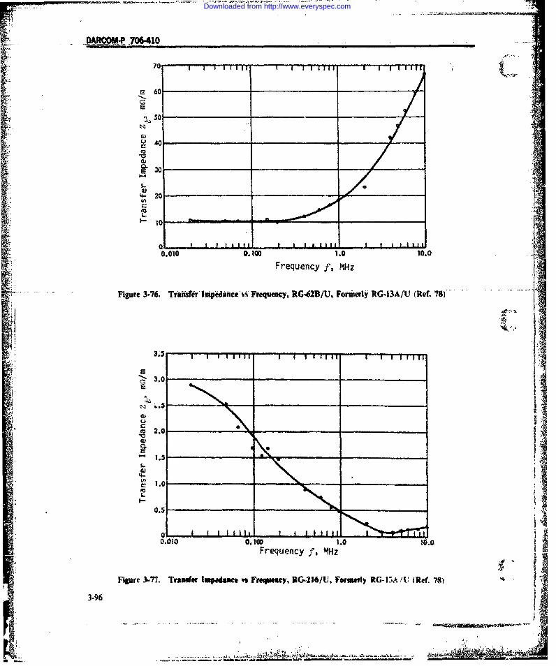
50
CU 40
S30
S.-.
olooio . o
SFrequency f, MHz'o-
I III
_____3,_ ___ _.......... 11
S3.0
2.0 -E
tA 1.0.
0.010 0.100 1.0 1.0Frequency f, MHz
Figure 3-7. Transer impase v Frequsay, RG-IE6/U, Forl IG-., '/t: (Re(. 78)
3-96
.AA 2j.
Downloaded from http://www.everyspec.com

-COP 70640
(7.0 1 1 1 i t I IiII - -rT
E6.0
~5.0
U ________ _______r- 4.0
E- 3.0
'U1.0
0. L III-I ...........J.1..±...L
0.010 G.101.0 10.0 IFrequency fMHz
'figure 34. TrausferIipedance-vs-FrequenyRG-S8-A/U Tdax-4Ref.--78)
~25
0
0
r.
A-1 i -I_1_-__1_1
01
Frequency f, MHz
Fig.. 3.79. Trnmar Iumpeiuc vs Freqme RG'12/U Armored (armr floating) (Ref. 78)
3-97
Downloaded from http://www.everyspec.com

OARCMP 706-410
6.0 1 1T11 1 f 4 1 111T II
1E
5.0
0
w 3.0
a)2.4-
1.0
0.010 0.100 1.0 10.0Frequency fMHz
Figure 340. Transfer Impedance vs Frequency, RG- 12/U- Armored (armor bonded to cable shield at ends)
(Ref. 78)E~
de
(A) Length of cable X/2 (13) Length of cable 5X/2
Figure 3-81. Patterns for Field from Leakage Currents (eaU.k in z-direeiios) Uter. 80)
3.98
................................
Downloaded from http://www.everyspec.com
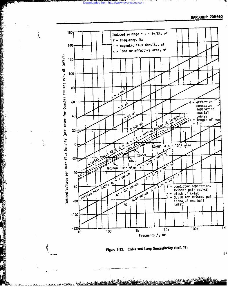
DAUCOUP 706410
160 ~Induced voltage V 1fA i
f = frequency. Hz140 B = magnetic flux density, IJ
A -loop or effective area, mn2
-~120
* 100 - - - - -
60 effectivecondutorseparationcoaxial
0
-;.t~ length of run
20
4A
S-0 tId ar abe
-100 -100k0I
ree59 PodH
Mlri 3-20 CSr'dLo Ssetbht (~f 5 .
Downloaded from http://www.everyspec.com

DAROOMP 7*4xo,
r ----...L
Z, C 'Z
C - El
Z3 CbEZ, .+ b , _ _
Ct /(C +.e 4. i :fr IetI Ctolu
C
i) Log Frequency
Irlp m 34 ,. Fr eque w D e m e of V oltag R to fo r E lectric C o pli ng!!(See Fitl. 3.-0 fer delotio of C + C,) (Ref. 81)
by the emitter tosentbis that of a plant wave, but tk radiating objects. The radiating properties of ob*ecs U.field components fall off inversely as the distance of finite size can be synthesized from assemblies offrom the source. The presence of the suswptor pro- such dipoles,duces negligi'ale reaction on the emitter.
The treatment here is based upon antenna theory, 3-$.2.1.1 Th Mapefic V4*kl,because devices which a're e itting or receiving Equations for the field of aot infinitts$tmal mag-
energy by "radiation" arc acting asentially as anten- netic dipole, as a function of diic from the di-nas. An equipment cabinet at a fte;pm,-y at wbieh its pole are given in Eqs MU1 , par. 3-3.1.1.1. Specificlength is a multitk o! a quarter wa length ha' the components of then fields vary inveriialy with the ds
is intentionally 4esilgned for th pu-pO . The magnitudes of the several component~s of any onefield vector are equal to a distance of i ,- ,/(2jr), at
+3 -3.2.1 The Ehowsla, D*pe& -dse distances, in the reactive near field region(**,The elcmentary €!a rc Rr.d _,nwtic dipohe may C fy), the (1'/r . and (l/r)I terms are dominant;.
ifbe considrre to be the prototypes for all a nterab or at grae distances in the ",'diation" fSeld. the I /P
': 3-1{0
'U6
-_ ). : \a,++L " i
....... . , , ' ,: .... , +.." " : . , . ..,/. .": :i • +, ,. ,
Downloaded from http://www.everyspec.com

D ARCOMP 701"4J_
A
R1
T
EG R2G
ELECTRIC MAGNETIC
COMPONENT COMPONENT
ERIR R 21 [ X1M 2O
E2 -k- 2G 2 K fjC [R +% RJ
E21. ____ R,] _____ 12L 1E0 1.i+R0 X] R+ R RG+ R2L L~
R R2L. 2G
2 L 2
Figure 3-85. Circuit OWd Equttens Represettg Electric Coupling and Magneiec Coupling BetweenParallel Lines (Ref. 81)
terms are dominant. Phenomena due to the (I /)' whereterm~ were discussed in par. 3-3.1.1.1. A area of a loop (asued to consist of only a
In the radiation field single torn) carrying a current of I amperes,ml1. The product Al is the magnetic dipole
02~fi1A moment.E 31-r sinO V/mn (3-138) r distance from source, ni
4w characteristic impedance of freespace, 03
(H. sinO ,Alm (3-139) o space coordinates defined on Fig. 3-60.
3-101
Downloaded from http://www.everyspec.com

DAROMP 706410
Lfl
ci
It t
4 3 uedV
LjLL
I I I I
SJp p"~ AajsuvLJ a6! LOA
3-102
Downloaded from http://www.everyspec.com

DARCOM-P 706.410
The power density, defined as the rate of energy designed using dipole arrays for frequencies up to atflow through unit area, is obtained from the Poynting least 100 MHz, and "aperture" antennas above that.vector An aperture antenna is usually a continuous metal
o 0surface. Its properties c?.n be computed in various- ." H e ways, including representing it as an extensive dipole
"IP1 =E x HI array.Detailed properties of arrays or apertures are dis-
i ,/ 3 ) cussed in par. 5-10. One of their significant prop-= 4H2sin18Wm'(-10 erties is that of antenna gain.Antenna gain, sometimes called directive gain, is
3-3.2.1.2 The Electric Dipole the ratio of the power required at the input of aThe fields produced by an elementary electric di- reference antenna to the power supplied to the inputpolehae ien d by ey e c d of a given antenna to produce, in a given direction.e ae the same field at the same distance. When not other-
SI ' (.-Vwise specified, a stated gain is the gain in the directionE, j -- 7- + cos 9 ,V/rn of the main radiation lobe. Two types of reference
antenna have been used in the past: (1) the half-wavedipole, and (2) the isotropic radiator. The first has
"A.& r 022 f -)- + sinO0, 1(3-141) been used primarily at frequen.ies where dipole typesare prevalent. The second is commonly used for
V/m antennas operated in the microwave region of the
Il'Ispectrum. Even though it cannot be realized in prac-H, - + j sin A-/m ... tice, the-isotropic-antenna is a-convenient referene,
4. \r J and is used in this handbook. An alternate term usedwhreto express the same property is effective aperture. Thewer n c p noteeffective aperture Aff is given in terms of the gain G .-• ." ° F . F fir and O components of the electric field,
respectively, V/m byH. - angular component of magnetic field, A/rn
I - dipole current, assumed in direction of = i(3-143)8-axis (Fig. 3-60), A 414
I = dipole length, assumed small comparedwith rand located at origin of coordinates, This usually is given for the maximum gain; i.e.,m G-Gmoi
w = angular frequency, It is customary to define the boundary separatingand other terms are as defined in par. 3-3 .1-.1, Eq. the Fresnel (close) and Fraunhofer (far) regions of an3-113. antenna as
From these relations, the Poynting vector yields
2D1PD F a ,,,Hazr sin2 ,W/ml (3-142)
whereIn this field region, the main factor that distin- r = distance measured from the antenna whose
guishes different emitters is their radiation pattern, greatest dimension normal to the direction of rThe equations for the infinitesimal dipole can be used is D.for finite size dipoles if their dimensions are sub- It is only at locations in the Fraunhofer region thatstantially less than a quarter wave length. one can count on the electromagnetic field compo-
nent magnitudes (E and H) varying inversely with the3-3.2.2 Antenna Gain distance from the antenna. For an aperture antenna
As the frequency increases, the relative size of any in the microwave region, the critical distance can begiven object increases when measured in terms of hundreds or even thousands of meters, whereas forwavelengths. In general, as the size increases in this an elementary dipole it is effectively X/6.way the possible radiation patterns become more In the Fraunhofer region, the electric field strengcomplex. To obtain directivity, antennas usually are at a distance r from a lossless antenna with gain t4
3-103
Downloaded from http://www.everyspec.com
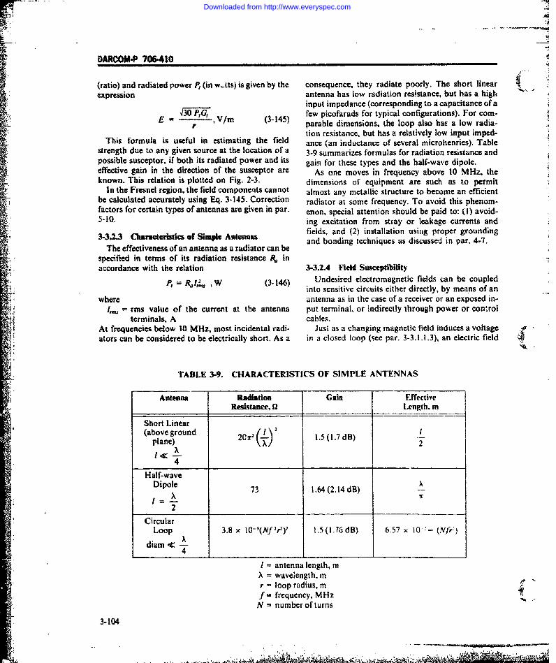
DARCM-P 706-410
(ratio) and radiated power P (in w-tts) is given by the consequence, they radiate poorly. The short linearL expression antenna has low radiation resistance, but has a high "
input impedance (corresponding to a capacitance of a430 PG, few picofarads for typical configurations). For com-
E - V/r (3-145) parable dimensions, the loop also has a low radia-tion resistance, but has a relatively low input imped-
This formula is useful in estimating the field ance (an inductance of several microhenries). Tablestrength due to any given source at the location of a 3-9 summarizes formulas for radiation resistance andII possible susccptor, if both its radiated power and its gain for these types and the half-wave dipole.effective gain in the direction of the susceptor are As one moves in frequency above 10 MHz. theknown. This relation is plotted on Fig. 2-3. dimensions of equipment are such as to permit
In the Fresnel region, the field components cannot almost any metallic structure to become an efficientbe calculated accurately using Eq. 3-145. Correction radiator at some frequency. To avoid this phenom-factors for certain types of antennas are given in par. enon, special attention should be paid to: (1) avoid-5-10. ing excitation from stray or leakage currents and
fields, and (2) installation usin~g proper grounding3-3.2.3 CharacteristIc of Simple Antennas and bonding techniques as discussed in par. 4-7.
The effectiveness of an antenna as a radiator can bespecified in terms of its radiation resistance R inaccordance with the relation 3-32.4 Field Susceptibility
P, R. ,W ( ) Undesired electromagnetic fields can be coupledinto sensitive circuits either directly, by means of an
where antenna as in the case of a receiver or an exposed in-,, = rms value of the current at the antenna put terminal, or indirectly through power or control
terminals, A cables.At frequencies below 10 MHz, most incidental radi- Just as a changing magnetic field induces a voltage .0
ators can be considered to be electrically short. As a in a closed loop (see par. 3-3.1.1.3), an electric field
TABLE 3-9. CHARACTERISTICS OF SIMPLE ANTENNAS
Antenna Radiation Gain EffectiveResistance, Q Length. m
Short Linear(above ground 21 I
plane) (1.7 dB) 2
4
Half-waveDipole 73 1.64 (2.14 dB)
2Circular
Loop 3.8 x 10-(Nf2r)1 1.5(1.76dB) 6.57 x1-- (Nfr-: )
diam < -4
I = antenna length, mX = wavelength, mr = loop radius, mf = frequency, MHz -N = number of turns
3.104
- aw u ._ - • , . • .. . . :
Downloaded from http://www.everyspec.com

IOAMCOM 7M410
will induce a voltage in an exposed metallic conduc. -30tor. The effective length of the conductor is defined asthe ratio of the open circuit voltage appearing at itsterminals to the component of the electric fieldparallel to its length.
Effective length is used frequently to describe ver-tical antennas over a ground plane. For lengths1, --.which are small compared with a quarter wave- a-s "length, the effective length is 1/2. This definition is o,.-- 3 -40useful at low frequencies for estimating currents
appearing on the outer surface of cabinets and cables :too ,due to external fields, but the accurate estimation of s- "L '3field susceptibility levels requires careful analysis ofthe exact configuration, including neighboring me- 0,000tallic structures. a j
Receiving antennas can also be characterized by a j, =c
gain G, applicable to the far field. Gain is a recipro- Ical property of an antenna, i.e., the gain of an anten- 05na used for receiving will be the same as when used 2o 3
00~for transmitting. At the higher frequencies where the 301 Ostructure size is comparable with, or more than, a ,_
wavelength, the power received P, can be estimated interms of the power transmitted, and the transmitter , .and receiver antenna- gains 4 and 6, (both expresse -0as ratios), respectively, by -- Go
-?go-
(4w W (3-147) ,,,
For isotropic antennas, the ratio of power received topower transmitted is. in free space,
140~~P, oT -= (3-148) Reprinted with permission from TheP, (41rr)2 -- co-y
Bell System Technical Journal, copy-
A nomograph for this relation is given on Fig. 3-87 righted by The American Telephone(Ref. 83), where the loss is given in dB. For antennas and Telegraph Company.with specified gains, the loss can be reduced by the Figure 3-87. Free Space Trnasmisnao (Ref. 83)corresponding number of dB for each antenna. Interms of effective areas, A, and A,
P, AA, (3-149) away, or its reflection coefficient is negligible. In, = M'' practice, the effects of the earth, the atmosphere, and
the ionosphere need to be considered. The treatmentwhere here is confined to phenomena of significance only
A, = effective aperture of transmitting antenna, over distances of tens of miles, so that ionosphericSm' 2and tropospheric scatter effects are ignored.
A, = effective aperture of receiving antenna, mi
3-3.2.4.2 Tramsiaulio Within Line of Sight3-3.2.4.1 Propagation Effects (Refs. 83 and 115) The presence of the ground modifies the genera-
The concept of free space transmission assumes tion and the propagation of radio waves so thiat thethat the atmosphere is perfectly uniform and nonab- received power or field strength is ordinarily less thansorbing, and that the earth is either infinitely far would be expected in free space, see Fig. 3-87. The
3-105
Downloaded from http://www.everyspec.com

r DACM-P 706-410
effect of plane earth on the propagation of radio near grazing paths. R is approximately equal to - 1,waves is given by and the factor A can be neglected provided both ~
antennas are elevated more than a wavelength aboveInduction the ground (or more than 5 to 10 wavelengths above
Fiel and sea water). Under these conditions, the effect of the"Srfc Effecndary earth is independent of polarization and ground con-
Diret Releced 'urfae Efect Of stants, and Eq. 3-150 reduces toWave Wave wave, the GroundI + Re JA + (I- R)Ae A ... (3-150) IEI 2 sin 2 , (2 h , k)
were (2 (o )pP4=free space electric field, V/rn(-11E=electric field due to a given source, V/rn
R -reflection coefficient of the groundwhrA = surfce wve' ttenatio facor.P 0 received power expected in free space,Wdimensionless More precisely, the reflection coefficient R IR I
h1 2 =antenna heights measured in same units as Fig. 3-88 (Ref. 84). The curves apply to the case of a
tewavelength and distance vertically polarized plane wave whose normal makesr itnefrom source, mi an angle 4', called the grazing angle, with the reflec-
TheparmetrsR and A vary with both polariza- ting earth's surface. The quantity n is the ratio orionandtheelectrical constants of the ground. For propagation constants of the region above the earth
%1'
4J 0.3 Ovee1.6 OW lend- 14(0
fill
c:0. 1.00 000 0.0 lilt V(~ I , 2 0
cations "Inc.i
F Fgu e w .Vauso ndv sFntin ftn (Ref. 4)
3.106
...................1 -1................... ---.- LIM W +
Downloaded from http://www.everyspec.com

.ARCOM P 706410
(taken to be empty space) and the region below the (Ref. 83). The error that can result from the use ofearth's surface. This quantity is given by this artifice does not exceed :k 3 dB, and occurs
where the actual antenna height is approximatelyn, - , - j 18 x 10-1 a/l" dimensionless (3-152) equal to the minimum effective antenna height.where Frequently the amount of clearance (or obstruc-
de c n tm i s tion) is described in terms of Fresnel zones. All pointse, = relative dielectric constant, dimensionless from which a wave could be reflected with a patha - conductivity of the reflecting region, mho/m difference of one-half wavelength from the boundaryf - frequency, Hz of the first Fresnel zone: similarly, the boundary of
The above-ground region is assumed to have , I the nth Fresnel zone consists of all points from whichand u - 0. The curves in Fig. 3-88 are plotted for the path difference is n/2 wavelengths. The nth Fres-typical values of permittivity and conductivity as nel zone clearance H. at any distance nl is given byfound in sea water and wet earth and indeed showthat for small grazing angles IRVI I and v "- 180 nYr(r )deg.
(r r, (3-154)For horizontal polarization, the reflection coe~ffi-
cient magnitude tends to be closer to one than it iswith vertical polarization and the phase shift at Although the reflection coefficient is very nearlyreflection is close to 180 deg for all conditions. equal to - I for grazing angles over smooth surfaces,
It is emphasized that the foregoing applies to un- its magnitude may be less than unity when the terrain
obstructed plane earth. Rough earth, violent seas, is rough. The classical Rayleigh criterion of rough.
and obstructions complicate the interaction causing ness indicates that specular reflection occurs whenmultiple reflections (scattering) and time variation, the phase deviations are less than about *(r/2), and
Refs. 85-88 deal with measurements and models of that the reflection coefficient R occurs when the
propagation in the presence of irregular terrain and phase deviations are less than unity when the phase
structural obstacles in an urban environment. Inone deviations are -greater than 1(1/2). In most cases this
and Akiyama (Ref. 89) report typical data of line-of- theoretical boundary between specular and diffuse
sight transmission over sea paths. reflection occurs when the variations in terrain
Eq. 3.151 is the sum of the direct and ground exceed 1/8 to 1/4 of the first Fresnel zone clearance.reflected rays. As a function of k2 , the height of the Experimental results with microwave transmission
receiver above ground, the field pattern shows an os- have shown that most practical paths are "rough",cillatory lobe structure. The first maximum occurs and ordinarily have a reflection coefficient in thewhen the difference between the direct and ground range of 0.2 to 0.4. In addition, experience has shownreflected waves is a half-wavelength. In most appli- that the reflection coefficient is a statistical problem
cations (except air to ground) the principal interest is and cannot be predicted accurately from the path
in the lower part of the first lobe; i.e., where profile (Ref. 90).A/2 < w/4. In this case, sin (A/2) w 4/2 and thetransmission loss ratio over plane earth is given by: 3-3.2.4.3 Miscellaneous Effects
P, /hjh2 Y This paragraph describes some miscellaneous1-.. 2 ;T (3-153) effects of line of sight transmission that may be im-
p, Pportant at frequencies above about I GHz. Theseeffects include variation in angles of arrival, maxi-
This relation is plotted in Fig. 3-89 (Ref. 83) for iso- mum useful antenna gain, useful bandwidth, the usetropic antennas. Fig. 3-89 is not valid when the in- of frequency or space diversity, and atmospheric ab-dicated transmission loss is less than the free space sorption.loss shown in Fig. 3-87, because this means that A is On line-of-sight paths with adequate clearance,too large for this approximation. some components of the signal may arrive with
Although the transmission loss shown in Eq. 3-153 variations in angle of arrival of as much as 0.5 dog toand in Fig. 3-89 has been derived from optical con- 0.75 deg in the vertical plane, but the variations in thecepts that are not strictly valid for antenna heights horizontal plane are less than 0.1 deg (Refs. 91 andless than a few wavelengths, approximate results can 92). Consequently, if antennas with beamwidths less
4 be obtained for lower heights 6y using h, (or 4k) as the than about 0.5 deg are used, there occasionally maylarger of either the actual antenna height, or the be some loss in received signal because most of the in.minimum effective antenna height shown in Fig. 3-90 coming energy arrives outside the antenna beam-
3-107
•.".
Downloaded from http://www.everyspec.com

I O
DAMM-1 70641
Lr4
Note: 1 Thi chrt i no vald wen te idicaed
powe isqetr hnte resac oe
efeciv eihtshw0o.5 g -0,wih
Rerned wihp5i0o rmTeB) ytmTcnclJunlby Te Mirica TeeoeadTlrphCmn.
quency~ ~ seaainnee oraeut00qecy vrain nte nl farvldiversity. ~ _10 0oj0d nens na4-mpt, the0 Whngon10lcin aecnrlig piu
fadngonfrquncis epraedbytOOto20 M z s sac dvesiy equre tatth seartin etee
M~ (ef. 3an 9).Lagr ntnns pcig s o kow, ecue heprncpl0adngi
Downloaded from http://www.everyspec.com

DARCOMIP 706-410 i1000- - -
800 - - _ _ _-
600 - -- - -1
400 I --- -
VerticalPolarization
100/
60 * - _ _ _ _
G God Soil
c0.02 mnho/m Sea Water
* 6 P~oarizaonl -
0.00
10 20 40 60 100 200 400 600 '1000
Frequency fMHzReprinted with permission from The Bell S stem Technical Journal,copyrighted by The American Telephone and Telegraph Company.
Figure 3-90. Minimum Effective Antenna Height 3.109
Downloaded from http://www.everyspec.com

DARCOM-P 706410
caused by multipath variations in the atmosphere. whereHowever, adequate diversity usually can be achieved a = true radius of earth, mwith a vertical separation of 100 to 200 wavelengths. df,At frequencies above 5 to 10 GHz, the presence of = rate of change of relative dielectric constant
rain, snow, or fog introduces an absorption in the at- with heightmosphere which depends on the amount of moisture Under certain atmospheric conditions the dielec-and on the frequency. During a rain of cloudburst tric constant may increase (0 < k,/a < 1) over aproportions, the attenuation at 10 GHz may reach reasonable height, thereby causing the waves in this3.1 dB/km and at 25 GHz it may be in excess of 15.5 region to bend away from the earth. Since the earth'sI dB/km (Ref. 95). in addition to the effect of rainfall, radius is about 6371 km, a decrease in dielectric cons-some selective absorption may result from the oxygen tant of only 7.85 x 10-' per km of height results in aand water vapor in the atmosphere. The first absorp, value ofk, = 4/3 which is commonly assumed to be ation peak due to water vapor occurs at about 24 good average value (Ref. 96). When the dielectricGHz, and the first absorption peak for oxygen occurs constant decreases about four times as rapidly, or byat about 60 GHz. about 3.1 x 10-' per km of height, the value of
, - -, Under such a condition, as far as propaga.3-3.2.5 Tropospheric Transmission Beyond tion is concerned, the earth then can be considered
Line of Sight flat, since any ray that starts parallel to the earth willThough the scope of this handbook limits the remain parallel.
region of concern around potential sources and When the dielectric constant decreases more rapid-receptors to the order of 10 miles, beyond line-of- ly than 3.1 x 10-' per km of height, radio waves thatsight transmission is of significance in this region. arc radiated parallel to, or at an angle above theThe distance to the horizon for an antenna 20 m off earth's surface, may be bent downward sufficiently tothe ground is about 10 mi. Furthermore, the direct be reflected from the earth. After reflection, the ray ispath between relatively close sources and receptors again bent toward the earth, and the electromagneticoften is obscured by buildings, hills, and other energy appears to be trapped in a duct or waveguideobstacles, between the earth and the maximum height of the '2
Energy can be transmitted beyond the line of sight wave path. This phenomenon is variously known asby three principal phenomena: reflection, refraction, trapping, duct transmission, anomalous propag,.and diffraction. The reflection mechanism of greatest tion, or guided propagation (Re;s. 97 and 98).significance for beyond-the-horizon-transmission is Duct transmission is important because it canionospheric reflection. This mechanism, which is cause long distance interference Mith another stationeffective at HF frequencies and below, is used mainly operating on the same frequency. however, it doesfor long distance transmission. Reflections from not occur often enough nor can its occurrence be pre-extended conductive surfaces at close range are also dicted with enough accuracy to make it useful forimportant, but the mechanism is essentially the same communication services requiring high reliability.as that covered in par. 3-3.2.4.2 (the ground reflected An important mechanism of beyond-the-horizonwave), transmission at VHF and above is that of tropo-
spheric scatter (Refs. 99 and 100). The phenomenon3-3.2.5.1 Refraction described earlier in this paragraph is based on a
The dielectric constant of the atmonphere normally smooth variation of refractive index with altitude. Itdecreases gradually with increasing altitude. The generally is believed that there are irregular spatialresult is that the velocity of transmission increases and temporal variations of refractive index ;n the at-with the height above the ground and, on the average, moaphere which have the effect of multiple reflectingthe electromagnetic energy is bent or refracted or refracting bodies turning back some of the im-toward the earth. Provided the change in dielectric pinging energy to earth. The mechanism is used forconstant is linear with height, the net effect of refrac- long-range transmission, usually exceeding 50 mi andtion is the same as if the waves continued to travel in extending to about 700 mi.a straight line but over an earth whose modifiedradius k, is 3-3.2.5.2 Diffraction Over a Smooth Spherical
Earth and Ridgeska da , m (3-155) As an object passes between a source and receiver
+ - so as to interrupt the direct path between them, a2 dh radio signal at the receiver does not immediately drop
3-110
Downloaded from http://www.everyspec.com

DARCOUMP 706"410
'" to zero because of the phenomenon of diffraction. Fig. 3-92 gives the loss relative to free-space trans-The magnitude of the loss caused by the obstruction mission (and hence is used with Fig. 3-87) as a func-increases as either the distance of separation or the tion of three distances: r, is the distance to the hori-frequency is increased, and it depends to some extent zon from the lower antenna, r2 is the distance to theon the antenna height (Ref, 101). The loss resulting horizon from the higher antenna, and P is thefrom the curvature of the earth is indicated by Fig. 3- distance beyond the line-of-sight. In other words, the91 (Ref. 83) as long as neither antenna is higher than total distance between antennas is r = r + t + r3.
the limiting value shown at the top of the chart. This The distance to the horizon over smooth earth isloss is in addition to the transmission loss over the given byplane earth obtained from Fig, 3-49.
When either antenna is as much as twice as high as r1.2 k h , m (3-156)the limiting value shown on Fig. 3-91, this method ofcorrecting for the curvature of the earth indicates a whereloss that is too great by about 2 dB, with the error in- h1,2 - appropriate antenna height. mcreasing as the antenna height increases. An alter- k - effective earth's radius,m
nate method of determining the effect of the earth's The preceding discussion assumes that the earth iscurvature is given by Fig. 3-92 (Ref. 83). This method a perfectly smooth sphere, since the results areis approximately correct for any anLenna height, but critically dependent on a smooth surface and a uni-it is theoretically limited in distance to points at or form atmosphere. The modification in these resultsbeyond line-of-sight, assuming that the curved earth caused by the presence of hills, trees, and buildings isis the only obstruction, difficult or impossible to compute, but the order of
Scale ALimiting Antenna Height h, ft
50 300200 100 bo5O 10
o I
Frequency f ,MHz -.0.JOO - 0 10,00
Woo 0-
oo C. " " .. 10.:
o0 -0 loa d ,
I100 - ~ I
sot . 1loot 100 j..- ,
~Reprinted with permission from The Bell System Technical Journal,copyrighted by The American Telephone and Telegraph Company.
F ligure 3-91. Diffraction Lou Around a Perfect Sphere (Ref. 83) 3- l7 0.. . . . .
do- :5 L
Downloaded from http://www.everyspec.com

DARCOM.P 706410
rI r2
LOSS RELATIVE "tO FREE SPACE .L1L2L3 l85+.56s1d 30--24 2
28- -22-20
.I25 ,5 I
- .20 "1-0.... ._
200 3 200 2401
-5~ 22 300 2 -5
_. Reprinted with permission from The Bell System Technical Journal,
" copyrighted by The American Telephone and Telegraph Company.
:-0
~~Figure 3-92. Diffraction Loss Relative to Free Space Transmission at All Locations Beyond Line-of-sight !00 2XOver a Smooth Sphere (Ref. 83)
magnitude of these effects may be obtained from a diffraction calculation is substantially independent of ii consideration of the other extreme case, which is a polarization provided the distance from the edge is[ propagation over a perfectly absorbing knife edge. more than a few wavelengths.
The diffraction of plane waves over a knife edge or At grazing incidence, the expected loss over a ridgescreen causes a shadow loss whose magnitude is is 6 dB (Fig. 3-93), while over a smooth sphericalIshown on Fig. 3-93 (Ref. 83). The height of the ob- earth (Fig. 3-92) indicates a loss of about 20 dB.struction h is measured from the line joining the two More accurate results in the vicinity of the horizonantennas to the top of the ridge. It will be noted that can be obtained by expressing radio transmission inthe shadow loss approaches 6 dB as h approaches 0 terms of path clearance measured in Fresnel zones as"(grazing incidence), and that it increases with in- shown in Fig. 3-94 (Ref. 115). In this representation
*creasingly positive values oF ii. When the direct ray the plane earth theory and the ridge diffraction canclears the obstruction, h is negative; and the shadow be represented by' single lines, but the smooth sphereloss approaches 0 dB in an oscillatory manner as the theory requires a family of curves with a parameter
clearance is increased. In othea words, a substantial M that depends primarily on antenna heights and Crc- s
clearance is required over line-of-sight paths in order quency. The big difference in the losses predicted byIto obtain "free-space" transmission. The knife-edge diffraction around a perfect sphere and by dif-3.112
a -. -- .'
Downloaded from http://www.everyspec.com

DARCOMUP 706410
ANTZ' . ANT
50 4-835020 5000 3-9
-,0 -3000 2- -O
2 -1450 30- -1.2- -o- 7.=0-3o :so- . I00 _20 50'05 4Z -
~200OQ3-* 10 0
200- 0 30,0WIt -0
)i 20- -1-410 40
.4 Note:;: ,When occrocy gjreter tn 50,, .+1 1.5 dS is required ,volues
:: ;on the r, scale should be:
Reprinted with permission from The Bell System Technical Journal,copyrighted by The American Telephone and Telegraph Company.
Figure 3-93. Knife-edge Diffraction Loss Relative to Free Space (Ref. V)
fraction over a knife-edge indicates that diffraction difference in elevation between the bottom of the
losses denend critically on the assumed type of pro- valley and the elevation necessary to obtain line offile. A suitable solution for the intermediate problem sight from the transmitting antenna. The right handof diffraction over a rough earth has not yet been ob- scale of Fig. 3-95 indicates the additional loss abovetained, that expected over plane earth. Both the median loss
and the difference between the median and the 103-3.2.5.3 Effects of Nearby Hills - Particularly on percent values are shown. For example, with vars-Short Paths tions in terrain of 152 m (500 ft), the estimated me-
The experimental results on the effects of hills in- dian shadow loss at 450 MHz is about 20 dB, and thedicate that the shadow losses increase with the fre- shadow loss exceeded in only 10 percent of the possi-quency and with the roughness of the terrain (Ref. ble locations between points A and B is about102). 20 + 15 - 35 dB. This analysis is based on large-, shown on Fig. 3-95 (Ref 115). The roughness of the the standing wave effects which sometimes cause the
A summary of the available empirical data is scale variations in field strength, and does not include
terrain is represented by the height h shown on the field strength to vary considerably within a few centi-profile at the top of the chart. This height is the meters.
3-113
....... "..-. .. . . .. ..-. " -. i " ...... .........-. . . - - . . . -
Downloaded from http://www.everyspec.com
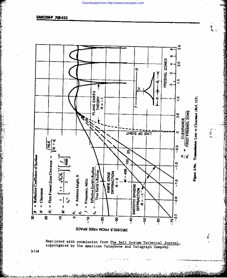
DACMP706.410
IIz
cc
W1 WC; 0
z w< 40
.3DI N1O 3N11 _j
- ~ INIHc
io GEi
a ai 1
3-11.
CO- -? ~C
Downloaded from http://www.everyspec.com

MY Tronsmitting
Antenna
tt
-50 S_181I 00
10000 -5
-020700°- 50 U)
-314. ID- -7150 -1 400-.,. _2WI0 O--.. o 3-00- X7 -'2
IO0- - :0005" O=
70-- -25
" $50" 20--30
*Referred to PlaneEarth Volues
Reprinted with permission from The Bell System Technical Journal,copyrighted by The American Telephone and Telegraph Company.
Figure 3-93. Field Intensity for Vertical Polarization Over Sea Water for l-kW Radiated Power from aGrounded Whip Antenna as a Function of Roughness of Terrain (Ref. 115)
3-3.2.5.4 Effects of Buildings and Trees thick trees and is below tree-top level, the averageloss at 30 MHz is usually 2 or 3 dB for vertical polar.
The shadow losses resulting from build.ngs and ization, and negligible with horizontal polarization.trees follow somewhat different laws from those However, large and rapid variations in the receivedcaused by hills. Buildings may be more transparent to field strength may exist within a small area, resultingradio waves than the solid earth, and ordinarily there from the standing-wave pattern set up by reflectionsis much more back scatter in urban areas than in from trees located at a distance of several wave.open country. Both of these factors tend to reduce the lengths from the antenna. Consequently, severalshadow losses caused by the buildings but, on the near-by locations should be investigated for bestother hand, the angles of diffraction over or around results. At 100 MHz the average loss from surround-the buildings are usually greater than for natural ing trees may be 5 to 10 dB for vertical polarizationterrain. and 2 or 3 dB for horizontal polarization. The tree
Typical values of attenuation through a brick wail losses continue to increase as the frequency increases,are from 2 to 5 dB at 30 MHz and 10 to 40 dB at 3 and above 300 to 500 MHz they tend to be indepen-GHz, depending on whether the wall is dry or wet. At dent of the type of polarization. Above I GHz, treesfrequencies in the UHF range, attenuation near win- that are thick enough to block vision are roughlydows can be quite negligible, equivalent to a solid obstruction of the same overall
When an antenna is surrounded by moderately size.
3-115
...- ,., .. .. ... .. . . . . . .. ,,, .
Downloaded from http://www.everyspec.com

DARcM-P 7064103-3.2.6 Medium and Low Frequency Gromn Wave approach zero and R approaches - I) and the mag- -
Trsmisdsion nitude of the third term becomesWherever the antenna heights are small compared 41rh -
with the wavelength, the received field strength is or- ( - R)A 1 _,2_._\ (3-159)dinarily stronger with vertical polarization than with _.
horizontal, and is stronger over sea water than over AI poor soil. In these cases the "surface wave" term in whereEq. 3-150 cannot be neglected. This use of the term = minimum effective antenna height shown in j"surface wave" follows Norton's usage and is not Fig. 3-90equivalent to the Sommerfeld or Zenneck "surface~w aves . - IrzThe parameter A is the plane earth attenuation fac. I jtor for ant.inas at ground level. It depends upon the z - as defined for Eq. 3-157frequency, ground constants, and type of polariza- The surface wave term arises because the earth istion. It is never greater than unity, and decreases with not a perfect reflector. Some energy is transmittedincreasing distance and frequency, as indicated by the into the ground and sets up ground currents which
following approximate equation (Ref. 83 and 103): are distorted relative to what would have been thecase in an ideal perfectly reflecting surface. The sur-face wave is defined as the vertical electric field for
A , dlss (3-157) vertical polarization, or the horizontal electric field2wd for horizontal polarization which is associated with
X (the extra components of the ground currents causedby lack of perfect reflection. Another component of
where iplarizationisn the irectio ofropagsoiatittho un. ....... ...the electric field associated with the -ground currentsij.,where is in the direction of propagation. It accounts for the ,
success of the wave antenna at lower frequencies, but1,7z = .for vertical polarization it is always smaller in magnitude than the surface "'-
CO wave as previously defined. The components of theelectric vector in three mutually perpendicular coor-
z - .e, - cos 9 , for horizontal polarization dinates are given by Norton (Ref. 105).
= j - J60r In addition to the effect of the earth on the propa-6 = angle between reflected ray and the ground, gation of radio waves, the presence of the ground also= 0 "or antennas at ground level, deg may affect the impedance of low antennas, and there.
e = dielectric constant of the ground relative to by may have an effect on the generation and recep-
unity in free space tion of radio waves (Ref. 104). As the antenna height
a - conductivity of the ground, mho/m varies, the impedance oscillates around the free spaceSwavelength, m value, but the variations in impedance are usually un-
d = distance from source, m important provided that the center of the antenna is
In terms of these same parameters, the reflection mote than a quarter-wavelength above the ground.
coefficient R of the ground is given by (Ref. 104). For vertical grounded antennas (such as are used instandard AM broadcasting) the impedance isdoubled and the net effect is that the maximum field
sine - Z strength is 3 dB above the free space value instead ofR - sin + z ,dimensionless (3-158) 6 dB as indicated in Eq. 3-151 for elevated antennas.sin 0 + z Typical values of the field strength to be expected
from a grounded quarter-wave vertical antenna areWhen sin 0 <1zI, the reflection coefficient ap- shown in Fig. 3-96 for transmission over poor soil,proaches - I; when sin 9 z I (which can happen and in Fig. 3-97 for transmission over sea water.only with vertical polarization), the reflection coeffi- These charts include the effect of diffraction andcient approaches + I. The angle for which the reflec- average refraction around a smooth spherical earthtian coeffcient is a minimum called the pseudo- as discussed in par. 3-3.2.5. but do not include theBrewster angle, and it occurs for sin 0 - I z I. ionospheric effects. The increase in signal obtained
For antennas approaching ground level the first by raising either antenna height is shown in Fig. 3-98 ""
two terms in Eq. 3-150 cancel each other (hi and h2 for poor soil, and in Fig. 3-99 for sea water.
3-116
. .. .. . • .. , ' . .~~~ ~~~~~~" . : . ,. -. -. " . ." . . - - . "
Downloaded from http://www.everyspec.com

DARCOtA'P 706410
60I8 ODIEw( eDitace m
Figue 3-. Feld ntesityforVertcalPolarization Over Poor- Soil for- I-IW Radiated Power from-
ReprntedwithGrounded Whip AntenaRepintd wthpermission from The Bell. System TcnclJunl
co~pyrighted bv The American Telejione and Telegraph Company.
IGO
48
Grouded hip nte NA
Ditace m
Fiue39.Fel nest o Vria oaiato vrSaWte o -WRdatdPwrfoC
3-O1
0-. ~ -
Downloaded from http://www.everyspec.com

DARCOM-P 706-410
bo a)
1EEI
X t Antenna Heicjht. ft
SFigure )-98. Antenna Height Gain Factor for Vertical Polarization Over Poor SoilOs-'
4.~ ~ L.-X-I..-a10"z -
I
AtnaHeiqht, ft* Figure 3-99. Antenna Height Gain Factor for Vertical Polarization Over Sea Water
3-3.3 CONDUCTVE COUPLING Signal line copigcanocuintomds
3-3.3.1 Introduction known as differential and common modes. In the dif-
In concept, direct or conductive coupling paths are coupled into the signal line directly from the circuit toreadily modeled in terms or a simple coupled circuit whicn it connects, and is poaae ln h ieias shown in Fig. 3-100 (Ref. 106). These coupling a manner similar to that of the desired signal. Corn-paths may exist in a variety of forms, especially in mon mode coupling, which is discussed in par. 3-complex circuits: however. it is convenient to identi- 3.3.3. can occur wherever circuits which are inter-2fy three types: connected by a signal cable are at different referernce
a. Common power supplies potentials. This mode of coupling is quite similar tob. Common ground return paths that classified as common ground return path cou-c. Signal lines. pling, which is discussed in par. 3-3.4.
3-118
-- . .....
Downloaded from http://www.everyspec.com

DARCOM-P 70410 .
Coupling through a common power supply is power line system, a standard single-phase, three-probably the most common form of conductive wire, 60-Hz, power line with switching and protec-coupling. Usually it occurs between equipments tive circuits; and the susceptor, an equipment whosethrough ac or dc main power lines, or between cir- performance may be degraded by the interferencecults in the same equipment through a common cce- from the source. ..
- tronic rectifier dc power source. In the latter case, the There are several features of this diagram thatmodel of Fig. 3-101 (Ref. 106) applies, and the cou- should be noted:piing impedance is the output impedance of the sup- a. The square blocks represent cabinets. In effect,ply. Methods of calculating the coupling and of the presence of a local ground plane shown on thereducing it through use of filters are discussed in par. figure requires that to represent accurately the inter-4-3.1.1.4. ference source and the susceptible device one needs a
Coupling through the main or primary ac or dc four-terminal equivalent circuit, one of the terminalspower line is the most difficult situation to analyze being the cabinet itself. If there is no direct connec-because of uncertainties as to the impedances of tion between the cabinet and the ground plane, as isvarious items connected to the line, and its length. frequently the case, it is necessary to recognize thatFurthermore the line actually consists of several con- there is in effect at least a capacitive coupling be-ductors which may be connected in a variety of ways tween them, This coupling can play a major role in :
at the distribution transformer. For these reasons it the interference properties of either a source or a can be treated properly only from a statistical ap- susceptor.proach. b. The power line system itself may or may not at-
tenuate signals coupled through it, depending upon3-33.2 Powerline Coupling the frequency and the ways in which the source andA general model of.power line conducted interfer- susceptor are connected. Although connecting the
ence is shown in Fig. 3-100. In this figurethe inter- ",sc-ipfible deviceto-the-poweriine system-can affectference source represents an equipment which gener- the impedance seen by the interference source, in in-ii iates undesired signals (interference) on the line-, the dividual cases, it is best considered as having little
Hiqh High[i, :: = - '[ . ... iqLow " '' Power --Hiw Susc..... ....
Interference .Lo . Line Low SuscentibleSource Safety (Ground) System Ground Device
7Ground Plane
Figure 3-100. Power Line Conducted Interference Model (Ref. 1061
High
Interfer- Low Powerence LineSource Safety (Ground) System
7 /7/77777/7/ Ground Plane
Figure 3-101. Model of Interference Source and Its Load (Ref. 106)
3-119------------------------- - -~-i
Downloaded from http://www.everyspec.com

DARCOMP 706410
effect in a statistical sense. That is, the average im- system. At intermediate frequencies a transition re-pedance as seen by the interference source is assumed gion must be recognized in passing from one modelindependent of the connection of the susceptor.* to the other.
c, For most circuits, at frequencies below about 10Hz, the low and safety ground lines can be consid- 3-3.3.2.1 Source and Line Models
. ered to be connected together, and indeed connected For the purpose of analyzing the spurious voltageto the cabinet. At interference sources and suscep- output impressed on the line by the interferencetors, usually the safety ground is connected to the source of Fig. 3-100, one considers only the sourcecabinets, effectively reducing them to three terminal and the load presented to it by the power line system,devices. At a distribution panel where the low line is as shown in Fig. 3-101.connected also to the neutral or safety line, a two-ter- .minal representation may be adequate. Oi the other 3-3.3.2.1.1 Two-terminal Representationhand, at frequencies above about 500 Hz. the imped- The source and line are represented as shown inances as seen from any of the three lines - high, low Fig. 3-102 (Ref. 106). Es and Zs are the Theveninand safety - when looking towards either the power equivalent voltage and impedance of the source, re-system, the source, or the susceptor, will be substan- spectively, at the frequency of interest, while ZL is thetially affected by the impedance of the individual con- line impedance at this frequency.ductors themselves and it is difficult to distinguish be- The power generator is not shown, but it is under.tween these lines on the basis of impedance, An exact stood in this and subsequent discussions that the in-analysis at high frequencies is extremely difficult to terference source is drawing its normal power currentcarry out because of the complexity of the equivalent from the line.circuit. Conducted emission measurement techniques pres-
Inorder to simplify the analysis-of-such-circuits, it -ertlyinuseprovide-themagnitude of the current IM.is common to approximate them in terms of their flowing from the source through a known load ZM.two-terminal characteristics. At low frequencies, each Typical techniques areof the power conductors is considered to act inde- a. Short-circuit current technique: Zm = 0pendently against a neutral if one exists; otherwise, b. Line impedance stabilization network tech.they are considered to act against each other. At fre- nique (Refs. 107 to 109).queicies above about 10 MHz, each of the line con- The ratio of the voltage appearing across the ter-ductors can be considered to act against the cabinet minals of a susceptible device connected to a line ofin the case of a source or susceptor, or against the impedance Z, to the current through an impedanceground plane in the case of the power distribution ZU is
This assumption may not be accurate in certain cases, for exam- vzpie. if the succeptor has a power line input filter containing Z_-capacitors which may dominate the line impedance In a specific L I I Z (3-160)frequency range. -4$
High 'IPower
Interference + LineSource
SSystem
- ~Low-G nid-G. P. - -
Figure 3-102. Two-terminal Representation
3-120
,. .. . ..... ..
Downloaded from http://www.everyspec.com

DARCOM-P 706-410
Thus if ZM matches the line impedance, the volt- whereage measured across ZM is equal to the voltage that b > -Ithe susceptible device will experience. c > 0
Typical values of line impedance as a function of F(b + I) - gamma functionfrequency are shown in Fig. 3-103 (Ref. 110). Theseparate curves are for different outlets in a labora. btory where the measurements were made between the r(b + 1) =,,to y e-'dy b r(b) (3-162)line conductor and earth (presumably the safetyground). This figure shows that the impedance at fre- The mean M, and variance a' of this distribution arequencies below about 200 kHz increases finearly with X
frequency as would be simulated by an inductance.Above about 500 kHz the impedance oscillated above + )and below a nominal value of about 50 9. (x = (3-163)
Other measurements have been made which showsimilar results. The solid curve on Fig. 3-103 corre- Var(x) ax, (3-164)sponds to an inductance of about 30 AH. EvidenceII. indicates that most power circuits have equivalent in-ductances ranging from about 20 AH to 50 pH, with wherethe lower values for those with the higher current rat- o. standard deviation of x
ings and the higher values typical for the home and Solving for b, an we findoffice or small laboratory. .~~b =\l'- I(3-165)
3-3.3.2.1.2 Statistical ApproachFig. 3-103 shows that, as a practical matter, it is c (3-166)
not possible to know the exact impedance of the lineto which a given source will be connected, especially The function f(x) may be fit to any set of resistancesince the impedance measured at any frequency and.. data by computing the data mean and standard de-at any given time can be modified substantially by the viation, and thence b and c from Eqs. 3-165 and 3-connection of any additional device to the line in the 166, respectively,vicinity of the point of measurement. Thus the Typically, the resistance data are found to have aprediction of the current or voltage produced by a standard deviation greater than the mean, i.e., thegiven source can be determined only in a statistical data have a large spread, with most of the values con-sense. In setting a limit for the current measured from centrated at the low end. Therefore, the appropriatea given source, one selects a value which insures that form of the assumed distribution is the curve in Fig.when the source is connected to a potentially sus- 3-104 for b < 0 or m < o. , viz., the one having aceptible load (receiver), its susceptibility threshold is vertical asymptote at zero.likely to be exceeded by more than a given proba-bility, say, one or two percent. To do this one musthave statistical data on the values of impedances like-ly to be experienced. Resistance and reactive compo- 3.3.3.2,1.4 Reactance Distributionnents are discussed separately. Since reactance is equally likely to be positive or
negative, at least at frequencies above about 1 MHz,a suitable distribution is one that is symmetrical
3-3.3.2.1.3 Resistance Distribution about its mean value. The Gaussian density func-A two-parameter, one-sided distribution which tion, which has a good fit with experimental data, is
seems to be suitable for a wide variety of data is the shown in Fig. 3-105 (Ref. 106) and given bygamma density, shown in Fig. 3-104 (Ref. 106), and Igiven by f(x) exp[ - (x - (3-167)
IM 0 ,forx < 0 Values of m and . determined from the react-f(x) C I e forx > 0 (3-161) ance data may be substituted directly into Eq. 3-167
r(b + I) to obtain the assumed distribution for reactance.
3.121
Downloaded from http://www.everyspec.com

DARCOM-P 706-410
Main RejectionFilters
SignalI Generator
Cicut 5o esi Reeivrs
1 00
N,
0.10.1 1 1FreQuency fMHz
Figure 3-103. Impedance Between Live and Earth Connectioos at Ring Main Sockets in ERA Laboratory{(Measurements made sit four suitably disposed points In the building.)
3-122
Downloaded from http://www.everyspec.com

v .............. I
DARCOMP 706410 -
f 1. b > 0; m >> a
2. b > Os m >a
4. b < 0; M < 0x
-!
2]2
Figure 3-104. Gamma Probability Density bkr Several Parameter Values (Ref. 106)
f () 3-3.3.2.2 Typical Characteristics3-3.3.2.2.1 5-30 MHz
Fig. 3-106 (Ref. 106) shows the distribution for the
1 ratio defined by Eq. 3-168 for interference injectedGaussianinto the power line by various receivers when con-ii nected to the power line by power cords of both 20
cm length and 6 ft length, The 20 cm length repro-Uni formi sents the shortest possible cord length between the
power duct and the receiver. The 6 ft length repro-sents the length of a flexible cord connection, Perti-
2. nent data for this figure are:
- Average VL/IM 66.7 0Standard deviation 116.9 0Minimum computed value 1.90 0
" Maximum computed value 3970.7 0
3-3.3.2.2.2 0.4-4.9 MHzFigure 3.105. Comparison of Uniform and Gaussian Fig. 3-107 (Ref. 106) shows data 4uite similar toProbability Density Functions With Same Mean and those for both high and low lines.
Standard Deviation (Ref. 106) Separate calculations were made for the neutral orsafety ground line in this frequency range because ofits consistently low impedance values, Here the data
Typical means and standard deviations for imped- lie to the left of those for the high and low lines. Theance data in the frequency range 5.30 MHz are given lower impedance at low frequencies results from thein Table 3-10 (Ref. 106)' These data were used to diminishing inductive impedance as frequency iscompute the statistics of I VL/1m I given by Eq. 3-160 lowered.for the short-circuit (SC) measurement case, Zu = 0,In this case, I VL/im I is simply the magnitude of theparallel combination of ZL and Zs 3-3.3.2.2.3 10 kHz to 200 kHz( V'L I, Ils z.~In this frequency range, one is almost always be-
Sc 1 I -. , (3-168) low the first maximum or "resonant" frequency ofSSC s + Ithe impedance vs frequency curve. Two conclusions
3-123
'I-
Downloaded from http://www.everyspec.com

DARCOM-P 706-410
TABLE 3-10. TYPICAL MEAN AND -STANDARD DEVIATION OF IMPEDANCES, 5-50 MHz
(Ref. 106)
_ _Resistance Reactance
Mean m,, Std. Dev. a, Mean mr, Std. Dev. a,.. ohm ohm ohm ohm
Source 25.58 44.44 - 0.95 106.60Line 27.21 36.75 42.65 66.83
are obvious: (I) the spread in values of Vj- IM on Fig. sence of a ground or return circuit, the common-3-108 is less than that for higher frequencies, and (2) mode current must be zero. The definition of com-the safety ground line curves lie considerably to the mon mode current can be extended to cables con-left of the high and low line curves. taining more than two conductors, i.e., to be the net
From each of these figures, the probability that a current (taking sign into account) carried by all con-given line voltage will be exceeded can be determined ductors. If it is other than zero there must be a returnif a specified short circuit current is measured from a path for the current - usually through a groundgiven source. For example, if the susceptibility of all return conductor or "ground plane".equipments is required to be above a certain level - The configuration of the ground return pathfor example, I V - one can determine where the lim. may have a significant effect on thq amount ofit current should be set in order that the probability common-mode current that can flow in a given con-of interference does not- exceed,-for example, 2.5%. nection. At frequencies below several hundred kHz -This statement implicitly assumes that all equipments where capacitive reactances between the cabinet ofbecome susceptible when the voltage on any of the a device and the "ground" plane may be high, the ab-conductors of the power line exceeds the specified sence of a direct connection to the ground plane canlimit. Actually, there will be a distribution of sus. reduce the common-mode current to quite smallceptibility voltages for groups of equipments on each values. For significant commrn-mode current, bothof the respective lines, even though the lowest sus- the source and the suscwiptor must be coupledceptibility on any of the three conductors may be at through fairly large carcitors such as with line toleast I V. A more exact calculation of the probability ground filters. At higher frequencies, the capacitiveof interference would have to take this distribution of reactance becomes low - and indeed since the powersusceptibility voltages into account. hne itself can be represented as an inductance to
common-mode currents, it is possible that at a givenfrequency series or parallel resonance will occur -
3.3.3.3 The Common-mode Concept and the impedance to common-mode current flowThe common-mode current is important for two will vary rapidly with frequency.
reasons: (1) it usually appears directly in a ground stxperimental data Omowiratt these effects. Thereturn path which may be shared with several circuits common-mode impedance of the power line of aand, (2) it can be a primary source of an induction receiver connected by a large ground strap to amagnetic field in the vicinity of cables on which it copper-covered test bench is shown in Fig. 3-110.exists. The relationships between common-mode These measurements were made by using a two.currents, differential-mode currents, and the actual current-probe method. In the frequency range be-line currents are explained by Fig. 3-109 (Ref. 106). tween about 800 kHz and 25 MHz, the impedance isThis shows a susceptible device B connected to a inductive, increases with frequency approximatelypower &ource A by a two-conductor cable, both linearly, and has a relatively constant phase angledevices located on a ground plane. For this system, near 90 deg. Fig. 3.111 shows a similar impedancethe common-mode current is defined by Ic - i + A, measurement in which the large ground strap waswhere the direction of the current must be taken into removed and effectively replaced by an antenna con.account and the differential-mode current, is defined nection. This antenna connection was a coaxial cable .
by ID - (I - 12)/2. The differential-mode compo- connected between the receiver and a connector, thenents of the current are equal in magnitude on the outer shell of which was conductively connected di-two conductors and in opposite directions. In the ab- rectly to the ground plane. The total length of this
3-124
, i v .. . ' - . .... .i ... . . .... .
Downloaded from http://www.everyspec.com

DARCOM*P 706410
[ 100
L POWER LINE LENGTH6rf10
POWER LINE LENGTH20 cm
10
0.0111 10 100 10
( Figure 3-106. Distribution, of VL/Iuf, 5- to 34)-MHz Typical Power Lin"s
Downloaded from http://www.everyspec.com

..... ...DARCOM-P 706-410
100
0.4 -4.9 MHz HIGH & LOW LINESI
POWER LINE LENGTH, 20 cm
100.4- 5 MHz HIGH & LOWX \LINES
POWER LINE LENGTH, 6 ft
FI Q)
-I -- -- --
0.4-4.9 MHzSAFETY GROUND LINE4
4j ~ POWER LINE LENG4TH, 20 cm 4
0
1.1
0.01t110 100 1000
Figure 3-107. Distribution of VL /'m, Typical Power Line (Ref. 106) )3-126
~ '- - - - - *&-
Downloaded from http://www.everyspec.com
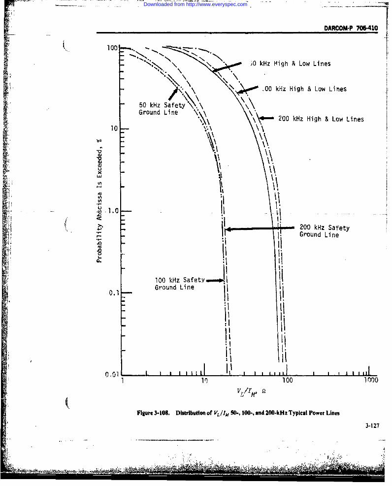
DARCOM-P 706-4101
r.....
f "- " > \ -" .0 kHz High & Low Lines
.00 kHz High & Low Lines
50 kHz Safety \\
Ground Line V\\0- 200 kHz High & Low Lines
10
° -IV
S .. .200 kHz Safety'- "Ground Line
0 II 11100 kHz Safet~y..11
0.1 Ground Line
0.1 I'-i
".ii Ii
I •'
110 100 1000
VL11te S
Figure 3-108. Distribution of VL/IM 50-, 100-, and 200-kHz Typical Power Lines
3-127
I I4
Downloaded from http://www.everyspec.com

V1
DARCOM-P 706410
r
GROUND PLANE
Common-mode Current: I C = T1 +'2 1 - 2
Differential-mode Current: = 2
Figure 3-109. Common-mode Model (Ref. 106)
lead was about 3 ft. In this frequency range the impe- In designing for electromagnetic compatibility, thedance is generally higher in Fig. 3-110 than in Fig. 3- objective is to prevent any electromagnetic field, volt-Ill, but passes through a resonance at approxi- age, or current generated or used at one point of the - -
mately 15.5 MHz. The phase angle of the impedance system from being transferred through a commonshown in Fig. 3-112 shifts from 90 deg positive to ground impedance to other units with whose opera-about 90 deg negative at the resonant frequency. The tion it could interfere. Sometimes this can beresonant impedance is of the order 50D0 Q. achieved best by segregating grounding connections
Figs. 3-113 and 3-114 show common-mode imped- among the various parts of the system. For example,ances for another receiver in the grounded and un- there may be a signal ground, a control ground, agrounded conditions. With the ground (Fig. 3-113) power ground, and a safety ground.the reactance is inductive and increases linearly withfrequency. When ungrounded, the impedance is ca- 3-3.4,2 Static and Structural Groundspacitive at low frequencies and passes through reso- Static and structural grounds include all those con-nance at about I I MHz. ductive parts of the system which are not designed es-
pecially to carry current. These parts may be me-3-3.4 GROUNDING chanical strength members and mechanical parts and3-3.4.1 General enclosures that act as static shields, cable shields,
The name "ground" originates from the use of the shafts of rotating machinery, or control shafts.term in connection with the general practice of pro- They may serve a twofold purpose: (I) to preventviding a path for the return of lightning discharge the build up of a static charge on structural members,current which could otherwise produce potentials and (2) to prevent electric fields from penetrating intohazardous to both personnel and equipment. Its use areas where they might degrade equipment perform-has been extended to include return paths and refer- ance. For the purpose of preventing static chargeence potentials for power and signal currents, from building up on structural members, all that is 3whether or not an actual connection to earth exists, required is a continuous connection to a ground ref-The basic principle is to maintain all portions of the erence plane which itself usually is connected tosystem - electrical, mechanical, or structural - at earth. This arrangement is used in lightning protec-the same reference potential by providing low-im- tion systems where the purpose is to return any dis-pedance paths at all frequencies for current returns charges to earth in such a way as to avoid high po-throughout the system. In some systems, reference tentials on any equipment since these may be haz-potential variations on the order of volts may be tol- ardous to personnel or the equipment itself. Meth-crated. In others, a few microvolts of variation may ods of obtaining good connections to earth art dis-be quite intolerable, cussed in Refs. 16 and I ll. The same techniques are
3-128
44!
Downloaded from http://www.everyspec.com

DARCO*P 7M42O
~~10 3 -
+106"
c102 +10Ono
i .i
+1010 +940O
U +96040
4a-
' 10
Impedance Phase Angle zw 90*
+850 over entire frequency range.
I0 -
0.1 1 Frequency MHz 10 102
Figure 3-110. Common-mode Impedance of Recever Bonded to Ground Plane
used where equipments or systems are exposed to the service entrance equipment, and at no other
high level radio transmitter fields which otherwise point.
could subject the equipment to high radio frequency Equipment that is powered by such a system
potentials. For the second purpose, a complete en- should have, in addition to the necessary high and
closure of the circuit to be protected is required, and low lines, a separate conductor connected to power
the structure becomes a "shield". The properties of system neutral. This conductor should not normally
shields are discussed in par. 4.6. carry current. Its presence is necessary to protect per-
sonnel and equipment in the event of a short circuit
3-3.4.3 Power System Ground to the equipment case. The grounding conductor and
In the U.S., the National Electrical Code requires associated bonds must have cross-sectional areas suf.
that the prime power system neutral be grounded at ficiently large to carry the required current.
3-129
- . ~ida
Downloaded from http://www.everyspec.com

DARCOM.P 706-410
10L-
4-i
U
10
~101
I0-1 1 1o0I2
Frequency f, MHz
Figure 3-1li. Common-mode Impedance of Receiver Grounded by Means or 3-ft Coaxial Antenna Cables
3-3.4.4 Ground Planes a. Convenience. Circuit construction can be sim-
Since the performance of electrical systems gener- plified by returning circuit elements to the nearest ap-ally is dependent on a number of related and inter- propriate point on the chassis.acting functiorn, acting in a precise way. their inter- b. Circuit efficiency. At the higher frequencies theactions must be controlled and carefully limited to lengths of leads must be short in order to keep thethose designed into it. Unintentional interactions be- self-inductance of the leads to acceptable values.tween various circuits can degrade the design per- An ideal ground plane is an equipotential surfaceformance seriously. The use of common potential having zero impedance. Practical ground planes mayplanes or ground plahes is frequently necessary for be conductive metal surfaces or a network of wires.two possible reasons: The dimensions of the ground plane can be critical if
3-130
A W ; c.....- ,-
Downloaded from http://www.everyspec.com

DARcOMP 41
+f.oo-
+80-
+60-
(' +40-
+20-
" 0
-20-
" -40-
' : " -6O
iiI -ro -
-100-
Frequency , MHz
Figure 3-112. Phase Angle of Common-mode Impedance of Receiver Connected as for Fig. 3-111
they are comparable with system wavelengths. In 3-3.44.2 Single-polnt Systemmany cases, a specific ground plane may not be easy This system is used where a ground is essential,to identify. such as to provide a power supply return where the
Circuit arrangements with respect to a ground circuits operate at frequencies such that the lengths ofplane may be of several types (Ref. I l): (1) a floating the several connections to the single tie point areground system as shown in Fig. 3-115, (2) a single- small fractions of a wavelength. This arrangementpoint ground system as is shown in Fig. 3-116, and (3) also tends to make the system performance inde-a multi-point ground system as is shown in Fig. 3- pendent of currents flowing in the ground plane.117.
3-3.4.4.3 Multipolnt System3-3.4.4.1 Floatlnf. Ground System Where the various parts of a system are physically
The floating ground is most feasible at low fre- separated by distances which are a substantial frac-quencies where the circuits can indeed be isolated, tion of a wave-length (say X/10)* of signals used byand any stray capacitance between the circuits and the system or which can couple into it, a multipointthe ground plane is sufficiently low to limit circulat- grounding system must be used. In this case a con-ing currents. The inductive coupling shown can in- tinuous conducting sheet or plane will provide thehibit such currents. To the extent that such currents lowest possible impedance path between compo-can be controlled, the system itself is not subject to nents.the quality of the ground plane. In critical cases X/50 has been recommended.
3-131
": "". .:.. ....".
Downloaded from http://www.everyspec.com

Phase Angle o, dego U (D Ll C> LIn Ln 0 n in~M~ 1 t M ,- 0ON ~ 0 t~ T
+ + c+
L.Iz
++
E[
M.I
"4 0.-q c
o I oz; 'z apnpjubeW o~uvpadwj
* 3-132
Downloaded from http://www.everyspec.com

-DARGO-P-7064Z0-
Phase Angle V, deg
o 0%00D
CII+U
CD+
t3 IzonjbW ~vaw
3-13
Downloaded from http://www.everyspec.com

.21-
DARCOMP 706410
zZ~I~i~i22U 3IGROUND PLANE
From I opics in Inler.ysIem Ekeclyoiagletir Cornpatibihifv. edited by Woodro- W- Everett. Jr. copyright (C) 1972 by Holt.
Rinehart and Winiton Inc. Reprinted by permission of l~t, Rinehart and Winson. i
Figure 3.115. Floating Ground Plane .11=2G(ROUND PLANE
From emlc I n Ers~lerf£icroagntc~l Compa~ilZtr. edited by Wkoodrow W. Everett. Jr. Copy right (C) 1912 by Holt.
Rinehart and"Winston,. Inc. Reprinted by permission of Holt. Rinehart and Winston.
............................ .. Riue3-116. Single-point Ground System
From Tnk nIntersynemf E-lectroniagfl-tic Ciompatibility, edited by Woodrow W, Evereit, Jr. Copyrighit (C) 1972 by Holt.
Rinehar nWinston, Inc. Reprinted by permission or Holt, Rinehart and Winston.
Figure 3-117. Muitipolnt Ground System
To increase the effectiveness of Multipoint 3-3.4.4.4 Balanced Coupling Circuits
grounds. each stage or unit of the system should be
wired with a single point ground as shown in Fig. 3- Fig. 3-119 (Ref. Ill1) shows the arrangement of a
118 (Ref. Il11). Thus the two stages have their own balanced coupling circuit. Current flowing in the
single-point grounds. High currents associated with loop forme~d by the signal cable and the ground will
the output stage circulate only in this stage, and do induce voltages across the twisted pair signal leads. If
not couple into the low level input, these leads are perfectly balanced, the voltages (also
In some multipoint ground systems, it may be ad- known as "common" mode voltages) on these leads
visable to cut holes or slots in the ground plane to act separately will produce equal and opposite effects in
as baffles and thus channel ground currcnts to proper the receiver, hence they tend to cancel. The circuit is
points, then said to have a high common-mode rejection
Where the circuits are separated by long distances ratio. Current in the shield of the cable can be mini-
so that cables are required for interconnection, sev- mized by connecting only one end of the shield to the
eral factors must be considered, The length of the ca. ground as shown, but then a substantial potential
ble may be such as to be resonant. If so, the cable can may appear between the end of the shield and the
act as an efficient radiator of energy; likewise, it can receiver input leads. The balance of the circuit should
receive energy radiated from some other sour-e. The also help to reduce the effects of this, however. In
possibility of such radiation can be reduced substan- particularly sensitive circuits, the balzrnce may be 0,V
tially by connecting the cable to the ground plane at a adjustable to obtain a maximum common-mode
iarge number of points, rejection.
3-134
11ip--mo
Downloaded from http://www.everyspec.com

r!
DARCOM* 7061-0
INPUT
iPUT /, I ' .I.OUTPUT
I-
From Topics in Intersystem Elecrnmnognetic Compatibility. edited by Woodrow W. Everett, Jr. Copyright (C) 1972 by Holt.Rinehart and Winston, Inc. Reprinted by permission of Holt, Rinehart and Winston,
Figure 3-118. Multipolat Ground Detail
CSOURCE
GROUN PLN --,---
From Toi ics in inters)y, vem Electromagnetic Comparbility. edited by Woodrow W. Everett, Jr. Copyright (C) 1972 by Holt,Rinehart and Winston. Inc, Reprinted by permission of Holt, Rinehart and Winston.
Figure 3-119 Balanced Coupling Circuit (Ref. III)
The use of balanced circuits can be made most REFERENCESeffective where conductive coupling is not required inthe original circuit, such as when the signal is ac, and !. A. Papoulis, Probability. Random Variables, and
atransformer coupling can be used. Even with de, a Stochastic Processes. McGraw-Hill, NY, 1965.balanced system can be used, but it may be less satis- 2. Reference Data for Radio Engineers, Fifth Edi-factory. In some cases, dc to ac inverters have been tion, Howard W. Sams & Co., Indianapolis, IN,inserted in signal circuits to avoid this difficulty. 1968.Details of common mode voltage rejection circuits 3 .World Ditribution and Characteristics of At.
and their analysis are given in Ref. 112. mospheric Radio Noise, Report 322. Interna-3-3.4.4.5 Ground Loops tional Radio Consultative Committee (CCIR),
Ground loops are most likely to arise where paral- International Telecommunication Union,lel grounds are possible because of conflicting re- Geneva, Switzerland, 1964.quirements. For example, where coaxial cable is 4. A. D. Watt and E. L. Maxwell, "Characteris-required for low loss or distortionless signal trans- tics of Atmospheric Noise from I to 100 KC",mission, the outer conductor may appear in parallel Proceedings of the IRE 45, 78784 (June 1957).with the power supply ground. The appearance of a 5. A. D. Watt, VLF Radio Engineering, Pergamonmagnetic field in the loop formed by the parallel Press, Elmsford, N.Y., 1967,grounds may result in a current induced at the 6. H. Norinder, "The Waveforms of the Electricfrequency of the magnetic field. If the magnetic field Field in Atmospherics Recorded Simultane-arises from switching or pulsed currents, it may have ously by two Distant Stations". Arkiv fra broad frequency spectrum. To reduce the effects of Geofysik Band 2. No. 9, 161.95 (Novembersuch loops, the power grounds should be run close to 1954).the signal cable, or triaxial cable may be used so that 7. G. D. McCann. "The Measurement of Light-the signal carrying portion of the cable may be insu- ning Current in Direct Strokes", Trans AIEElated from such loop currents. 63, 1157-64 (1944).
3-135
A
Downloaded from http://www.everyspec.com

DARCOM.P 706410
8. . H. Hagenguth, "Photographic Study of 22. V. Bashaw, Handbook of Electromagnetic Inter-Lightning", Trans. AIEE 66, 57785 (1947). ference, TIS 65SD230, General Electric Co.,
9. D. C. Hogg, "Problems in Low Noise Recep- Philadelphia, PA, 1965,i:tion of Mvicrowaves", IRE Trans., 5th National 23. P. W. Ellison, "Transients in an Electron-Symposium on Space Electronics and Telemetry, ics/Manufacturing Facility", IEEE Southeast-
1.11 (1960). ern EMC Symposium Record, Atlanta. GA, Oc-10. P. F. Panter, Communication Systems Design, tober 27.29, 1969, October 1969.
McGraw-Hill, NY, 1972. 24. NAVSHIPS 95938, Interference Studies, In-11. NAVAIR 5335, Electromagnetic Compatability vestigation and Tests Concerning Electric A rc-
Manual, Naval Air Systems Command. Producing Devices, Final Report, Contract12. L. A, Hartman..F. * Pogust, and S, Gitelson, NOBSR 72681, Bureau of Ships, Department of
"Precipitation Static at High Altitudes", IRE Navy, Washington, DC, November 1960.National Convention Record 7, Part 8, 114-117 25. F. Haber, J. Goldhirsh, and F. Livesey, Studies(1959). of Electromagnetic Compatibility of Equipment
13. H. M. Hucke, "Precipitation Static Interference and Systems, Progress Report No. 3, Contracton Aircraft and at Ground Stations", Proceed- NOBSR 85170, University of Pennsylvania,ings of the IRE, 3.1-16 (May 1939). Philadelphia, PA, August 1961.
14, R. L. Tanner and J. E. Nanevicz, "Radio Noise 26. F. Haber, et al, Studies of Electromagnetic ComGenerated on Aircraft Surfaces", SRI Project patibility of Equipment and Systems, Progress1267, Final Report Contract AF 33(616)-2761, Report No. I, University of Pennsylvania,
Stanford Research Institute, Menlo Park, CA, Philadel,,hia, PA. February 1961. Moe; September .1956.. 27. F. M. Livesay, Conducted Noise Source Model15. Interference Reduction Guide for Design Engi. In the VLF ae r a escent amp.........
neers, Contract No. OA-36-039-SC 90707, Fil- Fixture, Technical Report No. 3, University oftron Company Inc., NY, 1964. Pennsylvania, Philadelphia, PA, September -
16. Electromagnetic Compatibility Principles and 1962,Practices, Office of Manned Space Flight, 28. Evaluation of Interference Suppression of Flu.Apollo Program, NASA, Washington, DC, orescent Lamps, Technical Report 166, US1965. Naval Civil Engineering Laboratory, Port
17. S. G. Pearce and J. H. Bull, Interference from Hueneme, CA, October 1961.Industrial, Scientific, and Medical Sea Radio- 29. H. Myers, "Industrial Equipment SpectrumFrequency Equipment, Report 5033, The Elec- Signatures"*, IEEE Trans. on RFI (March 1963).trical Research Association, l.eatherland, 30. R. M. Showers, "Incidental Noise Genera-Surrey, England, October 1964. tion", Lecture Notes. Special Summer Session
18. H. Garlan and G. L. Whipple, Field Measure- 1965, Moore School of Electrical Engineering,ments of Electromagnetic Energy Radiated by University of Pennsylvania, Philadelphia, PA,RF Stabilized Arc Welders, FCC Technical Di. 1965.vision Report T-6401, Federal Communica- 31, A. C. Doty, Jr., A Progress Report on the De-tions Commission, Washington, DC, Febru- troit Electromagnetic Survey, Society of Auto-ary, 1964. motive Engineers, Inc., Automotive Engineer-
19, R. M. Showers, F. Haber, and K. H. Dolle, ing Congress, Detroit, MI, January 1971.EMC Data Collection Techniques, Test Method 32. R. A. Shepherd, et al., Measurements of Auto.CE and CS, Technical Report RADC-TR-69- motive Noise at HF, Final Report, Contract181, University of Pennsylvania, Philadelphia, N00039-71-A-0223, Naval Electronic SystemsPA, June 1969. Command, Department of Navy, Washington,
20. R. M. Showers, 0. M. Salati, and F. Haber, DC, February 1973.EMC Data Collection Techniques, Test Method 33. E. N. Skomal, "Comparative Radio Noise 4RE. Technical Report RADC-TR-69-406, Uni- Levels of Transmission Lines, Automotive Traf-versity of Pennsylvania. Philadelphia, PA, ic and RF Stabilized Arc Welders", IEEEJanuary 1970. Trans. on Electromagnetic Compatibility, 13-76
21. R. Rtidenberg, Transient Performance of Elec- (September 1967).: trical Power Systems, M.I.T. Press, Cambridge, 34. J. J. Krstansky and R. F. Eisner, "Environ-
MA, 1969. ment-Generated Inter-Modulation in Com-
3-136. . .'--2. .. ' . -, . . ... ... . j
DARCOM-P 70"_10.K
munication Complexes", Proceedings of the 48. L. Katz, "PPI Interference Prediction", IEEETenth Tri-Service Conference on Electromagnet- Transactions on EMC, 119 (June 1965).ic Compatibility, November 1964. 49. Schaepfer, Arps, Erdman, and Neal, "Charac-
35. G. Fairbanks, "Test of Phonetic Differentia- ter Legibility Versus Resolution in Image Proc-tion: The Rhyme Test", Journal of the Acous- essing of Printed Matter", IEEE Transactionstical Society of America 30, 595-600 (1958). on Man Machine Systems, 66 (September 1969).
36. H. Drucker, Speech Processing in a High Am. 50. D. A. Shurtleff, "Studies in Television Legibil.blent Noise Environment, Ph.D. Dissertation, ity: A Review of the Literature", InformationMoore School of Electrical Engineering, Uni- Displays, 40 (January 1967).versity of Pennsylvania, Philadelphia, PA, 1967. 51. A. S. Rosenbaum, "PSK Error Performance
37. L. L. Beranek, "The Design of Speech Commu- With Gaussian Noise and Interference", Thenication Systems", Proceedings of the IRE 35, Bell Systems Technical Journal, 413 (February880-90 (1947). 1969).
38. L. L. Beranek, Acoustics, McGraw-Hill, NY, 52. A. S. Rosenbaum, "Binary PSK Error Proba-1954. bilities With Multiple Co-Channel Interfer-
39. J. L. Flanagan, Speech Analysis Synthesis at 'I ences". IEEE Transactions on CommunicationPerception, Springer-Verlag, NY, 1972. Technology (June 1970).
40. K. D. Kryter, "Methods for Calculation and 53. A. S. Rosenbaum, "Error Performance WithUse of the Articulation Index", Journal of the Multiphase DPSK With Noise and Inter-Acoustical Society of America 34, 1689-97 ference", IEEE Transations on Communication(1962). Technology (December 1970).
41. Stevens, Miller, and Truscott, "Masking of 54. Schwartz, Bennet, and Stein, CommunicationSpeech by Sine Waves, Square Waves, and System and Technique., McGraw-Hill, NY,Regular Modulated Pulses". Journal of the 1966.Acoustical Society of America 18, 418-23 55. D. J. Sakrison, Communication Theory: Trans-(1946). mission of Waveforms and Digital Information,
42. Christman, Renand, and Rubin, The Effect of John Wiley and Sons, NY, 1968,Speech and Noise Level on the Masking of 56. W. C. Lindsey, "Coded Noncoherent Com-Speech by Pure Tones and Random Noise, Tech- munication", IEEE Transactions on Space Elec-nical Note RADC-TN-60-97, Rome Air Devel- tronics and Telemetry, 6 (March 1965).opment Center, NY, June 1960 (AD-241 096). 57. A. J. Viterbi, Principles of Coherent Communt-
43. L. E. Weaver, "Subjective Impairment of Tele- cation, McGraw-Hill, NY, 1966.vision Pictures", Electronic and Radin Engi- 58. R. F. Schwartz, "Signal Acceptibility Cri-neer, 170-9 (May 1959). teria", IRE Transactions on Radio Interference,
44. J. R. Cavanaugh, "A Single Weighting Charac- I I (May 1961).teristic for Random Noise in Monochrome and 59. Tierzza, Mayher, and Pressman, Degradation asNTSC Color Television", Journal of the Soci- a Function of Intelligence Modulation Type,ty of Motion Picture and Television Engineers ECAC Report MD-84, Ainapolis, MD, Oc-79, 105-9 (February 1970). tober 1963.
45 Allnatt, Mills, and Loveless, "The Subjective 60. Electromagnetic Compatibility Principles andEffect of Co-Channel and Adjacent-Channel In- Practices, NASA Isquance NHB 5320.3, NASA,terference in Television Reception", lEE Con- Washington, DC, October 1965,ference Report on Television Service 5, 1963. 61. W. C. Lindsey, Synchronization Systems in
46. C. L. Hudson and W. R. Limburg, "Loss of Communication and Control, Prentice-Hall,System Effectiveness Due to Electromagnetic 1972.Interference", Tenth IEEE Tri-Service Confer- 62 J. H. Laning and R. H. Battin, Randon Proc-ence on Electromagnetic Compatibility, Novem- esses in Automatic Control, McGraw-Hill, NY,ber 1964, pp. 28-57. 1956.
47l. AFM 100/24 ADC Supplement 2, Radio Corn- 63. S. Seely, Electron Tube Circuits, McGraw-Hill,municatlons Systems Operation-Air Defense NY. 1950, pp. 204-6.
. Command Instructions Pertaining so Radar In- 64. R. D. Trammell, Jr., "A Method for Determin-terference, Department of Air Force. ing Mixer Spurious Response Rejection", IEEE
3-137
. .-. .. ... ... ..-.
Downloaded from http://www.everyspec.com

DARCOM-P 706-410
Transactions on Electromagnetic Compatibility, 78. DASA EMP (Electromagnetic Pulse) Hand.,81-9 (June 1966). book, DASA Information and Analysis Center,
65. "Smithsonian Mathematical Formulae and General Electric Co., TEMPO, Santa Barbara,Tables of Elliptic Functions", Smithsonian Mis- CA, September, 1968.cellaneous Collection 74 No. 1 (1947). 79. Investigation of Interference from Radar Modu-
66. NASA SP-3067, Radio Frequency Interference lators, Vol. I1, RADC-TR-56-43-B, RensselaerHandbook, Scientific and Technical Informa- Polytechnic Institute, Troy, NY.tion Office, NASA, Washington, DC, 1971. 80. K. Ikrath, "Leakage of Electromagnetic Energy
67. W. C. Babcock, "Intermodulation Interference from Coaxial Cable Structure," 4th Conf. onin Radio Systems", Bell Systems Technical Jour- Radio Interference Reduction and Electronicnal, 63 (January 1953). Compatibility, Armour Research Foundation,
68. A. J. Beauchamp, "A Technique of Intermod- Illinois Inst. of Tech., October 1958, pp. 311.ulation Interference Determination", IRE Con- 357.vention Record, Part 8, Information Theory, 81. AFSG Design Handbook 1-4, ElectromagneticPaper No. 22.5, NY, (March 1953). Compatibility, Air Force Systems Command,
69. D. McLenon, "Measurements of Communica- Wa,,1hington, DC, January 1970.tion Receiver Interference Vulnerability", Pro- 82. L. 3. Greenstein, and H. G. Tobin, "Analysis ofceedings of the Unclassified Sessions of the Sym- Cable Coupled Interference", IEEE Trans. onposium on Electromagnetic Interference, US Radio Frequency Interference, Vol. RFI-5, No.Army Signal Corps Research and Develop- 1, March 1963.ment Laboratory, Fort Monmouth, NJ, June 83. K. Bullington, "Radio Propagation at Fro-1958. quencies Above 30 Megacycles", Proceedings of
70. Interference Reduction- Techniques-for Receivers, the IRE 35,-Il22-36 (October- 1947).Quarterly Report No. 4, Contract DA-36-039- 84. H. R. Reed, C. M. Russell, Ultra High Frequen-AMC-02345(E), Radio Corporation of Amer- cy Propagation, Chapman and Hall Ltd. 1965.ica, September, 1964. 85. A. P. Barris, "Radio Wave Propagation over Ir-
71, K. G. Heisler and H. J. Hewitt, Interference regular Terrain in the 76 to 9200 MHz Fre-Notebook, Report No. RADC-TR-66-1., Air quency Range", IEEE Trans. Vehicular Tech.Force Systems Command, Department of Air nology, VT-20 ,No. 2. August 1971.Force, Oriffis Air Force Base, NY, June 1966. 86. J. J. Egli, "Radio Propagation Above 40 MHzI 72. K. Tomiyasu, "On Spurious Outputs from High Over Irregular Terrain", Proc. IRE 45, No. 10,Power Microwave Tubes and Their Control", l'ctober, 1957.IRE Transactions on Microwave Theory and 87. D. C. Cox, "910 MHz Urban Mobile RadioTechniques, 480-4 (November 1961). Propagation: Multipath Characteristics in New
73. S. A. Schelkunoff, Electromagnetic Waves, D. York City", IEEE Trans. on Communications,Van Nostrand Company, Inc., Princeton, NJ, COM-21, No. II, November 1973.1943. 88. G. Turin, et al. "Statistical Model of Urban
74. R. M. Showers. Memorandum Report on Models Multipath Propagation", IEEE Trans. on Ve-for Magnetic Field Sources at Low Frequencies, hicular Technology, VT-1 2, February 1972, pp.Moore School of Electrical Engineering, Uni. 1-9.versity of Pennsylvania, Philadelphia, PA, 1974. 89. T. Inone and T. Akiyama, "Propagation Char-
75. R. M. Showers, K. Dolle, T. Conrad, Systems acteristics of Line-of-Sight Over-Sea Paths in
Electromagnetic Compatibility Evaluation, Japan", Trans. on Antennas and Propagation
Moore School Report No. 74-03, Contract AP-22, No. 4, July 1974, pp. 557-565.90. K. Bullington, "Reflection Coefficients of Ir-N00024-72-C-1413, University f Pennsyl- regular Terrain". Proceedings of the IRE 42,
vania, Philadelphia, PA, March 1974. 1258-62 (August 1954).76. R. M. Showers, Leakage and Coupling of Trans- 91. W. M. Sharpless, "Measurements of the Angle
mission Lines, Technical Report Number 29, of Arrival of Microwaves", Proceedings of theUniversity of Pennsylvania, Philadelphia, PA. IRE 34, 837-45 (November 1946).June 1971. 92. A. B. Crawford and W. M. Sharpless, "Further
77. J. D. Meindl, "The Calculation of Fields Exter- Observations of the Angle of Arrival of Micro-nal to Shielded Transmission Lines", Ph.D. waves", Proceedings of the IRE 34. 845-8Dissertation, Carnegie Inst. of Tech., 1958. (November 1946).
3-138
.... .
Downloaded from http://www.everyspec.com

DARCOM-P 706410
93. A. B. Crawford and W. C. Jakes, "Selective Upper Atmosphere, Part 11", Proceedings of theFading of Microwaves", Bell Systems Techni- IRE 25, 12-3-36 (September 1937)cal Journal 31, 68-90 (January 1952). 106. R. M. Showers and K. H. Dolle, EMC Data
94. R. L. Kaylor, "A Statistical Study of Selective Collection Techniques (Limit Setting by Statisti.Fading of Super High Frequency Radio Sig- cal Analysis) RADC-TR-71-88, Final Report,nals", Bell Systems Technical Journal, 1187- University of Pennsylvania, Philadelphia, PA,1202 (September 1953), May 1971.
95. H. E. Bussey, "Microwave Attenuation Statis- 107. J. L. Brooks, The Two Current Probe Method oftics Estimated from Rainfall and Water Vapor Measuring Conducted Radio Frequency Inter-Statistics", Proceedings of the IRE 38, 781-5 ference, Technical Report R-214, US Naval(July 1950). Civil Engineering Laboratory, September 1962.
96. J. C. Schelleng, C. R. Burrows, and E. B. 108, Development of Low Frequency Line ImpedanceFerrell, "Ultra-Short Wave Propagation", Bell Stabilization Network, Technical Memoran.Systems Technical Journal, 125-61 (April 1933). duam, Laboratory Project 6360, New York
97. Propagation of Short Radio Waves, MIT Radia- Naval Shipyard, 15 May 1963,tion Laboratory Series, McGraw-Hill, NY, 109. Ship Survey - Measurements Taken Aboard1951. USS Brownson 868DD, Laboratory Project
98. Stephen S. Attwood, Ed., Summary Technical 6360, Progress Report 13, New York NavalReport of the Committee on Propagation, Vols. Shipyard, December 1962.1-3, National Defense Research Committee, I10, The Impedance of the Supply Mains, CISPR/Washington, DC, 1946. WGI (UK/Jackson) 12, International Electro.
99 P. F. Panter, Communications Systems Design, technical Commission, International SpecialMcGraw-Hill Book Co., 1972. Chapters 12-14. Committee on Radio Interference, Working
100. P. L. Rice, A. C. Longley, K. A. Norton, and Group No. 1, Geneva, Switzerland, March-A P, Barsis, Transmission Loss Predictions for - 1967, a e -t-Syste -Ele ITropospheric No munrcation Circuits, NBS I . Everett, Adams, and Perini, InterSystem Elec-
101. C. W. Burrows and M. C. Gray, "The Effect of 0. M. Salati, Woodrow Everett, Jr., et al.the Earth's Curvature on Ground Wave Propa- Groton, NY, 1969.gation", Proceedings of the IRE 29, 16-24 1l2. R. Morrison, Shielding and Grounding for In-(January 1941). strumentation Systems, John Wiley and Sons,
102. K. Bullington, "Radio Propagation Variations NY, 1967.IRE38, 113, F. J. Nichols, "Radio Interference Control ofat- VHFJand UHF", ProceSemiconductor Circuitry", Proceedings of 4th
Conference on Radio Interference Reduction and103. K. A, Norton, "The Physical Reality of Space Electromagnetic Compatibility, Armour Re-
and Surface Waves in the Radiation Field of search Foundation, October 1948.Radio Antennas", Proceedings of the IRE 25, 114. L. D. Jamber, J. Schukantz, and E. Haber,1192-1202 (September 1937). "Parallel Wire Susceptibility Testing for Signal
104. C. R. Burrows, "Radio Propagation Over Plane Lines", IEEE Trans. on EMC, Vol. EMC-8, No.Earth-Field Strength Curves", Bell Systems 2, June 1966, pp. 111-117,Technical Journal 16, 45-75 (January 1937). 115. Kenneth Bullington, "Radio Propagation Fun-
105. K. A. Norton, "The Propagation of Radio damentals", Bell System Tech. Journal, Vol. 36,Waves Over the Surface of the Earth and in the May 1957.
3-139
Downloaded from http://www.everyspec.com

DARCOM.P 705410
CHAPTER 4
EMC DESIGN TECHNIQUES
In order to obtain electromagnetic compatibility, the as2 shielding factor, susceptible circuit shieldeddesign engineer has a variety of techniques at his dis- (ac), dimensionlessposal. These can be defined as lying in two broad B = re-reflection loss, dB; loss factor due todivisions: (I) initial design, in which one attempts to multiple reflections in shield, dBselect components and circuit arrangements which 8a, correction factor for aperture reflections,cause the minimum amount of undesired interaction dBand, where this is not possible or does not result in an b - length of a rectangular hole, m; width ofoptinmm design, (2) isolation, in which circuits that conductor, in.would mutually interact in an undesirable way are C - capacitance, F; mutual capacitance, Fprevented from doing so by interposing an electrical Cb - emitter bypass capacitorharrier. The isolation can be obtained by filters, Cd - decoupling capacitorshields, or physical spacing. As an example, one can (l) c - thickness of conductor, in.design a circuit so that the spurious frequencies are not D - depth of aperture, in.; distance betweengenerated In the first place, or (2) design a circuit in conductors, in.; damping coefficient, di-which the frequencies are generated but are prevented mensionlessfrom reaching a susceptible circuit by the interposition d diameter of conductor, in,; damping factorof an appropriate filter. (dimensionless); diameter of circular aper-
In this chapter, initial- design conslderations.-are ... ture,.m ------------.treated in the earl), paragraphs covering emission con E electric field strength, V/mtrol, susceptihility control, and coupling control. Isola- load voltage.V
- tion techniques are treated in the later paragraphs ELI - load voltage with filter, Vcovering wiring and cabling, filtering, shielding, and EL2 - load voltage without filter, Vgrounding and bonding. The emphasis is on circuit Es = source voltage, Vdesign. but the principles and techniques apply to oh. Ea, = input voltage, Vtaining electromagnetic compatibility between the e voltage, V
- . larger units such as specific equipments or systems. For e common-mode voltage, V
the latter, design details may be found In various para. ed - differential-mode or balanced voltage, V Igraphs of Chapters 5 and 6. ef = feedback signal, V
eg = interference generator voltage, V4-4 LST F.,L-e, source voltage, V4-0 LIST OF SYMBOLS e, = difference between input and feedback
A - area, ml; absorption power loss, dB; pene- signals, Vtration loss, dB; amplitude, V e2
= voltage induced in the susceptible circuit, V,A, - aperture attenuation, dB noise voltage, V
At.2 shielding factor, susceptible circuit un- f = frequency, Hzshielded (transient), dimensionless f- center tuned frequency, Hz
Ass = shielding factor, emitter and susceptor f- notch frequency, Hzshielded (transient), dimensionless f- = cutoff frequency, Hz; center frequency, Hz
Asy - shielding factor emitting circuit shielded G = relative conductance, dimensionless; gain I(transient), dimensionless without feedback, dimensionless
a = width or conductor between holes, m Gf - gainwidth feedback, dimensionlessa,.2 = shielding factor, susceptible circuit shield- g = conductivity relative to copper, dimensionless
ed (ac), dimensionless H = magnetic field strength. A/ma1,2 = shielding factor, susceptible circuit un- H(f) - voltage transfer function, dimensionless
shielded (ac), dimensionless h - height above ground plane, masv = shielding factor, emitting circuit shielded 1, = fault .urrent, A
(ac), dimensionless I,. = complex load current, A
________4-1
Downloaded from http://www.everyspec.com

-DARCOM-P- 764104
Is - complex source current, A Rs = resistive component of shield conductor, 0;IL insertion loss, dB shunt resistance, 0i - current, A R, - short circuit resistance; source resistance, 0il = source current, A; emitting circuit current, A R, = resistance of metalized foil, 0; first bound-
- current induced in the susceptible circuit, A; ary reflection loss, dBcurrent induced in victim circuit, A R2 = second boundary reflection loss, dB
SK - parameter ratio for twin T-filter, dimension- r - distance from source to shield, in. or mless r, - output impedance, Q
Kt= correction factor for number of openings per SE = shielding effectiveness, dBunit square - antenna is far from shield TE,,, - transverse electric mode (in waveguide)compared with distance between holes in t = time, s; material thickness, in or in.
-i shield, dB Vb - collector bias voltage, V !
K2 - correction factor for penetration of the con- Vj - magnitude of interference voltage,
ductor at low frequency, dB Vdma) - maximum magnitude of interferenceK3 = correction factor for coupling between close- voltage, V .1ly spaced shallow holes, dB YEE - emitter bias voltage, V
KA ratio of shield impedance to impedance of v - voltage, Vmagnetic field, i.e., Z/ZH, dimensionless - carrier signal, VI
k gyrator constant, il; ratio of aperture char- = predistorted carrier signal, Vacteristic impedance to impedance of an in- v, output voltage, V 'cident wave, dimensionless vj. = load voltage. V I
L = self-inductance, H; filter inductance, H; v, modulating signal, V
-. -conductor-length, m.. .......... predistorted-modulating signal,-V ............ .Lc - net self-inductance of a shielded suscepti- W - diameter, in.; width of rectangular aperture,
ble wire, H in.; width of center conductor, m or in.Ls - self-inductance of shield, H X - internal reflection correction factor, di- IL, - foil inductance, H; self-inductance of mensionless
source circuit, H Z,,= impedance of a rectangular waveguide wellL2 - self-inductance of victim circuit, H below cutoff, 0
1 - length, in Zb - ground impedance, 0M - mutual inductance, H Z, - collector impedance, Ql
N number of holes per square inch, I/in. Zd - decoupling impedance, pP = power density, W/mI -f interference generator impedance, 0l
P incident power density, W/m2 Zgp - ground plane impedance, 0P2 - transmitted pwrdensity, W/mI Zi - input impedance, 0
p - helix pitch, cm; ratio of% ire diameter to ZL = load impedance, 0skin depth, dimensionless; ratio of con- Zo = impedance at resonance, 01ductor width to skin depth, dimensionless Z, = source impedance, 0l; impedance of metal
Q - resonant circuit quality factor, dimension- (shield), fl/mn; aperture characteristic im-less pedance, 1/im,unloaded Q, dimensionless 7 = impedance of incident wave, 0
R - resistance, S); reflection power loss, dB Z, - impedance of magnetic field, 0*: R aperture reflection loss, dB; source resis.
tance of emitting circuit, 0 a = waveguide attenuation, neperSRb - load resistance, 11 0 - fraction of output fed back to the input,
R, - terminating resistance (nearest the emitting dimensionlesscircuit source), 0 6 - helix conductor separation, mm
d =- circuit terminating resistance (nearest the e = permittivity, F/memitting circuit load), 0 to = permittivity of free space = 10-'/(36r) F/m
RE - electric field reflection loss, dB A - wavelength, in fR/ emitter resistor, Q u = permeability, H/m
RM = magnetic field reflection loss, dB P0 - permeability of free space. 4i x 10-1 H/m
4-2
• , - . . ....
Downloaded from http://www.everyspec.com

DARCOIP 706410
u, - permeability relative to free space, dimen- more spectrum space than absolutely necessary forsionless the information rate required.
p - resistivity, Qicm or 0'm The minimum bandwidth required is dependent on= complex propagation constant; conductiv- the baseband signal. Voice at baseband requires
ity, mho/m about 3 kHz, while analog data requires a band-r - characteristic rise time, s width dependent upon the expected rate of change ofx - multiplying factor, dimensionless the variable being transmitted (current or voltage).w angular frequency, rad/s Digital systems required a bandwidth somewhat
greater than the maximum pulse rate.4-1 EMISSION CONTROL Digital signals are particularly easy to analyze. As
The emission of electrical energy that can ca-,sc in- was shown in par. 3.1.3.2.1, the simple step functionterference may be directly associated with the genera- has an infinite spectrum. By limiting the rise time oftion of the desired signal, or indirectly as a second- the step function, the spectrum energy is reduced, asary effect associated with providing equipment shown on Fig. 3-20. Similarly, the spectrum of a pulseoperational control, switching, ignition, or power. is critically dependent upon its shape. Fig. 4-1 shows
the spectra of several pulse types (including rectan-4-.1 SIGNAL DESIGN gular, triangular, trapezoidal, raised cosine, and
An electrical signal is used to convey information. Gaussian) for pulses of equal area. It is seen that theAs such. it will occupy a limitcd but necessary part of Gaussian-shaped pulse occupies the least spectrum.the frequency spectrum. In the interest of mini- Where signal transmission is required over longmizing interference, such a signal should occupy no distances, utilizing wire or radio transmission media,
NOTE: A - Amplitude, 1 Vd - Average duration, 10-6 st Rise time (trapezoidal only), 0.1 xR NR10'6-s
1. RECTANGULA:
1602. CLIPPED SATOOTH J ...
14 f 3. TRAPEZOIDAL140I 1
i > 2Ad 12 d I o 4. CRITICALLY DAMPED/ N,,2 Ad 16 d f EXPONENTIAL
10. TRIANGULAR
> 6. COSINE"j 100 \
7. RAISED COSINE
/ Frequency f, MHz
~Figure 4-1. Interferenee Lerels for Eight Common Pulses
4-3
4- - 7
0.0 0 . 1 0. , , " .: .. ::,/ . . • , .. , . .... .., .,.Frequency ., , M,., z :p
Downloaded from http://www.everyspec.com

DACOM-P 706410
translation in the frequency spectrum and modula- nant frequencies (because of multiple or distributedtion may be necessary. In addition, analog-to-digital reactances), oscillations can be generated at fre-conversion may be desired. The bandwidth con- quencies other than the intended one. Such behaviorsiderations in the choice of modulation are discussed can be avoided by using elements having a minimumadequately in texts on communication systems (Ref. of distributed reactance, short leads, and small seriesI) and are not repeated here, but in the early stages of parasitic damping resistors in circuits not part of thesystem design 1hey are important considerations, not main resonant path.only from the point of view of emission of inter-ference by the system, but also from that of suscepti-bility of the system to external signals. 4-1.5 TRIODES AND TRANSISTORS
Except for signal design considerations, inter- When operated in a switching mode, transistor andference generation in most emitters results from scc- semiconductor controlled rectifiers (SCR's) may pro-ondary effects associated with the normal functioning duce shorter rise times and larger currents thanof the device. Hence, interference control measures diodes. The emission spectrum can be controlled byapplied at the design stage call for minimizing un- similar techniques in which the suppression elementsdesired effects without degrading the efficiency with are placed between the emitter and the collector. Forwhich the device in question performs its intended use in amplifiers, modulators, or detectors, vacuumfunction. or semiconductor devices should be operated without
excessive voltages or currents in order to limit har-4-1.2 MECHANICAL SWITCHES monic or other spurious frequency generation (see
As discussed in par. 3-1.3.2, mechanical switches par. 3-2.2). One of the first steps to be taken is tocause sudden changes in current and produce energy select the operating point on transistor or tubeover a broad frequency spectrum. For many func- transfer characteristics to optimize performance. Fortions ihe changes in current are much more rapid amplifiers one should maximize -the linear -range,than required, and considerable interference results while for modulators and detectors usually a square-from arcing and restriking phenomena at the switch law characteristic is optimum.contacts caused by circuit inductance. The arcing andrestriking phenomena can be minimized by usingfast-acting swtiches. Otherwise, suppression tech- 4-1.6 POWER AMPLIFIER DESIGNniques - such as application of filters, nonlinear Where it is desired to obtain large power output, itdevices, and shielding, described in par. 5-3.1 - must is expedient to operate transistors or vacuum tubes inbe applied. a "large signal" mode. Inherently, such operation is
likely to generate large amounts of harmonics. The4-1.3 DIODES types of operation have been divided into broad
These circuit elements operate much as switches, classes known as Class A, B, and C (Ref. 2). In Classand indeed are capable of very short effective A operation, the plate or collector current flowsswitching times. The broad frequency spectrum can throughout a complete ac cycle and usually is con-be controlled in the same way as for mechanical sidered to generate the lowest harmonic levels of allswitches. Extremely sharp impulses may arise from three classes, In Class B operation, it flows only overminority carrier storage (see par. 3-1.3.2.5). one-half cycle in any one tube or transistor, but two
The typical diode used in rectifier or detector cir- of these elements are used connected back to back socuits switches at zero voltage. The Zener diode that current flows in the output circuit over the fullswitches from off to on at some negative voltage and, cycle. With balanced circuit elements there i6 abecause of the avalanche effect associated with break- tendency for even harmonics to be cancelled, but odddown, it can produce a very rapid rise in current. This harmonics can be quite large without careful design.can be controlled by series circuit resistance and reac- in Class C operation, current flows in the active ele-tance. ment only over a small fraction of the cycle. Large
amounts of harmonic% are generated which must be4-1.4 TUNNEL DIODES filtered in order to prevent them from reaching the
These devices have an inherent negative resistance output of the device. Class C amplifiers are used pri-characteristic and usually are used in circuits for ob- marily at radio frequencies where the signals to betaining high switching speeds, or in conjunction with amplified are narrow-band and where sharply-tuned.reactances to generate sustained oscillations at par. high-Q filters are available to control levels of har-ticular frequencies. In a circuit that has multiple reso- monic frequencies.
4-4
", . . ..
Downloaded from http://www.everyspec.com

4-1.7 LINEARIZATION TECHNIQUES An example of the use of predistortion of theReduction of harmonic generation in amplifiers applied signal to overcome nonlinearity is shown in
can be achieved by use of feedback and compensating Fig. 4-4. A p~arametric diode modulator was used.nonlinearity (Ref. 3). The predistortion network contains a compensating
The use of negative feedback to improve linearity is diode. Through this technique, considerable im-relatively well known (see Fig. 4-2). By using the tech. provement in modulator performance may be ob- ,nique. one reduces the gain of the stages over which it tained.is applied from the gain without feedback G to
Gf G dimensionless (4-1) e•e G1l=i+ Gfi v__(::,
where 0 is the fraction of the output voltage v. fedback to the input. This gain reduces to 1/) when GOis much larger than 1. d t we
The advantage of negative feedback is that it per-mits the amplifier output stage to be operated at alarge signal level, with distortion much reduced fromwhat is obtained without it. Fig. 4-3 shows how feed- efback can be applied to reduce distortion in the output ,'
of a modulator by connecting a demodulator in the2 feedback path. Figure 4-2. Feedback Network
I OSCILLATOR'A (HIGH FREQ)
eI eMODULATOR DEMODULATOR ed
AA
I I
Figure 4-3. ieedback Around Modulator
. 4-
• - , ,.: ,4 .
Downloaded from http://www.everyspec.com

, ..-.- -- - --....--
CARRIER c PREDISTORTIONSOURCE NETWORK 2
IV; Vcc
V PREDISTORTION VMODULATING S NETWORK 1 MOODULATOR
SIGNAL SOURCE o. OUTPUTL'. S IGNAL
V = carrier siqnal
: = :modulating siqnal
V = output signal
Vs = predistorted modulating signal
Scc = predistorted carrier signal
'I" Figure 4-4. Predistortion Block Diagram
4-1.8 BALANCED CIRCUITS presents an impedance jwL, where L is the self-As shown in par. 3-3.3.3, common-mode currents inductance of one of the windings, to the flow of
in cables are more effective in producing external currents excited by the common-mode voltage e. Tofields than differential-mode currents. To reduce be effective, the coefficient of coupling between thecommon-mode emissions, balanced circuits should two windings should be as near unity as possiblebe used. With such circuits, balanced output cables (Ref. 5).consisting of twisted-pair conductors can be used tomaintain the balance.
Where single ended circuits are used, a balanced 4-2 SUSCEPTIBILITY CONTROLoutput can be obtained using a transformer or a If undesired energy does apper in a circuit, mal-"balun", as shown in Fig. 4-5 (A). At frequencies up function can occur as a result of changes in operatingto at least 100 kHz, transformers are available for this characteristics such as stage gain or triggering volt-purpose. Some are designed specially to provide a age, or as a result of blocking or spurious signalhigh degree of balance, and have internal shields to generation. In addition, high level undesired signalsminimize capacitance between primary and second- can produce permanent performance degradationary windings, which could couple common-mode because of burnout. The energy can be considered tovoltages into the output circuit. enter the circuit in three ways: (1) via signal leads. (2)
Where sensitivity to common-mode signals is of via control or power leads, and (3) via radiationspecial concern, it may be appropriate to insert a effects of local fields.common-mode choke into the output line. A corn- Susceptibility to local fields can be reduced bymon-mode choke (Ref. 4) is essentially a one-to-one minimizing wiring loop areas and lengths of exposed-transformer in which the windings are connected in wires. Quantitative relations between induced volt-series with the lines to the load as shown in Fig. 4- ages and field levels are given in pars. 3-3.1.1. 3-3.1.2.5(B). The windings are polarized and the device and 3-3.2.4. If the field susceptibility cannot be
4-6
., . • .., " :,_:'. - . . .,,, ". .. . . .. -
Downloaded from http://www.everyspec.com

DARc" O 70610 Al
nLTVcb
(A) Use of Transformer for Balanced Output
I dz ,
..
(B) Circuit With Common-mode Choke
Vcb = collector bias voltageed =differential mode or balanced voltageZL = load impedanceee = common-mode voltage
Figure 4-5. Circuits for Controlling Common-made Currents
reduced adequately in this way, 3hields must be used current as possible. Techniques for improving-Ifti re _(see par. 4-6). ty have been discussed in connection with emission
The most important circuit design technique for control techniques (par. 4-1.7). Just as these tech- 4limiting susceptibility of signal circuits is to maintain niques reduce spurious frequency generatio)n andlinearity over as broad a range of input voltage or subsequent emission, they also limit response of a I
;............ .... ...................................__._.- *.._ .
Downloaded from http://www.everyspec.com

ACM- 706-410
signal-receiving device to unintended signals. The The matched filter or correlation detector also is .techniqtes include setting the operating point, using used to improve interference rejection, (Ref. 6).negative feedback, and compensating nonlinearities. 4-3 COUPLING CONTROL
4-2.1 SELECTIVITY As pointed out in par. 3-3, coupling is of two basicSusceptibility to frequencies outside of the normal types: conducted, and radiated (including induced).
range of a given device can be reduced by the addi-tion of selective circuits or filters, especially ahead of 4-3.1 CONDUCTIVE COUPLINGthe first nonlinear circuit element. Filters also can be The general principles underlying conductive (im-used to reject specific frequencies such as image or in- pedance) coupling are discussed in par. 3-3. It can betermediate frequencies. These techniques are dis. reduced by inserting filters which are frequency selec-cussed in more detail in par. 5-7 on receivers, tive to permit the desired signal to pass, but attenu-
The effects of undesired signals at frequencies close ate any undesired signal which is presumably of ato the desired one can be reduced by use of auto- different waveform and frequency. In certain cir-
matic frequency control (AFC). The function of this cumstances, where the desired signal is much strongercircuit is to compensate for shifts in receiver local os- than an undesired signal, coupling control might becillator frequency which otherwise would result in effected by inserting an attenuator which would bereceiver mistuning. nonfrequency selective. It would reduce the undesired
Other specialized techniques for reducing suscep- signal to a level which would render it harmless, whiletibility include limiting and noise pulse blanking. at the same time passing the desired signal with suffi-
L cient amplitude to allow it to perform its function.-4-2.2 L IM IT IN G4 - 1 . e ou in
The limiter makes use of the relatively sharp cut-off characteristic of a diode (or the base of a tran- Electromagnetic energy in any given functionali ithelectronic circuit can be unintentionally conductivelyt' !sister, or grid of a vacuum tube) by which the element
!ill ~ ~~switches from a nonconductive state toea conducting copdtOthrsaeuintesaebapwr "
state when the bias voltage reaches zero. By properto dcouple thecircuit design, this technique can be used to limit volt. bias supplied on a stage-by-stage basis.
ages in foli'-wing amplifier stages to those near the 4-3.1.1.1 Power Output Stagesmaximun , r which the circuit is designed. Thelimiter is most effective in reducing the effects of large For high-current stageA, such as a transistor powershort-duration transient voltages. Since the circuit in- output stage, the collector current which does notvolvces rectification of large signals, the circuit should flow through the load should be bypassed to the same
ppQint as the emitter as shown in Figs. 4-6(A) and (B).provide for rapid discharge of any accumulated [''tcnqerdcssga urn hog h
charges. used to reduce teupof current through theSilencers rreceiver power source Vh and hence the coupling to other cir-Siecr r sd ordc h utu farcie cuits connected to that supply. In addition, the
to an inaudible I-vel during the time when high inter- curt tto th a y in add infering voltages are applied to minimize interference current through the wiring may induce voltages inwith the received message. They are used also on other wires. A series impedance Z4 is provided todevices having other than an audio output.
4-2.3 COHERENT AND MATCHED zL 'bd
FILTER DETECTION Z tb C bCoherent detection is distinguished from envelope . Cd
detection in that it makes use of the reference or Cd _ Icarrier phase to detect signals modulated in ampli- z zLtude or phase. The reference phase is obtained fromthe signal source, usually in the form of a small un- Cbmodulated sinusoid sent along with the informationsignal. The technique has been shown to have someadvantage in detecting signals in random noise and to (A) Returned to (B) uptrvReturned to Biasbe useful in rejecting son. forms of co- and adjacentchannel interference, Figure 4-6. Output Stage Decoupling
4-8
Downloaded from http://www.everyspec.com

DARCOM.P 706410
raise the impedance of the path through the power through distributed capacitance to the chassis and forsupply which shunts Cd. There will be a frequency those cases C will have to be chosen large enough tobelow which the high impedance of C will force the handle the full tank current.current to flow through the power supply. The valueof Cd and Zd should be selected so that this frequency 43.1.1.3 Emitter Followersis much lower than any frequency likely to be im. Fig. 4-8 shows an emitter-follower stage with thepressed on the input to the stage. collector bypassed to the emitter ground. However, if
The signal current that flows through ZL is the ZL 4 Rf (typical case when a separate emitter supplydesired output of the device, This current also should is used), the current through the chassis can bebe returned to the emitter with a minimum of dis- reduced by returning C to the point at which theturbanlce to other circuits. If both the twitter and the load current is returned to the chassis,load are connected to the chassis, the return currentcan provide a voltage drop in the chassis impedance 4-3.1.1.4 Interstage Decouplingwhich might interfere with other circuits. For low-fre- The interstage coupling of a pair of transistors isquency circuits, where the signal system is grounded shown in Fi3. 4.9. The second stage transistor isI at only one point, the best return path is a wire which represented by its input impedance Z;, and its baseis twisted with the other wire to ZL. At high fre- biasing resistors by R, and R2. The function of thisquencies, the capacitance of the lead which connects stage is to amplify the input signal represented by eto ZL will cause currents to flow to the chassis along and supply maximum current in 2 and minimumits length and to adjacent wires. This current, too, current to the impedances in common with other cir-must get back to the emitter. A shield around the cuits. At the same time, disturbances on the suppliescable will provide a defined return current path if the or in the chassis impedance should supply minimumshield is connected to the emitter return point. If both current to Z. The emitter is shown bypassed -o theemitter and load are grounded, a percentage of the input signal ground to return the base current signalreturn current will flow oniterchassis---ounds. directly to o- tdriving s-ource ilthout going-throughTwisted pairs inside of shields and transformer the chassis impedance. The ground point of C hascoupling should be considered for decreasing thiscoupling. Fig. 4-6(8) shows the emitter bypasscapacitor used with two-supply biasing. With theconnection shown, the transistor current flowsId1through the emitter bypass capacitor q. It might L Lseem preferable to connect C to the emitter side of Ct '--
so that the collector current does not pass throughthe emitter bypass capacitor. However, that connec- 'Cd 'L
tion allows disturbances on the power supplied to becoupled into the base emitter signal loop, hence themethod shown in Fig. 4-6(B). (A) Tuning c.,4to, Acros nd.cto. (5) ng Caclto, Returned to GroUnd
4-3.1.1.2 Tuned Circuits Figure 4-7. Tuned Output Stage DecouplingInterference to tuned output currents can be mini-
mized by connecting any tuning capacitor across thetuning coil rather than between collector and ground.The two configurations are shown in Figs. 4-7(A) and Z(B). With the capacitor across the coil (Fig. 4-7(A) ) dthe current through the decoupling capacitor at reso- V cbnance is /(QwwL), where Q, is the unloaded Q (reso- dnant circuit quality factor) of the tank circuit, oiL isthe impedance of one arm of the tank at resonance.and v, is the output voltage. If the capacitor is R Zconnected instead to ground (Fig. 4-7(B)), the f Lcurrent through Cd is v/(aiL), which is higher by afactor Q , which may be approximately 100. Hence,for easier decoupling the former connection ispreferred. In many cases. most of the current is Figure 4-8. Emitter-Follower Decoupling
4-9
00 . 0 * -. . ."..
Downloaded from http://www.everyspec.com

- : D~~ARCOM-P 706410 :..... .. .
conflicting requirements. In the connection shown, signals. A decoupling network consisting of an induc-
all of the transistor current flows through the chassis tor and resistor, and shunt capacitor usually will k
so that coupling to other steps may exist. If q is enable control of high-frequency current in theconnected back to the first-stop ground, this chassis reference supply and wiring.current is reduced by the amount of current thatflows through 4 and R2. If a current exists in the 4-3.1.1.6 Switching Power Supplieschassis due to some other source, however, the con- Power supplies may use a square-wave chopper tofiguration of Fig. 4-9(A) minimizes the amplification generate the high voltage from the low voltage input.of this undesired current by the stages which follow. The sharp transient currents associated with theThis is demonstrated in equivalent circuits shown in chopper may have rise times in the order of I ss.Figs. 4-9(B) and (C). The transistor has been replaced Filtering and shielding may be required. Usually, aby its output impdance r,. The circuit of Fig. 4-9(A) transformer is incorporated which enables input andis shown in Fig. 4-9(x'), where eI and 7. represent the output circuits to be isolated so that the power supplyinterference source, e.g., chassis currents. Any might have the configuration shown in Fig. 4.10.current which passes through 71 must pass through Switching power supplies are discussed also in par. 5-r., which is usually a high impedance. However, in 5.Fig. 4.9(A), which represents the circuit with Cdreturned to the emitter ground, the current through 4-3.1.1.7 Sensitive Audio AmplifiersZ can flow through R, and Z4 which are usually Since the amplifier itself usually is grounded, inmuch lower impedances than iP, order to avoid coupling to various currents flowing in
the ground plane, it is necessary to use a transformer4.3.1.1. FI!p.Flop to isolate the input from common-mode voltages,When flip-flops change state, the current required With a reasonably well-balanced primary winding,
from the supply changes momentarily. The generated the rejection of common-mode voltages can be aspulse is rich in high-frequency components and can high as 120 dB. The signal wiring should use twistedcouple into wires adjacent to those carrying the sup- pairs, and single-point grounding should be usedply current. These transients should be kept on the within stages of amplification.flip-flop board with a decoupling network and bylocating all circuit elements as close as possible. 43.2 INDUCTIVE COUPLING
Some computer circuits use a reference voltage to Coupling, through induction, is an inherent prop.bias clamping diodes to obtain constant-level pulses. erty of all closely spaced circuit configurations. TheThe resulting pulsc currents in the reference supply coupling can be reduced by isolation of an emitterand wiring are a potential source of interfering and a susceptor by: (a) spacing by sufficient distance.
(b) judicious arrangement of components, or (c) in-sertion of appropriate shields between the circuits.Pars. 3-3.1 and 3-3.3 cover the mathematical models
Z, used for inductive and capacitive coupling.cc At the circuit level, inductive coupling usually
., - R takes place between wires and cables. Cables, whichc C d I1 consist of pairs of wires carrying currents in both
directions, should be twisted, or should be of thes 2 Z coaxial type to minimize emission and susceptibility
- VEE (A)
q U,' IUg (B) (C) L L ~ L~~
Figure 4-10. Typical Final Power SupplyFigure 4-9. lnterstage Decoupling Configuration
4-10
Downloaded from http://www.everyspec.com

DARCOM4- 706410
characteristics. In many cases, single conductors are by ground plant contributes to a more rapid fall offused, Their placement can be critical in some cir- than otherwise. Where circuit loops can be wellcuits. defined, the area subtended by the loops should be as
small as possible,4-3.2.1 Mutual Impedance These formulas may not be accurate for circuit di-
"(Inductive coupling can be looked upon as a form mensions and spacings larger than about 1/!10 of aof impedance coupling. Fig. 4.11 shows the mutual wavelength since the coupling can be influenced by
inductance per centimeter between two parallel wires, resonant conditions. At such frequencies, special careand Fig. 412 shows the mutual capacitance. From is necessary to avoid undesired coupling, and shieldsthose figures, the voltages and currents which can be must be used extensively.coupled unintentionally between co-located circuits Also, it should be noted that where there are manycan be estimated at the various frequencies of con- different circuits in close proximity, there will be mul-cern. It can be noted that the coupling falls off rapid. tiple coupling paths between any two points. In suchly as the distance is increased. The presence of a near- complex circuits, special care must be taken to reduce
unwanted coupling paths to the minimum possible.
4-3.2.2 Transient Coupling- Where the circuit contains pulses, approximate
analysis can be made in terms of rates of change ofvoltage and current. The current i induced in a cir-cuit through a mutual capacitance C is given by
' - .. . :::::and the effective series voltage v induced in a closed
0.0 o .circuit through mutual inductance M is
" ,V (4-3)
0 00 From a knowledge of the victim circuit imped-"T ances, the current resulting from Eq. 4.2 or the volt-
age from Eq. 4-3. which appears at the susceptibleFigure 4-11. Mutual Inductance Between device, can be estimated. This estimate is valid only ifTwo Wires Over a Ground Plane the total energy transferred between the two circuits
LL Id
z 0.01.5 . 0.5 1.0 5,0 10 20 1Spacinq D, in,
Figure 4-12. Capacity per Inch of Two-wire Line With Various Wire Diameters as a Function of Spacing
4-11
Downloaded from http://www.everyspec.com
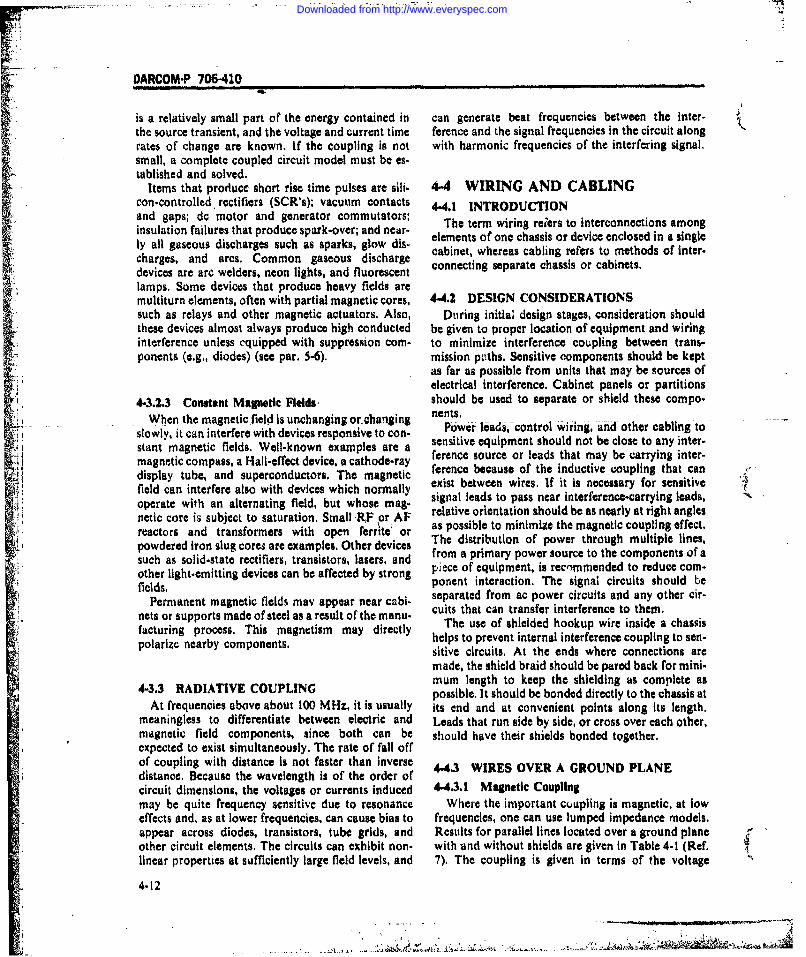
7OARCOM-P 706-410
is a relatively small part of the energy contained in can generate beat frequencies between the inter-
the source transient, and the voltage and current time ference and the signal frequencies in the circuit alongrates of change are known. If the coupling is not with harmonic frequencies of the interfering signal.small, a complete coupled circuit model must be es-tablished and solved.
Items that produce short rise time pulses are sill- 4-4 WIRING AND CABLINGcon-controlled rectifiers (SCR's); vacuum contacts 44.1 INTRODUCTIONand gaps; dc motor and generator commutators,insulation failures that produce spark-over; and near- The term wiring refers to interconnections among
ly all gaseous discharges such as sparks, glow dig. elements of one chassis or device enclosed in a single
charges, and arcs. Common gaseous discharge cabinet, whereas cabling refers to methods of inter-
devices are arc welders, neon lights, and fluorescent connecting separate chassis or cabinets.lamps, Some devices that produce heavy fields aremultiturn elements, often with partial magnetic cores, 44.2 DESIGN CONSIDERATIONSsuch as relays and other magnetic actuators. Also, During initial design stages, consideration shouldthese devices almost always produce high conducted be given to proper location of equipment and wiringinterference unless cquipped with suppression com- to minimize interference coupling between trans-ponents (e.g., diodes) (see par. 5-6). mission p.ths. Sensitive components should be kept
as far as possible from units that may be sources of. electrical interference. Cabinet panels or partitions
4-3.2.3 Constant Magnetic Fields. should be used to separate or shield these compo-i ~ ~When the magnetic field is unchanging or changing nns
slowly, it can interfere with devices responsive to con- -Power leads,€ontrol wiring, and other cabling to
stant magnetic fields. Well-known examples are a sensitive equipment should not be close to any inter-
magnetic compass, a Hall-effect device, a cathode-ray ference source or leads that may be carrying inter-
display tube, and superconductors. The magnetic ference because of the inductive coupling that can
field can interfere also with devices which normally exist between wires. If it is necessary for sensitive L'j. operate with an alternating field, but whose mag- signal leads to pass near interference-carrying leads,
netic core is subject to saturation. Small PRF or AF relative orientation should be as nearly at right anglesnreactors and transformers with open ferrte or as possible to minimize the magnetic coupling effect.
_ powdered iron slug cores are examples. Other devices The distribution of power through multiple lines,slugexamlesfrom a primary power source to the components of a
such as solid-state rectifiers, transistors, lasers, and.; piece of equipment, is recommended to reduce corn-other light-emitting devices can be affected by strong cecmmn s touredu efields, ponent interaction. The signal circuits should be
Permanent magnetic fields may appear near cabi- separated from ac power circuits and any other cir-nets or supports made of steel as a result of the manu- cuts that can transfer interference to them.netsursupprtsme ofstelas aget ma u- The use of shielded hookup wire inside a chassisfacturing process. This magnetism may directly helps to prevent internal interference coupling to sen-polarize nearby components. sitive circuits. At the ends where connections are
made, the shield braid should be pared back for mini.mum length to keep the shielding as complete as
4-3.3 RADIATIVE COUPLING possible. It should be bonded directly to the chassis atAt frequencies above about 100 MHz, it is usually its end and at convenient points along its length.
meaningless to differentiate between electric and Leads that run side by side, or cross over each other,magnetic field components, since both can be should have their shields bonded together.expected to exist simultaneously. The rate of fall offof coupling with distance is not faster than inverse 44.3 WIRES OVER A GROUND PLANEdistance. Because the wavelength is of the order ofcircuit dimensions, the voltages or currents induced 4-4.3.1 Magnetic Couplingmay be quite frequency sensitive due to resonance Where the important coupling is magnetic, at loweffects and, as at lower frequencies, can cause bias to frequencies, one can use lumped impedance models.appear across diodes, transistors, tube grids, and Results for parallel lines located over a ground planeother circuit elements. The circuits can exhibit non- with and without shields are given in Table 4-1 (Ref.linear properties at sufficiently large field levels, and 7). The coupling is given in terms of the voltage
4.12
Downloaded from http://www.everyspec.com

DARCOM.P 706410K
dI t
itf it
II I
1' 54wS
It Ii .4-. Ii I
o- .44.1i %4 -' 1'4.4
"I
4- -4-13
Downloaded from http://www.everyspec.com

DARCOM-P 706-410
across a resistor in the victim loop in terms of the In these formulas no account is taken of the effect incurrent in the interference source line. By dividing coaxial cables which occurs because the center con-these two quantities, one obtains an effective transfer ductor is not precisely in the center of the cable, andimpedance between the two lines under specified con- which is discussed in par. 3-3.1.1.2.2. At frequenciesditions of loading. The table also gives magnitudes of above about 100 kHz, braid leakage and skin effectthe transient voltages which are generated in the vic- become important and calculations should be madetim lines under the various conditions when the in terms of transfer impedance as discussed in par. 3-current in the source line is a simple exponential 3.1.1.2.5 (Ref, 8).rising with a characteristic risetime -r. The values ofmutual and self-inductance can be obtained from 4.4.3.2 Electric CouplingFigs. 4-l1 and 4-13, respectively. For shielded con- The discussion in par. 4-4.3.1, takes no account ofductors the appropriate parameters are obtained electric field coupling. Such coupling can be signifi.from Figs. 4.14 and 4-15. L2 is the self-inductance of cant with high impedance circuits or where long in.the susceptible wire, Ls, and Ls2 the self-inductance terconnections and highly sensitive circuits are in-of the shields on wires I and 2, respectively, and L-2 volved. In such cases, simple braided shields can beis the net inductance of the shielded susceptible wire, very effective. For low frequencies, where ground cir-i.e., the difference in the inductance of the wire taken culating currents should be avoided, the shield shouldby itself and the inductance of the shield. Rs, and R2 be grounded at one end only.are, respectively, the resistive components of theshield cdnductors. 4-4.3.3 High Frequency Considerations
-In the formulas in Table-4, It-is assumed that the At very high frequencies, the dimensions of wiringshields are connected to the ground plane at both required to provide significant effective radation orends, and that the ground plane is impedanceless. pickup become quite small. For instance, at 100Generally, these formulas can be used in the fre- MHz, a I in. length of wire formed into a loop can bequency range from about I kHz up to several hun- a significant impedance. Return circuit dimensionsdred kHz, and of course only for those situations in on wire shield ground connections, bypass capacitorwhich the cable is terminated with an impedance that ground leads, and similar wiring should be as short asis low compared with the characteristic impedance. possible. It is imperative that the wiring of filters be
ZOA-
-~ ~0.3 .4-)
'U
10100 1000 10,000
Ratio h
Figure 4.13. Inductance of a Wire Over a Ground Plane
4-14
0 .... . . ~.~ S~ tll *
Downloaded from http://www.everyspec.com

DARCOM-P 706-4i0
carefully controlled to prevent inductive coupling from Fig. 3-82,. if the spacings of the wires and theirbetween input and output of the filter, which will pitch distances are known. Values of these parame-make it ineffective and single-point grounding is not ters for a variety of cables now in use are given inpractical. Where long connections are necessary, Table 4-2 (Ref. 9).shielded cables must be used and all connectors mustbe electromagnetically tight to reduce radio fre-quency currents external to the shield. In order to 4-4.5 POWER WIRINGreduce such coupling, double shielding may be The three phases of each delta-connected trans-necessary in radio frequency cabling (see par. 3- mission system, and the three phases and the neutral3.1.1,2.5.2). wire of each four-wire, wye-connected transmission
system, should be twisted to form one cable. Twisting4-4.4 TWISTED PAIRS the wires together effectively cancels the electric and
In par. 4-3.2, it was emphasized thal wherever it is magnetic fields produced by the 120-deg phase-dif.possible to isolate return currents, twisted pairs or ferential voltages and currents for either type of con.coaxial leads should be used for signal transmission. nection. Inclusion of the neutral wire in the four-wire,The same principle applies to leads from power wyc-connection effectively cancels the magnetic fieldsupplies, both direct voltage and ac, such as used with produced by the in-phase third-harmonic currents.filament supplies where twisted leads are commonly These third harmonic currents are generated whenused. The fields from twisted wire pairs can be esti- the iron cores of transformers or motors are driven tomated from Figs. 3-66 and 3-68 and the suscepti- near saturation or operate in the nonlinear portion ofbility of twisted pairs to those fields can be estimated the magnetization curve.
iJifL 2 fLc2 fL sl ft
R +'Rc +Rd R 7C12d C d1 0 3 S 1 5104 Ins
, fLa 2 VS R.
d-
fL2as2 vs fLs2 "i.L
Figur 4-4 Cl',t~ adSil Attnua i : act i
10-= '2 V10 4-1
- . I .. -_I0310-2 0 t I) 0 0 0
fL2 frafsI fs
10- 4-15fL11 L 0
R "C + Rd -. , .Z-,
Figure 4I4 AC Inutv and ShedAtnato atr
Downloaded from http://www.everyspec.com

DARCOM4P 706410
4-4.5.1 Separation of Motor Loads From should be avoided, particularly in the vicinity of RF, Signal Equipment Loads sources, Closed wireways and conduit, suitably
Since a common source of interference is commu- grounded, are recommended.tation in dc motors and slip-ring friction in acmotors, low-level signal equipment power lines 44.6 CABLE TYPESshould be separated as much as possible from the The principal types of cables that are available in-power lines to such equipment. elude (Ref. 10) unshielded single and multiple con-
ductor, shielded single wire, shielded multicon-4-4.5.2 Separation of Utility Lines From ductor, coaxial, unshielded twisted-pair, and shielded
Signal Equipment Loads twisted-pair. Cables are also available with multiple
Likewise, because of the varied types of equip- shields, in many different forms, and with a variety ofment which can be connected to general utility lines, physical and electrical characteristics. Proper selec.they should be separated from signal equipment lines. tion and application of appropriate cables for specificw! design requirements are highly important in preven-4-4.5.3 Placement of Conduit and Wireways ting, controlling, and eliminating interference.f Installation plans should identify high- and low- Cables are generally specified or identified accord-level cables for special routing and segregation (see ing to:par. 4-4.11). The use of metal conduit for signal or a. Sizepower lines may be necessary. Where cables and wire- b. Number of conductorsways are tied into lunction boxes, separate boles c.-Characteristic impedance
" .... should be-used-for power and signal-equipment lines...d. Attonuatign.If not, separate tie points and internal shielding e. Shielding (single, double, triple) .......between lines are needed. Open overhead wireways f. Power rating
;!L2/RC+ Rd) (iRSI) LS2 R5
L2/(Rc + R (LS1/ ,) /RS 2Ls/R S /
r r r r
Fur 102 103 n0t 10ah Ac s+ 100 1':2 ; ::'::; t:' 1 -
Al A SL2 F2(R C R ON-x ... :-
1 0-~10-4
..L /R SL, /R L . I.:- S2 till
V) A S S2 S2 -Lei- ":.-Ke S2 r- - :;- -4-
10-2 0 -5S J , :. ::: +. - s_j Vs i , /.S
u s$2-IIIT' -- ..S r
vs r r] + r:: ... +
Fiur 4+15.: Tranien Inuciv an hedAtna i Factorit ::4-16
Downloaded from http://www.everyspec.com

OARCOM-P 7064107
g. Maximum operating voltage including hi..pot d. Voltage ratingstesting e. Capacitance per unit length
h. Type of jacket (standard black, standard gray, f. Characteristics impedancelow-temperature black, polyethylene, fiberglass, or g. Transfer impedances.armor) Also included are applicable equations and dis-
i. Type of dielectric (for example, polyethylene or cussions of important considerations in selectingTeflon, solid or spiral ribbon, pressurized, or un- cable and wire types.pressurized).
An excellent source of information concerning the 4-4.7 CONNECTORScharacteristics of wire and cable is available (Ref. 11). Cable connectors are made in many styles for aIt contains details of the more frequently used cable multitude of power, signal, control, instrumentation,types including: transducer, audio, video, pulse, and radio.frequency
a. Dimensions applications. They are made to fulfill special func-b. Materials used and their importsat characteris- tions, and may be required to be hermetically sealed,
tics submersion proof, and weatherproof. They arec. Power carrying characteristics manufactured in the straight type, angle type, screw-
on type, bayonet twist and lock type, bayonet screw-TABLE 4-2. SPACINGS AND PITCH on types, barrier type, straight plug-in type, and
DISTANCES FOR CABLES (Ref. 9) push-on type (Table 4-3). In addition to havingdesign features which will meet resistance to damage
Cable Helix Conductor Helix Ptchp. Area A, occurring during insertion anid extraction under fieldType Separation 6, cm m x 10-' conditions, and have a relible 'and ad&qiately low- .... ._ - .. .pin--contact- resistance, -a- connector- hould-have--
SGA 3 1.58 7 3. shielding effectiveness characteristics which will notDS3A 4 1.80 8.64 4.95DSGA 9 2.39 11.43 8.68 degrade that of the cable with which it is used.
* DSGA 14 2.74 13.21 11.52 To assure that the connector adequately shields theDSGA 23 3.18 1J524 15.39 circuits passing through it, the connector shell must
SDSOA 30 3.58 ! 7.15 19.52
DSGA 40 3.89 18.67 23.08 have a conductive finish, and there must be no breakDSGA 50 4.24 20.32 27.41 in the shielding through the connector/cable combi-DSGA60 4.72 22.61 33.96DSGA 75 5.18 24.89 41.02 nation through which unwanted fields may enter.DSGA 100 5.74 2.18 49.61 Where power circuits pass through a connector, the
DSGA 15 6.46 33.79 75.85 connector shield at the interface of the two connectorDSGA 200 8.05 38.68 98.86 halves must make positive contact before the powerDSGA 250 8.84 42.42 119.24 contacts mate, and maintain contact until after theDSGA 300 9.50 45.72 138.11DSGA 400 10.95 52.58 183.08 power contacts break. The entire periphery of the2SJ 22 0.84 3.81 1.02 shield of the cable being terminated must be bonded2SJ20 0.92 3.81 1.11 to the shell of the connector around the entire pe-2SJ 18 1.07 3.81 1.302S. 16 1.14 6.35 2.31 riphery of the cable entryway (see Fig. 4-16 (Ref.2SJ 14 1.32 6.35 2.67 10)). This should be done by soldering or metal form-DCOP ! 0.74 2.54 0.60 ing; "pig-tailing" or bonding with conductive epoxyDCOP 1-1/2 0.99 S.08 1.60 is unsatisfactory. Likewise, the entire periphery ofOCOP 2 0.99 5.08 1.60 bulkhead connectors must be bonded to the bulk-
STSP 0,76 6.35 1,542SWA 0.76 6.35 1.54 head or chassis in which it is mounted.2SWF 0.76 6.35 1.54 To assure that a good high conductivity path exists2SA 0.76 6.35 1.542SU 0.76 6.35 1.54 between mating pins, they should be plated with aTTHFWA 0.79 5.72 1.43 material which has good conductivity and resists tar-2rRSA 0.99 6.35 2.00 nishing and corrosion. Two layer plating, hard gold2A40 1.02 3.81 1.23
2AU40 1.02 3.81 1.23 over ductile nickel (elongation of not less than 5%)2SWU 1.22 7.62 2.95 has been found to be very effective over a copper2U 0.64 3.81 0.77TTSU 0.97 5.72 1.75 alloy base metal. Where the base metal is a nickelTPNW 0.61 5.08 0.99 iron alloy, as often used in hermetically sealed con-RG-22B/U 1.14 10.80 3.92 ductors, copper is plated on the contacts as a pre-RG-1 IIA/U 1.14 10.80 3.92RO I30/U 2.39 10.80 8.92 liminary step. A fine microfinish will increase corro-RG-108A/U 1.41 6.35 2.10 sion resistance and reduce friction as well.
4-17
...............................................:. .. .. '
Downloaded from http://www.everyspec.com

r - DARCO#4P 706-410
MIL-STD-454, Standard General Requirements for 4-4.8 CABLE APPLICATIONElectronic Equipment: Requirement 10 sets forth re-quirements for connectors to be used in military 4-4.8.1 Generalequipment. This document should be used to locate The choice of cable is dictated by the operatingspecifications applicable to connectors which are un- signal or power level, frequency range, susceptibilityder consideration for inclusion in equipment design. level, and physical isolation, While it is not feasible to
TABLE 4-3. CONNECTOR APPLICATION SUMMARY
Connec- Coaxial For RG-/U Dis- Voltage Character- Freq. Method oftor Cable Cables connect Rating istic Range Assembly
Series Size Style Impedance
Medium 5,6,8.9, Screw- 500 V 50 ohm up to ManualN & 10,11,12, on peak 70 ohm 10 GHz
Large 13,14,17, type (constant)18
Medium 8,9,29,55, Push- 1500 V 50 ohm up to ManualGR-874 & 58.58A,59, on -peak 7 GHz
-_-___ Large 62,116 type
Medium 8,9,10,12, Bayonet 1000 V 50 ohm - ManualC & 14,55,58 Lock peak
Small type
Medium 8,9,10,11, Screw- 500 V (noncon- up to ManualUHF & 12,13,55, on peak stant) 200 MHz
Small 58,62,63, type65,71
Screw- 5000 V 50 ohm - Manualon peak
Le. Large 17,18 type (modi-fied to10 kV)
Medium 8,9,10,17 Screw- 5000 V 50 ohm - ManualBN & 18 on peak (constant)
Large type
55,58.59, Screw- 250 V (noncon- up to ManualBN Small 62,71 on peak stant) 200 MHz
type
55,58,59, Bayonet 250 V 50 ohm up to Manual &BNC Small 62,71 lock peak (constant) 10 GHz Crimp-on
type
174 Screw- - 50 ohm - Crimp-onSubmin. Submin- on & 75 ohm
iature iature Push-on (constant)types _ __ _ _ _
4-18
• - .' :i ,' ../ -. : " " " :" "
Downloaded from http://www.everyspec.com

DARCOM-P 706410~IAi
set specific rules for cable selection without making 4-4.&2 Multlconductor Cablesan analysis of signal levels and waveforms, the Multiconductor cables are of many types. Theyfollowing general rules are suggested: may contain groups of unshielded lines, coaxial lines,
a. Use unshielded wire for external power circuits or multiple conductor shielded combinations. Forsuch as 115 V ac or 28 V dc. An exception to this rule maximum effectiveness of the shields it is essentialis when the power source itself generates substantial that each be insulated individually. The various con-EMI, such as with an inverter or an alternator recti, ductors within a single shield should be used :.'ier that is not adequately filtered at the source; preferably in pairs and should operate at comparable k!generally, leads to a power source regulator must be voltage and current levels. Ishielded (see par. 5-6). Ac line wires should be Initially unshielded cable may be shielded bytwisted. routing it through continuous flexible or rigid I-1
b. Use shielded wire for multiple-ground, audio metallic conduit. For economical reasons, rigid con-frequency, or power circuits. Single-conductor, duit is generally of aluminum; but from the stand-single-shield cable can be used for low-frequency in- point of shielding high-level power circuits, galva-strumentation applications using ground return cir- nized steel conduit is more effective at power fre-cuits. It is effective when signals to be transmitted are quencies. Continuous, high-A materials are alsoof moderate levels, and a good low-impedance system available for use with audio-frequency signal cables,ground is available. Flexible conduits for high- and low-voltage shield-
c. Use twisted-pair for audio-frequency circuits ing usually consist of flexible metal hoses over whichgrounded at a single point and for internal power*cir- are wound one or more layers of braid. Non- .,
cuits. conducting coverings sometimes are used over the
.. d _Use. shielded _twisted-pair for_ single-point br-aid. These coverings provide waterthtniess and/or-ground circuits and multiple-ground circuits where added mechanical protection. If applied tightly, theymaximum low-frequency isolation is required. may decrease contact resistance between wires com-
e. Use coaxial cable for transmission of RF pulses, prising the braid, thereby improving shielding effec-high-frequency applications, and where impedance tiveness. Such coverings should be reasonably ruggedmatch over a broad frequency range is critical, and not subject to physical and chemical attack by
f. Special measures may be required with short rise substances with which they come into contact. Theytime, for which solid copper transmission lines or tri- should maintain their desirable characteristics overaxial cables are used (Fig. 4-17). the anticipated range of operating temperatures.
Preferred: Fillet Weld Around Entire
1riphery of Female Connector Housinq..,..
Alternative: Bolt and Tooth Type Lock-Washer Connection as Shown by Dotted
, Outline Male f - -ShieldContacts
Continuous Shield-to-Shell Bond bySolder or Metal Forming (Never Pig- Spring Contacts (Shield Makes Before
Tail the Shield) and Breaks After Enclosed Conductors)
Figure 4-16. Shield Termination for Connectors (Ref. 10)
4-19
.~ ~~~ .......
Downloaded from http://www.everyspec.com

OA, COM-P.-T064-10 -
Shielded conduit is used for many diversified pur- 4-4.9 SHIELD GROUNDINGposes, such as.poss schid a s dIn accordance with the discussion of grounding
a. To shield wires and cables electrically that principles in par. 3-3.4.4, shields of balanced circuitsotherwise would radiate interferenceoprtnatfeucisptobut10kzhul
b. To provide a channel through which wires and operating at frequencies up to about 100 kHz shouldcables may be pulled or pushed for installation or re- be grounded at only one end. Furthermore, the shieldplacement in inaccessible places should be insulated so that the single point ground-
c. To protect insulated wires and cables againlst ing practice can be observed. On the other hand, if
mechanical damage, for example, chafing and abra- the cable length is more than about I/10 of a wave-sion length for any frequency of concern and an es-
i d. To keep foreign matter (moisture, oil, grease, tablished ground "plane" exists, the shield should begasoline) away from electrical conductors or their in- bonded periodically to limit the possibility of large
awsulation currents or voltages being induced on the externalsu.To fpsurface of the shield. MIL-STD-1310 requires that
. To facilitate dissipation of heat for protection of cable armor be bonded at each metallic bulkhead orinsulation.
To be effective, a flexible shielding conduit should equipment space penetration. On the other hand.be: shielding conduits need be bonded only at points 3 to
a. An effective shield against electrical inter- 5 ft from each end. Bonding should be as direct as
ference over the entire range of frequencies under possible (see par. 4-7.2). The outer shield of coaxialconsideration cables must be grounded to the chassis at both ends;cbReason e "pig-tail" type connections should be avoided. OnSb. Reasonably flexible and capable of being bent t e a s m t o h tg o n i g t c n q e a eb eto a small radius the assumption that grounairig techniques have been
c. Rugged enough to withstand considerable abuse employed, the following are suggested as guidelines
and prolonged vibration without serious-impairment - for good signal cable practice:of either its electrical or mechanical properties a. Shields should not be used for signal return cir-
d. Watertight and airtight. The coverings used cuits. fwith it should be immune to attack from lubricants, b. All signal circuits, including signal groundcoolants, antifreeze, and fuels, returns, should be individually shielded and have
e. Capable of withstanding ambient temperatures insulating sleeves or coverings over the shields.likely to be encountered. Balanced signal circuits should use twisted pair or
i CABINErT
SHIELD 3SHIELD
Figure 4-17. Triaxial Cable Application
4-20
..................................................................................................................
Downloaded from http://www.everyspec.com

DARCOM-P 706410
balanced coaxial line with a common shield. Where be run into a completely sealed box and gro.,nded in-multiconductor twisted pair cables are used which ternally; rather the shield should be tun well insideI have individual shields as well as a common shield, the connector and be bonded to the connector shell.all shields should be insulated from one another The arrows on Fig. 4.19 show the path tblt any signalwithin the cable. or interference, that is picked up on thu outer surface
c. Coaxial cab!es should be terminated in their of the shielding, must follow to return to ground. TheI. characteristic impedance and grounded at both ends. currents around the loop generate a field in thed. When electronic and electrical systems are dis- enclosed box, as do coupling loops used with reso-
tributed over a large area, multipoint shield ground- nant cavities. Fig. 4-20 illustrates the correct methoding is usually effective for interference control at the of treating the shield.higher radio frequencies. The multipoint approach For a low-impedance RF connection, the shortestallows short ground connections, permits a low-im- length of connecting strap or jumper that is me-pedance ground return circuit, and improves the chanically practical should be used, and the bondingeffectiveness of filter installations. At low frequency procedures in MIL-STD-1310, MIL-B-5087, andin low-level systems with audio or servo amplifiers, MIL-E-45782 should be followed (see also par. 4-single-point grounding may be necessary since, when 7.2). Great care must be taken at connectors if im-a shielded cable in a sensitive circuit is grounded at pedance characteristics and shielding integrity are toboth ends, power-frequency currents in the ground be maintained. A shielding shell should be used toplane can induce audio-frequency interference, shield the individual pins of a connector; a well-
e. Coaxial cables carrying high-level energy should designed connector has a shielding shell enclosing itsnot be bundled with unshielded cables or shielded connecting points (Fig. 4-21). The shell of multipincables carrying low-level signals. connectors should be connected to the cable shield.
Coaxial lines shiuld ierrninate in shielded pins. Theuse of pigtail connections for the outer conductor of
4.4,10 CONNECTOR GROUNDING coaxial- lines is undesirable- since it permits -RF .- Where shields are grounded at both ends of a leakage. Shields should be grounded on both sides of
cable, the objective is to obtain a continuous equip- a connector to avoid discontinuity, If this is notment enclosure shield as shown on Fig. 4-18. To ac- possible, the shield should be carried across the con-complish this, wires and coaxial cables must be ter- nector through a connector pin. Grounding a numberminated properly at the connector. The connector of conductor shields by means of a single wire to aitself must be grounded to its mounting by a clean connector ground pin should be avoided, particularlymetal-to-metal contact. A shielded cable should not if the shield-to-connector or connector-to-ground
EQUIPMENT EQUIPMENT
ENCLOSURE ENCLOSURE
# SHIELD 7 N 2
LOAD LOAD
e/00GROUND PLANE/° U/ /// // /
Figure 4-18. Continuous Equipment Enclosure Shield
4-21
W-
Downloaded from http://www.everyspec.com

DARCOM.P 706410
Itad length exceeds I in., or where different circuitsthat may interact are involved. Such a ground lead is
OUTER INSULION a common .impedance element across which inter-ference voltages can be developed and transferredfrom one circuit to another.
For grounding the outer shield on a cable, a back-shell type of connector with a continuous contactaround the shield is the most satisfactory. This maybe accomplished by means of tapered rings whereby
TE pressure is applied to a continous metal-to-metal con-INNE INSULATION tact between shield and connector. Typical arrange-
_ . ments are shown schematically in Fig. 4.22. In Fig, 4-22(A) the shield is flared and held between a pair of
ROwOU TAA, -TEM.,IAL POST tapered rings. In Fig, 4-22(g) a compressible "iris" isFigure 4-19. Incorrect Method of Introducing used to clamp the shield.
Shielded Cable If the cable also contains wires which are shieldedindividually, the individual shields can be broughtout of the cable assembly just before thu connectorbent back over the outer cable shield and held in the
OVE INSULATION same manner as the outer shield.
SHIEDIN In L a similar arrangement an elastomer pressure sealcan be made with a compressible "O"-ring contacting .a neoprene or other waterproofing jacket locatedover the shield.
INNER CONEIJLT~k Fig. 4-23 shows a backshell of the type used for fit-ting over an unshielded connector. Here again the
LOW RESISTANCEELECTRICAL n... CIAXIAL INSULATION outer shield, which may be separate from the cable, is :
BETWE s,, IDING AND 30X fastened completely around the shield by means of acrimping or soldered ring or other means. 1 he matingFigure 4-20. Co, rect Method of Introducing surface with the jack is rendered EMI-proof by the
S.ielded Cable use of an EMI gasket (see par. 6-4.5.4). Also, an EMIgasket is shown between the jack and the panel onwhich it is mounted.
Also note that connectors are available in whichsmall low-pass filters are incorporated so as to act in
0. series with individual pin connections (see par. 4-5.5.3).
Electric plugs and rect. ces usually are mountedon the front or rear of,' equipment chassis, or onthe mounting base. If ric receptacles are on thefront of the case, the piu, -,Iould be separate units.
4VSH I ELD ING Shield grounds should be II 'e in accordance withSHELL Fig. 4-24. If electric plugs and cceptacles are placed
.l at the rear of the case, at least one unit should be at-CONNEC IING tached securely to the case or chassis; the otherPINS should either be separate from or attached securely to
the mounting base. Methods of grounding cableshields shown on Fig. 4-25 are not recommended.
FITTING To prevent discontinuity of the shield because of0 Tpossible disconnect at intermediate connectors,
shields should be grounded to the structure on bothsides of the connector. Where this is not possible, the
Figure 4-21. Connector With Shielding Shell ground should be carried across the connector, orEnclosure For Connecting Points through a conductor pin, to ensure continuity.
4-22
S- - . V-
Downloaded from http://www.everyspec.com

DARCOM-P 70&410,
Coaxial fittings should be kept tight at all times, not radiate or conduct interference. A suitable low-im-only to provide a good impedance match but to elimi- pedance connection can be obtained by the use of annate loose connections that might result in possible extremely heavy pin, or by the use of several pins inrectification of interferince energy at the fittings. parallel, preferably distributed circuniferentiallyShielding or bonding clamps that may be a part of the about the pin attached to the pulse lead center-fittings also should be kept tight. Soldered fittings are conductor. The pulse lead and nearby susceptiblerecommended, particularly ut terminations of shield- leads should be shielded to prevent transfer to othering and braid. leads.
When any high level pulse lead passes through aF connector in a way that involves a discontinuity inthe coaxial structure of the shielded lead (for exam- 4-4.11 CABLE SEGREGATION ANDpie, when a pulse lead center-conductor and shield HARNESSING. are attached to separate pins of a connector), an Cable routing should be planned in order to !so.extremely low-impedance circuit should be provided late sensitive (susceptibility prone) wires and cablesfor the ground lead of the shield in the connector. If from possible interference carrying conductors.this is not done, the entire shield along the lead may Traditionally, this has been done by arranging cables
. - - S hield B raid Flared] Braid Flared
Cable Connector
Tapered Ring
(A) Tapered Ring Termination
Shield Braid
Cable Connector
Iris
(B) Compressed Irls Termination
Figure 4-22. Connector Backshell Arrangement for Terminating ('able Shields
4-23L.
Downloaded from http://www.everyspec.com

'A3. 3M.P_706410.
EM iaI I I
Joc
Figure 4-23. Backshell Arrangem.nt for Terminating Cable Shields
_ _ _ _A typical installation is shown on Fig. 4.26. Insome Installations, rows and tiers of cable trays areused to facilitate the desired physical cable separa.
.. tion. Detailed planning Is required prior to installa-ttion to ensure that the best overall routing is
As II I .0str Iachieved.S ., , UWYIRI ~ While arrangements of this kind are feasible, they
ELECTRICAL RECEPTACLES IN FRON must be used with care, since: (a) it is not alwayspossible to classify easily a given cable into only one
Figure 4-24. Cable Shield Bonding of these groupings; and (b) one must establish appro.priate minimum spacings between all of these cablegroups in the installation, and it may not be possible
into compatible groups. NIL-STD-461 identifies the to maintain these spacings everywhere.following five major categories: Another classification system (Ref. 10) includes 7
a. Power wiring including rain power distribu- wire classes and 9 circuit types as shown in Table 4.4.tion circuits Each circuit is assigned a classification on the basis of
b. Secondary power including low voltage power its being most similar to one of the following classes:and lighting circuits, servo and synchro circuits, and a. Power and Control Circuits (Class I):secondary dc power with voltages up to 5000 V (1) Dc Power Circuit. A dc circuit using current
c. Control wiring including that to relays or other more than 2 A.intermittent operating devices involving switching (2) Dc Control Circuit. A dc circuit which uses
d. Sensitive wiring including circuits carrying less than 2 A.signals such as adio, digital data, analog control, b. Dc Reference Circuit (Class II). A dc circuit re-and demodulator output. quiring critical tolerances on the voltage or current.
e. Susceptible wiring including wiring to electro- c. Ac Circuits (Class III and IV). Any circuitexplosive, antiskid, spoiler actuator or "safety ofmis- which is supplied by ac power sources.sion" devices; and coaxial cables to receiving anten- d, Ac Reference Circuit (Class III and IV). An acnas, fire warning, fuel quantity, and liquid oxygen in- circuit in which a single-phase line is used to supplydicator devices, critical voltages or frequencies.
4-24
'.. - .9. .
M 4'I
Downloaded from http://www.everyspec.com

DARCOM-P 706410
EQUIPMENT CASE OR CHASSIS (b) -75 dBmW from 5 to 25 MHz(c) -75 dBmW at 25 MHz increased to 10
dB per decade of frequency to -45 dBmW at I GHz(d) -45 dBmW above I GHz
(2) Broadband Circuits. Those RF-interfer-ence circuits which conduct pulse information ortransient disturbances such as caused by relay actua-tion, switch contacts, or clock pulses.
<(3) Antenna Circuits (Class VII). Those RF cir-cuits connecting subsystems or equipment to systemantennas.
In layout wiring and routing, the maximum prac-__ tical separation must be maintained in accordance
with the general rules described in the paragraphsMOUNTING AS ,,,that follow. A 2-in. separation between wires in
(A) different classes is a minimum design goal.Route dc power and control circuits (Wire Class 1)
in a separate wire group, The ac power and control
EU I PMENT CASE OR CHASS IS circuits are divided into groups when the system usesmore than one source of electrical power. Thefollowing general rules apply:
a. The ac wiring supplied by different powersources must never be routed together.
b. The ac wiring from different ac power sources... .... .... ...... mst-nii b-con nected to a siibisyister--quip- . .
ment, unless there is a specific design and installation,' c. Route reference and susceptible circuits sep-
arately from power and interference circuits except asfollows:
_ __ (1) Reference dc and audio-susceptibe circuitsmay be routed together in the same way provided
MOUNTING SASE- that proper isolation is maintained through shields,(B) shield terminations, and connectors.
(2) Reference ac circuits may be routed with acFigure 4-25. Poor Cable Bonding power circuits if the rules governing multiple power
sources are not violated, and they are not classified ase. AF Susceptible Circuits (Class Ii). '1 nose cir- susceptible.
cuits whose performance may be degraded in the RF-susceptible circuits may be routed with Class Iipresence of an undesired audio signal. The voltage or circuits if the RF-susceptible circuit is not a source ofcurrent of these circuits will normally be less than I V interference to the other circuits.rms or 200 mA rms. Direct current reference circuits Where a specific layout is given, computer pro-are considered as audio-susceptible circuits. grams are available to identify specific cases where
f. AFI Circuits (Class III or IV). Those circuits coupling will be sufficient to cause operational dcgra-operating below 15 kHz and whose amplitudes will dation (see Chapter 6). To use the programs, onenormally be greater than I V rms or 200 mA rms. must put into the computer all cable and location
g. RF Susceptible Circuits (Class V). Those cir- data. While this procedure can provide high ac-cuits whose performance may be degraded in the curacy, it is more involved than the use of the cablepresence of on undesired RF signal. categorization technique.
h. RFI Circuits (Class VI) are as follows:(1) Narrowband Circuits. Those RF-intcr- 4- FILTERS
ference circuits in which the signal levels exceed thefollowing values with respect to 50 ohms: 4.5.1 INTRODUCTION
(a) -45 dBmW at 150 kHz reduced to 20 Though proper circuit design has been emphasizeddB per decade of frequency to -75 dBmW at 5 MHz as an appropriate means for controlling interference.
4-25
...................... - -,-l.k. .
Downloaded from http://www.everyspec.com

DARCOM-P 706410
LOW HI GH .LEVEL LEVEL CONTROL PULSELINES LINES LEADS LEADS
TO SYSTEMGROUND PLANE
HOUSING
FRONT
TO SYSTEMGRCUND PLANE
CONNECTOR
HALO RING
CABLE SHIELD
NOTES 1. MODULES BONDED TO CABINET
2. ALL LINES INDIVIDUALLY SHIELDED AND INSULATED
3. LINES CROSS AT RIGHT ANGLES TO EACH OTHER TO
EFFECT MAXIMUM INTERFFRENCE REDUCTION
Figure 4-26. Typical Cabling Methods
4-26
.... i. ....
Downloaded from http://www.everyspec.com

M . .... .... . .
DARCOM-P 706-410
it is not always possible or advisable to control it in formance significantly. The consequences of this arethis manner. Thus, for technical as well as economic discussed in par. 4-5.2.1.6.reasons, filters should be viewed as legitimate tools of The transfer function is a complex quantityinterference control. specifying the gain, which is the ratio of the magni-
Filter theory is highly developed. A theoretical sur- tudes of EL and Ev and the phase shift from input tovey on lumped element filters is given in Chapters 7 output. The reciprocal of the gain is attenuation, aand 8 of Ref. 12, and transmission line, waveguide, quantity frequently used to characterize the behaviorand cavity filters will be found in Chapters 22 and 23 of a filter. Because the output is not fully determinedof Ref. 12. A filter is a linear two-port device modeled by the transfer function but is affected by the inputb the block diagram shown in Fig. 4-27. The source, impedance as well, a preferred filter characteristic isinput, and load voltages Es, Esi, and EL and the the insertion loss defined assource and load currents Is and IL are complexquantities representing sinusoids at frequency f. /ELI \Given Es, Z4, and ZL, the behavior of the filter is IL = 20 log , dB (4-5)determined from the voltage transfer function H(f)
where EL. and EL2 are the magnitudes of the loadH(.f) = EL(f)IET1(f) ,dimensionless (4-4) voltage, respectively, with and without the filter in
the circuit. The insertion loss and the attenuation areand the input impedance seen looking into the input identical if the input impedance of the filter and theterminals of the filter. load impedance are equal. The passband of a filter is
Manufacturers normally give filter characteristics the frequency range in which there is little or no at-for fixed source and load impedances, usually 50 tenuation. The stopband is the frequency range inohms as measured in accordance with MIL-STD-220. which attenuation is desired.t, However, actual circuit impedances can vary idely, Filters can be classified grossly according t h
especially with frequency, and will influence per- relative positions of the passband and stopband in! the frequency spectrum. There are four classes -
low-pass, high-pass, bandpass, and band-reject -i: and the discussions to follow deal with these classes.
TABLE 44. CIRCUITS AND WIRE CLASSES Attenuation as a function of frequency for each of the(Ref. 10) classes is shown in Fig. 4-28 (Ref. 13).
Filter synthesis for specified behavior using
WIRE lumped parameters has been, and still is, difficult. InCIRCUIT TYPE CLASS EMC work, precise attenuation characteristics gen-
erally are not demanded and an adequate approach isDC Power and Control to search through a collection of known structures to
4. DC Reference 11 obtain one that will perform the task. Sometimes asimple bypass capacitor or series inductor will be
AC Power and Control adequate. Otherwise, the more elaborate L, T or Pi(a) Left Hand Bus III (r) structure is required.(b) Right Hand Bus IV Certain guidelines are helpful in deciding what type
AC Reference of filter circuit to apply in any given instance. For(a) Left Hand Bus III example, if it is known that the filter will connect to(b) Right Hand Bus IV relatively low impedances in both directions, then a
Audio-Frequency-Susceptible if circuit which contains series filter elements may be
Audio-Frequency Interference(a) Left Hand Bus III Source 7.
(b) Right Hand Bus IV Impac
RF-Susceptible VRF-Interference VI
Coaxial Cables VII Figure 4-27. Linear Two Port Model of Filter
4-27
T.
Downloaded from http://www.everyspec.com

OAFWOMP 706410
MAI U "' '"L
IjATTENUATES ALLin
N--
.
~ I ATTENUATES ALL FRQECIESI - -
C.HISS , 'FREQUENCIES IN THIS SECTION SECTION PASSBAND
TOP9IANO -- --- -- STOP BAs,
f FREQUENCY -. FREQUBICY --.. fPASSBAND
(A) LOW-PASS FILTER (B) HIGH-PASS FILTER
T.. fo= cutoff frequencyjPASSAN D " i4L
PASSES ALLT
FREQUENCIES INI in i.
THIS SECTION I I -
5 U
i STOPBAND
STOPSAN STOPANATTENUATES ALL• PBADSOPiN FREQUENCIES IN in
ATTENUATES ALL I ATTENUATES ALL u F U E wA U - THIS SECTION --
FREQUENCIES IN FREQUENCIES IN 1
THIS SECTION THIS SECTION L .
f f f 0 f°201 02 01 02
FREQUENC FREQUENCY
(C) BANDPASS FILTER (D) BAND-REJECT FILTER
Figure 4-28. Filter Attenuatlon as a Function of Frequency
4-28
"" .. : £ . . . t ,, ; 1, . . .. . . . --2 .,, ., ... . ,
K . ... ,i .. :.. s. -. . . . . . . , . < , . ..-.
Downloaded from http://www.everyspec.com
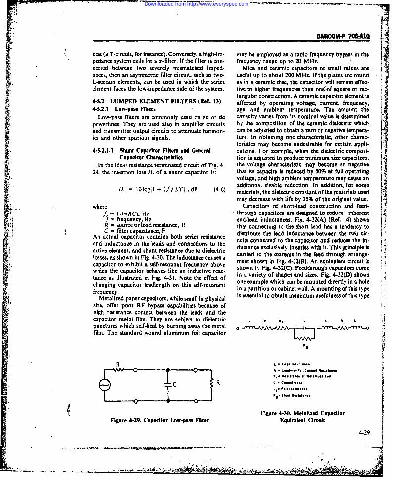
DARCOM-P 70&410
best (a T-circuit, for instance). Conversely, a high-im- may be employed as a radio frequency bypass in thepedance system calls for a .r-filter. If the filter is con- frequency range up to 20 MHz.nected between two severely mismatched imped- Mica and ceramic capacitors of small values areances, then an asymmetric filter circuit, such as two- useful up to about 200 MHz. If the plates are roundL-section elements, can be used in which the series as in a ceramic disc, the capacitor will remain effec-element faces the low-impedance side of the system. tive to higher frequencies than onc'of square or rec-
tangular construction. A ceramic capacitor element is4-5.2 LUMPED ELEMENT FILTERS (Ref. 13) affected by operating voltage, current, frequency,4-5.2.1 Low-pass Filters age, and ambient temperature. The amount the
Low-pass filters are commonly used on ac or dc capacity varies from its nominal value is determinedpowerlines. They are used also in amplifier circuits by the composition of the ceramic dielectric whichand transmitter output circuits to attenuate harmon- can be adjusted to obtain a zero or negative tempera-
" ics and other spurious signals. ture. In obtaining one characteristic, other charac-teristics may become undesirable for certain appli-
4-5.2.1.1 Shunt Capacitor Filters and General cations. For example, when the dielectric composi-Capacitor Characteristics tion is adjusted to produce minimum size capacitors,
In the ideal resistance terminated circuit of Fig. 4- the voltage characteristic may become so negative29, the insertion loss IL of a shunt capacitor is- that its capacity is reduced by 50% at full operating
voltage, and high ambient temperature may cause anadditional sizable reduction. In addition, for some
IL i log[I + (f //£)-] ,dB (4-6) materials, the dielectric constant of the materials usedmay decrease with life by 25% of the original value.
where Capacitors of short-lead. construction and feed-I/(irRC). Hz through capacitors are designed to reduce-inherent.
f -frequency, Hz end-lead inductances. Fig. 4-32(A) (Ref. 14) showsR - source or load resistance, Q that connecting to the short lead has a tendency toC = filter capacitance, F distribute the lead inductance between the two cir-
An actual capacitor contains both series resistance cuis connected to the capacitor and reduces the in-and inductance in the leads and connections to the- ductance exclusively in series with it. This principle isactive element, and shunt resistance duc to dielectric cane exsey in erie thr h prn eicarried to the extreme in the feed through arrange-losses, as shown in Fig. 4-30. The inductance causes a ment shown in Fig. 4-32(B). An equivalent circuit iscapacitor to exhibit a self-resonant frequency abovewhich the capacitor behaves like an inductive reac- sct l i.ein a variety of shapes and sizes. Fig. 4-32(D) shows[ ance as illustrated in Fig. 4-31. Note the effect of
changing capacitor ieadlength on this self-resonant one example which can be mounted directly in a holein a partition or cabinet wall. A mounting of this type! frequency.
Metalized paper capacitors, while small in physical Is essential to obtain maximum usefulness of this typesize, offer poor RF bypass capabilities because ofhigh resistance contact between the leads and thecapacitor metal film. They are subject to dielectric L a , L , Lpunctures which self-heal by burning away the metalfilm. The standard wound aluminum foil capacitor
its
R L Led l04eVeOtI
0 t L*Od-'"- Fall C@*t't ttho1gftes
ft, * ftft|OIence of Metalald Full1: 0 e_ ?n*L fa Fll Induemet..Rpt shunt Redletenee
Figure 4-30. Metalized Capacitor
Figure 4-29. Capacitor Low-pass Filter Equivalent Circuit
4-29
- -, ..---. - , .,.
Downloaded from http://www.everyspec.com

I
DARCOMP 706410
40
0.25"3C -j --- I--- °
20 -- Lead Length
10 30
Tit.
0.1 1.0 10
Frequency f, M*iz -
Figure 4-31. Insertion Loss of a 0.05-pF Aluminum Foil Capacitor
of component since then the separate circuits on in-X T put and output sides are otherwise isolated from each"1"l other.TThe short-lead capacitor is suited ideally for EMI
suppression in the frequency range of i to 1000 MHz.(A) tr Ciri of a (11) Eri1 rit or Feedthrough capacitors are avaiiable with a reso-hAort le adl C ap c iLto r e e d hr o u h U c lci o r
nant frequency well above I GHz. The feedthroughcurrent rating is determined by the stud diameter.Fig. 4-33 indicates the construction details of a feed-through unit.
Metalized Mylar capacitors oifer compact designand good reliability. Their dissipation factor is very
, low, and lead length generally can be kept short toimprove high frequency performance.
Wet-type electrolytic capacitors are used for dcMI rcctrica, EQsI.leo Circuit filtering and sometimes used in EMI filters. They are
single polarity devices, but their high dissipation fac-tor or series resistances make them paor RF filters.An RF bypass capacitor should be placed across. theoutput of dc supplies using electrolytics. The dissipa-tion factors of electrolytic capacitors increase, and
i. their capacitances decrease with age.Tantalum electrolytic capacitors provide a large
value of capacitance in a small space. They are sen-sitive to over-voltages and are damaged by reverse
Figure 4-32. Three-terminal Capacitor polarity. The dissipation factor is considerably higher
4-30
Downloaded from http://www.everyspec.com

DARCOM-P 7"64%l
HOUSIN GROUND FOILS
SOLDER CONNECTION TOFEED-THROUGH BUS
FEED-THROUGH BUS
LINE TO BE
BY-PSSEDALL EXTENDED FOILdI--_ _ __ T SOLDERED TOGETHERil 'HOT' FOILS_
- --
, SOLDER CONNECTION
TO HOUSING
Figure 4-33. Typical Feedthrough Capacitor Construction
than for Mylar or paper capacitors, and high fre- R L-quency- characteristics are poor.
Capacitors for 120 V ac applications should berated at 400 V dc to be suitable for ac use. A unit ofMylar and foil or of paper-Mylar and foil is recom.mended. The dissipation factor is low, and high fre- '
j:i quency performance is good. For 240 V ac appli-cations, an oil-impregnated paper and foil unit is rec-ommended. ____,--.,-,,-
4-5.2.1.2 Series Inductor Filters, and General Figure 4-34. Inductor Low-pass FilterInductor Characteristics
Another simple form of low-pass filter is an induc-tor connected in series with the interference carryingconductor (Fig. 4-34). Its theoretical insertion loss ILis given by the relationship:
[ /f\ netic flux should not drive the core to more than 50%IL = 10log + dB (4-7) of magnetic saturation. Distributed capacitance
I \fI effects may be reduced by a careful arrangement of
where turns. In some cases, two or more coils wound on
f, = R/OrL) , Hz separate cores are connected in series to raise the self-
L - filter inductance, H resonant frequency.In practice, inductors contain distributed capac-
itance between turns and exhibit a self-resonant fre-quency. Above self-resonance, it appears as a 4-5.2.1.3 Low-pass L-Section Filterscapacitive reactance, with the interwinding capac- In single-element filters, out-of-band falloff rate isitance being dominant, only 6 dB per frequency octave (20 dB per decade). A
Filter inductors are usually toroidal, wound on two element filter in an L configuration has a falloffcores of powdered iron, molybdenum permalloy, or rate of 12 dB/octave.ferrite material. The size of the core is determined by The two possible low-pass arrangements are shownrequired inductance and current rating. The mag- in Ftg. 4-35. The theoretical insertion loss for the L-
4-31
44• .". . ,w ..
Downloaded from http://www.everyspec.com

DARCOM-P 706-410
R L The theoretical insertion loss with source and loadresistance R is:
PU C R L = 10 log + D ='V - 2 L D + (
r f () d8 (4-9)
R L where
D =(I - 10bd - L/(2 CR2 ) = damping factor, dimensionless• i(21/3
C 2 \RLC) Hz
The shape of the insertion-loss curve is highly depen-dent on the damping factor as shown in Fig. 4-36.
_ _ _ _ _ _Again the sharpest cutoff characteristic occurs ford = 1.
I Figure 4-35. Low-pass L.Section Filter An actual insertion loss curve of a i-section filterhas a slope of approximately 18 dB per octave
-~ beyond the cut- _ff rcquencyf0 ,but it will ultimatelysflevel off. Typically, a filter with cutoff at 5o kHz willstion filter is independent of the direction of insert-at abouting it into the line, if source and load impedances are MHz. The high-frequency performance can be i-equal and is given by M z h ihfeunypromnecnb r- :
proved by internal shielding within the filter case.
F However, the r-circuit is very susceptible to oscilla- "
IL 10 log + ()D/2 +dB (f-(48 tory rin(gin- when excited by a transient.i 4-$.21.5 T-Section Filters
where A T-section filter (see Fig. 4-38) has an insertionD = (I - d)/JJ loss (with source and load resistance R) given byd = L/(CRj4 damping ratio, d'less
f, = I I'D 2 _L ) H
When source and load impedances are not equal, the IL = 10 log +' 2 + fgreatest insertion loss will be achieved when the A ()U
capacitor shunts the higher impedance. The "damp-ing ratio" d relates the magnitudes of the filter dB (4-10)elements to the magnitude of the source and load im-pedance. If it is equal to I (ideal damping), thesquared-frequency term cancels from the insertionloss equation and the most abrupt transition from the wherepassband to the stop band is produced. Correspond- D = (I - d)/(3RUing to a Butterworth filter design, Eq. 4-8 is plotted in d - R'C/(2L) = damping factor, dimensionlessFig. 4-36 for the case d - 1, where it can be compared - ( 28 _l/3with the single element C- or L-filter. Commercially 2 (LC ,available L-section low-pass filters can maintain an The major disadvantage of the T-type filter is the re-adequate rejection level to I GHz. quirement for two inductors, which under some cir-
cumstances may cause a size penalty. The equations4-5.2.1,4 ir-Section Filter for the insertion loss of a T-circuit and a i-circuit, as
The r-section filter, shown in Fig. 4-37 has high.in- given by Eqs. 4-9 and 4-10, are seen to be identical. ,sertion loss over a wide frequency range and mod- The filters have three modes of response. When dcrate space requirements. equals 1, the response is optimally damped and is the
4-32
.......................... - - ."
Downloaded from http://www.everyspec.com

DARCOM-P 7W6"10ui- i I 11u II r I I1 I
i . {40
- 2 Element Filter
3 Element Filter
LA
W12 Single Elemfent
d <11 .
': :Frequencyf
Figure 4-36. Response Modes of Filters
R L R L L
Figure 4-37. Low-pass r-Filter Figure 4-38. Low-paw T-F iter
4-33
" - .___-__ _. .. ,._ _.
Downloaded from http://www.everyspec.com

DARCOM-P 706-410
ideal (Butterworth) response curve. Whim d is less 4-5I2.1.8 1Ay Filters
than I, the curve has a maximum in-band loss of: Although these filters are not strictly "lumped" '
element filters, they are covered here because of thesimilarity of their characteristics to those of lumped
IL 10 log I + , dB (4-11) filters. Usually they are constructed using lossy fer-27/1 rite cores in the inductances or coaxial transmission
lines with ferrite or other lossy dielectrics. As anat the frequency where f - TD13. A minimum loss example, Fig. 4-40 (Ref. IS) shows a low-pass filterpoint will also occur at the frequency where f- -D made of ferrite tube with conducting silver coatings
deposited on the inner and outer surfaces to form theconductors of a coaxial transmission line. Lossy fer-
4-5.2.1.6 Multiple Section Filters rite beads encircling a wire produce an effective seriesAll of the filters just described can be cascaded. inductance of the order of microhenries and series
The main objectives of cascading are (1) when similar resistance varying from fractions of an ohm below Ifilters are cascaded, to obtain a higher rate of increase MHz to tens of ohms at 100 MHz (Ref. 14). More orin attenuation in the stop band over that obtainable longer beads provide additional series inductance andwith a single section; and (2) when dissimilar filters resistance. High amplitude power frequency or otherare cascaded, to provide good attenuation character- currents may cause some reduction in the suppressionistics over a broad frequency range. For example, effect due to ferrite saturation.with a simple shunt capacitor filter, two capacitors Improvement of high frequency rejection charac-commonly are used - one of which is effective at low teristics of a conventional low-pass filter may be ob-frequencies, and the other at high frequencies. tained by employing a conventional reactive filter in. In addition, the performaince of a-multiple section cascade with a lossy -line section. This arrangementfilter is less affected by terminating impedances as can provide an overall characteristic having both adiscussed in the next paragraph. rapid cutoff slope and a high-stop band attenuation.
An example of the improvement in stop-band at-tenuation that can be gained by preceding a reactive
4-5.2.1.7 Effects of Filter Terminations filter with a lossy line section is illustrated in Fig. 4-In actual use - especially with power line filters- 41, which shows the performance of a reactive low-
the source and load impedances are unequal, may be pass filter constructed with lumped constant ele-reactive, and vary with frequency. Furthermore, im- ments. The rapid cutoff at 400 MHz is followed by apedances can vary with time at any one location, high attenuation region between 400 MHz and 3
When the terminating impedances are primarily GHz, but at frequencies above 3 GHz the attenua-reactive, resonance with reactance in the filter may tion is greatly reduced. If the same low-pass filter isoccur, producing an insertion gain at or near the fre- preceded by a section of lossy coaxial line, the at-quencies of resonance. Thene are usually in the pass tenuation characteristic is altered to that shown in
band or near the cutoff frequency in the stop band. Fig. 4-42. The addition of the lossy section has in-When the terminating impedances are resistive but creased the passband attenuation only slightly, buteither very much higher or lower than the character- the stopband attenuation has been increased toistic impedance of the filter, the filter elements them- greater than 60 dB.
selves may exhibit resonance because of inadequate Still another form of ferrite filter that extends thedamping and likewise produce insertion gains at par- ferrite bead concept is the filtering connector. Lossyticular frequencies. Fig. 4-39 shows curves for filters filters are built directly into a male connectorof single T-, L-, and r-sections and two T- and L- assembly, as shown in Fig. 4-43(A). The insertion losssections under conditions of a 0.001-ohm source characteristic is shown in Fig. 443(B).resistance and a 3.33-ohm load resistance. Note that A variety of materials in other forms is availableeach filter has negative insertion losses at various fre- for suppressing EMI. These materials may not be ap-quencies. proved for certain military applications, especially
When the external impedances are not under the where exposure to weather or humidity is severe, suchdesigner's control, nor are they fully known, it may as with ignition systems. When contemplating theirbe advantageous to use filter structures which are less use one should make certain of the acceptability. Ansensitive to external influences, such as multisection example is tubing that can be slipped over standard I.
filters. Another alternative is to use lossy lumped wire and cable, and can provide shielding from lowfilter elements or lossy distributed elements. frequency electric and magnetic fields, and will not
4-34
Downloaded from http://www.everyspec.com

_ DARCOM-P. 70Ll
cause dc or power frequency losses. Representative This method is based an the fact that inductors and1 data are shown in Fig. 4-44. capacitors are inverse elements. The impedance of aninductor L in a given branch at a frequencyf. has the
4-5.2.2 High-po Filters same magnitude as that of a capacitor C at a fre-Although not as common as the low-pass type, quency fb if 21rfaL - l/(2rfbC). Thus, if a low-pass
high-pass filters also have application in EMI reduc- filter has been designed as shown in Fig, 4-45(A), ittion. In particular, such filters have been used to can be converted to a high-pass filter as shown in Fig.remove ac power line frequencies from signal 4-45(B). Each element in (A) has been inverted in (B)channels and to reject particular low frequency en- in such a way that LC - 10- . As a result, filter Bvironmental signals. will have attenuation at frequency fb equal to that of
High-pass filters can be designed by inverting the filter A at frequencyfa,high-pass filter response requirements, so that they wherebecome requirements on a low-pass filter. Low-passfilters meeting this new requirement can be readilytransformed back into the high-pass filter of interest. 1 10'2
The low-pass filter transforms into a high-pass 2 rfb = 1 rfLC 2 (4-12)filter by replacing each coil with a capacitor, and viceversa.Courtesy of Cornell-Dubilier, EMC Compatibility Solution Bulletin 220-2/72/
7. 5M (1SD).
-o ----- ,I i --o T 4o L, 7r
040--
20-
0.001 0.10.1 1.0
Frequency f, MHz
Figure 4-39. Insertion Loss for Mismatched Filters (Source Resistance = 0.001 Qi. Load Resistance = 3.33 )
4-35
,? .- .
Downloaded from http://www.everyspec.com

EF70co.70u70 I ... . i I -I-.--.....
Ferrite Tube 5/8" OD x 3/8" ID
60 .. -
V) 6" Length
40
L
3n e_ 3 Lengthi
20
tn
0.1 1l1 100Frequency fMHz
Figure 4-40. Insertion Loss of a Ferrite Tube Low-pass EMI Filter (Ref. 15)
V Limi Limi MeasuasuretentLLimit of Measurement.60----- - - --- 6.--~50----------------6------ - -
) 40 40- 30 -30
21 20 - 20If10- *10.
0 0.3 .0 .0 10.00.2 0.5 2.0 5.0 0.10.2 0 2.0 5 .0
Frqunc f Gz .2 0.5 2.0 5.0Frequency f, GHz Frequency f, GHz
Figure 4-41. Typical Low-pas ilter Low Figure 442. Typical Low-pass Filter PlusCharacteristics, Low-pass Filter Only Lossy Filter Section
4-36
Downloaded from http://www.everyspec.com

DARCOM-P 706.410
ENCAHAULATION designed to pass a given frequency band and rejectR NAsignals outside that band) can be established readily
.' CONTACT by use of the following transformation procedure:
FILTER a. Convert the desired bandpass filter require-ASSEMBLY ments into low-pass filter requirements. The low-pass
prototype has the same 3-dB bandwidth and insertion
FERT .loss as the bandpass filter.FERRITE b. In the case of single section L, T, and r filters
having equal input and output resistances, select alow-pass filter with the required attenuation using thetwo- and three-element filter design equations dis-cussed in the Handbook.
DIELECTRIC c. Establish the filter element values in the manner
EAL SHELL GROUND PLATE previously described using the RF 3dB bandwidthvalue.
(A) Construction Details d. Resonate'each L and. C at the required band-pass center frequency.
:I As an example of this procedure, consider a band-pass filter requirement of a center-tuned frequency,
- - -=
-1.0 MHz, and a skirt roll-off rate of at least 15dB/octave at the required input and output resis-
o 100- tance. There is to be no ripple in the pass-band, i.e.,80,- - - response should be monotonic at all points. Band.
WI " width is-to be 100 kHz between the -34Bb points.____60 A three-element, Butterworth, low-pass r-net-
work is selected as the prototype low-pass filter, Eq..- 40 4-9 is satisfied for L and C values of 160 ;H and 0.03
1&F, respectively, using a cutoff frequency of 100 kHz,20 S - -a damping factor of unity, and R - 50 Q.
0 The L and C values are next resonated at 1.0 MHz1O° 10 102 1O
3 104 using the relationship
, Frequency f, MHz
(B) Typical Attenuation, dB _ , Hz (4-13)2wr 4LCp.
Figure 4-43. Typical Characteristics ofLossy Connector The result is a 150-pF capacitor in parallel with L.
and a O.8-iAH inductor in series with C. The final filterconfiguration is shown in Fig. 4-46.
Note that the RF filter response is log-frequencysymmetrical. That means that the response on a loga-
, For example, the cutoff frequency of filter (A) is ap- rithmic frequency axis at some displacement abovefproximately 10 kHz. The cutoff frequency of filter (B) is a mirror image of the equivalent displacementis therefore approximately 2.5 MHz. belowf; i.e., if the attenuation at a frequency Xf is N
dB, then the attenuation will be the same at f/x - xis a multiplication factor. For the example given, thebandpass filter cutoff frequencies are shown in Fig. 4-
4.5.2.3 Bandpass Filters 46 as 0.95 and 1.05 MHz.Each low-pass filter also can be the basis for Note that in this transformation technique after
defining a unique family of symmetrical bandpass transforming the low-pass filter section into a band-filters with known characteristics and vice versa, pass filter, a capacitor is added across each coil of a
4-37
L1, ..
....................... .......... .
Downloaded from http://www.everyspec.com
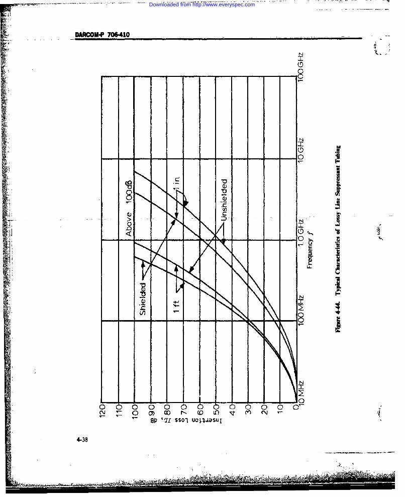
DAROM4P 706-410
(5
fl 3:
i J 0b Ol'r- 0 LO
ap 1,1 ssl uojaaIi4-3N
Downloaded from http://www.everyspec.com

DAACOM-P 706410
50 a 1500 PtH
(A) 03 F03 ~v. 5
LOW PASS
50 !R 1/1500 ijF 4
(1)1/0. 33 PiH 1/0. 33 u~H 50 $1
HIGH PASS
Figure 4-4S. Low-pass to High-pans Transformation
size to resonate the coil at. A coil is added in series c, per ohm of input impedance. etc.), designing thewith each capacitor of the low-pass filter of a size to low-pass filter on that basis, and then convertingresonate the capacitor atf.. back to the bandpasa equivalent.
The preceding approach Is conceptually the same Butterworth filters have a maximally flat band-for multiple-section bandpass filters, or for filters pass response. If some ripple within the passband canwhose input and output impedances differ. but the be tolerated, then a steeper descent into the attenua-process becomes much more complicated. Tabular tion band can be obtained. Tchebyscheff filters havetechniques are available to simplify the process under a greater roll-ofT rate than Butterworth filters for thethese circumstances. They are based on first convert. same number of components, and generally are usedin& the filter requirements to per-unit values (per cy- in bandpass designs where bandpass ripple can be
4-39
Downloaded from http://www.everyspec.com

DARCOM-P 706410
tolerated. Tabular approaches to the design of and (B) of Fig. 4-47. The configuration of Fig. 4- \.. YTchebyscheff bandpass filters are also available (Ref. 47(A) will give a high impedance at the resonant fre-16). quency, while the configuration of Fig. 4-47(B) pro-
vides a low impedance at resonance. The disadvan-tages of these circuits are that their skirt falloff ratesare low (6 dB/octave), and they do not present a
4-5.2.4 Band-reJecion Filters good impedance match to either the source or load.Band-rejection filters attenuate a specific narrow Band reject performance can be improved by using
band of frequencies. This type of device normally is parallel and series-tuned elements in L, r, or T con-used for series rejection between the interference figurations, also illustrated in Fig. 4-47(A) to (D).source and the load. An alternative is to use a band- The details on the design of the types of band-rejectpass configuration that shunts the interference to filters are available in many filter textbooks andground. A notch filter or wavetrap is a filter that handbooks, and will not be discussed here. How-rejects a specific frequency. It may take the form of a ever, some additional comments are considered ap-lumped-constant inductor-capacitor circuit, or it may propriate an one particular type of notch filter,be a shorted quarter-wave coaxial or waveguide stub, because of its wide use in this type of application.or a crystal or ceramic filter lattice. The inductive The twin-T notch filter shown in Fig. 4-48 is usefulcharacteristics of capacitor leads and foil can be as a band-reject filter in the lower frequency ranges.planned so that the capacitor acts as a self-contained At low frequencies, the twin-T filter can achieve a cir-wavetrap, For frequencies below about 1 MHz, a cuit Q on the order of 100, which would not be eco-twin-T resistor-capacitor filter often is found to be an nomically feasible for a wavetrap or inductance-
:i.acceptable configuration. capacitance type filter at the same frequency. Shunt-
The simplest types of wavetraps are parallel or ing effects reduce its usefulness at higii frequencies.series resonant circuits such as those shown in (A) The notch frequencyf,-is determined by (Ref. 17)
0. Hz (4-14)f. /" (RR 2CIC 2) ' "Z (
1 60 H Three special cases are of interest: The case when thetwin-T parameter ratio K 1 gives the symmetricalform of Fig. 4-49. With K - 0.5, a circuit with three
0. 50 pF 0.8 H equal resistances as shown in Fig. 4-30 is obtained. In
Fig. 4-51, with K - 2, three equal capacitances result.0. 0.03 p F It should be pointed out that the twin-T notch filter
parameters must be accurately selected to obtain at-tenuation at the null frequency. Getting the bestpossible null requires careful balancing in network1.0 MHz tuning; a convenient way to do this is by use of trim
capacitors or potentiometers.
LEMI filters made of passive elements are some-F E ptimes bulky and heavy. Active filters, using tran-
4 sisters, can provide large values of equivalent L and'n C-J without excessive size and weight. Moreover, the
, ,, low impedance levels existing at low frequencies inpower lines can be accommodated more easily with
fo active devices.
Active filters for a dc line may contain capacitors• 'Log Frequency f ,Hz as storage elements, series regulators to create a high :
- 0 impedance path, and shunt regulators in combina-~~tion with high gain feedback systems for cancellation ..
i Fiture 44,Example of Bandpass Filter Design of interference. In the cse of ac lines, cancellation is
4-40
": . ," . .... ... ~~~~~~~~~~.. . . .. + .....: . ...... : . . . . .• , . ; :. :: : . . .
Downloaded from http://www.everyspec.com

DARCOM-P 706410-
A)C 1 4 C D2
R R
C C
C3 R30+ 4 2)zC c7
i/RC
Fgr48Twin-T Nth WiteKr
SI /(RC)
Fiur f =0. 1 52(RC)
4-47 Bad-reectFigure 4-49. Twin-T Network With K I.
~~~ T... 4C4
Downloaded from http://www.everyspec.com

DARCOM-P 706-410
R R the input impedance of a gyrator is that of an induct- -
ance of value L = Ck where k is a constant charac-1 3 teristic of the gyrator. Gyrators at low frequencies are
fabricated using conventional amplifying elementsR. with feedback; a total of four such elements is needed
(Ref. 18).2 a 4 Negative-impedance converters have the property
of presenting a driving point impedance at one port,K = 2 which is the negative of the terminating impedance
--/(RC) connected to the other port. A practical realization ofan NIC is obtained using two conventional ampli-.f = 0.2251/(RC) fying elements (Ref. 18).
Integrated and hybrid circuit technology has en-Figure 4-51. Twin-T Network With K 2 abled the construction of small active filters for use in
low-level circuits to perform typical low-pass, high-pass, or bandpass filtering such as required forvarious circuit purposes. Multiple pole Butterworth,Tchebysheff, and Thomson characteristics are avail-
a most effective way to minimize interference. In con- able and, in some cases, are adjustable, Although it istrast to conventional regulators used in regulated possible to construct such filters with relatively largepower supplies, these filters must not regulate the power handling capacity, they are presently mostamplitude of the power to be passed. useful - in so far as EMC/EMI control is concerned
Active ac power line- interference filters pass, with - when they can be applied in low-level circuits.high efficiency, only a narrow band about the powerfrequency. Voltage attenuation values of approx-i~il imately 30 dB can be obtained even at very low load 4-5.A MICROWAVE FILTERS ,
and source impedane levels; two filters may be cas- Microwave filters usually are of coaxial, stripline,caded for higher attenuation values, or waveguide construction. The coaxial technique isThe power line filter scheme shown in Fig. 4-52(A) applicable up to 4 GHz, while waveguide elements
uses phase canellation and operates as follows. The normally are used at higher frequencies. An impor-input is fed into an ac-coupled amplifier through a tant consideration is choosing the filter structure tonotch filter, w1'ch is tuned to the power line fre- be used is the power-handling capacity. Waveguidequency. The amplified interference signal, without structures generally are capable of handling con-the power line fundamental frequency, and with op- siderably more power than either of the other two. Aposite polarity, is returned in series to the source survey of microwave filters useful in interference con-through the transformer. All signals except the fun- trol (Ref. 19) shows the application of all these struc-damental are attenuated by the gain of the amplifier. tural types to low-pass, high-pass, band-pass, andWithin a limited range, a separate control circuit can band-elimination filtering. The use of electricallyprovide automatic tuning of thfe notch filter to power- tunable ferromagnetic devices, such as the YIG (Yt-line frequency and correct any change in the filter trium Iron Garnet) crystal, also is mentioned there.tuning itself. The voltage attenuation curve for a 220-V, 20-A unit is shown in Fig, 4-52(B).
When inserted in the line, the filter introduces the 4-5.4.1 Stripline Filters (Ref. 20)equivalent of a small inductance of 700,uH at the pass The relative ease of fabricating stripline circuitsfrequency. The change in butput voltage at full and their inherent low losses make them attractive forcurrent rating caused by this inductance is negligible, microwave applications. Fig. 4-53 shows an examplei.e., I V for a load power factor approaching unity of the stripline configuration. A single copper stripand up to 6 V in the worst case for zero power factor, forms the center conductor. This strip is embeddedThis type of filter can handle large interference volt- between two dielectric sheets which are in turnages, but with some loss of efficiency. Efficiencies of covered by two copper plates considered to be at90% have been realized for 200-V, 20-A filters. ground potential. Filters are constructed using corn-
Two devices that have been used are two-ports binations of series lines, open or shorted shunt lines,known as the gyrator and the negative-impedance and series capacitors (formed by transverse slots).converter (NIC). When loaded with a capacitance C, Shunt lines are formed by lengths of stripline at right
4-42
' " z;,- .
Downloaded from http://www.everyspec.com

DARCOM-P 706-410
AUTOMATIC TUNINGi
0-
AC POWER
INTERFERENCE
0-
HIGH-GAIN / RNC OCAMPLIFIER FRICLDCANENTR
(A) CIRCUIT DIAGRAM I-
*40
0
4, .20-
0
60 1c0 1 00C. 10. 0 0
Frequency f, Hz(B) ATTENUATION CHARACTERISTIC
Figure 4-52. Active Filter for Powerlimie Interference
-~-~---~-----------4-43
Downloaded from http://www.everyspec.com

DARCM-P 706-410
DILCRI
GROUND PLANES
CENTER CONDUCTOR 17
Figure 4-53. Strip Transmission Line Construction
angles to the main line. Short lengths of open-cir- cutoff frequency. By combining the basic r- and T-cuited line appear capacitive; short lengths of short- sections, more complex filters may be fabricated. The '
circuited line appear inductive. A method of pro- center conductor configuration for a multiple sectionducing shorted shunt lines is shown in Fig. 4-54. A low-pass filter and its equivalent low-frequency net-common problem encountered in the use of stripline work are shown in Fig, 4-56.techniques is the propagation of higher-order modes. There are two types of spurious responses generallySuch modes can be excited by any unintentional tilt encountered in this type of stripline filter. One type ofof the center conductor, yielding narrow spurious response occurs at a frequency where the spacingpass responses in a rejection band. These can be between shunt elements is equal to a half wavelengtheliminated by loading the line with resistor cards, and at integer multiples thereafter. Another type oc-powdered iron slugs, or screws located so as to ab- curs when the shunt element length equals a halfsorb energy from the higher modes without affecting wavelength or an integer multiple thereof. In care-the main transverse electromagnetic (TEM) lines. In fully designed stripline filters, these responses occuraddition to preventing the propagation of undesired far above the pass-band. If it is found necessary, thesehigher-order modes by electrical means, the pre- responses may be eliminated by cascading the filterceding methods provide a mechanically rigid struc, with a low-pass filter having a cutoff frequency slight-ture. ly lower than the first spurious response, and having
Fig. 4-55 shows the stripline center conductor no coincident spurious responses.pattern and the low frequency equivalent circuit for a Impedance matching networks may be fabricatedT-type filter. The value of the inductive elements may readily in stripline. Purely resistive matching can bebe varied by altering the width W of the center con- accomplished by linearl or exponentially taperingductor and hence the characteristic impedance. The the width of the center conductor. Fig. 4-57 shows acapacitive element in the lumped model is produced line linearly tapered to match two different charac.by a transverse line of the appropriate electrical teristic impedances Z, and A2. More complexlength. Note that the transverse element is placed matching may be accomplished by including shuntsymmetrically about the center conductor totally to reactive elements of the proper electrical length.one side. Splitting the shunt capacitive reactance intotwo equal sections on either side of the line reduces 4-5.4.2 Waveguide Filtersthe necessary physical length of the stubs and there- All waveguides act as high-pass filters with cutofffore places spurious responses farther away from the frequencies determined by the shape and size of the
4-44
L
Downloaded from http://www.everyspec.com

-DARCOM.P 706410
SHUNT LINE CENTER CONDUCTOR GROUND PLANE
I DIELECTRIC
SCREW THROUGHGROUND PLANE
MAIN LINE
SHUNT LINE
Figure 4-54. Shorted Shunt Line Construction-
L L capacity of corresponding unridged waveguides at
L-eo Fonte an doiat modee opropagatessue iThis atpeand;ter-
TT~~~ls myayh Newrboree iseu as prtmofe pyrbemdTi filter isreth
wavguieandthemoe o trnsisson.Aplic- uorugated waveuideTh sae filter(i. -8 hben
the rincpleof te wvegiide elo cutf esivacated is caable-of handling becaus of t poe--. th desgn f eqipmnt eclouresto ro- thatin he unerrted, aegided anhandleat oney t-e
Figue 4S5. ymmtra-euie proies high dominant modte odaes Deictesto-adhmwideaen Nt reqe range. the re isnoumero rem evic s it ca s
lessthan0.1dE. nd o hasdling faaite desgn aboincrease the stop-spandinegwaegid.,ad hemoe tans issoer Aptwo-to- tinl or a pati rde. esresigte heha flte inthedesgn f e arpen atanoe wt r- ta thes dim nsioeorthred waveguide n hde fit will relet
Vaue o p osr-hand ln capacit ofes th is typ1 mono std onfiter desigmos ndr the dege-nert modes.
Downloaded from http://www.everyspec.com

r DARCOM-P 706-410
c.+C C 42 T'
T "I. L L
Figure 4-57. Linear Taper Matching of Strip Lines
L F--
i " -C j__ _C -
Figure 4-56. Low-pass Filter andEquivalent Network
thereby providing high insertion loss (50 dB or more).However, the power-handling capacity is decreasedin the same proportion that the height dimension isdecreased. The same insertion loss for the samemodes can be attained by placing a septum in the Figure 4-58. Waffle-iron Wavegulde Filterwaveguide, parallel to the y-z plane, which does notdisturb the propagation of the dominant mode. Bytapering and rounding the edges, as shown on Fig. 4-60, the gradient field enhancement at the front and the section to maintain 100% power-handling capaci-back edge of the septum becomes negligible. Thus, a ty.thin septum has little effect on the power-handlingcapacity, It can be constructed either in the form of a 4-SA.24 Ferite Filtersseries of rods projecting acros the filter, or in the Ferrite materials, properly located in a waveguide,form of bullets projecting out from the narrow walls provide attenuation by absorbing undesired energy,(Fig. 4.61). thus providing a nonreflective filter. By placing a thin
slab of ferrite material across the broad walls of a sec-4-5.4.2.3 Tued Cavities tion of waveguide and biasing the ferrite with mag-
Another reactive device that is useful for increasing nctic fields that control the resonant frequency, it isthe stop-band loss is the tuned cavity. Fig. 4-62 shows possible to absorb large amounts of microwavea section of such a cavity attached to a waveguide see- power over a selected frequency range. A substantialtion. A few cavities can add 30-dB loss over a narrow power loss may be experienced at the fundamentalfrequency range. Placement of thee cavities away frequency in attempting to obtain extra broad stop-
from the regions of maximum electric field enables band loss. Ferrite slabs, placed on the waveguide
4-46i
Downloaded from http://www.everyspec.com

DARCO*-P 106-410
V ~~50 - - _ _ -
40 -
-o TE1 0 MODE
M a- - STO BAND
'-20 - --- - -
V~)
10 - - - -- - -
- PASS BAN4D-
oss. IdB
0. ..- - ......
2.2 3.0 4.0 5.0 6.0 7.0 8.0 9.0 10.0
FREQUENICY f, GHz
Figure 4-59. Characteristics of Waffle-iron Wsveguide Filter
broad walls, will not absorb energy from all modes wall component of electric field, without affecting the
with equal efficiency because the intensities of the RF dominant mode. A narrow slot, filled with absorbingmagnetic fields often vary considerably from mode to material and placed along the broad wall of the wave-mode. In such filters, it is often necessary to reduce guide in a manner similar to a slotted line, will absorbthe height dimension of the waveguide to generate a the energy from all modes which have a current pathsufficient magnetic field across the ferrite slab. Then, perpendicular to the slot.a sizable amount of the energy in the narrow wallmodes is reflected instead of absorbed, and thepower-handling capacity is lowered. Excellent char- 4-5.5 FILTER INSTALLATION AND
acteristics of 0.2 dB to 0.3 dB pass-band loss and 30 MOUNTING TECHNIQUES
dB to 50 dB stop-band loss can be achieved using 4-5.5.1 Generalferrites at powers in the range of 5 MW and higher. Proper installation of filters is necessary to achieve
good results. Input and output wiring must be4-.4.2.5 Absorbig Mode Filtes separated - particularly for good high-frequency
There are various filter techniques that can be used performance - because radiation couples inputto absorb certain modes. Among these techniques is energy directly to output wiring, thus nullifying thethe placement of a thin resistance film perpendicular filter. Input and output terminal isolation is ac-to the narrow wall and parallel to the broad wall of a complished most easily by using a filter that mountswaveguide as shown on Fig. 4-63. Such a film effec- through a bulkhead or chassis. Where bulkheadtively absorbs many of the modes that have a narrow mounting isolation is not feasible, shielded wiring
* A, 4-47
• .:.. -... :.:-".q;,7A
Downloaded from http://www.everyspec.com

DAROUMP 706-410
T.IH OtSSTANCE FILM -
N -
Figure 4-60. Septum Section -
Figure 4-63. Narrow Wall Mode Absorber Strips
should be used. When a filter is connected between aline and ground, the impedance of the ground con-
() Rnection can have a significant effect on the filter per-()OST formance, as shown in Fig. 4-64. When a ground im-
pedance Zb exists, the filter case is raised aboveground and the current through the first shunt Zcapacitor C, divides at the junction of the two .
capacitors and Zb. Some current flows through 4.depending upon the impedance. The remainingcurrent flows through the second shunt capacitor Cto the load, thus compromising filter performance.
(8) BULLET SEPTA Although the location of the filter depends on theindividual application, it should be installed as closeas possible to the interference source.
Figure 4-6 1. Rod and Bullet Septa 4,5.51 a Mounting
In general, any of the following five methods canbe employed to mount grounded filters on a chassis:
CAVITES FIX-TLIMED a. Tabs on the filter bodyWITH SHORING PLATE Ib. Screws or bolts on the filter body
c. A flange on the filter bodyd. A clamp on the filter bodye. A feedthrough stud for bulkhead mounting.
Fig. 4-65 shows these mounting techniques.A typical filter installation is shown on Fig. 4-66,
where the filter is integral with the interference source-in this case, a dc motor. In Fig. 4-66A). the bulk-
head mounting principle is used, and the filter inputand output circuits are completely isolated. Fig. 4-66(B) shows how direct input-output coupling canreduce the effe. 'veness of the filter. Fig. 4-67 il-lustrates two incorrect methods of mounting a filter,both ineffective at high frequencies. In Fig. 4-67(A)
Figure 4-62. Tuned Cavity Section the input and output leads are physically crossed. In
4-48
. - n .. -'.. . mw w ' . --. ,: . - , ,.-' . .. .. .
Downloaded from http://www.everyspec.com

DARCOM-P 706"410
FI LTER
OF INTERFERENCE CURRENTS
i Figure 4-64. Effect of a* Poor RF Ground Bond on Filter Effectiveness
I LT
Fiue -4 Efc o oo FGrw on nFilter Efetvn mot
114,LG T** 4O1. ~ c a
(A1 (+}
(A) Profered Itaaltion
rU .Undesired Coupling Polh
(C) Moutin
Brooketo Motor
Q.-D -. tFilter r
sa ,t suo. () Not Recommended
((E
Figure 4-65. Typical Filter Mounting Techniques Figure 4.66. Filter Installation
4-49
Downloaded from http://www.everyspec.com

DARCOMP 705-410
Fig, 4-67(B) isolation between input and output cir- k..cuits is not complete due to lack of shielding on the
____________ DISCO_ leads - although there is the advantage of east ofassembly, and significant isolation can be obtained
- up to about 5 MHz. Proper installation of power ln- filters is shown on Fig. 4-68.
~ ~ I~'E~~'~4-5.5.3 Connector Mountingloc, 1 02As mentioned in par. 4-5.2.1.6. very small low-pass(A) R~$~ 051 5*1 Oj ?1 LI55Sfilters which are quite effective for frequencies above
about I MHz commonly are installed in pins on con-LO nectors, These may take the form of simple shunt
capacitors between the wire and ground or morecomplex L-, T-, or ir-arrangements. The series induc-
tance is a ferrite-type material which also has lossLOC. Was ffectiveparticularly in ~avoiin couping o n
(s UPRLE LIASS desired energy from one equipment to anotherthrough the cable, or radiation of this energy from
Figure 4-67. incorrect Filier Mounting Methods the cable.
CABINET, PANEL-CBNEPAEORCS RCS LOW RESISTANCE METAL-LOW RESISTANCE METAL-TO- TO-METAL CONTACTMETAL CONTACTPO WER INO PWR LINE
SPCAL POWER INTO W
POWWER LINE
LOW RES ST NC
REETAL-:TO-METALQONTACTNT
PO E
POWRN
CT
POE LNTO
~ 77777 17INET, ANE
Downloaded from http://www.everyspec.com

F--- DARCOM- 706.410
4-6. SHIELDING (Refs. 20, 21) 4.2 THEORETICAL CONSIDERATIONS
4.61 INTRODUCTION The properties of electromagnetic shields are very
It is often necessary to provide shielding to contain dependent on frequency. At frequencies belowinterference generated by particular electronic as- several kilohertz, the effectiveness of magnetic shieldssemblies, or to protect such assemblies from external can be calculated using a quasi-static theory in whichelectromagnetic fields, especially when unshielded the determining factor is the reluctance of the pathoff-the-shelf items must be integrated into an elec- followed by lines of magnetic flux. Such shields aretronic complex. The procedures for establishing discussed in par. 46.6,1. At higher frequencies, andshielding design are similar for any type of en- for nonmagnetic materials at all frequencies, a trans-closure. All seams should be designed to prevent mission line model is used in which skin depth plays aleakage (par. 4.6.5.3), and power circuits should be major role; the incident field is considered to be par-filtered (par. 4-5.5). Cable entry into the enclosure is tially reflected and partially transmitted at the outercritical (par. 4.7,1.3), access doors and removable surface of the shield, and attenuated in passingpanels should have gaskets (par. 4-6.5.4), and venti- through it (see Fig. 4.69) (Ref. 20). At the inner sur-lating apertures should be covered with screening face, partial transmission and reflection can occur
(par. 4-6.5.2). again.Because shield shapes deviate from configurations The shielding effectiveness can be defined in three
readily analyzed, such as infinite planes or circular basic ways: (I) by the ratio of the power densities in r.
cylinders, theory gives attenuation values that are the field at the point in question before and aftcr theonly approximations of those actually obtained, shield is inserted, (2) by the corresponding ratio of *2Where the shield entirely surrounds the object to be electric fields, or (3) the corresponding ratio of mag-protectt.d, the theoretical value is considered to be n-tic fields. It is possible also to define it in terms of-quite reliable. The usual procedureis to select a the ratio of field component of the wave incident onshielding material which, if perfect, would provide an the shield front surface to that r-adiaing from the .adequate amount of protection in the application in- other side. These definitions can produce different re-volved and then to design the penetrations so that the suits in particular circumstances which are de-effectiveness is not degraded to any appreciable ex- pendent on configuration, type of incident wave,tent by them. angle of incidence, etc.
INCIDENT THICKNESS OF
- METAL SHIELD
ABSIORPTION LOSS A
SECOND OUNDARY
; REFLECTION
FIRST SOUNDARY REFLECTION LOSS R RADIATION PASSINGLOSS 2R THE SHIELD P2
B-FACTOR
Figure 4-69. Metal Shielding Effectiveness (Ref. 20)
4-51
i
Downloaded from http://www.everyspec.com

IARCO s-II706410
For a plane wave normally incident on a plane sur- The reflection loss R is given in terms of the im-face the definitions are unambiguous, giving the same pedance of the incident wave 7,,, and that of the metalresult for all three definitions, i.e., expressing the Z byshielding effectiveness SE in dB.
22 (L R = 20 log[ dB (417)
where
10 log , dB (4-15) ' 0+j) f
where orE1,1l ,P1 = incident electric field strength, magnetic
field strength, power density, respective- ZI =- f 3.69 10-1 ,0 (4-19). iy
E2,HZ,P 2 =corresponding quantities of field exitingfrom the shield Thus, for a low impedance field
For the purpose of calculation, it has become con-" ventional to express the shielding as the sum (in dB)of three parts as follows: 10.462 +016 f=20log +0.136 -r +0.3 , dB
SE = R + A + , dB (4-16) r
where (4-20)R R, + R2 = reflection power loss of the
first and second boundarie4, dB For a plane wave fieldA - absorption power loss, dBB - factor due to multiple reflection within / ,d (42
the shield, which can be neglected if A is R = 168 - 10 log dB (4-21)greater than 10, dB
A plane .dve representation is a good approxi- For a high impedance fieldmation for flat surfaces if the source is remote fromthe surface. For such a source, the impedance of the
incident wave Z,, defined as the ratio E /Hjis close- R = 354 - 10 log r, dB (4-22)
ly equal to the impedance of free space 4/ 0 - 377Q. For dipole sources located closer to the source wherethan X/(2w), the wave impedance varies with dis- p - permeability relative to that of free space,tance and is higher or lower than 377 0, depending on dimensionlesswhether the source is of electric or magnetic type. g = conductivity relative to copper, dimension-Magnetic fields occur in the vicinity of coils or small lessloop nntennas. Because reflection losses for mag- f frequency, Hznetic fields are small for most materials, magnetic r - distance from source to shield, in.shielding depends primarily on absorption losses. These relations are plotted in Figs. 4-70, 4-71, and 4-Electric fields are stopped readily by metal shields be- 72 respectively (Ref. 21). The absorption loss A iscause large reflection losses easily are obtained, given by (Fig. 4-73)
Absorption loss represents the reduction in signaldue to dissipation as it proceeds through the body of A - 3.34 v;;fi , dB (4-23)a shield; for conventional materials, it is independentof the type of radiator emitting the signal. For thinshields, the reflection loss may be the most im- whereportant loss. t= material thickness, in.
4-52
Downloaded from http://www.everyspec.com

4. DARCOM-P 706-420V
[VO
H4-5
Downloaded from http://www.everyspec.com

DARCOM-P 706-410
CDC
4-54
Downloaded from http://www.everyspec.com

DARCOMAP.-76410
C)aC
4-5
w 9
AA<
Downloaded from http://www.everyspec.com

DAR=-P706-41
1000
100 Penetration LossA Plus Corv-ection'B Tr) ReflectionLoss (for=' H
V 00
10
-Penetration Lo SS A - ---
110 100 1000
Figure 4.73. Absorpthmosos Curve
4-56
. ~ ~ ~ ~ ~ -.t
Downloaded from http://www.everyspec.com

Tm r-1reflection loss B is given by attenuation of 10 dB at 100 kHz. For materiels other
than those listed, the attenuation can be calculated in: terms ~~~~~~~~~~relative fpermeability aprpit usand the fconductivity./ g h rc Also note e i
hat for magnetic materials, low frequency values ofi jsin0.230A)] AB (4-24) p, are assumed. Therefore, as frequency increases, ad-
justments in the point on the ight-hand scale must beThe correction factor X is given on Fig. 4-74 and is made to account for decreased effective values of K.very nearly equal to 1, except in the cast of low- Fig. 4-76 shows the magnetic fild reflection loss,frequency shielding against magnetic fields. A is given Fig. 4-77 electric field reflection loss and Fig. 4-78by Eq. 4-23. It should be noted that Ihe value of K is ptne wave reflection loss. Figs. 4-79 and 4-80 are 4relative to free space and the value of g is relative to used to acount for re-reflection losses B for incidentthat of copper. Typical values of g and t, (at 150 kHz) magnetic fields. Initially, Fig. 4-79 is used as shownare given in TA 4-5. for obtaining the appropriate value of K, defined as
Fwa these chtus and figures wae can determine the ratio of the shield impedance Z to the im-the iinfamum combination of thickness, permea- pedance of the incident magnetic field Z. and givenbility, andt conductivity which will have the effective- byness readsred. The sohLtion of the shielding equation 1.3
has ben put into nonrograph form (Refs. 29 and 29). = (4-25)
Fig. 4-75 gives the absorption loss. As an examp c of -4 4
its use, it shows that 10 mils of copper will product an
TABLE 4.5. ABSORPTION LOSS OF METALS AT 1- O kHz
g
Metal Relative Relative Absorption LossConductivity Permeability (at IS0 kHz) dB/mil
_ _ _ _ _ _ _ (at 150 kHz)Silver 1.05 1 1.32Copper, annealed 1.00 1 1.29Copper, hard drawn 0.97 1 1.26Gold 0.70 1 1.08Aluminum 0.61 1 1.01Magnesium 0.38 1 0.79Zinc 0.29 1 0.70Brass 0.26 1 0.66Cadmium 0.23 1 0.62Nickel 0.20 1 0.58Phosphor-hronze 0.18 1 0.55Iron 0.17 1000 16.9Tin 0.15 1 0.50Steel, SAW 1045 0.10 1000 12.9Beryllium 0.10 ! 0.41Lead 0.08 1 0.36Hypernick 0.06 80,000 88.5*Monel 0.04 1 0.26Nu-Metal 0.03 8OO00 63.2*Permalioy 0.03 80.000 63.2*Stainless steel 0.02 1000 5.7
"Obtu aabte only if the inident field does nt saturat nic metal
4-57
"4, , --- , -4.. . •. .. . ." . .' - ] '' - ' : . . ' - " " ¢,. " ' L ; . , .
Downloaded from http://www.everyspec.com

DARCOMP 706-410
1C1I,..
S_ 04--u
+k
j 4. S_ -J-
bj 4.)J
m 4J 0-V
0.fO4- 'Mif 11 I
to
it~
X JO 323 UO %3cl-IO3
Downloaded from http://www.everyspec.com

DARCOM-P 706410
500 M
SuDeralloy
t0 M -I00 I0 - 78 PenialoyPurified lironConefic4-79 PermalloyMu Metal
S0 Ni-Iron
"IMHypernick
0 -0
45 Permaltoy
4% Si Iron(grain oriented)Hot Rolled FeSi
too Commercial Irancod Rolled Steel
E Nickel
4% Si Iran
10 It 00O
Stainless Steel
Ik
SilverICowfe
GoldChromiumAluminum
.100Magnesium
ZincBrassCadmium
I ril 103in. PlatinumTin
Figure 4-75. Absorption Loss A4-59
-1 ' " 4,
- w
Downloaded from http://www.everyspec.com

DARCM.P 706410
1013 140
16 ~120Suw
d silver-Gold
100 Magnesium-Zic8lrass
loom Cadmiwn
ptiiel
w0 0 - Moe
Cod60g oe
LL Qo0 C RAW S"e
Commed Iron4~me Steel
0
1k 51.4Io,
Purified Iron2D 4% S Iiron
(grain oriented)45 Pennaltoy78 Permalloy
-100 Hypernic40
60 MU MetalL0 IC-6
Figure 4-76. Magnetic Field Reflection Los RM4
4-60
Downloaded from http://www.everyspec.com

CARCOMP 706-410-
Silv
Alumninum
3 ,wes-~
Bras
100 300 cadnmwrNickiel
i ' P l a t i n u m
Tin
I0k l0 ne
took 410I N-Iron
io Punnrifie Ir
sOO 4% Si Iron
45 Pertnalloy- 78 PerfnalloY
00 Hypennici
IG20
JOG ~ 10 Mu Metal-~ Conetic
Sigre 4-77. Eectic Field Reflecton LAMs RE
4-6141Li
Downloaded from http://www.everyspec.com

1
DARCOtIP 706-410
160 SilverI0 160 Cower
Gold
AMfwm
zinc
=-100 140 Nikel-iL Tm
130 Lead
Monel
120
l 110
took
80 4 Commerci Iron
70
t0IOt - Stainless SteelIOM
4% Si Iron50" 50 Ni-lron
Purifed Iron4% Si Ironigrain oriented)100 M 40" 45 Pemaoy
" 78 Permalloy
30 Hypernick
'iG
20
Mu Metal
10 Conetrc
lOG
Figure 4-78. Plane Wave Reflection Loss Rp
4.62
• ," s..A
Downloaded from http://www.everyspec.com

DARCOM-P 706-410
0.16
0.1 10 ConeticMu Metal
0 5 6 H y v efn id k
78 Permalloy45 Permalloy4% Si Iron(grain oriented)Purified Iron
10 102Stw~less teel
10 e
-
Gavnized Steel
Commercial Iron
U) Cold Rolled Steel
-2
00
2.2 10 cliel
Cadmiun.
Zinc
100 Magnesium
Gold
100 I Copper
Figure 4-79. Chart for Computing K for Magnetic Field Secondary Reflectioa Loss4-63
Downloaded from http://www.everyspec.com

DARCOM-P 706410
oA=6.0dB -Am5.d .
S Am2.OdBj IA-.d-- 5 ? .. .A : 2 .0 d B I fllA- • ; ..
• , -0 1 -
* AuO.6dB
20
) r Amfo.2 de
io-4 4
2 ,
Impedance K.= Z /Z
Figure 4-80. Chart for Computing Secondary Losses for Magnetic Fields
Then, Fig. 4-80 is used to obtain the value of B for the reflection losses as a function of frequency forappropriate value of absorption loss A. various types of materials and thicknesses and for
In some applications double shields are used. The various types of incident wave. Par. 4.6.3.4 considerscalculations of the properties of double shields are the effect of re-reflection (important for thin shields).fairly complex. If there is an air space between the and par. 4-6.3.5 gives examples of calculations ofsurfaces of double shields, the total shielding cf- shielding effectiveness.fectiveness may be estimated by doubling that for asingle shield. However, in critical cases a more care- 4-.3.1 Absorption Louful examination of the matter is advisable since re- For a given metal the absorption loss in dB is pro-flection effects between the surfaces may be sub- portional to the thickness. Values per mil are given instantial in the area between the shields. In the double the third column of Table 4-5 for a frequency of 150shield, however, the effects of penetrations by leads kHz.become quite serious and one must be extremely care- Table 4-6 gives values of g and j, and that of ab-ful in the design in order to obtain the maximum use sorption loss for copper, aluminum, and iron as aof the double thickness of material, function of frequency f. Note that the absorption loss
of Hypernick, at 150 kHz, is 88.5 dB per mil. It is4-6.3 DESIGN DATA cautioned, however, that the high permeability is use-
The next three paragraphs give data on ab- ful only if the incident field is not of sufficient in-sorption, reflection, and combined absorption and tensity to saturate the metal.
4-64
".-k-... '
Downloaded from http://www.everyspec.com

- 7 - ~ U 1--- 7041
. 4-6.3.1 Reflection Lou. Table 4-7, The reflection loss tc a magnetic fieldThe reflection loss R to an electric field source that source, located 12 in. from thr shield, can be cal-
i'exists approximately 12 in. from the shield can be cal- culated using Eq. 4-20 and for a plant wave field byculated using Eq. 4.22. Eq. 4-21. Actual values are also listed in Table 4-7 for
copper, aluminum, and iron. !
R 354 + 10log[g/(f'tr,:)J ,dB (4-26) 4 Combine LossesThe combined absorption and reflection shielding
effectiveness of copper, aluminum, and iron in mag-Values for copper, aluminum, and iron obtained netic fields is summarized in Table 4-8. Similarly, the: using parameters values in Table 4.6 are given in comparative shielding effeciveness of copper and .:
TABLE 4-6. ABSORPTION LOSS OF SOLID COPPER. ALUMINUM,
AND IRON SHIELDS AT 60 Hz TO 10,000 MHz
F Frequency Copper Aluminum Iron Absorption Loss.
.,g M. g p. g u, Copper Mmrun Io9 A 9 1 9 oper Aluminum Iron
60 Hz 1 1 0.61 1 0.17 1000 0.03 0.02 0.331000 HF I 1 1 0.61 1 0.17 1000 0.11 0.08 1.37
10 kHz 1 1 061 1 0.17 -1000 0.33 0.26 4.35150 kHz 1 1 0.61 1 0.17 1000 1.29 1.0 16.9
I MHz 1 1 0.61 1 0.17 700 3.34 2.6 36.315 MHz 1 1 0.61 1 0.17 400 12,9 10 106.0
100 MHz 1 1 0.61 1 0.17 100 33.4 26 137.01500 MHz 1 1 0.61 I 0.17 10 129.0 100,0 168.0
10,000 MHz 1 1 0.61 1 0.17 I 334.0 260.0 T 137.0
"Other values of p for iron are; 3 MHz, 600; 1 MHz. 508 and 1000 MIh. 50
TABLE 4-7. REFLECTION LOSS
Electric Field', dB Magnetic Field ". dB Plane Waveb ', dB
Copper Aluminum Iron Copper Aluminum Iron Copper Aluminum Iron60 Hz 279 241 22 - 1I0 148 111
1000 Hz 242 - 204 34 - 10 138 136 10010 kHz 212 - 174 44 - 8 128 126 90
150 kHz 177 175 - 56 54 19 117 114 79I MHz 152 150 116 64 62 28 108 106 72
15 MHz 117 115 83 76 74 42 96 94 63100 MHz 92 90 64 84 82 56 88 86 60
1500 MHz c - C e - 76 74 5710.000 MHz - c e - C 68 66 60
a For ,ignal source 12 in. from shield. Wave impedance much greater than 377 1!. (For distun e' much greater orsmaller than 12 in.. recalculate the reflection loss using the formulas given in text.)
-, b If penetration loss ik less than 10 dB total, reflection loss must be corrected by use of B-factor.At these frequencies, the fields approach plane waves with an impedance of 377 it.
dSignal source greater than 2X from the shield.
4-65
' . v i : • . . J
Downloaded from http://www.everyspec.com

DARCOM-P 706-410
iron for plane waves is summarized in Table 4-9; and electrical distance from the source increases, theof copper, aluminum, and iron for electric fields in radiation approaches a plane wave. Therefore, theTable 4-10. The curves of absorption and reflection three curves converge as frequency increases. Evenloss for copper and iron are shown on Figs. 4-81 and for the poorest reflection loss curve for iron at 104.82 in electric, magnetic, and plane wave fields. The kHz, A is 4.35 dB per mil of thickness. A shield ofcurves are plotted for signal sources that are I ft from iron 0.03 in. thick at this frequency would thereforethe shield. As frequency increases, the 1-ft distance have a theoretical shielding effectiveness of morebecomes a greater portion of a wavelength; as the than 130 dB.
TABLE 48SHIELDING EFFECTIVENEFS IN MAGNETIC FIELD (WAVE IMPEDANCE MUCH SMALLERTHAN 377 11) OF SOLID COPPER, ALUMINUM. AND IRON SHIELDS FOR SIGNAL SOURCE
12 IN. FROM THE SHIELD AT 150 kHz TO 100 MHz
Frequency, Copper (10 mils) Aluminum (10 mils) Iron (10 mils)MHz A + R - SE A + R SE A + R SE
(dB) (dB) (dB) (dB) (dB) (dB) (dB) (dB) (d0)
0.15 13 + 56 69 10 + 54 64 169 + 19 1881.0 -33 + 64 - 97 26 + 62 = 88 363 +- 28 - 391
15 129 + ',6 205 100 + 74 174 1060 + 42 =1102100 334 + 84 = 418 260 + 82 = 342 1370 + 56 = 1426
TABLE 4-9SHIELDING EFFECTIVENESS IN PLANE WAVE FIELD (WAVEIMPEDANCE EQUAL TO 377 9) OF SOLID COPPER AND IRON
SHIELDS FOR SIGNAL SOURCE GREATER THAN 2 A FROMTHE SHIELD AT 150 kHz TO 100 MHz
Frequency, Copper (10 mils) Iron (I mils)MHz A + R = SE A + R = SE
(dB) (dB) (dB) (dB) (dB) (dB)
0.15 13 + 117 = 130 169 + 79 - 2481.0 33 + 108 = 141 363 + 72 - 435
15 129 - 96 = 225 1060 + 63 1123f00 334 + 88 = 422 1370 + 60 = 1430
TABLE 4-10SHIELDING EFFECTIVENESS IN ELECTRIC FIELD (WAVE IMPEDANCE MUCH GREATERTHAN 377 9) OF SOLID COPPER, ALUMINUM AND IRON SHIELDS FOR SIGNAL SOURCE
12 IN. FROM THE SHIELD AT 0.15 MHz TO 100 MHz
Frequency, Copper (10 mils) Aluminum (10 mils) Iron (10 mils)MHz A + R = SE A + R = SE A + R = SE
(dB) (dB) (dB) (dB) (dB) (dB) (dB) (dB) (dB)
0.15 13 + 176 = 189 10 + 175 = 185 169 + 139 = 3081.0 33 + 152 = 185 26 + 150 = 176 363 + 116 = 479
15.0 129 + 116 = 245 100 + 115 = 215 1060 + 83 -1143100 334 + 92 = 426 260 + 90 = 350 1370 + 64 1434
* " 4-66 .. :.
Downloaded from http://www.everyspec.com

CIAXOM-P 706-410
OPPER
IRON
250---
__ ~ ABSORPTION LOSS
ANDt (dBORTONLS PER MIL)TIKESO EA
AN 4 "FCIN LOSS 01LCRI AE (TIKNS IN (dLS)
PLAo WAVE,6GsE WAUVEI''U V 2~" (HIKESINML
1r-4 S1iel3 (for Si taou-' 1.ro Sheda 100 l to 100 G0liziFREQUNCYM~z
1. AN. . .2_ _ASRTOLS I HIKESO EA3.. . . . . . . . . . . . . . . .. . . . . . . . . . . . . . . . . . . . . ..AVES
. . . . . . . . . . . . . . . . . . .. . . . . . . . . . . . . . . . . . . . . . .
Downloaded from http://www.everyspec.com

r DARCOM-P 706-410- __.... . . -.-.- ! b. Example No. 2. The shielding effectiveness of
-- ' steel (1 mil thick) at 30 Hz in an electric field 165 ft "I distant from the source is determined as follows:
SE R + A + Bi ! 0
whereR = 203 dB (from Table 4-16)A 0.2 dB (from Table 4-18)B = -27.0dB(fromTable4-19)
SE = 176.2 dB.
'Z 1 10 oo l w Obviously : shield can be designed so that there is anappropriate division between reflection loss and ab-
Figure 4-82. Absorption Loss for Copper and Iron, sorption loss. The reflection loss in the electric field
dB per mil decreases inversely with frequency and approachesthe plane wave reflection loss curve, while the re-flection loss in the magnetic field increases inverselywith frequency and approaches the plane wave reflec-
4-6.3.4 RE-REFLECTION LOSS tion curve (Fig. 4-81). The absorption loss of iron atIf the shield is electrically thin (A less than 10 dB), 10 MHz is about 70 dB greater than the magnetic
the hie - old ise etricallat(Aless tan 0 cde, field reflection loss, but, at 100 kHz, it is a Jew dB lessth.n the idnfact enesoud bealuatednd icldd + than the reflection loss. These factors should be fullyin the shielding effectiveness equation (SE - R + A+ B). The B-factors for copper and iron in an elec- considered when designing metal shields. For exam-r de f eple, if shielding against electric fields at frequencies ofl !i trical field, magnetic field, and for a plane wave are -
shown in Table 4-11. about 10 kHz is necessary, the tremendous reflectionloss (over 200 dB on curve 3 of Fig. 4-81) should beused rather than the absorption loss alone. To sum-
4-6.3.5 EXAMPLES OF SHIELDING marize, shielding effectiveness is the result of R + AEFFECTIVENESS CALCULATIONS + 8 together, and not any single part. At frequencies
To illustrate the application of the data, three as low as 60 Hz, absorption loss and reflection lossexamples of shielding effectiveness calculations are become negligible for magnetic fields so that, forgiven, lower frequencies, very thick metallic barriers may be
a. Example No. 1. The results of shielding of- necessary to shield against magnetic fields.fectiveness calculations for copper 7 mils thick, and c. Example No. 3. Based on the examples given insteel I mil and 50 mils thick, in electric, magnetic, and Table 4-20, a metallic barrier made of iron with aplane wave fields at a distance of 165 ft are plotted on thickness of 300 mils must be provided to obtain a
* Figs. 4.83, 4-84, and 4-85 and summarized in Tables shielding effectiveness of 100 dB at 60 Hz for mag-4-12. 4-13, and 4-14. The shielding effectiveness is netic fields. For copper and iron, reflection and pene-calculated by using Eq. 4-16: SE - R + A + B. R can tration losses are small for magnetic fields at lowbe calculated for several distances for the electric, frequencies. Since magnetic materials, such as Mu-magnetic, and plane wave fields (Tables 4-15, 4-16, metal, have high permeability at low frequencies, andand 4-17, respectively). The values for steel and therefore high absorption loss, they are most ef-copper are plotted on Figs. 4-86 and 4-87. For fective as shields. The resulting increase in absorptionexamples, at 10 kHz, for steel in an electric field at a loss is obtained at the expense of a reduction in re-distance of one mile, Fig. 4-86 shows 98 dB of re- flection loss. Following are general rules for selectionflection loss, At 150 kHz. for copper in a magnetic of shielding materials:field at a distance of 24 in., Fig. 4-87 shows 62 dB of a. Good conductors such as copper, aluminum,reflection loss. The absorption loss A can be cal- and magnesium should be used for high-frequencyculated for each thickness of meta!. In Table 4-18 the shields to obtain the highest reflection loss.values for steel (I mil and 50 mils thick) and copper (7 b. Magnetic materials such as iron and Mu-metalmils thick) are given. These values are plotted on Fig. should be used for low-frequency shields to obtain4-88. The 8-factors are summarized in Table 4-19. the highest absorption loss.
4-68
l . . . ,. . .... - .... : .-.. •- - -.; .,-
Downloaded from http://www.everyspec.com

DARCOM-P 706-410,
c. Any structurally sound ihielding material will 4-6.4 MULTIPLE SHIELDINGusually be thick enough for shielding electric fields atany frequency. l.4.1 General
d. To provide a given degree of shielding, The shielding requirements necessary to protectreference to the curves of absorption loss permit against magnetic field transference may be difficult to5 quick estimates of the required metal and thickness, achieve at low frequencies. In the normal power-In most applications, it is necessary to reduce an in- frequency range, for example, copper must be veryterference field to some specified level. This shielding thick to serve as a practical magnetic shield. Mu-requirement can be determined by measuring the in- metal and similar type high-permeability alloys pro-terference field without the shield and comparing it vide good shielding for weak fields; multiple mag-with the specification limits. netic shielding is recommended for strong fields,
TABLE 4-11. B-FACTORS IN ELECTRIC. MAGNETIC, AND PLANEWAVE FIELDS OF SOLID COPPER AND IRON SHIELDS
ShieldThickness, 60 Hz 100 Hz I kHz l0 kHz 100 kHz I Mliz
mils
Copper, t = 1, g = I, Magnetic Fields
1 -22.22 -24.31 -28.23 9.61 -10.34 -2.615 -21.30 -22.07 -15.83 - 6.98 - 0.55 +0.14
10 -19.23 -18.59 -10.37 - 2.62 + 0.57 020 -15.35 -13.77 - 5.41 + 0.13 - 0.1030 -12.55 -10.76 - 2.94 + 0.58 050 - 8.88 - 7.07 - 0.58 + .. 4
100 - 4,24 - 2.74 + 0.50200 - 0.76 + 0.05 0300 + 0.32 + 0.53
Copperg = 1, g =1, Electric Fields and Plane Waves1 -41.52 -39.31 -29.38" - 19.61 - 10.3-1 -2.61
5 -27.64 -25.46 -15.82 -- 0.55 0.14to ! -21.75 -19.61 -10.33 - 2.61 + 0.5-i 0
! 20 -15.99 -13.92 - 5.37 + 0.14 -0.)0
30 -12.73 -10.73 - 2.90 + 050 - 8*81 - 6.96 - 0.55 + 0.14
100 - 4.08 - 2.61 + 0.51 0
200 - 0.62 + 0.14 0300 + 0.41 + 0.58
Iron, =1000, g =0. 17, Eletic FieldsanPleWvs____
I + 0.95 + 1.23 - 1.60 1 - 1.35 + 0.93 + 0.89 0.59 010 + 0.78 + 0.48 + .0620 + 0.35 + 0.08 030 + 0.06 - 0.0650 0 0
Iron,) r4000, g = 0.-17, Electric Fields and Plane Waves1 - I9,53 -17.41 ' 8 35 -1.31
5 - 6.90 - 5.17 + 0.20 010 - 2.56 - 1,31 + 0.3620 + 0.16 + 0.54 030 + 0.58 + 0.4250 + 0.13 0
4 -69
Downloaded from http://www.everyspec.com

FDARCOM-P 706410
10,000 - INIi rIw I ]II II .. fiii' Iy m owlywn Im I III. k
110 0 ~~
Vd)LLJ
ELECTRIC FIELD
4-
SE az R+ A+ 13
WA.. .
to 102 10 0 0 0 0 108 lg 1010
FREQUENCY, Hz
Figure 4.83. Shielding Effectiveness in Electric, Magnetic, and Plane Wave Fields of Copper Shields(7 mil Thickness) for Signal Sources 165 ft from the Shield
Power transformers and audio transformers, mount- of metal in a single sheet. Copper, Mu-metal, iron.ed near each other, may require multiple shielding. conetic and netic type materials, and other metals -
At high frequencies, the shielding effectiveness is some with excellent electric-field reflection loss andgood because of reflections from the surface and some with excellent magnetic field absorption-lossrapid dissipation of the field by penetration losses. At properties - can be used effectively in combination.low frequencies. it is also possible to obtain re- In many applications, it is possible to reduceflection losses in magnetic materials. When much of shielding effectiveness requirements for the overallthe usefulness of shielding is due to reflection losses, equipment housing by employing suppressiontwo or more layers of metal - separated by dj- techniques within the equipment. The recommendedelectric materials, and yielding multiple reflections - techniques make use of component shields, filters atwill provide greater shielding than the same amount the source of the undesired signal interference, partial
4.70
...................................
Downloaded from http://www.everyspec.com

., I~ i - - - - -I
DAROOMP 706410
10.000 -m 1yy~y 1 IM 4 51 1 a I INT -1W TW1 YNW VVn II.V-
1 .000 - [
LAJ
LO4
iU
0
41J-.. 10 II..
0 102 10 106 107 1o8 1o9 to0 1
FREQUENCY, Hz
Figure 4-84. Shielding Effectiveness in Electric, Magnetic. and Plane Wave Fields of Steel Shield(I rll Thickness) for Signal Sources 165 ft from the Shield
shields, isolation of circuits by decoupling, short side of the shield. Such an arrangement is severalleads, and the ground plane as the ground return hundred times as effective as a simple, all-metal lidlead. with spring fit, and is satisfactory under many cir-
cumnstances that otherwise would require wing-nut4-6.4.2 Mutliple Shielding Applications clamping arrangements.
An effective method of handling a cabinet cover The most important source of fields in a signalproblem by multiple shielding is shown on Fig. 4- generator is the oscillator circuit coil. The effective.89(A). The cover shield is in the form of a sandwich, ness of the shielding system is increased greatly if thethe center of which is insulating material. The inner coil is enclosed in an auxiliary shield placed inside the
conducting surface of the lid makes spring contact main shield. In some cases, the entire tuned circuit -with the inner side of the shield, while the outer coh- or the oscillator tube and associated RF tuned cir-ductor of the lid makes spring contact with the other cuits and chokes - are placed in a separate shield
4-71
!.. -
Downloaded from http://www.everyspec.com

DARcOU.P 706-410
1 t ' 0 1 911 111 1 I | 1 I T I 1 | | 1 1 5 l o w " I I m
I I I II ~ l l |
q r
1,000
ELECTRIC FIELO
LUj
S100
I U. PLANE WAVESU-LU. MA NEI FELD _
i. ii10
1 11 I A20 AI I Ili I i i IlllJ a I Iaa!1111 0t11 I all~ I a Jul I a In~i I IJ I il 11k lll
FREQUENCY, Hz
Figure 445. Shielding Effectiveness in Electric, Magnetic, and Plane Wave Fields of Steel Shield-50 rail Thickness) for Signal Sources 165 ft from the Shield
that is within the main shield. In general, re- monly are provided with additional filtering locatedfinements such as filters for leads or single-point in the space between the shields. Shafts that extendgrounding are not used in such a coil or tuned-circuit from the outside to the inner compartment should be
shield. If the shielding that results with such an ar- of nonconducting material to avoid introduction ofSrangement is not adequate, the main shielding con- additional electrical connections between the shields.tainer is placed inside an outer shield. As shown onFig. 4-89(g) the inner shield is insulated from the out- 4-6.S IMPERVECTIONS IN SHIELDS
K. er shield except for a single connection between the Imperfections can be classified as of three types:two. This arrangement precludes the possibility of apertures, seams, and joints. Apertures are placed in-currents circulating around a loop completed tentionally in otherwise closed shields to permit ac-between the shields. In such an arrangement, leads cess via shafts or wiring or to provide ventilationspassing through both inner and outer shields com- and prevent moisture accumulation. Frequently,
4-72
Downloaded from http://www.everyspec.com
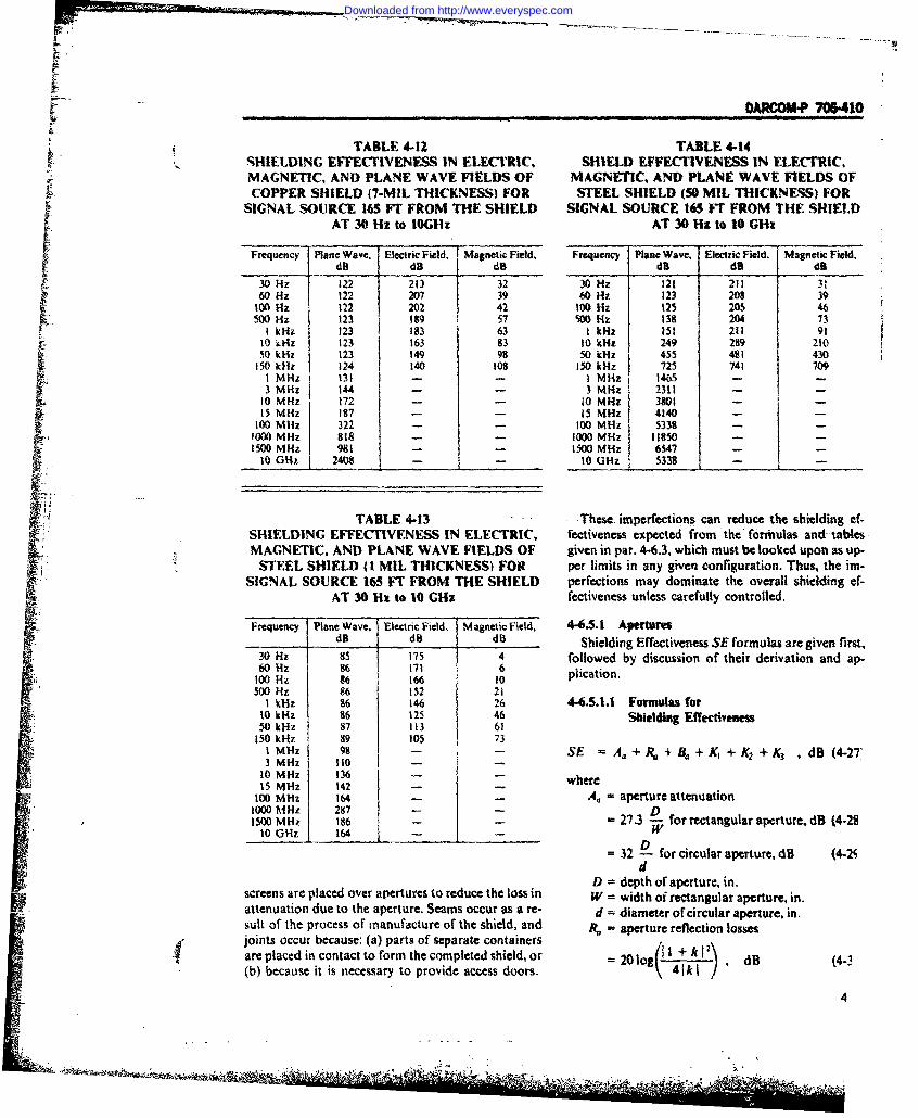
-ARCO-P 706410
TABLE 4-12 TABLE 4-14SHIELDING EFFECTIVENESS IN ELECTRIC. SHIELD EFFECTIVENESS IN ELECTRIC.
MAGNETIC, AND PLANE WAVE FIELDS OF MAGNETIC, AND PLANE WAVE FIELDS OFCOPPER SHIELD (7-MIL THICKNESS) FOR STEEL SHIELD (50 MIL THICKNESS) FOR
SIGNAL SOURCE 165 FT FROM THE SHIELD SIGNAL SOURCE 165 IT FROM THE SHIELDAT 30 Hz to IOGHz AT 30 Hzi to I0 GHz
Frequency PlatneWave. Electic Field. fMagnetic Field, Frequency Plane Wave, Electric Field. Magnetic Field.do do do dB do
30 Hz 122 213 32 30 Hz 1 121 211 3160 Hz 122 207 39 60 H1z 123 208 39
100 Hz 122 202 42 100 Hz 125 205 46500 Hz 123 189 57 S0 Hz 138 204 73
I kHz 123 183 63 1 kHz 151 211 9110 krz 123 163 83 1O kHz 249 289 210
50 kHz 123 149 98 50 kI-z 455 481 430150 kllz 124 140 log 150 kHz 725 741 709I MHz 131 - - I MHz 1465 - -3 MHz 144 - - 3 MHz 2311 - -
10 MHz 172 - - t0 MHz 3801 - -15 MHz 187 - - 15 MHz 4140 - -
100 MHz 322 - - 100 MHz 5338 - --1000 MHz 818 - - 1000 MHz 11850 -1500 MHz 981 - - 1500 MHz 6547 - -
10 GHz 2408 - - 10 GHz 5338 - -
TABLE 4-13 .These. imperfections can reduce the shielding cf-SHIELDING EFFECTIVENESS IN ELECTRIC, fectiveness expected from the formulas and tables-MAGNETIC, AND PLANE WAVE FIELDS OF given in par. 4-6.3, which must be looked upon as up-
STEEL SHIELD (1 MIL THICKNESS) FOR per limits in any given configuration. Thus, the ia-SIGNAL SOURCE 165 FT FROM THE SHIELD perfections may dominate the overall shielding ef-
AT 30 Hz to 10 GHz fectiveness unless carefully controlled.
Frequency Plane Wave, Electric Field, Magnetic Field, 4-6.5.1 Aperturesd8 do 4B Shielding Effectiveness SE formulas are given first,
30 Hz 85 175 4 followed by discussion of their derivation and ap-60 Hz 86 171 6
100 Hz 86 166 10 plication.500 Hz 86 152 21
1 kHz 86 146 26 4-.5.1.1 Formulas for10 kHz 86 125 46 Shielding Effectiveness50 kHz 87 113 61
150 kHz 89 105 731 MHz 98 - - SE = Aa+R +Ba+K, +K 2 +K 3 dB (4-27'3 MHz It O- -
10 MHz 136 where15 MI-z 142
100 MHz 164 - - A, = aperture attenuation1000 MHz 287 - - D1500 MHz 186 - - - 27.3 - for rectangular aperture. dB (4-28
10 GHz 164 - - W
= 32 R for circular aperture, dB (4.2Sd
D - depth of aperture, in.screens are placed over apertures to reduce the loss in W = width oi rectangular aperture, in.I attenuation due to the aperture. Seams occur as a re- d = diameter of circular aperture, in.suit of the process of nanufacture of the shield, and = aperture reflection lossesjoints occur because: (a) parts of separate containers = a
are placed in contact to form the completed shield, or = 20 log (4-3• .Olo-( l4 ...)(b) because it is necessary to provide access doors.
4
- .. . .. 'S.. . . , ,- -t+-. -4 i 5l
Downloaded from http://www.everyspec.com
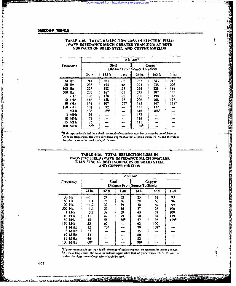
DARCOM-P 706410
TABLE 4-15. TOTAL REFLECTION LOSS IN ELECTRIC FIELD(WAVE IMPEDANCE MUCH GREATER THAN 377fl) AT BOTH
SURFACES OF SOLID STEEL AND COPPER SHIELDS
dB Loss'Frequency Steel CopperL Distan~ce From Source To Shield
24 in. ]165 ft I ml 24 in. 165 ft I mi
30 Hz 241 203 173 282 243 21360 Hz 233 195 165 273 235 205
100 Hz 226 188 158 266 228 198500 Hz 205 167 137 245 207 177I kHz 196 158 128 236 198 168
10 kHz 166 128 98 206 168 13850 kHz 145 107 77b 185 147 ! 7b
150 kHz 131 92 - 171 132I M Hz 108 69b - 146 !0g
b -..
3 MHz 91 - - 132 -
10 MHz 79 - - 116 -15MHz 75 - - Ill -100 MHz 56 - - 86 -
-If absorption loss is less than 10dB, the total reflection loss must be corrected by use of B-factor.bAt these frequencies, the wave impednace approaches that of plane waves (r> A). and the values[ ifor plane wave reflection loss should be used.
TABLE 4-16. TOTAL REFLECTION LOSS INMAGNETIC FIELD (WAVE IMPEDANCE MUCH SMALLER
THAN 3770) AT BOTH SURFACES OF SOLID STEELAND COPPER SHIELDS
dB LoseFrequency Steel Copper
Disiance From Source To Shield
24in. 165ft I mi 24in. 165ft i miI 30 Hz -I 24 53 25 63 9360 Hz -1.4 26 56 28 66 96100 Hz -1.2 30 59 30 69 99500 Hz 1.4 36 66 37 76 106
I kHz 3.2 39 69 40 79 10910 kHz 11 49 79 50 89 11950 kHz 18 56 86b 57 96 1 2 9 b
150 kHz 23 60 - 62 100 -I MHz 32 70b - 70 109 b
3 MHz 31 - - 7510 MHz 43 - - 8015 MHz 46 - - 82
100 MHz 60b
- 90b -
:If penetration loss is less than 10 dB, the total reflection loss must be corrected by use of B-factor.
bAt these frequencies, the wave impedance approaches that of plane waves (r> > .), and thevalues for plane wave reflection loss should be used.
4-74
-- ,S
Downloaded from http://www.everyspec.com

Ip
DARCOW-P 706410
TABLE 4-17
TOTAL REFLECTION LOSS IN PLANE WAVEKFIELD (WAVE IMPEDANCE EQUALS 3770)
AT BOTH SURFACES OF SOLID STEEL ANDCOPPER SHIELDS
dB Loss'
Frequency Steel Copper
30 Hz 113 15360 Hz Ito 150
100 Hz 108 148500 Hz 101 141
1 kHz 98 13810 kliz 88 12850 kHz 81 121
150 kHz 76 116I MHz 70 1083 MHz 66 103
10 MHz 61 9815 MHz 60 96
100 MHz 58 881000 MHz 51 781500 MHz 56 76I; 10 GHz - 58 68
,If penetration loss is Icss than 10 8M, the total reflection loss rnu-tbe corrm-ted by use of B-factor.
k = -Z
- = ratio of aperture characteristic im- =10 log , dB (4-36)
pedance Z4 in 91c=z to impedance of A = area of each hole, in.th nietwae4i 1m N - number of holes per in!the incident wave Z.in 0icm2
-- W/(3.142p) for rectangular apertures and K, = correction factor for penetration of themagnetic fields (4-31) conductor at low frequencies
= d/(3.682r) for circular apertures and ( 35\magnetic fields (4-32) = - 20 log I + , dB (4-37)
= fW 1.7 X 10' for rectangular apertures P Z/and radiated fields (4-33) p = ratio of the wire diameter to skin depth forj fd 1.47 X 10-' for circular apertures screeningand radiated fields (4-34) = ratio of the conductor width to skin depth
f = frequency, MHz between holes for perforated sheets, dimen-r = distance from signal source to shield, in. sionless. (Copper skin depth =
B. = correction factor for aperture reflections, 2.6 X l0 'dB (N. becomes insignificant when A, is - -- in,)
more than 10 dB.)(k - )2'/to dB(4-35) K3 = correction factor for coupling between20108jl - (k + 1)2 1 j closely spaced shallow holes
K, = correction factor for the number of openings ( Iper unit square when the test antennas are = 20 log dB (4-38)far from the shield in comparison to the dis- l ,(
tance between holes in the shield. 8.686
4-75
Downloaded from http://www.everyspec.com

DARCOM-P 706410
20
tOE7to o t 9 tt.II111FLsoPSCH
Figue 4-6. Olf leto osa ohSrae faSldSelSil
44512 SlgEfcte softewvgiecaatritcipdneblwct
Foml140aou f oteicietwv meane h hrcShelin efetiees frmla fllw triti ipeaceZ~ofa ecanuarwaegid wl
a LAttE o cWuAV oS .nEq4274rpr- blwctfisset h teuto sth aepse hog haprtr whcfrfeunie0eo0uofi rc W W(-0
tangular~ ~~ gud s, iLgv n Es
The imeacI. ftewveitdb ml
FiguanL re he 6 freqenc unelconder at Bt fso Solid Ste Shie4l4d
and51. t h ieloff frfysective lynIewllb ob- Tk the aio ofh q.ra 0tori Eq. 4.41,nc blwe have.seve otatWmsulay thriatole diefio toteerpen-av medne.Techrc
diuartS h e-ield. e q.es 4f3rmevlat for ferqutn- imeac 7,oI etnuarwvgiewlci. wteubelow calutions poIde Eq. 4-2, and- beo utf s
sieilare procdur for irqcrides prow oi Eq.- 4-±-29wicns heeqaio fr givens iy Eq.e 4a3: fo (a-40
b.RfA to clain . in68 Eq (4-39h loo- sercelds.Boith Eqs 4-o and 4ou41e care d n oK
aln loshe caculat edy aesafction of thl e rto uTsbitaking the ratioofE.40to. 4-1 and ave4-7dtatWi6lay hthoedmnio epn
Downloaded from http://www.everyspec.com
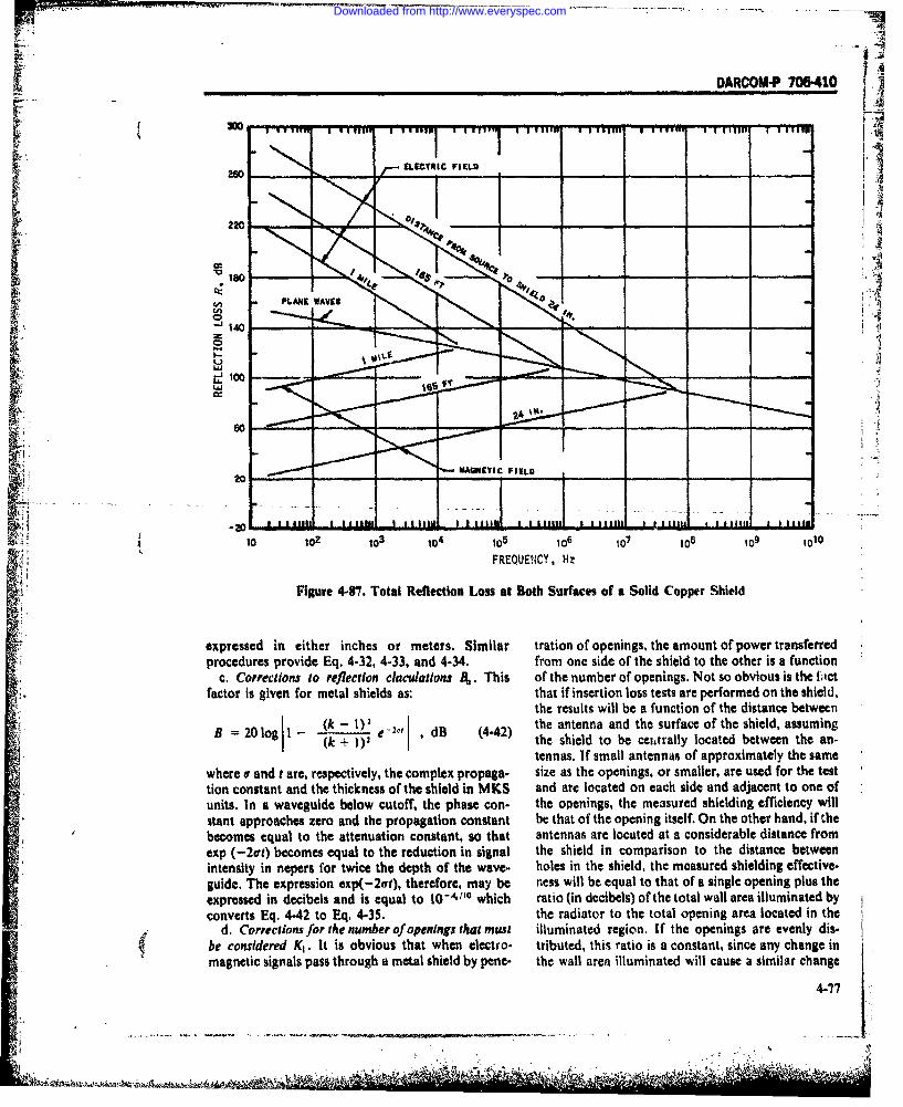
DARCOM-P 706410
I I'llyl I off,,.. I IlnlII I I.I.-I I I l 'W II1"1l ;i 1 1 1 1 1 11111 1 1 Iihp "
. !;J,20 J ELECTR IC D
•_'.... _ _ _ _"_I
0
V
10 10
expressed in either inches or meters. Similar tration of openings, the amount of power transferredprocedures provide Eq. 4-32, 4-33, and 4-34. from one side of the shield to the other is a function
c. Corrections to reflection clacidatlons Ba. This of the number of openings. Not so obvious is the fdctfactor is given for metal shields as: that if insertion loss tests are performed on the shield,
the results will be a function of the distance betweenB:21 l (k - 1)2 '' the antenna and the surface of the shield, assuming(20 l -1 e1 , dB (4-42) the shield to be et1rally located between the an.
ig tennas. If small antennas of approximately the samewhere e and are, respectively, the complex propaga- size as the openings, or smaller, are used for the tettion constant and the thickness of the shield in MKS and are located on each side and adjacent to one of
units. In a wavegulde below cutoff, the phase con- the openings, the measured shielding efficiency willsant approaches zero and the propagation constant be that of the opening itself. On the other hand, if thebecomes equal to the attenuation constant, so that antennas are locatedat a considerable distance fromexp (-2or) becomes equal to the reduction in signal the shield in comparison to the distance betweenintensity in nepers for twice the depth of the wave- holes in the shield, the measured shielding effective-guide. The expression exp(-2ut), therefore, may be ness will be equal to that of a single opening plus theexpressed in decibels and is equal to l' m which ratio (in decibels) of the total wall area illuminated byconverts Eq. 4-42 to Eq. 4-3. the radiator to the total opening area located in the
d. CorrecI ons for the number of openings that mus illuminated region. If the openings are evenly dil-considered It is obvious that when electro- this rati isefcOnt e any hang in
becoeqa to teatnaincsatoth tribntea aroated at a consieabl sne dancne m
magnetic signals pass through a metal shield by pne- the wall area illuminated will cause a similar change
be cons d K It is _o t
. . . . . . . . . . . . . .. . -:
Downloaded from http://www.everyspec.com

--
DARCOM-P 706-410
TABLE 4-18. ABSORPTION LOSS OF STEEL ANDCOPPER SHIELDS AT 30 Hz to 10 GHz
Frequency dB LossI Mil Steel 50 Mil Steel 7 MiICopper
30 Hz 0.2 9 0.1360 Hz 0.3 13 0.18100 Hz 0.3 17 0.23500 Hz 0.7 37 0.52
I kHz 1.0 53 0.7410 kHz 3.2 161 2.3450 kHz 7.5 374 5.23150 kHz 13 649 9I MHz 28 1395 23
:3 MHz 45 2245 40 1
10 MHz 75 . 3740 7415 MHz 82 4080 90100 MHz 106 5280 2341000 MHz 236 11800 7401500 MHz 130 6490 905I, 10 GHz 106 5280 2340
in hole area. Therefore, the minimum shielding ef- skin depth. However, this approach runs into dif-In fectiveness becomes that of the single opening plus ficulty when the skin depth becomes equal to orthe correction factor of Eq. 4-36. At intermediate greater than the wire radius, since this is the border-
points, the shielding effectiveness lies between the line region where leakage through the metal itselftwo values. Both values are of practical importance. must also be considered, To maintain reasonable sim-
The shielding effectiveness near the shield is impor- plicity for calculation purposes, test results for atant for protection of sensitive equipments which variety of copper screen shields were plotted as amay be placed close to the walls (data cables, etc.). It function of skin depth, and an empirical equationis especially important in cases where radiation (Eq. 4-37) was derived for the correction factor. Thishazards may exist, so that personnel are protected correction factor also may be satisfactory for per.who otherwise may unknowingly enter a strong field forated sheet metal, but no corroborative tests haveexisting In the vicinity of a poorly designed seam. been made.Calculations of shielding effectiveness in interior f. Corrections K3 for closely spaced shallow open-parts of a structure are important since, if advantage angs. When apertures in a shield are closely space, andis taken of added shielding effectiveness, a con. the depth of the openings is small compared to thesiderable reduction in cost of shield construction can width, the shielding effectiveness has been found tobe achieved, be greater than otherwise would be expected. This is
e. Low frequency corrections K2 for screen-type interpreted as being a result of coupling between ad-shields, Numerous tests have shown that the high- jacent holes, which becomes important when the at-frequency shielding effectiveness of screening mater- tenuatlon through the openings is small. By con-ials can be satisfactorily approximated by assuming sidering two such adjacent holes subjected to an clec-that the openings in the screen are equivalent in size tromagnetic field, aligned as shown In Fig, 4-90, it ap-to the openings in a flat perforated metal sheet, and pears that current induced on the conductor betweenthat the depth of the openings is equal to the wire the holes can flow into one side of a hole and returndiameter. At low frequencies, when the skin depth be- immediately via the adjacent hole - in effect, merelycomes comparable to the radius of the wire, a con- encircling the conductor. Since the current is the '1siocrable loss in shielding effectiveness occurs. This same in closely spaced holes, this is equivalent tomay be considered from the viewpoint that the aper- placing a low resistance short circuit at the end oftures, as waveguides, are made wider and shorter by a each hole considered as a waveguide. The impedance
4-78
• ;i 4;, t i
Downloaded from http://www.everyspec.com

F-- i
DAR00OMP 706-41010,000 1 i II . I -i rI I I I I 11114i..
1000
.7-mL COPPER SHIELD\
10D
0
4I/
FREQUENCY, Hz
Figure 4.88. Absorption Loss for Steel and Copper Shields at 30 Hz to 10,000 MHz
of the short may be approximated for rectangular a- conductivity of the metal -holes as the surface impedance presented by the sur- 5,11 X 101 mho/m for copperface of the conductor between the holes- a - width of conductor between holes
(Fig. 4-90), mjW(E) Ra (4-43) b - length of rectangular hole (Fig. 4-90), m7L \b The characteristic aperture impedance given by Eq.
where 4-40 is JwjAi W/ir at all frequencies being considered.The ratio of ZL to 7,~ is therefore:
J~intrinsic impedance of the metal, flCrZL Jwt/afa
- .
fM .ST Z. a N 7-,
7-7
Downloaded from http://www.everyspec.com

DARCOM-P 706-410
TABLE 4-19. CALCULATED B-FACTORS FOR STEEL AND COPPER SHIELDS FOR"SIGNAL SOURCES 165 FT FROM THE SHIELD
Electric Field and Plane Wave Magnetic FieldFrequency 50 Mil Steel, I Mil Steel, 7 Mil Copper, 50 "MiSteel. I MSteel, 7 MiCopper,
dB dB dB dB dB
30 Hz -1.14 -27.0 -30.7 30 Hz -1.07 -20.0 -30.760 Hz A > 10dO -24.7 -27.9 60 Hz A > dB -20.5 -27.9
100 Hz -22.7 -25.8 100 Hz -19.6 -25.8500 Hz -16.0 -19,0 500 Hz -15.6 -19.0
I kHz -13.3 -16,1 I kHz -13.3 -16.110 kHz - 5.6 - 7,5 10 kHz - 5.6 - 7.550 kHz - 1.7 - 3,1 50 kHz - 1.7 - 3.1
150 kHz 4 > 10dB - 1.2 150 kHz A > 10dB - 1.2A > l0dB A > l0dB
At frequencies as low as 10 kHz, the expression under For all practical purposes, the wave impedance 4, isthe radical is smaller than 10-1, showing that for all always much larger than either 7, or 71, and the ratioreasonable opening dimensions and any frequency of of Eqs. 4.48 to 4-47 reduces to:interest ZL is much smaller than Z,
In accordance with transmission line theory, the in- Z. Iput impedance of the guide Z4 may be calculated by: dimensionless (4-49),Zi tanha
Zt cosh a + 7, sinh a\. 1 4Z V Z-coh +sinh', ) 45) Eq. 4-49, in dB, provides the correction factor for7cs closely spaced shallow holes as given by Eq. 4-38. It
where a is the waveguide attenuation in nepers. will be observed that, since 4, is always larger than Zj!Since, for the express condition being investigated, a for A. equal to 10 dB or less, the correction factor is
4, always positive and increases the shielding effective-is small, and since ZL : _e Eq. 4-45 simplifies to. ness.
/sinh a.Z, = Z) Z4 tanh a, , A (4 46)n4-6.2 Aperture Screening
The ratio of the intensities of the reflected wave to the An equipment enclosure that requires inlet and/ortransmitted wave, when the attenuation is large, is outlet apertures for ventilation or pressurization
a tshould be designed with appropriate metallic cov-eu toerings placed over the apertures. Although louvered
openings generally are used for cooling air cicu-(Z. + 2)2 dimensionless (4-47) lation, they are extremely poor for RF integrity be-
4 2_ 7 cause of their long, narrow gaps. In descending orderof attenuation properties, the following materials
When the attenuation is small, the ratio becomes: should be used: waveijuide below cut-off panels, per-forated metal sheet, woven metal mesh, and knittedmetal mesh. Solid metal covers for apertures de-
(M + 4 ),_ dimensionless (4-48) signed for temporary access are discussed in par. 4-4 Z e. s 6.5.4.
4-80
Downloaded from http://www.everyspec.com

DARCOM-P 706410
4 TABLE 4-20EXAMPLES FOR CALCULATING SHIELDING EFFECTIVENESS OF SOLID-METAL SHIELD
10 kHz-10 Mils
Magnetic Field Electric Field Plane Wave
Copper Iron Copper Iron Copper Iron
Reflection 44.2 8.0 212.0 174.0 128.0 90.5Absorption 3.6 43.5 3.3 43.5 3.3 43.5B-Factor -2.6 0 -2.6 0 -2.6 0
Total Loss, 45.2 51.5 212.7 217.5 128.7 134.0dB
60 Hz-Magnetic
I Mil 10 Mils 300 Mils
Copper Iron Copper Iron Copper Iron
Reflection -. 22.4 -- 0.9 22.4 --. -0.9-----" .22.4 . -0.9Absorption 0.03 0.33 0.26 3.34 7.80 100.0B-Factor -22.2 +0.95 -19.2 +0.78 +0.32 0
Total Loss, 0.23 0.38 3.46 3.22 30.52 99.1I '
IdB
10 kHz-. 30 Mils- Magnetic I kHz -10 Mils - Magnetic
Copper Iron Copper Iron
Reflection 44.20 8.0 34.2 0.9Absorption 10.02 130.5 1.06 13.70B-Factor +0.58 0 -10.37 +0.06
Total Loss, 54.80 138.5 24.89 14.66dB
10 Mils-Copper
150 kHz I MHz
Electric Plane Magnetic Electric Plane MagneticWaves Waves
Reflection 176.8 117.0 56.0 152.0 108.2 64.2Absorption 12.9 12.9 12.9 33.4 33.4 33.4
SB-Factor +0.5 +0.5 +0.5 0 0 0" Total Loss, 190.2 130.4 69.4 185.4 141.6 97.6
il 4-81
,. ... " " '
, : ... ... ..... .............. ,,+ , :
Downloaded from http://www.everyspec.com

DARCOM-P 706410
INSU.ATING MATERIAL RE1OVABLE OUTER CONDUCTOR 4-6.5.2.1 Screening A
Z' SP or A single or double layer of copper or brass screen,u~N R m[ coNTAT$ or No. 16 or 22 gage wire, should have openings noS .... greater than 1/16 by 1/16 in. A mesh less than 18 by
18 (wires to the inch) should not be used. The mesh..... wire diameter should be a minimum of 0.025 in. (No.1 22 AWG). If more than a nominal 50 dB of at-tenuation is required, the screening should have holes
(A) SANDICH TYPE Or LID FOR A SHIELDED ENCLOSURE no larger than those in a 22 by 22 mesh made of 15rmil copper wires.The attenuation of an electromagnetic wave by a
mesh is considerably less than that afforded by a solid
metal screen. The principal shielding action of a mesh0 NB, "" is due to reflection. Tests have shown that mesh withi50% open area and 60 or more strands per wave-"' ,length introduces a reflection loss very nearly equal
to that of a solid sheet of the same material. The meshCIR&a construction should have individual strands per.
manently joined at points of intersection by a fusingCONNETTHE process so that permanent electrical contact is made,BETWEEN SHIELD and oxidation does not reduce shielding effective-(s) MULTIPIe SHIELDING SYSTEM PROVIDED WITH A SIN LE POINT CONNECrIONBETWEE THE SHIELD$ ess. A screen of this construction will be very ef-
fective for shielding againstelectric (high-impedance)Figure 449. Multiple Shielding Applications fields at low frequencies because the losses will be
caused primarily by reflection. Installation can bemade by connecting a screen around the periphery ofan opening (Figs. 4-91 and 4-92). The results ofshielding effectiveness measurements for screening
Inns,.sa.o, Di.ction are shown on Figs. 4-93 through 4-98. Table 4-21 listsof In iden FloIs, mesh, wire, and aperture sizes for various screening
materials.The screening materials given in Table 4.22 and on
Figs. 4-99 and 4-100 exhibit low-shielding effective.ness - probably because of crossover discontinui.ties in mesh. A comparison between No. 16 alumi-
Di-ctio of Ouro Cn,,nuo.a° num mesh and No. 12 copper mesh (Fig. 4-99) re-veals a 5 dB differential, and both have an at-tenuation that is comparable to that of 60 mils per-forated steel shown in Fig. 4-100. All are in the 50 dB
..... range, with the perforated material having a greaterpercentage of open area and, therefore, less re-sistance to air flow. Because mesh, for effectiveshielding, rarely has more than an open area of 50%,T the size of apertures must be increased correspond.
CI,,.a, so. aa Cougotoro sact°, RH MR0 OUor , ingly for effective ventilation. Mesh should be easilyBe.w. Me betwsen Holes removable; it should be attached with screws or bolts.
These should be in sufficient number to ensure high.pressure contact along a continuous line completelyaround the edge. Contact surfaces should be cleaned
-thoroughly each time the mesh is removed.In the 40-dB range, the 30-rail. 1/4-in. spacing gal-
Figure 4-90. Currents Induced on Perforated vanized steel mesh and the 0.037-in. aluminum per-Metal Sheet forated sheet (Fig. 4-100) are comparable to No. 10,
4-82
Downloaded from http://www.everyspec.com

[ DARCO*-P 706-410
WELDBEAD 0n $OLDER(CONTINUOUSLY FUSEDTO METAL ALONG THE
1/2 PREFERABL E - OW )
1/4' ACCEPTABLE /
Figure 4-91. Typical Welded Screen Installation Over a Ventilation Aperture
CIRCULAR CLAMP OIONN PS
POSITIONING PINS
IF REQUIRED
H SUFCIENT SCREWS OR OTHERASTENERS
TO OBTAIN CONTINUOUS CONTACT ALONGELECTRICALLY CLEANED METALLIC MATINGSURFACES
Figure 492. Typical Clamped Screen Installation Over a Ventilation Aperture
4-83
. , . • . ; .. _ .
Downloaded from http://www.everyspec.com

F DARCOM-P 706410
-'~ ~ 9 ~r
bit/
)A
GP ~ ~ I /NI~n3
4.84
Downloaded from http://www.everyspec.com
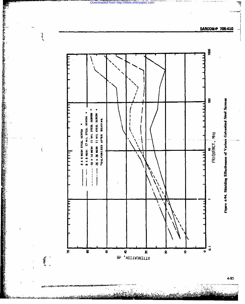
DARCOO*P 706414
N0
OPil - - --~il
14-85
Downloaded from http://www.everyspec.com

DARCOMP 706-410
sin~ -i- -v- -to
10' I
4
UP 'NOJJ.VnN3li.V
4-86
Downloaded from http://www.everyspec.com

DAROM-P 706.410
IL
-L * -
I/ 40
UP' / =IAN1
4-8
Downloaded from http://www.everyspec.com

I
DARGOMP 706-410
IiV
II
I i- - - - - 4
0%Ii
U0
I *1Uwe jif-s
w I-~ ~ N q~
~.. CI)
.. j gg~ - .~...h5 ,... - a
~ 2
0~
3
I I
'I 1.iiIt
- - - - - - - a2.
44'1..=
8 2 8 aSP 'NOIiVQN3JJ.V
448
Downloaded from http://www.everyspec.com

OARCOMP 7"s41
as ma
I ta
I UU
II
2pw INivn3
I flu-8
Downloaded from http://www.everyspec.com

DARCOM.P 706410_
R 7 TABLE 4-21 18 mils monel mesh (Fig. 4-99). The galvanized mesh
MESH, WIRE, AND APERTURE SIZES has the largest percentage of open area.FOR TYPICAL SCREENING MATERIALS Fig. 4-99 shows test results of materials. The 40-
count copper-nickel 36% open sample has a rangeMesh Wire Diameter, Size of Opening. greater than 90 dB. Such electroformed mesh
in. in. materials are excellent as RF screening agents for.... .... . ... ' .. . . .. :'- panel meters, pilot lamps, counters, and other simi-8 X 8 0.028 0.097 lar aperture discontinuities, or as simple inner-unit8 x 8 0.0325 0.093 shields where small volumes of air transmission are8 x 8 0.047 0.078 necessary.8 X 8 0.063 0.062 Figs. 4-101 and 4-102 illustrate the measured mag-
10 10 0.025 0075 netic feld shielding effectiveness of screens of the10 x 10 0.032 0.068 various designs and metallic compositions listed in10 X 10 0,035 0,065 Table 4-23 for the range of 0.15 to 1000 MHz.lox 10 0.041 0.05912 x 12 0,018 0.065 4-6.5.2.2 Wavegulde-below-cutoff Devices12)X 12 0.023 0.060 In many cases, shielding screens introduce ex-12 X 12 0.028 0.055 cessive air resistance, and sometimes greater shielding12 X 12 0,035 0.048 effectiveness may be needed than they can provide. In12 X 12 0.041 0.042 such cases, openings may be covered with specially14 X 14 0;017 0.054 designed ventilation panels (honeycombs) with open-14 X 14 0.020 0.051 ings that operate on the waveguide-below-cutoffii14 × 14 0.025 0.04614 x 14 0.032 0.039 principle. When an insulated control shaft passes16 x 16 0.016 0.0465 through a waveguide attenuator, the control function16 X 16 0.018 0.0445 can be accomplished with almost no interference16 x 16 0.028 0.0345 leakage. A sample panel is shown on Fig. 4-103.18 X 18 0.017 0.0386 Honeycomb-type ventilation panels in place of18 x 18 0.020 0.0356 screening:18 X 18 0.025 0.0306 a. Allow higher attenuation than can be obtained20 x 20 0.014 0.0360 with mesh over a specified frequency range.20 X 20 0.016 0.0340 b. Allow more air flow without pressure drop for20 x 20 0.020 0.0300 the same diameter opening.22 X 22 0.015 0.0305 c. Are less easily damaged, and are therefore more
reliable.
TABLE 4-22MESH, WIRE, AND APERTURE SIZES FOR
SCREENING MATERIALS TESTED
Wire Diameter,Metal Mesh Size mils
Monel No, 10 18Copper - No. 12 20Aluminum No. 16 20Galvanized steel 1/4 in. X 1/4 in. 30Galvanized steel 1/2 in. X 1/2 in. 30Perforated steel' 1/3 in. diameter holes on 3/16 in. ccntersPerforated aluminum: 1/4 in. diameter holes on 5/16 in. centersPerforated aluminumb 7/16 in. diameter holes on 5/16 in. centersAluminum honeycomb' 1/4 in. segregated cells
60 mils thick,37 mils thick
1 in. thick F4-90 ~i
Downloaded from http://www.everyspec.com

- - - POM-P 706410
IE A
a a, a4i
LL-
C 4 1
4-91
Downloaded from http://www.everyspec.com

F DARCOM-P 706-410
iaa
I O
I aI
It.
a a
4-92I
Downloaded from http://www.everyspec.com
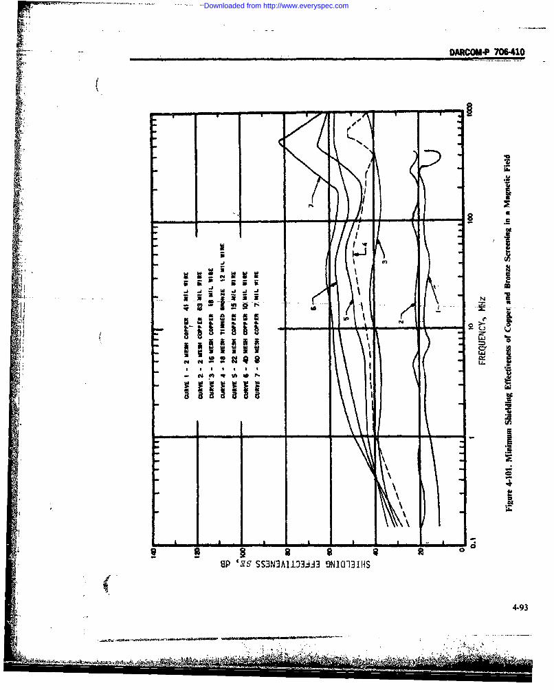
[ DARCOM-P 706-410
I7 .V3
hinI -JLai
WEL
a Q a aUU-
UP E ' 96SMAIJ DIO3H
-- a'.---4-93
Downloaded from http://www.everyspec.com

_- DARCOMiP -041
I" w I2 z
-- - -i
S SNA10 J3UIO131H
41 94
Downloaded from http://www.everyspec.com

DARODO-PIO K
ATABLE 4-23 .7 -
COPPER, BRONZE. ANDSTEEL SCREENING USED IN MAGNETIC .6 - " CIA. -oE -
FIELD SHIELDING EFFECTIVENESS 4 .TH0'c- TA
TEST MEASUREMENTS - - - -o 4
Mesh, Wire Diameter, .
Metal wi es/in. mils g . ,[Copper 2 41 ,.2 _
22 15 ' .O ,'WALL ALUMt I NUM
! 40 lo 060 7 0 o 10 0 0 0 o o
Tinned Bronze 18 12 AIR VOLUME, ft /min
SGalvanized Stee) 17 Figure 4-104. Air Impedance of Perforated Metal18 14 11 and Honeycomb
26 !IStainless Steel 16 18
• ,__•24 18
Cu- NJ 40 COUNT CU7MIL 40 3 MIL LANOCU-7mr. 40 5.0 NI.
, COUNT 2 5 COUNT- /
CU 3 MIL
- 25 COUNT
-. 5 - -.
0 2o 400 a003 o 00 0AIR VOLUME, ft /main
Figure 4-105. Air Impedance of Copper andFigure 4-103. Honeycomb Type Ventilation Panel Nickel Mesh
d. Are less subject to deterioration by oxidation volume of ventilating air, tubes should be placed sideand exposure. by side until sufficient air flow is achieved.
A comparison of air impedance characteristics of The attenuation of the waveguide operating belowhoneycomb and screen materials is shown on Figs. 4- cutoff frequency, given by Eq. 4-39, is plotted on Fig.104 and 4-105. Panels of honeycomb vary in thick- 4-106 for a rectangular waveguide, and Fig. 4-107 forness from 3/4 in. to 2-3/8 in., depending upon the at- a circular waveguide, both for a D/W ratio of I. Fortenuation desired. Honeycomb panels can achieve at. ratios other than I, the value in decibels, obtainedtenuations to 135 dB, above 10 MHz. from the curve, must be multiplied by DIW to arrive
When frequencies above 1000 MHz are to be at the correct value of attenuation. For example, ahighly attenuated, ventilation openings must be de- shielding effectiveness of over 100 dB can be obtainedsigned as waveguide attenuators. To obtain an at 10,000 MHz with a 0.25 in. diameter tube, I in. inopening of sufficient size to admit the required length, or a 1/2 in. diameter tube, 2.25 in. long.
4-95
A.
Downloaded from http://www.everyspec.com

DARCOM-P 706-410
" " II I I I 111 1 I I I 1I 1 l I I I fi ll
0 ZDEPTH OF THE WAVEGUIVE , IN.W 1 LARGEST INSIDE CROSS-SECYIONM. DIMENSION, IN.
LU
10 toO Iow 10.000
FREOUENCY, MHz
Figure 4-106. Attenuation - Rectangular Wavegulde
Openings I in. or more in diameter would have little thickness of the metal walls between openings are suf-or no attenuation at 10,000 MHz. For a rectangular ficient at frequencies as low as I MHz. The flatwaveguide attenuator, the cutoff frequencyf, is given characte-istic of the curves continues to the lowestby frequency at which this condition is met.
Control shafts can be brought out of a shielded210, MHz (4-50) equipment enclosure through a waveguide below cut-
W off attenuator. The shaft must be made of nylon,where Teflon, or other dielectric material. Fig. 4-108(A)W = largest inside cross-sectional dimension, shows a metal shaft which is shielded by a metal in-
in. sert under the knob but which must be grounded to
For a circular guide the panel of the equipment by means of a springwasher to complete the shield. Fig. 4-108(B) shows adielectric shaft mounted within a metal tube. The
S9044 MHz (4-51) tube acts as a waveguide below cut-off attenuator,W and no further shielding is required.
where:W = diameter, in.
Figs. 4-106 and 4-107 indicate the frequency range 4".5.3 Eadosmr. Seam Deignover which any particular opening size may be useful. The design of seams requires that joints be arc-It is assumed that the conductivity and electrical welded, bolted, spot-welded, or treated to produce
4-96
-~ --
W- ,
Downloaded from http://www.everyspec.com

DARCOM-P 706410
LAL
i4
0: wu. SF ,UENCYdIMIz
Figicseosm ur ye 4IN0. AtnainCrua aeu
4n4
BISL
Insulting letwI~~~ea Tube 00 0,0
ARGECY ~
Figure ~ ~ ~ ~ Oi 4-107 Ateatgg CruarW gu;
r. IR
(A) Metal shaft (6) Disleegrle Shaft
Figure 4-106. Shaft Arrangements 4I94 --V;
I-A " I mkv
Downloaded from http://www.everyspec.com

DARCOM-P 706-410 1continuous metallic contact. If a material with corn- 4-6.5.4.2 Groove Gasketsparatively poor conductivity is used, the depth of There are two general types of compressible gas-material through which signals must pass should pro- kets: (I) the flat gasket, and (2) the groove gasket.vide a shielding efficiency similar to that of the case The groove gasket usually has either a circular ormaterial itself. Fig. 4-109 illustrates a well-designed "D" cross section and is installed as shown on Fig. 4-seam, using solder along the edges, with a con- 113. The best shielding will occur in a situation inductivity of 1/10 that of copper. Complex seams are which the gasket makes good contact with the bot.openings that incorporate metallic folds or flanges as tom of a groove and the cover. Suggested groove di-part of the design (Fig. 4-110). In general, these types mensions for a given gasket size are available fromof seams provide better shielding efficiency than gasket manufacturers and should be followed.simpler types. Gaskets that are too large for a given slot don't make
good contact on the bottom because of side frictionand bulge out over the edges of the groove on top.
4-6.5.4 Joints in Shields Figs. 4.114 and 4-115(B), (C), and (D) illustrate ar-rangements for use of the groove type of conductive
4-6.5.4.1 General gasket.When it is necessary to join several parts of a com-
plete shield, it is important that a continuous metal-I! to-metal contact be maintained along the joint. When 4-.5.4.3 F Gasketsthe pressure is maintained by screws or bolts, a suf-
ficint umbr o the mut b usd toensre igh These gaskets are placed between abutting flangesi l ficient number of them must be used to ensure high
pressure at the points farthest away from any screw as shown in Fig. 4-115(A), Various types are shownor-bolt, Lack of-stjffness of mating members pro- in Fig. 4-116. They may be held in place by sidewallduce distortion, as shown in Fig. 4-111, and insuf- friction, an attachment fin, or--positioned by a ...--uoishoulder as shown on Fig. 4-117. Soldering is
ficient pressure for preserving good electrical con.tact. The design of these joints can be simplified by generally undesirable because of wicking action byemploying conductive gaskets (electronic weather the gasket, making it stiff. Bonding cement, even con-stripping), especially where close fabrication toler- ductive type, generally is a poorer conductor than theances need not be maintained. Even with such gas- gasket and creates a "hole" wherever it is used. In thekets, it is difficult to maintain a uniform pressure dis- sidewall friction method the friction may be too lowtribution over a large surface contact area unless to hold a gasket in by itself if the gasket is the properhold-down screws are very closely spaced. Recom- size for the slot. Periodic indentation along the sidemended spacings are given in Fig. 4-112. Gasket walls will overcome this problem. These inden-materials include metallic textile gaskets and knitted tations need to be used only every several inches andwire mesh which are available in many different are very effective in holding a gasket in place and stillmaterials such as tin-coated copper-clad steel, monel, allow for easy replacement.aluminum, and silver-plated brass. They can be com-bined with or imbedded in, rubber or plastic to serveas water, air, and oil seals, as well as interference 4.6.5,4,4 Resiliencyshields. Other materials in common use are con- A rule of thumb that applies specifically to fluidductive elastomers, and beryllium copper finger gaskets can also be applied to conduc'ive gaskets: thestock. To make a joint of this nature effective, the greater the compressibility, the greater the seal-covers must be sufficiently rigid to preclude bowing ability. This principle is illustrated by Fig 4-118,between screws. To prevent electrolytic action, which depicts a simulated joint and three gaskets.reference to metal compatibility tables (see Table 4- Gasket a is one-half the height of b and c. and is very31) should be made for proper selection of materials, resilient: gasket c has the same resiliency as a; andThese tables should be prepared for gasket purposes gasket b is harder than a. For simplicity, assume gas-since lists based on actual performance differ from kets a and c have twice the resiliency of b. They corn-theoretical handbook lists. Numerous combinations press 50% under the force F applied to the joint, whileof finger, mesh, and elastomeric gasket designs are b compresses only 25% down to 75% of originalavailable commercially so that any sealing problem height. Fig. 4-118(A) shows gasket a compressed tocan be resolved successfully with proper design of 50% at the point of maximum compression; this is notmating surfaces. Gasket materials shall comply with sufficient to seal the joint fully. Gasket b is then in- . .:applicable requirements of MIL-P-I 1268. serted (Fig. 4-118(B)), but, because it compresses
4-98
Downloaded from http://www.everyspec.com

DARCOM-P 70*410
SUFFICIENT SPOTWELDS, SCREWS OR OTHER FASTENERSTO OBTAIN CONTINUOUS CONTACT ALONG
MATING SURFACES
tjt
JQ7~J -~ I IN MUT M WDTHO BEADU E 0t
WDLE BELDE SEA SODE USEIUUSYFUE
Figurem. 4-0.SemD"inrrMniu nereec
__- , ., -TO METAL ALONG ALL EXPOSED EDGES TO
R E U C T H E L E K G F I T R E E C
STRUCTURAL METAL
E G E W E L D E D S A M 1 5 U S E D
i; ~ ~Figure 4-109. Seam lDeslign for Minimum Interference ,.
only 25% under the same force, its greater height does ficient to effect a seal. Thus, the gasket must be com-not result in more sealability (0.5 Ath 0.25 X 2k). In pressible enough to conform to the irregularities ofFig. 4-1 18(C), gasket c is compressed 50%, the same both surfaces under the applied force. However, anpercentage as a, because they are equally resilient, additional requirement is that the contact pressureBecause c is twice as thick as a, the same percentage must be high enough to make adequate contact, evenof compression results in twice the actual corn- in the presence of any possible nonconducting cor-pression. In the example in Fig. 4-118(C), this is suf- rosion films.
4 -99
...... ...... ..... ...... ..-3" ....
'.; .
Downloaded from http://www.everyspec.com

DARCOtIP 70"-10
FOLDED SEAM OUTSIDE
INSIDE PASSAGE-
WAII WELD BEAD OR $OLDERI, CONTINUOUSLY FUSED TOC) 4 METAL ALONG ALL EDGESII TO REDUCE THlE LEAKAGE
OF INTERFERENCE
SPOT WELD, SCREWS ORtOTH4ER FASTENERS TO
OBTAIN CONTINUOUSCONTACT ALONG 010ELECTRI CALLY CLEANEDMETALLIC MATING SURFACES.
Figure 4-110. Vertical Expans~ionJinaExmlofaC pexSm
4-6.5.4.5I Jon0lsiiainJit aecasfe sflosJoins vry ot nlyin hei dereeof isft, ut . CassA, ermnenly losd. fte intia
whencompessdFigurwil not0 er copleteoy uid aniExamp e e aCmplesxo SeasAjons
alo teintiathefrqecand melaner. imihr t arelloue a. Class A.fle prmn ntalalsed8 joint ise
occur with the second compression cycle, relative positions of mating surfaces and gasket are
4-100
-----------------------------------------o
Downloaded from http://www.everyspec.com

[ DARCM-P 706410
BOLTS OR OTHER FASTENERS
COMPRESSIBLE GASKET MATERIAL f .LEAKAGE OCCURS AT THESE POINTS
NOTES VIEW PURPOSELY EXAGGERATED TO DEMONSTRATE IMPERFECT SEAL CONDITIONS
Figure 4-11I. Improper Gasket Application
always the same. For example, any point on the edge 46.5.4.7 Gasket Characteristicsof a door will close against its equivalent point on the Various materials have been used to combinejamb after every opening. In a Class B joint, the gas- resiliency and conductivity. These characteristics canket is compressed and released from the same be combined by using several methods and materials.operating height at the same point on the gasket Gasketing materials, such as woven metal-neoprenemany times during its life. Hinged lids and doors, and combinations, are usually less effective than meshrack and panel installations are typical of Class B gaskets. Metal fingers are less effective than meshjoints, gaskets because of the few points of contact and the
3. Class C, completely iuerchangeable. A Class C openings between fingers. They are useful for slidingjoint is one in which mating surfaces and shielding contacts where other materials cannot be used.materials are completely interchangeable, and/or the Gasketing materials composed of conductive elasto-relative positions of two mating surfaces and gaskets meric materials are especially useful in cases where anmay change. In a Class C joint, the gaskets may be air or dust seal also is required. Some of the morecompressed to several different operating points common materials are tabulated in Table 4.24 andmany times. Symmetrical cover plates and wave- described in the following paragraphs:guide choke flanges are examples of Class C joints, a. Knitted wire mesh is made of many interlocked
loop-shaped springs; it combines springiness withflexibility and cohesion. These properties are re-
4-6.5.4.6 Insertion Loss tained when the mesh is compressed and make itFig. 4-119 depicts insertion loss, in dB. of a typical dense enough to be an efficient shielding material.
resilient metal gasket, plotted against applied pres- These types of gaskets should not be used on mag-sure measured as shown schematically in Fig. 4-120 nesium structures.(Ref. 30). Insertion loss gradually improves with in- b. Berllium copper gaskets are 10-mil strips ofcreasing pressure until a limit is reached. Values beryllium copper, made by puncturing thin sheets inmuch above 50 psi generally do not offer much both directions with a pointed tool. The resultantshielding improvement, but generally can be ob- sharp raised points do an excellent job of makingtained without difficulty in typical enclosure joints, good contact with both sides of the joint. Such a gas-Insertion loss data should be included with each ket can be imbedded in rubber to give a good pres-EMC/EMI control plan. sure seal as well as a good RF seal. It also can be used
4-101
-:3
Downloaded from http://www.everyspec.com

F
DARcOM-P 706410
______________ ______________ ______________ 0 KJ________ ________ ________ ________ S
U
_ __ __ I. Cat
____________ U
UC
U4 ______ ______ =
___ __ ___ ___ ___ . U
- U
C.~ 1-o ai
C
4-.0
'4. ___ ___ ___ ___ .1 1* I
E~iz -
________ C"
V) 4. @4 -
ial'BUoodS MSJOS
4.102
I 44& ~, *1 . A. ~
Downloaded from http://www.everyspec.com

(A)JOINT
GeROOVE GASKET
MAIN FRAMEI
Figure 4-113. Flat-flange Type Joint WithGroove Gasket
(A) FLAT PLATE C60140RATIOU (B) ktoeall PLATE CONrIWRATION (C)
Figure 4-114. Typical Conductive Gasket Applications- Flat Plate and Ridged Plate Configurations
where surfaces are anodized or corroded because ithas the ability to cut through the films, making goodmetal-to-metal contact.
c. Wmedded wire gaskets have many wires, eachshaped like an open V rotated 90 deg from the planeof the mating surfaces and imbedded in siliconerubber, they make very efficient conductive gaskets.The wires in the gaskets have the ability to punctureany ox~ide film on mating surfaces, and the bends inZ )the wires allow the gaskets to compress while the endsof the wires establish contact. Because of the small (D)amount of metal in this type of gasket, leakagethrough the vertical wires limits its effectiveness. This Figure 4-1 IS. Typical Conductive Gasket Applications
4-103
Downloaded from http://www.everyspec.com

DARCOM-P 706410
(A) ROUND KNITTED STRIP F
(R) RECTANGULAR KN4ITTED STRIP
(C) SINILE ROUNRD STRIP
(A) Gasket a in Simulated Joint
(nI) DOUBLE RDUST 5Wi ATTAC'PICST VII:F
(r) ALIJ'INMF EXTRUSIOn WITH STRIPdim = PERMANENTLY CRIMPED ON
h
(F) COMBINATION FLUID ANO AF GASKETINT,(STRIP BONDED TO RBBR NMER)
Figure 4-116. Types of "Flat" Gaskets(B GaktbiSmuteJin
o~ h
()HELD IN PLACE 10 SLOT BY SIE-ALL FRICTION
(C) Gasket c in Simulated Jloint
Figure 4-119. Sample Gaskets In Simulated Joints
( ) ILD. 1N PLACE Sy SLIERIAO (A9dRUNT OF qOLOER USED MUSTBE ANEULY CNENELO T PRBUT IS S~lS ITOtype of gasket should not be used on magnesium
THlE GASKET)structures.
d. Woven aluminwm mesh or screen impritgnatedwodh neoprene is ground off to expose peaks of thealuminum mesh on both sides. One example of thistype of material uses 16-gage aluminum screen.
e. Soft metals such as copper or lead have been(C) POSITIOBEN SY SHOULDER used as conductive gaskets.
f. Metal over rubber. By covering rubber withmetal foil, or wire, the resiliency of rubber is comi-
Figure 4-117. Typical Gasket Mounting Methods bined with the conductivity of metal.
4-104
Downloaded from http://www.everyspec.com

-DARCOMP -7064101-
, . I8. Serrated contacting fingers have resiliencyachieved by having cantilever springs which makewiping contact between the two surfaces (Fig. 4-121).
9. Convoluted spiral material is wound from thinflat spring material which offers a series of low im-pedance bond paths which readily conform to the un-
Pevenness of a joint.Table 4.25 is a guide to selection of RF gaskets
based on mechanical suitability.0I
4-6.5.4.8 Qualification of Gasket Material.. Gasket material should comply with MIL-P-! 1268
and withstand the equipment environmental re-quirements of MIL-STD-810. Gasket material
30 - -I should comply and be tested in accordance withFederal Test Method Std. No. 406 and Federal TestMethod Std. No. 601, as applicable for thecharacteristics shown in Table 4-26, as a minimum.
-0 - These data are submitted as part of the EMI/EMCcontrol plan.
4-6.5.4.9 Panels..............................Fig.- 4.122-.illustrates. an -equipment panel- sliding..
into a case with an internal flange. If the panel alsoholds the chassis, then the entire weight of the equip-
a 0 M D 30 5 -7, ment, exclusive of the case, is borne by the flange.PRESSUrE, Psi Therefore, it is very desirable that there be a rigid,
positive step on any gasketing material used in theFigure 4.119. Insertion Loss vs Pressure for Resilient joint between the panel and the case flange. The gas-
Metal Gasket ket shown is ideally suited for this application. It hasan aluminum extrusion to which is attached aresilient gasketing material. The panel comes to a
g. Conductive elastomers made of conducting par- stop at the thickness of the extrusion. Because the un-ticies embedded in polymer compounds have proven copressed thickness of the atrial.isecarge thanto be very effective, particularly at high frequencies. compressed thickness of the material is larger thanIn general, they requite greater pressure than metal the thickness of the extrusion, it operates under pres-mesh for satisfactory compression and necessitate sure.
strong, well-designed mating surfaces. Such materials "5.4.10 Connector.should have a resistivity at least as low as O.001 ohm -cm to achieve reasonable shielding effectiveness at Often, AN-type connectors are mounted on bulk-frequencies as low as 0.15 MHz. However, extreme heads and must maintain both electromagnetic radia-galvanic action occurs when these materials are tion and fluid seals. In such cases, conductivecoupled with aluminum and magnesium structures - elastomer sheet material, or sintered metal impreg-requiring special and unique treatment of the mating nated with neoprene, are suitable. The connectors aresurfaces. Unless specifically required by the pro- made to close tolerances and usually are mounted oncuring activity, silver conductive elastomer materials a surface sufficiently rigid so that the small amount ofshould not be used or coupled with magnesium struc- compression of this material is adequate. These gas-tures. For aluminum mating surfaces, baked or irri- kets are often so small that no other material could bedite treatment per MIL-F-14072 should be applied uscd-to make a successful combination sealing gas-prior to a light (0.001 to 0.002 in.) coating of silver ket.epoxy paint. Detailed surface treatment and finishesrequired for use with silver conductive elastomer 4".5.4.11 Prenuire Sealsshould be included in the equipment specification by Some applications require seals to be both pressurethe procuring activity, and interference tight. Fig. 4-123(A) shows one type
4-105
"- ' . " . " . .=:
" : '- ". h, ". "-& " -: :"'..'
Downloaded from http://www.everyspec.com

DARCOM~r 706410Courtesv of Magnetic Metals Co.
SHIELDINriGASKETMEMBER
E 2
(A) E2 Obtained for Varying Values of P With GasketShieldinq Material. El Held Constant.
9 * ATTMN UA TOR
'11
2 E °I
by Attenuator. E Held Constant.
Figure 4-120. Technique for Measurement of Insertion Loss of Resilient Metal Gasket
of gasket; Fig. 4-123(B) shows another. A con- water, and for cooling air to be ducted so as not toductive gasket is mounted directly to rubber, or other leak out indiscriminately at joints. A combination ofelastic material, to make a combination pressure and airtight and interference-tight gasket material to meetinterference seal. This combination seal can be held this requirement can be made by knitting one or twoin place by bonding the rubber to one of the sur- layers of mesh over a neoprene or silicone materialfaces, or by use of the screw holes in the gasket. Con. (Fig. 4-124). It will keep rain out, but not water underductive elastomer gaskets provide excellent pressure pressure. It also represents a compromise as an inter-seals and can be obtained in various materials that fcrence shield, since there is much less metal in thismeet outgassing and corrosive atmosphere require- structure than in an all-metal gasket. ..ments. In some equipment there may be a require- Pressure seals at waveguide joints may be ob-ment for a pressure differential of only I or 2 in. of tained with either a flat gasket (for flat flanges) or
4.106
Downloaded from http://www.everyspec.com

DARCOMP 70640
TABLE 4-24CHARACTERISTICS OF CONDUCTIVE GASKFTING MATERIALS
MATERIAL CHIEF ADVANTAGES CHIEF LIMITATIONS
Compressed Most resilient all-metal Not available in sheetknitted wire gasket (low flange pres- form (certain intricate
sure required). shapes difficult to make).Most points of contact. Must be 0.040 in. orAvailable in variety of thicker.thicknesses and resilien-I: cies.
Beryllium copper Best break-through on car- Not truly resilient. Notgasket or rosion films, generally reusable.equivalentImbedded wire Combines fluid and con- Requires 0.25 in. thick-gasket or ductive seal. ness and 0.5 in. widthequivalent for optimum shielding.Aluminum screen Combines fluid and con- Very low resiliency (highimpregnated with ductive seal. Thinnest gas- flange pressure required).neoprene ket. Can be cut to intri-
T - •. . Cate shapes.
Soft metals cheapest in small sizes Cold flows, ow resiliency...
Metal over Takes advantage of the Foil cracks or shiftsrubber resiliency of rubber, position. Generally lowV insertion loss yielding
poor RF properties.
Conductive Combines fluid and con- Relatively high cost.elastomer ductive seal.
Contact Best suited for sliding Easily damaged. Fewfingers contact. points of contact.Convo%.ted Can provide conduction Not available in sheetspiral. at forces as low as one form. (Many intricate
pound per linear inch. Dia- shapes cannot be made.)meter of one inch can be Smallest diameter is 3/64obtained, in.
groove gaskets (for choke flanges), In both cases, gas- external fields. Once interference has been trans.ket construction should be adequate to withstand the ferred by radiation or common-impedance circuit ele-expected temperature rise at the joint when carrying ments into a cable circuit of an electronic or electricalhigh power. Its conductivity should be high enough complex, it can be conducted through intercon-so that it does not increase the heat generated, and necting cables to other elements of the complex. Also,the material should not be subject to deterioration because of cable proximity in cable runs or else-from the gas used to pressurize the waveguide. where. intracable and/or intercable crosstalk may oc-
cur as a result of electromagnetic transference be-tween cables. The cables may be of the commercially
46.5 Cable Shielding available type, prefabricated, or specially assembledAs discussed in pars. 3-3 and 4.4, interference may from a group of individually insulated conductors.
be transferred from one circuit or location to another Electrical cables may be unshielded, individuall)by interconnecting cabling. The interference may be shielded, shielded as pairs or groups, or shielded as iradiated from a cable or transferred into a cable from whole by a single shield. When a shield is used, It
4-10
Downloaded from http://www.everyspec.com

DARM P 70".10
SERRATED SPRING STRIP Of
SERYLL I UM- COPP FR
(OR PHOSPHOR SRONZE)
RI VETS
41
METAL TO METAL CONTACT
COVER MACHI NED SRAE
SILVER-PLATED SERRATED
I NTERFERENCE SOU RCE SRN TI
HOUSING()
COVER METAL TO METAL CONTACT
Cm TYPE
Figure 4-121. Metal-to-Mettal Contact Tedtniqu Af Cover and Case for Interference Shields
4-108
---------------------------------------------------
Downloaded from http://www.everyspec.com

CARCOM.R70Milo0
TABLE 4-25. GUIDE TO CHOICE OF TYPE OF RF GASKET BASED ON MECHANICAL~SUITABILITY
I, WELL SUITEO 2.ANBE CONSI REO; 3, NOT SUITED
STRIP$
r' HELDIASLOT OR GROOVE 1 35 3 21 3 2 31 I53BY TILT SIDEWALL FIT a 1 1
NOCOMOUCTIVE SPOT-WiCOIMG 2 2 12 1 3 2 2 1 1 5 2 1NONOOOUCTIVE BONDINMGARYI
ATTACHMENT F PTIO . 1 1 1 3 3 1
so IF 1SET POTION WITH.OMETHOD O u;TIE 1E3 2 2-13 2
EO SCRE_,SPOTWELD OR RIVET 5 3 Id ,6 1 3 ' 2 5 3 3 , 1a I
SOER S 2 2 25332 2 3353 a153POSIrION-BV-ICLTS. THOGH.. . 3~2 2. . IBOLT HOLES . .......PRESSURE- SESITIVE3ADHESIVE BACH 3 1 3 3 a 3
CCLNAIR TtIHTMES$ T T T i T 7~OTER GASETIl CAILNT I GHTNE S S 3 3 t t- 3 1 II1 I 1, 1
,PRESSURE TIGT 3 3 a 3 3 3 _ s _ 1 3
P R E S S U R E ... .. .AVAILABLE 5-50PSI Ift 1 1/2 1/2 1 1 1 1 1 1 1/2 1 2 1 112
5 OVER PSI 1 2 2 1 2 2 1 2 1 2 3 2.LESS TAN 0 ,0 T 1 1 1 1 1TOTAL JOINT "0.0 TO 0iso 1 I I I I I I I 13 2 1 1 1'"UNEVENESS g
0,0O0TO 0,O.0 .. 1- 1 1 1 1 1:/ :2ts I 3 1 usI3 I I-=
_ _ _ OVER 0.060 1 1 112 1 1 2 2 3 2 3 1 5 1 1 1
SPACEAVAILABLE LESS THAN O.OO I I 3 3 3 3 2 S 3 I S I 3 I
WIDTH 0.060 TO 0.500 1 1 2 2/3 2 1 2 2 1 1 1 2 1 10.500 To 1.50 1 1 1 1 1 1 14 1
r 1 1 1 1 1 1 1 1 1
SLESS THAN 0.030 3'3 3' 3 3 3- 3 2 3 1 1 5 2-2 13 "3,
SPACE AVAILABLE, 0.030 TO 000 1 1 2 2-3 -I"1 21 2 1 1 106THICKNESS 0.00 10 01010 1 1 1 0 2 2 1
OMESSO ONLY I I I I I 1-L 3 1 I I I; I ;
TYPE OF JOINT COMR11IMED CMPRESSION LSLIDING 2 2 2 2 2 2 2 3 2 3 2 2 I 2 2SLIDI.NG..ONLY 1 2 ' 1 2 'a '- 4 %fi 2 3
- MNCCONDUCTIVE SPOT INODING : A N1ONCOUCTIVE ADHESIVE CAM BE USED DIRECTLY UNDER AM RF GASKET IFIT IS USED ONLY IN IlK-TO 114-INCH DIAMETER SPOTS, I- TO 2-INCHES APART.
b - A OICMOUCTIVE ADHESIVE CAN ALVAYS iE USED CONTINUOUSLY IF II IS USED UNDER THE ATTACHMENTOR RUOEN PORTION OF COMBINATION STRIP AND GASKETS, BUT NOT UNDER THE HF CASKET ITSELF.
* - A CONDUCTIVE ADHESIVE CAN BE APPLIED CONTINUOUSLY UODER AN HF OASKET.4 - WITH BACKING STRIP OVER ATTACHMENT FINS.* - IF NESW-OVENi-RUBBER VERSION OF EXTRUSION GASET IS USED.f - EVALUATION IS ONLY FOR MECHANICAL SUITABILITY. PRESSURE MAY RE HIGH ENOUOH TO GIVE SUFFICIENT
INCERTION LOSS.6 - EVALUATION BAUD ON SPACE BEING AVAILABLE TO USE THICK ENOUGH CASKETh - INCLUDING SPACE FOR ATTACHMENT METHOD INTEGRAL TO MATERIAL CONSIDERED
EVALUATION IS NOT BASED ON ELECTNICAL SUITARILITY OF CONOUCTIVE RUBBER INICH IS GENERALLYPOORER THAI OTHER MATERIALS LISTED.
•.*~~ -... ....... Z+: " +
.. . . .... + , ,. , b , ,'
. . -f+ + . .",. + : ,V + ; - : -, < +' + F :, '
Downloaded from http://www.everyspec.com

DARCOM-P 706-410
TABLE 426 (GASKET MECHANICAL TEST REQUIREMENTS
Method
Parameter Std. No. 406 Sid. No. 601
Brittleness 2051 5311,5321
Compression 1021 12151,3321.3331,12141.3311,12131,5411
Durometer 1082, 1083 3025,3021,5511
Elongation 1011,1012 4121,10311,11021. I1013, 1063 13031
Tear Strength 1121 4211,422!
Tensile Strength 1101, 1012 4111, 11011,130211013,!663"" 6111,6121.4131
Volume Resistivity 4042 9111-
jSft AIR I161.
M&Y d.C 4 SU|T,
(A) W._. SYE~P
7 GASKET HOUSED IN ALUHINUM EXTRUSION PACSSUIC "act
Figure 4.122. Typical Conductive Figre 4-123. Combination Pree wr* ad
Gasketing Application Interference Seala
4.110
Downloaded from http://www.everyspec.com

DARCOMP706410-
' tape recorder may be of sufficient magnitude todominate the signal completely unless the record andplayback heads are well-shielded. The electron beamof a cathode-ray tube can be bent by the field of atransformer used in the circuit. A magnetic compassis of such strength as to affect a radar scope 6 ft away.
KNI'rTw ME5 Because of such effects, input transformers handlingoviR s!oNGE very low-level signals must be protected from anyRE spurious fields. Some relief can be obtained in the
design of transformers by using a humbucking con-struction, where some of the fields are bucked out bysplitting the windings on the magnetic core structure.
L% Another solution is the use of a core structure inwhich air gaps between lamination pairs (where
Figure 4-124. Raintight Conductive Gasket Seal fringing of flux develops) are contained within theelectrical coil. In general, the solution of most ofthese problems lies in the use of a magnetic shield
generally consists of a braid or conduit. The purpose around the affected component.of such shielding is to attenuate radiated interferenceand susceptibility. Proper care should be takenduring installation to insure that shielding integrity is 4-6.6.1 Materialsmaintained. The choice. oL cable to be used dqggnds At low frequencies, attenuation occurs because theupon the characteristic impedance desired, amount of magnetic shield has a high permeability and there-signal attenuation permitted, environment within -fore provides a low-reluctance path for-the magnetic-which the cable must exist, and characteristics of the flux. The high s-materials generally have the samesignal to be transmitted. Signal isolation between dif- basic constituents of 80% nickel and 20% iron. Anferent cable circuits is a function not only of cable 80% nickel alloy is difficult to draw and form. Theshielding and the character of signals being dis- best way to handle these alloys is by the polyformtributed, but also of the physical separation of high- process - casting a matrix in a die or mold to the de-level and low-level circuits as discussed in par. 4-4.5. sired shape. The matrix is rotated and cooled whileThe effectiveness of a shield is a function of the con- the magnetic shielding material is sprayed on it to theductivity of the metal, strand sizes, percentage of desired thickness, When complete, subsequent grind-coverage, and size of openings. Multiple layers of ing, drilling, or other machining is carried out; thenshielding, separated by dielectric material (except at the matrix is removed, leaving an enclosure that isconnectors), are much more effective than a single adequate for electronic assemblies. The enclosure willlayer of shielding. Although leakage power may be a have internal dimensions exactly matching the matrixvery small percentage of transmitter power, if the and therefore will be superior to a fabricated can,power being carried by a cable is large, this percen- particularly when sharp corners are required. Tctage might cause a considerable interference problem achieve optimum efficiency and add to ductility, an.to sitive circuits, nealing usually follows this stage.
The shielding effectiveness is somewhat dependen4-6.6 MAGNETIC SHIELDING TECHNIQUES on the position of the shield surface with respect t(
At low frequencies, otherwise well-engineered cir- the orientation of the magnetic field, and upon thicuits can be affected seriously by interference from structure and treatment of the material. For examplespurious magnetic fields set up by neighboring corn- annealing of high permeability materials usually inponents. Experience has shown that these effects can creases shielding effectiveness, while physical shodbe minimized by judicious orientation of components decreases it. Fig. 4-125 gives data which are conon the chassis, There are many instances, however, sidered representative for 1/32 in. thicknesses cwhere this cannot be accomplished because of space various materials (Ref. 22).limitations. !n addition, many low-level applications Practically all magnetic materials are subject tcan be upset by the earth's magnetic field. This can be magnetic saturation effects at high flux densities ccritical ini amplifier circuits where the extraneous the order of I tesla as shown on Fig. 4-126. Theisignal may be amplified thousands of times. For high flux densities are likely to be experienced iexample, the field generated by the driving motor of a practice only near conductors carrying hundredsi
4-I
. . . . . . ... . ... , " , -, :,. - . .. . -. . - .- . ,
Downloaded from http://www.everyspec.com

DARCOM.P 706410
amperes, or near devices purposely designed to pro- b. If the field is large enough to cause saturation ofduce high fields such as electromagnets. Large clectri- high., material, a low-u material is used on the highcal motors, generators, and transformers are likely to field side to reduce the field to a value that will notproduce moderate fields because of their enclosed saturate the high-g material.I magnetic circuit construction, but next to the cables Laminates of magnetic and high-conductivityconnected to these devices and associated switch- materials sometimes are used- the former for shield-boards the 60-Hz fields may be large. These fields can ing of a magnetic field, and the latter for shielding ofbe controlled by using relatively low-a materials - an electric field. To insure maximum permeabilitywhich will not saturate - to enclose switchboards from these materials, they must be prepared metal-and for conduits for the cables. When weight is an lurgically with great caution.important consideration, the choice of material mustbe made with care. 4-6.6.2 Structures
Multiple shields may be used for two reasons: Structurally, magnetic shields fall into two broada. Where large attenuation is required, two thin classes: (1) those produced by deep drawing from flat
layers of material separated by a space filled with air, blanks, and (2) those formed and welded. Because ofor a low-permeability material will produce more difficulties involved in deep drawing nickel-ironshielding effectiveness than the same amount of alloys, drawn shields usually are confined to smallermaterial in a single shield, sizes; and because nickel-iron alloys work harden
120
m100- j
c 80-
4:
4-U
' '- 60
Cr
0-
40
50 300 1000 3000 10,000 30,000 { -
Frequency, Hz
Figure 4-125. Comparison of Shieldit Effectiveness vs Frequency for the Various 1/32-in. Thick Shield Cans
4-112
- . .. , - 1 ... ,":,-
Downloaded from http://www.everyspec.com

DARCOM-P--70r641
very rapidly in the drawing process, generous radii joints normal to the axis reduce the effectiveness ofmust be provided to prevent tearing. Shields for such the shielding. Fig. 4-127 shows examples of these con-items as transformers, cathode-ray tubes, and photo- structions, and also the developed blanks from whichmultiplier tubes are fabricated from flat, unannealed they are formed. The blank used to form the shieldsheets of metal. The material is bent on brakes or with the axial joint (Fig. 4-127(A)) has a maximumrolls and the joints are overlapped and spot welded, flux path: the normal joint in the second exampleAll holes and slots are pierced prior to the forming (Fig. 4-127(B)) divides the blank into two parts thatoperation. It has been fot'nd that a 3/8-in. overlap of have lower permeance, resulting in decreased shield.material is sufficient te. prevent any penetration by ing effectiveness. If space and mounting difficultiesthe extraneous field. Spot welding at intervals of 0.5 are no problem, costs can be cut by eliminating ex-in. is adequate to scoi the joint, pensive layouts, as shown on Fig. 4-128. Here, a sim-
Placement of joints in the shield surface affects the pie frustrum of a cone that follows the contour of theshield effectiveness. In a cathode-ray tube shield, for tube is substituted for a three-piece construction (Fig.example, joints in the axial direction of the tube have 4-128(A)). In addition to the economy realizedlittle degrading effect on shielding effectiveness, but through simpler construction, annealing costs can be
4' 0.001 0.01 ..:
MAGNETIC JLXESTST1
i~I zit .............
4-1
4:# T1 F-r4-
41 u, 4:+ _ J :, p hl -I
1020
" O.O~l 0.01 s.I1O0.MAGETI TXDNST,
Figure 1726 V1.ca CuvsSoigEfcso antcStrtino emaiiyo aiu aeiJ
Downloaded from http://www.everyspec.com

DARCOM-P 706410
greatly reduced by nesting the cones in the annealing ,box, as shown on Fig. 4-128(B).
The question often is raised as to the possibility ofusing annealed Mu-metal sheets to eliminate themuch higher cost of annealing in the final form. Un-fortunately, the permeability of Mu-metal is ad-versely affected by cold work of any kind; therefore,the effectiveness of this shield would be inferior to
(A) AXIAL CASE one made in the recommended manner and thengiven a final heat treatment. This is particularly truebecause most shields are produced from fairly heavy-gage material (0.025 to 0.035 in. thick).
4-6.7 SHIELD PENETRATIONSFor good shielding construction, it is necessary for
all items that penetrate the shielding, such as pipesand conduits, to be electrically bonded to the shield-ing at the point of entrance by soldering, brazing, or
)N A Awelding. Handles, latches, screw heads, nails, and:. (B) NORM4AL CASEother metal projections that pierce the shield shouldbe braied b'r oldcred to the shield, all breaks should
Figure 4-127. Effect of Joint Orientation on Flux Paths be bonded in continuous seams. These precautions-prevent the antenna effect, which can occur when ametal element projects through the shielding and actsas a receiving antenna on one side, picking upradiated energy and reradiating signals in the op-posite direction on the other side. At high fre-quencies, such isolated hardware is comparable to,and can radiate as, a waveguide probe. Minimal im-
)-. ~ pedance between such a projection and the shieldingwill eliminate the antenna effect.
1 Data output openings - such as those for directview storage tubes, cathode-ray tubes, and meters -represent a large discontinuity in an equipment case.Meters and other visual readout devices often pre-sent difficult interference protection problems, par-ticularly at high frequencies, because, at present,
(A) CIT S IELD CON STRUCTION materials that are both optically transparent and con-ductive are ineffectual shields. If fine knitted mesh orconductive glass is used for display shielding, it maynot furnish the degree of attenuation required. Inmost cases, this problem is overcome by installing ashield around the rear of the readout device andfiltering or bypassing all leads entering and leaving it,as shown on Fig. 4-129. A number of semitrans-
-....-. ~. .. ~parent shielding materials are available for appli-- -cation to data output and display devices. IncludedZare copper mesh screening, perforated metal, con-
ductively coated glass, and conductively coatedplastic. The optical and electrical transmission
(B) NESTING SHIELDS properties of some of these materials are sum- ..marized in Table 4-27. A comparison of relativelevels at three frequencies indicates that. for virtually
Figure 4-128. Shield Economies all of the conductively coated materials, the ratio of
4.114
Downloaded from http://www.everyspec.com

DAROM-P47064W10-
electrical transmittance to optical transmittance is can be postulated. The 20-mesh copper screen, whilerelatively high. For example, a 30-micron-thick gold showing the same order of electrical transmittance asfilm on plastic yields an electrical transmittance of the gold film at 5.9 GHz, has approximately twice the0.16% (at 5.9 GHz) and an optical transmittance of optical transmittance. In addition, the shielding ef-24%. The electrical transmittance decreases with fre- fectiveness of copper mesh improves with decreasingquency; at higher frequencies, considerably higher frequency, although at higher frequencies, com-electrical transmittance (poorer shielding qualities) parison of the two materials would favor the copper
mesh. Economically, copper mesh is more practicalbecause deposition of thin metal films is an ex-pensive process compared with using copper mesh.
4-6.7.1 Direct-View Storage TubesThe application of magnetic shielding to direct-
" LUview storage tubes practically eliminates the effects of0.1 0 BYPASS CAPACITOR stray magnetic fields. A double shield is required to
stop these fields effectively. It may consist of oneshield of Netic-type alloy and one shield of Co-Netic-type alloy. Principal Netic-type alloy material char-
: O.THR-UK CAPACITOR acteristics are high-flux capacities and extremely lowretentivity. Co-Netic-type alloy materials are moreeffective for low-intensity, low-frequency problems.The inner shield should be of Co-Netic ty)i materialor an equivalent;- the outer shield,Netictype materialor an equivalent. The Co-Netic-type shield should be0.025 in. thick; the Netic-type shield, 0.062 in. thick.In this arrangement, the dc magnetic field is reducedby a factor of 1000, and the ac magnetic field, tested
Figure 4-129. Meter Shielding and Isolation at 60 Hz, is reduced by a factor of 30,000.
TABLE 4-27
MICROWAVE AND OPTICAL PROPERTIES OF SEMITRANSPARENT SHIELDING MATERIALS
Microwave Transmittance. OpticalMaterial Percent Transmittance,
5.9 GHz 9. GHz 18.8 GHz Percent
Gold film about I I u thick on plastic (300 ohms/square) 23 10 0.8 49
Gold film about 30 g thick on plastic (12 ohms/square) 0.16 0.1 0.01 24Gold film about 75 pthick on glass (1.5 ohms/square) 0.04 0.01 0.004 3.2Copper mesh (20 per in.) 0.1 0.2 0.2 50Copper mesh (8 per in.) 1.0 1.3 2.5 60Lead glass (X-ray protective, 1/4 in. thick) 30 25 16 85Lucite (3/16 in. thick) 80 50 25 92Libby-Owens-Ford Electrapane glass, with conductive 16 16 16 85coating about 150 A thick (120 ohms/square)Libby-Owens-Ford Electrapane glass, with conductive 9 10 8 80coating about 300 I thick (70 ohms/square)
Corning heating panel glass, with conductive coating 1.6 1.2 0.08 45about 1.5 1 thick (I5 ohms/square)
4-115
I.. - )J:
Downloaded from http://www.everyspec.com

DARCOM-P 706410
4-6.7.2 Cathode-Avy Tubes and thickness. Shields for application on motorCathode-ray tube onenings represent one of the vehicles ignition and other circuits are discussed in
largest discontinuities and are of a type most dif- par, 5-6.3.2.2.ficult to treat. The disruption of the shield is such Another form of cable shield is heat shrinkablethat, if not considered in the initial design stages, it tubing and boots of various types containing an in-may become extremely difficult to achieve an ac- ternal conductive coating which is effective for dee-li ceptable final product. Treatment of the opening is tric field shielding. Where such materials are per-made additionadly difficult by the requirement for un- mitted, they are convenient because of their flexi-restricted transparency (Fig. 4-130). bility in application.
For low frequency applications, solid tubing of4-6,7.3 Indicating and Elapsed 1 , me Meters magnetic materials of both the rigid and flexible types
Meter movements, when shielded, are not affected are available. For use on cables carrying high cur-by ac or dc magnetic fields. The most common source rents, special layer type construction may be neces-of interference to unshielded meters are trans- sary to avoid saturation.formers, motors, generators, current-carrying cables An adequate magnetic shield often is developed by: or buses, solenoids, and other components pro- wrapping a continuous layer of annealed tape aroundducing magnetic fields. Shielding against inter- the cable. A typical application may involve shieldingference from such items permits unrestricted use of a cable of approximately 0.5 in. diameter, which hasI meters in otherwise difficult environments, to be flexible in the final assembly. Annealed mu-
metal tape 0.001 in. thick and 0.25 in. wide wrapped4.7.4 Fuse Holder and Indicator Lamp Openings in two layers should prdve suitable. The first layer
In electronic equipment, both active and spare can be spaced approximately 0.125 in. between con-fuses may be sources of radiation because they can volutions, with the second layer overlapping the firstact as antennas. The lack of shielding in most fuse- layer to cover the gaps between turns. The assemblyholders permits internal high-frequency interference can be covered with a protective rubber coating andto propagate through the opening in an otherwise may be flexed without losing its shielding effect. Awell-shielded panel. One solution is to group all fuse- form of shielded cable using four counterspiral-holders together; a shield of solid metal with wire wound bands of foil, Netic, Co-Netic or their equiv-mesh gasketing then may be used to surround the alent, is also recommendcd. This construction isfuse cluster. This approach can be used for indicating shown on Fig. 4-131. The strips can be from 0.25 in.lamps, provided screening or special conducting glass to I in. wide. To minimize leakage between un-is substituted for the solid-metal fuse holder shield, avoidable gaps, it is necessary to wind the material so
as to permit spiral positioning along the length of the4-6.7.5 Switching Devices cable, with each following layer consisting of another
Components, such as solenoids or other devices in- spiral in the opposite direction, Successive layers ofvolving high inrush currents or incorporating switch- the tape wound in this manner insure a minimum ofing devices that normally develop high amplitude gaps and permit flexibility. Such spiral-woundtransients, can prove a source of difficulty in an inter- shielded cables are commercially available. A designference-free design, particularly where space is at a engineer, who encounters the need for a shield of thispremium. nature, can procure the tape in foil forma and, for
Relay coils can produce strong local fields which evaluation purposes, fabricate a prototype shield formay require a magnetic shield. Otherwise, the magni- his own cables. A total of four wraps, or niultiples oftude of the current switched may produce transients four, may be necessary for cables carrying ap-on the wires or cables carrying this current. preciable current. For conduc!.ors carrying currents
greater than 2 A. the first tv. o layers should be Netic4-6.7.6 Cables S3-6 foil or its equivalent, the remaining layers
Interconnecting wires and cables may require should be Co-Netic AA foil or its equivalent. Neticshielding, either because they are carrying large cur- and Co-Netic type foils, or their equivalents, arerents or are connected to sensitive devices. The available from 0.002 to 0.007 in. in thickness and inshields may be made of metal braid, or it may be a various widths. Also, these alloys provide a simplesolid metal tube (see par. 3-3.1.1.2.5). In the latter method of shielding transformers and small reactors;case corrugated construction will produce con- the foils are wrapped carefully .. round them with thesiderable flexibility in a tube having as good a shield- necessary number of layers to provide the desired at-ing effectiveness as a rigid tube of the same material tenuation level. After wrapping, the cable can be
4-116
•~~~ ~ . k ".-
Downloaded from http://www.everyspec.com

I- - "ARCOM#7A &1-
WADI ATION 6 "
1"O LEKASI N .
eoN
S . EQUIPMENT
INTERFERENCE -,-CASE
SA) TYPICAL CATHONE RAY TIlE INSTALLATION
CRT OPENING - --.-
LEFT UNMODI FIED II - -. SHIELDED
I;,- INTERFERENCE
SOURCE
L. RF FILTER
(B) SUPPRESSION BY INTERNAL SHIELDING AID FILTERING
r-METAL SHNELO OVER CT
SHI ELD CONNECTEDTO EQUIPMENT CASE - -.
AROUND ENTIRE
PERIPHEfRY OF OPENING
L -- \- *
(C) SUPRESSION WITH CRT SHIELD
SFtgure 4-130. Treatment of Cathode-ray Tube Openings
4-117
Downloaded from http://www.everyspec.com

.-rDARCOWMP 706410
improved interference seals. Spraying of the coatingcan drive the silver particles into crevices and otherhard-to-reach places. For dilution, or as a cleanupsolvent, methyl ethyl ketone (MEK) may be used. Ina typical shielded box or enclosure of complete metalconstruction, application of this type of coating to allcontact surfaces improves insertion loss by a value ofabout 30 dB over the frequency range from 15 kHz to10,000 MHz. Improvement is greater at the high-frequency erd of this frequency spread. Thin coatingmaterial will not fill gross voids at joints or seams; acaulking compound must first be used in such ap-plications. When these coatings are to be used on a
Figure 4131. Shielding Cable With Four metal surface; grease, oil, wax, paint, dirt, and otherBands of Fol nonconductive films first must be removed with a sol-
vent or cleansing agent, or by grinding, buffing, ormachining the surface to be coated. When ele,;tricalcontact is established with the metallic base, the
potted or encapsulated to prevent unraveling of the coating is applied to the prepared surface by brush orfoil. The Netic-type foil and its equivalent exhibit the spray. The coating should air-dry to less than I ohmability to carry relatively high flux densities; the Co- per in." surface resistivity in I h. Additional coats canNetic-type foil and its equivalents have the property be applied as desired. Some of the conductive sur-of offering maximum attenuation. When an inter- face coating and caulking applications are illustratedfering field is of sufficient intensity to saturate the -on Fig. 4,132 and summarized 'in Table 4-28,-TheCo-Netic-type foil partially, and therefore limit the conductive caulking compounds have the consisten-realizable attenuation, Netic-type foil can be placed cy of putty and can be applied by hand or with an air.between layers of Co-Netic foil, The Netic-type foil, activated gun. The thickness of deposition is con-trider these circumstances, acts as a buffer for the trolled easily. Some of the compositions do not har-C o-Netic-type foil. These foils are extremely thin and den or set and therefore do not permit joint break but-annot function effectively in fields that approach do allow flexibility; others cure to a hard resin sur-their saturation levels. The extreme versatility of face and, still others, to a rubbery consistency. Ele-these materials should help the engineer to develop vated temperature cures can be used and are recom-many applications where their use will save space, im- mended. The joint should be maintained under pres-prove signal-to-noise ratios, and considerably reduce sure. Excess compound, squeezed from the joint, caninterference, be recovered and reused. Conductive caulking com-
pounds have some adhesivity, but should not be re-4.6.7.7 Cc~nducth'e Surface Coatings lied )n to hold a joint together. Most of these corn-
Highly conductive surface coatings specifically for- poi- are not cements; however, there are availablemulated for shielding applications are readily ava;l- ct :tive epoxys with great holding power.able. They are fine, silver-based lacquers that adhereexcellently to metal, plastic, ceramic, wood, and con-crete. When applied to a nonconductor, the surface 4-7 GkR3UNDING AND BONDIYNGresistivity is substantially less than I ohm/in.2 Suc-cessive coats further decrease the surface resistivity, The principles underlying grounding methods wereand some types can be brushed on or sprayed. These discussed in par. 3-3.4. The techniques for imple-coatings often are used to improve the RF integrity of menting those principles are discussed in this para-metal housings or screen rooms. This is done by ap- graph, which covers certain wiring practices, methodsplying a surface coating to joints, seams, and con- of obtaining a satisfactory "earth ground", and bon-tacting surfaces. The material is sufficiently fluid so ding.that it readily flows into cracks. Metal-to-metal con-tact is improved significantly by applying such 4-7.1 GROUNDINGcoatings. The surface coating fills slight irregularities 4-7.1.1 Grounding Connectionsand makes such intimate contact with exposed metal A ground point is the physical location where a cir-that even corroded joints can be made into greatly cuit, piece of equipment, or system is connected to
4-~l J
Downloaded from http://www.everyspec.com

- !-
-~DARCOM-P 706-410CAJLKINU COMPOUND LAID
UNDKR CHANNE lrFORE 4AND SETYING EPOXYORAWON To PREVEN TYPE CAULKING COMPOUNDHAIRLINE CRACKS CAULKING COMPOUND
(A) VERTICAL OR HORIZONTAL (B) CORNER OF EQUIPMENT CABINET (C) SNOW AND RF TIGHT
CORNER OF SHIELDED ROOM EXPANSION JOINT
CAULKING COMPOUND CAULKING COMPOUND
(0) FASTENER (E) TOP COVER OF(WASHERS CAN ALSO BE USED) EQUIPMENT CABINET
Figure 4.132. Typical Conductive Caulking Applications
APPLICATION.. TABLE-42&2.-CONDUCTIVES.V.RFACE APPLICATIONS
L *APPLICATION PREVIOUS METHOD PRESENT METHOD ADVANTAGES
Scams and static joints Welding or soldering Caulking compounds Ease of application- reliable41 in rooms, containers, performance; no damage to
and enclosures metal surfaces, flex resist-ance. no hairline cracks
Knurled surfaces on Caulking compounds Bolt spacing increased' noclamped joints; metal hairline cracks; lighter weightstrips for overlapping joints- accommodates Cxpan-seams sion, contraction, warping.
and vibration- weathertightSeam
Sealing of doors, access Woven wire mesh strip- Gaskets RF and pressure seal with ;Ihatches, container copper fingir stock Strip gaskets single material: low-scalingcovers, and flanges pressures: small-gap spacings:
good compression set. highattenuation
Oriented wire mesh Strip gaskets Reusable, reliable perform-embedded in rubber strip ance; high attenuationMachined metal seal Seal gaskets No scarring of flange races-with molded O.ring, lower cost: reusable: low-knurled contaCt surface; sealing pressureswire screen filled withrubber
Scaling of fasteners, Welding or soldering Seal caulking Ease of application- reliablebolts, nails, screw heads compounds performance: no damage to
Seal gaskets to metal surfaces easily dis-assembled
From P. J. Higgs, "Ati Tnvestigation of Earthing Resisrance", IEE Journal. 4-119Vol. 68, p. 736, Feb. 1930.
-A
Downloaded from http://www.everyspec.com

xv . nt , s ' . %LffI
DARCOM-P 706-410
the ground plane. The impedance of a ground con- the power or signal circuit contains high-frequencynection is a function of the conductor length, size, the interference currents, they may be conducted through_/shape of its cross section, and wiring techniques. If the ground pin into the external wiring. In contrast,the ground connection is made improperly, it may be Fig. 4-134(B) shows the proper method of installing ainadequate for satisfactory operation of the circuit ground to avoid conducting the interference throughand may, in fact, be more detrimental to the control the connector.of interference than if there were no ground con-nection. Grounding the RF portion of the spectrumis difficult and complex. Its complexity varies in 47.1.2 Chassis Groundsdirect proportion to the operating frequency. Several 4-7.1.2.1 Distribution of Chassis Potentialfactors contribute to this: A typical plot of the chassis-potential of a ground
a. Every wire has a definite inductance, plane carrying relatively large currents is shown onb. As radio frequencies increase, inductive re- Fig. 4-135. On this figure, the dark areas surround
actance causes circuit impedances to increase, ground lugs or shields in high-voltage and/or high-c. The resonant frequencies of even small in- current areas where the power is adequate to present
ductances acting in conjunction with circuit capaci- a signal on the physical ground plane. A potentialtance often fall within the operating frequency of the plot, if available, aids in determining the location ofcircuit. low potential or equipotential points that can be used
d. As radio frequencies increase, skin effect be- in grounding small-signal-sensitive circuits such ascomes an important consideration. grid bias resistors. A matter of an inch in the lo-
A low-impedance ground connection requires the cation of ground points can make a difference ofground leads to be as large in cross section and short several millivolts in the potential. It may be advan-as possible, and to be securely bonded directly to the tageous at times to run a longer ground wire to find aground plane. A representative ground lug con- point of lower potential on a ground plane.nectio n and. its equivalent circuit is shown. on- Fig, 4-.. .. ...- ......
133. It shows how two separate circuits connected tothe same ground point (Fig. 4-133(A)) can be In- 4-7.1.2.2 Circuit CosIderationsductively coupled together (Fig. 4-133(B)). Fig. 4- Each electronic circuit contributes its own ground134(A) illustrates a typical, albeit improper, method currents. Any ground return path that goes aroundof connecting power and signal grounds at a con- corners or crosses other return paths may cause inter-nector. As the frequency increases, the inductance of circuit or interstage coupling (Fig. 4-136). The magni-the ground jumper can become appreciable and, if tude of this coupling is dependent upon impedance
MUTUAL:i ~~couP . _ ; : .
WR IREI WRE
"-El IMPEDANCE , . . IMPEDANCE
OF WIRE I OF WIRE2
(-
(B)
Figure 4-133. Ground Lug Connection and Equivalent Circuit
4-120
Downloaded from http://www.everyspec.com

DARCOMP 706410 I
GROUND PIN
CONNE~o7 $ROUND CIRCUIT LEAD
INXL IPOWER WHEREINZOR GROUND
INTERFERENCESI GNAL SIGNAL CURRENT
GROUND CIRCUIT
CONNECTIONLEADIMPEDANCE
EQUIVALENT CIRCUIT
- _EQUIPMENT HOUSING
(A) METHOD COMMONLY EMPLOYED IN MAKING GROUND CONNECTIONS INELECTRICAL AND ELECTRONIC EQUIPMENT (NOT RECOMMENDED)
GROUND PIN
CONNECTOR GROUND CIRCUITLEAD
IIII 1/ NXL
WHEREINI NTERFERENCE
GROUND CURRENTSIGNAL. XL Z:LEAD
POWER IMPEDANCEOR
SI GN AL.GROUND CIRCUIT
EQUIVALENT CIRCUITVEUIPMENT HOUSING
(B) PROPER METHOD OF GROUNPING FOR MAXIMUM INTERFERENCE REDUJCTION
Figure 4-134. Grounding Methods
between the circuit ground points. and the current in formers as shown on Fig. 4.138. This method Is es-the ground plane (Fig. 4.137). The current I of a low- pecially effective at audio and low radio frequencies.impedance circuit produces a potential I2r, in a high-impedance circuit. Circuit components should be ar- 4.7.1.2.3 Shild Grossdaranged so that ground return paths are short and di- Grounds for apparatus housed within a shieldrect and have the fewest possible crossings. should be arranged so that the return conductor also
The effect of ground potential can be nullified by is housed within the shield and the shield itself is not~" electrically isolating circuits with isolation trans. used as a return conductor. In this way, the current
4.121
4..............................................
Downloaded from http://www.everyspec.com
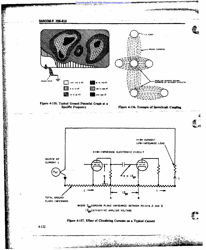
FI . - OARCOM-P-706410
*0 JllIl
~ ~jI I Ii GROUND CURRIENTS
U.....M1 go Y01O COUPLING 11ETIS9N GROUNDO
LESS .A 2CURNENTS OF ADJACEN4T CIRCUITS
tO TO 0MV fOvift w100, o--_--
Figure 4-135. Typical Ground Potential Graph at aSpecific Frequency Figure 4-136. Example or intercircuit Coupling
HI GH CURRENTLOW-IMPEDANCE LOAD
HIGH-IMPEDANCE ELECTRONIC CIRCUIT
SOURCE OFCURRENT I
I.I
TOTAL GROUND A BPLANE IMPEDANCE
WHERE Ztp:GROUND PLANE IMPEDANCE BETWEEN POINTS A AND 9
I "ip: EFFECTIVE APPLIED VOLTAGE
Figure 4-137. Effect of Clrculating Currents on a Typical Current
4-122
i . . . :- • , .......-...... ,j ,
Downloaded from http://www.everyspec.com

--
DARCOMP -70641O
that flows through the shield is reduced to a very grounding this type of shield is directly to the mainsmall value, and the tendency for energy to leak out chassis, as illustrated on Fig. 4-140.through holes or joints is minimized. The idealgrounding system makes use of a ground bus or 4-7.1.3 Cable Groundingground plate within the shield which is insulated from Electrical compatibility in a complex electrical orthe shield except at a single point (ground point) as il- electronic system is dependtnt in many cases on thelustrated on Fig. 4-139. treatment of the shielding and the grounding of the
shields of interconnecting leads. Injudicious ap-4-7.1.2.4 Printed Circuit Boards plication of a grounded shield to a wire may cause
For maximum shielding and isolation, shields on coupling problems that otherwise would not exist.printed-circuit boards should be grounded directly to Grounding of the shields may be accomplished with
the main chassis, independent of any grounds lo. single-point or multipoint connections as discussedcate ontheprinted-circuit board. In the case of a in par. 3-3.4.
shield for an RF transformer located on a printed- a. Single-point shield grounding. For multilcadcircuit board, grounding the shield to the printed- systems, each shield may be grounded at a differentcircuit board permits the conduction of stray cur- physical point provided individual shields are insu-rents into the printed-board circuits, thus causing lated from each other. Single-point grounding issecondary interference problems. The correct way of more effective than multipoint shield grounding only
ISOLATION TRANSFORMER
I- I I_ -.
CABINET A CABINET _ ZE_ _I . I , ,J _ . ..
mH
L .. .....
I I
I. -I
tFigure 4-138. Isolation Transformer Technique for Minimizing Ground Potential
Figure 4-139. Single-point Ground Bus Arrangement Figure 4-140. Direct Use of Chassis for Good Ground
4.123
. .*:,.
Downloaded from http://www.everyspec.com

DARCO*P 706410.
for short shield lengths. Single-point grounding is in- e, Have as few series connections (solder joints,effective in reducing magnetic or electrostatic coup- connectors) as possible in a ground bus, and makeling when conductor.length-to-wavelength (L/X) sure that they are good. solid electrical connections.
:ratios are greater than 0.15 where the wavelength is. . that of the highest frequency to be used (or the
highest frequency interference to be expected) on the 4-7.1.5.2 Separation ofAC Neutral fromwire or in the system. Frame Groundb. Muhtipoint shield grouhding. For L/X ratios A prime source of interfering ground currents is
greater than 0,15, multipoint grounding at intervals from ac neutral distribution through parallel frameof 0.15 A is recommended, since the shield can act as ground paths (common-made currents). They can bean antenna at frequencies for which L is a multiple of avoided by isolating all ac neutral sources from frameX/4. When grounding the shield at intervals of 0. 1SA ground. All ac power sources within the immediate
" is impracticable, shields should be grounded at each equipmeat area should be floated and referenced toend. Multipoint shield grounding is effective in re- frame ground at one point only, Power sources areducing all types of electrostatic coupling, but is sub- defined as secondary ac transmission to any part ofject to failure if large ground currents exist. In the equipment area to include lighting, heating, airgeneral, multipoint shield grounding is effective at conditioning, utility outlets, communication equip-frequencies greater than about 100 kHz, and single- ment, etc. Floating a circuit means using closed cir-point shield grounding is effective at frequencies cuit transmission with a single point as a groundbelow 100 kHz because of the ground currents. reference with no dependence on earth ground orWhere a circuit can respond at both low frequencies frame ground to complete any part of the neutral re-where single-point grounding should be used, and at turn path. All ac power circuits must be floated tohigh frequencies where multipoint grounding should one location. No ac neutral should be connected .to .beitsed, the-diect-gro-und Ca-n-be used a-one point frame or earth ground at airyother point. Ac n-eutril.and a capacitor used to connect the other points to bus bars should not be connected to the frame.ground. The size of the capacitor depends on the fre- ground bus bars in any major item or equipment areaquencies involved, except in one location. All power (input or intercon- i
necting) cables (portable or transportable) should beprovided with a green insulated conductor intended
4-7.1.4 Static Grounds only for grounding noncurrent-carrying metal partsMetallic parts not otherwise returned to "ground", of equipment. This equipment ground wire (EGW)
which may pick up static charges or are of sufficient should be terminated at both ends in the samedimension to receive and re-radiate energy from local manner as the other conductors, The EGW shouldradio transmitters, should be connected to the not be connected to the power return circuitground plane (see par. 3-3.4,2). (neutral), and the neutral wires should not be used as
EGW's. Wire color coding is recommended. All4-7,1.5 Power Supplies neutral power conductors should be white; all EGW
should be green. The following are examples:4-7.1.5.1 General a. Single phase two-wire ac service:
The power ground and signal ground should be (I) black (hot)isolated from each other throughout the chassis to (2) white (neutral)minimize the possible coupling of singals from any (3) green (ground)one type of ground line to any other type of ground b. Floating single phase two-wire ac service:line, The application of the following techniques (I) grey (hot)often can avoid potential problems: (2) grey (hot)
a. Incorporate, where possible, individual ground (3) green (ground)paths for ac voltages, dc voltages, and signals. NOTE: Ground wire is essential; 3-wire cable
b. Connect a ground path to the largest con- required.ductor (lowest impedance) by as direct a route as pos- c. Three phase ac circuits:sible. (i) black (hot)-L, (Phase A)
c. Use several arterial ground paths to the supply (2) red (hot)-L2 (Phase B)common point, as opposed to one super ground bus. (3) blue (hot)-L3 (Phase C)
d. Avoid multiended ground buses or lateral (4) white (neutral)ground loops. (5) green (ground)
4-124
, " . - ? •.,'. • . €.: ' ,.- h ,., -
Downloaded from http://www.everyspec.com

. -- ."
DARCOM-P 706410
*' NOTE: Ground wire is essential. Five-wire cable for should be made from copper or copper alloys. Termi-WYE connection and 4-wire cable for DELTA con- nal lugs should be tin-plated or hot tin dipped. Paint,nection are required. varnish, lacquer, etc,, should be removed from the vi.
J, d. Single phase three-wire ac service (such as 220 cinity of the fastening point to insure metallic con-,V): tact of the two surfaces. Corrosion protection should(I) black (hot) be provided for all ground connections. Internal or(2) red (hot) external lock washers should not be used on any(3) white (neutral) grounding or other screw-type electrical con-(4) green (ground). nections. Washers should not be located between the
NOTE: Ground wire is essential; 4-wire cable metal plate and terminal lug or other part beingrequired. grounded, so that they will not interfere with the full
and direct contact between these two members.Neither locking terminal lugs nor self-locking nutsit;4-7.1.53 Marine Craft Bonding and Grounding should be used for grounding. Flat washers should be
Methods inserted next to any part having insufficient contactMIL-STD-I 3 10, Shipboard Bonding and Grounding area with its adjacent part.Methods for Electromagnetic Compatibility, outlinesshipboard construction and equipment installation 4-7.1.6 Earth Groundrequirements, shipboard bonding methods, and the 4-7.1.6,1 Generalpractices necessary to minimize the electromagneticinterference (EM I) environment aboard marine craft. The earth can be used as a means of dissipating ex-
J T ru n hl do csive charges caused by man-made and natural in-........ These requirements should be adhered to when com-munication. radar, electronic, and electromechanical terference that may injure nersonnel who are oper-equipments are installed in Army marine craft. ating equipment, and damige the equipment in-
volved. Connections to the earth, called grounds or*"1 ground connections, are made to pipes or buried
4 7.1.5.4 Ground Studs water systems, driven rods, buried metal plates, or," A ground stud usally is required on individual buried wire. When buried pipe systems are not avail-
equipments and provides the electrical ground con- able, driven rods are considered the most satis-nection to the chassis or frame. It is secured mechani- factory substitutes. Low resistance grounds are es-cally to insure low resistance joints by: (I) soldering sential. Ground resistance is affected by the groundto a spot-welded terminal lug or to a portion of the rod resistance, lead connection, contact resistancechassis or frame that has been formed into a solder- between ground rod and soil, and by the type of soil.ing lug, or (2) by use of a terminal on the ground wire Type of soil will have the greatest affect on ground re-which then is secured by a screw, nut, or lock washer. sistance. Numerous kinds of soil prevent a simpleThe ground stud should be of a size to allow clec- classification. Study of certain types of soil reveals atrical connection of size AWG-10 wire. All hardware definite trend in resistivity. Soil can be roughly classi-used for grounding or other electrical connections fled into one of the types given in Table 4.29.
TABLE 4-29. SOIL CLASSIFICATION CHART
Resistance in ohms of Ground ConnectionType of Soil (One 5-ft rod, 5/8 in. diameter)
Average Minimum Maximum
Fills, ashes, cinders,brine waste 14 3.5 41Clay, shale, gumbo, loam 24 2 90Same, with varying proportionsof sand and gravel 93 6 800Gravel, sand, stones withlittle clay or loam 554 35 2,700
4-125
Downloaded from http://www.everyspec.com

DARCOM-P 706410
Temperature is another variable that affects 4.7.1.6.2 Grounding in Subzero Zonesground resistance. There will be only a slight change Two methods of grounding are presented:in ground resistance for temperatures above 320F. a. Method A. A good earth ground is difficult toFig. 4-141 shows how resistance increases with de- achieve beneath snow and ice; however, the follow-crease in soil temperature. ing method usually will produce satisfactory results.
Soils of the same type can differ greatly in re- Place a grounding rod horizontally in a narrowsistance due to variations in moisture content. There trench in the snow as deep as possible. Extend lines ofis a wide variation in the moisture content of soils, No. 6 gage or heavier copper wire radially from thefrom 10% during dry seasons to about 35% during rod for about 10 ft. Use chemical aids along the rodwet seasons. The approximate average is from 16 to and cables, and bury the entire system in the snow.18%. The effect of moisture content on resistance of For general effectiveness and anticorrosion qualities,soil can be seen from Table 4-30. the main usable chemical aids rank as follows:
(I) Magnesium sulphate(2) Copper sulphate(3) Calcium chloride
40,000 -- (4) Sodium chloride00 (5) Potassium nitrate.
b. Method B. Ground rods driven vertically in soilnormally have a relatively high resistance at depths of
-less than 5 ft. A shallow circular trench about 18 in.in internal diameter around the ground rod should bedug about I ft deep and lined with the chemical aids.
20,000-------------------The area around the ground rod should be kept moist(Ref. 31).
4-7.2 BONDING10, 1000 -4-7.2.1 General
A bond is an electrical union between two metallicstructures to provide a low impedance path between
0 -- them. Bonding is a process used to achieve a ground0 10 20 30 40 50 60 connection or the establishment of a ground plane, as
Temperature T, OF discussed in pars. 3-3.4 ane 4-1.4. The structures in.volved may be housings, subassemblies, or corn-
Figure 4-141. Variation of Soil Resistance ponents such as the chassis of an electronic assemblyWith Temperature or the frame of an electrical machine.
4-7.2.2 Types of BondsIt should be noted that the term "bond" refers to
both the mechanical interface between the joinedconductors, as well as the conductor bonding jumper
TABLE 4-30. EFFECT OF MOISTURE CONTENT or strap used to interconnect two separate struc-ON SOIL RESISTANCE tures. Where the separate structures are placed in im-
mediate contact, the bond is "direct", otherwise, it isMoisture Content, Resistivity, 11/cm' indirect.
% by weight Top Soil Sandy Loam 4-7.2.2.1 Direct Bonds0 over I billion over I billion Direct bonds include permanent metal-to-metal2.5 250,000 150,000 joints formed of machined metal surfaces, or with5 165,000 43,000 conductive gaskets held together by lock-threaded
10 53,000 18.000 devices, riveted joints, tie rods, or pinned fittings15 19,000 10,500 driven tight and not subject to wear or vibration. The20 12,000 6,300 best bonded joint is formed by welding, brazing, or30 6,400 4,200 sweating. Soldering is not a good method of direct
4-126
N ; . . ....
Downloaded from http://www.everyspec.com

SARCOM-P 706410
bonding because soldered joints have appreciable 4-7.2.3 bonding ImpedanceI .contact resistance. Good metal-to.metal contact The equivalent circuit of a bond which takes intomust be maintained for the life of the joint, and pro- account its series resistance R and the distributedcautions should -be taken to seal the joint against capacitance C between the two structures beingmoisture that would cause galvanic corrosion. Con- bnded together is shown in Fig. 4-142 along with a
dmoie thahould ae gasean croin Con- b o othe ishnin f is n a eance as.i cations. Dissimilar metals in direct contact should be function of frequency. It is seen that resonance pc-
avoided. Screw threads never are considered ade- curs at some frequency which may be of the order ofquate bonding surfaces. In particular, sheet-metal tens of megahertz, but depends upon the physicaltype screws are inadequate for use in bonding. If two characteristics of the bond. At frequencies above thisstructural members are held together by screws, the first resonance, the behavior is not easy to describe,impedance between them is usually comparatively but the equivalent circuit may resemble that of anhigh unless good direct contact is maintained. MIL- open-ended transmission line, and multiple reso-STD-1 310 and MIL-B-5087 give details on methods nances may occur. Also, it should be noted that whenof preparing bonding joints. resonance occurs, the bond is capable of radiating an
appreciable amount of energy.The sharpness of the resonant peak in Fig. 4-142 is
dependent upon the resistance of the bonding con-4-7.2.2.2 Indirect Bonds nection. The effective resistance of any conductor is a
function of frequency due to skin effect. Fig. 4.143When a direct bond is not practical, an indirect shows the skin depth in copper and the variation ofbond is necessary. A good indirect bond is one that resistance and inductive reactance (at frequenciespresents a low impedance throughout the inter- where it eaceeds the resistance) with frequency forference spectrum, and rtain its usefulness for an ex- several conductors of circular cross section, aid-l0 -tended period of time. An indirect bond is usually a cm (4 in.) length. At 1 MHz the resistive impedance is Ibond strap or junper. Bond jumpers are short, substantially le' than the inductive reactance for allround, braid conductors for application where the in- wire sizes. By using a conductor in the form of a stripterference frequency is below a few megahertz. They with rectangular cross section, both the inductive re-
, generally art; used in low-frequency devices, andg a i qiactance and the resistance can be decreased signifi-where the development of static charges must be pre- cantly.vented. Bond-straps are either solid, flat, metallic The inductance L of a bond strap (Ref. 24) isconductors, or woven braid configurations wheremany conductors are effectively in parallel. Solid-metal straps are preferred generally for the majority L 0 ! 21of applications. The most significant feature of a L 0 1 b.c lobond-strap is its resiliency which is determined by itsmaterial and thickness. Beryllium copper andphosphor bronze are used often. Under conditions of + 0.5 + 0.2235 1-1 (4-52)severe vibration, a corrugated strap often proves use-ful in preventing excessive damping and in achieving wheremaximum service life. Braided or stranded bond- I = length, in.straps generally are not recommended because of b = width, in.several undesirable characteristics. Oxides may form c - thickness, in.on each strand of nonprotected wire and cause cor- The corresponding inductive reactance is shown onrosion. Because such corrosion is not uniform, the Fig. 4-144. Reductions of about an order of magni-cross-sectional area of each strand of wire will vary tude are possible compared with wires of equal crossthroughout its length. The nonuniform cross- section. The relatively high impedance at high fre-sectional areas (and possible broken strands of wire) quencies illustrates that the bond strap is not a sub.may lead to generation of interference signals within stitute for a direct bond. A rule of thumb forthe cable or strap. Broken strands may act as ef- achieving minimum bond strap inductance is that theficient antennas at high frequencies, and interference length-to-width ratio of the strap should be 5:1 ormay be generated by intermittent contact between less. This ratio determines the inductance - thestrands. They also have higher self-inductance than major factor in the high-frequency impedance of thesolid straps, strap.
4.127
1 ' " i., :,. , ...7:
Downloaded from http://www.everyspec.com

DARCOM-P 706410
The bond strap or jumper may be held mechanical- of fault current, the bond resistance must be below aly by means of bolts, rivets, welding, brazing, or specified value for safety rea3ons. Fig. 4-146 showssweating. Tooth type lockwashers are used with bolt the maximum permitted resistance according to thefasteners to insure no deterioration of metal-to-metal National Electrical Code (Ref. 25).contact of bond strap connections. Fig. 4-145 shows atypical bond strap bolted into position.
4-7.2.4 Bond Measurements 4-7.2.5 Bond Design
It is conventional to check the quality of a bond by 4-7.2.5.1 Physical Requirementsmeasuring its dc or low-frequency resistance. Such a The mechanical stresses to which bonds are sub-test is satisfactory in production where it is desired to jected should not be of such a magnitude as to causedetermine the quality of the mechanical work per- damage. However, bonds should remain accessibleformed. Good bonds should have a resistance for maintenance and inspection and not interferebetween 0.1 and 2.5 mt, depending on the magni- with the intended operation of the equipment eithertude of the ground currents expected and the sensi- by reducing accessibility or by limiting its move-'s tivity of the equipment. To check the quality of a ment. When bonding jumpers are used, their lengthscompleted bond at high frequencies, it is necessary to are critical and must be as direct and as short as pos-use an impedance bridge. Particular care should be sible (see par. 4-7.2.3). A high area of contact re-taken to identify the frequency at which the first reso- quires that the surfaces to be joined be flat, with nonance appears. In hazardous areas, under conditions surface irregularities.
. . . .. ...... ...............
ii "Zo L/ (RC)
a~ll0
__
21Mi-
Figure 4-142. Banding Strap Impedance Characteristics
4-128
Downloaded from http://www.everyspec.com

DARCOMP 706410
4-7.2.5.2 Choice of Materials structural units of dissimilar metals. Where bi-
r metallic plates are to be used, the junctures of the twoThe choice of material for a given bonding ap- metals normally are covered with a protective
plication usually is dictated by consideration of the coating, such as grease or polysulphate, to excludet metals being bonded and the environment within moisture and retard corrosion. This coating reduceswhich the bond must function. When joining dis- the area of metal exposed to an electrolyte. If bond-similar metals, corrosion becomes an important con- ing is such that corrosion is likely to occur, the bondsideration. Factors contributing to corrosion are the should be designed as a replaceable element such as aproximity of metals in the electromotive series and jumper, plate, separator, or washer.the amount of moisture present. Corrosion is at- Acceptable contact surface materials that may betributed to two basic electrochemical processes: gal. used to fasten bonding jumpers to structures are in-
. vanic and electrolytic corrosion. dicated in Table 4-32. The arrangement of the metalsSeveral methods can be employed for minimizing listed in this table is in the order of their decreasing
or preventing corrosion and its adverse effects on galvanic activity when exposed to an electrolyte. Thebonding. One is to use metals low on the activity screws, nuts, and washers to be used in making thetable, such as copper, lead, or tin (Table 4-31). Where connections are indicated as Type l, cadmium or zincmembers of the electrolytic couple. are widely plated, or aluminum; and Type I1, passivated stain-separated on the activity table, it is sometimes practi- less steel. Where neither type of securing hardware iscal to use a plating such as cadmium or zinc, which indicated, Type 11 is preferred from a corrosionhelps to reconcile the dissimilarity (Refs. 26 and 27). standpoint.
J: Thin, bimetallic plates, formed by mechanical bond- The possibility of galvanic and/or electrolytic ac-ing of dissimilar metals, cold-flowed together under tion necessitates extreme care in assembling jointshigh pressures, have been used to interconnect two that serve as bonds. Surfaces should be absolutely dry
AI "I I If ll| I I I-- - r ------ T -1 I ] I II I i I I lll l" ' I l i lllTTTl
I __
36 No 4"
10-
4' 4
| I I ! l i l t ,J | I i lIiI I I Il i t t a[ I i l I t r l
Figure 4-143. Skin Depth in Copper, and Resistance and Reactance Variation With Frequency for Conductorof Circular Cross Section
4-1
.......................................... .. :..: !................ ........ . ....... ....... .. .. -. [ .o..
Downloaded from http://www.everyspec.com

DARCOM-P 706410
before mating, and should be held together under brushed clean; it should be about 1.5 times greater \ -'.high pressure to minimize the possibility of moisture than the area necessary for actual mounting. After aentering. The use of number 7/0 garnet finishing joint (free of moisture) is assembled, the periphery ofpaper or equivalent is recommended to remove the exposed edge should be sealed in accordance withpaints, anodic films, and oxides from surfaces. Care the applicable requirements of MIL-F-14072.must be taken not to remove excessive metal under The finishes which are currently available fall intothe protective finish. Abrasives, such as cmery cloth two categories: nonconductors and conductors. Theor sandpaper, cause corrosive action because their nonconductors - such as anodized films, Dow 8 andparticles embed themselves in the metal; therefore, HAE - are excellent for corrosion protection andthey should not be used. The contact area should be wearability but, being nonconductors, cannot be
100
NJN
Length, 4 in.10ICross Section, 0.005129 in.
4-)
12 ga Round Wire1/2 in. Wide Strap ,
OJ I in. Wide Strap
2 in. Wide Strap
1.01
1 10 100 1000Frequency f, MHz
Figure 4-144. Inductive Reactances of Bond Strap and a Rond Jumper Having Constant (ross-sectional Area
4-130
Downloaded from http://www.everyspec.com

DARCOM-P 706-410
)plied to surfaces used for bonding. The con-Iducting films - such as idite 14-2, Dow 15, Alo-dine. and Qakite 36 - offer fair cor-osion pro-tection (much better than bare metal), but do not af-ford as much wear resistance as the anodized films.The bond and adjacent metal should be covered withprotective finishes after the bond has beer. assembledand its resistance checked.
4-7.2.5.3 Conductive Adhesives LCWSE
Direct conductive permanent bonds sometimes canbe made between two surfaces with a high viscosityplastic cement. The user of such cements must dccide'upon the relative importance of such factors as high Figure 4-145. Recommended Bond Strapadhesive strength. low resistivity, cure cycle, ease of Bolting Installation
- BONDING RESISTANCE CAPABLE OF
i XI
UBONDING RESISTANCE FOR II fl,. ON
r -FAULT CURRENT PROTECTION
100 1,000 10,0M
Fault Current, A
Figure 4-146. Fault Current ~sMaximum Allowed Resistance for Bonding Between Equipment and Structure
4-131
Downloaded from http://www.everyspec.com

VARCOII-P 705410
TABLE 4-31 Bond shear strength values of 289 kg/cm-' are being ,,ELECTROMOTIVE FORCE claimed by at least one conductive adhesive manu-
SERIES OF facturer. This is coupled with the simultaneous claimCOMMONLY USED of 2.X 10-1 ohm'cm resistivity when fully cured. This
METALS, particular epoxy is coarse in texture and not in-tended for delicate electronic wiring work but rather
METAL ELECTRODE POTENTIAL- is used for gross metal-to-metal joints, heat con-V duction, and RF shielding. Finer work is obtainable
Magnesium -2.375 with 225 kg/cm2 adhesives having resistivities of 2 X
Beryllium -1,700 10-4 ohm'cm after curing.Aluminum - 1.670 Joint strength tests have indicated greatest strengthZinc -0.7628 in shear and least strength in peel when a length ofChromium -0.740 copper wire was attached by adhesive to an etchedIron -0.441 pad area in a phenolic laminate. It was found thatCadmium -0.402 those conductive adhesives with the highest jointNickel -0.230 strengths also had the least conductivity.Tin -0.1406Lead -0.1263Copper +0.346 4-7.2.5.4 Conductive PastesSilver +0.7996 Several types of paste, caulking, and sealing corn-Platinum +1.200 pounds are available for such applications as pipeGold +1.420 and conduit threads, shielded room or enclosure'Select dissimilar metals so that if corrosion occurs, it seams, removable cover plane seams, expansion
. will be in -the replaceable components - such as joints, and fastener hardware caulking. Resistivitygrounding jumpers, washers, bolts or clamps - ratherthan structural members or equipment enclosures. varies with:When two different metals are in contact, the one a. Type of metal loading use in the pastehigher in the electromotive-force series will be more b. Configuration of the metallic contentaffected by corrosion than the other. The smaller mass(generally the more easily replaceable) should there- c. Condition of the metal surfaces upon which thelore be made of the higher metal; for example, paste is appliedcadmium-plated washers are recommended for usewith steel surface, since cadmium is lower than steel. d. The pressure applied to the joint after applica-
tion of the paste.Manufacturers should be consulted for details of
handling, and cost. Adhesives may be used as al- applications and limitations.ternatives (subject to specific requirements) to solder-ing, welding, and mechanical joining operations.Most of the commercially available materials arebased on epoxy resins, either two-component low- 4-7,2.6.1 Shock Mountstemperature cure or one-component oven-cure A frequent application for which indirect bondingsystems. is the only suitable type is that involving shock-
The resistance of these two adhesives depends on mounted equipment. The designer should considerthe conductive materials with which they are loaded, the degree of relative motion to be expected betweenThe usual materials are: carbon, resistivity, p - 10 two surfaces to be bonded, the characteristics of theohm'cm; silver and gold, p = 5.7 X 10⁻¹ to 18 X 10-1 materials involved, and the frequency range overohm-cm. For silver, both platelet and metal powder which the bonding is expected to be effective. Acoated with silver are used. typical shock mount is shown on Fig. 4-147. The
The platelet form is ideal where a thin glue line is application of a bond-strap to a vehicle engine isneeded, whereas gritty powders make better contact shown on Figs. 4-148 and 4-149. The resiliency of thewith the metal surfaces to which they are applied and bonded mount should be determined by charac-generally offer lower resistivity. At least 60 to 70% by teristics of the mount, not of the bond-strap. Theweight of metallic content ,s needed to provide an strap should not significantly dampen the shockoptimum combination of adhesion and conductivity, mount and, where necessary, it should be corrugatedAs a rule, the greater the metal content, the less will to withstand severe and continued vibration. In the 4be the adhesion; and the less the metal content, the VHF range and higher, two bond straps across eachgreater the adhesion. shock mount should be used.
4-132
,' .
Downloaded from http://www.everyspec.com

. .. .... _....DARCOM-P 70610 -
TABLE 4-32. METAL CONNECTONS DRO- *1
Metal Structure Connection for Screw Type Connection for Screw Type'(Outer Finis tal AluminumJumper . Tinned Copper Jumper
Magnesium and magnesium Direct or mag- Type I Aluminum or magnesium Type Ialloys nesium washer washer
I Zinc, cadmium, aluminum Direct Type I Aluminum washer Type Iand aluminum alloys
Steel (except stainless Direct Type I Direct Type I
Tin, lead, and tin-lead Direct Type I Direct Type I or 11solders
Copper and copper alloys Tinned or cadmium. Type I or 1 Direct Type I or IIplated washer
Nickel and nickel alloys Tinned or cadmium- Type I or Ii Direct Type 1 or 11plated washer
Stainless steel Tinned or cadmium- Type I or 11 Direct Type I or iplated washer
Silver, gold, and pre- Tinned or cadmium- Type I or ! Direct Type I or 1Icious metals plated washer
Y- e Iis cadmiuim- or tinc-platcd. or iluminum..TypeI1 is stainless steel. Where either type is indicated as acceptabie. Type II is pre-Ferred from a corrosion standpoint. .
4-7.2.6.3 Tubing ConduitThe outer surfaces of long spans of conduit or
TINNED o BOND Sshielded cable may be high-impedance paths for in-tWrferencc currents frjm external sources. To mini-mize this possibility, such spans should be properlybonded to structures at both ends and at several in-termediate points. Ordinary clamps cannot be used tobond flexible conduit since the required pressure on acomparatively small surface area of the conduit maybe sufficiently high to compress or collapse it. To
uSDN TA overcome this, a flared split-sleeve is fitted aroundLAED TQO..YPES the flexible conduit. This sleeve distributes the high j
pressure of the bonding clamp over a large area.thereby exerting low pressure on the conduit (Fig. 4-
Figure 4-147. Typical Shock Mount Bond 150(A)). Contact further is improved by soldering thesleeve to the conduit, material permitting, throughseveral holes in the sleeve provided for this purpose.Fig. 4-15I(B) illustrates a method for bonding rigidconduit to a structure through supporting attach-ments. The conduit or tubing to which bonding
4-7.2.6.2 Rotating Joints clamps are attached should be cleansed of paint andFrequently, it is necessary to bond shafts of ro- foreign material over the entire area covered by the
tating machinery to prevent accumulation of static clamps. All insulating finishes should be removedcharges, Bonding generally is accomplished by use of from the contact area before assembly only and con-a slip ring and brush assembly, or a phosphor-bronze ductive screws, nuts, and washers should be used tofinger riding directly on the shaft. attach contacting parts.
4-133
Downloaded from http://www.everyspec.com

DARCOM*P 106-410 ~.
TIMED~ SECTION x HOSXA
tofe-13neig 8ADngM bcMutF ft MD
Vt I
RiguM 4-4.BoddEnieSoc ont-R
PAD1 ERNAWL
s~ a 37 W tCOTINTEP(NAII-E
YCONIrl HER
Figure 4-1 . b nd gnShck out, ondnt
UND TRI
I-,~t:SE 3/8,, ,
Downloaded from http://www.everyspec.com

.. Af.C.M 71J6410--
4-7.2.6.4 Hinges 4. T. H. Herring, "The Common Mode Choke",Where hinges must be used, it is necessary to ac- 1970 IEEE Electromagnetic Compatibility Sym-
complish bonding by suitable means. Fig. 4-151 posium Record, The Institute of Electrical andshows a typical configuration for bonding hinges. Electronic Engineers, Inc., NY, 1970,
5. F. E. King, "Baluns as EMC Control Devices".4-7.2.6.5 Cable Trays 1970 IEEE Electromagnetic Compatibility Sym-
Cable trays should be used as part of the overall posium Record, The Institute of Electrical andsystem bonding scheme. Each section of each tray Electronic Engineers Inc., NY, 1970.should be bonded to the following section to provide 6. E. J. Baghdayd, Lectures on Communicationsa continuous path (Fig. 4-152). The trays also should Systems Theory, McGraw-Hill, NY, 1961, pp.be connected to equipment housings by wide, flexi- 485-7.ble, solid bond-straps. A typical example of cable 7. R. J. Mohr, "Coupling Between Open and
tray bonding is shown on Fig. 4-153. Shielded Wire Lines Over a Ground Plane",IEEE Trans. on Electromagnetic Compatibility,
.I EFERNCESEMC-9, 34-5 (September 1967).REFERENCES 8. R, J. Mohr, "Coupling Between Lines at High
1. M. Schwartz, Information. Transmission, and Frequencies", IEEE Trans. on Electromagnetic
Noise. McGraw-Hill. NY, 1959. Compatibility, EMC-9, 127-9 (December 1967).NsM aw i9. D. Kjellquist, Low Frequencies EMC Charac.2. E. J. Angelo. Jr., Electronic Circuits, McGraw. ,
,2nd teritics of Common Navy Cables, TechnicalMemorandum EA33-145-72, New London
3. J. C. Otto, "Interference Reduction Techniques Laboratory, Naval Underwater Systems Center,i" I• ~~~~~~for Nonlinear Circuits", Proceedings, Tenth Trl. LbrtrNva newtrSstm etr ,New London, CT, 25SVpL. 1972 ... -Service Conference on- Electromagnetic- Compati - -
10. AFSC DH 1-4, Electromagnetic Compatibility.November 1964. Design Handbooks Branch (ASNPS-40), Air
Force Systems Command, Wright-Patterson,AFB, OH, 10 January, 1969.
IL. MIL-STD-454, Standard General RequirementV LfXSLE W *bING for Electronic Equipment.(THIN ET /12. Reference Data for Radio Engineers, Fifth Edi-
tion, Howard W. Sams and Co., Indianapolis,IN, 1968,
/oe I'sTENE 13. NAVAIR AD 1115, Electromagnetic Compati-
bility Design Guide for Avolnics and Related
Figure 4-151. Bonding of Hinges
CAM IRAL
Figure 4-153. Equipment Cabinets Bonded to
Figure 4-152. Cable Tray Section Bonding Cable Tray
4-135
'.... " ~ . .. " ' . ... ... ," -
1 . " " " .. "-'x "," " - . " - " "
t, . '
Downloaded from http://www.everyspec.com

DAROM-P 706-410
Ground Support Equipment, Naval Air Systems VLF Shields Cans", IEEE Trans. on Electro-Command, Naval Weapons Laboratory, Dahl- magnetic Compatibility, Vol. EMC-10, No. 1,gren, VA, July, 1973. March 1968, pp. 112-125.
14. NAVAIR 5335, Electromagnetic Compatibility 23. W. G. Wadey, "Magnetic Shielding With Multi-I Manual. Naval Air Systems Command, Wash- pie Magnetic Shields", Rev. Set. Inst.. Novemberington, DC, 1968. 1956, p. 910.
15. S. L. Shive, "The Lossy Transmission Line 24. F. E. Terman, Radio Engineers Handbook,Filter", Proceedings of the Second Conference on McGraw-Hill, NY, 1943.Radio Interference Reduction. Armour Research 25. MIL-B-5087, Military Specification, Bonding,Foundation, Illinois Institute of Technology, Electrical, and Lightning Protection, for Aero-Chicago, IL, March 1956. space Systems.
16. P. R. Geffe, Simplfed Modern Filter Design, 26. MIL-STD-1250 (MI), Corrosion Prevention andHayden Book Company, Inc., NY, 1963. Deterioration Control in Electronic Components
17. B. Wellman, "Convenient Twin-T Circuits", and Assemblies, March 1967.1958 Electrical Design Manual, Rogers Pub- 27. MIL-HDBK-721 (MR), Corrosion and Corrosionlishing Company, Englewood, CO, 1958. Protection of Metals. November 1965.
18. R. E. Thomas, "Integrated-circuit Synthesis", 28. Robert B. Cowdell, "Magnetic Shielding MadeTopics in Intersystem Electromagnetic Compati. Attractive", 1971 IEEE International Electro. ,bility, Ed W. W. Everett, Jr., Holt Rinehart and magnetic Compatibility Symposium Record, pp.Winston, Inc., NY 1972. 58-67.
19. L. Young, "Microwave Filters to Combat RF 29. Robert B. Cowdell, "Simplified Shielding", 1967Interference", IEEE Transactions on EMC, IEEE Electromagnetic Compatibility SymposiumEMC-lO, June 1968. Record. pp. 399-412.
20. Inierference" -Reduction- Guide for Design En- 30. ARP 11-73; -Test Procedure-to- Measure the RF .gineers, Filtron Company Inc., NY, 1964. Shielding Characteristics of EMI Gaskets, Society
21. R. B. Schulz, V. C. Plantz, and D. R. Brush, of Automotive Engineers, Inc., 1975."Shielding Theory and Practice", Proceedings of 31. Grounding. Bonding, and Shielding Practices andthe Ninth Tri-Service Conference on Electro- Procedures for Electronic Equipments and Facili-magnetic Compatibility, lIT Research Institute, ties. Final Report, FAA-RD75-215, Vol. 1, ppChicago, IL, October 1964. 1-65, Federal Aviation Administration, Wash-
22. J. R. Moser, "An Empirical Study of ELF and ington, DC 20590.
I(
4-136
- a-A-"--
Downloaded from http://www.everyspec.com

DARCOM4P 706410
i CHAPTER 5
APPLICATIONS TO SPECIFIC DEVICES
All military equipment which is capable of ema. E, - critical field gradient, electrostatic field,nating or is susceptible to electromagnetic energy re. V/mquires interference reduction treatment in order to as- EL - line phase voltage, Vsure that it will be electromagnetically compatible with E0 - field strength at angle 0, V/mother equipment or the environment in which it is ex- E, = secondary phase voltage, Vpected to operate. To assure compatibility the equip- Ep - field strength at angle 4,, V/mmeni must meet requirements given in various military e - electronic charge, C
standards as outlined in Chapter 2, especially con- e, = common-mode voltage, Vducted and radiated limits given In MIL-STD-461, in e, = differential-mode voltage, Vaccordance with test procedures In MIL-STD-462. In f - frequency, Hzgeneral, requirements exist over the frequency range Aff- ratio of frequency spacing of desiredfrom 30 Hz to 40 GHz. and undesired signals; Hz; relative air
In this chapter the objective is to give examples show- density, dimensionlessing how the various general techniques discussed in 3dB filter bandwidth, HzChapter 4 are applied in specific types of circuits and fd = binary data rate, Hzdevices, and also to describe any specialized techniques f4 - fundamental frequency, Hzthat may be appropriate. - frequency of nth harmonic Hz
= tuned receiver frequency, MHz5-0 LIST OF SYMBOLS f carrier frequency, Hz
A = constant G(GO) = gain of antenna, dimensionlessA, = effective area of receiving antenna, m- G, - receiver antenna power gain, dimen-A, - effective area of transmitting antenna, sionless
nm2 G, = transmitter antenna power gain, dimen-A1,A 2 - constant, V's sionless
a wire diameter, m; the ratio of the am- H = magnetic field strength, A/m; height ofplitudes of an undesired signal to that source from ground, mof the desired signal, dimensionless H(f) = filter transfer function, dimensionless
a, coefficient in series expansion h - height from power transmission line,B = bandwidth, Hz m; height of conductor from ground
B,- effective bandwidth, Hz plane, mBm, = moment bandwidth of a modulating I - current, A
waveform, Hz I, - induced cavity current, ABER bit error rate, s- ld - output current, A
C - capacitance, F IL - line current, Ac, = speed of light, m/s l, - direct current (in a tube), AD - antenna diameter, n p, = peak reverse current, A
Dy = antenna dimension (Y-axis), m I/S - interference-to-signal ratioDz = antenna diameter (Z-axis), m i = current, A
DPSK - differential phase shift keying i,, = current of nth harmonic, Ad = diameter: distance from a single wire; i1(0-) - value of the interrupted supply cur-
horizontal distance from power trans- rent, Amission line, m: distance from antenna, 12 - secondary current (coupled coils), Am J,, - nth order Bessel function of the first
E = electric field strength, V/M; ac voltage kindmagnitude, V; signal "energy" per pulse K = constant in propagation equation, V;(radar), V2's phase conversion factor, deg/dB
5-I
..- : , ,: . . . , ,, '
Downloaded from http://www.everyspec.com

DARCOM-P 706410
KaKF - empirical constants (microstrip), di- V = voltage, Vmensionless V(f) = Fourier spectrum, V's
k = an integer; coefficient of coupling V(t) - voltage of coupled line at the sending(coupled coils); attenuation line, V
L - inductance, H; loss factor, dimension- VJt) - voltage of coupled line at the receivingless line, V
L, = inductance of primary coil (coupled V = beam accelerating voltage, Vcoils), H V.(i ) = voltage at the receiving end of the
L2 secondary inductance (coupled coils), driving line at line s (microstrip), VH V, = supply voltage, V
LA aperture diameter measured in wave- V, - peak gap voltage at buncher (klystron),lengths, dimensionless V
I = length, m; dipole length, m vQ) = voltage, function of time. Vm = electron mass, kg v, - voltage of nth harmonic, V
No = noise power spectral density; V2/Hz; v, = voltage, primary winding, Vneutral point in a rectifier circuit v2 - voltage, secondary winding, V
NBFM = narrow-band frequency modulation W = conductor width, mn = order of harmonic; ratio of primary to WBFM - wide band frequency modulation
secondary phase voltage, dimensionless x = instantaneous input; bunching param-... ,_ numberrofturns,.coil-primary eter
n2 - number of turns, coil secondary X. = input (phase a)P = power, W xb = input (phase b)
Pi-power input, W x1(t) -information signalP, - power output, W x2(t) = carrier signalPr - power received, W y - instantaneous outputP, = power transmitted, W y, - intermodulation component; output of
PCM - pulse code modulation a nonlinear device (phase a)p = atmospheric pressure, cm of Hg yb = cross-modulation component; outputQ = quality factor of a network, dimension- of a nonlinear device (phase b)
less Z = impedance, 11R = resistance, 0; distance to the boundary Z= characteristic impedance, i
between the near-field and far-field (an-tennas), m; signal-to-noise ratio; re- a = firing angle, degflection loss, dB A = rise time of a trapezoidal pulse, s
RD - resistance of a diode, 11 6 = difference frequency between desiredR, - resistance of primary coil (coupled and undesired signals, Hz; relative air
coils), ft density, dimensionlessR2 - secondary resistance (coupled coils), I n - intrinsic standoff ratio, dimensionless
r = conductor radius, cm; range; separa- 0 = elevation angle, rad; beam angletion distance, m (antenna), rad; half of the conduction
S - spacing between conductors, m angle, rad; line length, radSE - shielding effectiveness, dB A = wavelength, m
s -spacing between input and output cavi- c = radar cross section, in'; VSWR of load,ties, m dimensionless
s(t) - signal level, function of time, V r = pulse duration, sT - spacing of pulses in time, s p - azimuth angle, rad; phase!!TI) - propagation time per unit length, ns/ft P" -' caroletr phase, radT, - reverse recovery time, s - diretion of horizon, rad
t - time, s; temperature, °C w = angular frequency, rad/s; excitationto = line propagation time, ns frequency, rad/st - rise time, s w, - angular carrier frequency, rad/s
5-2
Downloaded from http://www.everyspec.com

DARCOM-P 7W6410
5-1 ROTATING ELECTRICAL should match the requirements for good commuta-MACHINES tion. The design engineer should select material of the
5-1.1 BRUSH PHENOMENA lowest resistivity that satisfies the other requirementsof good functional performance. When used with slip
Any rotating machine with sliding contacts is a po- rings, a wide choice of brush material is available be-tential source of interference. If the contacts are used cause no switching action is involved. Low-resistanceon continuous "slip" rings, the interference gener- brushes are available with silver, copper, or cad-I. ated is a result of varying contact resistance caused by mium-impregnated graphite.varying brush pressure or surface conditions on thering. It is likely to be random in nature and have 5-1.2 COMMUTATIONenergy only in the low audio frequency portion of thespectrum. 5-1.2.1 Design Considerations
If the contact surface is that of a commutator, the Dc motors and generators are serious offenders inassociated switching and arcing processes cause rapid generating interference because they require commu-current and voltage changes that generate inter- tators for their operation. The bars of a commuta-ference energy throughout a wide frequency range as tor, rapidly sliding past the contacting brushes, pro-discussed in par. 3-1.3.2. duce a switching action that causes voltage transients, i
Brushes and brush leads are the most likely corn- or pulses. The objective of interference reductionponents from which interference can be radiated or design techniques is to provide a smooth transitiontransferred. Provision should be made in the original from one value of impedance to another while switch-design of motors or generators for installation of ing between each armature coil. The techniques in-capacitors at the brushes (see Fig. 5-1). In very criti- lude use of interpoles, compensating windings, in-cal cases it may be necessary also to shield the brush creased- number of armature coils and commutator __
leads. Brush-generated interference may be mini- bars, laminated brushes, and commutator plating. Amized by proper consideration of the following: discussion follows:
a. Brush pressure. Increasing brush pressure a. Interpole Windings. The best way to improvegenerally reduces generated interference at all fre- commutation is by adding interpole windings. Inter-quencies since it tends to reduce contact resistance poles counterbalance the selfrinduction of the arma-and variation of that resistance. In addition, in cases ture coils during the commutation period, and alsowhere the slip ring or commutator is not precisely reduce the induced voltage in the armature coils re-concentric or there is wear in shaft bearings, in- suiting from the coil-cutting fringing-flux during thecreased brush pressure will minimize contact commutation period. The use of properly designed"bounce" phenomena. The brush mounting ar- interpoleb produces a rapid change in the armature-rangement should be designed to provide some coil current at the beginning of the commutatingdamping without reducing the effective force exerted period, reducing the steepness of the transient at theon the contact. end of the commutating period.
However, as the brush pressure is increased the b. Compensating Windings. To a lesser degree,rate of wear of the brush and the slip ring or commu- compensating windings produce the same effect as in-tator increases necessitating frequent brush replace- terpoles and, in addition, help to prevent field dis-ment. tortion. They also assist in reducing cross flux pro-
b. Current density. Generated interference de- duced by the armature coils. The use of interpolescreases with decreased current density. As the current and compensating windings lessens critical brushdensity is increased, the heat generated at the brush positioning requirements with respect to the commu-surface is increased, possibly causing the Formation tator, and provides electromotive forces in the coilsof an oxide film on the sliding metal surface. Rapid under commutation which oppose the electromotivevariations in the sliding conact resistance, resulting forces of self- and mutual-induction in these coils.from iirgularities in this oxide film, produce high- c. Increased Number of Armature Coils. In-frequency transients. To off-t the heat increase, a creasing the number of coils on the armature (there-somewhat larger brush-surface area than otherwise by increasing the number of commutator segments,necessary can be used. or bars) reduces interference by reducing the current
c. Brush resistivity. Generally, low resistivity broken per bar and the reactance voltage per coil.brushes may be expected to generate less interference The largest number of armature slots, in which thethan those of higher resistance. However, when used coils are uniformly distributed with respect to thewith a commutator, the resistance of the brush commutator bars, should be used, and the armature
5-3
Downloaded from http://www.everyspec.com

______________________________ 70 -410-
NEGATIVE TERMINAL
POSITIVE TERMINAL
LOCK WASHER
CAPAC ITOR
Figure 5-1. Installation of By-pass Capacitors
3-4
Downloaded from http://www.everyspec.com
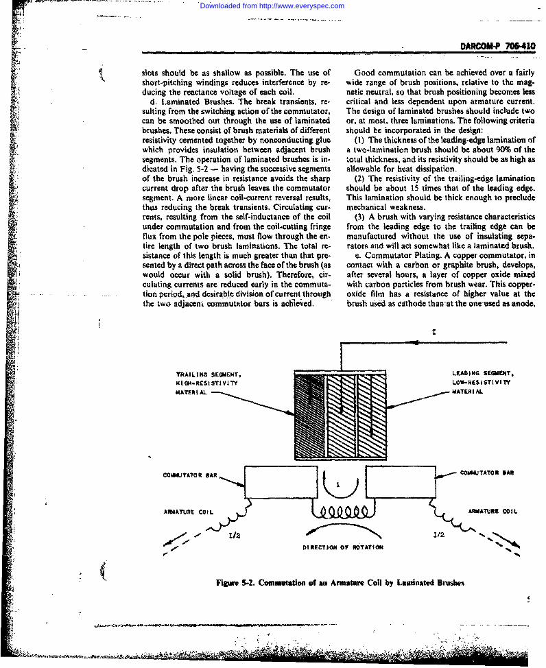
DARCOM-P 706410
slots should be as shallow as possible. The use of Good commutation can be achieved over a fairlyshort-pitching windings reduces interference by re- wide range of brush positions, relative to the mag-ducing the reactance voltage of each coil. netic neutral, so that brush positioning becomes less
d. Laminated Brushes. The break transients. re- critical and less dependent upon armature current.suiting from the switching action of the commutator, The design of laminated brushes should include twocan be smoothed out through the use of laminated or, at most, three laminations. The following criteriabrushes. These consist of brush materials of different should be incorporated in the design:resistivity cemented together by nonconducting glue (1) The thickness of the leading-edge lamination ofwhich provides insulation between adjacent brush a two-lamination brush should be about 90% of thesegments. The operation of laminated brushes is in- total thickness, and its resistivity should be as high asdicated in Fig. 5-2 - having the successive segments allowable for heat dissipation.of the brush increase in resistance avoids the sharp (2) The resistivity of the trailing-edge laminationcurrent drop after the brush leaves the commutator should be about 15 times that of the leading edge.segment. A more linear coil-current reversal results, This lamination should be thick enough to precludethus reducing the break transients. Circulating cur- mechanical weakness.rents, resulting from the self-inductance of the coil (3) A brush with varying resistance characteristicsunder commutation and from the coil-cutting fringe from the leading edge to the trailing edge can beflux from the pole pieces, must flow through the en- manufactured without the use of insulating sepa-tire length of two brush laminations. The total re- rators and will act somewhat like a laminated brush.sistance of this length is much greater than that pre- e. Commutator Plating. A copper commutator, insented by a direct path across the face of the brush (as contact with a carbon or graphite brush, develops,would occur with a solid brush). Therefore, cir- after several hours, a layer of copper oxide mixedculating currents are reduced early in the commuta- with carbon particles from brush wear. This copper-tion period, and desirable division of current through oxide film has a resistance of higher value at thethe two adjacent commutator bars is achieved. brush used as cathode than-at the one used-as-anode,
fI
TRAILING SEGMENT, LEADING SEGMENT,
NIGH-RESISTIVITY LOW.RE$I STI VI TYCl MATERI AL. MATERI AL
COIMUTATOR 8AR COIMUTATOR BAN
ARMATURE COILARTUECI
DIRECTION OF ROTATION
Figure 5-2. Commutation of an Armature Coil by Laminated Brushes
2" o.: fl"%Q f ~ n I m n S ~ .-
Downloaded from http://www.everyspec.com

DARCOM-P 706410
which upon breakdown passes current in discon- grounding. To do this. the shaft may be grounded totinuous surges. Approximately 10 times as much in- the housing by a brush, riding on a special slip ringterference may result from the cathode brush as from (or riding directly on the shaft). This grounding alsothe anode brush. Plating the copper commutator with will eliminate bearing interference (bearing static orchromium to a thickness of about I mil reduces the shaft current) that results from periodic discharge ofinterference level from a cathode brush to that of a static electricity generated in the bearing, and alsorelatively quiet anode. In addition, the hard leakage due to eddy currents induced in the shaft andchromium surface prevents threading and grooving the housing by the flux lines in the machine. Theseof the commutator. Wear-rate and sliding friction of currents also can be caused by certain combinationsmany brush materials on chromium are of the same of armature segments per pole, air gap and perme-order of magnitude as those for copper. ability inequalities, rotor eccentricities, insulation
leakage, or stray electric fields.5.1.2.2 Suppression On some dc motors an adjustable speed control is
The interference produced by a motor or generator included in which the field leads are connected to ancan be controlled by filtering and shielding. The most externally-rwounted rheostat. This arrangement caneffective and economical technique is the installation permit interfirence, generated inside the motor, to beof capacitors at the brushes. If the machine frame is conducted ou of the housing unless capacitors aregrounded, the interference can be bypassed to the connected to these leads to bypass such interferenceframe (see Fig. 5-1). The lead from the brush to the to ground and nounted either within the housing or,capacitor should be as short as possible. A good preferably, through the housing if of a feedthrough-value for such a co acitor is 0.IMF and it should have type.
. . an appropriate volt-age rating. An_additional capac- .....itor can be installed at the output (armature) termi- 5-13 ALTERNATORS ANDnal. The preferred installation is a feedthrough capac- SYNCHRONOUS MOTORSitor at the generator housing as shown in Fig. 5-3(A).Fig. 5-3(B) illustrates a less satisfactory mounting of 5-1.3.1 Design Considerationsa bypass capacitor at the armature terminal. The in- Alternators and synchronous motors have slipstallation of capacitors reduces the interference ap- rings rather than commutators. Interference can arisepearing externally on the armature, field terminals, from the brushes and from the generation of har-and wiring. monics. Brush interference is minimal because most
To prevent the radiation of interference from with- alternators and synchronous motors have stationaryin the machine, the machine housing should be de- armatures and rotating fields- heavy power currentssigned to provide maximum shielding effectiveness. It need not be supplied to the rotor. Only the muchmay be necessary to apply screening, which is bonded smaller field currents are supplied through theto the housing, over all ventilation openings. In ad- brushes. Because commutation need not be con-dition, commutator and brush inspection covers sidered in the selection of brushes, the design en-should be machined as closely as possible, and should gineer is permitted a much wider choice in brushbe wide enough to cover the inspection opening ade- pressure, size, and material than for commutatorquately, with sufficient overlap to ensure good con- machines.tact. The cover should have closely spaced bolts - 2 If the alternator is not intended to be used within. to 6 in. depending upon application - to assure nonlinear (rectifying) loads, the machine designer canthat a metal-to-metal surface is maintained between minimize the generation of harmonic currents andcover and housing. Interference gasketing can be in- voltages by giving special attention to the following:stalled around the periphery of the opening. After re- a. Flux distribution. The most important factor
moval of an inspection cover, all contact surfaces on determining the waveform of the generated voltage isthe cover and the generator should be thoroughly the distribution of the magnetic flux around thecleaned before the cover is put back into position. periphery of the armature. Sinusoidal distribution,
Finally, there should be metal-to-metal contact be- which produces the least amount of harmonics, maytween the three sections of the generator frame: the be achieved by chamfering the pole tips or skewingtwo end-plates and the main housing. Where neces- the pole faces.sary this may be accomplished by the bonding prac- b. Symmetry. In a perfectly symmetrical machine,tices discussed in par. 4-7. Since the shaft provides an there are no even harmonics. Special care must beexit path for interference, the interference ,.hould be exercised to construct identical pole pieces. to makebypassed directly to the generator housing by the yoke and armature perfectly symmetrical, and to
5-6
Downloaded from http://www.everyspec.com

DARCOM*P 706410
CAPACITOR, 0.01 iF
(A) -PREFERRED INSTALLATION OF FEED-THROUGH CAPACITOR
SOLDR TOTOOTH-TYPE LOC)(WASHERS
SEPARATI ON
SOLDER SHIELD TO CLAMIP
0.1 ,IJF, 100 VOC CAPACITOR
GENERATOR
SHIELDED CABLE
(B) MOUNTING OF BYPASS CAPACITOR AT ARMATURE TERMINALIN A DC GENERATOR
Figure 5-3. Mounting of By-pass Capacitors
5-7
Downloaded from http://www.everyspec.com

DARCOM.P 706410
produce a perfectly uniform winding on the arma- 5-1.4 INDUCTION MOTORSture. The primary source of interference in a single-
c. External connections.. In a three-phase alter- phase induction motor is the starting mechanism.nator, the third harmonic and its multiples tend to The starting winding is in series with a switch (orcancel at the terminals of a delta connection or a wye capacitor and switch) that is closed when power isconnection with floating neutral. off. When the motor reaches approximately 80% of
d. Distribution factor. The distribution factor its rated speed, the switch is opened (either by centri-should be chosen to eliminate the lowest harmonic fugal forca or by a solenoid coil) and a single pulse ofnot eliminated by any of the devices mentioned in interference is generated. To reduce interference, thepars. b or c. switch should be placed in a shielded housing and the
e. Tooth ripples. The generation of tooth ripples is leads leaving the housing should be filtered.greatly decreased by skewing, through one slot pitch,either the pole shoes or the armature slots. Toothripples may be eliminated altogether by making a 5-1.5 PORTABLE FRACTIONAL-
number of armature-slots per pole-pair an odd HORSEPOWER MACHINES
number. The chord factors for the harmonics that are Portable fractional-horsepower machines include
contained in the tooth ripples are then reduced to such equipment as portable electric drills and saws.
zero. Power is furnished by high-speed, lightweight, ac-dc
If the alternator is intended to be used with non- universal motors, or ac electric motors. Interference
linear loads, it is normally not possible to filter the generation occurs because of commutation, and thelower order harmonics generated, and these will ap- suppression techniques of par. 5-1.2.1 apply. In some
pear in the windings of the machine regardless of how portable ac-dc machines, restrictions of size and-well it is designed otherwise, The nature of the inter- shape prevent the installation of capacitors at theference generated by rectifying action and means of brushes, and it is more feasible and economical to
suppressing it are treated in par. 5-6. mount the capacitors in other parts of the equip-ment. Shielding may be used to insure that no inter-ference couples back into the leads before they leavethe unit.
5-1.3.2 Suppression
Slip ring and brush material design considerations 5-1,6 SPECIAL-PURPOSE MACHINESfor the commutator surface in dc machines apply Special-purpose rotating machinery includes aequally well here. The effects of brush bounce, due to variety of equipment; the most important of these arevibration or irregularities of armature motion, can be rotary inverters, dynamotors, motor generators, andminimized by the use of two or more brushes per slip generators for electric arc-welding equipment.ring.
The exciter, which is essentially a dc generator, iscorrespondingly a potential source of interference. 5-1.6.1 Rotary InverterThe techniques of shielding, plating of the com- A rotary inverter, which converts dc to ac, ismutator, the use of proper brushes and brush pros- basically a dc motor with added taps on the arma-sure, and the application of bypass capacitors are ap- ture winding; slip rings are connected to these taps toplicable to the exciter. Conducted interference provide the ac output. Interference is generated bygenerated directly by the alternator can be reduced by both the ac and dc functions - commutator andthe use of bypass capacitors installed at terminal out- brush action in the motor, and brush action and har-lets. monics in the alternator. Fig. 5-4 illustrates an
As in the case of the dc generator, shielding of the interference-reduction design technique for an in-alternator is incorporated in the design of its housing. verter. The schematic diagram shows two feed-Low-impedance paths between sections of the through capacitors bypassing interference from thehousing, provisions for bonding, and screening of all output leads of the alternator. The dc lead from theventilating louvers and shaft grounding must be care- motor is filtered by a feedthrough capacitor andfully maintained. The alternator terminal outlets can shielded to prevent radiation from the terminal onbe prevented from radiating interference by the in- the hot side of the capacitor. The ac output leads dostallation of capacitors of the two-terminal type just not require shielding because the interferenceinside the terminal strip, or of the feedthrough-typl generated by the alternator is much less severe thanin the terminal strip. .that generated by the dc motor.
~5-8
*, ~ - . - . . - . .. .-. ' -
Downloaded from http://www.everyspec.com

DARCO P 706-410
AC O"SAT IONIVAC I54~'LT
2.0 vF, 20 A, 100 VDC,,ACI SHU0 C*ACIr .0. 1 iF,
SHIELDING BRAID
IrlXCC OP92TATIO
12 VOC 1"U~r 117 VAC
IIk
Figure 5-4. Interference Reduction Design Techaique for Rotary Inverter
5-1.6.2 Dynamotor secondary sources of interference than primaryA dynamotor (a combination dc motor and sources. Thus, they form part of the coupling path
generator with a single magnetic field) has an arma- from an interference source to a susceptor. Theture with two separate windings and two separate sources involved can include any device connected tocommutators, one at each end of the armature. It the distribution circuit including the followig:transforms low-voltage dc to high-voltage dc, or vice a. Machinery. Motors and generatorsversa. The two commutators make this machine a b, Motor-driven Appliances:particularly prolific source of interference. The sup- (1) Electric office machinespression techniques for dc generators and motors ap- (2) Electric motor-driven household-type ap-ply to the dynamotor. Fig. 5-5 illustrates a dyna- pliancesmotor, with feedthrough capacitors bypassing inter- (3) Laundry equipmentference to the housing on both the input and output (4) Motor-driven toolsicads. c. Arc-producing Devices:
(I) Electric razors5-1.6.3 Electric Arc Generators (2) Welders
Generators for electric-arc equipment require (3) Gaseous rectifiersspecial attention only in that the supply power to the (4) Spark-ignition-oil burnersarc. which generates the interference, should be (5) Fluorescent and other gas-filled lampslocated away from communication equipment, and in d. Communication Devices:buildings with good shielding characteristics. The (1) Radar equipmentleads from the generator to the welding electrodes (2) Communication transmitterscan become very effective interference radiators and (3) Radio and television receiversshould be adequately shielded. (4) Teletype machines
e. Switching Devices:(1) Neon or flasher signs
S 52 POWER DISTRIBUTIION (2) Calls systems (bells. buzzers, etc.)Except at voltages greater than at least 30 kV, (3) Thermostats
power distribution circuits are more likely to bc (4) Electric heaters
5-9
Downloaded from http://www.everyspec.com

DARCOM-P 706-410 .
FEED-THROUGH CAPACI TOR FFED-THROUGH CAPACITOR
0.1 pF, 600 vDC -20 JF, 100 VOC
•V
,7/7
L r00Tn- TYFE LOCKWASHER
-BRUSH HOLDER (REVERSEDFR~OM LEFT TO RIGHT TO
SHORTEN CAPACITOR
LEAD)
Fij1 ure 5. l-iiqefito.ci Rtlion i) ,iltu I-,l fi r a Dynam oor
f. Industrial Eqtipmient: o ILCr';. or wberc there are extensive re-(1) Induction heating cqtipncnim lllll'.'ll fIor direct voltage for operation of motors(2) Medical dialherim equi ,i i' t'! i il,,N Such liJiiL , .iUstally are considered to be in-
(3) X-ray machines ,tirct siuICcs throu.ih conduction or induction. The
(4) Ultraviolet lamps. ,iitc 'rce s thc intcrference on the lines are
These devices can pioducc intcr-crcoi ,11 '.. 'Wll'llti: a ,,itchlng (discussed in par. 5-1) and re-
kinds. Perhaps the i-nost comnion ki i I,, -is t, I% e, I i addition, it is common to use either
ing transient which may hc vr\ 1'11;1 ! ,In ,.c ;1 L ti-\ tc lV r['S tit st ;tic inverters to convert low
broad frequency spectrum. Whit ,ii i~ig Lia ' ir. ,.,l:I , th iigher alternating or direct
from equipment turn on and tnk , i ',' , r ioff, iti.''c". If, 0hc 1:itt,:r ca,e, the frequency of in-
tively infrequently. A mornrC detiled d t*.,, C • '.i, .ld its, h:arrifoi ics will appear on the primary
such transients appears in pi. 5 .. ,iotli ki d I -,,I;i.i li
harmonic- of thie power trc Wht:L \ .V er I i:\,
pear, their manitude on i tcrw 01 li li . ....
rent) decreases at least as rapridly :' I ;-. 1t t;, ,ourcz l direct voltagc is a battery, the
order of the harmonic. (.thcr ic, Ili ,il" .1 i ,, t;'cI'. 1, iiall\ of- such a low impedance that little
ference can be characteriied by iii 1!ic ,.,,. .,t'lii_, ill ,tour beiten several sources con-e.g., a device gner.ifl r ; . , ia s..-ic'd r it the attery terminals. However. if
nection with its operation is 'ikcl, .. ii, c.I- c ," A.ih.lriti;al length of wire from the battery
onto the power lin, iii1 lij fre ics"\ Ih, lomi at \0hich different loads -, branched,, i..c o-,tipl;i;g can occur by virtue of the
5..t1 LOW VOLTAGE I)ISRI '-c".'ee, the tvo circuits con-,.:I Ih (IC ipth til ;ine from the branching point
5-2.1.1 Direct Voltage l)istrilh'"ii: i i,. t,tr\ I his impdlince can be obtained from 4Direct voltages are used di-klo fi ippori ute I ', .ii ,iptr.q'litcorrection is made for the \.
power where the prirniav\ N..icc -.I I oi.v C ,ii. vi>tu2 i tt;$ \'-ie Involved. At frequencies
..i0
Downloaded from http://www.everyspec.com

7 =
____ ___ ____ ___ ___ ____ ___ ___DARCOM P 706-410
where the total length of line is morwe tht abhout 1/60 sobsNIlit itl field. Where induction from such a fieldof a wavelength, the impedance must be ctit ed e ( i. l-o cise diifficutiles. it is hetter to return the neu-the basis of transmission line forniulzo, takiint IlI10 i;1 it. im ;nIdditisinal conductor in the basic poweraccount the spacing between the twot Jiithitnii -111. I III, \oldd give thle same effects of cancel-wires (or in the case of the groutid reiturn, the xpa;tt I!i tit cr ohitined in a twisted pair of wiresbetween the wire and the around pinne) intl thec nc- erlt' etilI cuirrents in opposite directions.ttaal length of line, In addition. filters caii hel nse d f'Li 11 nlins %crcuits using ac distribution it is coin-decoupling in) accordance with Pc it: >s 11 ip. Mi nia it' conntect fiiii: between each line and
4-5. utolind to ijiterf'i-re suppression purposes.Ypicilly- thc filters contain capacitors which can
5-2.1.1.2 Inductie Coupling 2nim poser trcq~ucrncy currents into the groundMagnetic or electric inductiVt: eLi 'p be1t cc I, iii . B) d te-ed filters on three-phase systems thea-the distribution line and any lines )r ciicnt, net~i it ret c ll nxi ot produce ai net ground current, but
can occur in accordance wiith discussion in !),I 4-. uini o tolerances on filter components areand the methods mentioned theree~i can hi usedi to cotl 'Ilk it act Iially subsita ntial currents will exist. The
tro i, Wer itisposihe t iolate thowe retvii n tiere itho ben defined in Chapter 3 as a common-circuit so that there is a return wire,, it ,,hotdd le totelt:ret ak i will indu(c magnetic Fields in ac-twisted with the main power conduictor lin oidet to I L- wcor1IL tieWi the parallel-wire line concept. Suchduce the magnitude of the induced ied.n ionc ;. cof NCit' il 011 n c l avoided by connecting the filtersplications. however. where weight saN . Milloi tilt iw-io !ine iiitl.id of line-to-ground or by insertingfactor such as in an aircraft, wherl: thle tosltit' Ise itinii ti inAstirs heisseen each equipment withfor power return currents, this teChini. ti is 110i I- tilt ci s nod the n alm power supply.able. Indeed, the tendency to use coilnoit bullitlis iiicables for various functions reu n itgth dec . S-.A wlinoy Transientscoupling between power circtiits w il si gii;lI o1 C01n- I anel~.ppear on poweikr lines primarily as atrol circuits which can he reduced it the simal uo - Wat oi -witettiti ction resulting from turning con-trol, circuit can be carried with tiic vCii\ itild w icc,-tde\tc ices oili and off. The basic theory of suchlines. Otherwise, the only cure Ito i potittit "In 'i. Iri~cIt sdscs in par. 3-1.3.2. The spectrumpatibility problem is phy-sical septiratitti ot tilt. at-! i.M- .i .. dt ith a1:'- given transient is related to itscuits, or the use of high quatitv ldflters II:a!rI oil tli- i-c II tl t ti, 4nd its.- strength is measured inpossibility of' any coupli nit Iroto die it i~tc Ii cv ii' in ampere-seconds. It should besource to the distribution ci rkIcut. 101 ,i JIia the: to:.t cerious transients do not arise
ho iihn bttI power equipment. Frequently.5-2.1.2 Alternating Voltage IDistriliutii to- ic xItit oti areaon feuvln
Similar principles appl\ for a jet i t11'0 . iti % i J1 -. "It ;ildl lto ic m genierate the most serious tran-tribution as for direct voltalge iii thitt it. t: Si
t r Xci!. I P-t. 1) Beciuse i f the wide variation in thethat it is not corrnoton with ac distritmut.i it. tll the 01 oht i tioi- i dividual trunsients, the results ofturn current to flo\As t bihl 141 lie:IT01i U mroti:t ie!'rnt; i uNst he presented statistically. Figs.Typically, for a single-phasecirettil. lot iiiiii is -t' :otd I- give ttistical data on the dis-are carried front the siouircc ito the 1 'idl it. lit .mi I n it on (i Irmisiertt disnturhance amplitude, dura-wire bundle. In recent years, i t~t lect h lit -ci . h iI tieS. It is seen that a transient maypractice for these line; ito h~e 3v-~e. ci etcc :1i iiINIltil oI Ftimnv hundrctds of volt%, a dura-the possibility of substatil PndUCtion I'l OW- iWt iii 'I'viiiihitsre ao onds and ai rise time r,lines. An exceptiotn is the case o is Ltrit1CIN i.irc.- t.c.itiGii i(ix en specific values of thesehigh-current lines having. a laire criix-x tNo i-. :--iictv.te pe un mhud -nbeotieLively large spttcittg (of the order ttof ~Itnt ii i -i~ wo0and a Itirge pitch distance (,;cc I-iF i ("41f Ifti, plse'c -niati suh..tantial components at
Multiphase circuits mia has-- :i iiiontid it tiin w e ilitic iixof ntegahert7 range. The use ofgrounded neutral. With ;I grouiieml iellI .A - O. 111 c-, Ici :JlIc \\tll initroduce attenuation fac- ibalanced load produLCS ', reli i itti'W1: lh. ii iltitige ti ulke shapes significantly inground plane. This :u-rent 0~e iC tI- ii, ths -uinponcn' ; arc concerned. Fig. 5-10( parallel line inade up ot [lit! tidin pm' -u I, ..-. ii.. iixc ank fall time; are affected for acable and its imnage tin the griounid planec a I.-lj leN. .1.d 1g. 5-11 Ishows thC at-figuration is therefore quite c~ql;Iiht- it1 1 o! it~w t Ir' iraiNmittance) of such a cable
Downloaded from http://www.everyspec.com

44
~U1
to0: tAooM- 70 00 406W.0 00bo1000
,AMPLITUDE,..
I 5-6. .....TrninDsrbto
as a fucto of friec an egho al. treec rig l g brako eithri h
i
)-0
0 t00 200 300 400 500 600 700 600 900 0 0
* AMPLITUDE, V
Figure 5-6. Power Line Transient Distribution of Amplitude
: as a function of frequency and length of cable. terference are high voltvge breakdown either in the
, Fig. 5-12 shows corresponding results for con- form of high field corona or across insulators. Suchductors in a 3-in. conduit. For these curves, it can be sources are mentioned in par. 3-1.3.2.6 and may oc-seen that one would not expect the higher frequency cur directly on the wires of the distribution circuits orcomponent to be carried along the power conductors on the hardware connected to them, such as thefor substantial distances, so that they must be con- transformers and switchgear.sidered only to the extent that they arise locally (forexample, within the immediate premises). 5-2.3 RADIO-NOISE FROM HIGH
VOLTAGE TRANSMISSION LINES5.2.2 HI GH VOLTAGE LINES (Ref. 2)
Although similar principals apply to high voltage Corona generated radio-noise on power lines is at-lines as for low voltage lines, the major sources of in- tenuated very quickly with distance. Figs. 5-13 and
5-12
Downloaded from http://www.everyspec.com

,.~ ~~ -i+-
0ACWP706410 4
SAMPLEoo - -SIZE
808
o 60
V)I
0-
20
0 100 200 300 400 500 600 70D S00 900 WO
DUR~ATION, ns
Figure 5-7. Power Line Transient D~shboton of Duration
5-14 show the levels (quasipeak) from typical 27' 5-kV cast band and below. These tests have shown thatand 750-kV power lines having the triangular con- levels of corona noise can also fluctuaft greatiy fowmstruction configurations shown. The level at 100 m day to day as indicated on Figs. 5-13 aad 5-t4. Coo-from the line is quite low in normal weather con- ditions of humidity and wind can cause large andditions. hut is likely to be at least 20 dB higher under rapid fluctuations of noise ieve!s. Thc lev'els alsoconditions of heavy rain. Corona radio-noise levels tend to change over iong periods of time as the tran*-are relatively significant in the broadcast and HF mission line ages; newly ins ..ed lines tnd to hehands but decrease rapidly at frequencies above noisier than older iiines.about 1.0 MHz. as shown on Fig. 5-15. At frequen- Corona alway.. wil emanate from "I points ofcies above 100 MHz. the levels appear to be virtually sufficiently high fie. intensity. i.e.. from point ofinsignificant. Most of the measurements taken during surface dcontin wy at which a high potnrtitlon-site tests have been at frequencies in the broad. graent o sts. Foo dis reason, corona 4schargea
5-13
strutio coniguatios sown.Thelevl at100m da today s idicted n Fgs• -13a 5|4.-o.
Downloaded from http://www.everyspec.com

DARCOMP 706410
_______________________I SAMPLE SIZE
LI.
0304
0 6 s 10 12 14 16 :e 20 22 24 26
RISE TIME, ns
Figmr 54I Power Line Trensital Distribution of Rise TIme
5.14
Downloaded from http://www.everyspec.com

DARCOM-P 706-410
-i 4 4 n r
=5 nS-
200 nDurat nsio-ttr 15 2
__ _ _ _ _ -- _ 1.__ _ns__
4 S 10 20 30 4050 To 100
Frequency f. MHz
Figure 5-9. Triangular Pulse Spectrum
take place at the sharpest points on the surface ot a charge point. The positive ions created by the dis-
conductor. The mechanism of discharge may be ex- charge are attracted to the negatively charged corona
plained as follows. Incidental ionization, which is point, thereby reducing the potential gradient and
always present, provides a supply of electrons in the quickly quenching the corona discharge. The dis-
vicinity of the conductor. At negatively charged charge current is therefore pulse shaped and lasts
points of high-potential gradient, thest electrons are only for L short time, ranging between 0.1 and 0.5 jus.
accelerated awvay from the conductor by the strong The discharge from a corona point tends to repeat
field and, in fact. possess sufficient energy to ionize itbelf such that a continuous series of recurrent pulses
.e the 3urrounding air molecul-s. An avalanche effect is generated. The repetition rate of these pulses is a
then results. However, the region of ionization function of the potential gra iient at the point where
remains confined to the space surrounding the dis- the corona is formed. Generally, pulse rep-tition
5-15
Downloaded from http://www.everyspec.com

PARCOMd.P 706-410
-'.
Four Conductor Rubber Covered Cable.12 Gage through 2 Gage
55 - Input Pulse: Fall Time--2 ns Rise Time
-S.: 5 ns Fall Time
5 -.--.. aa...... --
0
40.
. . 30 -
-J -O - -,-Rise Time
to - -
0 5 10 i5 20 ZS 30 35 40 45 5o 55 60LINE LENGTH, ft
Figure 5-10. Power Cable Degradatlio of Rise Time and Fall rune
rates are of the order of I MHz or greater, depend- Corona discharge from points that are at a highing on the line voltage. Whereas the discharge cur- positive potential have been found to be somewhatrent from a single corona point is roughly periodic, different from those at a negative potential. Thethe total discharge current on a line containing nu- potential gradient required for the formation of co-merous corona spots must be treated as a set of ran- rona is somewhat higher, and the current is not im-domly occurring pulses. To this extent, the noise pulsive in nature. The pulses obtained are cf greatergenerated by a power line is similar in effect to shot amplitude and lower repetition frequency than thosenoise, for negative corona.
5-16
.... .... ....... . -....Zf_ - .
Downloaded from http://www.everyspec.com

OARCOM.P 706410
Id
j 3 H>2C
-----I--
to _ _ _ _ _
d1 d
33NVIIWSN~h
_____ __Ale
Downloaded from http://www.everyspec.com

DARCOMp 706-410!..
0.6 -- 0,
0.6
0.5
0.4
0.3
0.2
0.1 -
0.06 ...
0.0 3 in. Conduit +
D44 ea. #2 AWG . .
o~o4 20, 40, and 80 ft
Lengths
0.03.
0.02
0.0, 2 4 a nd0 80
• ~ r FREQUENCY MHz
Figure 5-12. Typical Multiwire in Conduit 1jansfer Function
The initiation of corona occurs at a critical field where
gradient E usually considered to be given by Peek's r - conducto radius, cm
well-known formula 6 = relative air density
3.92 p
273 + t
E, 316 (1 + kV/cm (5-i) ph atmospheric pressure, cm of tig
i temperature, 'C
5-V8
_+_ _ . . .. . .. .. .. .+... ...- ,..,
Downloaded from http://www.everyspec.com

[ DARCOMP 706-410
- -0
fi, -. (a
o1 C.
C.>
or-
0
o -I- (D
00
*4 t z-
9:L. cis
I_ 0. -
4 a40 0 -0A.4 _ 0 0
- - - C) w t3
IWAtG LB9 04U.~jAjj e
- i
Downloaded from http://www.everyspec.com

DARCOM.P 706-410
CLC
ot
D0 0 4
00
'~J 0
t 4u
-1-4-1
E 10
9----------- JvI
//00 F75t
Downloaded from http://www.everyspec.com

DARCOMP 706-410
-r4
ra)
0
I I- - - -- - 0
0
-y C~ vi
d
ii I ~! I- - - -N
4Iupd ZH *
IP LA81 ~uzepH 44 l jods8S44MUOLIL~0
N-2
211
Downloaded from http://www.everyspec.com

OARCOM-P 706410
In actual practice, radio interference occurs at 5-2.4.1 Propagation of Interference (Ref. 2) ilktheoretical gradients well below this because the line At frequencies above 30 MHz the propagationconductors are far from smooth due to surface ir- mechanism of the interference along a high voltageregularities produced in manufacturing and handling line becomes quite different from that at frequenciesand because of contamination and water droplets (in around 1 'MHz.rainy weather). These irregularities cause local The attenuation of the line will rise with fre-gradients above the theoretical values. quency, and the length of line - over which the dis-
Fig. 5-16 shows the variation of relative inter- tributed and local noise sources can be assumed toference level as a function of the maximum cal- add up - will diminish. The result will be that theculated gradient based upon empirical data on actual contribution of the distributed corona noise sourceslines. The relative effect of rain and conductor radius on the conductors to the total interference field willis shown. Most lines operate under conditions be- become less, and the local noise sources in the towerstween the shaded areas. become more important and can be identified.
Whereas, the interference power is transmitted
-. Galong the line at frequencies around I MHz, at the5-2.4 GAP TYPE DISCHARGES higher frequencies, it is radiated in directions per-These discharges occur as the result of a potential pendicular to it.build up between conductors with a sudden dis- Radiation from a source above the ground and in acharge as the result of insulation breakdown. Be- direction perpendicular to the line can be describedcause of the highly impulsive nature of the discharge, by the addition of a direct wave and of a wave re-it has a frequency spectrum much broader than that flected by the ground. Exact calculation of the fieldof the usual corona type discharge. These kinds of strength caused by a particular source is possiblh butgap-type discharges are: will be complicated. However, .qualitative, con-
Sa.-Sparks- between -two metal parts siderations show that the field strength E at a height hb. Microsparks between a metal part and an elec- and a distance d (both in meters) from the line is
trically charged insulating surface mainly governed by a relation of the form:c. Surface discharges on insulatorsd. Internal discharges in voids within insulating 2K / 2,rhH
materials. d = -/ (5-2) ,Sparks may occur between poorly contactingmetallic parts carrying high voltage, e.g., where
a. Between caps and pins in insulator strings H = height of the source, mb. At the connections of the strings to the tower or X = wavelength, m
the line-conductor K = a constant for distances farther thanc. Between spacer and subconductor of a bundle d = .' + h' from the line, whose valuesd. Between parts of a counterweight or vibration depends on the power, the radiation ef-
damper. ficiency and the directivity of the source, VPoor contacts between metallic parts can be caused A graph showing a typical relationship between field
by corrosion, dust, or other forms of contamination. strength and distance is shown in Fig. 5-18. It can beDry weather improves the isolation of metallic parts seen that the field strength passes through a series ofand is therefore favorable for the occurrence of minima and maxima as the dist'lnce from the line in.sparks. Movement of an insulator string by the wind creases.sometimes causes a burst of interference, especially The values of the maxima in field strength decreasewith lightly loaded strings. by 6 dB for every doubling of the distance, while the
Sparks caused by electrostatic induction have been last maximum is found at a distance of d = 3.1 Hh/A.observed between a metal plate bearing a warning Beyond that distance the field strength decreasesnotice and the steel tower on which it was bolted. rapidly at a rate of 12 dB for every doubling of the
The typical frequency spectrum of a corona cur- distance.rent pulse and an example of the spectrum of a gap-type discharge is given in Fig. 5-17. 5-2.4.2 Passive Interference (Ref. 3)
When an overhead line has been correctly de- In the vicinity of high-voltage line with steelsigned to prevent radio interference in the frequency towers, an appreciable distortion of the field of an in-range around 1 MHz. interference problems above 30 cident electromagnetic wave can be observed at fre-MHz will be due to faulty equipment. quencies of about I MHz and higher. The distortion
-'Al',
Downloaded from http://www.everyspec.com
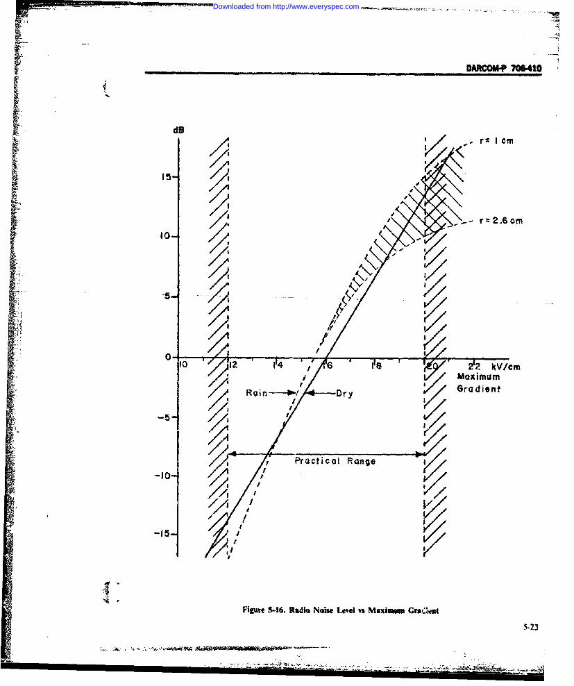
r DARCO*-P 706.410
dB r c
/ ~ r - tcm
-5-
-151
6iur &1.RdoN eLvlv aiu W M axmu
2 V2
Downloaded from http://www.everyspec.com

DARCOM.P 706410
0_ _
Lf0Ga i ype Discharge
Corona----
40
",1 .0,2 .O, 0.6 1.0 2 35 I0 2 1 S 10T 2 5 1 "11Frequency f, MHz
Figure 5-17. Relative Current Spectrum of Corona and of a Gap Discharge
of the field can be described as a suppression of the field strength of the reflected wave, expressed in dB,original incident wave and of waves that are re- is called the reflection loss.flected by the conducting parts of the line. This super- The level of the reflected wave can be surprisinglyposition of waves near the line is perceptible in two high, and in extreme cases it can be even higher thanways: the level of the incident wave. To explain this it
a. The incident and reflected waves form an inter- should be remembered that, due to ts height, the lineference pattern of standing waves with maxima and is in a much more favorable position to pick up theminima which make the total local field strength de- incident wave than the usual receiving antenna.pendent on the position relative to the line. The reflection loss R at a distance d from a single
b. The signals modulated on the reflected waves wire of diameter a (in meters) increases with fre-have a time delay with respect to the signal modu- quency to a value given by:lated on the incident wave, causing envelope dis.tortion. R = -20 log - d]3 (5.3)
Experience has shown that degradation from re- "flections by overhead lines mostly occurs when thereceiver is on the transmitter side of the line, and Therefore it can be found that at UHF, the reflec-more so when the incident wave is perpendicular to tions from an overhead line are less than those atthe line, VHF.
The reflected wave can be measured separately In case of bundled conductors, the frequencyfrom the incident wave by means of a directional an- dependence of the reflection loss is more compli-tenna. The ratio of the incident field strength to the cated because of the possible reflections between the
5-24
711117 _7 1
Downloaded from http://www.everyspec.com

.720DARCOM-P 706410
• - ~20 . . . .
0
-20
4-'
1 -- 40
-6f_ __ _ _ _ __ _ _ __ _ _ _ __ _ _ __ _ _ _ __ _ _ .. ...
10 2 3 5 102 2 3 5 2 3 5 10
Distance, m
Figure 5.18. Relative Interference Field Strength as a Function of the Distance from the Line
constituting conductors. Fig. 5-19 shows the cal- 53 POWER CONTROLculated reflection loss of 3-conductor bundle for hoi- Power flow may be controlled through (1) switch-zontally polarized waves as a function of the direc- ing in which currents and voltages are chianged sud-tion of reflection. At 62 MHz the reflection loss is denly in steps, or (2) continuous variation usingpractically independent of the direction of reflection, amplifiers, phase control devices, or other means.whereas at 519 MHz tl.e reflection loss increasesmarkedly depending on the direction of reflection. 5-3.1 SWITCH POWER CONTROLAdditional data are given in Ref. 3. The step action in opening or closing a switch or {
contactor gives rise to broad spectrum interference,as discussed in par. 3.1.3.2, whose magnitude is de-
5-2.5 INTERFERENCE LEVEL AND pendent on the magnitude of the current or voltageQUALITY OF RECEPTION (Ref. 2) which is initiated or interrupted. Where these quan-
Table 5-1 shows typical values of signal-to-noise tities are large, relays and remote controlled circuitratio required for various subjective reception quail- interruptors may be used.tics when interference generated by power lines de-grades amplitude modulated signals. For other types 5-3.1.1 Interference Generatioof modulation, e.g., frequency modulation, a quite Switch-generated interference can be associateddifferent performance may be expected (see par. 3- with three mechanisms of generation: (I) high-2.1.4). voltage gaseous discharges (which may give rise to a
5-25
-. ii *1i ~'( * "---i ....K i" ... .
Downloaded from http://www.everyspec.com

DARCOM*P 706-410
50
0
4-30 __
0 20 40 60 80 100
Angle *,deg120 ___________519 MHz
820
0
40
V
20 4060 Age .de
0~8 100
40
Figure 5-19 Reflection Loss and Phase of a! Three-conductor Bundle as a Function ofthe Direction of Reflection
5-26I
Downloaded from http://www.everyspec.com

DARC0M-P 706-410
r ~ . TABLE 5-I. RECEPTION QUALITY AS A FUNCTION OFSIGNAL-TO-NOISE RATIO
Signal/Noise Ratio Reception QualityScales Code Subjective impression
dB Ratio30 32 5 Interference not audible24 16 4 Interference just perceptible
18 8 3 Interference audible but speech_______perfectly received
12 4 2 Unacccptable for music but______speech intelligible
6 2 I Speech understandable onlywith great concentration
0 1 0 Spoken word unintelligible,noise swamps speech totally
saw-tooth type of waveform), (2) low-voltage high- the potential across the contact gap. It is impossiblefield breakdown (bridging), and (3) current changes to alter the changing load current between the twobetween the two steady-state values. The high-voltage steady-state values without affecting normal opera-discharge, when present, produces more interference tion of the circuit- however, interference may be con-than the other causes combined throughout the entire tained effectively in the regions of the switch and loadfrequency range from 15 kHz to 1000 MHz. There is side of the circuit by inserting filters in the externala broad peak in the spectral distribution of the inter- power supply leads. A good interference reductionference caused by high voltage breakdown that oc- circuit should:curs in the region of a few megahertz for common a. Retard the build-up of voltage across the gapvalues of circuit parameters. The bridging has a negli- during the initial period of contact separation togible effect at the lowest frequencies, but increases in minimize bridging reclosures.relative importance with frequency until, at 1000 b. Limit the peak voltage across the switch gap,MHz, it is nearly as great a source of interference as upon opening, to eliminate gaseous discharges.the high-voltage breakdown. The change of current c. Limit the surge of current through the switch,between the two steady-state values yields its greatest upon opening or closing, to minimize sharp wave-contribution to interference at the low-frequency end front transients.of the spectrum (Fig. 5-20). In selecting a suitable circuit, it is usually neces-
sary to make a trade-off between interference reduc-tion and other considerations such as the allowable
5-3.1.2 Interference Reduction rise or decay time of the load current, ease of installa-In reducing interfecence, first consideration should tion of the circuit, physical size of the interference re-
be given to elimination of the high-voltage discharge. duction components, and adaptability to the powerThis is accomplished by employing an interference supply. The circuits that are. used usually resemblereduction device that prevents the voltage across the simple types of low-pass filters. i.e., they consist ofswitch gap from exceeding the value required to in- capacitors placed across the contacts and/or in-itiate a glow discharge (approximately 300 V). To ductors in series with them to limit the rate of rise oreliminate the formation of bridges, it is necessary to fall of current through the external circuit. Resistorsprevent the electric field between the contacts from are placed at appropriate locations to absorb theexceeding a critical value (approximately 5 X l(Y' energy stored in these elements. The values of theseV/in. for untreated contacts). Bridge elimination may elements must be chosen so that they perform thebe accomplished upon switch opening by mechanical- necessary suppression function without disturbingly increasing the speed of separation of the contacts, the control function being performed in any signifi-and by electrically decreasing the rate of build-up of cant way.
5-27
,d ., . , . , " , *" " '" - ".v i . ,. . . •. ; ; . '- "' " ' :
Downloaded from http://www.everyspec.com

t DARCOUCP 706-410
.- 160'
SC V
120 r -
L.L
iS
40
, 20 dB per DeadC 0
S6
Dead
164 105 10 107 Id a 1@9
Frequency Hz
~Interference Caused by the Transition from One Steady
State to the Other
D Additional Interference Caused by Low Voltage
Breakdowns (Bridging)
~Additional Interference Caused by High Voltage
Breakdowns
5-28 Figlure 5-20. Spetra of Switching Interference Phenomena
.-2
. . .. . .. .. .. . . .. " .
.a ' . • . ...-". . ,
Downloaded from http://www.everyspec.com

DARCOM-P 706410 4
For example, the value of a capacitor C placed circuit through which the inductive current may flow.across the swilch is determined by the current value The peak voltage appearing across the switch is there-and the load inductance L; supply voltage and fre- by limited to the sum of the battery voltage and thelquency of switching not being important factors. It is forward drop of the diode. By choosing a diode with Anecessary that such a capacitor be able to store tern- a low forward resistance, the voltage across theporarily all of the energy previously contained in the switch is essentially just that of the battery. This cir-load inductance without the voltage across the cuit is very effective in providing the complete elimi-capacitor exceeding the glow discharge value of ap- nation of all high-voltage, saw-tooth type dis-proximately 300 V (C > L (I/300)', (from Eq. 3-39). charges; it is ineffective in retarding the gap voltage
build-up. A second method of using a diode is shown5-3.. Uon Fig. 5-22. This diode should possess a sharp knee J
-3,1.2.1 Use of Dodes and Varistors areusef in its voltage-current curve (Zener diode) at a voltageDevices with nonlinear resistance-voltage char- value that is somewhat greater than the supply
acteristics, such as diodes and varistors, are useful voltage, so that the steady-state current through the
components for interference reduction. A diode has load will be essentially zero when the switch is open.low forward resistance and high reverse resistance. A b. Ac Circuits. Components consisting of twovaristor conducts well at high voltage but not at low similar Zener diodes placed back-to-back are com-voltage. The function of either a diode or a varistor in mercially available as a single unit. Their combined .,an interference reduction application is to provide an current voltage characteristic is shown on Fig. 5-23.alternate path for the induced current to that through When placed across the load, as shown in Fig. 5-24,the contact. the back-to-back unit is inferior to the load-shunt
The diode need dissipate only a fraction of the total diode interference reduction circuit (useful in dc cir-energy stored in the load since most of it is dissipated cuits) in that it does not limit the overshoot in the gapwithin the load resistance itself, voltage to as small a value. Bridging is therefore more
A discussion follows: prevalent. When the contacts are opened, one diode,a. Dc Circuits. An effective interference reduction depending on the polarity of the source at the instant i
element is the diode shown on Fig. 5-21. The diode is switching occurs, will limit the peak driving voltageinserted in the circuit so that its polarity opposes that of the coil. The stored energy of the coil is dissipatedof the impressed voltage. The i'Rb loss (Rb is the re- in the diode and in the coil itself.sistance of the diode) through the shunt circuit is c. Varistors. A varistor could be used in place ofsmall. For maximum interference reduction, the the diode in Fig. 5-21. However, the circuit shown indiode should be installed as close to the inductive ele- Fig. 5-21 results in lower power consumption andment as possible. Negligible current flows through heating because it conducts at a lower inducedthe diode under steady-state conditions but, when the voltage. A varistor can be used in place of the diodeswitch is opened, the diode provides a low resistance in Fig. 5-22, but it may produce higher current drain
SWl TCH
R
E -LGAD- WHJNT +
PI) LFigure 5-21. DC Switching Interference Reduction by Load-Shunt Diode
5-29
Downloaded from http://www.everyspec.com

OAROM*P 706-410
Switch
Diode R
L
Figure 5-22. DC Switching Interference Reduction by Switch Shunt Diode
C
Vol taqe, V
Figure 5-23. Current vs Voltage Characteristics of Two flack-to-Back Zener Diodes
5-30
Downloaded from http://www.everyspec.com

OARCOM# -06410
when the switch is off than will the diode. A varistor (5) When using varistors, the characteristic curvecan be used in place of the back-to-back diodes resistance knee must be above the supply voltages,shown in Fig. 5-24. and have adequate heat dissipating capacity.
d. Application Guidelines. When designing in-terference reduction circuits using diodes or varis- 5-3.1.2.2 Interference Reduction Circuitstors, the following design guidelines should be con- A variety of circuits made up of resistors.sidered: capacitors, and inductors can be used with or with-
(1) When using a single diode, its current-rating out the nonlinear elements discussed in par. 5-3.1.2.1should be equal to the load current when repeated as follows:cycling is necessary. a. Series Capacitor and Resistor. Contact erosion
(2) For intermittent use, a rating equal to one-half arises from the use of capacitors and can be alleviat-of the current is usually sufficient, ed by the addition of a series resistor (Fig. 5-25). In a
(3) Breakdown-voltage ratings of diodes should circuit containing inductance, the voltage that ap-exceed the supply voltage by at least 20%. For sele- pears across the switch immediately upon opening isnium diodes, a low safety factor is normally satis- equal to the product of this resistance and the inter-
V. factory. rupted current; therefore this resistance should be(4) Back-to-back diodes may be used for ac cir- low. On the other hand, a large value of resistance is
cuits. The breakdown-voltage must exceed the supply desirable to minimize the contact erosion uponvoltage, closing. While the IR drop does allow some bridging
E cos (X t
DL
Figure 5-24. AC Switching Interferemc Reduction by Two Diodes
C R
Figure 5-25. Series Capacitor and Reuistor Circuit to Reduce Contact Frosion
5-31
- *.i].,--..w -
-]£i~. ~ ~
Downloaded from http://www.everyspec.com

DARCOM-P 706-410
to occur, a sufficiently large value of capacitance will 27). This circuit is similar to the series capacitor-*eliminate high-voltage breakdown. The values of re- resister combination of Fig. 5-25. Because thesistance and capacitance should be chosen empirical- resistor must carry the normal load current with aly from the results of test data to minimize inter- negligible voltage drop, there is a practical limit toference. the maximum value of the resistance. In practice, this
b. Series Capacitor and Nonlinear Resistance. The circuit is much more effective in reducing inter-series capacitor and resistor can be improved by ference than the series capacitor-resistor unit. What-shunting the resistor with a diode, as shown on Fig. ever disturbance is produced is largely confined to the5-26. This action permits the achievement of the de- switch-resistor capacitor loop. This circuit not onlysired low-resistance value for a switch opening and alters the phenomena occurring at the gap, therebythe desired high-resistance value for switch closing. functioning as an interference reducer, but also pro-For maximum effectiveness, it is necessary that the vides containment for the interference which iscapacitor discharge completely during the closed in- produced.
V. terval of the switch, or bridging will occur when the d. Special Interference Reduction Circuits. Specialswitch is again opened. Therefore, it is necessary to interference reduction circuits are those that deviatemaintain the linear resistance in shunt with the diode from the basic circuit of switch, supply, and load -
to assure that the initial condition is maintained. all connected in series. Several types of reduction cir-c. Typical Resistance-Capacitance Circuit. A very cuits are presented:
effective circuit consists of a resistor placed in series (1) Coupled Coils. The effect of inductance inwith the load circUit and a capacitor in parallel with series with the switch can be reduced by providing an
the series combination of resistor and switch (Fig. 5- alternate closed path through which the collapsing
f-i 7DI ODEI
Figure 5-26. Interference Reduction by Series Capacitor and Nonlinear Resistance
SWI TOH
C
i i f i
Figure 5-27. Interference Reduction by Series Resistance and Parallel Capacitance
5-32
,. ., •. . ~'; , -,
Downloaded from http://www.everyspec.com

_ - DARcOM.P 706410
magnetic field can cause the current to circulate (Fig. The corresponding expression for the current in the5-28). In such a circuit, the higher the value of the co- secondary loop is given by:efficient of coupling k the more rapidly is the storedenergy absorbed. A transient analysis of this circuit 60() - (nn 2)(O)xp (-RI/k) (3-6)shows the voltage v, across the primary winding to begiven by: Eq. 5-5 shows that, if the factor R2(nt In/l is made to
approach zero (either through the choice of second.v1(I) = -R(nln 2)2iI(O-)cxp(-Rt/k),V (5-5) ary resistance or of turns ratio), the voltage across the
primary winding will approach zero, and the voltagewhere across the switch will be that of the supply. This ciri(0-) the value of the interrupted supply cur- cuit exhibits the characteristic of a resistance load.
rent, A When the switch is closed, the current in the primaryn - number of turns, primary, dimensionless circuit rises more rapidly as the term R2('/y)- isn2 = number of turns, secondary, dimension- decreased. This requirement, however, is in direct op-
less position to the requirements for maximum inter-I = time, s ference reduction upon opening of the switch. Never-R= +(n?: theless, it should be possible to Select a compromise
(z value for this term which would make the openingRI resistance of primary coil, 0 and closing interference levels equal. Another possi-
R2 = resistance of secondary coil, S1 bility is to replace the resistor R by a diode as shown
VS
+ 0 L
R, = RESISTANCE OF RELAY COILWHICH ISTHE LOAD OF SWITCH S
Ll = INDUCTANCE OF RELAY COIL, WHiCH IS
THE LOAD OF SWITCH S
R2 = RESISTANCE OF COUPLING COIL
L 2 = INDUCTANCE OF COUPLING COIL
Figure 5-28. Inte-ference Reduction by Coupled Coils
5-33
Downloaded from http://www.everyspec.com

DARCOM.P 706.410
on Fig. 5-29 to present a low-resistance value to the an interference filter instead of a composite re-W. opening transient current and high resistance to the duction circuit.Sclosing transient current. As mentioned in par. 5-3. 1, to prevent the voltage
(2) Bias Batteries. In dc inductive circuits. re- across the switch from having an excessive peak valueduction of arcing at contacts can be achieved by em- during opening of the contacts, the capacitor mayploying bias batteries, or their equivalent, in ad- have to be large. The required value of capacitancedition to nonlinear resistances or diodes. The pri- can be calculated from the circuit parameters. If. formary advantage of these circuits is that the diodes instance, the load current is 3 A, the load inductanceneed to dissipate only an incidental portion of the in- is 10 H, and 300 V is the maximum allowable voltage,ductively-stored energy; the diodes may therefore then the calculated value of capacitance is:have low electrical rating3 and be of small physicalsize.Sixvariationsofthistypeofcircuitareshownon C = L(I/ V)2 = 10(3/300)-" = 10-1 F = 1000 pFFig. 5-30. Circuits (A) and (B) are essentially the (5-7)same - one employs a tapped inductive load and theother a load with a closely coupled second winding. The value of the capacitance C on Fig. 5-31 is also a
The dc source in each case also serves as the bias factor in determining the low-voltage breakdown orbattery. Circuit (C) employs a simple load winding bridging. For the larger capacitance values, thebut requires a separate bias battery. Circuit (D) is voltage build-up across the contacts upon switchsimilar to (C). except that the tapped winding allows opening is slower and, c, ,.equently, the electric fieldgreater freedom in selection of the bias voltage. Cir- intensity within the gap is reduced. This consid-cuit (E) is applicable when the switching occurs at a eration is a second factor in the selection of the valuereasonably rapid and constant rate so that the re- of this series capacitor. Under some circuit con-peated transient currents through the rectifier to ditions, and with a fast opening switch, the value sobuild up a nearly constant bias voltage across te determined will be less than the capacitance requiredparallel resistor-capacitor combination and eliminate to limit the peak switch voltage. Composite Circuitthe need for a separate battery. Circuit (F) is adapted (B) is a modified configuration of Circuit (A).for loads that are supplied from an ac source.I (3) Composite Interference Reduction Compo- 5-3.1.2.3 Summary
nnts. Interference reduction can be obtained by Table 5-2 compares the ability of several circuits tousing simple components in combination. Two com- retard the build-up of gap voltage, limit the peak gapposite arrangements are shown on Fig. 5-31. As each voltage, and minimize sharp wave-front transients.of the simple suppressors has some deficiency, it may Table 5-3 compares the general interference re-I be desirable to consider whether, when used together, duction characteristics of components. The factorseach can supplement the other to improve overall affecting the determination of component values areperformance. Frequently, however, it is easier to use summarized in Table 5-4.
SWITCH 9
+ L1 L2 DIODE
Figure 5-29. Interference Reduction by Coupled Coil With Diode
5-34
Downloaded from http://www.everyspec.com

F DARCOM-P 706410
MANUAL SWITCH .MAMWAL SWITCH
aa(A)()
14ANUAL SWITCH + MANUAL SWITCH+
(C)()
MANUAL SWITCH4... +. MANUAL. SWITCtH--.
(E) (F)
Figure 5-30. luterfercace Reduction Circuuits Employing Bias Batteries
5-35
Downloaded from http://www.everyspec.com

DARCOM-P 706-410
SWITC
, L
IIIC D RAI. .------.. ... ... Is
i- ILOAD
S I I RL IS I IDI
3 RLI______________(A) COMSITE cIcuT A
$ WI.TCH _.-, ..: . .
L '
gC D R A C
DII C RL
(eW€osI'E CIKUIT 8
Figure 5-31. Composite Interference Reduction Components
5-3.2 CONTINUOUS POWER CONTROL The interference generation characteristics of these
The use of simple on-off type controls is not prac- types of equipments were discussed in par. 5-1.
tical for controlling large amounts of power. Furthtr- The development of semiconductor devices has re-
more, for many purposes, such as control of traction suited in extensive application of them in recent years
equipment or in industrial type processes, con- in power control devices. They can be applied in
tinuous control of power output is required. This can various ways with ac power circuits. Typical tech-
be a, hievzd with special electromechanical equip. niques are shown in Fig. 5.32 and include, among
ment such as motor generator sets and amplidynes. others, phase angle control, symmetrical phase angle
5-36
.. . . . . . . . . . . .. .. ........ .... . . . . ....... . .. . ...
~ ~ IJ;
Downloaded from http://www.everyspec.com

DARCOM-P 70.410*
TABLE 5-2. COMPARISON OF INTERFERENCE REDUCTION COMPONENTS
Requirements
1 2 3
Retard Limit Minimize
Components Placement Build-up Peak of Sharp Waveof Gap Gap Front
.... _Voltage Voltage Transients
Load a As PCapacitor Swtch G A P
Linear Load P Ad AResistor Switch P A' G
Semiconductor Loid P 0 Ab
Diode Switch' P G
Back-to-back Load P G AbDiodes Switch* P Ab
Capacitor Load Capacitor is superfluousand Diode. .. ....
' .- Switch G A' G
Series R A' A' 0Shunt C
Coupled GSecondary
Diode and Load P G Ab
Battery
Switch P G G
CrutG G A
Composite ]" G Gi Circuit
GoGood A Intermediate P = Poor
i .I=-Diode must have knee at voltage greater than that of supply
b = Determined by inherent shunt capacitance of diodec = Capacitance must be sufficiently larged = Resistance must be sufficiently small
5-37
Downloaded from http://www.everyspec.com

DARCOM-P 706-410
izi A
I.-F
S0.M
i -
5-38
'a o0.
Downloaded from http://www.everyspec.com

OARCOM-P 706410
TABLE S.4. DETERMINATION OF COMPONENT VALUES
Suppressor Supply Voltage Load Current Load I nductanceCircuit I I L
Across Voltage for reverse Reversed diode must dissipate all of stored energy. Select
Switch knee must exceed on heat basis. If duty cycle is high, current rating may be____________ ., supply less than normal rectifier rating. Knee < 300 V.
Across Same Same Knee< (300 - V,)S Load
Diode must dissipate only a fraction of stored energy..• Diode with rectifier, average-current rating equal to load' Same current is conservative. If duty cycle is low, normal rating
of diode may be increased by a factor up to ten,
i i:Should have low for- in practice, no effect. Diode. se-
D No effect ward resistance. lected on rf basis, could carry loadNo~. effect 5 . < R "/I Icurrent indefinitely.
_C No effect C ?-L(1/300) to eliminate sawteeth
R No e Must completely discharge C during switch-closed inter-1' _____- _ _ _ _o _ efftVal. A _ P/(50)
Voltage for re- R/ must be less If V is large (to reduce decay time),D verse knee than: diode selected on basis of rf could
mustcarry load current indefinitely. No
- vb+e 3 effct of L.
V V, should be maximum possible and still keep gap voltage less than 300 V:
, + 6 +1R< 300V
C No effect C > L (1/300)1 to eliminate sawteeth
CR - value which pro-R No effect duces maximum al- No effect
SNlowable voltage regu-lation
*T duration of closed lnterv-l
control, burst control, and symmetrical burst control. automatically create significant levels of harmonic orIt should be noted that methods of power conversion subharmonic voltages and currents in circuits cou-from ac or dc sources, using rectifiers and inversion pled to them directly by conduction, or indirectly bytechniques, are discussed in par. 5-5. induction. Furthermore, these generally undesired
Because control methods using semiconductor t e- currents can result in overheating of some of the cir-ments generally produce waveform distortion, they cuit components.
5-39
.. .. . .... .. . .. ,_ . '
Downloaded from http://www.everyspec.com

DARC0MP-706-410
A)~~c Phs Coto Tim
(A)Symia Phase Control
(C) BsmmentrlPheCnto
1]4 4
(C) ymeia Burst Control
540
ims
Downloaded from http://www.everyspec.com

D ARCOM-P 706410
5-3.2.1 Distortion Levels (see Ref. 4) dc resistance which have values dependent on the sizeThe burst firing control technique will, product of the power source and interconnecting power line
periodic voltage fluctuations on the powerline at the conductors.burst frequency which in turn can cause a visual Values of L and R can vary from 50 AH and 0.01 Ql,flicker effect from lamps connected to the line. The respectively, for circuits capable of carrying severalsubjective effect of flicker is shown on Fig. 5-33, It is hundred amperes to values as much as 10 times theseseen that 2% or less voltage fluctuatiors can cause ob- for a typical low current household distribution cir-jectionable flicker. The use of higher power fre- cult (15 or 20 A).quencies, such as 400 Hz, may be more satisfactory The current i shown on Fig. 5-34 represents har-because the flicker rate is likely to be above the fre- monic currents generated in nonlinear loads whichquencies at which vision is sensitive, can be expected to flow back through L and R (rather
The voltage harmonic levels can be computed from than through the other loads since the equivalent it-.'nowledge of the current harmonic levels and the pedance of the connected loads is usually higher than
impedance of the power source. The equivalent cir- the impedance of the source) and thereby produce thecuit for a typical source in the audio-frequency range harmonic voltages appearing as distortion on theis an inductance and a resistance in series as shown in line. On a 60-Hz system for a current of 4 amperes atFig. 5-34. In this circuit V represents the generated the nth harmonic of 60 Hz, the voltage v, would beelectromotive force producing the power frequency(60 Hz) line voltage. L is an inductance, and R is the v. ii R2 + (27r60Ln)2 ,V (5-8)
.... Voltage Fluctuation
0 M
-A
t V)CD
W
0. I 1.0 10 tooFluctuations per Second, Hz
! ~ Figure 5-33. Objectionability of Latmp Flicker as a Function of Frequency
-- 4
.41_ .. , ., . ...' ...-.,
... ,,, . •- ; " / .v . , . , . .o " - - • -., -' 3 ,-- ' .-"." " ., .
Downloaded from http://www.everyspec.com

DARCOM-P 706-410
g R"
Connected
Loads
Figure 5-34. Typical Equivalent Circuit for a Power Source at Low Frequencies
For an unsymmetrical phase control arrangement, on Fig. 5-37 for a suppressed and unsuppressed 600-: Fig. 5-35 shows t~he variation of the 3rd, 4th, and Sth W lamp dimmer (suppression consisted of an- L-C.
harmonic levels in terms of the peak current as the filter).firing angle (shown as a of Fig. 5-32) is varied. Fig, 5- The types of filter suggested for use with SCR's are
. 36 shows the corresponding result for a symmetrical shown in Figs. 5-38 and 5-39. The circuit in Fig. 5-38arrangement, confines the high-frequency current to flow in the cir-
In addition to flicker, high harmonic content can cuit close to the SCR, whereas in the circuit in Fig. 5-cause other compatibility problems at power fre- 39, some of tht current flows in the load. Dependingquencies. Examples are: on the nature of the load and the current path
a. Metering. The flow of direct current and of har- through it, the latter arrangement may produce in-monic currents through a watt-hour meter can cause duction and radiation fields in the vicinity.it to show incorrectly the watt-hours consumed. The burst firing technique, because it tends toErrors up to 3% have been observed, switch at the time the voltage or current is zero, does
b. Pow.cr Factor. The power factor will be af- not produce the high rates of change. Consequentlyfected because of phase shifts between the supply fre- radio interference levels are orders of magnitudequency current and voltage. A phase controlled cir- lower than with phase control as shown on the bot-cuit with a resistance load will have a lagging power tom curve of Fig. 5-37.factor. For high firing angle (low loading), the power
factor approaches zero. Where low-pass type filters 5-3.2.3 Susceptibility of SCR Circuitsare used in conjunction with the device to reduce line SCR units are susceptible to pulse triggering fromharmonic content, the capacitance inserted across the undesired transients. They may appear on either theline may tend to improve the power factor, but also gate or anode supply voltage as a result of couplingmay cause it to change to leading. from other SCR's or other transient-producing de-
vices. Efforts should be made to suppress such tran-5-3.2.2 Radio Interference Generation sients, When they appear in the voltage supply, a
The sharp rise in current with phase control of capacitor divider may be used to protect the circuit assemiconductor devices can produce much higher shown for the unijunction transistor (UJT) circuitvalues of radio interference than gas tube vacuum cir- shown on Fig. 5-40 (Ref. 5). The capacitors shouldcuits. Estimates of the spectrum level at the point of have values satisfyingthe device in the circuit can be made using the formu- C,las in par. 3-1.3.2. The levels produced can be re- - dimensionless (5-9)duced using appropriate filters as discussed in pars. 4- C 2 + CU5 and 5-I. levels of conducted interference are shown where n is the intrinsic stand-off ratio for the UJT.
5-42
Downloaded from http://www.everyspec.com

.4 -4IF4. - V0.0OARCOM-P 706"410
, 0 .2 0 i .'el"
1.0 per Unit
0.16 >11
-"-3rd Harmonic
0.1
>4 .i
. 4th Harmonic
,' 0.08
4-J
' 0.045th Harmonic
0.4
0 30 60 90 120 150 180
Firing Angle a, deg
Figure 5-35. Harmonic Content vs Function of Firing Angle (Unsymmetrical Phase Control)
5-4 LIGHTING doam current conduction effects in the gas, and from5-4.1 INTRODUCTION oscillations that take place because the gas break-
Two types of lamps are in general use - incands- down phenomenon can exhibit negative resistance
cent and gaseous discharge. Incandescent lamps nor- characteristics.
mally are not considered to be a source of inter-ference. In par. 3-1.3.2.3.2 a brief description was 54.2 FLUORESCENT LAMPSgiven of the radio noise from a gaseous discharge The fluorescent lamp is an arc discharge that canlamp. It arises from the switching phenomenon, ran- be maintained at a relatively low voltage, but must be
5-43
..... .. .. . --
Downloaded from http://www.everyspec.com

DARCOM-P 706-410
0.36 The instant start lamp has no filaments as shown in
1.0 per Unit Fig. 5-41(C). Initially the combination of L1 and Cresonates to produce a high voltage to strike the arc.
0.32 ,i\ After the arc strikes, the resonant condition is no> 4 ) longer satisfied and the voltage across the lamp re-- .2duces.- 0.2 8 Often forms of these basic circuits are used for pur-
Balanced a poses of improving efficiency, power factor, and cost.w In a lamp for direct current, a series resistor is used to0- 0.24 limit the current after the arc is initiated. Fig. 5-42o 3rd Harmonic shows a two-lamp ballast.
4- The current through a lamp on ac supply will be0.20 nearly sinusoidal because of the presence of the
(. Iballast which causes the load to be primarily in-ductive. However, at each current zero the restriking
0 0.16 henomenon will causea voltagetransient which will4J t =appear across the lamp. Since this occurs on each half
cycle, one can expect relatively strong levels of har-g. 0.12 monies of the power line frequency to appear in the
circuit in addition to radio frequency components.o Because the ballast itself is a high impedance, the
: " 0.08levels of harmonic current appearing on the line willbe relatively small.
0.04_" "__To reduce radio frequency components it is con-0.04 ventional to place a capacitor across the bulb termi-
nals as shown with dotted lines in Fig. 5-41. Thedesign of the ballast and the effects of distributed
0 60 120 180 capacitance in its windings can be important in theFin Aoverall radio interference characteristics of the lamp.Firing Angle a, deg In addition to arc formation, another source of
Figure 5-36. Harmonic Content vs Firing Angle radio noise is oscillations produced by the nonlinear(Symmetrical Phase Control) characteristics of the arc discharge (see par. 3-
1.3.2.3.2). Such oscillations have been observed ex-tensively in the frequency range around 10 kHz butexperimental evidence indicates that similar phe-
restruck with a high voltage each time the lamp is nomena can occur at higher frequencies of the orderturned on (if supplied from direct carrent), or on each of I MHz.half cycle (if supplied by alternating current). The arcis struck by means of a ballast which is effectively a 5-4.2.1 Emission Levelslarge inductance which resists any sudden change in For an alternating voltage lamp supply, the switch-current (see Fig. 5-41). ing transient generated on each half cycle for re-
Three types of lamps are used (Ref. 6). The switch ignition is a major source of interference from lowstart and rapid start types have filaments to heat frequencies up to the megahertz range. Voltage levelscathodes which aid in arc initiation by emitting elec- measured at the terminals of the lamp connected totrons. The switch start circuit contains a "starter" as the power line can be expected to be of the order ofshown in Fig. 5-41(A) which when closed initially en- 50,000 to 100,000 gV at harmonics in the vicinity ofables the filament to heat and then opens after a few 100 Hz and vary inversely with the frequency re-seconds causing the arc to strike. ducing to a few microvolts at 100 kHz. Because of the
A rapid start circuit is shown in Fig. 5-41(B) in instability of the arc, the interference will be broad-which initially the tapped inductor causes the fila- band in nature so that higher order harmonics arements to heat. After the arc strikes, which may occur difficult to separate.in a few tenths of a second, the voltage across the The oscillations that appear can produce quite hightapped inductor drops and the filaments are operated voltages ranging from about a volt in the frequencywith reduced current. range around 10 kHz (see Fig. 3-29), down to several
5.44
m-...~~~~~~~ ' . .' - .. -:. . . ,
Downloaded from http://www.everyspec.com

DARCOM-P 706410
106
TypicalUnsuppressed Dimmer
105
.440
Tyia
O Suppressed Dimmer
0
Cotole
0A
0o.1 1 10 100Frequency f ,MHz
Figure 5-37. Conducted Interference for Light Dimmer
5-45
Downloaded from http://www.everyspec.com

DARcM-P-706410
SUPPLY C0LINE A
RF RGROUND
-i NEUTRALA
Figure 5-38. Conducted RFI Suppreauon With RF Grounid iaccesible
SI LI CON-CONTROLLED
SUPPLY
LINEL
RF GROUNDI
5-46 ~Figure 5-39. Conducted RFI Supjpruudsn With RF Ground AccessibeI
5-46
Downloaded from http://www.everyspec.com

[ DARCOMP 706410
-.--C R I R
Figure 5-40. Decoupling Against Supply Transients
millivolts in the range around I MHz as shown in when measured at a distance of approximately 3 ft. ItFig. 5-43 and several hundred microvolts at 2 MHz as varies inversely with the frequency. The level falls offshown in Fig. 5-44. Oscillations in the vicinity of 10 rapidly with distance and generally can be assumed tokHz are usually accompanied by a high impedance at obey an inverse cube law at distances from the lampthat frequency due to a self-resonant characteristic of which are larger than the lamp dimension itself.the ballast, such as shown in Fig. 3-30. It is likely that Furthermore, the level of emission is considerably depeaks in emission at frequencies in the neighborhood pendent upon the construction of the lamp fixture. Ifof 1 MHz occur because of electronic resonance the lamp is fully enclosed within a metal container,phenomena in the arc discharge itself. Radiated emis- except for the minimum opening necessary for il-sion characteristics of fluorescent lamps arise be- lumination, levels much lower than the levels showncause of two phenomena: (1) the magnetic field as- in Fig. 3-31 may be obtained. Furthermore, the emis-sociated with the ballast, and (2) the electric field as- sion level will depend upon one's position with re-sociated with the arc discharge in the fluorescent spect to the lamp opening. Usually because the lamptube. Because of the high impedance of the ballast, is backed by a metal box or reflector, levels on thethe ballast currents themselves are pretty much re- back side will be much lower than those on the frontstricted to low frequencies. Substantial magnetic side (Ref. 7).fields can be measured at 60 Hz and at the first fewodd harmonics of 60 Hz. The effective dipole strength 54.2.2 Inerference Redctionat 60 Hz is on the order of I ampere-turn metersquared and at harmonic frequencies can be expected 5-4.2.2.1 Radiationto be lower in accordance with an inverse harmonic The fluorescent lamp fixture is a significant sourcenumber squared law. The magnetic flux density will of interference only when it is located close to a sensi-vary inversely with the cube of the distance from the tive receiver or receiving antenna. At distances morecenter of the ballast and can be computed quanti- than a few meters, direct emission in the form of antatively using Eqs. 3-114 or 3-115. electric field is not likely to cause difficulty. Where in-
The electric field components are generated di- terference reduction is necessary, the two techniquesrectly as a result of the high voltage which appears usually used are: (1) a metal grille or louver which es-across the fluorescent tube on ignition. It is of a sentially surrounds the lamp with a complete metalbroadband type and, as shown in Fig. 3-31, is of the enclosure, and (2) conducting (transparent) glass ororder of 100 piVm/kHz of bandwidth at I MHz plastic. With regard to the former, openings in the
5-47
. , ,. ... .... . , .......
Downloaded from http://www.everyspec.com
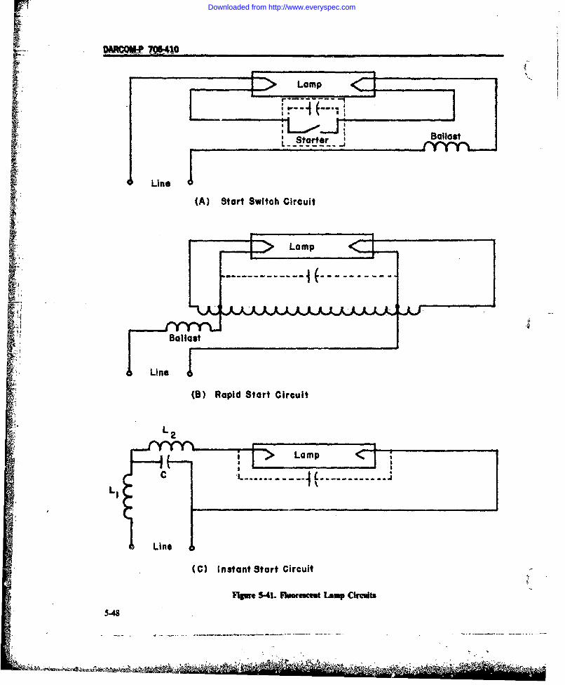
Line
(A) Start Switch Circuit
Lam
Line
(C) Rida Start Circuit
Fiw 54.FkoestLamp Ci
3-48
Downloaded from http://www.everyspec.com

VDARCOMP 7015410
, Starter.
Ballast
Line
Figure 5-42. Dual Lamp Fluorescent Fixture
grille are not significant sources of leakage or radia- and the associated ballast, and by carefully con-tion at the frequencies emitted by the lamp. The ex- trolling the distributed capacitance to the fixture. Ifpeeled attenuation can be estimated using formulas such techniques are not adequate, it is possible to in-in Chapter 4 for screens or, if of sufficient thickness, sert common-mode filters or chokes in series with thethose for waveguide below cutoff devices (see par. 4- power-line connection.6.5-2). The conducting technique probably permits Grounding of the lamp fixture is probably bestgreater light transmissibility. The effectiveness of a done through the ground wire or conduit of thegrille is indicated in Fig. 3-31. Corresponding at- power cable. Where an environmental (or local)tenuations can be obtained with conducting mater- ground is available, grounding to it can increaseial. common-mode currents, and thus increase local in-
duced or radiated fields.5-4.2.2.2 Couste
Although the levels of emission currents on thepower line are usually small, they can produce inter- 5-5 ELECTRONIC POWER SUPPLIESference to nearby equipments. To control emissionsin the broadcast frequency range, the ballasts should 5-5.1 INTRODUCTIONbe constructed to have a minimum distributed The most common form of electronic power sulcapacitance in order that substantial impedances to ply is one used to convert the power from an altecurrent flow will be obtained. Differential-mode cur- nating or direct voltage to a different direct voltagrents can be controlled by inserting filters at the line Usually, the ac supply uses a transformer and a recterminals. A simple line-to-line capacitor may be suf- tier. For converting from direct voltage to dircficient. The flow of common-mode currents can be voltage, a switching system is used which converts treduced by using balanced arrangements of lamps direct voltage to alternating voltage, which may
: - ' ,. " .i " " , ','" ',' - ;" " , 7": - . . i - , .5"
_____: , . .... , *. , .-
Downloaded from http://www.everyspec.com

rACMP 0-1
SM
5-50
Downloaded from http://www.everyspec.com

I, -
DARCOMP 706410
00
r --- -
- - - - - -- - -Oh
La.
Ii~-II5.
U'U
wOh
a, *,- U'4 4.' -
' 5..L&.. 4.'
Io44 ~
00 0 0 o02 t~..
* ii "~n~J
', I*'g
s-s I- - - - -- -
-4.
- .v,.,.~..A&- ~ I
Downloaded from http://www.everyspec.com

DARCOM-P 706410
transformed, and then a rectifier is provided to con- supply. These may be considerably less than thosevert it back again. Inverter power supplies of this type that appear internally due to filtering that takes placefrequently operate at frequencies in the kHz range. either automatically as a result of circuit design, orIndeed, some ac supplies are now being built with in- intentionally by interference reduction or powerverters. Because the operation of power supplies de. supply ripple filters. It is assumed that the designerpends upon switching action, they are potentially will limit any fields which are created within theprolific sources of interference. The basic theory of supply by placing appropriate shields around the cir-the generation of an emission spectrum from such cuits involved.switching action has been presented in pars. 3-1.3.2.1 Interference from power supplies can occur in twoand 3-1.3.3.1.1. In the circuits where the switching ac- ways (Fig. 5.45): (1) it may be generated within thetions take place, the spectrum of the currents that power supply itself or (2) it may be generated in one
flow is extensive, and locally such currents are circuit or equipment and transferred through thecapable of creating magnetic and electric fields of common impedance of the power supply to other cir-substantial magnitudes. Here, concern is not so much cuits or equipments. Interference control measureswith the internal currents, voltages, and fields as it is include filtering, shielding, circuit planning, andwih those that appear at the terminals of the power selection of components. The use of well-regulated
EQUIPMENT
TA
LZQJ I PMENT
PRIMARY ORBPOWER lRFI
SUPPLY RPe I SOU RCEO OURCE
9OUJI PMENT
RFI
SOU RCE
Figure 545. Mutual Interference Coupling
5.52
S-A-I. . -• - . , . "...
_ "- '" . " " --i-- . . . . . . .. . ," ,
Downloaded from http://www.everyspec.com

: OARCOM-P 705410
supplies helps to achieve very low common ia- 5.,3.3 Semiconductor Generated EMI
pedance coupling between circuits, which will sub-stantially reduce this mode of interference transfer. 5-5.3.3.1 General
Sudden step changes in current caused by semi.S-5.2 CIRCUIT ARRANGEMENTS conductor or mechanical switching generate a broad I5When a common power supply must serve many energy spectrum. This spectrum, once produced, can
circuits, the design should isolate interference sources the entire
from susceptible circuits by means of filters (Fig. 5- system. It can be reduced to practical limits, the46) in accordance with their individual power amount of reduction depending on factors such as
requirements and spectrum characteristics. When the cost, space, weight, and conflicting specifications. J1power supply is an interference source (Fig. 5-46(A)), Semiconductors used in power conversion circuits in.
its lines should be filtered. When the equipment is the elude diodes, thyristors, SCRs, dias and triacs.interference source, the equipment lines should be 5-9.3.3.2 Diode Recovery Timesfiltered (Fig. 5-46(B)).
Minimizing coupling path circuits is an important Reverse recovery (par. 313.25) is a phenomenon tldesign consideration. All circuits employing a corn- common to all p-n junction diodes. Reverse recoverymon power supply should be located as close to- time T,, occurs immediately after forward bias is re-
gether as practicable so that the number of sup- moved and is a measure of the time required to re-
pression components and amount of shielding is move or "sweep out" the minority carriers from theminimized, and long lengths of shielded cable can be n- and p-regions and reunite their covalent bonds. ,,
a eliminated. Fig. 5-47 illustrates a power supply that is for switching diodes ranges from 20 ns to 20 us and is
isolated from its load. The interference control proportional to the magnitude of peak reverse
measures consist of two shielded cases, filter, shielded current p,. -It has been-shown that I., ranges fromcables, and an internal case partition. greater than five times forward current to values less
.1 than forward current. The reverse current pulses,once produced, are then conducted back to the power
5-5,3 COMPONENTS source. The physical characteristics of the device,5-5.3.1 Vacuum and Gas Tubes such as size and diffused impurities, can reduce
Some components normally used in power supply reverse recovery time, Circuit conditions whichcircuits - such as diodes, and thyratrons - are sig- reduce T,, arc low forward current, large reversenificant sources of interference. Power-frequency voltages, low impedances, and parasitic circuitharmonic interference generation is discussed in par. capacitance.3-1.3.3.1, Magnetic field interference is generated bythe associated transformers and choke coils. Gas- 5-5.3.3.3 Forward Recoverytube and RF circuits usually prodiuce high levels of Forward recovery transients have an interferenceinterference in power supplies. When gas diodes and generating effect similar to reverse recovery tran-thyratrons (or silicon-controlled rectifiers) are used, sients. Forward recovery time occurs immediatelyinterference arises from two distinct effects: (1) the after a forward drive pulse is applied and is a measuresteep voltage and current wave-fronts assiciated with of the settling time of the p-n junction to a steady-the firing (ionization) cycle of the device, E nd (2) any state conduction level. The most common methods ofplasma oscillations that occur duri-ig thu discharge. reducing forward transients and the resulting EMIThe external effects of both types of interference can are: (I) shape the driving pulse for maximumbe minimized by shielding the circuit and by filter- tolerable rise time, (2) keep the junction slightly for-ing. ward biased, (3) reduce drive pulse amplitude to
lowest level to maintain reliable switching action, and5-5.3.2 Radio Frequency Components (4) select a device with fast recovery characteristics.
Radio-frequency power conversion circuits con-tain free-running oscillators and sharply resonant cir. 5-5.3.3.4 SCR Recoverycuits. The oscillator output is amplified, and recti- Silicon-controlled rectifiers (SCR's) can producefled and filtered. Stray RF energy radiates from the reverse recovery transient currents similar to p-nwiring, transformer, and other components, and is junction diodes. The reverse recovery transients inconducted along input and output wires. It must be SCR applications are intensified by increased for-confined to the power supply itself by shielding and ward current and large junction area. T, for a typi-filtering, cal SCR is of the order of microseconds. In full-wave
5-53
Downloaded from http://www.everyspec.com

DARCOM4P 706410
INTPRERIPP E .EQUIPMENT
SORtEPMEA
PRIMAR EQUIPMENT
(A) POWEP S'IPPLY A TNTEPF.ENCE SmtpC.F
INWERFEEC EQUIPMENT
EOU! PMENTINTERFERENCE RFIFILTER SOURCE
(3) EnlIIP"EI"T 4S p1.TorFPEMCE SOURCE( },
Figure 5-46. Power Supply Filtering
5-54
I- I. . . .. .. . . .. . . ... ' ." - ' 1-
Downloaded from http://www.everyspec.com

FR=O- 706410
SHIELDED CABLE SHIELDED CASE
I CIRCUITS WITHPOWER SUPPLY , INTERFERENCE SOURCES INTERNA
I INTERFERENCE
ILER FREE CIRCUIT
\\-7LED CASE
Figure 5-47. Power Supply Isolation
SCR rectifier applications, the reverse recovery cur- voltage switching is the most effective method torent has to be carried by the complementary SCR's. eliminate magnetizing current transients. FilteringWhen SCR's are connected in series, mismatch of re- can reduce the generated EMI, but physical sizeverse recovery times can alter the reverse voltage dis- limits high power low frequency filtering. Electro-tribution enough to exceed the maximum reverse static and electromagnetic shielding -are othervoltage rating of the SCR's. Consideration of load methods that could be used to reduce EMI radiatedcurrent and surge current sharing is necessary when from transformers.parallel SCR operation is required.: ': 5-5.3.4.1 Electrostatic Shielding of
5-5.3.3.5 SCR Turn On TransformersPerhaps a more important source of EMI in SCR's Electrostatic shielding is accomplished by en-
is the large and sudden rate of rise di/dt of forward closing the secondary of the transformer by a thincurrent when the device turns on, especially when metal conducting shield, or shields, usually made ofphase control is used. This phenomenon can be con- cnoper or aluminum. The shields are insulated fromtrolled by adding inductance in series with the SCR one another and are grounded in ways dependingas shown in Figs. 5-38 and 5-39, par. 5-3.2.2. Since upon the application. This does not hamper the in-the most significant transient occurs at turn on, ductive coupling of the primary and secondary, butwhere current is low, the inductors can be designed so does reduce the interwinding capacitances, thus stop-as to saturate at the maximum currents to be carried ping the direct flow of high-frequency currentswithout degrading their effectiveness, between primary and secondary.
5-5.3.4 Transformers 55.3.4.2 Electromagnetic Shielding ofTransformers produce transients that conduct and Transformers
radiate EMI to the load and back into the power dis- Stray magnetic fields outside a transformer may betribution system. The nonlinear hysteresis loop a source of hum in high-gain electronic systems.allows various amounts of residual flux to remain in a There are four methods for reducing these fields: (i)transformer core when line voltage is removed. When use of a wound toroidal-core construction, (2) re-line voltage is reapplied with a polarity that tends to duction of flux density in the core, (3) constructingincrease the residual flux, the core saturates resulting the transformer case of a high magnetic permeabilityin excessive current being drawn from the supply. material, and (4) enclosing the transformer in a mag-This magnetizing current transient is impressed on netic shield (see par. 4-6.6).the secondary of the transformer and also back The last of these techniques generally is the mostthrough the power distribution system. Line voltage practical, and can be quite effective where space isinterruptions can create magnetizing in-rush current available to accommodate the shield, and adequatetransients as well as at initial turn on. Controlled line transformer cabling can be maintained.
5-55
Downloaded from http://www.everyspec.com

F DARCOM-P 706-410
5-5.3.5 Relays (see par. 3-1.3.2.2) topped" approximation for the line current in recti- -- I
Relays generate EMI in both the switched circuit fier circuits having a resistive or inductive load, andand control circuit. The inductive coil induces tran- (2) the "impulse" approximation for rectifier circuitssients that can adversely affect other relays and low- having a capacitive load. The results of these calcu- Ivoltage components in the control circuit. In some lations are summarized in Table 5-5 and shown inapplications, relays can be replaced by semicon- Fig. 5-48. The calculations assume ideal diode andductor switches with controlled forward current rise transformer characteristics. Although both assump-time and noninductive control circuits. tions are reasonable, it must be remembered that an
additional line current, the magnetizing current, will&A Sbe present in the primary winding of any trans-5-.$.4 SUPPLY LINE HARMONICS (Ref. 8) former. The magnetizing current has two corn-5-5.4.1 Sigle-Phase Power Supply ponents - one component to supply transformer
Rectifier Circuits losses and another to provide the magnetomotiveThe conducted EMI caused by a rectifier can be de- force necessary to set up the flux in the transformer
termined by developing the Fourier Series of the ac core. The loss component is sinusoidal while the fluxline current. Unfortunately, the exact solution is component is cosinusoidal with a prominent thirdquite tedious and time consuming, particularly when harmonic due to the nonlinearity of the B-H curve ofthe rectifier load is complex. Therefore, it is expe- the core material. The powerline distortion caused bydient to use simplifying approximations. Two ap- rectifiers under different load conditions is shown inproximations that have been used are (I) the "flat- Fig, 5-49.
RELATIVE DISTORTION IN LINE CURRENT, dB*ORDER OF HALF-WAVE RECTIFIER BRIDGE RECTIFIER
HARMONIC C-LOAD R-LOAD C-LOAD R-LOADL R APPROX APPROX L APPROX APPROX
1 0 +4 +6 +3 0 +10 +6 +22 None -3.5 0 -4 None None None None3 None None -3.5 -6.5 None None -3.5 -7.54 None -17.5 -6 -10 None None None None5 None jNone -8 -11 None None -8 -126 None -25 -9.5 -13.5 None None None None
7 None None -I1 -14 None None -I1 -158 None -30 -12 -16 None None None None9 None None -13 -16.5 None None -13 -17
to None -34 -14 -18 None None None NoneII None None -15 -18 None None -15 -18.512 None -37 -15.5 -19.5 None None None None I13 None None -16 -19 None None -16.5 -2014 None -40 -17 -21 None None None None15 None None -17.5 -20.5 None None -17.5 -21.516 None -42 -18 -22 None None None None17 None None -18.5 -21.5 None None -18.5 -22.518 None -44 -19 -23 None None None None 319 None None -19.5 -22.5 None None -19.5 -23.520 None None -20 -24 None None None None
*Relative to dc Output
* 5-56
Downloaded from http://www.everyspec.com

DARC=* _7W 410
0- -20 dB/Decade
o -10
-3
Lii-40 dB/ Decade Flat-Top Approx.S -40
Resistive Load
110 100
ORDER OF HARMONIC
(A) HALF-WAVE RECTIFIER
Resistive Load
*~+10
Impulse Approx.10-2dBecd
\-Inductive Load
L)I
Flat-Top Approx.
1 10 100ORDER OF HARMONIC
(B) FULL-WAVE RECTIFIER
Figure 5-48. Currentt Spectrum for Single-phase Rectifiers
5-57
caw
Downloaded from http://www.everyspec.com

DARCOMP 706410
..-- Bridge Rectifier
o 0 0.C/) Half-wave and - Hal f-wave
. Bridge Rectifiers J= Hl(Even)
'- 1ectifier
S-20 - L) -2 0- -
1 10 100 10 lb00-20 1 ORDER OF HARMONICS ORDER OF HARMONICS
(A) L-Load (B) R-Load
i4
f--- Hal f-wave
u O-- (Odd and Even) CD -O- > lfw~(Odd and Even
, _and =and" 'w
z l" Bridge r l.~(Od 0 BridgeW" (( O d d
Rectifiers Ce-20- C - Rectifiers
Uj
OO 0 100 1 a0 100
ORDER OF HARMONICS ORDER OF HARMONICS
(C) C-Load Approximation (D) R-Load Approximation
Figure 549. Current Spectrum for Single.phase Rectifiers Under Different Load Conditions
5-58
.M .. ."V .- . - . " . ,; , -
Downloaded from http://www.everyspec.com

fr
OARCOM-P 706-410
5.4.1.1 Half-wave Rectifiers shown in Fig. 5-53 generates a second, fourth, andOf special interest is the half-wave rectifier as fifth harmonic. Moreover, the 24-phase circuit gen-
shown in Fig. 5-50. The current in the primary wind- crates no harmonics until the 23rd and 25th, while theing of a transformer whose secondary winding sup- 36-phase circuit doesn't generate any harmonicsplied a half-wave rectifier cannot be determined by lower than the 35th (see Table 5-7),the principle of superposition. The primary current is 5-5.4.2.2 Muldphas Rectifier Designsnot the summation of the secondary current plus thenonload exciting current. The primary current during A system consisting of six 6-phase rectifiers can bethe interval when the secondary current is zero is an converted into a 36-phase system by supplying threeexciting current, but it is not the nonload exciting rectifier transformers with delta-connected and threecurrent. Since the average value of the secondary cur- with wye-connected ac windings, and by the additionrent is not zero, the transformer core is subjected to a of four 10-deg phase shifting autotransformers, somagnetic bias that increases the exciting current in a that a 10-deg phase shift is obtained between themanner similar to that in a saturable reactor (refer to windings of successive rectifiers. Such systems areFig. 5-50). Obviously, half-wave rectifier circuits rather common in the electrochemical industry. A 24-should not be used without adequate determination phase rectifier, common in industrial power systems,that excessive EMI will not result, includes a transformer with two or three primary
windings that accept a 3-phase potential and multi-5-5.4.1.2 Full-wave Rectifiers pie secondary windings, with rectifiers connected in
dThe full-wave rctifier shown in Fig. 5-51 has twice four 6-phase groups displaced 15 electrical degrees.the ripple frequency in its output, thus reducing the Such a system requires 24 rectifier diodes instead of 6,smoothing filter requirements to achieve a given rip- but it produces much less EMI and less output ripple.[ pl output. This circuit features a minimum of dctransformer core polarization because the current 5-5.5 INTERFERENCE CONTROL METHODSflow in each half of the center-tapped secondarytends to cancel. 5.5.5,1 Filtering
Filters, as shown in Fig. 5-54, may be used at the ac5-5.4.1.3 Bridge Rectifiers line terminals of a rectifier to reduce the flow of hat-
It is of some significance that the bridge rectifier monic currents into the ac system. Such a filter usual.shown in Fig. 5-51 operating into either a resistive or ly consists of reactors connected in series with the a(an inductive load causes no appreciable line current line, and capacitors of resonant shunts connected be.harmonics. In practical cases, a filter capacitor is tween the line terminals on the rectifier side of th,used which produces harmonics. The power supply series reactors. The capacitors, or the resonandesigner should give careful consideration to the eco- shunts, provide a low-impedance path for the harnomics of using a choke-input filter sufficient to monic currents, while the impedance of the series rcmaintain the load inductive, actors opposes the flow of these currents into the a
system (see par. 4-5.2.1).5-54.2 Multiphase Rectifier Circuits 5-5.5.1.1 Conventional L-C Filters5-5.4,2.1 Harmonic Content of Multiphase A number of manufacturers provide high curre
Rectifier Circuits power line filters; however, there is often a wide diThe hrrmonics in the primary of a transformer crepancy between the actual in-circuit performanc
supplying a multiphase rectifier circuit are fewer in of these filters and the manufacturer's rated penumber, higher in frequency, and lower in amplitude formance. These discrepancies can be so great asthan the harmonics generated by a comparable result in insertion gain, rather than loss, at specilsingle-phase rectifier. Multiphase rectifiers can be frequencies within the range of 14 kHz to 10 OHanalyzed in the same manner as were the single-phase Most power-line filter problems can be traced to oicircuits and the same approximations can be ap- of the following: (1) the use of marginal or suplied. The results of such an analysis are summarized standard components, such as under-size inductin Table 5-6. Table 5-7 shows that a 12-phase recti- cores which saturate at much less than the rated ctfier causes a comparatively minor disturbance to the rent; and (2) impedance mismatch caused by the tline current with no harmonics being generated lower of 50 ohms for source and load impedance in tthan the I Ith. A 6-phase rectifier shown in Fig. 5-52 filter design criteria rather than full rated load igenerates a fifth harmonic, while a 3-phase rectifier pedance and more realistic source impedance ol
5
' i l -lli .... 'A
Downloaded from http://www.everyspec.com

lo
DARCOM-P 706-410
PRIMARYWINDINGVOLTAGE
o
TINE
SECONARYWINDINGCURRENT
0TIME~
TIME
5-60 Vlguve 5-50. Waveforms In the Half-wave Rectifier Circuit
.,t-6, 5
S~. ~ ~ 55-IS-s.A
Downloaded from http://www.everyspec.com

IT,,. Id ,
EL K
n EL
(A) HALF-WAVE RECTIFIER
IIL
Es i
Li;: (B) ~~ULLWVRETFR
EL
n=
' ~(B) FULL-AE ODUB -YRECTIFIER
j-6
LEL
0 ." 2 E
n 0
(C) BRIDGE OR DOUBLE-WAY RECTIFIER
Figure 5-5I. Single-p*s Rectifiers5-61
. S
Downloaded from http://www.everyspec.com

DARCM-P706-414tTABLE 5-6. THREE-PHASE RECTIFIERS
RELATIVE DISTORTION IN LINE CURRENT, dB*
ORDER OF A-Y BRIDGE ZIG-ZAG BRIDGE I Y-GENERATOR BRIDGE
HARMONIC R-LOAD C-LOAD R-LOAD C-LOAD R-LOAD C-LOADAPPROX APPROX APPROX APPROX APPROX APPROX
1 +5.5 +6 -2 +1 +12 None None -5.5 None None3 None None -11.6 None None4 None None None None None5 -8 -8 -16 -13 -13
6 None None -14.5 None -25.57 -11 -I! -19 -16 168 None None None None None9 None None -21.5 None -29
10 None None -19 None None
11 -15 -15 -23 -20 -2012 None None None None -31.513 -16.5 -16 -24.5 -21.5 -21.514 None None -22 None None15 None None -25.5 None NoneI" 16 None None None None17 -19 -18.5 -26.5 -24 -2418 None None -24 None -3519 -20 -19.5 -27.5 -25 -2520 None None None None None
*Relative to dc Output
7 fraction of an ohm to a few ohms at frequencies be- 5-5.5.1.2 Compadble Loasy Filterslow 100 kHz. One filter specified to provide 100 dB at (see par. 4-5.2.1.6)14 kHz (with 50-ohm load) did not reach this at- The compatible lossy filter is a lumped parametertenuation level in the actual circuit until 185 kHz. approximation of a lossy transmission line. Typically,Measurements on other filters at nondesign loads are the number of sections in a ladder filter are greatly in-shown on Fig. 5-55. These show a severe change in creased and the shunt capacitance is provided by low-the pass-band of the filter, with reduced attenuation Q (Q < 1) ceramic capacitors. Compatible filters areat the lower frequencies. not so dependent on impedance matching as are the
Obviously, the power supply designer must make conventional class of filters; thus, they have more de-his own analysis of the ability of a given power line pendable attenuation characteristics under a varietyfilter to reduce harmonics to meet an EMI require. of source and load impedance conditions. Difficul-ment, taking into account characteristics of the cir- ties encountered with this type ef filter include de-cuit into which it is to be inserted. Common power- valuation of ceramic capacitors with applied voltageline filters are the Butterworth and the m-derived and pronounced reduction of the dielectric constanttypes. The elliptic design has the advantage of pro- at only moderately high temperature (1251C).viding a rapid transition from stop-band to pass-band and may be worth serious consideration; how-ever, it usually will be accompanied by additional size 5-5.5.1.3 Common Mode Filteringand weight. The effect of saturation of the filter in- Because common mode currents (par. 3-3.3.3)ductors is a widening of the pass-band. For example, usually are so much more effective in generating EMIan increase of approximately 4 times (from 10 kHz to fields than differential mode currents, in many appli-43 kHz) in the breakpoint of the typical power line cations line-to-ground filtering should be avoided infilter was noted. favor of line-to-line filtering.
5-62
Downloaded from http://www.everyspec.com

VDMGOMP 706-410
~TABLE &7.g, LINE CURRENT HARMONICS IN MULTIPHASE RECTIFIERS
ORDER OF NUMBER OF PHASES FREQUENCY,HARMONICS 3 6 12 24 36 Hz
:2 X 120
3 1804 x 240
16 X 360
17 X X 4208 x 480
19 5X140
to x 60I" I1 X X x 660
12 12013 X X X 7801: 4 x 94o15 90026 X 960., X X 102018 -18019 X X 140520 x 1200:, *21 1 260
: 22 X 1320
23 X X X X 1380Fg. 524 1440i25 x x x x 1500
w h rr vt 26 X 156027 1620
,28 X 1680S29 X X 1740
30 1800-31 x X 1860
3'2 . .. X- 192033 198034 X 204035 X X X X 2100
S36 216037 X X X X 2220
Fig. 5-56 shows an equivalent circuit for a device in to high orders (several hundred), hcee filtering ofwhich interference voltages are generated and the line is best accomplished with the capacitor Ccoupled to a two wire power source (shown within connected line to line. If two separate capacitors aredotted lines) located over a ground plane G. The used, connected line to ground (as shown in Fig. 5-voltage source for differential mode currents is repre- 57), increased current flows in thr ;round plane - es-sented by ed, and that for common mode currents by pecially if the capacitors are not equal (typicale.4 Z 1, Z2 and Z3 are appropriate values for the im- capacitors of equal nominal value may be different bypedances of the equivalent circuit. In most two wire as much as 25%), or if the equivalent impedances Z,( power supplies the differential mode voltage ed is the and Z2 are not connected to the same point of thedominant one, especially at harmonic frequencies up ground plane. The inductors L impede the flow of
5-63
Downloaded from http://www.everyspec.com

DARCOMP 706 410
ILL
4E"4
EL
_n
(~) DT/TA. OR
--- I-AM
ET4Figue 5-2. Sx-pase ectiier
5-64
rl EL
Downloaded from http://www.everyspec.com

F7 ----- DARCM*706410
,L N o
SE
i n =ES.,
1.1.541d
0 it -0. 5771 d
(A) DELTA/ZIG-ZAG (WYE)
!l[.
-I- EL
E
(B) DELTA/DELTA
Figure 5-53. Three-phase Rectifiers5-6
Downloaded from http://www.everyspec.com

*1flM11.... IuIE
•(A) Simplified Filter
(B) Typical Filter
[:TT T T T T T T T(C) Compatible Lossy Version of the Simplified
Filter
Figure 5-54. Power-lime Filters
both common mode and differential mode currents. sary if the device is well isolated from ground so thatIn some common mode filters the two inductors are Z3 has a very high value. In that case the currents incoupled together with mutual inductance so as to lines A and B will tend to be balanced and an unsym-maintain balance in the currents in each line (equal metrical filter may be satisfactory and, of course, lessand opposite) as much as possible. Such an in. expensive.ductance arrangement is known as a common-mode On the other hand, if the common-mode voltage e,choke (see par. 4-1.8 and Fig. 4-5(B)) and can pre- is high, which is likely only at the higher frequenciessent very high impedance to common-mode cur- (above I MHz), or if for some reason the internal de-rents. vice connections are significantly asymmetrical, some
A symmetrical filter of this type will not be neces, line to ground filtering may be necessary. Thus low
5-66
S .. .. .. ... . ...
Downloaded from http://www.everyspec.com

DARCOM-P 706-410
K" 1. ~50-ohm source ---.. .
50-ohm Iload-
L= L2= 30 iiH 2C = C = 3 0.2 uF 40
2. 1 -ohm source50-ohm load _
L1 = L2 30 pHCl ~ ~ 20 U
s 1 fFREQUENCY, Hz
F 2 0
3. 50-ohm source50-ohm load
I= -2 1. 6 PH3
C1 a C2 =C 3 =0.2 PF ;4V) ~40-
4. 1-ohm source _1.2-ohm loadL =L = 1.6 iH I __
C1 .=C = C 0.2 PF V120
0-/
0.1k 1k 10k 100k
FREQUENCY, Hz
Figure 5-55. Effect of Different Load and Source Impedances on insertion Loss
5-67
Downloaded from http://www.everyspec.com

...
DARCOM-P 706-410
L
A 0
A _L. - .. .. . . .. .... a..
ZI
II2 •3
I 0J
~Figure 5.56. Common Mode Filtering
value capacitors (say, 0.01AF) may be required be- 5-...2 Shieldingtween each line and ground to obtain effective inter- Shielding (see par. 4-6) offers major wide-bandference reduction. protection from the power supply when it and the
In asymmetrical power sources, such as used with susceptible circuit cannot be separated far enough todirect current in which the return conductor is the attenuate the radiation sufficiently. At frequenciesground plant, only asymmetrical filters can be used. above 100 kHz, 40 dB of attenuation of magnetic
fields can be obtained easily with a single shield. Withcareful design and construction, values as high as 70
5-55.1A Filter installattn dB can be obtained with a single shield. DoubleIn arranging and mounting filters and filter com- shielding can produce much greater shielding cf-
ponents, good practice as described in par. 4-3.5 fectiveness SE, as high as 120 dB. Fig. 5-58 illus-should he followed. In particular, spurious capacitive trates typical expected shielding effectiveness forcoupling between input and output leads should be single and double thicknesses of high permeabilityprevented by judicious use of electric shields, on- material. Note that the SE decreases as the fr-closures, and food-through capacitors. Inductors, be- quency decreases but that it approaches asymptoticcause they may carry relatively high currents et values. The shielding effectiveness for an E-field
• power supply frequencies, should be enclosed in sagl- source is usually higher than that for an H-fieldnetic shields to prevent stray magnetic field coupling. source (see Tables 4-12, -1 3, and -14). Depending5-68
k - 7. , .
.... n-------------------------------------------...----------- ir i--------
Downloaded from http://www.everyspec.com

DARCOM41 70641w
I
r A
2 Z3
! L
C C
Figure 5-57. LIne-to-ground Filtering
upon th~e material and the configuration of the shield, 5.5.5.4 Voltage Regulatorsthe E-field shielding effectiveness may either de- 5.5.5.4.1 Liner Voltage Regulators (Ref. 8)crease or increase as frequency approaches zero (see Figs. 5-59 and 5-60 show the elements in series andFigs. 4-77, -78, and -79). shunt types of linear voltage regulators. Negative
5-5.5.3feedback is used to provide precise control of output-553Relay Transient Suppression voltage. In the frequency range where the feedback is
Relays are frequently used for switching power cir- effective, such a supply will have a very low outputcuts both on the primary (ac) and secondary (de) impedance and therefore will reduce the couplingsides of the supply. Since the relay control circu Iits are that might otherwise be expected in a conventionalusually operated at remote locations, the transients supply.generated will be carried on the interconnecting Whenever feedback is present in an active circuit, itwiring and can couple into nearby susceptible cir- is potentially unstable. To determine whether oscil-
ff cuits unless the relays are properly suppressed. lation will occur, as well as the frequency of oscil-Methods of suppression discussed in par. 5-3 are ap- lation, the entire circuit must, of course, be modeled
............................**;. - ' --..................plicable here. witg-requenc patr amtr.iodtemngih
5-6
Downloaded from http://www.everyspec.com

~71
DARCOM-P 706410 ... . . ..
system will be stable, the Routh-Hurwitz method, the very difficult to prevent oscillation without seriously (Nyquist plot, and the Bode plot or other methods compromising the ripple attenuation characteristicscould be used to analyze the system. at the regulator. The designer of a regulated circuit
can consider a number of possible approaches to pre.5-55.4.2 Prevention of Oscillation vent oscillation, such as reducing transistor gain at
Careful packaging is one of the most important high frequency, bypassing the filter capacitor at thesteps in preventing oscillation. Without careful com- output of the unregulated supply with a capacitorponent layout and minimization of lead lengths, it is with short leads; and using a relatively low value, low
inductance bleeder resistor connected from the out.put of the regulated supply to the ground side of ttheload,
'21 5-5.5.4.3 Switching Regulators100 . .The switching regulator shown in Fig. 5-61 per-
forms the voltage regulation function by means of aswitching transistor that chops the unregulated input
4 80- / (b-_ voltage in such a manner as to maintain the averageoutput voltage level constant. The output of the regu-
/______lator then consists of a series of rectangular pulses. A! .. . low-pass filter is used to smooth these pulses to a
relatively constant dc level. A portion of the outputiiI 40- -/ --. voltage- is-compared with -a refecrne.yvoltag_, and an.
U_ error voltage is generated. The error voltage is fedback to a voltage-controlled multivibrator. The duty
20-- cycle of the pulse output from the multivibrator de.pends upon the magnitude and phase of the error
____0 .. voltage. The output of the multivibrator controls a100 11, 10k 100k driver circuit that, in turn, controls the switching "
transistor. In this manner, voltage regulation isFREQUENCY, Hz achieved by what is, in essence, a pulse-duration
modulation process, For highest efficiency, theswitching transistor of the regulator must switch asFigure 5-48. Magnetic Shielding Effectiveness for (A) fast as possible between cutoff and saturation. This
A Single Thickness, and (B) a Double Tuicknem of method of voltage regulation can result in ef-Material With High Permeability flciencies as high as 95%. In contrast, the linear
SERIES VARIABLE RESISTANCE
UNREGULATED ,,
L . ..JC01NTROL L. ERROR LAAMPLIFIER VOLTAGE COMPARITOR .
|_REFERENCE "')
Figure 5-59. Series Regulator Block Diagram
5.70
......... 7
Downloaded from http://www.everyspec.com

DARCOMPF 706;4W~
voltage regulator is in a continuously "on" position, decrease at a rate of 20 dB/decade beyond the fre-usually resulting in greater power losses and re- quency of oscillation. If the radio interferencesultant efficiencies of only 20% to 40%. However, ef- generated by the switching regulator will causeR ficiencies of 80% or 90% can be obtained with linear problems, it must be suppressed. However, radio in-voltage regulators. terference suppression results in a decrease of ef-
ficiency since filters must be used and filters dissipate5-5.5.4.4 Applications power. By predicting whether or not the radio inter.
Switching regulators are used in applications where ference caused by the unsuppressed switching regu-space and weight are limited, and high efficiency is lator will create any interference problems, the de-needed. Because of the high efficiency, smaller power gree of suppression can be determined. Efficiencies ofsupplies and less cooling hardware are required for 60% to 80% can still be achieved by building thethe regulator itself since power dissipation is much switching regulator with radio interference sup-less than for linear regulators. However, as its name pression as a part of the circuit.suggests, the switching regulator operates on theprinciple of switching circuitry with its efficiency de- 5-5.5.4.5 Transient Suppressionpendent on its rectangular wave characteristics. An If the radio interference generated by the switchingideal rectangular wave generates harmonics which regulator is predicted to cause problems, there are
SHUNT VARIABLE RESISTANCE -
RUNREGULATED
DC SUPPLY- CONTROL EROR LAAMPLIFIER VOLTAGE COMPARIO
DCREFERENCE
Figure 5-60. Shunt Regulator Block Diagram,
_.r r - TuRuUNEGL ATE I N u'r TANSISTOR OUTPUT LOADDC SUPL J L. .FILTER SWITCH FILTER
VOLTAGE- CONTROLLEDDC ASYMMETRICAL -(E,,RENC / MULTIVIBRATOR
Figure 5-61. Switching Regulator Block Diagram
. ., V, ,.. .".-.
Downloaded from http://www.everyspec.com

various methods available to suppress the radio inter- c. Further protection against int frnce in" theferene and still maintain relatively high efficiency. higher frequency range can be added by the use of
Several different types of circuits can be incor- ferrite beads. Ferrite beads are relatively small andporated into the circuits of the regulator. The can be slipped onto component leads. No dc lossesfollowing are some examples of circuits that might be are introduced.incorporated: f. In some situations, voltage transients may reach
a. A filter consisting of an inductor and a shunt the input of the switching regulator. These voltagecapacitor could be placed on the input line from the transients may be fed through the regulator and causeunregulated supply to attenuate the ripple current a malfunction or destruction of the load. A sup-which would otherwise be reflected back into the line pressor circuit using a Zener diode or varistor to limit(Fig. 5-62). the transient can be designed and placed on the input
b. Inductors can be placed on both input lines to to the regulator (see Fig, 5-65(B)). Such circuits mustI" allow the regulator to float. Also, a transformer can be designed to handle transients of the maximumbe connected in series which permits the input to re-main constant (see Fig. 5-63).
c. Two low impedance capacitors in series, center-tapped to ground, can be placed across the line along '-with two high impedance inductors bifilar wound onthe same core in series with the shunt capacitor. Thisfilter attenuates ac currents and protects against tran-sients (see Fig. 5-64).
d. Since the rectangular wave produced by theswitching transistor causes noise due to the har- - _
monic content of the wave, another technique forradio interference reduction is to round the corners of -the pulse at the transistor. By rounding off the rec-tangular pulse, the drop-off of the harmonics can bereduced from 20 dB/decade to approximately 80dB/decade or greater. One possible circuit which canbe used is shown in Fig. 5-65(A). Care must be taken 0----in any type of rounding circuit since increased tran-sistor dissipation may occur. Transistor safe oper- Figure 5-63. Balanced L-C Transient Filterating area is the main consideration in the design ofany switching regulator. Inductive load lines or ex-cessive collector voltage, even for tens of nano-seconds, can result in transistor destruction. -
Figure 5-62. L-C Transient Filter Figure 5-64. Bifliar Transient Filter
5.72
.,- - • - -
Downloaded from http://www.everyspec.com

DARCOU-P 706410
magnitude and duration that can occur; otherwise, he made of material which has ".oft" saturationthe nonlinear element may be destroyed. Varistors characteristics. If abrupt core saturation occurs, ex-have relatively high energy handling capabilities al- cessive peak currents are developed in the switchingthough their "knee" is not sharp when compared transistors. Material with high permeability, lowwith a Zener diode. losses, and high electrical resistivity - such as
g. Abrupt switching due to inductor core satura- powdered molybdenum-permalloy cores - should betion also should be considered. Inductor cores should considered. With this type of core material, excessive
SWITCH iNG TRANSISTOR
__ I U
(A) Pulse Rounding Circuit
ell 0
4(B) Transient Clamp
Figure 5-65. Transient Suppression Circuits
5-73
Downloaded from http://www.everyspec.com
DARCOM-P 706410
currents will cause only a gradual increase in switch- utilize engine generators for which the suppressioning frequency since permeability reduction is gradual measures discussed are appropriate, such as motor Iwith excessive currents. generator sets.
h. It is important to note that any diodes orcapacitors which run to ground should be grounded 5-6.2 INTERFERENCE GENERATIONseparately from other circuit components. Large cur- The sources of interference in vehicles may be cats-rent transients flow through these diodes and gorized as:capacitors, which can develop large voltages across a. Ignition systems including spark plugs, ignitionrelatively short lengths of wire. Layout is one of the coils, breaker points, and magnetosmost important considerations in reducing inter- b. Rotating machinery including dc generators,ference. Stray capacity to ground can cause noise cur- motors, and ac alternatorsrents to circulate throughout the unit, and careful c. Switching devices including ac and dc regu-
C.. . control of these currents is necessary to prevent inter- lators, solenoids, and relaysference with other circuits. Short lead lengths and d. Static electrical discharges, including thosecareful component placement (packaging) can avoid from tank treadsthese problems, e. Intentional emitters including communications
transmitters, radar transmitters, and local oscillators5-6 VEHICLES AND OTHER ENGINE of receivers when their emission appears at un-
DRIVEN EQUIPMENT desirable places as the result of conductive, in-5-6.1 INTRODUCTION ductive, or radiated coupling
The term "vehicles" covers a wide range of equip- f. Miscellaneous sources including electrical send-ing units for gages, instruments, starting systems,ments; however, common sources of interference per-. turn signals, horns (some of-which are ofshort dura-
mit generalizations in the application of suppression t er ) n l r f t._: lion interference), windshield wipers, malfunction-techniques. Vehicles generally have ignition systems, ing warning devices, and personnel heaters
j charging circuits, starting circuits, switching devices,horns, and windshield wipers as potential inter- g. Special tactical equipment.hor s, an wi ds ie d ipe s s ot nti l nt r- T he levels of interference produced by ignition i: .; ference sources, Tactical vehicles, in addition to the Tnwere discussed in par. 3-1.3.2.4. Interference cur--, rinterference-producing components common to allieen-ocgo on cm nol rents and voltages produced by the other devices are
vehicles, have a variety of accessory equipments - similar to those which have been discussed in Chaptersuch as gun-tracking mechanisms, ventilating blow- Sers, personnel heaters, and auxiliary engine 3 and in pars. 5-2 and 5-3.generators - that complicate the suppression prob-lem. For example, basic armored vehicles have been $-6.3 SUPPRESSION AND CONTROLmodified as communication centers and as complex TECHNIQUESweapon systems. These systems employ electrical In determining required suppression techniquesdrive servos, complete radar fire control, and nu- three applications should be distinguished: (I) enginemerous other potential sources of interference, drive equipment such as motor generator sets whichTypical elements of military electrical and electronic may or may not be mounted on vehicles, (2) vehiclessystems that are associated with or part of vehicles for general military use (not tactical) which usuallyare shown in Table 5-8 (Ref. 9). are suppressed to SAE STD J551, and (3) technical
When missiles are mounted on vehicles, the possi- vehicles which are suppressed to MIL-STD-461 andbility of inadvertent launching due to EMI must be also usually are waterproofed.considered carefully, since: (1) missile launching isusually done with an electric initiator-electroex- $4.3.1 Nonignltlon Equipmentplosive device (EED), and (2) EMI could upset the Except for the suppression of the ignition system,missile control systems that are dependent on ratio, radio-interference suppression techniques for use onradar, and computer circuits. Protection against this vehicles are those described in Chapter 4.kind of hazard is covered in Ref. 10. Thus the corn- Proper bonding and the installation of bypassplexity of the interference reduction applications is capacitors will suppress most sources adequately.dependent upon the equipments installed aboard the When necessary, more sophisticated filters, shielding,vehicle. and special physical layouts may be used. Shielding .
The discussion in this paragraph applies also to de- of various circuits is necessary to attenuate high-vices normally not mounted on vehicles but which frequency interference. However, it is necessary that
5-74
' ' .... •." L, ";.- -"' - - . . . . . . . . -"
Downloaded from http://www.everyspec.com

DARCOM#P 706410 F.
Z E
<~~ w -.;j j lz 06 p6 -k:; z2Lx 'I. 7,
r E
0j U.0- < '
UQ 0
>;- 0 I~ ~ 0 -1 1~A
gL. . 0 0 (.6 ciii j-6 i -. 06 rA .6 - M a .
R-'. .Z
S v -a a E1
5--c: 05-= 5
Downloaded from http://www.everyspec.com

1-
DARCMt-P 706410
these items be bonded and shielded properly as dis- winding on the rotor which requires slip rings and as-cussed in par. 4-7. Efficient use of existing shielding sociated brushes carrying relatively little current. Be-- such as afforded by housings, dust covers, or par- cause commutation need not be considered in thetitions - is an excellent means of augmenting a sup- selection of brushes, a much wider choice in brushpression system. pressure, size, and material is permitted.
In the design of the physical layout, the source or Capacitors are usually the most effective sup-circuits in which interference is present should be pression components and the most economical.separated as far as practicable from susceptible parts These serve to bypass interference due to brush ac-of the same equipment and from external antenna cir- tion on the slip rings as well as reducing the rectifiercuits of any kind. harmonics from the armature.
Currently available commercial vehicular alter-5-6.3.1.1 Rotating Machinery nators are designed to provide 12 V dc and are sup-
The techniques of suppressing rotating machinery pressed to meet SAE STD J551. Military require-mounted in vehicles are those described in par. 5-1.1. ments dictate the use of 24-V dc alternators. Two are
Those principles especially apply to large separate available - one is a 60-A alternator-rectifier-regula-ac generators used for auxiliary power supplies to tor system, and the other is a 100-A alternator-recti-operate large electrical or electronic equipments and ier-shielded cable-regulator-EMI filter system. Inalso to the generator used with the vehicle engine for order to obtain high electrical capacity and low emis-
battery charging. sion, the military alternators are larger and heavierA typical vehicular alternator schematic is shown than their commercial counterparts.
in Fig. 5-66. The major sources of EMI in this exam--pie are the slip rings supplying the rotating field 5-63.1.2 Switching Deviceswinding and the harmonic content of the rectified This paragraph discusses, as an example, the sup-alternator output. As described in par. 5-1.1, shield- pression of an electromechanical voltage regulator.ing of the alternator is accomplished by its housing, Solid-state voltage regulators also are used in mili-and the original design of the alternator housing tary vehiclus. In addition, there are switches andshould incorporate the principles of good shielding, relays serving various purposes, which are also dis-Low-impcdance paths between sections of the cussed in par. 5-3.housing, adequate bonding, and screening of venti- Electromechanical voltage regulators are installedlating louvers should all be provided if the overall commonly in vehicles, aircraft, watercraft, locomo-suppression system is to be effective. As in dc gener- tives, power units, and a variety of other equip-ators, a means of escape from the shield for inter- ments. They are used to regulate both dc and acI
ference is the alternator shaft. It can be prevented by generators. A wiring diagram of a typical vibrating-the application of a brush which rides on a special type voltage regulator used in battery-chargingslip ring or directly on the shaft. systems is shown in Fig. 5-67. The regulator has two
Most alternators have a stationary armature and a functions which produce radio interference - therotating field. This field can be provided by a perma- make-and-break action of the contact points with thenent magnet which requires no field current, or by a rapid variations of impedance resulting from arcing,
IDC I
Figure 5-66. Typical Vehicular Alternator Schematic
5-76I.. ,. 1. ,
Downloaded from http://www.everyspec.com

... 1
DAR=#M 1706410 r
and the switching action of the contact points which in accordance with the discussion in par. 4-7. Acauses a transient due to the collapse and surge of typical bonding installation is shown on Fig. 5-69.vol'age. The resistors in the circuit aid in suppressing Usually, bonding is not required between weldedboth of these sources of interference (similar to the parts, but such a provision may be necessary on pan-resistor-suppressors in an ignition circuit); however, els supporting electrical devices even though boltedthey do not eliminate it entirely. To suppress the directly to the chassis of the vehicle.residual interference, shielding and capacitors are Track static is particularly difficult to deal withused. since bonding straps across the contacting parts are
Fig. 5-68 shows a voltage-regulator installation il- not possible. The magnitude of the interferencelustrating the application of shielding and capacitor; generated is highly dependent on the type of terrainwhere waterproofing is not necessary. The field and over which the vehicle is moving and on atmosphericarmature leads to the generator are covered with conditions. Since vehicle mounted communicationshielding braid to prevent radiation of interference systems operate at VHF or alone where the static in-created by the generator as well as by the rtgulator. A duced interference will be directional, it is possible tocapacitor is connected to the armature terminal of the construct the vehicle to provide shielding between itregulator. The interference present at the "B" termi- and the vehicle antennas.nal will be residual interference generated by the Iregulator, and this is bypassed by an additional 5-6.3.2 Ignition System Suppressioncapacitor. The lead to the battery, although rather A typical spark ignition system is shown in Fig. 5-long in most installations, generally does not require 70. EMI results from steep transients (see par. 3-shielding ....... 1.3.2.2) initiated by the firing of the spark plugs, and
arcing of the distributor cap and breaker points.5.6.3.1.3 Static Electric Discharges These transients may result in interference being
Parts of the vehice that can become electrically in- radiated by any of the ignition system components or
sulated from each other through corrosion of metal the interconnecting wiring. The spectrum of thisparts or shock mounting using nonconducting radiation extends into the microwave region (see par.materials must be bonded with conducting material 3-1.3.2.4).
BAT R CUTOUT CURRENT VOLTAGEBATTERY RELAY REGULATOR REGULATOR - SERIES WINDING
WINDNGA
i SERIES
,! WiNDING
BT/GEAL
Figure 5-67. Vibrating Type Voltage Regulator
5-77
A-'
Downloaded from http://www.everyspec.com

DARCO-PI 70"10
CAL 00
< E-
- In
;4.1Qj
wi
___________________________________________ ________ ___________________
5-78
Downloaded from http://www.everyspec.com

DARCOMP _7065-4410
'I-
5.79
Downloaded from http://www.everyspec.com

DARCOM-P 706.410
Ii"i
' .ii ~DSTIMUTO reAxe AANv .
I 4(SAH, ITINO )
Figure 5-70. Battery Spark Ignition System
d A typical electronic ignition system eliminates one however, cannot be suppressed by means of a seriesof the arcing points by substituting an impulse goner- resistor since this degrades system performance.ator for the breaker point but, as shown in the Some suppression of both conducted and radiated in-examples that follow, does not necessarily decrease terference can be achieved using a bypass capacitorthe EMI geterated. connected to the circuit near the breaker points and
Fig. 5-71 (Ref. 1i) shows the EMI generated by a connected to ground.I-I /4-ton commercial truck having an electronic ig- A suppression resistor should be located physicallynition system (with a commercial 12-V alternator) close to the gap where the transient is generated.designed to meet the requirements of SAE STD J551. Even a short length of conductor between sup-Note that it did not meet the requirements of MIL- pressor and arc may radiate considerable inter-STD-461. Fig. 5-72 (Ref. 12) shows the EMI gen- ference. In commerical vehicles built to meet SAEerated by a commercial truck having a breaker point Standard .135 the resistance is distributed along thenonelectronic-type ignition (with a commercial 12-V length of the ignition cable.alternator). Although therte are differences in the de- Suppression of the spark plug transient may betail of the curves in Fig. 5-71 and Fig. 572, there are achieved by using integrally suppressed spark plugs.no remarkable differences in the overall interference These units contain resistors internal to the plug andlevels found. may be shiclded or unshielded. A shielded unit is
shown on Fig. 5-73. Suppression of the distributorgap is achieved by the use of an integrally suppressed
5-6.3.2.1 Resistor Suppression distributor having 10-k0 resistive element mountedSuppression resistors serve to limit the rise time of in the distributor cap (usually in the central tower) or
the ignition transient and damp oscillations in the cir- on the rotor.cuit, A resistance value of 10 kil has been found (Ref. Because of the broad ignition transient spectrum,13) to suppress effectively both spark plugs and dis- the resistance of suppressors must not change withtributor gaps without degrading ignition perform- frequency. Wire wound resitors are not satisfactoryance. The transients generated by the breaker points, in this service.
5-80
. -. .4- .
S, :" ",..:... L, .. .. :,: ..'...* .-. .: , . '!''- -,. H
Downloaded from http://www.everyspec.com

DAROMP 706410
0
20
co la2(ZHV/A~)IIP'44U94SPIO
Downloaded from http://www.everyspec.com

DARCOM*P 706-410
SE I
0 co
5-82w
Downloaded from http://www.everyspec.com

DARCOM-P 706-410
II II I I I III II I I
z,--
----- .. .. ...
Figure 5-73. Integrally Shielded and Suppressed Spark Plug
54.3.2.2 Shielding may be used. It has the advantage of minimizing theFor military vehicles which are used in critical possibility of interference leakage since it is shielded
operational areas, suppression must be to MIL-STD- as a unit and requires little maintenance to retain its461. To obtain this degree of suppression requires suppression characteristics. Such an installation isshielding of the complete system including compo- shown in Fig. 5-74. It should be mounted on, andnents and exposed wiring from the ignition coil for- carefully bonded to, the engine block. Bonding prac-ward. The shielding should b: sufficient to contain tices are discussed in Chapter 4.the broad spectrum of interference, and generally will Flexible shielding hose gives high percent coverageprovide a waterproofed system. and is effective in preventing the radiation of inter-
An "ignitor" consisting of an integrally sup- ference from ignition wiring. The shielding is made ofpressed, self-shielded distributor and spark generator strip metal formed either into spiral bellows or into
5-83
Downloaded from http://www.everyspec.com

DARCOM-P 706-410
2 4 THREAD
.-S WIT C SPA iK PA.R1(
PLUPLU
IGNITION OIL
& ~i DIS lONtIN IShLT
INITIONrOIL.4
1. 0,000noim resistor..built.into..a-shieldedspark-plug- whose fitting. makes a-good electrical contactwith the high-tension cable shield end-fittings.
2. Braided shielding covering the high-tension cable. The end-fittings make good electrical contact withthe spark plug shield and the distributor cap shield.
3, 10,000-ohm resistor built into the distributor rotor as close as possible to the electrode.4. A feed-through capacitor in the ignition coil lead to the ignition switch mounted in the wall of the ig-
nition unit housing.5. The ignition coil mounts in a well in the distributor housing which is grounded to the engine. A metal
cover makes good electrical contact with the housing. The cover has fittings that mate with the high-tension cable shield end-fittings.
Figure 5-74. Integrally Suppressed and Shielded Coil and Distributor (Ignitor)
some other kind of spiral that allows interlocking of makes it possible to substitute tinned-copper braidadjacent strips. Either it may be soldered at the seams shielding for flexible conduit shielding. Fig. 5-75or allowed to provide sliding action between turns, shows a waterproof assembly using conduit for theFor more effective shielding, it may be covered with shield. Details on this structure are given in Militaryone or more layers of woven metal braid, The hose Standards MS 51010 and 51011. In addition, flexiblemust be used in waterproof applications or where metal hoses of both braided and solid metal con-severe abrasion can occur, e.g., exposed wiring on a struction are available which meet military require-bull-dozer, ments.
Flexible shielding hose has disadvantages which Tests performed to determine the effectiveness ofnecessitate holding its use to a minimum. Two of tinned-copper braid shielding show that braidedthese -re: shield ignition cables provide adequate shielding
a. ', is expensive, when installed in conjunction with integrally shieldedb. It requires the use of considerable quantities of and suppressed spark plugs and ignition units.
strategic copper, brass, and/or bronze. Special shielding materials are available which can (/1.The addition of resistor-suppressors in the secon- be applied to ignition or other wires after an engine is
dary circuit, which reduces the steep transients, assembled. They usually consist of flexible material
5-84
..................... A. ....'..........
Downloaded from http://www.everyspec.com

DARCOM-P 706410
• 1.2±.030
I (WTH 50I..OEREO STRAIGHT END COMMON TO OTH TYPE I&~~ND TYPE U ASSEMBLIES -
" .CONDUIT PE I
Figure 5-75. Waterproof Spark Plug Lead and Conduit Assembly
having magnetic or conducting properties which can passed SAE STD J551'A. The military requirementsbe wrapped or laid over the wires, and the over. of MIL-STD-461 were met on this vehicle by in-
tact and in some cases a moistureproof or waterproof alternator which itself met MIL-STD-461, and by re-joint. While these materials are effective in reducing designing the windshield wiper and heater motor cir-radiated interference, usually they are not approved cuits to bring them into compliance with MIL-STD-for permanent installation. 461. To make it meet MIL-STD-461, the truck with
The low-tension wiring is less important than the the standard breaker-point ignition system (datahigh-tension wiring in the radiation of interference shown on Fig. 5-72) was modified in a similar way.from the ignition system- however, it still neces- Magneto ignition suppression is accomplished insitates careful consideration because of the inter- the same manner as in battery ignition systems.ference resulting from the make-and-break contact Shielded and suppressed spark plugs should be used.action of the breaker points. The spark plug cables should be shielded and the
The battery supply lead to the coil dot's not need shields made continuous with those of the sparkshielding because of the capacitor installed at the coil. plugs and the magneto shield. A suppressor resitorSince transients in the lead from the breaker points to should be installed between the secondary winding ofthe coil cannot be suppressed without interfering with the magneto and the distributor, and the stop switchthe operation of the system, shielding of this lead lead should penetrate the magneto shield via a feed-usually is necessary. A single layer of tinned-copper through capacitor.braid shielding is adequate in most installations. Fig. 5-77 shows in summary form a typical sup-
In addition to vehicles designed specifically for pression system for a tactical vehicle. It should bemilitary use, the Department of the Army makes use noted that the lead length from the radio junctionof commercial type vehicles which it modifies to meet box to the battery should be as short as possible.appropriate specifications. As purchased, these ve-hicles are suppressed to the extent required by SAE 5-6.4 MISCELLANEOUS ENGINE.DRIVENSTD J551, the applicable industrial specification. EQUIPMENTS (Ref. 14)This was the case with the two vehicles described in Engine-driven equipments include a variety of in-par. 5-6.3.2. Fig. 5.76 (Ref. i1) presents results of a stallations such as cranes, concrete mixers, road
• different test on the truck with the electronic ignition graders, and road rollers. Since these equipments aresystem from that shown on Fig. 5-71, showing that it in the support category, they usually do not meet the
5-85
i,
Downloaded from http://www.everyspec.com

DARCOMP 706.410
aT oI - - - -0
ILI
411
on U- fI~i W :Il
I rT I0 0~ 0
m ~~ cc N10C
(AF)8P '446UO-AI PLa8 j
5-86
Downloaded from http://www.everyspec.com

m DARCOMP 7C410
0- 0
0 i0
CA Q
H ~0 0
w OR
So
U DU
0
0 0 4f i
040
>..
0-
5.8
M*
- -~ - ~-,i'~':
0 ~ -.-- - - - - -- - - - - - - - - - -
Downloaded from http://www.everyspec.com

DARCOM-P 706410
requirements for tactical vehicles and are not water- (4) The battery terminal of the regulator to the
proofed. As an example, typical suppression on a 20- regulator bracket.ton crane consisting of a truck driven by a 6-cylinder j. An approved braid bond strap and tooth-typegasoline engine is described. Another example is a washer, or tooth-type washers alone, or conductivematerial handling crane operated by electric motors gasket material are used between:and mounted on a truck bed. (I) Ignition assembly and engine
(2) Generator end plates and generator mount-ing brackets
5-6.4.1 Truck Suppression (3) Generator mounting bracket and engineThe system employed for suppression on the truck (4) Generator end plate and generator adjusting
engine follows: bracketa. Each spark plug is integrally shielded and sup- (5) Generator adjusting bracket and engine
pressed. (6) Engine and front cross memberb. The distributor and ignition coil are enclosed in (7) Hood top section and solid portion of the
an ignition coil shield assembly which is a part of an hood.ignitor.
c. Each high-tension lead is shielded with tinned- A-6.4.2 Material Handling Crane
copper braid terminating at the spark plugs and dis- Although electrically operated from the vehicletributor assembly coil shield with appropriate battery, this device illustrates techniques that are ef-threaded fittings, fective in interferenc, reduction (Ref. 15), namely:
d. A 10.000-ohm resistor-suppressor is inserted in a. Contact surfaces on the motor, reel, and relaythe high-tension coil-distributor lead in the dis- housing were sandblasted and cadmium plated.tributor shield. b. Relay mounting brackets were sandcd to re-
e. The low-tension lead from the ignition coil with- move rust, and tooth-lock washers were used on allin the distributor is shielded by the ignition housing, mounting bolts and contact terminals.terminating at each end with appropriate threaded c. A shielding housing was installed around thefittings. control lines filter and mounted over the point of en-
f. The low-tension lead from the ignition switch trance of the control lines connector jack. A similar '"
and the distributor is shielded with tinned-copper arrangement was provided for the main power filter.braid terminating at the coil shield assembly and at d. The boom limit-switch was rewired to the out-the instrument panel by means of clamp con- put of the control lines filter.nections. Cadmium-plated tooth-type lockwashers e. The main power cable and the control cableare used for bonding each clamp connection. were wrapped with a metallic tape which was bonded
g. For systems in which the regulator is in a unit to the housing, using an electrical type fitting.separate from the alternator, the armature and field f. Anodized aluminum boxes were made to shieldleads are individually enclosed in tinned-copper braid the brake solenoids, and the solenoid ground leadshielding terminating in a soldered receptacle and/or was terminated inside the box. The dc power lead toconnector bonded at the regulator receptacle housing each solenoid was shielded between the main housingand generator by means of tooth-type lockwashers. and the shielding box. The shield was grounded at
h. The battery lead from the voltage regulator to each end.the ammeter is shielded with tinned-copper braid ter- g. Correspondingly, the load limit switch cableminating at each end in clamp connections and was shielded.grounded at the voltage regulator mounting bracket h. A 4.0-gF, 50-V dc capacitor was installed acrossand at the instrument panel by means of plated tooth- each of the relay coils.type lockwashers.
i. Bypass capacitors (0.1 uF. 100 V dc, typical) 5.7 RECEIVERSmounted with tooth-type lockwashers are used be-tween: 5-7.1 INTRODUCTION
(1) The primary terminal of the ignition cnil and Receivers act as both interference emitters and asthe ignition coil shield susceptors.
(2) The armature terminal of the bttterycharging generator and the generator housing 5-7.2 EMISSION
(3) The armature terminal of the regulator to The likely frequencies of emission are the fre-the regulator bracket quencies of internally generated signals such as those
5-88
Downloaded from http://www.everyspec.com

DARCOM-P 706410
associated with generation of the local oscillator shows the essential elements of a typical receiver con-a signal, synchronizing signals in pulse and digital nected to an antenna via an external unit identified as
systems, the intermediate frequency (since the de- a coupling device. The RF bandpass preselector issired signal will be amplified to a fairly high level in mainly intended to provide some suppression againstthe IF amplifier), the audio or video frequencies of the mass of unwanted signals far from the receiverthe output signal, and power line harmonic fre- tuned frequency to which the active circuits of the RFquencies. The local oscillator waveform is generally amplifier otherwise would be exposed. Most of theof substantial amplitude, and because it is injected at receiver selectivity is obtained in the IF amplifier.
a point in the receiver not far from the antenna ter- Strong unwanted signals that are not sufficiently at-5 minals, it will likely couple to the antenna and be tenuated by the preselector will produce inter-radiated. ference. Intermodulation, cross modulation, and de-
At the antenna terminals MIL-STD-461A allows sensitization occur because of nonlinearity in the34 dB(MV) for narrowband emission and 40 stages preceding the mixer. Spurious and imagedB(pV/MHz) for broadband emissions, from 10 kHz responses arise in the mixer.to 12.4 GHz. On tests on one radar receiver (Ref. I1), Nonlinear effects also may occur in the couplingonly one emission frequency was found, the local os- network preceding the receiver itself. Solid-state de-cillator at 1380 MHz, at a level of 33 dB(jIV). Modern vices used in filters, circulators, and switches - e.g.,receivers using frequency synthesizers are potential ferrites and Yttrium-Iron-Garnet (YIG) devices -sources of emission at the many frequencies entering behave nonlinearly for large inputs.into the synthesizing process, both above and below Desensitization caused by high amplitude pulsedthe oscillator output frequency. signals was described in par. 3-2.2.2.3. Radar emis-
sions, because of their intensity, can penetrate lower.... frequency-eceivers and appear at the input of active
5-7.3 SUSCEPTIBILITY devices with sufficient magnitud e to overload the in-5-7.3.) Admission Ports put of the active device, decreasing the gain of the in-
co- put tuned circuit for the duration of the pulse. The
Unwanted signals may enter a receiver by o desired signal is thereby amplitude modulated at theduction through power and control wiring and by pulse rate, causing a cross modulation from the un-radiation or induction to the case, the external desired pulse carrier to the desired signal.cabling, or the antenna. An associated mechanism is that of detection in the
first active device. The sidebands of the detected7 n Isignal may contain energy in the receiver passband.
5-7.3.2 Nonantenn Inputs Broadband signals of this kind may have band-Limits specified in MIL-STD-461A for power line widths to about 15 MHz or even more, depending
susceptibility range between I V and 3 V from 30 Hz upon the parameters of the interfering radar. Byto 400 MHz. Measured data on a number of re- taking into account possible sideband distortion, thisceivers (Ref. 16) are shown in Fig. 5-78. The levels are mechanism should be considered potentially sig-seen to be lower than the limit for most of the types nificant through the HF band.tested by significant amounts which illustrates that The mechanisms described in the two precedingcare in receiver design is necessary to meet the limit, paragraphs are significant in receivers operating well
Limit levels on conducted susceptibility of control below the microwave frequency of the radar becausecircuit terminals of receivers are not specified in of the inability of the input circuits to filter signalsMIL-STD-461A except for the test of squelch cir- adequately very far from their design center fre-cuits (Test CS07). quencies. Ordinary HF tuned circuits can pass micro-
Receiver susceptibility to fields impinging on case wave frequencies through stray coupling paths. If aand cables can be significant because of inadequate receiver is expected to operate in such an environ-shielding. As discussed in Chapter 6 ventilation ment, low-pass filters suitable for rejecting micro-holes, lids, shaft passages, and connectors must not wan, lnals may be required at the receiver input.impair the integrity of the shield. Thr suppression mechanism known as the capture
effect, in fequency modulation receivers is well docu-mented (Ref. 17). In such a receiver it is possible to
5-7.3.3 Antenna Inputs reject chann,-ls operating near the desired signal evenMechanisms of receiver susceptibility to unwanted though the umplitude of the undesired signal is a
signals are discussed in detail in par. 3-2. Fig. 5-79 large fraction of the amplitude of the desired one. It is
=EE 5NN 9
Downloaded from http://www.everyspec.com

DARCOM.P 706-410
+
0 '0
00
0 0
I-i 0
0S03
-- aat
4 0 j0414I ) H L B B + 0~pd ~ n
0* 90
Downloaded from http://www.everyspec.com
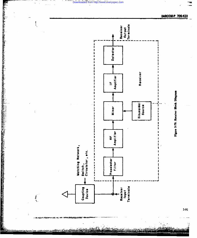
DARcoMP 706410
00 0.ca~ I
5-9
wn-- 5Y
Downloaded from http://www.everyspec.com
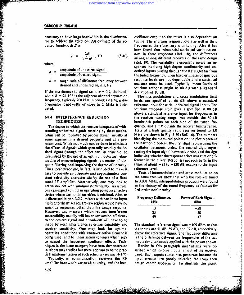
DARIDOM-P 706-41,0
necessary to have large bandwidth in the discrimina- oscillator output to the mixer is also dependent ontor to achieve the rejection. An estimate of the re- tuning. The spurious response levels as well as theirquired bandwidth B is frequencies therefore vary with tuning. Also it has
been found that substantial statistical variation oc-2a5 curs in these responses (Ref. 18). the differences
a -a2 ' arising among different receivers of the samt designwhere (Ref. 19). The variability is especially severe for re-
sponses involving high degree nonlinearity and un-a amplitude of undesired signal desired inputs passing through the RF stages far from
amplitude of desired signal the tuned frequency. Then fixed estimates of spurious
= magnitude of difference frequency between response levels are not dependable and a statisticaldesired and undesired signals, Hz measure must be used. Typically, mean levels of
spurious response might be 80 dB with a standardIf the interference-to-signal ratio, a = 0.9, the band- deviation of 10 dB.width B = 98. If S is the adjacent channel separation The intermodulation and cross modulation limitfrequency, typically 200 kHz in broadcast FM, a dis- levels are specified at 66 dB above a standardcriminator bandwidth of close to 2 MHz is indi- ref'erence input for each undesired signal input. Thecated. spurious response limit level is specified at 80 dB
above a standard reference input for frequencies in5-74 INTERFERENCE REDUCTION the receiver tuning range, but outside the 80-dB
TECHNIQUES bandwidth points on each side of the tuned fre-The degree to which the receiver is capable of with- quency, and I mV outside the receiver tuning range.
standing undesired signals entering by these mecha- Tests of a high quality radio receiver tuned to 3.0nisms can be improved by proper design, usually at MHz are shown in Fig.. 5-80 (Ref. 1.6). The numbers-some expense in a desired property and at a pre- identifying the measured points on the plot representmium cost. While not much can be done to eliminate the harmonic orders, the first digit representing thethe effects of signals which spectrally overlap the de- oscillator harmonic order, the second digit repre-sired signal (though the effect can, in principle, be senting the input signal harmonic order, and the signminimized by the use of an optimum detector), elim- indicating whether the response arises as a sum or dif-ination of nonoverlapping signals is a matter of ade- ference in the mixer. Responses are seen to be in thequate filtering and improving the degree- of linearity, range of about -83 to - 120 dB relative to the inputThe superheterodyne, in fat, is inteo.tied to make it reference level.easy to provide an adequate and approximately con- Tests of intermodulation and cross modulation onstant selectivity characteristic by the use of a fixed the same receiver show that with the receive, tunedtuned IF amplifier. AiternaLively, one may look to to 3.001 MHz, intermodulation products were foundactive devices with minimal nonlinearity. As a rule, in the vicinity of the tuned frequency as follows forone can expect to find an operating point on an active 3rd order nonlinearity:device where the nonlinear effect is minimal. Also, asis discussed in par. 3-2.2, mixers with oscillator input Frequency Difference, Power of Each Signal,limited to the mixer square-law region would have no kHz dBm "spurious responses other than the image response. 13 -58However, any measure which reduces interference 25 -50susceptibility usually will lower conversion efficiency 49 -37to the desired signal and a trade-off will have to bemade between interference rejection capability and The standard reference signal was - 109 dBm so thatreceiver sensitivity. One may look for optimal the inputs are 51 dB, 59 dB, and 72 dB, respectively,operating conditions with whatever active element is above the reference signal. The frequency differencebeing used, and to linearization schemes which seek is the difference between the frequencies of the twoto cancel the important nonlinear effects. Tech- inputs simultaneously applied with the power shown.
. niques in the latter category have been demonstrated Earlier in this paragraph mechanisms were de-in laboratory studies but there appears to be no prac- scribed which involve inputs far out of the receivedtical implementation of such schemes (see par. 4-1.7). band. Such inputs sometimes penetrate because the
Typically, in communication receivers the R.F input circuits are poorly selective far from theiramplifier bandwidth varies with tuning, and the local design center frequencies. To illustrate this point,
5-92
Downloaded from http://www.everyspec.com

DARCOM* 706410-- .
Vs 0 -
16-94W416"95M4
14-10H-
9090 -. ,(-) 2-741 0"4981)
-(-64--)
n 21114
" 17-0,9-551A) 11-53H
1 5-92M4 2,44H- 24-43H-
to 1100- " (7 )
LJ 41 3 ) 1.It(4) 4--- *431- )
I& 1 (6-93(+) )274 2II9+ 2 7-t0(4)
"0-5069
H0-0-60++
a= 120- 10-4-+-)J, I16"9(+ w
130
. 3 I I 1 I I~ i SI 1.-I -
2.90 2.92 2.94 2.96 2.96 3.0 3.02 3.04 &06 308 3.10
FREQUEIICY, M1Hz
Figure 5-80. Spurious Responses of Receiver Tuned to 3.0 MHz (Ref. 16)
Fig. 5-81 shows the relative response of the RF cir- 5.7.5 MILLIMETER WAVE RECTIFIERScuits of one receiver tuned to 70 MHz. At 435 MHz Receivers for use in the millimeter wave rangethe attenuation relative to that at 70 MHz is only (about 10 to 100 GHz) differ in EMC characteristicsabout 20 dB because of stray parameters in the tuned from receivers for use in the microwave range onlycircuits. Phenomena of this kind pose a major because of internal noise, linearity, and directivityproblem in interference control. The designer usually properties. The active electronic devices used arewill focus on the primary properties of a circuit and scaled down klystrons and travelling wave tubes, andbe satisfied when he achieves it. Secondary effects, solid-state devices such as IMPATT diodes, Schottkyparticularly when far outside the band, generally are barrier diodes, and tunnel diodes.overlooked, and virtually every circuit will behave A receiver for use in K-band (m35 GHz) makesunexpectedly far outside its design range. use of an IMPATT diode oscillator and a balanced
5-93
.. • ,,-.- • ." 47.I,-7. .'.
Downloaded from http://www.everyspec.com

DARCOM.P 706-410
0-
0 -fr = receiver frequency
*~40( . 'I
: 80
100* . ,:IO1
35 7- 1-15 -5 195- -235 25 315. 355- 395. 435
Frequency f, MHz
Figure 5-81. RF Amplifier Characteristic,f, - 70 MHz
mixer at the front end to achieve a noise figure of 10 5-7.6 INTERFERENCE EFFECT IN DIGITALdB (Ref. 21). Without special frequency stabilization RECEIVERSand with a single-ended mixer, a noise figure of about40 dB would have been obtained. Frequency stabili. In par. 3-2.1 the effects of the admitted signals inzation is used in a repeater for a millimeter wave terms of signal masking and error induction were dis-transmission system which achieves noise figures of cussed from the viewpoint of theory and principles.better than 9 dB (Ref. 22). Spurious response sensi. Data on the effects of interference on digital re-tivity of a Ka-band balanced mixer using IMPATT ceivers were obtained by simulation (Ref. 24), Thediodes are reported to be -40 dB relative to the de- simulated receiver was that used in the AN/GRC-103sired input (Ref. 23), a value said to be typical of for pulse code modulation-frequency modulationbalanced mixers. The relative intermodulation be- (PCM-FM). The local oscillator was not modeled tohavior of TWT amplifiers designed for microwave conform to the actual receiver oscillator but theoperation and millimeter wave operation is shown on mixer nonlinearity was modeled to generate har-Fig. 5-82. For operation near saturation, the 3rd monics as does the actual mixer. The timing recoveryorder intermodulation products of the millimeter was modeled so that the actual timing jitter is ap-wave and the microwave amplifiers are not sub- proximated in the simulated system. Figs. 5.83 and 5-stantially different. Below saturation the millimeter 84 show results obtained with various kinds of inter-wave device is better, attributed largely to the dif- ference for PCM-FM and 4 phase, oifferential phaseference in tuning systems in the two cases. shift keyed (40 DPSK) systems. respectively. The in-
It is also found that conducted susceptibility in terference is assumed added to the signal at the anten-millimeter wave systems occurs at higher levels than na terminals. The quantity of Af represents the ratioat microwave frequencies because of the decreased of the frequency separation between the two signalscable coupling and, because of the narrower beam- (desired and undesired) to the data rate. For bothwidths easily achievable at millimeter wave fre- cases illustrated it is to be noted that the theoreticalquencies, it is easier to colocate systems without fear error rates for Gaussian noise obtained by analysisof interaction. are substantially lower than those obtained in the
5-94
Downloaded from http://www.everyspec.com

DARCOM-P 706-410
e38 -"-.--.-...- -
-38
-30 - -
mm wave TWT at 55 GHz,Carriers 50 MHz Apart
o, -26 ,-
0 S-band TWT at 2 GHz
0o
I -22
00 0- 00- - ---- -
i i i ......
-18
-0 -, - - - -_ ... --.. - -i
0--4-6 -B -10 -1Fundamental Output Power (dB Below Saturation)
Figure 5-82. Comparison of Third Order Distortion of a Microwave Amplifier vs aHigh Power Millimeter Amplifier
5-9
t- -. .~ . .. '--
- - - - - - - - - - - - - - - - - - - - ----.,-,-. . ,
Downloaded from http://www.everyspec.com

DARCOM-P 706.410
0.2 .. .. + ,
0.1 AV
0.05
S0.02 -- _(
LAJ
4 0J
Interference-to-Carrier Ratio, dB
Figure 5-83. Susceptibility of 4% DPSK to Antenna-coupled Interference
simulation; in the case or PCM-FM it is worse by 5-8 TRANSMITTERSabout 3 dB and for 40 DPSK it is worse by 5 to 6 dB.Among reasons given for this is that the theoretical 5-8.1 INTRODUCI1 IONcase assumes an ideal detector, ideal bit timing re-covery, and ignores effects of pre-detection and post- In par. 5-8 emphasis is on those considerations di.detection filters, In short, the results suggest that ac- rectly related to the generation of radio frequencytual receivers fall substantially below the theoretical energy having the proper modulation and power levelpotential. necessary to transmit the desired signal. Associated
The results using various other kinds of inter- witL the basic transmitter are circuits and devicesference generally are found to degrade the error capable of genlerating interference as discussed inprobability less than does Gaussian noise of the same other portions of this handbook. Examples are powerlevel. The interference types presented are Con- supplies, motors for driving ventilating fans, powertinuous Wave (CW), Narrow-band FM (NBFM), switches, and relays. These can be controlled by theWide-band FM (WBFM), as well as interference usual techniques of filtering, shielding, and bonding.similar to the desired signal. In applying these techniques. special care may be
5-96
- -" M_ , . /
Downloaded from http://www.everyspec.com

DARCOMP 706410
0.2
- i.0.1--------------------------------
7 ~0.05 '..0 A .. ./
GAUSSIAN NOISETHEORI T ICAL
002 GAUSSIAN NOISEto, 0.02 -,I, * - -
-13 -12 -1 -10 -9 . .- 8 .. 7. -6 -.... .,4 -3
Fiue -4 Poablt o i Errrsfo P ,.FM WithI
i... . ..0.005 . f .... . .. .. . 1 . ;l l NBFM
' . - PM-FM
ffor
0.0012...
-13 -12 -11 -10 -9 -8 -7 -6 -5 - 3 -
}:!.:Interference-to-Carrier Ratio, dB ]
7; Figure 5-84. Probability of Bit Errors for PCM-FM With!I" Continuous Antenna-coupled Cochainnel interference (, f - 0.24)
necessary because of the numerous frequencies prt- hertz region of the spectrum, the filters may have to•sent in various circuits especially where frequency be more complex and have separate sections for low
multiplication occurs. Individual circuits should be and high frequencies, respectively. In addition, aper-isolated as much as possible with shields and filters to tures in cabinets for ventilation should be covered byavoid stray coupling. In particular, power supply out- screening, access door leakage prevented by metalput lines should be decoupled where several stages gaskets, and indicating meters mounted in leakproofare fed from the same supply, and separate circuits arrangements.should be isolated by compartmentalization.
Filters may be required on all power, control, and 5-8.2 POWER AND BANDWIDTH LIMITINGmonitoring leads where they penetrate the case or From a compatibility viewpoint, the design of thecabinet. To protect against radio frequency leakage, transmitter should be guided by the general principleusually these filters may be of relatively simple low that transmitted power and bandwidth should equal,pass types, The components should be designed to but not greatly exceed, that necessary to give the re-work at the frequencies present. Where it is neces- quired receiver output quality. Well-designed systemssary to prevent broad band interference such as such as radio relay systems take careful account ofgenerated by switching transients, rectifiers, or corn- noise, interference, and fading and are built withmutator motors producing energy in the low kilo- bandwidths and power levels to give a specifiedI'5-97
Downloaded from http://www.everyspec.com

DARCOM-P 706410
received signal reliability and quality. Over-design spectrum falls off slowly at the edge of the band. It "may insure good operation for one system but deny it turns out that many waveforms have the Nyquistto another. By experience, it is found that a band- property of no intersymbol interference. To have it,width of about 3.5 kHz is adequate for voice trans- the spectum must be such that the sum of all shiftedmission at a signal-to-noise power ratio of about 30 repetitions of the spectrum, the shift being thedB (Ref. 25, p, 50). Short rise-time radar pulses, when reciprocal of the pulse spacing, is constant. Thisnot needed to achieve some specified objective, situation is illustrated in Fig. 5-86. Note that theseE. should not be used. In digital data transmission, the waveforms occupy a band ranging from 1/(27) foruse of band-limited pulses may give rise to inter- the waveform given by Eqs. 5- 1l and 5-12 to I/T. Asymbol interference. However, by use .of the class of common choice is the raised cosine function forband-limited waveforms known as Nyquist wave- whichforms (Ref. 25, pp. 448-453), instead of rectangularor triangular waveforms, one can have band-limiting V(f) = A2 [I + cos (rf 7)] , - -
and zero intersymbol interference. T TThe most readily recognized Nyquist waveform is V-s (5-14)
one whose Fourier spectrum V(f) is given by a con-stant A, over a bandwidth interval 2B Hz. 0, elsewhere
V(f)- A, <fr< B, Vs (5-11) which occupies a band twice the minimum.= 0, elsewher Signal pulse shaping can be accomplished using
.The corresponding time-domain waveform s() is . -simple-resistor-capacitor (R-C) filters, typically oneor more isolated R-C circuits in cascade. The trans-
sin (2rBt) V (5-12) fer function of such a filter is of the form2 I B iB , ' 512
A ~~~which is zero at all pointsfr k/(28). k - 0, :k , Hf)=dmnines(-5:E2 The pulses last indefinitely but they are zero +J f)at periodic instants. The receiver measures the ampli-tude of each waveform by sampling at these instants.Successive signal pulses may be spaced by f, = 3-dB bandwidth of each filter section
n - number of sections in cascadeI (5-13) In a recent study (Ref. 26) a data filter of this kind
T was assumed for simulating the spectral output of adigital transmitter. Shown in Figs. 5-87 and 5-88 are
as shown in Fig. 5-85 without encountering inter- the digital signal spectra of a data sequence corn-symbol interference, prised of O's and I's in the order 0:, 401101 101010
The pulses of Eq. 5-12 are not convenient to before and after such a filter. The plots are of the dis-generate. A more practical pulse is one whose Fourier crete Fourier transform (using the Fast Fourier
Figure 5-85. Successive Nyquist Pulses
5-98
Downloaded from http://www.everyspec.com

DARCOM-P 706410
,. Transform Algorithm) withi O's represented by -1, Less common sources of unwanted outputs may beand I's represented by + 1. For Fig. 5-88 the binary found at intermediate points in a transmitter system.data ratefd was 2f, and n was 2. Filtering in this way The audio or video signal, prior to modulation, mayresults in substantial reduction of sideband energy, find a leakage path out of the transmitter. In systemsthough not as much as with the Nyquist waveform, wherein a low-frequency sinusoid is generated ini-and some intersymbol interference must be expected. tially and then multiplied to the required output fre-
quency, the intermediate frequencies may leak out ofthe transmitter. The possibility of parasitic oscil-
54.3 DESIGN CONSIDERATION lations also exists at various points. These are notTailoring the deliberately generated band is a first common in competently designed, low-frequency
step in limiting potential interference. The next step transmitters but are common in microwave trans-requires controlling emissions which arise because of mitters. Another mildly troublesome source is os-F nonideal characteristics of real electronic devices. cillator interference. The effect of such interference isTwo serious sources of unwanted components are the similar to that of sideband splatter, but the level istransmitter modulator and the final amplifier. In the generally lower.case of the former, nonlinear distortion in the base- There are times when the transmitter is not, byband amplifier will cause spectral broadening com- itself, responsible for the spurious output. The outputmonly called sideband splatter, and, when the base- of nearby transmitters may enter a transmitter, usual-band signal is modulated onto the RF carrier, the ly through its antenna, and mix with the desiredprocess - usually carried out in a nonlinear device - signal to form an unwanted output component.may give rise to further broadening of the spectum. Again, the effect depends on nonlinearity in the finalFor the sake of efficiency,-the final amplifier often is amplifier, in the transmission system between theoperated in a nonlinear mode (typically Class C for final amplifier and the antenna, or in the antenna it--amplitude and frequency modulation), generating self. The effect produced is either cross-modulation,harmonic currents into the final tank circuit. Though wherein the information sidebands of the undesired.the tuned tank provides a filtering effect, some signal appear with the desired signal, of intermodu-residual unwanted output is inevitable. Some types of lation, wherein a third signal, containing some ver-microwave amplifiers are inherently based on im- sion of the information sidebands of both signals, ispulse feeding a tuned cavity, implying strong har- formed.monic drive to the tuned cavity and consequent har- The nature of these mechanisms is developed inmonic output. greater detail in the paragraphs that follow.
T f+4V)(V f)
- ---1 % 1
-B BTT _ Be-2T T
Figure 5-86, Spectrum of Nyqulsi Pulse Showing Constancy of Repeated Spectrum
5-99
Downloaded from http://www.everyspec.com

DARCOM-P 706-4101
_
Iw
CD!
CD CD0C1 CD IlgP '~n~LLO
Downloaded from http://www.everyspec.com

DARcoM*P 706-410
_____ D
"_4,
Downloaded from http://www.everyspec.com

DARCOM-P 706-410
5-8.4 SIDEBAND SPLATTER AND ITS whereSUPPRESSION y = instantaneous output
Sideband splatter refers to the generation of spec- x = instantaneous inputtral components close to the carrier frequency but be- Input and output are either current, or voltage, or
* yond those ideally required for the modulation one current and the other voltage; the coefficients ,process. It is of particular importance in linear modu- must have the units necessary for consistency. Thus,lation systems such as amplitude modulation (AM), if y is in amperes, x is in volts; then. a, has units ofsingle-sideband (SSB). and double-sideband (DSB) ampere/(volt)'. The degree of significant non-systems. In these systems, as for narrow-band FM, linearity is assumed here not to exceed that repre-the minimum bandwidth is determined by the base- sented by N. The output of the nonlinear device forband signal and, if its spectrum is broadened, so is the the input [x1(t) + x2(t)] with x2(), as given in Fig. 5-spectrum of the transmitted signal. In broad-band 89, isfrequency modulation (FM) systems the transmittedbandwdth is largely a function of the deviationrather than the baseband bandwidth and the effect of Y E R(x + x2)Ysplatter is less significant, =0 (
5-8.4.1 Mechanism = ')ras(k+With linearly-modulated signals, t', principal M-o k=0
mechanism of modulation is multiplication of an RFcarrier by the baseband. This operation ordinarily is The nonlinear element is followed by a narrow-
c band filter centered at the carrier frequency 1W., sothat only terms containing cos(wt + 0,) are passed.vice as indicated in Fig. 5-89.
Ideal nonlinear elements are the square-law device By expanding cosi(et + P.) and retaining only theand the linear diode. To obtain the required result cos (w,4 + )terms,without distorting the desired sidebands, the ampli. IVtude of the sinusoidal carrier applied to the linear n,diode must be much larger than that of the in- Y L L. a.kJXrformation waveform. The ideal characteristics are, k-I.3.5..
however, only approximately realizable. A typicalnonlinear device can be described by the output-in- X
put characteristic 2 k It ,(9 k+ I)I
y = Fax' (5-16)n-o x cos(wj + €) (518)
" l~nformation 4- 10 X{) ] N~lirnear y f= Narrow- - 'I_
Signal X ) Device y t Band Filter
X
CarrierK;2t cos (W t + c
Figure 5-09. Basic Elements of Product Modulators
5-102
, , -- . i , . ... ...,......- *.. . .
Downloaded from http://www.everyspec.com

:: DARCOM-P 705410 !
The x, terms higher than the first degree are dis. is cut off and the sideband splatter components willtortion terms which extend the sidebands to (N - 1) be very large.
times the frequency band of the modulating signal. Measured and calculated results of excessive side-For instance, if N = 7, band output are reported by Firestone, et al. (Ref.
28). In an AM transmitter having an audio-modu-l+0a 5 + 35a\ lating signal of 3 kHz and 54.7% modulation, the
Y + 1- + spectrum distribution shown in Fig. 5-90 was ob-
(a 4 6 4 trtained. The total harmonic distortion amounted to/2a 124 i0\ 3.3%, which is not an excessive figure. A receiver
+ (2a2 + - a4 + 604AxI(t) operating in an adjacent channel 10 to 15 kHz fromI 16 the interfering signal will receive splatter com-
ponents of the order of 60 dB below the level of the(3a3 + 0.+- ) carrier component. If, as may readily happen with a
4 16nearby transmitter, the carrier power of the trans-pmitter produces at its frequency an input voltage of+ 64 4) x about 100 mV at the receiver, the level of unwanted
+ a () sidebands will correspond to about 100 AV. This
often will be far greater than the level of a desiredsignal at the sideband frequency.
(5 5-9.4.2 Control of Sideband Splatter
To minimize splatter, it is desirable to choose non-+cos (w+ (9 linear elements with characteristics as nearly ideal as
possible. For- a given, device intended to be used as.a-square-law modulator, usually it will be possible to
If coefficients a, are zero for n > 3, i.e., if the device is find empirical operating conditions which result in apurely square law, the output is exactly as required. 'characteristic that is nearly square law so that the
The component x2(t) cos (w,.t + :o) in Eq. 5-19 con- higher order coefficients are small. Furthermore, thetributes sideband energy covering a band equal to final tuned circuits in the transmitter also will act to
four times the modulating frequency rather than two reduce the level of the unwanted components. As atimes, as in the ideal case; ther x c (t)cos(wi + b p) co- rule, howeverd the circuit Q cannot be made highponent contributes energy in a band twelve times the enough to completely eliminate the splatter com-original modulating frequency. Thus, even when the ponents. An effective technique to eliminate the un-signal input x(t) is not nonlinarly distorted by the wanted sidebands associated with even powers ofbaseband-forming circuits, it may become distorted x1(t) in Eq. 5-18 is to use a balanced modulator.in the modulation process. Similar observations canbe made in the case of FM, where the signal wave- 5-8.5 HARMONIC GENERATION ANDform is required to vary linearly in the instantaneous SUPPRESSION
frequency of a carrier. One mechanism of frequency A pure sinusoid passing through a nonlinear de-modulation makes use of product modulators just as vice generates components at frequencies which aredoes AM, except that the carrier phase is different an integral multiple of the applied sinusoid fre-from that in AM (this mechanism generates a low quency. Modulated signals similarly applied give risedeviation FM signal which must be frequency multi- to components concentrated around integral mul-plied to get a high deviation signal (see Ref. 27)). tiples of the center frequency of the applied signal.Here, too, the product modulator will generate un- The modulation sidebands may remain unchanged orwanted sideband if the square law does not hold. If they may become distorted. In some devices the non-the frequency modulation is obtained by voltage linearity is incidental to normal linear amplificationvariation of capacity, or by varying pulse duration of as in class A tube and transistor amplifiers. In otherfrequency or a relaxation oscillator, similar phenom- devices, nonlinearity is a consequence of linear ampli-ena will be observed. The frequency is never a fication by impulsive re-enforcement of a wave. RFperfectly linear function of the applied voltage and amplifiers, of the class B or C type. pulse a tank cir-some nonlinear distortion is unavoidable. cuit throughout a portion of the sinusoidal cycle and
In the case of AM, one also must be careful to are therefore in this category. Klystrons and magne-avoid overmodulation, When this occurs, the carrier trans are also in this class. Oscillations continue to
5-103
Downloaded from http://www.everyspec.com

DARCOM-P 706-410
10 - FIaNT MODULATION 3.?.
0 '. .!
0 - - --.- -
FII QU[NCY VARIT MOWATION 54.7CIE FQE Y d
AUDI* MODULATION -23 W~a-MEAWUED
C-- ALCULATED'
-' 0
ad
0 is 20 25 30
FEUNYVARATION FROM CARIER FREQUENCY., k~tz
Figurt-90. Calculated and Measured Results of the TypicalSpectrum Distribution of Sidebands Produced by Amplitude
iodulated Transmitters
build up until the output is limited by saturation and It often will be possible to find modes of operationcutoff of the active element; hence, they also function for the active devices which minimize harmonicin this manner. In other cases, the harmonics are an amplitudes, but this occurs usually at the cost of ef-unwanted byproduct of a desired nonlinear function. ficiency. The extent to which such efforts are suc-It was pointed out earlier that the modulator may dis- cessful depends on the amount of filtering used. Low-tort the modulating signal; it also may distort the RF level circuits in the transmitter, incorporating manysignal. The ideal frequency multiplier yields only the frequency selective circuits, are unlikely to result indesired harmonic but this is unusual. Many un- significant harmonic output from the final stage.wanted harmonics are present as well as the original Some mechanisms for minimizing harmonic contentinput which becomes an unwanted component. are now described in more detail.
5-104A
i -lO.
Downloaded from http://www.everyspec.com

r. DARCOMP 706410
S-5L.1 Balanced Modulator where y is the output, x is the input, and x. and xbModulators for AM signals and signals related to have values shown in Fig. 5-91, the total output may
AM are multipliers. The modulation function is per- be writtenformed perfectly when the sum of the low-frequency 2 2
signal and a carrier is delivered to a square-law de- Ya - ' ai(xa xb) + a (x -
vice. If x(t) is the low-frequency signal and cos o.t is =the carrier, then the output of a square-law device isthe squared sum of these input signals: a2[ x() + cos 41]2
x(t) + cos t]2 = x (t) + 2x(t)cos W't + -2 -2ax(i) + 4a2xQt) cos w~t (5-22)
+ - Cos 2wt (5.20) No second harmonic term is present, assuming per-2 fect balance, and the term involving x(t) alone is re-I The desired term is 2x(t)cos oi. The term x2(t) is a jected in the output tank circuit. This arrangement,
distorted low-frequency signal which is readily re- however, leaves second harmonics in the output if the
jected in the RF filter following the modulator- the dc degree of nonlinearity is not limited to square law. If,
term, 1/2, is similarly rejected. Some energy at the se- for instance, a term a3x were added to Eq. 5-21, thecnd harmonic of the carrier (l/2)cos 24t may output would contain a term
trickle through, especially if the output circuit is not 6a3x1(t)cos2wt 3a3x1(t)highly selective. The use -of a properly designedbalanced modulator shown in Fig. 5-91 eliminates + 3a 3x,Q)cos 2wt (5-23)transmission of second harmonics. If each nonlineardevice has an output-input characteristic given by the which has a second harmonic modulated con-power series ponent. [The rejection of splatter components in-
volving even powers of x, (t) can be illustrated also byy = 0o + aIx + a2x (5-21) adding a3x
3 and expanding as in Eq. 5-23.1
I I
DNonvi iie7
: L
X b X( t)COSw t Device
Figure S-91. Schematic Diagram of a Balanced Modulator
5-105
.- 1
Downloaded from http://www.everyspec.com

DARCOM.P 706410
5-8.5.2 Amplifier Linearity Control may be better approximations of the magnitudes of "It is common practice to use crystal contrulled os- current pulses from some electronic devices than the
cillators operating at moderate frequencies (i.e., 30 undistorted caps illustrated in Fig. 5-92 (Ref. 29). TheMHz and below) and to employ frequency multipli- relative magnitudes of the first three harmonics forcation to obtain the needed output carrier frequency. the undistorted and square sinusoidal caps are shownIn such systems electronic devices biased at or below in Fig. 5-93 as a function of conduction angle 26. Incutoff (e.g., in class B and C amplifiers) are the source general, the larger the conduction angle, the smallerof the carrier output, which is rich in harmonici. The will be the amplitude of the harmonic in the output.current pulst. is approximately of the form of the cap It is, in principle, possible to estimate the har-of a sinusoid as shown in Fig. 5-92 and given by the monic output of the transmitter using the levels de-expression termined by Eq. 5-25 or Fig. 5-92 together with the
response characteristic of the tuned circuits followingA(cos wt - cos 0). the source of harmonics. Such a procedure is des-
for (2nir - 0) S o,: < (2nir + 0), cribed in Ref. 28. As a rough approximation, a single-n = 0, 11, ±2,..., (5-24) tuned circuit with a Q = 10 will attenuate the second,0 othird, and fourth harmonics approximately 24, 30,0 ,otherwise and 33 dB, respectively. Doubling the Q will increase
the attenuation in each case by about 6 dB.The Fourier expansion of this wave is given by thateuioinah sebaot6dBIn the usual case, the final amplifier will con-
tribute the major amount of harmonic output. TheA 'j_ rsin(n + 1)0 reasons for this are that ordinarily the final amplifier
r(l -cosa) n' + I is driven hard in order to get as much efficiency as ispossible and the tuned circuits following the final
sin(n - 1)8 - 2 sin uicos 0 amplifier have-limited selectivity, particularly-at then- I + cosuti4 (5-25) lower frequencies.Frequently, final amplifiers are operated as class C
Often it is found that the sinusoidal cap is itself amplifiers. In principle, the harmonic output fromsoIcw'at d',storted in passing through the amplifier, class C amplifiers is not different from that of the fre-so tl 'a higher levels of harmonics appear. Squared quency multipliers previously discussed. As the con-sinusoidal caps, given by the expression duction angle is increased, the harmonic output de-
creases, but so does the efficiency. To reduce inter.A (cos wt - cos 0)Y, ference and obtain the effect of a linear amplifier, it isfor (2na - 0) !5t < (2nr + 0), obviously advantageous to use a push-pull class B
i(t) = n = 0, :-l, +2,.... (5-26) final amplifier. It may even be advantageous to useclass C amplifiers in push-pull since this would tend
0 , otherwise to cancel the even harmonics. The amplitudes of odd
I(t)
w f
Conduction Angle,2 e
Figure -92. Coshmsoa Cap Waveform
S. 106
S-O
Downloaded from http://www.everyspec.com

DARCO*'P- -706-410. -
-2 n=2
o - --
01.,.(0 -12 -n=3-146
u t-"o -168"-8IfU- -2
-122
4- -24- SINUSOIDAL PULSE n=4-26 --26 - SQUARED SINUSOIDAL PULSE
1W> -28
20 40 60 80 100 120 14 10 10Conduction Angle 26, deg
Figure 5-93. Relative Intensity of Harmonics for Two Pulse Shapes as a Function of Conduction Angle
harmonics relative to that of the fundamental would wherebe unaffected by tubes in push-pull, but these har- n - order of the harmonicmonics are attenuated readily by tuned circuits in the L = direct current in the tube, Aoutput. J, - nth order of Bessel function of the first kind
The harmonic outputs of 14 representative corn- andmunication transmitters are shown in Fig. 5-94 (Ref. V,30). Note that some transmitters produce harmonics x = bunching parameter,whose levels are within 30 dB of that of the funda- (e/m)"2 (2 )1 '2 dimensionlessmental. For such harmonic content, a 50-kW trans-rmitter will emit a 50-W signal at the harmonic fre- in whichquency - in this case hardly insignificant. Trans- w - frequency of excitation, rid/secmitters made in accordance with M!L-STD-461 will s = spacing between input and output cavities,have to satisfy requirements of Test CE-06. This mlimits harmonic -ind spurious emissions to less than V, = peak gap voltage at buncher, V-44 dBW in all cases, and for transmitters with e- electronic charge, Cpower in the range 20-40 dBW, the limit of harmonic m = electronic mass, kgand spurious emission is -60 dBW. Yo - beam accelerating voltage, V
The bunching paramter value of x = 1.84 yields"-1.5.3 Microwave Circuit Design maximum efficiency. At maximum efficiency, the
Amplifiers for microwave frequencies may have pulses of induced current are very high. To avoidsignificant harmonic output. The k!ystron, which is large harmonic outputs, the cavity Q must be high.used extensively, generates harmonics through the For loaded circuits, values of Q ranging from 500bunching process. The current induced in the catcher to 1000 are obtainable. By using such values of Q, itcavity 1, has a harmonic intensity given approx- should b . possible to attenuate harmonic outputsimately by (Ref. 31). more than 60 dB below the fundamental, even with
equal fundamental and second harmonic current inie(n) 2!0J(nx), A (5-27) the tube. Measurements reported on a particular
5-107
.. . ... .- ,,- - -...... --. .- =- . . . .. . ,.- . -. . .. ., .
Downloaded from http://www.everyspec.com

- DARCOM-P 706-410 IIA O .P~ I - I i I I I ,
0 - - -X -Maximum Value -
S --- Mean Value2!- -20o
- M Minimum Value
0 4
l08r= E
:,," " -80
,14 -Harmonic Order
Figure 5-94. Typical Values of Harmonic Emissions Determined from Measurements on 14 Radio Transmitters
pulsed klystron (Ref. 32) are reproduced in Fig. 5-95. giving amplitude to phase conversion factor K vs in.Variation of beam voltage, which alters the bunching put power Pi, as measured using a typical TWT em-parameters, is seen to alter the second-harmonic con- ployed in radio relay application. The output powertent markedly. However, at the value of beam voltage vs input power curve saturates beyond a certainfor which the second harmonic is minimum, the se- point, and operation into this region will give rise tocond harmonic power is only about 40 dB below the observable harmonic content. The amplitude-to-fundamental output. phase conversion factor curve suggests another
The traveling wave tube (TWT) appears to be a mechanism by which unwanted components aregood choice as a microwave power amplifier, gener- generated. In effect, amplitude variations at the in-ating little interference. The operation of the TWT put give rise to phase variations at the output, there-depends upon uniform re-enforcement of a traveling by spreading the output spectrum. In multicarrierwave and does not involve impulsive re-enforcement systems, such as in radio relay applications, the phaseof a field, as in a klystron. Yet, reports (Ref. 31) in- effects as well as the amplitude effects give rise to thedicate that, in particular cases, the second-harmonic generation of intermodulation components (Ref. 33).output in TWT's may range from 20 to 40 dB below High-power magnetrons generally are used inthe fundamental. These conditions exist only at maxi- radars as sources of pulsed RF energy, coupled di-mum efficiency when the tube is driven heavily. The rectly to the antenna. In the magnetron, the energy ofinput-output characteristic for specific traveling wave a rotating cloud of electrons is imparted to the field intubes is found to be linear over a given range of in- tuned cavities on the periphery of rotati qn. Theputs: beyond the linear range, saturation is reached as mechanism which selects electrons emitted from theshown in Fig. 5-96 which shows two curves, one cathode, where they are roughly in proper phase,giving output power P, vs input power P the other tends to maintain them in bunches as in the klystron.
5-108
=, . L .. . . . . , , :' . ',,; :"= : , , , • - . , -= ,. .. . .. .. . .ii '
. .. . .
Downloaded from http://www.everyspec.com

0 VADARCOM-P 706.410
VA 87-B KLYSTRONINPUT POWER 2.5 W
j OUTPUT POWER = 1.75 MWSYNCHRONOUS TUNING
t .FREQUENCY = 2750 MHz
no insial ro h frgoniti eiet ht amni n
0l 1~ 40 0 0 ° o
4and, again, pulses rather than sinusoids arc induced tensities can be reduced by operating oscillators andin the cavities. The magnetron cavities also can be ex- amplifiers over linear regions at reduced efficiencies,cited in a harmonic mode so that a large number of canceling nonlinear components in balanced cir-output components are possible in addition to the cuits, and filtering. The first of these involves an in-easily identifiable harmonics. Harmonic level and fre- crease in power consumption and heat generation. Asquency are both difficult to predict. A value of -40 a result, more effort must be spent on heat removal.dB with respect to the fundamental has been quoted Balanced circuits and filtering involve additional cir-by Tomiyasu (Ref. 32) for the second harmonic, but cuits: the balanced push-pull circuit eliminates onlythe third harmonic was said to reach -20 dB. oven-order harmonics. Filtering is, by far, the most
Cridlan (Ref. 34) presents measured data on the practical method for suppressing harmonics. Coin-spurious outputs of L- and C-band radars, It is not mon forms use the wave trap or bypass principle. Inmade clear whether the radars use magnetrons or kly- the case of a transmission-line system, the filter ede-strons, but it is pointed out that both of these devices ments may take the form of shunt or series stubs. One
, generate nonharmonic spurious emissions. The L- application of such a filter to remove second har-, band radar is shown to have many spurious corn- monies is shown in Fig. 5-97.
ponents each of the order of 10-W EIRP spread The difficulty with wave-trap techniques is thatacross the band from its fundamental to its second power at the harmonic frequency is reflected back toharmonic frequency. The C-band radar is shown to the generator, causing an impedanc mismatch. inhave 10- to 20-W components, both above and below theory, one way of avoiding this difficulty is to use anits fundamental, not at a harmonic frequency. A isolator between the generator and the rdwer. Un-point to be observed about magnetrons is that the fortunately, most isolatvrs are designed to operate atoutput characteristics depend on the load (known as the fundamental frequency, and thedr performance atthe phenomena of "pulling") and that the spurious harmonic frequencies is usually unknown. Tha is es-emissions may vary therefore with antenna sweep. pecially true at the higher microwave frequencies. if5-109
!~
Downloaded from http://www.everyspec.com

DARCOM-P 706.410
40--- , 5
I
-0 - 1 -1 -5- 0 0
lotal Input Power Pi. dBm
Figure 5-96. Single Carrier Power Transmission Characteristic land'jAM-PM Conversion Factor for a 'Typical TWT
SHORT CIRCUIT an isolator is used, i-6 must be able to dissipate thepower of all reflected components (fundamental plus
T Iharmonies) without exceeding its rating.It is possible to use a ferrite circulator to suppress
harmonics. For example. the configuration in Fig. 5-98 cou~d be used to divert the reflected energy into a
4 resistive load. Unfortwiately, the circulator hasbandwidth problems as does the isolator. Anotherharmonic filteting-absorbing technique directionallycoupk- the unwanted signals into a second wave-guide, where they are Absorbed.
A simple method for harnionic absorptisn, which2atlso affords some reduction of the level of harmonicsin the main load, can lae achieved merely by couplingto !he main waveguide a smaller waveguide whose
Figure 5-97. Diagram of Two Sboet-Circuited Stubs cutoff frequency is below the fundamental but above(each 1/4 wave-length long and spaced 1 /8 wavelength that of all harmonics.
at the fundamental frequency) Arranged to Additional filtering techniques are given in Refs.Attenuate the Second Harmonic 25 and 35.
5-1 io
Downloaded from http://www.everyspec.com

DARCOM-P 70641 0-
5.6 TRANSMITTER INTERFERENCE 6.67 MHz, respectively, and three or four frequency-The spurious sidebands discussed in par. 5-8.4 can multiplier stages were used before the final amplifier.
be reduced through careful design of the modulator, The tests were performed on an unmodulated trans-but it frequently is found that a significant back- mitter, but the effewt of modulation on the noise side-ground interference level still exists around the trans- bands was not determined. Data, not presented here,mitter carrier center frequency. This results from osr was also obtained for the power amplifier alone.cillator noise modulating the carrier in amplitude, without the exciter and its multipliers; the resultingfrequency, or phase. The interference is associatedmainly with the oscillator itself, which is quite noisycompared to amplifiers, but some interference is pro- LOAD AT K2MONIC FREQUENCIESduced in the amplifiers as well. It is possible for co-rona to form, or for arcing to occur, at high-voltage SOMEpoints in the final amplifier. Subsequent filtering inthe output tank circuit results in a pair of noise side-bands on either side nf the carrier frequency; spurious CIRCULATORlevels are difficult to estimate accurately.
Measurements of noise power are appropriate
though they are difficult to make because of the iLEMENTS TO REFLECT HARMONICS
presence of the much larger power in the carrier.Some measurements have been reported on VHF % LOAD AT FUNDAMENTAL FREQUENCYtransmitters (Ref. 36), and the results of tests on a 45-MHz and a 160-MHz transmitter are shown in Fig. 5- Figure 5-9. Diagram Illustrating the Use99. The basic crystal frequencies were 3.75 MHz and of a Circulator to Separate Harmonics
-40 _ _ _ _ _ _ _ _ _ _ _ _ __
Ai -60
V.. -80
,_ 160 Mz
i "o -120-+3
-140
S -160
4 -180
10 20 40 60 80 100 200 400 600 8001l00Frequency Separation from Carrier Frequency,
kHz
Figure 5-99. Measured Values of the Sidemnd Noise Level of Unmodulated 45- and 160-MHz Transmitters .% 11
Fraiction of Freqmawy Separation from the Carrier Frequency
From the Pest Office Electrical Engineers Journal, UK.5-I
o w . , . - . . . - . . ? ;: , - -. . . .
Downloaded from http://www.everyspec.com

DARCOMP 706-410
noise was generally about 20 dB below that shown in original signals, and its amplitude is a combination ofFig. 5-99. The noise levels are quite low in these cases, the original amplitude coefficients of both mixed sig-but the noise interference injected into a receiver can nals. The intermodulation term is usually more
be quite significant when transmitter and receiver an- serious since it occurs in an entirely new frequencytennas are very close to each other. band. The cross-modulation term, given in Eq. 5-31,
implies that the unwanted signal is reradiated with a5-.7 INTERMODULATION AND CROSS distorted envelope. As a rule, the amplitude of the re-
MODULATION radiated signal is much smaller than that of theThe phenomena of intermodulation and cross- original unwanted signal, defined in Eq. 5-29, and the
modulation imply the mixing of two or more signals reradiated signal might be viewed as a small newin a nonlinear element in such a way that multipli- splatter or noise component.cative mixtures of the two signals result. This occursin receiver input circuits, as well as in transmitters, 54.8 OTHER SPURIOUS OUTPUTSand sometimes in a nonlinear element in the channel. Parasitic oscillations occur in both low- and high-As far as transmitters are concerned, the process in- frequency amplifiers. In low-frequency devices, theyvolves the reception of an unwanted signal by the result from stray external and internal capacitancestransmitting antenna, which conducts it back to the and inductances that form spurious feedback loops.output plate of the final amplifier, where it is mixed The cures are often very simple, sometimes involvingwith the transmitted signal. Therefore, the process is inserting resistors in the leads to the grid and plate ofof greatest significance when both the unwanted the amplifier to increase losses of the spurious tunedsignal and the nonlinear product are within the pass- circuit. The methods of handling these situations areband-of the final amplifier. This-can occur if the non- well described- in-standar4-refience-books (Ref. 37).linear device has a characteristic of odd degree. For At microwave frequencies, corresponding phe-example, suppose the output signal has a component nomena exist. Often, the phenomena are completelythat depends on the third power of the output internal to the tube. At some frequencies, transit-timevoltage. Two components of voltage at the output are effects are sources of negative resistance. If a tunedthe output signal voltage itself x, (t) circuit somewhere in the structure is coupled to the
negative resistance, parasitic oscillations occur.x10) = v1 )cos[Wit + ¢ 1()] (5.28) Various additional mechanisms of microwave tube
spurious emission are referenced and surveyed in Ref.and the unwanted signal voltage x2 (t) 32. These include harmonic and unharmonic genera-
X2(t = 1'(t)cos[Pt + ':(t)] (5-29) tion in magnetrons; harmonic generation, diode os-cillation, and drift tunnel oscillation in klystrons; and
The sum x, (1) + x2 (t), when applied to a nonlinear harmonic generation, diode oscillation, band edge,device having a cubic term, will result in a number of and second passband oscillation in travelling waveintermodulation components, one of which is of the tubes.-,: form
Ya() (f) t(t) cosi(2w, - ca")t + 2, 1(t) - ,P2(t)] 5-9 RADAR EQUIPMENT(5-30) 5-9.1 INTRODUCTION
Par. 5-9 is concerned with radar systems includingand cross modulation components, one of which is of equipment for modulation, transmission, and radia-the form tion of electromagnetic energy (usually pulses), and
=reception, amplification, detection, processing, andYb(t) = v (t) " (t) cost + ',2(t)1 (5-31) display of echoes received from desired targets. The
simplest types of radars provide target range byThe center frequency of the intermodulation corn- measuring time of occurrence of the echoes. Searchportent differs from either w, or w : but, if the two fre- radars provide angular information, as wll, by scan-quencies are close to one another, the frequency of ning a narrw antenna beam over a sector. Trackingthe new term is not too different from w. The modu- radars provide accurate real-time position data bylation on the term whose frequency is (2w, - &) is a setting up suitable servo loops for continual de-combination of the modulations on each of the ,termination of range gate position as well as angularcausative signals. The cross-modulation component beam pointing directions. Radar outputs can be used .,.has a frequency equal to one or the other of the to display a visual picture of the target environment
5-112
- . . ... ..
Downloaded from http://www.everyspec.com

ARCOMP 706-410
or can provide direct inputs to fie-control equip- power requirements as determined by Eq. 5-32 maymert for direction of artillery or rocket projectiles to be in the several megawatt range, producing fielda moving target location. Radar systems produce strengths of the order of a hundred volts per meter atemissions that can interfere with other equipments distances from the radiating antenna of a few hun-(sAch as communication, navigation, and other radar dred meters.equipments) and can be sensitive to external sourcesof lut m . The objective here is to describe the 5-9.2.1 Frequecy 5aM utilizationiarmfWt effects wtkh can occur and techniques by -.. FtqeyBuUtiztnhwbh tsy can be cured. Current practice in spectrum use of radar systems
is (Ref. 38) summarized in Table 5-9. The first
59.2 RMDAR EM ISSION CHARACTERISTICS column gives the designations commonly used forA determining factor for the power output of radar different frequency bands. The second column gives
emission is the requirement for discernible echoes the range of frequencies associated with each band.from targets at long ranges. This imposes the use of Corresponding wavelength ranges are given in theorders of magnitdtt more signal power than re- third column (obeying the relationship X - c/f wherequired by other types of systems (e.g., communica- f is frequency and c is the speed of light)wtion oI naigation) ov similar ranges. For line-of- The data on wavelength are important in relatingsight tras nion bet n two locations, the signal the approximate beam directivity to antenna size. Forpower P, isakvn by (see E4. 3-147) bea~m angles 0 less thn about 0.1 ad, the width of
the angle is related to the antenna effective diameter
\ GGP\ D by the relation:
w" re(4*,r)2 L0 ( D , rad (5-34)'i where
P, Ptransmitted power, W where A is the wavelength. Thus, in the SKF band, as-
=fi transmitter nat~n gaiin, ds - suming X 3cm, 0 3 ni, the beamwidth 8will be-! i :G, =rem.iving antenna pain, dimemionless approximately I/100D rad or 0.57 deg. In general, the
IX waventh, m lower frequencies (up to about 1-2 GHz) a:e ued forr ,m long-range search applicatioris, providing goodL, lossi factr, dimensionless moving-target indication and relative immunity from
For a manamck radar, however, (transmitter and weather effects. The higher frequencies (up to about.--ceiver co-located) the signal power received is given 100 GHz) are used where light weight is important
b) - and also where accurate tracking is required.\2 4(---W (5-33) 5-9.2.2 Tme-Frequecy Chswraterist sof
Radar Pulse Waytforms (Ref. 38)
where u is the radar cross section in square meters Interference standards (Rcf. 39) place a limit on the(Ref. 38) of the "point target" at range r. Typical "emission bandwidth" of a given radar. The shape of
TABLE 5-9. RADAR FREQUENCY BANDS
Band Designation Frequency Range Wavelength Range
HF (high frequency) 3-30 MHz 10-100 mViF (very-higl" frequency) 30-300 MHz 1-10 mUHF (uitra-hi.h frequency) 0.3-3 GHz 10-100cmSHF (super-high frequency) 3-30 GHz 1-10cmEHF (extremely-high 39-300 GHz IOmm
frequency) I I
Note: Above designations officially haw superseded the following radard, band designationn referred to fbquenily in the recent radar
literature: L. 1-2 GHz, S, 2A GHz; C. 44 GHz; X, 8-12.5 GHz, Ku,12.5-18 GHz; K. 18-26 GHz; V,, 26.5-40-GHz.
5-113
,--.0 0., . .. ".
Downloaded from http://www.everyspec.com

DARCOM-P 706-410
the pulse modulation waveform used has a direct ef- The energy ratio in Eq. 5-35 depends directly onfect on the amount of energy emitted outside any pre- the product of peak power by effective duration of '
scribed band. This results in a set of requirements on the radiated waveform. Since peak power is an im-system design distinct from those imposed by the de- portant limitation on available transmitting tubessired radar performance. Typical functions of a radar (i.e. magnetrons and klystrons), energy increase toequipment reduce to the following set of measure- achieved desired range must be achieved by cor-ments or decisions: responding increase in the duration of the pulse
a. Determine th: presence of an echo in a given in- waveform. Usually it is necessary to use waveformsterval of time (range resolutiun cell), of high intrinsic bandwidth to provide the necessary
b. Determine the time of occurrence of a given range accuracy and resolution capability. Hence, theecho response (range accuracy). use of high timq-bandwidth product waveforms, to-
One figure of merit for performance of these func- gether with suitable matched filters at tie receiver forI tions is the signal-to-noise ratio R pulse compression, is common practice in radar~system design.
R = , dimensionless (5-35) Four representative pulse waveforms are shown inN Table 5-10. The rectangle (a) is the simplest one used
where in practice and will be shown to have the least favor-N, = noise spectral density, V'/Hz able out-of-band spectral characteristics. The gaussE = signal "energy" per pulse defined by: (c) is the optimum with the trapezoid, and raisedF IVfcosine (d) representing compromises between de-:: f [ f sired performance and case of realization. The first
:E I=~~ I 't!ds = V(f)Pldf ,V-s (5-36) column gives their shapes and defines a "'duration" "fi f parameter 7 lor each. The. third column gives the
Note than in Eq. 5-36 v (t) is the waveform of a single mathematical expression-- )for each, while the lastpulse (time domain); V(f) is its spectrum (frequency column gives the spectrum V(f) (the Fourierdomain), transform of v( i)) for each. The energy spectral
Additional waveform ha tristi a also density I V( f)I can be readily calculated to deter-i:min Addtiea relative harterstic art diffren frequenciesnificant in the time measurement implied by (b); in mine the relative intensity at different frequencies.this case, not only accuracy of measurement is in- The spectra given in Table 5-10 can be interpretedvolved but also the ability of the system to resolve as follows (Refs. 38 and 40). If a repetitive train ofclosely-spaccd multiple targets. pulses is generated, the resultant Fourier series coef-
The performance of a radar system with respect to ficients will have magnitudes proportional to I V(J) Ithe rarge accuracy and range resolution require- where f, is the t'th harmonic o' the pulse repetitionmerts that are frequently used as the basis of system frequency. Further, if the pulse or pulses are used todesign can be expressed as a direct function of the modulate a carrier of frequency f,, the resultantmoment bandwidth B., of the modulating waveform spectra will be the displaced values V(f- f,,).given by Expressions for the energy effective bandwidth B
and moment bandwidth , of the representative- waveforms are given in Trble 5.11. Note that the mo-f j V(f)df ment bandwidth of the simple rectangular pulse isHz 7) infinite. This is caused by the discontinuities in the
B,,= , lz(5-37) waveform, which make it hard to realize physically as
c hV(k ) r df well.
A listing of numerical bandwidth characteristicsIn achieving this moment bandwidth, the behavior for these waveforms is given in Table 5-12. In ad-
of the spectrum V(f) at frequencies far removed dition to the effective and moment bandwidths B,from a desired B,, will have very little effect on the and B,, discussed, there are included the commonlyvalue of B, but may be paramount in determining the used 3-dB and 6-dB bandwidths frequently used asextent to which the radar may interfere with systems references (the frequencies at which I V(f) I is 3 or 6using contiguous frequency regions. Thus, the re- dB below the maximum I V(0) 1) as well as the 40-,quirement for minimization of interference effects 60-. 80-. and 100-dB bandwidths, important for as-adds a new dimension to the waveform design sessing the relhtive attenuation of emitted energyproblem. in frequency channels adjacent to an assigned carrier
5-114
N ........ . .
Downloaded from http://www.everyspec.com

~ji DARCOM*P 706410
U *.
I,.m
6 kU
-93.
w Ez
S it
Downloaded from http://www.everyspec.com

[v DARCOM-P 706410
TABLE 5-11
ENERGY AND MOMENT BANDWIDTHS OFREPRESENTATIVE WAVEFORMS
(Normalized with respect to duration parameter r)
Waveform rBe, dimensionless TBm, dimensionless
(a) 2
(b) L
(c)
3 i(d) 8
8 2,3
frequency band and in meeting required EMC speci- field tubes or linear-beam tubes (Ref. 38, Chapter 7).fications (Ref. 39). The-crossed-field categary is based on the use of high
For example, consider a l-jss pulse transmission. strength electric and magnetic fields at right angles to-To,deterrihe the minimum frequency separation re- each other, and includes magnetron high-power os-quired to have the emitted spectrum 60 dB below the cillators as well as variously named crossed-fieldcarrier frequency value, the following values of B0 amplifiers (CFA) that achieve amplification with ashould be used: nonresonant structure. Linear-beam tubes, such as
a. rectangular pulse: 318 MHz klystrons and travelling-wave tubes (TWT) use a .b. trapezoidal pulse: 31.8 MHz high-energy electron beam, formed by electrostaticc. gaussian pulse: 1.7 MHz lenses or a collinear magnetic field that interacts withd. raised cosine: 3.4 MHz suitably injected RF energy in a structure whoseSince the "duration" values defined in Table 5-10 dimensions are related to the operating wavelength.
are somewhat arbitrary, magnitudes of the different Tubes are available with peak power up to severalbandwidth measures relative to the corresponding megawatts. Average powers can be as much as tens or3-48 bandwidths are given in Table 5-13. hundreds of kilowatts. Thus, spurious responses
The preceding results are directly applicable to several tens of decibels below the carrier frequencyradars using simple pulse transmission. For long- power can still constitute significant interference torange, high-resolution applications, however, it is nearby receivers tuned to nearby frequencies.necessary to use pulse waveforms of high intrinsic In most radar systems, it is found economical andtime duration - frequency bandwidth products practical to feed the antenna, in the transmit mode,(rather than the BT - I relation which holds for sire- with energy from a single high-power tube or pair ofpIe pulses) (Ref. 38, Chapter 3, and Ref 40). In the tubes rather than using a large number of parallelcase of waveforms made up of sequences of con- low-power tubes to obtain the desired high energytiguous subpulses with a random phase coding, the output. However, solid-state technology currentlypreceding results can be applied directly, now re- under development (Ret. 38, Chapter 30) has the po-ferring to subpulse waveform rather than overall tential of altering this picture radically. In addition towaveform. For frequency-modulated (chirp) pulses, high-power transistors and transistor frequency mul-it is necessary to perform a separate calculation or tipliers, there are a number of new bulk-effect os-make a corresponding measurement to ensure that cillators that can generate several watts of micro-specifications will be met. wave energy. Such components form the basic build-
ing blocks of several large phased-array antennaradar systems (Ref. 41). Such systems are char-
5-9.2.3 Spurious Emissions acterized by the use of a large array of identical
Transmitter tubes used in radar equipment in- .elements independently controlled to permit elec-clude those which can be classified as either crossed- tronic steering of the emitted and received beams.
5-116
Downloaded from http://www.everyspec.com

DARCOM-P 706-410
TABLE 5-12FREQUENCY BANDWIDTH CHARACTERISTICS FOR
REPRESENTATIVE WAVEFORMS, NORMALIZED WITH RESPECTTO DURATION PARAMETER i
Fea-ure (a) rect (b) trap (c) gauss (d) raised
point cos
TB, 0.5 0.483 0.399 0.375
TBm 0.712 0.318 0.289
iSB3 0.442 0.440 0.374 0.360
i-B6 0.602 0.600 0.529 0.499
far-frequency 1 7 1voltage ratio - - cxp(- ir-X/4)
bound** 7x 7:x'N 21x(4x - 1)
T8 G 31.8 10.065 1,366 1.637
TH60 318.3 31.831 1.673 3.438
- 3181.... 100:658 1.932 7.366
.-B10 31831.0 318.310 2.160 - 15.851
. Bk = frequency at which attentuation is k dB with respect to that at 0 fre-
quency2. x = rfk1
•,3. For trapezoid.
A -0.1 assumed.T
4. B, = _ _1
V (0) P
f f'Iv(j)Ildf
I ,ff)2df
**Formulas given here are used in subsequent rows of table.
This flexibility carries with it the requirement for 5-9.2.3.1 Harmonicsmore extensive measurement procedures (Ref. 42) todefine spurious emissions that can be present, since Estimates of the relative magnitudes of harmonicssuch emissions can vary considerably with respect to of the carrier frequency that can be expected rangespace, time. and frequency - depending on the par- from -25 to -30 dB below the fundamental for theticular operation modes employed. 2nd and 3rd harmonics to -70 to -100 dB for the
5-117
:__ " .... .>.:.-, ... ..... .............. '. , .'-,_...•
Downloaded from http://www.everyspec.com

rDARCOM-P 706-410
first half dozen or so harmonics. Typical measure- Fig. 5-100, (Ref. 34). It is found that this type of emis-ments on a number of tubes recently gave results as sion changes in an anomalous manner as tube ad-shown in Table 5-14. The wide variation depends on justments are made, compounding the problem of in-the effective filtering performed in the transmission terference minimization in any specific situation.I. path between transmitting tube and antenna, whichcan bc designed to control this effect.
5-9.2.33 Transmitter Stability Considerations5-9.2.3.2 Adjacent Band Spurnius Noise High-power pulsed oscillator tubes have a carrier
Problems may arise with CFA's or TWTs due to frequency of emission that is highly dependent onadjacent band spurious oscillation modes. In fact, control electrode voltages. A small ripple in powersignificant spurious emissions of this type have been supply voltage can cause significant changes in oscil-Imeasured from most of the high powered tubes used lator frequency. Changes in frequency on the order ofas radar transmitters. Typical results are shown in I part in ]0Y can be experienced in magnetron oscil-
lators due to a 1% change in high-voltage powersupply voltage. Thus, at 10 GHz (X-band) frequen-
TABLE 5-13 cy, changes up to I M Hz can be expected from nomi-
FREQUENCY BANDWIDTH CHARACTERIS- nal. This problem is avoided in most sophisticatedsystems that require pulse-to-pulse coherence for
TICS FOR REPRESENTATIVE WAVEFORMS proper operation (such as MTI systems) (Ref. 38, pp.ST B5-12 to 5-19) by using a separate coherent crystal-
_ _ _ _ _ _ controlled oscillator with an amplifier at the output
Ratio Waveform of the system.(a) (b) (c) (d)
Be/B3 1.13 1.10 1.07 1.04 5-9.3 RADAR SUSCEPTIBILITY& / 8, i3 1.62 0.85 0.80
8~, 83 162 .85 .80 5-9.3.1 Effects of Interfacing SignalsB6/03 1.36 1.36 1.41 1.39B4 /83 73.0 22.9 3.65 4.55 The front end of a radar equipment is usually a0/; 720.0 72.3 4.47 9.55 highly sensitive receiver connected to a highly direc-/ 70 25 2tional antenna for reception of echoes of distant tar-
Bso/83 7200.0 23.0 5.7 40 gets. Due to the wide dynamic range of possible8,_/B3_ _72000.0 723.0 5.78 44.0 desired echo returns, the system can be sensitive to a
TABLE 5-14SUMMARY OF RADAR HARMONIC LEVELS* (DECIBELS BELOW FUNDAMENTAL)
: : typ Harmonic 2 3 4 5 6 7 8 9 1
:i Magnetron:
Mean .............. 78.1 71.7 77.1 86.0 87,2 91.9 99.3Range. high/low ... 57/103 45/100 62/93 67/114 76/96 I 83/96 83/14Number of samples.. 77 59 34 23 17 7 5
Mean ........... 71.3 78.2 76.9 73.9 82.3 87.2Range. high/low ... 38/119 57/105 56/101 59/1I 73/89 72/97Number of samples.. 44 27 21 8 7 4
Tetrode and triode:
Mean .............. 83.2 76.0 99.6 90.0 96.7 100.2 106.2 97.2 100Range. high/low ... 74/93 72/81 93/108 79/98 83/1081 93/112 98/1!3 93/100 100/100Number of samples.. 14 13 10 11 0 t 9 3 4 2
*Systems with waveguide transmission lines only.(Courtesy of Department of Defense. Electromagnetic Compatibility Analysis Center)
5-118
, .. -.' ,.: .:,, . _• .. ..- ..., .. :-'." , .. . . 7
Downloaded from http://www.everyspec.com

DARCOM#P 706-410
Fixed Radio- link f.Frequency Bonds
204J~ 3
L )- I
NomlzdRelative Freq e Rado-in
() Spurious- Radiation* in-Output of C-band Radar
0
C 4->
01.0 2.0 3.0 4.0 0 6.Normalized Relative Frequency f /fF
(B) Spurious and Harmonic Components in Output of L-band Roda
at Frequencies Above Fundamental
(fF=fundamental frequency)
Figure 5-100, Measured Characteristies of Typical Radars
Downloaded from http://www.everyspec.com

DARCOM-P 706-410
wide variety of other signal sources. The effects of and (c) diode devices such as varactor limiters or dif- ,such undesired signals can be listed as follows: ferential phase shifters. For higher power applica.
a. Equipment degradation. This includes burnout tions the gas discharge or ferrite-circulator duplexersof crystal detectors (Refs. 38 and 43) by strong are preferred.enough pulses that enter the system at a point prior to A related type of interference is that caused by in-sufficiently frequency-selective circuits that would at- traradar coupling of the pulse modulation waveformtenuate them. Other effects such as overloading of used, This involves high voltages and/or currentsamplifiers causing destruction of active elements may such as those required to drive a magnetron. Electricalso be present, and/or magnetic fields generated or resultant pulses
b. Desensitization, The interfering signals that nor- conducted via ground wires or power leads may bemally would be filtered out by receiving filters in later sufficient to cause deterioration of sensitive receiverstages may be strong enough to drive leading stages components. Careful design procedures are requiredinto nonlinear regions of decreased gain so as to pre- to avoid this danger.vent full amplification of desired echoes.6ec. Display reduction. In an oscilloscope display of 5-9.3.2.2 Undesired Echoesechoes (e.g., A-scope, B-scope, or PPI), desired echoindications may be masked by an interference pat- Echoes of undesired targets constitute passiveitern types of interference. The following list includes the
d. Erroneous responses. Especially in automatic more significant cases; usually the resulting echo pat-d.eroneous respons Edsa in automa terns are readily identifiable so as to distinguish them
detection and tracking radars, interference may from other types of interference:cause: a. Ground or sea clutter necessitates the use of
(I) False alarms-false target indications that can MT! (moving target indication) 'circuits when con.cause incorrect decisions and overloading of signal MT(ovntagtiicin)iruswhno-
csincapacity (Refs. 44 and 45) cerned with detection of aircraft, vehicles, or person-Sprocessing etsfilure 45) nel at low elevation angles.
(2) Missed targets-failure to detect targets when b. Clouds, rain, or snow produce echoes, an effecti ',Irequired(3) Erroneous target position estimates (e.g., angle which becomes more significant at the higher micro-
wave frequencies.e ratc. "Angels" or reflections from birds, insects, or
dust may be significant (Ref. 47).
5-9.3.2 Sources of Interfering Signals d. Multipath effects become important for radarsat significant heights: the ground-bounce-path caus-
pThe effects mentioned in par. 5.9.3.1 on system ing destructive interference with the direct-path echo,performance can be caused by a wide range of possi- leading to difficulty in properly locating targets atble signal sources. These are listed in the paragraphs low elevation angles.that follow together with a discussion of their main
e. Chaff or clouds of metallic strips may be emittedeffects. by an adversary. These usually will be effective over a
given band of frequencies and will lead to false de-
5-9.3.2.1 The Radar's Own Transmitter tections until enough temporal, velocity, and spatialFor most pulse radar equipments, the receiver and separation exists for desired targets.
transmitter share the same antenna. The decoupling*necessary is achieved partially by the time separation 5-4.3.2.3 Environmental Fields
of echoes from the transmitted pulse. However, pro- The radar receiver must operate in the real-worldtection of receiver circuits from the high power environment, subject to fields produced by ignition ofsignals radiated calls for special circuits, known as internal combustion engines, welding machines, etc.duplexers (Refs. 38 and 46). Isolation of the order of Such fields might act directly on the receiver circuits,60 to 80 dB is required. Devices in common use in- or enter through the power lines as well as possiblyelude (a) gas-discharge microwave switches called being picked up by the antenna and RF circuits. Thetransmit-receive (TR), and antitransmit-receive effect of such interference on radar performance and(ATR) tubes in various waveguide configurations. displays can be quite severe. Techniques for controlgenerally in conjunction with quadrature hybrid of such phenomena by shielding, use of filters, andjunctions to provide required broadband directional proper grounding are described in other areas of thischaracteristics; (b) ferrite circulators of the Faraday handbook. The effect of such fields on a given radarrotational, differertial-phase-shift, or junction types: system would be highly dependent on the site selected
5.120
...............
Downloaded from http://www.everyspec.com

DARCOM#P 706410
for the radar as well as the method of supplying equipments in the presence of interference and also to" power; power line filters may be required. minimize the effects of radar emissions on other
The remaining sources of EMI to be discussed here equipments. The interference control techniques toare active signal sources generating waves picked up be described are concerned with the design of systemby the antenna of the radar. components as well as the techniques employed forI. Nshaping
and processing the signals.
The sun and stars emit noise-like energy that can 5-9.4.1 Directional Selectivityinterfere with the detection of weak targets, see par. The objective is to confine both the emitted signal3-1.2.3. The effect is to increase the effective system and the receiver sensitivity to a preselected targetnoise temperature by amounts varying from a few to direction. This objective is complicated by the factseveral tens of decibels, depending on the antenna that the pointing direction changes as the radar scansgain and pointing direction with respect to the over a sector to search for targets, or tracks a movingsources. These effects can be predicted reasonably target.well, including the effects of solar storms (sun spots) The determining factor is the angular radiation (orin various parts of the RF spectrum. sensitivity) pattern of the antenna being used. Usual-
5 2 Cly, by reciprocity, the patterns (gain versus angles) are5- 9.3.2.5 Communication and Navigation Signals similar if not identical when the antenna is used for
These signals usually are confined to frequencies radiation or reception of microwave energy. Al-far removed from the radar bands, and can be con- though the required gain determines the width of thesidered of only marginal importance. An exception is main lobe of an antenna, certain steps can be taken toover-the-horizon, HF radar systems (in the frequency control specific side lobes and back lobes as dis-band 2-30 MHz) which must have specially designed cussed in par. 5-10,6.3, which describe techniques tooperating prczedures to select a "quiet band" for op- suppress radiation through cancellation.orations as well as to cope with daily and yearly varia-tion cyt~s of the ionospheric propagation medium. 5-9.4.2 Time Selectivity,-92 Time is important at several levels with respect to... 6 Other Radars the operation of a radar system. Significant from the
These are perhaps the most important source of in- interference point of view are the scan-time requiredterforence to a radar system since they can be by a search radar to cover a given angular sector andexpected to be present at frequency bands near the the time between pulses during which echoes of agiven radar operating frequency. Pertinent charac- transmitted pulse may be received.teristics of radar emitters have been mentioned in Concerning scan-time, it may be important to syn-par. 5.9.2, both inband and out-of-band. It should be chronize the scanning of nearby searching radar sys-pointed out here that there will be a complex time de- tems so that main-beam energy will not interferependence of the interfercnce caused by a radar due to directly when either radar points at the other.the usual low-duty-cycle pulsed waveform as well asthedirctina vrainofardrpntndre- Proper use of" the time relations from pulse-to-the directional variations or a radar pointing direc- pulse are of greater control importance. While targettion (e.g., rapid scanning of a search radar or dy- echoes will occur approximately equal times fromnamic tracking of a moving body) (Refs. 38 and 48). successive transmitted pulses, interfering pulses in
general will occur at differing times in the pulse re-5-9.3,2,7 Electronic Countermeasures (ECM) currence frequency (PRF) interval. Suitable gating
Electronic countermeasures involve deliberate associated with pulse-to-pulse integration for signalemissions by an adversary of noise-like signals (bar- enhancement can (Ref. 38) help suppress pulses at arage jammers) or pulses synchronized with the trans- different repetition rate from the radar; use ofmitted pulses ("spoofing") or other signals designed staggered (unequal) times between pulses also canto confuse. See Engineering Design Handbooks help this technique. For radars in the same installa.AMCP 706-411 through -416 for a detailed treat- tion, it may be useful to synchronize the PRF's soment of EMC. that interfering pulses occur too early in the pulse-to.
pulse interval to affect echoes. Another technique is5-9.4 INTERFERENCE CONTROL to provide a receiver blanking signal to prevent
Techniques exist for controlling the most signifi- radiated pulses fiom producing false alarm indica-cant interfering effects to enhance operation of radar tions in a neighboring radar receiver.
5-121
Downloaded from http://www.everyspec.com

DARCOM-P 706-410
An important technique used extensively is sensi- 5-9.4.4 Amplitude Selectivitytivity time control (STC). This is based on the fact Radar receivers are inherently quite sensitive toI that the energy in an echo from a given size target will wide ranges of interfering signals. Even though di-vary inversely as the fourth power of the range. STC rectional, time, and frequency selectivity can be usedattempts, by introducing a time variable attenuation to reduce interfering signal effects significantly, ain the radar receiver synchronized with the pulse dominant consideration must be the fact that the at-repetition period so that attenuation is maximum for tenuation of interfering signals with distance variesclose targets (minimum delay) and is zero for targets only as (1/r)2 (r = distance to interfering source),at maximum range (maximum delay), to equalize the whef -as desired target attenuation varies as (l/r)'.displayed echo amplitude at all ranges. This reduces Hence, interfering radar pulses (as well as jammingI the effect of clutter echoes on displays and tends to signals) can be many decibels larger than desired echoreduce active interference sensitivity at short ob- signals. Use of logarithmic amplifiers and limitersservation ranges. can help to reduce transient effects of large signals.
Techniques such as Instantaneous Automatic GainControl (IAGC) and Detector Balanced Bias (DBB)(Ref, 49) behave the same way, reducing saturation
4 F y idifficulties and permitting effective recognition andThe concept here is to use knowledge of the loca- processing of target echoes when they occur. The
tion of the interfering signal in the RF spectrum in Lamb Noise Silencing circuit is useful prior to thethe operation of a radar. By careful control of the op- normal bandwidth IF filters. Its limiter at this pointcrating frequency, a suitable location in the tunable serves to decrease significantly the energy of a strongband may be found to minimize interfering effects. off-frequency pulse so that spectral sidelobe energy inRapid accurate tunability of transmitter and receiver the passband of the receivers will be decreased corre-circuits is important here. It is important to design spondingly.the receiver IF circuits to match the transmitter spec-truni so that adjacent frequency energy will berejected as much as possible. Provision of RF circuitselectivity is important for rejection of signals at the 5-9,4.5 Waveform Selectivityimage frequency. The concern here is regarding techniques for
A useful technique is that of frequency agility designing waveform characteristics, together withwherein different carrier frequencies are used on suc- corresponding processor characteristics, to enhancecessive pulses. Coherent combination of successive response to desired target echoes and simultaneouslyechoes received by changing the receiver tuning, cor- discriminate against interfering signals. This need isrespondingly, will tend to enhance the target echo-to- closely related to the objective of obtaining high reso-interference ratio. This method is particularly useful lution capability, i.e., the ability of the radar to dis-for minimizing ground clutter effects. tinguish echoes from targets that are closely spaced in
Another technique designed primarily for elimina- time (range) or in frequency (range rate). Such high-tion of clutter echoes is MTI (Ref. 38, Chapter 17). resolution capability can be quite helpful in minimiz-This is a form of pulse-to-pulse processing that de- ing system effects of interference.sensitizes the receiver for echoes which remain the On recognition that radar waveforms are of neces-same so that only echoes having a Doppler frequen- sity wide-band in the frequency domain, steps shouldcy shift with resultant carrier phase variations from be taken to limit the spectral utilization to no morepulse-to-pulse are accepted. This technique is not too than required for a specified resolution. Methods ofhelpful against active interference sources. shaping a transmitted pulse (see par. 5-9.2.3) are use-
However, the pulse-Doppler technique for moving ful in this regard. The general principle of minimiz-target detection can have important benefits from the ing waveform time discontinuities is important topoint of view of interference suppression. Here, a achieve corresponding minimization of spectralburst of closely spaced pulses is transmitted; process- spread. For example, the use of a squared cosine oring consists of passing range-gated echoes into a bank Gaussian-like pulse envelope can give significantlyof relatively narrow-band filters. Only targets with less spread to adjacent frequency bands than a simplewell-defined Doppler frequency shifts will give sig- rectangular or even a trapezoidal waveform enve-nificant outputs from appropriate filters. Interfering lope. It should be recognized, however, that suchenergy that does not have a well-defined pulse-to- techniques are most important for the simplest radarpulse dependence will tend to be suppressed. waveforms where the significant energy bandwidth is
5-122
-, . . .. •- ..- , .. .
Downloaded from http://www.everyspec.com

O COM-P 706410
roughly the reciprocal of the pulse duration. A varie- Pseudo-random digital coding of pulse waveforms in-ty of techniques exist for making a radar receiver out- volving phase-modulation of a large number of "sub-put sensitive to specific features of the desired target pulse" segments is achievable by use of digital cir-echo waveforms and discriminate against other dis- cuits including solid-state components such as shiftsimilar interfering (pulse) waveforms. For pulse ra- registers. Matched filters using compact surfacedars such techniques can be classified as those con- acoustic wave technology are now available and arecerned with the interpulse periods and those con- incorporated into systems. Use of digital logic com-cerned with the pulse waveform itself. ponents is also important since it provides the capa-
Simple pulse-to-pulse integration, either post-de- bility of sensitizing the receiver to specific waveformtection (incoherently) or coherently (e.g., by delay- features, rejecting interfering waveforms which differline processing of IF data), will enhance desired in modulation structure even though the sametarget echoes at the expense of interfering pulses oc- frequency band is occupied.curring at a different repetition rate. Combining suchintegration with pulse-to-pulse frequency agility as 5-10 ANTENNA INTERACTIONpreviously mentioned is a related technique with the CONTROLsame objective. Random or pseudo-random varia-tion of interpulse period also can be useful in this 5-10.1 INTRODUCTIONregard. Antennas are designed to meet certain perform-
Pulse-length selection is a simple technique of ance specifications with respect to gain (or direc-processing received pulses to determine their dura- tivity), bandwidth, and physical characteristics (so astion and then rejecting all pulses whose duration is to be compatible with their locations). These charac-not close enough to that of the desired target echoes teristics are of direct concern also in evaluating EMC(as determined by the own-radar transmitted wave- situations. However, in addition, the EMC engineerform). A drawback of this technique is its depend- is concerned with characteristics of an antenna out-ence on an IF bandwidth somewhat larger than the side of its design operating band. Knowledge of suchreciprocal of the pulse duration so as to permit the characteristics is limited. Most is known about therequired estimate to be made accurately, thus per- simple dipole which can be treated fairly well analyt-mitting more noise into the system and limiting the ically. In the more complex antennas, especially thosemaximum range achievable for weak targets. Appli- of the aperture type, the characteristics must be de-cation of this technique should be limited, in any termined experimentally.event, to pulses greater than some energy threshold if Interactions through antenna coupling betweenpossible. equipments operating at different design frequencies
A significant degree of interference immunity is occur as follows:provided in the processing implicit in the use of high I. Intermodulation can take place in a transmitterresolution pulse-compression (Ref. 38, Chapter 2) output stage because of energy coupled to it from awaveforms. To this end, waveforms with high time- nearby transmitter.bandwidth products are used, such as FM pulses 2. A receiver can respond to a strong off-frequency("chirp") or pseudo-random digitally coded pulse emission from a nearby transmitter.trains. Such waveforms are necessary to increase total 3. A receiver can respond to a spurious output of aenergy per pulse for peak-power limited output tubes nearby transmitter or receiver (local oscillator radia-(to obtain desired long-distance range performance) tion) at the frequency to which the receiver is tuned.by increasing pulse duration without decreasing 2range resolution. By use of specific IF or coherent S-10.2 INTERACTION COMPUTATIONSvideo-matched filters, an output pulse can be ob- In estimating the interaction of two antennas onetained, the duration of which is proportional to the can begin with the formula for the ratio of powerreciprocal bandwidth rather than the duration of the received P, to the power transmitted P, (see Eq. 3-desired echo waveform. Interfering pulses will be 149).greatly attenuated unless their behavior is a close rep-lica of the own-radar waveform. P _ r 2.1 A,A,
Techniques have been extensively developed for p, 1j4 , rY J GG, (5-38)
generation and matched filter detection of chirppulses, involving oscillators with voltage-controlled wherefrequency as well as dispersive delay lines (with delay r = separation distance, ma specified. usually linear, function of frequency). X, = wave length, mn
5-123
-1
Downloaded from http://www.everyspec.com

OARCOM-P 706410
G, G, = respective power gains of the receiving and 5-10.4 PRESENTLY AVAILABLEtransmitting antennas with reference to an PERFORMANCE DATAisotrope, dimensionless In this paragraph data on parameters - such as
A A, =-corresponding effective areas, m: gain, pattern, polarization, and impedance - im-
These formulas apply strictly only for free-space portant in antenna interaction control are given toThese~th extenta tppey strrte onvyailable-pa.
propagation conditions. Appropriate corrections the extent they are available.should be made to account for reflecting objects inthe path between antennas (see par. 3-3.2.4.1) and, ifclosely spaced, for near-field corrections (see par. 5- 5-10.4.1 Thin Dipoles10.6.2). Thin dipoles are linear antennas having length-to-
The gains or effective areas must be known or esti- diameter ratios (Id) greater than 10. Theoretical ex-mated at the frequency of interaction under consid- pressions for impedance and patterns as a function oferation and for the direction of the interconnecting frequency are given in the literatuie (Refs. 50, 51).path, which in general will not be that of the main Very little measured data are available. Characteris-lobe of either antenna. tics are as follows:
a. Polarization Discrimination. The polarizationdiscrimination of thin symmetrical dipoles is of theorder of 30 dB or more and is independent of fre-
5-10.3 ANTENNA PARAMETERS quency. If the dipole is unsymmetrical, the discrimi-In this paragraph, representative characteristics of nation is less than 30 dB, cannot usually be deter-
various antennas are given, both at the design mined theoretically, and must be measured for enchfrequency and at frequencies off design to the extent antenna.that information is available. To define the perform- b. Impedance:ance of an antenna in free space at a given frequency, Dipole resistance and reactance are functions ofone must know its impedance at the feed point, its di- frequency and dipole length to diameter ratio (11d).rective radiation pattern, and its polarization dis- Fig. 5-10! modified from Polk's original data (Refs.crimination. 51 and 52) shows the VSWR (with reference to 50
In the design band, the antenna performance is ohms) of a typical dipole antenna for a frequencywell defined. Polarization discrimination may be of range of 5 to 1. For thinner dipoles (higher l/d), thethe order of 30 dB or more. Antenna standing-wave peaks of the curve are sharper and occur at higherratios are usually less than two, so that mismatch loss standing wave ratios. The data easily can be reducedis inconsequential. The antenna pattern usually has to transmission loss for a specified transmission lineonly one major lobe and the pattern description may (Ref. 53) and can be extended to frequency rangesbe given by azimuth and elevation cuts or by specify- greater than 5 to I by calculation. However, it shoulding gain in the direction of transmission, half-power be noted that the impedance can be affected signifi-beamwidths, sidelobe levels, and front-to-back ratio. cantly by nearby ground planes or other conductingIn more modern specifications, antenna noise tern- objects.perature may be given. Fig. 5-102, redrawn from Refs. 51 and 53, show
Outside of the design band it has been very unusual plots of thin dipole patterns as a function of dipoleto specify or control antenna performance and, as a length to wavelength ratio (1/X). The figures apply toconsequence. variability can be expected. The pat- center-fed dipoles as well as vertical dipoles above anterns may have several major lobes, and the gain in infinite perfectly conducting ground. The pattern isthe direction of maximum gain as well as in other di- shown for only one quadrant (it is symmetrical aboutrections of interest (along the horizon for instance) the coordinate axis). The true pattern would be ob-must be known. Polarization discrimination may be tained by rotating the plot about the antenna axis. Itvery small. Impedance variations are usually quite can be seen that as frequency increases (increasinglarge and the resulting mismatch loss must be con- 1/X). the main lobe eventually breaks up, giving twosidered. Otherwise, out-of-band emission or sus- main lobes (fI/X = 0.875 or 1) or two main lobes and aceptibility, especially at frequencies far from the multiplicity of side lobes. The direction of maximumdesign frequency of any particular device, can be con- gain departs from the horizon ( = 0).trolled by the use of filters or otherwise frequency- As the length to diameter ratio changes, theselective circuits in the antenna feeder coupling cir- number and position of the lobes remains unchanged.cuits or in electronic citcuits nearest the antenna. 4owever, the depth of the nulls (which are zero for
5-124
m,,,, *...'' a
Downloaded from http://www.everyspec.com

DARCOM-P 706410
_-_ -,
- d =30
a 7.25 cm
0 14-" ~r r I
12
0 2 4 .6 1.0 12 .4
Figure 5-101. Impedance of Center-fed Dipole
infinitely thin dipoles) becomes less deep as ld in- 5.103. It is given in the direction of the horizon (4t'creases and the amplitude of the side lobes increases 0) as well as in the direction of maximum gain. In the(Ref. 37). Measured and calculated patterns show ex- direction of the horizon, it will be noted that the gaincellent agreement. oscillates between zero and 1 .5 dB with decreasing
If a vertical dipole i5 mounted above a ground amplitude as frequency increases (1/X increases). Theplane having finite conductivity, the patterns change average gain is about I dB&from those shown. The main lobe, in general, is tilted In the direction of maximum gain, the gain oscil-above the horizon. The tilting is only in the vertical lates with increasing amplitude as frequency in-plane, the horizontal plane patterns remaining cir- creases. The minima of this curve coincide approxi-cles if the ground plane is isotropic. In this case one mately with the solid line curve given by Termanmust resort to measured patterns for each ground (Ref. 37). It will be noted that the average of theconductivity of interest. maximum gain will be higher than the value given by
c. Gain: Terman.The gain of a thin vertical dipole antenna, calcu- The direction of maximum gain for the thin Vet-
lated from the patterns of Fig. 5-102 is shown in Fig. tical dipole antenna is given by the dotted curve of
5-25~
Downloaded from http://www.everyspec.com

* DARCOM-P 706-410
X=wavelength 9
go90 0 90o
SHORT DIPOLE 0000 0.25 0.375
4,0
E /E630
.4 20
.2 10
00 0 00 00
0.50 0.625 0.75
a0 900 00
00 00 00
900 900 0
0.875 1.005 1.5
00 00 06
Figure 5-102(A) Far-field Radiation Patterns of Thin Dipoles WIX 0 Oto 1.5)
5-126
Downloaded from http://www.everyspec.com

90 ~ = .7 9 2.00 002.2518
60 5
EIE 640E /E*0 .6
.4 ~ 20
00 .2 10 0
j.900 goo 900
2.50 2.75 3.00
0D 00 0 00
930 900 900 I-
3.25 3.50 3.75
00 00 LOO
so,, 900 9004.00 4.25 4.50
00 00 00
900 9 00
4.75 5.00
-:00 G o
Figure S.102(B) Far-field Radiation Patterns of Thin Dipoles (fIX 1.75 to 5)__
-'4~'~A~ 2±A. -. 15V ~ 5-127
Downloaded from http://www.everyspec.com

U DARGOM-P 706-410
UI c.%
CD c
04 cc0 f 4~up
2:oppd:Jo.ls a,)U
Downloaded from http://www.everyspec.com

DARCOM-P 706-410
Fig. 5-104. Here it will be noted that as frequency in- c. Patterns:creases, the direction of maximum gain approaches Directivity patterns for the biconical antenna, con-70 deg. ical antenna above a semi-ininite ground plane, and
conical antenna above a hemispherical ground planeare shown in Fig. 5-106. These are measured patterns.5-10.4.2 Dipole Arrays Agreement between measured and computed
Polar directive amplitude diagrams for arrays of 2 patterns is reiatively good.and 16 identical antennas spaced at equal distances Measured directivity patterns for the biconical Valong a straight line with equal phase differences in- antenna, over the same frequency range of about 5 totroduced between the currents in adjacent elements 1, are given by Reich (Ref. 54).are available (Ref. 50). The patterns of these collec- The patterns for the 30-deg solid disc-cone anten-tions are for fundamental frequency operation only. na. given in Refs. 52 and 54, are not too differentOff-frequency data cannot be obtained readily from from those for the 47-deg solid disc-cone given in Fig.these collections. 5-105. The 30-deg solid disc-cone patterns may be
Measured patterns, over a 5 to I frequency range, expected to apply to the rod-disc-cone type of anten-for collinear cylindrical antennas, and V dipoles for na, such as the AT-197/GR, up to a length to wave-various length to diameter ratios are given by Reich length ratio of about 2.(Ref. 54). These data have not been reduced to gain d. Impedance:and direction of maximum gain. Consequently, data The VSWR of the 30-deg rod-disc-cone, the solidon these antennas outside of their design band must 47-deg cone above finite ground plane, and 47-degbe obtained by measurement. cone above hemispherical ground plane are given in
Fig. 5-107, Excellent agreement (Ref. 55) has beenobtained between theoretically computed and meas-
5-104.3 Disc-Cone Antennas ured impedance for the solid disc-cone antenna overThe disc-cone antenna may be used as a balanced the frequency range.
radiator (biconical antennaj, as a single-ended radia- The agreement between the measured impedancetor above a semi-infinite ground plane (disc-cone) or of the rod-disc-cone and the solid cone is fairly gooda hemispherical ground plane, or it may be used as a up to a frequency of about I GHz. Beyond that thebiconical V antenna. The radiator itself may have a VSWR rises rapidly and erratically. In this latter re-conical cap, a hemispherical cap, or be open-ended. gion, the spacing between the tips of the rods be-The half angle of the cone may vary from 0 deg (thin comes comparable with the wavelength and onedipole) to 47 deg with most values between 30 and 47 should not expect good agreement.
- deg. The rod disc-cone antenna is an approximationof the solid disc-cone antenna. In-band and out-of-band performance of the biconical horn antenna aresummarized (Refs. 54 and 55): 5-10.4.4 Exponential Horns
a. Polarization. No information is found in the lit- The horn antenna tends to have a uniform gainerature on the polarization discrimination of the bi- over a broad frequency range. Fig. 5.108 shows the 4conical antenna as a functiorn of frequency. This maximum insertion gain (including mismatch loss)probably will require experimental determination be- over a frequency range of 10 to I for both design po-cause of complications due to the feed structure. larization (vertical) and cross-polarization. Between
b. Gain. Since the directivity patterns of disc-cone 0.91 and 1.82 GHz - the cutoff frequencies for TF 0,antennas are somewhat similar to those of the thin di- TE01 and TE2 modes - the gain increases linearlypole, frequency increases the direction of maximum with frequency, as one would expect for an aperturegain changes. This is shown by the'solid curve on Fig. whose illumination remains constant. Below 0.915-104. The gain of the antenna in the direction of GHz. the gain drops rapidly to zero because of wave-maximum gain and along the horizon is shown in guide cutoff of the dominant propagating mode. TheFig. 5-105 for 47-deg solid cone over a hemispherical gain is seen to be relatively constant over a frequencyground. The maximum gain tends toward 3.5 dB at range of 7 or 8 to I. Other characteristics are:angles between 50 deg and 60 deg while the gain a. Polarization. The gain of the cross-polarizedalong the horizon falls at first to a minimum of 0.5 dB component (horizontal) is about 35 dB below designfor JX = 0.5 and then increases approximately lin- polarization in the design band, Outside of the designearly with frequency. Similar gain curves for the bi- band, the polarization rejection becomes progres-conical antenna have not been obtained as yet. sively less. Beyond a frequency range of 7 to 1, the
5-129
r..-1.2h.-
Downloaded from http://www.everyspec.com

DARCOM-P 706-410
-4O
Sc
5-1-0
." 2
.g.
I C, 0 , 0' 0
~5-130
. .... . .. _S z:. .
Downloaded from http://www.everyspec.com

U OARCOMAP 706-410
C\I
L~j' -
LAI
C;C
aP 'A4epe) 3Ldoulosl JaAQ Ui~q
5-131
Downloaded from http://www.everyspec.com

I
DARCOM-P 706410
0.16 0 20 0.16 0.48 0.48
'40
80
130
1501800 70 .
0.80 0.80 1.9 59
2.39 z = Length of Dipole= Wavelength
PATTERN FOR SYMMETRICALBICONICAL ANTENNA K N{0 o {180 ) SINGLE CONE(0 (o <180') OE
I OR SINGLE CONE OVER OVHEMISPHERE:: =GROUND ES Ri: ~ 0 o< 90°)
Figure 5-106. Far-field Radiation Patterns of Conical Antennas Above Infinite and Hemispherical (;round
5-132
Downloaded from http://www.everyspec.com

DARCOM4P 706.410
-w-SNOW-
_ _ _ _ _ __ _ _ _ _
or g4 oc
L.J#
wo00
w% C> CD
St4 C..)jJO M
.5.133
o C..)
Downloaded from http://www.everyspec.com

DARCOM-P 706-410
- ~ -- -4
A2
__0__00_
P-.
Sp. : 10VP2 )dils 8oU E
9- - -7
5-134-
Downloaded from http://www.everyspec.com

I" DARCOM-P 706.410moe1htaeexie1yte1o1a owvgud oncpe by aIecto of a I prbo Idalshe
desired and cross-polarized components have essen- 5-10.4.5 Horn Parabolatially the same gain. This is probably due to the The horn parabola antenna is an electromagneticmodes that are excited by the coaxial to waveguide horn capped by a sector of a paraboloidal-shapedtransducer which is used with the horn, reflector. The paraboloidal reflector converts the
b. Impedance. The dotted curve on Fig. 5-108 spherical wave emanating from the feed horn to ashows the measured variation of standing wave ratio plane or uniphase front at the antenna aperture, thusfor the horn and its waveguide to coaxial transducer. insuring maximum gain and minimum side lobe ra-: No attempt was made to measure VSWR beyond 4 diation. Fig. 5-I 11, from Ref. 57, illustrates a typicali. GHz because of the extremely large and rapid varia- pattern at 3.74 G Hz showing the excellent perform-
tions of frequency. It will be noticed, however, that ance of the antenna. Side and back lobes are eventhe VSWR is less than 2 and relatively constant over lower at higher frequencies. Table 5-15, compiledthe fr slequc an 2 an at iy c t or from Ref. 58, gives the antenna performance over a 3the frequency range of I to 2 GHz.
to 1 frequency range. It can be seen that the imped-c. Patterns: ance is constant, and gain does incrcase with frequen-Typical measured far field patterns are shown in cy. i
Fig, 5-409(A) for vertical polarization at 1, 2, and 4
GHz. Note that they get narrower as frequency in-creases. For the third harmonic, however, the pattern 5-10.5 DESIGN IMPROVEMENTSis broader than for the second and splits into three 5-10.5.1 Thin Dipoles and Disc-Conesbeams. The splitting is probably caused by the T-20 Because of the nature of these antennas, out-of.mode as shown. The measurement system noise level band performance cannot be controlled significantlyfor these patterns was 55 dB below maximum gain. by design. -Hence, tuned circuits or other forms of
Patterns for the horizontally polarized component filters - which take into account the dipole imped-.are shown in Fig. 5-109(B). Since the patterns are ance characteristics - must be applied as necessarynormalized, the true gain must be obtained from Fig. in the transmission system or circuits coupled to it.5-108. The dotted portions of the patterns are belowthe recording system noise level, 5-10.5.2 Dipole Arrays and Aperture Antennas
d. Mode Patterns: At the design frequency, side and back lobes can beSome of the pattern distortions become clear when reduced by smoothly reducing the amplitude of the
one examines antenna patterns as a function of ex- feed to the outermost dipoles of the array. Cosinecitation mode. Fig. 5-110 from Ref. 56 illustrates squared tapers give lower side lobe levels than linearthree patterns for an "S" band exponential horn, The tapers. This treatment may have a similar effect onsolid curves are experimental and theoretically cal- off-frequency patterns but is increasingly unreliableculated patterns for dominant mode transmission at as the deviation from the design frequency varies.design frequency. Considering the approximationsinvolved, there is good agreement between thesecurves. 5-10.6 GAIN CHARACTERISTICS OF
The dashed curves are for the same horn excited APERTURE ANTENNASwith dominant mode at the second harmonic of the For system performance prediction purposes,design frequency. The agreement between computed knowledge of the geometry (f the simplar types ofand measured performance is not as good in this case. antennas such as the dipole, disc-cone, log periodic,It will he noted, however, that the pattern does be- and helical types is adequate to make fair estimates ofcome narrower, indicating higher gain as one would the coupling that will be obtained. With apertureexpect for a constant aperture illumination, types, the prediction would be subject to statistical
The third set of curves, dotted in Fig. 5-i 10, are for uncertainty.the horn excited with a TE20 mode transducer at thesecond harmonic frequency. The transducer had a 5-10.6.1 Statistical Descriptionmode purity of the order of 30 to 35 dB. Note that the A typical pattern is shown in Fig. 5-112. The ir-main lobe has split up into two identical lobes with a regular nature of the side and back lobe region isdeep null along the antenna axis. The half-power characteristic and will vary in detail from one anten-
, beamwidth of the split beam is wider than that for the na to another, even for antennas of the same type.dominant mode second harmonic beam but narrower The statistical properties of this pattern are shown inthan dominant mode design beam, Fig. 5-113. To simplify prediction work it is common
5-135
.
I I
i//a,4. .-
Downloaded from http://www.everyspec.com

DARCOM-P 706410
h.4
4J0.
CDB
OdI
POO)
CDC
14,
Downloaded from http://www.everyspec.com

DARCOM-P 706-410
oc
E..
!%
_ _ _ _ 0 1 00
* 00
5-137
q4
. . .. ..
l0Ill l
Downloaded from http://www.everyspec.com

DARCOM*P 706-410Reprinted with permission from The Bell System Technical Journal, copyrighited
by The Amnerican Telephone adTl~~hCmayr
lj.1
N
0 I0
. 0
00)
.002
*C 0)
4-oc..J -
0'4.-I.- 0-
.- Ia0.0
'00OFIle 0#
doC
0000_ ___ _ __
-4 9- CC
OP '13A31 8JMOd 3A11V13H
5-138
..... ...... ....-.
Downloaded from http://www.everyspec.com

DARCOM-P 706-410
20e 10d 0 O'2(f
I0 300
803 e
800
90 0-
110
0" 14'10 6 70 S' 0 8"10 10
fS
* iue5Il Maue atrni Bo7on aaoaAtnn t370~ 0~t S7e
so* 09
Downloaded from http://www.everyspec.com

DARCOM-P 706-410
TABLE 5-15
HORN PARABOLA CHARACTERISTICS t(From Ref. 58)
Frequency, GHz 3.7 to 4.2 5.925 to 6.425 10.7 to 1.7
Polarization Vert. Horiz. Vert. Horiz. Vert. Horiz.
Midband gaindB above isotrope 39.6 39.4 43.2 43.0 48.0 47.4
Front-to-back
ratio, dB 71 77 71 71 78 71
Half-power beamwidthAzimuth. deg 2.5 1.6 1.5 1.25 1.0 0.8
Elevation, deg 2.0 2.13 1.25 1.39 0.75 0.88
VSWR 1.015 1.0055 1.020 1.008 1.007 1.01
Crosstalk betweenantennasspaced 20 ft apart
Ant. back toback, dB 140 122 140 127 139 140Ant. side to side, dB 81 89 120 122 94 112
Cross polarizationi disriminato*,d 46 51 53
*Only within the main lobe of the pattcrn.pattmineinn. dB4 1;
to use a three-level approximation as shown in Fig. 5- Fraunhofer region an antenna in free space produces114. an energy density that varies inversely with the square
The statistical representation is especially useful in of the distance (see, e.g., Eq. 3-147). In the Fresnelcases where the interacting antennas are rotating or region, the mean energy density has a lower valueotherwise have varying orientation with respect to than predicted by the far-field relation but the actualeach other. The three-level representation is useful if value may vary around the mean as the distancethe orientations are fixed or vary only in restricted changes (Ref. 59). Correction factors to be applied toways. the inverse distance squared formula have been cal-
Empirical data on typical values of the levels and culated for on-axis fields of rectangular aperturestheir expected standard deviations in terms of the with various types of illumination as shown in Figs.gain of the main beam have been tabulated (see Ref. 5-1I15 to 5-119 (Ref. 60). Additional data on Fresnel19). region patterns are given in Ref. 19.
5-10.6.2 Near Field Considerations 5-10.6.3 Design ConsiderationsIn antenna field prediction work it is convenient to Aperture antenna patterns can be specified in
define the boundary between the Fresnel (or near- terms of two angles, azimuth angle o and elevationfield) and the Fraunhofer (or far field) regions of an angle 0 (Fig. 5-120). Assume an aperture in the Y-Zantenna. The boundary R is considered given by plane centered at the origin, with radiation generally
in the O-X direction. Dy and D7 are the approximateR 2D1 dimensions of the aperture in the corresponding di-
---- m (5.39) rections. Angles , and 0 define the direction of theline OP.
where D is the antenna diameter and X is the wave- In the far-field (Ref. 38. Chapters 9, 10, and i1),length (all dimensions in the same units). In the most of the energy iadiated (or greatest sensitivity)
5-140
Downloaded from http://www.everyspec.com

~I;DAROM- 706-410
3300 3400 3500 0 100 200 300
5000
3200 400
30F
.1280
IE
'7,
310 ° 10 500
S3000 60"
290 0 700,2800 800
2700 900
i 2600 100
i250" 1100
ii;:2400 i1200
i~{ . 2300 130"
i. 220 ° 140°
2100 2000 1900 180" 1700 1600 150'0
Figure 5-112. Typical Directional Antenna Pattern
will be in a solid angle, generally in the O-X direction polarization induced by the direction of excitationof approximate dimensions Aia, A68 , given approxi- currents or fields). From this fact, two conclusionsmately by: A are reached regarding interference characteristics in-
X OF X herent in antenna design:0 ,ra ndA,,oB -, D r167 - ra a A .rnd a. The antenna patterns can be expected to have
(5.40) significant sidelobes in directions other than the
pointing directions. Generally, these will be smallerwhere X is the wavelength of the signal radiated or and smaller as angular separation from pointingreceived. The main beam will tend to be pencil-like if direction increases. However, for high-power, high-Dy and Dz are approximately equal, or fan-like if sensitivity radar systems, significant interference maythey are unequal (e.g., Ao8 Ar A88 if Dz c Dr). More exist between noncooperating equipments.precisely, the gain G (0,p) - a measure of radiation b. Gain in pointing direction will be maximumor sensitivity in the direction (6,v) - is given by the when amplitude and phase of illumination across thesquare of the magnitude of the two-dimensional aperture are uniform. This will provide a minimumFourier transform of the excitation or sensitivity in mainlobe-beamwidth, but appreciable sidelobes. Forthe aperture plane (with suitable normalizations, a rectangular aperture, the sidelobes may be only 13coordinate conversions, and account taken of dB below the mainlobe.
5-141
•Q " .. .
Downloaded from http://www.everyspec.com

DARCOM-P 706410
50- -.~4 ii IIt I I mlp m
- Actual Pattern Distribution0 .4-3Q _ attrn istibuionFunti ncto
o 0 Normal Approximations to the- ,-.-,Pattern Distribution Function
4Jc 20 -
10 90 9
-3 0 .. .. 1 " -'-
-- 0 5 0. 2 10 30 50 7 0 9.
Probability That Level Is Exceeded
Figure 5-113. Pattern Distribution Function for Typical Antennas
Direcional selectivity control of interference in- without excessive main beam spreading. In mechan-volves the following specific alternatives: ically-steered antennas, this can be achieved by
a. Decrease dimensions of main beam. suitable shaping and placement of illuminatingb. Decrease sidelobes. (waveguide) feedhorn with respect to reflecting dishc. Decrease back radiation (sensitivity). or dielectric lens. Also, proper shaping of the reflect-d. Use auxiliary elements. ing surface can provide desired beam shapes such ase. Use properly placed shielding, the cosecant-squared antenna pattern used in air-
Items a, b, and c are pertinent for both 9uppression of search radars for providing echo variation effectivelygenerated interference and reduction of receiver in- independent of range for constant altitude targets. Interference susceptibility. They are concerned in- phased array, electronically-stecred systems (Ref. 38,timately with the physical design of the anten- Chapter 1I), the necessary tapers of antenna illumi-na - the type of illumination used, the precision of nation can be achieved by insertion of suitable at-its fabrication, the size and shape of reflector or lens tenuation and/or phase shifts in the signal channelsused (usual in mechanically-steered antennas), and associated with each element of the array.the quality and uniformity of modules in phased Item c can be achieved by careful design and place-array systems. Items d and a are specific techniques went of the illuminator with respect to a reflectingconcerned with reducing receiver sensitivity to signals dish; also by adding suitable wavetraps (Ref. 19) nearfrom undesired directions. the circumference of the antenna surface to prevent
In light of the preceding discussion, Items a and b diffraction of significant energy to the reverse direc-generally are conflicting in that steps taken to de. tion.crease the main beamwidth will usually cause side. Item d (auxiliary elements located near the mainlobes to increase. As a result, "optimum" compro- antenna) can be used to suppress signals receivedmise designs have been devised (Ref. 38, Chapter 9) from certain directions. The Sidelobe Blanking Tech-involving amplitude and/or phase taper of aperture nique (Ref. 38) uses a small broadbeam antenna withillumination (or sensitivity) for sidelobe reduction a separate processing channel with decision circuits
5-142
-, ,.
Downloaded from http://www.everyspec.com

DARCOMP 706410
DEGREES
330 340 350 0 10 20 30- ~~50 -- - -
main beam region40
320 main side-lobe 4
310 5
t0
14
30 0 00 10 10 1761005
Fiur 514.The~eto epesnatono Aten2P0tr290 cc 70
-~~~~ ~- 30-~ .'-- ~ ~ ,
28 80 ~j
Downloaded from http://www.everyspec.com

DARcOM-P 706-410
4 A
6 I V -c i
III I/ IA ':1
4 A /
1 6 A
IV Y V /P
100 2 4 6 81I0 2 4 6 81 0 2 2 4 6 810 3
Distance from Antenna (wavelengths), r/
Figure 5-115. Fresnel Region Gain Correction for Uniform Illumination(Li = aperture diameter of antenna measured in wavelengths. dimensionless
which reject apparent echoes for which the ampli- 5-11 INFRARED EQUIPMENTtude of the received signal in the duxiliary channel istoo large compared to that received in the main- - INTRODUCTIONbeam, as would be the case for an interfering signal The region of the electromagnetic spectrum whichentering a sidelobc of the mainbcam. The Coherent is occupied by infrared radiation extends from aboutSidelobe Cancellation Technique forms a signal to I mm on the low-frequency end up to about l on thesubtract frorn the main beam signal at RF or IR with high-frequency end. This is divided into three regionsamplitude and phase adjusted to cancel out all inter- termed near infrared (NIR), intermediate infraredfeting signals from a given direction in the sidelobs. (lfR), and far infrared (FIR). These regions differThe amplitude and phase adjustments may be per- primarily in the nature of sensitivity of detectors. Informed adaptively if the interfering signal is of suffi- the IR region. photosensitive semiconductors of leadcient amplitude and duration. sulfide, lead telluride, lead selenide, and germanium
Item e, use of shielding, is important when high- materials are used. In the FIR region, the bolometerpowered transmitted signals originate physically near is used to detect and measure the radiation. Thissensitive receivers. Strategically placed shielding can device absorbs the incoming radiation and converts ithelp to reduce such effects. In predicting the in- into heat which causes an electrical resistance to in-terfering effects present, it is important to make use crease in temperature. The radiation is measured as a
of the near-field pattern corrections described in par. change in temperature. In the NIR region, photo-5-9.6.2. graphic plates and photoemissive cells arc used and
5-144
Downloaded from http://www.everyspec.com

BARCOM-P 706410
0i
2
4
DistaAce f1 Aey I
A- 1A R
Inrrdeupetcnbedvddit w yes omly n ol notexec anifeddvc
AA
" VV
14 ,
10 0 o 4 6 8 10 2 4 6 8 107- 2 4 6 8 10 3
. .-... Distance f rom Antenna (wavelengths-), ]
On tFli e 5-116. Fren el Region Gain Cre- th for Cosine Illuminationi~i ( L, = apertue diatmeter of amntui messisred in waveleughts, dimensionless)
some phosphors are satisfactory. Each type of dete- nected to the others with wires and cables. Clearly, inof he seicesitidite direftin o oe this device there is much more overall exposure to theinformation on this subject see R ef. 61. effects of undesired electromagnetic radiation.
}sacr112 EQUIPMENT TYPES 5-113 EMISSION CHARACTERISTICS
Infrared equipment can be divided into two types. Normally, one would not expect an infrared deviceOne is the relatively self-contained type such as rep- to be a significant emitter of electromagnetic energy.
resentw by the infrared viewer. In this device one end However, to the extent that it has motors and servoof the device is pointed in the direction of the object indicators for the purposes of control of the orienta-to be vieed, and one looks into the other end and tion of the sensor, it is possible for electromagneticsees a corresponding visual image. In operation the fields to exist in the immediate vicinity which couldinfrared rays are focused into an image on a sensitive affect nearby sensitive devices. Another possible
.screen which converts the infrared energy into elec- source of energy would be in a power supply de-
trical signals, which can then be converted back to signed to convert low voltage to high voltage requiredvisible light by means of a cathode-ray type device, for some of the viewing tubes. if an inverter is used, itSuch units can be relatively self-contained, except would have the possibility of radiating or conductingpossibly for the power supply. interference on interconnected wires at the inversion
The other type of device is exemplified by the dia- frequency and at its harmonics (see par. 5-5.5.4.4).gram which is shown in Fig. 5-121 (Rcf. 61). In the Both of these phenomena are discussed in other
extreme case each of the blocks shown on this figure areas of this handbook and are not treated furthercould be a separately contained device intercon- here.
5-145
.~~~ AA,'~A
Downloaded from http://www.everyspec.com

DARCOM-P 706-410
2 4.
,I,
VIIrz3 _
44 V
U51
100 2 4 63810 2 4 68 102 2 4 6 8103
Distance from Antenna (wavelengths), r7/x
Figure 5-117. Fresnel Region Gain Correction for Cosine Squared Illumination(L, = aperture diameter of antenna measured in wavelengths, dimensionless
5-11.4 SUSCEPTIBILITY each of the cables and determines their susceptibilitySusceptibility to electromagnetic fields can occur in levels in view of the functions that are performed;
two specific ways: (I) by virtue of penetration of the takes into consideration whether the signals are ana-aperture through which the infrared rays pass to the log or digital and their voltage levels; estimates theinfrared detector, and (2) through interconnecting coupling to sources of interference in the vicinity; andNires and cables such as required for the system then takes the necessary steps to improve shielding,shown on Fig. 5-121. The treatment of the coupling filtering, and cabling.to wires and cables is not significantly different than Interference directly through the infrared sensorthe treatment of other types of systems containing aperture is a slightly different problem from thoseelectrically interconnected units. One should be cau- that have been treated elsewhere in this handbook.tious about harmonics and transients on the power By its very nature, the aperture must be transparentline coupling into the device to upset the stability of to infrared rays. and any practical window materialthe power supply, the servo devices, and cause inter- that is used for this purpose also will admit electro-ference in the output display as 'he result of direct in- magnetic waves. These electromagnetic waves couldterference with electrical signals from the. sensor or penetrate into the electrical circuizs of the device i,'itfrom the signal processor to the display. Normally, does not have adequate metal barriers between the ir-the cables from the sensor to the signal processor will frared optical part and the electrical circuits. How-be the most sensitive cables because usually they ever, since it is possible to insert such barriers, p-ne-operate at a lower voltage level than other cables. In a tration beyond the infrared detector should not nor-typical situation, one examines the voltage levels on mally be of any consequence. Thus, the susceptible
5-146
Downloaded from http://www.everyspec.com

DARCOM.P 706-410
A ,0
6
/4 A YlJ I p/V l6~~l 1 •A,,t
M '4 /1
IA /I i '12, A
14/ A-.--
100 2 4- 68 10, 2 4 6- 1 "102- 4 6 8 103-
Dist~hce from Antenna (wavelengths), r/X
Figure 5-118. Fresnel Region Gain Correction for Cosine Cubed Illumination(L\ - aperture diameter ofantenna measured In wavelengths, dimensionless)
I
element is the infrared detector on which the electro- stantial conductivity to the surface of the trans-magnetic radiation can impinge directly or on con- parent material without seriously degrading its trans-ductors connected to it. Since the infrared detector is parency has been mentioned in pars. 3-1.3.2.3.2 andfrequently a semiconductor or nonlinear electrical 5-4. The procedures for preparing these materials areclement, partial detection of the electromagnetic ra- well established commercially and by estimating thediation can occur at the infrared sensor and be passed strength of fields to be experienced and the sensi-on to the rest of the clctrical circuit. The level of ra- tivity of the circuits in the detection section of thediation required to produce disturbing effects in the device, one can estimate the attenuation which isdetector will depend upon the material used as detec- required. Attenuation is directly related to the con-tor and may vary considerably from one type of de- ductivity of the coating placed on the window mate-tector to another. Data on the sensitivity of such ele- rial. In a similar way, one can design a screen mesh toments are not readily available at the present time. attain a certain attenuation of the radiation. The
screen mesh must be extremely fine and should not5-11.5 CONTROL AND SUPPRESSION occupy a very significant percentage of the total ef-
TECHNIQUES fktive window. Design formulas are given in par. 4-Control of susceptibility of the infrared portion of 6.51i
infrared equipment can be accomplished in three bas- Filters can be used on the wire connections in order
ic ways: (I) by the use of conducting glass. (2) the use to prevent the propagation of the currents on theof fine screen mesh in the aperture cover, and (3) the wires connected between the sensor and the inter-use of filters. connected electronic circuits. These filters can be Irm-
f The tech.aique of covering a transparent material pie shunt capacitors of relatively small size, such as iswith a thin metallic coating which will provide a sub- characteristic of filters used on pins in connectors.
5-147
Az.
Downloaded from http://www.everyspec.com

DARCOM-P 706410
IIAiV ,X ,
.4-
I/ AAIiAI
Y / 11 A A
0 _
" 12
100 2 4 6 810 2 4 6 8102 2 4 6 8103
Distance from Antenna (wavelengths), r/X
Figure 5-119. Fresnel Region Gain Correction for Cosine Fourth Illumination1,, -U aperture. diamiter of antenna measured in wavelengths, dimensionless)
The most serious radiation that can cause difficul- will depend upon the levels at which sensitive circuitsties with this type of equipment is that which arises operate in the infrared device. In most cases, thesefrom radar systems, As discussed in par. 4-6.5. the devices are designed to have a maximum sensitivity.ability of electra-magnetic radiation to penetrate the Normally, this means that circuits are designed to beaperture depends upon the wavelength of the radia. sensitive to any type of detected signal which fallstion. For typical apertures used in infrared devices, above the internal noise level of the sensor itself. As isappreciable penetration does not occur below fre. well known, the ultimate limit is determined by thequencies in the gigahertz range. When apertures are internal thermal and excess noise characteristic ofthe order of a wavelength in dimension or larger, ra- such circuits (see par. 3-1.2.1). The thermal noise de-diation can pass through them relatively freely pends upon the operating temperature of the device(unless protected by a conducting coating or screen (related to the so-called resistance noise) and themesh). Thus, by using the formulas available in equivalent noise resistance of the first amplifyingChapter 4, one can estimate as a function of the inci- device, Such devices operate close to the thermaldent power density and frequency, the amount of noise limit but may be some significant number ofpower that could be converted into a voltage or decibels above that. Also, excess noise may charac.current in the internal leads in the device. terize the infrared detector. especially if it has a bias
current flowing through it as part of the detection5-11.6 INTERFERENCE CRITERIA process. The figures that one uses with specific detec-
The level of electromagnetic radiation which will tion arrangements are available in standard treat-produce degradation of infrared system performance ments of the theory of infrared sensors (Ref. 62).
5-148
Downloaded from http://www.everyspec.com

DARCOM-P 706410
D z
..
I'fif
Figure 5-120. Simplified Aperture Antenna Geometry
5-12 AIRCRAFT contractor must not only control the entire system,but must direct and control the development and
5-12.1 INTRODUCTION manufacture of a number of subsystems. Much of theAircraft range in size from small fixed-wing ob- material presented in other areas of this handbook is
servation types through the variety of helicopters to directly applicable to these subsystems.complex fighter-bombers containing highly sophisti- EMC is a requirement both internal to the aircraftcated electronic systems. As with any electrical and hull and external to it. In par. 5-12 the major concernelectronic system, to produce an aircraft with saris- is with the internal region. The primary concern infactory characteristics, EMC control must be started the external region is with interactions betweenduring the conceptual phase of the aircraft design, various antennas, which are controlled by tech-carried through all of the system and subsystem niques of antenna placement, frequency assignment,designs, and eventually be proven in the final aircraft filters at receiver inputs and transmitter outputs, andtests. The airframe manufacturer locates and designs specialized techniques such as radar blanking.the equipment installation, does his own cabling and Models to be used for estimating coupling betweenharnessing, but looks to others to supply such sub- various types of antennas on aerospace vehicles aresystems as propulsion, communication, radar, arma- discussed in Ref. 63, and computer programs arement, and instrumentation. Thus, the prime aircraft available such as discussed in par. 6-4.10.
5-149
• .- - .- - - . . .. -, ,o. : .
Downloaded from http://www.everyspec.com
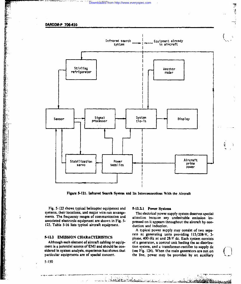
DARCOM-P 706.410
Infrared search Equipment already " N
system in aircraft
Sti rl ing Weather
refrigerator radar
Sensor Signal System DisplayI processor tie-in
i "I
Stabilization Power rimeservo supplies power
Figure 5-121. Infrared Search System and Its Interconnections With the Aircraft
Fig. 5-122 shows typical helicopter equipment and 5-12.2.1 Power Systemssystems, their locations, and major wire run arrange- The electrical power supply system deserves specialments. The frequency ranges of communication and attention because any undesirable emission im-associated electronic equipment are shown in Fig, 5- pressed on it appears throughout the aircraft by con.123. Table 5-16 lists typical aircraft equipment. duction and induction.
A typical power supply may consist of two sepa-rate ac generating units providing 115/208-V, 3-
&.12.2 EMISSION CHARACTERISTICS phase, 400-Hz ac and 28-V dc. Each system consistsAlthough each element of aircraft cabling or equip- of a generator, a control unit feeding the ac distribu-
ment is a potential source of EMI and should be con- tion system, and a transformer-rectifier to supply dcsidered in system analysis, experience has shown that (see Fig. 124). When the main generators are not onparticular equipments are of special concern, the line, power may be provided by an auxiliary
5-150
Downloaded from http://www.everyspec.com

DARCOMP 706-410
Cu-,
ZLz U
uj V)V o6- -I.-.
uj- C4C A IV
-4j
U-C
w Uw C)
uili<CD u ' iU)
cc
515
Downloaded from http://www.everyspec.com

DARCOM.P 706-10
F10,000 -~Q 960 X-BAND RADAR BEACON• " : -8500T
-4300 RADAR ALTIMETER
10 tO00 -1150 j-TACAN 1090 TRANSMIT1FF SET962 T 1030 RECEIVE
..- UHF COMMAND RADIO SET
--400 & UHF DIRECTION FINDER
-225 T
j 10-70 LIAISON SET
-30
S 10 HF SINGLE SIDEBAND SET121.75
-LF DIRECTION FINDER
-0.190-A
0.1
Figure 5-123. Typical Frequency Ranges of Communication and Associated Electronic Equipment
power unit (APU), ac from the APU.driven genera- the harmonics are contributed by the prime powertor and dc from a transformer-rectifier. it is impor- source. Other harmonics and transients are due totant to note that quality of rrgulation usually will be load changes as equipments are switched on and offmuch poorer when the APU is functioning and this as discussed in par. 5-2.may affect power dependent equipment. These effects can be particularly severe in aircraft
U3sually the power system voltage is distorted. Ac because of the limited size of the generators. The -
systems contain substantial levels of harmonics and levels of voltage distortion are proportional to theare subject to random transient variations. Some of magnitudes of the harmonic currents generated in
5.152
I- . ...- .
-' -- 2 -- '.-
Downloaded from http://www.everyspec.com

DARCOM-P 706-410
9 TABLE 5-16LIST OF TYPICAL AIRCRAFT EQUIPMENTS
Eng. Pwr. Management System Radar Altimeter
Engine Controls Tacan
Ignition Systems LF Direction Finder
Fuel Quantity System UHF Direction Finder
Transformer Rectifier Interphone System
AC-DC Generators 1FF Set
Elec. Sys. Control Panels X-Band Radar Beacon
Eng. Fire Detection System HIF Communications
APU Fire Detection System FM Communications
Environmental Control Unit UHF CommunicationsEngine Anti-icing System Electronic Flight Control Sys.
Interior Lighting Exterior Lighting
Auxiliary Power Unit Navigation Devices
Mag. Standby Compass Ordnance
Attitude-Heading Reference Sys. ECM Equipment
connected equipment and the combined impedance transmission. The system typically provides two-way
of the generator and intervening power cable. The re- communication on any one of 28,000 operating fre-
quirements for the generating equipment are called quencies spaced at l-kHz increments through the fre-
out in MIL-STD-704 which provides limits for ripple quency range of 2 to 30 MHz. The basic components(dc), harmonics (ac), and transients. Because of non- are receiver-transmitter, HIF control panel, antennalinear connected loads which feed harmonic currents tuner, and a monopole antenna.into the line, it is not unusual to find distortion levelswell above specification limits for the equipment it- 5-12.2.3 Environment EMIself. Interference originating external to the aircraft is
The extensive use of relays and solenoids in remote of three types:control of power to various systems adds additional a. Precipitation Static. Dust, snow, precipitation,EMI in the form of short duration spikes or rela- and engine charging static can cause severe interfer-tively long duration surges. ence in radio receiving systems. Noise from corona
discharges from the sharp edges of the aircraft cou--12.2.2 Radio Systems pie into the receiving antennas. Precipitation static
The presence of several relatively high-powerel occurs when the aircraft is operating in precipitationtransmitters, together with their cables or wave- containing ice crystals. while engine charging static isguides in a restricted space, presents a potential for caused by the action of heavy positive ions and free
radiated EMI. Any design, manufacturing, or instal- 4lectrons in hot engine exhaust gases. Helicopterslation flaws are likely to influence susceptible equip- generate appreciable static while hovering near thements that are in proximity, ground in clouds of dust or snow. Various additional
The HF single sideband radio system is generally types of static have been identified and described.the most difficult source of radiation to contrml. Be- Refs. 64 and 65 should be consulted,cause oi its power !,vel and the use of relatively non- b. Lightning:directive antennas in this frequzncy range, substan- Lightning strikes on aircraft generally impact the
tial fields will be present in the ct.%-e aircraft dtiri' upper portion of the wing or fuselage, or in the case
5-153
Downloaded from http://www.everyspec.com

DARC0M-P 706-410
:c Generator cc Generatof
L, c ControlI Control ContoUnit Ui
. --.----- Protection .
115/206 Vac-. 3 400'-
Transformer~R ectifier
~Battery I '
28 Vd Backup
AAuxiliaryPower
• I€~~c Generate!i
May be manuallyp1or Automatically r o
Switched to Bus Transformer~Reetif iorrm r
Figure 5-124. Typical Aircraft Power Unit
A W-
Downloaded from http://www.everyspec.com

DARCOM-P 706-410
of a helicopter, a rotor blade. From the point of ini- cuits arc particularly vulnerable because of their rela-tial impact, the current seeks a path through the ship tively slow recovery time. Typical examples of equip-to an exit point in the lower portion, probably near ment susceptibility that have occurred are (Ref. 66):the landing gear. a. The auxiliary power unit fire (APU) warning
Since the current caused by the strike is extremely light located in cockpit illuminated when the HFhigh, it is essential that the current be channeled communication system was keyed because the APUthrough preplanned conduction and major struc- fire detector leads picked up interference from thetural elements (with no spartl *N) and not diverted to HF communications system control leads.electrical systems and circuits, b. The fuel quantity indicators reacted erratically
c. Intentional and Unintentional Emitters. Aero- when the HF communication system was keyed, alsospace Ground Equipment (AGE) and airport equip- due to coupling; in this case between the fuel quan-ment may radiate, induce, or conduct interference to tity indicator signal lead and the HF system keyline.the aircraft while it is on the ground. Radiation en- c. The radar altimeter momentarily deflected whencountered in flight, especially near emitters such as the cabin heater was turned on because of a suddenpowerful ground based radars, may cause severe dis- change in line voltage.turbances. Fields as high as 100 V/m can be experi- d. The magnetic standby compass in the cockpitenced on the external surface. acted erratically when certain dc loads were in use be-
cause of coupling directly between the compass anddc leads,
5-12.3 SUSCEPTIBILITY e. The compass transmitter in the wing sent er-
5-12.3.1 General roneous signals to the directional gyro system duringnormal aircraft operation due to direct coupling be-
All electrical systems in an aircraft can malfunc- tween the transmitter.and the dc power leads.tion if subjected to appropriate and sufficient inter- f. Computer programs performed erratically be-ference. Obviously, susceptible equipment includes cause of transients in the power supply.all those with antenna inputs and instruments de. g. Sensors, accelerometers, and telemetry subsys-pendent on sensitive input transducers such as used tems were inaccurate because of susceptibility to linefor flight control. harmonics.
All equipment power requirements must be exam- h. The guidance system was inaccurate because ofined to make sure that raw aircraft power - con- transients in the power supply.trolled only by its own supervisory system but per-turbed by switches, relays, and solenoids and occa-sionally jolted by lightning strokes or static dis- 5-124 INTERFERENCE SUPPRESSIONcharges - will allow the equipment to function as EMC in aircraft is constrained by the limited en-required. velope of the aircarft and by the priority space allo-
Dc equipments and subsystems inherently seem to cation given to structural integrity, crew function,be more susceptible to interference than ac equip- and equipment function necessary for mission ac-ments, probably because input filtering may be less complishment. Thus, electrical equipment cannot beeffective than on ac circuits. The aircraft inter- bulky, and in some cases must be specifically pack-communication system, which will have several sta- aged to conform to the space available. The aircrafttions and a comprehensive wiring network, inte- envelope, of course, produces real constraints on gep-grates the audio facilities of the aircraft and has beer, aration of wires and cables.found to be vulnerable particularly to HF radio. Aircraft range and payload are direct functions of
aircraft weight. The weight constraint coupled with,5-12.3,2 Examples the need for high reliability for flight safety makes it
Systems such as navigation equipment, attitude necessary to perform difficult trade-offs to select re-heading reference systems, and electronic flight con- dundant equipment. In this engineering climate, it istrol systems may contain integrated circuits. These impossible to be lavish with shielding.circuits are not only sensitive to spikes but the circuit In many cases, the location of equipments, whichelements are themselves potential detectors due to are already constrained by the size of the aircraft, aretheir nonlinear characteristics and can be expected to further constrained by the necessity of functional lo-
t react to high frequency radiation. Computers and cation. For example, displays and controls must beother equipment containing logic and decision mak- located at specific crew stations, and generators areing circuits are sensitive to interference. Analog cir. located on the engines.
5-155
•. .W1.09 M; , -. _ _ _ *, ++, __
Downloaded from http://www.everyspec.com

DARCOM-P 706410
5-12.4.1 Program Organization signers involved in equipment installation but to
The aircraft as a system is particularly well suited structural designers who interface with the equip-to EMC program organization and implementation ment designers. In addition, at an early design stagedescribed in Chapter 2. The aircraft design naturally attention should be given to protection from precipi-
flows through the Life Cycle System Management tation and engine exhaust static as well as lightning.Model (LCSMM) stages, and the EMC organizationis a viable part of an organization that includes me-chanical, hydraulic, and electrical design; stress 5.12.5 INERTIAL NAVIGATION EQUIPMENTgroups; weight groups; aerodynamics and equip- 5-1.5.1 Introductionment experts. and a myriad of manufacturing quality Modern aircraft rely upon sophisticated inertialand test personnel. Mdr icatrl pnspitctdietaupoan alt apropriatenavigation systems for many operational maneuvers.EMC program plans, design criteria, and test plansall support the aircraft design and manufacture. These systems may be of the strapped down type, in
r rs b nwhich accelerometers and gyroscopes are mounted toEMC requirements must be established and placed the vehicle frame, or the type using a stable platform'" upon all appropriate subcontractors.
to carry the accelerometers and stabilizing gyro-scopes. Most systems in actual use are of the variety
5-12.4.2 Design Criteria having a stable platform.Much of the equipment installed by the airframe
manufacturer is, in essence, "off the shelf". Al- 5-12.5.2 System Description (Ref. 67)
though designed for aircraft use, it is not specifically Fig. 5-125 shows a block diagram of a conven-tailored to the aircraft in question. To counterbal- tional aircraft inertial navigator. The platform con-ance this situation, most aircraft are one of a line of sists -of a gyro-stabilized- cluster- of accelerometerssuccessful ships, and many of the EMI problems have whose outputs are fed to a computer. The computer,been solved previously or at least identified clearly which may be the central computer of the aircraft or
enough so that the latest model can profit by prior ex- a special-purpose inertial-navigation computer, cal-perience. Because of this hereditary growth, the prob- culates the aircraft position and velocity from the :lem of installing an absolutely new piece of avionic outputs of the two accelerometers. The computer alsoequipment in a currently successful aircraft should be calculates the gyro-precession signals, which main-approached with great caution. In particular: tain the stable element in the desired orientation rela-
a. Wiring and cabling, and the resulting coupling, tive to the earth. A vertical accelerometer sometimesshould be a major aircraft design consideration is added in order to smooth the indication of alti-
b. Grounding and bonding must be adequate, well tude, as measured by a barometric altimeter.installed, and free from degeneration due to stress or The inertial navigator also contains platform-sta.corrosion. bilization servos, a display-and-control panel, power
c. Antenna interaction must be minimized starting supplies for the platform and computer, and often aat the design stage. battery to protect the computer against power tran-
d. Particular attention must be paid to EMI caused sients. The system may be packaged in one or moreby H F, susceptibility of dc equipments, and suscepti- containers.bility of intcrcommunication systems. Typically, an inertial system consists of three parts:e. Whenever possible, EMC should be achieved (1) the stable platform, (2) the computer, and (3) thewithout the use of excess shielding, filtering, or sup- output indicator and control unit appearing in the
pression diodes. cockpit. These units are interconnected with cables.Wire and cable routing is perhaps the most impor- The platform and computer units may be quite close
tant of these design considerations. Grouping of like together and in the newer systems may, in fact, besignals with like signals and then appropriate separa- contained in the same enclosure.tion of groups such as shown in Fig. 5-122 or as dis-cussed in par. 4-4.11 can be planned by the EMC en- 5-12.5.3 Emissionsgineer and issued to the designer in the form of a set By its nature, inertial guidance equipment is notof specific directions for categorizing and installing likely to have high levels of emissions. The strongestwire bundles. Such initial design discipline will limit emissions would be from motor drives and synchroscoupling celulations to only the most difficult cases. which can produce significant fields only in their im-
The EMI engineer should issue grounding and mediate vicinity, and signal lines interconnectingbonding instructions (see par. 4-7) not only to de- equipments which may carry moderate level analog
5-156
L iat,
Downloaded from http://www.everyspec.com

DARCOM-P 701410Iniia atitdea-
Vertical accelerometer altitae rate atitude
L computer 8 atitude rate
Stable arormetric altitudeplatform
z.-axis
Gyros .:z,-axis
Gimbal Inertiai n"Obon a d Molaropickorisz...a. computer ,
ach anraft
-- iniianl peosity ~ Wllla e
Platform wandera&g4e, if not
Vehicle azimuth Vehide azimlithrelative to Platform from nfth
_ Vehicle attituda angles
(roll and 9ilci)
Figure 5-125. Block Diagram of an Aircraft Inertial Navigator
or digital information. These could be significant data will usually not be susceptible unless the logicemitters only to very closely spaced coils and cables. level is especially low (see par. 5-14.3)
5-12.5.4 Susceptibility 5-12.5.5 lnterference Control
Because an inertial system is a precision instru- Methods of compatibility control involve stand-ment, care must be exercised in its design to reduce its ard methods of cable separation and filtering. Filterssusceptibility to power supply transients, noise volt- may be needed in the power supplies, especiallyages, and variations of load current, or the power where a separate supply is not used. Since circuit sen-supply must prevent such variations from reaching sitivity to interference can vary significantly, de-the instrument. In some cases the power source may pending on the function performed, a careful anal-be separate from the main electrical power supply for ysis may be necessary to identify the most critical cir-the other subsystems. It is common to have both a cuits. Shields around cables are avoided, if possible,precision electrical power source for use with the pre- to minimize weight.cision instruments and a less accurate but higher Shields are used in the platform unit. Most gyros ofpower source for less critical use throughout the aero- gimbaled type have ferromagnetic elements (e.g. elec-space system. By keeping these two supplies separate tric motor laminations) and dc conductors (torquerit is possible to provide the heating and other less lead-wires) on the gimbal assembly, and usually alsocritical loads with a large power source while at the an electrically conductive rotor. The earth's field or asame time using an independent precision ac and dc stray field of artificial origin can have two effects.source for use with the precision instrument. One is magnetic attraction on the iron parts and dc
Cables carrying analog data, such as to and from circuits, and the other (usually the less serious) issynchros, could be susceptible because of the preci- eddy-current induction effect in the rapidly spinningsion which may be required. Cables carrying digital conductive rotor.
5-157
.Wn.
-1 A _
Downloaded from http://www.everyspec.com

DARCOM-P 706410
The disturbing effect of fields exterior to the gyro magnetic damping; and a microsyn pickoff. They arecan be reduced to a negligible value by surrounding considerably less accurate and less expensive than in-the instrument with shields of highly permeable ma- ertial gyros. A typical rate gyro (Ref. 67) has an out-terial such as permalloy or "Mumetal". put of 13 V rms at 400 Hz and is powered by 115 V.
400 Hz for the motor and 26 V, 400 Hz for the sensor.5-12.6 FLIGHT CONTROL EQUIPMENT b. Accelerometers. The accelerometers used to
measure the lateral, longitudinal, and normal accel-5-12.6.1 Introduction erations of an aircraft are usually simpler and less ac-
Flight control equipment is that associated, with curate than those required for inertial navigation sys-the direct adjustment of aircraft surfaces for pur- tems (Ref. 68). They consist of a spring loaded proofposes of maneuvering the aircraft. This control may mass enclosed in a fluid-filled case, the fluid provid-be direct through mechanical control, or indirect ing needed damping. A variable reluctance pickoff,through a servosystem arrangement. The latter is es- whose armature is mounted on the proof mass, pro-pecially required for large br high speed aircraft vides the output signal. A typical accelerometer haswhere substantial power is required to effect the an output of + 3 V rms, 400 Hz and is powered by 115required adjustments. In Ome cases the control V, 400 Hz.equipment constitutes small computers in order to c. Angle of Attack Sensors:stabilize the flight. The computers have been called Most frequently the angle of attack of an aircraft isstabilizers, auto-pilots, stability augmenters, and measured by a pivoted vane projecting into the air-dampers. This type of subsystem, Fig. 5-126, senses strearn whose axis of rotation is horizontal, and nor-one or more airframe motions and a control signal to mal to the centerline of the aircraft. Pickoff is usuallyoppose this motion. The resulting signal is used to accomplished by a potentiometer, synchro, or digitaloperate the servo actuator which in turn prodtces the encoder.appropriate surface motion. Ange of attack also can be snsed by means of
A typical pitch-axis stability augmentor system is static parts located above and below the fuselage orshown in Fig. 5-127 (Ref. 67). This system includes a above and below a rob- projecting into the air-pitch rate gyro for damping and a normal accel- stream, differencing th ir pressures and correcting forerometer which is used to achieve desirable handling static defects. Iqualities as well as pilot input and attituoc gyro and d. Other Sensors:path control inputs. The y.w axis stability augmen- In addition, sensors may be used to measure tern-ter system is similar, with the rate gyro replac-. by a perature (resistance hermometer), pressure (dia-yaw axis rate gyro and the normal accelerometer phragm or bellows with strain gage bridge or poten-replaced by a lateral accelerometer. The roll axis sta- tiometer pickoff), or position of control elements orbility augmenter is also similar to the pitch-axis sta- forces on them. For the latter, synchros, potentiome- Ibility augmenter but no accelerometer is included. ters, strain gages, or inductive pickoffs may be used.
In some cases, null balanchng systems such as6-12.6.2 Sensors shown in Fig. 5- 128 may be used to provide readings
The most common sensors used with flight control of improved accuracy frona the sensors.equipment are:
a. Gyroscopes. The rate gyros are conventional 5-12.6.3 Actuationsingle-degree-of-freedom gyros incorporating a rotor Electromechanical and hydraulic actuators aredriven by a synchronous motor, gimbal structure; commonly used in flight control equipment. Electro-and torsion bar providing spring restraint; viscous or mechanical actuators are used where the torques to
Sensors Controllers A tutor Cor ole ' Aircraft
Figure 5-126. Flight Control System Overall Block Diagram
5-158
... .. >. . :~ ~ ~ . . .- , " , .. .. . . . .. .;.." ,. . • ..--
Downloaded from http://www.everyspec.com

-DARCOMP 706-410
4J a
4-b'
to 91
0
CLIO4-b4
r-S 4.
5-159
Downloaded from http://www.everyspec.com

DARCOM-P 706410
Molor Generator
P iv o t a x is fo r 7 i t -o -.
Gear 'of altitude
f, Servo drives '°S"j pickoff to null
-. -. expands linearlywith pressure drop
Figure 5-128 Displacement Follow-up Absolute-pressure Transducer
be supplied arc not high and a moderate frequenc) motion of the control surfaces can result in an unco-bandwidth is adequate. Hydraulic actuators are used ordinated maneuver of the vehicle; accordingly, in-where high levels of force or a wide frequency band- terference in a sensor circuit can have serious consc-width is necessary to effect satisfactory control. quences. Evaluation of the need for reduction of sus-
ceptibility in such circuits will depend upon the level5-12.6.4 Emission of the sensor voltages and the sensitivity of the con-
Flight control equipment is not likely to be a sig- trol system to swell variations of the sensor voltages.nificant source of emission. Since direct and alter- Further discussion of sensor systems is given in par.iiating (400 Hz) power is supplied to both sensors and 5-15.actuators, these and the associated wirings can pro-duce local magnetic fields due to switching transients 5-12.6.6 Control Techniquesor altcrnating currents. Switching transients may be The control of compatibility of flight control sys-of special concern from circuits controlling hydrau- tcms in the aircraft requires the application of morelic valves with solenoids, trsi h icatrqie h plcto fmr
or less standard techniques of cable separation,52. Sgrounding, bonding, shielding, and filtering. Sensor5-12.6.5 Susceptibility outputs should be balanced twisted pairs wherever
Actuators are unlikely to be directly susceptible to possible so that common-mode voltages due tolocal fields since control voltage levels can be quite ground plane currents do not produce spurious sen-high. However, thiQ may not be true of some of the sor output voltages. Devices producing 'magneticsensor circuits. fields (actuators or sensor control motors) should be
The flight control subsystem has elements through- separated physically from sensitive devices orout tha entire vehicle, therefore information is trans- shielded (if the added weight is acceptable). Circuitsmitted over long cables into which signals -,ay be containing solenoids or relay coils should be isolatedcondcted or radiated. Transients that result when physically and filtered to reduce transients.switc.es close, heaters turn on, power subsystemloads change. etc., can be propagated into the flightcontrol subsystem and appear as a signal. Such a 5-12.6.6.1 Use of Fiber Opticstransient actuates the subsystem just as a signal from In order to reduce EMC problems and weight as-a gyro or an accelerometer would, and a spurious sociated with multiconductor cabling, especially on
5-160
Downloaded from http://www.everyspec.com

DARCOM-P 706410
aircraft, iiber optic systems have been developed Despite the extensive use of standard equipment,(Ref. 69). One hundred foot fiber-optic cables were AGE is unique in two respects: (1) it must interface
used lo connect aa elevator actuator with its control with the specific subsystem to be tested (mechan-computer on an otherwise "fly-by-wire" system. ically and electronically) and then suitably stimulateMore discussion of fiber optics systems is given in and measure the characteristics of the equipments un-par. 7-4.4. der test, and (2) the AGE equipment, both standard
and special. must be so packaged that it will be func-tional in the sometimes severe environment within
5.13 AEROSPACE GROUND which it must operate.EQUIPMENT (AGE)
5-13.1 INTRODUCTION 5-13.2 EMISSION CHARACTERISTICS
AGE, sometimes called ground-support equiipment A substantial portion of the emissions from AGE(GSE), consists of diverse equipments which must be comes from the standard equipment incorporated inused to check out the function of aircraft and corn- the test system. Motors, generators, vehicle ignition,plex missile systems on the ground. The type of and power control switches all contribute to i.#erfer-
roequipment may range from small battery-operated Sncp generation. See pars. 3-1.3, 5-t, 5-3, 5-6 for spe-test sets designed to check out a single function cific emission characteristics.through truck or van mounted systems to perma- Special problems can arise from the cabling used
nently installed systems. with the equipment and from the special stimuli usedA typical list of aircraft subsystems which may be to check out the designated subsystems. AGE often ischeckecr'by AGE includes: connected to the aircraft or missile and to base power
a. Armament by lengthy and complex cable systems.b. Control surfaces The special signals generated to stimulate equip-c. Instruments ment under test may be fidiated or-cnducted. If ra, ..d. Engine instruments diated, the levels are usually at low levels and shoulde. Flight instruments prokiuce no special problems. IfW onducted, they alsof. Heating, ventilating, and deicing will be at low levels, but where the cables convey a
g. Ignition large number of such signals, interaction within theh. Engine control cable is possible but can be avoided with care in se-i. Lighting lection of cables and allocation of signals to conduc-j. Electrical power tors within the cble.
k. Radio1. Radar
m. Special electronics, IR, navigation, etc, 5-13.3 SUSCEPTIBILITYn. Warning and emergency. If the equipment is connected to base power, largeAGE may be used in the field, on flight lines, and transients may appear on the lines. Furthermore, if I
at base shops as well as at formal test and rework the equipment under test is grounded, the transientsfacilities, or power frequency harmonics can produce signifi-
Preflight AGE must be rugged, portable, largely cant ground loop currents which can couple eitherself-contained, and self-checking. It may be capable conductively or inductively into sensitive test circuits.of operating from its own power sources, sources of Furthermore, in a typical location there may existthe equipment under test, or on locally available high levels of field strength due to nearby radars,power. Shop testing equipment may be fixed or port- communication transmitters, welders, and otherable, and is in general more complex. For example, sources.shop testing equipment may be computer directed. For many equipments the test signals will be of
AGE designers traditionally use as much "off-the- moderate level and not exhibit susceptibility undershelf" military and commercial ground equipment as normal conditions. However, the use of long cablespossible because usually it is produced in limited into which substantial voltages and currents can bequantities, and does not require airborne type relia- induced by high fields requires a careful evaluation inbility. Thus, it may incorporate standard trucks, each instance. Therefore, each item of equipmentvans, power supplies and regulators, batteries, should be examined with respect to its cabinet sus-meters, switches, amplifiers, receivers, transmitters, ceptibility and all signal and power leads connectedand instrumentation, to it.
5-161
wp m ,,i
Downloaded from http://www.everyspec.com

DARCOM-P 706410
In addition to the test equipment, the characteris- AGE is exposed. The following specifications andtics of the equipment under test and its configuration standards should be consulted:should be examined to determine if the method of a. MIL-STD-833 Minimization of Hazards ofconnection to AGE causes any special problems. In Electromagnetic Radiation to Electroexplosive Devicesparticular, the connection of a cable to an aircraft, b. MIL-STD-1377 Effectiveness of Cable. Connec-either through a connector mounted on the outside of tor, and Weapon Enclosure Shielding and Filters inthe aircraft or to one inside, can introduce voltages or Precluding Hazards of Electromagnetic Radiation tofields internally that would not exist otherwise. As Ordnance, Measurement ofmentioned previously, common-mode currents could c. MIL-STD-1385 Preclusion of Ordnance Haz-be troublesome, especially if the aircraft itself has a ards of Electromagnetic Fields; General Requirementsground connection. for
d. MIL-STD-1542 Electromagnetic Compatibility(EMC) and Grounding Requirements for Space Sys-
5-13.4 EMC CONTROL tern FacilitiesIn AGE EMC design decisions, cost-effectiveness e. MS-25384 Plug, Fuel Nozzle, Grounding
should be a consideration. Where the production f, MS-33645 Receptacle Installation. Fuel Nozzlevolume is small, it may be advantageous to over- Jumper, Aircraft Idesign rather than to carry out an extensive EMC g. MS-90298 Connector. Receptacle, Electric.analysis. Grounding
Some account should be taken of where the equip- '1ment involved is to be mounted, such as within a per- 5-14 SPECIAL CIRCUITmanent enclosure, on a vehicle, or exposed. CONSIDERATIONS
In addition to the-use of the techniques of shield-ing, filtering, and grounding for EMC control, as dis- 5.14.1 INTEGRATED CIRCUITScussed in Chapter 4, special attention should be given The advent of semiconductor devices has enabledto the selection of the cables used in the design stage. the construction of circuits having very high densi-
To avoid the effects of long cables, balanced out- ties of circuit elements, including resistors, capaci-put and input circuits should be used wherever possi- tors, diodes, and transistors. The high densities areble and filters should be inserted in these circuits to particularly characteristic of digital circuits. While -'reject signals other than those desired. Where high analog circuits can be made with the same densities insensitivity circuits are involved, signals should be am- most applications, the number of elements requiredplified before transmission through the cable wher- on a single chip is much less.ever possible. The analog circuit can be more susceptible to in-
Where the test equipment is located inside a truck ternal EMC problems than the digital circuit be-or van, the equipment itself may be protected from cause of the switching threshold which is characteris-
1'" high levels of environmental fields by the van enclo- tic of the digital circuit. However, with fast rise timesures or specially constructed shielding enclosures, circuits considerable care in design must be exercisedThe usual practices of bonding equipment cabinets (see par. 5-14.3). The internal EMC problems ariseand racks should be followed, and any external con- from (I) the close spacing of components and theirnections to power supplies should be filtered where connections. (2) the parasitic or unwanted elementsthe lines enter the vehicle, that appear in the circuit as a result of particular
To protect test cables from external high-frequen- methods of construction used, and (3) the need forcy fields, it may be necessary to use shielded cables. terminal connectors of small size to match the circuitThe shield probably will require a good connection to board sizes.the vehicle under test and also to the test equipmenton the vehicle or enclosure where it is located. 5-14.1.1 Emission
A specification for AGE for NASA installations is Because of their small size and consequent lowavailable (see Ref. 70). power requirements. integrated circuits themselves
Two matters.concerning safety should be exam.. are unlikely to be significant sources of emission.ined, One is the personnel shock and hazards asso- However, interconnections between circuit mount-ciated with the interconnection of separate vehicles or ing boards can be sources of both conducted and ra-test equipment by means of cables. Isolation trans- diated EM! unless adequate filtering and shielding isformers may be advisable where base power is used. used. The techniques described in detail in Chapter 4The other is protection against lightning wherever the apply to these circuits,
5-162
Downloaded from http://www.everyspec.com

DARCOM-P 706-410
5-14.1.2 Susceptibility analog signals. In some cases the significant degra-Because of the small size of integrated circuit pack- dation effect can be directly proportional to the level
ages, the primary cause of radiated susceptibility of interference. In others, as with frequency modula-arises from leads connected to them. Fig. 5-129 (Ref. tion signals, the degradation may exhibit a sharp71) shows predicted electric field susceptibility for a threshold, in which values of I/S up to a value closetypical amplifier. In this case linear susceptibility was to unity exhibit very little degradation, but beyonddefined as the field level necessary to produce an out- that there is almost total loss of information. Theseput voltage equal to that due to internal circuit noise. phenomena are discussed in some detail in par. 3-2.Nonlinear susceptibility is that field necessary to Analog circuits may operate at levels varying fromcause sufficient rectification to displace the operating a few nanovolts to hundreds or thousands of volts. Atpoint of the circuit by 1% from the normal value, In the lowest levels (below about I mV) they can bethe calculations the area, occupied by the circuit and expected to be extremely susceptible to externalleads, was assumed to have a length of 0.5 in. and a fields, whereas at higher levels (above about I V) theywidth of 0.2 in, This configuration is modeled as an will be relatively insensitive and more likely to beelectric dipole at low frequencies and a fixed area at sources of interference to other circuits, The mecha-frequencies above about I GHz. At frequencies in nisms of emission and susceptibility have been dis.this range the susceptibility is assumed to be due to cussed in some detail in Chapter 3 and are not dis-nonlinear phenomena. For larger areas such as aris. cussed further here.ing from wiring on circuit boards the levels of sus-ceptibility could be as much as 40 dB less.
For digital circuits a noise immunity threshold of 5"14.2.1 Electronic InstmmentsO.5. Y. was assumed, In this case the susceptibility Analog instrumentation includes devices used forthreshold for electric fields is shown in Fig, 5-130 for displaying the value -of somequantity as registered-byeffective areas of I cm2, 5 cm2 , and 25 cm 2. a proportional displacement of some type of indi-
Susceptibility of integrated circuits to conducted cator, usually on a D'Arsonval type meter or aEMI has been measured in the gigahertz frequency cathode-ray tube.range (Ref. 72). The data show that at 0.22 0Hz ana-log circuits begin to show susceptibility at 10-1 W and 5-14.2.1.1 Emissionthis increases to about 10-1 W at 9.1 GHz. Digital cir- Instruments are not likely to be significant emit-cuit susceptibility may be'two orders of magnitude ters except as follows:higher, at least at 0.22 GHz. a. Cathode-ray displays may use high magnetic
Because of their small size, integrated circuits can fields for beam deflection. By its nature the deflec-be particularly susceptible to destruction from high tion yoke has an air core and exhibits high leakagelevels of EMI or to static discharges as a result of flux. The frequency of operation is usually below ahandling. In some cases the circuits themselves con- few kilohertz, so that there can be coupling to audiorain self-protecting diodes to bypass high currents or frequency circuits in the vicinity.charges around the active transistors (Ref. 73). b. Devices which contain an internal generator can
produce significant conducted or radiated emissions.$-14.2 ANALOG CIRCUITS AND DEVICES Typical is the sweep oscillator used in cathode ray os-k14.d whereG a R I parameter ofVICES tcilloscopes, the frequency reference oscillator used in
Analog circuits include those carrying signals of frequency counters, and the local oscillator used forany kind where a parameter of the signal such as am- frequency conversion in transmitters or receivers.plitude, frequency, or phase varies in direct propor- Transformers and high inductance coils or chokestion to the value of the quantity being transmitted. also may radiate magnetic fields as may any sole-Analog circuits may operate at low audio (including noids or motor drives.dc) to provide control information, at audio fre.quencies for speech transmission, or at radio fre- 5-14.2.1.2 Susceptibilityquencies where modulation and demodulation arenecessary. In all cases, superimposed interference will 5-14.2.1.2.1 Input and Signal Circuitsprovide a distortion of the originally transmitted Usually, the input circuit is the most susceptiblemessage signal to an extent which is directly depend- part of any instrument because it operates 3t theent on the interference-to-signal ratio (I/S). lowest level. Standard methods of controlling sus-
There is no simple universal way of measuring the ceptibility include use of balanced circuits at low fro-signal degradation due to such interference for all quencies and coaxial systems at high frequencies
5-163
Downloaded from http://www.everyspec.com

DARCOM-P 706-410
zWu,'M 'AP4UGO JAOd 4
o 03
1
LA CJ
5-164
/. .... 1.
Downloaded from http://www.everyspec.com
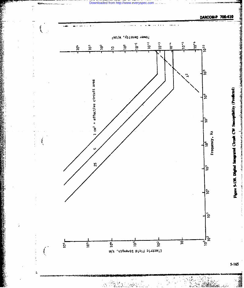
zWhr/M 'Ansuou .BMOd 0
4. l V, N 04CD .D -5
0iiv
Downloaded from http://www.everyspec.com

DARCOM-P 706-410
using small effective loop areas, and shielding. Spe- 5-14.3 DIGITAL DATA SYSTEMScial care is required for circuits connected to long in. 5-14.3.1 Introduction:p u t c a b le s to a v o id c o u p lin g to e x te rn a l fi e ld s a n dD i t a d t a e c n q s a r u ed f r o m n c -where high accuracy is involved. Digital data techniques are used for communica-
tion, data processing, indicator, and control systems.Frequently, a digital data processing unit functions as
5.14.2.1.2.2 Other Circuits a central control and interfacing unit for all radiodata link, navigation, flight stabilization target detec-
If the input circuits are properly protected, other tion, acquisition, tracking, and weapon control sys-parts o;" the instrument may have significant levels of tems. Moderp requirements for high data rates lead.susceptibility. Power and control cables can provide to systems having short pulse duration and wideadmission paths for conducted interference as can bandwidth which are subject to degradation from in-apertures in the cabinet for radiated interference. If terference on power, control, or signal leads. Digitalthe instrument is to be used in high field regions such data equipments, which contain large numbers ofas near electromagnets or radar systems, indicating solid-state switching circuits, are also capable ofmeters should have special shielded and filtered con- emitting conducted or radiated interference. Thestruction. Also, cathode ray tubes may require mag- emission and susceptibility level of digital data equip.netic shields to protect against the earth's field or ments depends upon design, construction, and in-local magnetic fields. stallation.
For industrial process instruments, the peak-to- Binary circuits are capable of restoring pulses orpeak ripple and total noise level in any circuit should levels that have become partially degraded in level orbe less than 0.25% of the maximum signal or 10 mV shape by EMI. In such circuits, it is necessary onlyfor a 5-V signal (Ref. 74). for the digital data information level to reach a value
sufficient to satisfy a switching threshold or com-5-142.2parator circuit, and the pulse or level will be restored' 5.14.2.2 Synchros thereby to a full-amplitude, relatively noise-free con-
Synchros, which are extensively used for transmit- dition. However, if EMI exceeds a certain threshold, .ting position or control information, operate at it can be quantized into a full-level bit error.relatively high voltages, but because they operate ona null principle, any undesired coupling into the null 5-14.3.2 Emissioncircuit will limit the accuracy of the indication ob- The predominant interference generated by digitaltained. The tolerable level can be calculated in terms equipment can be attributed to the repetitive opera-of the sensitivity of the synchros (approximately I tion of a multitude of switching circuits having fastV/dog) and the accuracy desired. In addition, the op- rise times, whose switching operations are synchro-eration is dependent upon the reference circuit, usual- nized by clock-timing logic. The clock frequency andly the 60- or 400-Hz power supply. Substantial levels its harmonics dominate the generated EMI spectrum.of harmonic voltages appearing on this circuit can in- Other major interference sources are the opera-troduce significant errors. Where power supply wave- tions involving the basic oscillator, time pulse dis-form purity cannot be maintained, a special power tributors, register counters, drums, and any othersupply should be used to supply the reference circuit, fixed repetitive functions.
Interference can be expected at the fundamentaland harmonic frequencies of these operations duringS5-14.2.3 Analog Computers normal computer functioning. Other computer op-
Computer circuits require special consideration be- erations may become sources of interference undercause of their accuracy requirements. Normally, they execution of certain instruction sequences in someare designed to operate with as large a signal range as programs. The program cycle itself, if sufficientlypossible and still maintain linearity. By using feed- short in duration, falls into this category.back, such as in the well-known operational ampli- In one series of tests on a computer using solid-fier, the signal range can be maximized while satisfy- state logic (Ref. 75), the computer was divided intoing linearity requirements. Since the range may be five test groups-several volts, an induced level of a few millivolts can a. Master clock timing and basic operationscause significant error. While this is not a highly sen- b. Central processing system and programmed op- "siLive level, if the computer must operate in high field orationsregions, special protection means may be required. c. Core storage element
5-166
_ .. .J
Downloaded from http://www.everyspec.com

DARCOM-P 705-410
d. Drum system and associated peripheral unit other inputs) of a gate even though the gate inputs* processing circuits did not atisfy the switching logic level. A coupled
e. Typewriter, czar4 rader, and associated periph- signal of sufficient magnitude and width may be am-oral -unit processing circLits. plified and shaped by a string of gates so that itFor each of these groups the antenna was positioned results in a logic signal that causes an error.3 ft from the ornputer frame. Results are shown in Of npecial concern are magnetic materials used as)fig. 5-131. The vadles ndicated are the muximum for information elements in digital data processing sys-each frequency. The spe.:ific ftequencls nf emission tems. Magnetic tapes, discs, or drums may be used as-correlate well with romputnr timing -fr3quencies, input/output or storage devices; and magnetic
toroids are frcquently used in:shift register, decoder,. 4A,3 Stact.-pdiy : buffer storage, and memory circuits. These magntc
'The noise marxiri audnise immunity parameters . materials may be easily influenced by extraneous.,. ii of gating circuits used i~n digital devices at emcoures .. magnetic fields so as to erase the data stored or it can
of thu gt. sustepbility t os .Nie bias the magnetic materials toward an "all ones" ormargin is defined as, tht.mainitde in-volts oil pulse, "all zeros " state. The portions of digital data prc-noise, which, when appead'ng at the input of a digital essing systems that use magnetic materials must,gate and riding on the "worst-case lo3ic level, will therefore be protected from internal and externalcause a signifiant -taction at the output of the gate. fields.Dc noise margin, as in wide,slow -rise time noise b. Conduction Coupling:pulses, is the difference between the worst-case logic Large switching transients in the power andvoltage level and' tha worst-case switching threshold ground circuits of digital circuits may be directly cou-voltage of the gate. Transients of ac noise margin, as pled into sensitive digital circuits. Because a number.. inast rise time noisepulses, are in most cases less of circuits -may be packaged to form one- module,
W than the dc noise margin. Noise immunity is defined power supply decoupling (see par. 4-3.1.1) riiay be ne.as cessary within the module. When the circuits are
-, worst case noise margin grouped into modules and each module containsNoise immunity power supply decoupling, the currents to be oval-
maximum logic voltage swing uated for EMI are:.*,+ (1) Ground currents that leave the module andX 100% (5-41) flow into the system ground
- (2) Signal currents that flow in decoupling capaci--. 14.3.3.1 Susceptibility Mechanisms tors mounted in the module,
Di~itil circult susceptibility coupling mechanisms High speed switching circuits may place a largeinclude: transient current demand upon power supplies dur-
a. Induction Coupling: ing transition from one logic state to the other.Induction coupling in a digital circuit may occur in Knowledge of the rate of change of these currents will
two ways: (1) internally within the device itself, or (2) allow the system designer to calculate, approxi-externally via cables and connectors of associated cir- mately, the tolerable impedance of the bypass ca-cuits. pacitor and the system ground.
Internal coupling occurs as a consequence of para- The path from the module to •system ground mustsitic mutual capacitance and inductance inherent in be a low impedance. If the module is a printed circuitthe semiconductor device. The effective isolation be- card, it is almost always necessary to use more thantween input and output of semiconductor devices (the one of the connector pins as a ground return. Thecircuit elements most commonly used in digital data common ground return for groups of modules alsosystems) may be poor, permitting undesirable cou- should be designed for low impedance,piing and crosstalk between two gates in the same Susceptibility of a digital circuit to disturbances inintegrated circuit package. Where there are unused the power and ground systems may be determined byterminals, a decision must be made as to whether they introducing a disturbing pulse between the groundcan be allowed to float or whether they should be tied pin of the module and the system ground, or be-to some bias voltage or to ground. tween the power pin and the system power. If the
External coupling is due to mutual capacitance and logic circuit under test is one of a string of gates, theinductance of interconnecting lines and conductors. width and amplitude of the disturbing pulse may be
' The effect is to cause differentiated leading and trail- varied to determine the minimum pulse that willing edges of input signals to appear on the output (or result in the propagation of an erroneous logic signal.
-. : 5.16"7
-..- . :.,_'._.•_,.__ _..-__ _ _ _ _,_-'_...._. "' - . - . : . . : : , . -. ... , , "'. " " "+ -.' - .- .
_44-4 I n I 1IiW i I
Downloaded from http://www.everyspec.com

DARCOM-P 706-410
-4J -~C
V) Z)
0 A_ _ _ _ ____
1.01
a) - x b..
o cn to
-t CCS
(paanu UOU)A@ Aqe2 avlA8u~4OUYla
Downloaded from http://www.everyspec.com

c. Radiation Coupling. Strong fields from nearby the circuit most Aensitive to electromagnetic radia-intentional emitters - such as radio stations, or in. tion.dustrial, scientific, or medical equipment - can b. Solid-state Computer (Ref. 75):penetrate shields of cables or equipment housings. If A solid-state computer was also subjected to pulse-they are of sufficient strength, such fields may cause modulated high-frequency radar signals produced byinterference either by direct interference with circuit the portable radar simulator.signals (if their frequencies are sufficiently close to The resulting computer susceptibility levels variedclock and switching frequetcies) or by causing bias from 64 V/m (peak) to over 400 V/m peak. The 64voltage changes due to ;.e6tfication in active circuits. V/m (peak) susceptibility level occurred in the pe-
ripheral unit processor. This unit along with the cen-tral processing system yielded the, most susceptible
5-14.3.3.2 Me red %sceptibilty Levels areas. These units predominantly ct ntain basic logicA discussion of n'ieasured susceptibility follows: circuits which have high frequency characteristics duea. Vacuum Tute Computer. A computer was to their design for fast rise and response times. Con-
exposed to the radiation from a radar simulator (Ref. sequently, they are more susceptible to the high fre-76). This system I ad about 50,000 vaccuum tubes and quency characteristics of the radar pulses than other170,000 diodes. Tests were performed in the frequen- circuits.cy range of 450 to 2900 MHz with various combina- The core storage and drum units, which house spe-tions of pulse dity cycle and signal polarization, and cial circuits, including core and drum informationexposures were tiken on each unit of eqiipment and amplifiers (both of which were most susceptible in thefront, back, and side. Results showed that: vacuum tube computer), were not as susceptible as
(1) Many circuits of the computer do not malfunc- circuits in the central processing system and the pe-lion under electromagnetic field radiation as high as ripheral unit processor. The core and drum ampli-400 V/m. Circuits in this category are high-level cir- iers amplify low-frequenc signals -and -therefore -
cuits such as flip-flops, gates, and/or pulse ampli- differ in design from high-speed pulse circuits. As afiers, relay drivers, level inverters, and cathode result, they do not so readily accept the radar pulses.followers. Also it was noted that for all units, susceptibility
(2) Low-lzvel circuits of the computers (whose nor- decreased as frequency increased.mal input is within the range of 50 mV to 2 V peak to Of the four units tested, the drum unit was the leastpeak) did malfunction when subjected to moderate susceptible, being below 400 V/m (peak) at only onefield strengths. test frequency. An important factor contributing to
(3) Sense amplifiers of the memory element mal- this effect is the method of packaging. This unit, al-functioned at the field strength of 16.4 V/m peak, the though not RF shielded, was designed in such atuning fork oscillator of the output section malfunc- manner that all circuits are drawer-mounted andtioned at 40.8 V/m peak, and drum read amplifiers of housed in a metallic enclosure. In one instance, onethe drum section malfunctioned at 44.8 V/m peak. of the drum circuit drawers was pulled out and the
(4) Data conversion receivers of the input section susceptible level decreased from 240 V/m (peak) tomalfunctioned at 52.1 V/m peak. 145 V/m (peak).
(5) Flux amplifier of the output section failed at98.7 V/m peak.
(6) Generally, circuits are more susceptible to ra-diation near the low end of the 450-2,900 MHz fre- 5-14.3.4 Interference Reductionquency band than to the higher frequencies in this As with other types of equipments the effects of ra-band. diation on digital equipment can be reduced, in some
(7) Variations in susceptibility due to variations in cases, by shielding the susceptible circuits, or bypulse width and PRF are slight, redesign.
(8) Polarization of the signal is significant, but Typical of the circuit changes which can reduce thevaries widely by computer unit. Generally, the corn- susceptibility of sensitive circuits are:puter is more susceptible to vertically polarized a. RF filtering of the interference at the circuit in-signals. put
In actual usage, the susceptibility data levels of b, Reduction of the circuit rectification character-malfunction must be identified with the specific pa- isticsrameters which characterize the radar. The sense am- c. AF filtering of the rectified interference pulses.lifier of the memory element was determined to be In typical digital data equipments, some circuits
5-169
.= -.. • ,. . + +-*,,A- * ++ . , . + ' ' '- , ,, - ..o- .- o . .
Downloaded from http://www.everyspec.com

DARCOM.P 706-410
have an inherent immunity to malfunction under in- c. Gating. The circuit status is read only over a ""
tense electromagnetic influence. Relatively invul- short period of time (the gate period) during each op-nerable circuits include high-level circuits such as oration cycle. In this way, spurious signals due to in-flip-flops, line drivers, relay drivers, level inverters, terference are prevented from causing errors unlessand emitter followers. On the other hand, low-level they occur simultaneously with the gate.circuits whose normal input is within the range of 50mV to 2 V peak to peak, tend to malfunction whensubjected to interference of moderate field intensi- 5-14.4 MICROWAVE CIRCUITSties. Circuits in this category include tape readers and Microwave circuits have only a limited number ofmagnetic core memory-sensing amplifiers. Digital significant EMC characteristics. This is becausedata systems employing radio data links are most sus- microwave energy is propagated over only limitedceptible to degradation in the radio circuit itself distances within equipment cabinets. It is coupled torather than in the logic circuits that follow the quan- an antenna by means of coaxial cable or waveguidetization process. The EMI control measures dis- using as short a length as possible considering the ap-cussed in par. 5-7 for receivers apply to digital data plication.receivers. In the design of microwave systems, one makes use
In comparing vacuum tube circuits with solid-state of several circuit components not in common use atcircuits, an important contribution to the reduction lower frequencies. Included are:of the drum information amplifier susceptibility in a. Directional couplersthe solid-state computer was a circuit change replac- b. Hybrid junctions n'ing the old input transformer with two stages of push- c. Isolatorspull amplification in order to eliminate in-phase d. TR switchesnoise. Susceptibility-reduction-in the memory core in- e. Circulators.formation amplifier was achieved by a drastic reduc- One of the most significant functions of these ele-tion in length of conductors in the high gain differen- ments is to permit the use of a single antenna both fortial amplifier stage. This reduction was made possi- transmission and reception. Their characteristics areble by using transistors and subsequently compact- important in determining the overall performance of king circuits. a system, especially with respect to frequencies out of
However, solid-state basic circuits are more sus- the design band. Unfortunately, very little specific in-ceptible than the vacuum tube type. The vacuum tube formation on such characteristics is available in pub-basic circuits were not susceptible at field strengths of lished form (Ref. 77). Where they are used, the400 V/m (peak) or better. however, levels below 100 number of interacting elements can be quite lurge andV/m (peak) were found to cause malfunctions in the analysis is performed using matrix methods such as issolid-state circuits. Two important factors contrib- common for treating a number of antennas havingute to this phenomenon. One is the better high fre- mutual coupling,quency handling capability of the new circuits. Theother is the 10 to I reduction in the operating signal 5-14.4.1 Emissionlevel of the circuits, thereby causing a reduction in the The only sources of emission at microwave fre-ratio of signal level to radar level for any given radar quencies are the devices used to generate and ampli-environment. Fig. 5-132 shows comparative data. fy microwave energy. High-power devices for use in
radar systems were discussed in par. 5-9.
5-14.3.5 Logic Design 5-14.4.1.1 Tunnel DiodeIn addition to other techniques of controlling sus- Tunnel diode oscillators are able to deliver milli-
ceptibility, special logical design techniques can be watts of power and thus are used in microminiaturi-used to reduce the susceptibility to impulse type in- zation programs. Both output amplitude and fre-terference, especially if it occurs infrequently, name- quency are dependent on the nonlinearity of thely: diode V-I curve.
a. Parity error check. Data words are transmitted If the tunnel-diode (T-D) oscillator is fed to a mis-with a known parity which is checked on reception, matched load through a length of transmirsion line.The more sophisticated systems can correct for sim- discontinuities may appear in its tuning curve. There "pie errors. may be jumps or skips in frequency and power out-
b. Redundancy. Each word is sent twice, either in put. The effect is due to the formation of cusps orseries or parallel channels, loops in the admittance curve seen by the negative
- -170
Downloaded from http://www.everyspec.com

DARCM* 766410
10001 *
8001 BASICCIRCUITS
600.1
400 1
~200-
CORE STORAGE
100.-CIRCUITRY
60- BASIC0- - I CIRCUITS
is40-1
CORE STORAGE20 AN~D DRUM4
CIRCUITRY
COMPUER 4 I~IISOLID0-STATE
C0OMPUCOPUTE
F~gue 5132 Sucepilty Compasont of Vacuum Tube and Solid-state Computr
conductance, and is called oscillation hysteresis. The a8 line length. radtoddebn
effect is avoided if the load is ptrfectly matched to the The oscillator frequency is sensitivetoddebs
charactcristic impedance of the transmission ine. as shown in Fig. 5-133, while output power vs bias
The condition for no oscillator hysteresis is given by: voltage is shown in Fig. 5-134. The second harmonicotutput vs bias is shown in Fig. 5- 135. All other out-puts were -60 dfim or lower.
~ ~ + *dimensionless (5-42) Other types of small semiconductor oscillators< __*have been developed including the Gunn and Read
where IMPATT diodes. Little specific EM! data on these
a - VSWR of load, dimensionless devices are available, but general design information
Q = resonance Q for line, dimensionless can be obtained from Ref. 7L 5.7
Downloaded from http://www.everyspec.com

DARCOU-P 706-410
640I.
N 630 /
U: 620
600
I ~ ~590, .
180 200 220 240 260
Bias Voltage, mV
(A) VARICAP BIAS VOLTAGE = 0 V
S780<1, • 770 -~" 770
LL- 180 200 220 240 260Bias Voltage, MV
(B) VARICAP BIAS VOLTAGE = -20 V
~910
900
890 -
" 180 200 220 240 260
Bias Voltage, mV
(C) VARICAP BIAS VOLTAGE = -90 V
Figure 5-133. Fundamental Frequency vs Bias Voltage of Tunnel Diode for Tunnel-diode Oscillator
5-14.4.2 Susceptibility a higher stability than the cavity maser and is the typeSusceptibility at microwave frequencies takes place in most general use.
either in active devices used for amplification or in Interference analysis of traveling wave masers wasdetectors, or through coupling between transmission carried out both experimentally and theoretically inline structures used for interconnecting circuit Ref. 79. The conclusions of this study were:elements, a. Masers arc the most sensitive amplifiers in all thefrequency bands for which they have been devel-
oped. A noise temperature of 10 K is typical.5-14.4.2.1 Masers b. Saturation of the maser is predictable and is a
The maser provides an amplifier with an extremely function of average input power and maser gain aslow noise level. The traveling wave maser (TWM) has shown in Fig. 5-136.
5-172
Downloaded from http://www.everyspec.com

.ARCOP 70r41 1 o
- 0.7
E0.6 -" 'IA0.4 , _
180 200 220 240 260
Bias Voltage, mV
(A) VARICAP BIAS VOLTAGE 0 V
S0.6__
3 0.5_____I
180 200 220 240 260
Bias Voltage, mV
(B) VARICAP BIAS VOLTAGE -20 V
:~0.5
. 0.4 _ _..
3
180 200 220 240 260Bias Voltage, mV
(C) VARICAP BIAS VOLTAGE -90 V
Figure 5-134. Total Output Power vs Bias Voltage of Tunnel Diode for Tunnel-diode Oscillator
c. Desensitization is predictable and is a function gain recovery time, no cross-modulation is observed,of average input power. but gain desensitization is proportional to total aver-
d. Cross-modulation effects are predictable on the age input power.basis of the input energy of the interfacing signal, the (3) If the interference AM period is approximatelymaser saturation characteristic, and Lhe gain-recov- equal to gain-recovery time, then cross-modulation isery characteristic. When interfering signal power a function of the ratio of the interference AM periodresults in an input power greater than maser saLura- to maser gain-recovery time.tion level, then: c. Intermodulation is nonexistent based on the fact
(1) If the interference amplitude modulation (AM) that no harmonic signal generation is predictable orperiod is greater than maser recovery time, the am- measurable.plitude of desired signal varies proportional to gain f. The gain stability of the maser is dependent onof maser. the stability of the externally applied dc magnetic
(2) If the interference AM period is tess than maser field.
5-173
-~ - ---. A L.A;<? * "
Downloaded from http://www.everyspec.com

DARCOM-P 706-410
-10- --
o-p
180 200 220 240 260Bias Voltage, mV
(A) VARICAP BIAS VOLTAGE 0 V
-10 - .-
, 0 . . .. -. . . . . .
S-20
-30.180 200 220 240 260
Bias Voltage, mV
(B) VARICAP BIAS VOLTAGE = -20 V- C - -..-
-o _____0
0
- 3 0 1 ,,,_ _ _.180 200 220 240 260
Bias Voltage, mV
(C) VARICAP BIAS VOLTAGE = -90 V
Figure 5-135. Ratio of Second-harmonic Power to Fundamental Power vs Bias Voltage of Tunnel Diode
5.174
. , - . , .. , . . -
"~~~~~~~~~~~~~~~~~~~~~ • Cit , ;; ' " . -,3"", ' "-"- " . : " ; ' -
Downloaded from http://www.everyspec.com

In
Is1
(U
CL
4 -)
CL .
ap 'upog Jasvw JaN
Downloaded from http://www.everyspec.com

F DACOM.MP 70&410 . ;,•I i
g. Gain-recovery .*,at of a maser is dependent on Fig. 5-140 shows small signal gain vs interference Amaser material and bath temperature. Typical gain- for several frequencies, Fig, 5-141 illustrates power
recovery times range from 50 to 200 ms. required for a fixed reduction in small signal gain (20h. The characteristics of the TWM, because of its dB).
high degree of output to input isolation, are rela- The parametric amplifier exhibits no unusualtively unaffected by moderate impedance mis- effects from large pulse-power inputs or moderate in-matches to external circuits. put powers at its idler frequency; however, pump-
The behavior of the TWM characteristic is given power radiation from input and output ports is ob-by a power output versus a power input curve rather served, Appropriate filtering is therefore necessary.than the V-I curve characteristic of vacuum tubes ortransistors. The transfer impedance of the maser is 514.4.2.3 Tunnel Diodesequal to a constant even at saturation levels, and the The block diagram of a typical tunnel diode am-equivalent V-1 characteristic is linear. plifier is shown in Fig. 5-142. The circulator is used to
isolate the amplifier input and output, and the direc-tional filter masks the out of band characteristics of
5-14.4.2.2 Parametric Amplifiers the circulator.The parametric amplifier also is a low noise, wide The noise figure of tunnel diode amplifiers is better
bandwidth signal frequency amplifier. Its noise per- than conventional mixers. They have rather low dy-formance is between that of a maser and good tunnel namic range, however. The dynamic range variesdiodes, traveling wave tubes, and conventional di- with the product of the differences between the peakodes. It can be shown that a timt-varying capaci. and valley currents and voltages. It can be increasedtance such as obtainable with a semiconductor diode by using matched diode pairs in push-pull as shown
-excited by a suitable "pump" frequency will give lin. in Fig. 5-143 This arrangement also provides opti-ear amplification of small amplitude signals, mum noise performance. A typical saturation curve
The interference characteristics of these devices are for a single diode amplifier Is shown in Fig. 5.144.saturation, desensitization and cross-modulation, in- The desensitization and cross-modulation charac-termodulation and gain stability, and impedance teristics of tunnel-diode amplifiers can be relatedeffects. Refs. 79 and 80 give a detailed experimental directly to the amplifier saturation curve. A typical %t
4 and theoretical analysis of parametric amplifiers un- desensitization curve is shown in Fig. 5-145. Cross.der CW and pulsed conditions. modulation is shown in Figs. 5-146 and 5-147.
The two most important interference charact- The resistive cutoff frequency of the tunnel diodeeristics in parametric amplifiers are gain-change limits the maximum gain-bandwidth prodi.ct and theeffects and generation of additional frequencies. minimum noise figure obtainable. The amplifier is
The measurement of the cross-modulation of a 1.4- also more susceptible to interfering signals whenGHz parametric amplifier indicated that: operating near the resistive cutoff frequency,
a. When the sum of the powers of the desired andinterfering signals is less than the saturating powerlevel, the cross-modulation is proportional to the in- 514.4.3 Compatibility Controlterfering power level. There are two means of controlling compatibility
b. For a constant gain, when the sum of the powers other than adjustment of active device and antenna-of !he desired and interfering signals is less than the characteristics (as discussed in pars, 5-10 and 5-saturating'power level, the percentage of cross.modu- 14.4.2): (1) use of filters, and (2) control of leakagelation is independent of the desired signal input from transmission lines,power.c. When the level of the interfering signal exceeds 5.14.4.3.1 Transmission Lines
-Ithe saturating power level, the power required for a Because the skin depth is so small at microwavegiven amount of cross-modulation increases by the frequencies, there will be no significant penetration ofsame amount as the decrease in gain for the desired solid conductor enclosed transmission lines such assignal, coaxial cables or waveguides except at discontinu-
Fig. 5-137 illustrates the saturation characteristic. ities such as at joints or penetrations for tuning ad-and cross-modulation performance versus frequency justments.is shown in Fig. 5-138, while cross-modulation ver. At waveguide flanges the leakage depends uponsus input interference signal level is shown in Fig. 5- mechanical alignment. Levels of field strength 130 dB139. below that in the guide have been measured (Ref. 81).
5-176
J .. 1~____. . . . . ._ _._ _ ..-. t4. - _
Downloaded from http://www.everyspec.com

JDARMP 706410
4J . -20
-50 -40 -30 -20 -10 0
input-signal Power, dBni
Figure 5.137. Saturation Characteristic of Microwave Parametric Amplifier
~'.SCALE CHANGE -W
0 -10, -20 -4-PRandT5-
0
-50 MO2DULATION800 900 1000 1100 1200 1275 1325 1375 1500 1600 1700 1800
1250 1300 1350 1400
Frequency, MHz
(Figure 5.138. Cross-modulatlon Measurenmts
5-177
Downloaded from http://www.everyspec.com

DARCOM-P 706-410
010
~20 -50
0-30
0.
-50 -40 -30 -20 -10InputInefrnSinlLvl m
~~ figure 5-139. Cross-modulation vs Input Power......
25
20
S Interfering SignalFrequency=
1000 MHz/~15
'p. 1200 MHz
1300 MHz
ru 1380 MHz(10- -
-40 -30 -20 -10 0Interfering Input Power, dBm
Figure 5-140. Small Signal Gain vs Interfereing Input Power
5-178
,~333t
Downloaded from http://www.everyspec.com
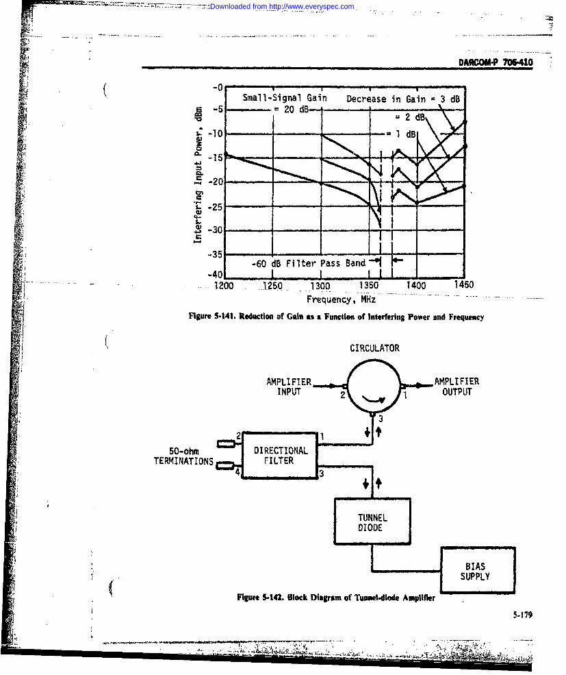
' AOM-P 70r,410 •. . .. . ---0"__r.
. .
Small-Signal Gain Decrease in Gain 3 dB-5 20 dB- ---..N
2 dB
S-30 ... 1dB
u:id -eaass . -14J -30-35
-- 60
-40 -- I1F . 1200 1300 1350 1400 1450
Frequency, MHz
Figure 5-141. Reduction of Gain as a Function of Interfering Power and Frequency
CIRCULATOR
. APL IFI ER AMPL IF IERINPUT 21 OUTPUT
3
50-ohm DIRECTIONALTERMINATIONS FILTER 3
,t [ TUNNEL
i DIODE
.BIAS
Figure 5.142. Block Diagram of Tunnel-diode Amplifier
5-179
• ,,, . :, , . .. - ,. - " - - -. - .- .",,, , . .. . .. . .- 4,.. -, , • . } . .
Downloaded from http://www.everyspec.com

DARCOM-P 706-410-
C COMPOSITE
,-.D1 D2
02
Figure .143. Method for Extending Tunnel-diode Dynamic Range Using Inverted Pairs
I i
-1 d11
AA o" -
-45 -40 -35 -30 -25 -20
INPUT SIGNAL LEVEL, dBm
Figure 5-144. Suluration Characteristics of Tunnel-diode Amplifiers
In critical cases the leakage can be controlled by wave ranges. For use at microwave frequencies, it isproperly designed gaskets (see par. 4-6.5.4). common to use double-braided cable where flexibil-
Flexible coaxial cables in which the outer conduc- ity is a requirement.tor is made of metal braid is subject to leakage at the Within device cabinets it is common to use micro-crossovers of the braid wires. Few data are available strip which consists of a single ribbon conductor laidon the magnitude of this leakage in the microwave over a "ground" plane and insulated by means of arange, but the theory of such leakage is discussed in flat dielectric. In such a structure the major portionpar. 3-3.1.1.2.5.2, along with some limited expe- of the energy, up to at least 90%, flows in the regionrimental data on transfer impedance in the micro- directly under the ribbon conductor. The remainder
5-180
A A . - - .
Downloaded from http://www.everyspec.com
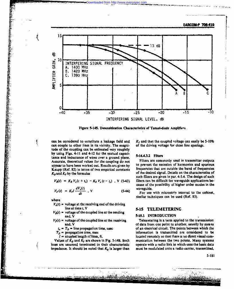
DARI=OP7*4O
• ; 15
INTERFERING SIGNAL FREQUENCYA. 1400 MHz
Cr B. 1420 MHzS C. 1390 M4Hz-
- ,
.";.A B C
. -40 -35 -30 -25 -20 -1 5 -10
:..- INTERFERING SIGNAL LEVEL, dB
ki{ Figure 5-145. Desensitization Characteristieg of Tunnel-diode Amplifiers
can be considered to constitute a leakage field and KF and that the coupled voltage can easily be 5-10%can couple to other lines in its vicinity. The magni- of the driving voltage for close line spacings.tude of the coupling can be estimated very roughtlyby using Figs. 4.11 and 4-12 for the mutual capaci-.tance and inductance of wires over a ground plane. 5-1443.2 FittersAccurate, theoretical values for the coupling do not Filters are commonly used in transmitter outputsappear to have been worked out. Results arc given by to prevent the emission of harmonics and spuriousKaupp (Ref. 82) in terms of two empirical constants frequencies that are outside the band of frequenciesK9 and K, by the formulas of the desired signal. Details on the characteristics of
such filters are given in par. 4-5.4. The design of suchVa(f) Ka V. (t + t.) - KB V. (f - to) , V (5-43) filters can be difficult for waveguide applications be-
cause of the possibility of higher order modes in the() 1 (44 waveguide.d V (4) For use with microstrip internal to the cabinet,
wsimilar techniques can be used (Ref. 83).where
Vo(t) - voltage at the receiving end of the drivingline at time t, V 5-15 TELEMETERING
VB,() - voltage of the coupled line at the sending 515.1 INTRODUCTIONend, V -,1NTOUT N,
V(t) = voltage of the coupled line at the receiving Telemetering is a term applied to the transmissionend, V of data from one point to another, usually by means
t. - TD - line propagation time, niec of an electrical circuit. The points between which theTD - propagation time, nsec information is transmitted are considered to be
I - coupled length of lines, ft. located remotely so that there is iao direct visual com-Values of Ks and KF are shown in Fig. 5-148. Both munication between the two points. Many systems
lines are assumed terminated in their characteristic operate with a radio link in which case the basic dataimpedance. It should be noted that K, is larger than must be modulated onto a radio carrier, transmitted,
5-181
. . . . . . . . . . . . . . . .. . . _. ,,,. . =.. , .. , !, . . ' .. . . ,., ..-. , , .. '.-. ,-'
.€ .:
Downloaded from http://www.everyspec.com

DARCOM-P 706410
_ _
CDI -1
QC J
to-
'4-
.40
CDC
C~C
5-182
§ 77TW-11- '>7
Downloaded from http://www.everyspec.com

DWOM M 7o64
- --- 13 dB- -0
dU- ____ _ __ ___10
100
NNII(144-
00
-4 -40 -35 -30 -25 -20
Sum of Desired and Interfering Sign-l Levels"=at the Diode, dm
Figure 5-147. Summary of Interference Characteristics of Tunnel-diode Amplifier
detected, and then coupled to an output device or in- e. Radio transmitterdicator, A general diagram for a telemetering system f. Radio receiveris shown in Fig. 5.149 (Ref. 84). Most telemetry sys- g. Power supplies.terns operate with a commutator so that various Interference from the radio transmite- and receiverkinds of data can be multiplexed onto a single is of the type discussed in Ref. 85 and in pars. 5-7 andchannel. A corresponding commutation system must 5-8, and will not be further discussed here. Brush arc-be used at the receiver in order to separate the in- ing is discussed in par. 5-1 and power supplies in par.formation into the various output channels. In some 5-5. Interference from the subcarrier oscillator is alsocases, the transducers will be followed directly by similar to that from a receiver local oscillator, thesignal-conditioners which convert the signal from the only difference being that the subcarrier oscillatortransducer into a form more suitable for modulation frequency may be lower than that used with mostof the subcarrier oscillators. receivers and transmitters. Interference can be both
The sensors of transducers can be of various types radiated and conducted, and is controlled in the sameas shown in Table 5-17. fundamental ways.
Interference from the transducers can occur onlywhere a voltage or current bias is required. For exam-
5-15.2 INTERFERENCE SOURCES pie, a variable resistance transducer will have either aTelemetering equipment can produce interference direct current or alternating curl ent impressed upon
from the following: it. If the effective loop area of the circuit in the vi-a. Bias supply on a passive transducer cinity of a transducer is large, the transducer itself is ab. Subcarrier oscillator potential source of interference to other transducersc. Commutator or devices located close to it. Correspondingly, ad. Brush arcing of commutator drive motor variable conductance, differential transformer, or
5-183
Downloaded from http://www.everyspec.com
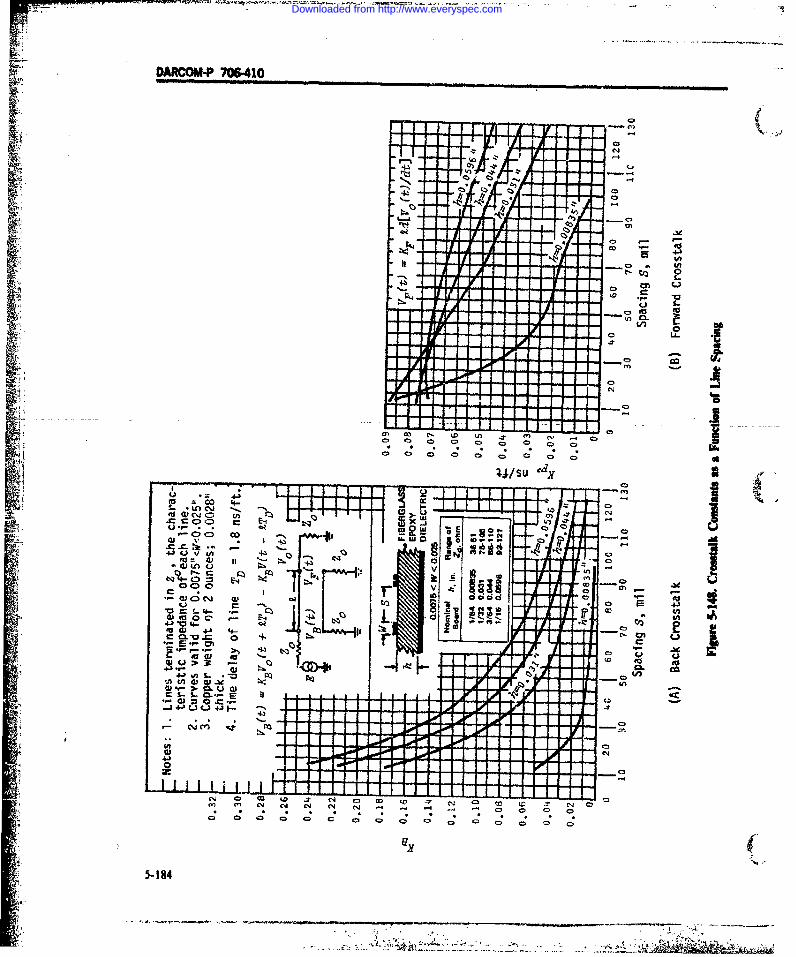
DARcOD-P 706-410
C5C
4,0
4a cm
70 9 Ie
C CC
cn,
N co ~ ± (J ~ ~
U u41 0
5-1CD
v * , . *i
Downloaded from http://www.everyspec.com

- -- - --- -- AROM- P 1706410
V. TRNSDUCOSCILLATOR
TRANSDUCERBCRREOSCILLATOR
FILTER
ANDTR SMTEMODULATOR
TRANSDUCER CMMTAO OCILAO
SUSUBCAIRRIDISCRIMINATOR PASSTTO
OSCIFILTER
BAND- SUBCARRIER. PASSRECEIVER PASS DISCRIMINATOR PILTE
FILTER FLE
MAGNETIC LOW-TAPE SUBCARRIER PASS
RECORDER DISCRIMINATOR FILTER
(B) Recf. !er Block Diagram
Figure 5-149. FM-FM Telemetry System (Ref. 75)
5-18
Downloaded from http://www.everyspec.com

DAR(O= -P 70641O
TABLE 5-17. ACTIVE AND PASSIVE TRANSDUCERS
Active Passive(voltage. or current- (variable-parameter
generating transducers) transducers)
I. Piezoelectric I. Variable resistance2. Photoelectric a. Nonmechanical resistance change3. Thermoelectric b. Change in internal structure4. Magnetoelectric c. Mechanically variable resistance5. Electronic 2. Variable capacitance6. Electrochemical 3. Variable inductance7. Radioactive 4. Differential transformer
5. Magnetostrictive
magnetostrictive type of device can produce signifi- to the type of modulation. It is common to use pulsecant levels of magnetic fields in their vicinity and duration modulation, pulse-width modulation, pulse-again can couple into closely located circuits. Gener- position modulation, pulse-code modulation, andally, the magnitudes of such fields will be low and pulse-amplitude modulation. Each of these has its
. with- a reasonable amount of-care they can be elim- own special performance crimriw(Ref..84). To the ex-_inated as significant sources of interference, tent that they are forms of analog or digital data
The commutator can be of either electronic or me- transmission, the performance as a function of sig-chanical type. The mechanical type may require rela- nal-to-noise ratio can be presented in standard form,tively large loop areas for the circuit connections to The most susceptible circuits in these systems arethe commutator segments and thus are capable of ra- those associated with the sensory element and the $diating magnetic fields. However, the current levels at radio receiver input circuit since these operate at the ,.which such commutators usually operate is low and lowest levels. For some of the sensing elements,unlikely to cause significant levels of interference a- operation can occur at relatively high signal levels,pecially at frequencies in the 10 kHz range. thus eliminating this as a potential source of system
Variations in contact resistance can produce un- degradation; however, in cases where the desire is todesired transients in the data circuits themselves, minimize weight such elements may operate atFundamentally, this is a circuit design problem and relatively low levels. The electrical connection to thenot a problem in electromagnetic compatibility, sensor may be either balanced or unbalanced, theMeasurements of ac generated noise may be in the latter with a ground return as part of the sensor cir-region of 10 to 15 mV. The same magnitude can be cuit. With the balanced circuit, the most sensitiveexpected in changes in dc level from one circuit to the part of the system will be that in the immediate vi-next. cinity of the sensor or in terminal boxes, since it is in
With the electronic switching technique, semicon- these regions that the two conductor pairs are likelyducting elements are pulsed in sequence to provide a to be separated with the largest spacing. The sus-conducting path for each channel in its turn, Rates of ceptibility can be computed easily based upon the ef-commutation may be in the megahertz range. Such fective loop area. If the system is unbalanced, thenfrequencies can produce radiation in a broad fre- the entire region between the sensor and the signalquency range, especially considering that rectangu- conditioner, if it exists, or the subcarrier oscillator orlar shaped waveforms are used. Again, the voltage commutator could be susceptible to currents in thelevels required are relatively small so that it should be ground planes or common-mode currents in nearbypossible to provide adequate shielding and filtering to wiring. Here, again, the susceptibility can be esti-prevent significant interference, mated directly in terms of models of wire lines as
presented in par. 3-3.1.1.6-15.3 SUSCEPTIBILITY
The radio circuits associated with telemetry are 5-15.4 CONTROL TECHNIQUESsusceptible in the same way as the radio circuits dis- The principal methods of interference coupling are 4cussed in par. 5-7. Special consideration may be given through common impedance in the ground circuit,
5-186
," .- L A. i
Downloaded from http://www.everyspec.com

DARCOM-P 706-410
magi.,.tic field coupling, antenna-to-antenna cou- factured by Dodge Corporation-For TACOM.
piing, and RF pickup in transducer leads if long (> Warren, MI, SSCO Standards Laboratory,20 ft) and exposed to nearby transmitter fields. In the Detroit, MI 48237, May 1974.latter cae shields grounded at both ends may be 12. R.F Interference Test Measurements on Truckrequired, otherwise such shields are grounded at only XM861 Manufactured by Jeep Corporation-Forone end to prevent coupling through "ground loops". TA COM. Warren. Michigan, Report NO. 7401-
Another method of reducing susceptibility to RF 7697, SSCO Standards Laboratory, Detroit, MIfields is by placing filters in the signal corditioning or 48237.commutating circuits. Such filters are most effective 13. TM 1-483, T031-3-9, Radio Interference Sup-where the data rates to be transmitted are low. presslon, Dept. of Army and Dept. of Air Force,
It is sometimes necessary to place a transducer or Washington, DC, October 1956.cable near a source of a strong magnetic field such as 14. Radio Interference Suppression Techniques, Sup,a motor or solenoid. Magnetic shielding material can pression and General Engineering Branch, Colesbe used to provide the necessary isolation. Signal Laboratory, Ft. Monmouth, NJ, Nov-
ember 1953.REFERENCES 15, Electromagnetic Interference (EMI) Investiga-
tions of the GOER Material Handling Crane, US1. W. D. Hayter, "High Voltage Nanosecond Army Electronics Command, Interference Con-
Duration Power Line Transients", 10th Tri-Ser- troi Branch, AMSEL-GG-SI, September 1975.vice Conference on Electromagnetic Compati- 16. F. Haber, K. H. Dolle, R. M. Showers, EMCbilly, lIT Research Institute, Chicago, IL, Data Collection Techniques, Rome Air Develop-November 1964, pp. 729-778. ment Center Report RADC-TR-69-181, June
2. Interference Produced by Corona Effect of Elec- 1969. Univ. of Pa.iic Systems. report prepared by-CIGRE (Inter- 17. E. J. Baghdady. Lectures on Communication Sys-national Conference on Large Electrical Systems) tems Theory, McGraw4ill Boik Co., 1971:Study Committee 36, Paris, 1974. 18. E. E. Donaldson and R. W. Moss, Study of
3 S. Takeshita, "Scattering of VHF and UHF Receiver Mixer Chcracteristics. Final Report,Radio Waves from Extra-High Voltage Power Contract DA 28-043-AMC-01426(E), GeorgiaTransmission Lines", 1970 IEEE International Inst. of Tech., September 1966. iSympoium on EMC, IEEE 70C28-EMC, pp. 19. Interference Notebook, Rome Air Development217-227. Center Report RADC-TR-66-1, Section IV, June
4. H. A. Gauper, Jr., J. D. Harnden, Jr., and A. M. 1966.McQuarrie, "Power Supply Aspects of Semicon- 20. Systems Component Electromagnetic Compati-ductor Equipment", IEEE Spectrum, Oct. 1971. bility, Naval Electronic Systems Command, Con-
S. Silicon Controlled Rectifier Manual, General tract NOOO39-69-C-0544, Moore School ofElectric Co., Electronics Park, Syracuse. NY, 4th Electrical Engineering Report NO. 70-22, 19Ed., 1967. March 1970; Report No. 70-14, 31 December
6. W. Elcnbaas, Ed., Fluorescent Lamps and 1970; Report 71-28, 30 June 1971, Univ. of Pa.Lighting, MacMillan Company, NY, 1959. 21. G. G. Sundberg, Millimeter Wave System Flec-
7. International Electronics Engineering, Inc., In- tromagnetic Compatibility Study, Quarterlyterfernce from Fluorescent Lighting Fixtures Report, ECOM-0171-1, Contract DAAB07-74-Aboard MSO and MSC Class Minesweepers, C-0171, June 1974.Washington, DC, 3 October 1956, lEE Report 22. S. Okamura, "Guided Millimeter-Wave Trans-No. 6020. Contract NObsr 71500, Task 7. mission System Components". Microwave Jour-
8. Design Guide for EMI Reduction in Power nal, December 1975, pp. 33-36.Supplies, Military Handbook, Naval Electronics 23. G. G. Sundberg and R. F. Marsolais, MillimeterSystems Command. (Draft document). Wave Systems Electromagnetic Compatibility
9. AMCP 706-360, Engineering Design Hand- Study, Final Report ECOM-0171-F, Contractbook, Miitary Vehicle Electrical Systems. DAAB07-74-C-0171, April 1975.
10. AMCP 706-235, Ereineering Design Hand- 24. D. D. Baxter, J. L. Wilson and J. F. Lecain, Dii-book, Hardening Wapon Systems Against RF tal Equipment Susceptibility, Final Report, Con-Energy. tract DAAB07-71-C-00i3, Martin-Marietta
It. Supplement to Report 7404-7904, R.F. lnterfer- Corp., Orlando, FL, Report No. ECOM-ODI 3-F,ence Test Measwurments on Truck XM861 Manu- August 1972.
- 5-187
[ ' ..
Downloaded from http://www.everyspec.com

DARCOM.P 706410
25. Transmission Systems for Communications, by 41. R. M. Scudder and W. H, Sheppard, "AN/SPY-
Bell Telephone Laboratories Technical Staff, 1 Phased-Array Antenna", Microwave Journal,I Western Electric Co., Winston Salem, NC, 4th Vol. 17, No. 5, May 1974, pp. 51-55.Ed. 1970. 42. R. C. Durham, "Electromagnetic Compatibility
26. J. C. Toler, L. D. Holland, and R. W. Moss, Ad- Measurements of Digital Phased Array Ra-vanced Measurement Techniques Study for Digi- dars", prcsentad at 1975 Symposium on Electro-tal Systems, Final Report ECOM-0278-F, magnetic Compatibility, Montreux, Switzeriand,Georgia Inst. of Tech., Atlanta, GA, December 1975.1972 43. Sylvania Electric Products, Inc., Point Contact
27. M. Schwartz, Information Transmission, Modu- Burnout Microwave Diodes, SM 1937-S.lation, and Noise, McGraw-Hill Book Co. 44. S. Silver, Microwave Antenna Theory and Design,
28. Win. Firestone, A. MacDonald, and H. Magnu- MIT Rad. Lab. Series, Vol. 12, McGraw-Hill.ski, "Modulation Sideband Splatter of VHF and 1949.UHF Transmitters", Proc. National Electronics 45. R. Berkowitz, Modern Radar, John Wiley andConference, October 4-6, 1954, Vol. 10, pp. 264- Sons, 1965.273, Feb. 1955. 46. L. D. Smullin and C. G. Montgomery, Micro.
29. J. G. Arnold, "Predicting Spurious Transmitter wave Duplexers, MIT Rad. Lab. Series, Vol. 14,Signals", Electronics, Vol. 34, No. 16, p. 68, 21 McGraw-Hill, 1948.
. April 1961. 47. V. G. Plank, "Radar Echoics from the Atmos-
30. 0. M. Salati, "Recent Developments in Interfer- phere", Radargrammetry (D. Levine), p. 222-243,ence", IRE Trans. on Radio Frequency interfer- McGraw-Hill, 1960.ence, Vol. RF1-4, No. 2, pp. 24-33, May 1962. 48. R. C. Johnson, "Mutual Gain of Radar Search
31. E. L. Gintzon, Microwave Measurements, Antennas", Proc. Ninth Trl-Service Conf. onMcGraw-Hill, NY, 1957. EMC, lIT Rrsearch Inst., Chicago, IL, 1963, pp.
32. K. Tomiyasu, "On Spurious Outputs from High 368-380.Power Pulsed Microwave Tubes and Their Con- 49. K. G. Shepherd, "Suppression cf Radar Inter-
j; trol", IRE Trans. on Microwave Theory and Tech- ference", Dec. 13, 1965 Summer Ses4lon in EMC.niques, Vol. MTT 9, No. 6, pp. 480-484, Vol. 2, Sylvania Electronic Products, Inc.,November 1961. Waltham, MA.
33. E. D. Silside, "Intermodulation Distortion in 50. J. G. Brainerd, Ed., Ultra-High Frequency Tech-Multicarrier FM Systems", iEEE Cony. Record, niques, D. Van Nostrand Co., Inc. NY, 1942.Part II, 1965, pp. 130-146. 51. C. Polk, "Propagation and Antenna Considera-
34. D. E. Cridland, "Microwave Radio-Relay Links: tions in the Prediction of Man-Made Interfer-The Effects of Spurious Emissions from High- ence", Proc. 1st Conf, on Interference Reduction,Powered Radars", Post Office Electrical Engi- Chicago, IL, December 1954, ASTIA AD-76686,neer Journal (U.K.), July 1969, pp. 80-83. pp. 330-352.
35. Handbook on Electrical Filters: Synthesis, De- 52. E. I. Hawthorne, et al., System Interferencesign and Application, White Electromagnetics, Evaluation, 2nd Quarterly Progress Report, Uni-Inc., 1963, Rockville, M D. vari of 2nd syuvanir , Mogres Report
36. J. S. Smith and N. H. Shepherd, "The Gaussian versity of Pennsylvania, Moore School Report
Curve-Transmitter Noise Limits Spectrum Uti- No. 54-23, 10 January 1954. ASTIA AD-29723.
lization", Proc. of Unclassified Sessions of the 53. C. Polk, et al., System Interference Evaluation,Symposium on Electromagnetic Interference, US 4th Quarterly Progress Report, Moore SchoolArmy Signal Corps, Research and Development Renort 54-49, Univ. of Pa., July 1954.Laboratory, Ft. Monmouth, NJ, pp. 138-144, 15 54. H. J. Reich, et al., Very-High Frequency Tech-June 1958. niques, Vol. 1, McGraw-Hill Book Co., NY,
37. F. E. Terman, Radio Engineers' Handbook, 1947.McGraw-Hill, NY, 1943. 55. C. Polk, "Analytical and Experimental Investi-
38. M. I. Skolnik, Radar Handbook, McGraw-Hill, gation of Wide-Angle, Finite Length, Biconical1970. Electromagnetic Radiators", University of Penn-
39. MIL-STD469, Radar Engineering Design Re- sylvania Master's Thesis, 1953.quirements, Electromagnetic Compatibility. 56. A. Anne, "Study of the Fresnel-Zone Field of a
40. A. Papoulis, The Fourier Integral and its Appli- Horn Antenna", University of Pennsylvaniacations, McGraw-Hill, 1962. Master's Thesis, 1960.
5-188
, ': ... ..:.. .. : . . . - .. ..
Downloaded from http://www.everyspec.com

DARCOM'P 706410
57. H. E. Curtis, "Interference between Satellite Investigation, Phase II, 1974, Contract N00178-Communication Systems and Common Carrier 73-C-0362 for US Naval Weapons Lab.,Surface Systems", Bell System Technical Jour- Dahligren, VA.nal, Vol. 41, No. 3, May 1962, pp. 921-943. 73. COS/MOS Digital Integrated Circuits, RCA
58. R. W. Friis, and A. S. May, "A New Broadband Solid State '74 Databook Series, SSD-203B.Microwave Antenna System", AIEE Trans., Pt. 74. Instrument Society of America (ISA) Standard1, V. 77, 1958, p. 97 (AIEE Trans. Paper 58-185). ISA-S50.1, 1975, Compatibility of Analog Sig-
59. R. C. Hansen. Microwave Scanning Antennas, nals for Electronic Industrial Process Instru-Vol. 1, Academic Press, 1964. melts.
60. E. Jacobs, "Fresnel Region Patterns and Gain 75. J, A. Harder, R. L. Powers, "Radio InterferenceCorrections of Large Rectangular Antennas", and Susceptibility Study of a Solid-State DigitalFifth Conf. on Radio Interference Reduction and Computer Model", Proc. 6th Conf. on Radio In-Electronic Compatibility, sponsored by US Army terference Reduction and Electronic Compati-Signal Res. and Dev. Lab. at Armour Research bility, Armour Research Foundation, OctoberFoundation, October 1959, pp. 499-525. 1960, pp. 194-215.
61. R. D. Hudson, Jr., Infrared System Engineering, 76. N. Taylor, D. Posklensky, "Radio Interference1969, John Wiley and Sons, Inc. Testing of Large-Scale Computing Systems",
2 62. W. L. Wolfe, Ed., Handbook of Military Infrared Proc. 51h Armour Conf on Radio InterferenceTechnology, 1965, Office of Naval Research, Reduction and Electronic Compatibility, OctoberDept. of the Navy, Washington, DC. (available 1959, pp. 355-381.from Supt. of Documents, US Government 77. W. W. Everett, Jr. Ed., Topics In IntersystemPrinting Office). Electromagnetic Compatibility, Holt, Rinehart, &
63. J. A. M. Lyon, et al." "Interference-Reduction - Winston. Inc, 1972.Methods for Antennas on Aerospace Vehicles", .18. S. M. Sze, Physics of Semiconductor Devices,.
4 Electromagnetic Compatibility Symposium Rec- John Wiley and Sons, 1969.ord, IEEE 27C80, July 1967. 79. S' Becker, et al., Final Report on Interference
64. Interference Control Design-Airplane Wiring Analysis of New Components and Circuit Tech.and Installations, Doc. No. D6-5247, 3 Nov. nlques, Airborne Inst. Labs., Deer Park, L.I.,1960, Boeing Airplane Co., Renton, WA. May 1962, RADC-TDR-62-221.
65. Wiring Techniques for EM! Control in Advanced 80. D. H. White, Long Range Communications Inter.Airplanes, Doc. No. D6A 10478-1, The Boeing ference Study: Technical Note on Parametric Am-Co., Renton, WA, 14 July 1967. plifler Interference Susceptibility Study, Melpar,
66. B. C. Toth, "Systems Analysis of Interference Inc., November 1962, RADC-TDR-62-360, Vol.Due to Coupling in Aircraft Cabling", Thesis, II.Moore School of Elec. Eng., University of Penn- 81. Reference Data for Radio Engineers, 5th Editionsylvania, August 1968. 1968, Howard W. Sams and Co., Inc.
67. M. Kayton and W. R. Fried, Avionics Navigation 82. H. R. Kaupp, "Effects of Embedding Micro-Systems, John Wiley and Sons, Inc., NY, 1969. strip Interconnections", Unpublished menoran-
69. Rt. H. Parvin, Inertial Navigation, D. Van dum, Feb. 1969, Camden Engineering, Informa-Nostrand Co., Inc., Princeton, NJ, 1962. tion Syst. Div.
69. S. Osder and D. LeFebre, "Fiber Optics and 83.n A D.
Flight Control Systems", 1974 IEEE Electro- 83. D. D. Grieg and H. F. Engelmanns, "Microstripmagnetic Compatibility Symposium Record, July - A Now Transmission Technique for the Kilo-1974, IEEE 74CHO03-7EMC. megacycle Range", Proc. IRE, Vol, 40, pp. 1644-
70. Electromagnetic Compatibility Specification 1663, December 1952.Standard for Aerospace G(ound Equipment, 84. Elliot L. Gruenberg, Ed., Handbook of Telem-GSFC S-523-P-7, Nov. 17, 1967, Goddard Space etry and Remote Control, McGraw-Hill, Inc.Flight Center. 1967.
71. W. W. Cowles and R, M. Showers, Integrated 85. R. Bruce, et al., An Investigation of Tracking. Te-Solid State Circuit EMI Susceptibility Investiga- lemetry, and Command Systems Susceptibility totion, AFAL-TR-67-341, 31 Jan. 1968, Univ. of Radio Interference, Electronic Warfare and Con-Pa., Moore School Report NO. 68-32. munications Laboratory, Aeronautical Systems
72. McDonnell Douglas Astronautics Co., East, Div., Air Force Systems Command, WPAFB,Integrated Circuit Electromagnetic Susceptibl!ity OH, 6 March 1964.
5-189
. -.., • ; : '. , . . . . . ,, -.
Downloaded from http://www.everyspec.com

r OARCOM-P 706-410
CHAPTER 6
SYSTEMATIC PREDICTION AND ANALYSIS
6-0 LIST OF SYMBOLSCW - continuous wave
A - parameter in shielding factor D = directivity of power radiated byequation, m- wire
A, = maximum effective aperture, ml D-j distance of susceptor from gener-A, - 0.32all ator wire for radiation coupling;
A LS - antenna lobe selection separation between antennas iA NT LB - antenna lobe andj, m
AS - s fnsitivity level of susceptorJ, V D, reciprocal square of first resonantA$j = total tolerable input of a frequency of generator wire and its
susceptorj to interference from shield, s'priority No. 2 generators, V d - conductor separation; distance to
a(fd) - power attenuation function image in ground plane; propa-a, - height of wire I above ground gation distance, m; reference dis-
- plane, m tance-
a,,2 = height of wire 2 above ground du - separation between wires I andj,plane, m m
a r - adjustment safety margin d12 - spacing between wires I and 2, mB - magnetic flux density, Wb/ml; - electric field strength, V/m
factor in magnetic field con- (FH)R - highest frequency to which re-version equation ceiver can be tuned, Hz
8B, B. - lower and upper limits, respec- (FHJr - highest frequency to which trans-tively, of receiver band pass, Hz mitter can be-tuned, Hz
B1 - constant in electric field A,,- propagation factor for fieldconversion, m-' through holes of shield
- constant in electric field (FL)R - lowest frequency to which re-conversion, in-' s- ceiver can be tuned, Hz
B3 - constant in electric field con- (FL)T - lowest frequency to which trans-version, rn's -1 /2 mitter can be tuned, Hz
84 - nondimensional f - frequency, Hz; reference fre-C, - shunt capacity to grouid, F quency, Hz; tuned frequency of
CL2 - lumped and distributed capaci- receiver or transmitter, MHztance to ground for wire 2, F £ base frequency; crystal fre-
C z - capacitance between wire 2 and quency, Hzand the shield of wire I, F A - interfering transmitter frequency,
Cr - total capacitance to ground. F HzC - coupling capacitance between - intermediate frequency, Hz
wire I and its shield, F fLo - local oscillator frequency, HzC.,,2 - wire-to-wire capacitance between - receiver tuned frequency, Hz
generator circuit and susceptor - frequency of spurious emission,circuit, F Hz
Cw2c - wire-to-around capacitance, F - transmitter tuned frequency, HzCi .. .Cs - constants in propagation for- (MHz where noted)
mula, dimensionless flf2 - interfering frequencies, HzCEAR - Comparative EMI Analysis G - generator circuit
Routine Gd - directive gain of dipole, dB
6-1
: t . ;
Downloaded from http://www.everyspec.com

DARCOMP 706410
GAf) magnitude of generator i circuit KHD - H-field fall-off exponentoutput Fourier spectrum, V/Hz k - width of guard band, Hz
G, = receiving antenna gain, dB Lf= off-frequency rejection, dB; band-G, - transmitting antenna gain, dB width mismatch loss, dB
G, - directive gain Lp = propagation path loss betweenGM - mean antenna coupling between transmitter and receiver, dB
transmitter and receiver, dB L1 - self-inductance of shield aroundGMA - mutual antenna gain, dB wire 1, H
GRI - main beam gain of susceptor an- L2 = self-inductance of circuit 2, Htenna, dB LPROP = path loss between antennas, dB;
GTI - main beam gain of transmitting path loss to receiver, dE
antenna, dB wire length, mg(ff) receiver power selectivity func- 1,, - length of wire i, m
lion for tuned frequency 1,2l~a = length of wire 2, mH - magnetic field strength, A/m 112 = common length of wires I and 2,
HAR - harmonic level, dBm mh ff) transmitter power spectral densi- M- mutual inductance of two cir-
ty function at tuned frequency cults, H; mean ratio of expectedf,,W/Hz signal and threshold level
h" desired portion of transmitter m = harmonic number from trans-power spectral density function, mitterW/Hz N - roll-off rate exponent, total re-
i 1 current-in generator wire, A; -ceiver noise power, dBWcurrent in wire I, A n - total noise power, W
IN, , net current, in generator wire I P - interference margin, dBWplus return current in its shield, A Pp - power density, W/ml or d~m/m
IL - received interference level, dB Pd - incident power density, dBW/m-11 - current induced into wire I shield, P, - probability of failure due to inter.
A ferenceINR - receiver output interference to PA f) - magnitude of the voltage transfer
noise ratio, dB function describing the frequencyINT MARGIN - receiver interference level relative response of susceptorJ, dimen-
to receiver interference threshold, sionlessdB Peieprobability of failure due to noise
IPR Initial Processing Routine P. - probability of successful opera-ISF - Intrasystem File tion
J factor which describes what frac- P, = transmitter output; interferingtion of the system specification transmitter power, dBW (excepteach subsystem will be allowed to where noted)generate Pl = power. Wvoltage induced in susceptor mP - desired output of transmitter,KAES votg10dcdi setrP l eiro tpu oftB nmWtrE-field at susceptor antenna 10 log pl, dBW
voltage induced in susceptor PCT0 VLA P percentage of receiver tuningKA H- ,'m range overlap
H-field at susceptor antenna PLO - local oscillator power present at
KE - voltage to E-field transfer func- antenna terminals of interferingtion for antenna source, mi- receiver, dBm
KE* - voltage to E-field transfer func- POP - power output, peak, kWtion for wire source, m- I p - oscillator harmonic number
KED - E-field fall-off exponent p, - desired output of transmitter, WKH - current to H-field transfer func- q - signal harmonic number
tion for antenna source, m R - signal-to-noise ratio, dBKH* = current to H-field transfer func- R.2 = parallel combination ofR, and
tion for wire source, m-' RL2, A
6-2
Downloaded from http://www.everyspec.com

DARCOM-P 706-410
Re source resistance of gener- SPSm - measured value of system per-ator circuit, t) formance scorc
Rs? - source resistance of susceptor cir- SPUR - receiver in-band spurious re-cut,sponse rejection, dB
Rj - susceptor circuitj SS - sidelobe of transmitter to sidelobeRLI - load resistance on generator wire of receiver
I'D 1(S/N)o - output signal-to-noise ratio, dBRL2 load resistance of susceptor cir- (S/ r)or - output signal-to-noise threshold
cuit, ai value, dBR dc resistance of wire I shield, Q [SI + N)]o - output signal-to-interference plus
R, radiation resistance, 11 noise ratio, dBR, - receiver sensitivity, dBW [S/(i+oN)Jor output signal-to-interference plus
Rj - resistance of the shield on wire 1, noise threshold value, dB0 s = signal power, W
R, - interference-to-noise ratio, dB T{ f) magnitude of the voltage transferRPS- relative performance score function from generator i to sus-
RSENS - receiver sensitivity or interference ceptorj, dimensionlessthreshold, dBm TART - task analysis routine
-. - frequency overlap ratio, dimen- TE - E-field to voltage transfer func-sionless tion for antenna receptor, m
rj - radius of shield 1, m TE* - E-field to voltage transfer func-.rj - radius of wire I m tion-for wire receptor, m -
=.radius of wire 2, m E-field at s eptor' S = low frequency shielding factor, TED use
dimensionless; signal level, W B-field at I i from genratr
= mean value of predicted distri- dimensionless /bution of S/l(+ N), where S TET field-to-voltage conveciion fac-signal, I = interference, and N tor, m
inoise, dB _ voltage induced insset
S = measured value of S/(I+N), TEV v t iu sceptorwhere S - signal, I - interference,and N = noise, BTH H-field to voltage transfer function
Ss, = parameter in H-field conversion for antenna receptor, f0-1m'pare ertion HfTH* = H-field to voltage transfer func-equationtinfrirreetr lm
Sn = twisting factor for wire I - frac- lion for wire receptor, 9-1m
tion of total current that returns THD = H-field at susceptorto generator by a path other than H-field at I m from generatorthe twisted return wire, dimen- dimensionlesssionless TIIT - H-field transfer function, Q -m
St2 twisting factor for wire 2 - frac-tion of total current that returns THV =voltage induced in susceptorto source end by a path other H-field at susceptor wirethan the twisted return wire, di- T! = inductive coupling current tomensionless voltage transfer function for close
S = total shielding factor coupled wires, 0SHL - spurious harmonic level TV - capacitive coupling voltage trans-
SIGMA G - standard deviation of the antenna fer function for close coupledgain product, dH wires, dimensionless
SIGMA P = standard deviation of path loss, t - shield thickness, mdB UPS - upper performance score
SGR - specification generation routine V - voltage induced on shield ofSPS - system performance source cable, VS7Y- mean SPS value for a specific bin V, = common-mode voltage, V
6-3
.. .. "."...
Downloaded from http://www.everyspec.com

I~ aplcto ofsyte pedctonan
DARCOM4P 706-410
V, voltage induced by generator i at An important application of system prediction anda reference point in circuit of sus- analysis is the determination of any special require-ceptorJ, V ments for individual systems. Trade-offs of physical
VN - voltage induced into wire pair as separation, shielding, and filtering against emissionresult of twisted loop area, V and susceptibility limits are frequently possible so
V, - generator voltage, V that EMC standard military requirements can beV2 = voltage appearing on susceptor "tailored" for a given configuration. Thus, comput-
wire, V ors can be programmed to develop a self-consistentX - parameter in shielding factor set of specifications for all equipments comprising
equation, m - any given configaration. In auother form they can ex.X, - frequency function in electric amine the consequences of granting waivers from the
field conversion equation standard limits.x = ratio of shield thickness i to field An important side benefit of automated analysis is
penetration depth 5, dimension- the ready availability of data stored in files for use inless analysis programs. Typical of such facilities are those
Z - common impedance (contained of the Electromagnetic Compatibility Analysis Cen-in the TI model), Q ter (ECAC) which are described in par. 6-4.4.
zo impedance in shielding factorequation, 0 6-2 PROCEDURES
6- - field penetration depth intoj shield, m; receiver bandwidth, Hz 6-2.1 GENERAL
6 - angle with respect to dipole axis; The basic logic of the large-scale EMC analysis...---direction of receiver relative to program typically proceeds as follows:
transmitter, rad a. A possible susceptor of EMI is-selected.X - wavelength, m b. A possible source of EMI to that susceptor is so-
po-permeability of free space lected.-. 4 X IV. H/m c. The EM Energy at the susceptor from the source
a standard deviation is determined over all possible coupling paths.4' = flux linking circuit in which V d. The process is repeated for all possible EMIis induced, Wb sources, and a decision is made of the extent to which/' \ - expcted value the susceptor performance is degraded." e e. The process is repeated for other susceptors of
interest. Computations are made by assigning quan-titative values to pertinent parameters which define
6-1 INTRODUCTION each source, susceptor and coupling path.Most electrical and electronic devices are used as Individual procedures will differ regarding which
parts of systems or subsystems that are sufficiently parameter values must be provided, and, according-complex that a large number of possible electromag- ly, the extent to which they use experimental or the-netic interactions are possible. The interactions can retical relationships; the types of source, receptor andtake place not only between antennas, but also inter- coupling path they can handle; and the accuracy oh-connecting cables and equipment cabinets, usually tained. The logic used to generate specification limitsconsidered on a pair-by-pair basis. Consequently, usually proceeds as follows:some organized procedure must be used in order to a. The tolerable interference threshold of a par-carry through a complete analysis. Various proce- ticular susceptor is identified.dures have been devised in accordance with the na- b. The unintentional or extraneous EM emissionsture of the interactions which are being considered, at the susceptor from all possible sources are com-
In order to carry out the detailed analysis, it may pared against the threshold.be convenient to use digital computer programs. Be- c. The emission limits of the sources or the con-cause of the specialized nature of most available pro- figuration parameters are adjusted to reduce the levelgrams, it is not possible to prescribe their use for gen- of signal in excess of this threshold or, where feasi-oral problem solving. They can be applied to those ble, the susceptibility limit of the susceptor is ad-problems for which they have been designed, but justed.their application to other problems must be ap- d. The process is repeated for other susceptors ofproached with caution. interest.
6-4
-' - .,. 7
Downloaded from http://www.everyspec.com

DARCOM-P 706410
From a problem processing-time standpoint, it is 6-2.4 STATISTICAL CONSIDERATIONScustomary to eliminate quickly any source/suscep- Many of the factors that influence whether or nottor combinations that obviously will not result in sys- interference will take place are time-dependent-tam degradation through a "culling" operation. It is such as coupling path loss variations, orientations ofcarried out by using very simple but conservative rep- scanning antennas, orientations and locations of mo-resentations of the emitters, coupling paths, and sus- bile equipment, and changes in equipment param- Liceptors involved. eters with time. Additional factors vary in a non-
time-dependent manner, such as changes in subsys-tern characteristics as a function of dial settings,
6-2.2 INTRASYSTEM VS INTERSYSTEM tuned frequency, or equipment serial number. Sys-1' EVALUATION tern analysis programs often take into account one or
The distinction between intrasystem and intersys- more of these effects.tern EMI evaluation is characterized most easily by The advantage of including statistical factors in anthe differences in coupling paths involved. Typically, EMC analysis is that a better understanding of thethe major paths dealt with in intersystem investiga- potential of interference can be provided. Thus, aI tions are those between antennas, especially those in conclusion that system degradation of a particularwhich the antennas are sufficiently far apart that ra- type can: occur 20% of the time, or in 40% of the cases, Mdiation field coupling calculations are made. is considerably more meaningful than to indicate
The major coupling paths for intrasystem EMI in- only that degradation van take place. However, sta-vestigations are between cables, between equipment tistical input desciptirins or data often are notcases, and between cables and cases. Common im- available.pedance effects, such as u.e of the power supply bus,or ground currents that couple from one circuit to 6-3 DATA FILESanother, also are considered. When coupling via an- In the application of a'w of these. techniques one oftennas is involved, it usually has to do with an anten- the most serious difficulties one experiances is hn get-
{ na illuminating a cable or case, or with antennas that iare in the near field of each other. ting adequate data on characteristics of equipment.
Usually design data - such as frequency range, sen-sitivity, type of modulation, and antenna gain - canbe obtained. For nondesign information such as oil6-2.3 NONLINEAR MODELING spurious emissions or susceptibility one usually must
Many effects of interference are due to the inher- rely on test data such as accumulated through the ap- ,:ent nonlinear characteristics of the source and sus- plication on MIL-STD-462 and MIL-STD-449.captor devices involved. Unfortunately, the param-cters that most strongly influence these nonlinear-ities are usually uncontrolled, and as a result cause 6-3.1 USAMSSAwide variations in EM effects. The C-E Branch, US Army Management Systems
The primary nonlinear system characteristics that Support Agency (USAMSSA), Washington, DC,are described in available analysis programs include: maintains an EMC data base primarily to support the
a. Harmonic and spurious emissions of emitters conduct of detailed EMC/EMI analyses; (Ref. 1)b. Spurious responses and desensitization effects in support from the EMC data base is available to any
susceptors military activity to aid in conceptual and/or Re-c. Intermodulation and cross modulation effects search and Development (R&D) projects. Some ofd. Signal processing through detectors. the data base files and their content are described in
The frequency translation effects of these nonlinear- the paragraphs that follow for a limited view of theitic; are describable using simple equations (for ex- type of data available for studies, plans, and pro-ample, see par. 3-2.2.2.1 for receiver spurious re. jects. Special retrievals and displays can be providedsponses and par. 3-2.2.2.2 for intermodulation), Ex- from each of these files.pressions for amplitude or power levels of nonlinear a. Tactical Deployment File. Large scale C-E de-outputs are much more complex and usually are ployments are developed and maintained to satisfyavoided in intrasystem EM models because they re- the analysis of C-E based problems related to de-quire a large amount of processing time. Instead, fined force structures. Deployments include C-Enonlinear effects are often treated using measured equipments for both firiendly and opposing forces.data. The deployments usually are centered around major
6-5
-. .C ..
:.. . ": ,~ , . . . .'.
Downloaded from http://www.everyspec.com

DARCOM-P 706-410
Army studies and provide the basic tool for analyz- lion type, frequency limits, and antenna polariza.ing the EMC implications of new equipments, or- tions.ganizations, and concepts. Deployments previously e. Antenna Characteristics File. The Antennadeveloped range in size from a complete the- Characteristics File (ACF) contains specific antennaater/Communication Zone operation to a separate data related to the production of deployment data.brigade. Once developed, deployments provide an Each antenna is described in relation to the type ofideal study base for determining the probable effect vehicles in which it can be mounted, antenna height,of introducing a new C-E component into a specified and the location on the vehicle when used with air-environment. The C-E deployments are maintained craft, etc. The purpose of the ACF is to reference the.And stored on magnetic tapes. Map overlays and vari- type of antenna used with the C-E equipments in theous narrative descriptions also are developed to sup- ECF and the EAuF.plement the magnetic tape. In addition to their use in f. Equipment Application File. The Equipmentdetailed analysis, the deployments contain a host of Application File (EAF) provides data on the use andstatistics relating to the tactical disposition of C-E purpose of the C-E equipment. Some examples ofequipments in a combat posture that can be useful in uses are mobile ground FM communications and airspecial projects. Examples of data that can be ex- ground communications.
tracted include: g. Frequency Allocation to Equipment File. The(1) Equipment densities in organizational units, Frequency Allocation to Equipment File (FAEF)
command posts, net types, vehicles, TOE's, frequen- contains all current frequency allocation and actions
cy bands, and modulation types issued by the Department of Defense Joint Frequen-(2) Other retrievals and displays: equipment distri- cy Panel. Each allocation for the Army, Navy, and
butions, frequency utilization data, net/frequency re- Air Force is entered into the FAEF record in Englishquirements, overlays, systems diagrams, and equip- with a maximum of ninety-five fields of information.ment characterists. This file is supported by two indexes. One ordered by
b. Equipment Authorization File. The Equipment frequency and one ordered by equipment nomencla-Authorization File (EAuF) contains information ture.normally derived from DA Tables of Organization h. Army Equipment Records File. The Armyand Equipment (TOE), US Air Force, and opposing Equipment Records File (AERF) is a consolidatedforce authorizations. Additional information is avail- equipment data base designed for retrieval of currentable to describe the normal netting associated with Army C-E equipment characteristics. It contains in-the C-E equipments. Each record in the EAuF has in- formation similar to that found in the FAEF but onlyformation on one C-E component. The equipment for Army C-E equipments. Some of the data found incomplement of each TOE is entered in the file, and this file are technical characteristics, phase in/phaseeach component of the major C-E equipment item is out, type classification, inventory objectives andassociated with an operator (equipment user, i.e., planned procurement quantities, equipment unitpilot, CO, XO, etc.). Vehicle types serving as C-E cost, line number, and Federal Stock Number. Thisplatforms (e.g., fixed, manpack, K-ton truck, and Ov- tile is also supported by two indexes, similar to theI D aircraft) also are entered in the file. FAEF.
c. Equipment Characteristics File. The EquipmentCharacteristics File (ECF) contains the nominal C-E 6-3.2 ECACequipment technical characteristics for each compo- The Electromagnetic Compatibility Analysis Cen-nent entered in the EAuF. The technical characteris- ter (ECAC) maintains a data base to support its worktics of de equipment are entered in the file as a func- in analysis and prediction, and as a service to DoDtion of the equipment application or operational (Ref. 2).mode. This file contains the component frequency To permit efficient control and usage in a wide va-range, emission type, antenna type, pulse data (if riety of applications, the data are organized into apulsed equipment), transmitter power output, etc. multiplicity of files and subfiles, namely:
d. Equipment Netting File. The Equipment Net- a. The Environmental File:ting File (ENF) is used to identify the various C-E The environmental file consists of many differentequipment net types typically associated with tacti- subfiles that pertain to the location and operatingcal military operations. A unique number is used to characteristics of communication and electronicidentify a discrete type net. The ENF carries the op- equipment. The principal use of environmental dataerational characteristics of the nets, such as modula- is to identify equipments in a given environment
6-6
Downloaded from http://www.everyspec.com

. ... ARC M-. 706410 fwhich are potential sources of interference to a pro- and NCF so that the technical characteristics ofposed victim receiver or which are susceptible to in- equipment referred to in the OPAF can be obtainedterference from a proposed transmitter. This infor- easily. If information concerning the specific ships ormation is used to assist the compatibility engineer in type of aircraft that may be operating in a geograph-such arcas as frequency assignment, planning, and ic area is available, the OPAF can be used to deter-site selection. mine the C-E equipment to be considered in an EMC
There are two types of environmental data files: Analysis. Table 6-2 lists the various OPAF subfiles.frequency oriented files and equipment oriented files, d. Spectrum Allocation and Use File (SAUF). TheFrequency files include records of frequency assign- SAUF is a file containing rules, regulations, andments made by the ITU, the FCC, the IRAC, and by agreements concerning the use of each allocated bandvarious elements of the DoD. Frequency files within in the frequency spectrum. Although some of the ma-
DoD constitute a consolidated system (Frequency jor allocation documents are readily available inResource Record System) which, is maintained by handbooks (e.g.. ITU Tables, US Government Ailo-
N ECAC. cation Tables, and FCC Tables) there are many ob-Equipment oriented files were developed for EMC scure documents that concern the use of the spec-
analysis activities at the Center. The major equip- trum both in the U.S. and in other areas of the world.ment oriented file (E-File) has been generated from The SAUF is an extract from these documents storeddata on DD Form 1374, Electronic Equipment Envi- in the computer so that all information concerning aronment Data Form. This form is no longer used by particular band and/or geographic area can readilythe Army. Instead, the Army collects corresponding be selected. Tables 6-3 through 6-5 list the docu-data on Frequency Assignment Request Form DA ments presently in the SAUF.2212. e. Topographic File:
-Examples of the types of information recorded in The topographic file consists of a grid of groundenvironmental files include equipment location, op- elevations extracted from -topographic- maps andcrating frequency, transmitter power, modulation stored in compressed form in the computer. The datatype, emission bandwidth, equipment nomenclature, are used to construct topographic profiles betweenand operating agency. Table 6-1 lists the various en- any two points of interest. Computer programs havevironmental data files. been developed to generate line-of-sight coverage
J b. The Nominal Characteristics File: overlays from the topographic file. This capability isThe Nominal Characteristics File (NCF) is com- referenced in the analysis section of this document.
posed of information regarding the technical charac- The topographic file is based on a spherical coor-teristics of communication-electronic equipments. dinate system and is designed to accommodate dataSuch items as transmitter power, receiver sensitivity, of variable grid spacing. The majority of the data hasbandwidths, antenna gain, antenna beamwidth, pulse a grid spacing of 30 s (this corresponds to approxi-width, pulse repetition frequency, and modulation mately 0.5 mi between data points).type are extracted from technical publications and f. The Frequency Allocation File:entered into the automated datu base via remote ter- One of ECAC's continuing tasks is to support theminals. Joint Frequency Panel (par. 2-6.4.3) in its frequency
In addition to containing equipment technical allocation mission. Support consists of a review ofcharacteristics, the NCF has information which re- each application for frequency allocation submittedlates individual receiver, transmitter, and antenna to the Joint Frequency Panel by the individual Mili-components to the systems of which they are a part. tary Services. The review process includes checks forWith this file, the compatibility engineer can identify consistency of the technical information, checks tothe technical characteristics of the individual trans- insure the application adheres to the national and in-mitters, receivers, and antennas, and, in addition, the ternational rules and agreements concerning usage ofcommunication-electronic systems, of which they are the frequency spectrum, and an evaluation of the pro-a part. posed equipment as a potential compatibility prob-
c. Organization and Platform Allowance File tem.(OPAF). The environmental data files (which are lo- Applications for a frequency allocation are sub-cation oriented) do not adequately accommodate mitted to the Joint Frequency Panel on DD Formmobile emitters on ships or aircraft. The OPAF was 1494, Application for Frequency Allocation, whichestablished to identify the C-E equipment comple- provides room for 109 fields of technical and admin-ment on ships, aircraft, missiles, satellites, and tacti- istrative information. Results of the deliberations ofcal ground units. Their is linkage between the OPAF the Joint Frequency Panel are announced in Action
6-7
Downloaded from http://www.everyspec.com

DARCOM-P 706410
TABLE 6-1.DESCRIPTION OF ENVIRONMENTAL DATA SUBFILES
UPDATE FREQUENCY COVERAGESUBFILE DESCRIPTION SCHEDULE BANDS, MHz ARFA AGENCIES FORMAT1374 Contains data on transmitters New data re- PrimarilyGov- US&P DOD 84 wordData and receivers at fixed locations ce.ived on eminent and AF-Europe FAA
obtained from reports made on continuing shared bandsDD-1374 forms. The instructions basison the form c-tclude reporting oftactical equipment and equip- Annual up-ment in operation less than six date of allmonths, such as experimental sys- data in fileterns. The Army is no longer pro.viding 1374 data.
NAVAIDS Contains data on TACAN, ILS, Monthly 0.2,0.415 US&P DOD 84 wordVOR, Glideslope, Beacons, Air from IFR 108-136 (VOR- FAA E-FiteGround Communications, and Handbook 225-400 TACAN FCCother Navigation Aids. Data are 960-1215 Worldwide)obtained from 1374 forms, fromthe IFR Handbook, from FCC Continuing
- Licenses. and any.other available input-from .. -
source. Although this file is often FCC Licensesconsidered part of the "E-File".it is not merely a file of 1374 re-ported data. . -
IFF Contains data on IFF ground in- Update from 1030 US&P DOD 84 wordterrogators obtained from DD 1374 file 1090 AF-Europe FAA E-File1374's and augmented with data every 3 FCCon tactical IFF systems from the monthsIRAC file and systems under de-velopment by industry from theFCC file. Additional data fieldshave been added which are need-ed to describe IFF systems. Thefile is maintained apart from thestandard E-File but records arelinked to the corresponding re-cords in the 1374 file.
Commer- Contains data which are extract- Weekly 890-960 US&P Non-Govt 84 wordcial Micro- ed from the FCC lienses for mi- 1850-1990 E-Filewave crowave communication stations. 2110-2200
This includes data on privately 2450-2690owned microwave stations uscd 3700-4200by industry as well as common 5925-6425carriers; however, data for the 6525-6875larg-st common carrier, the 10700-11700AT&T Corp.. are maintained 12200-12700separately in the AT&'[ file. Thisis considered part of Z-File.
AT&T The data in this file are obtained Semi- 3700-4200 US&P AT&T 28 worddirect from AT&T. It contains annually 5925-6425 E-Filehigh quality location and equip 11200-11700ment data. It does not containspecific operating frequency butdoes have the range of frequen-cies used on each link.
(cont'd)
6-8
Downloaded from http://www.everyspec.com

DARCOM-P 706410
TABLE 6-4 (Cont'd)
UPDATE FREQUENCY COVERAGESUBFILE DESCRIPTION SCHEDULE BANDS, MHz AREA AGENCIES FORMATFCC This is a file containing the fre- Semi- All Non-Go',t US&P Non-Govt 28 word
quency, power, emission and lo- annually Bands G-Filecation of all non-Government li-
censed emitters.!IRAC Tl~is is the Master Radio Fr- Monthly All Govt Primarily Govt CFEF
quency'File for Government Sta- bands US&P Agenciestions which constitutes the recordf " of frequency assignments ap-
proved by the Interdepartmen-tal Radio Advisory Committee(IkAC). This file is the onlysource of data on some of thenonmilitary government agencies.
ITU This is the record file of frequen- Semi- All bands Worldwide 28 wordcy assignments that have been annuallyregistered with the InternationalFrequency Registration Board(IFRB) of the International Tele-communications Union (ITU). "-Classified military usage of the
M spectrum is not in the ile.
CINCPAC These are frequency assignment Daily All bands As indicated *Ali US CFEF(Pacific) iles for the overseas commands. Message by subtile Military(Atlantic) They are the most reliable source InputCI SCAL of US Military environmental(Alaska) data outside of CONUS. Equip-CINC- ment data are available in vary,SOUTH ing degrees depending on the sub-(Panama) file.
' CINCEUR
(Europe)
AFC's6* These are frequency assignment As reed All bands Vicinity Determined CFEFWhite Sands files for the Area Frequency Co- (Data are of test by AFCAgizona ordinators (AFCs). They contain very current) rangesWestern reliable data in the vicinity of test indicatedEastern ranges for which the AFC's are by subfileGulf responsible.
*Although the "CINC Frequency Files" are primarily records of US Military uses of the spectrum, each command includes dataon nonmilitary operations in his area of responsibility (e.g., CINCAL includes FAA; CINCSOUTH includes PanamanianCivilian; CINCPAC includes Korean Civilian)." Area Frequency Coordinators
Memoranda which authorize, deny, or modify the al- ments, listings, and informal correspondence. Data inlocation request in some way. At this time, approxi- this "nonautomated" library category include:mately 4000 applications have been processed a. Spectrum signature reports that contain mas-through the Joint Frequency Panel and provide a ured data on the emission and reception characteris-source of ready reference information to the corupat- tics of selected C-E equipmentibility engineer. Key data elements from the DD
! / -" Form 1494 which are printed in the Frequency Allo- b Frequency allocation applcations (3-12 Appli-cation List (FAL) are stored in a file at ECAC. ca.ions) which are maintained in the ECAC Library
In addition to the automated files which have been c. Listings of data from Frequency Assignmentdescribed, there is a wealth of data available in docu- Files that are not in the automated data bast
6-9
. 7 -= - 7:.. ..... . ... *- -
Downloaded from http://www.everyspec.com

DARCOM-P 706-410
TABLE 6-2. ORGANIZATION AND PLATFORM ALLOWANCE FILES .
SUBFILES DESCRIPTION UPDATE SCHEDULE
WATER Contains data on the C-E equipment corn- Navy - Quarterlyplement on Navy and Coast Guard ships Coast Guard - Semiannuallyby type, class, hull number, and ship name. Army - SemiannuallyThe C-E complements are listed by systems Commercial Maritime - As required
~nomenclatures and do not include compo-
nents of systems unless the component isoperating independently from the system.The US Army watercraft are entered astypical C-E configurations by basic designnumber for each type of vessel. The file also. contains actual C-E configurations for
Commercial Dry Cargo and Tanker Mari-time ships operating under the US Flag.
AIR Contains Air Force, Army, Navy, and Ma- Air Force - Annuallyrine Corps Aircraft by Type/Model/Series Navy - Semiannuallyof aircraft together with their complete C-E Army - Deponds on availabil-configurations. Information as to what ity of publicationsequipments may be installed on specific tail Commercial Air Carrier - Annuallynumbers within a type/model/series of air-
' .. craft is not available. The file also containsthe quantities of the type/model/series ofaircraft in the present inventory for each 'Service. The file contains the Typical C-EConfiguration of Commercial Air CarrierType Aircraft by type, model, and manu-facturer. It does not contain informationon Air Carrier Aircraft manufactured byLockheed Corporation.
LAND Contains the complement of equipment in Army - No fixed scheduleUS Army, US Marine Corps, and US Air (Update source beingForce Land Tactical units including mobile investigated)tactical units. The C-E configuration for the US Marine Corps - QuarterlyUS Army units is entered as typical config- US Air Force - Annuallyuration for TO&E Company/Battery Levelof Tactical Ground Units. The C-E config-uration for the US Marine Corps and USAir Force Tactical Units is based on the ac-tual on hand C-E equipment.
d. Extensive information in Technical Reports 6-4 DESCRIPTION OF PROGRAMSwhich describe details of systems analyzed at ECAC
e. A Future Systems Index which serves as a cross 6-4.1 INTRODUCTIONreference to data available in the NCF and other The paragraphs that follow provide brief descrip-"hard copy" sources concerning future systems. tions of some of the programs used in EMC evalua- :
The library data described are usually not pro. tions. While no specific attempt is made to dividevided on routine data requests. It can be made avail- them into exclusive categories, the programs consid-able by establishing a data consulting task. ered to emphasize antenna coupling are described
6-10
." .. ..... _., . : -:," '--- ,--, ---
Downloaded from http://www.everyspec.com

DARCOM-P 706410
TABLE 6-3.
INTERNATIONAL SOURCE DOCUMENTS
FREQUENCY BAND & CLASS&
ISSUING AGENCY SHORT TITLE LONG TITLE GEOGRAPHICAL AREA DOC.DATEAllied Radio Freqency NATO Peace-Alloc. NATO Frequency Planning 20 MHz - 40 GHz CNAgency Tables Document Part I (Peace) NATO Countries Mar72
Allied Radio Frequency NATO War-Alloc Tables NATO Frequency Planning 20MHz -40 GHz SNAgency Document Part II (War) NATO Countries Mar 72
Department of State North American Reg. North American Regional 540 kHz - 1600 kHz U N 5B/C Broadcasting (TIAS 4460) North America i 5 Nov 50
Department of State US/Canadian Agreement Agreement Between the United 30.56 MHz - 36 GHz U
States and Canada North America 1967
International Tele- ICAO Facilities International Civil Aviation 108-117.915 MHz Ucommunication Union Organization - List of Facilities 960-1216 MHz Oct71
Sea Area (Except Australia& New Zealand)
German Bundes Post Microwave Constr. Channel Designations for Radio 2-14 GHz UMinistry FTC-173-R Frequencies in Germany Germany Aug 72
International Tale- I.T.U. Radio Regulations International Telecommunica- 10 kHz - 275 GHz Ucommunications Union tions Worldwide 1971
first and those emphasizing wire and cable coupling 64.2 THE ALLEN MODELare described last. This program was developed by the US Army Elec-
Table 6-6 shows a comparison of the programs, tronics Command, Fort Monmouth, NJ, to analyzewhich emphasizes explicit capabilities. In some cases, antenna coupled interactions in a field army deploy.programs not listed for a particular capability may be ment (Refs. 3 and 4).adopted for the purpose through a special opera- A complex of receivers and transmitters is locatedtional procedure, which may involve manual or au. at specific points throughout a geographic area. Thetomatic analysis in addition to the program itself. statistics of the signal-to-noise and signal-to-interfer-
Antenna-coupled (intersystem) electromagnetic in- ence ratios are then computed using the followingterference problems usually occur when several com- models.munication, radar, or navigation systems must oper-ate at the same time in a relatively small area such asa city, military base, industrial site, building, or vehi- 6-4.2.1 Power Level in Receivercle, such as a ship or airplane, and must send or The basic point of reference in system perform-receive signals over considerable distances. ance is the level of the power in the IF amplifier of the
The principal factors that enter into the analysis r..ceiver. Mathematically, this can be given asare:
P - interfering transmitter power, dBW S -fG - transmitter antenna gain, dB Jo (ff,)a(fd) h(f,)df ,W (6-1)L, = propagation path loss between trans-
mitter and receiver, dB whereL/- off-frequency rejection, dB; plus band- S - signal power, W
width mismatch loss, dB d = distance, m6,=receiver antenna gain, dR f = frequency, Hz
R, = receiver sensitivity, dBW g(f f, ) = receiver power selectivity functionf, - receiver tuned frequency, Hz based on tuned frequency f, as a param-f - transmitter tuned frequency, Hz eter
6-11
. .. . .. . . -. ....
Downloaded from http://www.everyspec.com

DARCOII.P 706-410+(+.TABLE 6-4.
NATIONAL SOURCE DOCUMENTS
FREQUENCY BAND & CLASS AISSUING AGENCY SHORT TITLE LONG TITLE GEOGRAPHICAL AREA DOC. DATE
The Portugese ARFA Portugal Allo. Portugese Allocation Ptan 27.5 MHz-40GHz CMember Tables Portugal 13 Jul 70
Ministry of National Rep. of China Alloc. Chinese Table of Frequency 10 kHz-40 GHz UDefense & Ministry of Tables Allocations, Republic of China 25 Aug 70Communications
Republic of Korea Korean Table Freq. Korean Table of Frequency 10 kHz -40GHz UAlloC. Allocations Korea Jul 71
Executive Office of OTP (IRAC) Manual The US Government Table of l0kHz-275 GHz Uthe President Frequency Allocations US & Possessions May 75
Executive Office of OTP (IRAC) Supplement Office of Telecommunications Various Frequencies Cthe President Policy Manul of Regulations and Canada & US & Jan 73
Procedures for Radio Frequency PossessionsManagement IRAC Supplement)
Board of Communica- Philippine Alloc. Philippine Table of Frequency 1605 kHz - 1525 MHz Utions Tables Allocation Republic of the 1973
Philippines
Ministryof Posts& Japan Allocation Principles of Freauency lOkHz-275 GHz UTelecommunications Tables Allocation Japan Jan 73
Federal Communication FCC Rules & Regulations Federal Communications Com- lOkHz-300GHz UCommission missions Rules & Regulation US civil May 75
German Bundespoat Fed. Rep. Ger-Afloc. Frequency Plan of the Federal t0lkHz-40GHz CMinistry Tables Republic of Germany Germany Jan 66
Australian Post Office Australian Alloc. Tables Australian Table of Frequency I0kHz-40GH& UAllocations Australia Feb 74
Department of Trans- Canada-Allocation Canadian Frequency Allocation 27.5 MHz -40 GHz Uport Tables Tables Canada 'an 69
German Bundespost CEFM-SA Subject: Additional Radio Fre- 70-8200 MWH CMinistry quency Information for the Fed- Germany Jul 64
cral Republic of Germany
L-
a(f, d) = power attenuation function which de- 4,L
pends, among other things, on the S = a(f. d) ,(ff,) h( f,)df W (6-2)transmission distance d as a parameter
h(ff) = transmitter power spectral density func- The transmitter outpu . spectrum h is considered
tion, which depends on transmission made up of separate emissions consisting of the de-frequencyf, as a parameter, W/Hz sired output emission and various spurious output
Normally, the integration taken only over a finite fre- emissions. Defining p, by the relation
quency range defined by B (in Hz) for the lower RF f*" Iffrequency and B (in Hz) for the upper RF frequen- P = 0 th (ff0 )df , W (&3)
cy. Over the bandwidth considered, the attenuationfunction a is considered to be independent of fre- where hi is the portion of h consisting of the desiredquency. Thus, Eq. 6-1 becomes output,
6-12 +
.. .. .. . . .. , . .. . .. . . . , .
Downloaded from http://www.everyspec.com

DARCOi70-10~
S a~f, d) fci t , W (6-4) the expected valute (.R) of the carrier-to-noise ratio
and, the signal-to-noise ratio R can be written as (,R) i 'nput Power) - NV , dB (6-8)follows: If the signal is not the intended transmission but in-
'. stead an interf-.rence signal, then the expectcd valueR tOlogs/~ - Rn) of- the interference-to-noise ratio and the stan-
+h 10 ff x - N ,dB dard deviation ,~ art given by.hlPeJ (A.)~ (InputlPower) - -N ,dB (6-9)
(6-5) anwhere
R -signal-to-noise ratio at the output of the a. f2(f, 4.) (6-10)IF amplifier, dBsusrpudeoeth"niedd r
N - 10,og n, total receiver noise power, dBW %whiere thesucrpudeosth"niedd"rP, = 10 log pi, desired output of transmitter, wuidesired" signal, and the rejection Lf is obtained
dBW fIom the RF or IF fitter characteristic as appro-n -total noise power, W prim-_.
Lp-propagation loss, 10 log a. dB 3-J carrying out the integrations of these equa-G,= receiver antenna gain, dB tions. one can determine the probability of a success-
G, - transmitter antenna gain, dB fxl transiiiision between the desired tranarnitter andi ts ir; 'env'ed- receiver in.-ernis.of these statistic~ al .
6-4.2.2 Expected Valucs ablvcs and the minimum acceptable values of carrier-The propagation loss is assumed to be statistical in to-ne.ac ratio and ca-ncer-to-interference ratin. The
nature and dependent upon the characteristics of the praccdure is relatively straightforward and is not de-terrain. It is assumed that the loss in dB is a normally scribed iii detail here. The model also takes, into ac-distributed randomn variable for which the mean or couui: the r.ossibility of interference being receivedexpected value ( LP) and the standard deviation a, from more'than one source on a given receiver.
respectively, can be defined by the functionsf, andh: 6-4.2.3 Recel-er ModelThe receiver modiel has an RF amplifier, frequen. V
fr = Jf2i(J, d) cy converter or mixer, ar~d IF amplifier. As men-a A (, ci)tioned earlier, the criteria '.or acceptable perform-
ance are in terms of the radio frequency energy in theBy use of the relationihips in Eq. 6-5, the expected IF amplifier. The RF and IF an~pAircrs are mode--
value (R) of the signal-to-noise ratio and the in terms of bandpass filter characteristics. Freqwu ':-
standard deviation or ere: cies received that are outside of the RIF amplifier, oroutside the IF amplifier after frequency conversion,are considered to be incapable of producing a signifi. j
P, + GP + G+G-Jf.(f, d) cant level of interference in the receiver. Spurious rn..-sponse frcquene,, f, are determined by mecans of the
h~ff~l equation (see I-+~ 3-75):+ lo1og f gem') [L _-. d - N ,B
(6-6) q
f2(,d 67 hr l0=local oscillator frequencyIfir - intermediate frequency
parameters normal A o the; signal ine detsig by the me- Since adnthere tat ca ntege be of ismbinto of tp
6-13
Downloaded from http://www.everyspec.com

DARCOM.P 706-410
TABLE 6-5. US MILITARY SOURCE DOCUMENTS
FREQUENCY BAND & CLASS. &ISISUING AGENCY SHORT TITLE LONG TITLE GEOGRAPHICAL AREA DOC. DATE
Military Communications MCEB-M I56-70 Subject: International Entire Spectrum SElectronics Board Registration of Frequencies Worldwide Apr 71(MCEB) Used by US Military on
Foreign Soil
MCEB MCEB-M 149-71 Subject: US Military 138-150.8 MHz CFrequency Allotment Plan for US Military/ 14 Apr 41the '38-150.8 M Hz Band Worldwide
EMIB MCEB-M 166-71 subject: Radio Frequency 1435-14535 MHz UCoordinatior Procedure Worldwide 27 Apr 71
MUEB MCEB-M 600.67 Subject: Augmentation of US Various Frequencies SMilitary Frequency Resources US Military Worldwide 29 Dec 67
MCEB MCEB-M 180-68 Subject: Military Frequency 4400-5000 MHz CPlanning 4400-5000 MHz Worldwide I May 68
MCEB MCEB-M 221-74 Subject: NATO Frequency Various Frequencies CNPlanning Information and Future Trends Nov 74
Information'- NATO Countries
MCEB MCEB-M 114-33 Message Form-Subject: Un- 138-153 MHz Cattended Sensor Radio 162-174 MHz 15 Jan 73Frequency Band Selection US Military
Worldwide
MCES MCEII-M 280-68 Subject: Clarification of 406-550 MI-z CPolicy Guidance on Frequency 4400-5000 MHz Jul68
S.isions for Drone Control US Militaryand Test Range Safety Control WorldwideDevices
MCED MCEB-M 415.68 Subject: Recommended Tuning 14 kHz-30 MI-z UStandards for Radio, Communi- US Military Aug 65cations in the 14 kHz-30 MHz WorldwideBand
MCEB MCEB-M 9-67 Subject: Frequency Alloca- 138-158 MHz Ction Plan for the 138-144 & US Military Jan 67148-158.8 MIHz Bands US & Possessions
MCEB MCEB-M 92-65 Subject: Freq;ency Assign- 225-260 MHz Uments Plan for Air/Space/ 435.1540 MHz Jan 65Ground Telemetering Operations 2200-1300 M Hz
US MilitaryWorldwide
MCEB MCEB 373-48 Subject: Frequency Plan for 225-400 MHz C225-400MHz Band US Military 9 Jan 69
WorldwideMCEB MCEB 445-33 Subject: Fstablishment of 2700-2900 MHz C
Parameters for Radar Equip- US Military 30 Dec63ment Development & Operations Worldwidein the 2700-2900 MHz Aero-nautical RadionavigationBand
Joint Frequer,-y Panel Army-Air Force Agree. Army-Air Force Agreement 162-174 MHz Sment Regarding Use of 406-420 MHz 12 Apr 71
Frequencies in the Bands US Military. US &162-173 and 406-420 MHz Possessions
MCEB CCB-199/17 Aus-Can-UK-US Combined 27.5 MHz-175 GHz SFunctional Frequency Allo- AUS/CAN/UK/US May 66cation Plan
Department of Navy OPNAVINST 2400.23 Subject: Discontinuance of 1605-30,000 kHz CMF/HF Doumie Side Band US Military 11 Aug 72Radio Telephony Emis- Worldwide
(cont'd)
6-14
Downloaded from http://www.everyspec.com

OARCOM.P 706410
TABLE 64 (Cont'd)
FREQUENCY BAND & CLASS. &ISSUING AGENCY SHORT TITLE LONG TITLE GEOGRAPHICAL AREA DOC. DATE
Joint Chiefs of Staff JCS 16030OZ Apr 71 Message: Interference 4 MHz-23 MHz CCoordination of Maritime Pacific Command Apr 71Mobile Bands
Joint Frequency Panel J/FP 232214Z April1 Message; Exceptions in 4.21 MHz C .Ship/Shore Operations in Pacific Command Apr 71the Maritime Mobile Bands
MCEE CINCPAC 28232SZ Message-. Frequency Diversity Certain Bands in the UJun71t Policy 1712-8400 MHz Range Jun71
MCEB COUSUK COMMANEX Subject: COUSUK COMMANEX Discrete HF S(69) 1 (69)] 1frequencies 12 Apr it
Joint Chiefs of Staff USCINCEUR EDIOO-6 USCINCEUR Spectrum Certain Bands in the U
Management 10 kHz-1700 Milz IApr 74(Policies & Procedures) Range
US Dol) Agencies&Organization-Europe
Joint Chiefs of Staff US/Japan Sta. of Chapter Two of the Various Frequencies U
Joaint Chiefs of Staff USCINCEUR 240934Z Subject: Radio Frequency 7.8GHz C
in Germany
MCEB it NA is1 set usA~;; JoiantseMleiry auon US 0MiHeary/Ipa - - Iused for Prticl andoo receivers al of the- for1mMzFrequenc) Sp215un Mode by NATO Cutre + TO C ontie +a C7ddB 2)
MComputations of7 inuereretc eafecme are mad at0~z18 ~disret frquecie evn houh te surcnma Ghvermn frqecie + MCltaryU & 1 og d74 3 6-3
aproad rm rangt s e. Thi s o e bydiiiniilcweehh values of con ie irtrud nats air. s formuas aseqsectumd int usdisree qecybnsadi- indfoth particular pathvrs (Ref 4). and ffanrm
Compuatin n the intedatarsnge efrecy conre mad, repciayt eeecefeunyadar
nnshaving energies equal to the total energy con- erence distance.tandin teincremental frequency bands. While this
i-an approximation, if the incremental frequency 6-4.2.6 Antennia Gainbnsaesmall enough, the total energy computed Two-dimensional antenna patterns of the sector
shudcorrespond closely with the expected total gain type are used. The gains may be functions ofenergy. frequency.
6-4.2.5 Propagation lana Model 6-4.2.7 Mehdof AnalysisBased upon the methods of Longley-Rice (Ref. 5). The model consists of 12 different computer pro-
1S different propagation less formulas are available grams each onz of which performs one or more spe-for use depending upon the propagation path, e.g., cial functions in setting up the matherl~atical repre-between antennas on the same vehicle, on the same sertation or in carrying out various aspects of the
6-15
Downloaded from http://www.everyspec.com

DARcOMP - 064 -0
TABLE6-6. COMPARISON OF INTRASYSTEM PROGRAMS
Mien EMETF/IPM ECAC-8 IPP-I COSAM SEMCA SEMCAP ISCAP IEMCAP SIGNCAP(6-4.2) (64.3) (6-4.4,S) (6-4.5) (6-4.6) (6-4.7) (6-4.81 (6.4.9) (6-4.10) (64.11)
Specification Generation/Compliance x X X
Interference Analysis X X X X X X X X X XWaiver Analysis X XCulling Routines x X X X XModel Routines
SourcesCW/AM/FM/FSK X X X, X X X X X X XPulse/Ramp/Step X X X X X X XDigital Modulation X X X XNoise X X X X XMIL-STD Levels X X X
Transfer Functions
Wire-WireInductive X X x XCapacitive X X X XConductive X X X XE.Field X X x X
H-Field x X X XCase/Case X X XCase/Wire X X XAntenna/Antenna X X X X X X X X X
SusceptorsLinearSingle Filter x X X X X X X X
. MultipleFilter X X X X X X- - - Nounlinear
Spurious X X X X X XIM/CM X X X X XHarmonics X X X X X
Threshold CriteriaInterference Levels X X X X X(S + I)/I Levels X X X XBit Eror Scores X X
Statistical Considerations XProbability Scoring X X xStatistical Analysis x x x X
Computer ConsiderationsComputer* 5700 1110 635 1110 6600 1108 6600 635
360/70 613 370/155Core Size (kilowords) 90 50 90 32 64 50 60 48Typical RunningTime(minutes) variable 10 2 10
Developer ECOM AEPG RADC ECAC GE TRW SFA Mac/ Signs-DAC Iron
Cognizant Agent ECOM AEPG RADC ECAC NSEC RADC ESD RADC RADC
*Computer Manufacturers are: 6600- CDC 1108 - Univac360/70 - IBM 635 - Honeywell613- Honeywell I110- Univac370/155 - IBM 5700 - Burroughs
compatibility analysis itself. The functions of the sep- The system data set consists of three separate dataarate programs and the interrelationship of the vari- arrays or lists. The first of these is the "circuit fist.,ous routines are shown in Fig. 6-1. which contains the requisite data for each of th. Am-
The Y program handles interference prediction by plex radio communication circuits estained ia thethe statistical terrain method. The other programs in overall system. Data pertaising to a Qzk circuit in-the model provide for the syiithesis of the problem elude the transmitter type. transmitter kentity or Lo.before interference prediction begins and for the sta- cation, receiver type, reoer ideatity or location,tistical analysis of the detailed results afterwards. All transmission frequency, re.ivcr putmhy, and &be12 programs have a common method of representing transmitter on-off confi sion. The ttries in tlbethe requisite details of the communication system un- circuit list are akvays ordmed with respect to cipekder study and a common "system data set". transmission frequeacy. The second list in the symm
6-16
L.,
Downloaded from http://www.everyspec.com

DAAOM-P 706-410
CLV)
I-'
-j L)I
It)C! (M c
LU V) cm
CA Ln LU L
o tz0 j .= uj (n
ujj < -A
Aff cc-
L" L.ZL 't) >I
cm-LAIA
-Jj ct J
Cc LO > (CL6-17
-) Ln C. CDa....-A koi
Downloaded from http://www.everyspec.com
DARCOM-P 706-410
data set is the "site list". It contains one entry for When the program has cycled through all possibleeach significant geographical location associated with signal sources the intended signal power distribution ,'the communications system. Each entry consists of a and the composite interference signal power distri-unique site number, three-dimensional coordinates bution then provide the basis for calculation of thefor the point, the total number of transmitters at the probability of successful operation P,, the proba-point, and the total number of receivers at the point. bility of failure due to noise P,, and the probability ofThe site number provides the cross-reference be- failure due to interference Pi. It should be noted thattween the site list and the circuit list: every circuit list P, + P" + P, = I.entry refers to two site list entries, one corresponding The power balance calculations for generating theto the transmitter site and one corresponding to the expected carrier-to-noise ratio for the intended andreceiver site. unintended signals of a receiver use two large sub-
The third list is the equipment list which contains routines called the Input Power Procedure and theone entry for each different type of radio communi- Rejection Procedure. This takes into account thecation equipment used in the overall system. Each en- various parameters in Eq. 6-5, such as geometry, an-try contains the unique designation of the equipment tcnna characteristics, propagation, and receiver se-type, total numbers of transmitters and receivers for lectivity.the given type, and other data relevant to the operat-ing characteristics of the equipment.
The Y program analyzes the interference picture 6-4.2.8 Availabilityfor only one radio receiver type in a single pass, re-gardless of the number of different types contained in For use of this program, contact should be made
the system. The investigator selects the receiver type tronic Command, Fort Monmouthe N J.to be analyzed in the pass by means of the-master in-put card. The program then analyzes all receivers ofthe selected type found in the circuit list. The pa.scontinues until the eaitire complement of receivers of 64.3 EMETF/IPMthe selected type has been examined or until the pro- 6-4.3.1 Introductiongram is interrupted on the basis of the elapsed time icon the computer. A separate pass must be scheduled TF of the Electro nic rongfor each radio receiver type for which interference Test Facility of the US Army Electronic Provingprediction is desired. Ground, Ft. Huachuca, AR. It has a test and valida-
peconpseraasir schemtion mission (Ref. I) derived from US Army Regula.The computer analysis scheme also provides fo;
the selection in each pass of the types of transmitters tion 11-13, Army Eleciromagnetic Compatibility Pro-to be included in the interference analysis. The pro- grain, to determine the "ability of communications-gram analyzes signals only from those transmitters electronics equipments, subsystems, and systtems, iO-
wh-e equipr..-nt types have been explicitly select-.d gether with electromechanical devices, to operate ina. the begcniing of the pass. All the remaining trans- their intended operational environments without suf-
mitters, if any, are presumed to be inoperative. The feting or causing unacceptable degradation becausetransmitter can he any signal source, friendly or of unwanted electromagrnetic radiation or response."enemy, intended or deliberate jamming. Since unwanted radiation could be either uninten-
Tha routine cycles through every receiver in the cir- tional interference or inter'tionai jamming, this re-cuit list. If the receiver on the list is one of the se- sponsibiiity embraces both susce:ibility and vul-ler.d equipment types, then a complete analysis is nerability.made of the intended and unintended signals towhich it responds. A transmitter loop zycles through
4 all possible aignal sources. Those whose signals are 6-4.3 2 Operational Co.ceptrejected by th: receiver by 235 dB or more are elimi- In the performance of its mission the EMETF h,'snated from further consideration. For those remah.- developed t combination of uutom3tic emnirical test-ing, if any, the program generates implicitly the ing facilities (sec Chapter 7) to determine the degreeprobability that the received signal exceeds the noise of degradation that different ypt4 of interference orthreshold of the recciver. Data for each of the 6 trans- jamming cawzse to C-E and weapon -ystems and themitters with the highest such probabilities are saved. conditiors under which this degradation occurs.No transmitter signal data are saved unless they e.- These empirically derived degradation data are usedhibit a probability larg8l than 0.00003. in czr jurction with an Interferenct. Prediction Model '-
6-18
..... -,,..,,,- , -
Downloaded from http://www.everyspec.com

IC I(IPM) (Ref. 6) to Provide a probability of satisfac- section. There are many separate Wrmputer pro-tory operation or system effectiveness for the equip- grams and routines within these two sections whichments or systems in typical tactical environments (de- are selected as appropriate for the specific task.ployments). These tactical environments include con-~ The Data Preparation section performs two majortinuously updated threat data of deployu;d opposing functions: (1) development and maintenance of aforces. .master data base, and (2) extraction arid cretion of a
These analyses determine whether or not equip- task test bed. The master data base isconstructedments or jammers in the environment can interfere from input data representing 'the deployment or us-with a particular equipment or systk-m and the pa- age of C-E materiel in hypothzical battle actions 3r
J/ tential degraeation in performance that eaih inter- scenarios.
tenialdegadaionis hencombined with other fac- merits in the deployment, as well. as scoringprm
tousuc asdut cyle.operational doctrine, scan. ettrs relating to the satisfactory- and unsatisfactorynin rae f rtatngantennas, and similar opera- operation of the equipments. The task test: bed con-
tional an naeetparameters to drva ob. sists-of daaslce rmtemaster dt aet cI..bility of satisfactory operation for the particular cordance with the reqiuirentents of a specific task.
6-4.3 Eectomaanetc Csupdhilty nalsis modules: Link Selection, Interference Identification,6F33EetrmptcCop'.yAnls Scoring, andOuptThe Analysis Facility includes a program library The Link Selection~ module accepts data from the
and a system executive. The program library consists task test bed and selects links to be analyzed in ac-of computer programs and routines used in a ;ariety cordance with criteria established in the test plan.of electromagnetic compatibility evaluations. By ap- The outpu-. of the Link- Selection module is inputtopropriate tailoring, the model can provide data on the Interference Identification module. Since thethe probability of satisfactory operation of equip. total nur~iber of equipmnts involved in a problemmerits in a specified tactical environment without any may be very large, a statistical sampling process isinterference or jamming, with unintentional interfer- used within the 'ink Selection module to reduce thecrnce, with jamming inc~luding the uninientional deg- number of links formed by the C-E equipments in theradation caused by the jayrmer, and the effectiveness e plcyment to a practical level for evaluation. Theof any Electronic Counttr-Counterm.asures. simple size is determined by the level of analytical(ECCM) techriqucs employed. The model can be tzi- wjecision required by the problem. The samplingle) " to provide an analysis of bot'h the technical vui- pro _rss is weighted toward selection of thoue equip-nerabifity of equipments or system and the operation irents having the greatest relative importance to thevulne~ability of the system in th- tactical en- accomplishment of the assigned tactical mission.vironment. In the Interference Idendjkation module, the sta-
Deplcvmezit test beds are avsi'asblc fromn di~isioat tistics of the desired and inierfering signal levels atsite to an army in the iel, complete with Air Force the input terminals of the receiver of the links beingsupport elem~ents and oposing forces. Deployments evaluated are calculated. These levels are a functionvary from thec ctirrent tmie frame to proposed con- of several factors, including transmitter RF outputCepts. power. the power gains of the transmitting and re-
The model consists of intcrrelated mathematical ce'ving antennas, and the basic propagation pathmodeL programmed basizaily in FORTRAN WVfai loss. The Interference identification section identi-the C DC 6OOO-Scr.'s Coranutcr. Thz model n.athe- fies those transmitters whiich are potential interfarersinat'cally s:ynulatc; the electromagnotic en-.ironmenL to each tiyrtem b.bing evaluated. This determination iso' the tactical situation, bimulutes tnt C-E matcrit I based on tr,.nsmitter power levels, transmitter dutyoperatig characteristic.%, and piedicts tLa perfurm- cycles, and r=:evct characteristics. Duty cycle is de-iince uw C-E equipments, subsystiams. iad systems. lined as the per.ertage of timc a transmitter actuallyThe rostheinaticil models an.. the inp-it data are de. is radiatirig. The outpu, fro'm the Inttrference Identi-csl'ed frorr applied theory supported wnerc pussible ficition module is input to the Scoring modulo,by enti~lcal diata from Actual phtysical incas- 'nit Scoring module contains proprams whichuremen~ts. compute the probability of satisfactory oration of
The --iotel consists nf two major sections: thes Data he equipiaieni bning evalLAted. The scores are pre-Prep.Aratior, section and the Intcrferenct. Pi odiction sented in terms appropriate to t~iu pafticular system
Downloaded from http://www.everyspec.com

DARCOM-P 706410
being evaluated. The output from the Scoring mod- rious responses and intermodulation characteristicsule is input to the Output module. of the receiver. They have been obtained from actual
The Output module accepts as input the link scores measurements made on the various receivers of in-computed by the Scoring module and computes the terest. Predictions of spurious response frequenciesI_ system effectiveness (SE) of groups of equipments. are calculated using Eq. 6-1 1, and frequencies pro-categorized on the basis of experimental design cri- ducing intermodulation interference are calculatedteria, in contributing to the success of the assigned from the following expressions:military mission,
The principal outputs provide quantitatiwe meas- f - , Hzures to predict how well the C-E equipments or sys- f, = 2f -f , Hz (6-14)tems will perform their designed functions, and f, = 3f,-f 2.2fHz Y;whether the C-E equipments and syies will func-tion in their intended operationat environments, whereTypical outputs are: f, andf 2 = interfering signal frequencies, Hz
a. The probability of satisfactory operation for in- .f - receiver tuned frequency, Hzdividual C-E equipment in the absence of other C-E The existence of cochannei and adjacent channelsystems, This is a measure of communicability or op. interfcrence is determined from information con.erability. tained in the file of permanent receiver data. Assum-
b. The probability of satisfactory operation for in- ing a rectangular IF passband, the bandwidth A isdividual C-E equipment in the presence or other C-E given and the corresponding adjacent channel at-systems (compatibility). The difference between the tenuation is given. Signals whose frequencies f areopeability and cotpatibifity scores is a measure of such thatL
Coau~atibility. - - -
c. The probability of satisfactory operation in the f, ' f : j , Hz (6.15)presence of enemy electronic countermeasures (vul- f 2nerability). The diffirence between compatibility andvnrability The isc b etweren ompulability.an present the possibility of cochannel interference, andvulnerability scores is a measure of vulnerability, signals whose frequencies are such that:
d. The system effectiveness of prese!ected group-ings of C-E systems under ach of the preceding con- 36 >+ditions. k + f2 + >f (646)
e. Low-scece analysis of links or groups of links inthe deployment with scores falling below specified orthresholds. These outputs are intended to provide 3 fquick recognition of C-E problem areas and provide - k + f, - -<f<f, - k , Hz (6-17)insights to possible causes and corrective measures.
Both printed and plotted output data can beprovided. All outputs are in camera-ready format, where k > 0 is the width of guard bands betweenand can be tailored to the requirements of the specif- channels, present the possibility qf adjacent channelic task. interference. These frequency ranges and corre-
sponding sensitivity values are stored to be used later6-4.3.4 Computatieoal Procedure (Rel. 7) in the program to determine signal power level re-
The steps followed in carrying out the computa- quired to iintetfere with the receiver at that frequen-tions are: cy
a. Receiver Characterization: b. Transmitter Characterization.A receiver is chosen from the environment, and A transmitter is chosen from the environment, and
data concerning its location, assigned frequency, an- data concerning its lodation, assigned frequency, an-tcnna type, and antema orientation are stored in the tenna type, and antenna orientation are stored in thecomputer memory. laon a search is conducted on a computer memory. Then a search is conducted on afile of permanent receiver spectrum signature data permanent transmitter spectrum signatare file to lo-pertaining to that particular type of r,.eiver. When cate the data corresponding to that particular type of
found. this information is stored in the =emury of transmitter. Each frequency with associated powerthe computer. It consists of measured receiver char- level now can be considered as a monofrequencyacteristics such as frequencies acceptable to te re- transmitter. And, for simulation purposes, an actualceiver, selectivity, ad sensitivity representing spu- transmitter is represented by its spectrum signature
6-20
. .... a '" "....' - ..... .. " - - : -.---- " .;- .-...
~. - - - ,... . .. i
Downloaded from http://www.everyspec.com

OARCOM-P 706410
data as a composite of many monofrequency trans- azimuth angle, elevation angle, and loss. When themitters. correct antenna pattern loss information has been ex-
When the desired transmitter spectrum signature tracted from the file, the angles that determine thehas been located iu the file, the frequency of each orientation of the transmitter and receiver antennasmonofrequency transmitter is compared against each are calculated and the antenna pattern loss factor isspurious response of the receiver. If there is no extracted from the array of elements and subtractedmatch, the transmitter is discarded and another from the transmitter power output.transmitter is chosen from the environment, and e. Propagation Loss. Propagation loss from trans-Steps 3, 4, and 5 of this paragraph are repeated until mitter to receiver is calculated on the basis of theall transmitters have been examined. If there is a Longley-Rice model (Ref. 5).match, there exists the possibility of an interfering f. Receiver Function, Scoring Function, and Out-signal and a further investigation must be made. put:When all transmitters in the environment have been At this point, the power level of the signal is com-investigated, another receiver is chosen from the en- pared with the corresponding receiver threshold-sen-vironment and Steps I through 5 are repeated until sitivity value, If the signal strength is less than the re-all receivers have been investigated. ceiver sensitivity, the signal is discarded, a new trans-
c. Antenna Mismatch and Terminal Loss: mitter frequency is chosen, and the complete processAt the matching frequencies it is necessary to ex- is repeated. If the signal strength is greater than the
amine the power output of the transmitter and to receiver sensitivity, two things occur: (1) signalmodify it by appropriate loss factors before assessing strength and transmitter-receiver identifying infor-its contribution to the electromagnetic environment mation are printed out to permit analysis, and (2) theat the receiver site. frequency and power level of the signal are stored in
The first modification to the transmitter power the computer memory to be used in an interference
joutput is for ahtefina cable loss and impedance mis- scoring process (Ref. 8).match. This modification to the output power is nec- When all signals affecting -a particular receiveressary since many spectrum signature measurements have bee determined, a test is made to determine ifare made into a resistive load. If the ansenna and the receiver has been saturated due to the presence oftransmitter are matched at the fundamental frequen- the desired and undesired signals. The saturationcy, the measurement of the fundamental into a resis- level is determined from a i-neasured "dynamictive load is quite realistic. However, a mismatch oc- range". If the sum of the power input to the receivercurs at other frequencies, namely, harmonics of the exceeds the saturation point, a condition of completefundamental, so that if measurements of power at interference is assumed, the demodulator and scor-those frequencies are made into a resistive load, an ing portion of the program is omitted, and a new re-unrealistic power output is reported. ceiver is chosen from the environment for analysis.
A search is conducted on a file of antenna infor- If the saturation point has not been exceeded, themation to determine the terminal power loss. This in- response of the demodulator to the signal in the IFformation is stored in the form of a four-dimen- stage is determined and a spectral analysis is made.sional matrix of which the dimensions represent types The scoring process is accomplished by dividing theof equipment, type of antenna, harmonic, and meas- audio spectrum into increments of unequal width inured power loss. When the power loss has been lo- frequency, but each of which contibutes equally to Acated for both transmitter and receiver antennas, the intelligibility according to the French and Stein-these numbers are subtracted from the transmittev berg theory. Signal-to-noise ratio in each band ispower output to provide a more realistic power in- computed and an articulation index determined (Ref.put to the antenna terminals. 9).
d. Antenna Pattern Loss:This portion of the program accounts for the loss
of power due to the transmitter and receiver antenna.A search is conducted on an antenna pattern file to 6-4.3.5 Availability
find the antenna pattern information associated withboth the transmitter and receiver antenna. This in- Information on the application of the IPM can beformation has been compil-"d as the result of field obtained from Cdr, US Army Electronic Provingmeasurements and appears in the form of a three-di- Ground, Attn: Code STEEP-MT-M. Ft. Haachuca,mensiovial array of elements whose dimensions are AZ 85613.
6-21
- - - ~ . - . -!
• . . 1
Downloaded from http://www.everyspec.com

DARCOM-P 7O6r4i0
6-4.4 ELECTROMAGNETIC COMPATIBILITY bility characteristics of the systems involved (EMC. ANALYSIS CENTER (ECAC) ECCM. FS). Applicabie data files and models are:
6-4.4.1 GeneralA tabulation of various analytical models which Data Files Models
have been programmed for automated calculation E File Emission Spectrumare shown in Table 6-7. Table 6-9 lists programs that Modelsare used primarily to retrieve specific information NCF Receiver Selectivityfrom the data files described in par. 6-3.2 Models
Representative applications of use of data files and Measured Equipment Degradation Modelsmodels are given in the paragraphs that follow. Typi- Characteristics Datacal applications arc grouped into three categories, OPAF Propagation Modelswhich are illustrative only. There i, !onsiderable Topographic Antenna Pattern Modelsoverlap of the items in each category, and there are lntermodulation Modelsvariations in the types of problems encountered ineach program. Many cpabilities are applicable tofrequency supportability (FS). radiation aspects of c. Adherence to Standards and Specifications. Asignal security (SIGSEC). and electronic counter- further requirement for a C-E system is confirmationcountermeasures (ECCM), in addition to EMC. that the system technical characteristics conform toAlso, indicated parenthetically, are the technical EM applicable EM standards for the band and its designareas applicable to each category. function. This type of evaluation is carried out ini-
Two of the more complex analysis programs avail- tially in the processing of a frequency allocation re-able at ECAC are described in some detail in par. 6- quest and further evaluated as the system design4.4.5- (Model B) and. par.. 6-4.61 (COSAM). evolves to its final configuration (EMC, FS, ECCM,
SIGSEC). Applicable data files-are:. . . . .6-4.4.2 Spectrum Utilization _1
Five examples of programs that relate to spectrum Data Filesutilizaion are:
a. Frequency Band Allocation and Use. Determi- Appropriate Specifications and Standardsbnation of the frequency band to be used for a new C-E system required a study of the allocation rules forcandidate bands and a survey of present and pro- n. Aostisjected use of the band by other C-E systems. Then lion. A study is conducted to identify a compatiblestudies not only identify the most appropriate band frequency assignment for a planned equipment de-for a C-E system but are useful in support of a fre- ployment or a modification of an existing network.qfenc alcasytion buareuseful in suppot o C a The ability to arrive at a compatible assignment isfrequently a prerequisite for production and opera-FS). Applicable data files and models are: tional deployment of a system (EMC, FS). Applica-
Data Files Models ble data files and models are:
SAUF Spectrum OccupancyPlots Data Files Models
NCF Environment Analysis E File Frequency AssignmentSystems Models
E File Special Collections Propagation Models
Topographicb. In-band EMC Assessment. An analysis of the OPAFEMC of the planned C-E system with those systemsalready operating in the band or planned for opera-tion in the band frequently is conducted to preclude c. Evaluation of Frequency Assignment. A num-developmcnt of a system that is fundamentally in- ber of problems require the evaluation of a proposedcompatible with other systems in the hand. These frequency assignment for a network or an opera-analyses consider the interaction oan a one-to-one ba- tional facility such as command post or an airfield.sis between the planned system and the others in the Capabilities have been developed which provide uni-band, taking into account the emission and suscepti- form and thorough evaluations of installations of this
6-22
Downloaded from http://www.everyspec.com

DARCO*-P 70&410
TABLE 6-7 LISTING OF ECAC MODELS
1. SUBSYSTEM MODELS 4. COSITE MODELSTransmitter Emission Spectrum Synthesis Cosite Analysis Model (COSAM)Transmitter Emission Spectrum Models Airframe Communications Analysis (AVPAK)Fourier Transform of FM Trapezoidal Pulses Aircraft Ordinance RF Analysis (AVPAK 2)
ii (HTRANS)
Receiver Waveform Simulation Model (RWS) 5. SPECTRUM MANAGEMENT ANALYSISFrequency Analyses Subroutine (FAS) MODELS (FREQUENCY ASSIGNMENT): Receiver Response: to a Family of Pulses
Reevrt Rsnse toatal Fles Multiple Channel Assignment Systems (MCAS)
Butterworth and Chebyshev Digital Filters LGS Angle Data Channel AssignmentLi Pulse Compression Matched Filter Mutual lnterfe,-ence TableImpedance Computation and Analysis Program Frequency Assignment Support Subroutine
(ZCAP) (GRAFAS)
Multiple Level Antenna Model (MLS) FAntenna Data Analysis Program (ANDATA) Tactical Landing Farce EMC EvaluationPattern An iSubroutine AOff-Frequency Rejection-Distance CalculationPtenAnalysi& urotn (PATAS)Transmitter/Receiver Antenna Coupler (OFRCAL)
(TRACE)
Intermodulation Analysis Model 6. DEGRADATION ANALYSIS MODELSpurious Response Identification Model Degradation AnalysisMixer Response ModelAdjacent Channel Interference Summary
' 7. STATISTICAL AND NUMERICAL
2. PROPAGATION MODELS ANALYSISMASTER PROPAGATION SYSTEM. Auto-Cross Correlation Anaiysis Model
Terrain Integrated Rough Earth Model (ACCAM)(TIREM) List Processing Routines for Digital
Integrated Propagation System (IPS) SimulationsSmooth Curve Smooth Earth (SCSE) Generalized File Statistics Analyzer (Q63)Distance Free Space Spherical Reflection MATH-PACK
Field (SFSRF) STAT-PACKSimplified Theoretical Ground Wave (STGW) Random E-File Generator (REG)Modified YEH Troposcatter (MYEH) E-File Equipment Statistics (X08K36)
NLAMBDA (NX) Ground Wave Model Antenna Data Analysis System (ADAS2)SKYWAVE HF PROPAGATION MODEL Topographic Data Scatter Diagram (SCATER)COSITE COUPLING MODEL Experimental Calculation-INR DistributionPROPAGATION STATISTICS GENERATOR
3. ENVIRONMENT ANALYSIS SYSTEMSDemand Analysis ProgramsModel BPulse Density ModelSite Analysis Model (SAM)Target Acquisition Model (TAM)Powcr Density Display Prog-am (PDDP)IFF MARK X (SIF) Model (AIMS-PPM)IFF MARK XII Model (AIMS-PPM)
/ Rapid Cull ModelEquipment Desnity Program
6-23
Downloaded from http://www.everyspec.com

- .......------
OARCOP 706410
TABLE 6-9 b. Specification of Measurement Requirements.DATA BASE SELECT CAPABILITIES Specific requirements and techniques must be for-DATA BASESELECTCAPABILITIESmulated for measuring the emission and suscepti-
biity characteristics of C-E systems. These empirical
On-Line E-File General Format and Print Program data are needed to assess the adherence to specifica-On-Line E-File General Select Capability tions, to evaluate the EMC with other systems, and to
provide an input to the enhancement of equipmentOn-Line E-File (SPACE) modeling (EMC, SIOSEC. ECCM). Applicable dataThe C&E Deployment System files are:Topographic Data File Select and Print Program(TOPSEL) Data File
Profile Print ProgramProfle Pint. roramAppropriate Specifications and StandardsOperational Platform Allowance File (OPAF)General Format and Print Program c. Evaluation of Measured Characteristics. Meas-Nominal Characteristics File (NCF) Equipment ured data for C-E system emission and susceptibility
Selection Programs must be evaluated to validate theoretical modeling ofPropagation Measurement Retrieval System (PMRS) these characteristics and to determine the con.
tribution of spurious and nondesign emission andsusceptibility to the overall characteristics of the
type (EMC, FS). Applicable data files and models system (EMC, SIGSEC, ECCM). Applicable dataare: files are:
Data FilesData Files. Models Appropriate Specifications and Standards
NCF Frequency AssignmentModels p,
Measured Equipment Cosite Models 6-4.4.4 EMC Cosultation and Guidance toCharacteristics Researod, Devlospmeat and (a~wring
:Data ECAC also will provide technical consulting as
Special Collction followsi a. Recommend EM Provisions for Requests for
. 6-4,4,3 Sysit EMC Andyses Proposals (RFP's). Review of RFP's in the drafting
determinephase has resulted in the incorporation of provisions
characteristics, measurement requirements and eval--aima flos tions that must be made in the design and develop-
a. Teoreica l nlyis oment of the equipment to be acquired (EMC, ECCM,a. Theoretical s of C-E Syst thaerm SIGSEC).
isticsceibilit caed toicscertain sytemin b. EM Evaluation of Proposals and Equipmentand suseptibility characteristics of a C-E system in Specifications. The proposals and specifications are
advance of the availability of hardware for assess- reviewed for consideration of all EM aspects in the
ment of adherence to specifications and standards, equipment development cycle. Recommendations areand for prediction of the impact of a proposed s- provided to the Program Manager for measures to in-tern on those already occupying the band. Models sure compatible operation of the systems being ac-and techniques for accomplishing this are applied toproposed designs (FS, EMC, ECCM, SIGSEC). Ap-plicable data files and modls are-
Data Files Models 6.4.5 Model BDataFils MoelsThe Model-B system is a computer model for the
NCF Emission Spectrum processing of large environments in compatibility
Models -anlysis. The program incorporates various modelsMeasured Equipment Receiver Selectivity listed in Table 6-7 and is used for two basic purposes:
Characteristics Models a. To assess the interference effects produced by aData Degradation surrounding transmitter -nvironment at a given re-
Intermodulation Models ceiver, or
6-24
Vi.
Downloaded from http://www.everyspec.com

DARCO*P 706410
lit xi b. To determine the interference effects produced f. Antenna pattern typewhen a new transmitter is introduced into a receiver g. Location.environment. The two required parameters that follow are not
The quantities desired as program outputs usually contained in the data base. Fixed values are auto-are either an interference-to-noise ratio R. at the matically assumed by the program.receiver or the power density Pd produced at some Io- a. Receiver spurious levelV cation by surrounding transmitters. &, is obtained b. Emission spectrum or selectivity slope fall-off.from the following equation (cf. Eq. 6-5): Missing data in some fields will result in the rec-
ord not being processed, since recovery is not possi-R = P, + G, - LO - Lf + G, ile with the existing program. The equipment identi-
fication and the contents of the void field are printed- - 20 log (f/f, ), dB (6-19) for all such records. The fields follow:
a. Tuned frequencyEach element of Eq. 6-19 is calculated with an in- b. Transmitter power
dividual program module, then they are summed for c. Transmitter bandwidthhigh-speed printer output. d. Receiver sensitivity
A cull threshold can be specified by the user. Any e. Receiver bandwidthcoupling that produces R below the threshold is not f. Receiver IF frequency.included in the printed output. The equipment records that pass the input con-
The incident power density Pd produced at a given straints are stored in the computer, and completelocation by a transmitter is given by: pairs (one transmitter, one receiver) are formed and
tanalyzed in turn.Ped P, + G, -L + 20logf 38.5,dBW/m 2
(620 6-4.A.5.2 Analysis Models
6-4.4.5Z.1 Transmitter Power-wherf, is the transmitter frequency in MHz (low end This parameter P, is carried in the equipment rec-
of tuning range if range-tuned). ord in kilowatts and is converted to dBW for use inThe user can specify a power density cull thresh- the R equation:
old. Those couplings that produce a power densityvalue below the cull are not included in the printed P = 30 + 10 log (P), dBW (6-21)output. where
il power. W6-4.4.5.1 Environment File Processing
The input processor selects equipment records 6-4.4.5.2.2 Trasmiitter and Receiver Antenna Gainfrom any of the data files based on user input con- The Multilevel Synthesis Model (MLS) was devel-straint. oped from a statistical analysis of measured antenna
Envirerment records with any or all of the follow- pattern data. An antenna pattern is synthesized con-ing options can be selected: sisting of up to four attenuation levels (number of
a. Equipment type (transmitter or receiver) levels in a function of main beam gain), the widths ofb. Frequency range which are a function of the antenna horizontal beam-c. Location (within a given radius of a selected width (see Fig. 6-2). Antenna A is a high gain fixed
point), directional antenna oriented along a 155 deg azi-Certain fields in the data base may be missing for muth, and Antenna B is a lower gain fixed direc-
various reasons. Where a missing value may be as- tional antenna oriented at 35 deg azimuth.sumed or calculated with a fair degree of accuracy, a The mutual gain between the two is found by add-procedure is used to replace it in the record. The fol- ing the gain of level (3) for Antenna A and the gain ollowing fields required in R. and Pd calculations are level (3) for Antenna B.recoverable: In the case of omnidirectional or rotating anten.
a. Antenna structural height nas the mainbeam gain is used for that antenna. Secb. Antenna gain tor scanning antennas are synthesized in the samic. Receiver image response level manner as fixed directional antennas, except that th,d. Transmitter harmonic suppression scan limits are taken into account when determinini
e. Pulse width which gain level to use.
6-2- ... -. 2
Downloaded from http://www.everyspec.com
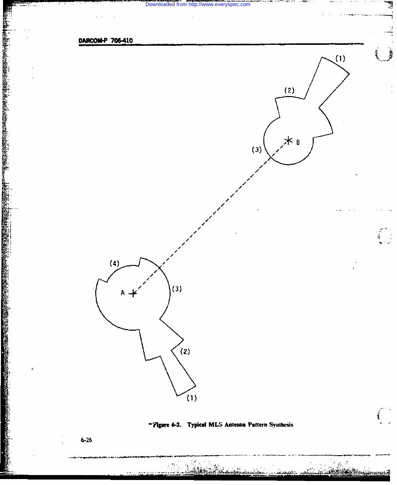
DAMMOMP 706-410
2(2)
A (3)
(2)
f-lgne 6-2. Typkcal MIS Antena Pattern Synthesis
6-26
wtOEaL
Downloaded from http://www.everyspec.com

rt
DARWM=P 706410
6-4,4.5.2.3 Propagation Path Loss the receiver bandwidth is less than the transmitterThere are two methods of path loss computation: bandwidth. The interaction producing off-frequency
one assumes that the earth is a smooth sphere with a rejection is selected.4/3 earth effective radius (smooth earth); the other
6-4.4.5.2.5 Receiver Senuitityincludes the effects of intervening terrain (roughearth). This parameter is available directly from the data
files in dBm units.6-4.4.5.2.3.1 Smooth Earth Path Loss Model 6 6 a i
The primary smooth earth model is the N- 64.4.6 AvailabilityLAMBDA Program. This is a ground-wave model Information may be obtained from the Armywith a valid frequency range of 0.01 MHz to 20 GHz. Deputy Director. Electromagnetic CompatibilityIt consists of three sections, with the choice of sec- Analysis Center, North Severn, Annapolis, MDtion depending on the path geometry for the given 21402.problem. The three paths are:
a. Liane-of-sight analysis using the direct and re- 6.4.5 INTERFERENCE PREDICTIONflected rays for propagation over a spherical earth PROCESS-NUMBER Iwith medium-height antennas
b. Plane earth surface wave analysis for low anten- 6-4.5.1 Introductionnas The Interference Prediction Process-Number I
c. Beyond line-of-sight diffraction analysis over a (IPP-1) (Ref. 10) was developed at the Rome Air De-spherical earth, with a check of possible tropo- velopment Center (RADC), Griffiss Air Force Base,spheric scatter propagation. NY. Its purpose is to analyze and predict potentially
The program selects the proper mode from the interfering situations among a proposed or existingpath characteristics and returns a path loss. deployment of transmitters and receivers, It is useful
for:6-4.4.5.2.3.2 Rough Earth Path Loss Model a. Developing preliminary equipmerit or system re-
The Terrain Integrated Rough Earth Model quirements and specifications(TIREM) is used to obtain a terrain-dependent path b. Preparing test plans for specification compli-loss. This model first extracts the topographic profile anceI between the two equipments concerned from a dig- c. Evaluating test resultsitized terrain file. It next analyzes the profile geom- d. Revising specifications or equipments for con-etry and selects one of the following propagation ditions of noncompliancemodes: e. Evaluating systems in specific operating envi-
a, Free space ronments.b. Knife edge beyond line-of-sight IPP-l was programmed initially for the Burroughsc. Effective double knife-edge 205 computer and the Univac I103A computer. Ad. Rough earth diffraction more complete and detailed set of programs was thene. Troposcatter developed for used in the CDC 1604 computer.f. Diffraction-troposcatter.
The propagation path loss is then computed using the 64.5.2 Analysis Processequations for the selected mode. An interference margin P, which corresponds
closely to the negative of the interference-to-noise ra-6-4.4.5.2.4 Off-Frequency Rejection tio R. (in dB), is calculated in terms of P, the re-
The Frequency Analysis System (FAS) is used to ceiver sensitivity at its input terminals; thuscalculate off-frequency rejection. It accounts for im-age and spurious responses in the receiver, and up to P - (PI + G + G, - Lp - R) , dBW (6-22)eight harmonics from the transmitter.
The module considers all the possible frequency in- The actual interference analysis is divided into twoteractions (such as fundamental-fundamental and parts: the rapid cull, as its name implies, uses someharmonic-image) by integrating the emission spec- very simple criteria for eliminating all of the more ob-trum and receiver selectivity curves to determine the viously noninterfering portions of the problem. Fortotal power coupled into the receiver for each case. all cases eliminated by the rapid cull, there is noThis power is then converted to a loss below the co- probability of interference. For the remaining cases,channel value, which may be different from zero if there is at least a small probability that interference
6-27
Downloaded from http://www.everyspec.com

F DOARCOM-P 706-410
occurs. The frequency cull considers the frequency b. The Receiver File, which contains all pertinentseparation between potentially interfering transmit- receiver information that is required in performingter outputs and receiver responses. It also considers the interference analysis. This information is analo-the statistical distribution of all of the amplitudes in- gous to the information provided in the transmittervolved and the criteria for interference to determine f!e.the significant probabilities of interference. c. The Antenna File, which contains general tech-
The basic portions of the analysis are carried out nical characteristics of the antenna (including no-during the frequency cull. Major steps of the fre- menclature, height, length, frequency range, etc.) andquency cull analysis are outlined in the block dia- detailed pattern distribution data.gram of Fig. 6-3. The analysis begins with a statisti- Also provided initially to the computer when per-cal expression for the transmitter output amplitudes forming an analysis are such specific problem data asand an independent tabulation of the specific trans- equipment coordinates, terrain characteristics be-mitter output frequencies over the range which was tween specific pieces of equipment, antenna orienta-determined from the rapid culling step. The trans- tion and modes of operation, and the specific tunedmitter amplitude function includes the statistical ef- frequencies of each piece of equipment.fects of the coupling system between the transmitterand the transmitting antenna. The transmitter am- 64.5.3 Data Outputsplitude function is modified successively by the pat-tern distribution function (PDF) for the transmitting The following illustration shows how this pro-antenna, the intervening propagation conditions, and gram can be used when installing a new transmitterthe pattern distribution function for the receiving into an existing equipment complex (Ref. It). Anantenna. The output frequencies from the transmit- equipment complex of three radar receivers and oneter are unmodified during these analysis steps, but UHF receiver is assumed. The deployment within the-_ site is shown -in Fig; 6-4. The -transmitter and theserve as references to the basic frequeticy range overwhich each of the factors must be considered. receivers are designated T-1 and R-l through R-4, re-! spectively, and their characteristics art summarized
The statistical description of the receiver response pivl, arr ramplitudes includes the statistical effects of the cou- hiepiing system between the receiving antenna and thein the analysis which begins receiver pairs show potential interference as follows:t receiver. At the next step6-n the a n y in s a. The fundamental output of the transmitter withat the lower left of Fig. 6-3, the frequency informa- the fundamental response of the R-I receivertion is merged with the amplitude information. The b. The second harmonic of the transmitter with thereceiver response frequencies are compared with the fundamental response of the R-2 receivertransmitter output frequencies to obtain the frequen- fundamental out of the ranier
cy difference between suspect output-response fre- c. The fundamental ot f the transmitter withqueny parsthe image response of the R-3 receiver,
quency pairs.The frequency analysis is now joined with the am-
plitude analysis for the remaining steps. The energy 6-4.5.4 Availabilitydistribution about each suspect transmitter output is The IPP-1 normally is used for internal work butconsidered along with the selectivity about each sus- may be used for external programs if time is avail-pect receiver response to determine the amount of in- able; Rome Air Development Center, Electronicsterfering energy that enters the receiver. The statisti- System Division, Code RADC/RBCT, Griffiss AFB,cal distribution of the "interierence margin" is then NY 13441 should be contacted.tabulated.
The program begins with three basic catalogs on 6-4.6 COSITE ANALYSIS MODELmagnetic tape. The catalogs are:
a. The Transmitter File, which contains all perti- 6-4.6.1 Introductionnent transmitter information that is required in per- The Cosite Analysis Model (COSAM) (Ref. 12) isforming the interference analysis. This information an automated program designed to evaluate the elec-includes nomenclature and general transmitter data tromagnetic compatibility of a single site that uses a(frequency range, type of modulation, etc.), describ- large number of transmitting and receiving equip-ing the multilist representation of the transmitter out- ments in the 200- to 400-MHz band, with AM, FM,put envelopes, and possibly exact outputs from the and SSB modulations. It can handle up to 50 singletransmitter which may be pertinent to the analysis. channel transmitters and 50 single channel receivers.
6-28
Downloaded from http://www.everyspec.com

DARCOM-P 706-410
a) (A
*r- 0+)4~
4-
C a
0,4-'
4-J'
-
*4 0-5
u) 0u di r_
.1W =U 4-' S*4..) a -- -0 Sl
Cu*- 4J ) :
C ~ I =LVL
jW 'ic(D
Downloaded from http://www.everyspec.com

YXDARCOM-P 706410
R-2~3
(0) Miles East (25)+(0 Miles North(0) Feet ElevationR-
I 30
- 140R-1 -
(1)0
Figure 6-4. Coordinate System for Installing a Traamaitter
TABLE 6-9. EQUIPMENT CHARACTERISTICS
Characteristic T-1 R-I R-2 R-3 R-4
Frequency Hand, MHz 2800 2800-3100 5450-5825 2700-2900 225-399
Tuned Freq.f. MHz 2800 2830 5600 2740 275
Power or Sensitivity, dBm +97 -100 -100 - 102 -92
Antenna Gain, dB 35 39 33 32 7
Antenna Height, ft 40 29 25 30 10
Antenna Bearing, deg/North 45 325
East Coordinate, mi 3 1 3 5 3
North Coordinate, nii 2.5 1.5 4 3
Spurious CharacteristicsFSlope. dB/docade -30 20 20 10 37Intercept. dB above Nominal -40 76 76 56 57
Standard Deviation. dB 10 12 12 12 12
*Denotes rotating antenna"Denotes omnidirectional antenna
6-30
Downloaded from http://www.everyspec.com

DARCOM-P 706410
t A cosite EMC problem implies (a) "close" prox- all transmitters whose frequencies are within 20 MHzimity between transmitting and receiving antennas, of the receiver tuned frequency are considered.and (b) relatively "large" signals impinging onreceiver inputs (as well as transmitter outputs). li 64.6.2.2 Noise Modelgeneral, five types of interactions are considered: (1) The noise model is used in conjunction with alladjacent signal, (2) spurious emissions, (3) spurious other submodels. If no interaction is attributed to anyresponses, (4) receiver intermodulation, and (5) trans- specific transmitter or groups of transmitters, the pri-mitter intermodulation. mary interference mechanism is assumed to be noise.
Because of uncertainties in defining the ampli- Consequently, a predicted noise interaction, in effect,tudes of the interactions, a statistical approach is indicates "no degradation" for all types of interac-used in analyzing these interactions. Furthermore, tions.several interactions are likely to occur simultaneous-ly, requiring a method for assessing multiple affects. 6-4.6.2.3 Spurious Ensission and Response
The program is written in FORTRAN, and These responses are identified in frequency with re-requires at least 32 words of memory. The program is spect to the tuned frequency. For transmitte.-s spu-run on a Univac I 110 computer at the DoD Electro- rious emission may arise from harmonics of a crystalmagnetic Compatibility Analysis Center (ECAC), frequency f,. In this case the computer determines ifAnnapolis, MD. the harmonics occur at spurious response frequen-
Inputs consist of a list of equipments involved and cies and if so stores them in ah interaction table.their operating frequencies, antenna types, and their In a corresponding way, significant receiver spu-
location on the site. Applications have included rious response frequencies are computed in terms ofUHF-AM transmitters (Ref. 13) and VHF-FM and receiver local oscillator and intermediate frequenciesAM transmitters and receivers. Antenna types are and stored.Yagi. helix, and corner reflector types as well asloaded and nonloaded whip antennas and vertical 64.6.2.4 Intermodulationground plane antennas. Equipment parameters are Transmitter or receiver intermodulation can occurobtained from a combination of nominal character- when a victim transmitter or receiver tuned to the fre-istics and spectrum signature data. Various auto- quencyf, also is subjected to a strong signal from an
Emated, semiautomated, and manual procedures are interfering transmitter of frequency fi related to f, as
used to compute the parameters. Where appropriate, discussed in par. 3-2.2.2.2.the parameters are described by means and standard An interaction table is developed to reduce ordeviations which have been derived from measured "cull" the problem. In the interest of conserving com-data. puter time, not every possible interaction is com-Outputs consist of (1) performance scores derived puted. Rules are established to eliminate interactions
from predicted S/N and S/(l + N) output distribu- which are clearly insignificant. The interaction table
any, which are identified for each receiver in quanti- ter pair which may cauge a significant interaction.tative terms, i.e., mean values of effective input on- Power levels ace not considered at this point. Thefrequency power levels due to each significant inter- table may be printed prior to the final computation ifaction. desired.
6-4.6.2 Program Models
The models used in the program are for adjacent 64.6.3 Scoring Techniquessignal, noise, spurious response and emission, and in- Three scores are provided based upon ratios of sig-termodulation. nal-to-noise (S/N)o and signal-to-interference plus
noise, [S/( + N)1o as illustrated in Figs. 6-5 and 6-6-4.6.2.1 Adjacent Signal Model 6, where (S/N)or and [S/(I + IN)]OT are, respec-
A review of measured data and practical experi- tively, output signal-to-noise and output signal-to-in-ence indicates that beyond a certain deviation (de- terference plus noise threshold value ratios (SINAD).pending on equipment type) from the receiver tuned The upper performance score UPS is the probabilityfrequency, adjacent signal interference is not signifi- of providing "adequate" or "good" performancecant. Therafore, a maximum deviation, e.g., 20 MHz, with no interference present. The system perform-is postulated, above which serious operational deg- ance score SPS is the probability of adequate (orradation is not anticipated. For each receiver, then, good) performance in the presence of interference.
6-31
Downloaded from http://www.everyspec.com

DARCOM-P 706-410
0
: '.,
4J
(SIN) o (SIN) o(n S/IN) -'I(sNOT 0 UPS)
Figure 6-5. Upper Performance Score (UPS)
;-- 1 i....
) m InN 0 max ( I 0+N O
Figure 6-6. System Performance Score (SPS)
The relative performance RPS score SPS/ UPS pro- average difference of less than I dB, with a standardvides the user with a third measure which, in con- deviation of 3.4 dB.junction with the other scores, gives additional un- b. The model bias (for all 436 interactions) wasderstanding of receiver performance. For example, if 1.55 dB, implying a small tendency toward predic-the SPS were 0.4, one would expect poor perform- tion of too much interference. The standard devia-ance. However, if the UPS were also 0.4, tion of the bias was 5.3 dB.RPS = 1.0. and an inadequate desired signal thus is c. An evaluation of each of the groups of interac-identified. tions identified as being due to one of the specified
mechanisms indicated that, for 85% of the cases, thebias values for each group were less than 3.5 dB and
6.4.6.4 Comparison of Measurements and that standard deviation values were less than 6.2 dB.Predictions d. As noted in Fig. 6-7, 92% of all of the cases
Measurements were made of numerous interac- resulted in differences between measured SINADtions at an installation involving 6 AM voice com- values SM ank associated predicted mean values 9 ofmunications transceivers operating in the 225400 less than 10 dB.
MHz frequency range (Refs. 12, 13). Twenty-five fre- e. Results of the "Bin Method", noted in Fig. 6-8,quency assignments were tested with 3 different de- indicated that a confidence level of 90% can be as-sired signal levels. Major results were: signed to a prediction of SPS 1 0.225. SIS is the av-
a. A comparison of 90 measured coupling values erage SPS value for a specified bin, and SPS, is theand associated predicted mean values resulted in an measured SPS value associated with the same bin.
6-32
-.Ii....1 ........ ..... 1 / /i I I Is I -
Downloaded from http://www.everyspec.com

ORM- -.. 06-410
1.0 _ _ __ __
0.8 _ _ _
0.6
CD
LU
L. SM measured sinad value, dB0.4 Sr = mean value of the predicted
0.2
Figure 6-1. Cumulative Probability Distribution of ISkl -
m ~ ~633....
Downloaded from http://www.everyspec.com

DAR-OMP 10 - - --1
~~90 ,,
80
70 -/n/60 -PS = average SPS value
for a specified bin- SPS = associated measured
_.F- 50 SPS value
A17 bins were employed.
u
'i', ~~30......
Circles are results of "bin method"20 calculations. The curve is based on -
expression for a Gaussian cumulativedistribution.
10 I I [ I I0 0.05 0.10 0.15 0.20 0.25 0.30 0.35
r SPSmIFigure 6-8. Cumulative Probability Distribution of I SS - SPS, I
f. Results of the "interference condition method", dicates intolerable degradation, or the converse sit-using a 5-condition scale, indicated that results were uation.)within I condition for 76% of the cases and within 2conditions for 92% of the cases.
g. By use of the results of the coarser "interference 6-4.6.5 Availabilitycondition method", the probability of a prediction Information may be obtained from the Armyresulting in a gross error is less than 0.08. (A gross Deputy Director, Electromagnetic Compatibilityerror is defined as a situation where a prediction will Analysis Center. North Severn, Annapolis, MDindicate good performance when a measurement in- 21402.
6-34
.. " - , " - , .
Downloaded from http://www.everyspec.com

DARCOMP 706.410
6.4.7 SHIPBOARD ELECTROMAGNETIC c. List frequencies between 22.5 and 30 MHz thatCOMPATIBILITY ANALYSIS AND are separated, from transmitter frequencies by 2.0SHIPBOARD ELECTROMAGNETIC MHz. The results indicated 176 frequencies to beCOMPATIBILITY ANALYSIS available.MICROWAVE (NAVSEA) d. List frequencies between 2 and 15 MHz that are
SEMCA is the acronym for Shipboard Electro- separated from transmitter frequencies by 0.5 MHz.magnetic Compatibility Analysis (Ref. 14). One Tje results indicated 91 frequencies to be available.program (cull 3) performs a basic analysis in which e. List frequencies between 15 and 30 MHz that aretransmitter output spectra are processed through separated from transmitter frequencies by 0.5 MHz.designated transmitter channel components (i.e., The results showed 199 frequencies, the maximumguides, antenna tuners, and antennas), the antenna the program will handle.coupling loss between all transmitting and receiving SEMCAM (Shipboard Electromagnetic Corn-antennas is calculated, and the resulting spectrum patibility Analysis Microwave) is a computer pro-that arrives at each receiving antenna is determined, gram developed to aid in assessing the electromag-From this information, plus data on the receiver RF netic compatibility between microwave transmittingchannel components (i.e., filters. RF section, etc.), and receiving equipments employed on the topsidethe potential interference spectrum at the first mixer region of Naval combatant ships. Some of the moreof each receiver ii determined. A second program important applications of the program are:(cull 4) then processes the resulting data through the a. Topside design of new shipsmodeled mixer and IF stage combinations to the b. Assess EMC impact of alternate equipment sitesdetector. c. Assess EMC merits of alternate antenna sites
A separate SEMCA program known as Frequen- d. Frequency assignmentcy Selection is used to assign compatible transmitter e. Assess EMI "quick fix" meritsand receiver center frequencies in the LF through f. Aid in generation of EMC specifications for newUHF frequency range. Frequency assignment is equipment design.based on a set of criteria to minimize potential inter- The model, operating from a user-prepared list ofference. These criteria specify the separation be- transmitters, receivers and antennas, calculates thetween spectral lines emitted by the transmitters. The interaction between each microwave transmitter/amount of separation is determined by whether the receiver pair for various relative tuning situations andspectral lines correspond to fundamental or harmon- antenna orientations. Several output parameters,ic frequencies. If the user desires, he can insert trans- which relate to the degree of interaction and degra-mitter and/or receiver frequencies, called priority fre- dation, are produced. The two primary parametersquencies, that are not to be considered as assignable are receiver output interference-to-noise ratio INRfrequencies. and mixer input "burnout" power. The INR param-
Fig. 6-9 is a sample output sheet for the Frequency eter is an indication of the degree of receiver degra-Selection Program. In the exercise of this program, dation. For example, for search radars the INR value,the input (not shown) had called for ten transmitter when processed through the radar signal processingfrequencies to be assigned; however, there was only model, leads to a performance degradation indexspectrum available for nine, as indicated by the out- which can he related to a reduction in detectionput comment at the top of the sheet. Under the cap- range. For fire-control radars the INR value, proc-tion "Row 1" the 9 available frequencies are printed. essed through the radars signal processing model.The priority frequencies that had been included in the leads to a performance degradation index which caninput data are printed next for reference purposes. be translated to a reduction in acquisition time, etc.Then the receiver frequencies are printed. A group of The mixer "burnout" power can be used in severalfrequencies appears for each row of the input data, ways: (I) It permits determination of possible degra-which was as follows: dation of the mixer crystal diodes due to high power
a. List frequencies between 2 and 15 MHz that are effects, and (2) the power level in the mixer can beseparated from transmitter frequencies by 1.0 MHz. used to assess the likelihood of spurious responses orThe results indicated 70 frequencies to be available receiver desensitization.with a channel separation of 20 kHz, Significant features of the model are the antenna-
b. List frequencies between 15 and 22.5 MHz that .to-antenna coupling functions. These functions are4' are separated from transmitter frequencies by 2.0 based on an elaborate, measured data base repre-MHz. The results indicated 73 frequencies to be senting several thousand data samples. The couplingavailablt.. model accounts for effects such as obstacle blockage,
6-35
Wig
Downloaded from http://www.everyspec.com

DAROMP 70".10
ONLY 9 FREQUENCIES ASSIGNED TO ROW 1I . ASSIGED MMMMflWIR FMQUIECS FOR
hww 1
4. 1206.4729. )d1iI
14. 1i816.05318.25220.75123.59126.818
PRIORITY TRANSMITTER FREQUENCIES
2.0003.5005.5005.0008.000
12.000
EX EE OFMW WR CANUMFlT Q A LDM-S O0 W1CSEANMB~IN1 ~
10.420 11.00013.010 13-120
NLUMER OF RX COEAWEIS AVAILABLE 73 ME SEPARATION 2. 0CE-0217.060 1T.24019.26o 19.74021.760 22.500
NUMJR OF EX CHAMWIS AVAILABI - 176 wIT sEPARATIOiI 2.o0C-O2
22.500 22.58024.60o 25.80027,820 30.000
NEMn OF RX CHARIWIB AVAILABE 91 WITH SEPARATION 5.OCE-02
2.500 2.950T.000 7.4508.500 8.9009.950 11.500
12.550 13.60014.650 15.000
NUNHER OF RX CHAIWIB AVAILABLE 199 =H SEPAMATION 5. OCE-0215.000 15.55016.600 I7.75018.800 20,25021.300 23.05024.10O 26.30027.350 29.900
Fire 69. Sample Output
6-36
Downloaded from http://www.everyspec.com

-ARCOM-P 706410
out-of-band antenna operations, and dissimilar an- plane, for shielded wires over a ground plane, and fork tenna polarization, two-wire circuits.
The entire microwave equipment complement of alarge combat ship can be completely characterized 648.1.1.1.1 Unshielded Wireswith only a nominal amount of computer expendi- For unshielded wires (Fig. 6-1 1(A)) the transfer
Sture and time. Information on the use of these pro- function TV is (see Eq. 3-124)
g-ams can be obtained from Naval Ship EngineeringCenter, Naval Sea Systems Command, Code 6174. TV - - (6-23)Hyattsville, MD 20782. V, I - 12 2 C. 1.2"648 SPECIFICATION AND ELECTRO- 2.C
MAGNETIC COMPATIBILITY whereANALYSIS PROGRAM V, = generator voltage. V
SEMCAP is an acroiym for Specification and V2 = voltage appearing on susceptor wire relativeElectromagnetic Compatibility Analysis Program to ground, V(Refs. 15 and 16). It is a computer program for:
a. Analyzing the electromagnetic compatibility of a R. = R2 ,
system Rg2 + RL
b. Developing black box EMC specification gen- R =2 = source resistance of susceptor circuit, Q2eration and susceptibility limits consistent with RL2 =load resistance of susceptor cir-desired signal requirements cuit, 0I
c. Evaluating waiver proposals in terms of their ef- C 1.2 = wire-to-wire capacitance between genera-fects on system performance. -..tor.circuit and susccptor circuit,.F6-.1C-- f = frequency, Hz
1 C n MThe calculation of C,,,. 2 is complex because of theElectromagnetic transfer functions arc defined for proximity of the ground plane. However, it has been
4 wire-to-wire, wire-to-field, and field-to-wire configii- established that the equation with no ground planerations. To account for the effects of antennas within effect is adequate for the proximities anticipated, anda system, antenna-to-antenna and wire-to-antenna this relationship is used in the model. The equation istransfer functions also are included (see Fig. 6-10).
The susceptor models include linear filters to con- 13.5X 10- , !trol bandwidth, and an integration process to per- C.1.2 = + I Fform spectral density integration. Threshold levels Iw.
are established that represent the expected malfunc- 6-24 ,
tion level of given susceptor circuits.where
6-4.8.1.1 Wire-to-Wire Coupling 112 = common length of wires I and 2, n,The wire-to-wire, or close coupled, transfer func- d 2 = spacing between wires I and 2, m
tions account for capacitive and inductive couplings, rwt = radius of wire 1, mas shown by parameters TV and TI. respectively, in r.,.2 = radius of wire 2, mFig. 6-10. They relate the voltage induced in a load Eq. 6-23 is an approximation that avoids a square-connected to a wire to the spectral voltages and cur- root computation, thereby reducing computationrents present on the wire. These models take into ac- time. The maximum error incurred is a factor of 1.4count many wire configurations, and can include (3.0 dB), and occurs only over a narrow frequencyshielding and wire twist effects over a frequency range in which the second term of the denominator isrange from 10 Hz to 10 GHz. approximately equal to unity.
Wire-to-wire transfer is treated as two additiveeffects: "capacitive transfer" and ~inductive trans- 6-4.8.1.1.1.2 Two-Wire Circuitsfer". This approach allows the shielding analyses for The coupling between nontwisted two-wire circuitsthe two effects to be handled separately, is given by the equivalent one- vire model (see Fig. 6-
11(B)), as determined by the theory of images. The6-4.8.1.1.1 Capacitive Transfer coupling between ground-referenced tw isted-pair cir-
Close-coupled capacitive transfer models have cuits is given by the one-wire model, using the net orbeen developed for unshielded wires over a ground average voltage of the twisted-pair generator. The
6-37
-... . .. . - ---
Downloaded from http://www.everyspec.com

DARCOM-P 706-410
GENERATOR(Voltage) Wiring Wiring
andCurrent)
- • TV-
TJ Length of close uoupling
z
-'KE* a TE*(KH* a TH*)
KE * TE(KH .TH)
1. TV - Voltage Transfer Function i close coupled wires2. TI - Current to Voltage Transfer Function3. KE - Voltage to E-field Transfer Function (antenna source)4. 7E - F-field to Voltage Transfer Function (antenna receptor)5. KE* - Voltage to E-field Transfer Function (wire source)6. TE* - F-field to Voltage Transfer Function (wire receptor)7. KH - Current to U-field Transfer Function (antenna source)8. TH - H-field to Voltage Transfer Function (antenna receptor)9 KH* - Current to H-field Transfer Function (wire source)
10. TH* - H-field to Voltage Transfer Function (wire receptor)11. Z - Common Impedance (contained in the TI Model)
RFg 6-10. Tmrer Funetm
6-38
Downloaded from http://www.everyspec.com

r DARCOM'P 706410
..
RLI g2 RL2V2
(A) Capac.itive Model for Unshielded Wires
g R g l R L/ R g l R L 2 /
/d/
:
/', 2 w l w Rg2 I
(8) Capacitive Model for Two Wire Circuits
Cwlsl Cslw 2
Wire IWire
2
R I ,I Vg R, 2
(C) Capacitive Model for Shielded Wires
Figure 6-11. riose-coupled Capacitive Transfer Models
6-39
.., . - ....-
Downloaded from http://www.everyspec.com

DARCOM-P 706.410
voltage used is one-half the total voltage for an un- 6-4.8.1.1.2 Inductive Transferbalanced pair, and zero for a perfectly balanced pair. Inductive transfer models have been developed for
6unshielded wires, for shielded wires, for twisted gen-6..4.8.1.1.1.3 Shielded Wires erator wires, and for twisted susceptor wires.
The capacitive models for shielded wires include The basic inductive transfer model represents theboth a nonresonant shielding effect and a resonant case of two single-wire ground return circuits that areshielding effect. With reference to Fig. 6-1 I(C). C1s parallel over some common run length (see Fig. 6-is the coupling capacity between wire I and its shield; 12). The inductive transfer factor TI, which is the ra-C,1 2 is the capacity between the shield and wire 2; tio of the voltage induced in RL2 to the current i inand R 1 is the resistance of the shield on wire 1. When the generator wire. is given bythe impedance of CU,,1 is large compared with Rsl, thecircuit may be decoupled as shown, The model uses R/ 2the decoupled equivalent, making it equal to two un- Ti - 27rfM + R2 R (6-27)shielded coupling models in series, An unshielded + R,2 +2rfL,2coupling term also is added to account for un- whereshielded portions of the wire. The low-frequency M mutual inductance of the two circuits, Hshielding factor S is giveo'by Eq. 6-25, which has thesame form as the unshielded transfer equation. = I. inIf(a + a.)2. + d2121 H
I. 4v , - a,,,2)2 + d 1 (6-28)S - dimensionless (6-25) permeability of free space - 4 X 10- H/m
i + a,,= height of wire I above ground plane, m2Jrf 1 CrfN , a,,2 = height of wire 2 above ground-plane, m
The shield resistance R,1 is approximated by L .2 - self-inductance of the circuit', H
1.25 X 10 2a2 ,)
Rx, R. +t j (6-26) 2r-) II" H (6"29)i! I R tI + x(i + 6x' ) ' w,Lwhere i,.2 length of wire 2, m
Res, - dc resistance of wire I shield, 11 The resistive terms include ground plane resis.tance (or spreading resistance due to the finite 'con.p x- t/6 dimensionless ductivity of the ground plane), and circuit lead resis-
t- shield thickness, m tance for both the source and load ends of the sus-6 = field penetration depth into shield, m cefor wire.
At frequencies at which the generator wire and its ceptor wire.shield resonate, tne shield will have minimum shield-ing effect, In this case, the RC product of Eq. 6-23 ismultiplied by [I + D,fI (I + 6D,2f 4 )], where D, is 6-4.8.1.1.2.1 Shielded Wiresthe reciprocal square of the first resonant frequency For shielded wires in which the shield is groundedand is calculated based on the capacitance and in- at both ends, a current Is1 is induced in the wire Iductance of the wire-shield circuit, shield,
To model the attenuation of the electric field /through the shield and its holes, the shielding factor S i21r - !A 6-3l0)is also multiplied by (e- ' + Fhi). The first term rep- A (6-30)
*resents the exponential decay of the field as it pene-trates the metal, and F&,1 represents the field propa- wheregated through the holes of the shield. Eq. 6-25 with 11= current in wire 1, ARj replaced by Eq. 6-26, and the result multiplied by L, - self-inductance of the shield around wire I,the resonating factor of the previous paragraph and Hthe penetration factor described in this paragraph, 1defines the total shield factor S1. L,( 1.25 X 10⁻⁶ Ill I2aH
The derivation of the models for the case of a = 2w In - 1 ,H (6-31)shielded susceptor wire, and for the case when bothwires were shielded, follows the same procedures, and /w1 = length of wire I, mvery similar results are obtained. r , = radius of shield I, m
6-40
Downloaded from http://www.everyspec.com

DARCOM-P 706410
M
~RO. , >Rg 2V" L2
Figure 6-12. Close-coupled Inductive Transfer Model for Unshielded Wires
If the shield is ungrounded at one or both ends, no Let a twisting factor Setl for wire I be defined as thecurrent flows through it, and there is no shielding multiplying factor to be applied to Eq. 6-27 as a resulteffect. of the generator connection being a twisted pair
When the wire current is forced to flow back on the rather than a single wire with ground return. Theshield instead of via the ground plane, the net cur- twisting factor therefore is the fraction of the totalrent 1N (in generator wire I plus return current in its current which is common mode, i.e., current whichshield) in the first circuit is given by the equation returns in the ground plane rather than in the twisted
- return wire due to distributed or lumped capacitance
S+ j Rd ) , A (6-32) to ground. This effect is given by Eq. 6-33 where C, is+ J2.rf4, the shunt capacity to ground and CT is the total ca-
pacity to ground. i.e., C. plus the wire-to-wire shuntThe magnitude of this current can be approximated capacity.by disregarding the orthogonality of the two de-nominator terms, as in the capacitive model. The 2IrRL, rshielding effect is given by the ratio of the net current ST 2RL T + i/f dimensionless (6-33)
to the wire current, which is the term in parentheses.The shield resistance, R, 1, is calculated using the same whereequation as in the capacitive model, Eq. 6-26, and 41 RLI = load resistance on generator wire I, Cis given by Eq. 6-31. If a shield is present and grounded at the same end as
When both wires are shielded, the shielding effect the one where one lead of the twisted pair isis given by the product of the two shielding factors. grounded, then the distributed capacity to ground isWhen shields are terminited with pigtails rather thait eliminated.
' coaxially, the loop created by the pigtail wire allows b. Susceptor. For twisted susceptor wires, refer tothe leakage of flux, which limits the amount of shield- Fig. 6-13. The voltage VN induced in the twisted looping. This effect is modeled by adjusting the shielding area is assumed to be negligible compared to thefactor by a term which is the ratio of the area of the voltage induced by conversion from a common modepigtail loop to the area of the shield loop. voltage V, induced in the ground plane. The common
mode voltage V, is given by64.9.1.1.2.2 Twisted Wires
Two models are used, one for an emitter and one V, - 2rfo , V (6-34)for a susceptor:
a. Emitter. If a pair of wires is twisted, the field whereproduced is a result of the net flow of current in one it = flux linking the circuit in whichdirection as seen externally. Thus, if the outgoing and V, is induced, Wb(return currents are equal, as occurs when there is no Thus, the twisting factor Sn for wire 2 is the ratio ofleakage to ground, no field is produced. the voltage V2 (induced by V, in the load resistance)
6-41
""..... .o .. 0. . .. . .
Downloaded from http://www.everyspec.com

DARCOM-P 706410
VI'tRg2 2 AL2
CL
Figure 6-13. Simplified Equivalent Lumped Circuit or Twisted Susceptor Wires
to V. This is obtained by circuit analysis and is given 6-4.8.1.2.1.1 Conversion of Voltage to E-Fieldby Eq. 6.35, which has the same form as for the case KE is a factor converting antenna terminal voltagewhere the generator wire is twisted (Eq. 6.33). to the E-field at a distance of I m from the antenna.
The program assumes the conversion- known at the-$- __ 2,r&2cL2 dimensionless (6-35) band center of the antenna and it models the varia-2rP.2CT + I/f tion with frequency using an arbitrary characteristic
similar to the form of the transfer function of awhere Butterworth filter (Ref. 15, par. 3-3.2.4.2.2). How-
RL2Rg2 ever, unlike filters for which out-of-band attenuation&R 2 + R , 0 (6.36) approaches infinity, the models assumed here have
L +limited out-of-band attenuation. The conversion fac-CL2 - lumped and distributed capacitance to tor used at band center is determined by a separate
ground for wire 2, F computation or measurement assuming the point ofCr - CL2 in parallel with wire-to-wire shunt ca- field observation is at a back lobe.
pacitance, i.e., total capacitance to ground, KE* is a factor converting voltage ou a long wireF above a ground plane to the E-field at a distance of I
m from the wire. The physical model of the gener-6..8.1.2 Field Coupling ator wire is similar to that shown in Fig. 6-11kA) or
The coupling of energy from a generator to a sus- the unshielded generator case and to that shown incaptor via an electromagnetic field is treated in two Fig. 6- 11(C) for the shielded generator case. Whileparts: the field produced by the generator (par. 6- the capacitance coupling computation in par. 6-4.8.1.2.1) and the voltage produced by the field in the 4.8. 1. 1.1 determined the voltage on a nearby wire, thesusceptor or receiver (par. 6-4.8.1.2.2). computation now is of the field near the generator
wire. The field equation is given in the form6.4.8.1.2.1 Generator Fields
The functions KH, KH*, KE, and CE* listed on KE* - (A + X)SI , -rn' (6-37)Fig. 6-10 are used to convert from a current oi volt-age on a wire, shielded or unshielded, and on an an- S, is a factor accounting for the effect of the shieldtenna, to the magnetic field H and electric field E at a and is determined in the manner described in par. 6-distance of I m from the wire or antenna. Formulas 4.8.1.1.1.3 to account for the effect of shield whenare available to establish coupling values for fre- calculating ;apacitive coupling. The two terms in pa-quencies between 10 and 1011 Hz. Antenna models rentheses, A and X, account respectively for the ver-allow the approximation of antenna properties as cal- tical induction field (near the ground plane) and theculated by a separate manual or computer analysis, radiation field components at the point of measure-
: I or as obtained by testing. ment. They are given by
6-42
Downloaded from http://www.everyspec.com

DARCOM0 70"410
A 2a, (6-38) 6-4.8.1.2.2 Field Rectption ModelsIn (2aw,/rq) The field reception models contain two effects: (I)
the field decay with distance, and (2) the voltage in-duced into wires and antennas. The susceptor model
( 5 (I + contains the voltage induced into both a wire and an ril.2 0 f antenna.
, ~In the field decay models, the decay of E-field and .€-
X fl + 0.4 In (i.0001 + 6.7 X 10"' f)] H-fields with distance is treated in the same manner.The field from the generator is described at I m, and
X + 8.3 x 10" the decay to greater distances or the increase to, P .T shorter distances is described by a field decay expo-Snent parameter associated with the generator. The
appropriate decay rate must be determined outsideawf P the computer.
w 6-4.8.!.2.2.1 E-Fleld Trarsfer Functionz, the magnitude of the impedance seen by TE and TE* are the E-field to voltage transfer ratiora-
the source of voltage Y, Q3 tics, TE applying to the voltage appearing at the ter-f frequency, Hz minals of an antenna and TE* applying to the volt-iii age induced on a wire. These quantities give the ratio
H-Field of voltage developed to the magnitude of the field at afaCor o urrent to point 1 m from a generator. The total voltage devel-:. ..K H is a facto r co nverting an ten n a in p u t cu rrent to op d a a u c t rin t - e n t f e d -s F g .6 1theFtfied t aditanen' Inifrotharienia.As ped at asusceptor input-per- unit-field(see.Fig. 6-l0 ....-t:theff~fleld at a distance Of I in from the antenna. As which shows, for example. a generator antenna it-.:in the electric field case described in par. 6-4.8.1.2.1.1 wen
luminating both the susceptors antenna and its an-the progrem assumes the conversion known at the lmntn ohtessetr nen n t n
t cnna lead-in wire) is the sum of voltages per unitantenna's band center and it models the variation edevlpdyannaadcoetigwr.Te
with frequency using an arbitrary filter-like charac-teristic of the same form as for the electric field, total voltage is given byKH* is a factor converting current on a long wire
parallel to a ground plane to the induction H-field at TET TE + TE* TED(KAE + TEV), ma distance of I m from the wire in the vicinity of the ( )ground plane. The field here is tangential to the (641)
ground plane in a direction perpendicular to the whereplane of the wire and its image. The physical model ofthe generator wire is similar to that shown in Fig. 6- TED = E-field at susceptor11(A) for an unshielded wire, and to that shown in E-field at 1 m from generator 'Fig. 6-11(C) for a shielded wire, with the shield voltage induced in susceptorgrounded at both ends. The model also applies to the KAE = , mcase of a twisted pair from source to load above a E-field at susceptor antennaground plane with ground at one end of the run. The voltage induced in susceptorfield equation is of the form TEV Eu ,mE-field at susceptor wire
KH* - A, (asi + B)STI, m-' (6-40) TE and TE* are, respectively, the susceptor antennawhere A I= 0.32 aw,, S1 accounts for the shield (- I contr bution and the susceptor wire contribution.if there is no shield or if shield is grounded only at The field decay vs distance function TED is Ione end), B accounts foc the area of pigtail loopswhen a shield is used and when the shield is not TED (Dt)grounded coaxially (= 0 if grounding is coaxial) and T ( 1 I
Sri is the twisting factor when a twisted pair is used E (at distance D, from source)(- if no twisting is used). The exact form of these -I (6-42factors, which depend on the geometry of the struc- E (at I m from source)ture and on the frequency, will be found in Ref. 15,par. 3-3.2.5.1. where KED E-field fall-off exponent. 6.4
6-43 .
Downloaded from http://www.everyspec.com

DARCOM.P 706410
The antenna reception function is KAE. It allows term in parentheses represents the result of imped-antenna properties to be specified by the user. In ad- ance mismatch in energy transfer to the susceptordition, a bulkhead factor (to account for shielding of load RL2 coming from a source with radiation resist-wires by intervening conductive materials) is applied ance R,.to fields from generator wires. The bulkhead factor isnot applied to fields from generator ar.tennas. The V 4 -,Pd + V (6-43)output of an E-field receiving antenna, KAE is a Ra 2 R"product of three factors. The first is the maximum ef-fective height of the antenna (as a function of fre- The power density is assumed to be E1/377, and
quency). The second is a function giving the frequen- the effective aperture of the wire of length/4 is givency characteristic of the antenna and is similar to that by .mused to determine field emission from an antenna . 2 X IO ,/f, m2 (6-44)(par. 6-1.8.1,2.1. 1). The third is a bulkhead attenua-tion factor which is set equal to I if the receptor is il- TEV then turns out to be of the formluminated by an antenna and less than I when it is ili-
The E-field wire reception function, TEV, con- TEV I + 4. + 1 84 mtains two effects; a low frequency capacitance-like re-
sponse to vertical fields, and a high frequency re- (6-45)sponse. The voltage is assumed to be induced over thelength of the wire not sharing a common run length where B, B , B3 and 84 are constants depending onwith the generator wire, i.e., the separation DU is too geometrical factors,-and X, is-slowly varying with fre-great for inductive or capacitive transfer. A bulk- quency at high frequencies (Ref. 15, par. 3-3.2.5.3.3).head factor is here applied to fields from generator The first term in the brackets represents the low fre-antennas, but not to fields from generator wires, quency coupling, the second term represents the high
Telwfrequency induced voltage is derived by frequency coupling, and the factor BA accounts forassuming that the wire-to-ground capacitance C1,2 bulkhead shielding. It is equal to unity when no bulk-represents the source impedance for the vertical field, head intervenes. The program also allows shielding ofresulting in the equivalent circuit shown in Fig. 6-14. the receptor wire to be accounted for. The form ob-
Ai This assumes a wire, such as the receptor wire of Fig. tained is similar to Eq. 6-45, except for changes in the6-1 I(A) or (C), with resistors Rg2 and RL2 at the ends. factors (Ref. 25, par. 3-3.2.5.3.4), which makes someThe source voltage is the E-field times the height of of them dependent on frequency.the wire,
The high frequency part of the function is based on 6-4.8.1.2.2.2 H-Field Transfer Functionaperture theory. The voltage V induced in the load is The H-field to voltage transfer function is formedgiven by Eq. 6-43, where A, is the maximum effective in a manner similar to the E-field function. It is com-aperture, Pd is the incident power density, and the prised of terms TH and TH*, respectively giving the
Ic w 2 g
Figure 6-14. Equivalent Circuit for E-Field Wire Reception Model
6-44
Downloaded from http://www.everyspec.com

DARCOM-P 706-410
voltage appearing at antenna terms and voltage in- based upon the functional requirements of any par-duced on a wire, when immersed in an H-field. The ticular system in such a way that no intolerable mal-total voltage per unit H-field I m from the generator functions occur in the equipment.is given by The various emission and susceptance portions of
the electronic system are divided into four broad clas-THT THD(KAH + THP) , f'm (6-46) sifications of two priorities. Priority No. I circuits are
where those which have generation and reception charac-teristics which are functionally required for system
H-field at susceptor operation, Priority No. 2 circuits are those circuitsi-field at I m from generator ' whose generation and reception characteristics are
voltage induced in susceptor unnecessary for system operation, and which mightKAH 11edo m be undesirable from the system environment point ofH-field at susceptor antenna view.
voltage induced in susceptor For each priority classification there are generatorTHV= H-field at susceptor wire and susceptor subclassifications whether the genera-
tor or susceptor characteristics are intentional or un-The field decay vs distance function THD is intentional. A single physical circuit possibly could
fall into all four of these classifications but, for pur-THD (D~J)-KHD poses of analysis, it is treated as four separate entities.
The analysis philosophy is to (1) limit the interfer-
H (at distance Dc from source) (6-47) ence generation of priority No. 2 generator circuits toH (at I m from source) a level which is compatible with the required recep-
[I tion properties of priority No. I -susceptor circuits,where KHD - field fall-off exponent, and (2) limit the total environment incident on prior.
The antenna reception function is KAH. It allows ity No. 2 susceptor circuits from both priority No. Iantenna properties as determined outside the corn- and priority No. 2 generators to a tolerable level.puter to be specified. In addition, a bulkhead factor In the first step in the analysis the total interfer-(to account for shielding of wires by intervening con- ence from required (priority No. 1) sources incidentductive materials) is applied to fields from generator upon each required (priority No. 1) susceptor is de-wires. The bulkhead factor is not applied to fields termined. Unless the required sources are incompati-from generator antennas. KA H is a product of three ble with the required susceptors, a margin will existfactors as in the E-field case. The first is the maxi. that represents the difference between the malfunc-mum antenna field to voltage transfer (as a function tion level of the susceptors and the total interferenceof frequency). The second is a filter-like model giv. incident. This margin or quota then may be allotteding the antenna frequency characteristic. The third is to the extraneous priority No. 2 generators.a bulkhead factor.
The H-field wire reception function, THV, is based 6-4.8.2.1 Compatibility Analysison the assumption that the pick-up loop area is that An approximation to the voltage V, induced by aportion of the wire which does not share a common generator i at a reference point in the circuit of sus-run with the generator. A bulkhead factor is applied ceptor J is calculated using the following formula:to fields from generator antennas, but not to fieldsfrom generator wires. The function THi for an un-shielded wire turns out to be directly proportional to V, f ' G,(f) Tj(f)P(f) df , V (6-48)frequency, the multiplying factor being determinedby the electrical ard geometric parameters of the wireand the bulkhead factor, if applicable. If the receptor wherewire is shielded and/or it is a twisted pair, the effects Gf) = magnitude of generator I output Fouriercan be accounted for in the multiplying factor which, spectrum in V/Hzhowever, puts a frequency dependence into the factor Tj( f) = magnitude of the voltage transfer function(Ref. 15, par. 3-3.2.5.4.3). from generator I to susccptorj, dimension-
less6-4,8.2 Model Utilization Pj(f) - magnitude of the voltage transfer function
The objective of the computer program is to pro. describing the frequency response ofduce interference generation and susceptibility limits susceptorj, dimensionless
6-45
Downloaded from http://www.everyspec.com

FDARCOM-P 706-410
I" Eq. 648 gives the peak response of a device to a The process described by Fig. 615 is performedspectral density function whose frequency compo- many times in several different modes.nents are all in phase and assumes the susceptor re-sponds to the peak voltage, and the transfer func-tions have linear phase characteristics. It is consid. 6-4.8.2.2 Specification Developmentered to represent a worst-case assumption. Fig. 6-16 shows a number of priority No. I gen-
Fig. 6-15 illustrates relationships for voltage trans- erators Gi, G2, G3, G4. etc., representing circuitsfers between one generator and one susceptor. The within a system,transferred and bandwidth limited spectrum is inte- System generators have both required and un-grated and can be compared with the susceptibility required emission characteristics. As an example, athreshold AS. If it does not exceed AS,. the two cir- transmitter must transmit at some required frequen.cuits represented are compatible with each other. cy at some prescribed power level and over a given
Interference Transfer ReceptorGenerator Function
Bandwidth negaonSusceptibilityLimiting Integration Threshold
f)f) f AS
.*
SP.ij~
f ff
G,( f )Till f )P. f)
Typical Example
Figure 6-15. SFMCAP Compatibility Analysis
6-46
'" " ' : :' 'MI ' ' .. .' " ' i
Downloaded from http://www.everyspec.com
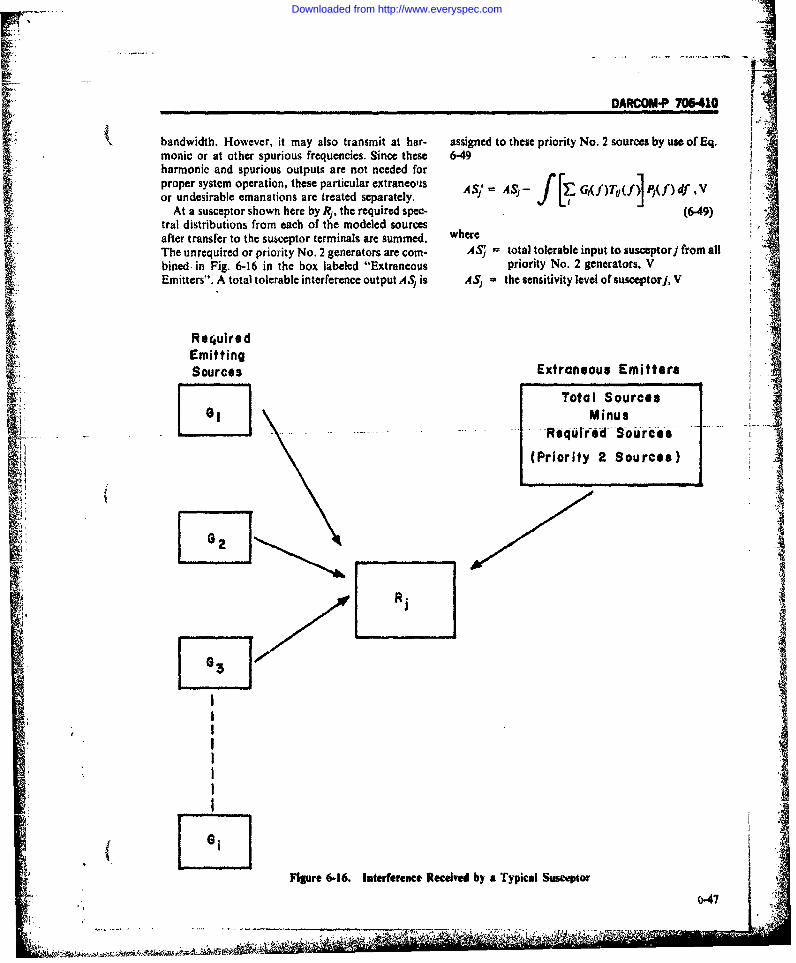
DARCOM-P 706-410
bandwidth. However, it may also transmit at bar- assigned to these priority No. 2 sources by use of Eq.monic or at other spurious frequencies. Since these 6-49harmonic and spurious outputs are not needed forproper system operation, these particular extraneous A ASj - f G,( f Tf P, df .Vor undesirable emanations are treated separately.J '"""J "'
At a susceptor shown here by Rj. the required spec- (6-49)tral distributions from each of the modeled sourcesafter transfer to the susceptor terminals are summed, whereThe unrequired or priority No. 2 generators are corn- AS total tolerable input to suscaptorj from allbined -in Fig. 6-16 in the box labeled "Extraneous priority No. 2 generators. VEmitters". A total tolerable interference output ASV, is A Sj the sensitivity level of susceptorj, V
Re juiredEmittingSources Extraneous Emitters
I I Total SourcesL8 .. . Minus........Reqird Souce
(Priority 2 Souress)
RI
ei]Figure 6-16. Interference Received by a Typical Swiceptor
~ "7
Downloaded from http://www.everyspec.com

DARCOM-P 706410
The quota of interference represented by AS can how many are significant for all priority No. Ibe assigned to the sum total of all extraneous emit- susceptors.ters. However, since AS's is a voltage which defines An interference generation specification is createdthe extraneous interference after it has been into- by the preceding process for each of four kinds of in-grated through the bandwidth of the susceptor in terference:question, there are an infinite number of generation a. Conducted voltagecharacteristics which, when passed through a trans- b. E-fieldsfer function, multiplied by a bandwidth limiting fac- c. Conducted currenttor and integrated could equal AS'. d. H-fields. 4
I' 6-4.8.2.2.1 Generation Specification RoutineThe routine used is shown in Fig. 6-!7. A spec- 6-4.8.2.2.2 Susceptibility Limits
trum called the first order standard is defined which Susceptibility limits are developed to control theportrays the spectral shape and amplitudes of the response of extraneous susceptors. Any susceptor inemanations ff. m all the extraneous generators when the system is exposed to the two sources of the totalfew limitations have been imposed. environment, as shown in Fig. 6-18, i.e., the summa-
Each priority No. 2 susceptor is allowed to modify tion of the emissions due to black-box specificationthis initial spectrum iteratively until a spectrum is limits (extraneous emitters) and the summation of en-created which induces into that susceptor a voltage ergy due to functional circuits. The sum of these twono greater than ASJ the voltage allowable from the sources represents the total system environment. Itextraneous generators. This iterative modification also represents the environment in which the suscep-process is designed to reduce the level of the first tor circuits are required to function. -
order- standard primarily in those areas of the spec- Since the priority No. 2 generator levels have beentrum where the most interference is received, such as established by the generation specification routinein the pass band of the susceptor. Up to four itera. (see par. 64.8.2.2.1), only the priority No. 2 suscep-.! !tions have been found to be required to reduce the tor levels are considered to be adjustable at this time. ,
received voltage to within 2 dB of ASj depending , f ?he effects of the total environment exceed ASptheupon the type of spectrum involved. routine reduced priority No. 2 susceptibility of a
The first o-der standard, as modified by the first -receiver to meet the compatibility requirement. Thispriority No. 2 susceptor, is stored. The second prior- is done on the assumption that the environment isity No. I susceptor is then allowed to modify the first- created from either broadband or narrowbandorder standard until a spectrum compatible with that sources. Each susceptor is considered successively insusceptor is crtated. This process is repeated for each this manner.susceptor to be examined. The final specificationspectrum must be compatible with all priority No. Isusceptors. A spectrum that is the minimum enve- 6-4.8.2.3 Waiver Evaluationlope of those individual spectrums, developed by this The SEMCAP computer program considers amodification process, achieves this result, It is no- request for a specification waiver in terms of its effectwhere higher than the first-order standard and is on system performance. The routine calculates thelower in those regions of the spectrum where the in- voltage induced into each priority No. I susceptorterference was incompatible with one or more of the based upon the spectral density data used for the gen.priority No. I susceptors of the system. erator. If the received voltages do not exceed the
This spectrum represents the interference level allowed voltages, the generator is compatible with thewhich all the extraneous generators of the system act- priority No. I requirements of the system and aing together can be allowed to generate. At this stage, waiver can be granted. However, if the generatorit is a system interference specification with no mar- spectrum exceeds the specification by a large amountgins present. in some frequency ranges, the impact of the in-
To create a specification with margins that can be terference on priority No, 2 susceptibilities must beapplied to individual subsystems or smaller units, the evaluated before a waiver can be granted.minimum spectrum is divided by a J factor that de- To evaluate this situation a new susceptibilityscribes what fraction of the system specification each specification is created based on the inclusion of thesubsystem will be allowed to generate. J must be new generator data. A determination then can bebased on an estimate of how the interference spec- made whether the granting of the waiver would sig-trums of each extraneous generator will combine, and nificantly change the susceptibility specifications.
6-48
. . . .. ... : .-- .o . . . : - , .. , -4 $o
Downloaded from http://www.everyspec.com

CFirst Order Sta_ _ _ _
1i r Reduoti1I____ __ I Program
V= )()-Tjjf).P.( f)df
yes Str odifiled
(AS G SPectrum
Ys More Susceptor MnmunoYes Modified 0
Divide by JIand Marginj
Sore SpecificatioLimit
Figure 6-17. Interference Specification Limits Program
* - C -- 6-49
Downloaded from http://www.everyspec.com

DARCOM-P 706-410
Black-box SpecificationLimits
J Boxes
Extraneous
Susceptors
FunctionalGenerators
Figure 6-18. Susceptibility Limit Development
6-4.8.2.4 Use and Insertion of Test Data Flags call attention to potential problem areas andAt the time of specification development, the por- have the following meaning:
tion of the EMC environment front uncontrolled a. A = Almost an interference problem. +10 tosources is assumed to have a set of levels equal to +30 dB marginthose of the specification limits. As test data are made b. M = Marginal interference problem, -10 toavailable, this assumed set of levels is replaced by ac- + 10 dB margintual test data. Then at the completion of all black- c. P = Probable interference problem, less thanbox-level testing. a final compatibility analysis run is - 10 dB marginmade, making maximum use of test data. Based on The flags in the left-hand column are based on thethis final prediction, circuits whose operations are sum of all four types of interference from each gen-marginal are selected for monitoring during the sys- erator. For the voltage fraction received from all gen-tem test. erators, together with generators operating simulta-
neously, the corresponding margin is given at the bot-64.8.2.5 Program Output tom of the printout.
Fig. 6-19 is a sample SEMCAP output sheet. It isan example of a portion of a detailed receptor-by-re-ceptor investigation. The quantitative details to es-tablish how each generator interferes with a particu- 6-4.8.2.6 Program Availabilitylar receptor are presented. The major part of the out- SEMCAP is currently operational on CDC-6600put identifies the fraction of tolerable voltage and IBM 360/70 computers. It requires 64k (deci-received from each generator via each of the four mal) of core storage. Some of the programming is inkinds of coupling. Th,- corresponding dB margin also machine language. It is able to handle 240 generatorsis printed, with negative margins representing inter- and 240 susceptors. One of the longest programs runference levels above the receptor threshold. The gen- to date, for the B-I Bomber, involved 150 emitterserators arc designated in the right-hand column by and 120 susceptors. This program required 5O min onname. An "S" indicates that a specified, rather than a the CDC-6500 or 20 min on the IBM 360/370. Ameasured, generator output was used in the com- spacecraft analysis generally can be done in 5 to 10putation. min. The program was developed by TRW Systems,
6-50
Downloaded from http://www.everyspec.com

-oARCOM 706410
Olt
a 1 5 w .446A # m
"Wo~w~mm we AmA 960
-4 1; -4044 .3O l p"" a :O04. g42 ". 008v I .0mcv0 1e 4..4~-4.K I -4... n t.34 S 4
R -0
~~~~~~~ .~~ .1 .~ ..* ~ ~ - . . . . 00- .~ ..
ad MIDI 011T c we0 .0.-43WP 0 ~ 4
4.a .4
C4 . 6 . 8 ;Im.
0e!oC!e a C! C!O C! . .d . .1'. . . .4. . 1. . .. ..
. . . . . . .. ...I . U. ' .4 . . . I .4 , . 0. 0 . . t 41iI4.
r4
0~ 1- 47 0Nv 04, t444WM
.d 4 am 0%~1 1 -V 2D 4 Q P141 U'PA '. AC
:b 4 I 4 lilt..4 nA U114 ' ;! .. .
C; 0~a IM.N i44 ft. 1P IN t ..4nM -
64
A %P A''-4 A ID ' -I'm
Downloaded from http://www.everyspec.com

-ARcMO-P 706410
Redondo Beach, CA, for the NASA Manned Space- obtained. The data base is self-organizing and con-craft Center, Houston, TX. Currently TRW Sys- tains characteristic data keyed to the four-level hier-tems, One Space Park, Redondo Beach, CA 90278, archy. It requires on'y one input file consisting ofprovides engineering services in connection with the cards whose number depends on the complexity ofuse of the program. the problem being considered. A minimum of 6 cards
are required for any run, and the normal maximum6-4.9 ISCAP length of the file is 15,000 cards. However, this limit
can be extended to the limit of available core storage6-4.9.1 Genea Descriptim in the computer. Multiple input files can be proc-
ISCAP is an acronym for Intrasystem Compati- essed in a single computer run.bility Analysis Program (Ref. 17). The analysis sec- Fig. 6.20 represents a simple example of the hier-tion consists of six routines designed to investigate archical organization of an electronic system. As onethe principal sources of interference and modes of en- considers elements at lower points in the hierarchy,ergy transfer which exist within an electronics-ori- characteristics become more and more unique until,ented system that has an identifiable electronic and at the minor unit level, information is pertinent to aphysical configuration, e.g., a communication cen- given specific item. Conversely, as one considerstral or a tactical air control center. They are: vhigher elements in the hierarchy, information be-
a. MIL-STD-469 (Ref. 18) Check of radar design comes more general, applying to all subordinate ele-Sparameters ments. For example, location information for equip-b. MIL-STD-188 (Ref. 19) Check of communica- ment No. I in Fig. 6-20 could apply to all subordi-
tions equipment design parameters nate elements. Hence, the computer program is de-c. Spectrum overlap and interference potential signed to model a series of elements that represent
-rom irans -emitters and receptors and, subsequently, to asso-rinous emissions ciate them with the proper higher level elements.
d. Interference potential through receiver spu- To conduct an analysis, characteristics of the le-rious, intermodulation, and cross-modulation re- ments within the four levels must be entered andsponses recorded. This is accomplished through the use of at-
e. Interference potential of receiver local oscillator tribute cards which contain data such as power out-radiation put, antenna gain, location, wire/cable characteris-
f. Interference potential due to radiation from tics, transmitter/receiver tuning range, signal/sus-cables, cases. and antennas coupling into nondesign ceptibility thresholds for receiver/control/signal cir-
receptors, cuits, etc.The computer program and supporting documen- Where measured or design data are not available,
tation provide the following capabilities: the analysis routines utilize limits specified by MIL-a. Organization of system component elements STD-461 (Ref. 20).
into a four-level hierarchy, i.e., systems, equipment,!major units, and minor units. 6.4,93 Mil"tary rd Cheek
b. Multilevel data input, storage, and retrieval. Two military standards checks are performed: (1)This means that characteristics that apply to subor- the MIL-STD-469 check of radar design parameters,dinte units within a system only need to be entered and (2) the MIL-STD-188 check of communicationsonce at the highest level of ownership and not at all equipment design parameters.lower level units. The MIL-STD-469 routine performs the following:
c. Analysis routines to investigate equipment con- a. Radar emission bandwidth check for whichformance 'o military standards, and potential inter- measured, design, or synthesized spectrum data canference interactions based on design characteristics be usedand specifications. b. Radar spurious emission checks which use
d. Run-time selection of analysis routines and sub- design, measured, or MIL-STD-461A dataoptions through use of a common program driver. c. Radar harmonic emission checks which use
e. Run-time identification of equipments and as- design, measured, or MIL-STD-461A datasociated minor units which require investigation. d. Radar tunability check
e. Transmitter stability check6-4.9.2 Data Base f. Receiver acceptance bandwidth check
The analysis program uses a common data base g. Receiver image rejection checkfrom which inputs to the various analysis routines are h. Receiver spurious rejection check.
6-52
* "
Downloaded from http://www.everyspec.com

DARCOM-P 706410
II
Mao Ui ajor Unit Major Unit Major Unit#2 #2
~Minor Uni t 2]
- Minor Unit 3l
Figure 6-20. Simple System Organization
The MIL-STD-188 routine checks harmonic and (FL)T = lowest frequency to which the transmit-
spurious emission levels for global, tactical, and lim- tar can be tuned, Hzited integration aircraft systems that fall within the m - harmonic number from transmitterfrequency limits and modulation classes specified by If the interfering transmitter tuning range, or theMIL-STD-188. mth harmonic of its range, overlaps the lower end of
-"' the receiver tuning range,6.4.9.4 Analysis of Transmitter Fundamental,
Harmonic, and Spurious Emissions m(FH)r - (FL)RThis subroutine, as illustrated in Fig. 6-21, investi- r, (FH)R - (FL)R dimensionless (6-51)
gates frequency overlap between the fundamentaland harmonics of intentional and spurious trans- wherzmitter emissions, and the receiving bands of poten- (FH)r = highest frequency to which the trans-tially susceptible devices. For those situations where mitter can be tuned, Hzoverlap occurs, the possibility of the received signal Similarly, if the interfering transmitter tuning range,exceeding the receiver sensitivity can be determined, or the mth harmonic of its range, fall totally within
The frequency overlap check compares the tuning the receiver tuning range,range of each fundamental and harmonic emissionwith a receiver tuning range, and identifies the per- m(FH)r - m(FL)r dimensionless (6-52)centage of the receiver range contained within the r (FH)R - (FL)transmitter range of concern. When the interferingtransmitter tuning range, or the mth harmonic of its If the transmitter tuning range, or its harmonic, com-range overlaps the upper end of the receiver tuning pletely overlaps the receiver range the ratio is unity.range, the overlap ratio r is Should the ratio be zero, the implication is that no
transmitter power will get into the receiver and no. (FH) - m(FL)r , dimensionless (6-50) magnitude or level computation is needed. If the ratio
(FH)R - (FL)R is small, interference might be avoided by a smallchange in frequency assignment.
where The fundamental emission range and the ranges of(FH)R highest frequency to which the receiver the first 49 harmonics of a transmitter are processed
can be tuned, Hz in this way. Input spurious signals and their harmon-(FL) lowest frequency to which the receiver ics falling within the receiver tuning range also are
can be tuned,.Hz identified. A user option provides for either a6-53
I I
Downloaded from http://www.everyspec.com

DARCOM-P 706-410
L3 U a
a *1
0 j
CL 0CL I
r45
CLI
4) 0
46) ,4
4 64 k re
Downloaded from http://www.everyspec.com

DARCOMP 706-410
"mean" computation (the relation between the The next section of the output provides funda-expected received signal level and threshold), desig- mental/harmonics checks and spurious/harmonicnated M or a "mean-plus-two-sigma" calculation checks as follows:(the relation between the value of signal level which is a. The absolute level (dBm) of the harmonic (HA R)
exceeded only about 2% of the time and the thresh- signalold), designated M + 2a, b. Whether MIL-STD-461 was used to identify the
For an amplitude check, the program identifies the harmonic levelharmonic or spurious emission level of the transmit- c. The harmonic number resulting in spectrumter for those cases which passed the frequency over- overlaplap check. Fundamental emissions that may be cou- d. The relative level (dB) of the harmonic signalpled into a receiver band are excluded from this anal- e. The percentage of receiver tuning range overlapysis. A user option also is provided for either a (PCT OVLAP)
mean" or a "mean-plus-two-sigma" calculation, f, Which run options were used ("mean" orThe program also computes the propagation path "mean-plus-two-sigma")
loss between the emitter and receiver of concern. The g. The interference level (dB) relative 'to themechanism for this computation is the EPM-l Em- receiver interference threshold (INT MARGIN)pirical Propagation Model reported by Frazier andAnderson (Ref. 21). This is a smooth earth, antenna The spurious/harmonics checks are:
height-dependent model which, in the version em- a. The absolute value (dBm) of the spurious/har-ployed here, requires only four input parameters; monic signal (SHL)namely, two antenna heights, a separation distance, b, Whether MIL-STD-461 was used to identify theand frequency. A standard deviation for the path loss spurious/harmonic level .also is determined. Fig. 6-22 provides a generalized il- c. The harmonic number resulting in spectrumlustration of the path loss model for use above 50 overlapMHz. d. Frequency of spurious emission
The program then establishes the mean mutual e. The relative level (dB) of the spurious (SPUR)/.antenna gain coupling value for the link of concern, harmonic signaland the standard deviation associated with this value, f. Which run options were used ("mean" orA bandwidth correction factor also is computed to "mean-plus-two-sigma")account for the reduced coupling situations that oc- g. The interference level (dB) relative to thecur when the emission bandwidth is large compared receiver interference threshold.with the receiver bandwidth,
The output format of this evaluation is shown inFig. 6-23, which is a sample run of the frequencyoverlap and transmitter harmonic/spurious interfer-ence checks, 6-4.9.5 Receiver Spurious Responses,
The first section of the output summarizes several Intermodulatlon, and Cross-Modulationof the run input parameters for the emitter-receptorpair being examined, plus the mean antenna gain 6-4.9.5.1 Description of Analysis Routineproduct GM, the standard deviation of the antennagain product SIGMA G, and the standard deviation Thi, analysis routine, shown in Fig. 6-24, investi-of the path loss SIGMA P. Other parameters in this gates the possibility of the fundamental emitter an.section are: tenna-radiated energy exceeding the sensitivity of a
receiver spurious, intermodulation, or cross-modu-ANTLB = antenna lobe lation response. The reference levels are those in
SS - sidelobe of transmitter to sidelobe MIL-STD-461.of receiver For each transmitter-receiver pair whose terminals
GTI = main beam gain of transmitting an- are not intended to communicate with one another,tenna, dB the program determines whether spectrum overlap
GRI - main beam gain of susceptor anten- could occur within or outside of the receiver tuningna, dB range.
POP = power output, peak, kW Using inputs describing receiver sensitivity, a cal-RSENS = receiver sensitivity or interference culation is made to determine whether or not the re-
threshold, dBm ceived interference signal will exceed the sensitivity
6-55
.. .-
Downloaded from http://www.everyspec.com

DARCOM-P 706-410
On
0i
caV
ItCSJ 0 t)vi V) 0)
Ill 0 CL0 ru
m 41a) rricm
4-btv
A 4-)rd
4-)
C
Z -45u furd&
(AIA
CL M 0-i
cuurd
ILL
OF
1.0
SP 'SSOl 44Rd
6.56
Downloaded from http://www.everyspec.com

r DARCOMP 706-410
tz LSo S3
C; ~ .4 .
f3 fL 31I c I
In) ;z 4
Vi 0.10
w 4655
;... C CA~~A* c - a:
in~ 9 -
Downloaded from http://www.everyspec.com

DARCOM-P 706-410
.1..54,* 01;>
a iiP
.9 L in1.U 0 ii
6.580
CL4 Oc----.. m-------
M2 1 .-~ 06 0
Downloaded from http://www.everyspec.com

OARCOM-P 706410I
* threshold. Eq. 6-53 is used to calculate the corre- wheresponding interference level IL. PLO = local oscillator power present at antenna
terminals of iterfering receiver. dBmnIL = 10 log POP + GM + LPROP GMA - mutual antenna gain, dB
The output format for this analysis routine isRSENS - SPUR + 60 ,d9 (6-53) shown in Fig. 6-26, which is a sample run for the local
where oscillator overlap and amplitude checks.
POP - peak power, kWLPROP = path loss between antennas, dB 64.9.7 Analysis of Cable, Case, and
Antenna Coupling6-4.9..2 Reslts of Receiver Analysis Routine A much simplified block diagram of this subrou-
Operation tine is presented in Fig. 6-27. The levels of signalsThe output format of the evaluation is shown in emanating from cases and cables are based on MIL-
Fig. 6-25 which is a sample-run of the receiver spu- STD-461 limits.rious, intermodulation, and cross-modulation rou- Emission limits for broad/narrowband conductedtine. The columns of significance are: (CE01, CE02, CE03, CE04), radiated magnetic field
a. Receiver Spurious Check: (RE01), and radiated broad/narrowband electric(1) The run option (mean, or mean + 2a) rela- field (RE02) are considered for all case and cable
tive to this test minor units. Transmitter/transceiver minor units(2) The interference level (dB) relative to the having antenna ports use the transmitter peak power
receiver sensitivity .. and. main beam antenna gain for the calculation of ef-(3) The receiver spurious level (dB) used in the fective radiated interference power.
calculation. Coupling calculations for wire and case combina-b. Cross-modulation Check: tions are based on the SEMCAP equations, as dis-
(I) The interference level (dB) relative to the cussed in par. 6-4.8.1. The output format of this anal-receiver cross-modulation threshold ysis routine is shown in Fig. 6-28. The first section of
(2) The guard band (MHz) required when using the output identifies the susceptor and generatorthe specified preselection filter. In the example (first pairs being examined- minor unit names and identifi-line), the guard band is 1.9 MHz and the interference cation numbers are presented. The next section of themargin is 56 dB. Thus a preselection filter having a output presents data concerning the interferencegreater than 56 dB rejection 1.9 MHz off the carrier modes and contains four subsections: antenna gen-frequency must be inserted in the receiving system. crated interference, conducted emission, radiated E-
(3) The cross-modulation threshold valse spe- field and radiated H-field.cifled by the user or by MIL-STD-461. The column headed "'Antenna Generated Inter-
c. Intermodulation Check: ference" presents interference signals which are cou-(I) The interference level (dB) relative to the pled into the susceptor wire port. Calculations are
receiver intermodulation threshold performed using the mid-band operating frequency(2) The guard-band (MHz) required when using of the transmitter which feeds the antenna port.
the specified preselector filter The column "Conducted Emission Mode" consid-(3) The intermodulation threshold value speci- ers both narrow and broadband emissions and pro-
fled by the user or by MIL-STD-461. vides the level of those interference signals that ared. Data. This section contains the data used in the coupled through capacitive and inductive transfer.
computations. ALS means "antenna lobe selection" Calculations are made using the mid-band frequencyand SS means "sidelobe to sidelobe" as before. of the wire information and the bandwidth,
Columns headed "Radiated E-Field" and "Radi-6-4.9.6 Description of Local Oscillator Radiation ated H-Field" present interference levels coupled into
The received interference level IL above the the receptor wire through E- and H-field transfer.Th eevditefrnelvl Laoete The third section of the output format is entitledreceiver sensitivity level, resulting from local oscilla- "Interference Data", This section presents the totaltor radiation, is calculated by Eq. 654,.Itreec aaTi scinpeet h oa
r tnsl t b q 4narrow and broadband interfering signals. These
IL - PLO + GMA + LPROP values represent the sum of entries for conducted andradiated modes. In addition, the interference levels
RSENS , dB (6-54) are compared to the desired signal and safety margin.
6-59
7. .. .' " }' " - -- -- - - '. :T ... "
' "" " ' : ... • ' .y :' .. .-
Downloaded from http://www.everyspec.com

DARCOM-P 706410
U3
in.
L2 CIDw Pl.
C9 9
E +
no0 00
£0 * U. *6
6.60
Downloaded from http://www.everyspec.com

DARCOM-P 706-410
i~sh . i U
L.4 C~ I ia
w an a c
gil II~0 cc*0e-
41-4 s
aaCC
Ii. aJ. Who . t . ..
0~~~~ 0 c u ~3O
a .Jj~U.
o 9
0 6L
6.0~ 4 o A
3 a, 4j C
-j 06"61
19u
Downloaded from http://www.everyspec.com

DAROMP 706-410
4 w0 0tM .4 0 0
CL w 0 -0 4C U$ CLQc
w 4ac1 0 -a'
w Eq -f 2 0 40 .3 4-0-1 014 M1-4 P 4J p a30r4z -> 1.4 )0-- 03
'0 0 i c.0.
0 0aCo )a-4.
to a
"4 64 0 .40I00- F40)
.4J0 ~ 4-4 -00m0z0 0 U4 4
W0 0 C043 V- 4 M to Ma CD C.4.3 340 "
to 0 a C LJ 4 r &1 0
(a 0 D 00 42 0000
_0~ .4 0- > C
r-I 4.. . . . .
Downloaded from http://www.everyspec.com

DARCOM-P 706410
IIUin a:n 9
14*C a d D . 0
w4 0 0
Ln m4 z _jC30 o 4 3I ccc_j 0 49 d m>_
2C
-1 0 la tn 0 az
0 a t". a ccI a
L_ Ln cc -M0 cc I m :a
2 0
an 0
I 1. oI I .0 E - a
Cc cc, m 0 0 10z :.a ". ~ -
~ 0 0.
fa
0 2 V,
I 2in fa
0 la~I1- E-4
cn X CL
6-63
q..~.,:7F,
Downloaded from http://www.everyspec.com

DARCOMP 706-410
The result of this comparison is presented under the c. Angle modulation with stochastic process ("Acceptability" heading. The last section presents E- d. Single sideband amplitude, phase, and frequen-and H-field strength levels at the receptor wire or cy modulation with a stochastic processcase. e. Chirp radar spectra
After all generators have been played against the f. Pulse code modulation/amplitude modula-susceptor the total interference signal present on the tion-nonreturn to zerowire is calculated. This interference signal then is g. Pulse position modulationused to calculate the total acceptability for the sus- h. Pulse code modulation/amplitude modulation-ceptor wire being examined. These data are found be- biphaselow the last generator entry for the susceptor being i. Pulse amplitude modulation/frequency modu-examined. lation
j. Pulse duration modulation6-4.9.8 Implementation k. Single pulse
The ISCAP program runs on a UNIVAC 1108. In- 1. Pulse train (rectangular, trapezoidal, triangular,formation on its use can be obtained from the Elcc- sawtooth, high frequency exponential, damped sinu-tronic Systems Division (AFSC), Hanscom AFB, soidal).MA 01731.
6-4.10.2.2 Susceptors6-4.10 INTRASYSTEM ELECTROMAGNETIC The basic approach is to accept input data on in-
COMPATIBILITY ANALYSIS band sensitivity, along with a bandwidth parameter.PROGRAM (IEMCAP) and then to form a rectangular-shaped susceptibility
6-4.10.1 Introduction function in the required spectral region that connectsThe Intrasystem Electromagnetic Compatibility to nonrequired spectra-defined by user-adjusted-mili-
Analysis Program (IEMCAP) (Ref. 22) was devel- tary specification interference limits. An RF receiveroped to provide an economical implementation of representation in the program will, in general, ac-
I EMC analysis at all stages of a system life cycle, from tually have a trapezoidal shaped susceptibility func-conceptual studies of new systems to field modifica- tion (in-band) due to the skirt slopes ofthe normal se-tion of old systems. This is accomplished by per- lectivity curve. Specifically, the susceptibility of anforming the following tasks: RF port is assumed to be equal to the tuned sensi-
a. Provide a data base which can be continually tivity of the receiver, as provided in the input data,maintained and updated to follow system design over the entire frequency range defined by the user-changes. specified bandwidth. The susceptibility of a signal or
b. Generate EMC specification limits tailored to control port is assumed to be equal to the operatingep e stem. ofrntinwalevel [dB(jiA)] less 20 dB. This somewhat arbitrary
c. Ealute he mpat o gratin waver tothe susceptibility level is based on characteristics of com-
tailored specifications. mon avionic equipments. If the user wants a higher ord. Survey a system for incompatibilities, lower susceptibility level in the required range of ae. Assess the effect of design changes on system signal or control port, he need only specify a higher
EMC. or lower operating level, respectively.f. Provide comparative analysis results on which In the case of receivers where more is known about
to base EMC trade-off decisions. the details of the response curve than just the flat re-sponse previously discussed, the user can specify the
6-4.10.2 Models known response curve by a discrete spectrum of up toten frequencies with associated levels. Interference
6-4.10.2.1 Emitters calculations using either the specified spectrum or theEmitter models are incorporated in the program flat response function are conducted by weighting the
which correspond to common signal sources-single received interference signal power by the ratio of thepulse, repetitive pulse, information-bearing pulse, receptor to emitter bandwidths, when the former isand CW signals. Provision is made for user input of the smaller value of the two.spectral dcnsities for those types not modeled. The The user has an additional option of augmentingfollowing sources are modeled: either of the two preceding models with certain filter
a. Binary frequency-shift keying functions as described in par. 6-4.10.2.3.1. When thusb. Amplitude modulation with stochastic process used, the filter models relate the susceptibility level of
6-64
-- " - -'.. t-- " " <.-,. . ' ' : - •
Downloaded from http://www.everyspec.com
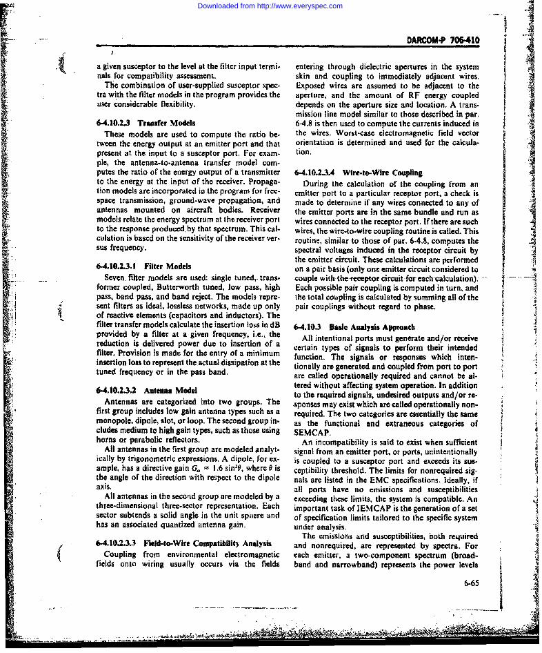
9j - DARCOM-P 706410
a given susceptor to the level at the filter input termi- entering through dielectric apertures in the systemnals for compatibility assessment. skin and coupling to immediately adjacent wires.
The combination of user-supplied susceptor spec- Exposed wires are assumed to be adjacent to thetra with the filter models in the program provides the aperture, and the amount of RF energy coupleduser considerable flexibility, depends on the aperture size and location. A trans-
mission line model similar to those described in par.6-4.10.2.3 Transfer Models 6-4.8 is then used to compute the currents induced in
These models are used to compute the ratio be- the wires. Worst-case electromagnetic field vectortween the energy output at an emitter port and that orientation is determined and used for the calcula-present at the input to a susceptor port. For exam- tion.pie, the antenna-to-antenna transfer model com-putes the ratio of the energy output of a transmitter 6.4.10.23.4 Wire-to-Wire Couplingto the energy at the input of the receiver. Propaga- During the calculation of the coupling from anF. tion models are incorporated in the program for free- emitter port to a particular receptor port, a check isspace transmission, ground-wave propagation, and made to determine if any wires connected to any ofantennas mounted on aircraft bodies. Receiver the emitter ports are in the same bundle and run asmodels relate the energy spectrum at the receiver port wires connected to the receptor port. If there are suchto the response produced. by that spectrum. This cal- wires, the wire-to-wire coupling routine is called. Thisculation is based on the sensitivity of the receiver ver- routine, similar to those of par. 6-4.8, computes thesus frequency. spectral voltages induced in the receptor circuit by
the emitter circuit. These calculations are performed6-4.10.23.1 Filter Models on a pair basis (only one emitter circuit considered to -
..Seven. filter models-are used: single tuned,- trans- couple-withthe-receptor circuit-for-each calculation) . -
former coupled, Butterworth tuned, low pass, high Each possible pair coupling is computed in turn, andpass, band pass, and band reject. The models repre- the total coupling is calculated by summing all of the
N sent filters as ideal, lossless networks, made up only pair couplings without regard to phase.of reactive elements (capacitors and inductors). Thefilter transfer models calculate the insertion lobs in dB 6-4.103 Basic Analysis Approachprovided by a filter at a given frequency, i.e., the All intentional ports must generate and/or receivereduction is delivered power due to insertion of a certain types of signals to perform their intendedfilter. Provision is made for the entry of a minimum function. The signals or responses which inten-insertion loss to represent the actual dissipation at the tionally are generated and coupled from port to porti~i: tuned frequency or in the pass band,tneare called operationally required and cannot be al-
tered without affecting system operation. In addition4.10.23.2 Antenna Model to the required signals, undesired outputs and/or re-Antennas are categorized into two groups. The sponses may exist which are called operationally non-
first group includes low gain antenna types such as a required. The two categories are essentially the samemonopole, dipole, slot, or loop. The second group in- as the functional and extraneous categories ofcludes medium to high gain types, such as those using SEMCAP.horns or parabolic reflectors. An incompatibility is said to exist when sufficient
All antennas in the first group are modeled analyt- signal from an emitter port, or ports, unintentionallyically by trigonometric expressions. A dipole, for ex- is coupled to a susceptor port and exceeds its sus-ample, has a directive gain G, 1.6 sin20, where 0 is ceptibility threshold. The limits for nonrequired sig-the angle of the direction with respect to the dipole nals are listed in the EMC specifications. Ideally, ifaxis. all ports have no emissions and susceptibilities
All antennas in the second group are modeled by a exceeding these limits, the system is compatible. Anthree-dimensional three-sector representation. Each important task of IEMCAP is the generation of a setsector subtends a solid angle in the unit sphere and of specification limits tailored to the specific systemhas an associated quantized antenna gain. under analysis.
The emissions and susceptibilities, both re4uired6-4.10.2.3.3 Fleld-to-Wire Compatibility Analysis and nonrequired, are represented by spectra. For
Coupling from environmental electromagnetic each emitter, a two-component spectrum (broad-fields onto wiring usually occurs via the fields band and narrowband) represents the power levels
6-65
NO4 A
; :|::~ ~ ~ ~ ~ ~-o ...N"Q::: ""/........ ''
Downloaded from http://www.everyspec.com

DARCOM-P 706-410
produced over the frequency range. The broadband also computes the total signal from all emitters cou-component represents continuous emissions which pled into each susceptor acting simultaneously. Do-vary slowly with respect to frequency, while the nat- tails of the two analyses are contained in Rtf. 22.rowband component represents discrete emissions In determining the spectra and in other phases ofwhich vary rapidly with respect to frequency. The the analysis, the termination impedance must bebroadband components are in units of power spec- known. A wide variety of terminations can exist intral density, and the narrowband components are in the system, but for the most part they can be repre-units of power. sented by a series resistor and inductor with a shunt
For each susceptor, a spectrum represents the sus- capacitor.ceptibility threshold over the frequency range. The Power transfer relationships are normalized to a Isusceptibility level is defined as the minimum re- ohm impedance. The actual port impedances that areceived signal which will produce a response at a given input to the program then are used to transform thesefrequency. power relationships appropriately.
For each intentional source or receiver port, a por-tion of the frequency range is defined as the requiredi range. All signals within this range are required andcannot be adjusted. Outside this range, limits may be 6-4.10.4 Spectrum Representation
set for the maximum emission and minimum sus- The fundamental computation carried out byceptibility levels. Within the required range, the spec- IEMCAP is one giving the power into the susceptortrum is defined by a mathematical model of signal and is essentially the same as Eq. 6-1 under the Allenlevel versus frequency. This can be either from equa- Model (par. 6-4.2.1). Note that it is also similar totions of the frequency domain representation of the Eq. 6-48 under SEMCAP (par. 64.8.2.1) except thatsignal.or- directly from a user-defnted spectrum. Out- the latter- uses source amplitudes-and-transfer-func- . ....side the required range, assumed levels are used for tion amplitudes rather than power spectral densitiesthe port spectra. and power transfer functions.
During specification generation, if these assumed A sampled spectrum technique is used in whichspectrum levels cause interference, they are adjusted each spectrum amplitude is sampled at various fre-for compatibility. By adjusting the spectra of emit- quencies across the range of interest. Considering theters and susceptors for compatibility the maximum requirement of MiL-STD-461 of 3 frequencies pernonrequired emission and minimum susceptibility octave from 30 Hz to 18 GHz, this requires approxi-levels are obtained for a compatible system. To pre- mately 90 sample frequencies. This is a reasonablevent overly stringent specifications from being resolution for EMC specifications in which limits ofgenerated, each spectrum has an adjustment limit, emission and susceptibilities are set and-can apply
Initially, the limits of military EMC specifications over large regions of the spectrum. If greater resolu-MIL-STD-461 and MIL-1-6181 are used. The levels tion is desired, the user can specify individual fre-may be relaxed or tightened from these it desired. quencies. To avoid missing narrow peaks betweenThese specifications are used for a variety of reasons, sample frequencies, the spectrum is samp'ed in the in-First, since they are widely used, most EMC engi- terval half-way between the sample frequency andneers are familiar with them. Those portions of the each of its neighboring sample frequencies. For emis-port spectra not requiring adjustment remain at the sion spectra, the maximum in the interval is used; forusual specification levels. Also, if new equipments are susceptibility spectra, the minimum is used. This ef-added to a system containing existing equipment de- fectively quantizes the spectra with respect to theveloped and tested to these specifications, the sample frequencies.IEMCAP-generated specifications will be at the same To minimize core memory and data file size re-general levels and not require radical changes in quirements, a tabL of sample frequencies is definedEMC design. This also facilitates adapting an equip- for an equipment, and all spectra of ports within thatment from one system to another system. equipment are quantized at these frequencies. Thii
The general approach in performing the various eliminates storing a table of sample frequencies fortasks is two-fold. First, a susceptor is selected and its each port which saves 50,400 words of file storage,type, connection, wire routing, etc.. is examined to plus the input/output time required to store and re-determine if a coupling path exists. If a path exists, trieve the information.the received signal is computed at the susceptor and The equipment frequency tables can be definedcompared to the susceptibility level. In addition to using two options. First, the user may specify the up-the emitter-susceptor port pair analysis, the program per ard lower frequency limits, the maximum num-
6-66
S '- ---- . ... _4
Downloaded from http://www.everyspec.com

DARCOM-P 706-410
. her of frequencies (up to 90), and the number of fre- program contains the data management and spec-quencics per octave. The program then generates a trum model routines, and the other contains the anal-table of geometrically spaced frequencies within the ysis and transfer model routines. Each section is exe-specified limits. Optionally, the user may specify the cuted separately so that both are not in core at oneupper and lower frequency limits, the maximum time.number of frequencies. and a number of specific fre-quencies (up to the maximum number) of interest.The program then generates geometrically spaced fre-quencies to fill in the number of frequencies not 6-4.10.5 Logic Flowspecified. For example, if the maximum number of Fig. 6-29 shows the basic functional flow throughfrequencies to be used is 90 and 10 are user specified, its two sections. These sections are executed inde-the program generates 80 geometrically spaced fre- pendently with intermediate data storage on aquencies over the specified frequency range and in- number of disc or tape files known as working files.serts the 10 user frequencies at the appropriate places. Depending on the analysis and the size of the system
The range of frequencies covered by the analysis is being analyzed, the program sections can be exe-controlled by the user. The program will accept any cuted in succession or run separately.range from 30 Hz to 18 GHz but, if desired, the user The functions performed by each program sectionmay concentrate all 90 frequencies over a smaller in- are described briefly in the paragraphs that follow.terval within this range. Details can be found in Ref. 22.
Each port is categorizedby function into one of six The first section called the Input Decode and Ini-types, each type having its own subintetval of fre- tial Processing Routine (IDIPR), is divided into threequencies within the overall frequency range. These basic routines (Fig. 6-29). The Input Decode Rou-subintervals, adapted from MIL-STD-461/462 tine (IPDCOD) reads and decodes the free-field 'nputranges for the poet function, are shown in Table 6-10. data from punched cards and.checks the data forThe nonrequired spectrum model routines will gen- errors.crate zero emission and susceptibility outside tht The program then proceeds into the Initial Proc-subintervals, essing Routine (IPR). This routine performs data
The spectra and amplitudes are represented within management, interfaces with spectrum models, andup to 90 cnntiguous intervals across the frequency generates the working files. Data defining the-systemrange of ;;i crest quantized to the sample frequen- and al! of its components are stored on a magneticcies. This ,epresentation allows for flexibility and disc or tape called the Intrasystem File (ISF). This fileprogram efficiency. It also allows the program to be is a data base which is maintained by IPR, incorpo-divided into two sections, each running in 60k (deci- rating changes in the system design. For a given run,mal) of core memory. With this arrangement, the the system to be analyzed can be defined fromprogram is readily adaptable to a wide variety of punched cards only, from a previously created ISF,computers, and machine-dependent techniques, such or from an old ISF updated by cards. IPR assemblesas overlaying, are not required. One section of the and merges the data to be analyzed and writes these
TABLE 6-10PORT EMISSION AND SUSCEPTIBILITY TESTS AND FREQUENCY RANGES
SPORT EMITTER RECEPTOR
FUNCTION MIL-STD-462 Freq Range. MIL-STD-462 Freq Range,Test(s) Hz Test(s) Hz
RF CE06 14k-ISG CS04 14k-18GPower CE02/03 30-50M CSO /02 I 30-400MSignal CE02/04 30- I G CS02/04 30-1OGControl CE02/04 30-IG CS02./04 30-1OGEED - CS02/04 30-1OGEqpt Case RE02 14k-lOG RS03/04 14k-IOG
6-67
. _ . " ; : . ." .'. . . ". ' .-..> & r ... . -. ..
Downloaded from http://www.everyspec.com

DARCOM.P 706410 ......
INPUfTL i - ECODEOAPT ROUTrINE
OLDERRORS? STOP
INITIAL INTASPECTRUM PROCESSING SYSTEMODELS ROUTINE -.
REOUIRED
6 - - -T -WIRE MAP -WORKING
A J CET ROUTINE FIE
NON-~D<~
* ~5PTOR STOP
!I
TART
SPECIFICATION COMPARATIVEr GENERATION 1 EMI ANALYSISCOUPLING J OTN ROUTINEMODELROUTINES ~
ANT,.COpL0 WRA.Up INTRA-WIRE. VIRE ROUTINE ISYSTEMCASE CASEFILTER
ENVIR.~Lo STOP
Figure 6-29. IEMCAP Functional Flow
6..4
Downloaded from http://www.everyspec.com

. ... DARCOM 70640
data on a new ISF for future runs and on the work- port spectra, initially computed to IPR, to produce aing files for analysis. During this process, IPR inter- compatible system. These spectra are limits. Thus, anfaces with the spectrum math model routines. These emitter cannot generate outputs greater than the non-use the user-specified port spectrum parameters to required spectrum levels, and a receptor cannot re-compute the spectrum amplitudes quantized to the spond to received signals less than these levels or in-equipment sample table frequencies for each port. terference will result. For the analysis, each port isFrom IPR, the program enters the wire map routine assumed to emit and respond at these levels. For eachwhich generates cross-reference map arrays for use by emitter-receptor port pair in the system with a cou-the wire coupling math models during analysis. At piing path between them, the received signal is corn-this point, execution of IDIPR terminates. The com- puted using the assumed maximum emission levels.puter can either stop or continue into the second sec- This signal is compared to the assumed minimumtion, depending on the job setup. susceptibility levels over the frequency range, and
The second section called the Task Analysis Rou- where the susceptibility level is exceeded in the emit-tine (TART) uses the data compiled by IDIPR to per- ter nonrequired range, the emission levels are reducedform the desired analysis task. This is one of the four such that the margin is equal to the user-defined ad-tasks summarized as follows: justment safety margin (asm) or to the adjustment
a. Specification Generation. Adjusts the initial limit level, whichever is greater.nonrequired emission and susceptibility spectra such When each emitter has been adjusted in conjunc-that the system is compatible, where possible. A sum- tion with each receptor, the receptor spectra aremary of interference situations not controlled by adjusted. The received signal from each emitter withEMC specifications is printed. The adjusted spectra a coupling path to a given receptor is computed usingare the maximum emission and minimum suscepti- the adjusted emission spectra and summed. The sus-bility specifications-for use in EMC tests, ceptibility spectrum- levels then are compared to this
b. Baseline System EMC Survey. Surveys the sys- total signal, and where the level is exceeded in thetern for interference. If the maximum of the EMI nonrequired range, the susceptibility is raised such
U margins over the frequency range for a coupled emit- that the margin is asm, or to the adjustment limitter-receptor port pair exceeds the user specified print- level, whichever is less.out limit, a summary of the interference is printed. As a result of this process, a set or port spectra isTotal received signal into each receptor from all emit- generated which must be met if the system is to beters also is printed, compatible. These then, are EMC specification lim-
c. Trade-off Analysis. Compares the interference its to which the equipment ports can be tested.for a modified system to that from a previous specifi- After the adjustment process, a number of portcation generation or survey run. The effect on inter- pairs may exist which are still incompatible. This isference of antenna changes, filter changes, spectrum called unresolved interference and results froniparameter changes, wire changes, etc., can be required emissions and responses, nonrequired spec-assessed from this analysis. tra adjusted to their limits, and from nonadjustabled, Specification Waiver Analysis. Shifts portions of spectra of previously procured equipments. Conse-
specific port spectra as specified and compares the re- quently, after susceptor adjustment, SGR recom-suiting interference to that from a previous specifica- putes the interference between adjusted emitters andtion generation or survey run. From this, the effect of adjusted susceptors. If the maximum of the EMIgranting waivers for specific ports can be assessed. margin exceeds a user specified printout limit, the
TART is composed of two basic routines (Fig. 6- case is printed as unresolved interference along with a29). The Specilication Generation Routine (SGR) summary of the spectrum levels and the EMIperforms the first task previously described and the margins.Comparative EMI Analysis Routine (CEAR) per-forms the remaining three. These interface with thecoupling math model routines to compute the trans. 6-4.10.7 Outputsfer ratios between emitter and receptor ports. Outputs are provided for the three SGR phases:
emitter spectrum adjustment, susceptor adjustment,and unresolved EMI. After these, the finally adjusted
6-4.10.6 System/Subsystem Spegiflcation spectra are summarized for each port. An exampleGeneration summary of the adjusted emitter broadband and nar-
The Specification Generation Routine (SGR) rowband spectra is shown in Fig, 6-30. After a givenattempts to adjust the nonrequired portions of the susceptor port has been adjusted, SGR scans through
6-69 j
Downloaded from http://www.everyspec.com

DARCOMP 70".10
of %I0 ftetat
a aa* ft tv N v4 1f t t NNtVc U
Vftb
ft All :00=B t t ff1 . 6 .0.0a ft ft on 10 l
j. a
b .4%C4 ftto 4 00w W .0t0tt4 w ffftf fw waf wft ft mtwt9g-tft
f I I I N* * m w T LA 06*w * .
-d .. bdpa C.4Ni wft*f.w ft Vfp~. W..4 W .V. f A.W ft f
of%. C. a ' ftft.4
. 4 N 4 1
I.J ~~~ ~ i 99 1. w ft ft0 t f t f t f
rw In*4.W~~~~ ~~~~~~~~~ ft f t a f V ft f , t0m 4 3 f4 Qt~
o-. "W 11 ". 14 u. r.lp an J" v r1 w
6-704
Downloaded from http://www.everyspec.com

DA.COM-1 706-410
the emitters coupled to it and computes the margins. 6-4.11.2 Data InputsIf the maximum margin exceeds the user specified Five types of inputs are needed to describe a givenprintout limit, a summary is printed, as illustrated in circuit. The input statements define the topology ofFig. 6-3 1. the circuit, the circuit element values, the linear and
Printouts also can be provided for baseline system nonlinear dcvices used in the circuit, the circuit exci-EMI survey outputs, trade-off, and waiver outputs. tation and the order of the analysis, and the desiredError printouts, input data card listings, and intra- output.system signature ite reports can be obtained as partof the IDIPR printed outputs.
6-4.11.3 Anlysls Process6.4.10.8 Availability The network is divided into segments which are au-
The program is written in FORTRAN 1V for the tomatically cascaded. The cascade equations includeCDC-6600 or the Honeywell 635. It is divided into linear loading effects. Segmentation is done such thattwo sections, each of which requires 60k (decimal) of nonlinear interaction is small. There is no limit to thecore memory (par. 6-4,10.4). One section is for data size of a network that can be analyzed.setup and the other is for the actual program run. A Structurally, the nonlinear network problem is7- or 9-track tape is used, with ACSII II code, solved by forming both the nodal admittance matrixh program, as well as technical assistance in its (Y matrix) for the entire network, and the first-order
use, can be provided via Code RBC, Rome Air De- generator (current source) excitation vector, for all ofvelopment Center, Oriffis Air Force Base, NY. the linear sources in the entire network. The genera-
. Copies of the program are made available to those 'tors can be located at any node in the network, andwho provide a blank tape for program recording. The can have any desired frequency, amplitude, andtape is recorded in. card image format.. phase. The usual procedure of premultiplying thetaenerator vector bycorded the inverse image matr in thegenerator vector by the inverse Y matrix results i h
first-order nodal voltage vector for the network, the•1 Celements of which are the first-order transfer func-6.4.11 SIGNCAP I tions at all nodes in the network at the given excita6:4.11.1 Objectives tion frequency. In the event that there is more than
This nonlinear circuit analysis program (Rcfs. 23, one generator at a given frequency, the first-orderT his n o n i n e r c rc ui a n ly s s p og ra ( R fs .2 3 , tra n sfer fu n ctio n is th e to ta l tra n sfe r fu n c tio n d u e to24, and 25) allows the engineer to determine the non- talinear transfer functions of an electronic circuit con- the superposition of the generators, since the first-taining resistors, inductors, capacitors, transistors, order transfer function is a linear function. Thevacuum tubes, and diodes. It uses a set of standard higher order functions are solved iteratively.electric circuit elements, and can analyze networksmade up of interconnections of these elements. The 6 4 Oobjective of determining these transfer functions and 6-4.11.4 Data Outputsanalyzing the networks is to provide a close predic- The software available can analyze up to 50 nodetion of the degradation caused by general classes of networks directly. The output of the program is theinterfering signals. nonlinear transfer function of the desired order at all
A realistic receiver model must be nonlinear to ac- the nodes of the network,count for such effects as desensitization, cross-modu-lation, intermodulation distortion, and spurious re-sponses. Models that have been developed are non. 6-4.11.5 Availabilitylinear canonic models of portions of communication The program is written in FORTRAN IV, and hasreceivers that lead to a representation of the given been implemented on two computers, the IBM 1130receiver in terms of building blocks of known form, with 8k of core and the Honeywell 635. The IBMmultipliers, and receiver-dependent parameters. The 1130 version can directly analyze networks contain-number of parameters required generally will be ing up to 50 nodes. Larger networks can be analyzedmuch smaller than the number of devices and com- by segmenting the network into subnetworks, andponents in the receiver, As a result, the canonic then employing a cascading program.model approach leads to a practical means of anal- Copies of the program on punched cards can beyzing and simulating the input-output behavior of a obtained by contacting Code RBCT, Rome Air De-receiver as a nonlinear signal-processing black-box, velopment Center, Griffiss Air Force Base, NY.
6-71
S- _ __ _
Downloaded from http://www.everyspec.com

DARCOM-P 706410
* c~~u .4.444
0* or' or it 0 v .4 )
-1. 44...
OL..4. - NTMWT :4
ow ~ ~~~ ~ ~ ~ .041 4:1 8I : :0 : I04~~~~ a do a t t I 2 I
up .0 " 0, W ftft
T 1 4 777 777*" "1 -99 44MN IV44--w -
*I: 1 f WWI #44 j~V '44.4'~ftl. Vdtlp Ala .4 - 0 W N 44 -
tT W 04 To I*l4g - "..
pd, I. ow 6 0 00b
fq ft In.4 4 a*44 * a 4 do "-* a wj4,* a
.0 OJ * j4 J4 44 j4 * J4 4 *4 4 *4 * *
0-1 *4 a4l0 * I &1-4 *4 No- a 4 a.al- 0. .44 * 4 * 4 **4 4 *
G. L 1- 4. , o. I I... IL a 6 L60 O 0 Cm, I. f .*4.4@8m U. r.4..1.Um 4Lk
54,4 1 4 -
J.04 no .4 4
6-724a.4la444a ~ a4*00.~8~~a408 8.
Downloaded from http://www.everyspec.com

DARCOM.P 706-410
REFERENCES 12. M. N. Lustgarten, "COSAM (Co-Site Analysis1. Department of the Army, Pamphlet Pam 11-13, Model)", 1970 IEEE Electromagnetic Compati-
March 1975, Army Electromagnetic Compati. bility Symposium Record, 394-406, July 14, 15,bilty Program Guide. 16, 1970.
2. ECAC-TN-74-01, The ECAC Data Base Re- 13. M. N. Lustgarten and D. J. Hughes, "Valida-source. 15 January, 1975, Electromagnetic Com- tion of the Cosite Analysis Model (COSAM) forpatibility Analysis Center, Annapolis, MD. Selected UHF AM Equipments", Tech. Report
3 R. A. Burt. C-E-I-R, Inc., "Radio Interference No. ESD-TR-71-356, Electromagnetic Com-Prediction by the Statistical Terrain Method", patibility Analysis Center, North Severn, An-Final Report, Contract DA-28-043-AMC-00346 napolis. MD 21402, December 1971.
.(E), US Army Electronics Laboratories. 26 April 14. Shipboard Electromagnetic Compatibility Anal-
1966. ysis. SEMCA III, Vol. VIIA, User's Reference4. "Input Data Format Instructions and Output Manual, General Electric Company Apollo Sys-
Tape/Disk Format for Electromagnetic Coin- terns, Daytona Beach, FL, January 1970.patibility Computer Programs (Allen Model)", 15,. W. R. Johnson, B. D. Cooperstein, and A. K.Revised Edition, January 1973, US Army Elec- Thomas, "Development of a Space Vehicle Elec-tronics Command, Fort Monmouth, NJ, tromagnetic Interference/Compatibility Specifi-Comm/ADP Lab. cation", TRW Document No. 08900.6001-TOOO,
5. A. G. Longley and P. L. Rice, "Prediction of TRW Systems, One Space Park, Redondo Beach,Tropospheric Radio Transmission Loss over CA 90878, 28 June 1968.
i Irregular Terrain, A Computer Method - 16. W. R. Johnson, J. A.- Spagon, and A. K.1.' 1968", ESSA Research Labs., Boulder, CO, July Thomas, "Application of Computer Technologyi 1968, ESSA Tech. Report ERL 79-ITS 67. to the Implementation of EMC Programs". 1969
6. "The Updated Interference Prediction Model of IEEE Electromagnetic Compatibility Symposiumthe Electromagnetic Environmental Test Facili- Record, pp. 155-166, Juno 17-19, 1969.ty", Vol. I - Management Aspects; Vol I1 - 17. R. D. Parlow, E. R. Freeman, H. M. Sachs andTheory; RDTE Proj. No. IS6.65701-D615.01, A. M. Singer, "An Intra-System CompatibilitySept. 1973, US Army Electronic Proving Analysis Program (ISCAP)", Report ESD-TR-Ground, Fort Huachuca, AZ. 70-261, Director of Planning and Technology,
7 J. B. Scott, "The Computer Approach to the In- Hq. Electronic Systems Div. (AFSC), L. G.terference-Prediction Model of the Electromag- Hanscom Field, Bedford, MA 01730, June 1970.netic Environmental Test Facility", 7th Conf. on 18. MIL-STD-469, Radar Engineering Design Re-Radio Interference Reduction and Electronic Com. quirements, Electromagnetic Compatibility, I De-patibility, November 1961, pp. 833-846. comber 1966, and Notice 1, dated 31 March 1967.
8. A. J. Hoehn, "Engineering Aspects of the 19. MIL-STD.188, Military Communications Sys.EMETF Interference-Prediction Model", Proc. terns, Technical Standards, 24 February 1964, andof the 7th Conf on Radio Interference Reduction Notice I dated 9 August 1966.and Electronic Compatibility, Armour Research 20. MIL-STD461, Interference Characteristics forFoundation, lIT, November 1961. Equipment, I August 1968.
9. N. Wilde, et al., "A Digital Representation of In- 21. W. F. Frazier and D. S. Anderson, "A Propaga-terference within a Communications Receiver In- tion Model for Electromagnetic Compatibilitycluding the Demodulation Process", Proc. of the Analysis", Ninth Tri-Service Conf. on Electro7th Conf. of Radio Interference Reduction and magnetic Compatibility, 505-533, October 1963.Electronic Compatibility, Armour Research 22. J. L. Bodganor, R. A. Pearlman, and M. D.Foundation, Ill. Inst. of Tech., November 1961. Siegel, Intrasystem Electromagnetic Compati-
10. Interference Notebook, RADC-TR-66-1, Rome bility Analysis Program, Report No. RADC-TR-Air Development Center, Griffiss Air Force 342, Rome Air Dev. Center, Griffiss Air ForceBase, NY, June 1966. Base, NY 13441, December 1974.
11. Prediction Routine Studies, Vol. I-Sample Prob- 23. Nonlinear System Modeling and Analysis withlems and Frequency Band Analysis, RADC-TR. Applications to Communication Receivers,345, Rome Air Development Center, Griffiss Air RADC-TR-73-178, Rome Air Dev. Center.Force Base, NY, Dec. 1968. GAFB, NY, May 1973.
6-73
.. -..... . . + ,
Downloaded from http://www.everyspec.com

DARCOM*P 706-410
24. J. W. Graharn and P. A. Bello, "Communica- munication Receivers Interference Modeling:tion Receivers Interference Modeling", Proc. of Nonlinear Transfer Functions from Circuit1972 IEEE international Conlf on Communica- Analysis: Mild Excitation", Proc. of 1972 Inter-tlons, pp. 30.1 to 30.9, June 1972. national Conf, on Communications, pp. 30-10 to
25. Leonard Ehrman and S. Ahmen Meer, "Corn. 30-15, June 1972.
6-74
L:'
Downloaded from http://www.everyspec.com

-DAROM-p- 706-
CHAPTER 7
MEASUREMENTS
7-0 LIST OF SYMBOLS Lm = magnetizing inductance, HA = area of loop antenna, m2 I = length (antenna), m
Af - antenna factor, dB 14 = effective length or effective heighta = loop diameter, m; interior dimension of an (antenna), m
enclosure, in; envelope amplitude, V m - integera,, - relative peak response with respect to peak N - number of turns, noise level (used in signalobtained with a slow sweep, dimensionless plus noise-to-noise ratio), W; noise power
B - magnetic flux density, T spectral density at frequency of measure-B, - effective noise power bandwidth. Hz ment, VI/HzB - effective impulse bandwidth, Hz N(f,) Gaussian random noise spectral density,B3 t 3-dB bandwidth, Hz V 2/Hz
b - interior dimension of an enclosure, in N (f) = spectral power density of noise current,C - capacitance, F A2/Hz
C. - capacitance at the'e trninali of an antenna, N, - number of turns of transmitting loop,F dimensionless' .......... v interior dimension-of an enclosurem; ... n.--integer ...... ...... ..
it!speed of light, 3 x 101 m/se P, - power received, WD a contact separation distance, m; diameter of P, = power transmitted, W
p l 1 erlarger antenna, m p - integer
d -distance, m; contact diameter, m; pulse p(v, ) - amplitude probability of v,duration, s; distance between loops, m; pa(a) - probability density of the output a of enve-
j diameter of smaller antenna, in lope detector, VE electric field strength, V/m; peak pulse vol- R resistance, 11; resolution, Hz; rms fluctua.
tage, V tion of a mean square relative to a trueE,,= free space electric field strength, V/m mean square value, dimensionlesse charge of an electron, C R, radiation resistance, fl primary resistiveF - sweep width (spectrum analyzer), Hz loss, 0if - frequency, Hz Rb = secondary resistive loss, af, tuned frequency, Hz R, = detector charge resistance, 0f - pulse recurrence frequency, Hz Rd - detector discharge resistance, 0G - antenna gain, dimensionless R, = Hall coefficient, m'/CG, - receiving antenna gain, dB Rm = core loss resistance, QG, - transmitting antenna gain, dB R. = antenna loss resistance, 0; load resistance,H - magnetic field strength, A/m (1, characteristic impedance of a transmis-
H(f 0 ) - voltage gain transfer function, dimension- sion line, 0less; center frequency gain, dimensionless R, - source resistance, n
hi - height of antenna number 1, m r - separation distance, mh2 - height of antenna number 2, m r- radius of transmitting loop, m; distance be-
I - current, A tween antennas, mIt - primary current, A r2 = radius of receiving loop, m; distance be-
Id a- direct current, A tween receiving antenna and source antenna. ,= noise current, A image m
niL c inductance, H S = signal level (used in signal plus noise toL, = self-inductance (loop antenna), H; primary noise ratio), W; scanning rate, Hz/s; im.
( Lb leakage inductance, H pulse strength, V'sb L-s econdary leakage inductance, H S(f) spectrum amplitude, V s
117J
_ _ _ _ _ _ _ _- 1__ _ _ _ _"_ _-
Downloaded from http://www.everyspec.com

DARCOM-P 706-410
S(f,) spectrum amplitude of the tuned then implemented and intended to verify that thefrequency, V-s final design and/or hardware meet the specification
s0(t) - RF-IF amplifier response to an impulse, V and contractual requirements.T = averaging time, s; time to sweep through F
(spectrum analyzer), s 7-2.1 DEVELOPMENT TESTINGSthickness, m: time, s During the course of equipment design and devel-
V = voltage, V opment, or prior to equipment redesign, it is oftenY~)=Fourier spectrum, V/Hz necessary to conduct tests to obtain data on:
V, = antenna coupled voltage, V a. Equipment emission and/or susceptibility char-Vb direct coupled voltage, V acteristicsY, - root mean square value of random noise avoltage, V b. Coupling properties of design configurations
Hall effect voltage, V c. Transfer functions of networks, filter, or shield-q - Halltet voltage, V ing effectiveness of equipment enclosuresd. The electromagnetic environment of the in-charging voltage, V tended equipment, subsystem, or system installation
yj - induced voltage, VvsQ) - source voltage (function of time), V site.
Z, - antenna impedance, 0; loop impedance(loop antenna), 0 7-2.2 VALIDATION TESTING
; - insertion impedance, 0 Validation or quality assurance testing is per-Z, - transfer impedance, 0 formed to ascertain that the design and hardware-y - reflection coefficient, dimensionless produced from that design meet the specified re-to - permittivity of free space, F/m_ quirements. Equipment, subsystem/system specifi-X wavelength, m cations and the requirements such as MIL-STD-461ao permeability of free space, H/m define acceptab'e EMC characteristics. Correspond-p resistivity, flm ing tests are described in MIL-STD-462 and the con- -
,= impulse strength, V' s tractor prepared, Government approved, test plan.wo = radian frequency, rad/s Also included under validation testing are field
tests, on-site or installation tests. Because the en-7-1 INTRODUCTION vironment cannot be controlled, facilities arc limited,
Measurements are made for three distinguishable or test time may be limited, plans for such testspurposes: should be carefully drawn up in advance to simplify
a. Determination of characteristics for use in test procedufcs as much as possible. To be consideredEMC analysis and prediction (programs) are:
b. Determination of compliance with specifica- a. Test facility required instrumentation - typetions and characteristics
c. Determination of environmental characteristics b. Scanning and identifying the spectrum for un-(site surveys). acceptable environmental levels of EMI, both radi-
The first two purposes may be accomplished with ated and conductedsimilar facilities. The last item may require separate c. Checking of electronic systems for responses tofacilities. The following pinciples must be borne in undesired signalsmind in planning and implementing any tests: d. Identification of internally generated signals
a. The test must meet the program requirements in which may cause EM! because of inadequate shield-types of data and accuracy. ing, grounding, and bonding at the installation.
b. A given test setup must be specific to the data Test setups should be engineered as thoroughly asrequired. possible during the test planning stage (par. 2-6.3).
c. The test must be cost effective. All the requirements of the applicable specificationEshould then be considered in detail, and special inter-
7-2 TEST REQUIREMENTS pretations may be sought when required.EMC test requirements, test plans, and test reports Measurements of radiated emission and suscepti-
generated as part of the EMC Program (par. 2-6) bility share many common problems. The wide fre-prescribe the types of measurement needed. quency range involved in EMI/EMC testing requires
Fig. 7-1 diagramatically shows applicable require- a variety of test equipment, facilities, and techniquesments evolving into program test plans, which are to perform the measurements in accordance with
7.2
............................----------....-....-..
Downloaded from http://www.everyspec.com

DARCOW P 706410
.. Resuirements
EMC TestsPr ogram Specific T., ]
Program
EMC Requirementi EM Development Aeceptable(e.gMIL-STD-461 ) Teo n 6. Design
EMC Testa Validation And[N.o.MIL,-STD-462 Hardware
or M IL-gTD-605I ,
Analysisle
DesinTets
Figre -1 EM PogrmDestiPla
I:prescribed requirements depicted in military stand- contains a variety of matching devices for coupling
ards and specifications. different sensors, attenuators, internal devices forcalibration, detectors with special properties, and7-3 INSTRUMENTATION output displays. The RF amplifier, mixer, local os-
Instruments for test and measurement fall into two cillator, and some IF amplifiers are similar to cir-categories, namely: (1) standard instruments for cuits found in communications receivers, buttesting according to prescribed methods, and (2) differences may exist in the bandwidths used and inspecialized instruments for laboratory analysis. In the amplitude range which the circuits are designed toCategory No. I are the measuring receivers, sensors, accommodate. The tuning range of available equip.and sources invoked by such standards as MIL-STD- ment extends from about 30 Hz to more than 40462, in Category No. 2 are such devices as auto- and GHz. To some extent these instruments are stand-cross-correlators, noise pulse counters, and proba- ardized both here and abroad though the standardsbility density analyzers. The distinction is blurred differ. Instruments covering 0.015 to 1000 MHz aresomewhat in that standard EMI instruments are standardized by the American National Standardsuseful in laboratory analysis, and special purpose Institute (Refs. 2 and 3) and the International Elec-devices are sometimes written into compatibility test trotechnical Commission (Refs. 4, 5, and 6).plans. The paragraphs that follow are devoted to Suggested instruments for use in testing for militarythose specific instruments and devices most often procurements are listed in MIL-STD-462.used in specification testing including field intensity The antennas used at low frequencies are either un-receivers and automatic testing equipment. tuned loops or rods; at higher frequencies broad-
band antenna types, e.g., the biconical antennas and7-3.1 MEASURING SYSi'EM double-ridged horns, are used. Means are available
A typical EMI measuring system, Fig. 7-2, is com- for measuring noise voltages conducted on cables andprised of a calibrated measuring receiver and asso- power transmission lines. Each of these input devicesciated pickup sensors (Ref. I). The receiver differs requires its own coupling circuit into the noise meterfrom conventional communication receivers in that it and some instruments have these built in.
7-3
'"" _"_ _ _ _ _ _ _ _ " •'
, ,A{ ;, .. . 4i g : ..€ .. . , . . . . .,, - . - - •- . , . - ,, r
Downloaded from http://www.everyspec.com
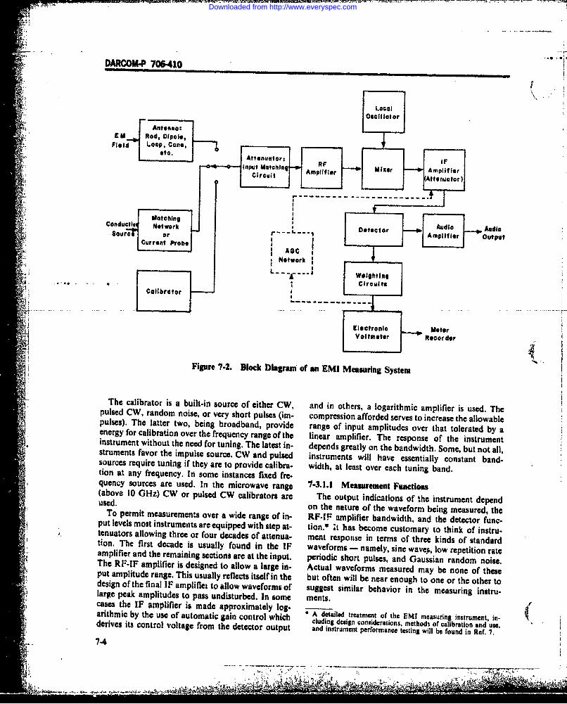
DARCOM P 706410
Local. 7 O sc illa to r
Antenina:E M Rod, Dipole,
Field Loop, Cone,+; -- n ut o r:. RF if
Input Matchin- Amplifier ON Mixer AmplifierCircuit Attenuator)
Condu tiw Network Am ui*i dutpsourer or -; " :I . . . I " Amplifier I-- OutputCeturrnnt Probe
Voleetrwecodk
1+ ' 1 • i " * . .. . tC i r c u i t s__ Calibrator
"--' [ mooro° RecorM~er
Figure 7-2. Block Diagram of an EMI Measuring System
The calibrator is a built-in source of either CW, and in others, a logarithmic amplifier is used. Thepulsed CW, random noise, or very short pulses (im- compression afforded serves to increase the allowablepulses). The latter two, being broadband, provide range of input amplitudes over that tolerated by aenergy for calibration over the frequency range of the linear amplifier. The response of the instrumentinstrument without the need for tuning. The latest in- depends greatly on the bandwidth. Some, but not all,struments favor the impulse source. CW and pulsed instruments will have essentially constant band-sources require tuning if they are to provide calibra, width, at least over each tuning band.tion at any frequency. In some instances fixed fre-quency sources are used. In the microwave range 7-3.1.1 Measurement Functions(above 10 GHz) CW or pulsed CW calibrators are The output indications of the instrument dependused. on the nature of the waveform being measured, theTo permit measurements over a wide range of in- RF-IF amplifier bandwidth, and the detector func-put levels most instruments are equipped with step at- tion." ;t has become customary to think of instru-tenuators allowing three or four decades of attenua- ment response in terms of three kinds of standardtion, The first decade is usually found in the IF waveforms - namely, sine waves, low repetition rateamplifier and the remaining sections are at the input, periodic short pulses, and Gaussian random noise.The RF-IF amplifier is designed to allow a large in- Actual waveforms measured may be none of theseput amplitude range. This usually reflects itself in the but often will be near enough to one or the other todesign of the final IF amplifiei to allow waveforms of suggest similar behavior in the measuring instru-large peak amplitudes to pass undisturbed. In some ments.cases the IF amplifier is made approximately log- * A' ~arithmic by the use of automatic gain control which q ealdteteto h M esrn instrument, in-a bo t oc luding design considerations, methods of calibration and use.derives its control voltage from the detector output and instrument performance testing will be found in Ref. 7.
7-4
V'. 7.4
Downloaded from http://www.everyspec.com

S .. . .... ,ARCOMP 706410
7-3.1.2 Defector Functions the peak value of the source voltage v,. These circuitsInstruments are equipped with one or more detec- have been made to operate very effectively for short
tors which read some parameter of the applied wve- pulse inputs so as to read the peak value of a singleform as it appears at the IF amplifier output. The pulse effectively. On such instruments, to avoid rapiddetector functions include peak, quasi-peak. tins, and fluctuations in the output indicator when scanning inaverage of the envelope, frequency or when observing rapidly fluctuating in-
terference, the peak reading is held for a manually ad-justable period. The output V is read by a high input,
7-3.1.2.1 Peak Detectors impedance electronic voltmeter. In the alternativeThe peak detectors are either of the direct reading arrangement of Fig. 7-3(B), the voltage V, is in-
kind as in Fig. 7-3(A) or of the indirect (or slide-back) creased manually until the audio output, as heard inkind as in Fig. 7-3(B). In the direct reading detector, head phones or as indicated on a meter, is reduced to'by making the discharge resistor as large as possible zero. At this point, the diode is just cut-off and V., isand the charging resistor as small as possible, the equal to the positive peak of v,(t). V, is then read on avoltage to which the capacitor charges is very nearly voltmeter.
II
v(t (A) Form of Direct-reading Peak Detector Circuit
.
eS( 0 Audio :•IF Amplifier I [Output
' VoltmeterT1Vi/ (B) Form of Slide-beck Peak Detector Circuit :
Figure 7-3. Detector Circuits •
• -7-5
Downloaded from http://www.everyspec.com

--1
DARCOM.P 706-410
The peak value is particularly useful when inputs whereare of an impulsive nature. Impulsive interference is S(f0 ) = spectrum amplitude of the impulse at thetypically of low repetition'frequency compared with tuned frequencyf,the bandwidths employed in the EMI instruments. H(f, ) = -center frequency gain.When a short pulse is applied to the meter, the If a sequence of impulses of repetition frequency4 isnarrow-band IF filter develops an output burst applied, the average value of the output iswhose width is of the order of the inverse of the IFamplifier bandwidth. If the inverse of the repetition V, = S(fo )H(f, )f, , V (7-3)rate is much less than the resulting output pulsewidth, then the impulses are, for practical purposes, The response of the average detector to Gaussianisolated, nonoverlapping, transients. Under these random noise is determined by recognizing that theconditions the reading obtained in the peak meas- output a of the envelope detector preceding theuring circuits of Fig. 7-3 is given by (see Eq. 3-60) averaging circuit is described by the Rayleigh distri-
bution
e V = S(f)H(f , ,V (7-I)
where pa(a) = exp [-a/(2 VF)j V
S(f. ) = spectrum amplitude of the pulse at the (74)tuned frequency, V-s = a,<a 0
H(f, ) = gain of the instrument at its tuned frequen-cy from the input to the detector output*, wheredimensionless a -envelope amplitude. V
B = effective impulse bandwidth, Hz V? = mean square value-of the Gaussian noise'7 entering the envelope detector, V17-3.12.2 Average Detector The averaging circuit develops an output V given by
The average detector, sometimes called the field in- the mean value of a which is found to betensity detector, is an envelope detector followed byan averaging circuit comprised of a series resistanceV, r 7and shunt capacitance. Time constants are chosen to (follow the envelope variations allowed by the band-width of the IF amplifier. (The principle of envelope In Chapter 3 (Eq. 3.57) the mean square value of thedetection is treated in Ref. 8.) u ~odetctin s teatd n Rf. .)output (v,, of a filter to Gaussian noise is given by
When a pure sinusoid (or a frequency-modulatedsinusoid) is applied to a detector of this nature the (vA) = V/= N(f. )IU(f. )1 24 (7-6)output is, in principle, the peak value of the sinusoid.An amplitude-niodulated wave results in an Output wherewhich is equal to the peak of the carrier alone. It is N(fo) = Guassian random noise spectral density,for this reason that the term "field intensity"" is VI/Hzused to identify this function; when measuring the B, effective noise bandwidth, Hzfield strengths of signals, readings independent of the so that the average meter reading ismodulation are obtained.
When an impulse is applied to the EMI instru- i.ment the area of the IF amplifier output envelope is Vo = -N(f. )H(f. )B V (7-7)given by
Area = S(f. )H(f, , V's (7-2) 7-3.1.2.3 RMS Detectors
For root mean square detectors if the input is ran-
* Efficiency of the detector is included in H( f) as here defined. It dom noise, tli reading is given directly by Eq. 7-5.would be determined by appling a sinusoidal input at frequen- For nonoverlapping repetitive impulses, the energy ofcy,. and measuring the dc output voltage at th dcetcctor. H( I) a single pulse at the detector input i-is then the ratio of output voltage to peak input voltage_
SThe use of the term field i,,wnsji (Fl) has been deprecated bythe IEEE in favor offi.qd strength. However. the term inter sir ,() dt V's (7-8)is still u.ed in connection with radio inerference instrumenta- J (tion.
7-6
] ~~~ ~, .. : . ..
Downloaded from http://www.everyspec.com

DARCOM-P 7=410
where TABLE 7-1. READINGS OF RFI METERso(t) RF-IF amplifier response to the impulse, V. CALIBRATED TO READ THE RMS VALUE OF
By the Fourier Integral Energy Theorem (or Parse- AN INPUT SINE WAVEval's theorem, Ref. 9, Eq. 2-75) this is also
'() f: Detector FunctionJ Q s,'(t) dt f ' (f)H(f)df Input Peak Average of RMSEnvelope RMS____
S(., )H2(f )B, , V2's (7-9) Sine wave; rms2 value = E E E E
where Impulses, Impulse rd -fa
V(f) Fourier transform of S,(t), V/Hz Strength =aN2T h e average po w er at the d etector inpu t is g iven by ...... .
the energy per pulse multiplied by the pulse repeti- Random noisetion rate. Thus, the mean square output is power spectral - 1,B
density -N
V, - S(f)H(f,)B f , V- (7-10) Bi = effective impulse bandwidth, Hz2B, - effective noise power bandwidth, HzA rm deectr radsYo thesqure ootof his f - pulse repetition rate, pps (assumed low
quantity, enough to prevent overlapping)
Interference meters are calibrated to read the rms N = noise power spectral density at frequency of--- value of an input sine wave regardless of which detec- measurement, V2s-.. ..- -
tor is being used. That is, an appropriate factor auto- impulse strength area under impulse. v-s,matically is inserted on each detector function to ac- Eq. 7-11.count for differences ia output voltage when a sinewave is applied. Under these conditions the outputreadings are as summarized in Table 7-1.
length determines the width of the pulse. Pulse widths7-3.1,3 Cali;,rat;on and Methods of Use of the order of 10- are in common use, with cor-
Two methoIs af calibration are the direct reading responding frequency spectra which exceed 1000method and the substitution method. In the direct MHz. Under ideal conditions, with the line im-reading method the instrument scale usually is cali- pedance R. perfectly matched to the discharging loadbrated in terms of the rms value of a sine wave. In the R and with instantaneous closing of the switch con.substitution method, the instrument is used as an in- tacts, the output is a rectangular pulse whose height isdicator, A reading is obtained with the waveform to 1/2 the voltage to which the line was charged by thebe measured, and a calibrated standard waveform dc source through the resistance R , and whose widthsource is then connected to the instrument input and is the time required I a disturbance to travel twiceits magnitude adjusted to duplicate the earlier read- the length of the lin,- ie repetition rate, in some in.ing. The source calibration provides the measured struments, is main d constant at about 60 Hz; invalue, others it is variable everal Hz to several thou-
Virtually all EMI meters, whether intended for sand Hz.direct or substitution measurements, have built-in The spectrum amplitudL (f) of the pulse is (par.calibration sources. For the direct reading instru- 3-1.3.2.1 and Fig. 3-20)ment they may be viewed as aids for setting the gainof the instrument for substitution measurements /sinrfd /sinfd\ Vthey provide the basis for the output readings. The S(f) = 2V,.d 2iof f_ ,V's (7-11)waveforms used are impulses, sine waves, or Gaus-sian random noise, with impulses preferred sincc theycan be constructed to give useful output to fre. wherequencies beyond 10 GHz. V, = line charging voltage, V
... One method of generating impulses is to discharge d - pulse duration, speriodically a transmission line (Fig. 7-4) whose o = impulse strength, V's
7-7
. b............
Downloaded from http://www.everyspec.com

DARCOM-P 706-410
Impulse calibrators are used at low frequencies where matically in Fig. 7.5. The noise current in the out-the approximation sin(rfd )f(irfd) I, and the spec- put load resistor has a power spectral density Xj(f)trum is independent of frequency. given by Eq. 3-7
It has been found useful to mismatch deliberatelythe pulse forming line and the load into which it dis- N(f) 2eld, , A2/Hz (7-13)charges. Then (Ref. 10) the spectrum is
where(sin 7rfd) 1 - -, e = charge of the electron - 1.602 x 10- 1 CS(f)= -d cos 2fd + y i, - direct current flowing between anode and
wfd fT~os2?T7 2cathode, AV's (7-12) Random noise calibrators using gas-filled devices
(thyratrons. neon bulbs, fluorescent tubes) also areused occasionally. Diodes have been used as internal
cient. By a proper choice of -, the spectrum can be calibrators in EMI meters only up to about 30 MHz.
made flatter in the region just belowf - l Id than the However, calibrated noise generators as separate
spectrum obtained with a matched line. Other meth- devices are available for use up to the UHF region.ods of generating impulse like spectra are available(Refs. I I and 12) including one using a pulsed sine 7-3.1.4 Summarywave. Table 7-2 summarizes the sensitivities of available
Sources of random noise are generally temperature EMI measuring instruments. The frequency rangeslimited diodes connected to the circuit shown sche- shown are representative of divisions used but most
ViCharctersti Impedance R
i~~i ~Pulse Forming Line-.•II DC SourceSwitc Pull*
.:V R. Output
0-0
Figure 7-4. Simplified Schematic of an Impulse Generator
RF Choke
Tempratue in Load
Diode Noie
Current
Figure 7.5. Simplified Schematic of a Random Noise Source
-7-3
,. -U
Downloaded from http://www.everyspec.com

III I
DARCOM-P 706410
0C >i
ta
4 .-. "- - __ - °
... ~
-
$C::
NL N N
IlIQ
04
- 7-9
Downloaded from http://www.everyspec.com

DARCOM-P 706410
actual instruments overlap these ranges. Some instru- their primary function the decomposition of wave-ments contain a basic measuring unit and replaceable forms into their spectral components and the meas-RF-IF amplifier heads. Virtually all instruments in- urement of these components. These instruments cantended for EMI work contain average-of-envelope, be used to obtain useful spectral measures of non-and direct reading or slide-back peak detectors. In periodic, or random, waveforms.addition, true rms and quasi-peak detectors areavailable. 7-3.2.1 Wave Analyzers
The narrowband sensitivity specified in Table 7-2 is The wave analyzer is essentially a tunable narrow-the rms level of an input sinusoid at the tuned fre- band filter followed by a suitable ac meter circuit asquency, which equals the rms value of the internal shown in Fig. 7-6. Commercially available instru-receiver noise reflected to the input terminals. Cor- ments generally have an upper frequency limit in therespondingly, the broadband sensitivity is the mini- order of I MHz.mum detectable output from an impulse generator. The more frequently used wave analyzers are of theThe levels given are considercd to be typical. Actual heterodyne type, as shown in Fig. 7-7, where a fixedinstruments can be expected to vary from these tuned narrowband filter selects a spectral slice of thefigures. The sensitivities for radiated measurements input after it has been frequency shifted in a mixer.are based on the use of a I-m rod below 30 MHz, and Typically, an intermediate frequency of 100 kHz orantennas described in par. 7-3.3.2.4 above that fre- higher is used. At IF amplifier frequencies crystalquency. Newly designed instruments are largely tran- filters can be used to obtain the very narrow band-sistorized and are therefore capable of battery opera- widths usually desired. Instruments are found whosetion. Such instruments are especially appropriate for bandwidth can be varied in discrete steps; the widerportable field use. - andwidth-allowsest critical tuning where high reso-
lution is not needed. Minimum bandwidths of theorder of 5 Hz and less are achieved. To help keep the
7-3.2 WAVE AND SPECTRUM ANALYZERS measured signal in a narrowband filter even when itsThe designations "wave analyzer" and "spectrum input frequency fluctuates, some devices use auto- f
analyzer" are reserved for instruments which have as matic frequency control. ' Nk
iiInput Tunable Meter
Waveform Filter
Figure 7-6. Basic Constituents of Wave Analyzer
Fixed Tuned Bandpass ACMixer Intermediate Frequency Meter
W eform , Filter
i Variable
Figure 7-7. Basic Constituents of Heterodyne Wave Analyzer
7-10
---- -. --. --. , ..--, , , . . ! ,i , • , , : , .:
Downloaded from http://www.everyspec.com

DARCOM*P 706410
Most available instruments use rectifier-filter averaging time so as to optimize the trade-off be-detectors which actually measure the half or full wave tween accuracy and observation time.average of the IF output. The meter is calibrated in
terms of the root-mean-square value of a sine wave.When random noise is applied at this input, the root- .2.2 Spectrm Analyzersmean-square value can be obtained by applying a The spectrum analyzer is basically a heterodyne
correction factor obtained from Table 7-i. It should wave analyzer that is automatically tuned and shows
be recognized that the final detector output is a con- the spectrum on a visual display. The block diagram
tinuing computation of the average in a moving finite of Fig. 7-8 shows it essential elements. It usually is
time interval. The running average so measured equipped with a manually variable marker oscillator
should not fluctuate excessively. When discrete spec- which applies a known frequency to the input for
trum signals are to be measured, the averaging inter- calibration purposes. The mixer input has a band-
val should be at least ten times the period of the width large enough to accommodate the range of fre-
lowest frequency component measured for a fluctua- quencies to be displayed, while the IF amplifier band-
tion of about 0,5%. For continuous spectrum input, width is small in order that spectrum variations with
the fluctuation depends on the statistical nature of frequency will be resolved properly. Analyzers have
the input. For Gaussian noise, the rms fluctuation R variable sweep ranges, and variable IF amplifier
in the mean square measurement relative to the true bandwidths. Lnear and square-law detectors some-
mean square value is given by (Ref. I) times are used and, occasionally, integration time isPt variable as well.
S1\ The resolving power of an analyzer is determinedft j-j , dimensionless (7-14) by the bandwidth of the IF amplifier. With a singleR G2 --... sinusoid -within- the sweeping range -of-the analyzer-
,I applied to the input, the resolution R can be definedwhere as the width of the response 3 dB below the maxi-
T - averaging time, s mum (see Fig. 7-9). For a slow sweep R is the 3-dBB, - effective noise power bandwidth of the bandwidth of the IF amplifier. Two sinusoids of
filter, Hz equal amplitude separated from one another by RValues of TB, of 70 would be needed for a relative hertz can just about be distinguished.fluctuation of less than 10%. This may b taken as a When the sweep rate is high the effect is to broad-
-' guide for other kinds of noise as well. Some commer- en the output shown in Fig. 7-9. The magnitude ofcial instruments make provisio,1 for adjusting the this effect is developed in Ref. 13 where it is shown
Input I .. I sm [Fixed Tuned Bandpass
~~~~Prese- o_1_.l Intem~ediate Frequency DetectorI - Ml xer
Waveform lector Filter
Voltage
ControlledLocal
, m Oscillator•
~Vertical
Input
[~~ "l Swe Horizontaloltage . .CR Oscilloscope
'1ISou rce Input. .. !
Figure 748. Basic Elements of Spectrum Analyzer
-7-i 1
.. .. t.4-* y....' ." .:r A s- - ' P {-. -L+P 1 -."
Downloaded from http://www.everyspec.com

DARCOM'P 706-410j
a p
3d8
F Sweep Width.- R --* R= Resolution
II:
F , Frequency
Figure 7-9. Response of a Spectrum Analyzer to a Sinusold
that for a filter having a Gaussian shaped amplitude- Assuming a fractional decrease of 10%, the sweepfrequency characteristic, and for a linear sawtooth rate should bisweep, the resolution R is given by FT 8 Hz1 (7-18)
rR 21 ('I _---.IF=- ,z(.5 T
R =B3 + F Hz (7.15) or less. The sweep frequency is then
where B?53 - 3-dB bandwidth of the IF amplifier, Hz - - ,Hz (7-19)F - sweep width, Hz T FT - time required to sweep through F, s For example, an instrument having an IF-bandwidth
Furthermore, the peak of the response shown in Fig. of 20 kHz and sweepwidth of 5 MHz requires7-9 falls off according to
a; = , dimensionless (7-16) 1T< 10) 80Hz (7-20)
where a,, is the relative peak response with respect to in order that the output be independent of sweep rate.the peak obtained with a slow sweep; it is equal to On some analyzers a special light operates if sweepone when there is no resolution reduction. The time is too high.relative resolution, RIBs, is shown plotted in Fig. 7- Because the emphasis on a spectrum analyzer nor-l0 as a function of F/(T3 ). mally is on speed of analysis, the circuit uses an enve-SNormally, the bandwidth determines the resolu- lope detector at the output of the IF. When randomtion. For R1B3 close to unity, the fractional decrease fluctuations are being observed, the fluctuations inin resolution defined by (A/B3 - 1), is approx- output indication can be annoying. For this reasonimately the analyzer usually contains provisions for insertion
2: of a video filter, which permits integrating the outputR -I 0.1 ,dimensionless (7-17) over a period of time, at the expense of scanning
i3 TB! speed.
7-12
.~~~~~~... . . .-...-.. ,., ., .. . .. . . ,
Downloaded from http://www.everyspec.com

DARCOM-P 706.410
fill I I0fill I0
I X.
I A
40-
42 z
CCN
"a~0 c0
O 0-
O 00
0 A-. uoIlIosS PfzIIOwJON
7-13
.,' ""~
Downloaded from http://www.everyspec.com

DARCOM-P 706410
The integration time T required should be at least amplifier frequency to sweep range, the more ef-enough to give a satisfactory average as discussed un- fective can the preselector be in eliminating mostder wave analyzers; i.e., BT > 70 for an output spurious responses.having rms deviation from the average of 10% (some Available instruments for spectral analysis cover acommercially available equipment quote 8,T in the frequency range from about I Hz to 100 GHz. Aorder of 5, but this will theoretically result in con. typical unit covering the range from HF throughsiderable fluctuation with noise inputs). It appears SHF has a variable sweep width from several tens ofreasonable that the scan should sweep no more than kilohertz to several tens of megahertz. The resolu-one IF bandwidth in the integration interval T. Thus tion is variable over the range from about I to 100the scanning rate S in hertz per second is kHz and the sweep repetition rate is variable from
about I to 100 sweeps per second. Sensitivities at the!B, low end of the frequency range can be expected to be
S <- ,Hz/s (7-21) about I 1AV; et the high end sensitivities of 10-50 1AV
N h a e cgenerally are. achieved. Instruments for the fre-Now, if the integration interval is chosen to be quency range below HF and into the audio range
have sweep widths from fractions of a hertz to the70 order of 100 kHz. Sensitivities of the order of 10 AzV,
T = - , s (7-22) and resolutions of fractions of a hertz to the order of
100 hertz are obtainable. Sweep repetition rates arc ofthen the same ord-r as for the higher frequency instru-
ments. Spectrum analyses are not recommended forB . .. .e. ir.arwming radiated eminsions.or suseptibility
- S ,Hz/s (7-23) tests.
For example, if B, = 20 kHz 7-3.3 ANTENNAS AND PROBES7-3.3.1 Conductive Measurement Sensors
$ 4 5.7 x 10⁶ Hz/s (7-24) Measurements of emission into power conductors,70 'and control and signal lines can be made in terms of
f te svoltage or current. Because the measured values de-If the sweep width is 5 MHz, the sweep duration re- pend on the impedance looking into the line from thequired is(5 x s0')/(5.t x th)e 0.88 s. equipment under test, it is essential that the imped-
The spectrum analyzer is subject to all the spurious ance be standardized. This is commonly done usingresponse problems of receivers, namely (1) imge feedthrough capacitors, line impedance stabilizationresponse, (2) mixing with harmonics of the local os- networks, or both. These devices are described incillator, (3) mixing with harmonics of the input 7h5 2.1.1. par.
signal, (4) IF feedthrough, and (5) detection in themixer. Because the receiver is to be swept over a widerange of frequencies, preselection is not ordinarily 7-3.3.1.1 Impedance Standardizationused. When the first IF amplifier frequency is sub- The use of a feedthrough capacitor has the disad-stantially greater than the sweep range, preselection vantage that if the source impedance is inductive, thecan be used to advantage. For instance, a typical first capacitor may resonate with it at a certain fre-IF amplifier frequency is 160 MHz and a typical quency. Under that condition, the current or voltagesweep for a receiver o~ierating near I 0Hz is 4: 50 measured could be much larger than would be ob-MHz. The local oscilla0or would then sweep over the tained in an actual circuit. The converse is also true,range 1.11 GHz to L.2' GHz, so that inputs in the i.e., the source impedance may actually resonate withrange 0.95 GHz to 1.05 GHz would be displayed. the circuit impedance producing much higher cur-This assumes the local ascillator is working above the rents (voltages) than actually measured. Because offrequency ol X ., 4 nal, but an acceptable this situation, measured data taken with this tech-IF signal will be developed also 'or inputs in the im- nique should be examined with some care.age range 1.27 GHz to 1.37 GHx. A single tuned pre- The line impedance stabilization network also canselector with 3-dB points at the end of the range 0.95 be subjected to the same criticism, at least at theto 1.05 GHz will attenuate image frequencies by more lower frequencies where its impedance tends to be in-than 14 dB. In general, the higher the ratio of IF ductive. However, data taken with it are probably
7-14
.- 7
Downloaded from http://www.everyspec.com

..-DAR-OU*-,7O410
more representative of what will be obtained in an ac- being measured. A typical transfer impedance char-tual installation for the following reasons: acteristic curve is shown in Fig. 7-12. Actual calibra-t a. Its impedance characteristic is similar to that of tion curves are furnished by the manufacturer.a typical line (see par. 3-3.3.2). An equivalent circuit is shown in Fig. 7-13 (Ref.
b. The network does contain some damping which 14). L, and 4 are primary and secondary leakagereduces resonant effects from those that could obtain inductances, respectively; wit and ut are the resistivewithout it. losses associated with these inductances. 4, repro.
Voltages can be measured directly by connecting sents magnetizing inductance, and ., represents corethe measuring instrument (input impedance 50 fl) losses. The turns ratio is I:N, the primary being of IL: from the line to be measured and the ground plane in turn for the current probe. R. includes the loadseries with a decoupling capacitor (so that power fre. presented by the measuring instrument. -.4quency voltage is not impressed directly across the in- To calculate the transfer impedance Z, replace theput terminals). Current is measureable with a current circuit on the left of Fig. 7-13, including the trans-probe. former, with a current generator of magnitude 1, IN.I 7a r r s Then neglecting Rb as being small compared with R.,7-3.3.1.2 The Current Probe and R, (core losses) :
{ The basic construction of a current probe is in- :.
dicated in Fig. 7-11. The current to be measured is _o____Re *shown at the center of the figure surrounded by a NJ . ( + , (725)
Storoid of high permeability material. The varying I N IQ T + (/, T/)
magnetic field in the toroid induces a voltage in thewinding about the toroid which is measured with anEMI meter. Several current probes of this kind use wheresplit toroidal cores which can be-pehed and clamped - o= frequency, rad/s -
around the wire to be measured. At frecuencies for which &(4 + 4) R R., -
The principle of operation is essentially that of a4 two-winding transformer in which the primary wind-ing has a single turn. Z N &'a (7-26)
The important properties of the current probe are(I) the ratio of output voltage to input current V/1,denoted transfer impedance; and (2) the insertion im- which is proportional to frequency. Fig. 7.12 showspedance Zj, which the instrument presents to the line this behavior below frequencyf - R/[2r(4 + L,)].
Current Carrying Wire
EMI - -- Turns High Permeablllt*Meter Torold
(,.- Figure 7-11. Current Probe
~ A
* *.. '92 ~ ~ .. <z~-'7.*15
Downloaded from http://www.everyspec.com

OARCOM-P 7068410
aMa
4-
(OF
IIf
Frequency f, Hz
Figure 7-12. Transfer Impedance Characteristic of a Current Probe
La Lb
ReI N I
F>ue71.Euvln iruto urn rb
whichur is13 inquivalent ofrui frqunc ia CurrentPrig.
7-1. As frequency increases gradually, the core loss and 3-dB fall off occurs atterm R., becomes significant along with the distrib-uted capacitance of windings and leads, and the trans- RM(" +) Hz (7-29)fer impedance begins to fall off (f> f2 Fig. 7-12). 2x,4
7-16
Downloaded from http://www.everyspec.com

.DARC -.
The insertion impedance can be obtained by trans- Dipoles, discones, and log periodic types are used atforming the impedance on the secondary side of Fig. VHF and UHF; and aperture types are used at UHF7-13 to the primary side as shown on Fig. 7-14. At and above. An important consideration in the choicelow frequencies, neglecting the shunting effect of Ro of an antenna is its bandwidth, in particular, the
on Lm (and neglecting R, and Ro), range of frequency over which it can be used withoutbeing tuned or adjusted.
I The use of active antennas should be avoidedZn (La +- , (7-30) because of the possibility of spurious responses when
subjected to strong fields.
in the mid-frequency range, R, dominates the im- 7-3.3.2.1 Electric DipoleA short (length less than X/4) vertical rod, above a
SRo ground plane has an effective length i, (see par. 3-Z , z (7-31) 3.2.4)
At higher frequencies the leakage reactances 4 and (7-32)Lb, core loss resistance R,. and distributed capaci- Ttance all can affect the impedance and it can eitherrise or fall with frequency. Note that in the mid-fre- where I is the physical length of the antenna. The in-quency range it has the same general shape as the duced open circuit voltage vi at the base of the anten-transfer impedance. na with respect to ground is
Typical values of mid-frequency transfe, imped-ance are about- I ohm-with)j about 100-kHz. How- V = A,- V (7-33)ever, current probes are available with fl's down to afew hundred hertz and up to about 100 MHz. Trans- wherefer impedances range up to 100 ohms. The ratio of E Th electric field strength, V/rne.to f may be several orders of magnitude. Note that to The short rod has an impedance Za
'be calibrated properly, the current probe must be (operated with the proper terminating impedance, Za = Ra + (7-34)usually 50 ohms.
where7-3.3.2 Antennas R. = radiation resistance, 0I
Many types of antennas are used in various fre- C. = capacitance measured at the termi-quency ranges. Up to high frequencies, the rod and nals, Funtuned dipole are used to measure the electric field, A I-m rod (41 in. physical length), which is typical ofand the loop is used to measure the magnetic field. EMI meter antennas, has a capacitance of about 10
La -b
no N2 e
R ,LR Open Open
Ideal
Transformer
Figure 7-14. Equivalent Circuit of a Trsa-forner Irobe With Impedances Reflected to Primary Side
77 7
~i~i~........... 3
Downloaded from http://www.everyspec.com

_ARCOM4'1 OIii
pF. The capacitance is absorbed in the tuning of the whereinput circuits of the measuring instrument. The radia- p - permeability of free space, 4710 - H/rntion resistance R is given by to permittivity of free space,
1/361t x 10' F/mH - magnetic field strength, A/m
40 0l (7-35) Then the effective height (effective length) isIisX being the wavelength of the electromagnetic field. 4 = ,m (7-39)The radiation resistance is quite small being about 6R C
for 1/X - 1/8, A I-rn rod functions in this manner up whereto 30 MHz. c - speed of light in free space = 3 x 10' m/s
It must be emphasized that in near-field measure-
7-3.3.2.2 Magnetic Antennas ment the height as calculated by this relationship hasno unique relationship with the actual electric field at
7-3.3.2.2.1 Loop Antenna the point of measurement.A small loop in a varying magnetic field will
develop an induced voltage vj (par. 3-3.1.1.3) 7-3.3.2.2.2 Hall Effect SensorI; = wBNA, V (7-36) The Hall effect sensor is a device for measuringmagnetic flux density in the HF range and below,
where using the principle of the Lorentz law for the force on
w radian frequency of flux variation, rad/s moving charges in a magnetic field. The principal ele-B = magnetic flux density normal to the lob .. ni in te sensoris a bar of semiconductor material, -
plane, T such as indium antimonide. The B-field to beN- number of turns, dimensionless measured impinges in the bar perpendicular to oneA = area of the loop, m2 face (see Fig. 7-15) and a direct current Idc is passed
Unless the loop area is small, it is possible that an through the bar perpendicular to the direction of B.electric dipole mode will generate a significant com- As a consequence, electrons (or holes) in motion ex-ponent of current in the loop (Ref. 15). It will have perience a force in a direction perpendicular to bothnegligible effect if the loop diameter is less than B and ldc and this manifests itself as an electric field0.0IX. The presence of an electric field effect can be perpendicular to both B and ldc which is sensedchecked by rotating the loop 180 deg in its own plane. externally as a voltage across two sides of the semi-If no change is observed, the effect can be neglected. conductor. The voltage Vu is given by (Ref. 16):
The loop impedance Z. is given by
Z. - Ra + R. + jWL, -0 (7-37) V = R i ,V (7-40)
where whereR, - 31.200 NA/2, the radiation resistance, Q RH = Hall coefficient, m2/CR, - loss resistance of the loop, 01 t - thickness of the bar, mL, = loop self-inductance, H Id, = direct current, A
There is also some distributed capacitance between B = magnetic flux density, Tturns and some capacitance due to the connecting Field probes using the Hall effect generally arecable which effectively shunts the source comprised comprised of a Hall sensor inserted in a gap in a fer-of s, and Za . The reactances generally become part of rite flux collector. (For construction details see Ref.the input circuit tuning. 17.) A probe using a I-ft long, high permeability fer.
The effective height 1, of a loop is commonly taken rite, with a Hall sensor current of 50 mA, wasto be the ratio of induced voltage to the electric field reported to have a transfer ratio of 0.3 volt/gauss (Istrength component of a plane wave. In such a field gauss - 10-' tesla). Field detectability depends onthe electric E and magnetic H components are related the noise generated by the device. It is reported (Ref.by 17) that for a unity signal-to-noise ratio at the output,
as seen in a I-Hz bandwidth, the flux density has to-- H = 377 H ,V/m (738) be about 10-" gauss at frequencies of several hundred
hertz and higher, and about 10-' gauss at 10 Hz. The
7-18
... ... ,.. -------------------------- --
• + . , . . ' .- , , -
Downloaded from http://www.everyspec.com

OARCOM.P 706.410
ii "INPUT-CURRENT .51
ELECTRODES
Id
IT H
Figure 7-15. Schematic View of a Hall Effect Sensor
deterioration of the sensitivity is a consequence of the excited by a biasing field to a region whereg vs the B-I/f noise. field is nearly linear. Then, external fields to be
measured modulated the is around the biased value.7-3.3.2.2.3 Variable-mu Sensor An inductor (see Fig. "-16) wound around the ferrite
The variable-mu sensor is another device for has a variable inductance, depending on the instan-measuring magnetic flux density. Practical imple- taneous value of the 1A and the inductance, being partmentations of this device operate in the range 0.1 Hz of an oscillator circuit, causes a frequency modu-to 50 MHz. It utilizes the property that the B-H curve lated signal to be generated. The frequency deviationof ferromagnetic material is not linear and that the A is therefore a measure of the magnetic flux density. Acan be controlled by an external field. A ferrite rod is particular realization (Ref. 18) operates from 10 Hz
7-19
.. .? .? • . . .- : .. .. ; .... . ...
Downloaded from http://www.everyspec.com

nc/i of Hn or length foument i hdct
1/4 in. disadvantage. Furthermore. it requires a balanced in-_ put circuit on the instrument for best results. With
care dipole antennas are capablc of good fieldmeasurement accuracy and often are used as a basisfor comparison with other antennas at frequenciesabove the HF range and into the UHF range wheretheir sensitivity becomes low.
7-3.3.2.4 Broadand AntennasFor frequencies above 20 MHz, antennas capable
of operating over frequency ranges of the order of10:1 without requiring tuning adjustment are avail-ing o:t automatially swept measurement overable. Such antennas are particularly useful for carry-
broad frequency range. MIL-STlD-1 recommendsuse of a number of broadband antennas for radiatedemission and susceptibility tests as follows:
a. 20-200 MHz : biconical with balun 91.n b. 30-300 MHz biconical with balun
c. 20 M -I ~ conical log-spirald. 200 MHz -2 GHz: double-ridged waveguidei horn--: - . I-I0 GHz : conical log-spiral antennai -f. 1- 12.4 GHz : doubic-ridged waveguide
i!. OscillIator horn
Windings g. 12-18GHz horn-fed ISin.-dish ..,h. 18-26GHz horn-fed 12 in.-dishi. 26-40GHz : horn-fed 18in.-dishIn dealing with such antennas it is customary to
specify the antenna factor A1 defined by
Af = 20 log(E/V), dB (7-42)
IwhereV = voltage measured at the input terminals of
, 7cthe EMI receiver, V.Ftgure 7-16, Bashc Stte of Va u Seo, E - electric field at the antenna location, V/m
MIL-STD-462, Notice 3, which is called out forArmy procurements, includes a biconical antenna
to 10 MHz and has a sensitivity of 5 x 10- gauss. In with an improved bifilar balun for the range 30-300a I-Hz bandwidth sensitivity of 10- uT has been MHz. It has an antenna factor ranging from about 5achieved. to 30 as shown in Fig. 7-17. The 20,200 MHz biconi-
cal antenna listed is an earlier design with antenna7-3.3.2.3 Half-wave Dipole factor ranging from about 9 d8 to about 18 dB.
At frequencies in the order of 50 MHz and higher, The conical log spiral, as the name implies, is ait becomes practical to use the tuned half-wave di- logarithmically spaced winding on a cone. It has anpole I - X/2 which has an effective length antenna factor as shown in Fig. 7-18 and is circularly
polarized as is characteristic of spiral antennas.X, An antenna type frequently used is the ridged guide
S- m (7-41) antenna covering the band 200 MHz to 2 Gljz. Thestructure is similar to that of a horn, using a double-
Its impedance is close to 72 0, resistive. This value is ridged construction to get broader bandwidth (aeasy to match in an instrument input circuit, but the decade range) than one gets with a conventional
7-20
. . .. . .
Downloaded from http://www.everyspec.com
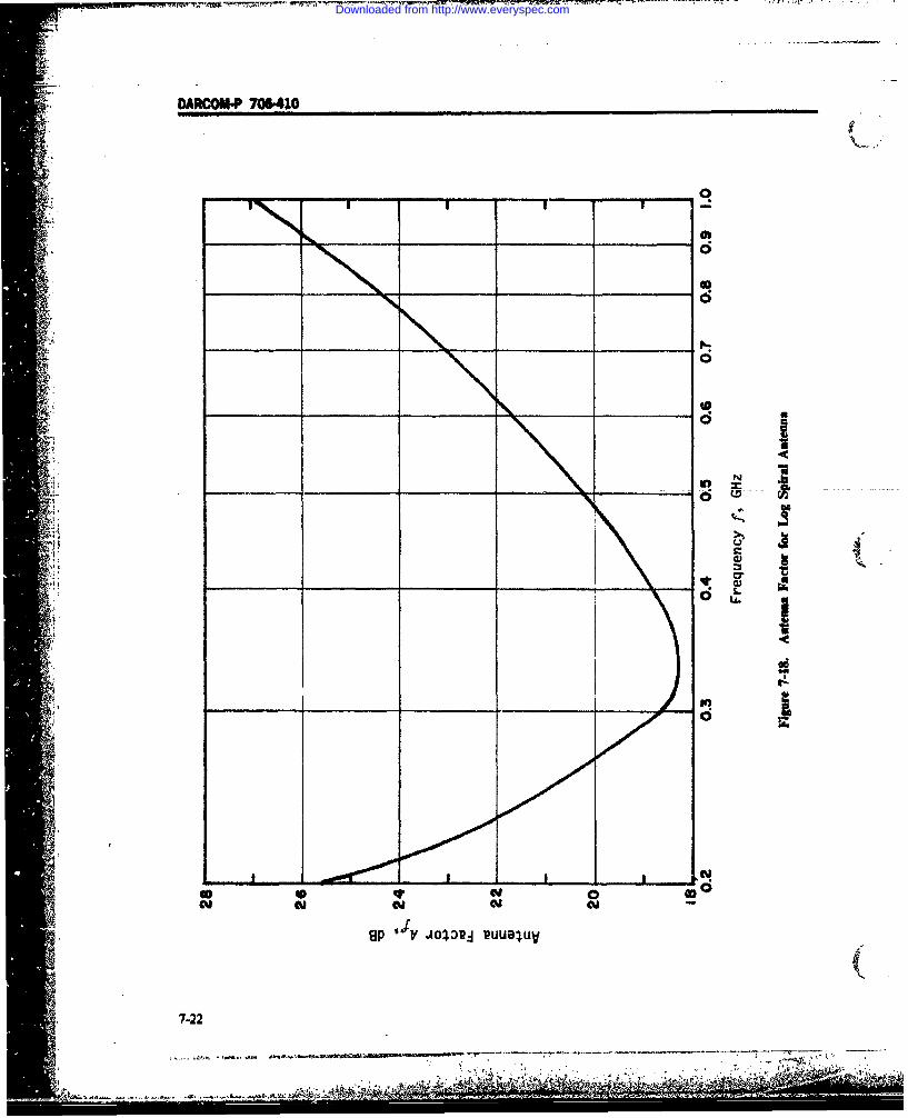
OARCOM.P 706410
40
0
_____ tv N N
ap sj JOIej vualo
7-22
Downloaded from http://www.everyspec.com

DARCOM-P 705-410,
horn. The antenna factor ranges from about 12 to 25 wise, an attached cable can cause considerable error
dB over the working frequency range. A similar in measured value.I structure for the 1-12 GHz range has an antenna fac- Matching transformers have to be used with a rodtor with ranges from 20 to 40 dB. The polarization is antenna connected at the end of a cable; however,linear, losses in sensitivity occur because of the reactive in-F The horn-fed parabolic dishes are relatively nar- put impedance.rowband comrared to the other antennas described, Loop antennas usually are calibrated with an in-principally because the horn feed is relatively narrow duction field method (Ref. 19) in which the loop to beband. Polarization is linear. The 12-18 GHz antenna calibrated is placed parallel to a transmitting loophas an antenna factor close to 19 dB; the 18-40 GHz carrying a current of I amperes and located at a dis-antenna has an antenna factor close to 23 dB. tance d from it. The effective value of the equivalent
Radiated susceptibility measurements are per- electric field E over the area of the receiving loop isformed using the same antennas as for emission test thenREOI. MIL-STD-461 specifies, however, that in therange 14 kHz - 25 MHz, where a 0.5-m rod or-dinarily would be used, this antenna be used for sus- E - Ad + (3+i), + V/m (7-43)ceptibility testing as well, except where fields in excess (d 7+ r1 + r22)of I V/mn are to be generated. In the latter case,antennas capable of handling the power are required wheresuch as the long wire and cage antennas and the par- A - area of transmitting loop, mlallei plate line, see par. 7.5.3.2.3. The long wire anten- N3 number of turns of transmitting loopna and the parallel plate line are approved devices for = radius of transmitting loop, mgenerating high field intensity in the range 14 kHz to radius of receiving loop, m• J 30 MHz. r30..z d = distance between loops, m
X - the wavelength, in7-3.3.3 Calibration The current in the transmitting loop usually is
Calibration of instruments with antennas or probes measured with an accurately calibrated theroam-connected usually is not carried out in the user'slaboratory. The National Bureau of Standards and Loops can be connected to cables because their im-tyopedance is low, cable loss is low, except at fre.the Army Metrology Center, Redstone Arsenal, AL, quencies near 30 MHz, and their self-inductance stillcan provide this service a can be treated as part of the tuned circuit of the inputTwo methods of antenna calibration have beenidentified as the standard antenna and standard field stage. Special design techniques may be necessary tom.aaenable insertion of an attenuator in the input circuit., ~~~methods (Ref. 19). The standard antenna method was MLSD41seiisatcnqefrdtr
used to calibrate a number of instruments having rodantennas under near perfect ground plane conditions mining the antenna factor for the antenna types In-
voked for use above 20 MHz. The technique is based(Ref. 20on .iTen probably showing that theoret- on a method using identical antennas fot source andamong instruments, preceiver as described in the specification ARP-958 ofical values of effective length for the rod antenna the Society of Automotive Engineers (SAE). The testwere close to actual values, and with theoretical cal- seupi o intoig.iv-19ngAfter uning tetcuain Rf 1.I hsetsstesuc1nen setup is shown in Fig. 7-19. After tuning adjustmentsiculations (Ref. 21). In these tests the source antenna have been made, the level in volts of the transmittedwas a rod located vertically over a ground plane. The hv dete in t thecurrent at its base was measured with a current signal is determined with (1) the antennas couplingprobe. transmitter and receiver, and (2) a direct connection
Since at frequencies below 30 MHz the rod anten- between transmitter and receiver (the antennas aredisconnected for this step) and transmitter read-na has a very high reactive impedance, it cannot be justed to give the same received level as in (1). The
attached to a cable - without using a matching cir- two levels of voltage are denoted V, (antenna cou-cuit - without severe losses, For this reason the an- pled) and Vb (direct coupled). The antenna gain Gtenna normally is mounted directly on the EMI in- and antenna factor Af arestrument case, and the case serves as a counterpoise,When the instrument is riounted off of a groundplane, relatively good accuracy can be obtained with G 4 rl d ioperation from batteries contained in the case. Other- G V/V, dimensionless (7-44)
7-23--- - -- ---- 7 - - . .
Downloaded from http://www.everyspec.com

DARCOM'P 706"410
IdenticalAntennas
SignalReceivero dB3 Pad ildB PadGenerator (50 a )
+11 I(50(Q0
Figure 7-19. S-tup for Measuring Antenna Factor
,[ 9.76 \ A block diagram of a typical automatic emissionA= 20 log ,dB (7-45) measuring system is shown in Fig. 7-20. The heart of
,A, the unit is the Programmer and Control Center. Here
where the program is stored for switching sensors, tuners,d n n t rbands, attenuators, and matching networks; selecting
e distance between transmitting and receiving sweep rates and ranges and carrying out tuningavlengt, mOperatiOnS; changing bandwidths and detector func-- =wavelength, moprtnscag
d i t nb tions; and for other operations according to the par-E i The distance r is shown to be I m in Fig. 7-19, but fort - iseticular system. The control circuits generate the[i ~~the cavity-backed spiral, MIL-STD461 specifies 4-ft ncsayisrcin oteohreeet fte
necessary instructions to the other elements of theseparation. system and provide the necessary signals and power
to carry out the operations.,The sensor selector unit receives inputs from theii:73.4 AUTOMATIC INSTRUMENT SYSTEMS control unit and connects the proper antennas,
Specifications such as MIL-STD-462 impose emis- probes, line stabilization networks, and sensor cou-sion and susceptibility test requirements over fre- pling devices to conform with the program require-quency ranges uxtending from 30 Hz to 20 GHz. For ments and with the frequency being observed. If thereexample, test RE03 for measuring transmitter are bandswitches on a sensor, it also is switched whenradiated spurious and harmonic emissions specifies the frequency requires it.testing over the range 10 kHz to I GHz, using a The RF unit typically contains (or is connected to)standard EMI motor using three antenna types to impulse calibrators, step attenuators, RF bandpasscover the range, and it specifies a spectrum analyzer and/or band-elimination filters, and, where impor-with a variety of preslectors and antennas to cover tant, a low noise preamplifier. The calibrator outputthe range above I GHz. The equipment switching, ultimately results in a set of calibrated lines appearingretuning, calibrating, measuring, and recording oper- on the output display identified with amplitude level.ations over such a wide range are time consuming Since the calibrator usually is coupled into the systemwhen done manually. Systems programmed to per- at a point after the sensor, it cannot account for theform these functions automatically or semi-auto- sensor senbitivity. Sensor sensitivity, i.e., antenna fac-matically are currently available for both emission tor, must be added to the calibration obtained whenand susceptibility testing. The available systems are the calibrator output is injected at the input of the RFnot designed to cover the entire range of audio fre- unit. In some cases, injection can be made at thequencies through the microwave range in a single antenna, but this normally will not account for anten-system. na directivity. When current probes are used, they
Fundamentally, these systems are comprised of can be calibrated by direct injection into a circuitstandard EMI measuring instruments which are me- arcund which it is clamped.chanically or electronically sweep-tuned and which The receiver qystem required to cover the wideautomatically switch in the proper tuning heads and range involved usually is comprised of several tuningantennas as needed. Output is displayed using an x-y heads and several IF amplifiers. These are switched inplotter. as the program requires, and the tuners are scanned
7-24I-
Downloaded from http://www.everyspec.com

1" DAI "OM-P 706-410
SensorBank
Sensor LUnit RFN Receiver so Processing Display
Switc Uni Unit Unit
'ii.
Program
and
Figure ?-20. Block Dlgram of Automatic Measuring Equipment
at speeds programmed by the operator. Typical pro- not known, a digital processing technique can be usedgrams allow portions of bands to be scanned, and to provide the correct average value.scans to be repeated. Since conventional EMI re- The displays are typically an x-y plotter oscillo-ceivers ordinarily are used, modifications are necs- scope, and/or audio monitor. The x-y plot is some-sary to allow automatic tuning, and to make the times a multiple line display showing many bands,signal conform to the frequency of the processing one above the other. The ordinary display showsequipment which follows, amplitude vs frequency, but some systems are
The signal processing unit is comprised of IF capable of other kinds of signal analysis (e.g., proba-amplifiers and detector circuits. The amplifiers are bility densiti function determination) and these toogenerally logarithmic to accommodate the wide range are printed out. In some systems it is possible to pro-of amplitudes expected. Bandwidth tailoring may be gram in the specification limit and have this printeddone here. The different detector functions may be out simultaneously, thus giving a quick indication ofswitched in, or programmed to operate simultane- nonconformity with the specification requirements.ously to give multiple outputs. As a rule peak and Automatic susceptibility testing involves pro-average functions are performed. The peak circuit gramming a suitable collection of signal generators,frequently is equipped with a variable peak holding and radiators or injectors. Modulation type (CW orduration and dump circuit to accommodate the pulse) and amplitude are programmable; driveresponse time of x-y plotters. Features which permit signals as required by specifications are thereby syn-signal reading while writing are also included. The thesized rapidly. These systems also extract outputaverage circuit measures the average of the envelope information from the equipment under test and dis-of the IF output in a time interval appropriate to the play it to show where in frequency, and to whatIF bandwidth. Where instantaneous logarithmic extent, malfunction occurs.compression is used in the IF amplifier, the measuredfunction is actually the average of the logarithm of 7-4 TEST FACILITIESthe envelope. Conversion to the true envelopeaverage can be done if the waveform shape is known, 74.1 GROUND PLANESor, for random waveforms, if the envelope proba- Ground planes, or more accurately ground sur-bility density function is known. If the waveform is faces, are used for two basic purposes: (I) establish a
', 7-25
~~~~~~~. .. .. -. ; . . . ...... .. : , ,
....... ........- - - ~
Downloaded from http://www.everyspec.com

DARCOM-P 706-410
known reference potential for conduct of measure. On the other hand, at distances where the inversements, and (2) establish a surface of known reflectivi- cube law applies (par. -3.2.1), if one is close to thety for radiated measurements. antenna compared with the antenna height above the
The theory of such surfaces, as applied to con- plane, the image can bt neglected.ducted measurements, is discussed in par. 3-3.4, and For a vertical electrid antenna, the image is not in-methods of connecting to them in par. 4-7. In test verted if the reflected r.y does not approach grazingarrangements they serve to minimize the possibility incidence. Then Eq. 7-4 is replaced withof spurious voltages being introduced on inter-connecting cables by tying all equipment cabinets to a E /2rhih \
common reference potential. Without this Ionion 2 c (748)potential surface, uncontrolled potential differences 7xrbetween cabinets can exist as a result of commonmode currents (see par. 3-3.3.3) flowing between and the field is greatest near the plane. However, un-cabinets, or currents induced on the cables from local der conditions of grazing incidence, the imageradio frequency fields, becomes inverted and Eq. 7-47 applies also in that
Except for open field tests, where it is impractical, case (Refs. 22 and 23). This latter condition is notthe size of the surface should correspond with that likely to apply in most EMC test work.required to accommodate the equipment under test For magnetic dipoles the effects of reflection areand the test equipment. It should be of sufficient reversed. i.e., the image of a horizontal magnetic di-thickness to accommodate the largest currents which pole is not inverted and a vertical magnetic dipole ismay flow, without producing potential differences inverted. It should be noted that while most con.which may either (I) adversely affect the operation of ducting surfaces form images that are of strength. ............equipment- -under -test, or-(2) cause significant errors- 'closely equal to that of 96arijinal -source--. ia-nic . ..... :-
in measured voltages and currents. sources are fully reflected in a ground plane if the sur-The resistance R between two circular areas of con- face itself has good magnetic properties. Practically
tact on a flat conducting sheet is this means that for frequencies in the kilohertz range 4and below, magnetic images will be formed only if thethickness of the conducting plane is about twice the
d I skin depth or it is of high permeability... iiR Ilnl Q -f(7-46)
d- [ 74.2 SHIELDED ENCLOSURESA shielded enclosure is used to provide an en-
where vironment free of extraneous electromagnetic radia-where tion which would otherwise disturb EMC testing.
p - resistivity, fl'm The basic theory of the attenuation provided by con-d - diameter of contact areas (assumed equal), ductors of which such enclosures are fabricated is dis-
m cussed in par. 4-6. A variety of materials has beenD - distance between contacts, m used depending upon the objectives, includingt - thickness of sheet, m screening and solid sheet material. Where screening is
Fig. 7-21 shows values for this function for a 0.25- used, it is common to use a double-wall constructionmm copper sheet, p - 1.724 x 10- 1 n'im in order to obtain the required attenuation. The two
The ground plane may have an important effect on walls can be either (I) completely insulated from eachradiation measurements. Fig. 7-22 shows that with a other except at the point where power leads pene-horizontal electric dipole, the effect of a ground plane trate the enclosure, or (2) in cpntact at the perimeteron the field is accounted for in terms of an inverted of panels (of the order of 3 ft x 8 ft or larger) whichimage. For a perfectly conducting plane and at dis- are bolted together to form the enclosure. The lattertances d large compared with the antenna heights hi, construction is sometimes referred to as a "cell" typeh2, the field E at point P (in the field region) at a dis- and generally can be expected to have a lower at-tance r is given in terms of the free space field E. (Eq. tenuation than the isolated wall type. Materials3-145) by (see Eq. 3-151) which have a high permeabilityu are used where high
attenuation is required below 10 kHz. As discussed in/ par. 4-6, in any construction method special care is (
E 2 sin 2rh, (747) required in making seams or joints and in necessaryoXr / openings.
7-26
...........
Downloaded from http://www.everyspec.com

Ii
DARCOVd*P 708410
- hfl 0
-U'I if
~I- - - - - - - - - S
__ ii004-
a.*0
1.)a ac
----- ---- h
M
B-
o
~~~~~~~1%I
- - - - - - - - - 2( ai 0 0 *
U 7*I~ * S0UD4S~9S~
7-27
- -
;.&<
Downloaded from http://www.everyspec.com
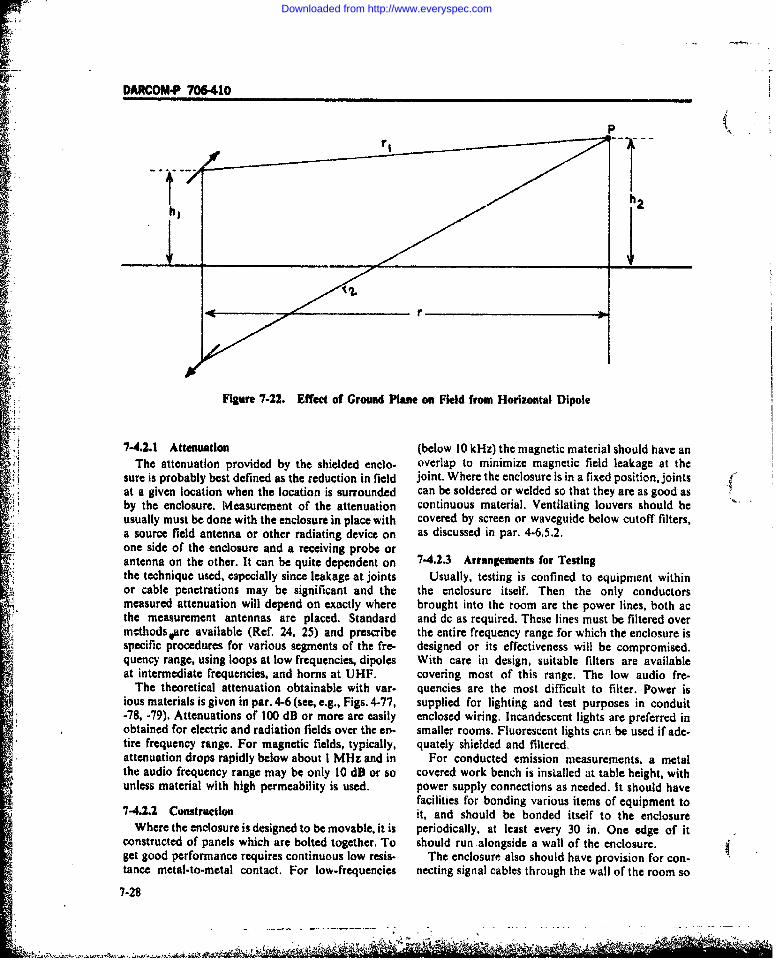
DARCOM-P 706410
h2
r
Figure 7-22. Effect of Ground Plane on Field from Horizontal Dipole
7-4.2.1 Attenuation (below 10 kHz) the magnetic material should have anThe attenuation provided by the shielded enclo- overlap to minimize magnetic field leakage at the
sure is probably best defined as the reduction in field joint. Where the enclosure is in a fixed position, jointsat a given location when the location is surrounded can be soldered or welded so that they are as good asby the enclosure. Measurement of the attenuation continuous material. Ventilating louvers should beusually must be done with the enclosure in place with covered by screen or waveguide below cutoff filters,a source field antenna or other radiating device on as discussed in par. 4-6.5.2.one side of the enclosure and a receiving probe orantenna on the other. It can be quite dependent on 7-4.2.3 Arrangements for Testingthe technique used, especially since leakage at joints Usually, testing is confined to equipment withinor cable penetrations may be significant and the the enclosure itself. Then the only conductorsmeasured attenuation will depend on exactly where brought into the room are the power lines, both acthe measurement antennas are placed. Standard and dc as required. These lines must be filtered overmcthods are available (Ref. 24, 25) and prescribe the entire frequency range for which the enclosure isspecific procedures for various segments of the fre- designed or its effectiveness will be compromised.quency range, using loops at low frequencies, dipoles With care in design, suitable filters are availableat intermediate frequencies, and horns at UHF. covering most of this range. The low audio fre-
The theoretical attenuation obtainable with var- quencies are the most difficult to filter. Power isious materials is given in par. 4-6 (see, e.g., Figs. 4-77, supplied for lighting and test purposes in conduit-78, -79). Attenuations of 100 dB or more are easily enclosed wiring. Incandescent lights are preferred inobtained for electric and radiation fields over the en- smaller rooms. Fluorescent lights can be used if ade-tire frequency range. For magnetic fields, typically, quately shielded and filtered.attenuation drops rapidly below about I MHz and in For conducted emission measurements, a metalthe audio frequency range may be only 10 dB or so covered work bench is installed at table height, withunless material with high permeability is used. power supply connections as needed. It should have
facilities for bonding various items of equipment to7-4.2.2 Construction it, and should be bonded itself to the enclosure
Where the enclosure is designed to be movable, it is periodically, at least every 30 in. One edge of itconstructed of panels which arc bolted together. To should run.alongside a wall of the enclosure.get good performance requires continuous low resis- The enclosure also should have provision for con-tance metal-to-metal contact. For low-frequencies necting signal cables through the wall of the room so
7-28
Downloaded from http://www.everyspec.com

DARCOM.P 706-410 .
that auxiliary test equipment can be isolated from the clear of reflecting objects. As the antenna dimensiontest space. The connectors should provide for coaxial increases sufficiently so that the ends of the antenna
S:i as well as twisted pair arrangements and, where nec. come close to the walls of the room, the capacitanceessary, should permit the possibility of passing multi- coupling produces significant errors at frequenciesconductor cables through the wall. The essential re- well below the first room resonance, say at 40 MHzquirement is that such cables be shielded and that a (Ref. 28).
good connection be made of this shield to the wall sothat currents picked up on the shield external to the 7-4.2.5 Recommended Arrangementsroom cannot be conducted inside. The design of any specific shielded enclosure will7-4.2.4 Radiated Emission Testing depend upon the use to be made of it; i.e., the size of
Aiaeds th at esntobing the device to be tested, the electromagnetic environ-An enclosure that does not contain absorbing ment surrounding it, size of necessary doors, and the
material will reflect most of the electromagnetic power and ventilation or air conditioning require-energy that impinges on its wall. Hence, the field ments. However, for general test purposes thefrom a radiating source can b- expected to be following design characteristics are recommended assignificantly different within an enclosure than out- a minimum:side of it. Indeed a room of rectangular shape and a. S!ze: 20 ft x 20 ft x 10 ftfree of objects with significant electrical properties b. Shielding Effectiveness: Magnetic Field, 30 dBwill resonate at frequenciesf defined by the relation at 10 kHz and above(Ref. 26, p. 23-19) Electric Field. 100 dB at 30 Hz and above
c. Power: Single phase, I 15 and 220 V, 60 and 400fzHzregulated with- not -more- than 3%2 2S2 total harmonic distortion
(a) b) 9) d. Filters at Entrance: 100 dB. 10 kHz to I 0Hze. Ventilation: air conditioned
f. Ground Plane: Table height 3 ft wide along theJ. wherea. b.c=itro ieso o h nlsri longest side
9a.b. c = interior dimensions g. Access Panel: For signal entry or exit.m, n. p - integers only one of which may be zero at
a timeFor an enclosure of cubical shape, 3 m in each 7-4.2.6 The Anecholc Enclosare
direction, the lowest resonant frequency is approx- An enclosure can be made nonreflecting by coat-imately 70 MHz. Clearly, at this frequency and above ing the walls with absorbing material. To be effective
the field will vary in an unpredictable way with dis. over a broad frequency range, experience has shown
tance from a source. that the depth of material should be about one-fourthA reflecting room can be used at frequencies well wavelength. For this reason, enclosures are practical
below resonance under the following conditionE: only for frequencies above about 50 MHz. Some-a. The object under test and the test antennas have times the enclosure walls are made nonrectangular to
dimensions no more than about 1/3 of the minimum reduce the number of resonant nodes. The effec-enclosure dimension and are located near the center tiveness of the absorption is such that essentially freeof the room. snace field patterns can be obtained within the enclo-
b. The receiving antenna s balanced and in the in- sure.duction or near-field of the Y ject under test. When the cost of installing such material over the
The first condition is imposed in order to insure walls of the entire enclosure is too great, partial in-that the enclosure does not affect significantly the stallation of material will provide significant im-radiating impedance of either receiving antenia or provement over a reflecting enclosure, especially if itemitting device. Because of the second condition the can be placed at locations at which energy is reflectedfield emitted can be expected to fall off according to from or towards a d-rective antennZ, or placedan inverse cube law (par, 3-3.2.1) and thereforc fields around the antcnna (Ref. 29).from image sources reflected by the walls of the en-closure can be expected to be quite weak. Tests have 7-4.2.7 Antemna Pattern Synthesis( shown that results obtained under these conditions In the past few years a technique of antennaare within a few dB of open field measurements (Ref. pattern synthesis has been developed in which the27) madc as the same distance from a room quite field distribution over the antenna aperture is
7-29
A.. . v.- :i i i i i 1 i I II I I ........ ..... ... ..; ....
Downloaded from http://www.everyspec.com

DARCOM-P 706-410
measured and the pattern is calculated by a com- shielded enclosures (Ref. 31), and (2) an electric fieldputer. A small dipole type antenna physically scans probe (Ref. 32).the aperture and both the amplitude and phase of the. In another technique (Ref. 33) a small dipole probedetected signal are recorded (Ref. 30). An anechoic whose impedance can be modulated by a light beamvolume is required which is only large enough to con- is used to measure the field distribution near antain the antenna under test and the scanning aprara- antenna. The modulation caused the reradiated con-tus. pone to he measurable even in the presence of act o
relatively strong antenna field and the absence of any7.4.3 OPEN FIELD TESTSto the probe avoids any significant
Open field test sites are used when: distortion of the original field.a. A suitable shielded or anechoic enclosure is not
available perhaps because of equipment size. 7-5 NEASUREMENT TECHNIQUESb. At the lower frequencies, testing in the far field 7.5.1 INTRODUCTION
requires large antenna spacings.c. It is desired to examine the effects of ground Just as in dealing with the analysis of EMC phe-reflections on antenna patterns, ea of un nomena, in discussing measurement techniques, it isrefA suitable site requires a flat convenient to separate them into those used for (I)
characteristics free from reflecting objects within a measuring the characteristics of emitters, (2)distance to the equipment in use at least equal to the measuring characteristics of susceptors, and (3)separation between the radiating and the receiving measuring coupling factors between emitters and sus-
ntennas, and preferably substantially greater than ceptors. Military standards are concerned primarilywith the first two categories. The third category is! ii ....... that. and it-should be-'remote from armas having sub. maue nyidrci codn omltr tn-
stantial industrial activity, dense population, orto military stand-stanialindstral ativtydene poulaion or ards, usually in the form of laboratory measure-J moderate or high power transmitters. Power lines to aens ssuch measurm of onidrable~ments since such measurements are of considerable
the equipment should be buried underground so asnot to affect the electromagnetic properties of the interest in connection with gathering data necessary
The device under test is usually placed on a turn- for analysis and prediction work in the early phasesra it.Te d aio n Fr tet sts whe o urnd Mesrmnsi"tefrttocteoisaedstable for convenience in determining the radiation of equipment or system design. They are treated inpattern, and in particular, for locating the direction par. 7-5.4.' Measurements in the first two categories are dis-
.!' of maximum radiation. For tests where groundi: ~ ~~~~~~~~~~~cussed i as -. n -.. Teepai so hreflections are significant, the height of the test object n pars. 7-5.5 and 7-5.6. The emphasis is on thecan be important as discussed in par. 7-4.1. Equip- principles to be observed in making significantment can be placed in weather protective buildings measurements rather than on details of the proce-ment can be lac d in weaher pro ecti e b ild ngs dures which, in m any cases, can be obtained from alpmade of nonconducting, low dielectric constant ma- drswih nmn aecnb bandfo ptalher ncessary.n, w tpropriate military specifications and standards. In-terial where necessary.
u odividual test methods described in MIL-STD-462 areBecause of the difficulty of finding suitable testdiscussionsites and the cost of acquiring and equipping them,open field testing usually is used only as a last resort. given here should not be interpreted as superseding
that document. When called out, that documentshould be consulted for details on the test setup and
74.4 ELECTRO-OPTICAL TECHNIQUES procedure.Recent developments in fiber optics employing For reference purposes, Table 7-3 lists the tests
light for data transmission have enabled develop- described in MIL-STD-462. These cover conductedment of instruments in which connected wires have and radiated emission and susceptibility tests over thebeen eliminated. Arrangements using these instru, frequency range 30 Hz to 40 GHz.ments have substantial advantages in some tests in- Uncertainties in test procedures arise especiallyvolving radiated fields, where the connected wires where there are large numbers of equipments thatcould otherwise disturb the fields being set up or have to be tested together. As a guide, the equipmentmeasured. The measured value is coded into a form should be placed as nearly as possible in relativesuitable for transmission on the fiber optic cable, positions that simulate their installation arrange-which itself does not disturb the field, to a remote ment, and generally the adjustable controls should bedetector which decodes the optic signal to indicate set in positions that will produce worst case emissionthe measured value. Devices using this principle in- or susceptibility. In other situations the device underdude (1) a 20-200 MHz antenna system for use in test will be connected to a simulator to provide
7-30
Downloaded from http://www.everyspec.com

operatinaly restigals:I a similar fashion, 7-5.2 MEASUREMENT ACCURACY 761auxiliary monitoring equipment may be connected to
thedeiceuner es toprvid ameasure of its per- The accuracy of measurement of EMC parametersforanc. I shuldbeascertained that such auxili- depends critically on the nature of the measurement,
ar qupenan nysanadtest eqimn h ntuet sdand the test arrangement.suc asoscllscoessigalgenerators, and fre- Specific items to be considered are as follows:
qunymtrs-d o themselves produce inter- a. Measuring Instrument. Measuring instrumentsference not present with the equipment under test in have an accuracy usually considered to be about 2 dBnormal operation. for voltage measurements and 3 dB for field measure-
Site survey measurementr are discussed in par. 7- ments, assuming quality instruments and rectent cali-
5.7. bration. Where substitution measurements a"~ made,
TABLE 7-3.LIST OF MIL-TD-462 EMI MEASUREMENT TESTS
Test Title
Conducted Emission (CE)
CEOI 30 Hz-SO kl-z, DC Power LeadsTCE02 10 kHz-50 kHz, AC Power Leads
CE03 30 Hz-SO kHz, Control and Signal LeadsCE04 50 kHz-5O MHz, Power LeadsCE05 50 kHz-50 MHz, Control and Signal LeadsCE06 10 kHz-] 2.4 GHz, Antenna TerminalCE07 1.5-65 MHz, Power Source, Tactical Vehicles
Conducted Susceptibility (CS)
CSOI 30 Hz-O kHz. DC Power LeadsCS02 50 kHz-400 MHz. Power LeadsI.*CS04 30 Hz-IOGHz,nRejecttion neie Signals (2 Generator Method)
CS08 Deleted
Radiated Emission (RE)
RE01 30 Hz-30 kHz. Magnetic FieldRE02 14 kHz-O00 MHz. Electric Field - BroadbandRE03 10 kHz--40 G Hz, Spurious and Harmonics, Radiated TechniqueRE04 20 Hz-SO kHz, Magnetic FieldRE05 150 kl-z-1 ODD MHz, Vehicles and Engine Driven EquipmentRE06 14 kHz-1 0Hz, Overhead Power Line Test
Radiated Susceptibility (RS)
(RSOI 30 Hz-30 kHz, Magnetic FieldRS02 Magnetic Induction Field SpikeRS03 10 kHz-400 MHz, Electric Field
7-31
Downloaded from http://www.everyspec.com

Aioa 7h6u41a
better accuracy is obtainable with a stable substitu- direction or if plane polarized, an appropriate correc-Stion source if it has the same type of waveformn as the tion factor should be used.interference being measured. For this reason, a stable e. Voltage Measurements. Accurate voltage meas-
-- internal impulse generator is potentially capable of urements usually require a well defined ground plantenabling measurements of broadband interference reference. Typical ground planes have significant ir-with accuracies better than 2 dB. When measuring pedance (see par. 74.1) so that areas of a plane nearnarrowband interference, however, the accuracy points to which large currents are returned, such asdepends upon knowledge of the bandwidth. Vari- from a signal or pulse generator, should be avoidedations of the bandwidth with time and tuned fre- for use as reference potentials.quency can occur. They can be detected and ac-counted for by calibration with an accurate sine wave 7-5.3 TEST EQUIPMENTgenerator along with the impulse generator. In addition to basic interference measuring instru-
b. Impedance Matching. Measurements at fre- ments, certain other items of test equipment will bequencies above 30 MHz can be quite sensitive to found to be very useful for EMC testing, and indeedcable lengths unless care is taken to match imped- will, in many cases, be essential to obtaining the most
ances at all terminations. Even relatively small stand- significant data. The equipment should be of gooding wave ratios can cause substantial error because of quality and be maintained regularly. The equipmentii-teractions that can occur between sources and complement could include the following:loads. a. Attenuators - 10-dB and l-dB steps, 50 fVc. Waveform Purity. Spurious emissions and b. Signal generators providing continous coverage
responses from communication equipment require - 10 kHz to 40 GHztof low signal levels in the presene of c. Power amplifiers (up to 100 W at frequencies to
large-signal levels. Since spurious signals can be several hundred megahertz)generated in any nonlinear device, care must be taken d. Line impedance stabilization networks (withto insure that in any measurement a characteristic of current carrying capacity up to at least 50 A)the device in question is being measured. For exam- e. Isolation transformers (up to I kW)pic, a receiver tuned to a harmonic of the generator f. Audio power transformers (up to 100 W)can respond either to a harmonic in the output of the g. lO-AF feedthrough capacitorsgenerator or a harmonic generated in the receiver in- h, Current probesput circuit as a result of the high amplitude funda- i. Adjustable filters (low-pass, high-pass andmental frequency at the receiver input. Thus, in bandpass)measurements of harmonic and spurious output of a j. Notch filterstransmitter, care must be taken to insure that k. Wave analyzers (at least 0-50 kHz)measured levels are not generated in the measuring I. Audio oscillatorreceiver. Likewise, auxiliary equipment in the circuit m. Impulse generatorsuch as power monitors and dummy loads should be n. Variable width pulse generatorchecked to determine that they are operating linearly. o. Transient generator (see Fig. 7-28 for typicalTechniques for detecting false measurements are wave form).mentioned in par. 7-5.6.1.2.
d. Radiation Measurements: The presence of 7-5.4 LABORATORY TYPE MEASUREMENTSreflecting objects can seriously degrade the accuracy Frequently measurements are made for explora-of radiation measurements. In open field measure- tory purposes to determine fundamental equipmentnments the effects of ground reflections can be ex- or component characteristics such as filter insertionplored by varying the antenna height and checking loss and shielding effectiveness.for conformity with Eq. 7-48. The effects of reflectingobjects can be checked by displacing the antenna in 75.4.1 Probe Meaurementsvarious directions to determine if significant stand- Four types of probes are used: voltage, current,ing waves are present at the test location, electric field, and magnetic field.
Antenna characteristics must be accounted for. In Conductor emission data can be obtained usinggeneral, any antenna should be oriented for maxi- voltage or current probes. At frequencies below 1mum sensitivity both in direction and polarization. If MHz, instruments are available with high imped-it is circularly polarized, it should be confirmed that ances (up to 100,000 1) so that usually direct connec-incident radiation is not polarized in the reverse tion to the circuit can be made without disturbing its
7-32
Downloaded from http://www.everyspec.com
DARCOM-P 706410
operation because of loading effects. On lines carry- of the measuring instrument, the series induced volt-ing power, a blocking capacitor of appropriate size age in the circuit it encloses is proportional to themay be adequate to reduce the power frequency volt- current through the probe and is a function of fre-age to levels that will not overload the measuring in- quency. Similarly, magnetic and electric field probesstrument. If not, or if the line carries a strong desired can be driven by a signal generator to produce localcarrier frequency not subject to emission restric- fields for susceptibility testing.tions, a notch filter may be used between the ter-minals of the circuit to be measured and the instru. 7,5.4.2 Filter Measurementsment. Current can be measured with a clip-on type The standard test for filters is contained in MIL-current probe. Since the insertion impedance of the STD-220 in which the filter is terminated in 50 I at
probe usually is less than I Q1, it is unlikely to disturb each en Sice filters raed in ciQ-~each end. Since many EMI filters are placed in cir-the measured current. However, note that the cali- cuits, such as power lines, in which the termination isbration of the probe (transfer impedance) is depend- quite different from 50 0, special tests may be ad.ent upon its termination impedance (see par. 7- visable for which there are no standard methods at3.3.1.1), and if the measuring instrument or volt- the present time. By placing the filter in a circuitmeter does not have an input impedance of the prop- simulating actual termination impedances, its effec-er value, a matching network must be constructed tiveness can be measured by means of current or volt.
Feand taken into account in the calibrationm age probes. In setting up a test circuit, the impedanceof the generator must be taken into consideration,
vicinity of equipments generally cannot be made ac- and appropriate matching networks used as needed,curately because of the interaction that takes placebetween the antenna and the equipment itself. Anexception to this occurs when measuring a small 7-5.4.3 Shielding Effectivenessmagnetic source which is surrounded by nonmag- Shielding effectiveness of enclosures or cabinetsnetic material. Such a source can be viewed as a mag- can be measured using MIL-STD-285 if the enc1o-netic dipole with a field having a highly predictable sure is sufficiently large. If not, special methods mustlocal distribution (see par. 3-3.1.1.1). It can be be devised. Included are the inserting of a smallmeasured quite accurately with a small loop or Hall battery operated transistor oscillator in the cavityeffect sensor. Furthermore, the presence of the and measuring the field outside of it. Otherwise,human body in the vicinity does not disturb the field, energy can be fed to small loops or electric dipoles inso that an unknown magnetic source can be quite ac- the enclosure, using well shielded coaxial cables.curately located by probing, especially at the lower Because of the possibility of cable leakage, the enclo-frequencies (below about 1 MHz.) sure can be placed against the wall of a shielded en-
Electric field probes are less effective for several closure and the cable connected to it through anreasons. In the first place, at low frequencies electric access connector in the wall of the enclosure.fields due to equipment are likely to be weak because Because the shields on most cables are quite effec-cabinets are conductors and will not support large tive providing high values of attenuation, measure-field strengths. As the frequency increases, the wave- ment of the actual value of cable shielding effec-length decreases and impedances increase so that tiveness requires special equipment. Perhaps the mostdetectable field strengths appear. However, the common method is that using a triaxial arrangementpresence of large amounts of metal such as in a tank (Ref. 34) in which the cable under test is placedturret causes multiple reflections which destroy any within a cylinder which together with the cable shieldsemblance of a "dipole" field. Furthermore, the forms a second coaxial structure isolated from theprobe, if on the end of a cable, will be insensitive first except for leakage through the shield of the innerbecause of poor impedance match and the field will cable. By measuring the voltage across the outervary as the body is moved in manipulating the probe. structure when the inner one is driven, the shieldingFor these reasons, electric field probes are seldom effectiveness can be determined.used. In the frequency range up to about 30 MHz, At frequencies where the triaxial structure becomesprobing with a loop of small size (about 6 in. resonant, a quadraxial method has been devised (Ref.diameter max) and a few turns will successfully locate 35) in which provision is made for proper loading ofthe most significant sources of field leakage. the structure to avoid standing waves.
Susceptibility of circuits to induce voltages can be In addition, techniques using an absorbing clampsimulated by using a current probe. When a signal and a leakage field measurement technique havegenerator is connected to the probe terminals in place shown good results at frequencies above 30 MHz
7.33--
Downloaded from http://www.everyspec.com

1k DARCOM.P 706-410
(Ref. 36). Because of the specialized nature of SE test when the measurement is being made as well as allmethods, they are not described here in detail. Those test equipment. In part, this procedure is included forinterested should consult the references. safety reasons. Furthermore, the measure of im-
pedance across the terminals of an active circuit is not7-5.4.4 Articulation Measurements a simple procedure and practically is never at-IL The principles underlying and general procedures tempted as a routine matter. The values of im-for making articulation measurements are discussed pedance that such lines are expected to have can varyextensively in par. 3-2.1.1. As mentioned, such tests over a large range, especially at frequencies above 0.5can be carried out with a group of individuals or, in MHz (par. 3-3.3.2.1.2) and for this reason knowledgecases where the primary objective is to compare the of the source impedance may not be critical. Like-relative merits of various types of similar equipment. wise, the importance of identifying a specific value ofby a simulation in which the elements of speech measurement impedance may not be critical.generally agreed as contributing to its quality are On power lines, measurements are made withanalyzed in analog and digital equipment in various either (1) a 10-)F feedthrough capacitor on dc lines atforms. Where human subjects are involved the facili- frequencies up to 50 kHz (CE01), or (2) a line stabili-ty should include acoustic dead rooms, quality micro- zation network on ac lines from 10 kHz to 50 MHzphones, amplifiers, loud speakers, and reproducing (CE02. CE04).facilities. The testing must be done carefully, with the The 1O-AF capacitor (Ref. 37) must be capable ofspeaking voice at a uniform level, with adequate die- carrying full line current and is connected from linetion, and controlled symbol enunciation speed. to ground in the line to be tested as shown in Fig. 7-Detailed procedures will be found in Ref. 36 of 23 to provide a low impedance path to ground. The
gChapter 3. Facilities for such measurements are current in the line is measured using a transformer
available at Ft. Huachuca (par. 7-6.1.3). having sufficiently low impedance on the line side tocarry the line current, and a turns ratio qufficient toprovide measurable voltages at the input to the RIFI
7-5,$ EMISSION CHARACTERISTICS meter for currents at the specification limits. The re-quirement on the 10-;LF capacitor is that it should
Measurement of emitter characteristics is compli- have a controlled equivalent leakage inductance. Thecated by the necessity to take into account both con- effects of leakage inductance are described in par. 4-duction and radiation, and the large variety of wave- 5.2.1. Fig. 4-31 shows the variation of impedanceforms which are possible from one emitter to with frequency for typical capacitors. Measured in-another. Current and voltage conducted meastere- sertion loss vs frequency is shown on Fig. 7-24 (Ref.ments, can be made, and field measutemets can be 38) along with the specification requirement of SAE.made of either the magnetic component or the elec- These measurements were made in a 50-ohm net-tric component and their various polarizations, work. It should be noted that power line source im-Variations in waveform are identified by using pedances typically are lowei than that of the capa-narrowband and broadband measurements as dis- citor at frequencies below about 10 kHz; in fact,cussed in par. 7-3. resonance with an inductive line impedance is pos-
sible near this frequency. The size of this impedance7-5.5.1 Conducted Measurements indicates that interference on the power source will7-5.5.1.1 Power Line Measurements not necessarily be bypassed. Hence, checks should be
As discussed in detail in par. 3-3.3, an interference made to assure that measured currents originate insource can be modeled as an active network with as the device under test.many terminals as there are individual conductors or The circuit for the line impedance stabilization net-conductor terminals connected to it, plus possibly an works is shown in Fig. 7-25. Their purpose is to pro-extra terminal to account for the cabinet of the de- vide an effective power supply impedance cor-vice itself. Because of the complexity of an exact equi- responding to that which would be experienced invalent circuit representation of such a source, no at- typical distribution circuits. Network (A), which istempt is made to obtain it. Indeed, except where used from 10 kHz to 10 MHz, has sn impedancecommon-mode measurements are made on power dominated by the inductance below about 250 kHzcircuits (see par. 3.3.3.3), it is customary to treat each and by the 50 0 resistor above. Network (B) is usedterminal as independent of others and measure be- above 2 MHz. With these networks, interferencetween it and a ground plane. The cabinet of the de- current is measured with appropriate current probesvice being measured is bonded to the ground plane on each power conductor. At the higher frequencies
7-34
• . .. . • . ..- - ~- . . , - . . ,
Downloaded from http://www.everyspec.com

DARCOM P 706410
RIFIMeter
0Line
0 Device
rUnder.. To st
Figure 7-23. Meauremeat of Interfence Current With IO-p F Capacitor
the probe is located along the conductor to find the 7-5.5.1.3 Antenna Terminalsposition of maximum reading. Receivers and transmitters with power outputs less
A special technique is used on vehicles where the than 5 kW having removable antennas are testedimpedance of the power supply is usually .quite low from 10 kHz to 12.4 GHz at the antenna terminals(CE07). In this case, the voltage on the line is (CE06). The upper frequency limit depends on themeasured directly through an appropriate decou- operating frequency of the device under test. Inpling capacitor. Two sizes are used, one from 0.15 to general, a network to reject the transmitter designed30 MHz. the other 20 to 1000 MHz in order to avoid output frequency must be inserted in front of thethe possibility of series resonance because of lead measuring instrument in key-down position. At fre-length distributed inductance. quencies below 100 MHz the output can be measured
directly across a dummy load. At frequencies above7-5.5.1.2 Signa Lines 100 MHz, directional couplers are used between the
Measurements on equipment signal and control transmitter and dummy load or actual antenna tolines (CE03, CEOS) are made with the lines termi- avoid effects of standing waves in the transmissionnated as in normal use or with dummy loads where line.that is not practical. In order to separate wires in asheathed bundle, a special unsheathed length of lead 7-52 Radiation Measrementsis constructed to enable the current probe to be in- Magnetic field H emission components usually areserted around appropriate groups of leads. Any made at frequencies from 30 Hz to 30 kHz, electricgroup of leads should not contain a pair carrying the fields E from 10 kHz to about 15 GHz. Above aboutsame signal in opposite directions. 100 MHz antennas may respond to the electric field,
7-35
.................................................................. ........
Downloaded from http://www.everyspec.com

DARCOM-P 706410
s ouopedft 1 urujS IDP IUOjDAjflb3
E00
I..
C In
00a
I. MI
0 m.
Downloaded from http://www.everyspec.com
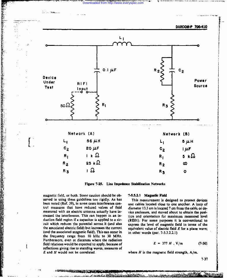
DARCOM.P 706410
L3
0IiI
I o.I/.LF R2 C2
DeviceUnder RI F Io eT e t ' ---.S o u r c eToo-,ut
50SI RI R3
Network (A) Network (B)L I 56 11H L I 5 ,kH
C2 20 .tF C2 1 /.F
RZ 25 kS1 R2 OD
R 3 I S R3 O
Figure 7-25. Line lImpedae Stbilization Networks
magnetic field, or both. Some caution should be ob- 7-5.5.2.1 Magnetic Fieldserved in using these guidelines too rigidly. As has This measurement is designed to protect devicesbeen noted (Ref. 39), in some cases interference con- and cables located close to one another. A loop oftrot measures that have reduced values of field diameter 13.3 cm is located 7 cm from the cabk; or de-measured with an electric antenna actually have in- vice enclosure, and moved about to obtain the posi-creased the interference. This can happen in an in- tion and orientation for maximum measured levelduction field region if a capacitor is applied to a cir- (RE01). For some purposes it is conventional tocuit which reduces the potential across it (and also express the level of magnetic field in terms of thethe associated electric field) but increases the current equivalent value of electric field E for a plane wave;(and the associated magnetic field). This can occur in in other words (par. 7-3.3.2.2.1)the frequency range from 10 kHz to 30 MHz.Furthermore, even at distances where the radiationfield relations would be expected to apply, because of E - 377 H , V/m (7-50)reflections giving rise to standing waves, measures ofE and H would not be correlated, where H is the magnetic field strength, A/r.
- ./.3/
Downloaded from http://www.everyspec.com

DARCOM-P 706,410
In another procedure (RE04) a loop or other form 7-5.5.2.2.2 Antenna Radiated Emissionsof magnetic loop sensor is placed at a distance of I m. This technique is used where the output power isBecause of the increased distance, a lower field level high or it is inconvenient to measure output poweris measured and also the measured level may be less with the antenna disconnected. A receiving antenna,sensitive to the exact position of the sensor. For pur- which may be directive, is placed at a convenient dis.poses of prediction, the measurement at a distance of tance which will provide adequate sensitivity. At fre-I m will provide the best basis for estimating the field quencies where aperture antennas are used, the sepa-at other distances (according to the inverse cube law, ration should be adequate to insure operation in thedistance measured to center of radiation, see par. 3- far field of both antennas so that the antenna gains3.2.1.1) except for distances close in, say less than 20 will be as close as possible to their calibrated values.cm, where the 7-cm measurement distance is Eq. 5-38 can be rewritten:
probably optimum.S(4rr)z P, W (7-51)
7-5.5.2.2 ELiectric Field where7-5.5.2.2.1 Nonantenna Emitted P = power transmitted, W
Measurements are made with an appropriate an- P, - power received, Wtenna at distances of I m for most equipment (RE02) G, and G, - respective gains of transmitting andbut up to 50 m for transmission lines (RE06). Port- receiving antennas, dBable equipment and the measuring antenna are lo- r = separation distance, mcated at a height of approximately I m above a X = wavelength, mground plane, which must underlie both the equip- and applies, provided-that,ment under test and the measurement antenna (seeFig. 7-26). Note that the EMI meter is also located on 2D1
r>-, .M (7-52)the ground plane as are the line impedance stabili- -zation networks which are used with the device undertest. Furthermore the length of power line leads where
; between the LISN's and the device under test is re- D = diameter of larger antenna, mstricted, since these leads can contribute to the and D d, the diameter of the smaller antenna.measured field. Antenna or other output terminals If d 0.D, MIL-STD462, Notice 3, RE03 requiresare connected to shielded dummy loads.
In the case of nonportable equipment, it is placed (D + d)2
directly on the ground plane and the antenna r m (7-53)counterpoise extended to join the ground plane asshown in Fig. 7-27. Antenna gain corrections that can be used if the far
Special techniques are necessary for the measure- field distance is not used are given in par. 5-10.6.2.ment of vehicles. In one test procedure (Ref. 40) the RE03 requires equipment sensitivity which will detectmeasurement distance is 10 m and both vertical and a spurious signal which is 80 dB below the funda-horizontal components of the field are measured. In mental transmitted power at a level which is at leastmethod REOS, which applies to tactical vehicles and 10 dB above the measuring receiver internal noisecertain special purpose engine driven equipment, the level.distance is 2 m from the perimeter of the vehicle, and During a measurement, the measuring antenna isadjusted in height from I to 2 m for maximum. The adjusted in direction and elevation to maximize thebiconical antenna, used between 25 and 200 MHz, is measured level. Because of the presence of a highplaced alternately to receive both horizontal and ver- level desired output signal, it may be necessary to (1)tical polarization. Where the engine compartment place a rejection filter at the input to the measuringhas a top opening, the antenna is placed over the receiver to limit its value, and (2) place the meas-opening with the direction of maximum sensitivity di- uring receiver in a shielded enclosure.rected towards the opening.
Figs. 7-28 and 7-29 show typical testing arrange-ments inside a shielded enclosure. Fig. 7-30 indicates 7-5.6 SUSCEPTIBILITYthe adaptation of the general procedures to a special In testing for susceptibility, voltages or fields are "situation, impressed on the device under test. The level is
7-38
Downloaded from http://www.everyspec.com

DARCOM*P 706-410,
V)i WiLii
2r C)I- (A Lii
<A W - -L -CC-)~ 0:x = - O-
-j~ ~ ~ LL ( u JD
WLJ LJ~- LLZ0 ajL o K L nU-
CA Ln-j wi:cLJ >- j
V) cc AOi w 03 co I-j
Gn~W LIJ LoUn LU M
= : -c UJ - V )V) -LU C 0-j Lu U-
CD~~a~ (Acc-U-iN-j 2 LAJcz c u2)U 1
-jt-1 L . =L
LL F -jF-~~ ClC) U-7: c
C) CD2! -Lu 4 < u uj CD -
>4 - U-iu ze co -
CO Cm o
CD 149
Downloaded from http://www.everyspec.com

[ DARCOMP 706410
LUJ
LI-
L1J
0U.-J M uJi~
LU0V) UL U
C) -j W
U-5 Do) -Z-V) C -
LU a-ULU CD-1 (n >: x
co V jw ))
oe w :3 LU
ui W u i-- I-7-40 )
Downloaded from http://www.everyspec.com

Ir Ir DARCOMP 706-410 II
i
*1
iS
C. *1
I-.
.1.3U
I-
LT.g
I7-41
I/-~
Downloaded from http://www.everyspec.com

DARCOM-P 706-410
91a
7-42
nia
Downloaded from http://www.everyspec.com

DARCO7- 706-410
7-43
Downloaded from http://www.everyspec.com

gradually increased or decreased until a certain cri- ance, as specified in the procurement documents for
teflon is met. If the impressed voltage or field is at a the equipment under test.frequency which enables direct detection, the For broadband tests one form of standard im-criterion is usually a certain ratio of observed output pulsive waveform is that shown in Fig. 7-31 which(either audible or visible) due to the internal noise has an amplitude up to 100 V and a duration of thelevel. In some cases the observation can be made at a main transient of 10 jus. In special cases, pulses ofhigh ratio of observed signal-to-noise, say 20 dB, and larger magnitude (up to about 1000 V) and shorterthe input level at another ratio, say 6 to 10 dB, cal- duration (down to 10, or even 1, ns) may be appro-culated from it. in other cases the measurement may priate.be made with a receiver bandwidth having one valueand corrected for a standard bandwidth havinganother value. 7-5.6.1 Conducted Susceptibility
Corrections for level are made proportionally.Corrections for bandwidth are made in accordance 7-5.6.1.1 Power Lime Susceptibilitywith the discussion in par. 7-3.1.2. For receiver sensi- Sine wave susceptibility can be measured bytivity the correction is according to the square root of coupling a voltage in series with one of the powerthe bandwidth. lines, In the case of dc lines, the voltage is coupled
In those tests in wnich it is necessary to have an im- directly in series with the high line (CSOI); otherwisepressed desired signal in order to detect suscepti- it is applied to the 50-ohm terminal of the LISN con-bility to an undesired emission, the level and modu- nected into the circuit as for emission tests (CS02). Inlation of the desired signal can have significant effects either case the injected current or voltage can beupon the result. In most cases they should be set at monitored with a current probe or tuned voltmeterthe conditions approximating minimum perform- placed line to line.
L4
IIJJt 101II1II III I
Fi!ure 3 1 S 1 1hA 1 1. .IeIl. ',
'1 1 il -- -aM I I I I I I I I
t 10 PsF II i l
7.44
.I I i I 1 !
I- tlI I[l IIm l
Downloaded from http://www.everyspec.com

DARCOM* 706410
For broadband tests the sine wave generator is re- In use, one of the signal generators is modulated. . placed with an impulse generator, and the voltmeter and the frequencies of each are adjusted according to
is replaced with a calibrated oscilloscope, which is the order of intermodulation of interest, as shown inpreceded by a line frequency rejection filter. The cir- Table 7-4 (see par. 3-2.2.2). One of the frequencies,cult is shown in Fig. 7-32. say f,, is usually adjusted as close to f, as possible
without producing a response at the output by itself.7-5.6.1.2 Intermodulation Thenf 2 is adjusted in frequency and amplitude until a
Because the signal sources used in intermodulation maximum intermodulation response is obtained. jtesting are themselves subject to nonlinear effects may be selected both above and below f. Normally,which may affect the measured result, special care is the 3rd and 5th order are the most significant, sincenecessary in the experimental arrangement. Corn- for those orders both f and f2 are close to £. Themonly, filters and attenuators are used as shown in intermodulation rejection is the difference betweenFig. 7-33 (CS03). the level in dB to which the outputs of the two gene-
In this arrangement, the filters are tuned to the raters are adjusted and the level of one of the modu-respective signal generator frequencies and in each lated generators when tuned to the receiver fre-case prevent frequencies frorn the other generator or quency when adjusted to provide standard output offrom the receiver from affecting their output. the receiver, say (S + N)/N = 10 dB.Furthermore, they attenuate harmonics of the de- Care should be exercised to make sure the desiredsired signal generator. The coupling network should intermodulation response is being observed and not ahave at least 20 dB insertion loss between signal spurious output of either-generatwr or spurious..-generator terminals. - ............ response of the receiver. If the correct response is
Test RII FGenerator Meter
Cut'rentProbe
0owe i DevicePour LI S N Under
Source _____ Teat
TunedHigh
Impedoae.... J VTVM __
Figure 7-32. Power line Condued Susceptibility Tests Using LISN
7.45
Eft- ' "= i-- i -i.. ..i .....F ..
Downloaded from http://www.everyspec.com

DARCOM-P 70b-410
Signal Generator~~~~~N o . I --_ , , -
coupling Receivere rAttenuator UnderN wr Test
Signa GeneratorutputNo. 2 -Indicator
JFigure 7-33. latermodlulatia Measrements
generator (S.G.) No. I is tuned to the same fre- JTABLE 7-4. quency to which the receiver under test is tuned andTEST FREQUENCY RELATIONSHIPS VS its output is adjusted to produce an appropriate levelMODULATION ORDER at the receiver input, say 10 or 20 dB above the re-,e oceiver sensitivity level. The interfering S.G. No. 2 is! Order Relationship tuned to a frequency near the tuned frequency but at2 f f f least two receiver bandwidths away from it. Initially3 f 2f -f2 with S.G. No. 2 turned off. S.G. No. I is modulatedS4 2f 2f 30% at 400 or 1000 Hz and the output level control- 2f , adjusted for a normal output level. Then with S.G.3 2f2 No. I unmodulated. the output of S.G. No. 2 with
30% modulation is adjusted for the same level in theoutput of the receiver as obtained with S.G. No. Inot produce a linear change in the observed output receiver is noted. The test is repeated for other fre-
level. quencies or S.G. No. 2 on both sides of the receiver7-5.6.1.3 Croas Modulation tuned frequency. The results are plotted in terms of7-.6.1Crs odu atio n eeamicrovolts
(on a logarithmic or dB scale) vs fre-Cross modulation can be measured with the same quency. The test can be repeated at other otu
equipment as is used fox intermooulation. Signal levels from S.G. No. I (see Ref. 41).
7-46 " "
.. {
Downloaded from http://www.everyspec.com

---- -- --- -- --- --
OARC09AP 706410
7-5.6.1.4 Spurious Response and Desensitization by a distance equal to the radius of each coil will pro-
Undesired receiver responses can be detected by vide a quite uniform fieldapplying a signal generator at the input and scanningthe frequency range of interest (CS04). The signal H - 8N , A/m (7-55)generator should not have spurious output frequen- 125 acies or they should be filtered as in Fig. 7-33. By ad-justing the attenuator, one can distinguish betweengenerator and receiver spurious since receiver 7-5.6.2.2 Electric Fieldspurious responses are not linearly related to input The fields required may be established in severallevel, ways. Where space is available a standard antenna
To make quantitative measurements, a second such as described in par. 7-3.3.2 can be fed from asignal generator adjusted to the receiver tuned fre- signal generator of sufficient power to generate thequency at a level which produces standard output can field required at the test distance. The field value ob-be applied at the input (see Fig. 7-33). The level of the tained should be checked with an antenna andfirst generator which causes noticeable change in the receiver combination of known sensitivity, with thestandard output level is the spurious response or de- antenna located at the test position. Since, for largesensitization level. equipments, the field strength may vary significantly
from one point to another, it may be necessary tochange the relative location of the equipment and thesource antenna during the test to insure that all parts
-. As withR mission easuremnradiated are exposed to the same field strength..As-with emission measurements, radiated sus- . . .....as......i.eTe....eceptibility testing is done with a magnetic field sourceat frequencies up to 30 kHz and with an electric field 7-5-.62-3 Transmisslon Ilse Teewiques
source at 14 kHz and above. The strip line tech- Two types of transmission line techniques haveniques enable combined electric and magnetic field been used. In one a wire is stretched between oppositetesting. sides of a shielded enclosure (RE03). The enclosure
then forms the outer conductor of a simulated co-axial structure. When the line is properly terminated,
7standing waves on the line are avoided and the ratio7-5.6.2.1 Magnetic Field of the radial electric to the circumferential magnetic
Usually the field is generated by a loop (12 cm field strengths approximates the characteristic im-diameter in RSO1) which is used to scan the surface of pedance of free space, at least close to the wire. Thean equipment to locate the point of maximum sensi- fields can be calculated in terms of the measured cur-tivity. The field H along the axis of a concentrated rent I in the wire. Because of the effect of the walls,loop of N turns can be calculated from (Ref. 42) corrections must be applied to the calculated fields.
One obtains:Nlaz A/r (7-42(a2 +r=)/ 2 + A/ (E= 601d + I ! ) Vm (7-56)
where (d 2d -d - 2d , +d
I - current, Aa = loop diameter, m wherer = distance along the axis from the center of I = current, A
the loop. m d, dl, d2 = distances as shown on Fig. 7-34, mThe magnitude of the field from a particular coil can The parallel plate transmission line is shown on
Sbe established either by measurement of the field at a Fig. 7.35. Except for fringing effects at the edges ofspecified distance using an appropriate magnetic sen- the line, the electric field component is normal to the
sor or by calculation in terms of the coil current, if plates and the magnetic field parallel. When the linethe construction is sufficiently precise. The current is properly terminated, the ratio of electric to mag-through the coil can be measured by a current probe netic field strengths is also that of free space or 377and tuned voltmeter or by measuring the voltage ohms.
* across a resistor in a series with the coil. The upper frequency at which both these-line, areA pair of identical coils parallel to each other in a usable is limited by the discontinuities in electrode
Helmholtz arrangement on the same axis and spaced shapes at the line ends. Generally, the parallel plate
7-47
Downloaded from http://www.everyspec.com

DARCOM-P 706-410
d2
ZL d
.4 Test Sample
Figure 7-34. Long-wire Transmission Line
line can be used to about 50 MHz and the wire line to suitability of a particular location for a future mili-somewhat less. tary installation or (2) whether fields at an already
A variation of the parallel plate line construction is existing installation (usually die to a recent installa-that of the fully enclosed parallel plate line, or "TEM tion of new tquipnient) are sufficient to degradeCell" (Ref. 43) in which a center is completely sur- operations in the vicinity. Most often, they are per-rounded by the outer enclosure. Fig. 7-36(A) shows formed on the ground, but also are carried out in air-the external appearaace of the line with tapered sec- craft. On the ground, it is most expedient to use ations at each end. Fig. 7-36(B) shows a cross section vehicle on which all equipment, antennas, and powerwith the plate in the center. A uniform field test supplies are self contained. Automatic frequencyregion is available both above and below the center scanning and recording are desirable unless the testsplate. Because this line is fully enclosed no leakage being conducted are of a specialized nature.field is produ.ed. and therefore it is easier to match The requirements on characteristics of equipmentwith the tapered sections than is the two-parallel- used follow.plate line. With this construction it is easier to obtainsatisfactory operation up to the point at which the 7-5.7.1 Frequency Rangespacing of the plates approaches 1/2 wavelength and Surveys can be conducted over the range 10 kHz tomoding occurs. 40 MHz. For particular purposes, such as for plotting
In all of the field susceptibility testing i.chniques, it the fields from a particular transmitter or othershould be observed that equipment can be expected source, only its fundamental frequency, its harmon-to be sensitive to polarization. Therefore, the object ics, and other expected spurious frequencies need beunder test should be repositioned during the test so as covered. If' the purpose of the survey is to determineto expose it to the most effective field polarization, the suitability for installation of a particular receiver,
frequencies to which the receiver may be susceptible7-5.7 SITE SURVEYS should be surveyed. Also frequencies at which
Surveys of the electromiignetic environment at par- extraordinarily high field strengths exist due to localticular locations are made to determine either (I) the transmitters should be measured.
7-48
.......................................... ........... | ............. ..... .... .. u ~*f~Ml-
Downloaded from http://www.everyspec.com

-_ _ _ _ _ _ _DARCOM-P 7C4410
TOP VIEW
-~--- COPPER GROUNDING STRIP-.,
T a 2! 2'MI11
ENARED2" X 4" WOOD_• ENLARGED "
DETAIL _
132"
NP NTHERMO SETTING PLASTIC
INPUT END SIDE VIEW. LOAD END
SEE ENLARGED DETAIL 1. S 7L. 24- .20"
"
F -I8"ALUMINUM SHEET- li
-/ 1 "ALUMINUM WITH PLYWOOD BACKING
END PLATES ARE MADE FROM 1/32"COPPER PLATE ------
Figure 7-35. Parallel Strip Line for Radiatee Susceptibility Tests (Top and Side View)
'7-5.5.2 Sensitivity 7-5.5.4 Locations of AntennasFor general purposes receiver sensitivity should be In general, test locations should be chosen as far as
equal to the state of the art for calibrated broad possible from reflecting objects. However, if the pur-tuning range receivers. i.e., a few dB at frequencies up pose of the survey is to determine hazards, numerousto the tens of megahertz increasing to about 10 dB at test locations - including some close to reflectingI GHz. Lesser sensitivities would be satisfactory for objects - may be appropriate. In such cases it is de-surveys in connection with radiation hazards. sirable to choose sufficient locations to enable plot-
ting contours of constant field strength (from a par-7-5.5.3 Antennas ticular source). The number required depends on the
Antennas should be broadly tunable to minimize frequency of radiation of interest, being greater at thethe number required to cover the frequency range higher frequencies. For a detailed survey, measure-and for most purposes should be as nondirectional as ment locations may be spaced as closely as everyrequired sensitivities permit. At frequencies up to 30 quarter wavelength or less.MHz both a vertical rod and loop can be used. The On large sites that are distant from local sources.latter should be rotatable in its vertical plane. only a few measurement locations may be necessary.
Above 30 MHz the antennas should be planepolarized and orientable for both horizontal and ver- 7-5.5.5 Data Recordingtical polarization. Peak, average, and rms detectors are useful in sur-
. Furthermore, the height of the antenna should be vey work. Normally signals are measured with theadjustable. preferably up to a height of 10 m so that average detector, and atmospherics are measuredpoints of maximum field strength can be identified. with the rms detector although sometimes both the
7.49
__,_
I-'
Downloaded from http://www.everyspec.com

,t DARCOM4P 706-410
(A) External Appearance
iE
_..4.
(B) Internal Field Distribution
Figure 7-36. Enclosed Parallel Plate Line
rms and average are measured (see par. 3-1.2.2.2). 7-5.5.6 CalibrationThe peak detector commonly is used for measuring Instruments and antennas should be calibrated inman-made radio-noise, especially when it is inter- accordance with pars. 7-3.1.3 and 7-3.3.3.mittent, or highly impulsive. In all cases it is im-portant to record the acceptance bandwidth of the 76 EMC TEST FACILITIESmeasuring receiver so that corrections can be made in Although "in-house" facilities may be used ex-the effective level for receivers having different band- tensively in carrying out the test procedures dis-widths. In this respect, measurements made on more cussed in this chapter, there may be times when thethan one detector may be helpful. In addition, use of outside facilities may be advisable, especially ifmeasurements of variations in measured level with large numbers of tests and special facilities are re-time should be recorded. if test time permits, along quired. Frequently, private test laboratories are avail-with antenna height. able. In addition a number of Military Laboratories
7-50
. .. - -
Downloaded from http://www.everyspec.com

DARCOMP 706410
have set up test facilities with a variety of capabilities b. The Weapon System Electromagnetic Environ-(Ref. 44). These may be available to individual con- ment Simulator (WSEES) is comprised of a com-tractors, especially in the case of unusual require- puter programmed RF generator, and RF ab-meats, and are described briefly. Table 7-5 gives sorption room, a steerable platform, and other sup-points of contact for each facility, port equipment necessary to simulate complex elec-
tromagnetic environments and develop scoring datafor systems operating in the microwave frequency
7-6.1 ARMY FACILITIES bands, including radar systems.c. The Systems Scoring Facility (SF) consists of
7411 Electromagnetic Interference two listener facilities (one mobile, one fixed) designedTest Facilities to measure the performance of voice communicationLocation: US Army Electronics Command, Fort systems used tactically by the Army in the field. "
Monmouth, NJ d. The Digital Scoring System (DSS) enables rapidInstrumentation is available for implementing test- evaluation of a variety of digital communication links
ing requirements of MIL-STD-461 and -462. and minimizes human intervention in obtaining thedata needed.
e. The Spectrum Signature Facility (SSF) can pro-7-6.1.2 Materiel Testing Directorate vide measurements in accordance with MIL-STD-
Location: Aberdeen Proving Ground, MD 449.EMI/EMC tests in accordance with MIL-STD-461 f. The Field Facility (FF) conducts EMC te3ts of
and other specifications can be performed at fre- large equipments, antenna measurements, and anyquencies up to 40 GHz. Of three automated spectrum tests that require open-field measurements or thatsurveillance systems; one- is mobile and used for the cannot be contained in the IWS.testing of noncommunication-electronic equipmentincluding track and wheel vehicles, watercraft, airconditioners, and other engine drive equipment, The 7-6.1.4 Electromagnetic Radiation Effectssecond system is transportable and is used for tests on Tea Fecilitycommunication-electronic equipment as well as Location: White Sands Missile Range, NMnoncommunication-electronic equipment. The third Equipments are available with power output up tosystem is permanently installed in a screened room. 50 kW to produce high intensity (200 V/m) electro-
An EMI shielded enclosure, 94 ft X 60 ft X 28 ft, is fields at frequencies from 100 kHz throughused for EMI/EMC tests of large vehicles; i.e., tanks, magetictractor-trailers, shelters, construction and materialhandling equipment, and engine-generator sets.
7-6.1.5 Missile Electromagnetic Effects7-6.1,3 Electromagnetic Environmental Test Facility
Test Facility (EMETF) Location: Redstone Arsenal, ALLoc' :ion: US Army Electronic Proving Ground, This missile electromagnetic effects (EME) test
Fort Huachuca. AZ facility is designed for rapid missile test and evalua-The EMETF has six interrelated experimental tion. Transmitter frequency coverage is from 100 kHz
capabilities as follows: to 18 GHz with power levels from I kW to 10 kW.a. The Instrumented Workshop (IWS)/Automatic Transmitters are servo tuned for rapid and remote
Data Collection System contains facilities for con- control in the 100 kHz to 350 MHz region. Sevenducting performance tests of electronic equipments fixed broadband transmitters are used above 350under controlled electromagnetic interference con- MHz. The facility includes a dedicated computerditions to investigate interference mechanisms, fur- which can provide transmitter test control, datanish information for designing interference sup- acquisition, and data analysis.pression devices, establish intelligibility measure- The EME test facility can interface with the Armyments, provide data for the further development of Missile Command Advanced Simulation Centerthe Interference Prediction Model (IPM) and the de- (ASC) to evaluate missile hardware during simulatedvelopment of methods of scoring the performance of missions. Missile testing utilizing the ASC in con-Communication-Electronics (C-E) systems. (See par. junction with EME testing provides precise missi.-6-4.3) hardware performance evaluation.
7-51
. .. ....... .. .+4r - i r i i +
Downloaded from http://www.everyspec.com

I-
DARCOM-P 706410
TABLE 7.5. POINT OF CONTACT LIST
Parent ParentAgency Facility Organization Address
Army EMETF (Electromagnetic US Army Test and Cdr US Army Electronic ProvingEnvironmental Test Facility) Evaluation Command Ground, Attn: Code STEEP-NT-
MP, Fort Huachuca, AZ 85613
Army EM Interference Test Facility USAECOM Cdr US Army USAECOM, Attn:AMSEL-GG-I
Fort Monmouth, NJ 07703
Army Materiel Testing Directorate US Army Test and US Aberdeen Proving GroundEvaluation Command Attn: STEAP-MT-G
Aberceen Pi oving Ground, M D21005
Army Electromagnetic Radiation US Army Missile Test White Sands Missile RangeEffects Test Facility, Evaluation Command NM 83002White Sands Missile Range
Army Missile Electromagnetic US Army Missile Cdr US Army MICOM,Effects Test Facility Command Attn: AMSM RTE -
Redstone Arsenal, AL 35809
Navy EMC Section, Electronic Systems Naval Air System Cmd, Naval Air Test CenterBranch Command Attn: SYSO
Systems Eng, Test Directorate Patuxent River, MD 20670Naval Air Test Center
Navy System Test Facility Naval Electronics San Diego, CA 92152Laboratory Center
Navy Technical & Environmental Naval Electronics 271 Catalina Blvd.Evaluation Division Laboratory Center San Diego, CA 92152
Navy Communications Systems Branch US Navy Research Washington, DC 20375Laboratory
Navy Systems Integration & US Navy Research Washington, DC 20375Instrumentation Branch Laboratory
Navy Naval Avionics Facility Naval Air System Dept. of the Navy, NavalCommand Avionics Facility
6000 E. 21 st StreetIndianapolis, IN 46218
Navy Naval Ship Engineering Naval Ship Eng. Center Naval Ship EngineeringCenter, Norfolk Div. Center. Norfolk Div. Naval
StationNorfolk, VA 23511
Navy Naval Electronic Systems Naval Electronic Patuxent River, MD 20670Test & Evaluation Facility Systems Command
(cont'd)
7-52
.. - .:- , : , - . ..
Downloaded from http://www.everyspec.com

ARCM-P 706410
TABLE 7.5. (Coat'd)
Parent ParentAgency Facility Organization Address
Navy Naval Surface Weapons Center Naval Materiel Dahlgren, VA 22448Dahlgren Laboratory Command
Navy Naval Underwater Systems Chief of Naval Materiel Newport, RI 02840~~Center '
T & E Facility (NESTEF)Air Force EM Interference & Compatibility Aeronautical Systems Wright Patterson AFB,
Branch Division OH 45433Air Force Antenna Proving Range Rome Air Development Griffiss AFB, NY 13441
Newport, NY CenterAir Force EM Test Facility Rome Air Development Griffiss AFB, NY 13441
Verona, NY CenterAir Force EM Interference & Analysis Electronics System Griffiss AFB, NY 13441
Facility DivisionAir Force Richards Gebaur AFB AF Communications Richards Gebaur AFB
Service MO 64030
7-6.2 NAVY FACILITIES 7-6.2.3 Naval Electronic Laboratory7-6.2.1 Naval Air Test Center (NATC) Center (NELC)
Locatiou: Patuxent River, MD Location: System Test Facility, San Diego, CAPersonnel and specialized test equipment are avail- The facility has the capability of conducting spec-
able to perform lightning and EMC tests of complete trum surveys of the RF environment and of the RFaircraft weapon systems and of airborne avionic/ environment internal to communication systems 1electrical equipment to determine compliance with from 14 kHz to I GHz and automatically plotting theMIL-E-6051 and MIL-STD-461. results.
The laboratory has a main shielded area approxi-mately 300 ft by 140 ft by 66 ft at the highest ceilingpoint, and an adjoining nosebay shielded area ap- (NEL letric ado r.y entrproximately 100 ft x 62 ft x 30 ft. The lightning testfacility contains a surge voltage generator and a surge Evaluation Divisioncurrent generator. Location: San Diego, CA
Measurement capability is principally in the areaof EMI testing of components and equipments and in
7-6,2.2 Naval Surface Weapons Center evaluation of EMI properties of shipboard electronicLocation: Dahlgren, VA equipments against requirements of MIL-I-16910.The Naval Weapons Laboratory has equipment
and facilities used to study HERO and high powerRF effects. Two ground planes, each 240 ft X 100 ft. 7-6.2.5 US Naval Research Laboratoryof 3/8-ft welded steel, are equipped with 21 ft diam- Location: Washington, DCeter turntables with a capacity of 40 tons. The Communications Sciences Division has in.
Shielded RF laboratories up to 2300 sq ft and an strumentation on hand for EMC/EMI measure- tanechoic chamber, 8 ft X 8 ft X 16 ft. are available. A ments over the LF through UHF bands and includesmobile rescarmh van can measure EME in the 2-32 enclosures in the security vault for critical TEMPESTMHz frequency band. measurements.
7-53
Downloaded from http://www.everyspec.com

DARCM I70r&4r10
'7-6.2.6 Naval Avionics Facility 7-6.33 Electromagnetic Test Facility
Location: Indianapolis, IN Location: Verona, NYI A shielded enclosure is available which can be The facility supports engineering evaluation andadapted for shielding effectiveness tests on materials, operational testing of ECCM, radar, communi-devices, cables and connectors, and filters. cations, millimeter wave research, and optical sur-
veillance techniques.
7-6.2.7 Naval Ship Engineering Center, 74.3.4 Electromagnetic InterferenceNorfolk Division and Analysis Facility
r Location: Norfolk, VA Location: Griffiss Air Force Base, NY0 Two instrumented vans capable of measurements Anechoic chambers up to 54 ft X 18 ft X 18 ft in
up to 40 Giz are available. Measurements can be size contain equipment to generate up to 50-kW peakmade of spectrum signature, EM ambient levels, an- powzr. Antenna gain and pattern measurements cantenna patterns, and limited MIL-STD-461 measure- be performed on any antenna whose physical di-meats. mensions are less than 6 ft overall.
7-6.3.S Air Force7-6.2.8 Naval Electronic Systems Test Communication Service (AFCS)
and Evaluation Facility (NESTEF) AFCS facilities have the capability of makingLocation: Patuxent River, MD measurement in the field and can be used to analyze,This laboratory is set up for measurement of spec- identify, and initiate corrective action to prevent elec-
trum signatures and the performance of technical in- tromagnetic interference world-wide on communica-vestigations in support of ECAC and site survey in- tion electronic-and-meterologicaI (C-E-M) equip-vestigations. ments.
L- :- REFERENCES7.6.2.9 Naval Underwater Systems Center (NUSC)
Location: Newport, RI I. R. F. Ficchi, Editor, Practical Design for Electro- "The Atlantic Undersea Test and Evaluation Center magnetic Compatibility, Hayden Book Co., 197I.
(AUTEC), located in the Andros Islands area, is 2. Radio Noise and Field Strength Meaers. 0.015 tocapable of monitoring and obtaining a bearing on 30 MHz. Specification for. American Nationalany electromagnetic radiation. Standards Association (ANSI) C63.2-1963.
3. Radio Noise and Field Strength Meters, 20-10007MHz/Second Specification for, American Na-7-4.3 AIR FORCE FACILITIES tional Standards Association C63.3-1964.7-6.3.1 Electromagnetic Interference 4. CISPR Publication 1, Specification for CISPR
and Compatibility Branch Radio Interference Measuring Apparatus for the
Location: Wright-Patterson AFB, OH Frequency Range 0. 15 MHz/s to 30 MHz/s. Cen-The facility can perform EMC measurements on tral Office of the International Electrotechnical
aeronautical systems. Commission, Geneva, Switzerland, 1972.5. CISPR Publication 2, Specification for CISPR
Radio Interference Measuring Apparatus for the7-6.3.2 Antema Proving Range Frequency Range 25 MHz/s to 300 MHz/s, Can-
Location: Newport, NY tral Office of IEC. Geneva. Switzerland, 1975.Four antenna ranges, one of length 7000 ft, are 6. CISPR Publication 4, CISPA Measuring Set
located in an essentially interference-free area and Specification for the Frequency Range 300 MHzused to measure antenna performance parameters to 1000 MHz, International Electrotechnical(down to +0.25 dB sidelobes with over 40.60 dB dy. Commission, Geneva, Switzerland, 1967.namic range at higher frequencies, 360 deg in azi- 7. The Radio Frequency Interference Meter. Bureaumuth, and 180 deg vertical cut for antennas with up of Ships, Department of the Navy, NAVSHIPSto 60-ft aperture width). A dark room range (15 ft x 94180. July 1962.12 ft x 22 ft) with walls covered with absorbing 8. L. B. Argimbau and R. B. Adler, Vacuum Tubematerial is used to test antennas (3 ft max dia, 20 lb Circuits and Transistors. John Wiley and Sons,max) with a lower frequency limit of I GHz. Inc., 1956.
7-54
M. ,. -
Downloaded from http://www.everyspec.com
DARCOM-P 706-410
9 A. Papoulis, The Fourier Integral and Its Appli- Frequency Propagation, John Wiley and Sons,cations, McGraw-Hill, Inc., 1962. Inc., NY, 1953.
10. The Design and Development of a Laboratory 24. IEEE Standard No. 299, June 1969, ProposedModel Standard Noise Generator, Purdue Uni- IEEE Recommended Practice for Measurement ofversity, June 30, 1947, Contract W28-099-ac-73. Shielding Effectiveness of High-Performance
11. IEEE Standard No. 376, Measurement of Im- Shielding Enclosures.pulse Strength and Impulse Bandwidth. Institute 25. MIL-STD-285, Attenuation Measurements forof Electrical and Electronics Engineers, Inc., Enclosure, Electromagnetic Shielding, for Elec-1975. tronic Test Purposes, Method of.
12. IEEE Standard 263, Measurement of Radio Noise 26. Reference Data for Radio Engineers. ITT, 5th V
Generated by Motor Vehicles and Affecting Edition, 1972.Mobile Communciations Receivers in the Fre- 27. H. A. Mendez, "Meaningful EMC Measure-quency Range 25 to 1000 MHz, IEEE, Inc., NY, ments in Shielded Enclosures", 1969 IEEE Elec-
i 1965. tromagnetic Compatibility Symposium Record. p.
13. M. Engelson and F. Telewski, Spectrum Analyzer 137, June 17-19, Asbury Park, NJ.Theory and Applications. Artech House, 1974. 28. W. R. Free and C. W. Stuckey, Electromagnetic
14. A. E. Fitzgerald and C. Kingsley, Electric Ma- Interference Measurement Methodology. Com-chinery, McGraw-Hill, 1952, Appendix A. munication Equipment, Final Report, Contract
: 15. H. Whiteside and R.W.P. King, "The Loop DAA B07-68-C-0189, Georgia Inst. ofTech.,Oc-Antenna as a Probe, IEEE Transactions on An- tober, 1969.tennas and Propagation, Vol. AP-12, No. 3, May 29. C. W. Stuckey, "The Hooded Antenna, an Ap-1964, pp. 291-297. proach to Meaningful Field Strength Measure-
16. Development of Techniques for Accurate Measure- ments in Shielded Enclosures", IEEE Trans-ment of Magnetic Fields between30 Cycles per Se- actions, on Electromagnetic Compatibility. De-cond and 30 Megacycles per Second, Final cember 1965, pp. 360-367. -
7.Report, Armour Research Foundation, Contract 30. D. M. Kerns, "Correction of Near-Field An-NObsr-72777, January 1960. tenna Measurement Made with an Arbitrary but
17. L. J. Greenstein and M. Epstein, Development of Known Measuring Antenna," Electronic Letters.Improved Hall Effect Sensors, Final Report, lIT Vol. 6, No. 11, 28 May 1970.Research Foundation, Contract NObsr 85-057, 31. Gus Van Steenberg, E. L. Bronaugh, G. T.December 1963. Daril-k and W. C. Dolle, "An Isolated Antenna
18. Variable-Mu Receiver for Measurement of Mag- Systi-m for Shielded Enclosure Measurements,netic Induction Fields Relative to Susceptibility of 20-200 MHz", 1971 IEEE International Electra-Integrated Solid-State Devices, Technical Report magnetic Compatibility Symposium Record.AFAL-TR-66-281, Electro-Mechanics Co., July Phila., PA, July 13-15, 1971, pp. 198-202.1966. 32. Timothy D'Arcangelis, "New Components,
19. IEEE Standard No. 291, IEEE Standards Report Instrumentation and Control Techniques foron Measuring Field Strength in Radio Wave Automatic RFI Susceptibility Testing", 1971Propagation, May, 1969. IEEE International Electromagnetic Compati-
20. R. D. Hitchcock, Calculations for the Cali- bility Symposium Record, Phila., PA, July 13-15,bration of Navy RIFI Meters Using n Vertical Rod 1971, pp. 251-252.Antenna. Report TN-534, U.S. Naval Civil En- 33. Keigo, lizuka, "How to Measure Field Patternsgineering Lab., Port Hueneme, CA, 6 September with Photosensitive Probes", Electronics, Jan-1963. uary 25, 1963, p. 39.
21. D. B. Clark. HA. Lasitter and R. D. Hitchcock, 34. L. Krugel, "Shielding Action of Outer Con-"Navy Field Strength Meter Measurements in a ductors of Flexible Coaxial Cables", (Abschirm-Quasi-Absolute Monopole Field," Proc. of 10th wirkung von Aussenleitern Flexibler Koaxialka-Tri-Servce Conference on Electromagnetic Com- beln), Telefvnken Zeitung. Vol. 29, pp. 256-266,patibility. November 1964, pp. 341-398. December 1966.
22. K. Bullington, "Radio Propagation at Fre- 35. E. D. Knowles and L. W. Olson, "Cable Shield-quencies Above 30 Megacycles", Proc. of the ing Effectiveness Testing", International Electro-IRE. 35, 1122-36, October 1947. magnetic Compatibility Symposium Record. IEEE
23. Heit.y R. Reed and Carl M. Russell, Ultra-High Pub. No. 71C29 EMC, July 1971.
7-55
i t .0. . - ., . : . .. . - .
Downloaded from http://www.everyspec.com

..-.--- P 70-1
36. COP Report No. 47. Measurement of she 40. SAE Standard J551. Measurement of Electro-
Shielding Efficiency of Coaxial Cables Having I magnetic Radiation from Motor Vehicles (20-1000or 2 Braids in the Metric Wavelength Range. MHz). ANSI Cl 12.1, 1972.CISPR Publication 811, International Electro- 41. IEEE Standard No. 186, Standards on Radio Re-technical Commission, Geneva, Switzerland. ceivers. Methods of Testing Amplitude-Motda-1975. tion Broadcast Receivers. Institute of Electrical
37. ARP 936. Capacitor, 10 tF for EMI Measuie- and Electronic Engineers, Inc., NY, 1948.ments. standard issued by Society of Automotive 42. R. P. Winch, Electricity and Magnetism. Pren-Engineers, Inc. (SAE) 5/31/68. tice-Hall, 1955.
38. Donald E. Groff, The Performance of 10 piF 43. Myron L. Crawford, "Techniques for Measure-Power Line Feedthrough Capacitors, Moore mnert of Electromagnetic Radiation and Sus-School or Electrical Engineering, University of ceptibility of Electronic Equipment," Proc. of 1stPennsylvania, July 1969, Tech. Report RADC- Symposium on Electromagnetic CompatibilityTR-69-67. (IEEE), Montreux, Switzerland, May 20.22.
39. W. Jarva. Problems of Radio Interference 1975, IEEE 75 CHI 1012 - 4 Mont., pp. 38-44.Measurements. Technical Report No. NADC- 44. PAM No. 11-13, Army Electromagnetic Corn-EL-N54149, 11 Feb. 1955. patibility Program Guide, March 1975.
7-56
2,
Downloaded from http://www.everyspec.com

DARCOM-P 706-4R0
GLOSSARY
The terms associated with EMC/EMI have been Antenna gain. The ratio of the power required at thedeveloped over many years by persons working in input of a reference antenna to the power suppliedseveral specialized technical areas. Hence, various to the input of the given antenna to produce, in aterms have broad as well as specialized meanings and given direction, the same field at the same dis-consequent differences in usage. The terms included tance. When not otherwise specified, the gainhere are those directly related to use in the text of this figure for an antenna refers to the gain in the direc-Handbook. In so far as practical, the definitions tion of the radiation main lobe. In services usinggiven are based upon the following sources: scattering modes of propagation the full gain of an
I. MIL-STD-463, Definitions and Systems of antenna may not be realizable in practice and theUnits. Electromagnetic Interference Technology apparent gain may vary with time.
2. Advance Edition of International Electrotechnical Antenna induced voltage. The voltage which isVocabulary. Publication 50 (902): Radio Interference. measured at, or calculated to exist across, the1973, International Electrotechnical Commission, open-circuited antenna terminals.Geneva, Switzerland Antenna, isotropic. A hypothetical antenna that
3. IEEE Std.100-1972, IEEE Standard Dictionary radiates or receives energy of all polarizationsof Electrical and Electronic Terms, The Institute of equally well in all directions. An isotropic antennaElectrical and Electronic Engineers, Inc.. NY, 1972. is a lossless point source used as the theoretical
_reference in describing the absolute gain of a realantenna.
J. Adjacent channel interference. Interference in which Antenna pattern. A graph of the radial component ofthe extraneous power originates from a signal of the Poynting vector at a constant radius as a func-assigned (authorized) type in an adjacent channel. tion of the azimuthal or elevation angle.
Ambient level. The level of radiated and conducted Antenna, phased array. An array antenna whose beamenergy existing at a specified location and time direction or radiation pattern is controlledwhen the test sample is de-energized. Atmospheric primarily by the relative phases of the excitationnoise, signals (both desired and undesired from coefficients of the radiating elements.other sources) and the internal noise level of the Antenna terminal conducted interference. Any un-measuring instruments all contribute to the "am- desired voltage or current generated within abient level". receiver, transmitter, or their associated equip-
Antenna. A device employed as a means for transmit- ment appearing at the antenna terminals.ting or receiving radiated electromagnetic energy. Balanced circuit. A circuit in which two branches are
Antenna effective area. In a given direction, the ratio electrically alike and symmetrical with respect to aof the power available at the terminals of an anten- common reference point, usually ground. Note.na to the power per unit area of a plane wave inci- For an applied signal difference at the input, thedent on the antenna from that direction, polarized signal relative to the reference at equivalent pointscoincident with the polarization that the antenna in the two branches must be opposite in polaritywould radiate. and equal in amplitude (See: Differential mode in-
Antenna effective length. The ratio of the antenna ter/erence).open circuit induced voltage to the strength of the Bandwidth. impulse. The peak value at the output offield component being measured. the circuit involved divided by the area of the im-
Antenna factor. That factor which when multiplied by pulse response envelope.the voltage at the input terminals of the measuring Bond, direct. An electrical bond in which the twoinstrument, yields the electric field strength in metal surfaces are placed in intimate contact.volts/meter or the magnetic field strength in Bond. electrical. A low resistance current pathamperes/meter. This factor can include the effects between two metallic surfaces (normally between aof antenna effective length, and mismatch and metallic device and a metal surface at groundtransmission line losses, reference potential).
G-1
i_ '.- i i i i -
Downloaded from http://www.everyspec.com

GLOSSARY (cont'd)
Bond, indirect. An electrical bond in which two sur- inductance between the interference source and Afaces are connected by a bond strap or other con- the signal system; i.e., the interference is inducedductor. in the signal system by a magnetic field produced
Common-mode conversion. The process by which by the interference source. Inductive coupling alsodifferential-mode voltages (or currents) are is called magnetic coupling. The term inductiveproduced in a signal circuit by common-mode coupling is used also in a more general sense to in-voltages (or currents) applied to the circuit. dude coupling due to both magnetic and electric
Common-mode interference. Interference that appears field components.between both signal leads and a common reference Coupling, mutual Impedance. Coupling of two circuitsplane (ground) and ca~ises the potential of both through one or more common elements. The ele-sides of the transmission path to be changed ment is usuglly a resistor, capacitor, or inductor.simultaneously and by the same amount relative to Coupling. radiative. That type of coupling in whichthe common reference plane (ground). the interference is induced in the signal system by
Common-mode rejection ratio. The ratio of the electromagnetic radiation produced by the in-common-mode interference voltage at the input terfering source. N'~ote. Where the interferenceterminals of the system to the effect produced by source and susceptors can be modeled as antennas,the common-mode interference, referred to the in- radiative coupling occurs if the antenna separation Iput terminals for an amplifier, For example, is sufficient for the one with the smaller equivalent
antenna to be in the radiating near-field region ofCMR - (root-mean-square) at input the other or beyond. If not, the coupling is induc-
--... effect at. oirtput/amplifir gan ive coupling. The term radiative coupling also isCompatibility. intersystem. The ability of electronic used in a more general-sense tolinclude both types .
or electromechanical equipments or systems to of coupling as opposed to "conductive" coupling.operate in an electromagnetic environment Cross-coupling. Undesired signal coupling betweenwithout causing unacceptable degradation or two or more different communication channels,malfunction to surrounding equipments or circuits, or components.systems. Cross modulation. A type of intermodulation in which
Compatibility. intrasystem. The ability of electronic modulation on an undesired signal is transferredor electromechanical components or subsystems to a desired signal.to operate in their intended operational environ- Cross talk. An undesired signal disturbance in-ment without suffering or causing unacceptable troduced in a transmission circuit by mutual elec-degradation or malfunction to related components tric or magnetic coupling with other transmissionor subsystems. circuits.
Conducted interference. Undesired electromagnetic Decoupling. The reduction of transfer of interference
energy which is propagated along a conductor. energy from one circuit to another.Coupling. The effect of one system or subsystem upon Desensitization. Reduction in receiver sensitivity due
another. (A) For interference, the effect of an in- to the presence of a high-level off-channel signalterfer.ng source on a signal transmission system. overloading the RF amplifier, mixer stage(s), or(B) The mechanism by which an interference causing AGC control action.source produces interference in a signal circuit. Differential mode interference. Interference that
Coupling, capacitive. That type of coupling in which causes the potential of one side of the signalthe mechanism is capacitance between the in- transmission path to be changed relative to theterference source and the signal system; i.e., the in- other side. Note: That type of interference interference is induced in the signal system by an which the interference current path is wholly in theelectric field produced by the interference source. signal transmission path.Capacitive coupling sometimes also is called elec- Electricfield strength. The magnitude of the potentialtric coupling, gradient in an electric field.
Coupling, conductive, That type of coupling in which Electric induction. The process of generating charges,the mechanism is conductance between the in- currents, or voltages in a conductor by means ofterference source and the signal system. an electric field.
Coupling, inductive (or induction field coupling), The Electromagnetic compatibility. The ability of C-Etype of coupling in which the mechanism is mutual equipments, subsystems, and systems to operate in
G-2
Downloaded from http://www.everyspec.com

GLOSSARY (cout'dl
their intended operational environments without sometimes referred to as the Fraunkofer region on" suffering or causing unacceptable degradation be. the basis of analogy to optical terminology.
caue of unintentional electromagnetic radiation Fraunhofi'r region, See: Far.field region,or response. Frequency. characteristic. A frequency which can be
Electromagnetic interference. The phenomenon easily identified and measured in a given emission.resulting when electromagnetic energy causes un- Fresnel region. The region (or regions) adjacent to theacceptable or undesirable responses, malfunction, region in which the field of an antenna is focuseddegradation, or interruption of the intended (i.e., just outside the Fraunhofer region). See Noteoperation of electronic equipment, subsystem, or 2 of Near-field region, radiating.system. Ground plane. A conducting surface or plane used as
Emission. Electromagnetic energy propagated from a a common reference point for circuit returns andsource by radiation or conduction. electrical or signal potentials.
Emission, spurious. Any electromagnetic emission on Grounding. single-point. A scheme of circuit/shielda frequency or frequencies 'which are outside the grounding in which each circuit/shield has onlynecessary emission bandwidth, the level of which one physical connection to ground, ideally at themay be reduced without degrading the corres- same point for a given subsystem. This techniqueponding intended transmission of information, prevents return currents from flowing into theSpurious emissions include harmonic emission, structure.parasitic emission, and intermodulation products. Image frequency. In heterodyne frequency convertersbut exclude emission in the immediate vicinity of in which one or two sidebands produced bythe necessary emissions bandwidth, which are a beating is selected, the image frequencyis an un-result of the modulation process for the transmis- desired input frequency capable of producing thesion of information, selected frequency by the same process. The word
Environment, electromagnetic. Radiated or conducted "image" implies the mirror-like symmetry ofelectromagnetic emission levels which may be en- signal and image frequencies about the beating os-countered by an equipment, subsystem, or system cillator frequency or the immediate frequency,during its life cycle, whichever is higher.
Environment, operational. The aggregate of all con- Image rejection. The decrease in response of a super-ditions and influences that may affect the opera- heterodyne receiver to the image frequency astion of a composite system, vehicle system, and compared with its response to the desired signal,ground system and their respective subsystems and usually expressed in decibels.equipment. Image rejection ratio. The magnitude of the ratio of
Equipment. Any electrical, electronic, or rice- the amplitude of the image signal to that of thetromechanical device, or collection of items in- desired signal to produce the same receivertended to operate as an individual unit and per- response. The ratio usually is expressed inform a singular function. As defined herein, decibels.equipments include, but are not limited to, the Immunity Ito interference). The quality of a receiverfollowing: receivers, transmitters, transceivers, enabiing it to reject radio interference.transponders, power supplies, electrical office Impulse. An electrical pulse of short duration relativemachines, hand tools, processors, test apparatus to a cycle at the highest frequency being con-and instruments, and material handling equip- sidered. Mathematically, it is a pulse of infinitement. amplitude, infinitesimal duration, and finite area.
Far-field region. The region of the field of an antenna Its spectral energy density is proportional to itswhere the angular field distribution is essentially volt-time area, and is unifnrmly and continuouslyindependent of the distance from the antenna. distributed through the spectrum up to the highestNotes: (1) If the antenna has a maximum over-all frequency at which it may be considered an im-dimension D that is large compared to the pulse. Regularly repeated impulses of uniformwavelength, the far-field region commonly is taken level will generate a uniform spectrum of discreteto exist at distances greater than 2D!/X from the frequencics (Fourier components) separated in fre-antenna, X being the wavelength. (2) For an anten- quency by an amount equal to the repetition fre-na focused at infinity, the far-field region is quency.
G5-3
Downloaded from http://www.everyspec.com

CA- -W 706410
GLOSSARY (cer'd)
Impulse bandwidth. The peak value of the response Magnetic field strength. The magnitude of the mag-envelope at the output of a network corrected for netic field vector.the sine wave gain of the network at a state Magnetic induction. The process of generatingreference frequency (usually the frequency of currents or voltages in a conductor by means of amaximum response) divided by the spectrum magnetic field.amplitude of an impulse applied at the input to the Malfunction. A failure of a system or associated sub-network. system/equipment due to electromagnetic inter-
Impulse strength. The area under the amplitude-time ference or susceptibility that results in loss of life.relation for the impulse. loss of vehicle, mission abort, or permanent un-
Incidental radiation device. A device that radiates acceptable reduction in system effectiveness.radio frequency energy during the course of its Neaw-field region, radiating. The region of the field ofoperation although the device is not intentionally an antenna between the reactive near-field regiondesigned to generate radio frequency energy. and the far-field region wherein rad;ation fields
Induced current (or voltage). The interference current predominate and wherein the angular field distri-(or voltage) appearing in a signal path as a result bution is dependent upon distance from the anten-of coupling of the signal path with an interference na. Notes: (1) If the antenna has a maximum over-field, all dimension which is not large compared to the
Insertion impedance. wavelength, this field region may not exist. (2) ForInsertion loss (of a network in a transmission system). an antenna focused at infinity, the radiating near-
At a given frequency, the ratio of voltages field region sometimes is referred to as the Fresnelappearing across the line immediately beyond the region on the basis of analogy to optical termi-
- point-of insertion. before and after insertion. nology.Interference, broadband. A disturbance that has a Near-field region, reactive. The region of the field im-
spectral energy distribution sufficiently broad that mediately surrounding the antenna wherein thethe response of the measuring receiver in use does reactive field predominates. Note: For most anten-not vary more than 3 dB when tuned * two im- nas the outer boundary of the region is commonlypulse bandwidths, taken to exist at a distance X/(2ir) from the anten-
Interference, narrowband. An undesired emission for na surface, where A is the wavelength.which the spectral energy falls entirely within the Noise (electrical). Disturbances of a random natureimpulse bandwidth of the measuring instrument, occurring in electrical circuits usually as a result of
Intermediate frequency rejection ratio. The ratio of the thermal effects and discrete electron flow (See:voltage level of the desired signal to that of an in- John.son noise).coming signal at the intermediate frequency for Noise, electromagnetic. An electromagnetic phenom-equal IF amplifier output. Both signals should be enon, usually impulsive and random, but whichunmodulated sine waves. The ratio usually is may be of a periodic nature, and which does notexpressed in decibels, correspond with any signal.
lntermodzlation. The mixing of two or more RF Noise figure. Of a linear system, at a selected inputsignals in a non-linear element to produce signals frequency, the ratio of (1) the total noise power perat new frequencies which are sums and differences unit bandwidth (at a corresponding output fre-of the input sign-.ls or their harmonics. The non- quency) delivered by the system into an output ter-linear element may be the output stage of a trans- mination to (2) the portion thereof engendered atmitter, the input circuits of a receiver, or some the input frequency by the input termination,external device. whose noise temperature is standard (290 K at all
Johnson noise. The noise caused by thermal agitation frequencies).(of electron charge) in a dissipative body. Notes: Noise temperature. The temperature of a passive(I) The available thermal (Johnson) noise power N system having an available noise power per unitfrom a resistor at temperature T is N - kTAf, bandwidth equal to that of the actual terminals.where k is Boltzmann's constant and Af is the fre- Open area. A site for radiated electromagnetic inter-quency increment. (2) The noise power distribu- ference measurements which is open flat terrain attion is equal throughout the frequency spectrum, a distance far enough away from buildings. electrici.e., the noise power is equal in all equal-frequency lines, fences, trees, underground cables, and pipeincrements, lines so that effects due to such are negligible. The
G-4
• . . ,k
Downloaded from http://www.everyspec.com

IIDARCOMP 706-410
GLOSSARY (cot'd)
ambient electromagnetic level of the open area output level may be in terms of power, fieldshould be at least 6 dB below the applicable emis- strength, current or voltage or several of these. de-sion level, pending upon the device and its electrical charac-
Radio interference. Impairment of the reception of a teristics.wanted radio signal caused by an unwanted radio Spurious response. Any response of an electronicsignal or a radio disturbance. device, through its intended input te'rminal, to
Radio noise (deprecated for use in the US Army). An energy outside its designed reception bandwidth.electromagnetic noise in the radio-frequency Subsystem. For the purpose of establishing EMI re-range. quirements either of the following shall be con-
Reflection coefficient. The ratio of the phasor magni- sidered as subsystems. In either case, the devices ortude of the reflected wave to the phasor magni- equipments may be physically separated when intude of the incident wave under specified con- operation and will be installed in fixed or mobileditions. stations. vehicles, or systems. (A) A collection of
Restricted radiation device. A device in which the devices or equipments designed and integrated togeneration of radio frequency energy is incor- function as a single entity but wherein any deviceporated intentionally into the design, exclusive of or equipment is not required to function as an in-transmitters which require licensing, and exclusive dividual device or equipment. (B) A collection ofof devices in which the radio frequency energy is equipments and subsystems as defined in (A),used to produce physical, chemical, or biological designed and integrated to function as a majoreffects in materials. subdivision of a system and to perform an
Shield. A housing, screen, or other object, usually operational function or functions. Some activitiesconducting, that substantially reduces the effect of consider these collections as systems; however, aselectric or magnetic fields on one side thereof, noted, they will be considered as subsystems.upon devices or circuits on the other side. Suppression. The reduction or elimination of un-
Shielded enclosure. A specially designed enclosure desired noise by means of filtering, bonding.which affords attenuation to outside RF ambients shielding, and grounding or any combinationthereby permitting measurements of electromag- thereof.netic emissions from the test sample to be Suppression component. A device used in the reduc-measured without interference from undesired tion of radio interference at its source. Commonexternal electromagnetic radiators, components are resistors, capacitors, inductors,
Shielding. An alternate term for shield frequently filters, and shields.used to describe metallic braid applied over a flexi- Susceptibility. The degree to which an electronicble electrical cable or wiring, equipment, subsystem, or system evidences un-
Shielding effectiveness. For a given external source, desirable responses when subjected to elec-the ratio of electric or magnetic field strength at a tromagnetic interference.point before and after the placement of the shield SuLsceptibility, conducted. A measure of the in-in question. terference signal voltage required on power leads
Spectrum. The distribution of the amplitude (and to cause an undesirable response or degradation ofsometimes phase) of the components of the wave performance.as a function of frequency. Susceptibility, electromagnetic. The ability of an cIce-
Spectrum amplitude. The magnitude of the spectrum tronic equipment to be degraded by unwanted(usually voltage, current, or field strength) per unit electromagnetic disturbances.frequency bandwidth. For a time function Rt), the Suceptibility, radiated. A measure of the radiated in-spectrum amplitude is 24(f), where A(f) is de- terference field required to cause equipmentfined by the expression: malfunction.
Susceptibility threshold. The signal level at which theI A test sample exhibits an undesirable response.
F0t) = 2 (f)os[2rft + r(f)]df System. A composite of equipment. subsystems,0. skills, and techniques capable of performing or
and P is the phase angle. supporting an operational role. A complete systemSpectrum signature. A presentation of output level includes related facilities, equipment, subsystems,
from any device as a function of frequency. The materials, services, and personnel required for its
G-5 I
Downloaded from http://www.everyspec.com

DACMP706-4102
GLOSSARY (cont'i) .operation to the degree that it can be considered Transmission line. A material structure forming aself-sufficient within its operational or support en- continuous path from one place t3 another forvironment. directing the transmission of electric or clec-
tromagnetic energy along this path, The termTransients. Single-incidence impulses or pulses of low transmission line(s) includes telephone lines,
repetition rates generated by a switching action, by power cables, waveguides, coaxial cables, andrelay closures. or other cyclic events, other similar items.
(3-6
Downloaded from http://www.everyspec.com

iI
INDEX VA specification, 6-35, 6-46, 6-69
Absorbing filters, 4-77, 4-80 waiver, 6-69Absorption loss, shielding, 4-101, 4-109 Analysis and prediction, 6-4
AC circuit, interference reduction, 5-29 Analysis model, 6-25Acceptance ratio, 3-56 Analysis programActive filters, 4-73 intrasystem EMC, 6.64
Accuracy, measurement, 7-31 specification and EMC, 6-37Adjacent channel, See: Interference Anechoic enclosure, 7-29Admittance coupling, 3-74 Analog computers, 5166Aerospace ground equipment, 5-161 Antenna .."
emission, 5-161 calibration, 7-23hazards, 5-162 characteristicsinterference reduction, 5-162 dipole, 5-124
Ssusceptibility, 5-161 dipole arrays, 5-129, 5-135
-. ,Aircraft disc-cone, 5-129, 5-135_ auxiliary power uniit. $150 --. exp.onintial5horn, 5-129 ,
communication frequencies, 5-150 coupling, 5-123, 5-1496.35,6-59-6=65design criteria, 5-156 design improvement, 5-135, 5-140
environment, 2-5. 5-153 effective area, 5-124, equipment, 5-150 factor, 7-18
flight control equipment, 5-158 ile, 66 6-28
interference, 5-149, 5.155 gain, 3.103, 5-124, 6-56
navigation equipment, 5-155 illumination, 5-142power systems, 5-150 mismatch, 6-21radio systems, 5-153 nondesign band, 5-124
Allen model, 6-1l parameters, 5-124Alternator interference pattern, 6-21
generation, 5-6, 5-76 rattern synthesis, 7-29suppression. 5-8. 5-76 performance data, 5-124
American National Standards Institute. 2-13, 7-3 shielding, 5-144Amplifier side-lobe cancellation, 5-144
class B, 5-106 side-lobe reduction, 5-141
class C. 5-106 temperature, 3-13
parametric, 5-176 wiring, 4-32
power, 4-6 AntennasAmplifier linearity, 5-106 aperture, 5-135Amplitude modulation, 3-22, 5-102 broadband, 7-20
Amplitude probability distribution, 3-7 isotropic, 3-107
Analysis loop. 7-18, 7-23
EMC. 6-19, 6-45 measuring, 7-17
environment, 6-23 near field. 5-140interference. 2-28 Aperture
intersystem, 6-5 effective, 3-103intrasystem. 6-5 infrared. 5-146
microwave, 6-35 shield, 4-118nonlinear, 6-5. 6-71 ventilation, 4-132
shipboard. 6-35 waveguide below cut-off, 4-901-4
.. . . . , - . . . .. : o ' - ."
Downloaded from http://www.everyspec.com

DARCOM-P 706410
INDEX (Cont'd)
Aperture antenna, 5-135 Broadband noise, 3-61 J
Aperture screening, 4-129 Broadband radio-noise, 3-20
Arc interference, 5-9 Brush interference, 5-3, 5-8
Arc suppression, 3-27 commutation, 5-3, 5-5
Army equipment records file, 6-6 laminated, 5-5
Articulation. 3-48 Burst fire control, 5-41, 5-42
Articulation measurement, 7-34Atmospheric interference, 3-7Audio circuit susceptibility, 5-155 CAutomatic frequency control (AFC), 4-6 Cable, coaxial, 3-85
Automatic gain control, 3-72 multiconductor, 4-19
Automatic instruments, 7-24 twisted pair, 4-22Cable
B application, 4-18
Backshell connector, 4-31 backshell connector, 4-22
Balanced circuits, 4-6 connectors, 4-17
Balanced coupling, 3-134 coupling. 6-59
Balun, 4-6 harnessing, 4-23
Bandwidth leakage, 5-180
energy, 5-114 separation, 4-16, 4-23
limiting, 5-97 shield bonding; 4-24 --
moment, 5-114 shield grounding, 4-20
k dB, 5-116 shielding, ignition, 4-116
6 dB, 5-114 shielding, magnetic, 4.116
3 dB, 5-114 tray bonding, 4-133
Bearing noise, 3-18 types, 4-16
Belt noise, 3-18 Cabling, 4-12
rvBeryllium copper gaskets, 4-101 Calibration, 7-7, 'Bond Capacitor
design, 4-128 ceramic, 4-29
materials. 4-129 electrolytic, 4-30
measurements. 4-128 feedthrough, 4-29, 7-82
preparation, 4-129 • metallized paper, 4-29
strap inductance, 4-127 mica, 4-29straps, 4-127. 4-132 Case coupling, 6-59
Bonding 4-118, 4-126 Cathode ray tube shield, 4-111, 4-113, 4-116
cable shield, 4-22 Caulking, conductive, 4-118
cable tray, 4-133 Cavities, tuned, 4-46
conduit, 4-133 Circuit linearization, 4-5
hinge, 4-135 Circuit susceptibility control, 4.6
impedance, 4-127 Circuitsmarine craft. 4-125 analog, 5-162, 5-163
rotating joint, 4-133 balanced, 4-6
shock mount, 4-132 digital. 5-162
vehicle, 5-77 integrated, 5-162, 4-42
Bonds microwave, 5-107
direct, 4-126 Circulators, 5-120. 5-170
indirect, 4-127 Coaxial cable leakage, 3-85, 3.89
Braid leakAge, 3-90, 5-367 Cochannel interference, 5-94, 6-20, 3-62
Brightness temperature, 3-13 Coherent detection, 4.8 (Broadband antennas, 7-20 Common mode, 3-85, 3-124, 4-6
1-2
1.. . . - ' . . , . - . . , ,. i
Downloaded from http://www.everyspec.com

INDEX (Coflt'd)
Common mode Coupling, differential mode, 3-118t cuplng,3-118 electric, 3-92
current, power line, 5-11 field, 6-42. 6-65filter. 4-6, 5-l1 ground current, 4-120
impedance. 3-124 high frequency, 4-14iCommutator impedance, 3-74, 4-11
interference generation, 5-3, 3-29 induction field, 3-76
plating, 5-5 Coupling, inductive, 3-74, 4-10, 6-87
Computer, analog, 5-166 digital computers, 5-167,Conductive power distribution systems, 5-10Cadhesives, 4-131 Coupling, magnetic, 3-77, 4-12Y- adhsivsing3
caulking, 4-118 Coupling
coupling, 3-74, 4-8 digital computer, 5-167
coupling, power distribution systems, 5-10 interforence, 1-1
elastomers, 4-98, 4-107 power line, 3-119
pastes, 4-132 radiative, 3-95, 4-12
surface coating shields, 4-118 transient, 4- 11
Conductors twisted pair, 6-41
bundled, 5-24 wire-to-wire, 6-37, 6-65
Conduit bonding, 4-133 Coupling control, 4-8
Conduit grounding, 4-20 . Coupling models, 6-65 -
Conduit Cross modulation, 3.68, 6-55, 6-71
flexible, 4-19 masers, 5-172
shielded. 4-27 parametric amplifier. 5-176
Connector transmitter, 5.112
filters. 4-34 Crossed-field amplifiers, 5-116
gaskets, 4-105 Crosstalk. 5-181
shield termination, 4-17 Crystal burnout. 5-120, 6-35
Consultation, 6-24 Current probe, 7-15
Continuous wave (CW) interference, 5-96Control
D
plan, 2-17, Appendix B-1 Decoupling
shaft penetrations, 4-96 audio amplifiers, 4-10
wiring, 4-23 emitter followers, 4.9
Conversion loss, 3-73 flip-flops, 4-10
Corona, 5-13, 3-19 interstage, 4-9
Corrosion, dissimilar metals, 4-129 output stage. 4-8
Cosite analysis model, 6-28 power supply. 5-53
Cosmic noise, 3-6 switching power supplies, 4-10
Cost effectiveness, 2-28 transient. 5-42
Coupling tuned circuit, 4-9
admittance, 3-74 Degradation criteria
antenna. 6-35, 6-59. 6-65 audible. 3-48
C balanced, 3-134 digital, 3-52
capacitive, 6-37, 4-14 visual, 3-50
common mode, 3-118 Department of Armyase, 3-63 Pamphlets. 2-14
Coupling, conductive, 3-118, 3-74, 4-8 program, 2-14
digital computers, 5-167 Regulutions, 2-14
%4 power distribution systems, 5-10 Department of Defense Program, 2-14
7-T3IiWW
Downloaded from http://www.everyspec.com

DARCOM-P 706-410
INDEX (Cont'd) (Depth of guidance, 2-36 ground, 4-125Depth of penetration, 4-127 smooth, 3-110Deputy Chief or Staff for Operations and Plans, Elastomers. conductive, 4-98, 4-107, 4-105
2-26 Electric dipole, 3-103, 7-17Desensitization, 6-35, 6-69, 6-71 Electrical machinesDetection. matched filter, 4-8 capacitor suppression, 5-6Detector, average, 7-6 dynamotor, 5-9Detector, rms, 7-6 fractional horsepower, 5-8Detectors, peak, 7-5 induction motors, 5-8Development interference, 5-1, 5-6
plan, 2-30 motor starters, 5-8testing, 7-2 rotary inverter, 5-8
Differential mode coupling, 3-118 shielding, 5-8Diffraction, knife edge, 3-112 Electrolytic galvanic series, 4-129Digital data processing equipment Electromagnetic Compatibility Analysis Center,
emission, 5-166 6.6, 6.19, 6-22interference reduction, 5-341 Electromagnetic environment, 2-36logic design, 5-170 Electromagnetic environmental test facility,susceptibility, 5-167, 5-169 6-35, 6-18
Digital signal spectra, 4-6 Electronic ignition, 5-77Diodes, 4-4 Electronic instruments, 5-163Diodes Electronic noise 3-4
interference reduction, 5-29 Electro-optical techniques, 7-30recovery time. 5-53 Emission control, 4-1tunnel, 4-4 EnclosureZener, 4.4 anechoic, 7.29
Dipole resonance, 7-29
electric, 3-103, 7-17 seam design, 4-96half-wave, 3-103, 7-20 Enclosures, 7-26magnetic, 3-77, 3-103, 7-18 Engine driven equipment, 5-74, 5-88
Directional coupler, 5-109, 5-170 EnvironmentDissimilar metal corrosion. 4-129 aircraft. 2-5Distortion phase analysis, 6-23
line current, 5-56, 5-59 battlefield, 2-5microwave amplifier, 5-94 electromagnetic, 2-36millimeter wave amplifier, 5-94 ground station, 2-5waveform, 5.41 military, 2-4
Double sideband modulation, 5-102 missile, 2-5Duct propagation. 3-110 natural, 2-36Dynamic range, 6-21 nonmilitary, 2-4Dynamotor. 3-33 radio-noise. 2-1
signal, 2-3Environmental file, 6-6, 6-25Equipment
E application, 6-6EMC, 1-1 authorization, 6-6EMC analysis, 6-45 characteristics, 6-6EMI, I-1 file, 6-6EMI control, 1-2 nettings, 6-6EMI gaskets. 4-98 Equipment environment, 2-5Earth Expansion joint, 4-98
effective radius, 3-110 Extraterrestrial noise, 3-171-4
AX- ' '
U . . . . . . . . . . . . . . . . . . . . . . . ..
Downloaded from http://www.everyspec.com

DARCOM-P 706410 iIINDEX (Cofll'd)
twin T, 4-40FM,32 wavetrap, 4-40 :4
FM, 3-22 Filter installation, 5-68
Fedral Communicati Filter power handling capacity, 4-45Feedback Filtering
amplifiers. 4-5 common mode, 5-62
caaitors, 7-34capac digital signal. 5-98Feedthrough capacitor. 4-40 harmonic, 5-1 t0Ferrite filters, 4-46 microwave, 5-181Fiber optics, 5-160 power supply, 5-52, 5
Field signal shaping, 5-9 2
coupling, 6-42, 6-65 signFilters
disturbance sensor 2-12 bandpass, 4-37
high impedance. 4-52 band-rejeCt, 4-40
low-impedance, 4-52 ferrite. 4-46plant wa, .4-52 high-pa,. 4 35susceptibility, 3-104, inductor, -31
.Fil . L section, 4-31, 4-42allocation, 6-7 lossy, 4-34antenna., 6-28 microwave, 4-42ateni nta 6-r6tr section, 4-32, 4-44
environmental, 6-6, 6-25 power line, 4-42equipment authorization, 6-6 serrated ridge, 4-45equipment characteristics. 6-7 T section, 4-32. 4.44
equipment netting, 6-6 waffle-iron, 4-45
frequency allocation. 6-6 waveguide, 4-4,
acteristics, 6- Finger stock, 4-98. 4-105
organization, 6-7 Finite length cable leakage. 3-91
platform allowance, 6-7 Flat gaskets. 4-98
receiver, 6-28 Flicker, 5.41spectrum allocation and use, 6-7 Flight control equipment, 5-15
tactical deployment, 6-5 accelerometer, 5-158transmitter, 6-28 actuators, 5-158
Filter angle-of-attack sensors, 5-158active, 4-40 emission, 5-160bandpass, 4-7 , 4-29 gyroscopes, 5-158band reject, 4 529 interference reduction, 5-160
bulkhed mounting, 4-50 pressure sensors, 5-158Butterworth. 4-39 susceptibility, 5-160capacitor. 4-29 Floating ground. 3-131chassis mounting, 4-4 Fluorescent lampcommon mode, 4-6 interference generation, 5-44connector mounting, 450 interference reduction. 5-47high-pass, 4-27 Fluorescent lamps, 3-21. 3-33, 3-40installation, 4-4? Flux density 3-77
low-pass, 4-29, 4-29 Fraunhofer region, 3-103lunped element, 4-29 Frequencymodels, 6-65 allocation. 2-26, 2-3multiple section, 4-34 allocation ile, 6-7
notch, 4-40 assignment. 6-22. 6-35Tchebycheff, 4-40 selection program, 6-35
terminations, 4-34 1-5
Downloaded from http://www.everyspec.com

-. r
DARCOM-P 706-410
INDEX (Cont'd)
conduit, 4-20Fresgeo connector, 4-21
region, 3-104 marine craft, 4-125zone, 3-104 multiple point shield, 4-124
Frictional noise, 3-18 single point shield, 4-123Fuse holder shields, 4-116 Grounding connections, 4-118
G- GroundsG power, 4-124
Gain, antenna, 3-103Gai, atena, -102 printed circuit, 4-123
Galactic noise, 3-12 s pirt, -23
Galvanic series, electrolytic, 4-129 single point, 4-123a. Gamma function, 3-121 sta , 3-128., Gap discharge, 5-22, 5-25
structural, 3-12Gapeo discharge, 5-255 Guidance, 6-24Gaseous discharge, 5-25 .33 categories, 2-34
Gaseous dshrelm, 3depth of. 2-36Gasket resiliency, 4-98Gasket screw spacing, 4-98Gaskets;
connector, 4-105 H
EMI, 4-98 Harmonic wave dipole, 3-103, 7-20
flat, 4-98 Hall effect sensor, 7-18
groove. 4-98 Harmonic distortion
panel, 4-105 burst fire, 5-41
pressure seal, 4-105 klystron, 5-108 4
wire mesh, 4-106 power supply, 5-56, 5-59 "
Gaussian distribution, 3-121 TWT, 5.108Gaussian process, 3-4 transmitters, -3Gear noiser 3-186Harmonic generation. 3-43
Grazing incidence, propagation for, Harmonics
Groove gaskets, 4-98 power frequency, 3-43
Ground transmitter. 6-53
earth, 4-125 Harnessing, cable, 4-23,equipment, 4-124 Hazards, 2-36
floating, 3-131 Heightmultipoint, 3-131 effective, 3-107power system, 3-129 transmitter, 3-21single point. 3-131 High frequency coupling. 4-14static, 4-124 High impedance field, 4-52
Ground current coupling, 4-120 High-pass, filter, 4-27, 4-35
Ground loops, 3-135 breakdown, 5-27
Ground plane, 3-130, 7.25 corona. S-12
Ground plane reflection, 7-26 lines, 5-12Ground plane resistance, 7-26 High voltage power lines, 3-39
iGround potential, 4-120 Hinge bonding, 4-135
Ground studs, 4-125 Hybrid junction, 5-170
4 Ground wave propagation. 3-116Grounding, 3-128. 4-118 1Grounding ISM, 2-12. 3-49
cable, 4-123 Ignition, 3-37cable shield, 4-20 ignition cable shields, 4-116chassis, 4-120
1-6-- '7~ I -67
Downloaded from http://www.everyspec.com

DARCOM'P 706-410
!i:- :INDEX (('ont'd)
Ignition, vehicle receiver, 6-28interference generation, 5-77 transmitter, 6
shielding, 5-83 Interference analysis, 2-28
suppression, 5-80, 5-85 Interference coupling, 1-1Ignitor, 5-83 Interference generation
Impedance coupling, 3-74 aircraft, 5-156Impulse generation, 7-7 power control circuits, 5-42Incidental radiation, 2-8 vehicles, 5-74, 5-77
Incidental radio noise, 2-3 Interference, narrow band FM, 5-96
Indicating lamp shields, 4-116 Interference, power line
Indicating meter shields, 4-116 ,"orona, 5-12
Inductance gap, 5-22
bond strap, 4-127 passive, 5-22
lead, 4-29 propagation. 5-22
Inductance wire over a ground plane, 4.12 Interference prediction. aircraft, 5-149
Induction field coupling, 3-76 Interference reduction
Inductive coupling, 3-73, 4-10, 6-40 aerospace ground equipment, 5-162
Inductive coupling aircraft, 5-155
computers, 5-167 bias batteries, 5-34
power distribution systems, 5-1l C-R circuits, 5-31, 5-32Inductor filters, 4-31 circuit comparison, 5-34
.. Inductores, 3-45 coupled coils, 5-32
Industry standards, 2-13 dc circuits, 5-29
.. Inertial navigation digital computer, 5-110equipment, 5-156 engine driven equipment. 585susceptibility, 5-157 flight control equipment, 5-160system, 5-156 ignition, 5-77
Infrared infrared system, 5-147
equipment, 5-145 microwave circuits, 5-176
interference emission, 5-145 navigation equipment, 5-157
interference reduction, 5.147 nonlinear devices, 5-32
susceptibility, 5-146 resistor suppressor, 5-80
Infrared system, 5-146 switching transients, 5-27
Insertion loss, 4-27, 4-101 telemetering equipment, 5-186
Instrumentation, 7-2 transmitter harmonics, 5-103
Instruments, automatic, 7-24 truck, 5-88
Instruments, electronic vehicles, 5-74
emission, 5-163 Interference, wide band FM, 5-96
susceptibility, 5.167 Intermediate frequency interference, 3-62
Integrated circuit, 4-42 lntermodulation, 3.68, 6-28, 6-55. 6-71Integrated circuit lntermodulation, transmitter, 5-112
entission, 5-163 International Electrotechnical Commission, 7-3
susceptibility, 5-163 International Special Committee on
Intelligibility. 3-93 Radio Interference, 2-13
Interdepartment Radio Advisory Committee, 2-26 Intersystem compatibility, 2-1
Interference Intrasystem compatibility, 2-1adjacent channel, 3-62, 6-20, 6-31 Intrasystem compatibility analysis program, 6-52
cochannel, 3-62, 5-94, 6-20 Intrasystem Electromagnetic Compatibility
continuous wave, 5-96 Analysis Program, 6-64
criteria, 5-148 Isolation transformer. 4-121
intermediate frequency, 3.62 Isolator, 5-10. 5-170
1-7
Downloaded from http://www.everyspec.com

DARCOM-P 706-410
INDEX (Cont'd)
Isotropic antenna, 3-107 Magnetic field coupling, 3-77Isotropic radiator, 3-103 Magnetic fields constant, 4-12
Magnetic flux density, 3-83J Magnetic loop, 3-77
Johnson noise, 3-4 Magnetic materials, 4-11IMagnetic saturation, 4.112
K Magnetic shield structures, 4-112Klystron, 3-22, 5-103, 5-107, 5-116 Magnetic shielding, 4-52Knife edge diffraction, 3-112 Magnetic shields, 4-107Knitted mesh shield, 4-114 Magnetic susceptibility, 3-91
Magnetron, 3-22, 5-108, 5-116L Major system, 2-30
LF, 3-20 Man-made radio interference, 3-20Lamps, fluorescent, 3-21, 3-33 Margin, interference, 6-27Lead inductance. 4-29 Marine craft bonding, 4-125Leakage, finite length cable, 3-91 Marine craft grounding, 4-125Life cycle management model, 2-26, 2-28, 5-156 Masers, 5-172Lighting gain recovery time, 5-176
dimmers, 5-42 traveling wave, 5-172emission levels, 5-44 Matched filter detection, 4-8fluorescent, 5-43 Material handling crane, 5-88
-Lightningi-3-12-- - Measuring-antennas,7;17 - .Lightning, strike on aircraft, 3-12 MeasurementLimitcrs, 4-8 articulation, 7-34Line impedance stabilization, 3-120 shielding effectiveness, 7-33Line impedance stabilization network, 7-14, 7.35 Measurement accuracy, 7-31Line of sight propagation, 3-105 Measurement techniques, 7-30Line Measurements
single wire, 3-83 antenna terminal, 7-33parallel wire, 3-85 bond, 4-128twisted pair, 3-85 conducted, 7-34
Linearization, 4-5 cross modulation, 7-46Local oscillation radiation. 6-59 desensitization, 7-47Local oscillator, receiver, 3-23 electric field, 7-38, 7-47Loop antenna, 7-17, 7-23 emission, 7-34Loop, magnetic, 3-78 intermodulation, 7-45Lossy filters, 4-34 laboratory, 7-32Low impedance field, 4-52 magnetic field, 7-37, 7-47Low-pass filter, 4-5, 4-29 power line, 7-34Low power device, 2-12 probe, 7-32
radiation, 7-37M spurious response, 7-47
MF, 3-20 susceptibility, 7-38, 7-47MIL-HDBK-237, 2-14 transmission line, 7-47Machinery, rotating, 3-33, 5-3, 5.76 Microwave circuitMagnetic cable shielding, 4-116 design, 5-107, 5-170Magnetic compass, 5-155 emission, 5-170Magnetic compass shield, 4-107 oscillators, 5-118, 5-171Magnetic core, 3-43 susceptibility, 5-172 (Magnetic coupling, 4-12 Microwave EMC analysis, 6-35Magnetic dipole, 3-113, 3-100, 7-41 Microwave filters. 4-42
1-8
. - . , .+.-. . ,- <"A :.: L: . i
Downloaded from http://www.everyspec.com

oARCOUp 706.410
INDEX (Coftd)
Microwave waveguide filters. 5-181 solar, 3-18
Military environment, 2-5 system, 3-7terrestrial, 3-7Military standards, list of, 2-18 ter al, 3-
r 'odel, Allen, 6-l1 thermal, 3-5antenna, 6-15 tire, 3-18
receiver, 6-13 transmitter, 5-1 lModels track , 3- 18
propagation, 6.23 triboeectric, 3-18subsystem, 6-23 Noise distribution, 3-7
Modulation. 5-102 Noise temperature, 3-6Modulator, balanced, 5-105 Nominal characteristics file, 6-7Modulator feedback, 4-5 Nonlinear analysis program, 6-71Multiconductor cables, 4-19 Nonlinear circuits, 3-64Multiconductor coupling, 3-95 Nonlinear devices, 3-41
Multipath, 3-108 Nonmajor system, 2-30
Multiphase rectifiers, 3-45 Nonmilitary environment, 2-4
Multipoint ground, 3-131 Notch filter, 4-40-Multiple point shield grounding, 4-124 Nyquist waveform, 5-99
Multiple shields, 4-69, 4-112Mutual impedance coupling, 4-110
Office o.f Telecommunications Policy, 2-27
Open field tests, 7-30N Organization file, 6-7
Narrow-band FM, 5-94 Organization program, 2-16
Narrow-band radio noise, 3-20National Electric Code, 3-129National Electrical Manufacturers Association, 2-13 P
Natural environment, 2-36 PMC, 3-58
Natural radio noise, 2-1 Pamphlets, Dept. of Army, 2-14
Navigation, 5-156 Panel gaskets, 4-105
Negative-impedance converter, 4-42 Parallel wire line, 3-85
Noise Parallel wires, 3-92
atmospheric, 3.7 Parametric amplifiers, 5-176
broadband, 3-62 Peak detector, 7-5
bearing. 3-18 Performance score, 6-31
belt, 3-18 Phase shift keying, 3-52
cosmic, 3-7 Phoneme, 3-48, 3-93
DC generator. 3-33 Plan
electronic, 3.4 control, 1-3, 1-9, 2-17
extraterrestrial, 3-17 development, 2-33
rigure, 3-6 program, 2-1748, 2-387
frictional, 3-19 test, 2-24, 2-33, 2-69
galactic, 3-12 Planck's law, 3-13
gear, 3-18 Plane wave field, 4-52
immunity, 5-167 Platform allowance file, 6-13
Johnson, 3-4 Power control, 5-25
margin, 5-167 burst fire, 5-41
natural. 3-4 continuous. 5-36resistor, 3-4 semiconductor device, 5-36
esshot, 3-5 switched, 5-25 .
1-9
_____ ~ 4
Downloaded from http://www.everyspec.com

DARCOM-P 706-410
INDEX (Cont'd) ,
Power distribution power distribution lines, 5-22ac, 5-11 rough earth, 6-27common mode current, 5-11 smooth earth, 6-27conducted coupling. 5-10 surface wave, 3-116grounding, 5-11 tropospheric scatter, 3-10high voltage, 5-12, 5-15 Propagation beyond line of sight, 3-110induction coupling, 5-11 Propagation duct, 3-110insulators, 5-22 Propagation for grazing incidence, 3-105, 3-112low voltage, 5-13. 5-15 Propagation loss, 6-13, 6-21, 6-27multiphase, 5-11 Propagation models, 6-23transients. 5-11 Propagation over plane earth, 3-107
- Power factor, 5-42 Propagation path loss, 6-55Power frequency harmonics, 3-43 Pulse shaping, 5-98Power grounds, 4-124 Pulse spectra, 4-3Power handling capacity, filter, 4-45Power limiting, 5-97Power line coupling, 3-119 QPower line filters, 4-42 Quality assurance testing, 7-2
- ----- Power line impedance. 3-121t Power-line transients, 3-28Power lines, high voltage, 3-39 R
t:+Power spectral density, 3-5 RMS detector, 7-841!': Power supplies Radar
harmonic generation, 5-56 directivity, 5-113interference generation, 5-53 duplexers. 5.120interference reduction, 5-59 emission, 5-113shielding, 5-68 frequency utilization, 5-113switching, 4-10 interference control, 5-121
Power system ground, 3-129 interference sources, 5-121Power wiring, 4-15, 4-23, 4-61 receiver emission, 5-88Poynting vector, 3-103 Radar, monostatic, 5-113Precipitation static, 3-20, 5-153 multipath, 5-120Prediction interference, 2-28 Radar, interference reductionPredistortion, 4-5 amplitude selectivity, 5-122Pressure seal gaskets, 4-105 antenna directional selectivity, 5-121Printed circuit grounds, 4-123 coded pulse trains, 5-122Probability density, Rayleigh. 3-7 detector balanced bias, 5-122Probability distribution, 6-34 frequency selectivity, 5-122Probability distribution, amplitude, 3-7 instantaneous AGC, 5-122Program, Dept. of Army, 2-14 Lamb noise silencer, 5-122Program, Dept. of Defense, 2-14 matched filters, 5-123Program, frequency selection, 6-35 moving target indicator, 5-122Program implementation, 2-30 pulse compression, 5-123Program organization, 2-16 pulse Doppler technique, 5-122Program plan, 2-17, 2-37, 2-78 pulse to pulse integration. 5-123Program planning, 2-17 time selectivity, 5.121Program responsibilities, 2-16 waveform selectivity, 5-122Propagation, 3-105 Radar, pulse
ground wave, 3-116 bandwidth, 5-114line of sight, 3-105 waveform, 5-113
1-10
• - .. , e
Downloaded from http://www.everyspec.com

DARCOM-P 706.410'
INDEX (Cont'd)
Radar receiver Rectifierdesensitization, 5-120 bridge, 5-59erroneous response, 5-120 distortion, 5-62ground clutter, 5-120 half-wave, 5-59interference, 5-120 harmonics, 5-56susceptibility, 5-118 multiphase, 3-45, 5-59transmitter decoupling, 5-118 single phase, 5-56u ndesired echoes, 5-120 Rectifiers, 3-43
Radar transmitter Reflection coefficient, 3-116, 7-8spurious emissions, 5-116 Reflection loss, shielding, 4-52, 4-65stability, 5-118 Reflection, power line. 5-24
Radiation Rereflection loss, shielding, 4-52incidental, 2-8 Refraction, 2-232restricted, 2-10 Regulators
Radiation field coupling, 3-95 switching, 5-70Radiative coupling. 4-12, 5-169 vehicle. 5-76Radio noise voltage, 5-69
broadband, 3-7 Relayenvironment, 2-1 contacts, 3-29narrowband, 3-7 interference generation. 5-56 -natural, 2-1 interference suppression, 5-69
Radio receivers, 2-12 shields, 5-254Radio Technical Committee for Aeronautics, 2-13 Requirements, EMC, 2-1, 2-17Random noise calibration, 7-8 Requirements, test, 7-2Rate of rise, 5-55 Resiliency, gasket, 4-98Rayleigh-Jeans law, 3-14 Resistance distribution, 3-121Rayleigh probability density, 3-7 Resistor noise, 3-4Reactance distribution, 3-121 Resolution, 7-12Reactive mode devices, 4-45 Resonance, enclosure, 7-29Reception quality, 5-25 Rise time, 4-12, 5-42Receiver Rotating joint bonds, 4-133
capture effect, 5-89 Rotating machines, 3-33cochannel interference, 5-94 Rough earth propagation, 6-27cross modulation, 5-92, 5-173 Rule-making procedure, 2-8desensitization, 5-89, 5-173emission, 5-88 Sint.rference reduction, 5-92 SAE, 3-37intermodulation, 5-92 SCR, 3-20millimeter wave, 5-93 SIGNCAP, 6-71nonlinear effects, 5-89 Scatter propagation, tropospheric scatter, 3-110spurious response, 5.92 Score, performance. 6-31
Receiver file. 6-28 Scoring, 6-31Receiver interference, 6-28 Screening, 5-147Receiver local oscillator, 3-23 aperture, 4-80Receiver model, 6-13 Screen-type shields. 4-78Receiver scoring, 6-21 Seam design, enclosure, 4-96Receiver susceptibility, 5-89 Selectivity. suscepLibility control, 4-8
I antenna, 5-89 Semiconductor switching, 3-39. nonantenna, 5-89 Sensitivity, radio-noise meter, 7-8
power line, 5-89 Sensitivity time control, 5-121
i-I
Downloaded from http://www.everyspec.com

DACO-P 706-410
INDEX (Contd) .
Sensor, field disturbance, 2-12 magnetic, 4-111Sensors, variable-mu, 7-19 magnetic compass, 4-111Shield multiple, 4-69, 4-112
conductive glass, 4-114 playback head shield, 4-107kn. .:d mesh, 4-114 relay, 4-116
Shield apertures, 4-73 screen type, 4-78Shield attenuation. 4-12 storage tubes, 4-116I Shield attenuation, ac. 4-12 transformer. 4-113Shield bonding. cable, 4-22 Shipboard EMC analysis, 6-35Shield design data, 4-57 Shock mount bonding, 4-132Shield grounds. 4-121 Shot noise. 3-5
Shield grounding Shrinkable tubing, 4-116cable, 4-20 Sideband splatter. 3-22multiple point, 4-124 Signal concept, 1-2single point. 4-124 Signal design, 4-3
Shield imperfections, 4-72 Signal environment, 2-3 =,Shield structures, magnetic, 4-112 Signal spectra, digital, 4-3Shield termination, 4-17 Silencers, 4-8Shield transient attenuation, 4-12 Silicon controlled rectifierShield enclosures. 7-26 recovery, 5-53Shielding, 4-51 . tOrn-on, 5-55Shielding Single point ground, 3-131, 4-120
absorption loss, 4-52 Single point shield grounding, 4-123braid, 3-90 Single sideband. 3-22cable, 4-116, 4-25' Single sideband modulation. 5-99connector. 4-17 Single wire line, 3-83flexible, 5-83 Site survey, 2-36, 7-48ignition, 5-83 Skin depth, 4-127inductor, 4-118 Smooth earth, 3-110magnetic cable, 4-116 Smooth earth propagation. 6-27
navigation equipment, 5-158 Society of Automotive Engineers, 2-13power supply, 5-69 Soft metal gaskets. 4-104reflection loss, 4-65 Soil classification. 4-125screened apertures. 5-147 Solar noise, 3-18thin film, 5-147 Specification analysis. 6-46, 6-69transformer, 4-118 Specification and EMC analysis program, 6-37wire, 4-12, 6-40 Specifications compliance. 6-22
Shielding absorption loss, 4-52 SpectraShielding effectiveness. 4-51 digital signal, 4-3Shielding effectiveness calculations, 4-68 pulse, 4-3Shielding reflection loss, 4-52 Spectrum allocation and use file, 6-7Shielding rereflection loss. 4-57 Spectrum amplitude, 3-26, 7-7Shielding theory. 4-51 Spectrum analyzers, 7-11Shields Spectrum engineering. 2-6
cable. 4-116 Spectrum management, 6-23cathode ray-tube shield. 4-!07, 4-112, 4-116 Spectrum Planning Subcommittee, 2-26conductive surface coating, 4-118 Spectrum signature, 6-21data output opening. 4-114 Spectrum utilization, 6-22fuse holder, 4-116 Speech. 3-48indicating lamp, 4-116 Spurious emission, 6-31indicating meter. 4-116 Spurious response, 3-64, 6-20, 6-27, 6-31, 6-35, 6-48
1-12
I.-- . * • ' . -, .
Downloaded from http://www.everyspec.com

__
OARCoM-F 706.410
INDEX I 4oft'd)
Stabilization, line impedance, 3-120 Tactical deployment file, 6-5
Standards check. 6-52 Tchebycheff filter, 4-39
Standards compliance, 6-22 Techniques. electro-optical, 7-30
Standards, industry, 2-13 Telemetering, 5-181Static dischargesTlemetering
tac 5.77 interference generation, 5-183track, 5-77 interference reduction, 5-187vehicle 5-77
Static ground, 4-124 susceptibility, 5-186
Static transducers, 5-183
tati 3-20 transmitter interference generation. 5-183precipitation. T3-er2u0
1track. 3-18 Temperature
Statistical analysis, 6-23 antenna, 3-13
Stripline filters, 4-42 brightness. 3-13
Storage tube shield, 4-116 noise, 3-6
Structural grounds, 3-128 system. 3-6Subsystem models. 6-23 Terrestrial noise. 3-7
Surface coating shields, conductive. 4-118 Test equipment, 7-32
Surface transfer impedance, 3-89 Test facilities, 7-25
Surface wave, 3-106 Test facilities 1Surface wave propagation. 3-116 Air Force. 7-54
Susceptible wiring, 4-24 Army. 5-51
Susceptibility, Navy3 -853 6-64......... . --
Susceptibility. Test facilities licensing. 2-12
SCR, 5-42 Test plan, 2-24, 2-33aircraft systems, 5-155 Test requirements, 7-2digital computer, 5-169
Tests, open field, 7-30
fiteld c 3-104 Thermal noise, 3-4infrared equipment, 5-146 Thin film shield, 5-147
magnetic, 3-91 Tire noise. 3-18
navigation equipment. 5-157 Topographic file. 6-7
radar receiver, 5-118 Track noise. 3-18
receiver, 5-88 Track static, 3-18
Susceptibility control, selectivity. 4-8 Transfer impedance. 7-15
Susceptibility measurements, 7-38, 7-47 Transfer impedance. surface. 3-89
Switchboard dipole strength, 3-83 Transformer
Switches, mechanical. 4-4 dipole strength. 3-83
Switching, 4-4 interference generation. 5-55
Switching power supplies, decoupling, 4-11 shielding. 4-116, 5-55
Synchronization, 3-57 shields, 4-112
Synchros .5-166 Transformer. isolation. 4-121
Synthesis, antenna pattern. 7-29 Transformers. 3-45
System approach. 2-7 Transient coupling. 4-11
System effectiveness, 6-20 Transients
System effectiveness measures. 2-36 core saturation, 5-73
System life cycle management model. 2-28 decoupling. 5-42
System noise, 3-6 power line. 3-28, 5-11
System temperature, 3-6 power line switching. 5-25
Systems aralysis, 6-24 spectra. 5-Ilswitching. 3-23
T switching regulators. 5-72
TR switches, 3-170 voltage regulators. 5-70
1-13
t : • o '- : : . - .. . , : "' . . -' t =
Downloaded from http://www.everyspec.com

DARCOM-P 706410
INDEX (Cont'd)
Transistors. 4-4 Variable-mu sensor, 7-19STransmission line Vehicles, 5-74
measurements, 7-47 Ventilation apertures, 4-82
microwave, 5-176 Ventilation panels. 4-90
Transmitter file, 6-27 Voltage regulation
Transmitter harmonics, 3-21, 6-53 power supply, 5-69
Transmitter interference, 6-28 vehicle, 5-77
Transmitter spurious emissions, 6-53Transmitters, 3-21, 5-96Transmitters W
bandwidth limiting, 5-97 W:iiver analysis, 6-69
carrier noise, 5-111 Waiver evaluation, 6-48
cross modulation, 5-112 Waterproof, 4-17, 4-19
design consideration, 5-99 Wave analyzers, 7-10
harmonics, 5-117 Wave impedance, 4-52
intermodulalon, 5-112 Waveguide below cut-off apertures, 4-90
- power limiting, 5-97 Waveform distortion, 5-41
sideboard splatter, 5-102, 5-103 Waveguide filters, 4-44
spurious outputs, 5-112, 5-118 Wavetrap, 5-110
stability, 5- 18. W................ .avetrap. filters._-4 ... .
Traveling wave tube, 5-94, 5-116 Weatherproof, 4-17
Triboelectric noise, 3-18 Weatherproofing, 4-98
Triodes, 4-4 Welders, 5-9
Tropospheric scatter propagation, 3-110 Wide-band FM, 5-96
Truck suppression, 5-88 Wire mesh gaskets, 4-103
Tuned cavities, 4-46 Wire shielding, 4-12, 6-40
Tunnel diode, 4-4, 5-172, 5-176 Wire-to-wire coupling, 6-37, 6-65
Twin T filer, 4-40 Wiring, 4-12
Twisted pair cables, 4-15 Wiring
Twisted pair coupling, 6-41 antenna, 4-25
Twisted pair line, 3-85 control, 4-24
Two terminal model, 3-120 power, 4-15, 4-24susceptible, 4-24
U
US Army Management Systems Support Agency,6-5 Y
Unijunction transistor. 5-42 Yttrium iron garnet, 4-42
VValidation testing, 7-2 z
Varistors, 5-29 Zener diode, 4-4, 5-31
1-14
Downloaded from http://www.everyspec.com

(DRCDE-L) DARCOM-P 706-410
rI FOR THE COMMANDER:
OFFICIAL: H. B. GIBSON, JR/ Maor General, USA
- _Chief of Staff
G. J. HAROLDLTC, GSAdjutant General
DISTRIBUTION:
Special
r, U.S. GOVERNMENT PRINTING OFFICE: 1977-7-Ol 71
IA
-.. ...... .•.... ,
Downloaded from http://www.everyspec.com

TABLE 3-7. COCHANNEL ACCEPTANCE
ZZ7 ie AM AM AM ANALOG FM FMSoreVOICE TELETYPE DATA VOICE TELETYPE_
AM VOICE 50% OdB(S) 50% 7.5dB(S) 50% OdB(S) 50% 3dr6(S) 50% l0.5d3(S)AM 199% l0dB(E) 99% I~dB(S) 99 OdB(E) 99% lOdB(S) 99% 1lOd B(S)
TELETYPE 10% OdB(E) 10% OdB(E) 10% OdB(E) 10% OdB(E) 10% OdB(E)AM FACSIMILE 50% I~dfl(S) 17.SdB(S) 50% l~d(S) l3dB(S) 22.2dB(S)
- AM ---8.30(S) 8 dB(S) * 8,3d5(S) - --6dB(S) -6dt)DIGITAL DATA
AM ANALOG DATA 50% l~dB(E) 1 7.SdB(E) 50% t~dB(E) * I3d8(E) 22.2dB(E)FM VOICE 50% OdB(S) 50% OdB(S) 50% OdB(S) 50% OdB(S) 50% Od B(S)
FM 99.999% l~dB(E) 99."99% lOdB(-E) 99.999% l~dR(E) 99.999% 1 Od H(E) 99.999% 1lOd B(E)TELETYPE 10% OdB(E) 10% OdB(E) 10% OdB(E) 10% OdB(E) 10% OdB(E)
DIIALDT 90% 6dB(S) 90% 6dB(S) 90% 6d(S) 90% dB(S) 90% 6dB(S)FM ANALOG DATA 50% OdB(E) 50% OdB(E) 50% OdB(E) 50% OdB(E) 50% Od B(E)
FDM 50% OdB(S) 50% OdB(S) 50% OdB(S) 50% OdB(S) 50% OdB(S)90% - I)dB(G)
SSB 50% - l~dB(G) * 3dB(S) 50% - 16.5dB(S) ' - .9dB(S) * 3dB(S)_________________10% - 20dB(G) _______
DSB-SC 50% -l9dB(E) * OdB(E) 50% -19.5d0E) ~ 5d B(E) OdB(Ii)
PULSE * OdB(S) - OdB(S) ' OdD(S) Od B(S) Od B(S)TV 99% - 45d-B(S) 199% 45dB(S) 99% 45dB(S) 99% 45dB(S) 199% 45dB(S)
Percentages, which indicate output fidelity, are in some cases not specified in the original soure.Bases for the acceptance ratios in these cases will be found in the appropriate references.
(E) Electromagnetic Compatibility Analysis Center (G) Georgia Institute of Technology (S) Schwartz.. Ref. 54
Downloaded from http://www.everyspec.com

DARCOM-P 706-410
CCEPTANCE RATIO (Adapted from Refs, 58 and 59)
FM FDM SSB PULSE RANDOM FM ANALOG TV
-,.TEL ETY PE 0NOISE DATA____10.5dB(S) 507o I Od B(S) 50% IOdB(S) 50% -44dB(S) 50% 1OdB(S) 50% 1OdB(E) 50% OdB(E)
I0dB(S) 99% IOdB(S) 99% l0dB(S) 999b lOdB(S) 99% lOdB(E) 99% lOdB(E) 99% 1 Od B(E)OdH(E) 10% 0dB(E) 10% OdB(E) 10% OdBl(E) 10% OdB(E) 100/ OdB(E) 10% OdB(E)
- 12BS 0% OdB(S) * 2OdB(S) * 3OdB(S) 50% lOdB(S) 509% OdB(E) 50% 1OdB(E)
6dB(S) * dB(S) 6 6dB(S) 6dH( S) * 12.1db(S)------6dB(P) - ---- 8.3dB(E)
22,2dB(E) 50% OdB(E.) 2OdBE) * 3OdH(E) 50% 1OdB(E) 50% OdB(E) 50% Odb(E)OdB(S) 50% OdB(S) 50% OdB(S) 50% OdB(S) 50% OdB(S) 50% OdB(E) 50% OdB(E)
.999%~ 1OdBE) 99.999% lOdB(E) 99.999% LOdB(E) 99.999% IOdB(E) 99.999% l~idB(E) 99.999% lOdB(E) 99.999% IOdB(E)odB(E). 10% 0dB(E) 10% OdB(E) 10% OdB(E) 10% OdB(E) 10% OdB(E) 10% OdB(E-)
6dB(S) 90% 6dB(S) 90% 6dB(S) 90% bdB(S) 90% lOdB(S) 90% 6dB(E) 90% 6dB(E)
% OdB(E) 50% OdB(E) 50% OdB(E) 50% OdB(E) 50% OdB(E) 50% Od B(E) 50% OdB(E)Od B(S) 50-~ OdB(S) 50% OdB(S) 50% OdB(S) 50% OdB(S) 50% OdB(E) 50% OdB(E)
90% -2dB(G)3dB(S) * -10dB(S) 50% -9dB(G) --60dB(S) 0dB(S) - I OdB(E) 50% -16.SdB(E)
10% - 16dB(G) _______
90% -?dB(G)Od B(E) -13dB(E) 50% - 14dB(cj) * -63dB(E) * 3dB(E) - 13dB(E) 5091 -19.SdB(E)
10% - [7dB(G)______________
OdI3S W OS) ) * Od B(S) Od B(S) * OdB(S) * OdB(E) * OdB(E)% 45dBS 99 4dBS 99 27(S 9% O() 99% 45dB(E)9% 4dB)9% 4d8E
hwartz. Rcf. 5h
3-59/3-60
Downloaded from http://www.everyspec.com

AW.
AD-A038 803.
PAGES 3-59 AND 3-60 ARE NOT AVAILABLE.
DTIC-FDAC31 Aug 89
Downloaded from http://www.everyspec.com
![Stephen Briggs [Compatibility Mode]](https://static.fdokumen.com/doc/165x107/6324c3005c2c3bbfa802dd10/stephen-briggs-compatibility-mode.jpg)


![Bai07_Thiet ke CPU.ppt [Compatibility Mode]](https://static.fdokumen.com/doc/165x107/6337655dd63e7c790105c48c/bai07thiet-ke-cpuppt-compatibility-mode.jpg)


![Straight Lines Slides [Compatibility Mode]](https://static.fdokumen.com/doc/165x107/6316ee6071e3f2062906978b/straight-lines-slides-compatibility-mode.jpg)
![Ok wk11 เทคนิคการแก้ปัญหาและตัดสินใจ [Compatibility Mode]](https://static.fdokumen.com/doc/165x107/63363f9e379741109e00f98f/ok-wk11-.jpg)
![Dr T Malakoutian.ppt [Compatibility Mode]](https://static.fdokumen.com/doc/165x107/63364bfed2b7284203084459/dr-t-malakoutianppt-compatibility-mode.jpg)
![Types of Gardens [Compatibility Mode] pdf](https://static.fdokumen.com/doc/165x107/631bd7dc7051d371800f3412/types-of-gardens-compatibility-mode-pdf.jpg)