Synthesis of New Cadmium(II) Antipyretic Drug. - Research ...
Upload
independentCategory
view
2download
0
Modeling of dark characteristics of mercury cadmiumtelluride nþ–p junctions
Vishnu Gopal *, Sudha Gupta, R.K. Bhan, R. Pal, P.K. Chaudhary, V. Kumar
Solid State Physics Laboratory, Lucknow Road, Timarpur, Delhi 110054, India
Received 7 May 2002
Abstract
Dark dynamic impedance versus applied bias voltage characteristics of HgCdTe nþ–p junctions has been modelled
here using a recently proposed [Infrared Phys. Technol. 43 (6) (2002) 317–326] analytical approach. The results of the
analysis on two pixels from the same array are discussed to illustrate the advantage of this approach in identifying the
possible source of variation of diode impedance among the diodes in an array. It has been shown that the contribution
of dark current contributing mechanisms can be separated from each other in each diode. An idea of the dominant
mechanism of the two sources of the ohmic current, namely surface leakage currents and contribution of dislocations
intersecting the junction can also be had from temperature dependent study of shunt impedance.
� 2002 Elsevier Science B.V. All rights reserved.
1. Introduction
In a previous paper [1] we have proposed a
systematic analytical approach and used it to es-
timate the contribution of each of the dark current
mechanisms from the analysis of dark current–
voltage (I–V ) and dynamic impedance–voltage(Rd–V ) characteristics of pþ–n HgCdTe junction
diodes. The object of this paper is now to extend
the same approach to model the dark (I–V ) and(Rd–V ) characteristics of nþ–p diodes. The diodes
were fabricated in our laboratory in linear array
configuration by Bþ implantation on p-type bulk
grown wafers using ZnS passivation layers. The
results of analysis on two diodes with wide differ-
ence in zero-bias diode impedances have been
presented to illustrate the advantage of our ana-
lytical approach in identifying the possible source
of variation of diode impedance among the diodes
in an array. It has been also shown that a tem-
perature dependent study of shunt impedance can
lead to the identification of the dominating ohmiccurrent sources, viz., the surface leakage and the
dislocation contributions.
2. Modeling of dark currents and dynamic resis-
tances
The dark current of a HgCdTe junction will bemodelled [1] here as a combination of the current
contributions due to the thermal diffusion of mi-
nority carriers from the quasi-neutral regions, g–r
current in the depletion region, band-to-band
*Corresponding author.
E-mail address: vishnu_gopal/[email protected] (V. Gopal).
1350-4495/02/$ - see front matter � 2002 Elsevier Science B.V. All rights reserved.
PII: S1350-4495 (02 )00185-8
Infrared Physics & Technology 44 (2003) 143–152
www.elsevier.com/locate/infrared
(BTB) tunnelling current, trap assisted tunnelling
(TAT) current and an ohmic component respon-
sible for shunt like behaviour. The contribution
due to avalanche multiplication (AVM) will be
omitted here as the diodes to be analysed in the
present paper belong to case I described in Ref. [1].In this section we will first briefly summarise the
relevant expressions for calculating the dark cur-
rents and the associated dynamic impedance con-
tribution due to each of these mechanisms in an
nþ–p junction.
2.1. Diffusion current (Idif )
In a one-sided step junction the thermal diffu-
sion of the minority carriers from the heavily
doped nþ-side may be assumed negligible. The
minority carrier diffusion current in an nþ–pjunction may therefore be described by the fol-
lowing well known equation [2]:
Idif ¼qAn2iNa
kTq
lnsn
� �1=2
C expqVkT
� ��� 1
�ð1Þ
where Na is the acceptor concentration on the
lightly doped p-side of the junction, ni the intrinsiccarrier concentration, A the junction area, V the
diode bias voltage, sn the electron lifetime and lnthe electron mobility. C, the multiplication factor,which accounts for the effect of the surface re-
combination velocity ðSÞ of the carriers at the backsurface in a diode of finite thickness ðdÞ of the basep-region, is given by:
C ¼Ssn cosh d
Ln
� �þ Ln sinh d
Ln
� �Ssn sinh d
Ln
� �þ Ln cosh d
Ln
� �
where Ln is the diffusion length of the minority
carriers, i.e. electrons.
The associated dynamic resistance and its de-
rivatives are given by:
R�1dif ¼
qkT
� � qAn2iNa
kTq
lnsn
� �1=2
C
" #exp
qVkT
� �
ð2Þ
o2IdifoV 2
¼ qkT
� �2 qAn2iNa
kTq
lnsn
� �1=2
C
" #exp
qVkT
� �
ð3ÞThe above Eq. (3) and similar expressions for g–r,
TAT and BTB mechanisms will be required lateron to determine the trap density Nt from the ex-
perimental data.
2.2. Generation–recombination current (Ig–r):
In this type of current mechanism, defects
within the depletion region act as intermediate
states (usually referred to as Shockley–Read orsimply S–R centres) for the thermal generation
and recombination of carriers. Sah, Noyce and
Shockley (SNS) analysed these currents and de-
veloped equations for the idealized case [3]. Un-
fortunately these do not yield a closed form
solution for describing the complete I–V charac-
teristics. In the literature, several simplifications of
their theory has been used [2,4–8]. In the previouspaper [1], an approximate expression with limited
range of validity was used for calculating the g–r
contribution. In the present paper, we will, how-
ever, use Schoolar�s [4] simplification of original
SNS approach as applicable to mercury cadmium
telluride diodes. These simplified expressions are
given below:
½Ig–r�V<0 ¼qAniWdepV
Vtsg–rð4aÞ
and
½Ig–r�V>0 ¼2AniWdepkT
Vtsg–rsinh
qV2kT
� �ð4bÞ
where sg–r is the g–r lifetime and Wdep is the voltage
dependent depletion region width given by:
Wdep ¼2eoesVtðNa þ NdÞ
qNaNd
1=2ð5Þ
where Vt ¼ Vbi � V is the total junction potential,
Vbi is the built-in junction voltage and V is theexternal bias applied to the junction, eo is the
permittivity of free space, es is the static dielectricconstant of HgCdTe and Nd the electron concen-
tration on the heavily doped n-side of the junction.
144 V. Gopal et al. / Infrared Physics & Technology 44 (2003) 143–152

It may be noted here that Eq. (4b) is valid for
forward bias voltage values less than Vbi by severalkT=q. Also, though, Eq. (4a) appears to be small
voltage approximation of Eq. (4b), it is valid
throughout the reverse bias region [4]. For the ease
of application, the g–r current can be rewritten as:
½Ig–r�V<0 ¼ 2Ag–rV
V 1=2t
ð6aÞ
½Ig–r�V>0 ¼4Ag–rkT
qV 1=2t
sinhqV2kT
� �ð6bÞ
Ag–r ¼qniA2sg–r
2eoesðNa þ NdÞqNaNd
1=2
where Ag–r is voltage independent term in Eqs. (6a)
and (6b). The associated dynamic resistance and
its derivatives are given by:
½R�1g–r�V<0 ¼ 2Ag–r
1
V 1=2t
"þ V
2V 3=2t
#ð7aÞ
½R�1g–r�V>0 ¼ 2Ag–r
kT
qV 3=2t
sinhqV2kT
� �"
þ 1
V 1=2t
coshqV2kT
� �#ð7bÞ
o2IoV 2
V<0
¼ 2Ag–r1
V 3=2t
"þ 3V
4V 5=2t
#ð8aÞ
o2IoV 2
V>0
¼ 2Ag–r
3kT
2qV 5=2t
"þ q
2kTV 1=2t
!sinh
qV2kT
� �
þ 1
V 3=2t
!cosh
qV2kT
� �#ð8bÞ
2.3. Trap assisted tunnelling current (Itat):
In this type of current, minority carriers may
tunnel from the occupied trap states on the quasi-
neutral side to the empty band states on the other
side of the junction or through trap sites present in
the depletion region of the junction [9–12]. In nþ–p
junctions, the major contribution of the TAT may
be due to tunnelling of electrons via trap levels to
conduction band on the n-side. This current is
being calculated using a modified simple one-di-
mensional model [13]:
Itat ¼ qANtWdepWcNc ð9Þ
where WcNc, the tunnelling rate of electrons is gi-
ven by [11]:
WcNc ¼p2qmenM2
h3ðEg � EtÞ
� exp
(� 8pð2meÞ1=2ðEg � EtÞ3=2
ð3qhnÞ
)ð10Þ
where me is the effective mass of electrons in the
conduction band, Eg is the band gap, M is the
matrix element associated with the trap potential,h the Planck�s constant, n the electric field strengthacross the depletion region and Et is the position oftrap levels in the band gap measured from the top
of the valence band on the p-side. As reported by
the earlier authors, we assume the value of the
quantity M2ðme=mÞ as 10�23 V cm3 for HgCdTe
[9,11].
The associated dynamic resistance and its de-rivatives are given by:
ðRtatÞ�1 ¼2q3Ap2meM2
h3ðEg � EtÞNt exp
� B
V 1=2t
!
� 1
þ B
2V 1=2t
!ð11Þ
o2ItatoV 2
¼ 2q3Ap2meM2
h3ðEg � EtÞNt
� exp
� B
V 1=2t
!B
4V 3=2t
þ B2
4V 2t
!ð12Þ
B ¼ 8pð2meÞ1=2ðEg � EtÞ3=2
3qh 2qNa=eoesð Þ1=2n o ð13Þ
where B, depends on the shape of the barrier andfor a triangular barrier it�s value is given in Eq.
(13) and Nt is the density of traps occupied by
holes.
V. Gopal et al. / Infrared Physics & Technology 44 (2003) 143–152 145
2.4. Band to band tunnelling current (Ibtb):
At relatively higher bias voltages, the electrons
directly tunnelling from the valance band on the p-
side to the conduction band on the nþ-side areresponsible for the BTB current [11,14,15]. For
modelling this current we use the simple approach
presented in Ref. [14]. The BTB tunnelling current
is given by:
Ibtb ¼qA4�hp2
EgkTP 2
� �1=2 Z 0
�Emax
TpE2
� �dE ð14Þ
where E is the energy of the carriers in eV and
Emax ¼ �qVt � Ef
where P is the momentum matrix element and Efthe Fermi energy. Tp is the tunnelling probabilityassociated with the BTB tunnelling and is given by:
Tp ¼ exp
"� 2me
�h2
� �1=22eoesq2Na
� �1=2
Eg 1
�(� EEg
�
� p2
"� sin�1
�EEg � E
� �1=2#��� EEg
�1=2)#
ð15Þ
The associated dynamic resistance and its deriva-
tives are given by:
ðRbtbÞ�1 ¼q2A4�hp2
� �EgkTP 2
� �Tp
Emax2
� �ð16Þ
o2IbtboV 2
¼ q3A4�hp2
� �EgkTP 2
� �2me
�h2
� �1=22eoesq2Na
� �1=2
� EgTpEmax2
� �264� p2Eg
þsin�1 �E
Eg�E
� �1=2Eg
375
ð17Þ
2.5. Ohmic current (Ish):
The current–voltage characteristics of a mercury
cadmium telluride junction often exhibit an excess
current component, a part of which can be mod-
elled as an ohmic current component given by
[1,9,10]:
Ish ¼VRsh
ð18Þ
where V is the applied voltage across the junction
and Rsh is the diode shunt resistance. The surfaceleakage currents [16] and the dislocations [17,18] inthe material that intersect the junction are gener-
ally held responsible as a possible source for this
part of excess current.
3. Analytical approach
Based on the physical and analytical consider-ations discussed in the previous paper [1], the
contribution of the various dark current contrib-
uting mechanisms to HgCdTe diodes can be
grouped in the following two cases:
Case I: If a diode has been fabricated in a ma-
terial which has sizeable number of defect levels in
the band gap contributing to g–r and TAT cur-
rents, then the experimental data of such a diodecould be analysed by assuming contribution from
diffusion, g–r, TAT, BTB and ohmic currents.
Case II: If a diode has been fabricated in a good
quality material with negligible defect levels re-
sponsible for g–r and TAT contributions, then the
AVM, diffusion and ohmic surface leakage cur-
rents can be considered as the possible dark cur-
rent contributing mechanisms to the diode current.The contribution due to BTB can be assumed
negligible in this case as the condition favourable
to AVM (e.g. relatively large depletion layer
width) is unfavorable to BTB.
In practice, an initial guess about the type of the
diode i.e. either belonging to case I or case II can
be had from the analysis of forward I–V charac-
teristic of the given diode for it�s ideality factor. Aunity ideality factor that indicates diffusion limited
diode performance will support the cause of ana-
lyzing the experimental data for a type II diode.
Whereas the cases belonging to ideality factor
g > 1, could be first analyzed for the case of type I
diode.
As will be seen later, the experimental data an-
alyzed in this paper is that of type I diode. We willtherefore limit our description of analytical ap-
proach to this case only. It is well known that
146 V. Gopal et al. / Infrared Physics & Technology 44 (2003) 143–152
Rd–V characteristic of this type of diode exhibit a
peak in the low or medium reverse bias region due
to TAT contribution. Recently we have shown
[1,9,10] that the position of this peak can be ex-
ploited to estimate Nt as well as Rsh as explainedbelow. The peak position in Rd–V curve corre-sponds to the condition:
oRdoV
¼ 0 ð19Þ
where Rd is the resultant dynamic resistance given
by:
1
Rd¼ 1
Rdifþ 1
Rg–rþ 1
Rtat
þ 1
Rbtbþ 1
Rshð20Þ
An expression for the trap density (Nt), obtained
from mathematical manipulation of Eqs. (3), (8a),
(8b), (12), (17), (19) and (20) is given by
Nt ¼o2IdifoV 2
� �þ o2Ig–r
oV 2
� �þ o2Ibtb
oV 2
� �n oV¼Vm
2q3Ap2meM2
h3ðEg�EtÞ exp � BV 1=2t
� �V¼Vm
B4V 1=2
t
þ B2
4V 2t
� �V¼Vm
ð21Þwhere Vm is the value of V at the peak position.
Since all the parameters on the right hand side of
the above equation are generally known for thegiven diode, the density of traps responsible for
TAT can be estimated in a straightforward manner
from the observed position of the maximum. It
may be noted here that the above estimate of Nt is
practically independent of ohmic current contri-
bution, since oRsh=oV ¼ 0 (shunt resistance Rsh is
independent of applied voltage V ). This situationallows us to further obtain an estimate of shuntresistance Rsh from a comparison of experimental
peak dynamic resistance and theoretically calcu-
lated resultant dynamic resistance due to TAT
(making use of estimated Nt), g–r current, BTB
tunnelling and thermal diffusion current contri-
butions.
4. Experimental
Hg1�xCdxTe diodes used in this study were
fabricated on p-type wafer obtained from crystals
grown in our laboratory by solid-state re-crystal-
lization. The composition of the material
(Hg1�xCdxTe) was x ¼ 0:27 and the measured
values of carrier concentration and mobility at 77
K were 1.5E16 cm�3 and 300 cm2 V�1 s�1. The nþ–
p diodes were fabricated in a linear array config-
uration by Bþ implantation with the active diodearea as 48 lm� 82 lm and base p-region thick-
ness of 10 lm glued to a sapphire substrate by a
low temperature adhesive. The concentration of
carriers in nþ-region was 1E18 cm�3. The diodes
were passivated on both front and back surfaces
by ZnS layers deposited by thermal evaporation.
The array was mounted in a dewar with facility to
vary the temperature of the device from 77 K toroom temperature. The DC current–voltage dark
characteristics were measured with zero FOV as a
function of temperature using a laboratory as-
sembled set up on IEEE-488 bus, HP4140B pico-
ammeter and Keithley 263 voltage source. In the
low current measurement range (6 1� 10�12 A),
long integration time of 2.56 s was used to achieve
an accuracy of about 5% (along with zero offset)for the current sampling. The noise of the system
was less than 8� 10�13 A. The temperature was
measured by a pre-calibrated resistance tempera-
ture detector (RTD) from British Electricals
mounted on the cold finger of the dewar. The
temperature resolution of this detector is limited
by resolution of resistance measurement which was
0.75 X (corresponding to 0.25 �C) with full reli-ability. The accuracy of the temperature controller
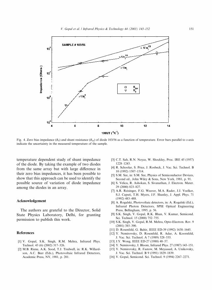
is indicated by the horizontal bars in Figs. 3 and 4.
5. Results and discussion
The measured 77 K I–V and the corresponding
Rd–V characteristics of the two diodes 103/43 and103/56 from the same array are shown in Figs. 1
and 2. These two diodes were chosen because of
the two orders of magnitude difference in their
zero bias impedance. To begin with, the ide-
ality factor was determined by subjecting the
forward I–V characteristics of these diodes to
the curve fitting by an expression of the form:
I ¼ I0 expðqV =gkT Þ, where g is the ideality factor.While determining g, the correction was made forthe voltage drop across the series resistance of the
V. Gopal et al. / Infrared Physics & Technology 44 (2003) 143–152 147

diode. Note that forward Rd–V characteristics of
these diodes indicate a finite series resistance. The
values of ideality factor thus determined are shown
in Table 1. There is also an evidence of TAT
contribution as Rd–V curve of each diode exhibits
a peak in the reverse bias region at low bias. Both
Fig. 1. I–V and Rd–V characteristics of diode #103/43.Fig. 2. I–V and Rd–V characteristics of diode #103/56.
Table 1
Comparison of dark current contributions to the zero bias impedance of the diodes
Sample no. Temp. (K) g Rdif0 (X) Rg–r0 (X) Rsh (X) R0 (X) NT (cm�3) ET (meV)
103/43 77 1.4 4E10 3.5E7 3.4E6 3.4E6 8.6E14 18
90 1.4 8.7E8 2.0E7 3.2E6 2.3E6 5.6E14 21
103 1.3 67E6 1.2E7 3E6 2.2E6 1.6E13 61
160 1 1.2E5 – 1.5E6 1.4E5 – –
172 1 34E3 – 1.7E6 72E3 – –
208 1 5E3 – 1E6 30E3 – –
103/56 77 1.3 5E10 1.9E9 4.9E8 3.8E8 4.6E12 24.8
120 1 6.4E6 – 1E8 5.8E6 – –
153 1 3.6E5 – 6.8E7 3.6E5 – –
185 1 34E3 – – 52E3 – –
148 V. Gopal et al. / Infrared Physics & Technology 44 (2003) 143–152
of these observations, i.e. an ideality factor of more
than unity and evidence of TAT contribution led
us to conclude that these diodes were of type I and
can be analysed by assuming diffusion, g–r, TAT,
BTB and ohmic contributions.
Before proceeding to estimate Nt and Rsh fromthe reverse bias Rd–V characteristics, one needs to
know the parameters sn and sg–r as these were notknown from independent measurements. Here
we propose to determine these parameters from
the fitting of forward I–V and Rd–V characteris-
tics by treating both sn and sg–r as variable fit-
ting parameters. An intermediate ideality factor
(1 < g < 2) suggests comparable g–r and diffusioncontributions. Thus to account for both g–r and
diffusion contributions, the forward I–V and Rd–Vcharacteristics of these diodes were fitted by using
expressions I ¼ Idif þ Ig–r and 1=R ¼ 1=Rdifþ1=Rg–r, where Idif , Rdif , Ig–r and Rg–r are respectively
defined by Eqs. (1), (2), (6b) and (7b). The trap
density Nt, contributing to TAT and ohmic shunt
resistance Rsh were next estimated from the peakposition (10 mV in diode 103/43 and 20 mV in
diode 103/56) in reverse bias Rd–V characteristics
and are shown in Table 1.
Using the estimated and fitted values of the
various parameters from Table 1, the calculated
I–V and Rd–V characteristics of both the diodes at
77 K are compared with the experimental data in
Figs. 1 and 2. It can be clearly seen that there is avery good agreement between theory and experi-
ment. To conclude the dominant contributions we
have also shown in these figures the individual
contributions due to each of the contributing
mechanisms. It is observed that ohmic shunt re-
sistance, whose source of origin could be either the
surface leakage currents or dislocations intersect-
ing the junction or both, limits the impedance ofboth the diodes. Interestingly it can also be seen
from Table 1 that ohmic shunt is approximately
two orders of magnitude lower in diode 103/43
than in diode 103/56. At the same time the esti-
mated trap density contributing to TAT in these
diodes also differ by two orders of magnitude,
though this contribution is not limiting the zero
bias impedance of these diodes. Similarly g–rcontribution also differ approximately by two or-
ders. Estimated sn and sg–r from forward charac-
teristics are also smaller in diode 103/43 (1.5
and 0.8 ns at 77 K) than in diode 103/56 (3 and
44 ns at 77 K). All of these observations put
together suggest that the material beneath the
diode 103/43 may have a higher defect density.
In this analysis though the ohmic shunt contri-bution could be isolated from other dark cur-
rent contributions, it is however not possible to
distinguish between the two different sources
(surface leakage and dislocations) of ohmic con-
tribution. As an attempt towards this end,
we present in the following paragraph an investi-
gation of the observed temperature depen-
dence of shunt and zero bias impedance of thesediodes.
In the past, a temperature dependent study of
zero bias impedance (R0) or its product with the
diode area (R0A) has been used by a number of
workers [2,17,19,20], to assess the limiting current
mechanism in HgCdTe diodes. In this case mi-
nority carrier lifetime is assumed to be tempera-
ture independent and variation of R0 or R0Aproportional to 1=n2i indicates diffusion limited
performance, variations proportional to 1=ni cor-responds to g–r limited performance while high
dislocation density samples exhibit variations [17]
proportional to 1=n1=2i . We have also carried out a
temperature dependent study of R0 of our diodes.
The results obtained by our detailed analysis are
shown in Table 1. Figs. 3 and 4 also show theseresults in the form of plots of R0 and Rsh versus
1000=T . Circles in these figures depict the observedvariation of corresponding ohmic shunt resistance
as a function of temperature. Some of the notice-
able features, which are clearly visible from this
study, are summarized below:
Only the three mechanisms namely thermal
diffusion, g–r and ohmic currents influence thezero bias impedance of HgCdTe diodes at low
temperatures normally used in the operation of
these diodes. TAT and BTB contribute to the
diode impedance in the low-to-medium and high
reverse bias regions respectively.
Zero bias impedance of both the diodes indi-
cates diffusion-limited performance in the higher
temperature region. This is also corroborated bythe observed unity ideality factor at these tem-
peratures.
V. Gopal et al. / Infrared Physics & Technology 44 (2003) 143–152 149

Shunt resistance limits low temperature zero
bias impedance of the diodes. In the intermediate
temperature range, depending upon the relativemagnitudes of diffusion, g–r and shunt contribu-
tions, the zero bias impedance may appear to fol-
low g–r trend even if it was not so. For example
the results of the detailed analysis given in Table 1
show the absence of g–r contribution to the im-
pedance of diode 103/56 at 120 K, but from Fig. 4
one may conclude it as g–r limited performance.
The most interesting and new result is in respectof temperature dependence of shunt resistance.
Note from Figs. 3 and 4 that the shunt resistance is
a slowly varying function of temperature. Our
experimental results of shunt resistance shown by
circles in Figs. 3 and 4 follow approximately pro-
portionality of 1=n1=4i , whereas reported [17] vari-
ation in high dislocation density samples is
proportional to 1=n1=2i . The evidence of excesscomponent of ohmic current over and above the
contribution of dislocations is interpreted here as
the contribution of surface leakage currents. These
results have thus led us to conclude that the two
orders of magnitude difference in the zero bias
impedance of these diodes is due to higher surface
leakage currents in diode 103/43. However thepossibility of degraded passivant-material inter-
face due to the higher defect density (as concluded
above) in the base material of diode 103/43 leading
to higher surface leakage currents can also be not
ruled out.
6. Summary and conclusions
In this paper we have used our recently pro-
posed [1] analytical method to model dark char-
acteristics of nþ–p HgCdTe junctions. For a given
diode it has been possible to isolate the contribu-
tions of each of the dark current contributing
mechanism operating in the diode. The method
has been further extended to show that an idea ofthe dominant contributing mechanism among the
two sources of ohmic current, namely surface
leakage currents and contribution of dislocations
intersecting the junction can also be had from the
h
Fig. 3. Zero bias impedance (R0) and shunt resistance (Rsh) of diode 103/43 as a function of temperature. Error bars parallel to x-axisindicate the uncertainty in the measured temperature of the sample.
150 V. Gopal et al. / Infrared Physics & Technology 44 (2003) 143–152
temperature dependent study of shunt impedanceof the diode. By taking the example of two diodes
from the same array but with large difference in
their zero bias impedances, it has been possible to
show that this approach can be used to identify the
possible source of variation of diode impedance
among the diodes in an array.
Acknowledgement
The authors are grateful to the Director, Solid
State Physics Laboratory, Delhi, for grantingpermission to publish this work.
References
[1] V. Gopal, S.K. Singh, R.M. Mehra, Infrared Phys.
Technol. 43 (6) (2002) 317–326.
[2] M.B. Riene, A.K. Sood, T.J. Tredwell, in: R.K. Willard-
son, A.C. Beer (Eds.), Photovoltaic Infrared Detectors,
Academic Press, NY, 1981, p. 201.
[3] C.T. Sah, R.N. Noyce, W. Shockley, Proc. IRE 45 (1957)
1228–1243.
[4] R. Schoolar, S. Price, J. Rosbeck, J. Vac. Sci. Technol. B
10 (1992) 1507–1514.
[5] S.M. Sze, in: S.M. Sze, Physics of Semiconductor Devices,
Second ed., John Wiley & Sons, New York, 1981, p. 91.
[6] S. Velicu, R. Ashokan, S. Sivanathan, J. Electron. Mater.
29 (2000) 823–827.
[7] A.R. Reisinger, F.G. Weaver, M.A. Rader, J.J. Voelker,
S.J. Caputi, T.H. Myers, J.F. Shanley, J. Appl. Phys. 71
(1992) 483–488.
[8] A. Rogalski, Photovoltaic detectors, in: A. Rogalski (Ed.),
Infrared Photon Detectors, SPIE Optical Engineering
Press, Bellingham, 1995, p. 56.
[9] S.K. Singh, V. Gopal, R.K. Bhan, V. Kumar, Semicond.
Sci. Technol. 15 (2000) 752–755.
[10] S.K. Singh, V. Gopal, R.M. Mehra, Opto-Electron. Rev. 9
(2001) 385–390.
[11] D. Rosenfeld, G. Bahir, IEEE ED-39 (1992) 1638–1645.
[12] Y. Nemirovsky, D. Rosenfeld, R. Adar, A. Koornfeld,
J. Vac. Sci. Technol. A 7 (1989) 528–535.
[13] J.Y. Wong, IEEE ED-27 (1980) 48–57.
[14] Y. Nemirovsky, I. Bloom, Infrared Phys. 27 (1987) 143–151.
[15] Y. Nemirovsky, R. Fastow, M. Meyassed, A. Unikovsky,
J. Vac. Sci. Technol. B 9 (1991) 1829–1839.
[16] V. Gopal, Semicond. Sci. Technol. 9 (1994) 2267–2271.
Fig. 4. Zero bias impedance (R0) and shunt resistance (Rsh) of diode 103/56 as a function of temperature. Error bars parallel to x-axisindicate the uncertainty in the measured temperature of the sample.
V. Gopal et al. / Infrared Physics & Technology 44 (2003) 143–152 151

[17] S.M. Johnson, D.R. Rhiger, J.P. Rosbeck, J.M. Peterson,
S.M. Taylor, M.E. Boyd, J. Vac. Sci. Technol. B 10 (1992)
1499–1506.
[18] I.M. Baker, C.D. Maxey, J. Electron. Mater. 30 (2001)
682–689.
[19] J.P. Rosbeck, R.E. Starr, S.L. Price, K.J. Riley, J. Appl.
Phys. 53 (1982) 6430–6440.
[20] J.M. Dell, J. Antoszewski, M.H. Rais, C. Musca, J.K.
White, B.D. Nerner, L. Faraone, J. Electron. Mater. 29
(2000) 841–848.
152 V. Gopal et al. / Infrared Physics & Technology 44 (2003) 143–152
Copyright © 2022 FDOKUMEN