
Modeling and Design of Spin Torque Transfer Magnetoresistive Random Access Memory
120
Modeling and Design of Spin Torque Transfer Magnetoresistive Random Access Memory by Safeen Huda A thesis submitted in conformity with the requirements for the degree of Masters of Applied Science Graduate Department of Electrical and Computer Engineering University of Toronto Copyright c 2012 by Safeen Huda
Transcript of Modeling and Design of Spin Torque Transfer Magnetoresistive Random Access Memory

Modeling and Design of Spin Torque Transfer
Magnetoresistive Random Access Memory
by
Safeen Huda
A thesis submitted in conformity with the requirementsfor the degree of Masters of Applied Science
Graduate Department of Electrical and Computer Engineering
University of Toronto
Copyright c© 2012 by Safeen Huda

Modeling and Design of Spin Torque TransferMagnetoresistive Random Access Memory
Safeen Huda
Master of Applied Science, 2012
Graduate Department of Electrical and Computer Engineering
University of Toronto
Abstract
This thesis presents the modeling and design of memory cells for Spin Torque Trans-
fer Magnetoresistive Random Access Memory (STT-MRAM). The theory of opera-
tion of STT-MRAM cells is explored, and a model to predict the transient behaviour
of STT-MRAM cells is presented. A novel three-terminal Magnetic Tunneling Junc-
tion (MTJ) and its associated cell structure is also presented. The proposed cell is shown
to have guaranteed read-disturbance immunity, as during a read operation the net torque
acting on the storage cell always acts to refresh the stored data in the cell. A simulation
study is conducted to compare the merits of the proposed device against a conventional
1 Transistor, 1 MTJ (1T1MTJ) cell, as a well as a differential 2 Transistors, 2 MTJs
(2T2MTJ) cell. Simulation results confirm that the proposed device offers disturbance-
free read operation while still offering performance advantages over conventional cells.
ii

To my parents, whose unbounded sacrifices have brought me this far.
iii

Acknowledgements
I am truly astonished when I think of how much I have learned and all of the rich
experiences I have been blessed with over the course of my Master’s degree. For this, I
am grateful to all those that not only helped me in my pursuit of my MASc, but have
made the past few years so very memorable.
I first must thank God for, among many other things, allowing me to come to this
point of my life and for giving me the strength to overcome the adversities I have faced
along the way.
I would like to thank my supervisor, Professor Ali Sheikholeslami, for his guidance
and support over the past few years. Professor Sheikholeslami was supportive of very
ambitious research targets, and I am grateful that he gave me the freedom to explore
a very interesting research area. I would also like to thank the members of my thesis
committee: Professor Roman Genov, Professor Glenn Gulak, and Professor Aleksandar
Prodic for taking time to review my thesis and for their very helpful comments and
suggestions.
Part of the research conducted as part of my thesis was with the help of Fujitsu
Laboratories, and I would like to extend my gratitude to the members at the Atsugi labs
for their help over the course of my degree. Special mention to Koji Tsunoda-san for his
help in understanding how to optimally characterize MTJs.
One of the highlights of my experiences in grad school has been the fact that I’ve
been able to meet and befriend so many truly fantastic people. I would specifically
like to acknowledge: Yunzhi (Rocky) Dong, Dustin Dunwell, Sadegh Jalali, Neno Ko-
iv

vacevic, Mario Milicevic, Alain Rousson, Mayukh Roy, Shayan Shahramian (we got on
the elite list of individuals who got banned from Saratoga!), Alireza Sharif-Bakhtiar,
Ravi Shivnaraine, Clifford Ting, Colin Tse, Aynaz Vatankhahghadim, Hemesh Yasotha-
ran, Meysam Zargham, and Guangzhao (Andy) Zhang. From our juvenile hijinks to
philosophical discussions on life to fierce debates on circuit design - the wide variety of
experiences I have shared with you guys have added colour to my time as a Master’s
student.
I must also thank all those “grad school veterans” who have acted as mentors or role
models during my time as a grad student. Special mention goes to Dave Halupka, who
advised me and mentored me when I first started my degree, Kentaro Yamamoto for
being such a helpful manager of the High Speed Lab, and Ameer Youssef who has been
giving me beneficial advice and encouragement since I was an undergraduate student.
I’ve also had a solid group of friends who have helped remind me of life outside of
grad school; an appropriate work-life balance has been essential in my pursuit of this
degree, and I am grateful to all of you for your support over the years. Special mention
goes to: Ahmad Abu-Abed, Aladdin Abu Jarad, Albiston Braz, Xander Chan, Kwun
Yin Choy, Ibrahim Esmat, Shakeeb Hasan, Hu Hong, Upal Hossain, Yusuf Iqbal, Salman
Kabir, Arbab Khan, Muntasir Mallick, Raihan Masroor, Imran Mohammed, Shahzad
Raza, Neeraj Sood, Jeeva Tharmakulasingam, and Farid Zare Seisan.
Last, but my no means least, I thank my parents, Shahedul and Rafaat Huda. My
parents have been my support and the source of my motivation from elementary school
and all the way through grad school. I will never be able to repay the tremendous
sacrifices they have made for me, but I hope that they may in some way feel rewarded
in any of the pursuits in which I am remotely successful in. This thesis is dedicated to
them.
v

Contents
1 Introduction 1
1.1 Motivation . . . . . . . . . . . . . . . . . . . . . . . . . . . . . . . . . . . 1
1.2 Thesis Objectives . . . . . . . . . . . . . . . . . . . . . . . . . . . . . . . 2
1.3 Thesis Outline . . . . . . . . . . . . . . . . . . . . . . . . . . . . . . . . . 2
2 Background 4
2.1 MRAM Basics . . . . . . . . . . . . . . . . . . . . . . . . . . . . . . . . . 4
2.1.1 MRAM Write Operation . . . . . . . . . . . . . . . . . . . . . . . 5
2.2 Device Physics . . . . . . . . . . . . . . . . . . . . . . . . . . . . . . . . 8
2.2.1 Introduction to Electron Spin . . . . . . . . . . . . . . . . . . . . 8
2.2.2 Spin Torque Transfer Effect . . . . . . . . . . . . . . . . . . . . . 11
2.3 Spin Torque Transfer in MTJs . . . . . . . . . . . . . . . . . . . . . . . . 14
2.3.1 Magnetodynamics . . . . . . . . . . . . . . . . . . . . . . . . . . . 18
2.4 STT-MRAM Design . . . . . . . . . . . . . . . . . . . . . . . . . . . . . 20
2.4.1 Device Types . . . . . . . . . . . . . . . . . . . . . . . . . . . . . 20
2.4.2 Conventional STT-MRAM Cell and Operation . . . . . . . . . . . 22
2.4.3 Basic Chip Architecture . . . . . . . . . . . . . . . . . . . . . . . 23
2.4.4 Write Circuitry . . . . . . . . . . . . . . . . . . . . . . . . . . . . 24
2.4.5 Read Circuitry . . . . . . . . . . . . . . . . . . . . . . . . . . . . 24
2.4.5.1 Current-Based Read Scheme . . . . . . . . . . . . . . . . 27
2.4.5.2 Voltage-Based Read Scheme . . . . . . . . . . . . . . . . 28
vi

2.4.5.3 Read Disturbance Issues . . . . . . . . . . . . . . . . . . 30
2.5 Summary . . . . . . . . . . . . . . . . . . . . . . . . . . . . . . . . . . . 32
3 MTJ Modeling 33
3.1 Prior Work . . . . . . . . . . . . . . . . . . . . . . . . . . . . . . . . . . 33
3.1.1 Static Models . . . . . . . . . . . . . . . . . . . . . . . . . . . . . 34
3.1.2 Dynamic Models . . . . . . . . . . . . . . . . . . . . . . . . . . . 35
3.1.3 Summary of Previous Work . . . . . . . . . . . . . . . . . . . . . 36
3.2 Proposed Model . . . . . . . . . . . . . . . . . . . . . . . . . . . . . . . . 37
3.2.1 Motivation . . . . . . . . . . . . . . . . . . . . . . . . . . . . . . . 37
3.2.2 Proposed Model Structure . . . . . . . . . . . . . . . . . . . . . . 37
3.2.2.1 Tunnel Model . . . . . . . . . . . . . . . . . . . . . . . . 38
3.2.2.2 Magnetodynamics Model . . . . . . . . . . . . . . . . . 39
3.2.2.3 Verilog-A Description . . . . . . . . . . . . . . . . . . . 41
3.3 Device Characterization and Experimental Setup . . . . . . . . . . . . . 41
3.4 Measurement Data . . . . . . . . . . . . . . . . . . . . . . . . . . . . . . 44
3.5 Model Correlation . . . . . . . . . . . . . . . . . . . . . . . . . . . . . . . 46
3.5.1 Tunnel Model Correlation . . . . . . . . . . . . . . . . . . . . . . 46
3.5.2 Magnetodynamics Model Correlation . . . . . . . . . . . . . . . . 47
3.6 Model Validation . . . . . . . . . . . . . . . . . . . . . . . . . . . . . . . 48
3.7 Summary . . . . . . . . . . . . . . . . . . . . . . . . . . . . . . . . . . . 50
4 Device and Cell Proposal 51
4.1 Previous Work . . . . . . . . . . . . . . . . . . . . . . . . . . . . . . . . 51
4.1.1 Circuit Level Solutions . . . . . . . . . . . . . . . . . . . . . . . . 51
4.1.2 Device Level Solutions . . . . . . . . . . . . . . . . . . . . . . . . 53
4.2 Proposed Cell . . . . . . . . . . . . . . . . . . . . . . . . . . . . . . . . . 55
4.2.1 Device and Cell Structure . . . . . . . . . . . . . . . . . . . . . . 55
vii

4.2.2 Cell Write Operation . . . . . . . . . . . . . . . . . . . . . . . . . 56
4.2.3 Cell Read Operation . . . . . . . . . . . . . . . . . . . . . . . . . 59
4.2.3.1 Increased Tolerance to Process Variation . . . . . . . . . 62
4.2.3.2 Read-Disturbance Immunity . . . . . . . . . . . . . . . . 64
4.2.4 Device Parameter Optimization . . . . . . . . . . . . . . . . . . . 68
4.2.4.1 Oxide Thickness Optimization . . . . . . . . . . . . . . . 68
4.2.4.2 Magnetization Parameter Optimization . . . . . . . . . . 69
4.3 Comparitive Study . . . . . . . . . . . . . . . . . . . . . . . . . . . . . . 70
4.3.1 Device Modeling . . . . . . . . . . . . . . . . . . . . . . . . . . . 71
4.3.1.1 Tunnel Model . . . . . . . . . . . . . . . . . . . . . . . . 72
4.3.1.2 Magnetodynamics Model . . . . . . . . . . . . . . . . . 73
4.3.1.3 Device Dimensions . . . . . . . . . . . . . . . . . . . . . 73
4.3.1.4 Material Parameters . . . . . . . . . . . . . . . . . . . . 75
4.3.2 Device Optimization . . . . . . . . . . . . . . . . . . . . . . . . . 75
4.3.3 Simulation Results: Write Performance . . . . . . . . . . . . . . . 83
4.3.4 Simulation Results: Read Performance . . . . . . . . . . . . . . . 85
4.3.5 Results Summary and Discussion . . . . . . . . . . . . . . . . . . 87
4.4 Summary . . . . . . . . . . . . . . . . . . . . . . . . . . . . . . . . . . . 88
5 Conclusion 96
5.1 Contributions . . . . . . . . . . . . . . . . . . . . . . . . . . . . . . . . . 96
5.2 Future Work . . . . . . . . . . . . . . . . . . . . . . . . . . . . . . . . . . 97
References 97
viii

List of Tables
3.1 Comparison of previous models . . . . . . . . . . . . . . . . . . . . . . . 37
3.2 Parameters for tunnel model . . . . . . . . . . . . . . . . . . . . . . . . . 46
3.3 Parameters for tunnel model . . . . . . . . . . . . . . . . . . . . . . . . . 48
3.4 Parameters for tunnel model . . . . . . . . . . . . . . . . . . . . . . . . . 49
4.1 Estimated IC0 reduction through minimization of HK . . . . . . . . . . . 71
4.2 Optimal oxide thicknesses . . . . . . . . . . . . . . . . . . . . . . . . . . 81
4.3 Chosen transistor widths . . . . . . . . . . . . . . . . . . . . . . . . . . . 82
4.4 Results summary . . . . . . . . . . . . . . . . . . . . . . . . . . . . . . . 95
ix

List of Figures
2.1 A Magnetic Tunneling Junction . . . . . . . . . . . . . . . . . . . . . . . 4
2.2 A FIMS MRAM cell. Figure taken from [12] . . . . . . . . . . . . . . . . 6
2.3 Switching mechanisms in STT-MRAM . . . . . . . . . . . . . . . . . . . 7
2.4 Spin dependent transport of itinerant electrons from Region I to Region II 11
2.5 Torques arising from current i flowing from Layer I to Layer II . . . . . . 14
2.6 Spin-dependent conductances from Layer I to Layer II . . . . . . . . . . . 16
2.7 Graphical representation of terms in LLGS equation . . . . . . . . . . . . 20
2.8 Conventional Device Types . . . . . . . . . . . . . . . . . . . . . . . . . . 21
2.9 Conventional 1 Transistor, 1 Magnetic Tunneling Junction (1T1MTJ) cell 22
2.10 Top level chip architecture . . . . . . . . . . . . . . . . . . . . . . . . . . 23
2.11 Write circuitry . . . . . . . . . . . . . . . . . . . . . . . . . . . . . . . . 25
2.12 Top level chip architecture with exposed read circuits . . . . . . . . . . . 26
2.13 Current based read scheme . . . . . . . . . . . . . . . . . . . . . . . . . . 27
2.14 Voltage based read scheme . . . . . . . . . . . . . . . . . . . . . . . . . . 29
2.15 Read disturb rate versus IREAD/IC0 . . . . . . . . . . . . . . . . . . . . . 31
3.1 Previously proposed dynamic model [34]. . . . . . . . . . . . . . . . . . . 35
3.2 Verilog-A model flowchart . . . . . . . . . . . . . . . . . . . . . . . . . . 41
3.3 Experimental setup . . . . . . . . . . . . . . . . . . . . . . . . . . . . . . 42
3.4 Circuitry used to characterize MTJs . . . . . . . . . . . . . . . . . . . . . 42
3.5 Test waveform applied to MTJs . . . . . . . . . . . . . . . . . . . . . . . 43
x

3.6 MTJ Resistance versus Voltage characteristic . . . . . . . . . . . . . . . . 44
3.7 Switching time versus applied voltage . . . . . . . . . . . . . . . . . . . . 45
3.8 Comparison of tunnel model to measured R-V characteristic of MTJ . . . 47
3.9 Comparison of model to measured Switching Time versus Applied Voltage 48
3.10 Pulses used to validate accuracy of transient response in proposed model 49
4.1 Previously proposed multi VDD driver. Figure taken from [25]. . . . . . . 52
4.2 Previously proposed 2T1MTJ cell. Figure taken from [42]. . . . . . . . . 53
4.3 Previously proposed 3-terminal device. Figure taken from [44]. . . . . . . 54
4.4 Proposed Device . . . . . . . . . . . . . . . . . . . . . . . . . . . . . . . 56
4.5 Proposed Device Symbols . . . . . . . . . . . . . . . . . . . . . . . . . . 56
4.6 Proposed cell shown with an IPA version of proposed device . . . . . . . 57
4.7 Top level chip diagram . . . . . . . . . . . . . . . . . . . . . . . . . . . . 58
4.8 Proposed Cell Write Operation . . . . . . . . . . . . . . . . . . . . . . . 59
4.9 Timing diagrams for write operations for proposed cell . . . . . . . . . . 60
4.10 Proposed read scheme . . . . . . . . . . . . . . . . . . . . . . . . . . . . 61
4.11 Timing diagrams for read operations for proposed cell . . . . . . . . . . . 61
4.12 Transient current waveforms during a “Read-0” operation . . . . . . . . . 65
4.13 Transient currents and voltages during a “Read-1” operation . . . . . . . 66
4.14 2T2MTJ Cell . . . . . . . . . . . . . . . . . . . . . . . . . . . . . . . . . 71
4.15 Conventional MTJ with annotated dimensions . . . . . . . . . . . . . . . 73
4.16 Proposed MTJ with annotated dimensions . . . . . . . . . . . . . . . . . 74
4.17 IPA device oxide thickness optimization . . . . . . . . . . . . . . . . . . . 77
4.18 PPA device oxide thickness optimization . . . . . . . . . . . . . . . . . . 78
4.19 IPA transistor width optimization . . . . . . . . . . . . . . . . . . . . . . 79
4.20 PPA transistor width optimization . . . . . . . . . . . . . . . . . . . . . 80
4.21 Cell layouts . . . . . . . . . . . . . . . . . . . . . . . . . . . . . . . . . . 82
4.22 Comparison of write performance for IPA cells . . . . . . . . . . . . . . . 90
xi

4.23 Comparison of write performance for PPA cells . . . . . . . . . . . . . . 91
4.24 Comparison of read performance for IPA cells . . . . . . . . . . . . . . . 92
4.25 Comparison of read performance for PPA cells . . . . . . . . . . . . . . . 93
4.26 FL Torques . . . . . . . . . . . . . . . . . . . . . . . . . . . . . . . . . . 94
xii

List of Acronyms
1T1MTJ 1 Transistor, 1 Magnetic Tunneling Junction
2T1MTJ 2 Transistor, 1 Magnetic Tunneling Junction
2T2MTJ 2 Transistors, 2 Magnetic Tunneling Junctions
AP Antiparallel
BL Bit Line
BPL Bottom Pinned Layer
FIMS Field-Induced Magnetization Switching
FL Free Layer
GMR Giant Magneto Resistance
IPA In-Plane Anisotropy
LLG Landau-Lifshitz-Gilbert Equation
LLGS Landau-Lifshitz-Gilbert-Slonczewski Equation
MRAM Magnetoresistive Random Access Memory
MTJ Magnetic Tunneling Junction
P Parallel
xiii

PL Pinned Layer
PPA Perpendicular-to-Plane Anisotropy
RSM Read Sense Margin
SL Select Line
STT Spin Torque Transfer
STT-MRAM Spin Torque Transfer Magnetoresistive Random Access Memory
TMR Tunneling Magnetoresistance Ratio
TPL Top Pinned Layer
TSP Tunneling Spin Polarization
WL Word Line
xiv

1 Introduction
1.1. Motivation
Recent years have seen considerable research interest in Spin Torque Transfer Magnetore-
sistive Random Access Memory (STT-MRAM). This technology has been presented as a
universal memory [1], as it combines several of the desired characteristics of the different
memory technologies currently available in the marketplace. Specifically, STT-MRAM
offers non-volatility, high density, and high-speed access [1]. A number of papers have
recently been published [2–4] that have presented STT-MRAM test chips with both high
speed access and high density. In [2], the authors demonstrated a high-speed STT-MRAM
chip fabricated in 0.13 µm CMOS with a read access time of 8ns and write access time of
12ns. In [3], the authors presented a 64 Mb STT-MRAM test chip with a 30ns cycle time.
Furthermore, in [4], the authors presented an analysis showing how a 1Gb STT-MRAM
chip with 10ns read/write access is achievable in todays technology. All of these works
have made use of the standard 1 Transistor, 1 Magnetic Tunneling Junction (1T1MTJ)
cell. However, several hurdles exist before STT-MRAM can truly become commercialized
and compete with existing memory technologies. One of the most fundamental require-
ments currently is the need to develop models which can accurately predict the behaviour
of the cells to arbitrary input stimuli; this is needed for not only the optimization of cir-
cuitry at the cell level, but also for large-scale system-level verification. Another hurdle
1

Chapter 1. Introduction 2
which is inherent to STT-MRAM is the read disturbance problem. To alleviate con-
cerns of read disturbance in the 1T1MTJ cell, the read sense current must be restricted,
which results in reduced sense margin. On the other hand, to ensure disturbance-free
read operation and large sense margin, the critical current of the MTJ must be increased,
which results in the need for larger access transistors (and thus larger cell area), increased
write access power, and potentially increased write access times. As such, the 1T1MTJ
cell has an inherent tradeoff between disturbance-free read operation and the read/write
performance.
1.2. Thesis Objectives
In this thesis, we explore the physics behind the operation of STT-MRAM cells, and
accordingly propose a model to predict the transient response of STT-MRAM cells. On
a separate front, we also propose a novel memory cell for STT-MRAM, which offers guar-
anteed immunity to read disturbance. The contributions of this thesis are the following:
• Provide a background on STT-MRAM, and explore the physics behind operation
of Magnetic Tunnel Junctions (MTJs) and STT-MRAM
• Characterization and modeling of the transient behaviour of Magnetic Tunneling
Junction (MTJ)s
• Proposal for a novel MTJ and STT-MRAM cell
1.3. Thesis Outline
The remaining chapters of this thesis are organized as follows:
• Chapter 2 provides background
• Chapter 3 describes the model developed and compares to measurement results

Chapter 1. Introduction 3
• Chapter 4 presents the proposed cell which offers guaranteed immunity to read
disturbance
• Chapter 5 concludes the thesis and provides the future directions for this work

2 Background
2.1. MRAM Basics
Magnetoresistive Random Access Memory (MRAM) is an emerging non-volatile memory
technology which has seen significant research interest over the past two decades [5–9].
At the core of any incarnation of MRAM is the MTJ, shown in Figure 2.1. An MTJ
Figure 2.1: A Magnetic Tunneling Junction
is comprised of two ferromagnetic thin film layers, the Free Layer (FL) and the Pinned
Layer (PL), with an oxide-tunneling barrier in between the two magnetic layers. As
the names suggest, the magnetization vector of the PL is pinned and thus cannot be
changed, while the magnetization vector of the FL is free to possibly assume one of two
directions; in conventional MTJs, the magnetization vector of the FL is free to assume
either a direction parallel or antiparallel to the PL magnetization vector. From a data
storage point of view an MTJ can therefore store 1 bit of data as the cell has two states:
the Parallel (P) state and the Antiparallel (AP) state. Therefore in MRAM, data is
4

Chapter 2. Background 5
stored in magnets, which are naturally non-volatile. An interesting property of an MTJ
is the dependence of the tunneling resistance between the FL and the PL on the state
of the cell; denoting the tunneling resistance from FL to PL when the FL magnetization
vector is oriented parallel and antiparallel to the PL magnetization vector as RP and
RAP , respectively, for MTJs RAP > RP . This means that the two states of the MTJ, the
P and AP states, are electrically distinguishable. A common figure-of-merit for MTJs is
the Tunneling Magnetoresistance Ratio (TMR) ratio:
TMR =RAP −RP
RP(2.1)
Since a large TMR ratio indicates a large difference between the P and AP state resis-
tances, the TMR ratio provides a measure of how easily the two states of an MTJ can
be distinguished.
All of the different types of MRAM that have been proposed have very similar read
schemes. Given that the state of an MTJ can be inferred by measuring its resistance,
the data stored in an MTJ can be read by applying a current through the MTJ and
measuring the resulting voltage or by applying a voltage across the MTJ and measuring
the current. The resulting currents/voltages that are sensed can then be compared to
a reference value to determine the state of the cell. The main difference between the
different types of MRAM is in their write operations. These are described in detail in
the following sections.
2.1.1. MRAM Write Operation
Fundamentally, there are two types of MRAM: Field-Induced Magnetization Switch-
ing (FIMS) MRAM and Spin Torque Transfer (STT) MRAM. FIMS MRAM was the
first incarnation of MRAM [10–12], and in this technology cells were written to by the
application of magnetic fields. Figure 2.2 depicts a FIMS MRAM cell. The cell shown
employs two lines which generate magnetic fields (Write Line 1 and Write Line 2) when

Chapter 2. Background 6
Figure 2.2: A FIMS MRAM cell. Figure taken from [12]
currents are passed through them, and the two magnetic fields act constructively to
switch the FL magnetization. Note that this technology requires that every row and
column of a chip to have separate write lines.
However, there were two major problems with this approach: since it is difficult to
contain a magnetic field and focus the field on one spot only, it is possible that when
a cell in a memory array is being written, the magnetic fields being used to write to
that cell inadvertently disturb the states of neighboring cells. More fundamental than
this however is the fact that FIMS MRAM has been shown [13] to offer poor scalability;
the current required to switch FIMS MRAM cell does not decrease as the technology is
scaled to smaller process nodes. This fact has made the use of MRAM prohibitive in
smaller process technologies, and has led to the development of STT-MRAM.
The spin torque transfer effect, first proposed by [14], is a technique which makes
use of the spin-dependent transport properties of MTJs to switch an MTJ’s state. We
discuss the spin transfer torque effect in detail in a following section, and in this section
provide an intuitive explanation of how it is employed to write data to an MTJ. Figure
2.3(a) shows a Write-0 operation, which aligns the FL magnetization in parallel to the

Chapter 2. Background 7
PL magnetization (antiparallel-to-parallel switching). Figure 2.3(b) shows a Write-1
operation, where the FL magnetization is switched to become antiparallel to the PL
magnetization (parallel-to-antiparallel switching).
Electrons
Tunnelling
from PL to FL
(a) Antiparallel-to-parallel switching
Reflected
Electrons
from PL
Electrons
tunnelling
from FL to PL
Transmitted
Electrons
(b) Parallel-to-antiparallel switching
Figure 2.3: Switching mechanisms in STT-MRAM
In antiparallel-to-parallel switching, a positive current is passed from the FL to the
PL. This causes electrons, which have become spin polarized to the magnetization of the
PL, to tunnel to the FL and exert a torque on the FL magnetization vector, thus causing
switching. In parallel-to-antiparallel switching, a current is passed from the PL to the
FL; as electrons tunnel from the FL to the PL, the minority spin electrons, which are of
opposite spin to the PL magnetization, are reflected back to the FL, and subsequently
exert a torque on the FL magnetization, causing it to switch. In either case, it is only
when the torque exceeds some critical value (governed by the magnetization parameters,
geometry, and spin polarization properties of the device), that the FL magnetization
switches. It is immediately obvious that STT-MRAM has numerous advantages over
FIMS MRAM; since no external magnetic fields are required to switch the state of an
MTJ, the problem of inadvertently writing to neighboring cells is solved. The spin torque
transfer effect allows for the generation of torques to switch the state of the cell which
are highly localized to the layers which have currents applied to them; the neighboring
cells will not to be affected by this torque. Also, this allows for greater area density as

Chapter 2. Background 8
STT-MRAM does not require additional write wires. More importantly however, it has
been shown [13] that the current required to switch STT-MRAM cells scales favourably
(i.e. decreases for smaller process nodes). As such, STT-MRAM is currently seen as a
path towards the large scale commercialization of MRAM as it has overcome the hurdles
previous generations of MRAM have faced.
2.2. Device Physics
2.2.1. Introduction to Electron Spin
In this section, we provide a brief overview of the quantum mechanical description of
angular momenta of particles. In classical physics, there are two components of the
angular momentum of a body: the angular momentum resulting from the rotation of
the body about some fixed axis, and the rotation of the body about its centre of mass.
From the viewpoint of quantum mechanics, the angular momentum of a particle can
similarly be described using the same notions as in classical physics; a particle which
moves about some fixed axis (for example an electron which moves about a nucleus as it
is confined to an orbital of an atom) has what is known as orbital angular momentum,
and in addition, the particle may have its own intrinsic angular momentum, which is
known as spin angular momentum. In this section, we concern ourselves only with the
spin angular momentum of electrons.
In quantum mechanics, the angular momentum of a particle is quantized. What
this means is that there are only a finite number of discrete values for the measured
angular momentum of a particle along a given axis. As an example, electrons are spin-
1/2 particles; as such, the measured spin angular momentum of an electron along a given
axis can either be +h/2 or −h/2, where h is the reduced or normalized Planck constant.
The probabilities associated with the measurement of the angular momentum of +h/2
and −h/2 are associated with the spin-state of the electron, with respect to a given axis.

Chapter 2. Background 9
An electron whose angular momentum along a given axis is always measured to be +h/2
(i.e. the probability of measuring +h/2 is 1) is said to be in a spin-up state, and this is
denoted in bra-ket notation as | ↑〉. Similarly, an electron whose angular momentum is
measured to be −h/2 with absolute certainty is said to be in a spin-down state, denoted
as | ↓〉. In general, the spin-state of an electron is:
|ψS〉 = a| ↑〉+ b| ↓〉 (2.2)
Where |a|2+|b|2 = 1. In other words, an electron can be in a superposition of the two spin
states (up-spin and down-spin), and all this means is that the measurement of the angular
momentum with respect to a given axis will not yield a result with absolute certainty;
the probability in this case of measuring +h/2 is |a|2, while the probability of measuring
−h/2 is |b|2. Finally, we discuss the transformation of spin-state from one reference axis
to another; that is to say, given the spin state of an electron, |ψzS〉 = a| ↑〉 + b| ↓〉,
which is with respect to some axis z, how do we transform |ψzS〉 to |ψz′
S 〉, i.e. so that
the probability amplitudes are now with respect to some other axis, z′? In quantum
mechanics, the expected value of a quantity can be obtained by using linear operators.
With regard to spin angular momentum, we may define linear operators Si which can
be used to find the expected value of the angular momentum measured along an axis
i for a particle in a given state. The operators, which are represented as matrices, for
the measurement of the spin angular momentum along the x, y and z axes, are (h/2)σx,

Chapter 2. Background 10
(h/2)σy, and (h/2)σz, respectively, where:
σx =
0 1
1 0
(2.3)
σy =
0 −i
i 0
(2.4)
σz =
1 0
0 −1
(2.5)
(2.6)
σx, σy and σz are known as the Pauli spin matrices, and the above matrices are for a spin
state which is given with respect to the z-axis, |ψzS〉. To find the expected value of the
angular momentum along an axis i, we simply take the inner product of the spin state
with the product of the corresponding operator and the spin state as follows:
〈Si〉 = 〈ψzS ∗ |Si|ψz
S〉 (2.7)
For an arbitrary axis z′, we may make use of the Pauli spin matrices; first, we find a unit
vector z′ = cxx + cyy + czz, and then form the operator Sz′ = cxSx + cySy + czSz. We
can then use Sz′ to find the expected value of the angular momentum along the z′ axis
for a state initially defined with respect to the z axis by making use of Equation 2.7. It
can be shown [15] that given the initial state |ψzS〉 =
(
ab
)
,
|ψz′
S 〉 =
acos(θ/2)− bsin(θ/2)
asin(θ/2) + bcos(θ/2)
(2.8)

Chapter 2. Background 11
where θ is the angle between the z and z′ axes. |ψz′
S 〉 can also be written as:
|ψz′
S 〉 =
cos(θ/2) −sin(θ/2)
sin(θ/2) cos(θ/2)
|ψz
S〉 (2.9)
The matrix used to transform |ψzS〉 to |ψz′
S 〉 is in fact a standard rotation matrix (rotation
by θ/2).
2.2.2. Spin Torque Transfer Effect
In this section, we describe the spin torque transfer effect. Consider the example of
the spin-dependent transmission and reflection of a stream of electrons as they travel
from one region to another, as shown in Figure 2.4. Here, we have a stream of incident
REGION I REGION II
Incident Electrons
Reflected
Electrons
Transmitted
Electrons
↑
↓↑
↓
X
Z
θ
Figure 2.4: Spin dependent transport of itinerant electrons from Region I to Region II
electrons flowing from Region I to Region II; as these electrons impinge on Region II,
they are either transmitted or reflected, based on the spin of the electrons at the moment

Chapter 2. Background 12
they are at the interface between Region I and Region II. In the example, Region II
is comprised of a material where all itinerant electrons are either in a spin-up state or
a spin-down state with respect to the z -axis, while Region I allows itinerant electrons
to be in any arbitrary state. The incident electrons are shown to be in a spin state,
|ψzSi〉 = ( cos(θ/2) sin(θ/2) )T , with respect to the z-axis, since the spin state is shown
to be aligned to an axis which is at an angle θ to the z-axis. The terms t↑, t↓, r↑ and r↓
are coefficients which relate the transmitted and reflected wavefunctions (the functions
describing the time varying spatial distribution of transmitted and reflected particles,
respectively) to the incident wavefunction. Therefore, the probability of transmission
and reflection for up-spin and down-spin electrons can be derived; at the interface of
Region I and Region II, electrons with up-spin are transmitted with probability |t↑|2
and reflected with a probability |r↑|2, while electrons with down-spin are transmitted
with probability |t↓|2 and reflected with a probability |r↓|2. For this example, we set
t↓ = r↑ = 0 and t↑ = r↓ = 1; as such, Region II acts as a spin filter, as electrons with
up-spin are always transmitted, while electrons with down-spin are always reflected. It is
useful to measure the expected values for the spin-angular momentum along the x-axis
for the incident, transmitted, and reflected wavefunctions. Recall from Equation 2.7,
we can do this by using the spin-angular momentum operator for the x-axis. Denoting
〈Sxi〉,〈Sxr〉, and 〈Sxt〉 as the expected values for the angular momentum along the x-axis

Chapter 2. Background 13
for the incident, reflected and transmitted wavefunctions respectively, we have:
〈Sxi〉 =
(
cos(θ/2) sin(θ/2)
)
h
2
0 1
1 0
cos(θ/2)
sin(θ/2)
=
(
cos(θ/2) sin(θ/2)
)
h
2
sin(θ/2)
cos(θ/2)
= sin(θ)h
2(2.10)
〈Sxt〉 = cos2(θ/2)
(
1 0
)
h
2
0 1
1 0
1
0
= cos2(θ/2)
(
1 0
)
h
2
0
1
= 0 (2.11)
〈Sxr〉 = sin2(θ/2)
(
0 1
)
h
2
0 1
1 0
0
1
= sin2(θ/2)
(
0 1
)
h
2
1
0
= 0 (2.12)
The above shows a very interesting result: while the incident electrons can have a non-
zero expected value for the spin angular momentum along the x-axis (equal to sin(θ)h/2),
the transmitted and reflected wavefunctions for this example clearly have an expected
value of zero for the spin angular momentum along the x-axis. Since angular momentum
must be conserved, it becomes evident that the angular momentum along the x-axis for
the incident wavefunction which is “lost” is actually absorbed at the interface between
Region I and Region II - this is the only place where the angular momentum can be
absorbed, as it is here where the incident wavefunction is split into a transmitted and
Chapter 2. Background 14
reflected component, and thus, it is here where there is a net flux of angular momentum.
The above example illustrates the spin torque transfer effect: whenever a system has the
spin-dependent transport properties highlighted in this example, there is a possibility
that the angular momentum of all the individual wavefunctions which are involved in
the transport process is not conserved; in this case, any “lost” angular momentum is
absorbed by the materials.
2.3. Spin Torque Transfer in MTJs
In this section, we reproduce the derivation of a quantitative model to predict the torque
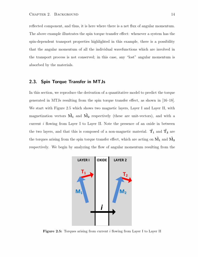
generated in MTJs resulting from the spin torque transfer effect, as shown in [16–18].
We start with Figure 2.5 which shows two magnetic layers, Layer I and Layer II, with
magnetization vectors M1 and M2 respectively (these are unit-vectors), and with a
current i flowing from Layer I to Layer II. Note the presence of an oxide in between
the two layers, and that this is composed of a non-magnetic material. T1 and T2 are
the torques arising from the spin torque transfer effect, which are acting on M1 and M2
respectively. We begin by analyzing the flow of angular momentum resulting from the
LAYER I LAYER 2
1 2
12
OXIDE
Figure 2.5: Torques arising from current i flowing from Layer I to Layer II
Chapter 2. Background 15
current flow between the layers. The flow of angular momentum from Layer I into the
Oxide region, denoted SIN, is:
˜SIN = M1
h(−i1↑ + i1↓)
2e(2.13)
Equation 2.13 can be explained as follows: the current flowing from Layer I into the Oxide
region can be broken down into two components, i1↑ which represents the current of the
spin-up electrons (where spin-up is defined with respect to direction of the magnetization
vector of Layer I), and i1↓ represents the current of the spin-down electrons. By doing
this, we can attribute angular momentum to the currents separately: by multiplying each
current by −h/2e, we convert electric current, which is the flow of electric charge, into
momentum current, as we now have a flow of angular momentum. We need to subtract
i1↑ from i1↓, as the angular momentum carried by i1↑ is of opposite sense as that carried
by i1↓, and finally we multiply by M1, as that gives the actual direction of the angular
momentum being transferred into the Oxide region. Similarly, the current through Layer
II effectively extracts angular momentum from the Oxide region. The flow of angular
momentum from the Oxide region into Layer II, denoted ˜SOUT, is given by:
˜SOUT = M2
h(−i2↑ + i2↓)
2e(2.14)
Now, by conservation of angular momentum,
T1 + T2 = SIN − ˜SOUT (2.15)
Since M1 · T1 = M2 · T2 = 0 (the torque must act perpendicular to the the magneti-
zation vectors, as any component parallel to the magnetization vectors would cause the
magnetization to increase, but the saturation magnetization of a material is constant,
and so this is not a possibility), we can take the dot product of Equation 2.15 with M1

Chapter 2. Background 16
and M2 to yield separate equations for T1 and T2:
T1 =h[(−i1↑ + i1↓)cosθ + i2↑ − i2↓]
2esinθ(2.16)
T2 =h[(−i2↑ + i2↓)cosθ + i1↑ − i1↓]
2esinθ(2.17)
Note that under the assumption that i1↑ − i1↓ = i2↑ − i2↓, i.e. the two layers are equally
biased towards the up-spin electrons, the two torques T1 and T2 are equal. We use
this assumption, and for the remainder of this section T1 = T2 = T||. While the above
equations show how torque is generated given the presence of spin-polarized currents
(i.e. when in↑ 6= in↓ for any n), we would like to be able to calculate torque from
the applied voltage across an MTJ and measurable parameters of the MTJ (such as
parallel and antiparallel resistances). We start with the following model for the tunneling
characteristics of an MTJ, as shown in Figure 2.6. In the figure, we see that we have
LAYER I LAYER 2OXIDE
++
+-
-+
--
Figure 2.6: Spin-dependent conductances from Layer I to Layer II
a set of conductances between Layer I and Layer II: G++, G+−, G−+, and G−−. These
conductances give the conduction properties for the four possible types of transport
between the two layers: tunneling from a spin-up state in Layer I to a spin-up state

Chapter 2. Background 17
in Layer II, tunneling from a spin-up state in Layer I to a spin-down state in Layer
II, tunneling from a spin-down state in Layer I to a spin-up state in Layer II, and
tunneling from a spin-down state in Layer I to a spin-down state in Layer II. When the
magnetizations of the two layers are parallel to one another, the spin-up states of the two
layers and the spin-down states of the two layers are the same; as such, the conductance
in this state is simply G++ + G−− which we denote as GP . When the two layers are
relatively antiparallel to one another, the down-spin states of Layer I are equal to the up-
spin states of Layer II, and the the up-spin states of Layer I are equal to the down-state
states of Layer II; the conductance between these two layers in this case is G+− + G−+
which we denote as GAP . In general however, if the magnetizations of the two layers are
not parallel or antiparallel to one another, we need to make use of all four conductances
(G++, G+−, G−+, and G−−), as well as the probability of an electron in the up-state or
down-state in one layer to be “measured” to be in the up-state or down-state of the other
layer. For instance, if there is an angle of θ between the magnetization vectors of the two
layers, we can use Equation 2.8 to find these probabilities; specifically, the probability
that an up-state electron in Layer I can tunnel into an up-state in Layer II is cos2θ, the
probability that an up-state electron in Layer I can tunnel into a down-state in Layer II
is sin2θ, the probability that a down-state electron in Layer I can tunnel into an up-state
in Layer II is sin2θ, and finally the probability that a down-state electron in Layer I can
tunnel into a down-state in Layer II is cos2θ. We now have expressions for the terms i1↑,
i1↓, i2↑, and i2↓ as follows:
i1↑ = V
(
cos2(
θ
2
)
G++ + sin2
(
θ
2
)
G+−
)
(2.18)
i1↓ = V
(
sin2
(
θ
2
)
G−+ + cos2(
θ
2
)
G−−
)
(2.19)
i2↑ = V
(
cos2(
θ
2
)
G++ + sin2
(
θ
2
)
G−+
)
(2.20)
i2↓ = V
(
sin2
(
θ
2
)
G+− + cos2(
θ
2
)
G−−
)
(2.21)

Chapter 2. Background 18
We can substitute the above equations into the torque equation given in Equation 2.17,
and using the trigonometric identities cos2( θ2)(1−cosθ) = sin2θ/2 and sin2( θ
2)(1+cosθ) =
sin2θ/2 to yield:
T|| =h
4e(G++ +G+− −G−+ −G−−)V sinθ (2.22)
While this now gives us an equation based on applied voltage, V , and device charac-
teristics (the conductances), this equation is not particularly convenient as it is difficult
to characterize the spin channel conductances (i.e. G++, G+−, G−+ and G−−). What
is particularly straightforward to characterize however are the conductances of an MTJ
when in parallel (GP ) or antiparallel GAP ) states. We first observe that GP = G+++G−−
and GAP = G+−+G−+. Next, we make the assumption that the each of the spin channel
conductances are separable and can be expressed in terms of factors specific to each layer;
this is to say that G++ = gL+gR+, G+− = gL+gR−, G−+ = gL−gR+, and G−− = gL−gR−,
which is what is referred to in Equation 16 in [17]. Finally, by assuming that the two
layers are identical and so gL+ = gR+ and gL− = gR−, we come to the following equation
for torque:
T|| =h
4e
2PS
1 + P 2S
sin(θ)GPV (2.23)
where PS is the Tunneling Spin Polarization (TSP) and is equal to√
(GP −GAP )/(GP +GAP )
which is also equivalent to√
TMR/(TMR + 2), GP is the parallel state conductance,
and V is the applied voltage across the MTJ (between the PL and FL).
2.3.1. Magnetodynamics
While Equation 2.23 gives us the magnitude of the spin transfer torque acting on a layer,
we would like to express the same torque in vector form. By considering the direction of
the torque acting on a layer, and the sin(θ) term in the equation, the vector form of the

Chapter 2. Background 19
torque equation is straightforward:
T|| =h
4e
2PS
1 + P 2S
GPV mFL × (mFL × mPL) (2.24)
where mFL and mPL are the normalized magnetization vectors of the FL and PL respec-
tively. We can now include this torque in the Landau-Lifshitz-Gilbert Equation (LLG)
equation [19], which we describe next.
The LLG equation is a phenomenological equation used to predict the time evolution
of a magnetization vector subject to external magnetic fields as well as device anisotropies.
By including the spin transfer torque term into the LLG equation, we form the Landau-
Lifshitz-Gilbert-Slonczewski Equation (LLGS) equation, which governs the dynamics of
the FL magnetization vector:
dm
dt= − γ
1 + α2m× ˜HEFF − γα
1 + α2m× (m× ˜HEFF)
− γ
(1 + α2)MSV olT|| (2.25)
Where α is the Gilbert damping parameter, γ is the gyromagnetic ratio, ˜HEFF is the
effective field within the magnetic film, MS is the saturation magnetization, V ol is the
volume of the FL, m is a unit vector describing the magnetization of the FL, and mPL is a
unit vector describing the magnetization of the PL. Since the magnetic layers comprising
MTJs are typically too small to support more than one magnetic domain, they are
modeled using the macrospin approximation [20], and so the effective field in Equation
2.25, ˜HEFF is primarily comprised of the external field HEXT and the anisotropy field
HANI . Furthermore, since external fields are not required for switching in STT-MRAM,
HEX = 0, and as such we are concerned only with anisotropy. The anisotropy term
dictates a preferred direction for the FL magnetization vector, which is called the easy
axis ; when mPL is aligned along this axis, it is in equilibrium, while when it is not aligned
with this axis, HEFF exerts a torque on the magnetization vector to bring it back in-line

Chapter 2. Background 20
with this axis. The LLGS equation is shown graphically in Figure 2.7. Here we have the
x
y
z
Magnetization vector
confined to sphere of
radius MS
Plane Tangential to
Sphere
Damping Term
Precession Term
Spin Transfer Torque
θ
φ
m~
Figure 2.7: Graphical representation of terms in LLGS equation
magnetization vector m, at an angle θ to the easy axis (the z-axis in the figure), and
the components of the dm/dt vector separated into the precession, dampening, and spin
torque transfer terms. These three terms are loosely referred to as torque terms, even
though they do not have the units of torque (the units are magnetization/time instead
of strictly angular momentum/time). Note that the magnetization vector is confined
to the sphere of radius MS, the precession term causes m to precess around the easy
axis (φ is continuously varying monotonically), the spin torque term causes θ to increase
(and thus switch the state of the MTJ), while the dampening term counteracts the spin
torque transfer term. In the absence of an applied spin transfer torque, the dampening
term is responsible for aligning the magnetization vector with the easy axis whenever the
magnetization vector is out of equilibrium.
2.4. STT-MRAM Design
2.4.1. Device Types
It is worth noting at this point that, broadly, MTJs can be grouped into two classes
based on the orientation of the easy axis with respect to the major axes of the layers

Chapter 2. Background 21
comprising the MTJ. The easy axis of the PL/FL can be either parallel to the plane
of the layer, these are In-Plane Anisotropy (IPA) devices, or perpendicular to the plane
of the layer, these are Perpendicular-to-Plane Anisotropy (PPA) devices; the two device
types are shown in Figures 2.8(a) and 2.8(b).
Pinned Layer (PL)
Oxide Layer
Metallic Contact
Metallic Contact
Free Layer (FL)
(a) IPA device
Pinned Layer (PL)
Oxide Layer
Metallic Contact
Metallic Contact
Free Layer (FL)
(b) PPA device
Figure 2.8: Conventional device types
It is also important to note at this point that the sources of anisotropy for IPA and
PPA devices are different; while the anisotropy of IPA devices originates from the shape
and geometry of the device, for PPA devices, the source of anisotropy is from mag-
netocrystalline effects [21]. Because of the geometry of the devices, while IPA devices
necessarily have large out-of-plane demagnetizing fields, PPA devices have virtually no
out-of-plane demagnetizing field. As such, the critical current for an IPA device is gen-
erally much larger than a PPA device of similar dimensions. The critical current for an
IPA device is [22]:
IC0 =2eαMSV (HK + 2πMS)
hη(2.26)
and for PPA devices [23]:
IC0 =2eαMSV HK
hη(2.27)
The ratio between the critical current of an IPA device to a PPA device is (HK +
2πMS)/HK , which is typically much larger than unity, since typically MS >> HK . The
drastically reduced critical current for PPA devices make them an attractive candidate
for STT-MRAM, however because these devices typically have lower TMR (which leads
to degradation in read performance) than IPA devices [4], recent STT-MRAM chips have

Chapter 2. Background 22
continued to see the use of IPA devices [24, 25].
2.4.2. Conventional STT-MRAM Cell and Operation
Figure 2.9 shows a conventional 1T1MTJ cell; the cell consists of an NMOS transistor (the
access transistor) in series with an MTJ. The gate of the access transistor is connected
to a Word Line (WL), while a Select Line (SL) is connected to the the drain of the access
transistor, and a Bit Line (BL) is connected to the bottom electrode of the MTJ.
Figure 2.9: Conventional 1T1MTJ cell
As described in Section 2.1, in STT-MRAM, MTJs are written to by passing currents
between the ferromagnetic layers; these currents transfer torque to the FL, and the
direction of the currents (i.e. whether electrons tunnel from FL to PL or from PL to
FL) determine the direction of the applied torque on the magnetization vector of the FL.
Write operations therefore entail selecting a cell using the WL, and then using the SL
and BL to drive current through the cell in the appropriate direction. Read operations
involve either applying a current through the cell and measuring the voltage, or applying
a voltage across the cell and measuring the resulting current. The following sections
describe the top level architecture, write circuitry, and read circuitry in more detail.

Chapter 2. Background 23
2.4.3. Basic Chip Architecture
Figure 2.10 shows the top level organization of a typical STT-MRAM chip; the 1T1MTJ
cells are organized in rows and columns, and sets of WLs, SLs, and BLs span the array of
cells throughout the chip, and are connected to peripheral circuitry. The address decodersA
DD
RE
SS
DE
CO
DE
R
WL D
RIV
ER
S
SL BL
WRITE CIRCUITS
READ SENSING CIRCUITS
WL0
WL1
WLn
REFERENCE
CELLS
Figure 2.10: Top level chip architecture
are used to map an address (represented in binary), to a particular row in the array of
cells; the output of the address decoders are inputs to the WL Drivers ; these are circuits
which set the WL to VDD (or higher if word-line boosting or bootstrapping techniques
are employed) when access to a particular row is desired; the WL is otherwise tied to
GND. The column circuitry use the SLs and BLs to read from and write to a cell in a
particular row in the array. The read and write circuitry are described in the following
sections.

Chapter 2. Background 24
2.4.4. Write Circuitry
Figures 2.11(b) and 2.11(c) show Write-0 and Write-1 operations respectively. One may
note that during a write operation, there are effectively three transistors and the MTJ
being written to itself all in series; this may raise questions about transistor sizing and
the ability to provide the relatively large currents required to switch the state of the MTJ
(which for current state-of-the-art IPA MTJs is between 100µA - 500µA [26]). While the
access transistor width is minimized for the sake of minimizing the overall chip area, since
the write drivers (transistors M1-M4) are shared by all the cells in a given column, the
cost of using large sizes for M1-M4 is amortized over the large number of cells comprising
a column in the memory array, as such the overall degradation in area is minimal. This
is indeed true for most circuits at the periphery of a memory chip.
2.4.5. Read Circuitry
We begin by first exposing the circuits comprising the Read Sensing Circuits block in
Figure 2.10 to analyze the underlying connectivity of reference cells, memory cells, and
the read circuits; this is shown in Figure 2.12. There are two important points to note
from this figure. The first is that the BL of all columns (including the reference column)
are connected to GND during a read operation. The reason for this is that since a read
operation inevitably requires the application of a current through the MTJ, read opera-
tions can disturb and indeed even destroy the existing data in a cell. Read disturbance
will be discussed in a following section, but given the fact that read operations can act as
write operations, it becomes obvious that since P → AP switching requires more current
that AP → P switching, we may reduce the probability of read disturbance by ensuring
that the read operations would only generate a P → AP switching torque, and not an
AP → P switching torque. This is done by ensuring that current flows from the FL to
PL, and thus the BLs are grounded during a read operation. The second point to note is

Chapter 2. Background 25
PL FL
BL SL
2:1
MUX
2:1
MUX
VDD
!DATA
!DATA
WRITE_EN
VDD
2:1
MUX
2:1
MUX
VDD
DATA
DATA
WRITE_EN
VDD
WL
M1
M2
M3
M4
(a) Conventional Write circuitry
PL FL
BL SL
2:1
MUX
2:1
MUX
VDD
1
VDD
2:1
MUX
2:1
MUX
VDD
VDD
WL
1
1
0
0
1
M1
M2
M3
M4
(b) Write circuitry during a Write-0 operation
PL FL
BL SL
2:1
MUX
2:1
MUX
VDD
VDD
2:1
MUX
2:1
MUX
VDD
VDD
WL
2:1
MUX
2:1
MUX
VDD
0
2:1
MUX
2:1
MUX
VDD
0
1
1
1
1
(c) Write circuitry during a Write-1 operation
Figure 2.11: Circuitry for write operations

Chapter 2. Background 26
AD
DR
ES
S D
EC
OD
ER
WL D
RIV
ER
S
SL BL
WL0
WL1
WLn
REFERENCE
CELLS
D0 D1 Dm
READ
CIRCUIT
Figure 2.12: Top level chip architecture with exposed read circuits
that the signal (voltage or current) sensed on the SL of the reference column is shared by
the read circuits for all the other columns. This may bring about concerns of variation,
since the reference cells are in general not in close proximity to the data cells being read.
As such, any spatially correlated variation in MTJ resistance may cause cells which are
located further away from the reference cells (for example in this case the cells residing
in the column on the other end of the chip) to be read incorrectly (at least at a higher
bit-error-rate than those cells residing close to the reference cells). One solution would
be to move the reference cells to a location such that the expected value of the distance
from the reference cells to the data cells is minimized, which was the approach taken
in [27]. For instance, given a row based reference scheme as shown in Figure 2.12, the
expected value of the distance to a data cell is:
E[d] ≈ l
2(2.28)

Chapter 2. Background 27
where l is the width of the memory subarray. On the other hand, a simple improvement
can be achieved by moving the column to the middle of the array. Now the expected
value of the distance to a data cell is:
E[d] ≈ l
4(2.29)
which shows a two-fold improvement in the expected distance to a cell being read. If
MTJ resistance variation is spatially correlated, such an improvement in the expected
distance to a cell would similarly reduce the variation in resistance of the reference cell
and the cell being read, thereby improving yield. Connectivity and architectural details
aside, we now delve into the actual read schemes used in STT-MRAM, and the circuits
employed to implement these schemes in the following sections.
2.4.5.1. Current-Based Read Scheme
A current-based read scheme is shown in Figure 2.13. The principle behind the current
VDD VDD
+
-DATAOUT
Voltage Sense
AmplifierIREAD IREAD
DATA
CELL
REFERENCE
CELL
VCELL
VREF
Figure 2.13: Current based read scheme
based read scheme is that a current, IREAD, is applied to both the reference and data
cells; the resulting voltage difference between the two signals, VCELL and VREF , allows for
the data stored in the cell to be inferred and thus detected. A current based read scheme
is favourable because of its relatively simple implementation, and as such has seen wide
spread use in implemented STT-MRAM chips [1, 24, 25]; from a design perspective, all
that is desired is that the voltage difference between VCELL and VREF , the Read Sense

Chapter 2. Background 28
Margin (RSM), is sufficiently large such that it can be detected correctly by the voltage
sense amplifier at a low error rate. The RSM for this scheme is:
RSM = IREAD(minRAP −RREF , RREF − RP) (2.30)
By setting RREF = (RAP +RP )/2, Equation 2.30 reduces to:
RSMI = IREADRAP −RP
2
= IREADRPTMR
2(2.31)
While one may argue that given a certain RP and TMR, a sufficiently large RSM can be
guaranteed by increasing the current IREAD, it should again be noted that this is not the
case because of constraints placed upon IREAD due to read disturbance; as is described
in a following section, to minimize the read disturbance rate to acceptable levels, IREAD
must be below a threshold value. As such, to ensure the accurate detection of the data
stored in a cell given this constraint can lead to difficult design of the sense amplifier,
especially if devices with low switching currents are employed, and this problem can be
further aggravated if the devices also have low tunneling resistance.
2.4.5.2. Voltage-Based Read Scheme
A voltage-based read scheme, such as the one implemented in [28], is shown in Figure 2.14.
In a voltage based read scheme, a voltage, VREAD, is applied across the two terminals
of both the data and reference cells. In Figure 2.14, we see that this is accomplished
by utilizing two amplifiers, A1 and A2, which are configured to use negative feedback
to force the voltage across the data and reference cells to be equal to VREAD. The
resulting currents drawn by the data and reference cells, ICELL and IREF respectively,
are then sensed by a current sense amplifier (such as a transimpedance amplifier) and
used to detect the data stored in the cell. The advantage of a voltage based read scheme
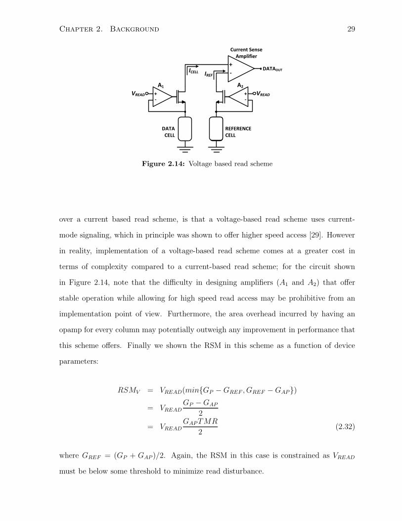
Chapter 2. Background 29
DATA
CELL
REFERENCE
CELL
+
-VREAD +
-VREAD
A1 A2
+
-ICELL
IREF
DATAOUT
Current Sense
Amplifier
Figure 2.14: Voltage based read scheme
over a current based read scheme, is that a voltage-based read scheme uses current-
mode signaling, which in principle was shown to offer higher speed access [29]. However
in reality, implementation of a voltage-based read scheme comes at a greater cost in
terms of complexity compared to a current-based read scheme; for the circuit shown
in Figure 2.14, note that the difficulty in designing amplifiers (A1 and A2) that offer
stable operation while allowing for high speed read access may be prohibitive from an
implementation point of view. Furthermore, the area overhead incurred by having an
opamp for every column may potentially outweigh any improvement in performance that
this scheme offers. Finally we shown the RSM in this scheme as a function of device
parameters:
RSMV = VREAD(minGP −GREF , GREF −GAP)
= VREADGP −GAP
2
= VREADGAPTMR
2(2.32)
where GREF = (GP + GAP )/2. Again, the RSM in this case is constrained as VREAD
must be below some threshold to minimize read disturbance.

Chapter 2. Background 30
2.4.5.3. Read Disturbance Issues
During a read operation, the current drawn by an STT-MRAM cell - resulting either from
the current due to the application of a fixed voltage across the cell, or from the application
of a fixed current to the cell - can potentially disturb the data stored in the cell. As such
a read operation can effectively act as a weak write operation, thus potentially destroying
the contents of the cell. In order to ensure that a read operation is nondestructive, the
current applied through the MTJ during a read operation is limited to be significantly
less than the write critical current. Note that even if the applied current is less than the
critical current, the data in the cell may still be destroyed as a consequence of thermal
noise processes. A stochastic model for predicting the likelihood of switching the state
of an MTJ was presented in [30]; the probability, PWRITE, of switching an MTJ given a
read current, Iread, which is less than the MTJ’s critical current, IC0 is given by:
Pwrite = 1− exp
[
− tPτP→AP
]
(2.33)
Where tP is the duration in time when Iread is applied to the MTJ, while τP→AP is given
by:
τP→AP = τ0exp
[
KUV
kBT
(
1− IreadIC0
)]
(2.34)
Where τ0 is the nominal switching time when a current of magnitude equal to IC0 is
applied to the cell, KU is the anisotropy constant, V is the volume of the MTJ’s FL, kB
is the Boltzmann constant, and T is the temperature given in Kelvin. The term KUVkBT
is also known at the thermal stability factor, ∆, and is the ratio between the magnetic
energy stored in the cell (KUV ) and the thermal energy (kBT ). Equation 2.33 indicates
that at some finite temperature T , and for some read current Iread < IC0, there exists
a finite probability for the cell to be switched, or in other words, for the data to be
destroyed. For the remainder of this thesis, we rely on Equations 2.33 and 2.34 as a
means to estimate read disturbance rate.

Chapter 2. Background 31
Read disturbance is the source of the fundamental tradeoff between read stability and
read/write performance. Figure 2.15 illustrates this tradeoff, where we see that the read
disturb rate (calculated using Equations 2.33 and 2.34) is an exponentially increasing
function of the ratio between the read sense current, IREAD, and the cell critical current,
IC0 (the figure shows the relationship for multiple values of the thermal stability factor,
∆).
0.4 0.5 0.6 0.7 0.8 0.9 110
-15
10-10
10-5
100
IREAD
/IC0
Read
Dis
turb
Rate
Δ = 45
Δ = 50
Δ = 55
Figure 2.15: Read disturb rate versus IREAD/IC0
If a high performance read operation is desired, the read sense margin must be in-
creased, which requires an increase in the read sense current. In order to maintain a
certain desired read disturb rate, IC0 then also must be increased (which can be achieved
by altering the FL size and/or geometry), such that the ratio IREAD/IC0 is kept constant.
As such, improving read performance inevitably results in increasing the critical current,
and thus increasing write power and potentially write time as well. On the other hand,
one may choose to increase read performance (by increasing IREAD) and write perfor-
mance (by reducing IC0), but this will result in an increased read disturb rate. This
tradeoff couples read and write performance, and places a tight constraint on the overall
performance and level of robustness that can be achieved in STT MRAM. In Chapter
4 we review existing approaches (both circuit and device level) to deal with read distur-

Chapter 2. Background 32
bance, and present a proposed device and cell to overcome the tradeoffs which plague
current STT MRAM cells.
2.5. Summary
In this chapter, we presented a brief overview of MRAM technology, and discussed some of
the challenges faced by previous generations of MRAM, and discussed how STT-MRAM
overcomes many of these challenges. We then provided a background in the fundamental
physics behind the write mechanism in STT-MRAM, the spin torque transfer effect.
We then discussed the cell and chip architecture of current STT-MRAM, as well as the
read and write operations currently employed. Finally we highlighted the problem of
read disturbance in STT-MRAM, and how this detrimentally effects both read and write
performance.

3 MTJ Modeling
This chapter presents an investigation into modeling the transient behaviour of Magnetic
Tunneling Junctions. First, we provide an overview of previous modeling approaches
and the shortcomings of prior work. Next we discuss the structure of the proposed
modeling approach taken in this work. We then present an experimental study where
test chips containing MTJs are characterized. Unfortunately, due to a limited access to
MTJs and poor reliability of the limited number of MTJs we had access to, we were
unable to completely characterize a single MTJ; as described in detail in Section 3.6, our
measurement results are actually an aggregate of different measurements done on different
MTJs, and on different dies. As such, the comparison between our measurement results
and those predicted by our proposed model are not completely conclusive, although we
may compare some of the overall trends that were observed during measurement and
those predicted by our model. Nonetheless, in the final part of this chapter we compare
measured results to those predicted by our model.
3.1. Prior Work
Previous work can be divided loosely into two categories: Static Models and Dynamic
Models. Static models seek to predict the static resistance versus applied voltage hys-
teresis characteristics of MTJs - that is to say they provide an estimate of the steady
state current expected to be drawn by the MTJ given an applied voltage and the state of
33

Chapter 3. MTJ Modeling 34
the MTJ. These models provide no information on the switching behaviour of the MTJ.
Dynamic models on the other hand seek to predict the general dynamic response of the
MTJ given an input stimulus. Examples of each modeling approach are provided in the
following sections.
3.1.1. Static Models
An example of a static model proposed recently is the work done by Zhao [31]. The
model is implemented in Verilog-A, and is able to replicate the resistance versus voltage
characteristic of MTJs. The model comprises two components: a model for the tunneling
resistance of the MTJ and a model to predict the critical current of the cell. The tunneling
model comprises of an equation derived from the Brinkman model [32] to predict the
tunneling resistance as a function of device parameters and the applied voltage bias. The
tunneling resistance is given as:
R(V ) =tOX
kφ−1/2A
exp[1.025tOXφ−1/2]
1 +t2OX
e2m
4hφV 2
(3.1)
Where tOX is the oxide thickness, φ is the barrier height of the tunnel, A is the area of the
MTJ, k is a parameter which depends on the barrier composition (must be determined
empirically), and V is the applied voltage to the MTJ. In addition to Equation 3.1, the
tunneling model also captures the dependence of the TMR ratio on applied voltage:
TMR(V ) =TMR0
1 + ( VVH
)2(3.2)
The critical current is calculated using the following equation:
JC = JC0
[
1− kBT
KUVln(τ/τ0)
]
(3.3)

Chapter 3. MTJ Modeling 35
Where JC0 is the nominal critical current. This equation allows for the calculation of
switching currents for pulses longer than the nominal pulsewidth τ0. This means the
model is able to estimate switching times, but this is only for currents less than the
nominal critical current JC0 and for pulsewidths greater than the nominal switching time
τ0; this model is unable to predict switching times for currents greater than JC0.
3.1.2. Dynamic Models
Numerous dynamic models for MTJs have been proposed, but they have notably lacked
rigor in their correlation to measured results. In [33], the authors propose to model the
FL using the LLGS equation which is solved to determine the switching time of the
magnetization vector of the FL. In this model, the tunneling resistance is set to either
RP (the parallel state resistance) or RAP (the antiparallel state resistance). While this
model proposes to predict the switching time of the MTJ for an arbitrary input stimulus,
this model remains to be validated experimentally.
Figure 3.1: Previously proposed dynamic model [34].
Another example of a dynamic model is the one proposed in [34], where the authors

Chapter 3. MTJ Modeling 36
provide a model which builds on their previously proposed static model [31]. The dynamic
model implemented in this work is shown graphically in Figure 3.1. In the model, for
applied currents less than the critical current, Equation 3.3 is used to predict if the applied
current for a given duration in time is sufficient to switch the state of the cell. For a
current applied for a given time duration, tpulse, and whose magnitude, Ipulse, exceeds
that of the critical current, the state of the cell is predicted to switch if tpulse ≥ τswitch,
where τswitch is given by:
τswitch(I) =1
αγMS
IC0
I − IC0ln
(
π
2θ0
)
(3.4)
While this model does overcome some of the weaknesses of the authors’ previous work
( [31]), Equation 3.4 is restricted only to ideal constant pulses; this implies that this
model cannot be used to predict the response of an MTJ to arbitrary input stimuli.
3.1.3. Summary of Previous Work
Table 3.1 summarizes some of the key features of previously proposed models. In the
table, the details of how the MTJ tunneling resistance and magnetodynamics are mod-
elled are compared. To accurately predict the tunnelling current of an MTJ under the
influence of a stimulus, it is imperative to model both the bias-dependence of the tun-
nelling resistance as well as the dependence of MTJ resistance on the relative alignment
between the FL and PL magnetization vectors (given by the angle, θ between the two
vectors). In the table, we compare whether or not these key features are present in previ-
ous work; one point to note is that in the context of Table 3.1, “θ Dependence” indicates
that a model is able to encapsulate the dependence of tunnelling resistance on arbitrary
values of θ. This is to say that a previous work which models the resistance as either RP
or RAP depending on the MTJ state (i.e. only models resistance dependence on θ for
θ = 0 and θ = π) would not be classified as a model which encapsulates θ dependence.
For magnetodynamics modelling, the previous work is classified as either incorporating

Chapter 3. MTJ Modeling 37
the LLGS equation to model the motion of the FL magnetization vector or utilizing an
equation (such as Equation 3.3 or Equation 3.4) to estimate switching time/current.
Table 3.1: Comparison of previous models
ModelResistance Magnetodynamics Correlated to
Model Model Measurements?
Bias θ Switching Time LLGS
Dependence Dependence Equation Based Based
[31] Yes No Yes No No[33] No No No Yes No[34] Yes No Yes No No
3.2. Proposed Model
3.2.1. Motivation
Currently, there is a lack of adequate circuit-level models which fully describe the be-
haviour of MTJs. An ideal model would need to be able to predict the response of MTJs
to a wide range of stimuli for the sake of the design optimization of STT-MRAM at
both cell and system level, as well as for the sake of functional verification of the cell
under the influence of non-idealities - for instance, how is the write-time of a cell effected
by VDD noise? As described in the preceding section, there is a void between what is
desired in terms of a model for MTJs and the models which exist currently. In this work,
we present a model for MTJs which attempts to predict their transient behaviour to
meet the aforementioned needs, and we correlate the results predicted by the model to
measurement results.
3.2.2. Proposed Model Structure
The proposed model has two components: a tunnel model to describe the resistance of
the MTJ as a function of the applied voltage and the relative orientation of the PL and
FL magnetization vectors, and a magnetodynamics model to estimate the movement of

Chapter 3. MTJ Modeling 38
the FL magnetization vector caused by spin transfer torques. These are discussed in
detail in the following sections. The model proposed in this work does not model any of
the dependencies of MTJ switching or tunnelling resistance on temperature. However,
this model can be extended to include temperature effects by relating the dependence of
key model parameters, such as RP , TMR0, α, and β (these parameters will be discussed
in the following sections), on temperature.
3.2.2.1. Tunnel Model
One common attribute of MTJs is the fact that while the tunneling resistance shows
negligible dependence on applied voltage across the barrier when the MTJ is in parallel
state (the resistance in this state is equal to RP ), the resistance of the MTJ when in
antiparallel state (equal to RAP ) shows considerable variation over applied bias voltage.
In modeling the tunneling resistances in this work, we assume that RP is constant and
does not vary with applied voltage, while TMR is a function of applied voltage. In
doing so, we model not only the voltage dependence of RAP , but also the variation of
spin torque efficiency factors (which will be discussed in the following subsection) with
applied voltage. A simple model for the variation of TMR over applied bias which has
been previously proposed [31] [35] is:
TMR(V ) =TMR0
1 + ( VVH
)2(3.5)
Where TMR0 is the nominal TMR at zero applied bias, VH is the voltage at which the
TMR ratio drops to half the value of TMR0, and V is the applied voltage across the
barrier. The dependence of the tunneling resistance on the relative orientation of the
magnetization vectors of the ferromagnetic layers on either side of the tunneling barrier
is given by the Julliere model [36]:
R(θ) =2RP ||RAP
1 + P 2Scos(θ)
(3.6)

Chapter 3. MTJ Modeling 39
Where PS is the tunneling polarization factor [37] and is equal to [(RAP − RP )/(RAP +
RP )]1/2 or equivalently,
PS =
√
TMR
TMR + 2(3.7)
Note that as per the model for TMR (Equation 3.5) , PS is dependent on applied voltage.
We are now in a position to form an equation for R(θ, V ) given Equations 3.5 and 3.6,
and the fact that RAP = RP [TMR(v) + 1], as per Equation 2.1:
RMTJ(θ, V ) =2RP (TMR0 + 1 + ( V
VHP
)2)
2(1 + ( VVHP
)2) + TMR0(1 + cos(θ)), V ≥ 0 (3.8)
RMTJ(θ, V ) =2RP (TMR0 + 1 + ( V
VHN)2)
2(1 + ( VVHN
)2) + TMR0(1 + cos(θ)), V < 0 (3.9)
3.2.2.2. Magnetodynamics Model
The magnetodynamics of the FL, and its interaction with spin transfer torque is modeled
using the LLGS equation [18]:
dm
dt= − γ
1 + α2m× ˜HEFF − γα
1 + α2m× (m× ˜HEFF)− ˜TSPIN (3.10)
Where γ is the gyromagnetic ratio (taken to be equal to 1.7608×10¹¹s−1T−1, as per [38]),
α is Gilbert dampening parameter, MS is the saturation magnetization of the layer,
and m is a unit vector representing the magnetization of the FL. For this work, we
assume the FL behaves as a single magnetic domain, and as such we use the macrospin
approximation for the FL [20]. As described in Section 2.3.1, under this approximation
˜HEFF, the effective field in the layer, is principally comprised of ˜HANI and HD, the
anisotropy and demagnetizing fields, respectively. Assuming a coordinate system where
the easy axis of FL is along the z-axis, the y-z plane is the easy plane of the FL, and the

Chapter 3. MTJ Modeling 40
x-axis is the hard axis, simple models for ˜HANI and HD are [39]:
˜HANI = HKcos(θ)z (3.11)
HD = −MSsin(θ)cos(φ)x (3.12)
Where HK is the strength of the anisotropy field (induced either by shape or magne-
tocrystalline properties [39]), θ is the angle between the magnetization of the FL and the
easy axis, φ is the azimuthal angle between the projection of the magnetization vector
of the FL on the x-y plane and the x-axis, and x and z are unit vectors along the x
and z axes respectively. It should be noted that the ˜HEFF for FLs of IPA devices is
comprised of both ˜HANI and HD, while the ˜HEFF for FLs of PPA devices comprises
only of ˜HANI and thus HD is excluded when modeling PPA devices. Finally ˜TSPIN is
given by Equation 3.13.
TSPIN =γhη(θ)
(1 + α2)2eMSV oli(t)m× (m× mPL) (3.13)
Where i(t) is the current flowing from PL to FL, while the other parameters were dis-
cussed in Section 2.3.1. For our model, we encapsulated some of the material dependent
parameters (η,MS, V ol) and other physical constants with a single constant, β. The
constants, α and β, are optimized to match model predicted switching results to exper-
imental data. As such the simplified expression for TSPIN , as coded in our model, is
shown below in Equation 3.14.
TSPIN =γβ
1 + α2i(t)m× (m× mPL) (3.14)

Chapter 3. MTJ Modeling 41
3.2.2.3. Verilog-A Description
The overall structure of the Verilog-A model is described in the flowchart shown in
Figure 3.2. The model works by computing the change in the magnetization vector (by
solving the LLGS equation) at each timestep, and then computing new values for θ (the
azimuthal angle of the magnetization vector), and then the tunnel resistance, based on
the tunnel model previously described. As shown, these three steps are repeated at each
timestep until the completion of the simulation.
Set initial conditions
θ(0) = θINIT
Compute Change in M
dM/dt = f1(IMTJ,θ(t))
Compute θ(t+Δt)
θ(t+Δt) = θ(t) + (dM(t))/MS
Compute new RMTJ
RMTJ = f2(VMTJ,θ(t+Δt))
Figure 3.2: Verilog-A model flowchart
3.3. Device Characterization and Experimental Setup
One of the important goals of this study was to assess how closely our model matched
experimental data. As such, we performed a set of experiments on a set of IPA MTJs
fabricated in Fujitsu’s 130nm process, to first correlate our model to measured data, and
then to validate the efficacy of our proposed model. Figure 3.3 shows the experimental
setup used to characterize the MTJs in this study.
We used an Agilent ParBERT 81250 to generate the voltage waveforms which were
applied to the MTJs. For the sake of our measurements, custom circuitry was required
specifically to measure the impedance of the MTJs. This circuitry was fabricated on a
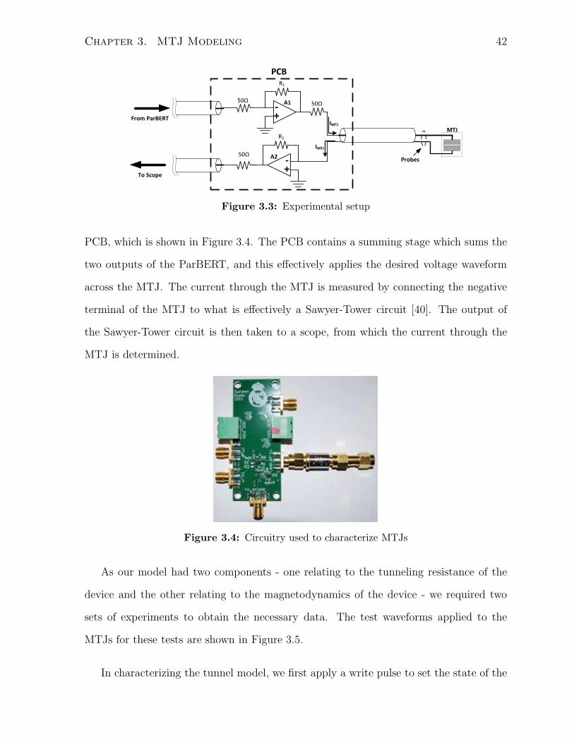
Chapter 3. MTJ Modeling 42
+
-
+
-
50Ω50Ω
50Ω
R1
R2
From ParBERT
To Scope
A1
A2
PCB
IMTJ
IMTJ
MTJ
Probes
Figure 3.3: Experimental setup
PCB, which is shown in Figure 3.4. The PCB contains a summing stage which sums the
two outputs of the ParBERT, and this effectively applies the desired voltage waveform
across the MTJ. The current through the MTJ is measured by connecting the negative
terminal of the MTJ to what is effectively a Sawyer-Tower circuit [40]. The output of
the Sawyer-Tower circuit is then taken to a scope, from which the current through the
MTJ is determined.
Figure 3.4: Circuitry used to characterize MTJs
As our model had two components - one relating to the tunneling resistance of the
device and the other relating to the magnetodynamics of the device - we required two
sets of experiments to obtain the necessary data. The test waveforms applied to the
MTJs for these tests are shown in Figure 3.5.
In characterizing the tunnel model, we first apply a write pulse to set the state of the

Chapter 3. MTJ Modeling 43
VMTJ
t
Figure 3.5: Test waveform applied to MTJs
MTJ; by applying a positive pulse we can set the MTJ to be in the antiparallel state,
while a negative pulse sets the MTJ in the parallel state. The amplitude of the pulse in
this case is +/ − 500mV , and this is applied for a duration TWRITE of 20ns. Following
the write operation, read pulses are applied to measure the current through the MTJ and
thus measure the resistance of the MTJ. The read pulses are also of a duration of 20ns,
but the read pulse amplitude is varied to characterize the voltage dependent resistance
of the MTJ.
To characterize the magnetodynamics model, we initially use a write pulse to set the
state of the MTJ. We then apply several test write cycles followed by read cycles, where
the read pulses are maintained at a constant amplitude (75 mV), while the write pulse
amplitude is increased cycle after cycle. This allows us to determine the critical switching
voltage for a given write pulse width. By performing these experiments over a wide range
of write pulse widths, we are able to characterize the critical switching voltage of the MTJ
as a function of pulse width. This data is then used for our magnetodynamics model.

Chapter 3. MTJ Modeling 44
3.4. Measurement Data
Figure 3.6 shows the measured resistance-voltage hysteresis characteristic for the MTJs
characterized in this study.
-500 -400 -300 -200 -100 0 100 200 300 400 500600
700
800
900
1000
1100
1200
1300
MTJ Voltage [mV]
Resis
tan
ce [
Oh
ms]
AP State
P State
Figure 3.6: MTJ Resistance versus Voltage characteristic
As is typical of MTJs, in the AP-state, the resistance decreases as the magnitude
of the applied voltage across the MTJ increases, and it should also be noted that there
is some asymmetry of the resistance versus voltage characteristic about the origin. In
P-state however, it can be seen that the overall trend is that the resistance shows very
little variation over applied voltage.
Figure 3.7 shows the measured switching time versus applied voltage characteristic
of the MTJs characterized in this study. As can be seen in the figure, at low applied
voltages, the switching time varies linearly with applied voltage, while the switching
time follows an approximately inverse characteristic at large applied voltages. This is an
expected result; at low applied voltages (less than the critical switching voltage of the
MTJ), the switching characteristic is dominated by thermal noise processes, while at high
applied voltages, the characteristic is dominated by the spin torque transfer effect [41].

Chapter 3. MTJ Modeling 45
0.5 0.6 0.7 0.8 0.9 1 1.1 1.21
2
3
4
5
6
7
8
9
10
Applied Voltage [V]
Sw
itch
ing
Tim
e [
ns]
Figure 3.7: Switching time versus applied voltage
We can use a simplification of the LLGS equation to estimate the applied voltage versus
switching time characteristic. We start with the LLGS equation, and then make the
simplifying approximation that the azimuthal angle of the FL magnetization vector, θ, is
not effected by the precession term in the LLGS equation; while this is an approximation
for IPA devices, whose out-of-plane demagnetizing field causes fluctuations in θ as the
magnetization vector precesses about the easy axis, this assumption is true for PPA
devices, as PPA devices do not have an out-of-plane demagnetizing field. We can therefore
use this approximation of the LLGS equation to form an equation which describes the
time evolution of θ:
dθ
dt= k1mFL × (mFL × ˜hEFF)− k2vMTJmFL × (mFL × mPL)
= (k1 − k2vMTJ)sin(θ) (3.15)
where k1 and k2 are given by:
k1 = −γα˜HEFF(θ)
MS(1 + α2)(3.16)
k2 = − γhη(θ)
2eMSV(3.17)

Chapter 3. MTJ Modeling 46
Using these simplifications, Equation 3.15 can be solved analytically to yield:
θ(t) = 2cot−1
[
cot
(
θ(0)
2
)
exp
[
(−k1 + k2vMTJ)t2
2
]]
(3.18)
It is now straight forward to find find the relationship between switching time and applied
voltage, vMTJ . If we say the MTJ has switched states when θ = θswitch, where typically
θswitch = π/2 + ǫ, we can solve Equation 3.18 for the time, tswitch, at which point the
MTJ switches states:
tswitch =
√
√
√
√
√
−2ln
(
cot(
θswitch
2
)
cot( θ(0)2 )
)
k2vMTJ − k2(3.19)
Equation 3.18 reveals that tswitch ∝ 1/√vMTJ , which agrees with the trend shown by
experimental results for large applied voltages.
3.5. Model Correlation
In this section, we describe the process of correlating our tunnel and magnetodynamics
models to measured results, and compare our model to measured results.
3.5.1. Tunnel Model Correlation
In correlating our tunnel model to measured data, we optimized the parameters in Equa-
tion 3.9 in a bid to minimize the sum of the squared error between our model and
measured results. It should be noted that we set RP as the average of the measured
P-state resistances. The parameters for our tunnel model are presented in Table 3.2,
while Figure 3.8 compares the tunnel model to measured results.
Table 3.2: Parameters for tunnel model
Model Parameter Value
VHP 144.38 mVVHN 320.95 mVRP 673.35 Ω
TMR0 0.836

Chapter 3. MTJ Modeling 47
-500 -400 -300 -200 -100 0 100 200 300 400 500600
700
800
900
1000
1100
1200
1300
MTJ Voltage [mV]
Resis
tan
ce [
Oh
ms]
AP State
Model
P State
Model
Figure 3.8: Comparison of tunnel model to measured R-V characteristic of MTJ
3.5.2. Magnetodynamics Model Correlation
In correlating our magnetodynamics model, we used our model to predict the switching
time versus applied voltage characteristic, and then optimized coefficients in the LLGS
equation to match measured results. We biased our optimization to match the data
corresponding to switching at high applied biases (shorter switching times). This is
because at lower applied biases (i.e. at larger switching times), thermal agitation effects
play an important part in switching [41]. At high-applied biases, precessional-switching
(i.e. the switching causes by the spin torque transfer effect) dominates, and so since our
model does not account for the effects of thermal agitation, it is only in this regime where
we expect our model to offer valid results. There were effectively two parameters in the
LLGS equation which needed to be optimized: the Gilbert damping parameter, α, and
the coefficient of the torque term, β (in Equation 3.14). The values of these parameters
after optimization are shown in Table 3.3.
Figure 3.9 compares the predicted switching time versus applied voltage characteristic
versus measurement results.

Chapter 3. MTJ Modeling 48
Table 3.3: Parameters for tunnel model
Model Parameter Value
α 0.02β 7.3× 10⁹
0.5 0.6 0.7 0.8 0.9 1 1.1 1.2 1.31
2
3
4
5
6
7
8
9
10
Applied Voltage [V]
Sw
itch
ing
Tim
e [
ns]
Model
Figure 3.9: Comparison of model to measured Switching Time versus Applied Voltage
3.6. Model Validation
One of the main goals for our model was to accurately predict the transient behaviour
of MTJs. While we were able to correlate the applied voltage versus switching charac-
teristics of our models to measurement results, we devised an additional experiment to
validate the accuracy of our model in predicting transient response. In this experiment,
we applied pulses of the form shown in Figure 3.10.
As shown in this figure, a pulse of duration TPULSE and amplitude VPULSE is applied,
followed by a duration of TBREAK where the applied voltage across the MTJ is zero,
followed again by a pulse of duration TPULSE and amplitude VPULSE. This experiment
tests the relaxation time of the MTJs, which is the time taken for an MTJ which is
disturbed by some stimulus to return to a stable state. If TBREAK is much shorter than
the relaxation time of the MTJ, the MTJ may still switch even if VPULSE is smaller than
the minimum voltage needed to switch the MTJ for a lone pulse of duration TPULSE.

Chapter 3. MTJ Modeling 49
TPULSE TBREAK TPULSE
VPULSE
VMTJ
t
Figure 3.10: Pulses used to validate accuracy of transient response in proposed model
Unfortunately however, due to limited access to MTJs, and a degraded reliability of these
MTJs (due to suspected oxidation of the passivation layer), we were unable to perform
a large number of these experiments as we observed breakdown of MTJs within a few
cycles for large ( > 500 mV) applied biases. Given that we could not perform all of
these measurements on a single MTJ, these experiments were spread over multiple dies.
What we present in Table 3.4 are the measurement results obtained in this way and the
results predicted by our model (note that the measurement results were rounded up to
the nearest 10 mV). Here we compare the measured minimum switching voltage, Vmeas,
obtained for a set of different values for TPULSE and TBREAK , and accordingly compare to
the minimum predicted switching voltage for our model, Vmod. As can be seen, the overall
Table 3.4: Parameters for tunnel model
TPULSE TBREAK Vmeas Vmod
3ns 1ns 530 mV 584 mV3ns 1.5ns 530 mV 596 mV4ns 1ns 450 mV 533 mV4ns 1.5ns 480 mV 543 mV4.5ns 1ns 420 mV 523 mV4.5ns 1.5ns 460 mV 530 mV
trends predicted by the model over increases in TPULSE and increases in TBREAK agree
with the trends observed in our measurement results, however the the model predicted

Chapter 3. MTJ Modeling 50
results are somewhat larger than those measured. Given the model parameters were
optimized for MTJs on a separate die from those measured, it is hard to draw too many
conclusions at this point. Future measurement opportunities will need to be pursued to
complete the validation of the proposed model.
3.7. Summary
In this chapter, we presented an overview of previously proposed models for MTJs. We
proposed a model which we believe will overcome the shortcomings of previous work.
We then described an experimental study where MTJs where characterized, and the
measured dynamic behaviour of MTJs was compared to that predicted by our proposed
model in order to validate its efficacy.

4 Device and Cell Proposal
This chapter presents a proposal for a novel MTJ and the associated memory cell, which
offers a guarantee of read-disturbance immunity. As mentioned in Chapter 2, Section
2.4.5.3, the problem of read disturbance is the source of the fundamental tradeoffs between
read and write performance in STT-MRAM. Techniques to mitigate read disturbance
are necessary to ensure error-free operation of STT-MRAM chips, and in addition, may
help in breaking the tradeoff between read and write performance, thereby potentially
leading to overall improved performance of an STT-MRAM chip. In the following, we
begin with a brief overview of prior MTJ structures and cell architectures that have
been proposed to address the problems of read disturbance in STT-MRAM. We then
present the proposed MTJ structure, cell architecture, and the read and write schemes
for the proposed cell, while also discussing device and transistor level optimization of the
proposed cell. Finally, we present a simulation study comparing the proposed cell with
conventional cells.
4.1. Previous Work
4.1.1. Circuit Level Solutions
Circuit level approaches to solving the problem of read disturbance revolve around lim-
iting the current applied to the cell during a read operation. Using Equation 2.33, and
given a target read disturb rate, the maximum current that can be applied to the cell
51

Chapter 4. Device and Cell Proposal 52
during a read operation to meet that targeted read disturb rate can be determined. For
example, for a targeted read disturb rate of 10−15, and given that tP is approximately
10% of the nominal switching time τ0, the read current must be limited to 45% of the
critical current IC0.
In [25] the authors propose a multi-VDD word line driver, as shown in Figure 4.1, which
minimizes read disturbance without compromising write performance. The advantage of
this approach is that the word line voltage can be used to control the current through
the cell; for a read operation, the word line voltage is set to a low voltage which reduces
the current through the MTJ, thus minimizing read disturbance rate, while for a write
operation, the word line voltage is set to a high voltage.
Figure 4.1: Previously proposed multi VDD driver. Figure taken from [25].
In [42], the authors propose a novel 2 Transistor, 1 Magnetic Tunneling Junction
(2T1MTJ) STT-MRAM cell, as shown in Figure 4.2. Again, the strategy employed in this
cell is to limit the current through the MTJ during a read operation, while maximizing
the current through the MTJ during a write operation. The cell is operated as follows.
During a write operation, Read-Wordline and Write-Wordline are both raised to VDD;
this turns both Read-NMOS and Write-NMOS on, and the total current supplied by
the parallel combination of these two transistors is used to switch the state of the MTJ.
During a read operation on the other hand, Read-Wordline is raised to VDD while Write-

Chapter 4. Device and Cell Proposal 53
Figure 4.2: Previously proposed 2T1MTJ cell. Figure taken from [42].
Wordline is held low; this ensures that only Read-NMOS is activated during a read
operation, thus limiting the total amount of current applied to the MTJ, and as such
reducing the probability of read disturbance. This approach therefore is able to limit
the current driven through the MTJ during a read operation without having to rely on
additional circuitry to control the word-line voltage, as is the case in [25].
The existing circuit level solutions, such as the two examples highlighted above, only
attempt to mitigate the possibility of read disturbance during a read operation; these
techniques specifically restrict the current through a cell during a read operation, and
so such an approach inevitably leads to degraded read performance. These techniques
make no effort to improve read performance while maintaining disturbance-free read
operation. Furthermore, techniques to tackle the problem of read disturbance at the
circuit level are still bound by choices of device parameters, which are themselves selected
as a compromise between read and write performance (this will be explained in the
following section and in greater detail in Section 4.2.4). As such, existing circuit level
techniques to deal with read disturbance are presently limited in their scope.
4.1.2. Device Level Solutions
While circuit level solutions have centered on separating read and write operations at the
circuit level, recently novel devices have been proposed which separate read and write

Chapter 4. Device and Cell Proposal 54
operations at the device level [43] [44]; by separating these operations, device parameters
can be independently optimized for read and write access. The device proposed in [44]
is shown in Figure 4.3.
Figure 4.3: Previously proposed 3-terminal device. Figure taken from [44].
As shown in the figure, the device has two PLs, PinnedLayer1 and PinnedLayer2 and
one FL; Oxide1 and Oxide2 are the names of the oxide barriers between PinnedLayer1
and the FL and PinnedLayer2 and the FL, respectively. Note that as indicated in
the figure, the FL-Oxide1-PinnedLayer1 combination is used for write operations, while
the FL-Oxide2-PinnedLayer2 combination is used for read operations; as such the device
effectively has separate read and write ports, with Port 2 being used for write operations,
Port 3 being used for read operations, and Port 1 acting as a common port for both
operations. The implication of separating the read and write operations at the device
level is that now, the different tunnel barriers which connect the read and write ports
to the FL, namely Oxide2 and Oxide1 respectively, can be independently optimized. By
choosing an oxide thickness for the Oxide1 which is thinner than a conventional MTJ,
the switching speed of the proposed device can be enhanced, as a thinner oxide results
in reduced resistance between the FL and the write port, thus allowing for the access
transistor to supply more current to the cell during a write operation. On the other
hand, Oxide2 can be made to be thicker than that of a conventional MTJ with similar

Chapter 4. Device and Cell Proposal 55
device parameters. Note that a thick oxide allows for larger RSM since:
RSM = IREAD(RAP − RP )
2
= IREADRP(TMR)
2(4.1)
Where RP is the parallel state resitance of an MTJ, RAP is the antiparallel state resis-
tance, and IREAD is the read sense current. Since a thicker oxide results in an increase
in RP , it also results in a larger RSM for a given read sense current; this allows for the
current during a read operation to be smaller than that of a conventional MTJ for a given
targeted RSM (and thus without sacrificing performance). As previously described, re-
ducing the current during a read operation inevitably results in further reduction in read
disturb rate.
4.2. Proposed Cell
4.2.1. Device and Cell Structure
The structure of the proposed device is shown in Figures 4.4(a) and 4.4(b) which illustrate
the IPA and PPA versions of the device, respectively. As shown in the figure, the MTJ
is comprised of two PLs: Top Pinned Layer (TPL) and Bottom Pinned Layer (BPL).
These layers are stacked vertically above and below the FL, respectively, with a tunneling
barrier in between each PL and the shared FL. This device is envisioned to make use of
the same processing steps described in [43,44] to allow for the fabrication of the metallic
contact attached to the FL. The fixed magnetizations of the two PLs are antiparallel
to one another. In contrast to the device presented in [30], this device also requires
metal contacts to all three ferromagnetic layers. Note that when the FL magnetization is
parallel to TPL, the resistance between TPL and FL is low, while the resistance between
BPL and FL is high. The opposite is true when the FL magnetization is parallel to BPL.

Chapter 4. Device and Cell Proposal 56
In this work, we assign a state of logical “1” when the FL magnetization is parallel to
TPL, and a state of logical “0” when the FL magnetization is parallel to BPL. Circuit
level symbols for the IPA and PPA devices are shown in Figures 4.5(a) and 4.5(b),
respectively.
Top Pinned Layer (TPL)
Oxide Layer
Free Layer (FL)
Metallic Contact
Oxide Layer
Bottom Pinned Layer (BPL)
Metallic Contact
Metallic Contact
(a) IPA version of proposed device
Top Pinned Layer (TPL)
Oxide Layer
Free Layer (FL)
Metallic Contact
Oxide Layer
Bottom Pinned Layer (BPL)
Metallic Contact
Metallic Contact
(b) PPA version of proposed device
Figure 4.4: Structure of proposed device
TPL
BPL
FL
(a) Circuit symbol forIPA version of pro-posed device
TPL
BPL
FL
(b) Circuit symbol forPPA version ofproposed device
Figure 4.5: Circuit symbols for proposed device
Figure 4.6 shows the proposed cell. The cell consists of two transistors, M1 and M2,
which are connected to the TPL and BPL of the proposed device, respectively. Note
that the FL of the proposed device is connected to the SL, and the two transistors are
connected to the same word line. Finally, Figure 4.7 shows the top level organization of
a hypothetical memory chip comprising of the proposed cells.
4.2.2. Cell Write Operation
The proposed cell’s write operation is illustrated in Figures 4.8(a) and 4.8(b). During
a write operation, current is passed from the FL to either TPL or BPL; as is shown in

Chapter 4. Device and Cell Proposal 57
Wo
rd Lin
e (W
L)
Select Line (SL)
M1
Bit Line 1 (BL1)
Bit Line 2 (BL2)
M2
Figure 4.6: Proposed cell shown with an IPA version of proposed device
Figures 4.8(a) and 4.8(b), this write operation allows us to always perform a parallelizing
write operation in switching the state of the cell. By selecting which path to carry current
during a write operation, the FL magnetization is switched to be parallel to either TPL
or BPL.
Since a parallelizing write operation requires less current than an antiparallelizing
write operation [18], this scheme will allow for reduced critical current on average. This
statement may be quantified by examining the spin torque efficiency gain, Gη, which
we define here as being the ratio between the spin torque transfer efficiency factor, η,
for a antiparallel to parallel write operation, over the spin torque efficiency factor for an
parallel to antiparallel write operation. The spin torque efficiency gain is therefore:
Gη =ηAP→P
ηP→AP
=
PS
1−P 2S
PS
1+P 2S
=1 + P 2
S
1− P 2S
(4.2)
Since 0 < PS ≤ 1, Gη ≥ 1, implying that the worst case current required to switch the
magnetization vector in the proposed device is always less than that of a conventional
MTJ. For a typical MTJ with a TMR ≈ 150%, PS ≈ 0.65, and so Gη ≈ 2.46; this
implies a reduction in worst-case critical current over a conventional MTJ of almost
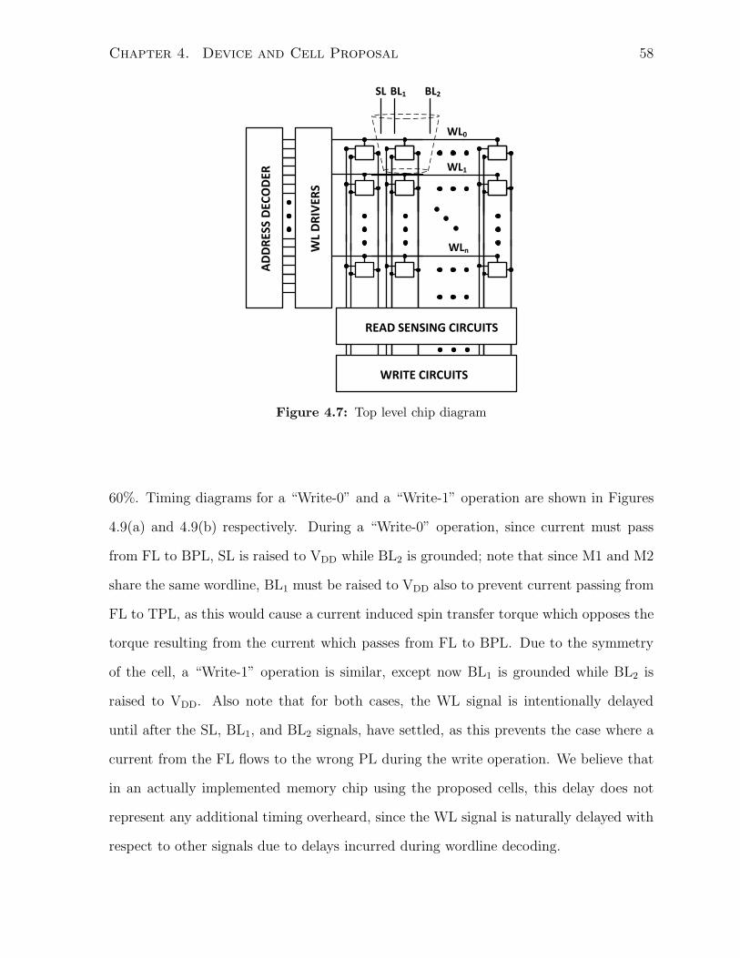
Chapter 4. Device and Cell Proposal 58
AD
DR
ES
S D
EC
OD
ER
WL D
RIV
ER
S
WL0
SL BL2
WRITE CIRCUITS
READ SENSING CIRCUITS
WL1
WLn
BL1
Figure 4.7: Top level chip diagram
60%. Timing diagrams for a “Write-0” and a “Write-1” operation are shown in Figures
4.9(a) and 4.9(b) respectively. During a “Write-0” operation, since current must pass
from FL to BPL, SL is raised to VDD while BL2 is grounded; note that since M1 and M2
share the same wordline, BL1 must be raised to VDD also to prevent current passing from
FL to TPL, as this would cause a current induced spin transfer torque which opposes the
torque resulting from the current which passes from FL to BPL. Due to the symmetry
of the cell, a “Write-1” operation is similar, except now BL1 is grounded while BL2 is
raised to VDD. Also note that for both cases, the WL signal is intentionally delayed
until after the SL, BL1, and BL2 signals, have settled, as this prevents the case where a
current from the FL flows to the wrong PL during the write operation. We believe that
in an actually implemented memory chip using the proposed cells, this delay does not
represent any additional timing overheard, since the WL signal is naturally delayed with
respect to other signals due to delays incurred during wordline decoding.

Chapter 4. Device and Cell Proposal 59
SL (tied to VDD)TPL
FL
BPL
ELECTRONS TUNNELLING
FROM BPL TO FL
BL1 (tied to VDD)
WL (tied to VDD)
M1
M2
BL2 (tied to GND)
(a) ”‘Write-0”’ operation for proposed cell
SL (tied to VDD)TPL
FL
BPL
ELECTRONS TUNNELLING
FROM TPL TO FL
BL1 (tied to GND)
WL (tied to VDD)
M1
M2
BL2 (tied to VDD)
(b) ”‘Write-1”’ operation for proposed cell
Figure 4.8: Write operations for proposed cell
4.2.3. Cell Read Operation
During a read operation, both M1 and M2 are turned on, FL is connected to GND
(through SL), and a sense amplifier is used to compare the TPL-to-FL resistance to the
BPL-to-FL resistance. In this way, the cell behaves much like a differential memory
element. Figure 4.10 shows a current-based read operation for the proposed cell. Here
(in steady state) identical currents are applied from TPL to FL and from BPL to FL.
By comparing the resulting voltages at TPL and BPL (or the drains of M1 and M2), the
resistance difference between the two paths can be detected, and thus the state of the

Chapter 4. Device and Cell Proposal 60
VDD
VDD
VDD
BL1
BL2
SL
WL
SL to WL Delay
V
t
(a) Timing diagram for a “Write-0” opera-tion
VDD
VDD
VDD
BL1
BL2
SL
WL
WL Delayed
V
t
(b) Timing diagram for a “Write-1” opera-tion
Figure 4.9: Timing diagrams for write operations for proposed cell
FL magnetization can be inferred.
Timing diagrams for a read operation are shown in Figures 4.11(a) and 4.11(b). As
shown in the timing diagram, the BL voltages are precharged to VDD; when the WL is
raised to VDD, the nodes BL1 and BL2 are discharged through the the TPL-to-FL and
BPL-to-FL paths, respectively - the different resistances of these two paths also give rise
to different time constants for these nodes. The steady state voltages of these two nodes
are given by the product of the current source magnitude, IREAD, and the different path
resistances between BL1 and GND and BL2 and GND. As such we see that in steady
state, when a logical “0” is stored in the cell, the steady state voltage of BL1 is larger
than BL2, and when a logical “1” is stored in the cell, the steady state voltage of BL2 is
larger than BL1. Also note that as shown in the timing diagrams, due to the fact that the
time constants for the nodes BL1 and BL2 are different, the transient current waveforms
for ITPL, the current flowing from TPL to FL, are different from the current waveforms
for IBPL, the current flowing from BPL to FL. However in steady state, during a read

Chapter 4. Device and Cell Proposal 61
VDD
SLSTT FROM
BPL
GREATER
THAN
FROM TPL
BL1M1
VDD
VREAD
+
-+-
SA
IREAD
WL (tied to VDD)
IREAD
2 x
IREAD
SAOUT
M2
BL2
WL (tied to VDD)
Sense
Amplifier
Figure 4.10: Proposed read scheme
WL
Vo
lta
ge
MT
J C
urr
en
ts
Time
v
t
i
t
ITPLIBPL
IREAD
BL
Vo
lta
ge
s
v
t
BL2
BL1
VDD
RSM
(a) Timing diagram for a “Read-0” opera-tion
WL
Vo
lta
ge
BL
Vo
lta
ge
sM
TJ
Cu
rre
nts
Time
v
t
v
t
i
t
BL1
BL2
ITPL IBPL
VDD
IREAD
RSM
(b) Timing diagram for a “Read-1” opera-tion
Figure 4.11: Timing diagrams for read operations for proposed cell

Chapter 4. Device and Cell Proposal 62
operation ITPL = IBPL = IREAD.
There are two key advantages to the proposed read scheme presented here. First, since
the read scheme is differential in nature, it inherently provides a two-fold improvement
in sense margin as compared to a conventional 1T1MTJ given the same read current
and the same ratio between RP and RAP. Second, the cell has the advantages of an
improvement to process variation and guaranteed immunity to read disturbance. We
show these benefits in the next two subsections.
4.2.3.1. Increased Tolerance to Process Variation
In a conventional 1T1MTJ based STT-MRAM, when a voltage/current stimulus is ap-
plied to the cell to measure the cell’s resistance, the resulting current/voltage which is
sensed is compared to that of a reference cell, which is typically not in close proxim-
ity to the cell being read. As a result of inherent process variation, there could be a
degradation in read sense margin. In cases of excessive process variation, the cell may be
incorrectly read. A simple analysis may be used to illustrate this point; first we consider
the worst-case RSM for a conventional 1T1MTJ cell, which was shown in Section 2.4.5
to be equal to:
RSMCONV 0 = IREADRAP −RP
2
= IREADTMR
2(4.3)
Equation 4.3 shows the RSM when there is no variation in the MTJ resistances between
the cell being read and the reference cell. In general however, within-die variation will
effect the RSM, and in the following we attempt to quantify this effect. Below, we denote
the random offset to the MTJ resistances of the cell being read as rCELL, while rREF is
the random offset to the resistance of the MTJ comprising the reference cell. The RSM

Chapter 4. Device and Cell Proposal 63
for a conventional cell under the effects of variation in MTJ resistance is then given by:
RSMCONV = RSMCONV 0 −
IREAD |rCELL − rREF | (4.4)
If we denote RSMDIFF0 to be the nominal read sense margin for a differential cell under
zero variation, and rCELL1 and rCELL2 to be the random offsets to the tunnel resistance
of the two tunnel junctions comprising the differential cell, we can write:
RSMDIFF = RSMDIFF0 +
IREAD |rCELL1 − rCELL2| (4.5)
If we assume that the variation in tunnel resistance is spatially correlated, then in the
worst case for the conventional cell, rCELL and rREF are uncorrelated - this would cor-
respond to the case when the reference cell and the cell being read are distant from one
another. For the differential cell however, rCELL1 ≈ rCELL2, since the two tunnel junc-
tions comprising the cell are in close proximity to one another. As such, Equation 4.4,
in the worst case, reduces to:
RSMCONV = RSMCONV 0 − IREAD (|rCELL|+ |RREF |) (4.6)
While Equation 4.5 reduces to:
RSMDIFF = RSMDIFF0 (4.7)
As such, under the assumption that variation in tunneling resistance is spatially corre-
lated, the read operation for the proposed cell is expected to show immunity to variation -
owing to the fact that the proposed cell is differential in its structure and is self-referenced

Chapter 4. Device and Cell Proposal 64
- while in the worst case, the conventional cell is expected to have degraded RSM as a re-
sult of variation between the tunneling resistances of the cell being read and the reference
cell.
4.2.3.2. Read-Disturbance Immunity
The advantages of improved RSM and greater tolerance to process variation are inherent
to the fact that the cell is differential in nature. Indeed, a differential 2 Transistors, 2
Magnetic Tunneling Junctions (2T2MTJ) cell, which effectively comprises two 1T1MTJ
cells which store complimentary data, would have the same advantages listed above.
However, perhaps the most significant advantage of the proposed cell which would not
be offered in a 2T2MTJ cell is the possibility of absolute immunity to read disturbance,
regardless of applied read sense current. To show this immunity, let us consider the net
torque acting on the FL during a read operation. If we consider the current waveforms
during a read operation for ITPL and IBPL, as depicted in Figure 4.12, we observe that
we may divide the waveforms generally into two phases: the transient phase, where ITPL
and IBPL are both increasing with time and ITPL 6= IBPL, and the steady state phase,
where ITPL and IBPL have reached (or for all practical purposes are near) their steady
state values, and ITPL = IBPL = IREAD. Thus, for our analysis, we begin by considering
the net torque acting on the FL during the transient phase of the read operation where
ITPL and IBPL are not equal, and then we consider the net torque acting on the FL in the
steady state phase during a read operation. Figure 4.13 shows the transient voltages and
currents of relevant nodes and branches during a read operation for a cell storing a logical
“1”, i.e. the TPL magnetization vector is parallel to the FL magnetization vector. In
the figure, VINT1 is the voltage between TPL and FL, VINT2 is the voltage between BPL
and FL, V1 is the voltage of BL1, V2 is the voltage of BL2, I1 is the current through M1,
I2 is the current through M2, and as before, ITPL is the current from TPL to FL while
IBPL is the current from BPL to FL. During the transient phase of a read operation,
given that the initial precharge voltages of BL1 and BL2 (i.e. V1(0) and V2(0)) are equal,

Chapter 4. Device and Cell Proposal 65
MT
J C
urre
nts
i
t
ITPL
IBPL
IREAD
Transient Phase Steady State
Phase
Figure 4.12: Transient current waveforms during a “Read-0” operation
it can be shown that V2(t) ≥ V1(t) for t > 0. It can further be shown that this implies
that VINT2(t) ≥ VINT1(t). Intuitively, this is true because the path resistance from BL2
to SL is larger than the resistance from BL1 to SL, because the cell is storing a logical
“1” and the BPL-to-FL resistance is larger than the TPL-to-FL resistance. We are now
in a position to comment on the net torque on the FL during the transient phase of a
read operation. We recall from Section 2.3 that the torque acting on a magnetic body
subjected to a current induced spin transfer torque is given by:
dτ||dV
=h
4e
2PS
1 + P 2S
sin(θ)GP (4.8)
Where τ|| is the component of the torque acting on the magnetic body which is in the same
plane as the magnetization vectors of the magnetic body and STT source, PS is the TSP,
GP is the conductance of the parallel state MTJ, θ is the angle between the magnetization
vector of the magnetic body and the source of the spin transfer torque, while V is the
voltage applied across the FL and PL of an MTJ. Equation 4.8 indicates that the
torque applied by a layer is a monotonically increasing function of applied voltage; this
is supported by experimental results which show the dependence of spin transfer torque
on voltage [45, 46], as well as measurements of the hysteresis characteristics of MTJs

Chapter 4. Device and Cell Proposal 66
ITPL
IBPL
Figure 4.13: Transient currents and voltages during a “Read-1” operation
which show that P → AP and AP → P switching occur at approximately the same
applied voltage [24, 47, 48]. Therefore, since the applied voltage across the BPL to FL
path, VINT2 is larger than the voltage across the TPL to FL path, VINT1, the net torque
on the FL must be in the same direction as the torque transferred by the BPL. Because
of the polarity of the currents applied to the FL, this torque must act in a direction
which is antiparallel to the BPL magnetization vector, which in turn would mean that
the torque acts to refresh the data in the cell. It follows that because of the symmetry
of the proposed cell, if a “0” was initially stored in the cell, the torque acting on the FL
from the TPL would be larger than the BPL, thus acting to “refresh” the existing data
in the cell.
After the currents ITPL and IBPL have settled to their steady state values (both equal
to IREAD), the net torque acting on the FL continues to serve to refresh the existing data
in the cell in the steady state phase of a read operation. In fact, in the steady state phase

Chapter 4. Device and Cell Proposal 67
we can find a simple closed form expression for the net torque acting on the FL. First,
we rewrite Equation 4.8 in terms of the applied current between the magnetic layers
of an MTJ. Using the Julliere model [36], and under the assumption that the parallel
state conductance is approximately constant with applied bias (as is consistent with
experimental results [1]), Equation 4.8 can be rearranged to give a torque term which is
only a function of the reduced magnetization vectors of the magnetic body, mB, and the
STT source, mS, as well as the applied current, IB, which flows from the magnetic body
to the spin torque transfer source, to yield the following equation:
τ|| =h
4eη(θ)IB[mB × (mB ×mS)] (4.9)
Where η(θ) is equal to PS/(1+P2Scos(θ)). Now, given Equation 4.9, we can determine the
net torque acting on the FL during the steady state phase of a read operation, given that
the net torque acting on the FL is simply the sum of the individual torques contributed
by the TPL and BPL:
τtotal = τTPL TO FL + τBPL TO FL
= − h
4eη(θ1)ITPL[mFL × (mFL ×mTPL)]
− h
4eη(θ2)IBPL[mFL × (mFL ×mBPL)]
=h
4e[η(π − θ1)− η(θ1)]IREAD[mFL × (mFL ×mTPL)] (4.10)
In the above θ1 represents the angle between the magnetization vectors of TPL and FL
and θ2 represent the angle between the magnetization vectors of BPL and FL. Note that
the following relations were used in reaching Equation 4.10: mBPL = −mTPL, θ2 = π−θ1,
and ITPL = IBPL = IREAD.
For our analysis, we must consider the net effective torque on the FL for both states
of the FL. First we consider when the FL magnetization is parallel to the TPL mag-

Chapter 4. Device and Cell Proposal 68
netization, θ1 ≈ 0. Given that the η(θ) is an increasing function of θ (over the range
0 ≤ θ ≤ π), clearly η(π − θ1) − η(θ1) must be greater than zero. As such, it becomes
evident that the net torque acting on the FL during read, τTOTAL, must be in a direc-
tion which pulls the FL magnetization towards TPL. Next, we consider when the FL
magnetization is parallel to the BPL magnetization, θ1 ≈ π. Now, η(π − θ1) − η(θ1)
must be less than zero. As such, the net torque acting on the FL is in the direction of
−mTPL, or equivalently, in the direction of mBPL; thus the net torque would pull the
FL magnetization towards BPL. Therefore, as was the case in the transient phase of the
read operation, in the steady state phase of the read operation the net torque acting on
the FL will always be in a direction which reinforces the data stored in the cell, and so
the proposed read operation for this cell offers guaranteed immunity to read disturbance.
4.2.4. Device Parameter Optimization
In conventional 1T1MTJ cells, due to problems of read disturbance, there is an inherent
trade off between read stability, read performance, and the critical write current. To
ensure read stability, the read current is restricted to be less than the critical write
current. The trade off here is that high speed read access which is still stable requires
large sense currents, which in turn necessitates a large critical current; on the other hand,
high speed access for a given constrained write current and/or low power write access is
achieved through a low critical write current. With the proposed cell offering guaranteed
immunity to read disturbance, there is no trade off between the read access and write
access currents. Indeed, the read access current can even exceed the cell’s critical current.
We are therefore in a position to optimize certain device parameters, namely the oxide
thickness and the strength of the anisotropy field.
4.2.4.1. Oxide Thickness Optimization
The oxide thickness plays a crucial role in the read/write trade off for an MTJ, as the
oxide thickness sets the parallel and antiparallel state resistances of the MTJ, in addition

Chapter 4. Device and Cell Proposal 69
to the TMR value. A thicker oxide results in not only a larger MTJ resistance, but also
for a range of oxide thicknesses, a larger TMR [49] [50]. Recall from Equation 4.3 that
RSM is proportional to both the tunneling resistance and TMR values; therefore, for
conventional cells, a larger oxide thickness is favoured, as this allows for high speed read
access. On the other hand, the increased resistance resulting from a thicker oxide results
in difficulty during a write operation. For a given critical current, the increased resistance
resulting from a thicker oxide causes the potential difference between the two terminals of
the MTJ to increase during a write operation, thereby potentially necessitating a larger
access transistor and/or a higher supply voltage. Since the proposed cell offers disturb
free read operation for any applied read sense current, the degradation to sense margin by
using a thinner oxide may be offset by using larger read sense currents. This allows us to
optimize the oxide thickness for write access, and we compensate the detrimental effects
to the RSM by using a larger read sense current during a read operation. We highlight
the choice of oxide thicknesses for the devices considered in this study in Section 4.3.2.
4.2.4.2. Magnetization Parameter Optimization
The thermal stability factor of a cell governs the data retention capabilities of the cell
in both salient operation as well as during a read operation. As explained in Section
2.4.5.3, even for currents smaller than the critical current, it is possible during a read
operation that the cell’s contents will be disturbed. The probability of cell flip for a
current less than the critical current is given by Equation 2.33. To ensure a low read
disturb rate (on the order of 10−15), ∆ = (KUV )/(kBT ) is set to be greater than 55 [30],
where KU =MSHK/2. However, for our proposed device, we are able to reduce ∆ since
read disturbance is no longer a concern. The only constraint on ∆ which remains is
the 10 year data retention requirement [30]; using Equation 2.33, ∆ of 43 results in a
probability of greater than 99% that the data will be retained in a cell after 10 years. A
smaller value for ∆ results in a decrease in the cell’s critical current; this is intuitively
obvious because a large value for ∆ indicates a large magnetostatic potential energy, as

Chapter 4. Device and Cell Proposal 70
such, a larger torque must be applied to switch the state of the cell. We can estimate
the potential reduction in critical current that can be brought about by a reduction in
the value of ∆ by a common approximation for critical current for IPA devices [22]:
IC0 =2eαMSV (HK + 2πMS)
hη(4.11)
and for PPA devices [23]:
IC0 =2eαMSV HK
hη(4.12)
Reducing the value of ∆ for a fixed volume entails either reducing HK or MS. Since
Equation 4.11 shows an approximate linear relationship between critical current and
MS, we would estimate that reducing MS by 22% (from a value of 55 to a value of 43)
would result in a corresponding 22% reduction in critical current. However, much of the
materials optimization of conventional MTJs has targeted a reduction inMS already, and
therefore it may be difficult to further reduce this value. Therefore, it is more probable
that a reduction in ∆ will be achieved through a reduction in HK . For PPA devices, since
IC0 is linearly related to HK , a 22% reduction in HK would result in a 22% reduction
in IC0, however for PPA devices, this is not the case, since IC0 is a linear function of
(HK + 2πMS) and not just HK . For large device volumes the term (HK + 2πMS) is
dominated by the 2πMS term, and so reductions in HK have negligible impact to IC0.
However, since HK increases for small device volumes (to maintain a given targeted value
for ∆), the gains in current reduction for IPA devices from reduction in HK become more
prominent. Estimated reductions in IC0 for various FL volumes are shown in Table 4.1.
4.3. Comparitive Study
In order to assess the merits of the proposed cell, we performed a simulation study to
compare the proposed cell against a conventional 1T1MTJ cell and against a 2T2MTJ
cell. The circuit diagram for the 2T2MTJ cell is shown in 4.14. The MTJs in both
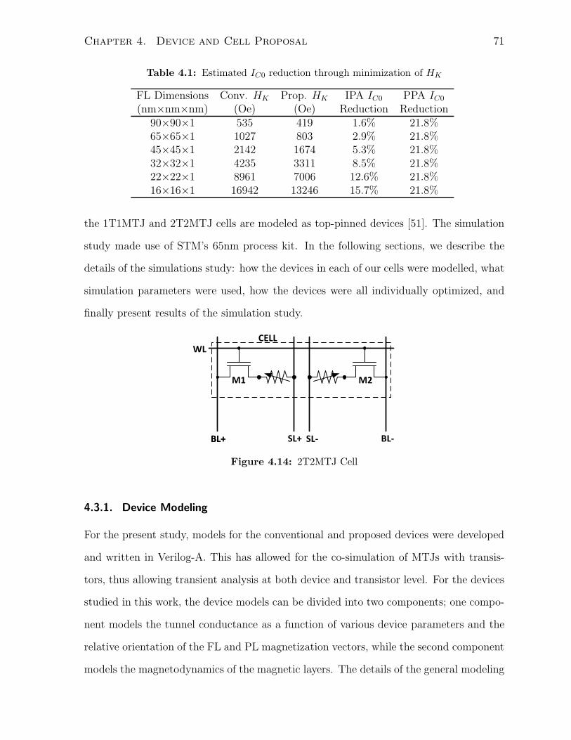
Chapter 4. Device and Cell Proposal 71
Table 4.1: Estimated IC0 reduction through minimization of HK
FL Dimensions Conv. HK Prop. HK IPA IC0 PPA IC0
(nm×nm×nm) (Oe) (Oe) Reduction Reduction90×90×1 535 419 1.6% 21.8%65×65×1 1027 803 2.9% 21.8%45×45×1 2142 1674 5.3% 21.8%32×32×1 4235 3311 8.5% 21.8%22×22×1 8961 7006 12.6% 21.8%16×16×1 16942 13246 15.7% 21.8%
the 1T1MTJ and 2T2MTJ cells are modeled as top-pinned devices [51]. The simulation
study made use of STM’s 65nm process kit. In the following sections, we describe the
details of the simulations study: how the devices in each of our cells were modelled, what
simulation parameters were used, how the devices were all individually optimized, and
finally present results of the simulation study.
WL
SL+ BL-
M1
BL+
M2
BL+ SL-
CELL
Figure 4.14: 2T2MTJ Cell
4.3.1. Device Modeling
For the present study, models for the conventional and proposed devices were developed
and written in Verilog-A. This has allowed for the co-simulation of MTJs with transis-
tors, thus allowing transient analysis at both device and transistor level. For the devices
studied in this work, the device models can be divided into two components; one compo-
nent models the tunnel conductance as a function of various device parameters and the
relative orientation of the FL and PL magnetization vectors, while the second component
models the magnetodynamics of the magnetic layers. The details of the general modeling

Chapter 4. Device and Cell Proposal 72
approaches are discussed below.
4.3.1.1. Tunnel Model
As discussed in the previous chapter, we used Equation 3.9 to model the MTJ resistance
as a function of θ - the relative angle between the magnetization vector of two adja-
cent layers - and the applied bias, V . However, in additon to modelling the θ and bias
voltage dependence on the MTJ resistance, for the purpose of device optimization it is
also imperative to model the effect of the oxide barrier thickness on tunneling resistance
and TMR. The tunnel resistance is a function of the dimensions of the oxide barrier -
namely the area of the barrier and the thickness of the barrier. The tunnel resistance
is inversely proportional to the cross sectional area of the barrier (as is typically the
case for most resistive materials), and is an exponential function of oxide thickness, as
confirmed by several experiments discussed in the literature comparing MTJ resistance
to the dimensions of the oxide barrier [49] [50]. The exponential relationship between
tunneling oxide thickness and tunneling resistance was also theoretically predicted by the
Brinkmann model [32], which provides an estimate of the tunneling resistance based on
the material parameters of the tunneling barrier. However, in addition to the tunneling
resistance, TMR is also a function of oxide thickness. TMR has been qualitatively pre-
dicted to be an increasing function of oxide thickness [18]; while this trend is somewhat
confirmed by experimental data [49] [50], TMR has been shown to decrease for large
oxide thicknesses [50], and can even display oscillatory behavior over a range of oxide
thickneses [49]. In lieu of a quantitative model relating oxide thickness to TMR, for this
work we used recent experimental data which presents both tunneling resistance and
TMR data over a range of oxide thicknesses [52]. In modeling resistance versus oxide
thickness, we fit an exponential model of the form R(tOX) = R0etOX to the experimental
data, while for modeling TMR versus oxide thickness, we built a simple piece-wise linear
model directly from the experimental data, instead of attempting to find a functional
relationship between TMR and oxide thickness.

Chapter 4. Device and Cell Proposal 73
4.3.1.2. Magnetodynamics Model
The modeling of the magnetodynamics of the devices considered in this study follows the
modeling approach described in Section 3.2.2.2, except we use Equation 3.13 to model
the torque acting on the FL, where η(θ) is again equal to PS/(1 + P 2Scos(θ)).
4.3.1.3. Device Dimensions
For the conventional MTJs considered in this study (found in both the conventional
1T1MTJ cell and the differential cell), we chose the FL dimensions to be: 60nm (length),
60nm (width), and 1nm (thickness). These dimensions are annotated on the conventional
MTJ shown in Figure 4.15.
60 nm60 nm
1 nm
Pinned Layer (PL)
Free Layer (FL)
Metallic Contact
Metallic Contact
Figure 4.15: Conventional MTJ with annotated dimensions
For the proposed device however, due to the fact that an additional metallic contact is
required adjacent to the tunneling barriers, the FL for the proposed device must be larger
than that of a conventional MTJ. This is similar to the case of a previously proposed 3-
terminal MTJ [44]. We use the same lambda design rule based analysis used in previous
work [44] to estimate the volume for the FL in the proposed device, given identical process
node as the conventional MTJ. Since the spacing between the additional metallic contact
and the tunneling barriers is half the width of the contact/oxide area, adding a contact
adjacent to the oxide area results in increasing the FL area by 250%. This is shown in
the following figure.

Chapter 4. Device and Cell Proposal 74
Top Pinned Layer (TPL)
Oxide Layer
Free Layer (FL)
Metallic Contact
Oxide Layer
Bottom Pinned Layer (BPL)
Metallic Contact
Metallic Contact
4λ 4λ2λ 4λ
Extended Region STT Region
Figure 4.16: Proposed MTJ with annotated dimensions
Thus the total FL area for the proposed device is 10λ×4λ, thus confirming the 250%
volume increase. Therefore, the dimensions of the FL for the proposed device are: 150nm
(length), 60nm (width), and 1nm (thickness).
An important point to note is that, as shown in the figure, the FL can be divided into
two regions: an STT region and an extended region. The STT region refers to the region
of the FL that overlaps with the tunneling barriers; this region corresponds to the region
where electrons tunneling to/from either the TPL or BPL transfer torque to the FL. The
extended region on the other hand is there to accommodate the metallic contact. As
such, angular momentum is transferred from either the TPL or BPL to the FL at the
STT region, but then this transferred angular momentum must be shared with the rest
of the FL, resulting in effectively a diminished torque per unit magnetic moment. As
such, a simple method to increase the torque per unit current for the proposed device is
to reduce the volume of the extended region. One possibility is to reduce the thickness
of the FL in the extended region compared to the thickness in the STT regions. Another
possibility is to explore fabrication techniques that would allow for the extended region
to comprise of a non-magnetic material, while the STT region is of course still magnetic.
Therefore, there exists much future work that could potentially reduce the penalty to the
torque per unit current the proposed device incurs as a result of increased FL volume.

Chapter 4. Device and Cell Proposal 75
4.3.1.4. Material Parameters
Material parameters for the devices were chosen to match the parameters and character-
istics of existing MTJs. The main material parameters to be set are the FL’s saturation
magnetization, MS, thermal stability factor, ∆, and the Gilbert damping constant, α,
of the FL. For this study, MS was chosen to be 1050 emu/cm3, this is in line with the
saturation magnetization of CoFeB alloys [41]. For ∆, we chose a value of 55 for the con-
ventional and differential devices, as this allows for a read disturb rate of less than 10−15
given a read sense current equal to 40% of the critical current, while for the proposed
device we chose a value of 43 to ensure 10 year data retention, as previously discussed.
As for the Gilbert damping constant, α, this was tuned to yield critical current densi-
ties similar to recent experimental results. For IPA devices α was set to 0.001 and for
PPA devices α was set to 0.002, yielding critical current density of 2-3 MA/cm3 and 2.1
MA/cm3, respectively, which are consistent with experimental results presented in [53]
and [23].
4.3.2. Device Optimization
For all versions of the proposed and conventional devices, oxide thickness and access
transistor sizes were optimized for the sake of optimal performance and area efficiency.
We targeted these devices for two classes of applications: read-write applications which
on average would have an equal number of read and write operations and read-mostly
applications which on average have more read operations than write operations. To
quantify the two classes of applications, we say that in the former class of applications,
read operations occur 50% of the time while write operations occur 50% of the time.
Thus the average access time - which is a weighted average of the read and write access
times - for a read-write application is:
T 50−50AV E = 0.5TREAD + 0.5TWRITE (4.13)

Chapter 4. Device and Cell Proposal 76
For a read-mostly application, we choose to set the average number of read operations
to be 90%. Thus for the read-mostly applications targeted in this work, the average
operation time is:
T 90−10AV E = 0.9TREAD + 0.1TWRITE (4.14)
We begin with device optimization in choosing the optimal oxide thickness for all the
devices for the two target application classes mentioned. It is prudent at this point to
discuss the tradeoff in performance presented by the oxide thickness. As discussed in
the Section 4.3.1.1, the resistance of tunneling barriers is exponentially related to the
oxide thickness, therefore, increasing oxide thickness reduces the amount of current an
access transistor can provide to the device, thus increasing switching time. On the other
hand, increasing oxide thickness results in increased RSM (for the same read sense cur-
rent), thus improving read access time. By taking weighted sums of these read and
write access times for all the devices studied in this work, we were able to find opti-
mal values of oxide thickness for the two different application classes targeted here. In
other words, we found values of oxide thickness which minimized T 50−50AV E and T 90−10
AV E for
the proposed, conventional, and differential devices, for both in-plane and out-of-plane
anisotropy embodiments of each device. The plots for the average operation time versus
oxide thicknesses are shown in Figures 4.17(a) - 4.18(b). Note that the conventional
and differential cells have different curves because the differential cell offers superior read
access performance; this is because its differential read access gives it a natural two-fold
improvement in RSM over the conventional cell.
The four plots show the same overall trend: while the proposed device average op-
eration time is monotonically increasing as a function of oxide thickness over the range
shown in the figures, the average operation time for the conventional and differential
devices is non-monotonic over oxide thicknesses. This is because for the conventional
and differential devices, since the read current is limited to 40% of the critical current,
to achieve a minimum RSM (chosen to be 50mV in this study) there is a lower limit on

Chapter 4. Device and Cell Proposal 77
0.7 0.75 0.8 0.85 0.9 0.95 1 1.052
3
4
5
6
7
8
9
10
Oxide Thickness [nm]
Avera
ge O
pera
tio
n T
ime [
ns]
Proposed Cell
Differential
Cell
Conventional Cell
(a) Read-Write Application
0.7 0.75 0.8 0.85 0.9 0.95 1 1.051
2
3
4
5
6
7
8
9
10
Oxide Thickness [nm]
Avera
ge O
pera
tio
n T
ime [
ns]
Proposed Cell
Differential Cell
Conventional Cell
(b) Read-Mostly Application
Figure 4.17: Average operation time versus oxide thickness for IPA devices
the minimum resistance of the tunneling oxide (and thus a minimum value for the oxide
thickness). For the proposed device however, as previously mentioned, we are free to
increase the read sense current as the tunneling oxide thickness is decreased (to compen-
sate for the decreased tunneling resistance), and thus a desired RSM can be maintained
as oxide thickness is reduced. This explains why the average operation time continues to
decrease as oxide thickness decreases for the proposed device; the read access time does
not degrade as oxide thickness is reduced (again because RSM does not degrade as oxide
thickness is reduced), while the write access time improves, and as such the overall aver-
age operation time improves. The plot also shows that the proposed cell shows inferior
performance compared to the conventional and differential cells as the oxide thickness
is increased; this is because given identical oxide thicknesses, the proposed device has

Chapter 4. Device and Cell Proposal 78
0.7 0.75 0.8 0.85 0.9 0.95 1 1.05 1.1 1.152
3
4
5
6
7
8
9
10
Oxide Thickness
Avera
ge O
pera
tio
n T
ime [
ns]
Proposed Cell
Differential
Cell
Conventional Cell
(a) Read-Write Application
0.7 0.75 0.8 0.85 0.9 0.95 1 1.05 1.1 1.15 1.21
2
3
4
5
6
7
8
9
10
Oxide Thickness [nm]
Avera
ge O
pera
tio
n T
ime
[n
s]
Proposed Cell
Differential
Cell
Conventional Cell
(b) Read-Mostly Application
Figure 4.18: Average operation time versus oxide thickness for PPA devices
inferior write performance compared to the conventional and differential cells (as will be
discussed in Section 4.3.3). For large oxide thicknesses, due to the limited output swing
of the read circuitry, the read sense current for the proposed cell cannot be increased
to improve read performance; as such the cell’s degraded write performance cannot be
compensated for by improving read performance. This is why the overall performance
(i.e. average access time) of the proposed cell is inferior to the conventional cells for
larger oxide thicknesses.
In addition to optimizing oxide thickness, we need to optimize access transistor size
for each cell. The access transistor width affects the read and write access times in
different ways: as transistor width is increased write access time improves (since a larger
current can be applied to the cell during a write operation), however read access time

Chapter 4. Device and Cell Proposal 79
is degraded due to the increased loading on the BLs. Figures 4.19(a) - 4.20(b) show the
average operation time versus transistor sizes.
1 2 3 4 5 6 7 8 9 101
2
3
4
5
6
7
8
9
10
Access Transistor Width [multiples of minimum size]
Av
era
ge
Op
era
tio
n T
ime [
ns
]
Proposed Cell
Differential
Cell
Conventional Cell
(a) Read-Write Application
1 2 3 4 5 6 7 8 9 101
2
3
4
5
6
7
8
9
10
Transistor Width [multiples of minimum size transistor]
Avera
ge O
pera
tio
n T
ime [
ns]
Proposed Cell
Differential
Cell
Conventional Cell
(b) Read-Mostly Application
Figure 4.19: Average operation time versus transistor width for IPA cells
Again, these four plots show similar trends. For the case of read-write applications,
the differential and conventional cells show a non-monotonic characteristic over access
transistor width, while the proposed cell shows a monotonically decreasing average access
time as access transistor width is increased (over the range shown in the plot). This
is because for the differential and conventional cells, as the access transistor width is
increased past a certain width (twice the minimum width for both cases for the plot
shown), the degradation in read access time cannot be overcome by the improvement
in write access time, and as such the overall average access time is degraded. However,
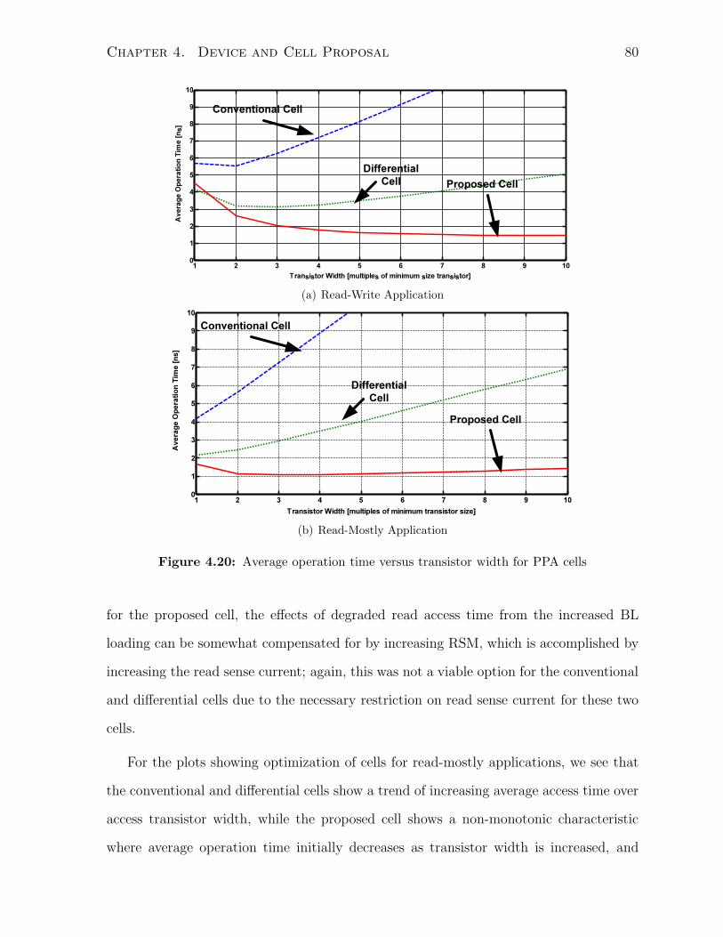
Chapter 4. Device and Cell Proposal 80
1 2 3 4 5 6 7 8 9 100
1
2
3
4
5
6
7
8
9
10
Transistor Width [multiples of minimum size transistor]
Avera
ge O
pera
tio
n T
ime [
ns]
Proposed Cell
Differential
Cell
Conventional Cell
(a) Read-Write Application
1 2 3 4 5 6 7 8 9 100
1
2
3
4
5
6
7
8
9
10
Transistor Width [multiples of minimum transistor size]
Ave
rag
e O
pe
rati
on
Tim
e [
ns]
Proposed Cell
Differential
Cell
Conventional Cell
(b) Read-Mostly Application
Figure 4.20: Average operation time versus transistor width for PPA cells
for the proposed cell, the effects of degraded read access time from the increased BL
loading can be somewhat compensated for by increasing RSM, which is accomplished by
increasing the read sense current; again, this was not a viable option for the conventional
and differential cells due to the necessary restriction on read sense current for these two
cells.
For the plots showing optimization of cells for read-mostly applications, we see that
the conventional and differential cells show a trend of increasing average access time over
access transistor width, while the proposed cell shows a non-monotonic characteristic
where average operation time initially decreases as transistor width is increased, and

Chapter 4. Device and Cell Proposal 81
then slowly increases as access transistor width is further increased. Since in read-mostly
applications the average operation time is primarily comprised of the read access time,
any degradation in read access time will degrade the overall operation time (i.e. it is
unlikely that the improvement in write access time will compensate for the loss is read
access time). For the conventional and differential cells, the improvment in write access
time cannot cover the losses to read access time, and as such the average operation time
is bound to increase as transistor width is increased. For the proposed cell, while the
read sense current can be increased as transistor width is increased to improve RSM
and thus reduce the penalty to read access time, the limitations on output swing of the
sense node (the swing is dictated by VDD and the overdrive voltage of the current source
providing the read sense current) limits the extent to which the read sense current can
be increased; as such for the proposed cell the penalty to read access time can only be
compensated for to a certain extent. This is why for the proposed cell, after a certain
transistor width, the degradation to read access time begins to result in a degradation
to the overall average operation time.
For this study, we chose to normalize cell areas between the three cells considered in
this study; we chose to first optimize the access transistor size of the conventional cells,
and then we chose access transistor sizes for the differential and proposed cells that would
minimize the difference in cell areas between all three cells. Tables 4.2 and 4.3 show the
optimal oxide thicknesses and the transistor widths chosen for the simulation study.
Table 4.2: Optimal oxide thicknesses
Read-Write Applications Read-Mostly ApplicationsConventional IPA 0.95nm 0.97nmConventional PPA 1.01nm 1.05nmDifferential IPA 0.875nm 0.925nmDifferential PPA 0.9nm 0.95nmProposed IPA 0.7nm 0.76nmProposed PPA 0.7nm 0.78nm
Finally, Figures 4.21(a)-4.21(d) show layouts of the cells in this study; all WLs are

Chapter 4. Device and Cell Proposal 82
Table 4.3: Chosen transistor widths
Read-Write Applications Read-Mostly ApplicationsConventional IPA 240nm 120nmConventional PPA 240nm 120nmDifferential IPA 120nm 120nmDifferential PPA 120nm 120nmProposed IPA 120nm 120nmProposed PPA 120nm 120nm
routed on Metal-1/Poly, while SLs and BLs are routed on Metal-2.
BL
WL
SL
Transistor
MTJ
Contact
Contact
Contact
(a) Conventional Cell, 120nm transistorwidth
BL
WL
SL
MTJ
Transistor
Transistor
Contact
Contact
Contact
Contact
(b) Conventional Cell, 240nm transis-tor width
Transistor
MTJs
BL+SL+ BL- SL-
WL
Contact
Contact Contact
Transistor
(c) Differential Cell
Proposed
MTJ
Contact
Contact Contact
SLBL1 BL2
WL
Transistor Transistor
(d) Proposed Cell
Figure 4.21: Cell layouts

Chapter 4. Device and Cell Proposal 83
4.3.3. Simulation Results: Write Performance
Figures 4.22(a)-4.23(b) show comparisons of the write performance between the different
cells considered in this study; the plots show the time evolution of the z -component of the
FL magnetization vectors during an antiparallelizing write operation (as this is the worst
case) for the devices being compared. We measure the switching time as the time taken
for the z -component of the FL magnetization vector to equal the switching threshold,
which we define to be equal to zero.
In Figures 4.22(a) and 4.22(b), we compare the write performance of cells comprising
IPA devices. Figure 4.22(a) shows the results for cells optimized for read-write applica-
tions; here we see that the switching times for the conventional, differential, and proposed
cells are 7.07ns, 8.65ns, and 8.39ns respectively. The conventional cell in this case al-
lows for a faster write access time because its access transistor width is twice that of
the differential and proposed cells, thus allowing for increased current during a write
operation.
Figure 4.22(b) shows a comparison of write performance for cells optimized for read-
mostly applications, and the switching times for the conventional, differential, and pro-
posed cells are now 10.69ns, 9.15ns, and 9.20ns respectively. The switching times have
all increased compared to the IPA cells optimized for read-write applications because in
read-mostly applications, the cell oxide thicknesses are increased (to allow for faster read
access), which degrades the write access performance.
In Figures 4.23(a) and 4.23(b), we compare the write performance of cells comprising
PPA devices. Figure 4.23(a) shows the results for cells optimized for read-write applica-
tions where the switching times for the conventional, differential, and proposed cells are
8.72ns, 6.50ns, and 7.45ns respectively. Figure 4.23(b) shows that switching times for the
conventional, differential, and proposed cells optimized for read-mostly applications are
13.62ns, 6.96ns, and 8.03ns respectively. Compared to the IPA devices, the differential

Chapter 4. Device and Cell Proposal 84
and proposed cells show an improvement in switching time, while the conventional cell
shows degradation - this is because PPA devices have lower critical current than the IPA
devices. A reduced critical current requires larger oxide thicknesses in both the conven-
tional and differential cells in order to obtain similar read sense margin compared to the
IPA devices. Since the differential cell naturally has larger read sense margin than the
conventional cell (by virtue of the differential nature of the read operation), the increase
in oxide thickness between the IPA and PPA embodiments of the differential cell was not
as large as compared to the conventional cell (an increase of 0.025nm for the differential
cell versus an increase of 0.05nm for the conventional cell). While the increase in oxide
thickness for the differential cell offsets the gains of reduced critical current, we still ob-
serve an improvement in switching time over the IPA version of the cell; however this is
not the case for the conventional cell. For the proposed cell however, since the read sense
margin is completely unrelated to the cell’s critical current, the oxide thickness does not
have to increase compared to the IPA version of the cell to maintain similar levels of read
performance.
In comparison to the differential cell, the proposed cell offers very similar switching
times for the case where the devices have IPA. When the devices have PPA however,
the proposed cell shows an increase over the differential cell of 14% and 11% in switching
time for the cases when the cells are optimized for read-write applications and read-
mostly applications, respectively. Compared to the conventional cell, the proposed cell
shows an increase in switching time of approximately 19% for the case where the cells are
comprised of IPA devices optimized for read-write applications. However, for all other
cases, the proposed cell shows an improvement in write access time: the proposed cell
shows decreases of 14% , 15%, and 41% for the cases of IPA devices optimized for read-
mostly applications, PPA devices optimized for read-write applications, and PPA devices
optimized for read-mostly applications, respectively. While the proposed device offers
various means to reduce switching time - such as reduced thermal stability and optimized

Chapter 4. Device and Cell Proposal 85
oxide thickness, in addition to ensuring the current driven torque always originates from
a PL whose magnetization vector is always antiparallel to the magnetization vector of the
FL - the simulation results show that in certain cases, the conventional and differential
cells offer faster switching This is mainly due to the fact that despite the measures
employed to reduce the switching time of the proposed cell, the degradation in spin
transfer torque due to the fact that the FL of the proposed cell is 250% the size of the
FLs in the conventional and differential cells can, in some cases, results in larger switching
times.
4.3.4. Simulation Results: Read Performance
The main advantage of the proposed cell is in its read performance, as will be shown in
this section. In Figures 4.24(a)-4.25(b), we monitor the read sense signal developed across
relevant nodes during a read operation for the conventional, differential, and proposed
cells. In memories, these signals are typically sensed and latched by a sense amplifier
circuit - these circuits typically require some minimum voltage to develop across their
input terminals to overcome effects of input offset, variation, and noise, so that the state
of the memory cells can be detected with a low error rate. For this study, we set the
required threshold to be 50 mV, and so our definition of read sense time is the time
it takes for the read sense signals to reach this 50 mV threshold. In Figures 4.24(a)
and 4.24(b), we compare the read performance for cells comprising IPA devices. Figure
4.24(a) shows the results for cells that have been optimized for read-write applications,
and the read access times for the conventional, differential, and proposed cells are 3.58ns,
1.46ns, and 1.08ns respectively. Figure 4.24(b) shows the results for cells that have been
optimized for read-mostly applications, and the read access times for the conventional,
differential, and proposed cells are 2.40ns, 1.2ns, and 0.76ns respectively.
In Figures 4.25(a) and 4.25(b), we compare the read performance for cells comprising
PPA devices. Figure 4.25(a) shows the results for cells that have been optimized for

Chapter 4. Device and Cell Proposal 86
read-write applications, and the read access times for the conventional, differential, and
proposed cells are of 4.65ns, 1.61ns, and 1.08ns respectively. Figure 4.25(b) shows the
results for cells that have been optimized for read-mostly applications, and the read access
times for the conventional, differential, and proposed cells are 2.96ns, 1.33ns, and 0.6ns
respectively. Since PPA devices have lower critical currents than their IPA counterparts,
the conventional and differential cells require reduced read sense currents to ensure a low
read disturbance rate, however this comes at the cost of increased read access times; this
is reflected in the results when comparing the simulations in Figures 4.25(a) and 4.25(b)
to Figures 4.24(a) and 4.24(b). However, this is not the case for the proposed cell since
the critical current does not limit how much current can be supplied to the cell during a
read operation.
Overall, we see that the proposed cell offers improvements in read access times over
the conventional and differential cell for all cases. Compared to a differential cell, the
proposed cell is able to achieve reductions of 26%, 37%, 33%, and 53% for the cases
of IPA devices optimized for read-write applications, IPA devices optimized for read-
mostly applications, PPA devices optimized for read-write applications, and PPA devices
optimized for read-mostly applications, respectively. Compared to a conventional cell, the
reductions in read access time are 70%, 68%, 77%, and 74% for the cases of IPA devices
optimized for read-write applications, IPA devices optimized for read-mostly applications,
PPA devices optimized for read-write applications, and PPA devices optimized for read-
mostly applications, respectively. The substantially reduced read access time for the
proposed cell is attributed to an increased read sense current which allows for larger read
sense margin (larger than the targeted 50mV sense margin for the conventional cell), and
also, the reduced oxide resistances allow for faster overall time constants for the sensing
operation.
As a verification of the immunity to read disturbance, we also plot the simulated
normalized net torque applied to the FL during a read operation for the different versions

Chapter 4. Device and Cell Proposal 87
of the proposed device studied in this work, shown in Figure 4.26. The plot shows the
value of ITPLη(θTPL) − IBPLη(θBPL), which is equal to the total spin transfer torque
acting on the FL, normalized by the term −γhη(θ)(1+α2)2eMSV ol
mFL× (mFL× ˜mTPL), during the
course of a read operation. The net torque acts to pull mFL towards ˜mBPL when the
normalized spin transfer torque term is positive, and pulls mFL towards ˜mTPL when this
term is negative. Thus these plots give insight into the direction of the net torque during
a read operation. In the figure, it is clear that for all versions of the proposed device,
during a read operation, when a “1” is stored in the cell (i.e. the FL magnetization
vector is parallel to the TPL magnetization vector), the net spin transfer torque pulls
mFL towards ˜mTPL. Similarly, when a “0” is stored in the cell, the net spin transfer
torque pulls mFL towards ˜mBPL. As such, these simulations show that the net spin
transfer torque acting on the FL during a read operation serves to refresh the existing
data in the cell, thus guaranteeing disturbance-free read operation.
4.3.5. Results Summary and Discussion
Table 4.4 summarizes the performance achieved (comparing average access times), energy
per operation, energy delay product (EDP) per operation, and cells sizes of the different
variants of the conventional, differential, and proposed cells considered in this study.
As can be seen in the table, by measure of average access time, the proposed device
offers the greatest performance in three of the four cases presented in this study, and
shows clear superiority for read-mostly applications (as is expected given its superior read
performance). One point to note is that the read operation energy for the proposed device
is larger in all cases than the conventional and differential cells; this is primarily because
the proposed cell makes use of a larger read sense current during a read operation, and the
higher read sense current results in increased power dissipation during a read operation.
However, note that as part of the design philosophy employed in optimizing this device, a
larger read sense current enables us to reduce oxide thickness, and this leads to optimized

Chapter 4. Device and Cell Proposal 88
write performance. The write operation energy of the proposed device is competitive
against the conventional and differential cells. As such, this design methodology enables
us to tradeoff write operation energy for read operation energy. Since write operation
energy is approximately an order of magnitude larger than read operation energy (over
all cases as shown in the table), it is favourable from the point of view of overall energy
consumption to sacrifice the energy efficiency of a read operation in a bid to improve
write operation energy.
From the point of view of EDP, we can see that for IPA devices, the proposed cell
is very close to the conventional cell, and the differential cell offers very poor overall
EDP. For PPA cells, we see the proposed cell offers the best overall EDP. In addition to
these benefits, it should again be stated that the cell offers guaranteed read disturbance
immunity and improved tolerance to process variation (over the conventional 1T1MTJ
cell, while the 2T2MTJ cell is anticipated to also have improved tolerance to variation),
although the proposed cell does incur the cost of increased cell area over the conventional
1T1MTJ cell. We believe that over a conventional 1T1MTJ cell, the improvement in
performance and efficiency - particularly for PPA devices, which are envisioned to become
the dominant MTJ technology in the future [26] - make the proposed cell ideally suited
for applications which allow sacrificing density for high performance, such as in emerging
embedded applications for which STT-MRAM have recently been targeted [54].
4.4. Summary
In this chapter, we presented an overview of circuit and device level techniques which were
previously proposed to tackle the challenges presented by read-disturbance in STT-MRAM.
We then presented a proposed device and cell structure which we believe will guarantee
disturbance-free read operation, and then discussed the read and write operations for
the proposed cell. We then presented a comparative study to assess the merits of the
proposed cell over the conventional 1T1MTJ as well as a differential 2T2MTJ cell, and

Chapter 4. Device and Cell Proposal 89
showed that the proposed cell offers considerable performance benefits over the conven-
tional cell in addition to (and by virtue of) its disturbance-free read operation.

Chapter 4. Device and Cell Proposal 90
0 1 2 3 4 5 6 7 8 9 10-1
-0.8
-0.6
-0.4
-0.2
0
0.2
0.4
0.6
0.8
1
Time [ns]
mZ [
no
rmalized
un
its]
Conventional Cell
Proposed Cell
Differential Cell
Switching Point (mZ = 0)
(a) Cells optimized for Read-Write application
0 2 4 6 8 10 12 14 15-1
-0.8
-0.6
-0.4
-0.2
0
0.2
0.4
0.6
0.8
1
Time [ns]
mZ [
no
rmalized
un
its]
Conventional CellProposed Cell
Differential Cell
Switching Point (mZ = 0)
(b) Cells optimized for Read-Mostly application
Figure 4.22: Write operation comparison for IPA cells

Chapter 4. Device and Cell Proposal 91
0 1 2 3 4 5 6 7 8 9 10-1
-0.8
-0.6
-0.4
-0.2
0
0.2
0.4
0.6
0.8
1
Time [ns]
mZ [
no
rmalized
un
its]
Conventional Cell
Proposed Cell
Differential Cell
Switching Point (mZ = 0)
(a) Cells optimized for Read-Write application
0 2 4 6 8 10 12 14 15-1
-0.8
-0.6
-0.4
-0.2
0
0.2
0.4
0.6
0.8
1
Time [ns]
mZ [
no
rmalized
un
its]
Conventional Cell
Proposed Cell
Differential Cell
Switching Point (mZ = 0)
(b) Cells optimized for Read-Mostly application
Figure 4.23: Write operation comparison for PPA cells

Chapter 4. Device and Cell Proposal 92
0 0.5 1 1.5 2 2.5 3 3.5 4 4.5 50
20
40
60
80
100
120
Time [ns]
Rea
d S
en
se V
olt
ag
e [
mV
]
Proposed Cell
Differential Cell
Conventional Cell
Sensing Threshold of
50mV
(a) Cells optimized for Read-Write application
0 0.5 1 1.5 2 2.5 3 3.5 4 4.5 50
20
40
60
80
100
120
140
160
Time [ns]
Read
Sen
se V
olt
ag
e [
mV
]
Proposed Cell
Differential Cell
Conventional Cell
Sensing Threshold
of 50mV
(b) Cells optimized for Read-Mostly application
Figure 4.24: Read operation comparison for IPA cells

Chapter 4. Device and Cell Proposal 93
0 0.5 1 1.5 2 2.5 3 3.5 4 4.5 50
20
40
60
80
100
120
Time [ns]
Read
Sen
se V
olt
ag
e [
mV
]
Proposed Cell
Differential Cell
Conventional Cell
Sensing Threshold
of 50mV
(a) Cells optimized for Read-Write application
0 0.5 1 1.5 2 2.5 3 3.5 4 4.5 50
20
40
60
80
100
120
140
160
180
Time [ns]
Rea
d S
en
se V
olt
ag
e [
mV
]
Proposed Cell
Differential Cell
Conventional Cell
Sensing Threshold
of 50mV
(b) Cells optimized for Read-Mostly application
Figure 4.25: Read operation comparison for PPA cells

Chapter 4. Device and Cell Proposal 94
0 1 2 3 4 5-4
-3
-2
-1
0
1
2
3
4x 10
-5
Time [ns]
I TPL
ηη ηη( θθ θθ
TPL)
- I B
PL
ηη ηη( θθ θθ
BPL)
IPA, R-W Appl.
IPA, R-M Appl.
PPA, R-M Appl.
PPA, R-W Appl.
Data = “0”
Data = “1”
Figure 4.26: Simulated normalized net torque acting on FLs of all version of proposed deviceduring a read operation

Chapter4.
Deviceand
CellProposal
95
Average Access Read Operation Write Operation Read Operation Write Operation Cell Area
Time Energy Energy EDP EDP
IPA
De-
vices
Read
Write Ap-
plications
Conv. Cell 5.32ns 0.19 pJ 1.4 pJ 0.67 pJ·ns 9.93 pJ·ns 0.567 µm2
Diff. Cell 5.06ns 0.15 pJ 2.54 pJ 0.22 pJ·ns 22 pJ·ns 0.643 µm2
Prop. Cell 4.74ns 0.3 pJ 1.51 pJ 0.32 pJ·ns 12.67 pJ·ns 0.643 µm2
Read Mostly
Applications
Conv. Cell 3.23 ns 0.13 pJ 1.33 pJ 0.3 pJ·ns 14.17 pJ·ns 0.352 µm2
Diff. Cell 2ns 0.12 pJ 2.47 pJ 0.15 pJ·ns 22.57 pJ·ns 0.643 µm2
Prop. Cell 1.6ns 0.2 pJ 1.6 pJ 0.15 pJ·ns 14.74 pJ·ns 0.643 µm2
PPA
De-
vices
Read
Write Ap-
plications
Conv. Cell 6.69ns 0.18 pJ 1.48 pJ 0.83 pJ·ns 12.89 pJ·ns 0.567 µm2
Diff. Cell 4.06ns 0.12 pJ 1.83 pJ 0.2 pJ·ns 11.87 pJ·ns 0.643 µm2
Prop. Cell 4.27ns 0.3 pJ 1.33 pJ 0.32 pJ·ns 9.91 pJ·ns 0.643 µm2
Read Mostly
Applications
Conv. Cell 4.03 ns 0.12 pJ 1.42 pJ 0.34 pJ·ns 19.39 pJ·ns 0.352 µm2
Diff. Cell 1.89ns 0.11 pJ 1.88 pJ 0.14 pJ·ns 13.09 pJ·ns 0.643 µm2
Prop. Cell 1.49ns 0.16 pJ 1.4 pJ 0.1 pJ·ns 11.24 pJ·ns 0.643 µm2
Table 4.4: Results summary

5 Conclusion
5.1. Contributions
This thesis provided a background to the physics behind STT-MRAM and provided
an overview of the current state of the art. A model to accurately predict the transient
response of MTJs was proposed and the model was compared to measurements conducted
on a set of MTJs. Due to the fact that the MTJs available to us had poor reliability, we
were unable to complete a single set of experiments on a single die. As such, some of our
measurement results did not fully correlate with the measured data. In addition, this
thesis proposed a novel STT-MRAM cell, both at the device and transistor level. To the
best of our knowledge, this cell is the first to offer true immunity to read-disturbance.
The cell has shown to offer overall superior performance (combining both read and write
performance) over the conventional 1T1MTJ cell. A summary of the contributions are:
• Background study for STT-MRAM
• Development of a model to predict transient response of MTJs
• Proposal for a novel STT-MRAM cell (A TCAS-I paper is submitted [55])
96
Chapter 5. Conclusion 97
5.2. Future Work
This thesis provides a foundation for much future work in the areas of modeling and
design of STT-MRAM cells. For modeling, the results in this thesis are inconclusive, and
so more measurement results must be obtained to validate the efficacy of the proposed
model. Alternatively, further measurement results may be used to guide other directions
for a model to predict the transient response of STT-MRAM cells. Another important
modeling goal is to encapsulate the effects of thermal agitation; these effects play a fairly
dominant role when applied pulses are longer in duration (greater than 10ns), and so
these effects need to be modeled.
With regards to the proposed device, as explained in Chapter 4, the geometry of the
proposed device is very simplistic, and further optimizations to the geometry may yield
improvements to the overall switching performance. Specifically, reducing the thickness
of the FL in the contact area or fabricating the contact area out of a non-magnetic
material would enable a reduction in the critical current. Alternative read and write
techniques not discussed in this thesis can also be explored. Finally, fabrication of a test
chip comprising the proposed device and testing the read disturb immunity theorized in
this work would be necessary.

References
[1] Takayuki Kawahara, Riichiro Takemura, Katsuya Miura, Jun Hayakawa, Shoji
Ikeda, Young Min Lee, Ryutaro Sasaki, Yasushi Goto, Kenchi Ito, Toshiyasu Me-
guro, Fumihiro Matsukura, Hiromasa Takahashi, Hideyuki Matsuoka, and Hideo
Ohno. 2 Mb SPRAM (SPin-Transfer Torque RAM) With Bit-by-Bit Bi-Directional
Current Write and Parallelizing-Direction Current Read. IEEE Journal of Solid
State Circuits, 43(1):109–120, 2008.
[2] David Halupka, Safeen Huda, William Song, Ali Sheikholeslami, Koji Tsunoda,
Chikako Yoshida, and Masaki Aoki. Negative-resistance read and write schemes
for STT-MRAM in 0.13m CMOS. 2010 IEEE International Solid-State Circuits
Conference ISSCC, pages 256–257, 2010.
[3] Kenji Tsuchida, Tsuneo Inaba, Katsuyuki Fujita, Yoshihiro Ueda, Takafumi
Shimizu, Yoshiaki Asao, Takeshi Kajiyama, Masayoshi Iwayama, Kuniaki Sugiura,
Sumio Ikegawa, Tatsuya Kishi, Tadashi Kai, Minoru Amano, Naoharu Shimomura,
Hiroaki Yoda, and Yohji Watanabe. A 64Mb MRAM with clamped-reference and
adequate-reference schemes. 2010 IEEE International Solid-State Circuits Confer-
ence ISSCC, pages 258–259, 2010.
[4] A. Driskill-Smith, S. Watts, D. Apalkov, D. Druist, X. Tang, Z. Diao, X. Luo,
A. Ong, V. Nikitin, and E. Chen. Non-volatile spin-transfer torque ram (stt-ram):
98

References 99
An analysis of chip data, thermal stability and scalability. In Memory Workshop
(IMW), 2010 IEEE International, pages 1 –3, May 2010.
[5] K.T.M. Ranmuthu, I.W. Ranmuthu, A.V. Pohm, C.S. Comstock, and M. Hassoun.
High speed (10-20 ns) non-volatile mram with folded storage elements. Magnetics,
IEEE Transactions on, 28(5):2359 –2361, Sep. 1992.
[6] J.O. Oti and S.E. Russek. Micromagnetic simulations of magnetoresistive behav-
ior of sub-micrometer spin-valve mram devices. Magnetics, IEEE Transactions on,
33(5):3298 –3300, Sep. 1997.
[7] E.L. Miller, S.A. Brandt, and D.D.E. Long. Hermes: high-performance reliable
mram-enabled storage. In Hot Topics in Operating Systems, 2001. Proceedings of
the Eighth Workshop on, pages 95 – 99, May 2001.
[8] M. Durlam, D. Addie, J. Akerman, B. Butcher, P. Brown, J. Chan, M. DeHerrera,
B.N. Engel, B. Feil, G. Grynkewich, J. Janesky, M. Johnson, K. Kyler, J. Molla,
J. Martin, K. Nagel, J. Ren, N.D. Rizzo, T. Rodriguez, L. Savtchenko, J. Salter, J.M.
Slaughter, K. Smith, J.J. Sun, M. Lien, K. Papworth, P. Shah, W. Qin, R. Williams,
L. Wise, and S. Tehrani. A 0.18 um 4mb toggling mram. In Electron Devices Meeting,
2003. IEDM ’03 Technical Digest. IEEE International, pages 34.6.1 – 34.6.3, Dec.
2003.
[9] T.W. Andre, J.J. Nahas, C.K. Subramanian, B.J. Garni, H.S. Lin, A. Omair, and
Jr. Martino, W.L. A 4-mb 0.18- um 1t1mtj toggle mram with balanced three in-
put sensing scheme and locally mirrored unidirectional write drivers. Solid-State
Circuits, IEEE Journal of, 40(1):301 – 309, Jan. 2005.
[10] M. Durlam, P.J. Naji, A. Omair, M. DeHerrera, J. Calder, J.M. Slaughter, B.N.
Engel, N.D. Rizzo, G. Grynkewich, B. Butcher, C. Tracy, K. Smith, K.W. Kyler,
J.J. Ren, J.A. Molla, W.A. Feil, R.G. Williams, and S. Tehrani. A 1-mbit mram

References 100
based on 1t1mtj bit cell integrated with copper interconnects. Solid-State Circuits,
IEEE Journal of, 38(5):769 – 773, May 2003.
[11] M. Durlam, D. Addie, J. Akerman, B. Butcher, P. Brown, J. Chan, M. DeHerrera,
B.N. Engel, B. Feil, G. Grynkewich, J. Janesky, M. Johnson, K. Kyler, J. Molla,
J. Martin, K. Nagel, J. Nahas, J. Ren, N.D. Rizzo, T. Rodriguez, L. Savtchenko,
J. Salter, J.M. Slaughter, K. Smith, J.J. Sun, M. Lien, K. Papworth, P. Shah,
W. Qin, R. Williams, L. Wise, and S. Tehrani. A 0.18 um 4 mbit toggling mram.
In Integrated Circuit Design and Technology, 2004. ICICDT ’04. International Con-
ference on, pages 27 – 30, 2004.
[12] B.N. Engel, J. Akerman, B. Butcher, R.W. Dave, M. DeHerrera, M. Durlam,
G. Grynkewich, J. Janesky, S.V. Pietambaram, N.D. Rizzo, J.M. Slaughter,
K. Smith, J.J. Sun, and S. Tehrani. A 4-mb toggle mram based on a novel bit
and switching method. Magnetics, IEEE Transactions on, 41(1):132 –136, Jan.
2005.
[13] Yiming Huai. Spin-transfer torque mram ( stt-mram ): Challenges and prospects.
AAPPS Bulletin, 18(6):33 – 40, 2008.
[14] J Slonczewski. Current-driven excitation of magnetic multilayers. Journal of Mag-
netism and Magnetic Materials, 159(1-2):L1–L7, 1996.
[15] D Ralph and M Stiles. Spin transfer torques. Journal of Magnetism and Magnetic
Materials, 320(7):1190–1216, 2007.
[16] J Slonczewski. Excitation of spin waves by an electric current. Journal of Magnetism
and Magnetic Materials, 195(2):261–268, 1999.
[17] J Slonczewski. Currents, Torques, and Polarization Factors in Magnetic Tunnel
Junctions. Physical Review B, 71(2):17, 2004.

References 101
[18] J Z Sun and D C Ralph. Magnetoresistance and spin-transfer torque in magnetic
tunnel junctions. Journal of Magnetism and Magnetic Materials, 320(7):37, 2008.
[19] T.L. Gilbert. A phenomenological theory of damping in ferromagnetic materials.
Magnetics, IEEE Transactions on, 40(6):3443 – 3449, Nov. 2004.
[20] Jiang Xiao, A Zangwill, and M D Stiles. Macrospin Models of Spin Transfer Dy-
namics. Physical Review B, 72(1):14, 2005.
[21] Dmytro Apalkov, Steven Watts, Alexander Driskill-Smith, Eugene Chen, Zhitao
Diao, and Vladimir Nikitin. Comparison of Scaling of In-Plane and Perpendicular
Spin Transfer Switching Technologies by Micromagnetic Simulation. IEEE Trans-
actions on Magnetics, 46(6):2240–2243, 2010.
[22] J Sun. Spin-current interaction with a monodomain magnetic body: A model study.
Physical Review B, 62(1):570–578, 2000.
[23] T Kishi, H Yoda, T Kai, T Nagase, E Kitagawa, M Yoshikawa, K Nishiyama,
T Daibou, M Nagamine, M Amano, S Takahashi, M Nakayama, N Shimomura,
H Aikawa, S Ikegawa, S Yuasa, K Yakushiji, H Kubota, A Fukushima, M Oogane,
T Miyazaki, and K Ando. Lower-current and fast switching of a perpendicular
TMR for high speed and high density spin-transfer-torque MRAM. 2008 IEEE
International Electron Devices Meeting, (4):1–4, 2008.
[24] C J Lin, S H Kang, Y J Wang, K Lee, X Zhu, W C Chen, X Li, W N Hsu, Y C
Kao, Yiching Lin, M Nowak, N Yu, and Luan Tran. 45nm Low Power CMOS Logic
Compatible Embedded STT MRAM Utilizing a Reverse-Connection 1T / 1MTJ
Cell. 2009 IEEE International Electron Devices Meeting IEDM, pages 279–282,
2009.
[25] Jung Pill Kim, Taehyun Kim, Wuyang Hao, Hari M Rao, Kangho Lee, Xiaochun
Zhu, Xia Li, Wah Hsu, Seung H Kang, Nowak Matt, Nick Yu, Qualcomm Incor-

References 102
porated, and San Diego. 28-1 A 45nm 1Mb Embedded STT-MRAM with Design
Techniques to Minimize Read-Disturbance. Semiconductor Manufacturing, pages
296–297, 2011.
[26] D Apalkov, V Nikitin, X Tang, S Watts, D Lottis, K Moon, A Khvalkovskiy,
R Kawakami, X Luo, A Ong, and et al. Latest advances and roadmap for in-plane
and perpendicular stt-ram. Workshop IMW 2011, 1(408):9–11, 2011.
[27] Hui William Song. A Spin-Torque Transfer MRAM in 90nm CMOS. PhD thesis,
University of Toronto, 2011.
[28] E K S Au, Wing-Hung Ki, Wai Ho Mow, S T Hung, and C Y Wong. A novel
current-mode sensing scheme for magnetic tunnel junction MRAM. Magnetics IEEE
Transactions on, 40(2):483–488, 2004.
[29] E. Seevinck, P.J. van Beers, and H. Ontrop. Current-mode techniques for high-speed
vlsi circuits with application to current sense amplifier for cmos sram’s. Solid-State
Circuits, IEEE Journal of, 26(4):525 –536, April 1991.
[30] M Pakala. Spin-transfer switching current distribution and reduction in magnetic
tunneling junction-based structures. IEEE Transactions on Magnetics, 41(10):2621–
2626, 2005.
[31] W Zhao, E Belhaire, Q Mistral, C Chappert, V Javerliac, B Dieny, and E Nicolle.
Macro-model of Spin-Transfer Torque based Magnetic Tunnel Junction device for
hybrid Magnetic-CMOS design. 2006 IEEE International Behavioral Modeling and
Simulation Workshop, pages 40–43, 2006.
[32] W F Brinkman. Tunneling Conductance of Asymmetrical Barriers. Journal of
Applied Physics, 41(5):1915, 1970.

References 103
[33] Yiran Chen, Xiaobin Wang, Hai Li, Haiwen Xi, Yuan Yan, and Wenzhong Zhu. De-
sign margin exploration of spin-transfer torque ram (stt-ram) in scaled technologies.
Very Large Scale Integration (VLSI) Systems, IEEE Transactions on, 18(12):1724
–1734, Dec. 2010.
[34] L.-B. Faber, Weisheng Zhao, J.-O. Klein, T. Devolder, and C. Chappert. Dynamic
compact model of spin-transfer torque based magnetic tunnel junction (mtj). In
Design Technology of Integrated Systems in Nanoscal Era, 2009. DTIS ’09. 4th In-
ternational Conference on, pages 130 –135, April 2009.
[35] Morgan Madec, Jean-Baptiste Kammerer, Fabien Pregaldiny, Luc Hebrard, and
Christophe Lallement. Compact modeling of magnetic tunnel junction. 2008 Joint
6th International IEEE Northeast Workshop on Circuits and Systems and TAISA
Conference, pages 229–232, 2008.
[36] M Julliere. Tunneling between ferromagnetic films. Physics Letters A, 54(3):225–
226, 1975.
[37] J Slonczewski and J Sun. Theory of voltage-driven current and torque in magnetic
tunnel junctions. Journal of Magnetism and Magnetic Materials, 310(2):169–175,
2007.
[38] P. J. Mohr, B. N. Taylor, and D. B. Newell. CODATA Recommended Values of the
Fundamental Physical Constants: 2010. ArXiv e-prints, 2012.
[39] M D Stiles and J Miltat. Spin Transfer Torque and Dynamics. Spin dynamics in
confined structures III, 101(September):1–58, 2006.
[40] C B Sawyer and Ch Tower. Rochelle salt as a dielectric. Physical Review, 35(3):269–
273, 1930.

References 104
[41] Zhitao Diao, Zhanjie Li, Shengyuang Wang, Yunfei Ding, Alex Panchula, Eugene
Chen, Lien-Chang Wang, and Yiming Huai. Spin-transfer torque switching in mag-
netic tunnel junctions and spin-transfer torque random access memory. Journal of
Physics: Condensed Matter, 19(16):165209, 2007.
[42] Jing Li, Haixin Liu, Sayeef Salahuddin, and Kaushik Roy. Variation-tolerant Spin-
Torque Transfer (STT) MRAM array for yield enhancement. 2008 IEEE Custom
Integrated Circuits Conference, (Cicc):193–196, 2008.
[43] P M Braganca, J A Katine, N C Emley, D Mauri, J R Childress, P M Rice, E Delenia,
D C Ralph, and Robert A Buhrman. A Three-Terminal Approach to Developing
Spin-Torque Written Magnetic Random Access Memory Cells. IEEE Transactions
on Nanotechnology, 8(2):190–195, 2009.
[44] N.N. Mojumder, S.K. Gupta, S.H. Choday, D.E. Nikonov, and K. Roy. A three-
terminal dual-pillar stt-mram for high-performance robust memory applications.
Electron Devices, IEEE Transactions on, 58(5):1508 –1516, May 2011.
[45] J C Sankey, Y T. Cui, R A Buhrman, D C Ralph, J Z Sun, and J C Slonczewski.
Measurement of the Spin-Transfer-Torque Vector in Magnetic Tunnel Junctions.
Nature Physics, 4(1):33, 2007.
[46] Hitoshi Kubota, Akio Fukushima, Kay Yakushiji, Taro Nagahama, Shinji Yuasa,
Koji Ando, Hiroki Maehara, Yoshinori Nagamine, Koji Tsunekawa, David D
Djayaprawira, Naoki Watanabe, and Yoshishige Suzuki. Quantitative measurement
of voltage dependence of spin-transfer torque in MgO-based magnetic tunnel junc-
tions. Nature Physics, 4(1):37–41, 2007.
[47] K T Nam, S C Oh, J E Lee, J H Jeong, I G Baek, E K Yim, J S Zhao, S O
Park, H S Kim, U-In Chung, and J T Moon. Switching Properties in Spin Transper

References 105
Torque MRAM with sub-5Onm MTJ size. 2006 7th Annual NonVolatile Memory
Technology Symposium, pages 49–51, 2006.
[48] Masahiko Nakayama, Tadashi Kai, Naoharu Shimomura, Minoru Amano, Eiji Kita-
gawa, Toshihiko Nagase, Masatoshi Yoshikawa, Tatsuya Kishi, Sumio Ikegawa, and
Hiroaki Yoda. Spin transfer switching in TbCoFeCoFeBMgOCoFeBTbCoFe mag-
netic tunnel junctions with perpendicular magnetic anisotropy. Journal of Applied
Physics, 103(7):07A710, 2008.
[49] Shinji Yuasa, Taro Nagahama, Akio Fukushima, Yoshishige Suzuki, and Koji Ando.
Giant room-temperature magnetoresistance in single-crystal Fe/MgO/Fe magnetic
tunnel junctions. Nature Materials, 3(12):868–871, 2004.
[50] Jun Hayakawa, Shoji Ikeda, Fumihiro Matsukura, Hiromasa Takahashi, and
Hideo Ohno. Dependence of Giant Tunnel Magnetoresistance of Sputtered
CoFeB/MgO/CoFeB Magnetic Tunnel Junctions on MgO Barrier Thickness and
Annealing Temperature. Japanese Journal of Applied Physics, 44(No. 19):L587–
L589, 2005.
[51] Young Min Lee, C. Yoshida, K. Tsunoda, S. Umehara, M. Aoki, and T. Sugii.
Highly scalable stt-mram with mtjs of top-pinned structure in 1t/1mtj cell. In VLSI
Technology (VLSIT), 2010 Symposium on, pages 49 –50, June 2010.
[52] Z M Zeng, P Khalili Amiri, G Rowlands, H Zhao, I N Krivorotov, J P Wang, J A
Katine, J Langer, K Galatsis, K L Wang, and H W Jiang. Effect of resistance-area
product on spin-transfer switching in MgO-based magnetic tunnel junction memory
cells. Applied Physics Letters, 98(7):072512, 2011.
[53] Yiming Huai, D Apalkov, Zhitao Diao, Yunfei Ding, A Panchula, M Pakala, Lien-
ChangWang, and E Chen. Structure, Materials and Shape Optimization of Magnetic
Tunnel Junction Devices: Spin-Transfer Switching Current Reduction for Future

References 106
Magnetoresistive Random Access Memory Application. Japanese Journal of Applied
Physics, 45(No. 5A):3835–3841, 2006.
[54] Kangho Lee and Seung H Kang. Development of Embedded STT-MRAM for Mobile
System-on-Chips. IEEE Trans Magn, 47(1):131–136, 2011.
[55] Safeen Huda and Ali Sheikholeslami. A novel stt-mram cell with disturbance-free
read operation. submitted to Transactions on Circuits and Systems-I, 2012.