System level modeling of MEMS at TU Chemnitz MEMS-Design group
Upload
khangminh22Category
view
1download
0
University of Windsor University of Windsor
Scholarship at UWindsor Scholarship at UWindsor
Electronic Theses and Dissertations Theses, Dissertations, and Major Papers
2010
MEMS based radar sensor for automotive collision avoidance MEMS based radar sensor for automotive collision avoidance
Ahmad Sinjari University of Windsor
Follow this and additional works at: https://scholar.uwindsor.ca/etd
Recommended Citation Recommended Citation Sinjari, Ahmad, "MEMS based radar sensor for automotive collision avoidance" (2010). Electronic Theses and Dissertations. 7873. https://scholar.uwindsor.ca/etd/7873
This online database contains the full-text of PhD dissertations and Masters’ theses of University of Windsor students from 1954 forward. These documents are made available for personal study and research purposes only, in accordance with the Canadian Copyright Act and the Creative Commons license—CC BY-NC-ND (Attribution, Non-Commercial, No Derivative Works). Under this license, works must always be attributed to the copyright holder (original author), cannot be used for any commercial purposes, and may not be altered. Any other use would require the permission of the copyright holder. Students may inquire about withdrawing their dissertation and/or thesis from this database. For additional inquiries, please contact the repository administrator via email ([email protected]) or by telephone at 519-253-3000ext. 3208.

MEMS BASED RADAR SENSOR FOR
AUTOMOTIVE COLLISION AVOIDANCE
By
Ahmad Sinjari
A Dissertation
Submitted to the Faculty of Graduate Studies
Through Electrical and Computer Engineering
In Partial Fulfillment of the Requirements for
The Degree of Doctor of Philosophy at the
University of Windsor
Windsor, Ontario, Canada
2010
©2010 Ahmad Sinjari

1*1 Library and Archives Canada
Published Heritage Branch
395 Wellington Street OttawaONK1A0N4 Canada
Bibliotheque et Archives Canada
Direction du Patrimoine de I'edition
395, rue Wellington OttawaONK1A0N4 Canada
Your file Votre reference ISBN: 978-0-494-81734-6 Our file Notre reference ISBN: 978-0-494-81734-6
NOTICE: AVIS:
The author has granted a nonexclusive license allowing Library and Archives Canada to reproduce, publish, archive, preserve, conserve, communicate to the public by telecommunication or on the Internet, loan, distribute and sell theses worldwide, for commercial or noncommercial purposes, in microform, paper, electronic and/or any other formats.
L'auteur a accorde une licence non exclusive permettant a la Bibliotheque et Archives Canada de reproduire, publier, archiver, sauvegarder, conserver, transmettre au public par telecommunication ou par I'lnternet, preter, distribuer et vendre des theses partout dans le monde, a des fins commerciales ou autres, sur support microforme, papier, electronique et/ou autres formats.
The author retains copyright ownership and moral rights in this thesis. Neither the thesis nor substantial extracts from it may be printed or otherwise reproduced without the author's permission.
L'auteur conserve la propriete du droit d'auteur et des droits moraux qui protege cette these. Ni la these ni des extraits substantiels de celle-ci ne doivent etre im primes ou autrement reproduits sans son autorisation.
In compliance with the Canadian Privacy Act some supporting forms may have been removed from this thesis.
Conformement a la loi canadienne sur la protection de la vie privee, quelques formulaires secondaires ont ete enleves de cette these.
While these forms may be included in the document page count, their removal does not represent any loss of content from the thesis.
Bien que ces formulaires aient inclus dans la pagination, il n'y aura aucun contenu manquant.
1*1
Canada

A MEMs Based Radar Sensor For Automotive Collision Avoidance
by
Ahmad Sinjari
APPROVED BY:
R. Mansour, External Examiner NSERC/IRC - University of Waterloo - Dept of Electrical & Computer Engineering
l/TCi^U^ 7<bm ru-A. Sodan, Outside Department Reader
School of Computer Science
/E . Abdel-Raheem, 1s t Departmental Reader department of Electrical & Computer Engineering
R/MusceHereT?*1 Depa>tmer sntal Reader Department oAEIectrical & Computer Engineering
S. Chowdhtffy, Advisor Department of Electrical & Computer Engineering
Defense Faculty of Education
October 8,2010

Author's Declaration of Originality
I hereby certify that I am the sole author of this thesis and that no part of this thesis
has been published or submitted for publication.
I certify that, to the best of my knowledge, my thesis does not infringe upon
anyone's copyright nor violate any proprietary rights and that any ideas, techniques,
quotations, or any other material from the work of other people included in my thesis,
published or otherwise, are fully acknowledged in accordance with the standard
referencing practices. Furthermore, to the extent that I- have included copyrighted
material that surpasses the bounds of fair dealing within the meaning of the Canada
Copyright Act, I certify that I have obtained a written permission from the copyright
owner(s) to include such material(s) in my thesis and have included copies of such
copyright clearances to my appendix.
I declare that this is a true copy of my thesis, including any final revisions, as
approved by my thesis committee and the Graduate Studies office, and that this thesis has
not been submitted for a higher degree to any other University or Institution.
in

Abstract This dissertation presents the architecture of a new MEMS based 77 GHz
frequency modulated continuous wave (FMCW) automotive long range radar sensor. The
design, modeling, and fabrication of a novel MEMS based TEio mode Rotman lens.
MEMS based Single-pole-triple-throw (SP3T) RF switches and an inset feed type
microstrip antenna array that form the core components of the newly developed radar
sensor. The novel silicon based Rotman lens exploits the principle of a TEio mode
rectangular waveguide that enabled to realize the lens in silicon using conventional
microfabrication technique with a cavity depth of 50 um and a footprint area to 27 mm x
36.2 mm for 77 GHz operation. The microfabricated Rotman lens replaces the
conventional microelectronics based analog or digital beamformers as used in state-of-
the-art automotive long range radars to results in a smaller form-factor superior
performance less complex low cost radar sensor. The developed Rotman lens has 3 beam
ports, 5 array ports, 6 dummy ports and HFSS simulation exhibits better than -2 dB
insertion loss and better than -20 dB return loss between the beam ports and the array
ports. A MEMS based 77 GHz SP3T cantilever type RF switch with conventional ground
connecting bridges (GCB) has been designed, modelled, and fabricated to sequentially
switch the FMCW signal among the beam ports of the Rotman lens. A new continuous
ground (CG) SP3T switch has been designed and modeled that shows a 4 dB
improvement in return loss, 0.5 dB improvement in insertion loss and an isolation
improvement of 3.5 dB over the conventional GCB type switch. The fabrication of the
CG type switch is in progress. Both the switches have a footprint area of 500 um x 500
um. An inset feed type 77 GHz microstrip antenna array has been designed, modelled,
and fabricated on a Duroid 5880 substrate using a laser ablation technique. The 12 mm x
35 mm footprint area antenna array consists of 5 sub-arrays with 12 microstrip patches in
each of the sub-arrays. HFSS simulation result shows a gain of 18.3 dB, efficiency of
77% and half power beam width of 9°.
IV

To my parents, my wife, and my kids
V

Acknowledgements
First and foremost I thank Allah subhanahu wa taala for his almighty support and
blessing without whom this work would not have completed. I would like to
acknowledge the aid and support provided by individuals and organizations. First I want
to express my sincere gratitude to my supervisor, professor Sazzadur Chowdhury for his
invaluable technical support, financial support, guidance, and encouragement. His
appreciation of my progress was a source of continuous inspiration that helped me to
make a steady progress towards the completion of this work. His encouragement to
break-through the limits rather than bypass and to take care of all minute phenomenal
possibilities in the design methodology, played the most significant role throughout this
research work.
I would like to acknowledge the financial support and encouragement provided by
the Ontario Centre of Excellence (OCE), whose interest in this research work formed the
major financial support of this project. I would like to acknowledge the financial support
provided by the Natural Sciences and Engineering Research Council of Canada
(NSERC).
I would like to thank Ansoft Corporation of Pittsburgh PA, for the collaborative
partnership that has enabled me to have access to their outstanding MEMS design
environment. Thanks for the customer supporting team for their timely response in
solving software related problems.
I would like to thank the crews at (CIRFE) Centre for Integrated RF engineering
at the university of Waterloo and university of Western Ontario during the fabrication

process of the system, for many technical discussions and interactions that have made
significant contributions in this research work.
I would like to express my deepest gratitude to my friends, peers and co-workers
associated with in the MEMS group for providing a friendly, helpful and enlightened
learning atmosphere.
Finally, special thanks to my wife, whose encouragement, support, and patience
over the past four years are just beyond words.
VI1

Table of Contents
Author's Declaration of Originality iii
Abstract i v
Dedication v
Acknowledgements vi
List of Tables xi
List of Figures xii
List of Symbols and Abbreviations xv
1. Introduction 1.1. Goal 1
1.2. Research Methodolgy 6
1.3. Principal Results 7
1.4. Dissertation organization 9
2. Research Perspective 2.1. Background 10
2.2. Radar Basics 11
2.3. Pulse-Doppler vs FMCW Radar 16
2.4. Automotive Radar 17
2.5. State-of-the-Art in Automotive Radars 18
2.6. Beamforming in Automotive Radars 22
2.6.1 Analog Beamforming 23
2.6.2 Digital Beamforming 24
2.7 Rotman Lens Beamformer 26
2.7.1 Microstrip Rotman Lens 27
2.7.2 Synthesized Rotman Lens 28
2.7.3 Dielectric Rotman Lens 28
2.8 RF Switching 30
2.9 Antenna System 32
2.10The MEMS Radar 34
viii

3. New Radar Architecture and MEMS Rotman Lens 3.1 Architecture of MEMS Radar 36
3.1.1 Radar type selection 36
3.1.2 Frequency Selection 37
3.1.3. Beamformer selection 38
3.1.4 Switch selection 38
3.1.5 Antenna Selection 38
3.1.6 Signal processor selection 38
3.1.7 New Radar Sensor Architecture 39
3.2 Rotman Lens Design Principles 40
3.3 Rotman Lens Design for Automotive Radar 43
3.3.1 Rotman Lens Design Methodology 44
3.3.2 New Approach of Rotman Lens Design 45
3.4 Fabrication 55
3.5 Conclusions 60
4 MEMS SP3T RF Switch 4.1 MEMS RF Switch Overview 61
4.2 Cantilever MEMS RF Switches 62
4.3 Bridge MEMS RF Switches 63
4.4 Design of SP3T MEMS RF Switch for 77 GHz Radar 64
4.5 CG MEMS SP3T RF Switch 66
4.6 Material Selection 66
4.7 Mathematical Modeling 67
4.8 HFSS and IntelliSuite Simulation Results for Both Types of RF Switches 69
4.9 Fabrication 75
4. lOConclusions 79
5. Microstrip Patch Antenna 5.1 Microstrip Antenna Overview 80
5.2 Microstrip Antenna 80
5.3 Microstrip Single Patch Design 84
ix

5.4 Design Requirements for Target Automotive Radar Antenna 88
5.5 Microstrip Antenna Array Design Considerations 88
5.5.1 Microstrip Antenna array Design 88
5.6 Microstrip Antenna Simulation Results 92
5.7 Microstrip Antenna Fabrication 94
5.7.1 Microstrip Antenna Array Fabrication Steps 96
5.8 Conclusions 98
6 Conclusions and Future Work 6.1 Conclusions 99
6.2 Future work 101
References 103
Appendices
Appendix A: Program code for Rotman lens design 109
Appendix B: Program code for (SP3T) switch design 143
Appendix C: Release recipe for the Single pole triple through (SP3T) switch.. 180
Appendix D: Program code for microstrip antenna design 181
VITAAUCTORIS 216
X

List of Tables Table 2.1 Road fatalities per 100,000 inhabitants 10
Table 2.2 Rank change order of the global burden of disease 11
Table 2.3 Commercially available new generation of automotive radar systems 20
Table 2.4 Bosch LLR3 Radar sensor features 20
Table 2.5 Requirements for Future Radar Systems 21
Table 3.1 Rotman Lens Final Design Specifications 55
Table 4.1 Layer Names, Thickness and Mask Level 67
Table 4.2 SP3T Design Specifications 69
Table 4.3 SP3T RF performance summar 74
Table 5.1 RT 5880 Specifications 84
Table 5.2 Microstrip Antenna Array Specifications 92
xi

List of Figures Figure 1.1 Phased array based automotive radar 4
Figure 1.2 Improved version of the phased array based automotive radar 5
Figure 2.1 Pulse characteristics in a pulsed-radar 12
Figure 2.2: Transmit signal frequency for FSK-CW radar 13
Figure 2.3 Up sweep and down sweep signal characteristics in a FMCW radar 14
Figure 2.4 A car fitted with radar 17
Figure 2.5 Different range radar system in a vehicle 18
Figure 2.6 Analog beamformer with power and phase adjustment to rotate the beam.. ..23
Figure 2.7 Bosch LLR automotive radar 24
Figure 2.8 Toyota CRDL 77 GHz LRR radar sensor 25
Figure 2.9 Schematic of the intrinsic beamforming capability of the Rotman lens 26
Figure 2.10 Microstrip Rotman lens 27
Figure 2.11 Synthesized Rotman lens 28
Figure 2.12 Dielectric Rotman lens 29
Figure 2.13 RF-MEMS-based automotive radar front-end 30
Figure 2.14 MEMS cantilever type RF 31
Figure 2.15 Microstrip patch antenna 33
Figure 2.16 Microstrip antenna array 33
Figure 3.1 Block diagram of the new MEMS based radar sensor 39
Figure 3.2 Rotman lens schematic diagram 41
Figure 3.3 Target scanning angle 44
Figure 3.4 design methodology of the Rotman lens 45
Figure 3.5 TEio propagation mode in a rectangular waveguide 48
Figure 3.6 Lens contour for a=\, g=\ 49
Figure 3.7 Lens contour for a=2, g=\ 50
Figure 3.8 Lens contour for a=3, g=l 50
Figure 3.9 Lens contour for a=4, g=\ 50
Figure 3.10 Rotman lens of 2.5 urn thickness 51
Figure 3.11 Rotman lens of 10 um thickness 51
Figure 3.12 (a) Rotman lens of 50 um thickness excited from beam port 1 52
xii

Figure 3.12 (b) Rotman lens of 50 urn thickness excited from beam port 2 52
Figure 3.12 (c) Rotman lens of 50 um thickness excited from beam port 3 52
Figure 3.13 characteristic impedance of the Rotman lens 53
Figure 3.14 Return loss of the Rotman lens 53
Figure 3.15 Insertion loss between beam port 1 and array port 2 53
Figure 3.16 Insertion loss between beam port 1 and array port 3 53
Figure 3.17 Insertion loss between beam port 1 and array port 4 54
Figure 3.18 Insertion loss between beam port 1 and array port 5 54
Figure 3.19 Insertion loss between beam port 1 and array port 6 54
Figure 3.20 Silicon wafers immersed in the RCA solution 56
Figure 3.21 Rotman lens mask 56
Figure 3.22 Alcatel 601E Deep Silicon Etch 57
Figure 3.23 SEM profiles of the silicon wafers 57
Figure 3.24 Rotman lens Fabrication process diagram 58
Figure 3.25 Fabricated Rotman lens and the cap 59
Figure 3.26 Fabricated Rotman lens after bonding process 59
Figure 4.1 Cantilever MEMS RF switch 63
Figure 4.2 Bridge MEMS RF switch 63
Figure 4.3 Bias tee 64
Figure 4.4 Conventional MEMS SP3T RF GCB switch 65
Figure 4.5 HFSS simulation shows the coupling capacitance between the GCB and a
CPW line of a conventional MEMS SP3T RF operating at 77 GHz 65
Figure 4.6 CG MEMS SP3T RF switch 66
Figure 4.7 Characteristic impedance (Both GCB and CG type switches) 70
Figure 4.8 Return loss between ports 1 and 2 71
Figure 4.9 Insertion loss between ports 1 and 2 72
Figure 4.10 Isolation between ports 1 and 3 72
Figure 4.11 Isolation between ports 1 and 4 73
Figure 4.12 Cantilever collapsing simulation 73
Figure 4.13 Cantilever displacement simulation 74
Figure 4.14 Cantilever pull-in voltage simulation 74
xiii

Figure 4.15 Chromium deposition and patterning 75
Figure 4.16 Silicon Nitride deposition and patterning 76
Figure 4.17 Chromium and Gold deposition 76
Figure 4.18 Gold and chromium patterning 76
Figure 4.19 Anchor and dimple patterning 77
Figure 4.20 G2 deposition using Electron Beam Evaporation method 77
Figure 4.21 Pattern of the top gold G2 77
Figure4.22 SP3T MEMS RF switch release 78
Figure 4.23 SEM pictures of the RF switch before and after release 78
Figure 5.1 Microstrip patch antenna 80
Figure 5.2 Electric field along the patch length 81
Figure 5.3 Microstrip patch equivalent circuit 83
Figure 5.4 Physical and effective length of microstrip patch 86
Figure 5.5 Microstrip antenna array 91
Figure 5.6 Microstrip antenna array return loss 93
Figure 5.7 Microstrip antenna array gain and half power beam width (HPBW) 93
Figure 5.8 Antenna array gain versus frequency 94
Figure 5.9 Antenna array efficiency 94
Figure 5.10 Ultrafast laser pulses 95
Figure 5.11 Microstrip antenna array fabrication zones 96
Figure 5.12 Fabricated microstrip antenna array 97
Figure 5.13 SEM figures of the fabricated microstrip antenna array 97
Figure 6.1 MEMS Multimode radar block diagram 101
Figure 6.2 FPGA Reconfigurable microstrip antenna array 102
Figure 6.3 Operation modes of the MEMS based automotive radar 102
xiv

List of Symbols and Abbreviations G
F
W
w, a
V
A0
c
Sr
K
Pr
P,
K
h
oa
ob
PZT
TEl0
HFSS
RF
DRIE
Ex,Ey,Ez
Hx,Hy,Hz
K fc ZTE
On-axis focal length
Off-axis focal length
Off-axis length of the transmission path
On-axis length of the transmission path
Scanning angle
Lens numerical aperture
Wavelength of the operating frequency f
Velocity of light
Dielectric constant
Modified wavelength
Received power
Transmitted power
Array port length
Beam port length
Array port angle
Beam port angle
Lead zirconium titanium
Transverse electric mode 10
High frequency structure simulator
Radio frequency
Deep reactive ion etching
Electric field components
Magnetic field components
Cut-off wavelength
Cut-off frequency
TE]0 wave characteristic impedance

V Phase velocity
Vg Group velocity
kc Propagation constant
CIRFE Center for integrated RF engineering
UWMEMS University of Waterloo MEMS process
SP3T
FET
SPST
CPW
C
A
d
Q
V
k
E
w
t
I
VP
go
£0
W
cr
Au
Siox
HPBW
MIC's
FEA
Single-Pole-Triple-Throw
Field effect transistor
Single-pole-single-throw
Coplanar waveguide
Capacitance
Area
Distance
Charge
Voltage
Beam stiffness
Young's modulus
Beam width
Beam thickness
Length of the beam
Pull-in voltage of the cantilever
zero bias gap
Permittivity of free space
Length of the DC pad
Chromium
Gold
Silicon oxide
Half power beam width
microwave integrated circuits
Finite Element Analysis

tan 8
/ ,
h
L
Mo
c
£reff
Z0
ADS
K
Dissipation factor
Resonance frequency
Substrate height
Patch length
Permittivity of the air
Velocity of the light
The effective dielectric constant
Resonant input impedance
Advanced Design System
Guided wave length
XVll

Chapter 1
Introduction
1.1 Goal
A significant research effort is going on worldwide to develop a system that can
provide collision warning to a driver, act to avoid collisions and to provide pre-crash
warning to a driver in case a collision is unavoidable [1-5]. Realization of such systems
requires sensors, which are able to observe the complete surrounding of cars and
sophisticated signal processing algorithm to evaluate the sensor data fast and reliably.
Current vehicle mounted proximity detection systems employ sensors like
electromagnetic radars (short, medium and long range), lasers, vision-based sensors like
video cameras; GPS based systems, and ultrasonic sensors. Out of all these systems, radar
based systems offer superior performance compared to others as they work under nearly
all weather conditions whereas the performance of other systems are compromised in bad
weather situations [1,3]. Additionally radars are able to provide information about
location (distance and angular direction) and relative velocity of objects.
However, due to high cost of stand-alone manufacturing and GaAs technology,
current radar based automotive collision avoidance systems are too expensive and
automakers are reluctant to incorporate these solutions in low-end vehicles. As a result
the overall highway safety situation remains almost the same even if some of the vehicles
are equipped with advanced radar systems. To put the problem in perspective, less than
1% of vehicles running in Canadian highways are equipped with radar sensors.
MEMS technology enables to create high performance microscale devices that could
be batch fabricated using microfabrication techniques like conventional VLSI chips. The
resulting microscale devices exhibit superior performance compared to their counterparts
in terms of performance, reliability, system level integration, and overall cost. The
advantage of higher performance and miniaturization coupled with low cost batch
fabrication will enable to use these devices to realize an affordable but superior small
form-factor radar sensor that can be used in collision avoidance and pre-crash warning
systems. Instead of using electronically scanning phased array principle as employed by
1

state-of-the-art automotive radars, MEMS based radio frequency (RF) components such
as Rotman lens, RF switches, antennas, filters, etc. can be used to realize a high
performance smaller size radar that can be mass produced cost-effectively due to the
batch fabrication capability. As the Rotman lens that exploits the physical geometry of a
cavity to realize a directional beam without any signal processing, a microfabricated
Rotman lens can eliminate the use of conventional microelectronic beamforming to
minimize the latency time and integration issues while improving system reliability and
thermal management situations. Similarly, MEMS based RF switches can be used to rout
the signal among different components of the radar sensor with a much superior
performance in terms of return loss, insertion loss and isolation compared to
microelectronic microwave switches.
The basic idea is to minimize and replace conventional microelectronic components
in a typical radar sensor by superior performance but low cost MEMS based components
to realize a compact small form-factor cost effective high performance radar sensor that
will have much higher penetration rate in the automotive market, and consequently will
help to minimize life losses and property damage due to automotive collisions.
Consequently, the overall highway safety situation will be dramatically improved. In this
context, the over all goal of this dissertation is to develop a radar architecture using
MEMS based Rotman lens and RF switches and design and fabricate the MEMS based
RF components and a microstrip antenna array that can be used to realize the developed
radar architecture.
Market research firm Strategy Analytics predicts that over the period 2006 to 2011,
the use of long-range distance warning systems in cars could increase by more than 65
percent annually, with demand reaching 3 million units in 2011, with 2.3 million of them
using radar sensors. By 2014, 7 percent of all new cars will include a distance warning
system, primarily in Europe and in Japan [6].
Global auto industries and governments are extensively pursuing radar based
proximity detection systems for 1) ACC support with Stop & Go functionality, (2)
collision warning, (3) pre-crash warning, (4) blind spot monitoring, (5) parking aid
(forward and reverse), (6) lane change assistant, and (7) rear crash collision warning. The
European Commission (EC) has set an ambitious target to reduce road deaths by 50% by
2

the end of 2010. German government formed a consortium called KOKON (which is a
consortium of semiconductor manufacturers Infineon and Atmel, the automotive sensor
suppliers Bosch and Continental Automotive Systems, and the car manufacturer Daimler-
Chrysler that are supported by several universities and institutes) to develop 77/79 GHz
radar systems and their components for automotive safety applications. The objective of
the project is to develop cost effective short range radar (SRR) and long range radars
(LRR) in order to achieve a higher market penetration of life-saving safety systems.
Similar research initiative like IVBSS, VII, VSC-2 are being pursued vigorously in the
US by the Department of transportation (DOT) and in Japan where forward collision
warning system for vehicles using a long range radar has been identified as a most critical
component for highway safety. However, due to the high price of the radar sensor based
ranging systems, only the expensive vehicles (less than 1%) in Canadian highways are
equipped with long range radars. As an outcome of the KOKON project, Infineon
developed a SiGe based 77 GHz radar chip set and is expecting that the new SiGe based
chip will be able to lower the price tag of automotive long range radar.
The development of both European and North American automotive radar technology
is relying on the 76-81 GHz frequency range as this range of frequency enables to
fabricate smaller radars and offers better performance compared to 24 GHz solutions.
The general trend of all these automotive radar systems is that 76-81 GHz frequency
modulated continuous wave (FMCW) radars based on phased array principle with
beamforming and beam steering capability are replacing the pulsed-Doppler radars that
were first introduced in vehicles in the 90s. Another trend is to develop SiGe based
chipsets to realize radar front end (transceiver, receiver and mixers) that will be cost
effective as compared to GaAs based discrete or integrated components. Though, a SiGe
based radar front-end chipset will lower the price of automotive radars to some degree,
the price reduction isn't sufficient to enable a radar in all the vehicles as a standard item
like the air-conditioner, the antenna system is still discrete, and resolution range and
distance measurement isn't adequate for some cases [7]. Additionally, though the phased
array based radar has become the current technology of choice, the time necessary to
form a beam using analog or digital microelectronics based beamforming engines
becomes a critical issue if real-time implementation is necessary.
3

The basic architecture of automotive radar working on the phased array principle is
shown in figure 1.1.
Transmitting Receiving \tHeniij Antennas
\ 7 X7 X7
Hg>
\7
A D
->0 *n
A-'I)
Signal Processing I nit
Figure 1.1 Phased array based automotive radar
This system consists of a transmitting antenna and several receiving antennas placed
along a line at equal intervals. Each receiving antenna is connected to an independent
receiver. To these receivers, a local signal separated from the transmitter signal is
supplied. The transmitted wave reflected by the object is received by the receiving
antennas. The receiver produces a baseband signal generated by synchronous detection.
After A-D conversion, the baseband signal is input to the signal processing unit, where
the direction of arrival of the received wave is estimated. Based on this configuration, the
direction resolution obtained by ESPRIT is evaluated by numerical simulation. An
implementation of such radar uses 9 receiving antennas. The problem with this
implementation is if the phase delay of one of the receivers is different from those in the
other receivers, the accuracy and resolution of angle detection by the super resolution
method are degraded. Also there is a risk that the phase delays of nine receivers may
fluctuate as a result of temperature variations. Further, the cost is increased because the
feed network of the local signal and nine receivers are needed.
4

An improved version of the basic architecture is shown in figure 1.2 where two single-
pole-triple-throw (SP3T) switches have been used to multiplex three transmit and three
receive channels to minimize the number of antennas from 10 to 6 and the number of
receivers from 9 to 1. A control circuit switches the 3 equal transmitting antennas and 3
receiving Antennas using the SP3T switches to result in one base band channel, and, after
demultiplexing in the digital domain, nine digital receiver channels are obtained for
digital beamforming. However, due to the transmission loss in the switches, the SNR is
degraded and the angular resolution may be decreased.
I ransmilter
Base Band C'ireuil ( Y V - T ^ * + ~ \
VVa'.cjaiide' 1—<f <>. it , . i , I • ^ Switch
Receiver
Figure 1.2 Improved version of the phased array based automotive radar
Investigation shows that the limitations associated with both the systems can be
overcome or minimized if the beamforming operation is shifted from electronic domain
to a passive microfabricated Rotman lens beamformer. This will drastically reduce the
system complexity, processing time, system integration, and thermal drift issues.
Additionally, if the waveguide switches are being replaced by MEMS based RF switches
that exhibit superior performance as compared to the waveguide ones, a highly improved
radar sensor can be realized. The MEMS based radar sensor can be commercialized at a
much lower cost due to the batch fabrication capability of the MEMS components.
Obviously, the current microstrip or dielectric waveguide based Rotman lens are
large enough to be fabricated using the microfabrication technology and not suitable to
realize the target small form-factor 77 GHz radar. Design of MEMS RF switches are also
5

needs to be optimized for 77 GHz to minimize the losses. As the radiating elements, high
performance microstrip antenna arrays are also needed to be designed.
In summary this dissertation investigates the development of a MEMS based
radar. The specific goals of this research are thus summarized as:
1. Develop the architecture of a MEMS based 77 GHz FMCW long range radar
sensor for automotive collision avoidance application. Due to the passive nature,
true time delay, and high reliability characteristics of the target MEMS Rotman
lens, high performance MEMS RF switches and a high gain high efficiency
microstrip patch antenna array, a relatively enhanced cycle time can be achieved
as compared to current state-of-the-art systems, and with appropriate off-the-shelf
radar front end, the target system would offer a highly compact higher
performance small form factor radar solution for automotive applications.
2. Investigate to develop a small size Rotman lens for the target radar sensor that can
be microfabricated using standard microfabrication techniques such as deep
reactive ion etching (DRIE). Carry out the design and simulation of the developed
Rotman lens for performance evaluation using industry standard software such as
HFSS, ADS, and Intellisuite.
3. Develop and realize a fabrication process sequence to fabricate the Rotman lens.
4. Design, simulate and fabricate a MEMS based SP3T switch operating in the 77
GHz range for use in the target radar sensor.
5. Design, simulate and fabricate a 77 GHz microstrip antenna array for use in the
target radar sensor
It is to be mentioned here that two other groups of students in the University of
Windsor MEMS lab are working on the packaging and FPGA implementation of the
signal processing algorithm to realize the complete radar sensor.
1.2 Research Methodology The course of developing a MEMS-based 77 GHz radar sensor involves the
following steps:
1. An extensive review of existing automotive radar sensors will be performed to
determine the state-of-the-art in automotive radar sensors and industry set
specifications of the future long range radars.
6

2. Develop the architecture of a new MEMS based radar sensor to meet or overcome
the industry set specifications for a future automotive long range radar.
3. Investigate the state-of-the-art in Rotman lens technology to design and develop a
new 77 GHz MEMS based Rotman lens.
4. Investigate the state-of-the-art in MEMS based RF switches and microstrip
antenna arrays to develop and design MEMS switches and an antenna array
suitable for use in the target radar sensor.
5. Simulation of the designed MEMS devices using HFSS, ADS and IntelliSuite
software for performance evaluation.
6. Optimization of the devices to yield maximum performance considering the
design constraints.
7. Devices fabrication.
1.3 Principal Results The principle results of this research work are summarized as follows:
1. The architecture of new MEMS based 77 GHz long range radar has been
developed for automotive collision avoidance application. A provisional patent
(US 61/282,595, March 5, 2010) has been filed in the US patent Office. The radar
has a form factor of 40 mm x 30 mm x 10 mm after packaging, which is smaller
than the state-of-the-art Bosch 3rd generation long range radar LRR3 that has
dimensions of 77 mm x 74 mm x 58 mm. The new radar architecture has been
evaluated by Keith Warble, an industry expert in radar technology who
commented that "The device is superior in architecture and can out-perform the
current industry leading state-of-the-art Bosch/Infineon LRR3 (3rd generation
long range radar) in performance and cost".
2. Novel MEMS based TE10 mode 77 GHz Rotman lens has been designed and
fabricated using deep reactive ion etching and thermo-compression bonding of
two 500 fim thick silicon wafers. The lens has 3 beam ports, 5 array ports, 6
dummy ports, and has a footprint area of 27 mm x 36.2 mm. The Rotman lens has
7

a cavity depth of 50 um with a footprint area of 11 mm x 14 mm. The lens has
been simulated using HFSS and exhibits better than -2 dB insertion loss and better
than -20 dB return loss between the beam ports and the array ports. The lens can
steer a beam by ±4 degrees.
3. Two types of MEMS based single-pole-triple-throw (SP3T) cantilever type RF
switches were designed and fabricated. One of them uses ground connecting
bridges (GCB) to connect the ground associated with different ports while the
other uses a novel continuous ground (CG) geometry. The CG configuration
SP3T switch has improved the switch performance by eliminating the coupling
capacitance between the ports and ground connecting bridges. Both the switches
have a footprint area of 500 urn x 500 urn. The GCB type switch has been
fabricated using the UWMEMS process in the University of Waterloo while the
fabrication of the CG type switch is in progress. The GCB type switch exhibits a
return loss of-16 dB. Insertion loss of-1.1 dB and maximum isolation of-13 dB
between input and the non-actuated output ports. The CG type switch exhibits a
return loss of -20 dB. Insertion loss of -0.65 dB and maximum isolation of -16.5
dB between input and the non-actuated output ports. The S-parameter values are
better than the measured values of a cantilever type MEMS RF switch published
in [36]. This validates the design of both types of switches. In summary, the CG
configuration has improved the return loss by 4 dB compared with the GCB
version of the switch. The insertion loss has improved by 0.5 dB and the isolation
has been improved by 3.5 dB.
4. An inset feed type 77 GHz microstrip antenna array has been designed and
fabricated on a Duroid RT5880 substrate. The 12 mm x 35 mm footprint area
antenna array consists of 5 sub-arrays with 12 microstrip patches in each of the
sub-arrays. HFSS simulation result shows a gain of 18.3 dB, efficiency of 77%
and half power beam width of 9°. The antenna array has been fabricated in the
Clark MXR facilities in Dexter Michigan using the PCB and laser ablation
techniques.
8

1.4 Dissertation organization Chapter 2 of this dissertation will cover the literature review of the automotive
radar.
Chapter 3 presents the architecture of the new MEMS based 77 GHz FMCW
radar sensor and design, simulation and fabrication of a novel MEMS Rotman lens, that
propagate TE)0 mode only. The air-cavity Rotman lens forms the core beamforming and
beam steering component of the new radar sensor.
Chapter 4 will cover design and fabrication of a MEMS Single-Pole-Triple-Throw
(SP3T) RF switch to sequentially feed the FMCW signal among the beam ports of a
microfabricated Rotman lens that forms an integral part of a MEMS based 77 GHz
automotive radar sensor. The series type MEMS RF switch relies on electrostatic
actuation of a microfbaricated cantilever beam and incorporates 1 input port and 3 output
ports. Two different versions of the MEMS RF switch have been designed: a ground
connecting bridge (GCB) conventional geometry where microfabricated bridges have
been used to provide the ground connectivity and a new continuous ground (CG) without
any bridge. Both the switches have been optimized for operation in the 77 GHz; however,
the CG version provides improved performance as it eliminates the effects of coupling
capacitance between the ports and the ground.
Chapter 5 describe the design, simulation and fabrication of a microstrip antenna
array that forms an integral part of a MEMS based radar working in the 77 GHz range.
The microstrip antenna array incorporates 5 sub-arrays and 12 patches in each sub-array.
The design is based on a serial array inset fed method.
Chapter 6 outline the conclusions and elaborate the future research work that
could be carried out.
9

Chapter 2
Research Perspective
2.1 Background Car accidents claim the lives of 1.2 million annually and 52 million injuries
globally up to the (WHO) world health organization latest statistics. Car accidents claim a
life every 15 minutes in the U.S. Nevertheless, one-third of all accidental deaths in the
U.S. per year still involve cars. In North America alone the rate of fatalities related to
road accidents has been stagnant at approximately 43,000 per year, which sums to a huge
annual loss of life and property [8]. Table 2.1 shows the road fatality rates in selected
countries or areas
Table 2.1 Road fatalities per 100,000 inhabitants
Country or area
Australia
European Union
Great Britain
Japan
Netherlands
Sweden
United States of America
Per 100,000 inhabitants
9.5
11.0
5.9
8.2
6.8
6.7
15.2
Table 2.2 [8] shows the change in rank order for the 10 leading causes of the global
burden of disease for the years of 1990 and 2020. It shows the rank of the road traffic
injuries has been changed from 9 to 3, which means a serious research have to be done to
make the roads more safe.
10

Table 2.2 Rank change order of the global burden of disease
1990
Rank
1
2
3
4
5
6
7
8
9
10
Disease or injury
Lower respiratory infections
Diarrheal diseases
Prenatal conditions
Unipolar major depression
Ischemic heart disease
Cerebrovascular disease
Tuberculosis
Measles
Road traffic injuries
Congenital abnormalities
2020
Rank
1
2
3
4
5
6
7
8
9
10
Disease or injury
Ischemic heart disease
Unipolar major depression
Road traffic injuries
Cerebrovascular disease
Chronic obstructive pulmonary disease
Lower respiratory infections
Tuberculosis
War
Diarrheal diseases
HIV
Canada and USA have set a target to reduce road traffic fatalities by 30% and
20% respectively by the end of 2010. The use of Forward Collision Warning long range
radar and Lane Departure Warning camera-based sensor among other security features
will become very effective to reduce road fatality rates.
2.2 Radar Basics The history of radar starts with experiments by Heinrich Hertz in the late 19th
century that showed that radio waves were reflected by metallic objects. This possibility
was suggested in James Clerk Maxwell's seminar work on electromagnetism [8].
However, it was not until the early 20th century that systems able to use these principles
were becoming widely available, and it was German engineer Christian Huelsmeyer who
first used them to build simple ship detection device intended to help avoid collisions in
fog [8].
The name radar comes from the acronym RADAR (Radio Detection and Ranging),
coined in 1940 by the U.S. Navy for public reference to their highly classified work in
Radio Detection and Ranging [9]. Thus, a true radar system must both detect and provide
11

range (distance) information for a target. Before 1934, no single system gave this
performance; some systems were Omni-directional and provided ranging information,
while others provided rough directional information but not range. A key development
was the use of pulses that were timed to provide ranging, which were sent from large
antennas that provided accurate directional information. Combining the two allowed for
accurate plotting of targets.
Radar systems can be classified by two major types: Pulsed and Continuous Wave
[10]. Both implementations have distinct operating principle, transmit signal generation,
receive signal conditioning and processing, control and synchronization issues, and
power requirements.
Pulsed Radar: Pulsed radars send short-duration in the range of a few hundred
nanoseconds, high-power (typically in kilowatts range) pulses which illuminate a target
in the line-of-sight. A pulse is essentially a sinusoid (carrier wave) at the chosen
operating frequency as shown in figure 2.1.
Pulse Repetition Period
Pulse Width
^wwvwww fWWWWW\r
Time
Figure 2.1 Pulse characteristics in a pulsed-radar.
In Pulsed radar the range and relative velocity of the target are determined as follows:
Range,
Relative velocity,
ex 71 r = •
vrel =
two-way
2
- / d x A )
(2.1)
(2.2)
12

Here, c is the speed of electromagnetic radiation in air, rtwo_way is the two-way travel
time for a pulse reflected from the target to return to the source, / d is the Doppler shift
and AQ is the operating wavelength.
The Doppler shift in the carrier wave frequency within the pulse corresponds to the
relative velocity of the target, and the time taken for the radar to detect a return of the
pulse determines the range of the target.
Continuous Wave Radar: Continuous Wave (CW) radars continuously transmit the RF
wave at a pre-specified frequency at a lower power level (typically less than 50mW). The
CW radar systems continuously receive the echo from a target over a period of time,
commonly called the Coherent Processing Interval (CPI). During the CPI, the
instantaneous transmit and receive signals are mixed, and the resultant intermediate
frequency (IF) signal is assessed over the CPI for valid targets. The CW radar technology
is still under constant refinement with new strategies related to both hardware and signal
processing algorithms being developed. There are two prime implementations of CW
radar, FSK-CW (Frequency Shift Keying) radar and FMCW (Frequency Modulated)
radar. In FSK-CW the RF frequency jumps between multiple frequencies over a CPI,
whereas FMCW makes use of a frequency chirp in a sine, saw-tooth or triangular fashion
[66]. The transmit waveforms for both CW radar types are shown in Figure 2.2.
F2-
'step
^CPI 2 7 C P I Time 'CPI ^ C P I Time
Figure 2.2: Transmit signal frequency for FSK-CW radar (left) and triangular FMCW radar (right) linear frequency up and down sweeps (or chirps).
The target range in FSK-CW radar can be determined as following:
cA<J> r = An{F2-Fx)
(2.3)
And, the relative velocity can be determined following
13

^rel _ ~ / d x ^ 0 (2.4)
Where, c is the speed of electromagnetic radiation in air, A<£ is the difference in phase
shift at the two frequencies Fx and F2, f& is the Doppler shift and A0 is the operating
wavelength. The main disadvantage of the FSK-CW radar is that it can not detect targets
in the direct path of the radar.
The up sweep and down sweep signal characteristics in a FMCW radar is shown in figure
2.3, the beat frequency for the up and down sweeps is different due to a change in range
of a moving target. If the target is stationary relative to the radar, both up and down
sweep beat frequencies will be the same. In the figure 2.3, B is the chirp bandwidth and
T is the chirp duration.
B f0
transmitting signal
up sweep f-' x down sweep A> /'
receiving signal . /
•<- K
T
i #
l U P ;
i
output signal
l"iT~ A i \
t
max. range
Figure 2.3 Up sweep and down sweep signal characteristics in a FMCW radar.
The range and velocity in FMCW radar can be calculated in the following manner:
For relatively stationary target, transmitted radar signal:
i f 1 s(/) = exp j2n fTt + -kt2
\ V 2
(2.5)
Where r = Round trip delay time=2 R/c
14

&=Rate of change of frequency =5/T
Received signal:
f f jln
V v
( ( 1 r (0 = exp jln fT{t-T)+-k{t-rf (2.6)
Mixing (2.5) and (2.6) results in:
IF(t) = exp jln fTr + ktT—kr (2.7) V v *
Differentiate the phase in (2.7) with respect to time to get instantaneous frequency:
fup=kr = k(lR/c) (2.8)
For a moving target, with velocity vr relative to the radar and assuming r0 is round trip
time, following the same methodology as the stationary target, after mixing:
IF(t) = exp jln f ( v^
fTr0+ kr0+2fT-^-lkT0^ V c c j
1 , 2 ^k
1 c
( ..2\
V v
Differentiate the phase of (2.9) signal with respect to time:
fuP=kTo + 2fT — = kT0+fd c
Similar analysis with the "down sweep" gives the result:
J down = k?Q - fd
\
t ) J)
(2.9)
(2.10)
(2.11)
Combining (2.9) and (2.10), we can extract the Doppler frequency shift and the frequency
shift due to distance to the target as:
fd
fr =
_ J up J down
J up """ J down
(2.12)
(2.13)
From fr the range R can be estimated as
15

4 J up J down
V B
And from fd the relative velocity vr can be obtained as
' f -f ' J up J down
(2.14)
V' = 2 /o (2.15)
2.3 Pulse-Doppler vs FMCW Radar FMCW radar can provide an accurate range measurement. It is also possible to
measure the range of a single target by comparing the phase difference between two or
more FMCW frequencies [9]. Range measurement with FMCW waveforms has been
widely employed, as in aircraft radar altimeters and surveying instruments. Weather
robustness of the FMCW radar options versus the mass, volume, power, and heat shield
blowout the Doppler radar features. The FMCW Radar is the lowest risk option based on
a better technological understanding of the design and its shorter development timeline.
Furthermore, it provides the weather robustness of a radar
Low cost and short range detection/localization of the FMCW radars arouse a growing
interest for civil and military applications such as automotive anti-collision radars or
target detection devices [10]. This field of application is principally devoted to FMCW
radars, which allow a direct range measurement, but are less expensive.
Some of the earlier automotive radar applications relied on a high-power Pulsed
Doppler radar technique, but the suitability of the technique came under criticism after
the televised failure of the Mercedes-Benz pulsed radar assisted Distronic cruise control
system on Stern TV in 2005 [11]. This has instigated the industry to study and use the
FMCW radar technique for modern radar systems. FMCW radar in automotive
applications is still a developing field of study, with on-going research at all system
levels including signal processing and RF hardware design.
The advantages of the FMCW radar can be summarized as:
• No lower theoretical limit to range resolution.
• Less affected by clutter.
16

• Lower power rating than Pulse radar; e.g. 100ns pulse width with 2kW peak
power, whereas 77 GHz continuous wave can operate with as low as 20mW to
same range.
• Typically, energy used by Pulse radar systems is 2.0-4.0J, whereas for CW radar
it is 1.2J-2.0J.
2.4 Automotive Radar
The first patent of radar application on car was claimed by Christian Huelsmeyer
in a German Patent on Apnl 30, 1904- In the 70's, more intensive automotive radar
developments started at microwave frequencies. A car fitted with radar in 1974 is shown
in figure 2.4.
Figure 2.4 A car fitted with radar [54].
The activities of the following decades were mainly concentrated on developments at 24
GHz, 49 GHz, 60 GHz, and 77 GHz [8]. The key driver of all these investigations has
been the idea of collision avoidance to save lives and minimize property damage. This
motivated for many engineers and scientists all over the world to develop smart vehicular
radar units. During this quite long period a lot of know-how has been gained in the field
of microwaves and in radar signal processing. Following the course, the
commercialization of automotive radar became feasible in the 90's.
17

Competing technologies in vehicular surround sensing and surveillance are ultrasonic's,
lasers and video cameras. Car manufacturers and suppliers are developing optimized
sensor configurations for comfort and safety functions with respect to functionality,
robustness, reliability and dependence on adverse weather conditions. The total system
costs have to meet the marketing targets to be attractive for the end customers. First
applications with surround sensing technologies were parking aid (based on ultrasonic's),
collision warning, and Adaptive Cruise Control (ACC).
2.5 State-of-the-Art in Automotive Radars First commercialization of the automotive radars started at late 90's. European
and US companies have been focused mainly on radar based ACC. Figure 2.5 shows the
automotive radar application portfolio, which has set an industry-wide standard for radar
systems. It has been identified that different capability radar technology can be used for
Long range radar (LRR) for ACC, medium range (MRR), short range (SRR) for stop and
go, parking aid, blind spot detection, back up, and lane change support to realize a
comprehensive collision avoidance, pre-crash warning, and collision mitigation system
by establishing a safety shell around the vehicle as shown in Figure 2.5 below.
Collision Vamine SRR
Collision Mitigation
I'recrash
Figure 2.5 Different range radar system in a vehicle [53].
In 1999, Mercedes introduced the 77 GHz "Distronic" into the S class (500 and
up) [12].Other premium models equipped optionally with an ACC, such as BMW 7
series, Jaguar (XKR, XK6), Cadillac (STS, XLR), Audi A8, and VW Phaeton. ACC is
also available in Mercedes E, CL, CLK, SL class, BMW 5 and 6 series, Audi A6, Nissan
(Cima, Primera), Toyota (Harrier, Celsior), Lexus (LS, GS), and Honda (Accord, Inspire,
Odyssey) [13]. European car manufacturers offer 77 GHz systems for ACC systems, their
18

Japanese competitors Honda and Toyota introduced an active brake assist for collision
mitigation (additionally to ACC) in 2003 based on 77 GHz long range radar (LRR)
technology [14]. In contrast to the only smooth deceleration capability of an ACC system
(because ACC is only marketed as a comfort feature), the active brake assist provides
much higher braking forces for deceleration, when a threatening situation is identified
and the driver starts braking, but maybe not as strong as it would be necessary to avoid a
crash.
A joint research project on "Automotive high frequency electronics - KOKON"
was started in September 2004, funded by the German Ministry of Education and
Research (BMBF) [15]. The consortium consists of two semiconductor companies
(Atmel and Infineon), two automotive radar sensor manufacturers (Bosch and
ContiTemic), and one automotive company (DaimlerChrysler) supported by institutes
and universities. Silicon Germanium (SiGe) has been identified as the chip technology
which may fulfill the technological requirements and the cost constraints and which
might be an alternative to already existing GaAs solutions used in 77 GHz LRR systems
[16]. Within the KOKON project the development of both 77 GHz LRR and 79 GHz
SRR radar chip technology is investigated. As spin-off cost reduction and performance
improvement of 77 GHz LRR sensors were expected.
The ROCC project essays a study of automotive radar vehicular integration and
live testing, investigation of complete sensor packaging including DSP unit(s), evaluation
of automotive radar beyond 100 GHz, SMD packaging of RF MMICs, feasibility study
for 500 GHz UWB automotive radar based on LFMCW technique, improvement of
energy efficiency and multi-mode multi-range self-calibrating sensors. The lattermost
objective is currently one of the most pursued topics in automotive radar; recent self-
calibrating dual-band MMICs such as those presented in [17] and [18] propose the
capability of switching between 24 GHz and 77 GHz SRR, MRR and LRR using the
same MMIC RF radar frontend.
Table 2.3 lists some of the commercially available automotive radar systems by
different developers and their operating specifications. The AC3 by TRW Automotive is
a third-generation adaptive cruise control radar operating at 77 GHz, capable of scanning
targets at a distance up to 250 meters [19].
19
Table 2.3 Commercially available new generation of automotive radar systems [19].
Developer
TRW Automotive
Delphi
Denso Bosch
Operation Frequency
77 GHz
76 GHz
77 GHz 77 GHz
Radar Type
Pulsed Doppler Pulsed
Doppler FMCW FMCW
Range (m)
1-250
1 -174
2-150 0.5 - 250
Relative Velocity (km/h)1
±220
-360 to +90
±200 -500 to +250
Field of
View ±8°
±10°
±20° ±30°
Refresh Time (ms)2
50
50
50 50
One of the most recent systems from Table 2.3 is the Bosch LRR3 which was
launched in September 2009 on the Porsche Panamera 2010 model. One of the claims of
Bosch LRR3 is being the world's smallest radar sensor package at 74mm x 77mm x
58mm, as it shown in tables 2.3 and 2.4.
Table 2.4 Bosch LLR3 Radar sensor features.
Frequency range
Distance
Accuracy
Relative speed
Accuracy
Vision range
Horizontal opening angle
Vertical opening angle
Modulation
Max. number of detected objects
Operating temperature
Vehicle connector
Cycle time (incl. auto diagnosis)
Dimensions (H x W x D)
Weight
Power consumption typically
ISO certification
76...77 GHz
0.5...250 m
±0.1 m
-75 ...+60m/s
±0.12 m/s
30 ° (-6 dB)
5 ° (-6 dB)
FMCW
32
-40°C...+85°C
MQS 8 Pins
typically 80 ms
77 mm x 74 mm x 58 mm
285 g
4 W
ISO 15622 Class IV sensor
20

The requirements for future radar systems to establish a safety shell around the
vehicle as shown in figure 2.5 as identified by the industry are listed in Table 2.5. [14]
Table 2.5 Requirements for Future Radar Systems [14]
Function
Parking Aid
Blind Spot Surveillanc e
ACC
ACC plus
ACC plus Stop&Go
Closing Velocity Sensing Pre-Crash Reversible Restraints
Pre-Crash Non-Rev. Restraints
Collision Mitigation
Collision Avoidance
Requirements Range/Velocity Field of view 0.2...5m 0...±30km/h full vehicle width 0.5...10m/0.5. 40m reasonable velocity interval two lane beside vehicle lm.. . l50m reasonable velocity interval three lanes in front of vehicle in 65m lm ..150m/0.5...40m reasonable velocity interval three lanes in front of vehicle in 20m 0.5m.. 150m/0.5 40m reasonable velocity interval three lanes in front of vehicle in 10m full vehicle width in 0.5m 0.5m.. 10m/0 5...30m any velocity about 45° 0.5m. .10m/0 5...30m any velocity full vehicle width in 0 5m
0.5m. ..10m/0.5... 30m any velocity full vehicle width in 0.5m
0.5m...l50m/0 5. .40m any velocity three lanes in front of vehicle in 10m full vehicle width in 0.5m
0.5m. ..150m/0.5.. .40m any velocity three lanes in front of vehicle in 10m full vehicle width in 0 5m
Sensors, Category
2-4xSRR per bumper
l-2xSRR or l-2xMRR per side lxLRR
lxLRR lxMRR
lxLRR 2xMRR
lxLRR lxMRR
2xSRR 2xMRR
2xSRR 2xMRR
lxLRR 2xMRR
lxLRR/ 2xMRR
Proposed Radar Principle UWB pulsed
FMCW/ FSK/ Pulsed
FMCW/ FSK/ Pulsed
FMCW/ FSK/ Pulsed
FMCW/ FSK/ Pulsed
FMCW/ FSK/
FMCW/ FSK/
FMCW/ FSK/
FMCW/ FSK/
FMCW/ FSK/
Proposed Carrier Frequency 24 GHz
24 GHz
77GHz
77GHz/ 24GHz
77GHz/ 24GHz
24GHz
24GHz
24GHz
77GHz/ 24GHz
77GHz/ 24GHz
Alternative Sensors
Ultrasonic
Video/ Laser
Laser
Laser
Laser
None
None
None
None
None
Remarks
100 ms cycle time
50ms cycle time
50ms cycle time
50ms cycle time Laser/Video sensor fusion reasonable
50ms cycle time Laser/Video sensor fusion reasonable
10ms cycle time
10ms cycle time function is add-on to line above very low false alarm rate 10ms cycle time function is add-on to line above ultra low false alarm rate laser/video sensor fusion requ. 10ms cycle time function is add-on to ACC plus ultra low false alarm rate laser/video sensor fusion requ 10ms cycle time function is add-on to line above ultra low false alarm rate laser/video sensor fusion requ
21

Though GaAs, or SiGe based MMIC are being pursued vigorously to minimize the cost
and size while improving the performance of automotive radars, the auto industry is
eyeing on to exploit the small cost, batch fabrication capability of the MEMS technology
to realize more sophisticated radar system that can provide improved performance over
the microelectronic based radars. The project goal of a European consortium SARFA has
been set to utilize RF MEMS as an enabling technology for performance improvement
and cost reduction of automotive radar front ends operating at 76-81 GHz. [20].
It has been determined that the radar sensors for automotive applications need to
have a beamforming, and beamsteering capability to scan the target area to precisely
determine the location of an obstacle, vehicle or a pedestrian, for example. Current
systems employ analog or digital beamforming and beamsteering techniques that employ
extensive microelectronic signal processing to realize a narrow beam that can be
electronically steered to determine the position of a target.
2.6 Beamforming in Automotive Radars Beamforming is a signal processing technique used in sensor arrays for
directional signal transmission or reception. Beamforming can be used for both radio and
sound waves. It has found numerous applications in radar, sonar, wireless
communications, radio astronomy, speech, acoustics, and biomedicine [21].
Beamforming takes advantage of interference to change the directionality of the
array. When transmitting, a beamformer controls the phase and relative amplitude of the
signal at each transmitter, in order to create a pattern of constructive and destructive
interference in the wavefront.
When receiving, information from different sensors is combined in such a way
that the expected pattern of radiation is preferentially observed. In automotive radar
systems, beamforming allows a means of electronic steering of a narrow scanning beam
to detect targets with higher angular resolution.
Beamforming involves both the generation of a directional pattern as well as steering of
the main lobe over the azimuth and also the elevation angles. Microelectronic
beamforming can be categorized into two main types:
22

• Analog Beamforming
• Digital Beamforming
2.6.1 Analog Beamforming The general layout of an analog beamformer is illustrated in figure 2.6 that can be
implemented using analog RF circuit components. A directional beam is formed at the
radiating elements after the generated RF signal is phase shifted using tuned phase
shifting elements and constant weights. An analog sine or triangle wave generator can be
used to continuously vary the phase shifting elements, which effectively causes the beam
to be steered [21].
A/2 A/2 A/2 A/2 A/2 A/2 A/2
RF Source
Figure 2.6 Analog beamformer with power and phase adjustment to rotate the beam.
Bosch 77 GHz LRR2 automotive radar has been developed to operate using this
analog beamforming concept. Fig. 2.7 shows Bosch's LRR in its 2nd generation [13].
The system has a box size of only 74 x 70 x 58 mm3 (H xW x D) and contains all sensing
and ACC functionality. The 77 GHz circuitry contains 4 feeding elements (polyrods)
directly attached to 4 patch elements on the RF board, illuminating a dielectric lens, that
results in a broad illuminating transmit beam and four single receiving beams which
partially overlap in azimuth yielding a total azimuthal coverage of ±8 degrees.
23

Figure 2.7 Bosch LLR automotive radar [13].
2.6.2 Digital Beamforming 77 GHz radar sensors with digital beamforming (DBF) front ends were introduced
into the market by Toyota motor company in 2003. Denso built a bistatic LRR with
planar patch antennas with a range capability up to 150m and a field of view of approx.
±10 degrees [11].
The Toyota CRDL 77GHz LRR radar shown in Figure.2.8, switches 3 equal
transmitting antennas and 3 receiving antennas resulting also in one base band channel,
and, after demultiplexing in the digital domain, nine digital receiver channels for digital
beamformer. Toyota claimed that they have developed a high-functionality, compact
millimeter-wave radar sensor that is applicable to convenience systems and active safety
systems simultaneously, but they claimed also that it will not be viable in mass
production phase.
24

Traiibmilliiig Antenna
Transmitter
Signal Processing Unit
Figure 2.8 Toyota CRDL 77 GHz LRR radar sensor
Digital control circuits will replace the analog circuits to control the phase and power
of the signal fed at every antenna patch, digital control offers the following advantages
[21-22].
• Improved beamformer control: The phase at individual patch or sub-array level
can be accurately controlled. The beam shape and size can be controlled
electronically to any degree resulting in a more selective beamforming.
• Switching between multiple beams: Switching between beams of different widths
by enabling or disabling array elements or generating distinct beams using
separate sub-arrays.
• High precision control of phase shift and power: DSPs or FPGAs are powerful
tools for high-resolution high-speed precise digital control of antenna
components. These digital circuits can be used to drive high power antenna
circuits with improved control and precision as compared to conventional analog
implementations.
Digital beamformers require memory blocks, adders and multipliers as system
building blocks. These digital components are available in high-speed on-chip resources
in FPGAs which typically operate at clock frequencies of 550 MHz (e.g. Virtex 6 FPGA
by Xilinx). This makes digital beamforming techniques more feasible and efficient.
25

Digital beamforaiing does require more signal conditioning prior to digital processing. If
the signal frequency is too high (greater than 100 MHz, say) direct sampling is not
possible. To overcome this issue, the signal needs to be down-converted to an
intermediate frequency (IF) using an RF mixer which can be sampled. Various
beamformer architectures are available in [21-22].
2.7 Rotman lens Beamformer A Rotman lens [23] is a passive device that can enable a beamforming and
beamsteering capability without any microelectronic signal processing as needed by
analog or digital beamformers. During operation, the electromagnetic property of a
dielectric cavity is exploited to realize a directional in-phase signal.
Antenna Beam ports Array ports
Figure 2.9 Schematic of the intrinsic beamforming capability of the Rotman lens [23].
A Rotman lens is a parallel plate architecture that has beam ports on one side and
array ports on the opposite side of a dielectric material filled cavity as shown in Figure
2.9. An input signal fed at any of the beam ports travel different distances through the
lens cavity to reach a pre-specified number of array ports positioned along the outer lens
contour depending on the dimension of the lens cavity and the shape of the lens contours.
By properly choosing the lens contours, lens cavity geometry, and the dielectric material
filling the lens cavity, it is possible for the signals arriving at the array ports to add up in
phase that in effect realizes a beam that is steered in a particular direction. The beam is
then radiated through a suitable antenna system. For example, if a signal is incident at the
beam port 2, it will produce a beam of 0° phase shift at the array ports (beam 2), while if
a signal is incident at the port 1 or 3, it will produce a beam that is steered by an angle of
± a at the array ports shown beams 1 & 3 in the figure. Thus, by sequentially switching
26
the signal through the beam ports, the radiating beam from the array ports can be steered
by an angle determined from the position of the beam ports. Detailed design methodology
of a Rotman is presented in chapter 3. Typical Rotman lenses are large and are realized
using micro strip geometries or dielectric material filled waveguides.
The Rotman Lens features a true time delay phase shift capability and removes
the need for costly phase shifters to steer a beam over wide angles. The Rotman Lens has
a long history in military radar, but it has also been used in communication systems. The
United States Army use it in C band (4-8 GHz) up to Ka Band (27.5-31 GHz) [24], [25].
The broadband performance of Rotman Lenses meets a key need of allowing the same
antenna system to serve multiple functions, thus further reducing cost, complexity, and
weight. Detailed techniques to design a conventional Rotman lens are available in [24-
27].
Rotman lens could be categorized as following:
2.7.1 Microstrip Rotman Lens
In a microstrip Rotman lens, the lens geometry is formed by etching the topside
metal cladding of a wafer with a desired dielectric constant and the other side cladding
serves as the ground plane. Representative designs of microstrip type Rotman lens are
available in [4-7]. The layout of a 77 GHz microstrip Rotman lens that has been
fabricated as a printed circuit on a dielectric substrate is shown in figure 2.10 [2].
Figure 2.10 Microstrip Rotman lens [2].
27

Although the Rotman lens of this category has a conformal geometry, the lens suffers a
high interference between the adjacent beam and array ports, mutual coupling, fringing
field and is limited to low power and low beamdwidth applications as only higher order
modes can propagate through the lens. In this type of Rotman lens, the beamwidth
usually is adjusted by combining adjacent beams to produce a broader beam with a lower
gain that results in a high fabrication cost.
2.7.2 Synthesized Rotman Lens
In [27] a Rotman lens is presented that has dielectric contours of varying
permittivity within the lens cavity. The varying permittivity is realized through a
synthesized dielectric technique, where a periodic lattice of holes is formed within the
dielectric substrate. The top side of the fabricated lens is shown in Figure 2.11 (a), while
the bottom side is shown in Figure 2.11 (b). The region of synthesized dielectric material
is placed upon a copper ground plane. The design improves the insertion loss by 1.2 dB
and it is usable only up to 11 GHz. The frequency limit of 11 GHz makes this type of lens
unsuitable for fabrication using typical micromachining techniques as the fabrication of
the synthesized dielectric layer involves etching of quarter wavelength (A/4) deep holes of
pre-specified diameters.
Arra'i ports
Beam ports
(a) Top side (b) Bottom side
Figure 2.11 Synthesized Rotman lens.[27]
2.7.3 Dielectric Rotman Lens
The dielectric Rotman lens consists of a dielectric slab, tapered slot (TS)
structure, and the transitions between the antipodal slots and microstrip lines [28]. The
top and side views of the lens are shown in figures 2.12 (a) and (b) respectively.
The top conductor in shown in black in the lens geometry, and the bottom
conductor in shown in hatched lines. A major drawback of this lens is the mutual
28

coupling between the adjacent ports that leads to change in the characteristic impedance
seen at the port due to the presence of nearby elements which makes the impedance
matching more difficult and a high drop in the power transferred from the beam ports to
the array ports (lower efficiency).
(b)
Figure 2.12 Dielectric Rotman lens (a) top view (b) side view.[28]
The above mentioned three categories of Rotman lens can't be realized using
microfabrication technology to fabricate them at 77 GHz, either due to their lower
efficiency and poor performance (due to interference, mutual coupling, fringing field, low
beamwidth, attenuation and impedance matching)or the availability of such high
thickness wafers.
The design of RF-MEMS-based automotive radar front-end based on phase shifters and
Rotman lens as shown in Figure 2.13 has been presented in [29]. In the design, the beam
and array ports of the low power microstnp type Rotman lens suffers a high interference
due to the small distance between the ports in the operating frequency of 77 GHz.
29

Dielectric lens - ^ Antenna columns
To p r e - a m p l ^ r ^ ^ ^ , r a n s t e i v i n g F V ^ R F - M E M S (SP4T)
mixers
Dela\ lines
^ Parallel plate line
C*-iQ mixer ^•Uunn VCO
(a) (b)
Figure 2.13 RF-MEMS-based automotive radar front-end. [29]
2.8 RF Switching
Switching signals between ports is a critical function in many microwave systems
such as radars, communications links, and electronically scanned antennas. In a radar, the
RF signal (pulse, FSK-CW or FMCW) needs to be fed to a beamforming and
beamsteering networks and the output of the beamforming and beamsteering networking
needs to be fed to an antenna system to radiate the signal. Similarly, the echoed RF signal
reflected back from the target also needs to be switched to generate a signal that can be
processed using microelectronic signal processing techniques to obtain the range, angle,
and velocity information of the target. In such an operation, the switch's insertion loss
adds directly to receiver noise figure and reduces transmitter power. Thus, low insertion
loss is an important requirement for switches to be used in a radar system. Isolation is
another very important parameter that quantifies the leakage from an "ON" to an "OFF"
port.
Advances in silicon-based processing technology in the last few decades resulted
in a rapid improvement in semiconductor based solid-state microwave switches.
However, for high frequency RF applications, these fast-acting solid-state switches
continue to have disadvantages such as low power handling capacity, high resistive
losses, higher insertion loss, relatively higher DC power consumption, and poor isolation.
Electromechanical switches, in contrast, are high power devices, but useful only at lower
RF frequencies, and operate at a much slower speed. On the other hand, heavy and bulky
waveguide type switches are not attractive to realize compact small form-factor switches
to realize low cost high performance automotive radars.
30

Advances in MEMS technology enabled to realize lost cost high performance
micromechanical RF switches that exhibit low resistive loss, negligible power
consumption, good isolation and high power handling capability compared with
semiconductor switches. Additionally MEMS RF switches can be batch fabricated and
easily integrated with the semiconductor drive and control circuits. Furthermore, being
smaller, lighter, faster and less power consuming, the MEMS RF switches and relays
have a high off-state to on-state impedance ratio. These improved performance
characteristics of MEMS RF switches can be exploited to rout signals among different
components of a highly compact small form-factor low cost high performance radar
sensor for automotive applications.
Typical operation of a MEMS cantilever type RF switch is shown in figure 2.14.
A bias voltage across the beam and the DC pad causes an electrostatic attraction force
between the beam and the DC pad that pulls the beam down towards the DC pad. At a
certain voltage, the electrostatic force overcomes the elastic restoring force of the beam
and the beam collapses on the DC pad to establish the connectivity (ON state). When the
bias voltage is withdrawn, the beam moves back to its rest position due to inertia (OFF
state). A detailed review of MEMS RF switches is presented in chapter 4.
Cantilever beam
Support T
CPW ~ V i i _ ^-CPW RF In — ̂ M l l H f c B 3 H I i^^ssssmm-* RF Out OFF State
DC Pad
RF in - » - H M ^ H mmmm immmum-*- RF Out ON state
Bias voltage
Figure 2.14 MEMS cantilever type RF.
A cantilever type MEMS switch was presented in [30] to be used in the range of 9.5-13
GHz; it is (600x600) um2 in size. It exhibits a return loss of-20 dB, insertion loss of-1
dB, isolation of-28 dB and actuation voltage of 65 V.
31

In [31] a capacitive type RF MEMS switch was presented to be used at 60 GHz, it has a
membrane size of (10x240) jim2. It exhibits a return loss of-25 dB, insertion loss of-0.2
dB, isolation of-15 dB and actuation voltage of 10 V.
The performance of a cantilever MEMS RF switch was reported in [32]. It has been
designed to operate at 40 GHz and it exhibits a return loss of -27 dB, insertion loss of-0.7
dB.
The goal of this research work is to design and fabricate a high performance MEMS
based RF switch to be used as an integral part of the system.
2.9 Antenna System The Antenna subsystem forms an integral part of a radar sensor to radiate and
receive the signal (pulse, FSK-CW of FMCW) that enables to determine the range,
velocity, or location of the target. There are different kinds of antennas used in
automotive radars like horn antenna, reflector antenna, dual reflector antenna, and
microstrip antenna Out of different types of antennae, microstrip antennas have become
the technology of choice for automotive radars for their simple and inexpensive
manufacturing using modern printed-circuit technology. They are mechanically robust
when mounted on rigid surfaces, compatible with MMIC designs, and when the particular
patch shape and mode are selected, they are very versatile in terms of resonant frequency,
polarization, pattern, and impedance.
Microstrip antennas are planar resonant cavities that utilize the fringing fields
along the edges of a microstrip patch to radiate electromagnetic energy. A typical
microstrip patch antenna consists of a very thin metallic strip (patch) of thickness /
placed on a dielectric substrate of thickness h and of dielectric constant of sr above a
ground plane as shown in figure 2.15.
The metallic patch can take many different configurations. The rectangular and
circular patches are the most popular because of ease of analysis and fabrication, and
their attractive radiation characteristics, especially low cross-polarization radiation.
32

Microstrip transmission line |-
"l
/ Microstrip antenna
Microstrip transmission line
Dielectric substrate
Microstrip antenna
Dielectric substrate
Ground plane
Figure 2.15 Microstrip patch antenna.
An array of patches has to be used to get certain gain, directivity and efficiency required
by the application to be performed using the microstrip antenna array. Figure 2.16 shows
a microstrip antenna array.
C LI LI LI LI LI LI LI LI LI LI LI I T_rT_j-T_JTL_j-T_j-T_jnL_rT_j-r_rT_jnLjnLj _frn_rr- i_jrn_jrn_x— i_x - i_x—Ljrn-rr- i j r -Ljr-Lin
r f T I~T r~r I T I T I T rnr r~T I T r~r r~r I
T_J-T_rT_JT_JT_JT_JT_JT__JT_JT_JT_JT_J _TTLi-n_jr- i_rr-Lxn_rr-urT_x--LX-^^
T_JT_JT_JT_JT_JT_JT_JT_JT_JT_JT__rT_J
T_J-TL_rT__rT_JT_JT_JT__rT_JT_JT_JT__rT_J Figure 2.16 Microstrip antenna array.
Recent microstrip antenna arrays are using different ways to feed the patch,
number of patches required by the specific application to get the gain and directivity
required [33-40]. Detailed analysis of microstrip antenna arrays is providing in chapter 5.
33

A microstrip antenna array was presented in [40] in which corporate feed was used to
feed the array in the 77 GHz range. It has a gain of 17.5 dB, return loss of -7 dB,
efficiency of 69% and half power beamwidth of 12°.
In [41] a corporate feed microstrip antenna array was presented to be operated in the
range of (32-36) GHz. It has a HPBW of 27°, gain of 16 dB.
A 2x8 microstrip corporate feed antenna array is presented in [42] to be used in 12 GHz,
it exhibit a return loss of-15 dB, gain of 20 dB and half power beamwidth of 10°.
All above mentioned designs are using corporate feed which suffers high RF losses due
to the feed line lengths. They also use a normal rectangular patch that lead to a lower gain
microstrip antenna array.
2.10 The MEMS Radar
The MEMS technology will have a great impact in automotive radar sensors by
introducing electronically scanned arrays (ESA) using recent UWB antenna array
developments, true-time-delay beamformers, transmit/receive (T/R) switches and
tuneable matching networks [43]. The integration of RF MEMS radar components in
automotive radar subsystems will make the new generation of automotive radars more
efficient, reliable and cost effective. It incorporate passive electronically scanned arrays
(lens arrays, and beamformers), passive subarrays, and T/R modules for active
electronically scanned arrays [44]
The application of an automotive radar system is classified according to the range
it covers. Long range radar (LRR) and medium range radar (MRR) are used in cruise
control and collision avoidance, and short range radar (SRR) is used in collision
avoidance, crash-prevention and parking-assist systems.
Having established that automotive radar can be very helpful in reducing the
number of fatal accidents, it is essential that low cost and reliable radar systems be made
to improve road safety globally. Lower cost (compared to $3000-$5000 approx. for
current systems) will enable even lower-end vehicles to be equipped with safety options,
boosting road safety. MEMS technology offers the advantage of realizing low cost batch
34

fabrication of high performance RF components like Rotman lens, RF switches that can
be sued to realize compact high performance lightweight radar in a small form factor.
35

Chapter 3
New Radar Architecture and MEMS Rotman
Lens This chapter presents the architecture of the new MEMS based 77 GHz FMCW
radar sensor and design, simulation and fabrication of a novel MEMS Rotman lens. The
TEio mode air-cavity Rotman lens forms the core beamforming and beam steering
component of the new radar sensor. The Rotman lens has a footprint area of 27 mm x36.2
mm including the transmission lines, incorporates 3 beam ports, 5 array ports, and 6
dummy ports. The Rotman lens has a cavity depth of 50 um with a cavity footprint area of
11 mm x 14 mm. The lens has been designed to steer a beam by ±4 degrees. HFSS
simulation shows that the designed Rotman lens has an insertion loss of -2 dB, return loss
of -20 dB and characteristic impedance of 50Q. The lens has been fabricated using deep
reactive ion etching and thermo-compression bonding of two 500 um thick silicon wafers.
3.1 Architecture of MEMS Radar Following the review of the state-of-the-art in automotive radars and requirements
set by the auto industry for long range radar as listed in table 2.5, a decision can be made
to select the radar type that can provide the best performance while addressing the design
constraints.
3.1.1 Radar type selection
The visible disadvantages of the 3 main radar types, pulsed, FSK-CW and FMCW
can be summarized as:
Pulsed Doppler disadvantages:
• Velocity measurement limited by blind speed when fd is a multiple of the PRF.
• Maximum measurable Doppler shift has to be less than PRF to avoid IS I among
different pulses and target returns.
• To reduce the above velocity ambiguity the PRF can be increased, however
increasing the PRF creates range ambiguity.
36

• Relatively high power requirements in the automotive scenario.
• Greater risk of jamming or confusion due to high-power pulses from other Pulsed
radars.
FSK-CW disadvantages:
• Invisible targets in the direct path of the radar.
• Target range is computed based on the difference in phase shift for two
consecutive frequency hops. This makes the system subject to phase noise.
• The CPI needs to be large enough to avoid range ambiguity.
FMCW radar overcomes these disadvantages with:
• No theoretical limit to range resolution and better short range detection.
• Reduced effects of clutter and atmospheric noise.
• Lower power rating than Pulsed radar.
• Less effects of phase noise.
• More resistance to interference from other similar radars in the vicinity.
• No theoretical blind spots.
• Resistance to jamming (frequency modulation is a common tool in ECCM -
Electronic Counter-Countermeasures to overcome jamming effects)
This qualitative comparison warrants the use of FMCW for the new MEMS radar sensor
for long range radar (LRR) application.
3.1.2 Frequency Selection
The 76-77 GHz band was regulated in the 90's followed by a standardization in
Europe (ETSI EN 301 091). Now, this band is allocated for Intelligent Transport Services
(ITS) in Europe, North America, and Japan [13]. In March 2004 the European
commission allocated the frequency range 7 7 - 8 1 GHz for UWB SRR with permitted
usage from 2005 onwards. In the USA and Canada, 77 GHz has been specified for
automotive radar applications.
37

With regard to the automotive long range radar, the maximum range (150 meters
following Table 2.5) is proportional to the effective antenna aperture size and to the
square root of the frequency. Therefore, highest frequencies should be preferred to get
smaller radar size. It will be also a cost saving approach.
3.1.3. Beamformer selection:
To eliminate the need for microelectronic based analog or digital beamforming
engine, a Rotman lens has been adopted to perform the operation of beamforming and
beamsteering.
3.1.4 Switch selection:
Instead of non-MEMS waveguide type switches, MEMS based RF switches have
been selected to feed the FMCW signal to the beam ports of the Rotman lens.
3.1.5 Antenna Selection
Microstrip based antenna arrays have been selected to radiate and receive the
signal due to their established superior performance, ease of fabrication, and small planar
geometry while offering high directivity and lower sidelobes.
3.1.6 Signal processor selection
The aspects of frequency generation, tuning and linearity become critical in
FMCW radar due to the requirement of highly linear frequency sweeps. In FMCW radar
the signal generation and sweep modulation can be accomplished using analog or digital
modulation. Analog PLLs or Phase Locked Loops containing a VCO were used in early
CW systems, however were overtaken by digital systems with better frequency response,
excellent linearity, easier design and improved performance in noise [45].
In digital implementation of a radar transmitter, the control and modulation
algorithm can be based on a Digital Signal Processor (DSP) or a Field Programmable
Gate Array (FPGA). Due to their highly parallel nature, ability to run several tasks
simultaneously without stalling other tasks, and on-chip resources (such as RAM blocks,
LUTs, fast DSP multipliers) FPGAs are the preferred solution for digital signal
processing for a radar sensor with a lower cycle time.
Even with a low clock frequency of 200 MHz the FPGA has comparable speed
performance compared to the other processors at higher clock rates. Power consumption
of a digital circuit is proportional to the total gate-level switching required to compute a
38

particular result: the higher the clock frequency and required clock cycles, the greater the
amount of switching, and thus the higher the power consumption. Given the automotive
scenario, FPGAs offer a desirable combination of speed and power efficiency.
Furthermore, to deal with possible VCO non-linearity FPGAs can be used to
implement a DDS or Direct Digital Synthesis algorithm. DDS is a method of creating
arbitrary yet repetitive waveforms using a RAM or LUT, a counter, and a DAC,
components that are readily available on FPGA platforms. DDS promises optimal
linearity in frequency sweeps, precise frequency tuning, and excellent phase error
recovery [45].
3.1.7 New Radar Sensor Architecture
Based on these decisions, the architecture of a new radar sensor has been
developed and is shown in the figure 3.1 below. The operating principle of the new radar
sensor is as follows:
77GH7 , FMCW VCO ' '
| DAC |
Switch control
%«'
~*\ ADC j
_TLn.ru~ir
SP3T switch control
Trai emitter
Signal prosesssng
Tx anitmiia
array
^ Trjrt&miited
signal
Rs antenna
dfrdy
Target velocity, range, sdfe Uibldnt-e
Dnvpf nniifieatinn
CAN Bus
^ Target
Reverted
Figure 3.1 Block diagram of the new MEMS based radar sensor.
1. An FPGA implemented control circuit generates a triangular signal (Vtune) to
modulate a voltage controlled oscillator (VCO) to generate a FMCW signal
having a frequency sweep range of 0-800 MHz centered at 77 GHz.
2. The signal is fed to a MEMS SP3T switch.
39

3. An FPGA implemented control algorithm controls the SP3T switch to
sequentially switch the FMCW signal among the three beam ports of a MEMS
implemented Rotman lens.
4. As the FMCW signal arrives at the array ports of the Rotman lens after traveling
through the Rotman lens cavity, the time-delayed in-phase signals are fed to a
microstrip antenna array that radiates the signal in a specific direction.
5. The sequential switching of the input signal among the beam ports of the Rotman
lens enables the beam to be steered across the target area in steps by a pre-specific
angle.
6. On the receiving side, a receiver antenna array receives the signal reflected off a
vehicle or an obstacle and feeds the signal to another SP3T switch through
another Rotman lens.
7. An FPGA based control circuit controls the operation of the receiver SP3T switch
in tandem with the transmit SP3T switch so that the signal output at a specific
beam port of the receiver Rotman lens can be mixed with the corresponding
transmit signal.
8. The output of the receiver SP3T switch is passed through a mixer to generate an
IF signal in the range of 0-200 KHz.
9. An analog-to-digital converter (ADC) samples the received IF signal and converts
it to a digital signal.
10. Finally, an FPGA implemented algorithm processes the digital signal from the
ADC to determine the range and velocity of the detected target. In mass volume
production, the FPGA will be substituted by an ASIC.
3.2 Rotman Lens Design Principles A schematic diagram of a typical Rotman lens is shown in figure 3.2. The inner
contour is determined by the design equations and locates the positions of the array ports.
The outer contour is a straight line and defines the positions of the radiating elements.
40

The array ports on the inner contour are connected to the radiating elements on the outer
contour via transmission lines of length W. Inner contour is defined by two coordinates
(x, y) that are specified relative to a point 0, on the central axis of the lens. Radiating
elements on the outer contour are determined by a single coordinate N. Point P on the
inner contour is connected to point Q on the outer contour by a transmission line of
length W. To obtain the path length equations, two off axis focal points Fl, F2 are defined
at the two perfect focal points and an on axis focal point F0at the center having
coordinates of (-Fcosa,Fsin«), ( - F c o s a , - F s i n a ) and (-G,0) respectively.
Focal arc l n , l e r Outer lens contour Icrii contour
Figure 3.2 Rotman lens schematic diagram.
In figure 3.2:
G is the on-axis focal length.
F is the off-axis focal length.
W is off-axis length of the transmission path.
WQ is the on-axis length of the transmission path.
a is the scanning angle.
TJ is the lens numerical aperture.
For any point P on the inner contour, the path lengths: FXP, F2P, and F0P as travelled
by a signal fed at the beam ports can be determined from the geometry [46] as:
F]P + W + Nsina = F + W0 (3.1)
F2P + W-Nsina = F + W0 (3.2)
F0P + W = G + WQ (3.3)
41
By normalizing all the parameters in (3.1)-(3.3) by the off-axis focal length F, one
obtains
t]=N/F,x = X/F,y = Y/F,w =
By defining the following constants as:
a0 =cosa, b0=s'ma
a =
b =
c =
l-rj1- g - 1 g-<*o
W~W\g-GIF F
(3.4)
(3.5)
(3.6)
2g g-i "I (g-0 b0-?j2 +2rj2 -> uo •2g
u 2 2 j . 4 4 *0 »7 . ^ 2
(3.7)
(3.8) g - « o 4 ( ^ - a 0 ) 2
The Rotman lens dimensions (width, length, transmission line length, and height) can be
found as follows
±X W - J !V g~a0 2(g-a0)_
y = T}(\- w)
-b + w = -
4b2 •4ac
2a
(3.9)
(3.10)
(3.11)
In [46], it has been mentioned that to ensure propagation of the TEM mode only, the
thickness of the lens cavity needed to be less than half of the modified wavelength Am
[46-47] defined as
Am=Av/^ = c/(fy[^) (3.12)
In (3.12), A0 is the wavelength of the operating frequency f, c is the velocity of light,
and s is the dielectric constant of the material filling the lens cavity.
Following [48], if only TEM mode propagates inside the lens region and if there is no
variation with lens height, the lens can be treated as a two-dimensional transmitting and
receiving antenna system without considering multiple reflections inside lens cavity. This
42

enables to use a two-dimensional equivalent of the Friis transmission formula derived in
[48] as given in (3.13) to calculate the power Pr received by each array port for a
transmit power of Pt at any of the beam ports.
Pt Z
where la, lb are the array and the beam ports lengths respectively, 6a , 0b are the array
port and beam ports angles with respect to the positive x axis (lens axis), respectively, and
ac .is the attenuation factor that count for material losses in the lens cavity.
To minimize grating lobes, port spacing d can be determined following [47]:
*- = —*— (3.14)
X 2 + sin a
Reflections from the sidewalls are the biggest limiting factor affecting lens
performance. Dummy ports are essential in any Rotman lens design to minimize or
eliminate the reflections from the sidewalls.
3.3 Rotman Lens Design for Automotive Radar For automotive applications, the radar needs to provide the angular position as
well as the distance of the vehicle or obstacle ahead. It is determined that at least three
directional beams are needed to cover the left, right and the main sights respectively [2-
9]. It has been determined that a Rotman lens with 3 beam ports, 5 array ports and a beam
steering capability of ±4° is sufficient for an automotive long range radar. In the design
process of the Rotman lens, there are four basic design parameters that determine the lens
performance:
• Off-axis focal length F
• Focal angle ex
normalized lens aperture rj and
• On-axis to off-axis focal length ratio g .
Shape of the lens depends on the design parameters oc ,r/ , g and F . The lens shape
determines the mutual coupling between ports and multiple scattering between ports. As
43
, 7d„ sin 0n
sin a a/
nla sin 6a
• Inlh sin 6h/ ml o o/ sin
7rlb sin 6b/ /A
e~2a<r (3.13)

77 increases, the height of the array contour increases up to a certain range. The value of
77 should be chosen to equalize the height of both contours. Equal heights of both
contours are required to couple the maximum power from the feed contour to array
elements.
For the design, three beam ports of the Rotman lens have been chosen at the three
perfect focal points on the focal arc to avoid path length error (phase error) [46]. To
detect a vehicle in the same lane at a distance of 150 meters, the scan angle a between
two steered beams at the extremities needs to be 2 degrees as shown in figure (3.3),
whereas to detect vehicles ahead in two side lanes also, a needs to be at least 4 degrees.
Il~cr I X 2.61 in _
y* 1 <o in *\
Figure 3.3 Target scanning angle
3.3.1 Rotman Lens Design Methodology
The specific tasks associated with the design of the Rotman lens are listed as
follows:
1. Scanning angle resolution
2. Lens contour determination
3. Lens thickness
4. Port dimensions
5. Port spacing
6. Minimizing lens internal reflection
7. Radiation pattern
8. Transmission path length determination
Figure 3.4 shows the flowchart that summarizes the design methodology of the Rotman
lens. The scanning angle ex should be specified in the range that the designed lens needs
to cover. The aperture length and the I/O ports will be optimized so as to avoid any
interference between the adjacent ports which will reduce the lens gain and affect the
44

return loss, insertion loss and isolation between the ports. The focal ratio is chosen so as
to eliminate any path length error, i.e. the beam ports locations are chosen on the perfect
off-axis foci and the middle one right on the horizontal axis x focal point. Lens contours
will then be determined and the lens shape will be finalized.
Specify beam port angle u
Specify aperture length, I/O ports
Choose focii ratio, focal length g
Complete the lens contour
Design matching circuit
Figure 3.4 design methodology of the Rotman lens.
3.3.2 New Approach of Rotman Lens Design
Following (3.12), it is evident that using a high dielectric constant material will
result in a lower thickness for the Rotman lens. However, to ensure batch
microfabrication, the selected dielectric material must be deposited using some standard
thin film deposition techniques. Investigation shows that Barium Strontium Titanate
(BSTO) and Tantalum Pentaoxide (T^Os) exhibit very high dielectric constants;
however, the state-of-the-art deposition techniques available for these materials don't
allow to deposit more than tens of nanometers. In [49, 50], it has been reported that Lead-
Zirconium Titanate (PZT) can be deposited at a high thickness using the sol-gel
deposition technique. Using ^=1200 for PZT and an operating frequency of 77 GHz,
45

(3.12) yields a modified wavelength Am of 112.5 urn that translates into a cavity
thickness of 56 (j.m. One technique to realize a 56 thick PZT layer is successive
deposition of 10-12 urn thick PZT layers using the sol-gel deposition technique until the
desired thickness is achieved. However, this technique is marred by the fact that at every
deposition stage, the residual stress must be totally released to avoid layer detachment
due to the residual stress. This makes the realization of a 56 urn thick PZT layer as a very
challenging task. Additionally, the high value of the dielectric constant of PZT (1200)
will results in a higher level of attenuation (400 to 2100 dB/cm) [8]. This makes the PZT
filled approach as not a suitable one and warrants to explore other possibilities to realize
a microfabricated Rotman lens. The fabrication technique must satisfy the requirement of
small thickness in the order of 10s of micrometers while the dielectric material filling the
lens cavity needs to offer very low attenuation.
Investigation shows that if the target Rotman lens can be designed using the principle of a
rectangular waveguide that supports the TEl0 mode only, both the requirements of lower
thickness and minimal attenuation can be satisfied.
The TEl0 mode, frequently referred to as the dominant mode, is one of the simplest of all
modes which may exist and has the following characteristics:
1. Cut-off frequency is independent of one of the dimensions of the cross section.
Consequently for a given frequency this dimension may be made small enough so
that the TE10 wave is the only wave which will propagate.
2. The polarization of the field is definitely fixed, electric field passing from top to
bottom of the I/O ports.
3. For a given frequency the attenuation due to metal losses is not excessive
compared with other wave types in guides of comparable size.
The expressions for the TEl0 wave characteristic impedance ZTE, phase velocity Vp and
group velocity Vg are as follows:
Z r £ = T T = 7 T (3-15)
46

VP =
v„ =
jusJl V2a>
i-Mj 2a'
(3.16)
(3.17)
where Vp, Vg are the phase velocity, group velocity, respectively, /u, s, and ?7 are
permeability, permittivity and intrinsic impedance, respectively, for the dielectric filling
the guide.
The propagation of the magnetic field can be reduced to two dimension wave equation.
V e2 ,2 + — - + k;
H=0 (3.18)
v dxl dy1
Where kc is the propagation constant and Hz I s the magnetic field in the z direction. The
TE wave impedance ZTE can be found as
ZTE -H„ Hr
The field distribution equations of the TEio mode are as follows
Ey = E0 sin ' * ^
\a J C n \
H=-\ZTE J
' * ^ sin
H, = jEQ
n K2aj
\a J
7ZX, fX\ f„\ cos
\a )
(3.19)
(3.20)
(3.21)
(3.22)
Hy=Ex=0 (3.23)
From the field distribution equations (3.20-3.23) [51] associated with the TEio
propagation mode in a rectangular waveguide, the TEio propagation is shown in Figure
3.5
47

*x
• • x
Figure 3.5 TEio propagation mode in a rectangular waveguide.
It is evident that both the Electric and magnetic field components are independent of the
vertical dimension y . The only electric field component E is passing between the top
and bottom, and it's maximum at the center and zero at the conducting walls
(x = 0,x = a) varying as a half sine wave as shown in figure 3.5.
From the expression of the cut-off frequency (the frequency for which the width of the
guide is a half wavelength (cut-off wavelength)) of a TEJO mode rectangular waveguide
as shown in (3.24) and (3.25), it is also evident that the cut-off frequency fc also is
independent of the vertical dimension b of the rectangular waveguide.
(3.24)
1
Xc = 2a
fc=- (3.25) 2CITJ JUS
where Xc represents the cut-off wavelength. As the cut-off frequency is independent of
the vertical dimension b, the thickness of the lens can be lowered below X12 if the lens
is designed to have the characteristics of a rectangular waveguide. Consequently, there is
no need to fill up the lens cavity with a high dielectric material as air can be used to fill
up the lens cavity. This resolves the fabrication and attenuation issues associated with the
use of a high dielectric material to fill up the lens cavity. However, though the thickness
of a TEio mode rectangular waveguide is independent of the vertical dimension, there is a
48

lower limit on the height of the vertical dimension set by the attenuation ac due to the
conduction loss associated with the imperfect conductivity of the waveguide walls
expressed as:
R<
b / j . l - fc 1 +
2b f s\ L (3.26)
where
Rs is the skin effect surface resistivity of the conducting walls
The precise value of the vertical dimension b considering the attenuation constant ac can
be determined from simulation using HFSS.
Following this approach, beam port and the array port widths have been determined to be
2 mm. To minimize the reflections from the cavity sidewalls (path loss), two sets of
dummy ports having the same dimensions as the beam ports and the array ports are
incorporated in the design. Absorber material with impedance 50 Ohms are to be used to
terminate the dummy ports.
Following this, the lens contours are initially determined by solving the equations (3.1)-
(3.11) for different values of a and g as shown in figures (3.6)-(3.9) which are
optimized later on using HFSS. In the figures, g-GIF is the normalized on-axis focal
length with respect to the off-axis focal length, a is the scanning angle and 77 is the
normalized numerical aperture.
08 1
06-
O d l
0 2'
0
' C 2 -
0 4 r
•06-
Figure 3.6 Lens contour for a=l, g=l
49

0 3 I
0 5 r
0 4 -
0 2 tz 0 S i
=" 02J
041-
-08-
0 8 -
08
os|-
0 4 ^
0 2 ' I
01
0 2 -
04L 0 6'-
Figure 3.7 Lens contour for ot=2, g=l
05 04 03 02 01
Figure 3.8 Lens contour for a=3, g=\
Figure 3.9 Lens contour for ec=4, g=l
To determine the optimum thickness of the lens cavity, simulations using HFSS
software has been carried out for different lens thicknesses. Program codes for designing
the Rotman lens in visual basic code (VB code) is shown in appendix A. Figures 3.10 and
3.11 show the E field characteristics for 2.5 urn and 10 urn thick lenses, respectively. In
the figures, the signal is fed through beam port 1 and the other two beam ports are
terminated with a matching resistance of 50 Q. For the 2.5 um thick lens (figure 3.10),
the signal cannot propagate through the lens cavity due to the high attenuation constant
associated with the wall conduction loss. Also the lens exhibits a very high characteristic
50

impedance and insertion loss. Little improved but far from desired response is observed
for the 10 urn thick lens (figure 3.11). Using an iterative process, it has been determined
that at a thickness of 50 um, the signal propagation through the lens is optimal. Figures
3.12a, 3.12b and 3.12c shows the E field characteristics when the beam ports 1, 2, and 3
are excited, respectively. Figure 3.13 shows that at the 50 urn thickness, the lens exhibits
a characteristics impedance of 50 ohms at 77 GHz. The associated return loss and
insertion losses are shown in the figures 3.14-3.19. From the figures, the lens exhibits a
return loss of better than -20 dB and insertion losses better than -2 dB between beam port
1 and array ports 2,3,4,5 and 6 at the operating frequency of 77 GHz.
E F1e
I
d lV/m] 9 4099e 8 8217e 8 2336e 7 64SSe 7 B57Me 6 4593e 5 3B12e 5 E930e H 7049e 4 1168e 3 5ZS7e 2 9406e 2 3525e 1 7B43e 1 1782e 5 8812e 2 0962e
004 •004 .004 -004 004
+004 .004
304
004
•004 .004 •004 .004
094
024
Figure 3.10 Rotman lens of 2.5 um thickness.
E F i e
3 3 ^ ^ M ^ j i • = - =
3 B
g|
l d [ V / n ]
4 981Be.80S 4 6795e»305 4 3591e-005 4 a477e+06S 3 7364C+0BS 3 42508*905 3 113Be.00S 2 S023e+3B5 2 4999e+005 2 1795e-»005 1 8682e'005 1 5S68e+00S 1 2155e.005 9 3t09e+00H S 2273e.004 3 1136e.004 1 7427e-902
Figure 3.11 Rotman lens of 10 um thickness.
51

E Field[V_per_n
§ 1 ~'"
—« ^
l l
I
l l l l 9 7 6 5 4 3 2
622le+005 7082e+005 594He-BBS 4805e+005 3666e+005 2527e+005 1388e+00S 3248e+025 1106e+004 9718e+004 8330e*004 6941e+004 5553e+004 4165e*004 2777e+004 1388e+004 2815e 002
-»*
Figure 3.12 (a) Rotman lens of 50 um thickness excited from beam port 1.
E F i e
US
•jismd
mm
IdCV/m]
2
2
2
1
1
1
1
1
1
1
8
7
S
4
2
1
5
3124e+00S
1679e+005
0234e+005
878Be+005
7343e+005
S89Be+005
445 3 e+005
3007e+005
1562e+005
0117e+00S
6716e+004
2263e+004
7811e+004
335 8 e+00 4
8905e+004
4453e+004
4472e 003
Figure 3.12 (b) Rotman lens of 50 um thickness excited from beam port 2.
E Fietd[V_per_n
U S 2
^m2§ 2 ==-& i
l 1
l 1 I
1 9
9 6
5
«"»yffl T
a i m m 2
2264e+00S
0873e+00S 948le+035
8090e+005 6698e+005
5307e+005 3915 e+005 252H=+eas
1132e+005 7407e+004
3492e+004 9575e+004 566le+004
1746e+004
7831e+004 3915e+004
1396e 002
Figure 3.12 (c) Rotman lens of 50 um thickness excited from beam port 3.
52

60
50
a 40-<u <j
£30 Hi
1^ 10-
0 20 30 40 50 Frequency [GHz]
Figure 3.13 characteristic impedance of the Rotman lens.
20 30 40 50 GO Frequency [GHz]
Figure 3.14 Return loss of the Rotman lens.
Frequency [GHzJ
Figure 3.15 Insertion loss between beam port 1 and array port 2.
Frequency [GHz)
Figure 3.16 Insertion loss between beam port 1 and array port 3.
53
30 40 Frequency [GHz)
Figure 3.17 Insertion loss between beam port 1 and array port 4.
40 SO Frequency [GHz]
Figure 3.18 Insertion loss between beam port 1 and array port 5.
JO 40 50 Frequency [GHz]
Figure 3.19 Insertion loss between beam port 1 and array port 6.
Similar insertion and return losses are observed for beam ports 2 and 3. This concludes
the design process and the final device specifications are listed in Table 3.1
54

Table 3.1 Rotman Lens Final Design Specifications
Parameter Substrate thickness Lens cavity depth Lens width (including transmission line)
Lens length (including transmission line)
Number of beam ports Number of array ports Beam scanning angle a Transmission line length Cavity foot print area Frequency Wavelength Characteristic impedance Return loss Insertion loss
Value 500 urn 50 urn 27 mm
36.2 mm
3 5 4° 4.5 1 14x11 mm2
77 GHz 3.89 mm 50 a -20 dB -2dB
3.4 Fabrication The Rotman lens is fabricated in the Center for RF Engineering (CIRFE) in the
University of Waterloo, University of Western Ontario in London and Advotec company
in Arizona using DRIE, E-beam and wafer thermo-coupling techniques in four steps as
listed below
Step 1; Wafer Preparation
The wafer undergoes RCA cleaning to remove all organic contamination, oxide
film or heavy metal contamination from the wafer.
Process Flow:
• 130 ml of Hydrogen Peroxide (Acid) is added into a beaker carrying 600 ml of DI
water followed by 130 ml of Ammonium Hydroxide (Base).
• Heat the beaker till temperature rise to 70±5 C°. Place the sample inside the
solution using Teflon holder for 15 minutes.
• When finished, turn on DI water tap and allow water to flush out the RCA-1
solution for 5 minutes.
• Dry the wafer using Nitrogen gas.
Figure 3.20 shows the Silicon wafers immersed in the RCA solution.
55
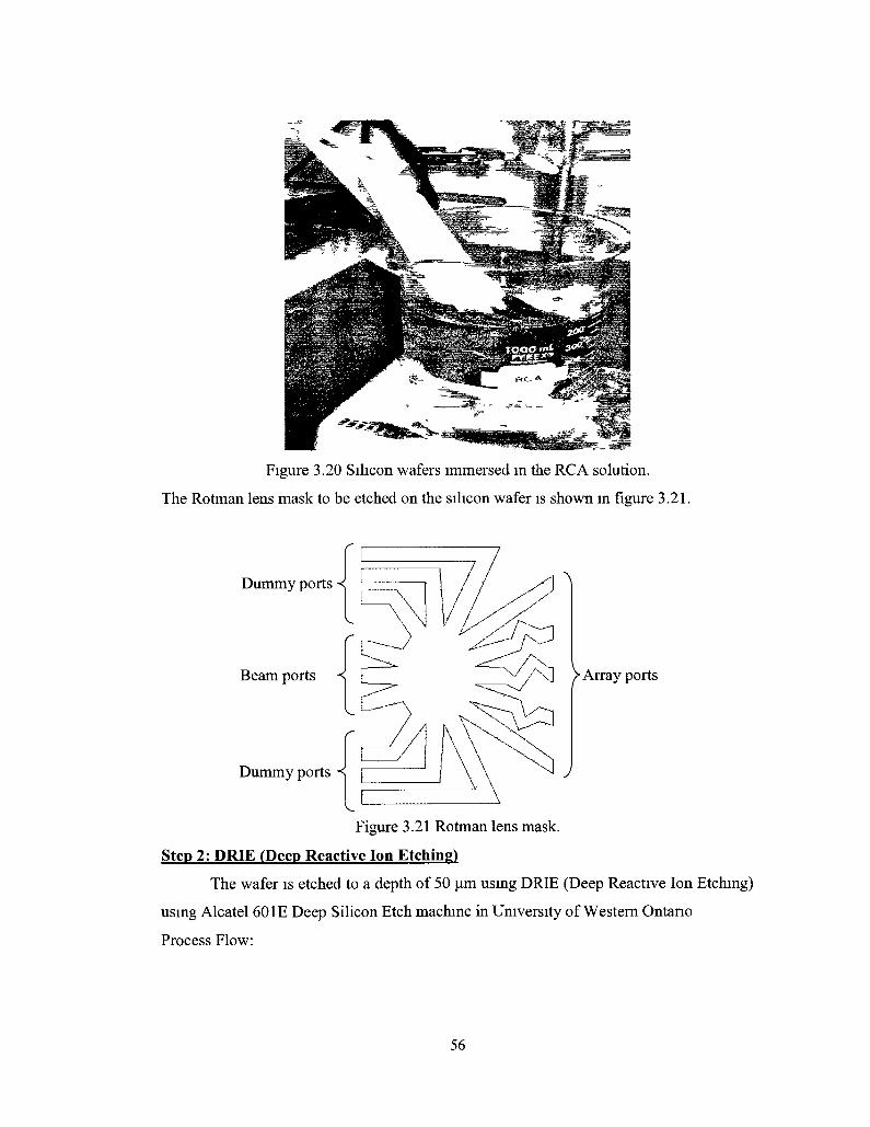
Figure 3.20 Silicon wafers immersed in the RCA solution.
The Rotman lens mask to be etched on the silicon wafer is shown in figure 3.21.
Dummy ports <
Beam ports •<
Dummy ports •<
> Array ports
J
Figure 3.21 Rotman lens mask.
Step 2: DRIE (Deep Reactive Ion Etching)
The wafer is etched to a depth of 50 um using DRIE (Deep Reactive Ion Etching)
using Alcatel 60 IE Deep Silicon Etch machine in University of Western Ontano
Process Flow:
56

The patterns are defined by a thin layer of silicon oxide which is patterned
lithographically prior to etching.
• Silicon is etched selectively relative to the oxide mask.
• The system is optimized for high etch rate and high aspect ratio etching of silicon.
• Vertical anisotropic deep plasma etching of silicon is used by depositing an ultra-
thin layer of silicon-dioxide which is used for sidewall protection to control the
(Bosch process).
Figure 3.22 shows the machine used for the process.
Figure 3.23 shows the SEM profiles of the silicon wafers after etching, captured at the
University of Western Ontario
Figure 3.22 Alcatel 60IE Deep Silicon Etch.
Figure 3.23 SEM profiles of the silicon wafers.
Step 3: Chromium (Cr) and Gold (AiT) Deposition
57

• Gold layer is used as a conductive layer.
• Chromium is used as an adhesion layer since Gold can't be deposited directly on
Silicon.
• Electron Beam Evaporation method has been used to deposit both layers using
Intlvac Nanochrome™ Deposition System
Process Flow:
• Chromium Deposition: 40 nm seed layer was deposited at 20% power which
gives a rate of 3.0 A/sec.
• Gold Deposition: 100 nm gold layer was deposited at 30% power which gives a
rate of 9.2 A/sec.
Step 4: Au Electroplatin2 and Bonding
• Gold layer of 3 um is electroplated by immersing the wafers in the solution for a
specified period of time to get the required thickness.
• Lens cap and etched wafer are bonded together using a thermo-compression
bonding and sidewall conductive epoxy technique to complete the fabrication
• Dummy ports are filled with RP absorbing materials with matched resistances of
50 £1
Figure 3.24 show the fabrication process diagram for the Rotman lens.
p — n Lens cap Si D R | E 5 0 u m <wafer)
r—n Lens cap Cr sputtering wafer Cr sputtering
r~i r~i
Lens cap Au electroplating wafer Au electroplating
Bonding of the lens and the cap
Gold (Au)
Chromium (Cr)
Figure 3.24 Rotman lens Fabrication process diagram.
58
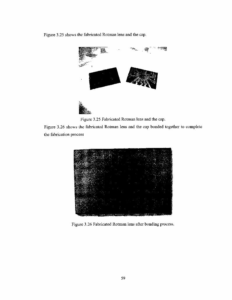
Figure 3.25 shows the fabricated Rotman lens and the cap.
-"&
Figure 3.25 Fabricated Rotman lens and the cap.
Figure 3.26 shows the fabricated Rotman lens and the cap bonded together to complete
the fabrication process
"^'•MSiO
IjgiSJfBftVH
Figure 3.26 Fabricated Rotman lens after bonding process.
59

3.5 Conclusions A new FMCW automotive radar architecture has been presented that can provide
the best performance while addressing the design constraints, following the review of the
state-of-the-art in automotive radars and requirements set by the auto industry for long
range radar. The radar is to operate at the 77 GHz, a Rotman lens has been adopted to
perform the operation of beamforming and beamsteering to eliminate the need for
microelectronic based analog or digital beamforming engine. MEMS based RF switches
have been selected to feed the FMCW signal to the beam ports of the Rotman lens.
Microstrip based antenna arrays have been selected to radiate and receive the signal due
to their established superior performance, ease of fabrication, and small planar geometry
while offering high directivity and lower sidelobes.
The design of a MEMS based Rotman lens has been presented. The lens has a
footprint area of 27x36.2 mm2, incorporates 3 beam ports, 5 array ports, and operates at
77 GHz. A novel TEio mode rectangular waveguide type Rotman lens has been designed
and fabricated. The new design enabled to reduce the lens size such that it can be batch
fabricated using conventional micromachining techniques like conventional VLSI chips.
The lens has been designed using full wave 3-D FEA simulation using industry standard
HFSS software. The performance parameters of the Rotman lens are optimized to get
excellent values for the insertion losses, return losses and characteristic impedance. A
fabrication technique has been developed to fabricate the Rotman lens. The lens has been
fabricated in the University of Waterloo, University of Western Ontario microfabrication
facilities and assembled in Advotec company in Arizona. The device can provide a cost
effective highly reliable and less complex solution compared to currently available radar
based proximity detection systems for automobiles.
60

Chapter 4
MEMS SP3T RF Switch The design and fabrication of a MEMS Single-Pole-Triple-Throw (SP3T) RF
switch to sequentially feed the FMCW signal among the beam ports of a microfabricated
Rotman lens that forms an integral part of a MEMS based 77 GHz automotive radar
sensor has been presented. The series type MEMS RF switch relies on electrostatic
actuation of a microfbaricated cantilever beam and incorporates 1 input port and 3 output
ports. Two different versions of the MEMS RF switch have been designed: a ground
connecting bridge (GCB) conventional geometry where microfabricated bridges have
been used to provide the ground connectivity and a new continuous ground (CG) without
any bridge. Both the switches have been optimized for operation in the 77 GHz; however,
the CG version provides improved performance as it eliminates the effects of coupling
capacitance between the ports and the ground. The HFSS simulation results show that at
77 GHz, the CG configuration has 4 dB improvement for the return loss compared to the
GCB version of the switch. The CG version of the switch also exhibits 0.5 dB
improvement for insertion loss and 3 dB improvement for isolation as compared to the
GCB version of the switch. The actuation voltage of the switch is 16.3 volts. The GCB
type SP3T RF switch has been fabricated using the UWMEMS process and the
fabrication of the CG version is in progress.
4.1 MEMS RF Switch Overview
RF switches are typically used in high frequency communication systems for
signal routing, phase shifting, impedance matching and for changing the gain of
amplifiers [52]. Spectrum allocation for different high frequency communication bands
such as L-band (1-2 GHz), K- band (18-27 GHz), or W-band (75-110 GHz) sets different
S-parameters requirements for the design of RF switches intended for use in those
frequency bands. Consequently, different switching technology, such as
electromechanical, Silicon FET, GaAs MOSFET, PIN diodes, and MEMS etc. are
adopted to meet the design requirements specific to the target frequency range. A
comparative overview of different RF switching systems is available in [53, 54].
Following [53, 54], at frequencies greater than a few GHz, the solid-state switches exhibit
61
large insertion loss and poor isolation whereas electromechanical switches exhibit slow
switching speed, high isolation consequently, they are not suitable for the target 77 GHz
MEMS radar. In contrast, MEMS based RF switches offer design factors not available in
other RF switches, such as the setting of the gap height independently, change the
dielectric that fills under the switching element from semiconductor to air and it change
the effective area of switching.
In conclusion, MEMS based RF switches have excellent performance figures as
they combine the low loss characteristic of the mechanical RF switches along with the
small size characteristic of the semiconductor FET switches [55]. As the MEMS RF
switches use air gaps for the OFF state, this result in excellent isolation and have very
low insertion loss [55-58]. These switches also exhibit higher isolation among the ports
in a multiport network to result in a lower leakage from an "ON" to an "OFF" port.
Additionally, they have a very low actuation power consumption, faster switching time
and speed, and extremely wide bandwidth characteristics [53, 54].
Actuation mechanisms used in MEMS RF switches include electrostatic,
electromagnetic, magnetic, piezoelectric and thermal. However, the electrostatically
actuated MEMS RF switches are the most efficient ones and electrostatic actuation has
become the most common actuation mechanism for MEMS RF switches. They consume
very low power and exhibits very large ON-OFF capacitance ratio.
Two common forms of MEMS RF switches are the series and the shunt types. In the
series type, typically an electrostatically actuated cantilever beam is used to establish the
connectivity between two RF ports whereas in the shunt type, an electrostatically
actuated fixed-fixed beam is used to realize the switching operation.
4.2 Cantilever MEMS RF Switches
The cantilever structure consists of a thin strip of metal fixed at one end and is
suspended over the metallic transmission line with a gap of a few micrometers. The
cantilever can be connected in series with the transmission line as shown in Figure 4.1 in
both OFF state (a) and ON state (b). When a bias voltage is applied between the
cantilever and the lower actuation electrode, an electrostatic attraction force is developed
between the cantilever beam and the lower actuation electrode. This force causes the
cantilever to move down towards lower actuation electrode, independent of the charge
62

polarity. This creates an opposing tensile force on the cantilever as the structure starts
bending. When the applied force reaches a threshold value, the tensile force is no longer
balanced by the electrostatic force, so the cantilever abruptly falls to the bottom electrode
and makes an electrical contact. The cantilever releases back when the applied voltage is
reduced below the threshold value.
Contact dimple
Anchor
m , T 1 O H c i actuation
electrode (a)
1 oner contact
electrode
t^^S&SSgjagMgJW
(b)
Figure 4.1 Cantilever MEMS RF switch.
4.3 Bridge MEMS RF Switches
The cross-sectional view of a bridge type MEMS RF switch is shown in Figure
4.2. The input RF signal traverses into a via interconnect to the top of the membrane. The
output line, which is underneath the membrane, is connected using a thin metal strip. Via*;
Lower actuation
clectiodt.
Figure 4.2 Bridge MEMS RF switch.
When an actuating voltage is applied to lower actuation electrode, the electrostatic force
causes the bridge to pull downwards. With enough voltage, the bridge deforms and
comes in contact with the bottom transmission line closing the two poles similar to the
cantilever beam type MEMS RF switch.
Due to the establishment of a metal-metal contact during the switching operation,
both types of switches exhibit good insertion loss and excellent linearity. Typically, a
63

bias tee circuit as shown in figure 4.3 is used to isolate the RF signal from the DC bias
voltage [59], by bypassing the DC voltage to the ground via the inductor L and block it
from the RF path by the capacitance C.
C
7 Figure 4.3 Bias tee.
4.4 Design of SP3T MEMS RF Switch for 77 GHz Radar
As the Rotman lens has three beamports, an SP3T MEMS RF switch is necessary
to sequentially feed the FMCW signal from the transceiver among the there beamports of
the Rotman lens. A conceptual geometry of a typical SP3T switch is shown in figure 4.4.
The switch has one input port (1) and three output ports (2, 3, 4). The grounds are
connected via bridges. An input signal at port 1 can be directed to any of the three output
ports by actuating the DC pad of the required port. The actuation of the DC pads is to be
controlled by an FPGA or ASIC implemented control algorithm.
However, most of the reported designs of MEMS based SP3T RF switches use a
discontinuous ground plane as shown in figure 4.4 [30, 31]. The grounds for individual
ports are connected by using conductive bridges passing over the CPW lines as can be
seen in the figure. These conducting bridges have a high resistance due to the limited size
of the anchors and bridge widths. Additionally, the coupling capacitance between the
bridge and the CPW underneath becomes significant at higher frequencies (77-81 GHz) as
is visible in the HFSS simulation result as shown in figure 4.5. Both of these effects
degrade the overall S-parameter figures associated with the switch performance resulting
in a noisy and low efficiency operation at the target frequency range.
64

Cantilever (Output port)
(iriuind
CPW line (Input port)
Rnd"e
Figure 4.4 Conventional MEMS SP3T RF GCB switch.
E Fieltl[V/m]
2 3109t»83S
1 SSHSe+SeS
1 -O9;ttQ0S
1 55S3e»804
i MSWBas
1 i'jSstnot,
1 W e » g u 6
? ?6«Oi>tW35
6 :i£?t»0O5
I B , 167 .̂005 I H 1 S5 39 f.005 ^ ^ i 1774e»e01
Coupling es Capacitance (field linkage)
• • ^
1 ! I t \"
L^A I?
•
n
/
Air gap
Briduc
Figure 4.5 HFSS simulation shows the coupling capacitance between the GCB and a CPW
line of a conventional MEMS SP3T RF operating at 77 GHz.
65

4.5 CG MEMS SP3T RF Switch
To overcome this limitation of the conventional MEMS SP3T switches at the
target frequency range of 77 GHz, a new SP3T RF switch has been designed that has a
continuous ground plane as show in figure 4.6a. The RF switch consists of three actuating
beams; each beam is connected to a 50 Q CPW line at one end and is suspended on top of
another CPW line of 50 Q as shown in figure 4.6a. The beams and the coplanar lines are
to be electrically connected with the drive and control circuitry using vias as shown in
figure 4.6b.
Cantilever^ (Output port)
\
s
1 1
C (In
>W line put port)
4
•MM
">
Ground
1 1 1 1
(a)
Via
Ground
JL. CPW line
Anchor Via
Cantilever CPW line Ground
* * < i *~>
DC pad
(b)
Figure 4.6 CG MEMS SP3T RF switch.
4.6 Material Selection
As the target RF switch has been decided to be fabricated using the UWMEMS
process available in the Centre for Integrated RF Engineering (CIRFE) of the University
66

of Waterloo due to lower fabrication cost, the material selection process and layer
thicknesses are guided by the materials and design rules specific to the UWMEMS
process. The materials and layer dimensions of the UWMMEMS process are shown in
Table 4.1 [60].
Following Table 1, it appears that the Gl layer can be used to fabricate the CPW
line and the ground and the G2 layer can be used to fabricate the cantilever beam. The 2.5
Hm thick sacrificial layer can be used to realize the anchor and the airgap. This dictates to
choose the thickness of the CPW lines and the ground lines as 1 urn. Similarly, the
cantilever beam thickness needs to be 1.25 um (thickness of the G2 layer).
Table 4.1 Layer Names, Thickness and Mask Level.
Material
Cr Chromium
Dl Silicon Nitride
Gl Goldl
D2 Silicon Nitride
Sacrificial Layer
G2 Gold 2
Thickness um
0.04
0.5
1
0.7
2.5
1.25
Mask Level
Mask # 1
Mask # 2
Mask # 3
Mask # 4
M a s k # 5 & # 6
Mask # 7
Layer Description
Resistive Voltage Biasing
Dielectric
Conductive Layer
Dielectric
Sacrificial Layer
Top Conductive
Layer
Comments
Resistive layer
Dielectric to cover Cr
0.5um Cr + 1 um Au
300ACr + 0.7um SiN
2.5 um Anchor and 1 um Dimple Openings
0.1 um Sputtered Au + 1.15 um
Electroplated Au
4.7 Mathematical Modeling
The cantilever beam stiffness k can be determined as follows [55]:
Where E is the Young's modulus of the beam material, w is the beam width, t is beam
thickness, and / represents the length of the beam
67

The pull-in voltage of the cantilever V can be calculated following the relation
8A: 3 , . .. go (4-4) p \ 27e0Ww
Where gQ is the zero bias gap, e0 is the permittivity of free space, and W is the length of
the DC pad.
The electrostatic force on the cantilever F can be determined as
s AV2
F = ^ j - (4.5)
Where A is the effective area of the capacitor and g is the physical separation between
the contacts.
The deflection of the tip of the beam, 8 can be calculated from [61]
x ,F(l-v2k3 Z3 .. _ (5 = 6—^ E- r- (4.6)
E Wt3
Where W, L and t are the width, length and thickness of the beam respectively. E and v are
the Young's modulus and poisson's ratio respectively and F is the electrostatic force.
Assuming the damping coefficient of the cantilever is relatively small, the switching time
can be calculated as [62] t = 0 . 5 8 4 ^ - (4.7)
V f
Where Vp is the pull-in voltage and Vs is the drive voltage. For fast switching, Vs is
adopted to 1.4^.
The up state capacitance Cu of the cantilever beam can be calculated as in [55]
Cu=Cs + Cp (4.8)
Where Cs is the series capacitance between the beam and the transmission line and Cp is
the parasitic capacitance between open ends of the transmission line
Cs is represented by a parallel plate capacitance Cpp = £jy and a fringing component of
30-60% of Cpp. The parasitic capacitance Cp of a CPW line of 40 urn width is about
2£F.
68
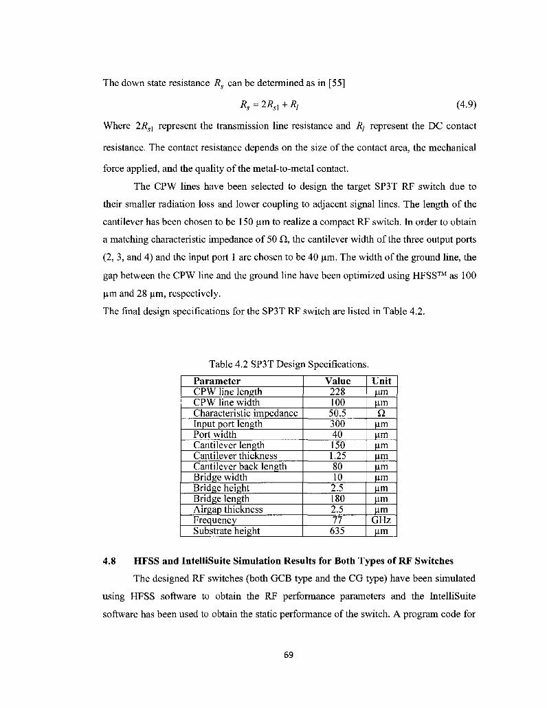
The down state resistance Rs can be determined as in [55]
Rs=2Rsl+R, (4.9)
Where 2Rsl represent the transmission line resistance and Rt represent the DC contact
resistance. The contact resistance depends on the size of the contact area, the mechanical
force applied, and the quality of the metal-to-metal contact.
The CPW lines have been selected to design the target SP3T RF switch due to
their smaller radiation loss and lower coupling to adjacent signal lines. The length of the
cantilever has been chosen to be 150 um to realize a compact RF switch. In order to obtain
a matching characteristic impedance of 50 Q., the cantilever width of the three output ports
(2, 3, and 4) and the input port 1 are chosen to be 40 um. The width of the ground line, the
gap between the CPW line and the ground line have been optimized using HFSS™ as 100
um and 28 um, respectively.
The final design specifications for the SP3T RF switch are listed in Table 4.2.
Table 4.2 SP3T Design Specifications.
Parameter CPW line length CPW line width Characteristic impedance Input port length Port width Cantilever length Cantilever thickness Cantilever back length Bridge width Bridge height Bridge length Airgap thickness Frequency Substrate height
Value 228 100 50.5 300 40 150 1.25 80 10
2.5 180 2.5 77
635
Unit urn um Q.
um um um um um um um um um
GHz um
4.8 HFSS and IntelliSuite Simulation Results for Both Types of RF Switches
The designed RF switches (both GCB type and the CG type) have been simulated
using HFSS software to obtain the RF performance parameters and the IntelliSuite
software has been used to obtain the static performance of the switch. A program code for
69

designing the RF switch in visual basic code (VB code) is shown in appendix B. Figure
4.7 shows that both the GCB type and the CG type switches exhibit a characteristic
impedance of 50.5 Q. at the operating frequency of 77 GHz. Figures 4.8-4.12 shows the
HFSS simulation results for S-parameters when a 77 GHz signal is fed at the input port
(port 1 in figure 4.6) with one of the output ports (port 2 in figure 4.6) is actuated.
From the figures 4.8a and 4.8b, it is evident that while the GCB type switch
exhibits a return loss better than -16 dB, the corresponding return loss for the CG type
switch is better than -20 dB at 77 GHz. Thus, a return loss improvement of -4 dB can be
achieved if the continuous ground version is used. The return loss figures compare better
with the measured value of-15 dB for a MEMS cantilever type of the same width (40um)
RF switch as reported in [63]. This validates the design of both types of switches. Figure
4.9(a) shows the HFSS simulation results for the insertion loss of the GCB switch (better
than -1.1 dB) while figure 4.9 (b) shows the insertion loss of the CG switch (better than -
0.65 dB) for the same simulation set up. Both the values compare better with the -3 dB
measured insertion loss for the 77 GHz cantilever type switch published in [63]. Figures
4.10 (a) and 4.11 (a) show that isolations between the ports 1 and 3 , and the ports 1 and 4
with port 2 actuated are better than -13 dB for the GCB switch, while as the figures 4.10
(b) and 4.11 (b) show, isolations better than -16.5 dB can be achieved for the CG type
switch. All of the isolation values are better than the -15 dB measured isolation value for
the switch published in [63].
In summary, the CG configuration has improved the return loss by 4 dB compared
with the GCB version of the switch. The insertion loss has improved by 0.5 dB and the
isolation has been improved by 3 dB.
53 5
53 I
52 5 I
S S2 \
°515 \ ^ ^ ^
51 ' ____̂
50 5 ' ~-~.
50 0 10 20 30 10 50 60 70 80
Frequency [GHz]
Figure 4.7 Characteristic impedance (Both GCB and CG type switches).
70

-45„ 20 30 40 50
Frequency [GHz!
(a) GCB switch
30 40 50
Frequency [GHz]
(b) CG switch
Figure 4.8 Return loss between ports 1 and 2.
_ - 0 6
-1 2
10 20 30 40 50
Frequency {GHz]
(a) GCB switch
70 80
71

— 02 CO
2 03
-2 04 c o
C 01
£ 06
JO ' 0 10 so Frequency IGHzl
(b) CG switch
Figure 4.9 Insertion loss between ports 1 and 2.
- 10
I - 20
| - 2 5
§-30-
I -35 o ~ -40
-45
-50 '
S 5 0
-10
- - 3 0
10 30 40 50 Frequency 1GHz]
60
(a) GCB switch
-50'
30 40 50 Frequency [GHz]
70
(b) CG switch
Figure 4.10 Isolation between ports 1 and 3.
72

- - 3 0 J
30 40 50 Frequency !GHz]
(a) GCB switch
60 70 80
30 40 SO Frequency [GHz]
80
(b) CG switch
Figure 4.11 Isolation between ports 1 and 4.
Ports 1 to 2 actuation is identical to actuation of ports 1 to 4 and ports 1 to 3 and exhibit similar return loss, insertion loss and isolation values.
3-D electromechanical finite element analysis using industry standard software
IntelliSuite has been carried out to determine the beam load-deflection simulation results
Figure 4.12 shows the cantilever collapsing state after carrying out the simulation. Figure
4.13 shows the cantilever displacement simulation, and figure 4.14 shows the pull-in
voltage simulation of the beam. The cantilever stiffness k has been calculated using (4.3)
to be of 1.203 N/m and the pull-in vol tage^ is calculated using (4.4) as \6.W.
Camik'% er
Subxlrale
Figure 4.12 Cantilever collapsing simulation.
73

Figure 4 13 Cantilever displacement simulation.
Z Displacement v-s Vattage
Figure 4.14 Cantilever pull-in voltage simulation.
In summary the RF charactenstics of the designed SP3T are listed in table 4.3
Table 4.3 SP3T RF performance summary.
Parameter Return loss Insertion loss Isolation Pull in voltage Beam stiffness Switching time Up state capacitance Down state resistance
Value -20 -0.65 dB -16.5 16.3 1.203 5.42xl0"lz
4 0.8
Unit dB dB dB V
N/m sec fF Q.
74

4.9 Fabrication
Surface micromachining has been the most important fabrication method for
MEMS RF switches, but other processes such as bulk micromachining and fusion
bonding are frequently used. Surface micromachining can be viewed as a three
dimensional lithographic process and involves depositing various patterns of thin films
on a substrate. Free-standing or suspended structures are created by applying patterns of
sacrificial layers below non-sacrificial or release layers [64]. Selective etching of the
sacrificial layers then leaves a suspended film which is capable of mechanical actuation.
The UWMEMS process is used to fabricate the SP3T RF switch on A1203
substrate of a thickness of 625 um. All the cantilever beams and I/O ports are made of
gold. The DC pads made of Chromium. A step by step fabrication process of the MEMS
RF switch following the UWMEMS 7 masks process in the University of Waterloo is
described below (both in GCB and CG versions). A low loss ceramic alumina wafer
(AI2O3) having a dielectric constant (e) of 9.8 has been used as the substrate in surface
micromachining process.
A 0.5 urn thick layer of Chromium deposited on the wafer using an e-beam
evaporation method as shown in figure 4.15. The layer is patterned using mask 1 and
etched to create the CPW lines. The process of (Cr lift-off) is then used to pattern the DC
biasing lines. The lift-off process is realized using thick insensitive resist (LOR) and
negative photoresist on top.
An insulation layer is formed by depositing a 0.7 u.m of Silicon Nitride using PECVD
process and patterned using mask 2 as shown in figure 4.16.
Figure 4.15 Chromium deposition and patterning.
75

PF.CVD Silicon Nitride (mask 2)
] A1:03
J Chromium (C'r)
Silicon Nitride (SiN)
CG type GCB type
Figure 4.16 Silicon Nitride deposition and patterning.
Electron Beam Evaporation method has been used to deposit a 0.5 urn of Chromium and
lum of gold to form Gl layer as shown in figure 4.17.
B
Deposit Cr &Au
I | A1203
I I Chromium (Cr)
I I Gold (Au)
Figure 4.17 Chromium and Gold deposition.
Gold and chromium layers are patterned using mask 3 and etched to create the CPW lines
as shown in figure 4.18
Pattern Cr & Au (mask 3)
1 A1203
J Chromium (Cr)
] Gold (Au)
GCB type
Figure 4.18 Gold and chromium patterning.
A 2.5 urn thick polyimide is added by spin deposition method to form a sacrificial layer
to be patterned by mask 4 to form the anchors on the lower gold layer and patterned by
76

mask 5 to form a dimple on the top layer as shown in figure 4.19.
Sacrificial la\cr(Mask -4 & 5)
I I Al :0,
c J Chromium (Cr)
] Gold (Au)
9 Silicon Nitride (SiN)
fcfllliii Sacrificial la\cr (Pohimide)
CGtype GCB type
Figure 4.19 Anchor and dimple patterning.
A 1.25 um thick layer of gold is then deposited on the sacrificial layer to form the G2
layer as shown in figure 4.20.
I I Chromium (Cr)
I 1 Gold (Au»
Silicon Nilnde (SiN)
Sacrificial la\er (Kohimidc)
Deposit lop \u
Figure 4.20 G2 deposition using Electron Beam Evaporation method.
The G2 gold layer is then patterned with mask 6 &7 to form the cantilever beam and
release holes in the cantilever beam as shown in figure 4.21.
B I
CGtype
B I
Pattern top Au (mask 6 &7)
I J A1:0, I 1 Cliromium (Cr)
c ] Gold (Au)
Silicon Nitride (SiN)
Sacrificial layer (Pol\ imidc)
GCB type
Figure 4.21 Pattern of the top gold G2.
77

The wafer is released by partial dry etching using oxygen plasma in RIE as shown in
figure 4.22 and the release process is detailed in appendix C.
Chromium (Ci I I I Gold (An) m g | SIIILOU Nitride (SiN)
mmm Sacrificing c, (Pol>mude)
Figure 4.22 SP3T MEMS RF switch release.
The SEM pictures of the RF switch before and after release are shown in figure 4.23
Before release After release
it' ' \ ' ! * • • *'.«
Figure 4.23 SEM pictures of the RF switch before and after release.
78

4.10 Conclusions
The Design, simulation and fabrication of a SP3T MEMS RF switch has been
presented in the GCB and CG versions The CG RF switch incorporates a continuous
ground instead of typical bridge mechanism to connect the ground segments. This
eliminates capacitive coupling between the bridge and the underneath beam to improve
the RF switch performance. The RF switch has been modeled and simulated using HFSS
and the simulation results show an insertion loss of better than -0.65 dB, -20 dB return
loss, and isolation of -16.5 dB and an actuation voltage of 16.3 volts. A fabrication
process sequence has been developed following University of Waterloo UWMEMS. The
SP3T RF switch is to be used in conjunction with a MEMS based solid state Rotman lens
to realize a compact MEMS radar for automotive collision avoidance application. The
CG configuration has improved the return loss by 4 dB compared with the GCB version
of the switch. The insertion loss has improved by 0.5 dB and the isolation has been
improved by 3 dB.
79

Chapter 5
Microstrip Patch Antenna The design, simulation and fabrication of a microstrip antenna array that forms an
integral part of a MEMS based radar working in the 77 GHz range has been presented.
The microstrip antenna array incorporates 5 sub-arrays and 12 patches in each sub-array.
The design is based on a serial array inset fed method. The HFSS simulation results show
that at 77 GHz, the microstrip antenna array exhibits a return loss of better than -15 dB,
antenna array gain of 18.3 dB, half power beam width (HPBW) of 9° and an efficiency of
77% at the operating frequency of 77 GHz.
5.1 Microstrip Antenna Overview
Microstrip concepts were first proposed in the 1950's [35, 36] but their use did not
gain momentum until the late 1960's and 1970's, mainly due to the lack of suitable low
loss, dielectric substrates. Microstrip circuits consist of a single substrate with a ground
plane on its bottom surface and a narrow strip of conducting transmission line on its top
surface.
5.2 Microstrip Antenna
Microstrip antennas are planar resonant cavities that utilize the fringing fields
along the edges of a microstrip patch to radiate electromagnetic energy. A typical
microstrip patch antenna consists of a very thin metallic strip (patch) of thickness /
placed on a dielectric substrate of thickness h and of dielectric constant of sr above a
ground plane as shown in figure 5.1
Ground
Figure 5.1 Microstrip patch antenna.
80

The maximum radiation pattern of a microstrip patch is normal to the patch. This is
accomplished by properly choosing the field configuration of excitation of the patch. The
fringing fields are cancelling each other along the microstrip patch length as shown in
figure 5.1, so it can be represented by two radiating slots along the patch width. The
radiation from these two relevant slots can be computed by considering them as a two-
element array separated by a distance L. The amount of fringing is a function of the
dimensions of the patch and the height of the substrate. The variation of the electric field
along the patch length is represented in figure 5.2.
1.5
•a i OX)
g 0.5 s -
to 0
.^ -0.5 b-
-I
^ ^
i X !
:
]
,
X
\
\ -̂
^
12
10
8
6
4
2
^ o
CD u c cs
T3 <U CL
£ >
1 0% 20% 40% 60% 80% 100%
Distance
Figure 5.2 Electric field along the patch length.
There are numerous substrates that can be used for the design of microstrip
antennas, and their dielectric constants are usually in the range of 2.2 <sr <12 [41].
The ones that are most desirable for good antenna performance are the substrates whose
dielectric constant is in the lower end of the range because they provide better efficiency,
larger bandwidth, loosely bound fields for radiation into space [37], also thin substrates
are desirable for microwave circuitry because they require tightly bound fields to
minimize undesired radiation and coupling, and lead to smaller element sizes.
Microstrip is basically printed circuits for microwaves and is usually fabricated
like printed circuit boards, but requires higher-resolution photolithographic processes
because of the dimensional accuracy required.
Microstrip limitations are few, the fundamental one being low power handling
capability which may be overcome with the realization of good impedance matching
circuitry. There are four separate mechanisms that can be identified for the power losses
81

and parasitic effects associated with microstrip lines [37], conductor losses, dissipation in
the dielectric substrate, radiation losses, and surface wave propagation. Conductor and
dielectric losses are lumped together and calculated as part of an attenuation coefficient
for the line. Discontinuities such as abrupt open-circuit lines, steps, and bends will radiate
to a certain extent and efforts must be made to reduce radiation and its undesirable side
effects in circuits such as filters and amplifiers. Most of the propagating electromagnetic
wave is confined to the region between the ground plane and the strip conductor but
surface waves do account for some of the lost transmission power. Surface waves are
waves trapped just beneath the surface of the dielectric substrate and propagate away
from discontinuities in the form of higher order TM and TE radial modes.
The feed mechanism plays an important role in the design of microstrip patch antennas.
There are many configurations that can be used to feed microstrip antennas. The four
most popular are the microstrip line, coaxial probe, aperture coupling and proximity
coupling [36-40]. A microstrip line inset feed was adopted in this research work, since
the patch antenna typically yields a high input impedance and the current is low at the
ends of a half-wave patch and increases in magnitude toward the center, the input
impedance (Z=V/I) could be reduced if the patch was fed closer to the center. One
method of doing this is by using an inset feed. The inset fed microstrip line is suitable for
developing high gain microstrip antenna arrays. The position or the inset feed length
determines the input impedance [38].
There are many methods of analysis for microstrip antennas. The most popular
models are the transmission-line, cavity, and full wave. The transmission-line model is
the easiest of all, it gives good physical insight, but is less accurate and it is more difficult
to model coupling. Compared to the transmission-line model, the cavity model is more
accurate but at the same time more complex. However, it also gives good physical insight
and is rather difficult to model coupling, although it has been used successfully. In
general when applied properly, the full-wave models are very accurate, very versatile,
and can treat single elements, finite and infinite arrays, stacked elements, arbitrary shaped
elements, and coupling. It is the more popular and practical model.
Microstrip antennas are radiating structures derived from microstrip transmission
lines (TL) as a means of integrating antennas with feed circuitry on the same substrate.
82

An obvious starting point for a simple analysis is thus the TL-model that uses a planar
transmission line model to capture the transmission line properties, and uses an open end
effect to capture the effects of radiation from the patch. A rectangular patch with length L
and width W can be viewed as a very wide transmission line that is transversely
resonating, with the electric field varying sinusoidally under the patch along its resonant
length. The electric field is assumed to be invariant along the width W of the patch.
Furthermore, it is assumed that the antenna's radiation comes from fields leaking out
along the width, or radiating edges, of the antenna. The radiating edges of the patch can
be thought of as radiating slots connected to each other by a microstrip transmission line.
The equivalent circuit for the microstrip patch is shown in figure 5.3. Each
radiating slot is represented by a parallel equivalent admittance Y (with conductance G
and susceptance B). The slots are labeled as slot 1 and slot 2.
_ siot U - — 4vSiot 2 ; — ^
G + J B| lzrJ
I I Patch
| |Sustrate
I | Ground plane
Figure 5.3 Microstrip patch equivalent circuit.
Based on the analysis presented so far, an inset fed microstrip antenna array has
been selected for the target 77 GHz MEMS radar. A straightforward transmission-line
model has been used to accurately model and analyze the designed microstrip inset fed
antenna array. In the design, the substrate electrical parameters, feed line width, slot size
and position are used to optimize the array performance. Impedance matching is
performed by controlling the width of the feed line and the length of the slot.
The use of microstrip antennas in most practical applications usually requires
multiple elements in an array configuration to achieve the required gain and beamwidth.
The design of these arrays require feed structures that are impedance matched to the
patch radiators and provide the proper amplitude and phase required at each radiator.
Current Finite Element Analysis (FEA) software HFSS is available that represents
microstrip network components by equivalent transmission lines.
G+jB
83

5.3 Microstrip Single Patch Design
The rectangular patch that has been adopted in this research work is by far the
most widely used configuration because it is very easy to analyze using the transmission-
line model, which is the most accurate for thin substrates [39]. The substrate that has
been used (RT 5880) is of thickness of 125 um which feature's the following:
• Lowest electrical loss for reinforced material.
• Low moisture absorption.
• Isotropic
• Uniform electrical properties over frequency.
• Excellent chemical resistance
RT 5880 specifications are listed in table 5.1.
Table 5.1 RT 5880 Specifications
Dielectric constant sr
Dissipation factor, tan 8
Moisture absorption
Thermal conductivity
2.2
0.0004
0.02 mg %
0.20 w/m/k
To start the design process a predetermined values of dielectric constant, substrate height,
resonant frequency, and patch length have to be specified. In this research work, the
dielectric constant sr, of 2.2, substrate height h of 125 um and resonance frequency fr
of 77 GHz has been predetermined. The patch length L, have to be \C to resonate at
the operating frequency. The patch width W can be calculated as following [37].
1 I 2 c \ 2 W =
2 / r A / / V ^ V ^ + l 2fr\er+l (5.1)
Where
ju0 Permittivity of the air
f0 Dielectric constant of the air
c Velocity of the light
84

The next step in designing the patch is to calculate the effective dielectric constant
Erejj . The effective dielectric constant is defined as the dielectric constant of the uniform
dielectric material so that the microstrip line has identical electrical characteristics,
particularly propagation constant, as the actual line that confine all the magnetic field
lines in the propagated wave or that accounts for the fringing and wave propagation in the
line [37]. The effective dielectric constant is also a function of frequency. As the
frequency of operation increases, most of the electric field lines concentrate in the
substrate. Therefore the microstrip line behaves more like a homogeneous line of one
dielectric (only the substrate), and the effective dielectric constant approaches the value
of the dielectric constant of the substrate. For a line with air above the substrate, the
effective dielectric constant has values in the range of.
1 < Sreff < £r (5-2)
_ sr +1 sr - 1
Where
ereff Effective dielectric constant
sr Substrate dielectric constant
h Substrate height
W Microstrip patch width
Because of the fringing effects, electrically the patch of the microstrip antenna looks
greater than its physical dimensions. For the principal .E-plane (xy-plane), this is
demonstrated in Figure 5.4 where the dimensions of the patch along its length have been
extended on each end by a distance AL, which is a function of the effective dielectric
constant sreff and the width-to-height ratio (W/h).
, ,~ h 1 + 12—
W
(5.3)
85

*icu_nr
(a)
Patch Patch
[ 1 Substrate
Ground plane
(b)
Figure 5.4 Physical and effective length of microstrip patch.
The normalized extension of the length is [37].
i V
w ^ ^k = 0.412 i A :
* (sreff - 0 . 2 5 8 ^ + 0.8 (5.4)
Since the length of the patch has been extended by AL on each side, the effective length
of the patch is now
Leff=L + 2AL (5.5)
The resonant frequency of the microstrip antenna fr is a function of its length given by
c fr = 2L^
(5.6)
As the substrate height increases, fringing also increases and leads to larger separations
between the radiating edges (L) that in turn lowers the resonant frequency following
(5.6).
Ideally the two slots should be separated by yi . However, because of fringing the length
of the patch is electrically longer than the actual length. Therefore the actual separation of
the two slots is slightly greater than yC . If the reduction of the length is properly chosen
then (typically 0.481 < L < 0.491) [38], the characteristic impedance Z0 is real, or
120;r Z0 =
^ eff W
+ 1.393 + 2 l n
h 3
/ . + 1.444
(5.7)
86

To find the exact inset length >>0to achieve 50 Q. input impedance following [37] as
following
_4fo.001699eJ + 0.13761s? -6.1783s* + 93.187s? -682.69*? +1 L y0=\0-
[2561.9s2r - 4043s,. + 6697
The radiation pattern of the patch is given by:
sin E0=- )
kWsm9sin0 2
cos kL
sin £'/*——-
£fFsin6?sin^
&^sin#sin^ -cos
sin6>cos^ cos^ 2 y
kL \ — sin 6 cos <f> cos (9 sin ̂ 2 y
(5.8)
(5.9)
(5.10)
Where A: is the propagation constant given by k = ^y.
The magnitude of the fields is given by
IE20 + El (5.11)
The patch parameters that have been found above then optimized using FEA software
HFSS to finalize the patch size and obtain it's RF performance. The microstrip patch feed
line width is optimized using Advanced Design System (ADS) software and the inset fed
is optimized using the HFSS software.
The standard procedure for antenna design starts with some pre-determined
performance specifications the antenna is to meet. Based on these specifications, all the
possible antenna configurations capable of meeting these requirement are evaluated, with
their advantages and disadvantages detailed, and the most suitable configuration selected.
When the antenna configuration is determined preliminary design work continues with
selection of a substrate. This process is also performed by evaluating all potential
substrate alternatives. A selection is made with equal emphasis on performance and
manufacturability. Based on the results from these studies, microstrip antenna array
design is to be pursued and be produced on Rogers RT5880 laminate material, because it
provide better efficiency, larger bandwidth, loosely bound fields for radiation into space
[39], also it's desirable for microwave circuitry because they require tightly bound fields
87

to minimize undesired radiation and coupling, and lead to smaller element sizes. This
concludes the preliminary design work and provides the framework for the design of the
radiating antenna element and the antenna array.
5.4 Design Requirements for Target Automotive Radar Antenna
The target application of this research work is to design an automotive radar
antenna to be used at 77 GHz as an integral part of a MEMS based long range radar
(LRR). The beamwidth required by for automotive radar is a crucial factor in the design
process. A beamwidth of 5° was suggested by [29] to be sufficient for a LRR coverage,
while a 10° beamwidth is considered as a reasonable value for automotive radars as stated
in [40]. It's obvious from figure 3.6 that in order to cover two lanes at a distance of
100m, a 4° is required to cover a target at this range.
To realize a HPBW of 9-10 degrees it is necessary to use an array of microstrip patches.
Based the industry requirements for a long range automotive radar [12, 13], a design
requirement has been set to realize a high efficiency, 9° wide HPBW microstrip antenna
array operating at 77 GHz.
5.5 Microstrip Antenna Array Design Considerations
Single element microstrip antennas typically have low gain, low radiation
efficiency, and wide beam widths [38]. Most applications require higher antenna
performance and must resort to an array of elements. Microstrip antenna array designs are
based on element type, feed methods, and substrate configurations to be employed. In
applications where antenna movement, multipath, or changing environments degrade
antenna performance, adaptive microstrip beam steering arrays may be used. In large
arrays, using a large number of array elements, feed losses may be excessive. There
exists a practical limitation on array gain of approximately 20dB [39]. The goal of
antenna array design is to find the easiest way to create multi-element units which meet
or exceed design specifications with the minimum fabrication labour. In these large
arrays, failure of a small portion of the array elements, or their feed circuitry, may cause a
significant degradation in the antenna performance.
5.5.1 Microstrip Antenna array Design
Planar arrays are the most frequently designed form of microstrip array designed
for automotive radar applications [12, 13]. The reasons for this are simply better
88

performance due to more control parameters that the designer can utilize to produce
symmetrical patterns with lower side lobes [37]. The feed lines for a microstrip antenna
array are characterized as in [34] as (1) series feed, (2) corporate feed, and (3) a
combination of both series and corporate feed. The feed line lengths for a series fed array
patches are inherently minimized compared to corporate fed, thus reducing line radiation
and dissipation losses, which increase array efficiency. Further, in large arrays high-
power feed lines are decoupled from elements radiating low-power levels. This permits
tighter control of aperture distributions. Steered beams can be easily achieved, and the
series configuration is particularly applicable when frequency scanning with single or
dual polarization is desired.
Assuming that the designed array include N elements, and that all the elements have
identical amplitudes but each succeeding element has a /? progressive phase lead current
excitation relative to the preceding one (/? represents the phase by which the current in
each element leads the current of the preceding element). The array factor AF can be
obtained as follows
AF = Yjej{n~l)'" (5.9)
n=\
Where
i// = kd cosd + /3
N =Number of array patches
k =Propagation constant ( A )
d =Space between elements
^Scanning angle
The directivity of the array D can be obtained as
D = 2N 'd^ (5.10)
The quality factor, bandwidth, and efficiency are antenna figures-of-merit. The quality
factor is a figure-of-merit that is representative of the antenna losses. Typically there are
radiation, conduction (ohmic), dielectric and surface wave losses. Therefore the total
quality factor Qt is influenced by all of these losses and is, in general, written as [53]
89

1 1 1 1 1 , _ „ , — = + — + — + (5.11) Qt Qrad Qc Qd Qsw
where
Qt =total quality factor
Qrad = q u a n t y factor due to radiation (space wave) losses
Qc =quality factor due to conduction (ohmic) losses
Qd =quality factor due to dielectric losses
gJW=quality factor due to surface waves
For very thin substrates, the losses due to surface waves are very small and can be
neglected. However, for thicker substrates they need to be taken into account [53]. For
very thin substrates (h « AQ), there are approximate formulas to represent the quality
factors of the various losses [81]. These can be expressed as
Qc=hjnfn<r (5.12)
Qd=T^ (5-13) tand
2cost Qrad-^rPl (5-14)
7
Where
h =Substrate thickness
5 =Loss tangent of the substrate material
a Conductivity of the conductors associated with the patch and ground plane
C / y, =Total conductance per unit length of the radiating aperture
The bandwidth of the antenna is inversely proportional to the Qt of the antenna and it is
identified by
^ ^ (5-15) /o Qt
The radiation efficiency of an antenna is defined as the power radiated over the input
power. It can also be expressed in terms of the quality factors as [53]
90

Efficiency = Q,
(5.16) rad
Array element spacing has to be in the range oilg to avoid grating lobes, where k is
guided wavelength defined as follows.
K- x f (5.17)
This spacing and amplitude distribution will be verified using simulations on the
commercial full wave analysis software package HFSS. These simulations are performed
separately on the linear arrays. These results should verify that the required spacing and
amplitude distribution are being used. The simulated results will also be able to provide
some information on the degree of mutual coupling between elements along these linear
array planes. The final part of the array design is the creation of a computer model of the
complete antenna array.
Through simulations it has been determined that 5 series fed linear arrays with 12
microstrip patches in each of the arrays as shown in figure 5.5 can realize a beam width
of 9-10 degrees when they are fed simultaneously from the 5 array ports of the MEMS
Rotman lens.
Microstrip p^ch antenna Microstrip line
Microstrip patch
Figure 5.5 Microstrip antenna array.
Another parameter is the inset feed size required to obtain a well-matched,
bandwidth and operating impedance while trying to optimize the microstrip antenna array
performance. The antenna size must be adjusted whenever the substrate thickness is
changed. The center frequency is controlled using the dimensions of the radiating patch,
and also the spacing between these radiating elements. The inset feed length and a
matching circuit will be used to match the antenna to a 50 ohm system impedance.
Based on the analysis parameter models presented in equations above and then
employing the optimization technique using the industry standard full wave analysis
91

software HFSS, the final design specifications for the target microstrip antenna array are
determined. Table 5.2 summarizes the specifications for the designed microstrip antenna
array.
Table 5.2 Microstrip Antenna Array Specifications
Parameter Substrate thickness Array length Array width Number of sub arrays Number of patches in every sub array Frequency Wavelength Space between elements Patch dimensions Gain Efficiency Half power beam width (HPBW) Sidelobe power
Value 125um 32 mm 12 mm 5 12 77 GHz 3.89 mm
K Xs/2 18.3 dB 77% 9° 3.5 dB
A layout of the designed array is shown in figure 5.5.
5.6 Microstrip Antenna Simulation Results
The radiation patterns obtained with a single element in general have relatively
wide beamwidths and a low value of directivity. To obtain narrow beamwidths, high
directivity, low side lobes or some other particularly desirable radiation characteristic, a
group of antenna elements is used. This group of antenna elements is usually referred to
as an antenna array or simply as an array. A program code for designing the microstrip
antenna array in visual basic code (VB code) is shown in appendix D. Figure 5.6 shows
the array return loss of -15 dB at the operating frequency compared to -7 dB in [40].
Which represent the microstrip antenna array transmission loss. Figure 5.7 shows the
Microstrip antenna array gain of 18.3 dB compared to [40] of 17.5 dB and half power
beam width (HPBW) of 9° compared to [40] of 12°. The high gain achieved and the
sharp beam width will make this antenna array identical for automotive radar sensor
applications that require narrow beam and high gain. Figure 5.8 shows the antenna array
gain versus frequency which indicates a gain of 18.3 dB.
92

Figure 5.9 shows the antenna array efficiency at the operating frequency of 77%
compared to 69% in [40]. Since The antenna efficiency is a factor used to account for all
losses experienced. There are three mechanisms for loss in the antenna. The antenna will
experience a mismatch loss if the antenna is not well matched to the feed circuit. The
largest source of antenna losses are usually the conductor and dielectric losses, and for
this high efficiency achieved through fine design and optimization processes made it well
matched with the other components of the MEMS based automotive radar.
' 74 74.5 75 75 5 76 76 5 77 77 5 78 78.5 79 Frequency [GHz]
Figure 5.6 Microstrip antenna array return loss.
-60 -40 -20 0 20 Theata [degj
40
Figure 5.7 Microstrip antenna array gain and half power beam width (HPBW).
93

Frequency fGHz]
Figure 5.8 Antenna array gain versus frequency.
Figure 5.9 Antenna array efficiency.
5.7 Microstrip Antenna Fabrication
The microstrip antenna array has been fabricated using the facilities at the Clark
MXR company in Dexter, Michigan using the PCB and ultra fast laser pulses technology
[65]. The most fundamental feature of laser-matter interaction in the very fast pulse
regime is that the heat deposited by the laser into the material does not have time to move
away from the work spot during the time the laser pulse is illuminating the material. The
duration of the laser pulse is shorter than the heat diffusion time. This is a very unusual
and very desirable regime, which can be reached only with ultrafast lasers. This regime
has numerous advantages as illustrated in Figure 5.10.
1) Because the energy does not have the time to diffuse away, the efficiency of the
machining process is high. The laser energy has nowhere to go (or more precisely
does not have the time to move away). It just piles up at the level of the working
spot, whose temperature rises instantly past the melting point of the matenal and
goes, very quickly, well beyond even the evaporation point. In fact, the
temperature keeps on climbing into what is called the plasma regime.
94

No recast layer Plasma plunq
No surface debris
1
Ultra fast I aser pulses
No melt zone No micmcracks
No shock wave
No damage caused to adjacent structures
L No heat transfer to
surrounding material
Hot dense plasma
Figure 5.10 Ultrafast laser pulses [65].
2) Femtosecond lasers, deliver an incredible amount of peak power. These systems
routinely deliver 5 to 10 Gigawatts of peak power (this is more than the average
power delivered by a large nuclear plant). The laser intensity easily reaches the
hundreds of Terawatts per square centimetre range at the work spot. Absolutely,
positively nothing else that is man-made gets anywhere close to this power
density.
3) No materials can withstand the forces at work at these power densities. This
means that with ultrafast laser pulses we can machine very hard materials, as well
as materials with extremely high melting points such as Molybdenum, Rhenium,
etc.
4) After the ultrafast laser pulse creates the plasma in the surface of the material, the
pressures created by the forces within it cause the material to expand outward
from the surface in a highly energetic plume or gas. The internal forces that
previously held the material together are vastly insufficient to contain this
expansion of highly ionized atoms (ions) and electrons from the surface. Because
the electrons are lighter and more energetic than the ions, they come off the
material first, followed later by the ions. And because the ions all have some
positive charge, they repel each other as they expand away from the material.
95

Consequently, there are no droplets that condense onto the surrounding material.
Additionally, since there is no melt phase, there is no splattering of material onto
the surrounding surface.
5.7.1 Microstrip Antenna Array Fabrication Steps
The complete antenna array is made is 5 steps depending on the fabrication zones
as defined in figure 5.11 below.
0 ft
E=r_urT-JTT_irT_£—i_TT_rn_iTTjrn_L-T_jr-i_ir-i ,=*Lj-T--rT—rTL-rT—rTL-rT—rz-j-T-nL-rT—rT^ c-i_s-n-L-n.jr-Ljrn^jr-uri-S—LX-n-S—Ljrn-£—\
T_j-TL_rx_J~t_j-r_j-T_rT_jnL_rTL_rT_j-T_rT_J c-T_rT-jrT_r-T_rn_rT_rT_iTT_rn_rn_rT_r—i cr_jn^jni_j_L_j-c_jn^j-c_jni_jnLjnL_rc_rr_l
=LjTL_rx_rT_j_r_j-T_jTL_rii_rc_r-c_rr_rc_l
Figure 5.11 Microstrip antenna array fabrication zones.
Step 1: Region B is made using an ultrafast laser configured to have a cut width of
approximately 0.05mm. The procedure to machine this area is to translate the part
horizontally underneath the beam from one side to the other indexing vertically by 0.05
mm at the end of each pass. While translating the part the laser beam is turned on and off
at the appropriate locations to leave a "rough out" of area C.
Step 2: The machining center is configured for more precise machining and the perimeter
of area C is cut out to clean up rough edges left in step 1.
Step 3: The entire part is excised from the panel by machining along the outside
perimeter of region A.
Step 4: The machining center is reconfigure again for more precise machining to allow
the machining of inset feds cuts into region C and 120 cuts are made.
Step 5: Areas B and C are masked off and Area A is etched using a PCB kit.
A fabricated antenna array is shown in figure 5.12.
96
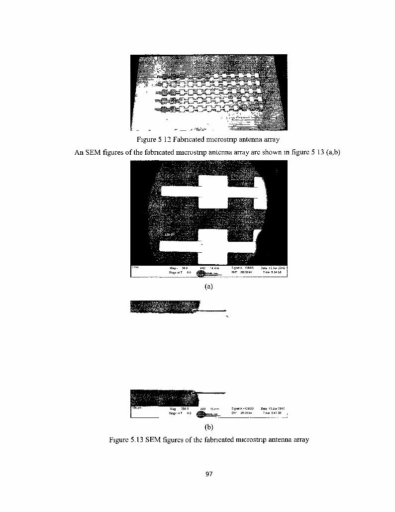
Figure 5 12 Fabncated microstnp antenna array
An SEM figures of the fabncated microstnp antenna array are shown in figure 5 13 (a,b)
(a)
Mag 250X WO 1 5 m m SgrtalA = G8CD Dnte 15Ju«2QlO
Stags a lT 0 0 ^ 8 6 k . - . - • EHT 20EJ0&V T mo 9 47 30
(b)
Figure 5.13 SEM figures of the fabncated microstnp antenna array
97

5.8 Conclusions
The Design, simulation and fabrication of a microstrip antenna array has been
presented. The microstrip antenna incorporates an inset fed instead of typical feed
mechanism to connect the array patches. This reduces the number of patches needed and
improves the antenna performance. The microstrip antenna array has been modeled and
simulated using HFSS software. The HFSS simulation results show that at 77 GHz, the
microstrip antenna array exhibits a return loss of better than -15 dB, antenna array gain of
18.3 dB, half power beam width (HPBW) of 9° and efficiency at the operating frequency
of 77%. A fabrication process sequence has been developed. The microstrip antenna is to
be used in conjunction with a MEMS based solid state Rotman lens to realize compact
MEMS radar for automotive collision avoidance application.
98

Chapter 6
Conclusions and Future Work 6.1 Conclusions
The thesis developed the architecture of a new MEMS based 77 GHz long range
FMCW radar for an automotive collision avoidance applications. The detailed design,
modeling and fabrication of the core components of the new radar: a microfabricated
Rotman lens, a MEMS SP3T RF switch, and an inset feed microstrip antenna array are
presented.
In the transmit segment, an FMCW signal is fed sequentially through the beam
ports of the microfabricated Rotman lens that has an intrinsic beamforming and
beamsteering capability. The output of the signal at the array ports of the Rotman lens are
radiated through the inset feed microstrip antenna array. In the receiving segment,
another set of antenna array, Rotman lens and SP3T switch and a mixer are used to
generate an IF signal corresponding to the echo signal reflected back from the target. An
FPGA based algorithm processes the digitized IF signal to extract the range and velocity
of the target vehicles.
The novel microfabricated Rotman lens eliminates the need for microelectronics
based analog or digital beamforming operations as necessary in conventional phased
array based FMCW automotive radars. This reduces the system complexity significantly,
enables to realize the complete radar sensor in a smaller form factor while offering
superior performance.
An extensive literature search has been performed to review the state-of-the-art in
automotive radars, radar technology, RF MEMS technology, and industry set
requirements to set up the target design specifications. To minimize the system
complexity and faster cycle time, a Rotman lens has been adopted for the beamforming
operation. As the Rotman lens is a passive device, it doesn't consume any power and
consequently, is free of all the issues related to microelectronic based analog or digital
beamforming operations including hardware related thermal drift and integration issues.
A novel technique has been developed to realize the Rotman lens in silicon so that
the lens can be batch fabricated using conventional microfabrication techniques to
99

minimize the manufacturing cost. The technique involves thermo-compression and
externally applied conductive epoxy bonding of two silicon wafers, one with the gold-
coated etched geometry and the other is a gold-coated planar geometry, to realize a TEio
mode rectangular waveguide type Rotman lens with air as the dielectric material filling
the lens cavity. The simple one mask fabrication of the Rotman lens has become possible
due to TEio rectangular waveguide type design that enabled to shrink the lens cavity to 50
um that can be easily realized using a DRIE technique.
The 77 GHz Rotman lens has a footprint area of 27x36.2 mm including the
transmission lines and incorporates 3 beam ports, 5 array ports, and 6 dummy ports to
prevent path loss due to sidewall reflections. The lens has been designed to steer the
beam by ± 4 degrees. The lens has been designed using full wave 3-D FEA simulation
using industry standard HFSS software and IntelliSuite™. The performance parameters
of the Rotman lens are optimized to get excellent values for the insertion losses, return
losses and characteristic impedance. The lens has been fabricated in the University of
Waterloo and University of Western Ontario and was assembled in Advotec Inc. in
Arizona.
The design, simulation and fabrication of a MEMS Single-Pole-Triple-Throw
(SP3T) RF switch to sequentially feed the FMCW signal among the beam ports of the
microfabricated Rotman lens has been presented. The series type MEMS RF switch relies
on electrostatic actuation of a microfbaricated cantilever beam and incorporates 1 input
port and 3 output ports. Two different versions of the MEMS RF switch have been
designed: a ground connecting bridge (GCB) conventional geometry where
microfabricated bridges have been used to provide the ground connectivity and a new
continuous ground (CG) without any bridge. Both the switches have been optimized for
operation in the 77 GHz; however, the CG version provides improved performance as it
eliminates the effects of coupling capacitance between the ports and the ground. The
HFSS simulation results show that at 77 GHz, the CG configuration has 4 dB
improvement for the return loss compared to the GCB version of the switch. The CG
version of the switch also exhibits 0.5 dB improvement for insertion loss and 3 dB
improvement for isolation as compared to the GCB version of the switch. The actuation
100

voltage of the switch is 16.3 volts. The GCB type SP3T RF switch has been fabricated
using the UWMEMS process and the fabrication of the CG version is in progress.
Finally, the design, simulation and fabrication of a microstrip antenna array that
forms an integral part of a MEMS based radar working in the 77 GHz range has been
presented. The microstrip antenna array incorporates 5 sub-arrays and 12 patches in each
sub-array. The design is based on a serial array inset fed method. The HFSS simulation
results show that at 77 GHz, the microstrip antenna array exhibits a return loss of better
than -15 dB, antenna array gain of 18.3 dB, half power beam width (HPBW) of 9° and an
efficiency of 77% at the operating frequency of 77 GHz.
It is expected that the developed radar sensor will be able to provide a cost
effective solution for long range radars to be used in an automotive collision avoidance
application.
6.2 Future work
MEMS Multimodal Radar
Investigation shows that the developed MEMS based radar technology can be
further extended to realize a compact multimode (long range, mid range and short range)
radar sensor as shown in the figure 6.1.
f / G H z VCO
p
SP3TT
(• -1
Reumfitjurable mcrostrtp
antenna array
-*\ ADC |
^
- &
Trans tnitied srgnal
<& Targe!
jxruxnr antenna
array
Swilcn ccmrol
Transmitter control
Signal process ng Target-velocity raige
^sfe distance
Dn,er notificalfon
CAN Bus
FOGAlASIC
Figure 6.1 MEMS Multimode radar block diagram
The conceived multimodal radar can operate in three basic modes: (1) long range (80-150
m), (2) mid-range (20-80 m), and (3) short range (0-20 m). While in operation, an FPGA
implemented algorithm controls the MEMS based RF switches to reconfigure a
101

microstrip antenna array to switch the radar constantly from one mode to another with a
pre-specified time constant to scan the near field and the far field regions. For the
multimode radar, in addition to the components and functionality of the currently
designed single mode radar, 2 additional sets of MEMS RF switches will be necessary as
shown in figure 6.2.
Microstrip Patch MEMS RF Switch
rn_ rn r~i r~kzJ~i r~i r~i r~u^~~i_r~i r~i r~i —r_j—i_j—L^j—LJ:sL^r-L-r-V-r-T--^L^—L-j—L^r-LJ —r~i_m m r~Ujm n r~i__rTc*(r"T_r~i__r_i rn —i_j-T_j~n_r—i_iaL_r—i_r—i_j—LJ^L-T-T—T-LJ—r_l _-j_i_j~n__rT_rrTKjr-a_i~T_JTT_ri)^^ —t: i—c i—L-j—L-p(<—r-uj-T-j-n-j^-tj—L_r—i_r-i_J — m r~i rn r""i™r~i n r~i f u j - ! r~i n r~]
C-J^T-J-L-TT—PT—r-T—TT-J—[—^L-n—T-!—!—LJ n n n mKnTT rn r~i c L-ai i r~i n r~i
—L-r i - j—L-r^^L^- i^ j—LJ—LJ ! : fL- r -L- j—Lj-n_J SW 1 SW 2
Figure 6.2 FPGA Reconfigurable microstrip antenna array
When both the switches are in the OFF position, 4 microstrip patches per linear array will
provide short range coverage. When the switch SW 1 is turned ON and SW 2 is OFF, 8
microstrip patches per linear array will provide mid-range range coverage. Finally, when
both the switches SW 1 and SW 2 are ON, 12 microstrip patches per linear array will
provide long range coverage. An FPGA implemented control algorithm with control the
operation of the switches. In this way a wider near-field area and a narrow far field area
can be covered with a minimum hardware. The initial timing constant has been decided
as 2 ms sweep time for each beam port (1 ms for up chirp, 1 ms for down chirp). The
characteristics of all the three modes are listed in figure 6.3.
A
De^ Host Vamrjr
SRR (30 multits) \ 1 MRR HQO ifwitor-.! I R R (?00 motors) T
Figure 6.3 Operation modes of the MEMS based automotive radar
102

References
[I] M. Camiade, D. Domnesque, Z Ouarch, A. Sion, "Fully MMIC-based Front End for
FMCW Automotive Radar at 77 GHz", Proceeding of European Microwave Week 2000
(GAAS), 2000, pp. 280-283.
[2] L. Hall, H. Hansen and D. Abbott, "Rotman lens for mm-wavelengths," Proc. SPIE
Smart Structures, Devices and Systems, Melbourne, Australia, Vol. 4935, 16-18
December 2002, pp 215-221.
[3] W. Rotman and R. Turner, "Wide-angle Microwave Lens for Line Source Applications,
"IEEE Transactions on Antennas and Propagation", vol. 11, pp. 623-632, 1963.
[4] G. J. Monser, "Advances in Lens-Fed Multibeam Technology," NTIS, p. 22, Feb 1992.
[5] D. H. Archer and M. J. Maybell, "Rotman lens development history at Raytheon
Electronic Warfare Systems 1967-1995," 2005, pp. 31-34 vol. 2B.
[6] D. H. Archer, "Lens-Fed Multiple-Beam Arrays," Microwave J., vol. 18, p. 6, Oct 1975.
[7] D. H. Archer, "Lens-Fed Multiple Beams Arrays," Microwave J., vol. 27, p. 6, 1984.
[8] World health organization WHO
[9] History of Radar, en.wikipedia.org/wiki/History_of_radar
[10] M. I. Skolnik, Radar Handbook, 2nd ed., New York: McGraw-Hill, 1970.
[II] A. Anderson. (November 2005). Mercedes-Benz Sudden Acceleration Incidents
[Online]. Available: http://www.antony-anderson.eom/Cruise/9.5 SA Links/Mercedes
20 Benz.html
[12] J. Wenger, "Automotive Radar - Status and Perspectives," in IEEE CSIC 2005 Dig.,
2005, Sitges (Spain), 2005, pp. 21-24.
[13] M. Schneider, "Automotive Radar - Status and Trends," in German Microwave Conf.
(GeMiC2005), Ulm (Germany), 2005, pp. 144-147.
[14] J. Wenger, "Automotive Radar - Status and Perspectives," in IEEE CSIC 2005 Dig.,
2005, Sitges (Spain), 2005, pp. 21-24.
[15] R. Schneider, J. Wenger, "Prototypic Realisation of Millimetre Wave Radar Imaging;
Advanced Microsystems for Automotive Applications 2003 (eds. J. Valldorf, W.
Gessner), Springer-VerlagBerlin Heidelberg, 2003, pp. 97-111.
[16] M. Camiade, D. Domnesque, Z Ouarch,, A. Sion, "Fully MMIC-based front end for
FMCW automotive radar at 77GHz, European Microwave Week, GaAs 2000
Proceedings, pp. 280-283, 2000.
103

[17] V. Jain, B. Javid, P. Heydari, "A 24/77GHz Dual-Band BiCMOS Frequency
Synthesizer," in IEEE 2008 Conf. Custom Integrated Circuits Conference (CICC), San
Jose, CA, 2008, pp. 487-490.
[18] V. Jain, B. Javid, P. Heydari, "A BiCMOS Dual-Band Millimeter-Wave Frequency
Synthesizer for Automotive Radars," IEEE J. Solid-State Circuits, Vol. 44, No. 8, pp.
2100-2113, Aug. 2009.
[19] TRW Automotive (2009). Adaptive Cruise Control (ACC) [Online]. Available:
http://www.trw.com/sites/default/files/DAS ACC Eng09 O.pdf
[20] H.-L. Bloecher, A. Sailer, G. Rollmann, J. Dickmann, "79 GHz UWB Automotive Short
Range Radar - Spectrum Allocation and Technology Trends," Adv. Radio Sc, Vol. 7,
2009, pp. 61-65.
[21] R. A. Mucci, "A Comparison of Efficient Beamforming Algorithms," IEEE Trans.
Acoustics, Speech, and Signal Processing, Vol. ASSP-32, No. 3, pp. 548-558, Jun.
1984.
[22] C. Wolff. (2008). Digital Beamforming [Online]. Available: http://www.radartutorial.eu
/06.antennas/an51 .en.html
[23] A.Sinjari, S. Chowdhury, "MEMS Automotive Collision Avoidence Radar
Beamformer", in Proc. of International Symposium on Circuits and Systems,ISCAS
2008, 18-21 May 2008, pp. 2086 - 2089.
[24] S. Weiss, S. Keller, and C. Ly, "Development of simple affordable beamformers for
army platforms, " presented at 2007 GOMACTech Conf, Lake Buena Vista, Fl, March.
2007.
[25] Jaeheung Kim, Senior Member, IEEE, Chul Soon Park, Senior Member, IEEE, and
Seungwook Min, "TM0 Mode Surface Wave Excited Dielectric Slab Rotman Lens,"
IEEE ANTENNAS AND WIRELESS PROPAGATION LETTERS, VOL. 6, 2007.
[26] Weiss, S., Dahlstrom, R., "Rotman Lens Development at the Army Research Lab",
IEEE Aerospace Conference 2006.pp. 1-7.
[27] Schulwitz, L., Mortazawi, A., "A New Low Loss Rotman Lens Design for Multibeam
Phased Arrays", IEEE MTT-S International Microwave Symposium Digest 2006. Pp
445-448.
[28] Jaeheung Kim, Senior Member, IEEE, Chul Soon Park, Senior Member, IEEE, and
Seungwook Min, "TM0 Mode Surface Wave Excited Dielectric Slab Rotman Lens,"
IEEE ANTENNAS AND WIRELESS PROPAGATION LETTERS, VOL. 6, 2007.
104

[29] mipoh J. Schoebel, T. Buck, M. Reimann, M. Ulm, M. Schneider, A. Jourdain, G.
Carchon, and H. A. C. Tilmans, "Design Considerations and Technology Assessment of
Phased-Array Antenna Systems with RF MEMS for Automotive Radar Applications,"
IEEE Trans. Antennas Prog., vol. AP-53, pp. 1968-1975, Jun. 2005.
[30] M. Daneshmand and R. R. Mansour, "Monolithic RF MEMS Switch Matrix
Integration", IEEE MTT-S, pp. 140 - 143, June 2006.
[31] G. Wang; H. Ding; W. Woods, and E. Mina, "Wideband on-chip RF MEMS Switches in
a BiCMOS Technology for 60 GHz Applications," International Conference on
Microwave and Millimeter Wave Technology ICMMT 2008, April 2008, vol. 3, pp.
1389-1392.
[32] L.E. Larson, R.H. Hachett, R.F. Lohr, "Microactuators for GaAs-Based Microwave
Integrated Circuits", Digest of technical papers; Solid State Sensors and Actuators,
P.743-746, June 1991.
[33] I.J. Bahl and P. Bhartia, "Microstrip Antennas", Canton, Mass., Artech House, 1980
[34] Constantine A. Balanis, "Antenna theory, analysis and design", Wiley interscience,
2005
[35] K. R. Carver and J. W. Mink, "Microstrip Antenna Technology," IEEE Trans. Antennas
Propagat., Vol. AP-29, No. 1, pp. 2-24, January 1981.
[36] J. R. James and P. S. Hall, Handbook of Microstrip Antennas, Vols. 1 and 2, Peter
Peregrinus, London, UK, 1989.
[37] D. M. Pozar, "Microstrip Antennas," Proc. IEEE, Vol. 80, No. 1, pp. 79-81, January
1992.
[38] H. G. Oltman and D. A. Huebner, "Electromagnetically Coupled Microstrip Dipoles,"
IEEE Trans. Antennas Propagat., Vol. AP-29, No. 1, pp. 151-157, January 1981.
[39] G. Gronau and I. Wolff, "Aperture-Coupling of a Rectangular Microstrip Resonator,"
Electronic Letters, Vol. 22, pp. 554-556, May 1986.
[40] F. D. L. Peters, B. Boukari, S. O. Tatu, and T. A. Denidni, "77GHz Millimeter wave
antenna array with Wilkinson divider feeding network," Progress In Electromagnetics
Research Letters, Vol. 9, pp. 193-199, 2009
[41] Vinod Kumar Singh, Ashok Mittal, "design of wide-band microstrip antenna array at
millimeter wave frequencies", DEAL, Government of India, 2000
[42] Heui Cho, Cheol-Sik Pyo and Jae-Ick Choi, "A High-Gain Microstrip Patch Array
Antenna Using a Superstrate Layer", ETRI Journal, vol. 25, no. 5, Oct 2003, pp. 407-
411 105

[43] A. Anderson. (November 2005). Mercedes-Benz Sudden Acceleration Incidents
[Online]. Available: http://www.antony-anderson.eom/Cruise/9.5 SA Links/Mercedes
20 Benz.html
[44] H. Rohling, Some Radar Topics: Waveform Design, Range CFAR and Target
Recognition, Advances in Sensing with Security Applications. [NATO Security Through
Science Book Series, Vol. 2]. Netherlands: Springer Netherlands, 2006. (ISBN: 978-1-
4020-4284-3)
[45] Y. K. Chan, S. Y. Lim, "Synthetic Aperture Radar (SAR) Signal Generation," Progress
in Electromagnetics Research B, Vol. 1, pp. 269-290, 2008.
[46] P. C. Sharma, R. D. Gupta and P. K. Singhal, "Recent Trades in Design and Analysis of
Rotman Type Lens for Multiple Beamforming", International Journal of RF and
Microwave Computer aided Engineering CAE 8, pp 321-338, 1998.
[47] L. Musa and M. S. Smith; "Microstrip Port Design and Sidewall Absorption for Printed
Rotman Lenses," IEE Proceedings on Microwaves, Antennas and propagation, vol.
136, Issue 1, pp. 53-58, Feb. 1989.
[48] Y. M. Tao, G. Y. Delisle, "Multiple Beam Antenna Arrays for Indoor Communications,
ANTEM96, Montreal (Quebec), 6-9 August 1996, pp. 725-728.
[49] T. Tsurumi, S. Ozawa and S. Wada, "Preparation of PZT Thick Films by an Interfacial
Polymerization Method", Journal of Sol-Gel Science and Technology, Vol 26, pp. 1037-
1040, Jan. 2003.
[50] L. Jang and K. Kuo, "Fabrication and Characterization of PZT Thick Films for Sensing
and Actuation", proc. of Sensors 2007, 2007, vol. 7, pp 493-507.
[51] David Pozar, Microwave Engineering, 3r Edition, Wiley and sons (2003).
[52] High isolation and low insertion loss switch IC using GaAs MESFETs', IEEE
Transactions Microwave Theory and Techniques 43: 2175-2177.
[53] V. K. Varadan, K J Vinoy, K. A. Jose,: RF MEMS and their applications, John Wiley &
Sons, 2003.
[54] Grant, P.D., Denhoff, M.W., Mansour, R.R., "A comparison between RF MEMS
Switches and Semiconductor Switches", ICMENS International Conference on MEMS,
NANO and Smart Systems, pp 515-521, August 2004
[55] G. M. Rebeiz, RF MEMS Theory, Design, and Technology: John Wiley & Sons, 2003.
[56] J. Schobel, T. Buck, M. Reimann, M. Ulm, M. Schneider, "W-band RF-MEMS
Subsystems for Smart Antennas in Automotive Radar Sensors," in Proc. of 34th
European Microwave Conference, 11-15 Oct. 2004, vol. 3, pp. 1305 - 1308. 106

[57] R. N. Simons, Coplanar Waveguide Circuits, Components and Systems. John Wiley &
Sons, Inc, 2001.
[58] J. Rizk and G. M. Rebeiz, "W-band CPW RF MEMS circuits on Quartz Substrates,"
IEEE Transactions on Microwave Theory and Techniques, vol. 51, no. 7, pp. 1857 -
1862,July 2003.
[59] James R. Andrews, "Broadband Coaxial Bias Tees", Picosecond Pulse Labs, November
2000
[60] UW-MEMS design handbook, University of Waterloo.
[61] Hyman, D., Lam, J., Warneke, B., Schmitz, A., Hsu, T.Y., Brown, J., Schaffner, J.,
Waltson, A., Loo, R.Y., Mehregany, M., Lee, J., 1999a, 'Surface micromachined RF
MEMS switches on GaAs Substrates', InternationalJournal ofRF and Computer Aided
Engineering 9: 348-361.
[62] Rebeiz, G.M.; Muldavin, J.B. RF MEMS switches and switch circuits. IEEE
Microwave. Mag. 2001, 2, 59-71.
[63] Ghodsian, B.; Bogdanoff, P.; Hyman, D.; "Wideband DC-contact MEMS series
switch", Micro & Nano Letters, September 2008 Page(s):66 - 69.
[64] E. R. Brown, "RF-MEMs switches for reconfigurable integrated circuits," IEEE
Transactions on Microwave Theory and Techniques, vol. 46, no. 11, pp. 1868-1880,
November 1998.
[65] Clark MXR corporation in Dexter, Michigan, USA.
107

Patents and papers produced during Ph.d. study
Patents
1. IP Protection Strategy For Radar Device published in United States Patents and
Trademark Office. (US 61/282,595, March 5, 2010)
2. Three more patents in process
Papers
1. A.Sinjari, S. Chowdhury, "MEMS Automotive Collision Avoidence Radar
Beamformer", in Proc. of International Symposium on Circuits and Systems,ISCAS 2008,
18-21 May 2008, pp. 2086 - 2089, Seatle, Washington.
2. A. Sinjari, S. Chowdhury, "Design of a PZT-based MEMS Rotman lens", in Proc. of
Canadian Conference on Electrical and Computer Engineering (CCECE 2008), 4-7
May 2008, pp. 1121-1124, Niagara falls, Ontario.
3. A. Sinjari, S. Chowdhury, "A Single-Pole-Triple-Throw (SP3T) MEMS RF Switch for
24 GHz Short Range Radar", in IEEE INTERNATIONAL CONFERENCE on
ELECTRO/INFORMATION TECHNOLOGY, 7-9 June 2009, Windsor, Ontario.
4. A. Sinjari, S. Chowdhury, "High Performance 77 GHz Single Pole Triple Throw (SP3T)
MEMS Switch", in Joint conference IEEE Toulouse France NEWCAS-TAISA '09, June
28-July 01 2009, Toulouse, France.
5. A. Sinjari, S. Chowdhury, "MEMS sensors in automotive collision avoidende systems",
in Ontario centre of excellence, Special poster presentation, May 9 2008, Toronto,
Ontario.
6. A. Sinjari, S. Chowdhury, "MEMS sensors for an integrated active vehicle safety
systems (IAVSS)", in North American international auto show(NAIAS), Special poster
presentation, Janl 6-172008,Detroit,Michigan
108

Appendix A
Program code for Rotman lens design
$begin 'AnsoftPro^ect' Product='HFSS' NextUmqueID=0 MoveBackwards=false $begin 'Desktop'
Version(ll, 0) InfrastructureVersion(1, 0)
$end 'Desktop' $begin 'HFSSEnvironment'
Versiond, 0) $end 'HFSSEnvironment' $begin 'geometry3deditor'
Version(l, 0) $end 'geometry3deditor' $begm 'ProjectDatasets'
NextUmqueID=0 MoveBackwards=false DatasetType='ProjectDatasetType' $begm ' DatasetDef mitions ' $end ' DatasetDef mitions '
$end 'ProjectDatasets' $begin 'Definitions'
$begm 'Folders' Definitions(1104, 10000, 1, 1, 0, false, false) Materials(1104, 9500, 9, 2, 1, false, false)
$end 'Folders' $begm 'Materials'
$begin 'vacuum' CoordmateSystemType=' Cartesian' $begin 'AttachedData' $end 'AttachedData' $begin 'ModiflerData' $end 'ModifierData' permittivity='1' ModTime=1028307 964 Library='Materials' LibLocation='SysLibrary '
$end 'vacuum' $begm 'gold'
CoordmateSystemType=' Cartesian' $begin 'AttachedData' $end 'AttachedData' $begin 'ModifierData' $end 'ModifierData' permeability='0.99996 ' conductivity='41000000' thermal_conductivity='315' mass_density='19300' specific_heat='129' youngs_modulus='80000000000' poissons_ratio='0.4' thermal_expansion_coeffcient='1.4e-005' ModTime=1132068239 Library='Materials' LibLocation='SysLibrary '
109

$end 'gold' $end 'Materials' $begm 'Scripts' $end 'Scripts'
$end 'Definitions' DesignIDServer=4 MoveBackwards=false $begm 'HFSSModel'
RepRewriteV2=true Name='HFSSDesignl' DesignID=0 'Allow Material Override'=false SolutionType='DrivenModal' MaterialDensity=l MassOfTissue=l $begm ' OutputVariable'
NextUmqueID=0 MoveBackwards=false
$end 'OutputVariable' $begm 'ModelSetup'
$begm 'Editor3D Doc Preferences' 'Plane Background'=true BackgroundColorl=167 7 7215 BackgroundColor2=0 'Need Lights'=true 'Ambient Light'=8355711 'Num Lights'=2 Light0[4: 8355711, 0.200000002980232,
0.400000005960464, 1] Lightl[4: 8355711, -0.200000002980232, -
0.400000005960464, -1] $end 'Editor3D Doc Preferences' $begm ' DesignDatasets'
NextUmqueID=0 MoveBackwards=false DatasetType='DesignDatasetType' $begm ' DatasetDef mitions ' $end ' DatasetDef mitions '
$end 'DesignDatasets' SnapMode=2 GroupByMaterial=true GroupSheetByMaterial=false $begm 'GeometryCore'
BlockVersionID=3 NativeKernel='ACIS' NativeKernelVersionID=l Units='mm' InstanceID=-l ExternalNativeGeometryAllowed=false $begm ' ValidationOptions'
EntityCheckLevel='Strict' $end 'ValidationOptions' $begm ' GeometryOperations'
BlockVersionID=2 $begm 'AnsoftRangedlDServerManager'
$begm 'AnsoftRangedlDServer' IDServerOb]ectTypeID=0 IDServerRangeMm=0
110

IDServerRangeMax=2146483647 NextUmqueID=4 525 MoveBackwards=false
$end 'AnsoftRangedlDServer' $begin 'AnsoftRangedlDServer'
IDServerObjectTypeID=l IDServerRangeMin=2146483648 IDServerRangeMax=2146485547 NextUmqueID=214 64 83 654 MoveBackwards=false
$end 'AnsoftRangedlDServer' $end 'AnsoftRangedlDServerManager' StartBackGroundFaceID=214 64 8364 8 $begin 'CoordinateSystems' $end 'CoordinateSystems' $begin 'ToplevelParts'
$begin 'GeometryPart' $begin 'Attributes'
Name='Polyline57 ' Flags='' Color='(132 132 193)'
Transparency=0.4 000000059604 64 PartCoordmateSystem=l MaterialName='vacuum' Solveinside=true
$end 'Attributes' $begin 'Operations'
$begin 'Operation'
OperationType='Polyline' ID=3599
ReferenceCoordSys temID=l $beg in
' P o l y l m e P a r a m e t e r s ' K e r n e l V e r s i o n = l
C o o r d m a t e S y s t e m I D = - l
I s P o l y l i n e C l o s e d = t r u e
' P o l y l i n e P o i n t s '
' P L P o i n t '
$begin 'rectangle' rectangle(16, 17, 18, 19, 27)
$end 'rectangle' $begin 'rectanglel7_'
rectanglel7_(1, 2, 3, 4) $end 'rectanglel7_'
$end 'CachedNames' $end 'GeometryOperations' $begin 'GeometryDependencies'
$begm 'Dependencylnformation' NumParents=l
$begin
$begin
111

$begin 'Dependencylnformation' NumParents=2
DependencyObject('GeometryBodyOperation', 1877)
DependencyObject('GeometryBodyOperation', 1876) DependencyObject ( ' CoordmateSystem' ,
1) $end 'Dependencylnformation' $begm 'Dependencylnformation'
NumParents=2
DependencyOb^ect('GeometryBodyOperation', 1878)
DependencyOb^ect('GeometryBodyOperation', 1877) DependencyOb] ect (' CoordmateSystem' ,
1) $end 'Dependencylnformation' $begin 'Dependencylnformation'
NumParents=2
DependencyObject('GeometryBodyOperation', 187 9)
DependencyObject('GeometryBodyOperation', 1878) DependencyOb^ect ( 'CoordmateSystem' ,
1) $end 'Dependencylnformation' $begin 'Dependencylnformation'
NumParents=2
DependencyObject('GeometryBodyOperation', 1880)
DependencyOb^ect('GeometryBodyOperation', 187 9) DependencyObj ect (' CoordmateSystem' ,
1) $end 'Dependencylnformation' $begm 'Dependencylnformation'
NumParents=2
DependencyObject('GeometryBodyOperation', 1936)
DependencyOb^ect (' CoordmateSystem' , 1)
DependencyOb^ect('GeometryBodyOperation', 1880) $end 'Dependencylnformation' $begm 'Dependencylnformation'
NumParents=2
DependencyObject('GeometryBodyOperation' , 1942)
DependencyObject ( ' CoordmateSystem' , 1)
DependencyObject('GeometryBodyOperation' , 1936) $end 'Dependencylnformation' $begm 'Dependencylnformation'
NumParents=2
DependencyObject('GeometryBodyOperation' , 1945)
112

1) DependencyObject ( ' CoordmateSystem' ,
DependencyObject('GeometryBodyOperation', 1942) $end 'Dependencylnformation' $begin 'Dependencylnformation'
NumParents=2
DependencyObject('GeometryBodyOperation' , 1951)
DependencyObject ( ' CoordmateSystem' , 1)
DependencyOb^ect('GeometryBodyOperation' , 1945) $end 'Dependencylnformation' $begin 'Dependencylnformation'
NumParents=2
DependencyObject('GeometryBodyOperation' , 1954)
DependencyOb] ect ( ' CoordmateSystem' , 1)
DependencyObject('GeometryBodyOperation' , 1951) $end 'Dependencylnformation' $begm 'Dependencylnformation'
NumParents=2
DependencyObject('GeometryBodyOperation', 1980) DependencyObj ect ( ' CoordmateSystem' ,
1)
DependencyObj ect('GeometryBodyOperation', 1954) $end 'Dependencylnformation' $begm 'Dependencylnformation'
NumParents=2
DependencyOb^ect('GeometryBodyOperation' , 1982)
DependencyObj ect ( ' CoordmateSystem' , 1)
DependencyObject('GeometryBodyOperation', 1980) $end 'Dependencylnformation' $begin 'Dependencylnformation'
NumParents=2
DependencyObject('GeometryBodyOperation', 1983)
DependencyObject ( 'CoordmateSystem', 1)
DependencyObject('GeometryBodyOperation' , 1982) $end 'Dependencylnformation' $begm 'Dependencylnformation'
NumParents=l
DependencyObject('GeometryBodyOperation', 1958) DependencyObject ( ' CoordmateSystem' ,
1) $end 'Dependencylnformation' $begin 'Dependencylnformation'
113

NumParents=l
DependencyObiect('GeometryBodyOperation', 1968)
DependencyObject('GeometryBodyOperation', 1958) $end 'Dependencylnformation' $begin 'Dependencylnformation'
NumParents=2
DependencyObiect('GeometryBodyOperation', 1970)
DependencyObiect('GeometryBodyOperation', 1968) DependencyObiect ( ' CoordmateSystem' ,
1) $end 'Dependencylnformation' $begin 'Dependencylnformation'
NumParents=2
DependencyObiect('GeometryBodyOperation', 1971)
DependencyObject('GeometryBodyOperation', 1970) DependencyObj ect ( ' CoordmateSystem' ,
1) $end 'Dependencylnformation' $begm 'Dependencylnformation'
NumParents=2
DependencyObiect('GeometryBodyOperation', 1972)
DependencyObiect('GeometryBodyOperation', 1971) DependencyOb] ect ( ' CoordmateSystem' ,
1) $end 'Dependencylnformation' $begin 'Dependencylnformation'
NumParents=2
DependencyObiect('GeometryBodyOperation', 1973)
DependencyObject('GeometryBodyOperation', 1972) DependencyObiect ( 'CoordmateSystem' ,
1) $end 'Dependencylnformation' $begm 'Dependencylnformation'
NumParents=2
DependencyOb3ect('GeometryBodyOperation', 197 4)
DependencyOb3ect('GeometryBodyOperation' , 1973) DependencyObiect ( ' CoordmateSystem' ,
1) $end 'Dependencylnformation' $begm 'Dependencylnformation'
NumParents=2
DependencyObject('GeometryBodyOperation', 1975)
DependencyObiect('GeometryBodyOperation', 1974)
114

DependencyObiect ( ' CoordmateSystem' , 1)
1)
1)
1)
1)
$end 'Dependencylnformation' $begm 'Dependencylnformation'
NumParents=2
DependencyObiect('GeometryBodyOperation', 1976)
DependencyObiect('GeometryBodyOperation' , 1975) DependencyObj ect ( ' CoordmateSystem' ,
$end 'Dependencylnformation' $begin 'Dependencylnformation'
NumParents=2
DependencyObject('GeometryBodyOperation' , 1977)
DependencyObiect('GeometryBodyOperation', 1976) DependencyOb] ect ( ' CoordmateSystem' ,
$end 'Dependencylnformation' $begm 'Dependencylnformation'
NumParents=2
DependencyObject('GeometryBodyOperation' , 197 8)
DependencyObject{'GeometryBodyOperation' , 197 7) DependencyObject ( 'CoordmateSystem' ,
$end 'Dependencylnformation' $begin 'Dependencylnformation'
NumParents=2
DependencyOb]ect('GeometryBodyOperation', 1979)
DependencyObject('GeometryBodyOperation', 1978) DependencyObiect ( ' CoordmateSystem' ,
$end 'Dependencylnformation' $begm 'Dependencylnformation'
NumParents=l
DependencyOb]ect('GeometryBodyOperation', 1984 ) DependencyObiect ( ' CoordmateSystem',
$end 'Dependencylnformation' $begm 'Dependencylnformation'
NumParents=l
DependencyObject('GeometryBodyOperation', 1994 )
DependencyObiect('GeometryBodyOperation' , 1984) $end 'Dependencylnformation' $begin 'Dependencylnformation'
NumParents=2
DependencyObject('GeometryBodyOperation', 1996)
115

D e p e n d e n c y O b j e c t ( ' G e o m e t r y B o d y O p e r a t i o n ' , 1994) DependencyObiect ( ' C o o r d m a t e S y s t e m ' ,
1) $end 'Dependencylnformation' $begin 'Dependencylnformation'
NumParents=2
DependencyObiect('GeometryBodyOperation' , 1997)
DependencyObiect('GeometryBodyOperation', 1996) DependencyObiect ( ' CoordmateSystem' ,
1) $end 'Dependencylnformation' $begm 'Dependencylnformation'
NumParents=2
DependencyObiect('GeometryBodyOperation' , 1998)
DependencyObiect('GeometryBodyOperation', 1997) DependencyObj ect (' CoordmateSystem' ,
1) $end 'Dependencylnformation' $begm 'Dependencylnformation'
NumParents=2
DependencyObiect('GeometryBodyOperation' , 1999)
DependencyObiect('GeometryBodyOperation', 1998) DependencyObject ( ' CoordmateSystem' ,
1) $end 'Dependencylnformation' $begm 'Dependencylnformation'
NumParents=2
DependencyObiect('GeometryBodyOperation' , 2000)
DependencyObiect('GeometryBodyOperation', 1999) DependencyObject (' CoordmateSystem' ,
1) $end 'Dependencylnformation' $begm 'Dependencylnformation'
NumParents=2
DependencyObiect('GeometryBodyOperation' , 2001)
DependencyObiect('GeometryBodyOperation', 2000) DependencyObject ( ' CoordmateSystem' ,
1) $end 'Dependencylnformation' $begm 'Dependencylnformation'
NumParents=2
DependencyObiect('GeometryBodyOperation', 2002)
DependencyOb]ect('GeometryBodyOperation', 2001)
DependencyOb] ect ( ' CoordmateSystem' ,
1)
116

$end 'Dependencylnformation' $begin 'Dependencylnformation'
NumParents=2
DependencyObject('GeometryBodyOperation', 2003)
DependencyObj ect('GeometryBodyOperation', 2002) DependencyObject ( ' CoordmateSystem' ,
1) $end 'Dependencylnformation' $begin 'Dependencylnformation'
NumParents=2
DependencyObject('GeometryBodyOperation', 2004)
DependencyObject('GeometryBodyOperation' , 2003) DependencyOb] ect (' CoordmateSystem' ,
1) $end 'Dependencylnformation' $begin 'Dependencylnformation'
NumParents=2
DependencyObject('GeometryBodyOperation', 2005)
DependencyObject('GeometryBodyOperation' , 2004) DependencyObject ( 'CoordmateSystem' ,
1) $end 'Dependencylnformation' $begm 'Dependencylnformation'
NumParents=2
DependencyOb^ect('GeometryBodyOperation', 2006)
DependencyOb^ect('GeometryBodyOperation', 2005) DependencyOb] ect ( ' CoordmateSystem' ,
1) $end 'Dependencylnformation' $begm 'Dependencylnformation'
NumParents=2
DependencyObject('GeometryBodyOperation', 2007)
DependencyObject('GeometryBodyOperation', 2006) DependencyObj ect ( ' CoordmateSystem' ,
1) $end 'Dependencylnformation' $begin 'Dependencylnformation'
NumParents=l
DependencyOb^ect('GeometryBodyOperation' , 204 9) DependencyObject ( 'CoordmateSystem' ,
1) $end 'Dependencylnformation' $begm 'Dependencylnformation'
NumParents=l
DependencyOb^ect('GeometryBodyOperation' , 2061)
117

DependencyObiect('GeometryBodyOperation', 204 9) $end 'Dependencylnformation' $begin 'Dependencylnformation'
NumParents=2
DependencyObiect('GeometryBodyOperation' , 2085)
DependencyObiect('GeometryBodyOperation', 2061)
DependencyObiect('GeometryBodyOperation', 2073) $end 'Dependencylnformation' $begm 'Dependencylnformation'
NumParents=2
DependencyObiect('GeometryBodyOperation', 2144)
DependencyObi ect ( ' CoordmateSystem' , 1)
DependencyObiect('GeometryBodyOperation', 2085) $end 'Dependencylnformation' $begm 'Dependencylnformation'
NumParents=2
DependencyObiect('GeometryBodyOperation' , 2145) DependencyObi ect ( ' CoordmateSystem' ,
1)
DependencyObiect('GeometryBodyOperation', 214 4) $end 'Dependencylnformation' $begin 'Dependencylnformation'
NumParents=2
DependencyObiect('GeometryBodyOperation' , 214 6)
DependencyObiect ( 'CoordmateSystem' , 1)
DependencyObiect('GeometryBodyOperation' , 214 5) $end 'Dependencylnformation' $begin 'Dependencylnformation'
NumParents=2
DependencyObiect('GeometryBodyOperation', 2180)
DependencyObi ect ( ' CoordmateSystem' , 1)
DependencyObiect('GeometryBodyOperation' , 2146) $end 'Dependencylnformation' $begin 'Dependencylnformation'
NumParents=2
DependencyObiect('GeometryBodyOperation' , 2182)
DependencyObi ect ( ' CoordmateSystem' ,
1)
DependencyObiect('GeometryBodyOperation' , 2180) $end 'Dependencylnformation' $begm 'Dependencylnformation'
118

NumParents=2
1)
1)
1)
1)
DependencyObject('GeometryBodyOperation', 2218) DependencyObject('CoordinateSystem',
DependencyObject('GeometryBodyOperation', 2182) $end 'Dependencylnformation' $begin 'Dependencylnformation'
NumParents=2
DependencyObject('GeometryBodyOperation', 2219) DependencyObject('CoordinateSystem' ,
DependencyObject('GeometryBodyOperation', 2218) $end 'Dependencylnformation' $begin 'Dependencylnformation'
NumParents=2
DependencyObj ect('GeometryBodyOperation' , 2257) DependencyObject('CoordinateSystem',
DependencyObj ect('GeometryBodyOperation', 2219) $end 'Dependencylnformation' $begin 'Dependencylnformation'
NumParents=2
DependencyObject('GeometryBodyOperation' , 22 58) DependencyObject('CoordinateSystem' ,
DependencyObject('GeometryBodyOperation', 2257) $end 'Dependencylnformation' $begin 'Dependencylnformation'
NumParents=2
DependencyObj ect('GeometryBodyOperation' , 2375)
DependencyObj ect('GeometryBodyOperation', 2258)
DependencyObject('GeometryBodyOperation' , 2111) $end 'Dependencylnformation' $begin 'Dependencylnformation'
NumParents=l
DependencyObject('GeometryBodyOperation' , 2063) DependencyObject('CoordinateSystem' ,
$end 'Dependencylnformation' $begin 'Dependencylnformation'
NumParents=l
DependencyObject('GeometryBodyOperation' , 2073)
DependencyObject('GeometryBodyOperation', 2063) $end 'Dependencylnformation'
119

$begin 'Dependencylnformation' NumParents=l
DependencyObject('GeometryBodyOperation', 2089) DependencyObject('CoordinateSystem' ,
1) $end 'Dependencylnformation' $begin 'Dependencylnformation'
NumParents=l
DependencyObject('GeometryBodyOperation' , 2 0 99)
DependencyObject('GeometryBodyOperation' , 208 9) $end 'Dependencylnformation' $begin 'Dependencylnformation'
NumParents=2
DependencyObject('GeometryBodyOperation', 2113)
DependencyOb]ect('CoordinateSystem', 1)
DependencyOb^ect('GeometryBodyOperation', 2099) $end 'Dependencylnformation' $begin 'Dependencylnformation'
NumParents=2
DependencyOb^ect('GeometryBodyOperation', 237 9)
DependencyObject('CoordinateSystem', 1)
DependencyObject('GeometryBodyOperation', 2113) $end 'Dependencylnformation' $begm 'Dependencylnformation'
NumParents=2
DependencyOb^ect('GeometryBodyOperation', 3344)
DependencyObject('CoordinateSystem', 1)
DependencyObject('GeometryBodyOperation', 237 9) $end 'Dependencylnformation' $begin 'Dependencylnformation'
NumParents=0 DependencyObj ect('GeometryOperation',
3367) $end 'Dependencylnformation' $begin 'Dependencylnformation'
NumParents=0 DependencyOb]ect('GeometryOperation',
3380) $end 'Dependencylnformation' $begin 'Dependencylnformation'
NumParents=l
DependencyObject('GeometryBodyOperation', 2101) DependencyOb]ect('CoordinateSystem',
1) $end 'Dependencylnformation'
120

$begin 'Dependencylnformation' NumParents=l
DependencyObject('GeometryBodyOperation', 2111)
DependencyOb]ect('GeometryBodyOperation', 2101) $end 'Dependencylnformation' $begin 'Dependencylnformation'
NumParents=0 DependencyOb^ect('GeometryOperation',
$end 'Dependencylnformation' $begin 'Dependencylnformation'
NumParents=0 DependencyObject('GeometryOperation',
$end 'Dependencylnformation' $begm 'Dependencylnformation'
NumParents=0 DependencyOb]ect('GeometryOperation',
$end 'Dependencylnformation' $begin 'Dependencylnformation'
NumParents=l
DependencyOb^ect('GeometryBodyOperation', 2114) DependencyObject ( ' CoordmateSystem' ,
$end 'Dependencylnformation' $begm 'Dependencylnformation'
NumParents=l
DependencyOb^ect('GeometryBodyOperation', 2126)
DependencyObject('GeometryBodyOperation', 2114) $end 'Dependencylnformation' $begm 'Dependencylnformation'
NumParents=2
DependencyObject('GeometryBodyOperation', 2128)
DependencyObject('GeometryBodyOperation', 212 6)
DependencyObject('GeometryBodyOperation', 2142) $end 'Dependencylnformation' $begin 'Dependencylnformation'
NumParents=l
DependencyOb^ect('GeometryBodyOperation', 2132) DependencyObj ect (' CoordmateSystem' ,
$end 'Dependencylnformation' $begin 'Dependencylnformation'
NumParents=l
DependencyOb^ect('GeometryBodyOperation', 2142)
DependencyOb^ect('GeometryBodyOperation', 2132)
121

$end 'Dependencylnformation' $begm 'Dependencylnformation'
NumParents=l
DependencyOb^ect('GeometryBodyOperation', 2380) DependencyObject ( ' CoordmateSystem' ,
) $end 'Dependencylnformation' $begm 'Dependencylnformation'
NumParents=l
DependencyOb^ect('GeometryBodyOperation' , 2388)
DependencyOb]ect('GeometryBodyOperation' , 2380) $end 'Dependencylnformation' $begm 'Dependencylnformation'
NumParents=2
DependencyObject('GeometryBodyOperation' , 2390)
DependencyOb^ect('GeometryBodyOperation', 2388)
DependencyObj ect('GeometryBodyOperation', 2375) $end 'Dependencylnformation' $begm 'Dependencylnformation'
NumParents=l
DependencyOb^ect('GeometryBodyOperation', 2846) DependencyOb] ect ( ' CoordmateSystem' ,
) $end 'Dependencylnformation' $begm 'Dependencylnformation'
NumParents=l
DependencyObject('GeometryBodyOperation', 2 8 68)
DependencyObject('GeometryBodyOperation', 2846) $end 'Dependencylnformation' $begm 'Dependencylnformation'
NumParents=2
DependencyObject('GeometryBodyOperation' , 2870)
DependencyObj ect ( ' CoordmateSystem' , )
DependencyOb^ect('GeometryBodyOperation', 28 68) $end 'Dependencylnformation' $begm 'Dependencylnformation'
NumParents=2
DependencyObject('GeometryBodyOperation' , 2878)
DependencyObject (' CoordmateSystem' , )
DependencyObject('GeometryBodyOperation' , 2870) $end 'Dependencylnformation' $begm 'Dependencylnformation'
NumParents=2
122

DependencyObnect('GeometryBodyOperation', 2906)
DependencyObj ect { ' CoordmateSystem' , 1)
DependencyObnect('GeometryBodyOperation' , 2878) Send 'Dependencylnformation' $begin 'Dependencylnformation'
NumParents=2
DependencyObnect('GeometryBodyOperation', 2 907)
DependencyOb] ect ( ' CoordmateSystem' , 1)
DependencyObnect('GeometryBodyOperation' , 2906) $end 'Dependencylnformation' $begm 'Dependencylnformation'
NumParents=2
DependencyObnect('GeometryBodyOperation', 2908)
DependencyObnect ( 'CoordmateSystem' , 1)
DependencyObnect('GeometryBodyOperation', 2 907) $end 'Dependencylnformation' $begm 'Dependencylnformation'
NumParents=l
DependencyObnect('GeometryBodyOperation', 2 910) DependencyObnect ( 'CoordmateSystem' ,
1) $end 'Dependencylnformation' $begm 'Dependencylnformation'
NumParents=l
DependencyObnect('GeometryBodyOperation' , 2 932)
DependencyObnect('GeometryBodyOperation' , 2 910) $end 'Dependencylnformation' $begm 'Dependencylnformation'
NumParents=2
DependencyObnect('GeometryBodyOperation', 2 934)
DependencyObnect('GeometryBodyOperation' , 2932) DependencyObn ect (' CoordmateSystem' ,
1) $end 'Dependencylnformation' $begm 'Dependencylnformation'
NumParents=2
DependencyObnect('GeometryBodyOperation' , 2935)
DependencyObnect('GeometryBodyOperation', 2934) DependencyObn ect (' CoordmateSystem' ,
1) $end 'Dependencylnformation' $begm 'Dependencylnformation'
123

1)
1)
1)
1)
1)
NumParents=l
DependencyObject('GeometryBodyOperation', 2 995) DependencyOb]ect('CoordinateSystem',
$end 'Dependencylnformation' $begin 'Dependencylnformation'
NumParents=l
DependencyOb]ect('GeometryBodyOperation', 3005)
DependencyObject('GeometryBodyOperation', 2995) $end 'Dependencylnformation' $begin 'Dependencylnformation'
NumParents=2
DependencyObject('GeometryBodyOperation', 3007)
DependencyOb^ject (' GeometryBodyOperation' , 3005) DependencyOb]ect('CoordinateSystem',
$end 'Dependencylnformation' $begin 'Dependencylnformation'
NumParents=2
DependencyObject('GeometryBodyOperation' , 3008)
DependencyObj ect('GeometryBodyOperation', 3007) DependencyOb]ect('CoordinateSystem',
$end 'Dependencylnformation' $begin 'Dependencylnformation'
NumParents=2
DependencyOb^ect('GeometryBodyOperation', 3009)
DependencyOb]ect('GeometryBodyOperation', 3008) DependencyOb]ect('CoordinateSystem',
$end 'Dependencylnformation' $begin 'Dependencylnformation'
NumParents=2
DependencyObject('GeometryBodyOperation' , 3010)
DependencyObject('GeometryBodyOperation', 3009) DependencyObject('CoordinateSystem' ,
$end 'Dependencylnformation' $begm 'Dependencylnformation'
NumParents=2
DependencyOb^ect('GeometryBodyOperation', 3011)
DependencyObject('GeometryBodyOperation', 3010) DependencyOb^ect('CoordinateSystem',
$end 'Dependencylnformation'
124

$begin 'Dependencylnformation' NumParents=2
DependencyObnect('GeometryBodyOperation', 3012)
DependencyObnect('GeometryBodyOperation' , 3011) DependencyObj ect('CoordinateSystem' ,
1) $end 'Dependencylnformation' $begin 'Dependencylnformation'
NumParents=2
DependencyObnect('GeometryBodyOperation' , 3013)
DependencyObject('GeometryBodyOperation' , 3012) DependencyObject('CoordinateSystem' ,
1) $end 'Dependencylnformation' $begin 'Dependencylnformation'
NumParents=l
DependencyObnect('GeometryBodyOperation', 3014) DependencyObnect('CoordinateSystem' ,
1) $end 'Dependencylnformation' $begin 'Dependencylnformation'
NumParents=l
DependencyOb]ect('GeometryBodyOperation' , 3024)
DependencyOb]ect('GeometryBodyOperation', 3014) $end 'Dependencylnformation' $begin 'Dependencylnformation'
NumParents=2
DependencyObject('GeometryBodyOperation', 3026)
DependencyObject('GeometryBodyOperation' , 302 4) DependencyObnect('CoordinateSystem',
1) $end 'Dependencylnformation' $begin 'Dependencylnformation'
NumParents=2
DependencyObnect('GeometryBodyOperation', 3027)
DependencyObject('GeometryBodyOperation' , 3026) DependencyObject('CoordinateSystem',
1) $end 'Dependencylnformation' $begin 'Dependencylnformation'
NumParents=2
DependencyObject('GeometryBodyOperation' , 3028)
DependencyObnect('GeometryBodyOperation' , 3027)
DependencyObject('CoordinateSystem', 1)
125

$end 'Dependencylnformation' $begm ' Dependencylnf ormation'
NumParents=l
DependencyObject('GeometryBodyOperation' , 302 9) DependencyObject ( ' CoordmateSystem' ,
1) $end 'Dependencylnformation' $begin 'Dependencylnformation'
NumParents=l
DependencyOb^ect('GeometryBodyOperation' , 3039)
DependencyObject('GeometryBodyOperation', 302 9) $end 'Dependencylnformation' $begm ' Dependencylnf ormation '
NumParents=2
DependencyObject('GeometryBodyOperation' , 3041)
DependencyObject('GeometryBodyOperation', 3039) DependencyObj ect ( ' CoordmateSystem' ,
1) $end 'Dependencylnformation' $begin 'Dependencylnformation'
NumParents=2
DependencyObject('GeometryBodyOperation', 304 2)
DependencyObject('GeometryBodyOperation', 3041) DependencyOb^ect ( ' CoordmateSystem' ,
1) $end 'Dependencylnformation' $begm ' Dependencylnf ormation '
NumParents=2
DependencyObject('GeometryBodyOperation' , 3043)
DependencyObject('GeometryBodyOperation', 3042) DependencyOb] ect ( ' CoordmateSystem' ,
1) $end 'Dependencylnformation' $begm ' Dependencylnf ormation'
NumParents=2
DependencyObject('GeometryBodyOperation', 3044)
DependencyOb^ect('GeometryBodyOperation', 3043) DependencyOb^ect ('CoordmateSystem' ,
1) $end 'Dependencylnformation' $begin 'Dependencylnformation'
NumParents=2
DependencyOb]ect('GeometryBodyOperation' , 3045)
DependencyObject('GeometryBodyOperation' , 304 4)
126

DependencyObject('CoordinateSystem', 1)
$end 'Dependencylnformation' $begin 'Dependencylnformation'
NumParents=l
DependencyObject('GeometryBodyOperation' , 3214) DependencyObj ect('CoordinateSystem' ,
1) $end 'Dependencylnformation' $begin 'Dependencylnformation'
NumParents=l
DependencyObj ect('GeometryBodyOperation' , 3228)
DependencyObject('GeometryBodyOperation' , 3214) $end 'Dependencylnformation' $begin 'Dependencylnformation'
NumParents=2
DependencyObject('GeometryBodyOperation', 3230)
DependencyObject('CoordinateSystem' , 1)
DependencyObj ect('GeometryBodyOperation', 3228) $end 'Dependencylnformation' $begin 'Dependencylnformation'
NumParents=2
DependencyObject('GeometryBodyOperation' , 3231)
DependencyObj ect('CoordinateSystem', 1)
DependencyObject('GeometryBodyOperation' , 3230} $end 'Dependencylnformation' $begin 'Dependencylnformation'
NumParents=2
DependencyObject('GeometryBodyOperation' , 3232)
DependencyObj ect('CoordinateSystem', 1)
DependencyObj ect('GeometryBodyOperation' , 3231) $end 'Dependencylnformation' $begin 'Dependencylnformation'
NumParents=2
DependencyObject('GeometryBodyOperation' , 337 9)
DependencyObj ect('GeometryBodyOperation' , 3232)
DependencyObject('GeometryBodyOperation', 3368) $end 'Dependencylnformation' $begin 'Dependencylnformation'
NumParents=2
DependencyObject('GeometryBodyOperation', 3503)
127

1) DependencyObn, ect ( ' CoordinateSystem' ,
DependencyObnect('GeometryBodyOperation' , 337 9) $end 'Dependencylnformation' $begin 'Dependencylnformation'
NumParents=2
DependencyObnect('GeometryBodyOperation' , 3506) DependencyObn.ect (' CoordinateSystem' ,
1)
DependencyObnect('GeometryBodyOperation' , 3503) $end 'Dependencylnformation' $begin 'Dependencylnformation'
NumParents=2
DependencyObn.ect ( ' GeometryBodyOperation' , 3509) DependencyObn ect('CoordinateSystem',
1)
DependencyObn.ect ( ' GeometryBodyOperation', 3506) $end 'Dependencylnformation' $begin 'Dependencylnformation'
NumParents=2
DependencyObn. ect ( ' GeometryBodyOperation', 3515) DependencyObn.ect ( 'CoordinateSystem' ,
1)
DependencyObn. ect ( ' GeometryBodyOperation ', 350 9) $end 'Dependencylnformation' $begin 'Dependencylnformation'
NumParents=2
DependencyObnect('GeometryBodyOperation', 3518)
DependencyObn.ect ( 'CoordinateSystem' , 1)
DependencyObnect('GeometryBodyOperation', 3515) $end 'Dependencylnformation' $begin 'Dependencylnformation'
NumParents=2
DependencyObnect{'GeometryBodyOperation', 3527)
DependencyObn ect('CoordinateSystem', 1)
DependencyObn ect{'GeometryBodyOperation' , 3518) $end 'Dependencylnformation' $begin 'Dependencylnformation'
NumParents=2
DependencyObn ect('GeometryBodyOperation' , 3532)
DependencyObnect('CoordinateSystem',
1)
DependencyObn ect('GeometryBodyOperation', 3527)
128
$end 'Dependencylnformation' $begin 'Dependencylnformation'
NumParents=2
DependencyOb]ect('GeometryBodyOperation', 3535)
DependencyObiect('CoordinateSystem' , 1)
DependencyOb]ect('GeometryBodyOperation', 3532) $end 'Dependencylnformation' $begin 'Dependencylnformation'
NumParents=2
DependencyOb] ect('GeometryBodyOperation', 3538)
DependencyObiect('CoordinateSystem', 1)
DependencyOb]ect('GeometryBodyOperation', 3535) $end 'Dependencylnformation' $begin 'Dependencylnformation'
NumParents=2
DependencyOb]ect('GeometryBodyOperation', 3541)
DependencyOb]ect('CoordinateSystem', 1)
DependencyOb]ect('GeometryBodyOperation', 3538) $end 'Dependencylnformation' $begm 'Dependencylnformation'
NumParents=2
DependencyOb]ect('GeometryBodyOperation', 3544)
DependencyOb]ect('CoordinateSystem' , 1)
DependencyOb]ect('GeometryBodyOperation', 3541) $end 'Dependencylnformation' $begm 'Dependencylnformation'
NumParents=2
DependencyOb]ect('GeometryBodyOperation', 3547)
DependencyOb]ect('CoordinateSystem', 1)
DependencyOb]ect('GeometryBodyOperation', 354 4) $end 'Dependencylnformation' $begin 'Dependencylnformation'
NumParents=2
DependencyOb]ect('GeometryBodyOperation', 3553)
DependencyOb]ect('CoordinateSystem', 1)
DependencyOb]ect('GeometryBodyOperation', 3547) $end 'Dependencylnformation' $begin 'Dependencylnformation'
NumParents=l
129

D e p e n d e n c y O b j e c t ( ' G e o m e t r y B o d y O p e r a t i o n ' , 3258) DependencyObj e c t ( ' C o o r d m a t e S y s t e m ' ,
1) $end 'Dependencylnformation' $begin 'Dependencylnformation'
NumParents=l
DependencyObject('GeometryBodyOperation' , 3272)
DependencyOb^ect('GeometryBodyOperation', 32 58) $end 'Dependencylnformation' $begin 'Dependencylnformation'
NumParents=2
DependencyOb^ect('GeometryBodyOperation', 327 4)
DependencyObject ( ' CoordmateSystem' , 1)
DependencyOb^ect('GeometryBodyOperation', 32 72) $end 'Dependencylnformation' $begin 'Dependencylnformation'
NumParents=2
DependencyObject('GeometryBodyOperation', 3275)
DependencyOb^ect ( 'CoordmateSystem' , 1)
DependencyOb^ect('GeometryBodyOperation', 3274) $end 'Dependencylnformation' $begm 'Dependencylnformation'
NumParents=2
DependencyOb^ect('GeometryBodyOperation', 3392)
DependencyOb^ect('GeometryBodyOperation', 3275)
DependencyObject('GeometryBodyOperation', 3381) $end 'Dependencylnformation' $begin 'Dependencylnformation'
NumParents=2
DependencyOb^ect('GeometryBodyOperation', 3504)
DependencyObject ( 'CoordmateSystem' , 1)
DependencyOb^ect('GeometryBodyOperation', 3392) $end 'Dependencylnformation' $begin 'Dependencylnformation'
NumParents=2
DependencyObject('GeometryBodyOperation', 3507)
DependencyObject ( ' CoordmateSystem' , 1)
DependencyObject('GeometryBodyOperation', 3504) $end 'Dependencylnformation' $begin 'Dependencylnformation'
130

NumParents=2
DependencyObiect{'GeometryBodyOperation' , 3510)
DependencyObject ( ' CoordmateSystem' , 1)
DependencyObj ect('GeometryBodyOperation', 3507) $end 'Dependencylnformation' $begin 'Dependencylnformation'
NumParents=2
DependencyObiect{'GeometryBodyOperation' , 3516)
DependencyObiect ( ' CoordmateSystem' , 1)
DependencyObiect('GeometryBodyOperation', 3510) $end 'Dependencylnformation' $begm 'Dependencylnformation'
NumParents=2
DependencyObiect('GeometryBodyOperation' , 3519)
DependencyObiect ( 'CoordmateSystem' , 1)
DependencyObject('GeometryBodyOperation', 3516) $end 'Dependencylnformation' $begm 'Dependencylnformation'
NumParents=2
DependencyOb]ect('GeometryBodyOperation' , 3528)
DependencyObj ect ( ' CoordmateSystem' , 1)
DependencyObiect('GeometryBodyOperation', 3519) $end 'Dependencylnformation' $begm 'Dependencylnformation'
NumParents=2
DependencyObiect('GeometryBodyOperation' , 3531)
DependencyObiect ( ' CoordmateSystem' , 1)
DependencyObject('GeometryBodyOperation' , 3528) $end 'Dependencylnformation' $begm 'Dependencylnformation'
NumParents=2
DependencyOb]ect('GeometryBodyOperation' , 3534 )
DependencyObj ect ( ' CoordmateSystem' ,
1)
DependencyOb]ect('GeometryBodyOperation' , 3531) $end 'Dependencylnformation' $begm 'Dependencylnformation'
NumParents=2
DependencyObiect('GeometryBodyOperation' , 3537)
131

1) DependencyObject('CoordinateSystem',
DependencyObject('GeometryBodyOperation', 3534) $end 'Dependencylnformation' $begm 'Dependencylnformation'
NumParents=2
Dependency0b3ect('GeometryBodyOperation', 354 0)
DependencyObj ect('CoordinateSystem', 1)
DependencyObj ect('GeometryBodyOperation', 3537) $end 'Dependencylnformation' $begm 'Dependencylnformation'
NumParents=2
DependencyObject('GeometryBodyOperation' , 354 3)
DependencyObject('CoordinateSystem' , 1)
DependencyOb^ect('GeometryBodyOperation' , 3540) $end 'Dependencylnformation' $begin 'Dependencylnformation'
NumParents=2
DependencyObject('GeometryBodyOperation', 354 6)
DependencyOb^ect('CoordinateSystem' , 1)
DependencyObject('GeometryBodyOperation', 354 3) $end 'Dependencylnformation' $begm 'Dependencylnformation'
NumParents=2
DependencyObject('GeometryBodyOperation' , 3552)
DependencyObject('CoordinateSystem', 1)
DependencyObject('GeometryBodyOperation' , 354 6) $end 'Dependencylnformation' $begm 'Dependencylnformation'
NumParents=l
DependencyObject('GeometryBodyOperation' , 3326) DependencyObject('CoordinateSystem',
1) $end 'Dependencylnformation' $begm 'Dependencylnformation'
NumParents=l
DependencyObject('GeometryBodyOperation', 334 0)
DependencyObject('GeometryBodyOperation', 332 6) $end 'Dependencylnformation' $begm 'Dependencylnformation'
NumParents=2
132

DependencyObject('GeometryBodyOperation', 334 2)
DependencyObject('CoordinateSystem', 1)
DependencyObject('GeometryBodyOperation', 334 0) $end 'Dependencylnformation' $begin 'Dependencylnformation'
NumParents=2
DependencyObject('GeometryBodyOperation', 334 3)
DependencyObject('CoordinateSystem', 1)
DependencyObject('GeometryBodyOperation', 334 2) $end 'Dependencylnformation' $begm 'Dependencylnformation'
NumParents=2
DependencyObject('GeometryBodyOperation', 3396)
DependencyObject('GeometryBodyOperation', 334 3)
DependencyObject('GeometryBodyOperation', 334 4) $end 'Dependencylnformation' $begm 'Dependencylnformation'
NumParents=2
DependencyObject('GeometryBodyOperation' , 3505)
DependencyObject('CoordinateSystem', 1)
DependencyObject('GeometryBodyOperation' , 3396) $end 'Dependencylnformation' $begin 'Dependencylnformation'
NumParents=2
DependencyObj ect('GeometryBodyOperation', 3508)
DependencyObj ect('CoordinateSystem' , 1)
DependencyObject('GeometryBodyOperation', 3505) $end 'Dependencylnformation' $begin 'Dependencylnformation'
NumParents=2
DependencyObj ect('GeometryBodyOperation', 3511)
DependencyObj ect('CoordinateSystem',
1)
DependencyObj ect('GeometryBodyOperation', 3508) $end 'Dependencylnformation' $begin 'Dependencylnformation'
NumParents=2
DependencyObject('GeometryBodyOperation', 3517)
DependencyObj ect('CoordinateSystem' ,
1)
133

DependencyOb]ect('GeometryBodyOperation', 3511) $end 'Dependencylnformation' $begin 'Dependencylnformation'
NumParents=2
DependencyOb]ect('GeometryBodyOperation' , 3520)
DependencyOb] ect ( ' CoordmateSystem' , 1)
DependencyObject('GeometryBodyOperation' , 3517) $end 'Dependencylnformation' $begin 'Dependencylnformation'
NumParents=2
DependencyOb^ect('GeometryBodyOperation' , 3529)
DependencyObject ( 'CoordmateSystem' , 1)
DependencyObject('GeometryBodyOperation', 3520) $end 'Dependencylnformation' $begin 'Dependencylnformation'
NumParents=2
DependencyObject('GeometryBodyOperation' , 3530)
DependencyObject ( 'CoordmateSystem' , 1)
DependencyObject('GeometryBodyOperation', 352 9) $end 'Dependencylnformation' $begin 'Dependencylnformation'
NumParents=2
DependencyObject('GeometryBodyOperation', 35 33)
DependencyObject ( ' CoordmateSystem' , 1)
DependencyOb]ect('GeometryBodyOperation', 3530) $end 'Dependencylnformation' $begm 'Dependencylnformation'
NumParents=2
DependencyObject('GeometryBodyOperation', 3536)
DependencyOb] ect ( ' CoordmateSystem' , 1)
DependencyObject('GeometryBodyOperation' , 3533) $end 'Dependencylnformation' $begin 'Dependencylnformation'
NumParents=2
DependencyObject('GeometryBodyOperation', 3539)
DependencyObject ( 'CoordmateSystem' , 1)
DependencyOb^ect('GeometryBodyOperation' , 3536) $end 'Dependencylnformation' $begm 'Dependencylnformation'
134

NumParents=2
DependencyObject('GeometryBodyOperation', 3542)
DependencyObj ect('CoordinateSystem', 1)
DependencyObject('GeometryBodyOperation', 3539) $end 'Dependencylnformation' $begin 'Dependencylnformation'
NumParents=2
DependencyObiect('GeometryBodyOperation', 354 5)
DependencyObiect('CoordinateSystem', 1)
DependencyObject{'GeometryBodyOperation', 3542) $end 'Dependencylnformation' $begin 'Dependencylnformation'
NumParents=2
DependencyObject('GeometryBodyOperation', 3551)
DependencyObiect('CoordinateSystem', 1)
DependencyObiect('GeometryBodyOperation', 3545) $end 'Dependencylnformation' $begin 'Dependencylnformation'
NumParents=2
DependencyObiect('GeometryBodyOperation', 3368)
DependencyObiect('GeometryBodyOperation', 334 4) DependencyObject('GeometryOperation',
3367) $end 'Dependencylnformation' $begin 'Dependencylnformation'
NumParents=2
DependencyObject('GeometryBodyOperation', 3381)
DependencyObject('GeometryBodyOperation', 334 4) DependencyObject('GeometryOperation',
3380) $end 'Dependencylnformation' $begin 'Dependencylnformation'
NumParents=l
DependencyObject('GeometryBodyOperation', 34 00) DependencyObj ect('CoordinateSystem',
1) $end 'Dependencylnformation' $begin 'Dependencylnformation'
NumParents=l
DependencyObject('GeometryBodyOperation', 3414)
DependencyObject('GeometryBodyOperation', 34 00) $end 'Dependencylnformation'
135

1)
1)
1)
1)
$begm ' Dependencylnformation' NumParents=2
DependencyOb^ect('GeometryBodyOperation', 3416)
DependencyObject('GeometryBodyOperation', 3414) DependencyOb] ect ( ' CoordmateSystem' ,
$end 'Dependencylnformation' $begin 'Dependencylnformation'
NumParents=2
DependencyObject('GeometryBodyOperation' , 3417)
DependencyObject('GeometryBodyOperation' , 3416) DependencyObject ( 'CoordmateSystem' ,
$end 'Dependencylnformation' $begin 'Dependencylnformation'
NumParents=2
DependencyObject('GeometryBodyOperation', 3418)
DependencyOb]ect{'GeometryBodyOperation', 3417) DependencyOb] ect ( ' CoordmateSystem' ,
$end 'Dependencylnformation' $begm 'Dependencylnformation'
NumParents=2
DependencyObject('GeometryBodyOperation', 3419)
DependencyObject('GeometryBodyOperation', 3418 )
DependencyObject('GeometryBodyOperation' , 34 81) $end 'Dependencylnformation' $begm 'Dependencylnformation'
NumParents=l
DependencyObject('GeometryBodyOperation', 3420) DependencyObj ect ( ' CoordmateSystem',
$end 'Dependencylnformation' $begm 'Dependencylnformation'
NumParents=l
DependencyOb]ect('GeometryBodyOperation', 34 34)
DependencyObject('GeometryBodyOperation' , 3420) $end 'Dependencylnformation' $begm 'Dependencylnformation'
NumParents=2
DependencyObject('GeometryBodyOperation' , 34 36)
DependencyObject('GeometryBodyOperation' , 34 34) DependencyObject ( ' CoordmateSystem',
1)
136

$end 'Dependencylnformation' $begin 'Dependencylnformation'
NumParents=2
DependencyOb^ect('GeometryBodyOperation', 34 37)
DependencyObject{'GeometryBodyOperation', 34 36) DependencyObject('CoordinateSystem',
$end 'Dependencylnformation' $begin 'Dependencylnformation'
NumParents=2
DependencyObject('GeometryBodyOperation ' , 34 38)
DependencyObj ect('GeometryBodyOperation', 34 37)
DependencyObject('GeometryBodyOperation' , 34 92) $end 'Dependencylnformation' $begin 'Dependencylnformation'
NumParents=l
DependencyObject('GeometryBodyOperation' , 34 42) DependencyObject('CoordinateSystem',
$end 'Dependencylnformation' $begin 'Dependencylnformation'
NumParents=l
DependencyObject('GeometryBodyOperation' , 3456)
DependencyObject('GeometryBodyOperation' , 3442) $end 'Dependencylnformation' $begm 'Dependencylnformation'
NumParents=2
DependencyObject('GeometryBodyOperation' , 34 58)
DependencyObject('GeometryBodyOperation' , 34 56) DependencyOb^ect('CoordinateSystem',
$end 'Dependencylnformation' $begm 'Dependencylnformation'
NumParents=2
DependencyObject('GeometryBodyOperation', 34 59)
DependencyObject('GeometryBodyOperation' , 34 58) DependencyOb]ect('CoordinateSystem',
$end 'Dependencylnformation' $begin 'Dependencylnformation'
NumParents=2
DependencyOb^ect('GeometryBodyOperation' , 34 60)
DependencyObject('GeometryBodyOperation' , 3459)
137

1)
1)
1)
3479)
DependencyObject('GeometryBodyOperation', 3478) $end 'Dependencylnformation' $begin 'Dependencylnformation'
NumParents=l
DependencyObiect('GeometryBodyOperation', 34 64) DependencyObiect ( ' CoordmateSystem' ,
$end 'Dependencylnformation' $begin 'Dependencylnformation'
NumParents=l
DependencyObiect('GeometryBodyOperation', 3474)
DependencyOb]ect('GeometryBodyOperation', 34 64) $end 'Dependencylnformation' $begm 'Dependencylnformation'
NumParents=2
DependencyOb]ect('GeometryBodyOperation' , 3476)
DependencyObiect('GeometryBodyOperation', 3474) DependencyObiect ( 'CoordmateSystem' ,
$end 'Dependencylnformation' $begin 'Dependencylnformation'
NumParents=2
DependencyObject('GeometryBodyOperation', 34 77)
DependencyObiect('GeometryBodyOperation', 34 7 6) DependencyObiect ( ' CoordmateSystem' ,
$end 'Dependencylnformation' $begin 'Dependencylnformation'
NumParents=2
DependencyObiect('GeometryBodyOperation' , 34 78)
DependencyObiect('GeometryBodyOperation', 34 77) DependencyObj ect ( ' CoordmateSystem' ,
$end 'Dependencylnformation' $begm 'Dependencylnformation'
NumParents=0 DependencyObiect('GeometryOperation',
$end 'Dependencylnformation' $begm 'Dependencylnformation'
NumParents=0 DependencyObiect('GeometryOperation',
3480) $end 'Dependencylnformation' $begm 'Dependencylnformation'
NumParents=2
DependencyObiect('GeometryBodyOperation' , 3481)
138

DependencyObiect('GeometryBodyOperation' , 34 78) DependencyObj ect('GeometryOperation',
3479) $end 'Dependencylnformation' $begin 'Dependencylnformation'
NumParents=2
DependencyOb]ect('GeometryBodyOperation' , 34 92)
DependencyObject('GeometryBodyOperation', 3478) DependencyObiect('GeometryOperation',
3480) $end 'Dependencylnformation'
$end 'GeometryDependencies' $end 'GeometryCore' $begin 'LastUserlnputs' $end 'LastUserlnputs'
$end 'ModelSetup' $begm ' BoundarySetup'
$begin 'GlobalBoundData' PortImpedance=' 1' GlobalMaterialEnv='vacuum'
$end 'GlobalBoundData' $begm 'Boundaries'
NextUmqueID=45 MoveBackwards=false
$end 'Boundaries' $begm ' ProductSpecif lcData '
$begin 'PMLData' $begm ' PMLGroups ' $end 'PMLGroups'
$end 'PMLData' $begin 'SortOrder'
Port[l: -1] Terminal[1: -1]
$end 'SortOrder' $end 'ProductSpeciflcData'
$end 'BoundarySetup' $begin 'MeshSetup'
$begin 'MeshOperations' NextUmqueID=0 MoveBackwards=false
$end 'MeshOperations' $end 'MeshSetup' $begin 'AnalysisSetup'
$begin 'HfssGlobalData' NextUmqueID=0 MoveBackwards=false
$end 'HfssGlobalData' $begm ' SolveSetups'
NextUniqueID=3 MoveBackwards=false
$end 'SolveSetups' $end 'AnalysisSetup' $begin 'Optimetrics'
$begm ' OptimetricsSetups' NextUmqueID=0
139

MoveBackwards=false $end 'OptimetricsSetups'
$end 'Optimetrics' $begin 'Solutions'
FieldType='NoIncidentWave' $end 'Solutions' $begm ' PortFieldDisplay'
$begm 'PortFieldDisplay' ScaleFactor=5 Frequency='1GHz '
$end 'PortFieldDisplay' $end 'PortFieldDisplay' $begin 'FieldsReporter'
$begin 'FieldsCalculator' Lme_Discretization=1000
$end 'FieldsCalculator' $begin 'PlotDefaults'
Default_SolutionId=-l Default_PlotFolder='Automatic'
$end 'PlotDefaults' $begm 'FieldsPlotManagerlD'
NextUniqueID=5 MoveBackwards=false NumQuantityType=0 NumPlots=0
$end 'FieldsPlotManagerlD' $end 'FieldsReporter' $begm 'RadField'
$begm ' FarFieldSetups' NextUmqueID=0 MoveBackwards=false
$end 'FarFieldSetups' $begin 'ArraySetup'
UseOption='NoArray' $begin 'RegularArray'
NumUCells='10' NumVCells='10' CellUDist='10mm' CellVDist='10mm' UDirnX='l' UDirnY='0' UDirnZ='0' VDirnX='0' VDirnY='1' VDirnZ='0' FirstCellPosX='Omm' FirstCellPosY='Omm' FirstCellPosZ='Omm' UseScanAngle=true ScanAnglePhi='45deg' ScanAngleTheta='45deg' UDirnPhaseShift='Odeg' VDirnPhaseShift='Odeg'
$end 'RegularArray' $begin 'CustomArray'
NumCells=0 $begin 'Cell' $end 'Cell'
140

$end ' Custom/Array' $end 'ArraySetup' $begin 'NearFieldSetups'
NextUmqueID=0 MoveBackwards=false
$end 'NearFieldSetups' RadFieldComputationVersion=l. 4 RadfieldHeaderFile='RAD7EEF557 6121805088 81.tmp'
$end 'RadField' $begin 'SolutionManager'
$begm 'Version ID Map' V=1589
$end 'Version ID Map' $end 'SolutionManager' Notes=$begm_cdata$ $end_cdata$ $begin ' AmmationSetups '
$begm ' Setup_0' AnimationName='Animationl' Description='Swept variable Phase' SweptVariable='Phase' SweptValues[9: 'Odeg', '22.5deg', '45deg',
'67.5deg', '90deg', '112.5deg', '135deg', '157.5deg', '180deg'] UseDesignInstance=true DesignPomt=' ' IntrmsicVarVals=' '
$end 'Setup_0' $end 'AmmationSetups' CacheHeaderFile='HDR7EEF557612180508882.tmp'
$end 'HFSSModel' $begin 'Datalnstances'
$begm 'Instance' DesignEditor='HFSSDesignl' $begin 'HfssDesignlnstance'
DesignInstanceID=l $begin 'WmdowPosition'
$begin ' EditorWmdow' '3D
Modeler' (Editor3d (View (WmdowPos (3, -1, -1, -8, -28, 46, 46, 873, 365), OnentationMatrix( 0.04 90372 6652264 6, -0.000178190370206721, 0.000288686977000907, 0, 0.000174057728145272, 0.0490336902439594, 0.000657658383715898, 0, -0.000291209202259779, -0.000656403135508299, 0.0490331090986729, 0, -0.134572267532349, -0.00343073648400605, -4.81887912750244, 1, 0, -1.6747967004776, 1.6747 967004776, -1, 1, -0.658746957778931, 10.2924852371216), Drawings [1: ' Polylme57 ' ] , 'View Data'('Render Mode'=1))))
$end 'EditorWmdow' $end 'WmdowPosition' $begm ' ReportSetup'
$begin 'ReportManager' $begin 'Reports' $end 'Reports' NextUmqueID=109 MoveBackwards=false $begin 'NextVersID'
NextUmqueID=531 MoveBackwards=false
$end 'NextVersID' $end 'ReportManager'
141

$end
$begin 'Reports' $end 'Reports' $begin 'ReportsWindowPositions' $end 'ReportsWindowPositions'
$end 'ReportSetup' $end 'HfssDesignlnstance'
$end 'Instance' 'Datalnstances'
$end 'AnsoftProject'
142

Appendix B
Program code for Single pole triple through (SP3T) switch design
$begin 'AnsoftProject' Product='HFSS' NextUmqueID=0 MoveBackwards=false $begin 'Desktop'
Version(ll, 0) InfrastructureVersion(1, 0)
$end 'Desktop' $begm ' HFSSEnvironment'
Version(l, 0) $end 'HFSSEnvironment' $begin 'geometry3deditor'
Version(l, 0) $end 'geometry3deditor' $begin 'Pro]ectDatasets'
NextUmqueID=0 MoveBackwards=false DatasetType='Pro]ectDatasetType' $begin ' DatasetDef mitions ' $end ' DatasetDef mitions '
$end 'Pro^ectDatasets' $begm 'Definitions'
$begm ' Folders' Definitions(1104, 10000, 1, 1, 0, false, false) Matenals(1104, 9500, 9, 2, 1, false, false)
$end 'Folders' $begin 'Materials'
$begin 'vacuum' CoordmateSystemType=' Cartesian' $begin 'AttachedData' $end 'AttachedData' $begin 'ModiflerData' $end 'ModifierData' permittivity='1' ModTime=1028 307 964 Library='Materials' LibLocation='SysLibrary '
$end 'vacuum' $begin 'gold'
CoordmateSystemType=' Cartesian' $begin 'AttachedData' $end 'AttachedData' $begm 'ModifierData' $end 'ModifierData' permeability='0.99996' conductivity='41000000' thermal_conductivity='315' mass density='19300' specific_heat='12 9' youngs_modulus='80000000000' poissons_ratio='0.4' thermal_expansion_coeffcient='1.4e-005' ModTime=1132068239 Library='Materials' LibLocation='SysLibrary '
143

$end 'gold' $begm 'A12_03_ceramie'
CoordmateSystemType=' Cartesian' $begin 'AttachedData' $end 'AttachedData' $begm 'Modif lerData' $end 'ModifierData' permittivity='9.8' thermal_conductivity='35' mass_density='3960' specific_heat='850' youngs_modulus='370000000000' poissons_ratio='0.22' thermal_expansion__coef f cient=' 8 . le-00 6 ' ModTime=1132 0 68239 Library='Materials ' LibLocation='SysLibrary '
$end 'A12_03_ceramic' $end 'Materials' $begin 'Scripts' $end 'Scripts'
$end 'Definitions' DesignIDServer=2 MoveBackwards=false $begin 'HFSSModel'
RepRewriteV2=true Name='HFSSDesignl' DesignID=0 'Allow Material Override'=false SolutionType='DrivenModal' MaterialDensity=l MassOfTissue=l $begm ' OutputVariable'
NextUmqueID=0 MoveBackwards=false
$end 'OutputVariable' $begm 'ModelSetup'
$begin 'Editor3D Doc Preferences' 'Plane Background'=true BackgroundColorl=167 7 7215 BackgroundColor2=0 'Need Lights'=true 'Ambient Light'=8355711 'Num Lights'=2 Light0[4: 8289918, 0.200000002980232,
0.400000005960464, 1] Lightl[4: 8289918, -0.200000002980232, -
0.400000005960464, -1] $end 'Editor3D Doc Preferences' $begin 'DesignDatasets'
NextUmqueID=0 MoveBackwards=false DatasetType='DesignDatasetType' $begin ' DatasetDefimtions' $end 'DatasetDefimtions'
$end 'DesignDatasets' $begin 'Properties'
VariableProp('Gl', 'UD', 'cpw length', '200um')
144

'2 96um')
MOum' )
'150um')
MOum' )
length',
length',
length',
height',
'300um')
'900um')
'1800um')
'80um')
'60um')
'496um'
'635um'
VariableProp VariableProp
VariableProp
VariableProp VariableProp
VariableProp
VariableProp
VariableProp
VariableProp VariableProp
VariableProp
VariableProp
VariableProp
VariableProp
'G2', 'UD', 'cpw width', '130um') 'PUN', 'UD', 'Input port length',
'P2IN', 'UD', 'Input port width',
'P25\ 'UD', •', MOum')
'CL', 'UD', 'Cantilever length',
'CW, 'UD', 'Cantilever width',
'CBL', 'UD', 'Cantilever back part
'CPAD', 'UD', 'Cantilever pad square
'sub_length', 'UD', '', M96um') 'subs_length', 'UD', 'substrate
'subs_height' , 'UD', 'substrate
'wpwidth', 'UD', 'wave port width',
'wpheight', 'UD', 'wave port height',
'airboxh', 'UD', 'air box height',
', '20um' ', MOum' '20um')
VariableProp('ANCHORL', 'UD', VariableProp ('ANCHORW, 'UD', VariablePropI
$end 'Properties' SnapMode=2 GroupByMaterial=true GroupSheetByMaterial=false $begin 'GeometryCore'
BlockVersionID=3 NativeKernel='ACIS' NativeKernelVersionID=l Units='um' InstanceID=-l ExternalNativeGeometryAllowed=false $begin 'ValidationOptions'
EntityCheckLevel='Strict' $end 'ValidationOptions' $begm 'GeometryOperations'
BlockVersionID=2 $begm 'AnsoftRangedlDServerManager'
$begin 'AnsoftRangedlDServer' IDServerOb3ectTypeID=0 IDServerRangeMm=0 IDServerRangeMax=214 64 8364 7 NextUmqueID=934 4 MoveBackwards=false
$end 'AnsoftRangedlDServer' $begm 'AnsoftRangedlDServer'
IDServerOb]ectTypeID=l IDServerRangeMin=2146483648 IDServerRangeMax=214 64 8 554 7 NextUmqueID=214 64 83654 MoveBackwards=false
145

$end 'AnsoftRangedlDServer' $end 'AnsoftRangedlDServerManager' StartBackGroundFaceID=214 64 8364 8 $begin ' CoordmateSystems' $end 'CoordmateSystems' $begin 'ToplevelParts'
$begin 'GeometryPart' $begin 'Attributes'
Name='air_box' Flags='' ~ Color=' {132 132 193) ' Transparency=l PartCoordinateSystem=l MaterialName='vacuum' SolveInside=true
$end 'Attributes' $begin 'Operations'
$begm 'Operation' OperationType='Box' ID=1826
ID=2 BoundType='Radiation' Faces(1832, 1831, 1830, 1833, 1828) ParentBndID=-l IsIncidentField=false IsEnforcedField=false IsFssReference=false IsForPML=false UseAdaptiveIE=false
$end 'Radl_sides_top_air_box' $begin 'Finite_cond_bottom_air_box'
ID=8 BoundType='Finite Conductivity' Faces(1829) ParentBndID=-l UseMaterial=false Material='vacuum' Conductivity='58000000' Permeability='1' Roughness='Oum' UseThickness=false Thickness='0mm' I n f G r o u n d P l a n e = f a l s e
$end ' F i n i t e _ c o n d _ b o t t o m _ a i r _ b o x ' $ b e g m ' 1 '
ID=19 BoundType='Wave Port' Objects(9280) NumModes=l ParentBndID=-l PolarizeEField=false DoDeembed=false DeembedDist='Oum' $begin 'Modes'
$ b e g m ' M o d e l ' ModeNum=l
146

IsAttachedToEntity=true
IsAttachedToEntity=true
UParam=0.4 5 967 7419354 8 4
UseIntLme=true $begin 'IntLine'
$begm 'GeometryPosition'
EntityID=8672 PositionType='OnEdge' UParam=0 VParam=0 XPosition='0' YPosition='0' ZPosition='0'
$end 'GeometryPosition' $begm 'GeometryPosition'
EntityID=7705 PositionType='OnEdge'
VParam=0 XPosition='0' YPosition='0' ZPosition='0'
$end 'GeometryPosition' $end 'IntLine' Charlmp='Zpi' RenormImp='5 0ohm'
$end 'Model' $end 'Modes'
$end '1' $begin '2'
ID=21 BoundType='Wave Port' Objects(9306) NumModes=l ParentBndID=-l PolarizeEField=false DoDeembed=false DeembedDist='Oum' $begin 'Modes'
$begin 'Model' ModeNum=l UseIntLme=true $begm 'IntLine'
$begm 'GeometryPosition'
IsAttachedToEntity=true EntityID=8368 PositionType='OnEdge' UParam=0 VParam=0 XPosition='0' YPosition='0' ZPosition='0'
$end 'GeometryPosition' $begin 'GeometryPosition'
147

IsAttachedToEntity=true
UParam=0.4 5967 7 419354 837
EntityID=7706 PositionType='OnEdge'
VParam=0 XPosition='0' YPosition='0' ZPosition='0'
$end 'GeometryPosition' $end 'IntLine' Charlmp='Zpi' RenormImp='5 Oohm'
$end 'Model' $end 'Modes'
$end '2' $begm '3'
ID=2 2 BoundType='Wave Port' Objects(9319) NumModes=l ParentBndID=-l PolarizeEField=false DoDeembed=false DeembedDist='Oum' $begm 'Modes'
$begm 'Model' ModeNum=l UseIntLme=true $begin 'IntLme'
$begm 'GeometryPosition'
IsAttachedToEntity=true EntityID=8333 PositionType='OnEdge' UParam=0 VParam=0 XPosition='0' YPosition='0' ZPosition='0'
$end 'GeometryPosition' $begin 'GeometryPosition'
IsAttachedToEntity=true EntityID=7703 PositionType='OnEdge'
UParam=0.459677419354838
$end
VParam=0 XPosition='0' YPosition='0' ZPosition='0'
$end 'GeometryPosition' $end 'IntLine' Charlmp='Zpi' RenormImp='5Oohm' 'Model'
148

$end 'Modes' $end '3' $begin '4'
ID=23 BoundType='Wave Port' Objects(9332) NumModes=l ParentBndID=-l PolarizeEField=false DoDeembed=false DeembedDist='Oum' $begin 'Modes'
$begin 'Model' ModeNum=l UseIntLme=true $begin 'IntLme'
$begin 'GeometryPosition'
IsAttachedToEntity=true EntityID=8603 PositionType='OnEdge' UParam=0 VParam=0 XPosition='0' YPosition='0' ZPosition='0'
$end 'GeometryPosition' $begin 'GeometryPosition'
IsAttachedToEntity=true EntityID=6311 PositionType='OnEdge' UParam=0 VParam=0 XPosition='0' YPosition='0' ZPosition='0'
$end 'GeometryPosition' $end 'IntLme' Charlmp='Zpi' RenormImp='50ohm'
$end 'Model' $end 'Modes'
$end '4' $end 'Boundaries' $begin 'ProductSpecificData'
$begin 'PMLData' $begm ' PMLGroups ' $end 'PMLGroups'
$end 'PMLData' $begin 'SortOrder'
Port[l: -1] Terminal[1: -1]
$end 'SortOrder' $end 'ProductSpecificData'
$end 'BoundarySetup' $begm 'MeshSetup'
$begin 'MeshOperations'
149

NextUmqueID=0 MoveBackwards=false
$end 'MeshOperations' $end 'MeshSetup' $begin 'AnalysisSetup'
$begin 'HfssGlobalData' NextUmqueID=0 MoveBackwards=false
$end 'HfssGlobalData' $begin 'SolveSetups'
NextUniqueID=5 MoveBackwards=false $begin ' Setupl'
ID=4 SetupType='HfssDriven ' Frequency='77GHz ' PortsOnly=false MaxDeltaS=0.02 UseMatrixConv=false MaximumPasses=9 MinimumPasses=l MimmumConvergedPasses=l PercentRefinement=30 BasisOrder=l UseIterativeSolver=false DoLambdaRefine=true DoMaterialLambda=true SetLambdaTarget=false Target=0.3333 UseConvOutputVariable=false IsEnabled=true ExternalMesh=false UseMaxTetIncrease=false MaxTetIncrease=100000 PortAccuracy=2 UseABCOnPort=false SetPortMmMaxTri=false PortMmTri=100 PortMaxTri=500 $begin 'Sweeps'
NextUniqueID=l MoveBackwards=false $begin 'Sweepl'
ID=0 IsEnabled=true SetupType='LinearStep' StartValue='lGHz' StopValue='8 0GHz' StepSize='lGHz' Type='Discrete' SaveFields=false ExtrapToDC=false
$end 'Sweepl' $end 'Sweeps'
$end 'Setupl' $end 'SolveSetups'
$end 'AnalysisSetup' $begm 'Optimetrics'
150

$begin 'OptimetricsSetups' NextUniqueID=0 MoveBackwards=false
$end 'OptimetricsSetups' $end 'Optimetrics' $begm 'Solutions'
FieldType='NoIncidentWave' SourceEntry(ID=19, lndex=0, Terminal=false,
Terminated=false, Magnitude='1W, Phase='Odeg') SourceEntry(ID=21, lndex=0, Terminal=false,
Termmated=false, Magnitude='OW , Phase=' Odeg' ) SourceEntry (ID=22, lndex=0, Termmal=f alse,
Termmated=false, Magmtude='OW , Phase='Odeg') SourceEntry(ID=23, lndex=0, Terminal=false,
Termmated=false, Magnitude='OW , Phase='Odeg') $end 'Solutions' $begm ' PortFieldDisplay'
$begm 'PortFieldDisplay' ScaleFactor=5 Solution='Setup1 : LastAdaptive' Frequency='77GHz'
$end 'PortFieldDisplay' $end 'PortFieldDisplay' $begm ' FieldsReporter'
$begin 'FieldsCalculator' Lme_Discretization=100 0
$end 'FieldsCalculator' $begm ' PlotDefaults '
Default_SolutionId=164 4 Default_PlotFolder='Automatic'
$end 'PlotDefaults' $begm ' FieldsPlotManagerlD'
NextUmqueID=2 4 MoveBackwards=false NumQuantityType=l $begm 'QuantityFolder_l'
PlotFolder='E Field' 'Real time mode'=true $begm ' ColorMapSettmgs'
ColorMapType='Spectrum' SpectrumType='Rainbow' UniformColor(127, 255, 255) RampColor(255, 127, 127)
$end 'ColorMapSettmgs' $begm ' Scale3DSettmgs '
m_nLevels=15 m_autoScale=true mmvalue=11.7 7 35 62 4 313354 maxvalue=24 8 605 9.7 5 log=false IntrinsicMm=l 1.77 35 624 313354 IntrmsicMax=2486059.75 LimitFieldValuePrecision=false FieldValuePrecisionDigits=4
$end 'Scale3DSettmgs' $begm 'Marker3DSettmgs'
MarkerType=9 MarkerMapSize=true
151

MarkerMapColor=false MarkerSize=0.25
$end 'Marker3DSettmgs' $begin 'Arrow3DSettings'
ArrowType=l ArrowMapSize=true ArrowMapColor=true ShowArrowTail=true ArrowSize=0.25
$end 'Arrow3DSettmgs ' $end 'QuantityFolder_l' NumPlots=l $begin ' PlotDef imtion_l'
PlotName='Mag_El' PlotDefimtionId=2 3 VersionID=0 SolutionId=1644 Quantityld=2 PlotFolder='E Field' UserSpecifyName=0 UserSpecifyFolder=0 IntnnsicVar='Freq=\'77GHz\' Phase=\'Odeg\ ' ' $begin 'PlotOnSurfaceSettings'
Filled=false IsoValType='Fringe' SmoothShade=true AddGrid=false MapTransparency=true Refinement=0 Transparency=0 $begm ' Arrow3DSpacingSettmgs'
ArrowUniform=true ArrowSpacmg=28 . 9777030944824 MmArrowSpacmg=19. 3184 680 938 721 MaxArrowSpacmg=38. 6369361877441
$end ' Arrow3DSpacmgSettings' GridColor(255, 255, 255)
$end 'PlotOnSurfaceSettings' $end ' PlotDefimtion_l'
$end 'FieldsPlotManagerlD' $end 'FieldsReporter' $begm 'RadField'
$begm ' FarFieldSetups' NextUmqueID=0 MoveBackwards=false
$end 'FarFieldSetups' $begin 'ArraySetup'
UseOption='NoArray' $begin 'RegularArray'
NumUCells='10' NumVCells='10' CellUDist='10mm' CellVDist='10mm' UDirnX='l' UDirnY='0' UDirnZ='0' VDirnX='0' VDirnY='l'
152

VDirnZ='0' FirstCellPosX='Omm' FirstCellPosY='Omm' FirstCellPosZ='Omm' UseScanAngle=true ScanAnglePhi='45deg' ScanAngleTheta='4 5deg' UDirnPhaseShift='Odeg' VDirnPhaseShift='Odeg '
$end 'RegularArray' $begin 'CustomArray'
NumCells=0 $begm 'Cell' $end 'Cell'
$end 'CustomArray' $end 'ArraySetup' $begin 'NearFieldSetups'
NextUmqueID=0 MoveBackwards=false
$end 'NearFieldSetups' RadFieldComputationVersion=l.4 RadfieldHeaderFile='RAD4 998 32721224 70 95220.tmp'
$end 'RadField' $begin 'SolutionManager'
$begin 'SimSetup' TypeName='BaseSetup' ID=1642 Name='Setupl' $begm 'Solution'
ID=1643 Name='AdaptivePass ' $begin 'SimDataExtractor'
$begin 'Sweeps' $begm 'Sweep'
Variable='Pass' Column='1;2;3;4;5;6;7;8 Umts=' '
$end 'Sweep' $begm 'Sweep'
Variable='Freq' Column='77GHz ' Umts='GHz'
$end 'Sweep' $begin 'PostprocessSweep'
VarIable='NormallzedDistance' RegularSweep=l Umts=' ' Mmimum=0 Maximum=l lncrement=0.01
CreateIndexedSubsweepFlag=false $end 'PostprocessSweep' $begm 'PostprocessSweep'
Variable='Phi' RegularSweep=l Units='deg'
153

Increments. 0872664625997165
CreateIndexedSubsweepFlag=false
Increment=0.08 72664 62 5 997165
Create!ndexedSubsweepFlag=false
Mimmum=0 Maximum=6.28318530717 959
$end ' P o s t p r o c e s s S w e e p ' $ b e g m ' P o s t p r o c e s s S w e e p '
V a r i a b l e = ' T h e t a ' RegularSweep=l U m t s = ' d e g ' Mmimum=0 Maximum=6.2 8 318530717959
$end 'PostprocessSweep' $begin 'PostprocessSweep'
Variable='Phase' RegularSweep=l Umts=' deg' Minirnum=0 Maximum=6.28318530717959
lncrement=0.0872 664 62 5997165
CreateIndexedSubsweepFlag=false $end 'PostprocessSweep'
$end 'Sweeps' IsPortOnly=false
$end 'SimDataExtractor' $end 'Solution' $begin 'Solution'
ID=1644 Name='LastAdaptive' $begin 'SimDataExtractor'
$begin 'Sweeps' $begin 'Sweep'
Variable='Freq' Column='77GHz' Umts='GHz'
$end 'Sweep' $begm 'PostprocessSweep'
Variable='NormalizedDistance'
Create!ndexedSubsweepFlag=false
RegularSweep=l Umts=' ' Mmimum=0 Maximum=l lncrement=0.01
$end 'PostprocessSweep' $begm 'PostprocessSweep'
Variable='Phi' Regularsweep=l Umts='deg'
154

Increments. 0872664625997165
CreateIndexedSubsweepFlag=false
Increment=0.0872 664 625 997165
CreateIndexedSubsweepFlag=false
Minimum=0 Maximum=6.28318530717 95 9
$end 'PostprocessSweep' $begin 'PostprocessSweep'
Variable='Theta' RegularSweep=l Units='deg' Minimum=0 Maximum=6.28318530717959
$end 'PostprocessSweep' $begin 'PostprocessSweep'
Variable='Phase' Regularsweep=l Units='deg' Minimura=0 Maximum=6.28 318530717 959
Increments. 0872664625997165
CreateIndexedSubsweepFlag=false $end 'PostprocessSweep'
$end 'Sweeps' IsPortOnly=false
$end 'SimDataExtractor' $end 'Solution' $begin 'Solution'
ID=1645 Name='Sweepl' $begin 'SimDataExtractor'
SimValue('S(l,1)', 2, 90, false, SimValueID=4325, 3, 0, 2, 0, false, false, -1, 1, 0, 1, 1, '', 0, 0)
SimValue('S(l,2)', 2, 90, false, SimValueID=4326, 3, 0, 2, 0, false, false, -1, 1, 0, 1, 1, '', 0, 0)
SimValue('S(1,3)', 2, 90, false, SimValueID=4327, 3, 0, 2, 0, false, false, -1, 1, 0, 1, 1, '', 0, 0)
SimValue('S(1,4)', 2, 90, false, SimValueID=4328, 3, 0, 2, 0, false, false, -1, 1, 0, 1, 1, '', 0, 0)
$begin 'Sweeps' $begin 'Sweep'
Variable^'Freq'
Column='lGHz;2GHz;3GHz;4GHz;5GHz;6GHz;7GHz;8GHz;9GHz;10GHz;llGHz;12 GHz;13GHz,• 14GHz,• 15GHz,• 16GHz,• 17GHz,-18GHz;19GHz;20GHz,• 21GHz; 22GHz,• 23GHz; 24G Hz,• 25GHz,• 26GHz,• 27GHz,• 28GHz;29GHz;30GHz,• 31GHz;32GHz,• 33GHz,• 34GHz,• 35GHz,• 36GH z;37GHz;38GHz;39GHz;40GHz;41GHz;42GHz;43GHz;44GHz;45GHz;46GHz;47GHz;48GHz ;4 9GHz;50GHz;51GHz,-52GHz,-53GHz,-54GHz;55GHz,-56GHz;57GHz;58GHz,-59GHz;60GHz; 61GHz;62GHz;63GHz;64GHz;65GHz;66GHz;67GHz;68GHz;69GHz;70GHz;71GHz;72GHz;7 3GHz;7 4GHz;75GHz;7 6GHz;77GHz;7 8GHz;7 9GHz;8 0GHz'
Units='GHz' $end 'Sweep'
155

$begin 'PostprocessSweep'
Variable='NormalizedDistance' RegularSweep=l U m t s = ' ' Mmimum=0 Maximum=l l n c r e m e n t = 0 . 0 1
CreateIndexedSubsweepFlag=false $end 'PostprocessSweep' $begin 'PostprocessSweep'
Variable='Phi' RegularSweep=l Units='deg' Mimmum=0 Maximum=6.28318530717 959
lncrement=0.0872 664 625 997165
CreateIndexedSubsweepFlag=false $end 'PostprocessSweep' $begin 'PostprocessSweep'
Variable='Theta' RegularSweep=l Umts= 'deg' Mmimum=0 Maximum=6.28318530717 95 9
lncrement=0.0872 664 625 997165
CreateIndexedSubsweepFlag=false $end 'PostprocessSweep' $begin 'PostprocessSweep'
Variable='Phase' RegularSweep=l Units='deg' Minimum=0 Maximum=6.2 8 318530717 95 9
•3D Modeler' (Editor3d (View (WmdowPos (3, -1, -1, -8, -28, 0, 0, 695, 301), OrientationMatrix(-0.0034198306966573, -1.28466917885817e-005, -1.6184962078114e-005, 0, 1.3118437891535e-005, -0.00341943977400661, -5.41112276550848e-005, 0, -1.59492446982767e-005, -5.42143643542659e-005, 0.00341942603699863, 0, 0.0470452755689621, -0.00393755361437798, -8.80115509033203, 1, 0, -1.9488753080368, 1.9488753080368, -1, 1, -8.62185668945313, 24.4116916656494), Drawings[12: 'airjoox', 'Shortmg_piece', ' Port_3 ', ' Port_l', ' Port__2 ', ' 1_1', ' Substrate_l', 'GND', 'wpl', 'wp2', 'wp3', 'wp4'], 'View Data'('Render Mode'=1))))
$end 'EditorWmdow' $end 'WindowPosition' $begm 'ReportSetup'
$begm 'ReportManager' $begm 'Reports'
$begin 'XY Plot 1' ReportID=327 ReportName='XY Plot 1'
156

$begin 'TraceDef
TraceDefinitionType='TraceDefmition' ID=323 VersionID=671 Name='dB(S(1,1))' TieNameToExpr=true $begin 'Components'
$begin 'TraceComponentDefinition'
Expr='Freq' $end
'TraceComponentDefinition' $begin
'TraceComponentDefinition'
Expr='dB(S(1,1))' $end
'TraceComponentDefinition' $end 'Components' $begin
'ExtendedTracelnfo' NumPoints=0 TraceType=0 Offset=0 XLabel=''
SamplingPeriod='0'
SamplmgPeriodOf f set=' 0 ' YAxis=l
Send 'ExtendedTracelnfo'
$begin 'DesignSolnDefn'
$begin 'DESIGN_SOLUTION_SIM_VALUE_CONTEXT'
DesignID=0
SolutionID=1645 $begin
'REPORT_TYPE_SIM_VALUE_CONTEXT'
ReportType=0
SimValueContext (3, 0, 2, 0, false, false, -1, 1, 0, 1, 1, '', 0, 0) $end
'REPORT_TYPE_SIM_VALUE_CONTEXT' $end
'DESIGN_SOLUTION_SIM_VALUE_CONTEXT' $end 'DesignSolnDefn'
name='XY Plot 2' ReportID=329 ReportType=0
157

DisplayType=l Title='' Domain='' $begin 'Graph2DsV2'
$begm 'Graph2D' TraceDefID=328
Type='Continuous ' Axis='Yl'
$end 'Graph2D' $end 'Graph2DsV2' $begin
'PlotDisplayDataManager' NextUniqueID=33 MoveBackwards=false $begin
'PlotHeaderDataSource'
CompanyName='Ansoft Corporation'
ShowDesignName=true
Pro]ectFileName=''
$end ' PlotHeaderDataSource'
StockNameIDMap(AxisX=4, AxisYl=5, AxisY2=6, AxisY3=7, AxisY4-8, Grid=9, Header=0, Legend=2)
$begin 'SourceList' $end 'SourceList' $begin
'PlotAttributeStoreMap' $begin
'MainMapItem' $begin
'SubMapItem'
DataSourceID=9
$begin 'CartesianGridDescAttribute'
ShowXMmor=true
ShowYMinor=true
ShowXMajor=true
ShowYMa]or=true $end
'CartesianGridDescAttribute' $end
'SubMapItem' $end
'MainMapItem' $begin
'MainMapItem' $begin
'SubMapItem'
158

DataSourceID=19
$begin 'CurveCartesianAttribute'
YAxis='Yl' $end
' C u r v e C a r t e s i a n A t t r i b u t e ' $end
'SubMapItem' $end
'MamMapItem' $ b e g m
'MamMapItem' $ b e g m
'SubMapItem'
DataSourceID=19
$ b e g m ' C u r v e R e n d e r A t t r i b u t e '
$ b e g m ' L m e R e n d e r A t t r i b u t e '
L m e S t y l e = ' S o l i d '
LmeWidth=2
L m e C o l o r (R=255, G=0, B=0)
$end ' L m e R e n d e r A t t r i b u t e '
T r a c e T y p e = ' C o n t i n u o u s '
S y m b o l T y p e = ' H o r I Z o n t a I L e f t T r i a n g l e '
SymbolColor(R=0, G=25, B=185)
ShowSymbols=false
SymbolFrequency=15
ShowArrows=false $end
' C u r v e R e n d e r A t t r i b u t e ' $end
'SubMapItem' $end
'MamMapItem' $ b e g i n
$ b e g m 'XY P l o t 4 ' Report ID=333 $beg in ' R e p o r t 2 D '
name='XY P l o t 4 ' Repor t ID=333 ReportType=0 Di sp l ayType= l T i t l e = ' ' D o i a m = ' '
159

$begm 'Graph2DsV2' $begin 'Graph2D'
TraceDefID=332
Type='Continuous' Axis='Yl'
$end 'Graph2D' $end 'Graph2DsV2' $begin
' PlotDisplayDataManager' NextUniqueID=33 MoveBackwards=false $begin
'PlotHeaderDataSource'
CompanyName='Ansoft Corporation'
ShowDesignName=true
ProjectFileName=''
$end ' PlotHeaderDataSource'
StockNameIDMap(AxisX=4, AxisYl=5, AxisY2=6, AxisY3=7, AxisY4=8, Grid=9, Header=0, Legend=2)
$begin 'SourceList' $end 'SourceList' $begin
'PlotAttributeStoreMap' $begm
'MainMapItem' $begin
'SubMapItem'
DataSourceID=9
$begin 'CartesianGridDescAttribute'
ShowXMmor=true
Show YMmor=t rue
ShowXMaj or=true
ShowYMajor=true $end
'CartesianGridDescAttribute' $end
'SubMapItem' $end
'MainMapItem' $begin
'MainMapItem' $begm
'SubMapItem'
DataSourceID=19
160
$begin 'CurveCartesianAttribute'
YAxis='Yl' $end
' C u r v e C a r t e s i a n A t t r i b u t e ' $end
'SubMapItem' $end
'MamMapItem' $ b e g m
'MamMapItem' $ b e g m
'SubMapItem'
DataSourceID=19
$ b e g m ' C u r v e R e n d e r A t t r i b u t e '
$ b e g m ' L m e R e n d e r A t t r i b u t e '
L m e S t y l e = ' S o l i d '
LmeWidth=2
L m e C o l o r (R=255, G=0, B=0)
$end ' L m e R e n d e r A t t r i b u t e '
T r a c e T y p e = ' C o n t i n u o u s '
S y m b o l T y p e = ' H o r i z o n t a l L e f t T r i a n g l e '
SymbolColor(R=0, G=25, B=185)
ShowSymbols=false
SymbolFrequency=15
ShowArrows=false $end
' C u r v e R e n d e r A t t r i b u t e ' $end
'SubMapItem' $end
'MamMapItem' $ b e g m
'MamMapItem' $ b e g m
'SubMapItem'
DataSourceID=4
$ b e g m ' L m e A x i s R e n d e r A t t r i b u t e '
Dec ima lF ie ldWid th=3
D e c i m a l F i e l d P r e c i s i o n = 2
161

ManualTitle=''
AxisColor(R=0, G=0, B=0)
MinScale=0
MaxScale=l
T i c k S p a c m g = l
M a n u a l U m t s = f a l s e
Uni t s= 'mm'
AxisScale='Linear'
NumberFormat='Auto'
ViewID=-l $begin 'SourcelDMap'
IDMapItem(332, 0, 19)
$end 'SourcelDMap' $begin
'TraceCharacteristicsMgr' $end
'TraceCharacteristicsMgr' $begm
'CartesianXMarkerManager' RefMarkerID=-l $begin
' ReferenceCurves' $end
'ReferenceCurves' $end
'CartesianXMarkerManager' $end
'PlotDisplayDataManager' $end 'Report2D'
$end 'XY Plot 4' $begin 'XY Plot 5'
ReportID=335 $begin 'Report2D'
name='XY Plot 5' ReportID=335 ReportType=0 DisplayType=l Title='' Domain='' $begin 'Graph2DsV2'
$begin 'Graph2D' TraceDefID=334
Type='Continuous' Axis='Yl'
$end 'Graph2D' $end 'Graph2DsV2'
162

$begin ' PlotDisplayDataManager'
NextUniqueID=33 MoveBackwards=false $begm
'PlotHeaderDataSource'
CompanyName='Ansoft Corporation'
ShowDesignName=true
ProjectFileName=''
$end 'PlotHeaderDataSource'
StockNameIDMap(AxisX=4, AxisYl=5, AxisY2=6, AxisY3=7, AxisY4=8, Grid=9, Header=0, Legend=2)
$begm ' SourceList' $end 'SourceList' $begin
'PlotAttributeStoreMap' $begm
'MamMapItem' $begin
'SubMapItem'
DataSourceID=9
$begin 'CartesianGridDescAttribute'
ShowXMinor=true
ShowYMmor=true
ShowXMaj or=true
ShowYMa]or=true $end
'CartesianGridDescAttribute' $end
'SubMapItem' $end
'MamMapItem' $begin
'MamMapItem' $begin
'SubMapItem'
DataSourceID=19
$begin 'CurveCartesianAttribute'
YAxis='Yl' $end
'CurveCartesianAttribute' $end
'SubMapItem'
163

$end 'MainMapItem'
$begin 'MainMapItem'
$begm 'SubMapItem'
DataSourceID=19
$begin 'CurveRenderAttribute'
$begin ' LmeRenderAttribute'
LmeStyle='Solid'
LmeWidth=2
LineColor(R=255, G=0, B=0)
$end 'LmeRenderAttribute'
TraceType='Continuous'
SymbolType='HorizontalLeftTriangle'
SymbolColor(R=0, G=25, B=185)
ShowSymbols=false
SymbolFrequency=15
ShowArrows=false $end
'CurveRenderAttribute' $end
'SubMapItem' $end
'MainMapItem' $begin
'MainMapItem' $begin
'SubMapItem'
DataSourceID=4
$begin 'LmeAxisRenderAttribute'
DecimalFieldWidth=3
DecimalFieldPrecision=2
ManualTitle=''
AxisCo lo r (R=0 , G=0, B=0)
MmScale=0
MaxScale=l
164

TickSpacing=l
M a n u a l U m t s = f a l s e
Uni t s= 'mm'
AxisScale='Linear'
NumberFormat='Auto'
$begin 'TextFont'
$begm 'FontAttribute'
$begin 'Font'
Height=-12
Width=0
Escapement=0
Orientation=0
Weight=400
ltalic=0
Underline=0
StnkeOut=0
CharSet=0
0utPrecision=7
ClipPrecision=4 8
Quality=6
PitchAndFamily=0
FaceName=' Anal'
$end 'Font'
Color(R=0, G=0, B=0)
$end 'FontAttribute'
$end 'TextFont'
InfMapMode=false
InfMapValue=1.7 97 693134 8 62 32e+306
AutoRangeMm=true
165

AutoRangeMax=true
AutoSpacing=true
kNumMmor Divisions=5 $end
' LmeAxisRenderAttribute' $end
'SubMapItem' $begin
'SubMapItem'
DataSourceID=5
$begin 'LmeAxisRenderAttribute'
DecimalFieldWidth=3
DecimalFieldPrecision=2
ManualTitle=''
AxisCo lo r (R=0 , G=0, B=0)
MmScale=0
MaxScale=l
T i c k S p a c i n g = l
M a n u a l U n i t s = f a l s e
U m t s = 'mm'
AxisScale='Linear'
NumberFormat='Auto'
$begin 'TextFont'
$begin 'FontAttribute'
$begin 'Font'
Height=-12
Width=0
Escapement=0
Orientation=0
Weight=400
l t a l i c = 0
U n d e r l m e = 0
166

StrikeOut=0
CharSet=0
OutPrecision=7
ClipPrecision=4 8
Quality=6
PitchAndFamily=0
FaceName=' Anal'
$end 'Font'
Color(R=0, G=0, B=0)
$end 'FontAttribute'
$end 'TextFont'
InfMapMode=false
InfMapValue=1.7 97 693134 8 6232e+306
Aut oRangeMm=t rue
AutoRangeMax=true
AutoSpacmg=true
kNumMmorDivisions=5 $end
' LmeAxisRenderAttribute' $end
'SubMapItem' $begm
'SubMapItem'
DataSourceID=6
$begm 'LmeAxisRenderAttribute'
DecimalFieldWidth=3
DecimalFieldPrecision=2
ManualTitle=''
AxisCo lo r (R=0 , G=0, B=0)
MmScale=0
MaxScale=l
T i c k S p a c m g = l
167

Manual U m t s = f a l s e
Uni t s= 'mm'
AxisSeale='Linear '
NumberFormat='Auto'
$begin 'TextFont'
$begm 'FontAttribute'
$begin 'Font'
Height=-12
Width=0
Escapement=0
Orientation=0
Weight=400
ltalic=0
Underline=0
StrikeOut=0
CharSet=0
0utPrecision=7
ClipPrecision=4 8
Quality=6
PitchAndFamily=0
FaceName=' Anal'
$end 'Font'
Color(R=0, G=0, B=0)
$end 'FontAttribute'
$end 'TextFont'
InfMapMode=false
InfMapValue=1.7 97 693134 8 6232e+306
AutoRangeMm=true
AutoRangeMax=true
168

AutoSpacmg=true
kNumMmorDivisions=5 $end
' LmeAxisRenderAttribute' $end
'SubMapItem' $begm
'SubMapItem'
DataSourceID=7
$begm 'LmeAxisRenderAttribute'
DecimalFieldWidth=3
DecimalFieldPrecision=2
ManualTitle=''
AxisCo lo r (R=0 , G=0, B=0)
MmScale=0
MaxScale=l
T i c k S p a c m g = l
Manual U m t s = f a l s e
Uni t s= 'mm'
AxisScale='Linear'
NumberFormat='Auto'
$begm 'TextFont'
$begm ' FontAttribute '
$begm ' Font'
Height=-12
Width=0
Escapement=0
Orientation=0
Weight=400
l t a l i c = 0
U n d e r l m e = 0
S t r i k e O u t = 0
169

CharSet=0
OutPrecision=7
ClipPrecision=4 8
Quality=6
PitchAndFamily=0
FaceName=' Anal'
$end 'Font'
Color(R=0, G=0, B=0)
$end 'FontAttribute'
$end 'TextFont'
InfMapMode=false
InfMapValue=1.79769313486232e+306
AutoRangeMm=true
AutoRangeMax=true
AutoSpacmg=true
kNumMinorDivisions=5 $end
' LmeAxisRenderAttribute ' $end
'SubMapItem' $begm
'SubMapItem'
DataSourceID=8
$begm 'LmeAxisRenderAttribute'
DecimalFieldWidth=3
DecimalFieldPrecision=2
ManualTitle=''
AxisCo lo r (R=0 , G=0, B=0)
MmScale=0
MaxScale=l
T i c k S p a c m g = l
M a n u a l U n i t s = f a l s e
170

Umts='nim'
AxisScale='Linear'
NumberFormat='Auto'
$begin 'TextFont'
$begm 'FontAttribute'
$begin 'Font'
Height=-12
Width=0
Escapement=0
Orientation=0
Weight=400
ltalic=0
Underline=0
StrikeOut=0
CharSet=0
0utPrecision=7
ClipPrecision=4 8
Quality=6
PitchAndFamily=0
FaceName=' Anal'
$end 'Font'
Color(R=0, G=0, B=0)
$end 'FontAttribute'
$end 'TextFont'
InfMapMode=false
InfMapValue=1.7 97 693134 8 6232e+306
AutoRangeMm=true
AutoRangeMax=true
AutoSpacmg=true
171

kNumMinorDivisions=5 $end
'LineAxisRenderAttribute' $end
'SubMapItem' $end
'MamMapItem' $end
'PlotAttributeStoreMap' $begxn
'PerViewPlotAttributeStoreMap' $begin 'Mapltem'
$begin 'PlotAttributeStoreMap'
$begin 'MamMapItem'
$begin 'SubMapItem'
DataSourceID=l
$begin 'BasicLayoutAttribute'
$begin 'LayoutRect'
Top=883
Left=1091
Bottom=9749
Right=8968
$end 'LayoutRect'
$end 'BasicLayoutAttribute'
$end 'SubMapItem'
$begin 'SubMapItem'
DataSourceID=10
$begin 'BasicLayoutAttribute'
$begm ' LayoutRect'
Top=883
Left=1091
Bottom=974 9
Right=8968
$end 'LayoutRect'
172

$end 'BasicLayoutAttribute'
$end 'SubMapItem'
$begin 'SubMapItem'
DataSourceID=17
$begm 'BasicLayoutAttribute'
$begin 'LayoutRect'
Top=75
Left=75
Bottom=9925
Right=916
$end 'LayoutRect'
$end 'BasicLayoutAttribute'
$end 'SubMapItem' $end
'MamMapItem'
$begin 'MamMapItem'
$begin 'SubMapItem'
DataSourceID=13
$begm 'CartesianAxisLayoutAttribute'
FontScale=l
$begin 'AxisRect'
Top=75
Left=8968
Bottom=9925
Right=9925
$end 'AxisRect'
$begm 'GridRect'
Top=883
Left=1091
Bottom=974 9
173

Right=8968
$end 'GridRect'
$end 'CartesianAxisLayoutAttribute'
$end 'SubMapItem'
$begm 'SubMapItem'
DataSourceID=14
$begin 'CartesianAxisLayoutAttribute'
FontScale=l
$begm 'AxisRect'
Top=7 5
Left=916
Bottom=882
Right=8968
$end 'AxisRect'
$begin 'GridRect'
Top=883
Left=1091
Bottom=9749
Right=8968
$end 'GridRect'
$end 'CartesianAxisLayoutAttribute'
$end 'SubMapItem' $end
'MamMapItem'
$begin 'MamMapItem'
$begin 'SubMapItem'
DataSourceID=3
$begin 'OverlayLayoutAttribute'
$begin ' BoundmgRect'
Top=8528
174

Left=3399
Bottom=9509
Right=4 5 97
$end ' BoundmgRect'
ModifySize=false
ModifyPosition=true
$end 'OverlayLayoutAttribute'
$end 'SubMapItem'
'MainMapItem'
'PlotAttributeStoreMap'
'PlotAttributeStoreMap'
$begm 'MainMapItem'
$begm 'SubMapItem'
DataSourceID=21
$begm 'BasicLayoutAttribute'
$begm ' LayoutRect'
Top=883
Left=1091
Bottom=9749
Right=8968
$end 'LayoutRect'
$end 'BasicLayoutAttribute'
$end 'SubMapItem'
$begin 'SubMapItem'
DataSourceID=23
$begm 'BasicLayoutAttribute'
$begin 'LayoutRect'
Top=883
175
$end
$end
$end 'Mapltem' $begin 'Mapltem'
$begin

Left=1091
Bottom=9749
Right=8968
$end 'LayoutRect'
$end 'BasicLayoutAttribute'
$end 'SubMapItem'
$begin 'SubMapItem'
DataSourceID=30
$begm 'BasicLayoutAttribute'
$begin 'LayoutRect'
Top=75
Left=75
Bottom=9925
Right=916
$end 'LayoutRect'
$end 'BasicLayoutAttribute'
$end 'SubMapItem' $end
'MainMapItem'
$begm 'MainMapItem'
$begin 'SubMapItem'
DataSourceID=2 6
$begm 'CartesianAxisLayoutAttribute'
FontScale=l
$begm 'AxisRect'
Top=7 5
Left=8968
Bottom=9925
Right=9925
$end 'AxisRect'
176

$ b e g m ' G r i d R e c t '
Top=883
Lef t=1091
Bottom=9749
Right=8968
$end 'GridRect'
$end 'CartesianAxisLayoutAttribute'
$end 'SubMapItem'
$begm 'SubMapItem'
DataSourceID=27
$begin 'CartesianAxisLayoutAttribute'
FontScale=l
$begm 'AxisRect'
Top=75
Left=916
Bottom=882
Right=8968
$end 'AxisRect'
$begin 'GridRect'
Top=883
Left=1091
Bottom=97 4 9
Right=8968
$end 'GridRect'
$end 'CartesianAxisLayoutAttribute'
$end 'SubMapItem' $end
'MamMapItem'
$ b e g m 'MamMapItem'
$ b e g m 'SubMapItem'
177

DataSourceID=22
$begin 'OverlayLayoutAttribute'
$begin ' BoundmgRect'
Top=8736
Left=2070
Bottom=9717
Right=3268
$end ' BoundmgRect'
ModifySize=false
ModifyPosition=true
$end 'OverlayLayoutAttribute'
$end 'SubMapItem' $end
'MainMapItem' $end
'PlotAttributeStoreMap' $end 'Mapltem'
$end 'PerViewPlotAttributeStoreMap'
IsViewAttribServer=false ViewID=-l $begin 'SourcelDMap'
IDMapItem(334, 0, 19)
$end 'SourcelDMap' $begin
' TraceCharacteristicsMgr' $end
'TraceCharacteristicsMgr' $begin
' CartesianXMarkerManager' RefMarkerID=-l $begin
'ReferenceCurves' $end
'ReferenceCurves' $end
'CartesianXMarkerManager' $end
'PlotDisplayDataManager' $end 'Report2D'
$end 'XY Plot 5' $end 'Reports' $begm ' ReportsWmdowPositions'
$begin 'XY Plot 1'
178

ReportID=327
WmdowPositions (Report2D (View (WmdowPos (5, -1, -1, -8, -28, 138, 138, 1064, 463))))
$end 'XY Plot 1' $begin 'XY Plot 2'
ReportID=329
WmdowPositions (Report2D (View (WmdowPos (5, -1, -1, -8, -28, 46, 46, 949, 378))))
$end 'XY Plot 2' $begm 'XY Plot 3'
ReportID=331
WmdowPositions (Report2D (View (WmdowPos (5, -1, -1, -8, -28, 69, 69, 995, 394))))
$end 'XY Plot 3' $begin 'XY Plot 4'
ReportID=333
WmdowPositions (Report2D (View (WmdowPos (5, -1, -1, -8, -28, 92, 92, 1018, 417))))
$end 'XY Plot 4' $begm 'XY Plot 5'
ReportID=335
WmdowPositions (Report2D (View (WmdowPos (5, -1, -1, -8, -28, 115, 115, 1041, 440))))
$end 'XY Plot 5' $end ' ReportsWmdowPositions'
$end 'ReportSetup' $end 'HfssDesignlnstance'
$end 'Instance' $end 'Datalnstances'
$end 'AnsoftProject'
179

Appendix C Release recipe for the Single pole triple through (SP3T) switch
1
2
3
4
5
6
7
8
9
10
11
12
13
14
15
16
Pr: pressure, O2: Pr 12, Read: 10, 02 30, 200, time 15min Pr 12, Read: 10, 02 30, 200, time 15min Pr 12, Read: 10, 02 30, 200, time 15min Pr 12, Read: 10, 02 30, 200, time 15min Pr 12, Read: 10, 02 30, 250, time 15min Pr 12, Read: 10, 02 30, 250, time 15min Pr 12, Read: 10, 02 30, 300, time 15min Pr 12, Read: 10, 02 30, 300, time 15min Pr 12, Read: 10, 02 30, 300, time 15min Pr 12, Read: 10, 02 30, 300, time 15min Pr 12, Read: 10, 02 30, 300, time 15min Pr 12, Read: 10, 02 30, 250, time 15min Pr 12, Read: 10, 02 30, 300, time 15min Pr 12, Read: 10, 02 30, 300, time 15min Pr 12, Read: 10, 02 35, 350, time 15min Pr 12, Read: 10, 02 35, 350, time 15min
ICP
ICP
ICP
ICP
ICP
ICP
ICP
ICP
ICP
ICP
ICP
ICP
ICP
ICP
ICP
ICP
: Oxygen, ICP: Inductive coupling plasma 15mincool
time 15min cool
time 15min cool
time 15mincool
time 15min cool
time 15mincool
time 15min cool
time 15mincool
time 15mincool
time 15 min cool
time 15min cool
time 15min cool
time 15min cool
time 15min cool
time 15min cool
time 15mincool
time
run this for 15 min Pressure: 02: 50, RF 0, ICP 0 run this for 15 min Pressure: 02: 50, RF 0, ICP 0 run this for 15 min Pressure: 02: 50, RF 0, ICP 0 run this for 15 min Pressure: 02: 50, RF 0, ICP 0 run this for 15 min Pressure: 02 : 50, RF 0, ICP 0 run this for 15 min Pressure: 02: 50, RF 0, ICP 0 run this for 15 min Pressure: 02: 50, RF 0, ICP 0 run this for 15 min Pressure: 02: 50, RF 0, ICP 0 run this for 15 min Pressure: 02: 50, RF 0, ICP 0 run this for 15 min Pressure: 02: 50, RF 0, ICP 0 run this for 15 min Pressure: 02: 50, RF 0, ICP 0 run this for 15 min Pressure: 02: 50, RF 0, ICP 0 run this for 15 min Pressure: 02: 50, RF 0, ICP 0 run this for 15 min Pressure: 02: 50, RF 0, ICP 0 run this for 15 min Pressure: 02: 50, RF 0, ICP 0 run this for 15 min Pressure: 02: 50, RF 0, ICP 0
100,
100,
100,
100,
100,
100,
100,
100,
100,
100,
100,
100,
100,
100,
100,
100,
180

Appendix D Program code for microstrip antenna design
$begin 'AnsoftPro]ect' Product='HFSS' NextUniqueID=0 MoveBackwards=false $begm 'Desktop'
Version(ll, 0) InfrastructureVersion(1, 0)
$end 'Desktop' $begm ' HFSSEnvironment'
Version(l, 0) $end 'HFSSEnvironment' $begin 'geometry3deditor'
Version(l, 0) $end 'geometry3deditor' $begm ' ProjectDatasets '
NextUmqueID=0 MoveBackwards=false DatasetType='Pro]ectDatasetType' $begin ' DatasetDef mitions ' $end ' DatasetDef mitions '
$end 'Pro^ectDatasets' $begm 'Definitions'
$begm ' Folders' Definitions(1104, 10000, 1, 1, 0, false, false) Materials (1104, 9500, 9, 2, 1, false, false)
$end 'Folders' $begm 'Materials'
$begm 'vacuum' CoordmateSystemType=' Cartesian' $begin 'AttachedData' $end 'AttachedData' $begm 'Modif lerData' $end 'ModifierData' perraittivity=' 1' ModTime=102 8307 964 Library='Materials' LibLocation='SysLibrary '
$end 'vacuum' $begm 'gold'
CoordmateSystemType=' Cartesian' $begm 'AttachedData' $end 'AttachedData' $begm 'ModifierData' $end 'ModifierData' permeability='0.99996 ' conductivity='41000000' thermal_conductivity='315' mass_density='19300' specific_heat='129 ' youngs_modulus='80000000000' poissons_ratio='0.4' thermal_expansion_coeffcient='1.4e-005' ModTime=1132068239 Library='Materials' LibLocation='SysLibrary '
181

$end 'gold' $begin 'A12_03_ceramic'
CoordmateSystemType=' Cartesian' $begin 'AttachedData' $end 'AttachedData' $begin 'ModifierData' $end 'ModifierData' permittivity='9.8' thermal_conductivity='35' mass_density='3960' specific_heat='850' youngs_modulus='370000000000' poissons_ratio='0.22' thermal_expansion__coef f cient=' 8 . le-00 6 ' ModTime=1132068239 Library='Materials ' LibLocation='SysLibrary '
$end 'A12_03_ceramic' $begm 'Rogers RT/duroid 5880 (tm) '
CoordinateSystemType='Cartesian' $begm 'AttachedData' $end 'AttachedData' $begm 'ModifierData' $end 'ModifierData' permittivity='2.2' dielectric_loss_tangent='0.0009' ModTime=1028 307 964 Library='Materials' LibLocation='SysLibrary '
$end 'Rogers RT/duroid 5880 (tm)' $begin 'air'
CoordmateSystemType=' Cartesian' $begm 'AttachedData' $end 'AttachedData' $begm 'ModifierData' $end 'ModifierData' permittivity='1.0006' permeability='1.0000004' thermal_conductivity='0.026' mass_density='1.1614' specific_heat='1007' ModTime=1132068239 Library='Materials' LibLocation='SysLibrary '
$end 'air' $end 'Materials' $begm 'Scripts' $end 'Scripts'
$end 'Definitions' DesignIDServer=2 MoveBackwards=false $begin 'HFSSModel'
RepRewriteV2=true Name='HFSSDesignl' DesignID=0 'Allow Material Override'=false SolutionType='DrivenModal' MaterialDensity=l
182

MassOfTissue=l $begin 'OutputVariable'
NextUmqueID=0 MoveBackwards=false
$end 'OutputVariable' $begin 'ModelSetup'
$begm 'Editor3D Doc Preferences' 'Plane Background'=true BackgroundColorl=167 7 7215 BackgroundColor2=0 'Need Lights'=true 'Ambient Light'=8355711 'Num Lights'=2 Light0[4: 8289918, 0.200000002980232,
0.400000005960464, 1] Lightl[4: 8289918, -0.200000002980232, -
0.400000005960464, -1] $end 'Editor3D Doc Preferences' $begin 'DesignDatasets'
NextUmqueID=0 MoveBackwards=false DatasetType='DesignDatasetType' $begin ' DatasetDef mitions ' $end ' DatasetDef mitions '
$end 'DesignDatasets' $begin 'Properties'
VariableProp('subs_length', 'UD', 'substrate length', '1.129mm')
height', '125um')
'2mm')
'900um')
'1800um')
VariableProp('subs_height', 'UD', 'substrate
VariableProp('wpwidth', 'UD', 'wave port width',
VariableProp('wpheight', 'UD', 'wave port height',
VariableProp('airboxh', 'UD', 'air box height',
VariableProp('w', 'UD', 'Patch width', '1.54mm') VariableProp('1', 'UD', 'Patch length (it was
1.3133763 mm)', '1.26mm') VariableProp('insetl', 'UD', 'Inset length it was
VariableProp('insetw', 'UD', 'Inset width',
VariableProp('wg', 'UD', 'Ground plane width',
VariableProp('lg', 'UD', 'Ground plane length',
0.702316', '1mm')
0.395822mm')
3.08mm')
9.328mm') VariableProp('iftw', 'UD',
inset_feed_test_width_cut', '0.593733mm') VariableProp('iftl', 'UD',
inset_feed_test_length_cut', '0.4mm') $end 'Properties' SnapMode=2 GroupByMaterial=true GroupSheetByMaterial=false $begm ' GeometryCore'
BlockVersionID=3 NativeKernel='ACIS'
183

NativeKernelVersionID=l Umts=' urn' InstanceID=-l ExternalNativeGeometryAllowed=false $begin 'ValidationOptions'
EntityCheckLevel='Strict' $end 'ValidationOptions' $begin 'GeoraetryOperations'
BlockVersionID=2 $begin 'AnsoftRangedlDServerManager'
$begin 'AnsoftRangedlDServer' IDServerOb]ectTypeID=0 IDServerRangeMm=0 IDServerRangeMax=214 64 8364 7 NextUmqueID=12303 MoveBackwards=false
$end 'AnsoftRangedlDServer' $begin 'AnsoftRangedlDServer'
IDServer0b3ectTypeID=l IDServerRangeMm=214 64 8 364 8 IDServerRangeMax=214 64 8 554 7 NextUmqueID=214 64 83654 MoveBackwards=false
$end 'AnsoftRangedlDServer' $end 'AnsoftRangedlDServerManager' StartBackGroundFacel0=214 64 83648 $begin ' CoordmateSystems' $end ' CoordmateSystems ' $begin 'ToplevelParts'
$begm ' GeometryPart' $begm 'Attributes'
Name='wpl' Flags='' Color='(132 132 193)'
Transparency=0.4 000000059604 64 PartCoordmateSystem=l MaterialName='vacuum' SolveInside=true
$end 'Attributes' $begm 'Operations'
$begin 'Operation'
OperationType='Rectangle' ID=9279
ReferenceCoordSystemID=l $begm
'RectangleParameters' KernelVersion=l
CoordmateSystemID=-l
XStart='0um'
YStart='354.213856605453um'
ZStart='216.902774953817um' Width='wpwidth'
184

Height='wpheight' WhichAxis='X'
$end 'RectangleParameters'
ParentPartID=9280 $begin
'Operationldentity' $begin
'Topology' NumLumps=l
NumShells=l NumFaces=0 NumWires=l NumLoops=0
NumCoedges=4 NumEdges=4
NumVertices=4 $end 'Topology' BodyID=9280 StartFaceID=-l StartEdgeID=9281
StartVertexID=9285 NumNewFaces=0 NumNewEdges=4 NumNewVertices=4
FaceNameAndlDMap()
EdgeNameAndlDMap()
VertexNameAndlDMap() $end
'Operationldentity' $end 'Operation' $begm 'Operation'
OperationType=' CoverLmes' ID=9289 $begm
'LocalOperationParameters' KernelVersion=l
CoordinateSystemID=-l LocalOpPart=9280
$end 'LocalOperationParameters'
ParentPartID=9280 $begin
'Operationldentity' $begin
'Topology' NumLumps=l
185

NumShells=l NumFaces=l NumWires=0 NumLoops=l
NumCoedges=4 NumEdges=4
NumVertices=4 $end 'Topology' BodyID=-l StartFaceID=9290 StartEdgeID=-l StartVertexID=-l NumNewFaces=l NumNewEdges=0 NumNewVertices=0
FaceNameAndlDMap()
EdgeNameAndlDMap()
VertexNameAndlDMap() $begin
'GeomTopolBasedOperationldentityHelper' $begin
'NewFaces'
$begm 'Face'
NormalizedSerialNum=0
ID=9290
$begin 'FaceGeomTopol'
FaceTopold, 4, 4, 4)
$begin 'FaceGeometry'
Area=1800000
FcUVMid(1.33597859192816e-013, 1354.2138566054 5, 666.902774953817)
$begin 'FcTolVts'
TolVtfO, 354.213856605453, 216.902774953817, 0)
TolVt(1.224 64 67 9914735e-013, 2354.21385 66054 5, 216.902774953817, 0)
TolVt(2.6719571838 5 633e-013, 2354.21385 66054 5, 1116.90277495382, 0)
TolVt(1.447 310384 7 0897e-013, 354.213856605453, 1116.90277495382, 0)
186

$end 'FcTolVts'
$end 'FaceGeometry'
$end 'FaceGeomTopol' $end
'Face' $end
'NewFaces' $begin
'NewEdges' $end
'NewEdges' $begin
'NewVertices' $end
'NewVertices' $end
'GeomTopolBasedOperationldentityHelper' $end
'Operationldentity'
ParentOperationID=927 9 $end 'Operation' $begin 'Operation'
OperationType='Move' ID=9505
ReferenceCoordSystemID=l $begin
'TranslateParameters' KernelVersion=l
CoordmateSystemID=-l
PartID=9280
TranslateVectorX='1323.27073277155um'
TranslateVectorY='-1104.31382 006404um'
TranslateVectorZ='-660.1527 7 4 953817um' $end
'TranslateParameters' ParentPartID=9280 $begin
'Operationldentity' $begin
'Topology' NumLumps=l
NumShells=l NumFaces=l NuraWires=0 NumLoops=l
NumCoedges=4
187
NumEdges=4

NumVertices=4
FaceNameAndlDMap
EdgeNameAndlDMap
VertexNameAndlDMap() $end
'Operationldentity'
TranformBaseOperationID=928 9 $end 'Operation' $begin 'Operation'
OperationType='Move' ID=9806
ReferenceCoordSystemID=l $begin
'TranslateParameters' KernelVersion=l
CoordinateSystemID=-l
PartID=9280
TranslateVectorX='3.637 97 88 07 09171e-012um'
TranslateVectorY='-250.000000000006um'
TranslateVectorZ='0.999999999999802um' $end
'TranslateParameters' ParentPartID=9280 $begin
'Operationldentity' $begin
'Topology' NumLumps=l
NumShells=l NumFaces=l NumWires=0 NumLoops=l
NumCoedges=4 NumEdges=4
NumVertices=4 $end 'Topology' BodyID=-l
188
$end 'Topology' BodyID=-l StartFaceID=-l StartEdgeID=-l StartVertexID=-l NumNewFaces=0 NumNewEdges=0 NumNewVertices=0
0

StartFaceID=-l StartEdgeID=-l StartVertexID=-l NumNewFaces=0 NumNewEdges=0 NumNewVertices=0
FaceNameAndlDMap()
EdgeNameAndlDMap()
VertexNameAndlDMap() $end
'Operationldentity'
TranformBaseOperationID=9505 $end 'Operation'
$end 'Operations' $end 'GeometryPart' $begin 'GeometryPart'
$begin 'Attributes' Name='Substrate' Flags='' Color='(132 132 193)'
Transparency=0.400000005960464 PartCoordmateSystem=l MaterialName='Rogers
RT/duroid 5880 (tm)' SolveInside=true
$end 'Attributes' $begm 'Operations'
$begm 'Operation'
OperationType='Rectangle' ID=9446
ReferenceCoordSystemID=l $begin
'RectangleParameters' KernelVersion=l
CoordinateSystemID=-l XStart='-
1981.27640649117um'
YStart='24 23.28260 94 4 205um' ZStart='0um' Width='wg' Height='lg' WhichAxis='Z'
$end 'RectangleParameters'
ParentPartID=94 4 7 $begin
'Operationldentity' $begm
'Topology'
189

NumLumps=l
NumShells=l NumFaces=0 NumWires=l NumLoops=0
NumCoedges=4 NumEdges=4
NumVertices=4 $end 'Topology' BodyID=9447 StartFaceID=-l StartEdgeID=9448
StartVertexID=94 52 NumNewFaces=0 NumNewEdges=4 NumNewVertices=4
FaceNameAndlDMap()
EdgeNameAndlDMap()
VertexNameAndlDMap() $end
'Operationldentity' $end 'Operation' $begxn 'Operation'
OperationType='CoverLines' ID=9456 $begin
'LocalOperationParameters' KernelVersion=l
CoordinateSystemID=-l LocalOpPart=9447
$end ' LocalOperationParameters'
ParentPartID=9447 $begin
'Operationldentity' $begm
'Topology' NumLumps=l
NumShells=l NumFaces=l NumWires=0 NumLoops=l
NumCoedges=4 NumEdges=4
NumVertices=4 $end 'Topology'
190

BodyID=-l StartFaceID=9457 StartEdgeID=-l StartVertexID=-l NumNewFaces=l NumNewEdges=0 NumNewVertices=0
FaceNameAndlDMap()
EdgeNameAndlDMap()
VertexNameAndlDMap() $begin
'GeomTopolBasedOperationldentityHelper' $begin
'NewFaces'
$begin 'Face'
NormalizedSerialNum=0
ID=9457
$begin 'FaceGeomTopol'
FaceTopolfl, 4, 4, 4)
$begin 'FaceGeometry'
Area=28730240
FcUVMid(-441.27640649117, 708
$begin 'FcTolVts'
TolVt(-1981.27 64 0 64 9117
TolVt(1098.72359350883,
TolVt(1098.723593508 83,
TolVt(-1981.27 64 064 9117
$end 'FcTolVts'
$end 'FaceGeometry'
$end 'FaceGeomTopol' $end
'Face' $end
'NewFaces' $begin
'NewEdges' $end
'NewEdges'
191
1 7 . 2 8 2 6 0 9 4 4 2 0 5 , 0)
, 2423.28260944205, 0, 0)
2423.28260944205, 0, 0)
11751.2826094421, 0, 0)
, 11751.2826094421, 0, 0)

$begin 'NewVertices'
$end 'NewVertices'
$end 'GeomTopolBasedOperationldentityHelper'
$end 'Operationldentity'
ParentOperationID=94 4 6 $end 'Operation' $begm 'Operation'
OperationType='Rotate' ID=9460
ReferenceCoordSystemID=l $begm
'RotateParameters' KernelVersion=l
CoordmateSystemID=-l PartID=9447 RotateAxis='Z'
RotateAngle='90deg' $end
'RotateParameters' ParentPartID=9447 $begin
'Operationldentity' $begin
'Topology' NumLumps=l
NumShells=l NumFaces=l NumWires=0 NumLoops=l
NumCoedges=4 NumEdges=4
NumVertices=4 $end 'Topology' BodyID=-l StartFaceID=-l StartEdgeID=-l StartVertexID=-l NumNewFaces=0 NumNewEdges=0 NumNewVertices=0
FaceNameAndlDMap()
EdgeNameAndlDMap()
VertexNameAndlDMap()
192

$end $begin 'Dependencylnformation'
NumParents=l
DependencyObject('GeometryBodyOperation', 928 9)
DependencyObject('GeometryBodyOperation' , 9279) $end 'Dependencylnformation' $begin 'Dependencylnformation'
NumParents=2
DependencyObj ect('GeometryBodyOperation', 9505)
DependencyOb] ect ( ' CoordmateSystem' , 1)
DependencyOb^ect('GeometryBodyOperation' , 928 9) $end 'Dependencylnformation' $begin 'Dependencylnformation'
NumParents=2
DependencyObject('GeometryBodyOperation' , 9806)
DependencyObj ect ( ' CoordmateSystem' , 1)
DependencyObject('GeometryBodyOperation' , 9505) $end 'Dependencylnformation' $begm 'Dependencylnformation'
NumParents=l
DependencyOb^ect('GeometryBodyOperation', 94 4 6) DependencyObject ( ' CoordmateSystem' ,
1) $end 'Dependencylnformation' $begm 'Dependencylnformation'
NumParents=l
DependencyObject('GeometryBodyOperation', 94 56)
DependencyOb^ect('GeometryBodyOperation', 9446) $end 'Dependencylnformation' $begm 'Dependencylnformation'
NumParents=2
DependencyOb]ect('GeometryBodyOperation' , 94 60)
DependencyObject ( ' CoordmateSystem' , 1)
DependencyObject('GeometryBodyOperation' , 94 56) $end 'Dependencylnformation' $begm 'Dependencylnformation'
NumParents=2
DependencyOb]ect('GeometryBodyOperation' , 94 61)
DependencyOb] ect ( ' CoordmateSystem' , 1)
DependencyOb]ect('GeometryBodyOperation' , 94 60) $end 'Dependencylnformation'
193

$begin 'Dependencylnformation' NumParents=2
DependencyObject('GeometryBodyOperation', 94 62)
DependencyObj ect ( ' CoordmateSystem' , 1)
DependencyObject('GeometryBodyOperation', 94 61) $end 'Dependencylnformation' $begin 'Dependencylnformation'
NumParents=2
DependencyObject('GeometryBodyOperation' , 9537)
DependencyObject ( 'CoordmateSystem' , 1)
DependencyObject('GeometryBodyOperation' , 94 62) $end 'Dependencylnformation' $begin 'Dependencylnformation'
NumParents=l
DependencyObject('GeometryBodyOperation' , 10953) DependencyObj ect ( ' CoordmateSystem' ,
1) $end 'Dependencylnformation' $begin 'Dependencylnformation'
NumParents=l
DependencyObject{'GeometryBodyOperation' , 10963)
DependencyObject('GeometryBodyOperation' , 10 953) $end 'Dependencylnformation' $begm 'Dependencylnformation'
NumParents=2
DependencyObject('GeometryBodyOperation' , 10965)
DependencyObj ect ( ' CoordmateSystem' , 1)
DependencyObject('GeometryBodyOperation' , 10963) $end 'Dependencylnformation' $begm 'Dependencylnformation'
NumParents=2
DependencyObject('GeometryBodyOperation' , 10984)
DependencyObj ect (' CoordmateSystem', 1)
DependencyObject('GeometryBodyOperation' , 10965) $end 'Dependencylnformation' $begm 'Dependencylnformation'
NumParents=2
DependencyObject('GeometryBodyOperation ' , 114 20)
DependencyObject ( 'CoordmateSystem',
1)
DependencyObject{'GeometryBodyOperation' , 10 984)
194

$end 'Dependencylnformation' $begin 'Dependencylnformation'
NumParents=2
DependencyObject('GeometryBodyOperation', 11421)
DependencyOb] ect ( ' CoordmateSystem' , 1)
DependencyOb]ect('GeometryBodyOperation', 11420) $end 'Dependencylnformation' $begm 'Dependencylnformation'
NumParents=2
DependencyOb]ect('GeometryBodyOperation', 12302) DependencyObject ( ' CoordmateSystem' ,
1)
DependencyObject('GeometryBodyOperation', 11421) $end 'Dependencylnformation' $begin 'Dependencylnformation'
NumParents=l
DependencyObject('GeometryBodyOperation' , 11041) DependencyOb^ect ( 'CoordmateSystem' ,
1) $end 'Dependencylnformation' $begin 'Dependencylnformation'
NumParents=2
DependencyObject('GeometryBodyOperation', 11417)
DependencyOb]ect ( 'CoordmateSystem' , 1)
DependencyObject('GeometryBodyOperation', 11041) $end 'Dependencylnformation' $begin 'Dependencylnformation'
NumParents=2
DependencyObject('GeometryBodyOperation' , 11418)
DependencyOb] ect ( ' CoordmateSystem' , 1)
DependencyOb^ect('GeometryBodyOperation', 11417) $end 'Dependencylnformation' $begm 'Dependencylnformation'
NumParents=2
DependencyObject('GeometryBodyOperation', 11419)
DependencyObj ect ( ' CoordmateSystem' , 1)
DependencyObject('GeometryBodyOperation', 11418) $end 'Dependencylnformation' $begin 'Dependencylnformation'
NumParents=2
DependencyOb^ect('GeometryBodyOperation', 12301)
195

1) DependencyObject (' CoordmateSystem' ,
DependencyObject('GeometryBodyOperation' , 11419) $end 'Dependencylnformation' $begin 'Dependencylnformation'
NumParents=l
DependencyObject('GeometryBodyOperation' , 12028) DependencyOb^ect ( 'CoordmateSystem' ,
1) $end 'Dependencylnformation' $begin 'Dependencylnformation'
NumParents=l
DependencyOb^ect('GeometryBodyOperation' , 12 0 38)
DependencyObject('GeometryBodyOperation' , 12 02 8) $end 'Dependencylnformation' $begin 'Dependencylnformation'
NumParents=2
DependencyObject('GeometryBodyOperation' , 12040)
DependencyObject('GeometryBodyOperation' , 12038) DependencyOb] ect ( ' CoordmateSystem' ,
1) $end 'Dependencylnformation' $begin 'Dependencylnformation'
NumParents=2
DependencyObject('GeometryBodyOperation' , 12058)
DependencyObject('GeometryBodyOperation' , 12 04 0)
DependencyObject('GeometryBodyOperation' , 12291) $end 'Dependencylnformation' $begm 'Dependencylnformation'
NumParents=2
DependencyOb^ect('GeometryBodyOperation' , 12086)
DependencyOb^ect('GeometryBodyOperation' , 12058)
DependencyObject('GeometryBodyOperation' , 122 60) $end 'Dependencylnformation' $begm 'Dependencylnformation'
NumParents=2
DependencyObject('GeometryBodyOperation', 12093)
DependencyObject('GeometryBodyOperation' , 12086) DependencyOb^ect ( 'CoordmateSystem' ,
1) $end 'Dependencylnformation' $begm 'Dependencylnformation'
NumParents=2
196

DependencyObnect('GeometryBodyOperation', 12094)
DependencyObnect('GeometryBodyOperation', 12093) DependencyObnect ( ' CoordmateSystem' ,
1) $end 'Dependencylnformation' $begin 'Dependencylnformation'
NumParents=2
DependencyObnect('GeometryBodyOperation', 12095)
DependencyObject('GeometryBodyOperation', 12094)
DependencyObject('GeometryBodyOperation', 12167) $end 'Dependencylnformation' $begin 'Dependencylnformation'
NumParents=2
DependencyObnect('GeometryBodyOperation', 122 93)
DependencyObnect ( ' CoordmateSystem' , 1)
DependencyObnect('GeometryBodyOperation' , 12 095) $end 'Dependencylnformation' $begin 'Dependencylnformation'
NumParents=2
DependencyObnect('GeometryBodyOperation' , 122 94)
DependencyObn ect('GeometryBodyOperation' , 12293)
DependencyObnect('GeometryBodyOperation', 12021) $end 'Dependencylnformation' $begin 'Dependencylnformation'
NumParents=l
DependencyObnect('GeometryBodyOperation' , 117 64) DependencyObnect ( ' CoordmateSystem' ,
1) $end 'Dependencylnformation' $begin 'Dependencylnformation'
NumParents=l
DependencyObnect('GeometryBodyOperation', 11774)
DependencyObnect('GeometryBodyOperation', 11764) $end 'Dependencylnformation' $begin 'Dependencylnformation'
NumParents=2
DependencyObnect('GeometryBodyOperation' , 1177 6)
DependencyObnect('GeometryBodyOperation' , 11774) DependencyObnect ( ' CoordmateSystem' ,
1) $end 'Dependencylnformation' $begm 'Dependencylnformation'
197

NumParents=2
DependencyObnect('GeometryBodyOperation', 11794)
DependencyOb]ect('GeometryBodyOperation', 11776)
DependencyOb]ect('GeometryBodyOperation', 118 91) $end 'Dependencylnformation' $begin 'Dependencylnformation'
NumParents=2
DependencyOb]ect('GeometryBodyOperation' , 11822)
DependencyOb]ect('GeometryBodyOperation', 117 94)
DependencyObnect('GeometryBodyOperation' , 11860) $end 'Dependencylnformation' $begin 'Dependencylnformation'
NumParents=2
DependencyObnect('GeometryBodyOperation' , 11829)
DependencyOb]ect('GeometryBodyOperation', 11822) DependencyObj ect ( ' CoordmateSystem' ,
1) $end 'Dependencylnformation' $begin 'Dependencylnformation'
NumParents=l
DependencyObject('GeometryBodyOperation' , 11830) DependencyOb]ect ( ' CoordmateSystem' ,
1) $end 'Dependencylnformation' $begin 'Dependencylnformation'
NumParents=l
DependencyObnect('GeometryBodyOperation' , 1184 0)
DependencyOb]ect('GeometryBodyOperation' , 11830) $end 'Dependencylnformation' $begin 'Dependencylnformation'
NumParents=2
DependencyOb]ect('GeometryBodyOperation', 11842)
DependencyObnect('GeometryBodyOperation' , 1184 0) DependencyOb] ect ( ' CoordmateSystem' ,
1) $end 'Dependencylnformation' $begm 'Dependencylnformation'
NumParents=2
DependencyOb]ect('GeometryBodyOperation' , 118 60)
DependencyOb]ect('GeometryBodyOperation' , 1184 2) DependencyOb]ect ( 'CoordmateSystem' ,
1) $end 'Dependencylnformation'
198

$begin 'Dependencylnformation' NumParents=l
DependencyOb]ect('GeometryBodyOperation', 118 61) DependencyOb]ect ( ' CoordmateSystem' ,
1) $end 'Dependencylnformation' $begm 'Dependencylnformation'
NumParents=l
DependencyOb]ect('GeometryBodyOperation', 11871)
DependencyOb]ect('GeometryBodyOperation' , 118 61) $end 'Dependencylnformation' $begin 'Dependencylnformation'
NumParents=2
DependencyOb]ect('GeometryBodyOperation' , 11873)
DependencyOb]ect('GeometryBodyOperation' , 11871) DependencyOb]ect ( ' CoordmateSystem' ,
1) $end 'Dependencylnformation' $begin 'Dependencylnformation'
NumParents=2
DependencyOb]ect('GeometryBodyOperation', 11891)
DependencyOb]ect('GeometryBodyOperation', 11873) DependencyObj ect ( ' CoordmateSystem',
1) $end 'Dependencylnformation' $begin 'Dependencylnformation'
NumParents=l
DependencyOb]ect('GeometryBodyOperation', 118 92) DependencyOb]ect ( ' CoordmateSystem',
1) $end 'Dependencylnformation' $begin 'Dependencylnformation'
NumParents=l
DependencyOb]ect('GeometryBodyOperation' , 11902)
DependencyOb]ect('GeometryBodyOperation', 11892) $end 'Dependencylnformation' $begin 'Dependencylnformation'
NumParents=2
DependencyOb]ect('GeometryBodyOperation', 11904)
DependencyOb]ect('GeometryBodyOperation' , 11902) DependencyOb]ect ('CoordmateSystem' ,
1) $end 'Dependencylnformation' $begm 'Dependencylnformation'
NumParents=2
199

DependencyObnect('GeometryBodyOperation', 11922)
DependencyObnect('GeometryBodyOperation', 11904)
DependencyObnect('GeometryBodyOperation', 12 019) $end 'Dependencylnformation' $begin 'Dependencylnformation'
NumParents=2
DependencyObnect('GeometryBodyOperation', 11950)
DependencyObnect('GeometryBodyOperation', 11922)
DependencyObnect('GeometryBodyOperation', 11988) $end 'Dependencylnformation' $begin 'Dependencylnformation'
NumParents=2
DependencyObnect('GeometryBodyOperation', 11957)
DependencyObnect('GeometryBodyOperation', 11950) DependencyObnect ( ' CoordmateSystem' ,
1) $end 'Dependencylnformation' $begin 'Dependencylnformation'
NumParents=2
DependencyObnect('GeometryBodyOperation', 12020) DependencyObn ect ( ' CoordmateSystem' ,
1)
DependencyObnect('GeometryBodyOperation', 11957) $end 'Dependencylnformation' $begm 'Dependencylnformation'
NumParents=2
DependencyObnect('GeometryBodyOperation', 12021)
DependencyObnect('GeometryBodyOperation' , 12 020)
DependencyObnect('GeometryBodyOperation', 11829) $end 'Dependencylnformation' $begin 'Dependencylnformation'
NumParents=l
DependencyObnect('GeometryBodyOperation', 11958) DependencyObnect ('CoordmateSystem' ,
1) $end 'Dependencylnformation' $begin 'Dependencylnformation'
NumParents=l
DependencyObnect('GeometryBodyOperation', 11968)
DependencyObnect{'GeometryBodyOperation', 11958) $end 'Dependencylnformation' $begin 'Dependencylnformation'
200

NumParents=2
DependencyObnect{'GeometryBodyOperation', 11970)
DependencyObnect('GeometryBodyOperation', 11968) DependencyObn ect ( ' CoordmateSystem' ,
1) $end 'Dependencylnformation' $begin 'Dependencylnformation'
NumParents=2
DependencyObnect('GeometryBodyOperation', 11988)
DependencyObnect('GeometryBodyOperation', 11970) DependencyObnect ( ' CoordmateSystem' ,
1) $end 'Dependencylnformation' $begm ' Dependencylnf ormation '
NumParents=l
DependencyObnect('GeometryBodyOperation', 11989) DependencyObnect ( 'CoordmateSystem' ,
1) $end 'Dependencylnformation' $begin 'Dependencylnformation'
NumParents=l
DependencyObnect('GeometryBodyOperation' , 11999)
DependencyObnect('GeometryBodyOperation', 11989) $end 'Dependencylnformation' $begm ' Dependencylnf ormation'
NumParents=2
DependencyObnect('GeometryBodyOperation' , 12001)
DependencyObnect('GeometryBodyOperation', 11999) DependencyObn ect ( 'CoordmateSystem' ,
1) $end 'Dependencylnformation' $begm ' Dependencylnf ormation'
NumParents=2
DependencyObnect('GeometryBodyOperation' , 12019)
DependencyObnect('GeometryBodyOperation', 12001) DependencyObn ect ( ' CoordmateSystem' ,
1) $end 'Dependencylnformation' $begm ' Dependencylnf ormation'
NumParents=l
DependencyObnect('GeometryBodyOperation', 12102) DependencyObn ect ( 'CoordmateSystem' ,
1) $end 'Dependencylnformation' $begm ' Dependencylnf ormation '
NumParents=l
201

DependencyOb]ect('GeometryBodyOperation' , 12112)
DependencyOb]ect('GeometryBodyOperation', 12102) $end 'Dependencylnformation' $begm 'Dependencylnformation'
NumParents=2
DependencyOb]ect('GeometryBodyOperation', 12114)
DependencyOb]ect('GeometryBodyOperation' , 12112) DependencyOb] ect ( ' CoordmateSystem' ,
1) $end 'Dependencylnformation' $begm 'Dependencylnformation'
NumParents=2
DependencyOb]ect('GeometryBodyOperation' , 12132)
DependencyOb]ect('GeometryBodyOperation', 12114)
DependencyOb]ect('GeometryBodyOperation', 1222 9) $end 'Dependencylnformation' $begin 'Dependencylnformation'
NumParents=2
DependencyOb]ect('GeometryBodyOperation', 12160)
DependencyOb]ect('GeometryBodyOperation' , 12132)
DependencyOb]ect('GeometryBodyOperation' , 12198) $end 'Dependencylnformation' $begm 'Dependencylnformation'
NumParents=2
DependencyOb]ect('GeometryBodyOperation' , 12167)
DependencyOb]ect('GeometryBodyOperation' , 12160) DependencyOb]ect ( ' CoordmateSystem' ,
1) $end 'Dependencylnformation' $begin 'Dependencylnformation'
NumParents=l
DependencyOb]ect('GeometryBodyOperation', 12168) DependencyOb]ect ( ' CoordmateSystem' ,
1) $end 'Dependencylnformation' $begin 'Dependencylnformation'
NumParents=l
DependencyOb]ect('GeometryBodyOperation' , 12178)
DependencyOb]ect('GeometryBodyOperation' , 12168) $end 'Dependencylnformation' $begm 'Dependencylnformation'
NumParents=2
202

DependencyOb]ect('GeometryBodyOperation', 12180)
DependencyOb]ect('GeometryBodyOperation', 1217 8) DependencyOb]ect ( ' CoordmateSystem' ,
1) $end 'Dependencylnformation' $begm 'Dependencylnformation'
NumParents=2
DependencyOb]ect('GeometryBodyOperation', 12198)
DependencyOb]ect('GeometryBodyOperation' , 12180) DependencyOb] ect ( ' CoordmateSystem' ,
1) $end 'Dependencylnformation' $begm 'Dependencylnformation'
NumParents=l
DependencyOb]ect('GeometryBodyOperation' , 12199) DependencyObj ect ( ' CoordmateSystem' ,
1) $end 'Dependencylnformation' $begin 'Dependencylnformation'
NumParents=l
DependencyOb]ect('GeometryBodyOperation' , 12209)
DependencyOb]ect('GeometryBodyOperation' , 12199) $end 'Dependencylnformation' $begm 'Dependencylnformation'
NumParents=2
DependencyOb]ect('GeometryBodyOperation' , 12211)
DependencyOb]ect('GeometryBodyOperation' , 12209) DependencyOb]ect ( 'CoordmateSystem' ,
1) $end 'Dependencylnformation' $begm 'Dependencylnformation'
NumParents=2
DependencyOb]ect('GeometryBodyOperation' , 12229)
DependencyOb]ect('GeometryBodyOperation' , 12211) DependencyOb]ect (' CoordmateSystem' ,
1) $end 'Dependencylnformation' $begm 'Dependencylnformation'
NumParents=l
DependencyOb]ect('GeometryBodyOperation' , 12230) DependencyOb]ect ( 'CoordmateSystem' ,
1) $end 'Dependencylnformation' $begm 'Dependencylnformation'
NumParents=l
203

DependencyObnect('GeometryBodyOperation', 12240)
DependencyObnect('GeometryBodyOperation', 12230) $end 'Dependencylnformation' $begin 'Dependencylnformation'
NumParents=2
DependencyObnect('GeometryBodyOperation', 1224 2)
DependencyObn ect('GeometryBodyOperation', 12240) DependencyObnect ( ' CoordmateSystem' ,
1) $end 'Dependencylnformation' $begin 'Dependencylnformation'
NumParents=2
DependencyObnect('GeometryBodyOperation', 12 2 60)
DependencyObnect('GeometryBodyOperation' , 12242) DependencyObnect ( 'CoordmateSystem' ,
1) $end 'Dependencylnformation' $begin 'Dependencylnformation'
NumParents=l
DependencyObnect('GeometryBodyOperation' , 122 61) DependencyObnect ( 'CoordmateSystem' ,
1) $end 'Dependencylnformation' $begm 'Dependencylnformation'
NumParents=l
DependencyObnect('GeometryBodyOperation', 12271)
DependencyObnect('GeometryBodyOperation', 12261) $end 'Dependencylnformation' $begm 'Dependencylnformation'
NumParents=2
DependencyObnect('GeometryBodyOperation' , 1227 3)
DependencyObnect('GeometryBodyOperation' , 12271) DependencyObnect (' CoordmateSystem' ,
1) $end 'Dependencylnformation' $begm 'Dependencylnformation'
NumParents=2
DependencyObnect('GeometryBodyOperation' , 122 91)
DependencyObnect('GeometryBodyOperation', 12273) DependencyObnect (' CoordmateSystem' ,
1) $end 'Dependencylnformation'
$end 'GeometryDependencies' $end 'GeometryCore' $begin 'LastUserlnputs'
204

$end 'LastUserlnputs' $end 'ModelSetup' $begin 'BoundarySetup'
$begm ' GlobalBoundData' PortImpedance='1' GlobalMaterialEnv='vacuum'
$end 'GlobalBoundData' $begin 'Boundaries'
NextUmqueID=30 MoveBackwards=false
$begin 'Solution' ID=1644 Name='LastAdaptive' $begm ' SimDataExtractor'
SimValue ( 'GamTotal' , 1, 90, true, SimValueID=5776, 0, 0, 2, 0, false, false, 6, 1, 0, 1, 1, '', 0, 0)
SimValue('rETotal', 1, 67, false, SimValueID=5812, 0, 0, 2, 0, false, false, 6, 1, 0, 1, 1, '', 0, 0)
SimValue('Mag_E', 1, 90, false, SimValueID=5813, 3, 0, 2, 0, false, false, -2, 1, 0, 1, 1, '', 0, 0)
$begm ' Sweeps ' $begm 'Sweep'
Variable='Freq' Column='77GHz' Umts='GHz'
$end 'Sweep' $begm ' PostprocessSweep'
Variable='NormalizedDistance' RegularSweep=l U m t s = ' * Mmimum=0 Maximum=l l n c r e m e n t = 0 . 0 1
CreatelndexedSubsweepFlag=false $end 'PostprocessSweep' $begin 'PostprocessSweep'
Variable='Phi' RegularSweep=l U m t s = ' d e g ' Mimmum=0 Maximum=6.28 318530717 959
lncrement=0.0872664625997165
CreatelndexedSubsweepFlag=false $end 'PostprocessSweep' $begm 'PostprocessSweep'
Variable='Theta' RegularSweep=l Umts='deg' Mmimum=0 Maximum=6.28318530717 95 9
lncrement=0.0872 664 62 5 997165
205

CreateIndexedSubsweepFlag=false
Increment=0.0872 664 62 5997165
CreateIndexedSubsweepFlag=false
$end 'PostprocessSweep' $begin 'PostprocessSweep'
Vanable=' Phase' RegularSweep=l Units=' deg' Mimmum=0 Maximum=6.28318530717 959
$end 'PostprocessSweep'
$begin 'MainMapItem'
$begin 'SubMapItem'
DataSourceID=3
$begin 'OverlayLayoutAttribute'
$begin 'BoundingRect'
Top=4850
Left=963
Bottom=9850
Right=8 4 63
$end 'BoundingRect'
ModifySize=false
ModifyPosition=false
$end 'OverlayLayoutAttribute'
$end 'SubMapItem'
'MainMapItem'
$begin 'MainMapItem'
$begin 'SubMapItem'
DataSourceID=5
$begxn 'PolarLayoutAttribute'
FontScale=l
$begin 'PolarCircleRect'
206
$end

Top=1225
Left=8368
Bottom=8774
Right=819
$end 'PolarCircleRect'
$begin 'AxisRect'
Top=-993693061
Left=-1005189397
Bottom=88583552
Right=-985551698
$end 'AxisRect'
$begin 'AxisLabelRect'
Top=1136801480
Left=0
Bottom=460512
Right=-1526660786
$end 'AxisLabelRect'
$end 'PolarLayoutAttribute'
$end 'SubMapItem'
$begin 'SubMapItem'
DataSourceID=7
$begin 'PolarLayoutAttribute'
FontScale=l
$begin 'PolarCircleRect'
Top=1225
Left=8368
Bottom=8774
Right=819
$end 'PolarCircleRect'
207

$begin 'AxisRect'
Top=-993693061
Left=-1005189397
Bottom=88583552
Right=-985551698
$end 'AxisRect'
$begin 'AxisLabelRect'
Top=1136801480
Left=0
Bottom=460512
Right=-1526660786
$end 'AxisLabelRect'
$end 'PolarLayoutAttribute'
$end 'SubMapItem'
$begm 'SubMapItem'
DataSourceID=ll
$begm 'PolarLayoutAttribute'
FontScale=l
$begin 'PolarCircleRect'
Top=1225
Left=8368
Bottom=8774
Right=819
$end 'PolarCircleRect'
$begin 'AxisRect'
Top=-993693061
Left=-1005189397
Bottom=88583552
Right=-985551698
208

$end 'AxisRect'
$begm ' AxisLabelRect'
Top=1136801480
Left=0
Bottom=460512
Right=-1526660786
$end 'AxisLabelRect'
$end 'PolarLayoutAttribute'
$end 'SubMapItem' $end
'MamMapItem' $end
'PlotAttributeStoreMap' $end 'Mapltem'
$end 'PerViewPlotAttributeStoreMap'
IsViewAttribServer=false ViewID=-l $begm ' SourcelDMap'
IDMapItem(481, 0, 10)
$end 'SourcelDMap' $begm
' TraceCharacteristicsMgr' $end
' TraceCharacteristicsMgr' $begm
'CartesianXMarkerManager' RefMarkerID=-l $begin
'ReferenceCurves' $end
'ReferenceCurves' $end
'CartesianXMarkerManager' $end
'PlotDisplayDataManager' $end 'Report2D'
$end 'Radiation Pattern 1' $begm 'XY Plot 1'
ReportID=484 $begm 'Report2D'
name='XY Plot 1' ReportID=484 ReportType=3 DisplayType=l Title='' Domam=' '
209

$begin 'Graph2DsV2' $begin 'Graph2D'
TraceDefID=483
Type='Continuous ' Axis='Yl'
$end 'Graph2D' $end 'Graph2DsV2' $begm
'PlotDisplayDataManager' NextUmqueID=21 MoveBackwards=false $begin
'PlotHeaderDataSource'
CompanyName='Ansoft Corporation'
ShowDesignName=true
ProjectFileName=''
$end 'PlotHeaderDataSource'
StockNameIDMap(AxisX=4, AxisYl=5, AxisY2=6, AxisY3=7, AxisY4=8, Grid=9, Header=0, Legend=2)
$begin 'SourceList' $end 'SourceList' $begin
'PlotAttributeStoreMap' $begin
'MainMapItem' $begm
'SubMapItem'
DataSourceID=9
$begin 'CartesianGridDescAttribute'
ShowXMmor=true
ShowYMmor=true
ShowXMajor=true
ShowYMaj or=true $end
' CartesianGridDescAttribute' $end
'SubMapItem' $end
'MainMapItem' $begin
'MainMapItem' $begin
'SubMapItem'
DataSourceID=19
210

$begin 'CurveCartesianAttribute'
YAxis='Yl' $end
'CurveCartesianAttribute' $end
'SubMapItem' $end
'MainMapItem' $begin
'MainMapItem' $begin
'SubMapItem'
DataSourceID=19
$begin 'CurveRenderAttribute'
$begin 'LineRenderAttribute'
LineStyle='Solid'
LineWidth=2
LineColor(R=255, G=0, B=0)
$end 'LineRenderAttribute'
TraceType='Continuous'
SymbolType='HorizontalLeftTriangle'
SymbolColor(R=0, G=25, B=185)
ShowSymbols=false
SymbolFrequency=15
ShowArrows=false $end
'CurveRenderAttribute' $end
'SubMapItem' $end
'MainMapItem' $begin
'MainMapItem' $begin
$begin 'PerViewPlotAttributeStoreMap'
$begin 'Mapltem' $begin
'PlotAttributeStoreMap'
$begin 'MainMapItem'
$begin 'SubMapItem'
211

DataSourceID=l
$begin 'BasicLayoutAttribute'
$begin 'LayoutRect'
Top=809
Left=702
Bottom=9718
Right=9256
$end 'LayoutRect'
$end 'BasicLayoutAttribute'
$end 'SubMapItem'
$begin 'SubMapItem'
DataSourceID=10
$begin 'BasicLayoutAttribute'
$begin 'LayoutRect'
Top=809
Left=702
Bottom=9718
Right=9256
$end 'LayoutRect'
$end 'BasicLayoutAttribute'
$end 'SubMapItem'
$begin 'SubMapItem'
DataSourceID=17
$begin 'BasicLayoutAttribute'
$begin 'LayoutRect'
Top=7 5
Left=75
Bottom=9925
Right=594
212

$end 'LayoutRect'
$end 'BasicLayoutAttribute'
$end 'SubMapItem' $end
'MainMapItem'
$begin 'MainMapItem'
$begin 'SubMapItem'
DataSourceID=13
$begin 'CartesianAxisLayoutAttribute'
FontScale=l
$begin 'AxisRect'
Top=75
Left=9256
Bottom=9925
Right=9925
$end ' A x i s R e c t '
$ b e g m ' G r i d R e c t '
Top=809
Lef t=702
Bottom=9718
Right=9256
$end 'GridRect'
$end 'CartesianAxisLayoutAttribute'
$end 'SubMapItem'
$begm 'SubMapItem'
DataSourceID=14
$begin ' CartesianAxisLayoutAttribute'
FontScale=l
$begin 'AxisRect'
Top=75
213

Left=594
Bottom=8 08
Right=9256
$end 'AxisRect'
$begin 'GridRect'
Top=809
Left=702
Bottom=9718
Right=9256
$end 'GridRect'
$end 'CartesianAxisLayoutAttribute'
$end 'SubMapItem'
'MamMapItem'
$begin 'MamMapItem'
$begin 'SubMapItem'
DataSourceID=3
$begm 'OverlayLayoutAttribute'
$begin 'BoundingRect'
Top=4850
Left=669
Bottom=9850
Right=8169
$end 'BoundingRect'
ModifySize=false
ModifyPosition=false
$end 'OverlayLayoutAttribute'
$end 'SubMapItem'
'MamMapItem'
'PlotAttributeStoreMap'
214
$end
$end
$end

$end 'Mapltem' $end
'PerViewPlotAttributeStoreMap'
IsViewAttribServer=false ViewID=-l $begm ' SourcelDMap'
IDMapItem(4 83, 0, 19)
$end 'SourcelDMap' $begm
'TraceCharacteristicsMgr' $end
' TraceCharacteristicsMgr' $begin
' CartesianXMarkerManager' RefMarkerID=-l $begm
'ReferenceCurves' $end
'ReferenceCurves' $end
'CartesianXMarkerManager' $end
' PlotDisplayDataManager' $end 'Report2D'
$end 'XY Plot 1' $end 'Reports' $begin 'ReportsWindowPositions'
$begin 'Radiation Pattern 1' ReportID=482
WmdowPositions (Report2D (View (WmdowPos (5, -1, -1, -8, -28, 92, 92, 995, 427))))
$end 'Radiation Pattern 1' $begm 'XY Plot 1'
ReportID=484
WmdowPositions (Report2D (View (WmdowPos (3, -1, -1, -8, -28, 23, 23, 949, 351))))
$end 'XY Plot 1' $end 'ReportsWindowPositions'
$end 'ReportSetup' $end 'HfssDesignlnstance'
$end 'Instance' $end 'Datalnstances'
$end 'AnsoftPro^ect'
215

VITAAUCTORIS
Ahmad Sinjari was born in 1964 in Sinjar, Iraq. He completed his bachelor degree in Electrical
Engineering from the University of Salahuddin, Iraq in 1987, and master in Electrical
Engineering from University of Mosul, Iraq in 1993, had experience in University teaching of 5
years and automotive industry of 10 years in different positions in North America, got his own
company in automation. His research intentrests include microprocessor hardware, PLC and
Microelectromechanical Systems (MEMS). At the time of writing this thesis Ahmad is a
member of the MEMS Lab, and a candidate for the degree of Ph.D. in Electrical and Computer
Engineering, at the University of Windsor (Ontario, Canada).
216
Copyright © 2022 FDOKUMEN