
Petroleum Contracts Taking Into Consideration Nigerian Communities
Upload
khangminh22Category
view
0download
0
MEASUREMENT SETUP CONSIDERATION AND
IMPLEMENTATION FOR INDUCTIVELY COUPLED
ONLINE IMPEDANCE EXTRACTION
Zhao Zhenyu
School of Electrical and Electronic Engineering
2021


MEASUREMENT SETUP CONSIDERATION AND
IMPLEMENTATION FOR INDUCTIVELY COUPLED
ONLINE IMPEDANCE EXTRACTION
by
Zhao Zhenyu
School of Electrical and Electronic Engineering
A thesis submitted to the Nanyang Technological University
in partial fulfillment of the requirement for the degree of
Doctor of Philosophy
2021


Statement of Originality
I hereby certify that the work embodied in this thesis is the result of original
research, is free of plagiarised materials, and has not been submitted for a
higher degree to any other University or Institution.
. . . . . . . . . . . . . . . . . . . . . . . . . . . . . . . . . . . . . . . . . . . .
Date Zhao Zhenyu
March 8, 2021


Supervisor Declaration Statement
I have reviewed the content and presentation style of this thesis and declare it is
free of plagiarism and of sufficient grammatical clarity to be examined. To the
best of my knowledge, the research and writing are those of the candidate except
as acknowledged in the Author Attribution Statement. I confirm that the
investigations were conducted in accord with the ethics policies and integrity
standards of Nanyang Technological University and that the research data are
presented honestly and without prejudice.
. . . . . . . . . . . . . . . . . . . . . . . . . . . . . . . . . . . . . . . . . . .
Date See Kye Yak
March 8, 2021


Authorship Attribution Statement
This thesis contains materials from 4 papers published in the following peer-reviewed
journals in which I was the first author.
Chapter 3 is published in:
Z. Zhao, K. Y. See, E. K. Chua, A. S. Narayanan, W. Chen, and A. Weerasinghe, "Time-
variant in-circuit impedance monitoring based on the inductive coupling method," IEEE
Trans. Instrum. Meas., vol. 68, no. 1, pp. 169-176, Jan. 2019.
The contributions of the co-authors are as follows:
• Prof See provided the initial project direction and edited the manuscript drafts.
• Dr. Chua, Dr. Narayanan, Mr. Chen, and Mr. Weerasinghe assisted in the revision
of this manuscript.
• I carried out the work and prepared the manuscript drafts.
Chapter 4 is published in:
Z. Zhao, A. Weerasinghe, W. Wang, E. K. Chua, and K. Y. See, "Eliminating the effect
of probe-to-probe coupling in inductive coupling method for in-circuit impedance
measurement," IEEE Trans. Instrum. Meas., vol. 70, 2021, Art no. 1000908.
The contributions of the co-authors are as follows:
• Prof See provided the initial project direction and edited the manuscript drafts.
• Mr. Weerasinghe assisted in the collection of the measurement data and the
revision of this manuscript.
• Dr. Wang and Dr. Chua assisted in the revision of this manuscript.
• I carried out the work and wrote the drafts of the manuscript.
Chapters 5 and 6 are published in:
Z. Zhao, F. Fan, W. Wang, Y. Liu, and K. Y. See, "Detection of stator inter-turn short-
circuit faults in inverter-fed induction motors by online common-mode impedance
monitoring," IEEE Trans. Instrum. Meas., accepted.
The contributions of the co-authors are as follows:

• Prof See provided the initial project direction and edited the manuscript drafts.
• Dr. Fan assisted in the collection of the measurement data and the revision of this
manuscript.
• Dr. Wang and Dr. Liu assisted in the revision of this manuscript.
• I carried out the work and prepared the manuscript drafts.
Chapter 7 is published in:
Z. Zhao, K. Y. See, W. Wang, E. K. Chua, A. Weerasinghe, Z. Yang, and W. Chen,
"Voltage-dependent capacitance extraction of SiC power MOSFETs using inductively
coupled in-circuit impedance measurement technique," IEEE Trans. Electromagn.
Compat., vol. 61, no. 4, pp. 1322-1328, Aug. 2019.
The contributions of the co-authors are as follows:
• Prof See provided the initial project direction and edited the manuscript drafts.
• Dr. Wang and Mr. Yang assisted in the collection of the measurement data and
the revision of this manuscript.
• Dr. Chua, Mr. Weerasinghe, and Mr. Chen assisted in the revision of this
manuscript.
• I carried out the work and prepared the manuscript drafts.
. . . . . . . . . . . . . . . . . . . . . . . . . . . . . . . . . . . . . . . . . . . .
Date Zhao Zhenyu
March 8, 2021

i
Acknowledgements
I would like to sincerely thank my supervisor, Professor See Kye Yak, for his unfailing
guidance and assistance during my PhD study. He is a passionate mentor who always
shows positive encouragement in our interactions related to my research direction. He
is also a knowledgeable scholar and I have learned a lot from him, which undoubtedly
set an example in my future research career.
I wish to express my thanks to Nanyang Technological University, National Research
Foundation Singapore, and SMRT Corporation for funding my education and research.
I would also like to show my gratitude to my fellow colleagues (Dr. Arun Shankar
Narayanan, Dr. Chua Eng Kee, Dr. Fan Fei, Dr. Li Kangrong, Dr. Li Tianliang, Dr. Li
Yuhua, Dr. Liao Xinqin, Dr. Liu Yong, Dr. Qu Zilian, Dr. Tengiz Svimonishvili, Dr.
Wang Liang, Dr. Wang Wensong, Dr. Zhang Junwu, Dr. Zhao Bo, Mr. Arjuna
Weerasinghe, Mr. Sin Kok Kee, Mr. Sun Xin, and Mr. Yang Zhenning) for their kind
support and friendship during my PhD study in SMRT-NTU Smart Urban Rail
Corporate Laboratory.
Finally, I am most grateful to my family, especially my dear wife Linkai, for their
endless support, encouragement, and understanding. Without their devoted love to me,
my thesis would never have been completed.

ii
Contents
Acknowledgements .......................................................................................................... i
Contents ..........................................................................................................................ii
Abstract ........................................................................................................................... v
List of Figures ...............................................................................................................vii
List of Tables ................................................................................................................xii
List of Abbreviations .................................................................................................. xiii
Chapter 1 Introduction .................................................................................................... 1
1.1. Background .......................................................................................................... 1
1.2. Motivation, Objectives, and Contributions .......................................................... 3
1.3. Organization of Thesis ......................................................................................... 4
Chapter 2 Literature Review of Online Impedance Extraction Approaches .................. 6
2.1. Capacitive Coupling Approach ............................................................................ 6
2.2. Voltage-Current Measurement Approach ............................................................ 8
2.3. Inductive Coupling Approach .............................................................................. 9
Chapter 3 Novel Measurement Setup and Time-Variant Online Impedance Extraction
....................................................................................................................................... 15
3.1. Measurement Setup and Principle ...................................................................... 16
3.2. Experimental Validation .................................................................................... 21
3.2.1. Online Impedance Extraction of Time-Invariant Electrical System ........... 22
3.2.2. Online Impedance Extraction of Time-Variant Electrical System .............. 25
3.3. Online Abnormality Detection of Time-Variant Electrical System ................... 30

iii
Chapter 4 Eliminating the Effect of Probe-to-Probe Coupling on Measurement Accuracy
....................................................................................................................................... 33
4.1. Three-Port Network Equivalent Circuit Model .................................................. 34
4.2. Three-Term Calibration for Error Elimination ................................................... 37
4.3. Experimental Validation .................................................................................... 41
4.3.1. Calibration for Measurement Setup ............................................................. 42
4.3.2. Online Impedance Extraction of RLC Circuits ............................................ 46
Chapter 5 Measurement Setup Consideration Under Significant Electrical Noise and
Power Surges ................................................................................................................ 51
5.1. Measurement Setup Incorporating Signal Amplification and Surge Protection
Modules ..................................................................................................................... 51
5.2. Equivalent Circuit Model based on Two-Port and Three-Port Network Concepts
................................................................................................................................... 53
5.3. Experimental Validation .................................................................................... 56
Chapter 6 Application in Fault Detection of Inverter-Fed Induction Motor ................ 61
6.1. ITSC Fault Analysis and FOI Selection ............................................................. 64
6.1.1. ITSC Fault Influence on CM Impedance of IM .......................................... 64
6.1.2. FOI Selection ............................................................................................... 66
6.2. Online Monitoring of IM’s CM Impedance ....................................................... 69
6.3. Experimental Validation .................................................................................... 73
Chapter 7 Application in Voltage-Dependent Capacitance Extraction of SiC Power
MOSFET ....................................................................................................................... 81
7.1. Equivalent Circuit Model of SiC Power MOSFET ............................................ 82

iv
7.2. Principle of Voltage-Dependent Capacitance Extraction ................................... 85
7.3. Experimental Validation .................................................................................... 89
Chapter 8 Conclusion and Future Work ....................................................................... 94
8.1. Conclusion .......................................................................................................... 94
8.2. Future Work ....................................................................................................... 95
Author’s Publications .................................................................................................... 97
Journal Publications .................................................................................................. 97
Conference Publications ............................................................................................ 98
References ..................................................................................................................... 99

v
Abstract
The online impedance serves as a key parameter for evaluating the operating status and
health condition of many critical electrical systems. For its non-contact nature and ease
of on-site implementation, the inductive coupling approach is a superior method to
extract the online impedance of the electrical systems. However, all earlier reported
works of this approach have assumed that the online impedance of an electrical system
is time-invariant for a specific time interval. Therefore, little work has been explored to
extract the time-variant online impedance of any electrical systems, especially those
systems with frequent impedance changes. Besides, the effect of the probe-to-probe
coupling between the inductive probes used in this approach on the accuracy of the
extracted online impedance has not been evaluated, especially when the inductive
probes are placed very close to each other due to space constraints in some special
circumstances. Moreover, in the harsh industrial environment where significant
electrical noise and power surges are present, the existing measurement setup of this
approach lacks the necessary signal-to-noise ratio (SNR) and front-end protection to the
measurement instruments, and consequently, the application of this approach becomes
challenging in such an environment.
To overcome the above-mentioned limitations and challenges, this thesis proposes an
improved measurement setup of the inductive coupling approach and develops a moving
window discrete Fourier transform (DFT) algorithm so that it has the ability to extract
not only the time-invariant online impedance but also the time-variant online impedance
of electrical systems. In addition, based on a three-port network concept, a
comprehensive equivalent circuit model of the proposed measurement setup is
described, in which the effect of the probe-to-probe coupling can be taken into account

vi
in the model. With the three-port equivalent circuit model, a three-term calibration
technique is proposed to deembed the effect of the probe-to-probe coupling with the
objective to improve the accuracy of online impedance extraction. Furthermore, by
incorporating signal amplification and surge protection modules into the proposed
measurement setup, the SNR can be enhanced and the damage to the measurement
instruments caused by the power surges can be avoided. With these improvements in
the measurement setup of the inductive coupling approach, it opens the door for the
application of this approach in many electrical systems, especially those with significant
electrical noise and power surges.
Based on the proposed measurement setup and the associated theories, the inductive
coupling approach has been validated experimentally to show its ability to detect the
incipient stator faults online in the inverter-fed induction motor, which shows its
capability for online condition monitoring of the electrical system. Besides, this
approach has also been demonstrated with the ability to extract the voltage-dependent
capacitances of the silicon carbide (SiC) power metal-oxide-semiconductor field-effect
transistor (MOSFET). With the extracted voltage-dependent capacitances of the SiC
power MOSFET, it facilitates the evaluation of the switching characteristics of the SiC
power MOSFET and the associated electromagnetic interference (EMI) noise caused by
the switching of the SiC power MOSFET.

vii
List of Figures
Fig. 2-1. Basic measurement setup of the capacitive coupling approach [19]. .............. 6
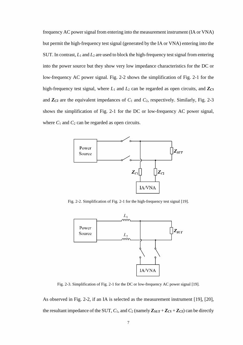
Fig. 2-2. Simplification of Fig. 2-1 for the high-frequency test signal [19]. .................. 7
Fig. 2-3. Simplification of Fig. 2-1 for the DC or low-frequency AC power signal [19].
......................................................................................................................................... 7
Fig. 2-4. Equivalent circuit model of Fig. 2-2 represented by a two-port network [21]. 8
Fig. 2-5. Basic measurement setup of the voltage-current measurement approach using
a current transformer as the signal injection device [33]. ............................................... 9
Fig. 2-6. Measurement setup of the inductive coupling approach using a VNA and two
clamp-on inductive probes [30]. ................................................................................... 10
Fig. 2-7. Two-port network of (a) the IIP with the wire being clamped; (b) the RIP with
the wire being clamped [30]. ........................................................................................ 11
Fig. 2-8. Equivalent circuit model of Fig. 2-6 represented by cascaded two-port
networks [30]. ............................................................................................................... 11
Fig. 2-9. Characterization of (a) NI and (b) NR [31]. .................................................... 13
Fig. 3-1. Proposed measurement setup of the inductive coupling approach................. 16
Fig. 3-2. Equivalent circuit model of Fig. 3-1 represented by cascaded two-port
networks. ....................................................................................................................... 17
Fig. 3-3. Procedure of extracting ZSUT with the moving window DFT algorithm. ....... 19
Fig. 3-4. A NI PXI platform chosen as the computer-controlled SGAS. ..................... 21
Fig. 3-5. Measurement setup for online impedance extraction of a RLC circuit. ......... 23
Fig. 3-6. (a) Magnitude and (b) phase of the extracted impedance of the RLC circuit
using the proposed measurement setup and the PM6306 RCL meter. ......................... 24
Fig. 3-7. Measurement setup for online impedance extraction of a switching circuit. . 25

viii
Fig. 3-8. (a) Magnitude and (b) phase of the extracted impedance of the switching circuit
when fsw is 1 kHz. .......................................................................................................... 27
Fig. 3-9. (a) Magnitude and (b) phase of the extracted impedance of the switching circuit
when fsw is 10 kHz. ........................................................................................................ 28
Fig. 3-10. (a) Magnitude and (b) phase of the extracted impedance of the switching
circuit when fsw is 50 kHz. ............................................................................................ 29
Fig. 3-11. (a) Magnitude and (b) phase of the extracted online impedance of the
switching circuit when the power MOSFET operates at normal temperature and high
temperature conditions. ................................................................................................. 31
Fig. 4-1. Equivalent circuit model of Fig. 3-1 represented by a three-port network. ... 34
Fig. 4-2. Online impedance measurement process based on the three-term calibration
technique. ...................................................................................................................... 41
Fig. 4-3. Measurement setup and calibration fixture for validation. ............................ 42
Fig. 4-4. Measured impedances of (a) the R0 calibration condition and (b) the R50
calibration condition. .................................................................................................... 43
Fig. 4-5. (a) Magnitude and (b) phase of V1/V2|t when d = 0 mm and fsig varies from 20
kHz to 1 MHz. ............................................................................................................... 44
Fig. 4-6. (a) Magnitude and (b) phase of V1/V2|t when fsig = 100 kHz and d varies from
0 to 50 mm. ................................................................................................................... 45
Fig. 4-7. Circuit configuration of the RLC circuits. ...................................................... 46
Fig. 4-8. Measurement setup and one of the SUTs. ...................................................... 47
Fig. 4-9. Calculated measurement errors from Table 4-2 when fsig = 100 kHz and d = 0
mm. ............................................................................................................................... 48
Fig. 4-10. Calculated measurement errors from Table 4-3 when fsig = 100 kHz and d =
80 mm. .......................................................................................................................... 49
ix
Fig. 5-1. Measurement Setup incorporating signal amplification and surge protection
modules. ........................................................................................................................ 52
Fig. 5-2. Equivalent circuit model of Fig. 5-1 represented by two-port and three-port
networks. ....................................................................................................................... 53
Fig. 5-3. Actual measurement setup incorporating signal amplification and surge
protector modules. ......................................................................................................... 57
Fig. 5-4. Calculated measurement errors from Table 5-3 when fsig =100 kHz and d = 0
mm. ............................................................................................................................... 58
Fig. 5-5. Calculated measurement errors from Table 5-4 when fsig = 50 kHz and d = 20
mm. ............................................................................................................................... 59
Fig. 6-1. A comprehensive CM equivalent circuit model of a typical 3-phase IM. ..... 64
Fig. 6-2. An ITSC fault that occurs in one of the phases of an IM. .............................. 66
Fig. 6-3. Offline measurement of ZDM,IM using an impedance analyzer....................... 66
Fig. 6-4. Frequency response of ZDM,IM of the healthy TECO IM measured offline from
40 Hz - 5 MHz. ............................................................................................................. 67
Fig. 6-5. Offline measurement of ZCM,IM using an impedance analyzer. ...................... 68
Fig. 6-6. Schematic of the emulated ITSC faults. ......................................................... 68
Fig. 6-7. Frequency responses of ZCM,IM of the healthy and faulty TECO IM measured
offline from 42 kHz to 5 MHz. ..................................................................................... 68
Fig. 6-8. Relative change in ZCM,IM of the TECO IM caused by ITSC faults with two
fault severity levels (i.e. 2-turn fault and 5-turn fault). ................................................. 69
Fig. 6-9. A typical inverter-fed MDS with the CM current path. ................................. 70
Fig. 6-10. (a) Measurement setup for online monitoring of ZCM,IM; (b) CM equivalent
circuit of the inverter-fed MDS with the measurement setup. ...................................... 71
Fig. 6-11. Actual measurement setup with the MDS under test. .................................. 74

x
Fig. 6-12. Noise current spectrum from 66 kHz to 96 kHz in the MDS under test. ..... 75
Fig. 6-13. Current spectrum around 82 kHz in the MDS under test when injecting an RF
sinusoidal excitation signal (600 mV at 82 kHz) into the MDS by using the measurement
setup. ............................................................................................................................. 75
Fig. 6-14. ZX of the healthy MDS under test measured online with the measurement
setup at varying load conditions (nominal speed). ........................................................ 76
Fig. 6-15. ZX of the healthy MDS under test measured online with the measurement
setup at varying speed conditions. ................................................................................ 76
Fig. 6-16. Relative change in ZCM,IM of the IM (healthy and 2-turn fault) monitored
online with the measurement setup at varying load conditions (nominal speed). ........ 78
Fig. 6-17. Relative change in ZCM,IM of the IM (healthy and 2-turn fault) monitored
online with the measurement setup at varying speed conditions. ................................. 78
Fig. 6-18. Emulated abnormal friction of bearing (AFB) and emulated rotor cage fault
(RCF) of the IM. ........................................................................................................... 79
Fig. 6-19. Relative change in ZCM,IM of the IM at the conditions of the AFB and the
RCF. .............................................................................................................................. 79
Fig. 7-1. Small-signal equivalent circuit model of the SiC power MOSFET in the off-
state. .............................................................................................................................. 83
Fig. 7-2. Simplified equivalent circuit model of Fig. 7-1 when fsig ≤ 1 MHz. .............. 83
Fig. 7-3. Star-connected equivalent circuit model of Fig. 7-2. ..................................... 84
Fig. 7-4. Test circuit to extract 𝒁𝒅𝒏, 𝒁𝒈𝒏, and 𝒁𝒔𝒏 with the inductive probes mounted
between (a) position 𝑎-𝑎′, (b) position 𝑏-𝑏′, and (c) position 𝑐-𝑐′. .............................. 86
Fig. 7-5. Measurement setup to extract the voltage-dependent capacitances of the Cree
SiC power MOSFET. .................................................................................................... 90
Fig. 7-6. Extracted interelectrode capacitances of the Cree SiC power MOSFET through

xi
the proposed method at the frequency of 1 MHz. ......................................................... 90
Fig. 7-7. Comparison of the extracted 𝐶𝑖𝑠𝑠, 𝐶𝑜𝑠𝑠, and 𝐶𝑟𝑠𝑠 via the proposed method and
those provided by the datasheet. ................................................................................... 91
Fig. 7-8. Comparison of the values of 𝐶𝑖𝑠𝑠 , 𝐶𝑜𝑠𝑠 , and 𝐶𝑟𝑠𝑠 obtained by the proposed
method at the frequency of 100 kHz, 1 MHz, and 10 MHz. ......................................... 92

xii
List of Tables
Table 3-1. Comparison of magnitude and phase of the extracted impedance between the
proposed measurement setup and the PM6306 RCL meter. ......................................... 24
Table 3-2. The steady-state magnitude of the impedance from Figs. 3-8 and 3-9. ...... 30
Table 3-3. The steady-state phase of the impedance from Figs. 3-8 and 3-9. .............. 30
Table 4-1. Values and tolerances of the selected components for experiments in Section
4.3. ................................................................................................................................. 47
Table 4-2. Comparison of the measured impedances of the SUTs in Table 4-1 when fsig
= 100 kHz and d = 0 mm. ............................................................................................. 48
Table 4-3. Comparison of the measured impedances of the SUTs in Table 4-1 when fsig
= 100 kHz and d = 80 mm. ........................................................................................... 49
Table 5-1. Details of the instruments (inst.) of the actual measurement setup
incorporating signal amplification and surge protection modules. ............................... 57
Table 5-2. Values and tolerances of the selected components for experiments in Section
5-3. ................................................................................................................................ 57
Table 5-3. Comparison of the measured impedances of the SUTs in Table 5-2 when fsig
= 100 kHz and d = 0 mm. ............................................................................................. 58
Table 5-4. Comparison of the measured impedances of the SUTs in Table 5-2 when fsig
= 50 kHz and d = 20 mm. ............................................................................................. 59
Table 6-1. Ratings of the 3-phase IM under test. .......................................................... 73
Table 6-2. Details of instruments (inst.) of the actual measurement setup. .................. 73
Table 6-3. Relative change in ZCM,IM of the IM for different ITSC fault severities ..... 78
Table 7-1. Errors of the extracted capacitances for 23 measurement points shown in Fig.
7-7. ................................................................................................................................ 91

xiii
List of Abbreviations
3-D Three-Dimensional
AC Alternating Current
ADC Analog-to-Digital Converter
AFB Abnormal Friction Bearing
AI Artificial Intelligence
AT Attenuator
CH1 Channel 1
CH2 Channel 2
CM Common-Mode
DC Direct Current
DFT Discrete Fourier Transform
DM Differential-Mode
DSP Digital Signal Processing
EMI Electromagnetic Interference
FOI Frequency of Interest
IA Impedance Analyzer
IIP Injecting Inductive Probe
IM Induction Motor
ITSC Inter-Turn Short-Circuit
KCL Kirchhoff’s Current Law
MDS Motor Drive System
MOSFET Metal-Oxide-Semiconductor Field-Effect Transistor
PA Power Amplifier
PCI Peripheral Component Interconnect
PWM Pulse Width Modulation
RCF Rotor Cage Fault
RF Radio Frequency
RIP Receiving Inductive Probe
SAC Signal Acquisition Card
SG Signal Generator

xiv
SGAS Signal Generation and Acquisition System
SGC Signal Generation Card
SiC Silicon Carbide
SID Signal Injection Device
SMPS Switched-Mode Power Supply
SNR Signal-to-Noise Ratio
SOC State of Charge
SOH State of Health
SP Surge Protector
ST Speed Transient
SUT System Under Test
VFD Variable-Frequency Drive
VNA Vector Network Analyzer
WBG Wide-Bandgap

1
Chapter 1 Introduction
1.1. Background
The online impedance is one of the key parameters for evaluating the operation status
and health condition of many critical electrical systems. For example, the online
impedance of the power grid has a significant impact on the performance of the grid-
connected power converters [1]-[3]. It affects not only the converters’ inner current
control loops [4], [5] but also their voltage control loops [6]. In both cases, inaccurate
estimation of the online impedance of the power grid can degrade the performance of
the grid-connected power converters and even make them unstable. Moreover, the
online impedance of the power grid can also provide useful information to meet certain
requirements, such as anti-islanding regulations [7]. In addition to the application in the
power grid, its application in the battery energy storage system has also been discussed
[8]-[10]. To achieve efficient battery energy management, accurate battery state of
charge (SOC) information is needed as a measure of the remaining energy stored in the
battery. The online impedance of the battery is an effective way to estimate its SOC
[11]. Moreover, the battery impedance would change due to factors such as aging and
temperature. Therefore, by comparing its measured impedance with the reference
impedance set based on long-term experimental data, it can also be used as a measure
of the state of health (SOH) or the battery internal temperature [12]-[14]. In addition to
these applications, the online noise source impedance of the switched-mode power
supply (SMPS) is essential in the design of power line electromagnetic interference
(EMI) filters [15], [16]. The noise source impedance of the SMPS would change with
certain parameters such as converter topology, component parasitic parameters, and
board layout [17]. Therefore, the impedance of an operating SMPS would be different

2
from that of an offline SMPS, and the online noise source impedance extraction of an
SMPS will bring more accurate results for a systematic EMI filter tailored to a specific
SMPS [18].
Acknowledging the significance and importance of the online impedance of the
electrical systems, developing an effective method to extract their online impedances is
necessary. In general, there are mainly three online impedance extraction approaches;
namely the capacitive coupling approach [19]-[21], the voltage-current measurement
approach [22]-[27], and the inductive coupling approach [28]-[31]. Among them, the
measurement setup of the inductive coupling approach does not have any physical
electrical connection to the energized system under test (SUT). Also, the clamp-on
inductive probes used in the measurement setup of this approach can be easily mounted
on or removed from the insulated wire that delivers the power to the SUT and therefore
it simplifies the on-site implementation [31].
The inductive coupling approach was firstly reported to extract the power line
impedance [28]. It was later extended to extract the noise source impedance of the SMPS
for systematic EMI filter design purposes [29]. It was further improved to simplify the
online impedance extraction process with the cascaded two-port network concept [30],
[31]. However, all earlier reported works of this approach have assumed that the online
impedance of an electrical system is time-invariant for a specific time interval and
therefore they lack the ability to extract the time-variant online impedance of electrical
systems, especially those power conversion systems that adopt switching techniques,
where frequent impedance changes take place. Besides, there is a minimum separation
distance between the inductive probes to minimize possible measurement errors due to
the probe-to-probe coupling between the inductive probes. This minimum separation

3
distance may not be always possible in some circumstances, where the inductive probes
have to be closely placed due to space constraints. Moreover, the lack of signal
amplification and surge protection modules in the conventional measurement setup of
this approach makes it is challenging to be used in the harsh industrial environment
where strong electrical noise and power surges are present. Due to the above-mentioned
limitations and challenges, the scope of application of the inductive coupling approach
is rather limited.
1.2. Motivation, Objectives, and Contributions
The motivation of this thesis is to develop an improved and more robust measurement
setup to address the aforementioned limitations and challenges of the conventional
measurement setup, thereby expanding the scope of application of the inductive
coupling approach and improving its measurement accuracy. The objectives of this
thesis are listed as follows:
• Propose an improved measurement setup of the inductive coupling approach, which
can extract not only the time-invariant online impedance but also the time-variant
online impedance of electrical systems.
• Develop a calibration scheme for the proposed measurement setup to deembed the
effect of the probe-to-probe coupling between the inductive probes with the
objective to improve the accuracy of online impedance extraction.
• Incorporate signal amplification and surge protection modules into the proposed
measurement setup to expand the scope of application of the inductive coupling
approach into the electrical systems where significant electrical noise and power
surges are present.

4
• Explore expanded applications of the inductive coupling approach based on the
proposed measurement setup in online condition monitoring, fault detection, and
electrical parameters evaluation of electrical systems.
The main contributions of this thesis are summarized as follows:
• Extension of the inductive coupling approach for time-variant online impedance
extraction of electrical systems.
• Development of a three-term calibration technique to deembed the effect of the
probe-to-probe coupling so that the measurement error due to such coupling can be
compensated to preserve the measurement accuracy.
• Incorporation of signal amplification and surge protection modules into the
proposed measurement setup and expansion of its applications into the electrical
systems with strong background noise and power surges.
1.3. Organization of Thesis
This thesis is organized as follows:
Chapter 1 introduces the background, motivation, objectives, and contributions of this
thesis.
Chapter 2 presents a review of existing online impedance extraction approaches.
Chapter 3 proposes the improved measurement setup of the inductive coupling approach
and introduces the theory behind time-variant online impedance extraction.
Chapter 4 develops a three-term calibration technique for the proposed measurement
setup to deembed the effect of the probe-to-probe coupling between the inductive probes

5
with the objective to improve the accuracy of online impedance extraction.
Chapter 5 discusses the additional measurement setup consideration in industrial
applications where significant electrical noise and power surges are present.
Chapter 6 discusses and demonstrates the application of the inductive coupling approach
in online detection of the incipient stator faults in the inverter-fed induction motor.
Chapter 7 further extends the application of this approach for non-intrusive extraction
of the voltage-dependent capacitances of the silicon carbide (SiC) power metal-oxide-
semiconductor field-effect transistor (MOSFET).
Finally, Chapter 8 concludes this thesis and proposes future works that are worth
exploring.

6
Chapter 2 Literature Review of Online Impedance
Extraction Approaches
In view of the significance and importance of the online impedance of the electrical
systems, many online impedance extraction methods have been reported in the
literature, which are mainly classified into three categories; namely the capacitive
coupling approach [19]-[21], the voltage-current measurement approach [22]-[27], and
the inductive coupling approach [28]-[31]. In this chapter, the three approaches are
carefully reviewed, and their merits and drawbacks are also discussed.
2.1. Capacitive Coupling Approach
Fig. 2-1 shows the basic measurement setup of the capacitive coupling approach to
extract the online impedance of an electrical system under test (SUT), where the SUT is
powered by either a direct current (DC) or a low-frequency (e.g. 50/60 Hz) alternating
current (AC) power source. The online impedance of the SUT is denoted by ZSUT.
Fig. 2-1. Basic measurement setup of the capacitive coupling approach [19].
To extract ZSUT, two coupling capacitors (C1 and C2), two inductors (L1 and L2), and an
impedance analyzer (IA) or vector network analyzer (VNA) form the basic
measurement setup [19]-[21], in which C1 and C2 are used to block the DC or low-
7
frequency AC power signal from entering into the measurement instrument (IA or VNA)
but permit the high-frequency test signal (generated by the IA or VNA) entering into the
SUT. In contrast, L1 and L2 are used to block the high-frequency test signal from entering
into the power source but they show very low impedance characteristics for the DC or
low-frequency AC power signal. Fig. 2-2 shows the simplification of Fig. 2-1 for the
high-frequency test signal, where L1 and L2 can be regarded as open circuits, and ZC1
and ZC2 are the equivalent impedances of C1 and C2, respectively. Similarly, Fig. 2-3
shows the simplification of Fig. 2-1 for the DC or low-frequency AC power signal,
where C1 and C2 can be regarded as open circuits.
Fig. 2-2. Simplification of Fig. 2-1 for the high-frequency test signal [19].
Fig. 2-3. Simplification of Fig. 2-1 for the DC or low-frequency AC power signal [19].
As observed in Fig. 2-2, if an IA is selected as the measurement instrument [19], [20],
the resultant impedance of the SUT, C1, and C2 (namely ZSUT + ZC1 + ZC2) can be directly

8
measured by the IA. After the resultant impedance is obtained, ZSUT can be extracted by
deembedding (ZC1 + ZC2) from the resultant impedance. Alternatively, if a VNA is
selected as the measurement instrument [21], Fig. 2-2 can be further equated as a two-
port network model, as shown in Fig. 2-4.
Fig. 2-4. Equivalent circuit model of Fig. 2-2 represented by a two-port network [21].
In Fig. 2-4, the SUT, C1, and C2 can be equated as a two-port network N, where N can
be expressed in terms of transmission (ABCD) parameters.
𝑵 = [𝑨 𝑩𝑪 𝑫
] (2-1)
Since B = ZSUT + ZC1 + ZC2 [32], we can directly measure the scattering parameters (S-
parameters) of N using a VNA and then convert the measured S-parameters into B
through (2-2) [32].
𝑩 = 50 ∙(1 + 𝑺𝟏𝟏)(1 + 𝑺𝟐𝟐) − 𝑺𝟏𝟐𝑺𝟐𝟏
2𝑺𝟐𝟏 (2-2)
After B is obtained, ZSUT can be extracted by deembedding (ZC1 + ZC2) from B.
2.2. Voltage-Current Measurement Approach
The voltage-current measurement approach is a very straightforward method, in which

9
the impedance of the SUT (ZSUT) is estimated via extracting the test signal voltage across
the SUT and the test signal current passing through it. It should be noted that the test
signal can be harmonics already presented in the SUT [24] or a signal injected by a
specific device, such as a current transformer [33], a voltage transformer [33], or a SUT-
connected converter [24].
Fig. 2-5. Basic measurement setup of the voltage-current measurement approach using a current
transformer as the signal injection device [33].
Fig. 2-5 shows the basic measurement setup of the voltage-current measurement
approach using a current transformer as the signal injection device (SID), where a signal
generator (SG) is applied to generate a test signal. The test signal is injected into the
wire connected between the power source and the SUT via the current transformer.
Subsequently, the induced signal voltage across the SUT and the current passing through
it are extracted using a current sensor and a voltage sensor, respectively. Finally, an
analog-to-digital converter (ADC) is used to sample the analog voltage and current
signals, and a digital signal processing (DSP) algorithm is applied to determine ZSUT.
2.3. Inductive Coupling Approach
The earliest work of the inductive coupling approach was reported in [28]. The work is
further improved to simplify the online impedance extraction process with the cascaded

10
two-port network concept [30], [31]. Fig. 2-6 shows its measurement setup for online
impedance extraction of a SUT, where the SUT is powered by either a DC or a low-
frequency (e.g. 50/60 Hz) AC power source through the wiring connection. The online
impedance of the SUT is denoted by ZSUT. The measurement setup consists of a VNA
and two clamp-on inductive probes. One of the inductive probes serves as the injecting
inductive probe (IIP) and the other is used as the receiving inductive probe (RIP). A
sweep-frequency excitation (test) signal generated by port 1 of the VNA is injected into
the connecting wire between the power source and the SUT via the IIP, and the response
signal is received by port 2 of the VNA via the RIP, where the IIP and RIP are clamped
onto the connecting wire with the clamping position denoted as p1-p2. VS and ZS are the
equivalent source voltage and impedance of the power source, respectively. ZW is the
equivalent impedance of the wiring connection except for the part being clamped by the
IIP and RIP. Therefore, the resultant impedance of the power source, the wiring
connection excluding the part being clamped, and the SUT is ZX = ZS + ZW + ZSUT.
Fig. 2-6. Measurement setup of the inductive coupling approach using a VNA and two clamp-on
inductive probes [30].
As shown in Fig. 2-7(a), the IIP with the wire being clamped can be regarded as a two-
port network NI, in which Llk1 and Cp1 represent the leakage inductance and the parasitic
capacitance between the winding of the IIP and its frame, respectively. Port 1 of NI
denotes the input port of the IIP, and Port 2 of NI denotes the two ends of the wire being

11
clamped [30]. Similarly, as shown in Fig. 2-7(b), the RIP with the wire being clamped
can also be regarded as a two-port network NR, in which Llk2 and Cp2 represent the
leakage inductance and the parasitic capacitance between the winding of the RIP and its
frame, respectively. Port 1 of NR denotes the two ends of the wire being clamped, and
Port 2 of NR denotes the output port of the RIP. Thus, based on the cascaded two-port
network concept, Fig. 2-8 shows the equivalent circuit model of Fig. 2-6, where NX is
the two-port network for the resultant impedance (ZX) to be measured; VVNA represents
the signal source voltage at Port 1 of the VNA.
(a) (b)
Fig. 2-7. Two-port network of (a) the IIP with the wire being clamped; (b) the RIP with the wire being
clamped [30].
Fig. 2-8. Equivalent circuit model of Fig. 2-6 represented by cascaded two-port networks [30].
Because the frequencies of the test signal generated by Port 1 of the VNA are much

12
higher than the frequency of the power source, VS can be treated as AC short at test
signal frequencies. Besides, since the three two-port networks NI, NX, and NR are
cascaded, the resulting two-port network N can be expressed as
N = NI NX NR (2-3)
From (2-3), the three two-port networks can be expressed in terms of their respective
transmission (ABCD) parameters, which can be rewritten as
[𝑨 𝑩𝑪 𝑫
] = [𝑨𝑰 𝑩𝑰
𝑪𝑰 𝑫𝑰] [
𝑨𝑿 𝑩𝑿
𝑪𝑿 𝑫𝑿] [
𝑨𝑹 𝑩𝑹
𝑪𝑹 𝑫𝑹] (2-4)
By solving NX, ZX can be obtained since BX = ZX [32]. From (2-3), NX can be derived
when N, NI, and NR are known. Among them, N can be directly measured via the VNA
setup in Fig. 2-6. To obtain NI and NR prior to the measurement, a test jig shown in Fig.
2-9 is required. In Fig. 2-9, the inductive probe is clamped onto the inner conductor of
the test jig and the outer cylindrical conductor serves as the common reference return
path for the VNA. One end of the test jig is terminated with a short so that the inner
conductor can be shorted with the outer conductor. The other end of the test jig is
connected to one of the VNA’s ports. To characterize NI, Port 1 of the VNA connects
to the input port of the IIP and Port 2 of the VNA connects to the other end of the test
jig, as shown in Fig. 2-9(a). To characterize NR, Port 1 of the VNA connects to the other
end of the test fixture and Port 2 of the VNA connects to the output port of the RIP, as
shown in Fig. 2-9(b). Thus, based on the test jig in Fig. 2-9, the S-parameters of NI and
NR can be measured by the VNA, respectively. Finally, the ACBD parameters of NI and
NR can be derived from the conversion of the measured S-parameters [32]. After NI and
NR are predetermined, ZX can be obtained based on the direct measurement of N via the
VNA. Thus, ZSUT can be extracted through deembedding (ZS + ZW) from ZX, where (ZS

13
+ ZW) can be predetermined by shunting the SUT with a capacitor of suitable value,
which provides an AC short circuit to the test signal. In many practical situations, ZX is
dominated by ZSUT, as ZS and ZW are usually relatively small [30].
(a)
(b)
Fig. 2-9. Characterization of (a) NI and (b) NR [31].
This chapter reviews and discusses three prevalent online impedance extraction
approaches; namely the capacitive coupling approach, the voltage-current measurement
approach, and the inductive coupling approach. Among them, the coupling capacitor
that forms part of the measurement setup of the capacitive coupling approach and the
voltage sensor that forms part of the measurement setup of the voltage-current
measurement approach require physical electrical connections to the energized SUT for
online impedance extraction. These physical electrical connections pose electrical safety
hazards to the service personnel who maintains the instruments on-site. Also, for a SUT

14
that is energized with high operating voltage, the coupling capacitor and the voltage
sensor are subject to high dielectric and thermal stresses, which require regular
maintenance and replacement; and result in unnecessary downtime of the SUT. In
contrast to the capacitive coupling approach and the voltage-current measurement
approach, the measurement setup of the inductive coupling approach does not have any
physical electrical connection to the energized SUT. Also, the clamp-on inductive
probes used in the measurement setup of this approach can be easily mounted on or
removed from the insulated wire that delivers the power to the SUT and therefore it
simplifies the on-site implementation.
Although the inductive coupling approach has shown its superiority in online impedance
extraction, there are still some issues that need to be overcome. This thesis will address
these issues and describe how the inductive coupling approach can be further improved
and refined. These issues are summarized as follows: the ability to extract the time-
variant online impedance of electrical systems, the ability to eliminate the measurement
error contributed by the probe-to-probe coupling between the inductive probes, and the
ability to extract the online impedance of electrical systems where significant electrical
noise and power surges are present.

15
Chapter 3 Novel Measurement Setup and Time-
Variant Online Impedance Extraction
With the widespread use of active devices such as power electronics devices in most
electrical systems [34]-[38], the time-variant electrical parameters of the systems
provide valuable inputs for the reliable and efficient operation of the systems. Among
the electrical parameters, the time-variant online impedance of an operating system is
useful to evaluate the system’s operation status and health condition [23]. As described
in Chapter 2, the inductive coupling approach has shown its superiority in online
impedance extraction because of its non-contact nature and ease of on-site
implementation. However, all earlier reported works of this approach have made the
simplifying assumption that the online impedance of an electrical system is time-
invariant for a specific time interval and its use to extract the time-variant online
impedance of electrical systems has not been explored, especially those systems with
fast switching rates such as power electronics systems. Therefore, this chapter
introduces an extension of this approach and proposes a time-domain based
measurement setup. By combining this measurement setup with a moving window
discrete Fourier transform (DFT) algorithm, it can extract not only the time-invariant
online impedance but also the time-variant online impedance of electrical systems.
The organization of this chapter is as follows. Section 3.1 introduces the proposed
measurement setup and the principle behind time-variant online impedance extraction.
In Section 3.2, the ability of this measurement setup for time-variant online impedance
extraction is verified experimentally using an emulated time-variant electrical system
that consists of a time-variant switching circuit. In Section 3.3, the same switching

16
circuit is used as a test case to demonstrate the ability of online impedance monitoring
in the abnormality detection of a time-variant electrical system.
3.1. Measurement Setup and Principle
Fig. 3-1 shows the proposed measurement setup for online impedance extraction of a
SUT, where the SUT is power by either a DC or a low-frequency (e.g. 50/60 Hz) AC
power source via the wiring connection. The measurement setup consists of a computer-
controlled signal generation and acquisition system (SGAS), an IIP, and a RIP.
Fig. 3-1. Proposed measurement setup of the inductive coupling approach.
To extract the online impedance of the SUT (ZSUT), a signal generation card (SGC) in
the SGAS produces a sinusoidal excitation (test) signal of known frequency (fsig). The
excitation signal is injected into the connecting wire between the power source and the
SUT through the IIP, and the RIP monitors the response signal, where the IIP and RIP
are clamped onto the connecting wire with the clamping position denoted as p1-p2.
Channel 1 (CH1) and channel 2 (CH2) of a signal acquisition card (SAC) in the SGAS
sample the excitation signal voltage at the input port of the IIP and the response signal
voltage at the output port of the RIP, respectively. VS and ZS are the equivalent source

17
voltage and impedance of the power source, respectively. ZW is the equivalent
impedance of the wiring connection except for the part being clamped by the IIP and
RIP. Therefore, the resultant impedance of the power source, the wiring connection
excluding the part being clamped, and the SUT is ZX = ZS + ZW + ZSUT.
Fig. 3-2. Equivalent circuit model of Fig. 3-1 represented by cascaded two-port networks.
Based on the cascaded two-port network concept, Fig. 3-2 shows the equivalent circuit
model of Fig. 3-1. VSGC and ZSGC are the equivalent source voltage and internal
impedance of the SGC, respectively. ZCH1 and ZCH2 are the input impedances of CH1
and CH2 of the SAC, respectively. V1 and I1 are the excitation signal voltage and current
at the input port of the IIP, respectively. V2 and I2 are the response signal voltage and
current at the output port of the RIP, respectively. NI is the two-port network of the IIP
with the wire being clamped, in which Llk1 and Cp1 represent the leakage inductance and
the parasitic capacitance between the winding of the IIP and its frame, respectively. NR
is the two-port network of the RIP with the wire being clamped, in which Llk2 and Cp2
represent the leakage inductance and the parasitic capacitance between the winding of
the RIP and its frame, respectively. NX is the two-port network for the resultant
impedance (ZX) to be measured. Since the frequency (fsig) of the sinusoidal test signal
(generated by the SGC) is much higher than the frequency of the power source, VS can

18
be treated as AC short at fsig. Expressing the three two-port networks (NI, NX, and NR)
in terms of their respective ABCD parameters, the input port of the IIP and the output
port of the RIP are related by
[𝑽𝟏
𝑰𝟏] = [
𝑨𝑰 𝑩𝑰
𝑪𝑰 𝑫𝑰] [
𝑨𝑿 𝑩𝑿
𝑪𝑿 𝑫𝑿] [
𝑨𝑹 𝑩𝑹
𝑪𝑹 𝑫𝑹] [
𝑽𝟐
𝑰𝟐] (3-1)
Since I2 = V2/ZCH2 and NX can be expressed as [32]
𝑵𝑿 = [1 𝒁𝑿
0 1] (3-2)
Substituting (3-2) into (3-1), ZX can be determined by
𝒁𝑿 =1
𝑨𝑰(𝑪𝑹 + 𝑫𝑹 𝒁𝑪𝑯𝟐⁄ )∙
𝑽𝟏
𝑽𝟐−
𝑨𝑹 + 𝑩𝑹 𝒁𝑪𝑯𝟐⁄
𝑪𝑹 + 𝑫𝑹 𝒁𝑪𝑯𝟐⁄−
𝑩𝑰
𝑨𝑰 (3-3)
As mentioned earlier, the ABCD parameters of NI and NR can be precharacterized
individually using the test jig in Fig. 2-9. ZCH2 can be directly obtained from the
datasheet of the SGC [39], [40]. Therefore, ZX can be obtained from (3-3) through the
measurement of V1 and V2. Once ZX is obtained, ZSUT can be extracted by deembedding
(ZS + ZW) from ZX. To obtain the dynamic voltage equivalents at different time
instances, the DFT is performed in a moving window [41]. The moving window size of
the DFT is fixed and the details of the DFT in a moving window is given by
𝑽𝑘(𝑚) = ∑ 𝑣(𝑛)𝑒−𝑖2𝜋𝑘[𝑛−(𝑚−𝑁+1)] 𝑁⁄
𝑚
𝑛=𝑚−𝑁+1
(3-4)
where i is the imaginary unit. N is the number of sampling points of the fixed moving
window size. m is the (m + 1)th discrete sample during the entire measurement process,
where m equates to the sampling time point t multiply by the sampling rate 1/∆t (namely

19
m = t/∆t). Vk(m) is the dynamic voltage equivalent at time t and specific frequency point
k. v(n) is the (n + 1)th discrete sampling voltage value in the time domain. In contrast to
the DFT with a fixed window, whose range of n is between 0 and N – 1, the range of n
of the DFT in a moving window is a variable with the value of m. Using Euler’s formula,
(3-4) can be expressed in the form of a trigonometric function as follows:
𝑽𝑘(𝑚) = ∑ 𝑣(𝑛) [cos (2𝜋𝑘𝑛 − 𝑚 − 1
𝑁) − 𝑖 ∙ sin (2𝜋𝑘
𝑛 − 𝑚 − 1
𝑁)]
𝑚
𝑛=𝑚−𝑁+1
(3-5)
Since v1(n) and v2(n) can be directly extracted by CH1 and CH2 of the SAC,
respectively, V1 and V2 at time t and specific frequency point k can be obtained through
(3-5). Thus, ZX at time t and specific frequency point k can be obtained by (3-3), and
subsequently, ZSUT can be determined through embedding as explained.
Fig. 3-3. Procedure of extracting ZSUT with the moving window DFT algorithm.

20
Fig. 3-3 describes the procedure of extracting ZSUT with the moving window DFT
algorithm. The procedure starts with samples v1(m) and v2(m) when t = 0. m corresponds
to the (m + 1)th discrete sample during the entire measurement process, where m = t/∆t.
When m ≥ N – 1, the DFT is performed to obtain V1 and V2 at time t and specific
frequency point k. Obtaining of V1 and V2 at time t and specific frequency point k is
based on the latest N samples in the time domain, which is from (m – N + 1)∆t to m∆t.
Therefore, the N samples are dynamically selected and are related to the sampling time
point t. Thus, ZX at time t and specific frequency point k can be obtained by (3-3), and
subsequently, ZSUT can be determined through deembedding as explained. After
obtaining ZSUT at time t and specific frequency point k, the next step is to judge whether
the sampling time point t has reached the last sampling time point (tend). The procedure
ends when t ≥ tend. Otherwise, resetting t = t + ∆t, a new sampling cycle will commence
and the same process is repeated until t ≥ tend.
For the moving window DFT algorithm, it is important to select the appropriate
sampling rate fs (namely 1/∆t) and the moving window size N because they have a
significant impact on the accuracy of the measurement results. Firstly, to ensure
sufficient sampling in each cycle of the sinusoidal test signal, fs is suggested to set at ten
times of fsig. Therefore, fs = 10fsig, which provides ten sampling points in each cycle of
the sinusoidal test signal. Besides, every DFT performed shall contain data of ten
complete cycles of the sinusoidal test signal as per the rule of thumb to achieve good
accuracy. Therefore, N is set at 100. Moreover, for a time-variant SUT, the selection of
fs depends on the frequency of impedance change (fch) of the time-variant SUT as well
as the value of N. To achieve valid and accurate DFT results, the time interval of N
samples should be much smaller than 1/fch, namely N/fs << 1/fch. Thus, it is obtained that

21
fs >> N ∙ fch (3-6)
Considering that the sampling rate (fs) of a SAC in the market can be up to a few
gigahertz [40], the proposed measurement setup has the ability to extract the time-
variant online impedance of most electrical systems. In addition, since the window is
shifted one sample at a time in the proposed moving window DFT algorithm, it shows
a better ability to detect the dynamic changes of the time-variant online impedance of
electrical systems as compared to the other DFT algorithms whose window is shifted
multi-sample at a time.
3.2. Experimental Validation
For experimental validation, a National Instruments (NI) PXI platform is selected as the
computer-controlled SGAS, as shown in Fig. 3-4. It consists of a signal generation card
(PXI-5412), a two-channel signal acquisition card (PXI-5922), a computer interface
card (PXI-8360), and a back panel (PXI-1031).
Fig. 3-4. A NI PXI platform chosen as the computer-controlled SGAS.
A computer with programmable software is interfaced with the PXI platform and
performs the DFT algorithm as described in the flowchart given in Fig. 3-3. The PXI-
5412 SGC generates a sinusoidal excitation signal with frequency of fsig. The PXI-5922
22
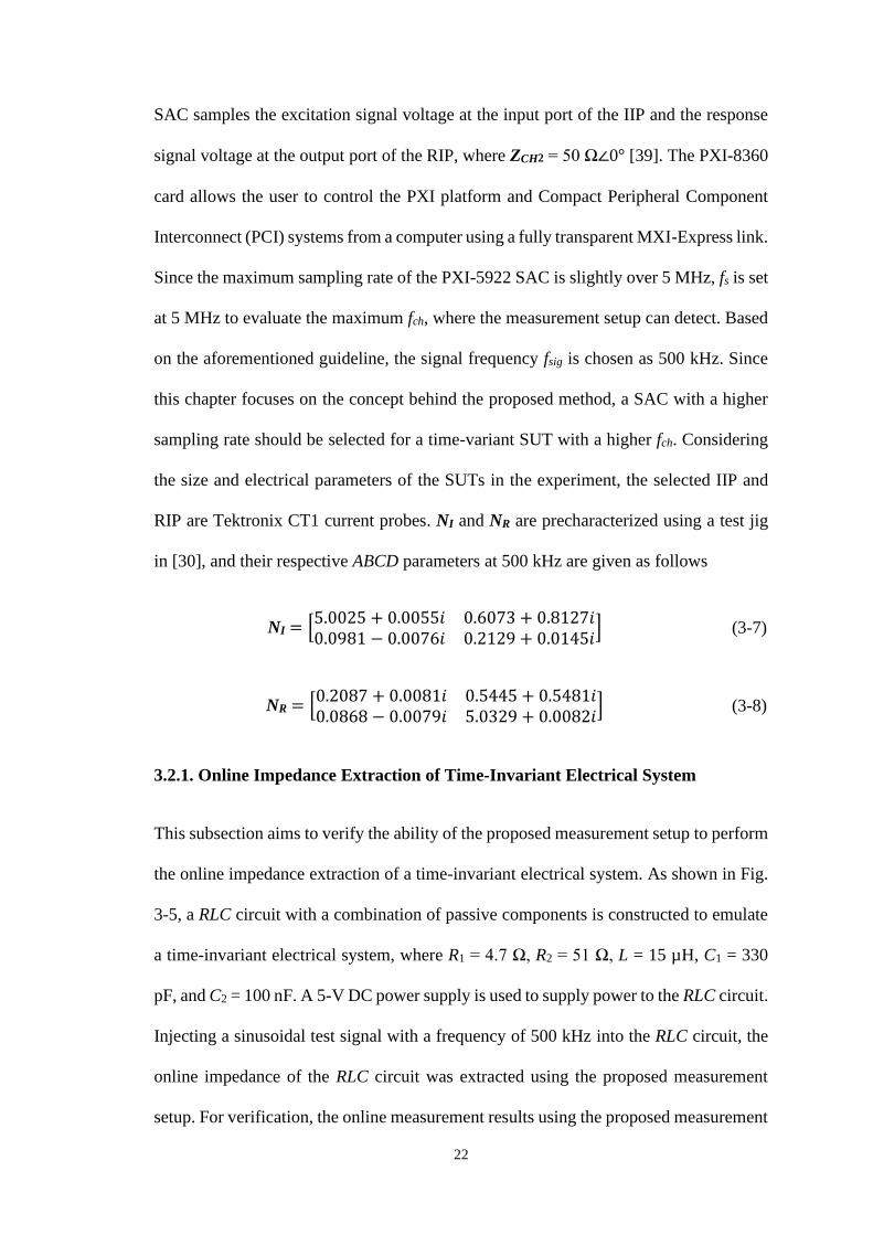
SAC samples the excitation signal voltage at the input port of the IIP and the response
signal voltage at the output port of the RIP, where ZCH2 = 50 Ω∠0° [39]. The PXI-8360
card allows the user to control the PXI platform and Compact Peripheral Component
Interconnect (PCI) systems from a computer using a fully transparent MXI-Express link.
Since the maximum sampling rate of the PXI-5922 SAC is slightly over 5 MHz, fs is set
at 5 MHz to evaluate the maximum fch, where the measurement setup can detect. Based
on the aforementioned guideline, the signal frequency fsig is chosen as 500 kHz. Since
this chapter focuses on the concept behind the proposed method, a SAC with a higher
sampling rate should be selected for a time-variant SUT with a higher fch. Considering
the size and electrical parameters of the SUTs in the experiment, the selected IIP and
RIP are Tektronix CT1 current probes. NI and NR are precharacterized using a test jig
in [30], and their respective ABCD parameters at 500 kHz are given as follows
NI = [5.0025 + 0.0055𝑖 0.6073 + 0.8127𝑖0.0981 − 0.0076𝑖 0.2129 + 0.0145𝑖
] (3-7)
NR = [0.2087 + 0.0081𝑖 0.5445 + 0.5481𝑖0.0868 − 0.0079𝑖 5.0329 + 0.0082𝑖
] (3-8)
3.2.1. Online Impedance Extraction of Time-Invariant Electrical System
This subsection aims to verify the ability of the proposed measurement setup to perform
the online impedance extraction of a time-invariant electrical system. As shown in Fig.
3-5, a RLC circuit with a combination of passive components is constructed to emulate
a time-invariant electrical system, where R1 = 4.7 Ω, R2 = 51 Ω, L = 15 µH, C1 = 330
pF, and C2 = 100 nF. A 5-V DC power supply is used to supply power to the RLC circuit.
Injecting a sinusoidal test signal with a frequency of 500 kHz into the RLC circuit, the
online impedance of the RLC circuit was extracted using the proposed measurement
setup. For verification, the online measurement results using the proposed measurement

23
setup will be compared with the off-line measurement results of the same RLC circuit
using a PM6306 RCL meter.
Fig. 3-5. Measurement setup for online impedance extraction of a RLC circuit.
Fig. 3-6 shows the magnitude and phase of the extracted impedance of the RLC circuit
using the proposed measurement setup and the PM6306 RCL meter, where their means
and standard deviations are presented in Table 3-1. Using the measurement results of
the PM6306 RCL meter as the reference, the magnitude and phase measurement errors
using the proposed measurement setup are calculated to be 0.2% and 1.1°, respectively.
This shows that the measurement results using the proposed measurement setup are very
consistent with those obtained from the PM6306 RCL meter. Therefore, it has
demonstrated that the proposed measurement setup offers good measurement accuracy
in the online impedance extraction of time-invariant electrical systems.

24
0.0 0.1 0.243
44
45
46
47
Mag
nit
ude
(W)
Time (s)
Proposed Measurement Setup
PM6306 RCL Meter
(a)
0.0 0.1 0.270
75
80
85
90
Ph
ase
(°)
Time (s)
Proposed Measurement Setup
PM6306 RCL Meter
(b)
Fig. 3-6. (a) Magnitude and (b) phase of the extracted impedance of the RLC circuit using the proposed
measurement setup and the PM6306 RCL meter.
Table 3-1. Comparison of magnitude and phase of the extracted impedance between the proposed
measurement setup and the PM6306 RCL meter.
Proposed Measurement Setup PM6306 RCL Meter
Mean Standard Deviation Mean Standard Deviation
Magnitude (Ω) 45.24 0.0025 45.13 0.0040
Phase (°) 88.7 0.0032 87.6 0.0020

25
3.2.2. Online Impedance Extraction of Time-Variant Electrical System
This subsection is to demonstrate the ability of the proposed measurement setup for the
online impedance extraction of a time-variant electrical system. To emulate a time-
variant electrical system, a switching circuit with a power MOSFET shown in Fig. 3-7
is applied, where R1 = 1 Ω, R2 = 51 Ω, L = 1 mH, C1 = 4.7 µF, and C2 = 47 µF. The
power MOSFET has a reverse diode and interelectrode capacitances. A gate drive signal
with a period T and a duty cycle D = 0.5 is connected to the gate of the power MOSFET
to control its switching frequency, fsw = 1/T. The equivalent impedance of the power
MOSFET at the specified frequency is represented as ZMOS and its value depends on
whether the power MOSFET is in the "on" or "off" state. D1 is a diode with opposite
switching states to the power MOSFET. A 1-V DC power supply is used to supply
power to the switching circuit.
Fig. 3-7. Measurement setup for online impedance extraction of a switching circuit.
Thus, the switching circuit can be equated as two separate time-invariant circuits when
the power MOSFET is "on" and "off", respectively. Considering that the impedance in

26
steady-state of each switching cycle is the same with the impedance of the two separate
time-invariant electrical circuits when the power MOSFET is always "on" or "off", the
measurement result when the power MOSFET is always "on" or "off" can be taken as
the reference impedance to verify the performance of the proposed measurement setup
when the switching circuit is constantly switching "on" and "off". Since the proposed
measurement setup has been verified to measure the online impedance of a time-
invariant electrical system in Subsection 3.2.1, it is feasible to use the measured
impedance when the power MOSFET is always "on" or "off" as the reference. In
addition, for the switching circuit, fch is the same as fsw. As mentioned earlier, accurate
impedance measurement of a time-variant electrical system needs to satisfy the
requirement of (3-6). Considering that N and fs have been selected as 100 and 5 MHz
respectively, it is found that fsw << 50 kHz. Therefore, experiments are conducted to
verify it.
Fig. 3-8 to Fig. 3-10 show the extracted online impedances using the proposed
measurement setup when fsw is 1 kHz, 10 kHz, and 50 kHz, respectively. The impedance
when the power MOSFET is always "on" or "off" is indicated as the reference for
comparison purposes. As explained, fch should be much smaller than fs/N (namely 50
kHz) to achieve valid and accurate DFT results. Therefore, fsw = 1 kHz yields a better
result as compared to the case when fsw = 10 kHz. By increasing fsw to 50 kHz, the
impedance changes can no longer be captured because fch = fs/N, causing the DFT
algorithm unable to obtain the dynamic impedance changes of the switching circuit.
Therefore, proper choices of fs and N are critical to the accuracy of the measurement
results. It should be explained that if the frequency of impedance change (fch) of a time-
variant electrical system is larger than 50 kHz, a SAC with a higher sampling rate (fs)
can be used in this case.

27
0.000 0.001 0.002 0.003 0.004 0.005
101
102
103
Mag
nit
ude
(W)
Time (s)
fsw = 1 kHz Always "on" Always "off"
(a)
0.000 0.001 0.002 0.003 0.004 0.005-90
-45
0
45
90
Phas
e (°
)
Time (s)
fsw = 1 kHz Always "on" Always "off"
(b)
Fig. 3-8. (a) Magnitude and (b) phase of the extracted impedance of the switching circuit when fsw is 1
kHz.

28
0.0000 0.0001 0.0002 0.0003 0.0004 0.0005
101
102
103
Mag
nit
ude
(W)
Time (s)
fsw = 10 kHz Always "on" Always "off"
(a)
0.0000 0.0001 0.0002 0.0003 0.0004 0.0005-90
-45
0
45
90
Phas
e (°
)
Time (s)
fsw = 10 kHz Always "on" Always "off"
(b)
Fig. 3-9. (a) Magnitude and (b) phase of the extracted impedance of the switching circuit when fsw is 10
kHz.

29
0.0 0.1 0.2100
101
102
fsw= 50 kHz
Mag
nit
ude
(W)
Time (s)
(a)
0.0 0.1 0.2-90
-45
0
45
90 fsw = 50 kHz
Phas
e (°
)
Time (s)
(b)
Fig. 3-10. (a) Magnitude and (b) phase of the extracted impedance of the switching circuit when fsw is
50 kHz.
Tables 3-2 and 3-3 show the steady-state magnitude and phase of the extracted
impedance from Figs. 3-8 and 3-9, respectively. The magnitude and phase deviations
are rather small when fsw is set at 1 kHz and 10 kHz. Using the measured results when
the power MOSFET is always in the "on" or "off" state as the reference, the
measurement errors of the magnitude and phase of the steady-state online impedance
using the proposed measurement setup are 7.7% and 0.42°, respectively.

30
Table 3-2. The steady-state magnitude of the impedance from Figs. 3-8 and 3-9.
(Ω) fsw = 1 kHz, 10 kHz Reference Values
"on" "off" Always "on" Always "off"
1 kHz 7.56 252.32
7.55 273.50 10 kHz 7.58 265.95
Table 3-3. The steady-state phase of the impedance from Figs. 3-8 and 3-9.
(°) fsw = 1 kHz, 10 kHz Reference Values
"on" "off" Always "on" Always "off"
1 kHz 50.12 -84.64
50.22 -85.00 10 kHz 50.09 -84.58
It should be noted that the extracted impedance at the switching edge has an oscillatory
behaviour due to the interelectrode capacitances of the power MOSFET and the circuit
loop inductance [42], [43]. From Figs. 3-8 and 3-9, the maximum transient impedances
at the switching edge extracted using the proposed measurement setup when fsw = 1 kHz
and 10 kHz are 326.81 Ω and 333.61 Ω, respectively. Using the measured time-domain
peak transient voltage and current, the impedances computed are 357.16 Ω at fsw = 1
kHz and 378.13 Ω at fsw = 10 kHz. Taking the computed impedances as the reference,
the deviations of the extracted maximum transient impedance when fsw = 1 kHz and 10
kHz are 8.5% and 11.8%, respectively.
3.3. Online Abnormality Detection of Time-Variant Electrical System
This section illustrates the ability of online impedance monitoring in the abnormality
detection of a time-variant electrical system. The same switching circuit in Fig. 3-7 is
used as a test case, where fs = 5 MHz, fsig = 500 kHz, fsw = 1 kHz, and D = 0.5. First of
all, the switching circuit starts operating at a normal temperature. Next, a heating
element is applied on the power MOSFET to emulate its operation at a high temperature,

31
and finally, the resulting online impedance of the switching circuit is re-measured.
0.000 0.001 0.002 0.003 0.004 0.005
101
102
103
Mag
nit
ud
e (W
)
Time (s)
Normal Temperature Operation
High Temperature Operation
(a)
0.000 0.001 0.002 0.003 0.004 0.005-90
-45
0
45
90
135 Normal Temperature Operation
High Temperature Operation
Ph
ase
(°)
Time (s)
(b)
Fig. 3-11. (a) Magnitude and (b) phase of the extracted online impedance of the switching circuit when
the power MOSFET operates at normal temperature and high temperature conditions.
The measurement results are shown in Fig. 3-11. By emulating the power MOSFET
operated at the high temperature condition, the magnitude and phase values of the
extracted online impedance when the power MOSFET is in the "off" state deviate from
their original values operated at the normal temperature condition. This deviation has
shown the ability of online impedance monitoring to detect the abnormal behavior of

32
the power MOSFET due to overheating. The detection for the early abnormal behavior
allows necessary remedial action to be taken before the electrical system deteriorates
further to a catastrophic failure.
In this chapter, a novel measurement setup of the inductive coupling approach is
proposed, which consists of a computer-controlled SGAS, an IIP, and a RIP. By using
the cascaded two-port network concept and a moving window DFT algorithm, the
proposed measurement setup can extract not only the time-invariant online impedance
but also the time-variant online impedance of electrical systems. For verification, a
switching circuit was chosen as a test case to validate the ability of this measurement
setup to extract the online impedance of a time-variant electrical system. Such ability is
useful to monitor the time-variant electrical system for abnormal behaviors that serve as
the early signs of failures.

33
Chapter 4 Eliminating the Effect of Probe-to-Probe
Coupling on Measurement Accuracy
As mentioned in Chapter 2, the online impedance serves as a key parameter for assessing
the operating status and health condition of many critical electrical systems. In Chapter
3, a novel measurement setup of the inductive coupling approach is proposed, which
consists of a computer-controlled SGAS, an IIP, and a RIP. Combined with a moving
window DFT algorithm, the proposed measurement setup can extract not only the time-
invariant online impedance but also the time-variant online impedance of electrical
systems. Before performing online impedance extraction of any electrical system, the
IIP and RIP must be precharacterized using a VNA and a dedicated test jig, as shown in
Fig. 2-9. Although the inductive coupling approach has been improved to handle time-
variant online impedance extraction, the possible impact of the probe-to-probe coupling
between the IIP and RIP on the accuracy of the extracted online impedance has not been
investigated, especially when both probes are closely placed due to space constraints in
some practical applications. Therefore, this chapter proposes a three-term calibration
technique to eliminate potential errors caused by the probe-to-probe coupling in the
extracted online impedance with the objective to achieve good measurement accuracy.
This chapter is organized as follows. Section 4.1 describes a comprehensive equivalent
circuit model of the measurement setup based on a three-port network concept, in which
the effect of the probe-to-probe coupling can be taken into account in the model. With
the three-port network equivalent circuit model, Section 4.2 introduces the three-term
calibration technique to eliminate the influence of the probe-to-probe coupling on the
accuracy of the extracted online impedance. In Section 4.3, experiments to investigate

34
the characteristics of the probe-to-probe coupling are carried out and the ability of the
three-term calibration technique to eliminate the measurement error contributed by such
coupling is demonstrated.
4.1. Three-Port Network Equivalent Circuit Model
In the previous inductively coupled online impedance extraction analysis, the probe-to-
probe coupling between the IIP and RIP has not been considered. In some practical
applications with space constraints, the IIP and RIP must be placed very close to each
other and the potential measurement error caused by the probe-to-probe coupling could
be significant and cannot be neglected. To account for the influence of the probe-to-
probe coupling, based on the three-port network concept [32], a comprehensive
equivalent circuit model of the proposed measurement setup in Fig. 3-1 is introduced,
as shown in Fig. 4-1.
Fig. 4-1. Equivalent circuit model of Fig. 3-1 represented by a three-port network.
In Fig. 4-1, VSGC and ZSGC are the equivalent source voltage and internal impedance of
the SGC, respectively. ZCH1 and ZCH2 are the input impedances of CH1 and CH2 of the
SAC, respectively. V1 and I1 are the excitation signal voltage and current at the input

35
port of the IIP, respectively; where V1 can be directly extracted by CH1 of the SAC. V2
and I2 are the response signal voltage and current at the output port of the RIP,
respectively; where V2 can be directly extracted by CH2 of the SAC and I2 = V2/ ZCH2.
V3 is the induced signal voltage between p1 and p2, and I3 is the induced signal current
passing through ZX to be measured. As mentioned in Section 3.1, since the frequency
(fsig) of the sinusoidal test signal generated by the SGC is much higher than the frequency
of the power source, VS can be treated as AC short at fsig. Thus, V3 and I3 can be related
by I3 = V3/ZX. Therefore, the coupling between the inductive probe (IIP or RIP) and the
respective wire being clamped, defined as the "probe-to-wire coupling", as well as the
probe-to-probe coupling, can be fully described with a three-port network given by
𝑵 = [𝒁𝟏𝟏 𝒁𝟏𝟐 𝒁𝟏𝟑
𝒁𝟐𝟏 𝒁𝟐𝟐 𝒁𝟐𝟑
𝒁𝟑𝟏 𝒁𝟑𝟐 𝒁𝟑𝟑
] (4-1)
where Zij (i and j = 1, 2 or 3) is the impedance parameter of N. Port 1 of N is the input
port of the IIP; Port 2 of N is the output port of the RIP; Port 3 of N is the input port
between p1 and p2. Therefore, the respective ports’ voltages and currents are related by
[𝑽𝟏
𝑽𝟐
𝑽𝟑
] = [𝒁𝟏𝟏 𝒁𝟏𝟐 𝒁𝟏𝟑
𝒁𝟐𝟏 𝒁𝟐𝟐 𝒁𝟐𝟑
𝒁𝟑𝟏 𝒁𝟑𝟐 𝒁𝟑𝟑
] [𝑰𝟏
𝑰𝟐
𝑰𝟑
] (4-2)
Since I2 = V2/ZCH2 and I3 = V3/ZX, (4-2) can be re-written as
[𝑽𝟏
𝑽𝟐
𝑽𝟑
] = [𝒁𝟏𝟏 𝒁𝟏𝟐 𝒁𝟏𝟑
𝒁𝟐𝟏 𝒁𝟐𝟐 𝒁𝟐𝟑
𝒁𝟑𝟏 𝒁𝟑𝟐 𝒁𝟑𝟑
] [
𝑰𝟏
𝑽𝟐 𝒁𝑪𝑯𝟐⁄
𝑽𝟑 𝒁𝑿⁄] (4-3)
Dividing V2 at both sides of (4-3), it becomes

36
[𝑽𝟏 𝑽𝟐⁄
1𝑽𝟑 𝑽𝟐⁄
] = [𝒁𝟏𝟏 𝒁𝟏𝟐 𝒁𝟏𝟑
𝒁𝟐𝟏 𝒁𝟐𝟐 𝒁𝟐𝟑
𝒁𝟑𝟏 𝒁𝟑𝟐 𝒁𝟑𝟑
] [
𝑰𝟏 𝑽𝟐⁄
1 𝒁𝑪𝑯𝟐⁄
(𝑽𝟑 𝑽𝟐⁄ ) 𝒁𝑿⁄] (4-4)
By solving (4-4), V1/V2, V3/V2, and I1/V2 can be represented in terms of Zij, ZCH2, and
ZX; where V1/V2 can be expressed as
𝑽𝟏
𝑽𝟐=
𝒂𝟏 ∙ 𝒁𝑿 + 𝒂𝟐
𝒁𝑿 + 𝒂𝟑 (4-5)
where
𝒂𝟏 =𝒁𝟏𝟏
𝒁𝟐𝟏∙ (1 −
𝒁𝟐𝟐
𝒁𝑪𝑯𝟐) +
𝒁𝟏𝟐
𝒁𝑪𝑯𝟐 (4-6)
𝒂𝟐 = (𝒁𝟏𝟑 −𝒁𝟏𝟏𝒁𝟐𝟑
𝒁𝟐𝟏) ∙ [
𝒁𝟑𝟏
𝒁𝟐𝟏∙ (1 −
𝒁𝟐𝟐
𝒁𝑪𝑯𝟐) +
𝒁𝟑𝟐
𝒁𝑪𝑯𝟐]
− (𝒁𝟑𝟑 −𝒁𝟑𝟏𝒁𝟐𝟑
𝒁𝟐𝟏) ∙ [
𝒁𝟏𝟏
𝒁𝟐𝟏∙ (1 −
𝒁𝟐𝟐
𝒁𝑪𝑯𝟐) +
𝒁𝟏𝟐
𝒁𝑪𝑯𝟐]
(4-7)
𝒂𝟑 =𝒁𝟑𝟏𝒁𝟐𝟑
𝒁𝟐𝟏− 𝒁𝟑𝟑 (4-8)
The detailed derivation of (4-5) is given as follows. From (4-4), we obtain
𝑽𝟏
𝑽𝟐= 𝒁𝟏𝟏 ∙
𝑰𝟏
𝑽𝟐+
𝒁𝟏𝟐
𝒁𝑪𝑯𝟐+
𝒁𝟏𝟑
𝒁𝑿∙
𝑽𝟑
𝑽𝟐 (4-9)
1 = 𝒁𝟐𝟏 ∙𝑰𝟏
𝑽𝟐+
𝒁𝟐𝟐
𝒁𝑪𝑯𝟐+
𝒁𝟐𝟑
𝒁𝑿∙
𝑽𝟑
𝑽𝟐 (4-10)
𝑽𝟑
𝑽𝟐= 𝒁𝟑𝟏 ∙
𝑰𝟏
𝑽𝟐+
𝒁𝟑𝟐
𝒁𝑪𝑯𝟐+
𝒁𝟑𝟑
𝒁𝑿∙
𝑽𝟑
𝑽𝟐 (4-11)
From (4-10), I1/V2 can be expressed by

37
𝑰𝟏
𝑽𝟐=
1
𝒁𝟐𝟏(1 −
𝒁𝟐𝟐
𝒁𝑪𝑯𝟐−
𝒁𝟐𝟑
𝒁𝑿∙
𝑽𝟑
𝑽𝟐) (4-12)
Substituting (4-12) into (4-11), V3/V2 has the expression given by
𝑽𝟑
𝑽𝟐=
𝒁𝟑𝟏
𝒁𝟐𝟏(1 −
𝒁𝟐𝟐
𝒁CH𝟐) +
𝒁𝟑𝟐
𝒁𝐂𝐇𝟐
1 +𝒁𝟑𝟏𝒁𝟐𝟑
𝒁𝟐𝟏𝒁𝑿−
𝒁𝟑𝟑
𝒁𝑿
(4-13)
Substituting (4-12) and (4-13) into (4-9), the final expression of V1/V2 is obtained and
given by (4-5). Finally, ZX can be denoted as a function of V1/V2 as follows
𝒁𝑿 =𝒂𝟑 ∙
𝑽𝟏
𝑽𝟐− 𝒂𝟐
−𝑽𝟏
𝑽𝟐+ 𝒂𝟏
(4-14)
4.2. Three-Term Calibration for Error Elimination
In this section, a three-term calibration technique is introduced and elaborated. By
performing this calibration, the probe-to-probe coupling between the IIP and RIP can
be evaluated and its effect can be eliminated. From (4-14), ZX can be determined by
V1/V2 once a1, a2, and a3 are known, where V1 and V2 can be directly extracted through
the measurement setup in Fig. 3-1. By observing (4-6), (4-7), and (4-8), for a given SAC
with a specific ZCH2, the values of a1, a2, and a3 depend solely on the impedance
parameters of N (i.e. Zij), which are determined by the physical properties of the
inductive probes and the test signal frequency fsig. Besides, the spacing between the
inductive probes, denoted as d, will also affect Zij because the probe-to-probe coupling
varies with d. To determine the values of a1, a2, and a3, ZX can be replaced with three
known but different conditions before the actual online measurement. Since the usual
industrial calibration standards adopt open, short, and 50-Ω resistive load for the three

38
conditions, we adopt the same calibration standards. Based on (4-14), when Port 3 of N
in Fig. 4-1 is left opened (ZX = ∞ and this condition is represented as R∞), then
𝒂𝟏 =𝑽𝟏
𝑽𝟐|
𝑅∞
(4-15)
When Port 3 of N in Fig. 4-1 is shorted (ZX = 0 Ω and this condition is represented as
R0), it leads to
𝒂𝟐 = 𝒂𝟑 ∙𝑽𝟏
𝑽𝟐|
𝑅0
(4-16)
When Port 3 of N in Fig. 4-1 is terminated with a 50-Ω resistive load (ZX = 50 Ω and
this condition is represented as R50), one can obtain
𝑅50 =
𝒂𝟑 ∙𝑽𝟏
𝑽𝟐|
𝑅50
− 𝒂𝟐
−𝑽𝟏
𝑽𝟐|
𝑅50
+ 𝒂𝟏
(4-17)
In (4-15), (4-16), and (4-17), V1/V2|t is the ratio of the voltages measured at the input
port of the IIP and the output port of the RIP, where "t" represents the termination, either
R∞, R0, or R50. Since V1/V2|t can be directly extracted through the measurement setup,
from (4-15), (4-16), and (4-17), a2 and a3 can be determined by (4-18) and (4-19),
respectively.
𝒂𝟐 = 𝑅50 ∙𝑽𝟏
𝑽𝟐|
𝑅0
∙
(𝑽𝟏
𝑽𝟐|
𝑅∞
−𝑽𝟏
𝑽𝟐|
𝑅50
)
(𝑽𝟏
𝑽𝟐|
𝑅50
−𝑽𝟏
𝑽𝟐|
𝑅0
)
(4-18)

39
𝒂𝟑 = 𝑅50 ∙
(𝑽𝟏
𝑽𝟐|
𝑅∞
−𝑽𝟏
𝑽𝟐|
𝑅50
)
(𝑽𝟏
𝑽𝟐|
𝑅50
−𝑽𝟏
𝑽𝟐|
𝑅0
)
(4-19)
Substituting (4-15), (4-18), and (4-19) into (4-14), ZX can be determined as follows
𝒁𝑿 = 𝑅50 ∙
(𝑽𝟏
𝑽𝟐|
𝑅∞
−𝑽𝟏
𝑽𝟐|
𝑅50
) (𝑽𝟏
𝑽𝟐−
𝑽𝟏
𝑽𝟐|
𝑅0
)
(𝑽𝟏
𝑽𝟐|
𝑅50
−𝑽𝟏
𝑽𝟐|
𝑅0
) (𝑽𝟏
𝑽𝟐|
𝑅∞
−𝑽𝟏
𝑽𝟐)
(4-20)
It should be noted that the prerequisite of obtaining ZX from (4-20) is that the signals
𝑽𝟏|𝑡 and 𝑽𝟐|𝑡 are measurable. Since 𝑽𝟏|𝑡 is the signal of the injecting side, it is well
above the measurement system’s noise floor with good signal-to-noise ratio (SNR).
Under the condition that ZX = 0 or R50, 𝑽𝟐|𝑅0 and 𝑽𝟐|𝑅50
are usually well above the
measurement system’s noise floor with good SNR. Under the condition that ZX = ∞, if
the probe-to-probe coupling is strong, 𝑽𝟐|𝑅∞ will still be measurable. Thus, ZX can be
extracted from (4-20). If the probe-to-probe coupling is weak, 𝑽𝟐|𝑅∞ will be lower than
the measurement system’s noise floor and therefore is very weak to affect the
measurement. Thus, the effect of the probe-to-probe coupling on the accuracy of the
extracted online impedance is negligible, and (3-3) will be accurate to extract ZX. To
simplify the expression of (3-3), it is rewritten as
𝒁𝑿 = 𝒌 ∙𝑽𝟏
𝑽𝟐+ 𝒃 (4-21)
where
𝒌 =1
𝑨𝑰(𝑪𝑹 + 𝑫𝑹 𝒁𝑪𝑯𝟐⁄ ) (4-22)

40
𝒃 = −𝑨𝑹 + 𝑩𝑹 𝒁𝑪𝑯𝟐⁄
𝑪𝑹 + 𝑫𝑹 𝒁𝑪𝑯𝟐⁄−
𝑩𝑰
𝑨𝑰 (4-23)
In addition to the characterization technique shown in Fig. 2-9, the proposed calibration
technique can also be used to determine the values of k and b. When ZX is replaced with
a short (ZX = 0 Ω), then (4-21) becomes
0 = 𝒌 ∙𝑽𝟏
𝑽𝟐|
𝑅0
+ 𝒃 (4-24)
Similarly, when ZX is replaced with a 50-Ω resistive load (ZX = R50), then (4-21) will be
𝑅50 = 𝒌 ∙𝑽𝟏
𝑽𝟐|
𝑅50
+ 𝒃 (4-25)
By solving (4-24) and (4-25), k and b can be obtained by
𝒌 =𝑅50
(𝑽𝟏
𝑽𝟐|
𝑅50
−𝑽𝟏
𝑽𝟐|
𝑅0 )
(4-26)
𝒃 =
−𝑅50 ∙𝑽𝟏
𝑽𝟐|
𝑅0
(𝑽𝟏
𝑽𝟐|
𝑅50 −
𝑽𝟏
𝑽𝟐|
𝑅0 )
(4-27)
Substituting (4-26) and (4-27) into (4-21), ZX can finally be determined by
𝒁𝑿 =
𝑅50 ∙ (𝑽𝟏
𝑽𝟐−
𝑽𝟏
𝑽𝟐|
𝑅0 )
(𝑽𝟏
𝑽𝟐|
𝑅50
−𝑽𝟏
𝑽𝟐|
𝑅0 )
(4-28)
Fig. 4-2 summarizes the measurement process according to the proposed calibration

41
technique and is briefly described as follows:
• If 𝑽𝟐|𝑅∞ > noise floor of the measurement system, it means that 𝑽𝟐|𝑅∞
is
measurable. Therefore, (4-20) should be used to determine ZX.
• If 𝑽𝟐|𝑅∞ < noise floor of the measurement system, it means that the probe-to-
probe coupling is weak and can be neglected. Therefore, (4-28) can be applied
to determine ZX.
• After extracting ZX, ZSUT can be determined through deembedding (ZS + ZW)
from ZX.
Fig. 4-2. Online impedance measurement process based on the three-term calibration technique.
4.3. Experimental Validation
Fig. 4.3 shows an actual measurement setup used for experimental validation. The
computer-controlled SGAS is a National Instruments (NI) PXI platform, which consists

42
of a signal generation card (PXI-5412), a two-channel signal acquisition card (PXI-
5922), and an embedded controller (PXIe-8840). A Solar 9144-1N inductive probe is
selected as the IIP and a Solar 9134-1 inductive probe is selected as the RIP. It should
be noted that the selection of the IIP and RIP must consider the maximum current
passing through the SUT to avoid the core saturation of the inductive probes. Since the
accuracy of the measurement depends largely on the performance of the calibration, a
calibration fixture with N-type short and N-type 50-Ω terminators are selected for the
premeasurement calibration, as shown in Fig. 4-3.
Fig. 4-3. Measurement setup and calibration fixture for validation.
4.3.1. Calibration for Measurement Setup
When using the fixture to calibrate the measurement setup, the IIP and RIP are clamped
onto the inner conductor of the fixture. One end of the fixture is connected with an N-
type short termination (HP 11512A) so that the inner conductor can be shorted with the
outer conductor of the fixture at one end. The other end of the fixture is either left
opened, terminated with an N-type short (HP 11512A), or terminated with an N-type 50
Ω (KARN-50-18+) to establish one of the three conditions. Thus, the inner conductor,

43
outer conductor, and N-type terminators at both ends of the fixture form a circuit loop.
In reality, it is impossible to have a perfect short and 50-Ω resistive load. Therefore, the
short and 50-Ω resistive load must be as close as possible to their respective ideal values
in the frequency range of interest. Fig. 4-4 shows the measured impedances of the R0
and R50 calibration conditions using an impedance analyzer (Agilent 4294A) in the
frequency range of interest from 20 kHz to 1 MHz.
20 500 10000.2
0.3
0.4
0.5
0.6 R0 Calibration Condition
Imp
edan
ce (
W)
fsig (kHz)
(a)
20 500 100050.4
50.5
50.6
50.7
50.8 R50 Calibration Condition
Imp
edan
ce (
W)
fsig (kHz)
(b)
Fig. 4-4. Measured impedances of (a) the R0 calibration condition and (b) the R50 calibration condition.
As can be seen in Fig. 4-4, the measured impedance of the R0 calibration condition varies

44
between 0.2 Ω and 0.5 Ω from 20 kHz to 1 MHz, which can be regarded as a short.
Also, the measured impedance of the R50 calibration condition varies between 50.4 Ω
and 50.7 Ω from 20 kHz to 1 MHz, which is very close to 50 Ω.
20 500 1000-30
0
30
60
90
120
150
15.1 dB
43.9 dB
99.5 dB
-7.2 dB
47.4 dBV1/V
2 (
dB
)
fsig (kHz)
R0 R50 R¥
78.3 dB
(a)
20 500 1000120
180
240
300
129.8°
183.4°
265.5°
136.1°
170.5°ÐV
1/V
2 (
°)
fsig (kHz)
R0 R50 R¥
230.9°
(b)
Fig. 4-5. (a) Magnitude and (b) phase of V1/V2|t when d = 0 mm and fsig varies from 20 kHz to 1 MHz.
As mentioned in Section 4.2, once the inductive probes are selected, the values of a1, a2,
and a3 mainly depend on the spacing (d) between the inductive probes and the sinusoidal
test signal frequency (fsig). Therefore, it is obtained from (4-5) that the values of V1/V2|t
are also influenced by d and fsig, where "t" represents the termination, either R∞, R0, or

45
R50. Fig. 4-5 shows the measured V1/V2|t when d = 0 mm (strongest coupling) and fsig
varies from 20 kHz to 1 MHz. In addition, Fig. 4-6 shows the measured V1/V2|t when
fsig is fixed at 100 kHz and d varies from 0 to 50 mm.
0 10 20 30 40 50-30
0
30
60
90
120
150
-2.1 dB
44.7 dB
113.5 dB
-2.2 dB
44.8 dB
V1/V
2 (
dB
)
d (mm)
R0 R50 R¥
91.7 dB
(a)
0 10 20 30 40 50120
180
240
300
167.7°
232.4°
269.0°
167.9°
231.6°
ÐV
1/V
2 (
°)
d (mm)
R0 R50 R¥
257.5°
(b)
Fig. 4-6. (a) Magnitude and (b) phase of V1/V2|t when fsig = 100 kHz and d varies from 0 to 50 mm.
As can be seen in Figs. 4-5 and 4-6, V1/V2 varies with the change of ZX. Fig. 4-5 shows
that when ZX varies from short (R0) to open (R∞), there is a significant difference
between 𝑽𝟏 𝑽𝟐⁄ |𝑅∞and 𝑽𝟏 𝑽𝟐⁄ |𝑅0
in the given frequency range (85.5 dB at fsig = 20 kHz
and 84.4 dB at fsig = 1 MHz). Fig. 4-6 also shows that for a given measurement setup

46
and a specific fsig = 100 kHz, 𝑽𝟏 𝑽𝟐⁄ |𝑅∞ increases with increasing d (91.7 dB when d =
0 mm to 113.5 dB when d = 50 mm), which is expected since the probe-to-probe
coupling weakens with increasing d and 𝑽𝟏 𝑽𝟐⁄ |𝑅∞ increases correspondently.
However, it is also observed that 𝑽𝟏 𝑽𝟐⁄ |𝑅0 and 𝑽𝟏 𝑽𝟐⁄ |𝑅50
remain rather constant with
increasing d. This is because when ZX is short (R0) or 50 Ω (R50), the probe-to-wire
coupling, which is the intended (or desired) coupling, is much stronger than the probe-
to-probe coupling, which is the unintended (or undesired) coupling.
4.3.2. Online Impedance Extraction of RLC Circuits
To verify the online measurement, a set of RLC circuits with circuit configuration shown
in Fig. 4-7 are selected to emulate different SUT. The RLC circuits are powered by a
20-V DC power supply via the wiring connection, as shown in Fig. 4-8. The total length
of the wiring connection is less than 1 meter, which is much shorter than the wavelength
of the sinusoidal test signal when fsig ≤ 1 MHz. Four RLC circuits with different R, L,
and C components are selected and named as SUT1, SUT2, SUT3, and SUT4.
Fig. 4-7. Circuit configuration of the RLC circuits.
The values and tolerances of these components are shown in Table 4-1. The rationale
for the selected components’ values is to provide a sufficiently wide impedance range
of ZSUT. Fig. 4-8 shows the measurement setup and one of the SUTs. Firstly, the
impedance of the SUT is measured directly using an impedance analyzer (Agilent

47
4294A) offline as a reference for comparison. Subsequently, the online measured
impedances with and without the proposed three-term calibration technique are
compared with that measured offline.
Table 4-1. Values and tolerances of the selected components for experiments in Section 4.3.
SUT R L C
1 0.2 kΩ, ±1% 0.82 µH, ±10% 8200 pF, ±5%
2 2.2 kΩ, ±1% 8.2 µH, ±10% 820 pF, ±20%
3 8.2 kΩ, ±1% 82 µH, ±5% 150 pF, ±20%
4 20 kΩ, ±1% 820 µH, ±5% 82 pF, ±5%
Fig. 4-8. Measurement setup and one of the SUTs.
Table 4-2 shows the comparison of the measured impedances when fsig = 100 kHz and
d = 0 mm. Using the offline measured impedances as a reference, Fig. 4-9 shows the
deviation of the online measured impedances based on the inductive coupling approach
with and without (w/o) the proposed calibration (Cal.) technique for varying online
impedance values. From Table 4-2 and Fig. 4-9, the deviation with and without the
proposed calibration technique is negligible when ZSUT is 139 Ω. As mentioned earlier,
this is because the probe-to-wire coupling is much stronger than the probe-to-probe
coupling for the given case. However, when ZSUT is relatively large (6.22 kΩ and 13.3
kΩ), the magnitude error (∆|ZSUT|) and the phase error (∆∠ZSUT) without the proposed

48
calibration technique are more than 10% and 30°, respectively. This is because the
probe-to-wire coupling weakens with increasing ZSUT. When ZSUT is relatively large, the
probe-to-probe coupling is comparable to the probe-to-wire coupling so that the probe-
to-probe coupling causes a significant error in the measured online impedance.
However, if the probe-to-probe coupling is taking into consideration via the proposed
calibration technique, the measurement accuracy improves significantly with ∆|ZSUT|
and ∆∠ZSUT kept within 3.0% and 1.6°, respectively, for all four emulated SUTs with
the impedance range from a few hundreds of ohms to a few tens of kiloohms.
Table 4-2. Comparison of the measured impedances of the SUTs in Table 4-1 when fsig = 100 kHz and d
= 0 mm.
SUT
Offline Measurement
(Reference)
Online Measurement w/o
Proposed Cal. Technique
Online Measurement with
Proposed Cal. Technique
|Z|(kΩ) ∠Z(°) |Z|(kΩ) ∠Z(°) |Z|(kΩ) ∠Z(°)
1 0.139 -45.5 0.138 -44.8 0.137 -45.2
2 1.53 -45.7 1.65 -40.6 1.51 -45.5
3 6.22 -38.6 7.12 -7.16 6.27 -37.7
4 13.3 -45.2 15.8 26.3 13.7 -43.6
0.1 1 10 20-10
0
10
20
30
0.3° 0.2°
0.9° 1.6°
3.0%0.8%
-1.3% No. 4No. 3No. 2
|ZSUT|, w/o Cal. |ZSUT|, with Cal.
ÐZSUT, w/o Cal. ÐZSUT, with Cal.
ZSUT (kW)
|Z
SU
T| (
%)
No. 1-1.4%
-30
0
30
60
90
Ð
ZS
UT (
°)
Fig. 4-9. Calculated measurement errors from Table 4-2 when fsig = 100 kHz and d = 0 mm.
Table 4-3 compares the measured impedances of the four SUTs when fsig = 100 kHz and

49
d = 80 mm. Based on the measurement process shown in Fig. 4-2, 𝑽𝟐|𝑅∞ is found to be
lower than the noise floor of the SGAS and therefore the probe-to-probe coupling
between the IIP and RIP is weak and negligible. Similarly, using the offline measured
impedance as a reference, Fig. 4-10 shows the measurement error of the inductive
coupling approach with and without the proposed calibration technique.
Table 4-3. Comparison of the measured impedances of the SUTs in Table 4-1 when fsig = 100 kHz and d
= 80 mm.
SUT
Offline Measurement
(Reference)
Online Measurement w/o
Proposed Cal. Technique
Online Measurement with
Proposed Cal. Technique
|Z|(kΩ) ∠Z(°) |Z|(kΩ) ∠Z(°) |Z|(kΩ) ∠Z(°)
1 0.139 -45.5 0.137 -45.3 0.138 -45.2
2 1.53 -45.7 1.49 -46.0 1.50 -45.9
3 6.22 -38.6 6.10 -39.3 6.05 -38.4
4 13.3 -45.2 13.0 -46.3 13.1 -46.3
0.1 1 10 20-3
-2
-1
0
1
No. 4
No. 3
No. 2
|ZSUT|, w/o Cal. |ZSUT|, with Cal.
ÐZSUT, w/o Cal. ÐZSUT, with Cal.
ZSUT (kW)
|Z
SU
T| (
%) No. 1
-2
-1
0
1
2
Ð
ZS
UT (
°)
Fig. 4-10. Calculated measurement errors from Table 4-3 when fsig = 100 kHz and d = 80 mm.
According to Table 4-3 and Fig. 4-10, the measured online impedances with and without
the proposed calibration technique show rather good accuracy (∆|ZSUT| kept within 3%
and ∆∠ZSUT kept within 1.1°) for the given SUT impedance range. It confirms that when
𝑽𝟐|𝑅∞ is lower than the SGAS’s noise floor, the probe-to-probe coupling between the

50
IIP and RIP is weak and has negligible impact on the accuracy of the online impedance
measurement.
In this chapter, a three-term calibration technique of the inductive coupling approach is
proposed to deembed the online impedance measurement error caused by the probe-to-
probe coupling between the IIP and RIP. Compared with the conventional equivalent
circuit model based on the cascaded two-port network concept, a comprehensive
equivalent circuit model based on the three-port network concept is introduced, in which
the effect of the probe-to-probe coupling can be taken into account in the model. With
the three-port network equivalent circuit model, in-depth analysis based on the three-
term calibration technique to deembed the effect of the probe-to-probe coupling
becomes possible. In this way, the accuracy of the online impedance measurement can
be preserved even the inductive probes are placed very close together.

51
Chapter 5 Measurement Setup Consideration Under
Significant Electrical Noise and Power Surges
In Chapter 3, a computer-controlled SGAS-based inductively coupled measurement
setup has been reported, which can extract not only the time-invariant but also the time-
variant online impedance of electrical systems. In Chapter 4, a three-term calibration
technique has been proposed to eliminate the effect of the probe-to-probe coupling on
the accuracy of the extracted online impedance. However, due to some practical issues,
the measurement setup in Fig. 3-1 cannot be directly applied to an electrical system with
significant electrical noise and power surges. For example, the significant electrical
noise in the electrical system can considerably mask the injecting test signal and the
power surges can cause expected damage to the measurement instruments. To overcome
these practical implementation issues, the measurement setup in Fig. 3-1 has to improve
its SNR by adding a power amplifier and to enhance its ruggedness by incorporating
surge protection devices. Therefore, an improved measurement setup incorporating
signal amplification and surge protection modules is introduced in this chapter.
This chapter is organized as follows. Section 5.1 introduces the improved measurement
setup that incorporates signal amplification and surge protection modules. In Section
5.2, a comprehensive equivalent circuit model of this measurement setup is introduced.
In Section 5.3, experiments are conducted for verification and evaluation.
5.1. Measurement Setup Incorporating Signal Amplification and
Surge Protection Modules
Fig. 5-1 shows the measurement setup incorporating signal amplification and surge

52
protection modules for online impedance extraction of a SUT, where the SUT is
powered by either a DC or a low-frequency (e.g. 50/60 Hz) AC power source through
the wiring connection. The measurement setup consists of a computer-controlled SGAS,
a power amplifier (PA), two attenuators (AT1 and AT2), two surge protectors (SP1 and
SP2), an IIP, and a RIP.
Fig. 5-1. Measurement Setup incorporating signal amplification and surge protection modules.
To extract the online impedance of the SUT (ZSUT), a SGC in the SGAS generates a
sinusoidal excitation (test) signal of known frequency (fsig). The excitation signal is
amplified by the PA and then is injected into the connecting wire through the IIP, and
the RIP monitors the response signal. The IIP and RIP are clamped onto the connecting
wire between p1 and p2 with a spacing d. Channel 1 (CH1) of the SAC in the SGAS
measures the excitation signal voltage at the output port of the AT1, and channel 2
(CH2) of the SAC measures the response signal voltage at the output port of the AT2.
AT1 and AT2 are required to ensure the measured signal voltage levels are within the
permissible input range of the SAC. SP1 and SP2 serve to protect the measurement
instruments from power surges in the electrical system. By doing so, the measurement

53
setup can be applied to an electrical system with significant electrical noise and power
surges and therefore the scope of application of the inductive coupling approach has
been expanded. In Fig. 5-1, VS and ZS are the equivalent source voltage and impedance
of the power source, respectively. ZW is the equivalent impedance of the wiring
connection except for the part being clamped by the IIP and RIP. ZX is the resultant
impedance seen at p1-p2, namely ZX = ZS + ZW + ZSUT.
Fig. 5-2. Equivalent circuit model of Fig. 5-1 represented by two-port and three-port networks.
5.2. Equivalent Circuit Model based on Two-Port and Three-Port
Network Concepts
Based on two-port and three-port network concepts [32], Fig. 5-2 shows an equivalent
circuit model of Fig. 5-1, where VSGC and ZSGC are the equivalent source voltage and
internal impedance of the SGC, respectively; ZCH1 and ZCH2 are the input impedances
of CH1 and CH2 of the SAC, respectively; V1 and I1 are the excitation signal voltage
and current at the input port of the SP1, respectively; VCH2 and ICH2 are the response
signal voltage and current at the output port of the AT2, respectively. VCH2 can be

54
directly measured by CH2 of the SAC and ICH2 = VCH2/ZCH2. V3 is the induced signal
voltage between p1 and p2, and I3 is the induced signal current passing through ZX to be
extracted. With the PA, the test signal can be amplified so that the induced signal level
is much higher than the noise level in the electrical system even if the noise level is
significant. Since the frequency (fsig) of the sinusoidal test signal is much higher than
the frequency of the power source, VS can be treated as AC short at fsig. Thus, V3 and I3
can be related by I3 = V3/ZX. N is a three-port network, in which Port 1 is the input port
of the SP1; Port 2 is the output port of the AT2; Port 3 is the input port between p1 and
p2. Thus, the respective ports’ voltages and currents of N are related by
[𝑽𝟏
𝑽𝑪𝑯𝟐
𝑽𝟑
] = [𝒁𝟏𝟏 𝒁𝟏𝟐 𝒁𝟏𝟑
𝒁𝟐𝟏 𝒁𝟐𝟐 𝒁𝟐𝟑
𝒁𝟑𝟏 𝒁𝟑𝟐 𝒁𝟑𝟑
] [𝑰𝟏
𝑰𝑪𝑯𝟐
𝑰𝟑
] (5-1)
where Zij (i and j = 1, 2 or 3) is the impedance parameter of N. Since ICH2 = VCH2/ZCH2
and I3 = V3/ZX, dividing VCH2 at both sides of (5-1), it becomes
[𝑽𝟏 𝑽𝑪𝑯𝟐⁄
𝟏𝑽𝟑 𝑽𝑪𝑯𝟐⁄
] = [𝒁𝟏𝟏 𝒁𝟏𝟐 𝒁𝟏𝟑
𝒁𝟐𝟏 𝒁𝟐𝟐 𝒁𝟐𝟑
𝒁𝟑𝟏 𝒁𝟑𝟐 𝒁𝟑𝟑
] [
𝑰𝟏 𝑽𝑪𝑯𝟐⁄
𝟏 𝒁𝑪𝑯𝟐⁄
(𝑽𝟑 𝑽𝑪𝑯𝟐⁄ )/𝒁𝑿
] (5-2)
By solving (5-2), V1/VCH2, V3/VCH2, and I1/VCH2 can be represented in terms of Zij, ZCH2,
and ZX; and V1/VCH2 can be expressed as
𝑽𝟏
𝑽𝑪𝑯𝟐=
𝒂𝟏 ∙ 𝒁𝑿 + 𝒂𝟐
𝒁𝑿 + 𝒂𝟑 (5-3)
where
𝒂𝟏 =𝒁𝟏𝟏
𝒁𝟐𝟏∙ (𝟏 −
𝒁𝟐𝟐
𝒁𝑪𝑯𝟐) +
𝒁𝟏𝟐
𝒁𝑪𝑯𝟐 (5-4)

55
𝒂𝟐 = (𝒁𝟏𝟑 −𝒁𝟏𝟏𝒁𝟐𝟑
𝒁𝟐𝟏) ∙ [
𝒁𝟑𝟏
𝒁𝟐𝟏∙ (𝟏 −
𝒁𝟐𝟐
𝒁𝑪𝑯𝟐) +
𝒁𝟑𝟐
𝒁𝑪𝑯𝟐]
− (𝒁𝟑𝟑 −𝒁𝟑𝟏𝒁𝟐𝟑
𝒁𝟐𝟏) ∙ [
𝒁𝟏𝟏
𝒁𝟐𝟏∙ (𝟏 −
𝒁𝟐𝟐
𝒁𝑪𝑯𝟐) +
𝒁𝟏𝟐
𝒁𝑪𝑯𝟐]
(5-5)
𝒂𝟑 =𝒁𝟑𝟏𝒁𝟐𝟑
𝒁𝟐𝟏− 𝒁𝟑𝟑 (5-6)
In addition, AT1 can be equated to a two-port network NAT1, as shown in Fig. 5-2. Thus,
the respective ports’ voltages and currents of NAT1 are related by
[𝑽𝟏
𝑰𝑨𝑻𝟏] = [
𝑨𝑨𝑻𝟏 𝑩𝑨𝑻𝟏
𝑪𝑨𝑻𝟏 𝑫𝑨𝑻𝟏] [
𝑽𝑪𝑯𝟏
𝑰𝑪𝑯𝟏] (5-7)
where AAT1, BAT1, CAT1, and DAT1 are the transmission parameters of NAT1; IAT1 is the
test signal current at the input port of the AT1; VCH1 and ICH1 are the excitation signal
voltage and current at the output port of the AT1, respectively. VCH1 can be directly
measured by CH1 of the SAC and ICH1 = VCH1/ZCH1. By solving (5-7), V1 and VCH1 are
related by
𝑽𝟏 = (𝑨𝑨𝑻𝟏 + 𝑩𝑨𝑻𝟏/𝒁𝑪𝑯𝟏) ∙ 𝑽𝑪𝑯𝟏 (5-8)
Substituting (5-8) into (5-3), the former takes the form
𝑽𝑪𝑯𝟏
𝑽𝑪𝑯𝟐=
𝒂𝟒 ∙ 𝒁𝑿 + 𝒂𝟓
𝒁𝑿 + 𝒂𝟑 (5-9)
where
𝒂𝟒 =𝒂𝟏
𝑨𝑨𝑻𝟏 + 𝑩𝑨𝑻𝟏/𝒁𝑪𝑯𝟏 (5-10)

56
𝒂𝟓 = −𝒂𝟐
𝑨𝑨𝑻𝟏 + 𝑩𝑨𝑻𝟏/𝒁𝑪𝑯𝟏 (5-11)
Finally, ZX can be represented as a function of VCH1/VCH2 as follows
𝒁𝑿 =𝒂𝟑 ∙
𝑽𝑪𝑯𝟏
𝑽𝑪𝑯𝟐− 𝒂𝟓
−𝑽𝑪𝑯𝟏
𝑽𝑪𝑯𝟐+ 𝒂𝟒
(5-12)
Once a3, a4, and a5 are known, ZX can be determined from (5-12) where VCH1 and VCH2
are directly measured by CH1 and CH2 of the SAC of the measurement setup,
respectively. By observing (5-4), (5-5), (5-6), (5-10), and (5-11), a3, a4, and a5 depend
only on the impedance parameters of N, the transmission parameters of NAT1, and the
input impedances of CH1 and CH2 of the SAC (i.e. ZCH1 and ZCH2). Since N, NAT1,
ZCH1, and ZCH2 at a given frequency are only determined by the inherent characteristics
of instruments of the measurement setup, a3, a4, and a5 at a given frequency remain
unchanged for a specific measurement setup. To determine a3, a4, and a5 of a given
measurement setup at fsig, the three-term calibration technique by sequentially replacing
ZX with three known but different conditions can be conducted before the actual online
measurement. Since the three-term calibration technique has been well described in
Section 4.2, it will not be repeated here. After determining a3, a4, and a5 according to
the three-term calibration technique, ZX can be obtained from (5-12) through the
measurement of VCH1 and VCH2 using the measurement setup. Thus, ZSUT can be
extracted through deembedding (ZS + ZW) from ZX.
5.3. Experimental Validation
Table 5-1 shows the details of the instruments of an actual measurement setup for
experimental validation. To verify the online measurement ability of this measurement
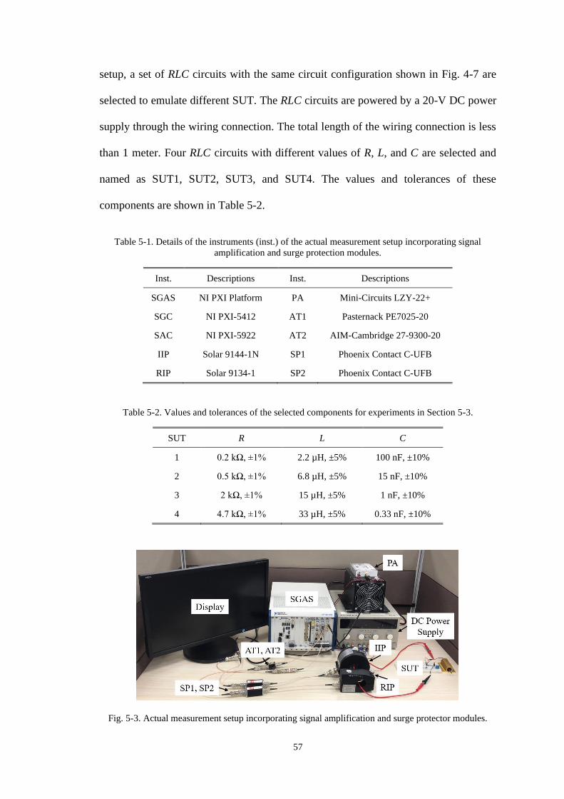
57
setup, a set of RLC circuits with the same circuit configuration shown in Fig. 4-7 are
selected to emulate different SUT. The RLC circuits are powered by a 20-V DC power
supply through the wiring connection. The total length of the wiring connection is less
than 1 meter. Four RLC circuits with different values of R, L, and C are selected and
named as SUT1, SUT2, SUT3, and SUT4. The values and tolerances of these
components are shown in Table 5-2.
Table 5-1. Details of the instruments (inst.) of the actual measurement setup incorporating signal
amplification and surge protection modules.
Inst. Descriptions Inst. Descriptions
SGAS NI PXI Platform PA Mini-Circuits LZY-22+
SGC NI PXI-5412 AT1 Pasternack PE7025-20
SAC NI PXI-5922 AT2 AIM-Cambridge 27-9300-20
IIP Solar 9144-1N SP1 Phoenix Contact C-UFB
RIP Solar 9134-1 SP2 Phoenix Contact C-UFB
Table 5-2. Values and tolerances of the selected components for experiments in Section 5-3.
SUT R L C
1 0.2 kΩ, ±1% 2.2 µH, ±5% 100 nF, ±10%
2 0.5 kΩ, ±1% 6.8 µH, ±5% 15 nF, ±10%
3 2 kΩ, ±1% 15 µH, ±5% 1 nF, ±10%
4 4.7 kΩ, ±1% 33 µH, ±5% 0.33 nF, ±10%
Fig. 5-3. Actual measurement setup incorporating signal amplification and surge protector modules.

58
Fig. 5-3 shows the actual measurement setup and one of the SUTs. Firstly, the
impedances of the SUTs are directly measured using an impedance analyzer (Agilent
4294A) offline as a reference for comparison. Subsequently, the online measured
impedances using this measurement setup are compared with that measured offline.
Table 5-3 shows the comparison of the measured impedances when fsig = 100 kHz and
d = 0 mm. Using the offline measured impedances as a reference, Fig. 5-4 shows the
deviation of the online measured impedances using this measurement setup. Similarly,
Table 5-4 shows the comparison of the measured impedances when fsig = 50 kHz and d
= 20 mm, and Fig. 5-5 shows the deviation of the online measured impedances using
this measurement setup.
Table 5-3. Comparison of the measured impedances of the SUTs in Table 5-2 when fsig = 100 kHz and d
= 0 mm.
SUT
Offline Measurement
(Reference)
Online Measurement using the
measurement setup in Fig. 5-3
|Z|(Ω) ∠Z(°) |Z|(Ω) ∠Z(°)
1 15.48 -84.7 15.32 -84.9
2 96.59 -77.9 95.51 -77.6
3 1272 -50.1 1284 -49.7
4 3332 -44.3 3376 -43.4
10 100 1k 5k-6
-3
0
3
6 |ZSUT|
ÐZSUT
ZSUT (W)
|Z
SU
T| (
%)
-1
0
1
2
3
Ð
ZS
UT (
°)
Fig. 5-4. Calculated measurement errors from Table 5-3 when fsig =100 kHz and d = 0 mm.

59
Table 5-4. Comparison of the measured impedances of the SUTs in Table 5-2 when fsig = 50 kHz and d
= 20 mm.
SUT
Offline Measurement
(Reference)
Online Measurement using the
measurement setup in Fig. 5-3
|Z|(Ω) ∠Z(°) |Z|(Ω) ∠Z(°)
1 32.72 -80.1 32.45 -80.2
2 188.2 -67.4 186.5 -67.2
3 1715 -31.0 1732 -30.6
4 4208 -26.1 4313 -25.2
20 100 1k 6k-6
-3
0
3
6 |ZSUT|
ÐZSUT
ZSUT (W)
|Z
SU
T| (
%)
-1
0
1
2
3
Ð
ZS
UT (
°)
Fig. 5-5. Calculated measurement errors from Table 5-4 when fsig = 50 kHz and d = 20 mm.
From Figs. 5-4 and 5-5, the measured online impedances show rather good accuracy
(∆|ZSUT| kept within 3% and ∆∠ZSUT kept within 1°) for all four SUTs. Therefore, the
accuracy of the measurement setup for online impedance extraction has been validated.
In this chapter, an inductively coupled measurement setup incorporating signal
amplification and surge protection modules is introduced. Based on two-port and three-
port network concepts, the equivalent circuit model of this measurement setup has been
described and its ability to extract the online impedance of an electrical system has been
verified by experiments. By doing so, this measurement setup can be used to extract the
online impedance of an electrical system with significant electrical noise and power

60
surges. Thus, the scope of application of the inductive coupling approach has been
expanded. In the next chapter, a practical application case to extract the online
impedance of an electrical system with significant electrical noise and power surges
using this measurement setup will be elaborated.

61
Chapter 6 Application in Stator Fault Detection of
Inverter-Fed Induction Motor
With the advancement of both the fast-switching power electronics and the pulse width
modulation (PWM) control techniques, the inverters have become highly popular for
variable torque and speed controls of induction motors (IMs) because of their excellent
conversion efficiency and control efficiency [44]. Just like any other electrical assets,
the IM is also subject to faults due to thermal, electrical, ambient, and mechanical
stresses. Among the common faults of the IM, bearing, stator and rotor faults are three
major ones that account for 41%, 36% and 9% of the total faults of the IM, respectively
[45]. The stator faults usually result from the stator winding insulation breakdown. Such
a breakdown can lead to an inter-turn short-circuit (ITSC) fault, which in turn will result
in a greater current flowing through the shorted turns and generate excessive heat in
adjacent turns. Thus, an ITSC fault can quickly develop into a more severe fault, such
as a coil-to-coil, phase-to-phase, or phase-to-ground short-circuit fault, and eventually
results in a complete failure of IM [46]. The failure is financially deleterious because of
the asset replacement and the loss of revenue associated with unscheduled IM
downtime. Therefore, effective detection of stator ITSC faults is necessary to avoid
catastrophic failures.
A variety of ITSC fault detection methods have been reported and in general, they can
be classified into two categories: the model-based methods [47]-[49] and the signal-
based methods [50]-[57]. The model-based methods require a rather accurate numerical
model of the faulty IM to identify the ITSC faults, which can be computationally
intensive and might not always be feasible. The signal-based methods monitor one or

62
more signals and detect the ITSC faults by analyzing these monitored signals. These
signals can be the motor current/voltage [50], [51], the stray flux [52], the air-gap torque
[53], the vibration [54], the temperature [55], the instantaneous power [56], and the
sequence component impedance matrix [57].
Although the above-mentioned signal-based methods have achieved effective detection
of ITSC faults under specific operation conditions, there are still a few aspects not
considered. For examples, the motor current, the stray flux, the air-gap torque, the
vibration and the temperature monitoring can be affected by the faults other than stator
ITSC faults, such as bearing or rotor faults [53], [58]-[61]; thus, the reliability of the
ITSC fault detection can be an issue. In addition, the voltage sensors used in the
measurement setups to monitor the motor voltage [51], the instantaneous power [56],
and the sequence component impedance matrix [57], require physical electrical
connection to the energized IM for online ITSC fault detection. This physical electrical
connection can pose electrical safety hazards to the service personnel who maintains the
instruments on-site. Also, the voltage sensors used in the measurement setups are subject
to dielectric and thermal stresses, which require regular maintenance and replacement;
and result in unnecessary downtime of the IM. Recently, several artificial intelligence
(AI) techniques [62]-[66] have been combined with the aforementioned signal-based
methods to improve the ITSC fault detection but these require a large set of training data
obtained from different operating states and conditions to ensure good detection
reliability and robustness.
In this chapter, a novel signal-based method for the detection of the stator ITSC faults
in the inverter-fed IM is proposed. The proposed method detects the ITSC faults through
online monitoring of the common-mode (CM) impedance of the IM (ZCM,IM) at a

63
specific frequency of interest (FOI). The inductively coupled measurement setup shown
in Fig. 5-1 is adopted to monitor ZCM,IM by tracking a known externally injected radio-
frequency (RF) sinusoidal signal in the IM. Thus, the monitored ZCM,IM will not be
affected by the supply voltage quality (e.g. unbalanced supply voltage). Also, the
measurement setup requires no physical electrical connection to the IM, and the clamp-
on inductive probes used in the measurement setup can be easily mounted on or removed
from the power cable connected between the IM and inverter. Therefore, it simplifies
the on-site implementation without shutting down the IM. In addition, the measurement
setup has incorporated signal amplification and surge protection modules to enhance its
ruggedness in the harsh industrial environment where significant electrical noise and
power surges are present. Furthermore, by carefully selecting the FOI to monitor ZCM,IM,
it eliminates the need of monitoring ZCM,IM for a wide frequency range, thereby
shortening the response time for ITSC fault detection. Fast response time is crucial for
quick decisions to be made before an ITSC fault develops into a catastrophic failure.
Through online monitoring of ZCM,IM at the FOI, the proposed method can detect stator
ITSC faults with good confidence. Also, this method is reliable and robust for stator
ITSC fault detection because it is invariant to motor load and speed variation, as well as
bearing and rotor faults.
The organization of this chapter is as follows. Section 6.1 looks into the influence of
ITSC faults on ZCM,IM and elaborates the process of selecting an appropriate FOI that is
sensitive to the variation of ZCM,IM due to the ITSC faults. Section 6.2 describes the
measurement setup for online monitoring of ZCM,IM at the FOI. Using an IM as a test
case, Section 6.3 illustrates the reliability and robustness of the proposed method for
ITSC fault detection under various conditions.

64
6.1. ITSC Fault Analysis and FOI Selection
6.1.1. ITSC Fault Influence on CM Impedance of IM
Before analyzing the influence of stator ITSC faults on ZCM,IM, the definition of ZCM,IM
is briefly introduced. Fig. 6-1 shows a comprehensive CM equivalent circuit model of a
typical 3-phase IM with all the relevant electrical elements [67].
Fig. 6-1. A comprehensive CM equivalent circuit model of a typical 3-phase IM.
Regardless of the actual stator winding connection, the equivalent model can take the
form of a star-connected configuration with the various elements calculated based on
available measurements. Therefore, the model is universal and remains effective for any
stator winding configuration (e.g. star, delta, series, or parallel) [67]. As shown in Fig.

65
6-1, Csw1 and Csw2 are the equivalent winding-to-frame parasitic capacitances. Rco1 and
Rco2 are the equivalent copper resistances including the skin- and proximity-effects. Lls
is the stator winding leakage inductance. Re is the eddy-current losses of the stator core.
Rt, Lt, and Ct represent the interturn parasitic effects of the stator windings. Lc is the
combined inductance of the IM’s internal feed conductors to the stator windings and the
stator winding leakage inductance of the first few turns. ZCM,IM is defined as
VCM,IM/ICM,IM, where VCM,IM and ICM,IM are the CM voltage and current present at the
IM, respectively.
To analyze the influence of ITSC faults on ZCM,IM, Fig. 6-2 shows an ITSC fault that
occurs in one of the phases of an IM. Such a fault results in a very low contact impedance
between the shorted turns (ZITSC) and it has an influence on ZCM,IM. It should be noted
that besides the ITSC faults, other stator faults like coil-to-coil, phase-to-phase, and
phase-to-ground short-circuit faults also have an effect on ZCM,IM. Since these more
serious stator faults arise from ITSC faults [46], this chapter focuses on the detection of
stator ITSC faults. Herein, the analysis looks into the relative change in ZCM,IM due to
the ITSC faults. To avoid the long measurement time to monitor ZCM,IM across a wide
frequency band, monitoring ZCM,IM at a single frequency is preferred for faster response
should an ITSC fault occurs. To ensure reliable detection of the ITSC faults, the
selection process of an appropriate FOI to monitor ZCM,IM will be explained in the
following section.

66
Fig. 6-2. An ITSC fault that occurs in one of the phases of an IM.
6.1.2. FOI Selection
It is reported that the IM’s load and speed have negligible effects on ZCM,IM in the mid-
to-high frequency range [67]. Once the FOI is selected within this frequency range, the
ITSC faults can be detected via monitoring ZCM,IM with good confidence under the
varying load and speed conditions. The following process is adopted to determine this
frequency range.
i. Measure the differential-mode (DM) impedance of the IM (ZDM,IM) offline using an
impedance analyzer shown in Fig. 6-3 over a wide frequency range, say, up to a
few megahertz.
ii. Determine the frequency where ZDM,IM exhibits a self-resonance. The self-resonant
frequency is the start frequency of the mid-to-high frequency range of the IM and
from this frequency onwards, the IM’s load and speed have negligible effects on its
impedance characteristics [67].
Fig. 6-3. Offline measurement of ZDM,IM using an impedance analyzer.
Using a 1/2-hp IM (TECO AEAV1902R500FUS) as an illustration, Fig. 6-4 shows the
frequency response of ZDM,IM of the healthy IM measured offline from 40 Hz to 5 MHz
with an impedance analyzer (Agilent 4294A). As observed in Fig. 6-4, ZDM,IM exhibits
a self-resonant frequency at 42 kHz. Therefore, the mid-to-high frequency range of the

67
IM starts from 42 kHz.
40 100 1k 10k 100k 1M 5M0
15
30
45
60 |ZDM,IM|
ÐZDM,IM
Frequency (Hz)
|ZD
M,I
M| (
kW
)42k
-90
-45
0
45
90
ÐZ
DM
,IM
(°)
Fig. 6-4. Frequency response of ZDM,IM of the healthy TECO IM measured offline from 40 Hz - 5 MHz.
Once the mid-to-high frequency range of the IM is determined, the next step is to select
the FOI within this frequency range as follows:
i. Measure ZCM,IM of the healthy IM offline in the mid-to-high frequency range using
an impedance analyzer, as shown in Fig. 6-5.
ii. Measure ZCM,IM of the IM of the same model with ITSC faults of different severity
levels offline in the same frequency range as (i) using an impedance analyzer.
iii. Compute the relative change in ZCM,IM caused by the ITSC faults and select a
frequency where the relative change is significant even for low severity ITSC faults.
The selected frequency is defined as the FOI.
The relative change in ZCM,IM at each frequency is defined and computed as follows:
Relative Change = |𝒁𝑪𝑴,𝑰𝑴(faulty)−𝒁𝑪𝑴,𝑰𝑴(healthy)|
|𝒁𝑪𝑴,𝑰𝑴(healthy)|× 100% (6-1)
The criterion for judging whether the relative change is significant or not is 5%, which
will be explained in Section 6.3. To emulate the ITSC faults with different severity
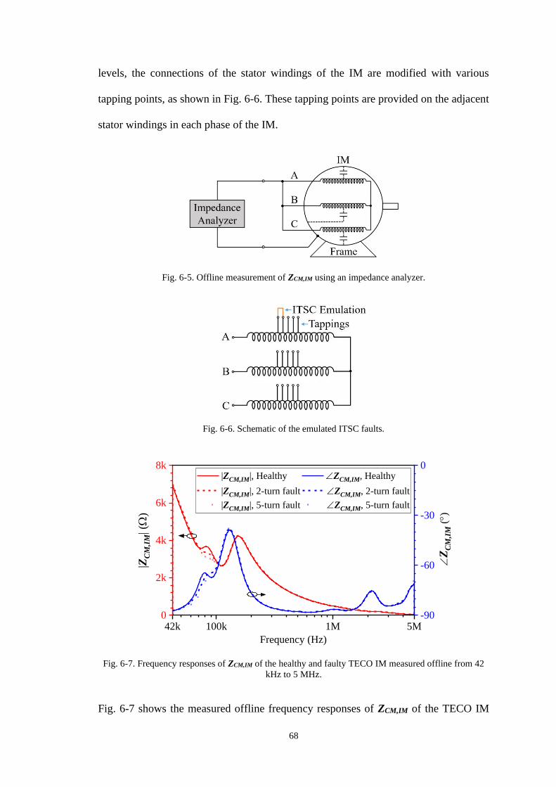
68
levels, the connections of the stator windings of the IM are modified with various
tapping points, as shown in Fig. 6-6. These tapping points are provided on the adjacent
stator windings in each phase of the IM.
Fig. 6-5. Offline measurement of ZCM,IM using an impedance analyzer.
Fig. 6-6. Schematic of the emulated ITSC faults.
42k 100k 1M 5M0
2k
4k
6k
8k |ZCM,IM|, Healthy ÐZCM,IM, Healthy
|ZCM,IM|, 2-turn fault ÐZCM,IM, 2-turn fault
|ZCM,IM|, 5-turn fault ÐZCM,IM, 5-turn fault
Frequency (Hz)
|ZC
M,I
M| (
W)
-90
-60
-30
0
ÐZ
CM
,IM
(°)
Fig. 6-7. Frequency responses of ZCM,IM of the healthy and faulty TECO IM measured offline from 42
kHz to 5 MHz.
Fig. 6-7 shows the measured offline frequency responses of ZCM,IM of the TECO IM

69
under the healthy condition and with emulated ITSC faults from 42 kHz to 5 MHz.
Taking the frequency response of ZCM,IM of the healthy IM as a reference, Fig. 6-8 shows
the relative change in ZCM,IM caused by two emulated ITSC faults of different severity
levels, the 2-turn and 5-turn ITSC faults. As observed in Fig. 6-8, the relative change
caused by the 2-turn fault is already noticeable (> 5%) between 66 kHz and 96 kHz and
it is as high as 9.6% at 80 kHz. For the 5-turn fault, an increase in the relative change
across almost the entire frequency range is clearly observed, especially between 66 kHz
and 96 kHz, where the highest relative change increases to 17.2%. The observation in
results has shown that a more severe ITSC fault causes a higher relative change.
Therefore, for the given IM, a frequency between 66 kHz and 96 kHz can be selected as
the FOI to monitor ZCM,IM for the detection of ITSC faults even the faults are at low
severity levels (e.g. 2-turn fault).
42k 100k 1M 5M0
5
10
15
20
96k66k
(80k,9.6)
(80k,17.2)
Rel
ativ
e C
han
ge
()
Frequency (Hz)
2-turn fault
5-turn fault
Fig. 6-8. Relative change in ZCM,IM of the TECO IM caused by ITSC faults with two fault severity levels
(i.e. 2-turn fault and 5-turn fault).
6.2. Online Monitoring of IM’s CM Impedance
The earlier section has shown that the ITSC faults can be detected by monitoring the
relative change of ZCM,IM. Also, the procedure to select an appropriate FOI for an IM to
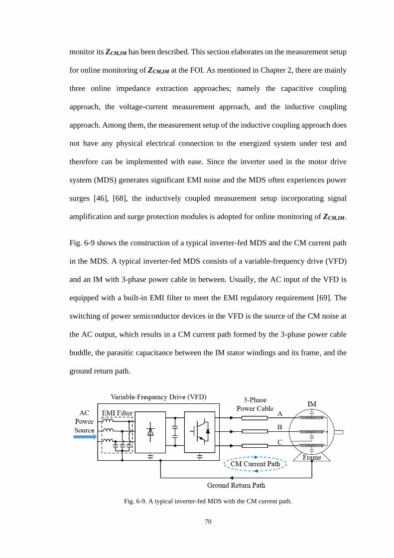
70
monitor its ZCM,IM has been described. This section elaborates on the measurement setup
for online monitoring of ZCM,IM at the FOI. As mentioned in Chapter 2, there are mainly
three online impedance extraction approaches; namely the capacitive coupling
approach, the voltage-current measurement approach, and the inductive coupling
approach. Among them, the measurement setup of the inductive coupling approach does
not have any physical electrical connection to the energized system under test and
therefore can be implemented with ease. Since the inverter used in the motor drive
system (MDS) generates significant EMI noise and the MDS often experiences power
surges [46], [68], the inductively coupled measurement setup incorporating signal
amplification and surge protection modules is adopted for online monitoring of ZCM,IM.
Fig. 6-9 shows the construction of a typical inverter-fed MDS and the CM current path
in the MDS. A typical inverter-fed MDS consists of a variable-frequency drive (VFD)
and an IM with 3-phase power cable in between. Usually, the AC input of the VFD is
equipped with a built-in EMI filter to meet the EMI regulatory requirement [69]. The
switching of power semiconductor devices in the VFD is the source of the CM noise at
the AC output, which results in a CM current path formed by the 3-phase power cable
buddle, the parasitic capacitance between the IM stator windings and its frame, and the
ground return path.
Fig. 6-9. A typical inverter-fed MDS with the CM current path.

71
Fig. 6-10(a) shows the measurement setup for online monitoring of ZCM,IM. As
mentioned in Section 5.1, it consists of a computer-controlled signal generation and
acquisition system (SGAS), a power amplifier (PA), two attenuators (AT1 and AT2),
two surge protectors (SP1 and SP2), a clamp-on injecting inductive probe (IIP), and a
clamp-on receiving inductive probe (RIP). To monitor ZCM,IM online, the IIP and RIP
are clamped onto the 3-phase power cable with the clamping position denoted as p1-p2.
(a)
(b)
Fig. 6-10. (a) Measurement setup for online monitoring of ZCM,IM; (b) CM equivalent circuit of the
inverter-fed MDS with the measurement setup.

72
Fig. 6-10(b) shows the CM equivalent circuit of the MDS, in which VCM,NS is the
equivalent CM noise source due to the switching of the VFD; ZCM,VFD is the equivalent
CM impedance of the VFD; ZCM,W is the equivalent CM loop impedance of the 3-phase
power cable and the ground return path. Therefore, the resultant impedance ZX seen at
p1-p2 is given by:
ZX = ZCM,VFD,CM + ZCM,W + ZCM,IM (6-2)
Since the physical length of the power cable is much shorter than the wavelength of the
FOI, the equivalent circuit concerned can be treated as a lumped circuit model [18]. As
described in Section 5.2, for this measurement setup, once the three-term calibration
technique is performed before online measurement, ZX can be directly extracted through
this measurement setup. It should be explained that with the PA, the test signal can be
amplified so that the level of the induced signal in the CM path of the MDS can be much
higher than the level of the noise at the FOI to achieve adequate SNR (> 40 dB). Since
the three-term calibration technique and the principle of extracting ZX have been well
described in Section 4.2 and Section 5.2, respectively, they will not be repeated here.
After obtaining ZX, ZCM,IM can be extracted online once the online (ZCM,VFD + ZCM,W) is
determined as follows:
i. Measure ZX of the healthy MDS online using the measurement setup. It should be
noted that ZX at the FOI is unaffected by varying load and speed conditions, which
will be verified in Section 6.3.
ii. Measure ZCM,IM of the healthy IM offline using an impedance analyzer, as shown
in Fig. 6-5. Since the offline measured ZCM,IM can be treated as the online ZCM,IM at
the FOI [67], [70], the online (ZCM,VFD + ZCM,W) can be obtained by subtracting the
offline measured ZCM,IM from the online measured ZX.

73
Noted that the online ZCM,VFD is mainly determined by the parasitic capacitances
between the switching devices and the heat sink in the VFD, as well as by the capacitors
(linked between each phase and the ground) in the built-in EMI filter [71]. Therefore,
the online ZCM,VFD at a given frequency remains almost unchanged for a specific VFD
under different operation modes [71], [72]. Besides, the online ZCM,W at a given
frequency also remains almost unchanged for a specific 3-phase power cable and ground
return path. Thus, once the online (ZCM,VFD + ZCM,W) at the FOI is determined and using
the ZCM,IM at the FOI of the healthy IM as a reference, any changes of ZCM,IM due to the
ITSC faults can be detected through online monitoring.
6.3. Experimental Validation
The same IM (TECO AEAV1902R500FUS) is used as the motor under test for
experimental validation. The ratings of the IM are shown in Table 6-1. A VFD (TECO
L510s) is used to control the IM and the length of the 3-phase power cable is 1 meter.
The details of instruments of the actual measurement setup are given in Table 6-2.
Table 6-1. Ratings of the 3-phase IM under test.
Rating Value Rating Value
Power 1/2-hp Frequency 50 Hz
Voltage 220-240 V (∆) Pole 2
Current 1.85-1.70 A (∆) Speed 2765 RPM
Table 6-2. Details of instruments (inst.) of the actual measurement setup.
Inst. Descriptions Inst. Descriptions
SGAS NI PXI Platform PA Mini-Circuits ZHL-32A-S+
SGC NI PXI-5412 AT1 Pasternack PE7025-20
SAC NI PXI-5922 AT2 AIM-Cambridge 27-9300-6
IIP Solar 9144-1N SP1 Bussmann BSPD5BNCDI
RIP Solar 9134-1 SP2 Bussmann BSPD5BNCDI

74
Fig. 6-11 shows the actual measurement setup with the MDS under test. An adjustable
friction load is driven by the IM with a belt. The ITSC faults are emulated by connecting
additional low-impedance contacts (< 1 Ω) between the selected tappings as shown in
Fig. 6-6. The response time with the measurement setup and the LabVIEW program to
monitor and detect the ITSC faults is found to be within 1 s.
Fig. 6-11. Actual measurement setup with the MDS under test.
As mentioned in Subsection 6.1.2, to ensure reliable detection of ITSC faults, the FOI
to monitor ZCM,IM of the IM is between 66 kHz and 96 kHz. For practical considerations,
the FOI has to also be selected with care so that the background noise in the MDS at the
FOI is relatively low to achieve the best SNR. Fig. 6-12 shows the noise current
spectrum from 66 kHz to 96 kHz in the MDS under test. It shows that the frequencies
with relatively low noise can be identified. It is observed from the enlarged image of
Fig. 6-12 that the noise level at 82 kHz is rather low at 2.4 µA. Therefore, the FOI is
selected to be 82 kHz to monitor ZCM,IM for online ITSC fault detection of the IM. As
mentioned in Section 6.2, the SNR in the MDS is required to be larger than 40 dB for
accurate extraction of ZCM,IM. Fig. 6-13 shows the current spectrum around 82 kHz in
the MDS under test with the present of the injected RF sinusoidal excitation signal at 82
kHz, which is clearly visible at 796 µA with an excitation signal source at 600 mV. With

75
the background noise of 2.4 µA at 82 kHz, the induced signal achieves 50 dB SNR for
online monitoring of ZCM,IM. The induced 796 µA is too small to affect the normal
operation of the MDS.
66k 70k 80k 90k 96k0
300
600
900
1200
Cu
rren
t (m
A)
Frequency (Hz)
Fig. 6-12. Noise current spectrum from 66 kHz to 96 kHz in the MDS under test.
74k 78k 82k 86k 90k0
300
600
900
1200
Cu
rren
t (m
A)
Frequency (Hz)
Induced Signal Current 796 mA
Fig. 6-13. Current spectrum around 82 kHz in the MDS under test when injecting an RF sinusoidal
excitation signal (600 mV at 82 kHz) into the MDS by using the measurement setup.
Injecting the RF sinusoidal excitation signal (600 mV at 82 kHz) into the MDS under
test with the measurement setup, Figs. 6-14 and 6-15 show the measured ZX of the
healthy MDS at varying load (nominal speed) and varying speed conditions,
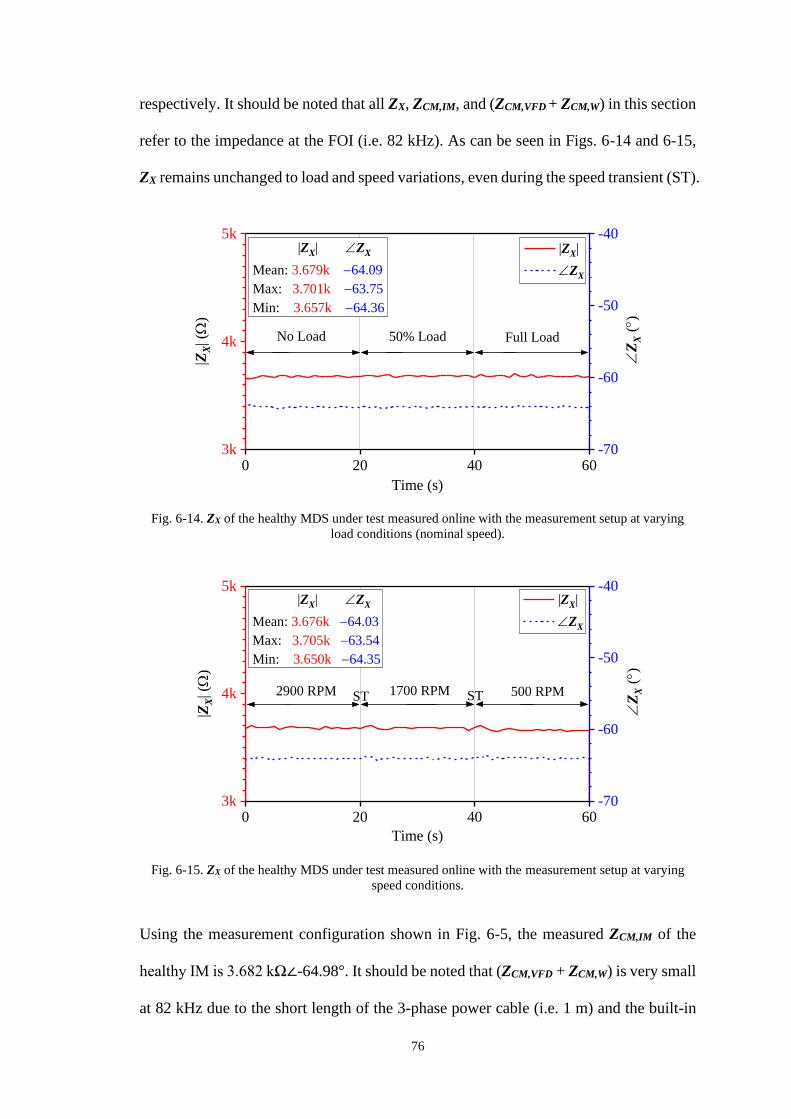
76
respectively. It should be noted that all ZX, ZCM,IM, and (ZCM,VFD + ZCM,W) in this section
refer to the impedance at the FOI (i.e. 82 kHz). As can be seen in Figs. 6-14 and 6-15,
ZX remains unchanged to load and speed variations, even during the speed transient (ST).
0 20 40 603k
4k
5k |ZX| ÐZX
Mean: 3.679k -64.09
Max: 3.701k -63.75
Min: 3.657k -64.36
|ZX|
ÐZX
Full Load50% Load
Time (s)
|ZX| (
W)
No Load
-70
-60
-50
-40
ÐZ
X (
°)
Fig. 6-14. ZX of the healthy MDS under test measured online with the measurement setup at varying
load conditions (nominal speed).
0 20 40 603k
4k
5k
Time (s)
|ZX| (
W)
|ZX|
ÐZX
-70
-60
-50
-40 |ZX| ÐZX
Mean: 3.676k -64.03
Max: 3.705k -63.54
Min: 3.650k -64.35
ST 500 RPM1700 RPM2900 RPM
ÐZ
X (
°)
ST
Fig. 6-15. ZX of the healthy MDS under test measured online with the measurement setup at varying
speed conditions.
Using the measurement configuration shown in Fig. 6-5, the measured ZCM,IM of the
healthy IM is 3.682 kΩ∠-64.98°. It should be noted that (ZCM,VFD + ZCM,W) is very small
at 82 kHz due to the short length of the 3-phase power cable (i.e. 1 m) and the built-in

77
EMI filter of the VFD [69]. Since (ZCM,VFD + ZCM,W) << ZCM,IM, ZX can be approximated
as ZCM,IM for the MDS under test. Therefore, the relative change in ZX is very much the
same as the relative change in ZCM,IM.
Fig. 6-16 shows the relative change in ZCM,IM of the IM at varying load conditions
(nominal speed) when the IM is in the healthy condition and in the 2-turn ITSC fault
condition, respectively. It is observed that the relative change is unaffected by the load
variations. Also, when the IM is in the 2-turn ITSC fault condition, the relative change
remains almost unchanged at about 9.4%. However, there is a very small relative change
(< 1%) when the IM is in the healthy condition. From Fig. 6-14, such a minor relative
change is caused by the slight normal fluctuation in the monitored impedance. Fig. 6-17
shows the relative change in ZCM,IM of the IM at varying speed conditions when the IM
is in the healthy condition and in the 2-turn ITSC fault condition, respectively. Again,
the relative change is unaffected by the speed variations. Also, under the 2-turn ITSC
fault condition, the relative change still remains almost unchanged at 9.4%. Besides, the
minor relative change caused by the slight normal fluctuation in the monitored
impedance is still kept within 1%. From Figs. 6-16 and 6-17, it is found that the relative
change in ZCM,IM at the FOI is unaffected by the load and speed variations. In addition,
since the minor relative change due to the slight normal fluctuation in the monitored
impedance is kept within 1%, the threshold can be determined to be 1% for the ITSC
fault detection. Based on the 1% threshold, the relative change can be treated as
significant when it is larger than 5%. Furthermore, even the IM with a 2-turn ITSC fault
has shown a rather noticeable relative change of 9.4%, which indicates that the proposed
method has good sensitivity to detect the ITSC faults that are less severe. Table 6-3
shows the relative change in ZCM,IM of the IM for the ITSC faults with different severity
levels, which increases with higher ITSC fault severity.

78
0 20 40 600
4
8
12
16 Healthy 2-turn fault
Mean: 0.3 9.4
Max: 0.8 9.9
Min: 0.0 8.9
Rel
ativ
e C
han
ge
(%)
Time (s)
Healthy
2-turn fault
Threshold
No Load 50% Load Full Load
Fig. 6-16. Relative change in ZCM,IM of the IM (healthy and 2-turn fault) monitored online with the
measurement setup at varying load conditions (nominal speed).
0 20 40 600
4
8
12
16
STST
Healthy 2-turn fault
Mean: 0.4 9.4
Max: 0.9 10.0
Min: 0.1 8.8
Rel
ativ
e C
han
ge
(%)
Time (s)
Healthy
2-turn fault
Threshold
2900 RPM 1700 RPM 500 RPM
Fig. 6-17. Relative change in ZCM,IM of the IM (healthy and 2-turn fault) monitored online with the
measurement setup at varying speed conditions.
Table 6-3. Relative change in ZCM,IM of the IM for different ITSC fault severities
Fault Severity
Level
Relative Change in ZCM,IM
Mean Value Maximum Value Minimum Value
2-turn fault 9.4% 10.0% 8.8%
3-turn fault 10.5% 11.2% 10.1%
4-turn fault 12.1% 12.9% 11.5%
5-turn fault 17.4% 18.1% 16.6%
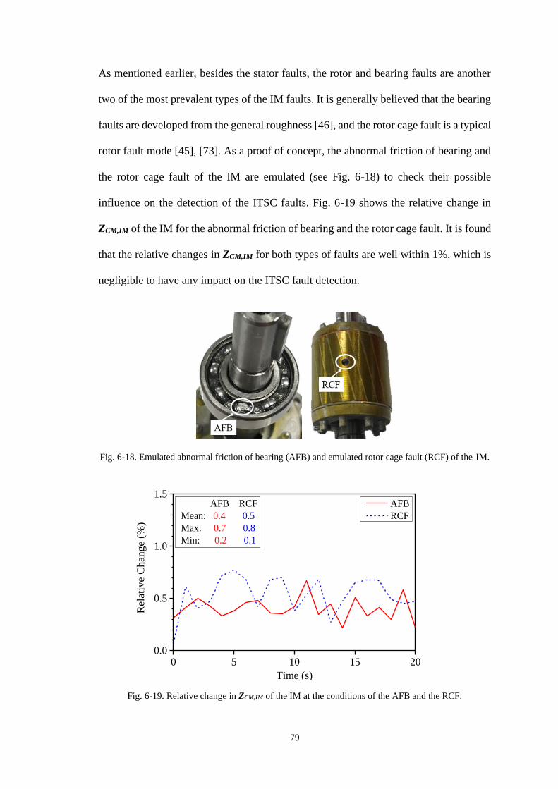
79
As mentioned earlier, besides the stator faults, the rotor and bearing faults are another
two of the most prevalent types of the IM faults. It is generally believed that the bearing
faults are developed from the general roughness [46], and the rotor cage fault is a typical
rotor fault mode [45], [73]. As a proof of concept, the abnormal friction of bearing and
the rotor cage fault of the IM are emulated (see Fig. 6-18) to check their possible
influence on the detection of the ITSC faults. Fig. 6-19 shows the relative change in
ZCM,IM of the IM for the abnormal friction of bearing and the rotor cage fault. It is found
that the relative changes in ZCM,IM for both types of faults are well within 1%, which is
negligible to have any impact on the ITSC fault detection.
Fig. 6-18. Emulated abnormal friction of bearing (AFB) and emulated rotor cage fault (RCF) of the IM.
0 5 10 15 200.0
0.5
1.0
1.5
Rela
tiv
e C
han
ge (
%)
Time (s)
AFB
RCF
AFB RCF
Mean: 0.4 0.5
Max: 0.7 0.8
Min: 0.2 0.1
Fig. 6-19. Relative change in ZCM,IM of the IM at the conditions of the AFB and the RCF.

80
Based on these findings, the proposed method has shown its reliability and robustness
for the stator ITSC fault detection under varying load and speed conditions, as well as
under rotor fault and bearing fault conditions.
In this chapter, a novel signal-based method for the detection of stator ITSC faults in the
inverter-fed IM has been described and developed. The measurement setup of the
proposed method does not have any physical electrical connection to the energized IM
under test and therefore eliminates electrical safety hazards. In addition, the clamp-on
IIP and RIP used in the measurement setup can be easily mounted on or removed from
the power cable connected to the IM and therefore facilitates ease of implementation.
By monitoring the CM impedance at a carefully selected FOI, it is efficient to detect the
ITSC faults to enable fast remedial response. This method has been experimentally
verified to be reliable and robust for the ITSC fault detection, as it is invariant to motor
load and speed variations, as well as bearing and rotor faults.

81
Chapter 7 Application in Voltage-Dependent
Capacitance Extraction of SiC Power MOSFET
Compared to the conventional power semiconductor devices, the wide-bandgap (WBG)
power semiconductor devices such as the silicon carbide (SiC) power MOSFETs have
lower on-resistance, higher switching frequency, and higher rated junction temperature,
and therefore are gaining more popularity [74]-[77]. However, the higher switching
frequency has resulted in undesirable oscillations at the rising and falling edges due to
the resonance of the circuit loop inductances and the interelectrode capacitances of the
SiC power MOSFET [78], [79]. Such oscillations can reduce the reliability of the system
due to their associated EMI [80], [81]. To evaluate and mitigate the negative effects in
the early design phase, the values of the interelectrode capacitances of the SiC power
MOSFET must be obtained [82]-[84]. Since the interelectrode capacitances are voltage-
dependent [85], knowing their values in the entire voltage operating range is required.
There are several methods reported in the literature to extract the voltage-dependent
capacitances. One of them is using 3-D full-wave simulation tools, such as the finite
element method, to compute the capacitances [86]. This method is possible only if the
full details of the geometries and material properties of the SiC power MOSFET are
known, which may not always be readily available since intellectual property issues.
Another method is using the impedance analyzer [20], in which many additional
accessories, such as DC blocking capacitors, AC blocking inductors, various resistors,
and protection diodes are necessary for safe and efficient online measurements. A time-
domain reflectometry method has also been reported [85], but proper isolation is
required to ensure that the measurement setup is disconnected from the ground. Besides,

82
this method is only limited to extract the output capacitance of the power MOSFET. A
three-probe measurement method has also been reported [87], but the parasitic
components of the probes and the probe-to-probe coupling between them are neglected
during the measurement process, which may affect the accuracy of the measured
capacitances. In addition to the aforementioned methods, a power device analyzer
(Keysight B1505A) is also available on the market. It requires to connect a specific bias-
tee to extract the voltage-dependent capacitance under high voltage biasing conditions.
Since the bias-tee has a physical electrical connection to the high voltage DC power
supply, additional protection devices are required for safety hazard compliance. To
extract the voltage-dependent capacitances of the SiC power MOSFET in a simple and
accurate manner, this chapter proposes an alternative approach based on the inductive
coupling approach. The measurement setup of this approach does not have any physical
electrical connection to the SiC power MOSFET that is biased by high DC voltage,
thereby eliminating potential safety hazards without introducing extra protection
devices. Besides, the measurement setup is simple for on-site implementation.
This chapter is organized as follows. Section 7.1 introduces an equivalent circuit model
of the SiC power MOSFET. Section 7.2 describes the principle and process of extracting
the voltage-dependent capacitances of the SiC power MOSFET. Using a 1.2 kV SiC
power MOSFET as a test case, Section 7.3 verifies the ability of the proposed method
to extract the values of the capacitances over a wide range of voltage biasing.
7.1. Equivalent Circuit Model of SiC Power MOSFET
Fig. 7-1 shows a small-signal equivalent circuit model of the SiC power MOSFET in
the off-state, where 𝑑, 𝑔, and 𝑠 are the drain, gate, and source terminals, respectively.
𝐶𝑔𝑑 , 𝐶𝑔𝑠 , and 𝐶𝑑𝑠 are the interelectrode capacitances; 𝐿𝑑 , 𝐿𝑔 , and 𝐿𝑠 are the terminal

83
inductances; 𝑅𝑑, 𝑅𝑔, and 𝑅𝑠 are the terminal resistances.
Fig. 7-1. Small-signal equivalent circuit model of the SiC power MOSFET in the off-state.
The terminal inductances are typically a few nanohenry [88]-[90] and the interelectrode
capacitances are typically smaller than a few nanofarad [91]-[94]. Therefore, in the
frequency range of fsig ≤ 1 MHz, the impedance of the SiC power MOSFET in the off-
state is dominated by its interelectrode capacitances, in which the terminal inductances
are negligible during the capacitances extraction process [20], [87]. Thus, the equivalent
circuit model in Fig. 7-1 can be simplified to that shown in Fig. 7-2.
Fig. 7-2. Simplified equivalent circuit model of Fig. 7-1 when fsig ≤ 1 MHz.

84
Fig. 7-3 shows the star-connected equivalent circuit model of Fig. 7-2. By using delta-
to-star circuit transformation, the star-connected capacitances 𝐶𝑑𝑛 , 𝐶𝑔𝑛 , and 𝐶𝑠𝑛 are
determined by:
𝐶𝑑𝑛 = 𝐶𝑔𝑑 + 𝐶𝑑𝑠 + 𝐶𝑔𝑑𝐶𝑑𝑠 𝐶𝑔𝑠⁄ (7-1)
𝐶𝑔𝑛 = 𝐶𝑔𝑑 + 𝐶𝑔𝑠 + 𝐶𝑔𝑑𝐶𝑔𝑠 𝐶𝑑𝑠⁄ (7-2)
𝐶𝑠𝑛 = 𝐶𝑔𝑠 + 𝐶𝑑𝑠 + 𝐶𝑔𝑠𝐶𝑑𝑠 𝐶𝑔𝑑⁄ (7-3)
Based on the star-connected capacitances, the equivalent star-connected impedances
𝒁𝒅𝒏, 𝒁𝒈𝒏, and 𝒁𝒔𝒏 are obtained by:
𝒁𝒅𝒏 = 𝑅𝑑 + 1/(𝑗𝜔𝐶𝑑𝑛) (7-4)
𝒁𝒈𝒏 = 𝑅𝑔 + 1/(𝑗𝜔𝐶𝑔𝑛) (7-5)
𝒁𝒔𝒏 = 𝑅𝑠 + 1/(𝑗𝜔𝐶𝑠𝑛) (7-6)
where 𝜔 = 2𝜋fsig.
Fig. 7-3. Star-connected equivalent circuit model of Fig. 7-2.

85
7.2. Principle of Voltage-Dependent Capacitance Extraction
From (7-4) to (7-6), once 𝒁𝒅𝒏, 𝒁𝒈𝒏, and 𝒁𝒔𝒏 are obtained, 𝐶𝑑𝑛 , 𝐶𝑔𝑛 , and 𝐶𝑠𝑛 can be
determined at a static functionality. Furthermore, 𝐶𝑔𝑑 , 𝐶𝑔𝑠 , and 𝐶𝑑𝑠 can be obtained
based on the determined 𝐶𝑑𝑛, 𝐶𝑔𝑛, and 𝐶𝑠𝑛 by (7-7) to (7-9).
𝐶𝑔𝑑 = 𝐶𝑔𝑛𝐶𝑑𝑛 (𝐶𝑑𝑛 + 𝐶𝑔𝑛 + 𝐶𝑠𝑛)⁄ (7-7)
𝐶𝑔𝑠 = 𝐶𝑔𝑛𝐶𝑠𝑛 (𝐶𝑑𝑛 + 𝐶𝑔𝑛 + 𝐶𝑠𝑛)⁄ (7-8)
𝐶𝑑𝑠 = 𝐶𝑑𝑛𝐶𝑠𝑛 (𝐶𝑑𝑛 + 𝐶𝑔𝑛 + 𝐶𝑠𝑛)⁄ (7-9)
Fig. 7-4 shows the test circuit to extract the equivalent terminal impedances, in which a
capacitor (𝐶1) is placed in parallel with the DC power supply to provide an AC short
circuit to the test signal (fsig). 𝒁𝒆𝒙𝒕𝟏, 𝒁𝒆𝒙𝒕𝟐, and 𝒁𝒆𝒙𝒕𝟑 are the equivalent impedances of
the external wires, which can be measured offline with an impedance analyzer. The
selected measurement setup is shown in Fig. 3-1, in which the signal amplification and
surge protection modules are not incorporated because there is no significant electrical
noise and power surges in the test circuit.
(a)

86
(b)
(c)
Fig. 7-4. Test circuit to extract 𝒁𝒅𝒏, 𝒁𝒈𝒏, and 𝒁𝒔𝒏 with the inductive probes mounted between (a)
position 𝑎-𝑎′, (b) position 𝑏-𝑏′, and (c) position 𝑐-𝑐′.
In Fig. 7-4(a), the IIP and RIP are mounted between position 𝑎-𝑎′. A test signal of
frequency fsig and current 𝑰𝒂𝒂′ is injected into the test circuit from the SGC through the
IIP. When the test signal current passes through point 𝑛, it is divided into two paths, one
through terminal 𝑠 (𝑰𝒔𝒏_𝒂𝒂′) and another via terminal 𝑔 (𝑰𝒈𝒏_𝒂𝒂′). Based on Kirchhoff’s
current law (KCL), 𝑰𝒂𝒂′ is given by

87
𝑰𝒂𝒂′ = 𝑰𝒈𝒏_𝒂𝒂′ + 𝑰𝒔𝒏_𝒂𝒂′ (7-10)
Thus, the resultant impedance measured by the measurement setup when the IIP and
RIP are mounted between position 𝑎-𝑎′ is given by
𝒁𝒂𝒂′ = 𝑽𝒂𝒂′/𝑰𝒂𝒂′ (7-11)
where 𝑽𝒂𝒂′ = 𝑽𝒂𝒂′𝟏 – 𝑽𝒂𝒂′𝟐; 𝑽𝒂𝒂′𝟏 and 𝑽𝒂𝒂′𝟐 represent the test signal voltages at the
output port of the IIP and the input port of the RIP, respectively. Furthermore, from Fig.
7-4(a)
𝑰𝒈𝒏_𝒂𝒂′ = 𝑽𝒏𝒎_𝒂𝒂′/(𝒁𝒆𝒙𝒕𝟐 + 𝒁𝒈𝒏) (7-12)
𝑰𝒔𝒏_𝒂𝒂′ = 𝑽𝒏𝒎_𝒂𝒂′/(𝒁𝒆𝒙𝒕𝟑 + 𝒁𝒔𝒏) (7-13)
𝑽𝒂𝒂′ = 𝑰𝒂𝒂′(𝒁𝒆𝒙𝒕𝟏 + 𝒁𝒅𝒏) + 𝑽𝒏𝒎_𝒂𝒂′ (7-14)
where 𝑽𝒏𝒎_𝒂𝒂′ is the test signal voltage between point n and m. Substituting (7-14) into
(7-11), 𝒁𝒂𝒂′ can be re-written as
𝒁𝒂𝒂′ = 𝒁𝒆𝒙𝒕𝟏 + 𝒁𝒅𝒏 + 𝑽𝒏𝒎_𝒂𝒂′/𝑰𝒂𝒂′ (7-15)
Substituting (7-12) and (7-13) into (7-10), 𝑰𝒂𝒂′ can be re-written as
𝑰𝒂𝒂′ = 𝑽𝒏𝒎_𝒂𝒂′/(𝒁𝒆𝒙𝒕𝟐 + 𝒁𝒈𝒏) + 𝑽𝒏𝒎_𝒂𝒂′/(𝒁𝒆𝒙𝒕𝟑 + 𝒁𝒔𝒏) (7-16)
Substituting (7-16) into (7-15), 𝒁𝒂𝒂′ can be finally extracted as
𝒁𝒂𝒂′ = 𝒁𝒆𝒙𝒕𝟏 + 𝒁𝒅𝒏 +(𝒁𝒆𝒙𝒕𝟐 + 𝒁𝒈𝒏)(𝒁𝒆𝒙𝒕𝟑 + 𝒁𝒔𝒏)
(𝒁𝒆𝒙𝒕𝟐 + 𝒁𝒈𝒏) + (𝒁𝒆𝒙𝒕𝟑 + 𝒁𝒔𝒏) (7-17)
Similarly, Fig. 7-4(b) and Fig. 7-4(c) show the current paths when the IIP and RIP are

88
mounted between position 𝑏-𝑏′ and between position 𝑐-𝑐′, respectively. Based on KCL,
(7-18) and (7-19) are obtained
𝑰𝒃𝒃′ = 𝑰𝒅𝒏_𝒃𝒃′ + 𝑰𝒔𝒏_𝒃𝒃′ (7-18)
𝑰𝒄𝒄′ = 𝑰𝒅𝒏_𝒄𝒄′ + 𝑰𝒈𝒏_𝒄𝒄′ (7-19)
Therefore, the resultant impedances measured by the measurement setup when the IIP
and RIP are mounted between position 𝑏-𝑏′ (𝒁𝒃𝒃′) and between position 𝑐-𝑐′ (𝒁𝒄𝒄′) are
extracted as follows
𝒁𝒃𝒃′ = 𝒁𝒆𝒙𝒕𝟐 + 𝒁𝒈𝒏 +(𝒁𝒆𝒙𝒕𝟏 + 𝒁𝒅𝒏)(𝒁𝒆𝒙𝒕𝟑 + 𝒁𝒔𝒏)
(𝒁𝒆𝒙𝒕𝟏 + 𝒁𝒅𝒏) + (𝒁𝒆𝒙𝒕𝟑 + 𝒁𝒔𝒏) (7-20)
𝒁𝒄𝒄′ = 𝒁𝒆𝒙𝒕𝟑 + 𝒁𝒔𝒏 +(𝒁𝒆𝒙𝒕𝟏 + 𝒁𝒅𝒏)(𝒁𝒆𝒙𝒕𝟐 + 𝒁𝒈𝒏)
(𝒁𝒆𝒙𝒕𝟏 + 𝒁𝒅𝒏) + (𝒁𝒆𝒙𝒕𝟐 + 𝒁𝒈𝒏) (7-21)
From (7-17), (7-20), and (7-21), 𝒁𝒅𝒏, 𝒁𝒈𝒏, and 𝒁𝒔𝒏 can be obtained via (7-24) to (7-26):
𝜟 = 𝒁𝒂𝒂′𝟐 𝒁𝒃𝒃′
𝟐 − 𝟐𝒁𝒂𝒂′𝟐 𝒁𝒃𝒃′𝒁𝒄𝒄′ + 𝒁𝒂𝒂′
𝟐 𝒁𝒄𝒄′𝟐 − 𝟐𝒁𝒂𝒂′𝒁𝒃𝒃′
𝟐 𝒁𝒄𝒄′
−𝟐𝒁𝒂𝒂′𝒁𝒃𝒃′𝒁𝒄𝒄′𝟐 + 𝒁𝒃𝒃′
𝟐 𝒁𝒄𝒄′𝟐
(7-22)
𝜦 = −𝟐𝒁𝒂𝒂′𝒁𝒃𝒃′𝒁𝒄𝒄′ (7-23)
𝒁𝒅𝒏 =𝜦(𝒁𝒂𝒂′𝒁𝒃𝒃′ + 𝒁𝒂𝒂′𝒁𝒄𝒄′ − 𝒁𝒃𝒃′𝒁𝒄𝒄′)
𝜟− 𝒁𝒆𝒙𝒕𝟏 (7-24)
𝒁𝒈𝒏 =𝜦(𝒁𝒂𝒂′𝒁𝒃𝒃′ − 𝒁𝒂𝒂′𝒁𝒄𝒄′ + 𝒁𝒃𝒃′𝒁𝒄𝒄′)
𝜟− 𝒁𝒆𝒙𝒕𝟐 (7-25)
𝒁𝒔𝒏 =𝜦(−𝒁𝒂𝒂′𝒁𝒃𝒃′ + 𝒁𝒂𝒂′𝒁𝒄𝒄′ + 𝒁𝒃𝒃′𝒁𝒄𝒄′)
𝜟− 𝒁𝒆𝒙𝒕𝟑 (7-26)
As mentioned earlier, 𝒁𝒂𝒂′ , 𝒁𝒃𝒃′ , and 𝒁𝒄𝒄′ can be directly extracted online using the

89
measurement setup. 𝒁𝒆𝒙𝒕𝟏 , 𝒁𝒆𝒙𝒕𝟐 , and 𝒁𝒆𝒙𝒕𝟑 can be measured offline using an
impedance analyzer. After 𝒁𝒅𝒏, 𝒁𝒈𝒏, and 𝒁𝒔𝒏 are obtained, 𝐶𝑑𝑛, 𝐶𝑔𝑛, and 𝐶𝑠𝑛 can be
determined by (7-4) to (7-6). Furthermore, 𝐶𝑔𝑑, 𝐶𝑔𝑠, and 𝐶𝑑𝑠 can be derived based on
the extracted 𝐶𝑑𝑛, 𝐶𝑔𝑛, and 𝐶𝑠𝑛 through (7-7) to (7-9). Based on the obtained 𝐶𝑑𝑛, 𝐶𝑔𝑛,
and 𝐶𝑠𝑛, the input capacitance (𝐶𝑖𝑠𝑠), output capacitance (𝐶𝑜𝑠𝑠), and reverse transfer
capacitance (𝐶𝑟𝑠𝑠) of the SiC power MOSFET can also be extracted via (7-27) to (7-29).
𝐶𝑖𝑠𝑠 = 𝐶𝑔𝑠 + 𝐶𝑔𝑑 (7-27)
𝐶𝑜𝑠𝑠 = 𝐶𝑑𝑠 + 𝐶𝑔𝑑 (7-28)
𝐶𝑟𝑠𝑠 = 𝐶𝑔𝑑 (7-29)
7.3. Experimental Validation
Fig. 7-5 shows an actual measurement setup for experimental validation. The computer-
controlled SGAS is a National Instruments (NI) PXI platform, which consists of a signal
generation card (PXI-5412), a two-channel signal acquisition card (PXI-5122), a
computer interface card (PXI-8360), and a back panel (PXI-1031). A laptop with
programmable software was connected to the SGAS for instrument control. Two
Tektronix CT1 current probes were selected as the IIP and RIP. A Cree SiC power
MOSFET (C2M0080120D, 1.2 kV) was selected as the test sample for extracting its
voltage-dependent capacitances at varying drain-source voltage (𝑉𝑑𝑠 ), where it was
controlled by a Xantrex DC power supply (XDC 600-10, 0 to 600 V). Besides, an
impedance analyzer (Agilent 4294A) was used to extract the values of 𝒁𝒆𝒙𝒕𝟏, 𝒁𝒆𝒙𝒕𝟐, and
𝒁𝒆𝒙𝒕𝟑 offline. To verify the proposed method, the capacitances specified in the
manufacturer’s datasheet are used as a reference for comparison. Since the datasheet

90
only gives the values of 𝐶𝑖𝑠𝑠, 𝐶𝑜𝑠𝑠, and 𝐶𝑟𝑠𝑠 at the frequency of 1 MHz, fsig is set to 1
MHz for ease of comparison. Besides, 𝐶1 was selected as 1 µF (TDK
B32656S7105K561, 1.25 kV). 𝒁𝒆𝒙𝒕𝟏, 𝒁𝒆𝒙𝒕𝟐, and 𝒁𝒆𝒙𝒕𝟑 at 1 MHz were measured by the
Agilent impedance analyzer, and their respective impedance values are 0.4422 Ω∠77.4°,
0.2053 Ω∠79.1°, and 0.0493 Ω∠54.8°.
Fig. 7-5. Measurement setup to extract the voltage-dependent capacitances of the Cree SiC power
MOSFET.
0 100 200 300 400 500100
101
102
103
104
Cgd
Cds
Cap
acit
ance
(p
F)
Drain-Source Voltage, Vds (V)
Cgs
Fig. 7-6. Extracted interelectrode capacitances of the Cree SiC power MOSFET through the proposed
method at the frequency of 1 MHz.
Fig. 7-6 shows the extracted interelectrode capacitances of the Cree SiC power

91
MOSFET with 𝑉𝑑𝑠 varying from 0 to 500 V. Since the datasheet only gives the values
of 𝐶𝑖𝑠𝑠, 𝐶𝑜𝑠𝑠, and 𝐶𝑟𝑠𝑠, the corresponding capacitances are derived from the extracted
interelectrode capacitances for ease of comparison. Fig. 7-7 shows the values of 𝐶𝑖𝑠𝑠,
𝐶𝑜𝑠𝑠, and 𝐶𝑟𝑠𝑠 extracted via the proposed method and those provided by the datasheet.
Based on the 23 measurement points at different 𝑉𝑑𝑠, Table 7-1 lists the measurement
errors. As observed in Fig. 7-7 and Table 7-1, the capacitances extracted by the proposed
method are very consistent with those provided by the datasheet, which is a good
indication of the validity of this method to extract the voltage-dependent capacitances
of the SiC power MOSFET with a reasonable accuracy for a wide range of voltage
biasing.
0 100 200 300 400 500100
101
102
103
104
Datasheet Proposed Method
Crss
Coss
Cap
acit
ance
(pF
)
Drain-Source Voltage, Vds (V)
Ciss
Fig. 7-7. Comparison of the extracted 𝐶𝑖𝑠𝑠, 𝐶𝑜𝑠𝑠, and 𝐶𝑟𝑠𝑠 via the proposed method and those provided
by the datasheet.
Table 7-1. Errors of the extracted capacitances for 23 measurement points shown in Fig. 7-7.
Capacitance 𝑪𝒊𝒔𝒔 𝑪𝒐𝒔𝒔 𝑪𝒓𝒔𝒔
Mean absolute error 1.9% 1.5% 3.7%
Standard deviation of absolute error 1.2% 1.4% 2.7%
Maximum absolute error 4.3% 4.4% 9.8%

92
Fig. 7-8 shows the values of 𝐶𝑖𝑠𝑠 , 𝐶𝑜𝑠𝑠 , and 𝐶𝑟𝑠𝑠 obtained by the proposed method
when fsig is 100 kHz, 1MHz, and 10 MHz. The values of 𝐶𝑖𝑠𝑠, 𝐶𝑜𝑠𝑠, and 𝐶𝑟𝑠𝑠 at 100 kHz
are slightly different from those extracted at 1 MHz. However, the values of 𝐶𝑖𝑠𝑠, 𝐶𝑜𝑠𝑠,
and 𝐶𝑟𝑠𝑠 at 10 MHz have a larger deviation from those extracted at 100 kHz or 1 MHz.
The larger deviation of these extracted capacitances at 10 MHz is expected because of
the effect of the terminal inductances ( 𝐿𝑑 , 𝐿𝑔 , and 𝐿𝑠 ). When fsig ≤ 1 MHz, the
impedances of the terminal inductances are much smaller than those of the interelectrode
capacitances. However, when fsig increases to 10 MHz, the impedances of the terminal
inductances become significant and cannot be ignored, which explains the larger
deviation of the obtained capacitances from those extracted at 100 kHz and 1 MHz.
Therefore, when the proposed method is used to extract the voltage-dependent
capacitances of the SiC power MOSFET, fsig should not exceed 1 MHz to ensure
measurement accuracy.
0 100 200 300 400 5000
200
400
600
800
1000
1200
1400
100 kHz 1 MHz 10 MHz
Crss
Coss
Cap
acit
ance
(pF
)
Drain-Source Voltage, Vds (V)
Ciss
Fig. 7-8. Comparison of the values of 𝐶𝑖𝑠𝑠, 𝐶𝑜𝑠𝑠, and 𝐶𝑟𝑠𝑠 obtained by the proposed method at the
frequency of 100 kHz, 1 MHz, and 10 MHz.
In this chapter, a novel method to extract the voltage-dependent capacitances of the SiC
power MOSFET based on the inductive coupling approach has been described and

93
verified. The proposed measurement setup can extract the voltage-dependent
capacitances of the SiC power MOSFET under its actual high voltage biasing condition
without any physical electrical connection to the energized power MOSFET and
therefore it is safe and relatively simple to set up. A 1.2 kV SiC power MOSFET was
selected as the test case, and the accuracy of the extracted capacitances has been verified
with the datasheet provided by the manufacturers. With the voltage-dependent
capacitances of the SiC power MOSFET, its equivalent circuit model can be represented
to evaluate and mitigate potential EMI issues in the early design phase of the power
converter.

94
Chapter 8 Conclusion and Future Work
8.1. Conclusion
Given the significance and importance of the online impedance of many critical
electrical systems, a comprehensive literature review on the existing online impedance
extraction approaches has been covered. In view of the limitations of the existing
approaches, this thesis has proposed several further improvements on the measurement
setup of the inductive coupling approach.
Firstly, by using a computer-controlled signal generation and acquisition system
(SGAS), a clamp-on injecting inductive probe (IIP), and a clamp-on receiving inductive
probe (RIP) as the basic measurement setup, combined with a moving window discrete
Fourier transform (DFT) algorithm, the proposed measurement setup has the ability to
extract not only the time-invariant online impedance but also the time-variant online
impedance of electrical systems.
Following that, based on the three-port network concept, a comprehensive equivalent
circuit model of the proposed measurement setup is introduced, in which the effect of
the probe-to-probe coupling between the IIP and RIP can be taken into account in the
model. With the three-port network equivalent circuit model, a three-term calibration
technique is proposed so that the influence of the probe-to-probe coupling can be
evaluated quantitatively and compensated, which helps enhance the accuracy of online
impedance measurement. By doing so, the accuracy of the extracted online impedance
can be preserved even the IIP and RIP are placed very close together.
Then, by incorporating signal amplification and surge protection modules into the

95
measurement setup, the signal-to-noise ratio (SNR) can be improved and the damage
caused by the power surges can be avoided. Thus, it expands the scope of application of
this approach into the electrical systems with significant electrical noise and power
surges.
Finally, with the improved measurement setup and the associated theories, the
application aspects of this approach are demonstrated. The first application is the
detection of the stator inter-turn short-circuit (ITSC) faults in the inverter-fed induction
motor (IM) through IM’s online common-mode (CM) impedance monitoring. By
selecting a 1/2-hp IM as a motor under test, it has been verified by experiments that the
proposed method can achieve excellent sensitivity to detect ITSC faults even the faults
are at low severity levels. Also, this method is reliable and robust to detect ITSC faults
because it is not affected by motor load and speed variations, as well as rotor and bearing
faults. The second application is to measure the voltage-dependent capacitances of the
silicon carbide (SiC) power metal-oxide-semiconductor field-effect transistor
(MOSFET) in a non-contact and simple manner. By using a 1.2 kV SiC power MOSFET
as the test sample, the accuracy of the extracted voltage-dependent capacitances has
been verified with the datasheet provided by manufacturers. With the extracted voltage-
dependent capacitances of a SiC power MOSFET, its equivalent circuit model can be
represented for the evaluation and mitigation of the potential electromagnetic
interference (EMI) issues in the early design phase of a power converter.
8.2. Future Work
The proposed measurement setup and the related theories behind have shown its
advantages and potential in the online impedance extraction of electrical systems. The
future works that are worth exploring are summarized as follows:

96
• Multitone signal injection and processing techniques can be explored so that the
online impedance of an electrical system at multiple frequency points can be
simultaneously measured so that the operation status and health condition of the
electrical system can be better evaluated.
• 3-D full-wave electromagnetic model of the injecting and receiving inductive
probes should be developed so that these probes can be evaluated in terms of
their performance, thereby selecting or customizing the most appropriate probes
in a given application.
• Based on the extracted online impedance and other useful information of an
electrical system, combined with the artificial intelligence (AI) algorithms to
classify various types of faults of the electrical system for preventive
maintenance purposes.

97
Author’s Publications
Journal Publications
1. Z. Zhao, K. Y. See, E. K. Chua, A. S. Narayanan, W. Chen, and A. Weerasinghe,
"Time-variant in-circuit impedance monitoring based on the inductive coupling
method," IEEE Trans. Instrum. Meas., vol. 68, no. 1, pp. 169-176, Jan. 2019.
2. Z. Zhao, K. Y. See, W. Wang, E. K. Chua, A. Weerasinghe, Z. Yang, and W.
Chen, "Voltage-dependent capacitance extraction of SiC power MOSFETs
using inductively coupled in-circuit impedance measurement technique," IEEE
Trans. Electromagn. Compat., vol. 61, no. 4, pp. 1322-1328, Aug. 2019.
3. Z. Zhao, A. Weerasinghe, W. Wang, E. K. Chua, and K. Y. See, "Eliminating
the effect of probe-to-probe coupling in inductive coupling method for in-circuit
impedance measurement," IEEE Trans. Instrum. Meas., vol. 70, 2021, Art no.
1000908.
4. Z. Zhao, F. Fan, W. Wang, Y. Liu, and K. Y. See, "Detection of stator inter-turn
short-circuit faults in inverter-fed induction motors by online common-mode
impedance monitoring," IEEE Trans. Instrum. Meas., accepted.

98
Conference Publications
1. Z. Zhao, K. Y. See, E. K. Chua, A. S. Narayanan, A. Weerasinghe, and W. Chen,
"Extraction of voltage-dependent capacitances of SiC device through inductive
coupling method," in Proc. IEEE Int. Symp. Electromagn. Compat. IEEE Asia-
Pacific Symp. Electromagn. Compat. (EMC&APEMC), Singapore, 2018, pp.
1301–1304. (Best Student Paper Award)
2. Z. Zhao, Y. Liu, K. Y. See, W. Wang, E. K. Chua, A. S. Narayanan, Arjuna
Weerasinghe, Ivan Christian, "Extraction of loop inductances of SiC half-bridge
power module using an improved two-port network method," in Proc. Annu.
Conf. IEEE Ind. Electron. Soc. (IECON), Washington, DC, USA, 2018, pp.
1204–1208.
3. Z. Zhao, K. Y. See, E. K. Chua, A. S. Narayanan, A. Weerasinghe, Z. Yang, K.
Tan, "Online insulation fault detection of stator winding of induction motor
based on a non-intrusive impedance extraction technique," in Proc. IEEE Int.
Conf. Intell. Rail Transp. (ICIRT), Singapore, 2018.

99
References
[1] L. Asiminoaei, R. Teodorescu, F. Blaabjerg, and U. Borup, "A new method of
on-line grid impedance estimation for PV inverter," in Proc. IEEE Appl. Power
Electron. Conf. Expo. (APEC), Anaheim, CA, USA, 2004, pp. 1527-1533.
[2] S. Cobreces, E. J. Bueno, D. Pizarro, F. J. Rodriguez, and F. Huerta, "Grid
impedance monitoring system for distributed power generation electronic
interfaces," IEEE Trans. Instrum. Meas., vol. 58, no. 9, pp. 3112-3121, Sep.
2009.
[3] Y. He, S.-H. Chung, C.-T. Lai, X. Zhang, and W. Wu, "Active cancelation of
equivalent grid impedance for improving stability and injected power quality of
grid-connected inverter under variable grid condition," IEEE Trans. Power
Electron., vol. 33, no. 11, pp. 9387-9398, Nov. 2018.
[4] M. Liserre, R. Teodorescu, and F. Blaabjerg, "Stability of photovoltaic and wind
turbine grid-connected inverters for a large set of grid impedance alues," IEEE
Trans. Power Electron., vol. 21, no. 1, pp. 263-272, Jan. 2006.
[5] S. Cobreces, E. Bueno, F. J. Sanchez, F. Huerta, and P. Rodriguez, "Influence
analysis of the effects of an inductive-resistive weak grid over L and LCL filter
current hysteresis controllers," in Proc. Eur. Power Electron. Conf., Aalborg,
Denmark, 2007, pp. 1-10.
[6] A. Tarkiainen, R. Pollanen, M. Niemela, and J. Pyrhonen, "Identification of grid
impedance for purposes of voltage feedback active filtering," IEEE Power
Electron. Lett., vol. 2, no. 1, pp. 6-10, Mar. 2004.
[7] M. Liserre, F. Blaabjerg, and R. Teodorescu, "Grid impedance estimation via
excitation of LCL-filter resonance," IEEE Trans. Ind. Appl., vol. 43, no. 5, pp.
1401-1407, Sep./Oct. 2007.
[8] A. Cuadras and O. Kanoun, "SoC Li-ion battery monitoring with impedance
spectroscopy," in Proc. Int. Multi-Conf. Syst., Signals Devices, Djerba, Tunisia,
2009, pp. 1-5.
[9] D. A. Howey, P. D. Mitcheson, V. Yufit, G. J. Offer, and N. P. Brandon, "Online
measurement of battery impedance using motor controller excitation," IEEE
Trans. Veh. Technol., vol. 63, no. 6, pp. 2557-2566, Jul. 2014.
[10] J. A. A. Qahouq, "Online battery impedance spectrum measurement method," in
Proc. IEEE Appl. Power Electron. Conf. Expo. (APEC), Long Beach, CA, USA,
2016, pp. 3611-3615.
[11] M. Coleman, C. K. Lee, C. Zhu, and W. G. Hurley, "State-of-charge
determination from EMF voltage estimation: Using impedance, terminal
voltage, and current for lead-acid and lithium-ion batteries," IEEE Trans. Ind.
Electron., vol. 54, no. 5, Oct. 2007.
[12] A. Zenati, P. Desprez, and H. Razik, "Estimation of the SOC and the SOH of Li-
ion batteries, by combining impedance measurements with the fuzzy logic
inference," in Proc. Annu. Conf. IEEE Ind. Electron. Soc. (IECON), Glendale,
AZ, USA, 2010, pp. 1773-1778.

100
[13] W. Waag, S. Kabitz, and D. U. Sauer, "Experimental investigation of the
lithium-ion battery impedance characteristic at various conditions and aging
states and its influence on the application," Appl. Energy, vol. 102, pp. 885-897,
Feb. 2013.
[14] J. Zhu, Z. Sun, X. Wei, and H. Dai, "A new lithium-ion battery internal
temperature on-line estimate method based on electrochemical impedance
spectroscopy measurement," J. Power Sources, vol. 274, pp. 990-1004, 2015.
[15] M. J. Nave, Power Line Filter Design for Switched-Mode Power Supplies. New
York: Van Nostrand Reinhold, 1991, pp. 43-48.
[16] C. R. Paul, Introduction to Electromagnetic Compatibility. New York: Wiley,
1992, pp. 477-487.
[17] J. A. Ferreira, P. R.Willcock, and S. R. Holm, "Sources, paths and traps of
conducted EMI in switch mode circuits," in Proc. IEEE Ind. Appl. Conf., New
Orleans, LA, USA, 1997, pp. 1584–1591.
[18] K. Y. See and J. Deng, "Measurement of noise source impedance of SMPS using
a two probes approach," IEEE Trans. Power Electron., vol. 19, no. 3, pp. 862-
868, May 2004.
[19] C. González, J. Pleite, V. Valdivia, and J. Sanz, "An overview of the on line
application of frequency response analysis (FRA)," in Proc. IEEE Int. Conf. Ind.
Electron., Vigo, Spain, 2007, pp. 1294-1299.
[20] T. Funaki, N. Phankong, T. Kimoto, and T. Hikihara, "Measuring terminal
capacitance and its voltage dependency for high-voltage power devices," IEEE
Trans. Power Electron., vol. 24, no. 6, pp. 1486-1493, Jun. 2009.
[21] X. Shang, D. Su, H. Xu, and Z. Peng, "A noise source impedance extraction
method for operating SMPS using modified LISN and simplified calibration
procedure," IEEE Trans. Power Electron., vol. 32, no. 6, pp. 4132-4139, Jun.
2017.
[22] M. Sumner, B. Palethorpe, and D. Thomas, "Impedance measurement for
improved power quality-part 1: The measurement technique," IEEE Trans.
Power Del., vol. 19, no. 3, pp. 1442-1448, Jul. 2004.
[23] A. V. Timbus, R. Teodorescu, F. Blaabjerg, and U. Borup, "Online grid
measurement and ENS detection for PV inverter running on highly inductive
grid," IEEE Power Electron. Lett., vol. 2, no. 3, pp. 77-82, Sep. 2004.
[24] L. Asiminoaei, R. Teodorescu, F. Blaabjerg, and U. Borup, "Implementation and
test of an online embedded grid impedance estimation technique for PV
inverters," IEEE Trans. Ind. Electron., vol. 52, no. 4, pp. 1136-1144, Aug. 2005.
[25] N. Hoffmann and F. W. Fuchs, "Minimal invasive equivalent grid impedance
estimation in inductive resistive power networks using extended Kalman filter,"
IEEE Trans. Power Electron., vol. 29, no. 2, pp. 631-641, Feb. 2014.
[26] W. Huang and J. A. A. Qahouq, "An online battery impedance measurement
method using DC–DC power converter control," IEEE Trans. Power Electron.,
vol. 61, no. 11, pp. 5987-5995, Nov. 2014.
[27] D. K. Alves, R. Ribeiro, F. B. Costa, and T. Rocha, "Real-time wavelet-based
grid impedance estimation method," IEEE Trans. Ind. Electron., vol. 66, no. 10,

101
pp. 8263-8265, Oct. 2019.
[28] R. A. Southwick and W. C. Dolle, "Line impedance measuring instrumentation
utilizing current probe coupling," IEEE Trans. Electromagn. Compat., vol.
EMC-13, no. 4, pp. 31-36, Nov. 1971.
[29] V. Tarateeraseth, K. Y. See, F. G. Canavero, and R. W. Chang, "Systematic
electromagnetic interference filter design based on information from in-circuit
impedance measurements," IEEE Trans. Electromagn. Compat., vol. 52, no. 3,
pp. 588-598, Aug. 2010.
[30] K. Li, K. Y. See, and X. Li, "Inductive coupled in-circuit impedance monitoring
of electrical system using two-port ABCD network approach," IEEE Trans.
Instrum. Meas., vol. 64, no. 9, pp. 2489-2495, Sep. 2015.
[31] S. B. Rathnayaka, K. Y. See, and K. Li, "Online impedance monitoring of
transformer based on inductive coupling approach," IEEE Trans. Dielectr.
Electr. Insul., vol. 24, no. 2, pp. 1273-1279, Apr. 2017.
[32] D. M. Pozar, Microwave engineering. Hoboken, NJ: Wiley, 2012, pp. 165-227.
[33] C. J. Kikkert, "An on-line plc frequency impedance analyzer," in Proc. IEEE Int.
Conf. Smart Gird Comm., Vancouver, BC, Canada, 2013, pp. 606-611.
[34] R. L. Steigerwald, A. Ferraro, and F. G. Turnbull, "Application of power
transistors to residential and intermediate rating photovoltatic array power
conditioners," IEEE Trans. Ind. Appl., vol. 19, no. 2, pp. 254-267, Mar. 1983.
[35] L. J. Feiner, "Power electronics for transport aircraft applications," in Proc.
Annu. Conf. IEEE Ind. Electron. Soc.(IECON), Maui, HI, USA, 1993, pp. 719-
724.
[36] T. M. Jahns and V. Blasko, "Recent advances in power electronics technology
for industrial and traction machine drives," Proc. IEEE, vol. 89, no. 6, pp. 963-
975, Jun. 2001.
[37] F. Blaabjerg, M. Liserre, and K. Ma, "Power electronics converters for wind
turbine systems," IEEE Trans. Ind. Appl., vol. 48, no. 2, pp. 708-719, Mar./Apr.
2012.
[38] B. K. Bose, "Global energy scenario and impact of power electronics in 21st
century," IEEE Trans. Ind. Electron., vol. 60, no. 7, pp. 2638-2651, Jul. 2013.
[39] "PXI-5922 Oscilloscope," Nat. Instrum., Austin, TX, USA, 2018.
[40] "PXIe-5186 Digitizer," Nat. Instrum., Austin, TX, USA, 2015.
[41] J. A. Rosendo Macias and A. Gomez Exposito, "Efficient moving-window DFT
algorithms," IEEE Trans. Circuits Syst. II. Analog Digit. Signal Process. (1993-
2003), vol. 45, no. 2, pp. 256-260, Feb. 1998.
[42] Y. Liu, Z. Zhao, W. Wang, and J.-S. Lai, "Characterization and extraction of
power loop stray inductance with SiC half-bridge power module," IEEE Trans.
Electron Devices, vol. 67, no. 10, pp. 4040-4045, Oct. 2020.
[43] J. Wang, H. S. Chung, and R. T. Li, "Characterization and experimental
assessment of the effects of parasitic elements on the MOSFET switching
performance," IEEE Trans. Power Electron., vol. 28, no. 1, pp. 573-590, Jan.
2013.
102
[44] H. Karkkainen, L. Aarniovuori, M. Niemela, and J. Pyrhonen, "Converter-fed
induction motor efficiency: Practical applicability of IEC methods," IEEE Ind.
Electron. Mag., vol. 11, no. 2, pp. 45-57, Jun. 2017.
[45] P. F. Albrecht, J. C. Appiarius, R. M. McCoy, E. L. Owen, and D. K. Sharma,
"Assessment of the reliability of motors in utility applications—Updated," IEEE
Trans. Energy Convers., vol. EC-1, no. 1, pp. 39-46, Mar. 1986.
[46] P. Zhang, Y. Du, T. G. Habetler, and B. Lu, "A survey of condition monitoring
and protection methods for medium-voltage induction motors," IEEE Trans. Ind.
Appl., vol. 47, no. 1, Jan./Feb. 2011.
[47] C. Rojas, M. Melero, M. Cabanas, J. Cano, G. Orcajo, and F. Pedrayes, "Finite
element model for the study of inter-turn short circuits in induction motors," in
Proc. IEEE Int. Symp. Diagnostics Electr. Mach., Power Electron. Drives,
Cracow, Poland, 2007, pp. 415–419.
[48] D. Diaz, M. Amaya, and A. Paz, "Inter-turn short-circuit analysis in an induction
machine by finite elements method and field tests," in Proc. IEEE Int. Conf.
Electr. Mach (ICEM), Marseille, France, 2012, pp. 1757–1763.
[49] K. Prasob, N. P. Kumar, and T. Isha, "Inter-turn short circuit fault analysis of
PWM inverter fed three-phase induction motor using finite element method," in
Proc. Int. Conf. Circuit, Power Comput. Technol. (ICCPCT), Kollam, India,
2017, pp. 1-6.
[50] W. T. Thomson, "On-line MCSA to diagnose shorted turns in low voltage stator
windings of 3-phase induction motors prior to failure," in Proc. Int. Electric.
Machines and Drives Conf. (IEMDC), Cambridge, MA, USA, 2001, pp. 891-
898.
[51] J. Sottile, F. C. Trutt, and J. L. Kohler, "Condition monitoring of stator windings
in induction motors. II. Experimental investigation of voltage mismatch
detectors," IEEE Trans. Ind. Appl., vol. 38, no. 5, pp. 1454–1459, Sep./Oct.
2002.
[52] G. N. Surya, Z. J. Khan, M. S. Ballal, and H. M. Suryawanshi, "A simplified
frequency-domain detection of stator turn fault in squirrel-cage induction motors
using an observer coil technique," IEEE Trans. Ind. Electron., vol. 64, no. 2, pp.
1495-1506, Feb. 2017.
[53] J. S. Hsu, "Monitoring of defects in induction motors through air-gap torque
observation," IEEE Trans. Ind. Appl., vol. 31, no. 5, pp. 1016-1021, Sep./Oct.
1995.
[54] F. B. Batista, P. C. Filho, R. Pederiva, and V. A. Silva, "An empirical
demodulation for electrical fault detection in induction motors," IEEE Trans.
Instrum. Meas., vol. 65, no. 3, pp. 559-569, Mar. 2016.
[55] A. Mohammed, J. I. Melecio, and S. Djurović, "Stator winding fault thermal
signature monitoring and analysis by in situ FBG sensors," IEEE Trans. Ind.
Electron., vol. 66, no. 10, pp. 8082-8092, Oct. 2019.
[56] S. F. Legowski, A. H. M. S. Ula, and A. M. Trzynadlowsh, "Instantaneous power
as a medium for the signature analysis of induction motors," IEEE Trans. Ind.
Appl., vol. 32, no. 4, pp. 904-909, Jul./Aug. 1996.

103
[57] S. B. Lee, R. M. Tallam, and T. G. Habetler, "A robust, on-line turn-fault
detection technique for induction machines based on monitoring the sequence
component impedance matrix," IEEE Trans. Power Electron., vol. 18, no. 3, pp.
865-872, May 2003.
[58] G. Betta, C. Liguori, A. Paolillo, and A. Pietrosanto, "A DSP-based FFT-
analyzer for the fault diagnosis of rotating machine based on vibration analysis,"
IEEE Trans. Instrum. Meas., vol. 51, no. 6, pp. 1316-1322, Dec. 2002.
[59] R. Romary, R. Pusca, J. P. Lecointe, and J. F. Brudny, "Electrical machines fault
diagnosis by stray flux analysis," in Proc. IEEE Workshop Electr. Mach. Des.
Control Diagn. (WEMDCD), Paris, France, 2013, pp. 245-256.
[60] T. Yang, H. Pen, Z. Wang, and C. S. Chang, "Feature knowledge based fault
detection of induction motors through the analysis of stator current data," IEEE
Trans. Instrum. Meas., vol. 65, no. 3, pp. 549-557, Mar. 2016.
[61] A. Glowacz and Z. Glowacz, "Diagnosis of the three-phase induction motor
using thermal imaging," Infrared Phys. Technol., vol. 81, pp. 7-16, 2017.
[62] R. M. Tallam, T. G. Habetler, and R. G. Harley, "Self-commissioning training
algorithms for neural networks with applications to electric machine fault
diagnostics," IEEE Trans. Power Electron., vol. 17, no. 6, pp. 1089-1095, Nov.
2002.
[63] J. Seshadrinath, B. Singh, and B. K. Panigrahi, "Vibration analysis based
interturn fault diagnosis in induction machines," IEEE Trans. Ind. Informat., vol.
10, no. 1, pp. 340-350, Feb. 2014.
[64] G. H. Bazan, P. R. Scalassara, W. Endo, A. Goedtel, R. H. Palácios, and W. F.
Godoy, "Stator short-circuit diagnosis in induction motors using mutual
information and intelligent systems," IEEE Trans. Ind. Electron., vol. 66, no. 4,
pp. 3237-3246, Apr. 2019.
[65] A. Stief, J. R. Ottewill, J. Baranowski, and M. Orkisz, "A PCA and two-stage
bayesian sensor fusion approach for diagnosing electrical and mechanical faults
in induction motors," IEEE Trans. Ind. Electron., vol. 66, no. 12, pp. 9510-9520,
Dec. 2019.
[66] M. Singh and A. G. Shaik, "Incipient fault detection in stator windings of an
induction motor using Stockwell Transform and SVM," IEEE Trans. Instrum.
Meas., vol. 69, no. 12, pp. 9496-9504, Dec 2020.
[67] M. S. Toulabi, L. Wang, L. Bieber, S. Filizadeh, and J. Jatskevich, "A universal
high-frequency induction machine model and characterization method for
arbitrary stator winding connections," IEEE Trans. Energy Convers., vol. 34, no.
3, pp. 1164-1177, Sep. 2019.
[68] X. Song, Z. Wang, S. Li, and J. Hu, "Sensorless speed estimation of an inverter-
fed induction motor using the supply-side current," IEEE Trans. Energy
Convers., vol. 34, no. 3, pp. 1432-1441, Sep. 2019.
[69] P. Baudesson, J. Lafontaine, and A. Nourrisson, "EMC filtering device in a
variable speed drive," U.S. Patent 7738268, Jun. 15, 2010.
[70] M. Moreau, N. Idir, and P. L. Moigne, "Modeling of conducted EMI in
adjustable speed drives," IEEE Trans. Electromagn. Compat., vol. 51, no. 3, pp.

104
665–672, Aug. 2009.
[71] E. Mazzola, F. Grassi, and A. Amaducci, "Novel measurement procedure for
switched-mode power supply modal impedances," IEEE Trans. Electromagn.
Compat., vol. 62, no. 4, pp. 1349-1357, Aug. 2020.
[72] D. Zhao, J. A. Ferreira, A. Roc’h, and F. Leferink, "Common-mode DC-bus
filter fesign for variable-speed drive system via transfer ratio measurements,"
IEEE Trans. Power Electron., vol. 24, no. 2, pp. 518-524, Feb. 2009.
[73] X. Liang, M. Z. Ali, and H. Zhang, "Induction motors fault diagnosis using finite
element method: a review," IEEE Trans. Ind. Appl., vol. 56, no. 2, pp. 1205-
1217, Mar./Apr. 2020.
[74] J. Biela, M. Schweizer, S. Waffler, and J. W. Kolar, "SiC versus Si—Evaluation
of potentials for performance improvement of inverter and DC–DC converter
systems by SiC power semiconductors," IEEE Trans. Ind. Electron., vol. 58, no.
7, pp. 2872-2882, Jul. 2011.
[75] X. Gong and J. A. Ferreira, "Investigation of conducted EMI in SiC JFET
inverters using separated heat sinks," IEEE Trans. Ind. Electron., vol. 61, no. 1,
pp. 115-125, Jan. 2014.
[76] Y. Liu et al., "LCL Filter Design of 50 kW 60 kHz SiC Inverter with Size and
Thermal Considerations for Aerospace Applications," IEEE Trans. Ind.
Electron., vol. 64, no. 10, pp. 8321-8333, Oct. 2017.
[77] S. Yin, K. J. Tseng, R. Simanjorang, Y. Liu, and J. Pou, "A 50-kW High-
Frequency and High-Efficiency SiC Voltage Source Inverter for More Electric
Aircraft," IEEE Trans. Ind. Electron., vol. 64, no. 11, pp. 9124-9134, Nov. 2017.
[78] R. Khanna, A. Amrhein, W. Stanchina, G. Reed, and Z.-H. Mao, "An analytical
model for evaluating the influence of device parasitics on Cdv/dt induced false
turn-on in SiC MOSFETs," in Proc. IEEE Appl. Power Electron. Conf. Expo.
(APEC), Long Beach, CA, USA, 2013, pp. 518-525.
[79] A. Lemmon, M. Mazzola, J. Gafford, and C. Parker, "Stability considerations
for silicon carbide field-effect transistors," IEEE Trans. Power Electron., vol.
28, no. 10, pp. 4453-4459, Oct. 2013.
[80] N. Oswald, P. Anthony, N. McNeill, and B. H. Stark, "An experimental
investigation of the tradeoff between switching losses and EMI generation with
hard-switched all-Si, Si-SiC, and all-SiC device combinations," IEEE Trans.
Power Electron., vol. 29, no. 5, pp. 2393-2407, May 2014.
[81] Z. Zhao et al., "Extraction of Loop Inductances of SiC Half-Bridge Power
Module Using An Improved Two-port Network Method," presented at the Proc.
Annu. Conf. IEEE Ind. Electron. Soc. (IECON), Washington, DC, USA, 2018.
[82] Z. Chen, D. Boroyevich, R. Burgos, and F. Wang, "Characterization and
modeling of 1.2 kv, 20 A SiC MOSFETs," in Proc. IEEE Energy Convers.
Congr. Expo. (ECCE), San Jose, CA, USA, 2009, pp. 1480-1487.
[83] P. Anthony, N. McNeill, and D. Holliday, "A first approach to a design method
for resonant gate driver architectures," IEEE Trans. Power Electron., vol. 27,
no. 8, pp. 3855-3868, Aug. 2012.
[84] Y. Liu, K. Y. See, R. Simanjorang, Z. Lim, and Z. Zhao, "Modeling and

105
simulation of switching characteristics of half-bridge SiC power module in
single leg T-type converter for EMI prediction," in Joint Proc. IEEE Int. Symp.
Electromagn. Compat. and Proc. Asia-Pacific Int. Symp. Electromagn. Compat.
(EMC/APEMC), Singapore, 2018, pp. 1314-1318.
[85] Z.-N. Ariga, K. Wada, and T. Shimizu, "TDR measurement method for voltage-
dependent capacitance of power devices and components," IEEE Trans. Power
Electron., vol. 27, no. 7, pp. 3444-3451, Jul. 2012.
[86] R. Elferich, T. López, and N. Koper, "Accurate behavioural modelling of power
MOSFETs based on device measurements and FE-simulations," in Proc. Eur.
Conf. Power Electron. Appl., Dresden, Germany, 2005, pp. 1-9.
[87] K. Li, A. Videt, and N. Idir, "Multiprobe measurement method for voltage-
dependent capacitances of power semiconductor devices in high voltage," IEEE
Transactions on Power Electronics, vol. 28, no. 11, pp. 5414-5422, 2013.
[88] Z. Chen, "Characterization and modeling of high-switching-speed behavior of
SiC active devices," Master of Science, Department of Electrical Engineering,
Virginia Tech., 2009.
[89] M. Ando and K. Wada, "Design of acceptable stray inductance based on scaling
method for power electronics circuits," IEEE J. Emerg. Sel. Topics Power
Electron., vol. 5, no. 1, pp. 568-575, Mar. 2017.
[90] Y. Mukunoki et al., "Modeling of a silicon-carbide MOSFET with focus on
internal stray capacitances and inductances, and its verification," IEEE Trans.
Ind. Appl., vol. 54, no. 3, pp. 2588-2597, May/Jun. 2018.
[91] "Silicon carbide power MOSFET," C2M0080120D Cree datasheet, 2015.
[92] "Silicon caribde power MOSFET," SCT2H12NZ ROHM datasheet, 2017.
[93] "Silicon carbide power MOSFET," UJ3C120150K3S UnitedSiC datasheet,
2018.
[94] "Silicon carbide power MOSFET," LSIC1MO120E0160 Littelfuse datasheet,
2019.
Copyright © 2022 FDOKUMEN